NXP Semiconductors JN5179M1X ZigBee Modular Transmitter User Manual UM11018
NXP Semiconductors ZigBee Modular Transmitter UM11018
User Manual
UM11018
ZigBee 3.0, ZigBee PRO and IEEE802.15.4 modules
Rev. 1.0 — 15 September 2016 User manual
Document information
Info Content
Keywords JN5179, Zigbee, module
Abstract JN5179-001-M1x modules user manual

UM11018
NXP
Semiconductors
UM11018
User manual
All information provided in this document is subject to legal disclaimers.
Rev. 1.0 — 15 September 2016
© NXP Semiconductors N.V. 2016. All rights reserved.
2 of 27
ZigBee 3.0, ZigBee PRO and IEEE802.15.4 modules
Revision history
Rev Date Description
1.0 20160913 Initial version
Contact information
For more information, please visit: http://www.nxp.com
For sales office addresses, please send an email to: salesaddresses@nxp.com

UM11018
NXP
Semiconductors
UM11018
User manual
All information provided in this document is subject to legal disclaimers.
Rev. 1.0 — 15 September 2016
© NXP Semiconductors N.V. 2016. All rights reserved.
3 of 27
ZigBee 3.0, ZigBee PRO and IEEE802.15.4 modules
1.
General description
The JN5179-001-M1x (with x = 0, 3 or 6) module family provides designers with a
ready-made component that provides a fully integrated solution for applications, using the
IEEE802.15.4 standard in the 2.4 GHz - 2.5 GHz ISM frequency band, including ZigBee
Smart Energy and Home Automation and can be quickly and easily included in product
designs. The modules integrate all of the RF components required, removing the need to
perform expensive RF design and test. Products can be designed by simply connecting
sensors and switches to the module IO pins. The modules use NXP’s single chip
IEEE802.15.4 wireless microcontroller, allowing designers to make use of the extensive
chip development support material. Hence, this range of modules allows designers to
bring wireless applications to market in the minimum time with significantly reduced
development effort and cost.
3 variants are available: JN5179-001-M10, JN5179-001-M13 and JN5179-001-M16. All
modules have FCC modular approval. The JN5179-001-M10 and JN5179-001-M13 are
also CE-compliant and subject to a Notified Body Opinion.
The variants available are described in the Ta ble 2.
1.1 Regulatory Approvals
The JN5179-001-M10 and JN5179-001-M13 have been tested against the requirements
of the following European standards.
•
Radio EN 300 328 v 1.9.1
•
EMC, EN 301 489-17 v 2.2.1, EN 62479 2010, EN 301 489-1 v 1.9.2
•
Basic Safety Assessment (BSA) EN 60950-1:2006
A Notified Body statement of opinion for this standard is available on request.
The High-power module with M16 suffix is not approved for use in Europe.
Additionally, both module types have received FCC “Modular Approval”, in compliance
with CFR 47 FCC part 15 regulations and in accordance to FCC public notice DA00-1407.
The modular approvals notice and test reports are available on request.
The JN5179-001-M16 module is subject to user proximity restrictions under FCC
regulations; more specific information is available in Section 12.2.
2.
Features and benefits
2.1 Benefits
•
Microminiature module solutions
•
Ready to use in products
•
Minimizes product development time
•
No RF test required for systems
•
Compliant with:
–
FCC 47CFR Part 15C

UM11018
NXP
Semiconductors
UM11018
User manual
All information provided in this document is subject to legal disclaimers.
Rev. 1.0 — 15 September 2016
© NXP Semiconductors N.V. 2016. All rights reserved.
4 of 27
ZigBee 3.0, ZigBee PRO and IEEE802.15.4 modules
– ETSI EN 300-328 V1.9
– EN 301-489-17 V2.2.1
– EN60950-1-2006
–
Temperature range: −40 °C to +85 °C
–
Lead-free and RoHS compliant
2.2 Features: modules
•
2.4 GHz IEEE 802.15.4, ZigBee Smart Energy and Home Automation compatible
•
JN5179-001-M10
–
Dimensions: 14.5 mm × 20.5 mm
–
Integrated printed antenna
–
TX power 8.5 dBm/10 dBm
–
Receiver sensitivity –96 dBm
–
TX current 26.2 mA at 10 dBm
–
TX current 22.6 mA at 8.5 dBm
–
RX current 16.6 mA at maximum input level –2 dBm
–
2.0 V/3.6 V operation
•
JN5179-001-M13
–
Dimensions: 14.5 mm × 20.5 mm
–
µFl connector
–
TX power 8.5 dBm/10 dBm
–
Receiver sensitivity –96 dBm
–
TX current 26.2 mA at 10 dBm
–
TX current 22.6 mA at 8.5 dBm
–
RX current 16.6 mA at maximum input level –2 dBm
–
2.0 V/3.6 V operation
•
JN5179-001-M16
–
Dimensions: 14.5 mm × 20.5 mm
–
Integrated printed antenna and µFl connector
–
Antenna diversity
–
TX power 21 dBm
–
Receiver sensitivity –100 dBm
–
TX current 125 mA at 21 dBm
–
RX current 21.42 mA at maximum input level –11 dBm
–
2.0 V/3.6 V operation
2.3 Features: microcontroller
•
ARM Cortex-M3 CPU with debug support
•
512 kB/32 kB/4 kB (Flash/RAM/EEPROM)

UM11018
NXP
Semiconductors
UM11018
User manual
All information provided in this document is subject to legal disclaimers.
Rev. 1.0 — 15 September 2016
© NXP Semiconductors N.V. 2016. All rights reserved.
5 of 27
ZigBee 3.0, ZigBee PRO and IEEE802.15.4 modules
•
OTA firmware upgrade capability
•
32 MHz clock selectable down to 1 MHz for low-power operation
•
Dual PAN ID support
•
Fail-safe I
2
C-bus interface. operates as either master or slave
•
9 × Timers (6 × PWM and 3 timer/counter)
•
2 low-power sleep counters
•
2 × UART supporting DALI and DMX512, one with flow control
•
SPI-bus master and slave port, 2 simultaneous selects
•
Variable instruction width for high coding efficiency
•
Multi-stage instruction pipeline
•
Data EEPROM with guaranteed 100 k write operations
•
ZigBee PRO stack with Smart Home, Smart Lighting and Smart Energy profiles
•
Supply voltage monitor with 8 programmable thresholds
•
Battery voltage and temperature sensors
•
6-input 10-bit ADC
•
Analog comparator
•
Digital monitor for ADC
•
Watchdog timer and POR
•
Standby power controller
•
Up to 18 Digital IO (DIO) and 2 digital outputs pins
3.
Applications
•
Robust and secure low-power wireless applications
•
ZigBee Home Automation networks
•
Toys and gaming peripherals
•
Energy harvesting - for example, self-powered light switch
4.
Overview
The JN5179-001-M1x family is a range of ultra-low power, high performance surface
mount modules targeted at IEEE 802.15.4, ZigBee Home Automation networking
applications, enabling users to realize products with minimum time to market and at the
lowest cost. They remove the need for expensive and lengthy development of custom RF
board designs and test suites. The modules use NXP’s JN5179 wireless microcontroller to
provide a comprehensive solution with large memory, high CPU and radio performance
and all RF components included. All that is required to develop and manufacture wireless
control or sensing products is to connect a power supply and peripherals such as
switches, actuators and sensors, considerably simplifying product development.
3 module variants are available: JN5179-001-M10 with an integrated printed antenna,
JN5179-001-M13 with a µFL antenna connector and JN5179-001-M16 with a power
amplifier, LNA for extended range and antenna diversity, thanks to the integrated antenna
and µFL antenna connector.
UM11018
NXP
Semiconductors
UM11018
User manual
All information provided in this document is subject to legal disclaimers.
Rev. 1.0 — 15 September 2016
© NXP Semiconductors N.V. 2016. All rights reserved.
6 of 27
ZigBee 3.0, ZigBee PRO and IEEE802.15.4 modules
The dimensions of the 3 module variants are: 14.5 x 20.5 mm.
5.
Ordering information
Table 1. Ordering information
Type number Description FCCID
JN5179-001-M10 standard power, integrated printed antenna XXMJN5179M1X
JN5179-001-M13 standard power, µFL antenna connector XXMJN5179M1X
JN5179-001-M16 high power, LNA, antenna diversity (integrated
printed antenna and µFL antenna connector) XXMJN5179M16
6.
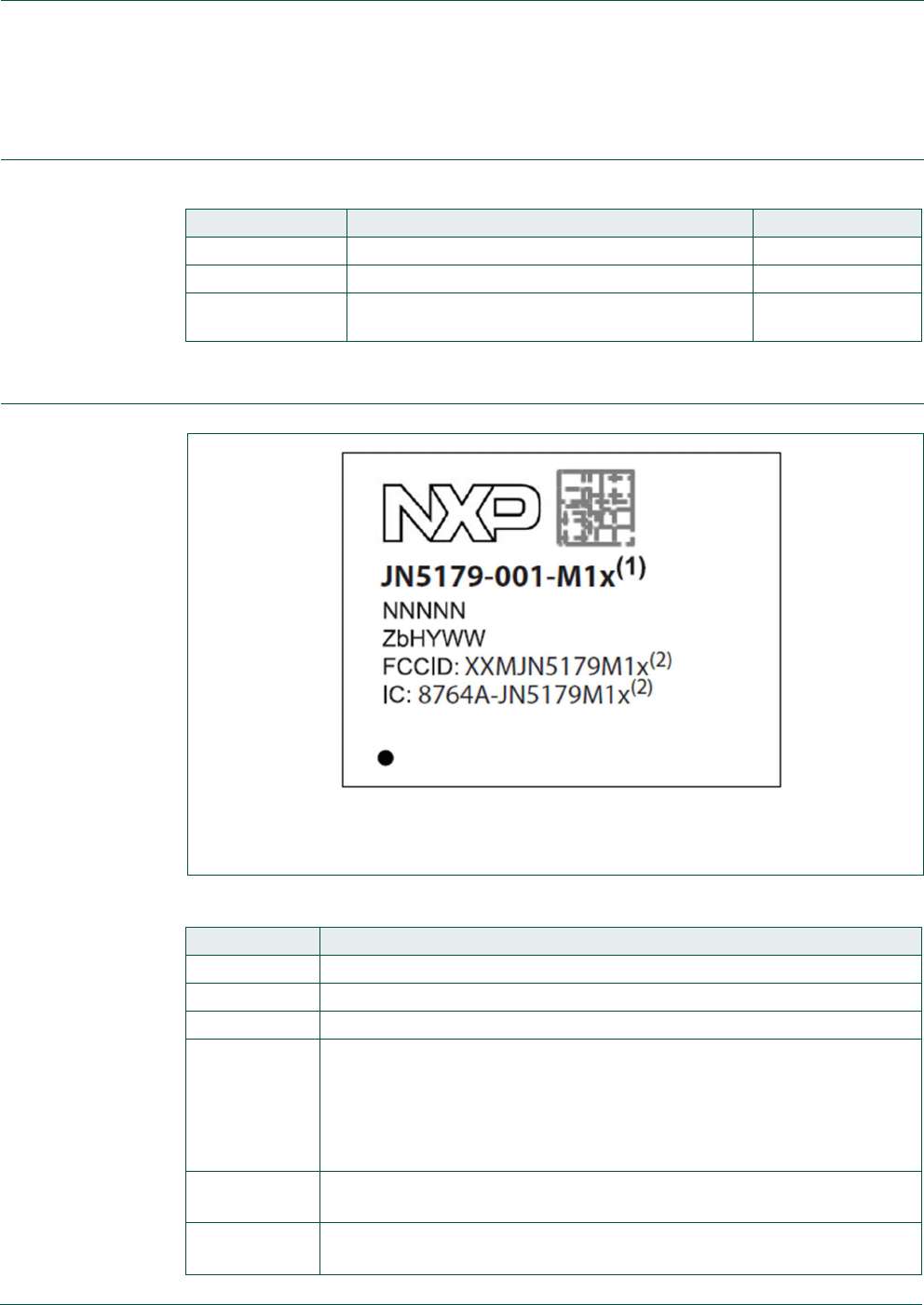
Marking
Table 2. Marking code
Line number Marking code
Line 1 NXP Logo: B&W outline logo - 2D barcode (internal NXP usage)
Line 2 part ID: JN5179-001-M1x, with x the module type 0, 3 or 6
Line 3 serial number: NNNNN
Line 4
•
Z: SSMC
•
b: SPIL
•
H: halogen free
•
Y: year
•
WW: week code
Line 5 FFC ID = FCCID: XXMJN5179M1x, with x = X for JN5179-001-M10 and
JN5179-001-M13 and x = 6 for JN5179-001-M16
Line 6 IC ID = IC: 8764A-JN5179M1x, with x = X for JN5179-001-M10 and
JN5179-001-M13 and x = 6 for JN5179-001-M16
JN5179-001-M1x
XXMJN5179M1x
(2)
8764A-
JN5179M1x
(2)
(1) With x = 0, 3 or 6.
(2) x = X for JN5179-001-M10 and JN5179-001-M13 and x = 6 for JN5179-001-M16.
Fig 1. UM11018 package marking (top view)
UM11018
NXP
Semiconductors
UM11018
User manual
All information provided in this document is subject to legal disclaimers.
Rev. 1.0 — 15 September 2016
© NXP Semiconductors N.V. 2016. All rights reserved.
7 of 27
2.4 GHz
RADIO
INCLUDING
DIVERSITY
EEPROM
IEEE802.15.4
MAC
ACCELERATOR
128-BIT AES
ENCRYPTION
ACCELERATOR
POWER
MANAGEMENT
MATCHING
µFL
CONNECTOR
MATCHING
µFL
CONNECTOR
PA/LNA
MATCHING
XTAL
integrated
antenna
M10
option
ARM
Cortex
-
M3
external
antenna
M13
option
external
antenna
integrated
antenna
M16
option
JN517
9
POWER
aaa-023361
Fig
2.
Block diagram
ZigBee 3.0, ZigBee PRO and IEEE802.15.4 modules
JN5179-001-M1x modules meet the requirements of Directive 2002/95/EC of the
European Parliament and of the Council on the Restriction of Hazardous Substance
(RoHS) and of the Chinese RoHS requirements SJ/T11363-2006 which came into force
on 1 March 2007.
7.
Block diagram
SPI-BUS
MASTER AND SLAVE
I
2
C-BUS
MASTER/SLAVE
6 X PWM
PLUS TIMER
2 X UART
DIO
SLEEP
COUNTER
6 CHAN
10 BIT ADC
SUPPLY AND
TEMP SENSORS
WATCHDOG
TIMER
RAM
FLASH
VOLTAGE
BROWNOUT
O-QPSK
MODEM
UM11018
NXP
Semiconductors
UM11018
User manual
All information provided in this document is subject to legal disclaimers.
Rev. 1.0 — 15 September 2016
© NXP Semiconductors N.V. 2016. All rights reserved.
8 of 27
ZigBee 3.0, ZigBee PRO and IEEE802.15.4 modules
8.
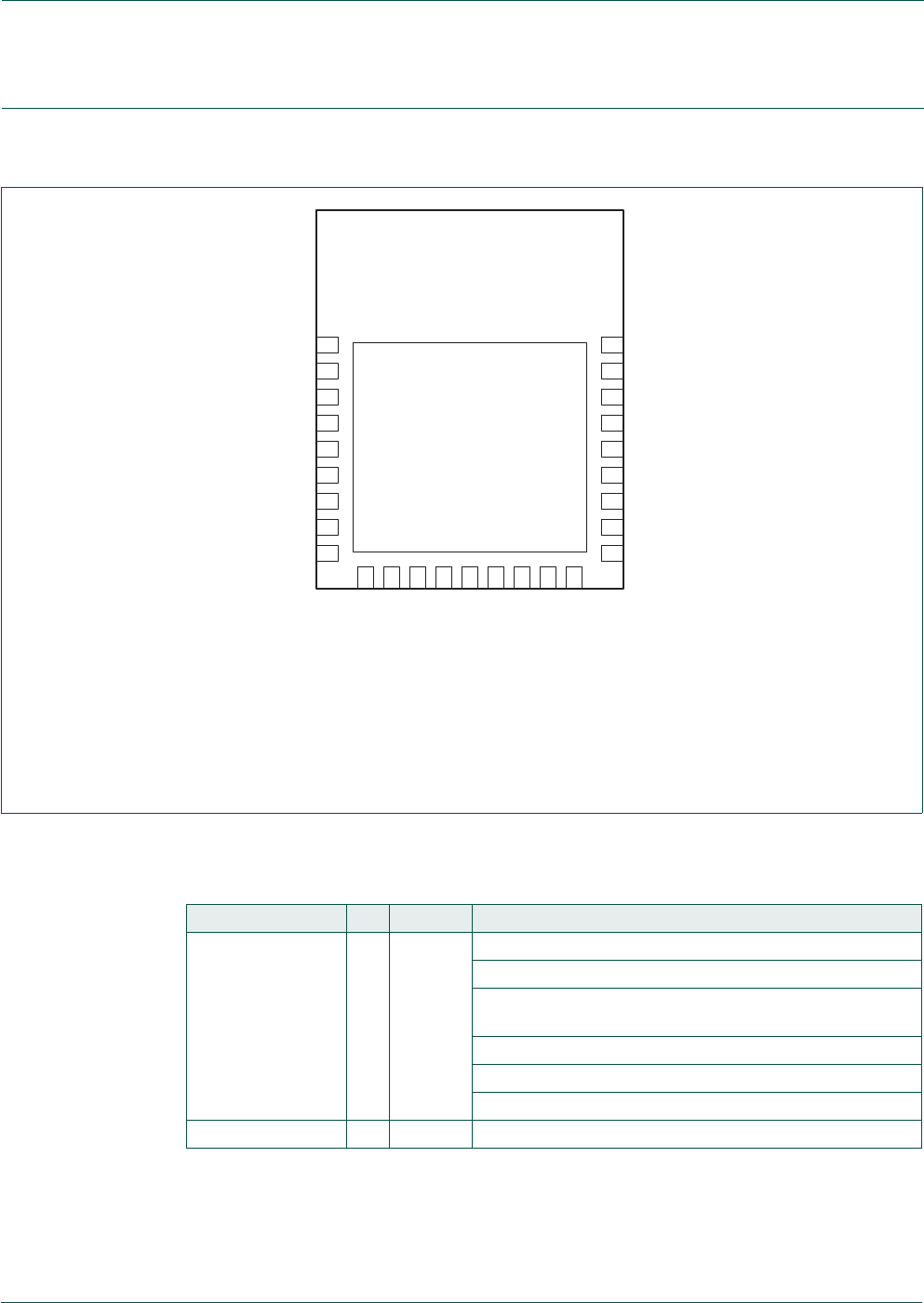
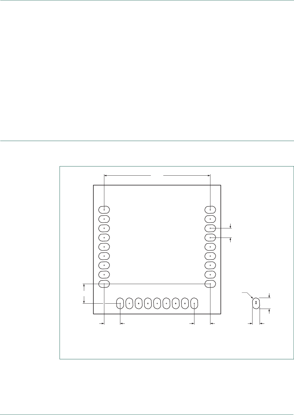
Pinning information
8.1 Pinning
8.2 Pin description
Table 3. Pin description
Symbol Pin Type
[1]
Description
DIO2 1 IO DIO2 — digital input/output 2
ADC5 — ADC input 5
SDA — I
2
C-bus master/slave SDA input/output (push-pull
output)
RXD1 — UART 1 receive data input
TIM0CAP — Timer0 capture input
RFRX — radios receiver control output
ADC0 2 I ADC0 — ADC input 0
DIO2
1
ADC0 2
DIO0
(1)
3
DIO1
(2)
4
DIO3 5
DIO4 6
DIO10/RXD0 7
DIO9/TXD0 8
DIO8 9
27
ADC1
26 DIO18
25 DIO15
24 RESET_N
23 DIO14
22 DIO13
21 DIO12
20 n.c.
19 DIO5
Transparent
top view
aaa
-
023363
(1)
DIO0
pin
of
the
JN5179
-
001
-
M16
is
not
connected
to
DIO0
pin
of
the
JN5179.
The
DIO0
of
the
module
is
LNA_BYPASS.
(2)
DIO1 pin of the JN5179-001-M16 is not connected to DIO1 pin of the JN5179. The DIO1 of the module is ANT_SEL.
Fig 3. Pin configuration
DIO7/SPIMOSI
10
DIO6/SPISEL0 11
DO1/SPIMISO 12
DO0/SPICLK 13
DIO17 14
DIO11 15
n.c. 16
V
SS
V
DDD
17
18
UM11018
NXP
Semiconductors
UM11018
User manual
All information provided in this document is subject to legal disclaimers.
Rev. 1.0 — 15 September 2016
© NXP Semiconductors N.V. 2016. All rights reserved.
9 of 27
ZigBee 3.0, ZigBee PRO and IEEE802.15.4 modules
Table 3. Pin description
…continued
Symbol Pin Type
[1]
Description
DIO0
[2]
3
DIO0 — digital input/output 0
ADC4 — ADC input 4
SPISEL0 — SPI-bus master select output 0
RFRX — radio receiver control output
FLICK_CTRL — flicker control output
ADO — antenna diversity odd output
DIO1
[2]
4 IO DIO1 — digital input/output 1
ADC3 — ADC input 3
RFTX — radio transmitter control input
PC0 — pulse counter 0 input
ADE — antenna diversity even output
DIO3 5 IO DIO3 — digital input/output 3
ADC2 — ADC input 2
PWM4 — PWM4 output
SCL — I
2
C-bus master/slave SCL input/output (push-pull
output)
TXD1 — UART 1 transmit data output
TIM0OUT — Timer0 output
RFTX — radio transmit control input
FLICK_CTRL — flicker control output
DIO4 6 IO DIO4 — digital input/output 4
SCL — I
2
C-bus master/slave SCL input/output (open-drain)
RXD0 — UART 0 receive data input
TIM0CK_GT — Timer0 clock/gate input
ADO — antenna diversity odd output
DIO10/RXD0 7 IO DIO10 — digital input/output 10
JTAG_TDI — JTAG TDI data input
RXD0 — UART 0 receive data input
DIO9/TXD0 8 IO DIO9 — digital input/output 9
JTAG_TDO — JTAG TDO data output
TXD0 — UART 0 transmit data output
TRACESWV — ARM trace serial wire viewer output
DIO8 9 IO DIO8 — digital input/output 8
PWM5 — PWM5 output
TIM0OUT — Timer0 output
TRACECLK — trace clock output
32KXTALIN — 32 kHz clock input
UM11018
NXP
Semiconductors
UM11018
User manual
All information provided in this document is subject to legal disclaimers.
Rev. 1.0 — 15 September 2016
© NXP Semiconductors N.V. 2016. All rights reserved.
10 of 27
ZigBee 3.0, ZigBee PRO and IEEE802.15.4 modules
Table 3. Pin description
…continued
Symbol Pin Type
[1]
Description
DIO7/SPIMOSI 10 IO DIO7 — digital input/output 7
SPIMOSI — SPI-bus master data output
JTAG_TDI — JTAG TDI data input
SPISEL2 — SPI-bus master select output 2
SPISSEL — SPI-bus slave select input
CMP_OUT — comparator output
32KIN — 32 kHz External clock input
32KXTALOUT — 32 kHz clock output
DIO6/SPISEL0 11 IO DIO6 — digital input/output 6
SPISEL0 — SPI-bus master select output 0
CTS0 — UART 0 clear to send input
RXD1 — UART 1 receive data input
JTAG_TCK — JTAG TCK input
SWCK — Serial Wire Debugger Clock input
SPISCLK — SPI-bus slave clock input
TIM1CAP — Timer1 capture input
DO1/SPIMISO
[3]
12 IO DO1 — digital output 1
SPIMISO — SPI-bus master data input
SPISMISO — SPI-bus slave data output
ADO — antenna diversity odd output
DO0/SPICLK
[4]
13 O DO0 — digital output 0
SPICLK — SPI-bus master clock output
ADE — antenna diversity even output
DIO17 14 IO DIO17 — digital input/output 17
JTAG_TCK — JTAG TCK input
SWCK — Serial Wire Debugger Clock input
SPISEL0 — SPI-bus master select output 0
TIM1CAP — Timer1 capture input
COMP1P — comparator plus input
SPISMISO — SPI-bus slave data output
DIO11 15 IO DIO11 — digital input/output 11
JTAG_TMS — JTAG TMS input
SWD — serial wire debugger input
RTS0 — UART 0 request to send output
TXD1 — UART 1 transmit data output
SPICLK — SPI-bus master clock output
SPISMOSI — SPI-bus slave data input
TIM1OUT — Timer1 output
TRACED0 — ARM trace data0 output
n.c. 16 - not connected; keep floating or ground
V
SS
17 G V
SS
— ground

UM11018
NXP
Semiconductors
UM11018
User manual
All information provided in this document is subject to legal disclaimers.
Rev. 1.0 — 15 September 2016
© NXP Semiconductors N.V. 2016. All rights reserved.
11 of 27
ZigBee 3.0, ZigBee PRO and IEEE802.15.4 modules
Table 3. Pin description
…continued
Symbol Pin Type
[1]
Description
V
DDD
18 P V
DDD
— digital supply voltage
DIO5
[5]
19 IO DIO5 — digital input/output 5
SDA — I
2
C-bus master/slave SDA input/output
(open-drain)
TXD0 — UART 0 transmit data output
PC1 — pulse counter 1 input
TIM0CAP — Timer0 capture input
n.c. 20 - not connected; keep floating or ground
DIO12 21 IO DIO12 — digital input/output 12
PWM1 — PWM1 output
TXD0 — UART 0 transmit data output
TRACED3 — ARM trace data3 output
DIO13 22 IO DIO13 — digital input/output 13
PWM2 — PWM2 output
RXD0 — UART 0 receive data input
PC0 — pulse counter 0 input
TRACED2 — ARM trace data2 output
DIO14 23 IO DIO14 — digital input/output 14
PWM3 — PWM3 output
PC1 — pulse counter 1 input
CMP_OUT — comparator output
TRACED1 — ARM trace data1 output
SPISMOSI — SPI-bus slave data input
RESET_N 24 IO RESET_N — reset input
DIO15 25 IO DIO15 — digital input/output 15
PWM6 — PWM6 output
JTAG_TDO — JTAG TDO data output
SPIMOSI — SPI-bus master data output
SPISEL1 — SPI-bus master select output 1
TIM0CK_GT — Timer0 - clock gate input
TRACESWV — ARM trace Serial Wire Viewer output
SPISSEL — SPI-bus slave select input
DIO18 26 IO DIO18 — digital input/output 18
JTAG_TMS — JTAG TMS input
SWD — Serial Wire Debugger input
SPIMISO — SPI-bus master data input
TIM1OUT — Timer1 output
COMP1M — comparator minus input
SPISCLK — SPI-bus slave clock input
ADC1 27 I VREF — analog peripheral reference voltage
ADC1 — ADC input 1

UM11018
NXP
Semiconductors
UM11018
User manual
All information provided in this document is subject to legal disclaimers.
Rev. 1.0 — 15 September 2016
© NXP Semiconductors N.V. 2016. All rights reserved.
12 of 27
ZigBee 3.0, ZigBee PRO and IEEE802.15.4 modules
[1] P = power supply; G = ground; I = input, O = output; IO = input/output.
[2] Not available on the JN5179-001-M16 since they are used to control the front-end module. DIO0 of the
module is LNA_BYPASS and the DIO1 of the module is ANT_SEL.
[3] UART programming mode: leave pin floating high during reset to avoid entering UART programming mode
or hold it low to program.
[4] JTAG programming mode: must be left floating high during reset to avoid entering JTAG programming
mode.
[5] Open-drain.
9.
Functional description
9.1 JN5179 single chip wireless microcontroller
The JN5179-001-M1x series is constructed around the JN5179-001 single chip wireless
microcontroller, which includes the radio system, an ARM Cortex-M3 CPU, Flash, RAM
and EEPROM memory and a range of analog and digital peripherals.
The chip is described fully in JN5179 Wireless Microcontroller Datasheet (see Ref. 2).
9.2 Peripherals
Table 4. Peripherals description
Peripherals JN5179-001-M10 JN5179-001-M13 JN5179-001-M16 Notes
Master SPI-bus port 3 selects 3 selects 3 selects 250 kHz - 16 MHz
Slave SPI-bus port 1 1 1 250 kHz - 4 MHz
UART 2 2 2 16550 compatible
Two-wire serial I/F (compatible with
SMbus and I
2
C-bus) 1 1 1 Up to 400 kHz
PWM
16 MHz clock
timer 4 4 4
timer/counter 1 1 1
Programmable Sleep Timers 2 2 2 32 kHz clock
Digital IO lines (multiplexed with
UARTs, timers and SPI-bus selects) 20 20 18 DIO2 and DIO3 are
not available on
JN5179-001-M16
modules
Analog-to-Digital converter 4 4 4 10 bit, up to
100 ks/s
Programmable analog comparator 1 1 1 ultra low-power
mode for sleep
Internal temperature sensor 1 1 1
Internal battery sensor 1 1 1
The performance of all peripherals is defined in the JN5179 Wireless Microcontroller
Datasheet (see Ref. 2).
NXP supplies all the development tools and networking stacks needed to enable
end-product development to occur quickly and efficiently. These are all freely available
from the NXP Wireless Connectivity TechZone (see Ref. 3). A range of
evaluation/developer kits is also available, allowing products to be quickly bread boarded.
UM11018
NXP
Semiconductors
UM11018
User manual
All information provided in this document is subject to legal disclaimers.
Rev. 1.0 — 15 September 2016
© NXP Semiconductors N.V. 2016. All rights reserved.
13 of 27
ZigBee 3.0, ZigBee PRO and IEEE802.15.4 modules
Efficient development of software applications is enabled by the provision of a complete,
unlimited, software developer kit. Together with the available libraries for the
IEEE802.15.4 MAC and ZigBee PRO network stacks, this package provides everything
required to develop application code and to trial it with hardware representative of the final
module.
The modules can be user programmed both in development and in production using
software supplied by NXP. Access to the on-chip peripherals, MAC and network stack
software is provided through specific APIs. This information is available on the NXP
support website, together with many example applications, user guides, reference
manuals and application notes.
9.3 JN5179-001-M16 Antenna diversity
ANT_SEL is used to select between the two antennas on the M16 module. Leaving
ANT_SEL unconnected or connecting to V
CC
selects the printed antenna. Tying ANT_SEL
to ground selects the µFL connector. The module can also be used in antenna diversity
solutions where the module will automatically swap between the two antennas in order to
achieve the best radio performance. This can be done connecting ANT_SEL to DIO4,
DIO5, DO0 or DO1 depend upon your application. The antenna diversity functionality can
be enabled by calling vAHI_AntennaDiversityEnable. The DIO can be selected using
vAHI_SetDIOpinMultiplexValue. Please see
JN-UG-3118-JN517x-Integrated-Peripherals-API for more details.
The LNA bypass signal can be used to switch off the LNA in the frontend. This can be
useful when in the presence of strong Wifi signals that can overload the frontend. If the pin
is left unconnected or tied to V
CC
then the LNA is enabled. If the signal is tied to ground
then the LNA will be bypassed during RX. The signal can be connected to a DIO to give
software control over the LNA if required.
10.
Limiting values
Table 5. Limiting values
Symbol Parameter Conditions Min Max Unit
V
DD
supply voltage
−0.3 +3.6 V
V
ADC0
voltage on pin ADC0
−0.3 V
DD
+ 0.3
V V
V
ADC1
voltage on pin ADC1
−0.3 V
DD
+ 0.3
V V
V
IO(dig)
digital input/output voltage
−0.3 V
DD
+ 0.3
V
V
T
stg
storage temperature
−40 +150 °C
11.
Recommended operating conditions
Table 6. Operating conditions
Symbol Parameter Conditions Min Max Unit
V
DD
supply voltage
[1]
2 3.6 V
T
amb
ambient temperature standard range −40 +85 °C
UM11018
NXP
Semiconductors
UM11018
User manual
All information provided in this document is subject to legal disclaimers.
Rev. 1.0 — 15 September 2016
© NXP Semiconductors N.V. 2016. All rights reserved.
14 of 27
ZigBee 3.0, ZigBee PRO and IEEE802.15.4 modules
[1] To reach the maximum TX power, 2.8 V is the minimum.
12.
Characteristics
12.1 DC current
Table 7. Active processing
V
DD
= 2 V to 3.6 V; T
amb
=
−
40
°
C to +85
°
C; unless otherwise specified.
Symbol Parameter Conditions Min Typ Max Unit
I
DD
supply current M10
radio in receive mode; maximum input level at –2 dBm - 16.6 - mA
radio in transmit mode 10 dBm
[1]
- 26.2 - mA
radio in transmit mode 8.5 dBm
[1]
- 22.6 - mA
M13
radio in receive mode; maximum input level at –2 dBm - 16.6 - mA
radio in transmit mode 10 dBm
[1]
- 26.2 - mA
radio in transmit mode 8.5 dBm
[1]
- 22.6 - mA
M16
radio in receive mode - 16.6 - mA
radio in transmit mode
[1]
- 125 - mA
[1] To reach the maximum TX power, 2.8 V is the minimum.
Table 8. Sleep mode
V
DD
= 2 V to 3.6 V; T
amb
=
−
40
°
C to +85
°
C; unless otherwise specified.
Symbol Parameter Conditions Min Typ Max Unit
I
DD(IO)
input/output supply
current in sleep mode; with I/O and RC oscillator
timer wake-up; T
amb
= 25 °C - 0.73 - µA
Table 9. Deep sleep mode
V
DD
= 2 V to 3.6 V; T
amb
=
−
40
°
C to +85
°
C; unless otherwise specified.
Symbol Parameter Conditions Min Typ Max Unit
I
DD
supply current deep sleep mode; measured at 25 °C and
[1]
V
DD
= 3.3 V - 80 - nA
[1] Waiting on chip RESET or I/O event.
12.2 AC characteristics
12.2.1
Radio transceiver
These modules meet all the requirements of the IEEE802.15.4 standard over 2.0 V
to 3.6 V and offers the improved RF characteristics shown in Ta ble 10. All RF
characteristics are measured single ended.
Table 10. RF port characteristics
Single-ended; Impedance = 50
Ω
[1]
; V
DD
= 2 V to 3.6 V; T
amb
=
−
40
°
C to +85
°
C; unless otherwise specified.
Symbol Parameter Conditions Min Typ Max Unit
f
range
frequency range
2.4 - 2.485 GHz
UM11018
NXP
Semiconductors
UM11018
User manual
All information provided in this document is subject to legal disclaimers.
Rev. 1.0 — 15 September 2016
© NXP Semiconductors N.V. 2016. All rights reserved.
15 of 27
ZigBee 3.0, ZigBee PRO and IEEE802.15.4 modules
[1] With external matching inductors and assuming PCB layout.
Table 11. Radio transceiver characteristics: +25 °C
V
DD
= 2 V to 3.6 V; unless otherwise specified.
Symbol Parameter Conditions Min Typ Max Unit
Receiver
M10
S
RX
receiver sensitivity nominal for 1 % PER, as per 802.15.4 - −96 - dBm
P
i(RX)(max)
maximum receiver input
power 1 % PER, measured as sensitivity; supply
current at 16.6 mA - −2 - dBm
∆α
RSSI
RSSI variation −95 dBm to −10 dBm; available through
UM11018 Integrated Peripherals API −4 - +4 dB
M13
S
RX
receiver sensitivity nominal for 1 % PER, as per 802.15.4 - −96 - dBm
P
i(RX)(max)
maximum receiver input
power 1 % PER, measured as sensitivity; supply
current at 16.6 mA - −2 - dBm
∆α
RSSI
RSSI variation −95 dBm to −10 dBm; available through
UM11018 Integrated Peripherals API −4 - +4 dB
M16
S
RX
receiver sensitivity nominal for 1 % PER, as per 802.15.4 - −100 - dBm
P
i(RX)(max)
maximum receiver input
power 1 % PER, measured as sensitivity - −11 - dBm
∆α
RSSI
RSSI variation −100 dBm to −25 dBm; available through
UM11018 Integrated Peripherals API −4 - +4 dB
Transmitter
M10
P
o
output power I
DD
= 26.2 mA
[1]
- 10 - dBm
I
DD
= 22.6 mA
[1]
- 8.5 - dBm
P
o(cr)
control range output
power in 6 major steps and then 4 fine steps
[2]
- −42 - dB
M13
P
o
output power I
DD
= 26.2 mA
[1]
- 10 - dBm
I
DD
= 22.6 mA
[1]
- 8.5 - dBm
P
o(cr)
control range output
power in 6 major steps and then 4 fine steps
[2]
- −42 - dB
M16
P
o
output power I
DD
= 125 mA
[1]
- 21 - dBm
[1] To reach the maximum TX power, 2.8 V is the minimum on V
DD
.
[2] Up to an extra 2.5 dB of attenuation is available if required.
13.
Federal Communication Commission Statement
•
This equipment has been tested and found to comply with the limits for a Class B
digital device, pursuant to Part 15 of the FCC Rules see Ref. 4. These limits are
designed to provide reasonable protection against harmful interference in a
residential installation. This equipment generates, uses, and can radiate radio

UM11018
NXP
Semiconductors
UM11018
User manual
All information provided in this document is subject to legal disclaimers.
Rev. 1.0 — 15 September 2016
© NXP Semiconductors N.V. 2016. All rights reserved.
16 of 27
ZigBee 3.0, ZigBee PRO and IEEE802.15.4 modules
frequency energy and, if not installed and used in accordance with the instructions,
may cause harmful interference to radio communications. However, there is no
guarantee that interference will not occur in a particular installation. If this equipment
does cause harmful interference to radio or television reception, which can be
determined by turning the equipment off and on, the user is encouraged to try to
correct the interference by one of the following measures:
–
Reorient or relocate the receiving antenna
–
Increase the separation between the equipment and receiver
–
Connect the equipment into an outlet on a circuit different from that to which the
receiver is connected
–
Consult the dealer or an experienced radio/TV technician for help
•
OEM integrators instructions
–
The OEM integrators are responsible for ensuring that the end-user has no manual
instructions to remove or install module
–
The module is limited to installation in mobile or fixed applications, according to
CFR 47 Part 2.1091(b)
–
Separate approval is required for all other operating configurations, including
portable configurations with respect to CFR 47 Part 2.1093 and different antenna
configurations
•
User guide mandatory statements
–
User's instructions of the host device must contain the following statements in
addition to operation instructions:
*
“This device complies with part 15 of the FCC Rules. Operation is subject to the
following two conditions:
(1)
This device may not cause harmful interference, and
(2)
This device must accept any interference received, including interference that
may cause undesired operation”
*
“Changes or modifications not expressly approved by the party responsible for
compliance could void the user's authority to operate the equipment”
•
FCC RF Exposure requirements
–
User's instructions of the host device must contain the following instructions in
addition to operation instructions:
Avoid direct contact to the antenna, or keep it to a 20 cm minimum distance while
using this equipment. This device must not be collocated or operating in
conjunction with another antenna or transmitter.
This module has been designed to operate with antennas having a maximum gain of
2 dBi. Antennas having a gain greater than 2 dBi are strictly prohibited for use with this
device. The required antenna impedance is 50 ohms.
13.1 FCC end product labelling
The final ‘end product’ should be labelled in a visible area with the following:
Contains TX FCC ID: XXMJN5179M1X or XXMJN5179M16 to reflect the version of the
module being used inside the product.
UM11018
NXP
Semiconductors
UM11018
User manual
All information provided in this document is subject to legal disclaimers.
Rev. 1.0 — 15 September 2016
© NXP Semiconductors N.V. 2016. All rights reserved.
17 of 27
ZigBee 3.0, ZigBee PRO and IEEE802.15.4 modules
13.2 European R&TTE Directive 1999/5/EC statement
JN5179-001-M10 and JN5179-001-M13 are compliant with ETSI EN 300 328 V1.9, EMC,
EN 301 489-17 v2.1.1 (2009-02) and the Basic Safety Assessment (BSA) EN
60950-1:2006 (2006-06) and are subject to a Notified Body Opinion.
These modules are approved for use with the antennas listed in the following table. The
JN5179-001-M16 module is not approved for use in Europe.
Alternative vertical antennas may be used provided that the gain does not exceed 2 dBi.
Table 12. Antennas description (R&TTE)
Brand Model Number Description Gain (dBi) Connector type
1 Aveslink Technology, Inc E-0005-AC vertical- flying lead 2 RP-SMA
2 Aveslink Technology, Inc E-2411-GC vertical - swivel 2 RP-SMA
3 Aveslink Technology, Inc E-2410-CA vertical - bulkhead- flying lead 2 µFL
4 Aveslink Technology, Inc E-2410-HA vertical- flying lead 2 µFL
5 Aveslink Technology, Inc E-2410-GC vertical - swivel 2 RP-SMA
6 Aveslink Technology, Inc E-2820-CA vertical - bulkhead- flying lead 2 µFL
7 Aveslink Technology, Inc E-2820-GC vertical - swivel 2 RP-SMA
8 Embedded Antenna Design FBKR35068-RS-KR vertical - knuckle antenna 2 RP-SMA
9 Nearson S131CL-L-PX-2450S vertical - knuckle-flying lead 2 µFL
10 Laird Technologies WRR2400-IP04 vertical - knuckle-flying lead 1.5 µFL
11 Laird Technologies WRR2400-RPSMA vertical - knuckle-flying lead 1.3 RP-SMA
12 Aveslink Technology, Inc E-6170-DA Vertical - right angle 1 µFL
13 Laird Technologies WCR2400-SMRP Vertical - knuckle antenna 1 RP-SMA
14.
Industry Canada statement
To reduce potential radio interference to other users, the antenna type and its gain should
be so chosen that the equivalent isotropic radiated power (e.i.r.p.) is not more than that
permitted for successful communication.
This device complies with Industry Canada
licence-exempt RSS standard(s). Operation is
subject to the following two conditions: (1) this
device may not cause interference, and (2) this
device must accept any interference, including
interference that may cause undesired
operation of the device.
This device complies with Industry Canada RF
radiation exposure limits set forth for general
population (uncontrolled exposure). This device
must be installed to provide a separation
distance of at least 20 cm from all persons and
must not be collocated or operating in
conjunction with any other antenna or
transmitter.
Le présent appareil est conforme aux CNR
d’Industrie Canada applicables aux appareils
radio exempts de licence. L’exploitation est
autorisée aux deux conditions suivantes: (1) il
ne doit pas produire de brouillage, et (2)
l’utilisateur du dispositif doit être prêt a accepter
tout brouillage radioélectrique reçu, même si ce
brouillage est susceptible de compromettre le
fonctionnement du dispositif.
Le présent appareil est conforme aux niveaux
limites d’exigences d’exposition RF aux
personnes définies par Industrie Canada. Cet
appareil doit être installé afin d’offrir une
distance de séparation d’au moins 20 cm avec
l’utilisateur, et ne doit pas être installé à
proximité ou être utilisé en conjonction avec une
autre antenne ou un autre émetteur.
UM11018
NXP
Semiconductors
UM11018
User manual
All information provided in this document is subject to legal disclaimers.
Rev. 1.0 — 15 September 2016
© NXP Semiconductors N.V. 2016. All rights reserved.
18 of 27
ZigBee 3.0, ZigBee PRO and IEEE802.15.4 modules
This module has been designed to operate with antennas having a maximum gain of
2 dBi. Antennas having a gain greater than 2 dBi are strictly prohibited for use with this
device. The required antenna impedance is 50 ohms.
As long as the above condition is met, further transmitter testing will not be required.
However, the OEM integrator is still responsible for testing their end-product for any
additional compliance requirements required with this module installed (for example,
digital device emissions, PC peripheral requirements, etc).
14.1 Industry Canada end product labelling
For Industry Canada purposes the following should be used: Contains
Industry Canada ID IC: 8764A-JN5179M1x (with x = X or 6).
15.
Footprint and PCB placement
15.1 Footprint information for reflow soldering
14.50
1.27
2.63
Ø1.00
1.50
2.17
2.17
1.00
aaa-023943
All
modules
have
the
same
footprint.
Fig 4.
Footprint
information
for
reflow soldering
of
modules
UM11018
NXP
Semiconductors
UM11018
User manual
All information provided in this document is subject to legal disclaimers.
Rev. 1.0 — 15 September 2016
© NXP Semiconductors N.V. 2016. All rights reserved.
19 of 27
ZigBee 3.0, ZigBee PRO and IEEE802.15.4 modules
15.2 Optimal PCB placement of JN5179-001-M10 and JN5179-001-M16
modules
The JN5179-001-M10 and JN5179-001-M16 modules feature an optimised, low-cost,
integrated, inverted F, printed PCB antenna. For size reduction no ground plane has been
added between the antenna and the JN5179 chip. So an additional ground plane must be
added on the main PCB beneath the module in order to ensure a good antenna efficiency.
This ground plane can be a rectangle or a square with respect to 2 conditions: it must be
as wide as the module (14.5 mm) and the area must be equal or greater than 610 mm
2
.
See Figure 5 below for correct placement of the module.
The antenna has a vertically polarised near omnidirectional radiation pattern and up to
1.8 dBi of peak gain. On the antenna side the ground plane of the module must be
vertically aligned with the ground plane of the main PCB. The area around the antenna
must be kept clear of conductors or other metal objects by a minimum distance of 20 mm
except the mandatory ground plane as indicated above. This is true for all layers of the
PCB and not just the top layer. Any conductive objects close to the antenna could
severely disrupt the antenna pattern resulting in deep nulls and high directivity in some
directions.
The Figure 5 show various possible scenarios. The top 3 scenarios are correct - the
ground plane must be placed beneath the JN5179-001-M10 or M16 module but it does
not protrude beyond the edge of the top layer ground plane on the module PCB.
The bottom fours scenarios are incorrect – in the left-hand side there is ground plane
underneath the antenna, in the middle-left example the ground planes of the main PCB
and the module are not vertically aligned, in the middle-right there is insufficient clearance
around the antenna, and in the right-hand example a battery’s metal casing is in the
recommended ‘keep out’ area.
Fig 5. PCB placement of the JN5179-001-M10 and JN5179-001-M16 modules
UM11018
NXP
Semiconductors
UM11018
User manual
All information provided in this document is subject to legal disclaimers.
Rev. 1.0 — 15 September 2016
© NXP Semiconductors N.V. 2016. All rights reserved.
20 of 27
ZigBee 3.0, ZigBee PRO and IEEE802.15.4 modules
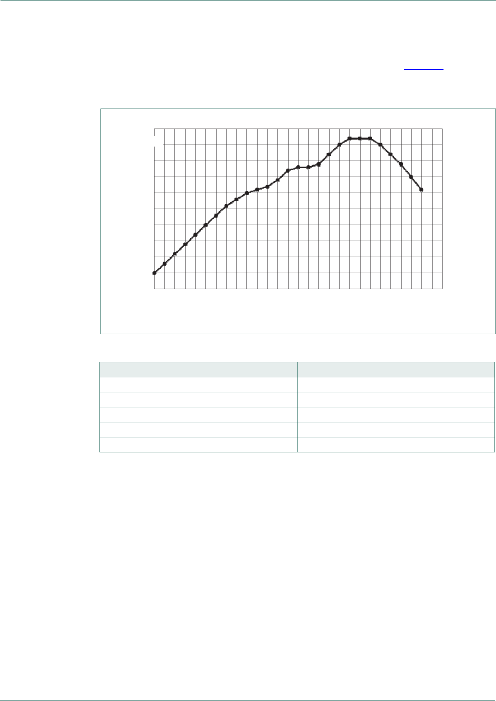
15.3 Reflow Profile
For reflow soldering, it is recommended to follow the reflow profile in Figure 6 as a guide,
as well as the paste manufacturer’s guidelines on peak flow temperature, soak times, time
above liquid and ramp rates.
Table 13. Recommended solder reflow profile
Temperature range (°C) Target time range (s)
from 25 to ~160 between 90 and ~130
from 160 to ~220 between 30 and ~60
from 220 to ~230 between 20 and ~50
from 230 to ~peak between 10 and ~20
from 25 to ~peak between 150 and ~260
15.4 Soldering paste and cleaning
NXP does not recommend use of a solder paste that requires the module and PCB
assembly to be cleaned (rinsed in water) for the following reasons:
•
Solder flux residues and water can be trapped by the PCB, can or components and
result in short circuits
NXP recommends use of a 'no clean' solder paste for all its module products.
aaa-024461
250
Temperature
(°C)
200
150
100
50
0 0
20 40 60
80 100 120 140 160 180 200 220 240 260 280
Time (seconds)
Fig 6. Guide for reflow profile of JN5179-001-M1x
UM11018
NXP
Semiconductors
UM11018
User manual
All information provided in this document is subject to legal disclaimers.
Rev. 1.0 — 15 September 2016
© NXP Semiconductors N.V. 2016. All rights reserved.
21 of 27
ZigBee 3.0, ZigBee PRO and IEEE802.15.4 modules
16.
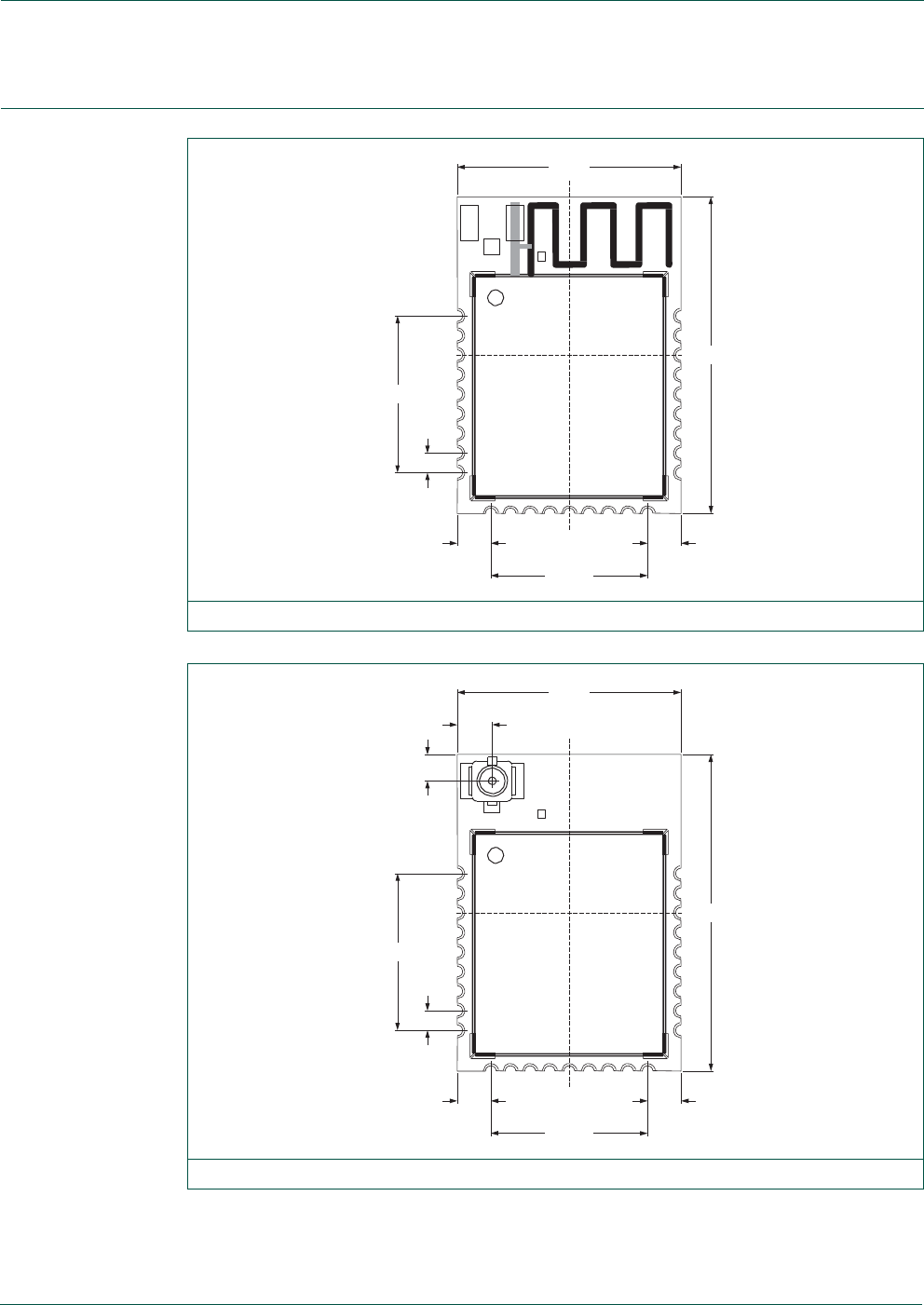
Package outline
(14.5)
(2.27)
(1.71)
(20.50)
(10.16)
(1.27)
(2.17) (2.17)
(10.16)
aaa-023973
Fig 8. Package outline JN5179-001-M13
(14.5)
(20.50)
(10.16)
(1.27)
(2.17) (2.17)
(10.16)
aaa-023972
Fig 7. Package outline JN5179-001-M10
UM11018
NXP
Semiconductors
UM11018
User manual
All information provided in this document is subject to legal disclaimers.
Rev. 1.0 — 15 September 2016
© NXP Semiconductors N.V. 2016. All rights reserved.
22 of 27
ZigBee 3.0, ZigBee PRO and IEEE802.15.4 modules
(14.5)
(2.27)
(1.71)
(20.50)
(10.16)
(1.27)
(2.17) (2.17)
(10.16)
aaa-023974
Fig 9. Package outline JN5179-001-M16

UM11018
NXP
Semiconductors
UM11018
User manual
All information provided in this document is subject to legal disclaimers.
Rev. 1.0 — 15 September 2016
© NXP Semiconductors N.V. 2016. All rights reserved.
23 of 27
ZigBee 3.0, ZigBee PRO and IEEE802.15.4 modules
17.
Abbreviations
Table 14. Abbreviations
Acronym Description
AC Alternating Current
ADC Analog-to-Digital Converter
API Application Program Interface
CE Conformity European
CPU Central Processing Unit
DC Direct Current
DIO Digital Input Output
EEPROM Electrically-Erasable Programmable Read-Only Memory
FCC Federal Communication Commission
ID IDentification
IO Input Output
ISM Industrial, Scientific and Medical radio bands
JTAG Joint Test Action Group
LNA Low Noise Amplifier
MAC Media Access Control
OEM Original Equipment Manufacturer
PC Pulse Counter
PCB Printed-Circuit Board
PER Packet Error Rate
PRO PROtocol
PWM Pulse-Width Modulation
TX Transmit
R&TTE Radio And Terminal Telecommunication Equipment
RAM Random Access Memory
RC Resistance-Capacitance
RF Radio Frequency
RISC Reduced Instruction Set Computing
RoHS Restriction of Hazardous Substance
RSSI Received Signal Strength Indicator
RX Receive
UART Universal Asynchronous Receiver Transmitter

UM11018
NXP
Semiconductors
UM11018
User manual
All information provided in this document is subject to legal disclaimers.
Rev. 1.0 — 15 September 2016
© NXP Semiconductors N.V. 2016. All rights reserved.
24 of 27
ZigBee 3.0, ZigBee PRO and IEEE802.15.4 modules
18.
References
[1] IEEE Std 802.15.4-2003 — IEEE Std 802.15.4-2003 IEEE Standard for Information
Technology – Part 15.4 Wireless Medium Access Control (MAC) and Physical Layer
(PHY) Specifications for Low-Rate Wireless Personal Area Networks (LR-WPANs).
[2]
JN5179 — JN5179 wireless microcontroller data sheet.
[3]
Wireless Connectivity —
http://www.nxp.com/products/interface-and-connectivity/wireless-connectivity:WIRE
LESS-CONNECTIVITY
[4]
Part 15 of the FCC Rules —
http://www.ecfr.gov/cgi-bin/text-idx?SID=d01e00935bfcb0d53b914e7c8e63f383&no
de=47:1.0.1.1.16&rgn=div5

UM11018
NXP
Semiconductors
UM11018
User manual
All information provided in this document is subject to legal disclaimers.
Rev. 1.0 — 15 September 2016
© NXP Semiconductors N.V. 2016. All rights reserved.
25 of 27
ZigBee 3.0, ZigBee PRO and IEEE802.15.4 modules
19.
Legal information
19.1 Definitions
Draft — The document is a draft version only. The content is still under
internal review and subject to formal approval, which may result in
modifications or additions. NXP Semiconductors does not give any
representations or warranties as to the accuracy or completeness of
information included herein and shall have no liability for the consequences of
use of such information.
19.2 Disclaimers
Limited warranty and liability — Information in this document is believed to
be accurate and reliable. However, NXP Semiconductors does not give any
representations or warranties, expressed or implied, as to the accuracy or
completeness of such information and shall have no liability for the
consequences of use of such information. NXP Semiconductors takes no
responsibility for the content in this document if provided by an information
source outside of NXP Semiconductors.
In no event shall NXP Semiconductors be liable for any indirect, incidental,
punitive, special or consequential damages (including - without limitation - lost
profits, lost savings, business interruption, costs related to the removal or
replacement of any products or rework charges) whether or not such
damages are based on tort (including negligence), warranty, breach of
contract or any other legal theory.
Notwithstanding any damages that customer might incur for any reason
whatsoever, NXP Semiconductors’ aggregate and cumulative liability towards
customer for the products described herein shall be limited in accordance
with the Terms and conditions of commercial sale of NXP Semiconductors.
Right to make changes — NXP Semiconductors reserves the right to make
changes to information published in this document, including without
limitation specifications and product descriptions, at any time and without
notice. This document supersedes and replaces all information supplied prior
to the publication hereof.
Suitability for use — NXP Semiconductors products are not designed,
authorized or warranted to be suitable for use in life support, life-critical or
safety-critical systems or equipment, nor in applications where failure or
malfunction of an NXP Semiconductors product can reasonably be expected
to result in personal injury, death or severe property or environmental
damage. NXP Semiconductors and its suppliers accept no liability for
inclusion and/or use of NXP Semiconductors products in such equipment or
applications and therefore such inclusion and/or use is at the customer’s own
risk.
Applications — Applications that are described herein for any of these
products are for illustrative purposes only. NXP Semiconductors makes no
representation or warranty that such applications will be suitable for the
specified use without further testing or modification.
Customers are responsible for the design and operation of their applications
and products using NXP Semiconductors products, and NXP Semiconductors
accepts no liability for any assistance with applications or customer product
design. It is customer’s sole responsibility to determine whether the NXP
Semiconductors product is suitable and fit for the customer’s applications and
products planned, as well as for the planned application and use of
customer’s third party customer(s). Customers should provide appropriate
design and operating safeguards to minimize the risks associated with their
applications and products.
NXP Semiconductors does not accept any liability related to any default,
damage, costs or problem which is based on any weakness or default in the
customer’s applications or products, or the application or use by customer’s
third party customer(s). Customer is responsible for doing all necessary
testing for the customer’s applications and products using NXP
Semiconductors products in order to avoid a default of the applications and
the products or of the application or use by customer’s third party
customer(s). NXP does not accept any liability in this respect.
Export control — This document as well as the item(s) described herein
may be subject to export control regulations. Export might require a prior
authorization from competent authorities.
Evaluation products — This product is provided on an “as is” and “with all
faults” basis for evaluation purposes only. NXP Semiconductors, its affiliates
and their suppliers expressly disclaim all warranties, whether express, implied
or statutory, including but not limited to the implied warranties of
non-infringement, merchantability and fitness for a particular purpose. The
entire risk as to the quality, or arising out of the use or performance, of this
product remains with customer.
In no event shall NXP Semiconductors, its affiliates or their suppliers be liable
to customer for any special, indirect, consequential, punitive or incidental
damages (including without limitation damages for loss of business, business
interruption, loss of use, loss of data or information, and the like) arising out
the use of or inability to use the product, whether or not based on tort
(including negligence), strict liability, breach of contract, breach of warranty or
any other theory, even if advised of the possibility of such damages.
Notwithstanding any damages that customer might incur for any reason
whatsoever (including without limitation, all damages referenced above and
all direct or general damages), the entire liability of NXP Semiconductors, its
affiliates and their suppliers and customer’s exclusive remedy for all of the
foregoing shall be limited to actual damages incurred by customer based on
reasonable reliance up to the greater of the amount actually paid by customer
for the product or five dollars (US$5.00). The foregoing limitations, exclusions
and disclaimers shall apply to the maximum extent permitted by applicable
law, even if any remedy fails of its essential purpose.
Translations — A non-English (translated) version of a document is for
reference only. The English version shall prevail in case of any discrepancy
between the translated and English versions.
19.3 Trademarks
Notice: All referenced brands, product names, service names and trademarks
are the property of their respective owners.
I
2
C-bus — logo is a trademark of NXP Semiconductors N.V.

UM11018
NXP
Semiconductors
UM11018
User manual
All information provided in this document is subject to legal disclaimers.
Rev. 1.0 — 15 September 2016
© NXP Semiconductors N.V. 2016. All rights reserved.
26 of 27
ZigBee 3.0, ZigBee PRO and IEEE802.15.4 modules
20.
Tables
Table 1. Marking code ...................................................... 6
Table 2. Pin description .................................................... 8
Table 3. Peripherals description ..................................... 12
Table 4. Limiting values.................................................. 13
Table 5. Operating conditions ........................................ 13
Table 6. Active processing ............................................. 14
Table 7. Sleep mode ...................................................... 14
Table 8. Deep sleep mode ............................................. 14
Table 9. RF port characteristics ..................................... 14
Table 10. Radio transceiver characteristics: +25 °C ......... 15
Table 11. Antennas description (R&TTE) ......................... 17
Table 12. Recommended solder reflow profile .................. 20
Table 13. Abbreviations .................................................... 23
21.
Figures
Fig 1. UM11018 package marking (top view) ................... 6
Fig 2. Block diagram ........................................................ 7
Fig 3. Pin configuration.................................................... 8
Fig 4. Footprint information for reflow soldering of modules
18
Fig 5. PCB placement of the JN5179-001-M10 and
JN5179-001-M16 modules................................... 19
Fig 6. Guide for reflow profile of JN5179-001-M1x ......... 20
Fig 7. Package outline JN5179-001-M10 ....................... 21
Fig 8. Package outline JN5179-001-M13 ....................... 21
Fig 9. Package outline JN5179-001-M16 ....................... 22

UM11018
NXP
Semiconductors
ZigBee 3.0, ZigBee PRO and IEEE802.15.4 modules
22.
Contents
1 General description . . . . . . . . . . . . . . . . . . . . . .
3 20 Figures . . . . . . . . . . . . . . . . . . . . . . . . . . . . . . . 26
1.1 Regulatory Approvals . . . . . . . . . . . . . . . . . . . .
3 21 Contents. . . . . . . . . . . . . . . . . . . . . . . . . . . . . .
27
2 Features and benefits . . . . . . . . . . . . . . . . . . . .
3
2.1 Benefits. . . . . . . . . . . . . . . . . . . . . . . . . . . . . . .
3
2.2 Features: modules . . . . . . . . . . . . . . . . . . . . . .
4
2.3 Features: microcontroller . . . . . . . . . . . . . . . . .
4
3 Applications . . . . . . . . . . . . . . . . . . . . . . . . . . . .
5
4 Overview. . . . . . . . . . . . . . . . . . . . . . . . . . . . . . .
5
5 Marking . . . . . . . . . . . . . . . . . . . . . . . . . . . . . . . .
6
6 Block diagram . . . . . . . . . . . . . . . . . . . . . . . . . .
7
7 Pinning information. . . . . . . . . . . . . . . . . . . . . .
8
7.1 Pinning . . . . . . . . . . . . . . . . . . . . . . . . . . . . . . .
8
7.2 Pin description . . . . . . . . . . . . . . . . . . . . . . . . .
8
8 Functional description . . . . . . . . . . . . . . . . . . 12
8.1 JN5179 single chip wireless microcontroller. . 12
8.2 Peripherals . . . . . . . . . . . . . . . . . . . . . . . . . . . 12
8.3 JN5179-001-M16 Antenna diversity . . . . . . . . 13
9 Limiting values. . . . . . . . . . . . . . . . . . . . . . . . . 13
10 Recommended operating conditions. . . . . . . 13
11 Characteristics. . . . . . . . . . . . . . . . . . . . . . . . . 14
11.1 DC current . . . . . . . . . . . . . . . . . . . . . . . . . . . 14
11.2 AC characteristics. . . . . . . . . . . . . . . . . . . . . . 14
11.2.1
Radio transceiver . . . . . . . . . . . . . . . . . . . . . . 14
12 Federal Communication Commission Statement
15
12.1 FCC end product labelling ................................ 16
12.2 European R&TTE Directive 1999/5/EC statement
17
13 Industry Canada statement ............................... 17
13.1 Industry Canada end product labelling.............. 18
14 Footprint and PCB placement .......................... 18
14.1 Footprint information for reflow soldering .......... 18
14.2 Optimal PCB placement of JN5179-001-M10 and
JN5179-001-M16 modules ............................... 19
14.3 Reflow Profile ................................................... 20
14.4 Soldering paste and cleaning ............................ 20
15 Package outline ................................................. 21
16 Abbreviations ..................................................... 23
17 References ......................................................... 24
18 Legal information............................................... 25
18.1 Definitions ......................................................... 25
18.2 Disclaimers ....................................................... 25
18.3 Trademarks ...................................................... 25
19 Tables .................................................................... 26
Please be aware that important notices concerning this document and the product(s)
described herein, have been included in section ‘Legal information’.
© NXP Semiconductors N.V. 2016. All rights reserved.
For more information, please visit: http://www.nxp.com
For sales office addresses, please send an email to: salesaddresses@nxp.com
Date of release: 15 September 2016
Document identifier: UM11018