NXP Semiconductors OM12001000 Automotive Telematics GSM/GPS Module User Manual
NXP Semiconductors Automotive Telematics GSM/GPS Module
UserManual.wiki
>
NXP Semiconductors
>
OM12001000 User Manual
user manual
Navigation menu
Upload a User Manual
Namespaces
Wiki Guide
HTML
PDF
Info
Views
User Manual
Discussion / Help
Navigation
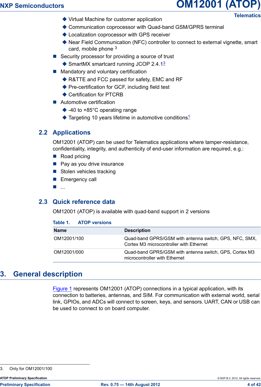
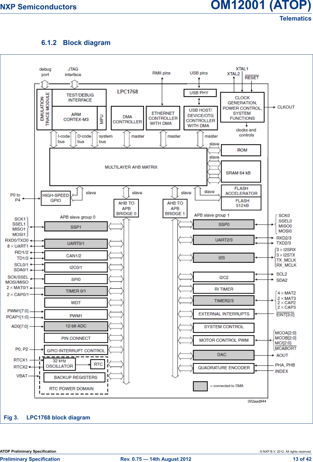
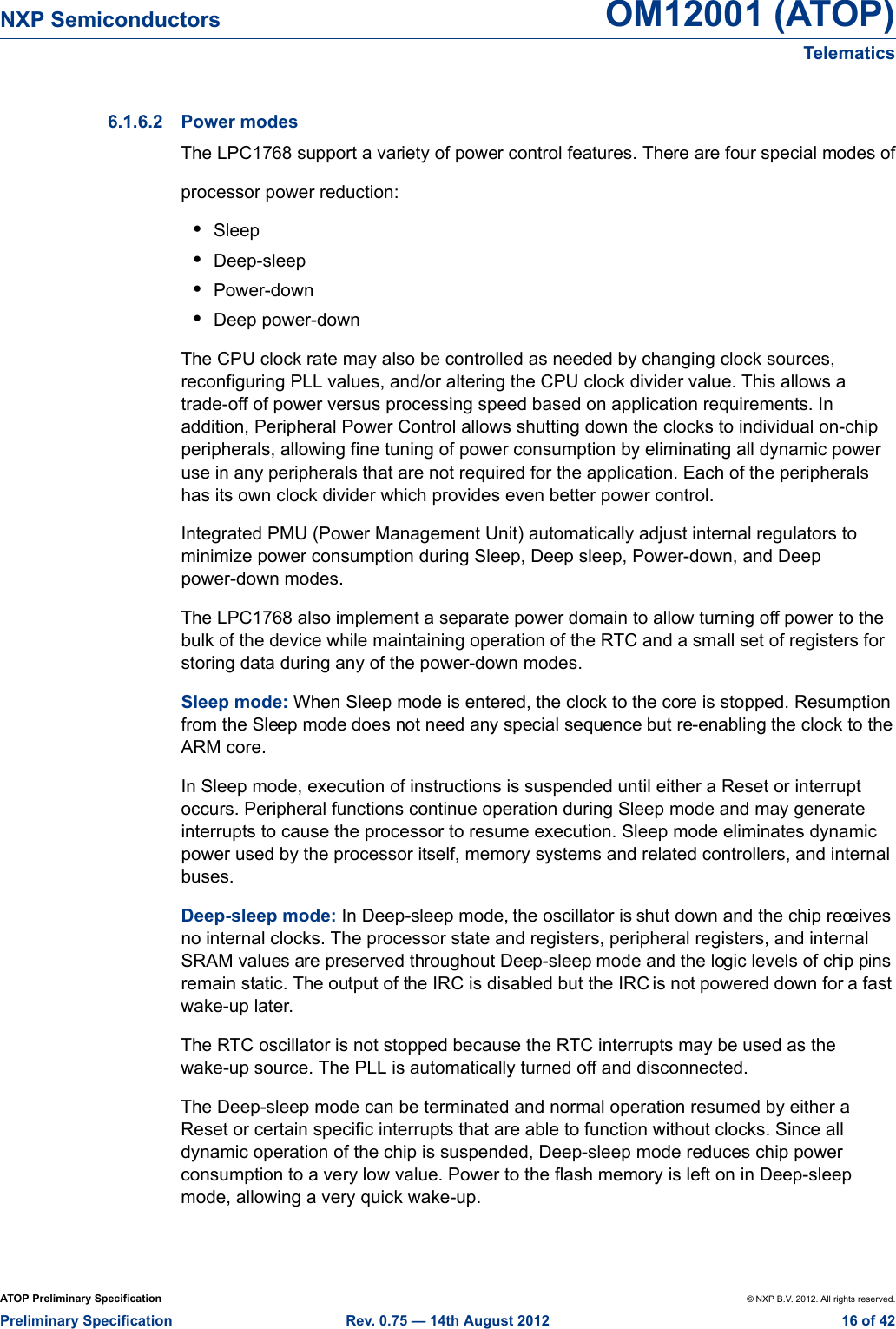
![ATOP Preliminary Specification © NXP B.V. 2012. All rights reserved.Preliminary Specification Rev. 0.75 — 14th August 2012 3 of 42NXP Semiconductors OM12001 (ATOP)Telematics1. IntroductionOM12001 (ATOP) is the NXP Semiconductors platform for automotive telematics on-board units (OBU's) for applications such as road pricing and eCall, based upon the following technologies:•GSM for communication•GPS for localization service•NFC for short range communication, e.g. configuration and law enforcement •SmartMX smartcard with Java card JCOP OS for security•J9 Virtual Machine for application portability and easy creation•Dedicated processor for Real-Time and connection to system via Ethernet, USB, ADC, CAN, UART, ...•Targeting 10 years lifetime1 in automotive conditionsThanks to on board ATOP security resources, product developers and manufacturers can offer products which guarantee fraud prevention and tamper evidence without extra effort for additional security precautions. These products can be used in end-to-end transaction systems requiring Common Criteria level 4+.OM12001 (ATOP) can be used by itself as a complete solution for GPS-GSM based road pricing and eCall applications. In this case OM12001 (ATOP) just needs to be complemented with a power supply, speaker, microphone, some knobs, and an optional display. OM12001 (ATOP) provides the processing power and SW application environment resources on board to complement road pricing and eCall with some other added value telematics services.OM12001 (ATOP) can also be applied as a 'front end' for more elaborate telematics products, by making its resources, i.e. GNSS, mobile communication, Security (ID authentication) available for use by other resources in the OBU. 2 different versions are available•OM12001/100: Implements all the features described in this document•OM12001/000: For market where security is not paramount, such as eCall, it does not include NFC short range communication, nor SmartMX security element2. Product profile2.1 FeaturesUtility processor for interfacing with external world and house-keepingARM Cortex M3 micro-controller with Ethernet, CAN, USB Host and device, UART, SPI, I2C Bus, ADCs, DAC, GPIOs, and PWMs Internal temperature sensor, and heating element2Application processor to run customer application code1. in accordance with NXP's "Knowledge-Based Qualification" ("KBQ", based upon ZVEI's Robustness Validation[1]), using AEC-Q100-defined qualification tests2. Heating element present only in OM12001/100](https://usermanual.wiki/NXP-Semiconductors/OM12001000/User-Guide-1779838-Page-3.png)
![ATOP Preliminary Specification © NXP B.V. 2012. All rights reserved.Preliminary Specification Rev. 0.75 — 14th August 2012 19 of 42NXP Semiconductors OM12001 (ATOP)Telematics Additionally other pins should be connected as follows:•VBAT_SENSE_P must be connected to the battery•VBAT_SENSE_N must be connected to ground•BB_BAT_THERM must be connected to a 10 kOhm pull-down, or to the battery thermistor7.2 Application without rechargable batteryIf no rechargable battery is used in the application, charging control pins must be connected as follows:•VCHG_SNK must be connected to ground•BB_CHARGE_[SW|REG]_CTL must be left unconnected•BB_ICHG_[P|N] must be connected together•VBAT_SENSE_P must be connected to VBAT_SNK•VBAT_SENSE_N must be connected to ground•BB_BAT_THERM must be connected to a 10 kOhm pull-downFig 6. Charging circuitry](https://usermanual.wiki/NXP-Semiconductors/OM12001000/User-Guide-1779838-Page-19.png)
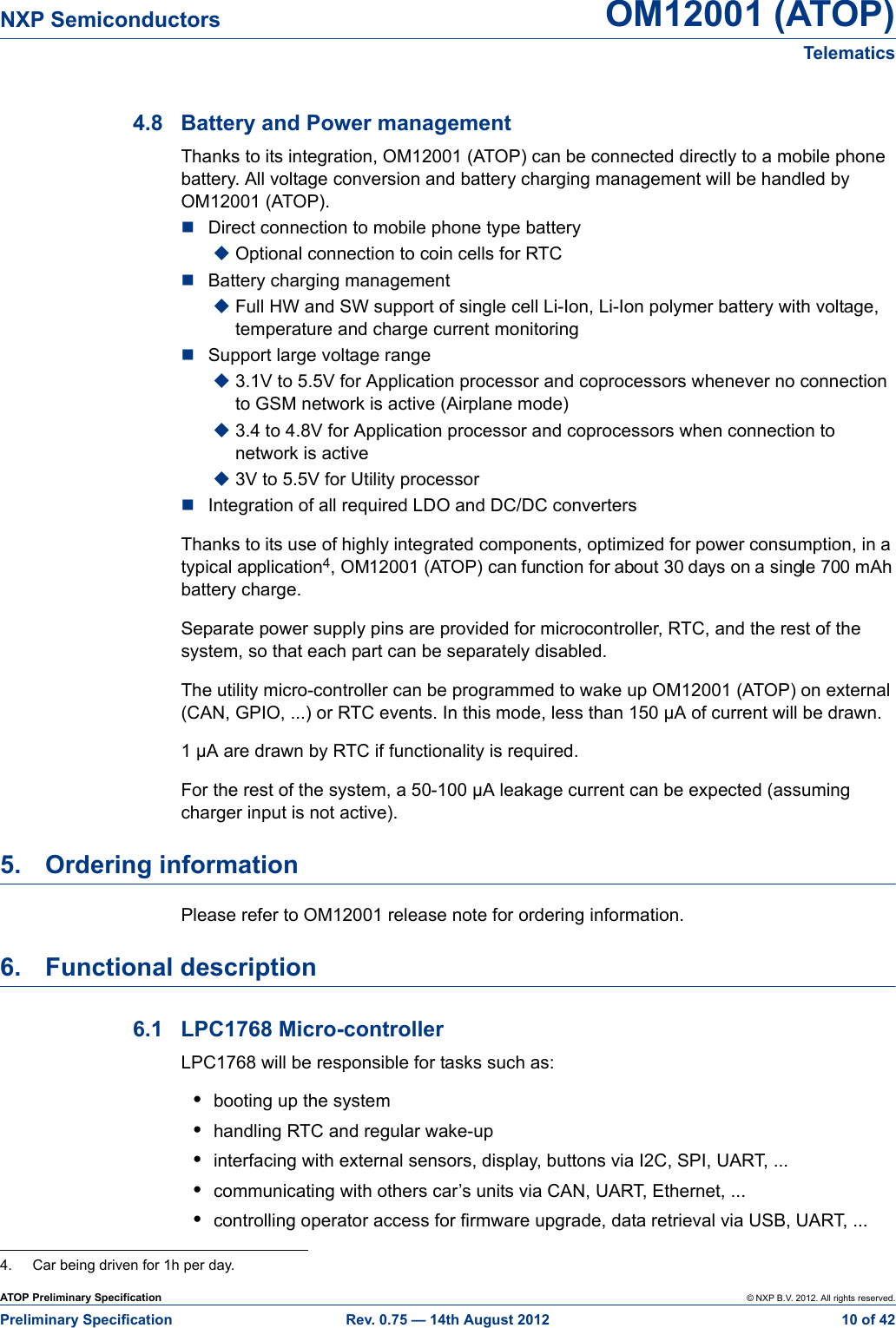
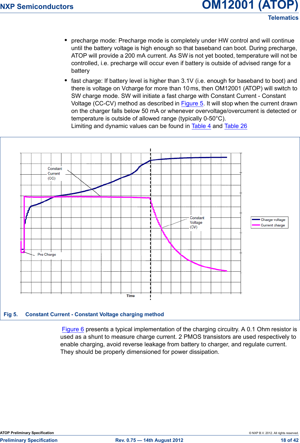
![ATOP Preliminary Specification © NXP B.V. 2012. All rights reserved.Preliminary Specification Rev. 0.75 — 14th August 2012 20 of 42NXP Semiconductors OM12001 (ATOP)Telematics7.3 Current sourceOM12001 (ATOP) handles internally all its voltage conversion. For Utility Processor, a separate input, VBAT_MC_SNK, is used. Internally, a LDO, controlled by VDD_3V0_SRC_ENA (active high, with internal pull-up), will convert it to the 3V required by the Utility Processor. As described in Figure 7, the output of the LDO is also available externally to power external component, up to a maximum of 100 mA can be drawn. Other limiting values can be found in Tab l e 13. 7.4 RTCMCU RTC is internally supplied by the output of the LDO described in Figure 7. It can also be supplied by a separate battery such as a coin cell via VBAT_RTC_SNK so that RTC is kept in case of power loss. If this feature is not required it is advised to connect VBAT_RTC_SNK and VDD_3V0_SRC.8. Application information8.1 NFC antenna design3For NFC antenna design, please refer to Ref. [6] for antenna design and Ref. [7] if application requires to boost NFC signal.Figure 8 describes the internal setup of NFC_ANT pins.Fig 7. VDD_3V0 current sourceOM12001 (ATOP)VBAT_MC_SNKVDD_3V0_SRC_ENA VDD_3V0_SRCUtility processorLDO](https://usermanual.wiki/NXP-Semiconductors/OM12001000/User-Guide-1779838-Page-20.png)
![ATOP Preliminary Specification © NXP B.V. 2012. All rights reserved.Preliminary Specification Rev. 0.75 — 14th August 2012 22 of 42NXP Semiconductors OM12001 (ATOP)Telematics10. Limiting values [1] Note this minimum voltage should take into account the voltage drop due to the high current during transmission, i.e. for a typical battery with a drop of 200 mV, minimum voltage is 3.6V [2] Occurs only during transmission slot (577 µs) in case of poor reception[3] It is not mandatory to connect Vbat_rtc_pnx as internal connection is provided, unless it is required to keep application processor RTC active when Vbat is disconnected [1] Charge voltage should obviously be higher than Vbat. Voltage drop into external transistors and resistors should be taken into accountTable 3. Power supply Symbol Parameter Min Typ Max Unit NoteVbat_rf Battery voltage for application processor3.4[1] 4.2 4.8 V Voltage range allowed in case of connection and transmission to GSM networkVbat_no_rf Battery voltage for application processor3.1 4.2 5.5 V Voltage range allowed without connection to GMS network (i.e. airplane mode)Vbat_mc Battery voltage for utility processor 3.1 4.2 5.5 VVbat_rtc_mc Battery voltage for utility processor RTC2.0 3.3 3.6 VVbat_rtc_bb Battery voltage for application processor RTC2.0 3.0 3.15 V [3]Ibat Battery current 1800[2] mA Peak current to be used to dimension decoupling capacitors (on VBAT_SNK)Table 4. Battery charging Handled by baseband integrated battery charging unitSymbol Parameter Min Typ Max Unit NoteVCharge Charge voltage 3.2 4.8 7.5 V [1]Ibat_empty Empty battery current 1 mA for VBAT_SNK < 1.5VIPreCharge Pre-charge current 160 200 240 mA pre-charge current, i.e. for VBAT_SNK < 3.35VIFastCharge Fast charge current 200 1400 mA For VBAT_SNK > 3.35V, Settable with 100mA steps, with additional step at 450 mAVFastCharge Fast Charge Voltage 3.45 4.2 5.5 V Settable with 50 mV step between 3.45 to 4.9V and 2 additional points at 5.25 and 5.55VVSW_CTL Maximum voltage allowed on BB_CHARGE_SW_CTL--VBAT_SNK VVSW_REG Maximum voltage allowed on BB_CHARGE_SW_REG--VCHG_SNK V](https://usermanual.wiki/NXP-Semiconductors/OM12001000/User-Guide-1779838-Page-22.png)
![ATOP Preliminary Specification © NXP B.V. 2012. All rights reserved.Preliminary Specification Rev. 0.75 — 14th August 2012 23 of 42NXP Semiconductors OM12001 (ATOP)Telematics [1] 5V tolerant pins, i.e. all I/O with MC prefix, except for oscillator IOs[2] Vbat_mc must be present[3] 3-state outputs go into 3-state mode when Vbat_mc is grounded Table 5. Limiting values for micro-controller pinsSymbol Parameter Conditions Min Typ Max UnitVIAmc Analog input voltage on ADC related pins -0.5 5.1 VVImc Input voltage 5V tolerant I/O pins[1][2][3] -0.5 5.5 Vother I/O pins[2] -0.5 3.6 VVimc_xtal1 Input voltage for XTAL1 Internal oscillator input 0 - 1.8 VVomc_xtal2 Output voltage Internal oscillator output 0 - 1.8 VTable 6. Limiting values for GSM baseband interfacesSIM interface, analog audio and PCM interfaceSymbol Parameter Conditions Min Typ Max UnitVIbb Input voltage -0.4 3.2 VIIbb Input current 20 mAIObb Output current 20 mATable 7. Limiting values for GSM antennasDue to their ESD protection implementation GSM antennas are DC groundedSymbol Parameter Conditions Min Typ Max UnitRIDC Input resistance DC voltage 1.96 ImaxDC Maximum current DC current 140 mALoad mismatch for all phase angles, before permanent degradation or damage20:1 VSWRSpurious (low bands) for all phase angles, no parasitic oscillations > -30 dbm12:1 VSWRSpurious (high bands) for all phase angles, no parasitic oscillations > -30 dbm8:1 VSWRTable 8. Limiting values for GPS passive antenna inputDue to its ESD protection implementation GPS antenna is DC groundedSymbol Parameter Conditions Min Typ Max UnitRIDC Input resistance DC voltage 0.14 ImaxDC Maximum current DC current 540 mATable 9. Limiting values for GPS active antenna input and antenna biasSymbol Parameter Conditions Min Typ Max UnitVmaxDC Maximum voltage DC voltage -25 25 VImaxDC Maximum current DC current 70 mA](https://usermanual.wiki/NXP-Semiconductors/OM12001000/User-Guide-1779838-Page-23.png)
![ATOP Preliminary Specification © NXP B.V. 2012. All rights reserved.Preliminary Specification Rev. 0.75 — 14th August 2012 24 of 42NXP Semiconductors OM12001 (ATOP)Telematics11. Characteristics12. Static characteristics12.1 Pins [1] Only allowed for a short time period Table 10. Characteristics for micro-controller pins Symbol Parameter Conditions Min Typ Max UnitVOmc Output voltage 0 3.0 VVIHmc High level input voltage 2.0 VVILmc Low level input voltage 0.8 VIILmc Low level input current VI=0 V; no pull-up 3 µAIIHmc High level input current VI=3.0 V; no pull-down 3 µAVOHmc High level output voltage IOHmc=-4 mA 2.6 VVOLmc Low level output voltage IOLmc=-4 mA 0.4 VIOLmc Low level output current VOL=0.4 V 4 mAIOHmc High level output current VOH=2.6 V -4 mAIOLSmc Low level short circuit output current VI=3.0 V[1] -45 mAIOHSmc High level short circuit output currentVI=0 V[1] 50 mAIOZmc Off state output current VO=3.0 or 0V; no pull-up/down 3 µAIpdmc Pull-down current VI=5 V 10 50 150 µAIpumc Pull-up current VI=0 V; -15 -50 -85 µA3.0 <VI<5 V 0 0 0 µAIIlatchmc I/O latchup current -1.5<VI<4.5V; Tj<125°C 100 mATable 11. Characteristic for baseband digital interfacenamely SIM interface, PCM, UART, JTAGSymbol Parameter Conditions Min Typ Max UnitVIHbb High level input voltage 2.4 VVILbb Low level input voltage 0.4 VIIHbb High level input current -10 +10 µAIILbb Low level input current -10 +10 µAVOHbb High level output voltage 2.7 VVOLbb Low level output voltage 0.1 VRpubb Pull-up resistance 100 kRpdbb Pull-down resistance 100 kCiLbb Input capacitance 0.1 pF](https://usermanual.wiki/NXP-Semiconductors/OM12001000/User-Guide-1779838-Page-24.png)
![ATOP Preliminary Specification © NXP B.V. 2012. All rights reserved.Preliminary Specification Rev. 0.75 — 14th August 2012 25 of 42NXP Semiconductors OM12001 (ATOP)Telematics 12.2 Current sources [1] Voltage is dynamically controlled to reduce power consumption when SIM card is not accessed12.3 Voltage references Table 12. Characteristic for GPS digital interfacenamely JTAG and GPS_UART2_RXDSymbol Parameter Conditions Min Typ Max UnitVIHbb High level input voltage 1.7 VVILbb Low level input voltage 0.7 VIIHbb High level input current -10 +10 µAIILbb Low level input current -10 +10 µAVOHbb High level output voltage 1.7 VVOLbb Low level output voltage 0.7 VRpubb Pull-up resistance 60 kRpdbb Pull-down resistance 75 kIOOutput current 6 mATable 13. Vdd_3v0_src current sourceCan be used to supply external componentsSymbol Parameter Min Typ Max Unit NoteVdd_3v0 Output voltage 2.9 3.0 3.1 V For Tj=-40 to 125°CIvdd3v0_max maximum current 100 mAVdd_3v0 Load regulation 0.0008 0.004 %/mAVdd_3v0 Line regulation -0.1 0.1 %/V For Vbat variationton_dd_3v0 Turn on time 240 µS Measured from the time VDD_3V0_SRC_ENA exceeds 1.4VTable 14. Vsim_src current sourceTo be only used to supply SIM cards[1]Symbol Parameter Min Typ Max Unit NoteVsim_src Output voltage 2.75 2.90 3.00 V Appropriate SIM card voltage is automatically detected and selected by the software1.65 1.80 1.95 VIsim_src Output current 80 mA Full power mode3 mA Sleep modeVo/VoRelative output voltage 50 mV/V For Vbat variationton_dd_3v0 Settling time 10 µS from power-downTable 15. Vio_ref voltage referenceTo be used as a reference to connect to BB_* test pins (JTAG)Symbol Parameter Min Typ Max Unit NoteVio_ref Output voltage 2.70 2.80 2.95 VVo/VoRelative output voltage 50 mV/V For Vbat variation](https://usermanual.wiki/NXP-Semiconductors/OM12001000/User-Guide-1779838-Page-25.png)
![ATOP Preliminary Specification © NXP B.V. 2012. All rights reserved.Preliminary Specification Rev. 0.75 — 14th August 2012 26 of 42NXP Semiconductors OM12001 (ATOP)Telematics [1] For VBAT_SNK = 3.1V[2] For VBAT_SNK = 3.6V[3] For VBAT_SNK = 5.5V 12.4 Clocks Table 16. Vperm_ref voltage referenceTo be used as a reference to connect to BB_* functional pinsSymbol Parameter Min Typ Max Unit NoteVperm_ref Output voltage 2.82[1] 3.0[2] 3.18[3] V Follows VBAT_SNK if <3VTable 17. Vadc_ref voltage referenceused as power supply reference for internal ADCs Symbol Parameter Min Typ Max Unit NoteVadc_ref Output voltage 2.9 3.0 3.1 V For Tj=-40 to 125°CV/V Line regulation -0.1 0.1 %/V For Vbat variationTable 18. 1PPSThis pulse is synchronized with GPS system clock Symbol Parameter Min Typ Max Unit NotePulse width 125 µsJitter -50 3 50 ns Stationary and receiving 4 or more satellites Table 19. BB_EXT_CLKThis clock is coupled to GSM network Symbol Parameter Min Typ Max Unit Notefbb_ext_clk frequency 26/N MHz for N= 1, 2, ..., 8156/M MHz for M=9, 10, .., 16f/fofrequency drift 0.7 1 ppmTable 20. Micro-controller clockExternal crystal required for high speed CAN, for all other purposes, internal RC oscillator is sufficientSymbol Parameter Min Typ Max Unit Notefmc_xtal Crystal frequency 1 - 24 MHz In case of externally oscillator, connected to MC_XTAL_(1|2)V(rms)mc_xtal Oscillation amplitude 0.2 - V (RMS)thmc_xtal Clock High time tcycle x 0.4 - nstlmc_xtal Clock Low time tcycle x 0.4 - nstrmc_xtal Clock rise time 5 nstfmc_xtal Cock fall time 5 nsfmc_ircl Oscillator frequency 3.96 4 4.04 MHz Frequency of internal RC oscillator](https://usermanual.wiki/NXP-Semiconductors/OM12001000/User-Guide-1779838-Page-26.png)
![ATOP Preliminary Specification © NXP B.V. 2012. All rights reserved.Preliminary Specification Rev. 0.75 — 14th August 2012 27 of 42NXP Semiconductors OM12001 (ATOP)Telematics13. Dynamic characteristics13.1 Power consumptionAll measured current consumption have been measured at 25°C with a power supply at 3.7V [1] No peripherals enabled[2] Wake-up can be initiated by event on RTC, CAN, USB and most GPIOs[3] If a separate power source such as coin cell battery is connected to VBAT_RTC_SNK and no power is supplied via VBAT_MC_SNK [1] Leakage currents are included in Table 23 [1] Network dependent, assumes a typical 7s radio measurement plus 0.5s network inscription[2] BS_PA_MFRMS = 9, i.e. paging from network will be checked every 2100 ms[3] BS_PA_MFRMS = 5, i.e. paging from network will be checked every 1175 ms. This is typically the setting used by most mobile operatorsTable 21. Utility processor power consumptionIncludes LDOSymbol Parameter Min Typ Max Unit NoteCortex M3 at 12 MHz 7 7[1] mA at 25°C, code while(1){}Cortex M3 at 100 MHz 42[1] mAPowerdown mode 150 µA [2]RTC active 1 µA backup registers saved [3]Table 22. Application processor consumption characteristics Baseband ARM and memories power consumption additionally to GSM/GPRS functionSymbol Parameter Min Typ Max Unit NoteApplication processor 0[1] 20 60 mATable 23. Communication coprocessor consumption characteristicsCovers baseband RF frontend as well as memories (PSRAM and flash)Symbol Parameter Min Typ Max Unit Notecomplete GSM function network attachment115[1] µAh Energy consumption equivalent to 300s of idle modecomplete GSM function active in idle mode1.085[2] 1.31[3] 2.05[4] mA Average consumption, assuming typical setting for mobile network. Peak consumption for GSM/GPRS at maximum power can reach up to 1600 mA during transfer slots (577 µs)complete GSM function during voice call79[5] 114[6] 220[7] mAcomplete GPRS function during data transfer (Class 10: 2T+3RX)140[5] 205[6] 400[7] mAcomplete GSM function in sleep mode600 µA GSM function activecomplete GSM function leakage current50 µA](https://usermanual.wiki/NXP-Semiconductors/OM12001000/User-Guide-1779838-Page-27.png)
![ATOP Preliminary Specification © NXP B.V. 2012. All rights reserved.Preliminary Specification Rev. 0.75 — 14th August 2012 28 of 42NXP Semiconductors OM12001 (ATOP)Telematics[4] BS_PA_MFRMS = 2, i.e. paging from network will be checked every 470 ms[5] PCL = 19, i.e. 4.9db amplification for GSM900[6] PCL = 7, i.e. 29.2db amplification for GSM900[7] PCL = 5, i.e. 33.1 db amplification for GSM900 13.2 Battery charging Table 24. Security processor power consumptionSymbol Parameter Min Typ Max Unit NoteFunction switched off 0 µA included in NFC coprocessorFunction active 6 mATable 25. NFC coprocessor power consumptionCovers NFC and SMX Symbol Parameter Min Typ Max Unit NoteFunction switched off 2 µAPower down 35 µA RF field detection onFunction active 30 mAfunction active with RF transmission ongoing90 130 mATable 26. Battery chargingMeasured at 3.7V, 25°CSymbol Parameter Min Typ Max Unit NoteBattery overvoltage detection60 90 130 mV Battery voltage in excess of VFAST above which fast charge is automatically disabled Battery overcurrent detection190 210 230 mA Battery current in excess of programmed current above which fast charge is automatically disabled Fast charge stop 50 mAVOreg/VOreg Relative regulator output voltage variation-1 +1 %IOreg/IOreg Relative regulator output current variation-12 +12 %Iqvchg Quiescent current drawn from VCHG_SNK3mAIqbb_ighgp Quiescent current drawn from BB_ICHG_P40 µA during chargeIqbb_ighgn Quiescent current drawn from BB_ICHG_P60 µA during chargeIqvbat_snk Quiescent current drawn from VBAT_SENSE_[P|N]200 µA during charge](https://usermanual.wiki/NXP-Semiconductors/OM12001000/User-Guide-1779838-Page-28.png)
![ATOP Preliminary Specification © NXP B.V. 2012. All rights reserved.Preliminary Specification Rev. 0.75 — 14th August 2012 40 of 42NXP Semiconductors OM12001 (ATOP)Telematics26. Glossary<term> — <definition>27. References[1] ZVEI - Zentralverband Elektrotechnik- und Elektronikindustrie e.V. — http://www.zvei.org/fachverbaende/electronic_components_and_systems/robustness_validation/druckansicht.html?type=1 [2] LPC1768 datasheet — http://www.nxp.com/documents/data_sheet/LPC1769_68_67_66_65_64_63.pdf[3] LPC1768 user manual — http://www.nxp.com/documents/user_manual/UM10360.pdf[4] LPC1768 errata sheet — http://www.nxp.com/documents/errata_sheet/ES_LPC176X.pdf[5] LPC1768 web page — http://www.nxp.com/products/microcontrollers/cortex_m3/lpc1700/LPC1768FET100.html#overview[6] AN1445 Antenna design guide for MFRC52x, PN51x, PN53xAN1444 RF Design Guideplus Excel Calculation — http://www.nxp.com/documents/application_note/AN1445_An1444.zip[7] AN1425 RF Amplifier for NFC Reader IC'sAN166510 Amplifier antenna matching calculation (Excel) — http://www.nxp.com/documents/application_note/AN1425_AN166510.zipRSA A public-key encryption technology developed by RSA Data Security, Inc. The acronym stands for Rivest, Shamir, and Adelman, the inventors of the techniqueRTC Real Time ClockRTOS Real Time Operating SystemSAW Surface Acoustic WaveSIM Subscriber Identification ModuleSNR Signal to Noise RatioSPA Simple Power AnalysisSPI Serial Peripheral InterfaceTCXO Temperature Controlled Crystal OscillatorUART Universal Asynchronous Receiver TransmitterTable 30. Abbreviations …continuedAcronym Description](https://usermanual.wiki/NXP-Semiconductors/OM12001000/User-Guide-1779838-Page-40.png)