NXP Semiconductors OM12001000 Automotive Telematics GSM/GPS Module User Manual
NXP Semiconductors Automotive Telematics GSM/GPS Module
user manual

OM12001 - Automotive
Telematics On-board unit
Platform
Road Pricing - ECall
Rev. 0.75 — 14th August 2012 Preliminary Specification
Document information
Info Content
Title OM12001 - Automotive Telematics On-board unit Platform
Short title (1 line) OM12001 (ATOP)
Subtitle Road Pricing - ECall
Short subtitle (1 line) Te l e m a t i c s
Document ID ATOP Preliminary Specification
Document type Preliminary Specification
Revision number 0.75
Keywords Telematics, Pay as you drive, eCall
Abstract An Automotive Telematics On Board Unit Platform for Road pricing, eCall
and Telematics added value services

ATOP Preliminary Specification © NXP B.V. 2012. All rights reserved.
Preliminary Specification Rev. 0.75 — 14th August 2012 2 of 42
NXP Semiconductors OM12001 (ATOP)
Telematics
Revision history
Rev Date Description
0.75 9th August 2012 Numerous typos corrected
Reference links updated
0.74 6th August 2012 Updated spec for “minus” version, ie. without NFC and security components.
Updated label
Added IC statement
0.73 1st February 2012 Added RHF indication description to label
0.72 8th December 2011 Revision history added!
NFC EMC section updated
2D barcode info added

ATOP Preliminary Specification © NXP B.V. 2012. All rights reserved.
Preliminary Specification Rev. 0.75 — 14th August 2012 3 of 42
NXP Semiconductors OM12001 (ATOP)
Telematics
1. Introduction
OM12001 (ATOP) is the NXP Semiconductors platform for automotive telematics
on-board units (OBU's) for applications such as road pricing and eCall, based upon the
following technologies:
•GSM for communication
•GPS for localization service
•NFC for short range communication, e.g. configuration and law enforcement
•SmartMX smartcard with Java card JCOP OS for security
•J9 Virtual Machine for application portability and easy creation
•Dedicated processor for Real-Time and connection to system via Ethernet, USB,
ADC, CAN, UART, ...
•Targeting 10 years lifetime1 in automotive conditions
Thanks to on board ATOP security resources, product developers and manufacturers can
offer products which guarantee fraud prevention and tamper evidence without extra effort
for additional security precautions. These products can be used in end-to-end transaction
systems requiring Common Criteria level 4+.
OM12001 (ATOP) can be used by itself as a complete solution for GPS-GSM based road
pricing and eCall applications. In this case OM12001 (ATOP) just needs to be
complemented with a power supply, speaker, microphone, some knobs, and an optional
display. OM12001 (ATOP) provides the processing power and SW application
environment resources on board to complement road pricing and eCall with some other
added value telematics services.
OM12001 (ATOP) can also be applied as a 'front end' for more elaborate telematics
products, by making its resources, i.e. GNSS, mobile communication, Security (ID
authentication) available for use by other resources in the OBU.
2 different versions are available
•OM12001/100: Implements all the features described in this document
•OM12001/000: For market where security is not paramount, such as eCall, it does not
include NFC short range communication, nor SmartMX security element
2. Product profile
2.1 Features
Utility processor for interfacing with external world and house-keeping
ARM Cortex M3 micro-controller with Ethernet, CAN, USB Host and device, UART,
SPI, I2C Bus, ADCs, DAC, GPIOs, and PWMs
Internal temperature sensor, and heating element2
Application processor to run customer application code
1. in accordance with NXP's "Knowledge-Based Qualification" ("KBQ", based upon ZVEI's Robustness Validation[1]), using
AEC-Q100-defined qualification tests
2. Heating element present only in OM12001/100

ATOP Preliminary Specification © NXP B.V. 2012. All rights reserved.
Preliminary Specification Rev. 0.75 — 14th August 2012 4 of 42
NXP Semiconductors OM12001 (ATOP)
Telematics
Virtual Machine for customer application
Communication coprocessor with Quad-band GSM/GPRS terminal
Localization coprocessor with GPS receiver
Near Field Communication (NFC) controller to connect to external vignette, smart
card, mobile phone 3
Security processor for providing a source of trust
SmartMX smartcard running JCOP 2.4.13
Mandatory and voluntary certification
R&TTE and FCC passed for safety, EMC and RF
Pre-certification for GCF, including field test
Certification for PTCRB
Automotive certification
-40 to +85°C operating range
Targeting 10 years lifetime in automotive conditions1
2.2 Applications
OM12001 (ATOP) can be used for Telematics applications where tamper-resistance,
confidentiality, integrity, and authenticity of end-user information are required, e.g.:
Road pricing
Pay as you drive insurance
Stolen vehicles tracking
Emergency call
...
2.3 Quick reference data
OM12001 (ATOP) is available with quad-band support in 2 versions
3. General description
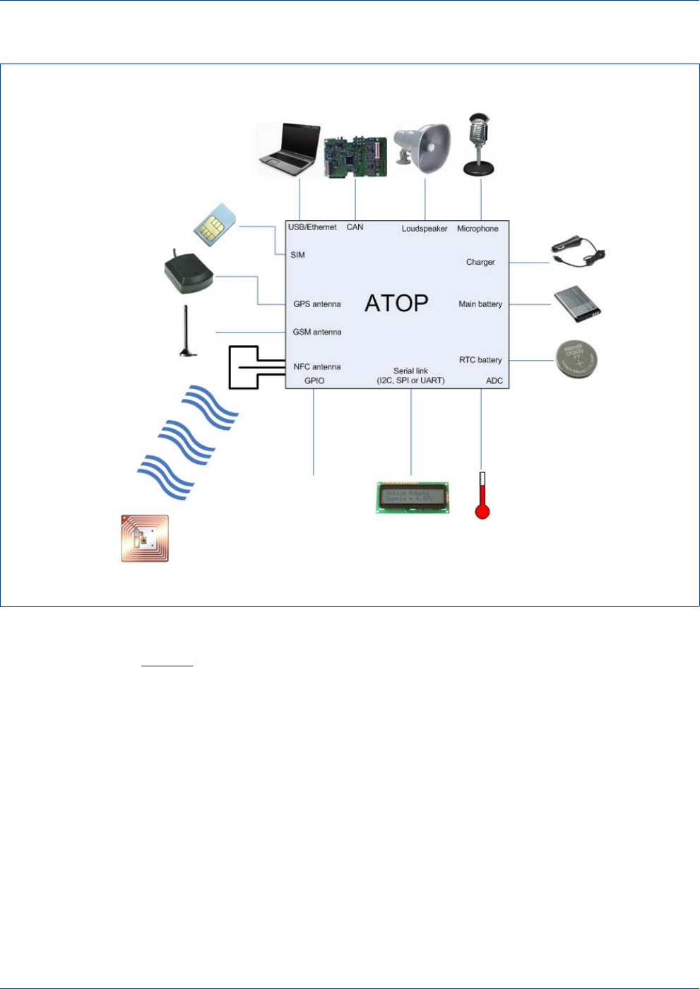
Figure 1 represents OM12001 (ATOP) connections in a typical application, with its
connection to batteries, antennas, and SIM. For communication with external world, serial
link, GPIOs, and ADCs will connect to screen, keys, and sensors. UART, CAN or USB can
be used to connect to on board computer.
3. Only for OM12001/100
Table 1. ATOP versions
Name Description
OM12001/100 Quad-band GPRS/GSM with antenna switch, GPS, NFC, SMX,
Cortex M3 microcontroller with Ethernet
OM12001/000 Quad-band GPRS/GSM with antenna switch, GPS, Cortex M3
microcontroller with Ethernet

ATOP Preliminary Specification © NXP B.V. 2012. All rights reserved.
Preliminary Specification Rev. 0.75 — 14th August 2012 6 of 42
NXP Semiconductors OM12001 (ATOP)
Telematics
Three main components can be seen in Figure 2:
•Application processor: This processor will run code specific to the application
(roadtolling, insurance, ...) which is portable from one platform to another one in order
to avoid recertification:
–A localization coprocessor provides accurate location information to the application
–A NFC coprocessor provides connection to an external vignette to increase
application security3
–A Communication coprocessor allows the application to connect to servers and
receive update and notifications, receive or generate voice call or SMS
•Security processor which provides a root of trust for signing messages to servers,
authenticate the presence of an external vignette, and run secure multiple security
applications3
•Utility processor: This processor takes care of all housekeeping tasks such as
connecting to external interfaces, displays, but also of power management, waking-up
and booting-up the system, i.e. all support tasks which are not part of the high level
applications but are required to make the system work.
4. Features
4.1 Utility processor
A LPC1768 micro-controller is available for interfacing to external world and user
interface.
ARM Cortex M3 core running up to 100 MHz
512 kB on-chip flash memory
64 kB SRAM memory
Dual AHB system that provides for simultaneous DMA and program execution from
on-chip flash with no contention between those functions.
General Purpose DMA controller (GPDMA) on AHB that can be used with the SSP
Fig 2. ATOP conceptual view
Application Processor
Localization
Security Processor
NFC GPRS
Utility Processor

ATOP Preliminary Specification © NXP B.V. 2012. All rights reserved.
Preliminary Specification Rev. 0.75 — 14th August 2012 7 of 42
NXP Semiconductors OM12001 (ATOP)
Telematics
serial interfaces, the I2S port, ADCs, DAC as well as for memory transfers
Serial Interfaces
3 UARTs
2 I2Cs
1 SSP (Synchronous Serial Port) and 1 SPI
I2S output/input
PWM/Capture unit
GPIOs (multiplexed)
High speed serial interfaces
Ethernet MAC with RMII interface and dedicated DMA controller
Full Speed USB 2.0 Host/Device controller with integrated PHY
2 CAN channels
Analog interfaces
7 12 bit ADCs (successive approximation)
1 internal temperature sensor (12 bit ADC)
1 10 bit DAC
Debug
ETJAG
Serial Wire Debug
4.2 Application processor
The application processor is actually a Virtual Machine (VM) running on the main CPU of
the GSM/GPRS baseband. Using a Virtual Machine offers numerous advantages:
portability to numerous platforms
maintainability via secure download and update mechanisms
large virtualized feature set, such as:
secure network access (https)
cryptography
Near Field Communication (NFC)3
VM has the following features:
CDC Foundation Profile including following additional API's
Wireless Messaging
Mobile playback
Location
Contactless Communication
Telephony
Power management
Connection to micro-controller via message passing
4.3 Localization coprocessor
GPS reception is used for localization.
Best in class acquisition and tracking sensitivity
Internal separate LNA for improved sensitivity

ATOP Preliminary Specification © NXP B.V. 2012. All rights reserved.
Preliminary Specification Rev. 0.75 — 14th August 2012 8 of 42
NXP Semiconductors OM12001 (ATOP)
Telematics
Advanced proprietary multipath algorithms for robust low dropout tracking in very low
signals environment
SW upgradable
1 Pulse per Second (1PPS) output for synchronization with GPS system clock
4.4 GSM/GPRS coprocessor
Connection to mobile networks is provided by a certified communications protocol stack
that is field tested worldwide. It runs on a single monolithic IC integrating analog and
digital basebands, RF transceiver, power management, and audio codec with
best-in-class RF performance and power consumption.
32-bit ARM926EJ-S™ control processor, up to 156 MHz
Communication engine
Support for 2 antennas with internal switch
Quad-band support: GSM 850, PCS 1900, E-GSM 900, and DCS 1800
GPRS multislot class 10, class B
Audio subsystem
HR / FR / EFR / AMR Vocoders
Noise suppression and echo cancellation
Microphone amplifier with differential input
High-performance 8 driver (500mW output power, 1% THD typ)
Digital PCM IO
SIM card interface
1.8/2.9V power generation
Compliant with SIM card interface in accordance with GSM11.11
Compliant with ISO7816-3 requirements
4.5 Near Field Communication coprocessor3
To connect to a external device, such as vignette, mobile phone, or personalization station
for a road pricing public scheme, a NFC communication link with the following features is
present:
Reader mode
Allows simultaneous access up to two external cards
Offers baud rate up to 424 kbps
Complete NFC framing and error detection
Supports ISO14443A&B/Mifare
Virtual Card mode
Direct connection to battery allowing operation with the rest of system is switched
off
Access to SmartMX in Mifare emulation mode
4.6 Smartcard & JCOP operating system3
For telematics and other high value applications, it is paramount to protect against data
tampering, loading of unauthorized applications, ID stealing, as well as to protect end user
privacy. For this, a secured component such as a smartcard is required to be used as a
root of trust.

ATOP Preliminary Specification © NXP B.V. 2012. All rights reserved.
Preliminary Specification Rev. 0.75 — 14th August 2012 9 of 42
NXP Semiconductors OM12001 (ATOP)
Telematics
OM12001 (ATOP) relies on a SmartMX component with the following features:
Common criteria CC EAL5+ certification according to BSI-PP-0002 protection profile
Latest built-in security features to avoid power (SPA/DPA), timing, and fault attacks
80 KB EEPROM
EEPROM with typical 500000 cycles endurance and minimum 20 years retention
time
6144 B RAM
200 KB ROM
75+ KB available for customer applications
Secure cryptographic processor
High-performance secured Public Key Infrastructure (PKI)
Secured dual/triple-DES coprocessor
Secured AES coprocessor
For portability and to allow multiple secure application (cardlets) to run in complete
isolation, OM12001 (ATOP) offers a Java Card Open Platform operating system (JCOP).
V2.4.1 based on independent, third party specifications, i.e. by Sun Microsystems, the
Global Platform consortium, the International Organization for Standards (ISO), EMV
(Europay, MasterCard, and VISA) and others.
SmartMX family was designed to service high volume, single- and multi-application
markets such as eGovernment e.g. Smart Passport, banking/finance, mobile
communications, public transportation, pay TV, conditional access, network access, and
digital rights management, thus ensuring applications running on OM12001 (ATOP) can
rely on the highest level of security available.
4.7 Debug and Security
For application development, but also field return analysis, debug capabilities are a must.
However the observability, test and control capabilities given by debug could be used for
device tampering.
That is why ATOP debug capabilities are locked until proper authentication. Additionally,
security features are present to ensure that only signed SW is executed.
For debug, the following features are present:
LPC1768 MCU
CPU debug via JTAG or Serial Wire Debug interface
Unique Serial Number
Core Read Protection with multiple levels
For security, the following features will protect against unauthorized debug, code
tampering, and insertion:
Observability
JTAG access locked down until authentication is performed
All sensitive bus are buried down in the PCB
Code authentication and integrity
Code is signed with RSA to ensure authentication and checked at boot

ATOP Preliminary Specification © NXP B.V. 2012. All rights reserved.
Preliminary Specification Rev. 0.75 — 14th August 2012 10 of 42
NXP Semiconductors OM12001 (ATOP)
Telematics
4.8 Battery and Power management
Thanks to its integration, OM12001 (ATOP) can be connected directly to a mobile phone
battery. All voltage conversion and battery charging management will be handled by
OM12001 (ATOP).
Direct connection to mobile phone type battery
Optional connection to coin cells for RTC
Battery charging management
Full HW and SW support of single cell Li-Ion, Li-Ion polymer battery with voltage,
temperature and charge current monitoring
Support large voltage range
3.1V to 5.5V for Application processor and coprocessors whenever no connection
to GSM network is active (Airplane mode)
3.4 to 4.8V for Application processor and coprocessors when connection to
network is active
3V to 5.5V for Utility processor
Integration of all required LDO and DC/DC converters
Thanks to its use of highly integrated components, optimized for power consumption, in a
typical application4, OM12001 (ATOP) can function for about 30 days on a single 700 mAh
battery charge.
Separate power supply pins are provided for microcontroller, RTC, and the rest of the
system, so that each part can be separately disabled.
The utility micro-controller can be programmed to wake up OM12001 (ATOP) on external
(CAN, GPIO, ...) or RTC events. In this mode, less than 150 µA of current will be drawn.
1 µA are drawn by RTC if functionality is required.
For the rest of the system, a 50-100 µA leakage current can be expected (assuming
charger input is not active).
5. Ordering information
Please refer to OM12001 release note for ordering information.
6. Functional description
6.1 LPC1768 Micro-controller
LPC1768 will be responsible for tasks such as:
•booting up the system
•handling RTC and regular wake-up
•interfacing with external sensors, display, buttons via I2C, SPI, UART, ...
•communicating with others car’s units via CAN, UART, Ethernet, ...
•controlling operator access for firmware upgrade, data retrieval via USB, UART, ...
4. Car being driven for 1h per day.

ATOP Preliminary Specification © NXP B.V. 2012. All rights reserved.
Preliminary Specification Rev. 0.75 — 14th August 2012 11 of 42
NXP Semiconductors OM12001 (ATOP)
Telematics
Except for a few services provided by NXP to handle communication between the
application running on Virtual Machine and virtualized external devices, Utility processor
will be completely available to the system integrator.
6.1.1 General features
•ARM Cortex-M3 microcontroller, running up to 100 MHz
•512 kB on-chip Flash Program Memory with In-System Programming (ISP) and
In-Application Programming (IAP) capabilities. Single Flash sector or full-chip erase in
400 ms and 256 bytes programming in 1 ms. Flash program memory is on the ARM
local bus for high performance CPU access
–10000 erase cycles
–10 years retention powered on, 20 years powered off
–First 8 erase block are 4 KB large, others are 32 KB large
•32 kB Static RAM with local code/data bus for high-performance CPU access
•Two 16 kB Static RAM blocks with separate access paths for higher throughput, for
Ethernet, USB, DMA memory as well as for CPU code and data.
These SRAM blocks may be used for Ethernet, USB, and DMA memory, as well as
for general purpose CPU instruction and data storage for general purpose SRAM
•Multilayer AHB matrix interconnect with separate bus for each AHB master
•Advanced Vectored Interrupt Controller, supporting up to 32 vectored interrupts
•Eight channel General Purpose DMA controller (GPDMA) on the AHB multilayer
matrix that can be used with the SSP, serial interfaces, the I2S port, as well as for
memory-to-memory transfers
•Serial interfaces available externally
–USB 2.0 Full-speed Device/Host controller with on-chip PHY and associated DMA
controller
–Three UARTs with fractional baud rate generation, one with modem control I/O,
one with IrDA support, all with FIFO. These reside on the APB bus
–One SSP controller with FIFO and multi-protocol capabilities, as well as a SPI port,
sharing its interrupt. The SSP controller can be used with the GPDMA controller
and reside on the APB bus
–Two I2C interfaces reside on the APB bus. The second and third I2C interfaces are
expansion I2C interfaces with standard port pins rather than special open-drain I2C
pins
–I2S (Inter-IC Sound) interface for digital audio input or output, residing on the APB
bus. The I2S interface can be used with the GPDMA
–Two channels with Acceptance Filter/FullCAN mode residing on the APB bus
•Other APB Peripherals
–12 bit A/D converter with input multiplexing among 7 external pins
–10 bit D/A converter with DMA support
–Four general purpose timers with a total of 8 capture inputs and ten compare
output pins each. Each timer block has an external count input

ATOP Preliminary Specification © NXP B.V. 2012. All rights reserved.
Preliminary Specification Rev. 0.75 — 14th August 2012 12 of 42
NXP Semiconductors OM12001 (ATOP)
Telematics
–One PWM/Timer block with support for three-phase motor control
–Real-Time Clock (RTC) with separate power pin; clock source can be the RTC
oscillator or the APB clock oscillator
–Watchdog Timer. The watchdog timer can be clocked from the internal RC
oscillator, the RTC oscillator, or the APB clock
•Standard ARM Test/Debug interface for compatibility with existing tools
•Three reduced power modes: Idle, Sleep, and Power-down
•Four external interrupt inputs. In addition every PORT0/2 pin can be configured as an
edge sensing interrupt
•Processor wake-up from Power-down mode via any interrupt able to operate during
Power-down mode (includes external interrupts, RTC interrupt)
•Two independent power domains allow fine tuning of power consumption based on
needed features
•Brownout detect with separate thresholds for interrupt and forced reset
•On-chip Power On Reset
•On-chip crystal oscillator with an operating range of 1 MHz to 24 MHz
–For CAN and USB, a clock generated internally to OM12001 (ATOP) is provided,
or an external crystal can be used
•On-chip PLL allows CPU operation up to the maximum CPU rate without the need for
a high-frequency crystal. May be run from the main oscillator, the internal RC
oscillator, or the RTC oscillator
•Versatile pin function selections allow more possibilities for using on-chip peripheral
functions
ATOP Preliminary Specification © NXP B.V. 2012. All rights reserved.
Preliminary Specification Rev. 0.75 — 14th August 2012 13 of 42
NXP Semiconductors OM12001 (ATOP)
Telematics
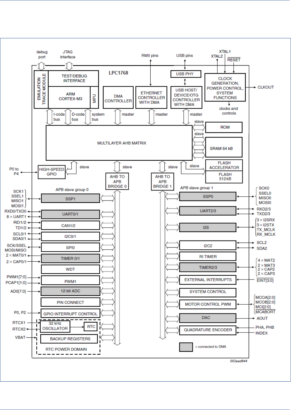
6.1.2 Block diagram
Fig 3. LPC1768 block diagram

ATOP Preliminary Specification © NXP B.V. 2012. All rights reserved.
Preliminary Specification Rev. 0.75 — 14th August 2012 14 of 42
NXP Semiconductors OM12001 (ATOP)
Telematics
6.1.3 Ethernet
Ethernet block supports bus clock rates of up to 100 MHz. The Ethernet block contains a
full featured 10 Mbit/s or 100 Mbit/s Ethernet MAC designed to provide optimized
performance through the use of DMA hardware acceleration. Features include a generous
suite of control registers, half or full duplex operation, flow control, control frames,
hardware acceleration for transmit retry, receive packet filtering and wake-up on LAN
activity. Automatic frame transmission and reception with scatter-gather DMA off-loads
many operations from the CPU.
The Ethernet block and the CPU share the ARM Cortex-M3 D-code and system bus
through the AHB-multilayer matrix to access the various on-chip SRAM blocks for
Ethernet data, control, and status information.
The Ethernet block interfaces between an off-chip Ethernet PHY using the Reduced MII
(RMII) protocol and the on-chip Media Independent Interface Management (MIIM) serial
bus.
6.1.4 USB
LPC1768 features an USB interface with a device and host controller with on-chip PHY.
6.1.4.1 USB device controller
The device controller enables Full Speed (12 Mbit/s) data exchange with a USB Host
controller. It consists of a register interface, serial interface engine, endpoint buffer
memory, and a DMA controller. The serial interface engine decodes the USB data stream
and writes data to the appropriate endpoint buffer. The status of a completed USB transfer
or error condition is indicated via status registers. An interrupt is also generated if
enabled. When enabled, the DMA controller transfers data between the endpoint buffer
and the on-chip SRAM.
6.1.4.2 USB host controller
The host controller enables full- and low-speed data exchange with USB devices attached
to the bus. It consists of a register interface, a serial interface engine, and a DMA
controller. The register interface complies with the OHCI specification.
6.1.5 CAN
6.1.5.1 Description
The Controller Area Network (CAN) is a serial communications protocol which efficiently
supports distributed real-time control with a very high level of security. Its domain of
application ranges from high-speed networks to low cost multiplex wiring. The CAN block
is intended to support multiple CAN buses simultaneously, allowing the device to be used
as a gateway, switch, or router among a number of CAN buses in industrial or automotive
applications.
6.1.5.2 Features
•Two CAN controllers and buses
•Data rates to 1 Mbit/s on each bus
•32-bit register and RAM access
•Compatible with CAN specification 2.0B, ISO 11898-1
ATOP Preliminary Specification © NXP B.V. 2012. All rights reserved.
Preliminary Specification Rev. 0.75 — 14th August 2012 15 of 42
NXP Semiconductors OM12001 (ATOP)
Telematics
•Global Acceptance Filter recognizes 11-bit and 29-bit receive identifiers for all CAN
buses
•Acceptance Filter can provide FullCAN-style automatic reception for selected
Standard Identifiers
•Full CAN messages can generate interrupts
6.1.6 Power saving modes
6.1.6.1 Peripheral and clock control
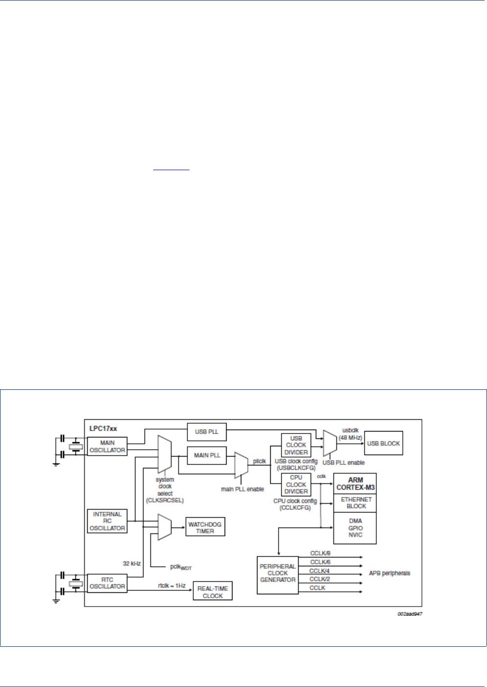
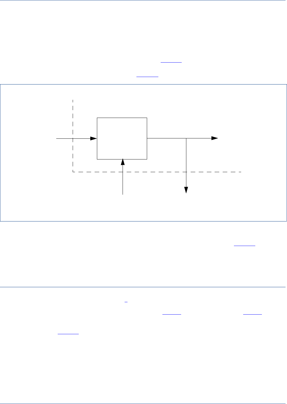
As shown in Figure 4, the CPU clock rate can also be controlled as needed by changing
clock sources, re-configuring PLL values, and/or altering the CPU clock divider value. This
allows a trade-off of power versus processing speed based on application requirements.
In addition, Peripheral Power Control allows shutting down the clocks to individual on-chip
peripherals, allowing fine tuning of power consumption by eliminating all dynamic power
use in any peripherals that are not required for the application.
The LPC1768 include three independent oscillators. These are the main oscillator, the
IRC oscillator, and the RTC oscillator. Each oscillator can be used for more than one
purpose as required in a particular application. Any of the three clock sources can be
chosen by software to drive the main PLL and ultimately the CPU.
Following reset, the LPC1768 will operate from the Internal RC oscillator until switched by
software. This allows systems to operate without any external crystal and the bootloader
code to operate at a known frequency. Main oscillator will be driven by an optional
external crystal on customer board. Its presence might be required if an accurate clock is
necessary, for instance for USB or HS CAN compliancy.
Fig 4. LPC1768 clock generation

ATOP Preliminary Specification © NXP B.V. 2012. All rights reserved.
Preliminary Specification Rev. 0.75 — 14th August 2012 16 of 42
NXP Semiconductors OM12001 (ATOP)
Telematics
6.1.6.2 Power modes
The LPC1768 support a variety of power control features. There are four special modes of
processor power reduction:
•Sleep
•Deep-sleep
•Power-down
•Deep power-down
The CPU clock rate may also be controlled as needed by changing clock sources,
reconfiguring PLL values, and/or altering the CPU clock divider value. This allows a
trade-off of power versus processing speed based on application requirements. In
addition, Peripheral Power Control allows shutting down the clocks to individual on-chip
peripherals, allowing fine tuning of power consumption by eliminating all dynamic power
use in any peripherals that are not required for the application. Each of the peripherals
has its own clock divider which provides even better power control.
Integrated PMU (Power Management Unit) automatically adjust internal regulators to
minimize power consumption during Sleep, Deep sleep, Power-down, and Deep
power-down modes.
The LPC1768 also implement a separate power domain to allow turning off power to the
bulk of the device while maintaining operation of the RTC and a small set of registers for
storing data during any of the power-down modes.
Sleep mode: When Sleep mode is entered, the clock to the core is stopped. Resumption
from the Sleep mode does not need any special sequence but re-enabling the clock to the
ARM core.
In Sleep mode, execution of instructions is suspended until either a Reset or interrupt
occurs. Peripheral functions continue operation during Sleep mode and may generate
interrupts to cause the processor to resume execution. Sleep mode eliminates dynamic
power used by the processor itself, memory systems and related controllers, and internal
buses.
Deep-sleep mode: In Deep-sleep mode, the oscillator is shut down and the chip receives
no internal clocks. The processor state and registers, peripheral registers, and internal
SRAM values are preserved throughout Deep-sleep mode and the logic levels of chip pins
remain static. The output of the IRC is disabled but the IRC is not powered down for a fast
wake-up later.
The RTC oscillator is not stopped because the RTC interrupts may be used as the
wake-up source. The PLL is automatically turned off and disconnected.
The Deep-sleep mode can be terminated and normal operation resumed by either a
Reset or certain specific interrupts that are able to function without clocks. Since all
dynamic operation of the chip is suspended, Deep-sleep mode reduces chip power
consumption to a very low value. Power to the flash memory is left on in Deep-sleep
mode, allowing a very quick wake-up.

ATOP Preliminary Specification © NXP B.V. 2012. All rights reserved.
Preliminary Specification Rev. 0.75 — 14th August 2012 17 of 42
NXP Semiconductors OM12001 (ATOP)
Telematics
Power-down mode: Power-down mode does everything that Deep-sleep mode does, but
also turns off the power to the IRC oscillator and the flash memory. This saves more
power but requires waiting for resumption of flash operation before execution of code or
data access in the flash memory can be accomplished.
Deep power-down mode: The Deep power-down mode can only be entered from the
RTC block. In Deep power-down mode, power is shut off to the entire chip with the
exception of the RTC module and the RESET pin. The LPC1768 can wake up from Deep
power-down mode via the RESET pin or an alarm match event of the RTC.
Wake-up interrupt controller: The Wake-up Interrupt Controller (WIC) allows the CPU to
automatically wake up from any enabled priority interrupt that can occur while the clocks
are stopped in Deep sleep, Power-down, and Deep power-down modes.
The WIC works in connection with the Nested Vectored Interrupt Controller (NVIC). When
the CPU enters Deep sleep, Power-down, or Deep power-down mode, the NVIC sends a
mask of the current interrupt situation to the WIC.This mask includes all of the interrupts
that are both enabled and of sufficient priority to be serviced immediately. With this
information, the WIC simply notices when one of the interrupts has occurred and then it
wakes up the CPU.
The WIC eliminates the need to periodically wake up the CPU and poll the interrupts
resulting in additional power savings.
6.1.7 RTC
The RTC on the LPC1768 is designed to have extremely low power consumption, i.e. less
than 1 µA. The RTC will typically run from the main chip power supply, conserving battery
power while the rest of the device is powered up. When operating from a battery, the RTC
will continue working down to 2.1 V. Battery power can be provided from a standard 3 V
Lithium button cell.
An ultra-low power 32 kHz oscillator will provide a 1 Hz clock to the time counting portion
of the RTC, moving most of the power consumption out of the time counting function.
The RTC contains a small set of backup registers (20 bytes) for holding data while the
main part of the LPC1768 is powered off.
The RTC includes an alarm function that can wake up the LPC1768 from all reduced
power modes with a time resolution of 1 s.
7. Application design-in information
7.1 Battery charging
OM12001 (ATOP) natively handles Lithium Ion battery technology.
There are 3 distinct modes for battery charging, depending on the battery voltage:
•trickling mode: In this mode, ATOP will detect whether battery is dead (i.e. voltage
drop as soon as a small current is applied). If that is not the case, a small current of 1
mA will be applied until the voltage is higher than 1.5V, and then ATOP will switch to
pre-charge mode
ATOP Preliminary Specification © NXP B.V. 2012. All rights reserved.
Preliminary Specification Rev. 0.75 — 14th August 2012 18 of 42
NXP Semiconductors OM12001 (ATOP)
Telematics
•precharge mode: Precharge mode is completely under HW control and will continue
until the battery voltage is high enough so that baseband can boot. During precharge,
ATOP will provide a 200 mA current. As SW is not yet booted, temperature will not be
controlled, i.e. precharge will occur even if battery is outside of advised range for a
battery
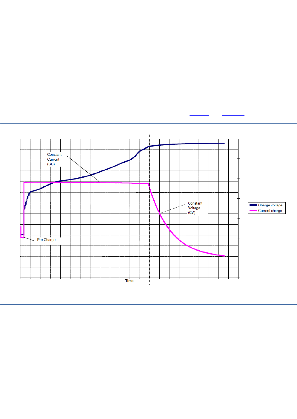
•fast charge: If battery level is higher than 3.1V (i.e. enough for baseband to boot) and
there is voltage on Vcharge for more than 10 ms, then OM12001 (ATOP) will switch to
SW charge mode. SW will initiate a fast charge with Constant Current - Constant
Voltage (CC-CV) method as described in Figure 5. It will stop when the current drawn
on the charger falls below 50 mA or whenever overvoltage/overcurrent is detected or
temperature is outside of allowed range (typically 0-50°C).
Limiting and dynamic values can be found in Table 4 and Table 2 6
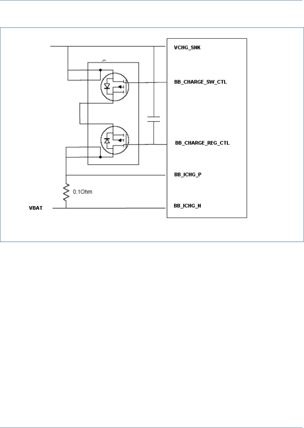
Figure 6 presents a typical implementation of the charging circuitry. A 0.1 Ohm resistor is
used as a shunt to measure charge current. 2 PMOS transistors are used respectively to
enable charging, avoid reverse leakage from battery to charger, and regulate current.
They should be properly dimensioned for power dissipation.
Fig 5. Constant Current - Constant Voltage charging method
ATOP Preliminary Specification © NXP B.V. 2012. All rights reserved.
Preliminary Specification Rev. 0.75 — 14th August 2012 19 of 42
NXP Semiconductors OM12001 (ATOP)
Telematics
Additionally other pins should be connected as follows:
•VBAT_SENSE_P must be connected to the battery
•VBAT_SENSE_N must be connected to ground
•BB_BAT_THERM must be connected to a 10 kOhm pull-down, or to the battery
thermistor
7.2 Application without rechargable battery
If no rechargable battery is used in the application, charging control pins must be
connected as follows:
•VCHG_SNK must be connected to ground
•BB_CHARGE_[SW|REG]_CTL must be left unconnected
•BB_ICHG_[P|N] must be connected together
•VBAT_SENSE_P must be connected to VBAT_SNK
•VBAT_SENSE_N must be connected to ground
•BB_BAT_THERM must be connected to a 10 kOhm pull-down
Fig 6. Charging circuitry
ATOP Preliminary Specification © NXP B.V. 2012. All rights reserved.
Preliminary Specification Rev. 0.75 — 14th August 2012 20 of 42
NXP Semiconductors OM12001 (ATOP)
Telematics
7.3 Current source
OM12001 (ATOP) handles internally all its voltage conversion. For Utility Processor, a
separate input, VBAT_MC_SNK, is used. Internally, a LDO, controlled by
VDD_3V0_SRC_ENA (active high, with internal pull-up), will convert it to the 3V required
by the Utility Processor. As described in Figure 7, the output of the LDO is also available
externally to power external component, up to a maximum of 100 mA can be drawn. Other
limiting values can be found in Tab l e 13.
7.4 RTC
MCU RTC is internally supplied by the output of the LDO described in Figure 7. It can also
be supplied by a separate battery such as a coin cell via VBAT_RTC_SNK so that RTC is
kept in case of power loss. If this feature is not required it is advised to connect
VBAT_RTC_SNK and VDD_3V0_SRC.
8. Application information
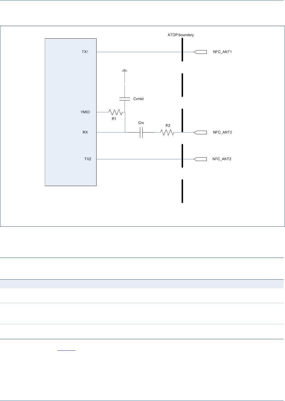
8.1 NFC antenna design3
For NFC antenna design, please refer to Ref. [6] for antenna design and Ref. [7] if
application requires to boost NFC signal.
Figure 8 describes the internal setup of NFC_ANT pins.
Fig 7. VDD_3V0 current source
OM12001 (ATOP)
VBAT_MC_SNK
VDD_3V0_SRC_ENA VDD_3V0_SRC
Utility processor
LDO
ATOP Preliminary Specification © NXP B.V. 2012. All rights reserved.
Preliminary Specification Rev. 0.75 — 14th August 2012 21 of 42
NXP Semiconductors OM12001 (ATOP)
Telematics
R1 = 1 K, R2 = 2.7 K, CRX = 1 nF, Cvmid = 100 NF
9. Recommended operating conditions
Table 7 presents in more details the tests performed to guarantee module lifetime.
Fig 8. Internal setup of NFC antennas
Table 2. Temperature
Allowed temperature range
Symbol Parameter Min Typ Max Unit Note
Module storage
temperature range
-40 85 °C Before final reflow, stored
in drypack
Module limited
operation temperature
range
-40 85 °C All functions, except for
NFC and Secure
processor
Module operating
temperature range
-25 85 °C

ATOP Preliminary Specification © NXP B.V. 2012. All rights reserved.
Preliminary Specification Rev. 0.75 — 14th August 2012 22 of 42
NXP Semiconductors OM12001 (ATOP)
Telematics
10. Limiting values
[1] Note this minimum voltage should take into account the voltage drop due to the high current during transmission, i.e. for a typical battery
with a drop of 200 mV, minimum voltage is 3.6V
[2] Occurs only during transmission slot (577 µs) in case of poor reception
[3] It is not mandatory to connect Vbat_rtc_pnx as internal connection is provided, unless it is required to keep application processor RTC
active when Vbat is disconnected
[1] Charge voltage should obviously be higher than Vbat. Voltage drop into external transistors and resistors should be taken into account
Table 3. Power supply
Symbol Parameter Min Typ Max Unit Note
Vbat_rf Battery voltage for
application processor
3.4[1] 4.2 4.8 V Voltage range allowed in
case of connection and
transmission to GSM network
Vbat_no_rf Battery voltage for
application processor
3.1 4.2 5.5 V Voltage range allowed
without connection to GMS
network (i.e. airplane mode)
Vbat_mc Battery voltage for
utility processor
3.1 4.2 5.5 V
Vbat_rtc_mc Battery voltage for
utility processor RTC
2.0 3.3 3.6 V
Vbat_rtc_bb Battery voltage for
application processor
RTC
2.0 3.0 3.15 V [3]
Ibat Battery current 1800[2] mA Peak current to be used to
dimension decoupling
capacitors (on VBAT_SNK)
Table 4. Battery charging
Handled by baseband integrated battery charging unit
Symbol Parameter Min Typ Max Unit Note
VCharge Charge voltage 3.2 4.8 7.5 V [1]
Ibat_empty Empty battery current 1 mA for VBAT_SNK < 1.5V
IPreCharge Pre-charge current 160 200 240 mA pre-charge current, i.e. for
VBAT_SNK < 3.35V
IFastCharge Fast charge current 200 1400 mA For VBAT_SNK > 3.35V,
Settable with 100mA steps,
with additional step at 450
mA
VFastCharge Fast Charge Voltage 3.45 4.2 5.5 V Settable with 50 mV step
between 3.45 to 4.9V and 2
additional points at 5.25 and
5.55V
VSW_CTL Maximum voltage allowed
on BB_CHARGE_SW_CTL
--V
BAT_SNK V
VSW_REG Maximum voltage allowed
on BB_CHARGE_SW_REG
--V
CHG_SNK V

ATOP Preliminary Specification © NXP B.V. 2012. All rights reserved.
Preliminary Specification Rev. 0.75 — 14th August 2012 23 of 42
NXP Semiconductors OM12001 (ATOP)
Telematics
[1] 5V tolerant pins, i.e. all I/O with MC prefix, except for oscillator IOs
[2] Vbat_mc must be present
[3] 3-state outputs go into 3-state mode when Vbat_mc is grounded
Table 5. Limiting values for micro-controller pins
Symbol Parameter Conditions Min Typ Max Unit
VIAmc Analog input voltage on ADC related pins -0.5 5.1 V
VImc Input voltage 5V tolerant I/O pins[1][2][3] -0.5 5.5 V
other I/O pins[2] -0.5 3.6 V
Vimc_xtal1 Input voltage for XTAL1 Internal oscillator input 0 - 1.8 V
Vomc_xtal2 Output voltage Internal oscillator output 0 - 1.8 V
Table 6. Limiting values for GSM baseband interfaces
SIM interface, analog audio and PCM interface
Symbol Parameter Conditions Min Typ Max Unit
VIbb Input voltage -0.4 3.2 V
IIbb Input current 20 mA
IObb Output current 20 mA
Table 7. Limiting values for GSM antennas
Due to their ESD protection implementation GSM antennas are DC grounded
Symbol Parameter Conditions Min Typ Max Unit
RIDC Input resistance DC voltage 1.96
ImaxDC Maximum current DC current 140 mA
Load mismatch for all phase angles, before
permanent degradation or
damage
20:1 VSWR
Spurious (low bands) for all phase angles, no parasitic
oscillations > -30 dbm
12:1 VSWR
Spurious (high bands) for all phase angles, no parasitic
oscillations > -30 dbm
8:1 VSWR
Table 8. Limiting values for GPS passive antenna input
Due to its ESD protection implementation GPS antenna is DC grounded
Symbol Parameter Conditions Min Typ Max Unit
RIDC Input resistance DC voltage 0.14
ImaxDC Maximum current DC current 540 mA
Table 9. Limiting values for GPS active antenna input and antenna bias
Symbol Parameter Conditions Min Typ Max Unit
VmaxDC Maximum voltage DC voltage -25 25 V
ImaxDC Maximum current DC current 70 mA

ATOP Preliminary Specification © NXP B.V. 2012. All rights reserved.
Preliminary Specification Rev. 0.75 — 14th August 2012 24 of 42
NXP Semiconductors OM12001 (ATOP)
Telematics
11. Characteristics
12. Static characteristics
12.1 Pins
[1] Only allowed for a short time period
Table 10. Characteristics for micro-controller pins
Symbol Parameter Conditions Min Typ Max Unit
VOmc Output voltage 0 3.0 V
VIHmc High level input voltage 2.0 V
VILmc Low level input voltage 0.8 V
IILmc Low level input current VI=0 V; no pull-up 3 µA
IIHmc High level input current VI=3.0 V; no pull-down 3 µA
VOHmc High level output voltage IOHmc=-4 mA 2.6 V
VOLmc Low level output voltage IOLmc=-4 mA 0.4 V
IOLmc Low level output current VOL=0.4 V 4 mA
IOHmc High level output current VOH=2.6 V -4 mA
IOLSmc Low level short circuit output current VI=3.0 V[1] -45 mA
IOHSmc High level short circuit output
current
VI=0 V[1] 50 mA
IOZmc Off state output current VO=3.0 or 0V; no pull-up/down 3 µA
Ipdmc Pull-down current VI=5 V 10 50 150 µA
Ipumc Pull-up current VI=0 V; -15 -50 -85 µA
3.0 <VI<5 V 0 0 0 µA
IIlatchmc I/O latchup current -1.5<VI<4.5V; Tj<125°C 100 mA
Table 11. Characteristic for baseband digital interface
namely SIM interface, PCM, UART, JTAG
Symbol Parameter Conditions Min Typ Max Unit
VIHbb High level input voltage 2.4 V
VILbb Low level input voltage 0.4 V
IIHbb High level input current -10 +10 µA
IILbb Low level input current -10 +10 µA
VOHbb High level output voltage 2.7 V
VOLbb Low level output voltage 0.1 V
Rpubb Pull-up resistance 100 k
Rpdbb Pull-down resistance 100 k
CiLbb Input capacitance 0.1 pF

ATOP Preliminary Specification © NXP B.V. 2012. All rights reserved.
Preliminary Specification Rev. 0.75 — 14th August 2012 25 of 42
NXP Semiconductors OM12001 (ATOP)
Telematics
12.2 Current sources
[1] Voltage is dynamically controlled to reduce power consumption when SIM card is not accessed
12.3 Voltage references
Table 12. Characteristic for GPS digital interface
namely JTAG and GPS_UART2_RXD
Symbol Parameter Conditions Min Typ Max Unit
VIHbb High level input voltage 1.7 V
VILbb Low level input voltage 0.7 V
IIHbb High level input current -10 +10 µA
IILbb Low level input current -10 +10 µA
VOHbb High level output voltage 1.7 V
VOLbb Low level output voltage 0.7 V
Rpubb Pull-up resistance 60 k
Rpdbb Pull-down resistance 75 k
IOOutput current 6 mA
Table 13. Vdd_3v0_src current source
Can be used to supply external components
Symbol Parameter Min Typ Max Unit Note
Vdd_3v0 Output voltage 2.9 3.0 3.1 V For Tj=-40 to 125°C
Ivdd3v0_max maximum current 100 mA
Vdd_3v0 Load regulation 0.0008 0.004 %/mA
Vdd_3v0 Line regulation -0.1 0.1 %/V For Vbat variation
ton_dd_3v0 Turn on time 240 µS Measured from the time
VDD_3V0_SRC_ENA exceeds 1.4V
Table 14. Vsim_src current source
To be only used to supply SIM cards[1]
Symbol Parameter Min Typ Max Unit Note
Vsim_src Output voltage 2.75 2.90 3.00 V Appropriate SIM card voltage is
automatically detected and selected
by the software
1.65 1.80 1.95 V
Isim_src Output current 80 mA Full power mode
3 mA Sleep mode
Vo/VoRelative output voltage 50 mV/V For Vbat variation
ton_dd_3v0 Settling time 10 µS from power-down
Table 15. Vio_ref voltage reference
To be used as a reference to connect to BB_* test pins (JTAG)
Symbol Parameter Min Typ Max Unit Note
Vio_ref Output voltage 2.70 2.80 2.95 V
Vo/VoRelative output voltage 50 mV/V For Vbat variation

ATOP Preliminary Specification © NXP B.V. 2012. All rights reserved.
Preliminary Specification Rev. 0.75 — 14th August 2012 26 of 42
NXP Semiconductors OM12001 (ATOP)
Telematics
[1] For VBAT_SNK = 3.1V
[2] For VBAT_SNK = 3.6V
[3] For VBAT_SNK = 5.5V
12.4 Clocks
Table 16. Vperm_ref voltage reference
To be used as a reference to connect to BB_* functional pins
Symbol Parameter Min Typ Max Unit Note
Vperm_ref Output voltage 2.82[1] 3.0[2] 3.18[3] V Follows VBAT_SNK if <3V
Table 17. Vadc_ref voltage reference
used as power supply reference for internal ADCs
Symbol Parameter Min Typ Max Unit Note
Vadc_ref Output voltage 2.9 3.0 3.1 V For Tj=-40 to 125°C
V/V Line regulation -0.1 0.1 %/V For Vbat variation
Table 18. 1PPS
This pulse is synchronized with GPS system clock
Symbol Parameter Min Typ Max Unit Note
Pulse width 125 µs
Jitter -50 3 50 ns Stationary and receiving 4 or more
satellites
Table 19. BB_EXT_CLK
This clock is coupled to GSM network
Symbol Parameter Min Typ Max Unit Note
fbb_ext_clk frequency 26/N MHz for N= 1, 2, ..., 8
156/M MHz for M=9, 10, .., 16
f/fofrequency drift 0.7 1 ppm
Table 20. Micro-controller clock
External crystal required for high speed CAN, for all other purposes, internal RC oscillator is sufficient
Symbol Parameter Min Typ Max Unit Note
fmc_xtal Crystal frequency 1 - 24 MHz In case of externally oscillator, connected
to MC_XTAL_(1|2)
V(rms)mc_xtal Oscillation amplitude 0.2 - V (RMS)
thmc_xtal Clock High time tcycle x 0.4 - ns
tlmc_xtal Clock Low time tcycle x 0.4 - ns
trmc_xtal Clock rise time 5 ns
tfmc_xtal Cock fall time 5 ns
fmc_ircl Oscillator frequency 3.96 4 4.04 MHz Frequency of internal RC oscillator

ATOP Preliminary Specification © NXP B.V. 2012. All rights reserved.
Preliminary Specification Rev. 0.75 — 14th August 2012 27 of 42
NXP Semiconductors OM12001 (ATOP)
Telematics
13. Dynamic characteristics
13.1 Power consumption
All measured current consumption have been measured at 25°C with a power supply at
3.7V
[1] No peripherals enabled
[2] Wake-up can be initiated by event on RTC, CAN, USB and most GPIOs
[3] If a separate power source such as coin cell battery is connected to VBAT_RTC_SNK and no power is supplied via VBAT_MC_SNK
[1] Leakage currents are included in Table 23
[1] Network dependent, assumes a typical 7s radio measurement plus 0.5s network inscription
[2] BS_PA_MFRMS = 9, i.e. paging from network will be checked every 2100 ms
[3] BS_PA_MFRMS = 5, i.e. paging from network will be checked every 1175 ms. This is typically the setting used by most mobile operators
Table 21. Utility processor power consumption
Includes LDO
Symbol Parameter Min Typ Max Unit Note
Cortex M3 at 12 MHz 7 7[1] mA at 25°C, code
while(1){}
Cortex M3 at 100 MHz 42[1] mA
Powerdown mode 150 µA [2]
RTC active 1 µA backup registers saved [3]
Table 22. Application processor consumption characteristics
Baseband ARM and memories power consumption additionally to GSM/GPRS function
Symbol Parameter Min Typ Max Unit Note
Application processor 0[1] 20 60 mA
Table 23. Communication coprocessor consumption characteristics
Covers baseband RF frontend as well as memories (PSRAM and flash)
Symbol Parameter Min Typ Max Unit Note
complete GSM function
network attachment
115[1] µAh Energy consumption
equivalent to 300s of idle
mode
complete GSM function
active in idle mode
1.085[2] 1.31[3] 2.05[4] mA Average consumption,
assuming typical setting
for mobile network. Peak
consumption for
GSM/GPRS at maximum
power can reach up to
1600 mA during transfer
slots (577 µs)
complete GSM function
during voice call
79[5] 114[6] 220[7] mA
complete GPRS
function during data
transfer (Class 10:
2T+3RX)
140[5] 205[6] 400[7] mA
complete GSM function
in sleep mode
600 µA GSM function active
complete GSM function
leakage current
50 µA

ATOP Preliminary Specification © NXP B.V. 2012. All rights reserved.
Preliminary Specification Rev. 0.75 — 14th August 2012 28 of 42
NXP Semiconductors OM12001 (ATOP)
Telematics
[4] BS_PA_MFRMS = 2, i.e. paging from network will be checked every 470 ms
[5] PCL = 19, i.e. 4.9db amplification for GSM900
[6] PCL = 7, i.e. 29.2db amplification for GSM900
[7] PCL = 5, i.e. 33.1 db amplification for GSM900
13.2 Battery charging
Table 24. Security processor power consumption
Symbol Parameter Min Typ Max Unit Note
Function switched off 0 µA included in NFC
coprocessor
Function active 6 mA
Table 25. NFC coprocessor power consumption
Covers NFC and SMX
Symbol Parameter Min Typ Max Unit Note
Function switched off 2 µA
Power down 35 µA RF field detection on
Function active 30 mA
function active with RF
transmission ongoing
90 130 mA
Table 26. Battery charging
Measured at 3.7V, 25°C
Symbol Parameter Min Typ Max Unit Note
Battery overvoltage
detection
60 90 130 mV Battery voltage in excess of
VFAST above which fast charge
is automatically disabled
Battery overcurrent
detection
190 210 230 mA Battery current in excess of
programmed current above
which fast charge is automatically
disabled
Fast charge stop 50 mA
VOreg/VOreg Relative regulator output
voltage variation
-1 +1 %
IOreg/IOreg Relative regulator output
current variation
-12 +12 %
Iqvchg Quiescent current drawn
from VCHG_SNK
3mA
Iqbb_ighgp Quiescent current drawn
from BB_ICHG_P
40 µA during charge
Iqbb_ighgn Quiescent current drawn
from BB_ICHG_P
60 µA during charge
Iqvbat_snk Quiescent current drawn
from VBAT_SENSE_[P|N]
200 µA during charge

ATOP Preliminary Specification © NXP B.V. 2012. All rights reserved.
Preliminary Specification Rev. 0.75 — 14th August 2012 29 of 42
NXP Semiconductors OM12001 (ATOP)
Telematics
14. Thermal characteristics
14.1 Internal heater2
As described in Tab l e 2 , OM12001 (ATOP) can operate between -40 and +85°C, except
for the NFC and Security processor which are limited to a -25 to +85°C temperature
range.
To ensure that operating range can be rapidly reached, an internal heater is available to
heat-up the device.
The internal heater is controlled by internal micro-controller pin P2.5 (active high).
Internal temperature should be monitored when heater is used. It must not be enabled for
more than a few seconds if current temperature is greater than 25°C as otherwise there is
a risk of destruction for the heater.
14.2 Internal temperature sensor
OM12001 (ATOP) includes an internal temperature sensor. This sensor is used by GSM
baseband to tune its VCXO to achieve network lock-on but is also accessible to the
internal micro-controller which can use it to.
Internal micro-controller (LPC1768) has also access to this sensor to adapt its behavior to
conditions, i.e enabling internal heater in case of low temperature, ... .
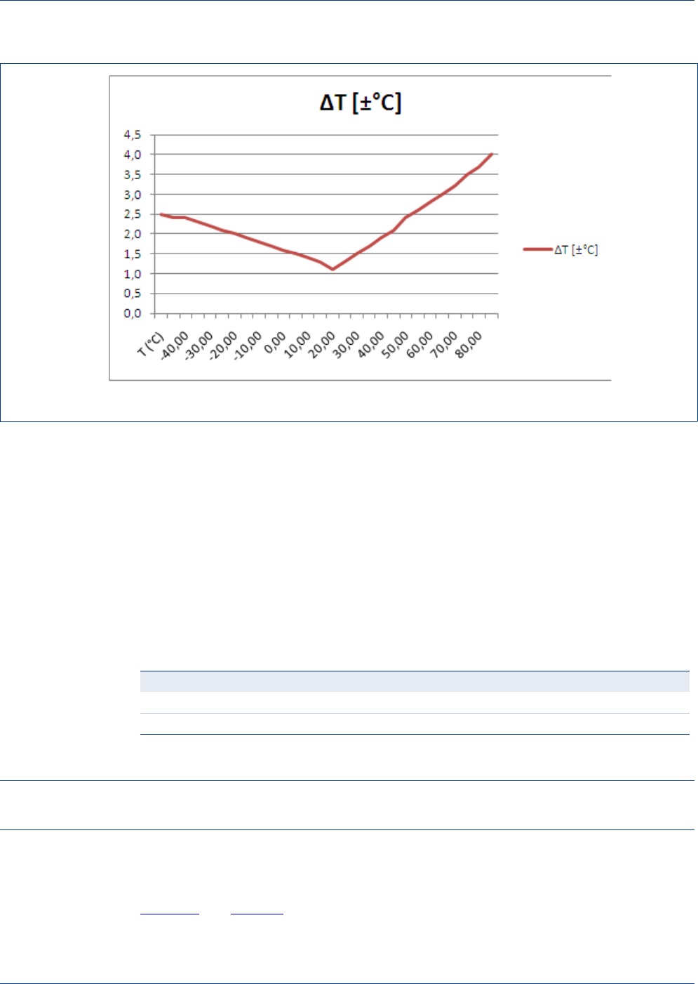
Figure 9 presents accuracy of the internal temperature measurement depending on
ambient temperature.
Table 27. Internal heater characteristics
Symbol Parameter Min Typ Max Unit Note
Current drawn 500 600 700 mA
Power dissipated 1600 2500 3400 mW Dependant on Vbat
ATOP Preliminary Specification © NXP B.V. 2012. All rights reserved.
Preliminary Specification Rev. 0.75 — 14th August 2012 30 of 42
NXP Semiconductors OM12001 (ATOP)
Telematics
14.3 Battery temperature sensor
To improve lifetime, it is recommended to avoid charging batteries, outside of the
temperature range specified by their manufacturers, typically 0 to 50°C.
For Lithium-Ion battery, the charger circuit inside OM12001 (ATOP) will use by default the
internal temperature sensor. However, in some cases, depending on implementation, it
can be expected the temperature of the battery will be significantly different from module
temperature. It is then recommended to use a battery with internal sensor. OM12001
(ATOP) supports the use of an external thermistor dedicated to battery.
Note that even if a separate thermistor is not used, this input is used to detect battery
presence.
15. Handling information
16. Soldering
OM12001 (ATOP) is a laminate based module with a metal cover and a Land Grid Array
(LGA) at the bottom side of the product. The OM12001 (ATOP) can be assembled using a
standard Surface Mount Technology (SMT) reflow process in a convection oven.
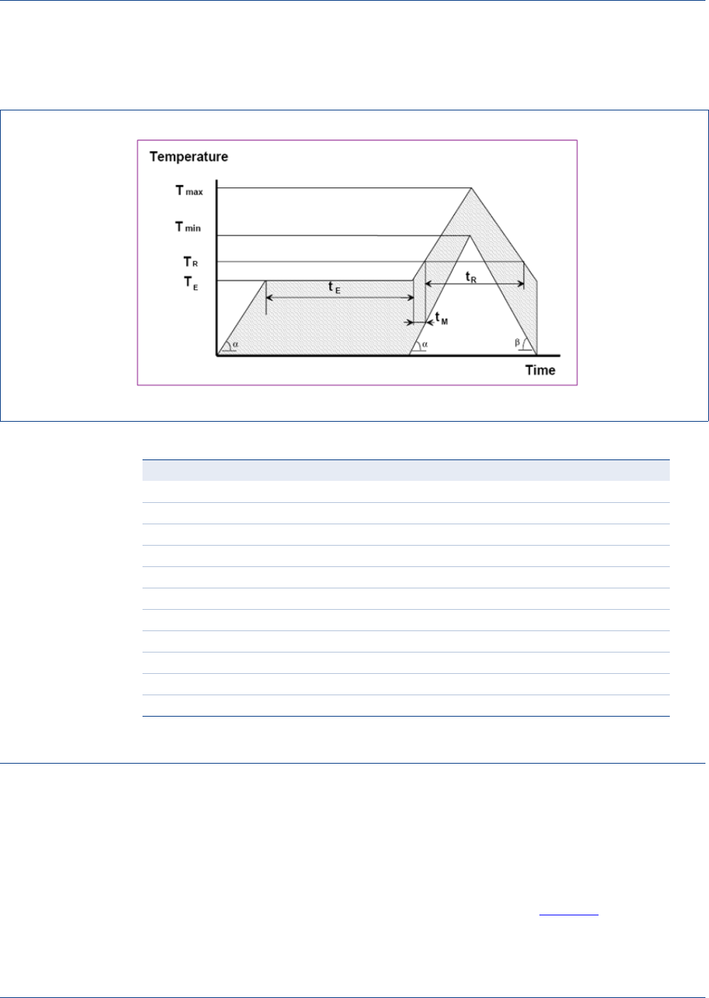
Figure 10 and Table 29I indicate the maximum and minimum limits of the solder profile.
The applied profile has to fit within these limits.
Fig 9. Internal temperature accuracy
Table 28. Battery temperature sensor
Symbol Parameter Min Typ Max Unit
Rthermin Internal pull-up 10 k
Rtol input resistor tolerance accuracy -1 1 %
ATOP Preliminary Specification © NXP B.V. 2012. All rights reserved.
Preliminary Specification Rev. 0.75 — 14th August 2012 31 of 42
NXP Semiconductors OM12001 (ATOP)
Telematics
It is recommended to use a standard no-clean SAC solder paste for a lead free assembly
process.
17. Mounting
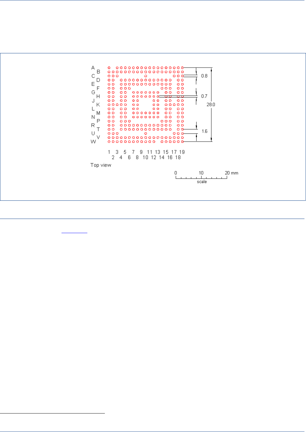
17.1 PCB layout
The PCB footprint design is a copy of the metal LGA pattern at the bottom side of the
ATOP package.
17.2 Stencil design
The dimensions of the solder stencil apertures can be found in Figure 11.
In general there are 2 aperture sizes applied for the stencil:
•0.7 mm diameter for the inner pads5
Fig 10. Reflow profile
Table 29. Reflow profile parameters
Symbol Parameter Min Unit
Temperature gradient (ramp-up) < 3 °C/s
Temperature gradient (cool-down) < 5 °C/s
TEPreheat (soak) temperature 150 to 200 °C
tEPreheat time 60 to 180 s
tMTime to melting 6 to 35 s
TRReflow temperature > 217 °C
tRReflow time 60 to 150 s
TMin Minimum peak temperature 235 °C
TMax Maximum peak temperature 260 °C
Maximum time above 250°C 10 s
Maximum time 25°C to peak temperature 8 mn
ATOP Preliminary Specification © NXP B.V. 2012. All rights reserved.
Preliminary Specification Rev. 0.75 — 14th August 2012 32 of 42
NXP Semiconductors OM12001 (ATOP)
Telematics
•0.8 mm for the outer pads
The recommendation for the stencil thickness is 150 µm.
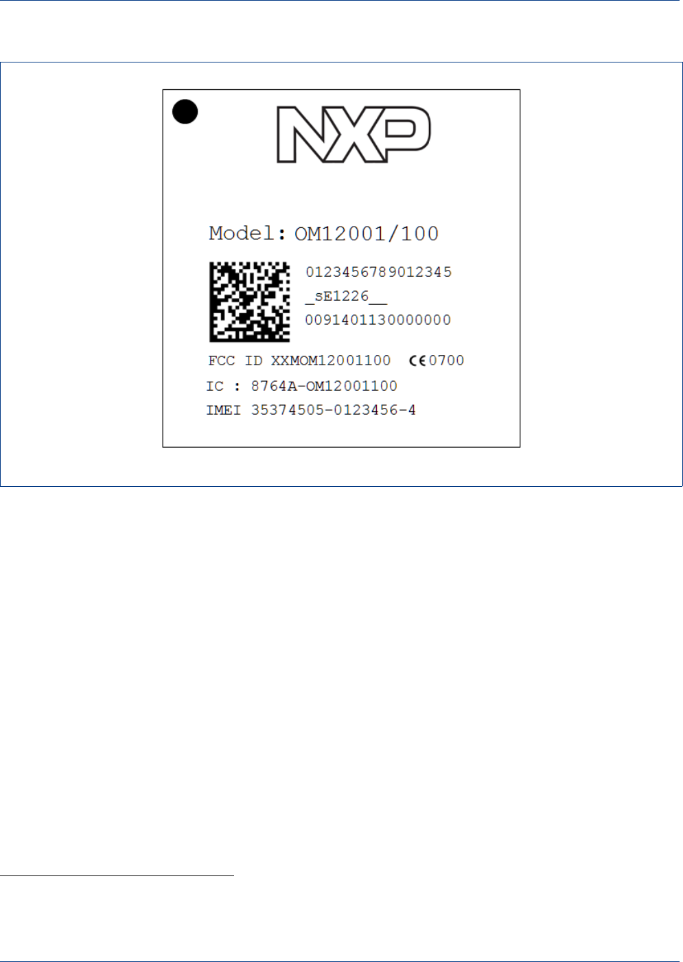
18. Marking
Figure 12 shows label present on the module.
5.G7-G13, H7-H13, J7, J8, J12, J13, K7, K8, K12, K13, L7, L8, L12, L13, M7-M13, N7-N13
Fig 11. Stencil design
ATOP Preliminary Specification © NXP B.V. 2012. All rights reserved.
Preliminary Specification Rev. 0.75 — 14th August 2012 33 of 42
NXP Semiconductors OM12001 (ATOP)
Telematics
Labelling can be decoded as follows:
•First line: Product name, ie OM12001/100 or OM12001/000
•Second line: Serial number
•Third line: Production info, including production site, RHF-2006 indicator6, date code
•Fourth line: BOM number
•Fifth line: FCC ID, ie XXMOM12001100 or XXMOM12001000 and Notified body for
CE certification
•Sixth line: IC ID, ie 8764A-OM12001100 or 8764A-OM12001000
•Seventh line: IMEI
DataMatrix 2D barcode includes the following information:
•Serial number
•EMS Internal product code
•Date code
•Product name, ie OM12001/100 or OM12001/000
•IMEI Type Allocation Code (TAC) iteration number7
Fig 12. OM12001/100 labelling
6. E standing for Exempted, ie. incorporates product containing exempted Lead that do contain Halogens/Antimony. For example
products with eutectic solder die-attach (HSOP/SIL-P) packages and glass-diodes containing Lead
7. 1 stands for a TAC value of 35374505 for OM12001. IMEI can be computed by concatenating TAC, the 6 last digits of serial
number and Check Digit, (CD) computed with Luhn formula

ATOP Preliminary Specification © NXP B.V. 2012. All rights reserved.
Preliminary Specification Rev. 0.75 — 14th August 2012 34 of 42
NXP Semiconductors OM12001 (ATOP)
Telematics
19. Packing information
OM12001 (ATOP) modules are packed in trays. Before packing and shipping, trays have
been dry baked for 16 hours at 125°C, according to IPC/JEDEC J-Std-033B.1.
OM12001 (ATOP) has been tested according to IPC/JEDEC J-STD 020D and is classified
as Moisture Sensitivity Level 3 (MSL3).
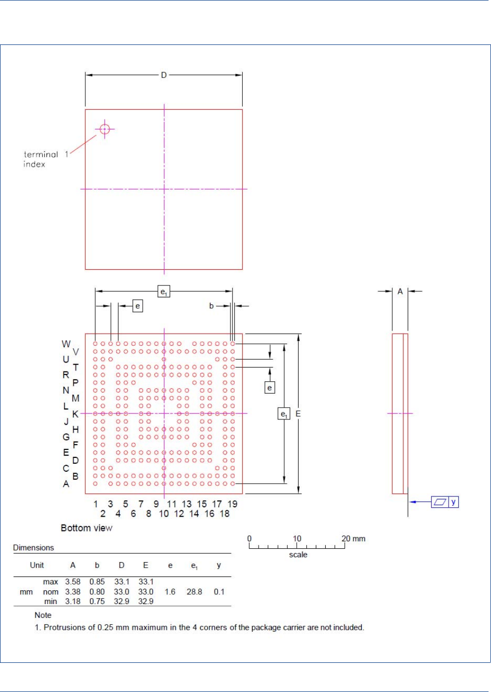
20. Package outline
ATOP presents itself as a 33x33x3.35 mm module. Ball size is 0.8 mm with a 1.6mm pitch.
ATOP Preliminary Specification © NXP B.V. 2012. All rights reserved.
Preliminary Specification Rev. 0.75 — 14th August 2012 35 of 42
NXP Semiconductors OM12001 (ATOP)
Telematics
Fig 13. OM12001 (ATOP) package outline and dimensions

ATOP Preliminary Specification © NXP B.V. 2012. All rights reserved.
Preliminary Specification Rev. 0.75 — 14th August 2012 36 of 42
NXP Semiconductors OM12001 (ATOP)
Telematics
21. Support information
For support, please contact support.telematics@nxp.com
22. Test information
For production and end of line testing the following tools will be provided:
•SW tools to interface to module:
–parameters setting (e.g. battery settings, ...)
–file download
–flash update
23. Safety instructions
OM12001 (ATOP) is a class A digital device marketed for use in a commercial, industrial
or business environment.
It has been tested to be conform to FCC as well as to R&TTE Articles 3.1(a) and (b),
safety and EMC respectively, and relevant Article 3.2 requirements using NXP reference
board. The manufacturer of the final product integrating OM12001 (ATOP) must assess its
equipment against the Essential requirements of the R&TTE and FCC Directives
OM12001 (ATOP) is compliant with the following standards:
•Mandatory european standards
–R&TTE Article 3.1a: Electrical safety (EN60950)
–R&TTE Article 3.1a: SAR (EN62209-1): MPE calculation as distance > 20 cm
–R&TTE Article 3.1b: EMC (EN301489-1 and -7 for GSM, EN301489-3 V1.4.1,
EN300440-2 for NFC and GPS)
–R&TTE Article 3.2: Radiated RF (EN301511 for GSM, EN302291-1-2 V1.1.1 for
NFC and GPS)
–Notified Body opinion according to Annex IV: Evaluation of compliance with
essential requirements
•Mandatory US and Canadian standards
–FCC EMC: part 15B
–FCC RF: part 24 for PCS1900, part 22 for GSM850, part 15.225 for GPS and NFC
–FCC certificate from Telecom Certification body
•Voluntary certification
–Global Certification Forum (GCF), including field tests
–PCS-1900 Type Certification Review Board (PTCRB)
Reports are available upon requests

ATOP Preliminary Specification © NXP B.V. 2012. All rights reserved.
Preliminary Specification Rev. 0.75 — 14th August 2012 37 of 42
NXP Semiconductors OM12001 (ATOP)
Telematics
SAR according to EN 62209-1 has not been checked and replaced by MPE calculation,
hence the antenna(s) used in the final application must be installed to provide a
separation distance of at least 20 centimeters from all persons and must not be co-located
or operating in conjunction with any other antenna or transmitter. Additionally, for FCC
compliance, the system antenna(s) gain must not exceed 2.24 dBi for mobile and fixed or
mobile operating configurations.
Manufacturer of the final product using OM12001 (ATOP) will have to provide instructions
for antenna installation and transmitter operating conditions to satisfy to RF exposure
compliance.
Manufacturer of the final product using OM12001 (ATOP) should take care that OM12001
(ATOP) is always within the operating limits (such as temperature, power supply, …)
described in the present document, in particular it must be supplied by a limited power
source according to EN 60950-1.
Physically, the clearance and creepage distances required by the end product must be
withheld when the module is installed. The cooling of the end product shall not negatively
be influenced by the installation of the module.
Manufacturers of devices incorporating this module are advised to clarify any regulatory
questions and to have their complete product tested and approved for R&TTE, FCC
compliance and all relevant regulations.
23.1 FCC DQG,CODEHO
If the FCC and IC IDs are not visible when the module is installed inside the host
device, then the outside of the device into which the module is installed must also
display a label referring to the enclosed module. This exterior label can use wording
such as the following: or “Contains FCC ID: XXMOM12001000 or XXMOM12001100.”
And “Contains IC : 8764A-OM12001000 or 8764A-OM12001100.” Any similar
wording that expresses the same meaning may be used.

ATOP Preliminary Specification © NXP B.V. 2012. All rights reserved.
Preliminary Specification Rev. 0.75 — 14th August 2012 38 of 42
NXP Semiconductors OM12001 (ATOP)
Telematics
Intentionally left blank.

ATOP Preliminary Specification © NXP B.V. 2012. All rights reserved.
Preliminary Specification Rev. 0.75 — 14th August 2012 39 of 42
NXP Semiconductors OM12001 (ATOP)
Telematics
24. Appendix
25. Abbreviations
Table 30. Abbreviations
Acronym Description
ADC Analog to Digital Converter
AES Advanced Encryption Standard
AHB AMBA High Performance Bus
ATOP Automotive Telematic On-board unit Platform
CLK Clock
CPU Central Processing Unit
DAC Digital to Analog Converter
DCS Digital Cellular System
DES Data Encryption Standard
DMA Direct Memory Access
DPA Differential Power Analysis
DSP Digital Signal Processor
EEPROM Electrically Erasable Programmable Read Only Memory
GP General Purpose
GPIO General Purpose Input Output
IF Intermediate Frequency
IRQ Interrupt ReQuest
JCOP Java Card Open Platform
LDO Low DropOut
LNA Low Noise Amplifier
MCU Micro-Controller Unit
MIDP Mobile Information Device Profile
NFC Near Field Communication
NiMH Nickel Metal Hybrid
OBU On Board Unit
OS Operating System
OTP One Time Programmable
PA Power Amplifier
PCB Printed Circuit Board
PCM Pulse Code Modulation
PKI Public Key Infrastructure
PLL Phase Locked Loop
PWM Pulse Width Modulation
RF Radio Frequency
ROM Read Only Memory

ATOP Preliminary Specification © NXP B.V. 2012. All rights reserved.
Preliminary Specification Rev. 0.75 — 14th August 2012 40 of 42
NXP Semiconductors OM12001 (ATOP)
Telematics
26. Glossary
<term> — <definition>
27. References
[1] ZVEI - Zentralverband Elektrotechnik- und Elektronikindustrie e.V. —
http://www.zvei.org/fachverbaende/electronic_components_and_systems/robustnes
s_validation/druckansicht.html?type=1
[2] LPC1768 datasheet —
http://www.nxp.com/documents/data_sheet/LPC1769_68_67_66_65_64_63.pdf
[3] LPC1768 user manual —
http://www.nxp.com/documents/user_manual/UM10360.pdf
[4] LPC1768 errata sheet —
http://www.nxp.com/documents/errata_sheet/ES_LPC176X.pdf
[5] LPC1768 web page —
http://www.nxp.com/products/microcontrollers/cortex_m3/lpc1700/LPC1768FET100
.html#overview
[6] AN1445 Antenna design guide for MFRC52x, PN51x, PN53x
AN1444 RF Design Guideplus Excel Calculation —
http://www.nxp.com/documents/application_note/AN1445_An1444.zip
[7] AN1425 RF Amplifier for NFC Reader IC's
AN166510 Amplifier antenna matching calculation (Excel) —
http://www.nxp.com/documents/application_note/AN1425_AN166510.zip
RSA A public-key encryption technology developed by RSA Data Security, Inc. The
acronym stands for Rivest, Shamir, and Adelman, the inventors of the
technique
RTC Real Time Clock
RTOS Real Time Operating System
SAW Surface Acoustic Wave
SIM Subscriber Identification Module
SNR Signal to Noise Ratio
SPA Simple Power Analysis
SPI Serial Peripheral Interface
TCXO Temperature Controlled Crystal Oscillator
UART Universal Asynchronous Receiver Transmitter
Table 30. Abbreviations …continued
Acronym Description

ATOP Preliminary Specification © NXP B.V. 2012. All rights reserved.
Preliminary Specification Rev. 0.75 — 14th August 2012 41 of 42
NXP Semiconductors OM12001 (ATOP)
Telematics
28. Legal information
28.1 Definitions
Draft — The document is a draft version only. The content is still under internal review and subject to formal approval, which may
result in modifications or additions. NXP Semiconductors does not give any representations or warranties as to the accuracy or
completeness of information included herein and shall have no liability for the consequences of use of such information.
Short data sheet — A short data sheet is an extract from a full data sheet with the same product type number(s) and title. A
short data sheet is intended for quick reference only and should not be relied upon to contain detailed and full information. For
detailed and full information see the relevant full data sheet, which is available on request via the local NXP Semiconductors
sales office. In case of any inconsistency or conflict with the short data sheet, the full data sheet shall prevail.
Product specification — The information and data provided in a Product data sheet shall define the specification of the product
as agreed between NXP Semiconductors and its customer, unless NXP Semiconductors and customer have explicitly agreed
otherwise in writing. In no event however, shall an agreement be valid in which the NXP Semiconductors product is deemed to
offer functions and qualities beyond those described in the Product data sheet.
28.2 Disclaimers
Limited warranty and liability — Information in this document is believed to be accurate and reliable. However, NXP
Semiconductors does not give any representations or warranties, expressed or implied, as to the accuracy or completeness of
such information and shall have no liability for the consequences of use of such information.
In no event shall NXP Semiconductors be liable for any indirect, incidental, punitive, special or consequential damages (including
- without limitation - lost profits, lost savings, business interruption, costs related to the removal or replacement of any products or
rework charges) whether or not such damages are based on tort (including negligence), warranty, breach of contract or any other
legal theory.
Notwithstanding any damages that customer might incur for any reason whatsoever, NXP Semiconductors’ aggregate and
cumulative liability towards customer for the products described herein shall be limited in accordance with the Terms and
conditions of commercial sale of NXP Semiconductors.
Right to make changes — NXP Semiconductors reserves the right to make changes to information published in this document,
including without limitation specifications and product descriptions, at any time and without notice. This document supersedes
and replaces all information supplied prior to the publication hereof.
Suitability for use — NXP Semiconductors products are not designed, authorized or warranted to be suitable for use in
medical, military, aircraft, space or life support equipment, nor in applications where failure or malfunction of an NXP
Semiconductors product can reasonably be expected to result in personal injury, death or severe property or environmental
damage. NXP Semiconductors accepts no liability for inclusion and/or use of NXP Semiconductors products in such equipment
or applications and therefore such inclusion and/or use is at the customer’s own risk.
Applications — Applications that are described herein for any of these products are for illustrative purposes only. NXP
Semiconductors makes no representation or warranty that such applications will be suitable for the specified use without further
testing or modification.
NXP Semiconductors does not accept any liability related to any default, damage, costs or problem which is based on a
weakness or default in the customer application/use or the application/use of customer’s third party customer(s) (hereinafter both
referred to as “Application”). It is customer’s sole responsibility to check whether the NXP Semiconductors product is suitable
and fit for the Application planned. Customer has to do all necessary testing for the Application in order to avoid a default of the
Application and the product. NXP Semiconductors does not accept any liability in this respect.
Limiting values — Stress above one or more limiting values (as defined in the Absolute Maximum Ratings System of
IEC 60134) will cause permanent damage to the device. Limiting values are stress ratings only and (proper) operation of the
device at these or any other conditions above those given in the Recommended operating conditions section (if present) or the
Characteristics sections of this document is not warranted. Constant or repeated exposure to limiting values will permanently and
irreversibly affect the quality and reliability of the device.
Terms and conditions of commercial sale — NXP Semiconductors products are sold subject to the general terms and
conditions of commercial sale, as published at http://www.nxp.com/profile/terms, unless otherwise agreed in a valid written
individual agreement. In case an individual agreement is concluded only the terms and conditions of the respective agreement
shall apply. NXP Semiconductors hereby expressly objects to applying the customer’s general terms and conditions with regard
to the purchase of NXP Semiconductors products by customer.
No offer to sell or license — Nothing in this document may be interpreted or construed as an offer to sell products that is open
for acceptance or the grant, conveyance or implication of any license under any copyrights, patents or other industrial or
intellectual property rights.
Export control — This document as well as the item(s) described herein may be subject to export control regulations. Export
might require a prior authorization from national authorities.
Quick reference data — The Quick reference data is an extract of the product data given in the Limiting values and
Characteristics sections of this document, and as such is not complete, exhaustive or legally binding.

ATOP Preliminary Specification © NXP B.V. 2012. All rights reserved.
Preliminary Specification Rev. 0.75 — 14th August 2012 42 of 42
NXP Semiconductors OM12001 (ATOP)
Telematics
Non-automotive qualified products — Unless this data sheet expressly states that this specific NXP Semiconductors product
is automotive qualified, the product is not suitable for automotive use. It is neither qualified nor tested in accordance with
automotive testing or application requirements. NXP Semiconductors accepts no liability for inclusion and/or use of
non-automotive qualified products in automotive equipment or applications.
In the event that customer uses the product for design-in and use in automotive applications to automotive specifications and
standards, customer (a) shall use the product without NXP Semiconductors’ warranty of the product for such automotive
applications, use and specifications, and (b) whenever customer uses the product for automotive applications beyond NXP
Semiconductors’ specifications such use shall be solely at customer’s own risk, and (c) customer fully indemnifies NXP
Semiconductors for any liability, damages or failed product claims resulting from customer design and use of the product for
automotive applications beyond NXP Semiconductors’ standard warranty and NXP Semiconductors’ product specifications.
28.3 Licenses
28.4 Patents
Notice is herewith given that the subject device uses one or more of the following patents and that each of these patents may
have corresponding patents in other jurisdictions.
<Patent ID> — owned by <Company name>
28.5 Trademarks
Notice: All referenced brands, product names, service names and trademarks are the property of their respective owners.
MIFARE — is a trademark of NXP B.V.
I²C-bus — logo is a trademark of NXP B.V.
Purchase of NXP ICs with ISO/IEC 14443 type B functionality
This NXP semiconductors IC is ISO/IEC 14443 Type B software enabled
and is licensed under Innovatron’s Contactless Card patents license for
ISO/IEC 14443 B.
The license includes the right to use the IC in systems and/or end-user
equipment.
Purchase of NXP ICs with NFC technology
Purchase of an NXP semiconductors IC that complies with one of the Near
Filed Communications (NFC) standards ISO/IEC 18092 and ISO/IEC 21481
does not convey an implied license under any patent right infringed by
implementation of any of those standards. A license for the patent portfolio
of NXP B.V. for the NFC standards needs to be obtained at Via Licensing,
the pool agent of the NFC Patent pool, e-mail: info@vialicensing.com.
Purchase of NXP ICs with DPA and SPA countermeasures
NXP ICs containing functionality implementing countermeasures to
Differential Power Analysis and Simple Power Analysis are produced and
sold under applicable license from Cryptography Research, Inc.