Nanotron Technologies NANOLOCAVR0108 nanoLOC AVR Module User Manual UserMan
Nanotron Technologies GmbH nanoLOC AVR Module UserMan
UserManual.wiki
>
Nanotron Technologies
>
NANOLOCAVR0108 User Manual
UserMan
Navigation menu
Upload a User Manual
Namespaces
Wiki Guide
HTML
PDF
Info
Views
User Manual
Discussion / Help
Navigation

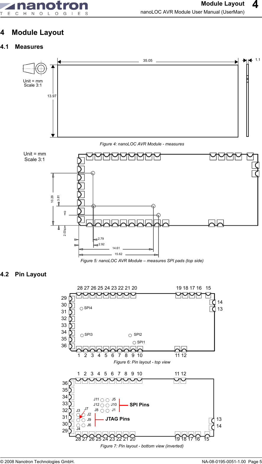
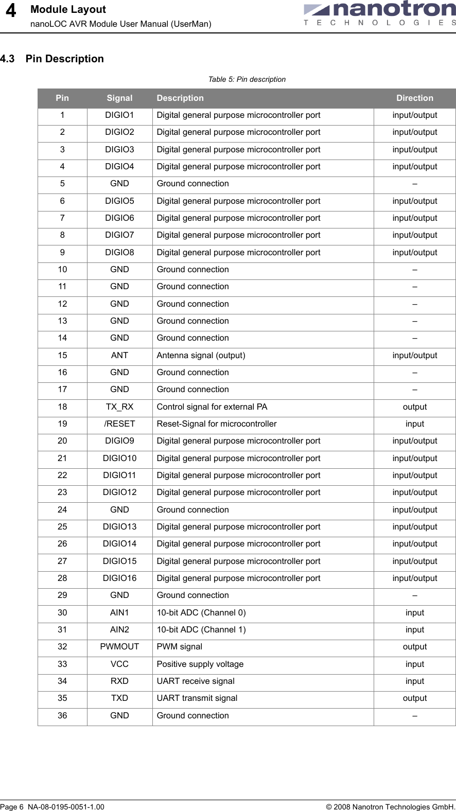
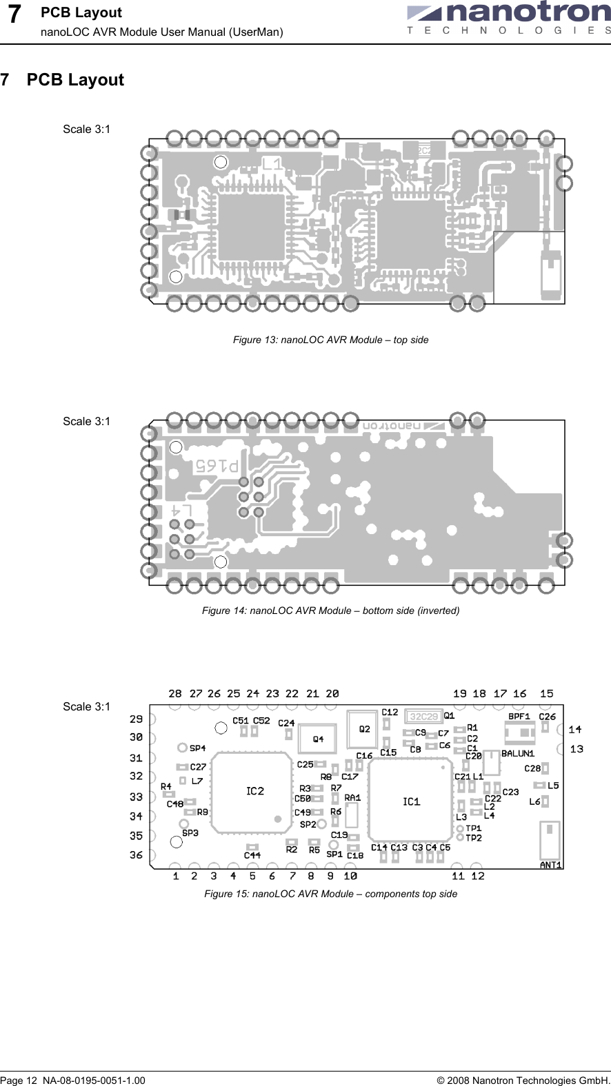
![Soldering InformationnanoLOC AVR Module User Manual (UserMan)Page 8 NA-08-0195-0051-1.00 © 2008 Nanotron Technologies GmbH.55 Soldering Information5.1 Recommended Temperature Profile for Lead Free Reflow SolderingFigure 8: Recommended soldering temperature profile5.2 Recommended Foot PatternThe same dimensions for the solder paste screen are recommended, depending on the solderscreen thickness.Figure 9: nanoLOC AVR Module – recommended foot patternTem p [° C ]150 °CBD230°C to 250°C220 °CTime [s]Room TemperaturePre-heating CoolRamping ReflowA Temperature ramping rate:1 to 7°C/sB Pre-heating temperature: 90 ± 30 sC Temperature ramping rate:1 to 7°C / sD Reflow time: 30 +20/-10 sAC190 °CRamping35.0527.6926.0417.0215.3713.7212.0710.418.767.115.463.8113.972.1612.711.059.47.756.14.442.791.1433.5331.2429.5927.9426.2915.3713.7212.0618.418.767.115.463.812.165.84 1.271.272.541.271.272.541.270.81.41.1410.1511.88.765.218](https://usermanual.wiki/Nanotron-Technologies/NANOLOCAVR0108/User-Guide-947844-Page-12.png)