Nanotron Technologies NANOPAN5375V1 Communication and Real Time Location Systems in 2.4 GHz ISM Band User Manual UserMan FCC Exhibit 12
Nanotron Technologies GmbH Communication and Real Time Location Systems in 2.4 GHz ISM Band UserMan FCC Exhibit 12
UserMan
FCC Required Exhibit 12
nanoPAN 5375 RF Module
User Manual (UserMan)
Version 1.0
NA-09-0256-0008-1.0
FCC ID: SIFNANOPAN5375V1
Document Information
nanoPAN 5375 RF Module User Manual (UserMan)
Page ii NA-09-0256-0008-1.0 © 2009 Nanotron Technologies GmbH.
Document Information
Document Title: nanoPAN 5375 RF Module User Manual (UserMan)
Document Version: 1.0
Published (yyyy-mm-dd): 2009-03-18
Current Printing: 2009-3-18, 11:52 am
Document ID: NA-09-0256-0008-1.0
Document Status: Released
Disclaimer
Nanotron Technologies GmbH believes the information contained herein is correct and accurate at the time of release. Nanotron
Technologies GmbH reserves the right to make changes without further notice to the product to improve reliability, function or
design. Nanotron Technologies GmbH does not assume any liability or responsibility arising out of this product, as well as any
application or circuits described herein, neither does it convey any license under its patent rights.
As far as possible, significant changes to product specifications and functionality will be provided in product specific Errata
sheets, or in new versions of this document. Customers are encouraged to check the Nanotron website for the most recent
updates on products.
Trademarks
nanoNET© is a registered trademark of Nanotron Technologies GmbH. All other trademarks, registered trademarks, and product
names are the sole property of their respective owners.
This document and the information contained herein is the subject of copyright and intellectual property rights under international
convention. All rights reserved. No part of this document may be reproduced, stored in a retrieval system, or transmitted in any
form by any means, electronic, mechanical or optical, in whole or in part, without the prior written permission of Nanotron
Technologies GmbH.
Copyright © 2009 Nanotron Technologies GmbH.
Life Support Policy
These products are not designed for use in life support appli-
ances, devices, or systems where malfunction of these prod-
ucts can reasonably be expected to result in personal injury.
Nanotron Technologies GmbH customers using or selling
these products for use in such applications do so at their own
risk and agree to fully indemnify Nanotron Technologies
GmbH for any damages resulting from such improper use or
sale.
Electromagnetic Interference / Compatibility
Nearly every electronic device is susceptible to electromag-
netic interference (EMI) if inadequately shielded, designed, or
otherwise configured for electromagnetic compatibility.
To avoid electromagnetic interference and/or compatibility
conflicts, do not use this device in any facility where posted
notices instruct you to do so. In aircraft, use of any radio fre-
quency devices must be in accordance with applicable regula-
tions. Hospitals or health care facilities may be using
equipment that is sensitive to external RF energy.
With medical devices, maintain a minimum separation of 15
cm (6 inches) between pacemakers and wireless devices and
some wireless radios may interfere with some hearing aids. If
other personal medical devices are being used in the vicinity
of wireless devices, ensure that the device has been ade-
quately shielded from RF energy. In a domestic environment
this product may cause radio interference in which case the
user may be required to take adequate measures.
CAUTION! Electrostatic Sensitive Device. Pre-
caution should be used when handling the
device in order to prevent permanent damage.
FCC User Information
Statement according to FCC part 15.19:
This device complies with Part 15 of the FCC Rules. Opera-
tion is subject to the following two conditions: (1) this device
may not cause harmful interference, and (2) this device must
accept any interference received, including interference that
may cause undesired operation.
Statement according to FCC part 15.21:
Modifications not expressly approved by this company could
void the user's authority to operate the equipment.
RF exposure mobil:
The internal / external antennas used for this mobile transmit-
ter must provide a separation distance of at least 20 cm from
all persons and must not be co-located or operating in con-
junction with any other antenna or transmitter.”
Statement according to FCC part 15.105:
This equipment has been tested and found to comply with the
limits for a Class A and Class B digital device, pursuant to Part
15 of the FCC Rules. These limits are designed to provide
reasonable protection against harmful interference in a resi-
dential installation and against harmful interference when the
equipment is operated in a commercial environment.
This equipment generates, uses, and can radiate radio fre-
quency energy and, if not installed and used in accordance
with the instructions as provided in the user manual, may
cause harmful interference to radio communications. How-
ever, there is no guarantee that interference will not occur in a
particular installation. Operation of this equipment in a resi-
dential area is likely to cause harmful interference in which
case the user will be required to correct the interference at his
or her own expense.
If this equipment does cause harmful interference to radio or
television reception, which can be determined by turning the
equipment off and on, the user is encouraged to try to correct
the interference by one or more of the following measures:
• Reorient or relocate the receiving antenna.
• Increase the separation between the equipment and
receiver.
• Connect the equipment into an outlet on a circuit different
from that to connected.
• Consult the dealer or an experienced technician for help.

Table of Contents
nanoPAN 5375 RF Module User Manual (UserMan)
© 2009 Nanotron Technologies GmbH. NA-09-0256-0008-1.0 Page 1
Table of Contents
1 Overview. . . . . . . . . . . . . . . . . . . . . . . . . . . . . . . . . . . . . . . . . . . . . . . . . . . . . . . . . . . . . . . . . . . . . . . . . 1
1.1 Key Components. . . . . . . . . . . . . . . . . . . . . . . . . . . . . . . . . . . . . . . . . . . . . . . . . . . . . . . . . . . . . . . 1
2 Absolute Maximum Ratings . . . . . . . . . . . . . . . . . . . . . . . . . . . . . . . . . . . . . . . . . . . . . . . . . . . . . . . . . 3
3 Electrical Characteristics . . . . . . . . . . . . . . . . . . . . . . . . . . . . . . . . . . . . . . . . . . . . . . . . . . . . . . . . . . . 3
3.1 General / DC Parameters . . . . . . . . . . . . . . . . . . . . . . . . . . . . . . . . . . . . . . . . . . . . . . . . . . . . . . . . 3
3.2 RF Parameters . . . . . . . . . . . . . . . . . . . . . . . . . . . . . . . . . . . . . . . . . . . . . . . . . . . . . . . . . . . . . . . . 4
3.3 Offset Clock Parameters. . . . . . . . . . . . . . . . . . . . . . . . . . . . . . . . . . . . . . . . . . . . . . . . . . . . . . . . . 4
3.3.1 Nominal Conditions . . . . . . . . . . . . . . . . . . . . . . . . . . . . . . . . . . . . . . . . . . . . . . . . . . . . . . . . 5
3.4 Digital Interface . . . . . . . . . . . . . . . . . . . . . . . . . . . . . . . . . . . . . . . . . . . . . . . . . . . . . . . . . . . . . . . . 5
4 Power Management. . . . . . . . . . . . . . . . . . . . . . . . . . . . . . . . . . . . . . . . . . . . . . . . . . . . . . . . . . . . . . . . 6
4.1 Overview – Icc . . . . . . . . . . . . . . . . . . . . . . . . . . . . . . . . . . . . . . . . . . . . . . . . . . . . . . . . . . . . . . . . . . . . . . . . . . . . . . . . . 6
4.2 Power Down Pad / Power Down Full . . . . . . . . . . . . . . . . . . . . . . . . . . . . . . . . . . . . . . . . . . . . . . . 6
4.3 Pout as a Function of Tx Register (Typical) . . . . . . . . . . . . . . . . . . . . . . . . . . . . . . . . . . . . . . . . . . . 7
4.4 Icc as a Function of Pout (Typical) . . . . . . . . . . . . . . . . . . . . . . . . . . . . . . . . . . . . . . . . . . . . . . . . . . 7
4.5 Icc as a Function of Tx Register (Typical) . . . . . . . . . . . . . . . . . . . . . . . . . . . . . . . . . . . . . . . . . . . . 8
5 Module Layout . . . . . . . . . . . . . . . . . . . . . . . . . . . . . . . . . . . . . . . . . . . . . . . . . . . . . . . . . . . . . . . . . . . . 9
5.1 Measures . . . . . . . . . . . . . . . . . . . . . . . . . . . . . . . . . . . . . . . . . . . . . . . . . . . . . . . . . . . . . . . . . . . . 9
5.2 Pin Layout . . . . . . . . . . . . . . . . . . . . . . . . . . . . . . . . . . . . . . . . . . . . . . . . . . . . . . . . . . . . . . . . . . . . 9
5.3 Pin Description . . . . . . . . . . . . . . . . . . . . . . . . . . . . . . . . . . . . . . . . . . . . . . . . . . . . . . . . . . . . . . . 10
6 Soldering Information . . . . . . . . . . . . . . . . . . . . . . . . . . . . . . . . . . . . . . . . . . . . . . . . . . . . . . . . . . . . . 11
6.1 Recommended Temperature Profile for Lead Free Reflow Soldering . . . . . . . . . . . . . . . . . . . . . 11
6.2 Footprint and Recommended Landing Pattern . . . . . . . . . . . . . . . . . . . . . . . . . . . . . . . . . . . . . . . 11
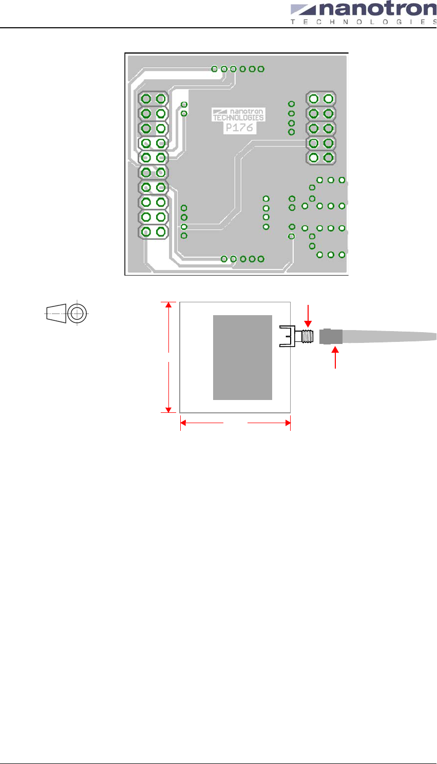
7 PCB Layout . . . . . . . . . . . . . . . . . . . . . . . . . . . . . . . . . . . . . . . . . . . . . . . . . . . . . . . . . . . . . . . . . . . . . 13
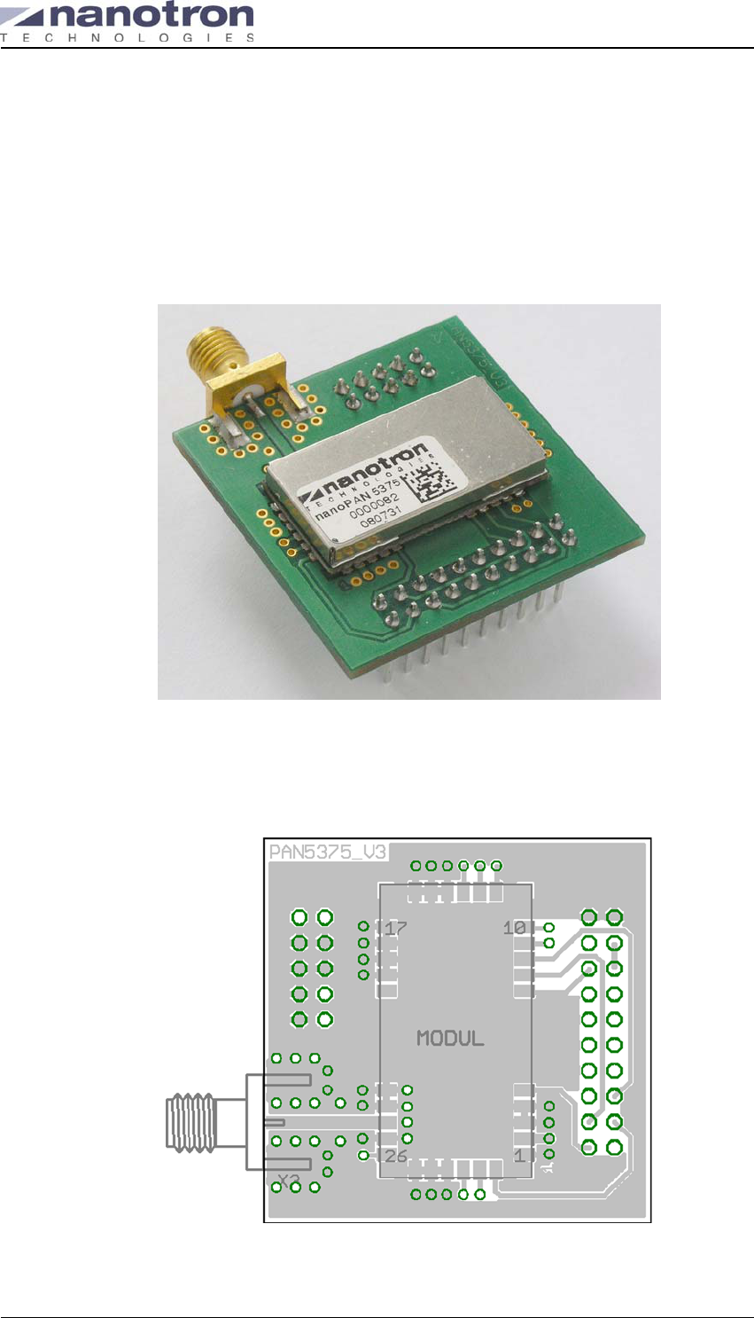
8 nanoPAN 5375 RF Test Module . . . . . . . . . . . . . . . . . . . . . . . . . . . . . . . . . . . . . . . . . . . . . . . . . . . . . 15
8.1 Overview . . . . . . . . . . . . . . . . . . . . . . . . . . . . . . . . . . . . . . . . . . . . . . . . . . . . . . . . . . . . . . . . . . . . 15
8.2 PCB Layout. . . . . . . . . . . . . . . . . . . . . . . . . . . . . . . . . . . . . . . . . . . . . . . . . . . . . . . . . . . . . . . . . . 15

List of Tables
nanoPAN 5375 RF Module User Manual (UserMan)
Page 2 NA-09-0256-0008-1.0 © 2009 Nanotron Technologies GmbH.
Intentionally Left Blank

Overview
nanoPAN 5375 RF Module User Manual (UserMan)
© 2009 Nanotron Technologies GmbH. NA-09-0256-0008-1.0 Page 1
1
1 Overview
The nanoPAN 5375 Module integrates all the required components for a complete RF module
based on Nanotron’s innovative nanoLOC TRX Transceiver. At only 29 mm by 15 mm and less
than 4 mm thick, this RF module includes a balun, a band pass filter, a set of clock crystals, a 20
dBm power amplifier, as well as the nanoLOC chip and required circuitry. Figure 1 below shows the
nanoPAN 5375 RF Module with a shielding cap and label.
Figure 1: nanoPAN 5375 RF Module – top showing shielding cap
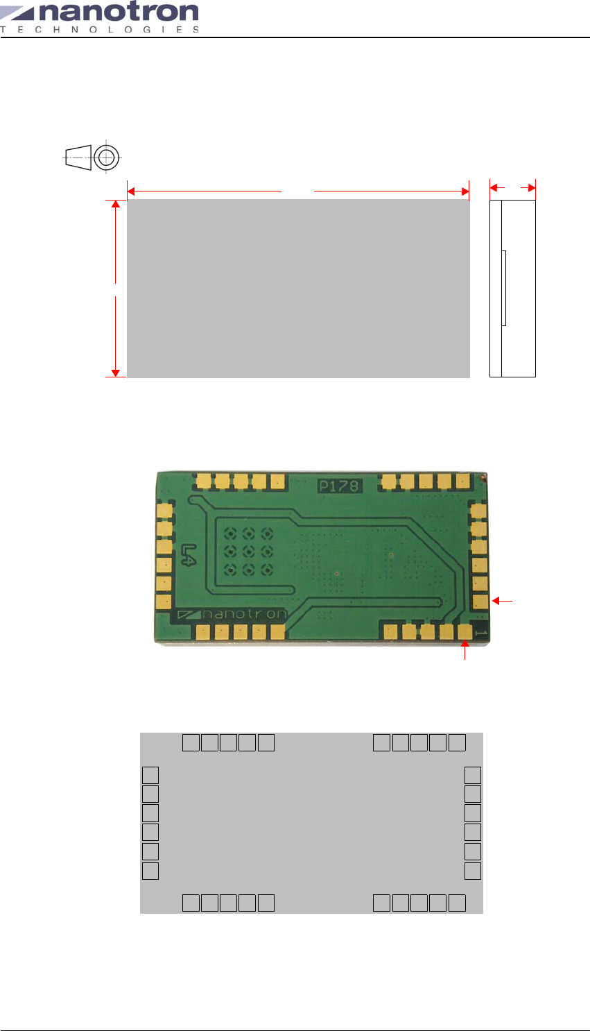
Figure 2 below shows the pad side of the nanoPAN 5375 RF Module with pins 1 and 32 indicated,
as well as dimensions.
Figure 2: nanoPAN 5375 RF Module – pad side
1.1 Key Components
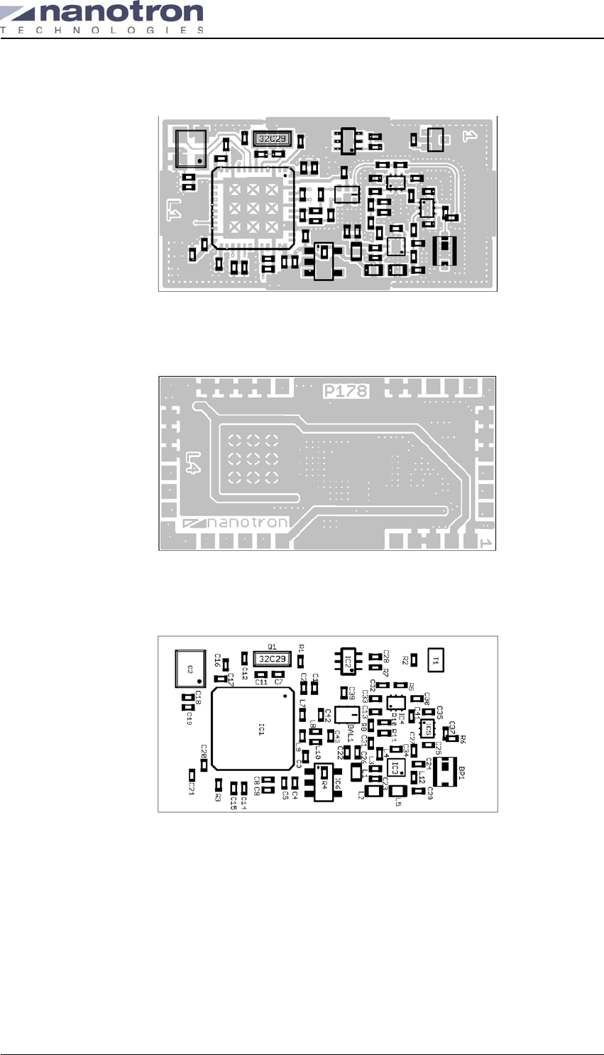
Figure 3 below shows the key components of the nanoPAN 5375 RF Module.
Figure 3: nanoPAN 5375 RF Module – key components
Scale 3:1
Pin 1
Pin 32
Scale 3:1 29.0 mm
15.0 mm
32 MHz crystal
Band pass filter
nanoLOC chip
32 kHz crystal Balun
Scale 3:1
RF Switch
Power amplifier
Overview
nanoPAN 5375 RF Module User Manual (UserMan)
Page 2 NA-09-0256-0008-1.0 © 2009 Nanotron Technologies GmbH.
1
Table 1: Key components
Component Description
nanoLOC TRX
Transceiver
The nanoLOC chip supports a freely adjustable center frequency with two sets of 3
non-overlapping frequency channels, as well as 14 overlapping frequency channels,
all within the 2.4 GHz ISM band. These channels provide support for multiple physi-
cally independent networks and improved coexistence performance with existing 2.4
GHz wireless technologies. Data rates are selectable from 2 Mbps to 250 kbps.
Due to the chip’s unique chirp pulse, adjustment of the antenna is not critical. This sig-
nificantly simplifies the system’s installation and maintenance (“pick and place”).
A sophisticated MAC controller with CSMA/CA and TDMA support is included, as is
Forward Error Correction (FEC) and 128 bit hardware encryption. To minimize soft-
ware and microcontroller requirements, the nanoLOC chip also provides scrambling,
automatic address matching, and packet retransmission.
Integrated into the nanoLOC chip is a Digital Dispersive Delay Line (DDDL). This is
responsible for distinguishing between two possible incoming signals generated by
another nanoLOC chip. These are either an Upchirp or a Downchirp, both of which
have the same center frequency and the same bandwidth. The difference between an
Upchirp and a Downchirp occurs only in the phase information of the complex spec-
trum. This phase information is enough for the DDDL to compress a pulse at one out-
put port and expand it at the other (that is, to extend the incoming signal to the doubled
duration). In this way the DDDL acts like a matched filter for one of the possible trans-
mitted pulses.
Matching circuits
(Balun)
At the RF interface of the nanoLOC chip, a differential impedance of 200 Ω exists
which is matched to the asymmetrical 50 Ω impedance of the antenna port by a
200 Ω to 50 Ω RF balun. Additional external components at the RF interface have a
power and noise matching function that allows a sharing of the antenna without an
external TX/RX – RF switch.
ISM band pass
filter
For an improved robustness against out-of-band inferences, an ISM band pass filter is
connected at the antenna port.
32.768 kHz and
32 MHz quartz
crystals
The 32.768 kHz quartz is used for the Real Time Clock oscillator. The 32 MHz quartz
works with the internal oscillator circuitry of the nanoLOC chip.
RF switch This switch is actually two devices that are used to switch the RX / TX paths between
receive and transmit mode.
Power amplifier This amplifier gives the module high efficiency, high gain, and a high output power of
20 dBm.
Absolute Maximum Ratings
nanoPAN 5375 RF Module User Manual (UserMan)
© 2009 Nanotron Technologies GmbH. NA-09-0256-0008-1.0 Page 3
2
2 Absolute Maximum Ratings
Note: It is critical that the ratings provided in Absolute Maximum Ratings be carefully observed.
Stress exceeding one or more of these limiting values may cause permanent damage to the
nanoPAN 5375 RF Module.
3 Electrical Characteristics
3.1 General / DC Parameters
Note 1: Tested in production @ 2.5 V, Temp= 25°C ± 5°C.
Note 2: Not tested in production. Only by characterization.
Note 3: RX off, TX off, Baseband Clock on.
Note 4: RX off, TX off, Baseband Clock off.
Table 2: Absolute maximum rating
Parameter Value Unit
Min. operating temperature -40.0 °C
Max. operating temperature +85.0 °C
Max. supply voltage (Vcc)2.7 V
Max. DC current per I/O pin 2.0 mA
Table 3: General / DC-Parameters
Note Symbol Parameter Condition Min. Typ. Max. Units
–Top Operating
temperature –-40.0 –+85.0 °C
–Vcc Supply voltage –2.3 –2.7 V
2Icc Supply current TX Low power TX
Reg 0x00 75.0 mA
2Icc Supply current TX Mid power TX
Reg 0x1F 80.0 mA
2Icc Supply current TX Full power TX
Reg 0xx3F –210.0 –mA
1Icc Supply current RX Unsync (80/1/1) 51.0 mA
1Icc Supply current RX Sync (80/1/1) 46.0 mA
2Icc Supply current Ready (3) 4.0 mA
2Icc Supply current StandBy (4) 2.5 mA
2Icc Supply current Power Up 750.0 uA
1Icc Supply current PD Pad 550.0 625.0 900.0 µA
1Icc Supply current PD FULL 3.0 3.8 5.0 uA
Electrical Characteristics
nanoPAN 5375 RF Module User Manual (UserMan)
Page 4 NA-09-0256-0008-1.0 © 2009 Nanotron Technologies GmbH.
3
3.2 RF Parameters
Note 1: Tested in production @ 2.5 V, Temp= 25°C ± 5°C.
Note 2: Not tested in production. Only by characterization.
Note 3: The displayed value is the minimum receive signal power required for BER = 10e-3, which is
equivalent to the maximum receiver sensitivity
3.3 Offset Clock Parameters
Note 1: Tested in production @ 2.5 V, Temp= 25°C ± 5°C.
Table 4: RF parameters
Note Symbol Parameter Condition Min. Typ. Max. Units
–Zant Line impedance of
antenna signal ANT – – 50.0 –Ω
–Rdata Data rate –250.0 –2000 kb/s
2Psens Receiver sensitivity 22/4, FECoff –-92.0 -95.0 dBm
2Psens Receiver sensitivity 22/4, FECon –-95.0 -97.0 dBm
1Psens Receiver sensitivity 80/1, FEC 0ff –-85 -86 dBm
2Psens Receiver sensitivity 80/4, FEC 0n –-92 -94 dBm
2Ptx MIN Transmit power TX Reg 0x00 –-17.5 –dBm
2Ptx MID Transmit power TX Reg 0x1F –6.0 –dBm
1Ptx FULL Transmit power TX Reg 0x3F 18.0 19.5 –dBm
1Ptx Transmit power
- 2 harmonics TX Reg 0x3F –-60.0 –dBm
1Ptx Transmit power
- 3 harmonics TX Reg 0x3F –-65.0 –dBm
Table 5: Offset clock parameters
Note Symbol Parameter Condition Min. Typ. Max. Units
1f32m Offset Clock 32.000 MHz 25 °C, 2.5V 0.0 ppm
1f32k Offset Clock 32.768 kHz 25 °C, 2.5V 25.0 ppm

Electrical Characteristics
nanoPAN 5375 RF Module User Manual (UserMan)
© 2009 Nanotron Technologies GmbH. NA-09-0256-0008-1.0 Page 5
3
3.3.1 Nominal Conditions
Table 6 below lists the nominal conditions, except otherwise noted:
3.4 Digital Interface
Note: Table 7 below lists the parameters and values for the following digital IOs:
+DIIO0, DIIO1, DIIO2, DIIO3
+UCRESET, UCIRQ
+SPITXD, SPIRXD, SPICLK, SPISSN
+/TX_RX
+/PONRESET
Table 6: Nominal conditions
+Tjunct = 30°C
+VSSA = VSSD = GND
+VDDA = VCC = +2.5 V
+Transmission / reception @ 250 kbps
+Nominal frequency bandwidth (TX/RX)
B = 22 MHz @ -30 dBr
+Raw data mode
+No CRC
+No FEC
+No encryption
+Receiver synchronized
+Bit scrambling
+BER = 0.001 during receive mode
+RF output power (PEP) during transmit phase
= 20 dBm EIRP measured during continuous
transmission
+Nominal process
+All RF ports are impedance matched according to
the specification
+All RF power are measured on the IC terminals
(pins)
+For link distance measurement, two identical
nanoLOC systems are used
Table 7: Digital Interface to Sensor / Actor
Symbol Parameter Value Unit
– Number of general purpose input/outputs 4 Number
– Width of each interface 1 Bit
– Direction In/Out
(bi-directional, open-
drain with pull-up
–
– Type Programmable –
CIN Logic Input Capacitance 2.5 pF
Input Voltage
VIL Low level input voltage (minimum) 0.2 x VCC V
VIH High level input voltage (maximum) 0.7 x VCC V
Output Voltage
VOL Low level output voltage (maximum) 0.3 V
VOH High level output voltage (minimum) VCC - 0.3 V
– Maximum output current 2 mA
RUP Equivalent pull-up resistance (minimum)1
1. Can be programmed in nanoLOC TRX. Default is off.
50 kΩ
RUP Equivalent pull-up resistance (maximum)1193 kΩ
RDN Equivalent pull-down resistance (minimum)150 kΩ
RDN Equivalent pull-down resistance (maximum)1275 kΩ
Power Management
nanoPAN 5375 RF Module User Manual (UserMan)
Page 6 NA-09-0256-0008-1.0 © 2009 Nanotron Technologies GmbH.
4
4 Power Management
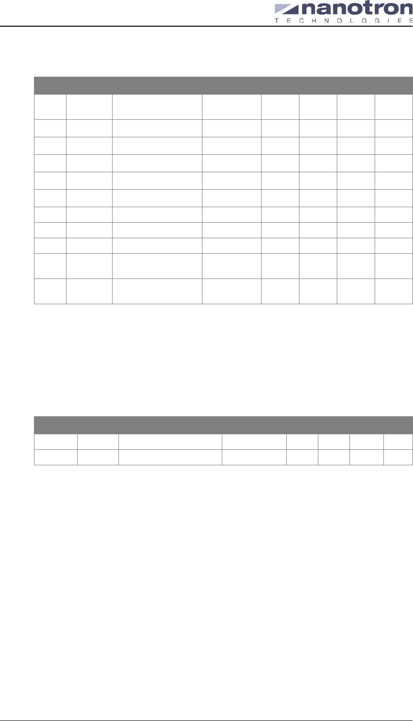
4.1 Overview – Icc
Figure 4: Typical Icc current drain for different operating modes
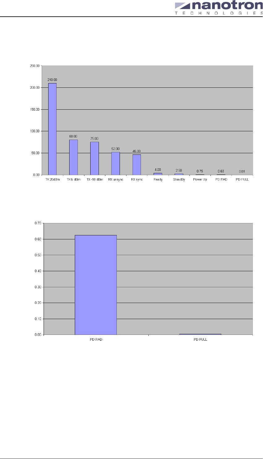
4.2 Power Down Pad / Power Down Full
Figure 5: Typical Icc current drain for Power Down Pad / Full
Icc / mA
Icc / mA
Power Management
nanoPAN 5375 RF Module User Manual (UserMan)
© 2009 Nanotron Technologies GmbH. NA-09-0256-0008-1.0 Page 7
4
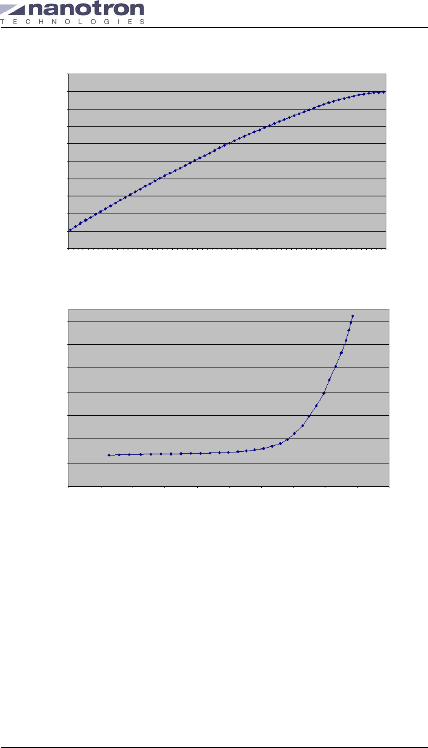
4.3 Pout as a Function of Tx Register (Typical)
Figure 6: Power management – Pout as a function of Tx register (typical)
4.4 Icc as a Function of Pout (Typical)
Figure 7: Power management – Icc as a function of Pout (typical)
-25
-20
-15
-10
-5
0
5
10
15
20
25
Pout /dBm
1 3 5 7 9 11 13 15 17 19 21 23 25 27 29 31 33 35 37 39 41 43 45 47 49 51 53 55 57 59 61 63
50
70
90
110
130
Icc / mA
150
170
190
-25 -20 -15 -10 -5 0 5 10 15 20 25
Pout dBm
Power Management
nanoPAN 5375 RF Module User Manual (UserMan)
Page 8 NA-09-0256-0008-1.0 © 2009 Nanotron Technologies GmbH.
4
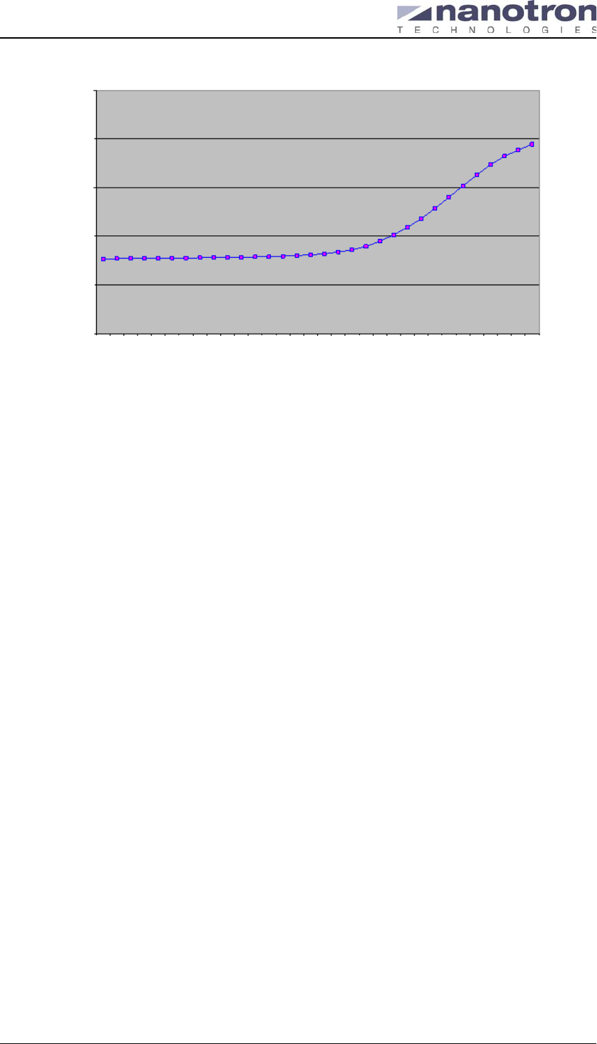
4.5 Icc as a Function of Tx Register (Typical)
Figure 8: Power management - Icc as a function of Tx register (typical)
0
50
100
150
200
250
Icc / mA
Register 0x44: TxOutputPower0
1 3 5 7 9 11 13 15 17 19 21 23 25 27 29 31 33 35 37 39 41 43 45 47 49 51 53 55 57 59 61 63
Module Layout
nanoPAN 5375 RF Module User Manual (UserMan)
© 2009 Nanotron Technologies GmbH. NA-09-0256-0008-1.0 Page 9
5
5 Module Layout
5.1 Measures
Figure 9: nanoPAN 5375 RF Module – measures
5.2 Pin Layout
Figure 10: nanoPAN 5375 RF Module – pins (bottom view)
Figure 11: nanoPAN 5375 RF Module – pin layout (bottom view)
Note: See section 5.3: Pin Description on page 10 for details on the nanoPAN 5375 RF Module
pinning.
15.0
29.0 3.8
Unit = mm
Scale 3:1
S
ca
l
e
3
:
1
Pin 1
Pin 32
17 18 19 20 21
GND
GND
GND
VCC
GND
22 23 24 25 26
GND
GND
ANT
GND
/TX_/RX
54321
SPICLK
GND
GND
VCC
10 9 8 7 6
DIIO2
DIIO3
SPITXD
UCVCC
SPIRXD
GND
16
GND
15
GND
14
/PONRESET
13
DIIO0
12
DIIO1
11
GND
27
GND
28
GND
29
UCIRQ
30
UCRESET
31
/SPISSN
32
Scale 3:1
GND
Module Layout
nanoPAN 5375 RF Module User Manual (UserMan)
Page 10 NA-09-0256-0008-1.0 © 2009 Nanotron Technologies GmbH.
5
5.3 Pin Description
Table 8: nanoPAN 5375 RF Module – pin description
Pin Signal Description Direction
1GND Ground connection (0Vdc) –
2VCC Positive supply voltage Power
3GND Ground connection (0Vdc) –
4GND Ground connection (0Vdc) –
5SPICLK SPI: CLK3Input
6UCVCC1
1. Should have a pull-down of between 100 kΩ and 1 MΩ if power-down mode is used.
Power Supply for µc Output
7SPITXD2
2. SPITXD is SPI data output from the module to the microcontroller. This pin is open-drain as default. This pin must have a pull-up to
Vcc because the pin is driven only when a logical 0 is sent from nanoLOC to the SPI marker. Reconnected value: 100 k
Ω
. This pin
can be programmed as push-pull output. (For more details, see the nanoLOC TRX Transceiver (NATR1) User Guide and the nano-
LOC SPI Application Note.)
SPI: TX Transmit Data (MISO)3
3. nanoLOC TRX is always a SPI slave device.
Output
8SPIRXD SPI: RX Receive Data (MOSI)3Input
9DIIO34
4. This pin should have a Pull-Down to GND, if not used. Recommended value: 1 M
Ω
.
Digital IO pin 3 for nanoLOC chip Input/Output
10 DIIO24Digital IO pin 2 for nanoLOC chip Input/Output
11 DIIO14Digital IO pin 1 for nanoLOC chip Input/Output
12 DIIO04Digital IO pin 0 for nanoLOC chip Input/Output
13 /PONRESET Power on reset signal Input
14 GND Ground connection (0Vdc) –
15 GND Ground connection (0Vdc) –
16 GND Ground connection (0Vdc) –
17 GND Ground connection (0Vdc) –
18 GND Ground connection (0Vdc) –
19 GND Ground connection (0Vdc) –
20 GND Ground connection (0Vdc) –
21 VCC internally connected to VCC (Pin 2) Power
22 GND Ground connection (0Vdc) –
23 GND Ground connection (0Vdc) –
24 ANT 50 Ohm RX/TX connection to antenna Input / Output
25 GND Ground connection (0Vdc) –
26 /TX_RX5
5. /TX_RX is Open-Drain output. It must have a Pull-Up to UCVCC if used. Imax: 2mA.
Status Tx / Rx6
6. Should be used as input signal to a logical input.
Output
27 GND Ground connection (0Vdc) –
28 GND Ground connection (0Vdc) –
29 GND Ground connection (0Vdc) –
30 UCIRQ7
7. This pin should have a Pull-Up to Vcc if used. Recommended value: 1 M
Ω
. Default is Open-Drain. and can be programmed as Push-
Pull. (For more details, see the nanoLOC TRX Transceiver (NATR1) User Guide.)
Interrupt request for µc Output
31 UCRESET8
8. This pin should have a pull-up of 75 K
Ω
and a capacitor of 1 nF to GND if used as controller input signal.
Reset for µc Output
32 /SPISSN9
9. This pin should have a Pull-Up to Vcc if used. Recommended value: 1 M
Ω
.
SPI: Slave Select Input
Soldering Information
nanoPAN 5375 RF Module User Manual (UserMan)
© 2009 Nanotron Technologies GmbH. NA-09-0256-0008-1.0 Page 11
6
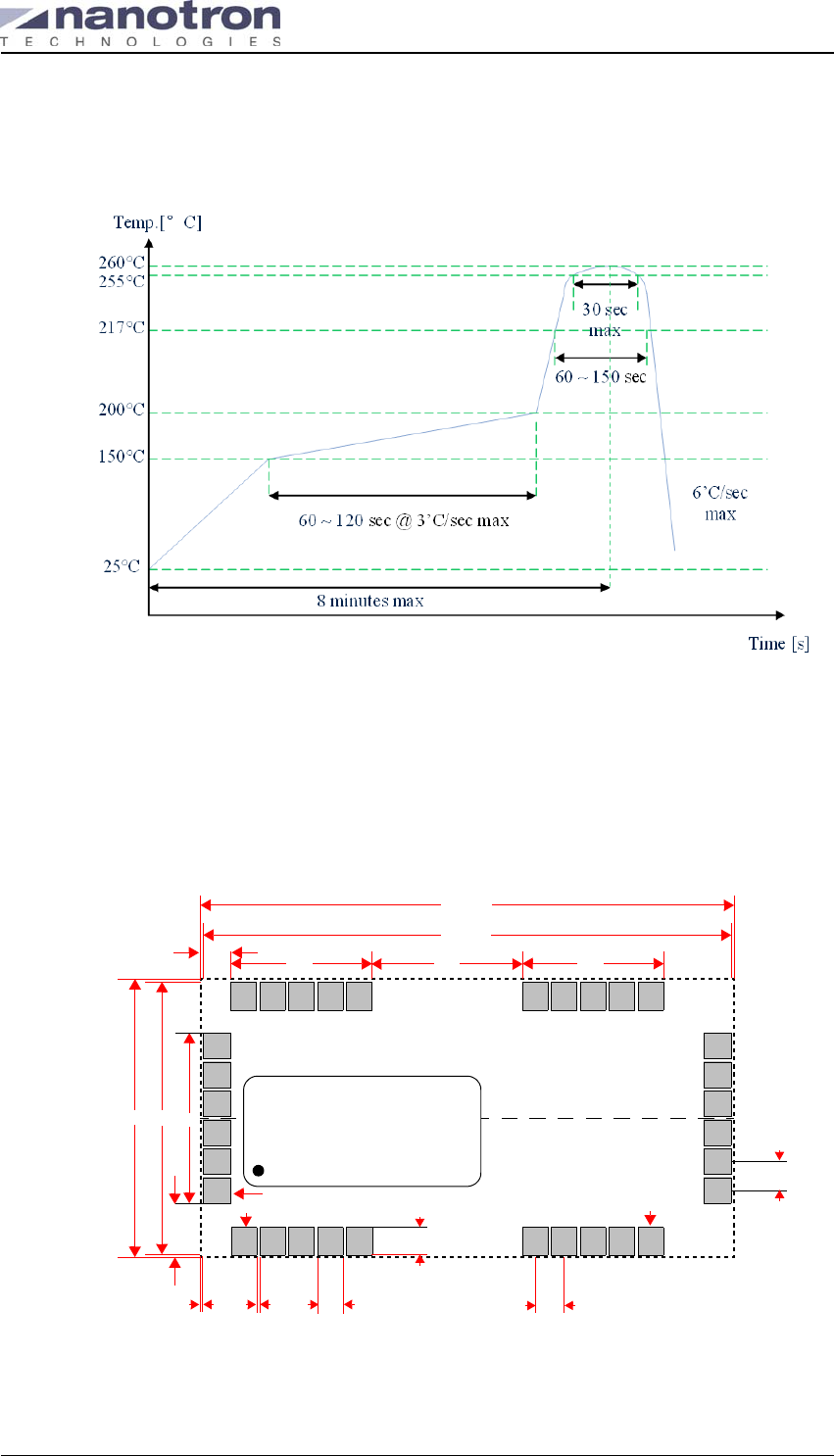
6 Soldering Information
6.1 Recommended Temperature Profile for Lead Free Reflow Soldering
Figure 12: Recommended temperature profile for reflow soldering (J-STD-020C)
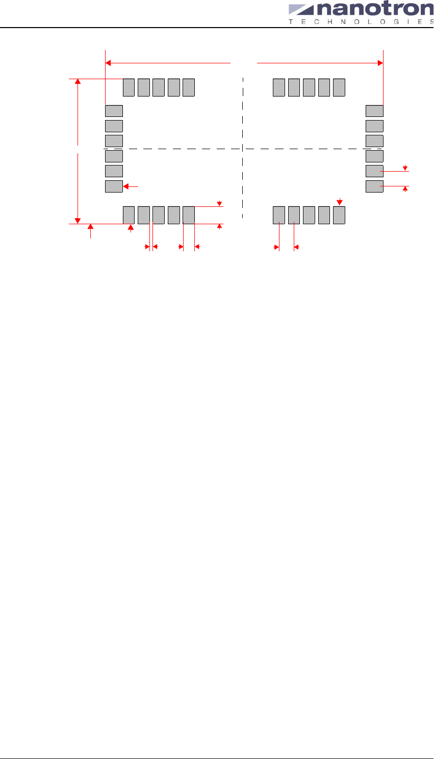
6.2 Footprint and Recommended Landing Pattern
The same dimensions for the solder paste screen are recommended, depending on the solder
screen thickness.
Figure 13: nanoPAN 5375 RF Module footprint – pad configuration (top view)
29.0
28.8
15 14.8 9.4
7.8 7.8
8.4
1.4
2.7 0.1 0.2 1.4 1.6
1.5
1.6
Pin 1 Pin 32 Pin 10
nanoPAN5375 RF Module
Soldering Information
nanoPAN 5375 RF Module User Manual (UserMan)
Page 12 NA-09-0256-0008-1.0 © 2009 Nanotron Technologies GmbH.
6
Figure 14: nanoPAN 5375 RF Module – landing pattern
1 Details of the landing pattern are dependent on the technology and should be defined by the
assembler.
2 For manual setting of the module, it is recommended to use the corner or side marker in the top
layer (copper) or stop mask.
3 For automatic assembly use pattern marker of the carrier board.
29.60
15.7
2.7 0.60 1.00 1.60
1.90
Pin 1
Pin 32 Pin 10
1.6
PCB Layout
nanoPAN 5375 RF Module User Manual (UserMan)
© 2009 Nanotron Technologies GmbH. NA-09-0256-0008-1.0 Page 13
7
7 PCB Layout
Figure 15: nanoPAN 5375 RF Module – top side
Figure 16: nanoPAN 5375 RF Module – bottom side (inverted)
Figure 17: nanoPAN 5375 RF Module – components top side
S
ca
l
e
3
:
1
S
ca
l
e
3
:
1
S
ca
l
e
3
:
1

PCB Layout
nanoPAN 5375 RF Module User Manual (UserMan)
Page 14 NA-09-0256-0008-1.0 © 2009 Nanotron Technologies GmbH.
7
Intentionally Left Blank
nanoPAN 5375 RF Test Module
nanoPAN 5375 RF Module User Manual (UserMan)
© 2009 Nanotron Technologies GmbH. NA-09-0256-0008-1.0 Page 15
8
8 nanoPAN 5375 RF Test Module
8.1 Overview
The nanoPAN 5375 RF Test Module was designed for testing and measurement purposes only. It
was used during measurements and simulations to determine parameters published in this docu-
ment, unless otherwise specified. For conducting tests purposes, the nanoPAN 5375 RF Test Mod-
ule includes a 50 Ω coaxial SMA connector.
Figure 18: nanoPAN 5375 RF Test Module
8.2 PCB Layout
Figure 19: nanoPAN 5375 RF Test Module – top layer
nanoPAN 5375 RF Test Module
nanoPAN 5375 RF Module User Manual (UserMan)
Page 16 NA-09-0256-0008-1.0 © 2009 Nanotron Technologies GmbH.
8
Figure 20: nanoPAN 5375 RF Test Module – bottom layer (inverted)
Figure 21: nanoPAN 5375 RF Test Module – measures
Scale = 2:1
2.4 GHz antenna
SMA connector
38.5
Unit = mm
Scale 1:1
38.5

Revision History
nanoPAN 5375 RF Module User Manual (UserMan)
© 2009 Nanotron Technologies GmbH. NA-09-0256-0008-1.0 Page 17
Revision History
Version Date Description/Changes
1.0 2009-03-18 Initial version.

About Nanotron Technologies GmbH
nanoPAN 5375 RF Module User Manual (UserMan)
Page 18 NA-09-0256-0008-1.0 © 2009 Nanotron Technologies GmbH.
About Nanotron Technologies GmbH
Nanotron Technologies GmbH develops world-class wireless products for demanding applications based on
its patented Chirp transmission system - an innovation that guarantees high robustness, optimal use of the
available bandwidth, and low energy consumption. Since the beginning of 2005, Nanotron's Chirp technol-
ogy has been a part of the IEEE 802.15.4a draft standard for wireless PANs which require extremely robust
communication and low power consumption.
ICs and RF modules include nanoNET TRX Transceiver, nanoLOC TRX Transceiver, and ready-to-use or
custom wireless solutions. These include, but are not limited to, industrial monitoring and control applica-
tions, medical applications (Active RFID), security applications, and Real Time Location Systems (RTLS).
nanoNET and nanoLOC are certified in Europe, United States, and Japan and supplied to customers world-
wide.
Headquartered in Berlin, Germany, Nanotron Technologies GmbH was founded in 1991 and is an active
member of IEEE and the ZigBee alliance.
Further Information
For more information about this product and other products from Nanotron Technologies, contact a sales
representative at the following address:
Nanotron Technologies GmbH
Alt-Moabit 60
10555 Berlin, Germany
Phone: +49 30 399 954 - 0
Fax: +49 30 399 954 - 188
Email: sales@nanotron.com
Internet: www.nanotron.com