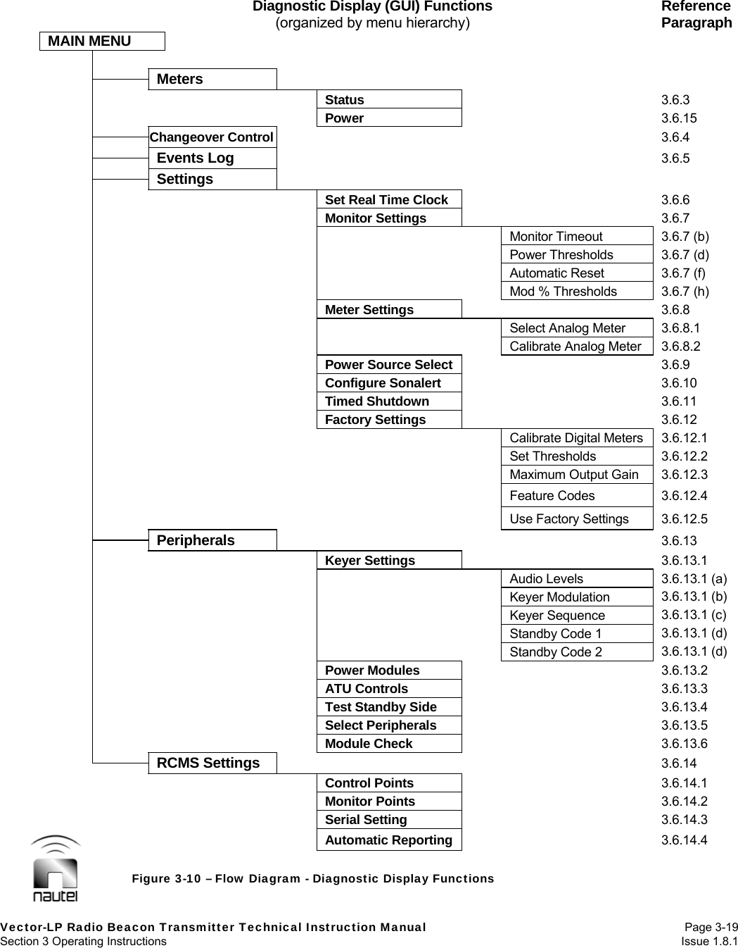
Nautel Maine VECTOR125 Nautel VR125 User Manual
Nautel Maine Inc Nautel VR125
UserManual.wiki
>
Nautel Maine
>
VECTOR125 User Manual
user manual
Navigation menu
Upload a User Manual
Namespaces
Wiki Guide
HTML
PDF
Info
Views
User Manual
Discussion / Help
Navigation


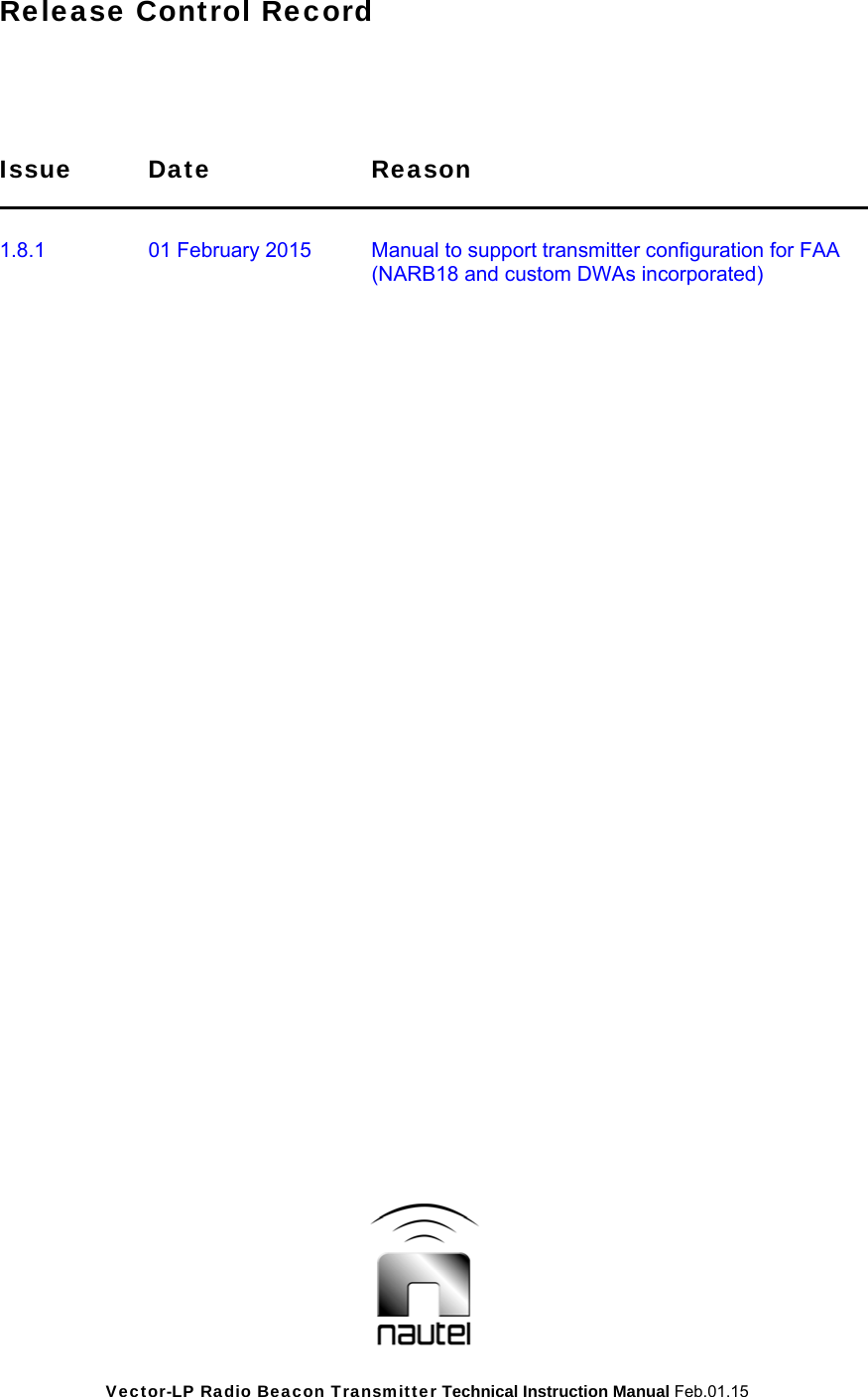


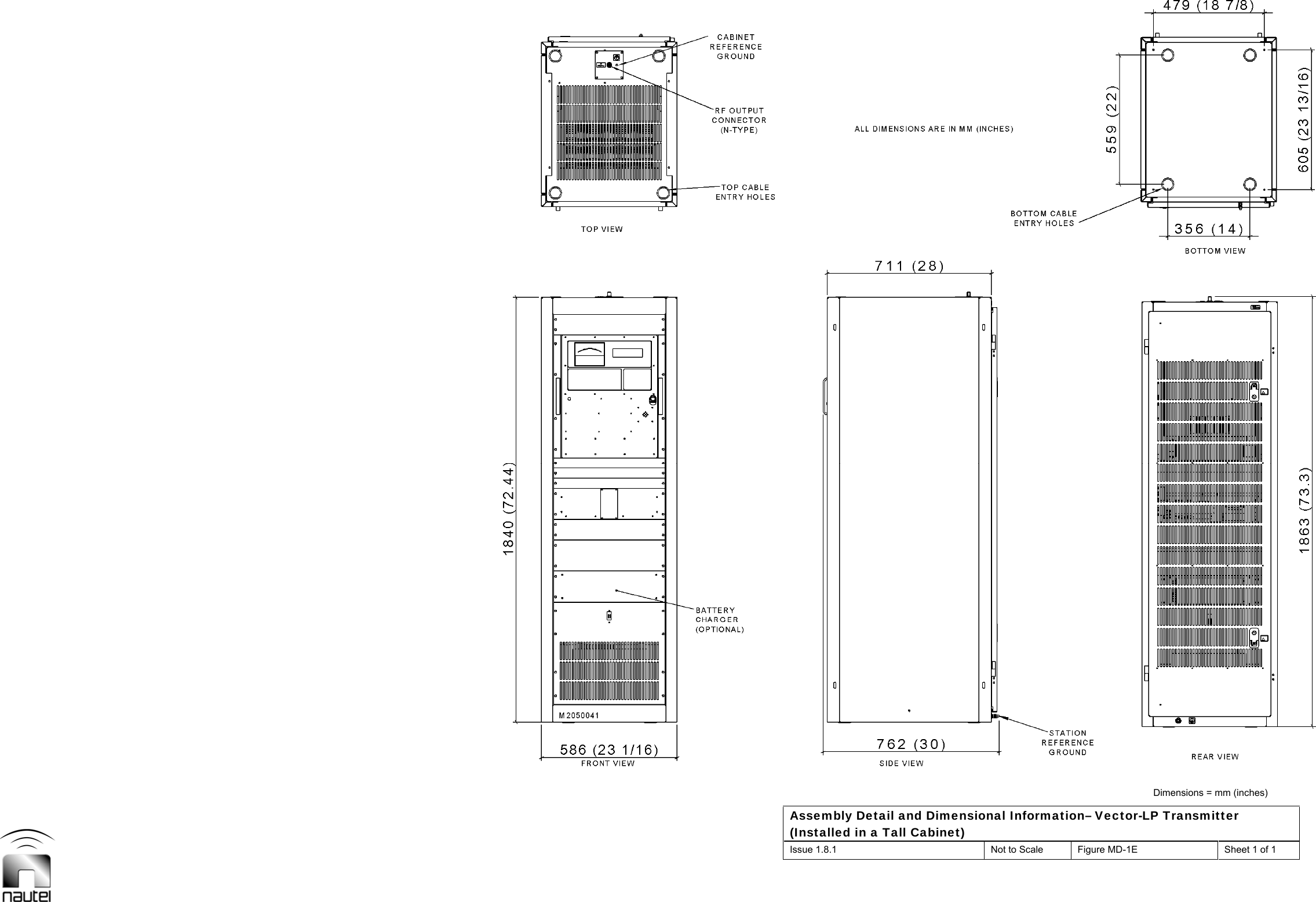
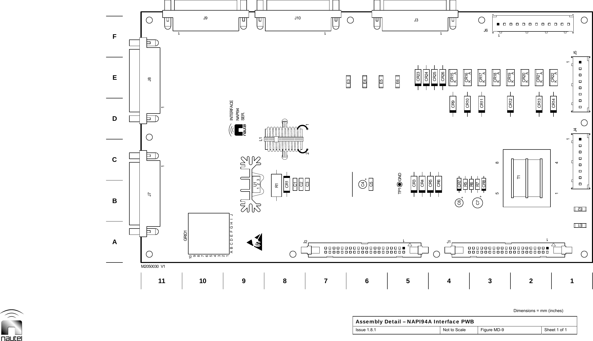
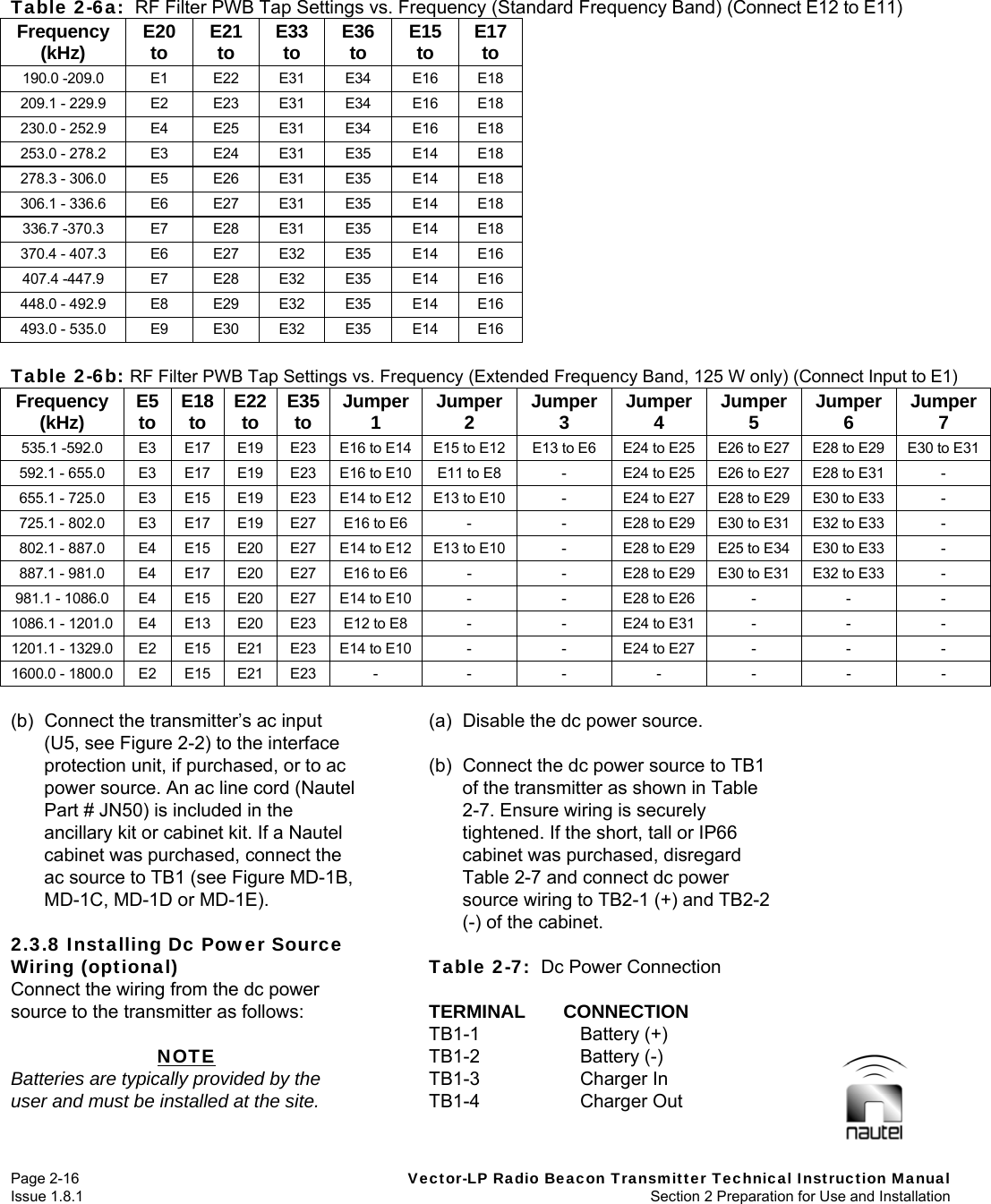
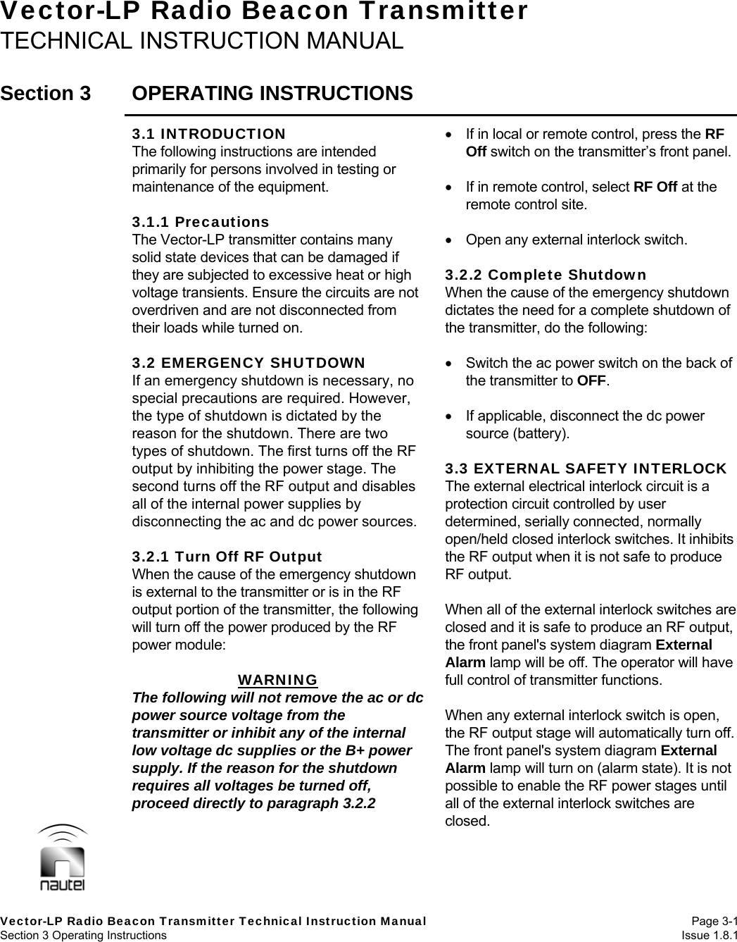
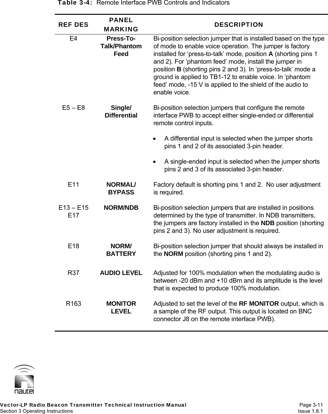
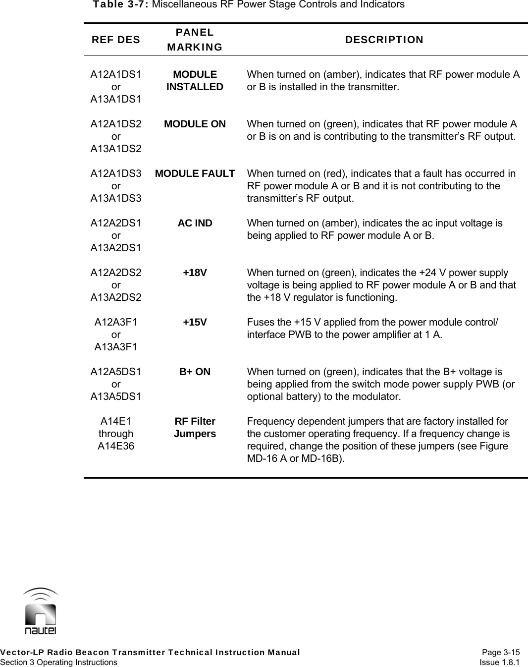
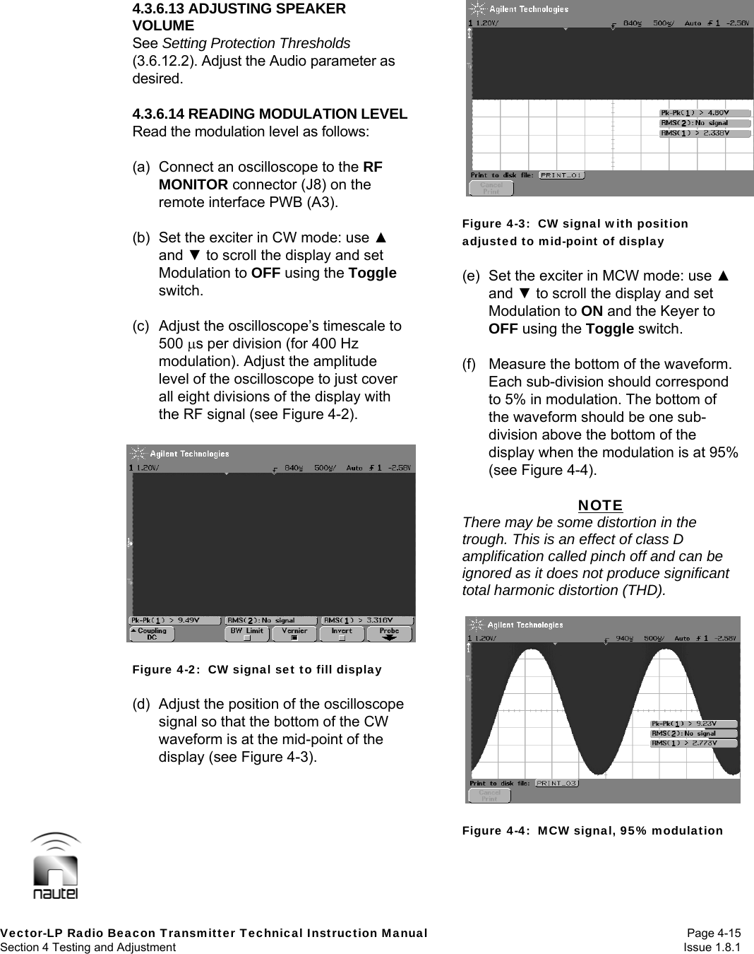
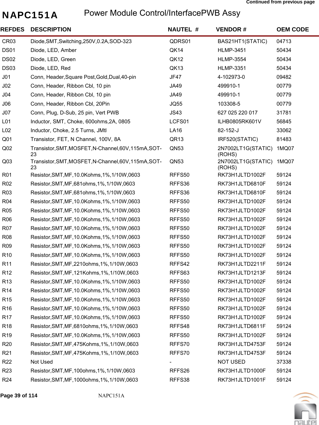
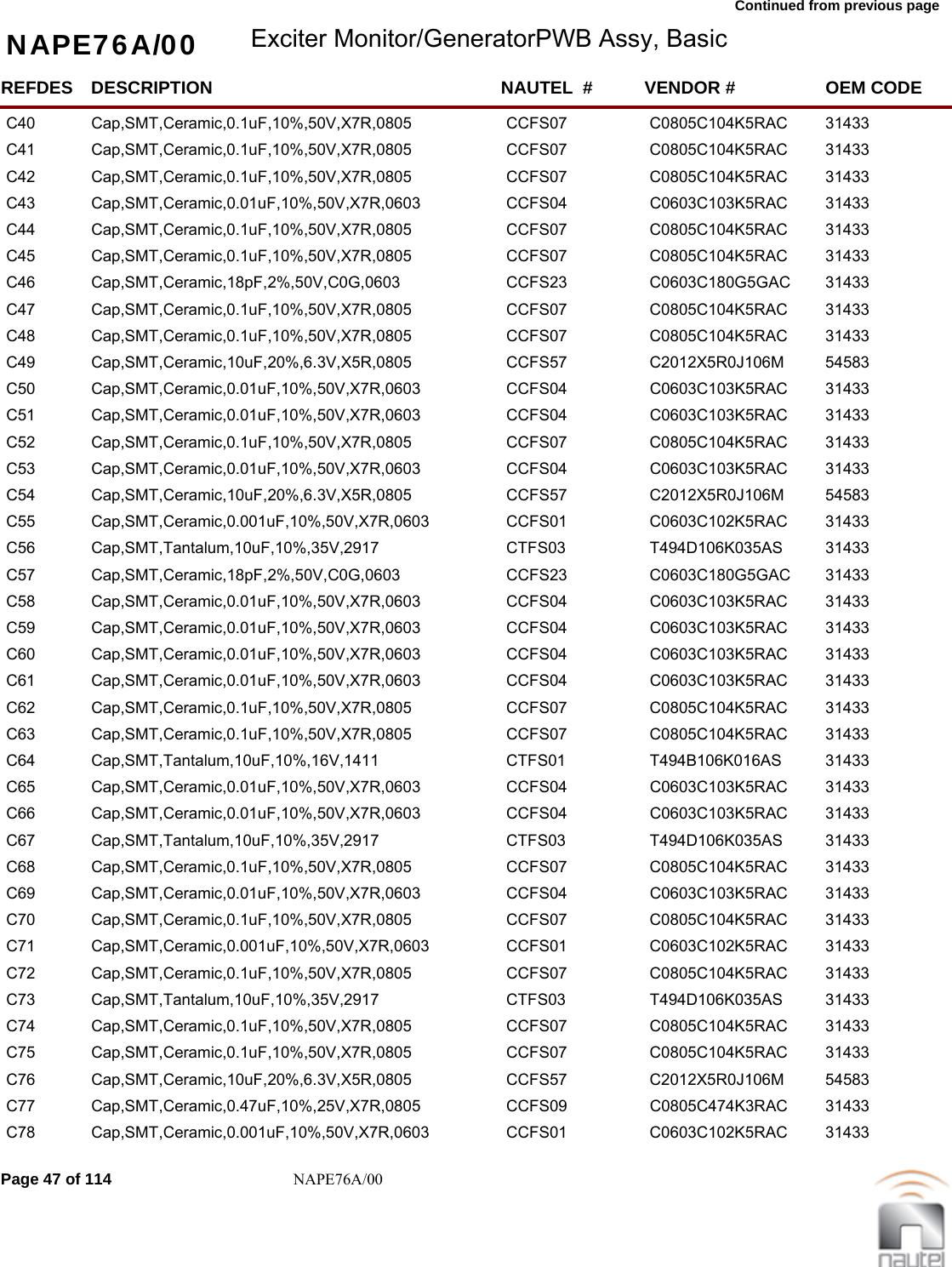
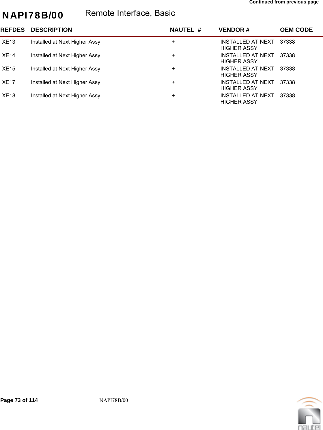
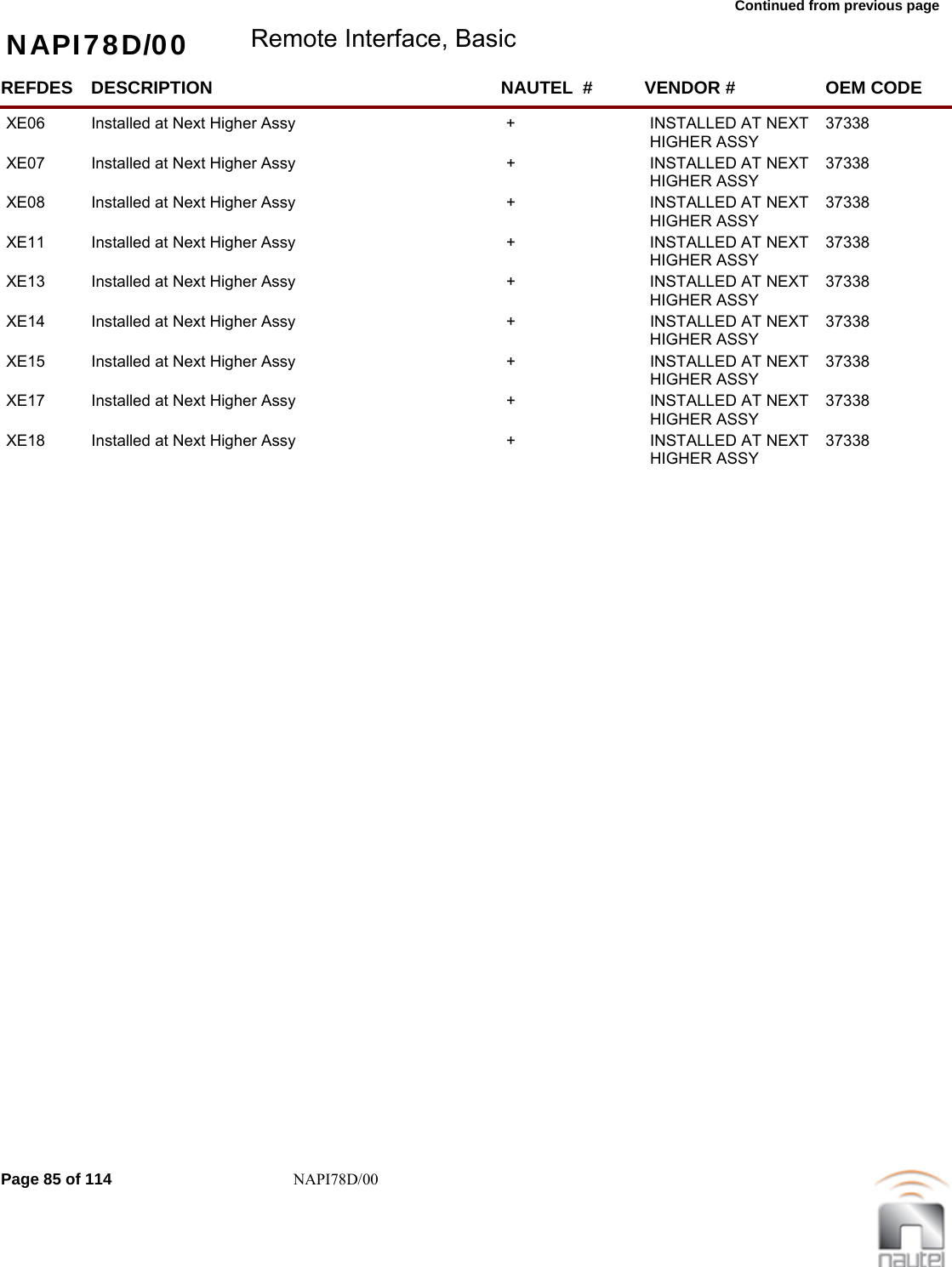
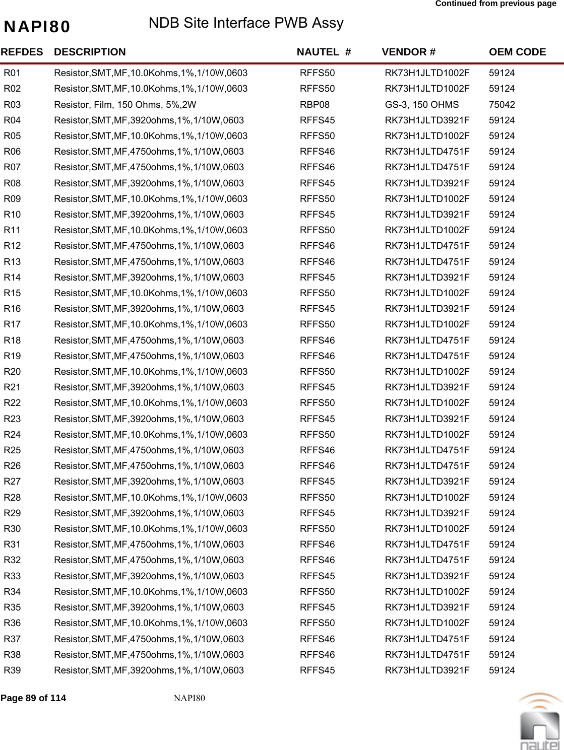
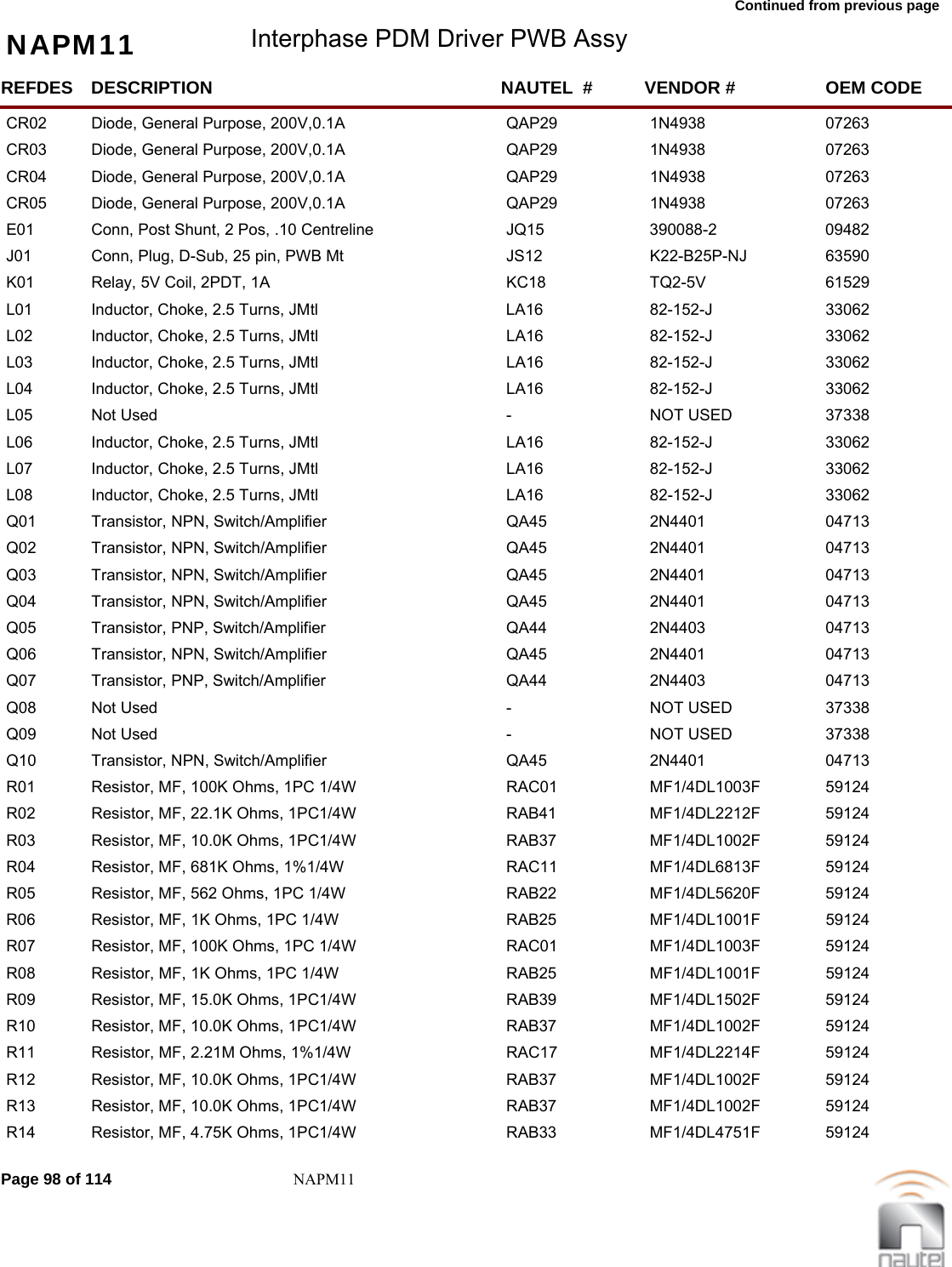
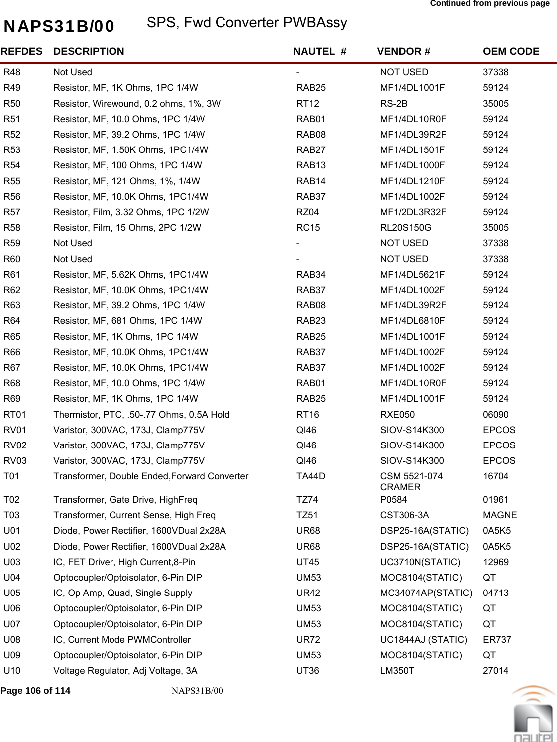
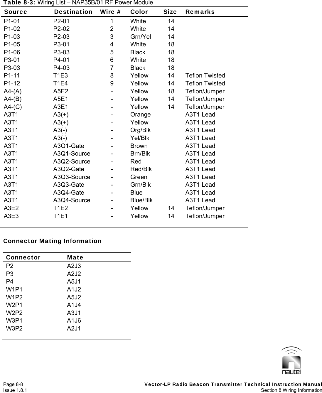
![Page 2-14 Vector-LP Radio Beacon Transmitter Technical Instruction Manual Issue 1.8.1 Section 2 Preparation for Use and Installation 2.3.3 Visual Inspection A visual inspection should be performed on the transmitter, its removable modules/ assemblies, and printed wiring boards. The inspection should cover the following: (a) Verify the LCD screen on the front panel is not damaged. (b) Remove any packing materials (tape, tyraps) used to secure wiring that was disconnected for shipment. (c) Check for obvious damage and missing parts. (d) Check electrical wiring/cabling for broken or frayed insulation, loose or improper connections, and broken, shorted or pinched conductors. (e) Verify all hardware is firmly tightened. (f) Remove any unwanted foreign objects from the interior of the transmitter/ assemblies, paying particular attention for floating conductive materials such as wire strands, metal slivers/filing, and loose hardware. 2.3.4 Cabinet Mounting If the user is supplying the 19-inch mounting cabinet, install the transmitter in the cabinet, ensuring the drawer slides on each side of the transmitter are mated/ locked together.If you purchased a Nautel cabinet option (deluxe, short, tall or IP66), the transmitter is shipped in the cabinet. If the transmitter was shipped in a deluxe, short or tall cabinet, temporarily remove both of the cabinet’s side panels [two screws at the top of the cabinet and one at the bottom (for the deluxe and tall cabinets) or two screws on the lower, front and rear (for the short cabinet)] and then remove four shipping screws (M8, two on each side) from the transmitter (see Figure MD-1B, MD-1D or MD-1E). 2.3.5 Determining Control/ Monitoring Requirements There are several remote control and monitoring options to consider before installing external wiring. The pre-installation information in paragraph 2.2 identifies the remote controls and alarm/ status outputs available. It is assumed the user has already reviewed this information and has determined which to use. It is also assumed the options available for the control inputs and the monitoring outputs have been reviewed and the user has determined which options are required to interface with the external equipment. 2.3.6 Installing External Control/ Monitor Wiring Connect the wiring from the remote control/monitoring devices to the remote interface PWB (A3) as follows: NOTE Remote control and monitor wiring terminate on the remote interface PWB (A3), which is accessible from the back of the front panel (see Figure 2-2). The connectors, included in the ancillary kit, are solder-cup type and the terminal blocks accept wires sizes (AWG) # 14 through # 24. A cable routing channel (see Figure 2-2) allows wiring to pass between the front and back of the transmitter. Remote control/monitor wiring should enter and exit at the back of the transmitter. Table 2-3: ATU Serial Interface (for INTERNAL RS-485 connector J3) Description Pin +5V (ISOL)1GND (ISOL)2, 6, 25 INT BUS (+)3INT BUS (-)4DE/RE 5](https://usermanual.wiki/Nautel-Maine/VECTOR125/User-Guide-2553568-Page-35.png)
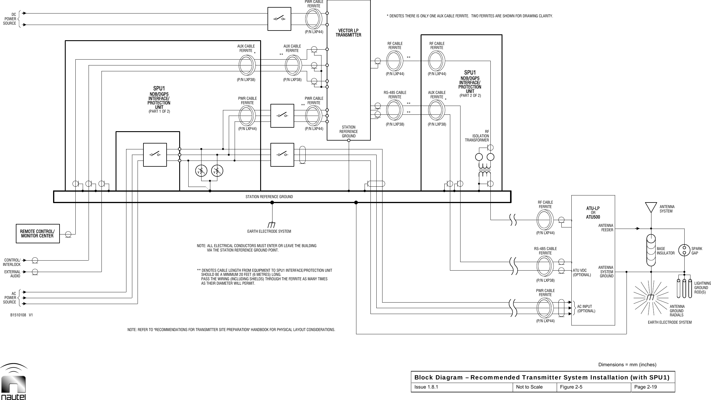
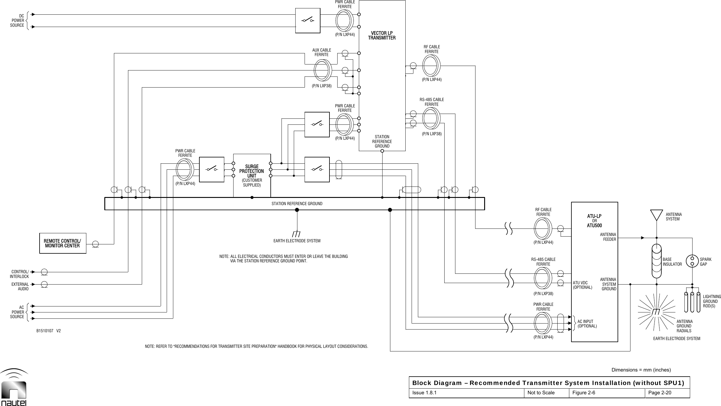
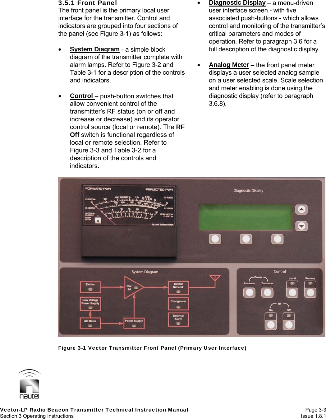
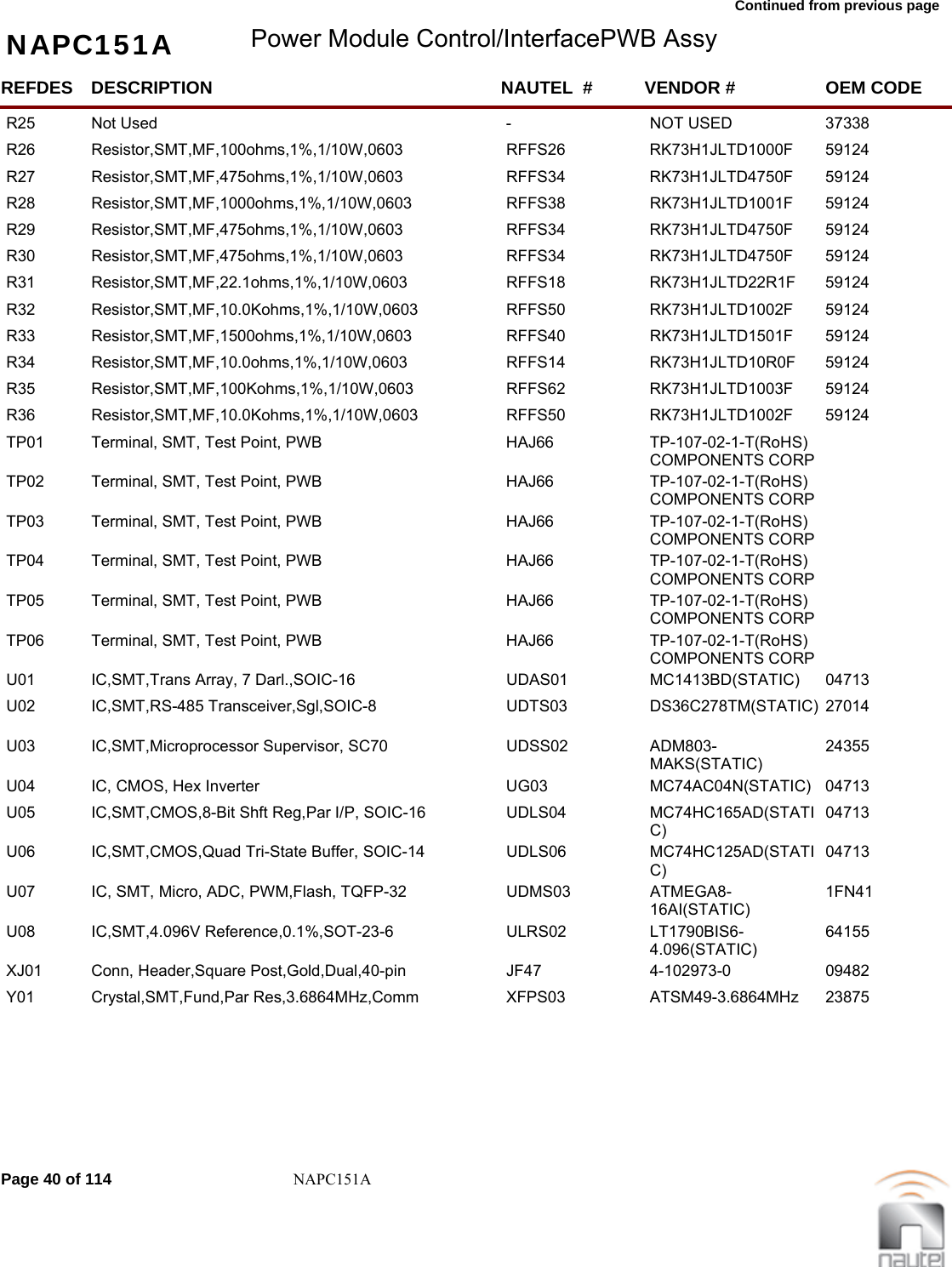
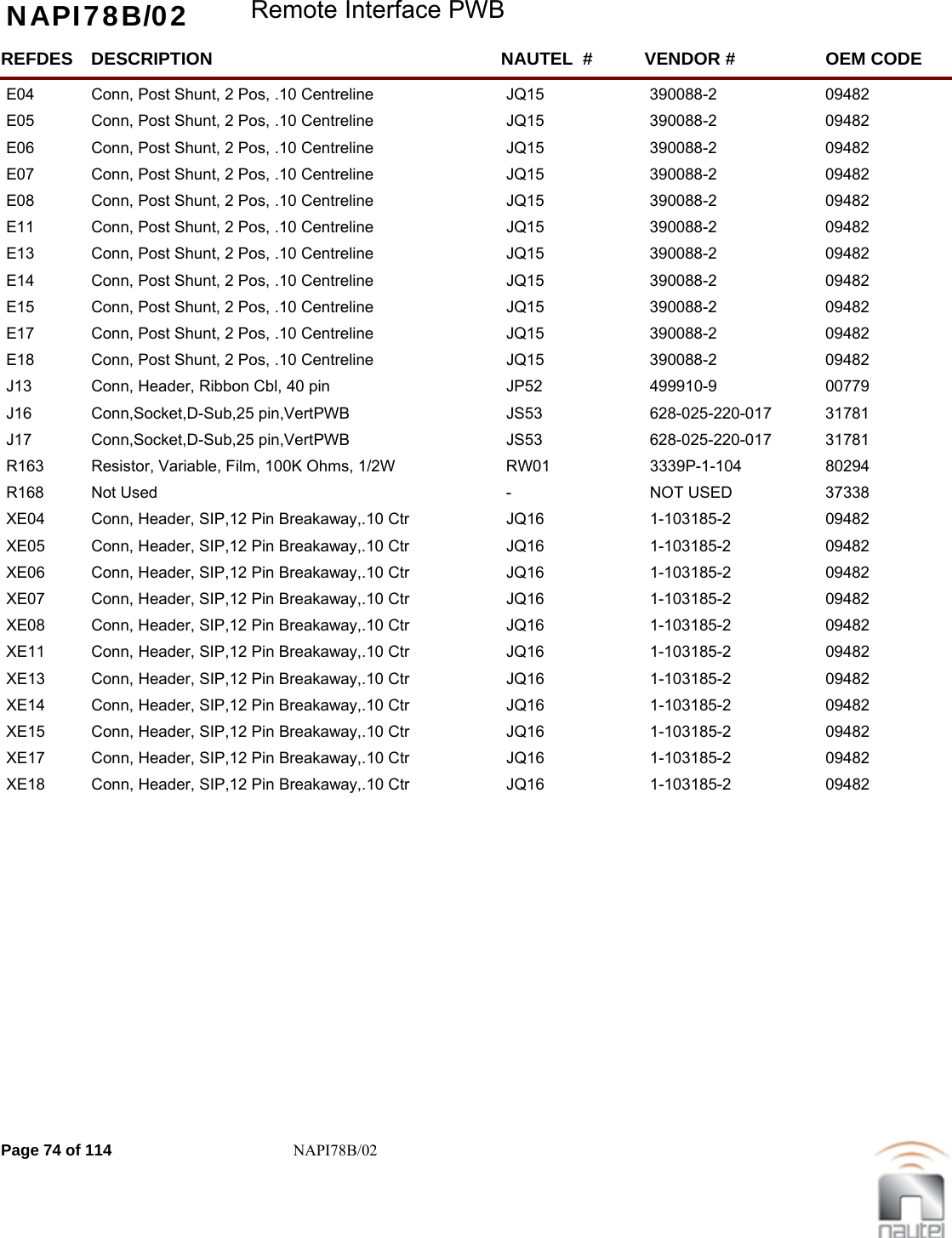
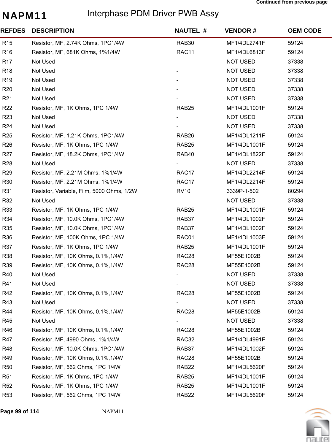
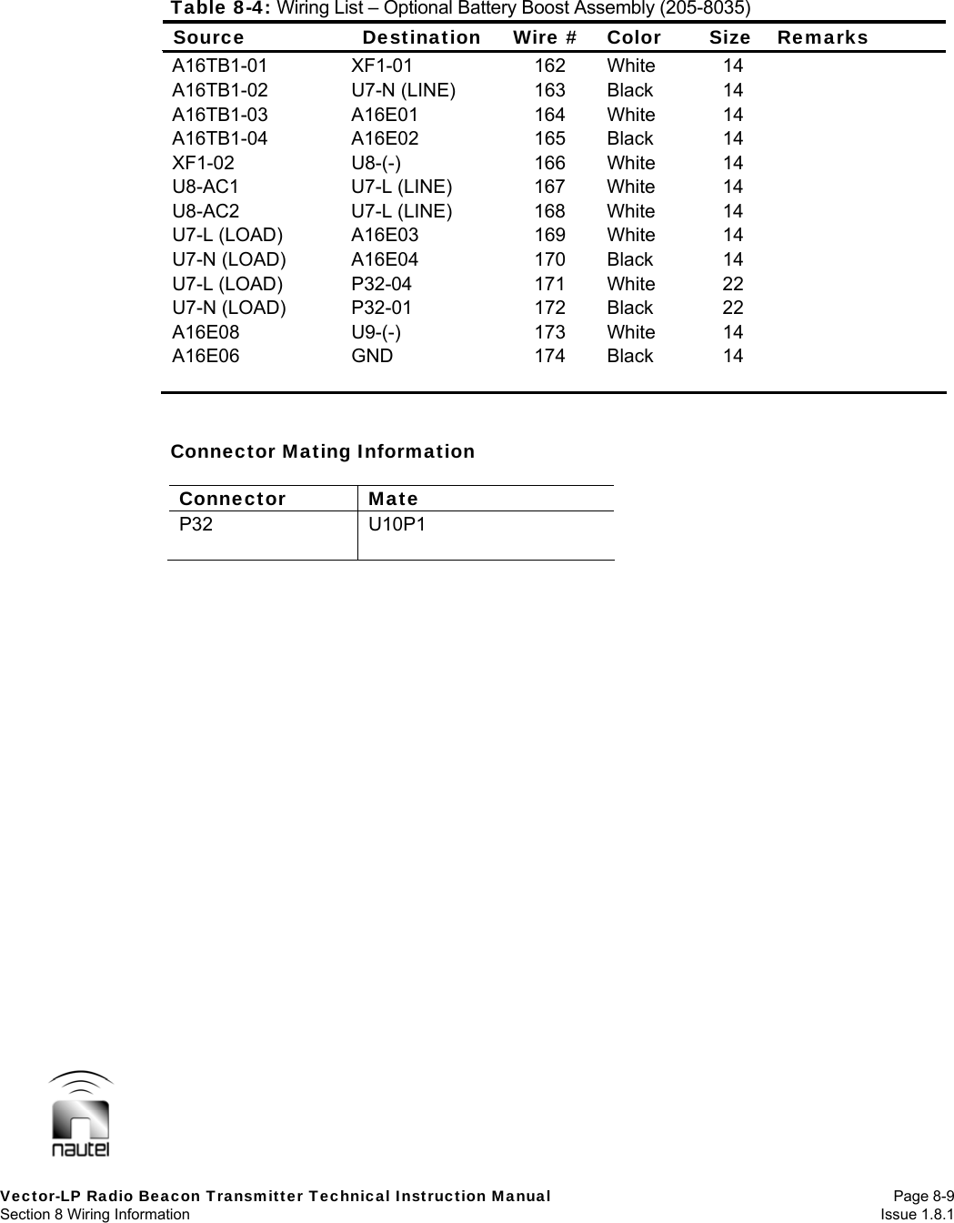
![Vector-LP Radio Beacon Transmitter Technical Instruction Manual Page 2-15 Section 2 Preparation for Use and Installation Issue 1.8.1 Table 2-4: RS-422 Remote Interface (for RS-422 connector J4) Description Pin TX 1TX 2GND 5RX 7RX 8 Table 2-5: RS-232 Remote Interface (for RS-232 connector J5) Description Pin DCD 1RXD 2TXD 3DTR 4GND 5DSR 6RTS 7CTS 8 (a) Route wires from the back of the transmitter through the cable routing channel hole to the remote interface PWB (A3) on the back of the front panel. Using Tables 2-3 through 2-5 (note the applicable serial interface options), determine the specific destination of each wire. (b) Pass all control/monitor wires, including their shields, through a ferrite toroid supplied in the ancillary kit. If practical, pass the wires through each toroid a minimum of two times (two turns). (c) Determine which remote control inputs are being applied and then determine, if applicable, whether they are differential or single-ended input. See section 2.2.12 (Remote Control Circuits), for more information on the type of input. (d) Cut each wire to the required length and, if the wire is being terminated at a terminal block, remove 3/8” (9.5 mm) of insulation from the end of each conductor; if the wire is being terminated in one of the connectors, remove 1/8” (3.2 mm) of insulation from the end of each conductor. (e) Insert the control/monitor wiring into the applicable terminals of the remote interface PWB (A3). Ensure the terminal block securing screws are firmly tightened and the adjacent wires do not touch (short). (f) If the optional modem kit (Nautel Part # 195-3032) is being used, verify connectors P7 and P8 are connected to the modem and connect the phone line to the modem. (g) If a Nautel ATU-LP or ATU500 is being used, complete the serial connection to the ATU (transmitter connections detailed in Table 2-3) as detailed in the ATU-LP or ATU500 Technical Instructions Manual. Also, provide the ATU’s dc input source by connecting a separate cable between the transmitter’s 24 V source [TB1-1 (+) and TB1-3 (ground), see Figure MD-1] and the associated ATU’s dc input (see ATU manual). 2.3.7 Installing Ac Power Wiring NOTE The following procedures assume the ac power is supplied from a single-phase, 50/60 Hz ac power source between 170 and 270 V ac (for VR250) or between 90 and 270 V ac (for VR125). (a) If an interface protection unit was purchased, route the ac power wiring from the ac power source (service entrance) to the interface protection unit, noting that it should be located close to the building’s ac entrance. If an interface protection unit was not purchased, Nautel recommends that all ac power wiring pass through one or more ferrite toroids positioned near the transmitter’s power connection.](https://usermanual.wiki/Nautel-Maine/VECTOR125/User-Guide-2553568-Page-36.png)
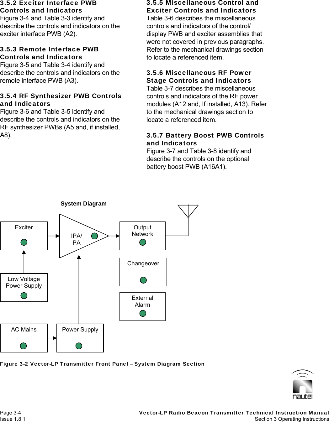
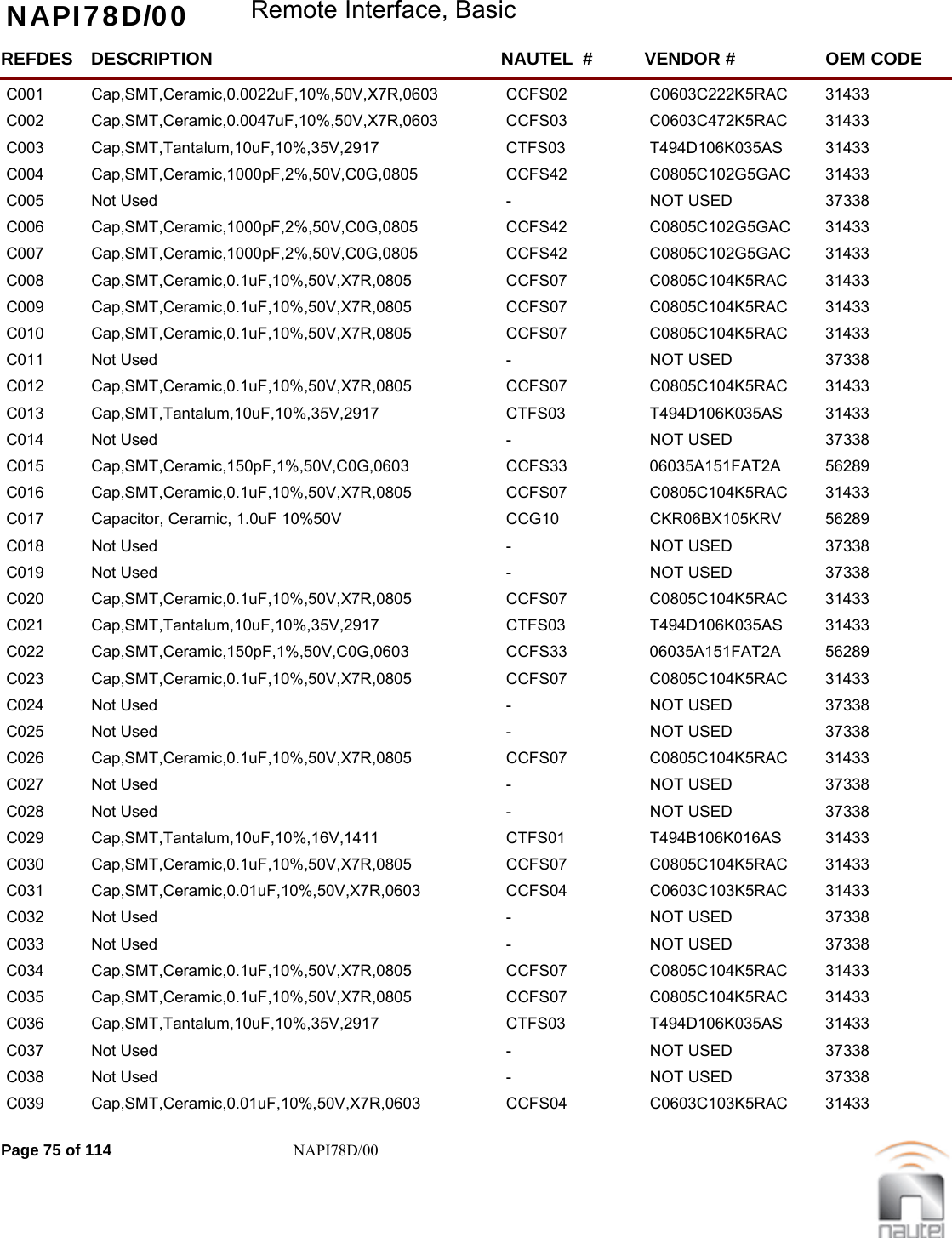
![Vector-LP Radio Beacon Transmitter Technical Instruction Manual Page 2-17 Section 2 Preparation for Use and Installation Issue 1.8.1 (c) Apply dc power. Verify the voltage between TB1-1 and TB1-2 is the battery’s nominal voltage [24 V dc (VR125 only) or 48 V dc]. 2.4 COMMISSIONING The following procedures are in a step-by-step format. They permit a person who is not familiar with the transmitter to perform required checks. Complete the procedures in sequence. The transmitter is calibrated and burned-in during manufacture. Unless otherwise specified you should not need to make any adjustment. If the tests associated with a procedure indicate the pre-set adjustments are not optimum, perform the appropriate adjustment procedure detailed in Section 4, Testing and Adjustment prior to proceeding with additional tests. 2.4.1 Precautions The transmitter contains many solid state devices that can be damaged by excessive heat or high voltage transients. Read and observe the precautionary information in Section 3 - Operating Instructions prior to applying power. 2.4.2 Turn-On Prerequisites Complete the following steps to verify the transmitter is ready to turn on: (a) Ensure that the RF filter PWB (A14) is tuned for the desired frequency: see Table 2-6a for standard frequencies between 190 and 535 kHz. see Table 2-6b for 125 W transmitters operating at extended frequencies between 536 and 1250 kHz or between 1600 and 1800 kHz. NOTE 250 W transmitters that operate in the extended band of 1600 to 1800 kHz do not require any jumper adjustments. WARNING If there is a jumper between TB1-19 and TB1-20 on remote interface PWB A3, safety features controlled by the external interlocks will be disabled. Implement a fail-safe method to alert personnel to this fact. Dangerous voltages are present on RF output stages and the antenna system if the transmitter is on. (b) Close all external interlocks or connect a temporary jumper wire between TB1-19 and TB1-20 of the remote interface PWB (A3). 2.4.3 Initial Turn-On Ensure that all connectors on the back of the transmitter and the back of the front panel are securely fastened. If there are any loose connectors, ensure they are mated according to the connector’s labeled tag. (a) Switch the ac power switch on the back of the transmitter to ON. (b) Verify that the GUI on the front panel is on and displays legible text. (c) Select local control by pressing the Control – Local button. (d) Confirm that the System Diagram’s Control - RF Off and Local lamps are on. Confirm that the amber LEDs in the RF power modules are all flashing. (e) Set the Requested Power Source to AC (see 3.6.9). (f) Clear the Events Log (see 3.6.5).](https://usermanual.wiki/Nautel-Maine/VECTOR125/User-Guide-2553568-Page-38.png)

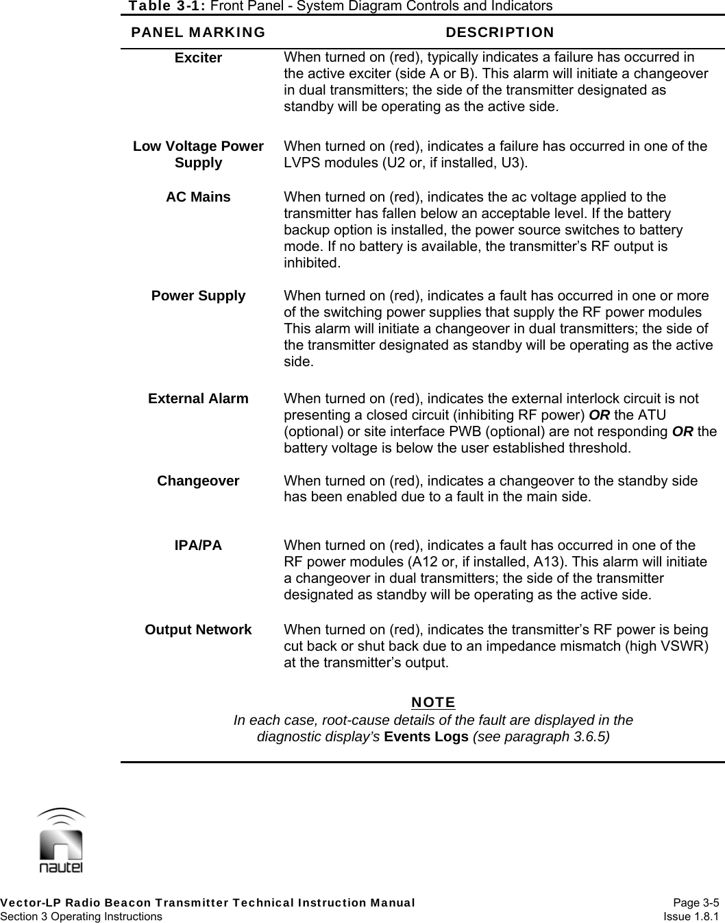

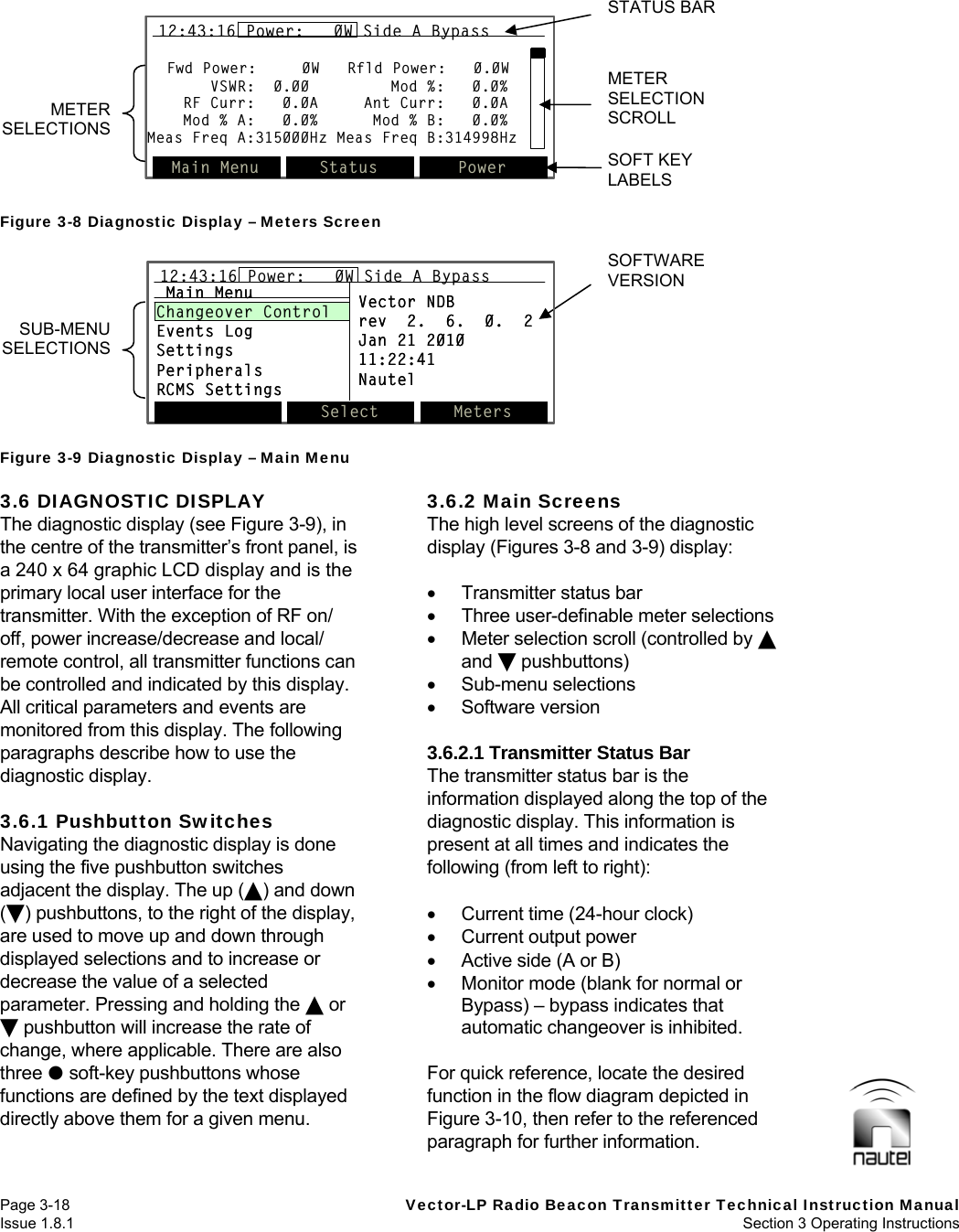
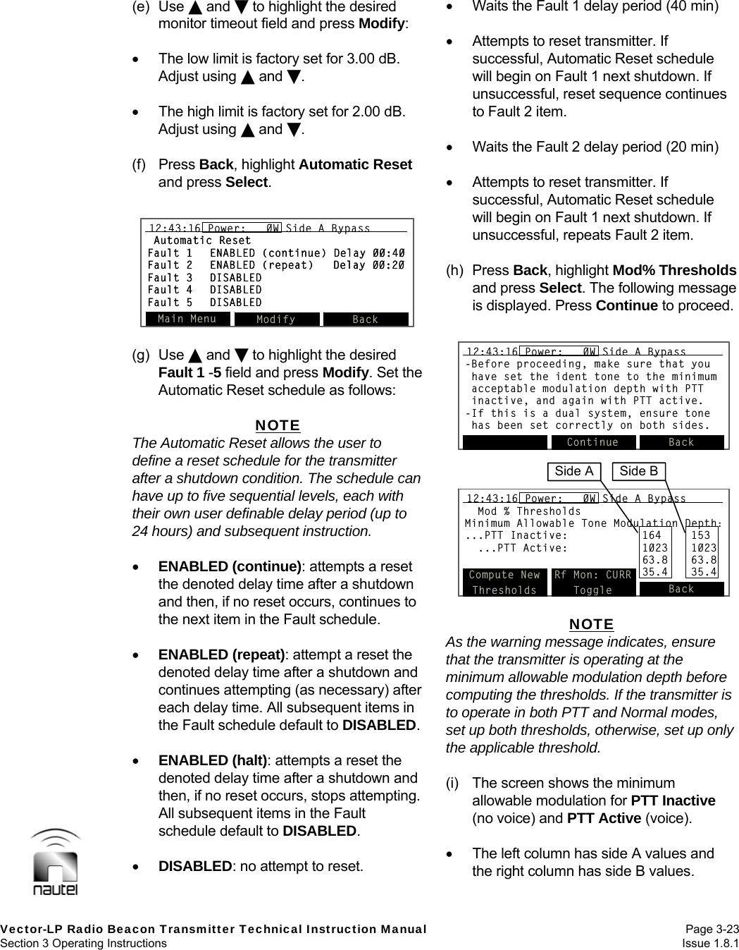
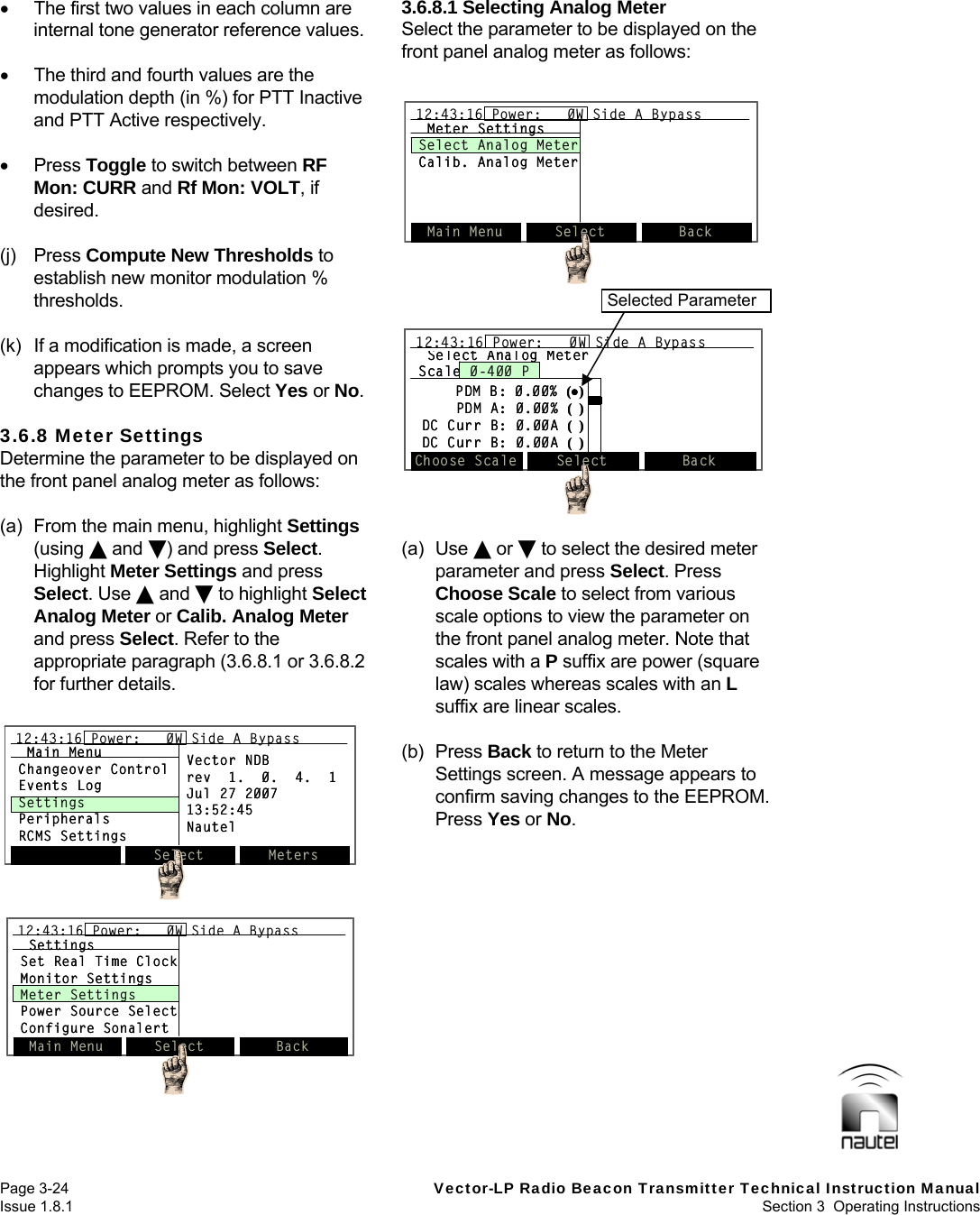
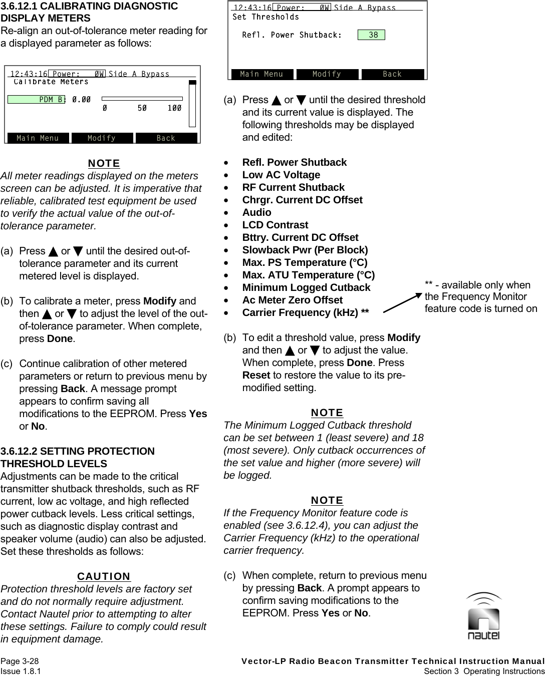
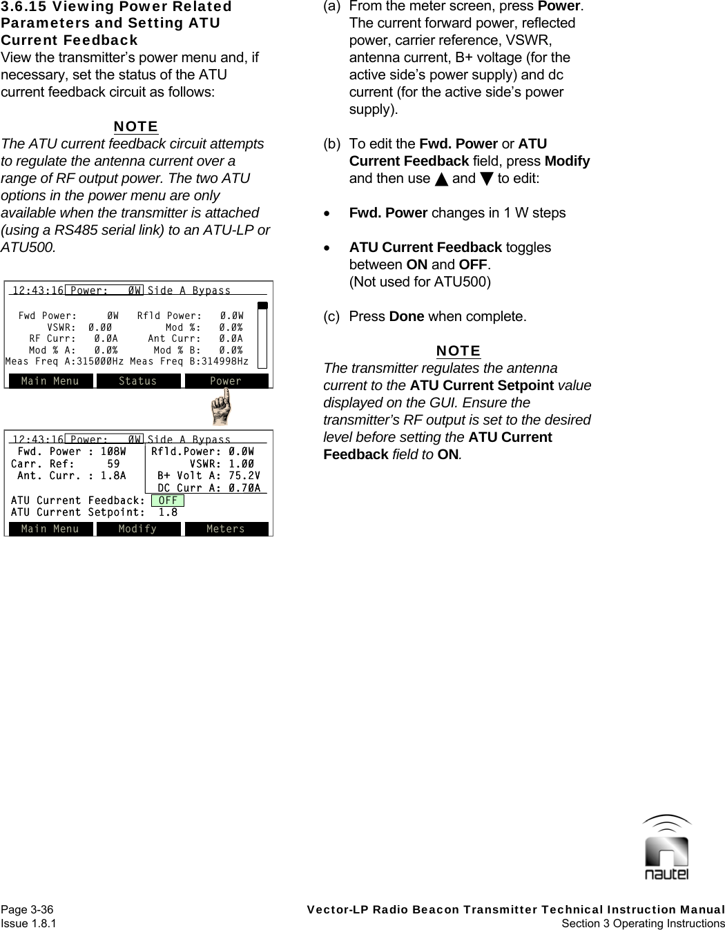
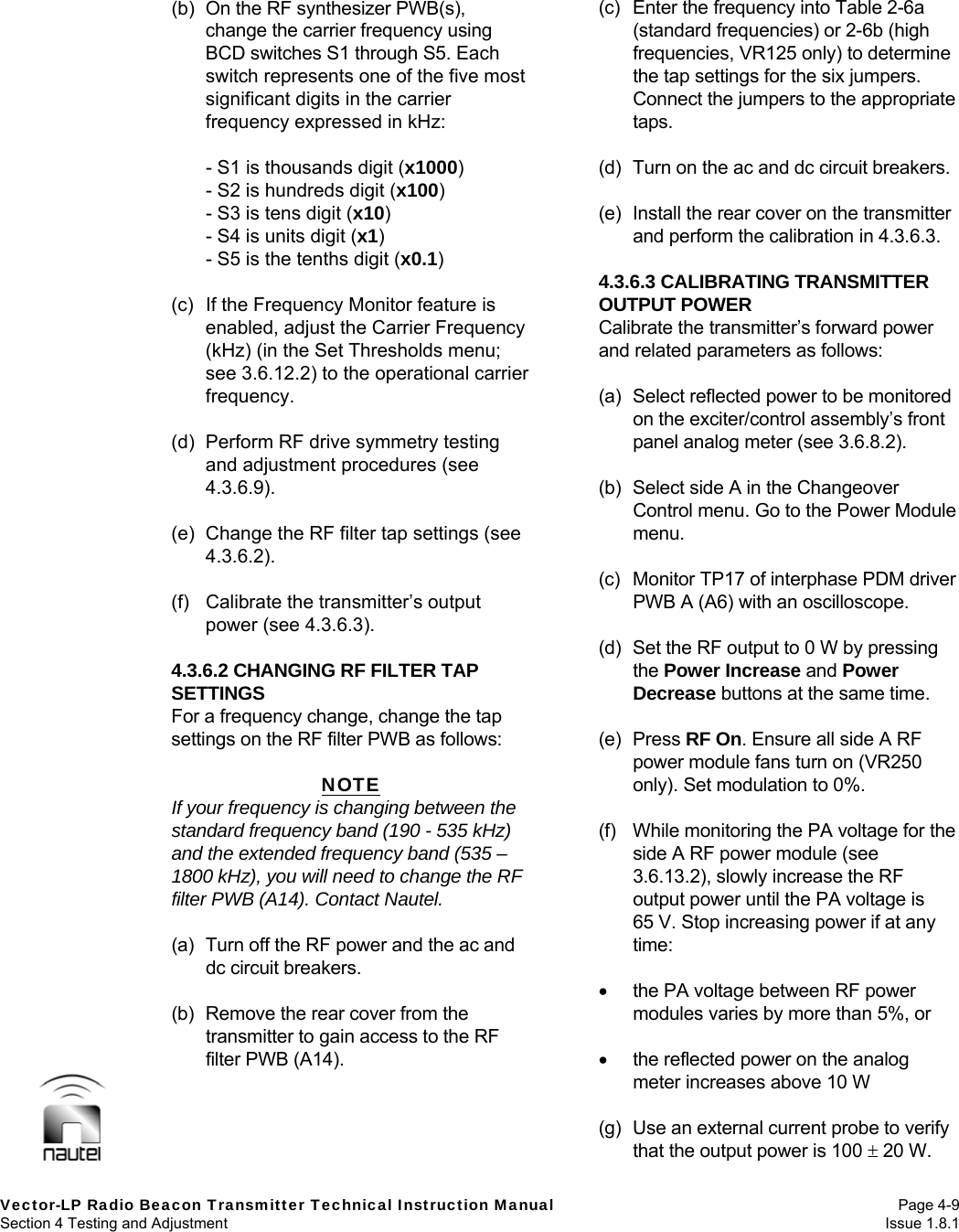
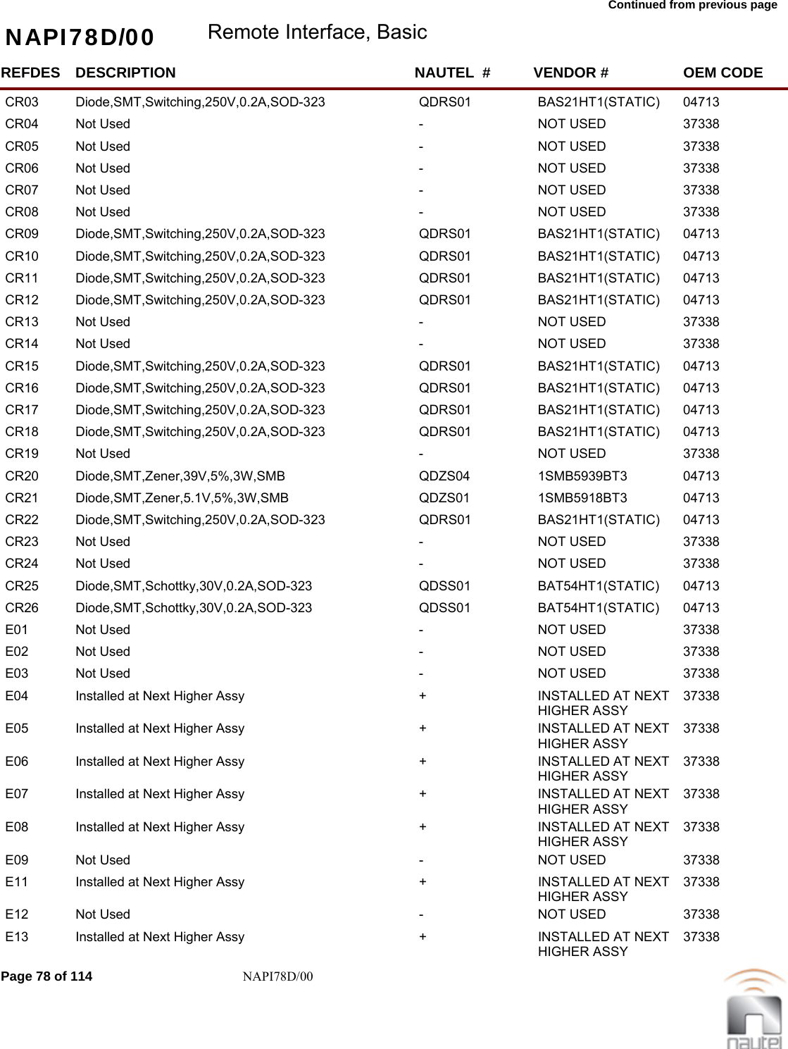
![Page 3-26 Vector-LP Radio Beacon Transmitter Technical Instruction Manual Issue 1.8.1 Section 3 Operating Instructions 3.6.10 Configuring the Sonalert Configure the status of the audible alarm (sonalert) for all transmitter alarms as follows: (a) From the main menu, highlight Settings (using and ) and press Select. Highlight Configure Sonalert and press Select. NOTE The Sonalert peripheral must be activated (see 3.6.13.5) before settings in this section can take effect. (b) A list of transmitter alarms and their current SonAlert (audible) and Site Ctrl (remote outputs) status is displayed. To configure an alarm for the sonalert, use and to select the desired alarm; press Toggle to change the status to ON. Press Modify to configure an alarm for use with site interface PWB A4 (if installed). Use and to select the desired alarm and press Toggle to change the status from OFF to the appropriate remote control output (1 through 16). 3.6.11 Setting a Timed Shutdown Modify timed shutdown parameters as follows: (a) From the main menu, highlight Settings (using and ) and press Select. Highlight Timed Shutdown and press Select. (b) Use and to highlight Timed Shutdown, Interval or Auto Assert, noting: Select Meters12:43:16 Power: 0W Side A BypassMain MenuChangeover ControlEvents LogSettingsPeripheralsRCMS SettingsVector NDBrev 2. 6. 0. 2Jan 21 201011:22:41NautelSelect Meters12:43:16 Power: 0W Side A Bypass12:43:16 Power: 0W Side A BypassMain MenuChangeover ControlEvents LogSettingsPeripheralsRCMS SettingsVector NDBrev 2. 6. 0. 2Jan 21 201011:22:41NautelSettingsMeter SettingsPower Source SelectConfigure SonalertTimed ShutdownFactory SettingsMain Menu Select Back12:43:16 Power: 0W Side A BypassSettingsMeter SettingsPower Source SelectConfigure SonalertTimed ShutdownFactory SettingsMain Menu Select Back12:43:16 Power: 0W Side A Bypass12:43:16 Power: 0W Side A BypassSelect Meters12:43:16 Power: 0W Side A BypassMain MenuChangeover ControlEvents LogSettingsPeripheralsRCMS SettingsVector NDBrev 2. 6. 0. 2Jan 21 201011:22:41NautelSelect Meters12:43:16 Power: 0W Side A Bypass12:43:16 Power: 0W Side A BypassMain MenuChangeover ControlEvents LogSettingsPeripheralsRCMS SettingsVector NDBrev 2. 6. 0. 2Jan 21 201011:22:41NautelSettingsSet Real Time ClockMonitor SettingsMeter SettingsPower Source SelectConfigure SonalertMain Menu Select Back12:43:16 Power: 0W Side A BypassSettingsSet Real Time ClockMonitor SettingsMeter SettingsPower Source SelectConfigure SonalertMain Menu Select Back12:43:16 Power: 0W Side A Bypass12:43:16 Power: 0W Side A BypassToggle Modify Back12:43:16 Power: 0W Side A BypassAlarm Signal SonAlert SiteCtrlPDM Latch B OFF OFFPDM Latch A OFF OFFHigh RF Curr OFF OFFSWR Shutback OFF OFFLow AC Voltage OFF OFFToggle Modify Back12:43:16 Power: 0W Side A Bypass12:43:16 Power: 0W Side A BypassAlarm Signal SonAlert SiteCtrlPDM Latch B OFF OFFPDM Latch A OFF OFFHigh RF Curr OFF OFFSWR Shutback OFF OFFLow AC Voltage OFF OFFMain Menu Toggle Back12:43:16 Power: 0W Side A BypassTimed ShutdownTimed Shutdown [DISABLED ]Interval [00:05 ]Auto Assert [Monitor Point 1 ]Timer State:Stopped 00:05:00Main Menu Toggle Back12:43:16 Power: 0W Side A Bypass12:43:16 Power: 0W Side A BypassTimed ShutdownTimed Shutdown [DISABLED ]Interval [00:05 ]Auto Assert [Monitor Point 1 ]Timer State:Stopped 00:05:00](https://usermanual.wiki/Nautel-Maine/VECTOR125/User-Guide-2553568-Page-67.png)
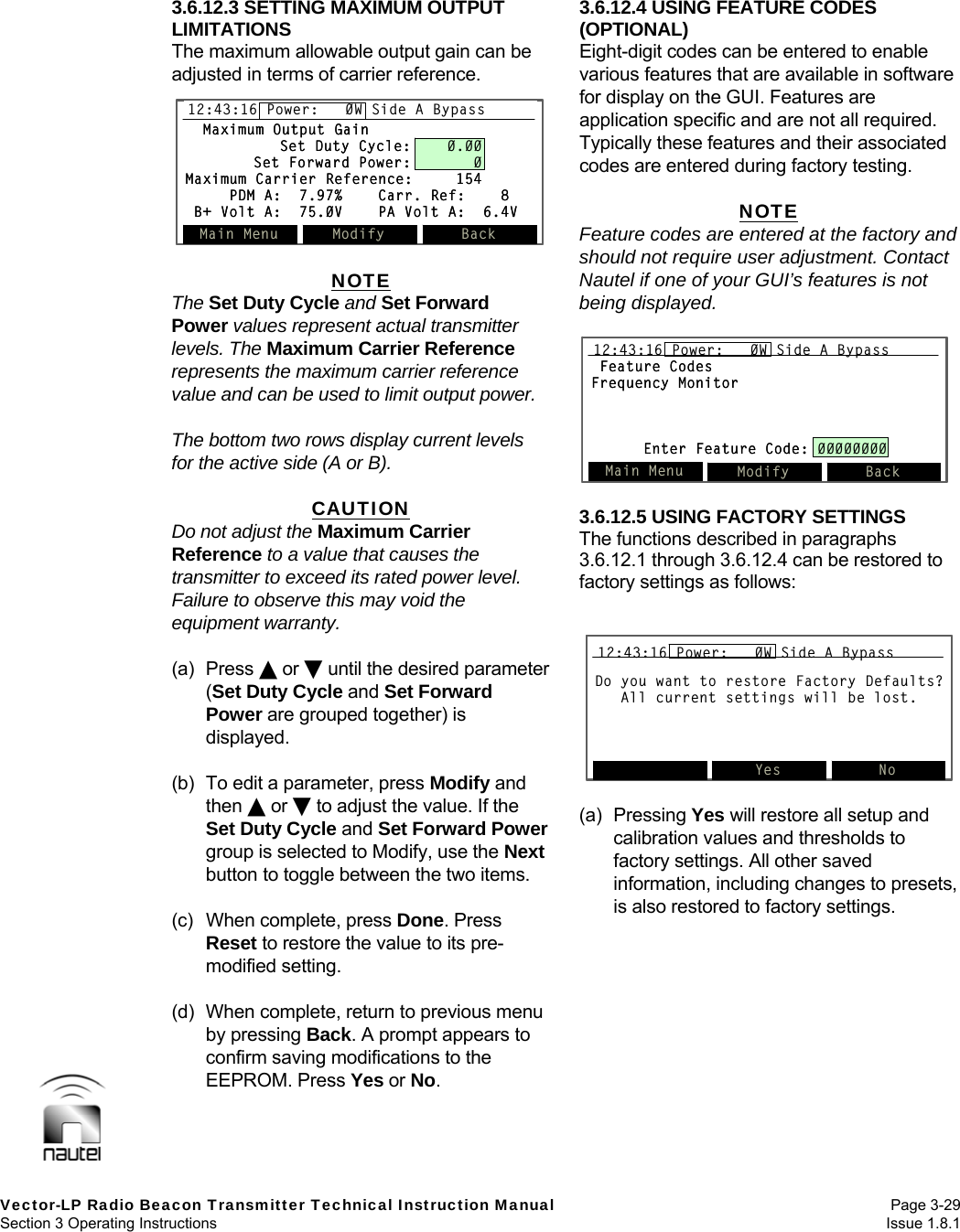
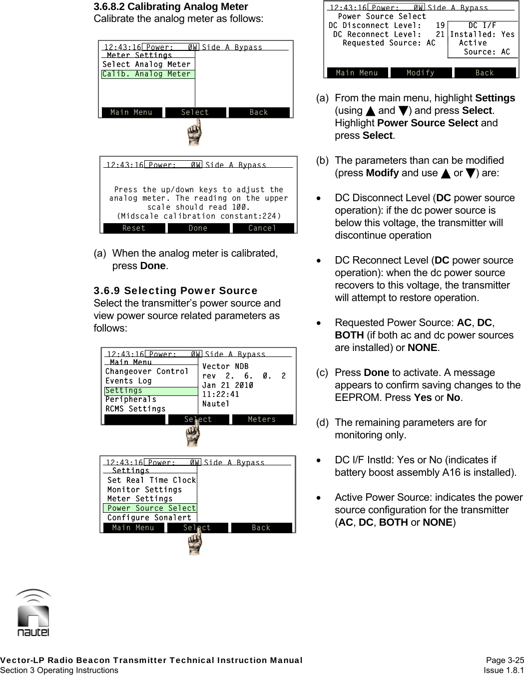
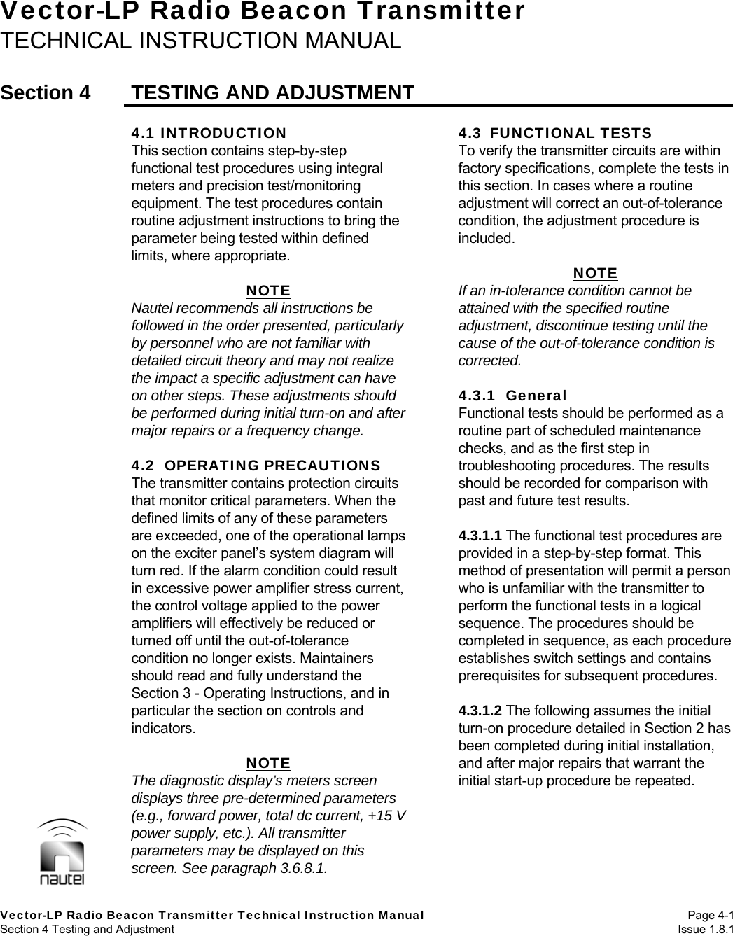
![Vector-LP Radio Beacon Transmitter Technical Instruction Manual Page 3-31 Section 3 Operating Instructions Issue 1.8.1 Reset Done Cancel12:43:16 Power: 0W Side A BypassFrame SequenceMK MK MK MK MK MK MK MKKeyed String: TESTFrame Format: NAV CANFrame Timing: 20.0 secPress up/downkeys to changethe duration ofeach frame.Press Done toconfirm changes.Reset Done Cancel12:43:16 Power: 0W Side A Bypass12:43:16 Power: 0W Side A BypassFrame SequenceMK MK MK MK MK MK MK MKKeyed String: TESTFrame Format: NAV CANFrame Timing: 20.0 secPress up/downkeys to changethe duration ofeach frame.Press Done toconfirm changes.Frame TimingReset Done Cancel12:43:16 Power: 0W Side A BypassFrame SequenceMK MK MK MK MK MK MK MKKeyed String: TESTFrame Format: NAV CANFrame Timing: 20.0 secPress up/downkeys to select aframe format touse. Press Doneto confirm yourselectionReset Done Cancel12:43:16 Power: 0W Side A BypassFrame SequenceMK MK MK MK MK MK MK MKKeyed String: TESTFrame Format: NAV CANFrame Timing: 20.0 secPress up/downkeys to select aframe format touse. Press Doneto confirm yourselectionFrame FormatReset Next Cancel12:43:16 Power: 0W Side A BypassFrame SequenceMK MK MK MK MK MK MK MKKeyed String: TESTFrame Format: NAV CANFrame Timing: 20.0 secLegend:MK: All MarksSP: All SpacesAL: AlternatingMarks/SpacesKY: Keyed StringReset Next Cancel12:43:16 Power: 0W Side A Bypass12:43:16 Power: 0W Side A BypassFrame SequenceMK MK MK MK MK MK MK MKKeyed String: TESTFrame Format: NAV CANFrame Timing: 20.0 secLegend:MK: All MarksSP: All SpacesAL: AlternatingMarks/SpacesKY: Keyed StringFrame SequenceReset Next Cancel12:43:16 Power: 0W Side A BypassFrame SequenceMK MK MK MK MK MK MK MKKeyed String: TESTFrame Format: NAV CANFrame Timing: 20.0 secPress up/downkeys to changethe selectedletter. PressNext to go on tothe next letterReset Next Cancel12:43:16 Power: 0W Side A Bypass12:43:16 Power: 0W Side A BypassFrame SequenceMK MK MK MK MK MK MK MKKeyed String: TESTFrame Format: NAV CANFrame Timing: 20.0 secPress up/downkeys to changethe selectedletter. PressNext to go on tothe next letterKeyed StringMain Menu Toggle Back12:43:16 Power: 0W Side A BypassKeyer ModulationModulationKeyerTone GeneratorTone Frequency[ON ][OFF ][ON ][1020 Hz]Main Menu Toggle Back12:43:16 Power: 0W Side A Bypass12:43:16 Power: 0W Side A BypassKeyer ModulationModulationKeyerTone GeneratorTone Frequency[ON ][OFF ][ON ][1020 Hz] (b) Keyer Modulation: Select the desired parameter, using or . Press Toggle to change the status or value and then press Back: Modulation, Keyer and Tone Generator can be set to ON or OFF. Tone Frequency can be set to 400 Hz or 1020 Hz. (c) Keyer Sequence: Select the desired parameter, Frame Sequence, Keyed String, Frame Format or Frame Timing, using or . Press Modify and follow the instructions on the right-hand side of the GUI display. (set to either NAV CAN or ICAO) - ICAO: International Civil Aviation Organization - NAV CAN: uses a 10 s frame and 0.125 ms bits to key out 3 symbols. (set between 4.0 s and 20.0 s) (d) Standby Codes 1 and 2: Press Toggle to enable [X] or disable [ ] the standby code 1 or 2. For Standby Code 1, use the and buttons to move between field. Continue using Toggle to select or de-select the location of additional inserted spaces. 3.6.13.2 VIEWING POWER MODULE STATUS Configure the transmitter’s software for the number of power blocks and view the status of individual power modules as follows: Main Menu Modify Back12:43:16 Power: 0W Side A BypassFrame SequenceMK MK MK MK MK MK MK MKKeyed String: TESTFrame Format: TRANS CANFrame Timing: 20.0 secPress up/downkeys to select afield to changePress Modify tomake changesMain Menu Modify Back12:43:16 Power: 0W Side A Bypass12:43:16 Power: 0W Side A BypassFrame SequenceMK MK MK MK MK MK MK MKKeyed String: TESTFrame Format: TRANS CANFrame Timing: 20.0 secPress up/downkeys to select afield to changePress Modify tomake changesMain Menu Toggle Back12:43:16 Power: 0W Side A BypassStandby Code 1[ X ] Enable Standby Code 1Inserts additional spaces betweenselected characters in each keyedFrame: __[ ]__[ ]__[ ]__[ ]__[ ]__Main Menu Toggle Back12:43:16 Power: 0W Side A Bypass12:43:16 Power: 0W Side A BypassStandby Code 1[ X ] Enable Standby Code 1Inserts additional spaces betweenselected characters in each keyedFrame: __[ ]__[ ]__[ ]__[ ]__[ ]__Main Menu Select Back12:43:16 Power: 0W Side A BypassStandby Code 2[ X ] Enable Standby Code 2Inserts a 2-bit mark at the beginningof each keyed frame.Main Menu Toggle Back12:43:16 Power: 0W Site A BypassMain Menu Select Back12:43:16 Power: 0W Side A BypassStandby Code 2[ X ] Enable Standby Code 2Inserts a 2-bit mark at the beginningof each keyed frame.Main Menu Select Back12:43:16 Power: 0W Side A Bypass12:43:16 Power: 0W Side A BypassStandby Code 2[ X ] Enable Standby Code 2Inserts a 2-bit mark at the beginningof each keyed frame.Main Menu Toggle Back12:43:16 Power: 0W Site A Bypass12:43:16 Power: 0W Site A Bypass](https://usermanual.wiki/Nautel-Maine/VECTOR125/User-Guide-2553568-Page-72.png)
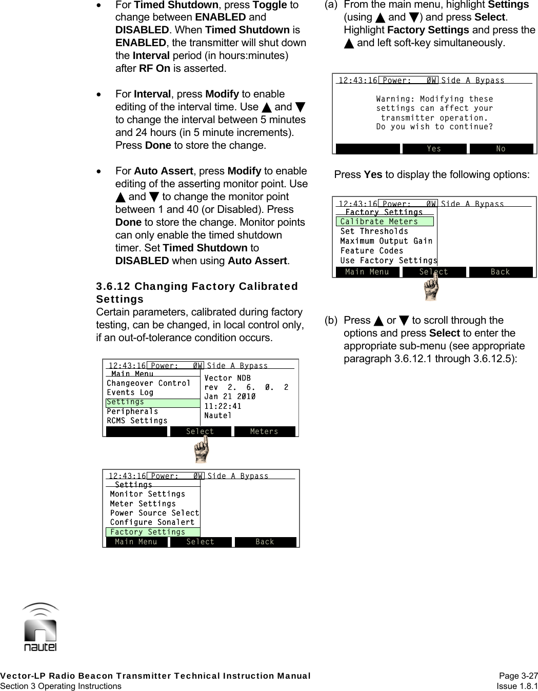
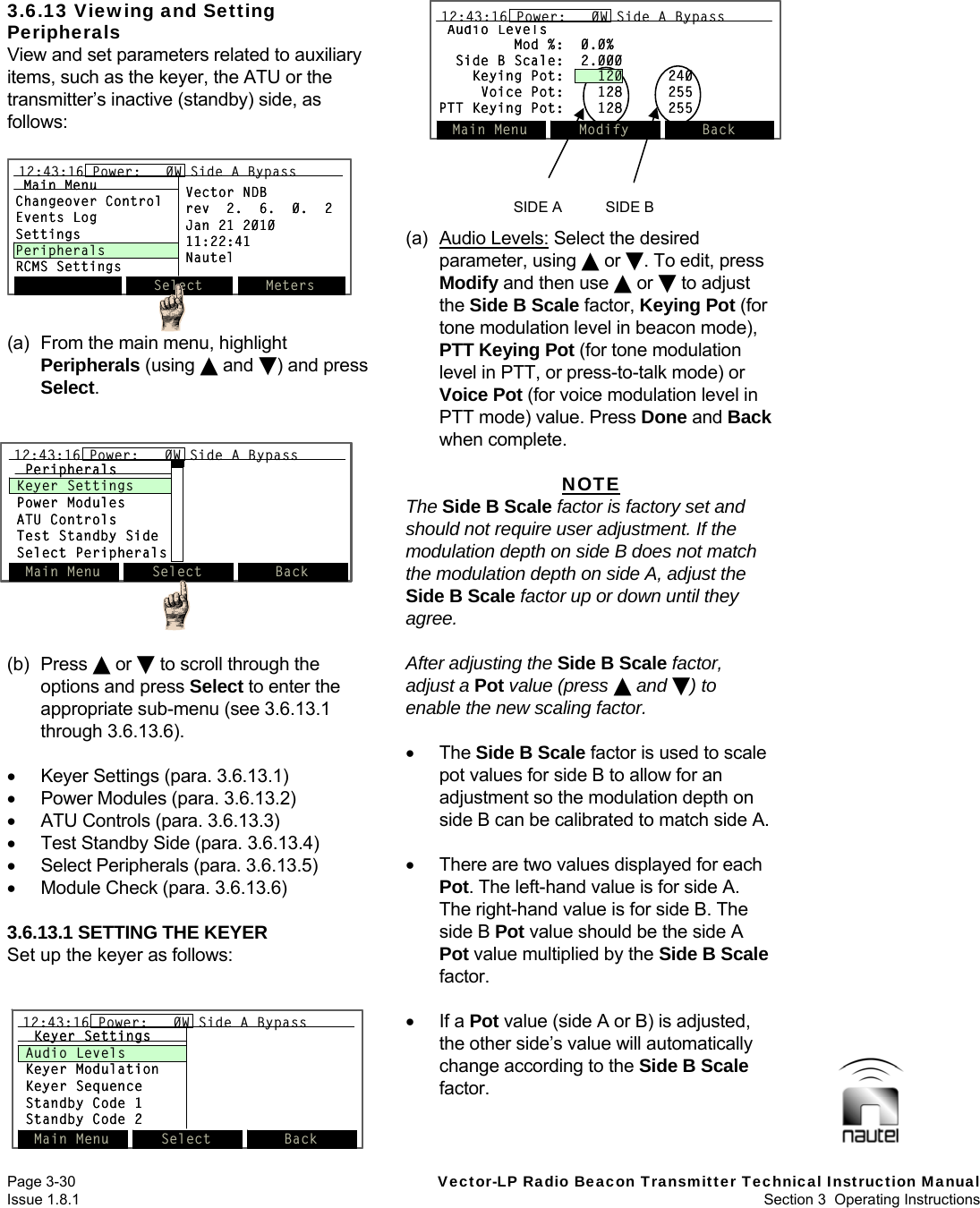
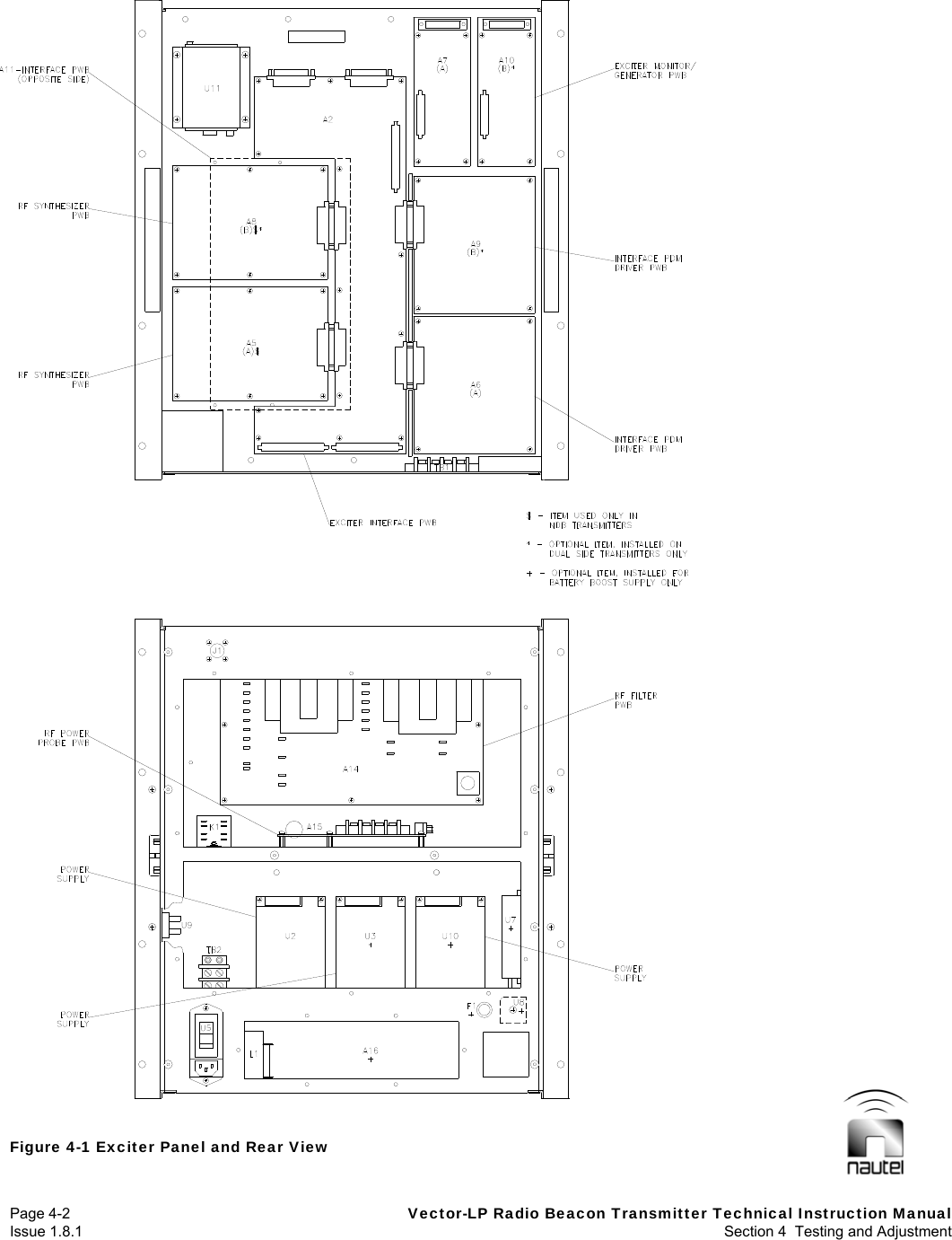
![Page 3-32 Vector-LP Radio Beacon Transmitter Technical Instruction Manual Issue 1.8.1 Section 3 Operating Instructions Power ModuleNumber of Power block expected: [3]Block # 1 2 3 4Side: A OK [X] [ ] [ ] [ ]B OK [X] [ ] [ ] [ ]Main Menu View Details Back12:43:16 Power: 0W Site A BypassPower ModuleNumber of Power block expected: [3]Block # 1 2 3 4Side: A OK [X] [ ] [ ] [ ]B OK [X] [ ] [ ] [ ]Main Menu View Details Back12:43:16 Power: 0W Site A Bypass12:43:16 Power: 0W Site A BypassX = installed Detailed Status PA Bloc 1B+ Setting : 150 Inhibited : YesTemperature: -50 B+ Voltage : 0.0Dc Current : 0.10 PA Voltage : 0.0Fan 1 Tach : 1 Fan 2 Tach : 0PDM Inhib : No PA Alarm : NoMain Menu Back12:43:16 Power: 0W Side A BypassDetailed Status PA Bloc 1B+ Setting : 150 Inhibited : YesTemperature: -50 B+ Voltage : 0.0Dc Current : 0.10 PA Voltage : 0.0Fan 1 Tach : 1 Fan 2 Tach : 0PDM Inhib : No PA Alarm : NoMain Menu Back12:43:16 Power: 0W Side A Bypass12:43:16 Power: 0W Side A BypassPA = Side A (a) Press or until the desired parameter is highlighted. If the Number of Power block expected value is highlighted, the Modify option is displayed. If necessary, press Modify and use or to select 1 (for Vector-LP). Press Done when complete. If one of the power module fields (Block # 1, Side A and B for Vector-LP) is highlighted, the View Details option is displayed. Press View Details to view the following RF power module details: (b) Return to the previous menu by pressing Back. 3.6.13.3 ATU CONTROLS If a Nautel antenna tuning unit (ATU) is being used, view and edit its control parameters as follows: NOTE A serial interface allows communication between the transmitter and the ATU. This interface connects to the transmitter via the INTERNAL RS-485 connector (25-pin D-sub) on the rear of the exciter/control assembly. (a) The screen below appears if the ATU is in local mode of operation and auto-tuning is active and is tuned. This screen allows viewing of ATU status only. No adjustments are possible while the ATU is in local mode. (b) If the ATU is set to the remote mode of operation, the screen is as shown below. This screen allows ATU tuning to be controlled from the transmitter GUI. Press Coil Control. (c) In the coil control screen shown below, use and to select the desired coil to control - Resistive Coil or Inductive Coil. Press Continue. ATU Control Antenna Curr.: 0.0ADec L N H Inc Auto-TuningR[ ] [] [ ] ActiveL[ ] [][ ] ActiveATU is in REMOTE ModePress Coil Control to modify ATU settings12:43:16 Power: 0W Site A BypassMain Menu Coil Control BackATU Control Antenna Curr.: 0.0ADec L N H Inc Auto-TuningR[ ] [] [ ] ActiveL[ ] [][ ] ActiveATU is in REMOTE ModePress Coil Control to modify ATU settings12:43:16 Power: 0W Site A Bypass12:43:16 Power: 0W Site A BypassMain Menu Coil Control BackATU Control Antenna Curr.: 0.0ADec L N H Inc Auto-TuningR[ ] [][ ] ActiveL[ ] [][ ] ActiveCoil Control: Resistive CoilUP/Down Keys: Select a coil to configure12:43:16 Power: 0W Site A BypassMain Menu Continue BackATU Control Antenna Curr.: 0.0ADec L N H Inc Auto-TuningR[ ] [][ ] ActiveL[ ] [][ ] ActiveCoil Control: Resistive CoilUP/Down Keys: Select a coil to configure12:43:16 Power: 0W Site A Bypass12:43:16 Power: 0W Site A BypassMain Menu Continue BackIncrease/Decrease Arrows (Affected arrow is highlighted during auto or manual tuning) Resistive (R) and Inductive (L) Tuning Status LineATU Control Antenna Curr.: 0.0ADec L N H Inc Auto-TuningR[ ] [] [ ] ActiveL[ ] [][ ] ActiveATU is in LOCAL Mode12:43:16 Power: 0W Site A BypassBackATU Control Antenna Curr.: 0.0ADec L N H Inc Auto-TuningR[ ] [] [ ] ActiveL[ ] [][ ] ActiveATU is in LOCAL Mode12:43:16 Power: 0W Site A Bypass12:43:16 Power: 0W Site A BypassBackAuto-Tuning Status (Active or Inhibited)](https://usermanual.wiki/Nautel-Maine/VECTOR125/User-Guide-2553568-Page-73.png)
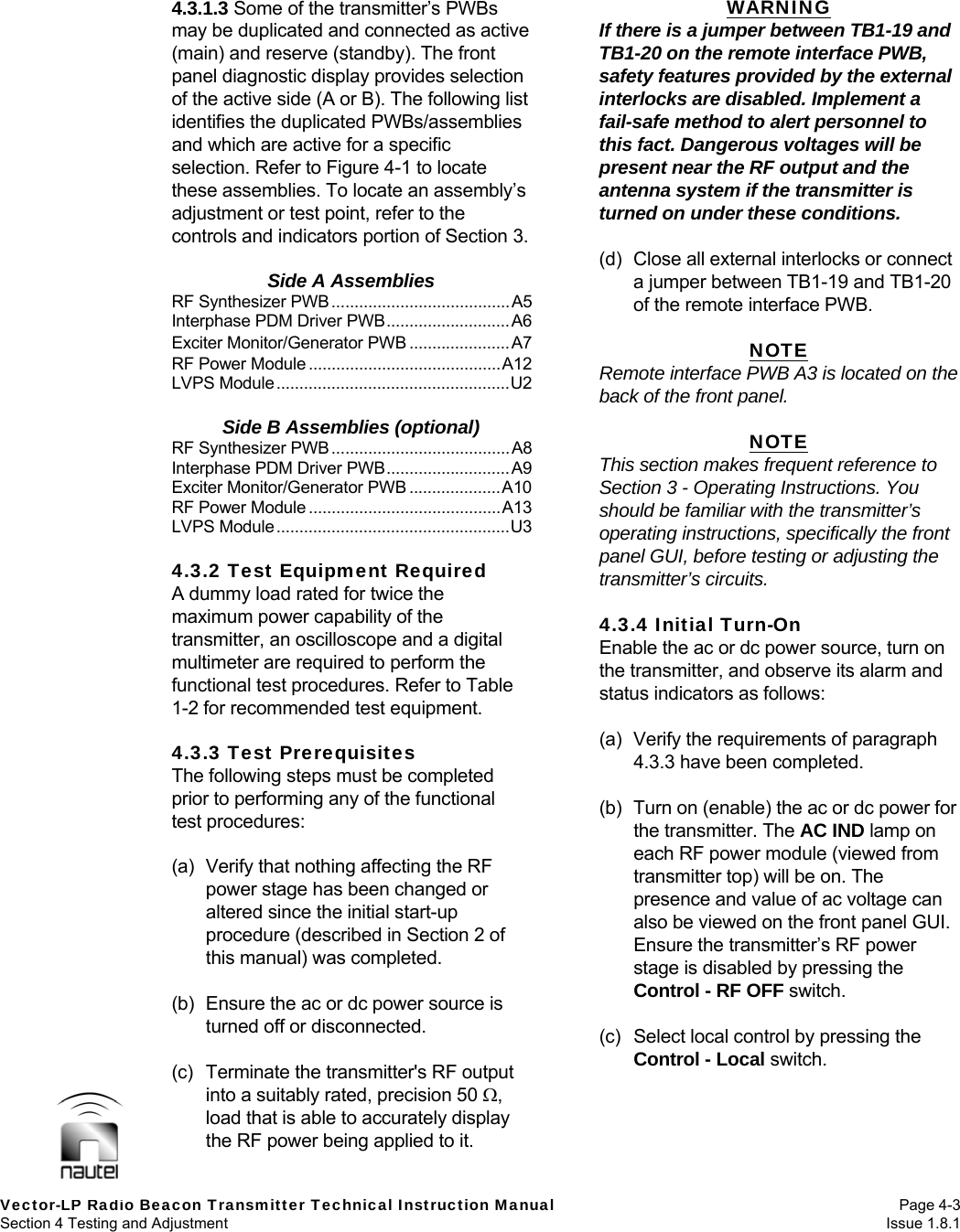
![Vector-LP Radio Beacon Transmitter Technical Instruction Manual Page 3-33 Section 3 Operating Instructions Issue 1.8.1 ATU Control Antenna Curr.: 0.0ADec L N H Inc Auto-TuningR[ ] [][ ] ActiveL[ ] [][ ] ActiveCoil Control: Resistive CoilWhat would you like to do:12:43:16 Power: 0W Site A BypassAuto Tuning Slew Servo BackATU Control Antenna Curr.: 0.0ADec L N H Inc Auto-TuningR[ ] [][ ] ActiveL[ ] [][ ] ActiveCoil Control: Resistive CoilWhat would you like to do:12:43:16 Power: 0W Site A Bypass12:43:16 Power: 0W Site A BypassAuto Tuning Slew Servo BackOR (d) If Auto Tuning is selected, the following screen appears which allows the selected coil to be auto tuned (active) or inhibited. Use and to highlight Active or Inhibited, then press Done to select. (e) If Slew Servo is selected, the following screen appears which allows the selected coil to be manually tuned. Use and to slew the coil high or low. Press Done when complete. 3.6.13.4 TESTING THE STANDBY SIDE Test the operation of the transmitter’s inactive (standby) side as follows: (a) Use and to highlight the desired test (Turn Standby Side Off, Test Power Supply, Test Modulators, Test RF Drive, or Run All Tests). Press Select to activate. (b) If you select a test, the display will initially indicate Running. When the test is complete, a pass (OK) or fail indication is displayed. If the item under test fails, a root cause message (e.g., PS Ovr Cur) is displayed. NOTE The root cause text is identical to that displayed in the Status menu (see 3.6.3). 3.6.13.5 SELECTING PERIPHERALS Configure the transmitter’s software for peripheral equipment, such as an ATU or site interface PWB as follows: (a) Use and to highlight the desired peripheral. Press Select to activate. If the site interface PWB (A2A4) is installed, select Site Control Board. If a Nautel ATU is used and a serial interface is connected to the INTERNAL RS-485 connector on the rear of the exciter/control assembly, select ATU. To hear the sonalert buzzer for a fault defined in the sonalert setup menu, select SonAlert. To hear the transmitter output, select Speaker. To enable the GUI to display Audio Limit alarm occurrences, select Overmod Alarm. If module fans are installed (VR250 only), select Module Fan Tachs. (b) Return to previous menu by pressing Back or press Main Menu. ATU Control Antenna Curr.: 0.0ADec L N H Inc Auto-TuningR[ ] [][ ] ActiveL[ ] [][ ] ActiveCoil Control: Resistive Coil:Slew ServoUp/Down Keys: Slew coil High/Low12:43:16 Power: 0W Site A BypassDoneATU Control Antenna Curr.: 0.0ADec L N H Inc Auto-TuningR[ ] [][ ] ActiveL[ ] [][ ] ActiveCoil Control: Resistive Coil:Slew ServoUp/Down Keys: Slew coil High/Low12:43:16 Power: 0W Site A Bypass12:43:16 Power: 0W Site A BypassDoneATU Control Antenna Curr.: 0.0ADec L N H Inc Auto-TuningR[ ] [][ ] ActiveL[ ] [][ ] ActiveCoil Control: Resistive CoilUp/Down Keys: (De)Activate Auto Tuning12:43:16 Power: 0W Site A BypassDoneATU Control Antenna Curr.: 0.0ADec L N H Inc Auto-TuningR[ ] [][ ] ActiveL[ ] [][ ] ActiveCoil Control: Resistive CoilUp/Down Keys: (De)Activate Auto Tuning12:43:16 Power: 0W Site A Bypass12:43:16 Power: 0W Site A BypassDoneMain Menu Select Back12:43:16 Power: 0W Side A BypassSelect PeripheralsSite Control BoardATUSonAlert BuzzerSpeakerOvermod Alarm[X][ ][ ][ ][ ]Main Menu Select Back12:43:16 Power: 0W Side A Bypass12:43:16 Power: 0W Side A BypassSelect PeripheralsSite Control BoardATUSonAlert BuzzerSpeakerOvermod Alarm[X][ ][ ][ ][ ]Indicates Selected Peripherals](https://usermanual.wiki/Nautel-Maine/VECTOR125/User-Guide-2553568-Page-74.png)
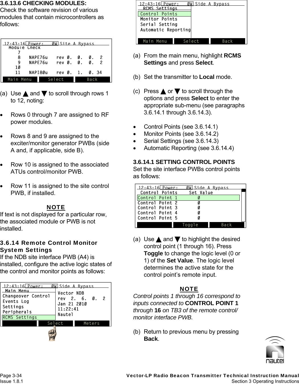
![Vector-LP Radio Beacon Transmitter Technical Instruction Manual Page 3-35 Section 3 Operating Instructions Issue 1.8.1 3.6.14.2 SETTING MONITOR POINTS Set the site interface PWB’s monitor points as follows: (a) Use and to highlight the desired monitor point (1 through 16). Press Toggle to change the logic level (0 or 1) of the Default value. The logic level determines the active (for status outputs) or normal (for alarm outputs) state for the monitor point’s remote output. NOTE Monitor points 1 through 16 correspond to outputs connected to MONITOR POINT 1 through 16 on TB1 and TB2 of the site interface PWB. (b) The values in the Current column represent the existing state of the monitor point. Press Set Current to set the Current values to match the Default values. (c) Return to previous menu by pressing Back. 3.6.14.3 SERIAL SETTINGS Set up the serial connection as follows: (a) Use and to highlight the desired serial setting. Press Modify or Toggle to change the setting. Press Next or Done when complete. To modify Tx Address, use and . Press Toggle to set Connection Mode to DIRECT or MODEM. When MODEM is selected, the following screen appears, which enables three further settings: Press Toggle to set Modem Line to DIAL UP or LEASED. The Dial-up number option disappears when LEASED is selected. Press , and Next to set the Passkey and the Dial-up Number. (b) Return to the previous menu by pressing Back. 3.6.14.4 AUTOMATIC REPORTING Configure the serial connection to automatically report transmitter alarms (without needing to poll the status) as follows: (a) A list of transmitter alarms and their current Automatic Reporting status is displayed. To configure an alarm for automatic reporting, use and to select the desired alarm and press Select to change the status to ON. Main Menu Modify Back12:43:16 Power: 0W Side A BypassSerial SettingsTx AddressConnection ModeABCD[DIRECT ]Main Menu Modify Back12:43:16 Power: 0W Side A Bypass12:43:16 Power: 0W Side A BypassSerial SettingsTx AddressConnection ModeABCD[DIRECT ]Main Menu Toggle Back12:43:16 Power: 0W Side A BypassSerial SettingsTx AddressConnection ModeModem LinePasskeyDial-up NumberABCD[MODEM ][DIAL UP]0000Main Menu Toggle Back12:43:16 Power: 0W Side A Bypass12:43:16 Power: 0W Side A BypassSerial SettingsTx AddressConnection ModeModem LinePasskeyDial-up NumberABCD[MODEM ][DIAL UP]0000Fault Automatic ReportingPDM Latch B OFFPDM Latch A OFFHigh RF Current OFFSWR Shutback OFFLow AC Volts OFFMain Menu Select Back12:43:16 Power: 0W Side A BypassFault Automatic ReportingPDM Latch B OFFPDM Latch A OFFHigh RF Current OFFSWR Shutback OFFLow AC Volts OFFMain Menu Select Back12:43:16 Power: 0W Side A Bypass12:43:16 Power: 0W Side A BypassMonitor Points Default CurrentMonitor Point 1 0 0Monitor Point 2 0 0Monitor Point 3 0 0Monitor Point 4 0 0Monitor Point 5 0 0Set Current Toggle Back12:43:16 Power: 0W Side A BypassMonitor Points Default CurrentMonitor Point 1 0 0Monitor Point 2 0 0Monitor Point 3 0 0Monitor Point 4 0 0Monitor Point 5 0 0Set Current Toggle Back12:43:16 Power: 0W Side A Bypass12:43:16 Power: 0W Side A Bypass](https://usermanual.wiki/Nautel-Maine/VECTOR125/User-Guide-2553568-Page-76.png)


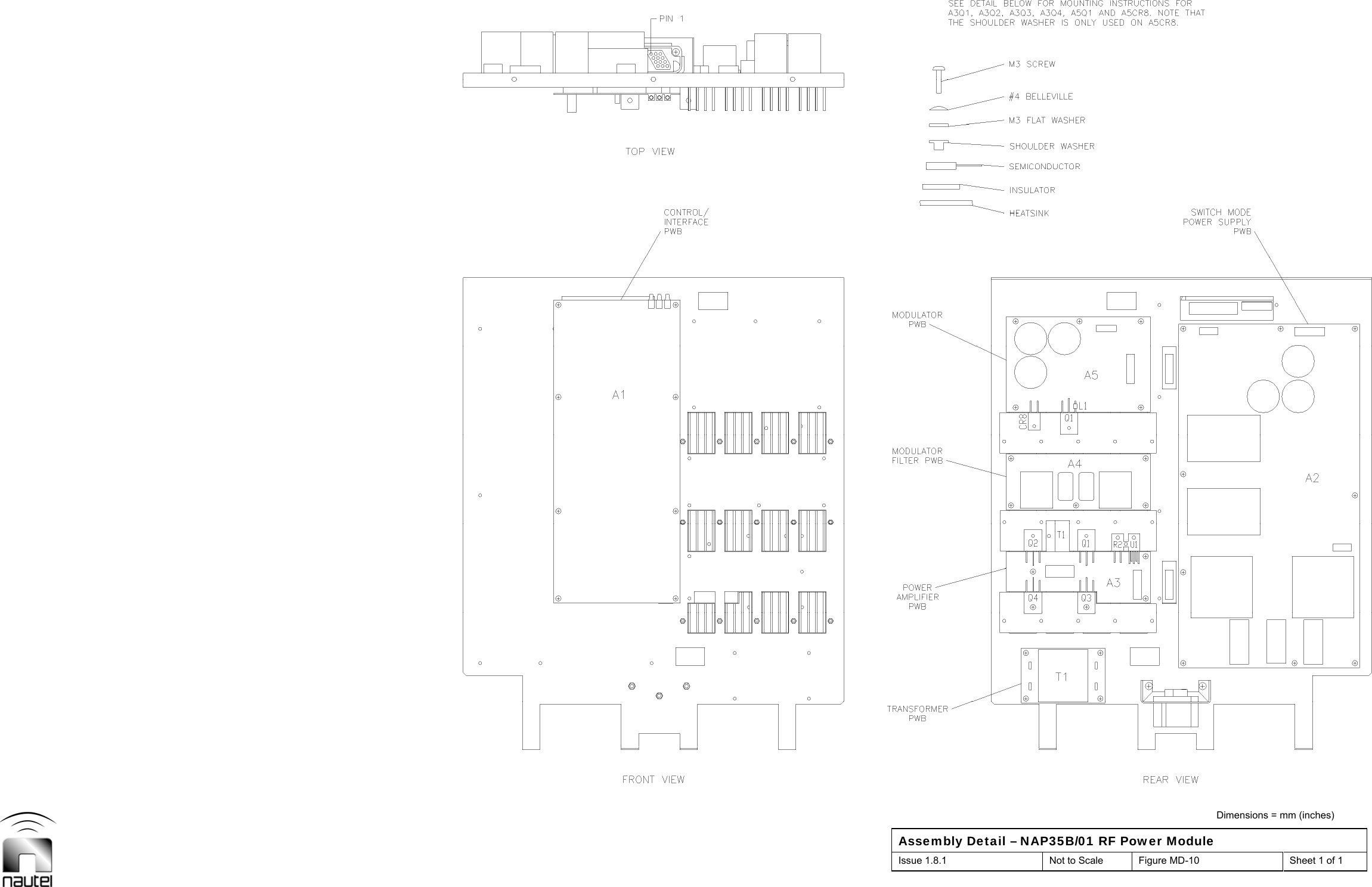
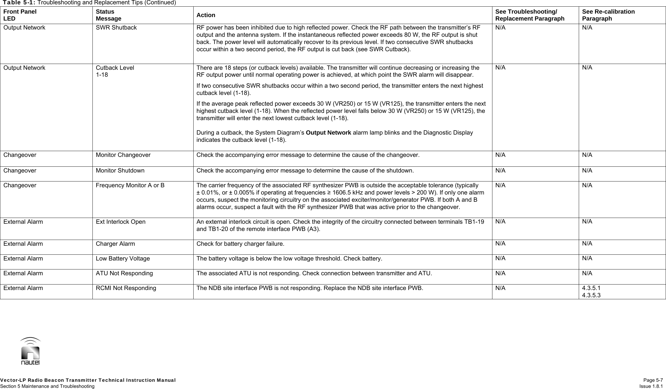
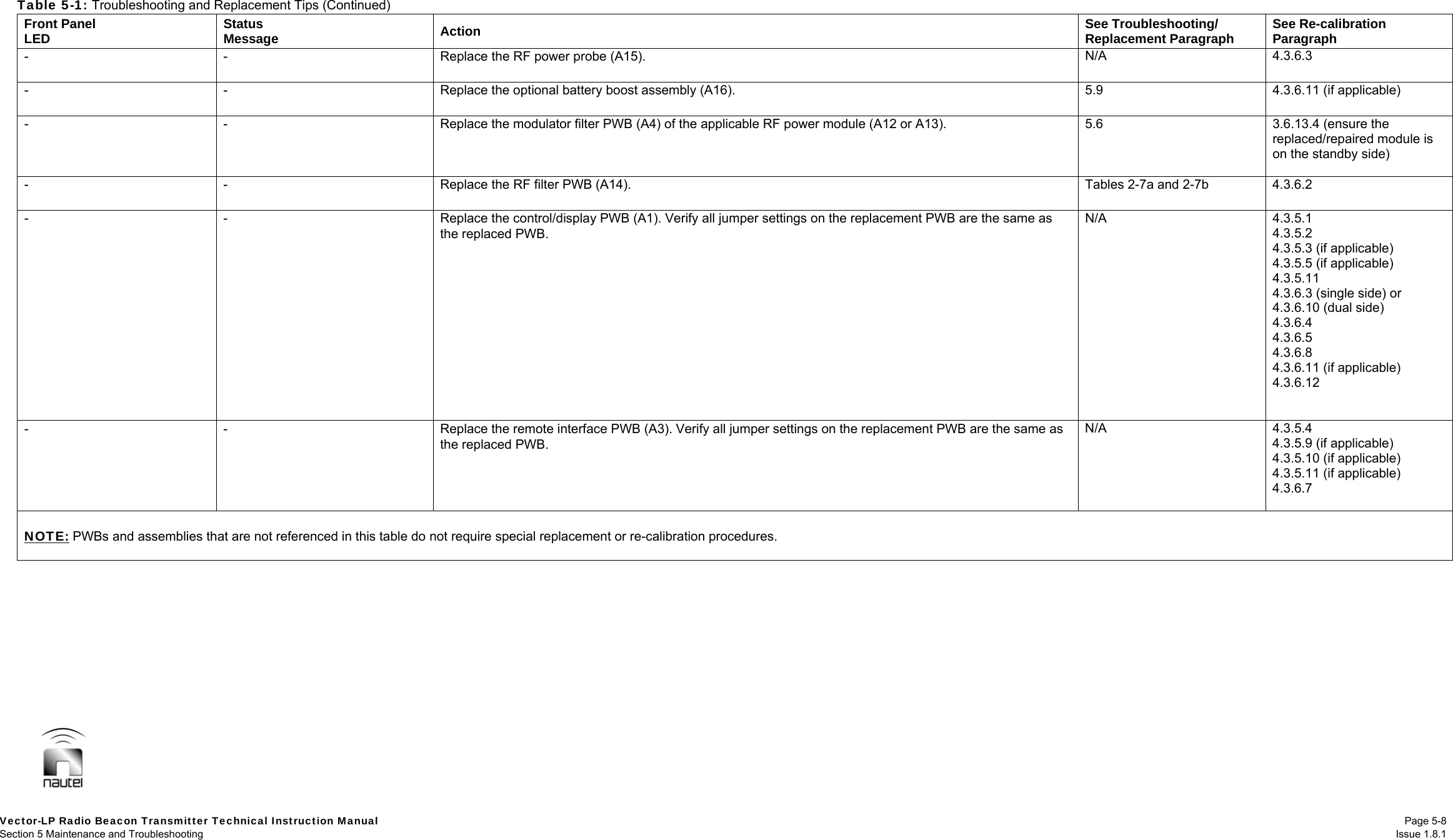
![Vector-LP Radio Beacon Transmitter Technical Instruction Manual Page 5-5 Section 5 Maintenance and Troubleshooting Issue 1.8.1 Table 5-1: Troubleshooting and Replacement Tips Front Panel LED Status Message Action See Troubleshooting/ Replacement Paragraph See Re-calibration Paragraph AC Mains Low AC Voltage The ac voltage is less than 170 V ac (or 90 V ac for VR125 transmitters). If the ac source voltage is present, check the ac breaker at the back of the transmitter. If the breaker is OK, replace the interface PWB (A11). 5.8.3 N/A Low Voltage Power Supply LVPS Fault A or B Replace associated ac/dc universal input power supply [side A (U2) or side B (U3)]. N/A N/A Power Supply Over Voltage PS A or B Replace switch mode power supply PWB (A2 of associated RF power module). 5.6.1 3.6.13.4 (ensure the replaced/repaired module is on the standby side) Power Supply Over Current PS A or B Replace switch mode power supply PWB (A2 of associated RF power module). If the transmitter is running in dc mode (optional), and this alarm is indicated on the active side, replace battery boost assembly A16. Otherwise, check cabling between A7 and A3 through A6. 5.6.1 5.9 3.6.13.4 (ensure the replaced/repaired module is on the standby side) Power Supply High Temp PS A or B Check fans. Ensure they are spinning at an adequate speed (a minimum of 3000 RPM, see 3.6.13.2). If necessary, replace the appropriate fan. N/A N/A Power Supply PS A or B Missing Module An RF power module has been removed from the associated side. N/A N/A PA Modulator Fail A or B Check/replace FET on modulator assembly (A5 of associated RF power module). 5.6.1 5.7 3.6.13.4 (ensure the replaced/repaired module is on the standby side) PA PA Alarm A or B Check/replace FETs on power amplifier (A3 of associated RF power module). 5.6.1 5.7 3.6.13.4 (ensure the replaced/repaired module is on the standby side) PA PDM Inhibit A or B A module has been removed from the transmitter. A PS Missing Module message will indicate which module has been removed. N/A N/A Exciter Low NVRAM Bty Replace battery BT1 on the control/display PWB (A1). N/A N/A Exciter RF Fail A or B Replace the RF synthesizer PWB [side A (A5) or side B (A8)]. 5.8.1.1 4.3.6.1 4.3.6.9 Exciter PDM Latch A or B Change the active side of the exciter and run a standby side test on the power supply (see 3.6.13.4). If a fault is detected, replace switch mode power supply PWB of faulty power module. If no fault is detected, replace interphase PDM driver PWB [side A (A6) or exciter B (A9)]. 5.8.1.2 4.3.6.3 (single side) or 4.3.6.10 (dual side) 3.6.13.4 (ensure the replaced/repaired module is on the standby side)](https://usermanual.wiki/Nautel-Maine/VECTOR125/User-Guide-2553568-Page-98.png)
![Vector-LP Radio Beacon Transmitter Technical Instruction Manual Page 5-6 Section 5 Maintenance and Troubleshooting Issue 1.8.1 Table 5-1: Troubleshooting and Replacement Tips (Continued) Front Panel LED Status Message Action See Troubleshooting/ Replacement Paragraph See Re-calibration Paragraph Exciter Monitor Fault A or B Indicates a fault in a monitor PWB. The Monitor Fault will be accompanied by an indication of the fault. If it is not accompanied by a specific fault, replace the exciter monitor/generator PWB [side A (A7) or side B (A10)]. 5.8.2 4.3.5.5 (if applicable) 4.3.5.6 (if applicable) 4.3.5.7 (if applicable) 4.3.5.8 (if applicable) 4.3.5.9 (if applicable) 4.3.5.10 Exciter E/G not responding A or B Indicates that an exciter monitor/generator PWB is not responding. Replace the exciter monitor/generator PWB [side A (A7) or side B (A10)]. 5.8.2 4.3.5.5 (if applicable) 4.3.5.6 (if applicable) 4.3.5.7 (if applicable) 4.3.5.8 (if applicable) 4.3.5.9 (if applicable) 4.3.5.10 Exciter Mon PGM Fault A or B Indicates that an exciter monitor/generator PWB has an EEPROM or Flash memory error. Replace the exciter monitor/generator PWB [side A (A7) or side B (A10)]. 5.8.2 4.3.5.5 (if applicable) 4.3.5.6 (if applicable) 4.3.5.7 (if applicable) 4.3.5.8 (if applicable) 4.3.5.9 (if applicable) 4.3.5.10 Exciter Keying Gate Monitor Fail A or B Indicates that the tone level is not at the correct level. Ensure that the thresholds have been set up correctly. If they have been, and the tone is at an adequate level, replace the exciter monitor/generator PWB [side A (A7) or side B (A10)]. As long as this fault persists, output power is inhibited. 5.8.2 4.3.5.5 (if applicable) 4.3.5.6 (if applicable) 4.3.5.7 (if applicable) 4.3.5.8 (if applicable) 4.3.5.9 (if applicable) 4.3.5.10 Exciter Pwr. Monitor Fail A or B Indicates that the transmitter’s output power is outside of the desired thresholds. If there is no accompanying error message, a power amplifier (A3) in an RF power block may be damaged. Try operating the transmitter at rated power. If the problem persists, check/replace FETs on the associated power amplifier. 5.6 3.6.13.4 (ensure the replaced/repaired module is on the standby side) Exciter Mod Depth Fault A or B Indicates that the transmitter’s modulation depth is below the desired low limit. Ensure that the thresholds have been set up correctly. If they have been, and the mod depth is at an adequate level, replace the exciter monitor/generator PWB [side A (A7) or side B (A10)]. 5.8.2 4.3.5.5 (if applicable) 4.3.5.6 (if applicable) 4.3.5.7 (if applicable) 4.3.5.8 (if applicable) 4.3.5.9 (if applicable) 4.3.5.10 Exciter Monitor Fail Indicates that one, not both, of the exciter monitor/generator PWBs [side A (A7) or side B (A10)] requested a changeover. It is typical for a brief monitor fail event to occur after a changeover. If the problem persists and the transmitter is not operating near an alarm threshold, replace the faulty exciter monitor/generator PWB [side A (A7) or side B (A10)]. 5.8.2 4.3.5.5 (if applicable) 4.3.5.6 (if applicable) 4.3.5.7 (if applicable) 4.3.5.8 (if applicable) 4.3.5.9 (if applicable) 4.3.5.10](https://usermanual.wiki/Nautel-Maine/VECTOR125/User-Guide-2553568-Page-99.png)


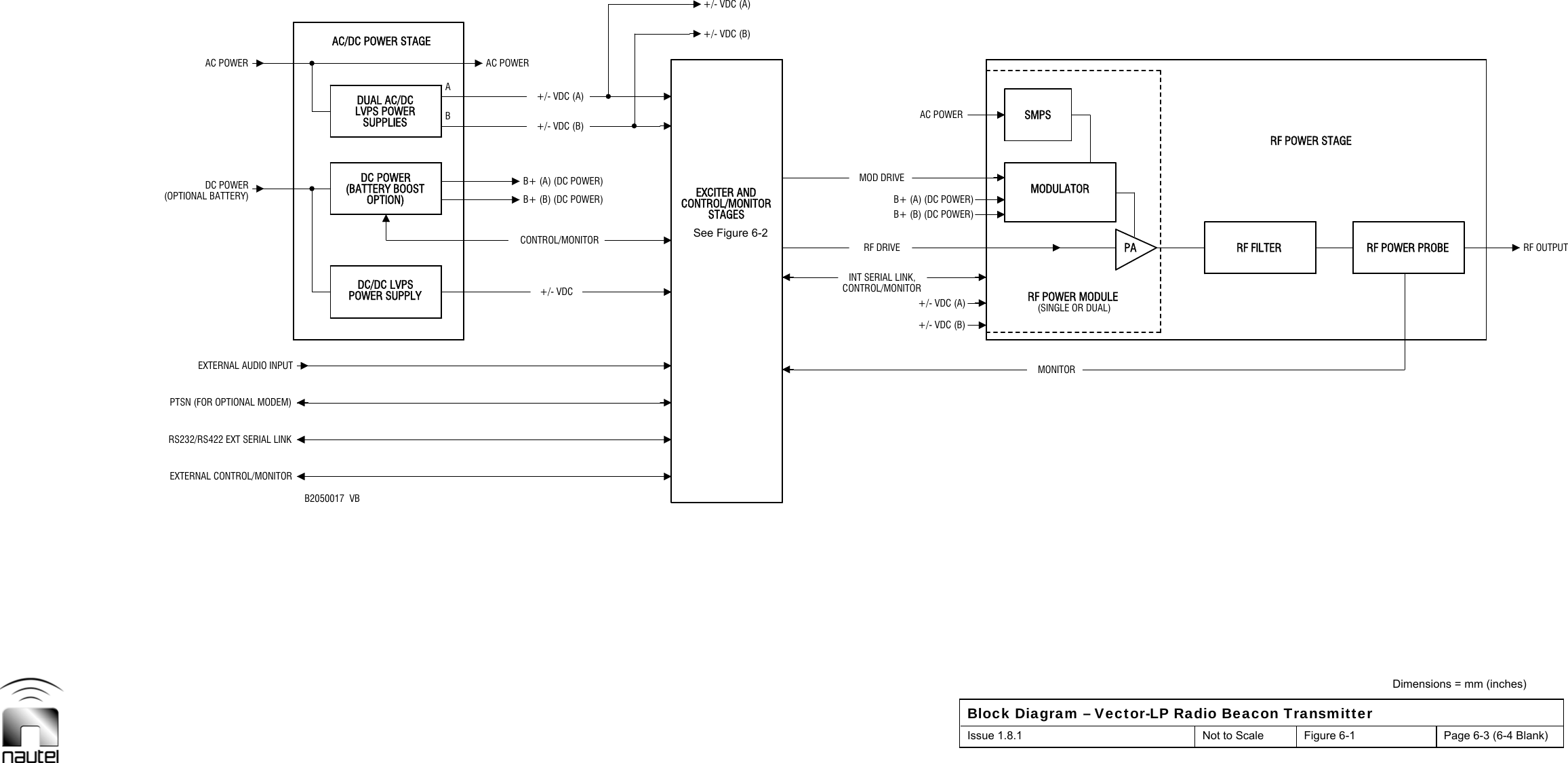
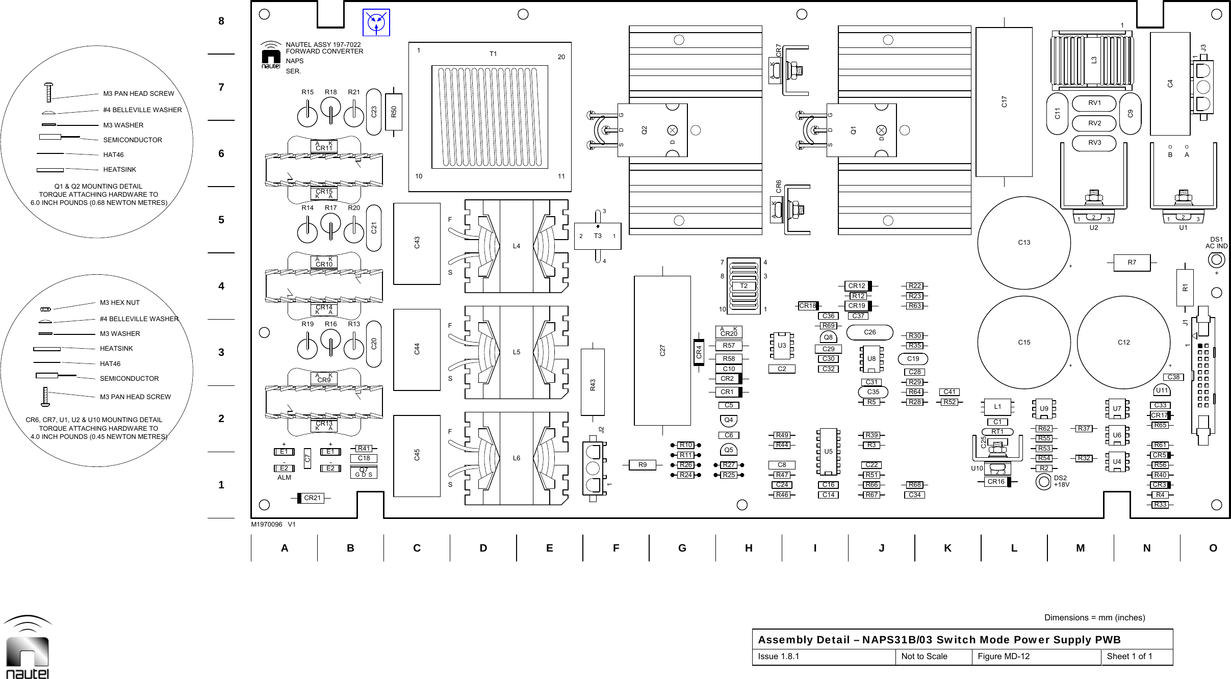
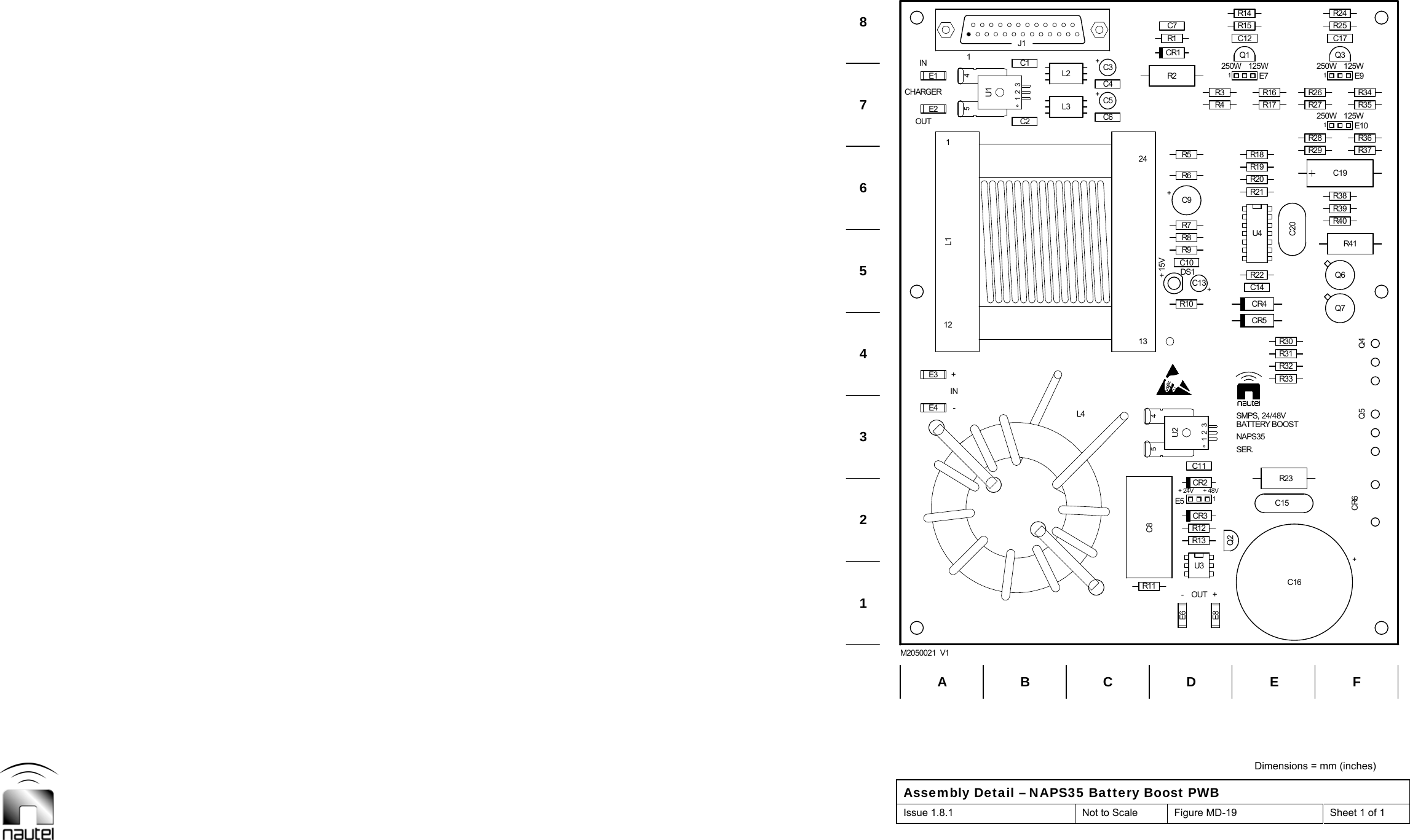
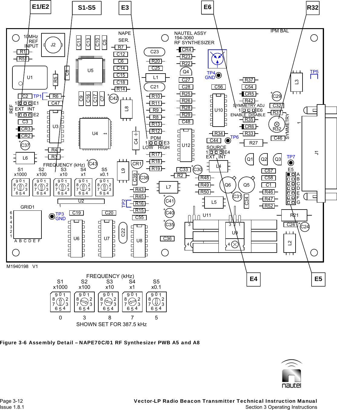
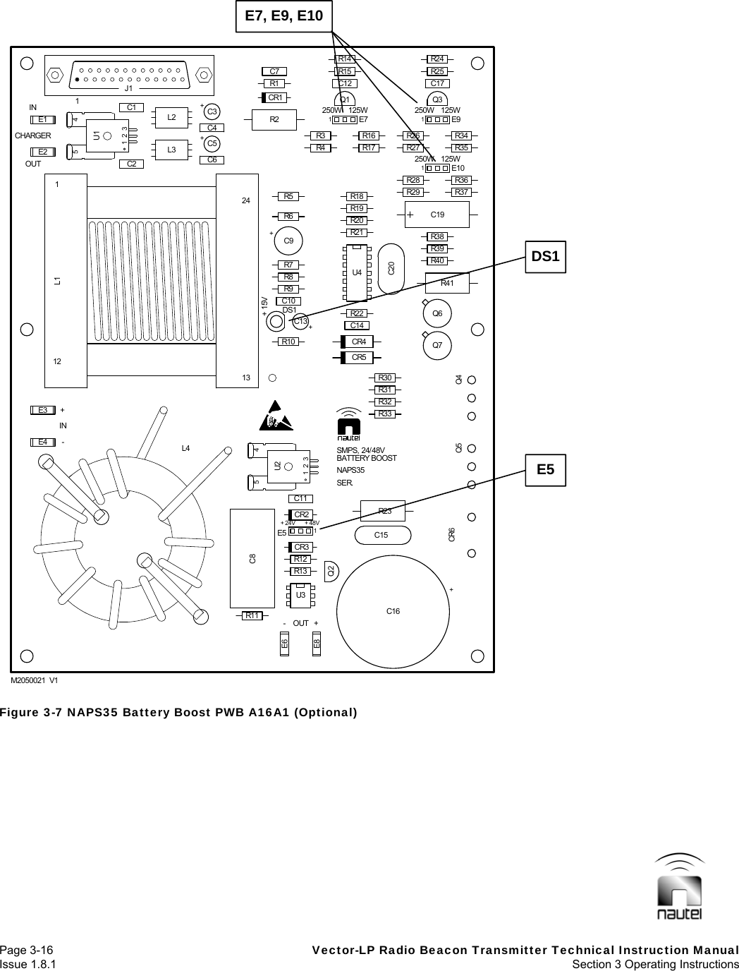
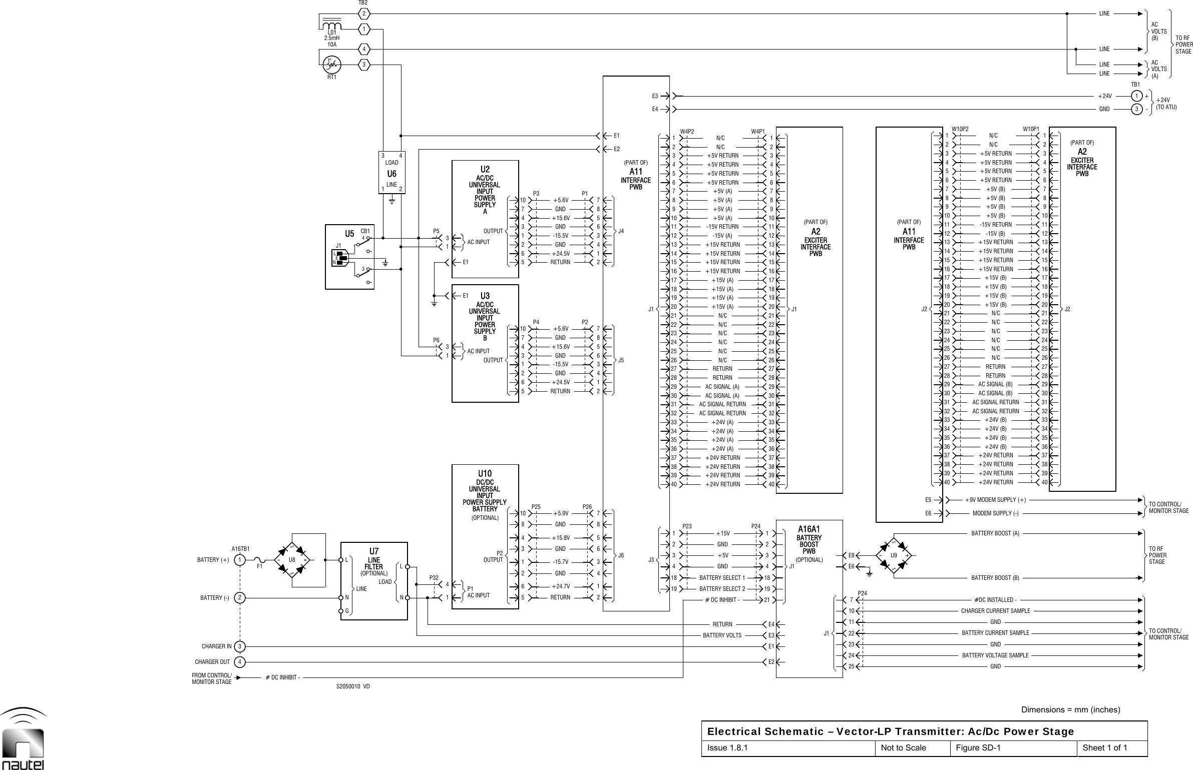
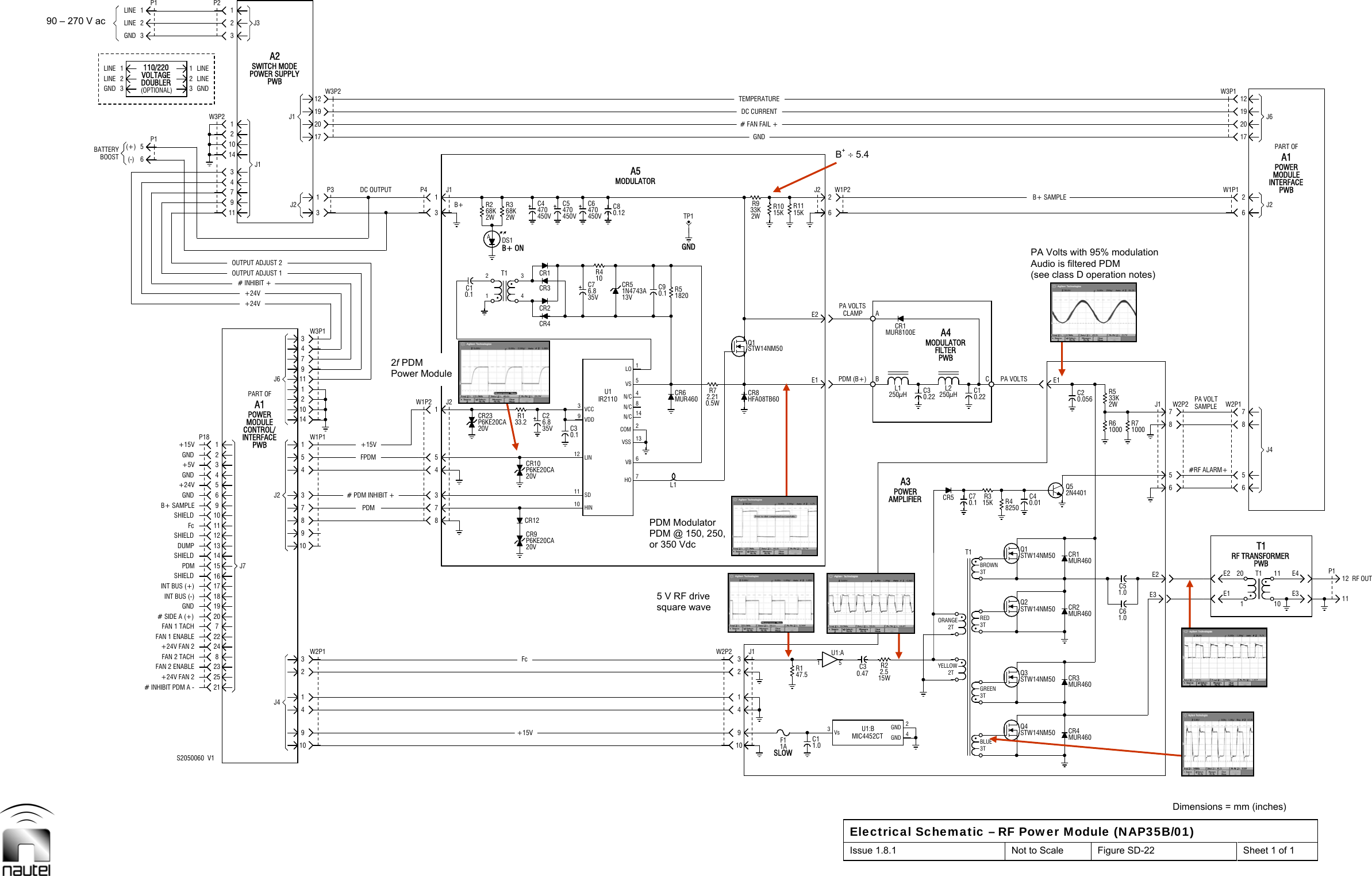
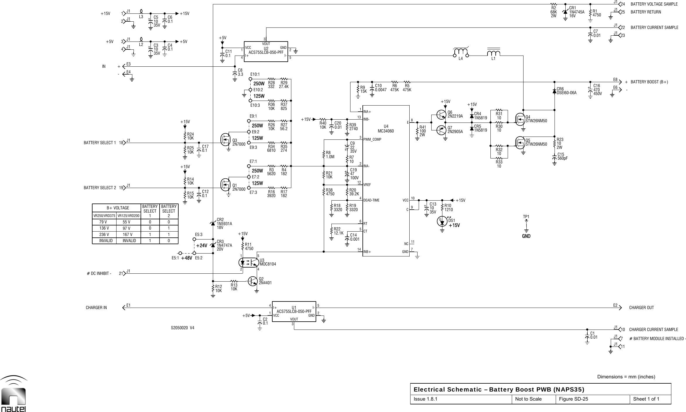
![Vector-LP Radio Beacon Transmitter Technical Instruction Manual Page 6-5 Section 6 Theory of Operation Issue 1.8.1 The ac input is applied through 10 A circuit breaker U5 and line filter U6. The ac voltage for the RF power stage (RF power modules A12 and A13) passes through thermistor RT1 and choke L1. Thermistor RT1 limits the inrush current to the RF power modules. Choke L1 improves the power factor on the ac lines applied to the RF power modules. The ac input is also applied to ac-dc universal power supplies U2 and U3 (U3 optional, for dual side transmitters), which convert the ac voltage to low level dc voltages. The ac input voltage is also applied to the interface PWB (A11) for sampling by the control/monitor stage. Dc voltage is applied from an external 24 V or 48 V battery connected to A16TB1. The dc voltage is fused by F1 and applied to rectifier U8 and line filter U7 before being distributed to dc-dc universal power supply U10 and battery boost PWB A16A1. The battery boost PWB boosts the dc voltage and applies it to the RF power stage via rectifier U9. 6.3.1 Interface PWB See Figures SD-1 and SD-21. The interface PWB (A11) provides an interface between the ac-dc power stage and the rest of the transmitter. It also contains voltage regulators (U1 and U2) that provide 9 V for the optional modem (via E5 and E6) and 24 V (limited to 1A) for the ATU (via E3 and E4). It also provides a dc sample of the ac input voltage to the control/display PWB as an aid in determining if the ac input source is at an acceptable level. 6.3.2 Ac/Dc Universal Input Power Supplies See Figure SD-1. The ac/dc universal input power supplies [U2 (side A) and U3 (side B, if used)] are 110 W, universal ac input, multiple dc output power supplies. The transmitter’s ac input is applied to U2 and U3 and the regulated 24.5 V, 15.6 V, 5.6 V and -15.5 V supplies are provided on the output. The outputs are applied through the interface PWB to the remaining functional blocks of the transmitter. 6.3.3 Battery Boost PWB (optional) See Figures SD-1 and SD-25. The battery boost PWB is a boost type switching power supplies that provide a regulated B+ supply voltage to the transmitter when a 24 V or 48 V battery is acting as the power source. A 24 V or 48 V supply is applied to the drain of switching FETs Q4 and Q5 through inductors L1 and L4. The gate of FETs Q4 and Q5 is driven with square wave pulses from pulse width modulation switching power supply controller U4 through push-pull buffer stage Q6/Q7. U4 is a fixed-frequency, pulse width modulation control circuit, incorporating the functions required for the control of a switching power supply. The device contains an internal sawtooth oscillator that is set to a nominal frequency of 100 kHz by external components R22 and C14. The output pulse width modulated control pulses to the gate of FETs Q4 and Q5 are generated by the comparison of this sawtooth waveform with a feed-back voltage sample from the output (CR6-cathode) and the bias voltage created from the in-circuit resistors selected by the Battery Select 1 (J1-18) and 2 (J1-19) inputs. The resultant variable pulse width, 100 kHz square wave at U4-8 (E) is applied to the gate of FETs Q4 and Q5 (through Q6/Q7) and turns it on and off with the appropriate pulses to maintain the desired set dc output voltage. The Battery Select 1 and 2 inputs, applied from the control/monitor stage, change the level of Battery Boost (B+) voltage based on the transmitter’s power level. See Table 6-1 for the logic levels. Table 6-1: Battery Select Logic B+ Voltage VR250 VR125 Battery Select 1 Battery Select 2 79 V 55 V 0 0 136 V 97 V 0 1 236 V 167 V 1 1 Invalid Invalid 1 0](https://usermanual.wiki/Nautel-Maine/VECTOR125/User-Guide-2553568-Page-111.png)


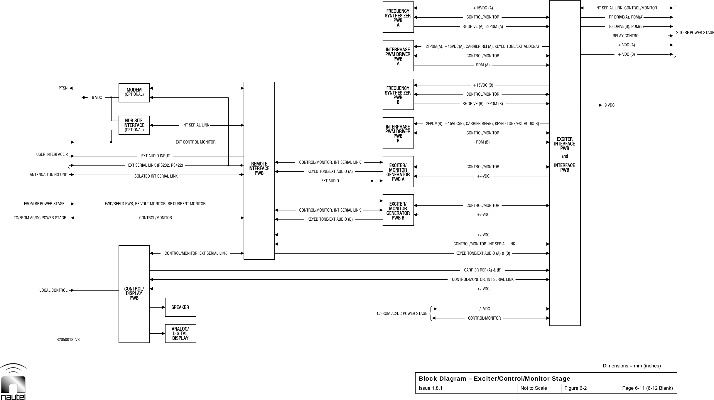
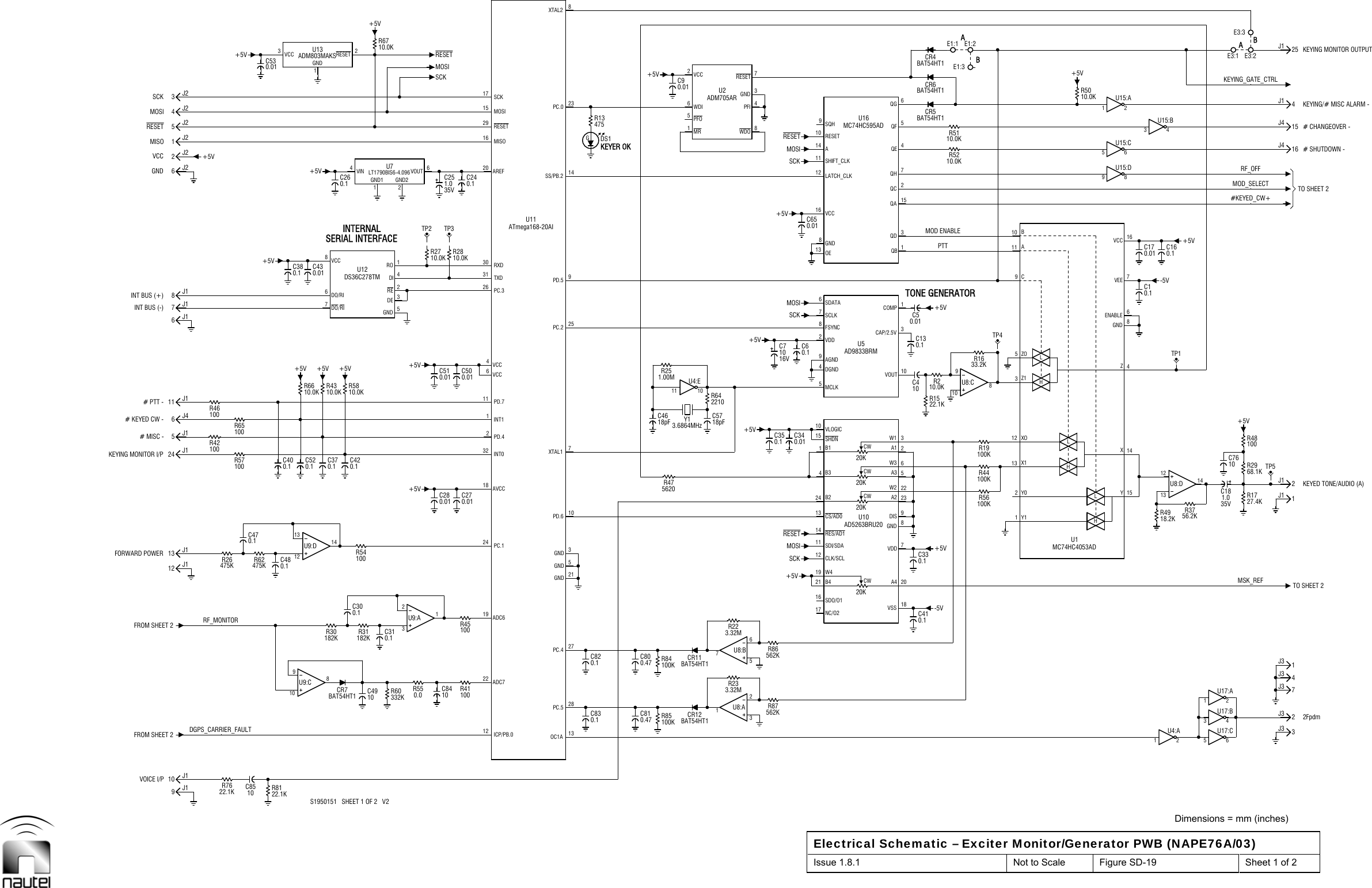
![Vector-LP Radio Beacon Transmitter Technical Instruction Manual Page 6-15 Section 6 Theory of Operation Issue 1.8.1 6.4.4 Exciter Monitor/Generator PWBs See Figures SD-19 and SD-20. The exciter/ monitor/generator PWBs [A7 (exciter A) and A10 (exciter B, if used)] perform the following functions: Use the press-to-talk input to select between beacon and voice modes. Monitor and control modulation depth Selects the parameter, RF current or RF voltage, to be applied to the remote interface PWB for external monitoring. Generate the appropriate tone frequency Monitors tone and keyer operation Monitors the forward power and controls changeover and inhibit functions. 6.4.4.1 MICROCONTROLLER Microcontroller U11 uses the SPI bus to communicate with shift register U16 which shifts out digital data used to control various signals including changeover, shutdown, RF off, and alarm. Watchdog timer IC U2 and associated components generate a Keying/ Misc Alarm (J1-4) if the microcontroller falls into an unknown state. The clock for the microcontroller and the tone oscillator is generated using Y1, U4:E and the associated components. The microcontroller (U11) continually monitors its internal Flash and EEPROM memory using checksums. If for some reason, the checksum returns as invalid, the microcontroller will detect the error and raise a flag, resulting in the output power being inhibit. U2 acts as a watchdog timer, if the watchdog times out, the monitor fault will also be raised, causing the output power to be inhibited (via the control/display PWB). This will guarantee that the U11 is always operating as intended. 6.4.4.2 PRESS-TO-TALK The input to U11:11 indicates to the exciter monitor/generator PWB which mode of operation it should be operating in. It will react by adjusting the U16:1 that controls the MUX U1:X. 6.4.4.3 MODULATION DEPTH FUNCTIONS Modulation depth of the beacon, voice and beacon, and voice are controlled using the digital pots 1, 2 and 3 of U10 respectively. The levels of the pots in U10 are adjusted by the microcontroller U11 over the SPI bus. A selection between RF Monitor Voltage and RF Monitor Current samples is made using the MUX U14:C. CR9, U9:B and their associated components RF detect the selected RF monitor signal. The RF monitor signal is then used to calculate the modulation depth. The microcontroller (U11) compares the average and peak levels of the RF signal. The average value is detected using U9:A and its associated components. The peak level is detected using U9:C, CR7, and their associated components. 6.4.4.4 TONE GENERATION The keyer tone is generated using the DDS IC U5. The microcontroller U11 sends an SPI signal to U5 indicating the frequency of the tone to generate. The tone is then amplified using U8:C and its associated components. The microcontroller (U11) then controls keying by toggling the MUX U1:Z. Correct operation of the keyer is monitored by U8:A, U8:B, CR11, and CR12 and there associated components. The analog samples at U11:27 and U11:28 are compared to the low threshold levels (set up using the GUI) to determine if the keying gate is opened or closed. If at any time the keying gate is opened when it should be closed or closed when it should be opened, and alarm is flagged and output power is inhibited (via the control/display PWB).](https://usermanual.wiki/Nautel-Maine/VECTOR125/User-Guide-2553568-Page-120.png)


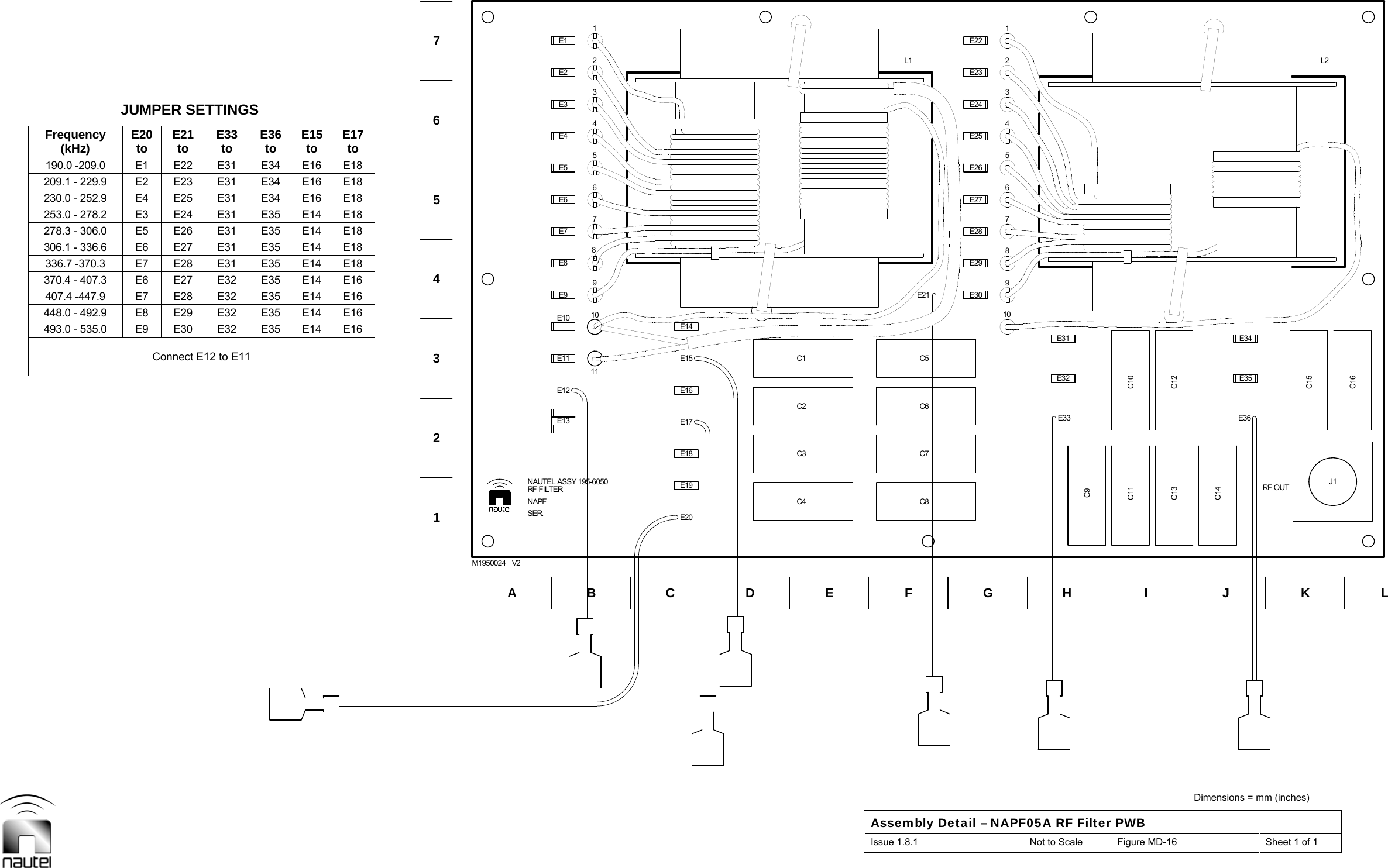
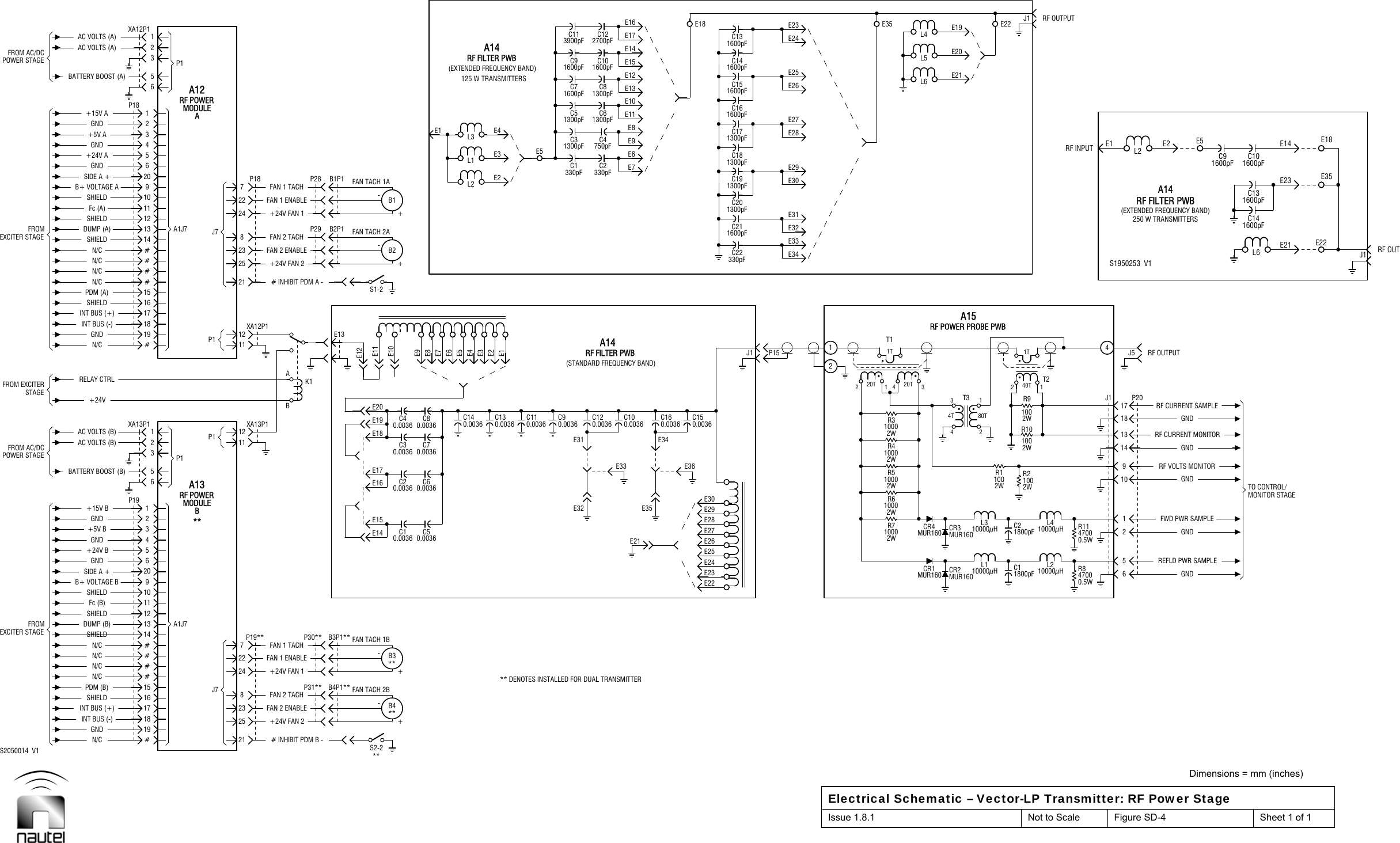
![Vector-LP Radio Beacon Transmitter Technical Instruction Manual Page 6-29 Section 6 Theory of Operation Issue 1.8.1 6.6.2 RF Filter PWB See Figure SD-4. The RF filter PWB (A14) is a band pass filter that attenuates the harmonics of the square wave output applied from the selected RF power module before it is applied to the RF combiner/probe. The filter has a flat response characteristic over the operating bandwidth [three PWB options; standard frequency band (190 - 535 kHz), extended frequency band for 125 W transmitters (536 - 1250 kHz and 1600 – 1800 kHz), and extended frequency band for 250 W transmitters (1600 – 1800 kHz)]. It has a nominal input and output impedance of 50 and a loaded Q of 2. The band-pass is selected using frequency dependent link connections (E1 through E36; see Tables 2-7a and 2-7b). 6.6.3 RF Power Probe PWB See Figure SD-4. The RF power probe PWB (A15) contains various circuits that monitor the RF output and provide RF voltage, RF current, forward power and reflected power monitoring samples to the control/monitor stage. 6.6.3.1 FORWARD/REFLECTED POWER PROBE The forward/reflected power probe circuit consists of 40:1 RF current transformer T1, 80:4 RF voltage transformer T3 and associated components. These transformers form the current and voltage arms of a forward/reflected power bridge, which samples the RF output. The current flowing into the RF output passes through transformer T1’s primary. The current in T1’s secondary develops a voltage across resistors R33, R34, R41, R42, R43 that is proportional to the RF output current. The anti-phase voltage across the secondary of RF voltage transformer T3 is applied (summed) to the centre-tap of T1’s secondary. When the RF output impedance is precisely 50 , the RF current waveform is in-phase and of equal amplitude to the RF voltage waveform on one half of T1’s center-tapped secondary and equal amplitude, but 180 out-of-phase on the other half. The in-phase voltages are summed, rectified by CR35, low-pass filtered by L9/C53/L11, resulting in a dc voltage being applied to the Fwd Pwr Sample output (J1-1). This voltage is proportional to the RF output's forward power level. The out-of-phase voltages are summed, rectified by CR36, low-pass filtered by L8/C54/L10, resulting in a dc voltage being applied to the Refld Pwr Sample output (J1-5). This voltage is proportional to the RF output's reflected power level. T3’s secondary voltage, which is a true sample of the RF output’s voltage waveform, is also applied to the RF Volts Monitor output (J1-9). This output is intended for monitoring by a modulation monitor and for test equipment during maintenance. 6.6.3.2 RF CURRENT PROBE The RF current probe circuit consists of 40:1 RF current transformer T2 and associated components. The current flowing into the RF output passes through the primary of transformer T2. The current in T2’s secondary winding develops a voltage across resistors R37 and R40 that is proportional to the primary (RF output) current. This voltage is applied to the RF Current Sample output (J1-17), which is used by the control/display PWB's high RF current detector and metering circuit. This high RF current detector produces a high RF current alarm and – via the control/display PWB - causes the transmitter's RF output to shut back (turn off) when the RF current exceeds a threshold that represents the maximum stress current for the RF power modules. The current sample voltage is also applied to the RF Current Monitor output (J1-13), which is used for external monitoring purposes.](https://usermanual.wiki/Nautel-Maine/VECTOR125/User-Guide-2553568-Page-132.png)


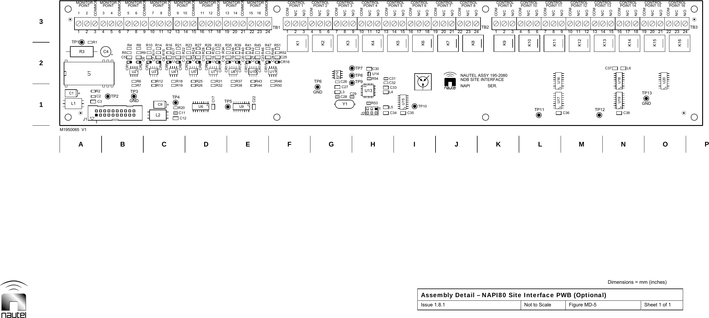
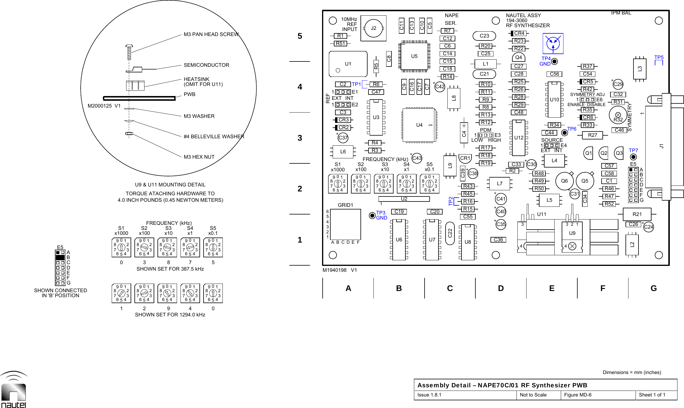
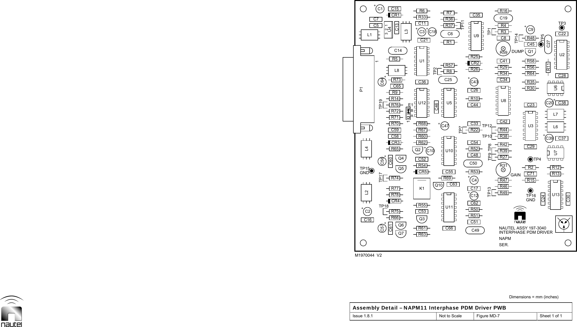
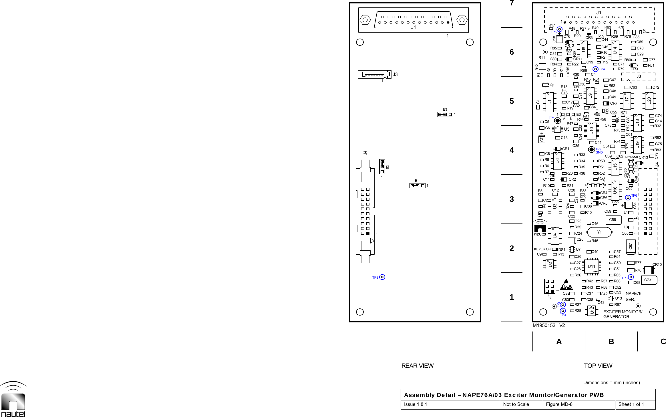
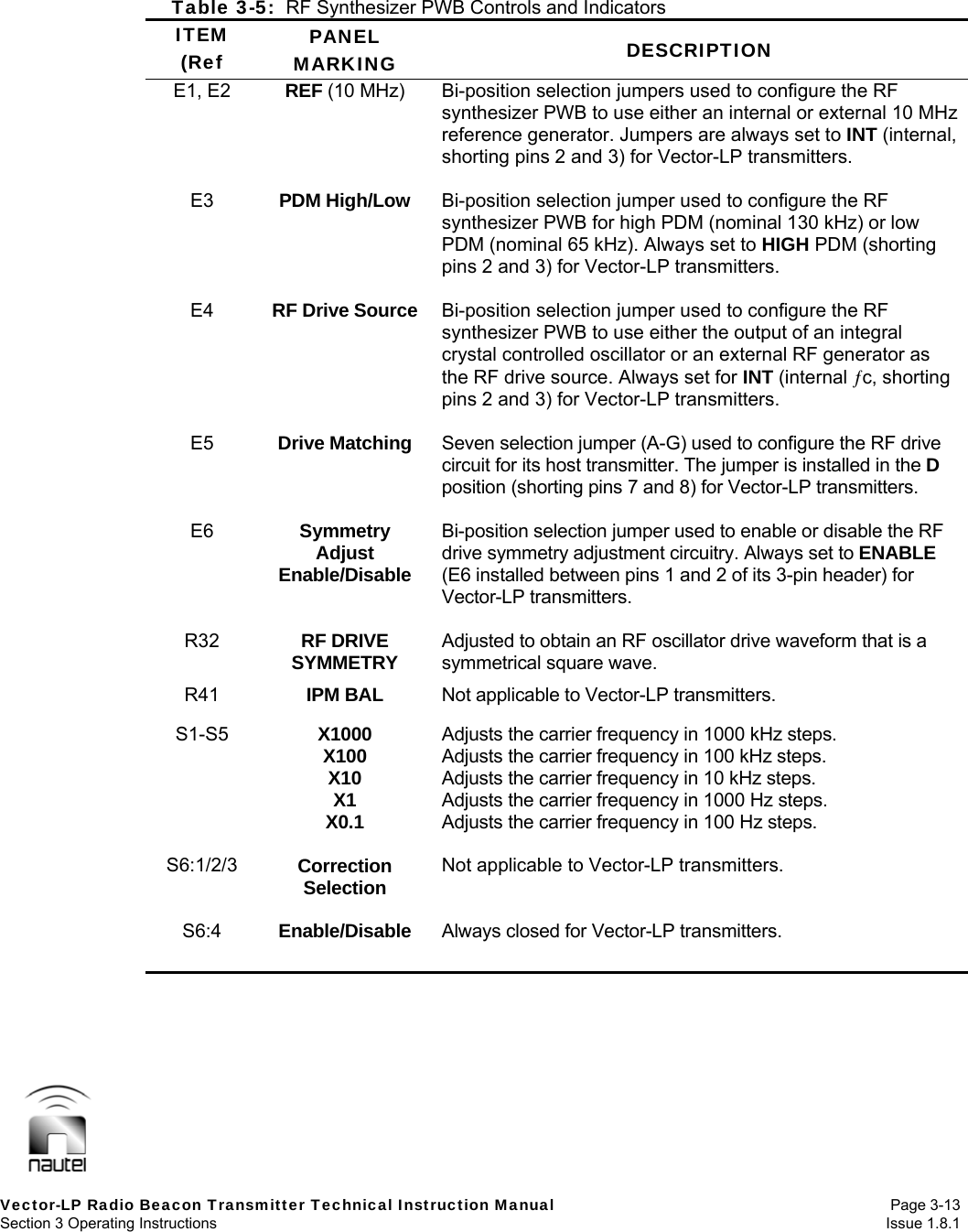
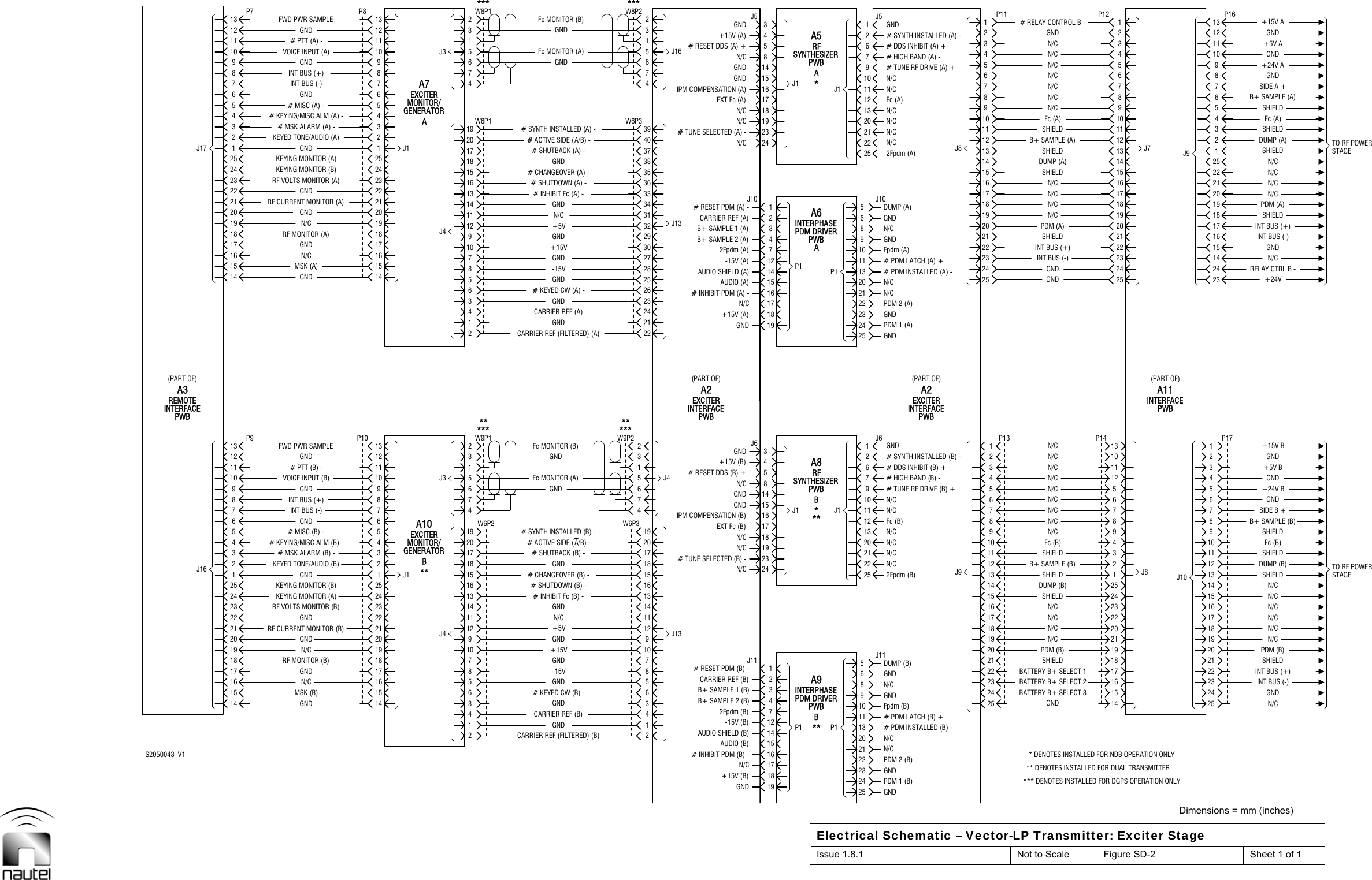
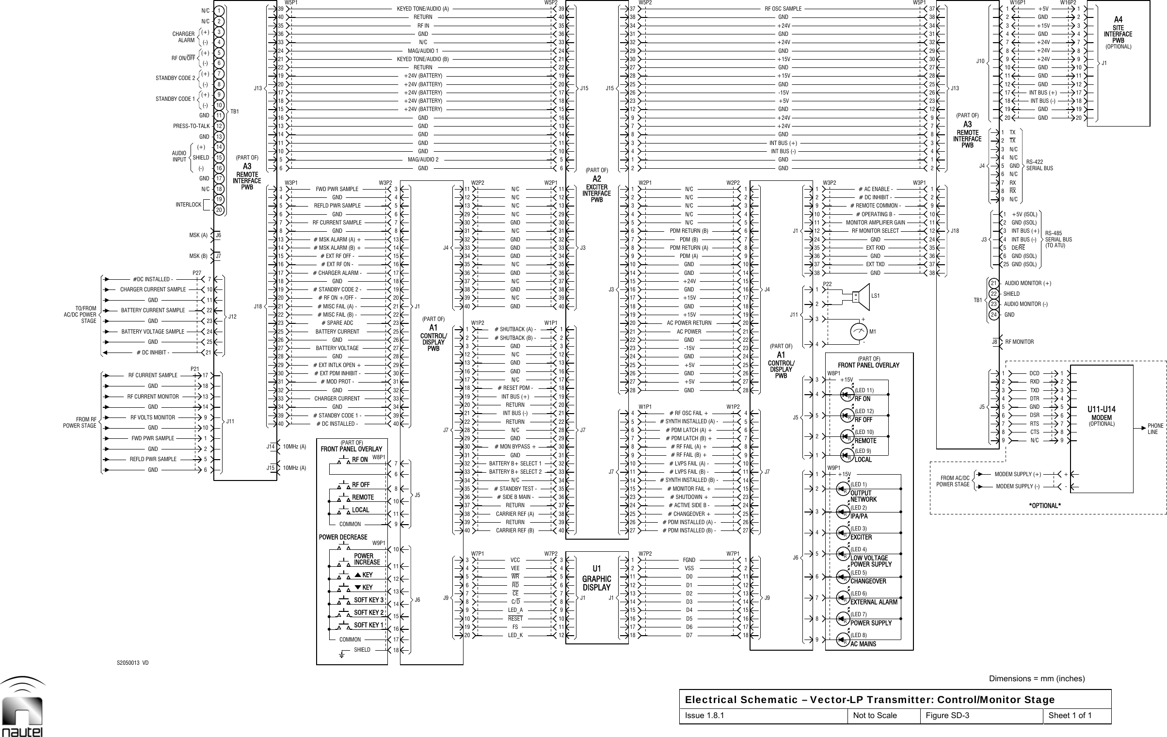
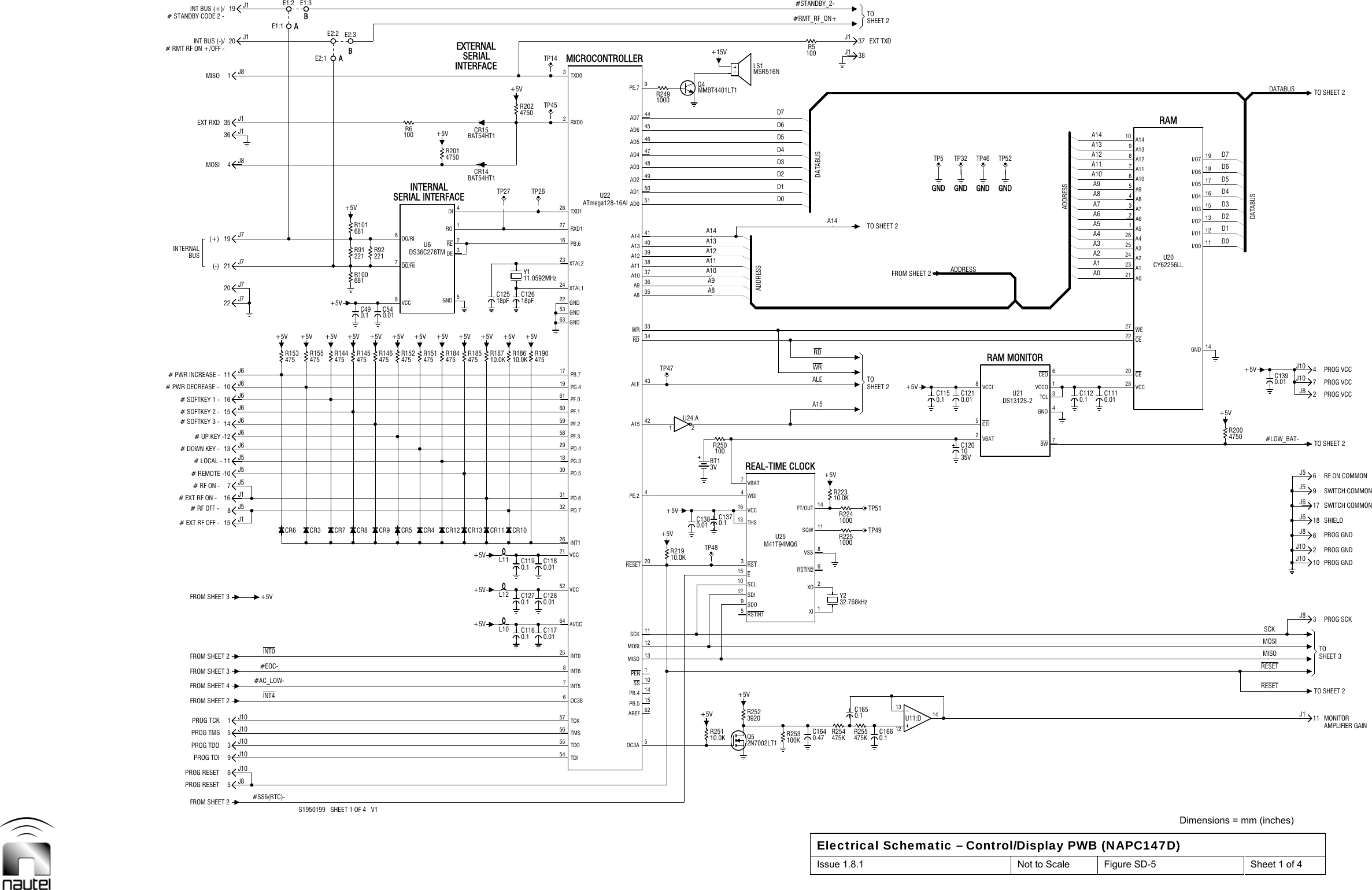
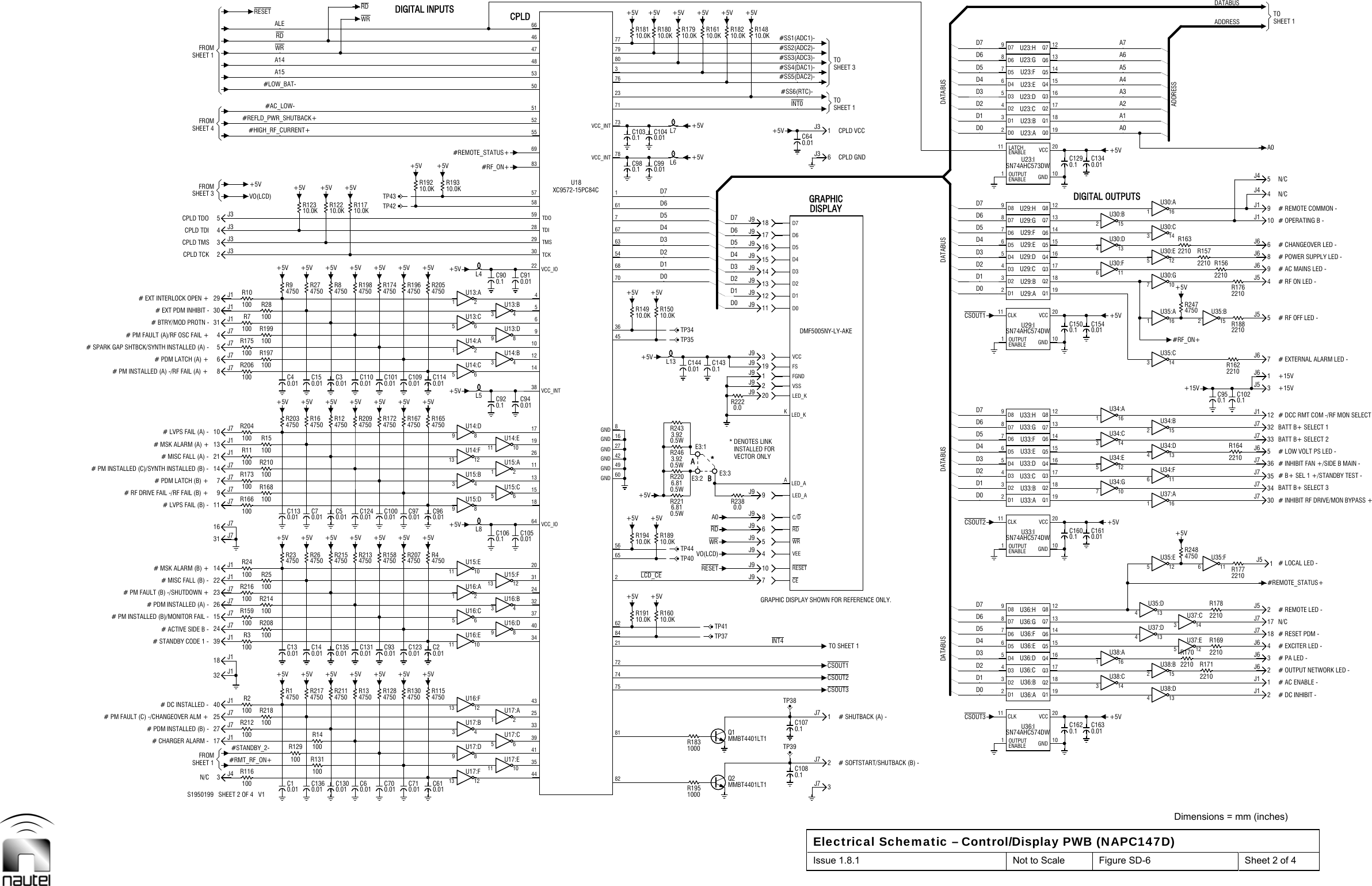
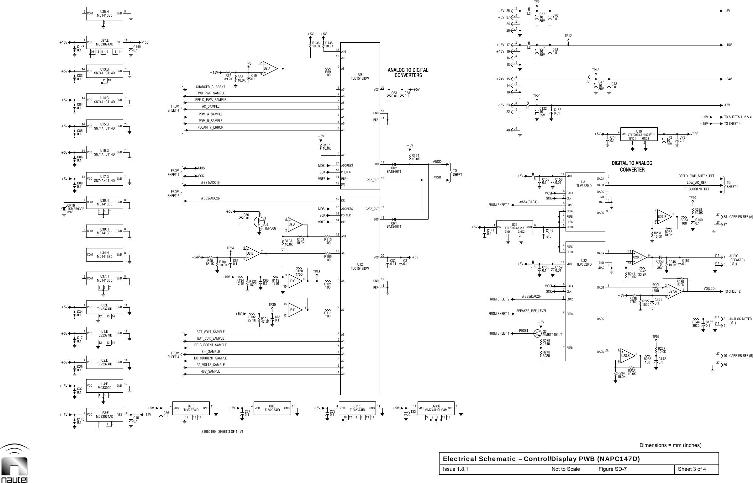
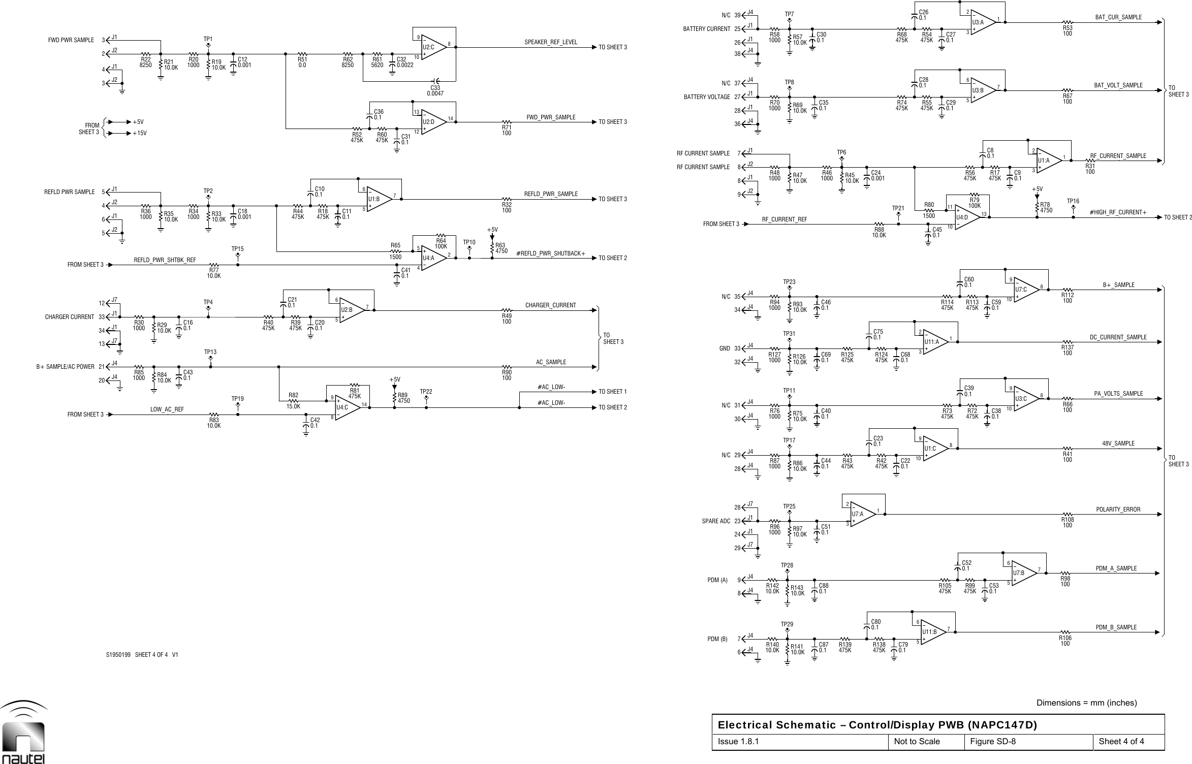
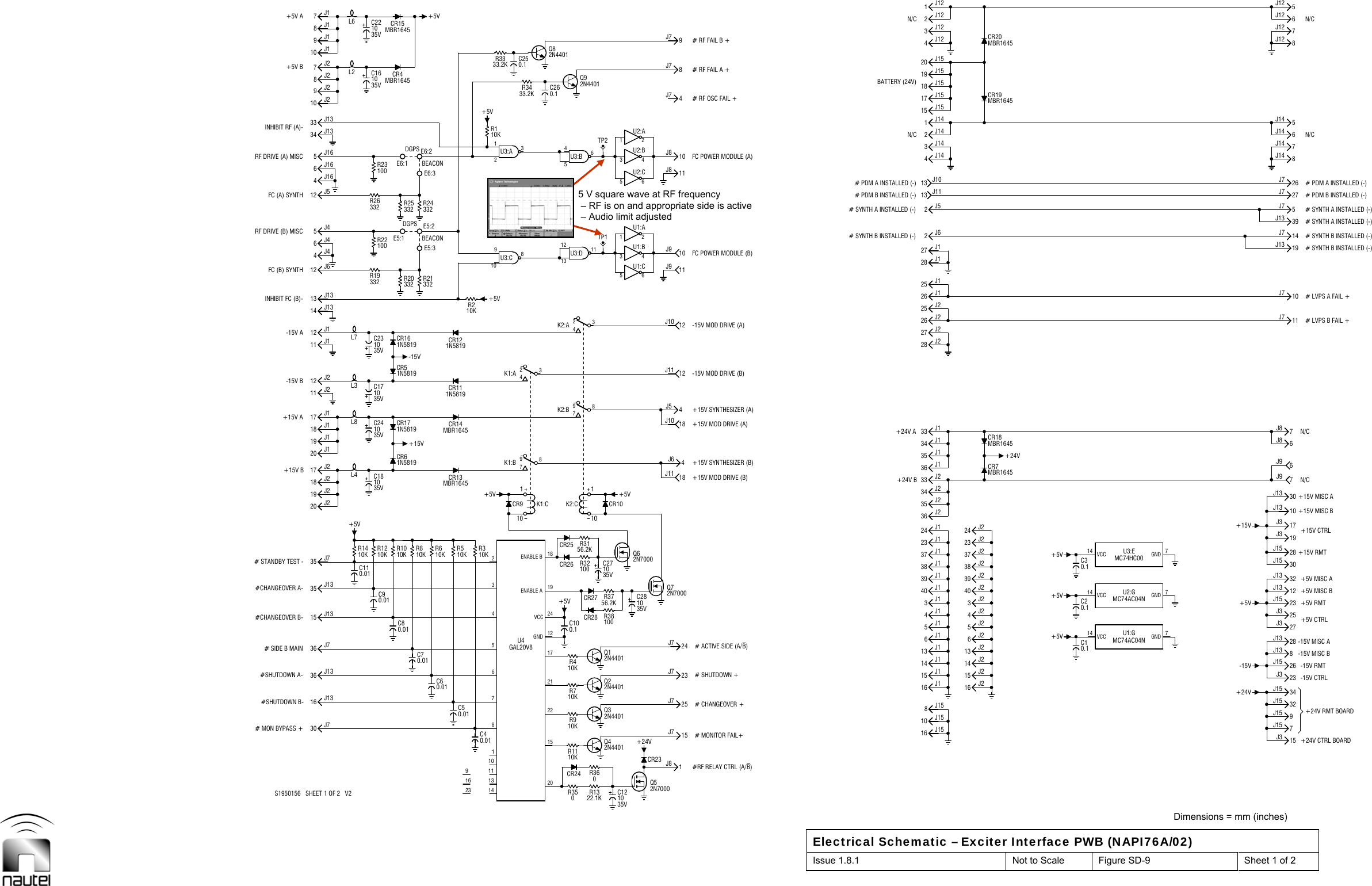
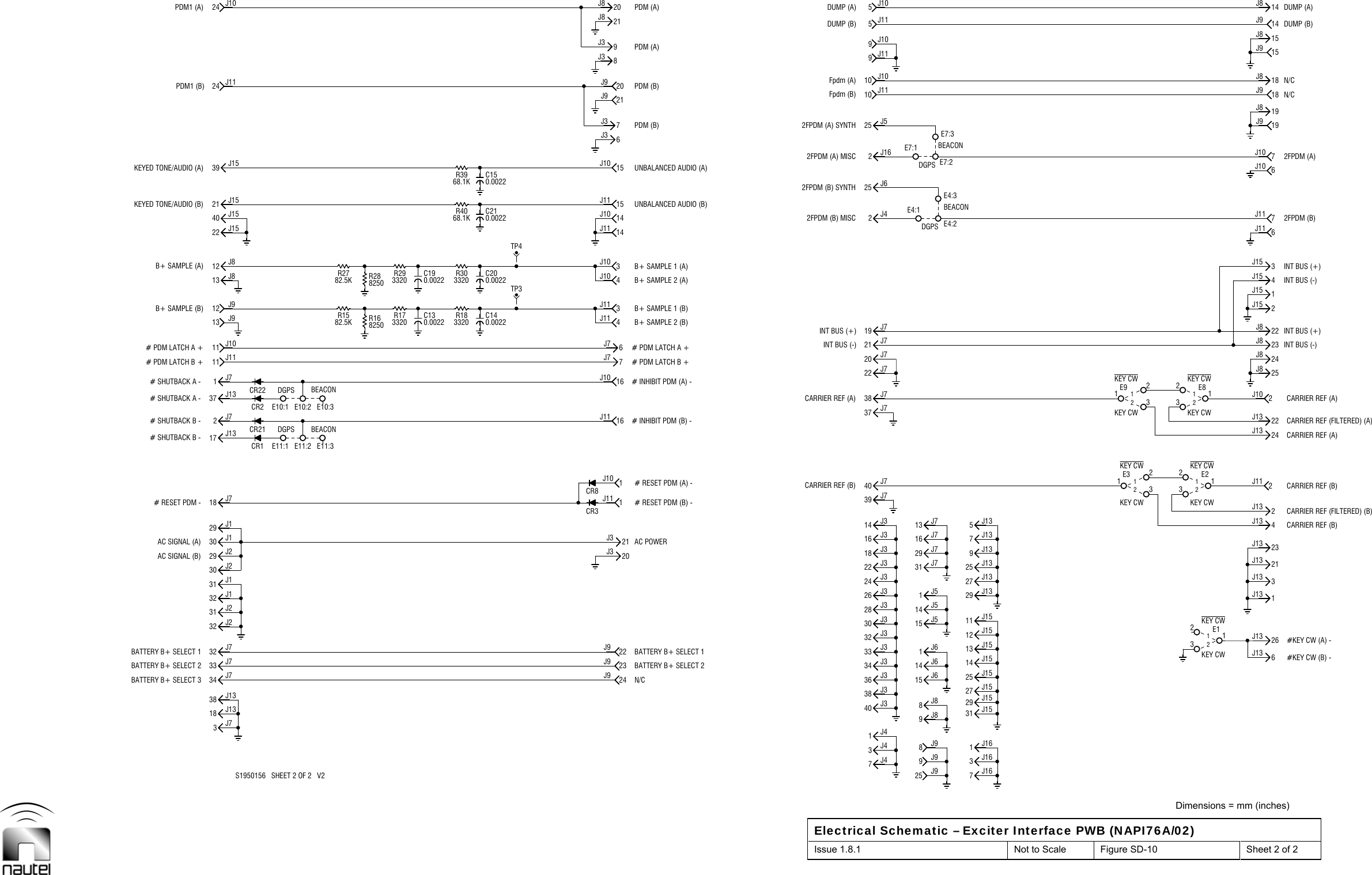
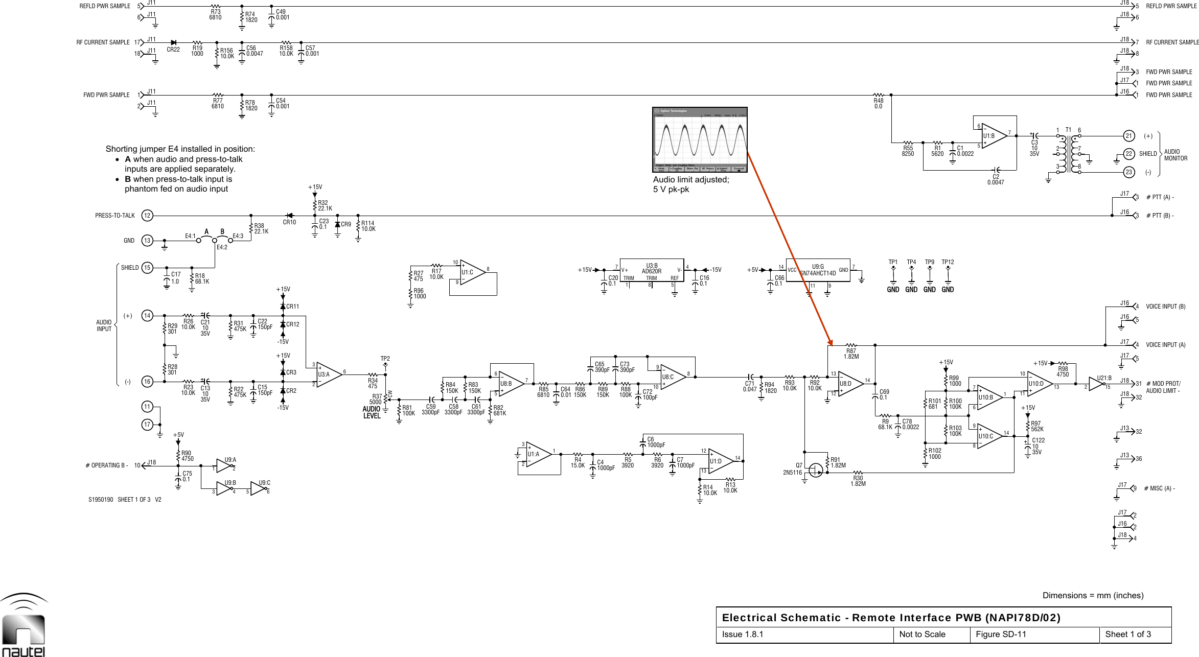
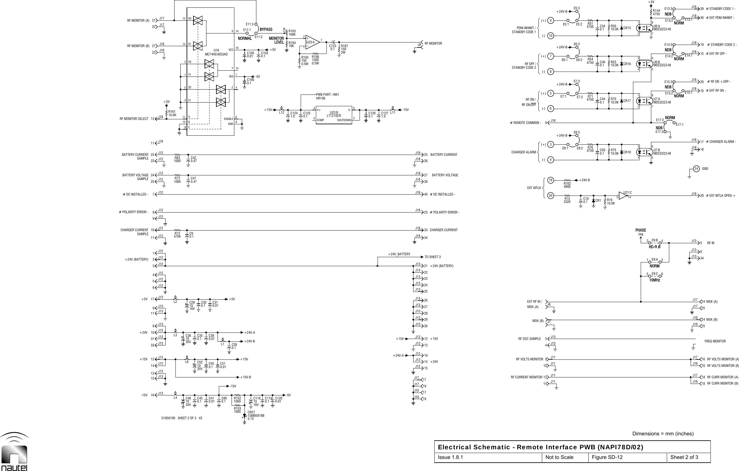
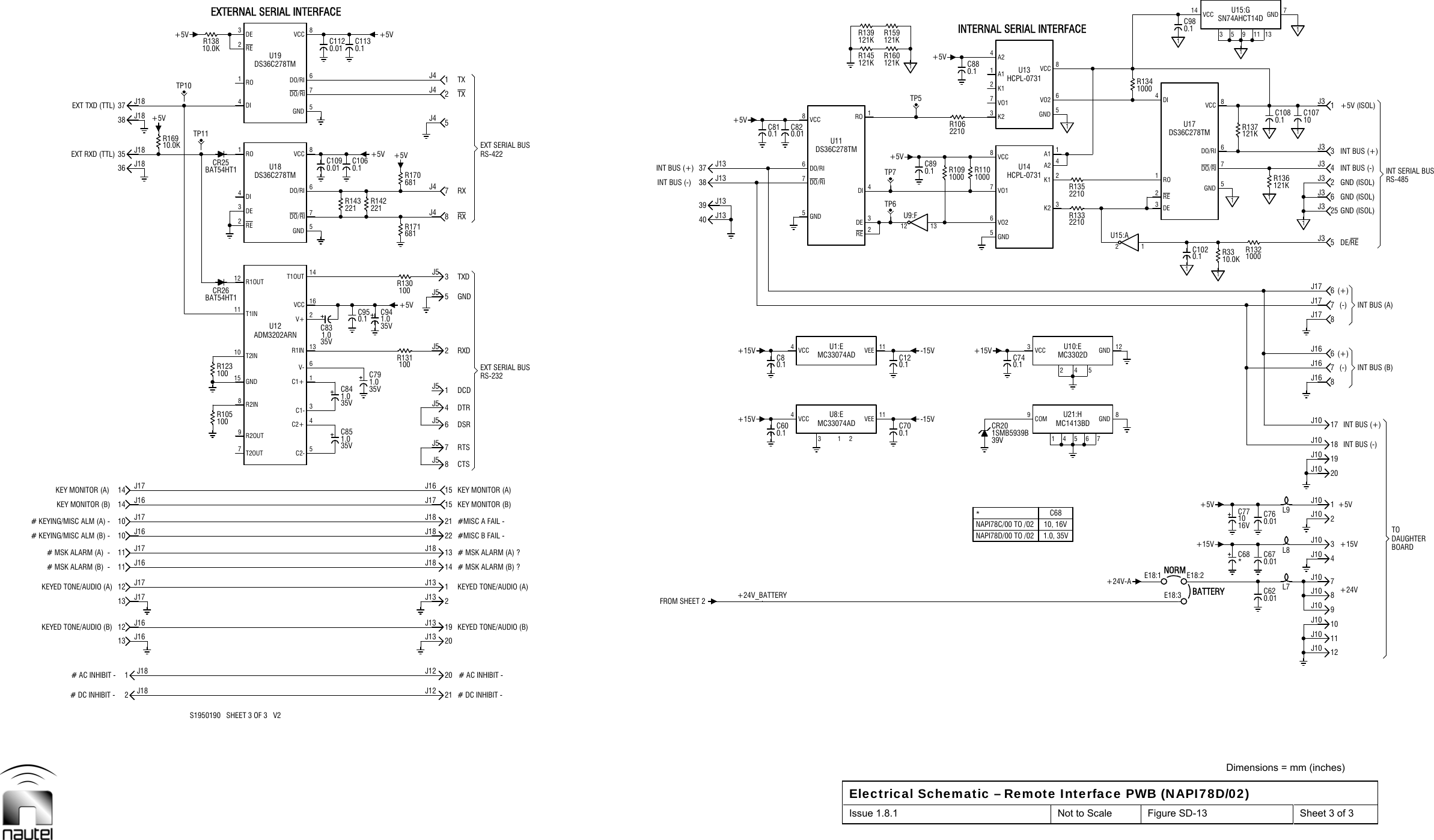
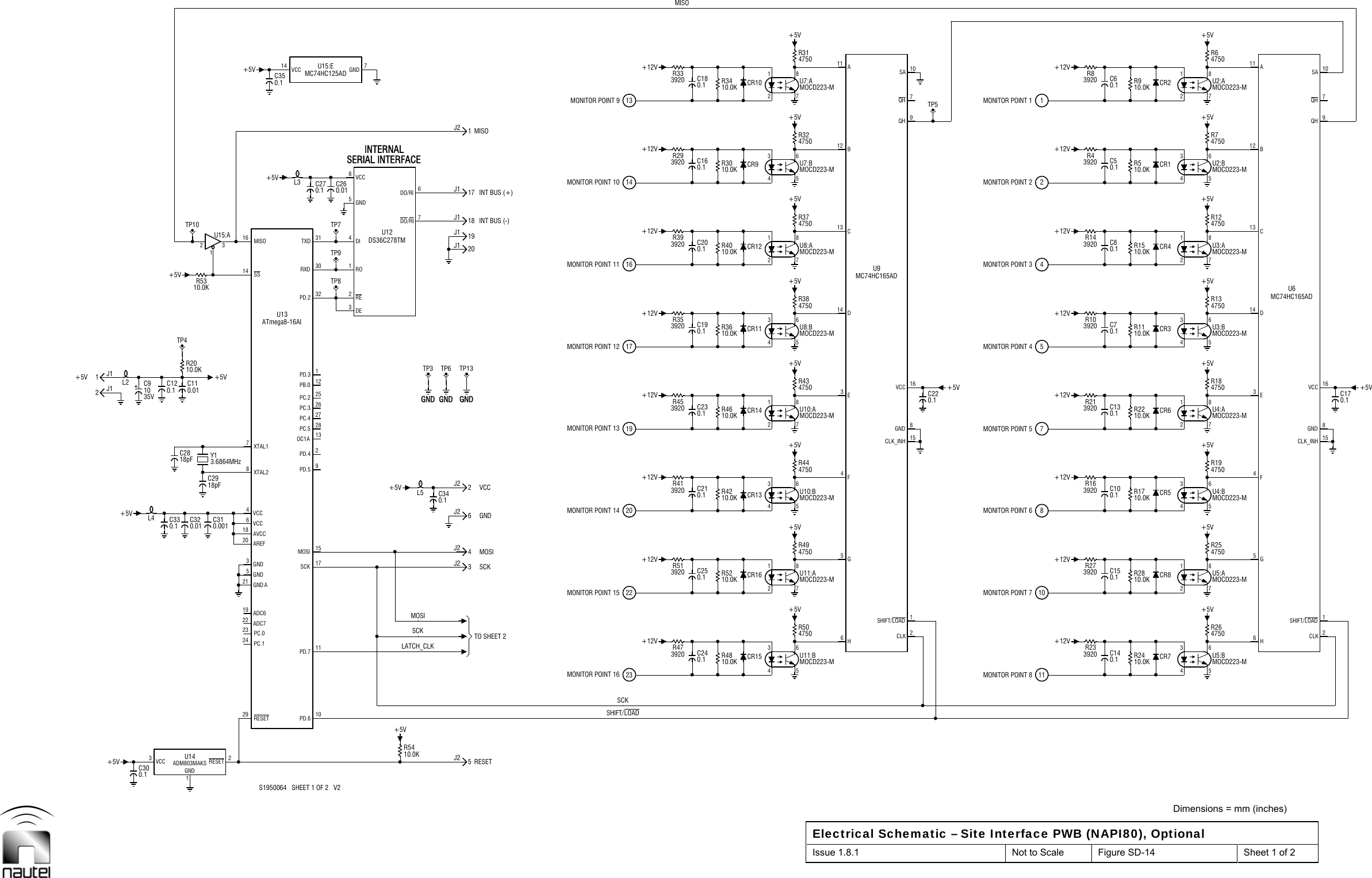
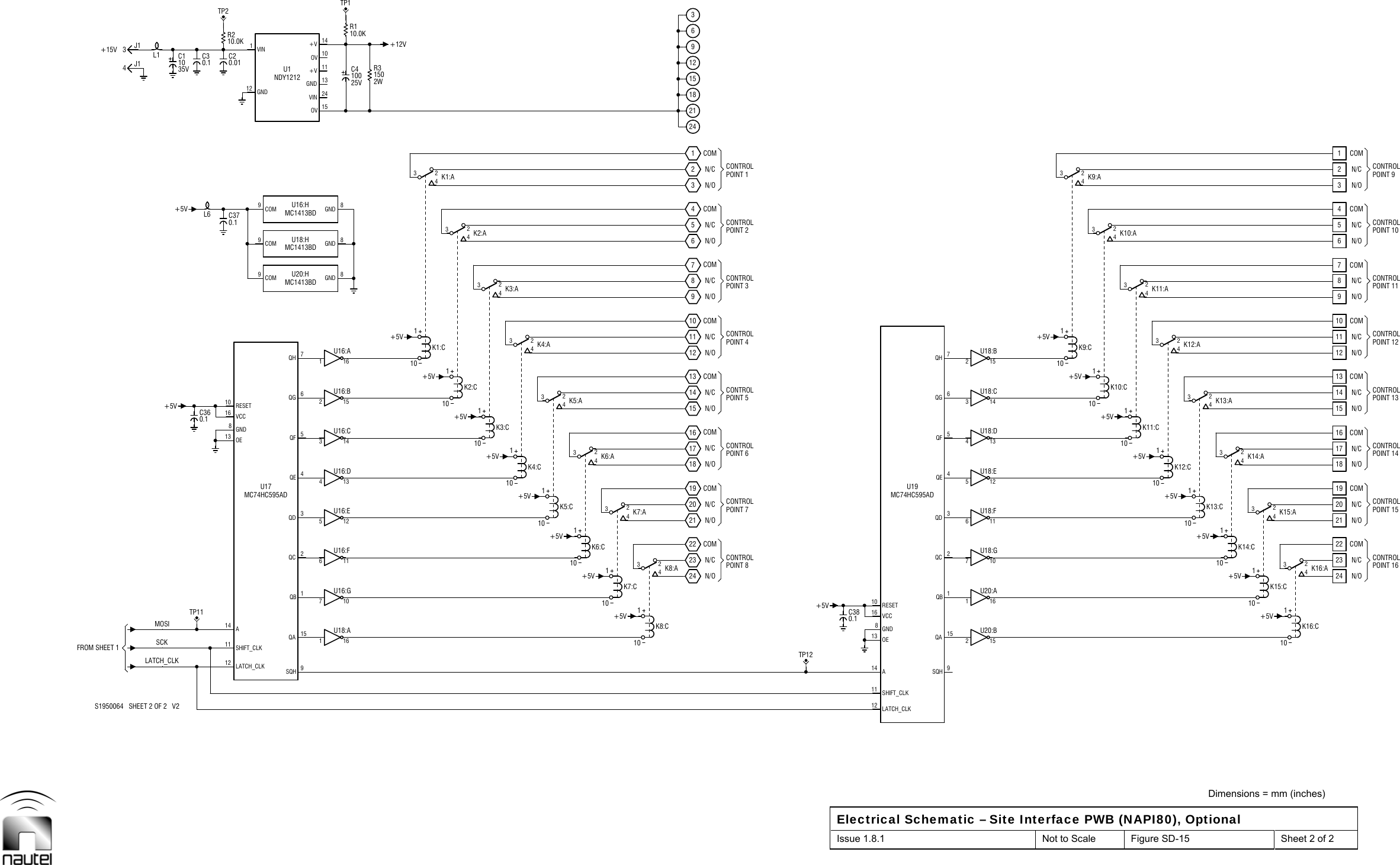
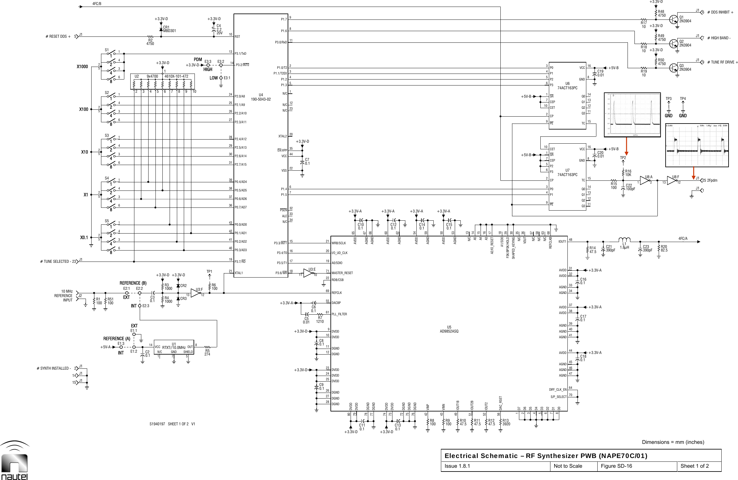
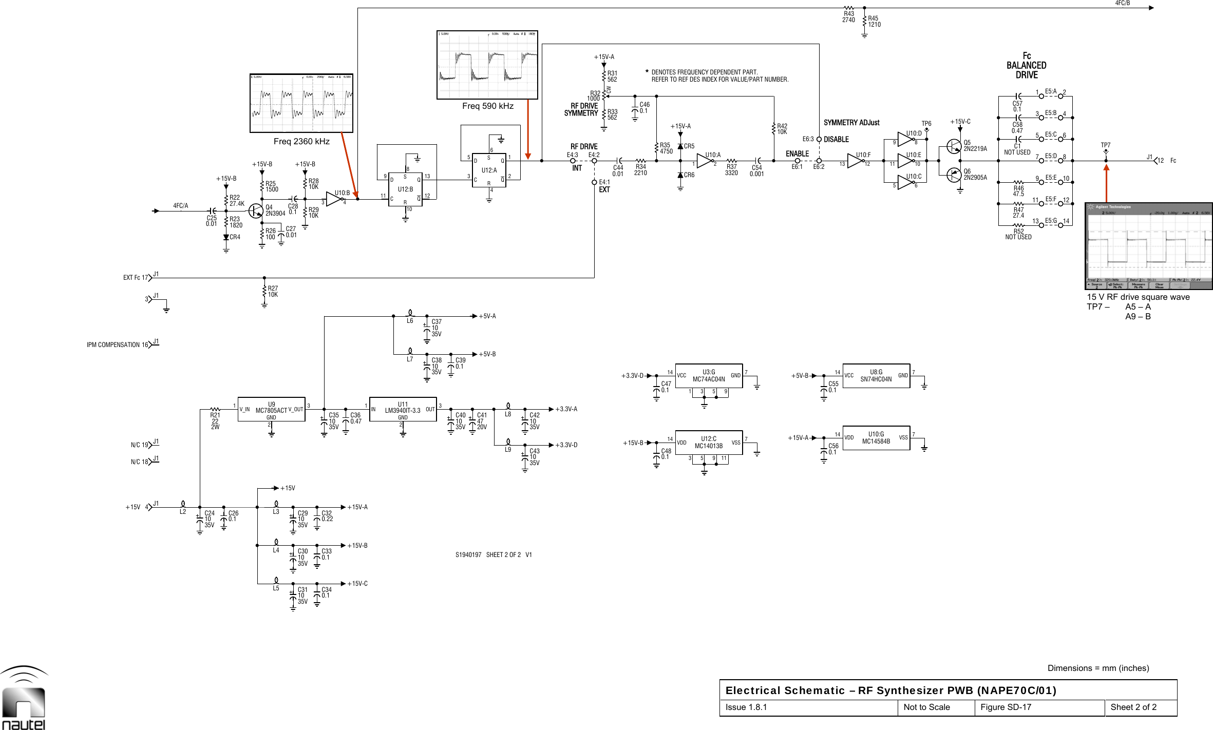
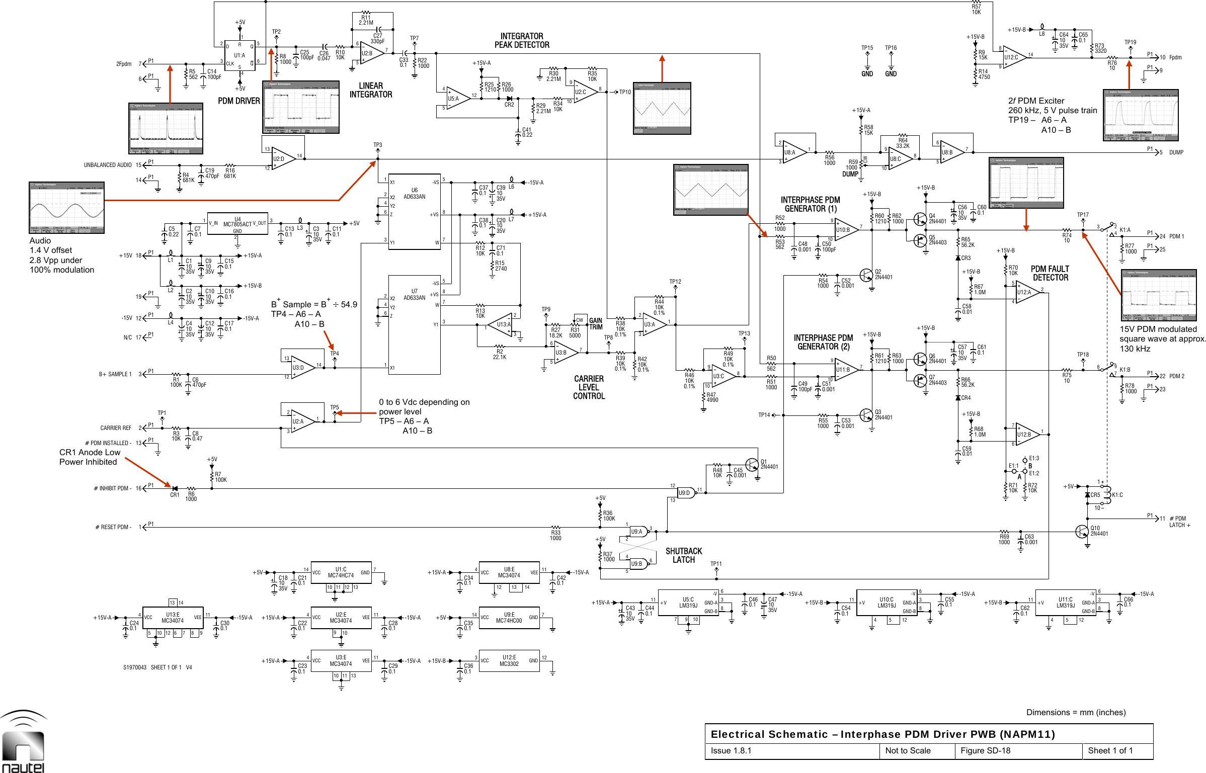
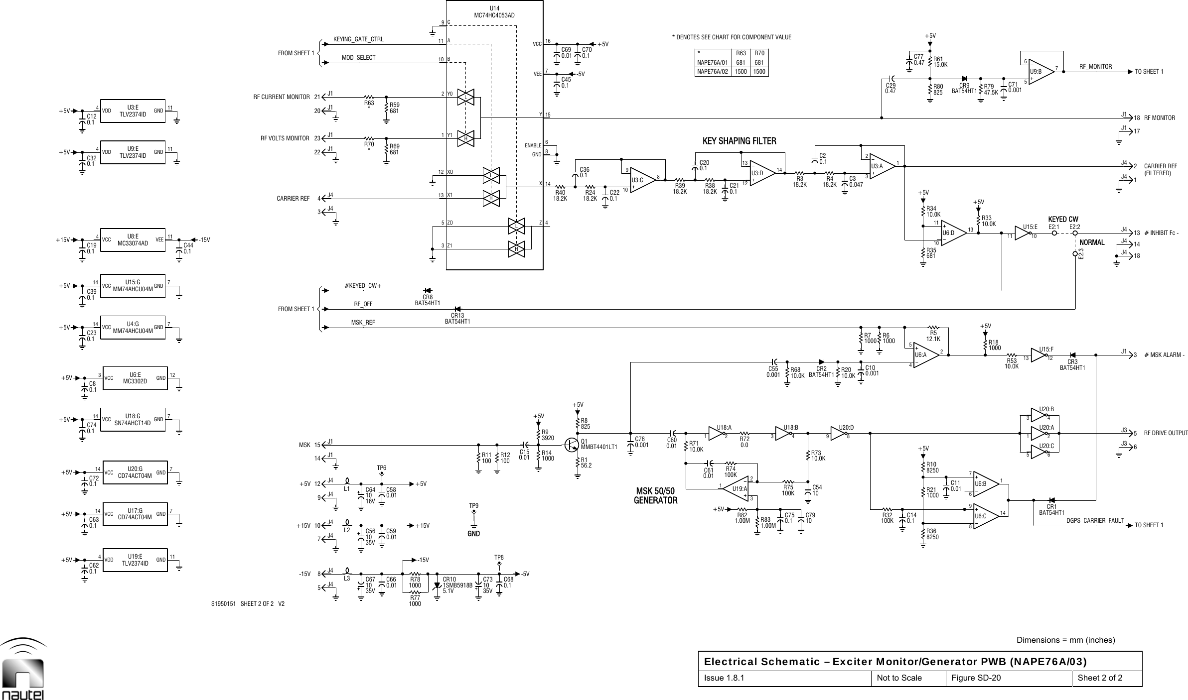
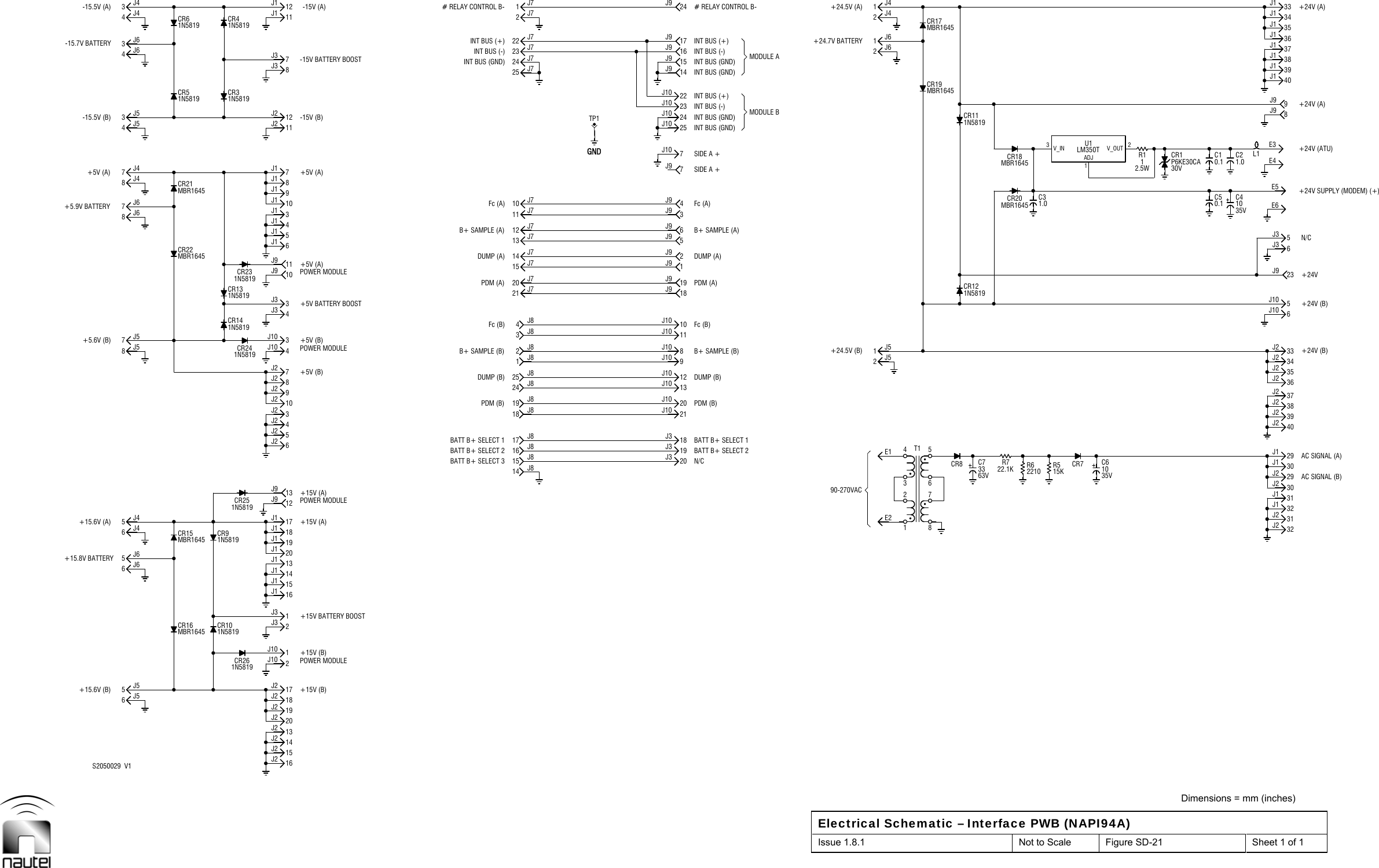
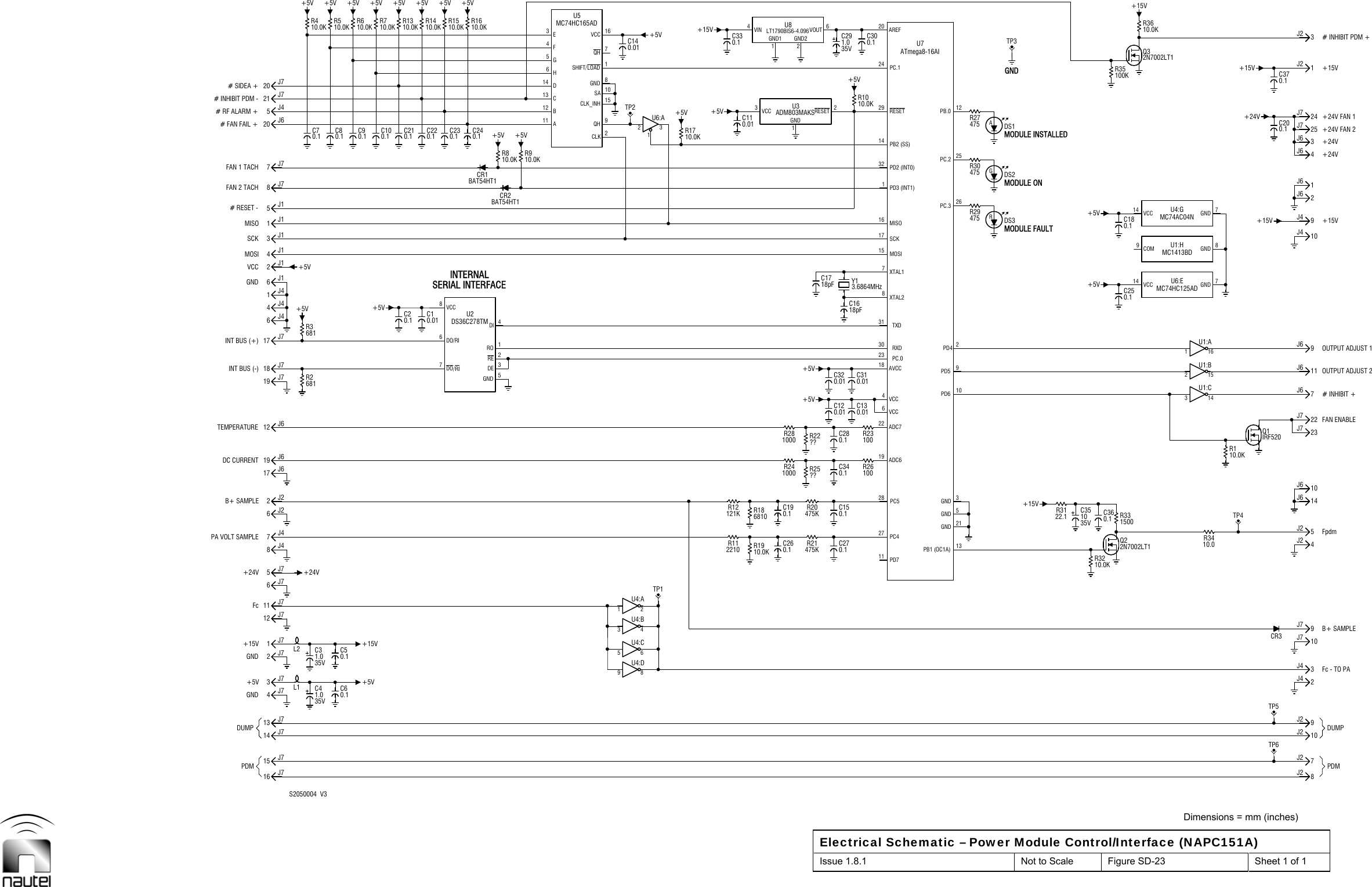
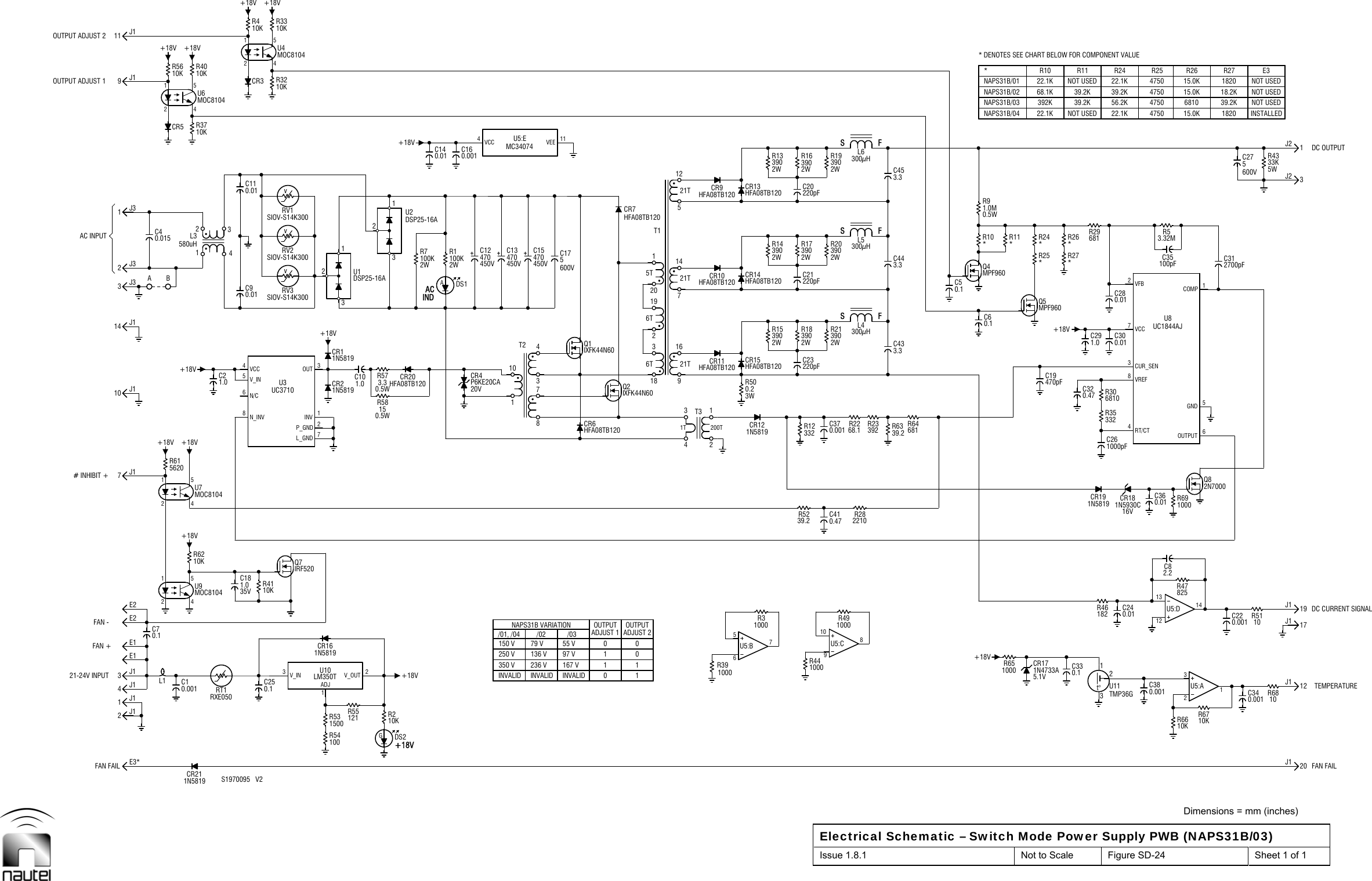
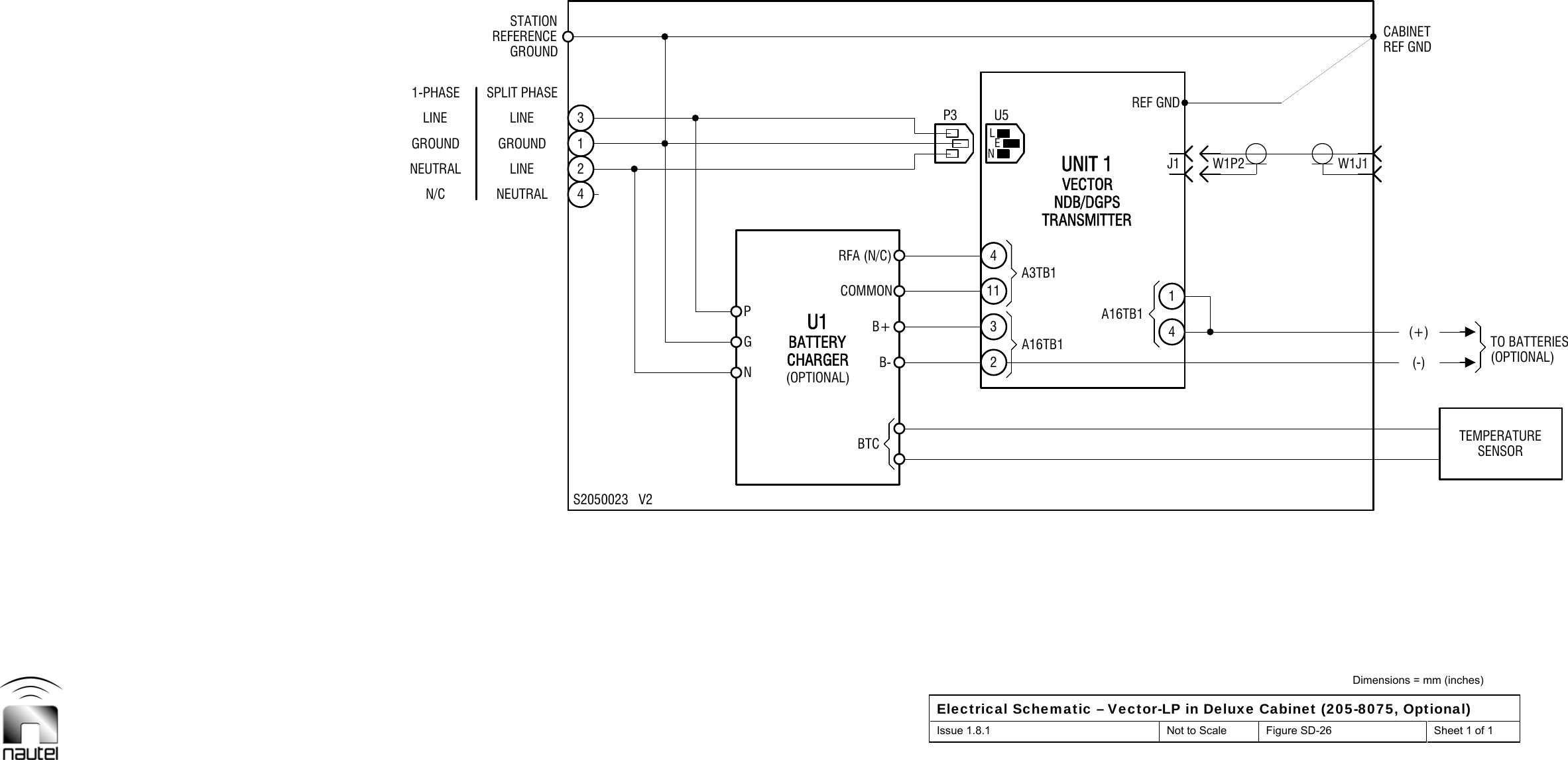
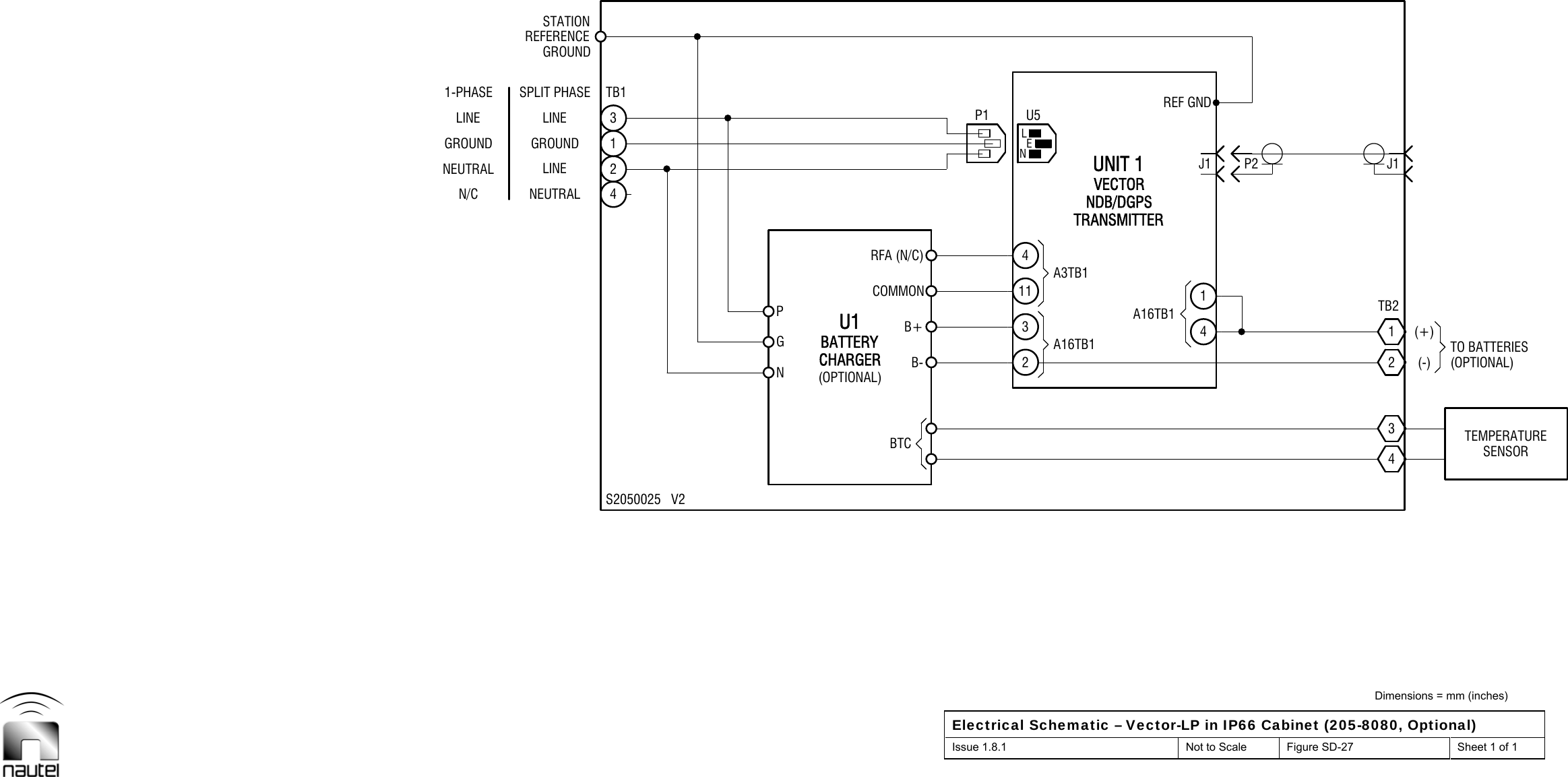
![Vector-LP Radio Beacon Transmitter Technical Instruction Manual Page 9-3 Section 9 Electrical Schematics Issue 1.8.1 Table 9-1: Electrical Schematics Figure # Description SD-1 Electrical Schematic – Vector-LP Transmitter: Ac/Dc Power Stage SD-2 Electrical Schematic – Vector-LP Transmitter: Exciter Stage SD-3 Electrical Schematic – Vector-LP Transmitter: Control/Monitor Stage SD-4 Electrical Schematic – Vector-LP Transmitter: RF Power Stage SD-5 Electrical Schematic – Control/Display PWB (NAPC147D) (Sheet 1 of 4) SD-6 Electrical Schematic – Control/Display PWB (NAPC147D) (Sheet 2 of 4) SD-7 Electrical Schematic – Control/Display PWB (NAPC147D) (Sheet 3 of 4) SD-8 Electrical Schematic – Control/Display PWB (NAPC147D) (Sheet 4 of 4) SD-9 Electrical Schematic – Exciter Interface PWB (NAPI76A/02) (Sheet 1 of 2) SD-10 Electrical Schematic – Exciter Interface PWB (NAPI76A/02) (Sheet 2 of 2) SD-11 Electrical Schematic – Remote Interface PWB (NAPI78D/02) (Sheet 1 of 3) SD-12 Electrical Schematic – Remote Interface PWB (NAPI78D/02) (Sheet 2 of 3) SD-13 Electrical Schematic – Remote Interface PWB (NAPI78D/02) (Sheet 3 of 3) SD-14 Electrical Schematic – Site Interface PWB (NAPI80, Optional) (Sheet 1 of 2) SD-15 Electrical Schematic – Site Interface PWB (NAPI80, Optional) (Sheet 1 of 2) SD-16 Electrical Schematic – RF Synthesizer PWB (NAPE70C/01) (Sheet 1 of 2) SD-17 Electrical Schematic – RF Synthesizer PWB (NAPE70C/01) (Sheet 2 of 2) SD-18 Electrical Schematic – Interphase PDM Driver PWB (NAPM11) SD-19 Electrical Schematic – Exciter Monitor/Generator PWB (NAPE76A/03) (Sheet 1 of 2) SD-20 Electrical Schematic – Exciter Monitor/Generator PWB (NAPE76A/03) (Sheet 2 of 2) SD-21 Electrical Schematic – Interface PWB (NAPI94A) SD-22 Electrical Schematic – RF Power Module (NAP35B/01) SD-23 Electrical Schematic – Power Module Control/Interface PWB (NAPC151A) SD-24 Electrical Schematic – Switch Mode Power Supply PWB (NAPS31B/03) SD-25 Electrical Schematic – Battery Boost PWB (NAPS35, Optional) SD-26 Electrical Schematic – Vector-LP in Deluxe Cabinet (205-8075, Optional) SD-27 Electrical Schematic – Vector-LP in IP66 Cabinet (205-8080, Optional) SD-28 Electrical Schematic – Vector-LP in Short Cabinet [205-8120 (with battery) & 205-8120-01(no battery), Optional]SD-29 Electrical Schematic – Vector-LP in Tall Cabinet (205-8200, Optional)](https://usermanual.wiki/Nautel-Maine/VECTOR125/User-Guide-2553568-Page-272.png)
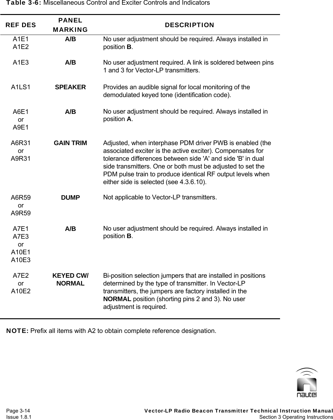
![Dimensions = mm (inches) Electrical Schematic – Vector-LP in Short Cabinet [205-8120 (with battery) or 205-8120-01 (no battery), Optional] Issue 1.8.1 Not to Scale Figure SD-28 Sheet 1 of 1 *LINE(-)(+)2123PH1143241A16TB1J1N/CGROUND1-PHASETB241TB1BT1**A3TB1NGS2050037 V3FROM BATTERIESLINENEUTRALLINEGROUNDSTATIONRFA (N/C)(OPTIONAL)CHARGERU1 B-20ANDB/DGPSVECTORJ1 P2(OPTIONAL)NEUTRALGROUNDSPLIT PHASEREFERENCESENSORTEMPERATURE BTCCOMMONCB1BATTERYTRANSMITTERLNEU5UNIT 1B+DENOTES BATTERY AND CIRCUIT BREAKER CB1REF GNDINSTALLED ONLY IN 205-8120 VARIATION.REF GNDCABINETP1](https://usermanual.wiki/Nautel-Maine/VECTOR125/User-Guide-2553568-Page-301.png)
![Dimensions = mm (inches) Electrical Schematic – Vector-LP in Tall Cabinet (205-8200), Optional] Issue 1.8.1 Not to Scale Figure SD-29 Sheet 1 of 1 N/CLINEB-J1U2P3LNEA3J5LINENEUTRALGROUND GROUNDLINE1-PHASE2141TB1(OPTIONAL)CHARGERU1PH20AW2P1 VR-LINKRS-232 W3P1114324A16TB11NDB/DGPSVECTORJ1J1 P2SENSORTEMPERATURETB2BT123BTCCB1BATTERYW2P2 W2P3(OPTIONAL)A1J1A3TB1UNIT 1LNEU5P1REF GNDNGS2050042 V1RFA (N/C)NEUTRALSPLIT PHASEGROUNDSTATION4W3P2REF GNDCOMMONREFERENCETRANSMITTER1CABINETB+](https://usermanual.wiki/Nautel-Maine/VECTOR125/User-Guide-2553568-Page-302.png)