Nautel Maine VECTOR125 Nautel VR125 User Manual
Nautel Maine Inc Nautel VR125
user manual

Vector-LP
Radio Beacon
Transmitter
Technical Instruction Manual
VR125
VR250
Issue 1.8.1 ................. 01 February 2015
Nautel Limited
10089 Peggy's Cove Road,
Hackett's Cove, NS, Canada B3Z 3J4
T.877 6 nautel (628835) or +1.902.823.2233
F.+1.902.823.3183 info@nautel.com
U.S. customers please contact:
Nautel Inc.
201 Target Industrial Circle, Bangor ME 04401
T.877 6 nautel (628835) or +1.207.947.8200
F.+1.207.947.3693 info@nautel.com
e-mail: support@nautel.com
www.nautel.com
Copyright 2015 NAUTEL. All rights reserved.

Vector-LP Radio Beacon Transmitter Technical Instruction Manual Feb.01.15
IMPORTANT
This manual makes frequent references to a mode of
operation called ‘beacon and voice’ (e.g., pages 1-1,
3-11, 3-23, 3-30, 4-4, 4-5, 4-7, 6-1 and 6-15).
Please ignore these references, as voice operation is not
authorized in FCC/FAA compliant transmitters.

Vector-LP Radio Beacon Transmitter Technical Instruction Manual Feb.01.15
Warranty
by Nautel Limited/Nautel Inc. (herein after referred to as Nautel)
Nautel Limited/Nautel Incorporated, hereinafter referred to as Nautel, guarantees all mechanical and electrical parts of
the equipment for a period of 18 months from date of shipment.
1. A "Part Failure" shall be deemed to have occurred when the part has become defective, or does not have the
characteristics required for the specified equipment performance:
(a) When the equipment is operated within the design parameters, and
(b) When the equipment is installed and adjusted according to Nautel's prescribed procedures as stated in
the instruction manual.
2. Nautel shall provide replacements for all "Parts" at no cost to the Customer when they become defective during
the warranty period, and upon the return of the defective part.
3. In the event that a "Part" fails during the warranty period and causes damage to a sub-assembly that cannot be
readily repaired in the field, the entire sub-assembly so damaged may be returned to Nautel for repair. The
repairs will be made without charge to the Customer.
4. Where warranty replacements or repair are provided under items 2 or 3, Nautel will pay that part of the shipping
costs incurred in returning the part/assembly to the Customer.
5. Warranty replacement parts and repair, which are provided under items 2 or 3, shall be guaranteed for a period
of ninety days from date of shipment or until the end of the original warranty period, whichever occurs later.
6. Nautel will not assume responsibility for any charges incurred by other than Nautel employees.
7. Nautel shall have the privilege of investigating whether failures have been caused by factors beyond its control.
8. Nautel shall in no event be liable for any consequential damages arising from the use of this equipment.
9. When requesting a warranty repair/replacement, please provide complete and accurate information. Observe
the instructions regarding 'Equipment Being Returned to Nautel' on page two of this warranty and provide the
information requested.
10. When ordering spare/replacement parts, please provide complete and accurate information. Refer to the parts
list of the Repair manual for ordering information. Provide as much of the information requested for 'Equipment
Being Returned to Nautel' on page two of this warranty as is practical. The information identified by an asterisk
is the minimum required.
Nautel Limited Nautel Inc.
10089 Peggy's Cove Road 201 Target Industrial Circle
Hackett's Cove NS Canada B3Z 3J4 Bangor ME USA 04401
T. 877 6 nautel (628835) or 1.902.823.2233 T. 877 6 nautel (628835) or 1.207.947.8200
F. 1.902.823.3183 F. 1.207.947.3693
24hr. Answering Service 1.902.823.3900
Customer Service Notice
A ‘Technical Assistance’ and ‘Plug-in Module Exchange’ service is available to Nautel users.
Factory Support
TECHNICAL ASSISTANCE
Nautel's field service department provides telephone technical assistance on a 24 hour, seven days a week basis.
Requests by other media (facsimile or e-mail) will be responded to the next working day if received after Nautel's normal
working hours. Contact the appropriate field service centre from the following:
U.S.A. customers use: Nautel Incorporated T. +1.207.947.8200 (24 hours) or 877 6 nautel (628835)
201 Target Industrial Circle F. +1.207.947.3693
Bangor, Maine 04401
All other customers use: Nautel Limited T. +1.902.823.3900 (24 hours) or 877 6 nautel (628835)
10089 Peggy’s Cove Road, F. +1.902.823.3183
Hackett’s Cove, NS, Canada E-Mail support@nautel.com
B3Z 3J4 Web www.nautel.com
MODULE EXCHANGE SERVICE
In order to provide Nautel customers with a fast and efficient service in the event of a problem, Nautel operates a
factory rebuilt, module exchange service which takes full advantage of the high degree of module redundancy in
Nautel equipment. This module exchange service is operated from Nautel’s factory in Bangor, Maine and Hackett’s
Cove, Nova Scotia. These two locations allow us to provide a quick turn around service to keep our customers on
the air. During the transmitter’s warranty period, up to 18 months from shipment, repair and exchange of modules is
at no charge to the customer. When the warranty has expired, a charge of 80% of the list price for all exchanged
modules is made. If the faulty module is returned to Nautel within 30 days, a credit is issued reducing this charge by
one half to 40% of the list price. U.S.A. customers are required to contact our Bangor, Maine facility. Canadian and
overseas customers should contact our Nova Scotia, Canada facility.
EQUIPMENT BEING RETURNED TO NAUTEL
For all equipment being returned to Nautel and all requests for repairs or replacements:
Obtain an RMA number from Nautel (you must have an RMA number to return equipment)
Mark the item as 'field return'
Mark the item with the RMA number assigned by Nautel
Address the item to the appropriate Nautel facility
Complete and accurate information regarding the equipment being returned will ensure prompt attention and will
expedite the dispatch of replacements. Refer to the nameplate on the transmitter and/or the appropriate
module/assembly to obtain name, type, part and serial number information. Refer to the parts list of this manual or the
appropriate service instruction manual for additional ordering information.
The following information should accompany each request:
* Model of Equipment
* Serial number of Equipment
* Name of Part/Assembly
Serial number of Part/Assembly
* Complete reference designation of Part/Assembly
* Nautel's part number of Part/Assembly
* OEM's part number of Part/Assembly
Number of hours in Use
Nature of defect
* Return shipping address
* Denotes minimum information required to order spare/replacement parts
Vector-LP Radio Beacon Transmitter Technical Instruction Manual Feb.01.15
Safety
Symbols
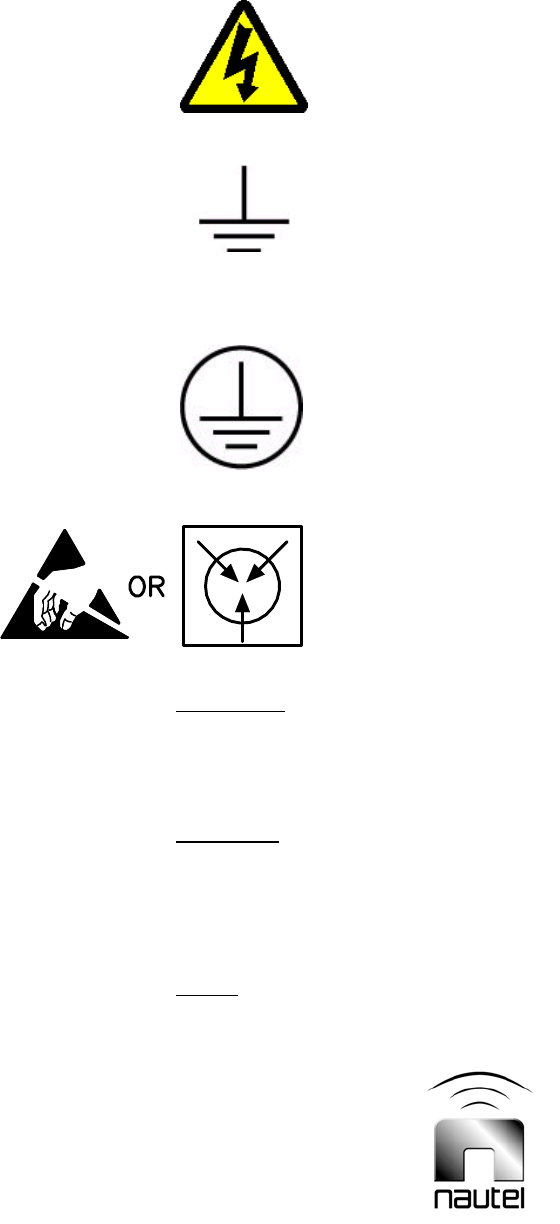
General definitions of safety symbols used on equipment or in manuals.
DANGER – HIGH VOLTAGE
Indicates dangerous voltages (in excess of 72 V), capable of causing a fatal
electrical shock, are present on or near parts bearing this label.
GROUND (EARTH)
Used with wiring terminals to indicate the terminal must be connected to
earth ground before operating equipment. If power is supplied without
grounding the equipment, there is a risk of receiving a severe or fatal
electrical shock. Also used on electrical schematics to indicate a part that is
connected to earth ground.
GROUND (PROTECTIVE or SAFETY)
Used with protective (safety) conductor terminals to indicate the terminal
must be connected to ground before operating the equipment. If power is
supplied without grounding the equipment, there is a risk of receiving a
severe or fatal electrical shock.
ELECTROSTATIC SENSITIVE
Indicates a part or assembly is or contains devices that are electrostatic
sensitive. To prevent damage to these devices, ensure the handling
procedures outlined in this manual are observed.
WARNING A WARNING denotes a hazard. It identifies an operating procedure,
condition, etc. which, if not strictly observed or adhered to, could result in
injury or death to personnel. Throughout the technical manual, a
WARNING shall immediately precede the text to which it applies.
CAUTION A CAUTION denotes a hazard. It identifies an operating procedure,
condition, etc., which, if not strictly observed or adhered to, could result in
damage to, or destruction of the equipment. Throughout the technical
manual, a CAUTION shall immediately precede the text to which it
applies.
NOTE A NOTE denotes important information pertaining to an operating
procedure, condition, statement, etc., which is essential to highlight. A
NOTE may precede or follow the text to which it applies.

Vector-LP Radio Beacon Transmitter Technical Instruction Manual Feb.01.15
Safety
Toxic Hazard Warning
There are devices used in this equipment containing beryllium oxide ceramic,
which is non-hazardous during normal device operation and under normal device
failure conditions. These devices are specifically identified in the equipment parts
list(s) by including ‘BeO’ in the part’s description.
DO NOT cut, crush or grind devices because the resulting dust may be
HAZARDOUS IF INHALED. Unserviceable devices should be disposed of as
harmful waste.

Vector-LP Radio Beacon Transmitter Technical Instruction Manual Feb.01.15
Contents Page
1 GENERAL INFORMATION
1.1 INTRODUCTION 1-1
1.2 FACTORY SUPPORT 1-1
1.3 PURPOSE AND SCOPE OF MANUAL 1-1
1.4 PURPOSE OF EQUIPMENT 1-1
1.5 MECHANICAL DESCRIPTION 1-2
1.6 TEST EQUIPMENT AND SPECIAL TOOLS 1-2
1.7 GLOSSARY OF TERMS 1-2
2 PREPARATION FOR USE AND INSTALLATION
2.1 INTRODUCTION 2-1
2.2 PREPARATION FOR USE 2-1
2.2.1 Transmitter Room Requirements 2-1
2.2.1.1 Transmitter Dimensions 2-1
2.2.1.2 Transmitter Weights 2-1
2.2.1.3 Transmitter Clearances 2-1
2.2.1.4 Air Flushing 2-1
2.2.1.5 Cooling and Heating 2-1
2.2.1.6 Work Area 2-1
2.2.1.7 Power Source Switch 2-1
2.2.2 Lightning Protection 2-2
2.2.3 Station Reference Ground 2-2
2.2.4 Ac Power Source 2-2
2.2.4.1 Ac Wiring 2-2
2.2.5 Antenna Feed Cable 2-7
2.2.6 Antenna Tower 2-7
2.2.7 External Control/Monitor Wiring 2-7
2.2.8 Electrical Power 2-7
2.2.8.1 Ac Voltage Source 2-7
2.2.8.2 External Ac Switching 2-7
2.2.8.3 Dc Voltage Source 2-7
2.2.9 Antenna System 2-8
2.2.9.1 RF Feed Cable 2-8
2.2.9.2 Interface Protection Option 2-8
2.2.10 Internal DDS Source 2-8
2.2.11 External Interlocks 2-9
2.2.12 Remote Control Circuits 2-9
2.2.12.1 On/Off Control 2-10
2.2.12.2 Charger Alarm 2-10
2.2.12.3 Standby Code 1 2-10
2.2.12.4 Standby Code 2 2-10
2.2.13 Press-To-Talk Input 2-10
2.2.14 User Assigned Information 2-10
2.2.14.1 Carrier Frequency 2-10
2.2.14.2 Keyed Tone Frequency 2-10

Vector-LP Radio Beacon Transmitter Technical Instruction Manual Feb.01.15
Contents Page
2.2.14.3 Identification Code 2-10
2.2.14.4 Standby Codes 2-10
2.2.15 Serial Port Features 2-11
2.2.15.1 Remote Control and Monitoring Interface 2-11
2.2.15.2 ATU Interface 2-11
2.2.16 RF Monitoring Sample 2-11
2.2.17 Parts Supplied By Nautel 2-11
2.2.18 Parts Not Supplied By Nautel 2-11
2.2.19 Test Equipment and Special Tools 2-11
2.2.20 Available Options 2-11
2.3 INSTALLATION 2-13
2.3.1 Acceptance of Shipment 2-13
2.3.2 Unpacking Instructions 2-13
2.3.3 Visual Inspection 2-14
2.3.4 Cabinet Mounting 2-14
2.3.5 Determining Control/Monitor Requirements 2-14
2.3.6 Installing External Control/Monitor Wiring 2-14
2.3.7 Installing Ac Power Source Wiring 2-15
2.3.8 Installing Dc Power Source Wiring (Optional) 2-16
2.4 COMMISSIONING 2-17
2.4.1 Precautions 2-17
2.4.2 Turn-On Prerequisites 2-17
2.4.3 Initial Turn-On 2-17
3 OPERATING INSTRUCTIONS
3.1 INTRODUCTION 3-1
3.1.1 Precautions 3-1
3.2 EMERGENCY SHUTDOWN 3-1
3.2.1 Turn Off RF Output 3-1
3.2.2 Complete Shutdown 3-1
3.3 EXTERNAL SAFETY INTERLOCK 3-1
3.4 ELECTROSTATIC DISCHARGE PROTECTION 3-2
3.5 CONTROLS AND INDICATORS 3-2
3.5.1 Front Panel 3-3
3.5.2 Exciter Interface PWB 3-4
3.5.3 Remote Interface PWB 3-4
3.5.4 RF Synthesizer PWB 3-4
3.5.5 Miscellaneous Control and Exciter 3-4
3.5.6 Miscellaneous RF Power Stage 3-4
3.5.7 Battery Boost PWB 3-4
3.6 DIAGNOSTIC DISPLAY 3-18
3.6.1 Pushbutton Switches 3-18

Vector-LP Radio Beacon Transmitter Technical Instruction Manual Feb.01.15
Contents Page
3.6.2 Main Screens 3-18
3.6.3 Viewing Faults 3-20
3.6.4 Changeover Control 3-20
3.6.5 Viewing Events Log 3-20
3.6.6 Setting Real Time Clock 3-21
3.6.7 Setting RF Monitor Limits 3-22
3.6.8 Meter Settings 3-24
3.6.8.1 Changing Meter Groups 3-24
3.6.8.2 Selecting Analog Meter 3-25
3.6.8.3 Calibrating Analog Meter 3-25
3.6.9 Selecting Power Source 3-25
3.6.10 Configuring the Sonalert 3-26
3.6.11 Setting a Timed Shutdown 3-26
3.6.12 Changing Factory Calibrated Settings 3-27
3.6.12.1 Calibrating Diagnostic Display Meters 3-28
3.6.12.2 Setting Protection Threshold Levels 3-28
3.6.12.3 Setting Maximum Output Limitations 3-29
3.6.12.4 Using Factory Settings 3-29
3.6.13 Viewing and Setting Peripherals 3-30
3.6.13.1 Setting the Keyer 3-30
3.6.13.2 Viewing Power Module Status 3-31
3.6.13.3 ATU Controls 3-32
3.6.13.4 Testing the Standby Side 3-33
3.6.13.5 Selecting Peripherals 3-33
3.6.13.6 Checking Modules 3-34
3.6.14 Remote Control Monitor System Settings 3-34
3.6.14.1 Setting Control Points 3-34
3.6.14.2 Setting Monitor Points 3-35
3.6.14.3 Serial Settings 3-35
3.6.14.4 Automatic Reporting 3-35
3.6.15 Viewing Power Related Parameters and
Setting ATU Current Feedback 3-36
4 TESTING AND ADJUSTMENT
4.1 INTRODUCTION 4-1
4.2 OPERATING PRECAUTIONS 4-1
4.3 FUNCTIONAL TESTS 4-1
4.3.1 General 4-1
4.3.2 Test Equipment Required 4-3
4.3.3 Test Prerequisites 4-3
4.3.4 Initial Turn On 4-3
4.3.5 Standard Adjustments 4-4
4.3.6 Non-Standard Adjustments 4-8

Vector-LP Radio Beacon Transmitter Technical Instruction Manual Feb.01.15
Contents Page
5 MAINTENANCE AND TROUBLESHOOTING
5.1 GENERAL 5-1
5.2 SCHEDULED MAINTENANCE 5-1
5.3 CORRECTIVE MAINTENANCE 5-2
5.4 ELECTROSTATIC PROTECTION 5-2
5.5 TROUBLESHOOTING FRONT PANEL ALARMS 5-3
5.6 REPLACING AN RF POWER MODULE 5-9
5.7 FET CHECKING/REPLACEMENT 5-11
5.8 EXCITER PANEL PWB REPLACEMENT 5-12
5.8.1 Exciter Interface PWB and Interconnecting PWB
Replacement 5-12
5.8.2 Exciter Monitor/Generator PWB Replacement 5-13
5.8.3 Interface PWB Replacement 5-14
5.9 BATTERY BOOST ASSEMBLY REPLACEMENT 5-14
6 THEORY OF OPERATION
6.1 INTRODUCTION 6-1
6.2 TRANSMITTER OVERVIEW 6-1
6.3 AC_DC POWER STAGE 6-1
6.3.1 Interface PWB 6-5
6.3.2 Ac/Dc Universal Input Power Supplies 6-5
6.4 EXCITER STAGE 6-6
6.4.1 Exciter Interface PWB 6-6
6.4.2 RF Synthesizer PWBs 6-6
6.4.3 Interphase PDM Driver PWBs 6-8
6.4.4 Exciter Monitor/Generator PWBs 6-15
6.5 CONTROL/MONITOR STAGE 6-16
6.5.1 Control/Display PWB 6-16
6.5.2 Remote Interface PWB 6-19
6.5.3 Front Panel Metering 6-20
6.5.4 NDB Site Interface PWB (Optional) 6-21
6.5.5 Modem (Optional) 6-21
6.6 RF POWER STAGE 6-22
6.6.1 RF Power Module(s) 6-22
6.6.2 RF Filter PWB 6-29
6.6.3 RF Power Probe PWB 6-29
6.7 MODULATION DEPTH WHEN USING A HIGH ‘Q’
ANTENNA 6-30

Vector-LP Radio Beacon Transmitter Technical Instruction Manual Feb.01.15
Contents Page
7 PARTS INFORMATION
7.1 INTRODUCTION 7-1
7.2 FAMILY TREE 7-1
7.3 HOW TO LOCATE INFORMATION FOR A
SPECIFIC PART 7-1
7.4 REFERENCE DESIGNATION LISTS 7-1
7.5 COLUMN CONTENT EXPLANATION 7-1
7.6 OEM CODE TO MANUFACTURER CROSS-REFERENCE 7-2
7.7 COMMON ABBREVIATIONS/ACRONYMS 7-3
8 WIRING INFORMATION
8.1 INTRODUCTION 8-1
8.2 WIRING LISTS NOT PROVIDED 8-1
8.3 PRINTED WIRING PATTERNS 8-1
8.4 WIRE COLOURS 8-1
8.5 WIRING LISTS PROVIDED 8-1
8.5.1 Connector Mating Information 8-1
9 ELECTRICAL SCHEMATICS
9.1 INTRODUCTION 9-1
9.2 COMPONENT VALUES 9-1
9.3 GRAPHIC SYMBOLS 9-1
9.4 LOGIC SYMBOLS 9-1
9.5 REFERENCE DESIGNATIONS 9-1
9.6 UNIQUE SYMBOLOGY 9-1
9.7 TROUBLESHOOTING AIDS 9-1
9.8 IDENTIFICATION OF SCHEMATIC DIAGRAMS 9-2
9.9 STRUCTURE OF SCHEMATICS 9-2
9.10 LOCATING THE SCHEMATIC DIAGRAM(S) FOR A
FUNCTIONAL BLOCK 9-2
9.11 LOCATING A PART/ASSEMBLY IDENTIFIED
ON A SCHEMATIC 9-2
10 MECHANICAL DRAWINGS
10.1 INTRODUCTION 10-1
10.2 LOCATING ASSEMBLY DETAIL DRAWINGS 10-1
10.3 CONTENT OF MECHANICAL DRAWINGS 10-1

Vector-LP Radio Beacon Transmitter Technical Instruction Manual Feb.01.15
Contents Page
List of Tables
1-1 Dimensions and Weights 1-2
1-2 Recommended Site Test Equipment 1-3
1-3 Glossary of Terms 1-4
2-1 Ac Power Consumption 2-7
2-2 Dc Power Consumption 2-8
2-3 ATU Serial Interface 2-14
2-4 RS-422 Remote Interface 2-14
2-5 RS-232 Remote Interface 2-14
2-6a RF Filter PWB Tap Settings vs Frequency (Standard Frequency Band) 2-16
2-6b RF Filter PWB Tap Settings vs Frequency (Extended Frequency Band) 2-16
2-7 Dc Power Connection 2-16
3-1 Front Panel – System Diagram Controls and Indicators 3-5
3-2 Front Panel – Control Section Controls and Indicators 3-7
3-3 Exciter Interface PWB Controls and Indicators 3-9
3-4 Remote Interface PWB Controls and Indicators 3-11
3-5 RF Synthesizer PWB Controls and Indicators 3-13
3-6 Miscellaneous Control and Exciter Assembly Controls and Indicators 3-14
3-7 Miscellaneous RF Power Stage Controls and Indicators 3-15
3-8 Battery Boost PWB Controls and Indicators 3-17
3-9 Events Log Displays – Non Alarm Events 3-21
5-1 Troubleshooting and Replacement Tips 5-5
6-1 Battery Select Logic 6-5
7-1 Manufacturer’s Index 7-4
8-1 Wiring Lists Provided 8-1
9-1 Electrical Schematics 9-3
10-1 Mechanical Drawings 10-2

Vector-LP Radio Beacon Transmitter Technical Instruction Manual Feb.01.15
Contents Page
List of Figures/Drawings
2-1 Vector-LP Transmitter Environment Considerations 2-3
2-2 Customer Interface to Vector-LP Transmitter 2-5
2-3 Single Ended Input Selected 2-9
2-4 Differential Input Selected 2-10
2-5 Block Diagram – Recommended Transmitter System Installation (with SPU1) 2-19
2-6 Block Diagram – Recommended Transmitter System Installation (without SPU1)2-20
3-1 Vector-LP Transmitter Front Panel (Primary User Interface) 3-3
3-2 Vector-LP Transmitter Front Panel – System Diagram Section 3-4
3-3 Vector-LP Transmitter Front Panel – Control Section 3-6
3-4 Part of NAPI76A/02 Exciter Interface PWB A2 3-8
3-5 Part of NAPI78D/02 Remote Interface PWB A3 3-10
3-6 NAPE70C/01 RF Synthesizer PWB A5 and A8 3-12
3-7 NAPS35 Battery Boost PWB A16A1 (Optional) 3-16
3-8 Diagnostic Display – Meters Screen 3-18
3-9 Diagnostic Display – Main Menu 3-18
3-10 Flow Diagram – Diagnostic Display Functions 3-19
4-1 Exciter Panel and Rear View 4-2
4-2 CW signal set to fill display 4-15
4-3 CW signal with position adjusted to mid-point of display 4-15
4-4 MCW signal, 95% modulation 4-15
5-1 RF Power Module Securing Hardware 5-10
6-1 Block Diagram - Vector-LP Radio Beacon Transmitter 6-3
6-2 Block Diagram – Exciter/Control/Monitor Stage 6-11
6-3 Timing Diagram for PDM Differential Amplifier 6-13
6-4 Block Diagram – RF Power Stage 6-25
6-5 Block Diagram – RF Power Module 6-27
6-6 Simplified Principles of Class ‘D’ Operation 6-31
7-1 Family Tree – Vector-LP Radio Beacon Transmitter 7-5

Vector-LP Radio Beacon Transmitter Technical Instruction Manual Feb.01.15
Release Control Record
Issue Date Reason
1.8.1 01 February 2015 Manual to support transmitter configuration for FAA
(NARB18 and custom DWAs incorporated)

Vector-LP Radio Beacon Transmitter Technical Instruction Manual Page 1-1
Section 1 General Information Issue 1.8.1
Vector-LP Radio Beacon Transmitter
TECHNICAL INSTRUCTION MANUAL
Section 1 GENERAL INFORMATION
1.1 INTRODUCTION
The Vector-LP radio beacon transmitter:
Automatically transmits specific
beacon identification signals at pre-
selected repetition rates. Special codes
may also be transmitted when
commanded from an external source.
Provision is made for local or remote
operation of the transmitter as well as
antenna fine-tuning through controls on
the transmitter's front panel. Emission
is continuous carrier (NON), beacon
keyed identification tone (A2A) and
beacon with voice (A2A/A3A).
Provides continuous carrier power for
two different power configurations:
VR125 125 W maximum
VR250 250 W maximum
Can be modulated from 0 to 95%.
Operates in the LF/MF band (190 kHz
to 535 kHz).
VR125 has provision for extended
band operation, up to 125 W, in the MF
band (536 kHz to 1200 kHz and
1600 kHz to 1800 kHz).
Has provision for a standby exciter
section, which duplicates the PDM
and RF drive generation circuitry and
low voltage power supplies.
Has provision for single side or dual
side (A and B) RF power sections,
which can be manually or
automatically selected.
Can be serially connected to Nautel’s
ATU-LP or ATU500 Antenna Tuning
Unit, allowing a variety of control/
monitoring features, including
stabilization of the antenna current
(ATU-LP only) by automatically
adjusting transmitter power level.
1.2 FACTORY SUPPORT
Nautel provides after sales factory
support. Technical assistance is available
on a 24 hour, seven days a week basis. A
factory service facility for repair of
modules/assemblies is also available.
Refer to the Factory Support portion of the
Warranty pages at the front of this manual
for additional information.
1.3 PURPOSE AND SCOPE OF
MANUAL
This Technical Instruction manual
provides the information required to
install, operate and maintain the
equipment. Where applicable, changes
have been incorporated to reflect non-
standard customer requests.
1.4 PURPOSE OF EQUIPMENT
When combined with an appropriate
antenna system, the Vector-LP transmitter
provides reliable facilities for an NDB
reference station. It is ideally suited for
remote or unmanned sites. Remote control
facilities are incorporated to allow
unattended operation from a remote
location.

Page 1-2 Vector-LP Radio Beacon Transmitter Technical Instruction Manual
Issue 1.8.1 Section 1 General information
1.5 MECHANICAL DESCRIPTION
See Figure MD-1. The Vector-LP
transmitter is a fabricated metal chassis
with an attached full-depth front panel. It is
intended for installation in a 19-inch
mounting rack. It can be supplied with non-
swivel type drawer slides (including portion
attached to mounting rack).
Nautel provides four rack mounting options
(see Table 1-1 for dimensions and
weights).
- Deluxe Cabinet: supports 19-inch rack
mount equipment, including side
panels and rear door (see also
2.2.20.7 and Figure MD-1B)
- IP66 Cabinet: meets IP66
requirements (see also 2.2.20.8 and
Figure MD-1C)
- Short Cabinet (with or without internal
battery): supports 19-inch rack mount
equipment, including side panels and
rear door (see also 2.2.20.9 and Figure
MD-1D)
- Tall Cabinet (with internal battery):
supports 19-inch rack mount
equipment, including side panels and
rear door (see also 2.2.20.10 and
Figure MD-1E)
All external connections are terminated at
the rear of the transmitter. The RF output
coaxial cable connects to an N-type
connector. The ac power cable connects to
a standard ac line connector. The dc power
cabling, if applicable, connects to a
terminal block. External input (RF drive and
control) and output (status and alarm
monitoring) connect to connectors on the
remote interface PWB. If the transmitter is
installed in the optional deluxe, short or tall
cabinet, cable entry holes are provided. If
the transmitter is installed in the optional
IP66 cabinet, weather-proof cable glands
are provided.
1.6 TEST EQUIPMENT AND
SPECIAL TOOLS
Table 1-2 lists the test equipment and
special tools that are required to operate
and maintain the Vector transmitter.
1.7 GLOSSARY OF TERMS
Table 1-3 provides a list of unique terms,
abbreviations, and acronyms used in this
publication.
Table 1-1: Dimensions and Weights
DIMENSIONS WEIGHT
VR125/VR250
(dual side installed) Height Width Depth Packed Unpacked
No cabinet 21.0 in.
(53.3 cm)
19.0 in.
(48.3 cm)
27 in.
(68.6 cm) TBD 54 lbs
(24.5 kg)
Deluxe cabinet 73.2 in.
(185.9 cm)
23.0 in.
(58.4 cm)
30.0 in.
(76.2 cm)
345 lbs
156.5 kg) TBD
Short cabinet 42 in.
(106.7 cm)
23.0 in.
(58.4 cm)
30 in.
(76.2 cm) TBD TBD
Tall cabinet 73.3 in.
(186.3 cm)
23.1 in.
(58.6 cm)
30 in.
(76.2 cm) TBD TBD
IP66 cabinet 32.4 in.
(82.3 cm)
23.7in.
(60.0 cm)
26.1 in.
(66.3 cm) TBD 87 lbs
(39.5 kg)

Vector-LP Radio Beacon Transmitter Technical Instruction Manual Page 1-3
Section 1 General Information Issue 1.8.1
Table 1-2: Recommended Site Test Equipment
EQUIPMENT PART/MODEL NUMBER
OR TYPE (EQUIVALENT
MAY BE USED)
APPLICATION
Dummy load
50 , rated for at least twice
the maximum continuous
carrier power level (250 W
and 500 W), VSWR 1.1
Provides precise load for ‘off-
air’ testing (calibration and
troubleshooting).
Digital multimeter 3-1/2 digit, ac and dc volts
(10 M input), ohms and
amps, ± 0.5% accuracy,
Beckman 3010
Testing and maintenance
Ac Voltmeter HP400E Precise measurement of RF
voltage across dummy load
during calibration procedures
Frequency counter 5 ppm up to 10 MHz
Fluke model 1900A
Measure carrier frequency
Oscilloscope Tektronix model T922 Testing and maintenance
RF Signal Generator Capable of operating in
frequency range of 190 – 550
kHz with an adjustable output
capable of supplying 0.5 V
pp – 4 V pp into 50
Simulate external RF drive
source during testing and
troubleshooting.
Dc power supply (variable)
0 – 50 V, 1A Testing and maintenance
Torque wrench Capable of providing five
inch-pounds (0.665 Newton-
Meters) of torque.
Installing power MOSFETs
Serial null modem adapter
9-pin null modem
Programming firmware
Current probe Calibrate reflected power
Clip-on dc current meter Calibrate battery current

Page 1-4 Vector-LP Radio Beacon Transmitter Technical Instruction Manual
Issue 1.8.1 Section 1 General information
Table 1-3: Glossary of Terms
TERM DESCRIPTION
ac Alternating current
AM Amplitude modulation
Bit Basic timing increment derived from master clock in keying unit.
Length is dependent on frame length and number of characters
used. An 8-bit frame is nominally 125 ms long.
Character Letter or number in the beacon identification signal
dBm Decibel reference 1 mW
dc Direct current
Element Smallest divisible part of a character. May be either a dot or a
dash
Frame Selected, fixed interval of time that is sufficiently long to
accommodate the beacon identification signal and an interval of
continuous tone. Normally set to 80 bits (10 seconds)
GUI Graphic user interface. Referred to as diagnostic display
throughout the manual
Hz Hertz
Modular Redundancy Identical modules operating in an overall system design such that
failure of one module does not affect the output of the system
PDM Pulse duration modulation
PSTN Public Switched Telephone Network
PWB Printed wiring board (also known as printed circuit board)
RF Radio frequency
SPI Serial Peripheral Interface
V ac Volts ac
VSWR Voltage standing wave ratio

Vector-LP Radio Beacon Transmitter Technical Instruction Manual Page 2-1
Section 2 Preparation for Use and Installation Issue 1.8.1
Vector-LP Radio Beacon Transmitter
TECHNICAL INSTRUCTION MANUAL
Section 2 PREPARATION FOR USE AND INSTALLATION
2.1 INTRODUCTION
This section contains pre-installation and
installation information for the transmitter.
Nautel recommends that you incorporate
all requirements to ensure optimum
reliability and performance.
NOTE
Failure to comply with these
recommendations and instructions could
void the manufacturer’s warranty. Please
review Nautel’s warranty terms for more
information.
2.2 PREPARATION FOR USE
Prepare the transmitter site to receive the
transmitter prior to its delivery and
installation. Use the following information
to prepare new sites and as evaluating
criteria at existing sites.
NOTE
Frequent reference is made to connectors
and terminal blocks on the remote
interface PWB. This PWB is located on
the back of the front panel.
2.2.1 Transmitter Room
Requirements
The following criteria must be addressed
when finalizing the transmitter site.
2.2.1.1 Transmitter Dimensions
Refer to Table 1-1 or Figure MD-1 for
transmitter dimensions. Dimensions
identify room entry and floor space
requirements and will assist in determining
cable lengths and routing.
2.2.1.2 Transmitter Weights
Refer to Table 1-1 for transmitter weights.
Sufficient manpower or lifting apparatus is
required to move the transmitter.
2.2.1.3 Transmitter Clearances
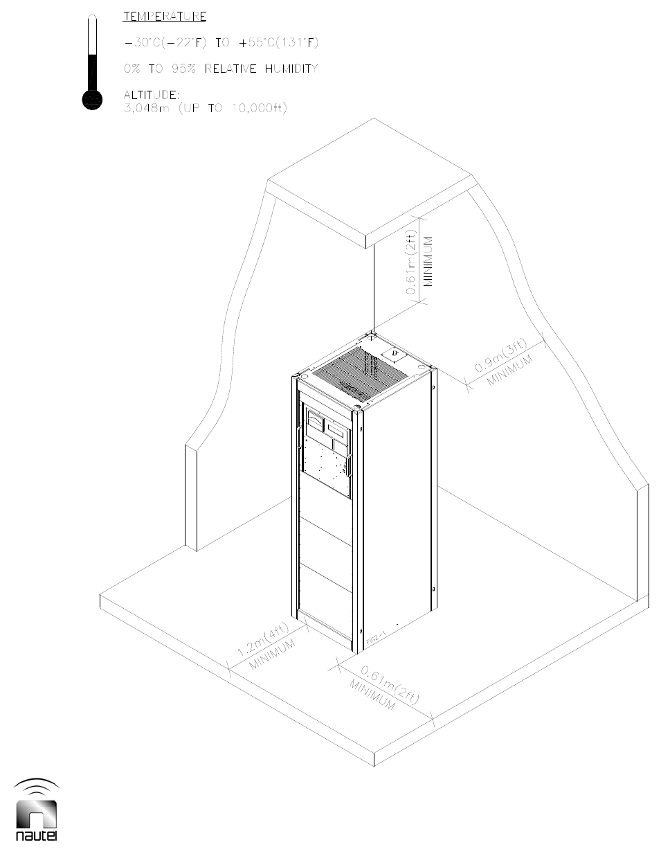
Refer to Figure 2-1 for recommended
transmitter clearances.
2.2.1.4 Air Flushing
Fans below each RF power module draw
cooling air through filters in the bottom of
the transmitter and exhaust it through
ventilation holes in the top of the RF
power modules. For VR250 transmitters,
the air exchange rate required to achieve
an acceptable intake/exhaust temperature
rise is 110 CFM. Standard VR125
transmitters are convection cooled, but
can be equipped with optional cooling
fans for each RF power module.
2.2.1.5 Cooling and Heating
Refer to Figure 2-1 for transmitter room
ambient air temperature limitations. If
necessary, ensure adequate cooling and/
or heating systems are in place to
maintain appropriate ambient air
temperature.
2.2.1.6 Work Area
Nautel recommends that a suitable work
area with an adequate table surface be
provided adjacent to the transmitter to
permit bench adjustment and repair of
modules. Static precautions must be
observed.
2.2.1.7 Power Source Switch
The AC INPUT switch on the back of the
transmitter controls the application of the
ac power source. If an optional dc power
source is being used, Nautel recommends
installing a switching assembly for the dc
power source in close proximity to the
transmitter.

Page 2-2 Vector-LP Radio Beacon Transmitter Technical Instruction Manual
Issue 1.8.1 Section 2 Preparation for Use and Installation
2.2.2 Lightning Protection
Extremely high voltage and current
transients are produced when a lightning
strike occurs. These transients, which are
usually the most significant hazard to any
solid state transmitter, may be passed to
the transmitter through the wiring
connecting the transmitter to the power
source and the antenna system. All
practical precautions should be taken to
protect the transmitter from this
phenomenon. Refer to the Lightning
Protection section of Nautel’s
Recommendations for Transmitter Site
Preparation booklet for specific protection
techniques. Installing Nautel’s interface
protection unit is highly recommended.
The following requirements are
considered to be essential and failure to
follow the site layout requirements may
void the transmitter warranty.
NOTE
The following paragraphs discuss
customer required connections to the
transmitter. Figure 2-2 is provided as an
aid for various customer interface
connections and should be referenced
while planning and installing these
connections.
2.2.3 Station Reference Ground
The site must contain a station reference
ground, as defined in Nautel’s
Recommendations for Transmitter Site
Preparation booklet. This ground must
provide a continuous, low impedance path
to the earth. The transmitter cabinet's
designated station reference ground point,
the shield of the coaxial feed cable, and
the ground connection of the power
source's surge protection devices must be
connected directly to the station reference
ground using, as a minimum, 100 mm (4
inch) copper strap.
2.2.4 Ac Power Source
If an ac power source is used, all
conductors should be protected by bi-
directional surge protection devices that
are connected between each conductor
and the station reference ground. In
addition, the conductors, as a group,
should pass through a ferrite toroid. The
inductance formed by this toroid is
transparent to ac voltages, but presents
impedance to transients originating in the
power source. A surge protector panel,
containing suitably rated varistors, is
available from Nautel for this purpose. If
used, the surge protector panel should be
installed in close proximity to the station
reference ground.
2.2.4.1 Ac Wiring
The ac wiring for the transmitter should
not be smaller than 18 AWG, based on an
average ac input voltage of 200 V ac.
NOTE
Local electrical codes must be observed
when sizing cables. The ac power source
usually presents the lowest impedance
path to ground potential for a lightning
strike and will normally carry most of the
lightning induced current away from the
transmitter. When lightning hits the power
source, a significant amount of induced
current may flow towards the transmitter.
In this instance, the objective is to route
the current around the transmitter, instead
of through it, to the best ground available.
Vector-LP Radio Beacon Transmitter Technical Instruction Manual Page 2-3 (2-4 Blank)
Section 2 Preparation for Use and Installation Issue 1.8.1
Figure 2-1 Vector-LP Transmitter Environment Considerations
SHOWN MOUNTED
IN DELUXE
CABINET OPTION
Dimensions = mm (inches)
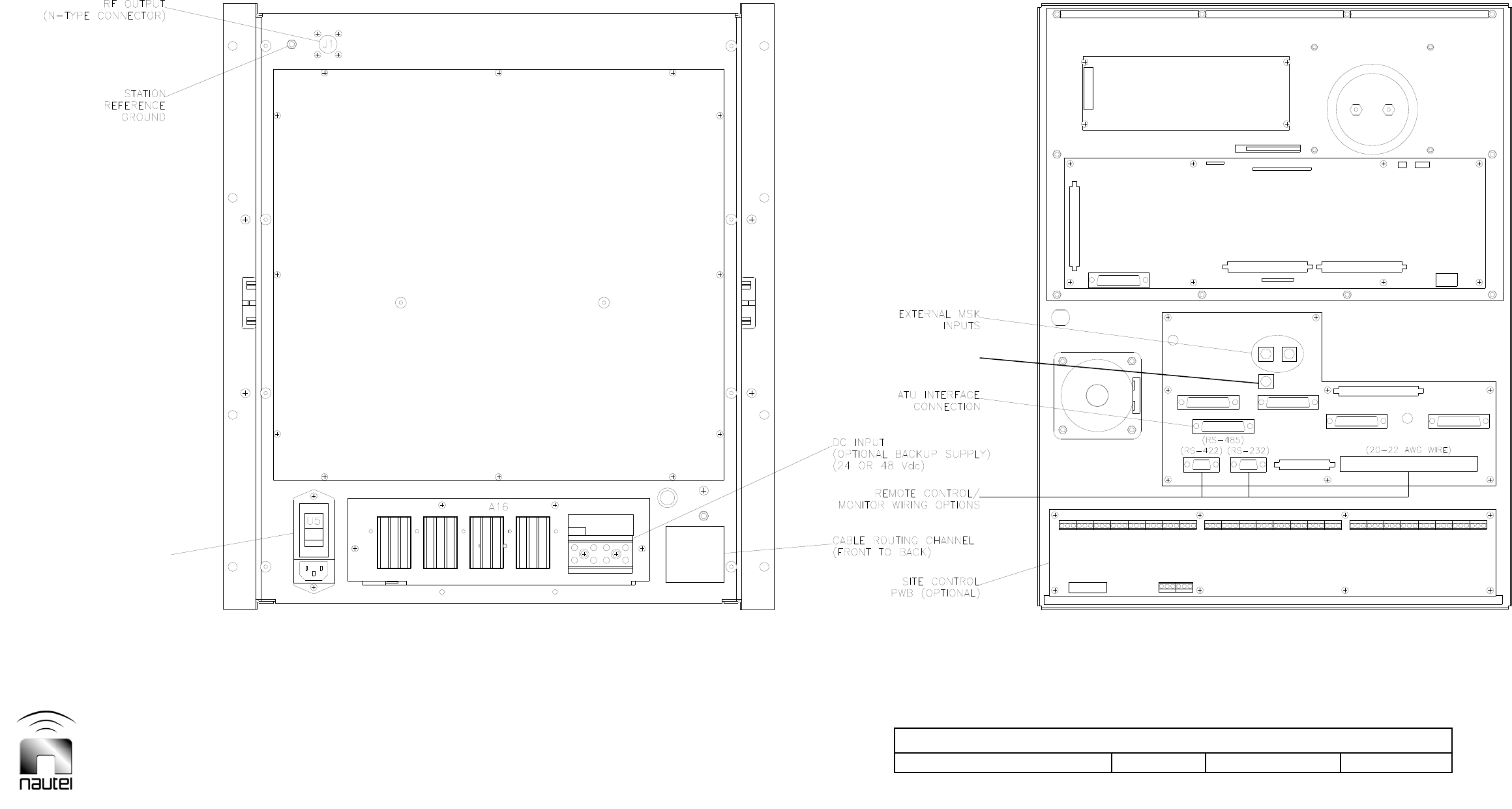
Customer Interface to Vector-LP Transmitter
Issue 1.8.1 Not to Scale Figure 2-2 Page 2-5 (2-6 Blank)
BACK OF TRANSMITTER BACK OF FRONT PANEL
AC INPUT
90-270 V ac
1-PHASE
(L-L OR L-N)
RF MONITOR
Vector-LP Radio Beacon Transmitter Technical Instruction Manual Page 2-7
Section 2 Preparation for Use and Installation Issue 1.8.1
2.2.5 Antenna Feed Cable
The shield of the antenna feed coaxial cable
should be connected directly to the station
reference ground where it enters the
building. In addition, the centre conductor
and the shield of the feed cable should pass
through a ferrite toroid positioned between
the shield ground at the building entrance
and the shield termination at the transmitter
reference ground. This toroid is transparent
to the RF signal, but presents impedance to
transients originating in the antenna. When
Nautel’s interface protection unit is installed,
the RF feed cable is connected directly to it.
It contains the necessary ferrite for the ac
wiring and RF feeder cable.
2.2.6 Antenna Tower
The antenna tower is the most likely target
for lightning strikes. It is imperative that it
contain lightning protection devices as the
first line of defense against lightning strikes.
2.2.7 External Control/Monitor
Wiring
All external control/monitor wiring that may
be subject to lightning induced transients
should be interfaced to the station reference
ground by surge protection devices at the
building entry. All conductors and shields
should pass through a ferrite toroid that is
positioned between its surge protection
device and the transmitter. This toroid is
transparent to control/monitor signals, but
presents impedance to lightning induced
transients. Connect shields to the ground
stud at the back of the transmitter, above the
cable routing channel (see Figure 2-2).
2.2.8 Electrical Power
The transmitter is configured during
manufacture to operate from an ac or dc
power source. The power source and
associated switching components and wiring
must meet the following requirements:
2.2.8.1 Ac Voltage Source
The VR250 can operate from a 170 to 270 V
ac, 50 Hz, (line-to-neutral) or 60 Hz (line-to-
line) ac power source. The VR125 can
operate from a 90 to 270 V ac, 50/60 Hz,
(line-to-neutral) or 60 Hz (line-to-line) ac
power source. The voltage must be
maintained within the specified voltage
range under all loading conditions. The
transmitter contains circuitry that maintains
the RF output at the pre-set carrier level for
voltage variations within this range. Power
consumption and line current depends on
the transmitter’s maximum rated power level
(see Table 2-1). Nautel recommends the ac
power source have a 20% over-capacity to
ensure adequate regulation.
Table 2-1: Ac Power Consumption
Vector
Product Max. Power
Consumption Max. Line
Current
VR125 500 VA *5 A RMS
VR250 1000 VA *5 A RMS
based on worst-case parameters (maximum RF
output power, minimum ac voltage and efficiency)
* maximum line current cannot exceed 5 A (ac
power entrance uses a 5 A breaker)
2.2.8.2 External Ac Switching
All current carrying conductors from the ac
power source should be controlled by an
external switching box located in close
proximity to the transmitter. This switch box
should be clearly marked TRANSMITTER
EMERGENCY ON/OFF SWITCH. Refer to
Table 2-1 for current ratings that should be
observed when selecting a circuit breaker
and associated input wiring.
2.2.8.3 Dc Voltage Source
As an option, the transmitter may operate
from a dc power source (battery bank).
The dc source must provide a nominal
24 V (VR125 only) or 48 V. When a 24 V
battery is used in VR125 transmitters, a
24-48 V power supply (A16) is used to
boost the dc voltage. The no-load voltage
must be in excess of 44.0 V (or 22.0 V for
24 V sources, limit is adjustable) for the
transmitter to turn on initially.
Line current depends on the
transmitter’s maximum rated power level
(see Table 2-2).

Page 2-8 Vector-LP Radio Beacon Transmitter Technical Instruction Manual
Issue 1.8.1 Section 2 Preparation for Use and Installation
Table 2-2: Dc Power Consumption
Transmitter Max. Line Current
VR125 6.3 A (48 V); 12.6 A (24 V)
VR250 12.4 A (for 48 V)
based on worst-case parameters (maximum RF
output power, minimum dc voltage and efficiency)
The capacity of the dc battery bank and
the Low Battery Voltage Threshold
setting, dictates the length of time the
transmitter will operate. When the battery
bank voltage falls below the low battery
voltage threshold (factory set for 42 V dc
for 48 V sources or 21 V for 24 V
sources; limit is adjustable), the
transmitter turns off and prevents the
battery from fully discharging.
Use an external circuit breaker for the dc
power source. There is an internal fuse
for the dc supply.
2.2.9 Antenna System
The antenna system must present 50 ± j0
impedance at the carrier frequency. The
transmitter will function while operating into
a maximum VSWR of 1.5:1, but overall
system performance will be degraded.
Circuitry within the transmitter will prevent
damage to the transmitter from high VSWR
loads. Refer to the associated antenna
tuning unit’s manual for further information.
2.2.9.1 RF Feed Cable
The RF feed cable must be a 50 coaxial
cable that is terminated by a type N coaxial
connector. The RF output connector of the
transmitter is located at the back of the
transmitter. If the transmitter is installed in the
deluxe, short or tall cabinet mounting option,
the RF output connector is located on top of
the cabinet. If the transmitter is installed in the
IP66 cabinet mounting option, the RF output
connector is located on the side of the
cabinet.
2.2.9.2 Interface Protection Unit
An interface protection unit (SPU1) is
available from Nautel. It prevents lightning
induced transients from flowing through the
transmitter. Isolation of the transmitter and
the desired lightning protection is
accomplished by:
Inserting a 1:1 isolation transformer in the
RF feed cable to ensure there is no dc
connection between the transmitter's RF
output and the antenna system.
Passing all wires through ferrite toroids. A
toroid is an inductance transparent to
normal signals but presents impedance to
lightning induced transients.
Connecting suitably rated varistors
between the ac line and the station
reference ground.
Connecting the shield of the coaxial
cable from the antenna/phaser directly to
the reference ground.
When used, the antenna feed cable is
connected directly to the interface protection
unit. Fifty feet of coaxial cable is provided for
the connection between the interface unit
and the transmitter.
2.2.10 Internal DDS Source
The integral numerically controlled oscillator
is the RF drive source. Configure the
shorting posts on RF synthesizer PWBs (A5
and, if used, A8) as follows:
- E1 in INT position (pins 2 and 3 shorted)
- E2 in INT position (pins 2 and 3 shorted)
- E4 in INT position (pins 2 and 3 shorted)
Vector-LP Radio Beacon Transmitter Technical Instruction Manual Page 2-9
Section 2 Preparation for Use and Installation Issue 1.8.1
2.2.11 External Interlocks
The external electrical interlock circuit
connects between INTERLOCK terminals
TB1-19 and TB1-20 of the remote interface
PWB. When it is safe to produce an RF
output, the circuit must be closed and the
transmitter must be applying +24 V to
TB1-20. When it is not safe to produce RF
output (one or more of the external interlock
switches activated), the circuit must provide
an open circuit to TB1-20. You can install
any number of serial interlock switches,
provided +24 V is removed from TB1-20 if
any interlock switch is activated.
NOTE
Transients may be induced on the 24 V
source if the external wiring is lengthy. To
prevent this, install a relay controlled by
external interlock switches near the remote
interface PWB. Connect it as a fail-safe relay
(energized when the interlock circuit is
closed, de-energized when it is opened) with
its normally open contacts interconnecting
TB1-19 and TB1- 20.
2.2.12 Remote Control Circuits
You can control and monitor transmitter
functions by connecting to the remote
interface PWB using a conventional remote
interface or using an RS232 or RS422 serial
port (see 2.2.15 for a description of the serial
port features). You can control the on/off
status, standby code 1, and standby code 2
using switching circuits that are either a
single ended input or a differential input. The
charger alarm can also be monitored
remotely.
NOTE
External control circuits connect to the
transmitter circuits through opto- couplers on
the remote interface PWB. The opto-
couplers buffer/isolate the external circuits
and prevent any transients from affecting
transmitter operation. These opto-couplers
only have influence when Remote control is
selected at the transmitter. The remote
interface PWB contains selection circuits
that allow the user to select an internal
(single ended input) or external (differential
input) dc power supply as the current source
for the opto-coupler associated with each
controlled function.
The switching circuit for each remotely
controlled function must be the equivalent of
a normally open/held closed spring-loaded
(momentary) switch. Each must be
configured to operate as a single ended
input using the transmitter's unregulated
+24 V as the dc volts source (see Figure
2-3) or as a differential input using an
external dc power supply (24 V to 30 V) as
the dc volts source (see Figure 2-4). Each
control function has positive and negative
input terminals on the remote interface PWB
to accommodate the selected configuration.
Figure 2-3 Single Ended Input Selected
Single Ended Input (Internal V dc)
When using the transmitter’s +24 V as the
current source for a control function’s opto-
coupler, configure the remote interface PWB
circuit for a single ended input. Configure the
2-socket shunt post on the 3-pin header
associated with the control function as
shown in Figure 2-3. Apply a negative logic
command (current-sink-to-ground is active)
to the control’s negative (-) input terminal.
The ground must come from TB1-24.
12
3INTERFACE
PWB
REMOTE SELECTION CIRCUITRY
CONFIGURED FOR INTERNAL
DC VOLTS
REMOTE
+24V
E#
1
S1970005 V1
Page 2-10 Vector-LP Radio Beacon Transmitter Technical Instruction Manual
Issue 1.8.1 Section 2 Preparation for Use and Installation
Figure 2-4 Differential Input Selected
Differential Input (External V dc)
When using an external dc voltage (24 V to
30 V) as the current source for a control
function’s opto-coupler, configure the control
function’s external switching circuit and the
remote interface PWB’s selection circuitry
for a differential input. Configure the 2-
socket shunt post on the 3-pin header
associated with the control function as
shown in Figure 2-4. The normally open/
held closed switch may be located between
the dc voltage's negative output and the
negative (-) input terminal (negative logic), or
between its positive output and the positive
(+) input terminal (positive logic).
2.2.12.1 On/Off Control
The remote on/off circuitry (TB1-5/6)
controls the on/off status of the RF power
stage. Activation of this circuit toggles the
status between on and off.
2.2.12.2 Charger Alarm
If an external battery charger is used, its
charger alarm output may be connected to
the transmitter (TB1-3/4) for fault monitoring.
2.2.12.3 Standby Code 1
The standby code 1 circuit (TB1-9/10)
controls the on/off status of standby code 1
generation.
2.2.12.4 Standby Code 2
The standby code 2 circuit (TB1-7/8)
controls the on/off status of standby code 2
generation.
2.2.13 Press-To-Talk Input
The press-to-talk circuit should be a normally
open, single pole switch. When closed
(press-to-talk), it should apply a ground to
TB1-12. If the press-to-talk information is
phantom fed on the audio shield (TB1-15),
the switching circuit is not required (see
jumper E4 in Table 3-4 and on Figure SD-11).
In phantom feed operation, -15 V must be
applied to the shield of the audio input when
press-to-talk is to be asserted.
2.2.14 User Assigned Information
Determine the final configuration of the
transmitter according to user requirements
and applications. Obtain the following user
assigned information prior to final assembly
and installation of the transmitter.
2.2.14.1 Carrier Frequency
Determine the transmitter's assigned carrier
frequency.
2.2.14.2 Keyed Tone Frequency
Determine which keyed tone frequency
(400 Hz, 1020 Hz or external) is to be used.
2.2.14.3 Identification Code
Determine the identification code that has
been assigned to the transmitter. Determine if
the programmable filler space after the last
character of the identification code is to be no
tone (CW) (ICAO) or continuous tone (MCW)
(NAVCAN).
2.2.14.4 Standby Codes
Determine the code variation to be
transmitted as standby '1', noting that options
consist of increasing one or more of the no-
tone intervals, between characters of the
identification code from 3 bits to 5 bits. When
the programmable filler space after the last
character is continuous tone, the no-tone
interval between the last character and the
continuous tone may be increased a similar
amount.
1
3
+24V
EXTERNAL DC
PWR SUPPLY
(+12V TO +30V)
E# 2
INTERFACE
PWB
REMOTE SELECTION CIRCUITRY
REMOTE
CONFIGURED FOR EXTERNAL
DC VOLTS
S1970004 V1
1

Vector-LP Radio Beacon Transmitter Technical Instruction Manual Page 2-11
Section 2 Preparation for Use and Installation Issue 1.8.1
2.2.15 Serial Port Features
The Vector transmitter has several serial
port features which allow interfacing to the
remote control/monitor center and the ATU.
2.2.15.1 Remote Control and Monitoring
Interface
Remote control and monitoring is optionally
available over a serial connection. This
connection can be RS-232, RS-422 or
optionally via modem, USB or TCP/IP. Serial
connections are made to the remote
interface PWB on the back of the front
panel. The modem, USB to serial adapter,
and TCP/IP to serial adapter plug into the
RS-232 connection on the rear of the
exciter.
If purchased, the NAPI80 Site Interface
PWB provides 16 optically isolated monitor
points and 16 form C relay contact control
points. Using the front panel GUI, monitor
points can be configured to indicate alarms
in a high or low logic state and control points
can be configured to automatically toggle on
any status change in the transmitter.
2.2.15.2 ATU Interface
For transmitter systems that use a Nautel
ATU-LP or ATU500 (NAT39B only) antenna
tuning unit, a serial interface can be
established by connecting to the ATU RS-
485 25-pin D-sub connector (J3) on the
remote interface PWB on the back of the
front panel (see Figure 2-2).
2.2.16 RF Monitoring Sample
A true sample of the RF output voltage
waveform is provided on the RF MONITOR
BNC connector (J8) on the remote interface
PWB on the back of the front panel. The RF
MONITOR output should be applied to a
station modulation monitor with a 50 input
impedance. It may also be monitored by an
oscilloscope during maintenance
procedures. The RF MONITOR output will
be a nominal 1 V RMS, into a 50 load,
when the RF output power level is at rated
power.
2.2.17 Parts Supplied by Nautel
An ancillary parts kit is provided with the
transmitter. These parts ensure installation
is not delayed due to lost or damaged parts,
and allow you to maintain the equipment
until a full maintenance spares kit is
obtained. These parts are not intended to be
long-term maintenance spares. The contents
of the ancillary parts kit are itemized in the
packing list. Connectors for remote control/
monitor wiring are included in the ancillary
kit. Detailed information about these parts is
not included in this manual.
2.2.18 Parts Not Supplied by Nautel
Some parts required to complete installation
are not supplied with the transmitter, or are
not provided by Nautel. Each installation
dictates the parts required, but users will
normally need to supply the following:
A suitable 50 RF output coaxial cable,
terminated by the appropriate RF
connector.
All external control/monitor wiring,
including the associated terminating
devices and conduit clamps.
All electrical power cables, including
conduit, clamps and terminating devices.
Appropriate batteries when the dc option
is purchased.
Appropriate ac breaker and dc fusing
2.2.19 Test Equipment and Special
Tools
The test equipment and special tools
required to install and maintain the
transmitter are listed in Table 1-2.
2.2.20 Available Options
There are several options available for the
Vector-LP transmitter. Each option is
described below to assist the user in
selecting the final configuration.

Page 2-12 Vector-LP Radio Beacon Transmitter Technical Instruction Manual
Issue 1.8.1 Section 2 Preparation for Use and Installation
2.2.20.1 Standby Side
The Vector-LP transmitter can be upgraded
to accept a standby RF power module and a
set of standby exciter assemblies, including:
RF synthesizer PWB (A8)
Interphase PDM driver PWB (A9)
Exciter monitor/generator PWB (A10)
RF power module (A13)
Universal input ac/dc power supply (U3)
When the standby side components are
installed, the transmitter must be placed in
NORMAL changeover mode to enable the
standby switching feature.
2.2.20.2 Spares Kit
A comprehensive maintenance spares kit is
available. The kit includes a quantity of each
through-hole semiconductor, LED, and fuse
used in the equipment as well as important
repair items such as semiconductor
insulators, fan filters, etc.
2.2.20.3 Interface Protection Unit
A surge protector panel rated for the ac
power source being applied to the
transmitter is available from Nautel. The
surge protector panel will help protect the
transmitter against lightning-induced voltage
transients on the ac power source and/or the
antenna system.
NOTE
Figure 2-5 shows the recommended system
installation for a transmitter system. This
drawing emphasizes the interconnections to
the interface protection unit.
2.2.20.4 Battery Backup
If purchased, the battery boost assembly
(A16) will distribute appropriate voltages to
the exciter assemblies and power modules.
When purchased, the battery boost PWB is
used in conjunction with a bank of user
supplied batteries attached in such a
manner as to provide 24 V dc (VR125 only)
or 48 V dc and suitable current to allow the
system to operate in battery backup mode.
2.2.20.5 Site Interface
The optional site interface PWB (A4) mounts
below the remote interface PWB on the back
of the front panel (see Figure 2-2). It can be
used to provide 16 control points and 16
monitor points from a remote location via
terminal block connectors. The active status
of these control and monitor points can be
configured using the front panel GUI.
2.2.20.6 Modem Kit
An optional modem kit (Nautel Part #
195-3032) is available. The kit includes a
Multi-Tech Systems MT5634 modem (Nautel
Part # UW66) and cabling. The transmitter
can be set up for modem operation in the
RCMS section of the front panel GUI.
2.2.20.7 Deluxe Cabinet Mounting
A deluxe cabinet (Nautel Part # 205-8075,
see Figures SD-26 and MD-1B) is available.
This cabinet supports the Vector-LP on slides
and also contains:
terminal block TB1 to accept the external
ac power source
ac line cord (P3, Nautel Part # JN50) to
connect between TB1 and the Vector-LP
RF output connector on the side of the
cabinet, and coaxial cable (P2) for
connection to the Vector-LP’s RF output
interconnect cabling (see Table 8-6)
optional battery charger (U1), which
receives its ac input via TB1
2.2.20.8 IP66 Cabinet Mounting
An IP66 cabinet (Nautel Part # 205-8080-01,
see Figures SD-27 and MD-1C) is available.
This cabinet supports the Vector-LP in a
weather-proof cabinet with accessible
weather-proof connectors and also contains:
terminal block TB1 to accept the external
ac power source
terminal block TB2 accepts the optional
battery charger connections
ac line cord (P1, Nautel Part # JN50) to
connect between TB1 and the Vector-LP
RF output connector (N-type, J1) and
coaxial cable (P2) for connection to the
Vector-LP’s RF output

Vector-LP Radio Beacon Transmitter Technical Instruction Manual Page 2-13
Section 2 Preparation for Use and Installation Issue 1.8.1
2.2.20.9 Short Cabinet Mounting
A short cabinet (Nautel Part # 205-8120 or
-01, see Figures SD-28 and MD-1D) is
available. This cabinet supports the
Vector-LP on slides and also contains:
terminal block TB1 to accept the
external ac power source and ac line
cord P1 (Nautel Part # JN50) to
connect between TB1 and the
Vector-LP
terminal block TB2 to accept the
optional battery charger connections
RF output connector at the top of the
cabinet, and coaxial cable (W1) for
connection to the Vector-LP’s RF
output
interconnect cabling (see Tables 8-7a
and 8-7b)
optional battery (205-8120 only) and
charger (U1), which receives its ac
input via TB1, and dc circuit breaker
(CB1), which provides on/off control of
the dc voltage
2.2.20.10 Tall Cabinet Mounting
A tall cabinet (Nautel Part # 205-8200, see
Figures SD-29 and MD-1E) is available.
This cabinet supports the Vector-LP on
slides and also contains:
terminal block TB1 to accept the
external ac power source and ac line
cord P1 (Nautel Part # JN50) to
connect between TB1 and the
Vector-LP
terminal block TB2 to accept the
optional battery charger connections
RF output connector at the top of the
cabinet, and coaxial cable (W1) for
connection to the Vector-LP’s RF
output
interconnect cabling (see Table 8-8)
internal battery
optional battery charger (U1), which
receives its ac input via TB1, and dc
circuit breaker (CB1), which provides
on/off control of the dc voltage
optional VR-Link unit, which facilitates
remote control/monitoring of the
Vector-LP
2.3 INSTALLATION
All assemblies (listed below) are installed
in the transmitter cabinet for shipping.
NOTE
Figure 2-5 shows the recommended
installation for a transmitter system. This
drawing emphasizes the interconnections
to the interface protection unit.
Refer to Figure MD-1 for the transmitter’s
assembly detail and dimensions.
NOTE
Metric, stainless steel attaching hardware
is used in this transmitter. Unless
otherwise specified, use metric wrenches/
sockets, except where an imperial
measure is specifically identified. When
required, replacement hardware should be
identical to the items being replaced.
2.3.1 Acceptance of Shipment
Inspect all shipments for transmitter
damage prior to acceptance.
2.3.2 Unpacking Instructions
Instructions for unpacking are dictated by
the method of packaging for shipment and
whether the transmitter has been installed
in one of the optional cabinets available
from Nautel. Transmitters not shipped by
electronic equipment moving specialists
may be packed in wooden crates.
Instructions accompany any crate that
requires special unpacking information.
Remove all items from packing and place
on a suitable work area. Verify shipped
contents with packing lists, which provide
detailed listings of shipment contents.
Page 2-14 Vector-LP Radio Beacon Transmitter Technical Instruction Manual
Issue 1.8.1 Section 2 Preparation for Use and Installation
2.3.3 Visual Inspection
A visual inspection should be performed
on the transmitter, its removable modules/
assemblies, and printed wiring boards.
The inspection should cover the following:
(a) Verify the LCD screen on the front
panel is not damaged.
(b) Remove any packing materials (tape,
tyraps) used to secure wiring that was
disconnected for shipment.
(c) Check for obvious damage and
missing parts.
(d) Check electrical wiring/cabling for
broken or frayed insulation, loose or
improper connections, and broken,
shorted or pinched conductors.
(e) Verify all hardware is firmly tightened.
(f) Remove any unwanted foreign objects
from the interior of the transmitter/
assemblies, paying particular attention
for floating conductive materials such
as wire strands, metal slivers/filing,
and loose hardware.
2.3.4 Cabinet Mounting
If the user is supplying the 19-inch
mounting cabinet, install the transmitter in
the cabinet, ensuring the drawer slides on
each side of the transmitter are mated/
locked together.If you purchased a Nautel
cabinet option (deluxe, short, tall or IP66),
the transmitter is shipped in the cabinet.
If the transmitter was shipped in a deluxe,
short or tall cabinet, temporarily remove
both of the cabinet’s side panels [two
screws at the top of the cabinet and one
at the bottom (for the deluxe and tall
cabinets) or two screws on the lower, front
and rear (for the short cabinet)] and then
remove four shipping screws (M8, two on
each side) from the transmitter (see
Figure MD-1B, MD-1D or MD-1E).
2.3.5 Determining Control/
Monitoring Requirements
There are several remote control and
monitoring options to consider before
installing external wiring. The pre-
installation information in paragraph 2.2
identifies the remote controls and alarm/
status outputs available. It is assumed the
user has already reviewed this information
and has determined which to use. It is
also assumed the options available for the
control inputs and the monitoring outputs
have been reviewed and the user has
determined which options are required to
interface with the external equipment.
2.3.6 Installing External Control/
Monitor Wiring
Connect the wiring from the remote
control/monitoring devices to the remote
interface PWB (A3) as follows:
NOTE
Remote control and monitor wiring
terminate on the remote interface PWB
(A3), which is accessible from the back of
the front panel (see Figure 2-2). The
connectors, included in the ancillary kit,
are solder-cup type and the terminal
blocks accept wires sizes (AWG) # 14
through # 24.
A cable routing channel (see Figure 2-2)
allows wiring to pass between the front
and back of the transmitter. Remote
control/monitor wiring should enter and
exit at the back of the transmitter.
Table 2-3: ATU Serial Interface
(for INTERNAL RS-485 connector J3)
Description Pin
+5V
(
ISOL
)
1
GND
(
ISOL
)
2
,
6
,
25
INT BUS
(
+
)
3
INT BUS
(
-
)
4
DE/RE 5
Vector-LP Radio Beacon Transmitter Technical Instruction Manual Page 2-15
Section 2 Preparation for Use and Installation Issue 1.8.1
Table 2-4: RS-422 Remote Interface
(for RS-422 connector J4)
Description Pin
TX 1
TX 2
GND 5
RX 7
RX 8
Table 2-5: RS-232 Remote Interface
(for RS-232 connector J5)
Description Pin
DCD 1
RXD 2
TXD 3
DTR 4
GND 5
DSR 6
RTS 7
CTS 8
(a) Route wires from the back of the
transmitter through the cable routing
channel hole to the remote interface
PWB (A3) on the back of the front
panel. Using Tables 2-3 through 2-5
(note the applicable serial interface
options), determine the specific
destination of each wire.
(b) Pass all control/monitor wires,
including their shields, through a
ferrite toroid supplied in the ancillary
kit. If practical, pass the wires through
each toroid a minimum of two times
(two turns).
(c) Determine which remote control
inputs are being applied and then
determine, if applicable, whether they
are differential or single-ended input.
See section 2.2.12 (Remote Control
Circuits), for more information on the
type of input.
(d) Cut each wire to the required length
and, if the wire is being terminated at
a terminal block, remove 3/8” (9.5
mm) of insulation from the end of
each conductor; if the wire is being
terminated in one of the connectors,
remove 1/8” (3.2 mm) of insulation
from the end of each conductor.
(e) Insert the control/monitor wiring into
the applicable terminals of the remote
interface PWB (A3). Ensure the
terminal block securing screws are
firmly tightened and the adjacent
wires do not touch (short).
(f) If the optional modem kit (Nautel Part
# 195-3032) is being used, verify
connectors P7 and P8 are connected
to the modem and connect the phone
line to the modem.
(g) If a Nautel ATU-LP or ATU500 is
being used, complete the serial
connection to the ATU (transmitter
connections detailed in Table 2-3) as
detailed in the ATU-LP or ATU500
Technical Instructions Manual. Also,
provide the ATU’s dc input source by
connecting a separate cable between
the transmitter’s 24 V source [TB1-1
(+) and TB1-3 (ground), see Figure
MD-1] and the associated ATU’s dc
input (see ATU manual).
2.3.7 Installing Ac Power Wiring
NOTE
The following procedures assume the ac
power is supplied from a single-phase,
50/60 Hz ac power source between 170
and 270 V ac (for VR250) or between 90
and 270 V ac (for VR125).
(a) If an interface protection unit was
purchased, route the ac power wiring
from the ac power source (service
entrance) to the interface protection
unit, noting that it should be located
close to the building’s ac entrance. If
an interface protection unit was not
purchased, Nautel recommends that
all ac power wiring pass through one
or more ferrite toroids positioned near
the transmitter’s power connection.

Page 2-16 Vector-LP Radio Beacon Transmitter Technical Instruction Manual
Issue 1.8.1 Section 2 Preparation for Use and Installation
Table 2-6a: RF Filter PWB Tap Settings vs. Frequency (Standard Frequency Band) (Connect E12 to E11)
Frequency
(kHz) E20
to E21
to E33
to E36
to E15
to E17
to
190.0 -209.0 E1 E22 E31 E34 E16 E18
209.1 - 229.9 E2 E23 E31 E34 E16 E18
230.0 - 252.9 E4 E25 E31 E34 E16 E18
253.0 - 278.2 E3 E24 E31 E35 E14 E18
278.3 - 306.0 E5 E26 E31 E35 E14 E18
306.1 - 336.6 E6 E27 E31 E35 E14 E18
336.7 -370.3 E7 E28 E31 E35 E14 E18
370.4 - 407.3 E6 E27 E32 E35 E14 E16
407.4 -447.9 E7 E28 E32 E35 E14 E16
448.0 - 492.9 E8 E29 E32 E35 E14 E16
493.0 - 535.0 E9 E30 E32 E35 E14 E16
Table 2-6b: RF Filter PWB Tap Settings vs. Frequency (Extended Frequency Band, 125 W only) (Connect Input to E1)
Frequency
(kHz) E5
to E18
to E22
to E35
to Jumper
1 Jumper
2 Jumper
3 Jumper
4 Jumper
5 Jumper
6 Jumper
7
535.1 -592.0 E3 E17 E19 E23 E16 to E14 E15 to E12 E13 to E6 E24 to E25 E26 to E27 E28 to E29 E30 to E31
592.1 - 655.0 E3 E17 E19 E23 E16 to E10 E11 to E8 - E24 to E25 E26 to E27 E28 to E31 -
655.1 - 725.0 E3 E15 E19 E23 E14 to E12 E13 to E10 - E24 to E27 E28 to E29 E30 to E33 -
725.1 - 802.0 E3 E17 E19 E27 E16 to E6 - - E28 to E29 E30 to E31 E32 to E33 -
802.1 - 887.0 E4 E15 E20 E27 E14 to E12 E13 to E10 - E28 to E29 E25 to E34 E30 to E33 -
887.1 - 981.0 E4 E17 E20 E27 E16 to E6 - - E28 to E29 E30 to E31 E32 to E33 -
981.1 - 1086.0 E4 E15 E20 E27 E14 to E10 - - E28 to E26 - - -
1086.1 - 1201.0 E4 E13 E20 E23 E12 to E8 - - E24 to E31 - - -
1201.1 - 1329.0 E2 E15 E21 E23 E14 to E10 - - E24 to E27 - - -
1600.0 - 1800.0 E2 E15 E21 E23 - - - - - - -
(b) Connect the transmitter’s ac input
(U5, see Figure 2-2) to the interface
protection unit, if purchased, or to ac
power source. An ac line cord (Nautel
Part # JN50) is included in the
ancillary kit or cabinet kit. If a Nautel
cabinet was purchased, connect the
ac source to TB1 (see Figure MD-1B,
MD-1C, MD-1D or MD-1E).
2.3.8 Installing Dc Power Source
Wiring (optional)
Connect the wiring from the dc power
source to the transmitter as follows:
NOTE
Batteries are typically provided by the
user and must be installed at the site.
(a) Disable the dc power source.
(b) Connect the dc power source to TB1
of the transmitter as shown in Table
2-7. Ensure wiring is securely
tightened. If the short, tall or IP66
cabinet was purchased, disregard
Table 2-7 and connect dc power
source wiring to TB2-1 (+) and TB2-2
(-) of the cabinet.
Table 2-7: Dc Power Connection
TERMINAL CONNECTION
TB1-1 Battery (+)
TB1-2 Battery (-)
TB1-3 Charger In
TB1-4 Charger Out

Vector-LP Radio Beacon Transmitter Technical Instruction Manual Page 2-17
Section 2 Preparation for Use and Installation Issue 1.8.1
(c) Apply dc power. Verify the voltage
between TB1-1 and TB1-2 is the
battery’s nominal voltage [24 V dc
(VR125 only) or 48 V dc].
2.4 COMMISSIONING
The following procedures are in a step-by-
step format. They permit a person who is
not familiar with the transmitter to perform
required checks. Complete the
procedures in sequence. The transmitter
is calibrated and burned-in during
manufacture. Unless otherwise specified
you should not need to make any
adjustment. If the tests associated with a
procedure indicate the pre-set
adjustments are not optimum, perform the
appropriate adjustment procedure detailed
in Section 4, Testing and Adjustment prior
to proceeding with additional tests.
2.4.1 Precautions
The transmitter contains many solid state
devices that can be damaged by
excessive heat or high voltage transients.
Read and observe the precautionary
information in Section 3 - Operating
Instructions prior to applying power.
2.4.2 Turn-On Prerequisites
Complete the following steps to verify the
transmitter is ready to turn on:
(a) Ensure that the RF filter PWB (A14) is
tuned for the desired frequency:
see Table 2-6a for standard
frequencies between 190 and
535 kHz.
see Table 2-6b for 125 W transmitters
operating at extended frequencies
between 536 and 1250 kHz or
between 1600 and 1800 kHz.
NOTE
250 W transmitters that operate in the
extended band of 1600 to 1800 kHz do
not require any jumper adjustments.
WARNING
If there is a jumper between TB1-19 and
TB1-20 on remote interface PWB A3,
safety features controlled by the external
interlocks will be disabled. Implement a
fail-safe method to alert personnel to this
fact. Dangerous voltages are present on
RF output stages and the antenna system
if the transmitter is on.
(b) Close all external interlocks or
connect a temporary jumper wire
between TB1-19 and TB1-20 of the
remote interface PWB (A3).
2.4.3 Initial Turn-On
Ensure that all connectors on the back of
the transmitter and the back of the front
panel are securely fastened. If there are
any loose connectors, ensure they are
mated according to the connector’s
labeled tag.
(a) Switch the ac power switch on the
back of the transmitter to ON.
(b) Verify that the GUI on the front panel is
on and displays legible text.
(c) Select local control by pressing the
Control – Local button.
(d) Confirm that the System Diagram’s
Control - RF Off and Local lamps are
on. Confirm that the amber LEDs in the
RF power modules are all flashing.
(e) Set the Requested Power Source to
AC (see 3.6.9).
(f) Clear the Events Log (see 3.6.5).

Page 2-18 Vector-LP Radio Beacon Transmitter Technical Instruction Manual
Issue 1.8.1 Section 2 Preparation for Use and Installation
(g) For dual side transmitters only, ensure
the transmitter’s main side is set to B
or and the monitor mode is set to
BYPASS (see 3.6.4).
(h) Reset the alarm status (see 3.6.3). The
pre-existing alarms should clear.
(i) There should be no alarms indicated
on the System Diagram or GUI.
(j) Connect the transmitter’s RF output to
a 50 dummy load rated for twice the
transmitter’s maximum output power.
(k) In the Test Standby Side menu (see
3.6.13.4), select Run All Tests. Each
test should take about 20 s. OK
should be displayed.
(l) For dual side transmitters only, set the
transmitter’s operating side to A (see
3.6.4). For single side transmitters,
skip to step (n).
(m) For dual side transmitters only, in the
Test Standby Side menu, select Run
All Tests. Each test should take
about 20 s. OK should be displayed.
(n) Press RF On and set the power level
to 0 W (simultaneously press the
Power - Increase and Decrease
buttons). Set modulation to 0% (off).
(o) Set the analog meter to display
reflected power on the 0 to 100 W
scale (see 3.6.8.2).
(p) In the Meters menu, use the or
buttons to display the average PA volts
for side A.
(q) Slowly increase the RF output until the
PA voltage is 65 V dc while ensuring
the reflected power does not exceed
the reflected power limit of 80 W. The
output power from the A side RF
power module should be 100 20 W.
(r) Increase the RF output to rated power.
If a dual side system was not
purchased, proceed to step (y).
(s) Set power to 0 W. Press RF Off. Set
the active side to B.
(t) There should be no alarms indicated
on the System Diagram or the GUI.
(u) In the Meters menu, use the or
buttons to display the average PA volts
for side B.
(v) Increase the RF output until the PA
voltage is 65 V dc while ensuring the
reflected power does not exceed the
reflected power limit of 80 W. The
output from the B side RF power
module should be 100 20 W.
(w) Increase the RF output to rated power.
(x) Set the active side to A. The
transmitter should resume operating at
full power.
(y) If the dc power source option was not
purchased, proceed to step (cc).
(z) Apply dc power. In the GUI set the
Requested Power Source to BOTH
(see 3.6.9).
(aa) Switch the ac power switch on the
back of the transmitter to OFF. The
transmitter should continue to run at
full power on the dc source (battery).
(bb) Switch the ac power switch on the
back of the transmitter to ON. The
transmitter should return to operating
in ac mode.
(cc) Complete the Standard Adjustments in
Section 4 of this manual.
(dd) Set the RF output power to 0 W. Press
Control - RF Off.
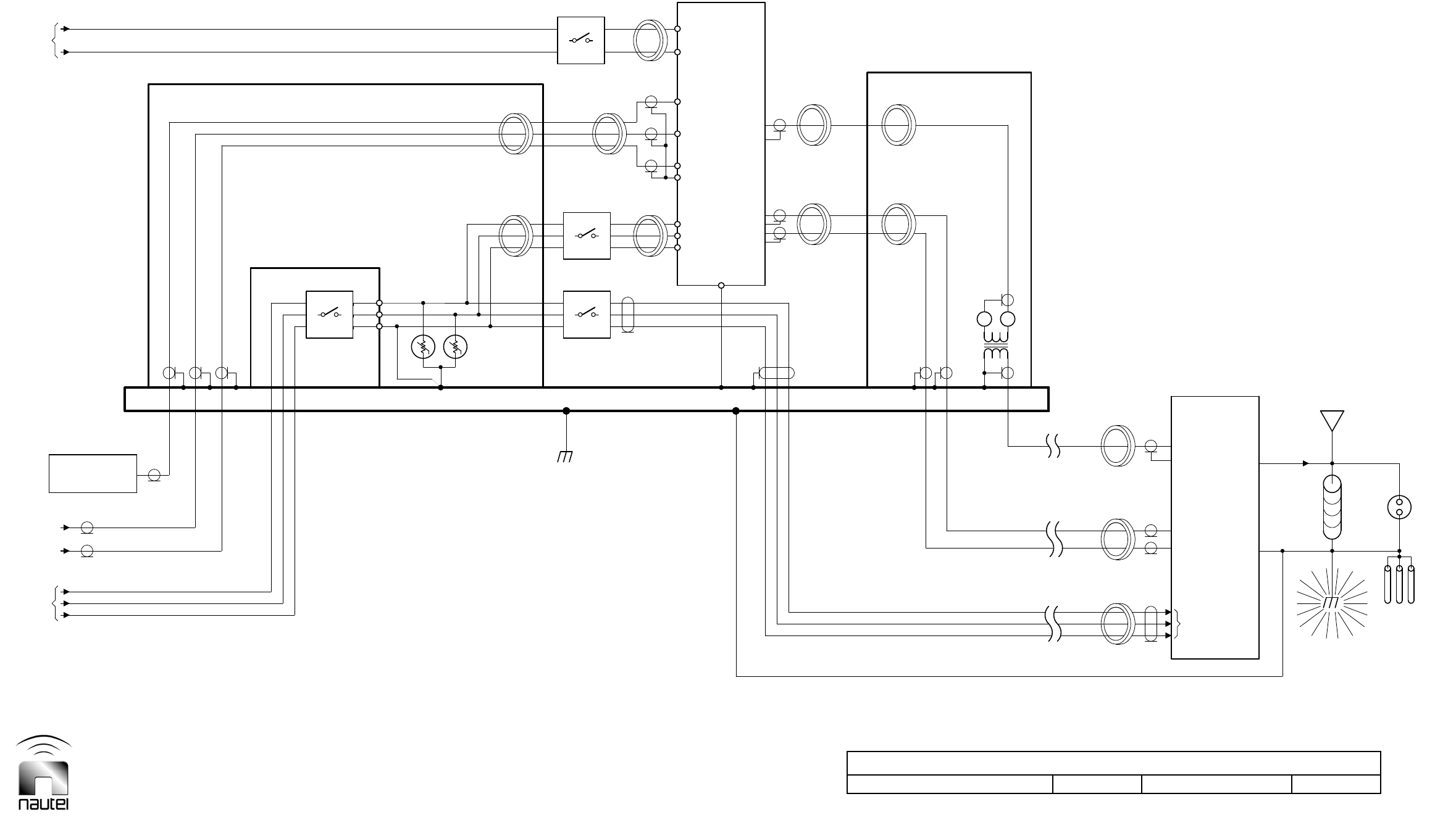
Dimensions = mm (inches)
Block Diagram – Recommended Transmitter System Installation (with SPU1)
Issue 1.8.1 Not to Scale Figure 2-5 Page 2-19
DC
FERRITE *
**
**
*
OR
FEEDER
GAP
AC
AUDIO
UNIT
SPU1
v
** **
B1510108 V1
POWER
SOURCE
EXTERNAL
CONTROL/
SOURCE
(PART 1 OF 2)
NDB/DGPS
INTERFACE/
(P/N LXP44)
PWR CABLE
(P/N LXP38)
**
(P/N LXP44)
PWR CABLE
FERRITE
(P/N LXP38)
FERRITE
RF CABLE
(P/N LXP38)
FERRITE
AUX CABLE
RF CABLE
ISOLATION
TRANSFORMER
FERRITE
(P/N LXP38)
FERRITE
RF CABLE
SYSTEM
ANTENNA
ANTENNA
RADIALS
GROUND
INSULATOR
SYSTEM
INTERLOCK
MONITOR CENTER
REMOTE CONTROL/
POWER
PROTECTION
v
FERRITE
AUX CABLE
FERRITE
(P/N LXP44)
PWR CABLE
(P/N LXP44)
FERRITE FERRITE
(P/N LXP44)
UNIT
RF
SPU1
(P/N LXP44)
PWR CABLE
FERRITE
RS-485 CABLE
(P/N LXP44)
GROUND
ATU-LP
ATU500
EARTH ELECTRODE SYSTEM
ANTENNA
ANTENNA
BASE
EARTH ELECTRODE SYSTEM
STATION REFERENCE GROUND
GROUND
STATION
RS-485 CABLE
(P/N LXP38)
FERRITE
(OPTIONAL)
ATU VDC
(OPTIONAL)
(PART 2 OF 2)
INTERFACE/
GROUND
LIGHTNING
VIA THE STATION REFERENCE GROUND POINT.
REFERENCE
AUX CABLE
VECTOR LP
TRANSMITTER
AC INPUT
PROTECTION
NDB/DGPS
ROD(S)
SPARK
NOTE: REFER TO "RECOMMENDATIONS FOR TRANSMITTER SITE PREPARATION" HANDBOOK FOR PHYSICAL LAYOUT CONSIDERATIONS.
AS THEIR DIAMETER WILL PERMIT.
SHOULD BE A MINIMUM 20 FEET (6 METRES) LONG.
** DENOTES CABLE LENGTH FROM EQUIPMENT TO SPU1 INTERFACE/PROTECTION UNIT
NOTE: ALL ELECTRICAL CONDUCTORS MUST ENTER OR LEAVE THE BUILDING
PASS THE WIRING (INCLUDING SHIELDS) THROUGH THE FERRITE AS MANY TIMES
* DENOTES THERE IS ONLY ONE AUX CABLE FERRITE. TWO FERRITES ARE SHOWN FOR DRAWING CLARITY.
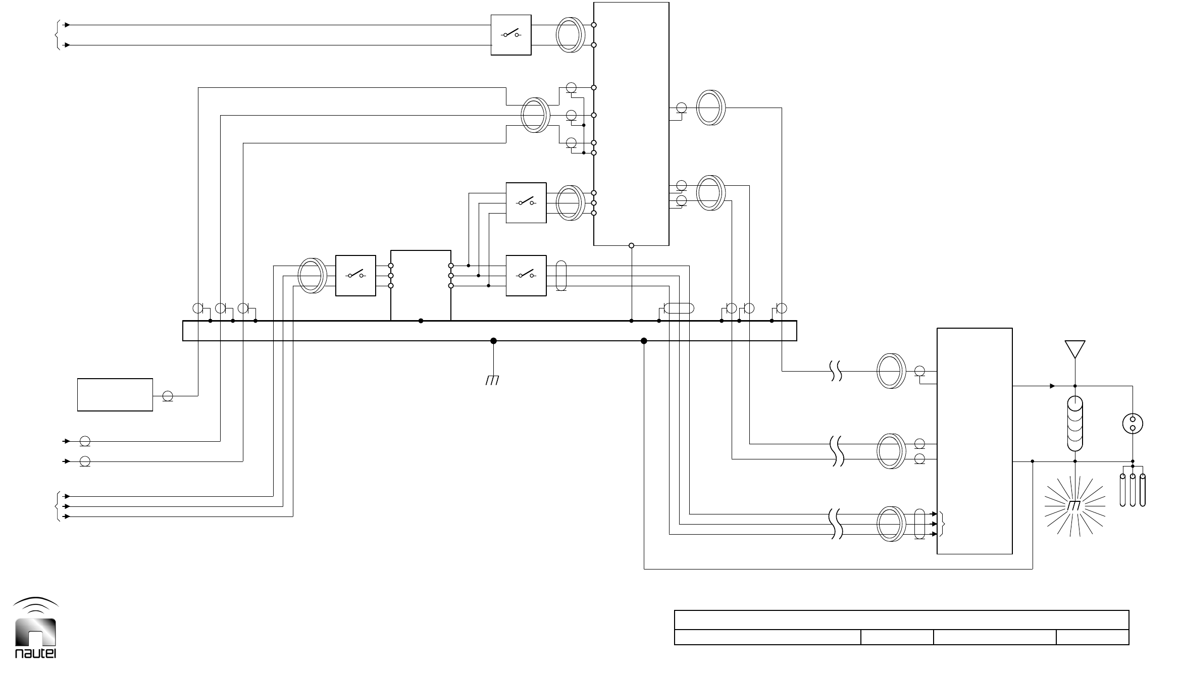
Dimensions = mm (inches)
Block Diagram – Recommended Transmitter System Installation (without SPU1)
Issue 1.8.1 Not to Scale Figure 2-6 Page 2-20
FERRITE
ROD(S)
AC
POWER
SOURCE
DC
POWER
B1510107 V2
(P/N LXP44)
FERRITE
SUPPLIED)
UNIT
PROTECTION
AUX CABLE
REFERENCE
STATION
GROUND
FERRITE
VECTOR LP
FERRITE
RS-485 CABLE
(P/N LXP44)
RF CABLE
FERRITE
FERRITE
(P/N LXP38)
FERRITE
FERRITE
SYSTEM
ANTENNA
FEEDER
ANTENNA
OR
ATU-LP
EARTH ELECTRODE SYSTEM
RADIALS
GROUND
GAPINSULATOR
ANTENNA
SYSTEM
SOURCE
MONITOR CENTER
REMOTE CONTROL/
PWR CABLE
(CUSTOMER
SURGE
(P/N LXP38)
TRANSMITTER
(P/N LXP38)
FERRITE
(P/N LXP44)
RS-485 CABLE
PWR CABLE
(P/N LXP44)
RF CABLE
GROUND
ATU500
ANTENNA
BASE
EXTERNAL
INTERLOCK
VIA THE STATION REFERENCE GROUND POINT.
STATION REFERENCE GROUND
(P/N LXP44)
PWR CABLE
(P/N LXP44)
PWR CABLE
(OPTIONAL)
ATU VDC
GROUND
LIGHTNING
AUDIO
CONTROL/
NOTE: ALL ELECTRICAL CONDUCTORS MUST ENTER OR LEAVE THE BUILDING
EARTH ELECTRODE SYSTEM
AC INPUT
(OPTIONAL)
SPARK
NOTE: REFER TO "RECOMMENDATIONS FOR TRANSMITTER SITE PREPARATION" HANDBOOK FOR PHYSICAL LAYOUT CONSIDERATIONS.

Vector-LP Radio Beacon Transmitter Technical Instruction Manual Page 3-1
Section 3 Operating Instructions Issue 1.8.1
Vector-LP Radio Beacon Transmitter
TECHNICAL INSTRUCTION MANUAL
Section 3 OPERATING INSTRUCTIONS
3.1 INTRODUCTION
The following instructions are intended
primarily for persons involved in testing or
maintenance of the equipment.
3.1.1 Precautions
The Vector-LP transmitter contains many
solid state devices that can be damaged if
they are subjected to excessive heat or high
voltage transients. Ensure the circuits are not
overdriven and are not disconnected from
their loads while turned on.
3.2 EMERGENCY SHUTDOWN
If an emergency shutdown is necessary, no
special precautions are required. However,
the type of shutdown is dictated by the
reason for the shutdown. There are two
types of shutdown. The first turns off the RF
output by inhibiting the power stage. The
second turns off the RF output and disables
all of the internal power supplies by
disconnecting the ac and dc power sources.
3.2.1 Turn Off RF Output
When the cause of the emergency shutdown
is external to the transmitter or is in the RF
output portion of the transmitter, the following
will turn off the power produced by the RF
power module:
WARNING
The following will not remove the ac or dc
power source voltage from the
transmitter or inhibit any of the internal
low voltage dc supplies or the B+ power
supply. If the reason for the shutdown
requires all voltages be turned off,
proceed directly to paragraph 3.2.2
If in local or remote control, press the RF
Off switch on the transmitter’s front panel.
If in remote control, select RF Off at the
remote control site.
Open any external interlock switch.
3.2.2 Complete Shutdown
When the cause of the emergency shutdown
dictates the need for a complete shutdown of
the transmitter, do the following:
Switch the ac power switch on the back of
the transmitter to OFF.
If applicable, disconnect the dc power
source (battery).
3.3 EXTERNAL SAFETY INTERLOCK
The external electrical interlock circuit is a
protection circuit controlled by user
determined, serially connected, normally
open/held closed interlock switches. It inhibits
the RF output when it is not safe to produce
RF output.
When all of the external interlock switches are
closed and it is safe to produce an RF output,
the front panel's system diagram External
Alarm lamp will be off. The operator will have
full control of transmitter functions.
When any external interlock switch is open,
the RF output stage will automatically turn off.
The front panel's system diagram External
Alarm lamp will turn on (alarm state). It is not
possible to enable the RF power stages until
all of the external interlock switches are
closed.

Page 3-2 Vector-LP Radio Beacon Transmitter Technical Instruction Manual
Issue 1.8.1 Section 3 Operating Instructions
3.4 ELECTROSTATIC DISCHARGE
PROTECTION
The transmitter's assemblies contain
semiconductor devices that are susceptible
to damage from electrostatic discharge
(ESD). Observe the following precautions
when handling an assembly that contains
these devices:
NOTE
Electrostatic energy is produced when two
insulating materials are rubbed together. A
person wearing rubber-soled shoes,
walking across a nylon carpet or a waxed
floor can generate an extremely large
electrostatic charge. This effect is
magnified during periods of low humidity.
This high voltage may damage
semiconductor devices such as integrated
circuits, field-effect transistors, thyristors
and Schottky diodes unless adequate
precautions are taken.
3.4.1 Discharging of Personnel
Maintainers must be electrically discharged
by a suitable ground system (anti-static
mats, grounding straps) when removing an
assembly from the transmitter and while
handling the assembly for maintenance
procedures.
3.4.2 Handling/Storage
Place the assembly in an anti-static bag
when it is not installed in a host transmitter
or when it is not being subjected to
maintenance procedures. Electronic
components should be stored in anti-static
materials.
3.4.3 Tools/Test Equipment
Testing and maintenance equipment,
including soldering and unsoldering tools,
should be suitable for contact with static
sensitive semiconductor devices.
3.4.4 Stress Current Protection
Always ensure the static sensitive
semiconductor devices are protected from
unnecessary stress current. This is
achieved by ensuring:
Current is not flowing when an electrical
connection is broken.
Voltages are not present on external
control/monitoring circuits when they
are connected.
3.5 CONTROLS AND INDICATORS
Nautel recommends the operator/
maintainer is familiar with the transmitter's
controls and indicators before operating the
transmitter and/or attempting to perform
fault diagnostics. In most cases, controls
and indicators are presented in an
assembly-by assembly format. A
mechanical drawing and an associated
table are provided as aids to locating and
understanding the assembly’s controls and
indicators.
NOTE
On some mechanical drawings, numbered
callouts are provided to cross-reference the
control/indicator to the description table.
The names used in the PANEL MARKING
column of the controls and indicators tables
are intended to be the closest possible
representation to the item’s label/
silkscreen.
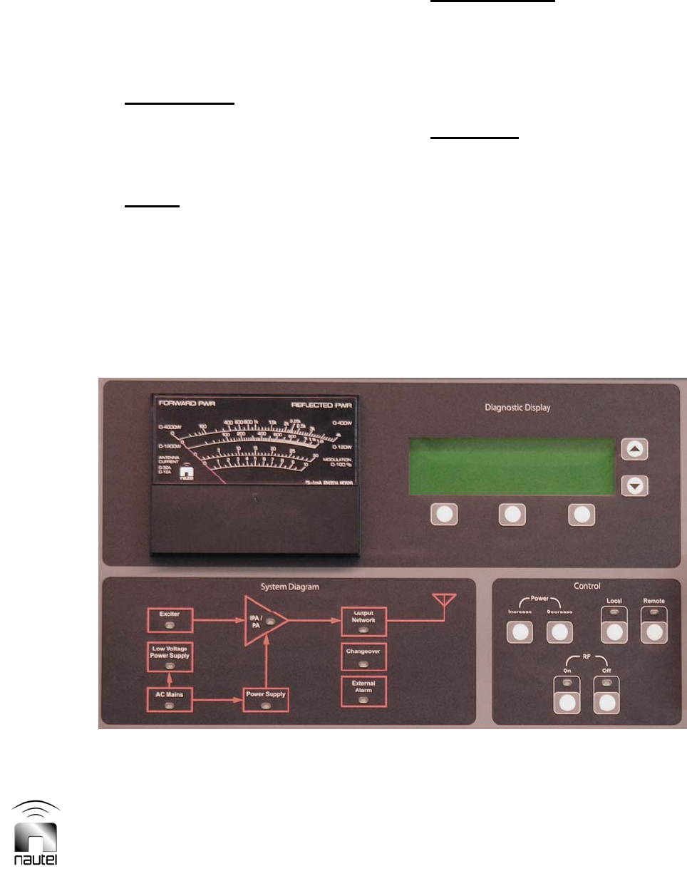
Vector-LP Radio Beacon Transmitter Technical Instruction Manual Page 3-3
Section 3 Operating Instructions Issue 1.8.1
3.5.1 Front Panel
The front panel is the primary local user
interface for the transmitter. Control and
indicators are grouped into four sections of
the panel (see Figure 3-1) as follows:
System Diagram - a simple block
diagram of the transmitter complete with
alarm lamps. Refer to Figure 3-2 and
Table 3-1 for a description of the controls
and indicators.
Control – push-button switches that
allow convenient control of the
transmitter’s RF status (on or off and
increase or decrease) and its operator
control source (local or remote). The RF
Off switch is functional regardless of
local or remote selection. Refer to
Figure 3-3 and Table 3-2 for a
description of the controls and
indicators.
Diagnostic Display – a menu-driven
user interface screen - with five
associated push-buttons - which allows
control and monitoring of the transmitter’s
critical parameters and modes of
operation. Refer to paragraph 3.6 for a
full description of the diagnostic display.
Analog Meter – the front panel meter
displays a user selected analog sample
on a user selected scale. Scale selection
and meter enabling is done using the
diagnostic display (refer to paragraph
3.6.8).
Figure 3-1 Vector Transmitter Front Panel (Primary User Interface)
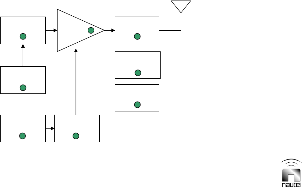
Page 3-4 Vector-LP Radio Beacon Transmitter Technical Instruction Manual
Issue 1.8.1 Section 3 Operating Instructions
3.5.2 Exciter Interface PWB
Controls and Indicators
Figure 3-4 and Table 3-3 identify and
describe the controls and indicators on the
exciter interface PWB (A2).
3.5.3 Remote Interface PWB
Controls and Indicators
Figure 3-5 and Table 3-4 identify and
describe the controls and indicators on the
remote interface PWB (A3).
3.5.4 RF Synthesizer PWB Controls
and Indicators
Figure 3-6 and Table 3-5 identify and
describe the controls and indicators on the
RF synthesizer PWBs (A5 and, if installed,
A8).
3.5.5 Miscellaneous Control and
Exciter Controls and Indicators
Table 3-6 describes the miscellaneous
controls and indicators of the control/
display PWB and exciter assemblies that
were not covered in previous paragraphs.
Refer to the mechanical drawings section
to locate a referenced item.
3.5.6 Miscellaneous RF Power
Stage Controls and Indicators
Table 3-7 describes the miscellaneous
controls and indicators of the RF power
modules (A12 and, If installed, A13). Refer
to the mechanical drawings section to
locate a referenced item.
3.5.7 Battery Boost PWB Controls
and Indicators
Figure 3-7 and Table 3-8 identify and
describe the controls on the optional
battery boost PWB (A16A1).
Figure 3-2 Vector-LP Transmitter Front Panel – System Diagram Section
System Diagram
Output
Network
IPA/
PA
Exciter
Low Voltage
Power Supply
AC Mains Power Supply
External
Alarm
Changeover

Vector-LP Radio Beacon Transmitter Technical Instruction Manual Page 3-5
Section 3 Operating Instructions Issue 1.8.1
Table 3-1: Front Panel - System Diagram Controls and Indicators
PANEL MARKING DESCRIPTION
Exciter When turned on (red), typically indicates a failure has occurred in
the active exciter (side A or B). This alarm will initiate a changeover
in dual transmitters; the side of the transmitter designated as
standby will be operating as the active side.
Low Voltage Power
Supply When turned on (red), indicates a failure has occurred in one of the
LVPS modules (U2 or, if installed, U3).
AC Mains When turned on (red), indicates the ac voltage applied to the
transmitter has fallen below an acceptable level. If the battery
backup option is installed, the power source switches to battery
mode. If no battery is available, the transmitter’s RF output is
inhibited.
Power Supply When turned on (red), indicates a fault has occurred in one or more
of the switching power supplies that supply the RF power modules
This alarm will initiate a changeover in dual transmitters; the side of
the transmitter designated as standby will be operating as the active
side.
External Alarm When turned on (red), indicates the external interlock circuit is not
presenting a closed circuit (inhibiting RF power) OR the ATU
(optional) or site interface PWB (optional) are not responding OR the
battery voltage is below the user established threshold.
Changeover When turned on (red), indicates a changeover to the standby side
has been enabled due to a fault in the main side.
IPA/PA When turned on (red), indicates a fault has occurred in one of the
RF power modules (A12 or, if installed, A13). This alarm will initiate
a changeover in dual transmitters; the side of the transmitter
designated as standby will be operating as the active side.
Output Network When turned on (red), indicates the transmitter’s RF power is being
cut back or shut back due to an impedance mismatch (high VSWR)
at the transmitter’s output.
NOTE
In each case, root-cause details of the fault are displayed in the
diagnostic display’s Events Logs (see paragraph 3.6.5)
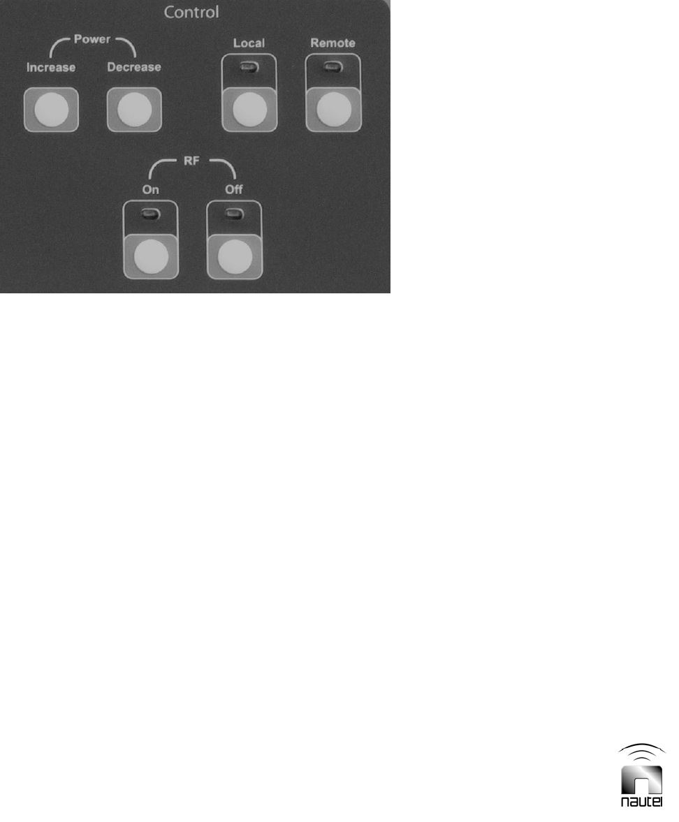
Page 3-6 Vector-LP Radio Beacon Transmitter Technical Instruction Manual
Issue 1.8.1 Section 3 Operating Instructions
Figure 3-3 Vector-LP Transmitter Front Panel – Control Section

Vector-LP Radio Beacon Transmitter Technical Instruction Manual Page 3-7
Section 3 Operating Instructions Issue 1.8.1
Table 3-2: Front Panel - Control Section Controls and Indicators
PANEL
MARKING DESCRIPTION
Power Increase Pushbutton switch that increases the RF output power level of the
transmitter. RF power is increased from minimum power to maximum
power in approximately 200 steps. Each step will increase the output
voltage of the switch mode power supplies to the RF power modules
linearly – the RF output power increase will follow a square law.
Pressing and holding the switch increases the rate of change.
Power Decrease Pushbutton switch that decreases the RF output power level of the
transmitter. RF power is decreased from maximum power to minimum
power in approximately 200 steps. Each step will decrease the output
voltage of the switch mode power supplies to the RF power modules
linearly – the RF output power decrease will follow a square law.
Pressing and holding the switch increases the rate of change.
Local Pushbutton switch that sets control of transmitter functions to switches
on the front panel. When its integral lamp is on (amber) (by pressing the
switch), Local control has been selected.
When Local control is selected, all of the remote control circuits (except
the external interlock and RF off function) are disabled.
Remote Pushbutton switch that sets control of transmitter functions to remote
control circuits. When its integral lamp is on (amber) (by pressing the
switch), Remote control has been selected.
When Remote control is selected, all pushbutton switches on the
exciter’s front panel that execute control functions, except the RF Off
switch, are disabled and have no influence. The RF Off switch is still
enabled to ensure the RF power stage can be turned off locally in the
event of an emergency.
RF On Push button switch that turns on the transmitter's RF power stage and,
for VR250 transmitters, its cooling fans when it is pressed. Its integral
lamp will be on when the RF power stage is turned on. Transmitter will
operate at the level stored in the selected power pre-set.
RF Off Push button switch that turns off the transmitter's RF power stage when
it is pressed. Its integral lamp will be on when the RF power stage is
turned off.
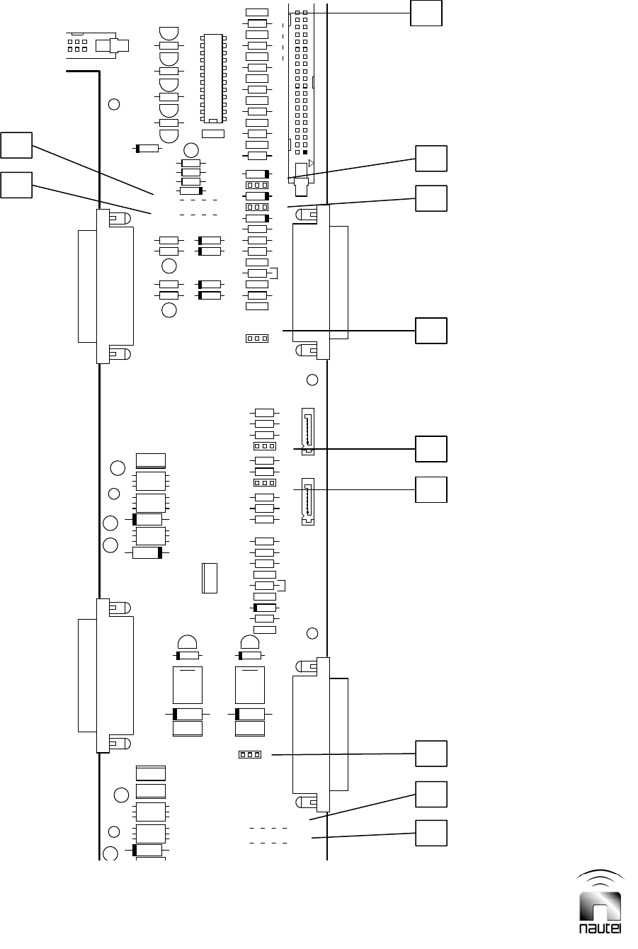
Page 3-8 Vector-LP Radio Beacon Transmitter Technical Instruction Manual
Issue 1.8.1 Section 3 Operating Instructions
Figure 3-4 Part of NAPI76A/02 Exciter Interface PWB A2
E1
E11
E10
E2
E3
E4
E5
E6
E7
E8
E9
TP3
TP4
C4
Q1 C5
C6
R7
C7
R9 C8
R11 C9
C11
E111
E101
R15
R17
R18
R40
R20
1E5
R23
R24
R26
R27
R29
R30
CR8
C15
E8
21
E9
21
R13
CR24
R36
C10
CR27
CR28
CR26
+
C16
+
C17
+
C18
+
C22
R4 R5
R3
Q4
Q3 R8
R6
R12
R10
R14
CR1
CR3
CR2
R37
R38
+
C27
R32
R16
C13
C14
C21
E4
1
AK
CR4
L2 1E6
R19
R21
R22
CR5
L4
CR6
R25
R28
C19
Q6
CR10
R39
Q7
C20
CR12
CR14
AK
L7
L6
CR15
AK
R35
21
E2
21
E3
CR9
CR11
CR13
AK
12
E1
CR23
U4
CR25
1
J11
J16
1
J4
1
+
C23
CR7
AK
1
J10
Q5
Q2
+
C12
J15
+
C28
L3
R31
1
J6
K1
AK
CR18
CR16
1
J5
K2
E7
1
J13
1
DGPS
DGPS
DGPS
BEACON
BEACON
BEACON
BEACON
DGPS
DGPS
BEACON
DGPS BEACON

Vector-LP Radio Beacon Transmitter Technical Instruction Manual Page 3-9
Section 3 Operating Instructions Issue 1.8.1
Table 3-3: Exciter Interface PWB Controls and Indicators
REF DES PANEL
MARKING DESCRIPTION
E1, E2,
E3, E8,
E9
Key CW
Jumpers
Shorting jumpers that are installed in positions determined by
the type of transmitter. In NDB transmitters, the jumpers are
factory installed in position 1. No user adjustment is required.
E4, E5,
E6, E7,
E10, E11
DGPS/BEACON
Jumpers Bi-position selection jumpers that are installed in positions
determined by the type of transmitter. In NDB transmitters,
the jumpers are factory installed to short pins 2 and 3. No
user adjustment is required.
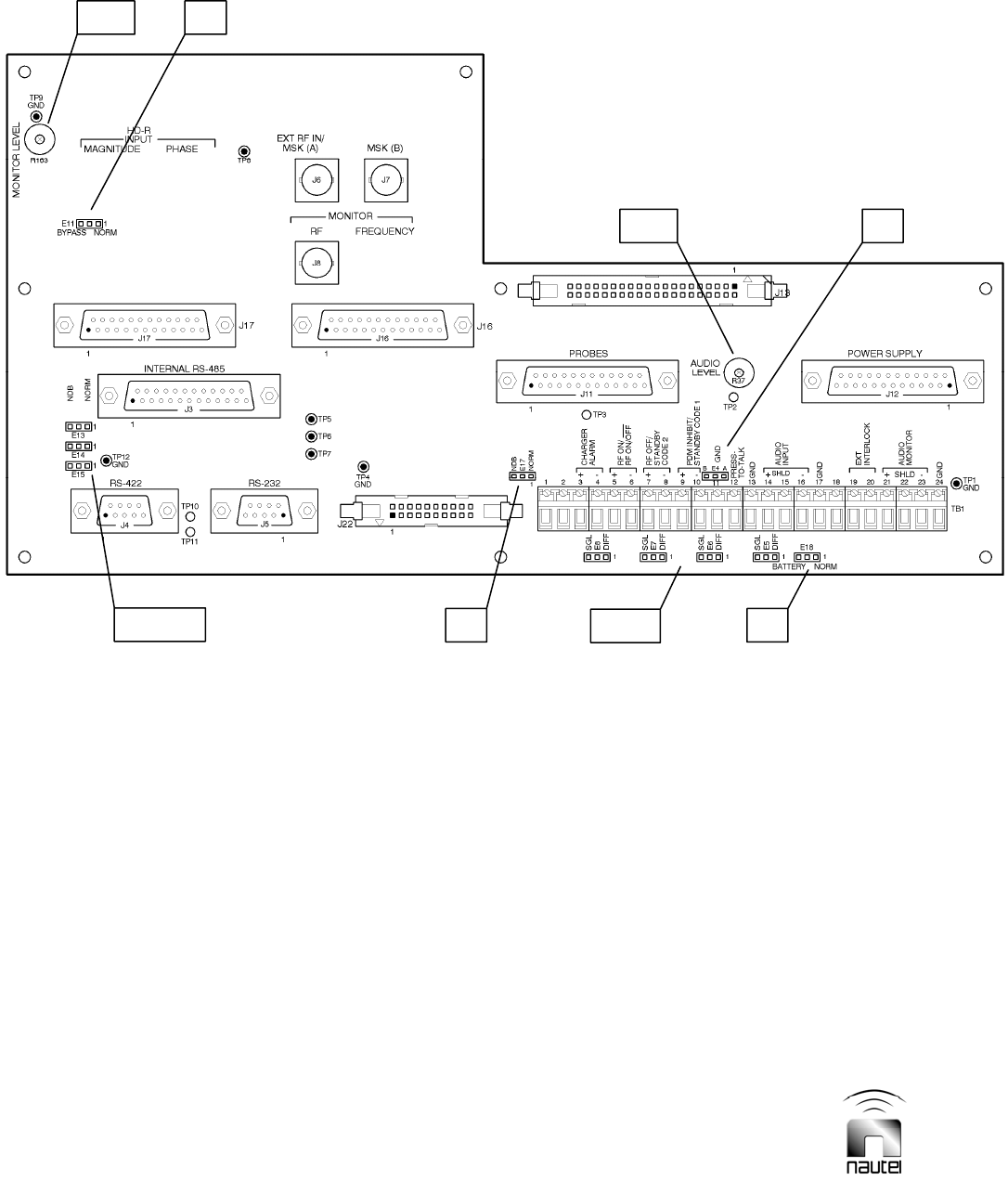
Page 3-10 Vector-LP Radio Beacon Transmitter Technical Instruction Manual
Issue 1.8.1 Section 3 Operating Instructions
Figure 3-5 Part of NAPI78D/02 Remote Interface PWB A3
E18
E5 – E8
E17
E11
E13 - E15
E4R37
R163

Vector-LP Radio Beacon Transmitter Technical Instruction Manual Page 3-11
Section 3 Operating Instructions Issue 1.8.1
Table 3-4: Remote Interface PWB Controls and Indicators
REF DES PANEL
MARKING DESCRIPTION
E4 Press-To-
Talk/Phantom
Feed
Bi-position selection jumper that is installed based on the type
of mode to enable voice operation. The jumper is factory
installed for ‘press-to-talk’ mode, position A (shorting pins 1
and 2). For ‘phantom feed’ mode, install the jumper in
position B (shorting pins 2 and 3). In ‘press-to-talk’ mode a
ground is applied to TB1-12 to enable voice. In ‘phantom
feed’ mode, -15 V is applied to the shield of the audio to
enable voice.
E5 – E8
Single/
Differential Bi-position selection jumpers that configure the remote
interface PWB to accept either single-ended or differential
remote control inputs.
A differential input is selected when the jumper shorts
pins 1 and 2 of its associated 3-pin header.
A single-ended input is selected when the jumper shorts
pins 2 and 3 of its associated 3-pin header.
E11 NORMAL/
BYPASS Factory default is shorting pins 1 and 2. No user adjustment
is required.
E13 – E15
E17
NORM/NDB Bi-position selection jumpers that are installed in positions
determined by the type of transmitter. In NDB transmitters,
the jumpers are factory installed in the NDB position (shorting
pins 2 and 3). No user adjustment is required.
E18 NORM/
BATTERY Bi-position selection jumper that should always be installed in
the NORM position (shorting pins 1 and 2).
R37 AUDIO LEVEL Adjusted for 100% modulation when the modulating audio is
between -20 dBm and +10 dBm and its amplitude is the level
that is expected to produce 100% modulation.
R163 MONITOR
LEVEL Adjusted to set the level of the RF MONITOR output, which is
a sample of the RF output. This output is located on BNC
connector J8 on the remote interface PWB).
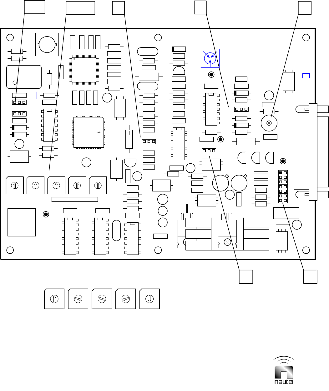
Page 3-12 Vector-LP Radio Beacon Transmitter Technical Instruction Manual
Issue 1.8.1 Section 3 Operating Instructions
Figure 3-6 Assembly Detail – NAPE70C/01 RF Synthesizer PWB A5 and A8
TP5
C13C16
TP3
R3
R4
C47
C20
R18
1E3
R12
R8
R11
L1
R20
L5
R34
TP4
R52
R46
C57
C58
C32
43
2
19
8
7
5
0
6
S2
U3
TP1
C8
R5
R6
U7
43
2
19
8
7
5
0
6
S5
C36
+
C35
R19
L7
+
C41
C39
R17
C4
R9
R13
R10
C25
C21
Q6
1E4
C44 TP6
C56
C1
C34
R47
C46
R31
R32
+
C29
J2
+
C43
L9C22
C7 C5
+
C42
C17 C10
+
C40
C23
L4
U10
Q1 Q2 Q3
C19
CR2
CR3
1E2
C3
1E1
R51
C55
R16
TP2
R50
R49
R43
R2
TP7
R33
R35
R29
C48
R42
R28
R26
R25 CR5
C54C28
R14
R37C27
C15
R22
C6
CR4
R7
U6
43
2
19
8
7
5
0
6
S1
43
2
19
8
7
5
0
6
S3
43
2
19
8
7
5
0
6
S4
+
C37
C2
R1
U1
U8
+
C24
C26
L2
R48
R45
R15
+
C38
C33
+
C31
Q5
E5
A
B
C
D
E
F
G
R27
CR6
1E6
R23
Q4
C18
C14
C12
L3
6
5
4
3
2
1
ABCDEF
GRID1
L6
C11
C9
+
C30
CR1
U11
3
4
U9
231
4
R21
L8
U12
1
U2
U4
U5
1
J1
M1940198 V1
GND
GND
x0.1
EXT INT
REF
SYMMETRY
x100 x10
INPUT
10MHz
x1
HIGHLOW
EXT INT
SOURCE
DISABLE
IPM BAL
REF
SER.
PDM
x1000
ENABLE
SYMMETRY ADJ
NAUTEL ASSY
194-3060
NAPE
FREQUENCY (kHz)
RF SYNTHESIZER
E4 E5
R32
E6
E3 S1-S5
E1/E2
7
82
37
8
3
2
6
0
5
91
46
9 1
44
19
6
0
56
9 1
46
0
5
91
4
7
82
3 3
2
7
8
7
82
3
0
5
0
5
0
x1000
S1
8
x10
S3
5
x0.1
S5
3
x100
S2
7
x1
S4
FREQUENCY (kHz)
SHOWN SET FOR 387.5 kHz

Vector-LP Radio Beacon Transmitter Technical Instruction Manual Page 3-13
Section 3 Operating Instructions Issue 1.8.1
Table 3-5: RF Synthesizer PWB Controls and Indicators
ITEM
(Ref PANEL
MARKING DESCRIPTION
E1, E2
REF (10 MHz)
Bi-position selection jumpers used to configure the RF
synthesizer PWB to use either an internal or external 10 MHz
reference generator. Jumpers are always set to INT (internal,
shorting pins 2 and 3) for Vector-LP transmitters.
E3 PDM High/Low Bi-position selection jumper used to configure the RF
synthesizer PWB for high PDM (nominal 130 kHz) or low
PDM (nominal 65 kHz). Always set to HIGH PDM (shorting
pins 2 and 3) for Vector-LP transmitters.
E4 RF Drive Source
Bi-position selection jumper used to configure the RF
synthesizer PWB to use either the output of an integral
crystal controlled oscillator or an external RF generator as
the RF drive source. Always set for INT (internal c, shorting
pins 2 and 3) for Vector-LP transmitters.
E5 Drive Matching Seven selection jumper (A-G) used to configure the RF drive
circuit for its host transmitter. The jumper is installed in the D
position (shorting pins 7 and 8) for Vector-LP transmitters.
E6 Symmetry
Adjust
Enable/Disable
Bi-position selection jumper used to enable or disable the RF
drive symmetry adjustment circuitry. Always set to ENABLE
(E6 installed between pins 1 and 2 of its 3-pin header) for
Vector-LP transmitters.
R32 RF DRIVE
SYMMETRY Adjusted to obtain an RF oscillator drive waveform that is a
symmetrical square wave.
R41 IPM BAL Not applicable to Vector-LP transmitters.
S1-S5 X1000
X100
X10
X1
X0.1
Adjusts the carrier frequency in 1000 kHz steps.
Adjusts the carrier frequency in 100 kHz steps.
Adjusts the carrier frequency in 10 kHz steps.
Adjusts the carrier frequency in 1000 Hz steps.
Adjusts the carrier frequency in 100 Hz steps.
S6:1/2/3
S6:4
Correction
Selection
Enable/Disable
Not applicable to Vector-LP transmitters.
Always closed for Vector-LP transmitters.

Page 3-14 Vector-LP Radio Beacon Transmitter Technical Instruction Manual
Issue 1.8.1 Section 3 Operating Instructions
Table 3-6: Miscellaneous Control and Exciter Controls and Indicators
REF DES PANEL
MARKING DESCRIPTION
A1E1
A1E2
A/B No user adjustment should be required. Always installed in
position B.
A1E3
A/B No user adjustment required. A link is soldered between pins
1 and 3 for Vector-LP transmitters.
A1LS1 SPEAKER Provides an audible signal for local monitoring of the
demodulated keyed tone (identification code).
A6E1
or
A9E1
A/B No user adjustment should be required. Always installed in
position A.
A6R31
or
A9R31
GAIN TRIM Adjusted, when interphase PDM driver PWB is enabled (the
associated exciter is the active exciter). Compensates for
tolerance differences between side 'A' and side 'B' in dual
side transmitters. One or both must be adjusted to set the
PDM pulse train to produce identical RF output levels when
either side is selected (see 4.3.6.10).
A6R59
or
A9R59
DUMP Not applicable to Vector-LP transmitters.
A7E1
A7E3
or
A10E1
A10E3
A/B No user adjustment should be required. Always installed in
position B.
A7E2
or
A10E2
KEYED CW/
NORMAL Bi-position selection jumpers that are installed in positions
determined by the type of transmitter. In Vector-LP
transmitters, the jumpers are factory installed in the
NORMAL position (shorting pins 2 and 3). No user
adjustment is required.
NOTE: Prefix all items with A2 to obtain complete reference designation.

Vector-LP Radio Beacon Transmitter Technical Instruction Manual Page 3-15
Section 3 Operating Instructions Issue 1.8.1
Table 3-7: Miscellaneous RF Power Stage Controls and Indicators
REF DES PANEL
MARKING DESCRIPTION
A12A1DS1
or
A13A1DS1
MODULE
INSTALLED
When turned on (amber), indicates that RF power module A
or B is installed in the transmitter.
A12A1DS2
or
A13A1DS2
MODULE ON When turned on (green), indicates that RF power module A
or B is on and is contributing to the transmitter’s RF output.
A12A1DS3
or
A13A1DS3
MODULE FAULT When turned on (red), indicates that a fault has occurred in
RF power module A or B and it is not contributing to the
transmitter’s RF output.
A12A2DS1
or
A13A2DS1
AC IND
When turned on (amber), indicates the ac input voltage is
being applied to RF power module A or B.
A12A2DS2
or
A13A2DS2
+18V
When turned on (green), indicates the +24 V power supply
voltage is being applied to RF power module A or B and that
the +18 V regulator is functioning.
A12A3F1
or
A13A3F1
+15V Fuses the +15 V applied from the power module control/
interface PWB to the power amplifier at 1 A.
A12A5DS1
or
A13A5DS1
B+ ON When turned on (green), indicates that the B+ voltage is
being applied from the switch mode power supply PWB (or
optional battery) to the modulator.
A14E1
through
A14E36
RF Filter
Jumpers Frequency dependent jumpers that are factory installed for
the customer operating frequency. If a frequency change is
required, change the position of these jumpers (see Figure
MD-16 A or MD-16B).
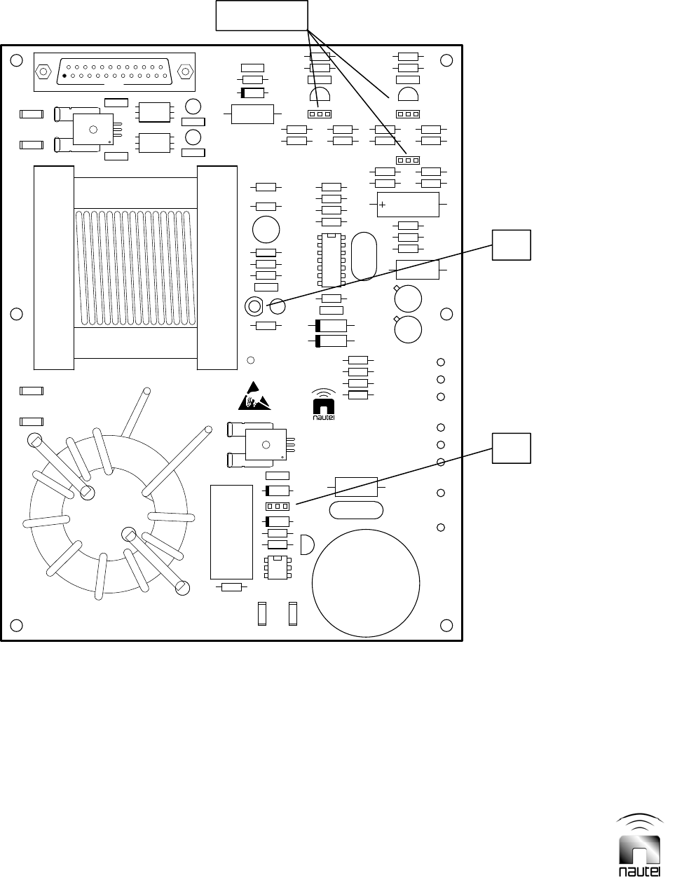
Page 3-16 Vector-LP Radio Beacon Transmitter Technical Instruction Manual
Issue 1.8.1 Section 3 Operating Instructions
Figure 3-7 NAPS35 Battery Boost PWB A16A1 (Optional)
C6
+
C3
C11
R3
C12
R40
R38
C17
R24
E4
E2
C2
+
C5
C4
E8
R12
Q2
+
C13
1
E7
R4
Q1
Q7
R39
C20
1
E9
1
E10
R26
R27
R28
R29
Q3
R25
E3
E1
C1
C8
U3
Q6
R11
CR3
R32
R30
CR5
C14
C10
R8
R21
R19
R1
R14
E6
1
E5
R13
CR2
R33
23
4
1
5
U2
R31
R10 CR4
R22
+
C9
U4
R20
R6
R7
R9
L3 R17
R16
R18R5
C7 R15
CR1
CR6 Q5
R35
R34
R37
R36
DS1
L2
23
4
1
5
U1
R2
Q4
C15
R23
R41
1
J1
C19
+
C16
12
13
1
24
L1
M2050021 V1
IN
IN
L4
-
250W
250W
125W
125W
-
+
OUT
CHARGER
+ 15V
OUT +
+ 48V
NAPS35
250W 125W
SER.
+ 24V
SMPS, 24/48V
BATTERY BOOST
E7, E9, E10
DS1
E5

Vector-LP Radio Beacon Transmitter Technical Instruction Manual Page 3-17
Section 3 Operating Instructions Issue 1.8.1
Table 3-8: Battery Boost PWB Controls and Indicators
REF DES PANEL
MARKING DESCRIPTION
A16A1DS1 +15V When turned on (green), indicates the +15 V power supply
voltage is being applied to the battery boost PWB and its
switch mode PWM IC U4.
A16A1E5 +24V/+48V Bi-position selection jumper that is installed in the position
determined by the backup battery voltage. The jumper is
installed in the +48V position (shorting pins 1 and 2) if a 48 V
battery is used. The jumper is installed in the +24V position
(shorting pins 2 and 3) if a 24 V battery is used.
A16A1E7
A16A1E9
A16A1E10
250W/125W Bi-position selection jumpers that are installed in positions
determined by the rated power level of the transmitter. The
jumper is installed in the 250W position (shorting pins 1 and
2) for a VR250. The jumper is installed in the 125W position
(shorting pins 2 and 3) for a VR125.
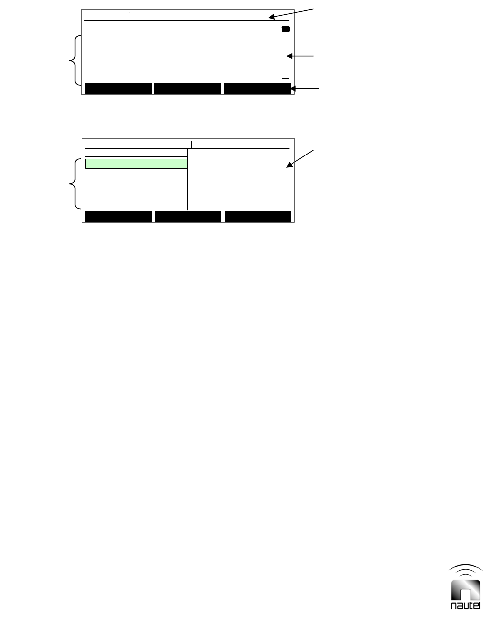
Page 3-18 Vector-LP Radio Beacon Transmitter Technical Instruction Manual
Issue 1.8.1 Section 3 Operating Instructions
Figure 3-8 Diagnostic Display – Meters Screen
Figure 3-9 Diagnostic Display – Main Menu
3.6 DIAGNOSTIC DISPLAY
The diagnostic display (see Figure 3-9), in
the centre of the transmitter’s front panel, is
a 240 x 64 graphic LCD display and is the
primary local user interface for the
transmitter. With the exception of RF on/
off, power increase/decrease and local/
remote control, all transmitter functions can
be controlled and indicated by this display.
All critical parameters and events are
monitored from this display. The following
paragraphs describe how to use the
diagnostic display.
3.6.1 Pushbutton Switches
Navigating the diagnostic display is done
using the five pushbutton switches
adjacent the display. The up () and down
() pushbuttons, to the right of the display,
are used to move up and down through
displayed selections and to increase or
decrease the value of a selected
parameter. Pressing and holding the or
pushbutton will increase the rate of
change, where applicable. There are also
three soft-key pushbuttons whose
functions are defined by the text displayed
directly above them for a given menu.
3.6.2 Main Screens
The high level screens of the diagnostic
display (Figures 3-8 and 3-9) display:
Transmitter status bar
Three user-definable meter selections
Meter selection scroll (controlled by
and pushbuttons)
Sub-menu selections
Software version
3.6.2.1 Transmitter Status Bar
The transmitter status bar is the
information displayed along the top of the
diagnostic display. This information is
present at all times and indicates the
following (from left to right):
Current time (24-hour clock)
Current output power
Active side (A or B)
Monitor mode (blank for normal or
Bypass) – bypass indicates that
automatic changeover is inhibited.
For quick reference, locate the desired
function in the flow diagram depicted in
Figure 3-10, then refer to the referenced
paragraph for further information.
Fwd Power: 0W Rfld Power: 0.0W
VSWR: 0.00 Mod %: 0.0%
RF Curr: 0.0A Ant Curr: 0.0A
Mod % A: 0.0% Mod % B: 0.0%
Meas Freq A:315000Hz Meas Freq B:314998Hz
Main Menu Status Power
12:43:16 Power: 0W Side A Bypass
Fwd Power: 0W Rfld Power: 0.0W
VSWR: 0.00 Mod %: 0.0%
RF Curr: 0.0A Ant Curr: 0.0A
Mod % A: 0.0% Mod % B: 0.0%
Meas Freq A:315000Hz Meas Freq B:314998Hz
Main Menu Status Power
12:43:16 Power: 0W Side A Bypass12:43:16 Power: 0W Side A Bypass
STATUS BAR
METER
SELECTION
SCROLL
SOFT KEY
LABELS
METER
SELECTIONS
SUB-MENU
SELECTIONS
SOFTWARE
VERSION
Select Meters
12:43:16 Power: 0W Side A Bypass
Main Menu
Changeover Control
Events Log
Settings
Peripherals
RCMS Settings
Vector NDB
rev 2. 6. 0. 2
Jan 21 2010
11:22:41
Nautel
Select Meters
12:43:16 Power: 0W Side A Bypass12:43:16 Power: 0W Side A Bypass
Main Menu
Changeover Control
Events Log
Settings
Peripherals
RCMS Settings
Vector NDB
rev 2. 6. 0. 2
Jan 21 2010
11:22:41
Nautel

Vector-LP Radio Beacon Transmitter Technical Instruction Manual Page 3-19
Section 3 Operating Instructions Issue 1.8.1
Diagnostic Display (GUI) Functions
(organized by menu hierarchy)
Reference
Paragraph
MAIN MENU
Meters
Status 3.6.3
Power 3.6.15
Changeover Control 3.6.4
Events Log 3.6.5
Settings
Set Real Time Clock 3.6.6
Monitor Settings 3.6.7
Monitor Timeout 3.6.7 (b)
Power Thresholds 3.6.7 (d)
Automatic Reset 3.6.7 (f)
Mod % Thresholds 3.6.7 (h)
Meter Settings 3.6.8
Select Analog Meter 3.6.8.1
Calibrate Analog Meter 3.6.8.2
Power Source Select 3.6.9
Configure Sonalert 3.6.10
Timed Shutdown 3.6.11
Factory Settings
3.6.12
Calibrate Digital Meters 3.6.12.1
Set Thresholds 3.6.12.2
Maximum Output Gain 3.6.12.3
Feature Codes 3.6.12.4
Use Factory Settings 3.6.12.5
Peripherals 3.6.13
Keyer Settings 3.6.13.1
Audio Levels 3.6.13.1 (a)
Keyer Modulation 3.6.13.1 (b)
Keyer Sequence 3.6.13.1 (c)
Standby Code 1 3.6.13.1 (d)
Standby Code 2 3.6.13.1 (d)
Power Modules 3.6.13.2
ATU Controls 3.6.13.3
Test Standby Side 3.6.13.4
Select Peripherals 3.6.13.5
Module Check 3.6.13.6
RCMS Settings 3.6.14
Control Points 3.6.14.1
Monitor Points 3.6.14.2
Serial Setting 3.6.14.3
Automatic Reporting 3.6.14.4
Figure 3-10 – Flow Diagram - Diagnostic Display Functions
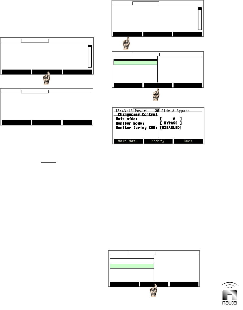
Page 3-20 Vector-LP Radio Beacon Transmitter Technical Instruction Manual
Issue 1.8.1 Section 3 Operating Instructions
3.6.3 Viewing Faults
In addition to the system diagram’s fault
indicators, a list of current faults can be
viewed on the diagnostic display. View the list
of faults as follows:
(a) From the meter screen, press Status. A
list of current faults is displayed. If Status
is not displayed.
NOTE
Use the Events Log (see paragraph 3.6.5) to
view alarm history.
(b) If necessary, press or to scroll
through the faults.
(c) Press Reset to attempt to clear the
alarm.
(d) Press Meters to return to the meters
screen.
3.6.4 Changeover Control
The transmitter may optionally contain two
fully redundant exciter and RF power paths
(sides A and B). The active side and the
monitor mode can be controlled using the
diagnostic display. View and, if necessary,
edit the changeover control settings as
follows:
(a) Set the main side to either A or B.
(b) Set the monitor mode to either BYPASS
or NORMAL. Bypass mode inhibits
automatic changeover from the main side
to the standby side.
(c) Set Monitor During SWR to ENABLED to
allow the transmitter to change over
during an SWR alarm. Monitor mode
must be set to NORMAL.
3.6.5 Viewing Events Log
The most recent 256 transmitter events
(alarms, operational changes, etc.) are stored
in memory. View the events log as follows:
Fwd Power: 0W Rfld Power: 0.0W
VSWR: 0.00 Mod %: 0.0%
RF Curr: 0.0A Ant Curr: 0.0A
Mod % A: 0.0% Mod % B: 0.0%
Meas Freq A:315000Hz Meas Freq B:314998Hz
Main Menu Status Power
12:43:16 Power: 0W Side A Bypass
Fwd Power: 0W Rfld Power: 0.0W
VSWR: 0.00 Mod %: 0.0%
RF Curr: 0.0A Ant Curr: 0.0A
Mod % A: 0.0% Mod % B: 0.0%
Meas Freq A:315000Hz Meas Freq B:314998Hz
Main Menu Status Power
12:43:16 Power: 0W Side A Bypass12:43:16 Power: 0W Side A Bypass
Currently Active Faults:
Command RF OFF
Reset Meters
12:43:16 Power: 0W Side A Bypass
Currently Active Faults:
Command RF OFF
Reset Meters
12:43:16 Power: 0W Side A Bypass12:43:16 Power: 0W Side A Bypass
Select Meters
12:43:16 Power: 0W Side A Bypass
Main Menu
Changeover Control
Events Log
Settings
Peripherals
RCMS Settings
Vector NDB
rev 2. 6. 0. 2
Jan 21 2010
11:22:41
Nautel
Select Meters
12:43:16 Power: 0W Side A Bypass12:43:16 Power: 0W Side A Bypass
Main Menu
Changeover Control
Events Log
Settings
Peripherals
RCMS Settings
Vector NDB
rev 2. 6. 0. 2
Jan 21 2010
11:22:41
Nautel
Fwd Power: 0W Rfld Power: 0.0W
VSWR: 0.00 Mod %: 0.0%
RF Curr: 0.0A Ant Curr: 0.0A
Mod % A: 0.0% Mod % B: 0.0%
Meas Freq A:315000Hz Meas Freq B:314998Hz
Main Menu Status Power
12:43:16 Power: 0W Side A Bypass
Fwd Power: 0W Rfld Power: 0.0W
VSWR: 0.00 Mod %: 0.0%
RF Curr: 0.0A Ant Curr: 0.0A
Mod % A: 0.0% Mod % B: 0.0%
Meas Freq A:315000Hz Meas Freq B:314998Hz
Main Menu Status Power
12:43:16 Power: 0W Side A Bypass12:43:16 Power: 0W Side A Bypass
Select Meters
12:43:16 Power: 0W Side A Bypass
Main Menu
Changeover Control
Events Log
Settings
Peripherals
RCMS Settings
Vector NDB
rev 2. 6. 0. 2
Jan 21 2010
11:22:41
Nautel
Select Meters
12:43:16 Power: 0W Side A Bypass12:43:16 Power: 0W Side A Bypass
Main Menu
Changeover Control
Events Log
Settings
Peripherals
RCMS Settings
Vector NDB
rev 2. 6. 0. 2
Jan 21 2010
11:22:41
Nautel
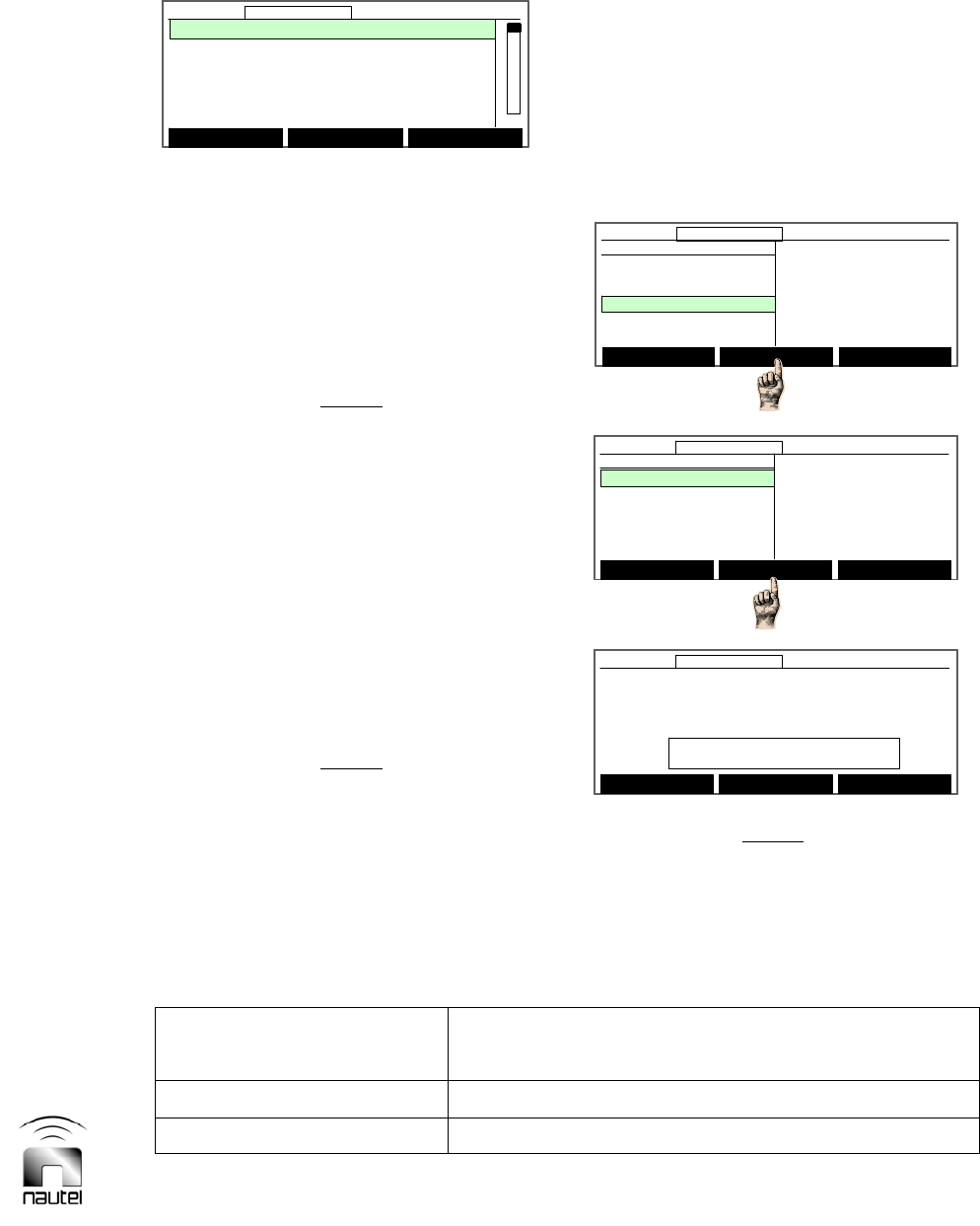
Vector-LP Radio Beacon Transmitter Technical Instruction Manual Page 3-21
Section 3 Operating Instructions Issue 1.8.1
(a) From the main menu, highlight Events
Log (using and ) and press Select.
The center soft-key permits viewing the
Events Log in two different modes – All
Events or Alarms Only. For either
mode, a list of events is displayed, sorted
chronologically, with a root-cause
description of the event.
NOTE
Refer to Table 3-9 for a list of non-alarm
events that can be displayed on the Events
Log and a brief description of each. A list of
alarm events is available in Table 5-1.
(b) Press or to scroll through the
events.
(d) Press Select ### on a highlighted event
to display the transmitter status when the
highlighted event occurred. Use the Next
event button to check the status of
subsequent numbered events.
NOTE
The 3-digit number shown in the Select ###
display is the number allocated to the
highlighted event. Event 000 is the most
recent occurrence.
(e) To clear the history stored in the events
log, press the and buttons
simultaneously.
(f) Press Back to return to the main menu.
3.6.6 Setting Real Time Clock
Set the real-time clock as follows:
NOTE
The real-time clock does not automatically
update for Daylight Savings Time (DST).
Table 3-9: Events Log Displays – Non-Alarm Events
NON-ALARM EVENTS
(as displayed) DESCRIPTION
Return to normal Transmitter alarms have cleared.
Power up Transmitter has completed power up.
12:43:16 Power: 0W Side A Bypass
08Apr80 12:33:15 PS Module A1 Missing
08Apr80 12:33:13 Return to normal
08Apr80 12:33:13 Command Exciter B
08Apr80 12:33:13 Low AC Voltage
08Apr80 12:33:02 Power Up
08Apr80 12:32:56 Mod. Protection
Select 000 Alarms Only Back
12:43:16 Power: 0W Side A Bypass12:43:16 Power: 0W Side A Bypass
08Apr80 12:33:15 PS Module A1 Missing
08Apr80 12:33:13 Return to normal
08Apr80 12:33:13 Command Exciter B
08Apr80 12:33:13 Low AC Voltage
08Apr80 12:33:02 Power Up
08Apr80 12:32:56 Mod. Protection
Select 000 Alarms Only Back
Select Meters
12:43:16 Power: 0W Side A Bypass
Main Menu
Changeover Control
Events Log
Settings
Peripherals
RCMS Settings
Vector NDB
rev 2. 6. 0. 2
Jan 21 2010
11:22:41
Nautel
Select Meters
12:43:16 Power: 0W Side A Bypass12:43:16 Power: 0W Side A Bypass
Main Menu
Changeover Control
Events Log
Settings
Peripherals
RCMS Settings
Vector NDB
rev 2. 6. 0. 2
Jan 21 2010
11:22:41
Nautel
Main Menu Select Back
12:43:16 Power: 0W Side A Bypass
Settings
Set Real Time Clock
Monitor Settings
Meter Settings
Power Source Select
Configure Sonalert
Main Menu Select Back
12:43:16 Power: 0W Side A Bypass12:43:16 Power: 0W Side A Bypass
Settings
Set Real Time Clock
Monitor Settings
Meter Settings
Power Source Select
Configure Sonalert
Set Real Time Clock
Use up / down keys to select a value to
change. Press MODIFY to make changes.
SET: Save changes to clock BACK: done
Set Modify Back
12:43:16 Power: 0W Side A Bypass
Time Day Date
14:30:29 Wed 08/Apr/80
Set Real Time Clock
Use up / down keys to select a value to
change. Press MODIFY to make changes.
SET: Save changes to clock BACK: done
Set Modify Back
12:43:16 Power: 0W Side A Bypass12:43:16 Power: 0W Side A Bypass
Time Day Date
14:30:29 Wed 08/Apr/80
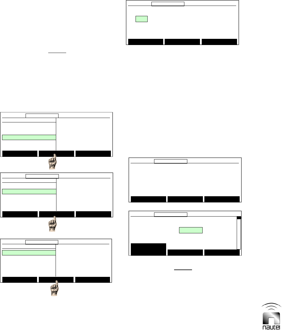
Page 3-22 Vector-LP Radio Beacon Transmitter Technical Instruction Manual
Issue 1.8.1 Section 3 Operating Instructions
Monitor Timeout
Monitor Timeout Period:
20 seconds
Monitor Shutdown:
DISABLED
Main Menu Modify Back
12:43:16 Power: 0W Side A Bypass
Monitor Timeout
Monitor Timeout Period:
20 seconds
Monitor Shutdown:
DISABLED
Main Menu Modify Back
12:43:16 Power: 0W Side A Bypass12:43:16 Power: 0W Side A Bypass
3.6.7 Setting RF Monitor Limits
High and low power thresholds, low
modulation threshold and loss of keying can
be set to ensure the transmitter is operating
within acceptable limits. If the RF carrier is
outside these limits for a pre-defined delay
period, the transmitter initiates a changeover
to the standby side (in normal operation) or
continues to operate (in bypass mode). Set
the transmitter’s RF monitor limits as follows:
NOTE
International Civil Aviation Organization
(ICAO) standards dictate the transmitter be
turned off or a warning alarm be generated
when the RF output decreases by 3.0 dB or
increases by 2.0 dB from the intended carrier
level. The user can alter the monitor settings
provided these criteria are still met.
(a) From the main menu, highlight Settings
and press Select. Highlight Monitor
Settings and press Select.
(b) Highlight Monitor Timeout and press
Select. See step (d) for Power
Thresholds.
(c) Use and to highlight the desired
monitor timeout field and press Modify:
The monitor timeout period can be set
(using and ) between 4 and 82 s
(factory set for 20 s).
The monitor shutdown can be set (using
and ) for ENABLED or DISABLED.
(d) Press Back, highlight Power
Thresholds and press Select. The
following message is displayed. Press
Continue to proceed.
NOTE
As the warning message indicates, ensure
that the transmitter is operating at the desired
power level before computing the new
thresholds. If the power level of the
transmitter changes after computing the
thresholds, re-establish the thresholds.
Before proceeding, make sure that you
have set the power level to your
Desired operating conditions.
Continue Back
12:43:16 Power: 0W Side A Bypass
Before proceeding, make sure that you
have set the power level to your
Desired operating conditions.
Continue Back
12:43:16 Power: 0W Side A Bypass12:43:16 Power: 0W Side A Bypass
Power Thresholds A B
Monitor Power Reading: 0 0
Low Power Limit: -2.99 dB 0 0
High Power Limit: 1.99 dB 0 0
Compute New
Thresholds Modify Back
12:43:16 Power: 0W Side A Bypass
Power Thresholds A B
Monitor Power Reading: 0 0
Low Power Limit: -2.99 dB 0 0
High Power Limit: 1.99 dB 0 0
Compute New
Thresholds Modify Back
12:43:16 Power: 0W Side A Bypass12:43:16 Power: 0W Side A Bypass
Select Meters
12:43:16 Power: 0W Side A Bypass
Main Menu
Changeover Control
Events Log
Settings
Peripherals
RCMS Settings
Vector NDB
rev 2. 6. 0. 2
Jan 21 2010
11:22:41
Nautel
Select Meters
12:43:16 Power: 0W Side A Bypass12:43:16 Power: 0W Side A Bypass
Main Menu
Changeover Control
Events Log
Settings
Peripherals
RCMS Settings
Vector NDB
rev 2. 6. 0. 2
Jan 21 2010
11:22:41
Nautel
Main Menu Select Back
12:43:16 Power: 0W Side A Bypass
Monitor Settings
Monitor Timeout
Power Thresholds
Automatic Reset
Mod % Thresholds
Main Menu Select Back
12:43:16 Power: 0W Side A Bypass12:43:16 Power: 0W Side A Bypass
Monitor Settings
Monitor Timeout
Power Thresholds
Automatic Reset
Mod % Thresholds
Settings
Set Real Time Clock
Monitor Settings
Meter Settings
Power Source Select
Configure Sonalert
Main Menu Select Back
12:43:16 Power: 0W Side A Bypass
Settings
Set Real Time Clock
Monitor Settings
Meter Settings
Power Source Select
Configure Sonalert
Main Menu Select Back
12:43:16 Power: 0W Side A Bypass12:43:16 Power: 0W Side A Bypass
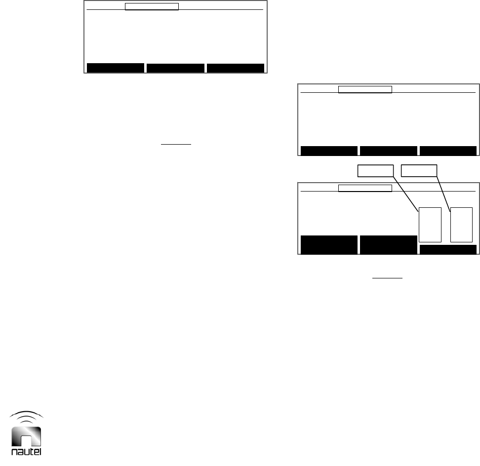
Vector-LP Radio Beacon Transmitter Technical Instruction Manual Page 3-23
Section 3 Operating Instructions Issue 1.8.1
(e) Use and to highlight the desired
monitor timeout field and press Modify:
The low limit is factory set for 3.00 dB.
Adjust using and .
The high limit is factory set for 2.00 dB.
Adjust using and .
(f) Press Back, highlight Automatic Reset
and press Select.
(g) Use and to highlight the desired
Fault 1 -5 field and press Modify. Set the
Automatic Reset schedule as follows:
NOTE
The Automatic Reset allows the user to
define a reset schedule for the transmitter
after a shutdown condition. The schedule can
have up to five sequential levels, each with
their own user definable delay period (up to
24 hours) and subsequent instruction.
ENABLED (continue): attempts a reset
the denoted delay time after a shutdown
and then, if no reset occurs, continues to
the next item in the Fault schedule.
ENABLED (repeat): attempt a reset the
denoted delay time after a shutdown and
continues attempting (as necessary) after
each delay time. All subsequent items in
the Fault schedule default to DISABLED.
ENABLED (halt): attempts a reset the
denoted delay time after a shutdown and
then, if no reset occurs, stops attempting.
All subsequent items in the Fault
schedule default to DISABLED.
DISABLED: no attempt to reset.
Waits the Fault 1 delay period (40 min)
Attempts to reset transmitter. If
successful, Automatic Reset schedule
will begin on Fault 1 next shutdown. If
unsuccessful, reset sequence continues
to Fault 2 item.
Waits the Fault 2 delay period (20 min)
Attempts to reset transmitter. If
successful, Automatic Reset schedule
will begin on Fault 1 next shutdown. If
unsuccessful, repeats Fault 2 item.
(h) Press Back, highlight Mod% Thresholds
and press Select. The following message
is displayed. Press Continue to proceed.
NOTE
As the warning message indicates, ensure
that the transmitter is operating at the
minimum allowable modulation depth before
computing the thresholds. If the transmitter is
to operate in both PTT and Normal modes,
set up both thresholds, otherwise, set up only
the applicable threshold.
(i) The screen shows the minimum
allowable modulation for PTT Inactive
(no voice) and PTT Active (voice).
The left column has side A values and
the right column has side B values.
-Before proceeding, make sure that you
have set the ident tone to the minimum
acceptable modulation depth with PTT
inactive, and again with PTT active.
-If this is a dual system, ensure tone
has been set correctly on both sides.
Continue Back
12:43:16 Power: 0W Side A Bypass
-Before proceeding, make sure that you
have set the ident tone to the minimum
acceptable modulation depth with PTT
inactive, and again with PTT active.
-If this is a dual system, ensure tone
has been set correctly on both sides.
Continue Back
12:43:16 Power: 0W Side A Bypass12:43:16 Power: 0W Side A Bypass
Mod % Thresholds
Minimum Allowable Tone Modulation Depth:
...PTT Inactive: 164 153
...PTT Active: 1023 1023
63.8 63.8
35.4 35.4
Compute New
Thresholds
Rf Mon: CURR
Toggle Back
12:43:16 Power: 0W Side A Bypass
Mod % Thresholds
Minimum Allowable Tone Modulation Depth:
...PTT Inactive: 164 153
...PTT Active: 1023 1023
63.8 63.8
35.4 35.4
Compute New
Thresholds
Rf Mon: CURR
Toggle Back
12:43:16 Power: 0W Side A Bypass
Mod % Thresholds
Minimum Allowable Tone Modulation Depth:
...PTT Inactive: 164 153
...PTT Active: 1023 1023
63.8 63.8
35.4 35.4
Compute New
Thresholds
Rf Mon: CURR
Toggle Back
12:43:16 Power: 0W Side A Bypass
Side A Side B
Main Menu Modify Back
12:43:16 Power: 0W Side A Bypass
Automatic Reset
Fault 1 ENABLED (continue) Delay 00:40
Fault 2 ENABLED (repeat) Delay 00:20
Fault 3 DISABLED
Fault 4 DISABLED
Fault 5 DISABLED
Main Menu Modify Back
12:43:16 Power: 0W Side A Bypass12:43:16 Power: 0W Side A Bypass
Automatic Reset
Fault 1 ENABLED (continue) Delay 00:40
Fault 2 ENABLED (repeat) Delay 00:20
Fault 3 DISABLED
Fault 4 DISABLED
Fault 5 DISABLED
Page 3-24 Vector-LP Radio Beacon Transmitter Technical Instruction Manual
Issue 1.8.1 Section 3 Operating Instructions
The first two values in each column are
internal tone generator reference values.
The third and fourth values are the
modulation depth (in %) for PTT Inactive
and PTT Active respectively.
Press Toggle to switch between RF
Mon: CURR and Rf Mon: VOLT, if
desired.
(j) Press Compute New Thresholds to
establish new monitor modulation %
thresholds.
(k) If a modification is made, a screen
appears which prompts you to save
changes to EEPROM. Select Yes or No.
3.6.8 Meter Settings
Determine the parameter to be displayed on
the front panel analog meter as follows:
(a) From the main menu, highlight Settings
(using and ) and press Select.
Highlight Meter Settings and press
Select. Use and to highlight Select
Analog Meter or Calib. Analog Meter
and press Select. Refer to the
appropriate paragraph (3.6.8.1 or 3.6.8.2
for further details.
3.6.8.1 Selecting Analog Meter
Select the parameter to be displayed on the
front panel analog meter as follows:
(a) Use or to select the desired meter
parameter and press Select. Press
Choose Scale to select from various
scale options to view the parameter on
the front panel analog meter. Note that
scales with a P suffix are power (square
law) scales whereas scales with an L
suffix are linear scales.
(b) Press Back to return to the Meter
Settings screen. A message appears to
confirm saving changes to the EEPROM.
Press Yes or No.
Select Meters
12:43:16 Power: 0W Side A Bypass
Main Menu
Changeover Control
Events Log
Settings
Peripherals
RCMS Settings
Vector NDB
rev 1. 0. 4. 1
Jul 27 2007
13:52:45
Nautel
Select Meters
12:43:16 Power: 0W Side A Bypass12:43:16 Power: 0W Side A Bypass
Main Menu
Changeover Control
Events Log
Settings
Peripherals
RCMS Settings
Vector NDB
rev 1. 0. 4. 1
Jul 27 2007
13:52:45
Nautel
Settings
Set Real Time Clock
Monitor Settings
Meter Settings
Power Source Select
Configure Sonalert
Main Menu Select Back
12:43:16 Power: 0W Side A Bypass
Settings
Set Real Time Clock
Monitor Settings
Meter Settings
Power Source Select
Configure Sonalert
Main Menu Select Back
12:43:16 Power: 0W Side A Bypass12:43:16 Power: 0W Side A Bypass
Main Menu Select Back
12:43:16 Power: 0W Side A Bypass
Meter Settings
Select Analog Meter
Calib. Analog Meter
Main Menu Select Back
12:43:16 Power: 0W Side A Bypass12:43:16 Power: 0W Side A Bypass
Meter Settings
Select Analog Meter
Calib. Analog Meter
Select Analog Meter
Scale 0-400 P
PDM B: 0.00% ()
PDM A: 0.00% ( )
DC Curr B: 0.00A ( )
DC Curr B: 0.00A ( )
Choose Scale Select Back
12:43:16 Power: 0W Side A Bypass
Select Analog Meter
Scale 0-400 P
PDM B: 0.00% ()
PDM A: 0.00% ( )
DC Curr B: 0.00A ( )
DC Curr B: 0.00A ( )
Choose Scale Select Back
12:43:16 Power: 0W Side A Bypass12:43:16 Power: 0W Side A Bypass
Selected Parameter
Vector-LP Radio Beacon Transmitter Technical Instruction Manual Page 3-25
Section 3 Operating Instructions Issue 1.8.1
3.6.8.2 Calibrating Analog Meter
Calibrate the analog meter as follows:
(a) When the analog meter is calibrated,
press Done.
3.6.9 Selecting Power Source
Select the transmitter’s power source and
view power source related parameters as
follows:
(a) From the main menu, highlight Settings
(using and ) and press Select.
Highlight Power Source Select and
press Select.
(b) The parameters than can be modified
(press Modify and use or ) are:
DC Disconnect Level (DC power source
operation): if the dc power source is
below this voltage, the transmitter will
discontinue operation
DC Reconnect Level (DC power source
operation): when the dc power source
recovers to this voltage, the transmitter
will attempt to restore operation.
Requested Power Source: AC, DC,
BOTH (if both ac and dc power sources
are installed) or NONE.
(c) Press Done to activate. A message
appears to confirm saving changes to the
EEPROM. Press Yes or No.
(d) The remaining parameters are for
monitoring only.
DC I/F Instld: Yes or No (indicates if
battery boost assembly A16 is installed).
Active Power Source: indicates the power
source configuration for the transmitter
(AC, DC, BOTH or NONE)
Select Meters
12:43:16 Power: 0W Side A Bypass
Main Menu
Changeover Control
Events Log
Settings
Peripherals
RCMS Settings
Vector NDB
rev 2. 6. 0. 2
Jan 21 2010
11:22:41
Nautel
Select Meters
12:43:16 Power: 0W Side A Bypass12:43:16 Power: 0W Side A Bypass
Main Menu
Changeover Control
Events Log
Settings
Peripherals
RCMS Settings
Vector NDB
rev 2. 6. 0. 2
Jan 21 2010
11:22:41
Nautel
Settings
Set Real Time Clock
Monitor Settings
Meter Settings
Power Source Select
Configure Sonalert
Main Menu Select Back
12:43:16 Power: 0W Side A Bypass
Settings
Set Real Time Clock
Monitor Settings
Meter Settings
Power Source Select
Configure Sonalert
Main Menu Select Back
12:43:16 Power: 0W Side A Bypass12:43:16 Power: 0W Side A Bypass
Press the up/down keys to adjust the
analog meter. The reading on the upper
scale should read 100.
(Midscale calibration constant:224)
Reset Done Cancel
12:43:16 Power: 0W Side A Bypass
Press the up/down keys to adjust the
analog meter. The reading on the upper
scale should read 100.
(Midscale calibration constant:224)
Reset Done Cancel
12:43:16 Power: 0W Side A Bypass12:43:16 Power: 0W Side A Bypass
Main Menu Select Back
12:43:16 Power: 0W Side A Bypass
Meter Settings
Select Analog Meter
Calib. Analog Meter
Main Menu Select Back
12:43:16 Power: 0W Side A Bypass12:43:16 Power: 0W Side A Bypass
Meter Settings
Select Analog Meter
Calib. Analog Meter
Power Source Select
DC Disconnect Level: 19 DC I/F
DC Reconnect Level: 21 Installed: Yes
Requested Source: AC Active
Source: AC
Main Menu Modify Back
12:43:16 Power: 0W Side A Bypass
Power Source Select
DC Disconnect Level: 19 DC I/F
DC Reconnect Level: 21 Installed: Yes
Requested Source: AC Active
Source: AC
Main Menu Modify Back
12:43:16 Power: 0W Side A Bypass
Page 3-26 Vector-LP Radio Beacon Transmitter Technical Instruction Manual
Issue 1.8.1 Section 3 Operating Instructions
3.6.10 Configuring the Sonalert
Configure the status of the audible alarm
(sonalert) for all transmitter alarms as follows:
(a) From the main menu, highlight Settings
(using and ) and press Select.
Highlight Configure Sonalert and press
Select.
NOTE
The Sonalert peripheral must be activated
(see 3.6.13.5) before settings in this section
can take effect.
(b) A list of transmitter alarms and their
current SonAlert (audible) and Site Ctrl
(remote outputs) status is displayed.
To configure an alarm for the sonalert,
use and to select the desired alarm;
press Toggle to change the status to ON.
Press Modify to configure an alarm for
use with site interface PWB A4 (if
installed). Use and to select the
desired alarm and press Toggle to
change the status from OFF to the
appropriate remote control output (1
through 16).
3.6.11 Setting a Timed Shutdown
Modify timed shutdown parameters as
follows:
(a) From the main menu, highlight Settings
(using and ) and press Select.
Highlight Timed Shutdown and press
Select.
(b) Use and to highlight Timed
Shutdown, Interval or Auto Assert,
noting:
Select Meters
12:43:16 Power: 0W Side A Bypass
Main Menu
Changeover Control
Events Log
Settings
Peripherals
RCMS Settings
Vector NDB
rev 2. 6. 0. 2
Jan 21 2010
11:22:41
Nautel
Select Meters
12:43:16 Power: 0W Side A Bypass12:43:16 Power: 0W Side A Bypass
Main Menu
Changeover Control
Events Log
Settings
Peripherals
RCMS Settings
Vector NDB
rev 2. 6. 0. 2
Jan 21 2010
11:22:41
Nautel
Settings
Meter Settings
Power Source Select
Configure Sonalert
Timed Shutdown
Factory Settings
Main Menu Select Back
12:43:16 Power: 0W Side A Bypass
Settings
Meter Settings
Power Source Select
Configure Sonalert
Timed Shutdown
Factory Settings
Main Menu Select Back
12:43:16 Power: 0W Side A Bypass12:43:16 Power: 0W Side A Bypass
Select Meters
12:43:16 Power: 0W Side A Bypass
Main Menu
Changeover Control
Events Log
Settings
Peripherals
RCMS Settings
Vector NDB
rev 2. 6. 0. 2
Jan 21 2010
11:22:41
Nautel
Select Meters
12:43:16 Power: 0W Side A Bypass12:43:16 Power: 0W Side A Bypass
Main Menu
Changeover Control
Events Log
Settings
Peripherals
RCMS Settings
Vector NDB
rev 2. 6. 0. 2
Jan 21 2010
11:22:41
Nautel
Settings
Set Real Time Clock
Monitor Settings
Meter Settings
Power Source Select
Configure Sonalert
Main Menu Select Back
12:43:16 Power: 0W Side A Bypass
Settings
Set Real Time Clock
Monitor Settings
Meter Settings
Power Source Select
Configure Sonalert
Main Menu Select Back
12:43:16 Power: 0W Side A Bypass12:43:16 Power: 0W Side A Bypass
Toggle Modify Back
12:43:16 Power: 0W Side A Bypass
Alarm Signal SonAlert SiteCtrl
PDM Latch B OFF OFF
PDM Latch A OFF OFF
High RF Curr OFF OFF
SWR Shutback OFF OFF
Low AC Voltage OFF OFF
Toggle Modify Back
12:43:16 Power: 0W Side A Bypass12:43:16 Power: 0W Side A Bypass
Alarm Signal SonAlert SiteCtrl
PDM Latch B OFF OFF
PDM Latch A OFF OFF
High RF Curr OFF OFF
SWR Shutback OFF OFF
Low AC Voltage OFF OFF
Main Menu Toggle Back
12:43:16 Power: 0W Side A Bypass
Timed Shutdown
Timed Shutdown [DISABLED ]
Interval [00:05 ]
Auto Assert [Monitor Point 1 ]
Timer State:
Stopped 00:05:00
Main Menu Toggle Back
12:43:16 Power: 0W Side A Bypass12:43:16 Power: 0W Side A Bypass
Timed Shutdown
Timed Shutdown [DISABLED ]
Interval [00:05 ]
Auto Assert [Monitor Point 1 ]
Timer State:
Stopped 00:05:00
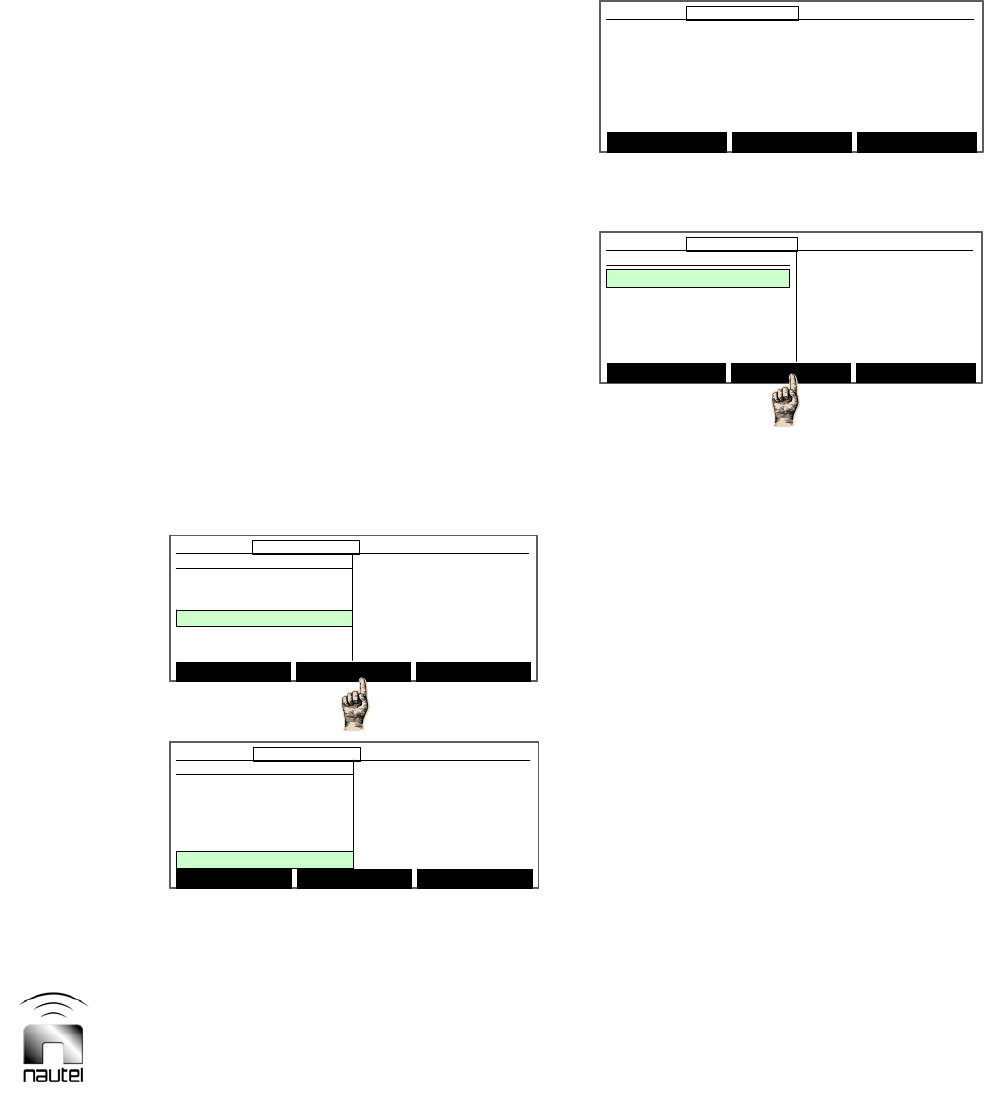
Vector-LP Radio Beacon Transmitter Technical Instruction Manual Page 3-27
Section 3 Operating Instructions Issue 1.8.1
For Timed Shutdown, press Toggle to
change between ENABLED and
DISABLED. When Timed Shutdown is
ENABLED, the transmitter will shut down
the Interval period (in hours:minutes)
after RF On is asserted.
For Interval, press Modify to enable
editing of the interval time. Use and
to change the interval between 5 minutes
and 24 hours (in 5 minute increments).
Press Done to store the change.
For Auto Assert, press Modify to enable
editing of the asserting monitor point. Use
and to change the monitor point
between 1 and 40 (or Disabled). Press
Done to store the change. Monitor points
can only enable the timed shutdown
timer. Set Timed Shutdown to
DISABLED when using Auto Assert.
3.6.12 Changing Factory Calibrated
Settings
Certain parameters, calibrated during factory
testing, can be changed, in local control only,
if an out-of-tolerance condition occurs.
(a) From the main menu, highlight Settings
(using and ) and press Select.
Highlight Factory Settings and press the
and left soft-key simultaneously.
Press Yes to display the following options:
(b) Press or to scroll through the
options and press Select to enter the
appropriate sub-menu (see appropriate
paragraph 3.6.12.1 through 3.6.12.5):
Warning: Modifying these
settings can affect your
transmitter operation.
Do you wish to continue?
Yes No
12:43:16 Power: 0W Side A Bypass
Warning: Modifying these
settings can affect your
transmitter operation.
Do you wish to continue?
Yes No
12:43:16 Power: 0W Side A Bypass12:43:16 Power: 0W Side A Bypass
Select Meters
12:43:16 Power: 0W Side A Bypass
Main Menu
Changeover Control
Events Log
Settings
Peripherals
RCMS Settings
Vector NDB
rev 2. 6. 0. 2
Jan 21 2010
11:22:41
Nautel
Select Meters
12:43:16 Power: 0W Side A Bypass12:43:16 Power: 0W Side A Bypass
Main Menu
Changeover Control
Events Log
Settings
Peripherals
RCMS Settings
Vector NDB
rev 2. 6. 0. 2
Jan 21 2010
11:22:41
Nautel
Settings
Monitor Settings
Meter Settings
Power Source Select
Configure Sonalert
Factory Settings
Main Menu Select Back
12:43:16 Power: 0W Side A Bypass
Settings
Monitor Settings
Meter Settings
Power Source Select
Configure Sonalert
Factory Settings
Main Menu Select Back
12:43:16 Power: 0W Side A Bypass12:43:16 Power: 0W Side A Bypass
Main Menu Select Back
12:43:16 Power: 0W Side A Bypass
Factory Settings
Calibrate Meters
Set Thresholds
Maximum Output Gain
Feature Codes
Use Factory Settings
Main Menu Select Back
12:43:16 Power: 0W Side A Bypass12:43:16 Power: 0W Side A Bypass
Factory Settings
Calibrate Meters
Set Thresholds
Maximum Output Gain
Feature Codes
Use Factory Settings
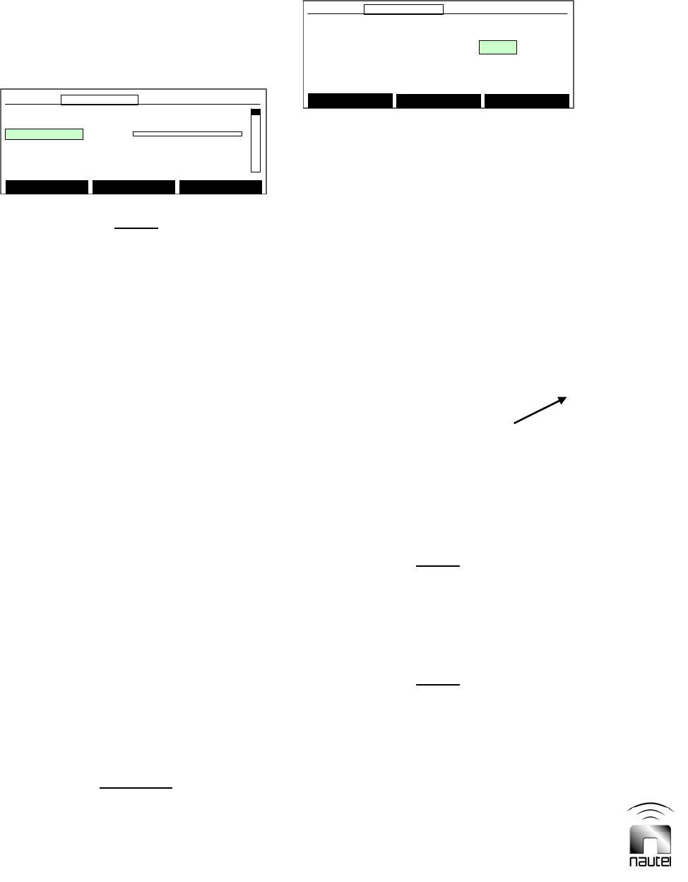
Page 3-28 Vector-LP Radio Beacon Transmitter Technical Instruction Manual
Issue 1.8.1 Section 3 Operating Instructions
Set Thresholds
Refl. Power Shutback: 38
Main Menu Modify Back
12:43:16 Power: 0W Side A Bypass
Set Thresholds
Refl. Power Shutback: 38
Main Menu Modify Back
12:43:16 Power: 0W Side A Bypass12:43:16 Power: 0W Side A Bypass
3.6.12.1 CALIBRATING DIAGNOSTIC
DISPLAY METERS
Re-align an out-of-tolerance meter reading for
a displayed parameter as follows:
NOTE
All meter readings displayed on the meters
screen can be adjusted. It is imperative that
reliable, calibrated test equipment be used
to verify the actual value of the out-of-
tolerance parameter.
(a) Press or until the desired out-of-
tolerance parameter and its current
metered level is displayed.
(b) To calibrate a meter, press Modify and
then or to adjust the level of the out-
of-tolerance parameter. When complete,
press Done.
(c) Continue calibration of other metered
parameters or return to previous menu by
pressing Back. A message prompt
appears to confirm saving all
modifications to the EEPROM. Press Yes
or No.
3.6.12.2 SETTING PROTECTION
THRESHOLD LEVELS
Adjustments can be made to the critical
transmitter shutback thresholds, such as RF
current, low ac voltage, and high reflected
power cutback levels. Less critical settings,
such as diagnostic display contrast and
speaker volume (audio) can also be adjusted.
Set these thresholds as follows:
CAUTION
Protection threshold levels are factory set
and do not normally require adjustment.
Contact Nautel prior to attempting to alter
these settings. Failure to comply could result
in equipment damage.
(a) Press or until the desired threshold
and its current value is displayed. The
following thresholds may be displayed
and edited:
Refl. Power Shutback
Low AC Voltage
RF Current Shutback
Chrgr. Current DC Offset
Audio
LCD Contrast
Bttry. Current DC Offset
Slowback Pwr (Per Block)
Max. PS Temperature (°C)
Max. ATU Temperature (°C)
Minimum Logged Cutback
Ac Meter Zero Offset
Carrier Frequency (kHz) **
(b) To edit a threshold value, press Modify
and then or to adjust the value.
When complete, press Done. Press
Reset to restore the value to its pre-
modified setting.
NOTE
The Minimum Logged Cutback threshold
can be set between 1 (least severe) and 18
(most severe). Only cutback occurrences of
the set value and higher (more severe) will
be logged.
NOTE
If the Frequency Monitor feature code is
enabled (see 3.6.12.4), you can adjust the
Carrier Frequency (kHz) to the operational
carrier frequency.
(c) When complete, return to previous menu
by pressing Back. A prompt appears to
confirm saving modifications to the
EEPROM. Press Yes or No.
Calibrate Meters
PDM B: 0.00
050100
Main Menu Modify Back
12:43:16 Power: 0W Side A Bypass
Calibrate Meters
PDM B: 0.00
050100
Main Menu Modify Back
12:43:16 Power: 0W Side A Bypass12:43:16 Power: 0W Side A Bypass
** - available only when
the Frequency Monitor
feature code is turned on
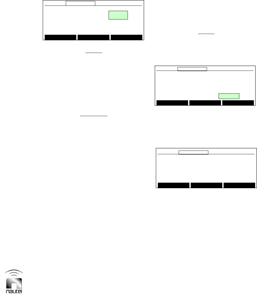
Vector-LP Radio Beacon Transmitter Technical Instruction Manual Page 3-29
Section 3 Operating Instructions Issue 1.8.1
3.6.12.3 SETTING MAXIMUM OUTPUT
LIMITATIONS
The maximum allowable output gain can be
adjusted in terms of carrier reference.
NOTE
The Set Duty Cycle and Set Forward
Power values represent actual transmitter
levels. The Maximum Carrier Reference
represents the maximum carrier reference
value and can be used to limit output power.
The bottom two rows display current levels
for the active side (A or B).
CAUTION
Do not adjust the Maximum Carrier
Reference to a value that causes the
transmitter to exceed its rated power level.
Failure to observe this may void the
equipment warranty.
(a) Press or until the desired parameter
(Set Duty Cycle and Set Forward
Power are grouped together) is
displayed.
(b) To edit a parameter, press Modify and
then or to adjust the value. If the
Set Duty Cycle and Set Forward Power
group is selected to Modify, use the Next
button to toggle between the two items.
(c) When complete, press Done. Press
Reset to restore the value to its pre-
modified setting.
(d) When complete, return to previous menu
by pressing Back. A prompt appears to
confirm saving modifications to the
EEPROM. Press Yes or No.
3.6.12.4 USING FEATURE CODES
(OPTIONAL)
Eight-digit codes can be entered to enable
various features that are available in software
for display on the GUI. Features are
application specific and are not all required.
Typically these features and their associated
codes are entered during factory testing.
NOTE
Feature codes are entered at the factory and
should not require user adjustment. Contact
Nautel if one of your GUI’s features is not
being displayed.
3.6.12.5 USING FACTORY SETTINGS
The functions described in paragraphs
3.6.12.1 through 3.6.12.4 can be restored to
factory settings as follows:
(a) Pressing Yes will restore all setup and
calibration values and thresholds to
factory settings. All other saved
information, including changes to presets,
is also restored to factory settings.
Do you want to restore Factory Defaults?
All current settings will be lost.
Yes No
12:43:16 Power: 0W Side A Bypass
Do you want to restore Factory Defaults?
All current settings will be lost.
Yes No
12:43:16 Power: 0W Side A Bypass12:43:16 Power: 0W Side A Bypass
Maximum Output Gain
Set Duty Cycle: 0.00
Set Forward Power: 0
Maximum Carrier Reference: 154
PDM A: 7.97% Carr. Ref: 8
B+ Volt A: 75.0V PA Volt A: 6.4V
Main Menu Modify Back
12:43:16 Power: 0W Side A Bypass
Maximum Output Gain
Set Duty Cycle: 0.00
Set Forward Power: 0
Maximum Carrier Reference: 154
PDM A: 7.97% Carr. Ref: 8
B+ Volt A: 75.0V PA Volt A: 6.4V
Main Menu Modify Back
12:43:16 Power: 0W Side A Bypass
Main Menu Modify Back
12:43:16 Power: 0W Side A Bypass
Feature Codes
Frequency Monitor
Enter Feature Code: 00000000
Main Menu Modify Back
12:43:16 Power: 0W Side A Bypass12:43:16 Power: 0W Side A Bypass
Feature Codes
Frequency Monitor
Enter Feature Code: 00000000
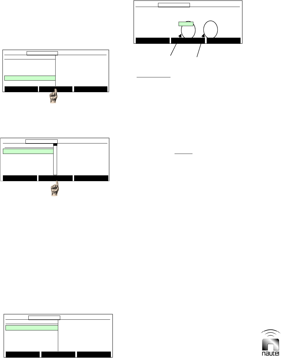
Page 3-30 Vector-LP Radio Beacon Transmitter Technical Instruction Manual
Issue 1.8.1 Section 3 Operating Instructions
3.6.13 Viewing and Setting
Peripherals
View and set parameters related to auxiliary
items, such as the keyer, the ATU or the
transmitter’s inactive (standby) side, as
follows:
(a) From the main menu, highlight
Peripherals (using and ) and press
Select.
(b) Press or to scroll through the
options and press Select to enter the
appropriate sub-menu (see 3.6.13.1
through 3.6.13.6).
Keyer Settings (para. 3.6.13.1)
Power Modules (para. 3.6.13.2)
ATU Controls (para. 3.6.13.3)
Test Standby Side (para. 3.6.13.4)
Select Peripherals (para. 3.6.13.5)
Module Check (para. 3.6.13.6)
3.6.13.1 SETTING THE KEYER
Set up the keyer as follows:
(a) Audio Levels: Select the desired
parameter, using or . To edit, press
Modify and then use or to adjust
the Side B Scale factor, Keying Pot (for
tone modulation level in beacon mode),
PTT Keying Pot (for tone modulation
level in PTT, or press-to-talk mode) or
Voice Pot (for voice modulation level in
PTT mode) value. Press Done and Back
when complete.
NOTE
The Side B Scale factor is factory set and
should not require user adjustment. If the
modulation depth on side B does not match
the modulation depth on side A, adjust the
Side B Scale factor up or down until they
agree.
After adjusting the Side B Scale factor,
adjust a Pot value (press and ) to
enable the new scaling factor.
The Side B Scale factor is used to scale
pot values for side B to allow for an
adjustment so the modulation depth on
side B can be calibrated to match side A.
There are two values displayed for each
Pot. The left-hand value is for side A.
The right-hand value is for side B. The
side B Pot value should be the side A
Pot value multiplied by the Side B Scale
factor.
If a Pot value (side A or B) is adjusted,
the other side’s value will automatically
change according to the Side B Scale
factor.
Main Menu Select Back
12:43:16 Power: 0W Side A Bypass
Peripherals
Keyer Settings
Power Modules
ATU Controls
Test Standby Side
Select Peripherals
Main Menu Select Back
12:43:16 Power: 0W Side A Bypass12:43:16 Power: 0W Side A Bypass
Peripherals
Keyer Settings
Power Modules
ATU Controls
Test Standby Side
Select Peripherals
Main Menu Select Back
12:43:16 Power: 0W Side A Bypass
Keyer Settings
Audio Levels
Keyer Modulation
Keyer Sequence
Standby Code 1
Standby Code 2
Main Menu Select Back
12:43:16 Power: 0W Side A Bypass12:43:16 Power: 0W Side A Bypass
Keyer Settings
Audio Levels
Keyer Modulation
Keyer Sequence
Standby Code 1
Standby Code 2
Audio Levels
Mod %: 0.0%
Side B Scale: 2.000
Keying Pot: 120 240
Voice Pot: 128 255
PTT Keying Pot: 128 255
Main Menu Modify Back
12:43:16 Power: 0W Side A Bypass
Audio Levels
Mod %: 0.0%
Side B Scale: 2.000
Keying Pot: 120 240
Voice Pot: 128 255
PTT Keying Pot: 128 255
Main Menu Modify Back
12:43:16 Power: 0W Side A Bypass12:43:16 Power: 0W Side A Bypass
SIDE A SIDE B
Select Meters
12:43:16 Power: 0W Side A Bypass
Main Menu
Changeover Control
Events Log
Settings
Peripherals
RCMS Settings
Vector NDB
rev 2. 6. 0. 2
Jan 21 2010
11:22:41
Nautel
Select Meters
12:43:16 Power: 0W Side A Bypass12:43:16 Power: 0W Side A Bypass
Main Menu
Changeover Control
Events Log
Settings
Peripherals
RCMS Settings
Vector NDB
rev 2. 6. 0. 2
Jan 21 2010
11:22:41
Nautel
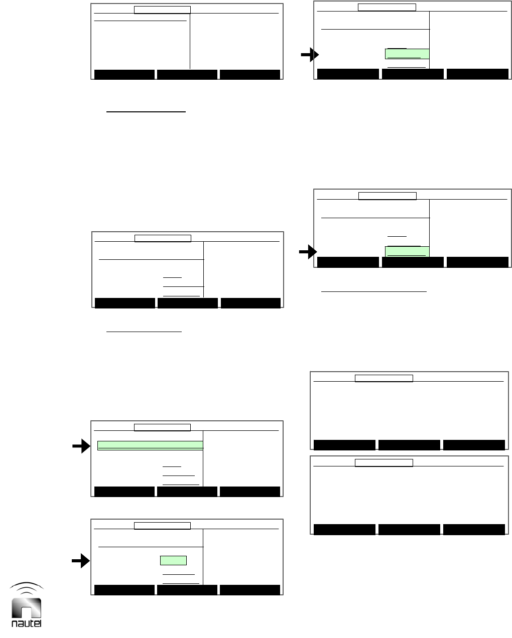
Vector-LP Radio Beacon Transmitter Technical Instruction Manual Page 3-31
Section 3 Operating Instructions Issue 1.8.1
Reset Done Cancel
12:43:16 Power: 0W Side A Bypass
Frame Sequence
MK MK MK MK MK MK MK MK
Keyed String: TEST
Frame Format: NAV CAN
Frame Timing: 20.0 sec
Press up/down
keys to change
the duration of
each frame.
Press Done to
confirm changes.
Reset Done Cancel
12:43:16 Power: 0W Side A Bypass12:43:16 Power: 0W Side A Bypass
Frame Sequence
MK MK MK MK MK MK MK MK
Keyed String: TEST
Frame Format: NAV CAN
Frame Timing: 20.0 sec
Press up/down
keys to change
the duration of
each frame.
Press Done to
confirm changes.
Fr
a
m
e
Timin
g
Reset Done Cancel
12:43:16 Power: 0W Side A Bypass
Frame Sequence
MK MK MK MK MK MK MK MK
Keyed String: TEST
Frame Format: NAV CAN
Frame Timing: 20.0 sec
Press up/down
keys to select a
frame format to
use. Press Done
to confirm your
selection
Reset Done Cancel
12:43:16 Power: 0W Side A Bypass
Frame Sequence
MK MK MK MK MK MK MK MK
Keyed String: TEST
Frame Format: NAV CAN
Frame Timing: 20.0 sec
Press up/down
keys to select a
frame format to
use. Press Done
to confirm your
selection
Frame Format
Reset Next Cancel
12:43:16 Power: 0W Side A Bypass
Frame Sequence
MK MK MK MK MK MK MK MK
Keyed String: TEST
Frame Format: NAV CAN
Frame Timing: 20.0 sec
Legend:
MK: All Marks
SP: All Spaces
AL: Alternating
Marks/Spaces
KY: Keyed String
Reset Next Cancel
12:43:16 Power: 0W Side A Bypass12:43:16 Power: 0W Side A Bypass
Frame Sequence
MK MK MK MK MK MK MK MK
Keyed String: TEST
Frame Format: NAV CAN
Frame Timing: 20.0 sec
Legend:
MK: All Marks
SP: All Spaces
AL: Alternating
Marks/Spaces
KY: Keyed String
Frame Se
q
uence
Reset Next Cancel
12:43:16 Power: 0W Side A Bypass
Frame Sequence
MK MK MK MK MK MK MK MK
Keyed String: TEST
Frame Format: NAV CAN
Frame Timing: 20.0 sec
Press up/down
keys to change
the selected
letter. Press
Next to go on to
the next letter
Reset Next Cancel
12:43:16 Power: 0W Side A Bypass12:43:16 Power: 0W Side A Bypass
Frame Sequence
MK MK MK MK MK MK MK MK
Keyed String: TEST
Frame Format: NAV CAN
Frame Timing: 20.0 sec
Press up/down
keys to change
the selected
letter. Press
Next to go on to
the next letter
Ke
y
ed Strin
g
Main Menu Toggle Back
12:43:16 Power: 0W Side A Bypass
Keyer Modulation
Modulation
Keyer
Tone Generator
Tone Frequency
[ON ]
[OFF ]
[ON ]
[1020 Hz]
Main Menu Toggle Back
12:43:16 Power: 0W Side A Bypass12:43:16 Power: 0W Side A Bypass
Keyer Modulation
Modulation
Keyer
Tone Generator
Tone Frequency
[ON ]
[OFF ]
[ON ]
[1020 Hz]
(b) Keyer Modulation: Select the desired
parameter, using or . Press Toggle
to change the status or value and then
press Back:
Modulation, Keyer and Tone Generator
can be set to ON or OFF.
Tone Frequency can be set to 400 Hz or
1020 Hz.
(c) Keyer Sequence: Select the desired
parameter, Frame Sequence, Keyed
String, Frame Format or Frame Timing,
using or . Press Modify and follow
the instructions on the right-hand side of
the GUI display.
(set to either NAV CAN or ICAO)
- ICAO: International Civil Aviation
Organization
- NAV CAN: uses a 10 s frame and 0.125
ms bits to key out 3 symbols.
(set between 4.0 s and 20.0 s)
(d) Standby Codes 1 and 2: Press Toggle to
enable [X] or disable [ ] the standby code
1 or 2. For Standby Code 1, use the
and buttons to move between field.
Continue using Toggle to select or de-
select the location of additional inserted
spaces.
3.6.13.2 VIEWING POWER MODULE
STATUS
Configure the transmitter’s software for the
number of power blocks and view the status
of individual power modules as follows:
Main Menu Modify Back
12:43:16 Power: 0W Side A Bypass
Frame Sequence
MK MK MK MK MK MK MK MK
Keyed String: TEST
Frame Format: TRANS CAN
Frame Timing: 20.0 sec
Press up/down
keys to select a
field to change
Press Modify to
make changes
Main Menu Modify Back
12:43:16 Power: 0W Side A Bypass12:43:16 Power: 0W Side A Bypass
Frame Sequence
MK MK MK MK MK MK MK MK
Keyed String: TEST
Frame Format: TRANS CAN
Frame Timing: 20.0 sec
Press up/down
keys to select a
field to change
Press Modify to
make changes
Main Menu Toggle Back
12:43:16 Power: 0W Side A Bypass
Standby Code 1
[ X ] Enable Standby Code 1
Inserts additional spaces between
selected characters in each keyed
Frame: __[ ]__[ ]__[ ]__[ ]__[ ]__
Main Menu Toggle Back
12:43:16 Power: 0W Side A Bypass12:43:16 Power: 0W Side A Bypass
Standby Code 1
[ X ] Enable Standby Code 1
Inserts additional spaces between
selected characters in each keyed
Frame: __[ ]__[ ]__[ ]__[ ]__[ ]__
Main Menu Select Back
12:43:16 Power: 0W Side A Bypass
Standby Code 2
[ X ] Enable Standby Code 2
Inserts a 2-bit mark at the beginning
of each keyed frame.
Main Menu Toggle Back
12:43:16 Power: 0W Site A Bypass
Main Menu Select Back
12:43:16 Power: 0W Side A Bypass
Standby Code 2
[ X ] Enable Standby Code 2
Inserts a 2-bit mark at the beginning
of each keyed frame.
Main Menu Select Back
12:43:16 Power: 0W Side A Bypass12:43:16 Power: 0W Side A Bypass
Standby Code 2
[ X ] Enable Standby Code 2
Inserts a 2-bit mark at the beginning
of each keyed frame.
Main Menu Toggle Back
12:43:16 Power: 0W Site A Bypass12:43:16 Power: 0W Site A Bypass
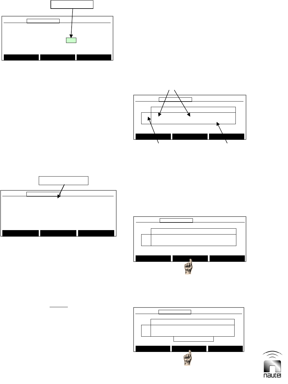
Page 3-32 Vector-LP Radio Beacon Transmitter Technical Instruction Manual
Issue 1.8.1 Section 3 Operating Instructions
Power Module
Number of Power block expected: [3]
Block # 1 2 3 4
Side: A OK [X] [ ] [ ] [ ]
B OK [X] [ ] [ ] [ ]
Main Menu View Details Back
12:43:16 Power: 0W Site A Bypass
Power Module
Number of Power block expected: [3]
Block # 1 2 3 4
Side: A OK [X] [ ] [ ] [ ]
B OK [X] [ ] [ ] [ ]
Main Menu View Details Back
12:43:16 Power: 0W Site A Bypass12:43:16 Power: 0W Site A Bypass
X = installed
Detailed Status PA Bloc 1
B+ Setting : 150 Inhibited : Yes
Temperature: -50 B+ Voltage : 0.0
Dc Current : 0.10 PA Voltage : 0.0
Fan 1 Tach : 1 Fan 2 Tach : 0
PDM Inhib : No PA Alarm : No
Main Menu Back
12:43:16 Power: 0W Side A Bypass
Detailed Status PA Bloc 1
B+ Setting : 150 Inhibited : Yes
Temperature: -50 B+ Voltage : 0.0
Dc Current : 0.10 PA Voltage : 0.0
Fan 1 Tach : 1 Fan 2 Tach : 0
PDM Inhib : No PA Alarm : No
Main Menu Back
12:43:16 Power: 0W Side A Bypass12:43:16 Power: 0W Side A Bypass
PA = Side A
(a) Press or until the desired parameter
is highlighted.
If the Number of Power block expected
value is highlighted, the Modify option is
displayed. If necessary, press Modify
and use or to select 1 (for Vector-
LP). Press Done when complete.
If one of the power module fields (Block
# 1, Side A and B for Vector-LP) is
highlighted, the View Details option is
displayed. Press View Details to view
the following RF power module details:
(b) Return to the previous menu by pressing
Back.
3.6.13.3 ATU CONTROLS
If a Nautel antenna tuning unit (ATU) is being
used, view and edit its control parameters as
follows:
NOTE
A serial interface allows communication
between the transmitter and the ATU. This
interface connects to the transmitter via the
INTERNAL RS-485 connector (25-pin D-sub)
on the rear of the exciter/control assembly.
(a) The screen below appears if the ATU is
in local mode of operation and auto-
tuning is active and is tuned. This screen
allows viewing of ATU status only. No
adjustments are possible while the ATU
is in local mode.
(b) If the ATU is set to the remote mode of
operation, the screen is as shown below.
This screen allows ATU tuning to be
controlled from the transmitter GUI.
Press Coil Control.
(c) In the coil control screen shown below,
use and to select the desired coil to
control - Resistive Coil or Inductive
Coil. Press Continue.
ATU Control Antenna Curr.: 0.0A
Dec L N H Inc Auto-Tuning
R[ ] [] [ ] Active
L[ ] [][ ] Active
ATU is in REMOTE Mode
Press Coil Control to modify ATU settings
12:43:16 Power: 0W Site A Bypass
Main Menu Coil Control Back
ATU Control Antenna Curr.: 0.0A
Dec L N H Inc Auto-Tuning
R[ ] [] [ ] Active
L[ ] [][ ] Active
ATU is in REMOTE Mode
Press Coil Control to modify ATU settings
12:43:16 Power: 0W Site A Bypass12:43:16 Power: 0W Site A Bypass
Main Menu Coil Control Back
ATU Control Antenna Curr.: 0.0A
Dec L N H Inc Auto-Tuning
R[ ] [][ ] Active
L[ ] [][ ] Active
Coil Control: Resistive Coil
UP/Down Keys: Select a coil to configure
12:43:16 Power: 0W Site A Bypass
Main Menu Continue Back
ATU Control Antenna Curr.: 0.0A
Dec L N H Inc Auto-Tuning
R[ ] [][ ] Active
L[ ] [][ ] Active
Coil Control: Resistive Coil
UP/Down Keys: Select a coil to configure
12:43:16 Power: 0W Site A Bypass12:43:16 Power: 0W Site A Bypass
Main Menu Continue Back
Increase/Decrease Arrows
(Affected arrow is highlighted during
auto or manual tuning)
Resistive (R) and
Inductive (L)
Tuning Status Line
ATU Control Antenna Curr.: 0.0A
Dec L N H Inc Auto-Tuning
R[ ] [] [ ] Active
L[ ] [][ ] Active
ATU is in LOCAL Mode
12:43:16 Power: 0W Site A Bypass
Back
ATU Control Antenna Curr.: 0.0A
Dec L N H Inc Auto-Tuning
R[ ] [] [ ] Active
L[ ] [][ ] Active
ATU is in LOCAL Mode
12:43:16 Power: 0W Site A Bypass12:43:16 Power: 0W Site A Bypass
Back
Auto-Tuning Status
(Active or Inhibited)
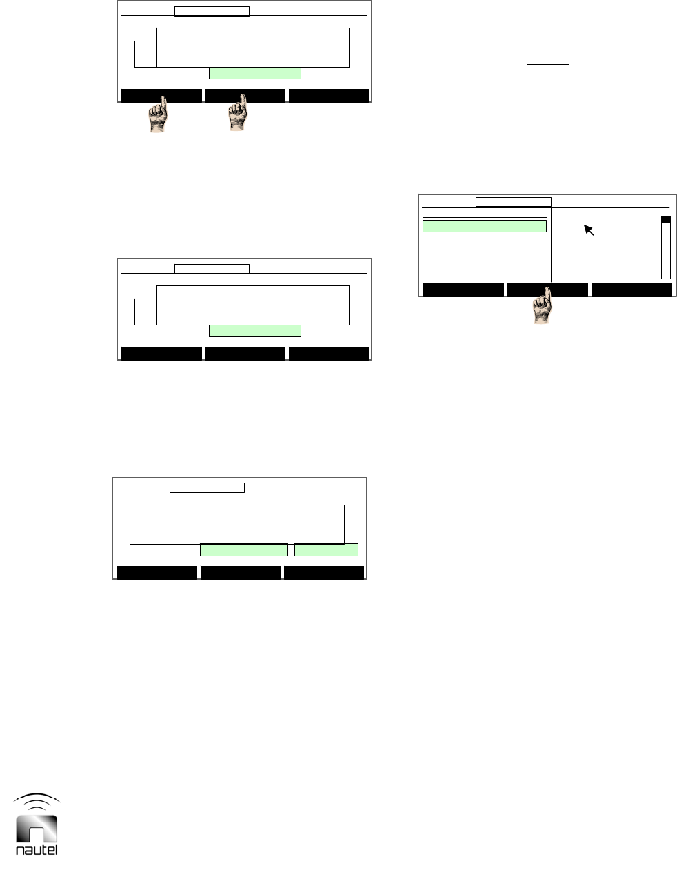
Vector-LP Radio Beacon Transmitter Technical Instruction Manual Page 3-33
Section 3 Operating Instructions Issue 1.8.1
ATU Control Antenna Curr.: 0.0A
Dec L N H Inc Auto-Tuning
R[ ] [][ ] Active
L[ ] [][ ] Active
Coil Control: Resistive Coil
What would you like to do:
12:43:16 Power: 0W Site A Bypass
Auto Tuning Slew Servo Back
ATU Control Antenna Curr.: 0.0A
Dec L N H Inc Auto-Tuning
R[ ] [][ ] Active
L[ ] [][ ] Active
Coil Control: Resistive Coil
What would you like to do:
12:43:16 Power: 0W Site A Bypass12:43:16 Power: 0W Site A Bypass
Auto Tuning Slew Servo Back
OR
(d) If Auto Tuning is selected, the
following screen appears which allows
the selected coil to be auto tuned
(active) or inhibited. Use and to
highlight Active or Inhibited, then
press Done to select.
(e) If Slew Servo is selected, the following
screen appears which allows the
selected coil to be manually tuned. Use
and to slew the coil high or low.
Press Done when complete.
3.6.13.4 TESTING THE STANDBY SIDE
Test the operation of the transmitter’s
inactive (standby) side as follows:
(a) Use and to highlight the desired
test (Turn Standby Side Off, Test
Power Supply, Test Modulators,
Test RF Drive, or Run All Tests).
Press Select to activate.
(b) If you select a test, the display will
initially indicate Running. When the
test is complete, a pass (OK) or fail
indication is displayed. If the item
under test fails, a root cause message
(e.g., PS Ovr Cur) is displayed.
NOTE
The root cause text is identical to that
displayed in the Status menu (see 3.6.3).
3.6.13.5 SELECTING PERIPHERALS
Configure the transmitter’s software for
peripheral equipment, such as an ATU or
site interface PWB as follows:
(a) Use and to highlight the desired
peripheral. Press Select to activate.
If the site interface PWB (A2A4) is
installed, select Site Control Board.
If a Nautel ATU is used and a serial
interface is connected to the
INTERNAL RS-485 connector on the
rear of the exciter/control assembly,
select ATU.
To hear the sonalert buzzer for a fault
defined in the sonalert setup menu,
select SonAlert.
To hear the transmitter output, select
Speaker.
To enable the GUI to display Audio
Limit alarm occurrences, select
Overmod Alarm.
If module fans are installed (VR250
only), select Module Fan Tachs.
(b) Return to previous menu by pressing
Back or press Main Menu.
ATU Control Antenna Curr.: 0.0A
Dec L N H Inc Auto-Tuning
R[ ] [][ ] Active
L[ ] [][ ] Active
Coil Control: Resistive Coil:Slew Servo
Up/Down Keys: Slew coil High/Low
12:43:16 Power: 0W Site A Bypass
Done
ATU Control Antenna Curr.: 0.0A
Dec L N H Inc Auto-Tuning
R[ ] [][ ] Active
L[ ] [][ ] Active
Coil Control: Resistive Coil:Slew Servo
Up/Down Keys: Slew coil High/Low
12:43:16 Power: 0W Site A Bypass12:43:16 Power: 0W Site A Bypass
Done
ATU Control Antenna Curr.: 0.0A
Dec L N H Inc Auto-Tuning
R[ ] [][ ] Active
L[ ] [][ ] Active
Coil Control: Resistive Coil
Up/Down Keys: (De)Activate Auto Tuning
12:43:16 Power: 0W Site A Bypass
Done
ATU Control Antenna Curr.: 0.0A
Dec L N H Inc Auto-Tuning
R[ ] [][ ] Active
L[ ] [][ ] Active
Coil Control: Resistive Coil
Up/Down Keys: (De)Activate Auto Tuning
12:43:16 Power: 0W Site A Bypass12:43:16 Power: 0W Site A Bypass
Done
Main Menu Select Back
12:43:16 Power: 0W Side A Bypass
Select Peripherals
Site Control Board
ATU
SonAlert Buzzer
Speaker
Overmod Alarm
[X]
[ ]
[ ]
[ ]
[ ]
Main Menu Select Back
12:43:16 Power: 0W Side A Bypass12:43:16 Power: 0W Side A Bypass
Select Peripherals
Site Control Board
ATU
SonAlert Buzzer
Speaker
Overmod Alarm
[X]
[ ]
[ ]
[ ]
[ ]
Indicates
Selected
Peripherals
Page 3-34 Vector-LP Radio Beacon Transmitter Technical Instruction Manual
Issue 1.8.1 Section 3 Operating Instructions
3.6.13.6 CHECKING MODULES:
Check the software revision of various
modules that contain microcontrollers as
follows:
(a) Use and to scroll through rows 1
to 12, noting:
Rows 0 through 7 are assigned to RF
power modules.
Rows 8 and 9 are assigned to the
exciter/monitor generator PWBs (side
A and, if applicable, side B).
Row 10 is assigned to the associated
ATUs control/monitor PWB.
Row 11 is assigned to the site control
PWB, if installed.
NOTE
If text is not displayed for a particular row,
the associated module or PWB is not
installed.
3.6.14 Remote Control Monitor
System Settings
If the NDB site interface PWB (A4) is
installed, configure the active logic states of
the control and monitor points as follows:
(a) From the main menu, highlight RCMS
Settings and press Select.
(b) Set the transmitter to Local mode.
(c) Press or to scroll through the
options and press Select to enter the
appropriate sub-menu (see paragraphs
3.6.14.1 through 3.6.14.3).
Control Points (see 3.6.14.1)
Monitor Points (see 3.6.14.2)
Serial Settings (see 3.6.14.3)
Automatic Reporting (see 3.6.14.4)
3.6.14.1 SETTING CONTROL POINTS
Set the site interface PWBs control points
as follows:
(a) Use and to highlight the desired
control point (1 through 16). Press
Toggle to change the logic level (0 or
1) of the Set Value. The logic level
determines the active state for the
control point’s remote input.
NOTE
Control points 1 through 16 correspond to
inputs connected to CONTROL POINT 1
through 16 on TB3 of the remote control/
monitor interface PWB.
(b) Return to previous menu by pressing
Back.
Main Menu Select Back
12:43:16 Power: 0W Side A Bypass
RCMS Settings
Control Points
Monitor Points
Serial Setting
Automatic Reporting
Main Menu Select Back
12:43:16 Power: 0W Side A Bypass12:43:16 Power: 0W Side A Bypass
RCMS Settings
Control Points
Monitor Points
Serial Setting
Automatic Reporting
Control Points Set Value
Control Point 1 0
Control Point 2 0
Control Point 3 0
Control Point 4 0
Control Point 5 0
Toggle Back
12:43:16 Power: 0W Side A Bypass
Control Points Set Value
Control Point 1 0
Control Point 2 0
Control Point 3 0
Control Point 4 0
Control Point 5 0
Toggle Back
12:43:16 Power: 0W Side A Bypass12:43:16 Power: 0W Side A Bypass
Module Check
7
8 NAPE76u rev 0. 0. 0. 2
9 NAPE76u rev 0. 0. 0. 2
10
11 NAPI80u rev 0. 1. 0. 34
Main Menu Select Back
12:43:16 Power: 0W Site A Bypass
Module Check
7
8 NAPE76u rev 0. 0. 0. 2
9 NAPE76u rev 0. 0. 0. 2
10
11 NAPI80u rev 0. 1. 0. 34
Main Menu Select Back
12:43:16 Power: 0W Site A Bypass12:43:16 Power: 0W Site A Bypass
Select Meters
12:43:16 Power: 0W Side A Bypass
Main Menu
Changeover Control
Events Log
Settings
Peripherals
RCMS Settings
Vector NDB
rev 2. 6. 0. 2
Jan 21 2010
11:22:41
Nautel
Select Meters
12:43:16 Power: 0W Side A Bypass12:43:16 Power: 0W Side A Bypass
Main Menu
Changeover Control
Events Log
Settings
Peripherals
RCMS Settings
Vector NDB
rev 2. 6. 0. 2
Jan 21 2010
11:22:41
Nautel
Vector-LP Radio Beacon Transmitter Technical Instruction Manual Page 3-35
Section 3 Operating Instructions Issue 1.8.1
3.6.14.2 SETTING MONITOR POINTS
Set the site interface PWB’s monitor points
as follows:
(a) Use and to highlight the desired
monitor point (1 through 16). Press
Toggle to change the logic level (0 or
1) of the Default value. The logic level
determines the active (for status
outputs) or normal (for alarm outputs)
state for the monitor point’s remote
output.
NOTE
Monitor points 1 through 16 correspond to
outputs connected to MONITOR POINT 1
through 16 on TB1 and TB2 of the site
interface PWB.
(b) The values in the Current column
represent the existing state of the
monitor point. Press Set Current to
set the Current values to match the
Default values.
(c) Return to previous menu by pressing
Back.
3.6.14.3 SERIAL SETTINGS
Set up the serial connection as follows:
(a) Use and to highlight the desired
serial setting. Press Modify or Toggle
to change the setting. Press Next or
Done when complete.
To modify Tx Address, use and .
Press Toggle to set Connection Mode
to DIRECT or MODEM. When
MODEM is selected, the following
screen appears, which enables three
further settings:
Press Toggle to set Modem Line to
DIAL UP or LEASED. The Dial-up
number option disappears when
LEASED is selected.
Press , and Next to set the
Passkey and the Dial-up Number.
(b) Return to the previous menu by
pressing Back.
3.6.14.4 AUTOMATIC REPORTING
Configure the serial connection to
automatically report transmitter alarms
(without needing to poll the status) as
follows:
(a) A list of transmitter alarms and their
current Automatic Reporting status is
displayed.
To configure an alarm for automatic
reporting, use and to select the
desired alarm and press Select to
change the status to ON.
Main Menu Modify Back
12:43:16 Power: 0W Side A Bypass
Serial Settings
Tx Address
Connection Mode
ABCD
[DIRECT ]
Main Menu Modify Back
12:43:16 Power: 0W Side A Bypass12:43:16 Power: 0W Side A Bypass
Serial Settings
Tx Address
Connection Mode
ABCD
[DIRECT ]
Main Menu Toggle Back
12:43:16 Power: 0W Side A Bypass
Serial Settings
Tx Address
Connection Mode
Modem Line
Passkey
Dial-up Number
ABCD
[MODEM ]
[DIAL UP]
0000
Main Menu Toggle Back
12:43:16 Power: 0W Side A Bypass12:43:16 Power: 0W Side A Bypass
Serial Settings
Tx Address
Connection Mode
Modem Line
Passkey
Dial-up Number
ABCD
[MODEM ]
[DIAL UP]
0000
Fault Automatic Reporting
PDM Latch B OFF
PDM Latch A OFF
High RF Current OFF
SWR Shutback OFF
Low AC Volts OFF
Main Menu Select Back
12:43:16 Power: 0W Side A Bypass
Fault Automatic Reporting
PDM Latch B OFF
PDM Latch A OFF
High RF Current OFF
SWR Shutback OFF
Low AC Volts OFF
Main Menu Select Back
12:43:16 Power: 0W Side A Bypass12:43:16 Power: 0W Side A Bypass
Monitor Points Default Current
Monitor Point 1 0 0
Monitor Point 2 0 0
Monitor Point 3 0 0
Monitor Point 4 0 0
Monitor Point 5 0 0
Set Current Toggle Back
12:43:16 Power: 0W Side A Bypass
Monitor Points Default Current
Monitor Point 1 0 0
Monitor Point 2 0 0
Monitor Point 3 0 0
Monitor Point 4 0 0
Monitor Point 5 0 0
Set Current Toggle Back
12:43:16 Power: 0W Side A Bypass12:43:16 Power: 0W Side A Bypass
Page 3-36 Vector-LP Radio Beacon Transmitter Technical Instruction Manual
Issue 1.8.1 Section 3 Operating Instructions
3.6.15 Viewing Power Related
Parameters and Setting ATU
Current Feedback
View the transmitter’s power menu and, if
necessary, set the status of the ATU
current feedback circuit as follows:
NOTE
The ATU current feedback circuit attempts
to regulate the antenna current over a
range of RF output power. The two ATU
options in the power menu are only
available when the transmitter is attached
(using a RS485 serial link) to an ATU-LP or
ATU500.
(a) From the meter screen, press Power.
The current forward power, reflected
power, carrier reference, VSWR,
antenna current, B+ voltage (for the
active side’s power supply) and dc
current (for the active side’s power
supply).
(b) To edit the Fwd. Power or ATU
Current Feedback field, press Modify
and then use and to edit:
Fwd. Power changes in 1 W steps
ATU Current Feedback toggles
between ON and OFF.
(Not used for ATU500)
(c) Press Done when complete.
NOTE
The transmitter regulates the antenna
current to the ATU Current Setpoint value
displayed on the GUI. Ensure the
transmitter’s RF output is set to the desired
level before setting the ATU Current
Feedback field to ON.
Fwd Power: 0W Rfld Power: 0.0W
VSWR: 0.00 Mod %: 0.0%
RF Curr: 0.0A Ant Curr: 0.0A
Mod % A: 0.0% Mod % B: 0.0%
Meas Freq A:315000Hz Meas Freq B:314998Hz
Main Menu Status Power
12:43:16 Power: 0W Side A Bypass
Fwd Power: 0W Rfld Power: 0.0W
VSWR: 0.00 Mod %: 0.0%
RF Curr: 0.0A Ant Curr: 0.0A
Mod % A: 0.0% Mod % B: 0.0%
Meas Freq A:315000Hz Meas Freq B:314998Hz
Main Menu Status Power
12:43:16 Power: 0W Side A Bypass12:43:16 Power: 0W Side A Bypass
Fwd. Power : 108W Rfld.Power: 0.0W
Carr. Ref: 59 VSWR: 1.00
Ant. Curr. : 1.8A B+ Volt A: 75.2V
DC Curr A: 0.70A
ATU Current Feedback: OFF
ATU Current Setpoint: 1.8
Main Menu Modify Meters
12:43:16 Power: 0W Side A Bypass
Fwd. Power : 108W Rfld.Power: 0.0W
Carr. Ref: 59 VSWR: 1.00
Ant. Curr. : 1.8A B+ Volt A: 75.2V
DC Curr A: 0.70A
ATU Current Feedback: OFF
ATU Current Setpoint: 1.8
Main Menu Modify Meters
12:43:16 Power: 0W Side A Bypass12:43:16 Power: 0W Side A Bypass

Vector-LP Radio Beacon Transmitter Technical Instruction Manual Page 4-1
Section 4 Testing and Adjustment Issue 1.8.1
Vector-LP Radio Beacon Transmitter
TECHNICAL INSTRUCTION MANUAL
Section 4 TESTING AND ADJUSTMENT
4.1 INTRODUCTION
This section contains step-by-step
functional test procedures using integral
meters and precision test/monitoring
equipment. The test procedures contain
routine adjustment instructions to bring the
parameter being tested within defined
limits, where appropriate.
NOTE
Nautel recommends all instructions be
followed in the order presented, particularly
by personnel who are not familiar with
detailed circuit theory and may not realize
the impact a specific adjustment can have
on other steps. These adjustments should
be performed during initial turn-on and after
major repairs or a frequency change.
4.2 OPERATING PRECAUTIONS
The transmitter contains protection circuits
that monitor critical parameters. When the
defined limits of any of these parameters
are exceeded, one of the operational lamps
on the exciter panel’s system diagram will
turn red. If the alarm condition could result
in excessive power amplifier stress current,
the control voltage applied to the power
amplifiers will effectively be reduced or
turned off until the out-of-tolerance
condition no longer exists. Maintainers
should read and fully understand the
Section 3 - Operating Instructions, and in
particular the section on controls and
indicators.
NOTE
The diagnostic display’s meters screen
displays three pre-determined parameters
(e.g., forward power, total dc current, +15 V
power supply, etc.). All transmitter
parameters may be displayed on this
screen. See paragraph 3.6.8.1.
4.3 FUNCTIONAL TESTS
To verify the transmitter circuits are within
factory specifications, complete the tests in
this section. In cases where a routine
adjustment will correct an out-of-tolerance
condition, the adjustment procedure is
included.
NOTE
If an in-tolerance condition cannot be
attained with the specified routine
adjustment, discontinue testing until the
cause of the out-of-tolerance condition is
corrected.
4.3.1 General
Functional tests should be performed as a
routine part of scheduled maintenance
checks, and as the first step in
troubleshooting procedures. The results
should be recorded for comparison with
past and future test results.
4.3.1.1 The functional test procedures are
provided in a step-by-step format. This
method of presentation will permit a person
who is unfamiliar with the transmitter to
perform the functional tests in a logical
sequence. The procedures should be
completed in sequence, as each procedure
establishes switch settings and contains
prerequisites for subsequent procedures.
4.3.1.2 The following assumes the initial
turn-on procedure detailed in Section 2 has
been completed during initial installation,
and after major repairs that warrant the
initial start-up procedure be repeated.
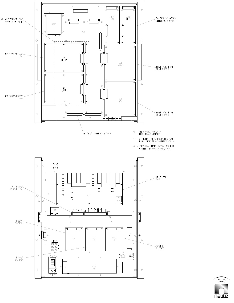
Page 4-2 Vector-LP Radio Beacon Transmitter Technical Instruction Manual
Issue 1.8.1 Section 4 Testing and Adjustment
Figure 4-1 Exciter Panel and Rear View

Vector-LP Radio Beacon Transmitter Technical Instruction Manual Page 4-3
Section 4 Testing and Adjustment Issue 1.8.1
4.3.1.3 Some of the transmitter’s PWBs
may be duplicated and connected as active
(main) and reserve (standby). The front
panel diagnostic display provides selection
of the active side (A or B). The following list
identifies the duplicated PWBs/assemblies
and which are active for a specific
selection. Refer to Figure 4-1 to locate
these assemblies. To locate an assembly’s
adjustment or test point, refer to the
controls and indicators portion of Section 3.
Side A Assemblies
RF Synthesizer PWB.......................................A5
Interphase PDM Driver PWB...........................A6
Exciter Monitor/Generator PWB ......................A7
RF Power Module ..........................................A12
LVPS Module...................................................U2
Side B Assemblies (optional)
RF Synthesizer PWB.......................................A8
Interphase PDM Driver PWB...........................A9
Exciter Monitor/Generator PWB ....................A10
RF Power Module ..........................................A13
LVPS Module...................................................U3
4.3.2 Test Equipment Required
A dummy load rated for twice the
maximum power capability of the
transmitter, an oscilloscope and a digital
multimeter are required to perform the
functional test procedures. Refer to Table
1-2 for recommended test equipment.
4.3.3 Test Prerequisites
The following steps must be completed
prior to performing any of the functional
test procedures:
(a) Verify that nothing affecting the RF
power stage has been changed or
altered since the initial start-up
procedure (described in Section 2 of
this manual) was completed.
(b) Ensure the ac or dc power source is
turned off or disconnected.
(c) Terminate the transmitter's RF output
into a suitably rated, precision 50 ,
load that is able to accurately display
the RF power being applied to it.
WARNING
If there is a jumper between TB1-19 and
TB1-20 on the remote interface PWB,
safety features provided by the external
interlocks are disabled. Implement a
fail-safe method to alert personnel to
this fact. Dangerous voltages will be
present near the RF output and the
antenna system if the transmitter is
turned on under these conditions.
(d) Close all external interlocks or connect
a jumper between TB1-19 and TB1-20
of the remote interface PWB.
NOTE
Remote interface PWB A3 is located on the
back of the front panel.
NOTE
This section makes frequent reference to
Section 3 - Operating Instructions. You
should be familiar with the transmitter’s
operating instructions, specifically the front
panel GUI, before testing or adjusting the
transmitter’s circuits.
4.3.4 Initial Turn-On
Enable the ac or dc power source, turn on
the transmitter, and observe its alarm and
status indicators as follows:
(a) Verify the requirements of paragraph
4.3.3 have been completed.
(b) Turn on (enable) the ac or dc power for
the transmitter. The AC IND lamp on
each RF power module (viewed from
transmitter top) will be on. The
presence and value of ac voltage can
also be viewed on the front panel GUI.
Ensure the transmitter’s RF power
stage is disabled by pressing the
Control - RF OFF switch.
(c) Select local control by pressing the
Control - Local switch.

Page 4-4 Vector-LP Radio Beacon Transmitter Technical Instruction Manual
Issue 1.8.1 Section 4 Testing and Adjustment
NOTE
During initial turn-on and adjustment of
transmitter power, the diagnostic display’s
meters screen should be monitored.
Various input parameters, such as
Forward Power, Average B+ Voltage,
and Total Dc Current should be displayed
while the transmitter RF output power is
being increased.
If the diagnostic display indicates an alarm,
discontinue adjustment of the transmitter
and press the Status button to determine
the nature of the fault.
4.3.5 Standard Adjustments
The following standard adjustments are
described in this section. Verify them after
transmitter commissioning.
4.3.5.1 Setting Sonalert Remote Control
States
4.3.5.2 Setting Low Battery Threshold
4.3.5.3 Setting Default Monitor States
4.3.5.4 Adjusting Audio Limiter
4.3.5.5 Setting Changeover Mode and RF
Monitor Thresholds
4.3.5.6 Verifying Exciter Changeover
Thresholds
4.3.5.7 Setting Mod Depth in Beacon Mode
4.3.5.8 Setting Mod Depth in Beacon and
Voice Mode
4.3.5.9 Setting Standby Codes
4.3.5.10 Setting the Keyer
4.3.5.11 Setting the Antenna Current Level
4.3.5.1 SETTING SONALERT REMOTE
CONTROL STATES
Use the sonalert menu to allow a
transmitter alarm to generate a change in a
control points state. See Configuring the
Sonalert (3.6.10).
4.3.5.2 SETTING LOW BATTERY
THRESHOLD
If a dc power source (battery) is used, see
Selecting Power Source (3.6.9) to set the
DC disconnect and reconnect levels.
4.3.5.3 SETTING DEFAULT MONITOR
STATES
If the optional NDB site interface PWB (A4)
is installed, see 3.6.14.1 and 3.6.14.2 to
set default monitor states.
4.3.5.4 ADJUSTING AUDIO LIMITER
Adjust the audio limit threshold as follows:
(a) Adjust the remote interface PWB (A3)
AUDIO LEVEL potentiometer (R37)
fully clockwise.
(b) Connect an audio signal at the desired
level (between -20 dBm and +10 dBm,
in a 600 load) to the AUDIO INPUT
(+) (TB1-14) and (–) (TB1-16)
terminals of the remote interface PWB.
(c) The system diagram’s External Alarm
LED should turn on.
(d) In the Configure Sonalert menu (see
3.6.10), set the Mod Protection alarm
signal to ON.
(e) In the Select Peripherals menu
(3.6.13.5), select Sonalert Buzzer. The
sonalert will sound an alarm.
(f) Adjust the AUDIO LEVEL
potentiometer counter-clockwise until
the alarm stops, noting there is a five
second delay between the adjustment
and the alarm reaction. The External
Alarm LED should also turn off.
(g) Sweep the test signal’s frequency
across the desired frequency band.
Adjust the AUDIO LEVEL
potentiometer when an audible alarm
occurs so that the level is as high as
possible without generating an alarm.
(h) In the Configure Sonalert menu (see
3.6.10), set the Mod Protection alarm
signal to OFF, if desired.

Vector-LP Radio Beacon Transmitter Technical Instruction Manual Page 4-5
Section 4 Testing and Adjustment Issue 1.8.1
4.3.5.5 SETTING CHANGEOVER MODE
AND RF MONITOR THRESHOLDS
If a standby side is being used, adjust the
transmitter’s high and low RF power limits,
low modulation and tone levels, and the
monitor delay period, as follows:
NOTE
International Civil Aviation Organization
(ICAO) standards dictate the transmitter be
turned off or a warning alarm be generated
when the RF output decreases by at least
3.0 dB or increases by at least 2.0 dB from
the intended carrier level. The user can
alter the monitor settings provided these
criteria are still met.
(a) Disable changeover. Set changeover
control to bypass mode (see 3.6.4).
(b) Set the transmitter to the desired RF
output level.
(c) Set the transmitter for desired
modulation depth in ‘beacon’ (PTT
inactive) and ‘beacon and voice’ (PTT
active) modes (see 3.6.7).
NOTE
If the NDB is to be used only in ‘beacon’ or
‘beacon and voice’ mode, you only need to
set up the NDB for the appropriate mode.
(d) Calculate the desired low modulation
depth for each mode. Set the
transmitter to modulate at these levels.
(e) In the Monitor Timeout screen (see
3.6.7), set the monitor timeout period
(in seconds) and decide whether
shutdown will be enabled or disabled.
(f) In the Power Thresholds screen (see
3.6.7), set the high and low power
limits and press Compute New
Thresholds.
(g) In the Mod % Thresholds screen (see
3.6.7), press Compute New
Thresholds in ‘beacon’ (PTT inactive)
and ‘beacon and voice’ (PTT active)
modes (see 3.6.7). The thresholds
should be updated with the desired
values.
NOTE
At this point the system has automatically
determined to use either a current or
voltage sample to control the modulation
detection and protection circuitry.
(h) Set the transmitter for desired
modulation depth in ‘beacon’ (PTT
inactive) and ‘beacon and voice’ (PTT
active) modes (see 3.6.7).
(i) Enable changeover. Set changeover
control to normal mode (see 3.6.4).
NOTE
Changeover is inhibited when a VSWR of
1.4:1 or greater is present.
(j) Check each threshold to ensure that it
functions properly by adjusting the
transmitter beyond the desired limit
and observing that the transmitter
reacts as expected. For detailed
testing information see 4.3.5.6.
NOTE
If you manually decrease the modulation
depth, the transmitter will inhibit output
power when the tone level is below the
desired threshold. The Keying Gate
Monitor Fail A or B fault will be displayed.
To restore power, increase the modulation
level and reset the fault status.
(k) When complete, restore the transmitter
to the desired power level and press
reset to clear all alarms (see 3.6.3).
Normal operation should resume.
4.3.5.6 VERIFYING EXCITER
CHANGEOVER THRESHOLDS
Verify the exciter changeover thresholds as
follows:
(a) Set the exciter control mode to
NORMAL (see 3.6.4). Set Keyer
Modulation to ON (see 3.6.13.1)
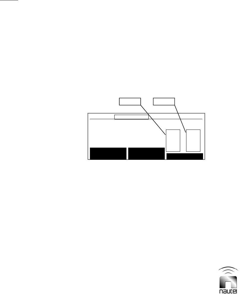
Page 4-6 Vector-LP Radio Beacon Transmitter Technical Instruction Manual
Issue 1.8.1 Section 4 Testing and Adjustment
Ensure that antenna current feedback
is OFF (disabled, see 3.6.15) before
proceeding.
(b) Select the exciter (A or B) that will be
operational for the next year as the
Main Side (see 3.6.4) and note the
forward power level on the screen.
NOTE
For clarity of description this procedure
uses factory default values for changeover
thresholds (3 dB for low RF power, 60% for
low modulation) and timeout values (20
seconds). These thresholds and values are
user adjustable.
(c) From the diagnostic display, select
Main Menu / Settings / Monitor
Settings. The timeout counter should
read 20 sec. (default value; can be
user adjusted).
(d) Decrease the RF power until the
counter begins to count down. The RF
power should be 3 dB (default value,
can be user adjusted) below the
power noted in step (b).
(e) A changeover should occur after the
timeout counter value in step (c). If
not, adjust the RF power to the
original level noted in step (b). Select
Main Menu/Settings/Monitor Settings/
Power Thresholds. Press Continue to
proceed. Press Compute New
Thresholds to establish new power
thresholds. If a modification is made,
a screen appears which prompts you
to save changes to EEPROM. Select
Yes. Return to step (d).
(f) Increase the RF power to the desired
power level noted in step (b). Press
Reset in the Status menu. The
transmitter should switch back to the
main side and the Changeover LED
should no longer be on.
(g) Select Main Menu/Peripherals/Keyer
Settings/Audio Levels.
(h) Note the modulation level. Decrease
the Keying Pot level (see 3.6.13.1).
Power should be inhibited when 60
2% modulation is reached. A
changeover should occur 20 seconds
later. Power should still be inhibited
on the standby side. If not, continue to
decrease the Keying Pot until power is
inhibited on the standby side (this
should also occur at 60 2%
modulation). Press Cancel. Press
Reset in the Status menu. The
transmitter should switch back to the
main side and the Changeover LED
should no longer be on.
(i) Select Main Menu/Settings/Monitor
Settings/Mod % Thresholds. Press
Continue to proceed.
The third row in the Side A column
(63.8 in the example above) should
read 60 2%. The third row in the
Side B column (also 63.8 in the
example above) should read 60 2%.
Mod % Thresholds
Minimum Allowable Tone Modulation Depth:
...PTT Inactive: 164 153
...PTT Active: 1023 1023
63.8 63.8
35.4 35.4
Compute New
Thresholds
Rf Mon: CURR
Toggle Back
12:43:16 Power: 0W Side A Bypass
Mod % Thresholds
Minimum Allowable Tone Modulation Depth:
...PTT Inactive: 164 153
...PTT Active: 1023 1023
63.8 63.8
35.4 35.4
Compute New
Thresholds
Rf Mon: CURR
Toggle Back
12:43:16 Power: 0W Side A Bypass
Mod % Thresholds
Minimum Allowable Tone Modulation Depth:
...PTT Inactive: 164 153
...PTT Active: 1023 1023
63.8 63.8
35.4 35.4
Compute New
Thresholds
Rf Mon: CURR
Toggle Back
12:43:16 Power: 0W Side A Bypass
Side A Side B

Vector-LP Radio Beacon Transmitter Technical Instruction Manual Page 4-7
Section 4 Testing and Adjustment Issue 1.8.1
(j) If the requirements of step (i) are not
met, set the transmitter to operate in
BYPASS mode. Press Reset in the
Status menu. The transmitter should
switch back to the main side and the
Changeover LED should no longer
be on.
(k) Decrease the modulation depth
(Keying Pot level) to 60%. Select Main
Menu/Settings/Monitor Settings/Mod
% Thresholds. Press Continue to
proceed. Press Compute New
Thresholds to establish new monitor
modulation % thresholds. If a
modification is made, a screen
appears which prompts you to save
changes to EEPROM. Select Yes.
Increase the modulation depth to the
desired level. Set changeover mode
to NORMAL. Return to step (g).
(l) Select Main Menu/Peripherals/Keyer
Settings/Audio Levels.
(m) The modulation levels should be as
close to desired modulation without
distortion.
4.3.5.7 SETTING MOD DEPTH IN
BEACON MODE
Set the modulation depth in beacon (no
voice) mode as follows:
(a) Ensure there is no link between the
PRESS-TO-TALK terminal (TB1-12)
and GND (TB1-13) on the remote
interface PWB (A3).
(b) In the Keyer Modulation menu (see
3.6.13.1), set Modulation and Tone
Generator to ON and set Keyer to
OFF. Set the Tone Frequency to 400
Hz or 1020 Hz.
(c) In the Audio Levels menu (see
3.6.13.1), set Keying Pot to 0.
(d) Press RF On. Increase the
transmitter’s output to desired power.
(e) In the Audio Levels menu, while
monitoring the Mod %, increase the
Keying Pot value until the Mod % is as
desired. If the modulating signal begins
to distort, stop increasing mod depth.
(f) In the Keyer Modulation menu, set
Keyer to ON.
4.3.5.8 SETTING MOD DEPTH IN
BEACON AND VOICE MODE
Set the modulation depth in PTT (beacon
and voice) mode as follows:
(a) Adjust the audio limiter as described in
4.3.5.4. The audio generator should
remain connected.
(b) Assert Press–To-Talk. The status
screen should indicate press to talk.
NOTE
If the system is in normal mode, connect a
link between the PRESS-TO-TALK
terminal (TB1-12) and GND (TB1-13) on
the remote interface PWB (A3). If the
system is being used in phantom feed
mode, apply -15 V down the shield of the
audio signal (see 2.2.13).
(c) In the Keyer Modulation menu (see
3.6.13.1), set Modulation to ON and
set Keyer and Tone Generator to OFF.
(d) In the Audio Levels menu (see
3.6.13.1), set Voice Pot and Keying
Pot to 0.
(e) Press RF On. Increase the
transmitter’s output to rated power.
(f) In the Audio Levels menu, while
monitoring the Mod %, increase the
Voice Pot value until the Mod % is at
the desired depth. If the modulating
signal begins to distort, stop increasing
the modulation depth.
(g) Turn off the audio generator.

Page 4-8 Vector-LP Radio Beacon Transmitter Technical Instruction Manual
Issue 1.8.1 Section 4 Testing and Adjustment
(h) In the Keyer Modulation menu, set
Modulation and Tone Generator to ON.
Set the Tone Frequency to 400 Hz or
1020 Hz.
(i) In the Audio Levels menu, while
monitoring the Mod %, increase the
PTT Keying Pot value until the Mod %
is at the desired depth. If the
modulating signal begins to distort,
stop increasing the modulation depth.
The total modulation depth cannot
exceed 95%.
(j) In the Keyer Modulation menu, set
Keyer to ON.
4.3.5.9 SETTING STANDBY CODES
See 3.6.13.1, Setting the Keyer.
4.3.5.10 SETTING THE KEYER
See Setting the Keyer (3.6.13.1).
4.3.5.11 SETTING THE ANTENNA
CURRENT LEVEL
Adjust the antenna current to the desired
level and set the antenna current feedback
feature as follows:
(a) Ensure the serial interface cable is
installed between the transmitter (at
the INTERNAL RS-485 connector on
remote interface PWB A3) and the
ATU.
(b) Apply power to the ATU.
(c) In the Power menu (see 3.6.15), set
the antenna current feedback to OFF.
(d) Adjust the transmitter for the desired
antenna current by adjusting the output
power level.
(e) Ensure that the changeover mode and
monitor thresholds have been set (see
4.3.5.5)
(f) In the Power menu, set the antenna
current feedback to ON.
NOTE
When antenna current feedback is
enabled, the transmitter will adjust the
output power to ensure that antenna
current remains constant. With each
power adjustment, a new high and low
forward power threshold is calculated. In
this case the low and high power
thresholds have essentially become low
and high antenna current thresholds.
4.3.6 Non-Standard Adjustments
The following non-standard adjustments
are described in this section. They have
been factory set prior to shipping and do
not require verification or re-calibration
unless an unintentional adjustment has
been made or a fault has occurred.
4.3.6.1 Changing Frequency
4.3.6.2 Changing RF Filter Tap Settings
4.3.6.3 Calibrating Transmitter Output Power
4.3.6.4 Calibrating Exciter Dc Voltages and
Ambient Temperature
4.3.6.5 Calibrating PDM
4.3.6.6 Calibrating Reflected Power
Threshold and Output Network Alarm
4.3.6.7 Setting the RF Monitor Level
4.3.6.8 Calibrating the Ac Failure Alarm
4.3.6.9 Adjusting for RF Drive Symmetry
4.3.6.10 Equalizing Exciter Gain (Dual Exciter
Transmitters Only)
4.3.6.11 Calibrating Battery Voltage, Current
and Charger Current(Optional)
4.3.6.12 Setting Display Contrast
4.3.6.13 Adjusting Speaker Volume
4.3.6.14 Reading Modulation Level
(a) Verify the initial turn-on requirements
of paragraph 4.3.4 have been
completed and are being met.
4.3.6.1 CHANGING FREQUENCY
To perform a frequency change, perform
the following steps in order:
(a) Press RF Off.

Vector-LP Radio Beacon Transmitter Technical Instruction Manual Page 4-9
Section 4 Testing and Adjustment Issue 1.8.1
(b) On the RF synthesizer PWB(s),
change the carrier frequency using
BCD switches S1 through S5. Each
switch represents one of the five most
significant digits in the carrier
frequency expressed in kHz:
- S1 is thousands digit (x1000)
- S2 is hundreds digit (x100)
- S3 is tens digit (x10)
- S4 is units digit (x1)
- S5 is the tenths digit (x0.1)
(c) If the Frequency Monitor feature is
enabled, adjust the Carrier Frequency
(kHz) (in the Set Thresholds menu;
see 3.6.12.2) to the operational carrier
frequency.
(d) Perform RF drive symmetry testing
and adjustment procedures (see
4.3.6.9).
(e) Change the RF filter tap settings (see
4.3.6.2).
(f) Calibrate the transmitter’s output
power (see 4.3.6.3).
4.3.6.2 CHANGING RF FILTER TAP
SETTINGS
For a frequency change, change the tap
settings on the RF filter PWB as follows:
NOTE
If your frequency is changing between the
standard frequency band (190 - 535 kHz)
and the extended frequency band (535 –
1800 kHz), you will need to change the RF
filter PWB (A14). Contact Nautel.
(a) Turn off the RF power and the ac and
dc circuit breakers.
(b) Remove the rear cover from the
transmitter to gain access to the RF
filter PWB (A14).
(c) Enter the frequency into Table 2-6a
(standard frequencies) or 2-6b (high
frequencies, VR125 only) to determine
the tap settings for the six jumpers.
Connect the jumpers to the appropriate
taps.
(d) Turn on the ac and dc circuit breakers.
(e) Install the rear cover on the transmitter
and perform the calibration in 4.3.6.3.
4.3.6.3 CALIBRATING TRANSMITTER
OUTPUT POWER
Calibrate the transmitter’s forward power
and related parameters as follows:
(a) Select reflected power to be monitored
on the exciter/control assembly’s front
panel analog meter (see 3.6.8.2).
(b) Select side A in the Changeover
Control menu. Go to the Power Module
menu.
(c) Monitor TP17 of interphase PDM driver
PWB A (A6) with an oscilloscope.
(d) Set the RF output to 0 W by pressing
the Power Increase and Power
Decrease buttons at the same time.
(e) Press RF On. Ensure all side A RF
power module fans turn on (VR250
only). Set modulation to 0%.
(f) While monitoring the PA voltage for the
side A RF power module (see
3.6.13.2), slowly increase the RF
output power until the PA voltage is
65 V. Stop increasing power if at any
time:
the PA voltage between RF power
modules varies by more than 5%, or
the reflected power on the analog
meter increases above 10 W
(g) Use an external current probe to verify
that the output power is 100 20 W.

Page 4-10 Vector-LP Radio Beacon Transmitter Technical Instruction Manual
Issue 1.8.1 Section 4 Testing and Adjustment
(h) Increase power to rated or maximum,
whichever is lower. Use an external
current probe and the following formula
to determine the output power:
Power = Current2 x Rload
(i) In the Maximum Output Gain menu
(see 3.6.12.3), calibrate the duty cycle
and forward power as follows:
Highlight the value for Set Duty Cycle.
Press Modify.
Change the value to match the positive
duty cycle measured at TP17 in step
(c). Press Next.
Change the value for Set Forward
Power to match the power calculated
in step (h).
(j) If the transmitter is operating at full
power, go to step (l). If not:
Highlight the value for Maximum
Carrier Reference. Press Modify.
Increase the value by 5. Press Done.
(k) Return to step (h).
(l) Set the maximum carrier reference:
Record the current duty cycle and
forward power values.
Record the power according to the
external current probe.
Highlight the value for Maximum
Carrier Reference. Press Modify.
Adjust the value to 1 higher than the
current Carr. Ref value. Press Done.
(m) The initial Forward Power
measurement should be within 20 % of
the actual value. In the Calibrate
Meters menu (see 3.6.12 and 3.6.12.1)
calibrate the Forward Power.
Scroll through the parameters until
Forward Power is highlighted. Press
Modify.
Adjust the reading to the same value
calculated in step (h). Record this
level. Press Done.
(n) Increase the power until maximum
power is reached. Record the power
level on the top line (status bar) of the
GUI display.
(o) Press Power Increase and Power
Decrease at the same time to set the
RF power to 0 W. Press RF Off.
4.3.6.4 CALIBRATING EXCITER DC
VOLTAGES AND AMBIENT
TEMPERATURE
(a) Measure and record the following dc
voltages on the control/display PWB
(A1):
TP18 (approx. 24 V)
TP12 (approx. 15 V)
TP20 (approx. -15 V)
TP9 (approx. 5 V)
(b) In the Calibrate Meters menu (see
3.6.12 and 3.6.12.1) scroll through the
parameters until +24 Volt P/S is
highlighted. Press Modify.
(c) Adjust the value to match the TP18
voltage measured in step (a). Press
Done.
(d) Repeat step (c) to calibrate the other
parameters:
+15 Volt P/S (measured on TP12)
-15 Volt P/S (measured on TP20)
+5 Volt P/S (measured on TP9)
AC Voltage
Temperature (use a thermometer to
measure the ambient room
temperature

Vector-LP Radio Beacon Transmitter Technical Instruction Manual Page 4-11
Section 4 Testing and Adjustment Issue 1.8.1
NOTE
When you exit the Calibrate Meters menu a
message is displayed indicating that you
have made changes. You will be prompted
to save the changes to EEPROM so that
they can be restored in the event of a
power failure. Press Yes each time this
prompt is displayed during the setup
procedure.
During initial turn-on and adjustment of
transmitter power, the diagnostic display’s
meters screen should be monitored.
4.3.6.5 CALIBRATING PDM
(a) Use an oscilloscope to monitor TP17 of
the active interphase PDM driver PWB
(A6 for side A or A9 for side B).
(b) Press RF On. Set modulation to 0%.
(c) In the Calibrate Meters menu (see
3.6.12 and 3.6.12.1) scroll through the
parameters until PDM A (or PDM B,
depending on the transmitter’s active
side) is highlighted. Press Modify.
(d) Adjust the value to match the positive
duty cycle measured on TP17 in step
(a). Press Done.
4.3.6.6 CALIBRATING REFLECTED
POWER THRESHOLD AND OUTPUT
NETWORK ALARM
(a) Turn off the transmitter and disconnect
the dummy load from the transmitter’s
RF output. Short the transmitter’s RF
output to ground near the RF output.
Install the external current probe on the
shorting jumper.
(b) In the Set Thresholds menu (see
3.6.12 and 3.6.12.2) set the Slowback
Pwr (Per Block) value to 100 W.
(c) Set RF output power to 0 W. Press RF
On. Monitor the external current while
slowly increasing the power to half of
the reflected power limit. Try to achieve
a current of 1.8 A (should occur at
approximately 40 W).
(d) Calculate the actual reflected power
using the following equation:
Refld Pwr = (Ishort circuit / 2)2 x 50
(e) In the Calibrate Meters menu (see
3.6.12 and 3.6.12.1) scroll through the
parameters until Reflec. Power is
highlighted. The Reflec. Power value
should be within 20% of the value
determined in step (d).
Press Modify.
Adjust the value to match the level
calculated in step (d). Press Done.
(f) Press Back and select Set
Thresholds.
(g) Press , or Next until Refl. Power
Shutback is displayed.
Monitor the external current while
slowly increasing the power to the
reflected power limit. Try to achieve a
current of 2.5 A (should occur at
approximately 80 W).
(h) If an Output Network alarm occurs
before reaching the reflected power
limit, increase the Refl. Power
Shutback threshold level and press
Done and return to step (h). Otherwise
continue to step (j).
(i) Decrease the Refl. Power Shutback
threshold level until the Output
Network alarm occurs. Press Done.
(j) In the Set Thresholds menu, set the
Slowback Pwr to 30 W (for VR250) or
15 W (for VR125).

Page 4-12 Vector-LP Radio Beacon Transmitter Technical Instruction Manual
Issue 1.8.1 Section 4 Testing and Adjustment
(k) Verify the reflected power cutback is
below 30 W (for VR250) or 15 W (for
VR125). Press RF Off.
(l) Remove the shorting jumper from the
transmitter’s RF output. Reconnect the
dummy load to the transmitter’s RF
output.
4.3.6.7 SETTING THE RF MONITOR
LEVEL
(a) Increase the transmitter’s RF output to
full power.
(b) Connect a 50 load to the RF
MONITOR BNC connector (J8 of
remote interface PWB A3, accessible
at the back of the front panel. Monitor
the voltage with an oscilloscope.
(c) Adjust the remote interface PWB’s
MONITOR LEVEL potentiometer
(R163) until the voltage is 1.0 V RMS.
4.3.6.8 CALIBRATING THE AC FAILURE
ALARM
(a) With the transmitter connected to a
suitably rated dummy load, press RF
On and increase to rated power.
(b) Measure the dc voltage at TP13 on the
control/display PWB (A1). Calculate
and record the low ac voltage
reference:
For VR250:
Low AC ref = 170 x TP13/Ac Voltage
For VR125:
Low AC ref = 90 x TP13/Ac Voltage
(c) Monitor the dc voltage at TP19 on the
control/display PWB.
(d) In the Set Thresholds menu (see
3.6.12 and 3.6.12.2), scroll to the Low
AC Voltage threshold. Press Modify.
(e) Adjust the Low AC Voltage value until
the voltage at TP19 matches the low
ac voltage reference calculated in step
(b). Press Done.
(f) Turn off the transmitter’s ac power. If
testing is required, connect a variac
between the ac power source and the
transmitter. Turn on the ac power.
(g) Use the variac to decrease the ac
voltage until the System Diagram’s AC
Mains LED. The Diagnostic Display
should display both Shutback A and
Low AC. Record the ac voltage.
(h) Press RF Off.
(i) Turn off the ac power and disconnect
the variac. Reconnect ac to the
transmitter.
4.3.6.9 ADJUSTING FOR RF DRIVE
SYMMETRY
Measure the symmetry of the RF drive
applied from the active RF synthesizer
PWB to the RF power modules as follows:
(a) Select the side for the symmetry
adjustment.
(b) Press RF On and set the transmitter’s
RF output power to 0 W.
(c) Connect an oscilloscope between TP2
(TP1 for side B) and ground on the
exciter interface PWB (A2).
(d) The oscilloscope should indicate a
symmetrical (50% duty cycle) square
wave with a nominal amplitude of 5 V
peak-to-peak.
(e) Adjust the appropriate RF synthesizer
PWB’s SYMMETRY potentiometer
(R32) to obtain a 50 1 % duty cycle.

Vector-LP Radio Beacon Transmitter Technical Instruction Manual Page 4-13
Section 4 Testing and Adjustment Issue 1.8.1
NOTE
If an external RF generator is producing
the RF drive, verify its output waveform is
symmetrical.
4.3.6.10 EQUALIZING EXCITER GAIN
(Dual Side Transmitters Only)
If the RF output of the transmitter varies
between side A and B, you may need to
equalize the exciter gain. Equalize the
PDM pulse train between sides A and B so
that no change in RF output level occurs
during exciter changeover, as follows:
(a) Go to the Power Module Status menu
(see 3.6.13.2).
(b) Use an oscilloscope to monitor TP17 of
interphase PDM driver PWB A (A6).
(c) On interphase PDM driver PWB A
(A6), adjust the GAIN TRIM
potentiometer (R31) four turns counter
clockwise and one and a half turns
clockwise. On interphase PDM driver
PWB B (A9), adjust the GAIN TRIM
potentiometer (R31) four turns counter
clockwise.
(d) Press RF On. Increase the
transmitter’s RF output to full rated or
maximum power, whichever is lower.
(e) Use an external current probe to
measure RF output power:
Power = Current2 x Rload
(f) In the Maximum Output Gain menu
(see 3.6.12.3), calibrate the duty cycle
and forward power as follows:
Highlight the value for Set Duty Cycle.
Press Modify.
Change the value to match the positive
duty cycle measured at TP17 in step
(c). Press Next.
Change the value for Set Forward
Power to match the power calculated
in step (e). Press Done.
(g) If the transmitter is operating at full
power, go to step (o). If not:
Highlight the value for Maximum
Carrier Reference. Press Modify.
Increase the value by 5. Press Done.
(h) Repeat step (e).
(i) Set the maximum carrier reference:
Record the current duty cycle and
forward power values.
Record the power according to the
external current probe.
Highlight the value for Maximum
Carrier Reference. Press Modify.
Adjust the value to 1 higher than the
current Carr. Ref value. Press Done.
(j) Increase the power until maximum
power is reached. Record the power
level on the top line (status bar) of the
GUI display.
(k) Press Power Increase and Power
Decrease at the same time to set the
RF power to 0 W. Press RF Off.
(l) Select side B in the Changeover
Control menu.
(m) Press RF On. Ensure all side B RF
power module fans are on.
(n) Press Power Increase until you reach
maximum power. Adjust GAIN TRIM
potentiometer R31 on interphase PDM
driver PWB B (A9) to ensure that the
output power matches the output
power recorded in step (j).

Page 4-14 Vector-LP Radio Beacon Transmitter Technical Instruction Manual
Issue 1.8.1 Section 4 Testing and Adjustment
4.3.6.11 CALIBRATING BATTERY
VOLTAGE, BATTERY CURRENT AND
CHARGER CURRENT (Optional)
NOTE
This procedure applies to transmitters that
use a dc power source and the battery
boost PWB (A16).
(a) Press RF Off.
(b) Open the dc breaker and remove ac
power from the transmitter. Disconnect
the positive lead of the battery from the
terminal block (TB1) on the battery
boost PWB (A16). Reconnect the
positive lead of the battery to TB1-3 on
the battery boost PWB.
(c) Connect a link, using 14 AWG wire,
between TB1-4 and TB1-1 on the
battery boost PWB. Close the dc
breaker.
(d) Measure and record the dc voltage
between TB1-1 and TB1-2 on the
battery boost PWB.
(e) In the Calibrate Meters menu (see
3.6.12 and 3.6.12.1) scroll through the
parameters until Battery Voltage is
highlighted. Press Modify.
(f) Adjust the value to match the voltage
measured in step (a). Press Done.
NOTE
When you exit the Calibrate Meters menu a
message is displayed indicating that you
have made changes. You will be prompted
to save the changes to EEPROM so that
they can be restored in the event of a
power failure. Press Yes each time this
prompt is displayed during the setup
procedure.
(g) In the Power Source Select menu,
change the transmitter’s Requested
Power Source to DC (see 3.6.9).
(h) Press RF On and increase the RF
output to rated power.
(i) Use a clip-on dc current meter to
measure the current between the
battery and TB1-3 of the battery boost
PWB.
(j) In the Calibrate Meters menu scroll
through the parameters until Battery
Current is highlighted. Press Modify.
(k) Adjust the value to match the current
measured in step (i). Press Done.
(l) In the Calibrate Meters menu scroll
through the parameters until Charger
Current is highlighted. Press Modify.
(m) Adjust the value to match the current
measured in step (i). Press Done.
(n) Press RF Off.
(o) Open the dc breaker. Remove the link,
between TB1-4 and TB1-1 on the
battery boost PWB. Disconnect the
positive lead of the battery from TB1-3
on the battery boost PWB and
reconnect it to TB1-1.
(p) Close the dc breaker and reapply ac
power to the transmitter.
(q) In the Power Source Select menu,
change the transmitter’s Requested
Power Source to AC (see 3.6.9).
4.3.6.12 SETTING DISPLAY CONTRAST
Set the contrast of the diagnostic display’s
GUI as follows:
(a) In the Set Thresholds menu (see
3.6.12 and 3.6.12.2), scroll to the LCD
Display Contrast threshold. Press
Modify.
(b) Adjust the contrast to the desired level.
Press Done.
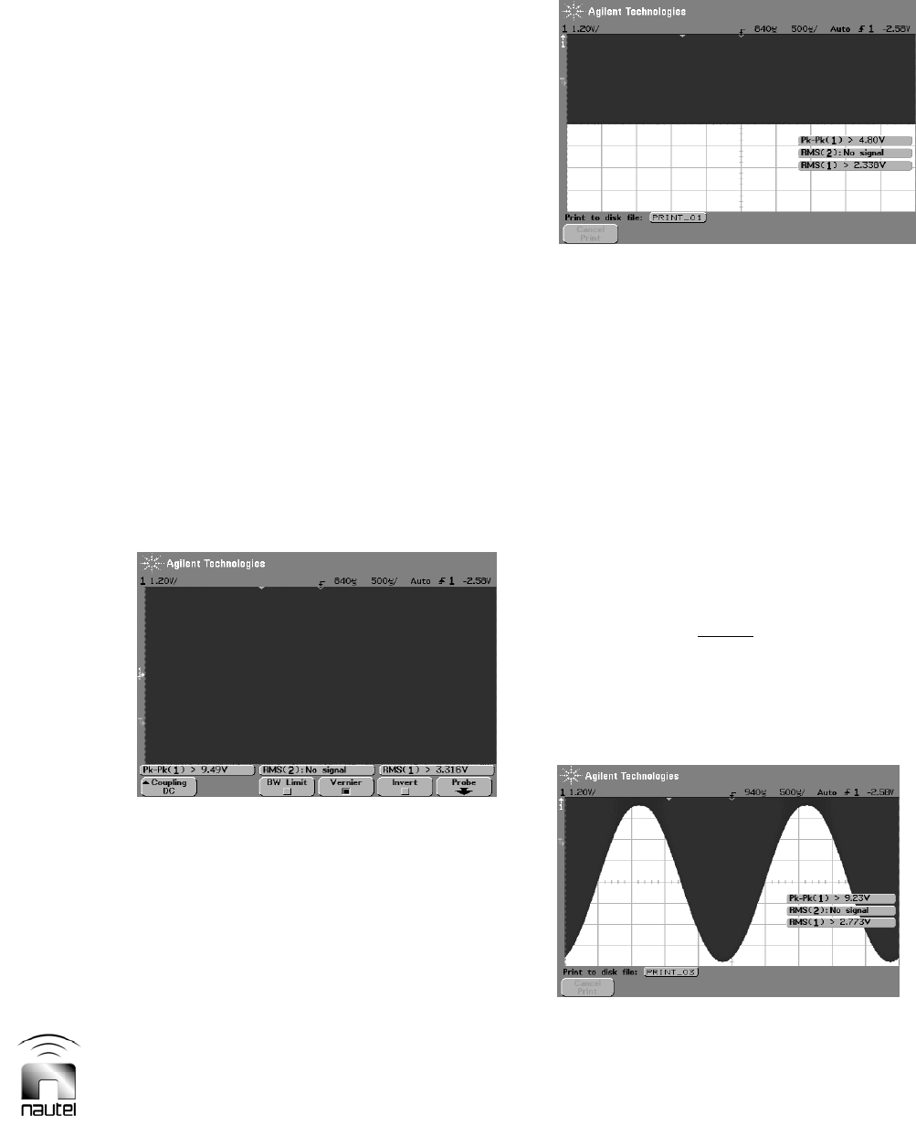
Vector-LP Radio Beacon Transmitter Technical Instruction Manual Page 4-15
Section 4 Testing and Adjustment Issue 1.8.1
4.3.6.13 ADJUSTING SPEAKER
VOLUME
See Setting Protection Thresholds
(3.6.12.2). Adjust the Audio parameter as
desired.
4.3.6.14 READING MODULATION LEVEL
Read the modulation level as follows:
(a) Connect an oscilloscope to the RF
MONITOR connector (J8) on the
remote interface PWB (A3).
(b) Set the exciter in CW mode: use ▲
and ▼ to scroll the display and set
Modulation to OFF using the Toggle
switch.
(c) Adjust the oscilloscope’s timescale to
500 s per division (for 400 Hz
modulation). Adjust the amplitude
level of the oscilloscope to just cover
all eight divisions of the display with
the RF signal (see Figure 4-2).
Figure 4-2: CW signal set to fill display
(d) Adjust the position of the oscilloscope
signal so that the bottom of the CW
waveform is at the mid-point of the
display (see Figure 4-3).
Figure 4-3: CW signal with position
adjusted to mid-point of display
(e) Set the exciter in MCW mode: use ▲
and ▼ to scroll the display and set
Modulation to ON and the Keyer to
OFF using the Toggle switch.
(f) Measure the bottom of the waveform.
Each sub-division should correspond
to 5% in modulation. The bottom of
the waveform should be one sub-
division above the bottom of the
display when the modulation is at 95%
(see Figure 4-4).
NOTE
There may be some distortion in the
trough. This is an effect of class D
amplification called pinch off and can be
ignored as it does not produce significant
total harmonic distortion (THD).
Figure 4-4: MCW signal, 95% modulation

Page 4-16 Vector-LP Radio Beacon Transmitter Technical Instruction Manual
Issue 1.8.1 Section 4 Testing and Adjustment
(g) If the modulation level requires
adjustment select Main Menu/
Peripherals/Keyer Settings/Audio
Levels.
(h) Adjust the Keying Pot (in Press-to-talk
mode adjust the PTT Keying Pot) to
get the desired level of modulation.
This adjustment will affect both
exciters.
(i) Check if the reading on the diagnostic
display agrees with the oscilloscope
measurement. If necessary calibrate
the meter as described in 3.6.12.1.

Vector-LP Radio Beacon Transmitter Technical Instruction Manual Page 5-1
Section 5 Maintenance and Troubleshooting Issue 1.8.1
Vector-LP Radio Beacon Transmitter
TECHNICAL INSTRUCTION MANUAL
Section 5 MAINTENANCE AND TROUBLESHOOTING
5.1 GENERAL
This section contains scheduled and
corrective maintenance information for the
Vector-LP transmitter. Fault symptoms
should be analyzed to determine the
corrective action required. Troubleshooting
information (see paragraph 5.5) is
presented based on the exciter panel’s
diagnostic information.
CAUTION
The Vector-LP transmitter contains many
solid state devices that may be damaged if
subjected to excessive heat or high voltage
transients. Ensure circuits are not
overdriven or disconnected from their loads
while turned on.
5.2 SCHEDULED MAINTENANCE
Scheduled maintenance consists of
performing a visual inspection of the
transmitter at scheduled intervals. The
recommended minimum time between
scheduled maintenance visits is one year.
Local operating and environmental
conditions may dictate more frequent visits
and in remote sites, less frequent visits
may be acceptable. Experience and
system reliability will determine the most
practical schedule for a specific installation.
5.2.1 Cleaning the Transmitter
As a minimum, perform the following
cleaning procedures:
NOTE
A site located in a dirty area using open-air
cooling requires more extensive cleaning
than a site located in a clean area using
closed-air cooling.
Once a year, clean the transmitter
using a vacuum cleaner and a soft-
bristle brush to remove loose dirt. Use
clean, damp rags to remove dirt that
cannot be vacuumed. NEVER use
compressed air to clean the
transmitter.
For VR250 transmitters only: Once a
year, inspect and clean air filters using
soap and warm water. If the air filters
are damaged, replace them as soon as
possible.
5.2.2 Checking Hardware
All hardware MUST be checked at least
once a year. Thermal cycling from turning
the transmitter on and off will require more
frequent checks.
Ensure the proper sized tools are used
to prevent damaging the hardware. In
most cases, hardware is metric.
A mounting surface or terminal that
has changed colour indicates a loose
hardware connection.
Multi-stranded cables installed on
terminal strips MUST be re-torqued.
5.2.3 Battery Replacement
The transmitter's control/display PWB
contains a battery backup circuit that
provides a memory of alarm occurrences
during ac power failure. The battery
should be replaced at least once a year or
whenever the diagnostic display on the
exciter/control assembly’s front panel
indicates a ‘low NVRM battery’ message.

Page 5-2 Vector-LP Radio Beacon Transmitter Technical Instruction Manual
Issue 1.8.1 Section 5 Maintenance and Troubleshooting
5.3 CORRECTIVE MAINTENANCE
Corrective maintenance procedures consist
of identifying and correcting defects or
deficiencies that arise during operation of
the transmitter. Local/remote alarm signals
are generated when a malfunction occurs.
The nature of the fault and station policy
dictates whether immediate maintenance
response is necessary. Fault analysis and
rectification may be conducted from three
different levels with a different technical
competence level required for each.
5.3.1 On-Air Troubleshooting
On-air troubleshooting can be performed
from a remote location or locally at the
transmitter site.
5.3.1.1 Remote Troubleshooting
Remote on-air troubleshooting consists of
monitoring the transmitter's RF output
using an on-air monitor and polling the
status of the transmitter using the optional
remote control and monitoring software.
This information enables you to decide if a
response is deferred to a more convenient
time, if immediate corrective action is
taken, and whether a standby transmitter is
enabled (if available). Nautel recommends
you incorporate the significance of remote
indications and the appropriate responses
into the station’s standard operating
procedures. Refer to paragraph 5.5 to
determine the troubleshooting action
required for a given fault.
5.3.1.2 Local Troubleshooting
Local on-air troubleshooting consists of
monitoring the transmitter's diagnostic
display and fault alarm indicators. Analysis
of their status normally identifies the type of
fault and in most cases determines what
corrective action must be taken. Refer to
paragraph 5.5 to determine the
troubleshooting action required for a given
fault.
5.3.2 Off-Air and Standby Side
Troubleshooting
Off-air troubleshooting is performed when
proper operation cannot be restored. In
dual side (A and B) transmitters, if an
active side PWB or assembly is defective,
the transmitter automatically changes over
allowing safe replacement of the defective
PWB or assembly. You can remove the RF
power module from the active side, but a
changeover (for dual side applications) or
inhibit (for single side applications) will
occur. Troubleshooting for a majority of
standby side faults can be performed using
the test standby side troubleshooting menu
(paragraph 3.6.13.4).
For off-air troubleshooting procedures,
Nautel recommends you connect the
output to a precision 50 , resistive
dummy load (rated for twice the
transmitter’s maximum carrier power). If a
suitable dummy load is not available, the
transmitter may remain connected to its
antenna for these procedures. When it is
necessary to troubleshoot faults in the
power amplifier stage, reduce the RF
output level to a minimal value when the
RF output is connected to the antenna.
5.4 ELECTROSTATIC PROTECTION
The transmitter's assemblies contain
semiconductor devices that may be
damaged by electrostatic discharge. Before
removing an assembly from the transmitter,
and while servicing an assembly, observe
the following precautions:
NOTE
Electrostatic energy is produced when two
insulating materials are rubbed together. A
person wearing rubber-soled shoes,
walking across a nylon carpet or a waxed
floor can generate an extremely large
electrostatic charge. This effect is
magnified during periods of low humidity.
This high voltage may damage
components such as integrated circuits,
field-effect transistors, thyristors, and
Schottky diodes unless adequate
precautions are taken.

Vector-LP Radio Beacon Transmitter Technical Instruction Manual Page 5-3
Section 5 Maintenance and Troubleshooting Issue 1.8.1
5.4.1 Discharging of Personnel
Maintainers should be electrically
discharged by a suitable grounding
system (anti-static mats, grounding
straps) during removal of an assembly
from the exciter and while handling the
assembly for maintenance procedures.
5.4.2 Handling/Storage
A sub-assembly should be placed in an
anti-static bag when it is not installed in the
exciter or when it is not being subjected to
maintenance procedures. Electronic
components should be stored in anti-static
materials.
5.4.3 Tools/Test Equipment
Testing and maintenance equipment,
including soldering (for example: Irons with
grounded tips) and unsoldering tools,
should be suitable for contact with static
sensitive semiconductor devices.
5.4.4 Stress Current Protection
Protect static sensitive semiconductor
devices from unnecessary stress current
as follows:
Ensure electrical connections are not
broken while current is flowing in the
circuit.
Ensure voltages are not present on
external control/monitoring circuits
when they are connected.
5.5 TROUBLESHOOTING FRONT
PANEL ALARMS
Front panel fault analysis can be performed
from the exciter panel. There are several
ways to use the front panel to determine
the occurrence and origin of a fault:
The system diagram is a flow diagram
that indicates the operational status of
various sections of the transmitter. If a
lamp is on (red), a fault is occurring in
the associated section of the
transmitter.
The diagnostic display’s meter screen
has real-time meter indications (e.g.,
forward power) to assist in fault
analysis.
The diagnostic display’s main screen
will indicate when a fault is occurring.
Press the Status soft key to display all
active faults.
The diagnostic display’s Events Log
(see paragraph 3.6.5) provides a
chronological list of faults/events as
well as root cause information to assist
in fault diagnosis.
NOTE
It is important to consider both the real-time
and the logged information when
troubleshooting. Displayed active faults
may or may not be the root cause of the
problem. The Events Log displays the root
cause of an event (i.e., the first fault
detected), which may have been transient,
but resulted in other faults that remain
active. It also displays the status of certain
parameters at the time of the event.
(a) Determine the origin of the fault by
noting which of the system diagram’s
lamps has turned on. If no system
diagram lamp is on, proceed to step (b)
for non-alarm troubleshooting tips.
NOTE
In dual side (A and B) transmitters, some
faults will also initiate a Changeover
alarm. In this case, the transmitter will
continue to operate using the standby side.
This may allow troubleshooting (and
subsequent repair) to be deferred to a
more convenient time.
NOTE
The troubleshooting procedures in this
manual are limited to module level checks
and sub-assembly replacement.

Page 5-4 Vector-LP Radio Beacon Transmitter Technical Instruction Manual
Issue 1.8.1 Section 5 Maintenance and Troubleshooting
(b) From the diagnostic display’s main
screen, press the Status button. Note
the alarm indication(s) and refer to
Table 5-1 for troubleshooting tips,
which may also reference replacement
and subsequent re-calibration
procedures.
(c) The diagnostic display will indicate the
current active faults and more
specifically identify the nature of the
fault.
e.g., PDM Drive A Fail
(d) Attempt to clear the alarm by pressing
the reset button. If the alarm persists,
it will not be cleared from the display.
(e) In the example given in step (c), a
PDM Drive A Fail has occurred
indicating a problem with exciter A’s
interphase PDM driver PWB. The
suspect PWB should be replaced as
detailed in paragraph 5.8.1.2.
NOTE
For dual side transmitters, a changeover
to the standby side should also occur.
Determine which side caused the fault,
noting it is the opposite side to that
displayed on the transmitter status bar at
the top of the diagnostic display.
Viewing the diagnostice display’s Events
Log (see paragraph 3.6.5) can also assist
in diagnosing a fault.
(f) Other fault indications may prompt the
troubleshooter to replace other PWBs/
assemblies or an RF power module
(e.g., PA Alarm A indicates a fault has
occurred on the side A RF power
module).
NOTE
Replacement procedures (paragraphs 5.6,
5.8 and 5.9) are provided for RF power
modules and PWBs/assemblies that
require specific removal/installation or
adjustment instructions. Instructions have
not been included for assemblies that are
straightforward to replace and require no
re-calibration.
(g) If replacement of a suspect PWB or
assembly does not remove the fault
condition, contact Nautel.

Vector-LP Radio Beacon Transmitter Technical Instruction Manual Page 5-5
Section 5 Maintenance and Troubleshooting Issue 1.8.1
Table 5-1: Troubleshooting and Replacement Tips
Front Panel
LED Status
Message Action See Troubleshooting/
Replacement Paragraph See Re-calibration
Paragraph
AC Mains Low AC Voltage The ac voltage is less than 170 V ac (or 90 V ac for VR125 transmitters). If the ac source voltage is present,
check the ac breaker at the back of the transmitter. If the breaker is OK, replace the interface PWB (A11).
5.8.3 N/A
Low Voltage Power Supply LVPS Fault A or B Replace associated ac/dc universal input power supply [side A (U2) or side B (U3)]. N/A N/A
Power Supply Over Voltage PS
A or B
Replace switch mode power supply PWB (A2 of associated RF power module). 5.6.1 3.6.13.4 (ensure the
replaced/repaired module is
on the standby side)
Power Supply Over Current PS
A or B
Replace switch mode power supply PWB (A2 of associated RF power module).
If the transmitter is running in dc mode (optional), and this alarm is indicated on the active side, replace
battery boost assembly A16. Otherwise, check cabling between A7 and A3 through A6.
5.6.1
5.9
3.6.13.4 (ensure the
replaced/repaired module is
on the standby side)
Power Supply High Temp PS
A or B
Check fans. Ensure they are spinning at an adequate speed (a minimum of 3000 RPM, see 3.6.13.2). If
necessary, replace the appropriate fan.
N/A N/A
Power Supply PS A or B Missing Module An RF power module has been removed from the associated side. N/A N/A
PA Modulator Fail
A or B
Check/replace FET on modulator assembly (A5 of associated RF power module). 5.6.1
5.7
3.6.13.4 (ensure the
replaced/repaired module is
on the standby side)
PA PA Alarm
A or B
Check/replace FETs on power amplifier (A3 of associated RF power module). 5.6.1
5.7
3.6.13.4 (ensure the
replaced/repaired module is
on the standby side)
PA PDM Inhibit A or B A module has been removed from the transmitter. A PS Missing Module message will indicate which module
has been removed.
N/A N/A
Exciter Low NVRAM Bty Replace battery BT1 on the control/display PWB (A1).
N/A N/A
Exciter RF Fail A or B Replace the RF synthesizer PWB [side A (A5) or side B (A8)].
5.8.1.1 4.3.6.1
4.3.6.9
Exciter PDM Latch A or B Change the active side of the exciter and run a standby side test on the power supply (see 3.6.13.4). If a fault
is detected, replace switch mode power supply PWB of faulty power module. If no fault is detected, replace
interphase PDM driver PWB [side A (A6) or exciter B (A9)].
5.8.1.2 4.3.6.3 (single side) or
4.3.6.10 (dual side)
3.6.13.4 (ensure the
replaced/repaired module is
on the standby side)

Vector-LP Radio Beacon Transmitter Technical Instruction Manual Page 5-6
Section 5 Maintenance and Troubleshooting Issue 1.8.1
Table 5-1: Troubleshooting and Replacement Tips (Continued)
Front Panel
LED Status
Message Action See Troubleshooting/
Replacement Paragraph See Re-calibration
Paragraph
Exciter Monitor Fault
A or B
Indicates a fault in a monitor PWB. The Monitor Fault will be accompanied by an indication of the fault. If it is
not accompanied by a specific fault, replace the exciter monitor/generator PWB [side A (A7) or side B (A10)].
5.8.2 4.3.5.5 (if applicable)
4.3.5.6 (if applicable)
4.3.5.7 (if applicable)
4.3.5.8 (if applicable)
4.3.5.9 (if applicable)
4.3.5.10
Exciter E/G not responding A or B Indicates that an exciter monitor/generator PWB is not responding. Replace the exciter monitor/generator
PWB [side A (A7) or side B (A10)].
5.8.2 4.3.5.5 (if applicable)
4.3.5.6 (if applicable)
4.3.5.7 (if applicable)
4.3.5.8 (if applicable)
4.3.5.9 (if applicable)
4.3.5.10
Exciter Mon PGM Fault A or B Indicates that an exciter monitor/generator PWB has an EEPROM or Flash memory error. Replace the
exciter monitor/generator PWB [side A (A7) or side B (A10)].
5.8.2 4.3.5.5 (if applicable)
4.3.5.6 (if applicable)
4.3.5.7 (if applicable)
4.3.5.8 (if applicable)
4.3.5.9 (if applicable)
4.3.5.10
Exciter Keying Gate Monitor Fail A or B Indicates that the tone level is not at the correct level. Ensure that the thresholds have been set up correctly.
If they have been, and the tone is at an adequate level, replace the exciter monitor/generator PWB [side A
(A7) or side B (A10)]. As long as this fault persists, output power is inhibited.
5.8.2 4.3.5.5 (if applicable)
4.3.5.6 (if applicable)
4.3.5.7 (if applicable)
4.3.5.8 (if applicable)
4.3.5.9 (if applicable)
4.3.5.10
Exciter Pwr. Monitor Fail A or B Indicates that the transmitter’s output power is outside of the desired thresholds. If there is no accompanying
error message, a power amplifier (A3) in an RF power block may be damaged. Try operating the transmitter
at rated power. If the problem persists, check/replace FETs on the associated power amplifier.
5.6 3.6.13.4 (ensure the
replaced/repaired module is
on the standby side)
Exciter Mod Depth Fault A or B Indicates that the transmitter’s modulation depth is below the desired low limit. Ensure that the thresholds
have been set up correctly. If they have been, and the mod depth is at an adequate level, replace the exciter
monitor/generator PWB [side A (A7) or side B (A10)].
5.8.2 4.3.5.5 (if applicable)
4.3.5.6 (if applicable)
4.3.5.7 (if applicable)
4.3.5.8 (if applicable)
4.3.5.9 (if applicable)
4.3.5.10
Exciter Monitor Fail Indicates that one, not both, of the exciter monitor/generator PWBs [side A (A7) or side B (A10)] requested a
changeover. It is typical for a brief monitor fail event to occur after a changeover.
If the problem persists and the transmitter is not operating near an alarm threshold, replace the faulty exciter
monitor/generator PWB [side A (A7) or side B (A10)].
5.8.2 4.3.5.5 (if applicable)
4.3.5.6 (if applicable)
4.3.5.7 (if applicable)
4.3.5.8 (if applicable)
4.3.5.9 (if applicable)
4.3.5.10

Vector-LP Radio Beacon Transmitter Technical Instruction Manual Page 5-7
Section 5 Maintenance and Troubleshooting Issue 1.8.1
Table 5-1: Troubleshooting and Replacement Tips (Continued)
Front Panel
LED Status
Message Action See Troubleshooting/
Replacement Paragraph See Re-calibration
Paragraph
Output Network SWR Shutback RF power has been inhibited due to high reflected power. Check the RF path between the transmitter’s RF
output and the antenna system. If the instantaneous reflected power exceeds 80 W, the RF output is shut
back. The power level will automatically recover to its previous level. If two consecutive SWR shutbacks
occur within a two second period, the RF output is cut back (see SWR Cutback).
N/A N/A
Output Network Cutback Level
1-18
There are 18 steps (or cutback levels) available. The transmitter will continue decreasing or increasing the
RF output power until normal operating power is achieved, at which point the SWR alarm will disappear.
If two consecutive SWR shutbacks occur within a two second period, the transmitter enters the next highest
cutback level (1-18).
If the average peak reflected power exceeds 30 W (VR250) or 15 W (VR125), the transmitter enters the next
highest cutback level (1-18). When the reflected power level falls below 30 W (VR250) or 15 W (VR125), the
transmitter will enter the next lowest cutback level (1-18).
During a cutback, the System Diagram’s Output Network alarm lamp blinks and the Diagnostic Display
indicates the cutback level (1-18).
N/A N/A
Changeover Monitor Changeover Check the accompanying error message to determine the cause of the changeover.
N/A N/A
Changeover Monitor Shutdown Check the accompanying error message to determine the cause of the shutdown.
N/A N/A
Changeover Frequency Monitor A or B The carrier frequency of the associated RF synthesizer PWB is outside the acceptable tolerance (typically
± 0.01%, or ± 0.005% if operating at frequencies ≥ 1606.5 kHz and power levels > 200 W). If only one alarm
occurs, suspect the monitoring circuitry on the associated exciter/monitor/generator PWB. If both A and B
alarms occur, suspect a fault with the RF synthesizer PWB that was active prior to the changeover.
N/A N/A
External Alarm Ext Interlock Open An external interlock circuit is open. Check the integrity of the circuitry connected between terminals TB1-19
and TB1-20 of the remote interface PWB (A3).
N/A N/A
External Alarm
Charger Alarm Check for battery charger failure. N/A N/A
External Alarm Low Battery Voltage The battery voltage is below the low voltage threshold. Check battery.
N/A N/A
External Alarm ATU Not Responding The associated ATU is not responding. Check connection between transmitter and ATU.
N/A N/A
External Alarm RCMI Not Responding
The NDB site interface PWB is not responding. Replace the NDB site interface PWB. N/A 4.3.5.1
4.3.5.3

Vector-LP Radio Beacon Transmitter Technical Instruction Manual Page 5-8
Section 5 Maintenance and Troubleshooting Issue 1.8.1
Table 5-1: Troubleshooting and Replacement Tips (Continued)
Front Panel
LED Status
Message Action See Troubleshooting/
Replacement Paragraph See Re-calibration
Paragraph
- - Replace the RF power probe (A15). N/A 4.3.6.3
- - Replace the optional battery boost assembly (A16). 5.9 4.3.6.11 (if applicable)
- - Replace the modulator filter PWB (A4) of the applicable RF power module (A12 or A13). 5.6 3.6.13.4 (ensure the
replaced/repaired module is
on the standby side)
- - Replace the RF filter PWB (A14). Tables 2-7a and 2-7b 4.3.6.2
- - Replace the control/display PWB (A1). Verify all jumper settings on the replacement PWB are the same as
the replaced PWB.
N/A 4.3.5.1
4.3.5.2
4.3.5.3 (if applicable)
4.3.5.5 (if applicable)
4.3.5.11
4.3.6.3 (single side) or
4.3.6.10 (dual side)
4.3.6.4
4.3.6.5
4.3.6.8
4.3.6.11 (if applicable)
4.3.6.12
- - Replace the remote interface PWB (A3). Verify all jumper settings on the replacement PWB are the same as
the replaced PWB.
N/A 4.3.5.4
4.3.5.9 (if applicable)
4.3.5.10 (if applicable)
4.3.5.11 (if applicable)
4.3.6.7
NOTE: PWBs and assemblies that are not referenced in this table do not require special replacement or re-calibration procedures.

Vector-LP Radio Beacon Transmitter Technical Instruction Manual Page 5-9
Section 5 Maintenance and Troubleshooting Issue 1.8.1
5.6 REPLACING AN RF POWER
MODULE
The diagnostic display status messages
indicate which RF power module caused
an alarm. In dual side applications (A and
B), the transmitter should change over to
operate on the standby side.
NOTE
A defective RF power module can be
removed for repair as described below.
After removing the RF power module (in
dual side applications), the transmitter can
resume operation on its standby side.
CAUTION
RF power modules contain solid-state
devices that can be damaged if subjected
to excessive heat or high voltage
transients. Ensure circuits are not
overdriven or disconnected from their loads
while turned on.
5.6.1 RF Power Module Removal
See Figure 5-1.
(a) Remove the top cover from the
applicable RF power module by
removing five M4 screws. RF power
module A is nearer the front of the
transmitter. For some transmitters, it
will also be necessary to remove the
support brackets on either side of the
RF power module. To do this, you will
need to remove the two screws from
the other RF power module’s cover.
(b) If they were not removed during
installation, remove four M4 shipping
screws (for each RF power module)
from the bottom of the transmitter.
These screws are no longer required.
(c) Remove the cable connected near the
top of the RF power module by
releasing the spring latches on either
side of the connector, then unplugging
the connector.
(d) Grip the flanged edge at the top of the
RF power module and carefully lift the
module out of the transmitter cabinet.
(e) Replace a defective FET (see 5.7) or
an entire PWB or assembly (see
Figure MD-10) as necessary.
NOTE
If an operational RF power module is
available, you can install it in the
transmitter while you repair the defective
module. Refer to paragraph 5.6.2 to install
an RF power module.
5.6.2 RF Power Module Installation
CAUTION
Ensure proper orientation of an RF power
module before installing it in the
transmitter. The mating connector at the
bottom of the module (see Figure MD-10)
should face the back of the transmitter.
(a) Carefully insert the operational RF
power module in the appropriate slot in
the top of the transmitter. Align the
module with the guides on each side of
the transmitter. Slide the module down
into the transmitter and push firmly into
place.
(b) Replace the top cover for the
applicable RF power module and
secure using five M4 screws. Three of
these screws fasten to the holes in the
flanged edge at the top of the module.
(c) Press Reset in the status menu. Verify
the PA or Power Supply lamp on the
front panel’s system diagram turns off.
In single side applications, the
transmitter should resume operation at
the desired operating level.
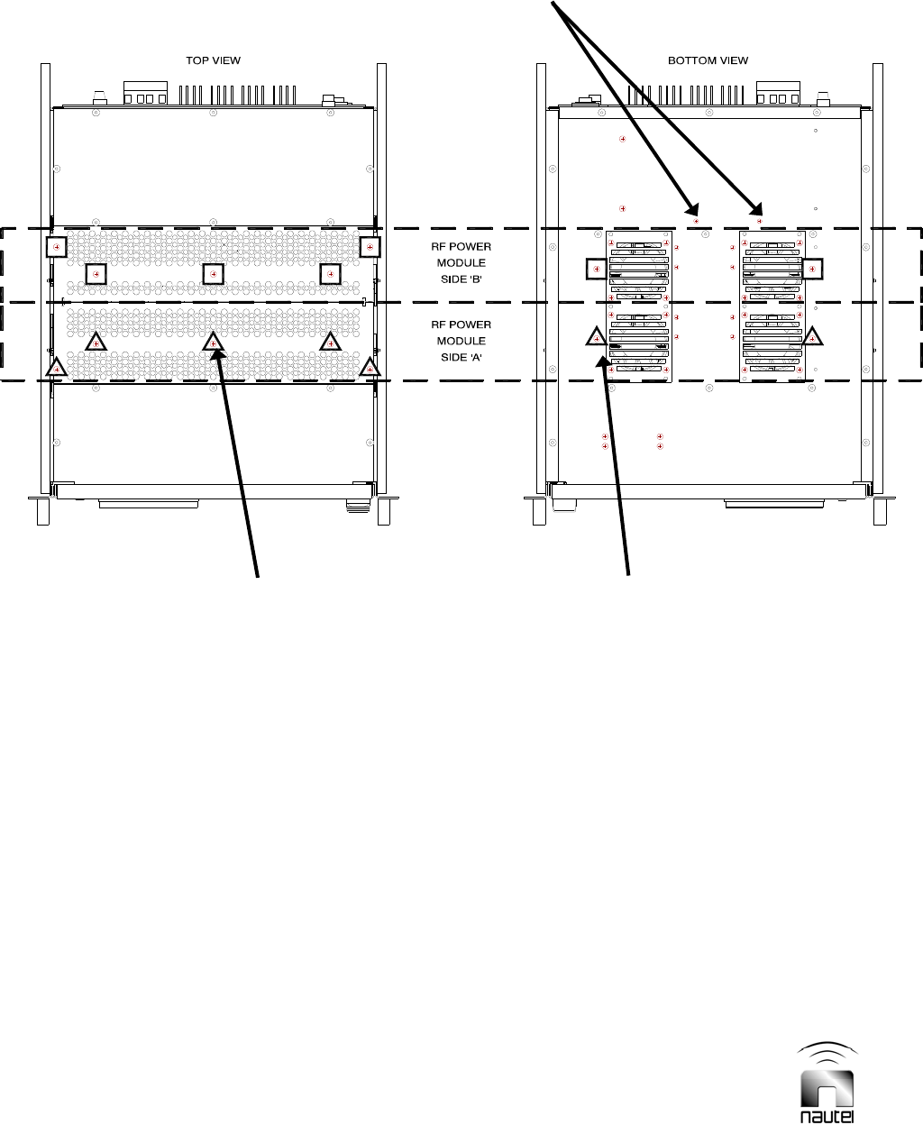
Page 5-10 Vector-LP Radio Beacon Transmitter Technical Instruction Manual
Issue 1.8.1 Section 5 Maintenance and Troubleshooting
Figure 5-1: RF Power Module Securing Hardware
TOP COVERS: Remove five M4
screws from top cover for each RF
power module. Reinstall this
hardware after module replacement
SHIPPING SCREWS: Remove two M4
screws from bottom for each RF power
module. NOTE: Shipping screws may have
been removed during installation. They are
not required after module replacement.
Battery Boost Assembly A16
R
ep
l
ace
m
e
n
t
: R
e
m
o
v
e
t
w
o
M
3

Vector-LP Radio Beacon Transmitter Technical Instruction Manual Page 5-11
Section 5 Maintenance and Troubleshooting Issue 1.8.1
5.7 FET CHECKING/
REPLACEMENT
The transmitter contains many FETs. The
FETs most likely to fail are in RF power
modules A and B. For failures caused in
an RF power module, remove the module
(see 5.6.1), check the devices listed below
and, if necessary, replace them.
NOTE
The station spares kit, if purchased,
contains Nautel parts referenced below.
FETs Q1 and Q2 (Nautel Part # QR54)
of switch mode power supply PWB A2
(see Figures MD-10 and MD-12)
power MOSFETs Q1 through Q4
(Nautel Part # QAP49) of power
amplifier A3 (see Figures MD-10 and
MD-13)
power MOSFET Q1 (Nautel Part #
QAP49) of modulator A5 (see Figures
MD-10 and MD-15; same device as in
power amplifier A3)
(a) Unsolder the gate pins of the FET
under test and all parallel devices.
Refer to the assembly’s electrical
schematic in Section 9 to determine
the parallel devices, if applicable.
Refer to the assembly’s detail drawing
in Section 10 to verify pin-out.
NOTE
To turn on a FET under test, apply a dc
voltage between its gate and source
terminals. Some digital multimeters have
enough dc voltage (9 V battery
recommended) on their test leads when
set to the ‘diode’ or ‘resistance’ positions.
If not, obtain another dc voltage source.
(b) Turn off the FET by shorting the gate
and source. Using a digital multimeter,
momentarily place the negative lead
on the gate pin and positive lead on
the source pin for each FET in the
circuit.
(c) Measure the drain-source resistance
with the positive lead on the drain and
the negative lead on the source. The
digital multimeter should indicate an
open circuit.
(d) Measure the drain-source resistance
with the negative lead on the drain
and the positive lead on the source.
The digital multimeter should indicate
a diode pedestal.
(e) If the requirements of steps (c) and (d)
are not met, replace the device as
detailed in steps (i) through (m).
(f) Turn on the device under test by
placing the positive lead on the gate
and the negative lead on the source.
(g) Measure the drain-source resistance
with the positive lead on the drain and
the negative lead on the source. The
digital multimeter reading should
indicate a short circuit.
(h) If the requirement of step (g) is met,
the FET is operational. Turn it off as
detailed in step (b) and proceed to the
next suspect device. If the
requirement of step (g) is not met,
replace the device as detailed in steps
(i) through (m).
(i) Unsolder the drain and source pins of
the defective device.
(j) Remove the hardware securing the
device in place and remove the
defective device. Clean the
associated heat sink surface near the
input PWB.
(k) Apply a thin, even coat of thermal
compound on the bottom of the new
device. NOTE
FETs are static sensitive. Handle
replacement devices in a manner that
protects the FETs from static.

Page 5-12 Vector-LP Radio Beacon Transmitter Technical Instruction Manual
Issue 1.8.1 Section 5 Maintenance and Troubleshooting
(l) Reinstall the device on its cleaned
heat sink using the hardware removed
in step (j). Replace the Belleville
(cupped) washer with a new washer
(Nautel Part # HZ48, located in
ancillary kit). Apply a thin, even coat
of thermal compound to both sides of
the insulator (if replaced). Refer to the
assembly’s detail drawing in Section
10 to verify the hardware orientation
for the device being replaced.
(m) Using a torque screwdriver, tighten
the mounting hardware to the value
(typically 3 to 4 inch-pounds) specified
on the assembly’s detail drawing in
Section 10, ensuring that the pins of
the device are aligned with their
corresponding solder terminals.
Solder the pins to their associated
terminals.
5.8 EXCITER PANEL PWB
REPLACEMENT
Replace defective printed wiring boards
(PWBs) on the exciter panel and perform
necessary adjustments as follows:
NOTE
The exciter panel is located directly
behind the transmitter’s front panel (see
Figure 2-2). It contains all the PWBs
referenced in the following replacement
procedures.
(a) Press the Control - RF OFF switch.
Switch off the ac power and disconnect
the dc supply, if applicable.
(b) Gain access to the exciter panel by
opening the hinged front panel.
(c) Replace the appropriate assembly or
PWB (see 5.8.1, 5.8.2 or 5.8.3).
5.8.1 Exciter Interface PWB and
Interconnecting PWB Replacement
See 5.8 first. The exciter interface PWB
(A2) physically interconnects with the RF
synthesizer PWBs (A5 and A8) and the
interphase PDM driver PWBs (A6 and A9).
Removing the exciter interface PWB
involves removing its interconnecting
PWBs first. Complete the instructions in the
sub-paragraphs (5.8.1.1, 5.8.1.2, and/or
5.8.1.3) to replace the appropriate PWB.
Complete all three paragraphs if replacing
the exciter interface PWB.
5.8.1.1 RF SYNTHESIZER PWB
REMOVAL/REPLACEMENT
(See 5.8 and 5.8.1 first)
(a) Remove six sets of mounting hardware
from the RF synthesizer PWB being
replaced (A5 or A8). If the exciter
interface PWB is to be removed (see
5.8.1.3), remove both RF synthesizer
PWBs, if applicable, and go to 5.8.1.2.
(b) Pull the PWB(s) away from the exciter
interface PWB (A2A2). It may be
helpful to gently pry the connector
loose with a screwdriver.
(c) Install the new RF synthesizer PWB by
reversing the steps above.
(d) Install all shorting jumpers on the
replacement PWB in the same position
as the replaced PWB.
(e) Verify the carrier frequency is set using
BCD switches S1 through S5. Each
switch represents one of the five most
significant digits in the carrier
frequency expressed in kHz:
- S1 is thousands digit (x1000)
- S2 is hundreds digit (x100)
- S3 is tens digit (x10)
- S4 is units digit (x1)
- S5 is the tenths digit (x0.1)

Vector-LP Radio Beacon Transmitter Technical Instruction Manual Page 5-13
Section 5 Maintenance and Troubleshooting Issue 1.8.1
NOTE
When an RF synthesizer PWB configured
to operate from an external RF drive
source is installed in a transmitter, its
frequency synthesizer must be operational
and its BCD switches must be set to
produce the assigned carrier frequency.
The synthesizer's output is used to obtain
the 2(PDM) output which ultimately
determines the host transmitter's pulse
duration modulation frequency (PDM).
(f) Perform RF drive symmetry testing
and adjustment procedures (see
4.3.6.9).
5.8.1.2 INTERPHASE PDM DRIVER PWB
REMOVAL/REPLACEMENT
(See 5.8 and 5.8.1 first)
(a) Remove the protective cover over the
interphase PDM driver PWB being
replaced (A6 or A9). The cover is
secured using seven sets of M3
mounting hardware.
(b) Remove and retain four sets of
mounting hardware for the interphase
PDM driver PWB being replaced (A6 or
A9). If the exciter interface PWB is to
be removed (see 5.8.1.3, remove both
interphase PDM driver PWBs, if
applicable, and go to 5.8.1.3.
(c) Pull the PWB(s) away from the exciter
interface PWB (A2). It may be helpful to
gently pry the connector loose with a
screwdriver.
(d) Install the new interphase PDM driver
PWB by reversing the steps above.
(e) Verify that shorting jumper E1 is
installed in the D position.
(f) For dual side transmitters, perform the
Equalizing Exciter Gain adjustment
procedure (see 4.3.6.10). For a single
side transmitter perform the
Calibrating Transmitter Output Power
adjustment procedure (see 4.3.6.3).
5.8.1.3 EXCITER INTERFACE PWB
REMOVAL/REPLACEMENT
(See 5.8 and 5.8.1 first)
(a) Remove all connections to the top and
bottom of the exciter interface PWB.
(b) Remove and retain 13 sets of mounting
hardware for the exciter interface PWB.
Remove the PWB.
(c) Install the new exciter interface PWB.
Re-install connections to the top and
bottom sides. Use the connector tag
labels or the connector mating
information after Table 8-2 to determine
proper connections.
(d) Set all shorting jumpers as per the
original exciter interface PWB.
(e) Re-install the RF synthesizer PWB(s)
removed in paragraph 5.8.1.1 and the
interphase PDM driver PWB(s)
removed in paragraph 5.8.1.2.
(f) Re-install the exciter/control assembly
in the transmitter by reversing the steps
in paragraph 5.8.
5.8.2 Exciter Monitor/Generator
PWB Replacement
See 5.8 first. Remove the exciter/monitor
generator PWB (A7 and, for dual side
transmitters, A10) as follows.
(a) Remove and retain four sets of
mounting hardware for the exciter
monitor/generator PWB being replaced.
(b) Remove all connections to the exciter
monitor/generator PWB.
(c) Install the new exciter monitor/
generator PWB. Re-install connections.
Use the connector tag labels or the
connector mating information in Section
8 to determine proper connections.
(d) Perform the following calibration
procedures: 4.3.5.5, 4.3.5.6, 4.3.5.7,
4.3.5.8, 4.3.5.9 and 4.3.5.10.

Page 5-14 Vector-LP Radio Beacon Transmitter Technical Instruction Manual
Issue 1.8.1 Section 5 Maintenance and Troubleshooting
5.8.3 Interface PWB Replacement
See 5.8 first. Remove the interface PWB
(A11) as follows.
NOTE
The interface PWB is located on the back of
the exciter panel (see Figure 4-1).
(a) Remove the RF power module(s) from
the transmitter (see 5.6.1) to gain
access to the interface PWB.
(b) Remove all connections (ribbon cables,
D-subs and quick-disconnects) to the
interface PWB.
(c) Using a short Philips screwdriver,
remove and retain ten sets of M3
mounting hardware.
(d) Install the new interface PWB. Re-
install connections. Use the connector
tag labels or the connector mating
information in Section 8 to determine
proper connections.
(e) Reinstall the RF power module(s) in the
transmitter (see 5.6.2).
5.9 BATTERY BOOST ASSEMBLY
REPLACEMENT
Replace a defective battery boost assembly
(A16) as follows:
NOTE
The battery boost PWB (A16A1) is not
provided as a spare part on its own. If a
spare is purchased, it is provided as part of
the entire battery boost assembly (A16).
For ease of maintenance it should be
replaced as an assembly, as described in
this paragraph.
(a) Press the Control - RF OFF switch.
Switch off the ac power and disconnect
the dc supply, if applicable.
(b) Disconnect the dc input wiring from in
terminal block A16TB1
(c) Remove the access panel at the back
of the transmitter (see Figure 2-2),
noting it is secured by 12 M3 screws.
(d) Remove all connections (D-sub and
quick-disconnects) to the battery boost
assembly.
(e) Remove and retain four sets of M3
mounting hardware for the battery
boost assembly at the back of the
transmitter (see Figure 2-2) and two
sets of M3 mounting hardware on the
bottom of the transmitter (see Figure
5-1). Remove the battery boost
assembly.
(f) On the replacement assembly, ensure
that shorting jumpers A1E5 and A1E7
through A1E10 are installed in the
same position as the replaced
assembly (see Table 3-8).
(g) Install the new battery boost assembly
using retained hardware for the back
and the bottom. Re-install dc input
wiring and mating connectors. Use the
connector tag labels or the connector
mating information in Section 8 to
determine proper connections.
(h) Reinstall the access panel removed in
step (c).

Vector-LP Radio Beacon Transmitter Technical Instruction Manual Page 6-1 (6-2 Blank)
Section 6 Theory of Operation Issue 1.8.1
Vector-LP Radio Beacon Transmitter
TECHNICAL INSTRUCTION MANUAL
Section 6 THEORY OF OPERATION
6.1 INTRODUCTION
The theory of operation for the Vector-LP
Radio Beacon transmitter is presented in
this section. Frequent reference is made to
electrical schematics (e.g., Figure SD-1).
They are located in Section 9 of this
manual. Circuits that are shown on
electrical schematics, but not described in
this section are either beyond the scope of
this manual or are not used for NDB
applications.
6.2 TRANSMITTER OVERVIEW
The transmitter operates at one fixed
frequency in the LF/MF band (190 kHz to
535 kHz) or in the MF band (536 kHz to
1200 kHz and 1600 kHz to 1800 kHz). It
provides up to 125 W (VR125) or 250 W
(VR250) of continuous carrier power. It
automatically transmits specific beacon
identification signals at pre-selected
repetition rates. Special codes may also be
transmitted when commanded from an
external source. Provision is made for local
or remote operation of the transmitter as
well as antenna fine-tuning through
controls on the transmitter's front panel. If
the standby option is purchased, provision
is made for automatic changeover from the
selected main side of the transmitter to the
standby side when the selected main side's
critical parameters are not met. The
transmitter operates from a single phase,
47 Hz to 63 Hz ac power supply (170 V to
270 V ac for VR250; 90 V to 270 V for
VR125), using switch mode power
supplies. A 48 V dc input option (and 24 V
dc for VR125 only) can also be
purchased. Emission is continuous carrier
(NON) beacon keyed identification tone
(A2A) and beacon with voice (A2A/A3A).
Local control/monitoring is done using
front panel membrane switches and a
graphic liquid crystal display. Critical
parameters such as forward power,
reflected power and antenna current can
also be displayed on an analog meter on
the front of the transmitter.
Remote control and monitoring can be
provided over several optional interfaces.
The transmitter also has provision to
interface with a Nautel antenna tuning unit
(ATU), using an isolated RS485 serial link.
This ATU link allows the transmitter to
regulate antenna current, and therefore
maintain constant field strength, by auto-
adjusting its output power in accordance
with the ATUs antenna current sample.
The transmitter circuitry can be
represented using four functional stages
(see Figure 6-1):
Ac-Dc Power Stage
Exciter Stage
Control/Monitor Stage
RF Power Stage
6.3 AC-DC POWER STAGE
See Figures 6-1 and SD-1. The ac-dc
power stage accepts the ac power source
or optional dc power source and converts it
to the necessary low level dc voltages
required throughout the transmitter. The ac
input voltage is also applied directly to the
RF power stage. The ac-dc power stage’s
primary components are the ac-dc
universal input power supplies (U2 and U3,
if used) and the interface PWB (A11). If the
dc input option is purchased, the
transmitter also includes the dc-dc
universal input power supply (U10) and the
battery boost PWB (A16A1).
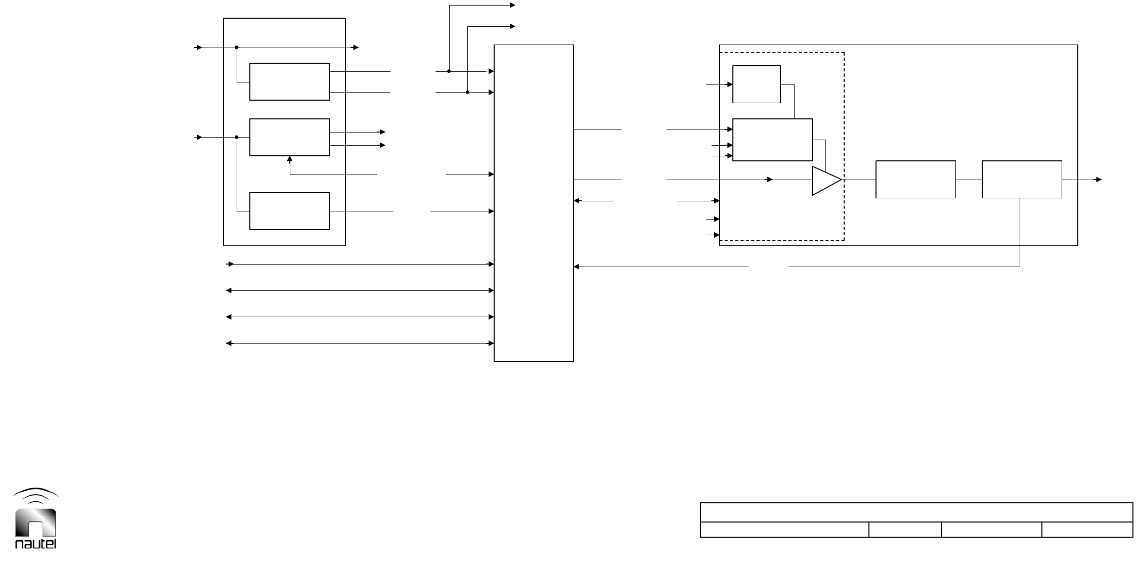
Dimensions = mm (inches)
Block Diagram – Vector-LP Radio Beacon Transmitter
Issue 1.8.1 Not to Scale Figure 6-1 Page 6-3 (6-4 Blank)
PA
OPTION)
B
SUPPLIES
LVPS POWER
A
+/- VDC
CONTROL/MONITOR
B+ (B) (DC POWER)
B+ (A) (DC POWER)
+/- VDC (B)
EXCITER AND
+/- VDC (B)
+/- VDC (A)
INT SERIAL LINK,
MONITOR
MODULATOR
SMPS
DC/DC LVPS
DC POWER
DUAL AC/DC +/- VDC (A)
STAGES
CONTROL/MONITOR
RF DRIVE
MOD DRIVE
CONTROL/MONITOR
RF POWER STAGE
EXTERNAL CONTROL/MONITOR
B2050017 VB
RS232/RS422 EXT SERIAL LINK
PTSN (FOR OPTIONAL MODEM)
EXTERNAL AUDIO INPUT
POWER SUPPLY
DC POWER
(OPTIONAL BATTERY)
+/- VDC (A)
B+ (A) (DC POWER)
AC POWER
(SINGLE OR DUAL)
RF POWER MODULE
AC POWER
+/- VDC (B)
B+ (B) (DC POWER)
AC POWER
RF FILTER RF POWER PROBE RF OUTPUT
(BATTERY BOOST
AC/DC POWER STAGE
See Figure 6-2

Vector-LP Radio Beacon Transmitter Technical Instruction Manual Page 6-5
Section 6 Theory of Operation Issue 1.8.1
The ac input is applied through 10 A circuit
breaker U5 and line filter U6. The ac voltage
for the RF power stage (RF power modules
A12 and A13) passes through thermistor RT1
and choke L1. Thermistor RT1 limits the
inrush current to the RF power modules.
Choke L1 improves the power factor on the
ac lines applied to the RF power modules.
The ac input is also applied to ac-dc universal
power supplies U2 and U3 (U3 optional, for
dual side transmitters), which convert the ac
voltage to low level dc voltages. The ac input
voltage is also applied to the interface PWB
(A11) for sampling by the control/monitor
stage.
Dc voltage is applied from an external 24 V or
48 V battery connected to A16TB1. The dc
voltage is fused by F1 and applied to rectifier
U8 and line filter U7 before being distributed
to dc-dc universal power supply U10 and
battery boost PWB A16A1. The battery boost
PWB boosts the dc voltage and applies it to
the RF power stage via rectifier U9.
6.3.1 Interface PWB
See Figures SD-1 and SD-21. The interface
PWB (A11) provides an interface between the
ac-dc power stage and the rest of the
transmitter. It also contains voltage regulators
(U1 and U2) that provide 9 V for the optional
modem (via E5 and E6) and 24 V (limited to
1A) for the ATU (via E3 and E4). It also
provides a dc sample of the ac input voltage
to the control/display PWB as an aid in
determining if the ac input source is at an
acceptable level.
6.3.2 Ac/Dc Universal Input Power
Supplies
See Figure SD-1. The ac/dc universal input
power supplies [U2 (side A) and U3 (side B,
if used)] are 110 W, universal ac input,
multiple dc output power supplies. The
transmitter’s ac input is applied to U2 and
U3 and the regulated 24.5 V, 15.6 V, 5.6 V
and -15.5 V supplies are provided on the
output. The outputs are applied through the
interface PWB to the remaining functional
blocks of the transmitter.
6.3.3 Battery Boost PWB (optional)
See Figures SD-1 and SD-25. The battery
boost PWB is a boost type switching power
supplies that provide a regulated B+ supply
voltage to the transmitter when a 24 V or
48 V battery is acting as the power source.
A 24 V or 48 V supply is applied to the drain
of switching FETs Q4 and Q5 through
inductors L1 and L4. The gate of FETs Q4
and Q5 is driven with square wave pulses
from pulse width modulation switching power
supply controller U4 through push-pull buffer
stage Q6/Q7. U4 is a fixed-frequency, pulse
width modulation control circuit,
incorporating the functions required for the
control of a switching power supply. The
device contains an internal sawtooth
oscillator that is set to a nominal frequency
of 100 kHz by external components R22 and
C14. The output pulse width modulated
control pulses to the gate of FETs Q4 and Q5
are generated by the comparison of this
sawtooth waveform with a feed-back voltage
sample from the output (CR6-cathode) and
the bias voltage created from the in-circuit
resistors selected by the Battery Select 1
(J1-18) and 2 (J1-19) inputs.
The resultant variable pulse width, 100 kHz
square wave at U4-8 (E) is applied to the
gate of FETs Q4 and Q5 (through Q6/Q7)
and turns it on and off with the appropriate
pulses to maintain the desired set dc output
voltage.
The Battery Select 1 and 2 inputs, applied
from the control/monitor stage, change the
level of Battery Boost (B+) voltage based on
the transmitter’s power level. See Table 6-1
for the logic levels.
Table 6-1: Battery Select Logic
B+ Voltage
VR250 VR125
Battery
Select 1 Battery
Select 2
79 V 55 V 0 0
136 V 97 V 0 1
236 V 167 V 1 1
Invalid Invalid 1 0

Page 6-6 Vector-LP Radio Beacon Transmitter Technical Instruction Manual
Issue 1.8.1 Section 6 Theory of Operation
6.4 EXCITER STAGE
See Figures 6-2 and SD-2. In dual
configuration the exciter stage contains two
independent exciter sections (A and B) which
can be supplied in a single or a main/standby
configuration. In a main/standby
configuration, the exciter can be selected
automatically or manually by local or remote
control. Each exciter section consists of an
RF synthesizer PWB, interphase PDM driver
PWB and exciter monitor/generator PWB.
6.4.1 Exciter Interface PWB
See Figures SD-9 and SD-10.The exciter
interface PWB (A2) provides signal
distribution, as well as the interconnection for
all the PWBs and assemblies in the exciter
control/monitor stage. The RF drive failure
detection, changeover/shutdown and monitor
fail logic circuits are located on the exciter
interface PWB.
6.4.1.1 RF Drive Circuitry and Failure
Detection
U3:A, U3:B, U2:A, U2:B, and U2C and their
associated components drive the RF signal to
the RF power blocks for side A. Q9 and its
associated components provide a low when
the RF drive is present and a high when it is
not present.
U3:C, U3:D, U1:A, U1:B, and U1C and their
associated components drive the RF signal to
the power blocks for side B. Q8 and its
associated components provide a low when
the RF drive is present and a high when it is
not present.
6.4.1.2 Changeover/Shutdown
U4, Q1 through Q7, K1 and K2 along with
their associated components allows for the
selection of the main side of the transmitter. If
the NDB A/B input is held low, the main side
will be B, otherwise it will be A. If no
changeover or shutdown is indicated (U4
inputs 3, 4, 6, and 7 are all high level), the
relay for the main side will be energized,
closing the contact and providing voltages to
the main PDM driver and RF synthesizer. The
relay for the standby side will be open. The
RF relay control FET (Q5) selects the main
position for RF relay K1. If a changeover is
indicated by a low on either U4:3 or U4:4, the
relay for the main side will open and the relay
for the standby side will close. The RF relay
control FET (Q5), will select the standby
position for RF relay K1. U4:17, U4:21,
U4:22, and U4:15 drive transistors Q1
through Q4 to indicate to the control board
information about the active side of the
transmitter and the changeover/ shutdown
state. If a shutdown is indicated, both K2 and
K1 are opened so that neither PDM driver or
RF synthesizer has power.
6.4.2 RF Synthesizer PWBs
See Figures SD-16 and SD-17. The RF
synthesizer PWBs (A5 and, if installed, A8)
use direct digital synthesis (DDS) to
generate carrier frequencies within the
LF/MF broadcast band (190 kHz to 1800
kHz). The output of a digital synthesizer
integrated circuit with internal high-speed
12-bit digital-to-analog converter is low-pass
filtered to provide a sinusoidal continuous
output. The sine wave is digitized and
divided by a factor of four to obtain the
carrier frequency. The digitized sine wave is
also divided by a factor of N to obtain a
2PDM frequency that ultimately determines
the transmitter's pulse duration modulation
(PDM) frequency. The RF synthesizer PWB
consists of a microprocessor, direct digital
synthesizer, low pass filter, digitizer, IPM
correction, balanced drive, and N divider.
6.4.2.1 MICROPROCESSOR
The microprocessor consists of an 87C51
integrated circuit (U4), which is clocked at
the system oscillator frequency (10.0000
MHz). Firmware resides in U4's internal four
kilobytes of EPROM memory. The
microprocessor generates control
information for the DDS circuit and
generates control information for the N
divider circuit.

Vector-LP Radio Beacon Transmitter Technical Instruction Manual Page 6-7
Section 6 Theory of Operation Issue 1.8.1
6.4.2.1.1 DDS Control Information
The RF carrier frequency is set using five
binary coded decimal (BCD) switches (S1
through S5). When a current-sink-to-ground
is applied at the Reset DDS input, or during
turn on, the microprocessor monitors these
switches and outputs the appropriate 48-bit
value to the DDS Frequency Tuning Word
#1 register. The 48-bit value is written in six
consecutive bytes to the DDS's six internal
registers. The sclk signal is enabled on each
write cycle.
6.4.2.1.2 N Divider Control Information
The 4C/B frequency is divided by an 'N'
factor to provide 2PDM output frequency
between 126 kHz and 134 kHz (when E3 is
set in LOW PDM mode) or between 245 kHz
and 276 kHz (when E3 is set in HIGH PDM
mode) (see formula below). The
microprocessor determines the value of N
and outputs the information at pins 2, 3, 4, 5,
6 and 7. The N divider circuit uses this
information as the N dividing factor.
- for
PDM = 130 kHz (HIGH PDM position):
C and PDM are expressed in kHz
130
652
int
4
2C
C
PDM
6.4.2.2 DIRECT DIGITAL SYNTHESIZER
The direct digital synthesizer consists of
integrated circuit U5 (AD98525Q) and
associated components. It generates a
frequency of 4C based on information
provided by microprocessor U4 (refer to
paragraph 6.5.2.1). Integrated circuit U5 is a
CMOS, numerically controlled oscillator with
a 48-bit phase accumulator and 12-bit
digital-to-analog converter (DAC). The
phase accumulator, which is responsible for
generating an output frequency, is presented
with a 48-bit value from the Frequency
Tuning Word 1 registers, whose contents
determine the FTW as follows:
The 10 MHz clock input is coupled with U5's
internal programmable reference clock
multiplier. This results in a system clock of
50 MHz (i.e., SYSCLK = 50 MHz).
The 12-bit output from the phase
accumulator is input to the DAC, which
outputs a stepped sine wave at 4c. The 4c
output is then low-pass filtered to remove
high frequency components.
6.4.2.3 LOW PASS FILTER
A low-pass filter consisting of C21, L1, and
C23 removes the high frequency images
present in the DDS output signal. The output
is a sine wave at a frequency of 4C.
6.4.2.4 DIGITIZER
The output of the low-pass filter is connected
to a digitizer circuit consisting of transistor
Q4, inverter U10:B, and associated
components. Inverter U10:B outputs an
approximate square wave at a frequency of
4C, which is applied to a 4 circuit and to
the N divider circuit.
6.4.2.5 IPM CORRECTION
Not applicable to Vector transmitters.
6.4.2.6 WAVEFORM SYMMETRY
RF DRIVE SYMMETRY potentiometer R32
is adjusted for an RF drive output waveform,
which is a symmetrical square wave (50%
duty cycle). The position of SYMMETRY
ADJ shorting jumper E6 determines when
the RF drive symmetry circuit is enabled or
disabled. E6 should be installed in the
ENABLE position (shorting pins 1 and 2)
when used in a Vector transmitter.
SYSCLK
cyxputFrequenDesiredOutFTW )
48
2(

Page 6-8 Vector-LP Radio Beacon Transmitter Technical Instruction Manual
Issue 1.8.1 Section 6 Theory of Operation
6.4.2.7 BALANCED DRIVE
The balanced drive buffer is a switching
circuit that ensures the rise and fall times of
its output square wave are minimal. The C
signal is a 15 V peak-to-peak square wave
that is the low level RF drive signal for the
RF power stage of the transmitter.
6.4.2.7.1 Balanced Drive Matching
Different values are possible on the
balanced drive output, depending on the
transmitter’s requirements. The position of
shorting shunt post E5 on 7-position header
XE5 can be changed to choose between
different capacitor and resistor values. E5 is
factory installed in the D position (shorting
pins 7 and 8) for Vector transmitters.
6.4.2.8 N DIVIDER
The N divider circuit is a cascade counter
made up of U6, U7, and inverters U8:A and
U8:F. The 4C/B signal is divided by N to
provide a 2PDM frequency, which is between
126 kHz and 134 kHz (when E3 is set in
LOW PDM mode) or between 245 kHz and
276 kHz (when E3 is set in HIGH PDM
mode). The value of N is supplied by
microprocessor U4 (see 6.5.2.1.2). The
2PDM output, which is nominal 5 V pk-to-pk
pulses, is applied to the transmitter's PDM
generation circuit, and ultimately determines
the PDM frequency.
6.4.2.9 RF DRIVE SOURCE SELECTION
The RF drive (c) source is provided by the
integral numerically controlled oscillator or
an external RF generator. The position of
shorting shunt posts E1, E2 and E4
determine which source is selected. Vector
transmitters use the internal source.
6.4.2.9.1 Internal c Source
To use the integral numerically controlled
oscillator’s output as the RF drive source,
set the shorting shunt posts as follows:
E1 in INT position (pins 2 and 3 shorted)
E2 in INT position (pins 2 and 3 shorted)
E4 in INT position (pins 2 and 3 shorted)
6.4.3 Interphase PDM Driver PWBs
See Figure SD-18. The interphase PDM
driver PWBs (A6 and, if installed, A9)
produce a pulse train of variable width as
their PDM output. The PDM repetition rate
(PDM) is a fixed frequency normally between
130 kHz and 133 kHz. The frequency is
determined by the 2PDM input, which is
produced by the active exciter monitor/
generator PWB. The PDM drive signal, which
determines the transmitter output power level,
is applied to the modulator assemblies in RF
power modules A or B (see Figure SD-22).
6.4.3.1 CARRIER LEVEL CONTROL
The carrier level control circuit consists of U6,
U7, U2A, U2D, U3B, U3D, U13A and their
associated components. U6 and U7 are
analog multipliers connected as a variable
gain, wide-band, linear amplifier. The
modulation reference (U6-X1) is multiplied by
a factor determined by the carrier ref (U6-Y1)
and B+ sample (U7-X1) signals to determine
the gain and, in turn, the status of U7-Y1.
When there is no Unbalanced Audio input at
P1-15, U2D's output (TP3), which is the
modulation reference, will be a nominal 1.4 V.
This voltage is applied as U6's X1 input.
The Carrier Ref input at P1-2 is a dc voltage
directly proportional to the square of the
expected RF carrier level. This voltage is
applied to U6-Y1.

Vector-LP Radio Beacon Transmitter Technical Instruction Manual Page 6-9 (6-10 Blank)
Section 6 Theory of Operation Issue 1.8.1
The B+ Sample input at P1-3 is a dc voltage
directly proportional to the B+ voltage being
applied to the transmitter's RF power stage.
When the B+ voltage is 236 V (for VR250) or
167 V (for VR125), the B+ Sample input and,
in turn, the output of buffer U3D (TP4), are a
nominal 4.0 V (for VR250) or 2.8 V (for
VR125). This voltage is applied to U7-X1.
The gain of U6 and U7 and, in turn, the
voltage at U7-Y1 is determined by the
following formula:
Unbalanced Audio * Carrier Ref / B+ Ref
When the Carrier Ref input (U6-Y1) is 4.7 V
and the B+ Sample input (U7-X1) is 4.0 V (for
VR250) or 2.8 V (for VR125), the gain of U6
is 1.18 (for VR250) or 1.68 (for VR125) for the
dc reference applied to U6-X1. The U7-Y1
current is 1.18 (for VR250) or 1.68 (for
VR125) times the U6-X1 current. U3B is
connected as a less than unity amplifier and
its gain is summed with U7's gain. The end
result is the total voltage gain of the circuit,
relative to the voltage at the output of U2D
(1.4 V), is a nominal 1.11 (for VR250) or 1.58
(for VR125) when GAIN TRIM potentiometer
R31 is set to the centre of its range. The
output of U3B (TP8) is 1.55 (for VR250; 1.4 V
x 1.11) or 2.21 (for VR125; 1.4 V x 1.58).
The gain of U7 will change in direct proportion
to changes in the Carrier Ref voltage. If the
Carrier Ref voltage is set to 0 V, or it is
clamped to ground because Q1 is turned on,
U7's gain is minimum (zero). In turn, the dc
reference's multiplication factor is minimum
(zero). The transmitter's RF output is turned
off.
The gain of U7 will change in inverse
proportion to changes in the B+ Sample input.
This feature eliminates the need for
sophisticated filtering of the transmitter's B+
power supply and maintains the transmitter's
RF output at the original level for B+ voltage
variations of ±10%.
GAIN TRIM potentiometer R31 provides a
nominal 10% adjustment in the carrier level
ref output of U3B. In dual exciter applications,
it is adjusted to compensate for tolerance
differences in the PDM generators of exciters
A and B. When it is set properly, the
transmitter's RF output is the same when
either exciter is selected, provided the same
Carrier Ref is being applied.
6.4.3.2 PDM DIVIDER
The PDM divider circuit divides the 2PDM
input frequency (P1-7) by two. The resulting
PDM output (P1-10) is a 0 V to 15 V square
wave. Unless otherwise established during
the transmitter's manufacture, it should be a
fixed frequency, nominally 130 kHz.
6.4.3.3 LINEAR INTEGRATOR
The linear integrator circuit converts the PDM
square wave input to a triangular waveform.
The triangular waveform has negative and
positive voltage excursions of equal
amplitude and duration. The long R/C time
constant formed by C26/R10 ensures a linear
rise and fall time. Since the R/C time constant
is fixed, the waveform amplitude varies over
the frequency range of PDM. The charge/
discharge time and waveform amplitude are
maximum at the lowest frequency.
6.4.3.4 INTEGRATOR PEAK DETECTOR
The integrator peak detector circuit detects
the positive going parts of the linear
integrator's triangular waveform. A portion of
the resulting positive dc voltage (nominally
1.8 V) at U2C’s output, is applied to the
inverting input of differential amplifier U3A.
The carrier level ref output of U3A is offset by
this voltage, which is proportional to the
triangular waveform voltage peaks. This
offset effectively sets the carrier level ref’s
zero power reference to the triangular
waveform's peak voltage. This ensures no RF
output is produced when the Carrier Ref input
(P1-2) is 0 V.
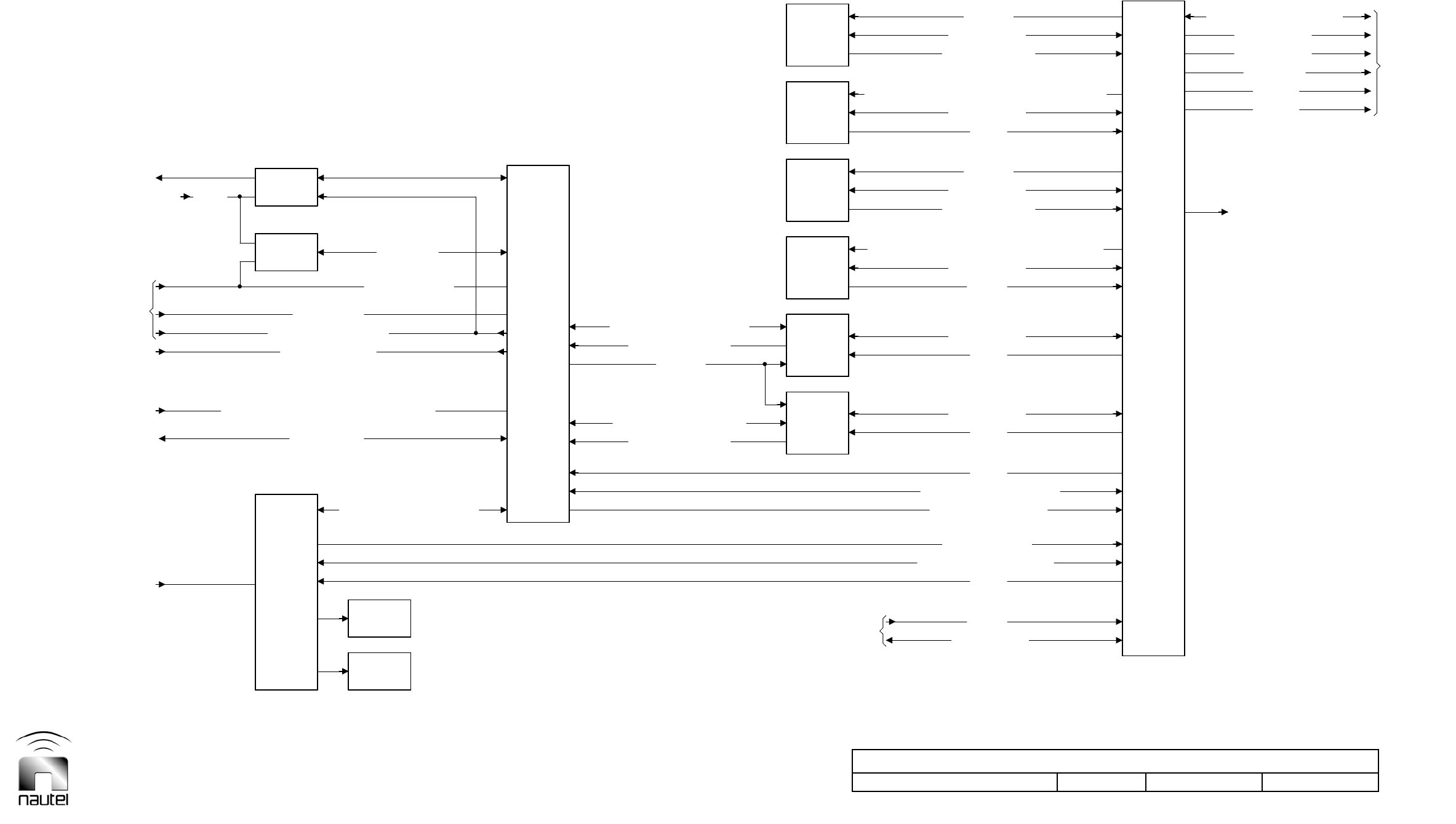
Dimensions = mm (inches)
Block Diagram – Exciter/Control/Monitor Stage
Issue 1.8.1 Not to Scale Figure 6-2 Page 6-11 (6-12 Blank)
9 VDC
+/- VDC
+/-VDC
+/-VDC
+/-VDC
PDM (B)
PDM (A)
+/-VDC
FROM RF POWER STAGE
USER INTERFACE
PWB
CONTROL/MONITOR
ISOLATED INT SERIAL LINK
EXT AUDIO INPUT
PWB
PWB B
EXCITER/
MONITOR
GENERATOR
B
INTERPHASE
PWB
SYNTHESIZER
A
INTERPHASE
PWB
SYNTHESIZER
+15VDC (B)
+15VDC (A)
and
DIGITAL
DISPLAY
EXT AUDIO
GENERATOR
MONITOR
PWB A
EXCITER/
PWB
B
PWM DRIVER
FREQUENCY
PWB
A
PWM DRIVER
FREQUENCY
9 VDC
B2050018 VB
ANALOG/
DISPLAY
TO/FROM AC/DC POWER STAGE
FWD/REFLD PWR, RF VOLT MONITOR, RF CURRENT MONITOR
ANTENNA TUNING UNIT
EXT CONTROL MONITOR
INTERFACE
(OPTIONAL)
INT SERIAL LINK
(OPTIONAL)
TO/FROM AC/DC POWER STAGE
KEYED TONE/EXT AUDIO (B)
KEYED TONE/EXT AUDIO (A)
CONTROL/MONITOR, INT SERIAL LINK
PWB
EXCITER
INTERFACE
+ VDC (A)
+ VDC (B)
RELAY CONTROL
RF DRIVE(A), PDM(A)
INT SERIAL LINK, CONTROL/MONITOR
LOCAL CONTROL
SPEAKER
CONTROL/
EXT SERIAL LINK (RS232, RS422)
NDB SITE
MODEM
PTSN
CONTROL/MONITOR, INT SERIAL LINK
INTERFACE
REMOTE INTERFACE
PWB
RF DRIVE(B), PDM(B)
CONTROL/MONITOR, INT SERIAL LINK
CARRIER REF (A) & (B)
KEYED TONE/EXT AUDIO (A) & (B)CONTROL/MONITOR, EXT SERIAL LINK
CONTROL/MONITOR
2FPDM(B), +15VDC(B), CARRIER REF(B), KEYED TONE/EXT AUDIO(B)
CONTROL/MONITOR
2FPDM(A), +15VDC(A), CARRIER REF(A), KEYED TONE/EXT AUDIO(A)
TO RF POWER STAGE
CONTROL/MONITOR
CONTROL/MONITOR
CONTROL/MONITOR, INT SERIAL LINK
CONTROL/MONITOR
RF DRIVE (B), 2FPDM (B)
CONTROL/MONITOR
RF DRIVE (A), 2FPDM (A)
CONTROL/MONITOR
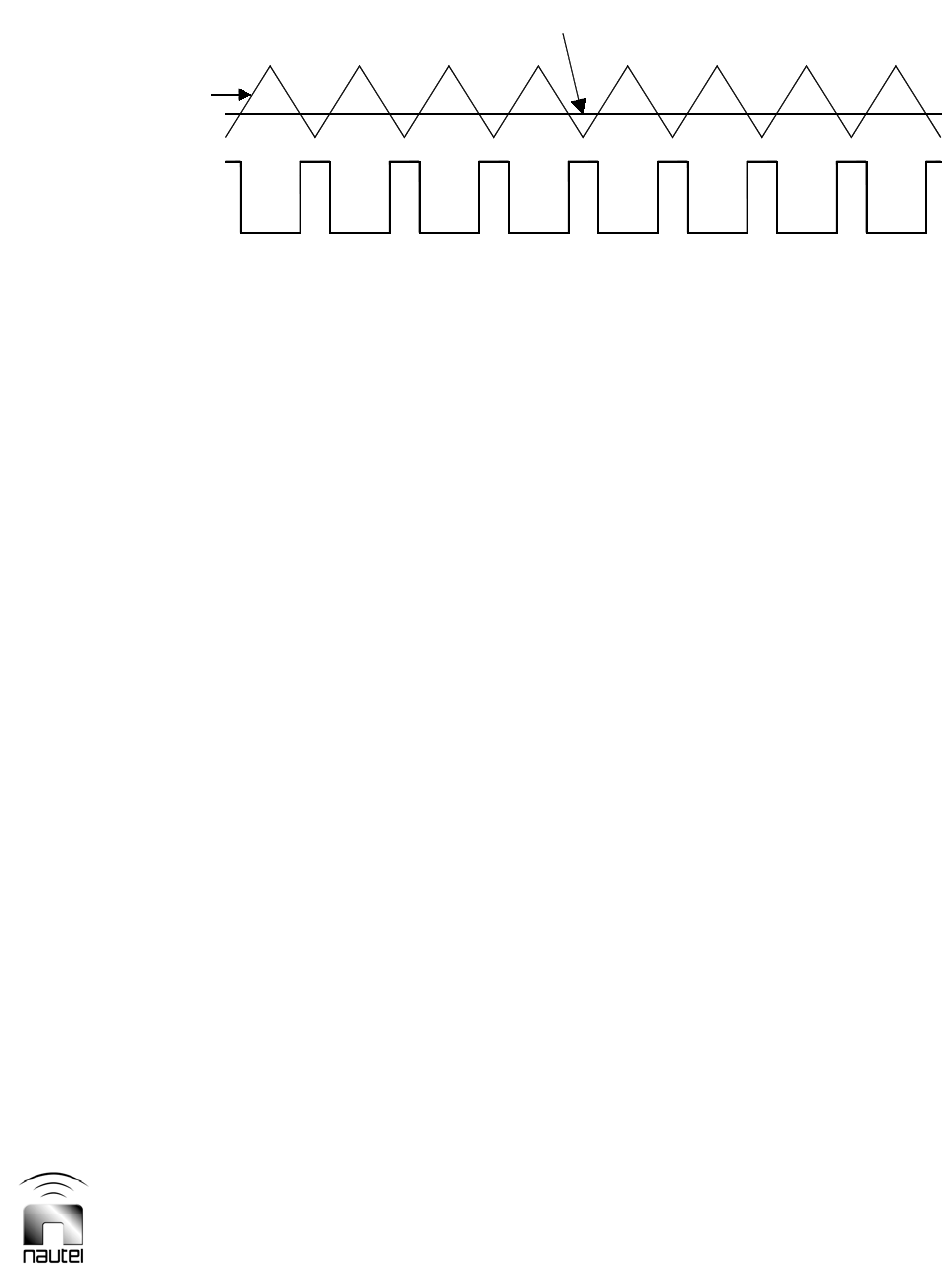
Vector-LP Radio Beacon Transmitter Technical Instruction Manual Page 6-13
Section 6 Theory of Operation Issue 1.8.1
Figure 6-3 Timing Diagram for PDM Differential Amplifier
6.4.3.5 INTERPHASE PDM
GENERATOR
The interphase PDM generator consists of
two identical variable pulse duration
generators (PDM1 and PDM2; PDM1
circuitry is described). The PDM1
generator produces a 0 V to 15 V
rectangular waveform at the PDM
repetition rate. The waveform on/off ratio
(duty cycle) is directly proportional to the
carrier level. The transmitter uses three B+
voltage levels to maximize performance.
As the RF output power is increased from
0 W (B+ voltage is 55 V for VR125; 79 V
for VR250), the PDM duty cycle increases
proportionally. When the RF output is
increased so that the PDM duty cycle
reaches 45 %, the control/ display PWB
initiates a B+ voltage increase (to 97 V for
VR125; 136 V for VR250) and a PDM duty
cycle decrease (to 27%). When the RF
output is increased to a level where the
PDM duty cycle again reaches 45%, the
control/ display PWB initiates a B+ voltage
increase (to 167 V for VR125; 236 V for
VR250) and a PDM duty cycle decrease
(to 32%).
6.4.3.5.1 PDM1 Generator
The PDM1 generator consists of U10B,
transistors Q4, Q5, and associated
components. The compensated carrier
level ref input from the integrator peak
detector circuit is applied to differential
amplifier U10B's non-inverting input,
where it is compared to the triangular
waveform from the linear integrator circuit.
When the compensated carrier level ref is
more positive than the triangular
waveform, U10B's output is open collector.
+15 V is applied through R60 and R62 to
the balanced drive formed by Q4/Q5. Q4
turns on and applies +15 V to K1-3 as the
PDM1 output (Q5 is off). For the rest of the
triangular waveform's period, the
compensated carrier level ref is less
positive than the triangular waveform.
U10B's output is a current-sink-to -15 V
and Q4 turns off. Q5 turns on and clamps
the PDM1 output to ground. The minimum
'on time' (zero RF power) occurs at the
negative peaks of the triangular waveform.
See Figure 6-3 for a timing diagram.
PDM 1
Ramp
Carrier Reference
Level

Page 6-14 Vector-LP Radio Beacon Transmitter Technical Instruction Manual
Issue 1.8.1 Section 6 Theory of Operation
6.4.3.6 PDM FAULT DETECTOR
The PDM fault detector circuit contains a
voltage controlled switch that controls the
'set/'reset' status of the shutback latch
circuit and, in turn, controls the on/off
status of relay K1.
The PDM1 fault detector circuit consists of
U12A and its associated components.
R67/C58 form an integrator with a long
time constant, relative to the PDM
frequency. C58's charge voltage is applied
to U12A's inverting input and compared to
the 5 V reference voltage applied to its
non-inverting input from voltage divider
R70/R71/R72. U12A's output is an open
collector and has no influence when C58's
charge voltage is less positive than the
reference voltage. U12A's output will
switch to a current-sink-to-ground when
C58's charge voltage goes more positive
than the reference voltage.
During normal operation, C58 will charge
through R67 towards 15 V when the
PDM1 output is 15 V ('on time') and CR3
is reversed biased. It will instantly
discharge to 0 V, through CR3, when the
PDM1 output switches to 0 V ('off time').
The repetition rate of the PDM1 on/off
periods ensures the charge on C58 will not
exceed 5 V, provided each PDM1 cycle
contains an 'off time'. If a PDM failure
occurs such that it produces a continuous
'on time', C58 will charge more positively
than 5 V. U12A's output will switch to a
current-sink-to-ground and toggle the
shutback latch circuit to its 'set' state.
6.4.3.7 SHUTBACK LATCH
The shutback latch circuit inhibits the 'on
time' of the PDM output and, in turn, the
RF output of the transmitter whenever a
transmitter originated Inhibit PDM (P1-16)
command is applied. This circuit provides
additional protection to the transmitter's
RF power stages when faults are detected
or actions are initiated that may cause RF
stress current thresholds to be exceeded.
Its function is to de-energize K1 and
disconnect the PDM 1 output from the
transmitter circuits when the PDM fault
detector output is a current-sink-to-ground
(logic low). It also inhibits the PDM
generator when relay K1 is de-energized
or when a logic true inhibit PDM command
is applied to P1-16.
U9A/U9B form a bistable flip/flop. The flip-
flop's output (U9-3) will be 15 V (logic
high) in its 'reset' state, and a current-sink-
to-ground (logic low) in its 'set' state.
Normally the inhibit PDM input and the
output of the PDM fault detector circuit,
which are the flip-flop's controlling inputs,
are open collector. 5 V (logic high) is
applied to U9-1 and U9-5 through their
pull-up resistors and the flip-flop is latched
in its 'reset' state. Relay K1 is held
energized and the PDM output is applied
to the transmitter circuits.
If a PDM fault is sensed, the PDM fault
detector circuit applies a current-sink-to-
ground (logic low) to U9-5 and causes the
flip-flop to switch to and latch in its 'set'
state. Relay K1 de-energizes and
disconnects the PDM output from the
transmitter circuits. The PDM latch output
(J1-11) is activated (5 V). This condition is
maintained until the flip-flop is reset by the
removal of the logic low from U9-5 (no
PDM fault) and the application of logic low
to U9-1 (a logic true current-sink-to-ground
reset PDM command is applied to J1-1).
6.4.3.8 PDM INHIBIT
The PDM inhibit circuit consists of U9D,
transistor Q2, and their associated circuits.
Its function is to instantly clamp the output
of the PDM generator to ground (zero
carrier level) when a logic true (current-
sink-to-ground) inhibit PDM input is
applied to P1-16, or when the PDM fault
detector circuit senses a PDM fault and
the shutback latch circuit’s flip-flop is
latched in its ‘set’ state. When neither of
these conditions are true, the PDM inhibit
circuit has no influence.

Vector-LP Radio Beacon Transmitter Technical Instruction Manual Page 6-15
Section 6 Theory of Operation Issue 1.8.1
6.4.4 Exciter Monitor/Generator
PWBs
See Figures SD-19 and SD-20. The exciter/
monitor/generator PWBs [A7 (exciter A) and
A10 (exciter B, if used)] perform the
following functions:
Use the press-to-talk input to select
between beacon and voice modes.
Monitor and control modulation depth
Selects the parameter, RF current or RF
voltage, to be applied to the remote
interface PWB for external monitoring.
Generate the appropriate tone frequency
Monitors tone and keyer operation
Monitors the forward power and controls
changeover and inhibit functions.
6.4.4.1 MICROCONTROLLER
Microcontroller U11 uses the SPI bus to
communicate with shift register U16 which
shifts out digital data used to control various
signals including changeover, shutdown, RF
off, and alarm. Watchdog timer IC U2 and
associated components generate a Keying/
Misc Alarm (J1-4) if the microcontroller falls
into an unknown state.
The clock for the microcontroller and the tone
oscillator is generated using Y1, U4:E and the
associated components.
The microcontroller (U11) continually
monitors its internal Flash and EEPROM
memory using checksums. If for some
reason, the checksum returns as invalid, the
microcontroller will detect the error and raise
a flag, resulting in the output power being
inhibit. U2 acts as a watchdog timer, if the
watchdog times out, the monitor fault will also
be raised, causing the output power to be
inhibited (via the control/display PWB). This
will guarantee that the U11 is always
operating as intended.
6.4.4.2 PRESS-TO-TALK
The input to U11:11 indicates to the exciter
monitor/generator PWB which mode of
operation it should be operating in. It will
react by adjusting the U16:1 that controls the
MUX U1:X.
6.4.4.3 MODULATION DEPTH
FUNCTIONS
Modulation depth of the beacon, voice and
beacon, and voice are controlled using the
digital pots 1, 2 and 3 of U10 respectively.
The levels of the pots in U10 are adjusted by
the microcontroller U11 over the SPI bus.
A selection between RF Monitor Voltage and
RF Monitor Current samples is made using
the MUX U14:C. CR9, U9:B and their
associated components RF detect the
selected RF monitor signal. The RF monitor
signal is then used to calculate the
modulation depth. The microcontroller (U11)
compares the average and peak levels of
the RF signal. The average value is detected
using U9:A and its associated components.
The peak level is detected using U9:C, CR7,
and their associated components.
6.4.4.4 TONE GENERATION
The keyer tone is generated using the DDS
IC U5. The microcontroller U11 sends an
SPI signal to U5 indicating the frequency of
the tone to generate. The tone is then
amplified using U8:C and its associated
components. The microcontroller (U11) then
controls keying by toggling the MUX U1:Z.
Correct operation of the keyer is monitored
by U8:A, U8:B, CR11, and CR12 and there
associated components. The analog
samples at U11:27 and U11:28 are
compared to the low threshold levels (set up
using the GUI) to determine if the keying
gate is opened or closed. If at any time the
keying gate is opened when it should be
closed or closed when it should be opened,
and alarm is flagged and output power is
inhibited (via the control/display PWB).

Page 6-16 Vector-LP Radio Beacon Transmitter Technical Instruction Manual
Issue 1.8.1 Section 6 Theory of Operation
6.4.4.5 FORWARD POWER MONITOR
A dc voltage, proportional to the transmitter’s
forward power, is applied to the Forward
Power Sample input (P1-1). This voltage is
filtered by operational amplifier U9 and
associated components and applied to
U11’s internal ADC. If the forward power
sample is above or below user-defined limits
for a user-defined time period, the
Changeover output (J4-15) becomes active
(logic low). If a changeover had already
occurred prior to this occurrence, a
Shutdown output (J4-16) will also be
generated. All user-defined parameters are
established using the front panel GUI and
applied to the exciter monitor/generator
PWB via the internal serial bus.
6.4.4.6 RF MONITOR PARAMETER
SELECTION
Multiplexer U14 and associated components
allows the user to select the parameter (RF
voltage or RF current) to be applied to the
RF MONITOR output at the rear of the
exciter.
6.5 CONTROL/MONITOR STAGE
See Figures 6-2 and SD-3. The control/
monitor stage contains the control/display
PWB, which contains the transmitter’s
embedded microcontroller. The remote
interface PWB, graphic user interface (GUI),
analog/digital displays and audio speaker are
also contained here. The NDB site interface
PWB (A4) and a modem (U11) are optional
items that can also be part of the control/
monitor stage.
6.5.1 Control/Display PWB
See Figures SD-5 through SD-8. The control/
display PWB (A1) performs the following
functions:
Produces dc voltage Carrier Ref (A) and
(B) outputs that ultimately determine the
forward power (RF carrier) level of the RF
output. These voltages are the reference
voltages for the variable pulse duration
modulation (PDM) generator in each
exciter (A and B).
Monitors critical parameters and turns off
(shuts back) or reduces (cuts back) the
Carrier Ref voltage when defined fault
threshold limits are exceeded.
Identifies out-of-tolerance parameters
when the carrier level is shut back or cut
back by providing a visual indication for
local monitoring or an electrical status
output for remote monitoring.
Selects the main exciter (A or B) that will
provide the RF drive and PDM drive to
the RF power stage’s RF amplifiers, if no
changeover has occurred.
Determines on/off status of RF power
stage.
Interfaces with the diagnostic display.
6.5.1.1 CARRIER REFERENCE VOLTAGE
The Carrier Ref (A) (J7-38) and (B) (J7-40)
outputs are applied to the interphase PDM
driver PWB of each exciter to generate the
PDM drive pulse that ultimately controls the
RF output of the transmitter. DACs U31 and
U32, in conjunction with microcontroller U22,
establish a dc reference voltage for the
Carrier Ref outputs. The voltage is buffered
through operational amplifiers U27B, U28B
and associated components.
6.5.1.2 ALARM THRESHOLD CIRCUITS
Certain parameters that are monitored by the
control/display PWB can initiate an alarm
indication and appropriate transmitter control
if an out of tolerance condition occurs.

Vector-LP Radio Beacon Transmitter Technical Instruction Manual Page 6-17
Section 6 Theory of Operation Issue 1.8.1
6.5.1.2.1 Ac Supply Voltage
The Ac Power input (J4-21) is an
unregulated dc voltage that is proportional to
the ac source. The input is filtered and
compared to the low ac ref fault threshold on
operational amplifier U4C. If the Ac Power
voltage is below this threshold, the ac low
signals switch to 0 V. The Carrier Ref (A)
and (B) outputs clamp to 0 V and the
Shutback (A) (J7 1) and (B) (J7-2) outputs
switch to 0 V and inhibit the exciter’s
modulator drive. The transmitter's RF output
turns off (shuts back) and remains off until
the ac power returns to an acceptable
voltage. The system diagram’s AC Mains
lamp displays a fault condition. An Ac
Sample signal is applied to ADC U9 for
application to the diagnostic display.
6.5.1.2.2 Reflected Power Monitor
The Refld Pwr Sample input (J1-5) is a dc
voltage that is proportional to the reflected
power at the transmitter's output. The input is
filtered and buffered by operational amplifier
U1B and associated components, and then
applied to the remote interface PWB via the
external serial interface (microcontroller U22).
The signal is also compared to a pre-
determined refld pwr shtbk ref fault threshold
on operational amplifier U4A. When the
reflected power indicates a VSWR of greater
than 2:1, relative to rated forward power, the
refld pwr sample input exceeds the fault
threshold and the refld_pwr_shutback signal
switches to 5 V. The Carrier Ref (A) and (B)
outputs clamp to 0 V and the Shutback (A)
(J7-1) and (B) (J7-2) outputs switch to 0 V
and inhibit the exciter’s modulator drive. A
clock pulse is also applied to an alarm count/
cutback circuit in complex programmable
logic device (CPLD) U18. The RF output is
instantly shut back (turn off). The system
diagram’s Output Network lamp displays a
fault condition. A Refld Pwr Sample signal is
applied to ADC U9 for application to the front
panel’s diagnostic display.
Turning off the RF output reduces the refld
pwr sample input to 0 V. The Carrier Ref (A)
and (B) outputs are restored to their
pre-shutback levels, the Shutback A and B
outputs return to open collector, and the RF
output is restored at an exponential rate. If
the fault threshold is exceeded before the
pre-set power level is reached, the shutback
cycle is repeated. If two or more shutback
cycle clock pulses are applied within any two
second period, the Carrier Ref outputs are cut
back (reduced) until the carrier level is cut
back to a level that results in an acceptable
reflected power. When the transmitter enters
cutback mode, the system diagram’s Output
Network lamp flashes on and off. When the
refld pwr sample input returns to or is
maintained at a level which is less than the
fault threshold, the Shutback outputs returns
to open collector but the system diagram’s
Output Network lamp continues to display a
fault as a maintenance aid. The lamp remains
on until reset by the diagnostic display menu.
6.5.1.3 SAMPLE MONITORING CIRCUITS
In addition to the parameters described in
paragraph 6.5.6.2, various parameters are
applied to the control/display PWB for local
(via the front panel’s diagnostic display) and
external (via the remote interface PWB)
monitoring. In some cases, these parameters
have associated alarm detection circuitry, but
it is not resident on the control/display PWB.
6.5.1.3.1 PDM Drive
The PDM (A) (J4-9) and PDM (B) (J4-7)
inputs are pulses which represent the PDM
signal applied to RF power modules A and B.
The inputs are filtered through operational
amplifiers U7B and U11B and associated
components. PDM (A) Sample and PDM (B)
Sample signals are applied to ADC U9 for
application to the front panel’s diagnostic
display.

Page 6-18 Vector-LP Radio Beacon Transmitter Technical Instruction Manual
Issue 1.8.1 Section 6 Theory of Operation
6.5.1.3.2 Forward Power
The Fwd Pwr Sample input (J1-3) is a dc
voltage which represents the forward power at
the transmitter’s RF output. The input is filtered
through operational amplifier U2D and
associated components. A fwd_pwr_sample
signal is applied to ADC U9 for application to
the front panel’s diagnostic display. The
fwd_pwr_sample input is also applied to the
remote interface PWB via the external serial
interface (microcontroller U22). The Fwd Pwr
Sample input is also low-pass filtered through
operational amplifier U2C and associated
components. A speaker_ref_level signal is
applied through DAC U32. The analog output
(pin 12) is filtered through operational amplifier
U28D and associated components and applied
to the Audio (Speaker) output (J11-1), then
applied to speaker LS1 for audio monitoring.
6.5.1.3.3 Battery Voltage
The Battery Voltage input (J1-27) is a dc
voltage which represents the voltage applied
from the transmitter’s optional battery supply.
The input is filtered through operational
amplifier U3B and associated components.
The bat_volt_sample signal is applied to ADC
U12 for application to the front panel’s
diagnostic display.
6.5.1.3.4 Battery Current
The Battery Current input (J1-25) is a dc
voltage which represents the current drawn
by the transmitter’s optional battery supply.
The input is filtered through operational
amplifier U3A and associated components.
The bat_cur_sample signal is applied to ADC
U12 for application to the front panel’s
diagnostic display.
6.5.1.3.5 Low Voltage Power Supplies
Attenuated, buffered samples of all low
voltage dc power supplies (+24 V, 15 V and
+ 5 V) are applied to ADCs U9 and U12 for
application to the front panel’s diagnostic
display.
6.5.1.3.6 Cabinet Temperature
Low voltage temperature sensor U5 provides
a dc voltage (between 0 and 5 V) which
represents the ambient cabinet temperature.
This voltage is buffered by operational
amplifier U8A and associated components
and applied to ADC U12 for application to the
front panel’s diagnostic display.
6.5.1.4 MICROCONTROLLER
Microcontroller IC U22 interfaces between the
diagnostic display and its associated soft-
keys. It controls the level of the Carrier Ref
signals (see paragraph 6.5.1.1), which
ultimately determines the forward power level
of the transmitter. It also acts as an internal
and external serial interface for transmitter
alarm and status signals.
6.5.1.5 CPLD
Complex programmable logic device (CPLD)
U18 continuously reads digital inputs for all
transmitter alarm events. It is programmed to
perform root cause detection of a fault as well
as high-speed fault protection. Depending on
the nature of the fault, the CPLD generates
transmitter Shutback outputs (J7-1 and J7-2)
or various digital control/inhibit signals via a
parallel data bus.

Vector-LP Radio Beacon Transmitter Technical Instruction Manual Page 6-19
Section 6 Theory of Operation Issue 1.8.1
6.5.2 Remote Interface PWB
See Figures SD-11 through SD-13. The
remote interface PWB (A2A2) performs the
following functions:
Buffers all external transmitter remote
control inputs and provides the
connection for the system’s external
interlock circuit
Provides RF filtering for RF power probe
samples (forward power, reflected
power, and RF current)
Provides an isolated ATU serial interface
Converts external serial levels from TTL
to RS232 and RS422
RF monitor conditioning
Press-to-talk input
Audio conditioning
Audio monitoring
Provides distribution and interface point
between the ac/dc distribution stages and
exciter control/monitor stage
6.5.2.1 Remote Inputs/Outputs
U7:A and associated components form the
circuitry to allow control of RF on/off when in
remote mode. U21:C and associated
components form the circuitry to control the
external interlock. If the link between TB1-19
and TB2-20 is open, U21:C will output a high
(external interlock), causing the transmitter to
inhibit RF power.
6.5.2.2 Isolated ATU Serial Interface
U9, U11, U13, U14, U15, and U17 provide
isolation to the internal serial bus (RS485) to
allow for ATU control. The ATU provides 5 V
to opto-isolators U13 and U14, which provide
isolation between differential transceivers
U11 and U17. The ATU controls the DE/RE
signal (J3-5), allowing the ATU to specify
direction of transmission through the isolated
link preventing collisions over the serial bus.
6.5.2.3 RS232 and RS422 Interface
U19, U18, U12, convert the TTL levels
produced by the control/display PWB to
RS232 and RS422 levels for external
control/monitoring of the transmitter.
6.5.2.4 RF Monitor Conditioning
U16 and associated components allow the
user to specify the RF monitor level from the
GUI. U23 and R163 form an adjustable gain
amplifier for the RF monitor signal that is able
to drive a 50 load.
6.5.2.5 Press-To-Talk Input
Link E4 allows for the selection of phantom
feed or normal press-to-talk operation. When
in position A, normal operation is selected
and grounding TB1-12 indicates press-to-talk
mode. When in position B, phantom feed
mode is selected and applying -15 V to the
shield (TB1-15) will indicate press-to-talk
mode.
6.5.2.6 Audio Conditioning
The audio conditioning circuitry on the remote
interface board consists of 3 parts, balanced
conditioning, audio filtering, and the audio
limiting.
6.5.2.6.1 Balanced Conditioning
U3:A and its associated components convert
the balance audio signal between TB1-14
and TB1-16 to an unbalanced signal. The
level of the audio signal is adjusted using
AUDIO LEVEL potentiometer R37.
6.5.2.6.2 Audio Filtering
U8:B, U8:C, U8:D and their associated
components forms the audio input filter. This
filter, along with the poles located on the
Exciter Interface PWB and the Modulator
Filter, is a band pass filter passing signals
from 300 to 3000 Hz.

Page 6-20 Vector-LP Radio Beacon Transmitter Technical Instruction Manual
Issue 1.8.1 Section 6 Theory of Operation
6.5.2.6.3 Audio Limiting
U10:B, U10:C, U10:D, Q7, and their
associated components form the audio
limiter. The limiter will raise an alarm at
U10:13 when the audio signal goes above a
pre-defined threshold. It will then compress
the audio signal by adjusting the resistance
across the JFET Q7. This is accomplished by
adjusting the JFET’s base voltage at the
output of the comparators U10:B and U10:C.
6.5.2.7 Audio Monitor
U1:B and T1 condition the forward power
sample signal to produce an audio monitor
signal that can be used to view the modulated
signal being output by the transmitter.
6.5.3 Front Panel Metering
The front panel of the exciter control/monitor
assembly provides local controls and a
graphic user interface to display operating
status, root cause fault detection, RF power,
and critical dc voltage/current levels. The
controller/display PWB is mounted on the
rear of the panel. The front panel is divided
into three sections – system diagram,
diagnostic display and control.
6.5.3.1 SYSTEM DIAGRAM
The system diagram is a functional flow
diagram of the transmitter. Each section of
the flow diagram contains an alarm lamp,
which turns on when a fault occurs in that
section. If a lamp is flashing, the transmitter
has entered a cutback (reduced power) mode
of operation. The lamp that is flashing is likely
the cause for the cutback.
6.5.3.2 DIAGNOSTIC DISPLAY
The diagnostic display is a graphic user
interface (GUI) screen that is navigated using
five associated soft-keys. The majority of the
transmitter’s local control (exciter selection,
power level, etc.) and monitoring (critical
parameter levels, alarm events, etc.) may be
performed from menus on this display. An
analog meter is provided, which can display
forward power, reflected power, modulation
percentage or antenna current.
6.5.3.3 CONTROL SWITCHES
The control switches determine the
transmitter’s control location (local or remote)
and its RF status (on or off).
6.5.3.3.1 Local/Remote Selection
When Local is selected, all remote control
functions, except RF off, are disabled and
have no influence on the transmitter's
operating status or pre-set RF power levels.
When Remote is selected, all front panel
control functions, except RF Off, are disabled
and have no influence on the transmitter's
operating status or pre-set RF power levels.
6.5.3.3.2 RF On/RF Off Selection
When RF On is selected (enabled in Local
mode only), the transmitter’s RF power stage
is enabled to provide an RF output. When RF
Off is selected (enabled in Local and
Remote modes), the transmitter’s RF power
stage is inhibited.
6.5.3.3.3 Power Increase/Decrease
When Power Increase is pressed (enabled in
Local mode only), the transmitter’s RF output
power is increased. When Power Decrease
is pressed (enabled in Local mode only), the
transmitter’s RF output power is decreased.
Additionally, if both the Power Increase and
Power Decrease switches are depressed
simultaneously, the transmitter’s RF output
power will be reduced to 0 W.

Vector-LP Radio Beacon Transmitter Technical Instruction Manual Page 6-21
Section 6 Theory of Operation Issue 1.8.1
6.5.4 NDB Site Interface PWB
(Optional)
See Figures SD-14 and 15. The NDB site
interface PWB (A4), if purchased, provides:
16 optically isolated monitor inputs.
16 form C contact relay closure control
points.
6.5.4.1 Site Monitor Points
RFI filtering is provided on all control input
lines to ensure transmitter operation is not
interrupted due to RF pick-up on control lines.
Opto-couplers buffer/isolate the external
circuits and prevent unwanted transients
from affecting transmitter operation. All
isolated inputs are driven by isolated dc to
dc converter U1 to prevent unwanted
transients from affecting the transmitter’s dc
supplies. The monitor inputs are shifted in
through shift registers U6 and U9. These
values are then relayed to the control/display
PWB over the internal serial bus using
RS485 transceiver U12.
6.5.4.2 Site Control Points
Shift registers U17 and U19, controlled by
microcontroller U13 over the SPI bus will
control relays K1 to K16. Control point logic
levels are determined by the control/display
PWB and are communicated to the NDB site
interface PWB over the internal serial bus.
6.5.5 Modem (Optional)
See Figure SD-3. An optional modem (U11)
can be provided to interface the transmitter’s
RS232 Ext Serial Link to a PTSN. The link
provides remote monitoring and status for the
transmitter.

Page 6-22 Vector-LP Radio Beacon Transmitter Technical Instruction Manual
Issue 1.8.1 Section 6 Theory of Operation
6.6 RF POWER STAGE
See Figures 6-5 and SD-4. The RF power
stage produces the transmitter’s final RF
output. It contains the RF power modules
(A12 and A13, if used), the RF filter PWB
(A14) and the RF power probe (A15).
6.6.1 RF Power Module(s)
See Figure SD-22. Each RF power module
(A12 and, if purchased, A13) produces up to
250 W (for VR250) or 125 W (for VR125) RF
carrier power to the transmitter's RF output
and contains a wideband power amplifier, a
modulator, and a modulator filter. A switch
mode power supply PWB is provided to
convert the ac input voltage to the high level
B+ voltage used by the modulator assembly.
Each module’s RF output is applied to the
RF filter PWB (A14) via RF relay K1 (see
SD-4), which determines the ‘on-air’
module’. A power module interface PWB is
provided to interface control/monitor signals
between the RF power modules and the
exciter and control/monitor stages as
required. For VR250 transmitters, cooling air
for the RF power modules is provided by
fans B1 and B2.
6.6.1.1 SWITCH MODE POWER SUPPLY
PWB
See Figure SD-24. The switch mode power
supply PWB (A2) converts the transmitter’s
ac input voltage to the B+ voltage used by
the modulator. In the VR250, the ac input
voltage range is 170 – 270 V ac and the B+
voltages used by the modulator are 79 V,
136 V and 236 V. In the VR125, the ac input
voltage range is 90 – 270 V ac and the B+
voltages used by the modulator are 55 V,
97 V and 167 V.
6.6.1.1.1 Rectifier
The ac input voltage is rectified by diodes
U1 and U2, providing a dc voltage across
capacitors C12 through C17. Varistors RV1
through RV3 provide protection from high
voltage transients. AC IND lamp DS1
provides a status indication of the ac voltage
on the RF power module.
6.6.1.1.2 Switching Signal
IC U3 is a high current FET driver that
provides a switching PWM signal (0-18 V) to
the primary of transformer T2. The
secondaries of T2 control the on/off status of
FETs Q1 and Q2, which in turn switch the
rectified ac voltage to the primary of step-up
transformer T1/T4.
6.6.1.1.3 B+ Voltage
The secondaries of step-up transformer T1
are rectified by diodes CR9, CR10, CR11,
CR13, CR14, and CR15 and combine,
through chokes L4, L5 and L6, to form the
high level B+ voltage. This voltage is applied
to the Dc Output (J2-1). Samples of the B+
voltage and current are applied to inputs of
current mode PWM controller U8, which
provides PWM switching information to
regulate the B+ voltage. FETs Q4, Q5 and
resistors R10, R11, R24 and R25, in
conjunction with opto-couplers U4 and U6,
provide a means to adjust the attenuated
voltage applied to U8, thereby adjusting the
level of the B+ voltage.
6.6.1.1.4 Inhibit PWM
When an RF power module fault occurs, an
Inhibit signal is provided to J1-7. Opto-coupler
U7 will turn on and apply a signal to current
mode PWM controller U8 to inhibit the
switching signal output of FET driver U3.
6.6.1.2 POWER MODULE CONTROL/
INTERFACE PWB
See Figure SD-23. With the exception of the
ac input for the switching power supply and
the RF output of the module, the power
module control/interface PWB (A1) provides
the input and output connections for the RF
power module. It performs the following
functions:
6.6.1.2.1 Module Status
Module status such as B+ and PA voltage,
dc current, and temperature are measured
using ADC inputs on microcontroller U7. The
Fan Tach 1 and 2 inputs are also captured
using interrupt 0 and interrupt 1 on U7. All
information is transmitted to the control/
display PWB using the internal serial bus.

Vector-LP Radio Beacon Transmitter Technical Instruction Manual Page 6-23 (6-24 Blank)
Section 6 Theory of Operation Issue 1.8.1
6.6.1.2.2 Gate Bias Drive Signal
U7, Q2 and associated components
generate a 15 V square wave at 263 kHz to
drive the gate bias drive in the modulator.
6.6.1.2.3 Switch Mode Supply Control
Decodes the serial control (B+ settings) from
the control/display PWB and outputs the
settings using darlington transistor U1.
6.6.1.3 MODULATOR
See Figure SD-22. The modulator (A5) is a
logic level converter that converts the low
level (0 to 15 V) logic of the PDM input to a
high level (0-B+) logic PDM (B+) output.
6.6.1.3.1 13 V Power Supply
The 15 V LO output (pin 1) of FET driver U1
is full-wave rectified by bridge rectifier CR1
through CR4, at the PDM frequency. The
resultant dc voltage is filtered by capacitor
C7 and limited to 13 V by zener diode CR5.
The power supply's less positive output is
referenced to the source terminal of power
FET Q1 via resistor R7. Therefore, the
positive output is always 13 V higher than
the voltage on the FET source terminal. The
13 V output is applied to U1’s VB (+) and VS
(-) inputs as the switched gate drive for the
FETs. Transformer T1 provides isolation
between the high and low level signals.
6.6.1.3.2 FET Driver
FET driver U1 is an integrated circuit
configured to produce outputs as follows:
When the PDM signal applied to the HIN
input is high (15 V), the HO output is the dc
voltage applied to the VB input.
When the PDM signal applied to the HIN
input is low (0 V), the HO output is the
reference voltage applied to the VS input.
The HO output, which contains the PDM data,
is applied to the gate of power MOSFET Q1
as its on/off control.
6.6.1.3.3 B+ Switching MOSFET
Power MOSFET Q1 is connected to switch
the B+ voltage at the on/off ratio of the PDM
data on U1's HO output, which is applied to its
gate. The resultant PDM (B+) output contains
the PDM data applied to J2-7 at a high (0-B+)
logic level. Free-wheeling diode CR6
prevents negative overshoot by providing
current flow when MOSFET Q1 is off.
6.6.1.4 MODULATOR FILTER PWB
See Figure SD-22. The modulator filter PWB
(A4) consists of inductors L1 and L2 and
capacitors C1 and C3 as well as C2 of the
power amplifier (A3). These components form
a low pass filter that passes the audio
components but rejects the PDM frequency.
When no modulating audio information is
present, the PA Volts output will be a dc
voltage equal to the modulator input voltage
multiplied by the duty cycle of the PDM (B+)
signal. Capacitor C3 in conjunction with L2 is
resonant at a frequency to provide optimal
rejection of the PDM frequency.
6.6.1.5 POWER AMPLIFIER
See Figure SD-22. The power amplifier (A3)
uses two parallel pairs of MOSFETs to
produce an unfiltered, modulated RF output.
Q1 through Q4 are connected as cascode or
‘H’ bridge class ‘D’ amplifiers, which switch
the PA volts at the RF drive frequency (see
Figure 6-6 for a description of class D
operation). Transformer T1 splits the RF
drive signal and applies it, through buffer
amplifier U1 (fused by F1) to the MOSFETs
with the required phase relationship. Diodes
CR1 through CR4 prevent the output of the
RF amplifier from going negative. Transistor
Q5 and associated components detect the
RF drive level and provide an alarm signal to
the control/display PWB. Resistors R5
through R7 provide a PA Volts Sample for
front panel monitoring.
6.6.1.6 RF TRANSFORMER
RF transformer T1 provides impedance
matching between the power amplifier
output and the RF filter PWB.
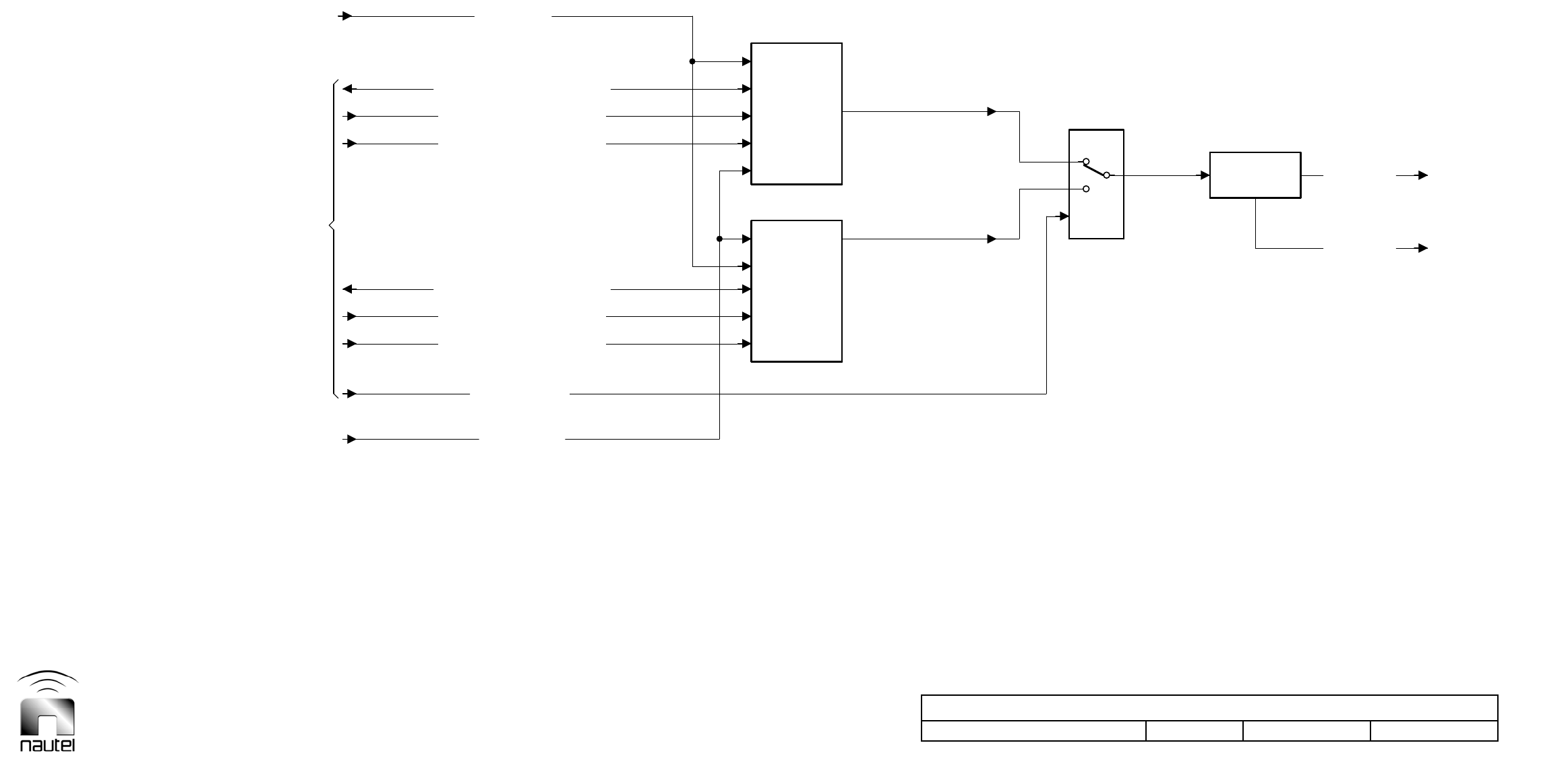
Dimensions = mm (inches)
Block Diagram – RF Power Stage
Issue 1.8.1 Not to Scale Figure 6-4 Page 6-25 (6-26 Blank)
B
A
B
A
B2050103 VA
DC POWER
(OPTIONAL)
RELAY CONTROL
+VDC
RF DRIVE(B), PDM(B)
RF DRIVE(A), PDM(A)
RF POWER MODULE
OUTPUT B
RF POWER MODULE
OUTPUT A
RF FILTER
+VDC
AC POWER
FROM AC/DC
POWER STAGE
FROM EXCITER/
SERIAL LINK, CONTROL/MONITOR
MONITOR
RF OUTPUT TO RF POWER PROBE
MODULE
RF POWER
SERIAL LINK, CONTROL/MONITOR
CONTROL/MONITOR BLOCK
MODULE
RF POWER
FROM AC/DC
POWER STAGE
TO EXCITER/
CONTROL/MONITOR BLOCK
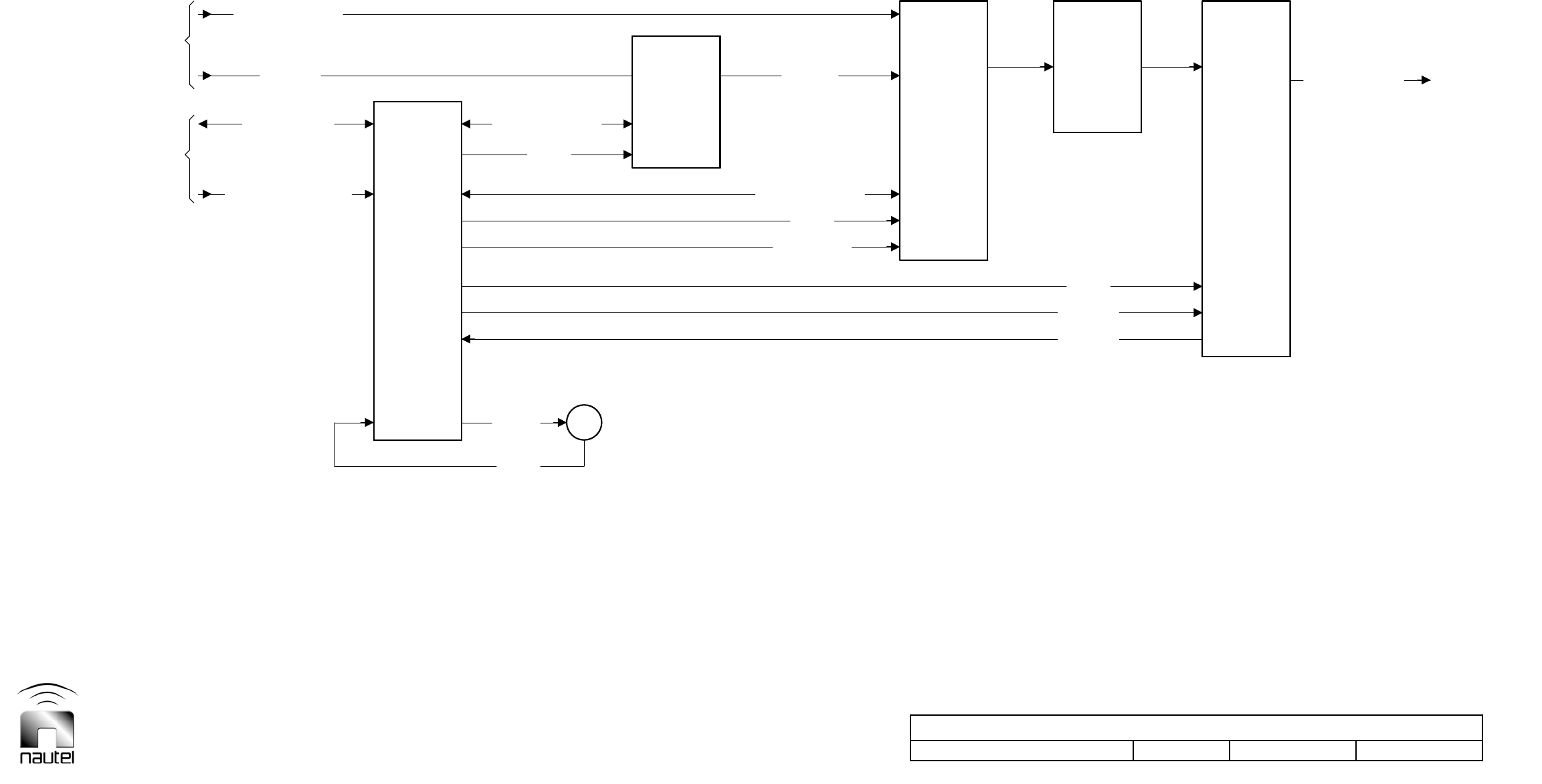
Dimensions = mm (inches)
Block Diagram – RF Power Module
Issue 1.8.1 Not to Scale Figure 6-5 Page 6-27 (6-28 Blank)
FILTER
B2050101 VB
POWER
MODULE
TACH
24VDC
+VDC
CONTROL/MONITOR
B+ VDC
MONITOR
+VDC
RF POWER
TO RF FILTER
STAGE
INTERFACE
FANS
+VDC
MODULATOR
RF DRIVE
MODULATOR
AMPLIFIER
CONTROL/MONITOR
FROM AC/DC
Fpdm/PDM
CONTROL/MONITOR+VDC, RF DRIVE, PDM
INT SERIAL LINK,
POWER
SUPPLY
AC POWER SWITCH
BATTERY BOOST B+
(OPTIONAL)
RF POWER MODULE
FROM EXCITER/
POWER STAGE
CONTROL/MONITOR
MODE OUTPUT VIA SELECTION RELAY

Vector-LP Radio Beacon Transmitter Technical Instruction Manual Page 6-29
Section 6 Theory of Operation Issue 1.8.1
6.6.2 RF Filter PWB
See Figure SD-4. The RF filter PWB (A14) is
a band pass filter that attenuates the
harmonics of the square wave output applied
from the selected RF power module before it
is applied to the RF combiner/probe. The filter
has a flat response characteristic over the
operating bandwidth [three PWB options;
standard frequency band (190 - 535 kHz),
extended frequency band for 125 W
transmitters (536 - 1250 kHz and 1600 –
1800 kHz), and extended frequency band for
250 W transmitters (1600 – 1800 kHz)]. It
has a nominal input and output impedance of
50 and a loaded Q of 2. The band-pass is
selected using frequency dependent link
connections (E1 through E36; see Tables 2-
7a and 2-7b).
6.6.3 RF Power Probe PWB
See Figure SD-4. The RF power probe PWB
(A15) contains various circuits that monitor
the RF output and provide RF voltage, RF
current, forward power and reflected power
monitoring samples to the control/monitor
stage.
6.6.3.1 FORWARD/REFLECTED POWER
PROBE
The forward/reflected power probe circuit
consists of 40:1 RF current transformer T1,
80:4 RF voltage transformer T3 and
associated components. These transformers
form the current and voltage arms of a
forward/reflected power bridge, which
samples the RF output.
The current flowing into the RF output passes
through transformer T1’s primary. The current
in T1’s secondary develops a voltage across
resistors R33, R34, R41, R42, R43 that is
proportional to the RF output current. The
anti-phase voltage across the secondary of
RF voltage transformer T3 is applied
(summed) to the centre-tap of T1’s
secondary. When the RF output impedance is
precisely 50 , the RF current waveform is in-
phase and of equal amplitude to the RF
voltage waveform on one half of T1’s center-
tapped secondary and equal amplitude, but
180 out-of-phase on the other half.
The in-phase voltages are summed, rectified
by CR35, low-pass filtered by L9/C53/L11,
resulting in a dc voltage being applied to the
Fwd Pwr Sample output (J1-1). This voltage
is proportional to the RF output's forward
power level.
The out-of-phase voltages are summed,
rectified by CR36, low-pass filtered by
L8/C54/L10, resulting in a dc voltage being
applied to the Refld Pwr Sample output
(J1-5). This voltage is proportional to the RF
output's reflected power level.
T3’s secondary voltage, which is a true
sample of the RF output’s voltage waveform,
is also applied to the RF Volts Monitor output
(J1-9). This output is intended for monitoring
by a modulation monitor and for test
equipment during maintenance.
6.6.3.2 RF CURRENT PROBE
The RF current probe circuit consists of 40:1
RF current transformer T2 and associated
components. The current flowing into the RF
output passes through the primary of
transformer T2. The current in T2’s
secondary winding develops a voltage across
resistors R37 and R40 that is proportional to
the primary (RF output) current. This voltage
is applied to the RF Current Sample output
(J1-17), which is used by the control/display
PWB's high RF current detector and
metering circuit. This high RF current
detector produces a high RF current alarm
and – via the control/display PWB - causes
the transmitter's RF output to shut back (turn
off) when the RF current exceeds a
threshold that represents the maximum
stress current for the RF power modules.
The current sample voltage is also applied to
the RF Current Monitor output (J1-13), which
is used for external monitoring purposes.

Page 6-30 Vector-LP Radio Beacon Transmitter Technical Instruction Manual
Issue 1.8.1 Section 6 Theory of Operation
6.7 MODULATION DEPTH WHEN
USING A HIGH ‘Q’ ANTENNA
When the transmitter's output is connected to
a high 'Q' antenna system, the modulation
envelope observed on the RF current
waveform may differ from that on the RF
voltage waveform. This difference is caused
by antenna impedance mismatch at the
sideband frequencies, which results in
reflected power standing waves on the feed
cable. Depending upon feed cable length, the
sideband impedance may be more or less
than 50 . When the sideband impedance is
less than 50 , the sideband current will
increase and may place undesirable stress
on the solid state devices in modulator/power
amplifier.
When calibrating the modulation limits for the
monitor (see 3.6.7), the system automatically
tests using both current and voltage samples
and selects the sample that places most
stress on the transmitter (i.e., the highest
modulation depth).
The following explanation should assist in
understanding this phenomenon.
A typical radiobeacon antenna is relatively
inefficient, since it is very short when
compared with the wavelength of the carrier
frequency. The high capacitive reactance of a
typical antenna is tuned to the carrier
frequency, by an antenna tuning unit's (ATU)
loading coils, to produce a series resonant
circuit. The resulting net antenna system
resistance is then transformed to 50 by a
matching transformer. When the antenna is
very short compared with the wavelength of
the carrier frequency, the series resonant
circuit has an extremely high 'Q'. Under these
conditions, the antenna system may present
a 50 load to the transmitter at the carrier
frequency but different impedance at the
sideband frequencies.
The mismatch at the sideband frequencies
will cause a standing wave on the feed cable.
Depending upon the length of the feed cable,
the sideband impedance of the antenna
system will appear to be more or less than
50 . When the transmitter is connected to a
high 'Q' antenna system, the difference
between the carrier impedance and the
sideband impedance may cause RF stress
current limits to be exceeded. When this
occurs, remedial action must be taken
instantly.
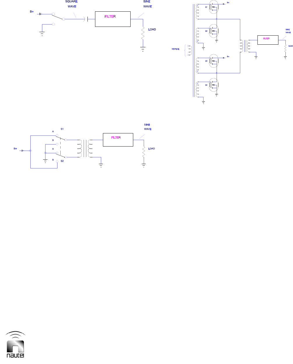
Vector-LP Radio Beacon Transmitter Technical Instruction Manual Page 6-31
Section 6 Theory of Operation Issue 1.8.1
SIMPLE CLASS 'D' OPERATION
If the switch is opened and closed with a 50%
duty cycle, a square wave at the switching
frequency will result at the filter input. If the
filter is designed to pass the switching
frequency, but attenuate its harmonics, a sine
wave is applied to the load.
PUSH-PULL CLASS 'D' OPERATION
If S1 and S2 are opened and closed with a
50% duty cycle, a square wave of current, at
the switching frequency, is passed through
the primary of the transformer and
transformed to its secondary. If the filter is
designed to pass the switching frequency, but
attenuate its harmonics, a sine wave is
applied to the load.
POWER MOSFET CLASS 'D' OPERATION
Power MOSFETs can be used to replace the
switches as depicted in the simple class 'D'
operation and push-pull class 'D' operation
examples. Note that the switch contacts are
replaced by the phase-oriented secondaries
of an RF drive transformer. Q1 corresponds
to S1-A, Q2 to S1-B, Q3 to S2-B and Q4 to
S2-A, as depicted in the push-pull class 'D'
operation example. Q1 and Q4 turn on/off
together and Q2 and Q3 turn on/off together.
Figure 6-6 Simplified Principles of Class 'D' Operation

Vector-LP Radio Beacon Transmitter Technical Instruction Manual Page 7-1
Section 7 Parts Information Issue 1.8.1
Vector-LP Radio Beacon Transmitter
TECHNICAL INSTRUCTION MANUAL
Section 7 PARTS INFORMATION
7.1 INTRODUCTION
This section contains parts lists that provide
descriptive and provisioning information for all
electrical and mechanical parts that have
been assigned a reference designation and
form a part of the subject equipment.
7.2 FAMILY TREE
Figure 7-1 depicts the family tree for the
subject equipment. It is based on the
descending order of the reference
designation hierarchy and identifies all
assemblies that have an assigned Nautel
configuration control number.
7.3 HOW TO LOCATE INFORMATION
FOR A SPECIFIC PART
To locate the information for a specific part,
the assigned reference designation for the
part must be known. In addition, the Nautel
configuration control number (e.g.,
NAPC147D) assigned to the assembly
containing the part or the full reference
designation, including the reference
designation of all higher assemblies, must be
known.
7.3.1 When Nautel Configuration
Control Number Is Known
When the Nautel configuration control
number (e.g., NAPC147D) is known, the
information for a specific part can be located
in the alphanumerically sorted reference
designation lists.
7.3.2 When Ref Des Is Known
When the full reference designation is
known, the information for a part can be
located as follows:
Refer to the family tree depicted in Figure
7-1 with the full reference designation.
Follow the family tree branches to the
block that represents the lowest level
assembly assigned a Nautel
configuration control number. Then locate
the reference designation table for that
Nautel configuration control number.
Locate the part's reference designation in
the specified table.
7.4 REFERENCE DESIGNATION
LISTS
Individual reference designation lists are
provided for:
Assemblies assigned an alpha-prefixed
Nautel nomenclature (e.g., NAPC147D)
Cable harnesses that are assigned a
numbered Nautel part (e.g., 205-8001)
Optional kits that are assigned a
numbered Nautel part (e.g., 205-8045)
The reference designation lists, which are
titled and presented in alphanumeric order,
are divided into columns to aid in locating
specific information.
7.5 COLUMN CONTENT
EXPLANATION
The following paragraphs explain the purpose
and contents of each column in the reference
designation lists.
7.5.1 Ref Des Column
The ‘ref des’ column contains the reference
designation for a specific part. These
designations are assigned in accordance with
the requirements of American National
Standard Specification ANSI Y32.16.
Reference designations are listed
alphanumerically in this column.

Page 7-2 Vector-LP Radio Beacon Transmitter Technical Instruction Manual
Issue 1.8.1 Section 8 Parts Information
7.5.2 Description Column
This column contains the name and
descriptive information for each part. The key
word or noun is presented first, followed by
the adjective identifiers. When the description
is 'See Family Tree for Assembly
Nomenclature', the associated part is subject
to its own reference designation list or is
contained in an optional kit’s list. If a family
tree is not provided in this section, assume
the latter to be true.
7.5.3 Nautel # Column
This column contains the Nautel part number
assigned to each part. This number is
Nautel's drawing number for Nautel
manufactured parts, Nautel's configuration
control number for assemblies that are under
configuration control management or Nautel's
inventory management number for purchased
parts. When a Nautel configuration control
number (e.g. NAPC*) is referenced in this
column, the associated ref des item is subject
to its own reference designation table.
7.5.4 Vendor # Column:
This column contains an original equipment
manufacturer's part number for a part. A
single part number is listed for each part,
even if there is more than one known
manufacturer. The listed number is Nautel's
usual or preferred choice. The use of this
number does not restrict Nautel from
selecting and using commercial equivalents,
where their use will not degrade circuit
operation or reliability, during manufacture.
7.5.5 OEM Code Column
This column typically contains a five digit
coded group as the original equipment
manufacturer's (OEM) identifier. The code
was extracted from Cataloging Handbook
H4/H8 - Commercial and Government Entity
(Cage) Code. Manufacturers that were not
listed in the catalog when this listing was
compiled have been assigned a unique five-
letter code. This code is assigned arbitrarily
and has no other significance. The
manufacturers identified for parts that have
JAN or MIL part numbers are Nautel's
normal supply source for that part.
NOTE
OEM code 37338 is listed for parts
manufactured by Nautel or to a Nautel control
drawing. United States of America customers
should refer all replacement part orders to
Nautel Maine Incorporated (OEM code
57655).
7.6 OEM CODE TO
MANUFACTURER CROSS-
REFERENCE
The OEM (CAGE) codes listed in the
reference designation lists are
representative of the original equipment
manufacturers of those parts. To determine
a specific part’s manufacturer contact
information, enter the five-character OEM
(CAGE) code for that part in the following
website:
https://www.bpn.gov/bincs/begin_search.asp
Upon entering the OEM (CAGE) code
number, manufacturer pertinent information
(address, telephone number, fax number,
etc.) shall be displayed. Please contact
Nautel if a part cannot be obtained (see also
ON-LINE PART QUOTES in this manual’s
Warranty section).
7.6.1 Manufacturer’s Index
For users without internet access, Table 7-1
provides a cross-reference from the original
equipment manufacturer’s (OEM) codes to
the manufacturer’s name. The listing is sorted
alphanumerically by the OEM code.

Vector-LP Radio Beacon Transmitter Technical Instruction Manual Page 7-3
Section 7 Parts Information Issue 1.8.1
7.7 COMMON ABBREVIATIONS/
ACRONYMS
The following abbreviations/acronyms may
appear in Description column:
DIP - Dual In-line Package
IDC - Denotes item is an Insulation
Displacement connector for ribbon
cable.
MTA - Denotes item is a Mass Termination
Assembly connector.
SIP - Single In-line Package
SMT - Denotes item is designed to be
installed using Surface Mount
Technology.

Page 7-4 Vector-LP Radio Beacon Transmitter Technical Instruction Manual
Issue 1.8.1 Section 8 Parts Information
Table 7-1: Manufacturer’s Index
00779 CTS Company Incorporated
01295 Texas Instruments Incorporated
01961 Pulse Engineering Inc.
021P3 Ametherm Inc.
02660 Amphenol Corp Spectra-Strip/Ltd.
04713 Motorola Incorporated
06090 Raychem Corporation
07263 Fairchild Camera and Instrument Corp
08779 Signal Transformer Company Inc
09482 Amp of Canada Limited
0A5K5 IXYS Corporation
0B0A9 Dallas Semiconductor Corporation
0CVK3 Allegro Microsystems Inc.
0G343 Huffman Mfg. Co.
0GP12 Radiall Incorporated
12969 Micro USPD Incorporated
13150 Axsys Technologies Incorporated
14655 Cornell Dubilier Electronics
16704 Cramer Coil and Transformer Co. Inc.
17856 Vishay Siliconix
19647 Caddock Electronics Incorporated
1EM90 Lumex Opto/Components Incorporated
1FN41 Atmel Corporation
1JRT7 Epson Electronics American, Inc
1K126 C & D Technologies
1MQ07 ZRG Incorporated
1UX99 Molex Connector Corporation
1W344 United Chemi-Con
22421 Thomas and Betts Limited
23875 M-Tron Industries Incorporated
24355 Analog Devices Inc.
25706 Daburn Electronics & Cable Corporation
27014 National Semiconductor Corp
31433 Kemet Electronics Corporation
31781 Edac Incorporated
33062 Ferronics Incorporated
35005 Dale Electronics Limited
37338 Nautel Limited
36AB3 Pacific Display Devices
3DX59 Citizen America Corporation
3N087 Mill-Max Manufacturing Corporation
45496 Digital Systems
50434 Agilent Technologies Incorporated
54583 TDK Electronics Corporation
56289 Sprague Electric Company
56699 BC Components
56845 Vishay Dale Electronics Incorporated
57655 Nautel Incorporated
59124 KOA Speer Electronics Incorporated
5Y407 Phoenix Contact Incorporated
61529 Airmat Corporation
62959 Multi-Tech Systems, Inc.
63590 Premier Industrial Corp SPC Technology
Div
64155 Linear Technology Corporation
65786 Cypress Semiconductor Corp.
68994 XILINX Incorporated
69669 Hammond Power Solutions Inc
74199 Quam Nichols Co.
75042 TRW Incorporated
75915 Littelfuse Tracor Incorporated
7D893 Fairchild Semiconductor Corporation
80294 Bourns Instruments Incorporated
81073 Grayhill Incorporated
81483 International Rectifier
83330 Dialight Corporation, DBA Dialight
90201 Mallory Sonalert Products Inc.
91833 Keystone Electronics Corporation
91929 Honeywell Incorporated
96095 AVX Ceramics Div of AVX Corp.
97525 Transico Inc.
AGILENT See 50434
ATC-FROS ATC-Frost
BIVAR Bivar Inc.
C3057 Conec Elektronische Bauelemente
GMBH
COILCRA Coilcraft
COMP-C Components Corporation
DEARBO Dearborn Electronics Incorporated
EPCOS Epcos
ER737 Texas Instruments
IPD Integrated Power Designs
IR See 81483
ITT CANN ITT Cannon
IXYS See 0A5K5
LITEON Liteon Inc.
MAGNE MagneTek Triad
MICREL Micrel Incorporated
MURATA Murata
ONSEMI ON Semiconductors
PANAS Panasonic
QT QT Optoelectronics
RALTRON Ralton Electroincs Corp.
ROHM ROHM
SBE SB Electronics Incorporated
Shurter Schurter Inc.
SOSH Soshin Electric Company, Limited
TYCO Tyco Electronics
U3040 ST Microelectronics Ltd.
UNITED United Chemi-Con, Inc.
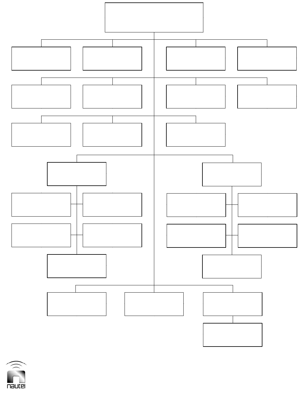
Vector-LP Radio Beacon Transmitter Technical Instruction Manual Page 7-5
Section 7 Parts Information Issue 1.8.1
Figure 7-1: Family Tree – Vector-LP Radio Beacon Transmitter
F2050501 V1
(DWAs inc'd)
A15
RF POWER PROBE
NAPF07C/01
A14
RF FILTER
NAPF05A (190 - 535 kHz)
A12A2
SWITCH MODE POWER SUPPLY
NAPS31B/03
A6
INTERPHASE PDM DRIVER
NAPM11
A2
EXCITER INTERFACE
NAPI76A/02
A13A2
SWITCH MODE POWER SUPPLY
NAPS31B/03
(DUAL NDB)
A8
RF SYNTHESIZER PWB
NAPE70C/01
(OPTIONAL)
A4
SITE INTERFACE
NAPI79 OR NAPI80
A12A4
MODULATOR FILTER
NAPF06A
A12
RF POWER MODULE
NAP35B/01
A12A5
MODULATOR
NASM11A/01
VECTOR - LP
NARB18
(DUAL NDB/DGPS)
A10
EXTERNAL MONITOR/GENERATOR PWB
NAPE76A/03
A13A4
MODULATOR FILTER
NAPF06A
(OPTIONAL)
A16
BATTERY BOOST ASSEMBLY
205-8035
A12A1
CONTROL/INTERFACE
NAPC151A
A13A1
CONTROL/INTERFACE
NAPC151A
A7
EXTERNAL MONITOR/GENERATOR PWB
NAPE76A/03
(NDB)
A5
RF SYNTHESIZER PWB
NAPE70C/01
A1
CONTROL/DISPLAY PWB
NAPC147D
A3
REMOTE INTERFACE
NAPI78D/02
A12A3
POWER AMPLIFIER
NAAA06
A13
RF POWER MODULE
NAP35B/01
A13A3
POWER AMPLIFIER
NAAA06
A13A5
MODULATOR
NASM11A/01
(DUAL NDB/DGPS)
A9
INTERPHASE PDM DRIVER
NAPM11
A11
INTERFACE PWB
NAPI94A
A16A1
BATTERY BOOST PWB
NAPS35

195-3019 Display Mod
REFDES NAUTEL #DESCRIPTION VENDOR # OEM CODE
J01 JQ55Conn, Header, Ribbon Cbl, 20Pin 103308-5 00779
U01 UT81Display,LCD,240x60 Graphic,Ext Temp C10815(STATIC)
PACIFIC DISPLAY
DEVICES
36AB3
195-3023 Ribbon Cable Assy
REFDES NAUTEL #DESCRIPTION VENDOR # OEM CODE
W16P01 JP45Conn, Recept, Ribbon Cable, 20 pin 746288-4 00779
W16P02 JP45Conn, Recept, Ribbon Cable, 20 pin 746288-4 00779
195-3032 Modem Kit
REFDES NAUTEL #DESCRIPTION VENDOR # OEM CODE
U04 UW66Modem, Industrial, V.92 Data/Fax MT5634IND-NAM 62959
205-1016 Cableform Assy
REFDES NAUTEL #DESCRIPTION VENDOR # OEM CODE
P01 JP65Conn,Rcpt Housing,12 Pin,Metrimate 211759-1 09482
P02 JT50Conn, Plug, 3-Pin, Mate-N-Lok 350766-1 00779
P03 JT50Conn, Plug, 3-Pin, Mate-N-Lok 350766-1 00779
P04 JT50Conn, Plug, 3-Pin, Mate-N-Lok 350766-1 00779
205-1018 Ribbon Cable Assy
REFDES NAUTEL #DESCRIPTION VENDOR # OEM CODE
W1P1 JP50Conn, Recept, Ribbon Cable, 10 pin 746285-1 00779
W1P2 JP50Conn, Recept, Ribbon Cable, 10 pin 746285-1 00779
W2P1 JP50Conn, Recept, Ribbon Cable, 10 pin 746285-1 00779
W2P2 JP50Conn, Recept, Ribbon Cable, 10 pin 746285-1 00779
W3P1 JP45Conn, Recept, Ribbon Cable, 20 pin 746288-4 00779
W3P2 JP45Conn, Recept, Ribbon Cable, 20 pin 746288-4 00779
Page 1 of 114 205-1018

205-5050 RF Transformer Assy
REFDES NAUTEL #DESCRIPTION VENDOR # OEM CODE
E01 HR26Connector, Quick-Dis, M,1/4 Tab, PWB 1287 91833
E02 HR26Connector, Quick-Dis, M,1/4 Tab, PWB 1287 91833
E03 HR26Connector, Quick-Dis, M,1/4 Tab, PWB 1287 91833
E04 HR26Connector, Quick-Dis, M,1/4 Tab, PWB 1287 91833
T01 195-6055RF Transformer Assy 195-6055 37338
Page 2 of 114 205-5050

205-8001 Cableform, Vector-LP
REFDES NAUTEL #DESCRIPTION VENDOR # OEM CODE
P01 JU07MTA, Standard Dust Cover, 8 pin 640551-8 09482
P01 JU28MTA, Keyed Closed End Housing,8 pin,22AWG 644463-8 00779
P02 JU07MTA, Standard Dust Cover, 8 pin 640551-8 09482
P02 JU28MTA, Keyed Closed End Housing,8 pin,22AWG 644463-8 00779
P03 JU37MTA, Keyed Closed End Housing,10 Pin, 22 AWG 1-644463-0 00779
P03 JU38MTA, Standard Dust Cover,10 Pin 1-640551-0 00779
P04 JU37MTA, Keyed Closed End Housing,10 Pin, 22 AWG 1-644463-0 00779
P04 JU38MTA, Standard Dust Cover,10 Pin 1-640551-0 00779
P05 JU46MTA,Closed End Housing,3 pin,22 AWG 3-640433-3(ROHS) TYCO
P05 JU47MTA,Standard Dust Cover,3 pin 640551-3(ROHS) TYCO
P06 JU46MTA,Closed End Housing,3 pin,22 AWG 3-640433-3(ROHS) TYCO
P06 JU47MTA,Standard Dust Cover,3 pin 640551-3(ROHS) TYCO
P07 JR39Conn, Plug, D-Sub, 25 pin, HDP-20 205208-1 09482
P07 JT16Conn, Lock Screw, D-Sub, Male 205980-1 09482
P08 JR38Conn, Socket, D-Sub, HDP-20, 25 pin 205207-1 09482
P08 JT16Conn, Lock Screw, D-Sub, Male 205980-1 09482
P09 JR39Conn, Plug, D-Sub, 25 pin, HDP-20 205208-1 09482
P09 JT16Conn, Lock Screw, D-Sub, Male 205980-1 09482
P10 JR38Conn, Socket, D-Sub, HDP-20, 25 pin 205207-1 09482
P10 JT16Conn, Lock Screw, D-Sub, Male 205980-1 09482
P11 JR38Conn, Socket, D-Sub, HDP-20, 25 pin 205207-1 09482
P12 JR38Conn, Socket, D-Sub, HDP-20, 25 pin 205207-1 09482
P12 JT16Conn, Lock Screw, D-Sub, Male 205980-1 09482
P13 JR39Conn, Plug, D-Sub, 25 pin, HDP-20 205208-1 09482
P14 JR39Conn, Plug, D-Sub, 25 pin, HDP-20 205208-1 09482
P14 JT16Conn, Lock Screw, D-Sub, Male 205980-1 09482
P15 JDP22Conn, Coax, N, Plug, 50ohm, Crimp, RG58 82-5375 02660
P16 JR39Conn, Plug, D-Sub, 25 pin, HDP-20 205208-1 09482
P17 JR38Conn, Socket, D-Sub, HDP-20, 25 pin 205207-1 09482
P18 JS65Conn,Spring Latch,D-sub Plate D110278(ROHS) ITT CANNO
P18 JS66Conn,Shell,D-sub,25 pin,90 deg DB51213(ROHS) ITT CANNO
P18 JT30Conn, IDC, D-Sub, S, HDE-20, 25-Pos 745495-3 09482
P19 JS65Conn,Spring Latch,D-sub Plate D110278(ROHS) ITT CANNO
P19 JS66Conn,Shell,D-sub,25 pin,90 deg DB51213(ROHS) ITT CANNO
P19 JT30Conn, IDC, D-Sub, S, HDE-20, 25-Pos 745495-3 09482
P20 JR39Conn, Plug, D-Sub, 25 pin, HDP-20 205208-1 09482
P21 JR39Conn, Plug, D-Sub, 25 pin, HDP-20 205208-1 09482
P21 JT16Conn, Lock Screw, D-Sub, Male 205980-1 09482
P22 JU02MTA, Standard Dust Cover, 4 pin 640551-4 09482
Page 3 of 114 205-8001

Continued from previous page
205-8001 Cableform, Vector-LP
REFDES NAUTEL #DESCRIPTION VENDOR # OEM CODE
P22 JU27MTA, Keyed Closed End Housing,4 pin,22AWG 3-644463-4(ROHS)
AMP
00779
P23 JR38Conn, Socket, D-Sub, HDP-20, 25 pin 205207-1 09482
P24 JR39Conn, Plug, D-Sub, 25 pin, HDP-20 205208-1 09482
P24 JT16Conn, Lock Screw, D-Sub, Male 205980-1 09482
P25 JU37MTA, Keyed Closed End Housing,10 Pin, 22 AWG 1-644463-0 00779
P25 JU38MTA, Standard Dust Cover,10 Pin 1-640551-0 00779
P26 JU04MTA, Standard Dust Cover, 12 pin 1-640551-2 09482
P26 JU26MTA, Keyed Closed End Housing,12pin,22AWG 1-644463-2 00779
P27 JR38Conn, Socket, D-Sub, HDP-20, 25 pin 205207-1 09482
P27 JT16Conn, Lock Screw, D-Sub, Male 205980-1 09482
P28 JT40Conn, Recept, Mate-N-Lok, 3 pin, Mini 172234-1 09482
P29 JT40Conn, Recept, Mate-N-Lok, 3 pin, Mini 172234-1 09482
P30 JT40Conn, Recept, Mate-N-Lok, 3 pin, Mini 172234-1 09482
P31 JT40Conn, Recept, Mate-N-Lok, 3 pin, Mini 172234-1 09482
P32 JU02MTA, Standard Dust Cover, 4 pin 640551-4 09482
P32 JU27MTA, Keyed Closed End Housing,4 pin,22AWG 3-644463-4(ROHS)
AMP
00779
XA12P1 JP66Conn,Sckt Housing,12 Socket,Metrimate 211758-1 09482
XA13P1 JP66Conn,Sckt Housing,12 Socket,Metrimate 211758-1 09482
Page 4 of 114 205-8001

205-8019 Ribbon Cable Assy
REFDES NAUTEL #DESCRIPTION VENDOR # OEM CODE
W01P1 JP51Conn, Recept, Ribbon Cable, 40 pin 746288-9 00779
W01P2 JP51Conn, Recept, Ribbon Cable, 40 pin 746288-9 00779
W02P1 JP51Conn, Recept, Ribbon Cable, 40 pin 746288-9 00779
W02P2 JP51Conn, Recept, Ribbon Cable, 40 pin 746288-9 00779
W03P1 JP51Conn, Recept, Ribbon Cable, 40 pin 746288-9 00779
W03P2 JP51Conn, Recept, Ribbon Cable, 40 pin 746288-9 00779
W04P1 JP51Conn, Recept, Ribbon Cable, 40 pin 746288-9 00779
W04P2 JP51Conn, Recept, Ribbon Cable, 40 pin 746288-9 00779
W05P1 JP51Conn, Recept, Ribbon Cable, 40 pin 746288-9 00779
W05P2 JP51Conn, Recept, Ribbon Cable, 40 pin 746288-9 00779
W06P1 JP45Conn, Recept, Ribbon Cable, 20 pin 746288-4 00779
W06P2 JP45Conn, Recept, Ribbon Cable, 20 pin 746288-4 00779
W06P3 JP51Conn, Recept, Ribbon Cable, 40 pin 746288-9 00779
W07P1 JP45Conn, Recept, Ribbon Cable, 20 pin 746288-4 00779
W07P2 JP45Conn, Recept, Ribbon Cable, 20 pin 746288-4 00779
W10P1 JP51Conn, Recept, Ribbon Cable, 40 pin 746288-9 00779
W10P2 JP51Conn, Recept, Ribbon Cable, 40 pin 746288-9 00779
205-8035 Battery Boost Assy
REFDES NAUTEL #DESCRIPTION VENDOR # OEM CODE
A01 NAPS35SMPS, 24/48V Battery Boost PWB Assy 205-7020 37338
C01 CS11Capacitor, Plastic, 1.0uF 10PC 250V B32232A3105K EPCOS
C02 CS22Capacitor, Metal,Polyprop, 5uF +/-10% 100V 5MP12D505K 50558
CR06 QH43Diode, Fast Recovery, 600V, 60A DSEI60-06A 0A5K5
Q04 QR56Transistor,FET,N,500V,0.1 Ohm STW26NM50(STATIC) 0G343
Q05 QR56Transistor,FET,N,500V,0.1 Ohm STW26NM50(STATIC) 0G343
TB01 JF27Terminal Block, 4-Pos, Double, 61A G10/4 5Y407
205-8073 Wire Assy Cabinet Vector-LP
REFDES NAUTEL #DESCRIPTION VENDOR # OEM CODE
J1 JT52Conn, Coax, Jack, N, Crimp for RG303 24-N-50-3-11C/133 0GZ58
P2 JDP22Conn, Coax, N, Plug, 50ohm, Crimp, RG58 82-5375 02660
Page 5 of 114 205-8073

205-8075 Cabinet-Vector-LP (Tall Rack)
REFDES NAUTEL #DESCRIPTION VENDOR # OEM CODE
P3 JN50Cord, Line Assy, SJT, 250V,10A 17569 VOLEX
TB01 JF27Terminal Block, 4-Pos, Double, 61A G10/4 5Y407
W1 205-8073Wire Assy Cabinet Vector-LP 205-8073 37338
205-8080 IP66 Cabinet w/Vector-LP Assy
REFDES NAUTEL #DESCRIPTION VENDOR # OEM CODE
J01 JA54Conn, Coax, N, Bulkhead,Receptacle UG-680/U 00795
P01 JN50Cord, Line Assy, SJT, 250V,10A 17569 VOLEX
P02 JDP22Conn, Coax, N, Plug, 50ohm, Crimp, RG58 82-5375 02660
TB01 JF27Terminal Block, 4-Pos, Double, 61A G10/4 5Y407
TB02 JF27Terminal Block, 4-Pos, Double, 61A G10/4 5Y407
205-8120 Cabinet-Vector-LP (Short Rack)w/ Internal Battery
REFDES NAUTEL #DESCRIPTION VENDOR # OEM CODE
CB01 SB46Circuit Breaker, 1-pole, 65Vdc20A W91-X152-20 U5588
P01 JN50Cord, Line Assy, SJT, 250V,10A 17569 VOLEX
TB01 JF27Terminal Block, 4-Pos, Double, 61A G10/4 5Y407
TB02 JF27Terminal Block, 4-Pos, Double, 61A G10/4 5Y407
W01 205-8073Wire Assy Cabinet Vector-LP 205-8073 37338
205-8120-01 Cabinet-Vector-LP (Short Rack)
REFDES NAUTEL #DESCRIPTION VENDOR # OEM CODE
P01 JN50Cord, Line Assy, SJT, 250V,10A 17569 VOLEX
TB01 JF27Terminal Block, 4-Pos, Double, 61A G10/4 5Y407
TB02 JF27Terminal Block, 4-Pos, Double, 61A G10/4 5Y407
W01 205-8073Wire Assy Cabinet Vector-LP 205-8073 37338
Page 6 of 114 205-8120-01

205-8200 Cabinet-Vector-LP (Tall Rack)w/ Internal Battery
REFDES NAUTEL #DESCRIPTION VENDOR # OEM CODE
CB01 SB46Circuit Breaker, 1-pole, 65Vdc20A W91-X152-20 U5588
P01 JN50Cord, Line Assy, SJT, 250V,10A 17569 VOLEX
P03 %See Sales Order % SEE SALES
ORDER
37338
TB01 JF27Terminal Block, 4-Pos, Double, 61A G10/4 5Y407
TB02 JF27Terminal Block, 4-Pos, Double, 61A G10/4 5Y407
U01 %See Sales Order % SEE SALES
ORDER
37338
U02 %See Sales Order % SEE SALES
ORDER
37338
W01 205-8073Wire Assy Cabinet Vector-LP 205-8073 37338
W02 %See Sales Order % SEE SALES
ORDER
37338
W03 %See Sales Order % SEE SALES
ORDER
37338
Page 7 of 114 205-8200

NAAA06 Power Amplifier Assy
REFDES NAUTEL #DESCRIPTION VENDOR # OEM CODE
C01 CAP16Capacitor, Ceramic, 1.0uF 100V RPE114Z5U105M100V
91929
C02 CP30Capacitor,Polyprop,0.056uF,10%,600V 716P56396L SBE
C03 CCG09Capacitor, Ceramic, 0.47uF 10% 50V CKR06BX474KRV 56289
C04 CCG04Capacitor, Ceramic, 0.01uF 10% 100V CKR05BX103KRV 56289
C05 CAP16Capacitor, Ceramic, 1.0uF 100V RPE114Z5U105M100V
91929
C06 CAP16Capacitor, Ceramic, 1.0uF 100V RPE114Z5U105M100V
91929
C07 CCG07Capacitor, Ceramic, 0.1uF 10%100V CKR06BX104KRV 56289
CR01 QM22Diode, Power Rectifier, 4A, Ultra Fast MUR460 04713
CR02 QM22Diode, Power Rectifier, 4A, Ultra Fast MUR460 04713
CR03 QM22Diode, Power Rectifier, 4A, Ultra Fast MUR460 04713
CR04 QM22Diode, Power Rectifier, 4A, Ultra Fast MUR460 04713
CR05 QAP29Diode, General Purpose, 200V,0.1A 1N4938 07263
E01 HR26Connector, Quick-Dis, M,1/4 Tab, PWB 1287 91833
E02 HR26Connector, Quick-Dis, M,1/4 Tab, PWB 1287 91833
E03 HR26Connector, Quick-Dis, M,1/4 Tab, PWB 1287 91833
F01 FA08Fuse, 1A, 250V, Slow, 3AG 313001 75915
J01 JA49Conn, Header, Ribbon Cbl, 10 pin 499910-1 00779
Q01 +Installed at Next Higher Assy INSTALLED AT NEXT
HIGHER ASSY
37338
Q02 +Installed at Next Higher Assy INSTALLED AT NEXT
HIGHER ASSY
37338
Q03 +Installed at Next Higher Assy INSTALLED AT NEXT
HIGHER ASSY
37338
Q04 +Installed at Next Higher Assy INSTALLED AT NEXT
HIGHER ASSY
37338
Q05 QA45Transistor, NPN, Switch/Amplifier 2N4401 04713
R01 RBP07Resistor, Film, 100 Ohms, 5%2W GS-3, 100 OHMS 75042
R02 +Installed at Next Higher Assy INSTALLED AT NEXT
HIGHER ASSY
37338
R03 RAB39Resistor, MF, 15.0K Ohms, 1PC1/4W MF1/4DL1502F 59124
R04 RAB36Resistor, MF, 8.25K Ohms, 1PC1/4W MF1/4DL8251F 59124
R05 RBP22Resistor, Film, 33K Ohms, 5%,2W GS-3, 33K OHMS 75042
R06 RAB25Resistor, MF, 1K Ohms, 1PC 1/4W MF1/4DL1001F 59124
R07 RAB25Resistor, MF, 1K Ohms, 1PC 1/4W MF1/4DL1001F 59124
T01 +Installed at Next Higher Assy INSTALLED AT NEXT
HIGHER ASSY
37338
U01 +Installed at Next Higher Assy INSTALLED AT NEXT
HIGHER ASSY
37338
XF01 FA31Fuseholder, PWB Mount, Type 3AG 4245 91833
Page 8 of 114 NAAA06

NAP35%RF Power Module Assy,Vector-LP250/D375
REFDES NAUTEL #DESCRIPTION VENDOR # OEM CODE
A01 NAPC151APower Module Control/InterfacePWB Assy 205-4110-01 37338
A02 NAPS31B/02SPS, Forward Converter PWBAssy 197-7022-10 37338
A03 NAAA06Power Amplifier Assy 195-1055 37338
A04 NAPF06AModulator Filter PWB Assy 195-1090-01 37338
A05 NASM11A/01Modulator (Vector) Assy 195-1077-02 37338
A3Q01 QAP49Transistor, FET, N Channel STW14NM50(STATIC) OG343
A3Q02 QAP49Transistor, FET, N Channel STW14NM50(STATIC) OG343
A3Q03 QAP49Transistor, FET, N Channel STW14NM50(STATIC) OG343
A3Q04 QAP49Transistor, FET, N Channel STW14NM50(STATIC) OG343
A3R02 RAB51Resistor, 2.5 Ohm/15W, TO-126 MP915-2.5-1 19647
A3T01 197-1020RF Drive Transformer Assy 197-1020 37338
A3U01 UD54IC, Mosfet Driver, T0220-5-12A MIC4452CT(STATIC) MICRELL
A5CR08 QR24Diode, Ultrafast, Soft Recovery, 600V, 8A HFA08TB60(STATIC) 81483
A5L01 LXP20Bead, Ferrite, 3.5mm, B Mtl 21-030-B 33062
A5Q01 QAP49Transistor, FET, N Channel STW14NM50(STATIC) OG343
T01 205-5050RF Transformer Assy 205-5050-P 37338
NAP35%/01 RF Power Module Assy,Vector-LP125/D200
REFDES NAUTEL #DESCRIPTION VENDOR # OEM CODE
A01 NAPC151APower Module Control/InterfacePWB Assy 205-4110-01 37338
A02 NAPS31B/03SPS, Fwd Conv PWB Assy 197-7022-11 37338
A03 NAAA06Power Amplifier Assy 195-1055 37338
A04 NAPF06AModulator Filter PWB Assy 195-1090-01 37338
A05 NASM11A/01Modulator (Vector) Assy 195-1077-02 37338
A3Q01 QAP49Transistor, FET, N Channel STW14NM50(STATIC) OG343
A3Q02 QAP49Transistor, FET, N Channel STW14NM50(STATIC) OG343
A3Q03 QAP49Transistor, FET, N Channel STW14NM50(STATIC) OG343
A3Q04 QAP49Transistor, FET, N Channel STW14NM50(STATIC) OG343
A3R02 RAB51Resistor, 2.5 Ohm/15W, TO-126 MP915-2.5-1 19647
A3T01 197-1020RF Drive Transformer Assy 197-1020 37338
A3U01 UD54IC, Mosfet Driver, T0220-5-12A MIC4452CT(STATIC) MICRELL
A5CR08 QR24Diode, Ultrafast, Soft Recovery, 600V, 8A HFA08TB60(STATIC) 81483
A5L01 LXP20Bead, Ferrite, 3.5mm, B Mtl 21-030-B 33062
A5Q01 QAP49Transistor, FET, N Channel STW14NM50(STATIC) OG343
T01 205-5050RF Transformer Assy 205-5050-P 37338
Page 9 of 114 NAP35A/01

NAPC147B Control Display PWB Assy
REFDES NAUTEL #DESCRIPTION VENDOR # OEM CODE
BT01 BBLT01Battery, Lithium, 3V,20mm Coin Cell CR2032 PANAS
C001 CCFS04Cap,SMT,Ceramic,0.01uF,10%,50V,X7R,0603 C0603C103K5RAC 31433
C002 CCFS04Cap,SMT,Ceramic,0.01uF,10%,50V,X7R,0603 C0603C103K5RAC 31433
C003 CCFS04Cap,SMT,Ceramic,0.01uF,10%,50V,X7R,0603 C0603C103K5RAC 31433
C004 CCFS04Cap,SMT,Ceramic,0.01uF,10%,50V,X7R,0603 C0603C103K5RAC 31433
C005 CCFS04Cap,SMT,Ceramic,0.01uF,10%,50V,X7R,0603 C0603C103K5RAC 31433
C006 CCFS04Cap,SMT,Ceramic,0.01uF,10%,50V,X7R,0603 C0603C103K5RAC 31433
C007 CCFS04Cap,SMT,Ceramic,0.01uF,10%,50V,X7R,0603 C0603C103K5RAC 31433
C008 CCFS07Cap,SMT,Ceramic,0.1uF,10%,50V,X7R,0805 C0805C104K5RAC 31433
C009 CCFS07Cap,SMT,Ceramic,0.1uF,10%,50V,X7R,0805 C0805C104K5RAC 31433
C010 CCFS07Cap,SMT,Ceramic,0.1uF,10%,50V,X7R,0805 C0805C104K5RAC 31433
C011 CCFS07Cap,SMT,Ceramic,0.1uF,10%,50V,X7R,0805 C0805C104K5RAC 31433
C012 CCFS01Cap,SMT,Ceramic,0.001uF,10%,50V,X7R,0603 C0603C102K5RAC 31433
C013 CCFS04Cap,SMT,Ceramic,0.01uF,10%,50V,X7R,0603 C0603C103K5RAC 31433
C014 CCFS04Cap,SMT,Ceramic,0.01uF,10%,50V,X7R,0603 C0603C103K5RAC 31433
C015 CCFS04Cap,SMT,Ceramic,0.01uF,10%,50V,X7R,0603 C0603C103K5RAC 31433
C016 CCFS07Cap,SMT,Ceramic,0.1uF,10%,50V,X7R,0805 C0805C104K5RAC 31433
C017 CCFS07Cap,SMT,Ceramic,0.1uF,10%,50V,X7R,0805 C0805C104K5RAC 31433
C018 CCFS01Cap,SMT,Ceramic,0.001uF,10%,50V,X7R,0603 C0603C102K5RAC 31433
C019 CCFS07Cap,SMT,Ceramic,0.1uF,10%,50V,X7R,0805 C0805C104K5RAC 31433
C020 CCFS07Cap,SMT,Ceramic,0.1uF,10%,50V,X7R,0805 C0805C104K5RAC 31433
C021 CCFS07Cap,SMT,Ceramic,0.1uF,10%,50V,X7R,0805 C0805C104K5RAC 31433
C022 CCFS07Cap,SMT,Ceramic,0.1uF,10%,50V,X7R,0805 C0805C104K5RAC 31433
C023 CCFS07Cap,SMT,Ceramic,0.1uF,10%,50V,X7R,0805 C0805C104K5RAC 31433
C024 CCFS01Cap,SMT,Ceramic,0.001uF,10%,50V,X7R,0603 C0603C102K5RAC 31433
C025 CCFS07Cap,SMT,Ceramic,0.1uF,10%,50V,X7R,0805 C0805C104K5RAC 31433
C026 CCFS07Cap,SMT,Ceramic,0.1uF,10%,50V,X7R,0805 C0805C104K5RAC 31433
C027 CCFS07Cap,SMT,Ceramic,0.1uF,10%,50V,X7R,0805 C0805C104K5RAC 31433
C028 CCFS07Cap,SMT,Ceramic,0.1uF,10%,50V,X7R,0805 C0805C104K5RAC 31433
C029 CCFS07Cap,SMT,Ceramic,0.1uF,10%,50V,X7R,0805 C0805C104K5RAC 31433
C030 CCFS07Cap,SMT,Ceramic,0.1uF,10%,50V,X7R,0805 C0805C104K5RAC 31433
C031 CCFS07Cap,SMT,Ceramic,0.1uF,10%,50V,X7R,0805 C0805C104K5RAC 31433
C032 CCFS02Cap,SMT,Ceramic,0.0022uF,10%,50V,X7R,0603 C0603C222K5RAC 31433
C033 CCFS03Cap,SMT,Ceramic,0.0047uF,10%,50V,X7R,0603 C0603C472K5RAC 31433
C034 CCFS07Cap,SMT,Ceramic,0.1uF,10%,50V,X7R,0805 C0805C104K5RAC 31433
C035 CCFS07Cap,SMT,Ceramic,0.1uF,10%,50V,X7R,0805 C0805C104K5RAC 31433
C036 CCFS07Cap,SMT,Ceramic,0.1uF,10%,50V,X7R,0805 C0805C104K5RAC 31433
C037 CCFS07Cap,SMT,Ceramic,0.1uF,10%,50V,X7R,0805 C0805C104K5RAC 31433
C038 CCFS07Cap,SMT,Ceramic,0.1uF,10%,50V,X7R,0805 C0805C104K5RAC 31433
Page 10 of 114 NAPC147B

Continued from previous page
NAPC147B Control Display PWB Assy
REFDES NAUTEL #DESCRIPTION VENDOR # OEM CODE
C039 CCFS07Cap,SMT,Ceramic,0.1uF,10%,50V,X7R,0805 C0805C104K5RAC 31433
C040 CCFS07Cap,SMT,Ceramic,0.1uF,10%,50V,X7R,0805 C0805C104K5RAC 31433
C041 CCFS07Cap,SMT,Ceramic,0.1uF,10%,50V,X7R,0805 C0805C104K5RAC 31433
C042 CCFS07Cap,SMT,Ceramic,0.1uF,10%,50V,X7R,0805 C0805C104K5RAC 31433
C043 CCFS07Cap,SMT,Ceramic,0.1uF,10%,50V,X7R,0805 C0805C104K5RAC 31433
C044 CCFS07Cap,SMT,Ceramic,0.1uF,10%,50V,X7R,0805 C0805C104K5RAC 31433
C045 CCFS07Cap,SMT,Ceramic,0.1uF,10%,50V,X7R,0805 C0805C104K5RAC 31433
C046 CCFS07Cap,SMT,Ceramic,0.1uF,10%,50V,X7R,0805 C0805C104K5RAC 31433
C047 CTFS03Cap,SMT,Tantalum,10uF,10%,35V,2917 T494D106K035AS 31433
C048 CCFS04Cap,SMT,Ceramic,0.01uF,10%,50V,X7R,0603 C0603C103K5RAC 31433
C049 CCFS07Cap,SMT,Ceramic,0.1uF,10%,50V,X7R,0805 C0805C104K5RAC 31433
C050 CCFS04Cap,SMT,Ceramic,0.01uF,10%,50V,X7R,0603 C0603C103K5RAC 31433
C051 CCFS07Cap,SMT,Ceramic,0.1uF,10%,50V,X7R,0805 C0805C104K5RAC 31433
C052 CCFS07Cap,SMT,Ceramic,0.1uF,10%,50V,X7R,0805 C0805C104K5RAC 31433
C053 CCFS07Cap,SMT,Ceramic,0.1uF,10%,50V,X7R,0805 C0805C104K5RAC 31433
C054 CCFS04Cap,SMT,Ceramic,0.01uF,10%,50V,X7R,0603 C0603C103K5RAC 31433
C055 CCFS07Cap,SMT,Ceramic,0.1uF,10%,50V,X7R,0805 C0805C104K5RAC 31433
C056 CCFS07Cap,SMT,Ceramic,0.1uF,10%,50V,X7R,0805 C0805C104K5RAC 31433
C057 CCFS07Cap,SMT,Ceramic,0.1uF,10%,50V,X7R,0805 C0805C104K5RAC 31433
C058 CCFS07Cap,SMT,Ceramic,0.1uF,10%,50V,X7R,0805 C0805C104K5RAC 31433
C059 CCFS07Cap,SMT,Ceramic,0.1uF,10%,50V,X7R,0805 C0805C104K5RAC 31433
C060 CCFS07Cap,SMT,Ceramic,0.1uF,10%,50V,X7R,0805 C0805C104K5RAC 31433
C061 CCFS04Cap,SMT,Ceramic,0.01uF,10%,50V,X7R,0603 C0603C103K5RAC 31433
C062 CCFS04Cap,SMT,Ceramic,0.01uF,10%,50V,X7R,0603 C0603C103K5RAC 31433
C063 CCFS04Cap,SMT,Ceramic,0.01uF,10%,50V,X7R,0603 C0603C103K5RAC 31433
C064 CCFS04Cap,SMT,Ceramic,0.01uF,10%,50V,X7R,0603 C0603C103K5RAC 31433
C065 CCFS07Cap,SMT,Ceramic,0.1uF,10%,50V,X7R,0805 C0805C104K5RAC 31433
C066 CCFS07Cap,SMT,Ceramic,0.1uF,10%,50V,X7R,0805 C0805C104K5RAC 31433
C067 CTFS03Cap,SMT,Tantalum,10uF,10%,35V,2917 T494D106K035AS 31433
C068 CCFS07Cap,SMT,Ceramic,0.1uF,10%,50V,X7R,0805 C0805C104K5RAC 31433
C069 CCFS07Cap,SMT,Ceramic,0.1uF,10%,50V,X7R,0805 C0805C104K5RAC 31433
C070 CCFS04Cap,SMT,Ceramic,0.01uF,10%,50V,X7R,0603 C0603C103K5RAC 31433
C071 CCFS04Cap,SMT,Ceramic,0.01uF,10%,50V,X7R,0603 C0603C103K5RAC 31433
C072 CTFS03Cap,SMT,Tantalum,10uF,10%,35V,2917 T494D106K035AS 31433
C073 CCFS07Cap,SMT,Ceramic,0.1uF,10%,50V,X7R,0805 C0805C104K5RAC 31433
C074 CCFS07Cap,SMT,Ceramic,0.1uF,10%,50V,X7R,0805 C0805C104K5RAC 31433
C075 CCFS07Cap,SMT,Ceramic,0.1uF,10%,50V,X7R,0805 C0805C104K5RAC 31433
C076 CCFS04Cap,SMT,Ceramic,0.01uF,10%,50V,X7R,0603 C0603C103K5RAC 31433
C077 CTFS03Cap,SMT,Tantalum,10uF,10%,35V,2917 T494D106K035AS 31433
Page 11 of 114 NAPC147B

Continued from previous page
NAPC147B Control Display PWB Assy
REFDES NAUTEL #DESCRIPTION VENDOR # OEM CODE
C078 CCFS07Cap,SMT,Ceramic,0.1uF,10%,50V,X7R,0805 C0805C104K5RAC 31433
C079 CCFS07Cap,SMT,Ceramic,0.1uF,10%,50V,X7R,0805 C0805C104K5RAC 31433
C080 CCFS07Cap,SMT,Ceramic,0.1uF,10%,50V,X7R,0805 C0805C104K5RAC 31433
C081 CCFS07Cap,SMT,Ceramic,0.1uF,10%,50V,X7R,0805 C0805C104K5RAC 31433
C082 CCFS04Cap,SMT,Ceramic,0.01uF,10%,50V,X7R,0603 C0603C103K5RAC 31433
C083 CCFS07Cap,SMT,Ceramic,0.1uF,10%,50V,X7R,0805 C0805C104K5RAC 31433
C084 CCFS07Cap,SMT,Ceramic,0.1uF,10%,50V,X7R,0805 C0805C104K5RAC 31433
C085 CCFS07Cap,SMT,Ceramic,0.1uF,10%,50V,X7R,0805 C0805C104K5RAC 31433
C086 CCFS07Cap,SMT,Ceramic,0.1uF,10%,50V,X7R,0805 C0805C104K5RAC 31433
C087 CCFS07Cap,SMT,Ceramic,0.1uF,10%,50V,X7R,0805 C0805C104K5RAC 31433
C088 CCFS07Cap,SMT,Ceramic,0.1uF,10%,50V,X7R,0805 C0805C104K5RAC 31433
C089 CCFS07Cap,SMT,Ceramic,0.1uF,10%,50V,X7R,0805 C0805C104K5RAC 31433
C090 CCFS07Cap,SMT,Ceramic,0.1uF,10%,50V,X7R,0805 C0805C104K5RAC 31433
C091 CCFS04Cap,SMT,Ceramic,0.01uF,10%,50V,X7R,0603 C0603C103K5RAC 31433
C092 CCFS07Cap,SMT,Ceramic,0.1uF,10%,50V,X7R,0805 C0805C104K5RAC 31433
C093 CCFS04Cap,SMT,Ceramic,0.01uF,10%,50V,X7R,0603 C0603C103K5RAC 31433
C094 CCFS04Cap,SMT,Ceramic,0.01uF,10%,50V,X7R,0603 C0603C103K5RAC 31433
C095 CCFS07Cap,SMT,Ceramic,0.1uF,10%,50V,X7R,0805 C0805C104K5RAC 31433
C096 CCFS04Cap,SMT,Ceramic,0.01uF,10%,50V,X7R,0603 C0603C103K5RAC 31433
C097 CCFS04Cap,SMT,Ceramic,0.01uF,10%,50V,X7R,0603 C0603C103K5RAC 31433
C098 CCFS07Cap,SMT,Ceramic,0.1uF,10%,50V,X7R,0805 C0805C104K5RAC 31433
C099 CCFS04Cap,SMT,Ceramic,0.01uF,10%,50V,X7R,0603 C0603C103K5RAC 31433
C100 CCFS04Cap,SMT,Ceramic,0.01uF,10%,50V,X7R,0603 C0603C103K5RAC 31433
C101 CCFS04Cap,SMT,Ceramic,0.01uF,10%,50V,X7R,0603 C0603C103K5RAC 31433
C102 CCFS07Cap,SMT,Ceramic,0.1uF,10%,50V,X7R,0805 C0805C104K5RAC 31433
C103 CCFS07Cap,SMT,Ceramic,0.1uF,10%,50V,X7R,0805 C0805C104K5RAC 31433
C104 CCFS04Cap,SMT,Ceramic,0.01uF,10%,50V,X7R,0603 C0603C103K5RAC 31433
C105 CCFS04Cap,SMT,Ceramic,0.01uF,10%,50V,X7R,0603 C0603C103K5RAC 31433
C106 CCFS07Cap,SMT,Ceramic,0.1uF,10%,50V,X7R,0805 C0805C104K5RAC 31433
C107 CCFS07Cap,SMT,Ceramic,0.1uF,10%,50V,X7R,0805 C0805C104K5RAC 31433
C108 CCFS07Cap,SMT,Ceramic,0.1uF,10%,50V,X7R,0805 C0805C104K5RAC 31433
C109 CCFS04Cap,SMT,Ceramic,0.01uF,10%,50V,X7R,0603 C0603C103K5RAC 31433
C110 CCFS04Cap,SMT,Ceramic,0.01uF,10%,50V,X7R,0603 C0603C103K5RAC 31433
C111 CCFS04Cap,SMT,Ceramic,0.01uF,10%,50V,X7R,0603 C0603C103K5RAC 31433
C112 CCFS07Cap,SMT,Ceramic,0.1uF,10%,50V,X7R,0805 C0805C104K5RAC 31433
C113 CCFS04Cap,SMT,Ceramic,0.01uF,10%,50V,X7R,0603 C0603C103K5RAC 31433
C114 CCFS04Cap,SMT,Ceramic,0.01uF,10%,50V,X7R,0603 C0603C103K5RAC 31433
C115 CCFS07Cap,SMT,Ceramic,0.1uF,10%,50V,X7R,0805 C0805C104K5RAC 31433
C116 CCFS07Cap,SMT,Ceramic,0.1uF,10%,50V,X7R,0805 C0805C104K5RAC 31433
Page 12 of 114 NAPC147B

Continued from previous page
NAPC147B Control Display PWB Assy
REFDES NAUTEL #DESCRIPTION VENDOR # OEM CODE
C117 CCFS04Cap,SMT,Ceramic,0.01uF,10%,50V,X7R,0603 C0603C103K5RAC 31433
C118 CCFS04Cap,SMT,Ceramic,0.01uF,10%,50V,X7R,0603 C0603C103K5RAC 31433
C119 CCFS07Cap,SMT,Ceramic,0.1uF,10%,50V,X7R,0805 C0805C104K5RAC 31433
C120 CTFS03Cap,SMT,Tantalum,10uF,10%,35V,2917 T494D106K035AS 31433
C121 CCFS04Cap,SMT,Ceramic,0.01uF,10%,50V,X7R,0603 C0603C103K5RAC 31433
C122 CTFS03Cap,SMT,Tantalum,10uF,10%,35V,2917 T494D106K035AS 31433
C123 CCFS04Cap,SMT,Ceramic,0.01uF,10%,50V,X7R,0603 C0603C103K5RAC 31433
C124 CCFS04Cap,SMT,Ceramic,0.01uF,10%,50V,X7R,0603 C0603C103K5RAC 31433
C125 CCFS23Cap,SMT,Ceramic,18pF,2%,50V,C0G,0603 C0603C180G5GAC 31433
C126 CCFS23Cap,SMT,Ceramic,18pF,2%,50V,C0G,0603 C0603C180G5GAC 31433
C127 CCFS07Cap,SMT,Ceramic,0.1uF,10%,50V,X7R,0805 C0805C104K5RAC 31433
C128 CCFS04Cap,SMT,Ceramic,0.01uF,10%,50V,X7R,0603 C0603C103K5RAC 31433
C129 CCFS07Cap,SMT,Ceramic,0.1uF,10%,50V,X7R,0805 C0805C104K5RAC 31433
C130 CCFS04Cap,SMT,Ceramic,0.01uF,10%,50V,X7R,0603 C0603C103K5RAC 31433
C131 CCFS04Cap,SMT,Ceramic,0.01uF,10%,50V,X7R,0603 C0603C103K5RAC 31433
C132 CCFS04Cap,SMT,Ceramic,0.01uF,10%,50V,X7R,0603 C0603C103K5RAC 31433
C133 CCFS07Cap,SMT,Ceramic,0.1uF,10%,50V,X7R,0805 C0805C104K5RAC 31433
C134 CCFS04Cap,SMT,Ceramic,0.01uF,10%,50V,X7R,0603 C0603C103K5RAC 31433
C135 CCFS04Cap,SMT,Ceramic,0.01uF,10%,50V,X7R,0603 C0603C103K5RAC 31433
C136 CCFS04Cap,SMT,Ceramic,0.01uF,10%,50V,X7R,0603 C0603C103K5RAC 31433
C137 CCFS07Cap,SMT,Ceramic,0.1uF,10%,50V,X7R,0805 C0805C104K5RAC 31433
C138 CCFS04Cap,SMT,Ceramic,0.01uF,10%,50V,X7R,0603 C0603C103K5RAC 31433
C139 CCFS04Cap,SMT,Ceramic,0.01uF,10%,50V,X7R,0603 C0603C103K5RAC 31433
C140 CCFS07Cap,SMT,Ceramic,0.1uF,10%,50V,X7R,0805 C0805C104K5RAC 31433
C141 CCFS07Cap,SMT,Ceramic,0.1uF,10%,50V,X7R,0805 C0805C104K5RAC 31433
C142 CCFS07Cap,SMT,Ceramic,0.1uF,10%,50V,X7R,0805 C0805C104K5RAC 31433
C143 CCFS07Cap,SMT,Ceramic,0.1uF,10%,50V,X7R,0805 C0805C104K5RAC 31433
C144 CCFS04Cap,SMT,Ceramic,0.01uF,10%,50V,X7R,0603 C0603C103K5RAC 31433
C145 CCFS07Cap,SMT,Ceramic,0.1uF,10%,50V,X7R,0805 C0805C104K5RAC 31433
C146 CTFS03Cap,SMT,Tantalum,10uF,10%,35V,2917 T494D106K035AS 31433
C147 CCFS07Cap,SMT,Ceramic,0.1uF,10%,50V,X7R,0805 C0805C104K5RAC 31433
C148 CCFS07Cap,SMT,Ceramic,0.1uF,10%,50V,X7R,0805 C0805C104K5RAC 31433
C149 CCFS07Cap,SMT,Ceramic,0.1uF,10%,50V,X7R,0805 C0805C104K5RAC 31433
C150 CCFS07Cap,SMT,Ceramic,0.1uF,10%,50V,X7R,0805 C0805C104K5RAC 31433
C151 CCFS07Cap,SMT,Ceramic,0.1uF,10%,50V,X7R,0805 C0805C104K5RAC 31433
C152 CCFS07Cap,SMT,Ceramic,0.1uF,10%,50V,X7R,0805 C0805C104K5RAC 31433
C153 CCFS07Cap,SMT,Ceramic,0.1uF,10%,50V,X7R,0805 C0805C104K5RAC 31433
C154 CCFS04Cap,SMT,Ceramic,0.01uF,10%,50V,X7R,0603 C0603C103K5RAC 31433
C155 CCFS07Cap,SMT,Ceramic,0.1uF,10%,50V,X7R,0805 C0805C104K5RAC 31433
Page 13 of 114 NAPC147B

Continued from previous page
NAPC147B Control Display PWB Assy
REFDES NAUTEL #DESCRIPTION VENDOR # OEM CODE
C156 CCFS04Cap,SMT,Ceramic,0.01uF,10%,50V,X7R,0603 C0603C103K5RAC 31433
C157 CCFS07Cap,SMT,Ceramic,0.1uF,10%,50V,X7R,0805 C0805C104K5RAC 31433
C158 CTFS03Cap,SMT,Tantalum,10uF,10%,35V,2917 T494D106K035AS 31433
C159 CCFS04Cap,SMT,Ceramic,0.01uF,10%,50V,X7R,0603 C0603C103K5RAC 31433
C160 CCFS07Cap,SMT,Ceramic,0.1uF,10%,50V,X7R,0805 C0805C104K5RAC 31433
C161 CCFS04Cap,SMT,Ceramic,0.01uF,10%,50V,X7R,0603 C0603C103K5RAC 31433
C162 CCFS07Cap,SMT,Ceramic,0.1uF,10%,50V,X7R,0805 C0805C104K5RAC 31433
C163 CCFS04Cap,SMT,Ceramic,0.01uF,10%,50V,X7R,0603 C0603C103K5RAC 31433
C164 CCFS09Cap,SMT,Ceramic,0.47uF,10%,25V,X7R,0805 C0805C474K3RAC 31433
C165 CCFS07Cap,SMT,Ceramic,0.1uF,10%,50V,X7R,0805 C0805C104K5RAC 31433
C166 CCFS07Cap,SMT,Ceramic,0.1uF,10%,50V,X7R,0805 C0805C104K5RAC 31433
CR01 QDSS01Diode,SMT,Schottky,30V,0.2A,SOD-323 BAT54HT1(STATIC) 04713
CR02 QDSS01Diode,SMT,Schottky,30V,0.2A,SOD-323 BAT54HT1(STATIC) 04713
CR03 QDSS01Diode,SMT,Schottky,30V,0.2A,SOD-323 BAT54HT1(STATIC) 04713
CR04 QDSS01Diode,SMT,Schottky,30V,0.2A,SOD-323 BAT54HT1(STATIC) 04713
CR05 QDSS01Diode,SMT,Schottky,30V,0.2A,SOD-323 BAT54HT1(STATIC) 04713
CR06 QDSS01Diode,SMT,Schottky,30V,0.2A,SOD-323 BAT54HT1(STATIC) 04713
CR07 QDSS01Diode,SMT,Schottky,30V,0.2A,SOD-323 BAT54HT1(STATIC) 04713
CR08 QDSS01Diode,SMT,Schottky,30V,0.2A,SOD-323 BAT54HT1(STATIC) 04713
CR09 QDSS01Diode,SMT,Schottky,30V,0.2A,SOD-323 BAT54HT1(STATIC) 04713
CR10 QDSS01Diode,SMT,Schottky,30V,0.2A,SOD-323 BAT54HT1(STATIC) 04713
CR11 QDSS01Diode,SMT,Schottky,30V,0.2A,SOD-323 BAT54HT1(STATIC) 04713
CR12 QDSS01Diode,SMT,Schottky,30V,0.2A,SOD-323 BAT54HT1(STATIC) 04713
CR13 QDSS01Diode,SMT,Schottky,30V,0.2A,SOD-323 BAT54HT1(STATIC) 04713
CR14 QDSS01Diode,SMT,Schottky,30V,0.2A,SOD-323 BAT54HT1(STATIC) 04713
CR15 QDSS01Diode,SMT,Schottky,30V,0.2A,SOD-323 BAT54HT1(STATIC) 04713
CR16 QDZS04Diode,SMT,Zener,39V,5%,3W,SMB 1SMB5939BT3 04713
E01 JQ15Conn, Post Shunt, 2 Pos, .10 Centreline 390088-2 09482
E02 JQ15Conn, Post Shunt, 2 Pos, .10 Centreline 390088-2 09482
E03 JQ15Conn, Post Shunt, 2 Pos, .10 Centreline 390088-2 09482
J01 JP52Conn, Header, Ribbon Cbl, 40 pin 499910-9 00779
J02 JS12Conn, Plug, D-Sub, 25 pin, PWB Mt K22-B25P-NJ 63590
J03 JQ16Conn, Header, SIP,12 Pin Breakaway,.10 Ctr 1-103185-2 09482
J04 JP52Conn, Header, Ribbon Cbl, 40 pin 499910-9 00779
J05 JQ16Conn, Header, SIP,12 Pin Breakaway,.10 Ctr 1-103185-2 09482
J06 JQ16Conn, Header, SIP,12 Pin Breakaway,.10 Ctr 1-103185-2 09482
J07 JP52Conn, Header, Ribbon Cbl, 40 pin 499910-9 00779
J08 JF47Conn, Header,Square Post,Gold,Dual,40-pin 4-102973-0 09482
J09 JQ55Conn, Header, Ribbon Cbl, 20Pin 103308-5 00779
Page 14 of 114 NAPC147B

Continued from previous page
NAPC147B Control Display PWB Assy
REFDES NAUTEL #DESCRIPTION VENDOR # OEM CODE
J10 JF47Conn, Header,Square Post,Gold,Dual,40-pin 4-102973-0 09482
J11 JU25MTA, Keyed Square Post HeaderAssy, 4 pin 647123-4 00779
L01 LCFS01Inductor, SMT, Choke, 600ohms,2A, 0805 ILHB0805RK601V 56845
L02 LCFS01Inductor, SMT, Choke, 600ohms,2A, 0805 ILHB0805RK601V 56845
L03 LCFS01Inductor, SMT, Choke, 600ohms,2A, 0805 ILHB0805RK601V 56845
L04 LCFS01Inductor, SMT, Choke, 600ohms,2A, 0805 ILHB0805RK601V 56845
L05 LCFS01Inductor, SMT, Choke, 600ohms,2A, 0805 ILHB0805RK601V 56845
L06 LCFS01Inductor, SMT, Choke, 600ohms,2A, 0805 ILHB0805RK601V 56845
L07 LCFS01Inductor, SMT, Choke, 600ohms,2A, 0805 ILHB0805RK601V 56845
L08 LCFS01Inductor, SMT, Choke, 600ohms,2A, 0805 ILHB0805RK601V 56845
L09 LCFS01Inductor, SMT, Choke, 600ohms,2A, 0805 ILHB0805RK601V 56845
L10 LCFS01Inductor, SMT, Choke, 600ohms,2A, 0805 ILHB0805RK601V 56845
L11 LCFS01Inductor, SMT, Choke, 600ohms,2A, 0805 ILHB0805RK601V 56845
L12 LCFS01Inductor, SMT, Choke, 600ohms,2A, 0805 ILHB0805RK601V 56845
L13 LCFS01Inductor, SMT, Choke, 600ohms,2A, 0805 ILHB0805RK601V 56845
L14 LCFS01Inductor, SMT, Choke, 600ohms,2A, 0805 ILHB0805RK601V 56845
L15 LCFS01Inductor, SMT, Choke, 600ohms,2A, 0805 ILHB0805RK601V 56845
LS01 LP30Alarm, Audio Piezoelectric,Sonalert MSR516N 90201
Q01 QBNS01Transistor,SMT,NPN,Switch/Amp,SOT-23 MMBT4401LT1(STATI
C)
04713
Q02 QBNS01Transistor,SMT,NPN,Switch/Amp,SOT-23 MMBT4401LT1(STATI
C)
04713
Q03 QBNS01Transistor,SMT,NPN,Switch/Amp,SOT-23 MMBT4401LT1(STATI
C)
04713
Q04 QBNS01Transistor,SMT,NPN,Switch/Amp,SOT-23 MMBT4401LT1(STATI
C)
04713
Q05 QN53Transistor,SMT,MOSFET,N-Channel,60V,115mA,SOT-
23
2N7002LT1G(STATIC)
(ROHS)
1MQ07
R001 RFFS46Resistor,SMT,MF,4750ohms,1%,1/10W,0603 RK73H1JLTD4751F 59124
R002 RFFS26Resistor,SMT,MF,100ohms,1%,1/10W,0603 RK73H1JLTD1000F 59124
R003 RFFS26Resistor,SMT,MF,100ohms,1%,1/10W,0603 RK73H1JLTD1000F 59124
R004 RFFS46Resistor,SMT,MF,4750ohms,1%,1/10W,0603 RK73H1JLTD4751F 59124
R005 RFFS26Resistor,SMT,MF,100ohms,1%,1/10W,0603 RK73H1JLTD1000F 59124
R006 RFFS26Resistor,SMT,MF,100ohms,1%,1/10W,0603 RK73H1JLTD1000F 59124
R007 RFFS26Resistor,SMT,MF,100ohms,1%,1/10W,0603 RK73H1JLTD1000F 59124
R008 RFFS46Resistor,SMT,MF,4750ohms,1%,1/10W,0603 RK73H1JLTD4751F 59124
R009 RFFS46Resistor,SMT,MF,4750ohms,1%,1/10W,0603 RK73H1JLTD4751F 59124
R010 RFFS26Resistor,SMT,MF,100ohms,1%,1/10W,0603 RK73H1JLTD1000F 59124
R011 RFFS26Resistor,SMT,MF,100ohms,1%,1/10W,0603 RK73H1JLTD1000F 59124
R012 RFFS46Resistor,SMT,MF,4750ohms,1%,1/10W,0603 RK73H1JLTD4751F 59124
R013 RFFS46Resistor,SMT,MF,4750ohms,1%,1/10W,0603 RK73H1JLTD4751F 59124
R014 RFFS26Resistor,SMT,MF,100ohms,1%,1/10W,0603 RK73H1JLTD1000F 59124
Page 15 of 114 NAPC147B

Continued from previous page
NAPC147B Control Display PWB Assy
REFDES NAUTEL #DESCRIPTION VENDOR # OEM CODE
R015 RFFS26Resistor,SMT,MF,100ohms,1%,1/10W,0603 RK73H1JLTD1000F 59124
R016 RFFS46Resistor,SMT,MF,4750ohms,1%,1/10W,0603 RK73H1JLTD4751F 59124
R017 RFFS70Resistor,SMT,MF,475Kohms,1%,1/10W,0603 RK73H1JLTD4753F 59124
R018 RFFS70Resistor,SMT,MF,475Kohms,1%,1/10W,0603 RK73H1JLTD4753F 59124
R019 RFFS50Resistor,SMT,MF,10.0Kohms,1%,1/10W,0603 RK73H1JLTD1002F 59124
R020 RFFS38Resistor,SMT,MF,1000ohms,1%,1/10W,0603 RK73H1JLTD1001F 59124
R021 RFFS50Resistor,SMT,MF,10.0Kohms,1%,1/10W,0603 RK73H1JLTD1002F 59124
R022 RFFS49Resistor,SMT,MF,8250ohms,1%,1/10W,0603 RK73H1JLTD8251F 59124
R023 RFFS46Resistor,SMT,MF,4750ohms,1%,1/10W,0603 RK73H1JLTD4751F 59124
R024 RFFS26Resistor,SMT,MF,100ohms,1%,1/10W,0603 RK73H1JLTD1000F 59124
R025 RFFS26Resistor,SMT,MF,100ohms,1%,1/10W,0603 RK73H1JLTD1000F 59124
R026 RFFS46Resistor,SMT,MF,4750ohms,1%,1/10W,0603 RK73H1JLTD4751F 59124
R027 RFFS46Resistor,SMT,MF,4750ohms,1%,1/10W,0603 RK73H1JLTD4751F 59124
R028 RFFS26Resistor,SMT,MF,100ohms,1%,1/10W,0603 RK73H1JLTD1000F 59124
R029 RFFS50Resistor,SMT,MF,10.0Kohms,1%,1/10W,0603 RK73H1JLTD1002F 59124
R030 RFFS38Resistor,SMT,MF,1000ohms,1%,1/10W,0603 RK73H1JLTD1001F 59124
R031 RFFS26Resistor,SMT,MF,100ohms,1%,1/10W,0603 RK73H1JLTD1000F 59124
R032 RFFS26Resistor,SMT,MF,100ohms,1%,1/10W,0603 RK73H1JLTD1000F 59124
R033 RFFS50Resistor,SMT,MF,10.0Kohms,1%,1/10W,0603 RK73H1JLTD1002F 59124
R034 RFFS38Resistor,SMT,MF,1000ohms,1%,1/10W,0603 RK73H1JLTD1001F 59124
R035 RFFS50Resistor,SMT,MF,10.0Kohms,1%,1/10W,0603 RK73H1JLTD1002F 59124
R036 RFFS38Resistor,SMT,MF,1000ohms,1%,1/10W,0603 RK73H1JLTD1001F 59124
R037 RFFS57Resistor,SMT,MF,39.2Kohms,1%,1/10W,0603 RK73H1JLTD3922F 59124
R038 RFFS50Resistor,SMT,MF,10.0Kohms,1%,1/10W,0603 RK73H1JLTD1002F 59124
R039 RFFS70Resistor,SMT,MF,475Kohms,1%,1/10W,0603 RK73H1JLTD4753F 59124
R040 RFFS70Resistor,SMT,MF,475Kohms,1%,1/10W,0603 RK73H1JLTD4753F 59124
R041 RFFS26Resistor,SMT,MF,100ohms,1%,1/10W,0603 RK73H1JLTD1000F 59124
R042 RFFS70Resistor,SMT,MF,475Kohms,1%,1/10W,0603 RK73H1JLTD4753F 59124
R043 RFFS70Resistor,SMT,MF,475Kohms,1%,1/10W,0603 RK73H1JLTD4753F 59124
R044 RFFS70Resistor,SMT,MF,475Kohms,1%,1/10W,0603 RK73H1JLTD4753F 59124
R045 RFFS50Resistor,SMT,MF,10.0Kohms,1%,1/10W,0603 RK73H1JLTD1002F 59124
R046 RFFS38Resistor,SMT,MF,1000ohms,1%,1/10W,0603 RK73H1JLTD1001F 59124
R047 RFFS50Resistor,SMT,MF,10.0Kohms,1%,1/10W,0603 RK73H1JLTD1002F 59124
R048 RFFS38Resistor,SMT,MF,1000ohms,1%,1/10W,0603 RK73H1JLTD1001F 59124
R049 RFFS26Resistor,SMT,MF,100ohms,1%,1/10W,0603 RK73H1JLTD1000F 59124
R050 -Not Used NOT USED 37338
R051 RFFS01Resistor,SMT,MF,0.0ohms,Jumper,0603 RK73Z1JLTD 59124
R052 RFFS70Resistor,SMT,MF,475Kohms,1%,1/10W,0603 RK73H1JLTD4753F 59124
R053 RFFS26Resistor,SMT,MF,100ohms,1%,1/10W,0603 RK73H1JLTD1000F 59124
Page 16 of 114 NAPC147B

Continued from previous page
NAPC147B Control Display PWB Assy
REFDES NAUTEL #DESCRIPTION VENDOR # OEM CODE
R054 RFFS70Resistor,SMT,MF,475Kohms,1%,1/10W,0603 RK73H1JLTD4753F 59124
R055 RFFS70Resistor,SMT,MF,475Kohms,1%,1/10W,0603 RK73H1JLTD4753F 59124
R056 RFFS70Resistor,SMT,MF,475Kohms,1%,1/10W,0603 RK73H1JLTD4753F 59124
R057 RFFS50Resistor,SMT,MF,10.0Kohms,1%,1/10W,0603 RK73H1JLTD1002F 59124
R058 RFFS38Resistor,SMT,MF,1000ohms,1%,1/10W,0603 RK73H1JLTD1001F 59124
R059 RFFS26Resistor,SMT,MF,100ohms,1%,1/10W,0603 RK73H1JLTD1000F 59124
R060 RFFS70Resistor,SMT,MF,475Kohms,1%,1/10W,0603 RK73H1JLTD4753F 59124
R061 RFFS47Resistor,SMT,MF,5620ohms,1%,1/10W,0603 RK73H1JLTD5621F 59124
R062 RFFS49Resistor,SMT,MF,8250ohms,1%,1/10W,0603 RK73H1JLTD8251F 59124
R063 RFFS46Resistor,SMT,MF,4750ohms,1%,1/10W,0603 RK73H1JLTD4751F 59124
R064 RFFS62Resistor,SMT,MF,100Kohms,1%,1/10W,0603 RK73H1JLTD1003F 59124
R065 RFFS40Resistor,SMT,MF,1500ohms,1%,1/10W,0603 RK73H1JLTD1501F 59124
R066 RFFS26Resistor,SMT,MF,100ohms,1%,1/10W,0603 RK73H1JLTD1000F 59124
R067 RFFS26Resistor,SMT,MF,100ohms,1%,1/10W,0603 RK73H1JLTD1000F 59124
R068 RFFS70Resistor,SMT,MF,475Kohms,1%,1/10W,0603 RK73H1JLTD4753F 59124
R069 RFFS50Resistor,SMT,MF,10.0Kohms,1%,1/10W,0603 RK73H1JLTD1002F 59124
R070 RFFS38Resistor,SMT,MF,1000ohms,1%,1/10W,0603 RK73H1JLTD1001F 59124
R071 RFFS26Resistor,SMT,MF,100ohms,1%,1/10W,0603 RK73H1JLTD1000F 59124
R072 RFFS70Resistor,SMT,MF,475Kohms,1%,1/10W,0603 RK73H1JLTD4753F 59124
R073 RFFS70Resistor,SMT,MF,475Kohms,1%,1/10W,0603 RK73H1JLTD4753F 59124
R074 RFFS70Resistor,SMT,MF,475Kohms,1%,1/10W,0603 RK73H1JLTD4753F 59124
R075 RFFS50Resistor,SMT,MF,10.0Kohms,1%,1/10W,0603 RK73H1JLTD1002F 59124
R076 RFFS38Resistor,SMT,MF,1000ohms,1%,1/10W,0603 RK73H1JLTD1001F 59124
R077 RFFS50Resistor,SMT,MF,10.0Kohms,1%,1/10W,0603 RK73H1JLTD1002F 59124
R078 RFFS46Resistor,SMT,MF,4750ohms,1%,1/10W,0603 RK73H1JLTD4751F 59124
R079 RFFS62Resistor,SMT,MF,100Kohms,1%,1/10W,0603 RK73H1JLTD1003F 59124
R080 RFFS40Resistor,SMT,MF,1500ohms,1%,1/10W,0603 RK73H1JLTD1501F 59124
R081 RFFS70Resistor,SMT,MF,475Kohms,1%,1/10W,0603 RK73H1JLTD4753F 59124
R082 RFFS52Resistor,SMT,MF,15.0Kohms,1%,1/10W,0603 RK73H1JLTD1502F 59124
R083 RFFS50Resistor,SMT,MF,10.0Kohms,1%,1/10W,0603 RK73H1JLTD1002F 59124
R084 RFFS50Resistor,SMT,MF,10.0Kohms,1%,1/10W,0603 RK73H1JLTD1002F 59124
R085 RFFS38Resistor,SMT,MF,1000ohms,1%,1/10W,0603 RK73H1JLTD1001F 59124
R086 RFFS50Resistor,SMT,MF,10.0Kohms,1%,1/10W,0603 RK73H1JLTD1002F 59124
R087 RFFS38Resistor,SMT,MF,1000ohms,1%,1/10W,0603 RK73H1JLTD1001F 59124
R088 RFFS50Resistor,SMT,MF,10.0Kohms,1%,1/10W,0603 RK73H1JLTD1002F 59124
R089 RFFS46Resistor,SMT,MF,4750ohms,1%,1/10W,0603 RK73H1JLTD4751F 59124
R090 RFFS26Resistor,SMT,MF,100ohms,1%,1/10W,0603 RK73H1JLTD1000F 59124
R091 RAD17Resistor, SMT, MF, 221 Ohms,1% 1/4W RK73H2BL2210F 59124
R092 RAD17Resistor, SMT, MF, 221 Ohms,1% 1/4W RK73H2BL2210F 59124
Page 17 of 114 NAPC147B

Continued from previous page
NAPC147B Control Display PWB Assy
REFDES NAUTEL #DESCRIPTION VENDOR # OEM CODE
R093 RFFS50Resistor,SMT,MF,10.0Kohms,1%,1/10W,0603 RK73H1JLTD1002F 59124
R094 RFFS38Resistor,SMT,MF,1000ohms,1%,1/10W,0603 RK73H1JLTD1001F 59124
R095 RFFS60Resistor,SMT,MF,68.1Kohms,1%,1/10W,0603 RK73H1JLTD6812F 59124
R096 RFFS38Resistor,SMT,MF,1000ohms,1%,1/10W,0603 RK73H1JLTD1001F 59124
R097 RFFS50Resistor,SMT,MF,10.0Kohms,1%,1/10W,0603 RK73H1JLTD1002F 59124
R098 RFFS26Resistor,SMT,MF,100ohms,1%,1/10W,0603 RK73H1JLTD1000F 59124
R099 RFFS70Resistor,SMT,MF,475Kohms,1%,1/10W,0603 RK73H1JLTD4753F 59124
R100 RFFS36Resistor,SMT,MF,681ohms,1%,1/10W,0603 RK73H1JLTD6810F 59124
R101 RFFS36Resistor,SMT,MF,681ohms,1%,1/10W,0603 RK73H1JLTD6810F 59124
R102 RFFS50Resistor,SMT,MF,10.0Kohms,1%,1/10W,0603 RK73H1JLTD1002F 59124
R103 RFFS50Resistor,SMT,MF,10.0Kohms,1%,1/10W,0603 RK73H1JLTD1002F 59124
R104 RFFS50Resistor,SMT,MF,10.0Kohms,1%,1/10W,0603 RK73H1JLTD1002F 59124
R105 RFFS70Resistor,SMT,MF,475Kohms,1%,1/10W,0603 RK73H1JLTD4753F 59124
R106 RFFS26Resistor,SMT,MF,100ohms,1%,1/10W,0603 RK73H1JLTD1000F 59124
R107 RFFS50Resistor,SMT,MF,10.0Kohms,1%,1/10W,0603 RK73H1JLTD1002F 59124
R108 RFFS26Resistor,SMT,MF,100ohms,1%,1/10W,0603 RK73H1JLTD1000F 59124
R109 RFFS26Resistor,SMT,MF,100ohms,1%,1/10W,0603 RK73H1JLTD1000F 59124
R110 RFFS26Resistor,SMT,MF,100ohms,1%,1/10W,0603 RK73H1JLTD1000F 59124
R111 RFFS26Resistor,SMT,MF,100ohms,1%,1/10W,0603 RK73H1JLTD1000F 59124
R112 RFFS26Resistor,SMT,MF,100ohms,1%,1/10W,0603 RK73H1JLTD1000F 59124
R113 RFFS70Resistor,SMT,MF,475Kohms,1%,1/10W,0603 RK73H1JLTD4753F 59124
R114 RFFS70Resistor,SMT,MF,475Kohms,1%,1/10W,0603 RK73H1JLTD4753F 59124
R115 RFFS46Resistor,SMT,MF,4750ohms,1%,1/10W,0603 RK73H1JLTD4751F 59124
R116 RFFS26Resistor,SMT,MF,100ohms,1%,1/10W,0603 RK73H1JLTD1000F 59124
R117 RFFS50Resistor,SMT,MF,10.0Kohms,1%,1/10W,0603 RK73H1JLTD1002F 59124
R118 RFFS58Resistor,SMT,MF,47.5Kohms,1%,1/10W,0603 RK73H1JLTD4752F 59124
R119 RFFS39Resistor,SMT,MF,1210ohms,1%,1/10W,0603 RK73H1JLTD1211F 59124
R120 RFFS46Resistor,SMT,MF,4750ohms,1%,1/10W,0603 RK73H1JLTD4751F 59124
R121 RFFS26Resistor,SMT,MF,100ohms,1%,1/10W,0603 RK73H1JLTD1000F 59124
R122 RFFS50Resistor,SMT,MF,10.0Kohms,1%,1/10W,0603 RK73H1JLTD1002F 59124
R123 RFFS50Resistor,SMT,MF,10.0Kohms,1%,1/10W,0603 RK73H1JLTD1002F 59124
R124 RFFS70Resistor,SMT,MF,475Kohms,1%,1/10W,0603 RK73H1JLTD4753F 59124
R125 RFFS70Resistor,SMT,MF,475Kohms,1%,1/10W,0603 RK73H1JLTD4753F 59124
R126 RFFS50Resistor,SMT,MF,10.0Kohms,1%,1/10W,0603 RK73H1JLTD1002F 59124
R127 RFFS38Resistor,SMT,MF,1000ohms,1%,1/10W,0603 RK73H1JLTD1001F 59124
R128 RFFS46Resistor,SMT,MF,4750ohms,1%,1/10W,0603 RK73H1JLTD4751F 59124
R129 RFFS26Resistor,SMT,MF,100ohms,1%,1/10W,0603 RK73H1JLTD1000F 59124
R130 RFFS46Resistor,SMT,MF,4750ohms,1%,1/10W,0603 RK73H1JLTD4751F 59124
R131 RFFS26Resistor,SMT,MF,100ohms,1%,1/10W,0603 RK73H1JLTD1000F 59124
Page 18 of 114 NAPC147B

Continued from previous page
NAPC147B Control Display PWB Assy
REFDES NAUTEL #DESCRIPTION VENDOR # OEM CODE
R132 RFFS54Resistor,SMT,MF,22.1Kohms,1%,1/10W,0603 RK73H1JLTD2212F 59124
R133 RFFS41Resistor,SMT,MF,1820ohms,1%,1/10W,0603 RK73H1JLTD1821F 59124
R134 RFFS51Resistor,SMT,MF,12.1Kohms,1%,1/10W,0603 RK73H1JLTD1212F 59124
R135 RFFS50Resistor,SMT,MF,10.0Kohms,1%,1/10W,0603 RK73H1JLTD1002F 59124
R136 RFFS50Resistor,SMT,MF,10.0Kohms,1%,1/10W,0603 RK73H1JLTD1002F 59124
R137 RFFS26Resistor,SMT,MF,100ohms,1%,1/10W,0603 RK73H1JLTD1000F 59124
R138 RFFS70Resistor,SMT,MF,475Kohms,1%,1/10W,0603 RK73H1JLTD4753F 59124
R139 RFFS70Resistor,SMT,MF,475Kohms,1%,1/10W,0603 RK73H1JLTD4753F 59124
R140 RFFS50Resistor,SMT,MF,10.0Kohms,1%,1/10W,0603 RK73H1JLTD1002F 59124
R141 RFFS50Resistor,SMT,MF,10.0Kohms,1%,1/10W,0603 RK73H1JLTD1002F 59124
R142 RFFS50Resistor,SMT,MF,10.0Kohms,1%,1/10W,0603 RK73H1JLTD1002F 59124
R143 RFFS50Resistor,SMT,MF,10.0Kohms,1%,1/10W,0603 RK73H1JLTD1002F 59124
R144 RFFS50Resistor,SMT,MF,10.0Kohms,1%,1/10W,0603 RK73H1JLTD1002F 59124
R145 RFFS50Resistor,SMT,MF,10.0Kohms,1%,1/10W,0603 RK73H1JLTD1002F 59124
R146 RFFS50Resistor,SMT,MF,10.0Kohms,1%,1/10W,0603 RK73H1JLTD1002F 59124
R147 -Not Used NOT USED 37338
R148 RFFS50Resistor,SMT,MF,10.0Kohms,1%,1/10W,0603 RK73H1JLTD1002F 59124
R149 RFFS50Resistor,SMT,MF,10.0Kohms,1%,1/10W,0603 RK73H1JLTD1002F 59124
R150 RFFS50Resistor,SMT,MF,10.0Kohms,1%,1/10W,0603 RK73H1JLTD1002F 59124
R151 RFFS50Resistor,SMT,MF,10.0Kohms,1%,1/10W,0603 RK73H1JLTD1002F 59124
R152 RFFS50Resistor,SMT,MF,10.0Kohms,1%,1/10W,0603 RK73H1JLTD1002F 59124
R153 RFFS50Resistor,SMT,MF,10.0Kohms,1%,1/10W,0603 RK73H1JLTD1002F 59124
R154 RFFS50Resistor,SMT,MF,10.0Kohms,1%,1/10W,0603 RK73H1JLTD1002F 59124
R155 RFFS50Resistor,SMT,MF,10.0Kohms,1%,1/10W,0603 RK73H1JLTD1002F 59124
R156 RFFS42Resistor,SMT,MF,2210ohms,1%,1/10W,0603 RK73H1JLTD2211F 59124
R157 RFFS42Resistor,SMT,MF,2210ohms,1%,1/10W,0603 RK73H1JLTD2211F 59124
R158 RFFS46Resistor,SMT,MF,4750ohms,1%,1/10W,0603 RK73H1JLTD4751F 59124
R159 RFFS26Resistor,SMT,MF,100ohms,1%,1/10W,0603 RK73H1JLTD1000F 59124
R160 RFFS50Resistor,SMT,MF,10.0Kohms,1%,1/10W,0603 RK73H1JLTD1002F 59124
R161 RFFS50Resistor,SMT,MF,10.0Kohms,1%,1/10W,0603 RK73H1JLTD1002F 59124
R162 RFFS42Resistor,SMT,MF,2210ohms,1%,1/10W,0603 RK73H1JLTD2211F 59124
R163 RFFS42Resistor,SMT,MF,2210ohms,1%,1/10W,0603 RK73H1JLTD2211F 59124
R164 RFFS42Resistor,SMT,MF,2210ohms,1%,1/10W,0603 RK73H1JLTD2211F 59124
R165 RFFS46Resistor,SMT,MF,4750ohms,1%,1/10W,0603 RK73H1JLTD4751F 59124
R166 RFFS26Resistor,SMT,MF,100ohms,1%,1/10W,0603 RK73H1JLTD1000F 59124
R167 RFFS46Resistor,SMT,MF,4750ohms,1%,1/10W,0603 RK73H1JLTD4751F 59124
R168 RFFS26Resistor,SMT,MF,100ohms,1%,1/10W,0603 RK73H1JLTD1000F 59124
R169 RFFS42Resistor,SMT,MF,2210ohms,1%,1/10W,0603 RK73H1JLTD2211F 59124
R170 RFFS42Resistor,SMT,MF,2210ohms,1%,1/10W,0603 RK73H1JLTD2211F 59124
Page 19 of 114 NAPC147B

Continued from previous page
NAPC147B Control Display PWB Assy
REFDES NAUTEL #DESCRIPTION VENDOR # OEM CODE
R171 RFFS42Resistor,SMT,MF,2210ohms,1%,1/10W,0603 RK73H1JLTD2211F 59124
R172 RFFS46Resistor,SMT,MF,4750ohms,1%,1/10W,0603 RK73H1JLTD4751F 59124
R173 RFFS26Resistor,SMT,MF,100ohms,1%,1/10W,0603 RK73H1JLTD1000F 59124
R174 RFFS46Resistor,SMT,MF,4750ohms,1%,1/10W,0603 RK73H1JLTD4751F 59124
R175 RFFS26Resistor,SMT,MF,100ohms,1%,1/10W,0603 RK73H1JLTD1000F 59124
R176 RFFS42Resistor,SMT,MF,2210ohms,1%,1/10W,0603 RK73H1JLTD2211F 59124
R177 RFFS42Resistor,SMT,MF,2210ohms,1%,1/10W,0603 RK73H1JLTD2211F 59124
R178 RFFS42Resistor,SMT,MF,2210ohms,1%,1/10W,0603 RK73H1JLTD2211F 59124
R179 RFFS50Resistor,SMT,MF,10.0Kohms,1%,1/10W,0603 RK73H1JLTD1002F 59124
R180 RFFS50Resistor,SMT,MF,10.0Kohms,1%,1/10W,0603 RK73H1JLTD1002F 59124
R181 RFFS50Resistor,SMT,MF,10.0Kohms,1%,1/10W,0603 RK73H1JLTD1002F 59124
R182 RFFS50Resistor,SMT,MF,10.0Kohms,1%,1/10W,0603 RK73H1JLTD1002F 59124
R183 RFFS38Resistor,SMT,MF,1000ohms,1%,1/10W,0603 RK73H1JLTD1001F 59124
R184 RFFS50Resistor,SMT,MF,10.0Kohms,1%,1/10W,0603 RK73H1JLTD1002F 59124
R185 RFFS50Resistor,SMT,MF,10.0Kohms,1%,1/10W,0603 RK73H1JLTD1002F 59124
R186 RFFS50Resistor,SMT,MF,10.0Kohms,1%,1/10W,0603 RK73H1JLTD1002F 59124
R187 RFFS50Resistor,SMT,MF,10.0Kohms,1%,1/10W,0603 RK73H1JLTD1002F 59124
R188 RFFS42Resistor,SMT,MF,2210ohms,1%,1/10W,0603 RK73H1JLTD2211F 59124
R189 RFFS50Resistor,SMT,MF,10.0Kohms,1%,1/10W,0603 RK73H1JLTD1002F 59124
R190 RFFS50Resistor,SMT,MF,10.0Kohms,1%,1/10W,0603 RK73H1JLTD1002F 59124
R191 RFFS50Resistor,SMT,MF,10.0Kohms,1%,1/10W,0603 RK73H1JLTD1002F 59124
R192 RFFS50Resistor,SMT,MF,10.0Kohms,1%,1/10W,0603 RK73H1JLTD1002F 59124
R193 RFFS50Resistor,SMT,MF,10.0Kohms,1%,1/10W,0603 RK73H1JLTD1002F 59124
R194 RFFS50Resistor,SMT,MF,10.0Kohms,1%,1/10W,0603 RK73H1JLTD1002F 59124
R195 RFFS38Resistor,SMT,MF,1000ohms,1%,1/10W,0603 RK73H1JLTD1001F 59124
R196 RFFS46Resistor,SMT,MF,4750ohms,1%,1/10W,0603 RK73H1JLTD4751F 59124
R197 RFFS26Resistor,SMT,MF,100ohms,1%,1/10W,0603 RK73H1JLTD1000F 59124
R198 RFFS46Resistor,SMT,MF,4750ohms,1%,1/10W,0603 RK73H1JLTD4751F 59124
R199 RFFS26Resistor,SMT,MF,100ohms,1%,1/10W,0603 RK73H1JLTD1000F 59124
R200 RFFS46Resistor,SMT,MF,4750ohms,1%,1/10W,0603 RK73H1JLTD4751F 59124
R201 RFFS46Resistor,SMT,MF,4750ohms,1%,1/10W,0603 RK73H1JLTD4751F 59124
R202 RFFS46Resistor,SMT,MF,4750ohms,1%,1/10W,0603 RK73H1JLTD4751F 59124
R203 RFFS46Resistor,SMT,MF,4750ohms,1%,1/10W,0603 RK73H1JLTD4751F 59124
R204 RFFS26Resistor,SMT,MF,100ohms,1%,1/10W,0603 RK73H1JLTD1000F 59124
R205 RFFS46Resistor,SMT,MF,4750ohms,1%,1/10W,0603 RK73H1JLTD4751F 59124
R206 RFFS26Resistor,SMT,MF,100ohms,1%,1/10W,0603 RK73H1JLTD1000F 59124
R207 RFFS46Resistor,SMT,MF,4750ohms,1%,1/10W,0603 RK73H1JLTD4751F 59124
R208 RFFS26Resistor,SMT,MF,100ohms,1%,1/10W,0603 RK73H1JLTD1000F 59124
R209 RFFS46Resistor,SMT,MF,4750ohms,1%,1/10W,0603 RK73H1JLTD4751F 59124
Page 20 of 114 NAPC147B

Continued from previous page
NAPC147B Control Display PWB Assy
REFDES NAUTEL #DESCRIPTION VENDOR # OEM CODE
R210 RFFS26Resistor,SMT,MF,100ohms,1%,1/10W,0603 RK73H1JLTD1000F 59124
R211 RFFS46Resistor,SMT,MF,4750ohms,1%,1/10W,0603 RK73H1JLTD4751F 59124
R212 RFFS26Resistor,SMT,MF,100ohms,1%,1/10W,0603 RK73H1JLTD1000F 59124
R213 RFFS46Resistor,SMT,MF,4750ohms,1%,1/10W,0603 RK73H1JLTD4751F 59124
R214 RFFS26Resistor,SMT,MF,100ohms,1%,1/10W,0603 RK73H1JLTD1000F 59124
R215 RFFS46Resistor,SMT,MF,4750ohms,1%,1/10W,0603 RK73H1JLTD4751F 59124
R216 RFFS26Resistor,SMT,MF,100ohms,1%,1/10W,0603 RK73H1JLTD1000F 59124
R217 RFFS46Resistor,SMT,MF,4750ohms,1%,1/10W,0603 RK73H1JLTD4751F 59124
R218 RFFS26Resistor,SMT,MF,100ohms,1%,1/10W,0603 RK73H1JLTD1000F 59124
R219 RFFS50Resistor,SMT,MF,10.0Kohms,1%,1/10W,0603 RK73H1JLTD1002F 59124
R220 RC09Resistor, Film, 4.75 Ohms, 1PC 1/2W MF1/2DL4R75F 59124
R221 RC09Resistor, Film, 4.75 Ohms, 1PC 1/2W MF1/2DL4R75F 59124
R222 RFFS01Resistor,SMT,MF,0.0ohms,Jumper,0603 RK73Z1JLTD 59124
R223 RFFS50Resistor,SMT,MF,10.0Kohms,1%,1/10W,0603 RK73H1JLTD1002F 59124
R224 RFFS38Resistor,SMT,MF,1000ohms,1%,1/10W,0603 RK73H1JLTD1001F 59124
R225 RFFS38Resistor,SMT,MF,1000ohms,1%,1/10W,0603 RK73H1JLTD1001F 59124
R226 RFFS46Resistor,SMT,MF,4750ohms,1%,1/10W,0603 RK73H1JLTD4751F 59124
R227 RFFS40Resistor,SMT,MF,1500ohms,1%,1/10W,0603 RK73H1JLTD1501F 59124
R228 RFFS50Resistor,SMT,MF,10.0Kohms,1%,1/10W,0603 RK73H1JLTD1002F 59124
R229 RFFS46Resistor,SMT,MF,4750ohms,1%,1/10W,0603 RK73H1JLTD4751F 59124
R230 RFFS52Resistor,SMT,MF,15.0Kohms,1%,1/10W,0603 RK73H1JLTD1502F 59124
R231 RFFS50Resistor,SMT,MF,10.0Kohms,1%,1/10W,0603 RK73H1JLTD1002F 59124
R232 RFFS50Resistor,SMT,MF,10.0Kohms,1%,1/10W,0603 RK73H1JLTD1002F 59124
R233 RFFS26Resistor,SMT,MF,100ohms,1%,1/10W,0603 RK73H1JLTD1000F 59124
R234 RFFS50Resistor,SMT,MF,10.0Kohms,1%,1/10W,0603 RK73H1JLTD1002F 59124
R235 RFFS50Resistor,SMT,MF,10.0Kohms,1%,1/10W,0603 RK73H1JLTD1002F 59124
R236 RFFS26Resistor,SMT,MF,100ohms,1%,1/10W,0603 RK73H1JLTD1000F 59124
R237 RFFS50Resistor,SMT,MF,10.0Kohms,1%,1/10W,0603 RK73H1JLTD1002F 59124
R238 RFFS01Resistor,SMT,MF,0.0ohms,Jumper,0603 RK73Z1JLTD 59124
R239 RFFS43Resistor,SMT,MF,2740ohms,1%,1/10W,0603 RK73H1JLTD2741F 59124
R240 RFFS45Resistor,SMT,MF,3920ohms,1%,1/10W,0603 RK73H1JLTD3921F 59124
R241 RFFS50Resistor,SMT,MF,10.0Kohms,1%,1/10W,0603 RK73H1JLTD1002F 59124
R242 RFFS56Resistor,SMT,MF,33.2Kohms,1%,1/10W,0603 RK73H1JLTD3322F 59124
R243 RC08Resistor, Film, 3.92 Ohms, 1PC 1/2W MF1/2DL3R92F 59124
R244 RFFS45Resistor,SMT,MF,3920ohms,1%,1/10W,0603 RK73H1JLTD3921F 59124
R245 RFFS50Resistor,SMT,MF,10.0Kohms,1%,1/10W,0603 RK73H1JLTD1002F 59124
R246 RC08Resistor, Film, 3.92 Ohms, 1PC 1/2W MF1/2DL3R92F 59124
R247 RFFS46Resistor,SMT,MF,4750ohms,1%,1/10W,0603 RK73H1JLTD4751F 59124
R248 RFFS46Resistor,SMT,MF,4750ohms,1%,1/10W,0603 RK73H1JLTD4751F 59124
Page 21 of 114 NAPC147B

Continued from previous page
NAPC147B Control Display PWB Assy
REFDES NAUTEL #DESCRIPTION VENDOR # OEM CODE
R249 RFFS38Resistor,SMT,MF,1000ohms,1%,1/10W,0603 RK73H1JLTD1001F 59124
R250 RFFS26Resistor,SMT,MF,100ohms,1%,1/10W,0603 RK73H1JLTD1000F 59124
R251 RFFS50Resistor,SMT,MF,10.0Kohms,1%,1/10W,0603 RK73H1JLTD1002F 59124
R252 RFFS45Resistor,SMT,MF,3920ohms,1%,1/10W,0603 RK73H1JLTD3921F 59124
R253 RFFS62Resistor,SMT,MF,100Kohms,1%,1/10W,0603 RK73H1JLTD1003F 59124
R254 RFFS70Resistor,SMT,MF,475Kohms,1%,1/10W,0603 RK73H1JLTD4753F 59124
R255 RFFS70Resistor,SMT,MF,475Kohms,1%,1/10W,0603 RK73H1JLTD4753F 59124
U01 ULAS02IC,SMT,Opamp,Quad,Rail-To-Rail,SOIC-14 TLV2374ID(STATIC) 01295
U02 ULAS02IC,SMT,Opamp,Quad,Rail-To-Rail,SOIC-14 TLV2374ID(STATIC) 01295
U03 ULAS02IC,SMT,Opamp,Quad,Rail-To-Rail,SOIC-14 TLV2374ID(STATIC) 01295
U04 ULCS01IC,SMT,Comparator,Quad,SOIC-14 MC3302D(STATIC) 04713
U05 UC58IC,Low Voltage Temp Sensor,+/-3 Deg,TO-92 TMP36GT9(STATIC) 45496
U06 UDTS03IC,SMT,RS-485 Transceiver,Sgl,SOIC-8 DS36C278TM(STATIC)
27014
U07 ULAS02IC,SMT,Opamp,Quad,Rail-To-Rail,SOIC-14 TLV2374ID(STATIC) 01295
U08 ULAS02IC,SMT,Opamp,Quad,Rail-To-Rail,SOIC-14 TLV2374ID(STATIC) 01295
U09 UMAS01IC,SMT,ADC,10-Bit,11-ch,SPI,SOIC-20 TLC1543IDW(STATIC)
01295
U10 ULRS02IC,SMT,4.096V Reference,0.1%,SOT-23-6 LT1790BIS6-
4.096(STATIC)
64155
U11 ULAS02IC,SMT,Opamp,Quad,Rail-To-Rail,SOIC-14 TLV2374ID(STATIC) 01295
U12 UMAS01IC,SMT,ADC,10-Bit,11-ch,SPI,SOIC-20 TLC1543IDW(STATIC)
01295
U13 UG35IC,CMOS,Hex Schmitt,Trigger Inverter,SOIC-14 MM74HC14M(STATIC)
07263
U14 UG35IC,CMOS,Hex Schmitt,Trigger Inverter,SOIC-14 MM74HC14M(STATIC)
07263
U15 UG35IC,CMOS,Hex Schmitt,Trigger Inverter,SOIC-14 MM74HC14M(STATIC)
07263
U16 UG35IC,CMOS,Hex Schmitt,Trigger Inverter,SOIC-14 MM74HC14M(STATIC)
07263
U17 UG35IC,CMOS,Hex Schmitt,Trigger Inverter,SOIC-14 MM74HC14M(STATIC)
07263
U18 UX74IC,SMT,Complex Prog Logic Dev,PLCC-84 XC9572-
15PC84I(STATIC)
68994
U19 -Not Used NOT USED 37338
U20 UDMS01IC, SMT, SRAM, 32Kx8, SOIC-28(Wide) CY62256NLL-
55SNXI(STATIC)(RoH
S)
65786
U21 UDSS01IC,SMT,Non-Volatile RAM Ctrlr,SOIC-8 DS1312S-2(STATIC) 0B0A9
U22 UDMS02IC, SMT, Micro, ADC, PWM,Flash, TQFP-64 ATMEGA128-
16AI(STATIC)
1FN41
U23 UDLS02IC, SMT, CMOS, Octal Latch,SOIC-20 SN74AHC573DW(STA
TIC)
01295
U24 UG35IC,CMOS,Hex Schmitt,Trigger Inverter,SOIC-14 MM74HC14M(STATIC)
07263
U25 UDTS01IC,SMT,Real-Time Clock,SPI,SOIC-16 M41T94MQ6(STATIC) U3040
Page 22 of 114 NAPC147B

Continued from previous page
NAPC147B Control Display PWB Assy
REFDES NAUTEL #DESCRIPTION VENDOR # OEM CODE
U26 UX83IC,SMT,2.5V Reference,0.1%,SOT-23-6 LT1790BIS6-
2.5(STATIC)
64155
U27 ULAS01IC,SMT,Opamp,Quad,Single Supply,SOIC-14 MC33074AD(STATIC) 04713
U28 ULAS01IC,SMT,Opamp,Quad,Single Supply,SOIC-14 MC33074AD(STATIC) 04713
U29 UDLS01IC,SMT,CMOS,Octal Flip Flop,SOIC-20 SN74AHC574DW(STA
TIC)
01295
U30 UDAS01IC,SMT,Trans Array, 7 Darl.,SOIC-16 MC1413BD(STATIC) 04713
U31 UMDS01IC,SMT,DAC,8-Bit,4-ch,SPI,SOIC-14 TLV5620ID(STATIC) 64155
U32 UMDS01IC,SMT,DAC,8-Bit,4-ch,SPI,SOIC-14 TLV5620ID(STATIC) 64155
U33 UDLS01IC,SMT,CMOS,Octal Flip Flop,SOIC-20 SN74AHC574DW(STA
TIC)
01295
U34 UDAS01IC,SMT,Trans Array, 7 Darl.,SOIC-16 MC1413BD(STATIC) 04713
U35 UDAS01IC,SMT,Trans Array, 7 Darl.,SOIC-16 MC1413BD(STATIC) 04713
U36 UDLS01IC,SMT,CMOS,Octal Flip Flop,SOIC-20 SN74AHC574DW(STA
TIC)
01295
U37 UDAS01IC,SMT,Trans Array, 7 Darl.,SOIC-16 MC1413BD(STATIC) 04713
U38 UDAS01IC,SMT,Trans Array, 7 Darl.,SOIC-16 MC1413BD(STATIC) 04713
XBT01 BBHT01Holder, 20mm Coin Cell, PWB Mt 1065 91833
XE01 JQ16Conn, Header, SIP,12 Pin Breakaway,.10 Ctr 1-103185-2 09482
XE02 JQ16Conn, Header, SIP,12 Pin Breakaway,.10 Ctr 1-103185-2 09482
XE03 JQ16Conn, Header, SIP,12 Pin Breakaway,.10 Ctr 1-103185-2 09482
XJ08 JF47Conn, Header,Square Post,Gold,Dual,40-pin 4-102973-0 09482
Y01 XFPS01Crystal,SMT,Fund,Par Res,11.0592MHz CMR309T11.0592MAB
JTR
3DX59
Y02 XFPS02Crystal,SMT,Fund,Par Res,32.768kHz MC20632.7680KA-A0 1JRT7
Page 23 of 114 NAPC147B

NAPC147D Control Display PWB Assy
REFDES NAUTEL #DESCRIPTION VENDOR # OEM CODE
BT01 BBLT01Battery, Lithium, 3V,20mm Coin Cell CR2032 PANAS
C001 CCFS04Cap,SMT,Ceramic,0.01uF,10%,50V,X7R,0603 C0603C103K5RAC 31433
C002 CCFS04Cap,SMT,Ceramic,0.01uF,10%,50V,X7R,0603 C0603C103K5RAC 31433
C003 CCFS04Cap,SMT,Ceramic,0.01uF,10%,50V,X7R,0603 C0603C103K5RAC 31433
C004 CCFS04Cap,SMT,Ceramic,0.01uF,10%,50V,X7R,0603 C0603C103K5RAC 31433
C005 CCFS04Cap,SMT,Ceramic,0.01uF,10%,50V,X7R,0603 C0603C103K5RAC 31433
C006 CCFS04Cap,SMT,Ceramic,0.01uF,10%,50V,X7R,0603 C0603C103K5RAC 31433
C007 CCFS04Cap,SMT,Ceramic,0.01uF,10%,50V,X7R,0603 C0603C103K5RAC 31433
C008 CCFS07Cap,SMT,Ceramic,0.1uF,10%,50V,X7R,0805 C0805C104K5RAC 31433
C009 CCFS07Cap,SMT,Ceramic,0.1uF,10%,50V,X7R,0805 C0805C104K5RAC 31433
C010 CCFS07Cap,SMT,Ceramic,0.1uF,10%,50V,X7R,0805 C0805C104K5RAC 31433
C011 CCFS07Cap,SMT,Ceramic,0.1uF,10%,50V,X7R,0805 C0805C104K5RAC 31433
C012 CCFS01Cap,SMT,Ceramic,0.001uF,10%,50V,X7R,0603 C0603C102K5RAC 31433
C013 CCFS04Cap,SMT,Ceramic,0.01uF,10%,50V,X7R,0603 C0603C103K5RAC 31433
C014 CCFS04Cap,SMT,Ceramic,0.01uF,10%,50V,X7R,0603 C0603C103K5RAC 31433
C015 CCFS04Cap,SMT,Ceramic,0.01uF,10%,50V,X7R,0603 C0603C103K5RAC 31433
C016 CCFS07Cap,SMT,Ceramic,0.1uF,10%,50V,X7R,0805 C0805C104K5RAC 31433
C017 CCFS07Cap,SMT,Ceramic,0.1uF,10%,50V,X7R,0805 C0805C104K5RAC 31433
C018 CCFS01Cap,SMT,Ceramic,0.001uF,10%,50V,X7R,0603 C0603C102K5RAC 31433
C019 CCFS07Cap,SMT,Ceramic,0.1uF,10%,50V,X7R,0805 C0805C104K5RAC 31433
C020 CCFS07Cap,SMT,Ceramic,0.1uF,10%,50V,X7R,0805 C0805C104K5RAC 31433
C021 CCFS07Cap,SMT,Ceramic,0.1uF,10%,50V,X7R,0805 C0805C104K5RAC 31433
C022 CCFS07Cap,SMT,Ceramic,0.1uF,10%,50V,X7R,0805 C0805C104K5RAC 31433
C023 CCFS07Cap,SMT,Ceramic,0.1uF,10%,50V,X7R,0805 C0805C104K5RAC 31433
C024 CCFS01Cap,SMT,Ceramic,0.001uF,10%,50V,X7R,0603 C0603C102K5RAC 31433
C025 CCFS07Cap,SMT,Ceramic,0.1uF,10%,50V,X7R,0805 C0805C104K5RAC 31433
C026 CCFS07Cap,SMT,Ceramic,0.1uF,10%,50V,X7R,0805 C0805C104K5RAC 31433
C027 CCFS07Cap,SMT,Ceramic,0.1uF,10%,50V,X7R,0805 C0805C104K5RAC 31433
C028 CCFS07Cap,SMT,Ceramic,0.1uF,10%,50V,X7R,0805 C0805C104K5RAC 31433
C029 CCFS07Cap,SMT,Ceramic,0.1uF,10%,50V,X7R,0805 C0805C104K5RAC 31433
C030 CCFS07Cap,SMT,Ceramic,0.1uF,10%,50V,X7R,0805 C0805C104K5RAC 31433
C031 CCFS07Cap,SMT,Ceramic,0.1uF,10%,50V,X7R,0805 C0805C104K5RAC 31433
C032 CCFS02Cap,SMT,Ceramic,0.0022uF,10%,50V,X7R,0603 C0603C222K5RAC 31433
C033 CCFS03Cap,SMT,Ceramic,0.0047uF,10%,50V,X7R,0603 C0603C472K5RAC 31433
C034 CCFS07Cap,SMT,Ceramic,0.1uF,10%,50V,X7R,0805 C0805C104K5RAC 31433
C035 CCFS07Cap,SMT,Ceramic,0.1uF,10%,50V,X7R,0805 C0805C104K5RAC 31433
C036 CCFS07Cap,SMT,Ceramic,0.1uF,10%,50V,X7R,0805 C0805C104K5RAC 31433
C037 CCFS07Cap,SMT,Ceramic,0.1uF,10%,50V,X7R,0805 C0805C104K5RAC 31433
C038 CCFS07Cap,SMT,Ceramic,0.1uF,10%,50V,X7R,0805 C0805C104K5RAC 31433
Page 24 of 114 NAPC147D

Continued from previous page
NAPC147D Control Display PWB Assy
REFDES NAUTEL #DESCRIPTION VENDOR # OEM CODE
C039 CCFS07Cap,SMT,Ceramic,0.1uF,10%,50V,X7R,0805 C0805C104K5RAC 31433
C040 CCFS07Cap,SMT,Ceramic,0.1uF,10%,50V,X7R,0805 C0805C104K5RAC 31433
C041 CCFS07Cap,SMT,Ceramic,0.1uF,10%,50V,X7R,0805 C0805C104K5RAC 31433
C042 CCFS07Cap,SMT,Ceramic,0.1uF,10%,50V,X7R,0805 C0805C104K5RAC 31433
C043 CCFS07Cap,SMT,Ceramic,0.1uF,10%,50V,X7R,0805 C0805C104K5RAC 31433
C044 CCFS07Cap,SMT,Ceramic,0.1uF,10%,50V,X7R,0805 C0805C104K5RAC 31433
C045 CCFS07Cap,SMT,Ceramic,0.1uF,10%,50V,X7R,0805 C0805C104K5RAC 31433
C046 CCFS07Cap,SMT,Ceramic,0.1uF,10%,50V,X7R,0805 C0805C104K5RAC 31433
C047 CTFS03Cap,SMT,Tantalum,10uF,10%,35V,2917 T494D106K035AS 31433
C048 CCFS04Cap,SMT,Ceramic,0.01uF,10%,50V,X7R,0603 C0603C103K5RAC 31433
C049 CCFS07Cap,SMT,Ceramic,0.1uF,10%,50V,X7R,0805 C0805C104K5RAC 31433
C050 CCFS04Cap,SMT,Ceramic,0.01uF,10%,50V,X7R,0603 C0603C103K5RAC 31433
C051 CCFS07Cap,SMT,Ceramic,0.1uF,10%,50V,X7R,0805 C0805C104K5RAC 31433
C052 CCFS07Cap,SMT,Ceramic,0.1uF,10%,50V,X7R,0805 C0805C104K5RAC 31433
C053 CCFS07Cap,SMT,Ceramic,0.1uF,10%,50V,X7R,0805 C0805C104K5RAC 31433
C054 CCFS04Cap,SMT,Ceramic,0.01uF,10%,50V,X7R,0603 C0603C103K5RAC 31433
C055 CCFS07Cap,SMT,Ceramic,0.1uF,10%,50V,X7R,0805 C0805C104K5RAC 31433
C056 CCFS07Cap,SMT,Ceramic,0.1uF,10%,50V,X7R,0805 C0805C104K5RAC 31433
C057 CCFS07Cap,SMT,Ceramic,0.1uF,10%,50V,X7R,0805 C0805C104K5RAC 31433
C058 CCFS07Cap,SMT,Ceramic,0.1uF,10%,50V,X7R,0805 C0805C104K5RAC 31433
C059 CCFS07Cap,SMT,Ceramic,0.1uF,10%,50V,X7R,0805 C0805C104K5RAC 31433
C060 CCFS07Cap,SMT,Ceramic,0.1uF,10%,50V,X7R,0805 C0805C104K5RAC 31433
C061 CCFS04Cap,SMT,Ceramic,0.01uF,10%,50V,X7R,0603 C0603C103K5RAC 31433
C062 CCFS04Cap,SMT,Ceramic,0.01uF,10%,50V,X7R,0603 C0603C103K5RAC 31433
C063 CCFS04Cap,SMT,Ceramic,0.01uF,10%,50V,X7R,0603 C0603C103K5RAC 31433
C064 CCFS04Cap,SMT,Ceramic,0.01uF,10%,50V,X7R,0603 C0603C103K5RAC 31433
C065 CCFS07Cap,SMT,Ceramic,0.1uF,10%,50V,X7R,0805 C0805C104K5RAC 31433
C066 CCFS07Cap,SMT,Ceramic,0.1uF,10%,50V,X7R,0805 C0805C104K5RAC 31433
C067 CTFS03Cap,SMT,Tantalum,10uF,10%,35V,2917 T494D106K035AS 31433
C068 CCFS07Cap,SMT,Ceramic,0.1uF,10%,50V,X7R,0805 C0805C104K5RAC 31433
C069 CCFS07Cap,SMT,Ceramic,0.1uF,10%,50V,X7R,0805 C0805C104K5RAC 31433
C070 CCFS04Cap,SMT,Ceramic,0.01uF,10%,50V,X7R,0603 C0603C103K5RAC 31433
C071 CCFS04Cap,SMT,Ceramic,0.01uF,10%,50V,X7R,0603 C0603C103K5RAC 31433
C072 CTFS03Cap,SMT,Tantalum,10uF,10%,35V,2917 T494D106K035AS 31433
C073 CCFS07Cap,SMT,Ceramic,0.1uF,10%,50V,X7R,0805 C0805C104K5RAC 31433
C074 CCFS07Cap,SMT,Ceramic,0.1uF,10%,50V,X7R,0805 C0805C104K5RAC 31433
C075 CCFS07Cap,SMT,Ceramic,0.1uF,10%,50V,X7R,0805 C0805C104K5RAC 31433
C076 CCFS04Cap,SMT,Ceramic,0.01uF,10%,50V,X7R,0603 C0603C103K5RAC 31433
C077 CTFS03Cap,SMT,Tantalum,10uF,10%,35V,2917 T494D106K035AS 31433
Page 25 of 114 NAPC147D

Continued from previous page
NAPC147D Control Display PWB Assy
REFDES NAUTEL #DESCRIPTION VENDOR # OEM CODE
C078 CCFS07Cap,SMT,Ceramic,0.1uF,10%,50V,X7R,0805 C0805C104K5RAC 31433
C079 CCFS07Cap,SMT,Ceramic,0.1uF,10%,50V,X7R,0805 C0805C104K5RAC 31433
C080 CCFS07Cap,SMT,Ceramic,0.1uF,10%,50V,X7R,0805 C0805C104K5RAC 31433
C081 CCFS07Cap,SMT,Ceramic,0.1uF,10%,50V,X7R,0805 C0805C104K5RAC 31433
C082 CCFS04Cap,SMT,Ceramic,0.01uF,10%,50V,X7R,0603 C0603C103K5RAC 31433
C083 CCFS07Cap,SMT,Ceramic,0.1uF,10%,50V,X7R,0805 C0805C104K5RAC 31433
C084 CCFS07Cap,SMT,Ceramic,0.1uF,10%,50V,X7R,0805 C0805C104K5RAC 31433
C085 CCFS07Cap,SMT,Ceramic,0.1uF,10%,50V,X7R,0805 C0805C104K5RAC 31433
C086 CCFS07Cap,SMT,Ceramic,0.1uF,10%,50V,X7R,0805 C0805C104K5RAC 31433
C087 CCFS07Cap,SMT,Ceramic,0.1uF,10%,50V,X7R,0805 C0805C104K5RAC 31433
C088 CCFS07Cap,SMT,Ceramic,0.1uF,10%,50V,X7R,0805 C0805C104K5RAC 31433
C089 CCFS07Cap,SMT,Ceramic,0.1uF,10%,50V,X7R,0805 C0805C104K5RAC 31433
C090 CCFS07Cap,SMT,Ceramic,0.1uF,10%,50V,X7R,0805 C0805C104K5RAC 31433
C091 CCFS04Cap,SMT,Ceramic,0.01uF,10%,50V,X7R,0603 C0603C103K5RAC 31433
C092 CCFS07Cap,SMT,Ceramic,0.1uF,10%,50V,X7R,0805 C0805C104K5RAC 31433
C093 CCFS04Cap,SMT,Ceramic,0.01uF,10%,50V,X7R,0603 C0603C103K5RAC 31433
C094 CCFS04Cap,SMT,Ceramic,0.01uF,10%,50V,X7R,0603 C0603C103K5RAC 31433
C095 CCFS07Cap,SMT,Ceramic,0.1uF,10%,50V,X7R,0805 C0805C104K5RAC 31433
C096 CCFS04Cap,SMT,Ceramic,0.01uF,10%,50V,X7R,0603 C0603C103K5RAC 31433
C097 CCFS04Cap,SMT,Ceramic,0.01uF,10%,50V,X7R,0603 C0603C103K5RAC 31433
C098 CCFS07Cap,SMT,Ceramic,0.1uF,10%,50V,X7R,0805 C0805C104K5RAC 31433
C099 CCFS04Cap,SMT,Ceramic,0.01uF,10%,50V,X7R,0603 C0603C103K5RAC 31433
C100 CCFS04Cap,SMT,Ceramic,0.01uF,10%,50V,X7R,0603 C0603C103K5RAC 31433
C101 CCFS04Cap,SMT,Ceramic,0.01uF,10%,50V,X7R,0603 C0603C103K5RAC 31433
C102 CCFS07Cap,SMT,Ceramic,0.1uF,10%,50V,X7R,0805 C0805C104K5RAC 31433
C103 CCFS07Cap,SMT,Ceramic,0.1uF,10%,50V,X7R,0805 C0805C104K5RAC 31433
C104 CCFS04Cap,SMT,Ceramic,0.01uF,10%,50V,X7R,0603 C0603C103K5RAC 31433
C105 CCFS04Cap,SMT,Ceramic,0.01uF,10%,50V,X7R,0603 C0603C103K5RAC 31433
C106 CCFS07Cap,SMT,Ceramic,0.1uF,10%,50V,X7R,0805 C0805C104K5RAC 31433
C107 CCFS07Cap,SMT,Ceramic,0.1uF,10%,50V,X7R,0805 C0805C104K5RAC 31433
C108 CCFS07Cap,SMT,Ceramic,0.1uF,10%,50V,X7R,0805 C0805C104K5RAC 31433
C109 CCFS04Cap,SMT,Ceramic,0.01uF,10%,50V,X7R,0603 C0603C103K5RAC 31433
C110 CCFS04Cap,SMT,Ceramic,0.01uF,10%,50V,X7R,0603 C0603C103K5RAC 31433
C111 CCFS04Cap,SMT,Ceramic,0.01uF,10%,50V,X7R,0603 C0603C103K5RAC 31433
C112 CCFS07Cap,SMT,Ceramic,0.1uF,10%,50V,X7R,0805 C0805C104K5RAC 31433
C113 CCFS04Cap,SMT,Ceramic,0.01uF,10%,50V,X7R,0603 C0603C103K5RAC 31433
C114 CCFS04Cap,SMT,Ceramic,0.01uF,10%,50V,X7R,0603 C0603C103K5RAC 31433
C115 CCFS07Cap,SMT,Ceramic,0.1uF,10%,50V,X7R,0805 C0805C104K5RAC 31433
C116 CCFS07Cap,SMT,Ceramic,0.1uF,10%,50V,X7R,0805 C0805C104K5RAC 31433
Page 26 of 114 NAPC147D

Continued from previous page
NAPC147D Control Display PWB Assy
REFDES NAUTEL #DESCRIPTION VENDOR # OEM CODE
C117 CCFS04Cap,SMT,Ceramic,0.01uF,10%,50V,X7R,0603 C0603C103K5RAC 31433
C118 CCFS04Cap,SMT,Ceramic,0.01uF,10%,50V,X7R,0603 C0603C103K5RAC 31433
C119 CCFS07Cap,SMT,Ceramic,0.1uF,10%,50V,X7R,0805 C0805C104K5RAC 31433
C120 CTFS03Cap,SMT,Tantalum,10uF,10%,35V,2917 T494D106K035AS 31433
C121 CCFS04Cap,SMT,Ceramic,0.01uF,10%,50V,X7R,0603 C0603C103K5RAC 31433
C122 CTFS03Cap,SMT,Tantalum,10uF,10%,35V,2917 T494D106K035AS 31433
C123 CCFS04Cap,SMT,Ceramic,0.01uF,10%,50V,X7R,0603 C0603C103K5RAC 31433
C124 CCFS04Cap,SMT,Ceramic,0.01uF,10%,50V,X7R,0603 C0603C103K5RAC 31433
C125 CCFS23Cap,SMT,Ceramic,18pF,2%,50V,C0G,0603 C0603C180G5GAC 31433
C126 CCFS23Cap,SMT,Ceramic,18pF,2%,50V,C0G,0603 C0603C180G5GAC 31433
C127 CCFS07Cap,SMT,Ceramic,0.1uF,10%,50V,X7R,0805 C0805C104K5RAC 31433
C128 CCFS04Cap,SMT,Ceramic,0.01uF,10%,50V,X7R,0603 C0603C103K5RAC 31433
C129 CCFS07Cap,SMT,Ceramic,0.1uF,10%,50V,X7R,0805 C0805C104K5RAC 31433
C130 CCFS04Cap,SMT,Ceramic,0.01uF,10%,50V,X7R,0603 C0603C103K5RAC 31433
C131 CCFS04Cap,SMT,Ceramic,0.01uF,10%,50V,X7R,0603 C0603C103K5RAC 31433
C132 CCFS04Cap,SMT,Ceramic,0.01uF,10%,50V,X7R,0603 C0603C103K5RAC 31433
C133 CCFS07Cap,SMT,Ceramic,0.1uF,10%,50V,X7R,0805 C0805C104K5RAC 31433
C134 CCFS04Cap,SMT,Ceramic,0.01uF,10%,50V,X7R,0603 C0603C103K5RAC 31433
C135 CCFS04Cap,SMT,Ceramic,0.01uF,10%,50V,X7R,0603 C0603C103K5RAC 31433
C136 CCFS04Cap,SMT,Ceramic,0.01uF,10%,50V,X7R,0603 C0603C103K5RAC 31433
C137 CCFS07Cap,SMT,Ceramic,0.1uF,10%,50V,X7R,0805 C0805C104K5RAC 31433
C138 CCFS04Cap,SMT,Ceramic,0.01uF,10%,50V,X7R,0603 C0603C103K5RAC 31433
C139 CCFS04Cap,SMT,Ceramic,0.01uF,10%,50V,X7R,0603 C0603C103K5RAC 31433
C140 CCFS07Cap,SMT,Ceramic,0.1uF,10%,50V,X7R,0805 C0805C104K5RAC 31433
C141 CCFS07Cap,SMT,Ceramic,0.1uF,10%,50V,X7R,0805 C0805C104K5RAC 31433
C142 CCFS07Cap,SMT,Ceramic,0.1uF,10%,50V,X7R,0805 C0805C104K5RAC 31433
C143 CCFS07Cap,SMT,Ceramic,0.1uF,10%,50V,X7R,0805 C0805C104K5RAC 31433
C144 CCFS04Cap,SMT,Ceramic,0.01uF,10%,50V,X7R,0603 C0603C103K5RAC 31433
C145 CCFS07Cap,SMT,Ceramic,0.1uF,10%,50V,X7R,0805 C0805C104K5RAC 31433
C146 CTFS03Cap,SMT,Tantalum,10uF,10%,35V,2917 T494D106K035AS 31433
C147 CCFS07Cap,SMT,Ceramic,0.1uF,10%,50V,X7R,0805 C0805C104K5RAC 31433
C148 CCFS07Cap,SMT,Ceramic,0.1uF,10%,50V,X7R,0805 C0805C104K5RAC 31433
C149 CCFS07Cap,SMT,Ceramic,0.1uF,10%,50V,X7R,0805 C0805C104K5RAC 31433
C150 CCFS07Cap,SMT,Ceramic,0.1uF,10%,50V,X7R,0805 C0805C104K5RAC 31433
C151 CCFS07Cap,SMT,Ceramic,0.1uF,10%,50V,X7R,0805 C0805C104K5RAC 31433
C152 CCFS07Cap,SMT,Ceramic,0.1uF,10%,50V,X7R,0805 C0805C104K5RAC 31433
C153 CCFS07Cap,SMT,Ceramic,0.1uF,10%,50V,X7R,0805 C0805C104K5RAC 31433
C154 CCFS04Cap,SMT,Ceramic,0.01uF,10%,50V,X7R,0603 C0603C103K5RAC 31433
C155 CCFS07Cap,SMT,Ceramic,0.1uF,10%,50V,X7R,0805 C0805C104K5RAC 31433
Page 27 of 114 NAPC147D

Continued from previous page
NAPC147D Control Display PWB Assy
REFDES NAUTEL #DESCRIPTION VENDOR # OEM CODE
C156 CCFS04Cap,SMT,Ceramic,0.01uF,10%,50V,X7R,0603 C0603C103K5RAC 31433
C157 CCFS07Cap,SMT,Ceramic,0.1uF,10%,50V,X7R,0805 C0805C104K5RAC 31433
C158 CTFS03Cap,SMT,Tantalum,10uF,10%,35V,2917 T494D106K035AS 31433
C159 CCFS04Cap,SMT,Ceramic,0.01uF,10%,50V,X7R,0603 C0603C103K5RAC 31433
C160 CCFS07Cap,SMT,Ceramic,0.1uF,10%,50V,X7R,0805 C0805C104K5RAC 31433
C161 CCFS04Cap,SMT,Ceramic,0.01uF,10%,50V,X7R,0603 C0603C103K5RAC 31433
C162 CCFS07Cap,SMT,Ceramic,0.1uF,10%,50V,X7R,0805 C0805C104K5RAC 31433
C163 CCFS04Cap,SMT,Ceramic,0.01uF,10%,50V,X7R,0603 C0603C103K5RAC 31433
C164 CCFS09Cap,SMT,Ceramic,0.47uF,10%,25V,X7R,0805 C0805C474K3RAC 31433
C165 CCFS07Cap,SMT,Ceramic,0.1uF,10%,50V,X7R,0805 C0805C104K5RAC 31433
C166 CCFS07Cap,SMT,Ceramic,0.1uF,10%,50V,X7R,0805 C0805C104K5RAC 31433
CR01 QDSS01Diode,SMT,Schottky,30V,0.2A,SOD-323 BAT54HT1(STATIC) 04713
CR02 QDSS01Diode,SMT,Schottky,30V,0.2A,SOD-323 BAT54HT1(STATIC) 04713
CR03 QDSS01Diode,SMT,Schottky,30V,0.2A,SOD-323 BAT54HT1(STATIC) 04713
CR04 QDSS01Diode,SMT,Schottky,30V,0.2A,SOD-323 BAT54HT1(STATIC) 04713
CR05 QDSS01Diode,SMT,Schottky,30V,0.2A,SOD-323 BAT54HT1(STATIC) 04713
CR06 QDSS01Diode,SMT,Schottky,30V,0.2A,SOD-323 BAT54HT1(STATIC) 04713
CR07 QDSS01Diode,SMT,Schottky,30V,0.2A,SOD-323 BAT54HT1(STATIC) 04713
CR08 QDSS01Diode,SMT,Schottky,30V,0.2A,SOD-323 BAT54HT1(STATIC) 04713
CR09 QDSS01Diode,SMT,Schottky,30V,0.2A,SOD-323 BAT54HT1(STATIC) 04713
CR10 QDSS01Diode,SMT,Schottky,30V,0.2A,SOD-323 BAT54HT1(STATIC) 04713
CR11 QDSS01Diode,SMT,Schottky,30V,0.2A,SOD-323 BAT54HT1(STATIC) 04713
CR12 QDSS01Diode,SMT,Schottky,30V,0.2A,SOD-323 BAT54HT1(STATIC) 04713
CR13 QDSS01Diode,SMT,Schottky,30V,0.2A,SOD-323 BAT54HT1(STATIC) 04713
CR14 QDSS01Diode,SMT,Schottky,30V,0.2A,SOD-323 BAT54HT1(STATIC) 04713
CR15 QDSS01Diode,SMT,Schottky,30V,0.2A,SOD-323 BAT54HT1(STATIC) 04713
CR16 QDZS04Diode,SMT,Zener,39V,5%,3W,SMB 1SMB5939BT3 04713
E01 JQ15Conn, Post Shunt, 2 Pos, .10 Centreline 390088-2 09482
E02 JQ15Conn, Post Shunt, 2 Pos, .10 Centreline 390088-2 09482
E03 JQ15Conn, Post Shunt, 2 Pos, .10 Centreline 390088-2 09482
J01 JP52Conn, Header, Ribbon Cbl, 40 pin 499910-9 00779
J02 JS12Conn, Plug, D-Sub, 25 pin, PWB Mt K22-B25P-NJ 63590
J03 JQ16Conn, Header, SIP,12 Pin Breakaway,.10 Ctr 1-103185-2 09482
J04 JP52Conn, Header, Ribbon Cbl, 40 pin 499910-9 00779
J05 JQ16Conn, Header, SIP,12 Pin Breakaway,.10 Ctr 1-103185-2 09482
J06 JQ16Conn, Header, SIP,12 Pin Breakaway,.10 Ctr 1-103185-2 09482
J07 JP52Conn, Header, Ribbon Cbl, 40 pin 499910-9 00779
J08 JF47Conn, Header,Square Post,Gold,Dual,40-pin 4-102973-0 09482
J09 JQ55Conn, Header, Ribbon Cbl, 20Pin 103308-5 00779
Page 28 of 114 NAPC147D

Continued from previous page
NAPC147D Control Display PWB Assy
REFDES NAUTEL #DESCRIPTION VENDOR # OEM CODE
J10 JF47Conn, Header,Square Post,Gold,Dual,40-pin 4-102973-0 09482
J11 JU25MTA, Keyed Square Post HeaderAssy, 4 pin 647123-4 00779
L01 LCFS01Inductor, SMT, Choke, 600ohms,2A, 0805 ILHB0805RK601V 56845
L02 LCFS01Inductor, SMT, Choke, 600ohms,2A, 0805 ILHB0805RK601V 56845
L03 LCFS01Inductor, SMT, Choke, 600ohms,2A, 0805 ILHB0805RK601V 56845
L04 LCFS01Inductor, SMT, Choke, 600ohms,2A, 0805 ILHB0805RK601V 56845
L05 LCFS01Inductor, SMT, Choke, 600ohms,2A, 0805 ILHB0805RK601V 56845
L06 LCFS01Inductor, SMT, Choke, 600ohms,2A, 0805 ILHB0805RK601V 56845
L07 LCFS01Inductor, SMT, Choke, 600ohms,2A, 0805 ILHB0805RK601V 56845
L08 LCFS01Inductor, SMT, Choke, 600ohms,2A, 0805 ILHB0805RK601V 56845
L09 LCFS01Inductor, SMT, Choke, 600ohms,2A, 0805 ILHB0805RK601V 56845
L10 LCFS01Inductor, SMT, Choke, 600ohms,2A, 0805 ILHB0805RK601V 56845
L11 LCFS01Inductor, SMT, Choke, 600ohms,2A, 0805 ILHB0805RK601V 56845
L12 LCFS01Inductor, SMT, Choke, 600ohms,2A, 0805 ILHB0805RK601V 56845
L13 LCFS01Inductor, SMT, Choke, 600ohms,2A, 0805 ILHB0805RK601V 56845
L14 LCFS01Inductor, SMT, Choke, 600ohms,2A, 0805 ILHB0805RK601V 56845
L15 LCFS01Inductor, SMT, Choke, 600ohms,2A, 0805 ILHB0805RK601V 56845
LS01 LP30Alarm, Audio Piezoelectric,Sonalert MSR516N 90201
Q01 QBNS01Transistor,SMT,NPN,Switch/Amp,SOT-23 MMBT4401LT1(STATI
C)
04713
Q02 QBNS01Transistor,SMT,NPN,Switch/Amp,SOT-23 MMBT4401LT1(STATI
C)
04713
Q03 QBNS01Transistor,SMT,NPN,Switch/Amp,SOT-23 MMBT4401LT1(STATI
C)
04713
Q04 QBNS01Transistor,SMT,NPN,Switch/Amp,SOT-23 MMBT4401LT1(STATI
C)
04713
Q05 QN53Transistor,SMT,MOSFET,N-Channel,60V,115mA,SOT-
23
2N7002LT1G(STATIC)
(ROHS)
1MQ07
R001 RFFS46Resistor,SMT,MF,4750ohms,1%,1/10W,0603 RK73H1JLTD4751F 59124
R002 RFFS26Resistor,SMT,MF,100ohms,1%,1/10W,0603 RK73H1JLTD1000F 59124
R003 RFFS26Resistor,SMT,MF,100ohms,1%,1/10W,0603 RK73H1JLTD1000F 59124
R004 RFFS46Resistor,SMT,MF,4750ohms,1%,1/10W,0603 RK73H1JLTD4751F 59124
R005 RFFS26Resistor,SMT,MF,100ohms,1%,1/10W,0603 RK73H1JLTD1000F 59124
R006 RFFS26Resistor,SMT,MF,100ohms,1%,1/10W,0603 RK73H1JLTD1000F 59124
R007 RFFS26Resistor,SMT,MF,100ohms,1%,1/10W,0603 RK73H1JLTD1000F 59124
R008 RFFS46Resistor,SMT,MF,4750ohms,1%,1/10W,0603 RK73H1JLTD4751F 59124
R009 RFFS46Resistor,SMT,MF,4750ohms,1%,1/10W,0603 RK73H1JLTD4751F 59124
R010 RFFS26Resistor,SMT,MF,100ohms,1%,1/10W,0603 RK73H1JLTD1000F 59124
R011 RFFS26Resistor,SMT,MF,100ohms,1%,1/10W,0603 RK73H1JLTD1000F 59124
R012 RFFS46Resistor,SMT,MF,4750ohms,1%,1/10W,0603 RK73H1JLTD4751F 59124
R013 RFFS46Resistor,SMT,MF,4750ohms,1%,1/10W,0603 RK73H1JLTD4751F 59124
R014 RFFS26Resistor,SMT,MF,100ohms,1%,1/10W,0603 RK73H1JLTD1000F 59124
Page 29 of 114 NAPC147D

Continued from previous page
NAPC147D Control Display PWB Assy
REFDES NAUTEL #DESCRIPTION VENDOR # OEM CODE
R015 RFFS26Resistor,SMT,MF,100ohms,1%,1/10W,0603 RK73H1JLTD1000F 59124
R016 RFFS46Resistor,SMT,MF,4750ohms,1%,1/10W,0603 RK73H1JLTD4751F 59124
R017 RFFS70Resistor,SMT,MF,475Kohms,1%,1/10W,0603 RK73H1JLTD4753F 59124
R018 RFFS70Resistor,SMT,MF,475Kohms,1%,1/10W,0603 RK73H1JLTD4753F 59124
R019 RFFS50Resistor,SMT,MF,10.0Kohms,1%,1/10W,0603 RK73H1JLTD1002F 59124
R020 RFFS38Resistor,SMT,MF,1000ohms,1%,1/10W,0603 RK73H1JLTD1001F 59124
R021 RFFS50Resistor,SMT,MF,10.0Kohms,1%,1/10W,0603 RK73H1JLTD1002F 59124
R022 RFFS49Resistor,SMT,MF,8250ohms,1%,1/10W,0603 RK73H1JLTD8251F 59124
R023 RFFS46Resistor,SMT,MF,4750ohms,1%,1/10W,0603 RK73H1JLTD4751F 59124
R024 RFFS26Resistor,SMT,MF,100ohms,1%,1/10W,0603 RK73H1JLTD1000F 59124
R025 RFFS26Resistor,SMT,MF,100ohms,1%,1/10W,0603 RK73H1JLTD1000F 59124
R026 RFFS46Resistor,SMT,MF,4750ohms,1%,1/10W,0603 RK73H1JLTD4751F 59124
R027 RFFS46Resistor,SMT,MF,4750ohms,1%,1/10W,0603 RK73H1JLTD4751F 59124
R028 RFFS26Resistor,SMT,MF,100ohms,1%,1/10W,0603 RK73H1JLTD1000F 59124
R029 RFFS50Resistor,SMT,MF,10.0Kohms,1%,1/10W,0603 RK73H1JLTD1002F 59124
R030 RFFS38Resistor,SMT,MF,1000ohms,1%,1/10W,0603 RK73H1JLTD1001F 59124
R031 RFFS26Resistor,SMT,MF,100ohms,1%,1/10W,0603 RK73H1JLTD1000F 59124
R032 RFFS26Resistor,SMT,MF,100ohms,1%,1/10W,0603 RK73H1JLTD1000F 59124
R033 RFFS50Resistor,SMT,MF,10.0Kohms,1%,1/10W,0603 RK73H1JLTD1002F 59124
R034 RFFS38Resistor,SMT,MF,1000ohms,1%,1/10W,0603 RK73H1JLTD1001F 59124
R035 RFFS50Resistor,SMT,MF,10.0Kohms,1%,1/10W,0603 RK73H1JLTD1002F 59124
R036 RFFS38Resistor,SMT,MF,1000ohms,1%,1/10W,0603 RK73H1JLTD1001F 59124
R037 RFFS57Resistor,SMT,MF,39.2Kohms,1%,1/10W,0603 RK73H1JLTD3922F 59124
R038 RFFS50Resistor,SMT,MF,10.0Kohms,1%,1/10W,0603 RK73H1JLTD1002F 59124
R039 RFFS70Resistor,SMT,MF,475Kohms,1%,1/10W,0603 RK73H1JLTD4753F 59124
R040 RFFS70Resistor,SMT,MF,475Kohms,1%,1/10W,0603 RK73H1JLTD4753F 59124
R041 RFFS26Resistor,SMT,MF,100ohms,1%,1/10W,0603 RK73H1JLTD1000F 59124
R042 RFFS70Resistor,SMT,MF,475Kohms,1%,1/10W,0603 RK73H1JLTD4753F 59124
R043 RFFS70Resistor,SMT,MF,475Kohms,1%,1/10W,0603 RK73H1JLTD4753F 59124
R044 RFFS70Resistor,SMT,MF,475Kohms,1%,1/10W,0603 RK73H1JLTD4753F 59124
R045 RFFS50Resistor,SMT,MF,10.0Kohms,1%,1/10W,0603 RK73H1JLTD1002F 59124
R046 RFFS38Resistor,SMT,MF,1000ohms,1%,1/10W,0603 RK73H1JLTD1001F 59124
R047 RFFS50Resistor,SMT,MF,10.0Kohms,1%,1/10W,0603 RK73H1JLTD1002F 59124
R048 RFFS38Resistor,SMT,MF,1000ohms,1%,1/10W,0603 RK73H1JLTD1001F 59124
R049 RFFS26Resistor,SMT,MF,100ohms,1%,1/10W,0603 RK73H1JLTD1000F 59124
R050 -Not Used NOT USED 37338
R051 RFFS01Resistor,SMT,MF,0.0ohms,Jumper,0603 RK73Z1JLTD 59124
R052 RFFS70Resistor,SMT,MF,475Kohms,1%,1/10W,0603 RK73H1JLTD4753F 59124
R053 RFFS26Resistor,SMT,MF,100ohms,1%,1/10W,0603 RK73H1JLTD1000F 59124
Page 30 of 114 NAPC147D

Continued from previous page
NAPC147D Control Display PWB Assy
REFDES NAUTEL #DESCRIPTION VENDOR # OEM CODE
R054 RFFS70Resistor,SMT,MF,475Kohms,1%,1/10W,0603 RK73H1JLTD4753F 59124
R055 RFFS70Resistor,SMT,MF,475Kohms,1%,1/10W,0603 RK73H1JLTD4753F 59124
R056 RFFS70Resistor,SMT,MF,475Kohms,1%,1/10W,0603 RK73H1JLTD4753F 59124
R057 RFFS50Resistor,SMT,MF,10.0Kohms,1%,1/10W,0603 RK73H1JLTD1002F 59124
R058 RFFS38Resistor,SMT,MF,1000ohms,1%,1/10W,0603 RK73H1JLTD1001F 59124
R059 RFFS26Resistor,SMT,MF,100ohms,1%,1/10W,0603 RK73H1JLTD1000F 59124
R060 RFFS70Resistor,SMT,MF,475Kohms,1%,1/10W,0603 RK73H1JLTD4753F 59124
R061 RFFS47Resistor,SMT,MF,5620ohms,1%,1/10W,0603 RK73H1JLTD5621F 59124
R062 RFFS49Resistor,SMT,MF,8250ohms,1%,1/10W,0603 RK73H1JLTD8251F 59124
R063 RFFS46Resistor,SMT,MF,4750ohms,1%,1/10W,0603 RK73H1JLTD4751F 59124
R064 RFFS62Resistor,SMT,MF,100Kohms,1%,1/10W,0603 RK73H1JLTD1003F 59124
R065 RFFS40Resistor,SMT,MF,1500ohms,1%,1/10W,0603 RK73H1JLTD1501F 59124
R066 RFFS26Resistor,SMT,MF,100ohms,1%,1/10W,0603 RK73H1JLTD1000F 59124
R067 RFFS26Resistor,SMT,MF,100ohms,1%,1/10W,0603 RK73H1JLTD1000F 59124
R068 RFFS70Resistor,SMT,MF,475Kohms,1%,1/10W,0603 RK73H1JLTD4753F 59124
R069 RFFS50Resistor,SMT,MF,10.0Kohms,1%,1/10W,0603 RK73H1JLTD1002F 59124
R070 RFFS38Resistor,SMT,MF,1000ohms,1%,1/10W,0603 RK73H1JLTD1001F 59124
R071 RFFS26Resistor,SMT,MF,100ohms,1%,1/10W,0603 RK73H1JLTD1000F 59124
R072 RFFS70Resistor,SMT,MF,475Kohms,1%,1/10W,0603 RK73H1JLTD4753F 59124
R073 RFFS70Resistor,SMT,MF,475Kohms,1%,1/10W,0603 RK73H1JLTD4753F 59124
R074 RFFS70Resistor,SMT,MF,475Kohms,1%,1/10W,0603 RK73H1JLTD4753F 59124
R075 RFFS50Resistor,SMT,MF,10.0Kohms,1%,1/10W,0603 RK73H1JLTD1002F 59124
R076 RFFS38Resistor,SMT,MF,1000ohms,1%,1/10W,0603 RK73H1JLTD1001F 59124
R077 RFFS50Resistor,SMT,MF,10.0Kohms,1%,1/10W,0603 RK73H1JLTD1002F 59124
R078 RFFS46Resistor,SMT,MF,4750ohms,1%,1/10W,0603 RK73H1JLTD4751F 59124
R079 RFFS62Resistor,SMT,MF,100Kohms,1%,1/10W,0603 RK73H1JLTD1003F 59124
R080 RFFS40Resistor,SMT,MF,1500ohms,1%,1/10W,0603 RK73H1JLTD1501F 59124
R081 RFFS70Resistor,SMT,MF,475Kohms,1%,1/10W,0603 RK73H1JLTD4753F 59124
R082 RFFS52Resistor,SMT,MF,15.0Kohms,1%,1/10W,0603 RK73H1JLTD1502F 59124
R083 RFFS50Resistor,SMT,MF,10.0Kohms,1%,1/10W,0603 RK73H1JLTD1002F 59124
R084 RFFS50Resistor,SMT,MF,10.0Kohms,1%,1/10W,0603 RK73H1JLTD1002F 59124
R085 RFFS38Resistor,SMT,MF,1000ohms,1%,1/10W,0603 RK73H1JLTD1001F 59124
R086 RFFS50Resistor,SMT,MF,10.0Kohms,1%,1/10W,0603 RK73H1JLTD1002F 59124
R087 RFFS38Resistor,SMT,MF,1000ohms,1%,1/10W,0603 RK73H1JLTD1001F 59124
R088 RFFS50Resistor,SMT,MF,10.0Kohms,1%,1/10W,0603 RK73H1JLTD1002F 59124
R089 RFFS46Resistor,SMT,MF,4750ohms,1%,1/10W,0603 RK73H1JLTD4751F 59124
R090 RFFS26Resistor,SMT,MF,100ohms,1%,1/10W,0603 RK73H1JLTD1000F 59124
R091 RAD17Resistor, SMT, MF, 221 Ohms,1% 1/4W RK73H2BL2210F 59124
R092 RAD17Resistor, SMT, MF, 221 Ohms,1% 1/4W RK73H2BL2210F 59124
Page 31 of 114 NAPC147D

Continued from previous page
NAPC147D Control Display PWB Assy
REFDES NAUTEL #DESCRIPTION VENDOR # OEM CODE
R093 RFFS50Resistor,SMT,MF,10.0Kohms,1%,1/10W,0603 RK73H1JLTD1002F 59124
R094 RFFS38Resistor,SMT,MF,1000ohms,1%,1/10W,0603 RK73H1JLTD1001F 59124
R095 RFFS60Resistor,SMT,MF,68.1Kohms,1%,1/10W,0603 RK73H1JLTD6812F 59124
R096 RFFS38Resistor,SMT,MF,1000ohms,1%,1/10W,0603 RK73H1JLTD1001F 59124
R097 RFFS50Resistor,SMT,MF,10.0Kohms,1%,1/10W,0603 RK73H1JLTD1002F 59124
R098 RFFS26Resistor,SMT,MF,100ohms,1%,1/10W,0603 RK73H1JLTD1000F 59124
R099 RFFS70Resistor,SMT,MF,475Kohms,1%,1/10W,0603 RK73H1JLTD4753F 59124
R100 RFFS36Resistor,SMT,MF,681ohms,1%,1/10W,0603 RK73H1JLTD6810F 59124
R101 RFFS36Resistor,SMT,MF,681ohms,1%,1/10W,0603 RK73H1JLTD6810F 59124
R102 RFFS50Resistor,SMT,MF,10.0Kohms,1%,1/10W,0603 RK73H1JLTD1002F 59124
R103 RFFS50Resistor,SMT,MF,10.0Kohms,1%,1/10W,0603 RK73H1JLTD1002F 59124
R104 RFFS50Resistor,SMT,MF,10.0Kohms,1%,1/10W,0603 RK73H1JLTD1002F 59124
R105 RFFS70Resistor,SMT,MF,475Kohms,1%,1/10W,0603 RK73H1JLTD4753F 59124
R106 RFFS26Resistor,SMT,MF,100ohms,1%,1/10W,0603 RK73H1JLTD1000F 59124
R107 RFFS50Resistor,SMT,MF,10.0Kohms,1%,1/10W,0603 RK73H1JLTD1002F 59124
R108 RFFS26Resistor,SMT,MF,100ohms,1%,1/10W,0603 RK73H1JLTD1000F 59124
R109 RFFS26Resistor,SMT,MF,100ohms,1%,1/10W,0603 RK73H1JLTD1000F 59124
R110 RFFS26Resistor,SMT,MF,100ohms,1%,1/10W,0603 RK73H1JLTD1000F 59124
R111 RFFS26Resistor,SMT,MF,100ohms,1%,1/10W,0603 RK73H1JLTD1000F 59124
R112 RFFS26Resistor,SMT,MF,100ohms,1%,1/10W,0603 RK73H1JLTD1000F 59124
R113 RFFS70Resistor,SMT,MF,475Kohms,1%,1/10W,0603 RK73H1JLTD4753F 59124
R114 RFFS70Resistor,SMT,MF,475Kohms,1%,1/10W,0603 RK73H1JLTD4753F 59124
R115 RFFS46Resistor,SMT,MF,4750ohms,1%,1/10W,0603 RK73H1JLTD4751F 59124
R116 RFFS26Resistor,SMT,MF,100ohms,1%,1/10W,0603 RK73H1JLTD1000F 59124
R117 RFFS50Resistor,SMT,MF,10.0Kohms,1%,1/10W,0603 RK73H1JLTD1002F 59124
R118 RFFS58Resistor,SMT,MF,47.5Kohms,1%,1/10W,0603 RK73H1JLTD4752F 59124
R119 RFFS39Resistor,SMT,MF,1210ohms,1%,1/10W,0603 RK73H1JLTD1211F 59124
R120 RFFS46Resistor,SMT,MF,4750ohms,1%,1/10W,0603 RK73H1JLTD4751F 59124
R121 RFFS26Resistor,SMT,MF,100ohms,1%,1/10W,0603 RK73H1JLTD1000F 59124
R122 RFFS50Resistor,SMT,MF,10.0Kohms,1%,1/10W,0603 RK73H1JLTD1002F 59124
R123 RFFS50Resistor,SMT,MF,10.0Kohms,1%,1/10W,0603 RK73H1JLTD1002F 59124
R124 RFFS70Resistor,SMT,MF,475Kohms,1%,1/10W,0603 RK73H1JLTD4753F 59124
R125 RFFS70Resistor,SMT,MF,475Kohms,1%,1/10W,0603 RK73H1JLTD4753F 59124
R126 RFFS50Resistor,SMT,MF,10.0Kohms,1%,1/10W,0603 RK73H1JLTD1002F 59124
R127 RFFS38Resistor,SMT,MF,1000ohms,1%,1/10W,0603 RK73H1JLTD1001F 59124
R128 RFFS46Resistor,SMT,MF,4750ohms,1%,1/10W,0603 RK73H1JLTD4751F 59124
R129 RFFS26Resistor,SMT,MF,100ohms,1%,1/10W,0603 RK73H1JLTD1000F 59124
R130 RFFS46Resistor,SMT,MF,4750ohms,1%,1/10W,0603 RK73H1JLTD4751F 59124
R131 RFFS26Resistor,SMT,MF,100ohms,1%,1/10W,0603 RK73H1JLTD1000F 59124
Page 32 of 114 NAPC147D

Continued from previous page
NAPC147D Control Display PWB Assy
REFDES NAUTEL #DESCRIPTION VENDOR # OEM CODE
R132 RFFS54Resistor,SMT,MF,22.1Kohms,1%,1/10W,0603 RK73H1JLTD2212F 59124
R133 RFFS41Resistor,SMT,MF,1820ohms,1%,1/10W,0603 RK73H1JLTD1821F 59124
R134 RFFS51Resistor,SMT,MF,12.1Kohms,1%,1/10W,0603 RK73H1JLTD1212F 59124
R135 RFFS50Resistor,SMT,MF,10.0Kohms,1%,1/10W,0603 RK73H1JLTD1002F 59124
R136 RFFS50Resistor,SMT,MF,10.0Kohms,1%,1/10W,0603 RK73H1JLTD1002F 59124
R137 RFFS26Resistor,SMT,MF,100ohms,1%,1/10W,0603 RK73H1JLTD1000F 59124
R138 RFFS70Resistor,SMT,MF,475Kohms,1%,1/10W,0603 RK73H1JLTD4753F 59124
R139 RFFS70Resistor,SMT,MF,475Kohms,1%,1/10W,0603 RK73H1JLTD4753F 59124
R140 RFFS50Resistor,SMT,MF,10.0Kohms,1%,1/10W,0603 RK73H1JLTD1002F 59124
R141 RFFS50Resistor,SMT,MF,10.0Kohms,1%,1/10W,0603 RK73H1JLTD1002F 59124
R142 RFFS50Resistor,SMT,MF,10.0Kohms,1%,1/10W,0603 RK73H1JLTD1002F 59124
R143 RFFS50Resistor,SMT,MF,10.0Kohms,1%,1/10W,0603 RK73H1JLTD1002F 59124
R144 RFFS34Resistor,SMT,MF,475ohms,1%,1/10W,0603 RK73H1JLTD4750F 59124
R145 RFFS34Resistor,SMT,MF,475ohms,1%,1/10W,0603 RK73H1JLTD4750F 59124
R146 RFFS34Resistor,SMT,MF,475ohms,1%,1/10W,0603 RK73H1JLTD4750F 59124
R147 -Not Used NOT USED 37338
R148 RFFS50Resistor,SMT,MF,10.0Kohms,1%,1/10W,0603 RK73H1JLTD1002F 59124
R149 RFFS50Resistor,SMT,MF,10.0Kohms,1%,1/10W,0603 RK73H1JLTD1002F 59124
R150 RFFS50Resistor,SMT,MF,10.0Kohms,1%,1/10W,0603 RK73H1JLTD1002F 59124
R151 RFFS34Resistor,SMT,MF,475ohms,1%,1/10W,0603 RK73H1JLTD4750F 59124
R152 RFFS34Resistor,SMT,MF,475ohms,1%,1/10W,0603 RK73H1JLTD4750F 59124
R153 RFFS34Resistor,SMT,MF,475ohms,1%,1/10W,0603 RK73H1JLTD4750F 59124
R154 RFFS50Resistor,SMT,MF,10.0Kohms,1%,1/10W,0603 RK73H1JLTD1002F 59124
R155 RFFS34Resistor,SMT,MF,475ohms,1%,1/10W,0603 RK73H1JLTD4750F 59124
R156 RFFS42Resistor,SMT,MF,2210ohms,1%,1/10W,0603 RK73H1JLTD2211F 59124
R157 RFFS42Resistor,SMT,MF,2210ohms,1%,1/10W,0603 RK73H1JLTD2211F 59124
R158 RFFS46Resistor,SMT,MF,4750ohms,1%,1/10W,0603 RK73H1JLTD4751F 59124
R159 RFFS26Resistor,SMT,MF,100ohms,1%,1/10W,0603 RK73H1JLTD1000F 59124
R160 RFFS50Resistor,SMT,MF,10.0Kohms,1%,1/10W,0603 RK73H1JLTD1002F 59124
R161 RFFS50Resistor,SMT,MF,10.0Kohms,1%,1/10W,0603 RK73H1JLTD1002F 59124
R162 RFFS42Resistor,SMT,MF,2210ohms,1%,1/10W,0603 RK73H1JLTD2211F 59124
R163 RFFS42Resistor,SMT,MF,2210ohms,1%,1/10W,0603 RK73H1JLTD2211F 59124
R164 RFFS42Resistor,SMT,MF,2210ohms,1%,1/10W,0603 RK73H1JLTD2211F 59124
R165 RFFS46Resistor,SMT,MF,4750ohms,1%,1/10W,0603 RK73H1JLTD4751F 59124
R166 RFFS26Resistor,SMT,MF,100ohms,1%,1/10W,0603 RK73H1JLTD1000F 59124
R167 RFFS46Resistor,SMT,MF,4750ohms,1%,1/10W,0603 RK73H1JLTD4751F 59124
R168 RFFS26Resistor,SMT,MF,100ohms,1%,1/10W,0603 RK73H1JLTD1000F 59124
R169 RFFS42Resistor,SMT,MF,2210ohms,1%,1/10W,0603 RK73H1JLTD2211F 59124
R170 RFFS42Resistor,SMT,MF,2210ohms,1%,1/10W,0603 RK73H1JLTD2211F 59124
Page 33 of 114 NAPC147D

Continued from previous page
NAPC147D Control Display PWB Assy
REFDES NAUTEL #DESCRIPTION VENDOR # OEM CODE
R171 RFFS42Resistor,SMT,MF,2210ohms,1%,1/10W,0603 RK73H1JLTD2211F 59124
R172 RFFS46Resistor,SMT,MF,4750ohms,1%,1/10W,0603 RK73H1JLTD4751F 59124
R173 RFFS26Resistor,SMT,MF,100ohms,1%,1/10W,0603 RK73H1JLTD1000F 59124
R174 RFFS46Resistor,SMT,MF,4750ohms,1%,1/10W,0603 RK73H1JLTD4751F 59124
R175 RFFS26Resistor,SMT,MF,100ohms,1%,1/10W,0603 RK73H1JLTD1000F 59124
R176 RFFS42Resistor,SMT,MF,2210ohms,1%,1/10W,0603 RK73H1JLTD2211F 59124
R177 RFFS42Resistor,SMT,MF,2210ohms,1%,1/10W,0603 RK73H1JLTD2211F 59124
R178 RFFS42Resistor,SMT,MF,2210ohms,1%,1/10W,0603 RK73H1JLTD2211F 59124
R179 RFFS50Resistor,SMT,MF,10.0Kohms,1%,1/10W,0603 RK73H1JLTD1002F 59124
R180 RFFS50Resistor,SMT,MF,10.0Kohms,1%,1/10W,0603 RK73H1JLTD1002F 59124
R181 RFFS50Resistor,SMT,MF,10.0Kohms,1%,1/10W,0603 RK73H1JLTD1002F 59124
R182 RFFS50Resistor,SMT,MF,10.0Kohms,1%,1/10W,0603 RK73H1JLTD1002F 59124
R183 RFFS38Resistor,SMT,MF,1000ohms,1%,1/10W,0603 RK73H1JLTD1001F 59124
R184 RFFS34Resistor,SMT,MF,475ohms,1%,1/10W,0603 RK73H1JLTD4750F 59124
R185 RFFS34Resistor,SMT,MF,475ohms,1%,1/10W,0603 RK73H1JLTD4750F 59124
R186 RFFS50Resistor,SMT,MF,10.0Kohms,1%,1/10W,0603 RK73H1JLTD1002F 59124
R187 RFFS50Resistor,SMT,MF,10.0Kohms,1%,1/10W,0603 RK73H1JLTD1002F 59124
R188 RFFS42Resistor,SMT,MF,2210ohms,1%,1/10W,0603 RK73H1JLTD2211F 59124
R189 RFFS50Resistor,SMT,MF,10.0Kohms,1%,1/10W,0603 RK73H1JLTD1002F 59124
R190 RFFS34Resistor,SMT,MF,475ohms,1%,1/10W,0603 RK73H1JLTD4750F 59124
R191 RFFS50Resistor,SMT,MF,10.0Kohms,1%,1/10W,0603 RK73H1JLTD1002F 59124
R192 RFFS50Resistor,SMT,MF,10.0Kohms,1%,1/10W,0603 RK73H1JLTD1002F 59124
R193 RFFS50Resistor,SMT,MF,10.0Kohms,1%,1/10W,0603 RK73H1JLTD1002F 59124
R194 RFFS50Resistor,SMT,MF,10.0Kohms,1%,1/10W,0603 RK73H1JLTD1002F 59124
R195 RFFS38Resistor,SMT,MF,1000ohms,1%,1/10W,0603 RK73H1JLTD1001F 59124
R196 RFFS46Resistor,SMT,MF,4750ohms,1%,1/10W,0603 RK73H1JLTD4751F 59124
R197 RFFS26Resistor,SMT,MF,100ohms,1%,1/10W,0603 RK73H1JLTD1000F 59124
R198 RFFS46Resistor,SMT,MF,4750ohms,1%,1/10W,0603 RK73H1JLTD4751F 59124
R199 RFFS26Resistor,SMT,MF,100ohms,1%,1/10W,0603 RK73H1JLTD1000F 59124
R200 RFFS46Resistor,SMT,MF,4750ohms,1%,1/10W,0603 RK73H1JLTD4751F 59124
R201 RFFS46Resistor,SMT,MF,4750ohms,1%,1/10W,0603 RK73H1JLTD4751F 59124
R202 RFFS46Resistor,SMT,MF,4750ohms,1%,1/10W,0603 RK73H1JLTD4751F 59124
R203 RFFS46Resistor,SMT,MF,4750ohms,1%,1/10W,0603 RK73H1JLTD4751F 59124
R204 RFFS26Resistor,SMT,MF,100ohms,1%,1/10W,0603 RK73H1JLTD1000F 59124
R205 RFFS46Resistor,SMT,MF,4750ohms,1%,1/10W,0603 RK73H1JLTD4751F 59124
R206 RFFS26Resistor,SMT,MF,100ohms,1%,1/10W,0603 RK73H1JLTD1000F 59124
R207 RFFS46Resistor,SMT,MF,4750ohms,1%,1/10W,0603 RK73H1JLTD4751F 59124
R208 RFFS26Resistor,SMT,MF,100ohms,1%,1/10W,0603 RK73H1JLTD1000F 59124
R209 RFFS46Resistor,SMT,MF,4750ohms,1%,1/10W,0603 RK73H1JLTD4751F 59124
Page 34 of 114 NAPC147D

Continued from previous page
NAPC147D Control Display PWB Assy
REFDES NAUTEL #DESCRIPTION VENDOR # OEM CODE
R210 RFFS26Resistor,SMT,MF,100ohms,1%,1/10W,0603 RK73H1JLTD1000F 59124
R211 RFFS46Resistor,SMT,MF,4750ohms,1%,1/10W,0603 RK73H1JLTD4751F 59124
R212 RFFS26Resistor,SMT,MF,100ohms,1%,1/10W,0603 RK73H1JLTD1000F 59124
R213 RFFS46Resistor,SMT,MF,4750ohms,1%,1/10W,0603 RK73H1JLTD4751F 59124
R214 RFFS26Resistor,SMT,MF,100ohms,1%,1/10W,0603 RK73H1JLTD1000F 59124
R215 RFFS46Resistor,SMT,MF,4750ohms,1%,1/10W,0603 RK73H1JLTD4751F 59124
R216 RFFS26Resistor,SMT,MF,100ohms,1%,1/10W,0603 RK73H1JLTD1000F 59124
R217 RFFS46Resistor,SMT,MF,4750ohms,1%,1/10W,0603 RK73H1JLTD4751F 59124
R218 RFFS26Resistor,SMT,MF,100ohms,1%,1/10W,0603 RK73H1JLTD1000F 59124
R219 RFFS50Resistor,SMT,MF,10.0Kohms,1%,1/10W,0603 RK73H1JLTD1002F 59124
R220 RC09Resistor, Film, 4.75 Ohms, 1PC 1/2W MF1/2DL4R75F 59124
R221 RC09Resistor, Film, 4.75 Ohms, 1PC 1/2W MF1/2DL4R75F 59124
R222 RFFS01Resistor,SMT,MF,0.0ohms,Jumper,0603 RK73Z1JLTD 59124
R223 RFFS50Resistor,SMT,MF,10.0Kohms,1%,1/10W,0603 RK73H1JLTD1002F 59124
R224 RFFS38Resistor,SMT,MF,1000ohms,1%,1/10W,0603 RK73H1JLTD1001F 59124
R225 RFFS38Resistor,SMT,MF,1000ohms,1%,1/10W,0603 RK73H1JLTD1001F 59124
R226 RFFS46Resistor,SMT,MF,4750ohms,1%,1/10W,0603 RK73H1JLTD4751F 59124
R227 RFFS40Resistor,SMT,MF,1500ohms,1%,1/10W,0603 RK73H1JLTD1501F 59124
R228 RFFS50Resistor,SMT,MF,10.0Kohms,1%,1/10W,0603 RK73H1JLTD1002F 59124
R229 RFFS46Resistor,SMT,MF,4750ohms,1%,1/10W,0603 RK73H1JLTD4751F 59124
R230 RFFS52Resistor,SMT,MF,15.0Kohms,1%,1/10W,0603 RK73H1JLTD1502F 59124
R231 RFFS50Resistor,SMT,MF,10.0Kohms,1%,1/10W,0603 RK73H1JLTD1002F 59124
R232 RFFS50Resistor,SMT,MF,10.0Kohms,1%,1/10W,0603 RK73H1JLTD1002F 59124
R233 RFFS26Resistor,SMT,MF,100ohms,1%,1/10W,0603 RK73H1JLTD1000F 59124
R234 RFFS50Resistor,SMT,MF,10.0Kohms,1%,1/10W,0603 RK73H1JLTD1002F 59124
R235 RFFS50Resistor,SMT,MF,10.0Kohms,1%,1/10W,0603 RK73H1JLTD1002F 59124
R236 RFFS26Resistor,SMT,MF,100ohms,1%,1/10W,0603 RK73H1JLTD1000F 59124
R237 RFFS50Resistor,SMT,MF,10.0Kohms,1%,1/10W,0603 RK73H1JLTD1002F 59124
R238 RFFS01Resistor,SMT,MF,0.0ohms,Jumper,0603 RK73Z1JLTD 59124
R239 RFFS43Resistor,SMT,MF,2740ohms,1%,1/10W,0603 RK73H1JLTD2741F 59124
R240 RFFS45Resistor,SMT,MF,3920ohms,1%,1/10W,0603 RK73H1JLTD3921F 59124
R241 RFFS50Resistor,SMT,MF,10.0Kohms,1%,1/10W,0603 RK73H1JLTD1002F 59124
R242 RFFS56Resistor,SMT,MF,33.2Kohms,1%,1/10W,0603 RK73H1JLTD3322F 59124
R243 RC08Resistor, Film, 3.92 Ohms, 1PC 1/2W MF1/2DL3R92F 59124
R244 RFFS45Resistor,SMT,MF,3920ohms,1%,1/10W,0603 RK73H1JLTD3921F 59124
R245 RFFS50Resistor,SMT,MF,10.0Kohms,1%,1/10W,0603 RK73H1JLTD1002F 59124
R246 RC08Resistor, Film, 3.92 Ohms, 1PC 1/2W MF1/2DL3R92F 59124
R247 RFFS46Resistor,SMT,MF,4750ohms,1%,1/10W,0603 RK73H1JLTD4751F 59124
R248 RFFS46Resistor,SMT,MF,4750ohms,1%,1/10W,0603 RK73H1JLTD4751F 59124
Page 35 of 114 NAPC147D

Continued from previous page
NAPC147D Control Display PWB Assy
REFDES NAUTEL #DESCRIPTION VENDOR # OEM CODE
R249 RFFS38Resistor,SMT,MF,1000ohms,1%,1/10W,0603 RK73H1JLTD1001F 59124
R250 RFFS26Resistor,SMT,MF,100ohms,1%,1/10W,0603 RK73H1JLTD1000F 59124
R251 RFFS50Resistor,SMT,MF,10.0Kohms,1%,1/10W,0603 RK73H1JLTD1002F 59124
R252 RFFS45Resistor,SMT,MF,3920ohms,1%,1/10W,0603 RK73H1JLTD3921F 59124
R253 RFFS62Resistor,SMT,MF,100Kohms,1%,1/10W,0603 RK73H1JLTD1003F 59124
R254 RFFS70Resistor,SMT,MF,475Kohms,1%,1/10W,0603 RK73H1JLTD4753F 59124
R255 RFFS70Resistor,SMT,MF,475Kohms,1%,1/10W,0603 RK73H1JLTD4753F 59124
U01 ULAS02IC,SMT,Opamp,Quad,Rail-To-Rail,SOIC-14 TLV2374ID(STATIC) 01295
U02 ULAS02IC,SMT,Opamp,Quad,Rail-To-Rail,SOIC-14 TLV2374ID(STATIC) 01295
U03 ULAS02IC,SMT,Opamp,Quad,Rail-To-Rail,SOIC-14 TLV2374ID(STATIC) 01295
U04 ULCS01IC,SMT,Comparator,Quad,SOIC-14 MC3302D(STATIC) 04713
U05 UC58IC,Low Voltage Temp Sensor,+/-3 Deg,TO-92 TMP36GT9(STATIC) 45496
U06 UDTS03IC,SMT,RS-485 Transceiver,Sgl,SOIC-8 DS36C278TM(STATIC)
27014
U07 ULAS02IC,SMT,Opamp,Quad,Rail-To-Rail,SOIC-14 TLV2374ID(STATIC) 01295
U08 ULAS02IC,SMT,Opamp,Quad,Rail-To-Rail,SOIC-14 TLV2374ID(STATIC) 01295
U09 UMAS01IC,SMT,ADC,10-Bit,11-ch,SPI,SOIC-20 TLC1543IDW(STATIC)
01295
U10 ULRS02IC,SMT,4.096V Reference,0.1%,SOT-23-6 LT1790BIS6-
4.096(STATIC)
64155
U11 ULAS02IC,SMT,Opamp,Quad,Rail-To-Rail,SOIC-14 TLV2374ID(STATIC) 01295
U12 UMAS01IC,SMT,ADC,10-Bit,11-ch,SPI,SOIC-20 TLC1543IDW(STATIC)
01295
U13 UG35IC,CMOS,Hex Schmitt,Trigger Inverter,SOIC-14 MM74HC14M(STATIC)
07263
U14 UG35IC,CMOS,Hex Schmitt,Trigger Inverter,SOIC-14 MM74HC14M(STATIC)
07263
U15 UG35IC,CMOS,Hex Schmitt,Trigger Inverter,SOIC-14 MM74HC14M(STATIC)
07263
U16 UG35IC,CMOS,Hex Schmitt,Trigger Inverter,SOIC-14 MM74HC14M(STATIC)
07263
U17 UG35IC,CMOS,Hex Schmitt,Trigger Inverter,SOIC-14 MM74HC14M(STATIC)
07263
U18 UX74IC,SMT,Complex Prog Logic Dev,PLCC-84 XC9572-
15PC84I(STATIC)
68994
U19 -Not Used NOT USED 37338
U20 UDMS01IC, SMT, SRAM, 32Kx8, SOIC-28(Wide) CY62256NLL-
55SNXI(STATIC)(RoH
S)
65786
U21 UDSS01IC,SMT,Non-Volatile RAM Ctrlr,SOIC-8 DS1312S-2(STATIC) 0B0A9
U22 UDMS02IC, SMT, Micro, ADC, PWM,Flash, TQFP-64 ATMEGA128-
16AI(STATIC)
1FN41
U23 UDLS02IC, SMT, CMOS, Octal Latch,SOIC-20 SN74AHC573DW(STA
TIC)
01295
U24 UG35IC,CMOS,Hex Schmitt,Trigger Inverter,SOIC-14 MM74HC14M(STATIC)
07263
U25 UDTS01IC,SMT,Real-Time Clock,SPI,SOIC-16 M41T94MQ6(STATIC) U3040
Page 36 of 114 NAPC147D

Continued from previous page
NAPC147D Control Display PWB Assy
REFDES NAUTEL #DESCRIPTION VENDOR # OEM CODE
U26 UX83IC,SMT,2.5V Reference,0.1%,SOT-23-6 LT1790BIS6-
2.5(STATIC)
64155
U27 ULAS01IC,SMT,Opamp,Quad,Single Supply,SOIC-14 MC33074AD(STATIC) 04713
U28 ULAS01IC,SMT,Opamp,Quad,Single Supply,SOIC-14 MC33074AD(STATIC) 04713
U29 UDLS01IC,SMT,CMOS,Octal Flip Flop,SOIC-20 SN74AHC574DW(STA
TIC)
01295
U30 UDAS01IC,SMT,Trans Array, 7 Darl.,SOIC-16 MC1413BD(STATIC) 04713
U31 UMDS01IC,SMT,DAC,8-Bit,4-ch,SPI,SOIC-14 TLV5620ID(STATIC) 64155
U32 UMDS01IC,SMT,DAC,8-Bit,4-ch,SPI,SOIC-14 TLV5620ID(STATIC) 64155
U33 UDLS01IC,SMT,CMOS,Octal Flip Flop,SOIC-20 SN74AHC574DW(STA
TIC)
01295
U34 UDAS01IC,SMT,Trans Array, 7 Darl.,SOIC-16 MC1413BD(STATIC) 04713
U35 UDAS01IC,SMT,Trans Array, 7 Darl.,SOIC-16 MC1413BD(STATIC) 04713
U36 UDLS01IC,SMT,CMOS,Octal Flip Flop,SOIC-20 SN74AHC574DW(STA
TIC)
01295
U37 UDAS01IC,SMT,Trans Array, 7 Darl.,SOIC-16 MC1413BD(STATIC) 04713
U38 UDAS01IC,SMT,Trans Array, 7 Darl.,SOIC-16 MC1413BD(STATIC) 04713
XBT01 BBHT01Holder, 20mm Coin Cell, PWB Mt 1065 91833
XE01 JQ16Conn, Header, SIP,12 Pin Breakaway,.10 Ctr 1-103185-2 09482
XE02 JQ16Conn, Header, SIP,12 Pin Breakaway,.10 Ctr 1-103185-2 09482
XE03 JQ16Conn, Header, SIP,12 Pin Breakaway,.10 Ctr 1-103185-2 09482
XJ08 JF47Conn, Header,Square Post,Gold,Dual,40-pin 4-102973-0 09482
Y01 XFPS01Crystal,SMT,Fund,Par Res,11.0592MHz CMR309T11.0592MAB
JTR
3DX59
Y02 XFPS02Crystal,SMT,Fund,Par Res,32.768kHz MC20632.7680KA-A0 1JRT7
Page 37 of 114 NAPC147D

NAPC151A Power Module Control/InterfacePWB Assy
REFDES NAUTEL #DESCRIPTION VENDOR # OEM CODE
C01 CCFS04Cap,SMT,Ceramic,0.01uF,10%,50V,X7R,0603 C0603C103K5RAC 31433
C02 CCFS07Cap,SMT,Ceramic,0.1uF,10%,50V,X7R,0805 C0805C104K5RAC 31433
C03 CTFS02Cap,SMT,Tantalum,1uF,10%,35V,1411 T494B105K035AS 31433
C04 CTFS02Cap,SMT,Tantalum,1uF,10%,35V,1411 T494B105K035AS 31433
C05 CCFS07Cap,SMT,Ceramic,0.1uF,10%,50V,X7R,0805 C0805C104K5RAC 31433
C06 CCFS07Cap,SMT,Ceramic,0.1uF,10%,50V,X7R,0805 C0805C104K5RAC 31433
C07 CCFS07Cap,SMT,Ceramic,0.1uF,10%,50V,X7R,0805 C0805C104K5RAC 31433
C08 CCFS07Cap,SMT,Ceramic,0.1uF,10%,50V,X7R,0805 C0805C104K5RAC 31433
C09 CCFS07Cap,SMT,Ceramic,0.1uF,10%,50V,X7R,0805 C0805C104K5RAC 31433
C10 CCFS07Cap,SMT,Ceramic,0.1uF,10%,50V,X7R,0805 C0805C104K5RAC 31433
C11 CCFS04Cap,SMT,Ceramic,0.01uF,10%,50V,X7R,0603 C0603C103K5RAC 31433
C12 CCFS04Cap,SMT,Ceramic,0.01uF,10%,50V,X7R,0603 C0603C103K5RAC 31433
C13 CCFS04Cap,SMT,Ceramic,0.01uF,10%,50V,X7R,0603 C0603C103K5RAC 31433
C14 CCFS04Cap,SMT,Ceramic,0.01uF,10%,50V,X7R,0603 C0603C103K5RAC 31433
C15 CCFS07Cap,SMT,Ceramic,0.1uF,10%,50V,X7R,0805 C0805C104K5RAC 31433
C16 CCFS23Cap,SMT,Ceramic,18pF,2%,50V,C0G,0603 C0603C180G5GAC 31433
C17 CCFS23Cap,SMT,Ceramic,18pF,2%,50V,C0G,0603 C0603C180G5GAC 31433
C18 CCFS07Cap,SMT,Ceramic,0.1uF,10%,50V,X7R,0805 C0805C104K5RAC 31433
C19 CCFS07Cap,SMT,Ceramic,0.1uF,10%,50V,X7R,0805 C0805C104K5RAC 31433
C20 CCFS07Cap,SMT,Ceramic,0.1uF,10%,50V,X7R,0805 C0805C104K5RAC 31433
C21 CCFS07Cap,SMT,Ceramic,0.1uF,10%,50V,X7R,0805 C0805C104K5RAC 31433
C22 CCFS07Cap,SMT,Ceramic,0.1uF,10%,50V,X7R,0805 C0805C104K5RAC 31433
C23 CCFS07Cap,SMT,Ceramic,0.1uF,10%,50V,X7R,0805 C0805C104K5RAC 31433
C24 CCFS07Cap,SMT,Ceramic,0.1uF,10%,50V,X7R,0805 C0805C104K5RAC 31433
C25 CCFS07Cap,SMT,Ceramic,0.1uF,10%,50V,X7R,0805 C0805C104K5RAC 31433
C26 CCFS07Cap,SMT,Ceramic,0.1uF,10%,50V,X7R,0805 C0805C104K5RAC 31433
C27 CCFS07Cap,SMT,Ceramic,0.1uF,10%,50V,X7R,0805 C0805C104K5RAC 31433
C28 CCFS07Cap,SMT,Ceramic,0.1uF,10%,50V,X7R,0805 C0805C104K5RAC 31433
C29 CTFS02Cap,SMT,Tantalum,1uF,10%,35V,1411 T494B105K035AS 31433
C30 CCFS07Cap,SMT,Ceramic,0.1uF,10%,50V,X7R,0805 C0805C104K5RAC 31433
C31 CCFS04Cap,SMT,Ceramic,0.01uF,10%,50V,X7R,0603 C0603C103K5RAC 31433
C32 CCFS04Cap,SMT,Ceramic,0.01uF,10%,50V,X7R,0603 C0603C103K5RAC 31433
C33 CCFS07Cap,SMT,Ceramic,0.1uF,10%,50V,X7R,0805 C0805C104K5RAC 31433
C34 CCFS07Cap,SMT,Ceramic,0.1uF,10%,50V,X7R,0805 C0805C104K5RAC 31433
C35 CTFS03Cap,SMT,Tantalum,10uF,10%,35V,2917 T494D106K035AS 31433
C36 CCFS07Cap,SMT,Ceramic,0.1uF,10%,50V,X7R,0805 C0805C104K5RAC 31433
C37 CCFS07Cap,SMT,Ceramic,0.1uF,10%,50V,X7R,0805 C0805C104K5RAC 31433
CR01 QDSS01Diode,SMT,Schottky,30V,0.2A,SOD-323 BAT54HT1(STATIC) 04713
CR02 QDSS01Diode,SMT,Schottky,30V,0.2A,SOD-323 BAT54HT1(STATIC) 04713
Page 38 of 114 NAPC151A

Continued from previous page
NAPC151A Power Module Control/InterfacePWB Assy
REFDES NAUTEL #DESCRIPTION VENDOR # OEM CODE
CR03 QDRS01Diode,SMT,Switching,250V,0.2A,SOD-323 BAS21HT1(STATIC) 04713
DS01 QK14Diode, LED, Amber HLMP-3451 50434
DS02 QK12Diode, LED, Green HLMP-3554 50434
DS03 QK13Diode, LED, Red HLMP-3351 50434
J01 JF47Conn, Header,Square Post,Gold,Dual,40-pin 4-102973-0 09482
J02 JA49Conn, Header, Ribbon Cbl, 10 pin 499910-1 00779
J04 JA49Conn, Header, Ribbon Cbl, 10 pin 499910-1 00779
J06 JQ55Conn, Header, Ribbon Cbl, 20Pin 103308-5 00779
J07 JS43Conn, Plug, D-Sub, 25 pin, Vert PWB 627 025 220 017 31781
L01 LCFS01Inductor, SMT, Choke, 600ohms,2A, 0805 ILHB0805RK601V 56845
L02 LA16Inductor, Choke, 2.5 Turns, JMtl 82-152-J 33062
Q01 QR13Transistor, FET, N Channel, 100V, 8A IRF520(STATIC) 81483
Q02 QN53Transistor,SMT,MOSFET,N-Channel,60V,115mA,SOT-
23
2N7002LT1G(STATIC)
(ROHS)
1MQ07
Q03 QN53Transistor,SMT,MOSFET,N-Channel,60V,115mA,SOT-
23
2N7002LT1G(STATIC)
(ROHS)
1MQ07
R01 RFFS50Resistor,SMT,MF,10.0Kohms,1%,1/10W,0603 RK73H1JLTD1002F 59124
R02 RFFS36Resistor,SMT,MF,681ohms,1%,1/10W,0603 RK73H1JLTD6810F 59124
R03 RFFS36Resistor,SMT,MF,681ohms,1%,1/10W,0603 RK73H1JLTD6810F 59124
R04 RFFS50Resistor,SMT,MF,10.0Kohms,1%,1/10W,0603 RK73H1JLTD1002F 59124
R05 RFFS50Resistor,SMT,MF,10.0Kohms,1%,1/10W,0603 RK73H1JLTD1002F 59124
R06 RFFS50Resistor,SMT,MF,10.0Kohms,1%,1/10W,0603 RK73H1JLTD1002F 59124
R07 RFFS50Resistor,SMT,MF,10.0Kohms,1%,1/10W,0603 RK73H1JLTD1002F 59124
R08 RFFS50Resistor,SMT,MF,10.0Kohms,1%,1/10W,0603 RK73H1JLTD1002F 59124
R09 RFFS50Resistor,SMT,MF,10.0Kohms,1%,1/10W,0603 RK73H1JLTD1002F 59124
R10 RFFS50Resistor,SMT,MF,10.0Kohms,1%,1/10W,0603 RK73H1JLTD1002F 59124
R11 RFFS42Resistor,SMT,MF,2210ohms,1%,1/10W,0603 RK73H1JLTD2211F 59124
R12 RFFS63Resistor,SMT,MF,121Kohms,1%,1/10W,0603 RK73H1JLTD1213F 59124
R13 RFFS50Resistor,SMT,MF,10.0Kohms,1%,1/10W,0603 RK73H1JLTD1002F 59124
R14 RFFS50Resistor,SMT,MF,10.0Kohms,1%,1/10W,0603 RK73H1JLTD1002F 59124
R15 RFFS50Resistor,SMT,MF,10.0Kohms,1%,1/10W,0603 RK73H1JLTD1002F 59124
R16 RFFS50Resistor,SMT,MF,10.0Kohms,1%,1/10W,0603 RK73H1JLTD1002F 59124
R17 RFFS50Resistor,SMT,MF,10.0Kohms,1%,1/10W,0603 RK73H1JLTD1002F 59124
R18 RFFS48Resistor,SMT,MF,6810ohms,1%,1/10W,0603 RK73H1JLTD6811F 59124
R19 RFFS50Resistor,SMT,MF,10.0Kohms,1%,1/10W,0603 RK73H1JLTD1002F 59124
R20 RFFS70Resistor,SMT,MF,475Kohms,1%,1/10W,0603 RK73H1JLTD4753F 59124
R21 RFFS70Resistor,SMT,MF,475Kohms,1%,1/10W,0603 RK73H1JLTD4753F 59124
R22 -Not Used NOT USED 37338
R23 RFFS26Resistor,SMT,MF,100ohms,1%,1/10W,0603 RK73H1JLTD1000F 59124
R24 RFFS38Resistor,SMT,MF,1000ohms,1%,1/10W,0603 RK73H1JLTD1001F 59124
Page 39 of 114 NAPC151A

Continued from previous page
NAPC151A Power Module Control/InterfacePWB Assy
REFDES NAUTEL #DESCRIPTION VENDOR # OEM CODE
R25 -Not Used NOT USED 37338
R26 RFFS26Resistor,SMT,MF,100ohms,1%,1/10W,0603 RK73H1JLTD1000F 59124
R27 RFFS34Resistor,SMT,MF,475ohms,1%,1/10W,0603 RK73H1JLTD4750F 59124
R28 RFFS38Resistor,SMT,MF,1000ohms,1%,1/10W,0603 RK73H1JLTD1001F 59124
R29 RFFS34Resistor,SMT,MF,475ohms,1%,1/10W,0603 RK73H1JLTD4750F 59124
R30 RFFS34Resistor,SMT,MF,475ohms,1%,1/10W,0603 RK73H1JLTD4750F 59124
R31 RFFS18Resistor,SMT,MF,22.1ohms,1%,1/10W,0603 RK73H1JLTD22R1F 59124
R32 RFFS50Resistor,SMT,MF,10.0Kohms,1%,1/10W,0603 RK73H1JLTD1002F 59124
R33 RFFS40Resistor,SMT,MF,1500ohms,1%,1/10W,0603 RK73H1JLTD1501F 59124
R34 RFFS14Resistor,SMT,MF,10.0ohms,1%,1/10W,0603 RK73H1JLTD10R0F 59124
R35 RFFS62Resistor,SMT,MF,100Kohms,1%,1/10W,0603 RK73H1JLTD1003F 59124
R36 RFFS50Resistor,SMT,MF,10.0Kohms,1%,1/10W,0603 RK73H1JLTD1002F 59124
TP01 HAJ66Terminal, SMT, Test Point, PWB TP-107-02-1-T(RoHS)
COMPONENTS CORP
TP02 HAJ66Terminal, SMT, Test Point, PWB TP-107-02-1-T(RoHS)
COMPONENTS CORP
TP03 HAJ66Terminal, SMT, Test Point, PWB TP-107-02-1-T(RoHS)
COMPONENTS CORP
TP04 HAJ66Terminal, SMT, Test Point, PWB TP-107-02-1-T(RoHS)
COMPONENTS CORP
TP05 HAJ66Terminal, SMT, Test Point, PWB TP-107-02-1-T(RoHS)
COMPONENTS CORP
TP06 HAJ66Terminal, SMT, Test Point, PWB TP-107-02-1-T(RoHS)
COMPONENTS CORP
U01 UDAS01IC,SMT,Trans Array, 7 Darl.,SOIC-16 MC1413BD(STATIC) 04713
U02 UDTS03IC,SMT,RS-485 Transceiver,Sgl,SOIC-8 DS36C278TM(STATIC)
27014
U03 UDSS02IC,SMT,Microprocessor Supervisor, SC70 ADM803-
MAKS(STATIC)
24355
U04 UG03IC, CMOS, Hex Inverter MC74AC04N(STATIC) 04713
U05 UDLS04IC,SMT,CMOS,8-Bit Shft Reg,Par I/P, SOIC-16 MC74HC165AD(STATI
C)
04713
U06 UDLS06IC,SMT,CMOS,Quad Tri-State Buffer, SOIC-14 MC74HC125AD(STATI
C)
04713
U07 UDMS03IC, SMT, Micro, ADC, PWM,Flash, TQFP-32 ATMEGA8-
16AI(STATIC)
1FN41
U08 ULRS02IC,SMT,4.096V Reference,0.1%,SOT-23-6 LT1790BIS6-
4.096(STATIC)
64155
XJ01 JF47Conn, Header,Square Post,Gold,Dual,40-pin 4-102973-0 09482
Y01 XFPS03Crystal,SMT,Fund,Par Res,3.6864MHz,Comm ATSM49-3.6864MHz 23875
Page 40 of 114 NAPC151A

NAPE70C/01 RF Synthesizer PWB Assy
REFDES NAUTEL #DESCRIPTION VENDOR # OEM CODE
C01 -Not Used NOT USED 37338
C02 CCG07Capacitor, Ceramic, 0.1uF 10%100V CKR06BX104KRV 56289
C03 CCG07Capacitor, Ceramic, 0.1uF 10%100V CKR06BX104KRV 56289
C04 CCP16Capacitor, Tantalum, 2.2uF 10PC 20V CSR13E225KM 56289
C05 CCG04Capacitor, Ceramic, 0.01uF 10% 100V CKR05BX103KRV 56289
C06 CCG07Capacitor, Ceramic, 0.1uF 10%100V CKR06BX104KRV 56289
C07 CCG07Capacitor, Ceramic, 0.1uF 10%100V CKR06BX104KRV 56289
C08 CCG07Capacitor, Ceramic, 0.1uF 10%100V CKR06BX104KRV 56289
C09 CCG07Capacitor, Ceramic, 0.1uF 10%100V CKR06BX104KRV 56289
C10 CCG07Capacitor, Ceramic, 0.1uF 10%100V CKR06BX104KRV 56289
C11 CCG07Capacitor, Ceramic, 0.1uF 10%100V CKR06BX104KRV 56289
C12 CCG07Capacitor, Ceramic, 0.1uF 10%100V CKR06BX104KRV 56289
C13 CCG07Capacitor, Ceramic, 0.1uF 10%100V CKR06BX104KRV 56289
C14 CCG07Capacitor, Ceramic, 0.1uF 10%100V CKR06BX104KRV 56289
C15 CCG07Capacitor, Ceramic, 0.1uF 10%100V CKR06BX104KRV 56289
C16 CCG07Capacitor, Ceramic, 0.1uF 10%100V CKR06BX104KRV 56289
C17 CCG07Capacitor, Ceramic, 0.1uF 10%100V CKR06BX104KRV 56289
C18 CCG07Capacitor, Ceramic, 0.1uF 10%100V CKR06BX104KRV 56289
C19 CCG04Capacitor, Ceramic, 0.01uF 10% 100V CKR05BX103KRV 56289
C20 CCG04Capacitor, Ceramic, 0.01uF 10% 100V CKR05BX103KRV 56289
C21 CB32Capacitor, Mica, Dipped, 390pF 2% 500V CM05FD391G03 14655
C22 CB25Capacitor, Mica, Dipped, 100pF 2% 500V CM05FD101G03 SOSH
C23 CB32Capacitor, Mica, Dipped, 390pF 2% 500V CM05FD391G03 14655
C24 CCP36Capacitor, Tantalum, Dipped, 10uF, 35V T351G106K035AT(Ro
HS) KEMET
96095
C25 CCG04Capacitor, Ceramic, 0.01uF 10% 100V CKR05BX103KRV 56289
C26 CCG07Capacitor, Ceramic, 0.1uF 10%100V CKR06BX104KRV 56289
C27 CCG04Capacitor, Ceramic, 0.01uF 10% 100V CKR05BX103KRV 56289
C28 CCG07Capacitor, Ceramic, 0.1uF 10%100V CKR06BX104KRV 56289
C29 CCP36Capacitor, Tantalum, Dipped, 10uF, 35V T351G106K035AT(Ro
HS) KEMET
96095
C30 CCP36Capacitor, Tantalum, Dipped, 10uF, 35V T351G106K035AT(Ro
HS) KEMET
96095
C31 CCP36Capacitor, Tantalum, Dipped, 10uF, 35V T351G106K035AT(Ro
HS) KEMET
96095
C32 CCG08Capacitor, Ceramic, 0.22uF 10% 50V CKR06BX224KRV 56289
C33 CCG07Capacitor, Ceramic, 0.1uF 10%100V CKR06BX104KRV 56289
C34 CCG07Capacitor, Ceramic, 0.1uF 10%100V CKR06BX104KRV 56289
C35 CCP36Capacitor, Tantalum, Dipped, 10uF, 35V T351G106K035AT(Ro
HS) KEMET
96095
C36 CCG09Capacitor, Ceramic, 0.47uF 10% 50V CKR06BX474KRV 56289
Page 41 of 114 NAPE70C/01

Continued from previous page
NAPE70C/01 RF Synthesizer PWB Assy
REFDES NAUTEL #DESCRIPTION VENDOR # OEM CODE
C37 CCP36Capacitor, Tantalum, Dipped, 10uF, 35V T351G106K035AT(Ro
HS) KEMET
96095
C38 CCP36Capacitor, Tantalum, Dipped, 10uF, 35V T351G106K035AT(Ro
HS) KEMET
96095
C39 CCG07Capacitor, Ceramic, 0.1uF 10%100V CKR06BX104KRV 56289
C40 CCP36Capacitor, Tantalum, Dipped, 10uF, 35V T351G106K035AT(Ro
HS) KEMET
96095
C41 CM01Capacitor, Tantalum, 47uF 10%20V T356K476K020AT(Ro
HS) KEMET
96095
C42 CCP36Capacitor, Tantalum, Dipped, 10uF, 35V T351G106K035AT(Ro
HS) KEMET
96095
C43 CCP36Capacitor, Tantalum, Dipped, 10uF, 35V T351G106K035AT(Ro
HS) KEMET
96095
C44 CCG04Capacitor, Ceramic, 0.01uF 10% 100V CKR05BX103KRV 56289
C45 -Not Used NOT USED 37338
C46 CCG07Capacitor, Ceramic, 0.1uF 10%100V CKR06BX104KRV 56289
C47 CCG07Capacitor, Ceramic, 0.1uF 10%100V CKR06BX104KRV 56289
C48 CCG07Capacitor, Ceramic, 0.1uF 10%100V CKR06BX104KRV 56289
C49 -Not Used NOT USED 37338
C50 -Not Used NOT USED 37338
C51 -Not Used NOT USED 37338
C52 -Not Used NOT USED 37338
C53 -Not Used NOT USED 37338
C54 CCG01Capacitor, Ceramic, 0.001uF 10% 200V CKR05BX102KRV
SPRAGUE
91929
C55 CCG07Capacitor, Ceramic, 0.1uF 10%100V CKR06BX104KRV 56289
C56 CCG07Capacitor, Ceramic, 0.1uF 10%100V CKR06BX104KRV 56289
C57 CCG07Capacitor, Ceramic, 0.1uF 10%100V CKR06BX104KRV 56289
C58 CCG09Capacitor, Ceramic, 0.47uF 10% 50V CKR06BX474KRV 56289
CR01 QR15Diode, Schottky MBD301(STATIC) 04713
CR02 QAP29Diode, General Purpose, 200V,0.1A 1N4938 07263
CR03 QAP29Diode, General Purpose, 200V,0.1A 1N4938 07263
CR04 QAP29Diode, General Purpose, 200V,0.1A 1N4938 07263
CR05 QAP29Diode, General Purpose, 200V,0.1A 1N4938 07263
CR06 QAP29Diode, General Purpose, 200V,0.1A 1N4938 07263
E01 JQ15Conn, Post Shunt, 2 Pos, .10 Centreline 390088-2 09482
E02 JQ15Conn, Post Shunt, 2 Pos, .10 Centreline 390088-2 09482
E03 JQ15Conn, Post Shunt, 2 Pos, .10 Centreline 390088-2 09482
E04 JQ15Conn, Post Shunt, 2 Pos, .10 Centreline 390088-2 09482
E05 JQ15Conn, Post Shunt, 2 Pos, .10 Centreline 390088-2 09482
E06 JQ15Conn, Post Shunt, 2 Pos, .10 Centreline 390088-2 09482
J01 JS13Conn, Socket, D-Sub, 25 pin, PWB Mt K22-B25S-NJ 22421
J02 JF35Conn, BNC, Recept, PWB Mt R141426161 0GP12
Page 42 of 114 NAPE70C/01

Continued from previous page
NAPE70C/01 RF Synthesizer PWB Assy
REFDES NAUTEL #DESCRIPTION VENDOR # OEM CODE
L01 LAP28Inductor, Moulded, Shielded, 1.8uH IMS-5-1.8UH+/-10% 35005
L02 LA16Inductor, Choke, 2.5 Turns, JMtl 82-152-J 33062
L03 LA16Inductor, Choke, 2.5 Turns, JMtl 82-152-J 33062
L04 LA16Inductor, Choke, 2.5 Turns, JMtl 82-152-J 33062
L05 LA16Inductor, Choke, 2.5 Turns, JMtl 82-152-J 33062
L06 LA16Inductor, Choke, 2.5 Turns, JMtl 82-152-J 33062
L07 LA16Inductor, Choke, 2.5 Turns, JMtl 82-152-J 33062
L08 LA16Inductor, Choke, 2.5 Turns, JMtl 82-152-J 33062
L09 LA16Inductor, Choke, 2.5 Turns, JMtl 82-152-J 33062
L10 -Not Used NOT USED 37338
Q01 QA15Transistor, NPN, Switch/Amplifier 2N3904 04713
Q02 QA15Transistor, NPN, Switch/Amplifier 2N3904 04713
Q03 QA15Transistor, NPN, Switch/Amplifier 2N3904 04713
Q04 QA15Transistor, NPN, Switch/Amplifier 2N3904 04713
Q05 QAP04Transistor, NPN, General Purpose 2N2219A 04713
Q06 QA23Transistor, PNP, Switch/Amplifier 2N2905A 04713
R01 RAB13Resistor, MF, 100 Ohms, 1PC 1/4W MF1/4DL1000F 59124
R02 RAB33Resistor, MF, 4.75K Ohms, 1PC1/4W MF1/4DL4751F 59124
R03 RAB25Resistor, MF, 1K Ohms, 1PC 1/4W MF1/4DL1001F 59124
R04 RAB25Resistor, MF, 1K Ohms, 1PC 1/4W MF1/4DL1001F 59124
R05 RAB18Resistor, MF, 274 Ohms, 1PC 1/4W MF1/4DL2740F 59124
R06 RAB13Resistor, MF, 100 Ohms, 1PC 1/4W MF1/4DL1000F 59124
R07 RAB26Resistor, MF, 1.21K Ohms, 1PC1/4W MF1/4DL1211F 59124
R08 RAB13Resistor, MF, 100 Ohms, 1PC 1/4W MF1/4DL1000F 59124
R09 RAB13Resistor, MF, 100 Ohms, 1PC 1/4W MF1/4DL1000F 59124
R10 RAB09Resistor, MF, 47.5 Ohms, 1PC 1/4W MF1/4DL47R5F 59124
R11 RAB09Resistor, MF, 47.5 Ohms, 1PC 1/4W MF1/4DL47R5F 59124
R12 RAB09Resistor, MF, 47.5 Ohms, 1PC 1/4W MF1/4DL47R5F 59124
R13 RAB32Resistor, MF, 3.92K Ohms, 1PC1/4W MF1/4DL3921F 59124
R14 RAB09Resistor, MF, 47.5 Ohms, 1PC 1/4W MF1/4DL47R5F 59124
R15 RAB13Resistor, MF, 100 Ohms, 1PC 1/4W MF1/4DL1000F 59124
R16 RAB37Resistor, MF, 10.0K Ohms, 1PC1/4W MF1/4DL1002F 59124
R17 RAB01Resistor, MF, 10.0 Ohms, 1PC 1/4W MF1/4DL10R0F 59124
R18 RAB01Resistor, MF, 10.0 Ohms, 1PC 1/4W MF1/4DL10R0F 59124
R19 RAB01Resistor, MF, 10.0 Ohms, 1PC 1/4W MF1/4DL10R0F 59124
R20 RAB12Resistor, MF, 82.5 Ohms, 1PC 1/4W MF1/4DL82R5F 59124
R21 RBP03Resistor, Film, 22 Ohms, 5% 2W GS-3, 22 OHMS 75042
R22 RAB42Resistor, MF, 27.4K Ohms, 1PC1/4W MF1/4DL2742F 59124
R23 RAB28Resistor, MF, 1.82K Ohms, 1PC1/4W MF1/4DL1821F 59124
Page 43 of 114 NAPE70C/01

Continued from previous page
NAPE70C/01 RF Synthesizer PWB Assy
REFDES NAUTEL #DESCRIPTION VENDOR # OEM CODE
R24 -Not Used NOT USED 37338
R25 RAB27Resistor, MF, 1.50K Ohms, 1PC1/4W MF1/4DL1501F 59124
R26 RAB13Resistor, MF, 100 Ohms, 1PC 1/4W MF1/4DL1000F 59124
R27 RAB37Resistor, MF, 10.0K Ohms, 1PC1/4W MF1/4DL1002F 59124
R28 RAB37Resistor, MF, 10.0K Ohms, 1PC1/4W MF1/4DL1002F 59124
R29 RAB37Resistor, MF, 10.0K Ohms, 1PC1/4W MF1/4DL1002F 59124
R30 -Not Used NOT USED 37338
R31 RAB22Resistor, MF, 562 Ohms, 1PC 1/4W MF1/4DL5620F 59124
R32 RV06Resistor, Variable, Film, 1000 Ohms, 1/2W 3339P-1-102 80294
R33 RAB22Resistor, MF, 562 Ohms, 1PC 1/4W MF1/4DL5620F 59124
R34 RAB29Resistor, MF, 2.21K Ohms, 1PC1/4W MF1/4DL2211F 59124
R35 RAB33Resistor, MF, 4.75K Ohms, 1PC1/4W MF1/4DL4751F 59124
R36 -Not Used NOT USED 37338
R37 RAB31Resistor, MF, 3.32K Ohms, 1PC1/4W MF1/4DL3321F 59124
R39 -Not Used NOT USED 37338
R40 -Not Used NOT USED 37338
R41 -Not Used NOT USED 37338
R42 RAB37Resistor, MF, 10.0K Ohms, 1PC1/4W MF1/4DL1002F 59124
R43 RAB30Resistor, MF, 2.74K Ohms, 1PC1/4W MF1/4DL2741F 59124
R44 -Not Used NOT USED 37338
R45 RAB26Resistor, MF, 1.21K Ohms, 1PC1/4W MF1/4DL1211F 59124
R46 RAB09Resistor, MF, 47.5 Ohms, 1PC 1/4W MF1/4DL47R5F 59124
R47 RAB06Resistor, MF, 27.4 Ohms, 1PC 1/4W MF1/4DL27R4F 59124
R48 RAB33Resistor, MF, 4.75K Ohms, 1PC1/4W MF1/4DL4751F 59124
R49 RAB33Resistor, MF, 4.75K Ohms, 1PC1/4W MF1/4DL4751F 59124
R50 RAB33Resistor, MF, 4.75K Ohms, 1PC1/4W MF1/4DL4751F 59124
R51 RAB13Resistor, MF, 100 Ohms, 1PC 1/4W MF1/4DL1000F 59124
R52 -Not Used NOT USED 37338
S01 SB40Switch, DIP, Rotary, 10-pos, BCD 230002G 97525
S02 SB40Switch, DIP, Rotary, 10-pos, BCD 230002G 97525
S03 SB40Switch, DIP, Rotary, 10-pos, BCD 230002G 97525
S04 SB40Switch, DIP, Rotary, 10-pos, BCD 230002G 97525
S05 SB40Switch, DIP, Rotary, 10-pos, BCD 230002G 97525
S06 -Not Used NOT USED 37338
U01 UT55Oscillator, TCXO, 10.000MHz,2ppm RTXT-781DJZ5-C-
10.000(STATIC)
RALTRON
U02 RT07Res, Network, SIP, 9 x 4700 Ohms, 2% Bus 4610X-101-472 80294
U03 UG03IC, CMOS, Hex Inverter MC74AC04N(STATIC) 04713
U04 190-5043-02IC, Programmed MicrocontrollerDDS 190-5043-02 37338
U05 UT58IC, CMOS, 48-bit DDS AD9852ASQ(STATIC) 45496
Page 44 of 114 NAPE70C/01

Continued from previous page
NAPE70C/01 RF Synthesizer PWB Assy
REFDES NAUTEL #DESCRIPTION VENDOR # OEM CODE
U06 UT56ZIC, CMOS, Synchronous Counter 74ACT163PC(STATIC)
07263
U07 UT56ZIC, CMOS, Synchronous Counter 74ACT163PC(STATIC)
07263
U08 UX11IC, CMOS, Hex Inverter MC74HC04AN(STATIC
)
01295
U09 UX17IC, Voltage Regulator, +5V, 1A, Plastic MC7805ACT 04713
U10 UM23IC, CMOS, Hex Schmitt Trigger MC14584BCP(STATIC
)
04713
U11 UT59IC, Voltage Regulator, +3.3V,1A LM3940IT-3.3/NOPB 27014
U12 UB15IC, CMOS, Dual, Type D, Flip Flop MC14013BCP(STATIC
)
04713
U13 -Not Used NOT USED 37338
XE01 JQ16Conn, Header, SIP,12 Pin Breakaway,.10 Ctr 1-103185-2 09482
XE02 JQ16Conn, Header, SIP,12 Pin Breakaway,.10 Ctr 1-103185-2 09482
XE03 JQ16Conn, Header, SIP,12 Pin Breakaway,.10 Ctr 1-103185-2 09482
XE04 JQ16Conn, Header, SIP,12 Pin Breakaway,.10 Ctr 1-103185-2 09482
XE06 JQ16Conn, Header, SIP,12 Pin Breakaway,.10 Ctr 1-103185-2 09482
XE5A JQ16Conn, Header, SIP,12 Pin Breakaway,.10 Ctr 1-103185-2 09482
XE5B JQ16Conn, Header, SIP,12 Pin Breakaway,.10 Ctr 1-103185-2 09482
XS01 UD43Socket, IC, 6-pin 390261-1 00779
XS02 UD43Socket, IC, 6-pin 390261-1 00779
XS03 UD43Socket, IC, 6-pin 390261-1 00779
XS04 UD43Socket, IC, 6-pin 390261-1 00779
XS05 UD43Socket, IC, 6-pin 390261-1 00779
XU01 -Not Used NOT USED 37338
XU02 -Not Used NOT USED 37338
XU03 UC02Socket, IC, 14-pin 2-641261-1 00779
XU04 -Not Used NOT USED 37338
XU05 -Not Used NOT USED 37338
XU06 UC03Socket, IC, 16-pin 2-641262-1 00779
XU07 UC03Socket, IC, 16-pin 2-641262-1 00779
XU08 UC02Socket, IC, 14-pin 2-641261-1 00779
XU09 -Not Used NOT USED 37338
XU10 UC02Socket, IC, 14-pin 2-641261-1 00779
XU11 -Not Used NOT USED 37338
XU12 UC02Socket, IC, 14-pin 2-641261-1 00779
XU13 -Not Used NOT USED 37338
Page 45 of 114 NAPE70C/01

NAPE76A/00 Exciter Monitor/GeneratorPWB Assy, Basic
REFDES NAUTEL #DESCRIPTION VENDOR # OEM CODE
C01 CCFS07Cap,SMT,Ceramic,0.1uF,10%,50V,X7R,0805 C0805C104K5RAC 31433
C02 CCFS07Cap,SMT,Ceramic,0.1uF,10%,50V,X7R,0805 C0805C104K5RAC 31433
C03 CCFS06Cap,SMT,Ceramic,0.047uF,10%,50V,X7R,0603 C0603C473K5RAC 31433
C04 CCFS57Cap,SMT,Ceramic,10uF,20%,6.3V,X5R,0805 C2012X5R0J106M 54583
C05 CCFS04Cap,SMT,Ceramic,0.01uF,10%,50V,X7R,0603 C0603C103K5RAC 31433
C06 CCFS07Cap,SMT,Ceramic,0.1uF,10%,50V,X7R,0805 C0805C104K5RAC 31433
C07 CTFS01Cap,SMT,Tantalum,10uF,10%,16V,1411 T494B106K016AS 31433
C08 CCFS07Cap,SMT,Ceramic,0.1uF,10%,50V,X7R,0805 C0805C104K5RAC 31433
C09 CCFS04Cap,SMT,Ceramic,0.01uF,10%,50V,X7R,0603 C0603C103K5RAC 31433
C10 CCFS01Cap,SMT,Ceramic,0.001uF,10%,50V,X7R,0603 C0603C102K5RAC 31433
C11 CCFS04Cap,SMT,Ceramic,0.01uF,10%,50V,X7R,0603 C0603C103K5RAC 31433
C12 CCFS07Cap,SMT,Ceramic,0.1uF,10%,50V,X7R,0805 C0805C104K5RAC 31433
C13 CCFS07Cap,SMT,Ceramic,0.1uF,10%,50V,X7R,0805 C0805C104K5RAC 31433
C14 CCFS07Cap,SMT,Ceramic,0.1uF,10%,50V,X7R,0805 C0805C104K5RAC 31433
C15 CCFS04Cap,SMT,Ceramic,0.01uF,10%,50V,X7R,0603 C0603C103K5RAC 31433
C16 CCFS07Cap,SMT,Ceramic,0.1uF,10%,50V,X7R,0805 C0805C104K5RAC 31433
C17 CCFS04Cap,SMT,Ceramic,0.01uF,10%,50V,X7R,0603 C0603C103K5RAC 31433
C18 CTFS02Cap,SMT,Tantalum,1uF,10%,35V,1411 T494B105K035AS 31433
C19 CCFS07Cap,SMT,Ceramic,0.1uF,10%,50V,X7R,0805 C0805C104K5RAC 31433
C20 CCFS07Cap,SMT,Ceramic,0.1uF,10%,50V,X7R,0805 C0805C104K5RAC 31433
C21 CCFS07Cap,SMT,Ceramic,0.1uF,10%,50V,X7R,0805 C0805C104K5RAC 31433
C22 CCFS07Cap,SMT,Ceramic,0.1uF,10%,50V,X7R,0805 C0805C104K5RAC 31433
C23 CCFS07Cap,SMT,Ceramic,0.1uF,10%,50V,X7R,0805 C0805C104K5RAC 31433
C24 CCFS07Cap,SMT,Ceramic,0.1uF,10%,50V,X7R,0805 C0805C104K5RAC 31433
C25 CTFS02Cap,SMT,Tantalum,1uF,10%,35V,1411 T494B105K035AS 31433
C26 CCFS07Cap,SMT,Ceramic,0.1uF,10%,50V,X7R,0805 C0805C104K5RAC 31433
C27 CCFS04Cap,SMT,Ceramic,0.01uF,10%,50V,X7R,0603 C0603C103K5RAC 31433
C28 CCFS04Cap,SMT,Ceramic,0.01uF,10%,50V,X7R,0603 C0603C103K5RAC 31433
C29 CCFS09Cap,SMT,Ceramic,0.47uF,10%,25V,X7R,0805 C0805C474K3RAC 31433
C30 CCFS07Cap,SMT,Ceramic,0.1uF,10%,50V,X7R,0805 C0805C104K5RAC 31433
C31 CCFS07Cap,SMT,Ceramic,0.1uF,10%,50V,X7R,0805 C0805C104K5RAC 31433
C32 CCFS07Cap,SMT,Ceramic,0.1uF,10%,50V,X7R,0805 C0805C104K5RAC 31433
C33 CCFS07Cap,SMT,Ceramic,0.1uF,10%,50V,X7R,0805 C0805C104K5RAC 31433
C34 CCFS04Cap,SMT,Ceramic,0.01uF,10%,50V,X7R,0603 C0603C103K5RAC 31433
C35 CCFS07Cap,SMT,Ceramic,0.1uF,10%,50V,X7R,0805 C0805C104K5RAC 31433
C36 CCFS07Cap,SMT,Ceramic,0.1uF,10%,50V,X7R,0805 C0805C104K5RAC 31433
C37 CCFS07Cap,SMT,Ceramic,0.1uF,10%,50V,X7R,0805 C0805C104K5RAC 31433
C38 CCFS07Cap,SMT,Ceramic,0.1uF,10%,50V,X7R,0805 C0805C104K5RAC 31433
C39 CCFS07Cap,SMT,Ceramic,0.1uF,10%,50V,X7R,0805 C0805C104K5RAC 31433
Page 46 of 114 NAPE76A/00

Continued from previous page
NAPE76A/00 Exciter Monitor/GeneratorPWB Assy, Basic
REFDES NAUTEL #DESCRIPTION VENDOR # OEM CODE
C40 CCFS07Cap,SMT,Ceramic,0.1uF,10%,50V,X7R,0805 C0805C104K5RAC 31433
C41 CCFS07Cap,SMT,Ceramic,0.1uF,10%,50V,X7R,0805 C0805C104K5RAC 31433
C42 CCFS07Cap,SMT,Ceramic,0.1uF,10%,50V,X7R,0805 C0805C104K5RAC 31433
C43 CCFS04Cap,SMT,Ceramic,0.01uF,10%,50V,X7R,0603 C0603C103K5RAC 31433
C44 CCFS07Cap,SMT,Ceramic,0.1uF,10%,50V,X7R,0805 C0805C104K5RAC 31433
C45 CCFS07Cap,SMT,Ceramic,0.1uF,10%,50V,X7R,0805 C0805C104K5RAC 31433
C46 CCFS23Cap,SMT,Ceramic,18pF,2%,50V,C0G,0603 C0603C180G5GAC 31433
C47 CCFS07Cap,SMT,Ceramic,0.1uF,10%,50V,X7R,0805 C0805C104K5RAC 31433
C48 CCFS07Cap,SMT,Ceramic,0.1uF,10%,50V,X7R,0805 C0805C104K5RAC 31433
C49 CCFS57Cap,SMT,Ceramic,10uF,20%,6.3V,X5R,0805 C2012X5R0J106M 54583
C50 CCFS04Cap,SMT,Ceramic,0.01uF,10%,50V,X7R,0603 C0603C103K5RAC 31433
C51 CCFS04Cap,SMT,Ceramic,0.01uF,10%,50V,X7R,0603 C0603C103K5RAC 31433
C52 CCFS07Cap,SMT,Ceramic,0.1uF,10%,50V,X7R,0805 C0805C104K5RAC 31433
C53 CCFS04Cap,SMT,Ceramic,0.01uF,10%,50V,X7R,0603 C0603C103K5RAC 31433
C54 CCFS57Cap,SMT,Ceramic,10uF,20%,6.3V,X5R,0805 C2012X5R0J106M 54583
C55 CCFS01Cap,SMT,Ceramic,0.001uF,10%,50V,X7R,0603 C0603C102K5RAC 31433
C56 CTFS03Cap,SMT,Tantalum,10uF,10%,35V,2917 T494D106K035AS 31433
C57 CCFS23Cap,SMT,Ceramic,18pF,2%,50V,C0G,0603 C0603C180G5GAC 31433
C58 CCFS04Cap,SMT,Ceramic,0.01uF,10%,50V,X7R,0603 C0603C103K5RAC 31433
C59 CCFS04Cap,SMT,Ceramic,0.01uF,10%,50V,X7R,0603 C0603C103K5RAC 31433
C60 CCFS04Cap,SMT,Ceramic,0.01uF,10%,50V,X7R,0603 C0603C103K5RAC 31433
C61 CCFS04Cap,SMT,Ceramic,0.01uF,10%,50V,X7R,0603 C0603C103K5RAC 31433
C62 CCFS07Cap,SMT,Ceramic,0.1uF,10%,50V,X7R,0805 C0805C104K5RAC 31433
C63 CCFS07Cap,SMT,Ceramic,0.1uF,10%,50V,X7R,0805 C0805C104K5RAC 31433
C64 CTFS01Cap,SMT,Tantalum,10uF,10%,16V,1411 T494B106K016AS 31433
C65 CCFS04Cap,SMT,Ceramic,0.01uF,10%,50V,X7R,0603 C0603C103K5RAC 31433
C66 CCFS04Cap,SMT,Ceramic,0.01uF,10%,50V,X7R,0603 C0603C103K5RAC 31433
C67 CTFS03Cap,SMT,Tantalum,10uF,10%,35V,2917 T494D106K035AS 31433
C68 CCFS07Cap,SMT,Ceramic,0.1uF,10%,50V,X7R,0805 C0805C104K5RAC 31433
C69 CCFS04Cap,SMT,Ceramic,0.01uF,10%,50V,X7R,0603 C0603C103K5RAC 31433
C70 CCFS07Cap,SMT,Ceramic,0.1uF,10%,50V,X7R,0805 C0805C104K5RAC 31433
C71 CCFS01Cap,SMT,Ceramic,0.001uF,10%,50V,X7R,0603 C0603C102K5RAC 31433
C72 CCFS07Cap,SMT,Ceramic,0.1uF,10%,50V,X7R,0805 C0805C104K5RAC 31433
C73 CTFS03Cap,SMT,Tantalum,10uF,10%,35V,2917 T494D106K035AS 31433
C74 CCFS07Cap,SMT,Ceramic,0.1uF,10%,50V,X7R,0805 C0805C104K5RAC 31433
C75 CCFS07Cap,SMT,Ceramic,0.1uF,10%,50V,X7R,0805 C0805C104K5RAC 31433
C76 CCFS57Cap,SMT,Ceramic,10uF,20%,6.3V,X5R,0805 C2012X5R0J106M 54583
C77 CCFS09Cap,SMT,Ceramic,0.47uF,10%,25V,X7R,0805 C0805C474K3RAC 31433
C78 CCFS01Cap,SMT,Ceramic,0.001uF,10%,50V,X7R,0603 C0603C102K5RAC 31433
Page 47 of 114 NAPE76A/00

Continued from previous page
NAPE76A/00 Exciter Monitor/GeneratorPWB Assy, Basic
REFDES NAUTEL #DESCRIPTION VENDOR # OEM CODE
C79 CCFS57Cap,SMT,Ceramic,10uF,20%,6.3V,X5R,0805 C2012X5R0J106M 54583
C80 CCFS09Cap,SMT,Ceramic,0.47uF,10%,25V,X7R,0805 C0805C474K3RAC 31433
C81 CCFS09Cap,SMT,Ceramic,0.47uF,10%,25V,X7R,0805 C0805C474K3RAC 31433
C82 CCFS07Cap,SMT,Ceramic,0.1uF,10%,50V,X7R,0805 C0805C104K5RAC 31433
C83 CCFS07Cap,SMT,Ceramic,0.1uF,10%,50V,X7R,0805 C0805C104K5RAC 31433
C85 CCFS57Cap,SMT,Ceramic,10uF,20%,6.3V,X5R,0805 C2012X5R0J106M 54583
CR01 QDSS01Diode,SMT,Schottky,30V,0.2A,SOD-323 BAT54HT1(STATIC) 04713
CR02 QDSS01Diode,SMT,Schottky,30V,0.2A,SOD-323 BAT54HT1(STATIC) 04713
CR03 QDSS01Diode,SMT,Schottky,30V,0.2A,SOD-323 BAT54HT1(STATIC) 04713
CR04 QDSS01Diode,SMT,Schottky,30V,0.2A,SOD-323 BAT54HT1(STATIC) 04713
CR05 QDSS01Diode,SMT,Schottky,30V,0.2A,SOD-323 BAT54HT1(STATIC) 04713
CR06 QDSS01Diode,SMT,Schottky,30V,0.2A,SOD-323 BAT54HT1(STATIC) 04713
CR07 QDSS01Diode,SMT,Schottky,30V,0.2A,SOD-323 BAT54HT1(STATIC) 04713
CR08 QDSS01Diode,SMT,Schottky,30V,0.2A,SOD-323 BAT54HT1(STATIC) 04713
CR09 QDSS01Diode,SMT,Schottky,30V,0.2A,SOD-323 BAT54HT1(STATIC) 04713
CR10 QDZS01Diode,SMT,Zener,5.1V,5%,3W,SMB 1SMB5918BT3 04713
CR11 QDSS01Diode,SMT,Schottky,30V,0.2A,SOD-323 BAT54HT1(STATIC) 04713
CR12 QDSS01Diode,SMT,Schottky,30V,0.2A,SOD-323 BAT54HT1(STATIC) 04713
CR13 QDSS01Diode,SMT,Schottky,30V,0.2A,SOD-323 BAT54HT1(STATIC) 04713
DS01 QDLS01Diode, SMT, LED, Green,(560nm), 0603 597-5312-
402F(STATIC)(RoHS)
83330
E01 +Installed at Next Higher Assy INSTALLED AT NEXT
HIGHER ASSY
37338
E02 +Installed at Next Higher Assy INSTALLED AT NEXT
HIGHER ASSY
37338
E03 +Installed at Next Higher Assy INSTALLED AT NEXT
HIGHER ASSY
37338
J01 +Installed at Next Higher Assy INSTALLED AT NEXT
HIGHER ASSY
37338
J02 JF47Conn, Header,Square Post,Gold,Dual,40-pin 4-102973-0 09482
J03 JQ57Conn,SMT,Plug,SATA,Signal,Vert PWB 67491-0031 1UX99
J04 +Installed at Next Higher Assy INSTALLED AT NEXT
HIGHER ASSY
37338
L01 LCFS01Inductor, SMT, Choke, 600ohms,2A, 0805 ILHB0805RK601V 56845
L02 LCFS01Inductor, SMT, Choke, 600ohms,2A, 0805 ILHB0805RK601V 56845
L03 LCFS01Inductor, SMT, Choke, 600ohms,2A, 0805 ILHB0805RK601V 56845
Q01 QBNS01Transistor,SMT,NPN,Switch/Amp,SOT-23 MMBT4401LT1(STATI
C)
04713
R01 RFFS23Resistor,SMT,MF,56.2ohms,1%,1/10W,0603 RK73H1JLTD56R2F 59124
R02 RFFS50Resistor,SMT,MF,10.0Kohms,1%,1/10W,0603 RK73H1JLTD1002F 59124
R03 RFFS53Resistor,SMT,MF,18.2Kohms,1%,1/10W,0603 RK73H1JLTD1822F 59124
R04 RFFS53Resistor,SMT,MF,18.2Kohms,1%,1/10W,0603 RK73H1JLTD1822F 59124
R05 RFFS51Resistor,SMT,MF,12.1Kohms,1%,1/10W,0603 RK73H1JLTD1212F 59124
Page 48 of 114 NAPE76A/00

Continued from previous page
NAPE76A/00 Exciter Monitor/GeneratorPWB Assy, Basic
REFDES NAUTEL #DESCRIPTION VENDOR # OEM CODE
R06 RFFS38Resistor,SMT,MF,1000ohms,1%,1/10W,0603 RK73H1JLTD1001F 59124
R07 RFFS38Resistor,SMT,MF,1000ohms,1%,1/10W,0603 RK73H1JLTD1001F 59124
R08 RFFS37Resistor,SMT,MF,825ohms,1%,1/10W,0603 RK73H1JLTD8250F 59124
R09 RFFS45Resistor,SMT,MF,3920ohms,1%,1/10W,0603 RK73H1JLTD3921F 59124
R10 RFFS49Resistor,SMT,MF,8250ohms,1%,1/10W,0603 RK73H1JLTD8251F 59124
R11 RAD13Resistor, SMT, MF, 100 Ohms,1% 1/4W RK73H2BL1000F 59124
R12 RAD13Resistor, SMT, MF, 100 Ohms,1% 1/4W RK73H2BL1000F 59124
R13 RFFS34Resistor,SMT,MF,475ohms,1%,1/10W,0603 RK73H1JLTD4750F 59124
R14 RFFS38Resistor,SMT,MF,1000ohms,1%,1/10W,0603 RK73H1JLTD1001F 59124
R15 RFFS54Resistor,SMT,MF,22.1Kohms,1%,1/10W,0603 RK73H1JLTD2212F 59124
R16 RFFS56Resistor,SMT,MF,33.2Kohms,1%,1/10W,0603 RK73H1JLTD3322F 59124
R17 RFFS55Resistor,SMT,MF,27.4Kohms,1%,1/10W,0603 RK73H1JLTD2742F 59124
R18 RFFS38Resistor,SMT,MF,1000ohms,1%,1/10W,0603 RK73H1JLTD1001F 59124
R19 RFFS62Resistor,SMT,MF,100Kohms,1%,1/10W,0603 RK73H1JLTD1003F 59124
R20 RFFS50Resistor,SMT,MF,10.0Kohms,1%,1/10W,0603 RK73H1JLTD1002F 59124
R21 RFFS38Resistor,SMT,MF,1000ohms,1%,1/10W,0603 RK73H1JLTD1001F 59124
R22 RFFS80Resistor,SMT,MF,3.32Mohms,1%,1/10W,0603 RK73H1JLTD3324F 59124
R23 RFFS80Resistor,SMT,MF,3.32Mohms,1%,1/10W,0603 RK73H1JLTD3324F 59124
R24 RFFS53Resistor,SMT,MF,18.2Kohms,1%,1/10W,0603 RK73H1JLTD1822F 59124
R25 RFFS74Resistor,SMT,MF,1.00Mohms,1%,1/10W,0603 RK73H1JLTD1004F 59124
R26 RFFS70Resistor,SMT,MF,475Kohms,1%,1/10W,0603 RK73H1JLTD4753F 59124
R27 RFFS50Resistor,SMT,MF,10.0Kohms,1%,1/10W,0603 RK73H1JLTD1002F 59124
R28 RFFS50Resistor,SMT,MF,10.0Kohms,1%,1/10W,0603 RK73H1JLTD1002F 59124
R29 RFFS60Resistor,SMT,MF,68.1Kohms,1%,1/10W,0603 RK73H1JLTD6812F 59124
R30 RFFS65Resistor,SMT,MF,182Kohms,1%,1/10W,0603 RK73H1JLTD1823F 59124
R31 RFFS65Resistor,SMT,MF,182Kohms,1%,1/10W,0603 RK73H1JLTD1823F 59124
R32 RFFS62Resistor,SMT,MF,100Kohms,1%,1/10W,0603 RK73H1JLTD1003F 59124
R33 RFFS50Resistor,SMT,MF,10.0Kohms,1%,1/10W,0603 RK73H1JLTD1002F 59124
R34 RFFS50Resistor,SMT,MF,10.0Kohms,1%,1/10W,0603 RK73H1JLTD1002F 59124
R35 RFFS36Resistor,SMT,MF,681ohms,1%,1/10W,0603 RK73H1JLTD6810F 59124
R36 RFFS49Resistor,SMT,MF,8250ohms,1%,1/10W,0603 RK73H1JLTD8251F 59124
R37 RFFS59Resistor,SMT,MF,56.2Kohms,1%,1/10W,0603 RK73H1JLTD5622F 59124
R38 RFFS53Resistor,SMT,MF,18.2Kohms,1%,1/10W,0603 RK73H1JLTD1822F 59124
R39 RFFS53Resistor,SMT,MF,18.2Kohms,1%,1/10W,0603 RK73H1JLTD1822F 59124
R40 RFFS53Resistor,SMT,MF,18.2Kohms,1%,1/10W,0603 RK73H1JLTD1822F 59124
R41 RFFS26Resistor,SMT,MF,100ohms,1%,1/10W,0603 RK73H1JLTD1000F 59124
R42 RFFS26Resistor,SMT,MF,100ohms,1%,1/10W,0603 RK73H1JLTD1000F 59124
R43 RFFS50Resistor,SMT,MF,10.0Kohms,1%,1/10W,0603 RK73H1JLTD1002F 59124
R44 RFFS62Resistor,SMT,MF,100Kohms,1%,1/10W,0603 RK73H1JLTD1003F 59124
Page 49 of 114 NAPE76A/00

Continued from previous page
NAPE76A/00 Exciter Monitor/GeneratorPWB Assy, Basic
REFDES NAUTEL #DESCRIPTION VENDOR # OEM CODE
R45 RFFS26Resistor,SMT,MF,100ohms,1%,1/10W,0603 RK73H1JLTD1000F 59124
R46 RFFS26Resistor,SMT,MF,100ohms,1%,1/10W,0603 RK73H1JLTD1000F 59124
R47 RFFS47Resistor,SMT,MF,5620ohms,1%,1/10W,0603 RK73H1JLTD5621F 59124
R48 RFFS26Resistor,SMT,MF,100ohms,1%,1/10W,0603 RK73H1JLTD1000F 59124
R49 RFFS53Resistor,SMT,MF,18.2Kohms,1%,1/10W,0603 RK73H1JLTD1822F 59124
R50 RFFS50Resistor,SMT,MF,10.0Kohms,1%,1/10W,0603 RK73H1JLTD1002F 59124
R51 RFFS50Resistor,SMT,MF,10.0Kohms,1%,1/10W,0603 RK73H1JLTD1002F 59124
R52 RFFS50Resistor,SMT,MF,10.0Kohms,1%,1/10W,0603 RK73H1JLTD1002F 59124
R53 RFFS50Resistor,SMT,MF,10.0Kohms,1%,1/10W,0603 RK73H1JLTD1002F 59124
R54 RFFS26Resistor,SMT,MF,100ohms,1%,1/10W,0603 RK73H1JLTD1000F 59124
R55 RFFS01Resistor,SMT,MF,0.0ohms,Jumper,0603 RK73Z1JLTD 59124
R56 RFFS62Resistor,SMT,MF,100Kohms,1%,1/10W,0603 RK73H1JLTD1003F 59124
R57 RFFS26Resistor,SMT,MF,100ohms,1%,1/10W,0603 RK73H1JLTD1000F 59124
R58 RFFS50Resistor,SMT,MF,10.0Kohms,1%,1/10W,0603 RK73H1JLTD1002F 59124
R59 RFFS36Resistor,SMT,MF,681ohms,1%,1/10W,0603 RK73H1JLTD6810F 59124
R60 RFFS68Resistor,SMT,MF,332Kohms,1%,1/10W,0603 RK73H1JLTD3323F 59124
R61 RFFS52Resistor,SMT,MF,15.0Kohms,1%,1/10W,0603 RK73H1JLTD1502F 59124
R62 RFFS70Resistor,SMT,MF,475Kohms,1%,1/10W,0603 RK73H1JLTD4753F 59124
R64 RFFS42Resistor,SMT,MF,2210ohms,1%,1/10W,0603 RK73H1JLTD2211F 59124
R65 RFFS26Resistor,SMT,MF,100ohms,1%,1/10W,0603 RK73H1JLTD1000F 59124
R66 RFFS50Resistor,SMT,MF,10.0Kohms,1%,1/10W,0603 RK73H1JLTD1002F 59124
R67 RFFS50Resistor,SMT,MF,10.0Kohms,1%,1/10W,0603 RK73H1JLTD1002F 59124
R68 RFFS50Resistor,SMT,MF,10.0Kohms,1%,1/10W,0603 RK73H1JLTD1002F 59124
R69 RFFS36Resistor,SMT,MF,681ohms,1%,1/10W,0603 RK73H1JLTD6810F 59124
R71 RFFS50Resistor,SMT,MF,10.0Kohms,1%,1/10W,0603 RK73H1JLTD1002F 59124
R72 RFFS01Resistor,SMT,MF,0.0ohms,Jumper,0603 RK73Z1JLTD 59124
R73 RFFS50Resistor,SMT,MF,10.0Kohms,1%,1/10W,0603 RK73H1JLTD1002F 59124
R74 RFFS62Resistor,SMT,MF,100Kohms,1%,1/10W,0603 RK73H1JLTD1003F 59124
R75 RFFS62Resistor,SMT,MF,100Kohms,1%,1/10W,0603 RK73H1JLTD1003F 59124
R76 RFFS54Resistor,SMT,MF,22.1Kohms,1%,1/10W,0603 RK73H1JLTD2212F 59124
R77 RAD25Resistor, SMT, MF, 1000 Ohms,1% 1/4W RK73H2BL1001F 59124
R78 RAD25Resistor, SMT, MF, 1000 Ohms,1% 1/4W RK73H2BL1001F 59124
R79 RFFS58Resistor,SMT,MF,47.5Kohms,1%,1/10W,0603 RK73H1JLTD4752F 59124
R80 RFFS37Resistor,SMT,MF,825ohms,1%,1/10W,0603 RK73H1JLTD8250F 59124
R81 RFFS54Resistor,SMT,MF,22.1Kohms,1%,1/10W,0603 RK73H1JLTD2212F 59124
R82 RFFS74Resistor,SMT,MF,1.00Mohms,1%,1/10W,0603 RK73H1JLTD1004F 59124
R83 RFFS74Resistor,SMT,MF,1.00Mohms,1%,1/10W,0603 RK73H1JLTD1004F 59124
R84 RFFS62Resistor,SMT,MF,100Kohms,1%,1/10W,0603 RK73H1JLTD1003F 59124
R85 RFFS62Resistor,SMT,MF,100Kohms,1%,1/10W,0603 RK73H1JLTD1003F 59124
Page 50 of 114 NAPE76A/00

Continued from previous page
NAPE76A/00 Exciter Monitor/GeneratorPWB Assy, Basic
REFDES NAUTEL #DESCRIPTION VENDOR # OEM CODE
R86 RFFS71Resistor,SMT,MF,562Kohms,1%,1/10W,0603 RK73H1JLTD5623F 59124
R87 RFFS71Resistor,SMT,MF,562Kohms,1%,1/10W,0603 RK73H1JLTD5623F 59124
U01 UX86IC,SMT,CMOS,Analog Multiplexer,SOIC-16 MC74HC4053AD(STA
TIC)
04713
U02 UX85IC,SMT,Micro Supervisor,Watchdog,SO-8 ADM705AR(STATIC) 45496
U03 ULAS02IC,SMT,Opamp,Quad,Rail-To-Rail,SOIC-14 TLV2374ID(STATIC) 01295
U04 UDLS09IC,SMT,CMOS,Hex Inverter,Unbuff,SO-14 MM74HCU04M(STATI
C)
07263
U05 UX89IC,SMT,Prog Wave Gen,28 bit,MSOP-10 AD9833BRM(STATIC) 45496
U06 ULCS01IC,SMT,Comparator,Quad,SOIC-14 MC3302D(STATIC) 04713
U07 ULRS02IC,SMT,4.096V Reference,0.1%,SOT-23-6 LT1790BIS6-
4.096(STATIC)
64155
U08 ULAS01IC,SMT,Opamp,Quad,Single Supply,SOIC-14 MC33074AD(STATIC) 04713
U09 ULAS02IC,SMT,Opamp,Quad,Rail-To-Rail,SOIC-14 TLV2374ID(STATIC) 01295
U10 UX87IC,SMT,Digital Pot,Quad,20K,TSSOP-24 AD5263BRU20(STATI
C)
45496
U11 UX95IC,SMT,Micro, ADC,PWM,TQFP-32,16k Flash ATMEGA 168-
20AI(STATIC)
1FN41
U12 UDTS03IC,SMT,RS-485 Transceiver,Sgl,SOIC-8 DS36C278TM(STATIC)
27014
U13 UDSS02IC,SMT,Microprocessor Supervisor, SC70 ADM803-
MAKS(STATIC)
24355
U14 UX86IC,SMT,CMOS,Analog Multiplexer,SOIC-16 MC74HC4053AD(STA
TIC)
04713
U15 UDLS09IC,SMT,CMOS,Hex Inverter,Unbuff,SO-14 MM74HCU04M(STATI
C)
07263
U16 UDLS05IC,SMT,CMOS,8-Bit Shft Reg,Par O/P, SOIC-16 MC74HC595AD(STATI
C)
04713
U17 UX88IC,SMT,CMOS,Hex Inv,SOIC CD74ACT04M(STATIC
)
01295
U18 UDLS03IC,SMT,CMOS,Hex Schm,Trig,Inv,SOIC-14 SN74AHCT14D(STATI
C)
01295
U19 ULAS02IC,SMT,Opamp,Quad,Rail-To-Rail,SOIC-14 TLV2374ID(STATIC) 01295
U20 UX88IC,SMT,CMOS,Hex Inv,SOIC CD74ACT04M(STATIC
)
01295
XE01 +Installed at Next Higher Assy INSTALLED AT NEXT
HIGHER ASSY
37338
XE02 +Installed at Next Higher Assy INSTALLED AT NEXT
HIGHER ASSY
37338
XE03 +Installed at Next Higher Assy INSTALLED AT NEXT
HIGHER ASSY
37338
Y01 XFPS03Crystal,SMT,Fund,Par Res,3.6864MHz,Comm ATSM49-3.6864MHz 23875
Page 51 of 114 NAPE76A/00

NAPE76A/03 Exciter Monitor/GeneratorPWB Assy
REFDES NAUTEL #DESCRIPTION VENDOR # OEM CODE
E01 JQ15Conn, Post Shunt, 2 Pos, .10 Centreline 390088-2 09482
E02 JQ15Conn, Post Shunt, 2 Pos, .10 Centreline 390088-2 09482
E03 JQ15Conn, Post Shunt, 2 Pos, .10 Centreline 390088-2 09482
J01 JS43Conn, Plug, D-Sub, 25 pin, Vert PWB 627 025 220 017 31781
J04 JP46Conn, Header, Ribbon Cbl, 20 pin 499910-4 00779
R63 RAD23Resistor, SMT, MF, 681 Ohms,1% 1/4W MCR18EZHF6810(RO
HS)
ROHM
R70 RAD23Resistor, SMT, MF, 681 Ohms,1% 1/4W MCR18EZHF6810(RO
HS)
ROHM
XE01 JQ16Conn, Header, SIP,12 Pin Breakaway,.10 Ctr 1-103185-2 09482
XE02 JQ16Conn, Header, SIP,12 Pin Breakaway,.10 Ctr 1-103185-2 09482
XE03 JQ16Conn, Header, SIP,12 Pin Breakaway,.10 Ctr 1-103185-2 09482
Page 52 of 114 NAPE76A/03

NAPF05A RF Filter PWB Assy
REFDES NAUTEL #DESCRIPTION VENDOR # OEM CODE
C01 CP29Capacitor,Polyprop,0.0036uF,3%,900VAC 715P3623900L-1138 SBE
C02 CP29Capacitor,Polyprop,0.0036uF,3%,900VAC 715P3623900L-1138 SBE
C03 CP29Capacitor,Polyprop,0.0036uF,3%,900VAC 715P3623900L-1138 SBE
C04 CP29Capacitor,Polyprop,0.0036uF,3%,900VAC 715P3623900L-1138 SBE
C05 CP29Capacitor,Polyprop,0.0036uF,3%,900VAC 715P3623900L-1138 SBE
C06 CP29Capacitor,Polyprop,0.0036uF,3%,900VAC 715P3623900L-1138 SBE
C07 CP29Capacitor,Polyprop,0.0036uF,3%,900VAC 715P3623900L-1138 SBE
C08 CP29Capacitor,Polyprop,0.0036uF,3%,900VAC 715P3623900L-1138 SBE
C09 CP29Capacitor,Polyprop,0.0036uF,3%,900VAC 715P3623900L-1138 SBE
C10 CP29Capacitor,Polyprop,0.0036uF,3%,900VAC 715P3623900L-1138 SBE
C11 CP29Capacitor,Polyprop,0.0036uF,3%,900VAC 715P3623900L-1138 SBE
C12 CP29Capacitor,Polyprop,0.0036uF,3%,900VAC 715P3623900L-1138 SBE
C13 CP29Capacitor,Polyprop,0.0036uF,3%,900VAC 715P3623900L-1138 SBE
C14 CP29Capacitor,Polyprop,0.0036uF,3%,900VAC 715P3623900L-1138 SBE
C15 CP29Capacitor,Polyprop,0.0036uF,3%,900VAC 715P3623900L-1138 SBE
C16 CP29Capacitor,Polyprop,0.0036uF,3%,900VAC 715P3623900L-1138 SBE
E01 HR26Connector, Quick-Dis, M,1/4 Tab, PWB 1287 91833
E02 HR26Connector, Quick-Dis, M,1/4 Tab, PWB 1287 91833
E03 HR26Connector, Quick-Dis, M,1/4 Tab, PWB 1287 91833
E04 HR26Connector, Quick-Dis, M,1/4 Tab, PWB 1287 91833
E05 HR26Connector, Quick-Dis, M,1/4 Tab, PWB 1287 91833
E06 HR26Connector, Quick-Dis, M,1/4 Tab, PWB 1287 91833
E07 HR26Connector, Quick-Dis, M,1/4 Tab, PWB 1287 91833
E08 HR26Connector, Quick-Dis, M,1/4 Tab, PWB 1287 91833
E09 HR26Connector, Quick-Dis, M,1/4 Tab, PWB 1287 91833
E10 HR26Connector, Quick-Dis, M,1/4 Tab, PWB 1287 91833
E11 HR26Connector, Quick-Dis, M,1/4 Tab, PWB 1287 91833
E13 HR26Connector, Quick-Dis, M,1/4 Tab, PWB 1287 91833
E14 HR26Connector, Quick-Dis, M,1/4 Tab, PWB 1287 91833
E16 HR26Connector, Quick-Dis, M,1/4 Tab, PWB 1287 91833
E18 HR26Connector, Quick-Dis, M,1/4 Tab, PWB 1287 91833
E19 HR26Connector, Quick-Dis, M,1/4 Tab, PWB 1287 91833
E22 HR26Connector, Quick-Dis, M,1/4 Tab, PWB 1287 91833
E23 HR26Connector, Quick-Dis, M,1/4 Tab, PWB 1287 91833
E24 HR26Connector, Quick-Dis, M,1/4 Tab, PWB 1287 91833
E25 HR26Connector, Quick-Dis, M,1/4 Tab, PWB 1287 91833
E26 HR26Connector, Quick-Dis, M,1/4 Tab, PWB 1287 91833
E27 HR26Connector, Quick-Dis, M,1/4 Tab, PWB 1287 91833
E28 HR26Connector, Quick-Dis, M,1/4 Tab, PWB 1287 91833
Page 53 of 114 NAPF05A

Continued from previous page
NAPF05A RF Filter PWB Assy
REFDES NAUTEL #DESCRIPTION VENDOR # OEM CODE
E29 HR26Connector, Quick-Dis, M,1/4 Tab, PWB 1287 91833
E30 HR26Connector, Quick-Dis, M,1/4 Tab, PWB 1287 91833
E31 HR26Connector, Quick-Dis, M,1/4 Tab, PWB 1287 91833
E32 HR26Connector, Quick-Dis, M,1/4 Tab, PWB 1287 91833
E34 HR26Connector, Quick-Dis, M,1/4 Tab, PWB 1287 91833
E35 HR26Connector, Quick-Dis, M,1/4 Tab, PWB 1287 91833
J01 JDP21Conn, Coax, N, Recept, Panel,50ohm UG58A/U 02660
L01 195-6056-01Tapped Inductor Assy 195-6056-01 37338
L02 195-6057-01Tapped Inductor Assy 195-6057-01 37338
NAPF06$Modulator Filter PWB Assy
REFDES NAUTEL #DESCRIPTION VENDOR # OEM CODE
C01 Capacitor, Metal, Polyprop, 0.22uF, 5%, 630V CAP50 2222-378-64224 BC COMP
C02 -Not Used NOT USED 37338
C03 Capacitor, Metal, Polyprop, 0.22uF, 5%, 630V CAP50 2222-378-64224 BC COMP
C04 -Not Used NOT USED 37338
CR01 QM45Diode, Power Rectifier, 1000V,8A MUR8100E(STATIC) 1MQ07
L01 HX63Clip,Spring,Mounting Clamp forLY50 00C353517(ROHS) MAGNETIC
L01 LY41Pot Core (halves), 35mm, PC44Gapped PC44PQ35/35G2.27-
22SG+/-
0.022mm(ROHS) TDK
54583
L01 LY42Bobbin for 35mm Pot Core BPQ35/35 - OD 54583
L01 WB45Wire, Litz, 170/40 SNSN, Nylon18 AWG NELC170/40SNSN 25706
L02 HX63Clip,Spring,Mounting Clamp forLY50 00C353517(ROHS) MAGNETIC
L02 LY41Pot Core (halves), 35mm, PC44Gapped PC44PQ35/35G2.27-
22SG+/-
0.022mm(ROHS) TDK
54583
L02 LY42Bobbin for 35mm Pot Core BPQ35/35 - OD 54583
L02 WB45Wire, Litz, 170/40 SNSN, Nylon18 AWG NELC170/40SNSN 25706
Page 54 of 114 NAPF06A

NAPF07C/00 RF Power Probe PWB Assy
REFDES NAUTEL #DESCRIPTION VENDOR # OEM CODE
C01 CB40Capacitor, Mica, Dipped,1800pF 2% 500V CM06FD182G03 14655
C02 CB40Capacitor, Mica, Dipped,1800pF 2% 500V CM06FD182G03 14655
C03 +Installed at Next Higher Assy INSTALLED AT NEXT
HIGHER ASSY
37338
C04 +Installed at Next Higher Assy INSTALLED AT NEXT
HIGHER ASSY
37338
C05 +Installed at Next Higher Assy INSTALLED AT NEXT
HIGHER ASSY
37338
C06 +Installed at Next Higher Assy INSTALLED AT NEXT
HIGHER ASSY
37338
CR01 QN33Diode, Power Rectifier, 1A, UltraFast MUR160 04713
CR02 QN33Diode, Power Rectifier, 1A, UltraFast MUR160 04713
CR03 QN33Diode, Power Rectifier, 1A, UltraFast MUR160 04713
CR04 QN33Diode, Power Rectifier, 1A, UltraFast MUR160 04713
CR05 +Installed at Next Higher Assy INSTALLED AT NEXT
HIGHER ASSY
37338
CR06 +Installed at Next Higher Assy INSTALLED AT NEXT
HIGHER ASSY
37338
CR07 +Installed at Next Higher Assy INSTALLED AT NEXT
HIGHER ASSY
37338
CR08 +Installed at Next Higher Assy INSTALLED AT NEXT
HIGHER ASSY
37338
CR09 +Installed at Next Higher Assy INSTALLED AT NEXT
HIGHER ASSY
37338
E01 +Installed at Next Higher Assy INSTALLED AT NEXT
HIGHER ASSY
37338
E02 +Installed at Next Higher Assy INSTALLED AT NEXT
HIGHER ASSY
37338
E03 +Installed at Next Higher Assy INSTALLED AT NEXT
HIGHER ASSY
37338
E04 +Installed at Next Higher Assy INSTALLED AT NEXT
HIGHER ASSY
37338
J01 JS13Conn, Socket, D-Sub, 25 pin, PWB Mt K22-B25S-NJ 22421
J02 +Installed at Next Higher Assy INSTALLED AT NEXT
HIGHER ASSY
37338
L01 LAP41Inductor, Moulded, Shielded, 10000uH IMS-5-10000UH+/-
10%
35005
L02 LAP41Inductor, Moulded, Shielded, 10000uH IMS-5-10000UH+/-
10%
35005
L03 LAP41Inductor, Moulded, Shielded, 10000uH IMS-5-10000UH+/-
10%
35005
L04 LAP41Inductor, Moulded, Shielded, 10000uH IMS-5-10000UH+/-
10%
35005
R01 +Installed at Next Higher Assy INSTALLED AT NEXT
HIGHER ASSY
37338
R02 +Installed at Next Higher Assy INSTALLED AT NEXT
HIGHER ASSY
37338
R03 RBP13Resistor, Film, 1000 Ohms, 5%, 2W GS-3, 1000 OHMS 75042
R04 RBP13Resistor, Film, 1000 Ohms, 5%, 2W GS-3, 1000 OHMS 75042
Page 55 of 114 NAPF07C/00

Continued from previous page
NAPF07C/00 RF Power Probe PWB Assy
REFDES NAUTEL #DESCRIPTION VENDOR # OEM CODE
R05 RBP13Resistor, Film, 1000 Ohms, 5%, 2W GS-3, 1000 OHMS 75042
R06 RBP13Resistor, Film, 1000 Ohms, 5%, 2W GS-3, 1000 OHMS 75042
R07 RBP13Resistor, Film, 1000 Ohms, 5%, 2W GS-3, 1000 OHMS 75042
R08 RD03Resistor, Film, 4700 Ohms, 2PC 1/2W RL20S472G 35005
R09 RBP07Resistor, Film, 100 Ohms, 5%2W GS-3, 100 OHMS 75042
R10 RBP07Resistor, Film, 100 Ohms, 5%2W GS-3, 100 OHMS 75042
R11 RD03Resistor, Film, 4700 Ohms, 2PC 1/2W RL20S472G 35005
T01 195-9065Transformer Assy 195-9065 37338
T02 195-9064RF Current Transformer 195-9064 37338
T03 195-9060Voltage Transformer 195-9060 37338
TB01 JB33Terminal Block, 4-pos, Double, 30A 382100104 13150
NAPF07C/01 RF Power Probe (VECTOR) PWBAssy
REFDES NAUTEL #DESCRIPTION VENDOR # OEM CODE
C03 -Not Used NOT USED 37338
C04 -Not Used NOT USED 37338
C05 -Not Used NOT USED 37338
C06 -Not Used NOT USED 37338
CR05 -Not Used NOT USED 37338
CR06 -Not Used NOT USED 37338
CR07 -Not Used NOT USED 37338
CR08 -Not Used NOT USED 37338
CR09 -Not Used NOT USED 37338
E01 -Not Used NOT USED 37338
E02 -Not Used NOT USED 37338
E03 -Not Used NOT USED 37338
E04 -Not Used NOT USED 37338
E05 -Not Used NOT USED 37338
E06 -Not Used NOT USED 37338
J02 -Not Used NOT USED 37338
R01 RBP07Resistor, Film, 100 Ohms, 5%2W GS-3, 100 OHMS 75042
R02 RBP07Resistor, Film, 100 Ohms, 5%2W GS-3, 100 OHMS 75042
Page 56 of 114 NAPF07C/01

NAPI76A/00 Exciter Interface PWB AssyBasic
REFDES NAUTEL #DESCRIPTION VENDOR # OEM CODE
C01 CCG07Capacitor, Ceramic, 0.1uF 10%100V CKR06BX104KRV 56289
C02 CCG07Capacitor, Ceramic, 0.1uF 10%100V CKR06BX104KRV 56289
C03 CCG07Capacitor, Ceramic, 0.1uF 10%100V CKR06BX104KRV 56289
C04 CCG04Capacitor, Ceramic, 0.01uF 10% 100V CKR05BX103KRV 56289
C05 CCG04Capacitor, Ceramic, 0.01uF 10% 100V CKR05BX103KRV 56289
C06 CCG04Capacitor, Ceramic, 0.01uF 10% 100V CKR05BX103KRV 56289
C07 CCG04Capacitor, Ceramic, 0.01uF 10% 100V CKR05BX103KRV 56289
C08 CCG04Capacitor, Ceramic, 0.01uF 10% 100V CKR05BX103KRV 56289
C09 CCG04Capacitor, Ceramic, 0.01uF 10% 100V CKR05BX103KRV 56289
C10 CCG07Capacitor, Ceramic, 0.1uF 10%100V CKR06BX104KRV 56289
C11 CCG04Capacitor, Ceramic, 0.01uF 10% 100V CKR05BX103KRV 56289
C12 CCP36Capacitor, Tantalum, Dipped, 10uF, 35V T351G106K035AT(Ro
HS) KEMET
96095
C13 CCG02Capacitor, Ceramic, 0.0022uF 10% 100V CKR05BX222KRV 56289
C14 CCG02Capacitor, Ceramic, 0.0022uF 10% 100V CKR05BX222KRV 56289
C15 CB41Capacitor, Mica, Dipped, 2200pF 2% 500V CM06FD222G03 14655
C16 CCP36Capacitor, Tantalum, Dipped, 10uF, 35V T351G106K035AT(Ro
HS) KEMET
96095
C17 CCP36Capacitor, Tantalum, Dipped, 10uF, 35V T351G106K035AT(Ro
HS) KEMET
96095
C18 CCP36Capacitor, Tantalum, Dipped, 10uF, 35V T351G106K035AT(Ro
HS) KEMET
96095
C19 CCG02Capacitor, Ceramic, 0.0022uF 10% 100V CKR05BX222KRV 56289
C20 CCG02Capacitor, Ceramic, 0.0022uF 10% 100V CKR05BX222KRV 56289
C21 CB41Capacitor, Mica, Dipped, 2200pF 2% 500V CM06FD222G03 14655
C22 CCP36Capacitor, Tantalum, Dipped, 10uF, 35V T351G106K035AT(Ro
HS) KEMET
96095
C23 CCP36Capacitor, Tantalum, Dipped, 10uF, 35V T351G106K035AT(Ro
HS) KEMET
96095
C24 CCP36Capacitor, Tantalum, Dipped, 10uF, 35V T351G106K035AT(Ro
HS) KEMET
96095
C25 CCG07Capacitor, Ceramic, 0.1uF 10%100V CKR06BX104KRV 56289
C26 CCG07Capacitor, Ceramic, 0.1uF 10%100V CKR06BX104KRV 56289
C27 CCP36Capacitor, Tantalum, Dipped, 10uF, 35V T351G106K035AT(Ro
HS) KEMET
96095
C28 CCP36Capacitor, Tantalum, Dipped, 10uF, 35V T351G106K035AT(Ro
HS) KEMET
96095
CR01 QAP29Diode, General Purpose, 200V,0.1A 1N4938 07263
CR02 QAP29Diode, General Purpose, 200V,0.1A 1N4938 07263
CR03 QAP29Diode, General Purpose, 200V,0.1A 1N4938 07263
CR04 +Installed at Next Higher Assy INSTALLED AT NEXT
HIGHER ASSY
37338
CR05 +Installed at Next Higher Assy INSTALLED AT NEXT
HIGHER ASSY
37338
Page 57 of 114 NAPI76A/00

Continued from previous page
NAPI76A/00 Exciter Interface PWB AssyBasic
REFDES NAUTEL #DESCRIPTION VENDOR # OEM CODE
CR06 +Installed at Next Higher Assy INSTALLED AT NEXT
HIGHER ASSY
37338
CR07 +Installed at Next Higher Assy INSTALLED AT NEXT
HIGHER ASSY
37338
CR08 QAP29Diode, General Purpose, 200V,0.1A 1N4938 07263
CR09 QAP29Diode, General Purpose, 200V,0.1A 1N4938 07263
CR10 QAP29Diode, General Purpose, 200V,0.1A 1N4938 07263
CR11 +Installed at Next Higher Assy INSTALLED AT NEXT
HIGHER ASSY
37338
CR12 +Installed at Next Higher Assy INSTALLED AT NEXT
HIGHER ASSY
37338
CR13 +Installed at Next Higher Assy INSTALLED AT NEXT
HIGHER ASSY
37338
CR14 +Installed at Next Higher Assy INSTALLED AT NEXT
HIGHER ASSY
37338
CR15 +Installed at Next Higher Assy INSTALLED AT NEXT
HIGHER ASSY
37338
CR16 +Installed at Next Higher Assy INSTALLED AT NEXT
HIGHER ASSY
37338
CR17 +Installed at Next Higher Assy INSTALLED AT NEXT
HIGHER ASSY
37338
CR18 +Installed at Next Higher Assy INSTALLED AT NEXT
HIGHER ASSY
37338
CR19 +Installed at Next Higher Assy INSTALLED AT NEXT
HIGHER ASSY
37338
CR20 +Installed at Next Higher Assy INSTALLED AT NEXT
HIGHER ASSY
37338
CR21 QAP29Diode, General Purpose, 200V,0.1A 1N4938 07263
CR22 QAP29Diode, General Purpose, 200V,0.1A 1N4938 07263
CR23 QAP29Diode, General Purpose, 200V,0.1A 1N4938 07263
CR24 QAP29Diode, General Purpose, 200V,0.1A 1N4938 07263
CR25 QAP29Diode, General Purpose, 200V,0.1A 1N4938 07263
CR26 QAP29Diode, General Purpose, 200V,0.1A 1N4938 07263
CR27 QAP29Diode, General Purpose, 200V,0.1A 1N4938 07263
CR28 QAP29Diode, General Purpose, 200V,0.1A 1N4938 07263
E01 -Not Used NOT USED 37338
E02 -Not Used NOT USED 37338
E03 -Not Used NOT USED 37338
E04 JQ15Conn, Post Shunt, 2 Pos, .10 Centreline 390088-2 09482
E05 JQ15Conn, Post Shunt, 2 Pos, .10 Centreline 390088-2 09482
E06 JQ15Conn, Post Shunt, 2 Pos, .10 Centreline 390088-2 09482
E07 JQ15Conn, Post Shunt, 2 Pos, .10 Centreline 390088-2 09482
E08 -Not Used NOT USED 37338
E09 -Not Used NOT USED 37338
E10 JQ15Conn, Post Shunt, 2 Pos, .10 Centreline 390088-2 09482
Page 58 of 114 NAPI76A/00

Continued from previous page
NAPI76A/00 Exciter Interface PWB AssyBasic
REFDES NAUTEL #DESCRIPTION VENDOR # OEM CODE
E11 JQ15Conn, Post Shunt, 2 Pos, .10 Centreline 390088-2 09482
J01 JP52Conn, Header, Ribbon Cbl, 40 pin 499910-9 00779
J02 JP52Conn, Header, Ribbon Cbl, 40 pin 499910-9 00779
J03 JP52Conn, Header, Ribbon Cbl, 40 pin 499910-9 00779
J04 JQ57Conn,SMT,Plug,SATA,Signal,Vert PWB 67491-0031 1UX99
J05 JS12Conn, Plug, D-Sub, 25 pin, PWB Mt K22-B25P-NJ 63590
J06 JS12Conn, Plug, D-Sub, 25 pin, PWB Mt K22-B25P-NJ 63590
J07 JP52Conn, Header, Ribbon Cbl, 40 pin 499910-9 00779
J08 JS12Conn, Plug, D-Sub, 25 pin, PWB Mt K22-B25P-NJ 63590
J09 JS13Conn, Socket, D-Sub, 25 pin, PWB Mt K22-B25S-NJ 22421
J10 JS13Conn, Socket, D-Sub, 25 pin, PWB Mt K22-B25S-NJ 22421
J11 JS13Conn, Socket, D-Sub, 25 pin, PWB Mt K22-B25S-NJ 22421
J12 +Installed at Next Higher Assy INSTALLED AT NEXT
HIGHER ASSY
37338
J13 +Installed at Next Higher Assy INSTALLED AT NEXT
HIGHER ASSY
37338
J14 +Installed at Next Higher Assy INSTALLED AT NEXT
HIGHER ASSY
37338
J15 +Installed at Next Higher Assy INSTALLED AT NEXT
HIGHER ASSY
37338
J16 JQ57Conn,SMT,Plug,SATA,Signal,Vert PWB 67491-0031 1UX99
K01 KC18Relay, 5V Coil, 2PDT, 1A TQ2-5V 61529
K02 KC18Relay, 5V Coil, 2PDT, 1A TQ2-5V 61529
L02 LA16Inductor, Choke, 2.5 Turns, JMtl 82-152-J 33062
L03 LA16Inductor, Choke, 2.5 Turns, JMtl 82-152-J 33062
L04 LA16Inductor, Choke, 2.5 Turns, JMtl 82-152-J 33062
L06 LA16Inductor, Choke, 2.5 Turns, JMtl 82-152-J 33062
L07 LA16Inductor, Choke, 2.5 Turns, JMtl 82-152-J 33062
L08 LA16Inductor, Choke, 2.5 Turns, JMtl 82-152-J 33062
Q01 QA45Transistor, NPN, Switch/Amplifier 2N4401 04713
Q02 QA45Transistor, NPN, Switch/Amplifier 2N4401 04713
Q03 QA45Transistor, NPN, Switch/Amplifier 2N4401 04713
Q04 QA45Transistor, NPN, Switch/Amplifier 2N4401 04713
Q05 QN54Transistor, FET, N Channel 2N7000(STATIC) 04713
Q06 QN54Transistor, FET, N Channel 2N7000(STATIC) 04713
Q07 QN54Transistor, FET, N Channel 2N7000(STATIC) 04713
Q08 QA45Transistor, NPN, Switch/Amplifier 2N4401 04713
Q09 QA45Transistor, NPN, Switch/Amplifier 2N4401 04713
R01 RAB37Resistor, MF, 10.0K Ohms, 1PC1/4W MF1/4DL1002F 59124
R02 RAB37Resistor, MF, 10.0K Ohms, 1PC1/4W MF1/4DL1002F 59124
R03 RAB37Resistor, MF, 10.0K Ohms, 1PC1/4W MF1/4DL1002F 59124
Page 59 of 114 NAPI76A/00

Continued from previous page
NAPI76A/00 Exciter Interface PWB AssyBasic
REFDES NAUTEL #DESCRIPTION VENDOR # OEM CODE
R04 RAB37Resistor, MF, 10.0K Ohms, 1PC1/4W MF1/4DL1002F 59124
R05 RAB37Resistor, MF, 10.0K Ohms, 1PC1/4W MF1/4DL1002F 59124
R06 RAB37Resistor, MF, 10.0K Ohms, 1PC1/4W MF1/4DL1002F 59124
R07 RAB37Resistor, MF, 10.0K Ohms, 1PC1/4W MF1/4DL1002F 59124
R08 RAB37Resistor, MF, 10.0K Ohms, 1PC1/4W MF1/4DL1002F 59124
R09 RAB37Resistor, MF, 10.0K Ohms, 1PC1/4W MF1/4DL1002F 59124
R10 RAB37Resistor, MF, 10.0K Ohms, 1PC1/4W MF1/4DL1002F 59124
R11 RAB37Resistor, MF, 10.0K Ohms, 1PC1/4W MF1/4DL1002F 59124
R12 RAB37Resistor, MF, 10.0K Ohms, 1PC1/4W MF1/4DL1002F 59124
R13 RAB41Resistor, MF, 22.1K Ohms, 1PC1/4W MF1/4DL2212F 59124
R14 RAB37Resistor, MF, 10.0K Ohms, 1PC1/4W MF1/4DL1002F 59124
R15 RAB48Resistor, MF, 82.5K Ohms, 1PC1/4W MF1/4DL8252F 59124
R16 RAB36Resistor, MF, 8.25K Ohms, 1PC1/4W MF1/4DL8251F 59124
R17 RAB31Resistor, MF, 3.32K Ohms, 1PC1/4W MF1/4DL3321F 59124
R18 RAB31Resistor, MF, 3.32K Ohms, 1PC1/4W MF1/4DL3321F 59124
R19 RAB19Resistor, MF, 332 Ohms, 1PC 1/4W MF1/4DL3320F 59124
R20 RAB19Resistor, MF, 332 Ohms, 1PC 1/4W MF1/4DL3320F 59124
R21 RAB19Resistor, MF, 332 Ohms, 1PC 1/4W MF1/4DL3320F 59124
R22 RAB13Resistor, MF, 100 Ohms, 1PC 1/4W MF1/4DL1000F 59124
R23 RAB13Resistor, MF, 100 Ohms, 1PC 1/4W MF1/4DL1000F 59124
R24 RAB19Resistor, MF, 332 Ohms, 1PC 1/4W MF1/4DL3320F 59124
R25 RAB19Resistor, MF, 332 Ohms, 1PC 1/4W MF1/4DL3320F 59124
R26 RAB19Resistor, MF, 332 Ohms, 1PC 1/4W MF1/4DL3320F 59124
R27 RAB48Resistor, MF, 82.5K Ohms, 1PC1/4W MF1/4DL8252F 59124
R28 RAB36Resistor, MF, 8.25K Ohms, 1PC1/4W MF1/4DL8251F 59124
R29 RAB31Resistor, MF, 3.32K Ohms, 1PC1/4W MF1/4DL3321F 59124
R30 RAB31Resistor, MF, 3.32K Ohms, 1PC1/4W MF1/4DL3321F 59124
R31 RAB46Resistor, MF, 56.2K Ohms, 1PC1/4W MF1/4DL5622F 59124
R32 RAB13Resistor, MF, 100 Ohms, 1PC 1/4W MF1/4DL1000F 59124
R33 RAB43Resistor, MF, 33.2K Ohms, 1PC1/4W MF1/4DL3322F 59124
R34 RAB43Resistor, MF, 33.2K Ohms, 1PC1/4W MF1/4DL3322F 59124
R35 RAB41Resistor, MF, 22.1K Ohms, 1PC1/4W MF1/4DL2212F 59124
R36 RAB41Resistor, MF, 22.1K Ohms, 1PC1/4W MF1/4DL2212F 59124
R37 RAB46Resistor, MF, 56.2K Ohms, 1PC1/4W MF1/4DL5622F 59124
R38 RAB13Resistor, MF, 100 Ohms, 1PC 1/4W MF1/4DL1000F 59124
R39 RAB47Resistor, MF, 68.1K Ohms, 1PC1/4W MF1/4DL6812F 59124
R40 RAB47Resistor, MF, 68.1K Ohms, 1PC1/4W MF1/4DL6812F 59124
U01 UG03IC, CMOS, Hex Inverter MC74AC04N(STATIC) 04713
U02 UG03IC, CMOS, Hex Inverter MC74AC04N(STATIC) 04713
Page 60 of 114 NAPI76A/00

Continued from previous page
NAPI76A/00 Exciter Interface PWB AssyBasic
REFDES NAUTEL #DESCRIPTION VENDOR # OEM CODE
U03 UM15IC, CMOS, Quad, 2-input NAND GAte MC74HC00N(STATIC) 04713
U04 190-5077IC, Programmed, GAL 190-5077 37338
XE04 JQ16Conn, Header, SIP,12 Pin Breakaway,.10 Ctr 1-103185-2 09482
XE05 JQ16Conn, Header, SIP,12 Pin Breakaway,.10 Ctr 1-103185-2 09482
XE06 JQ16Conn, Header, SIP,12 Pin Breakaway,.10 Ctr 1-103185-2 09482
XE07 JQ16Conn, Header, SIP,12 Pin Breakaway,.10 Ctr 1-103185-2 09482
XE10 JQ16Conn, Header, SIP,12 Pin Breakaway,.10 Ctr 1-103185-2 09482
XE11 JQ16Conn, Header, SIP,12 Pin Breakaway,.10 Ctr 1-103185-2 09482
XK01 UW43Socket, IC, 10 Pin 110-93-310-41-001 3N087
XK02 UW43Socket, IC, 10 Pin 110-93-310-41-001 3N087
XU01 -Not Used NOT USED 37338
XU02 -Not Used NOT USED 37338
XU03 -Not Used NOT USED 37338
XU04 UD44Socket, IC, 24-Pin, 0.3"W 390261-8 00779
Page 61 of 114 NAPI76A/00

NAPI76A/02 Exciter Interface PWB AssyVector-LP
REFDES NAUTEL #DESCRIPTION VENDOR # OEM CODE
CR04 QM43Diode, Schottky Rectifier, 45V, 16A MBR1645(STATIC) ONSEMI
CR05 QS13Diode, Schottky, 1A 40V 1N5819(STATIC)
MOTO
04713
CR06 QS13Diode, Schottky, 1A 40V 1N5819(STATIC)
MOTO
04713
CR07 QM43Diode, Schottky Rectifier, 45V, 16A MBR1645(STATIC) ONSEMI
CR11 QS13Diode, Schottky, 1A 40V 1N5819(STATIC)
MOTO
04713
CR12 QS13Diode, Schottky, 1A 40V 1N5819(STATIC)
MOTO
04713
CR13 QM43Diode, Schottky Rectifier, 45V, 16A MBR1645(STATIC) ONSEMI
CR14 QM43Diode, Schottky Rectifier, 45V, 16A MBR1645(STATIC) ONSEMI
CR15 QM43Diode, Schottky Rectifier, 45V, 16A MBR1645(STATIC) ONSEMI
CR16 QS13Diode, Schottky, 1A 40V 1N5819(STATIC)
MOTO
04713
CR17 QS13Diode, Schottky, 1A 40V 1N5819(STATIC)
MOTO
04713
CR18 QM43Diode, Schottky Rectifier, 45V, 16A MBR1645(STATIC) ONSEMI
CR19 QM43Diode, Schottky Rectifier, 45V, 16A MBR1645(STATIC) ONSEMI
CR20 QM43Diode, Schottky Rectifier, 45V, 16A MBR1645(STATIC) ONSEMI
J12 -Not Used NOT USED 37338
J13 JP52Conn, Header, Ribbon Cbl, 40 pin 499910-9 00779
J14 -Not Used NOT USED 37338
J15 JP52Conn, Header, Ribbon Cbl, 40 pin 499910-9 00779
Page 62 of 114 NAPI76A/02

NAPI78B/00 Remote Interface, Basic
REFDES NAUTEL #DESCRIPTION VENDOR # OEM CODE
C001 CCFS02Cap,SMT,Ceramic,0.0022uF,10%,50V,X7R,0603 C0603C222K5RAC 31433
C002 CCFS03Cap,SMT,Ceramic,0.0047uF,10%,50V,X7R,0603 C0603C472K5RAC 31433
C003 CTFS03Cap,SMT,Tantalum,10uF,10%,35V,2917 T494D106K035AS 31433
C004 CCFS42Cap,SMT,Ceramic,1000pF,2%,50V,C0G,0805 C0805C102G5GAC 31433
C005 -Not Used NOT USED 37338
C006 CCFS42Cap,SMT,Ceramic,1000pF,2%,50V,C0G,0805 C0805C102G5GAC 31433
C007 CCFS42Cap,SMT,Ceramic,1000pF,2%,50V,C0G,0805 C0805C102G5GAC 31433
C008 CCFS07Cap,SMT,Ceramic,0.1uF,10%,50V,X7R,0805 C0805C104K5RAC 31433
C009 CCFS07Cap,SMT,Ceramic,0.1uF,10%,50V,X7R,0805 C0805C104K5RAC 31433
C010 CCFS07Cap,SMT,Ceramic,0.1uF,10%,50V,X7R,0805 C0805C104K5RAC 31433
C011 -Not Used NOT USED 37338
C012 CCFS07Cap,SMT,Ceramic,0.1uF,10%,50V,X7R,0805 C0805C104K5RAC 31433
C013 CTFS03Cap,SMT,Tantalum,10uF,10%,35V,2917 T494D106K035AS 31433
C014 -Not Used NOT USED 37338
C015 CCFS33Cap,SMT,Ceramic,150pF,1%,50V,C0G,0603 06035A151FAT2A 56289
C016 CCFS07Cap,SMT,Ceramic,0.1uF,10%,50V,X7R,0805 C0805C104K5RAC 31433
C017 CCG10Capacitor, Ceramic, 1.0uF 10%50V CKR06BX105KRV 56289
C018 -Not Used NOT USED 37338
C019 -Not Used NOT USED 37338
C020 CCFS07Cap,SMT,Ceramic,0.1uF,10%,50V,X7R,0805 C0805C104K5RAC 31433
C021 CTFS03Cap,SMT,Tantalum,10uF,10%,35V,2917 T494D106K035AS 31433
C022 CCFS33Cap,SMT,Ceramic,150pF,1%,50V,C0G,0603 06035A151FAT2A 56289
C023 CCFS07Cap,SMT,Ceramic,0.1uF,10%,50V,X7R,0805 C0805C104K5RAC 31433
C024 -Not Used NOT USED 37338
C025 -Not Used NOT USED 37338
C026 CCFS07Cap,SMT,Ceramic,0.1uF,10%,50V,X7R,0805 C0805C104K5RAC 31433
C027 -Not Used NOT USED 37338
C028 -Not Used NOT USED 37338
C029 CTFS01Cap,SMT,Tantalum,10uF,10%,16V,1411 T494B106K016AS 31433
C030 CCFS07Cap,SMT,Ceramic,0.1uF,10%,50V,X7R,0805 C0805C104K5RAC 31433
C031 CCFS04Cap,SMT,Ceramic,0.01uF,10%,50V,X7R,0603 C0603C103K5RAC 31433
C032 -Not Used NOT USED 37338
C033 -Not Used NOT USED 37338
C034 CCFS07Cap,SMT,Ceramic,0.1uF,10%,50V,X7R,0805 C0805C104K5RAC 31433
C035 CCFS07Cap,SMT,Ceramic,0.1uF,10%,50V,X7R,0805 C0805C104K5RAC 31433
C036 CTFS03Cap,SMT,Tantalum,10uF,10%,35V,2917 T494D106K035AS 31433
C037 -Not Used NOT USED 37338
C038 -Not Used NOT USED 37338
C039 CCFS04Cap,SMT,Ceramic,0.01uF,10%,50V,X7R,0603 C0603C103K5RAC 31433
Page 63 of 114 NAPI78B/00

Continued from previous page
NAPI78B/00 Remote Interface, Basic
REFDES NAUTEL #DESCRIPTION VENDOR # OEM CODE
C040 CCFS07Cap,SMT,Ceramic,0.1uF,10%,50V,X7R,0805 C0805C104K5RAC 31433
C041 CCFS04Cap,SMT,Ceramic,0.01uF,10%,50V,X7R,0603 C0603C103K5RAC 31433
C042 CCFS09Cap,SMT,Ceramic,0.47uF,10%,25V,X7R,0805 C0805C474K3RAC 31433
C043 -Not Used NOT USED 37338
C044 CCFS07Cap,SMT,Ceramic,0.1uF,10%,50V,X7R,0805 C0805C104K5RAC 31433
C045 CCFS07Cap,SMT,Ceramic,0.1uF,10%,50V,X7R,0805 C0805C104K5RAC 31433
C046 CTFS03Cap,SMT,Tantalum,10uF,10%,35V,2917 T494D106K035AS 31433
C047 CCFS09Cap,SMT,Ceramic,0.47uF,10%,25V,X7R,0805 C0805C474K3RAC 31433
C049 CCFS01Cap,SMT,Ceramic,0.001uF,10%,50V,X7R,0603 C0603C102K5RAC 31433
C050 CCFS07Cap,SMT,Ceramic,0.1uF,10%,50V,X7R,0805 C0805C104K5RAC 31433
C051 CCFS04Cap,SMT,Ceramic,0.01uF,10%,50V,X7R,0603 C0603C103K5RAC 31433
C052 CTFS03Cap,SMT,Tantalum,10uF,10%,35V,2917 T494D106K035AS 31433
C053 -Not Used NOT USED 37338
C054 CCFS01Cap,SMT,Ceramic,0.001uF,10%,50V,X7R,0603 C0603C102K5RAC 31433
C055 CCFS07Cap,SMT,Ceramic,0.1uF,10%,50V,X7R,0805 C0805C104K5RAC 31433
C056 CCFS03Cap,SMT,Ceramic,0.0047uF,10%,50V,X7R,0603 C0603C472K5RAC 31433
C057 CCFS01Cap,SMT,Ceramic,0.001uF,10%,50V,X7R,0603 C0603C102K5RAC 31433
C058 CCFS46Cap,SMT,Ceramic,3300pF,2%,50V,C0G,1206 C1206C332G5GAC 31433
C059 CCFS46Cap,SMT,Ceramic,3300pF,2%,50V,C0G,1206 C1206C332G5GAC 31433
C060 CCFS07Cap,SMT,Ceramic,0.1uF,10%,50V,X7R,0805 C0805C104K5RAC 31433
C061 CCFS46Cap,SMT,Ceramic,3300pF,2%,50V,C0G,1206 C1206C332G5GAC 31433
C062 CCFS04Cap,SMT,Ceramic,0.01uF,10%,50V,X7R,0603 C0603C103K5RAC 31433
C063 -Not Used NOT USED 37338
C064 CCFS04Cap,SMT,Ceramic,0.01uF,10%,50V,X7R,0603 C0603C103K5RAC 31433
C065 CCFS37Cap,SMT,Ceramic,390pF,2%,50V,C0G,0603 C0603C391G5GAC 31433
C066 CCFS07Cap,SMT,Ceramic,0.1uF,10%,50V,X7R,0805 C0805C104K5RAC 31433
C067 CCFS04Cap,SMT,Ceramic,0.01uF,10%,50V,X7R,0603 C0603C103K5RAC 31433
C068 CTFS01Cap,SMT,Tantalum,10uF,10%,16V,1411 T494B106K016AS 31433
C069 CCFS07Cap,SMT,Ceramic,0.1uF,10%,50V,X7R,0805 C0805C104K5RAC 31433
C070 CCFS07Cap,SMT,Ceramic,0.1uF,10%,50V,X7R,0805 C0805C104K5RAC 31433
C071 CCFS06Cap,SMT,Ceramic,0.047uF,10%,50V,X7R,0603 C0603C473K5RAC 31433
C072 CCFS32Cap,SMT,Ceramic,100pF,2%,50V,C0G,0603 C0603C101G5GAC 31433
C073 CCFS37Cap,SMT,Ceramic,390pF,2%,50V,C0G,0603 C0603C391G5GAC 31433
C074 CCFS07Cap,SMT,Ceramic,0.1uF,10%,50V,X7R,0805 C0805C104K5RAC 31433
C075 CCFS07Cap,SMT,Ceramic,0.1uF,10%,50V,X7R,0805 C0805C104K5RAC 31433
C076 CCFS04Cap,SMT,Ceramic,0.01uF,10%,50V,X7R,0603 C0603C103K5RAC 31433
C077 CTFS01Cap,SMT,Tantalum,10uF,10%,16V,1411 T494B106K016AS 31433
C078 CCFS02Cap,SMT,Ceramic,0.0022uF,10%,50V,X7R,0603 C0603C222K5RAC 31433
C079 CTFS02Cap,SMT,Tantalum,1uF,10%,35V,1411 T494B105K035AS 31433
Page 64 of 114 NAPI78B/00

Continued from previous page
NAPI78B/00 Remote Interface, Basic
REFDES NAUTEL #DESCRIPTION VENDOR # OEM CODE
C080 CCFS07Cap,SMT,Ceramic,0.1uF,10%,50V,X7R,0805 C0805C104K5RAC 31433
C081 CCFS07Cap,SMT,Ceramic,0.1uF,10%,50V,X7R,0805 C0805C104K5RAC 31433
C082 CCFS04Cap,SMT,Ceramic,0.01uF,10%,50V,X7R,0603 C0603C103K5RAC 31433
C083 CTFS02Cap,SMT,Tantalum,1uF,10%,35V,1411 T494B105K035AS 31433
C084 CTFS02Cap,SMT,Tantalum,1uF,10%,35V,1411 T494B105K035AS 31433
C085 CTFS02Cap,SMT,Tantalum,1uF,10%,35V,1411 T494B105K035AS 31433
C086 -Not Used NOT USED 37338
C087 -Not Used NOT USED 37338
C088 CCFS07Cap,SMT,Ceramic,0.1uF,10%,50V,X7R,0805 C0805C104K5RAC 31433
C089 CCFS07Cap,SMT,Ceramic,0.1uF,10%,50V,X7R,0805 C0805C104K5RAC 31433
C091 -Not Used NOT USED 37338
C092 -Not Used NOT USED 37338
C094 CTFS02Cap,SMT,Tantalum,1uF,10%,35V,1411 T494B105K035AS 31433
C095 CCFS07Cap,SMT,Ceramic,0.1uF,10%,50V,X7R,0805 C0805C104K5RAC 31433
C098 CCFS07Cap,SMT,Ceramic,0.1uF,10%,50V,X7R,0805 C0805C104K5RAC 31433
C100 CCFS07Cap,SMT,Ceramic,0.1uF,10%,50V,X7R,0805 C0805C104K5RAC 31433
C102 CCFS07Cap,SMT,Ceramic,0.1uF,10%,50V,X7R,0805 C0805C104K5RAC 31433
C103 CCFS07Cap,SMT,Ceramic,0.1uF,10%,50V,X7R,0805 C0805C104K5RAC 31433
C105 CCFS04Cap,SMT,Ceramic,0.01uF,10%,50V,X7R,0603 C0603C103K5RAC 31433
C106 CCFS07Cap,SMT,Ceramic,0.1uF,10%,50V,X7R,0805 C0805C104K5RAC 31433
C107 CCFS57Cap,SMT,Ceramic,10uF,20%,6.3V,X5R,0805 C2012X5R0J106M 54583
C108 CCFS07Cap,SMT,Ceramic,0.1uF,10%,50V,X7R,0805 C0805C104K5RAC 31433
C109 CCFS04Cap,SMT,Ceramic,0.01uF,10%,50V,X7R,0603 C0603C103K5RAC 31433
C112 CCFS04Cap,SMT,Ceramic,0.01uF,10%,50V,X7R,0603 C0603C103K5RAC 31433
C113 CCFS07Cap,SMT,Ceramic,0.1uF,10%,50V,X7R,0805 C0805C104K5RAC 31433
C115 -Not Used NOT USED 37338
C118 CTFS01Cap,SMT,Tantalum,10uF,10%,16V,1411 T494B106K016AS 31433
C119 CCFS07Cap,SMT,Ceramic,0.1uF,10%,50V,X7R,0805 C0805C104K5RAC 31433
C120 CCFS04Cap,SMT,Ceramic,0.01uF,10%,50V,X7R,0603 C0603C103K5RAC 31433
C121 -Not Used NOT USED 37338
C122 CCP36Capacitor, Tantalum, Dipped, 10uF, 35V T351G106K035AT(Ro
HS) KEMET
96095
C123 CCG07Capacitor, Ceramic, 0.1uF 10%100V CKR06BX104KRV 56289
C124 CAP16Capacitor, Ceramic, 1.0uF 100V RPE114Z5U105M100V
91929
C125 CCG07Capacitor, Ceramic, 0.1uF 10%100V CKR06BX104KRV 56289
C126 CCG07Capacitor, Ceramic, 0.1uF 10%100V CKR06BX104KRV 56289
C127 CAP16Capacitor, Ceramic, 1.0uF 100V RPE114Z5U105M100V
91929
CR01 QDRS01Diode,SMT,Switching,250V,0.2A,SOD-323 BAS21HT1(STATIC) 04713
CR02 QDRS01Diode,SMT,Switching,250V,0.2A,SOD-323 BAS21HT1(STATIC) 04713
Page 65 of 114 NAPI78B/00

Continued from previous page
NAPI78B/00 Remote Interface, Basic
REFDES NAUTEL #DESCRIPTION VENDOR # OEM CODE
CR03 QDRS01Diode,SMT,Switching,250V,0.2A,SOD-323 BAS21HT1(STATIC) 04713
CR04 -Not Used NOT USED 37338
CR05 -Not Used NOT USED 37338
CR06 -Not Used NOT USED 37338
CR07 -Not Used NOT USED 37338
CR08 -Not Used NOT USED 37338
CR09 QDRS01Diode,SMT,Switching,250V,0.2A,SOD-323 BAS21HT1(STATIC) 04713
CR10 QDRS01Diode,SMT,Switching,250V,0.2A,SOD-323 BAS21HT1(STATIC) 04713
CR11 QDRS01Diode,SMT,Switching,250V,0.2A,SOD-323 BAS21HT1(STATIC) 04713
CR12 QDRS01Diode,SMT,Switching,250V,0.2A,SOD-323 BAS21HT1(STATIC) 04713
CR13 -Not Used NOT USED 37338
CR14 -Not Used NOT USED 37338
CR15 QDRS01Diode,SMT,Switching,250V,0.2A,SOD-323 BAS21HT1(STATIC) 04713
CR16 QDRS01Diode,SMT,Switching,250V,0.2A,SOD-323 BAS21HT1(STATIC) 04713
CR17 QDRS01Diode,SMT,Switching,250V,0.2A,SOD-323 BAS21HT1(STATIC) 04713
CR18 QDRS01Diode,SMT,Switching,250V,0.2A,SOD-323 BAS21HT1(STATIC) 04713
CR19 -Not Used NOT USED 37338
CR20 QDZS04Diode,SMT,Zener,39V,5%,3W,SMB 1SMB5939BT3 04713
CR21 QDZS01Diode,SMT,Zener,5.1V,5%,3W,SMB 1SMB5918BT3 04713
CR22 QDRS01Diode,SMT,Switching,250V,0.2A,SOD-323 BAS21HT1(STATIC) 04713
CR23 -Not Used NOT USED 37338
CR24 -Not Used NOT USED 37338
E01 -Not Used NOT USED 37338
E02 -Not Used NOT USED 37338
E03 -Not Used NOT USED 37338
E04 +Installed at Next Higher Assy INSTALLED AT NEXT
HIGHER ASSY
37338
E05 +Installed at Next Higher Assy INSTALLED AT NEXT
HIGHER ASSY
37338
E06 +Installed at Next Higher Assy INSTALLED AT NEXT
HIGHER ASSY
37338
E07 +Installed at Next Higher Assy INSTALLED AT NEXT
HIGHER ASSY
37338
E08 +Installed at Next Higher Assy INSTALLED AT NEXT
HIGHER ASSY
37338
E09 -Not Used NOT USED 37338
E11 +Installed at Next Higher Assy INSTALLED AT NEXT
HIGHER ASSY
37338
E12 -Not Used NOT USED 37338
E13 +Installed at Next Higher Assy INSTALLED AT NEXT
HIGHER ASSY
37338
E14 +Installed at Next Higher Assy INSTALLED AT NEXT
HIGHER ASSY
37338
Page 66 of 114 NAPI78B/00

Continued from previous page
NAPI78B/00 Remote Interface, Basic
REFDES NAUTEL #DESCRIPTION VENDOR # OEM CODE
E15 +Installed at Next Higher Assy INSTALLED AT NEXT
HIGHER ASSY
37338
E16 -Not Used NOT USED 37338
E17 +Installed at Next Higher Assy INSTALLED AT NEXT
HIGHER ASSY
37338
E18 +Installed at Next Higher Assy INSTALLED AT NEXT
HIGHER ASSY
37338
J01 -Not Used NOT USED 37338
J02 -Not Used NOT USED 37338
J03 JS53Conn,Socket,D-Sub,25 pin,VertPWB 628-025-220-017 31781
J04 JS50Conn, Socket, D-Sub, 9-Pin,Vertical PWB 164A16669X C3057
J05 JPDT01Connector,Plug,D-Sub,9-Pin,Vert., PWB 163 A 16259 X C3057
J06 JF35Conn, BNC, Recept, PWB Mt R141426161 0GP12
J07 JF35Conn, BNC, Recept, PWB Mt R141426161 0GP12
J08 JF35Conn, BNC, Recept, PWB Mt R141426161 0GP12
J09 -Not Used NOT USED 37338
J10 JP46Conn, Header, Ribbon Cbl, 20 pin 499910-4 00779
J11 JS53Conn,Socket,D-Sub,25 pin,VertPWB 628-025-220-017 31781
J12 JS43Conn, Plug, D-Sub, 25 pin, Vert PWB 627 025 220 017 31781
J13 +Installed at Next Higher Assy INSTALLED AT NEXT
HIGHER ASSY
37338
J14 -Not Used NOT USED 37338
J15 -Not Used NOT USED 37338
J16 +Installed at Next Higher Assy INSTALLED AT NEXT
HIGHER ASSY
37338
J17 +Installed at Next Higher Assy INSTALLED AT NEXT
HIGHER ASSY
37338
J18 JQ53Conn, Header, Ribbon Cbl, 40-Pin 103308-8 00779
L01 LCFS01Inductor, SMT, Choke, 600ohms,2A, 0805 ILHB0805RK601V 56845
L02 LCFS01Inductor, SMT, Choke, 600ohms,2A, 0805 ILHB0805RK601V 56845
L03 LA16Inductor, Choke, 2.5 Turns, JMtl 82-152-J 33062
L04 LCFS01Inductor, SMT, Choke, 600ohms,2A, 0805 ILHB0805RK601V 56845
L06 LCFS01Inductor, SMT, Choke, 600ohms,2A, 0805 ILHB0805RK601V 56845
L07 LA16Inductor, Choke, 2.5 Turns, JMtl 82-152-J 33062
L08 LCFS01Inductor, SMT, Choke, 600ohms,2A, 0805 ILHB0805RK601V 56845
L09 LCFS01Inductor, SMT, Choke, 600ohms,2A, 0805 ILHB0805RK601V 56845
L10 -Not Used NOT USED 37338
L11 LA16Inductor, Choke, 2.5 Turns, JMtl 82-152-J 33062
L12 LA16Inductor, Choke, 2.5 Turns, JMtl 82-152-J 33062
Q01 -Not Used NOT USED 37338
Q02 -Not Used NOT USED 37338
Q03 -Not Used NOT USED 37338
Page 67 of 114 NAPI78B/00

Continued from previous page
NAPI78B/00 Remote Interface, Basic
REFDES NAUTEL #DESCRIPTION VENDOR # OEM CODE
Q04 -Not Used NOT USED 37338
Q05 -Not Used NOT USED 37338
Q06 -Not Used NOT USED 37338
Q07 QM21Transistor, FET, P ChannelSTATIC 2N5116(STATIC) 17856
Q08 -Not Used NOT USED 37338
Q11 -Not Used NOT USED 37338
R001 RFFS47Resistor,SMT,MF,5620ohms,1%,1/10W,0603 RK73H1JLTD5621F 59124
R002 -Not Used NOT USED 37338
R003 -Not Used NOT USED 37338
R004 RFFS52Resistor,SMT,MF,15.0Kohms,1%,1/10W,0603 RK73H1JLTD1502F 59124
R005 RFFS45Resistor,SMT,MF,3920ohms,1%,1/10W,0603 RK73H1JLTD3921F 59124
R006 RFFS45Resistor,SMT,MF,3920ohms,1%,1/10W,0603 RK73H1JLTD3921F 59124
R007 -Not Used NOT USED 37338
R008 -Not Used NOT USED 37338
R009 RFFS60Resistor,SMT,MF,68.1Kohms,1%,1/10W,0603 RK73H1JLTD6812F 59124
R010 -Not Used NOT USED 37338
R011 -Not Used NOT USED 37338
R012 RFFS38Resistor,SMT,MF,1000ohms,1%,1/10W,0603 RK73H1JLTD1001F 59124
R013 RFFS50Resistor,SMT,MF,10.0Kohms,1%,1/10W,0603 RK73H1JLTD1002F 59124
R014 RFFS50Resistor,SMT,MF,10.0Kohms,1%,1/10W,0603 RK73H1JLTD1002F 59124
R015 RAD31Resistor, SMT, MF, 3320 Ohms,1% 1/4W RK73H2BL3321F 59124
R016 RFFS50Resistor,SMT,MF,10.0Kohms,1%,1/10W,0603 RK73H1JLTD1002F 59124
R017 RFFS50Resistor,SMT,MF,10.0Kohms,1%,1/10W,0603 RK73H1JLTD1002F 59124
R018 RFFS60Resistor,SMT,MF,68.1Kohms,1%,1/10W,0603 RK73H1JLTD6812F 59124
R019 RFFS38Resistor,SMT,MF,1000ohms,1%,1/10W,0603 RK73H1JLTD1001F 59124
R020 -Not Used NOT USED 37338
R021 -Not Used NOT USED 37338
R022 RFFS70Resistor,SMT,MF,475Kohms,1%,1/10W,0603 RK73H1JLTD4753F 59124
R023 RFFS50Resistor,SMT,MF,10.0Kohms,1%,1/10W,0603 RK73H1JLTD1002F 59124
R024 -Not Used NOT USED 37338
R025 -Not Used NOT USED 37338
R026 RFFS50Resistor,SMT,MF,10.0Kohms,1%,1/10W,0603 RK73H1JLTD1002F 59124
R027 RFFS34Resistor,SMT,MF,475ohms,1%,1/10W,0603 RK73H1JLTD4750F 59124
R028 RAC23Resistor, MF, 301 Ohms, 1%1/4W MF1/4DL3010F 59124
R029 RAC23Resistor, MF, 301 Ohms, 1%1/4W MF1/4DL3010F 59124
R030 RFFS77Resistor,SMT,MF,1.82Mohms,1%,1/10W,0603 RK73H1JLTD1824F 59124
R031 RFFS70Resistor,SMT,MF,475Kohms,1%,1/10W,0603 RK73H1JLTD4753F 59124
R032 RFFS54Resistor,SMT,MF,22.1Kohms,1%,1/10W,0603 RK73H1JLTD2212F 59124
R033 RFFS50Resistor,SMT,MF,10.0Kohms,1%,1/10W,0603 RK73H1JLTD1002F 59124
Page 68 of 114 NAPI78B/00

Continued from previous page
NAPI78B/00 Remote Interface, Basic
REFDES NAUTEL #DESCRIPTION VENDOR # OEM CODE
R034 RFFS34Resistor,SMT,MF,475ohms,1%,1/10W,0603 RK73H1JLTD4750F 59124
R035 -Not Used NOT USED 37338
R036 -Not Used NOT USED 37338
R037 RV10Resistor, Variable, Film, 5000 Ohms, 1/2W 3339P-1-502 80294
R038 RFFS54Resistor,SMT,MF,22.1Kohms,1%,1/10W,0603 RK73H1JLTD2212F 59124
R039 -Not Used NOT USED 37338
R040 -Not Used NOT USED 37338
R041 -Not Used NOT USED 37338
R042 -Not Used NOT USED 37338
R043 -Not Used NOT USED 37338
R044 -Not Used NOT USED 37338
R045 -Not Used NOT USED 37338
R046 -Not Used NOT USED 37338
R047 -Not Used NOT USED 37338
R048 RFFS01Resistor,SMT,MF,0.0ohms,Jumper,0603 RK73Z1JLTD 59124
R049 -Not Used NOT USED 37338
R050 RFFS50Resistor,SMT,MF,10.0Kohms,1%,1/10W,0603 RK73H1JLTD1002F 59124
R051 RAD33Resistor, SMT, MF, 4750 Ohms,1%, 1/4W RK73H2BL4751F 59124
R052 -Not Used NOT USED 37338
R053 RFFS50Resistor,SMT,MF,10.0Kohms,1%,1/10W,0603 RK73H1JLTD1002F 59124
R054 RAD33Resistor, SMT, MF, 4750 Ohms,1%, 1/4W RK73H2BL4751F 59124
R055 RFFS49Resistor,SMT,MF,8250ohms,1%,1/10W,0603 RK73H1JLTD8251F 59124
R056 -Not Used NOT USED 37338
R057 -Not Used NOT USED 37338
R058 -Not Used NOT USED 37338
R059 -Not Used NOT USED 37338
R060 -Not Used NOT USED 37338
R061 -Not Used NOT USED 37338
R062 -Not Used NOT USED 37338
R063 RFFS38Resistor,SMT,MF,1000ohms,1%,1/10W,0603 RK73H1JLTD1001F 59124
R064 -Not Used NOT USED 37338
R065 -Not Used NOT USED 37338
R066 -Not Used NOT USED 37338
R067 -Not Used NOT USED 37338
R068 -Not Used NOT USED 37338
R069 -Not Used NOT USED 37338
R070 RFFS50Resistor,SMT,MF,10.0Kohms,1%,1/10W,0603 RK73H1JLTD1002F 59124
R071 RAD33Resistor, SMT, MF, 4750 Ohms,1%, 1/4W RK73H2BL4751F 59124
R072 RFFS38Resistor,SMT,MF,1000ohms,1%,1/10W,0603 RK73H1JLTD1001F 59124
Page 69 of 114 NAPI78B/00

Continued from previous page
NAPI78B/00 Remote Interface, Basic
REFDES NAUTEL #DESCRIPTION VENDOR # OEM CODE
R073 RFFS48Resistor,SMT,MF,6810ohms,1%,1/10W,0603 RK73H1JLTD6811F 59124
R074 RFFS41Resistor,SMT,MF,1820ohms,1%,1/10W,0603 RK73H1JLTD1821F 59124
R075 RFFS50Resistor,SMT,MF,10.0Kohms,1%,1/10W,0603 RK73H1JLTD1002F 59124
R076 RAD33Resistor, SMT, MF, 4750 Ohms,1%, 1/4W RK73H2BL4751F 59124
R077 RFFS48Resistor,SMT,MF,6810ohms,1%,1/10W,0603 RK73H1JLTD6811F 59124
R078 RFFS41Resistor,SMT,MF,1820ohms,1%,1/10W,0603 RK73H1JLTD1821F 59124
R079 -Not Used NOT USED 37338
R081 RFFS62Resistor,SMT,MF,100Kohms,1%,1/10W,0603 RK73H1JLTD1003F 59124
R082 RFFS72Resistor,SMT,MF,681Kohms,1%,1/10W,0603 RK73H1JLTD6813F 59124
R083 RFFS64Resistor,SMT,MF,150Kohms,1%,1/10W,0603 RK73H1JLTD1503F 59124
R084 RFFS64Resistor,SMT,MF,150Kohms,1%,1/10W,0603 RK73H1JLTD1503F 59124
R085 RFFS48Resistor,SMT,MF,6810ohms,1%,1/10W,0603 RK73H1JLTD6811F 59124
R086 RFFS64Resistor,SMT,MF,150Kohms,1%,1/10W,0603 RK73H1JLTD1503F 59124
R087 RFFS77Resistor,SMT,MF,1.82Mohms,1%,1/10W,0603 RK73H1JLTD1824F 59124
R088 RFFS62Resistor,SMT,MF,100Kohms,1%,1/10W,0603 RK73H1JLTD1003F 59124
R089 RFFS64Resistor,SMT,MF,150Kohms,1%,1/10W,0603 RK73H1JLTD1503F 59124
R090 RFFS46Resistor,SMT,MF,4750ohms,1%,1/10W,0603 RK73H1JLTD4751F 59124
R091 RFFS77Resistor,SMT,MF,1.82Mohms,1%,1/10W,0603 RK73H1JLTD1824F 59124
R092 RFFS50Resistor,SMT,MF,10.0Kohms,1%,1/10W,0603 RK73H1JLTD1002F 59124
R093 RFFS50Resistor,SMT,MF,10.0Kohms,1%,1/10W,0603 RK73H1JLTD1002F 59124
R094 RFFS41Resistor,SMT,MF,1820ohms,1%,1/10W,0603 RK73H1JLTD1821F 59124
R095 -Not Used NOT USED 37338
R096 RAB25Resistor, MF, 1K Ohms, 1PC 1/4W MF1/4DL1001F 59124
R097 RFFS71Resistor,SMT,MF,562Kohms,1%,1/10W,0603 RK73H1JLTD5623F 59124
R098 RFFS46Resistor,SMT,MF,4750ohms,1%,1/10W,0603 RK73H1JLTD4751F 59124
R099 RFFS38Resistor,SMT,MF,1000ohms,1%,1/10W,0603 RK73H1JLTD1001F 59124
R100 RFFS74Resistor,SMT,MF,1.00Mohms,1%,1/10W,0603 RK73H1JLTD1004F 59124
R101 RFFS38Resistor,SMT,MF,1000ohms,1%,1/10W,0603 RK73H1JLTD1001F 59124
R102 RFFS38Resistor,SMT,MF,1000ohms,1%,1/10W,0603 RK73H1JLTD1001F 59124
R103 RFFS74Resistor,SMT,MF,1.00Mohms,1%,1/10W,0603 RK73H1JLTD1004F 59124
R104 -Not Used NOT USED 37338
R105 RFFS26Resistor,SMT,MF,100ohms,1%,1/10W,0603 RK73H1JLTD1000F 59124
R106 RFFS42Resistor,SMT,MF,2210ohms,1%,1/10W,0603 RK73H1JLTD2211F 59124
R107 -Not Used NOT USED 37338
R108 -Not Used NOT USED 37338
R109 RFFS38Resistor,SMT,MF,1000ohms,1%,1/10W,0603 RK73H1JLTD1001F 59124
R110 RFFS38Resistor,SMT,MF,1000ohms,1%,1/10W,0603 RK73H1JLTD1001F 59124
R114 RFFS50Resistor,SMT,MF,10.0Kohms,1%,1/10W,0603 RK73H1JLTD1002F 59124
R116 -Not Used NOT USED 37338
Page 70 of 114 NAPI78B/00

Continued from previous page
NAPI78B/00 Remote Interface, Basic
REFDES NAUTEL #DESCRIPTION VENDOR # OEM CODE
R117 -Not Used NOT USED 37338
R123 RFFS26Resistor,SMT,MF,100ohms,1%,1/10W,0603 RK73H1JLTD1000F 59124
R127 -Not Used NOT USED 37338
R130 RFFS26Resistor,SMT,MF,100ohms,1%,1/10W,0603 RK73H1JLTD1000F 59124
R131 RFFS26Resistor,SMT,MF,100ohms,1%,1/10W,0603 RK73H1JLTD1000F 59124
R132 RFFS38Resistor,SMT,MF,1000ohms,1%,1/10W,0603 RK73H1JLTD1001F 59124
R133 RFFS42Resistor,SMT,MF,2210ohms,1%,1/10W,0603 RK73H1JLTD2211F 59124
R134 RFFS38Resistor,SMT,MF,1000ohms,1%,1/10W,0603 RK73H1JLTD1001F 59124
R135 RFFS42Resistor,SMT,MF,2210ohms,1%,1/10W,0603 RK73H1JLTD2211F 59124
R136 RFFS63Resistor,SMT,MF,121Kohms,1%,1/10W,0603 RK73H1JLTD1213F 59124
R137 RFFS63Resistor,SMT,MF,121Kohms,1%,1/10W,0603 RK73H1JLTD1213F 59124
R138 RFFS50Resistor,SMT,MF,10.0Kohms,1%,1/10W,0603 RK73H1JLTD1002F 59124
R139 RAE02Resistor, SMT, MF, 121K Ohms,1% 1/4W RK73H2BL1213F 59124
R140 -Not Used NOT USED 37338
R141 -Not Used NOT USED 37338
R142 RFFS30Resistor,SMT,MF,221ohms,1%,1/10W,0603 RK73H1JLTD2210F 59124
R143 RFFS30Resistor,SMT,MF,221ohms,1%,1/10W,0603 RK73H1JLTD2210F 59124
R144 RFFS46Resistor,SMT,MF,4750ohms,1%,1/10W,0603 RK73H1JLTD4751F 59124
R145 RAE02Resistor, SMT, MF, 121K Ohms,1% 1/4W RK73H2BL1213F 59124
R147 -Not Used NOT USED 37338
R149 -Not Used NOT USED 37338
R150 -Not Used NOT USED 37338
R152 RAD25Resistor, SMT, MF, 1000 Ohms,1% 1/4W RK73H2BL1001F 59124
R153 RAD25Resistor, SMT, MF, 1000 Ohms,1% 1/4W RK73H2BL1001F 59124
R154 -Not Used NOT USED 37338
R155 -Not Used NOT USED 37338
R156 RFFS50Resistor,SMT,MF,10.0Kohms,1%,1/10W,0603 RK73H1JLTD1002F 59124
R157 -Not Used NOT USED 37338
R158 RFFS50Resistor,SMT,MF,10.0Kohms,1%,1/10W,0603 RK73H1JLTD1002F 59124
R159 RAE02Resistor, SMT, MF, 121K Ohms,1% 1/4W RK73H2BL1213F 59124
R160 RAE02Resistor, SMT, MF, 121K Ohms,1% 1/4W RK73H2BL1213F 59124
R161 RFFS50Resistor,SMT,MF,10.0Kohms,1%,1/10W,0603 RK73H1JLTD1002F 59124
R162 RAB32Resistor, MF, 3.92K Ohms, 1PC1/4W MF1/4DL3921F 59124
R163 +Installed at Next Higher Assy INSTALLED AT NEXT
HIGHER ASSY
37338
R164 RAB37Resistor, MF, 10.0K Ohms, 1PC1/4W MF1/4DL1002F 59124
R165 RC27Resistor, Film, 150 Ohms, 2PC1/2W RL20S151G 35005
R166 RC39Resistor, Film, 1500 Ohms, 2PC 1/2W RL20S152G 35005
R167 RBP08Resistor, Film, 150 Ohms, 5%,2W GS-3, 150 OHMS 75042
Page 71 of 114 NAPI78B/00

Continued from previous page
NAPI78B/00 Remote Interface, Basic
REFDES NAUTEL #DESCRIPTION VENDOR # OEM CODE
R168 +Installed at Next Higher Assy INSTALLED AT NEXT
HIGHER ASSY
37338
S01 -Not Used NOT USED 37338
T01 TTAT01Transformer, Audio,600CT/600CT, PWB 101F 69669
T02 -Not Used NOT USED 37338
TB01 JR49Terminal Block,5mm,3-pos,PWBMt,Angled,Blue 796688-3 5Y407
U01 ULAS01IC,SMT,Opamp,Quad,Single Supply,SOIC-14 MC33074AD(STATIC) 04713
U02 -Not Used NOT USED 37338
U03 UP98IC,SMT,Instrumentation Amp,SOIC-8 AD620AR(STATIC) 45496
U04 -Not Used NOT USED 37338
U05 -Not Used NOT USED 37338
U06 UDOS01IC,SMT,Dual Optocoupler,SOIC-8 MOCD223-M(STATIC) 7D893
U07 UDOS01IC,SMT,Dual Optocoupler,SOIC-8 MOCD223-M(STATIC) 7D893
U08 ULAS01IC,SMT,Opamp,Quad,Single Supply,SOIC-14 MC33074AD(STATIC) 04713
U09 UDLS03IC,SMT,CMOS,Hex Schm,Trig,Inv,SOIC-14 SN74AHCT14D(STATI
C)
01295
U10 ULCS01IC,SMT,Comparator,Quad,SOIC-14 MC3302D(STATIC) 04713
U11 UDTS03IC,SMT,RS-485 Transceiver,Sgl,SOIC-8 DS36C278TM(STATIC)
27014
U12 UDTS05IC,SMT,RS-232 Transceiver,3.3V,SO-16 ADM3202ARN(STATIC
)
45496
U13 UX81IC,SMT,Dual,Optocoupler,SOIC-8 HCPL-0731(STATIC) AGILENT
U14 UX81IC,SMT,Dual,Optocoupler,SOIC-8 HCPL-0731(STATIC) AGILENT
U15 UDLS03IC,SMT,CMOS,Hex Schm,Trig,Inv,SOIC-14 SN74AHCT14D(STATI
C)
01295
U16 UX86IC,SMT,CMOS,Analog Multiplexer,SOIC-16 MC74HC4053AD(STA
TIC)
04713
U17 UDTS03IC,SMT,RS-485 Transceiver,Sgl,SOIC-8 DS36C278TM(STATIC)
27014
U18 UDTS03IC,SMT,RS-485 Transceiver,Sgl,SOIC-8 DS36C278TM(STATIC)
27014
U19 UDTS03IC,SMT,RS-485 Transceiver,Sgl,SOIC-8 DS36C278TM(STATIC)
27014
U21 UDAS01IC,SMT,Trans Array, 7 Darl.,SOIC-16 MC1413BD(STATIC) 04713
U23 UT90IC,SMT,Amp,35MHz,CurrentFeedback 1.1A,TO263-7 LT1210CR(STATIC) 64155
XE04 +Installed at Next Higher Assy INSTALLED AT NEXT
HIGHER ASSY
37338
XE05 +Installed at Next Higher Assy INSTALLED AT NEXT
HIGHER ASSY
37338
XE06 +Installed at Next Higher Assy INSTALLED AT NEXT
HIGHER ASSY
37338
XE07 +Installed at Next Higher Assy INSTALLED AT NEXT
HIGHER ASSY
37338
XE08 +Installed at Next Higher Assy INSTALLED AT NEXT
HIGHER ASSY
37338
XE11 +Installed at Next Higher Assy INSTALLED AT NEXT
HIGHER ASSY
37338
Page 72 of 114 NAPI78B/00

Continued from previous page
NAPI78B/00 Remote Interface, Basic
REFDES NAUTEL #DESCRIPTION VENDOR # OEM CODE
XE13 +Installed at Next Higher Assy INSTALLED AT NEXT
HIGHER ASSY
37338
XE14 +Installed at Next Higher Assy INSTALLED AT NEXT
HIGHER ASSY
37338
XE15 +Installed at Next Higher Assy INSTALLED AT NEXT
HIGHER ASSY
37338
XE17 +Installed at Next Higher Assy INSTALLED AT NEXT
HIGHER ASSY
37338
XE18 +Installed at Next Higher Assy INSTALLED AT NEXT
HIGHER ASSY
37338
Page 73 of 114 NAPI78B/00

NAPI78B/02 Remote Interface PWB
REFDES NAUTEL #DESCRIPTION VENDOR # OEM CODE
E04 JQ15Conn, Post Shunt, 2 Pos, .10 Centreline 390088-2 09482
E05 JQ15Conn, Post Shunt, 2 Pos, .10 Centreline 390088-2 09482
E06 JQ15Conn, Post Shunt, 2 Pos, .10 Centreline 390088-2 09482
E07 JQ15Conn, Post Shunt, 2 Pos, .10 Centreline 390088-2 09482
E08 JQ15Conn, Post Shunt, 2 Pos, .10 Centreline 390088-2 09482
E11 JQ15Conn, Post Shunt, 2 Pos, .10 Centreline 390088-2 09482
E13 JQ15Conn, Post Shunt, 2 Pos, .10 Centreline 390088-2 09482
E14 JQ15Conn, Post Shunt, 2 Pos, .10 Centreline 390088-2 09482
E15 JQ15Conn, Post Shunt, 2 Pos, .10 Centreline 390088-2 09482
E17 JQ15Conn, Post Shunt, 2 Pos, .10 Centreline 390088-2 09482
E18 JQ15Conn, Post Shunt, 2 Pos, .10 Centreline 390088-2 09482
J13 JP52Conn, Header, Ribbon Cbl, 40 pin 499910-9 00779
J16 JS53Conn,Socket,D-Sub,25 pin,VertPWB 628-025-220-017 31781
J17 JS53Conn,Socket,D-Sub,25 pin,VertPWB 628-025-220-017 31781
R163 RW01Resistor, Variable, Film, 100K Ohms, 1/2W 3339P-1-104 80294
R168 -Not Used NOT USED 37338
XE04 JQ16Conn, Header, SIP,12 Pin Breakaway,.10 Ctr 1-103185-2 09482
XE05 JQ16Conn, Header, SIP,12 Pin Breakaway,.10 Ctr 1-103185-2 09482
XE06 JQ16Conn, Header, SIP,12 Pin Breakaway,.10 Ctr 1-103185-2 09482
XE07 JQ16Conn, Header, SIP,12 Pin Breakaway,.10 Ctr 1-103185-2 09482
XE08 JQ16Conn, Header, SIP,12 Pin Breakaway,.10 Ctr 1-103185-2 09482
XE11 JQ16Conn, Header, SIP,12 Pin Breakaway,.10 Ctr 1-103185-2 09482
XE13 JQ16Conn, Header, SIP,12 Pin Breakaway,.10 Ctr 1-103185-2 09482
XE14 JQ16Conn, Header, SIP,12 Pin Breakaway,.10 Ctr 1-103185-2 09482
XE15 JQ16Conn, Header, SIP,12 Pin Breakaway,.10 Ctr 1-103185-2 09482
XE17 JQ16Conn, Header, SIP,12 Pin Breakaway,.10 Ctr 1-103185-2 09482
XE18 JQ16Conn, Header, SIP,12 Pin Breakaway,.10 Ctr 1-103185-2 09482
Page 74 of 114 NAPI78B/02

NAPI78D/00 Remote Interface, Basic
REFDES NAUTEL #DESCRIPTION VENDOR # OEM CODE
C001 CCFS02Cap,SMT,Ceramic,0.0022uF,10%,50V,X7R,0603 C0603C222K5RAC 31433
C002 CCFS03Cap,SMT,Ceramic,0.0047uF,10%,50V,X7R,0603 C0603C472K5RAC 31433
C003 CTFS03Cap,SMT,Tantalum,10uF,10%,35V,2917 T494D106K035AS 31433
C004 CCFS42Cap,SMT,Ceramic,1000pF,2%,50V,C0G,0805 C0805C102G5GAC 31433
C005 -Not Used NOT USED 37338
C006 CCFS42Cap,SMT,Ceramic,1000pF,2%,50V,C0G,0805 C0805C102G5GAC 31433
C007 CCFS42Cap,SMT,Ceramic,1000pF,2%,50V,C0G,0805 C0805C102G5GAC 31433
C008 CCFS07Cap,SMT,Ceramic,0.1uF,10%,50V,X7R,0805 C0805C104K5RAC 31433
C009 CCFS07Cap,SMT,Ceramic,0.1uF,10%,50V,X7R,0805 C0805C104K5RAC 31433
C010 CCFS07Cap,SMT,Ceramic,0.1uF,10%,50V,X7R,0805 C0805C104K5RAC 31433
C011 -Not Used NOT USED 37338
C012 CCFS07Cap,SMT,Ceramic,0.1uF,10%,50V,X7R,0805 C0805C104K5RAC 31433
C013 CTFS03Cap,SMT,Tantalum,10uF,10%,35V,2917 T494D106K035AS 31433
C014 -Not Used NOT USED 37338
C015 CCFS33Cap,SMT,Ceramic,150pF,1%,50V,C0G,0603 06035A151FAT2A 56289
C016 CCFS07Cap,SMT,Ceramic,0.1uF,10%,50V,X7R,0805 C0805C104K5RAC 31433
C017 CCG10Capacitor, Ceramic, 1.0uF 10%50V CKR06BX105KRV 56289
C018 -Not Used NOT USED 37338
C019 -Not Used NOT USED 37338
C020 CCFS07Cap,SMT,Ceramic,0.1uF,10%,50V,X7R,0805 C0805C104K5RAC 31433
C021 CTFS03Cap,SMT,Tantalum,10uF,10%,35V,2917 T494D106K035AS 31433
C022 CCFS33Cap,SMT,Ceramic,150pF,1%,50V,C0G,0603 06035A151FAT2A 56289
C023 CCFS07Cap,SMT,Ceramic,0.1uF,10%,50V,X7R,0805 C0805C104K5RAC 31433
C024 -Not Used NOT USED 37338
C025 -Not Used NOT USED 37338
C026 CCFS07Cap,SMT,Ceramic,0.1uF,10%,50V,X7R,0805 C0805C104K5RAC 31433
C027 -Not Used NOT USED 37338
C028 -Not Used NOT USED 37338
C029 CTFS01Cap,SMT,Tantalum,10uF,10%,16V,1411 T494B106K016AS 31433
C030 CCFS07Cap,SMT,Ceramic,0.1uF,10%,50V,X7R,0805 C0805C104K5RAC 31433
C031 CCFS04Cap,SMT,Ceramic,0.01uF,10%,50V,X7R,0603 C0603C103K5RAC 31433
C032 -Not Used NOT USED 37338
C033 -Not Used NOT USED 37338
C034 CCFS07Cap,SMT,Ceramic,0.1uF,10%,50V,X7R,0805 C0805C104K5RAC 31433
C035 CCFS07Cap,SMT,Ceramic,0.1uF,10%,50V,X7R,0805 C0805C104K5RAC 31433
C036 CTFS03Cap,SMT,Tantalum,10uF,10%,35V,2917 T494D106K035AS 31433
C037 -Not Used NOT USED 37338
C038 -Not Used NOT USED 37338
C039 CCFS04Cap,SMT,Ceramic,0.01uF,10%,50V,X7R,0603 C0603C103K5RAC 31433
Page 75 of 114 NAPI78D/00

Continued from previous page
NAPI78D/00 Remote Interface, Basic
REFDES NAUTEL #DESCRIPTION VENDOR # OEM CODE
C040 CCFS07Cap,SMT,Ceramic,0.1uF,10%,50V,X7R,0805 C0805C104K5RAC 31433
C041 CCFS04Cap,SMT,Ceramic,0.01uF,10%,50V,X7R,0603 C0603C103K5RAC 31433
C042 CCFS09Cap,SMT,Ceramic,0.47uF,10%,25V,X7R,0805 C0805C474K3RAC 31433
C043 -Not Used NOT USED 37338
C044 CCFS07Cap,SMT,Ceramic,0.1uF,10%,50V,X7R,0805 C0805C104K5RAC 31433
C045 CCFS07Cap,SMT,Ceramic,0.1uF,10%,50V,X7R,0805 C0805C104K5RAC 31433
C046 CTFS03Cap,SMT,Tantalum,10uF,10%,35V,2917 T494D106K035AS 31433
C047 CCFS09Cap,SMT,Ceramic,0.47uF,10%,25V,X7R,0805 C0805C474K3RAC 31433
C049 CCFS01Cap,SMT,Ceramic,0.001uF,10%,50V,X7R,0603 C0603C102K5RAC 31433
C050 CCFS07Cap,SMT,Ceramic,0.1uF,10%,50V,X7R,0805 C0805C104K5RAC 31433
C051 CCFS04Cap,SMT,Ceramic,0.01uF,10%,50V,X7R,0603 C0603C103K5RAC 31433
C052 CTFS03Cap,SMT,Tantalum,10uF,10%,35V,2917 T494D106K035AS 31433
C053 -Not Used NOT USED 37338
C054 CCFS01Cap,SMT,Ceramic,0.001uF,10%,50V,X7R,0603 C0603C102K5RAC 31433
C055 CCFS07Cap,SMT,Ceramic,0.1uF,10%,50V,X7R,0805 C0805C104K5RAC 31433
C056 CCFS03Cap,SMT,Ceramic,0.0047uF,10%,50V,X7R,0603 C0603C472K5RAC 31433
C057 CCFS01Cap,SMT,Ceramic,0.001uF,10%,50V,X7R,0603 C0603C102K5RAC 31433
C058 CCFS46Cap,SMT,Ceramic,3300pF,2%,50V,C0G,1206 C1206C332G5GAC 31433
C059 CCFS46Cap,SMT,Ceramic,3300pF,2%,50V,C0G,1206 C1206C332G5GAC 31433
C060 CCFS07Cap,SMT,Ceramic,0.1uF,10%,50V,X7R,0805 C0805C104K5RAC 31433
C061 CCFS46Cap,SMT,Ceramic,3300pF,2%,50V,C0G,1206 C1206C332G5GAC 31433
C062 CCFS04Cap,SMT,Ceramic,0.01uF,10%,50V,X7R,0603 C0603C103K5RAC 31433
C063 -Not Used NOT USED 37338
C064 CCFS04Cap,SMT,Ceramic,0.01uF,10%,50V,X7R,0603 C0603C103K5RAC 31433
C065 CCFS37Cap,SMT,Ceramic,390pF,2%,50V,C0G,0603 C0603C391G5GAC 31433
C066 CCFS07Cap,SMT,Ceramic,0.1uF,10%,50V,X7R,0805 C0805C104K5RAC 31433
C067 CCFS04Cap,SMT,Ceramic,0.01uF,10%,50V,X7R,0603 C0603C103K5RAC 31433
C068 CTFS02Cap,SMT,Tantalum,1uF,10%,35V,1411 T494B105K035AS 31433
C069 CCFS07Cap,SMT,Ceramic,0.1uF,10%,50V,X7R,0805 C0805C104K5RAC 31433
C070 CCFS07Cap,SMT,Ceramic,0.1uF,10%,50V,X7R,0805 C0805C104K5RAC 31433
C071 CCFS06Cap,SMT,Ceramic,0.047uF,10%,50V,X7R,0603 C0603C473K5RAC 31433
C072 CCFS32Cap,SMT,Ceramic,100pF,2%,50V,C0G,0603 C0603C101G5GAC 31433
C073 CCFS37Cap,SMT,Ceramic,390pF,2%,50V,C0G,0603 C0603C391G5GAC 31433
C074 CCFS07Cap,SMT,Ceramic,0.1uF,10%,50V,X7R,0805 C0805C104K5RAC 31433
C075 CCFS07Cap,SMT,Ceramic,0.1uF,10%,50V,X7R,0805 C0805C104K5RAC 31433
C076 CCFS04Cap,SMT,Ceramic,0.01uF,10%,50V,X7R,0603 C0603C103K5RAC 31433
C077 CTFS01Cap,SMT,Tantalum,10uF,10%,16V,1411 T494B106K016AS 31433
C078 CCFS02Cap,SMT,Ceramic,0.0022uF,10%,50V,X7R,0603 C0603C222K5RAC 31433
C079 CTFS02Cap,SMT,Tantalum,1uF,10%,35V,1411 T494B105K035AS 31433
Page 76 of 114 NAPI78D/00

Continued from previous page
NAPI78D/00 Remote Interface, Basic
REFDES NAUTEL #DESCRIPTION VENDOR # OEM CODE
C080 CCFS07Cap,SMT,Ceramic,0.1uF,10%,50V,X7R,0805 C0805C104K5RAC 31433
C081 CCFS07Cap,SMT,Ceramic,0.1uF,10%,50V,X7R,0805 C0805C104K5RAC 31433
C082 CCFS04Cap,SMT,Ceramic,0.01uF,10%,50V,X7R,0603 C0603C103K5RAC 31433
C083 CTFS02Cap,SMT,Tantalum,1uF,10%,35V,1411 T494B105K035AS 31433
C084 CTFS02Cap,SMT,Tantalum,1uF,10%,35V,1411 T494B105K035AS 31433
C085 CTFS02Cap,SMT,Tantalum,1uF,10%,35V,1411 T494B105K035AS 31433
C086 -Not Used NOT USED 37338
C087 -Not Used NOT USED 37338
C088 CCFS07Cap,SMT,Ceramic,0.1uF,10%,50V,X7R,0805 C0805C104K5RAC 31433
C089 CCFS07Cap,SMT,Ceramic,0.1uF,10%,50V,X7R,0805 C0805C104K5RAC 31433
C091 -Not Used NOT USED 37338
C092 -Not Used NOT USED 37338
C094 CTFS02Cap,SMT,Tantalum,1uF,10%,35V,1411 T494B105K035AS 31433
C095 CCFS07Cap,SMT,Ceramic,0.1uF,10%,50V,X7R,0805 C0805C104K5RAC 31433
C098 CCFS07Cap,SMT,Ceramic,0.1uF,10%,50V,X7R,0805 C0805C104K5RAC 31433
C100 CCFS07Cap,SMT,Ceramic,0.1uF,10%,50V,X7R,0805 C0805C104K5RAC 31433
C102 CCFS07Cap,SMT,Ceramic,0.1uF,10%,50V,X7R,0805 C0805C104K5RAC 31433
C103 CCFS07Cap,SMT,Ceramic,0.1uF,10%,50V,X7R,0805 C0805C104K5RAC 31433
C105 CCFS04Cap,SMT,Ceramic,0.01uF,10%,50V,X7R,0603 C0603C103K5RAC 31433
C106 CCFS07Cap,SMT,Ceramic,0.1uF,10%,50V,X7R,0805 C0805C104K5RAC 31433
C107 CCFS57Cap,SMT,Ceramic,10uF,20%,6.3V,X5R,0805 C2012X5R0J106M 54583
C108 CCFS07Cap,SMT,Ceramic,0.1uF,10%,50V,X7R,0805 C0805C104K5RAC 31433
C109 CCFS04Cap,SMT,Ceramic,0.01uF,10%,50V,X7R,0603 C0603C103K5RAC 31433
C112 CCFS04Cap,SMT,Ceramic,0.01uF,10%,50V,X7R,0603 C0603C103K5RAC 31433
C113 CCFS07Cap,SMT,Ceramic,0.1uF,10%,50V,X7R,0805 C0805C104K5RAC 31433
C115 -Not Used NOT USED 37338
C118 CTFS01Cap,SMT,Tantalum,10uF,10%,16V,1411 T494B106K016AS 31433
C119 CCFS07Cap,SMT,Ceramic,0.1uF,10%,50V,X7R,0805 C0805C104K5RAC 31433
C120 CCFS04Cap,SMT,Ceramic,0.01uF,10%,50V,X7R,0603 C0603C103K5RAC 31433
C121 -Not Used NOT USED 37338
C122 CCP36Capacitor, Tantalum, Dipped, 10uF, 35V T351G106K035AT(Ro
HS) KEMET
96095
C123 CCG07Capacitor, Ceramic, 0.1uF 10%100V CKR06BX104KRV 56289
C124 CAP16Capacitor, Ceramic, 1.0uF 100V RPE114Z5U105M100V
91929
C125 CCG07Capacitor, Ceramic, 0.1uF 10%100V CKR06BX104KRV 56289
C126 CCG07Capacitor, Ceramic, 0.1uF 10%100V CKR06BX104KRV 56289
C127 CAP16Capacitor, Ceramic, 1.0uF 100V RPE114Z5U105M100V
91929
CR01 QDRS01Diode,SMT,Switching,250V,0.2A,SOD-323 BAS21HT1(STATIC) 04713
CR02 QDRS01Diode,SMT,Switching,250V,0.2A,SOD-323 BAS21HT1(STATIC) 04713
Page 77 of 114 NAPI78D/00

Continued from previous page
NAPI78D/00 Remote Interface, Basic
REFDES NAUTEL #DESCRIPTION VENDOR # OEM CODE
CR03 QDRS01Diode,SMT,Switching,250V,0.2A,SOD-323 BAS21HT1(STATIC) 04713
CR04 -Not Used NOT USED 37338
CR05 -Not Used NOT USED 37338
CR06 -Not Used NOT USED 37338
CR07 -Not Used NOT USED 37338
CR08 -Not Used NOT USED 37338
CR09 QDRS01Diode,SMT,Switching,250V,0.2A,SOD-323 BAS21HT1(STATIC) 04713
CR10 QDRS01Diode,SMT,Switching,250V,0.2A,SOD-323 BAS21HT1(STATIC) 04713
CR11 QDRS01Diode,SMT,Switching,250V,0.2A,SOD-323 BAS21HT1(STATIC) 04713
CR12 QDRS01Diode,SMT,Switching,250V,0.2A,SOD-323 BAS21HT1(STATIC) 04713
CR13 -Not Used NOT USED 37338
CR14 -Not Used NOT USED 37338
CR15 QDRS01Diode,SMT,Switching,250V,0.2A,SOD-323 BAS21HT1(STATIC) 04713
CR16 QDRS01Diode,SMT,Switching,250V,0.2A,SOD-323 BAS21HT1(STATIC) 04713
CR17 QDRS01Diode,SMT,Switching,250V,0.2A,SOD-323 BAS21HT1(STATIC) 04713
CR18 QDRS01Diode,SMT,Switching,250V,0.2A,SOD-323 BAS21HT1(STATIC) 04713
CR19 -Not Used NOT USED 37338
CR20 QDZS04Diode,SMT,Zener,39V,5%,3W,SMB 1SMB5939BT3 04713
CR21 QDZS01Diode,SMT,Zener,5.1V,5%,3W,SMB 1SMB5918BT3 04713
CR22 QDRS01Diode,SMT,Switching,250V,0.2A,SOD-323 BAS21HT1(STATIC) 04713
CR23 -Not Used NOT USED 37338
CR24 -Not Used NOT USED 37338
CR25 QDSS01Diode,SMT,Schottky,30V,0.2A,SOD-323 BAT54HT1(STATIC) 04713
CR26 QDSS01Diode,SMT,Schottky,30V,0.2A,SOD-323 BAT54HT1(STATIC) 04713
E01 -Not Used NOT USED 37338
E02 -Not Used NOT USED 37338
E03 -Not Used NOT USED 37338
E04 +Installed at Next Higher Assy INSTALLED AT NEXT
HIGHER ASSY
37338
E05 +Installed at Next Higher Assy INSTALLED AT NEXT
HIGHER ASSY
37338
E06 +Installed at Next Higher Assy INSTALLED AT NEXT
HIGHER ASSY
37338
E07 +Installed at Next Higher Assy INSTALLED AT NEXT
HIGHER ASSY
37338
E08 +Installed at Next Higher Assy INSTALLED AT NEXT
HIGHER ASSY
37338
E09 -Not Used NOT USED 37338
E11 +Installed at Next Higher Assy INSTALLED AT NEXT
HIGHER ASSY
37338
E12 -Not Used NOT USED 37338
E13 +Installed at Next Higher Assy INSTALLED AT NEXT
HIGHER ASSY
37338
Page 78 of 114 NAPI78D/00

Continued from previous page
NAPI78D/00 Remote Interface, Basic
REFDES NAUTEL #DESCRIPTION VENDOR # OEM CODE
E14 +Installed at Next Higher Assy INSTALLED AT NEXT
HIGHER ASSY
37338
E15 +Installed at Next Higher Assy INSTALLED AT NEXT
HIGHER ASSY
37338
E16 -Not Used NOT USED 37338
E17 +Installed at Next Higher Assy INSTALLED AT NEXT
HIGHER ASSY
37338
E18 +Installed at Next Higher Assy INSTALLED AT NEXT
HIGHER ASSY
37338
J01 -Not Used NOT USED 37338
J02 -Not Used NOT USED 37338
J03 JS53Conn,Socket,D-Sub,25 pin,VertPWB 628-025-220-017 31781
J04 JS50Conn, Socket, D-Sub, 9-Pin,Vertical PWB 164A16669X C3057
J05 JPDT01Connector,Plug,D-Sub,9-Pin,Vert., PWB 163 A 16259 X C3057
J06 JF35Conn, BNC, Recept, PWB Mt R141426161 0GP12
J07 JF35Conn, BNC, Recept, PWB Mt R141426161 0GP12
J08 JF35Conn, BNC, Recept, PWB Mt R141426161 0GP12
J09 -Not Used NOT USED 37338
J10 JP46Conn, Header, Ribbon Cbl, 20 pin 499910-4 00779
J11 JS53Conn,Socket,D-Sub,25 pin,VertPWB 628-025-220-017 31781
J12 JS43Conn, Plug, D-Sub, 25 pin, Vert PWB 627 025 220 017 31781
J13 +Installed at Next Higher Assy INSTALLED AT NEXT
HIGHER ASSY
37338
J14 -Not Used NOT USED 37338
J15 -Not Used NOT USED 37338
J16 +Installed at Next Higher Assy INSTALLED AT NEXT
HIGHER ASSY
37338
J17 +Installed at Next Higher Assy INSTALLED AT NEXT
HIGHER ASSY
37338
J18 JQ53Conn, Header, Ribbon Cbl, 40-Pin 103308-8 00779
L01 LCFS01Inductor, SMT, Choke, 600ohms,2A, 0805 ILHB0805RK601V 56845
L02 LCFS01Inductor, SMT, Choke, 600ohms,2A, 0805 ILHB0805RK601V 56845
L03 LA16Inductor, Choke, 2.5 Turns, JMtl 82-152-J 33062
L04 LCFS01Inductor, SMT, Choke, 600ohms,2A, 0805 ILHB0805RK601V 56845
L06 LCFS01Inductor, SMT, Choke, 600ohms,2A, 0805 ILHB0805RK601V 56845
L07 LA16Inductor, Choke, 2.5 Turns, JMtl 82-152-J 33062
L08 LCFS01Inductor, SMT, Choke, 600ohms,2A, 0805 ILHB0805RK601V 56845
L09 LCFS01Inductor, SMT, Choke, 600ohms,2A, 0805 ILHB0805RK601V 56845
L10 -Not Used NOT USED 37338
L11 LA16Inductor, Choke, 2.5 Turns, JMtl 82-152-J 33062
L12 LA16Inductor, Choke, 2.5 Turns, JMtl 82-152-J 33062
Q01 -Not Used NOT USED 37338
Q02 -Not Used NOT USED 37338
Page 79 of 114 NAPI78D/00

Continued from previous page
NAPI78D/00 Remote Interface, Basic
REFDES NAUTEL #DESCRIPTION VENDOR # OEM CODE
Q03 -Not Used NOT USED 37338
Q04 -Not Used NOT USED 37338
Q05 -Not Used NOT USED 37338
Q06 -Not Used NOT USED 37338
Q07 QM21Transistor, FET, P ChannelSTATIC 2N5116(STATIC) 17856
Q08 -Not Used NOT USED 37338
Q11 -Not Used NOT USED 37338
R001 RFFS47Resistor,SMT,MF,5620ohms,1%,1/10W,0603 RK73H1JLTD5621F 59124
R002 -Not Used NOT USED 37338
R003 -Not Used NOT USED 37338
R004 RFFS52Resistor,SMT,MF,15.0Kohms,1%,1/10W,0603 RK73H1JLTD1502F 59124
R005 RFFS45Resistor,SMT,MF,3920ohms,1%,1/10W,0603 RK73H1JLTD3921F 59124
R006 RFFS45Resistor,SMT,MF,3920ohms,1%,1/10W,0603 RK73H1JLTD3921F 59124
R007 -Not Used NOT USED 37338
R008 -Not Used NOT USED 37338
R009 RFFS60Resistor,SMT,MF,68.1Kohms,1%,1/10W,0603 RK73H1JLTD6812F 59124
R010 -Not Used NOT USED 37338
R011 -Not Used NOT USED 37338
R012 RFFS38Resistor,SMT,MF,1000ohms,1%,1/10W,0603 RK73H1JLTD1001F 59124
R013 RFFS50Resistor,SMT,MF,10.0Kohms,1%,1/10W,0603 RK73H1JLTD1002F 59124
R014 RFFS50Resistor,SMT,MF,10.0Kohms,1%,1/10W,0603 RK73H1JLTD1002F 59124
R015 RAD31Resistor, SMT, MF, 3320 Ohms,1% 1/4W RK73H2BL3321F 59124
R016 RFFS50Resistor,SMT,MF,10.0Kohms,1%,1/10W,0603 RK73H1JLTD1002F 59124
R017 RFFS50Resistor,SMT,MF,10.0Kohms,1%,1/10W,0603 RK73H1JLTD1002F 59124
R018 RFFS60Resistor,SMT,MF,68.1Kohms,1%,1/10W,0603 RK73H1JLTD6812F 59124
R019 RFFS38Resistor,SMT,MF,1000ohms,1%,1/10W,0603 RK73H1JLTD1001F 59124
R020 -Not Used NOT USED 37338
R021 -Not Used NOT USED 37338
R022 RFFS70Resistor,SMT,MF,475Kohms,1%,1/10W,0603 RK73H1JLTD4753F 59124
R023 RFFS50Resistor,SMT,MF,10.0Kohms,1%,1/10W,0603 RK73H1JLTD1002F 59124
R024 -Not Used NOT USED 37338
R025 -Not Used NOT USED 37338
R026 RFFS50Resistor,SMT,MF,10.0Kohms,1%,1/10W,0603 RK73H1JLTD1002F 59124
R027 RFFS34Resistor,SMT,MF,475ohms,1%,1/10W,0603 RK73H1JLTD4750F 59124
R028 RAC23Resistor, MF, 301 Ohms, 1%1/4W MF1/4DL3010F 59124
R029 RAC23Resistor, MF, 301 Ohms, 1%1/4W MF1/4DL3010F 59124
R030 RFFS77Resistor,SMT,MF,1.82Mohms,1%,1/10W,0603 RK73H1JLTD1824F 59124
R031 RFFS70Resistor,SMT,MF,475Kohms,1%,1/10W,0603 RK73H1JLTD4753F 59124
R032 RFFS54Resistor,SMT,MF,22.1Kohms,1%,1/10W,0603 RK73H1JLTD2212F 59124
Page 80 of 114 NAPI78D/00

Continued from previous page
NAPI78D/00 Remote Interface, Basic
REFDES NAUTEL #DESCRIPTION VENDOR # OEM CODE
R033 RFFS50Resistor,SMT,MF,10.0Kohms,1%,1/10W,0603 RK73H1JLTD1002F 59124
R034 RFFS34Resistor,SMT,MF,475ohms,1%,1/10W,0603 RK73H1JLTD4750F 59124
R035 -Not Used NOT USED 37338
R036 -Not Used NOT USED 37338
R037 RV10Resistor, Variable, Film, 5000 Ohms, 1/2W 3339P-1-502 80294
R038 RFFS54Resistor,SMT,MF,22.1Kohms,1%,1/10W,0603 RK73H1JLTD2212F 59124
R039 -Not Used NOT USED 37338
R040 -Not Used NOT USED 37338
R041 -Not Used NOT USED 37338
R042 -Not Used NOT USED 37338
R043 -Not Used NOT USED 37338
R044 -Not Used NOT USED 37338
R045 -Not Used NOT USED 37338
R046 -Not Used NOT USED 37338
R047 -Not Used NOT USED 37338
R048 RFFS01Resistor,SMT,MF,0.0ohms,Jumper,0603 RK73Z1JLTD 59124
R049 -Not Used NOT USED 37338
R050 RFFS50Resistor,SMT,MF,10.0Kohms,1%,1/10W,0603 RK73H1JLTD1002F 59124
R051 RAD33Resistor, SMT, MF, 4750 Ohms,1%, 1/4W RK73H2BL4751F 59124
R052 -Not Used NOT USED 37338
R053 RFFS50Resistor,SMT,MF,10.0Kohms,1%,1/10W,0603 RK73H1JLTD1002F 59124
R054 RAD33Resistor, SMT, MF, 4750 Ohms,1%, 1/4W RK73H2BL4751F 59124
R055 RFFS49Resistor,SMT,MF,8250ohms,1%,1/10W,0603 RK73H1JLTD8251F 59124
R056 -Not Used NOT USED 37338
R057 -Not Used NOT USED 37338
R058 -Not Used NOT USED 37338
R059 -Not Used NOT USED 37338
R060 -Not Used NOT USED 37338
R061 -Not Used NOT USED 37338
R062 -Not Used NOT USED 37338
R063 RFFS38Resistor,SMT,MF,1000ohms,1%,1/10W,0603 RK73H1JLTD1001F 59124
R064 -Not Used NOT USED 37338
R065 -Not Used NOT USED 37338
R066 -Not Used NOT USED 37338
R067 -Not Used NOT USED 37338
R068 -Not Used NOT USED 37338
R069 -Not Used NOT USED 37338
R070 RFFS50Resistor,SMT,MF,10.0Kohms,1%,1/10W,0603 RK73H1JLTD1002F 59124
R071 RAD33Resistor, SMT, MF, 4750 Ohms,1%, 1/4W RK73H2BL4751F 59124
Page 81 of 114 NAPI78D/00

Continued from previous page
NAPI78D/00 Remote Interface, Basic
REFDES NAUTEL #DESCRIPTION VENDOR # OEM CODE
R072 RFFS38Resistor,SMT,MF,1000ohms,1%,1/10W,0603 RK73H1JLTD1001F 59124
R073 RFFS48Resistor,SMT,MF,6810ohms,1%,1/10W,0603 RK73H1JLTD6811F 59124
R074 RFFS41Resistor,SMT,MF,1820ohms,1%,1/10W,0603 RK73H1JLTD1821F 59124
R075 RFFS50Resistor,SMT,MF,10.0Kohms,1%,1/10W,0603 RK73H1JLTD1002F 59124
R076 RAD33Resistor, SMT, MF, 4750 Ohms,1%, 1/4W RK73H2BL4751F 59124
R077 RFFS48Resistor,SMT,MF,6810ohms,1%,1/10W,0603 RK73H1JLTD6811F 59124
R078 RFFS41Resistor,SMT,MF,1820ohms,1%,1/10W,0603 RK73H1JLTD1821F 59124
R079 -Not Used NOT USED 37338
R081 RFFS62Resistor,SMT,MF,100Kohms,1%,1/10W,0603 RK73H1JLTD1003F 59124
R082 RFFS72Resistor,SMT,MF,681Kohms,1%,1/10W,0603 RK73H1JLTD6813F 59124
R083 RFFS64Resistor,SMT,MF,150Kohms,1%,1/10W,0603 RK73H1JLTD1503F 59124
R084 RFFS64Resistor,SMT,MF,150Kohms,1%,1/10W,0603 RK73H1JLTD1503F 59124
R085 RFFS48Resistor,SMT,MF,6810ohms,1%,1/10W,0603 RK73H1JLTD6811F 59124
R086 RFFS64Resistor,SMT,MF,150Kohms,1%,1/10W,0603 RK73H1JLTD1503F 59124
R087 RFFS77Resistor,SMT,MF,1.82Mohms,1%,1/10W,0603 RK73H1JLTD1824F 59124
R088 RFFS62Resistor,SMT,MF,100Kohms,1%,1/10W,0603 RK73H1JLTD1003F 59124
R089 RFFS64Resistor,SMT,MF,150Kohms,1%,1/10W,0603 RK73H1JLTD1503F 59124
R090 RFFS46Resistor,SMT,MF,4750ohms,1%,1/10W,0603 RK73H1JLTD4751F 59124
R091 RFFS77Resistor,SMT,MF,1.82Mohms,1%,1/10W,0603 RK73H1JLTD1824F 59124
R092 RFFS50Resistor,SMT,MF,10.0Kohms,1%,1/10W,0603 RK73H1JLTD1002F 59124
R093 RFFS50Resistor,SMT,MF,10.0Kohms,1%,1/10W,0603 RK73H1JLTD1002F 59124
R094 RFFS41Resistor,SMT,MF,1820ohms,1%,1/10W,0603 RK73H1JLTD1821F 59124
R095 -Not Used NOT USED 37338
R096 RAB25Resistor, MF, 1K Ohms, 1PC 1/4W MF1/4DL1001F 59124
R097 RFFS71Resistor,SMT,MF,562Kohms,1%,1/10W,0603 RK73H1JLTD5623F 59124
R098 RFFS46Resistor,SMT,MF,4750ohms,1%,1/10W,0603 RK73H1JLTD4751F 59124
R099 RFFS38Resistor,SMT,MF,1000ohms,1%,1/10W,0603 RK73H1JLTD1001F 59124
R100 RFFS74Resistor,SMT,MF,1.00Mohms,1%,1/10W,0603 RK73H1JLTD1004F 59124
R101 RFFS38Resistor,SMT,MF,1000ohms,1%,1/10W,0603 RK73H1JLTD1001F 59124
R102 RFFS38Resistor,SMT,MF,1000ohms,1%,1/10W,0603 RK73H1JLTD1001F 59124
R103 RFFS74Resistor,SMT,MF,1.00Mohms,1%,1/10W,0603 RK73H1JLTD1004F 59124
R104 -Not Used NOT USED 37338
R105 RFFS26Resistor,SMT,MF,100ohms,1%,1/10W,0603 RK73H1JLTD1000F 59124
R106 RFFS42Resistor,SMT,MF,2210ohms,1%,1/10W,0603 RK73H1JLTD2211F 59124
R107 -Not Used NOT USED 37338
R108 -Not Used NOT USED 37338
R109 RFFS38Resistor,SMT,MF,1000ohms,1%,1/10W,0603 RK73H1JLTD1001F 59124
R110 RFFS38Resistor,SMT,MF,1000ohms,1%,1/10W,0603 RK73H1JLTD1001F 59124
R114 RFFS50Resistor,SMT,MF,10.0Kohms,1%,1/10W,0603 RK73H1JLTD1002F 59124
Page 82 of 114 NAPI78D/00

Continued from previous page
NAPI78D/00 Remote Interface, Basic
REFDES NAUTEL #DESCRIPTION VENDOR # OEM CODE
R116 -Not Used NOT USED 37338
R117 -Not Used NOT USED 37338
R123 RFFS26Resistor,SMT,MF,100ohms,1%,1/10W,0603 RK73H1JLTD1000F 59124
R127 -Not Used NOT USED 37338
R130 RFFS26Resistor,SMT,MF,100ohms,1%,1/10W,0603 RK73H1JLTD1000F 59124
R131 RFFS26Resistor,SMT,MF,100ohms,1%,1/10W,0603 RK73H1JLTD1000F 59124
R132 RFFS38Resistor,SMT,MF,1000ohms,1%,1/10W,0603 RK73H1JLTD1001F 59124
R133 RFFS42Resistor,SMT,MF,2210ohms,1%,1/10W,0603 RK73H1JLTD2211F 59124
R134 RFFS38Resistor,SMT,MF,1000ohms,1%,1/10W,0603 RK73H1JLTD1001F 59124
R135 RFFS42Resistor,SMT,MF,2210ohms,1%,1/10W,0603 RK73H1JLTD2211F 59124
R136 RFFS63Resistor,SMT,MF,121Kohms,1%,1/10W,0603 RK73H1JLTD1213F 59124
R137 RFFS63Resistor,SMT,MF,121Kohms,1%,1/10W,0603 RK73H1JLTD1213F 59124
R138 RFFS50Resistor,SMT,MF,10.0Kohms,1%,1/10W,0603 RK73H1JLTD1002F 59124
R139 RAE02Resistor, SMT, MF, 121K Ohms,1% 1/4W RK73H2BL1213F 59124
R140 -Not Used NOT USED 37338
R141 -Not Used NOT USED 37338
R142 RFFS30Resistor,SMT,MF,221ohms,1%,1/10W,0603 RK73H1JLTD2210F 59124
R143 RFFS30Resistor,SMT,MF,221ohms,1%,1/10W,0603 RK73H1JLTD2210F 59124
R144 RFFS46Resistor,SMT,MF,4750ohms,1%,1/10W,0603 RK73H1JLTD4751F 59124
R145 RAE02Resistor, SMT, MF, 121K Ohms,1% 1/4W RK73H2BL1213F 59124
R147 -Not Used NOT USED 37338
R149 -Not Used NOT USED 37338
R150 -Not Used NOT USED 37338
R152 RAD25Resistor, SMT, MF, 1000 Ohms,1% 1/4W RK73H2BL1001F 59124
R153 RAD25Resistor, SMT, MF, 1000 Ohms,1% 1/4W RK73H2BL1001F 59124
R154 -Not Used NOT USED 37338
R155 -Not Used NOT USED 37338
R156 RFFS50Resistor,SMT,MF,10.0Kohms,1%,1/10W,0603 RK73H1JLTD1002F 59124
R157 -Not Used NOT USED 37338
R158 RFFS50Resistor,SMT,MF,10.0Kohms,1%,1/10W,0603 RK73H1JLTD1002F 59124
R159 RAE02Resistor, SMT, MF, 121K Ohms,1% 1/4W RK73H2BL1213F 59124
R160 RAE02Resistor, SMT, MF, 121K Ohms,1% 1/4W RK73H2BL1213F 59124
R161 RFFS50Resistor,SMT,MF,10.0Kohms,1%,1/10W,0603 RK73H1JLTD1002F 59124
R162 RAB32Resistor, MF, 3.92K Ohms, 1PC1/4W MF1/4DL3921F 59124
R163 +Installed at Next Higher Assy INSTALLED AT NEXT
HIGHER ASSY
37338
R164 +Installed at Next Higher Assy INSTALLED AT NEXT
HIGHER ASSY
37338
R165 RC27Resistor, Film, 150 Ohms, 2PC1/2W RL20S151G 35005
R166 RC39Resistor, Film, 1500 Ohms, 2PC 1/2W RL20S152G 35005
Page 83 of 114 NAPI78D/00

Continued from previous page
NAPI78D/00 Remote Interface, Basic
REFDES NAUTEL #DESCRIPTION VENDOR # OEM CODE
R167 RBP08Resistor, Film, 150 Ohms, 5%,2W GS-3, 150 OHMS 75042
R168 +Installed at Next Higher Assy INSTALLED AT NEXT
HIGHER ASSY
37338
R169 RFFS50Resistor,SMT,MF,10.0Kohms,1%,1/10W,0603 RK73H1JLTD1002F 59124
R170 RAD23Resistor, SMT, MF, 681 Ohms,1% 1/4W MCR18EZHF6810(RO
HS)
ROHM
R171 RAD23Resistor, SMT, MF, 681 Ohms,1% 1/4W MCR18EZHF6810(RO
HS)
ROHM
S01 -Not Used NOT USED 37338
T01 TTAT01Transformer, Audio,600CT/600CT, PWB 101F 69669
T02 -Not Used NOT USED 37338
TB01 JR49Terminal Block,5mm,3-pos,PWBMt,Angled,Blue 796688-3 5Y407
U01 ULAS01IC,SMT,Opamp,Quad,Single Supply,SOIC-14 MC33074AD(STATIC) 04713
U02 -Not Used NOT USED 37338
U03 UP98IC,SMT,Instrumentation Amp,SOIC-8 AD620AR(STATIC) 45496
U04 -Not Used NOT USED 37338
U05 -Not Used NOT USED 37338
U06 UDOS01IC,SMT,Dual Optocoupler,SOIC-8 MOCD223-M(STATIC) 7D893
U07 UDOS01IC,SMT,Dual Optocoupler,SOIC-8 MOCD223-M(STATIC) 7D893
U08 ULAS01IC,SMT,Opamp,Quad,Single Supply,SOIC-14 MC33074AD(STATIC) 04713
U09 UDLS03IC,SMT,CMOS,Hex Schm,Trig,Inv,SOIC-14 SN74AHCT14D(STATI
C)
01295
U10 ULCS01IC,SMT,Comparator,Quad,SOIC-14 MC3302D(STATIC) 04713
U11 UDTS03IC,SMT,RS-485 Transceiver,Sgl,SOIC-8 DS36C278TM(STATIC)
27014
U12 UDTS05IC,SMT,RS-232 Transceiver,3.3V,SO-16 ADM3202ARN(STATIC
)
45496
U13 UX81IC,SMT,Dual,Optocoupler,SOIC-8 HCPL-0731(STATIC) AGILENT
U14 UX81IC,SMT,Dual,Optocoupler,SOIC-8 HCPL-0731(STATIC) AGILENT
U15 UDLS03IC,SMT,CMOS,Hex Schm,Trig,Inv,SOIC-14 SN74AHCT14D(STATI
C)
01295
U16 UX86IC,SMT,CMOS,Analog Multiplexer,SOIC-16 MC74HC4053AD(STA
TIC)
04713
U17 UDTS03IC,SMT,RS-485 Transceiver,Sgl,SOIC-8 DS36C278TM(STATIC)
27014
U18 UDTS03IC,SMT,RS-485 Transceiver,Sgl,SOIC-8 DS36C278TM(STATIC)
27014
U19 UDTS03IC,SMT,RS-485 Transceiver,Sgl,SOIC-8 DS36C278TM(STATIC)
27014
U21 UDAS01IC,SMT,Trans Array, 7 Darl.,SOIC-16 MC1413BD(STATIC) 04713
U23 UT90IC,SMT,Amp,35MHz,CurrentFeedback 1.1A,TO263-7 LT1210CR(STATIC) 64155
XE04 +Installed at Next Higher Assy INSTALLED AT NEXT
HIGHER ASSY
37338
XE05 +Installed at Next Higher Assy INSTALLED AT NEXT
HIGHER ASSY
37338
Page 84 of 114 NAPI78D/00

Continued from previous page
NAPI78D/00 Remote Interface, Basic
REFDES NAUTEL #DESCRIPTION VENDOR # OEM CODE
XE06 +Installed at Next Higher Assy INSTALLED AT NEXT
HIGHER ASSY
37338
XE07 +Installed at Next Higher Assy INSTALLED AT NEXT
HIGHER ASSY
37338
XE08 +Installed at Next Higher Assy INSTALLED AT NEXT
HIGHER ASSY
37338
XE11 +Installed at Next Higher Assy INSTALLED AT NEXT
HIGHER ASSY
37338
XE13 +Installed at Next Higher Assy INSTALLED AT NEXT
HIGHER ASSY
37338
XE14 +Installed at Next Higher Assy INSTALLED AT NEXT
HIGHER ASSY
37338
XE15 +Installed at Next Higher Assy INSTALLED AT NEXT
HIGHER ASSY
37338
XE17 +Installed at Next Higher Assy INSTALLED AT NEXT
HIGHER ASSY
37338
XE18 +Installed at Next Higher Assy INSTALLED AT NEXT
HIGHER ASSY
37338
Page 85 of 114 NAPI78D/00

NAPI78D/02 Remote Interface PWB (Vector-LP)
REFDES NAUTEL #DESCRIPTION VENDOR # OEM CODE
E04 JQ15Conn, Post Shunt, 2 Pos, .10 Centreline 390088-2 09482
E05 JQ15Conn, Post Shunt, 2 Pos, .10 Centreline 390088-2 09482
E06 JQ15Conn, Post Shunt, 2 Pos, .10 Centreline 390088-2 09482
E07 JQ15Conn, Post Shunt, 2 Pos, .10 Centreline 390088-2 09482
E08 JQ15Conn, Post Shunt, 2 Pos, .10 Centreline 390088-2 09482
E11 JQ15Conn, Post Shunt, 2 Pos, .10 Centreline 390088-2 09482
E13 JQ15Conn, Post Shunt, 2 Pos, .10 Centreline 390088-2 09482
E14 JQ15Conn, Post Shunt, 2 Pos, .10 Centreline 390088-2 09482
E15 JQ15Conn, Post Shunt, 2 Pos, .10 Centreline 390088-2 09482
E17 JQ15Conn, Post Shunt, 2 Pos, .10 Centreline 390088-2 09482
E18 JQ15Conn, Post Shunt, 2 Pos, .10 Centreline 390088-2 09482
J13 JP52Conn, Header, Ribbon Cbl, 40 pin 499910-9 00779
J16 JS53Conn,Socket,D-Sub,25 pin,VertPWB 628-025-220-017 31781
J17 JS53Conn,Socket,D-Sub,25 pin,VertPWB 628-025-220-017 31781
R163 RW01Resistor, Variable, Film, 100K Ohms, 1/2W 3339P-1-104 80294
R164 RAB37Resistor, MF, 10.0K Ohms, 1PC1/4W MF1/4DL1002F 59124
R168 -Not Used NOT USED 37338
XE04 JQ16Conn, Header, SIP,12 Pin Breakaway,.10 Ctr 1-103185-2 09482
XE05 JQ16Conn, Header, SIP,12 Pin Breakaway,.10 Ctr 1-103185-2 09482
XE06 JQ16Conn, Header, SIP,12 Pin Breakaway,.10 Ctr 1-103185-2 09482
XE07 JQ16Conn, Header, SIP,12 Pin Breakaway,.10 Ctr 1-103185-2 09482
XE08 JQ16Conn, Header, SIP,12 Pin Breakaway,.10 Ctr 1-103185-2 09482
XE11 JQ16Conn, Header, SIP,12 Pin Breakaway,.10 Ctr 1-103185-2 09482
XE13 JQ16Conn, Header, SIP,12 Pin Breakaway,.10 Ctr 1-103185-2 09482
XE14 JQ16Conn, Header, SIP,12 Pin Breakaway,.10 Ctr 1-103185-2 09482
XE15 JQ16Conn, Header, SIP,12 Pin Breakaway,.10 Ctr 1-103185-2 09482
XE17 JQ16Conn, Header, SIP,12 Pin Breakaway,.10 Ctr 1-103185-2 09482
XE18 JQ16Conn, Header, SIP,12 Pin Breakaway,.10 Ctr 1-103185-2 09482
Page 86 of 114 NAPI78D/02

NAPI80 NDB Site Interface PWB Assy
REFDES NAUTEL #DESCRIPTION VENDOR # OEM CODE
C01 CTFS03Cap,SMT,Tantalum,10uF,10%,35V,2917 T494D106K035AS 31433
C02 CCFS04Cap,SMT,Ceramic,0.01uF,10%,50V,X7R,0603 C0603C103K5RAC 31433
C03 CCFS07Cap,SMT,Ceramic,0.1uF,10%,50V,X7R,0805 C0805C104K5RAC 31433
C04 CAP42Capacitor, Elect, 100uF 20% 25V KME25VB101M6X11L
L
1W344
C05 CCFS07Cap,SMT,Ceramic,0.1uF,10%,50V,X7R,0805 C0805C104K5RAC 31433
C06 CCFS07Cap,SMT,Ceramic,0.1uF,10%,50V,X7R,0805 C0805C104K5RAC 31433
C07 CCFS07Cap,SMT,Ceramic,0.1uF,10%,50V,X7R,0805 C0805C104K5RAC 31433
C08 CCFS07Cap,SMT,Ceramic,0.1uF,10%,50V,X7R,0805 C0805C104K5RAC 31433
C09 CTFS03Cap,SMT,Tantalum,10uF,10%,35V,2917 T494D106K035AS 31433
C10 CCFS07Cap,SMT,Ceramic,0.1uF,10%,50V,X7R,0805 C0805C104K5RAC 31433
C11 CCFS04Cap,SMT,Ceramic,0.01uF,10%,50V,X7R,0603 C0603C103K5RAC 31433
C12 CCFS07Cap,SMT,Ceramic,0.1uF,10%,50V,X7R,0805 C0805C104K5RAC 31433
C13 CCFS07Cap,SMT,Ceramic,0.1uF,10%,50V,X7R,0805 C0805C104K5RAC 31433
C14 CCFS07Cap,SMT,Ceramic,0.1uF,10%,50V,X7R,0805 C0805C104K5RAC 31433
C15 CCFS07Cap,SMT,Ceramic,0.1uF,10%,50V,X7R,0805 C0805C104K5RAC 31433
C16 CCFS07Cap,SMT,Ceramic,0.1uF,10%,50V,X7R,0805 C0805C104K5RAC 31433
C17 CCFS07Cap,SMT,Ceramic,0.1uF,10%,50V,X7R,0805 C0805C104K5RAC 31433
C18 CCFS07Cap,SMT,Ceramic,0.1uF,10%,50V,X7R,0805 C0805C104K5RAC 31433
C19 CCFS07Cap,SMT,Ceramic,0.1uF,10%,50V,X7R,0805 C0805C104K5RAC 31433
C20 CCFS07Cap,SMT,Ceramic,0.1uF,10%,50V,X7R,0805 C0805C104K5RAC 31433
C21 CCFS07Cap,SMT,Ceramic,0.1uF,10%,50V,X7R,0805 C0805C104K5RAC 31433
C22 CCFS07Cap,SMT,Ceramic,0.1uF,10%,50V,X7R,0805 C0805C104K5RAC 31433
C23 CCFS07Cap,SMT,Ceramic,0.1uF,10%,50V,X7R,0805 C0805C104K5RAC 31433
C24 CCFS07Cap,SMT,Ceramic,0.1uF,10%,50V,X7R,0805 C0805C104K5RAC 31433
C25 CCFS07Cap,SMT,Ceramic,0.1uF,10%,50V,X7R,0805 C0805C104K5RAC 31433
C26 CCFS04Cap,SMT,Ceramic,0.01uF,10%,50V,X7R,0603 C0603C103K5RAC 31433
C27 CCFS07Cap,SMT,Ceramic,0.1uF,10%,50V,X7R,0805 C0805C104K5RAC 31433
C28 CCFS23Cap,SMT,Ceramic,18pF,2%,50V,C0G,0603 C0603C180G5GAC 31433
C29 CCFS23Cap,SMT,Ceramic,18pF,2%,50V,C0G,0603 C0603C180G5GAC 31433
C30 CCFS07Cap,SMT,Ceramic,0.1uF,10%,50V,X7R,0805 C0805C104K5RAC 31433
C31 CCFS01Cap,SMT,Ceramic,0.001uF,10%,50V,X7R,0603 C0603C102K5RAC 31433
C32 CCFS04Cap,SMT,Ceramic,0.01uF,10%,50V,X7R,0603 C0603C103K5RAC 31433
C33 CCFS07Cap,SMT,Ceramic,0.1uF,10%,50V,X7R,0805 C0805C104K5RAC 31433
C34 CCFS07Cap,SMT,Ceramic,0.1uF,10%,50V,X7R,0805 C0805C104K5RAC 31433
C35 CCFS07Cap,SMT,Ceramic,0.1uF,10%,50V,X7R,0805 C0805C104K5RAC 31433
C36 CCFS07Cap,SMT,Ceramic,0.1uF,10%,50V,X7R,0805 C0805C104K5RAC 31433
C37 CCFS07Cap,SMT,Ceramic,0.1uF,10%,50V,X7R,0805 C0805C104K5RAC 31433
C38 CCFS07Cap,SMT,Ceramic,0.1uF,10%,50V,X7R,0805 C0805C104K5RAC 31433
CR01 QDRS01Diode,SMT,Switching,250V,0.2A,SOD-323 BAS21HT1(STATIC) 04713
Page 87 of 114 NAPI80

Continued from previous page
NAPI80 NDB Site Interface PWB Assy
REFDES NAUTEL #DESCRIPTION VENDOR # OEM CODE
CR02 QDRS01Diode,SMT,Switching,250V,0.2A,SOD-323 BAS21HT1(STATIC) 04713
CR03 QDRS01Diode,SMT,Switching,250V,0.2A,SOD-323 BAS21HT1(STATIC) 04713
CR04 QDRS01Diode,SMT,Switching,250V,0.2A,SOD-323 BAS21HT1(STATIC) 04713
CR05 QDRS01Diode,SMT,Switching,250V,0.2A,SOD-323 BAS21HT1(STATIC) 04713
CR06 QDRS01Diode,SMT,Switching,250V,0.2A,SOD-323 BAS21HT1(STATIC) 04713
CR07 QDRS01Diode,SMT,Switching,250V,0.2A,SOD-323 BAS21HT1(STATIC) 04713
CR08 QDRS01Diode,SMT,Switching,250V,0.2A,SOD-323 BAS21HT1(STATIC) 04713
CR09 QDRS01Diode,SMT,Switching,250V,0.2A,SOD-323 BAS21HT1(STATIC) 04713
CR10 QDRS01Diode,SMT,Switching,250V,0.2A,SOD-323 BAS21HT1(STATIC) 04713
CR11 QDRS01Diode,SMT,Switching,250V,0.2A,SOD-323 BAS21HT1(STATIC) 04713
CR12 QDRS01Diode,SMT,Switching,250V,0.2A,SOD-323 BAS21HT1(STATIC) 04713
CR13 QDRS01Diode,SMT,Switching,250V,0.2A,SOD-323 BAS21HT1(STATIC) 04713
CR14 QDRS01Diode,SMT,Switching,250V,0.2A,SOD-323 BAS21HT1(STATIC) 04713
CR15 QDRS01Diode,SMT,Switching,250V,0.2A,SOD-323 BAS21HT1(STATIC) 04713
CR16 QDRS01Diode,SMT,Switching,250V,0.2A,SOD-323 BAS21HT1(STATIC) 04713
J01 JQ55Conn, Header, Ribbon Cbl, 20Pin 103308-5 00779
J02 JF47Conn, Header,Square Post,Gold,Dual,40-pin 4-102973-0 09482
K01 KC18Relay, 5V Coil, 2PDT, 1A TQ2-5V 61529
K02 KC18Relay, 5V Coil, 2PDT, 1A TQ2-5V 61529
K03 KC18Relay, 5V Coil, 2PDT, 1A TQ2-5V 61529
K04 KC18Relay, 5V Coil, 2PDT, 1A TQ2-5V 61529
K05 KC18Relay, 5V Coil, 2PDT, 1A TQ2-5V 61529
K06 KC18Relay, 5V Coil, 2PDT, 1A TQ2-5V 61529
K07 KC18Relay, 5V Coil, 2PDT, 1A TQ2-5V 61529
K08 KC18Relay, 5V Coil, 2PDT, 1A TQ2-5V 61529
K09 KC18Relay, 5V Coil, 2PDT, 1A TQ2-5V 61529
K10 KC18Relay, 5V Coil, 2PDT, 1A TQ2-5V 61529
K11 KC18Relay, 5V Coil, 2PDT, 1A TQ2-5V 61529
K12 KC18Relay, 5V Coil, 2PDT, 1A TQ2-5V 61529
K13 KC18Relay, 5V Coil, 2PDT, 1A TQ2-5V 61529
K14 KC18Relay, 5V Coil, 2PDT, 1A TQ2-5V 61529
K15 KC18Relay, 5V Coil, 2PDT, 1A TQ2-5V 61529
K16 KC18Relay, 5V Coil, 2PDT, 1A TQ2-5V 61529
L01 LA16Inductor, Choke, 2.5 Turns, JMtl 82-152-J 33062
L02 LA16Inductor, Choke, 2.5 Turns, JMtl 82-152-J 33062
L03 LCFS01Inductor, SMT, Choke, 600ohms,2A, 0805 ILHB0805RK601V 56845
L04 LCFS01Inductor, SMT, Choke, 600ohms,2A, 0805 ILHB0805RK601V 56845
L05 LCFS01Inductor, SMT, Choke, 600ohms,2A, 0805 ILHB0805RK601V 56845
L06 LCFS01Inductor, SMT, Choke, 600ohms,2A, 0805 ILHB0805RK601V 56845
Page 88 of 114 NAPI80

Continued from previous page
NAPI80 NDB Site Interface PWB Assy
REFDES NAUTEL #DESCRIPTION VENDOR # OEM CODE
R01 RFFS50Resistor,SMT,MF,10.0Kohms,1%,1/10W,0603 RK73H1JLTD1002F 59124
R02 RFFS50Resistor,SMT,MF,10.0Kohms,1%,1/10W,0603 RK73H1JLTD1002F 59124
R03 RBP08Resistor, Film, 150 Ohms, 5%,2W GS-3, 150 OHMS 75042
R04 RFFS45Resistor,SMT,MF,3920ohms,1%,1/10W,0603 RK73H1JLTD3921F 59124
R05 RFFS50Resistor,SMT,MF,10.0Kohms,1%,1/10W,0603 RK73H1JLTD1002F 59124
R06 RFFS46Resistor,SMT,MF,4750ohms,1%,1/10W,0603 RK73H1JLTD4751F 59124
R07 RFFS46Resistor,SMT,MF,4750ohms,1%,1/10W,0603 RK73H1JLTD4751F 59124
R08 RFFS45Resistor,SMT,MF,3920ohms,1%,1/10W,0603 RK73H1JLTD3921F 59124
R09 RFFS50Resistor,SMT,MF,10.0Kohms,1%,1/10W,0603 RK73H1JLTD1002F 59124
R10 RFFS45Resistor,SMT,MF,3920ohms,1%,1/10W,0603 RK73H1JLTD3921F 59124
R11 RFFS50Resistor,SMT,MF,10.0Kohms,1%,1/10W,0603 RK73H1JLTD1002F 59124
R12 RFFS46Resistor,SMT,MF,4750ohms,1%,1/10W,0603 RK73H1JLTD4751F 59124
R13 RFFS46Resistor,SMT,MF,4750ohms,1%,1/10W,0603 RK73H1JLTD4751F 59124
R14 RFFS45Resistor,SMT,MF,3920ohms,1%,1/10W,0603 RK73H1JLTD3921F 59124
R15 RFFS50Resistor,SMT,MF,10.0Kohms,1%,1/10W,0603 RK73H1JLTD1002F 59124
R16 RFFS45Resistor,SMT,MF,3920ohms,1%,1/10W,0603 RK73H1JLTD3921F 59124
R17 RFFS50Resistor,SMT,MF,10.0Kohms,1%,1/10W,0603 RK73H1JLTD1002F 59124
R18 RFFS46Resistor,SMT,MF,4750ohms,1%,1/10W,0603 RK73H1JLTD4751F 59124
R19 RFFS46Resistor,SMT,MF,4750ohms,1%,1/10W,0603 RK73H1JLTD4751F 59124
R20 RFFS50Resistor,SMT,MF,10.0Kohms,1%,1/10W,0603 RK73H1JLTD1002F 59124
R21 RFFS45Resistor,SMT,MF,3920ohms,1%,1/10W,0603 RK73H1JLTD3921F 59124
R22 RFFS50Resistor,SMT,MF,10.0Kohms,1%,1/10W,0603 RK73H1JLTD1002F 59124
R23 RFFS45Resistor,SMT,MF,3920ohms,1%,1/10W,0603 RK73H1JLTD3921F 59124
R24 RFFS50Resistor,SMT,MF,10.0Kohms,1%,1/10W,0603 RK73H1JLTD1002F 59124
R25 RFFS46Resistor,SMT,MF,4750ohms,1%,1/10W,0603 RK73H1JLTD4751F 59124
R26 RFFS46Resistor,SMT,MF,4750ohms,1%,1/10W,0603 RK73H1JLTD4751F 59124
R27 RFFS45Resistor,SMT,MF,3920ohms,1%,1/10W,0603 RK73H1JLTD3921F 59124
R28 RFFS50Resistor,SMT,MF,10.0Kohms,1%,1/10W,0603 RK73H1JLTD1002F 59124
R29 RFFS45Resistor,SMT,MF,3920ohms,1%,1/10W,0603 RK73H1JLTD3921F 59124
R30 RFFS50Resistor,SMT,MF,10.0Kohms,1%,1/10W,0603 RK73H1JLTD1002F 59124
R31 RFFS46Resistor,SMT,MF,4750ohms,1%,1/10W,0603 RK73H1JLTD4751F 59124
R32 RFFS46Resistor,SMT,MF,4750ohms,1%,1/10W,0603 RK73H1JLTD4751F 59124
R33 RFFS45Resistor,SMT,MF,3920ohms,1%,1/10W,0603 RK73H1JLTD3921F 59124
R34 RFFS50Resistor,SMT,MF,10.0Kohms,1%,1/10W,0603 RK73H1JLTD1002F 59124
R35 RFFS45Resistor,SMT,MF,3920ohms,1%,1/10W,0603 RK73H1JLTD3921F 59124
R36 RFFS50Resistor,SMT,MF,10.0Kohms,1%,1/10W,0603 RK73H1JLTD1002F 59124
R37 RFFS46Resistor,SMT,MF,4750ohms,1%,1/10W,0603 RK73H1JLTD4751F 59124
R38 RFFS46Resistor,SMT,MF,4750ohms,1%,1/10W,0603 RK73H1JLTD4751F 59124
R39 RFFS45Resistor,SMT,MF,3920ohms,1%,1/10W,0603 RK73H1JLTD3921F 59124
Page 89 of 114 NAPI80

Continued from previous page
NAPI80 NDB Site Interface PWB Assy
REFDES NAUTEL #DESCRIPTION VENDOR # OEM CODE
R40 RFFS50Resistor,SMT,MF,10.0Kohms,1%,1/10W,0603 RK73H1JLTD1002F 59124
R41 RFFS45Resistor,SMT,MF,3920ohms,1%,1/10W,0603 RK73H1JLTD3921F 59124
R42 RFFS50Resistor,SMT,MF,10.0Kohms,1%,1/10W,0603 RK73H1JLTD1002F 59124
R43 RFFS46Resistor,SMT,MF,4750ohms,1%,1/10W,0603 RK73H1JLTD4751F 59124
R44 RFFS46Resistor,SMT,MF,4750ohms,1%,1/10W,0603 RK73H1JLTD4751F 59124
R45 RFFS45Resistor,SMT,MF,3920ohms,1%,1/10W,0603 RK73H1JLTD3921F 59124
R46 RFFS50Resistor,SMT,MF,10.0Kohms,1%,1/10W,0603 RK73H1JLTD1002F 59124
R47 RFFS45Resistor,SMT,MF,3920ohms,1%,1/10W,0603 RK73H1JLTD3921F 59124
R48 RFFS50Resistor,SMT,MF,10.0Kohms,1%,1/10W,0603 RK73H1JLTD1002F 59124
R49 RFFS46Resistor,SMT,MF,4750ohms,1%,1/10W,0603 RK73H1JLTD4751F 59124
R50 RFFS46Resistor,SMT,MF,4750ohms,1%,1/10W,0603 RK73H1JLTD4751F 59124
R51 RFFS45Resistor,SMT,MF,3920ohms,1%,1/10W,0603 RK73H1JLTD3921F 59124
R52 RFFS50Resistor,SMT,MF,10.0Kohms,1%,1/10W,0603 RK73H1JLTD1002F 59124
R53 RFFS50Resistor,SMT,MF,10.0Kohms,1%,1/10W,0603 RK73H1JLTD1002F 59124
R54 RFFS50Resistor,SMT,MF,10.0Kohms,1%,1/10W,0603 RK73H1JLTD1002F 59124
TB01 JR50Terminal Block,5mm,3-pos,PWBMt,Green 282836-3 5Y407
TB02 JR50Terminal Block,5mm,3-pos,PWBMt,Green 282836-3 5Y407
TB03 JR50Terminal Block,5mm,3-pos,PWBMt,Green 282836-3 5Y407
U01 UT80IC,DC-DC Converter,12V-12V,Isolated,3W NDY1212(STATIC) 1K126
U02 UDOS01IC,SMT,Dual Optocoupler,SOIC-8 MOCD223-M(STATIC) 7D893
U03 UDOS01IC,SMT,Dual Optocoupler,SOIC-8 MOCD223-M(STATIC) 7D893
U04 UDOS01IC,SMT,Dual Optocoupler,SOIC-8 MOCD223-M(STATIC) 7D893
U05 UDOS01IC,SMT,Dual Optocoupler,SOIC-8 MOCD223-M(STATIC) 7D893
U06 UDLS04IC,SMT,CMOS,8-Bit Shft Reg,Par I/P, SOIC-16 MC74HC165AD(STATI
C)
04713
U07 UDOS01IC,SMT,Dual Optocoupler,SOIC-8 MOCD223-M(STATIC) 7D893
U08 UDOS01IC,SMT,Dual Optocoupler,SOIC-8 MOCD223-M(STATIC) 7D893
U09 UDLS04IC,SMT,CMOS,8-Bit Shft Reg,Par I/P, SOIC-16 MC74HC165AD(STATI
C)
04713
U10 UDOS01IC,SMT,Dual Optocoupler,SOIC-8 MOCD223-M(STATIC) 7D893
U11 UDOS01IC,SMT,Dual Optocoupler,SOIC-8 MOCD223-M(STATIC) 7D893
U12 UDTS03IC,SMT,RS-485 Transceiver,Sgl,SOIC-8 DS36C278TM(STATIC)
27014
U13 UDMS03IC, SMT, Micro, ADC, PWM,Flash, TQFP-32 ATMEGA8-
16AI(STATIC)
1FN41
U14 UDSS02IC,SMT,Microprocessor Supervisor, SC70 ADM803-
MAKS(STATIC)
24355
U15 UDLS06IC,SMT,CMOS,Quad Tri-State Buffer, SOIC-14 MC74HC125AD(STATI
C)
04713
U16 UDAS01IC,SMT,Trans Array, 7 Darl.,SOIC-16 MC1413BD(STATIC) 04713
U17 UDLS05IC,SMT,CMOS,8-Bit Shft Reg,Par O/P, SOIC-16 MC74HC595AD(STATI
C)
04713
U18 UDAS01IC,SMT,Trans Array, 7 Darl.,SOIC-16 MC1413BD(STATIC) 04713
Page 90 of 114 NAPI80

Continued from previous page
NAPI80 NDB Site Interface PWB Assy
REFDES NAUTEL #DESCRIPTION VENDOR # OEM CODE
U19 UDLS05IC,SMT,CMOS,8-Bit Shft Reg,Par O/P, SOIC-16 MC74HC595AD(STATI
C)
04713
U20 UDAS01IC,SMT,Trans Array, 7 Darl.,SOIC-16 MC1413BD(STATIC) 04713
Y01 XFPS03Crystal,SMT,Fund,Par Res,3.6864MHz,Comm ATSM49-3.6864MHz 23875
Page 91 of 114 NAPI80

NAPI94 Interface PWB Assy
REFDES NAUTEL #DESCRIPTION VENDOR # OEM CODE
C01 CCG07Capacitor, Ceramic, 0.1uF 10%100V CKR06BX104KRV 56289
C02 CCG10Capacitor, Ceramic, 1.0uF 10%50V CKR06BX105KRV 56289
C03 CCG10Capacitor, Ceramic, 1.0uF 10%50V CKR06BX105KRV 56289
C04 CCP36Capacitor, Tantalum, Dipped, 10uF, 35V T351G106K035AT(Ro
HS) KEMET
96095
C05 CCG07Capacitor, Ceramic, 0.1uF 10%100V CKR06BX104KRV 56289
C06 CCP36Capacitor, Tantalum, Dipped, 10uF, 35V T351G106K035AT(Ro
HS) KEMET
96095
C07 CBP16Capacitor, Elect, 33uF, 63V,+/-20% KME63VB33RM6X11L
L
UNITED
CR01 QM12Diode, Zener Transient Supressor, 30V P6KE30CA 04713
CR02 QS13Diode, Schottky, 1A 40V 1N5819(STATIC)
MOTO
04713
CR03 QS13Diode, Schottky, 1A 40V 1N5819(STATIC)
MOTO
04713
CR04 QS13Diode, Schottky, 1A 40V 1N5819(STATIC)
MOTO
04713
CR05 QS13Diode, Schottky, 1A 40V 1N5819(STATIC)
MOTO
04713
CR06 QS13Diode, Schottky, 1A 40V 1N5819(STATIC)
MOTO
04713
CR07 QAP29Diode, General Purpose, 200V,0.1A 1N4938 07263
CR08 QAP29Diode, General Purpose, 200V,0.1A 1N4938 07263
CR09 QS13Diode, Schottky, 1A 40V 1N5819(STATIC)
MOTO
04713
CR10 QS13Diode, Schottky, 1A 40V 1N5819(STATIC)
MOTO
04713
CR11 QS13Diode, Schottky, 1A 40V 1N5819(STATIC)
MOTO
04713
CR12 QS13Diode, Schottky, 1A 40V 1N5819(STATIC)
MOTO
04713
CR13 QS13Diode, Schottky, 1A 40V 1N5819(STATIC)
MOTO
04713
CR14 QS13Diode, Schottky, 1A 40V 1N5819(STATIC)
MOTO
04713
CR15 QM43Diode, Schottky Rectifier, 45V, 16A MBR1645(STATIC) ONSEMI
CR16 QM43Diode, Schottky Rectifier, 45V, 16A MBR1645(STATIC) ONSEMI
CR17 QM43Diode, Schottky Rectifier, 45V, 16A MBR1645(STATIC) ONSEMI
CR18 QM43Diode, Schottky Rectifier, 45V, 16A MBR1645(STATIC) ONSEMI
CR19 QM43Diode, Schottky Rectifier, 45V, 16A MBR1645(STATIC) ONSEMI
CR20 QM43Diode, Schottky Rectifier, 45V, 16A MBR1645(STATIC) ONSEMI
CR21 QM43Diode, Schottky Rectifier, 45V, 16A MBR1645(STATIC) ONSEMI
CR22 QM43Diode, Schottky Rectifier, 45V, 16A MBR1645(STATIC) ONSEMI
CR23 QS13Diode, Schottky, 1A 40V 1N5819(STATIC)
MOTO
04713
CR24 QS13Diode, Schottky, 1A 40V 1N5819(STATIC)
MOTO
04713
Page 92 of 114 NAPI94

Continued from previous page
NAPI94 Interface PWB Assy
REFDES NAUTEL #DESCRIPTION VENDOR # OEM CODE
CR25 QS13Diode, Schottky, 1A 40V 1N5819(STATIC)
MOTO
04713
CR26 QS13Diode, Schottky, 1A 40V 1N5819(STATIC)
MOTO
04713
E01 HR26Connector, Quick-Dis, M,1/4 Tab, PWB 1287 91833
E02 HR26Connector, Quick-Dis, M,1/4 Tab, PWB 1287 91833
E03 HR26Connector, Quick-Dis, M,1/4 Tab, PWB 1287 91833
E04 HR26Connector, Quick-Dis, M,1/4 Tab, PWB 1287 91833
E05 HR26Connector, Quick-Dis, M,1/4 Tab, PWB 1287 91833
E06 HR26Connector, Quick-Dis, M,1/4 Tab, PWB 1287 91833
J01 JP52Conn, Header, Ribbon Cbl, 40 pin 499910-9 00779
J02 JP52Conn, Header, Ribbon Cbl, 40 pin 499910-9 00779
J03 JS12Conn, Plug, D-Sub, 25 pin, PWB Mt K22-B25P-NJ 63590
J04 JU24MTA, Keyed Square Post HeaderAssy, 8 pin 647123-8 00779
J05 JU24MTA, Keyed Square Post HeaderAssy, 8 pin 647123-8 00779
J06 JU23MTA, Keyed Square Post HeaderAssy,12 Pin 1-647123-2 00779
J07 JS12Conn, Plug, D-Sub, 25 pin, PWB Mt K22-B25P-NJ 63590
J08 JS13Conn, Socket, D-Sub, 25 pin, PWB Mt K22-B25S-NJ 22421
J09 JS13Conn, Socket, D-Sub, 25 pin, PWB Mt K22-B25S-NJ 22421
J10 JS12Conn, Plug, D-Sub, 25 pin, PWB Mt K22-B25P-NJ 63590
L01 195-9535Transformer Assy, Servo Probe 195-9535 37338
R01 RS44Resistor, Wirewound, 1 Ohms, 1%, 2.5W, NH NS-2C-1 OHM-1% 35005
R02 RAB14Resistor, MF, 121 Ohms, 1%, 1/4W MF1/4DL1210F 59124
R03 RAB22Resistor, MF, 562 Ohms, 1PC 1/4W MF1/4DL5620F 59124
R04 RAB16Resistor, MF, 182 Ohms, 1PC 1/4W MF1/4DL1820F 59124
R05 RAB39Resistor, MF, 15.0K Ohms, 1PC1/4W MF1/4DL1502F 59124
R06 RAB29Resistor, MF, 2.21K Ohms, 1PC1/4W MF1/4DL2211F 59124
R07 RAB41Resistor, MF, 22.1K Ohms, 1PC1/4W MF1/4DL2212F 59124
T01 TD46Signal Transformer, 1.1VA230V/36V DST-2-36 08779
TP01 HR10Terminal, Test Point, PWB,Yellow TP-106-01-04 COMP-C
U01 UT36Voltage Regulator, Adj Voltage, 3A LM350T 27014
U02 UT36Voltage Regulator, Adj Voltage, 3A LM350T 27014
Page 93 of 114 NAPI94

NAPI94A Interface PWB Assy
REFDES NAUTEL #DESCRIPTION VENDOR # OEM CODE
C01 CCG07Capacitor, Ceramic, 0.1uF 10%100V CKR06BX104KRV 56289
C02 CCG10Capacitor, Ceramic, 1.0uF 10%50V CKR06BX105KRV 56289
C03 CCG10Capacitor, Ceramic, 1.0uF 10%50V CKR06BX105KRV 56289
C04 CCP36Capacitor, Tantalum, Dipped, 10uF, 35V T351G106K035AT(Ro
HS) KEMET
96095
C05 CCG07Capacitor, Ceramic, 0.1uF 10%100V CKR06BX104KRV 56289
C06 CD48Capacitor, Elect, 4.7uF, 100V,+/-20% KME100VB4R7M5X11
LL
C07 CD48Capacitor, Elect, 4.7uF, 100V,+/-20% KME100VB4R7M5X11
LL
CR01 QM12Diode, Zener Transient Supressor, 30V P6KE30CA 04713
CR02 -Not Used NOT USED 37338
CR03 QS13Diode, Schottky, 1A 40V 1N5819(STATIC)
MOTO
04713
CR04 QS13Diode, Schottky, 1A 40V 1N5819(STATIC)
MOTO
04713
CR05 QS13Diode, Schottky, 1A 40V 1N5819(STATIC)
MOTO
04713
CR06 QS13Diode, Schottky, 1A 40V 1N5819(STATIC)
MOTO
04713
CR07 QAP29Diode, General Purpose, 200V,0.1A 1N4938 07263
CR08 QAP29Diode, General Purpose, 200V,0.1A 1N4938 07263
CR09 QS13Diode, Schottky, 1A 40V 1N5819(STATIC)
MOTO
04713
CR10 QS13Diode, Schottky, 1A 40V 1N5819(STATIC)
MOTO
04713
CR11 QS13Diode, Schottky, 1A 40V 1N5819(STATIC)
MOTO
04713
CR12 QS13Diode, Schottky, 1A 40V 1N5819(STATIC)
MOTO
04713
CR13 QS13Diode, Schottky, 1A 40V 1N5819(STATIC)
MOTO
04713
CR14 QS13Diode, Schottky, 1A 40V 1N5819(STATIC)
MOTO
04713
CR15 QM43Diode, Schottky Rectifier, 45V, 16A MBR1645(STATIC) ONSEMI
CR16 QM43Diode, Schottky Rectifier, 45V, 16A MBR1645(STATIC) ONSEMI
CR17 QM43Diode, Schottky Rectifier, 45V, 16A MBR1645(STATIC) ONSEMI
CR18 QM43Diode, Schottky Rectifier, 45V, 16A MBR1645(STATIC) ONSEMI
CR19 QM43Diode, Schottky Rectifier, 45V, 16A MBR1645(STATIC) ONSEMI
CR20 QM43Diode, Schottky Rectifier, 45V, 16A MBR1645(STATIC) ONSEMI
CR21 QM43Diode, Schottky Rectifier, 45V, 16A MBR1645(STATIC) ONSEMI
CR22 QM43Diode, Schottky Rectifier, 45V, 16A MBR1645(STATIC) ONSEMI
CR23 QS13Diode, Schottky, 1A 40V 1N5819(STATIC)
MOTO
04713
CR24 QS13Diode, Schottky, 1A 40V 1N5819(STATIC)
MOTO
04713
Page 94 of 114 NAPI94A

Continued from previous page
NAPI94A Interface PWB Assy
REFDES NAUTEL #DESCRIPTION VENDOR # OEM CODE
CR25 QS13Diode, Schottky, 1A 40V 1N5819(STATIC)
MOTO
04713
CR26 QS13Diode, Schottky, 1A 40V 1N5819(STATIC)
MOTO
04713
E01 HR26Connector, Quick-Dis, M,1/4 Tab, PWB 1287 91833
E02 HR26Connector, Quick-Dis, M,1/4 Tab, PWB 1287 91833
E03 HR26Connector, Quick-Dis, M,1/4 Tab, PWB 1287 91833
E04 HR26Connector, Quick-Dis, M,1/4 Tab, PWB 1287 91833
E05 HR26Connector, Quick-Dis, M,1/4 Tab, PWB 1287 91833
E06 HR26Connector, Quick-Dis, M,1/4 Tab, PWB 1287 91833
J01 JP52Conn, Header, Ribbon Cbl, 40 pin 499910-9 00779
J02 JP52Conn, Header, Ribbon Cbl, 40 pin 499910-9 00779
J03 JS12Conn, Plug, D-Sub, 25 pin, PWB Mt K22-B25P-NJ 63590
J04 JU24MTA, Keyed Square Post HeaderAssy, 8 pin 647123-8 00779
J05 JU24MTA, Keyed Square Post HeaderAssy, 8 pin 647123-8 00779
J06 JU23MTA, Keyed Square Post HeaderAssy,12 Pin 1-647123-2 00779
J07 JS12Conn, Plug, D-Sub, 25 pin, PWB Mt K22-B25P-NJ 63590
J08 JS13Conn, Socket, D-Sub, 25 pin, PWB Mt K22-B25S-NJ 22421
J09 JS13Conn, Socket, D-Sub, 25 pin, PWB Mt K22-B25S-NJ 22421
J10 JS12Conn, Plug, D-Sub, 25 pin, PWB Mt K22-B25P-NJ 63590
L01 195-9535Transformer Assy, Servo Probe 195-9535 37338
R01 RS44Resistor, Wirewound, 1 Ohms, 1%, 2.5W, NH NS-2C-1 OHM-1% 35005
R02 -Not Used NOT USED 37338
R03 -Not Used NOT USED 37338
R04 -Not Used NOT USED 37338
R05 RAB39Resistor, MF, 15.0K Ohms, 1PC1/4W MF1/4DL1502F 59124
R06 RAB29Resistor, MF, 2.21K Ohms, 1PC1/4W MF1/4DL2211F 59124
R07 RAB41Resistor, MF, 22.1K Ohms, 1PC1/4W MF1/4DL2212F 59124
T01 TD46Signal Transformer, 1.1VA230V/36V DST-2-36 08779
TP01 HR10Terminal, Test Point, PWB,Yellow TP-106-01-04 COMP-C
U01 UT36Voltage Regulator, Adj Voltage, 3A LM350T 27014
U02 -Not Used NOT USED 37338
Page 95 of 114 NAPI94A

NAPM11 Interphase PDM Driver PWB Assy
REFDES NAUTEL #DESCRIPTION VENDOR # OEM CODE
C01 CCP36Capacitor, Tantalum, Dipped, 10uF, 35V T351G106K035AT(Ro
HS) KEMET
96095
C02 CCP36Capacitor, Tantalum, Dipped, 10uF, 35V T351G106K035AT(Ro
HS) KEMET
96095
C03 CCP36Capacitor, Tantalum, Dipped, 10uF, 35V T351G106K035AT(Ro
HS) KEMET
96095
C04 CCP36Capacitor, Tantalum, Dipped, 10uF, 35V T351G106K035AT(Ro
HS) KEMET
96095
C05 CCG08Capacitor, Ceramic, 0.22uF 10% 50V CKR06BX224KRV 56289
C06 CB33Capacitor, Mica, Dipped, 470pF 2% 500V CD15FD471G03 14655
C07 CCG07Capacitor, Ceramic, 0.1uF 10%100V CKR06BX104KRV 56289
C08 CCG09Capacitor, Ceramic, 0.47uF 10% 50V CKR06BX474KRV 56289
C09 CCP36Capacitor, Tantalum, Dipped, 10uF, 35V T351G106K035AT(Ro
HS) KEMET
96095
C10 CCP36Capacitor, Tantalum, Dipped, 10uF, 35V T351G106K035AT(Ro
HS) KEMET
96095
C11 CCG07Capacitor, Ceramic, 0.1uF 10%100V CKR06BX104KRV 56289
C12 CCP36Capacitor, Tantalum, Dipped, 10uF, 35V T351G106K035AT(Ro
HS) KEMET
96095
C13 CCG07Capacitor, Ceramic, 0.1uF 10%100V CKR06BX104KRV 56289
C14 CB25Capacitor, Mica, Dipped, 100pF 2% 500V CM05FD101G03 SOSH
C15 CCG07Capacitor, Ceramic, 0.1uF 10%100V CKR06BX104KRV 56289
C16 CCG07Capacitor, Ceramic, 0.1uF 10%100V CKR06BX104KRV 56289
C17 CCG07Capacitor, Ceramic, 0.1uF 10%100V CKR06BX104KRV 56289
C18 CCP36Capacitor, Tantalum, Dipped, 10uF, 35V T351G106K035AT(Ro
HS) KEMET
96095
C19 CB33Capacitor, Mica, Dipped, 470pF 2% 500V CD15FD471G03 14655
C20 CCP36Capacitor, Tantalum, Dipped, 10uF, 35V T351G106K035AT(Ro
HS) KEMET
96095
C21 CCG07Capacitor, Ceramic, 0.1uF 10%100V CKR06BX104KRV 56289
C22 CCG07Capacitor, Ceramic, 0.1uF 10%100V CKR06BX104KRV 56289
C23 CCG07Capacitor, Ceramic, 0.1uF 10%100V CKR06BX104KRV 56289
C24 CCG07Capacitor, Ceramic, 0.1uF 10%100V CKR06BX104KRV 56289
C25 CB25Capacitor, Mica, Dipped, 100pF 2% 500V CM05FD101G03 SOSH
C26 CCG06Capacitor, Ceramic, 0.047uF 10% 100V CKR06BX473KRV 56289
C27 CB31Capacitor, Mica, Dipped, 330pF 2% 500V CM05FD331G03 14655
C28 CCG07Capacitor, Ceramic, 0.1uF 10%100V CKR06BX104KRV 56289
C29 CCG07Capacitor, Ceramic, 0.1uF 10%100V CKR06BX104KRV 56289
C30 CCG07Capacitor, Ceramic, 0.1uF 10%100V CKR06BX104KRV 56289
C31 -Not Used NOT USED 37338
C32 -Not Used NOT USED 37338
C33 CCG07Capacitor, Ceramic, 0.1uF 10%100V CKR06BX104KRV 56289
C34 CCG07Capacitor, Ceramic, 0.1uF 10%100V CKR06BX104KRV 56289
C35 CCG07Capacitor, Ceramic, 0.1uF 10%100V CKR06BX104KRV 56289
Page 96 of 114 NAPM11

Continued from previous page
NAPM11 Interphase PDM Driver PWB Assy
REFDES NAUTEL #DESCRIPTION VENDOR # OEM CODE
C36 CCG07Capacitor, Ceramic, 0.1uF 10%100V CKR06BX104KRV 56289
C37 CCG07Capacitor, Ceramic, 0.1uF 10%100V CKR06BX104KRV 56289
C38 CCG07Capacitor, Ceramic, 0.1uF 10%100V CKR06BX104KRV 56289
C39 CCP36Capacitor, Tantalum, Dipped, 10uF, 35V T351G106K035AT(Ro
HS) KEMET
96095
C40 -Not Used NOT USED 37338
C41 CCG08Capacitor, Ceramic, 0.22uF 10% 50V CKR06BX224KRV 56289
C42 CCG07Capacitor, Ceramic, 0.1uF 10%100V CKR06BX104KRV 56289
C43 CCP36Capacitor, Tantalum, Dipped, 10uF, 35V T351G106K035AT(Ro
HS) KEMET
96095
C44 CCG07Capacitor, Ceramic, 0.1uF 10%100V CKR06BX104KRV 56289
C45 CCG01Capacitor, Ceramic, 0.001uF 10% 200V CKR05BX102KRV
SPRAGUE
91929
C46 CCG07Capacitor, Ceramic, 0.1uF 10%100V CKR06BX104KRV 56289
C47 CCP36Capacitor, Tantalum, Dipped, 10uF, 35V T351G106K035AT(Ro
HS) KEMET
96095
C48 CCG01Capacitor, Ceramic, 0.001uF 10% 200V CKR05BX102KRV
SPRAGUE
91929
C49 CB25Capacitor, Mica, Dipped, 100pF 2% 500V CM05FD101G03 SOSH
C50 CB25Capacitor, Mica, Dipped, 100pF 2% 500V CM05FD101G03 SOSH
C51 CCG01Capacitor, Ceramic, 0.001uF 10% 200V CKR05BX102KRV
SPRAGUE
91929
C52 CCG01Capacitor, Ceramic, 0.001uF 10% 200V CKR05BX102KRV
SPRAGUE
91929
C53 CCG01Capacitor, Ceramic, 0.001uF 10% 200V CKR05BX102KRV
SPRAGUE
91929
C54 CCG07Capacitor, Ceramic, 0.1uF 10%100V CKR06BX104KRV 56289
C55 CCG07Capacitor, Ceramic, 0.1uF 10%100V CKR06BX104KRV 56289
C56 CCP36Capacitor, Tantalum, Dipped, 10uF, 35V T351G106K035AT(Ro
HS) KEMET
96095
C57 CCP36Capacitor, Tantalum, Dipped, 10uF, 35V T351G106K035AT(Ro
HS) KEMET
96095
C58 CCG04Capacitor, Ceramic, 0.01uF 10% 100V CKR05BX103KRV 56289
C59 CCG04Capacitor, Ceramic, 0.01uF 10% 100V CKR05BX103KRV 56289
C60 CCG07Capacitor, Ceramic, 0.1uF 10%100V CKR06BX104KRV 56289
C61 CCG07Capacitor, Ceramic, 0.1uF 10%100V CKR06BX104KRV 56289
C62 CCG07Capacitor, Ceramic, 0.1uF 10%100V CKR06BX104KRV 56289
C63 CCG01Capacitor, Ceramic, 0.001uF 10% 200V CKR05BX102KRV
SPRAGUE
91929
C64 CCP36Capacitor, Tantalum, Dipped, 10uF, 35V T351G106K035AT(Ro
HS) KEMET
96095
C65 CCG07Capacitor, Ceramic, 0.1uF 10%100V CKR06BX104KRV 56289
C66 CCG07Capacitor, Ceramic, 0.1uF 10%100V CKR06BX104KRV 56289
C71 CCG07Capacitor, Ceramic, 0.1uF 10%100V CKR06BX104KRV 56289
CR01 QAP29Diode, General Purpose, 200V,0.1A 1N4938 07263
Page 97 of 114 NAPM11

Continued from previous page
NAPM11 Interphase PDM Driver PWB Assy
REFDES NAUTEL #DESCRIPTION VENDOR # OEM CODE
CR02 QAP29Diode, General Purpose, 200V,0.1A 1N4938 07263
CR03 QAP29Diode, General Purpose, 200V,0.1A 1N4938 07263
CR04 QAP29Diode, General Purpose, 200V,0.1A 1N4938 07263
CR05 QAP29Diode, General Purpose, 200V,0.1A 1N4938 07263
E01 JQ15Conn, Post Shunt, 2 Pos, .10 Centreline 390088-2 09482
J01 JS12Conn, Plug, D-Sub, 25 pin, PWB Mt K22-B25P-NJ 63590
K01 KC18Relay, 5V Coil, 2PDT, 1A TQ2-5V 61529
L01 LA16Inductor, Choke, 2.5 Turns, JMtl 82-152-J 33062
L02 LA16Inductor, Choke, 2.5 Turns, JMtl 82-152-J 33062
L03 LA16Inductor, Choke, 2.5 Turns, JMtl 82-152-J 33062
L04 LA16Inductor, Choke, 2.5 Turns, JMtl 82-152-J 33062
L05 -Not Used NOT USED 37338
L06 LA16Inductor, Choke, 2.5 Turns, JMtl 82-152-J 33062
L07 LA16Inductor, Choke, 2.5 Turns, JMtl 82-152-J 33062
L08 LA16Inductor, Choke, 2.5 Turns, JMtl 82-152-J 33062
Q01 QA45Transistor, NPN, Switch/Amplifier 2N4401 04713
Q02 QA45Transistor, NPN, Switch/Amplifier 2N4401 04713
Q03 QA45Transistor, NPN, Switch/Amplifier 2N4401 04713
Q04 QA45Transistor, NPN, Switch/Amplifier 2N4401 04713
Q05 QA44Transistor, PNP, Switch/Amplifier 2N4403 04713
Q06 QA45Transistor, NPN, Switch/Amplifier 2N4401 04713
Q07 QA44Transistor, PNP, Switch/Amplifier 2N4403 04713
Q08 -Not Used NOT USED 37338
Q09 -Not Used NOT USED 37338
Q10 QA45Transistor, NPN, Switch/Amplifier 2N4401 04713
R01 RAC01Resistor, MF, 100K Ohms, 1PC 1/4W MF1/4DL1003F 59124
R02 RAB41Resistor, MF, 22.1K Ohms, 1PC1/4W MF1/4DL2212F 59124
R03 RAB37Resistor, MF, 10.0K Ohms, 1PC1/4W MF1/4DL1002F 59124
R04 RAC11Resistor, MF, 681K Ohms, 1%1/4W MF1/4DL6813F 59124
R05 RAB22Resistor, MF, 562 Ohms, 1PC 1/4W MF1/4DL5620F 59124
R06 RAB25Resistor, MF, 1K Ohms, 1PC 1/4W MF1/4DL1001F 59124
R07 RAC01Resistor, MF, 100K Ohms, 1PC 1/4W MF1/4DL1003F 59124
R08 RAB25Resistor, MF, 1K Ohms, 1PC 1/4W MF1/4DL1001F 59124
R09 RAB39Resistor, MF, 15.0K Ohms, 1PC1/4W MF1/4DL1502F 59124
R10 RAB37Resistor, MF, 10.0K Ohms, 1PC1/4W MF1/4DL1002F 59124
R11 RAC17Resistor, MF, 2.21M Ohms, 1%1/4W MF1/4DL2214F 59124
R12 RAB37Resistor, MF, 10.0K Ohms, 1PC1/4W MF1/4DL1002F 59124
R13 RAB37Resistor, MF, 10.0K Ohms, 1PC1/4W MF1/4DL1002F 59124
R14 RAB33Resistor, MF, 4.75K Ohms, 1PC1/4W MF1/4DL4751F 59124
Page 98 of 114 NAPM11

Continued from previous page
NAPM11 Interphase PDM Driver PWB Assy
REFDES NAUTEL #DESCRIPTION VENDOR # OEM CODE
R15 RAB30Resistor, MF, 2.74K Ohms, 1PC1/4W MF1/4DL2741F 59124
R16 RAC11Resistor, MF, 681K Ohms, 1%1/4W MF1/4DL6813F 59124
R17 -Not Used NOT USED 37338
R18 -Not Used NOT USED 37338
R19 -Not Used NOT USED 37338
R20 -Not Used NOT USED 37338
R21 -Not Used NOT USED 37338
R22 RAB25Resistor, MF, 1K Ohms, 1PC 1/4W MF1/4DL1001F 59124
R23 -Not Used NOT USED 37338
R24 -Not Used NOT USED 37338
R25 RAB26Resistor, MF, 1.21K Ohms, 1PC1/4W MF1/4DL1211F 59124
R26 RAB25Resistor, MF, 1K Ohms, 1PC 1/4W MF1/4DL1001F 59124
R27 RAB40Resistor, MF, 18.2K Ohms, 1PC1/4W MF1/4DL1822F 59124
R28 -Not Used NOT USED 37338
R29 RAC17Resistor, MF, 2.21M Ohms, 1%1/4W MF1/4DL2214F 59124
R30 RAC17Resistor, MF, 2.21M Ohms, 1%1/4W MF1/4DL2214F 59124
R31 RV10Resistor, Variable, Film, 5000 Ohms, 1/2W 3339P-1-502 80294
R32 -Not Used NOT USED 37338
R33 RAB25Resistor, MF, 1K Ohms, 1PC 1/4W MF1/4DL1001F 59124
R34 RAB37Resistor, MF, 10.0K Ohms, 1PC1/4W MF1/4DL1002F 59124
R35 RAB37Resistor, MF, 10.0K Ohms, 1PC1/4W MF1/4DL1002F 59124
R36 RAC01Resistor, MF, 100K Ohms, 1PC 1/4W MF1/4DL1003F 59124
R37 RAB25Resistor, MF, 1K Ohms, 1PC 1/4W MF1/4DL1001F 59124
R38 RAC28Resistor, MF, 10K Ohms, 0.1%,1/4W MF55E1002B 59124
R39 RAC28Resistor, MF, 10K Ohms, 0.1%,1/4W MF55E1002B 59124
R40 -Not Used NOT USED 37338
R41 -Not Used NOT USED 37338
R42 RAC28Resistor, MF, 10K Ohms, 0.1%,1/4W MF55E1002B 59124
R43 -Not Used NOT USED 37338
R44 RAC28Resistor, MF, 10K Ohms, 0.1%,1/4W MF55E1002B 59124
R45 -Not Used NOT USED 37338
R46 RAC28Resistor, MF, 10K Ohms, 0.1%,1/4W MF55E1002B 59124
R47 RAC32Resistor, MF, 4990 Ohms, 1%1/4W MF1/4DL4991F 59124
R48 RAB37Resistor, MF, 10.0K Ohms, 1PC1/4W MF1/4DL1002F 59124
R49 RAC28Resistor, MF, 10K Ohms, 0.1%,1/4W MF55E1002B 59124
R50 RAB22Resistor, MF, 562 Ohms, 1PC 1/4W MF1/4DL5620F 59124
R51 RAB25Resistor, MF, 1K Ohms, 1PC 1/4W MF1/4DL1001F 59124
R52 RAB25Resistor, MF, 1K Ohms, 1PC 1/4W MF1/4DL1001F 59124
R53 RAB22Resistor, MF, 562 Ohms, 1PC 1/4W MF1/4DL5620F 59124
Page 99 of 114 NAPM11

Continued from previous page
NAPM11 Interphase PDM Driver PWB Assy
REFDES NAUTEL #DESCRIPTION VENDOR # OEM CODE
R54 RAB25Resistor, MF, 1K Ohms, 1PC 1/4W MF1/4DL1001F 59124
R55 RAB25Resistor, MF, 1K Ohms, 1PC 1/4W MF1/4DL1001F 59124
R56 RAB25Resistor, MF, 1K Ohms, 1PC 1/4W MF1/4DL1001F 59124
R57 RAB37Resistor, MF, 10.0K Ohms, 1PC1/4W MF1/4DL1002F 59124
R58 RAB39Resistor, MF, 15.0K Ohms, 1PC1/4W MF1/4DL1502F 59124
R59 RV06Resistor, Variable, Film, 1000 Ohms, 1/2W 3339P-1-102 80294
R60 RAB26Resistor, MF, 1.21K Ohms, 1PC1/4W MF1/4DL1211F 59124
R61 RAB26Resistor, MF, 1.21K Ohms, 1PC1/4W MF1/4DL1211F 59124
R62 RAB25Resistor, MF, 1K Ohms, 1PC 1/4W MF1/4DL1001F 59124
R63 RAB25Resistor, MF, 1K Ohms, 1PC 1/4W MF1/4DL1001F 59124
R64 -Not Used NOT USED 37338
R64 RAB43Resistor, MF, 33.2K Ohms, 1PC1/4W MF1/4DL3322F 59124
R65 RAB46Resistor, MF, 56.2K Ohms, 1PC1/4W MF1/4DL5622F 59124
R66 RAB46Resistor, MF, 56.2K Ohms, 1PC1/4W MF1/4DL5622F 59124
R67 RAC13Resistor, MF, 1.00M Ohms, 1%1/4W MF1/4DL1004F 59124
R68 RAC13Resistor, MF, 1.00M Ohms, 1%1/4W MF1/4DL1004F 59124
R69 RAB25Resistor, MF, 1K Ohms, 1PC 1/4W MF1/4DL1001F 59124
R70 RAB37Resistor, MF, 10.0K Ohms, 1PC1/4W MF1/4DL1002F 59124
R71 RAB37Resistor, MF, 10.0K Ohms, 1PC1/4W MF1/4DL1002F 59124
R72 RAB37Resistor, MF, 10.0K Ohms, 1PC1/4W MF1/4DL1002F 59124
R73 RAB31Resistor, MF, 3.32K Ohms, 1PC1/4W MF1/4DL3321F 59124
R74 RAB01Resistor, MF, 10.0 Ohms, 1PC 1/4W MF1/4DL10R0F 59124
R75 RAB01Resistor, MF, 10.0 Ohms, 1PC 1/4W MF1/4DL10R0F 59124
R76 RAB01Resistor, MF, 10.0 Ohms, 1PC 1/4W MF1/4DL10R0F 59124
R77 RAB25Resistor, MF, 1K Ohms, 1PC 1/4W MF1/4DL1001F 59124
R78 RAB25Resistor, MF, 1K Ohms, 1PC 1/4W MF1/4DL1001F 59124
R79 -Not Used NOT USED 37338
R80 -Not Used NOT USED 37338
U01 UX13IC, CMOS, Dual, Type D, Flip-Flop MC74HC74N(STATIC) 04713
U02 UR42IC, Op Amp, Quad, Single Supply MC34074AP(STATIC) 04713
U03 UR42IC, Op Amp, Quad, Single Supply MC34074AP(STATIC) 04713
U04 UX17IC, Voltage Regulator, +5V, 1A, Plastic MC7805ACT 04713
U05 UD07IC, Comparator, Dual, High Speed LM319J(STATIC) 27014
U06 UN44IC, Analog Multiplier, 8 PDIP AD633AN(STATIC) 45496
U07 UN44IC, Analog Multiplier, 8 PDIP AD633AN(STATIC) 45496
U08 UR42IC, Op Amp, Quad, Single Supply MC34074AP(STATIC) 04713
U09 UM15IC, CMOS, Quad, 2-input NAND GAte MC74HC00N(STATIC) 04713
U10 UD07IC, Comparator, Dual, High Speed LM319J(STATIC) 27014
U11 UD07IC, Comparator, Dual, High Speed LM319J(STATIC) 27014
Page 100 of 114 NAPM11

Continued from previous page
NAPM11 Interphase PDM Driver PWB Assy
REFDES NAUTEL #DESCRIPTION VENDOR # OEM CODE
U12 UL02IC, Comparator, Quad MC3302L(STATIC) 04713
U13 UR42IC, Op Amp, Quad, Single Supply MC34074AP(STATIC) 04713
XE01 JQ16Conn, Header, SIP,12 Pin Breakaway,.10 Ctr 1-103185-2 09482
XK01 UW43Socket, IC, 10 Pin 110-93-310-41-001 3N087
Page 101 of 114 NAPM11

NAPS31B/00 SPS, Fwd Converter PWBAssy
REFDES NAUTEL #DESCRIPTION VENDOR # OEM CODE
C01 CCG01Capacitor, Ceramic, 0.001uF 10% 200V CKR05BX102KRV
SPRAGUE
91929
C02 CAP16Capacitor, Ceramic, 1.0uF 100V RPE114Z5U105M100V
91929
C03 -Not Used NOT USED 37338
C04 CT39Capacitor,Polypro,0.015uF800Vac 715P1535800L SBE
C05 CCG07Capacitor, Ceramic, 0.1uF 10%100V CKR06BX104KRV 56289
C06 CCG07Capacitor, Ceramic, 0.1uF 10%100V CKR06BX104KRV 56289
C07 CCG07Capacitor, Ceramic, 0.1uF 10%100V CKR06BX104KRV 56289
C08 CCG45Capacitor, Ceramic, Coated, 2.2uF 20% 50V C340C225M5R5CA 91929
C09 CCG44Capacitor, Ceramic, Y, 0.01uF250VAC DE1607F103M-KH MURATA
C10 CAP16Capacitor, Ceramic, 1.0uF 100V RPE114Z5U105M100V
91929
C11 CCG44Capacitor, Ceramic, Y, 0.01uF250VAC DE1607F103M-KH MURATA
C12 CBP15Capacitor, Electrolytic, 470uF450V 381LR471M450A052
CORNELL
14655
C13 CBP15Capacitor, Electrolytic, 470uF450V 381LR471M450A052
CORNELL
14655
C14 CCG04Capacitor, Ceramic, 0.01uF 10% 100V CKR05BX103KRV 56289
C15 CBP15Capacitor, Electrolytic, 470uF450V 381LR471M450A052
CORNELL
14655
C16 CCG01Capacitor, Ceramic, 0.001uF 10% 200V CKR05BX102KRV
SPRAGUE
91929
C17 CT40Capacitor, Metal,Polyprop, 5uF +/-20% 600V 734G505X0600 DEARBO
C18 CAP16Capacitor, Ceramic, 1.0uF 100V RPE114Z5U105M100V
91929
C19 CB33Capacitor, Mica, Dipped, 470pF 2% 500V CD15FD471G03 14655
C20 CT16Capacitor, Dipped Mica, 220pF5% 1000V CDV18FF221J03 14655
C21 CT16Capacitor, Dipped Mica, 220pF5% 1000V CDV18FF221J03 14655
C22 CCG01Capacitor, Ceramic, 0.001uF 10% 200V CKR05BX102KRV
SPRAGUE
91929
C23 CT16Capacitor, Dipped Mica, 220pF5% 1000V CDV18FF221J03 14655
C24 CCG07Capacitor, Ceramic, 0.1uF 10%100V CKR06BX104KRV 56289
C25 CCG07Capacitor, Ceramic, 0.1uF 10%100V CKR06BX104KRV 56289
C26 CB37Capacitor, Mica, Dipped, 1000pF 2% 500V CM06FD102G03 14655
C27 CT40Capacitor, Metal,Polyprop, 5uF +/-20% 600V 734G505X0600 DEARBO
C28 CCG04Capacitor, Ceramic, 0.01uF 10% 100V CKR05BX103KRV 56289
C29 CAP16Capacitor, Ceramic, 1.0uF 100V RPE114Z5U105M100V
91929
C30 CCG04Capacitor, Ceramic, 0.01uF 10% 100V CKR05BX103KRV 56289
C31 CAP47Capacitor, Ceramic, 2700pF, 1%, 100V C052C272F1G5CA 91929
C32 CCG09Capacitor, Ceramic, 0.47uF 10% 50V CKR06BX474KRV 56289
C33 CCG07Capacitor, Ceramic, 0.1uF 10%100V CKR06BX104KRV 56289
C34 CCG01Capacitor, Ceramic, 0.001uF 10% 200V CKR05BX102KRV
SPRAGUE
91929
Page 102 of 114 NAPS31B/00

Continued from previous page
NAPS31B/00 SPS, Fwd Converter PWBAssy
REFDES NAUTEL #DESCRIPTION VENDOR # OEM CODE
C35 CB25Capacitor, Mica, Dipped, 100pF 2% 500V CM05FD101G03 SOSH
C36 CCG04Capacitor, Ceramic, 0.01uF 10% 100V CKR05BX103KRV 56289
C37 CCG01Capacitor, Ceramic, 0.001uF 10% 200V CKR05BX102KRV
SPRAGUE
91929
C38 CCG01Capacitor, Ceramic, 0.001uF 10% 200V CKR05BX102KRV
SPRAGUE
91929
C39 -Not Used NOT USED 37338
C40 -Not Used NOT USED 37338
C41 CCG09Capacitor, Ceramic, 0.47uF 10% 50V CKR06BX474KRV 56289
C42 -Not Used NOT USED 37338
C43 CD47Capacitor, Metal,Polyprop, 3.3uF, 10%, 250V 725M33592LA3 SBE
C44 CD47Capacitor, Metal,Polyprop, 3.3uF, 10%, 250V 725M33592LA3 SBE
C45 CD47Capacitor, Metal,Polyprop, 3.3uF, 10%, 250V 725M33592LA3 SBE
CR01 QS13Diode, Schottky, 1A 40V 1N5819(STATIC)
MOTO
04713
CR02 QS13Diode, Schottky, 1A 40V 1N5819(STATIC)
MOTO
04713
CR03 QAP29Diode, General Purpose, 200V,0.1A 1N4938 07263
CR04 QI29Diode, Zener Transient Supressor, 20V P6KE20CA 07263
CR05 QAP29Diode, General Purpose, 200V,0.1A 1N4938 07263
CR06 QM52Diode, Rect, 1200V,8 AmpUltrafast, Soft Recovery HFA08TB120(STATIC)
IR
CR07 QM52Diode, Rect, 1200V,8 AmpUltrafast, Soft Recovery HFA08TB120(STATIC)
IR
CR08 -Not Used NOT USED 37338
CR09 QM52Diode, Rect, 1200V,8 AmpUltrafast, Soft Recovery HFA08TB120(STATIC)
IR
CR10 QM52Diode, Rect, 1200V,8 AmpUltrafast, Soft Recovery HFA08TB120(STATIC)
IR
CR11 QM52Diode, Rect, 1200V,8 AmpUltrafast, Soft Recovery HFA08TB120(STATIC)
IR
CR12 QS13Diode, Schottky, 1A 40V 1N5819(STATIC)
MOTO
04713
CR13 QM52Diode, Rect, 1200V,8 AmpUltrafast, Soft Recovery HFA08TB120(STATIC)
IR
CR14 QM52Diode, Rect, 1200V,8 AmpUltrafast, Soft Recovery HFA08TB120(STATIC)
IR
CR15 QM52Diode, Rect, 1200V,8 AmpUltrafast, Soft Recovery HFA08TB120(STATIC)
IR
CR16 QS13Diode, Schottky, 1A 40V 1N5819(STATIC)
MOTO
04713
CR17 QM07Diode, Zener, 5.1V, 1W, 5% 1N4733A 04713
CR18 QL23Diode, Zener, 16V, 1.5W, 2% 1N5930C 91929
CR19 QS13Diode, Schottky, 1A 40V 1N5819(STATIC)
MOTO
04713
CR20 QM52Diode, Rect, 1200V,8 AmpUltrafast, Soft Recovery HFA08TB120(STATIC)
IR
Page 103 of 114 NAPS31B/00

Continued from previous page
NAPS31B/00 SPS, Fwd Converter PWBAssy
REFDES NAUTEL #DESCRIPTION VENDOR # OEM CODE
CR21 QS13Diode, Schottky, 1A 40V 1N5819(STATIC)
MOTO
04713
DS01 QK14Diode, LED, Amber HLMP-3451 50434
DS02 QK12Diode, LED, Green HLMP-3554 50434
E01 +Installed at Next Higher Assy INSTALLED AT NEXT
HIGHER ASSY
37338
E02 +Installed at Next Higher Assy INSTALLED AT NEXT
HIGHER ASSY
37338
E03 +Installed at Next Higher Assy INSTALLED AT NEXT
HIGHER ASSY
37338
E04 +Installed at Next Higher Assy INSTALLED AT NEXT
HIGHER ASSY
37338
E05 +Installed at Next Higher Assy INSTALLED AT NEXT
HIGHER ASSY
37338
J01 +Installed at Next Higher Assy INSTALLED AT NEXT
HIGHER ASSY
37338
J02 JT65Conn, Pin Header,3-Pin,Mate-N-Lok, Vert 641966-1 09482
J03 +Installed at Next Higher Assy INSTALLED AT NEXT
HIGHER ASSY
37338
L01 LA16Inductor, Choke, 2.5 Turns, JMtl 82-152-J 33062
L02 -Not Used NOT USED 37338
L03 TG48Choke, Common Mode High L, .58mH, 13Amps P3224-A COILCRA
L04 197-1105Inductor Assy 197-1105 37338
L05 197-1105Inductor Assy 197-1105 37338
L06 197-1105Inductor Assy 197-1105 37338
Q01 QR54Transistor, FET, 600V, 44A,TO264 IXFK44N60 IXYS
Q02 QR54Transistor, FET, 600V, 44A,TO264 IXFK44N60 IXYS
Q03 -Not Used NOT USED 37338
Q04 QN54Transistor, FET, N Channel 2N7000(STATIC) 04713
Q05 QN54Transistor, FET, N Channel 2N7000(STATIC) 04713
Q06 -Not Used NOT USED 37338
Q07 QR13Transistor, FET, N Channel, 100V, 8A IRF520(STATIC) 81483
Q08 QN54Transistor, FET, N Channel 2N7000(STATIC) 04713
R01 RBP25Resistor, Film, 100K Ohms, 5%, 2W GS-3, 100K OHMS 75042
R02 RAB37Resistor, MF, 10.0K Ohms, 1PC1/4W MF1/4DL1002F 59124
R03 RAB25Resistor, MF, 1K Ohms, 1PC 1/4W MF1/4DL1001F 59124
R04 RAB37Resistor, MF, 10.0K Ohms, 1PC1/4W MF1/4DL1002F 59124
R05 RAC19Resistor, MF, 3.32M Ohms, 1%1/4W MF1/4DL3324F 59124
R07 RBP25Resistor, Film, 100K Ohms, 5%, 2W GS-3, 100K OHMS 75042
R08 -Not Used NOT USED 37338
R09 RD31Resistor, Film, 1M Ohms, 2PC 1/2W RL20S105G 14655
R10 +Installed at Next Higher Assy INSTALLED AT NEXT
HIGHER ASSY
37338
Page 104 of 114 NAPS31B/00

Continued from previous page
NAPS31B/00 SPS, Fwd Converter PWBAssy
REFDES NAUTEL #DESCRIPTION VENDOR # OEM CODE
R11 +Installed at Next Higher Assy INSTALLED AT NEXT
HIGHER ASSY
37338
R12 RAB19Resistor, MF, 332 Ohms, 1PC 1/4W MF1/4DL3320F 59124
R13 RBP33Resistor, Film, 390 Ohms, 5%,2W GS-3, 390 OHMS 75042
R14 RBP33Resistor, Film, 390 Ohms, 5%,2W GS-3, 390 OHMS 75042
R15 RBP33Resistor, Film, 390 Ohms, 5%,2W GS-3, 390 OHMS 75042
R16 RBP33Resistor, Film, 390 Ohms, 5%,2W GS-3, 390 OHMS 75042
R17 RBP33Resistor, Film, 390 Ohms, 5%,2W GS-3, 390 OHMS 75042
R18 RBP33Resistor, Film, 390 Ohms, 5%,2W GS-3, 390 OHMS 75042
R19 RBP33Resistor, Film, 390 Ohms, 5%,2W GS-3, 390 OHMS 75042
R20 RBP33Resistor, Film, 390 Ohms, 5%,2W GS-3, 390 OHMS 75042
R21 RBP33Resistor, Film, 390 Ohms, 5%,2W GS-3, 390 OHMS 75042
R22 RAB11Resistor, MF, 68.1 Ohms, 1PC 1/4W MF1/4DL68R1F 59124
R23 RAB20Resistor, MF, 392 Ohms, 1PC 1/4W MF1/4DL3920F 59124
R24 +Installed at Next Higher Assy INSTALLED AT NEXT
HIGHER ASSY
37338
R25 +Installed at Next Higher Assy INSTALLED AT NEXT
HIGHER ASSY
37338
R26 +Installed at Next Higher Assy INSTALLED AT NEXT
HIGHER ASSY
37338
R27 +Installed at Next Higher Assy INSTALLED AT NEXT
HIGHER ASSY
37338
R28 RAB29Resistor, MF, 2.21K Ohms, 1PC1/4W MF1/4DL2211F 59124
R29 RAB23Resistor, MF, 681 Ohms, 1PC 1/4W MF1/4DL6810F 59124
R30 RAB35Resistor, MF, 6.81K Ohms, 1PC1/4W MF1/4DL6811F 59124
R31 -Not Used NOT USED 37338
R32 RAB37Resistor, MF, 10.0K Ohms, 1PC1/4W MF1/4DL1002F 59124
R33 RAB37Resistor, MF, 10.0K Ohms, 1PC1/4W MF1/4DL1002F 59124
R34 -Not Used NOT USED 37338
R35 RAB19Resistor, MF, 332 Ohms, 1PC 1/4W MF1/4DL3320F 59124
R36 -Not Used NOT USED 37338
R37 RAB37Resistor, MF, 10.0K Ohms, 1PC1/4W MF1/4DL1002F 59124
R38 -Not Used NOT USED 37338
R39 RAB25Resistor, MF, 1K Ohms, 1PC 1/4W MF1/4DL1001F 59124
R40 RAB37Resistor, MF, 10.0K Ohms, 1PC1/4W MF1/4DL1002F 59124
R41 RAB37Resistor, MF, 10.0K Ohms, 1PC1/4W MF1/4DL1002F 59124
R42 -Not Used NOT USED 37338
R43 RN13Resistor, Wirewound, 33K ohms, 1PC5W RS5-33K OHMS-1% 35005
R44 RAB25Resistor, MF, 1K Ohms, 1PC 1/4W MF1/4DL1001F 59124
R45 -Not Used NOT USED 37338
R46 RAB16Resistor, MF, 182 Ohms, 1PC 1/4W MF1/4DL1820F 59124
R47 RAB24Resistor, MF, 825 Ohms, 1PC 1/4W MF1/4DL8250F 59124
Page 105 of 114 NAPS31B/00

Continued from previous page
NAPS31B/00 SPS, Fwd Converter PWBAssy
REFDES NAUTEL #DESCRIPTION VENDOR # OEM CODE
R48 -Not Used NOT USED 37338
R49 RAB25Resistor, MF, 1K Ohms, 1PC 1/4W MF1/4DL1001F 59124
R50 RT12Resistor, Wirewound, 0.2 ohms, 1%, 3W RS-2B 35005
R51 RAB01Resistor, MF, 10.0 Ohms, 1PC 1/4W MF1/4DL10R0F 59124
R52 RAB08Resistor, MF, 39.2 Ohms, 1PC 1/4W MF1/4DL39R2F 59124
R53 RAB27Resistor, MF, 1.50K Ohms, 1PC1/4W MF1/4DL1501F 59124
R54 RAB13Resistor, MF, 100 Ohms, 1PC 1/4W MF1/4DL1000F 59124
R55 RAB14Resistor, MF, 121 Ohms, 1%, 1/4W MF1/4DL1210F 59124
R56 RAB37Resistor, MF, 10.0K Ohms, 1PC1/4W MF1/4DL1002F 59124
R57 RZ04Resistor, Film, 3.32 Ohms, 1PC 1/2W MF1/2DL3R32F 59124
R58 RC15Resistor, Film, 15 Ohms, 2PC 1/2W RL20S150G 35005
R59 -Not Used NOT USED 37338
R60 -Not Used NOT USED 37338
R61 RAB34Resistor, MF, 5.62K Ohms, 1PC1/4W MF1/4DL5621F 59124
R62 RAB37Resistor, MF, 10.0K Ohms, 1PC1/4W MF1/4DL1002F 59124
R63 RAB08Resistor, MF, 39.2 Ohms, 1PC 1/4W MF1/4DL39R2F 59124
R64 RAB23Resistor, MF, 681 Ohms, 1PC 1/4W MF1/4DL6810F 59124
R65 RAB25Resistor, MF, 1K Ohms, 1PC 1/4W MF1/4DL1001F 59124
R66 RAB37Resistor, MF, 10.0K Ohms, 1PC1/4W MF1/4DL1002F 59124
R67 RAB37Resistor, MF, 10.0K Ohms, 1PC1/4W MF1/4DL1002F 59124
R68 RAB01Resistor, MF, 10.0 Ohms, 1PC 1/4W MF1/4DL10R0F 59124
R69 RAB25Resistor, MF, 1K Ohms, 1PC 1/4W MF1/4DL1001F 59124
RT01 RT16Thermistor, PTC, .50-.77 Ohms, 0.5A Hold RXE050 06090
RV01 QI46Varistor, 300VAC, 173J, Clamp775V SIOV-S14K300 EPCOS
RV02 QI46Varistor, 300VAC, 173J, Clamp775V SIOV-S14K300 EPCOS
RV03 QI46Varistor, 300VAC, 173J, Clamp775V SIOV-S14K300 EPCOS
T01 TA44DTransformer, Double Ended,Forward Converter CSM 5521-074
CRAMER
16704
T02 TZ74Transformer, Gate Drive, HighFreq P0584 01961
T03 TZ51Transformer, Current Sense, High Freq CST306-3A MAGNE
U01 UR68Diode, Power Rectifier, 1600VDual 2x28A DSP25-16A(STATIC) 0A5K5
U02 UR68Diode, Power Rectifier, 1600VDual 2x28A DSP25-16A(STATIC) 0A5K5
U03 UT45IC, FET Driver, High Current,8-Pin UC3710N(STATIC) 12969
U04 UM53Optocoupler/Optoisolator, 6-Pin DIP MOC8104(STATIC) QT
U05 UR42IC, Op Amp, Quad, Single Supply MC34074AP(STATIC) 04713
U06 UM53Optocoupler/Optoisolator, 6-Pin DIP MOC8104(STATIC) QT
U07 UM53Optocoupler/Optoisolator, 6-Pin DIP MOC8104(STATIC) QT
U08 UR72IC, Current Mode PWMController UC1844AJ (STATIC) ER737
U09 UM53Optocoupler/Optoisolator, 6-Pin DIP MOC8104(STATIC) QT
U10 UT36Voltage Regulator, Adj Voltage, 3A LM350T 27014
Page 106 of 114 NAPS31B/00

Continued from previous page
NAPS31B/00 SPS, Fwd Converter PWBAssy
REFDES NAUTEL #DESCRIPTION VENDOR # OEM CODE
U11 UC58IC,Low Voltage Temp Sensor,+/-3 Deg,TO-92 TMP36GT9(STATIC) 45496
NAPS31B/02 SPS, Forward Converter PWBAssy
REFDES NAUTEL #DESCRIPTION VENDOR # OEM CODE
E01 HR26Connector, Quick-Dis, M,1/4 Tab, PWB 1287 91833
E02 HR26Connector, Quick-Dis, M,1/4 Tab, PWB 1287 91833
J01 JP46Conn, Header, Ribbon Cbl, 20 pin 499910-4 00779
J03 JT65Conn, Pin Header,3-Pin,Mate-N-Lok, Vert 641966-1 09482
R10 RAB47Resistor, MF, 68.1K Ohms, 1PC1/4W MF1/4DL6812F 59124
R11 RAB44Resistor, MF, 39.2K Ohms, 1PC1/4W MF1/4DL3922F 59124
R24 RAB44Resistor, MF, 39.2K Ohms, 1PC1/4W MF1/4DL3922F 59124
R25 RAB33Resistor, MF, 4.75K Ohms, 1PC1/4W MF1/4DL4751F 59124
R26 RAB39Resistor, MF, 15.0K Ohms, 1PC1/4W MF1/4DL1502F 59124
R27 RAB40Resistor, MF, 18.2K Ohms, 1PC1/4W MF1/4DL1822F 59124
NAPS31B/03 SPS, Fwd Conv PWB Assy
REFDES NAUTEL #DESCRIPTION VENDOR # OEM CODE
E01 HR26Connector, Quick-Dis, M,1/4 Tab, PWB 1287 91833
E02 HR26Connector, Quick-Dis, M,1/4 Tab, PWB 1287 91833
J01 JP46Conn, Header, Ribbon Cbl, 20 pin 499910-4 00779
J03 JT65Conn, Pin Header,3-Pin,Mate-N-Lok, Vert 641966-1 09482
R10 RAC08Resistor, MF, 392K Ohms, 1%1/4W MF1/4DL3923F 59124
R11 RAB44Resistor, MF, 39.2K Ohms, 1PC1/4W MF1/4DL3922F 59124
R24 RAB46Resistor, MF, 56.2K Ohms, 1PC1/4W MF1/4DL5622F 59124
R25 RAB33Resistor, MF, 4.75K Ohms, 1PC1/4W MF1/4DL4751F 59124
R26 RAB35Resistor, MF, 6.81K Ohms, 1PC1/4W MF1/4DL6811F 59124
R27 RAB44Resistor, MF, 39.2K Ohms, 1PC1/4W MF1/4DL3922F 59124
Page 107 of 114 NAPS31B/03

NAPS35 SMPS, 24/48V Battery Boost PWB Assy
REFDES NAUTEL #DESCRIPTION VENDOR # OEM CODE
C01 CCG04Capacitor, Ceramic, 0.01uF 10% 100V CKR05BX103KRV 56289
C02 CCG07Capacitor, Ceramic, 0.1uF 10%100V CKR06BX104KRV 56289
C03 CCP36Capacitor, Tantalum, Dipped, 10uF, 35V T351G106K035AT(Ro
HS) KEMET
96095
C04 CCG07Capacitor, Ceramic, 0.1uF 10%100V CKR06BX104KRV 56289
C05 CCP36Capacitor, Tantalum, Dipped, 10uF, 35V T351G106K035AT(Ro
HS) KEMET
96095
C06 CCG07Capacitor, Ceramic, 0.1uF 10%100V CKR06BX104KRV 56289
C07 CCG04Capacitor, Ceramic, 0.01uF 10% 100V CKR05BX103KRV 56289
C08 CD47Capacitor, Metal,Polyprop, 3.3uF, 10%, 250V 725M33592LA3 SBE
C09 CCF05Capacitor, Tantalum, 22uF 10%35V T356K226K035AT(Ro
HS) KEMET
56289
C10 CCG03Capacitor, Ceramic, 0.0047uF10% 100V CKR05BX472KRV 56289
C11 CCG07Capacitor, Ceramic, 0.1uF 10%100V CKR06BX104KRV 56289
C12 CCG07Capacitor, Ceramic, 0.1uF 10%100V CKR06BX104KRV 56289
C13 CCP36Capacitor, Tantalum, Dipped, 10uF, 35V T351G106K035AT(Ro
HS) KEMET
96095
C14 CCG01Capacitor, Ceramic, 0.001uF 10% 200V CKR05BX102KRV
SPRAGUE
91929
C15 CB34Capacitor, Mica, Dipped, 560pF 2% 500V CM06FD561G03 14655
C16 CBP15Capacitor, Electrolytic, 470uF450V 381LR471M450A052
CORNELL
14655
C17 CCG07Capacitor, Ceramic, 0.1uF 10%100V CKR06BX104KRV 56289
C19 CD13Capacitor, Elect, 47uF 100V TVX2A47OMAA 55680
C20 CCG44Capacitor, Ceramic, Y, 0.01uF250VAC DE1607F103M-KH MURATA
CR01 QE32Diode, Zener, 16V, 1W, 5% 1N4745A 04713
CR02 QK37Diode, Zener, 18V, 1.5W, 10% 1N5931A 04713
CR03 QK46Diode, Zener, 20V, 1W, 5% 1N4747A(STATIC) 04713
CR04 QS13Diode, Schottky, 1A 40V 1N5819(STATIC)
MOTO
04713
CR05 QS13Diode, Schottky, 1A 40V 1N5819(STATIC)
MOTO
04713
CR06 +Installed at Next Higher Assy INSTALLED AT NEXT
HIGHER ASSY
37338
DS01 QK12Diode, LED, Green HLMP-3554 50434
E01 HR26Connector, Quick-Dis, M,1/4 Tab, PWB 1287 91833
E02 HR26Connector, Quick-Dis, M,1/4 Tab, PWB 1287 91833
E03 HR26Connector, Quick-Dis, M,1/4 Tab, PWB 1287 91833
E04 HR26Connector, Quick-Dis, M,1/4 Tab, PWB 1287 91833
E05 JQ15Conn, Post Shunt, 2 Pos, .10 Centreline 390088-2 09482
E06 HR26Connector, Quick-Dis, M,1/4 Tab, PWB 1287 91833
E07 JQ15Conn, Post Shunt, 2 Pos, .10 Centreline 390088-2 09482
E08 HR26Connector, Quick-Dis, M,1/4 Tab, PWB 1287 91833
E09 JQ15Conn, Post Shunt, 2 Pos, .10 Centreline 390088-2 09482
Page 108 of 114 NAPS35

Continued from previous page
NAPS35 SMPS, 24/48V Battery Boost PWB Assy
REFDES NAUTEL #DESCRIPTION VENDOR # OEM CODE
E10 JQ15Conn, Post Shunt, 2 Pos, .10 Centreline 390088-2 09482
J01 JS53Conn,Socket,D-Sub,25 pin,VertPWB 628-025-220-017 31781
L01 205-8037LVPS Distribution Board ChokeAssy 205-8037 37338
L02 LA16Inductor, Choke, 2.5 Turns, JMtl 82-152-J 33062
L03 LA16Inductor, Choke, 2.5 Turns, JMtl 82-152-J 33062
L04 205-7026Inductor Assy 205-7026 37338
Q01 QN54Transistor, FET, N Channel 2N7000(STATIC) 04713
Q02 QA45Transistor, NPN, Switch/Amplifier 2N4401 04713
Q03 QN54Transistor, FET, N Channel 2N7000(STATIC) 04713
Q04 +Installed at Next Higher Assy INSTALLED AT NEXT
HIGHER ASSY
37338
Q05 +Installed at Next Higher Assy INSTALLED AT NEXT
HIGHER ASSY
37338
Q06 QAP04Transistor, NPN, General Purpose 2N2219A 04713
Q07 QA23Transistor, PNP, Switch/Amplifier 2N2905A 04713
R01 RAB33Resistor, MF, 4.75K Ohms, 1PC1/4W MF1/4DL4751F 59124
R02 RBP24Resistor, Film, 68K Ohms, 5%,2W GS-3, 68K OHMS 75042
R03 RAB34Resistor, MF, 5.62K Ohms, 1PC1/4W MF1/4DL5621F 59124
R04 RAB16Resistor, MF, 182 Ohms, 1PC 1/4W MF1/4DL1820F 59124
R05 RAC09Resistor, MF, 475K Ohms, 1%1/4W MF1/4DL4753F 59124
R06 RAC09Resistor, MF, 475K Ohms, 1%1/4W MF1/4DL4753F 59124
R07 RAB01Resistor, MF, 10.0 Ohms, 1PC 1/4W MF1/4DL10R0F 59124
R08 RAC13Resistor, MF, 1.00M Ohms, 1%1/4W MF1/4DL1004F 59124
R09 RAB39Resistor, MF, 15.0K Ohms, 1PC1/4W MF1/4DL1502F 59124
R10 RAB26Resistor, MF, 1.21K Ohms, 1PC1/4W MF1/4DL1211F 59124
R11 RAB33Resistor, MF, 4.75K Ohms, 1PC1/4W MF1/4DL4751F 59124
R12 RAB37Resistor, MF, 10.0K Ohms, 1PC1/4W MF1/4DL1002F 59124
R13 RAB37Resistor, MF, 10.0K Ohms, 1PC1/4W MF1/4DL1002F 59124
R14 RAB37Resistor, MF, 10.0K Ohms, 1PC1/4W MF1/4DL1002F 59124
R15 RAB37Resistor, MF, 10.0K Ohms, 1PC1/4W MF1/4DL1002F 59124
R16 RAB32Resistor, MF, 3.92K Ohms, 1PC1/4W MF1/4DL3921F 59124
R17 RAB16Resistor, MF, 182 Ohms, 1PC 1/4W MF1/4DL1820F 59124
R18 RAB31Resistor, MF, 3.32K Ohms, 1PC1/4W MF1/4DL3321F 59124
R19 RAB31Resistor, MF, 3.32K Ohms, 1PC1/4W MF1/4DL3321F 59124
R20 RAB44Resistor, MF, 39.2K Ohms, 1PC1/4W MF1/4DL3922F 59124
R21 RAB37Resistor, MF, 10.0K Ohms, 1PC1/4W MF1/4DL1002F 59124
R22 RAB38Resistor, MF, 12.1K Ohms, 1PC1/4W MF1/4DL1212F 59124
R23 RBP01Resistor, Film, 10 Ohms, 5%, 2W GS-3, 10 OHMS 75042
R24 RAB37Resistor, MF, 10.0K Ohms, 1PC1/4W MF1/4DL1002F 59124
R25 RAB37Resistor, MF, 10.0K Ohms, 1PC1/4W MF1/4DL1002F 59124
Page 109 of 114 NAPS35

Continued from previous page
NAPS35 SMPS, 24/48V Battery Boost PWB Assy
REFDES NAUTEL #DESCRIPTION VENDOR # OEM CODE
R26 RAB37Resistor, MF, 10.0K Ohms, 1PC1/4W MF1/4DL1002F 59124
R27 RAB10Resistor, MF, 56.2 Ohms, 1PC 1/4W MF1/4DL56R2F 59124
R28 RAB19Resistor, MF, 332 Ohms, 1PC 1/4W MF1/4DL3320F 59124
R29 RAB42Resistor, MF, 27.4K Ohms, 1PC1/4W MF1/4DL2742F 59124
R30 RAB01Resistor, MF, 10.0 Ohms, 1PC 1/4W MF1/4DL10R0F 59124
R31 RAB01Resistor, MF, 10.0 Ohms, 1PC 1/4W MF1/4DL10R0F 59124
R32 RAB01Resistor, MF, 10.0 Ohms, 1PC 1/4W MF1/4DL10R0F 59124
R33 RAB01Resistor, MF, 10.0 Ohms, 1PC 1/4W MF1/4DL10R0F 59124
R34 RAB35Resistor, MF, 6.81K Ohms, 1PC1/4W MF1/4DL6811F 59124
R35 RAB18Resistor, MF, 274 Ohms, 1PC 1/4W MF1/4DL2740F 59124
R36 RAB37Resistor, MF, 10.0K Ohms, 1PC1/4W MF1/4DL1002F 59124
R37 RAB24Resistor, MF, 825 Ohms, 1PC 1/4W MF1/4DL8250F 59124
R38 RAB33Resistor, MF, 4.75K Ohms, 1PC1/4W MF1/4DL4751F 59124
R39 RAB30Resistor, MF, 2.74K Ohms, 1PC1/4W MF1/4DL2741F 59124
R40 RAB37Resistor, MF, 10.0K Ohms, 1PC1/4W MF1/4DL1002F 59124
R41 RBP07Resistor, Film, 100 Ohms, 5%2W GS-3, 100 OHMS 75042
U01 UP102Current sensor,Hall,50A,5VDCUniDirect ACS755LCB-050-
PFF(STATIC)(ROHS)
AMI
OCVK3
U02 UP102Current sensor,Hall,50A,5VDCUniDirect ACS755LCB-050-
PFF(STATIC)(ROHS)
AMI
OCVK3
U03 UM53Optocoupler/Optoisolator, 6-Pin DIP MOC8104(STATIC) QT
U04 UM39IC, Switchmode PWM Control Circuits MC33060AP(STATIC)
MOTO
04713
XE05 JQ16Conn, Header, SIP,12 Pin Breakaway,.10 Ctr 1-103185-2 09482
XE07 JQ16Conn, Header, SIP,12 Pin Breakaway,.10 Ctr 1-103185-2 09482
XE09 JQ16Conn, Header, SIP,12 Pin Breakaway,.10 Ctr 1-103185-2 09482
XE10 JQ16Conn, Header, SIP,12 Pin Breakaway,.10 Ctr 1-103185-2 09482
Page 110 of 114 NAPS35

NARB18 Final Assy, Vector-LP
REFDES NAUTEL #DESCRIPTION VENDOR # OEM CODE
A01 NAPC147DControl Display PWB Assy 195-2050-04 37338
A02 NAPI76A/02Exciter Interface PWB AssyVector-LP 195-3020-03 37338
A03 NAPI78D/02Remote Interface PWB 195-2060-10 37338
A04 %See Sales Order % SEE SALES
ORDER
37338
A05 *See Master Work Order * SEE MASTER
WORK ORDER
37338
A06 NAPM11Interphase PDM Driver PWB Assy 197-3060 37338
A07 NAPE76A/03Exciter Monitor/GeneratorPWB Assy 195-3030-06 37338
A08 *See Master Work Order * SEE MASTER
WORK ORDER
37338
A09 *See Master Work Order * SEE MASTER
WORK ORDER
37338
A10 *See Master Work Order * SEE MASTER
WORK ORDER
37338
A11 NAPI94AInterface PWB Assy 205-4044-01 37338
A12 *See Master Work Order * SEE MASTER
WORK ORDER
37338
A13 *See Master Work Order * SEE MASTER
WORK ORDER
37338
A14 *See Master Work Order * SEE MASTER
WORK ORDER
37338
A15 NAPF07C/01RF Power Probe (VECTOR) PWBAssy 195-6020-08 37338
A16 %See Sales Order % SEE SALES
ORDER
37338
B01 *See Master Work Order * SEE MASTER
WORK ORDER
37338
B02 *See Master Work Order * SEE MASTER
WORK ORDER
37338
B03 *See Master Work Order * SEE MASTER
WORK ORDER
37338
B04 *See Master Work Order * SEE MASTER
WORK ORDER
37338
F01 %See Sales Order % SEE SALES
ORDER
37338
J01 JDP21Conn, Coax, N, Recept, Panel,50ohm UG58A/U 02660
K01 KA55Relay,24Vdc,DPDT,25A W389CX-8(RoHS) MAGN ECR
L01 TC46Choke, 2.5mH, 10A CHC159ZL-N ATC-FROS
LS01 LP07Speaker, 45 Ohm, 2W 30A05Z45 74199
M01 MD53Meter,0-400W/100W,0-12/4A,mod%,142ohm,1mA FSD 195-9020-01 37338
RT01 Thermistor, Mega Surge, 10 Ohm, 15 A RX54 MS32 10015 021P3
S01 SD47Switch, Miniature, SPDT, Actuated V-15G4-1C25-K 34361
S02 SD47Switch, Miniature, SPDT, Actuated V-15G4-1C25-K 34361
TB01 JB33Terminal Block, 4-pos, Double, 30A 382100104 13150
TB02 JB33Terminal Block, 4-pos, Double, 30A 382100104 13150
U01 195-3019Display Mod 195-3019 37338
Page 111 of 114 NARB18

Continued from previous page
NARB18 Final Assy, Vector-LP
REFDES NAUTEL #DESCRIPTION VENDOR # OEM CODE
U02 UG50Pwr Sply,85-264Vac,80W,5.6,15.6,24.5,-15.5V REL-110-4007-5.6-
WT(STATIC)(ROHS)
INTEGRATED
IPD
U03 *See Master Work Order * SEE MASTER
WORK ORDER
37338
U05 UC56AC Power Entrance,c/w 5A Circuit Brkr 6145.3431.001 61935
U06 UC54Filter, AC Line, 20A, 250Vac,50/60Hz 20VP6 05245
U07 %See Sales Order % SEE SALES
ORDER
37338
U08 %See Sales Order % SEE SALES
ORDER
37338
U09 UF28Rect/Assy, Bridge, 800V, 35A GBPC3508 LITEON
U10 %See Sales Order % SEE SALES
ORDER
37338
U11 %See Sales Order % SEE SALES
ORDER
37338
U12 %See Sales Order % SEE SALES
ORDER
37338
U13 %See Sales Order % SEE SALES
ORDER
37338
U14 %See Sales Order % SEE SALES
ORDER
37338
XF01 %See Sales Order % SEE SALES
ORDER
37338
Page 112 of 114 NARB18

NASM11A/00 Modulator Assy
REFDES NAUTEL #DESCRIPTION VENDOR # OEM CODE
C01 CCG07Capacitor, Ceramic, 0.1uF 10%100V CKR06BX104KRV 56289
C02 CCP19Capacitor, Tantalum, 6.8uF 10PC 35V CSR13F685KM 56289
C03 CCG07Capacitor, Ceramic, 0.1uF 10%100V CKR06BX104KRV 56289
C04 CBP15Capacitor, Electrolytic, 470uF450V 381LR471M450A052
CORNELL
14655
C05 CBP15Capacitor, Electrolytic, 470uF450V 381LR471M450A052
CORNELL
14655
C06 CBP15Capacitor, Electrolytic, 470uF450V 381LR471M450A052
CORNELL
14655
C07 CCP19Capacitor, Tantalum, 6.8uF 10PC 35V CSR13F685KM 56289
C08 CT44Capacitor, Polyprop, 0.12uF,5%, 600V 715P12456MA3 SBE
C09 CCG07Capacitor, Ceramic, 0.1uF 10%100V CKR06BX104KRV 56289
C10 +Installed at Next Higher Assy INSTALLED AT NEXT
HIGHER ASSY
37338
CR01 QAP29Diode, General Purpose, 200V,0.1A 1N4938 07263
CR02 QAP29Diode, General Purpose, 200V,0.1A 1N4938 07263
CR03 QAP29Diode, General Purpose, 200V,0.1A 1N4938 07263
CR04 QAP29Diode, General Purpose, 200V,0.1A 1N4938 07263
CR05 QK19Diode, Zener, 13V, 1W, 10% 1N4743 04713
CR06 QM22Diode, Power Rectifier, 4A, Ultra Fast MUR460 04713
CR07 +Installed at Next Higher Assy INSTALLED AT NEXT
HIGHER ASSY
37338
CR08 +Installed at Next Higher Assy INSTALLED AT NEXT
HIGHER ASSY
37338
CR09 QI29Diode, Zener Transient Supressor, 20V P6KE20CA 07263
CR10 QI29Diode, Zener Transient Supressor, 20V P6KE20CA 07263
CR11 +Installed at Next Higher Assy INSTALLED AT NEXT
HIGHER ASSY
37338
CR12 QE28Diode, General Purpose, 400V,1A 1N4004 04713
CR13 QI29Diode, Zener Transient Supressor, 20V P6KE20CA 07263
DS01 QM19Diode, LED, Yellow, 8.6mm Lg SSL-LX5093YD 1EM90
E01 HR26Connector, Quick-Dis, M,1/4 Tab, PWB 1287 91833
E02 HAM52Connector, Quick-Dis, M,3/16 Tab PWB 1212 91833
J01 +Installed at Next Higher Assy INSTALLED AT NEXT
HIGHER ASSY
37338
J02 JA49Conn, Header, Ribbon Cbl, 10 pin 499910-1 00779
L01 +Installed at Next Higher Assy INSTALLED AT NEXT
HIGHER ASSY
37338
Q01 +Installed at Next Higher Assy INSTALLED AT NEXT
HIGHER ASSY
37338
Q02 +Installed at Next Higher Assy INSTALLED AT NEXT
HIGHER ASSY
37338
R01 RAB07Resistor, MF, 33.2 Ohms, 1PC 1/4W MF1/4DL33R2F 59124
R02 RBP24Resistor, Film, 68K Ohms, 5%,2W GS-3, 68K OHMS 75042
R03 RBP24Resistor, Film, 68K Ohms, 5%,2W GS-3, 68K OHMS 75042
Page 113 of 114 NASM11A/00

Continued from previous page
NASM11A/00 Modulator Assy
REFDES NAUTEL #DESCRIPTION VENDOR # OEM CODE
R04 RAB01Resistor, MF, 10.0 Ohms, 1PC 1/4W MF1/4DL10R0F 59124
R05 RAB28Resistor, MF, 1.82K Ohms, 1PC1/4W MF1/4DL1821F 59124
R06 +Installed at Next Higher Assy INSTALLED AT NEXT
HIGHER ASSY
37338
R07 RC05Resistor, Film, 2.21 Ohms, 1%, 1/2W MF1/2DL2R21F 59124
R08 +Installed at Next Higher Assy INSTALLED AT NEXT
HIGHER ASSY
37338
R09 RBP22Resistor, Film, 33K Ohms, 5%,2W GS-3, 33K OHMS 75042
R10 RAB39Resistor, MF, 15.0K Ohms, 1PC1/4W MF1/4DL1502F 59124
R11 RAB39Resistor, MF, 15.0K Ohms, 1PC1/4W MF1/4DL1502F 59124
R12 +Installed at Next Higher Assy INSTALLED AT NEXT
HIGHER ASSY
37338
T01 197-1019Transformer Assy 197-1019 37338
U01 UN18IC, MOS Gate Driver, High Voltage IR2110(STATIC) 81483
XU01 UC02Socket, IC, 14-pin 2-641261-1 00779
NASM11A/01 Modulator (Vector) Assy
REFDES NAUTEL #DESCRIPTION VENDOR # OEM CODE
C10 -Not Used NOT USED 37338
CR07 -Not Used NOT USED 37338
CR08 +Installed at Next Higher Assy INSTALLED AT NEXT
HIGHER ASSY
37338
CR11 -Not Used NOT USED 37338
J01 JT65Conn, Pin Header,3-Pin,Mate-N-Lok, Vert 641966-1 09482
L01 +Installed at Next Higher Assy INSTALLED AT NEXT
HIGHER ASSY
37338
Q01 +Installed at Next Higher Assy INSTALLED AT NEXT
HIGHER ASSY
37338
Q02 -Not Used NOT USED 37338
R06 -Not Used NOT USED 37338
R08 -Not Used NOT USED 37338
R12 -Not Used NOT USED 37338
Page 114 of 114 NASM11A/01

Vector-LP Radio Beacon Transmitter Technical Instruction Manual Page 8-1
Section 8 Wiring Information Issue 1.8.1
Vector-LP Radio Beacon Transmitter
TECHNICAL INSTRUCTION MANUAL
Section 8 WIRING INFORMATION
8.1 INTRODUCTION
This section contains wiring information for
hard-wired assemblies of the subject unit.
Refer to Table 8-1 for an itemized listing of
assemblies that have wiring lists.
8.2 WIRING LISTS NOT PROVIDED
Separate wiring lists are not provided for
some assemblies, including:
Assemblies that have separate
maintenance manuals. Refer to the
associated maintenance manual for
detailed wiring information of these
assemblies.
Assemblies that have their wiring
information adequately depicted/
tabulated on their assembly detail
drawings. Refer to the associated
assembly detail drawing for detailed
wiring information of these assemblies.
8.3 PRINTED WIRING PATTERNS
Printed wiring pattern information is beyond
the scope of this manual. Therefore, detailed
printed wiring patterns for printed circuit
boards are not included.
8.4 WIRE COLOURS
Every effort is made to manufacture the
assemblies using wire that is the colour
tabulated in the ‘Code’ column of the wiring
list tables. In some instances, a white wire
will be substituted. In this case identification
must be determined by locating the assigned
identification number.
8.5 WIRING LIST PROVIDED
Wiring lists are provided in table format. A
list of the table numbers and the associated
wiring list are shown in Table 8-1. These
lists provide non-printed wiring pattern,
point-to-point (source/destination) inter-
connecting information.
8.5.1 Connector Mating Information
Where applicable, connector mating
information is provided at the bottom of an
associated wiring list. These tables identify
the mating connectors for the referenced
assembly.
Table 8-1: Wiring Lists Provided
Table # Description
8-2 Wiring List – NARB18 Transmitter
8-3 Wiring List – NAP35B/01 RF Power Module
8-4 Wiring List – Optional Battery Boost Assembly (205-8035)
8-5 Wiring List – Optional Modem Kit (195-3032) Interface
8-6 Wiring List – Optional Deluxe Cabinet (205-8075)
8-7a Wiring List – Optional Short Cabinet, with battery (205-8120)
8-7b Wiring List – Optional Short Cabinet, without battery (205-8120-01)
8-8 Wiring List – Optional Tall Cabinet (205-8200)

Page 8-2 Vector-LP Radio Beacon Transmitter Technical Instruction Manual
Issue 1.8.1 Section 8 Wiring Information
Table 8-2: Wiring List – NARB18 Transmitter
Source Destination Wire # Color Size Remarks
TB2-03 TB2-04 - - RT1
TB2-01 TB2-02 - - L1
U5-04 U6-1 (line) - Grey 18 Jumper
U5-03 U6-1 (line) - Grey 18 Jumper
U5-G SFTY GND - Grn/Yel 14 Jumper
TB2-01 P5-03 1 Grey 22
TB2-01 P6-03 2 Grey 22
TB2-01 A11E2 3 Grey 22
- - 4 Not Used
TB2-03 P5-01 5 Grey 22
TB2-03 P6-01 6 Grey 22
TB2-03 A11E1 7 Grey 22
- - 8 Not Used
TB2-2 XA12P1-01 9 Grey 14
TB2-2 XA13P1-01 10 Grey 14
TB2-04 XA12P1-02 11 Grey 14
TB2-04 XA13P1-02 12 Grey 14
XA12P1-12 K1-01 13 Yellow 14 Teflon
XA13P1-12 K1-04 14 Yellow 14 Teflon
XA12P1-11 GND 15 Yellow 14 Teflon
XA13P1-11 GND 16 Yellow 14 Teflon
K1-07 A14E13 - Yellow 14 Teflon
P15 A15TB1-01 - Core
RG58A/U Jumper
P15 A15TB1-02 - Shield
- - 18 Not Used
P1-01 P3-06 19 White 22
P1-02 P3-05 20 Black 22
P1-03 P3-01 21 White 22
P1-04 P3-02 22 Black 22
P1-05 P3-04 23 White 22
P1-06 P3-03 24 Black 22
P1-07 P3-10 25 White 22
P1-08 P3-07 26 Black 22
P2-01 P4-06 27 White 22
P2-02 P4-05 28 Black 22
P2-03 P4-01 29 White 22
P2-04 P4-02 30 Black 22
P2-05 P4-04 31 White 22
P2-06 P4-03 32 Black 22
P2-07 P4-10 33 White 22
P2-08 P4-07 34 Black 22
P7-02 P8-02 35 White 22 1 conductor shielded
P7-01 P8-01 35 Shield
P7-03 P8-03 36 White 22
P7-04 P8-04 37 White 22

Vector-LP Radio Beacon Transmitter Technical Instruction Manual Page 8-3
Section 8 Wiring Information Issue 1.8.1
Table 8-2: Wiring List – NARB18 Transmitter (Continued)
Source Destination Wire # Color Size Remarks
P7-05 P8-05 38 White 22
P7-08 P8-08 39 White 22 2 conductor shielded
P7-07 P8-07 39 Black 22
P7-06 P8-06 39 Shield
P7-10 P8-10 40 White 22 1 conductor shielded
P7-09 P8-09 40 Shield
P7-11 P8-11 41 White 22
P7-13 P8-13 42 White 22 1 conductor shielded
P7-12 P8-12 42 Shield
P7-15 P8-15 43 White 22 1 conductor shielded
P7-14 P8-14 43 Shield
P7-18 P8-18 44 White 22 1 conductor shielded
P7-17 P8-17 44 Shield
P7-21 P8-21 45 White 22 1 conductor shielded
P7-20 P8-20 45 Shield
P7-23 P8-23 46 White 22 1 conductor shielded
P7-22 P8-22 46 Shield
P7-24 P8-24 47 White 22
P7-25 P8-25 48 White 22
P9-02 P10-02 49 White 22 1 conductor shielded
P9-01 P10-01 49 Shield
P9-03 P10-03 50 White 22
P9-04 P10-04 51 White 22
P9-05 P10-05 52 White 22
P9-08 P10-08 53 White 22 2 conductor shielded
P9-07 P10-07 53 Black 22
P9-06 P10-06 53 Shield 22
P9-10 P10-10 54 White 22 1 conductor shielded
P9-09 P10-09 54 Shield
P9-11 P10-11 55 White 22
P9-13 P10-13 56 White 22 1 conductor shielded
P9-12 P10-12 56 Shield
P9-15 P10-15 57 White 22 1 conductor shielded
P9-14 P10-14 57 Shield
P9-18 P10-18 58 White 22 1 conductor shielded
P9-17 P10-17 58 Shield
P9-21 P10-21 59 White 22 1 conductor shielded
P9-20 P10-20 59 Shield
P9-23 P10-23 60 White 22 1 conductor shielded
P9-22 P10-22 60 Shield
P9-24 P10-24 61 White 22
P9-25 P10-25 62 White 22
P11-01 P12-01 63 White 22
P11-02 P12-02 64 Black 22
P11-10 P12-10 65 White 22 1 conductor shielded
P11-11 P12-11 65 Shield

Page 8-4 Vector-LP Radio Beacon Transmitter Technical Instruction Manual
Issue 1.8.1 Section 8 Wiring Information
Table 8-2: Wiring List – NARB18 Transmitter (Continued)
Source Destination Wire # Color Size Remarks
P11-12 P12-12 66 White 22 1 conductor shielded
P11-13 P12-13 66 Shield
P11-14 P12-14 67 White 22 1 conductor shielded
P11-15 P12-15 67 Shield
P11-20 P12-20 68 White 22 1 conductor shielded
P11-21 P12-21 68 Shield
P11-22 P12-22 69 White 22 2 conductor shielded
P11-23 P12-23 69 Black 22
P11-24 P12-24 69 Shield
P11-25 P12-25 70 Black 22
P13-10 P14-04 71 White 22 1 conductor shielded
P13-11 P14-03 71 Shield
P13-12 P14-02 72 White 22 1 conductor shielded
P13-13 P14-01 72 Shield
P13-14 P14-25 73 White 22 1 conductor shielded
P13-15 P14-24 73 Shield
P13-20 P14-19 74 White 22 1 conductor shielded
P13-21 P14-18 74 Shield
P13-22 P14-17 75 White 22
P13-23 P14-16 76 White 22
P13-24 P14-15 77 White 22
P13-25 P14-14 78 Black 22
P16-13 P18-01 79 White 22
P16-12 P18-02 80 Black 22
P16-11 P18-03 81 White 22
P16-10 P18-04 82 Black 22
P16-09 P18-05 83 White 22
P16-08 P18-06 84 Black 22
P16-07 P18-20 85 White 22
P16-06 P18-09 86 White 22 1 conductor shielded
P16-05 P18-10 86 Shield
P16-04 P18-11 87 White 22 1 conductor shielded
P16-03 P18-12 87 Shield
P16-02 P18-13 88 White 22 1 conductor shielded
P16-01 P18-14 88 Shield
P16-24 K1-A 89 White 22
P16-23 K1-B 90 Black 22
P16-19 P18-15 91 White 22 1 conductor shielded
P16-18 P18-16 91 Shield
P16-17 P18-17 92 White 22 2 conductor shielded
P16-16 P18-18 92 Black 22
P16-15 P18-19 92 Shield
P17-01 P19-01 93 White 22
P17-02 P19-02 94 Black 22
P17-03 P19-03 95 White 22
P17-04 P19-04 96 Black 22

Vector-LP Radio Beacon Transmitter Technical Instruction Manual Page 8-5
Section 8 Wiring Information Issue 1.8.1
Table 8-2: Wiring List – NARB18 Transmitter (Continued)
Source Destination Wire # Color Size Remarks
P17-05 P19-05 97 White 22
P17-06 P19-06 98 Black 22
P17-07 P19-20 99 White 22
P17-08 P19-09 100 White 22 1 conductor shielded
P17-09 P19-10 100 Shield
P17-10 P19-11 101 White 22 1 conductor shielded
P17-11 P19-12 101 Shield
P17-12 P19-13 102 White 22 1 conductor shielded
P17-13 P19-14 102 Shield
P17-20 P19-15 103 White 22 1 conductor shielded
P17-21 P19-16 103 Shield
P17-22 P19-17 104 White 22 2 conductor shielded
P17-23 P19-18 104 Black 22
P17-24 P19-19 104 Shield
P18-21 S1-02 105 White 22
P19-21 S2-02 106 White 22
- - 107 Not Used
- - 108 Not Used
TB1-01 A11E3 109 White 22
TB1-03 A11E4 110 Black 22
P20-01 P21-01 111 White 22 1 conductor shielded
P20-02 P21-02 111 Shield
P20-05 P21-05 112 White 22 1 conductor shielded
P20-06 P21-06 112 Shield
P20-09 P21-09 113 White 22 1 conductor shielded
P20-10 P21-10 113 Shield
P20-13 P21-13 114 White 22 1 conductor shielded
P20-14 P21-14 114 Shield
P20-17 P21-17 115 White 22 1 conductor shielded
P20-18 P21-18 115 Shield
P18-07 P28-02 116 White 22
P18-08 P29-02 117 White 22
P18-22 P28-03 118 Black 22
P18-23 P29-03 119 Black 22
P18-24 P28-01 120 White 22
P18-25 P29-01 121 White 22
P19-07 P30-02 122 White 22
P19-08 P31-02 123 White 22
P19-22 P30-03 124 Black 22
P19-23 P31-03 125 Black 22
P19-24 P30-01 126 White 22
P19-25 P31-01 127 White 22
P22-01 LS1-(+) 128 White 22
P22-02 LS1-(-) 129 Black 22
P22-03 M1-(+) 130 White 22
P22-04 M1-(-) 131 Black 22

Page 8-6 Vector-LP Radio Beacon Transmitter Technical Instruction Manual
Issue 1.8.1 Section 8 Wiring Information
Table 8-2: Wiring List – NARB18 Transmitter (Continued)
Source Destination Wire # Color Size Remarks
P23-01 P24-01 132 White 22
P23-02 P24-02 133 Black 22
P23-03 P24-03 134 White 22
P23-04 P24-04 135 Black 22
P23-18 P24-18 136 White 22
P23-19 P24-19 137 White 22
P25-01 P26-03 138 White 22
P25-02 P26-04 139 Black 22
P25-03 P26-06 140 Black 22
P25-04 P26-05 141 White 22
P25-05 P26-02 142 Black 22
P25-06 P26-01 143 White 22
P25-08 P26-08 144 Black 22
P25-10 P26-07 145 White 22
P24-07 P27-07 146 White 22
P24-10 P27-10 147 White 22
P24-11 P27-11 148 Black 22
P24-21 P27-21 149 White 22
P24-22 P27-22 150 White 22
P24-23 P27-23 151 Black 22
P24-24 P27-24 152 White 22
P24-25 P27-25 153 Black 22
U9-AC1 XA12P1-05 154 White 14
U9-AC2 XA13P1-05 155 White 14
XA12P1-06 GND 156 Black 14
XA13P1-06 GND 157 Black 14
XA12P1-03 SFTY GND 160 Grn/Yel 14 Jumper
XA13P1-03 SFTY GND 161 Grn/Yel 14 Jumper
S1-01 GND - Black 22 Jumper
S2-01 GND - Black 22 Jumper
A15TB1-04 J1-Centre - Yellow 14 Jumper
A15TB1-02 J1-GND - Yellow 14 Jumper
TB1-01 XF1-01 162 Grey 18 Jumper
TB1-02 U7-N (LINE) 163 Grey 18 Jumper
TB1-03 A16E01 164 Grey 18 Jumper
TB1-04 A16E02 165 Grey 18 Jumper
XF1-02 U8-(-) 166 Grey 18 Jumper
U8-AC1 U7-L (LINE) 167 Grey 18 Jumper
U8-AC2 U7-L (LINE) 168 Grey 18 Jumper
U7-L (LOAD) A16E03 169 Grey 18 Jumper
U7-N (LOAD) A16E04 170 Grey 18 Jumper
U7-L (LOAD) P32-04 171 White 22
U7-N (LOAD) P32-01 172 Black 22
A16E08 U9-(-) 173 White 14 Jumper
A16E06 GND 174 Black 14 Jumper

Vector-LP Radio Beacon Transmitter Technical Instruction Manual Page 8-7
Section 8 Wiring Information Issue 1.8.1
Table 8-2: Wiring List – NARB18 Transmitter (Continued)
Source Destination Wire # Color Size Remarks
U6-3 TB2-01 - Grey 14
U6-4 TB2-03 - Grey 14
U6-GND SFTY GND - Grn/Yel 14
Connector Mating Information
Connector Mate Connector Mate
P1 A11J4 W1P1 A2J7
P2 A11J5 W1P2 A1J7
P3 U2-OUTPUT W2P1 A2J3
P4 U3-OUTPUT W2P2 A1J4
P5 U2-INPUT W3P1 A3J18
P6 U3-INPUT W3P2 A1J1
P7 A3J17 W4P1 A11J1
P8 A7J1 W4P2 A2J1
P9 A3J16 W5P1 A3J13
P10 A10J1 W5P2 A2J15
P11 A2J8 W6P1 A7J4
P12 A11J7 W6P2 A10J4
P13 A2J9 W6P3 A2J13
P14 A11J8 W7P1 A1J9
P15 A14J1 W7P2 U1J1
P16 A11J9 W8P1 A1J5
P17 A11J10 W9P1 A1J6
P18 A12A1J7 W10P1 A11J2
P19 A13A1J7 W10P2 A2J2
P20 A15J1
P21 A3J11
P22 A1J11
P23 A11J3
P24 A16J1
P25 U10P2
P26 A11J6
P27 A3J12
P28 B1P1
P29 B2P1
P30 B3P1
P31 B4P1
P32 U10P1

Page 8-8 Vector-LP Radio Beacon Transmitter Technical Instruction Manual
Issue 1.8.1 Section 8 Wiring Information
Table 8-3: Wiring List – NAP35B/01 RF Power Module
Source Destination Wire # Color Size Remarks
P1-01 P2-01 1 White 14
P1-02 P2-02 2 White 14
P1-03 P2-03 3 Grn/Yel 14
P1-05 P3-01 4 White 18
P1-06 P3-03 5 Black 18
P3-01 P4-01 6 White 18
P3-03 P4-03 7 Black 18
P1-11 T1E3 8 Yellow 14 Teflon Twisted
P1-12 T1E4 9 Yellow 14 Teflon Twisted
A4-(A) A5E2 - Yellow 18 Teflon/Jumper
A4-(B) A5E1 - Yellow 14 Teflon/Jumper
A4-(C) A3E1 - Yellow 14 Teflon/Jumper
A3T1 A3(+) - Orange A3T1 Lead
A3T1 A3(+) - Yellow A3T1 Lead
A3T1 A3(-) - Org/Blk A3T1 Lead
A3T1 A3(-) - Yel/Blk A3T1 Lead
A3T1 A3Q1-Gate - Brown A3T1 Lead
A3T1 A3Q1-Source - Brn/Blk A3T1 Lead
A3T1 A3Q2-Source - Red A3T1 Lead
A3T1 A3Q2-Gate - Red/Blk A3T1 Lead
A3T1 A3Q3-Source - Green A3T1 Lead
A3T1 A3Q3-Gate - Grn/Blk A3T1 Lead
A3T1 A3Q4-Gate - Blue A3T1 Lead
A3T1 A3Q4-Source - Blue/Blk A3T1 Lead
A3E2 T1E2 - Yellow 14 Teflon/Jumper
A3E3 T1E1 - Yellow 14 Teflon/Jumper
Connector Mating Information
Connector Mate
P2 A2J3
P3 A2J2
P4 A5J1
W1P1 A1J2
W1P2 A5J2
W2P1 A1J4
W2P2 A3J1
W3P1 A1J6
W3P2 A2J1

Vector-LP Radio Beacon Transmitter Technical Instruction Manual Page 8-9
Section 8 Wiring Information Issue 1.8.1
Table 8-4: Wiring List – Optional Battery Boost Assembly (205-8035)
Source Destination Wire # Color Size Remarks
A16TB1-01 XF1-01 162 White 14
A16TB1-02 U7-N (LINE) 163 Black 14
A16TB1-03 A16E01 164 White 14
A16TB1-04 A16E02 165 Black 14
XF1-02 U8-(-) 166 White 14
U8-AC1 U7-L (LINE) 167 White 14
U8-AC2 U7-L (LINE) 168 White 14
U7-L (LOAD) A16E03 169 White 14
U7-N (LOAD) A16E04 170 Black 14
U7-L (LOAD) P32-04 171 White 22
U7-N (LOAD) P32-01 172 Black 22
A16E08 U9-(-) 173 White 14
A16E06 GND 174 Black 14
Connector Mating Information
Connector Mate
P32 U10P1

Page 8-10 Vector-LP Radio Beacon Transmitter Technical Instruction Manual
Issue 1.8.1 Section 8 Wiring Information
Table 8-5: Wiring List – Optional Modem Kit (195-3032) Interface
Source Destination Wire # Color Size Remarks
P7 A13-A - Black Modem DC cable,
Without ribbing
P7 A13-B - Black Modem DC cable,
With ribbing
P8 (male) P9 (female) - - Modem 9-pin D-sub
Connector Mating Information
Connector Mate
P7 Modem-DC
P8 Modem-DB9
P9 Remote Interface PWB - EXTERNAL RS-232
Table 8-6: Wiring List – Optional Deluxe Cabinet (205-8075)
Source Destination Wire # Color Size Remarks
W1J1-Center W1P2-Center - Core RG58A/U Coaxial Cable W1
W1J1-Bodt W1P2-Body - Shield
Station Ref Gnd Ground Bolt - Grn/Yel 14
Station Ref Gnd Ground Bolt - Grn/Yel 14
TB1-1 Ground Bolt - Grn/Yel 14
TB1-1 Ground Bolt - Grn/Yel 14
TB1-1 P3-Ground - Grn/Yel 18
Ac line cord
TB1-2 P3-Neutral - Blue 18
Ac line cord
TB1-3 P3-Line - Brown 18
Ac line cord
1-Ref Gnd Ground Bolt - Grn/Yel 14
1-Ref Gnd Ground Bolt - Grn/Yel 14
*TB1-1 U1-G (Input) - Grn/Yel
*TB1-2 U1-N (Input) - Blue
*TB1-3 U1-PH (Input) - Brown
*U1- B+ 1A16TB1-3 1 White 14
*U1- B- 1A16TB1-2 2 Black 14
*1A16TB1-4 1A16TB1-1 - White 14
*U1-RFA (NC) 1A3TB1-3 3 White 22
*U1-RFA (COM) 1A3TB1-4 4 Black 22
*U1-BTC U1-Battery Sensor - White 22 Battery Sensor Assy
*U1-BTC U1-Battery Sensor - White 22 Battery Sensor Assy
Items prefixed with 1 are part of Vector-LP transmitter
* - Denotes used only if optional battery charger kit is installed
Connector Mating Information
Connector Mate
W1P2 1J1 (RF Output)
P3 1U5

Vector-LP Radio Beacon Transmitter Technical Instruction Manual Page 8-11
Section 8 Wiring Information Issue 1.8.1
Table 8-7a: Wiring List – Optional Short Cabinet, with battery (205-8120)
Source Destination Wire # Color Size Remarks
*U1-B+ 1A16TB1-3 1 White 14
*U1-B- 1A16TB1-2 2 Black 14
*U1-RFA (NC) 1A3TB1-4 3 White 22
*U1-RFA (COM) 1A3TB1-11 4 Black 22
*U1-BTC Temp Sensor -
*U1-BTC Temp Sensor -
*1A16TB1-2 TB2-2 8 Black 14
*CB1-Load 1A16TB1-1 9 Black 8
*CB1-Line TB2-1 10 Black 8
W1J1-Center W1P2-Center - Core RG58A/U W1
W1J1-Body W1P2-Body - Shield
TB1-1 Gnd Bolt - Grn/Yel 14
TB1-1 Gnd Bolt - Grn/Yel 14
TB1-1 P1-Ground - Grn/Yel 18 Line Cord
TB1-2 P1-Neutral - Blue 18 Line Cord
TB1-3 P1-Line - Brown 18 Line Cord
1-Ref Gnd Gnd Bolt - Grn/Yel 14
1-Ref Gnd Gnd Bolt - Grn/Yel 14
TB1-1 *U1-G (Input) - Grn/Yel 14
TB1-2 *U1-N (Input) - Blue 14
TB1-3 *U1-PH (Input) - Brown 14
1A16TB1-4 *1A16TB1-1 - White 14
GND GND - Grn/Yel 14
GND bolt Station Ref GND - Grn/Yel 14
GND bolt Station Ref GND - Grn/Yel 14
Battery (-) TB2-2 - Black 8 Jumper
Battery (+) TB2-1 - Black 8 Jumper
Items prefixed with 1 are part of Vector-LP transmitter
* - Denotes used only if optional battery charger kit is installed
Connector Mating Information
Connector Mate
W1P2 1J1 (RF Output)
P3 1U5

Page 8-12 Vector-LP Radio Beacon Transmitter Technical Instruction Manual
Issue 1.8.1 Section 8 Wiring Information
Table 8-7b: Wiring List – Optional Short Cabinet, without battery (205-8120-01)
Source Destination Wire # Color Size Remarks
*U1-B+ 1A16TB1-3 1 White 14
*U1-B- 1A16TB1-2 2 Black 14
*U1-RFA (NC) 1A3TB1-4 3 White 22
*U1-RFA (COM) 1A3TB1-11 4 Black 22
*U1-BTC Temp Sensor -
*U1-BTC Temp Sensor -
1A16TB1-2 TB2-2 8 Black 14
TB2-1 1A16TB1-1 9 White 14
W1J1-Center W1P2-Center - Core RG58A/U W1
W1J1 - Body W1P2-Body - Shield
TB1-1 Gnd Bolt - Grn/Yel 14
TB1-1 Gnd Bolt - Grn/Yel 14
TB1-1 P1-Ground - Grn/Yel 18 Line Cord
TB1-2 P1-Neutral - Blue 18 Line Cord
TB1-3 P1-line - Brown 18 Line Cord
1 Ref Gnd Gnd Bolt - Grn/Yel 14
1 Ref Gnd Gnd Bolt - Grn/Yel 14
TB1-1 *U1-G (Input) - Grn/Yel 14
TB1-2 *U1-N (Input) - Blue 14
TB1-3 *U1-PH (Input) - Brown 14
1A16TB1-4 *1A16TB1-1 - White 14
GND GND - Grn/Yel 14
GND bolt Station Ref GND - Grn/Yel 14
GND bolt Station Ref GND - Grn/Yel 14
Items prefixed with 1 are part of Vector-LP transmitter
* - Denotes used only if optional battery charger kit is installed
Connector Mating Information
Connector Mate
W1P2 1J1 (RF Output)
P3 1U5

Vector-LP Radio Beacon Transmitter Technical Instruction Manual Page 8-13
Section 8 Wiring Information Issue 1.8.1
Table 8-8: Wiring List – Optional Tall Cabinet (205-8200)
Source Destination Wire # Color Size Remarks
*U1-B+ 1A16TB1-3 1 White 14
*U1-B- 1A16TB1-2 2 Black 14
*U1-RFA (NC) 1A3TB1-4 3 White 22
*U1-RFA (COM) 1A3TB1-11 4 Black 22
*U1-BTC Temp Sensor -
*U1-BTC Temp Sensor -
*1A16TB1-2 TB2-2 8 Black 14
CB1-Load 1A16TB1-1 9 Black 8
CB1-Line TB2-1 10 Black 8
W1P1-Center W1P2-Center - Core RG58A/U W01
W1P1-Body W1P2-Body - Shield
TB1-1 GND Bolt - Grn/Yel 14
TB1-1 GND Bolt - Grn/Yel 14
TB1-1 P1-Ground - Grn/Yel 18 Line Cord
TB1-2 P1-Neutral - Blue 18 Line Cord
TB1-3 P1-line - Brown 18 Line Cord
1 Ref Gnd GND Bolt - Grn/Yel 14
1 Ref Gnd GND Bolt - Grn/Yel 14
TB1-1 *U1-G (Input) - Grn/Yel 14
TB1-2 *U1-N (Input) - Blue 14
TB1-3 *U1-PH (Input) - Brown 14
1A16TB1-4 *1A16TB1-1 - White 14
GND GND - Grn/Yel 14
GND bolt Station Ref GND - Grn/Yel 14
GND bolt Station Ref GND - Grn/Yel 14
*Battery (-) TB2-2 - Black 8 Jumper
*Battery (+) TB2-1 - Black 8 Jumper
TB1-1 P3-Ground - Grn/Yel 18 Line Cord
TB1-2 P3-Neutral - Blue 18 Line Cord
TB1-3 P3-Line - Brown 18 Line Cord
W3P1 W3P2 - Serial Cable
W2P1-1 W2P2 - White 14
W2P1-4 W2P3 - Black 14
Items prefixed with 1 are part of Vector-LP transmitter
* - Denotes used only if optional battery charger kit is installed
Connector Mating Information
Connector Mate
W1P1 J1{RF OUT}
W1P2 1J1{RF OUT}
W2P1* U2J1{DC}
W2P2* 1A16TB1-3
W2P3* 1A16TB1-2
W3P1* U2A1J1{RS232}
W3P2* 1A3J5{RS232}
P1 1U5{AC}
P3* U2U2{AC}

Vector-LP Radio Beacon Transmitter Technical Instruction Manual Page 9-1
Section 9 Electrical Schematics Issue 1.8.1
Vector-LP Radio Beacon Transmitter
TECHNICAL INSTRUCTION MANUAL
Section 9 ELECTRICAL SCHEMATICS
9.1 INTRODUCTION
This section contains electrical schematics/
logic diagrams for the subject equipment.
Block diagrams, simplified electrical
schematics, and/or logic diagrams may be
included. Refer to Table 9-1 for an itemized
listing.
9.2 COMPONENT VALUES
Unless otherwise specified on the logic/
schematic diagram, the following applies:
Resistor values are shown in ohms.
(K = 1000 and M = 1 000 000).
Resistor power ratings are not shown
when less than 0.5 W.
Capacitor values are shown in
microfarads (F).
Unidentified diodes are part number
1N4938.
9.3 GRAPHIC SYMBOLS
The graphic symbols used on electrical
schematics are in accordance with American
National Standard ANSI Y32.2-1975 -
Graphic Symbols for Electrical and Electronic
Diagrams.
9.4 LOGIC SYMBOLS
The logic symbols used on electrical
schematics and logic diagrams are in
accordance with American National Standard
ANSI Y32.14-1975 - Graphic Symbols for
Logic Diagrams.
9.5 REFERENCE DESIGNATIONS
Reference designations were assigned in
accordance with American National Standard
ANSI Y32.16-1975 - Reference Designations
for Electrical and Electronic Parts and
Equipment. Each electrical symbol is
identified with its basic reference designation.
To obtain the full reference designation for a
specific part, this basic identifier must be
prefixed with the reference designation
assigned to all higher assemblies.
9.6 UNIQUE SYMBOLOGY
Nautel utilizes unique symbology on electrical
schematics to describe two-state (logic)
inputs/outputs that differ from those inputs/
outputs having only one distinct state or
multiple states (analog).
9.6.1 Type of Inputs/Outputs
On electrical schematics, names used to
describe two-state (logic) inputs/outputs are
prefixed by a '#'. Those inputs/outputs
representing a one-state or analog signal will
have no prefix.
9.6.2 Logic Level/Convention
The '#' prefix identifies an input/output that
has two distinct states - 'high' and 'low'. A
suffix, '+' or '-', identifies the active (true)
state of the input/output. The 'high' (+) is the
more positive of the two levels used to
represent the logic states. The 'low' (-) is the
less positive of the two levels used to
represent the logic states. Two types of
logic, positive and negative, may be
represented on a particular schematic. In
positive logic, 'high' represents the active
(true) state and 'low' represents the inactive
(false) state. In negative logic, 'low'
represents the active state and 'high'
represents the inactive state.
9.7 TROUBLESHOOTING AIDS
Waveforms and/or voltage levels are
provided on some electrical schematics to
aid in troubleshooting. Where applicable,
accompanying text is included to establish
conditional operating parameters that apply
to the corresponding waveforms or voltages.

Page 9-2 Vector-LP Radio Beacon Transmitter Technical Instruction Manual
Issue 1.8.1 Section 9 Electrical Schematics
9.8 IDENTIFICATION OF SCHEMATIC
DIAGRAMS
A number that is both the figure number and
the page number identifies each illustration
in this section. The numbers are assigned
sequentially and are prefixed by the letters
'SD-'. The electrical schematics/logic
diagrams included in this section are listed in
Table 9-1.
9.9 STRUCTURE OF SCHEMATICS
The electrical schematics are structured in a
hierarchical format that is based on function
and signal flow. Wherever practical, the
signal flow is from left to right. Inputs normally
originate on the left-hand side and outputs will
extend to the right-hand side. Exceptions are
shown by an arrow indicating the direction of
signal flow.
NOTE
The physical location of a part/assembly was
not necessarily a factor when a schematic
was drawn. The full reference designation
assigned to a part/assembly, in conjunction
with the family tree in Figure 7-1 and the
assembly detail drawings in section 10 will
identify its location.
Figure SD-1 identifies each major stage and
its detailed interconnection. Each stage
contains cross-references that identify which
block is the signal source for inputs or the
destination for outputs.
When a sub-function is treated as a block in
Figure SD-1, its detailed circuit information is
included in its own schematic drawing(s), also
included in this section.
9.10 LOCATING THE SCHEMATIC
DIAGRAM(S) FOR A FUNCTIONAL
BLOCK
The text inside a functional block provides
the key to locating its schematic diagram(s).
When a functional block is assigned a
reference designation, refer to Table 9-1 with
the Nautel nomenclature number and/or the
description to identify the appropriate figure
number(s), if applicable.
9.11 LOCATING A PART/ ASSEMBLY
IDENTIFIED ON A SCHEMATIC
The full reference designation assigned to a
part/assembly is the key to physically locating
that part/assembly.
NOTE
Full reference designations contain the
assembly hierarchical coding. When the end
item is divided into units (cabinets), the first
coding is a unit number (1, 2, 3, etc). When
the end item is divided into assemblies, the
first coding is an assembly number (A1, A2,
A3, etc). If a unit or an assembly is divided
into sub-assemblies, assembly coding that
identifies assembly relationship (1A1, A2A1,
A2A1A1, etc) is added.

Vector-LP Radio Beacon Transmitter Technical Instruction Manual Page 9-3
Section 9 Electrical Schematics Issue 1.8.1
Table 9-1: Electrical Schematics
Figure # Description
SD-1 Electrical Schematic – Vector-LP Transmitter: Ac/Dc Power Stage
SD-2 Electrical Schematic – Vector-LP Transmitter: Exciter Stage
SD-3 Electrical Schematic – Vector-LP Transmitter: Control/Monitor Stage
SD-4 Electrical Schematic – Vector-LP Transmitter: RF Power Stage
SD-5 Electrical Schematic – Control/Display PWB (NAPC147D) (Sheet 1 of 4)
SD-6 Electrical Schematic – Control/Display PWB (NAPC147D) (Sheet 2 of 4)
SD-7 Electrical Schematic – Control/Display PWB (NAPC147D) (Sheet 3 of 4)
SD-8 Electrical Schematic – Control/Display PWB (NAPC147D) (Sheet 4 of 4)
SD-9 Electrical Schematic – Exciter Interface PWB (NAPI76A/02) (Sheet 1 of 2)
SD-10 Electrical Schematic – Exciter Interface PWB (NAPI76A/02) (Sheet 2 of 2)
SD-11 Electrical Schematic – Remote Interface PWB (NAPI78D/02) (Sheet 1 of 3)
SD-12 Electrical Schematic – Remote Interface PWB (NAPI78D/02) (Sheet 2 of 3)
SD-13 Electrical Schematic – Remote Interface PWB (NAPI78D/02) (Sheet 3 of 3)
SD-14 Electrical Schematic – Site Interface PWB (NAPI80, Optional) (Sheet 1 of 2)
SD-15 Electrical Schematic – Site Interface PWB (NAPI80, Optional) (Sheet 1 of 2)
SD-16 Electrical Schematic – RF Synthesizer PWB (NAPE70C/01) (Sheet 1 of 2)
SD-17 Electrical Schematic – RF Synthesizer PWB (NAPE70C/01) (Sheet 2 of 2)
SD-18 Electrical Schematic – Interphase PDM Driver PWB (NAPM11)
SD-19 Electrical Schematic – Exciter Monitor/Generator PWB (NAPE76A/03) (Sheet 1 of 2)
SD-20 Electrical Schematic – Exciter Monitor/Generator PWB (NAPE76A/03) (Sheet 2 of 2)
SD-21 Electrical Schematic – Interface PWB (NAPI94A)
SD-22 Electrical Schematic – RF Power Module (NAP35B/01)
SD-23 Electrical Schematic – Power Module Control/Interface PWB (NAPC151A)
SD-24 Electrical Schematic – Switch Mode Power Supply PWB (NAPS31B/03)
SD-25 Electrical Schematic – Battery Boost PWB (NAPS35, Optional)
SD-26 Electrical Schematic – Vector-LP in Deluxe Cabinet (205-8075, Optional)
SD-27 Electrical Schematic – Vector-LP in IP66 Cabinet (205-8080, Optional)
SD-28 Electrical Schematic – Vector-LP in Short Cabinet [205-8120 (with battery) &
205-8120-01
(
no batter
y)
, O
p
tional
]
SD-29 Electrical Schematic – Vector-LP in Tall Cabinet (205-8200, Optional)
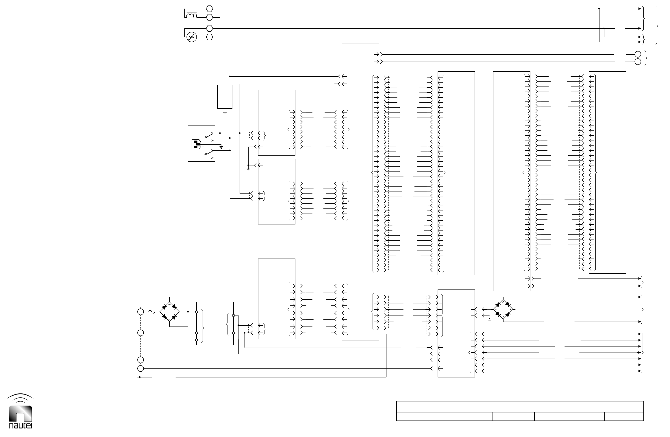
Dimensions = mm (inches)
Electrical Schematic – Vector-LP Transmitter: Ac/Dc Power Stage
Issue 1.8.1 Not to Scale Figure SD-1 Sheet 1 of 1
U5
3
4
TB2
1LINE
LOAD
P6
P5
B
A
P2
P1
E1
E2
PWB
J3
E3
RETURN
GND
GND
RETURN
N/C
N/C
N/C
N/C
-15V (A)
+5V (A)
+5V (A)
N/C
N/C
J1
A2
J1
E6
E5
N/C
N/C
LINE
LINE
LINE
+
3
U6
P32
P2
P26
A11
J1
E4
+5V
+15V
RETURN
N/C
N/C
+5V (A)
+5V (A)
J1
PWB U9
J2
A2
LINE
GND -
FROM CONTROL/
MONITOR STAGE
CHARGER IN
BATTERY (+)
F1
1
A16TB1
G
U8
LOAD
L
2
P1 6
OUTPUT 1
4
3
8
(OPTIONAL)
INPUT
POWER SUPPLY
U10
5
6
OUTPUT 1
4
7
INPUT P4
POWER
E1 U3
6
OUTPUT 1
3
SUPPLY 7
INPUT P3
UNIVERSAL
U2
+24.7V 1
-15.7V 3
+15.8V 5
GND 6
GND
+5.9V
8
RETURN
+24.5V
2
1
J5
-15.5V 3
+15.6V
GND
5
8
+24.5V 1
J4
-15.5V
GND
3
6
GND 8
19
4
2
P23
39
37
36
34
32
31
29
27
26
24
22
21
19
17
16
14
12
11
9
7
6
4
2
1
E3
19
4
2
P24
39
37
36
34
32
31
29
27
26
24
22
21
19
17
16
14
12
11
9
7
6
4
2
1
24
22
10
P24
E6
39
40
37
34
35
32
29
30
27
24
25
22
19
20
17
14
15
A11 12
9
10
7
4
5
2
39
40
37
34
35
32
29
30
N/C
27
N/C
N/C
24
25
N/C
N/C
22
19
20
17
14
15
12
9
10
7
4
5
2
STAGE
TO RF
+24V 1
(A)
AC
(B)
STAGE
TO RF
CHARGER OUT 4
BATTERY (-)
3
2 N
L
NE
J1
10A
t°
RT1
N
U7
4
AC INPUT 5
2
DC/DC
BATTERY
UNIVERSAL
P25
10
AC/DC
AC INPUT
SUPPLY
UNIVERSAL
2
3
10
E1
AC INPUT
5
2
4
AC/DC
POWER 10
RETURN
GND
2
4
J6
7
GND
GND
+5.6V
4
6
7
GND
RETURN
+15.6V
2
4
5
+5.6V 7
18
3
1
40
38
35
33
30
28
25
23
20
18
15
13
10
W4P2
8
5
3
E2
E1
E4
21
18
3
1
40
38
35
33
30
28
25
23
20
18
15
13
10
W4P1
8
5
3
25
23
11
7
E8
36
31
38
33
26
21
28
23
PWB
16
11
18
13
6
1
W10P2
8
3
GND
GND
GND
36
31
38
33
N/C
J2
26
21
28
23
16
11
18
13
6
1
8
3
W10P1
AC
TB1
3
POWER
L
2.5mH
L01
# DC INHIBIT -
LINE 4
FILTER
LINE
3
3
4
1
2
BATTERY VOLTS
BATTERY SELECT 2
(OPTIONAL)
BATTERY
BOOST
+24V RETURN
+24V (A)
+24V RETURN
+24V (A)
AC SIGNAL RETURN
AC SIGNAL RETURN
AC SIGNAL (A)
+15V (A)
+15V (A)
+15V RETURN
PWB
+15V RETURN
-15V RETURN
+5V RETURN
(PART OF) +5V RETURN
BATTERY VOLTAGE SAMPLE
TO CONTROL/
BATTERY CURRENT SAMPLE MONITOR STAGE
CHARGER CURRENT SAMPLE
MODEM SUPPLY (-)
TO CONTROL/
+9V MODEM SUPPLY (+)
+24V RETURN
+24V RETURN
+24V RETURN
+24V (B)
+24V (B)
+24V (B)
AC SIGNAL RETURN
AC SIGNAL RETURN
AC SIGNAL (B)
AC SIGNAL (B)
RETURN
+15V (B)
+15V (B)
+15V (B)
+15V RETURN
+15V RETURN
+15V RETURN
-15V RETURN
-15V (B)
+5V (B)
+5V (B)
+5V (B)
+5V RETURN
+5V RETURN INTERFACE
EXCITER
+5V RETURN
(PART OF)
+24V
VOLTS
VOLTS
S2050010 VD
1
(OPTIONAL)
1
1
CB1
3
# DC INHIBIT -
BATTERY SELECT 1
+24V RETURN
A16A1
+24V (A)
+24V (A)
+24V RETURN
AC SIGNAL (A)
+15V (A)
+15V (A)
INTERFACE
(PART OF)
EXCITER
+15V RETURN
+15V RETURN
INTERFACE
+5V RETURN
+5V RETURN
#DC INSTALLED -
BATTERY BOOST (B)
POWER
BATTERY BOOST (A)
MONITOR STAGE
+24V RETURN
+24V (B)
RETURN
(PART OF)
INTERFACE
+15V (B)
+15V RETURN
+5V (B)
PWB
+5V RETURN
(TO ATU)
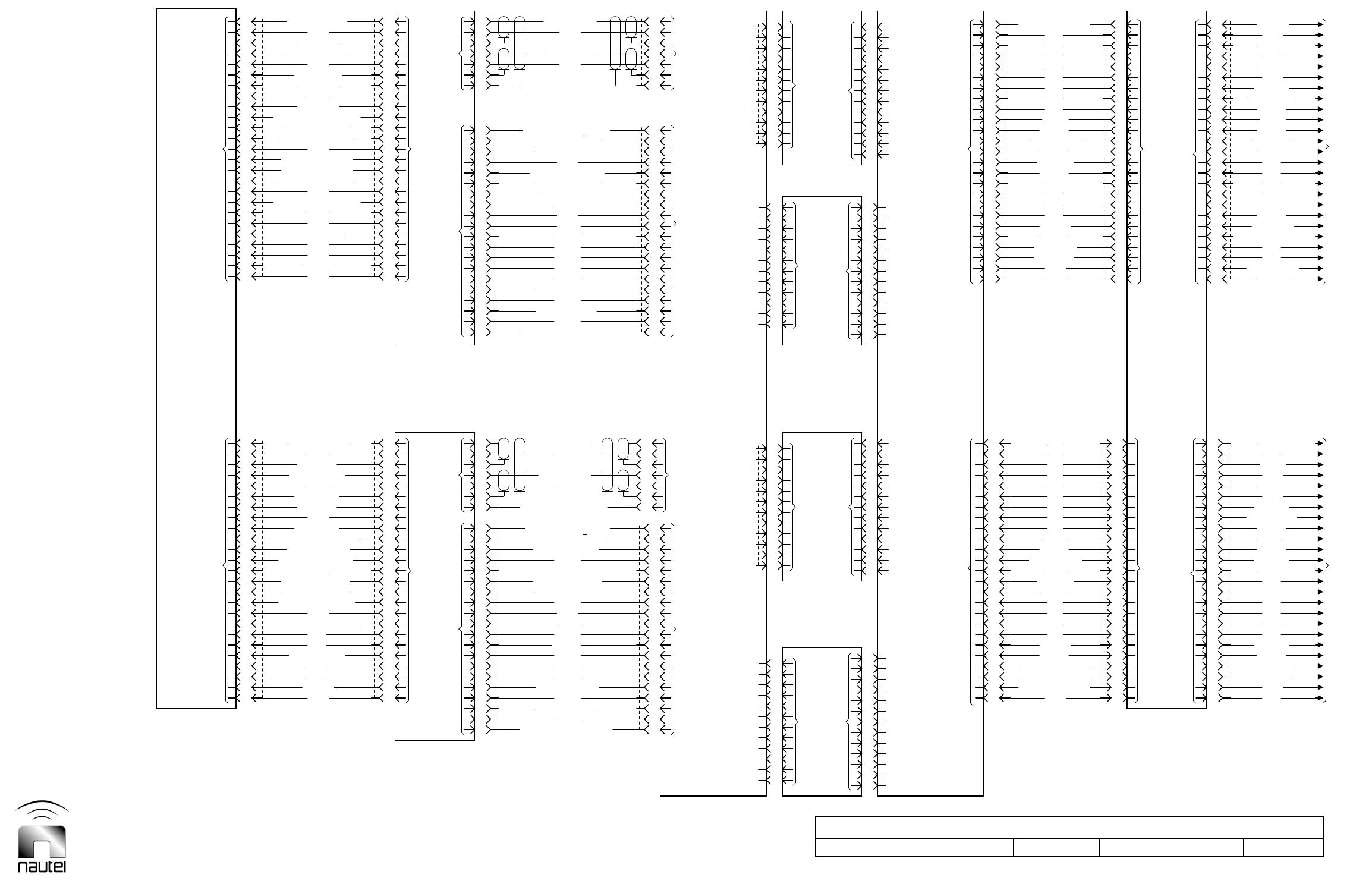
Dimensions = mm (inches)
Electrical Schematic – Vector-LP Transmitter: Exciter Stage
Issue 1.8.1 Not to Scale Figure SD-2 Sheet 1 of 1
B
A7
J3
J3
***
***
GND
GND
-15V
+15V
GND
N/C
GND
GND
GND
GND
GND
-15V
+15V
GND
N/C
GND
GND
GND
***
J4
GND
N/C
N/C
N/C
GND
N/C
N/C
N/C
N/C
P1
J1
P1
J1
P1
P1
J6
J9
P14
J8
P17
PWB
A3
P8
J1
J1
**
A10
A
J4
J4
**
GND
GND
+5V
GND
GND
GND
+5V
GND
N/C
J11
N/C
J6
J10
N/C
J5
J11
J10
J5
J8 J7
J10
P16
S2050043 V1
J16
INTERFACE
REMOTE
(PART OF)
GND
MSK (B)
GND
N/C
GND
GND
KEYING MONITOR (A)
KEYING MONITOR (B)
KEYED TONE/AUDIO (B)
# MISC (B) -
INT BUS (-)
GND
VOICE INPUT (B)
GND
P9
GND
MSK (A)
GND
RF MONITOR (A)
N/C
GND
GND
RF VOLTS MONITOR (A)
KEYING MONITOR (B)
KEYING MONITOR (A)
KEYED TONE/AUDIO (A)
# MSK ALARM (A) -
# MISC (A) -
INT BUS (-)
INT BUS (+)
GND
VOICE INPUT (A)
GND
FWD PWR SAMPLE
14
15
17
19
20
22
24
25
2
MONITOR/
4
EXCITER
5
7
9
10
12
P10
14
15
17
19
20
22
24
25
2
4
5MONITOR/
GENERATOR
7
9
10
12
W9P1
4
6
5
3
W9P2
***
+15V (B)
AUDIO (B)
# INHIBIT PDM (B) -
-15V (B)
AUDIO SHIELD (B)
B+ SAMPLE 1 (B)
B+ SAMPLE 2 (B)
# RESET PDM (B) -
CARRIER REF (B)
# TUNE SELECTED (B) -
IPM COMPENSATION (B)
GND
+15V (B)
GND
EXCITER
INTERFACE
(PART OF)
+15V (A)
# INHIBIT PDM (A) -
AUDIO SHIELD (A)
-15V (A)
2Fpdm (A)
B+ SAMPLE 2 (A)
J13 CARRIER REF (A)
# RESET PDM (A) -
# TUNE SELECTED (A) -
EXT Fc (A)
IPM COMPENSATION (A)
GND
J16 # RESET DDS (A) +
+15V (A)
GND
**
PDM DRIVER
J1
*
PWB
SYNTHESIZER
A8
A
PWB
A6
J1
*
SYNTHESIZER
GND
PDM 1 (B)
N/C
PDM 2 (B)
# PDM LATCH (B) +
# PDM INSTALLED (B) -
GND
Fpdm (B)
DUMP (B)
GND
N/C
N/C
N/C
N/C
# TUNE RF DRIVE (B) +
# HIGH BAND (B) -
# SYNTH INSTALLED (B) -
EXCITER
INTERFACE
(PART OF)
PDM 1 (A)
GND
PDM 2 (A)
N/C
# PDM INSTALLED (A) -
# PDM LATCH (A) +
Fpdm (A)
GND
GND
DUMP (A)
2Fpdm (A)
N/C
N/C
N/C
Fc (A)
N/C
N/C
# HIGH BAND (A) -
# DDS INHIBIT (A) +
GND
# SYNTH INSTALLED (A) -
GND
BATTERY B+ SELECT 3
BATTERY B+ SELECT 1
PDM (B)
N/C
N/C
SHIELD
DUMP (B)
B+ SAMPLE (B)
Fc (B)
N/C
N/C
N/C
N/C
N/C
P13
GND
INT BUS (+)
SHIELD
N/C
N/C
N/C
DUMP (A)
B+ SAMPLE (A)
SHIELD
N/C
N/C
N/C
N/C
GND
# RELAY CONTROL B -
PWB
INTERFACE
(PART OF)
24
22
21
19
17
16
J9
14
12
11
9
7
6
4
2
1
N/C
GND
INT BUS (+)
PDM (B)
N/C
N/C
N/C
N/C
DUMP (B)
Fc (B)
SHIELD
SIDE B +
+24V B
GND
GND
RELAY CTRL B -
GND
INT BUS (-)
SHIELD
N/C
N/C
N/C
DUMP (A)
SHIELD
SHIELD
SIDE A +
GND
GND
GND
+15V A
TO RF POWER
TO RF POWER
J17
N/C
GND
RF VOLTS MONITOR (B)
RF MONITOR (B)
GND
INT BUS (+)
# PTT (B) -
# MSK ALARM (B) -
FWD PWR SAMPLE
N/C
GND
GND
# PTT (A) -
P7
16
18
21
23
1
GENERATOR
3
6
8
11
13
16
18
21
23
1
3
6EXCITER
8
11
13
W6P2
W6P1
W8P1
W6P3
7
1
2
**
W6P3
W8P2
2Fpdm (B)
J13
EXT Fc (B)
GND
# RESET DDS (B) +
PWB
A2
AUDIO (A)
B+ SAMPLE 1 (A)
GND
B
INTERPHASE
PWB
A9
B
RF
**
PDM DRIVER
INTERPHASE
PWB
A5
A
RF
GND
N/C
N/C
2Fpdm (B)
N/C
Fc (B)
N/C
# DDS INHIBIT (B) +
GND
PWB
A2
GND
N/C
N/C
N/C
# TUNE RF DRIVE (A) +
BATTERY B+ SELECT 2
SHIELD
N/C
N/C
SHIELD
SHIELD
N/C
N/C
N/C
N/C
GND
INT BUS (-)
PDM (A)
N/C
SHIELD
SHIELD
Fc (A)
N/C
N/C
N/C
P11
A11
25
23
20
18
15
13
10
8
5
3
P12
INT BUS (-)
SHIELD
N/C
N/C
SHIELD
SHIELD
GND
+5V B
B+ SAMPLE (B)
+15V B
+24V
N/C
INT BUS (+)
PDM (A)
N/C
SHIELD
Fc (A)
+24V A
+5V A
B+ SAMPLE (A)
STAGE
STAGE
1
314
615
817
1019
920
1122
1324
1625
182
204
195
# KEYING/MISC ALM (B) -
47
69
510
312
1
3
6
14
8
15
10
9
17
19
11
20
13
16
22
24
18
25
20
19
2
4
5
# KEYING/MISC ALM (A) -
47
69
510
312
18
19 24
21
16 22
112
14 13
3
6# KEYED CW (B) - 9
410
81
26
10
9
11
13# INHIBIT Fc (B) -
16# SHUTDOWN (B) -
24
23 2218
2020
13
18
19# SYNTH INSTALLED (B) -
# ACTIVE SIDE (A/B) -
16
15 11
9
7
8
Fc MONITOR (A)
4
32
21 19 24
23 17 22
# KEYED CW (A) - 26 16 21
28 14 13
30 7 10
29 4 9
31 2 6
# INHIBIT Fc (A) - 33
# SHUTDOWN (A) - 36
38
40
# SYNTH INSTALLED (A) - 39
24 22
23 21
# ACTIVE SIDE (A/B) -
18 13
416 11
15 10
6
58 7
Fc MONITOR (A)
34 2
3 1
Fc MONITOR (B)
*** DENOTES INSTALLED FOR DGPS OPERATION ONLY
* DENOTES INSTALLED FOR NDB OPERATION ONLY
1425 25
1524 24
1722 22
1920 20
2119 19
2217 17
2415 15
2514 14
212 12
410 10
99 9
77 7
55 5
124 4
102 2
2424
1522
1621
1819
2017
2116
2514
212
311
59
77
86
104
122
131
2
4
516
718
1221
1423
151
RF CURRENT MONITOR (B)
173
6
78
111
213
2
4
5
7
16
18
12
14
21 RF CURRENT MONITOR (A)
23
15
17
1
3
6
78
111
213
25
2CARRIER REF (FILTERED) (B)
4CARRIER REF (B)
5
17 23
20
15
711
8
3
7
12
14
2515# CHANGEOVER (B) -
5
19 2117
17 12
14 10
56
# SHUTBACK (B) -
1Fc MONITOR (B)
CARRIER REF (FILTERED) (A) 25
22
CARRIER REF (A) 24 18 23
15 20
25
27 12 11
3 8
32
34 1 5
# CHANGEOVER (A) - 35
# SHUTBACK (A) - 37 25
7
1
19 20
14 9
17 12
5 6
2
1623 23
** DENOTES INSTALLED FOR DUAL TRANSMITTER
1821 21
2018 18
2316 16
113 13
311 11
88 8
66 6
113 3
131 1
2325
1423
1720
1918
2215
113
410
68
95
113
Dimensions = mm (inches)
Electrical Schematic – Vector-LP Transmitter: Control/Monitor Stage
Issue 1.8.1 Not to Scale Figure SD-3 Sheet 1 of 1
STAGE
GND
GND
GND
GND
GND
GND
GND
GND
P21
19
17
15
13
11
9
7
5
3
1
TB1
J18
GND
GND
GND
GND
W3P2
GND
GND
GND
GND
J9
J7
J4
FS
CE
RD
W7P2
W1P1
W2P1 A2
J1
J7
J3
J9
J7
J4
GND
GND
+24V
+5V
-15V
+15V
+15V
GND
GND
GND
J6
J5
P22
+15V
-
J3
N/C
N/C
RX
GND
N/C
TX
TX
CTS
DSR
GND
TXD
DCD
P27
(-)
20
J6
J7
16
12
14
18
4
6
10
8
2
J12
J13
GND
GND
GND
GND
SHIELD
GND
GND
GND
N/C
RF IN
W5P2
U1
J15
PWB
A1
GND
+24V
GND
GND
GND
+24V
+24V
J1
+15V
+
PWB
A3
GND
SHIELD
RX
N/C
N/C
RTS
DTR
RXD
RS-485
PWB
A4
SITE
POWER STAGE
TO/FROM
# DC INHIBIT -
INTERLOCK
GND
SHIELD
AUDIO
INPUT
GND
GND
(+)
STANDBY CODE 1
(+)
STANDBY CODE 2
(+)
RF ON/OFF
ALARM
(+)
CHARGER
N/C
34
39
32
29
30
27
23
25
21
18
19
16
13
14
7
4
5
W3P1
INTERFACE
(PART OF) 5
14
11
16
17
18
19
24
21
36
39
40
COMMON
KEY
INCREASE
POWER
POWER DECREASE
REMOTE
# STANDBY CODE 1 -
# EXT PDM INHIBIT -
# EXT INTLK OPEN +
BATTERY VOLTAGE
BATTERY CURRENT
# SPARE ADC
# MISC FAIL (A) -
# STANDBY CODE 2 -
# EXT RF ON -
# MSK ALARM (B) +
# MSK ALARM (A) +
RF CURRENT SAMPLE
REFLD PWR SAMPLE
J6
J5
PWB
A1
J1
MAG/AUDIO 2
+24V (BATTERY)
+24V (BATTERY)
+24V (BATTERY)
KEYED TONE/AUDIO (B)
MAG/AUDIO 1
RETURN
KEYED TONE/AUDIO (A)
LED_K
RESET
C/D
WR
W7P1
VCC
CARRIER REF (B)
RETURN
CARRIER REF (A)
# STANDBY TEST -
# SIDE B MAIN -
BATTERY B+ SELECT 2
N/C
GND
# MON BYPASS +
GND
N/C
RETURN
INT BUS (-)
INT BUS (+)
# RESET PDM -
GND
GND
N/C
GND
W1P2
# SHUTBACK (A) -
GND
GND
N/C
N/C
GND
GND
GND
N/C
N/C
W2P2
J1
GRAPHIC
J7
J3
PWB
D7
D6
D5
D2
D3
D1
D0
W7P2
FGND
# PDM INSTALLED (B) -
# PDM INSTALLED (A) -
# CHANGEOVER +
# MONITOR FAIL +
# SHUTDOWN +
# LVPS FAIL (B) -
# RF FAIL (A) +
# RF FAIL (B) +
# PDM LATCH (B) +
# PDM LATCH (A) +
W1P1
# RF OSC FAIL +
GND
GND
+5V
-15V
AC POWER
AC POWER RETURN
GND
GND
+24V
GND
PDM (B)
PDM RETURN (A)
N/C
N/C
N/C
W2P1
17
16
14
12
11
W7P1
1
26
25
23
14
11
9
7
6
W1P2
4
28
25
26 DISPLAY
23 (PART OF)
20
21
18
15
16
10
7
8
5
2
3
W2P2
INT BUS (+)
(LED 8)
AC MAINS
(LED 7)
(LED 6)
(LED 5)
EXCITER
IPA/PA
NETWORK
OUTPUT
W9P1
(LED 9)
R
(LED 10)
(LED 12)
(LED 11)
W8P1
EXT TXD
GND
EXT RXD
W3P2
37
24
35
11
2
9
W3P1
1
8
3
9
26
23
28
29
30
31
37
38
MODEM SUPPLY (+)
8
6
J5 5
3
1
RF MONITOR
AUDIO MONITOR (-)
TB1 23
AUDIO MONITOR (+)
21
GND (ISOL)
25
DE/RE
INT BUS (-)
5
4
GND (ISOL)
2
9
7
J4 RS-422
4
5
2
GND
20
17
18
GND
11
J10 +24V
+24V
8
9
GND4
GND
+5V
1
2
U11-U14
20
17
18
11
8
9
4INTERFACE
1
2
LINE
PHONE
FROM RF
AC/DC POWER
MSK (B)
MSK (A)
N/C
(+)
PRESS-TO-TALK
(-)
(-)
(-)
(-)
N/C
J15
40
33
31
J11
28
26
22
20
17
15
8
6
PWB
A3
REMOTE
3
6
10
13
15
20
22
33
W5P1
35
KEY
COMMON
RF ON
LOCAL
RF OFF
(PART OF)
# DC INSTALLED -
CHARGER CURRENT
# MOD PROT -
# MISC FAIL (B) -
# RF ON +/OFF -
# CHARGER ALARM -
# EXT RF OFF -
FWD PWR SAMPLE
CONTROL/
DISPLAY
(PART OF)
RETURN
+24V (BATTERY)
+24V (BATTERY)
VEE
LED_A
RETURN
BATTERY B+ SELECT 1
N/C
RETURN
N/C
# SHUTBACK (B) -
GND
GND
N/C
N/C
N/C
DISPLAY
EXCITER
INTERFACE
(PART OF)
J15
D4
VSS
# ACTIVE SIDE B -
# LVPS FAIL (A) -
+5V
GND
GND
+15V
+15V
GND
PDM (A)
N/C
PDM RETURN (B)
N/C
W5P2
18
15
13
2
27
24
15
10
8
5
27
J11
24
22
19
17
CONTROL/
14
9
6
4
1
INT BUS (-)
R
R
R
R
(LED 4)
R
R
(LED 3)
(LED 2)
(LED 1)
LOCAL
REMOTE
RF OFF
RF ON
R
R
R
(PART OF)
M1
GND
GND
J18
38
36
12
10
1
2
4
7
J13
12
25
27
32
W5P1
34
MODEM SUPPLY (-)
9
7
4
2
J8
22
24
GND (ISOL)
INT BUS (+)
+5V (ISOL)
3
1
6
6
1
3
8
GND
GND
GND
+24V
19
12
10
7
+15V
3
W16P1
(OPTIONAL)
MODEM
J1
19
12
10
7(OPTIONAL)
3
W16P2
J14
R
R
LS1
S2050013 VD
17
15
SOFT KEY 1
14
SOFT KEY 3
12
W9P1
11
10
10MHz (A)
6
6
10MHz (A) FRONT PANEL OVERLAY
W8P1
2
REFLD PWR SAMPLE 5
10
FWD PWR SAMPLE 1
34
39
14
RF VOLTS MONITOR 9
32
18
RF CURRENT MONITOR 13
29
30
RF CURRENT SAMPLE 17
27
21
23
25BATTERY VOLTAGE SAMPLE 24
21
BATTERY CURRENT SAMPLE 22
18
19CHARGER CURRENT SAMPLE
#DC INSTALLED -
10
16
13
14
7
4
5
19 11 17
10 10 16
8 8 14
6 6 12
5 5 11
3 3 1
39 39 26
38 38 25
36 36 23
34 34 14
33 33 11
# SYNTH INSTALLED (B) -
31 31 9
29 29 7
28 28 6
21 21 4
19 19
18 18 28
25
16 16 26
12 12
3 3 23
20
1 1 21
40 40 18
37 37 15
38 38 16
35 35 10
32 32 7
33 33 8
30 30 5
12 12 2
13 13 3
5 1
14 8
11 3
16 9
17 26
18 23
19 28
24 29
21 30
36 31
39 37
40 38
9
8POWER SUPPLY
7EXTERNAL ALARM
6CHANGEOVER
5LOW VOLTAGE
4
3
1FROM AC/DC +
1
28
5 6
5
43
FRONT PANEL OVERLAY
1
4
2
1
37
24 SERIAL BUS
35 (TO ATU)
11 MONITOR AMPLIFIER GAIN
2 # DC INHIBIT -
9 # REMOTE COMMON -
INTERFACE
(PART OF)
INT BUS (-)
INT BUS (+)
RF OSC SAMPLE
18
16
13
11
10
SOFT KEY 2
9
8
7
40
33
31
28
26
22
20
25
23
11
17
15
8
6
7
3
20 12 18
9
7
4
9
7
4
15
13
2
40
37
35
32
40
37
35
32
27
24
15
10
30
22
20
17
30
22
20
17
8
5
27
# SYNTH INSTALLED (A) -
13
2
39
13
2
39
24
22
19
17
36
34
31
29
36
34
31
29
14
9
6
4
11 11
6
10
13
1
2
4
7
15
20
22
33
12
25
27
32
35 34
POWER SUPPLY
2
*OPTIONAL*
-
POWER STAGE
3
9
7
4
2
3
38
36
12
10
RF MONITOR SELECT
# OPERATING B -
1 # AC ENABLE -
REMOTE
SERIAL BUS
Dimensions = mm (inches)
Electrical Schematic – Vector-LP Transmitter: RF Power Stage
Issue 1.8.1 Not to Scale Figure SD-4 Sheet 1 of 1
N/C
GND
N/C
N/C
N/C
Fc (B)
GND
+5V B
GND
N/C
GND
N/C
N/C
N/C
Fc (A)
GND
+5V A
GND
**
P18
**
-
**
-
E1
L2
L1
E2
E3
E4
A14
E5
E18
2
2
R7
R6
R5
R4
R3
1
T1
E35
T3
E21
E20
E19
L3
C1
C2
2
L4
1
N/C
GND
+24V
N/C
GND
P1
P1
B
A13
A
A12
P19**
E12
**
-
-
E7
E5
L3
E2
C1
C3
C5
C7
C9
C11
C2
C4
C6
C8
E35
J1 P15 1
L1
2
1
L2
T2
S2050014 V1
INT BUS (+)
SHIELD
PDM (B)
SHIELD
DUMP (B)
SHIELD
B+ VOLTAGE B
SIDE A +
+24V B
P19
BATTERY BOOST (B)
AC VOLTS (B)
INT BUS (+)
SHIELD
PDM (A)
SHIELD
DUMP (A)
SHIELD
B+ VOLTAGE A
SIDE A +
+24V A
P18
BATTERY BOOST (A)
AC VOLTS (A)
A1J7
RF POWER
P1
P1
A1J7 J7
RF POWER
# INHIBIT PDM B -
FAN 2 ENABLE
P31** B4P1**
+24V FAN 1
FAN 1 TACH
FAN 1 ENABLE
E13
# INHIBIT PDM A -
FAN 2 ENABLE
+24V FAN 2
P29 B2P1
FAN 2 TACH
FAN 1 ENABLE
+24V FAN 1
P28 B1P1
FAN 1 TACH
+
E15
E17
E19
S1-2
+
+
E21
E33
E31 E34
A14
E6
E8
E10
E12
E14
E16
E23
E25
E26
E28
E30
E36
C22
C21
C20
C19
C18
C17
C16
E34
E32
E30
E28
E27
E25
E23
CR1
MUR160
CR2
CR4 CR3
4T 80T
4 3
A15
L6
1800pF
0.5W
4700
R8
10000μHR11
R1 R2
E22 J1 RF OUTPUT
6 GND
1
9
14 GND
18 GND
J1 P20
TO CONTROL/
MONITOR STAGE
INT BUS (-)
SHIELD
+15V B
AC VOLTS (B)
RELAY CTRL
INT BUS (-)
SHIELD
+15V A
AC VOLTS (A)
J7
MODULE
MODULE
+24V FAN 2
FAN 2 TACH
P30** B3P1**
A
B
K1
S2-2
+
B4
B3
E14
C3
0.0036
C2
0.0036
E16
E18
C7
0.0036
C6
0.0036
E11
E8
E20
E10
E9
E6
B2
E3
E4
E1
RF FILTER PWB
E32
RF FILTER PWB
330pF E7
E9
E11
750pF
C10
C12
E13
E15
E17
1600pF
1300pF
2700pF
E22
E24
E27
E29
330pF
1600pF
1300pF
1300pF
1300pF
C15
C14
C13
1600pF
1600pF
1600pF
20T
E33
E31
E29
E26
E24
MUR160
MUR160
4
3
20T
L5
L4
10000μH
0.5W
4700
2W
100
100
2W
R10
1T
40T
R9
5
2 GND
10
13
GND
17
RF OUTPUT
J5
C1
0.0036
C4
0.0036
C5
0.0036
C8
0.0036
B1
C13
0.0036 C11
0.0036 C12
0.0036 C10
0.0036
1300pF
C15
0.0036
1300pF
1600pF
MUR160 1800pF
100
2W
#
19
21
17 23
15
#
#22
14
13FROM
EXCITER STAGE
11
9
20
5
3
2
5
2 11
FROM AC/DC
XA13P1XA13P1
FROM EXCITER
STAGE
11#
1219
17
15
# 21
#25
14
13FROM
EXCITER STAGE FAN TACH 2A
8
11
22
24
9
20 FAN TACH 1A
7
5
3
2
5
2
FROM AC/DC
XA12P1
** DENOTES INSTALLED FOR DUAL TRANSMITTER
(STANDARD FREQUENCY BAND)
(EXTENDED FREQUENCY BAND)
FWD PWR SAMPLE
10000μH
RF VOLTS MONITOR
RF CURRENT MONITOR
18
16
#
#
25
8
24
7FAN TACH 1B
FAN TACH 2B
12
10
6
4
1
6
3
1 12
POWER STAGE
18 XA12P1
16
#
#
12
23
10
6
4
1
6
3
1
POWER STAGE
330pF
1300pF
1600pF
1600pF
3900pF
REFLD PWR SAMPLE
10000μH
2W
1000
2W
1000
2W
1000
2W
100
4
RF POWER PROBE PWB
1T
RF CURRENT SAMPLE
C14
0.0036 C9
0.0036 C16
0.0036
1300pF
2W
1000
2W
1000
125 W TRANSMITTERS
E5
L6
E14 E18
E21
E23
E22
E35
E1
RF INPUT L2 E2
RF OUT
C9
1600pF
C14
1600pF
C13
1600pF
C10
1600pF
J1
S1950253 V1
A14
RF FILTER PWB
(EXTENDED FREQUENCY BAND)
250 W TRANSMITTERS
Dimensions = mm (inches)
Electrical Schematic – Control/Display PWB (NAPC147D)
Issue 1.8.1 Not to Scale Figure SD-5 Sheet 1 of 4
(+)
MOSI
MISO
6J10
9J10
5J10
8J5
7J5
4J8
CR6
E1:2
CR3
E1:3
CR7
A
E2:2
CR8
475
R145
4
DI
+5V
+5V
54
56
6
7
25
32
18
58
60
19
27
28
OC3A
PB.4
PB.5
SS
MISO
MOSI
SCK
PE.2
A15
ALE
WR
A10
A9
A12
A14
AD0
AD2
AD4
AD6
PE.7
A9
A12
A11
A14
D1
D3
D5
D7
+5V
38
J1
37
J1
GND
A2
A4
A7
A9
A12
A14
D1
D3
D5
D7
SCK
TO
(-)
5J8
3J10
1J10
1J8
+5V +5V
B
+5V
C49
0.1 C54
0.01
+5V
+5V
+5V +5V +5V
55
8
57
26
31
29
30
59
61
17
16
2
3
RD
A11
A13
A8
AD5
AD3
AD1
AD7
A13
A10
A8
ADDRESS
D4
D2
D0
D6
A14
5CEI
TP52
A3
A1
A0
A6
A5
A8
A10
A11
A13
+5V
D0
D6
D2
D4
DATABUS
R6
100
+5V
FROM SHEET 2
PROG TDI
PROG TDO
PROG TMS
PROG TCK
FROM SHEET 2 INT4
FROM SHEET 3
#AC_LOW-
INT0
FROM SHEET 2
FROM SHEET 3 +5V
# RF OFF -
# REMOTE -
# RF ON -
11 J5
# LOCAL -
12 J6
# UP KEY -
15 J6
10 J6
22 J7
20 J7
BUS
19 J7
36 J1
20 J1
INT BUS (-)/
19 J1
INT BUS (+)/
475
R144
475
R155
+5V
E2:1
E2:3
CR4CR5 CR13CR12
475
R184
475
R151
475
R152 475
R185
8VCC
3
DE
6DO/RI
1
RO
INTERNAL
TDI
TDO
TCK
TMS
INT6
INT0
L10
C127
0.1 C128
0.01
21 VCC
L11
CR10
PD.6
PD.7
PD.5
PD.4
PG.3
PF.2
PF.3
PF.1
PF.0
PG.4
PB.7
475
R190
10.0K
R186
22 GND
53 GND
4750
R202
15
1
PEN
10
13
11
43
34
33
36
39
38
41
51
50
49
47
48
45
46
44
9
+5V
9SDO
15 E
10 SCL
16 VCC
7VBAT
+15V
8
VSS
11
SQW
14
FT/OUT
A15
TO
ALE
RD
#STANDBY_2-
TO
+5V
FROM SHEET 2
GND GND
4
GND
1
VCCO
RAM MONITOR
28 VCC
27 WE
21 A0
24 A2
1A5
26 A4
3A7
5A9
6A10
8A12
10 A14
12
I/O1
15
I/O3
17
I/O5
19
I/O7
MONITOR
AMPLIFIER GAIN
SHEET 3
PROG SCK
PROG GND2
J10
PROG GND
6
J8
SHIELD
17
J6 SWITCH COMMON
6
J5 RF ON COMMON
PROG VCC7
J10
FROM SHEET 4
#EOC-
15 J1
16 J1
13 J6
10 J5
16 J6
14 J6
11 J6
21 J7
EXT RXD 35 J1
S1950199 SHEET 1 OF 4 V1
+5V+5V
221
R92
221
R91
681
R100
+5V
B
A
+5V+5V +5V
DS36C278TM
U6
7DO/RI
5
GND
2
RE
SERIAL INTERFACE
4750
R201
INT5
L12
52 VCC
INT1
C118
0.01
C119
0.1
63 GND
C125
18pF C126
18pF
Y1
11.0592MHz
PB.6
TP27 TP26
TP14
TP45
+5V
5
14
62
AREF
12
20
RESET
+5V
4
42
TP47
40
37
35
R249
1000
Q5
2N7002LT1
3920
R252
TP48
3RST
12 SDI
5RSTIN1
R250
100
BT1
3V
4WDI
13 THS
C164
0.47
C165
0.1
1
XI
6
RSTIN2
2
XO
Y2
32.768kHz
R224
1000
10.0K
R223
WR
DATABUS
R5
100
#RMT_RF_ON+
C120
10
35V
C115
0.1 C121
0.01
TP5 TP32
7
BW
6
CEO
3
TOL
DS1312S-2
U21
ADDRESS
22 OE
20 CE
C111
0.01
25 A3
23 A1
4A8
7A11
2A6
9A13
+5V
14
GND
11
I/O0
18
I/O6
13
I/O2
16
I/O4
TO SHEET 2
11
J1
PROG GND10
J10
3
J8
TO SHEET 2
9
J5 SWITCH COMMON
18
J6
4
J10 PROG VCC
PROG VCC
2
J8
TO SHEET 2
681
R101
+5V
C116
0.1 C117
0.01
C137
0.1
C138
0.01
10.0K
R251 R255
475K
R254
475K
R225
1000
13
12
14
U11:D
4750
R200
#SS6(RTC)-
PROG RESET
# EXT RF OFF -
CR9 CR11
# EXT RF ON -
# DOWN KEY -
# SOFTKEY 3 -
# SOFTKEY 1 -
# SOFTKEY 2 -
# PWR DECREASE -
# PWR INCREASE -
475
R146
475
R153 10.0K
R187
INTERNAL
SERIAL
E1:1
# STANDBY CODE 2 -
OC3B
64 AVCC
10.0K
R219
TP49
+5V TP51
SHEET 2
24 XTAL1
23 XTAL2
RXD1 TO SHEET 2
TXD1
TXD0
MICROCONTROLLER
EXT TXD
MISO
8VCCI
C139
0.01
GND
DATABUS
PROG RESET
BAT54HT1
CR14
# RMT RF ON +/OFF - EXTERNAL
INTERFACE
C166
0.1
100K
R253
M41T94MQ6
U25
REAL-TIME CLOCK
ATmega128-16AI
U22
RXD0
LS1
MSR516N
Q4
MMBT4401LT1
SHEET 2
RESET
MOSI
RESET
2VBAT #LOW_BAT-
C112
0.1
ADDRESS CY62256LL
U20
TP46
RAM
BAT54HT1
CR15
1 2
U24:A
Dimensions = mm (inches)
Electrical Schematic – Control/Display PWB (NAPC147D)
Issue 1.8.1 Not to Scale Figure SD-6 Sheet 2 of 4
9J7
8J7
5J7
2J3
4J3
A14
RD
TCK
TDI
81
75
72
21
62
56
36
70
54
67
61
71
76
80
77
D0
D2
D4
D6
RESET
WR
A0
D0
D2
D4
D6
TO
TO
D0
D2
D4
D6
D0
D2
D4
D6
D1
D3
D5
D7
D0
D2
D4
D6
A0
A2
A4
A6
A0
TO
N/C 3 J4
7J7
4J7
6J7
3J3
5J3
WR
A15
ALE
+5V +5V +5V
+5V +5V
TMS
TDO
82
74
84
65
2
45
63
68
7
1
23
79
3
D3
D1
D5
D7
A
RD
B
*
R238
0.0
R222
0.0
D1
D3
D5
D7
D5
D1
D3
D7
D5
D3
D1
D7
D4
D2
D0
D6
D3
D7
D1
D5
A1
A3
A5
A7
ADDRESS
R156
2210
S1950199 SHEET 2 OF 4 V1
#RMT_RF_ON+
FROM
SHEET 1
17 J1
25 J7
R3
100
39 J1
R159
100
15 J7
R216
100
23 J7
R24
100
14 J1
16 J7
14 J7
13 J1
31 J1
29 J1
CPLD TCK
CPLD TDI
VO(LCD)
+5V
FROM
SHEET 4
SHEET 1
RESET
C1
0.01 C130
0.01
C136
0.01
+5V +5V +5V +5V
4750
R12
4750
R16
4750
R203
RD
C70
0.01 C71
0.01 C61
0.01
+5V+5V +5V
4750
R167
4750
R172 4750
R165
TP42
DIGITAL INPUTS
11 10
U17:E 35
5 6
U17:C 39
1 2
U17:A 25
34
37
24
20
64 VCC_IO
18
15
11
13
26
19
17
14
10
12
9
6
5
4
C91
0.01
C90
0.1
30
28
58
69
55
51
50
48
46
10.0K
R191
+5V +5V
+5V
49
GND
60
GND
27
GND
8
GND
+5V
78
VCC_INT
10.0K
R181
R195
1000
TP37
E3:3
E3:2
E3:1
+5V
L6
L7 +5V
10.0K
R182
10.0K
R179 10.0K
R161
3
J7
2
J7
1
J7
CSOUT3
CSOUT1
INT4
RESET
WR
C/D
LED_A
LED_K
FS
FGND
VCC
DMF5005NY-LY-AKE
D1
D0
D3
D2
D5
D4
D7
D6
GRAPHIC
DISPLAY
6
J3
+5V 1
J3
INT0 SHEET 1
#SS5(DAC2)-
#SS3(ADC3)-
#SS1(ADC1)-
CSOUT3
CSOUT2
+5V
+5V
C150
0.1 C154
0.01
+5V
C95
0.1
# DC INHIBIT -2
J1
# AC ENABLE -
2
J6
# PA LED -
# RESET PDM -
4
J6 # EXCITER LED -
17
J7
# REMOTE LED -
N/C
# LOCAL LED -
30
J7
BATT B+ SELECT 3
35
J7
5
J6 # LOW VOLT PS LED -
BATT B+ SELECT 2
32
J7 BATT B+ SELECT 1
1
J6 +15V
# RF OFF LED -
4
J5 # RF ON LED -
# AC MAINS LED -
8
J6
# CHANGEOVER LED -
# POWER SUPPLY LED -
# OPERATING B -
9
J1 # REMOTE COMMON -
5
J4 N/C
R212
100
R116
100
27 J7
#STANDBY_2-
32 J1
18 J1
40 J1
24 J7
26 J7
22 J1
31 J7
R173
100
R166
100
11 J7
R11
100
21 J1
10 J7
R206
100
R175
100
30 J1
R10
100
CPLD TMS
SHEET 3
CPLD TDO
FROM
FROM
R131
100
R129
100
R14
100
4750
R1
C14
0.01
C13
0.01
+5V
C135
0.01
+5V+5V+5V
4750
R211
4750
R217
4750
R23 4750
R26 4750
R215
C15
0.01
C4
0.01 C3
0.01
+5V+5V+5V+5V
+5V+5V +5V+5V
4750
R8
4750
R9 4750
R27
10.0K
R117
10.0K
R122
10.0K
R123
WR
C123
0.01
C93
0.01
+5V+5V
4750
R128 4750
R130 4750
R115
C2
0.01
+5V
4750
R158 4750
R207 4750
R4
+5V +5V
C101
0.01 C109
0.01 C114
0.01
+5V
+5V +5V
4750
R174 4750
R196 4750
R205
+5V
10.0K
R192
TP43
10.0K
R193
33
44
41
9 8
U16:D 40
43
13 12
U15:F
C106
0.1 C105
0.01
31
3 4
U16:B 32
5 6
U15:C
1 2
U15:A
11 10
U14:E
L5 C94
0.01
C92
0.1
38 VCC_INT
3 4
U14:B
3 4
U13:B
L4
22 VCC_IO
29
#RF_ON+ 83
59
57
47
52
53
CPLD
66
LCD_CE
10.0K
R194
+5V +5V
16
GND
42
GND
+5V +5V
10.0K
R149
C98
0.1
73
VCC_INT
+5V+5V
R183
1000
TP41
VO(LCD)
0.5W
3.92
R246
0.5W
6.81
R220
0.5W
6.81
R221
C143
0.1
C144
0.01
+5V+5V+5V+5V
C107
0.1
C108
0.1
TP39
CSOUT2
CE
RD
VEE
ALED_A
VSS
KLED_K
C64
0.01
#SS4(DAC1)-
#SS6(RTC)-
#SS2(ADC2)-
SHEET 3
DATABUS DATABUS DATABUS DATABUS
CSOUT1
C162
0.1 C163
0.01
3 14
U38:C
1 16
U38:A
C160
0.1 C161
0.01
5 12
U34:E
3 14
U34:C
7 10
U34:G
4 13
U30:D
+5V
6 11
U30:F
DIGITAL OUTPUTS
C134
0.01
C129
0.1
R169
2210
R170
2210 R171
2210
5 12
U37:E
+5V
4750
R248
6 11
U35:F
R164
2210
#RF_ON+
R162
2210
+15V
+5V
R157
2210
R163
2210
4750
R247
1
J1
3
J6
18
J7
#REMOTE_STATUS+
1
J5
2
J5
33
J7
36
J7
34
J7
7
J6
12
J1
3
J5 +15V
5
J5
9
J6
6
J6
10
J1
4
J4 N/C
SHEET 1
R2
100
R204
100
R7
100
C5
0.01
C7
0.01
C113
0.01 C97
0.01
C100
0.01 C96
0.01
L8
9 8
U13:D
C103
0.1
0.5W
3.92
R243
TP38
1 16
U34:A
2 15
U30:B
R178
2210
3 14
U37:C
2 15
U35:B
C6
0.01
# CHARGER ALARM -
# STANDBY CODE 1 - 11 10
U16:E
5 6
U16:C
1 2
U16:A
# MSK ALARM (B) + 11 10
U15:E
+5V
# MSK ALARM (A) +
4750
R209
# BTRY/MOD PROTN -
# EXT INTERLOCK OPEN +
#REMOTE_STATUS+
#HIGH_RF_CURRENT+
#AC_LOW-
#LOW_BAT-
# SHUTBACK (A) -
TO SHEET 1
10.0K
R160
GRAPHIC DISPLAY SHOWN FOR REFERENCE ONLY.
10
J9
TP44
5
J9
8
J9
9
J9
* DENOTES LINK
INSTALLED FOR
20
J9
1
J9
3
J9
TP34
11
J9
13
J9
15
J9
17
J9
CPLD GND
CPLD VCC
10.0K
R180 10.0K
R148
2D1 19
Q1
U36:A
4D3 17
Q3
U36:C
6D5 15
Q5
U36:E
8D7 13
Q7
U36:G
R177
2210
2D1 19
Q1
U33:A
4D3 17
Q3
U33:C
6D5 15
Q5
U33:E
8D7 13
Q7
U33:G
C102
0.1
3D2 18
Q2
U29:B
5D4 16
Q4
U29:D
7D6 14
Q6
U29:F
9D8 12
Q8
U29:H
2D0 19
Q0
U23:A
4D2 17
Q2
U23:C
6D4 15
Q4
U23:E
8D6 13
Q6
U23:G
DATABUS
# PDM INSTALLED (B) - 3 4
U17:B
13 12
U17:F
9 8
U17:D
# DC INSTALLED -
# ACTIVE SIDE B -
C131
0.01
4750
R13
R208
100
13 12
U16:F
# PDM INSTALLED (A) - R214
100
R25
100
4750
R213
# MISC FALL (B) -
# LVPS FAIL (B) -
# PDM LATCH (B) +
# LVPS FAIL (A) - R15
100
R210
100
R168
100
9 8
U15:D
3 4
U15:B
13 12
U14:F
# MISC FALL (A) -
C110
0.01
5 6
U14:C
+5V
# PDM LATCH (A) + R197
100
1 2
U14:A
# EXT PDM INHIBIT - R28
100
4750
R198
1 2
U13:A
+5V
#REFLD_PWR_SHUTBACK+
Q1
MMBT4401LT1
Q2
MMBT4401LT1
10.0K
R189
TP40
6
J9
7
J9
4
J9
VECTOR ONLY
TP35
19
J9
L13
2
J9
14
J9
12
J9
16
J9
10.0K
R150
XC9572-15PC84C
U18
C99
0.01
18
J9
7D6 14
Q6
U36:F
5D4 16
Q4
U36:D
3D2 18
Q2
U36:B
4 13
U37:D
4 13
U38:D
2 15
U38:B
9D8 12
Q8
U36:H
5 12
U35:E
7D6 14
Q6
U33:F
5D4 16
Q4
U33:D
3D2 18
Q2
U33:B
4 13
U34:D
6 11
U34:F
1 16
U37:A
3 14
U35:C
9D8 12
Q8
U33:H
6D5 15
Q5
U29:E
2D1 19
Q1
U29:A
4D3 17
Q3
U29:C
R176
2210
7 10
U30:G
5 12
U30:E
20
VCC
10
GND
1
11 LATCH
ENABLE
OUTPUT
ENABLE
U23:I
SN74AHC573DW
8D7 13
Q7
U29:G
1 16
U30:A
3D1 18
Q1
U23:B
5D3 16
Q3
U23:D
7D5 14
Q5
U23:F
9D7 12
Q7
U23:H
ADDRESS
R218
100
C124
0.01
9 8
U14:D
R199
100
5 6
U13:C
C104
0.01
10
GND
20
VCC
11 CLK
1OUTPUT
ENABLE
U36:I
SN74AHC574DW
10
GND
20
VCC
11 CLK
1OUTPUT
ENABLE
U33:I
SN74AHC574DW
2 15
U34:B
4 13
U35:D
10
GND
20
VCC
11 CLK
1OUTPUT
ENABLE
U29:I
SN74AHC574DW
R188
2210
3 14
U30:C
1 16
U35:A
# SOFTSTART/SHUTBACK (B) -
# PM FAULT (C) -/CHANGEOVER ALM +
# OUTPUT NETWORK LED -
# PM INSTALLED (B)/MONITOR FAIL -
# PM FAULT (B) -/SHUTDOWN +
# RF DRIVE FAIL -/RF FAIL (B) +
# INHIBIT RF DRIVE/MON BYPASS +
# PM INSTALLED (C)/SYNTH INSTALLED (B) - # INHIBIT FAN +/SIDE B MAIN -
# B+ SEL 1 +/STANDBY TEST -
# DCC RMT COM -/RF MON SELECT
# PM INSTALLED (A) -/RF FAIL (A) +
# SPARK GAP SHTBCK/SYNTH INSTALLED (A) -
# PM FAULT (A)/RF OSC FAIL +
# EXTERNAL ALARM LED -
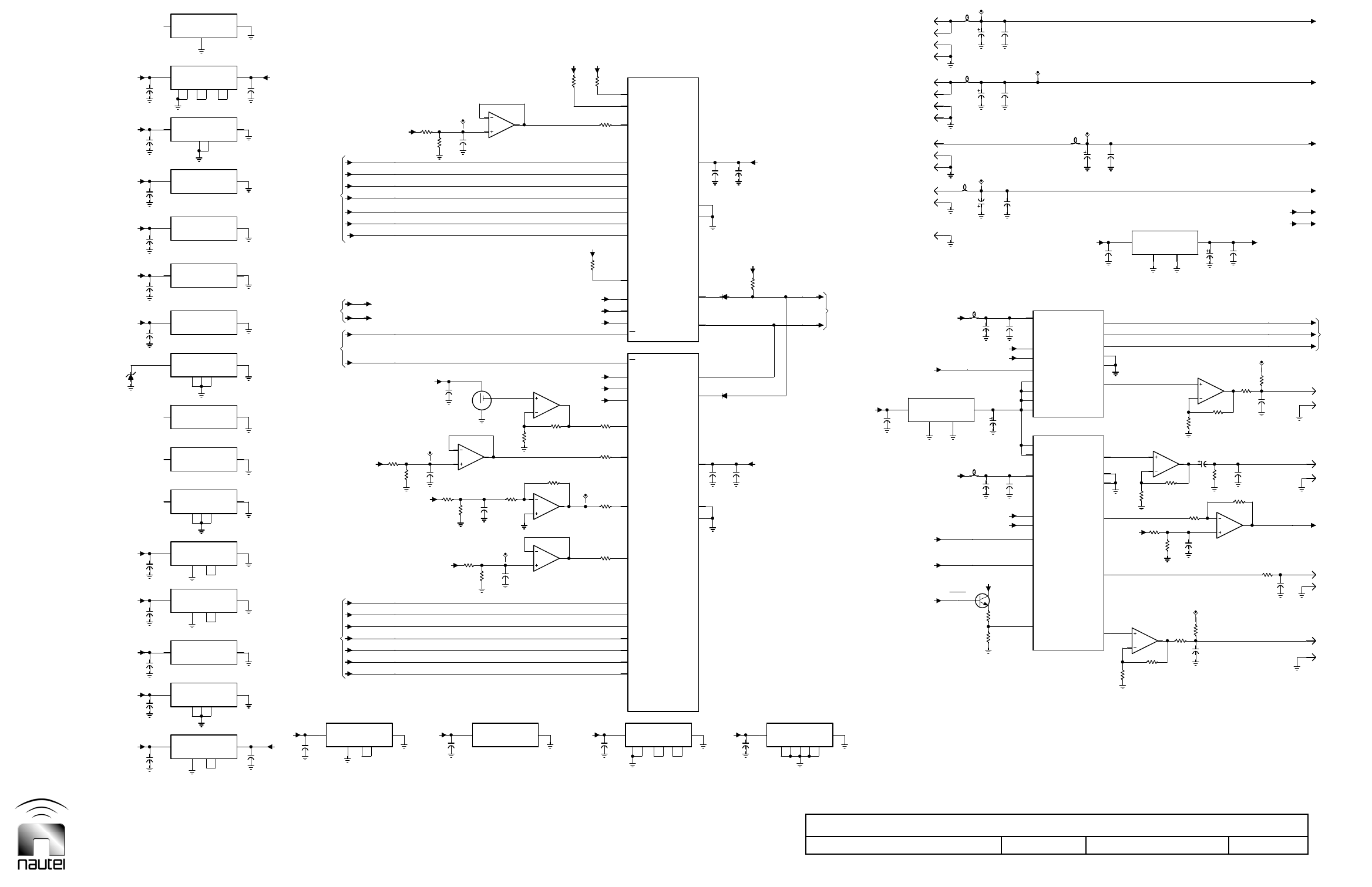
Dimensions = mm (inches)
Electrical Schematic – Control/Display PWB (NAPC147D)
Issue 1.8.1 Not to Scale Figure SD-7 Sheet 3 of 4
3
1
5
21
67
13
13
67
11 13
7
FROM
FROM
SCK
+5V
C78
0.1 C133
0.1
MISO
#EOC-
+15V
+5V
L2
C76
0.01
2
10 12
67
9 14
C151
0.1
C149
0.1
FROM
FROM
12 14
MOSI
R132
22.1K
C19
0.1
10 8913 14
+5V
3 95 13
-15V
+24V
+15V
+5V
L9
L3
+5V
35V
10
C122
C67
10
35V
C62
0.01
TP12
R235
10.0K
R226
4750
C158
10
35V
R233
100
R134
12.1K
TP33
C147
0.1
C77
10
35V
+15V
+15V
+5V
12
+5V
12
+5V
+5V
+5V
+5V
+5V
+5V
+15V
-15V
14
14
-15V
SHEET 4
+24V
SHEET 1
SHEET 4
C57
0.1
C50
0.01
C65
0.1
10.0K
R103
1A0
3A2
5A4
7A6
8A7
9A8
TLC1543IDW
U12
11 A9
SCK 18 I/O_CLK
15 CS
SCK
14 REF+
17 ADDRESS
1A0
5A4
7A6
R59
100
11 A9
10.0K
R135
10
GND
+5V
20
VCC
19
EOC
19
EOC
10
GND
SHEET 1
FROM SHEET 1
FROM SHEET 2
22 J4
14 J4
16 J4
17 J4
26 J4
27 J4
3REFB
Q3
MMBT4401LT1
SCK
C159
0.01
C155
0.1
5REFD
3REFB
SCK
8LOAD
MOSI 6DATA
L15
14 VDD
C132
0.01
10
DACC
+5V
13
LDAC
12
DACA
13
LDAC
10
DACC
12
DACA
+5V
C48
0.01
C142
0.1
3
J11
(M1)
1
J11
38
J7
VREF
+15V
+15V
C37
0.1
C145
0.1
C25
0.1
C17
0.1
C34
0.1
1SMB5939B
39V
CR16
C89
0.1
C86
0.1
C85
0.1
C84
0.1
C83
0.1
C148
0.1 8
+5V
13
13
SHEET 2
+5V
+5V
-15V
C55
0.1
10.0K
R104
TP24 6
5
7
U8:B
+5V
10.0K
R38
13
12
14
U8:D
TP30
R120
4750
R102
10.0K
+5V
12
2A1
6A5
4A3
R111
100
R109
100
R110
100
12 A10
17 ADDRESS
14 REF+
15 CS
10.0K
R107
18 I/O_CLK
3A2
4A3
TLC1543IDW
U9
8A7
6A5
2A1
+5V
12 A10
9A8
+5V
13
REF-
C81
0.1
C82
0.01
BAT54HT1
CR2
10.0K
R154
+5V
C58
0.1
C63
0.01
13
REF-
20
VCC
11
TO
FROM SHEET 2
FROM SHEET 4
40 J4
23 J4
10 J4
15 J4
24 J4
18 J4
19 J4
25 J4
3920
R240
2740
R239
MOSI
2REFA
7CLK
6DATA
8LOAD
4REFC
5REFD
L14
14 VDD
C153
0.1 C156
0.01
7CLK
2REFA
4REFC
TP20
TP9
9
DACD
10.0K
R234
11
DACB
1
GND
11
DACB
1
GND
9
DACD
C74
0.1
C47
10
35V
L1
R236
100
10.0K
R237
TP53
R229
4750
1500
R227 C141
0.1
R242
33.2K
10.0K
R245
10.0K
R231
5
6
7
U27:B
C72
10
35V
39
J7
40
J7
VO(LCD)
R244
3920 C152
0.1 4
J11
2
J11
TO
LOW_AC_REF
10.0K
R228
C140
0.1
TP50
37
J7
+24V
-15V
+5V
+5V
1820
R133
R37
39.2K
TP3
9
10
8
U8:C
R119
1210
3
2
1
U8:A
R121
100
BAT54HT1
CR1
C146
10
35V
TP18
R232
10.0K
48V_SAMPLE
DC_CURRENT_SAMPLE
RF_CURRENT_SAMPLE
BAT_VOLT_SAMPLE
47.5K
R118
C66
0.1
PDM_B_SAMPLE
REFLD_PWR_SAMPLE
CHARGER_CURRENT
+15V
+5V
VREF 16
DATA_OUT
MOSI
ANALOG TO DIGITAL
10.0K
R136
RESET
#SS5(DAC2)-
R230
15.0K
#SS4(DAC1)-
RF_CURRENT_REF
+5V
DIGITAL TO ANALOG
CARRIER REF (B)
ANALOG METER
TO SHEET 2
(LS1)
AUDIO
CARRIER REF (A)
SHEET 4
TO SHEET 4
C56
0.1
4VDD 11
GND
U7:E
TLV2374ID
S1950199 SHEET 3 OF 4 V1
BAT_CUR_SAMPLE
B+_SAMPLE
PA_VOLTS_SAMPLE
R95
68.1K
#SS2(ADC2)-
#SS1(ADC1)-
POLARITY_ERROR
FWD_PWR_SAMPLE
AC_SAMPLE
PDM_A_SAMPLE
+5V 4VDD 11
GND
U11:E
TLV2374ID
14 VCC 7
GND
U24:G
MM74AHCU04M
VREF
MOSI 16
DATA_OUT
CONVERTERS
5
6
7
U28:B
SPEAKER_REF_LEVEL
2
3
1
U27:A
+5V TLV5620ID
U32
12
13
14
U28:D
10.0K
R241
C157
0.1
TLV5620ID
U31
CONVERTER
C73
0.1
4VIN
1
GND1
2
GND2
6
VOUT
U10
LT1790BIS6-4.096
(SPEAKER)
TO SHEETS 1, 2 & 4
2
1
3
t° U5
TMP36G
2
3
1
U2:A
REFLD_PWR_SHTBK_REF
4VCC 11
VEE
U28:E
MC33074AD
4VDD 11
GND
U8:E
TLV2374ID
4VDD 11
GND
U2:E
TLV2374ID
4VDD 11
GND
U3:E
TLV2374ID
9COM 8
GND
U34:H
MC1413BD
9COM 8
GND
U38:H
MC1413BD
14 VCC 7
GND
U16:G
SN74AHCT14D
14 VCC 7
GND
U14:G
SN74AHCT14D
4VCC 11
VEE
U27:E
MC33074AD
3VCC 12
GND
U4:E
MC3302D
4VDD 11
GND
U1:E
TLV2374ID
9COM 8
GND
U30:H
MC1413BD
9COM 8
GND
U37:H
MC1413BD
4VIN
1
GND1
2
GND2
6
VOUT
U26
LT1790BIS6-2.5
14 VCC 7
GND
U17:G
SN74AHCT14D
14 VCC 7
GND
U15:G
SN74AHCT14D
9COM 8
GND
U35:H
MC1413BD
14 VCC 7
GND
U13:G
SN74AHCT14D
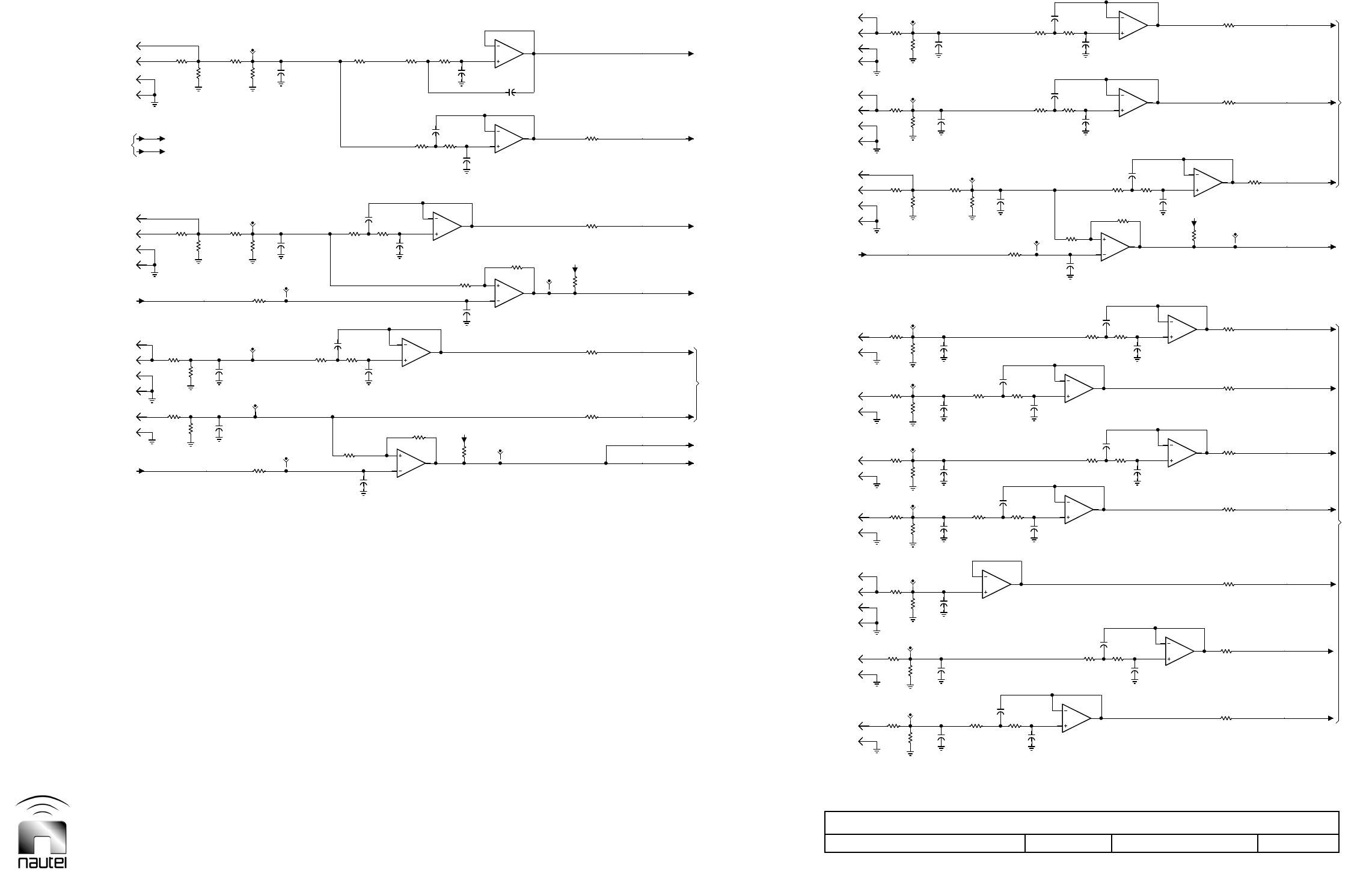
Dimensions = mm (inches)
Electrical Schematic – Control/Display PWB (NAPC147D)
Issue 1.8.1 Not to Scale Figure SD-8 Sheet 4 of 4
20 J4
34 J1
6J1
5J1
3J2
3J1
C42
0.1
TO
N/C
GND
N/C
N/C
6J4
9J4
24 J1
28 J4
30 J4
31 J4
34 J4
9J2
7J1
36 J4
28 J1
37 J4
26 J1
39 J4
R124
475K
C22
0.1
C29
0.1
C27
0.1
R56
475K
C59
0.1
R17
475K
+5V
TO
21 J4
13 J7
33 J1
12 J7
5J2
4J2
4J1
2J2
R40
475K
C41
0.1
C31
0.1
TP10
+5V
N/C
N/C
8J4
7J4
23 J1
28 J7
29 J7
29 J4
33 J4
32 J4
35 J4
8J1
8J2
27 J1
38 J4
25 J1
TP29
TP25
TP17
TP31
TP23
TP8
TP7
R138
475K
R42
475K
R88
10.0K
C68
0.1
R74
475K R55
475K
R73
475K R72
475K C38
0.1
C9
0.1
TO
C21
0.1
R52
475K R60
475K
TP22
TP28
TP11
R68
475K R54
475K
R114
475K
R99
475K
R113
475K
10.0K
R84
+15V
+5V
R22
8250
C18
0.001
10.0K
R33
R20
1000
C11
0.1
C10
0.1
R51
0.0 R62
8250
4750
R89
R61
5620
R71
100
TO SHEET 1
TO SHEET 2
TO SHEET 3
TO SHEET 3
10.0K
R141
10.0K
R86
R127
1000
10.0K
R93
RF_CURRENT_REF
R48
1000
C80
0.1
C44
0.1
C23
0.1
R125
475K
C46
0.1
R46
1000
C60
0.1
C28
0.1
C26
0.1
PDM_B_SAMPLE
POLARITY_ERROR
48V_SAMPLE
PA_VOLTS_SAMPLE
B+_SAMPLE
#HIGH_RF_CURRENT+
BAT_VOLT_SAMPLE
BAT_CUR_SAMPLE
R85
1000
R30
1000 10.0K
R29
R83
10.0K
TP13
TP15
R77
10.0K
TP2
C12
0.001
10.0K
R19
R39
475K C20
0.1
+5V
R65
1500
6
5
7
U1:B
C32
0.0022
C33
0.0047
C36
0.1
R90
100
4750
R63
R32
100
TO SHEET 2
SHEET 3
TO SHEET 3
10.0K
R143
R140
10.0K
R96
1000 10.0K
R97
R87
1000
R76
1000 10.0K
R75
10.0K
R126
10.0K
R47
10.0K
R69
R70
1000
R139
475K
C51
0.1
2
3
1
U7:A
C40
0.1
R43
475K
C75
0.1
C69
0.1
C24
0.001
10.0K
R45
TP6
6
5
7
U11:B
C52
0.1
9
10
8
U1:C
2
3
1
U11:A
C45
0.1
R79
100K
R106
100
R108
100
R41
100
R137
100
R112
100
9
10
8
U7:C
4750
R78
2
3
1
U1:A
R67
100
PDM_A_SAMPLE
DC_CURRENT_SAMPLE
RF_CURRENT_SAMPLE
R36
1000
TP19
TP4
R34
1000
TP1
R82
15.0K
R44
475K R18
475K
R49
100
R142
10.0K
R94
1000
10.0K
R57
R58
1000
R105
475K
C39
0.1
R80
1500
11
10
13
U4:D
R66
100
9
10
8
U3:C
R98
100
6
5
7
U7:B
R53
100
TP16
S1950199 SHEET 4 OF 4 V1
FROM SHEET 3
C43
0.1
FROM SHEET 3 REFLD_PWR_SHTBK_REF
10.0K
R35
REFLD PWR SAMPLE
SHEET 3
FROM
FWD PWR SAMPLE
PDM (A)
#AC_LOW-
CHARGER_CURRENT
R64
100K
FROM SHEET 3
REFLD_PWR_SAMPLE
RF CURRENT SAMPLE
RF CURRENT SAMPLE
BATTERY VOLTAGE
BATTERY CURRENT
C87
0.1 C79
0.1
C35
0.1
C30
0.1
SHEET 3
TO SHEET 2
LOW_AC_REF
C16
0.1
CHARGER CURRENT
10.0K
R21
PDM (B)
SPARE ADC
AC_SAMPLE
#AC_LOW-
#REFLD_PWR_SHUTBACK+
5
4
2
U4:A
SPEAKER_REF_LEVEL
FWD_PWR_SAMPLE
C88
0.1 C53
0.1
C8
0.1
R31
100
6
5
7
U3:B SHEET 3
9
8
14
U4:C
R81
475K
6
5
7
U2:B
13
12
14
U2:D
9
10
8
U2:C
TP21
2
3
1
U3:A
B+ SAMPLE/AC POWER
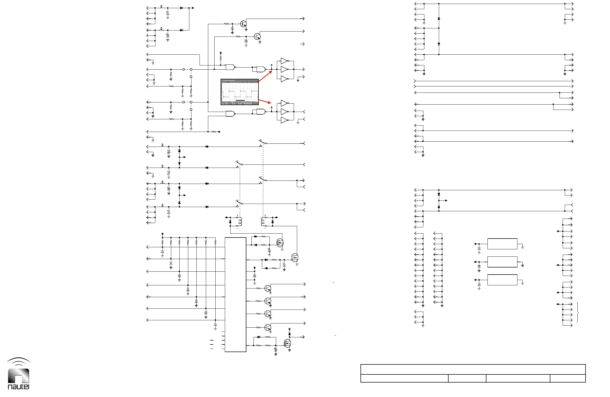
Dimensions = mm (inches)
Electrical Schematic – Exciter Interface PWB (NAPI76A/02)
Issue 1.8.1 Not to Scale Figure SD-9 Sheet 1 of 2
+15V B
+15V A
-15V B
-15V A
+5V B
+5V A
23
16
14
13
10
6
5
4
9
J15
7
J9
7
J8
N/C
N/C
N/C
N/C
10K
R8
DGPS
C6
0.01
10K
R6
9
1
8
11
7
2
3
+5V
+5V
R32
100
R31
56.2K
R37
56.2K
TP1
TP2
7
J15
8
J13
6
J8
6
J9
R38
100
36 J7
# SIDE B MAIN
#CHANGEOVER B- 15 J13
#CHANGEOVER A-
# STANDBY TEST -
19 J2
17 J2
20 J1
18 J1
12 J2
12 J1
14 J13
INHIBIT FC (B)-
4J4
5J4
RF DRIVE (B) MISC
4J16
5J16
RF DRIVE (A) MISC
INHIBIT RF (A)-
34 J13
9J2
7J2
9J1
7J1
C11
0.01
L4
+15V
CR17
1N5819
-15V
332
R21
332
R20
E5:3
DGPS
E5:1
E5:2
332
R24
332
R25
E6:2
E6:1
L6
C4
0.01
C5
0.01
GAL20V8
U4
+5V
+5V
R2
10K
C25
0.1
20
15
Q3
2N4401
22
R7
10K
CR27
19
C27
10
35V
+5V
1
J8
CR23
15
J7
24
J7
18
J11
18
J10
12
J11
12
J10
10
J9
10
J8
8
J7
9
J7
+24V B
+24V A
# SYNTH B INSTALLED (-)
# SYNTH A INSTALLED (-)
# PDM A INSTALLED (-)
N/C
BATTERY (24V)
N/C
16 J2
14 J2
6J1 6J2
4J1 4J2
40 J2
38 J2
23 J2
CR7
MBR1645
2J6
2J5
4J14
2J14
4J12 CR20
MBR1645
2J12
+5V
+5V
15
J3
+24V 34
J15
-15V 26
J15
28
J13
25
J3
12
J13
28
J15
+15V 17
J3
30
J13
14
J7
5
J7
26
J7
8
J14
6
J14
8
J12
6
J12
30 J7
# MON BYPASS +
#SHUTDOWN B- 16 J13
36 J13
#SHUTDOWN A-
35 J7
35 J13
19 J1
18 J2
20 J2
17 J1
11 J1
11 J2
FC (B) SYNTH
6J4
12 J6
13 J13
FC (A) SYNTH
6J16
12 J5
10 J1
10 J2
8J2
33 J13
8J1
C7
0.01
C8
0.01
C9
0.01
10K
R14 10K
R12 10K
R10
C18
10
35V
CR6
1N5819
35V
10
C17
35V
10
C23
L3
CR16
1N5819
CR5
1N5819
100
R22
R19
332
100
R23
R26
332
E6:3
C16
10
35V
L2
MBR1645
CR4
MBR1645
CR15
10K
R3
10K
R5
CR9
MBR1645
CR13
1N5819
CR11
8
9
10
U3:C
3
1
2
U3:A
R33
33.2K
10
C12
35V
Q4
2N4401
CR24
R11
10K
R36
0
R13
22.1K
R35
0
C10
0.1
Q2
2N4401
Q1
2N4401
R4
10K
21
17
CR26
CR25
18
CR10
8
9
7
K2:B
11
12
13
U3:D
6
4
5
U3:B
C26
0.1
Q9
2N4401
+24V
23
J7
25
J7
Q7
2N7000
4
J6
4
J5
11
J9
11
J8
4
J7
# PDM B INSTALLED (-)
5J1
15 J2
13 J2
5J2
8J15
3J1 3J2
39 J2
37 J2
24 J2
CR18
MBR1645
3J14
1J14
CR19
MBR1645
1J12
3J12
C1
0.1
+5V C3
0.1
C2
0.1
27
J3
23
J3
32
J15
+5V
19
J3
32
J13
23
J15
30
J15
10
J13
10
J7
11
J7
19
J13
27
J7
7
J14
39
J13
5
J14
5
J12
7
J12
+5V
C24
10
35V
L8
C22
10
35V
L7
MBR1645
CR14
10K
R1
1N5819
CR12
1
10
K2:C
CR28
R9
10K
3
2
4
K2:A
S1950156 SHEET 1 OF 2 V2
24
VCC
ENABLE A
BEACON
BEACON
R34
33.2K
+5V
#RF RELAY CTRL (A/B)
# MONITOR FAIL+
10 J15
16 J1
14 J1
# ACTIVE SIDE (A/B)
40 J1
38 J1
23 J1
35 J2
+15V MOD DRIVE (B) 33 J2
35 J1
+15V MOD DRIVE (A)
33 J1
-15V MOD DRIVE (B)
-15V MOD DRIVE (A)
27 J2
25 J2
25 J1
FC POWER MODULE (B)
28 J1
1 2
U1:A
13 J10
FC POWER MODULE (A)
1 2
U2:A
15 J15
18 J15
# RF FAIL A +
20 J15
# RF FAIL B +
+24V CTRL BOARD
+24V RMT BOARD
-15V RMT
-15V MISC A
+5V CTRL
+5V MISC B
+15V RMT
+15V MISC A
+24V
# LVPS B FAIL +
# LVPS A FAIL +
12
GND
ENABLE B
8
9
7
K1:B
3
2
4
K1:A
Q8
2N4401
Q5
2N7000
16 J15
15 J1
13 J1
# SHUTDOWN +
# CHANGEOVER +
C28
10
35V
39 J1
37 J1
24 J1
Q6
2N7000
+15V SYNTHESIZER (B)
34 J1
36 J1
36 J2
34 J2
+15V SYNTHESIZER (A)
28 J2
26 J1
27 J1
26 J2
5 6
U1:C
3 4
U1:B
13 J11
3 4
U2:B
5 6
U2:C
# RF OSC FAIL + 17 J15
19 J15
-15V CTRL
-15V MISC B
14 VCC 7
GND
U1:G
MC74AC04N
+15V CTRL
+5V MISC A
+5V RMT
14 VCC 7
GND
U2:G
MC74AC04N
14 VCC 7
GND
U3:E
MC74HC00
+15V MISC B
1
10
K1:C
# SYNTH B INSTALLED (-)
# SYNTH B INSTALLED (-)
# SYNTH A INSTALLED (-)
# PDM A INSTALLED (-)
# PDM B INSTALLED (-)
# SYNTH A INSTALLED (-)
5 V square wave at RF frequency
– RF is on and appropriate side is active
– Audio limit adjusted
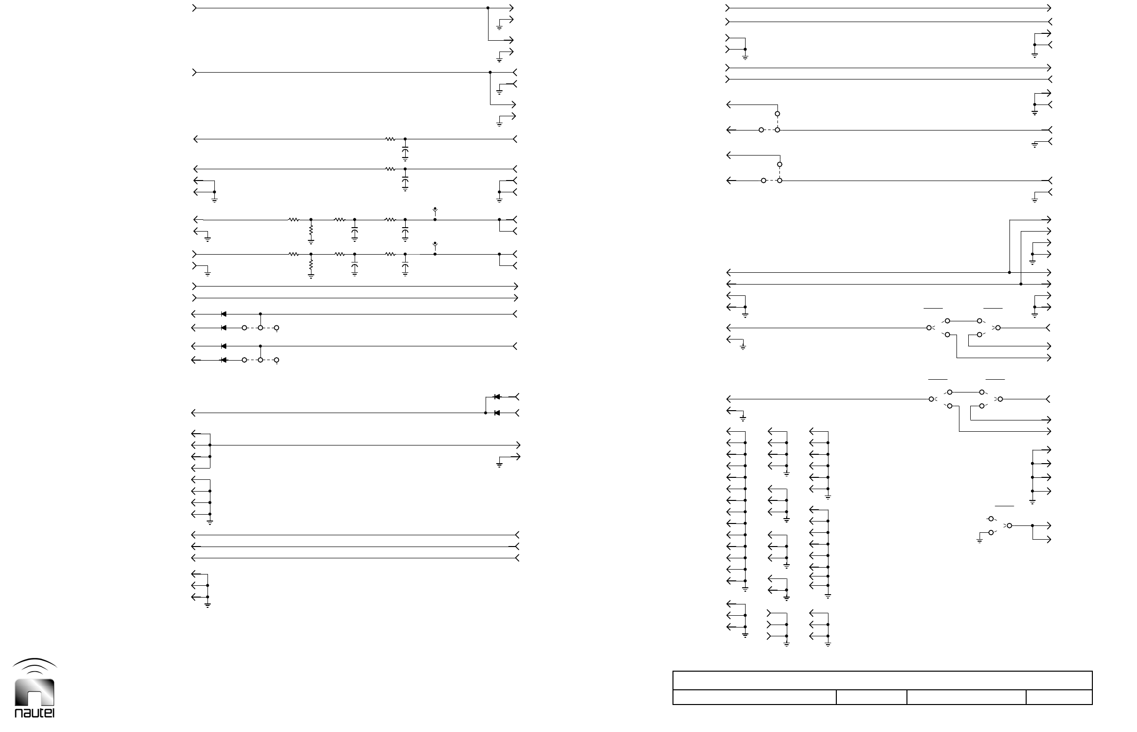
Dimensions = mm (inches)
Electrical Schematic – Exciter Interface PWB (NAPI76A/02)
Issue 1.8.1 Not to Scale Figure SD-10 Sheet 2 of 2
CR1
CR22 DGPS
3J4
38 J3
34 J3
32 J3
28 J3
24 J3
18 J3
14 J3
39 J7
37 J7
20 J7
19 J7
2J4
25 J6
10 J10
9J11
5J11
DGPS
KEY CW
CR2
DGPS
R27
82.5K R29
3320
TP4
CR8
CR3
7J4
36 J3
33 J3
40 J3
1J4
26 J3
22 J3
30 J3
16 J3
40 J7
22 J7
21 J7
38 J7
25 J5
10 J11
9J10
5J10
KEY CW
CR21
R15
82.5K R17
3320
TP3
3J7
38 J13
33 J7
31 J2
31 J1
29 J2
29 J1
18 J7
E11:1
2J7
11 J11
12 J9
13 J8
40 J15
39 J15
24 J11
E11:3
C20
0.0022
C21
0.0022
23
J9
20
J3
1
J11
16
J11
7
J7
3
J11
4
J10
14
J10
15
J10
6
J3
20
J9
9
J3
21
J8
INT BUS (+)
2FPDM (B) MISC
2FPDM (B) SYNTH
2FPDM (A) MISC
2FPDM (A) SYNTH
Fpdm (A)
DUMP (B)
9J9
8J8
14 J6
14 J5
29 J7
13 J7
E4:1
E4:2
E4:3
DGPS E7:2
E7:3
KEY CW
KEY CW
KEY CW KEY CW
KEY CW KEY CW
26
J13
3
J13
21
J13
4
J13
22
J13
24
J8
22
J8 INT BUS (+)
2
J15
4
J15
INT BUS (+)
INT BUS (-)
2FPDM (B)
7
J11
2FPDM (A)
6
J10
19
J8
18
J8 N/C
15
J9
DUMP (B)
14
J9
32 J7
34 J7
18 J13
30 J1
32 J1
32 J2
30 J2
E11:2
17 J13
1J7
13 J9
11 J10
E10:1 E10:2
37 J13
12 J8
21 J15
22 J15
24 J10
8250
R16
E10:3
8250
R28
C14
0.0022
R30
3320
R40
68.1K
C15
0.0022
R39
68.1K
24
J9
22
J9
N/C
21
J3
1
J10
6
J7
16
J10
4
J11
3
J10
14
J11
15
J11
7
J3
21
J9
8
J3
20
J8
CARRIER REF (B)
CARRIER REF (A)
INT BUS (-)
Fpdm (B)
DUMP (A)
25 J9
15 J6
1J6
9J8
8J9
31 J7
16 J7
15 J5
1J5
BEACON
BEACON
E7:1
1
2
3
E3 1
2
1
2
3
E9 1
2
6
J13
1
J13
23
J13
2
J11
2
J13
24
J13
25
J8
23
J8
2
J10
INT BUS (-)
6
J11
1
J15
3
J15
19
J9
18
J9
7
J10
N/C
DUMP (A)
14
J8
15
J8
R18
3320
S1950156 SHEET 2 OF 2 V2
BATTERY B+ SELECT 2
AC SIGNAL (B)
# RESET PDM -
# SHUTBACK B -
# SHUTBACK B -
BEACON
# SHUTBACK A -
# PDM LATCH B +
B+ SAMPLE (B)
C19
0.0022
B+ SAMPLE (A)
KEYED TONE/AUDIO (A)
PDM1 (B)
BATTERY B+ SELECT 2
# RESET PDM (B) -
# INHIBIT PDM (B) -
# INHIBIT PDM (A) -
# PDM LATCH B +
B+ SAMPLE 2 (B)
B+ SAMPLE 1 (B)
B+ SAMPLE 1 (A)
B+ SAMPLE 2 (A)
UNBALANCED AUDIO (A)
PDM (B)
PDM (B)
PDM (A)
3J16
29 J15
25 J15
13 J15 #KEY CW (A) -
11 J15
27 J13
9J13
5J13 CARRIER REF (B)
KEY CW
KEY CW
CARRIER REF (A)
CARRIER REF (FILTERED) (A)
BATTERY B+ SELECT 1
BATTERY B+ SELECT 3
AC SIGNAL (A)
BEACON
# PDM LATCH A +
C13
0.0022
# SHUTBACK A -
KEYED TONE/AUDIO (B)
PDM1 (A)
BATTERY B+ SELECT 1
AC POWER
# RESET PDM (A) -
# PDM LATCH A +
UNBALANCED AUDIO (B)
2J16
PDM (A)
7J16
1J16
14 J15
27 J15
31 J15
#KEY CW (B) -
7J13
25 J13
29 J13
12 J15
CARRIER REF (B)
1
2
3
E2
1
2
CARRIER REF (FILTERED) (B)
CARRIER REF (A)
1
2
3
E8
1
2
1
2
3
E1
1
2
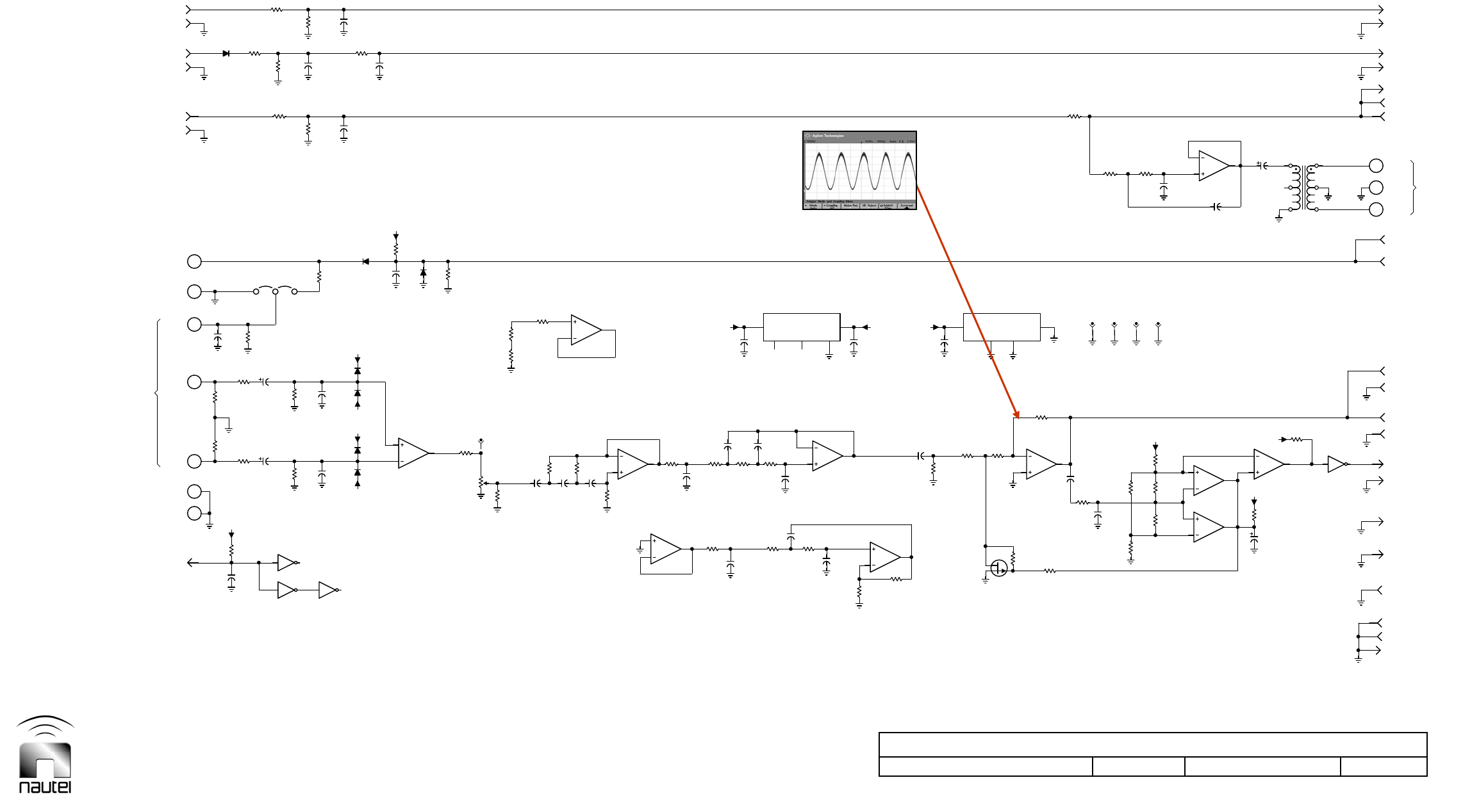
Dimensions = mm (inches)
Electrical Schematic - Remote Interface PWB (NAPI78D/02)
Issue 1.8.1 Not to Scale Figure SD-11 Sheet 1 of 3
INPUT
(-)
(+)
GND
17
11
16
14
15
13
-15V
+15V
-15V
+15V 11 9
4
J18
2
J17
23
22
21
(-)
(+)
AUDIO
AUDIO
12
301
R28
301
R29
1.0
C17
E4:1 B
R77
6810
R73
6810
R86
150K R89
150K
R5
3920
R88
100K
R48
0.0
+15V
GND
TP12
2
J16
9
J17
CR22 R158
10.0K
C3
10
35V
SHIELD
2J11
17 J11
6J11
E4:2
1820
R74
C23
0.1 CR9
+15V -15V
Q7
2N5116
R92
10.0K
R93
10.0K
+5V
C78
0.0022
100K
R100
1000
R99
C1
0.0022
562K
R97
+15V
# MISC (A) -
32
J13
# MOD PROT/31
J18
5
J17
5
J16
VOICE INPUT (B)
# PTT (B) -
# PTT (A) -3
J17
SHIELD MONITOR
FWD PWR SAMPLE1
J17
7
J18
6
J18
C75
0.1
10 J18
+5V
1J11
18 J11
5J11
1 2
U9:A
C15
150pF
C13
10
35V 475K
R22
C22
150pF
475K
R31
E4:3
A
1820
R78
C56
0.0047
10.0K
R156
3
2
6
U3:A
+15V
22.1K
R32
C57
0.001
150K
R84
TP2
R96
1000
R17
10.0K
475
R27
R85
6810
6
5
7
U8:B
C4
1000pF
R4
15.0K
C65
390pF C73
390pF
C20
0.1
R13
10.0K
C7
1000pF
9
10
8
U8:C
C16
0.1
C71
0.047 1820
R94
C66
0.1
R30
1.82M
R9
68.1K
C69
0.1
R87
1.82M
GND
TP1
GND
TP4
R55
8250
100K
R103 9
8
14
U10:C
TP9
C2
0.0047
R1
5620
35V
10
C122
11
10
13
U10:D
R98
4750
36
J13
AUDIO LIMIT -
VOICE INPUT (A)
4
J17
32
J18
4
J16
3
J16
FWD PWR SAMPLE
1
J16
FWD PWR SAMPLE
3
J18
8
J18
5
J18
3 4
U9:B
5 6
U9:C
C21
10
35V
22.1K
R38
C58
3300pF
C59
3300pF
100K
R81 681K
R82
10.0K
R14
7
6
1
U10:B
+15V
1
2
3
6
7
8
T1
S1950190 SHEET 1 OF 3 V2
# OPERATING B -
AUDIO
PRESS-TO-TALK
RF CURRENT SAMPLE
C49
0.001
681
R101
2 15
U21:B
4750
R90
LEVEL
CR3
R23
10.0K
R34
475
CR2
CR12
68.1K
R18
FWD PWR SAMPLE C54
0.001
REFLD PWR SAMPLE
3
2
1
U1:A 12
13
14
U1:D
C6
1000pF
R6
3920
C64
0.01 C72
100pF
150K
R83
7V+
1
TRIM
8
TRIM
5
REF
4
V-
AD620R
U3:B
10
9
8
U1:C
1000
R102
1.82M
R91
13
12
14
U8:D
GND
CW
5000
R37
CR11
R26
10.0K
10.0K
R114
CR10
R19
1000
C61
3300pF
6
5
7
U1:B
RF CURRENT SAMPLE
14 VCC 7
GND
U9:G
SN74AHCT14D
REFLD PWR SAMPLE
A
udio limit adjusted;
5 V pk-pk
Shorting jumper E4 installed in position:
A when audio and press-to-talk
inputs are applied separately.
B when press-to-talk input is
phantom fed on audio input
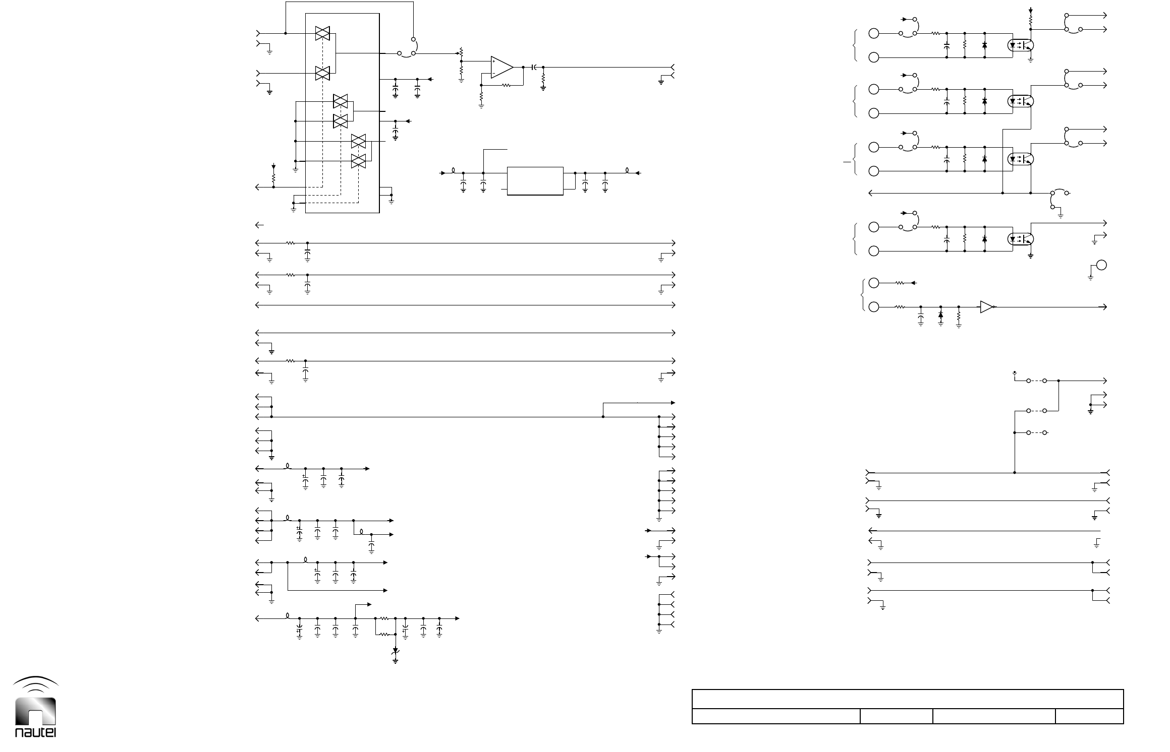
Dimensions = mm (inches)
Electrical Schematic - Remote Interface PWB (NAPI78D/02)
Issue 1.8.1 Not to Scale Figure SD-12 Sheet 2 of 3
L3
L6
9C
11 A
13 X1
12 XO
H
L
H
L
C120
0.01
(-)
(+)
(-)
(+)
(+)
NDB
RF IN
L4
L2
35V
10
C46
C36
10
35V
10 B
5ZO
3Z1
1Y1
2Y0
H
L
R152
1000
R153
1000
0.5W
1500
R166
L11
J8
(-)
(-)
(+)
C10
0.1 CR1
-15V
13 J13
+15V 12 J13
+24V
31 J13
8J13
11 J13
9J13
+5V 17 J13
6J12
4J12
2J12
SAMPLE R12
475K
9J12
7J12
SAMPLE 25 J12
SAMPLE
22 J12
11 J18
12 J18
+5V
22 J16
22 J17
C41
0.01 C80
0.1
C45
0.1
-15V
C26
0.1
+5V
MC74HC4053AD
U16
C119
0.1
-5V
C105
0.01 C103
0.1
MONITOR
LEVEL
BYPASS
19
J16
19
J17
+24V14
J12
+15V +15V12
J12
30
J13
28
J13
26
J13
24
J13
22
J13
TO SHEET 3
40
J18
28
J18
25
J18
RF MONITOR
RF CURRENT MONITOR
RF VOLTS MONITOR
RF OSC SAMPLE
MSK (B)
MSK (A)
CHARGER ALARM
RF ON/OFF
RF OFF /
STANDBY CODE 2
PDM INHIBIT /
STANDBY CODE 1
J7
20
19 +24V-B
3
5
7
PHASE
3 14
U21:C
10.0K
R50 CR15
HD-R Ø
E17:3
NORM
E15:1
E15:2
E15:3
E14:1
E14:2
E14:3
NDB
+5V
RF CURR MONITOR (B)
RF CURR MONITOR (A)
RF VOLTS MONITOR (A)
MSK (B)
# EXT INTLK OPEN +
GND
# CHARGER ALARM -
# EXT RF ON -
# RF ON +/OFF -
# EXT RF OFF -
# STANDBY CODE 2 -
# EXT PDM INHIBIT -
15 J13
16 J13
14 J13
10 J13
33 J13
5J12
11 J12
10 J12
1J12
3J12
24 J12
8J12
R72
1000
23 J12 R63
1000
21 J16
21 J17
C51
0.01
C39
0.01
C55
0.1
C35
0.1
C52
10
35V
L1
C31
0.01
C30
0.1
16V
10
C118
5.1V
CR21
1SMB5918B
C100
0.1
L12
+15V
E11:1
E11:2
E11:3
+5V
PWB PART:
HR106
HW1
0.5W
R165
150
C123
0.1
2
1
7
U23:A
17
J16
17
J17
+24V-A 19
J12
15
J12
13
J12
29
J13
27
J13
25
J13
23
J13
21
J13
34
J18
33
J18
27
J18
23
J18
26
J18
-15V
EXT RF IN /
EXT INTLK
# REMOTE COMMON -
RF ON /
J6
R15
3320
R162
4990
E8:1
4
E8:2
E8:3
R76
4750
+24V-B
E7:1
6
8
E7:3
E7:2 R71
4750
+24V-B
E5:1
E6:1
10
9
E5:2
E6:2
E6:3
R54
4750
R51
4750
+24V-B
E5:3
+24V-B
TP8
10.0K
R16
10.0K
R75 CR18
10.0K
R70 CR17
10MHz
NORM
E17:2
E17:1
NDB
NORM
NDB
NORM
NORM
E13:3
FREQ MONITOR
RF VOLTS MONITOR (B)
MSK (A)
# STANDBY CODE 1 -
10.0K
R161
0.1
C125 0.1
C126 1.0
C127
10.0K
R53 CR16
4750
R144
E13:1
E13:2
+15V-B
+15V
+24V-A
+24V (BATTERY)
CHARGER CURRENT
# DC INSTALLED -
C47
0.47
BATTERY CURRENT
RF MONITOR SELECT 6
ENABLE
15
Y
NORMAL
14
X
CHARGER CURRENT
# DC INSTALLED -
BATTERY CURRENT
13 J11 18
J17
9J11 16
J17
3J13
25
J16
25
J17
21 E9:A 34
J13
29
J18
24
17
J18
16
J18
20
J18
15
J18
19
J18
C34
0.1
30
J18
-5V
S1950190 SHEET 2 OF 3 V2
+24V-B
C29
10
16V
C9
0.1
# POLARITY ERROR -
BATTERY VOLTAGE
C42
0.47
8
GND
7
VEE
4
Z
RF MONITOR (B)
RF MONITOR (A)
16
VCC
CW
100K
R163
10K
R164
+24V_BATTERY
+24V (BATTERY)
BATTERY VOLTAGE
# POLARITY ERROR -
2W
R167
150
14 J11 18
J16
4J13
10 J11 16
J16
65 E9:C
24
J16
24
J17
43 E9:B
6
J13
5
J13
9J18
C50
0.1
3 6
4 5
MOCD223-M
U7:B 18
J18
C44
0.1
1 8
2 7
MOCD223-M
U7:A
1 8
2 7
MOCD223-M
U6:A
39
J18
1.0
C124
C40
0.1
3 6
4 5
MOCD223-M
U6:B
4V+
5COMP
6
V-
3
SHUTDOWN
LT1210CR
U23:B
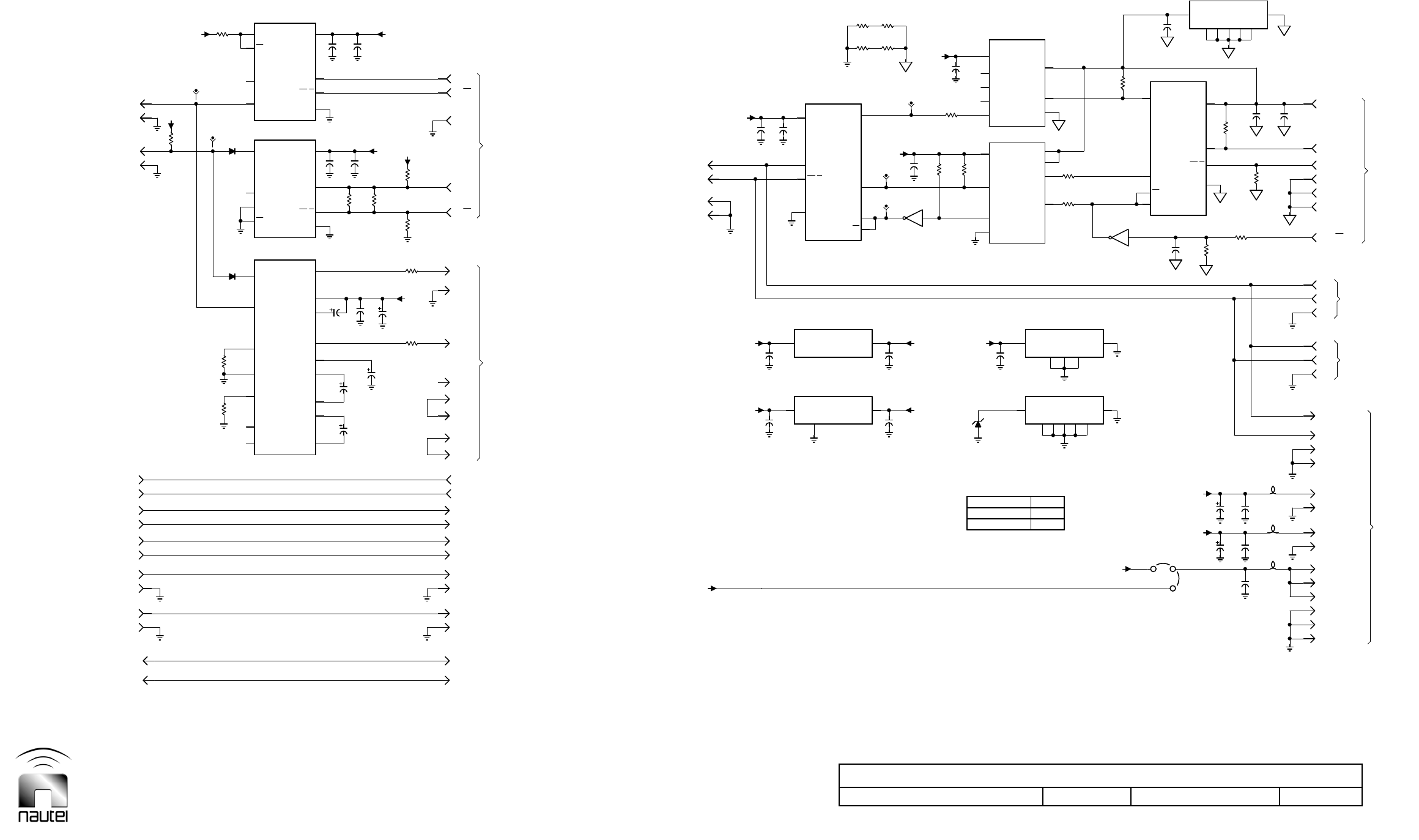
Dimensions = mm (inches)
Electrical Schematic – Remote Interface PWB (NAPI78D/02)
Issue 1.8.1 Not to Scale Figure SD-13 Sheet 3 of 3
4DI
+5V
2
J13
6
J5
1
J4
RTS
DSR
DCD
TXD
RX
RX
TX
8VCC
2
RE
3
DE
1
RO
R145
121K R160
121K
-15V
*
245
1
1
59
1
11 13 1
+24V
+15V
+5V
(-)
(-)
(+)
+5V
TP10
R138
10.0K
4DI
C83
1.0
35V
C94
1.0
35V
681
R171
1
J13
8
J5
7
J5
4
J5
1
J5
2
J5
5
J5
3
J5
8
J4
7
J4
5
J4
2
J4
CTS
DTR
RXD
GND
TX
C60
0.1
C8
0.1
31
4
DI
R139
121K
TP6
R159
121K
-15V
TP5
41 5
1
76
1
1 1
(+)
DE/RE
681
R170 TP7 1000
R110
# AC INHIBIT -
12 J16
13 J17
11 J16
10 J16
14 J17
36 J18
EXT TXD (TTL)
38 J18
S1950190 SHEET 3 OF 3 V2
7T2OUT
8R2IN
100
R123
11 T1IN
12 R1OUT
2RE
1RO
3DE
C84
1.0
35V
6
V-
C109
0.01 C106
0.1
# AC INHIBIT -
19
J13
14
J18 # MSK ALARM (B) ?
#MISC B FAIL -
22
J18
KEY MONITOR (B)
KEY MONITOR (A)
15
J16
RS-232
FROM SHEET 2
39 J13
INT BUS (+) 37 J13 6DO/RI C89
0.1
+5V
1.0, 35V
C68
6VO2
4
A2
HCPL-0731
U14
3K2
5
GND
2K1
4A2
E18:3
NORM
2RE
1000
R134
C98
0.1
C62
0.01
L9
10.0K
R33
1
3
BOARD
TO
DAUGHTER
INT BUS (-)
INT BUS (+)
INT BUS (B)
INT BUS (A)
GND (ISOL)
INT BUS (-)
+5V (ISOL)
# DC INHIBIT - 2J18
1J18
13 J16
12 J17
11 J17
10 J17
14 J16
EXT RXD (TTL) 35 J18
37 J18
9R2OUT
100
R105
15 GND
10 T2IN
3DE
1RO
TP11
2RE
C85
1.0
35V
C79
1.0
35V
C95
0.1
221
R143 221
R142
+5V
# DC INHIBIT -
21
J12
20
J12
20
J13
13
J18
#MISC A FAIL -
21
J18
# MSK ALARM (A) ?
15
J17
RS-422
40 J13
INT BUS (-) 38 J13
2
5GND
7DO/RI
C82
0.01
C81
0.1
DS36C278TM
U11
C70
0.1
C12
0.1
1312
U9:F
+5V
1
R106
2210
10, 16V
C74
0.1
5GND
3
K2
7VO1
2
K1
R135
2210
R133
2210
1
A1
8VCC
6
VO2
7VO1
1A1
8
VCC
HCPL-0731
U13
+24V-A E18:1 E18:2
1
12
U15:A
3DE
1RO
4DI
L7
L8
C67
0.01
*
C68
1
121K
R136
R132
1000
C108
0.1
121K
R137
C107
10
GND (ISOL)
GND (ISOL) RS-485
INT BUS (+)
BAT54HT1
CR26
BAT54HT1
CR25 +5V
C112
0.01 C113
0.1
1000
R109
C76
0.01
C77
10
16V
KEYED TONE/AUDIO (B)
KEYED TONE/AUDIO (A)
# MSK ALARM (B) -
# KEYING/MISC ALM (B) -
KEY MONITOR (B)
KEY MONITOR (A)
5
C2-
4
C2+
2
V+
+5V
R130
100
5
GND
DS36C278TM
U18
10.0K
R169
5
GND
6
DO/RI
8
VCC
+5V
+24V_BATTERY
+15V
EXT SERIAL BUS
EXT SERIAL BUS
+5V
12
J10
10
J10
BATTERY 8
J10
+15V 3
J10
NAPI78D/00 TO /02
+5V
2
J10
19
J10
17
J10
7
J16
8
J17
6
J17
C102
0.1
6
J3
4
J3
7
DO/RI
INTERNAL SERIAL INTERFACE
INT SERIAL BUS
# MSK ALARM (A) -
# KEYING/MISC ALM (A) -
3
C1-
R131
100
16
VCC
1
C1+
13
R1IN
ADM3202ARN
U12
14
T1OUT
7
DO/RI
6
DO/RI
8
VCC
7
DO/RI
EXTERNAL SERIAL INTERFACE
4VCC 11
VEE
U8:E
MC33074AD
+15V 4VCC 11
VEE
U1:E
MC33074AD
11
J10
9
J10
7
J10
4
J10
NAPI78C/00 TO /02
1SMB5939B
39V
CR20
1
J10
20
J10
18
J10
9COM 8
GND
U21:H
MC1413BD
8
J16
+15V 6
J16
7
J17
3VCC 12
GND
U10:E
MC3302D
5
J3
25
J3
2
J3
5
GND
8
VCC
3
J3
6
DO/RI
DS36C278TM
U17
1
J3
C88
0.1
14 VCC 7
GND
U15:G
SN74AHCT14D
DS36C278TM
U19
KEYED TONE/AUDIO (B)
KEYED TONE/AUDIO (A)
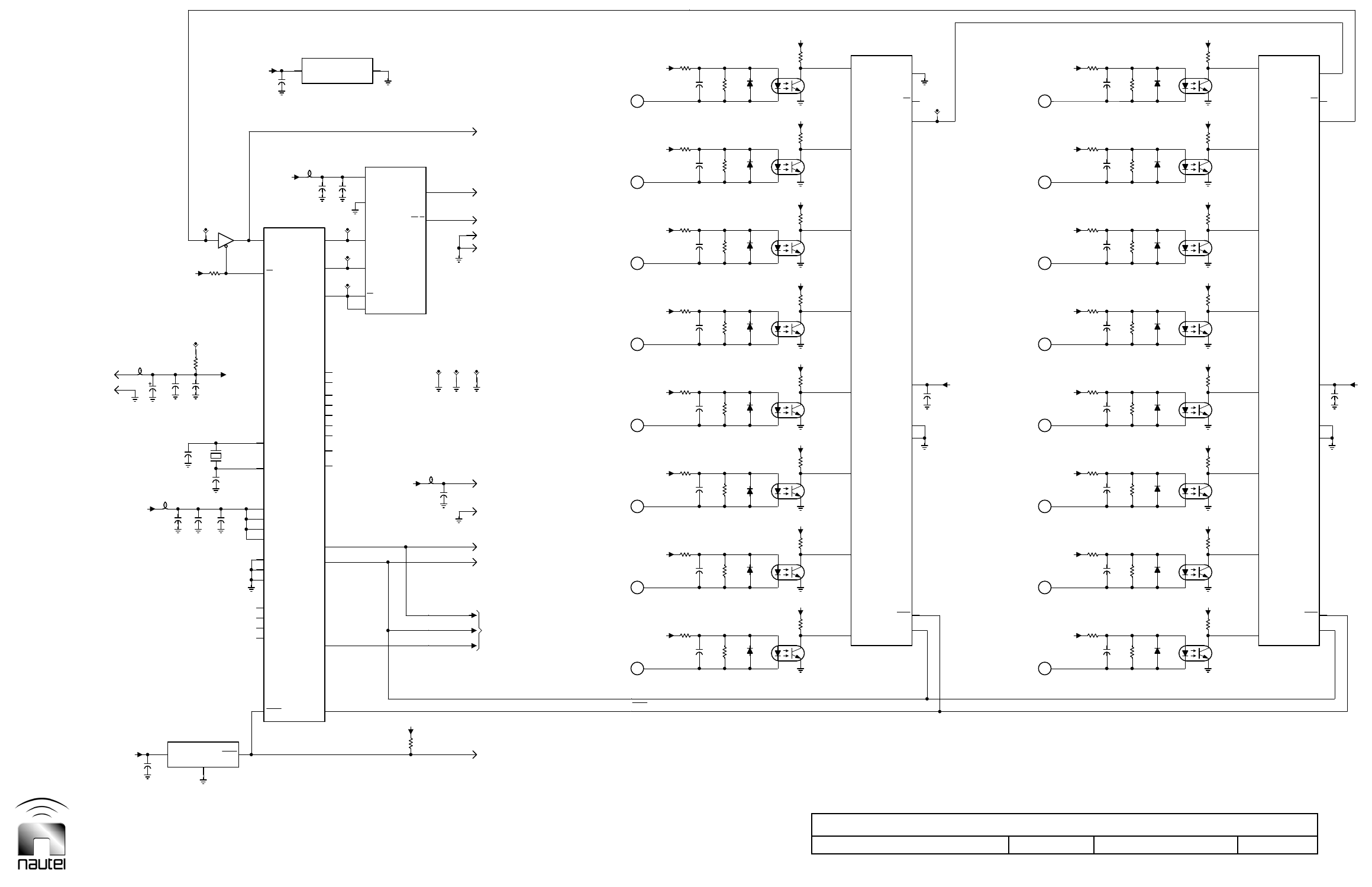
Dimensions = mm (inches)
Electrical Schematic – Site Interface PWB (NAPI80), Optional
Issue 1.8.1 Not to Scale Figure SD-14 Sheet 1 of 2
29
23
SS
14
A
PD.7
MOSI
PD.5
PD.4
PC.5
PC.4
PC.3
PC.2
PD.3
PD.2
RXD
TXD
2RE
1RO
+5V
19
17
4F
7
5
C9
10
35V
24
8
7
16
C35
0.1
PD.6
SCK
OC1A
PB.0
L3
4DI
3DE
GND
TP3
SCK
VCC
MISO
23
22
20
16
14
13
MISO
3E
11
10
8
4
2
1
C33
0.1
1J1
+5V
+5V
10
PC.0
19 ADC6
21 GND
15
18 AVCC
XTAL2
2
XTAL1
28
26
25
12
1
32
30
MISO
+5V
+5V
SCK
7
DO/RI
5GND
6
DO/RI
8VCC
INTERNAL
RESET5
J2
TO SHEET 2
MOSI4
J2
20
J1
18
J1 INT BUS (-)
17
J1 INT BUS (+)
MONITOR POINT 16
MONITOR POINT 14
MONITOR POINT 13
MONITOR POINT 12
MONITOR POINT 11
MONITOR POINT 9
C24
0.1
+12V
+12V
+12V R45
3920
C20
0.1
+12V
+12V
CR15
4750
R50
+5V
+5V
CR12
4750
R37
+5V
+5V
2
CLK
8
GND
C22
0.1
MC74HC165AD
U9
9
QH
7
QH
10
SA
MONITOR POINT 8
MONITOR POINT 6
MONITOR POINT 5
MONITOR POINT 4
MONITOR POINT 3
MONITOR POINT 1
C14
0.1
+12V
+12V
+12V R21
3920
C8
0.1
+12V
+12V
CR7
4750
R26
+5V
+5V
CR4
4750
R12
+5V
+5V
2
CLK
8
GND
9
QH
7
QH
10
SA
2J1
C30
0.1
L4
C28
18pF
C29
18pF
C11
0.01
C12
0.1
10.0K
R20
TP4
R53
10.0K
RESET
PC.1 11
22 ADC7
20 AREF
17
3GND
5GND
9
13
6VCC
4VCC
27
31
10.0K
R54
MOSI
+5V
DS36C278TM
U12
TP9
TP8
SERIAL INTERFACE
C26
0.01
3
J2
GND6
J2
C34
0.1
2
J2
GND GND
TP6 TP13
19
J1
1
J2
SCK
MONITOR POINT 15
MONITOR POINT 10
+12V R47
3920
C25
0.1
R51
3920
R41
3920 C21
0.1
C23
0.1
+12V
+12V
R39
3920
C16
0.1
R29
3920
C18
0.1
R33
3920
3 6
4 5
MOCD223-M
U11:B
+5V
CR16
4750
R49
1 8
2 7
MOCD223-M
U11:A
CR13
3 6
4 5
MOCD223-M
U10:B
4750
R44
+5V
4750
R43
CR14
+5V
4750
R38
1 8
2 7
MOCD223-M
U8:A
+5V
CR9
4750
R32
3 6
4 5
MOCD223-M
U7:B
CR10
4750
R31
1 8
2 7
MOCD223-M
U7:A
1
SHIFT/LOAD
15
CLK_INH
16
VCC
MONITOR POINT 7
MONITOR POINT 2
+12V R23
3920
R27
3920 C15
0.1
R16
3920 C10
0.1
C13
0.1
+12V
+12V
R14
3920
R4
3920 C5
0.1
R8
3920 C6
0.1
3 6
4 5
MOCD223-M
U5:B
CR8
4750
R25
1 8
2 7
MOCD223-M
U5:A
+5V
CR5
3 6
4 5
MOCD223-M
U4:B
4750
R19
+5V
CR6
4750
R18
+5V
4750
R13
1 8
2 7
MOCD223-M
U3:A
+5V
CR1
4750
R7
3 6
4 5
MOCD223-M
U2:B
CR2
4750
R6
1 8
2 7
MOCD223-M
U2:A
1
SHIFT/LOAD
15
CLK_INH
16
VCC
MC74HC165AD
U6
C32
0.01
TP10
ATmega8-16AI
U13
TP7
C19
0.1
R35
3920
1 8
2 7
MOCD223-M
U10:A
CR11
3 6
4 5
MOCD223-M
U8:B
TP5
R10
3920 C7
0.1
1 8
2 7
MOCD223-M
U4:A
CR3
3 6
4 5
MOCD223-M
U3:B
S1950064 SHEET 1 OF 2 V2
+5V
L2 +5V
SHIFT/LOAD
10.0K
R48
5G
10.0K
R40
12 B
11 A
10.0K
R24
5G
4F
10.0K
R15
12 B
11 A
C17
0.1
3VCC
1
GND
2
RESET
U14
ADM803MAKS
LATCH_CLK
+5V
Y1
3.6864MHz
L5
2 3
1
U15:A
C27
0.1
14 VCC 7
GND
U15:E
MC74HC125AD
6H
10.0K
R52
10.0K
R42
10.0K
R46
14 D
13 C
10.0K
R30
10.0K
R34
6H
10.0K
R28
10.0K
R17
+5V
10.0K
R22
3E
14 D
13 C
10.0K
R5
10.0K
R9
+5V
C31
0.001
10.0K
R36 10.0K
R11
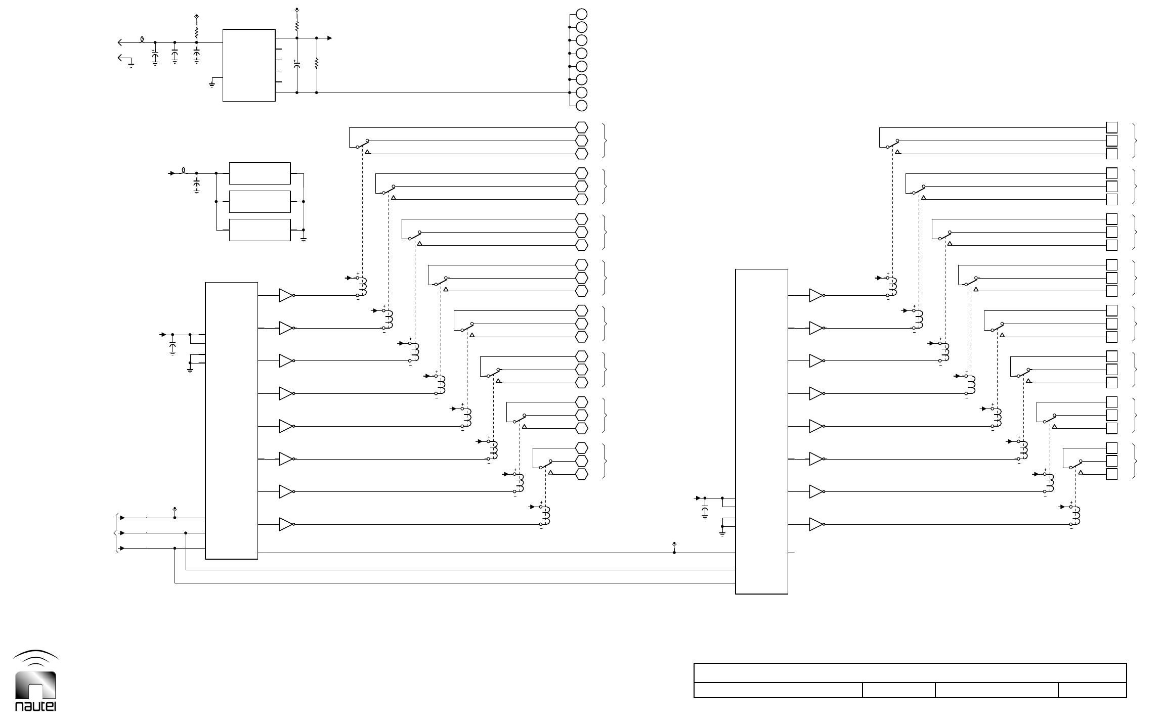
Dimensions = mm (inches)
Electrical Schematic – Site Interface PWB (NAPI80), Optional
Issue 1.8.1 Not to Scale Figure SD-15 Sheet 2 of 2
C36
0.1 +5V
N/O
COM
N/O
COM
N/C
N/O
N/C
N/O
N/C
N/C
N/C
COM
N/C
COM
N/C
N/O
COM
15
QA
2
QC
4
QE
6
QG
C3
0.1
TP2
+5V
N/C
COM
COM
N/O
COM
N/O
N/O
9
SQH
1
QB
5
QF
3
QD
7
QH
TP11
+15V
LATCH_CLK
MOSI
+5V
4J1
3J1
15
QA
2
QC
4
QE
6
QG
24
VIN
11
+V
NDY1212
U1
1VIN
14
+V
+5V
+12V
+5V
32
4K2:A
+5V 24
CONTROL
22
21
CONTROL
18
CONTROL
17
POINT 5
CONTROL
14
CONTROL
POINT 4
11
CONTROL
POINT 3
8
POINT 2
CONTROL
5
4
POINT 1
1
24
18
9
3
+5V
12 LATCH_CLK
8GND
10 RESET
+5V
+5V
32
4K10:A
+5V N/O24
COM22
N/O21
N/C
COM
N/O
18
N/C17
N/O
N/C
14
N/C11
N/C8
COM
N/C
5
COM4
N/C POINT 9
N/O
COM
1
SCK
+5V
C1
10
35V
L1
9
SQH
1
QB
5
QF
3
QD
MC74HC595AD
U17
7
QH
15
OV
12 GND
13
GND
10
OV
C4
100
25V
10.0K
R1
2W
R3
150
TP1
+5V 1
10
K4:C
1
10
K2:C
32
4K3:A
+5V 1
10
K6:C
1
10
K7:C
32
4K6:A
32
4K7:A
POINT 8
23
POINT 6
16
POINT 7
19
20
13
15
10
12
6
7
9
21
CONTROL
2
3
6
12
15
TP12
C38
0.1
14 A
13 OE
11 SHIFT_CLK
16 VCC
MC74HC595AD
U19
+5V
1
10
K10:C
32
4K11:A
+5V
1
10
K15:C
1
10
K14:C
+5V
32
4K14:A
32
4K13:A
N/C
23
COM16
19
20
N/O
COM
10
12
COM13
15
N/O
N/O
6
7
9
2
3
L6
1
10
K3:C
1
10
K11:C
S1950064 SHEET 2 OF 2 V2
FROM SHEET 1
14 A
13 OE
16 VCC
+5V
CONTROL
CONTROL
CONTROL
POINT 13
CONTROL
CONTROL
POINT 12
CONTROL
POINT 11
CONTROL
POINT 10
12 LATCH_CLK
11 SHIFT_CLK
6 11
U16:F
7 10
U16:G
3 14
U16:C
4 13
U16:D
8GND
2 15
U16:B
10 RESET
1
10
K1:C
+5V
1 16
U16:A
C37
0.1
9COM 8
GND
U18:H
MC1413BD
9COM 8
GND
U20:H
MC1413BD
32
4K1:A
C2
0.01
10.0K
R2
32
4K8:A
32
4K5:A
32
4K4:A
1 16
U20:A
7 10
U18:G
32
4K16:A
4 13
U18:D
5 12
U18:E
32
4K15:A
1
10
K12:C
2 15
U18:B
32
4K12:A
3 14
U18:C
1
10
K9:C
+5V
32
4K9:A
POINT 16
POINT 14
POINT 15
CONTROL
1 16
U18:A
5 12
U16:E
9COM 8
GND
U16:H
MC1413BD
1
10
K5:C
1
10
K8:C
2 15
U20:B
6 11
U18:F
1
10
K13:C
1
10
K16:C
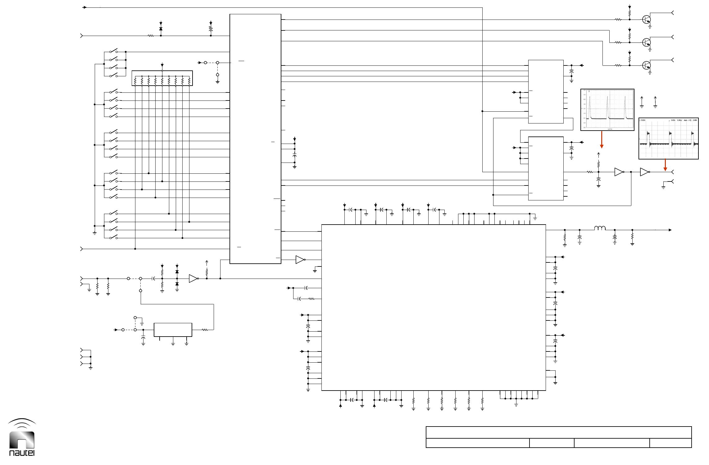
Dimensions = mm (inches)
Electrical Schematic – RF Synthesizer PWB (NAPE70C/01)
Issue 1.8.1 Not to Scale Figure SD-16 Sheet 1 of 2
10 MHz
4FC/B
E2:1 E2:2
E3:3 E3:2
15
A4
C17
0.1
INPUT
J2
INT
EXT C3
0.1 1000
R4
1000
R3
CR3
CR2
TP1
HIGH
80 DVDD
79 DVDD
65
AVDD
78 DGND
67
AGND
C12
0.1
62
AGND
75 DGND
42 VINP
C14
0.1
59
AGND
U5
53
AGND
13
N/C
2D6 36
VOUT
4D4
5D3
58
N/C
7D1
U7
U6
C16
0.1
TP2
TP3 TP4
100
R1 100
R51
29
FSK/BPSK/HOLD
30
SHAPED_KEYING
68
REFCLKB
C18
0.1
14 J1
+5V-A
23 J1
X0.1
X1
X10
X100
X1000
5J1
E1:2
E1:1
INT E2:3
+3.3V-D
+3.3V-D
+3.3V-D
13 12
U3:F
LOW E3:1
+3.3V-D
+3.3V-D
17
P3.5/T1
16
P3.4/T0
34
N/C
32
PSEN
7
P1.5
35
EA/VPP
20
XTAL2
12
N/C
23
N/C
1
N/C
U4
4
P1.2
2
P1.0/T2
9
P1.7
28 DGND
26 DGND
24 DVDD
25 DVDD
11 DGND
10 DVDD
69 REFCLK
22 RDB/CSB
19 A0/SDIO
20 I/O_UD_CLK
C7
0.1
AD9852ASQ
16
A3
14
A5
64
DIFF_CLK_EN
47
AGND
45
AGND
44
AVDD
41
AGND
37
AVDD
34
AGND
32
AVDD
9PE
4P1
74ACT163PC
2CP
5P2
10 CET
9PE
10 CET
1SR
74ACT163PC
5P2
3P0
+3.3V-A
+3.3V-A
C21
390pF
47.5
R14
11
Q3
13
Q1
15
TC
+5V-B
15
TC
12
Q2
14
Q0
+5V-B
C23
390pF 82.5
R20
2Fpdm
# TUNE RF DRIVE +
# HIGH BAND -
15 J1
2J1
6
3
4
1
2
5
4
8
1
2
S2
C2
0.1
EXT
CR1
MBD301
R2
4750
R5
274
100
R6
PDM
C4
2.2
20V
18
P3.6/WR
15
P3.3/INT1
33
ALE
22
VSS
6
P1.4
44
VCC
5
P1.3
190-5043-02
11
P3.0/RxD
8
P1.6
3
P1.1/T2EX
C9
0.1
23 DVDD
27 DGND
C5
0.01
9DVDD
61 PLL_FILTER
C8
0.1
R7
1210
12 DGND
11 10
U3:E
55 DACBP
21 WRB/SCLK
+3.3V-D
+3.3V-D
74 DVDD
77 DGND
73 DVDD
72 DGND
C10
0.1
66
AGND
60
AVDD
+3.3V-A
49 IOUT1B
43 VINN
76 DGND
+3.3V-A +3.3V-A
C15
0.1
54
AVDD
50
AVDD
56 DAC_RSET
52 IOUT2
51 IOUT2B
1D7
18
A1/SD0
35
N/C
46
AGND
8D0
3D5
6D2
70
S/P_SELECT
40
AGND
39
AGND
38
AVDD
31
AVDD
33
AGND
63
N/C
57
N/C
48
IOUT1
1SR
3P0
6P3
7CEP
2CP
7CEP
6P3
4P1
+3.3V-A
12
Q2
C20
0.01
14
Q0
R15
100
10K
R16
11
Q3
13
Q1
4FC/A
13 12
U8:F
GND GND
Q2
2N3904
Q3
2N3904
+3.3V-D
+3.3V-D
R19
10
R18
10
4750
R49
4750
R50
+3.3V-D
4750
R48 # DDS INHIBIT +
6
3
4
1
2
5
4
8
1
2
S3
6
3
4
1
2
5
4
8
1
2
S4
6
3
4
1
2
5
4
8
1
2
S1
C6
0.1
C11
0.1 C13
0.1
100
R8 100
R9 47.5
R11 47.5
R12 3920
R13
17
A2/IO_RESET
L1
1.8μH
C19
0.01
C22
100pF
Q1
2N3904
R17
10
6
3
4
1
2
5
4
8
1
2
S5
S1940197 SHEET 1 OF 2 V1
REFERENCE
+3.3V-D
# TUNE SELECTED - 19 P3.7/RD
40 P0.3/AD3
42 P0.1/AD1
43 P0.0/AD0
36 P0.7/AD7
38 P0.5/AD5
39 P0.4/AD4
31 P2.7/A15
29 P2.5/A13
28 P2.4/A12
27 P2.3/A11
25 P2.1/A9
24 P2.0/A8
14 P3.2/INT0
13 P3.1/TxD
# RESET DDS + 10 RST
+3.3V-D
+3.3V-A
1
J1
25
J1
16
VCC
+5V-B
8
GND
16
VCC
9
J1
7
J1
14 VCC
1
N/C
7
GND
5
SHIELD
8
OUT
RTXT//10.0MHz
U1
REFERENCE (A)
E1:3
REFERENCE (B)
21 XTAL1
41 P0.2/AD2
37 P0.6/AD6
30 P2.6/A14
26 P2.2/A10
+3.3V-D
+3.3V-D
71 MASTER_RESET
+3.3V-A
+5V-B
8
GND
1 2
U8:A
6
J1
32 4 5 6 7 8 109
1
9xU2 4610X-101-4724700
47.5
R10
# SYNTH INSTALLED -
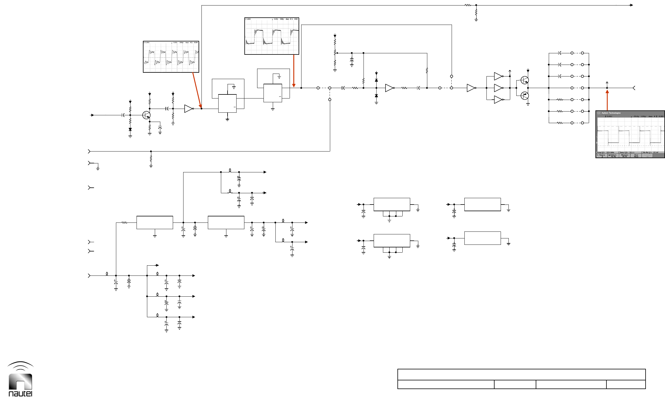
Dimensions = mm (inches)
Electrical Schematic – RF Synthesizer PWB (NAPE70C/01)
Issue 1.8.1 Not to Scale Figure SD-17 Sheet 2 of 2
+15V
N/C
4J1
3J1
L3
C33
0.1
562
R31 *
3
1
95
53
11
9
N/C
EXT Fc
4FC/A
+15V-B
L4
L5
C30
10
35V
C31
10
35V
C29
10
35V
C34
0.1
EXT
562
R33
+15V-A 10K
R42
E6:1 E6:2
R43
2740 1210
R45
C57
0.1
C58
0.47
TP7
L2
18 J1
16 J1
+15V
10K
R27
1820
R23
+15V-C
+15V-A
3 4
U10:B
C39
0.1
L6
L8 +3.3V-A
INT
+15V-B
C47
0.1
4750
R35
+15V-A
C55
0.1
ENABLE
DRIVE
Fc
4FC/B
19 J1
17 J1
C26
0.1
2W
22
R21
+15V-B
C25
0.01
27.4K
R22
100
R26
Q4
2N3904
1500
R25
+15V-B
C32
0.22
C35
10
35V
C36
0.47
10K
R28
10K
R29
L7 C38
10
35V
C40
10
35V
C41
47
20V
C37
10
35V
C43
10
35V
L9 +3.3V-D
C42
10
35V
E4:3
C48
0.1
+3.3V-D
C44
0.01
R34
2210
E4:2
E4:1
C46
0.1
CW
R32
1000
R37
3320 C54
0.001
1 2
U10:A
C56
0.1
+5V-B
DISABLE
E6:3
11 10
U10:E
5 6
U10:C
TP6
9 8
U10:D
R46
47.5
R47
27.4
R52
NOT USED
BALANCED
Fc
CR4
+15V-A
C1
NOT USED
IPM COMPENSATION
S1940197 SHEET 2 OF 2 V1
+5V-A
CR6
CR5
RF DRIVE
RF DRIVE
1413 E5:G
1211 E5:F
Q6
2N2905A
+15V-C
SYMMETRY ADJust
C24
10
35V
1V_IN
2
GND
3
V_OUT
MC7805ACT
U9
+15V-B
C28
0.1
C27
0.01
+5V-B
1IN
2
GND
3
OUT
LM3940IT-3.3
U11
9D
11 C
10
R
12
Q
13
Q
8
S
U12:B
SYMMETRY
14 VCC 7
GND
U8:G
SN74HC04N
13 12
U10:F 87 E5:D
109 E5:E
21 E5:A
43 E5:B
65 E5:C
12
J1
5D
3C
4
R
2
Q
1
Q
6
S
U12:A
14 VDD 7
VSS
U10:G
MC14584B
Q5
2N2219A
DENOTES FREQUENCY DEPENDENT PART.
REFER TO REF DES INDEX FOR VALUE/PART NUMBER.
14 VCC 7
GND
U3:G
MC74AC04N
14 VDD 7
VSS
U12:C
MC14013B
Freq 2360 kHz
Freq 590 kHz
15 V RF drive square wave
TP7 – A5 – A
A9 – B
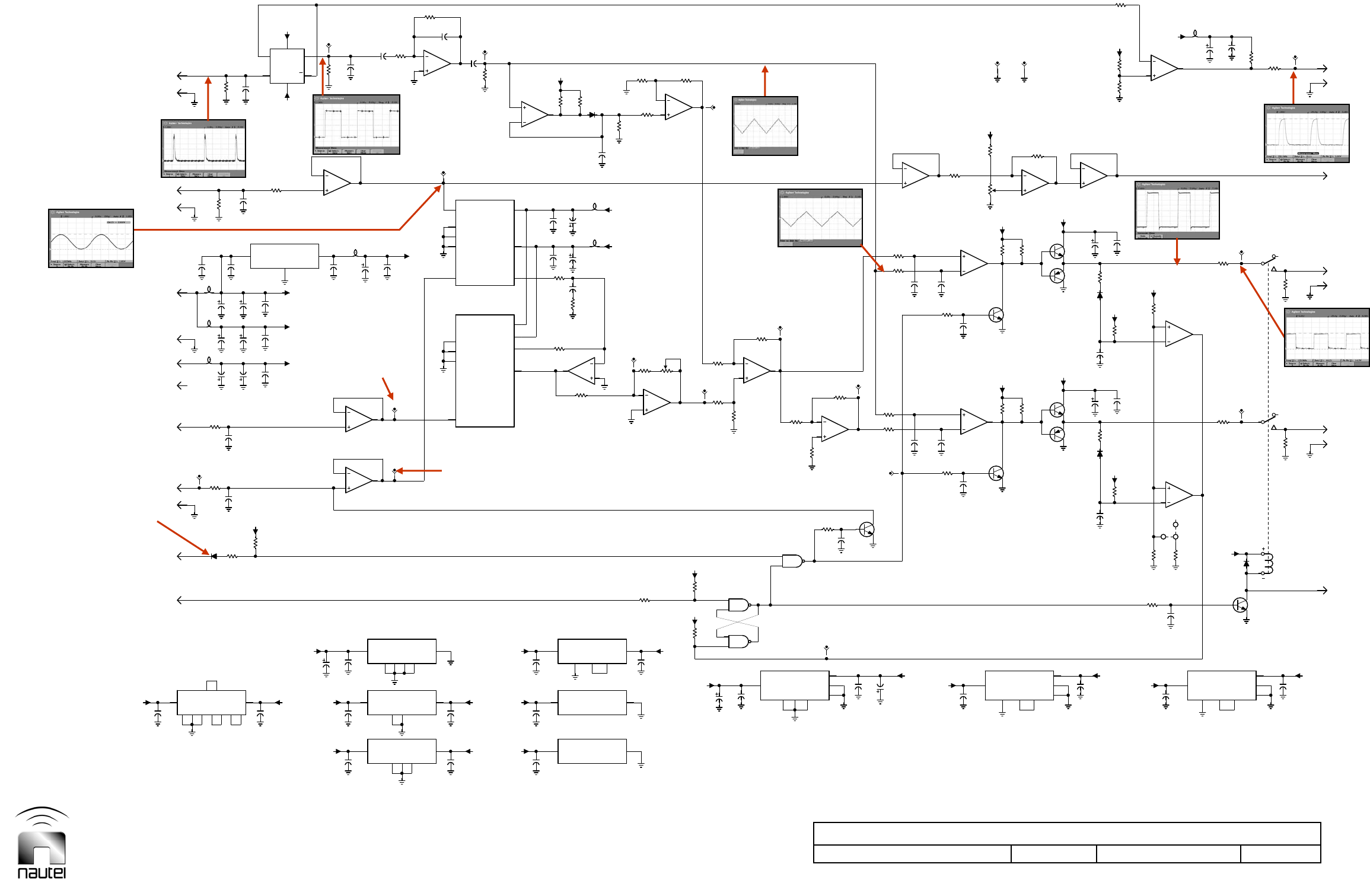
Dimensions = mm (inches)
Electrical Schematic – Interphase PDM Driver PWB (NAPM11)
Issue 1.8.1 Not to Scale Figure SD-18 Sheet 1 of 1
N/C
-15V
13
CR1
L4
L1
C7
0.1
+5V
1X1
2X2
6Z
2X2
7910 5 12
+15V-B
E1:1
A
B
4 12
C65
0.1
C24
0.1 5 612
L2
98
C8
0.47
+5V
+5V
C18
10
35V
TP2
L3
10
C26
0.047
10
11
11 12
R11
2.21M
C28
0.1
C29
0.1
6Z
4Y2
4Y2
3Y1
1X1
TP7
12
C20
10
35V
35V
10
C39
13
+5V
+5V
C43
10
35V
C44
0.1
0.1%
10K
R46
C54
0.1
15K
R58
+15V-B
C71
0.1
TP8
+15V-A
14
R6
1000
2P1
C6
470pF
12 P1
19 P1
18 P1
C5
0.22
7P1
+15V-A
-15V-A +15V-A
-15V-A
+15V-A
C13
0.1
R16
681K
PDM DRIVER
C11
0.1
C3
10
35V
LINEAR
-15V-A +15V-B
-15V-A +5V
C34
0.1
3
Y1
7
W
5
-VS
8
+VS
AD633AN
U6
1000
R22
L7 +15V-A
INTEGRATOR
PEAK DETECTOR
+15V-A
1000
R37
100K
R36
LEVEL
GAIN
LATCH
C46
0.1
C49
100pF
R50
562
4
DUMP
C55
0.1
C59
0.01
CR3
C56
10
35V
C60
0.1
+15V-B
+15V-B
5
R69
1000
E1:2
DETECTOR
+15V-B
R74
10
C64
10
35V
C66
0.1
CR5
5
P1
R76
10
# PDM
PDM 1
DUMP
Fpdm
710
4VCC 11
VEE
U13:E
MC34074
1P1
13 P1
16 P1
3P1
R1
100K
17 P1 35V
10
C4
C2
10
35V
35V
10
C12
C10
10
35V
C1
10
35V
C9
10
35V
14 P1
15 P1
562
R5
6P1
+5V
C17
0.1
+15V-B
C16
0.1
C15
0.1
1000
R8
10
9
13
13
TP4
TP5
+5V
TP3
R10
10K
C27
330pF
C36
0.1
C35
0.1
+15V-A
8
+VS
AD633AN
U7
7
W
5
-VS
C33
0.1
14
3
2
1U13:A
TP9
2740
R15
L6 -15V-A
2.21M
R29
CR2
C41
0.22
-15V-A
0.1%
10K
R39
CARRIER
CONTROL
TRIM
0.1%
10K
R38
CW
5000
R31
TP10
R35
10K
TP11
SHUTBACK
11
12
13
U9:D
R48
10K
4990
R47
TP12
0.1%
10K
R44
-15V-A
Q1
2N4401
TP14
1000
R51
C48
0.001
1000
R52
R53
562
2
3
1
U8:A
1210
R61 1000
R63
9
10
7
U11:B
Q3
2N4401
C52
0.001
Q2
2N4401
+15V-B
1210
R60 1000
R62
9
10
7
U10:B
+15V-A
R56
1000
GND GND
TP15 TP16
-15V-A
Q7
2N4403
Q6
2N4401
CR4
56.2K
R66
C61
0.1
C57
10
35V
1.0M
R67
+15V-B
C58
0.01
Q4
2N4401
Q5
2N4403 56.2K
R65
6
5
7
U8:B
15K
R9
4750
R14
C62
0.1
C63
0.001
E1:3
10K
R72
10K
R71
R75
10
PDM FAULT
10K
R70
5
4
2
U12:A
8
9
14
U12:C
L8
+15V-B
-15V-A
1
10
K1:C
89
7K1:B
1000
R78
32
4K1:A
TP19
3320
R73
9
P1
LATCH +
PDM 2
TP1
R3
10K
681K
R4
R2
22.1K
1210
R25 1000
R26 9
10
8
U2:C
11 +V
6
-V
3
GND-A
8
GND-B
U5:C
LM319J 35V
10
C47
TP13 +15V-B
C53
0.001
CW
1000
R59
1.0M
R68
R57
10K
7
6
1
U12:B
1000
R77
S1970043 SHEET 1 OF 1 V4
C21
0.1
# INHIBIT PDM -
CARRIER REF
+15V
2Fpdm
C42
0.1
C45
0.001
0.1%
R42
10K
C37
0.1
+15V-B +15V-B
C51
0.001
INTERPHASE PDM
GENERATOR (2)
GENERATOR (1)
11
P1
23
P1
24
P1
C30
0.1 C22
0.1
4VCC 11
VEE
U2:E
MC34074
4VCC 11
VEE
U3:E
MC34074
C23
0.1
# RESET PDM -
14 VCC 7
GND
U1:C
MC74HC74
100K
R7
13
12
14
U3:D
B+ SAMPLE 1
1V_IN
2
GND
3
V_OUT
MC7805ACT
U4
INTEGRATOR
C14
100pF
C25
100pF
2D
3CLK
4
S
6
Q
5
Q
1
R
U1:A
6
5
7
U2:B
3VCC 12
GND
U12:E
MC3302
14 VCC 7
GND
U9:E
MC74HC00
4VCC 11
VEE
U8:E
MC34074
3
1
2
U9:A
6
4
5
U9:B
R33
1000
9
10
8
U3:C
0.1%
10K
R49
R13
10K
R27
18.2K
2
3
1
U3:A
C38
0.1
4
5
12
U5:A R34
10K
+15V-A
R30
2.21M
Q10
2N4401
+5V
TP18
R54
1000
INTERPHASE PDM
C50
100pF
TP17
R64
33.2K
22
P1
25
P1
10
P1
2
3
1
U2:A
C19
470pF
13
12
14
U2:D
6
5
7
U3:B
R12
10K
11 +V
6
-V
3
GND-A
8
GND-B
U10:C
LM319J
R55
1000
11 +V
6
-V
3
GND-A
8
GND-B
U11:C
LM319J
9
10
8
U8:C
# PDM INSTALLED -
UNBALANCED AUDIO
2f PDM Exciter
260 kHz, 5 V pulse train
TP19 – A6 – A
A10
–
B
15V PDM modulated
square wave at approx.
1
30
kHz
A
udio
1.4 V offset
2.8 Vpp under
100% modulation
CR1 Anode Low
Power Inhibited
0 to 6 Vdc depending on
power level
TP5 – A6 – A
A10 – B
B+ Sample = B+ 54.9
TP4 – A6 – A
A10 – B
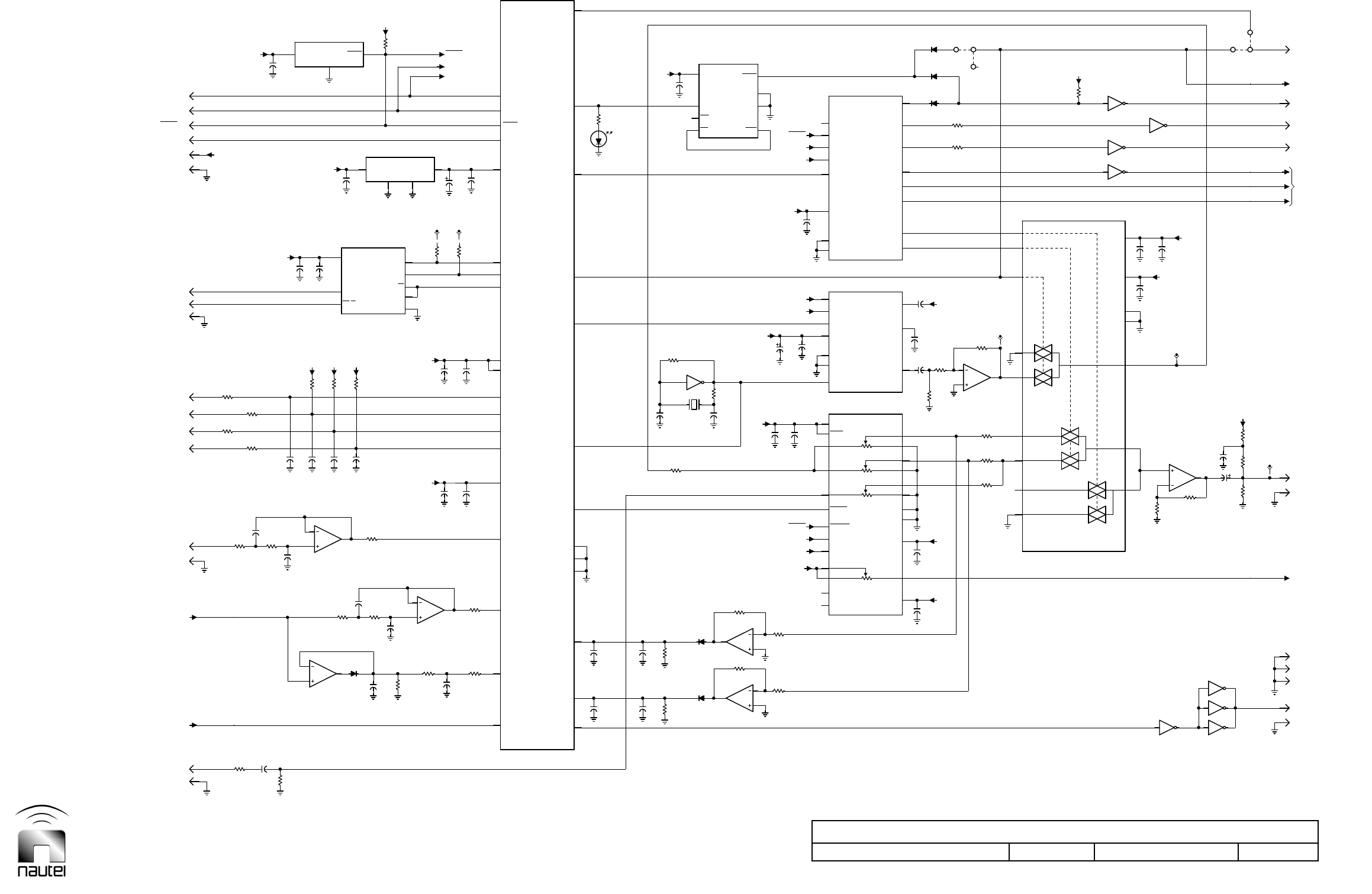
Dimensions = mm (inches)
Electrical Schematic – Exciter Monitor/Generator PWB (NAPE76A/03)
Issue 1.8.1 Not to Scale Figure SD-19 Sheet 1 of 2
R65
100
+5V
SCK
R45
100
0.01
C27
0.01
C50
24
32
11
31
29
15
PC.4
PD.6
PC.2
PD.5
PC.0
20K
CW
CW
CW
CW
+5V
+5V
H
L
H
L
-5V
E3:1
R42
100
R46
100
R57
100
0.01
C43
0.1
C26
MOSI
R41
100
12
2
1
30
26
16
17
PC.5
+5V
20K
20K
20K
-5V
R2
10.0K
A
R44
100K
R56
100K
R19
100K
B
+5V
AB
R31
182K
VOICE I/P
FORWARD POWER
KEYING MONITOR I/P
# KEYED CW -
# PTT -
INT BUS (+)
INT BUS (-)
GND
VCC
RESET
SCK
10 J1
RF_MONITOR
13 J1
24 J1
11 J1
7J1
+5V2 J2
5J2
+5V
+5V+5V
7DO/RI
+5V
0.01
C28
0.01
C51
3
DE
4
DI
RESET
+5V
PC.1
INT0
INT1
PD.7
6VCC
TXD
ATmega168-20AI
U11
RESET
SCK
28
27
7
25
9
14
KEYER OK
23
8
2210
R64
1MR
6WDI
2VCC
R86
562K
16 SDO/O1
+5V 19 W4
MOSI 11 SDI/SDA
24 B2
4B3
1B1
10 VLOGIC
0.1
C6
8FSYNC
MOSI 6SDATA
13 OE
0.01
C65
12 LATCH_CLK
MOSI 14 A
9SQH
7
VDD
8
GND
23
A2
5
A3
2
A1
22.1K
R15
10
VOUT
3
CAP/2.5V
1
COMP
PTT
1
QB
15
QA
7
QH
4
QE
5
QF
6
QG
1Y1
2Y0
3Z1
5ZO
9C
11 A
10 B
H
L15
Y
14
X
8
GND
7
VEE
0.01
C17
1 2
U15:A
+5V
1 2
U17:A
+5V
E3:3
2Fpdm
4
J3
1
J1
# SHUTDOWN -16
J4
# CHANGEOVER -
15
J4
4
J1
25
J1
# MISC -
MISO
MOSI
DGPS_CARRIER_FAULT
C85
10
R76
22.1K
9J1
0.1
C47
R26
475K
12 J1
5J1
6J4
6J1
8J1
6J2
1J2
4J2
3J2
BAT54HT1
CR7
9
10
8
U9:C
0.1
C30
0.1
C48
13
12
14
U9:D
0.1
C42
0.1
C37
0.1
C52
0.1
C40
10.0K
R43
10.0K
R66
0.1
C38
6DO/RI
8VCC
3VCC
1
GND
2
RESET
ADM803MAKS
U13
0.1
C31
10
C84
R55
0.0
332K
R60
+5V
+5V
10.0K
R27
2
RE
1
RO
5
GND
1.0
C25
35V
10.0K
R67
ICP/PB.0
22 ADC7
19 ADC6
PD.4
18 AVCC
4VCC
PC.3
RXD
MISO
20 AREF
MOSI
13
0.1
C82 0.47
C80
10
DS1
G
BAT54HT1
CR11
R23
3.32M
5
6
7U8:B
11 10
U4:E
0.01
C9
5PFO
ADM705AR
U2
R87
562K
RESET
SCK 12 CLK/SCL
14 RES/AD1
17 NC/O2
21 B4
0.01
C34
0.1
C35
13 CS/AD0
15 SHDN
10
C7
16V
5MCLK
4DGND
2VDD
9AGND
SCK
8GND
7SCLK
SCK
RESET
16 VCC
10 RESET
11 SHIFT_CLK
0.1
C33
18
VSS
20
A4
9
DIS
22
W2
6
W3
3
W1
0.1
C13
C4
10
3
QD
2
QC
E1:1
BAT54HT1
CR4
BAT54HT1
CR5
BAT54HT1
CR6
13 X1
12 XO
R16
33.2K
TP4
E1:2
4
Z
0.1
C1
6
ENABLE
16
VCC
9 8
U15:D
5 6
U15:C
10.0K
R50
5 6
U17:C
10
C76
35V
C18
1.0
100
R48
12
13
14
U8:D
R37
56.2K
TP1
3
J3
2
J3
7
J3
1
J3
TO SHEET 2
TP5
2
J1
TO SHEET 2
R30
182K
2
3
1
U9:A
TP3TP2
0.1
C83 0.47
C81
475
R13
18pF
C57
BAT54HT1
CR12
R22
3.32M
3
2
1U8:A
Y1
3.6864MHz
0.1
C41
C5
0.01
3 4
U17:B
S1950151 SHEET 1 OF 2 V2
10
C49
FROM SHEET 2
DS36C278TM
U12
INTERNAL
21
GND
3
GND
AD5263BRU20
U10
XTAL1
+5V
AD9833BRM
U5
SS/PB.2
8
WDO
4
PFI
+5V 7
RESET
XTAL2
27.4K
R17
0.1
C16
MOD ENABLE
#KEYED_CW+
3 4
U15:B
KEYING_GATE_CTRL
E3:2
22.1K
R81
FROM SHEET 2
R54
100
R62
475K
10.0K
R58
SERIAL INTERFACE
+5V 10.0K
R28
0.1
C24
4VIN
1
GND1
2
GND2
6
VOUT
U7
LT1790BIS6-4.096
0.01
C53
OC1A
100K
R84
5
GND
R47
5620
+5V
R25
1.00M
3
GND
1 2
U4:A
MSK_REF
MC74HC4053AD
U1
68.1K
R29
10
9
8
U8:C
RF_OFF
MOD_SELECT
R52
10.0K
E1:3
18pF
C46
100K
R85
MC74HC595AD
U16
18.2K
R49
R51
10.0K
KEYING/# MISC ALARM -
KEYING MONITOR OUTPUT
KEYED TONE/AUDIO (A)
TONE GENERATOR
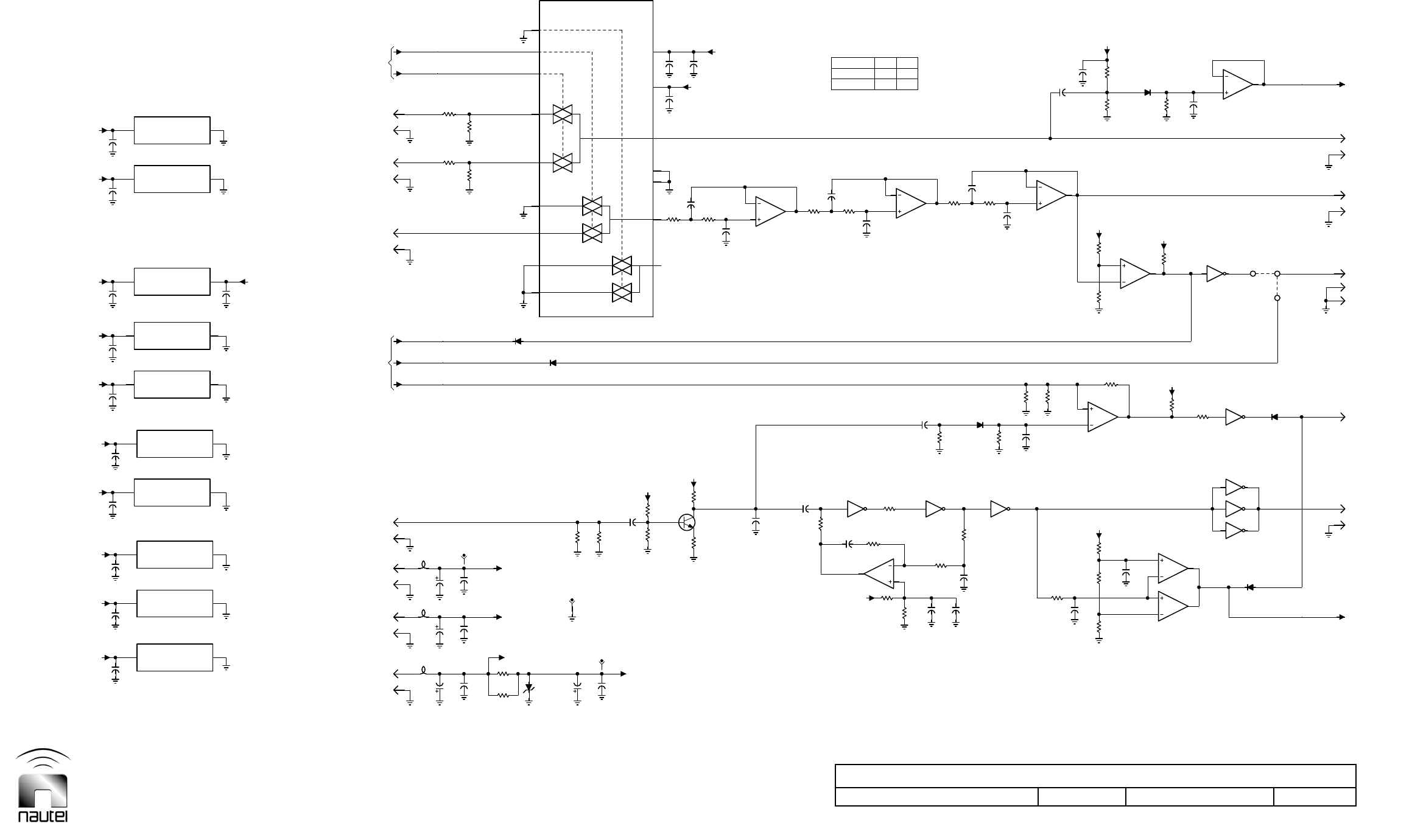
Dimensions = mm (inches)
Electrical Schematic – Exciter Monitor/Generator PWB (NAPE76A/03)
Issue 1.8.1 Not to Scale Figure SD-20 Sheet 2 of 2
+5V
+5V
+5V
+5V
MSK
5J4
7J4
9J4
15 J1
4J4
22 J1
R63
*
681
R69
L
10
C73
35V
H
L
-5V
*
1500
R63
681
1500
R70
681
0.1
C75 10
C79
+5V
6
J3
3
J1
14
J4
17
J1
0.1
C44
-15V
+15V
+5V
8J4
10 J4
14 J1
12 J4
23 J1
3J4
20 J1
21 J1
L2
L3
L1
R70
*
681
R59
R77
1000
H
100
R11
H
L
C60
0.01
R4
18.2K
+5V
1000
R18
5
J3
13
J4
18
J4
1
J4
2
J4
18
J1
R78
1000
+5V
-15V
FROM SHEET 1
CARRIER REF
FROM SHEET 1
0.01
C66
10
C67
35V
-15V
0.01
C58
RF_OFF
0.1
C68
MC74HC4053AD
U14
825
R8
4
Z
0.1
C22
0.1
C36
8
GND
0.01
C69 0.1
C70
MSK 50/50
10.0K
R71
1000
R21
+5V
R5
12.1K
13 12
U15:F
KEYED CW
(FILTERED)
RF MONITOR
TO SHEET 1
0.1
C62
0.1
C63
0.1
C72
0.1
C74
0.1
C8
0.1
C23
0.1
C19
0.1
C39
0.1
C32
RF VOLTS MONITOR
+15V
0.01
C59
10
C56
35V
+5V
TP6
MSK_REF
-5V
TP9
TP8
GND
100
R12
+5V
Q1
MMBT4401LT1
56.2
R1
1000
R14
3920
R9
R24
18.2K
R40
18.2K
14
X
+5V
0.1
C45
7
VEE
16
VCC
15
Y
GENERATOR
0.001
C78
0.1
C20
R39
18.2K
R82
1.00M 1.00M
R83
R72
0.0
R74
100K
3 4
U18:B
C55
0.001 10.0K
R68
0.1
C21
13
12
14
U3:D
R32
100K
9 8
U20:D
0.001
C10
BAT54HT1
CR2
1000
R7 1000
R6
10.0K
R20
0.047
C3
0.1
C2
C29
0.47
8250
R36
8250
R10
5
4
2
U6:A
681
R35
11
10
13
U6:D
+5V
0.47
C77
BAT54HT1
CR9
825
R80
15.0K
R61
BAT54HT1
CR1
3 4
U20:B
5 6
U20:C
1 2
U20:A
R53
10.0K
E2:2E2:1
11 10
U15:E
0.001
C71
6
5
7
U9:B
TO SHEET 1
0.1
C12
10
C64
16V
BAT54HT1
CR13
R75
100K 0.01
C11
+5V
10.0K
R34
S1950151 SHEET 2 OF 2 V2
+5V
+5V
#KEYED_CW+
+5V
+15V
+5V
RF CURRENT MONITOR
MOD_SELECT
5.1V
CR10
1SMB5918B
3Z1
5ZO
13 X1
12 XO
6
ENABLE
NAPE76A/02
10 BNAPE76A/01
DGPS_CARRIER_FAULT
0.1
C14
10
C54
NORMAL
# MSK ALARM -
# INHIBIT Fc -
CARRIER REF
4VDD 11
GND
U19:E
TLV2374ID
14 VCC 7
GND
U17:G
CD74ACT04M
14 VCC 7
GND
U18:G
SN74AHCT14D
14 VCC 7
GND
U20:G
CD74ACT04M
14 VCC 7
GND
U4:G
MM74AHCU04M
3VCC 12
GND
U6:E
MC3302D
14 VCC 7
GND
U15:G
MM74AHCU04M
4VCC 11
VEE
U8:E
MC33074AD
4VDD 11
GND
U9:E
TLV2374ID
KEYING_GATE_CTRL
+5V 4VDD 11
GND
U3:E
TLV2374ID
+5V
C61
0.01
C15
0.01
1 2
U18:A
BAT54HT1
CR8
R38
18.2K
9
10
8
U3:C
1Y1
11 A
2Y0
9C
9
8
14
U6:C
10.0K
R73
BAT54HT1
CR3
E2:3
R3
18.2K
2
3
1
U3:A
RF_MONITOR
47.5K
R79
RF DRIVE OUTPUT
2
3
1U19:A
7
6
1
U6:B
10.0K
R33
* DENOTES SEE CHART FOR COMPONENT VALUE
KEY SHAPING FILTER
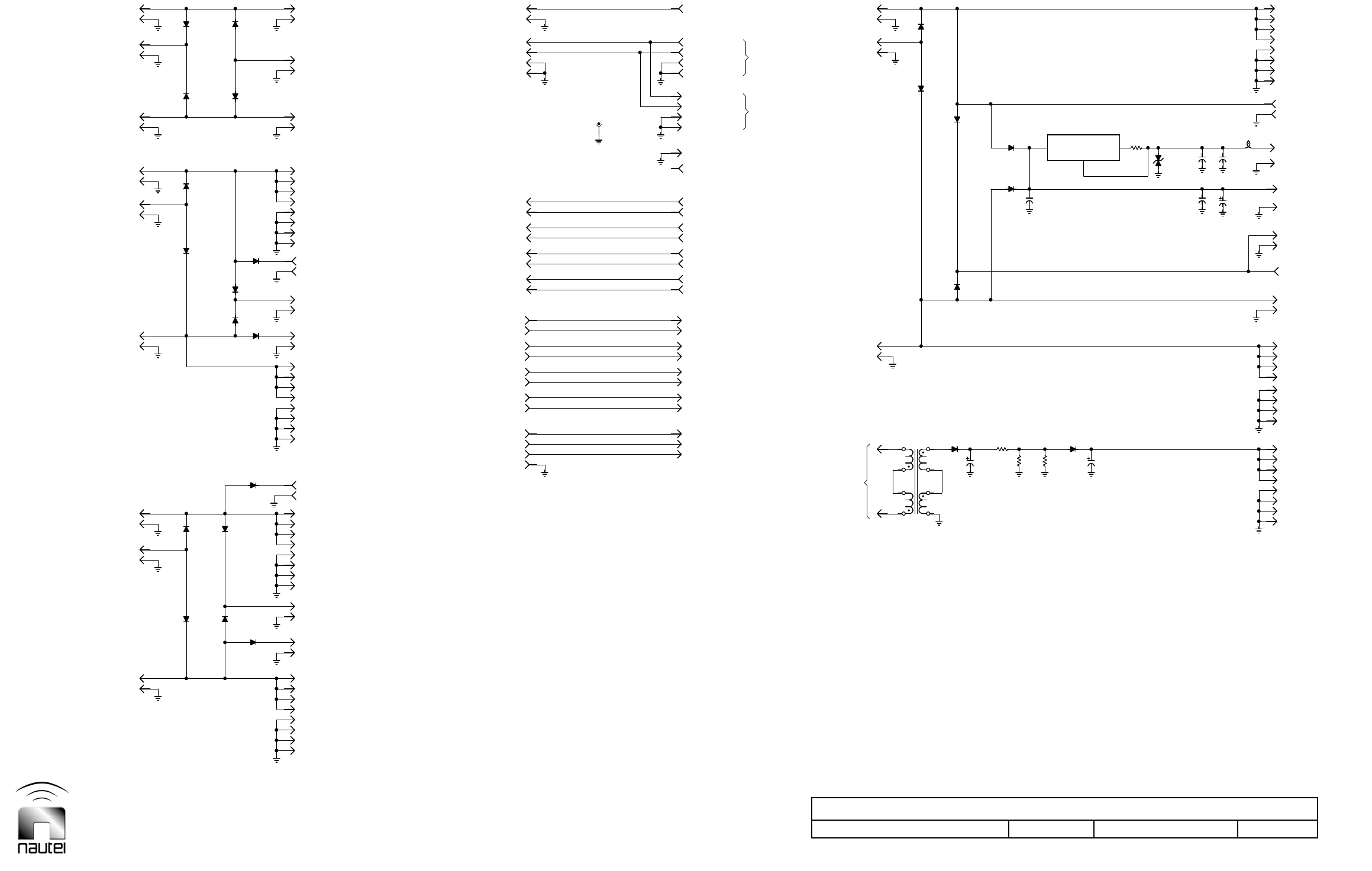
Dimensions = mm (inches)
Electrical Schematic – Interface PWB (NAPI94A)
Issue 1.8.1 Not to Scale Figure SD-21 Sheet 1 of 1
C5
0.1
1N5819
CR24
1N5819
CR23
5
6
CR8 C7
33
63V
R7
22.1K
C1
0.1
7
8
6J5
6J6
5J4
7J5
7J6
8J4
4J5
3J6
4J6
4J4
15
J2
16
J2
13
J2
18
J2
19
J2
1
J10
2
J3
16
J1
14
J1
20
J1 19
J1
17
J1
13
J9
6
J2
3
J2
9
J2
3
J10
4
J3
11
J9
5
J1
10
J1
8
J1
11
J2
CR3
1N5819
8
J3
11
J1
CR4
1N5819
+15V (B)
+15V BATTERY BOOST
+15V (A)
+15V (A)
POWER MODULE
+5V (B)
+5V BATTERY BOOST
+5V (A)
+5V (A)
-15V (B)
BATT B+ SELECT 3
BATT B+ SELECT 1
PDM (A)
DUMP (A)
B+ SAMPLE (A)
Fc (A)
INT BUS (-)
INT BUS (+)
14 J8
17 J8
18 J8
24 J8
1J8
3J8
20 J7
14 J7
12 J7
10 J7
GND
25 J7
23 J7
2J7
N/C
18
J3
21
J10
13
J10
9
J10
11
J10
19
J9
2
J9
6
J9
4
J9 Fc (A)
7
J10
25
J10
22
J10
23
J10
14
J9
16
J9
E2
90-270VAC
T1
2J5
2J6
2J4
15K
R5
31
J2
31
J1
30
J1
39
J2
37
J2
34
J2
+24V (B)
6
J10
+24V
5
J3 N/C
E6
E3
L1 +24V (ATU)
9
J9 +24V (A)
39
J1
40
J1
37
J1
35
J1 34
J1
S2050029 V1
5J5
5J6
6J4
8J5
8J6
7J4
3J5
3J4
14
J2
17
J2
20
J2
1N5819
CR26 2
J10
15
J1
13
J1
18
J1
CR9
1N5819
1
J3
1N5819
CR25
5
J2 4
J2
12
J9
10
J2
8
J2 7
J2
CR14
1N5819
4
J10
6
J1
4
J1 3
J1
CR13
1N5819
10
J9
3
J3
9
J1
7
J1
12
J2
12
J1
7
J3
+15V (B)
POWER MODULE
+5V (B)
POWER MODULE
POWER MODULE
-15V BATTERY BOOST
-15V (A)
BATT B+ SELECT 2
PDM (B)
DUMP (B)
B+ SAMPLE (B)
Fc (B)
INT BUS (GND)
# RELAY CONTROL B-
15 J8
16 J8
4J8
2J8
19 J8
25 J8
21 J7
11 J7
13 J7
15 J7
TP1
22 J7
24 J7
1J7
20
J3 19
J3
12
J10
10
J10
8
J10
20
J10
Fc (B)
1
J9
3
J9
5
J9
18
J9
7
J9
24
J10
15
J9
17
J9
24
J9
MODULE B
MODULE A
E1
3
4
1J5
+24.5V (B)
1J4
1J6
+24.5V (A)
CR12
1N5819
CR11
1N5819
MBR1645
CR18
CR7 C6
10
35V
3V_IN
1
ADJ
2
V_OUT
LM350T
U1
CR1
P6KE30CA
30V
32
J2
32
J1
30
J2 AC SIGNAL (B)
29
J1 AC SIGNAL (A)
40
J2
29
J2
38
J2
36
J2
33
J2 +24V (B)
35
J2
5
J10
23
J9
6
J3
E4
8
J9
E5
38
J1
36
J1
33
J1 +24V (A)
CR10
1N5819
1
2
MBR1645
CR20
+15.6V (A)
+5.6V (B)
CR22
MBR1645
+5.9V BATTERY
+5V (A)
-15.5V (B)
CR5
1N5819
-15.7V BATTERY
CR6
1N5819
BATT B+ SELECT 1
PDM (A)
DUMP (A)
B+ SAMPLE (A)
SIDE A +
SIDE A +
INT BUS (GND)
INT BUS (GND)
INT BUS (-)
INT BUS (+)
INT BUS (GND)
INT BUS (-)
INT BUS (+) +24.7V BATTERY
2210
R6
C3
1.0 C4
10
35V
+15.6V (B)
CR15
MBR1645
+15.8V BATTERY
CR21
MBR1645
-15.5V (A)
BATT B+ SELECT 2
PDM (B)
DUMP (B)
B+ SAMPLE (B)
INT BUS (GND)
# RELAY CONTROL B-
C2
1.0
2.5W
1
R1
CR19
MBR1645
CR17
MBR1645
+24V SUPPLY (MODEM) (+)
CR16
MBR1645
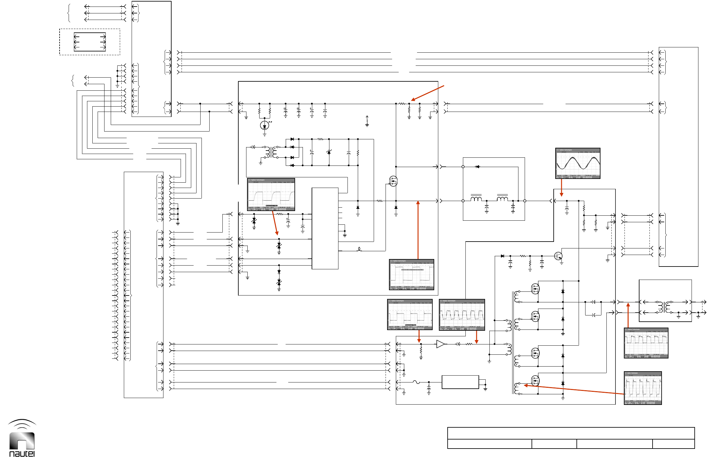
Dimensions = mm (inches)
Electrical Schematic – RF Power Module (NAP35B/01)
Issue 1.8.1 Not to Scale Figure SD-22 Sheet 1 of 1
GND
LINE
(-)
GND
PDM
DUMP
+24V
GND
GND
+5V
+15V
W3P2
P2
J7
J1
J1
W1P1
W3P1
PDM
FPDM
+15V
P4 J1
C1
R2
Fc
R1
R3
C2
CR2
CR3
C4 C5
C7
C6 C8
C9
TP1
R7
Q1
R1
R11
15K
C1
E1
E2
J2 W1P2
C3
L1 C3 L2
PWB
A4
C1
CR2
Q5
C6
C5
E3 E1
J2
J6
E3
P1
LINE
GND
Fc
A1
W2P1
J2
0.1
2
1
3
4
6.8
35V
CR4
CR1
C3
R4
J1
U1:B
B
A
CR1
CR5
FILTER
T1
C7
0.1
Q4
Q3
Q2
Q1
CR4
CR3
CR1
1.0
1.0
E2 E2 11
10
J4
E4
0.1
BOOST
GND
LINE
S2050060 V1
21# INHIBIT PDM A -
23FAN 2 ENABLE
FAN 2 TACH
24+24V FAN 2
22FAN 1 ENABLE
20# SIDE A (+)
18INT BUS (-)
17INT BUS (+)
15
SHIELD
13
12SHIELD
10
B+ SAMPLE
SHIELD
5
6
3
1
P18
6
P1
GND
LINE
DOUBLER
(OPTIONAL)
2
3
3
P1
1
10
4
1
3
2
9
10
7
8
J2 3
5
4
1
INTERFACE
10
14
POWER
J6
1
PART OF
7
9
3
+24V
+24V
3
P3
17
19
PWB
A2
# PDM INHIBIT +
DC OUTPUT
+15V
CR9
CR12
CR10
DS1
B+
2W
68K 2W
68K
11 SD
3VCC
9VDD
U1
CR5
0.12
470
450V
470
450V
CR6
R5
F1 1.0
CR8
R10
15K
GND
R2
POWER
PA VOLTS
MUR460
E1
R5
C2
6
#RF ALARM+
J1 SAMPLE W2P1W2P2
7
W1P1
W3P1
PWB
PWB
INTERFACE
A1
(+)
BATTERY
LINE
+24V FAN 2 25
8
7
SHIELD 16
19
14
FAN 1 TACH
2
4
9
11
5
LINE
110/220
VOLTAGE 1
2
J4
9
PWB
2
11
4
CONTROL/
MODULE
1
J2
20
12
SWITCH MODE
POWER SUPPLY
W1P2
33.2
CR23
P6KE20CA
20V
T1
B+ ON
10 HIN
12 LIN
IR2110
10
6.8
35V
A5
W2P2
L1
0.5W
2.21
MUR460
0.1 1820
47.5
R9
33K
2W
0.47 15W
2.5
A3
AMPLIFIER
250μH0.22
GREEN
3T
RED
3T
BROWN
3T
R3
15K R4 C4
0.01
8250
C
0.22
MUR460
MUR460
R6 R7
2W
33K
1000 1000
0.056
5
PA VOLT
8
T1
T1
MODULE
POWER
PART OF
RF OUT
J3
A
GND
1A
SLOW
MUR8100E
BLUE
3T
MUR460
7
8
3
5
4
1
# INHIBIT +
OUTPUT ADJUST 2
11 3
4
7
14
2
W3P2
2
3
3
1
10
4
1
3
2
6
VB
13
VSS
14
N/C
5
VS PDM (B+)
1
LO
CLAMP
PA VOLTS
470
450V 6
MODULATOR
DC CURRENT
6
2N4401
7
MODULATOR
6
17
19
OUTPUT ADJUST 1
9
3
10
1
1
1
2
U1:A
9
1 5
7
HO
P6KE20CA
20V
8
N/C
4
N/C
2
COM
HFA08TB60
1N4743A
13V
2
TEMPERATURE
# FAN FAIL +
STW14NM50
YELLOW
2T
STW14NM50
STW14NM50
ORANGE
2T
RF TRANSFORMER
20
1
5
8
250μH
B+ SAMPLE 2
20
12
11
12
P6KE20CA
20V
STW14NM50
STW14NM50
4
GND
2
GND
3Vs MIC4452CT
PDM Modulator
PDM @ 150, 250,
or 350 Vdc
B+ 5.4
5 V RF drive
square wave
PA Volts with 95% modulation
A
udio is filtered PDM
(see class D operation notes)
2f PDM
Power Module
90 – 270 V ac
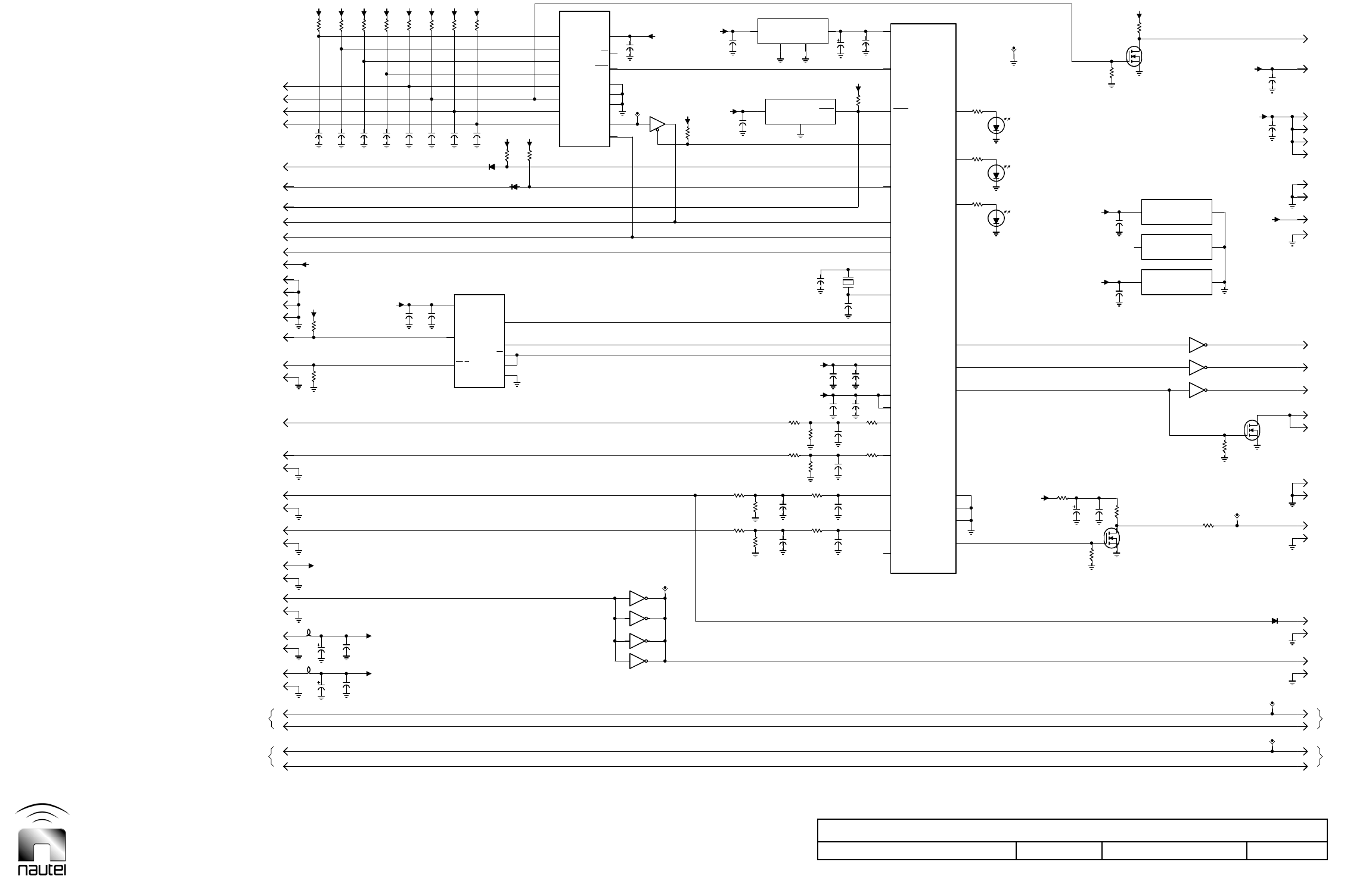
Dimensions = mm (inches)
Electrical Schematic – Power Module Control/Interface (NAPC151A)
Issue 1.8.1 Not to Scale Figure SD-23 Sheet 1 of 1
Fc
+5V
PC5
RXD
TXD
XTAL2
XTAL1
SCK
MISO
RESET
PC.1
PD6
PD5
PD4
PC.2
PB.0
R30
475
C25
0.1
8
J2
9
J2
2
J4
9
J7
4
J2
7
J6
9
J6
9
J4
2
J6
3
J6
24
J7
1
J2
3
J2
+15V
+24V
+15V
+5V
C6
0.1
+5V +5V
C11
0.01
PD7
PC4
PC.0
MOSI
PC.3
R29
475
R27
475
C18
0.1
TP5
CR3
C37
0.1
C20
0.1
7
J2
3
J4
5
J2
1
J6
4
J6
25
J7
PDM
Fpdm
+24V
C7
0.1
C5
0.1
C8
0.1
TP6
16 J7
DUMP 13 J7
GND
+5V 3J7
GND
+15V
2J7
11 J7
+24V 5J7
8J4
B+ SAMPLE 2 J2
17 J6
TEMPERATURE 12 J6
18 J7
INT BUS (-)
17 J7
INT BUS (+)
6J4
1J4
VCC 2J1
SCK 3J1
MISO
# RESET -
1J1
FAN 2 TACH 8J7
FAN 1 TACH 7J7
# RF ALARM + 5J4
# SIDEA + 20 J7
S2050004 V3
+5V
+15V
L2
+24V
+5V
7DO/RI
6DO/RI
C1
0.01
C2
0.1 DS36C278TM
U2
+5V
12 B
14 D
5G
3E
5 6
U4:C
3 4
U4:B
+5V
10
SA
+5V
C26
0.1
10.0K
R19
+5V
C33
0.1
C27
0.1
28
C34
0.1
??
R25
+5V
+5V
30
31
8
7
17
16
1
32
14
29
24
C30
0.1
PB1 (OC1A) 13
21
GND
3
GND
10
9
2
12
+15V
MODULE INSTALLED
+15V
+15V
+24V
+15V
DUMP
Fc - TO PA
B+ SAMPLE
FAN ENABLE
# INHIBIT +
OUTPUT ADJUST 2
OUTPUT ADJUST 1
+24V FAN 1
# INHIBIT PDM +
PDM 15 J7
4J7
14 J7
1J7
6J7
12 J7
PA VOLT SAMPLE
DC CURRENT
7J4
6J2
19 J6
19 J7
GND
MOSI
4J4
4J1
6J1
5J1
20 J6
21 J7
# INHIBIT PDM -
# FAN FAIL +
C4
1.0
35V
L1
681
R2
+5V
681
R3
+5V +5V +5V
10.0K
R4 10.0K
R5 10.0K
R6
8VCC
+5V+5V
10.0K
R13 10.0K
R14 10.0K
R15 10.0K
R16
BAT54HT1
CR2
10.0K
R8 10.0K
R9
4F
6H
11 A
13 C
9 8
U4:D
TP1
1 2
U4:A
TP2
7
QH
9
QH
C19
0.1
R12
121K 6810
R18
+15V
11
C15
0.1
R20
475K
R26
100
27
C12
0.01 C13
0.01
C31
0.01
C32
0.01
R23
100
23
C16
18pF
C17
18pF Y1
3.6864MHz
15
+5V
10.0K
R10
5
GND
25
26
ATmega8-16AI
U7
C35
10
35V
R31
22.1
MODULE FAULT
MODULE ON
GND
1500
R33
Q3
2N7002LT1
100K
R35
10.0K
R36
TP4
+24V FAN 2
C3
1.0
35V
C9
0.1 C21
0.1 C22
0.1 C23
0.1 C24
0.1
C14
0.01
2 3
1
U6:A
R11
2210
C28
0.1
R21
475K
??
R22
C29
1.0
35V
TP3
Q1
IRF520
10.0K
R1
3
DE
1
RO
4
DI
22 ADC7
4VCC
18 AVCC
PD3 (INT1)
PD2 (INT0)
PB2 (SS)
2
CLK
1
SHIFT/LOAD
16
VCC
14
J6
22
J7
3 14
U1:C
11
J6
2 15
U1:B
+5V
2
RE
5
GND
SERIAL INTERFACE
INTERNAL
+5V
BAT54HT1
CR1
10.0K
R7
19 ADC6
R24
1000
6VCC
R28
1000
3VCC
1
GND
2
RESET
ADM803MAKS
U3
8
GND
15
CLK_INH
20 AREF
MC74HC165AD
U5
10
J2
10
J7
10.0K
R32
10
J6
C36
0.1
23
J7
+5V 14 VCC 7
GND
U6:E
MC74HC125AD
GDS2
RDS3
10
J4
14 VCC 7
GND
U4:G
MC74AC04N
ADS1
C10
0.1 10.0K
R17
4VIN
1
GND1
2
GND2
6
VOUT
U8
LT1790BIS6-4.096
Q2
2N7002LT1
R34
10.0
1 16
U1:A
9COM 8
GND
U1:H
MC1413BD
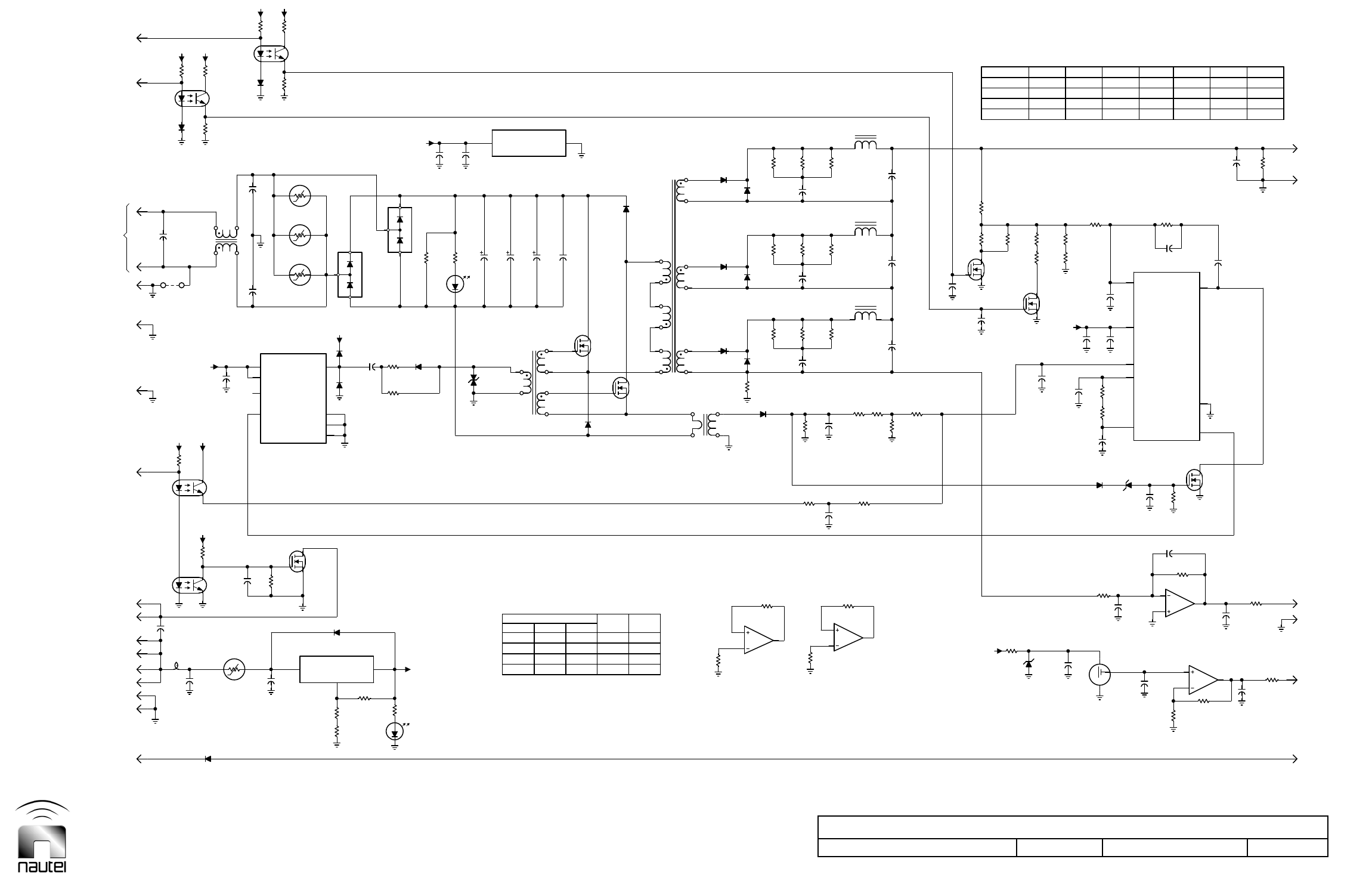
Dimensions = mm (inches)
Electrical Schematic – Switch Mode Power Supply PWB (NAPS31B/03)
Issue 1.8.1 Not to Scale Figure SD-24 Sheet 1 of 1
E3*
E1
E2
L1
L3
250 V
C17
5
0
1
1
0
3W
R50
0.2
2W
R15
390 390
2W
R18
F
F
* R10
22.1K
39.2K
56.2K
R24
1820
39.2K
18.2K
R27
600V
E1
E2
580uH
C18
1.0
35V
C25
0.1
10K
R41
AC
IND
2W
R1
100K
350 V
150 V 79 V
1
0
1
0
2W
R14
390
2W
R13
390
390
2W
R17
390
2W
R16
R22
68.1
FC6
0.1
*
R10
0.5W
R9
1.0M
*
R11 *
R24
*
R25 *
R27
*
R26
22.1K
U8
1820
+18V
+18V
C29
1.0
R29
681
FAN FAIL
2J1
4J1
FAN +
FAN -
7J1
10 J1
3J3 A B
10K
R56
S1970095 V2
8N_INV
U3
6N/C
4VCC
14
3
2
10K
R40
7
L_GND
1
INV
CR2
1N5819
3
OUT
+18V
INVALIDINVALID
136 V 97 V
NAPS31B VARIATION
/02 /03
OUTPUT
ADJUST 2
6T 21T
5T 21T
T1
C23
220pF
CR15
HFA08TB120
C21
220pF
CR14
HFA08TB120
S
3.3
C45
S
+18V
NAPS31B/04
NAPS31B/02
NAPS31B/03
C26
1000pF
332
R35
+18V
2VFB
NOT USED
39.2K
39.2K
R11
UC1844AJ
1
COMP
4750 15.0K
4750
4750
15.0K
6810
R25 R26
20
J1 FAN FAIL
TEMPERATURE
12
J1
17
J1
19
J1
3
J2
DC OUTPUT
1
J2
E3
1J1
3J1
C7
0.1
5620
R61
2J3
14 J1
1J3
9J1
11 J1
+18V
RT1
RXE050
5V_IN
C2
1.0
C9
0.01
C11
0.01
CR3 10K
R32
1500
R53 R55
121 10K
R2
100
R54
C10
1.0
2
P_GND
CR1
1N5819
0.5W
3.3
R57
0.5W
15
R58
1
3
2U1
DSP25-16A
CR4
P6KE20CA
20V
2W
R7
100K
C12
470
450V
DS1
A
C16
0.001
C14
0.01
236 V 167 V
55 V
T2 4
3
7
8
600V
C15
470
450V
16
9
3
18
6T
14
7
1
20
12
5
21T
CR7
HFA08TB120
R3
1000
R52
39.2
1N5819
CR12
332
R12
C20
220pF
CR13
HFA08TB120
R49
1000
R28
2210
3.3
C43
R23
392 R64
681
39.2
R63
S
3.3
C44
300μH
L6
C5
0.1
Q4
MPF960
NAPS31B/01
C33
0.1 2
1
3
t° U11
TMP36G
C24
0.01
R46
182
1N5819
CR19
16V
CR18
1N5930C
C32
0.47 6810
R30
7VCC
C28
0.01
NOT USED
2
3
1
U5:A
10K
R66 R67
10K
C22
0.001
13
12
14
U5:D
R47
825
C8
2.2
Q8
2N7000
1000
R69
5
GND
6
OUTPUT
C31
2700pF
C35
100pF
4750 15.0K
R68
10
5W
R43
33K
+18V
CR5
C4
0.015
10K
R37
+18V +18V
10K
R33
10K
R4
1N5819
CR16
19
2
1000
R44
5
6
7
U5:B
300μH
L4
300μH
L5
R65
1000
C30
0.01
R5
3.32M
21-24V INPUT +18V
# INHIBIT +
UC3710
+18V
AC INPUT
+18V
OUTPUT ADJUST 2
INVALID
ADJUST 1
OUTPUT
/01, /04
0.47
C41
2W
R21
390
3CUR_SEN
22.1K INSTALLED
68.1K
392K
NOT USED
NOT USED
DC CURRENT SIGNAL
3V_IN
1
ADJ
2
V_OUT
LM350T
U10
C1
0.001
DS2
G
+18V
Q7
IRF520
1 5
2 4
MOC8104
U9
1 5
2 4
MOC8104
U7
HFA08TB120
CR20
v
RV3
SIOV-S14K300
v
RV1
SIOV-S14K300
+18V
OUTPUT ADJUST 1 1 5
2 4
MOC8104
U6
1 5
2 4
MOC8104
U4
R39
1000
10
1
Q2
IXFK44N60
HFA08TB120
CR11
CR6
HFA08TB120 C37
0.001
C13
470
450V 2W
R20
390
HFA08TB120
CR10
4VCC 11
VEE
U5:E
MC34074
2W
R19
390
HFA08TB120
CR9
1N4733A
5.1V
CR17
0.001
C38
C34
0.001
R51
10
C36
0.01
4RT/CT
8VREF
C19
470pF
Q5
MPF960
C27
5
22.1K NOT USED
* DENOTES SEE CHART BELOW FOR COMPONENT VALUE
1N5819
CR21
10K
R62
v
RV2
SIOV-S14K300
1
3
2
U2
DSP25-16A
3
4
1
2
1T 200T
T3
10
9
8
U5:C
Q1
IXFK44N60
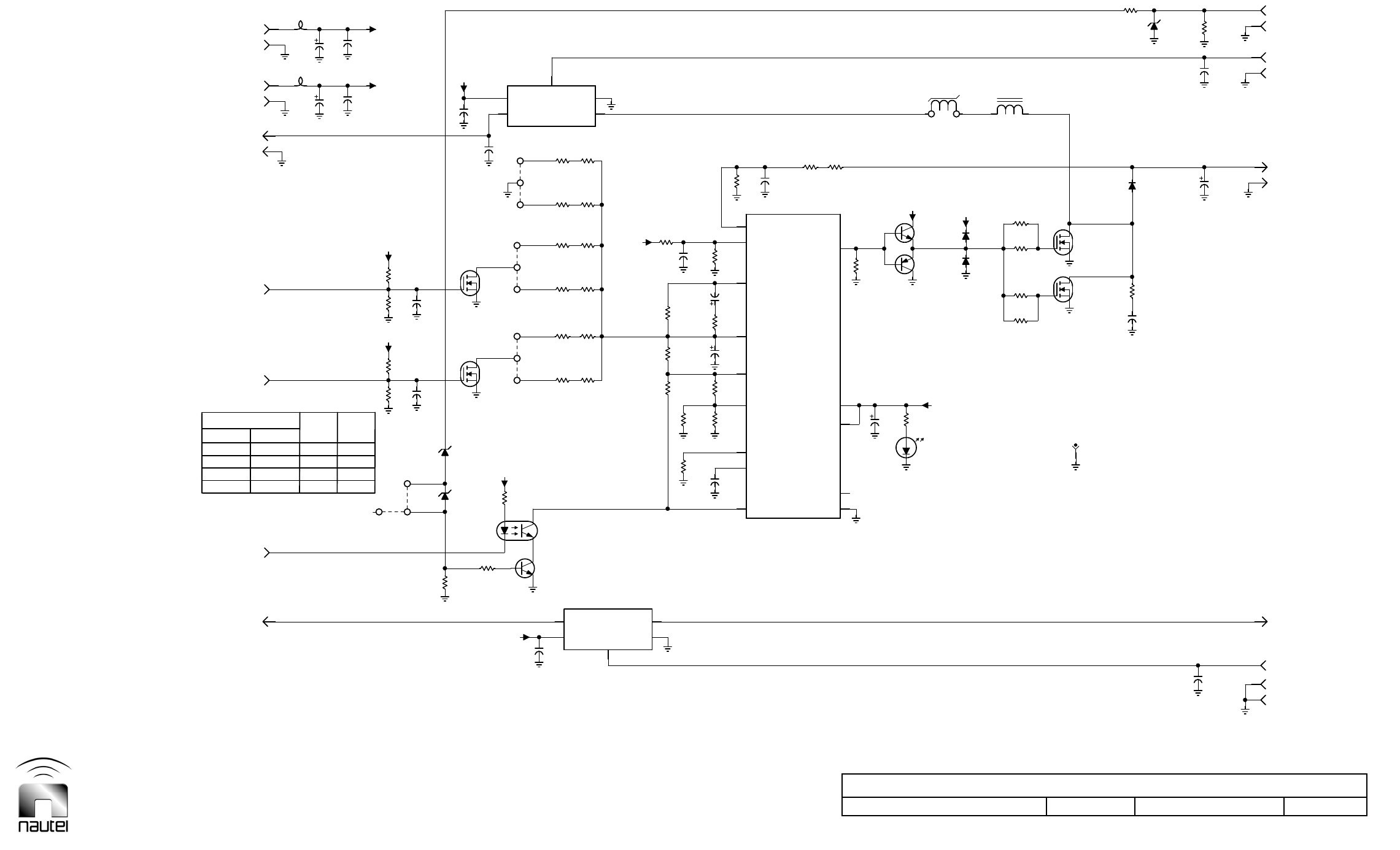
Dimensions = mm (inches)
Electrical Schematic – Battery Boost PWB (NAPS35)
Issue 1.8.1 Not to Scale Figure SD-25 Sheet 1 of 1
79 V
136 V
IN
+15V
-
+
1
0
0
SELECT
1
0
0
1
2
250W
+15V
L4
7
J1
E2
E6
22
J1
25
J1
236 V 1 1
0.1
C4
E5:2
E5:3 +15V
125W
R40
10K
TP1
GND
11
J1
10
J1
E8
23
J1
24
J1
0.1
C6
10
C13
35V 1210
R10
2W
R23
10
CHARGER IN
# DC INHIBIT -
INVALID
VR250/VRD375
+5V
E1
INVALID
97 V
55 V
BATTERY BATTERY
SELECT
E4
L2
3J1
1J1
10K
R12
+24V
10K
R15 0.1
C12
10K
R14
10K
R25 0.1
C17
3.3
C8
0.1
C11
+5V
0.1
C2
125W
E7:1
E9:1
E10:3
E10:2
5CT
11
NC
9
C
10
VCC
8
E
0.0047
C10
+15V
+15V
CR4
1N5819
0.01
C1
CHARGER OUT
-
+ BATTERY BOOST (B+)
BATTERY CURRENT SAMPLE
BATTERY VOLTAGE SAMPLE
BATTERY RETURN
BATTERY SELECT 2
BATTERY SELECT 1
167 V
E3
4J1 10
C3
35V
2J1 L3
R13
10K
1N5931A
18V
CR2
1N4747A
20V
CR3
10K
R24
Q2
2N4401
R16
3920
R3
5620
E7:3
250W
R17
182
R4
182
R36
10K
R26
10K
125W
250W
R37
825
R27
56.2
E10:1
12.1K
R22
6RT
0.001
C14
10
R7
4750
R38
10K
R21
39.2K
R20
47
C19
100V
0.01
C20
2740
R39
7
GND
MC34060
U4
2W
R41
100
DS1
G
+15V
Q7
2N2905A
Q6
2N2219A
CR5
1N5819
Q4
STW26NM50
0.01
C7
1N4745A
16V
CR1
4750
R1
CHARGER CURRENT SAMPLE
10
C5
35V
R34
6810
R28
332
E9:3 R35
274
R29
27.4K
3320
R18 3320
R19
15K
R9
1.0M
R8
22
C9
35V
R6
475K R5
475K
Q5
STW26NM50
470
C16
450V
21 J1
+48V
VR125/VRD200
B+ VOLTAGE
+5V
+15V
4DEAD-TIME
12 VREF
E7:2
2INA-
E9:2
+15V 13 INB-
# BATTERY MODULE INSTALLED -
R32
10
S2050020 V4
E5:1
19 J1
+15V
18 J1
+15V
+5V
3
VOUT
4I+
1VCC
5
I-
2
GND
U1
ACS755LCB-050-PFF
1 5
2 4
MOC8104
U3
14 INB+
4750
R11
Q1
2N7000
3PWM_COMP
1INA+
Q3
2N7000
3
VOUT
4I+
1VCC
5
I-
2
GND
ACS755LCB-050-PFF
U2
R33
10
560pF
C15
R30
10
R31
10
L1
2W
68K
R2
CR6
DSEI60-06A
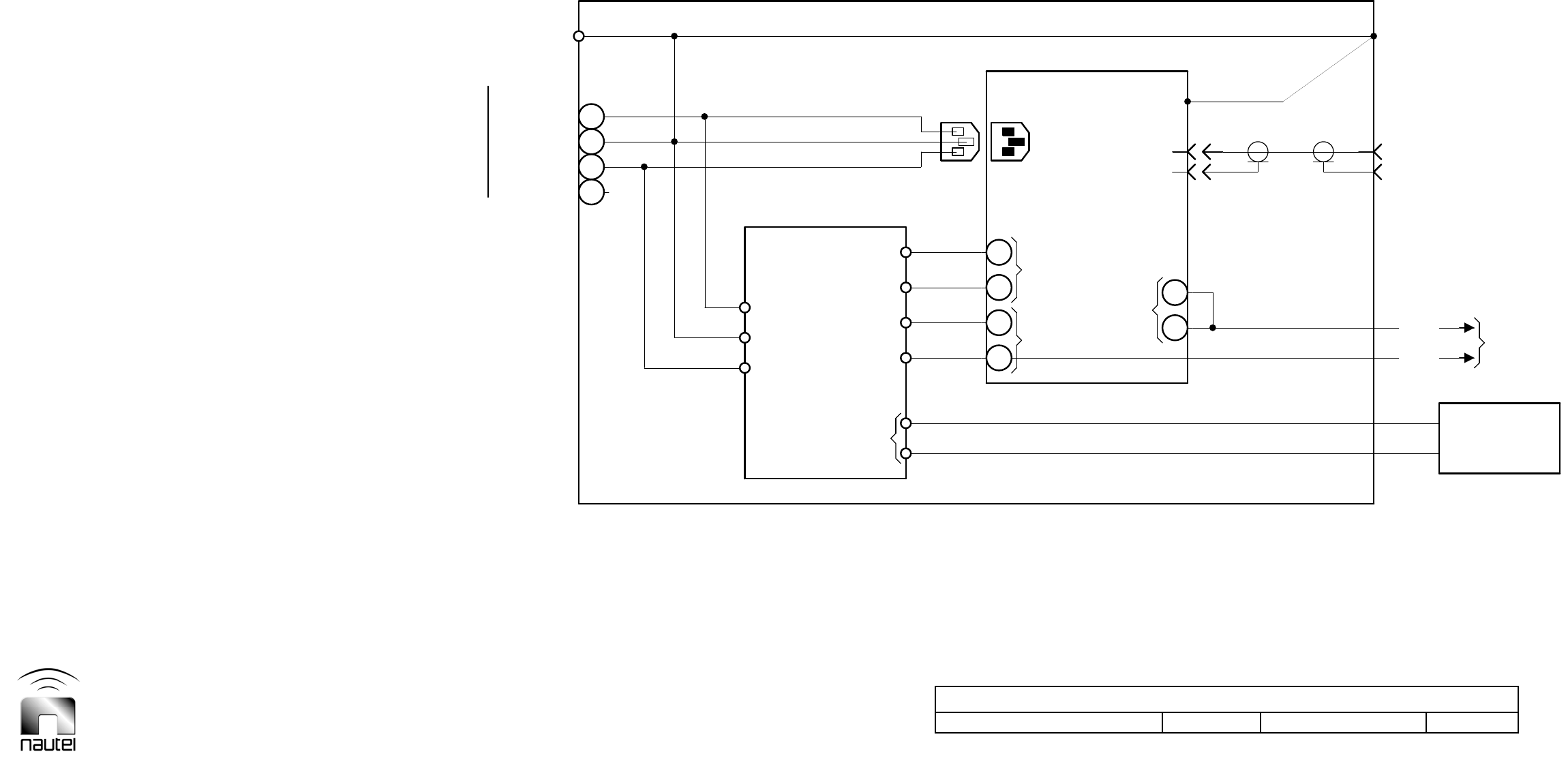
Dimensions = mm (inches)
Electrical Schematic – Vector-LP in Deluxe Cabinet (205-8075, Optional)
Issue 1.8.1 Not to Scale Figure SD-26 Sheet 1 of 1
N/C
LINE
LINE
LINE
2
3
P
2
4
A3TB1
SENSOR
4
1
G
N
3
11
A16TB1
NEUTRAL
GROUND
1-PHASE
S2050023 V2
B-
(OPTIONAL)
CHARGER
U1
RFA (N/C)
TRANSMITTER
NDB/DGPS
UNIT 1 J1 W1P2
(-)
REF GND
BATTERY
BTC
COMMON
VECTOR
4
1
(+)
TEMPERATURE
CABINET
B+
L
NE
U5
NEUTRAL
GROUND
SPLIT PHASE
GROUND
STATION
A16TB1
W1J1
REF GND
(OPTIONAL)
REFERENCE
TO BATTERIES
P3
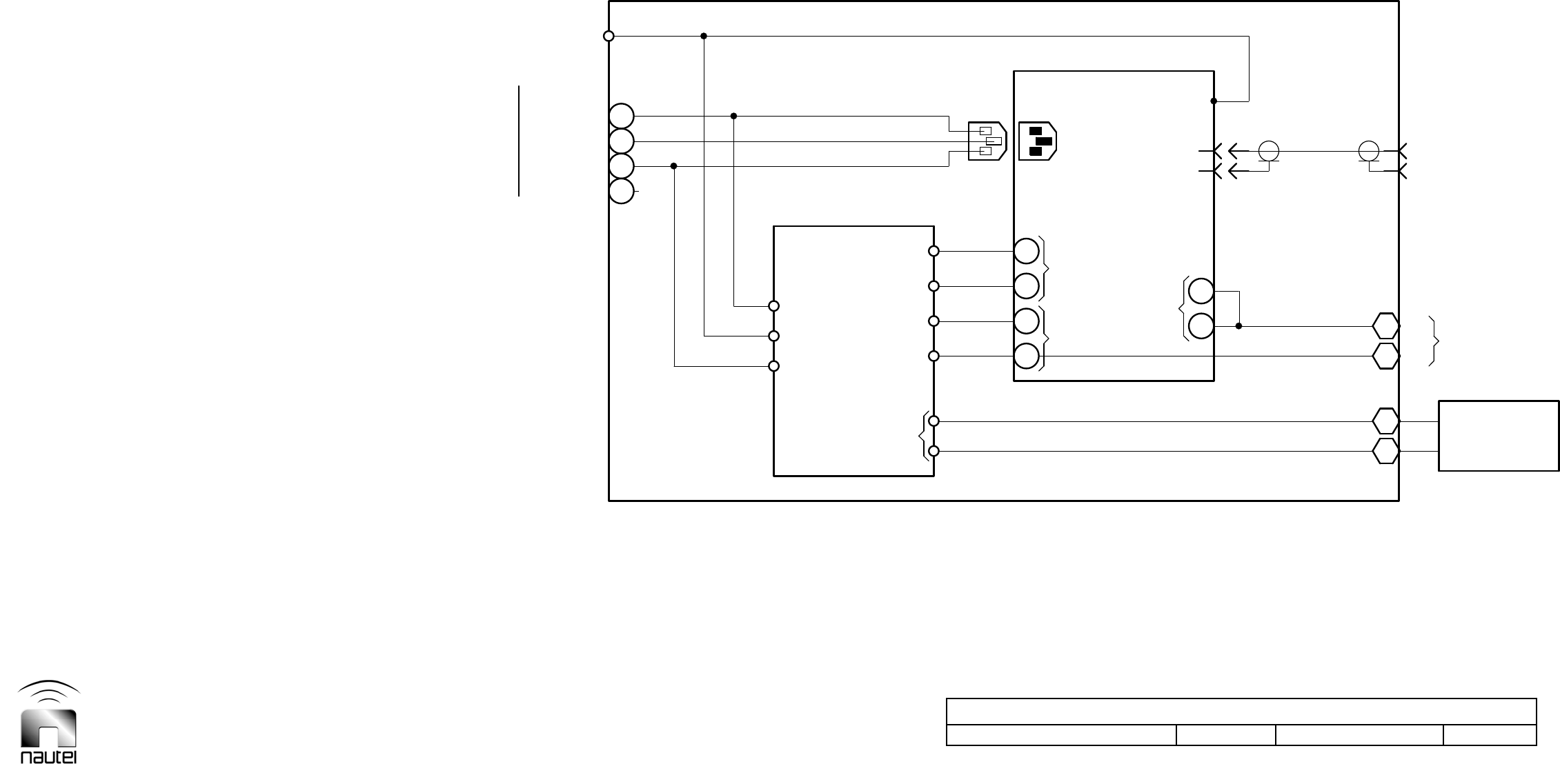
Dimensions = mm (inches)
Electrical Schematic – Vector-LP in IP66 Cabinet (205-8080, Optional)
Issue 1.8.1 Not to Scale Figure SD-27 Sheet 1 of 1
N/C
LINE
LINE
LINE
2
3
TB1
P
2
4
A3TB1
TB2
(-)
4
1
G
N
3
11
A16TB1 (+)
NEUTRAL
GROUND
1-PHASE
S2050025 V2
B-
(OPTIONAL)
CHARGER
U1
RFA (N/C)
TRANSMITTER
NDB/DGPS
UNIT 1 J1 P2
SENSOR
TO BATTERIES
(OPTIONAL)
J1
BATTERY
BTC
COMMON
VECTOR
4
1
TEMPERATURE
B+
L
NE
U5
NEUTRAL
GROUND
SPLIT PHASE
GROUND
STATION
4
2
A16TB1
REF GND
REFERENCE
1
3
P1
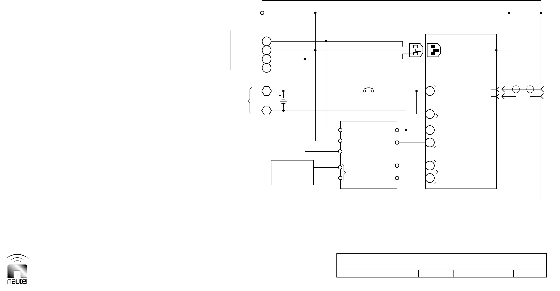
Dimensions = mm (inches)
Electrical Schematic – Vector-LP in Short Cabinet [205-8120 (with battery) or
205-8120-01 (no battery), Optional]
Issue 1.8.1 Not to Scale Figure SD-28 Sheet 1 of 1
*
LINE
(-)
(+)
2
1
2
3
PH
11
4
3
2
4
1
A16TB1
J1
N/C
GROUND
1-PHASE
TB2
4
1
TB1
BT1
*
*
A3TB1
N
G
S2050037 V3
FROM BATTERIES
LINENEUTRAL
LINE
GROUND
STATION
RFA (N/C)
(OPTIONAL)
CHARGER
U1 B-
20A
NDB/DGPS
VECTOR
J1 P2
(OPTIONAL)
NEUTRAL
GROUND
SPLIT PHASE
REFERENCE
SENSOR
TEMPERATURE BTC
COMMON
CB1
BATTERY
TRANSMITTER
L
NE
U5
UNIT 1
B+
DENOTES BATTERY AND CIRCUIT BREAKER CB1
REF GND
INSTALLED ONLY IN 205-8120 VARIATION.
REF GND
CABINET
P1
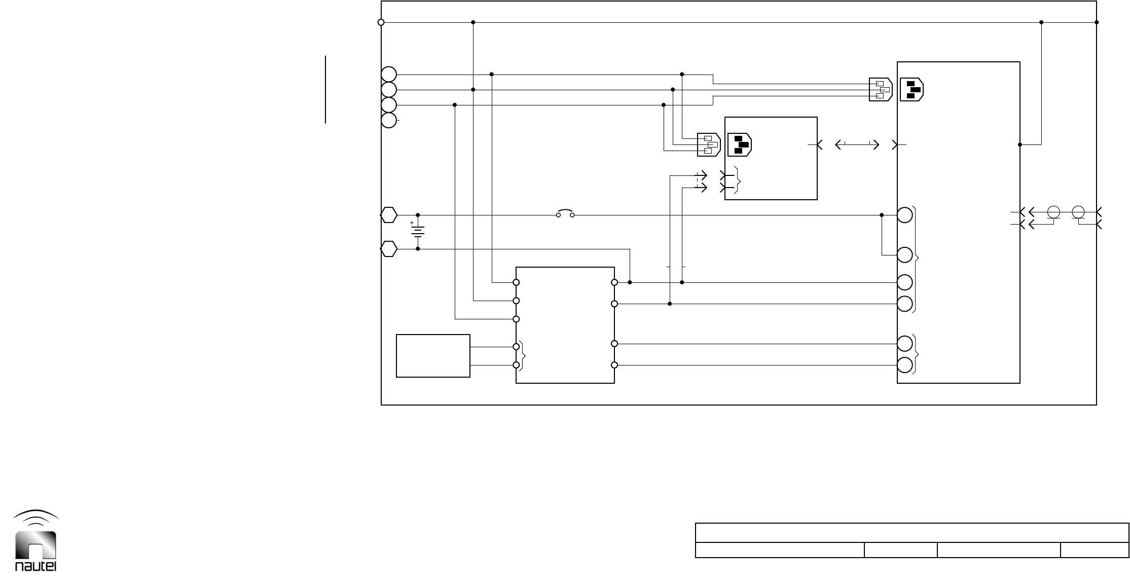
Dimensions = mm (inches)
Electrical Schematic – Vector-LP in Tall Cabinet (205-8200), Optional]
Issue 1.8.1 Not to Scale Figure SD-29 Sheet 1 of 1
N/C
LINE
B-
J1
U2
P3
L
NEA3J5
LINENEUTRAL
GROUND GROUND
LINE
1-PHASE
2
1
4
1
TB1
(OPTIONAL)
CHARGER
U1
PH
20A
W2P1 VR-LINK
RS-232 W3P1
11
4
3
2
4A16TB1
1
NDB/DGPS
VECTOR
J1J1 P2
SENSOR
TEMPERATURE
TB2
BT1
2
3
BTC
CB1
BATTERY
W2P2 W2P3
(OPTIONAL)
A1J1
A3TB1
UNIT 1
L
NE
U5P1
REF GND
N
G
S2050042 V1
RFA (N/C)
NEUTRAL
SPLIT PHASE
GROUND
STATION
4
W3P2
REF GND
COMMON
REFERENCE
TRANSMITTER
1
CABINET
B+

Vector-LP Radio Beacon Transmitter Technical Instruction Manual Page 10-1
Section 10 Mechanical Drawings Issue 1.8.1
Vector-LP Radio Beacon Transmitter
TECHNICAL INSTRUCTION MANUAL
Section 10 MECHANICAL DRAWINGS
10.1 INTRODUCTION
This section contains mechanical drawings
for assemblies of the subject equipment.
Dimensional drawings may be included.
Refer to Table 10-1 for an itemized list.
Assembly detail drawings for assemblies/
modules that have separate maintenance
manuals are not included. Refer to the
appropriate maintenance manual for the
assembly detail of these assemblies.
10.2 LOCATING ASSEMBLY DETAIL
DRAWINGS
Each illustration in this section is identified
by a number that is both the figure number
and the page number. The numbers are
assigned sequentially and are prefixed by
the letters 'MD-'. Drawings in this section are
listed in Table 10-1.
10.3 CONTENT OF MECHANICAL
DRAWINGS
Mechanical drawings are illustrations that
depict the location of electrical components
and show assembly outline detail.
Dimensional information is included, where
appropriate.
When a module/assembly is the subject of its
own assembly detail drawing and it is also
shown in a higher level assembly, the detail
depicted in the higher level assembly may
have minor differences from the module/
assembly actually installed. In this case,
always refer to the assembly detail drawing of
the module/assembly for detailed information.

Page 10-2 Vector-LP Radio Beacon Transmitter Technical Instruction Manual
Issue 1.8.1 Section 10 Mechanical Drawings
Table 10-1: Mechanical Drawings
Figure # Description
MD-1A Assembly Detail and Dimensional Information – Vector-LP Transmitter
MD-1B Assembly Detail and Dimensional Information – Vector-LP Transmitter
(Installed in a Deluxe Cabinet)
MD-1C Assembly Detail and Dimensional Information – Vector-LP Transmitter
(Installed in an IP66 Cabinet)
MD-1D Assembly Detail and Dimensional Information – Vector-LP Transmitter
(Installed in a Short Cabinet)
MD-1E Assembly Detail and Dimensional Information – Vector-LP Transmitter
(Installed in a Tall Cabinet)
MD-2 Assembly Detail – NAPC147D Control/Display PWB
MD-3 Assembly Detail – NAPI76A/02 Exciter Interface PWB
MD-4 Assembly Detail – NAPI78D/02 Remote Interface PWB
MD-5 Assembly Detail – NAPI80 Site Interface PWB (Optional)
MD-6 Assembly Detail – NAPE70C/01 RF Synthesizer PWB
MD-7 Assembly Detail – NAPM11 Interphase PDM Driver PWB
MD-8 Assembly Detail – NAPE76A/03 Exciter Monitor/Generator PWB
MD-9 Assembly Detail – NAPI94A Interface PWB
MD-10 Assembly Detail – NAP35B/01 RF Power Module
MD-11 Assembly Detail – NAPC151A Control/Interface PWB
MD-12 Assembly Detail – NAPS31B/03 Switch Mode Power Supply PWB
MD-13 Assembly Detail – NAAA06 Power Amplifier
MD-14 Assembly Detail – NAPF06A Modulator Filter PWB
MD-15 Assembly Detail – NASM11A/01 Modulator Assembly
MD-16 Assembly Detail – NAPF05A RF Filter PWB (Standard Frequency Band)
MD-17 Assembly Detail – NAPF07C/01 RF Power Probe
MD-18 Assembly Detail – 205-8035 Battery Boost Assembly (Optional)
MD-19 Assembly Detail – NAPS35 Battery Boost PWB (Optional)
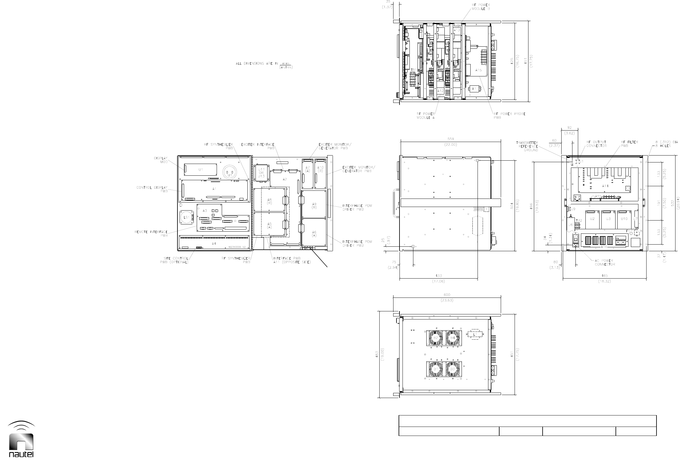
Dimensions = mm (inches)
Assembly Detail and Dimensional Information– Vector-LP Transmitter
Issue 1.8.1 Not to Scale Figure MD-1A Sheet 1 of 1
TB1
A
TU DC POWER
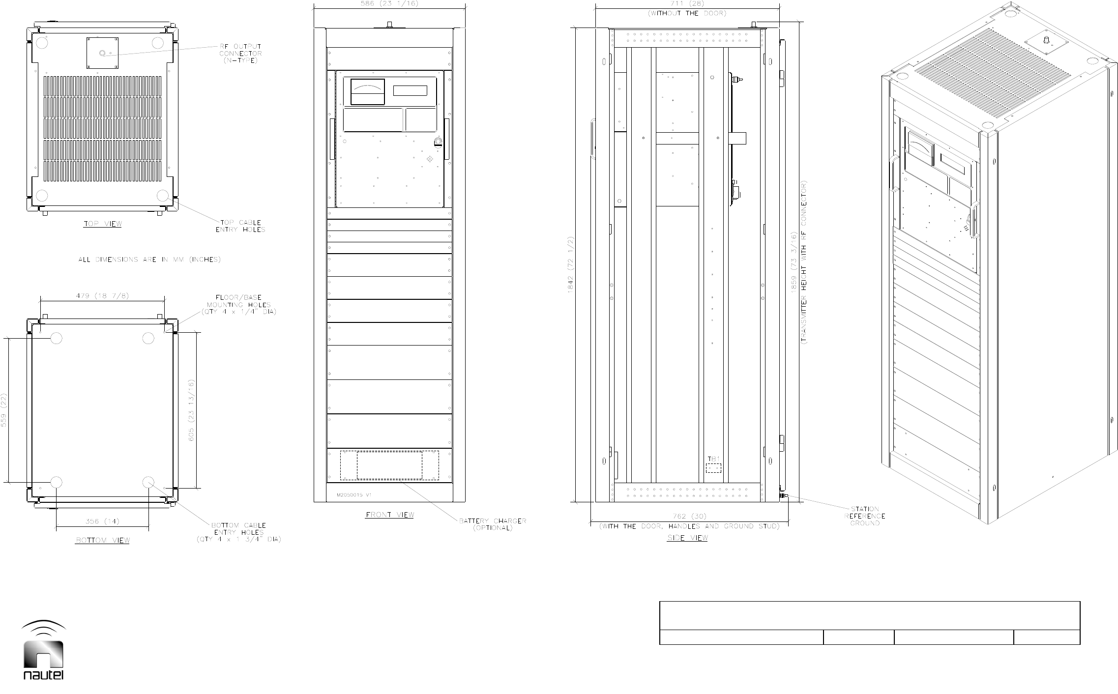
Dimensions = mm (inches)
Assembly Detail and Dimensional Information– Vector-LP Transmitter
(Installed in a Deluxe Cabinet)
Issue 1.8.1 Not to Scale Figure MD-1B Sheet 1 of 1
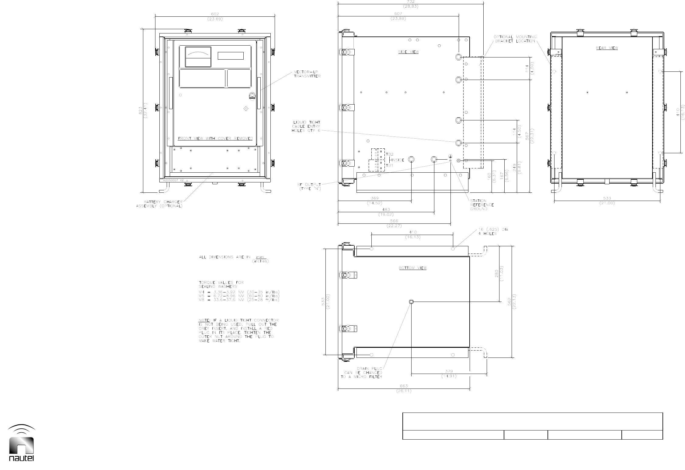
Dimensions = mm (inches)
Assembly Detail and Dimensional Information– Vector-LP Transmitter
(Installed in an IP66 Cabinet)
Issue 1.8.1 Not to Scale Figure MD-1C Sheet 1 of 1
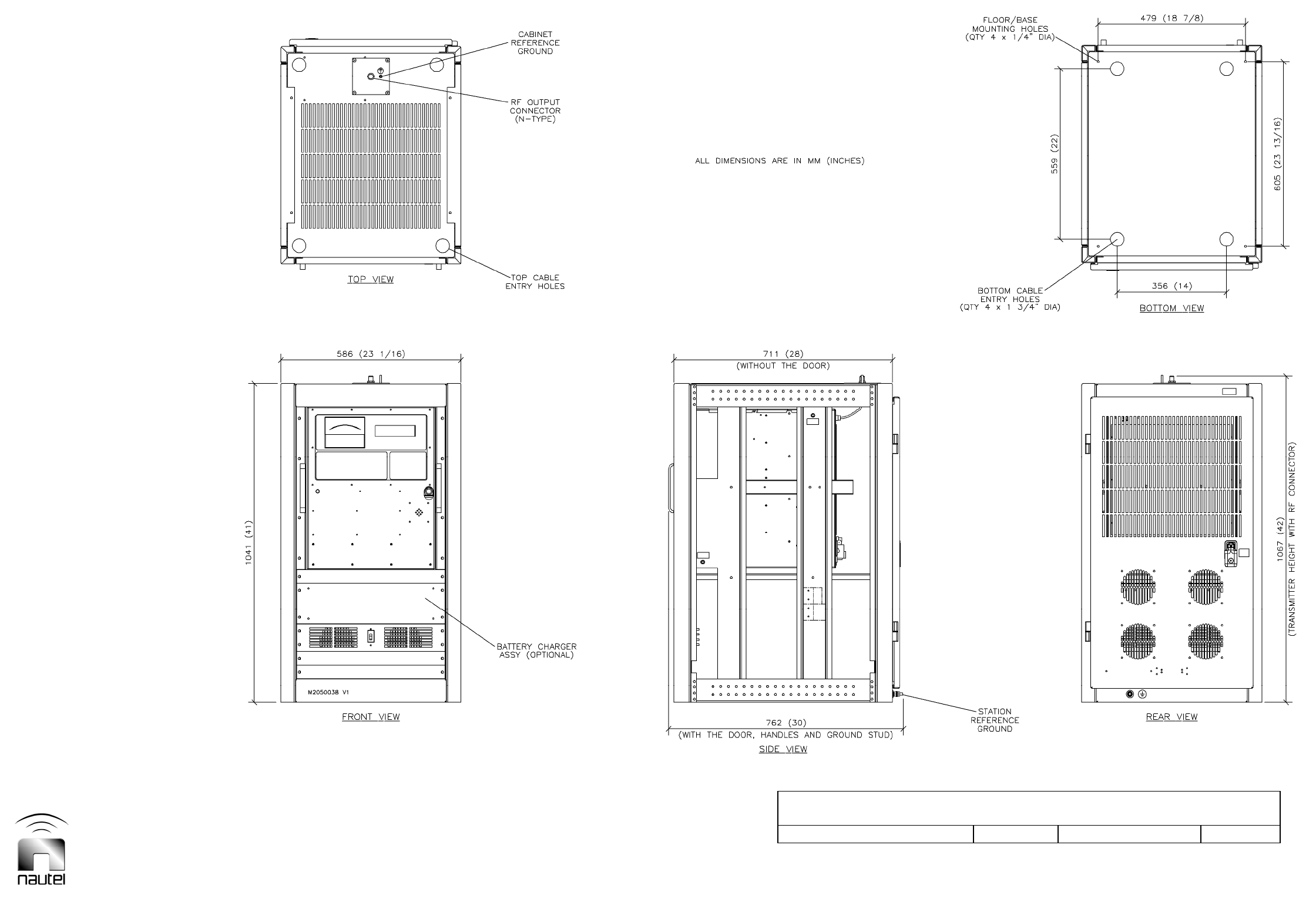
Dimensions = mm (inches)
Assembly Detail and Dimensional Information– Vector-LP Transmitter
(Installed in a Short Cabinet)
Issue 1.8.1 Not to Scale Figure MD-1D Sheet 1 of 1
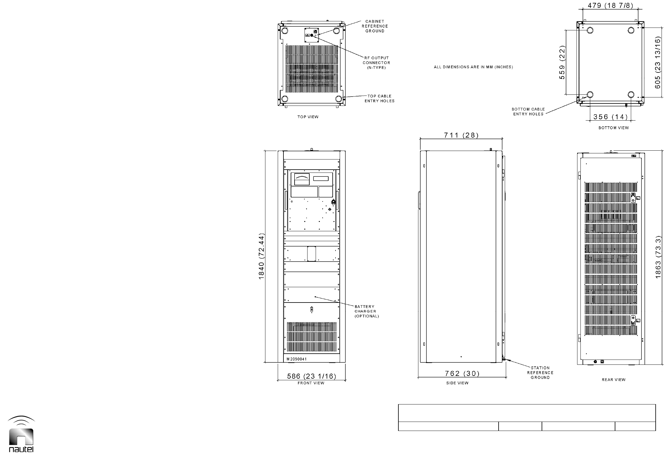
Dimensions = mm (inches)
Assembly Detail and Dimensional Information– Vector-LP Transmitter
(Installed in a Tall Cabinet)
Issue 1.8.1 Not to Scale Figure MD-1E Sheet 1 of 1
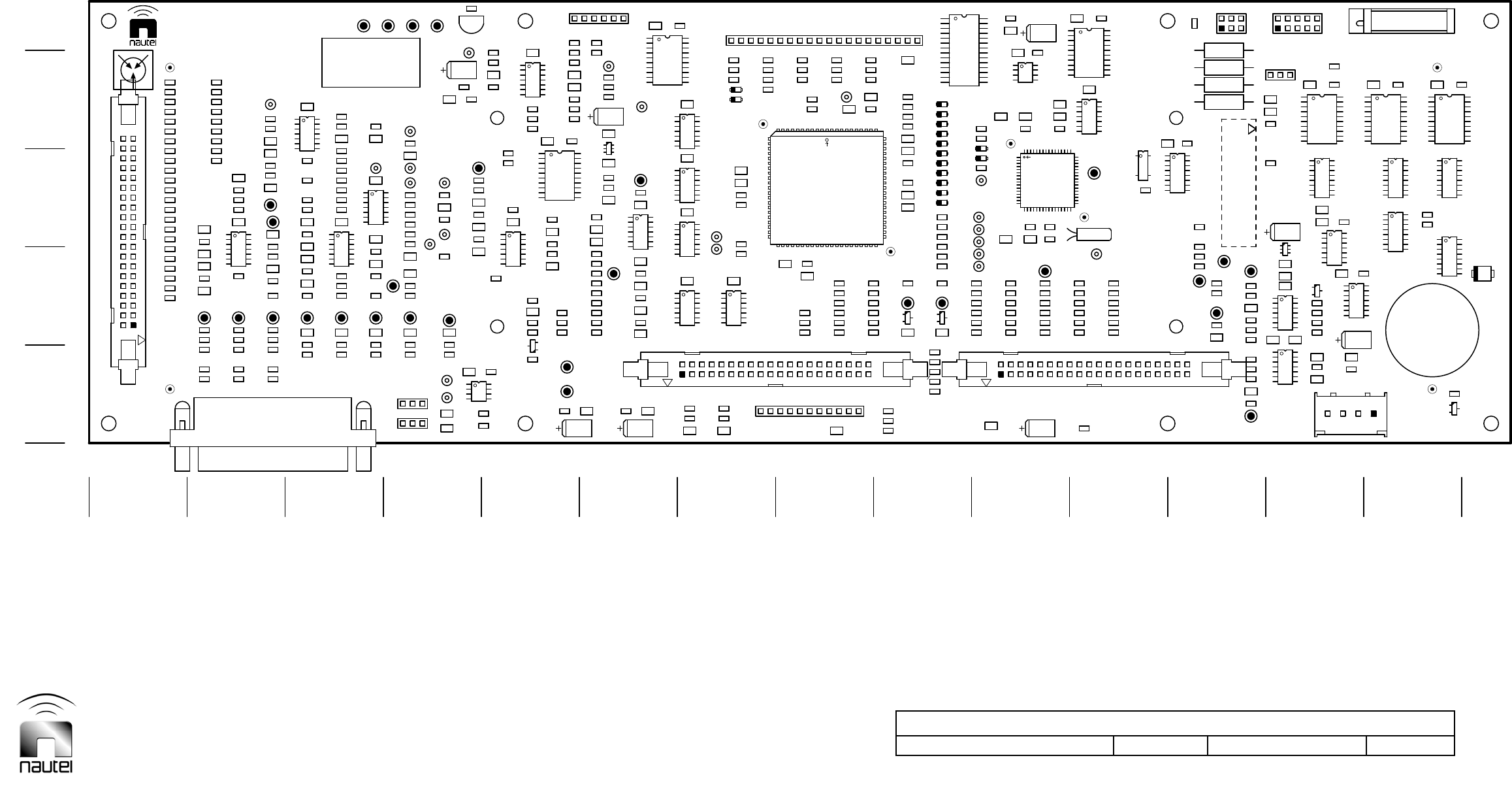
Dimensions = mm (inches)
Assembly Detail – NAPC147D Control/Display PWB
Issue 1.8.1 Not to Scale Figure MD-2 Sheet 1 of 1
TP27
TP3
TP26
L11
R22 R36 R48
R20 R34 R46
C11 R44
C10
C9 R42
C8 C22
R30 TP4
R40
R39
C16
R27
R28
C19
C14
R25 R37
R23
R24
R69
R70
R75
R76
R74R68
R67
C39
C38
R65
R64
R62 C37
C33
C36
C32
R59
R100R91
R93
R94
R90
TP22 C52
R99
C45 C51
R88
R96
R104C48
R103
R102
U5
C62
L2
C76
C61
R115 R130
C71
R128
C70
C60
R114
R126
R125
C59 C68
C75
R135
C63
U10
R120
C72
C66 R133
R117
R118
R123
C87 C88
R140 R142
R150
TP34
C91
L4
R146
CR1
R144
C82
C95
R158 R167
C97
C96
R165
C94
C98
R161
R157 R164
R155 R162
R186 R187
R184
Q1 Q2 C110
R198
R183 R195
R196
C109
R193
R194 TP44
R190
R191
TP41
CR13
L8
CR10
TP45
C103
CR7
L7
CR4
R181
C102
C131C124
R209 R213
R211R207
TP48
C127
C116
C133
C121
R228
R226
R227
R224
R225
C137 C138
C152
C151
R240
R241
C148 Q3
C147
L15
C143
C150
C154
Q4
R248
C160
C161
C162
R21 R35 R47
C12
R19
R17
R18 R43
R41
R32
C23
TP6TP2
C18 C24
R33 R45
C15
R26
R31
R29 C21
C20
C17 TP5
R38
C13
R73
R72
R66
TP11TP8
C35 C40
C34
U4
R63
R61
C31
TP10
R71R60
TP12TP9
C54
R101
R92
U6
C49
C53
R105
TP23
C46
TP25
TP21
R89
R97
R98
R106
R107
L1
C55
C50
C47
TP24
R95
TP29
TP28
C67
R113
R127
R116 R131
R129
C69
TP31
R112
R136
R124
C74
C73
1
J3
C65
C64
R119 R134
R132
R122
TP30
R141 R143
U16
U17
R149
C89C86
TP35
R148
C90
C85
C84
U14
R145
CR2
C83
R159 R168
C93
L5
R166
TP37
R156
R160
R163
R188
C107 C108
TP39
R192
R197
TP42
R199
CR5
C104
C105
C106
CR11
CR12
CR6
CR8
CR9
R182
R189 TP40
CR3
R179
R180
U20
C122 C132
R212
C130
R208
C126
C123
C119
TP46
R210 R214
C128
TP47
U22
C117
U21
L12
C129
C120
TP49
R223
R219
U25
C139
R244
C155
L14
R239
U26
C149 R242
U27
C144
R238
U30
L13
1
J10
1
E3
R247
U34
1J1
U1
U3
R121
U13U15
R185
Y1
U24
C125
C118
R222
C146
C153
C145
U28
U33
U35
R57
R58
R86
R87 Q5
R253
R15
R16
TP13
R56
C29 R84
R85
C6
R14 C28 C42
R11
R12 R54 R82
R81
C4
R10
R53
R52 R78
R79 R108
R7
R8 R51
TP15
R5
R6
R77 C58
C2
R3
R109
R110
R1
R2
R178
J5
1L3 R176
R255 R174
C101 C114
R205
R139
C80
R172 R203
C92
C79 TP43
C78
TP32 R202
R201
CR14
C99 L10
R154
R153 R171
R151 R169
C115
TP53
R237
R236
C157
C136
R217 R231
R215
C135 R229
R220 C163
R243
1
E1
1
E2
R251
TP1
C7
R13 R83
R55
C27 TP19
C43
C164
R254
TP17TP7
C30 C44 R252
C3
C5
R4
R9
R49
C26
TP14
TP16
C41
R80
R111
C56
C1 C25
4
3
2
1
ABCDEFGH I J
5
GRID1
TP18
C57
TP20
U8
C77
R177 L9
R175
C166
C165
R138
TP38
C100
R173 R204
C113
R206
R137
CR15
R200
U12
R152
J6
1
C81
TP33 L6
R170
C112
C111
C142 1
J11
R234
R235
R245
R249
R216 TP50
TP51
TP52
C141
R230
C140
R218 R232
U32
C159
U38
CR16
Y2
C156
U37
C134
R246
R221
1
J8 BT1
R250
U2
U7
1
J4
U18
U11
1
J9
U29
R233
C158
+
LS1
U31
U36
1
J2
U9
U23
K
A
1
J7
BC EF H I K L NOADGJM
1
2
3
4
M1950078 V1
5
GND
GND GND
+5V +15V
GND
-15V+24V
B
AB
(U/S)
A
U19
(U/S)
SER.
CONTROL/DISPLAY
NAPC
NAUTEL ASSY 195-2050
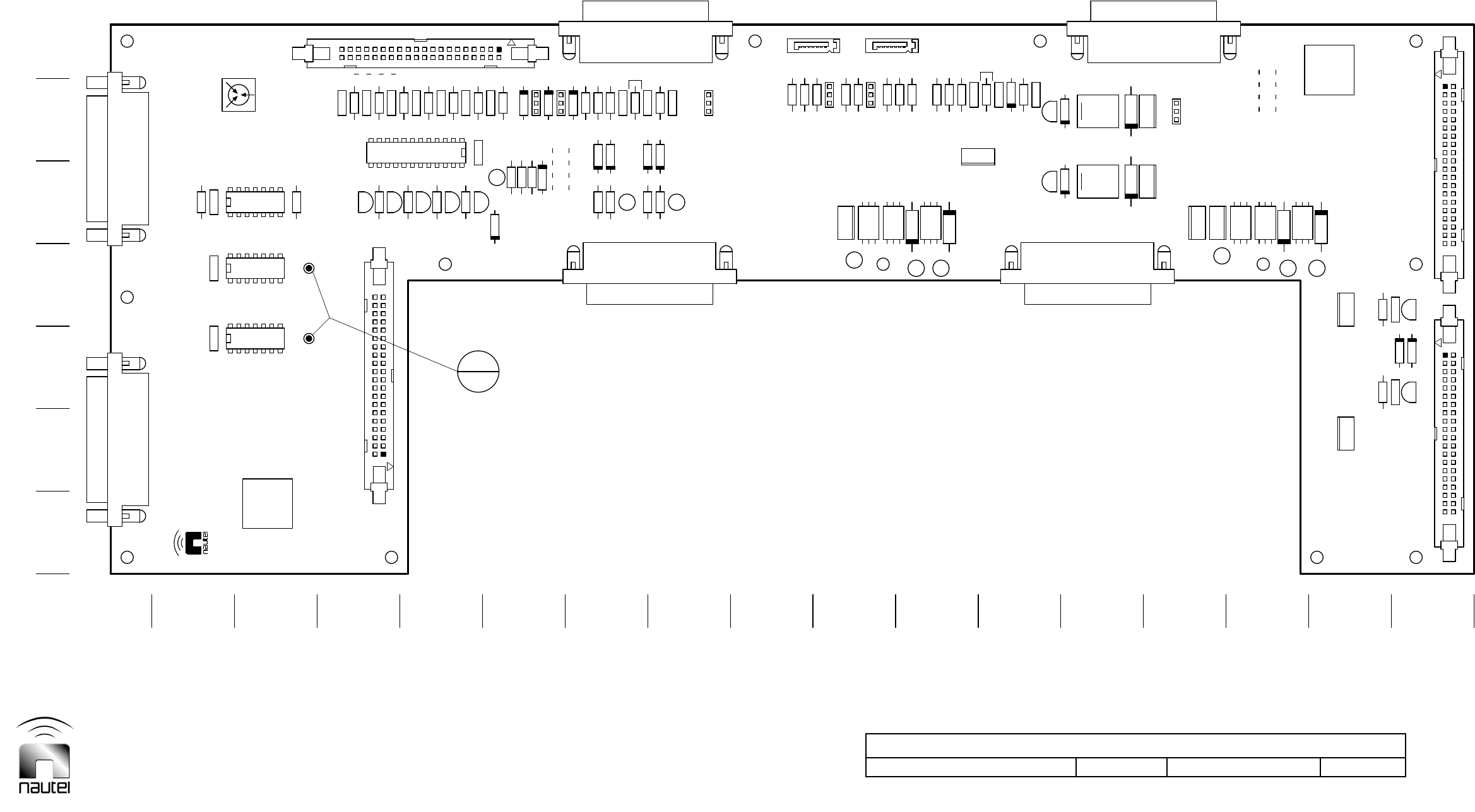
Dimensions = mm (inches)
Assembly Detail – NAPI76A/02 Exciter Interface PWB
Issue 1.8.1 Not to Scale Figure MD-3 Sheet 1 of 1
C1 C2
TP3
TP4
C3
C4
Q1 C5
C6
R7
C7
R9 C8
R11 C9
C11
E111
E101
R15
R17
R18
R40
R20
1E5
R23
R24
R26
R27
R29
R30
CR8
C15
E8
21
E9
21
R34R33
R13
CR24
R36
U1 U2
TP1 TP2
C10
CR27
CR28
CR26
+
C16
+
C17
+
C18
+
C22
+
C24
CR22
CR21
R1
U3
R4
R2
R5
R3
Q4
Q3 R8
R6
R12
R10
R14
CR1
CR3
CR2
R37
R38
+
C27
R32
R16
C13
C14
C21
E4
1
AK
CR4
L2 1E6
R19
R21
R22
CR5
L4
CR6
R25
R28
C19
Q6
CR10
R39
Q7
C20
CR12
CR14
AK
L7
L6
CR15
AK
L8
CR17
AK
CR20
AK
CR19
6
5
4
3
2
1
ABCDEF
GRID2
Q9Q8
C26C25
R35
21
E2
21
E3
CR9
CR11
CR13
AK
J7
1J3
1
12
E1
CR23
U4
CR25
1
J11
J16
1
J4
1
+
C23
CR7
AK
1
J10
Q5
Q2
+
C12
6
5
4
3
2
1
ABCDEF
GRID1
1
J15
+
C28
L3
R31
1
J6
K1
AK
CR18
CR16
1
J5
K2
E7
1
HR10 TERMINAL,TESTPOINT,PWB,YELLOW
2
J13
1
1
J9
1
J8
87 54 21
A
B
C
D
F
G
17
M1950154 V1
15 14 13 12 11 9 6 3
E
16 10
DGPS
DGPS
DGPS
SER.
BEACON
BEACON
BEACON
BEACON
EXCITER INTERFACE
DGPS
DGPS
BEACON
NAPI
DGPS
NAUTEL ASSY 195-3020
BEACON
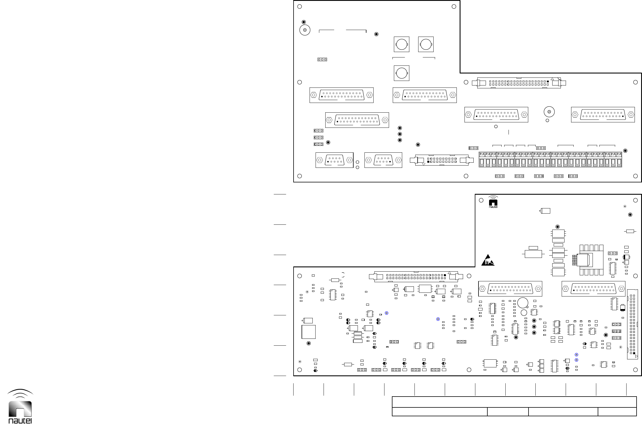
Assembly Detail – NAPI78D/02 Remote Interface PWB
Issue 1.8.1 Not to Scale Figure MD-4 Sheet 1 of 1
R26
R123
C98
R51 R54
TP10
C2
C1
R6
R4
C4
R162
C9 CR2
C12
R13
R50
R38
CR10
C23
R114
CR11
C16 C22
TP2
R27
R70R53 R75
CR18
C49
R55
TP3
R73
R78
C54
R72
C57
C56 R86
C64CR22
R83
C61
C60
C76
TP4
R101
R102
R98
R97 R99
C78
R91 R30
R92
C95
R159R139
C124
R165
C126
C127
R138
R143
R142
R135
C109
R144
R132 R136
C107
R161
C119
CR21
R152
R164
TP1
C3
1
T1
R1
R5
R163
R12
CR3
R23
R14
R17
R96
U1
1
E5
C34
CR15
R31
R32
CR12
C21
R18
CR9
R34
C20
1
E7
C40
R71
C44
CR16 CR17
C35
C36
C39 C41
R76
C50
R74
R77
R48
C46
C45
C55
C52
C51
C47
L4 L6
L7
C62
R84 R85
C65
C66
U9
R156
R82
L9
R105
C77
C79
U10
R93
R100
R94
R103
Q7
R9
C81
C94
U12
CR26
R160
U14 U13
R145
R110
R166
C125
TP8
L11
U19
U17
R134
R137C102 C108
CR25
R169
R153
C120
C118
TP9
U3
U6
U8
+
C122
L12
U18
1J18
CR20
C10 C26
R16
R29
C13
C15
C8 R63
C7
L2
C84 R130
C67
C106
R133
C74
R158 R109
C89
TP5
R33
R106
C73
R19
R88
C70
C71
C80C59 R87
R81
C123
C87
C113
R171
C105
1
E18
1
E6
1
E8
L1
R15
CR1
R22
E4
1
C17
R28
C6 L3
C29
C30
C31 C42
J8
J7J6
TP11
C83
C85
L8
R131C68
TP7
TP6
1
E17
C88
R89
U15
R90
C75
C72
C82
C58
C69
1
J16
R167
U23
1
J11
R37
1
C112
1
E14
1
E13
E15
1
TP12
R170
U21
C100
E111
C103
U7
1
J3
1
J5
1
J4
1
J17
U11
U16
1
J17
1
J12
J13
1
TB1
1
J16
J22
1
GND
TP8
TP7
TP5
TP1
MONITOR LEVEL
TP9
B C
TP6
EF HI K
GND
L
TP4
1
2
3
4
6
A
M1950192 V2
TP12
GND
D
GND
G
TP3 TP2
J
5
TP10
REAR
TP11
FRONT
GND
GND
GND
GND
NDB
FILTER
1
1
A
B
DIFF
B
DIFF
DIFF
+
1
+-
1
-+-
BE4
1
+
11
+-
AUDIO
1
NORM
1
SINGLE
SINGLE
NORM
1
2
SGL CHARGER
3
SER.
DIFF
56
DIFF
8
STANDBY
CODE 2
9
DIFF
E6
11
GND
12
TO-TALK
PRESS-
E5
14
INPUT
15
GND
17 18 20
AUDIO
21 23
LEVEL
GND
24
J17
RF ON/OFF
PDM INHIBIT/
INTERLOCK
E15
E14
EXCITER
INPUT
BATTERY
DIFF
A
THRESHOLD
NORM NDB
MONITOR
-
10MHz
+
E18
1
SHLD
-
A
NORM
NORM
SHLD
NDB
NDB
MONITOR
E13
BYPASS
E11
AUDIO HD-R
RS-422
NORM
HD-R
RS-232
SINGLE
SINGLE
RF
NORM
J16
10MHz (B)
10MHz (A)
E8 ALARM
41
NDB
E17
NORM
SGL
SGL
E7
7
RF OFF/
RF ON/
10
SGL
DIFF
BATTERY
AUDIO
16
GND
13
J13
NORM
NORM
MONITOR
2219
EXT
NDB
BYPASS
STANDBY CODE 1
NORM
INTERNAL RS-485
EXT RF IN/
HD-R PHASE
NAPI78
LEVEL
FREQUENCY
PHASE MSK (B)MSK (A)
MAGNITUDE
NDB
REMOTE INTERFACE
NORM
AUDIO
PROBES POWER SUPPLY
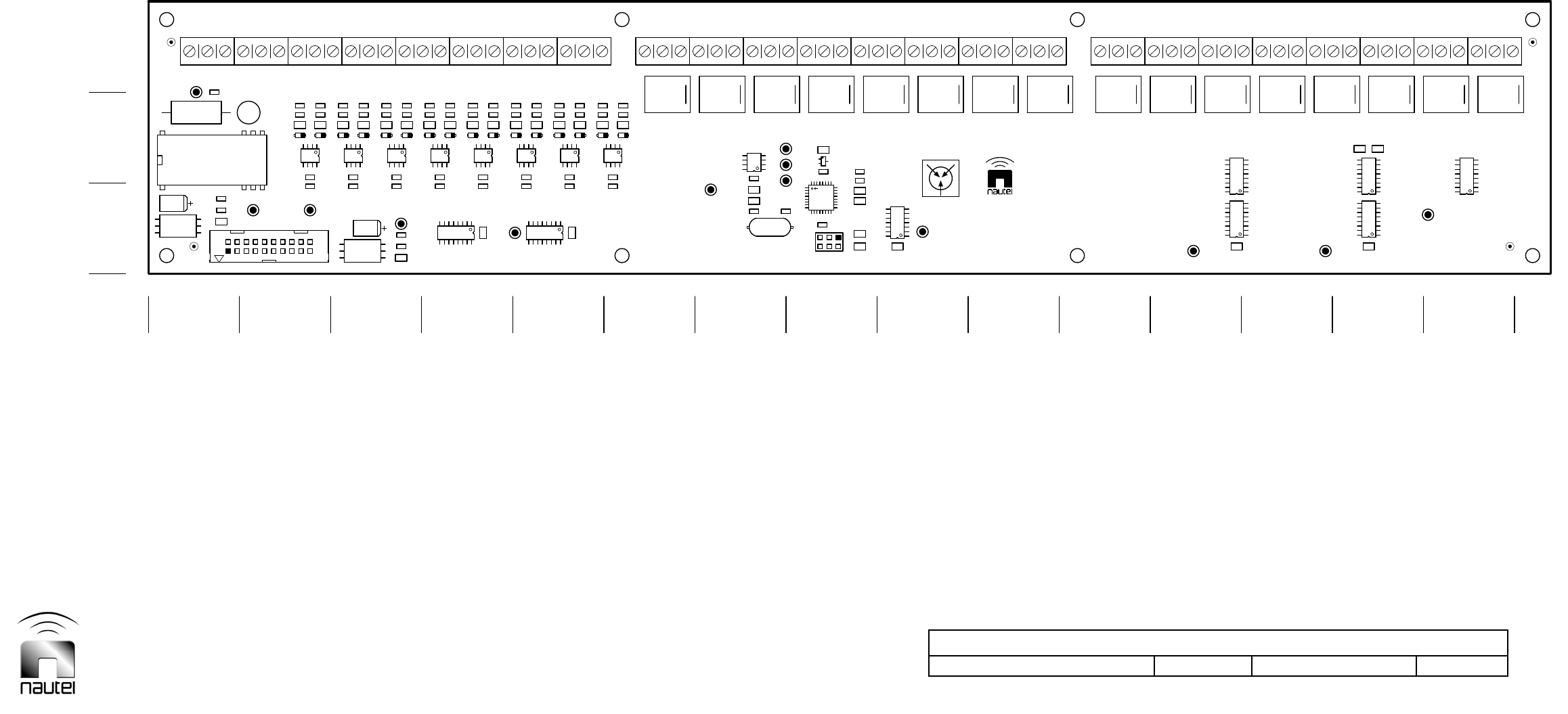
Dimensions = mm (inches)
Assembly Detail – NAPI80 Site Interface PWB (Optional)
Issue 1.8.1 Not to Scale Figure MD-5 Sheet 1 of 1
TP2
C1 C2
C3
1
J1
L1
U1
R2
TP1
+
C4
R1
R3
TB1
R4 R8 R10 R14 R16 R21 R23 R27 R29 R33 R35 R39 R41 R45 R47
CR11
CR12
CR13
CR14
CR15
CR10
CR9
CR8
CR7
CR6
CR5
CR4
CR3
CR2
CR1
C5
R5 R9
C7
C6
R11
R15C8
C10 R17
R22C13
R24C14
R28C15
R30C16
R34C18
R36C19
R40C20
R42C21
R46C23
R48C24
TP4
TP5
TP3
C11
C12
C17
C22
C9
L2
U10 U11U2 U3 U4 U5
U6
U7 U8
U9
R20
R6
R7
R12
R13
R18
R19
R25
R26
R31
R32
R37
R38
R43
R44
R49
R50
TP7
TP9
TP6
TP8
C26
C27
C31
C32
C33
C34 C35 C36
J2
1
K1
K10
K11
K12
K2
K3
K4
K5
K6
K7
K8
K9
R53
U12
U13
U14
U15
U16U17
Y1
TP11
R51
R52
C25
CR16
L3
C28 C29
C30
R54
L4
L5 TP10
TB3TB2
TP13
C38
K13
K14
K15
K16
U18U19
U20
TP12
C37 L6
1
2
3
ABCDEFGH IJKLMNOP
M1950065 V1
GND
GND
GND
123456789 12131415 17 2021 232410 191816 2211
12 34 65 7 8 9 10 11 12 13 14 1615
COMMO
N
COMMO
N
COMMO
N
COMMO
N
COMMO
N
COMMO
N
COMMO
N
COMMO
N
MONITOR MONITOR MONITOR MONITOR MONITOR MONITOR MONITOR MONITOR
POINT POINT POINT POINT POINT POINT POINT POINT
SER.
NDB SITE INTERFACE
NAUTEL ASSY 195-2080
181716151413121110987654321 242322212019 1110987654321
COM
N/C
N/O
CONTROL
POINT 1
COM
N/C
N/O
CONTROL
COM
N/C
N/O
CONTROL
COM
N/C
N/O
CONTROL
COM
N/C
N/O
CONTROL
COM
N/C
N/O
CONTROL
COM
N/C
N/O
CONTROL
COM
N/C
N/O
CONTROL
COM
N/C
N/O
CONTROL
COM
N/C
N/O
CONTROL
COM
N/C
N/O
CONTROL
COM
N/C
CONTROL
POINT 2 POINT 3 POINT 4 POINT 5 POINT 6 POINT 7 POINT 8 POINT 9 POINT 10 POINT 11 POINT 12
NAPI
12 13 14 15 16 17 18 19 20 21 22 23 24
N/O
COM
N/C
N/O
CONTROL
COM
N/C
N/O
CONTROL
COM
N/C
N/O
CONTROL
COM
N/C
N/O
CONTROL
POINT 13 POINT 14 POINT 15 POINT 16
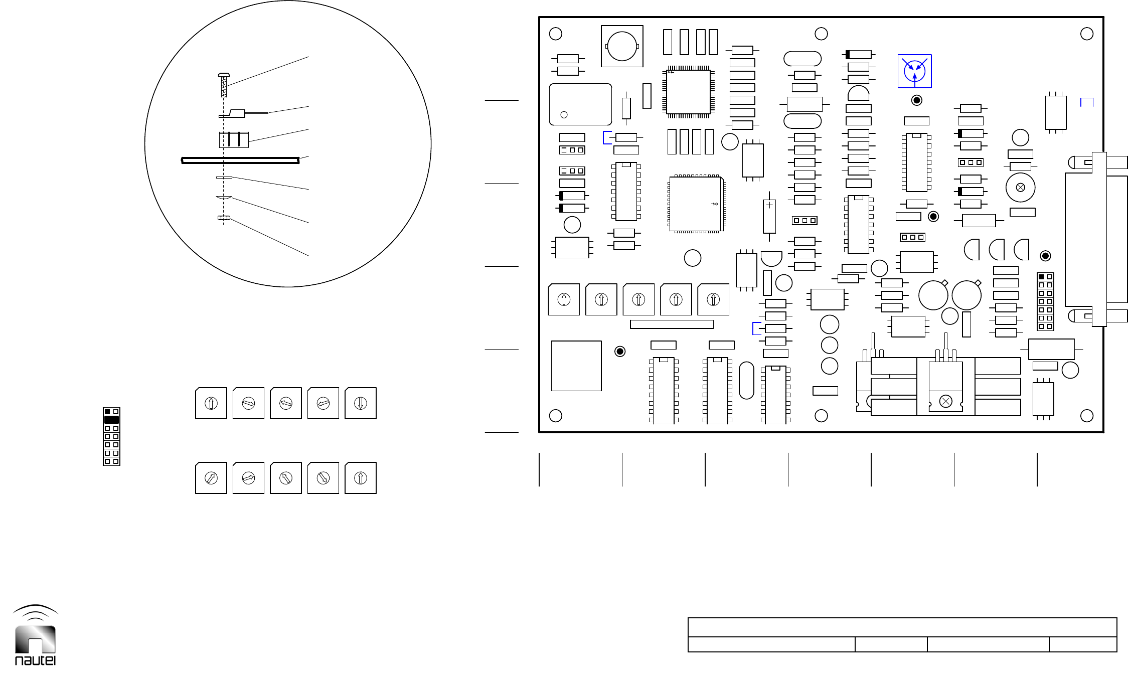
Dimensions = mm (inches)
Assembly Detail – NAPE70C/01 RF Synthesizer PWB
Issue 1.8.1 Not to Scale Figure MD-6 Sheet 1 of 1
TP5
C13C16
TP3
R3
R4
C47
C20
R18
1E3
R12
R8
R11
L1
R20
L5
R34
TP4
R52
R46
C57
C58
C32
43
2
19
8
7
5
0
6
S2
U3
TP1
C8
R5
R6
U7
43
2
19
8
7
5
0
6
S5
C36
+
C35
R19
L7
+
C41
C39
R17
C4
R9
R13
R10
C25
C21
Q6
1E4
C44 TP6
C56
C1
C34
R47
C46
R31
R32
+
C29
A
B
C
D
E
F
G
J2
+
C43
L9C22
C7 C5
+
C42
C17 C10
+
C40
C23
L4
U10
Q1 Q2 Q3
C19
CR2
CR3
1E2
C3
1E1
R51
C55
R16
TP2
R50
R49
R43
R2
TP7
R33
R35
R29
C48
R42
R28
R26
R25 CR5
C54C28
R14
R37C27
C15
R22
C6
CR4
R7
U6
43
2
19
8
7
5
0
6
S1
43
2
19
8
7
5
0
6
S3
43
2
19
8
7
5
0
6
S4
+
C37
C2
R1
U1
U8
+
C24
C26
L2
R48
R45
R15
+
C38
C33
+
C31
Q5
E5
A
B
C
D
E
F
G
R27
CR6
1E6
R23
Q4
C18
C14
C12
L3
6
5
4
3
2
1
ABCDE F
GRID1
L6
C11
C9
+
C30
CR1
U11
3
4
U9
231
4
R21
L8
U12
1
U2
U4
U5
1
J1
E5
8
7
7
8
3
2
2
3
7
8
7
8
3
2
3
2
4
19
5
0
6
6
0
5
91
4
9
6
6
9
1
4
1
4
654
19 0
4
19
6
0
5
6
9
6
9
4
1
1
4
4
5
0
91
6
6
0
5
91
4
AB DE G
3
28
7
7
82
3
8
7
7
82
3
3
2
7
8
7
8
PWB
HEATSINK
3
2
2
3
3
0
5
0
5
5
0
0
5
M3 WASHER
1
2
4
C F
5
M2000125 V1
M3 HEX NUT
#4 BELLEVILLE WASHER
SEMICONDUCTOR
M3 PAN HEAD SCREW
M1940198 V1
(OMIT FOR U11)
4.0 INCH POUNDS (0.45 NEWTON METERS)
U9 & U11 MOUNTING DETAIL
TORQUE ATACHING HARDWARE TO
GND
GND
1
0
x1000
S1
9
8
x10
S3
0
5
x0.1
S5
x0.1
EXT INT
REF
SYMMETRY
SHOWN CONNECTED
IN 'B' POSITION
2
3
x100
S2
4
7
x1
S4
x100 x10
INPUT
10MHz
x1
HIGHLOW
EXT INT
SOURCE
DISABLE
IPM BAL
REF
SER.
PDM
x1000
ENABLE
SYMMETRY ADJ
NAUTEL ASSY
194-3060
NAPE
FREQUENCY (kHz)
RF SYNTHESIZER
SHOWN SET FOR 1294.0 kHz
FREQUENCY (kHz)
SHOWN SET FOR 387.5 kHz
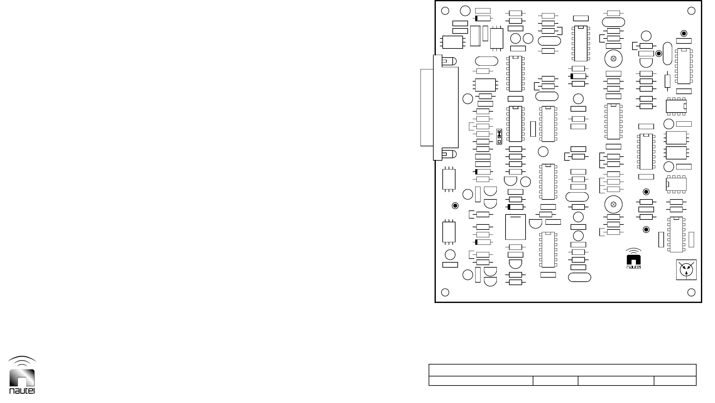
Dimensions = mm (inches)
Assembly Detail – NAPM11 Interphase PDM Driver PWB
Issue 1.8.1 Not to Scale Figure MD-7 Sheet 1 of 1
1
P1
+C39
R62CR3
U11
U10
R78
R77
R75
R74 R69
R66
R65
R63
R61
R55
R54
R52
Q7
Q6
Q5
Q4
Q3
Q2
Q10
L4L2
K1
CR5
CR4
C66
C63
C61 C60
+
C57
+
C56
C55
C53
C52
C48
C17
C16
+C10
TP15
TP18
TP17
+C2
C54
TP9
TP4
TP8
TP13
TP16
+C12
C24
C29
+C4
C49
C50
C51
C62
C71
R12
R13
R15
R2
R27
R31
R39
R42
R46
R47
R49
R50
R51
R53
U13
U7
L3
C65
+
C64
C59
C58
+C47
C46
C36 C25
C21
C14
C13
1
E1
TP2
TP19
L1
L8
R1
R14
R5
R57
+C3
U4123
U5U12
U1
R9
R8
R76
R73
R72
R71
R70 R68
R67
R60
+C18
C15
C11
+C1
TP11
C5
C6
C7
CR1 R33 R36
R37
R6 R7
C22
C19
TP1
TP3
C35
+C9
R16
R3
R4
U8
U6
U3
U2
R64
R59
R58
R56
R44
R38
R35
R34
R30
R29
R26
R25
R22
R11
R10
Q1
L7
L6
CR2
C45
C44
+
C43
C38
U9
TP7
C41
C42
TP10
TP12
TP14
TP5
+
C20
C23
C26
C27
C28
C33
C34
C37
C8 R48
C30
M1970044 V
2
GND
GND
DUMP
A
B
GAIN
NAPM
INTERPHASE PDM DRIVER
NAUTEL ASSY 197-3040
SER.
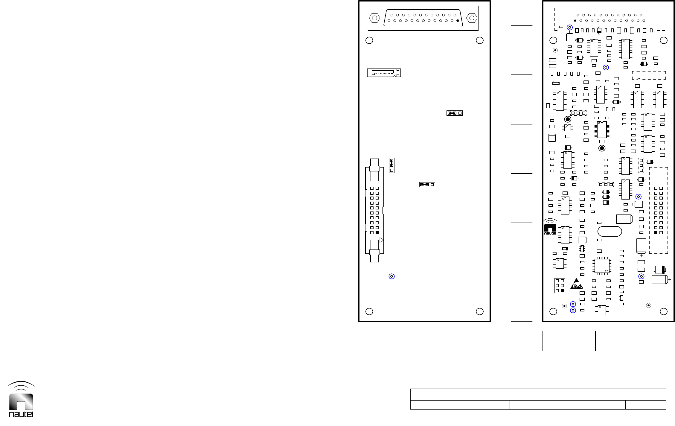
Dimensions = mm (inches)
Assembly Detail – NAPE76A/03 Exciter Monitor/Generator PWB
Issue 1.8.1 Not to Scale Figure MD-8 Sheet 1 of 1
R8
R14
R60
R29
R49 R63
R76
R81
R27
TP2
R28
C82 C42
C37
R26
R57R42
C27
DS1 U7 C40
C24
C23
C21
R24
CR5
C36
R21
R38
R52R36R20
R53
R50R34
C41
CR1 C35
C33
R56
R41
R44
C17
C30
R18 R31
TP4
R86
C4
R87
C81 R16
R2
C80
C44
CR12
TP5
TP8
R77
C66
L2
C64
C65
C79
CR13
R74 C75
R75
R32
R73
R71 C74
C63 C72
C29
R80 C77
C69
E2
1
1
E3
1
C1 R1
C43
C83 C38
R58R43
C28
TP3
U12
R13 C26
C25 R46
R25
C22
R40
U4
C46
R39 CR6
R51R35
R33
C20C12
CR2
CR4
TP9
U6
C13
C34
R55
R19 C84
C16
U5
R47
C32
U10
C31
R54R45
R22R84
R23
R85
R9
C15
C45
R30
C19
CR11
C18
U8
R78
C68 C73
L3
L1
C67
TP6
C62
CR8
R83
R82
R72
C61
C60
C14
U18
U17
U20
CR9
R61
C70
1
J3
U3
U11
C76
R37
R59
R48
CR3
U9
CR10
U19
R69
R70
C85
R67
C53
R65
R66
U2
C50
C57
C2
R4
C58
R3
R7
C10
R5
C54
C6
C55
C49
CR7
R62
R79
R17
U13
C52
C51
J2
1
C9
C3
R64
C59
C56
Y1
R10
1
E1
R6
C39
C11
U16 U15
C8
C5
C78
TP1
R68
C48
U1
R12
C47
R15 C71
R11
U14
C7
Q1
1
J4
1
J1
2
5
1E3
1
1
1
6
7
A
1
1
B
E2
J4
3
4
J3
J1
E1
C
REAR VIEW TOP VIEW
M1950152 V2
TP8
GND
A
B
KEYED
CW
A
B
NAPE76
NORMAL
SER.
KEYER OK
GENERATOR
EXCITER MONITOR/
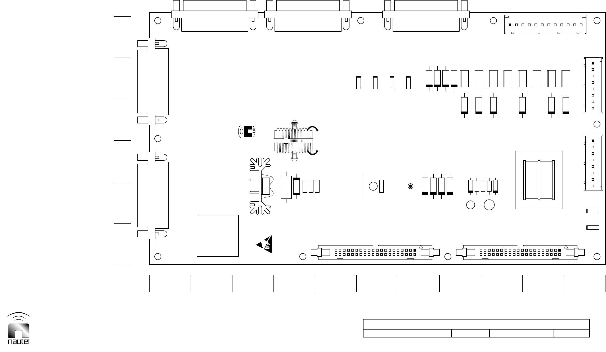
Dimensions = mm (inches)
Assembly Detail – NAPI94A Interface PWB
Issue 1.8.1 Not to Scale Figure MD-9 Sheet 1 of 1
CR1
C1
C3
C5
CR4
CR23
CR5
CR25
CR26
CR7
R6
CR8
AK
CR17
TP1
+
C7
+
C6
CR10
CR11
CR13
CR12
CR14
R1
C2
+
C4
E5
E4
CR3
CR6
CR24
R7
R5
AK
CR16
AK
CR15
AK
CR19
AK
CR20
AK
CR22
321
U1
2 1
E1
1
J2
CR9
E2
10
9
8
7
6
5
4
3
2
1
ABCDEFGH I J
GRID1
1
J8
1
J9
E6
E3
J3
1
AK
CR21
AK
CR18
1
J5
1
J6
1
J7
1
J4
58
14
T1
1
J1
1
J10
L1
B
E
A
C
D
F
11 8 5297643110
M2050030 V1
NAPI94
GND
SER.
INTERFACE
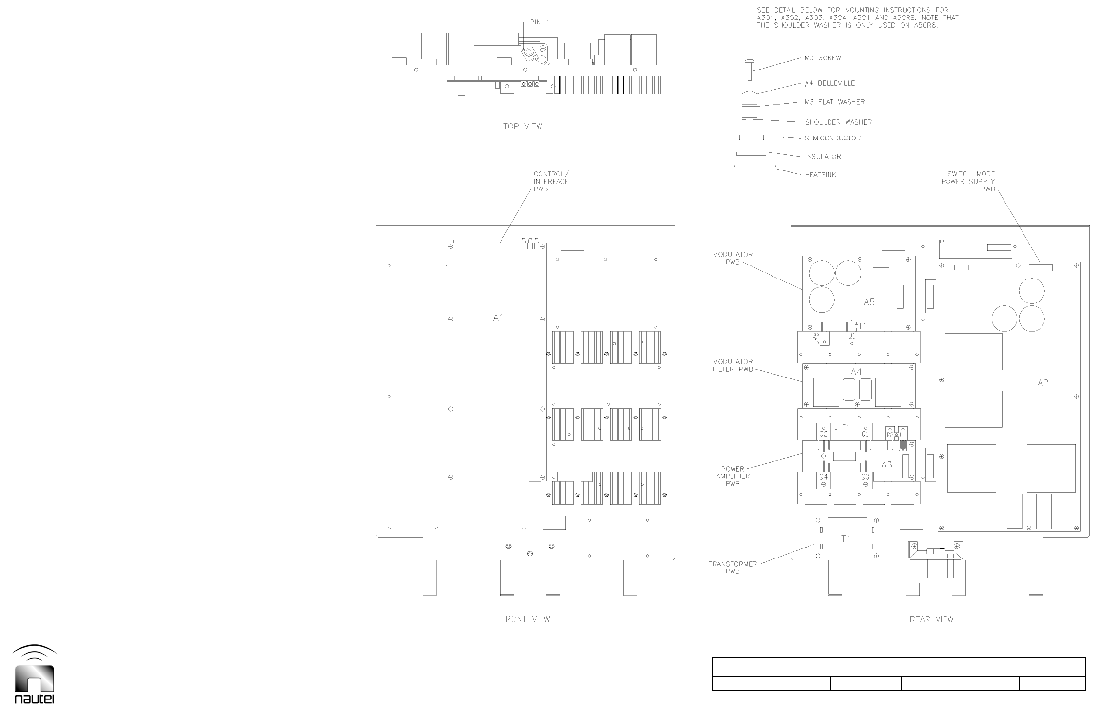
Dimensions = mm (inches)
Assembly Detail – NAP35B/01 RF Power Module
Issue 1.8.1 Not to Scale Figure MD-10 Sheet 1 of 1
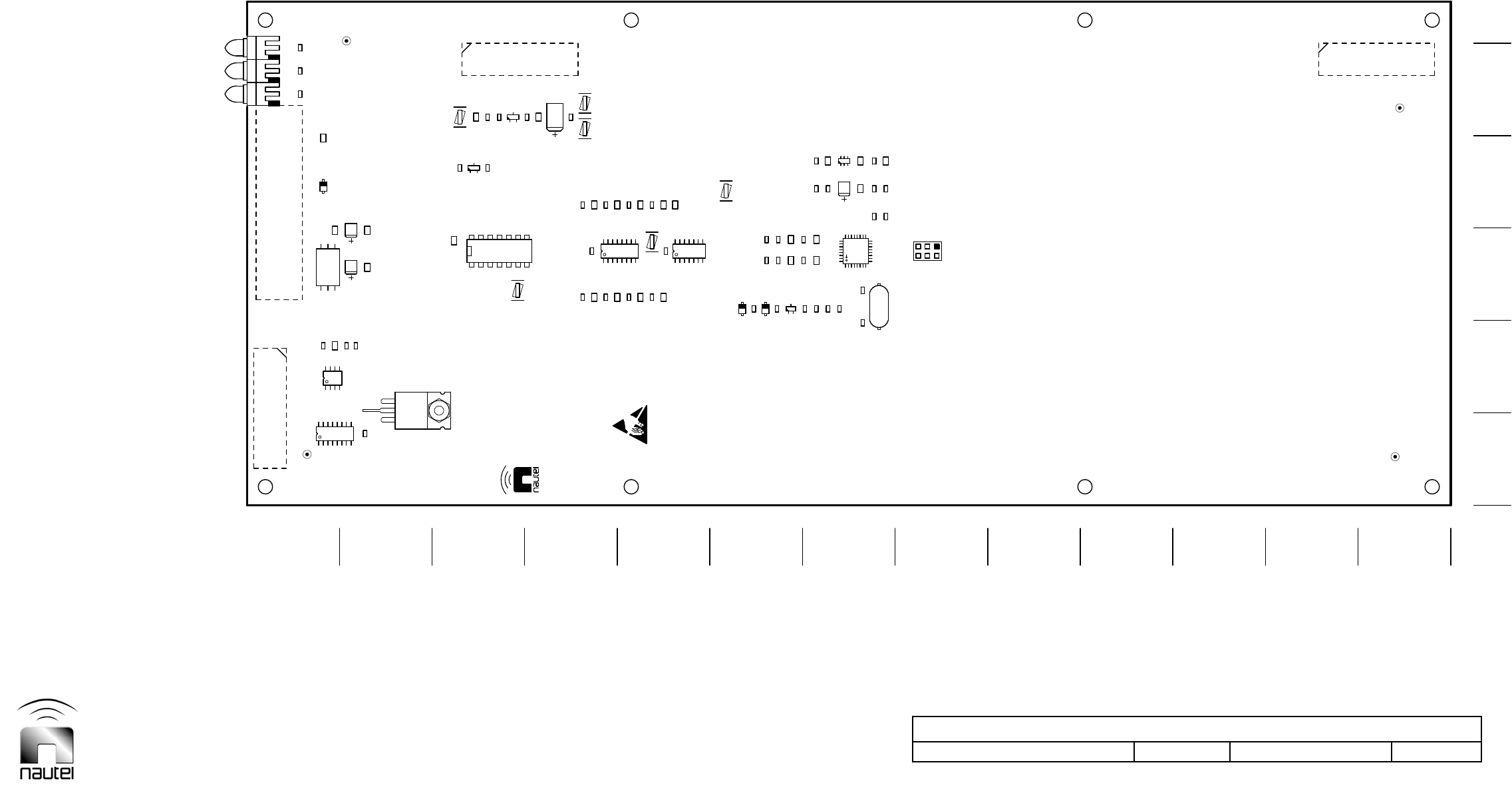
Dimensions = mm (inches)
Assembly Detail – NAPC151A Power Module Control/Interface PWB
Issue 1.8.1 Not to Scale Figure MD-11 Sheet 1 of 1
C2
L1
R1
R3
C6
C18
Q3
C37
R32
R33
C35
R4 R13
R5
C8
R14
C22
C9 C23
C10 C24
C25
R8
R9 R19
C11 R21
C12
C13
R23
C16C17 C30
C32 R26
C5
C14
R17
R18
R20
C28
C33
C34
U1
C1
R2
CR3
C4
R30R27
R36
TP4
R34
C7 C21
Q2
C36
R31
TP6 TP5
R6
R7
R15
R16
CR1
CR2
U3
R10
R11
C26
C27
R22
Y1
C31
C29
R25
U2
L2
C3
R29
C20
R35
TP2
U6
R12
C19
C15
R28
U7
U8
R24
Q1
G
D
S
D
TP1
+
DS2
+
DS1
TP3
1
U4
+
DS3
U5
1
J1
1
1
1
13
11
10
9
8
7
5
4
3
2
1
B E
12
M2050022 V1
6
ACD
F
GND
SER.
J7 (U/SIDE)
NAPC151
INSTALLED
J6 (U/SIDE)
FAULT
MODULE
MODULE
MODULE ON
PWR MODULE CONTROL/INTERFACE
J2 (U/SIDE)J4 (U/SIDE)
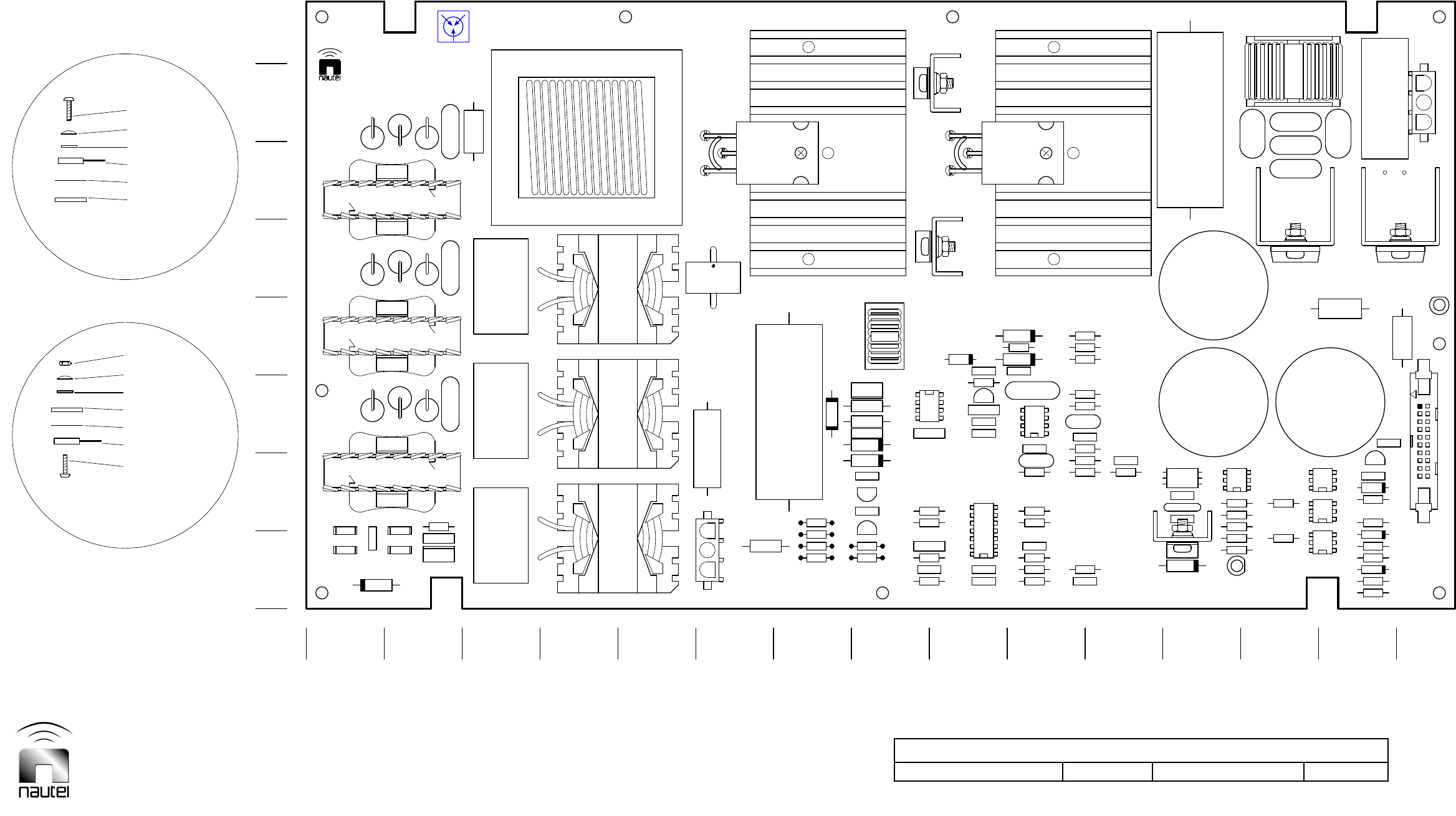
Dimensions = mm (inches)
Assembly Detail – NAPS31B/03 Switch Mode Power Supply PWB
Issue 1.8.1 Not to Scale Figure MD-12 Sheet 1 of 1
C20 C23C21
R50
C18
C14
C30
Q8
C36
C34
C28
C19
R30
R23
RT1
R32
R4
R40
CR5
SDG
Q7
R41
R16 R13
R18 R21
R24
R26
R10
C10
C16
C29
C32
R69
R68
R28
R29
R64
R35
R63
R22
CR16
U10
231
C1
L1
C25
R37
C11
R33
R56
CR3
U11
C33
R65
R61
C9
R17 R20
R43
C27
CR4
R11
7
8
10
4
3
1
T2
KA
CR6 CR7
KA
U5
C38
+
DS1
1
J2
CR21 R46 R67
R47 R51R25
R39C6 R49
CR1 C35
CR2
R58
C37
R12
R54
R55
CR17
C41
AK
CR13
AK
CR14
R19
CR10
AK
AK
CR15
CR11
AK
R15
C8 C22
C24
R27
R66
R9
C5
R44
Q4
C31
R3
R5
C2
CR18 CR19
C26
R57 U3
CR20
AK
CR12
DS2
R2
R53
R52
U7U9
R62
R7
RV1
C44 C43
L4
L5
R14
CR9
AK
C7
E1
E2
Q5
U8
Q1
GDS
D
+
C12
+
C13
+
C15
U4
U6
R1
31
U2
231
U1
2
C4
1
L3
RV2
RV3
C45
L6
1
10 11
20
T1
C17
3
4
T3
21
E1
E2
Q2
GDS
D
1J1
1
J3
BCEFHI KLNO
SEMICONDUCTOR
M3 WASHER
HAT46
HAT46
M3 HEX NUT
HEATSINK
HEATSINK
M3 WASHER
1
2
3
4
6
7
8
A
M1970096 V1
D G JM
5
4.0 INCH POUNDS (0.45 NEWTON METRES)
CR6, CR7, U1, U2 & U10 MOUNTING DETAIL
M3 PAN HEAD SCREW
#4 BELLEVILLE WASHER
TORQUE ATTACHING HARDWARE TO
SEMICONDUCTOR
M3 PAN HEAD SCREW
TORQUE ATTACHING HARDWARE TO
6.0 INCH POUNDS (0.68 NEWTON METRES)
Q1 & Q2 MOUNTING DETAIL
#4 BELLEVILLE WASHER
NAPS
F
S
S
F
BA
SER.
-
+
S
F
ALM
-
+
+18V
AC IND
NAUTEL ASSY 197-7022
FORWARD CONVERTER
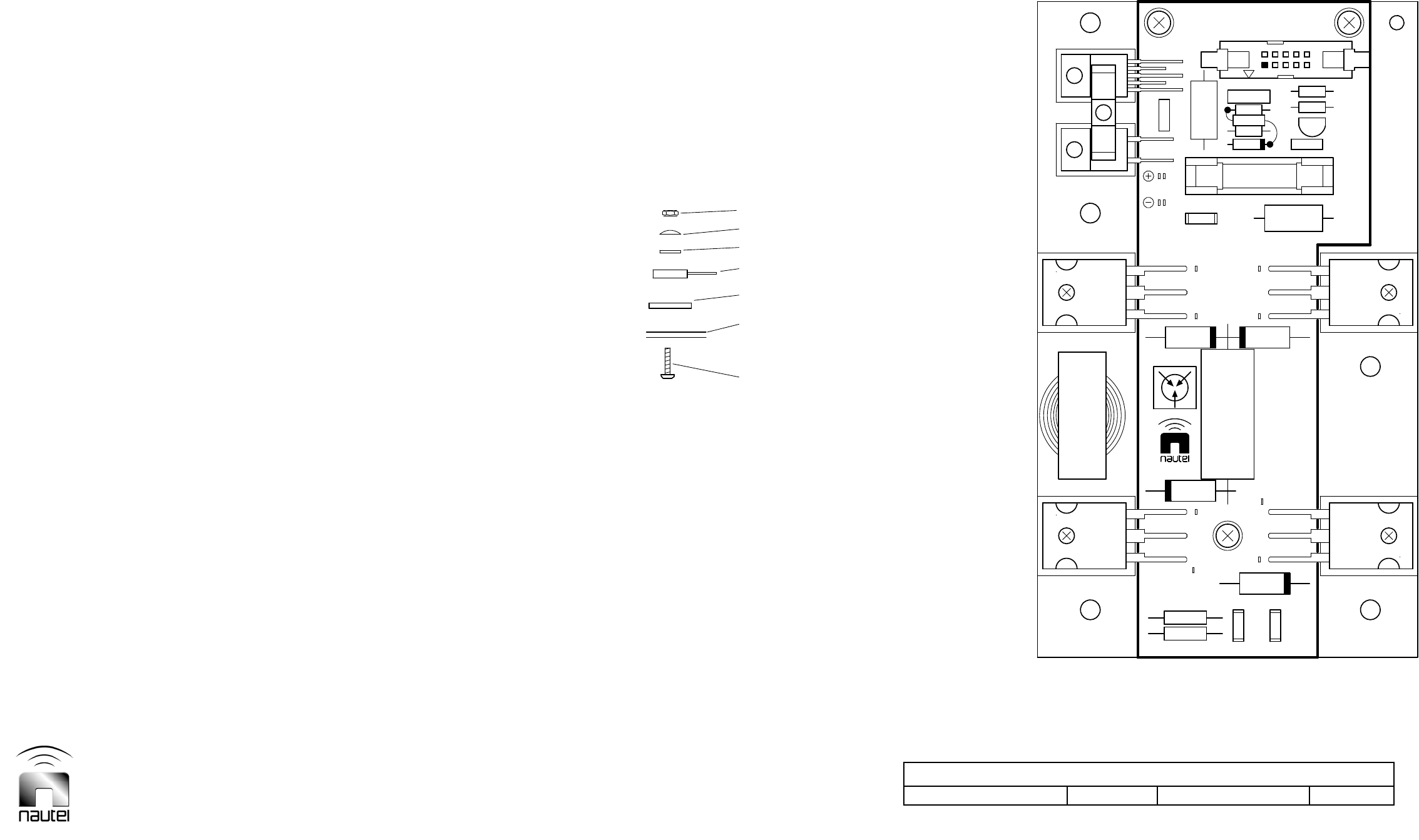
Dimensions = mm (inches)
Assembly Detail – NAAA06 Power Amplifier
Issue 1.8.1 Not to Scale Figure MD-13 Sheet 1 of 1
U1
Q1 Q3
Q4
Q2
R2
GDS
D
Q1
GDS
D
Q2
GDS
D
Q4
GDS
D
Q3
T1
32145
6
U1
R2
C1
CR1
CR2
CR3
CR4
CR5
E1
E3
1
J1
Q5
C6
C5
C4
F1
R5
R6
R7
C2
C3
R1
E2
R4
R3
C7
M1970016 V1
M3 PAN HEAD SCREW
4.0 INCH POUNDS (0.45 NEWTON METRES)
TORQUE ATTACHING HARDWARE TO
INSULATOR
SEMICONDUCTOR
CHASSIS
M3 HEX NUT
M3 WASHER
#4 BELLEVILLE WASHER
S
G
G
S
GS
G
NAUTEL ASSY 197-1055
POWER AMPLIFIER
SER.
S
NAAA
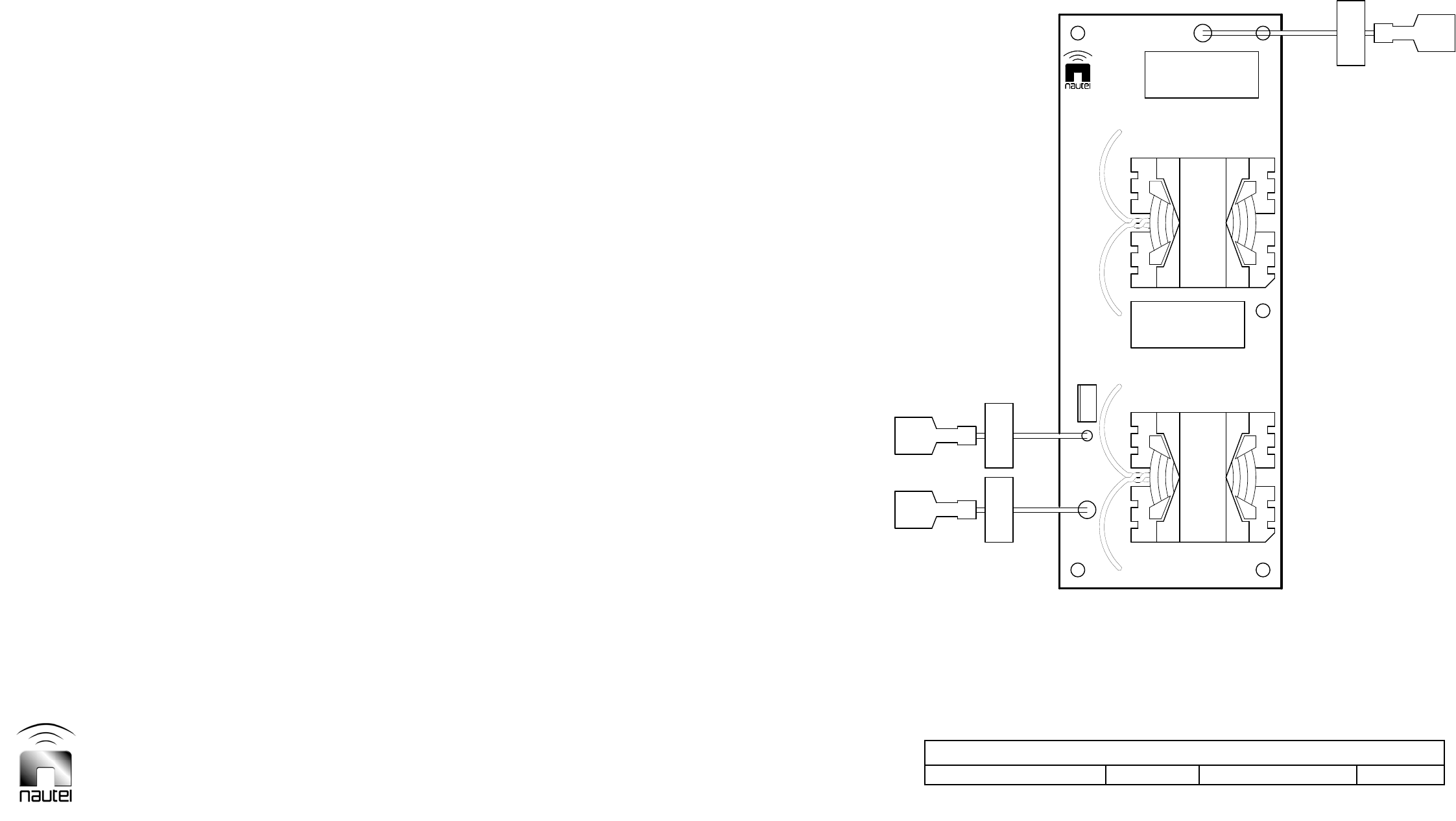
Dimensions = mm (inches)
Assembly Detail – NAPF06A Modulator Filter PWB
Issue 1.8.1 Not to Scale Figure MD-14 Sheet 1 of 1
A
B
AK
CR1
C
C3
L2
C1
L1
A3E2
M1950012 V2
A5E1
A3E1
SER.
195-1090
NAPF
NAUTEL ASSY
MODULATOR FILTER
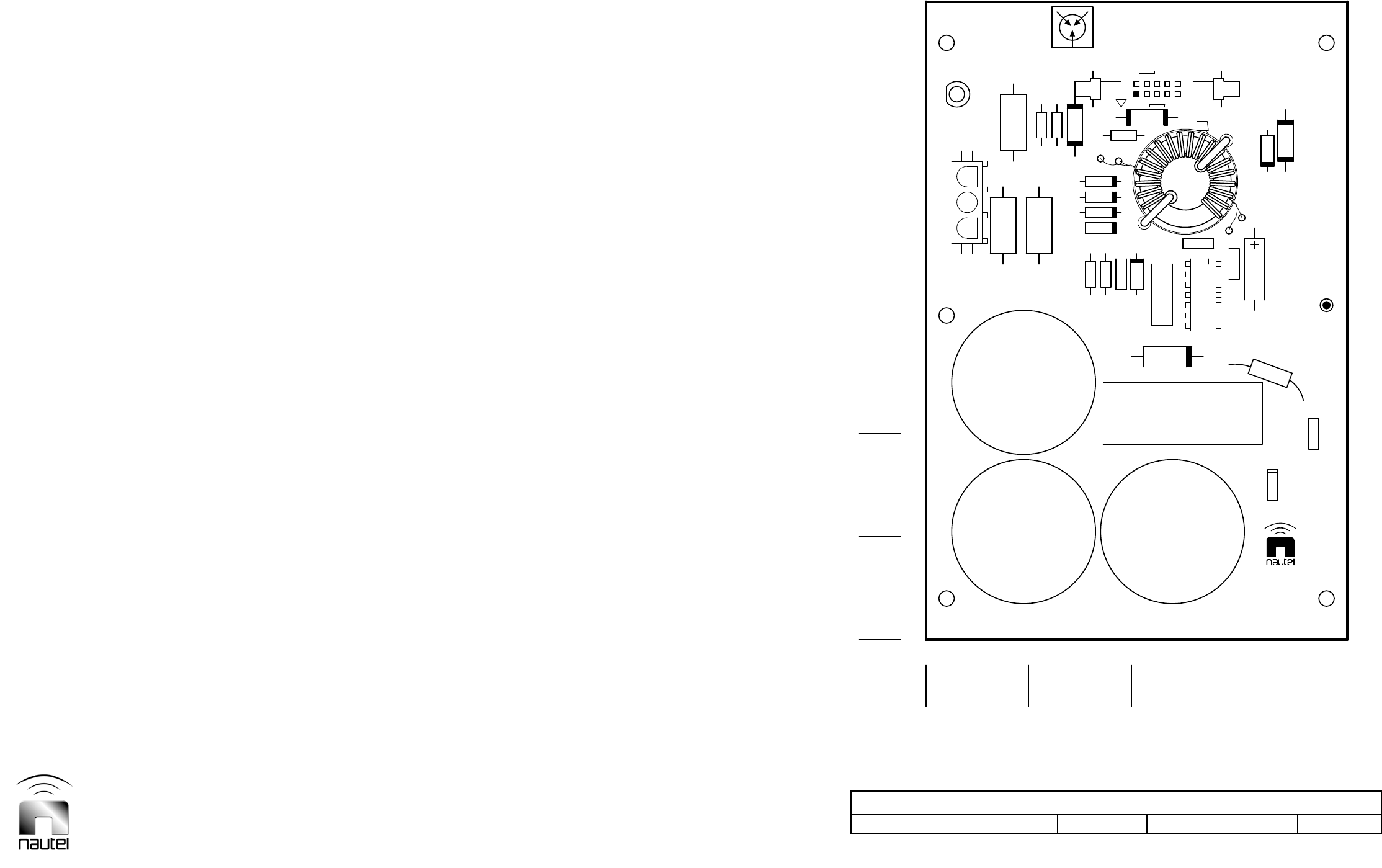
Dimensions = mm (inches)
Assembly Detail – NASM11A/01 Modulator Assembly
Issue 1.8.1 Not to Scale Figure MD-15 Sheet 1 of 1
R5
C9
R11
E2
CR5
R4
C7
R1
4
C3
CR12
R10
R2
J1
1
R3
R9
CR13
2
1
CR9
C2
CR2
CR4
3
R7
C8
C1
U1 TP1
CR1
CR3
CR10
E1
CR6
+
C6
+
C4
+
C5
J2
1
T1
DS1
3
6
4
5
C
1
2
J2
AB D
M1950121 V1
GND
RED
ON
CAUTION
SER.
B+
RED
WHT
WHT
WHEN LAMP IS ON
NASM
MODULATOR
HIGH VOLTAGE PRESENT
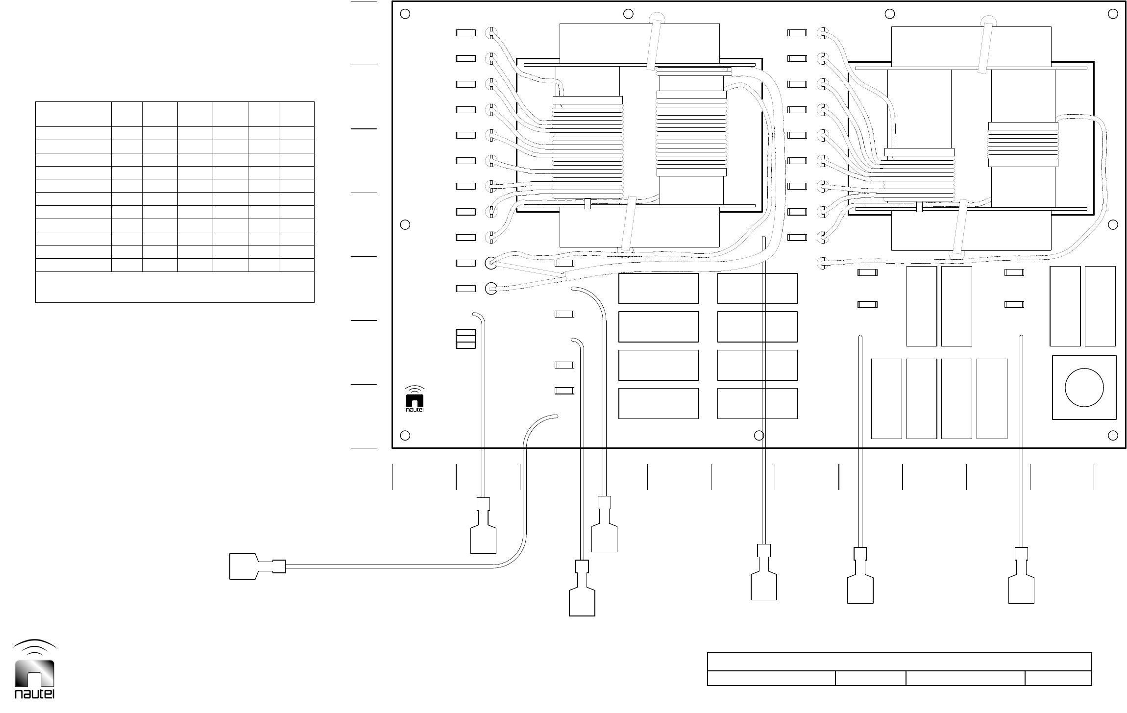
Dimensions = mm (inches)
Assembly Detail – NAPF05A RF Filter PWB
Issue 1.8.1 Not to Scale Figure MD-16 Sheet 1 of 1
Frequency
(kHz) E20
to E21
to E33
to E36
to E15
to E17
to
190.0 -209.0 E1 E22 E31 E34 E16 E18
209.1 - 229.9 E2 E23 E31 E34 E16 E18
230.0 - 252.9 E4 E25 E31 E34 E16 E18
253.0 - 278.2 E3 E24 E31 E35 E14 E18
278.3 - 306.0 E5 E26 E31 E35 E14 E18
306.1 - 336.6 E6 E27 E31 E35 E14 E18
336.7 -370.3 E7 E28 E31 E35 E14 E18
370.4 - 407.3 E6 E27 E32 E35 E14 E16
407.4 -447.9 E7 E28 E32 E35 E14 E16
448.0 - 492.9 E8 E29 E32 E35 E14 E16
493.0 - 535.0 E9 E30 E32 E35 E14 E16
Connect E12 to E11
JUMPER SETTINGS
E13
E9
E6
E3
E11
E8
E5
E2
E10
E7
E4
E1
C11
C14
C10
C16
C15
E19
E16
E18 C3
C1
E31
E32
E34
E35
C4
C2
E14
C9
C13 C12
E30
E27
E24
C7
C5
E29
E26
E23
J1
C8
C6
E28
E25
E22
11
10
8
7
5
4
2
1
E20
E17
E21
B
9
6
3
C
E15
E F H I K
L
2
5
E12
E33
10
8
7
5
4
2
1
E36
A
3
4
6
D G
9
6
3
J
1
7
M1950024 V2
L1 L2
SER.
NAUTEL ASSY 195-6050
RF FILTER
NAPF
RF OUT
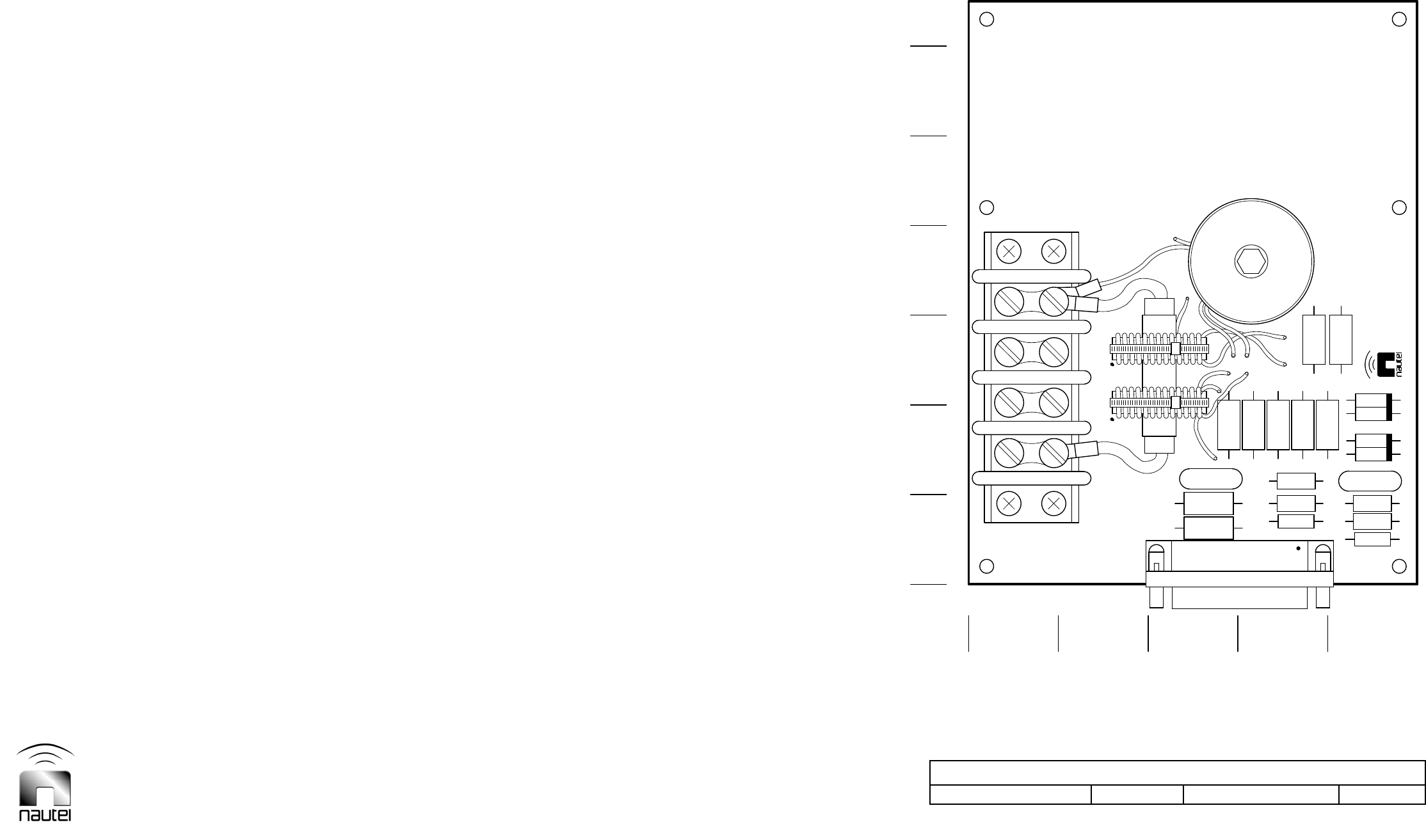
Dimensions = mm (inches)
Assembly Detail – NAPF07C/01 RF Power Probe
Issue 1.8.1 Not to Scale Figure MD-17 Sheet 1 of 1
2
R2
C1
3
R1
L1
L2
R3
R9
R10
R6
R7
R5
R8 L4
1
2
R11
C2
CR4
L3
4
CR2
1
34
T1
CR1
5
R4
CR3
T2
1
J1
2
T3
TB1
B E
3
6
4
5
A
M1950170 V1
C D
1
2
7
34
SER.
RF IN
1
GND
2
RF OUT
RF POWER PROBE
NAPF07
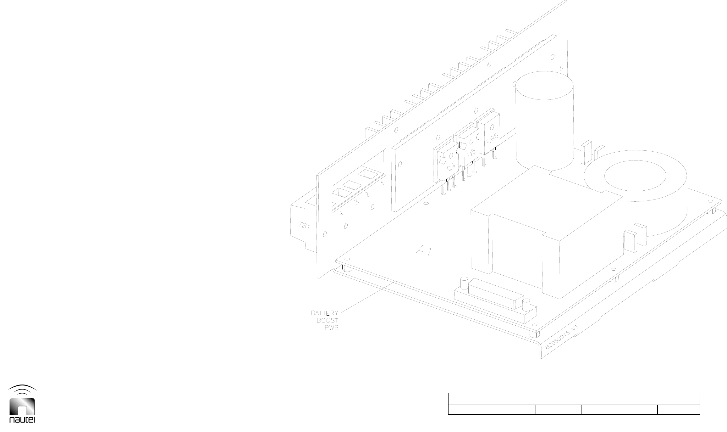
Dimensions = mm (inches)
Assembly Detail – 205-8035 Battery Boost Assembly
Issue 1.8.1 Not to Scale Figure MD-18 Sheet 1 of 1
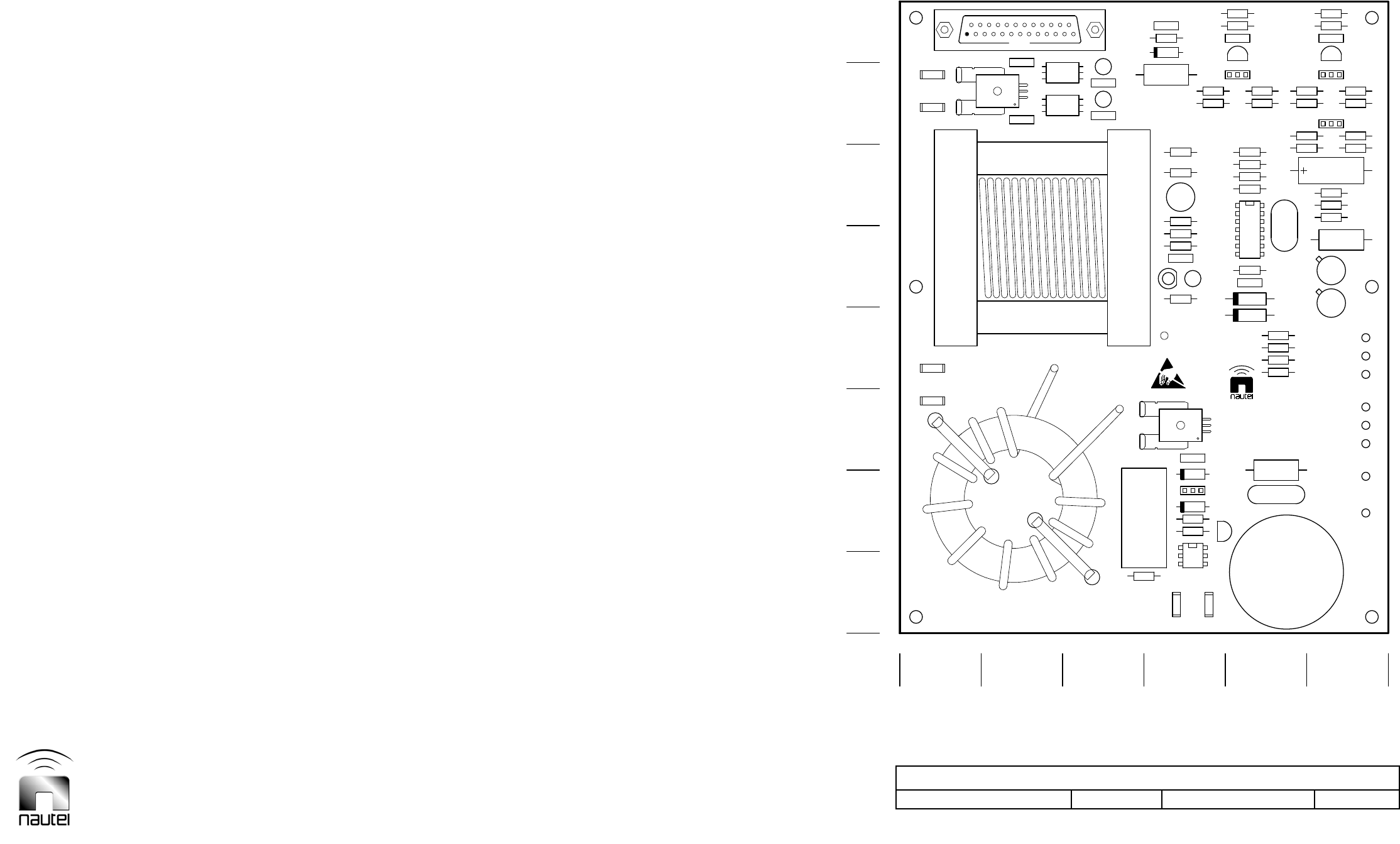
Dimensions = mm (inches)
Assembly Detail – NAPS35 Battery Boost PWB
Issue 1.8.1 Not to Scale Figure MD-19 Sheet 1 of 1
C6
+
C3
C11
R3
C12
R40
R38
C17
R24
E4
E2
C2
+
C5
C4
E8
R12
Q2
+
C13
1
E7
R4
Q1
Q7
R39
C20
1
E9
1
E10
R26
R27
R28
R29
Q3
R25
E3
E1
C1
C8
U3
Q6
R11
CR3
R32
R30
CR5
C14
C10
R8
R21
R19
R1
R14
E6
1
E5
R13
CR2
R33
23
4
1
5
U2
R31
R10 CR4
R22
+
C9
U4
R20
R6
R7
R9
L3 R17
R16
R18R5
C7 R15
CR1
CR6 Q5
R35
R34
R37
R36
DS1
L2
23
4
1
5
U1
R2
Q4
C15
R23
R41
1
J1
C19
+
C16
12
13
1
24
L1
B C EF
1
2
3
4
6
7
8
A
M2050021 V1
D
5
IN
IN
L4
-
250W
250W
125W
125W
-
+
OUT
CHARGER
+15V
OUT +
+48V
NAPS35
250W 125W
SER.
+24V
SMPS, 24/48V
BATTERY BOOST