Nexus 21 1066Mt S Interposer Users Manual NEX NEXVuDDR800M X
1066MTs Interposer to the manual 0f8e1930-12e6-4c16-8b9b-dc677d1a1114
2015-02-05
: Nexus-21 Nexus-21-1066Mt-S-Interposer-Users-Manual-494957 nexus-21-1066mt-s-interposer-users-manual-494957 nexus-21 pdf
Open the PDF directly: View PDF ![]() .
.
Page Count: 91
- 1.0 OVERVIEW
- 2.0 SOFTWARE INSTALLATION
- 3.0 CONNECTING to the NEX-DDR3INTR-THIN INTERPOSER
- 4.0 CLOCK SELECTION
- 5.0 CONFIGURING FOR READ / WRITE DATA ACQUISITION
- 5.1 A Note About the Different Data Groups
- 5.2 MagniVu Signals
- 5.3 Adjusting Input Thresholds for Proper Data Acquisition
- 5.4 DDR3 and DDR3SPA
- 5.5 Selecting B_DDR3E_XX Read Data Sample Points
- 5.6 Selecting B_DDR3D_XX Write Data Sample Points
- 5.7 B_DDR3D_XX Support Setup
- 5.8 Setting B_DDR3D_3A Read Data Sample Points
- 6.0 VIEWING DATA
- 7.0 HINTS & TIPS
- APPENDIX A – How DDR Data is Clocked
- APPENDIX B - Considerations
- APPENDIX C – 240-pin DDR3 DIMM Pinout
- APPENDIX D –Data Flow Through the Probes (coax cable to chan
- APPENDIX E – B_DDR3D_2D Support Pinout, DIMM Slot 0
- APPENDIX F – B_DDR3_2G Support Pinout, DIMM Slot 0 Auxiliary
- APPENDIX G – B_DDR3D_3A Support Pinout, DIMM Slot 1
- APPENDIX H – Data Group / Data Byte / Strobe Cross-Reference
- APPENDIX I – NEX-DDR3INTR-THIN Silkscreen
- APPENDIX J – Keep out area
- APPENDIX K – Simulation Model
- APPENDIX L - References
- APPENDIX M - Support

DDR3THIN-MN-XXX 1 Doc. Rev. 1.11
NEX-DDR3INTR-THIN
DDR3 800/1066MT/s Interposer
For use with the TLA7BB4 Logic Analyzer
Modules
Including these Software Support packages:
B_DDR3D_2D (Single/Dual/Quad Rank, single slot with Selective Clocking)
*B_DDR3D_2G (2 or 3 DIMM slots, two Rank @ 800MT/s)
*B_DDR3D_3A (2 DIMM slots, two Rank @ 1066MT/s)
* Optional Software
Copyright © 2007 Nexus Technology, Inc. All rights reserved.
Contents of this publication may not be reproduced in any form without
the written permission of Nexus Technology, Inc.
Brand and product names used throughout this manual are the trademarks
of their respective holders.

DDR3THIN-MN-XXX 2 Doc. Rev. 1.11
Product Warranty
Due to wide variety of possible customer target implementations, this product has a 30 day
acceptance period by the customer from the date of receipt. If the customer does not contact
Nexus Technology within 30 days of the receipt of the product, it will be said that the customer
has accepted the product. If the customer is not satisfied with this product, they may return it
within 30 days for a refund.
This Nexus Technology product has a warranty against defects in material and workmanship for a
period of 1 year from the date of shipment. During the warranty period, Nexus Technology will,
at its option, either replace or repair products proven to be defective. For warranty service or
repair, this product must be returned to the factory.
For products returned to Nexus Technology for warranty service, the Buyer shall prepay shipping
charges to Nexus Technology and Nexus Technology shall pay shipping charges to return the
product to the Buyer. However, the Buyer shall pay all shipping charges, duties, and taxes for
products returned to Nexus Technology from another country.
Nexus Technology warrants that its software and hardware designated by Nexus Technology for
use with an instrument will execute its programming instructions when properly installed on that
instrument. Nexus Technology does not warrant that the operation of the hardware or software
will be uninterrupted or error-free.
Limitation of Warranty
The foregoing warranty shall not apply to defects resulting from improper or inadequate
maintenance by the Buyer, Buyer-supplied software or interfacing, unauthorized modification or
misuse, operation outside of the environmental specifications for the product, or improper site
preparation or maintenance. NO OTHER WARRANTY IS EXPRESSED OR IMPLIED. NEXUS
TECHNOLOGY SPECIFICALLY DISCLAIMS THE IMPLIED WARRANTIES OF
MERCHANTABILITY AND FITNESS FOR A PARTICULAR PURPOSE.
Exclusive Remedies
THE REMEDIES PROVIDED HERIN ARE BUYER’S SOLE AND EXCLUSIVE REMEDIES.
NEXUS TECHNOLOGY SHALL NOT BE LIABLE FOR ANY DIRECT, INDIRECT,
SPECIAL, INCIDENTAL OR CONSEQUENTIAL DAMAGES, WHETHER BASED ON
CONTRACT, TORT OR ANY OTHER LEGAL THEORY.
Software License Agreement
IMPORTANT – Please read this license agreement carefully before opening the CD case. Rights
in the software are offered only on the condition that the customer agrees to all terms and
conditions of the license agreement. Opening the CD case indicates your acceptance of these
terms and conditions. If you do not agree to the licensing agreement, you may return the
unopened package for a full refund.

DDR3THIN-MN-XXX 3 Doc. Rev. 1.11
License Agreement
In return for payment for this product, Nexus Technology grants the Customer a SINGLE user
LICENSE in the software subject to the following:
Use of the Software:
- Customer may use the software on only one Tektronix mainframe logic analysis system at
any given time
- Customer may make copies or adaptations of the software (see Copies and Adaptations below
for more information)
- Customer may NOT reverse assemble or decompile the software
Copies and Adaptations:
- Are allowed for archival purpose only
- When copying for adaptation is an essential step in the use of the software with the logic
analyzer and/or logic analysis mainframe so long as the copies and adaptations are used in no
other manner. Customer has no right to copy software unless it acquires an appropriate
license to reproduce from Nexus Technology.
- Customer agrees that it does not have any title or ownership of the software, other than the
physical media.
Ownership:
- Customer acknowledges and agrees that the software is copyrighted and protected under the
copyright laws.
- Transfer of the right of ownership shall only be done with the consent of Nexus Technology.
Sublicensing and Distribution:
- Customer may not sublicense the software or distribute copies of the software to the public in
physical media or by electronic means or any other means without the prior written consent
of Nexus Technology.
Compliance with WEEE and RoHS Directives
This product is subject to European Union regulations on Waste Electrical and Electronics
Equipment. Return to Nexus Technology for recycle at end of life. Costs associated with the
return to Nexus Technology are the responsibility of the sender.

DDR3THIN-MN-XXX 4 Doc. Rev. 1.11
TABLE OF CONTENTS
1.0 OVERVIEW ........................................................................................................................... 9
1.1 General Information ............................................................................................................ 9
1.2 Software Package description..............................................................................................9
1.3 Eye size required ............................................................................................................... 11
2.0 SOFTWARE INSTALLATION........................................................................................... 11
3.0 CONNECTING to the NEX-DDR3INTR-THIN INTERPOSER ........................................ 12
3.1 General .............................................................................................................................. 12
3.2 B_DDR3D_2D Support..................................................................................................... 12
3.3 B_DDR3D_2G Support..................................................................................................... 12
3.4 B_DDR3D_3A Support..................................................................................................... 13
3.5 Short “LEASH” probes ..................................................................................................... 15
3.5.1 Samtec connector on the LEASH probe pins ............................................................ 16
3.5.2 LEASH probe to NEX-PRB1X/2X connection......................................................... 17
3.5.3 Alternate use of NEX-PRB1X or NEX-PRB2X probes ............................................ 17
3.6 Slot Numbering............................................................................................................. 18
3.7 Display Groups not in Tables 1,2 or 3............................................................................... 39
4.0 CLOCK SELECTION .......................................................................................................... 40
4.1 B_DDR3D_2D Clocking Selections ................................................................................. 40
4.2 B_DDR3D_2G Clocking Selections ................................................................................. 41
4.3 B_DDR3D_3A Clocking Selections ................................................................................. 43
5.0 CONFIGURING FOR READ / WRITE DATA ACQUISITION........................................ 44
5.1 A Note About the Different Data Groups.......................................................................... 44
5.2 MagniVu Signals ............................................................................................................... 44
5.3 Adjusting Input Thresholds for Proper Data Acquisition.................................................. 53
5.4 DDR3 and DDR3SPA ....................................................................................................... 53
5.5 Selecting B_DDR3E_XX Read Data Sample Points ........................................................ 53
5.6 Selecting B_DDR3D_XX Write Data Sample Points....................................................... 54
5.7 B_DDR3D_XX Support Setup.......................................................................................... 55
5.8 Setting B_DDR3D_3A Read Data Sample Points ............................................................ 62
6.0 VIEWING DATA................................................................................................................. 63
6.1 Viewing B_DDR3D_XX Data .......................................................................................... 63
6.2 Viewing Raw DDR3 Data using B_DDR3D_XX Supports......................................... 66
6.3 B_DDR3D_2A / 3A Mnemonics Description................................................................... 66
6.4 B_DDR3D_2G Mnemonics Description........................................................................... 66
6.5 Viewing Timing Data on the TLA .................................................................................... 67
7.0 HINTS & TIPS ..................................................................................................................... 69
7.1 Symbolic Triggering on a Command using B_DDR3D_XX Supports............................. 69
7.3 Capturing MRS (Mode Register Set) Cycles .................................................................... 70
7.4 Clock Capture quality........................................................................................................ 71
7.5 Thresholds ......................................................................................................................... 72
APPENDIX A – How DDR Data is Clocked ............................................................................... 73
A.1 Background....................................................................................................................... 73
A.2 DDR Acquisition - General .............................................................................................. 73
A.3 B_DDR3D_2D / 2G / 3A Data Acquisition ..................................................................... 74
APPENDIX B - Considerations.................................................................................................... 75
B.1 NEX-DDR3INTR-THIN Bus Loading............................................................................. 75
B.2 DIMM connector location for best quality signal capture................................................ 75
DDR3THIN-MN-XXX 5 Doc. Rev. 1.11
B.3 TLA7BB4 Module to module skew.................................................................................. 75
APPENDIX C – 240-pin DDR3 DIMM Pinout ........................................................................... 76
APPENDIX D –Data Flow Through the Probes (coax cable to channel) .................................... 78
APPENDIX E – B_DDR3D_2D Support Pinout, DIMM Slot 0.................................................. 80
APPENDIX F – B_DDR3_2G Support Pinout, DIMM Slot 0 Auxiliary Signals ....................... 82
APPENDIX G – B_DDR3D_3A Support Pinout, DIMM Slot 1 ................................................. 84
APPENDIX H – Data Group / Data Byte / Strobe Cross-Reference............................................ 86
APPENDIX I – NEX-DDR3INTR-THIN Silkscreen................................................................... 87
APPENDIX J – Keep out area ...................................................................................................... 88
APPENDIX K – Simulation Model.............................................................................................. 89
APPENDIX L - References .......................................................................................................... 90
APPENDIX M - Support .............................................................................................................. 91

DDR3THIN-MN-XXX 6 Doc. Rev. 1.11
TABLE OF FIGURES
Figure 1 – Drawing of Interposer with probes attached ............................................................... 15
Figure 2 – Samtec connector on the LEASH probe...................................................................... 16
Figure 3 – LEASH probe to NEX-PRB1X/2X connection .......................................................... 17
Figure 4 - Read Data Latency = CAS Latency + CAS Additive Latency + RDIMM (5+0+1) = 6
cycles) ........................................................................................................................................... 54
Figure 5 - Write Data Latency = CAS Write Latency + RDIMM (5+1) = 6 cycles..................... 54
Figure 6 - Locating Minimum Valid B_DDR3D_XX Read Data Window ................................. 55
Figure 7 - Measuring B_DDR3D_XX RdA_DatHi / Lo Read Data Setup & Hold..................... 56
Figure 8 - Measuring B_DDR3D_XX RdB_DatHi / Lo Read Data Setup & Hold ..................... 57
Figure 9 - Setting B_DDR3D_XX RdA_DatHi / Lo and RdB_DatHi / Lo Sample Points ......... 57
Figure 10 - Locating Minimum Valid B_DDR3D_XX Write Data Window .............................. 58
Figure 11 - Measuring B_DDR3D_XX WrA_DatHi / Lo Write Data Setup & Hold.................. 59
Figure 12 - Measuring B_DDR3D_XX WrB_DatHi / Lo Write Data Setup & Hold.................. 59
Figure 13 - Setting B_DDR3D_XX WrA_DatHi / Lo and WrB_DatHi / Lo Sample Points ...... 60
Figure 14 - Viewing Individual 8-bit Read Data Groups ............................................................. 61
Figure 15 - Setting Individual Setup & Hold Values for the 8-bit Read Data Groups................. 61
Figure 16 - B_DDR3D_XX Listing Display ................................................................................ 63
Figure 17 - Disassembly Properties .............................................................................................. 64
Figure 18 - B_DDR3D_XX Listing Display - Control Flow ....................................................... 65
Figure 19 - B_DDR3D_XX MagniVu Display on TLA .............................................................. 68
Figure 20 - B_DDR3D_2D MRS Trigger .................................................................................... 71
Figure 21 - MRS Cycle Acquisition Disassembly........................................................................ 71

DDR3THIN-MN-XXX 7 Doc. Rev. 1.11
TABLE OF TABLES
Table 1 - B_DDR3D_2D (<=1066MT/s Read and Write) TLA Channel Grouping.................... 19
Table 2 - B_DDR3D_2G (<=1066MT/s Read and Write) TLA Channel Grouping.................... 25
Table 3 - B_DDR3D_3A (<=1066MT/s Read and Write) TLA Channel Grouping.................... 31
Table 4 - B_DDR3D_2D/_2G TLA MagniVu Channel Grouping .............................................. 45
Table 5 - B_DDR3D_3A TLA MagniVu Channel Grouping ...................................................... 48
Table 6 - B_DDR3D_2A / 3A Mnemonics Definition................................................................. 66
Table 7 - B_DDR3D_2G Mnemonics Definition......................................................................... 67
Table 8 - B_DDR3D_2D / 3A Control Symbol Table ................................................................ 69
Table 9 - B_DDR3D_2G Control Symbol Table ........................................................................ 70
DDR3THIN-MN-XXX 8 Doc. Rev. 1.11

DDR3THIN-MN-XXX 9 Doc. Rev. 1.11
1.0 OVERVIEW
1.1 General Information
The DDR3 Interposer Products are designed for ease of use. Interposers extra signal trace
length, also an extra connector that might affect the quality of the system operation in some
systems.
• This Product is designed for capture of 1066MT/s or slower, and may only be used with
the Tektronix TLA7BB4 acquisition modules.
This product requires the use of the new NEX-PRB1X-T / PRB2X-T Low Profile Distributed
probes available from Nexus. Tektronix P68xx or P69xx probes can not be used.
This Interposer has been designed to provide a quick and easy connection to interface to a
Tektronix TLA7BB4 Logic Analyzer acquisition cards to a 240-pin DDR3 (Double Data Rate 3)
bus. Contact NEXUS Technology for other available DDR3 Products. The Nexus Technology
web site (www.NexusTechnology.com) contains information on the latest software release.
1.2 Software Package description
The NEX-DDR3INTR-THIN support includes the following software packages:
B_DDR3D_2D allows the user to acquire Read AND Write data from a single, dual or
quad rank DDR3 DIMM running 1066MT/s or less. This support requires 1ea. NEX-
PRB1X-T and 3ea. NEX-PRB2X-T Low Profile Distributed probes, and two merged
Tektronix TLA7BB4 acquisition cards. This support can use selective clocking to reduce
the number of Idle states acquired by the logic analyzer.
Optional software available for the NEX-DDR3INTR-THIN support includes the following
software packages:
B_DDR3D_2G allows the user to acquire Read AND Write data from a memory
channel made up of two or three DIMM slots with one or two rank DDR3 DIMMs
running 800MT/s or less. This is total disassembly for the 3 DIMM memory channel.
This support requires 2ea. NEX-PRB1X-T and 3ea. NEX-PRB2X-T Low Profile
Distributed probes, and two merged Tektronix TLA7BB4 acquisition cards. This support
also requires the NEX-PRBCOAX product. This support can be used with Single Rank
and Dual Rank DIMMs (will also support a single quad rank DIMM). Reads for the three
DIMMs must have a common data eye (over lap) of 330ps. No selective clocking
B_DDR3D_3A allows the user to acquire Read AND Write data from a memory channel
made up of two DIMM slots with single or dual rank DDR3 DIMMs running 1066MT/s
or less. This is total disassembly for the 2 DIMM memory channel. This support
requires 5ea. NEX-PRB1X-T and 3ea. NEX-PRB2X-T Low Profile Distributed probes,
and three merged Tektronix TLA7BB4 acquisition cards. This support also requires two
DDR3THIN-MN-XXX 10 Doc. Rev. 1.11
NEX-DDR3INTR-THIN Interposer products. This support can be used with Single
Rank and Dual Rank DIMMs.
Note that this manual uses some terms generically. For instance, references to the TLA700/7000
apply to all suitable TLA700/7000 Logic Analyzers, or PCs being used to control the TLA.
NEX-DDR3INTR-THIN refers to the B_DDR3D_2D/2G/3A software support packages.
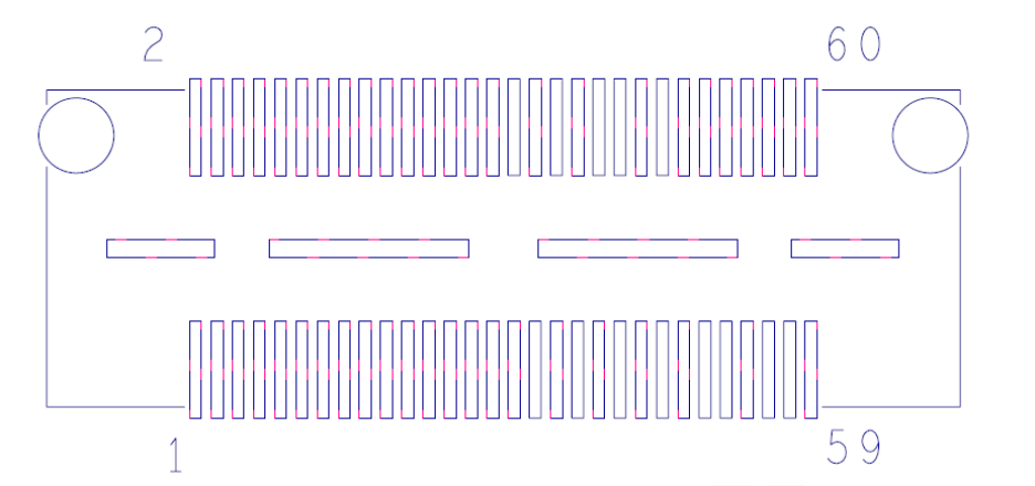
Appendix G has a silk-screened print of the NEX-DDR3INTR-THIN Logic Analyzer Interposer
board. Referring to this drawing while reading the manual is suggested.
This manual assumes that the user is familiar with the DDR3 SDRAM Specification and the
Tektronix TLA Logic Analyzers. It is also expected that the user is familiar with the Windows
environment used with the TLA.

DDR3THIN-MN-XXX 11 Doc. Rev. 1.11
1.3 Eye size required
The Eye size (stable data) required at the input resistor to the Nexus passive probes (NEX-
PRB1X(-T) & NEX-PRB2X(-T)) is 330ps, and 0.2V. Capture accuracy may be affected if a
stable eye can not meet this requirement. . The eye is a perfectly shaped diamond with each side
equal distant from the center.
2.0 SOFTWARE INSTALLATION
To Install the NEX-DDR3INTR-THIN software support place the B_DDR3D_XX Install CD in
the CD drive of the TLA or the PC being used to control the TLA. Using Windows Explorer
select the CD, navigate to the support_software folder, select the folder of the support to be
installed (B_DDR3D_2D, B_DDR3D_2G or B_DDR3D_3A) and then run the .MSI file within
the folder. The selected software will be installed on the TLA’s hard disk.
To load the support into the TLA, first select the desired Logic Analyzer module (different
supports require different module counts) in the Setup window, select Load Support Package
from the File pull-down, then choose the software package name you are want to load and click
on Okay. Note that this support requires two or more merged modules and that the TLA
acquisition cards must be configured properly for the software to load.

DDR3THIN-MN-XXX 12 Doc. Rev. 1.11
3.0 CONNECTING to the NEX-DDR3INTR-THIN INTERPOSER
3.1 General
Care should be taken to support the weight of the acquisition probes so that the Logic Analyzer
Interposer board and/or target socket are not damaged.
3.2 B_DDR3D_2D Support
To acquire DDR3 Read and Write data at speeds up to 1066MT/s requires two merged
TLA7BB4 136-channel, with 1.4G state option, acquisition cards and the use of the
B_DDR3D_2D support software. The Master card will be in the lower numbered of the two
cards. Slave card #1 is in the adjacent high-numbered slots. The logic analyzer modules should
be connected to the DDR3 DIMM Interposer as follows using (1) NEX-PPRB1X-T probes and
three (3) NEX-PRB2X-T probes:
TLA Master
Connect the NEX-PRB1X-T “C” probe head to DDR3 Interposer’s LEASH (soldered-on
coax cable) that is attached to “M_C” position on the Interposer.
Connect the NEX-PRB2X-T A3/2 & A1/0 probe head to DDR3 Interposer’s LEASH
that is attached to “M_ A3/2 A1/0” position on the Interposer.
Match the label on the end of the NEX-PRB1X-T/2X-T probes with the labels on the
front of the Tektronix Logic Analyzer Master module and connect.
TLA Slave
Connect the NEX-PRB2X-T A3/2 & A1/0 probe head to DDR3 Interposer’s LEASH
that is attached to “S_ A3/2 A1/0” position on the Interposer.
Connect the NEX-PRB2X-T “C3/2” & “E3/2” probe head to DDR3 Interposer’s LEASH
that is attached to “S_C3/2 E3/2” position on the Interposer.
See Figure 1 for connections. Table 1 shows the Channel Grouping / Wiring for use with the
B_DDR3D_2D support.
3.3 B_DDR3D_2G Support
To acquire DDR3 Read and Write data from two or three DIMM slots, for total memory channel
disassembly, at speeds up to 800MT/s requires two merged TLA7BB4 136-channel, with 1.4G
state option, acquisition cards and the use of the B_DDR3D_2G optional support software. The
Master card will be in the lower numbered, of the two cards. Slave card #1 will be in the
adjacent high-numbered slots. This support requires an additional NEX-PRB1X-T (for a total of
2), and the NEX-PRBCOAX product. The logic analyzer modules should be connected to the
DDR3 DIMM Interposer as follows using (1) NEX-PPRB1X-T probes and three (3) NEX-
PRB2X-T probes, with the additional NEX-PRB1X-T connected to the NEX-PRBCOAX:
DDR3THIN-MN-XXX 13 Doc. Rev. 1.11
TLA Master
Connect the NEX-PRB1X-T “C” probe head to DDR3 Interposer’s LEASH (soldered-on
coax cable) that is attached to “M_C” position on the Interposer.
Connect the NEX-PRB2X-T A3/2 & A1/0 probe head to DDR3 Interposer’s LEASH
that is attached to “M_ A3/2 A1/0” position on the Interposer.
Connect the NEX-PRB1X-T “E” probe head to the NEX-PRBCOAX.
Note the leads 9- 12 of the NEX-PRBCOAX must be connected to the second slots Chip
Select lines (CS) near the second and third DIMM socket, usually on the back of the
mother board.
Match the label on the end of the NEX-PRB1X-T/2X-T probes with the labels on the
front of the Tektronix Logic Analyzer Master module and connect.
TLA Slave
Connect the NEX-PRB2X-T A3/2 & A1/0 probe head to DDR3 Interposer’s LEASH
that is attached to “S_ A3/2 A1/0” position on the Interposer.
Connect the NEX-PRB2X-T “C3/2” & “E3/2” probe head to DDR3 Interposer’s LEASH
that is attached to “S_C3/2 E3/2” position on the Interposer.
See Figure 1 for connections. Table 2 shows the Channel Grouping / Wiring for use with the
B_DDR3D_2G support.
3.4 B_DDR3D_3A Support
To acquire DDR3 Read and Write data from a two DIMM slots, for total memory channel
disassembly, at speeds up to 1066MT/s requires three merged TLA7BB4 136-channel, with
1.4G state option, acquisition cards and the use of the B_DDR3D_3A optional support software.
The Master card will be in the lower numbered, of the three cards. Slave card #1 will be in the
adjacent high-numbered slots. Slave card #2 will be in the adjacent low-numbered slots. This
support also requires two NEX-DDR3INTR-THIN Interposer products. The logic analyzer
modules should be connected to the DDR3 DIMM Interposer as follows using (5) NEX-
PPRB1X-T probes and three (3) NEX-PRB2X-T probes:
TLA Master
Connect the NEX-PRB1X-T “C” probe head to DDR3 Interposer’s LEASH (soldered-on
coax cable) that is attached to “M_C” position on the Interposer.
Connect the NEX-PRB2X-T A3/2 & A1/0 probe head to DDR3 Interposer’s LEASH
that is attached to “M_ A3/2 A1/0” position on the Interposer.
Match the label on the end of the NEX-PRB1X-T/2X-T probes with the labels on the
front of the Tektronix Logic Analyzer Master module and connect.
DDR3THIN-MN-XXX 14 Doc. Rev. 1.11
TLA Slave1
Connect the NEX-PRB2X-T A3/2 & A1/0 probe head to DDR3 Interposer’s LEASH
that is attached to “S_ A3/2 A1/0” position on the Interposer.
Connect the NEX-PRB2X-T “C3/2” & “E3/2” probe head to DDR3 Interposer’s LEASH
that is attached to “S_C3/2 E3/2” position on the Interposer.
TLA Slave2
Connect the NEX-PRB1X-T A3/2 D3/2 probe head to DDR3 Interposer’s LEASH that is
attached to “M_A3/2 A1/0” position on the second Interposer.
Connect the NEX-PRB1X-T A1/0 D1/0 probe head to DDR3 Interposer’s LEASH that is
attached to “S_A3/2 A1/0” position on the second Interposer.
Connect the NEX-PRB1X-T “C” probe head to DDR3 Interposer’s LEASH that is
attached to “M_C3/2 C1/0” position on the second Interposer.
Connect the NEX-PRB1X-T “E” probe head to DDR3 Interposer’s LEASH that is
attached to “S_C3/2 E3/2” position on the second Interposer.
See Figure 1 for connections. Table 3 shows the Channel Grouping / Wiring for use with the
B_DDR3D_3A support.
DDR3THIN-MN-XXX 15 Doc. Rev. 1.11
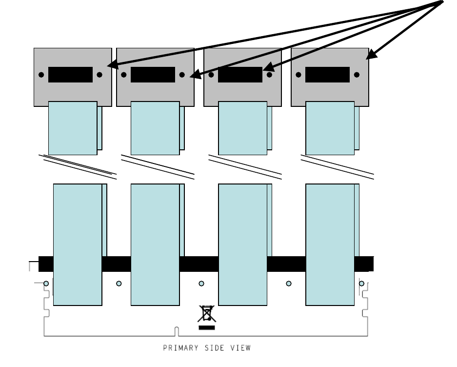
3.5 Short “LEASH” probes
The standard product includes 4 “LEASH” probes connected to this Interposer product. These
short probes are soldered directly onto the interposer and interface the Interposer to the Passive
probes that connect to the logic analyzer. These “LEASH” probes are to allow the user to easily
install and remove the Interposer product in their system with out the added weight of the
passive probe attached. There may be other probing options in the future. Contact Nexus for any
updates.
Figure 1 below shows the location on the Interposer of the LEASH probe connections.
Location of HCD connectors, right under metal compression plate, and probe tip board:
Figure 1 – Drawing of Interposer with probes attached
The four (4) each, 1 foot long, “LEASH” probes that are soldered onto the Interposer are in turn
connected to either a NEX-PRB1X-T or NEX-PRB2X-T probe. The NEX-PRB1X-T or NEX-
PRB2X-T probe in turn connects to the input of the logic analyzer modules. The connection
between the LEASH Probes and the logic Analyzer is a Samtec connector with a pin out as
shown below on the LEASH probe. Refer to 3.2 to determine if a NEX-PRB1X-T or NEX-
PRB2X-T connects to each LEASH probe.
PRB2
S_A3/2 A1/0 M_
PRB1PRB2PRB2
S_C3/2 M_A3/2 A1/0
DDR3THIN-MN-XXX 16 Doc. Rev. 1.11
The strain relief on the LEASH to NEXPRB1X/2X interface, while designed for bench handling,
can be damaged by twisting the coax cables. Bends of over 45 degrees in this area should be
avoided. The coax connection points, under any circumstances, are not to be bent.
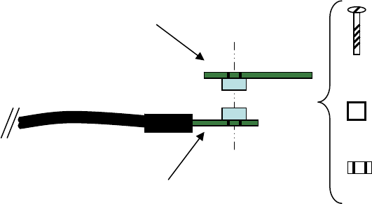
3.5.1 Samtec connector on the LEASH probe pins
Figure 2 – Samtec connector on the LEASH probe
The LEASH probe connects to the NEX-PRB1X-T or NEX-PRB2X-T probe using two plastic
nuts and screws, with a plastic spacer between the two boards. These parts are supplied.
DDR3THIN-MN-XXX 17 Doc. Rev. 1.11
3.5.2 LEASH probe to NEX-PRB1X/2X connection
Figure 3 – LEASH probe to NEX-PRB1X/2X connection
3.5.3 Alternate use of NEX-PRB1X or NEX-PRB2X probes
The NEX-PRB1X or NEX-PRB2X can be used in place of the “-T” probes but will have to be
secured for long term connection by tie-wraps.
Two each plastic
Spacers
Screws
&
Nuts
Hold each probe
together
Transition board on the “LEASH”
Cable end
Probe tip on the NEX-PRB1X-T or
NEX-PRB2X-T
Interposer
here

DDR3THIN-MN-XXX 18 Doc. Rev. 1.11
3.6 Slot Numbering
The Interposer must be installed in the furthest slot from the memory controller. For 1066MT/s
support only the two furthest slots may be used. Slots are named as shown below:
Slot naming for a three slot system
Memory controller
Slot C Slot B Slot A
S0-3#
CLKE0-
bS0-1#
bCLKE0-1
(from NEX-
PRBCOAX)
cS0-1#
cCLKE0-1
(from NEX-
PRBCOAX)
If only one slot is used it must be the furthest slot from the memory controller.
If two slots are used they must be the furthest slots from the memory controller.
Quad rank is only supported in the single slot configuration
Interposer in any two or three slot configuration must be in the furthest slot.
1066MT/s full channel support (B_DDR3D_3A) requires two interposers in the two
furthest slots from the memory controller.

DDR3THIN-MN-XXX 19 Doc. Rev. 1.11
Group
Name
Signal
Name
DDR3
Pin #
TLA
Input
Group
Name
Signal
Name
DDR3
Pin #
TLA
Input
RdA_DatHi RD_A_DQ63 234 S_A2:0 RdA_DatLo RD_A_DQ31 156 M_A0:6
(Hex) RD_A_DQ62 233 S_A2:1 (Hex) RD_A_DQ30 155 M_A0:3
RD_A_DQ61 228 S_A2:5 RD_A_DQ29 150 S_C2:0
RD_A_DQ60 227 S_CK0 RD_A_DQ28 149 S_C2:1
RD_A_DQ59 115 S_A2:2 RD_A_DQ27 37 M_A0:4
RD_A_DQ58 114 S_A2:3 RD_A_DQ26 36 M_A0:1
RD_A_DQ57 109 S_A2:7 RD_A_DQ25 31 S_C2:2
RD_A_DQ56 108 S_A3:0 RD_A_DQ24 30 S_C2:3
RD_A_DQ55 225 S_A3:2 RD_A_DQ23 147 S_C2:4
RD_A_DQ54 224 S_A3:3 RD_A_DQ22 146 S_C2:5
RD_A_DQ53 219 S_A3:7 RD_A_DQ21 141 S_C3:2
RD_A_DQ52 218 S_A1:5 RD_A_DQ20 140 S_C3:3
RD_A_DQ51 106 S_A3:1 RD_A_DQ19 28 S_C2:6
RD_A_DQ50 105 S_A3:4 RD_A_DQ18 27 S_C2:7
RD_A_DQ49 100 S_A1:7 RD_A_DQ17 22 S_C3:1
RD_A_DQ48 99 S_A1:6 RD_A_DQ16 21 S_C3:4
RD_A_DQ47 216 S_A1:4 RD_A_DQ15 138 S_C3:6
RD_A_DQ46 215 S_A1:1 RD_A_DQ14 137 S_C3:7
RD_A_DQ45 210 S_A0:7 RD_A_DQ13 132 S_E3:4
RD_A_DQ44 209 S_A0:6 RD_A_DQ12 131 S_E3:1
RD_A_DQ43 97 S_A1:3 RD_A_DQ11 19 S_C3:5
RD_A_DQ42 96 S_A1:2 RD_A_DQ10 18 S_E3:7
RD_A_DQ41 91 S_A0:5 RD_A_DQ9 13 S_E3:3
RD_A_DQ40 90 S_A0:4 RD_A_DQ8 12 S_E3:2
RD_A_DQ39 207 S_A0:3 RD_A_DQ7 129 S_E3:0
RD_A_DQ38 206 S_A0:2 RD_A_DQ6 128 S_E2:7
RD_A_DQ37 201 M_C2:1 RD_A_DQ5 123 S_E2:3
RD_A_DQ36 200 M_C2:4 RD_A_DQ4 122 S_E2:2
RD_A_DQ35 88 S_A0:1 RD_A_DQ3 10 S_Q3
RD_A_DQ34 87 S_A0:0 RD_A_DQ2 9 S_E2:5
RD_A_DQ33 83 M_C2:6 RD_A_DQ1 4 S_E2:1
RD_A_DQ32 81 M_C2:7 RD_A_DQ0 3 S_E2:0
Table 1 - B_DDR3D_2D (<=1066MT/s Read and Write) TLA Channel Grouping
Notes:
1. All signals on this page are required for accurate post-processing of acquired data
2. The ‘S’ in front of a TLA channel denotes the Slave card of the merged pair

DDR3THIN-MN-XXX 20 Doc. Rev. 1.11
Group
Name
Signal
Name
DDR3
Pin#
TLA
Input
Group
Name
Signal
Name
DDR3
Pin#
TLA
Input
RdB_DatHi RD_B_DQ63 234 S_A2:0^1 RdB_DatLo RD_B_DQ31 156 M_A0:6^1
(Hex) RD_B_DQ62 233 S_A2:1^1 (Hex) RD_B_DQ30 155 M_A0:3^1
RD_B_DQ61 228 S_A2:5^1 RD_B_DQ29 150 S_C2:0^1
RD_B_DQ60 227 S_CK0^1 RD_B_DQ28 149 S_C2:1^1
RD_B_DQ59 115 S_A2:2^1 RD_B_DQ27 37 M_A0:4^1
RD_B_DQ58 114 S_A2:3^1 RD_B_DQ26 36 M_A0:1^1
RD_B_DQ57 109 S_A2:7^1 RD_B_DQ25 31 S_C2:2^1
RD_B_DQ56 108 S_A3:0^1 RD_B_DQ24 30 S_C2:3^1
RD_B_DQ55 225 S_A3:2^1 RD_B_DQ23 147 S_C2:4^1
RD_B_DQ54 224 S_A3:3^1 RD_B_DQ22 146 S_C2:5^1
RD_B_DQ53 219 S_A3:7^1 RD_B_DQ21 141 S_C3:2^1
RD_B_DQ52 218 S_A1:5^1 RD_B_DQ20 140 S_C3:3^1
RD_B_DQ51 106 S_A3:1^1 RD_B_DQ19 28 S_C2:6^1
RD_B_DQ50 105 S_A3:4^1 RD_B_DQ18 27 S_C2:7^1
RD_B_DQ49 100 S_A1:7^1 RD_B_DQ17 22 S_C3:1^1
RD_B_DQ48 99 S_A1:6^1 RD_B_DQ16 21 S_C3:4^1
RD_B_DQ47 216 S_A1:4^1 RD_B_DQ15 138 S_C3:6^1
RD_B_DQ46 215 S_A1:1^1 RD_B_DQ14 137 S_C3:7^1
RD_B_DQ45 210 S_A0:7^1 RD_B_DQ13 132 S_E3:4^1
RD_B_DQ44 209 S_A0:6^1 RD_B_DQ12 131 S_E3:1^1
RD_B_DQ43 97 S_A1:3^1 RD_B_DQ11 19 S_C3:5^1
RD_B_DQ42 96 S_A1:2^1 RD_B_DQ10 18 S_E3:7^1
RD_B_DQ41 91 S_A0:5^1 RD_B_DQ9 13 S_E3:3^1
RD_B_DQ40 90 S_A0:4^1 RD_B_DQ8 12 S_E3:2^1
RD_B_DQ39 207 S_A0:3^1 RD_B_DQ7 129 S_E3:0^1
RD_B_DQ38 206 S_A0:2^1 RD_B_DQ6 128 S_E2:7^1
RD_B_DQ37 201 M_C2:1^1 RD_B_DQ5 123 S_E2:3^1
RD_B_DQ36 200 M_C2:4^1 RD_B_DQ4 122 S_E2:2^1
RD_B_DQ35 88 S_A0:1^1 RD_B_DQ3 10 S_Q3^1
RD_B_DQ34 87 S_A0:0^1 RD_B_DQ2 9 S_E2:5^1
RD_B_DQ33 83 M_C2:6^1 RD_B_DQ1 4 S_E2:1^1
RD_B_DQ32 81 M_C2:7^1 RD_B_DQ0 3 S_E2:0^1
Table 1 – B_DDR3D_2D (<=1066MT/s Read and Write) TLA Channel Grouping (cont’d.)
Notes:
1. All signals on this page are required for accurate post-processing of acquired data
2. The ‘S’ in front of a TLA channel denotes the Slave card of the merged pair
3. All signals on this page are stored in the TLA7BB4’s Prime memory and will not have a
MagniVu display value

DDR3THIN-MN-XXX 21 Doc. Rev. 1.11
Group
Name
Signal
Name
DDR3
Pin #
TLA
Input
Group
Name
Signal
Name
DDR3
Pin #
TLA
Input
WrA_DatHi WR_A_DQ63 234 S_D2:0 WrA_DatLo WR_A_DQ31 156 M_D0:6
(Hex) WR_A_DQ62 233 S_D2:1 (Hex) WR_A_DQ30 155 M_D0:3
WR_A_DQ61 228 S_D2:5 WR_A_DQ29 150 S_C0:0
WR_A_DQ60 227 S_Q1 WR_A_DQ28 149 S_C0:1
WR_A_DQ59 115 S_D2:2 WR_A_DQ27 37 M_D0:4
WR_A_DQ58 114 S_D2:3 WR_A_DQ26 36 M_D0:1
WR_A_DQ57 109 S_D2:7 WR_A_DQ25 31 S_C0:2
WR_A_DQ56 108 S_D3:0 WR_A_DQ24 30 S_C0:3
WR_A_DQ55 225 S_D3:2 WR_A_DQ23 147 S_C0:4
WR_A_DQ54 224 S_D3:3 WR_A_DQ22 146 S_C0:5
WR_A_DQ53 219 S_D3:7 WR_A_DQ21 141 S_C1:2
WR_A_DQ52 218 S_D1:5 WR_A_DQ20 140 S_C1:3
WR_A_DQ51 106 S_D3:1 WR_A_DQ19 28 S_C0:6
WR_A_DQ50 105 S_D3:4 WR_A_DQ18 27 S_C0:7
WR_A_DQ49 100 S_D1:7 WR_A_DQ17 22 S_C1:1
WR_A_DQ48 99 S_D1:6 WR_A_DQ16 21 S_C1:4
WR_A_DQ47 216 S_D1:4 WR_A_DQ15 138 S_C1:6
WR_A_DQ46 215 S_D1:1 WR_A_DQ14 137 S_C1:7
WR_A_DQ45 210 S_D0:7 WR_A_DQ13 132 S_E1:4
WR_A_DQ44 209 S_D0:6 WR_A_DQ12 131 S_E1:1
WR_A_DQ43 97 S_D1:3 WR_A_DQ11 19 S_C1:5
WR_A_DQ42 96 S_D1:2 WR_A_DQ10 18 S_E1:7
WR_A_DQ41 91 S_D0:5 WR_A_DQ9 13 S_E1:3
WR_A_DQ40 90 S_D0:4 WR_A_DQ8 12 S_E1:2
WR_A_DQ39 207 S_D0:3 WR_A_DQ7 129 S_E1:0
WR_A_DQ38 206 S_D0:2 WR_A_DQ6 128 S_E0:7
WR_A_DQ37 201 M_C0:1 WR_A_DQ5 123 S_E0:3
WR_A_DQ36 200 M_C0:4 WR_A_DQ4 122 S_E0:2
WR_A_DQ35 88 S_D0:1 WR_A_DQ3 10 S_CK2
WR_A_DQ34 87 S_D0:0 WR_A_DQ2 9 S_E0:5
WR_A_DQ33 83 M_C0:6 WR_A_DQ1 4 S_E0:1
WR_A_DQ32 81 M_C0:7 WR_A_DQ0 3 S_E0:0
Table 1 – B_DDR3D_2D (<=1066MT/s Read and Write) TLA Channel Grouping (cont’d.)
Notes:
1. All signals on this page are required for accurate post-processing of acquired data
2. The ‘S’ in front of a TLA channel denotes the Slave card of the merged pair

DDR3THIN-MN-XXX 22 Doc. Rev. 1.11
Group
Name
Signal
Name
DDR3
Pin #
TLA
Input
Group
Name
Signal
Name
DDR3
Pin #
TLA
Input
WrB_DatHi WR_B_DQ63 234 S_D2:0^1 WrB_DatLo WR_B_DQ31 156 M_D0:6^1
(Hex) WR_B_DQ62 233 S_D2:1^1 (Hex) WR_B_DQ30 155 M_D0:3^1
WR_B_DQ61 228 S_D2:5^1 WR_B_DQ29 150 S_C0:0^1
WR_B_DQ60 227 S_Q1^1 WR_B_DQ28 149 S_C0:1^1
WR_B_DQ59 115 S_D2:2^1 WR_B_DQ27 37 M_D0:4^1
WR_B_DQ58 114 S_D2:3^1 WR_B_DQ26 36 M_D0:1^1
WR_B_DQ57 109 S_D2:7^1 WR_B_DQ25 31 S_C0:2^1
WR_B_DQ56 108 S_D3:0^1 WR_B_DQ24 30 S_C0:3^1
WR_B_DQ55 225 S_D3:2^1 WR_B_DQ23 147 S_C0:4^1
WR_B_DQ54 224 S_D3:3^1 WR_B_DQ22 146 S_C0:5^1
WR_B_DQ53 219 S_D3:7^1 WR_B_DQ21 141 S_C1:2^1
WR_B_DQ52 218 S_D1:5^1 WR_B_DQ20 140 S_C1:3^1
WR_B_DQ51 106 S_D3:1^1 WR_B_DQ19 28 S_C0:6^1
WR_B_DQ50 105 S_D3:4^1 WR_B_DQ18 27 S_C0:7^1
WR_B_DQ49 100 S_D1:7^1 WR_B_DQ17 22 S_C1:1^1
WR_B_DQ48 99 S_D1:6^1 WR_B_DQ16 21 S_C1:4^1
WR_B_DQ47 216 S_D1:4^1 WR_B_DQ15 138 S_C1:6^1
WR_B_DQ46 215 S_D1:1^1 WR_B_DQ14 137 S_C1:7^1
WR_B_DQ45 210 S_D0:7^1 WR_B_DQ13 132 S_E1:4^1
WR_B_DQ44 209 S_D0:6^1 WR_B_DQ12 131 S_E1:1^1
WR_B_DQ43 97 S_D1:3^1 WR_B_DQ11 19 S_C1:5^1
WR_B_DQ42 96 S_D1:2^1 WR_B_DQ10 18 S_E1:7^1
WR_B_DQ41 91 S_D0:5^1 WR_B_DQ9 13 S_E1:3^1
WR_B_DQ40 90 S_D0:4^1 WR_B_DQ8 12 S_E1:2^1
WR_B_DQ39 207 S_D0:3^1 WR_B_DQ7 129 S_E1:0^1
WR_B_DQ38 206 S_D0:2^1 WR_B_DQ6 128 S_E0:7^1
WR_B_DQ37 201 M_C0:1^1 WR_B_DQ5 123 S_E0:3^1
WR_B_DQ36 200 M_C0:4^1 WR_B_DQ4 122 S_E0:2^1
WR_B_DQ35 88 S_D0:1^1 WR_B_DQ3 10 S_CK2^1
WR_B_DQ34 87 S_D0:0^1 WR_B_DQ2 9 S_E0:5^1
WR_B_DQ32 83 M_C0:6^1 WR_B_DQ1 4 S_E0:1^1
WR_B_DQ33 81 M_C0:7^1 WR_B_DQ0 3 S_E0:0^1
Table 1 – B_DDR3D_2D (<=1066MT/s Read and Write) TLA Channel Grouping (cont’d.)
Notes:
1. All signals on this page are required for accurate post-processing of acquired data
2. The ‘S’ in front of a TLA channel denotes the Slave card of the merged pair
3. All signals on this page are stored in the TLA7BB4’s Prime memory and will not have a
MagniVu display value

DDR3THIN-MN-XXX 23 Doc. Rev. 1.11
Group
Name
Signal
Name
DDR3
Pin #
TLA
Input
Group
Name
Signal
Name
DDR3
Pin #
TLA
Input
RdAChkBits RD_A_CB7 165 M_A1:5 WrAChkBits 4 WR_A_CB7 165 M_D1:5
(OFF) RD_A_CB6 164 M_A1:4 (OFF) WR_A_CB6 164 M_D1:4
RD_A_CB5 159 M_A1:0 WR_A_CB5 159 M_D1:0
RD_A_CB4 158 M_A0:7 WR_A_CB4 158 M_D0:7
RD_A_CB3 46 M_A1:6 WR_A_CB3 46 M_D1:6
RD_A_CB2 45 M_A1:3 WR_A_CB2 45 M_D1:3
RD_A_CB1 40 M_CK1 WR_A_CB1 40 M_Q0
RD_A_CB0 39 M_A0:5 WR_A_CB0 39 M_D0:5
RdBChkBits 4 RD_B_CB7 165 M_A1:5^1 WrBChkBits 4 WR_B_CB7 165 M_D1:5^1
(OFF) RD_B_CB6 164 M_A1:4^1 (OFF) WR_B_CB6 164 M_D1:4^1
RD_B_CB5 159 M_A1:0^1 WR_B_CB5 159 M_D1:0^1
RD_B_CB4 158 M_A0:7^1 WR_B_CB4 158 M_D0:7^1
RD_B_CB3 46 M_A1:6^1 WR_B_CB3 46 M_D1:6^1
RD_B_CB2 45 M_A1:3^1 WR_B_CB2 45 M_D1:3^1
RD_B_CB1 40 M_CK1^1 WR_B_CB1 40 M_Q0^1
RD_B_CB0 39 M_A0:5^1 WR_B_CB0 39 M_D0:5^1
ADatMsks A_DM7/DQS16 230 S_A2:4 BDatMsks 4 B_DM7/DQS16 230 S_A2:4^1
(BIN) A_DM6/DQS15 221 S_A3:6 (BIN) B_DM6/DQS15 221 S_A3:6^1
A_DM5/DQS14 212 S_A1:0 B_DM5/DQS14 212 S_A1:0^1
A_DM4/DQS13 203 M_C2:0 B_DM4/DQS13 203 M_C2:0^1
A_DM3/DQS12 152 M_A0:2 B_DM3/DQS12 152 M_A0:2^1
A_DM2/DQS11 143 S_CK3 B_DM2/DQS11 143 S_CK3^1
A_DM1/DQS10 134 S_E3:5 B_DM1/DQS10 134 S_E3:5^1
A_DM0/DQS9 125 S_E2:6 B_DM0/DQS9 125 S_E2:6^1
Table 1 – B_DDR3D_2D (<=1066MT/s Read and Write) TLA Channel Grouping (cont’d.)
Notes:
1. ‘ # ‘ denotes a low-true signal
2. The ‘S’ in front of a TLA channel denotes the Slave card of the merged set
3. The ‘M’ in front of a TLA channel denotes the Master card of the merged pair
4. Signals in these groups are acquired using the TLA’s demux capability and will not have
a MagniVu display value

DDR3THIN-MN-XXX 24 Doc. Rev. 1.11
Group
Name
Signal
Name
DDR3
Pin #
TLA
Input
Group
Name
Signal
Name
DDR3
Pin #
TLA
Input
Control 2 CKE1 169 M_A3:2 Address 2 BA2 52 M_A3:0
(SYM) CKE0 50 M_A3:1 (Hex) BA1 190 M_C3:7
S3# 49 M_C2:5 BA0 71 M_C1:6
S2# 48 M_C3:0 A15 171 M_CK0
S1# 76 M_C3:4 A14 172 M_A2:5
S0# 193 M_C3:3 A13 196 M_CK3
BA2 52 M_A3:0 A12/BC# 174 M_A2:4
BA1 190 M_C3:7 A11 55 M_A2:6
BA0 71 M_C1:6 A10/AP 70 M_C1:3
A15 171 M_CK0 A9 175 M_A2:1
A14 172 M_A2:5 A8 177 M_A2:0
A13 196 M_CK3 A7 56 M_A2:3
A12/BC# 174 M_A2:4 A6 178 M_C0:3
A10/AP 70 M_C1:3 A5 58 M_A2:2
RAS# 192 M_C3:6 A4 59 M_C0:5
CAS# 74 M_C3:5 A3 180 M_C1:0
WE# 73 M_C1:7 A2 61 M_Q1
Strobes DQS7 111 S_A2:6 A1 181 M_C1:1
(HEX) DQS6 103 S_A3:5 A0 188 M_C1:5
DQS5 94 S_CK1 Misc 2 MISC1
Placeholder
DQS4 85 M_C2:3 (OFF) MISC0
Placeholder
DQS3 34 M_A0:1 DDRCK0+/- 184/185 M_C1:4
DQS2 25 S_C3:0 Ungrouped DQS8 43 M_A1:2
DQS1 16 S_E3:6 DM8 161 M_A1:1
DQS0 7 S_E2:4 ERR_OUT#³ 53 M_A2:7
Unprobed All DQSx# RESET# 168 M_A3:6
DDRCK1+/- 63/64 TEST 167 M_A3:7
SA1 237 ODT0 195 M_C2:0
SDA 238 ODT1 77 M_C2:1
SA0 117 PAR_IN 68 M_C1:2
SCL 118
Table 1 – B_DDR3D_2D TLA Channel Grouping (cont’d.)
Notes:
1. ‘ # ‘ denotes a low-true signal
2. These signals are required for accurate acquisition and post-processing of acquired data
3. The ‘S’ in front of a TLA channel denotes the Slave card of the merged pair
4. The ‘M’ in front of a TLA channel denotes the Master card of the merged pair
5. Signals in these groups are acquired using the TLA’s demux capability and will not have
a MagniVu display value

DDR3THIN-MN-XXX 25 Doc. Rev. 1.11
Group
Name
Signal
Name
DDR3
Pin #
TLA
Input
Group
Name
Signal
Name
DDR3
Pin #
TLA
Input
RdA_DatHi RD_A_DQ63 234 S_A2:0 RdA_DatLo RD_A_DQ31 156 M_A0:6
(Hex) RD_A_DQ62 233 S_A2:1 (Hex) RD_A_DQ30 155 M_A0:3
RD_A_DQ61 228 S_A2:5 RD_A_DQ29 150 S_C2:0
RD_A_DQ60 227 S_CK0 RD_A_DQ28 149 S_C2:1
RD_A_DQ59 115 S_A2:2 RD_A_DQ27 37 M_A0:4
RD_A_DQ58 114 S_A2:3 RD_A_DQ26 36 M_A0:1
RD_A_DQ57 109 S_A2:7 RD_A_DQ25 31 S_C2:2
RD_A_DQ56 108 S_A3:0 RD_A_DQ24 30 S_C2:3
RD_A_DQ55 225 S_A3:2 RD_A_DQ23 147 S_C2:4
RD_A_DQ54 224 S_A3:3 RD_A_DQ22 146 S_C2:5
RD_A_DQ53 219 S_A3:7 RD_A_DQ21 141 S_C3:2
RD_A_DQ52 218 S_A1:5 RD_A_DQ20 140 S_C3:3
RD_A_DQ51 106 S_A3:1 RD_A_DQ19 28 S_C2:6
RD_A_DQ50 105 S_A3:4 RD_A_DQ18 27 S_C2:7
RD_A_DQ49 100 S_A1:7 RD_A_DQ17 22 S_C3:1
RD_A_DQ48 99 S_A1:6 RD_A_DQ16 21 S_C3:4
RD_A_DQ47 216 S_A1:4 RD_A_DQ15 138 S_C3:6
RD_A_DQ46 215 S_A1:1 RD_A_DQ14 137 S_C3:7
RD_A_DQ45 210 S_A0:7 RD_A_DQ13 132 S_E3:4
RD_A_DQ44 209 S_A0:6 RD_A_DQ12 131 S_E3:1
RD_A_DQ43 97 S_A1:3 RD_A_DQ11 19 S_C3:5
RD_A_DQ42 96 S_A1:2 RD_A_DQ10 18 S_E3:7
RD_A_DQ41 91 S_A0:5 RD_A_DQ9 13 S_E3:3
RD_A_DQ40 90 S_A0:4 RD_A_DQ8 12 S_E3:2
RD_A_DQ39 207 S_A0:3 RD_A_DQ7 129 S_E3:0
RD_A_DQ38 206 S_A0:2 RD_A_DQ6 128 S_E2:7
RD_A_DQ37 201 M_C2:1 RD_A_DQ5 123 S_E2:3
RD_A_DQ36 200 M_C2:4 RD_A_DQ4 122 S_E2:2
RD_A_DQ35 88 S_A0:1 RD_A_DQ3 10 S_Q3
RD_A_DQ34 87 S_A0:0 RD_A_DQ2 9 S_E2:5
RD_A_DQ33 83 M_C2:6 RD_A_DQ1 4 S_E2:1
RD_A_DQ32 81 M_C2:7 RD_A_DQ0 3 S_E2:0
Table 2 - B_DDR3D_2G (<=1066MT/s Read and Write) TLA Channel Grouping
Notes:
1. All signals on this page are required for accurate post-processing of acquired data
2. The ‘S’ in front of a TLA channel denotes the Slave card of the merged set

DDR3THIN-MN-XXX 26 Doc. Rev. 1.11
Group
Name
Signal
Name
DDR3
Pin#
TLA
Input
Group
Name
Signal
Name
DDR3
Pin#
TLA
Input
RdB_DatHi RD_B_DQ63 234 S_A2:0^1 RdB_DatLo RD_B_DQ31 156 M_A0:6^1
(Hex) RD_B_DQ62 233 S_A2:1^1 (Hex) RD_B_DQ30 155 M_A0:3^1
RD_B_DQ61 228 S_A2:5^1 RD_B_DQ29 150 S_C2:0^1
RD_B_DQ60 227 S_CK0^1 RD_B_DQ28 149 S_C2:1^1
RD_B_DQ59 115 S_A2:2^1 RD_B_DQ27 37 M_A0:4^1
RD_B_DQ58 114 S_A2:3^1 RD_B_DQ26 36 M_A0:1^1
RD_B_DQ57 109 S_A2:7^1 RD_B_DQ25 31 S_C2:2^1
RD_B_DQ56 108 S_A3:0^1 RD_B_DQ24 30 S_C2:3^1
RD_B_DQ55 225 S_A3:2^1 RD_B_DQ23 147 S_C2:4^1
RD_B_DQ54 224 S_A3:3^1 RD_B_DQ22 146 S_C2:5^1
RD_B_DQ53 219 S_A3:7^1 RD_B_DQ21 141 S_C3:2^1
RD_B_DQ52 218 S_A1:5^1 RD_B_DQ20 140 S_C3:3^1
RD_B_DQ51 106 S_A3:1^1 RD_B_DQ19 28 S_C2:6^1
RD_B_DQ50 105 S_A3:4^1 RD_B_DQ18 27 S_C2:7^1
RD_B_DQ49 100 S_A1:7^1 RD_B_DQ17 22 S_C3:1^1
RD_B_DQ48 99 S_A1:6^1 RD_B_DQ16 21 S_C3:4^1
RD_B_DQ47 216 S_A1:4^1 RD_B_DQ15 138 S_C3:6^1
RD_B_DQ46 215 S_A1:1^1 RD_B_DQ14 137 S_C3:7^1
RD_B_DQ45 210 S_A0:7^1 RD_B_DQ13 132 S_E3:4^1
RD_B_DQ44 209 S_A0:6^1 RD_B_DQ12 131 S_E3:1^1
RD_B_DQ43 97 S_A1:3^1 RD_B_DQ11 19 S_C3:5^1
RD_B_DQ42 96 S_A1:2^1 RD_B_DQ10 18 S_E3:7v
RD_B_DQ41 91 S_A0:5^1 RD_B_DQ9 13 S_E3:3^1
RD_B_DQ40 90 S_A0:4^1 RD_B_DQ8 12 S_E3:2^1
RD_B_DQ39 207 S_A0:3^1 RD_B_DQ7 129 S_E3:0^1
RD_B_DQ38 206 S_A0:2^1 RD_B_DQ6 128 S_E2:7^1
RD_B_DQ37 201 M_C2:1^1 RD_B_DQ5 123 S_E2:3^1
RD_B_DQ36 200 M_C2:4^1 RD_B_DQ4 122 S_E2:2^1
RD_B_DQ35 88 S_A0:1^1 RD_B_DQ3 10 S_Q3^1
RD_B_DQ34 87 S_A0:0^1 RD_B_DQ2 9 S_E2:5^1
RD_B_DQ33 83 M_C2:6^1 RD_B_DQ1 4 S_E2:1^1
RD_B_DQ32 81 M_C2:7^1 RD_B_DQ0 3 S_E2:0^1
Table 2 – B_DDR3D_2G (<=1066MT/s Read and Write) TLA Channel Grouping (cont’d.)
Notes:
1. All signals on this page are required for accurate post-processing of acquired data
2. The ‘S’ in front of a TLA channel denotes the Slave card of the merged set
3. All signals on this page are acquired using the TLA’s demux capability and will not have
a MagniVu display value

DDR3THIN-MN-XXX 27 Doc. Rev. 1.11
Group
Name
Signal
Name
DDR3
Pin #
TLA
Input
Group
Name
Signal
Name
DDR3
Pin #
TLA
Input
WrA_DatHi WR_A_DQ63 234 S_D2:0 WrA_DatLo WR_A_DQ31 156 M_D0:6
(Hex) WR_A_DQ62 233 S_D2:1 (Hex) WR_A_DQ30 155 M_D0:3
WR_A_DQ61 228 S_D2:5 WR_A_DQ29 150 S_C0:0
WR_A_DQ60 227 S_Q1 WR_A_DQ28 149 S_C0:1
WR_A_DQ59 115 S_D2:2 WR_A_DQ27 37 M_D0:4
WR_A_DQ58 114 S_D2:3 WR_A_DQ26 36 M_D0:1
WR_A_DQ57 109 S_D2:7 WR_A_DQ25 31 S_C0:2
WR_A_DQ56 108 S_D3:0 WR_A_DQ24 30 S_C0:3
WR_A_DQ55 225 S_D3:2 WR_A_DQ23 147 S_C0:4
WR_A_DQ54 224 S_D3:3 WR_A_DQ22 146 S_C0:5
WR_A_DQ53 219 S_D3:7 WR_A_DQ21 141 S_C1:2
WR_A_DQ52 218 S_D1:5 WR_A_DQ20 140 S_C1:3
WR_A_DQ51 106 S_D3:1 WR_A_DQ19 28 S_C0:6
WR_A_DQ50 105 S_D3:4 WR_A_DQ18 27 S_C0:7
WR_A_DQ49 100 S_D1:7 WR_A_DQ17 22 S_C1:1
WR_A_DQ48 99 S_D1:6 WR_A_DQ16 21 S_C1:4
WR_A_DQ47 216 S_D1:4 WR_A_DQ15 138 S_C1:6
WR_A_DQ46 215 S_D1:1 WR_A_DQ14 137 S_C1:7
WR_A_DQ45 210 S_D0:7 WR_A_DQ13 132 S_E1:4
WR_A_DQ44 209 S_D0:6 WR_A_DQ12 131 S_E1:1
WR_A_DQ43 97 S_D1:3 WR_A_DQ11 19 S_C1:5
WR_A_DQ42 96 S_D1:2 WR_A_DQ10 18 S_E1:7
WR_A_DQ41 91 S_D0:5 WR_A_DQ9 13 S_E1:3
WR_A_DQ40 90 S_D0:4 WR_A_DQ8 12 S_E1:2
WR_A_DQ39 207 S_D0:3 WR_A_DQ7 129 S_E1:0
WR_A_DQ38 206 S_D0:2 WR_A_DQ6 128 S_E0:7
WR_A_DQ37 201 M_C0:1 WR_A_DQ5 123 S_E0:3
WR_A_DQ36 200 M_C0:4 WR_A_DQ4 122 S_E0:2
WR_A_DQ35 88 S_D0:1 WR_A_DQ3 10 S_CK2
WR_A_DQ34 87 S_D0:0 WR_A_DQ2 9 S_E0:5
WR_A_DQ33 83 M_C0:6 WR_A_DQ1 4 S_E0:1
WR_A_DQ32 81 M_C0:7 WR_A_DQ0 3 S_E0:0
Table 2 – B_DDR3D_2G (<=1066MT/s Read and Write) TLA Channel Grouping (cont’d.)
Notes:
1. All signals on this page are required for accurate post-processing of acquired data
2. The ‘S’ in front of a TLA channel denotes the Slave card of the merged set

DDR3THIN-MN-XXX 28 Doc. Rev. 1.11
Group
Name
Signal
Name
DDR3
Pin #
TLA
Input
Group
Name
Signal
Name
DDR3
Pin #
TLA
Input
WrB_DatHi WR_B_DQ63 234 S_D2:0^1 WrB_DatLo WR_B_DQ31 156 M_D0:6^1
(Hex) WR_B_DQ62 233 S_D2:1^1 (Hex) WR_B_DQ30 155 M_D0:3^1
WR_B_DQ61 228 S_D2:5^1 WR_B_DQ29 150 S_C0:0^1
WR_B_DQ60 227 S_Q1^1 WR_B_DQ28 149 S_C0:1^1
WR_B_DQ59 115 S_D2:2^1 WR_B_DQ27 37 M_D0:4^1
WR_B_DQ58 114 S_D2:3^1 WR_B_DQ26 36 M_D0:1^1
WR_B_DQ57 109 S_D2:7^1 WR_B_DQ25 31 S_C0:2^1
WR_B_DQ56 108 S_D3:0^1 WR_B_DQ24 30 S_C0:3^1
WR_B_DQ55 225 S_D3:2^1 WR_B_DQ23 147 S_C0:4^1
WR_B_DQ54 224 S_D3:3^1 WR_B_DQ22 146 S_C0:5^1
WR_B_DQ53 219 S_D3:7^1 WR_B_DQ21 141 S_C1:2^1
WR_B_DQ52 218 S_D1:5^1 WR_B_DQ20 140 S_C1:3^1
WR_B_DQ51 106 S_D3:1^1 WR_B_DQ19 28 S_C0:6^1
WR_B_DQ50 105 S_D3:4^1 WR_B_DQ18 27 S_C0:7^1
WR_B_DQ49 100 S_D1:7^1 WR_B_DQ17 22 S_C1:1^1
WR_B_DQ48 99 S_D1:6^1 WR_B_DQ16 21 S_C1:4^1
WR_B_DQ47 216 S_D1:4^1 WR_B_DQ15 138 S_C1:6^1
WR_B_DQ46 215 S_D1:1^1 WR_B_DQ14 137 S_C1:7^1
WR_B_DQ45 210 S_D0:7^1 WR_B_DQ13 132 S_E1:4^1
WR_B_DQ44 209 S_D0:6^1 WR_B_DQ12 131 S_E1:1^1
WR_B_DQ43 97 S_D1:3^1 WR_B_DQ11 19 S_C1:5^1
WR_B_DQ42 96 S_D1:2^1 WR_B_DQ10 18 S_E1:7^1
WR_B_DQ41 91 S_D0:5^1 WR_B_DQ9 13 S_E1:3^1
WR_B_DQ40 90 S_D0:4^1 WR_B_DQ8 12 S_E1:2^1
WR_B_DQ39 207 S_D0:3^1 WR_B_DQ7 129 S_E1:0^1
WR_B_DQ38 206 S_D0:2v WR_B_DQ6 128 S_E0:7^1
WR_B_DQ37 201 M_C0:1^1 WR_B_DQ5 123 S_E0:3^1
WR_B_DQ36 200 M_C0:4^1 WR_B_DQ4 122 S_E0:2^1
WR_B_DQ35 88 S_D0:1v WR_B_DQ3 10 S_CK2^1
WR_B_DQ34 87 S_D0:0^1 WR_B_DQ2 9 S_E0:5^1
WR_B_DQ32 83 M_C0:6^1 WR_B_DQ1 4 S_E0:1^1
WR_B_DQ33 81 M_C0:7^1 WR_B_DQ0 3 S_E0:0^1
Table 2 – B_DDR3D_2G (<=1066MT/s Read and Write) TLA Channel Grouping (cont’d.)
Notes:
1. All signals on this page are required for accurate post-processing of acquired data
2. The ‘S’ in front of a TLA channel denotes the Slave card of the merged set
3. All signals on this page are stored in the TLA7BB4’s Prime memory and will not have a
MagniVu display value

DDR3THIN-MN-XXX 29 Doc. Rev. 1.11
Group
Name
Signal
Name
DDR3
Pin #
TLA
Input
Group
Name
Signal
Name
DDR3
Pin #
TLA
Input
RdAChkBits RD_A_CB7 165 M_A1:5 WrAChkBits 4 WR_A_CB7 165 M_D1:5
(OFF) RD_A_CB6 164 M_A1:4 (OFF) WR_A_CB6 164 M_D1:4
RD_A_CB5 159 M_A1:0 WR_A_CB5 159 M_D1:0
RD_A_CB4 158 M_A0:7 WR_A_CB4 158 M_D0:7
RD_A_CB3 46 M_A1:6 WR_A_CB3 46 M_D1:6
RD_A_CB2 45 M_A1:3 WR_A_CB2 45 M_D1:3
RD_A_CB1 40 M_CK1 WR_A_CB1 40 M_Q0
RD_A_CB0 39 M_A0:5 WR_A_CB0 39 M_D0:5
RdBChkBits 4 RD_B_CB7 165 M_A1:5^1 WrBChkBits 4 WR_B_CB7 165 M_D1:5^1
(OFF) RD_B_CB6 164 M_A1:4^1 (OFF) WR_B_CB6 164 M_D1:4^1
RD_B_CB5 159 M_A1:0^1 WR_B_CB5 159 M_D1:0^1
RD_B_CB4 158 M_A0:7^1 WR_B_CB4 158 M_D0:7^1
RD_B_CB3 46 M_A1:6^1 WR_B_CB3 46 M_D1:6^1
RD_B_CB2 45 M_A1:3^1 WR_B_CB2 45 M_D1:3^1
RD_B_CB1 40 M_CK1^1 WR_B_CB1 40 M_Q0^1
RD_B_CB0 39 M_A0:5^1 WR_B_CB0 39 M_D0:5^1
ADatMsks A_DM7/DQS16 230 S_A2:4 BDatMsks 4 B_DM7/DQS16 230 S_A2:4^1
(BIN) A_DM6/DQS15 221 S_A3:6 (BIN) B_DM6/DQS15 221 S_A3:6^1
A_DM5/DQS14 212 S_A1:0 B_DM5/DQS14 212 S_A1:0^1
A_DM4/DQS13 203 M_C2:0 B_DM4/DQS13 203 M_C2:0^1
A_DM3/DQS12 152 M_A0:2 B_DM3/DQS12 152 M_A0:2^1
A_DM2/DQS11 143 S_CK3 B_DM2/DQS11 143 S_CK3^1
A_DM1/DQS10 134 S_E3:5 B_DM1/DQS10 134 S_E3:5^1
A_DM0/DQS9 125 S_E2:6 B_DM0/DQS9 125 S_E2:6^1
Table 2 – B_DDR3D_2G (<=1066MT/s Read and Write) TLA Channel Grouping (cont’d.)
Notes:
1. ‘ # ‘ denotes a low-true signal
2. The ‘S’ in front of a TLA channel denotes the Slave card of the merged set
3. The ‘M’ in front of a TLA channel denotes the Master card of the merged set
4. All signals on this page are stored in the TLA7BB4’s Prime memory and will not have a
MagniVu display value

DDR3THIN-MN-XXX 30 Doc. Rev. 1.11
Group
Name
Signal
Name
DDR3
Pin #
TLA
Input
Group
Name
Signal
Name
DDR3
Pin #
TLA
Input
Control 2 cCKE1 From Slot C M_E3:5 Address 2 BA2 52 M_A3:0
(SYM) cCKE0 From Slot C M_E3:4 (Hex) BA1 190 M_C3:7
bCLK1 From Slot B M_Q2 BA0 71 M_C1:6
bCLK0 From Slot B M_E1:7 A15 171 M_CK0
CKE1 169 M_A3:2 A14 172 M_A2:5
CKE0 50 M_A3:1 A13 196 M_CK3
cS1# From Slot C M_E2:6 A12/BC# 174 M_A2:4
cS0# From Slot C M_E2:2 A11 55 M_A2:6
bS1# From Slot B M_E0:4 A10/AP 70 M_C1:3
bS0# From Slot B M_E0:0 A9 175 M_A2:1
S3# 49 M_C2:5 A8 177 M_A2:0
S2# 48 M_C3:0 A7 56 M_A2:3
S1# 76 M_C3:4 A6 178 M_C0:3
S0# 193 M_C3:3 A5 58 M_A2:2
BA2 52 M_A3:0 A4 59 M_C0:5
BA1 190 M_C3:7 A3 180 M_C1:0
BA0 71 M_C1:6 A2 61 M_Q1
A15 171 M_CK0 A1 181 M_C1:1
A14 172 M_A2:5 A0 188 M_C1:5
A13 196 M_CK3 Strobes DQS7 111 S_A2:6
A12/BC# 174 M_A2:4 (HEX) DQS6 103 S_A3:5
A10/AP 70 M_C1:3 DQS5 94 S_CK1
RAS# 192 M_C3:6 DQS4 85 M_C2:3
CAS# 74 M_C3:5 DQS3 34 M_A0:1
WE# 73 M_C1:7 DQS2 25 S_C3:0
Misc 2 MISC1
Placeholder M_A3:5 DQS1 16 S_E3:6
(OFF) MISC0
Placeholder M_A3:4 DQS0 7 S_E2:4
DDRCK0+/- 184/185 M_C1:4 Ungrouped DQS8 43 M_A1:2
Unprobed All DQSx# 1_DQS8 43 S2_D3:2
DDRCK1+/- 63/64 DM8 161 M_A1:1
SA1 237 ERR_OUT#³ 53 M_A2:7
SDA 238 RESET# 168 M_A3:6
SA0 117 TEST 167 M_A3:7
SCL 118 ODT0 195 M_C2:0
ODT1 77 M_C2:1
PAR_IN 68 M_C1:2
Table 2 – B_DDR3D_2G (<=1066MT/s Read and Write) TLA Channel Grouping (cont’d.)
Notes:
1. ‘ # ‘ denotes a low-true signal
2. These signals are required for accurate acquisition and post-processing of acquired data
3. The ‘S’ in front of a TLA channel denotes the Slave card of the merged set
4. The ‘M’ in front of a TLA channel denotes the Master card of the merged set

DDR3THIN-MN-XXX 31 Doc. Rev. 1.11
Group
Name
Signal
Name
DDR3
Pin #
TLA
Input
Group
Name
Signal
Name
DDR3
Pin #
TLA
Input
RdA_DatHi RD_A_DQ63 234 S_A2:0 RdA_DatLo RD_A_DQ31 156 M_A0:6
(Hex) RD_A_DQ62 233 S_A2:1 (Hex) RD_A_DQ30 155 M_A0:3
RD_A_DQ61 228 S_A2:5 RD_A_DQ29 150 S_C2:0
RD_A_DQ60 227 S_CK0 RD_A_DQ28 149 S_C2:1
RD_A_DQ59 115 S_A2:2 RD_A_DQ27 37 M_A0:4
RD_A_DQ58 114 S_A2:3 RD_A_DQ26 36 M_A0:1
RD_A_DQ57 109 S_A2:7 RD_A_DQ25 31 S_C2:2
RD_A_DQ56 108 S_A3:0 RD_A_DQ24 30 S_C2:3
RD_A_DQ55 225 S_A3:2 RD_A_DQ23 147 S_C2:4
RD_A_DQ54 224 S_A3:3 RD_A_DQ22 146 S_C2:5
RD_A_DQ53 219 S_A3:7 RD_A_DQ21 141 S_C3:2
RD_A_DQ52 218 S_A1:5 RD_A_DQ20 140 S_C3:3
RD_A_DQ51 106 S_A3:1 RD_A_DQ19 28 S_C2:6
RD_A_DQ50 105 S_A3:4 RD_A_DQ18 27 S_C2:7
RD_A_DQ49 100 S_A1:7 RD_A_DQ17 22 S_C3:1
RD_A_DQ48 99 S_A1:6 RD_A_DQ16 21 S_C3:4
RD_A_DQ47 216 S_A1:4 RD_A_DQ15 138 S_C3:6
RD_A_DQ46 215 S_A1:1 RD_A_DQ14 137 S_C3:7
RD_A_DQ45 210 S_A0:7 RD_A_DQ13 132 S_E3:4
RD_A_DQ44 209 S_A0:6 RD_A_DQ12 131 S_E3:1
RD_A_DQ43 97 S_A1:3 RD_A_DQ11 19 S_C3:5
RD_A_DQ42 96 S_A1:2 RD_A_DQ10 18 S_E3:7
RD_A_DQ41 91 S_A0:5 RD_A_DQ9 13 S_E3:3
RD_A_DQ40 90 S_A0:4 RD_A_DQ8 12 S_E3:2
RD_A_DQ39 207 S_A0:3 RD_A_DQ7 129 S_E3:0
RD_A_DQ38 206 S_A0:2 RD_A_DQ6 128 S_E2:7
RD_A_DQ37 201 M_C2:1 RD_A_DQ5 123 S_E2:3
RD_A_DQ36 200 M_C2:4 RD_A_DQ4 122 S_E2:2
RD_A_DQ35 88 S_A0:1 RD_A_DQ3 10 S_Q3
RD_A_DQ34 87 S_A0:0 RD_A_DQ2 9 S_E2:5
RD_A_DQ33 83 M_C2:6 RD_A_DQ1 4 S_E2:1
RD_A_DQ32 81 M_C2:7 RD_A_DQ0 3 S_E2:0
Table 3 - B_DDR3D_3A (<=1066MT/s Read and Write) TLA Channel Grouping
Notes:
1. All signals on this page are required for accurate post-processing of acquired data
2. The ‘M’ in front of a TLA channel denotes the Master card of the merged set
3. The ‘S’ in front of a TLA channel denotes Slave card #1 of the merged set

DDR3THIN-MN-XXX 32 Doc. Rev. 1.11
Group
Name
Signal
Name
DDR3
Pin#
TLA
Input
Group
Name
Signal
Name
DDR3
Pin#
TLA
Input
RdB_DatHi RD_B_DQ63 234 S_A2:0^1 RdB_DatLo RD_B_DQ31 156 M_A0:6^1
(Hex) RD_B_DQ62 233 S_A2:1^1 (Hex) RD_B_DQ30 155 M_A0:3^1
RD_B_DQ61 228 S_A2:5^1 RD_B_DQ29 150 S_C2:0^1
RD_B_DQ60 227 S_CK0^1 RD_B_DQ28 149 S_C2:1^1
RD_B_DQ59 115 S_A2:2^1 RD_B_DQ27 37 M_A0:4^1
RD_B_DQ58 114 S_A2:3^1 RD_B_DQ26 36 M_A0:1^1
RD_B_DQ57 109 S_A2:7^1 RD_B_DQ25 31 S_C2:2^1
RD_B_DQ56 108 S_A3:0^1 RD_B_DQ24 30 S_C2:3^1
RD_B_DQ55 225 S_A3:2^1 RD_B_DQ23 147 S_C2:4^1
RD_B_DQ54 224 S_A3:3^1 RD_B_DQ22 146 S_C2:5^1
RD_B_DQ53 219 S_A3:7^1 RD_B_DQ21 141 S_C3:2^1
RD_B_DQ52 218 S_A1:5^1 RD_B_DQ20 140 S_C3:3^1
RD_B_DQ51 106 S_A3:1^1 RD_B_DQ19 28 S_C2:6^1
RD_B_DQ50 105 S_A3:4^1 RD_B_DQ18 27 S_C2:7^1
RD_B_DQ49 100 S_A1:7^1 RD_B_DQ17 22 S_C3:1^1
RD_B_DQ48 99 S_A1:6^1 RD_B_DQ16 21 S_C3:4^1
RD_B_DQ47 216 S_A1:4^1 RD_B_DQ15 138 S_C3:6^1
RD_B_DQ46 215 S_A1:1^1 RD_B_DQ14 137 S_C3:7^1
RD_B_DQ45 210 S_A0:7^1 RD_B_DQ13 132 S_E3:4^1
RD_B_DQ44 209 S_A0:6^1 RD_B_DQ12 131 S_E3:1^1
RD_B_DQ43 97 S_A1:3^1 RD_B_DQ11 19 S_C3:5^1
RD_B_DQ42 96 S_A1:2^1 RD_B_DQ10 18 S_E3:7^1
RD_B_DQ41 91 S_A0:5^1 RD_B_DQ9 13 S_E3:3^1
RD_B_DQ40 90 S_A0:4^1 RD_B_DQ8 12 S_E3:2^1
RD_B_DQ39 207 S_A0:3^1 RD_B_DQ7 129 S_E3:0^1
RD_B_DQ38 206 S_A0:2^1 RD_B_DQ6 128 S_E2:7^1
RD_B_DQ37 201 M_C2:1^1 RD_B_DQ5 123 S_E2:3^1
RD_B_DQ36 200 M_C2:4^1 RD_B_DQ4 122 S_E2:2^1
RD_B_DQ35 88 S_A0:1^1 RD_B_DQ3 10 S_Q3^1
RD_B_DQ34 87 S_A0:0^1 RD_B_DQ2 9 S_E2:5^1
RD_B_DQ33 83 M_C2:6^1 RD_B_DQ1 4 S_E2:1^1
RD_B_DQ32 81 M_C2:7^1 RD_B_DQ0 3 S_E2:0^1
Table 3 – B_DDR3D_3A (<=1066MT/s Read and Write) TLA Channel Grouping (cont’d.)
Notes:
1. All signals on this page are required for accurate post-processing of acquired data
2. The ‘M’ in front of a TLA channel denotes the Master card of the merged set
3. The ‘S’ in front of a TLA channel denotes Slave card #1 of the merged set
4. All signals on this page are stored in the TLA7BB4’s Prime memory and will not have a
MagniVu display value

DDR3THIN-MN-XXX 33 Doc. Rev. 1.11
Group
Name
Signal
Name
DDR3
Pin #
TLA
Input
Group
Name
Signal
Name
DDR3
Pin #
TLA
Input
1_RdA_DatHi 1_RD_A_DQ63 234 S2_A0:0 1_RdA_DatLo 1_RD_A_DQ31 156 S2_D2:6
(Hex) 1_RD_A_DQ62 233 S2_A0:1 (Hex) 1_RD_A_DQ30 155 S2_D2:3
1_RD_A_DQ61 228 S2_A0:5 1_RD_A_DQ29 150 S2_E2:0
1_RD_A_DQ60 227 S2_CK1 1_RD_A_DQ28 149 S2_E2:1
1_RD_A_DQ59 115 S2_A0:2 1_RD_A_DQ27 37 S2_D2:4
1_RD_A_DQ58 114 S2_A0:3 1_RD_A_DQ26 36 S2_D2:1
1_RD_A_DQ57 109 S2_A0:7 1_RD_A_DQ25 31 S2_E2:2
1_RD_A_DQ56 108 S2_A1:0 1_RD_A_DQ24 30 S2_E2:3
1_RD_A_DQ55 225 S2_A1:2 1_RD_A_DQ23 147 S2_E2:4
1_RD_A_DQ54 224 S2_A1:3 1_RD_A_DQ22 146 S2_E2:5
1_RD_A_DQ53 219 S2_A1:7 1_RD_A_DQ21 141 S2_E3:2
1_RD_A_DQ52 218 S2_D1:5 1_RD_A_DQ20 140 S2_E3:3
1_RD_A_DQ51 106 S2_A1:1 1_RD_A_DQ19 28 S2_E2:6
1_RD_A_DQ50 105 S2_A1:4 1_RD_A_DQ18 27 S2_E2:7
1_RD_A_DQ49 100 S2_D1:7 1_RD_A_DQ17 22 S2_E3:1
1_RD_A_DQ48 99 S2_D1:6 1_RD_A_DQ16 21 S2_E3:4
1_RD_A_DQ47 216 S2_D1:4 1_RD_A_DQ15 138 S2_E3:6
1_RD_A_DQ46 215 S2_D1:1 1_RD_A_DQ14 137 S2_E3:7
1_RD_A_DQ45 210 S2_D0:7 1_RD_A_DQ13 132 S2_E1:4
1_RD_A_DQ44 209 S2_D0:6 1_RD_A_DQ12 131 S2_E1:1
1_RD_A_DQ43 97 S2_D1:3 1_RD_A_DQ11 19 S2_E3:5
1_RD_A_DQ42 96 S2_D1:2 1_RD_A_DQ10 18 S2_E1:7
1_RD_A_DQ41 91 S2_D0:5 1_RD_A_DQ9 13 S2_E1:3
1_RD_A_DQ40 90 S2_D0:4 1_RD_A_DQ8 12 S2_E1:2
1_RD_A_DQ39 207 S2_D0:3 1_RD_A_DQ7 129 S2_E1:0
1_RD_A_DQ38 206 S2_D0:2 1_RD_A_DQ6 128 S2_E0:7
1_RD_A_DQ37 201 S2_C2:1 1_RD_A_DQ5 123 S2_E0:3
1_RD_A_DQ36 200 S2_C2:4 1_RD_A_DQ4 122 S2_E0:2
1_RD_A_DQ35 88 S2_D0:1 1_RD_A_DQ3 10 S2_Q2
1_RD_A_DQ34 87 S2_D0:0 1_RD_A_DQ2 9 S2_E0:5
1_RD_A_DQ33 83 S2_C2:6 1_RD_A_DQ1 4 S2_E0:1
1_RD_A_DQ32 81 S2_C2:7 1_RD_A_DQ0 3 S2_E0:0
Table 3 – B_DDR3D_3A (<=1066MT/s Read and Write) TLA Channel Grouping (cont’d.)
Notes:
1. These signals are acquired from the second DIMM slot
2. All signals on this page are required for accurate post-processing of acquired data
3. The ‘S2’ in front of a TLA channel denotes Slave card #2 of the merged set

DDR3THIN-MN-XXX 34 Doc. Rev. 1.11
Group
Name
Signal
Name
DDR3
Pin#
TLA
Input
Group
Name
Signal
Name
DDR3
Pin#
TLA
Input
1_RdB_DatHi 1_RD_B_DQ63 234 S2_A0:0^1 1_RdB_DatLo 1_RD_B_DQ31 156 S2_D2:6^1
(Hex) 1_RD_B_DQ62 233 S2_A0:1^1 (Hex) 1_RD_B_DQ30 155 S2_D2:3^1
1_RD_B_DQ61 228 S2_A0:5^1 1_RD_B_DQ29 150 S2_E2:0^1
1_RD_B_DQ60 227 S2_CK1^1 1_RD_B_DQ28 149 S2_E2:1^1
1_RD_B_DQ59 115 S2_A0:2^1 1_RD_B_DQ27 37 S2_D2:4^1
1_RD_B_DQ58 114 S2_A0:3^1 1_RD_B_DQ26 36 S2_D2:1^1
1_RD_B_DQ57 109 S2_A0:7^1 1_RD_B_DQ25 31 S2_E2:2^1
1_RD_B_DQ56 108 S2_A1:0^1 1_RD_B_DQ24 30 S2_E2:3^1
1_RD_B_DQ55 225 S2_A1:2^1 1_RD_B_DQ23 147 S2_E2:4^1
1_RD_B_DQ54 224 S2_A1:3^1 1_RD_B_DQ22 146 S2_E2:5^1
1_RD_B_DQ53 219 S2_A1:7^1 1_RD_B_DQ21 141 S2_E3:2^1
1_RD_B_DQ52 218 S2_D1:5^1 1_RD_B_DQ20 140 S2_E3:3^1
1_RD_B_DQ51 106 S2_A1:1^1 1_RD_B_DQ19 28 S2_E2:6^1
1_RD_B_DQ50 105 S2_A1:4^1 1_RD_B_DQ18 27 S2_E2:7^1
1_RD_B_DQ49 100 S2_D1:7^1 1_RD_B_DQ17 22 S2_E3:1^1
1_RD_B_DQ48 99 S2_D1:6^1 1_RD_B_DQ16 21 S2_E3:4^1
1_RD_B_DQ47 216 S2_D1:4^1 1_RD_B_DQ15 138 S2_E3:6^1
1_RD_B_DQ46 215 S2_D1:1^1 1_RD_B_DQ14 137 S2_E3:7^1
1_RD_B_DQ45 210 S2_D0:7^1 1_RD_B_DQ13 132 S2_E1:4^1
1_RD_B_DQ44 209 S2_D0:6^1 1_RD_B_DQ12 131 S2_E1:1^1
1_RD_B_DQ43 97 S2_D1:3^1 1_RD_B_DQ11 19 S2_E3:5^1
1_RD_B_DQ42 96 S2_D1:2^1 1_RD_B_DQ10 18 S2_E1:7^1
1_RD_B_DQ41 91 S2_D0:5^1 1_RD_B_DQ9 13 S2_E1:3^1
1_RD_B_DQ40 90 S2_D0:4^1 1_RD_B_DQ8 12 S2_E1:2^1
1_RD_B_DQ39 207 S2_D0:3^1 1_RD_B_DQ7 129 S2_E1:0^1
1_RD_B_DQ38 206 S2_D0:2^1 1_RD_B_DQ6 128 S2_E0:7^1
1_RD_B_DQ37 201 S2_C2:1^1 1_RD_B_DQ5 123 S2_E0:3^1
1_RD_B_DQ36 200 S2_C2:4^1 1_RD_B_DQ4 122 S2_E0:2^1
1_RD_B_DQ35 88 S2_D0:1^1 1_RD_B_DQ3 10 S2_Q2^1
1_RD_B_DQ34 87 S2_D0:0^1 1_RD_B_DQ2 9 S2_E0:5^1
1_RD_B_DQ33 83 S2_C2:6^1 1_RD_B_DQ1 4 S2_E0:1^1
1_RD_B_DQ32 81 S2_C2:7^1 1_RD_B_DQ0 3 S2_E0:0^1
Table 3 – B_DDR3D_3A (<=1066MT/s Read and Write) TLA Channel Grouping (cont’d.)
Notes:
1. These signals are acquired from the second DIMM slot
2. All signals on this page are required for accurate post-processing of acquired data
3. The ‘S2’ in front of a TLA channel denotes Slave card #2 of the merged set
4. All signals on this page are stored in the TLA7BB4’s Prime memory and will not have a
MagniVu display value

DDR3THIN-MN-XXX 35 Doc. Rev. 1.11
Group
Name
Signal
Name
DDR3
Pin #
TLA
Input
Group
Name
Signal
Name
DDR3
Pin #
TLA
Input
WrA_DatHi WR_A_DQ63 234 S_D2:0 WrA_DatLo WR_A_DQ31 156 M_D0:6
(Hex) WR_A_DQ62 233 S_D2:1 (Hex) WR_A_DQ30 155 M_D0:3
WR_A_DQ61 228 S_D2:5 WR_A_DQ29 150 S_C0:0
WR_A_DQ60 227 S_Q1 WR_A_DQ28 149 S_C0:1
WR_A_DQ59 115 S_D2:2 WR_A_DQ27 37 M_D0:4
WR_A_DQ58 114 S_D2:3 WR_A_DQ26 36 M_D0:1
WR_A_DQ57 109 S_D2:7 WR_A_DQ25 31 S_C0:2
WR_A_DQ56 108 S_D3:0 WR_A_DQ24 30 S_C0:3
WR_A_DQ55 225 S_D3:2 WR_A_DQ23 147 S_C0:4
WR_A_DQ54 224 S_D3:3 WR_A_DQ22 146 S_C0:5
WR_A_DQ53 219 S_D3:7 WR_A_DQ21 141 S_C1:2
WR_A_DQ52 218 S_D1:5 WR_A_DQ20 140 S_C1:3
WR_A_DQ51 106 S_D3:1 WR_A_DQ19 28 S_C0:6
WR_A_DQ50 105 S_D3:4 WR_A_DQ18 27 S_C0:7
WR_A_DQ49 100 S_D1:7 WR_A_DQ17 22 S_C1:1
WR_A_DQ48 99 S_D1:6 WR_A_DQ16 21 S_C1:4
WR_A_DQ47 216 S_D1:4 WR_A_DQ15 138 S_C1:6
WR_A_DQ46 215 S_D1:1 WR_A_DQ14 137 S_C1:7
WR_A_DQ45 210 S_D0:7 WR_A_DQ13 132 S_E1:4
WR_A_DQ44 209 S_D0:6 WR_A_DQ12 131 S_E1:1
WR_A_DQ43 97 S_D1:3 WR_A_DQ11 19 S_C1:5
WR_A_DQ42 96 S_D1:2 WR_A_DQ10 18 S_E1:7
WR_A_DQ41 91 S_D0:5 WR_A_DQ9 13 S_E1:3
WR_A_DQ40 90 S_D0:4 WR_A_DQ8 12 S_E1:2
WR_A_DQ39 207 S_D0:3 WR_A_DQ7 129 S_E1:0
WR_A_DQ38 206 S_D0:2 WR_A_DQ6 128 S_E0:7
WR_A_DQ37 201 M_C0:1 WR_A_DQ5 123 S_E0:3
WR_A_DQ36 200 M_C0:4 WR_A_DQ4 122 S_E0:2
WR_A_DQ35 88 S_D0:1 WR_A_DQ3 10 S_CK2
WR_A_DQ34 87 S_D0:0 WR_A_DQ2 9 S_E0:5
WR_A_DQ33 83 M_C0:6 WR_A_DQ1 4 S_E0:1
WR_A_DQ32 81 M_C0:7 WR_A_DQ0 3 S_E0:0
Table 3 – B_DDR3D_3A (<=1066MT/s Read and Write) TLA Channel Grouping (cont’d.)
Notes:
1. All signals on this page are required for accurate post-processing of acquired data
2. The ‘M’ in front of a TLA channel denotes the Master card of the merged set
3. The ‘S’ in front of a TLA channel denotes Slave card #1 of the merged set

DDR3THIN-MN-XXX 36 Doc. Rev. 1.11
Group
Name
Signal
Name
DDR3
Pin #
TLA
Input
Group
Name
Signal
Name
DDR3
Pin #
TLA
Input
WrB_DatHi WR_B_DQ63 234 S_D2:0^1 WrB_DatLo WR_B_DQ31 156 M_D0:6^1
(Hex) WR_B_DQ62 233 S_D2:1^1 (Hex) WR_B_DQ30 155 M_D0:3^1
WR_B_DQ61 228 S_D2:5^1 WR_B_DQ29 150 S_C0:0^1
WR_B_DQ60 227 S_Q1^1 WR_B_DQ28 149 S_C0:1^1
WR_B_DQ59 115 S_D2:2^1 WR_B_DQ27 37 M_D0:4^1
WR_B_DQ58 114 S_D2:3^1 WR_B_DQ26 36 M_D0:1^1
WR_B_DQ57 109 S_D2:7^1 WR_B_DQ25 31 S_C0:2^1
WR_B_DQ56 108 S_D3:0^1 WR_B_DQ24 30 S_C0:3^1
WR_B_DQ55 225 S_D3:2^1 WR_B_DQ23 147 S_C0:4^1
WR_B_DQ54 224 S_D3:3^1 WR_B_DQ22 146 S_C0:5^1
WR_B_DQ53 219 S_D3:7^1 WR_B_DQ21 141 S_C1:2^1
WR_B_DQ52 218 S_D1:5^1 WR_B_DQ20 140 S_C1:3^1
WR_B_DQ51 106 S_D3:1^1 WR_B_DQ19 28 S_C0:6^1
WR_B_DQ50 105 S_D3:4^1 WR_B_DQ18 27 S_C0:7^1
WR_B_DQ49 100 S_D1:7^1 WR_B_DQ17 22 S_C1:1v
WR_B_DQ48 99 S_D1:6^1 WR_B_DQ16 21 S_C1:4^1
WR_B_DQ47 216 S_D1:4^1 WR_B_DQ15 138 S_C1:6^1
WR_B_DQ46 215 S_D1:1^1 WR_B_DQ14 137 S_C1:7^1
WR_B_DQ45 210 S_D0:7^1 WR_B_DQ13 132 S_E1:4^1
WR_B_DQ44 209 S_D0:6^1 WR_B_DQ12 131 S_E1:1v
WR_B_DQ43 97 S_D1:3^1 WR_B_DQ11 19 S_C1:5^1
WR_B_DQ42 96 S_D1:2^1 WR_B_DQ10 18 S_E1:7^1
WR_B_DQ41 91 S_D0:5^1 WR_B_DQ9 13 S_E1:3^1
WR_B_DQ40 90 S_D0:4^1 WR_B_DQ8 12 S_E1:2^1
WR_B_DQ39 207 S_D0:3^1 WR_B_DQ7 129 S_E1:0^1
WR_B_DQ38 206 S_D0:2^1 WR_B_DQ6 128 S_E0:7^1
WR_B_DQ37 201 M_C0:1^1 WR_B_DQ5 123 S_E0:3^1
WR_B_DQ36 200 M_C0:4^1 WR_B_DQ4 122 S_E0:2^1
WR_B_DQ35 88 S_D0:1^1 WR_B_DQ3 10 S_CK2^1
WR_B_DQ34 87 S_D0:0^1 WR_B_DQ2 9 S_E0:5^1
WR_B_DQ32 83 M_C0:6^1 WR_B_DQ1 4 S_E0:1^1
WR_B_DQ33 81 M_C0:7^1 WR_B_DQ0 3 S_E0:0^1
Table 3 – B_DDR3D_3A (<=1066MT/s Read and Write) TLA Channel Grouping (cont’d.)
Notes:
1. All signals on this page are required for accurate post-processing of acquired data
2. The ‘M’ in front of a TLA channel denotes the Master card of the merged set
3. The ‘S’ in front of a TLA channel denotes Slave card #1 of the merged set
4. All signals on this page are stored in the TLA7BB4’s Prime memory and will not have a
MagniVu display value
DDR3THIN-MN-XXX 37 Doc. Rev. 1.11
Group
Name
Signal
Name
DDR3
Pin #
TLA
Input
Group
Name
Signal
Name
DDR3
Pin #
TLA
Input
RdAChkBits RD_A_CB7 165 M_A1:5 WrAChkBits 4 WR_A_CB7 165 M_D1:5
(OFF) RD_A_CB6 164 M_A1:4 (OFF) WR_A_CB6 164 M_D1:4
RD_A_CB5 159 M_A1:0 WR_A_CB5 159 M_D1:0
RD_A_CB4 158 M_A0:7 WR_A_CB4 158 M_D0:7
RD_A_CB3 46 M_A1:6 WR_A_CB3 46 M_D1:6
RD_A_CB2 45 M_A1:3 WR_A_CB2 45 M_D1:3
RD_A_CB1 40 M_CK1 WR_A_CB1 40 M_Q0
RD_A_CB0 39 M_A0:5 WR_A_CB0 39 M_D0:5
RdBChkBits 4 RD_B_CB7 165 M_A1:5^1 WrBChkBits 4 WR_B_CB7 165 M_D1:5^1
(OFF) RD_B_CB6 164 M_A1:4^1 (OFF) WR_B_CB6 164 M_D1:4^1
RD_B_CB5 159 M_A1:0^1 WR_B_CB5 159 M_D1:0^1
RD_B_CB4 158 M_A0:7^1 WR_B_CB4 158 M_D0:7^1
RD_B_CB3 46 M_A1:6^1 WR_B_CB3 46 M_D1:6^1
RD_B_CB2 45 M_A1:3^1 WR_B_CB2 45 M_D1:3^1
RD_B_CB1 40 M_CK1^1 WR_B_CB1 40 M_Q0^1
RD_B_CB0 39 M_A0:5^1 WR_B_CB0 39 M_D0:5^1
1_RdAChkBits 1_RD_A_CB7 165 S2_D3:5 1_RdBChkBits 4 1_RD_B_CB7 165 S2_D3:5^1
(OFF) 1_RD_A_CB6 164 S2_D3:4 (OFF) 1_RD_B_CB6 164 S2_D3:4^1
1_RD_A_CB5 159 S2_D3:0 1_RD_B_CB5 159 S2_D3:0^1
1_RD_A_CB4 158 S2_D2:7 1_RD_B_CB4 158 S2_D2:7^1
1_RD_A_CB3 46 S2_D3:6 1_RD_B_CB3 46 S2_D3:6^1
1_RD_A_CB2 45 S2_D3:3 1_RD_B_CB2 45 S2_D3:3^1
1_RD_A_CB1 40 S2_Q0 1_RD_B_CB1 40 S2_Q0^1
1_RD_A_CB0 39 S2_D2:5 1_RD_B_CB0 39 S2_D2:5^1
ADatMsks A_DM7/DQS16 230 S_A2:4 BDatMsks 4 B_DM7/DQS16 230 S_A2:4^1
(BIN) A_DM6/DQS15 221 S_A3:6 (BIN) B_DM6/DQS15 221 S_A3:6^1
A_DM5/DQS14 212 S_A1:0 B_DM5/DQS14 212 S_A1:0^1
A_DM4/DQS13 203 M_C2:0 B_DM4/DQS13 203 M_C2:0^1
A_DM3/DQS12 152 M_A0:2 B_DM3/DQS12 152 M_A0:2^1
A_DM2/DQS11 143 S_CK3 B_DM2/DQS11 143 S_CK3^1
A_DM1/DQS10 134 S_E3:5 B_DM1/DQS10 134 S_E3:5^1
A_DM0/DQS9 125 S_E2:6 B_DM0/DQS9 125 S_E2:6^1
Table 3 – B_DDR3D_3A (<=1066MT/s Read and Write) TLA Channel Grouping (cont’d.)
Notes:
1. ‘ # ‘ denotes a low-true signal
2. The ‘M’ in front of a TLA channel denotes the Master card of the merged set
3. The ‘S’ in front of a TLA channel denotes Slave card #1 of the merged set
4. The ‘S2’ in front of a TLA channel denotes Slave card #2 of the merged set
5. Signals in these groups are acquired using the TLA’s demux capability and will not have
a MagniVu display value

DDR3THIN-MN-XXX 38 Doc. Rev. 1.11
Group
Name
Signal
Name
DDR3
Pin #
TLA
Input
Group
Name
Signal
Name
DDR3
Pin #
TLA
Input
Control 2 CKE1 169 M_A3:2 Address 2 BA2 52 M_A3:0
(SYM) CKE0 50 M_A3:1 (Hex) BA1 190 M_C3:7
S3# 49 S2_C2:5 BA0 71 M_C1:6
S2# 48 S2_C3:0 A15 171 M_CK0
S1# 76 M_C3:4 A14 172 M_A2:5
S0# 193 M_C3:3 A13 196 M_CK3
BA2 52 M_A3:0 A12/BC# 174 M_A2:4
BA1 190 M_C3:7 A11 55 M_A2:6
BA0 71 M_C1:6 A10/AP 70 M_C1:3
A15 171 M_CK0 A9 175 M_A2:1
A14 172 M_A2:5 A8 177 M_A2:0
A13 196 M_CK3 A7 56 M_A2:3
A12/BC# 174 M_A2:4 A6 178 M_C0:3
A10/AP 70 M_C1:3 A5 58 M_A2:2
RAS# 192 M_C3:6 A4 59 M_C0:5
CAS# 74 M_C3:5 A3 180 M_C1:0
WE# 73 M_C1:7 A2 61 M_Q1
Strobes DQS7 111 S_A2:6 A1 181 M_C1:1
(HEX) DQS6 103 S_A3:5 A0 188 M_C1:5
DQS5 94 S_CK1 Misc 2 MISC1
Placeholder M_A3:5
DQS4 85 M_C2:3 (OFF) MISC0
Placeholder M_A3:4
DQS3 34 M_A0:1 DDRCK0+/- 184/185 M_C1:4
DQS2 25 S_C3:0 Ungrouped DQS8 43 M_A1:2
DQS1 16 S_E3:6 DM8 161 M_A1:1
DQS0 7 S_E2:4 ERR_OUT#³ 53 M_A2:7
Unprobed All DQSx# RESET# 168 M_A3:6
DDRCK1+/- 63/64 TEST 167 M_A3:7
SA1 237 ODT0 195 M_C2:0
SDA 238 ODT1 77 M_C2:1
SA0 117 PAR_IN 68 M_C1:2
SCL 118
Table 3 – B_DDR3D_3A TLA Channel Grouping (cont’d.)
Notes:
1. ‘ # ‘ denotes a low-true signal
2. These signals are required for accurate acquisition and post-processing of acquired data
3. The ‘M’ in front of a TLA channel denotes the Master card of the merged set
4. The ‘S’ in front of a TLA channel denotes Slave card #1 of the merged set
5. The ‘S2’ in front of a TLA channel denotes Slave card #2 of the merged set
6. Signals in these groups are acquired using the TLA’s demux capability and will not have
a MagniVu display value
DDR3THIN-MN-XXX 39 Doc. Rev. 1.11
3.7 Display Groups not in Tables 1,2 or 3
There are several groups in the List window that are not documented in the tables as these
groups are used only by the post-processing display software. To ensure correct data display
these groups must not be modified. These groups are:
• DataHi
• DataLo
• ChekBits
• Command
• DataMasks
• MRSAddr

DDR3THIN-MN-XXX 40 Doc. Rev. 1.11
4.0 CLOCK SELECTION
4.1 B_DDR3D_2D Clocking Selections
There are two clocking option fields available when using the B_DDR3D_2D support package.
These select fields permit the user to setup the TLA acquisition as follows:
SDRAM Clocking: – Permits selecting the Clocking Mode to be used to acquire DDR3
data. It is important to note that the selection chosen will force unused Chip Selects and
CKE1 into inactive states. The field choices are:
S0#; Every Rising Edge (default) – Clocks data using every rising edge of DDR
Clock 0. Forces CKE1 low and S1-3# high. No Idle Cycle filtering is done.
S0# & S1#; Every Rising Edge – Clocks data using every rising edge of DDR
Clock 0. Forces S2-3# high. No Idle Cycle filtering is done.
S0-3#; Every Rising Edge – Clocks data using every rising edge of DDR Clock
0. No Idle Cycle filtering is done.
S0#; Total L <=5 – utilizes Selective Clocking to reduce acquisition of Idle bus
states. Forces CKE1 low and S1-3# high.
S0# & S1#; Total L <=5 - utilizes Selective Clocking to reduce acquisition of
Idle bus states. Forces S2-3# high.
S0-3#; Total L <=5 - utilizes Selective Clocking to reduce acquisition of Idle bus
states.
S0#; Total L <=6
S0# & S1#; Total L <=6
S0-3#; Total L <=6
.
.
.
S0#; Total L <=25
S0# & S1#; Total L <=25
S0-3#; Total L <=25
The above selections reduce the number of Idle cycles stored by the acquisition
card to provide optimum use of the acquisition memory. Data is stored whenever
RAS# or CAS# is asserted low along with a valid Chip Select. After every
assertion of CAS# (paired with a valid Chip Select) samples are taken during the
next X DDR Clock cycles to ensure that all valid memory cycles have been
acquired. The acquisition then pauses and waits for the next Command. If CAS#
and a Chip Select are asserted during these X clock cycles the count is reset. The
X-clock cycle value is determined by adding the maximum Burst Length of 8
clock cycles to the selected maximum Read Latency. So for a selected Total
DDR3THIN-MN-XXX 41 Doc. Rev. 1.11
Latency of <= 5 cycles the support software will store a total of 13 clock cycles
worth of data after the Read or Write Command appears on the bus.
Refresh Cycles: – Permits choosing whether Refresh Cycles will be stored or not. The
field choices are:
Acquire (default) – Refresh Cycles will be stored.
Do Not Acquire – This mode will reduce the number of Refresh cycles stored by
the acquisition card to provide optimum use of the acquisition memory.
NOTE: This mode is disabled when the SDRAM Clocking choice is set to a
Every Rising Edge selection.
4.2 B_DDR3D_2G Clocking Selections
There is one clocking option field available when using the B_DDR3D_2G support package.
These select fields permit the user to setup the TLA acquisition as follows:
Active Chip Selects: – Permits selecting which of 8 possible Chip Selects are active on
the target. The rising edge of the DDR Clock is always used to acquire data. How the
display software interprets which Chip Selects are active will be based on this field
setting. With 8 possible Chip Selects and 6 Clock Enable signals it is possible to support
data acquisition from a 3 slot channel at 800. See section 3.6 for channel configuration.
This support only allows one quad rank support in slot A (the interposer slot), or most
combinations of single and dual rank DIMMs in the three slots.
The “B” slot is the DIMM slot between the Interposer and the memory controller.
The “C” slot is the slot nearest the memory controller in a three slot system.
The field choices shown correspond to the Chip Select number defined in the channel
map, and are as follows:
Chip Select(s) Equivalent Memory DIMM configuration
C:____B:____A:___0 0r0r1r (default) –
Only S0# in the Interposer slot is active; all other Chip Selects will be
forced inactive (high) by the support package. Equivalent to one Single
Rank DIMM.
C:____B:____A:__10 0r0r2r –
S0# and S1# in the Interposer slot are active, equivalent to a Dual Rank
DIMM.
C:____B:____A:3210 0r0r4r –
S0#, S1#, S2# and S3# in the Interposer slot are active, equivalent to a
Quad Rank DIMM.
DDR3THIN-MN-XXX 42 Doc. Rev. 1.11
C:____B:_0__A:___0 0r1r1r –
bS0# in the slot between the Interposer and the memory controller and
S0# in the Interposer slot are active, equivalent to two Single Rank
DIMMs.
C:____B:_0__A:__10 0r1r2r –
bS0#, S0# and S1# are active, equivalent to one Single Rank DIMM and
one Dual Rank DIMM.
C:____B:10__A:___0 0r2r1r –
bS1#, bS0# and S0# are active, equivalent to a Dual Rank DIMM and a
Single Rank DIMM.
C:____B:10__A:__10 0r2r2r –
bS1#, bS0#, S1# and S0# are active, equivalent to two Dual Rank
DIMMs.
C:_0__B:_0__A:___0 1r1r1r –
cS0# is the slot nearest the memory control if three slot channel, bS0# is
the slot in the middle of a three slot channel and S0# in the Interposer slot
are active, equivalent to three Single Rank DIMMs.
C:_0__B:_0__A:__10 1r1r2r –
cS0#, bS0#, S0# and S1# are active, equivalent to two Single Rank
DIMMs and one Dual Rank DIMM.
C:_0__B:10__A:___0 1r2r1r –
cS0#, bS1#, bS0# and S0# are active, equivalent to a Dual Rank DIMM
and two Single Rank DIMMs.
C:_0__B:10__A:__10 1r2r2r –
cS0#, bS1#, bS0#, S1# and S0# are active, equivalent to a Single Rank
DIMM, and two Dual Rank DIMMs.
C:10__B:_0__A:___0 2r1r1r –
cS1#, cS0#, bS0# and S0# are active, equivalent to two Single Rank
DIMMs, and a dual rank DIMM.
C:10__B:_0__A:__10 2r1r2r –
cS1#, cS0#, bS0#, S0# and S1# are active, equivalent to one Single Rank
DIMM and two Dual Rank DIMMs.
C:10__B:10__A:___0 2r2r1r –
cS1#, cS0#, bS1#, bS0# and S0# are active, equivalent to two Dual Rank
DIMM and a Single Rank DIMM.
C:10__B:10__A:__10 2r2r2r –
cS1#, cS0#, bS1#, bS0#, S1# and S0# are active, equivalent to three Dual
Rank DIMMs.
DDR3THIN-MN-XXX 43 Doc. Rev. 1.11
4.3 B_DDR3D_3A Clocking Selections
There is one clocking option field available when using the B_DDR3D_3A support package.
This select field sets up the TLA acquisition as follows:
SDRAM DDR CLK0 Clocking: – Permits selecting the Clocking Mode to be used to
acquire DDR3 data. Only one choice is available:
Every Rising Edge – As the name implies this will cause the acquisition card to
acquire data on every Rising edge of the DDR Clock 0.

DDR3THIN-MN-XXX 44 Doc. Rev. 1.11
5.0 CONFIGURING FOR READ / WRITE DATA ACQUISITION
Prior to configuring your NEX-DDR3INTR-THIN support package it is strongly recommended
that Appendix A (“How DDR Data is Clocked”), section 5.4 (“Selecting DDR Read Sample
Points”) and section 5.5. (“Selecting DDR Write Sample Points”) be read. This background
information is very helpful and facilitates proper support configuration.
5.1 A Note About the Different Data Groups
The NEX-DDR3INTR-THIN support software have three different areas where signal groups are
defined to provide specific functionality. There are the MagniVu data groups (see Table 4) are
the groups that contain raw MagniVu data. Storage data groups (see Tables 1, 2 and 3) can be
seen in the acquisition card Setup window and contain the data stored in Main Memory which is
used for the Listing display. Capture data groups (not defined in this manual) are the groups seen
in the TLA’s Setup & Hold dialog box and are the groups used to capture data during each DDR
clock cycle. The MagniVu and Capture data groups will be referred to in the following
explanation on determining and setting the correct sample points to acquire Read and Write data.
Please contact your local Tektronix representative for a detailed explanation of the different data
group areas and what they mean.
5.2 MagniVu Signals
Because of the design of the Tektronix TLA7BB4 acquisition cards different data groups need to
be defined for use within MagniVu. Table 4 shows the MagniVu group definitions present in the
B_DDR3D_2D/_2G supports. Table 5 shows the MagniVu group definitions present in the
B_DDR3D_3A support.

DDR3THIN-MN-XXX 45 Doc. Rev. 1.11
Group
Name
Signal
Name
TLA
Input
Group
Name
Signal
Name
TLA
Input
Data_H
i
DQ63 S_A2:0 Data_L
o
DQ31 M_A0:6
DQ62 S_A2:1 DQ30 M_A0:3
DQ61 S_A2:5 DQ29 S_C2:0
DQ60 S_CK0 DQ28 S_C2:1
DQ59 S_A2:2 DQ27 M_A0:4
DQ58 S_A2:3 DQ26 M_A0:1
DQ57 S_A2:7 DQ25 S_C2:2
DQ56 S_A3:0 DQ24 S_C2:3
DQ55 S_A3:2 DQ23 S_C2:4
DQ54 S_A3:3 DQ22 S_C2:5
DQ53 S_A3:7 DQ21 S_C3:2
DQ52 S_A1:5 DQ20 S_C3:3
DQ51 S_A3:1 DQ19 S_C2:6
DQ50 S_A3:4 DQ18 S_C2:7
DQ49 S_A1:7 DQ17 S_C3:1
DQ48 S_A1:6 DQ16 S_C3:4
DQ47 S_A1:4 DQ15 S_C3:6
DQ46 S_A1:1 DQ14 S_C3:7
DQ45 S_A0:7 DQ13 S_E3:4
DQ44 S_A0:6 DQ12 S_E3:1
DQ43 S_A1:3 DQ11 S_C3:5
DQ42 S_A1:2 DQ10 S_E3:7
DQ41 S_A0:5 DQ9 S_E3:3
DQ40 S_A0:4 DQ8 S_E3:2
DQ39 S_A0:3 DQ7 S_E3:0
DQ38 S_A0:2 DQ6 S_E2:7
DQ37 M_C2:1 DQ5 S_E2:3
DQ36 M_C2:4 DQ4 S_E2:2
DQ35 S_A0:1 DQ3 S_Q3
DQ34 S_A0:0 DQ2 S_E2:5
DQ33 M_C2:6 DQ1 S_E2:1
DQ32 M_C2:7 DQ0 S_E2:0
Table 4 - B_DDR3D_2D/_2G TLA MagniVu Channel Grouping
Notes:
1. The ‘S’ in front of a TLA channel denotes the Slave card of the merged pair
2. The ‘M’ in front of a TLA channel denotes the Master card of the merged pair

DDR3THIN-MN-XXX 46 Doc. Rev. 1.11
Group
Name
Signal
Name
TLA
Input
Group
Name
Signal
Name
TLA
Input
DataByte
7
DQ63 S_A2:0 DataByte
3
DQ31 M_A0:6
DQ62 S_A2:1 DQ30 M_A0:3
DQ61 S_A2:5 DQ29 S_C2:0
DQ60 S_CK0 DQ28 S_C2:1
DQ59 S_A2:2 DQ27 M_A0:4
DQ58 S_A2:3 DQ26 M_A0:1
DQ57 S_A2:7 DQ25 S_C2:2
DQ56 S_A3:0 DQ24 S_C2:3
DataByte
6
DQ55 S_A3:2 DataByte
2
DQ23 S_C2:4
DQ54 S_A3:3 DQ22 S_C2:5
DQ53 S_A3:7 DQ21 S_C3:2
DQ52 S_A1:5 DQ20 S_C3:3
DQ51 S_A3:1 DQ19 S_C2:6
DQ50 S_A3:4 DQ18 S_C2:7
DQ49 S_A1:7 DQ17 S_C3:1
DQ48 S_A1:6 DQ16 S_C3:4
DataByte
5
DQ47 S_A1:4 DataByte
1
DQ15 S_C3:6
DQ46 S_A1:1 DQ14 S_C3:7
DQ45 S_A0:7 DQ13 S_E3:4
DQ44 S_A0:6 DQ12 S_E3:1
DQ43 S_A1:3 DQ11 S_C3:5
DQ42 S_A1:2 DQ10 S_E3:7
DQ41 S_A0:5 DQ9 S_E3:3
DQ40 S_A0:4 DQ8 S_E3:2
DataByte
4
DQ39 S_A0:3 DataByte
0
DQ7 S_E3:0
DQ38 S_A0:2 DQ6 S_E2:7
DQ37 M_C2:1 DQ5 S_E2:3
DQ36 M_C2:4 DQ4 S_E2:2
DQ35 S_A0:1 DQ3 S_Q3
DQ34 S_A0:0 DQ2 S_E2:5
DQ33 M_C2:6 DQ1 S_E2:1
DQ32 M_C2:7 DQ0 S_E2:0
Table 4 – B_DDR3D_2D/_2G TLA MagniVu Channel Grouping (cont’d.)
Notes:
1. The ‘S’ in front of a TLA channel denotes the Slave card of the merged pair
2. The ‘M’ in front of a TLA channel denotes the Master card of the merged pair

DDR3THIN-MN-XXX 47 Doc. Rev. 1.11
Group
Name
Signal
Name
TLA
Input
Group
Name
Signal
Name
TLA
Input
CheckBit
s
CB7 M_A1:5 DataMasks DM7 S_A2:4
CB6 M_A1:4 DM6 S_A3:6
CB5 M_A1:0 DM5 S_A1:0
CB4 M_A0:7 DM4 M_C2:0
CB3 M_A1:6 DM3 M_A0:2
CB2 M_A1:3 DM2 S_CK3
CB1 M_CK1 DM1 S_E3:5
CB0 M_A0:5 DM0 S_E2:6
Strobes 2 DQS8 M_A1:2 Address 2 BA2 M_A3:0
DQS7 S_A2:6 BA1 M_C3:7
DQS6 S_A3:5 BA0 M_C1:6
DQS5 S_CK1 A15 M_CK0
DQS4 M_C2:3 A14 M_A2:5
DQS3 M_A0:0 A13 M_CK3
DQS2 S_C3:0 A12/BC# M_A2:4
DQS1 S_E3:6 A11 M_A2:6
DQS0 S_E2:4 A10/AP M_C1:3
Control 2 CKE1 M_A3:2 A9 M_A2:1
CKE0 M_A3:1 A8 M_A2:0
S3# M_C2:5 A7 M_A2:3
S2# M_C3:0 A6 M_C0:2
S1# M_C3:4 A5 M_A2:2
S0# M_C3:3 A4 M_C0:5
BA2 M_A3:0 A3 M_C1:0
BA1 M_C3:7 A2 M_Q1
BA0 M_C1:6 A1 M_C1:1
A15 M_CK0 A0 M_C1:5
A14 M_A2:5 Orphans PAR_IN M_C1:2
A13 M_CK3 ERR_OUT# M_A2:7
A12/BC# M_A2:4 TEST M_A3:7
A10/AP M_C1:3 RESET# M_A3:6
RAS# M_C3:6 ODT1 M_C3:1
CAS# M_C3:5 ODT0 M_C3:2
WE# M_C1:7 Misc 2,5 MISC1 M_A3:5
MISC0 M_A3:4
DDRCK0 M_C1:4
Table 4 – B_DDR3D_2D/_2G (<=1333MT/s Read and Write) TLA Channel Grouping (cont’d.)
Notes:
1. ‘ # ‘ denotes a low-true signal
2. These signals are required for accurate acquisition and post-processing of acquired data
3. The ‘S’ in front of a TLA channel denotes the Slave card of the merged pair
4. The ‘M’ in front of a TLA channel denotes the Master card of the merged pair
5. MISC1 and MISC0 are placeholders only and will not have interesting data on them

DDR3THIN-MN-XXX 48 Doc. Rev. 1.11
Group
Name
Signal
Name
TLA
Input
Group
Name
Signal
Name
TLA
Input
Data_H
i
DQ63 S_A2:0 Data_L
o
DQ31 M_A0:6
DQ62 S_A2:1 DQ30 M_A0:3
DQ61 S_A2:5 DQ29 S_C2:0
DQ60 S_CK0 DQ28 S_C2:1
DQ59 S_A2:2 DQ27 M_A0:4
DQ58 S_A2:3 DQ26 M_A0:1
DQ57 S_A2:7 DQ25 S_C2:2
DQ56 S_A3:0 DQ24 S_C2:3
DQ55 S_A3:2 DQ23 S_C2:4
DQ54 S_A3:3 DQ22 S_C2:5
DQ53 S_A3:7 DQ21 S_C3:2
DQ52 S_A1:5 DQ20 S_C3:3
DQ51 S_A3:1 DQ19 S_C2:6
DQ50 S_A3:4 DQ18 S_C2:7
DQ49 S_A1:7 DQ17 S_C3:1
DQ48 S_A1:6 DQ16 S_C3:4
DQ47 S_A1:4 DQ15 S_C3:6
DQ46 S_A1:1 DQ14 S_C3:7
DQ45 S_A0:7 DQ13 S_E3:4
DQ44 S_A0:6 DQ12 S_E3:1
DQ43 S_A1:3 DQ11 S_C3:5
DQ42 S_A1:2 DQ10 S_E3:7
DQ41 S_A0:5 DQ9 S_E3:3
DQ40 S_A0:4 DQ8 S_E3:2
DQ39 S_A0:3 DQ7 S_E3:0
DQ38 S_A0:2 DQ6 S_E2:7
DQ37 M_C2:1 DQ5 S_E2:3
DQ36 M_C2:4 DQ4 S_E2:2
DQ35 S_A0:1 DQ3 S_Q3
DQ34 S_A0:0 DQ2 S_E2:5
DQ33 M_C2:6 DQ1 S_E2:1
DQ32 M_C2:7 DQ0 S_E2:0
Table 5 - B_DDR3D_3A TLA MagniVu Channel Grouping
Notes:
1. The ‘S’ in front of a TLA channel denotes the Slave card of the merged pair
2. The ‘M’ in front of a TLA channel denotes the Master card of the merged pair

DDR3THIN-MN-XXX 49 Doc. Rev. 1.11
Group
Name
Signal
Name
TLA
Input
Group
Name
Signal
Name
TLA
Input
DataByte
7
DQ63 S_A2:0 DataByte
3
DQ31 M_A0:6
DQ62 S_A2:1 DQ30 M_A0:3
DQ61 S_A2:5 DQ29 S_C2:0
DQ60 S_CK0 DQ28 S_C2:1
DQ59 S_A2:2 DQ27 M_A0:4
DQ58 S_A2:3 DQ26 M_A0:1
DQ57 S_A2:7 DQ25 S_C2:2
DQ56 S_A3:0 DQ24 S_C2:3
DataByte
6
DQ55 S_A3:2 DataByte
2
DQ23 S_C2:4
DQ54 S_A3:3 DQ22 S_C2:5
DQ53 S_A3:7 DQ21 S_C3:2
DQ52 S_A1:5 DQ20 S_C3:3
DQ51 S_A3:1 DQ19 S_C2:6
DQ50 S_A3:4 DQ18 S_C2:7
DQ49 S_A1:7 DQ17 S_C3:1
DQ48 S_A1:6 DQ16 S_C3:4
DataByte
5
DQ47 S_A1:4 DataByte
1
DQ15 S_C3:6
DQ46 S_A1:1 DQ14 S_C3:7
DQ45 S_A0:7 DQ13 S_E3:4
DQ44 S_A0:6 DQ12 S_E3:1
DQ43 S_A1:3 DQ11 S_C3:5
DQ42 S_A1:2 DQ10 S_E3:7
DQ41 S_A0:5 DQ9 S_E3:3
DQ40 S_A0:4 DQ8 S_E3:2
DataByte
4
DQ39 S_A0:3 DataByte
0
DQ7 S_E3:0
DQ38 S_A0:2 DQ6 S_E2:7
DQ37 M_C2:1 DQ5 S_E2:3
DQ36 M_C2:4 DQ4 S_E2:2
DQ35 S_A0:1 DQ3 S_Q3
DQ34 S_A0:0 DQ2 S_E2:5
DQ33 M_C2:6 DQ1 S_E2:1
DQ32 M_C2:7 DQ0 S_E2:0
Table 5 – B_DDR3D_3A TLA MagniVu Channel Grouping (cont’d.)
Notes:
1. The ‘S’ in front of a TLA channel denotes the Slave card of the merged pair
2. The ‘M’ in front of a TLA channel denotes the Master card of the merged pair

DDR3THIN-MN-XXX 50 Doc. Rev. 1.11
Group
Name
Signal
Name
TLA
Input
Group
Name
Signal
Name
TLA
Input
Data_Hi_1 1_DQ63 S2_A0:0 Data_Lo_
1
1_DQ31 S2_D2:6
1_DQ62 S2_A0:1 1_DQ30 S2_D2:3
1_DQ61 S2_A0:5 1_DQ29 S2_E2:0
1_DQ60 S2_CK1 1_DQ28 S2_E2:1
1_DQ59 S2_A0:2 1_DQ27 S2_D2:4
1_DQ58 S2_A0:3 1_DQ26 S2_D2:1
1_DQ57 S2_A0:7 1_DQ25 S2_E2:2
1_DQ56 S2_A1:0 1_DQ24 S2_E2:3
1_DQ55 S2_A1:2 1_DQ23 S2_E2:4
1_DQ54 S2_A1:3 1_DQ22 S2_E2:5
1_DQ53 S2_A1:7 1_DQ21 S2_E3:2
1_DQ52 S2_D1:5 1_DQ20 S2_E3:3
1_DQ51 S2_A1:1 1_DQ19 S2_E2:6
1_DQ50 S2_A1:4 1_DQ18 S2_E2:7
1_DQ49 S2_D1:7 1_DQ17 S2_E3:1
1_DQ48 S2_D1:6 1_DQ16 S2_E3:4
1_DQ47 S2_D1:4 1_DQ15 S2_E3:6
1_DQ46 S2_D1:1 1_DQ14 S2_E3:7
1_DQ45 S2_D0:7 1_DQ13 S2_E1:4
1_DQ44 S2_D0:6 1_DQ12 S2_E1:1
1_DQ43 S2_D1:3 1_DQ11 S2_E3:5
1_DQ42 S2_D1:2 1_DQ10 S2_E1:7
1_DQ41 S2_D0:5 1_DQ9 S2_E1:3
1_DQ40 S2_D0:4 1_DQ8 S2_E1:2
1_DQ39 S2_D0:3 1_DQ7 S2_E1:0
1_DQ38 S2_D0:2 1_DQ6 S2_E0:7
1_DQ37 S2_C2:1 1_DQ5 S2_E0:3
1_DQ36 S2_C2:4 1_DQ4 S2_E0:2
1_DQ35 S2_D0:1 1_DQ3 S2_Q2
1_DQ34 S2_D0:0 1_DQ2 S2_E0:5
1_DQ33 S2_C2:6 1_DQ1 S2_E0:1
1_DQ32 S2_C2:7 1_DQ0 S2_E0:0
Table 5 - B_DDR3D_3A TLA MagniVu Channel Grouping
Notes:
1. The ‘S’ in front of a TLA channel denotes the Slave card of the merged pair
2. The ‘M’ in front of a TLA channel denotes the Master card of the merged pair

DDR3THIN-MN-XXX 51 Doc. Rev. 1.11
Group
Name
Signal
Name
TLA
Input
Group
Name
Signal
Name
TLA
Input
DataByte7_
1
1_DQ63 S2_A0:0 DataByte3_
1
1_DQ31 S2_D2:6
1_DQ62 S2_A0:1 1_DQ30 S2_D2:3
1_DQ61 S2_A0:5 1_DQ29 S2_E2:0
1_DQ60 S2_CK1 1_DQ28 S2_E2:1
1_DQ59 S2_A0:2 1_DQ27 S2_D2:4
1_DQ58 S2_A0:3 1_DQ26 S2_D2:1
1_DQ57 S2_A0:7 1_DQ25 S2_E2:2
1_DQ56 S2_A1:0 1_DQ24 S2_E2:3
DataByte6_
1
1_DQ55 S2_A1:2 DataByte2_
1
1_DQ23 S2_E2:4
1_DQ54 S2_A1:3 1_DQ22 S2_E2:5
1_DQ53 S2_A1:7 1_DQ21 S2_E3:2
1_DQ52 S2_D1:5 1_DQ20 S2_E3:3
1_DQ51 S2_A1:1 1_DQ19 S2_E2:6
1_DQ50 S2_A1:4 1_DQ18 S2_E2:7
1_DQ49 S2_D1:7 1_DQ17 S2_E3:1
1_DQ48 S2_D1:6 1_DQ16 S2_E3:4
DataByte5_
1
1_DQ47 S2_D1:4 DataByte1_
1
1_DQ15 S2_E3:6
1_DQ46 S2_D1:1 1_DQ14 S2_E3:7
1_DQ45 S2_D0:7 1_DQ13 S2_E1:4
1_DQ44 S2_D0:6 1_DQ12 S2_E1:1
1_DQ43 S2_D1:3 1_DQ11 S2_E3:5
1_DQ42 S2_D1:2 1_DQ10 S2_E1:7
1_DQ41 S2_D0:5 1_DQ9 S2_E1:3
1_DQ40 S2_D0:4 1_DQ8 S2_E1:2
DataByte4_
1
1_DQ39 S2_D0:3 DataByte0_
1
1_DQ7 S2_E1:0
1_DQ38 S2_D0:2 1_DQ6 S2_E0:7
1_DQ37 S2_C2:1 1_DQ5 S2_E0:3
1_DQ36 S2_C2:4 1_DQ4 S2_E0:2
1_DQ35 S2_D0:1 1_DQ3 S2_Q2
1_DQ34 S2_D0:0 1_DQ2 S2_E0:5
1_DQ33 S2_C2:6 1_DQ1 S2_E0:1
1_DQ32 S2_C2:7 1_DQ0 S2_E0:0
Table 5 – B_DDR3D_3A TLA MagniVu Channel Grouping (cont’d.)
Notes:
1. The ‘S’ in front of a TLA channel denotes the Slave card of the merged pair
2. The ‘M’ in front of a TLA channel denotes the Master card of the merged pair

DDR3THIN-MN-XXX 52 Doc. Rev. 1.11
Group
Name
Signal
Name
TLA
Input
Group
Name
Signal
Name
TLA
Input
ChkBits CB7 M_A1:5 ChkBits_1 1_CB7 S2_D3:5
CB6 M_A1:4 1_CB6 S2_D3:4
CB5 M_A1:0 1_CB5 S2_D3:0
CB4 M_A0:7 1_CB4 S2_D2:7
CB3 M_A1:6 1_CB3 S2_D3:6
CB2 M_A1:3 1_CB2 S2_D3:3
CB1 M_CK1 1_CB1 S2_Q0
CB0 M_A0:5 1_CB0 S2_D2:5
Strobes 2 DQS8 M_A1:2 Strobes_1 2 1_DQS8 S2_D3:2
DQS7 S_A2:6 1_DQS7 S2_A0:6
DQS6 S_A3:5 1_DQS6 S2_A1:5
DQS5 S_CK1 1_DQS5 S2_CK2
DQS4 M_C2:3 1_DQS4 S2_C2:3
DQS3 M_A0:0 1_DQS3 S2_D2:0
DQS2 S_C3:0 1_DQS2 S2_E3:0
DQS1 S_E3:6 1_DQS1 S2_E1:6
DQS0 S_E2:4 1_DQS0 S2:E0:4
DataMasks DM7 S_A2:4 Address 2 BA2 M_A3:0
DM6 S_A3:6 BA1 M_C3:7
DM5 S_A1:0 BA0 M_C1:6
DM4 M_C2:0 A15 M_CK0
DM3 M_A0:2 A14 M_A2:5
DM2 S_CK3 A13 M_CK3
DM1 S_E3:5 A12/BC# M_A2:4
DM0 S_E2:6 A11 M_A2:6
Control 2 CKE1 M_A3:2 A10/AP M_C1:3
CKE0 M_A3:1 A9 M_A2:1
S3# S2_C2:5 A8 M_A2:0
S2# S2_C3:0 A7 M_A2:3
S1# M_C3:4 A6 M_C0:2
S0# M_C3:3 A5 M_A2:2
BA2 M_A3:0 A4 M_C0:5
BA1 M_C3:7 A3 M_C1:0
BA0 M_C1:6 A2 M_Q1
A15 M_CK0 A1 M_C1:1
A14 M_A2:5 A0 M_C1:5
A13 M_CK3 Orphans PAR_IN M_C1:2
A12/BC# M_A2:4 ERR_OUT# M_A2:7
A10/AP M_C1:3 TEST M_A3:7
RAS# M_C3:6 RESET# M_A3:6
CAS# M_C3:5 ODT1 M_C3:1
WE# M_C1:7 ODT0 M_C3:2
Misc 2,5 MISC1 M_A3:5
MISC0 M_A3:4
DDRCK0 M_C1:4
Table 5 – B_DDR3D_3A (<=1333MT/s Read and Write) TLA Channel Grouping (cont’d.)
Notes:
1. ‘ # ‘ denotes a low-true signal
2. These signals are required for accurate acquisition and post-processing of acquired data
3. The ‘S’ in front of a TLA channel denotes the Slave card of the merged pair
4. The ‘M’ in front of a TLA channel denotes the Master card of the merged pair
5. MISC1 and MISC0 are placeholders only and will not have interesting data on them
DDR3THIN-MN-XXX 53 Doc. Rev. 1.11
5.3 Adjusting Input Thresholds for Proper Data Acquisition
The Interposer DDR3 support was designed to work with the new Nexus Low Profile Distributed
probes. To maximize the electrical characteristics of the acquired waveforms the probe input
resistors values were placed at 510 ohms. This value results in a divide by ten of the signals to
the logic analyzer when using the NEX-PRB1X-T and NEX-PRB2X-T probes. The logic
analyzer expects a divide by 20. Since the divide value is different than the standard Tektronix
probe the voltage swing and offset will be higher than expected, and the thresholds will be
different. Instead of the expected 0.75 threshold of approximately 1.9V threshold will be
required. Use of the logic analyzer output to a scope will be required to determine the exact
threshold for the system under test.
5.4 DDR3 and DDR3SPA
It is strongly recommended that Nexus’ DDR3SPA (DDR3 Sample Point Analyzer) be used to
determine the proper sample point setting necessary for accurate Read and Write data
acquisition. Given the correct DDR bus parameters (Latency, Burst Length, etc.) SPA will
analyze any Read and/or Write bus transactions in MagniVu memory and return suggested
sample points. Refer to the DDR SPA documentation for more specific information on using this
software.
If for whatever reason DDR3SPA doesn’t appear to provide good sample point setting
information the following sections describe how to evaluate acquired DDR3 data to determine
the proper sample points manually.
5.5 Selecting B_DDR3E_XX Read Data Sample Points
For the DDR3 Read data to be properly acquired it is necessary to choose the proper sample
points to ensure that data is acquired at the proper point in the transaction. Since valid DDR3
Read data is straddled by the Strobes (see Figure 4) the Setup & Hold sample point must be set
for the valid data that occurs closest to the clock edge. The appropriate clock edge for Reads is
determined by adding the Additive Latency value to the CAS Latency value and adding one if
Registered memory (RDIMMs) are being used, resulting in the total number of clock cycles from
the Read Command to the first valid Read Data. (If these values are not known the technique
described in Section 7.3 can be used to determine the necessary values with the exception of
whether or not the memory is RDIMM or UDIMM.) In Figure 4 the total Read latency is 6
cycles.
The B_DDR3D_XX supports acquire two samples of valid Read data on each rising edge of the
DDR3 clock. So to acquire both pieces of data the RdA_DatHi/Lo data groups must have their
sample point set to that shown by Sample Pt. #1 in the Figure, and the RdB_DatHi/Lo data
groups must have their sample point set to that shown by Sample Pt. #2.
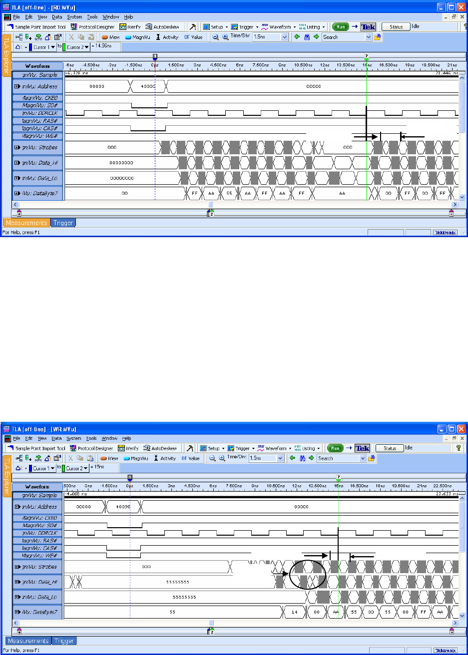
DDR3THIN-MN-XXX 54 Doc. Rev. 1.11
Figure 4 - Read Data Latency = CAS Latency + CAS Additive Latency + RDIMM (5+0+1) = 6 cycles)
5.6 Selecting B_DDR3D_XX Write Data Sample Points
Unlike valid DDR Read data, valid Write data is bisected by the Strobes. Since valid DDR3
Write data is bisected by the Strobes (see Figure 5) the Setup & Hold sample point must be set
for the valid data that occurs closest to the clock edge. The appropriate clock edge for Writes is
determined by counting the number of clock cycles specified by the Write Latency MRS value
from the Write Command to the first valid Write Data. (If these values are not known the
technique described in Section 7.3 can be used to determine them.) In Figure 5 the total Write
latency is 6 cycles (Write Latency plus the additional one cycle delay for RDIMM memory).
Figure 5 - Write Data Latency = CAS Write Latency + RDIMM (5+1) = 6 cycles
Sample Pt. #1 Sample Pt. #2
Sample Pt. #1 Sample Pt. #2
Write Data
Preamble
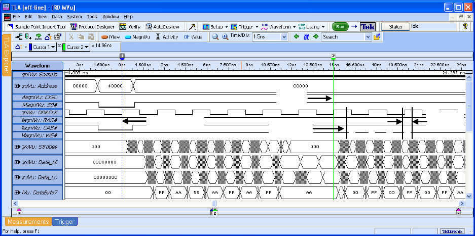
DDR3THIN-MN-XXX 55 Doc. Rev. 1.11
The B_DDR3D_XX supports acquire two samples of valid Write data on each rising edge of the
DDR3 clock. So to acquire both pieces of data the WrA_DatHi/Lo data groups must have their
sample point set to that shown by Sample Pt. #1 in the Figure, and the WrB_DatHi/Lo data
groups must have their sample point set to that shown by Sample Pt. #2.
NOTE - It is important to note that because of the design of the TLA acquisition card inputs and
the Strobe activity prior to Write data being placed on the data bus it will appear as if the Strobes
indicate valid Write data earlier than the data is actually there (see the circle indicated as Write
Data Preamble in Figure 5). These Write Preamble Strobe edges should NOT be used to
determine where valid Write data is on the data bus.
5.7 B_DDR3D_XX Support Setup
Using the B_DDR3D_XX supports it is possible to acquire both Read and Write data by setting
the sample point of the data groups appropriately. To adjust the Read Data group sample points
first make an appropriate acquisition of Read data by triggering on a Read command. Then
create a timing window display of MagniVu data and display the Data_Hi and Data_Lo 32-bit
data groups, the individual Command group signals and the DDR3 clock that was used for the
data acquisition (DDRCK0). A sample waveform display of MagniVu Read data is shown in
Figure 6. To determine the sample point, locate the smallest window of valid Read data during
the acquired burst (see Figure 6). Note that in this instance the first piece of valid data happens
significantly after the rising edge it is associated with. In fact the initial valid data appears at the
DDR Clock falling edge. This delay must be taken into account or data will not be aligned
properly in the Listing display window. Note that A and B data (corresponding to ADataHi/Lo
and BDataHi/Lo data groups) have been indicated.
Figure 6 - Locating Minimum Valid B_DDR3D_XX Read Data Window
Read Command Valid Read
Data Begins
Minimum
S&H
Latency
expires
AB A B
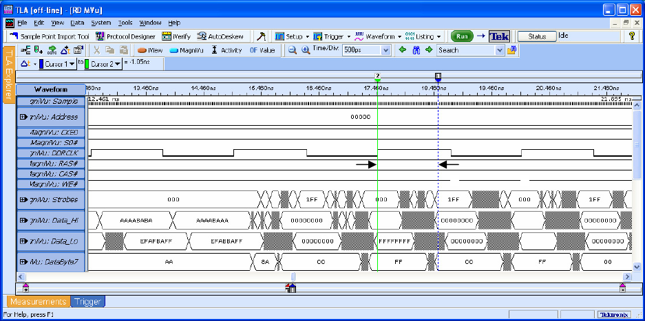
DDR3THIN-MN-XXX 56 Doc. Rev. 1.11
Figure 7 - Measuring B_DDR3D_XX RdA_DatHi / Lo Read Data Setup & Hold
Zoom in further to determine the Setup and Hold sample point necessary to acquire valid data at
that point (Figure 7) and use the cursors to measure the time from the clock edge to the start of
valid Read data. In this example the delay from edge to data is approximately -1.05ns after the
clock edge, meaning that a suitable Setup & Hold value for the RdA_DatHi capture group would
be -1.055ns/1.289ns. Note that the Data_Lo group is valid somewhat later than the Data_Hi
group with its valid time starting at approximately 1.23ns after the clock edge, so the Setup &
Hold sample point for the RdA_DatLo capture group would be set to -1.23ns/1.465ns.
Now the sample point for the RdB_DatHi and RdB_DatLo groups must be determined (see
Figure 8). The next valid Read data (after the cycle measured above) occurs approximately
2.37ns after the rising edge of DDRCK0, so a suitable Setup & Hold value for the RdB_DatHi
capture group would be –2.383ns/2.617ns. As with the A data the Data_Lo group is somewhat
later than the Data_Hi group. The Data_Lo valid time starts at approximately -2.52ns so a
suitable Setup & Hold value for the RdB_DatLo capture group would be -2.52ns/2.754ns.
B
A
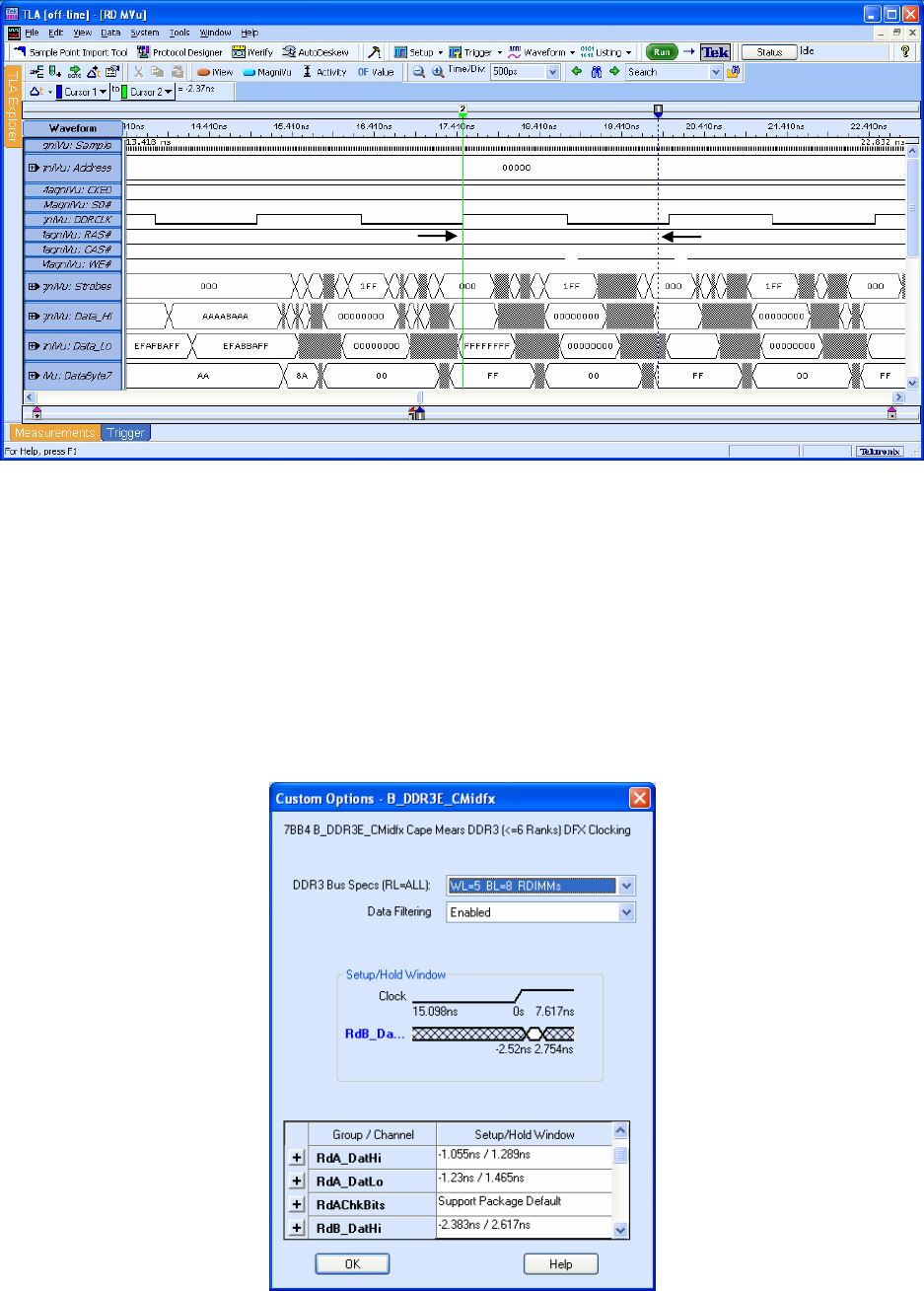
DDR3THIN-MN-XXX 57 Doc. Rev. 1.11
Figure 8 - Measuring B_DDR3D_XX RdB_DatHi / Lo Read Data Setup & Hold
Now the sample point positions must be set for the RdA_DatHi, RdA_DatLo, RdB_DatHi and
RdB_DatLo capture groups in the Setup window (see Figure 9). This window is found by going
to the LA Card’s Setup window, then clicking on the More button to the right of the clock select
field. The TLA acquisition cards require a valid data window of approximately 300ps, and this
window can be placed to begin from 15.098ns prior to the clock edge to 7.383ns after the edge in
roughly 20ps increments. Each 32-bit data group (RdA_DatHi, RdA_DatLo, RdB_DatHi,
RdB_DatLo) will require its own value programmed from the measurements noted in the
MagniVu window.
Figure 9 - Setting B_DDR3D_XX RdA_DatHi / Lo and RdB_DatHi / Lo Sample Points
AB
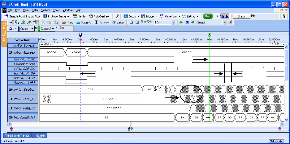
DDR3THIN-MN-XXX 58 Doc. Rev. 1.11
Setting the Setup & Hold values for acquiring Write data is a similar process. To determine the
Write Data group sample points first make an appropriate acquisition of Write data by triggering
on a Write Command. Then, as above, create a timing window display of MagniVu data and
display the Data_Hi and Data_Lo 32-bit data groups, the individual Command group signals and
the DDR3 clock that was used for the data acquisition (DDRCK0).
A sample waveform display of MagniVu Write data is shown in Figure 10. To determine the
sample point, locate the smallest window of valid Write data during the acquired burst (see
Figure 10). Note that in this instance the first piece of valid data happens before the rising edge it
is associated with. This shift must be taken into account or data will not be aligned properly in
the Listing display window. Note that A and B data (corresponding to ADataHi/Lo and
BDataHi/Lo data groups) have been indicated. Refer to section 5.6 for important information on
properly determining the Write data sample points.
Figure 10 - Locating Minimum Valid B_DDR3D_XX Write Data Window
Zoom in further to determine the Setup and Hold sample point necessary to acquire valid data at
that point (Figure 11) and use the cursors to measure the time from the clock edge to the start of
valid Write data. In this example the data leads the clock edge by approximately 740ps, meaning
that a suitable Setup & Hold value for the WrA_DatHi capture group would be 742ps/-508ps.
Note that the Data_Lo group is valid somewhat later than the Data_Hi group with its valid time
starting at approximately 430ps prior to the clock edge, so the Setup & Hold sample point for the
WrA_DatLo capture group would be set to 430ps/-195ps.
Write Command
Latency
ex
p
ires
Minimum
S&H
Write Data
Preamble
AA
BB
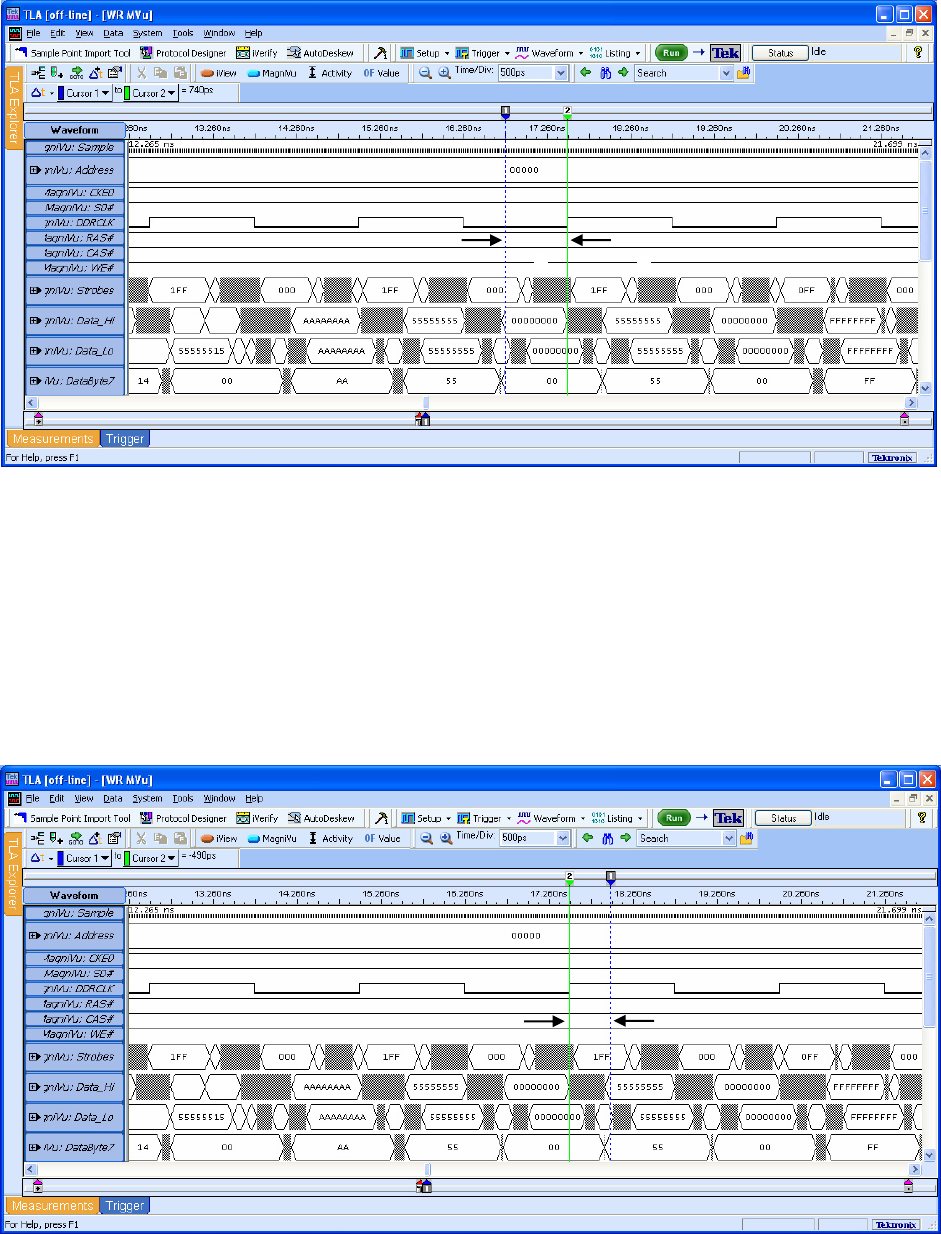
DDR3THIN-MN-XXX 59 Doc. Rev. 1.11
Figure 11 - Measuring B_DDR3D_XX WrA_DatHi / Lo Write Data Setup & Hold
Now the sample point for the WrB_DatHi and WrB_DatLo groups must be determined (see
Figure 12). The next valid Write data (after the cycle measured above) occurs approximately
500ps after the rising edge of DDRCK0, so a suitable Setup & Hold value for the WrB_DatHi
capture group would be -508ps/742ps. As with the A data the Data_Lo group is somewhat later
than the Data_Hi group. The Data_Lo valid time starts at approximately -800ps so a suitable
Setup & Hold value for the WrB_DatLo capture group would be -801ps/1.035ns.
Figure 12 - Measuring B_DDR3D_XX WrB_DatHi / Lo Write Data Setup & Hold
The sample point positions must now be set for the WrA_DatHi, WrA_DatLo, WrB_DatHi,
WrB_DatLo groups in the Setup window (Figure 13). Note that if the Upper Strobes are being
AB
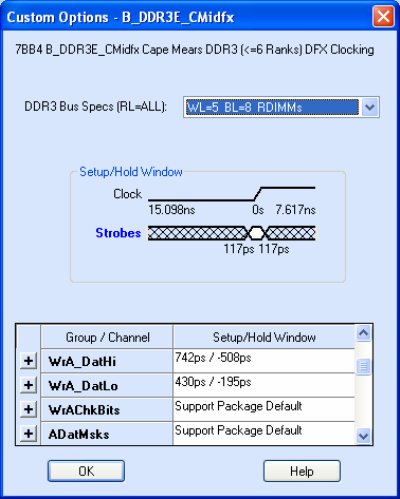
DDR3THIN-MN-XXX 60 Doc. Rev. 1.11
used as Data Masks then the WrtMasks group should have a Setup & Hold value that matches
that of the Write Data groups.
Figure 13 - Setting B_DDR3D_XX WrA_DatHi / Lo and WrB_DatHi / Lo Sample Points
Because of the speeds of DDR3 data it may be necessary to program Setup & Hold values for
each of the 8-bit groups that are associated with a given Strobe. This could be required if there is
significant skew between the DDR Strobes. Figure 14 shows some of these additional data
groups (DataByte7-0) added to the same Waveform display shown in Figure 12. Note that it is
now possible to determine the skew between data groups and place these values into the Setup &
Hold Window settings in the TLA Setup window (see Figure 15). Refer to Appendix F Data
Group / Byte / Strobe Cross-Reference for details on which 8-bit groups make up a 32-bit group.
When setting the individual Setup & Hold values it is suggested that the settings for the
associated 32-bit group (RdA_DatHi, RdA_DatLo, RdB_DatHi, RdB_DatLo, WrA_DatHi,
WrA_DatLo, WrB_DatHi, WrB_DatLo) be reset to “Support Package Default”. This will
prevent the TLA from displaying warnings that conflicting values have been set for the data bits.
The Support Package Default Setup & Hold values are the same as the TLA default values –
117ps/117ps. It will also be necessary to program the Setup & Hold values for all of the 8-bit
groups in the affected 32-bit group. If conflicting Setup & Hold points are programmed then the
values will have exclamation marks beside them to denote the conflict.
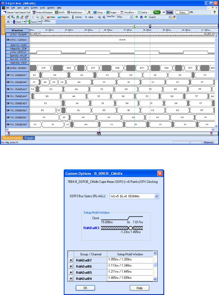
DDR3THIN-MN-XXX 61 Doc. Rev. 1.11
Figure 14 - Viewing Individual 8-bit Read Data Groups
Figure 15 - Setting Individual Setup & Hold Values for the 8-bit Read Data Groups
Note: Values shown are for illustration purposes only
DDR3THIN-MN-XXX 62 Doc. Rev. 1.11
5.8 Setting B_DDR3D_3A Read Data Sample Points
The same procedure outlined above for setting Read Data sample points should be used to
determine the sample points for Read Data from teh second DIMM slot. Set the sample points
for the groups named RdA_DatHi_1, RdA_DatLo_1, RdB_DatHi_1 and RdB_DatLo_1.
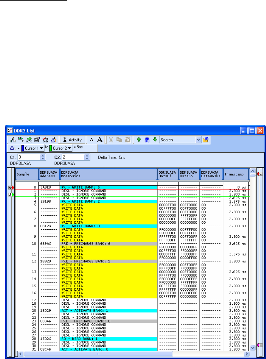
DDR3THIN-MN-XXX 63 Doc. Rev. 1.11
6.0 VIEWING DATA
6.1 Viewing B_DDR3D_XX Data
When using the NEX-DDR3INTR-THIN support packages the raw Address and Data groups are
suppressed and are replaced with post-processed data in new groups. This data is displayed in
new groups that have the support package name preceding it (i.e., B_DDR3D_XX Address,
B_DDR3D_XX DataHi, etc.). The raw data groups are suppressed so that the display of data can
be done in a more user-friendly fashion.
The Command group is suppressed because its function is replaced with a column labeled
“B_DDR3D_XX Mnemonics”. The Interposer support software includes post-processing code
that permits masking out all invalid Read / Write and non-Command data, providing the user a
much better overview of bus activity. Figure 16 shows the default B_DDR3D_XX display where
all DDR3 data is displayed.
Figure 16 - B_DDR3D_XX Listing Display
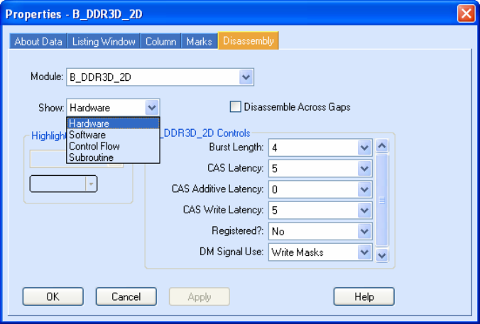
DDR3THIN-MN-XXX 64 Doc. Rev. 1.11
To change the display it is necessary to bring up the window’s Properties window (perform a
right mouse-click in the State display window) and select the Disassembly tab. This will bring up
the configuration window shown in Figure 17.
Figure 17 - Disassembly Properties
There are several select fields available in this window, some of which must be set correctly for
the post-processing software to work properly. These fields and their selections are:
Burst Length - permits setting the burst length for Read and Write data. Valid choices
are 4 (the default) 8, and 4/8 On-the-Fly. This value must be set properly for all valid
Read and Write data to be displayed.
CAS Latency (CL) - sets the delay, in clock cycles, from the Read command until the
first piece of valid Read data is available. This value must be set properly for all valid
Read Data to be displayed. Valid choices are 5 (default), 6, 7, 8, 9 or 10 cycles.
CAS Additive Latency - additional latency for data cycles. This value must also be set
properly for valid Read Data to be displayed. Valid choices are 0 (default), CL-1, or CL-
2 cycles.
CAS Write Latency – number of clock cycles from Write command to the first Write
Data. This value must be set properly for all valid Write Data to be displayed. Valid
choices are 5 (default), 6, 7, or 8 cycles.
Registered? – must be set to reflect whether or not Registered DDR memory is used.
Default is No. When set to Yes an additional clock cycle delay is added to CAS Latency
and to valid Read and Write Data tagging.
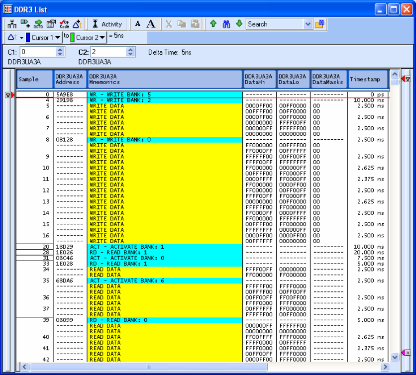
DDR3THIN-MN-XXX 65 Doc. Rev. 1.11
DM Signal Use - permits setting Data Mask functionality to Write Masks (default) or
Strobes. When set to Write Mask the DM signals will be used to mask Write Data to
show which data bytes were valid in the cycle.
In addition to these Disassembly Properties selections, changing the settings in the Show field
results in display changes as well:
Hardware - (default) displays all acquired cycles
Software - suppresses all idle or wait cycles
Control Flow - shows Address Command and valid Read / Write data cycles
Subroutine - shows valid Read / Write data cycles only
Figure 18 - B_DDR3D_XX Listing Display - Control Flow
Changing the Show field setting in the display of Figure 16 from Hardware to Control Flow
results in the display of Figure 18 where only Row and Column Address commands and valid

DDR3THIN-MN-XXX 66 Doc. Rev. 1.11
data are displayed. Note that the timestamp is updated to reflect the time between displayed
cycles.
6.2 Viewing Raw DDR3 Data using B_DDR3D_XX Supports
In order to make the display of DDR3 data more user-friendly the raw data from the Address, all
Data and other groups is suppressed in the B_DDR3D_2D Listing display. Instead the post-
processing display software formats and reorders the data to tag and display valid DDR3
Address, Commands and Data. In the case of the B_DDR3D_2D supports, which stores two
Read and two Write data cycles in each TLA Sample location, the data is reordered
chronologically in the display with the oldest data being shown on the line above the newer data.
To see the raw data using the Interposer support package perform a right mouse click in the
Listing window, select Add Column… then click on the group to be added. Refer to the TLA
User’s Manual or online help for further information on added or deleting data groups.
6.3 B_DDR3D_2A / 3A Mnemonics Description
Table 6 gives a brief description of each of the text lines displayed in the B_DDR3D_2A / _3A
post-processing software display.
Mnemonic Description
ACT – BANK ACTIVATE (Sx#) Bank: Active command – activate a row in a bank for subsequent access
(Chip Select 0-3; Bank x)
DESL - IGNORE COMMAND Deselect function – no new command
(E)MRS – (EXTENDED) MODE
REGISTER SET x (Sx#)
Mode Register Set command, registers 0-3;
(Chip Select 0-3)
NOP - NO OPERATION (Sx#) No Operation command (Chip Select 0-3)
PRE – SINGLE BANK PRECHARGE (Sx#)
Bank:
Precharge command (Chip Select 0-3; Bank x)
PREA – PRECHARGE ALL BANK (Sx#) Precharge All command (Chip Select 0-3)
RDA – READ W/AUTO PRECHARGE
(Sx#) Bank:
Read command with auto precharge (Chip Select 0-3; Bank x)
RD - READ (Sx#) Bank: Read command – initiates a burst read access to active row
(Chip Select 0-3; Bank x)
READ DATA Valid Read data on the bus
REF - REFRESH (Sx#) Self Refresh command (Chip Select 0-3)
WRA – WRITE W/AUTO PRECHARGE
(Sx#) Bank:
Write command with auto precharge (Chip Select 0-3; Bank x)
WR - WRITE (Sx~) Bank: Write command – initiates a burst write access to active row
(Chip Select 0-3; Bank x)
WRITE DATA Valid Write data on the bus
ZQCL – ZQ CALIBRATION LONG (Sx#) ZQ Calibration Long (Chip Select 0-3)
ZQCS – ZQ CALIBRATION SHORT (Sx#) ZQ Calibration Short (Chip Select 0-3)
Table 6 - B_DDR3D_2A / 3A Mnemonics Definition
6.4 B_DDR3D_2G Mnemonics Description

DDR3THIN-MN-XXX 67 Doc. Rev. 1.11
Table 7 gives a brief description of each of the text lines displayed in the B_DDR3D_2G post-
processing software display.
Mnemonic Description
ACT – BANK ACTIVATE
(Sx# / bS# / cS#) Bank:
Active command – activate a row in a bank for subsequent access
(Slot A, B or C; Chip Select 0-3; Bank x)
DESL - IGNORE COMMAND Deselect function – no new command
(E)MRS – (EXTENDED) MODE
REGISTER SET x (Sx# / bS# / cS#)
Mode Register Set command, registers 0-3;
(Slot A, B or C; Chip Select 0-3)
NOP - NO OPERATION (Sx# / bS# / cS#) No Operation command (Slot A, B or C; Chip Select 0-3)
PRE – SINGLE BANK PRECHARGE
(Sx# / bS# / cS#) Bank:
Precharge command (Slot A, B or C; Chip Select 0-3; Bank x)
PREA – PRECHARGE ALL BANK
(Sx# / bS# / cS#)
Precharge All command (Slot A, B or C; Chip Select 0-3)
RDA – READ W/AUTO PRECHARGE
(Sx# / bS# / cS#) Bank:
Read command with auto precharge
(Slot A, B or C; Chip Select 0-3; Bank x)
RD - READ (Sx# / bS# / cS#) Bank: Read command – initiates a burst read access to active row
(Slot A, B or C; Chip Select 0-3; Bank x)
READ DATA Valid Read data on the bus
REF - REFRESH (Sx# / bS# / cS#) Self Refresh command (Slot A, B or C; Chip Select 0-3)
WRA – WRITE W/AUTO PRECHARGE
(Sx# / bS# / cS#) Bank:
Write command with auto precharge
(Slot A, B or C; Chip Select 0-3; Bank x)
WR - WRITE (Sx# / bS# / cS#) Bank: Write command – initiates a burst write access to active row
(Slot A, B or C; Chip Select 0-3; Bank x)
WRITE DATA Valid Write data on the bus
ZQCL – ZQ CALIBRATION LONG
(Sx# / bS# / cS#)
ZQ Calibration Long (Slot A, B or C; Chip Select 0-3)
ZQCS – ZQ CALIBRATION SHORT
(Sx# / bS# / cS#)
ZQ Calibration Short (Slot A, B or C; Chip Select 0-3)
Table 7 - B_DDR3D_2G Mnemonics Definition
6.5 Viewing Timing Data on the TLA
By default, the TLA will display an acquisition in the Listing (State) mode. However, the same
data can be displayed in Timing form by adding a Waveform Display window. This is done by
clicking on the Window pull-down, selecting New Data Window, clicking on Waveform
Window Type, then choosing the Data Source. Two valid choices are presented:
B_DDR3D_XX and B_DDR3D_XX: MagniVu. The first will show the exact same data (same
acquisition mode) as that shown in the Listing window, except in Waveform format. The second
selection will show all of the channels in 8GHz MagniVu mode, so that edge relationships can
be examined around the MagniVu trigger point. MagniVu is very useful and in some cases
necessary to see/resolve DDR3 data. With either selection, all channels can be viewed by
scrolling down the window. Refer to the TLA System User’s Manual for additional information
on formatting the Waveform display.
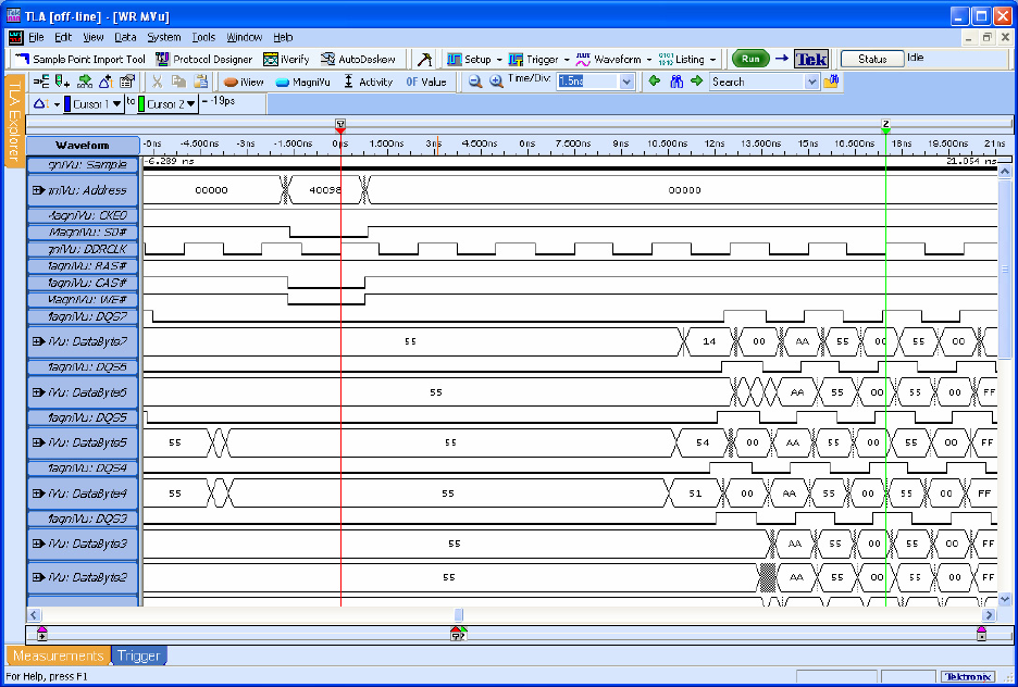
DDR3THIN-MN-XXX 68 Doc. Rev. 1.11
Figure 19 - B_DDR3D_XX MagniVu Display on TLA
DDR3THIN-MN-XXX 69 Doc. Rev. 1.11
7.0 HINTS & TIPS
7.1 Symbolic Triggering on a Command using B_DDR3D_XX Supports
A Symbol Table has been included for the Control data groups defined in each of the support
packages. The Symbol Table for the B_DDR3D_2D / 3A supports is shown in Table 8; the
Symbol Table for the B_DDR3D_2G support is shown in Table 9. The use of Symbol Tables
when triggering makes it easier for the user to define a given cycle to be triggered on. Rather
than trying to remember what signals make up the Control group, the Symbol Table has the
appropriate bits already set for the given cycle.
It is important to note that changing the channel definition of the Control group can result in
incorrect symbol information being displayed.
Symbol Definition
cc ssss = x1 1110 for S0#
cc ssss = 1x 1101 for S1#
cc ssss = x1 1011 for S2#
cc ssss = 1x 0111 for S3#
x in Definition = Don’t Care
MRS – Sx# MODE REGISTER SET cc ssss xxx xxx xx000
REF – Sx# REFRESH cc ssss xxx xxx xx001
PRE – Sx# SINGLE BANK PRECHARGE cc ssss xxx xxx x0010
PREA – Sx# PRECHARGE ALL BANKS cc ssss xxx xxx x1010
ACT – Sx# ACTIVATE BANK cc ssss xxx xxx xx011
WR – Sx# WRITE cc ssss xxx xxx x0100
WRA – Sx# WRITE WITH AUTO
PRECHARGE
cc ssss xxx xxx x1100
RD – Sx# READ cc ssss xxx xxx x0101
RDA – Sx# READ WITH AUTO
PRECHARGE
cc ssss xxx xxx x1101
NOP –Sx# NO OPERATION cc ssss xxx xxx xx111
DES - DEVICE DESELECT cc ssss xxx xxx xxxxx
ZQCL – Sx# ZQ CALIBRATION LONG cc ssss xxx xxx x1110
ZQCS – Sx# ZQ CALIBRATION SHORT cc ssss xxx xxx x0110
Table 8 - B_DDR3D_2D / 3A Control Symbol Table
Signals, left-to-right: CKE1, CKE0, S3#, S2#, S1#, S0#, BA2, BA1, BA0, A15, A14, A13,
A12/BC#, A10/AP, RAS#, CAS#, WE#

DDR3THIN-MN-XXX 70 Doc. Rev. 1.11
Symbol Definition
cccc ssssssss = xxxxx1 1110 for S0#
cccc ssssssss = xxxx1x 1101 for S1#
cccc ssssssss = xxxxx1 1011 for S2#
cccc ssssssss = xxxx1x 0111 for S3#
cccc ssssssss = xxxxx1 1110 for bS0#
cccc ssssssss = xxxx1x 1101 for bS1#
cccc ssssssss = xxxxx1 1011 for cS0#
cccc ssssssss = xxxx1x 0111 for cS1#
x in Definition = Don’t Care
MRS – Sx# MODE REGISTER SET cccc ssssssss xxx xxx xx000
MRS – bSx# MODE REGISTER SET cccc ssssssss xxx xxx xx000
MRS – cSx# MODE REGISTER SET cccc ssssssss xxx xxx xx000
REF – Sx# REFRESH cccc ssssssss xxx xxx xx001
PRE – Sx# SINGLE BANK PRECHARGE cccc ssssssss xxx xxx x0010
PREA – Sx# PRECHARGE ALL BANKS cccc ssssssss xxx xxx x1010
ACT – Sx# ACTIVATE BANK cccc ssssssss xxx xxx xx011
WR – Sx# WRITE cccc ssssssss xxx xxx x0100
WRA – Sx# WRITE WITH AUTO
PRECHARGE
cccc ssssssss xxx xxx x1100
RD – Sx# READ cccc ssssssss xxx xxx x0101
RDA – Sx# READ WITH AUTO
PRECHARGE
cccc ssssssss xxx xxx x1101
NOP –Sx# NO OPERATION cccc ssssssss xxx xxx xx111
DES - DEVICE DESELECT cccc ssssssss xxx xxx xxxxx
ZQCL – Sx# ZQ CALIBRATION LONG cccc ssssssss xxx xxx x1110
ZQCS – Sx# ZQ CALIBRATION SHORT cccc ssssssss xxx xxx x0110
Table 9 - B_DDR3D_2G Control Symbol Table
Signals, left-to-right: cCKE1, cCKE0, bCKE1, bCKE0, CKE1, CKE0,
cS1#, cS0#, bS1#, bS0#, S3#, S2#, S1#, S0#,
BA2, BA1, BA0, A15, A14, A13, A12/BC#, A10/AP, RAS#, CAS#, WE#
7.3 Capturing MRS (Mode Register Set) Cycles
If the characteristics of the DDR target (latency, burst length) are not known it is possible to
acquire this information using the TLA so that the post-processing Control settings can be
properly set. This information is programmed into the DDR memory upon system boot by use of
the MRS (Mode Register Set) command, and is required when using the NEX-DDR3INTR-
THIN supports for the post-processing software to properly decode the acquisitions. The TLA
trigger shown in Figure 19 can be used to acquire the MRS cycles when using either of these
supports.
Note that because there is no Trigger event defined in this example that it will be necessary to
Stop the TLA acquisition manually to display the MRS data. A trigger could certainly be added
in either (or both) of the Trigger events, but the method shown ensures that the last valid MRS
cycles will be acquired regardless of the memory depth setting of the acquisition card.
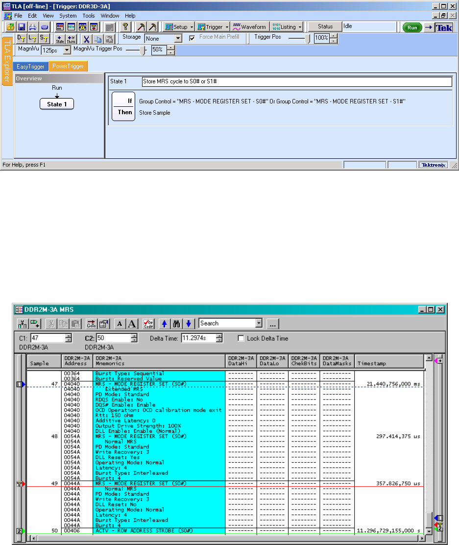
DDR3THIN-MN-XXX 71 Doc. Rev. 1.11
Figure 20 - B_DDR3D_2D MRS Trigger
In the trigger example a Storage condition has been created so that only MRS cycles will be
stored. In testing, multiple MRS cycles were seen during the boot process, and the example
triggers shown will ensure that all of the MRS cycles will be acquired, an example of which is
shown in Figure 20. The last acquired MRS cycle will reflect the settings used in the DDR target
– in this case, a CAS latency of 2 cycles with a Burst length of 8.
Figure 21 - MRS Cycle Acquisition Disassembly
7.4 Clock Capture quality
The clock captured by the logic analyzer may exhibit ringing. If this ringing is such that a clock
reference voltage can not be determined it is suggested that the capacitor on the DIMM across
DDR3THIN-MN-XXX 72 Doc. Rev. 1.11
the differential pair by removed. The added capacitance of the logic analyzer compensates for
this missing capacitor.
7.5 Thresholds
Analog waveforms and their associated thresholds viewed using the Tektronix Analog Mux will
display amplitudes and thresholds that are not an exact representation of the actual analog
waveform. The Nexus passive probes used on DDR3 NEXVu and Interposer products are
designed to supply maximum voltage swing to the Logic analyzer to insure correct digital signal
swing capture at the high DDR3 rates. While the Tektronix active P69xx and P68xx series of
probe, being general purpose probes, divide the input voltage swing by 20 the passive probes
from Nexus divide the signals by approximately 7.5. Since the divide value is different than the
standard Tektronix probe the voltage swing and offset will be higher than expected, and the
thresholds will be different. Instead of the expected 0.75 threshold of approximately 1.9V
threshold will be required. This was designed specifically for DDR3 signals to allow the best
possible capture of the digital representation of these signals. Viewing the output of the Logic
Analyzer analog mux should be used as a tool to provide fine adjustment of the logic analyzer
signal Vref. The threshold value determined in this manner should be used as the threshold
setting for the Nexus DDR3 product. Please note: Only the vertical resolution is affected by the
Nexus passive probes.

DDR3THIN-MN-XXX 73 Doc. Rev. 1.11
APPENDIX A – How DDR Data is Clocked
A.1 Background
Demultiplexing means that the TLA’s Logic Analyzer card can have one data probe connected to
the target yet store incoming data in two or four separate data sections of the card. For instance,
the A3 data section (8-bits) can be connected to the target and data can be stored in the A3
section and the D3 section. Using the equivalent of 4X demux (by utilizing both the cross-point
switch and prime memory capabilities of the acquisition card), connections made to the A3
channels permit data to be stored in the A3, A3B (prime channels), D3 and D3B sections. A very
useful side benefit of using demux is that, since only one set of TLA data channels has to be
connected, only one probe load is added to the target, even though data is stored in two or four
different locations of the acquisition card.
A.2 DDR Acquisition - General
All of the above is background necessary to understand how the TLA is able to acquire data at
rates that initially look too fast. The speeds of DDR3 (1066 MT/s) require different setups to
enable proper data acquisition. In addition, instead of trying to use the 8 Data Strobes to acquire
data our solution uses CLK0 of the DDR SDRAM Clocks and all data acquisition is adjusted in
relation to the clock edges. The 8 Data Strobes cannot be easily used to acquire data as some
TLA configurations only support 4 Clock Inputs. Also, the Strobes cannot be used to acquire
Address and Command information.
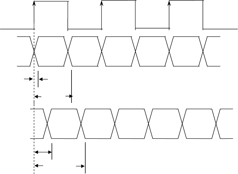
DDR3THIN-MN-XXX 74 Doc. Rev. 1.11
A.3 B_DDR3D_2D / 2G / 3A Data Acquisition
These supports requires two (2) merged 136-channel with 1.4G state option TLA7BB4
acquisition cards used in a TLA7XX logic analyzer. Data is acquired using the rising edge of the
DDR clock. A_Data information is earlier (older) data than the information stored in B_Data.
Different Sample Points must be set for each of the four 32-bit Data groups, and, if necessary,
sample points can be set for any of the 8-bit data groups or for individual data bits.
Clock
Read
R
a
R
b
R
c
R
d
R
e
RdA-S&H
RdB-S&H
Wb Wc Wd We
WrB-S&H
WrA-S&H
Wa
Write

DDR3THIN-MN-XXX 75 Doc. Rev. 1.11
APPENDIX B - Considerations
B.1 NEX-DDR3INTR-THIN Bus Loading
It must be noted that the NEX-DDR3INTR-THIN Interposer is designed to minimal effect on the
user’s circuit. The acquired signals are sampled at top edge connector, and then passed through
isolation resistors to the probe. There will be an effective 600 ohm load on all probed signals.
The B_DDR3D_3A support will use two Interposers and will double probe all signal. Thus the
DC load will be near 300 ohms. The DDR3 Interposer has been tested via detailed simulations,
and by actual in circuit testing.
B.2 DIMM connector location for best quality signal capture
An interposer is subject to reflected noise and the quality of the acquisitions should improve if
the Interposer is in the furthest slot away from the memory controller. If the memory channel
contains two DIMM slots and only one will be used, the slot used must be the furthest away from
the memory controller.
B.3 TLA7BB4 Module to module skew
At print time Tektronix had not yet specified the module to module skew that will be displayed
in MagniVu, and timing modes. This skew is around 300ps. It is expected that in future releases
Tektronix will remove this skew. Contact Tektronix for updates.

DDR3THIN-MN-XXX 76 Doc. Rev. 1.11
APPENDIX C – 240-pin DDR3 DIMM Pinout
Front Side (left 1-60) Back Side (right 121-180 Front Side (left 61-120) Back Side (right 181-240)
Pin
#
X64
Non-
Parity
X72
ECC
Pin
#
X64
Non-Parity
X72
ECC Pin #
X64
Non-
Parity
X72
ECC Pin #
X64
Non-
Parity
X72
ECC
1 VREF VREF 121 VSS VSS 61 A2 A2 181 A1 A1
2 VSS VSS 122 DQ4 DQ4 62 VDD VDD 182 VDD VDD
3 DQ0 DQ0 123 DQ5 DQ5 63 CK1 CK1 183 VDD VDD
4 DQ1 DQ1 124 VSS VSS 64 CK1# CK1# 184 CK0 CK0
5 VSS VSS 125 DM0
DQS9
DM0
DQS9 65 VDD VDD 185 CK0# CK0#
6 DQS0# DQS0# 126 NC
DQS9#
NC
DQS9# 66 VDD VDD 186 VDD VDD
7 DQS0 DQS0 127 VSS VSS 67 VREF VREF 187 TEST/NC TEST/NC
8 VSS VSS 128 DQ6 DQ6 68 NC
Par_In
NC
Par_In 188 A0 A0
9 DQ2 DQ2 129 DQ7 DQ7 69 VDD VDD 189 VDD VDD
10 DQ3 DQ3 130 VSS VSS 70 A10/AP A10/AP 190 BA1 BA1
11 VSS VSS 131 DQ12 DQ12 71 BA0 BA0 191 VDD VDD
12 DQ8 DQ8 132 DQ13 DQ13 72 VDD VDD 192 RAS# RAS#
13 DQ9 DQ9 133 VSS VSS 73 WE# WE# 193 S0# S0#
14 VSS VSS 134 DM1
DQS10
DM1
DQS10 74 CAS# CAS# 194 VDD VDD
15 DQS1# DQS1# 135 NC
DQS10#
NC
DQS10# 75 VDD VDD 195 ODT0 ODT0
16 DQS1 DQS1 136 VSS VSS 76 S1# S1# 196 A13 A13
17 VSS VSS 137 DQ14 DQ14 77
RSVD
ODT1
RSVD
ODT1 197 VDD VDD
18 DQ10 DQ10 138 DQ15 DQ15 78 VDD VDD 198 Free Free
19 DQ11 DQ11 139 VSS VSS 79 RSVD
SPD#
RSVD
Spd3 199 VSS VSS
20 VSS VSS 140 DQ20 DQ20 80 VSS VSS 200 DQ36 DQ36
21 DQ16 DQ16 141 DQ21 DQ21 81 DQ32 DQ32 201 DQ37 DQ37
22 DQ17 DQ17 142 VSS VSS 82 DQ33 DQ33 202 VSS VSS
23 VSS VSS 143 DML2,
DQS11
DML2
DQS11 83 VSS VSS 203
DM4
DQS13
DM4
DQS13
24 DQS2# DQS2# 144 DQS11# DQS11# 84 DQS4# DQS4# 204 DQS13# DQS13#
25 DQS2 DQS2 145 VSS VSS 85 DQS4 DQS4 205 VSS VSS
26 VSS VSS 146 DQ22 DQ22 86 VSS VSS 206 DQ38 DQ38
27 DQ18 DQ18 147 DQ23 DQ23 87 DQ34 DQ34 207 DQ39 DQ39
28 DQ19 DQ19 148 VSS VSS 88 DQ35 DQ35 208 VSS VSS
29 VSS VSS 149 DQ28 DQ28 89 VSS VSS 209 DQ44 DQ44
30 DQ24 DQ24 150 DQ29 DQ29 90 DQ40 DQ40 210 DQ45 DQ45
31 DQ25 DQ25 151 VSS VSS 91 DQ41 DQ41 211 VSS VSS
32 VSS VSS 152 DM3
DQS12
DM3
DQS12 92 VSS VSS 212
DM5
DQS14
DM5
DQS14
33 DQS3# DQS3# 153 DQS12# DQS12# 93 DQS5# DQS5# 213 DQS14# DQS14#
34 DQS3 DQS3 154 VSS VSS 94 DQS5 DQS5 214 VSS VSS
35 VSS VSS 155 DQ30 DQ30 95 VSS VSS 215 DQ46 DQ46
36 DQ26 DQ26 156 DQ31 DQ31 96 DQ42 DQ42 216 DQ47 DQ47
37 DQ27 DQ27 157 VSS VSS 97 DQ43 DQ43 217 VSS VSS
38 VSS VSS 158 NC CB4 98 VSS VSS 218 DQ52 DQ52
39 NC CB0 159 NC CB5 99 DQ48 DQ48 219 DQ53 DQ53
40 NC CB1 160 VSS VSS 100 DQ49 DQ49 220 VSS VSS
DDR3THIN-MN-XXX 77 Doc. Rev. 1.11
APPENDIX C - 240-pin DDR3 DIMM Pinout (cont’d.)
Front Side (left 1-60) Back Side (right 121-180 Front Side (left 61-120) Back Side (right 181-240)
Pin
#
X64
Non-
Parity
X72
ECC
Pin
#
X64
Non-Parity
X72
ECC
Pin
#
X64
Non-
Parity
X72
ECC
Pin
#
X64
Non-
Parity
X72
ECC
41 VSS VSS 161 DM8
DQS17
DM8
DQS17 101 VSS VSS 221
DM6
DQS15
DM6
DQS15
42 DQS8# DQS8# 162 DQS17# DQS17# 102 DQS6# DQS6# 222 DQS15# DQS15#
43 DQS8 DQS8 163 VSS VSS 103 DQS6 DQS6 223 VSS VSS
44 VSS VSS 164 NC CB6 104 VSS VSS 224 DQ54 DQ54
45 NC CB2 165 NC CB7 105 DQ50 DQ50 225 DQ55 DQ55
46 NC CB3 166 VSS VSS 106 DQ51 DQ51 226 VSS VSS
47 VSS VSS 167 Test Test 107 VSS VSS 227 DQ60 DQ60
48 Free Free 168 Free Free 108 DQ56 DQ56 228 DQ61 DQ61
KEY KEY 109 DQ57 DQ57 229 VSS VSS
49 RESET# RESET# 169 CKE1 CKE1 110 VSS VSS 230 DM7
DQS16
DM7
DQS16
50 CKE0 CKE0 170 VDD VDD 111 DQS7# DQS7# 231 DQS16# DQS16#
51 VDD VDD 171 A15 A15 112 DQS7 DQS7 232 VSS VSS
52 BA2 BA2 172 A14 A14 113 VSS VSS 233 DQ62 DQ62
53 NC
ERR-OUT#
NC
ERR-OUT# 173 VDD VDD 114 DQ58 DQ58 234 DQ63 DQ63
54 VDD VDD 174 A12 A12 115 DQ59 DQ59 235 VSS VSS
55 A11 A11 175 A9 A9 116 VSS VSS 236 VDDSPD VDDSPD
56 A7 A7 176 VDD VDD 117 SA0 SA0 237 SA1 SA1
57 VDD VDD 177 A8 A8 118 SLC SLC 238 SDA SDA
58 A5 A5 178 A6 A6 119 SA2 SA2 239 VSS VSS
59 A4 A4 179 VDD VDD 120 VTT VTT 240 VTT VTT
60 VDD VDD 180 A3 A3
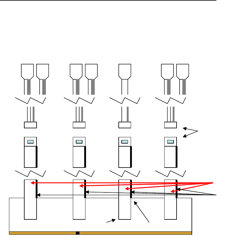
DDR3THIN-MN-XXX 78 Doc. Rev. 1.11
APPENDIX D –Data Flow Through the Probes (coax cable to channel)
Data flow
Slave1 C3/2 & E3/2
Master A3/2 &
Master
Slave1 A3/2 & A1/0
Slave1 C3/2/1/0
Slave1 E3/2/1/0
Master A3/2 D3/2
Master A1/0 D1/0
Master C3/2/1/0
Slave1 A3/2 D3/2
Slave1 A1/0 D1/0
J15-x Coax on top
J16-x Coax on
Samtec Connectors
plug together at this
point
Plastic Housing
that plugs into
TLA 7BB4
J15-1 edge J16-1 edge Interposer

DDR3THIN-MN-XXX 79 Doc. Rev. 1.11
APPENDIX D - Data Flow Through the Probes (cont’d.)
Coax wire
PIN
M_C
Channel
M_A3/2 A1/0
Channel
S_A3/2 A1/0
Channel
S_C3/2 E3/2
Channel
J16-2 C2:0 A0:0 A0:0 E2:0
J16-5 C2:5 A0:5 A0:5 E2:5
J16-8 C3:3 A1:3 A1:3 E3:3
J16-11 C1:5 A3:5 A3:5 C3:5
J16-14 C1:0 A3:0 A3:0 C3:0
J16-17 C0:3 A2:3 A2:3 C2:3
J16-4 C2:4 A0:4 A0:4 E2:4
J16-7 C3:2 A1:2 A1:2 E3:2
J16-10 C3:7 A1:7 A1:7 E3:7
J16-13 C1:1 A3:1 A3:1 C3:1
J16-16 C0:6 A2:6 A2:6 C2:6
J16-3 C2:1 A0:1 A0:1 E2:1
J16-6 CLK3 CLK1 CLK1 Q3
J16-9 C3:6 A1:6 A1:6 E3:6
J16-12 C1:4 A3:4 A3:4 C3:4
J16-15 C0:7 A2:7 A2:7 C2:7
J16-18 C0:2 A2:2 A2:2 C2:2
J15-18 C2:2 A0:2 A0:2 E2:2
J15-15 C2:7 A0:7 A0:7 E2:7
J15-12 C3:4 A1:4 A1:4 E3:4
J15-9 C1:6 A3:6 A3:6 C3:6
J15-6 Q1 CLK0 CLK0 CLK3
J15-3 C0:1 A2:1 A2:1 C2:1
J15-16 C2:6 A0:6 A0:6 E2:6
J15-13 C3:1 A1:1 A1:1 E3:1
J15-10 C1:7 A3:7 A3:7 C3:7
J15-7 C1:2 A3:2 A3:2 C3:2
J15-4 C0:4 A2:4 A2:4 C2:4
J15-17 C2:3 A0:3 A0:3 E2:3
J15-14 C3:0 A1:0 A1:0 E3:0
J15-11 C3:5 A1:5 A1:5 E3:5
J15-8 C1:3 A3:3 A3:3 C3:3
J15-5 C0:5 A2:5 A2:5 C2:5
J15-2 C0:0 A2:0 A2:0 C2:0

DDR3THIN-MN-XXX 80 Doc. Rev. 1.11
APPENDIX E – B_DDR3D_2D Support Pinout, DIMM Slot 0
Samtec
Pin
Coax
Pin
TLA
Channe
l
DDR3
Signal
Samte
c
Pin
Coax
Pin
TLA
Channe
l
DDR3
Signal
15 J15-6 CK1 CB1 46 J16-6 CK3+ A13
29 J15-10 A1:7 NC 32 J16-10 C3:7 BA1
25 J15-9 A1:6 CB3 36 J16-9 C3:6 RAS#
28 J16-11 A1:5 CB7 33 J15-11 C3:5 CAS#
24 J16-12 A1:4 CB6 37 J15-12 C3:4 S1#
21 J15-8 A1:3 CB2 40 J16-8 C3:3 S0#
19 J15-7 A1:2 DQS8 42 J16-7 C3:2 ODT0
20 J16-13 A1:1 DM8 41 J15-13 C3:1 ODT1
16 J16-14 A1:0 CB5 45 J15-14 C3:0 S2#
12 J16-15 A0:7 CB4 49 J15-15 C2:7 DQ32
10 J16-16 A0:6 DQ31 51 J15-16 C2:6 DQ33
11 J15-5 A0:5 CB0 50 J16-5 C2:5 S3#
9 J15-4 A0:4 DQ27 52 J16-4 C2:4 DQ36
6 J16-17 A0:3 DQ30 55 J15-17 C2:3 DQS4
4 J16-18 A0:2 DM3 57 J15-18 C2:2 NC
5 J15-3 A0:1 DQ26 56 J16-3 C2:1 DQ37
3 J15-2 A0:0 DQS3 58 J16-2 C2:0 DM4
46 J16-6 CK0 A15 15 J15-6 Q1+ A2
32 J16-10 A3:7 TEST 29 J15-10 C1:7 WE#
36 J16-9 A3:6 RESET# 25 J15-9 C1:6 BA0
33 J15-11 A3:5 NC 28 J16-11 C1:5 A0
37 J15-12 A3:4 NC 24 J16-12 C1:4 CK0
40 J16-8 A3:3 NC 21 J15-8 C1:3 A10
42 J16-7 A3:2 CKE1 19 J15-7 C1:2
PAR_I
N
41 J15-13 A3:1 CKE0 20 J16-13 C1:1 A1
45 J15-14 A3:0 BA2 16 J16-14 C1:0 A3
49 J15-15 A2:7
ERR_OUT
# 12 J16-15 C0:7 NC
51 J15-16 A2:6 A11 10 J16-16 C0:6 NC
50 J16-5 A2:5 A14 11 J15-5 C0:5 A4
52 J16-4 A2:4 A12 9 J15-4 C0:4 NC
55 J15-17 A2:3 A7 6 J16-17 C0:3 A6
57 J15-18 A2:2 A5 4 J16-18 C0:2 NC
56 J16-3 A2:1 A9 5 J15-3 C0:1 NC
58 J16-2 A2:0 A8 3 J15-2 C0:0 NC
2X Probe Connection used with
B_DDR3D_2D software
M_A3/2 A1/0
1X Probe Connection used with
B_DDR3D_2D software
M_C3/2 C1/0

DDR3THIN-MN-XXX 81 Doc. Rev. 1.11
APPENDIX E – B_DDR3D_2D Support Pinout, DIMM Slot 0 (Cont’d.)
Samtec
Pin
Coax
Pin
TLA
Channel
DDR3
Signal
Samtec
Pin
Coax
Pin
TLA
Channel
DDR3
Signal
15 J15-6 CK1 DQS5
46 J15-6 Q3 DQ3
29 J15-10 A1:7 DQ49 32 J15-10 E3:7 DQ10
25 J15-9 A1:6 DQ48
36 J15-9 E3:6 DQS1
28 J16-11 A1:5 DQ52 33 J16-11 E3:5 DM1
24 J16-12 A1:4 DQ47 37 J16-12 E3:4 DQ13
21 J15-8 A1:3 DQ43
40 J15-8 E3:3 DQ9
19 J15-7 A1:2 DQ42
42 J15-7 E3:2 DQ8
20 J16-13 A1:1 DQ46 41 J16-13 E3:1 DQ12
16 J16-14 A1:0 DM5 45 J16-14 E3:0 DQ7
12 J16-15 A0:7 DQ45 49 J16-15 E2:7 DQ6
10 J16-16 A0:6 DQ44 51 J16-16 E2:6 DM0
11 J15-5 A0:5 DQ41
50 J15-5 E2:5 DQ2
9 J15-4 A0:4 DQ40
52 J15-4 E2:4 DQS0
6 J16-17 A0:3 DQ39 55 J16-17 E2:3 DQ5
4 J16-18 A0:2 DQ38 57 J16-18 E2:2 DQ4
5 J15-3 A0:1 DQ35
56 J15-3 E2:1 DQ1
3 J15-2 A0:0 DQ34
58 J15-2 E2:0 DQ0
46 J16-6 CK0 DQ60
15 J16-6 CK3 DM2
32 J16-10 A3:7 DQ53 29 J16-10 C3:7 DQ14
36 J16-9 A3:6 DM6 25 J16-9 C3:6 DQ15
33 J15-11 A3:5 DQS6 28 J15-11 C3:5 DQ11
37 J15-12 A3:4 DQ50 24 J15-12 C3:4 DQ16
40 J16-8 A3:3 DQ54
21 J16-8 C3:3 DQ20
42 J16-7 A3:2 DQ55
19 J16-7 C3:2 DQ21
41 J15-13 A3:1 DQ51 20 J15-13 C3:1 DQ17
45 J15-14 A3:0 DQ56 16 J15-14 C3:0 DQS2
49 J15-15 A2:7 DQ57 12 J15-15 C2:7 DQ18
51 J15-16 A2:6 DQS7 10 J15-16 C2:6 DQ19
50 J16-5 A2:5 DQ61
11 J16-5 C2:5 DQ22
52 J16-4 A2:4 DM7 9 J16-4 C2:4 DQ23
55 J15-17 A2:3 DQ58 6 J15-17 C2:3 DQ24
57 J15-18 A2:2 DQ59 4 J15-18 C2:2 DQ25
56 J16-3 A2:1 DQ62 5 J16-3 C2:1 DQ28
58 J16-2 A2:0 DQ63 3 J16-2 C2:0 DQ29
2X Probe Connection used with
B_DDR3D_2D software
S_A3/2 A1/0
2X Probe Connection used with
B_DDR3D_2D software
S_C3/2 E3/2

DDR3THIN-MN-XXX 82 Doc. Rev. 1.11
APPENDIX F – B_DDR3_2G Support Pinout, DIMM Slot 0 Auxiliary Signals
Samte
c Pin
Coax
Pin
TLA
Channe
l
DDR3
Signal
46 J16-6 NC
32 J16-10 E3:7 NC
36 J16-9 E3:6 NC
33 J15-11 E3:5
cCLKE1
LEAD-6
37 J15-12 E3:4
cCLKE0
LEAD-5
40 J16-8 E3:3 NC
42 J16-7 E3:2 NC
41 J15-13 E3:1 LEAD-4
45 J15-14 E3:0 LEAD-3
49 J15-15 E2:7 NC
51 J15-16 E2:6
cS1#
LEAD-2
50 J16-5 E2:5 NC
52 J16-4 E2:4 NC
55 J15-17 E2:3 NC
57 J15-18 E2:2
cS0#
LEAD-1
56 J16-3 E2:1 NC
58 J16-2 E2:0 NC
15 J15-6 Q2
bCLKE1
LEAD-
10
29 J15-10 E1:7
bCLKE0
LEAD-7
25 J15-9 E1:6 LEAD-8
28 J16-11 E1:5 NC
24 J16-12 E1:4 NC
21 J15-8 E1:3 NC
19 J15-7 E1:2 LEAD-9
20 J16-13 E1:1 NC
16 J16-14 E1:0 NC
12 J16-15 E0:7 NC
10 J16-16 E0:6 NC
11 J15-5 E0:5 NC
9 J15-4 E0:4
bS1#
LEAD-
11
6 J16-17 E0:3 NC
4 J16-18 E0:2 NC
5 J15-3 E0:1 NC
3 J15-2 E0:0
bS0#
LEAD-
12
Optional Flying Lead Probe Connection used with
B_DDR3D_2G software
M_E3/2 E1/0
DDR3THIN-MN-XXX 83 Doc. Rev. 1.11

DDR3THIN-MN-XXX 84 Doc. Rev. 1.11
APPENDIX G – B_DDR3D_3A Support Pinout, DIMM Slot 1
Samte
c Pin
Coax
Pin
TLA
Channe
l
DDR3
Signal
Samte
c
Pin
Coax
Pin
TLA
Channe
l
DDR3
Signal
15 J15-6 Q0+ CB1 46 J16-6 CK3+ A13
29 J15-10 D3:7 NC 32 J16-10 C3:7 BA1
25 J15-9 D3:6 CB3 36 J16-9 C3:6 RAS#
28 J16-11 D3:5 CB7 33 J15-11 C3:5 CAS#
24 J16-12 D3:4 CB6 37 J15-12 C3:4 S1#
21 J15-8 D3:3 CB2 40 J16-8 C3:3 S0#
19 J15-7 D3:2 DQS8 42 J16-7 C3:2 ODT0
20 J16-13 D3:1 DM8 41 J15-13 C3:1 ODT1
16 J16-14 D3:0 CB5 45 J15-14 C3:0 S2#
12 J16-15 D2:7 CB4 49 J15-15 C2:7 DQ32
10 J16-16 D2:6 DQ31 51 J15-16 C2:6 DQ33
11 J15-5 D2:5 CB0 50 J16-5 C2:5 S3#
9 J15-4 D2:4 DQ27 52 J16-4 C2:4 DQ36
6 J16-17 D2:3 DQ30 55 J15-17 C2:3 DQS4
4 J16-18 D2:2 DM3 57 J15-18 C2:2 NC
5 J15-3 D2:1 DQ26 56 J16-3 C2:1 DQ37
3 J15-2 D2:0 DQS3 58 J16-2 C2:0 DM4
46 J16-6 CK0+ A15 15 J15-6 Q1+ A2
32 J16-10 A3:7 TEST 29 J15-10 C1:7 WE#
36 J16-9 A3:6 RESET# 25 J15-9 C1:6 BA0
33 J15-11 A3:5 NC 28 J16-11 C1:5 A0
37 J15-12 A3:4 NC 24 J16-12 C1:4 CK0
40 J16-8 A3:3 NC 21 J15-8 C1:3 A10
42 J16-7 A3:2 CKE1 19 J15-7 C1:2 PAR_IN
41 J15-13 A3:1 CKE0 20 J16-13 C1:1 A1
45 J15-14 A3:0 BA2 16 J16-14 C1:0 A3
49 J15-15 A2:7
ERR_OUT
# 12 J16-15 C0:7 NC
51 J15-16 A2:6 A11 10 J16-16 C0:6 NC
50 J16-5 A2:5 A14 11 J15-5 C0:5 A4
52 J16-4 A2:4 A12 9 J15-4 C0:4 NC
55 J15-17 A2:3 A7 6 J16-17 C0:3 A6
57 J15-18 A2:2 A5 4 J16-18 C0:2 NC
56 J16-3 A2:1 A9 5 J15-3 C0:1 NC
58 J16-2 A2:0 A8 3 J15-2 C0:0 NC
2X Probe Connection used with
B_DDR3D_2D software
M_A3/2 A1/0
(S2_A3/2 D3/2 Logic Analyzer Probe)
1X Probe Connection used with
B_DDR3D_2D software
M_C3/2 C1/0
(S2_C3/2/1/0 Logic Analyzer Probe)

DDR3THIN-MN-XXX 85 Doc. Rev. 1.11
APPENDIX G – B_DDR3D_3A Support Pinout, DIMM Slot 1 (cont’d.)
Samtec
Pin
Coax
Pin
TLA
Channe
l
DDR
3
Signa
l
Samte
c
Pin
Coax
Pin
TLA
Channe
l
DDR
3
Signa
l
15 J15-6 CK2+ DQS5 15 J15-6 Q2+ DQ3
29 J15-10 D1:7 DQ49 29 J15-10 E1:7 DQ10
25 J15-9 D1:6 DQ48 25 J15-9 E1:6 DQS1
28 J16-11 D1:5 DQ52 28 J16-11 E1:5 DM1
24 J16-12 D1:4 DQ47 24 J16-12 E1:4 DQ13
21 J15-8 D1:3 DQ43 21 J15-8 E1:3 DQ9
19 J15-7 D1:2 DQ42 19 J15-7 E1:2 DQ8
20 J16-13 D1:1 DQ46 20 J16-13 E1:1 DQ12
16 J16-14 D1:0 DM5 16 J16-14 E1:0 DQ7
12 J16-15 D0:7 DQ45 12 J16-15 E0:7 DQ6
10 J16-16 D0:6 DQ44 10 J16-16 E0:6 DM0
11 J15-5 D0:5 DQ41 11 J15-5 E0:5 DQ2
9 J15-4 D0:4 DQ40 9 J15-4 E0:4 DQS0
6 J16-17 D0:3 DQ39 6 J16-17 E0:3 DQ5
4 J16-18 D0:2 DQ38 4 J16-18 E0:2 DQ4
5 J15-3 D0:1 DQ35 5 J15-3 E0:1 DQ1
3 J15-2 D0:0 DQ34 3 J15-2 E0:0 DQ0
46 J16-6 CK1+ DQ60 46 J16-6 Q3+ DM2
32 J16-10 A1:7 DQ53 32 J16-10 E3:7 DQ14
36 J16-9 A1:6 DM6 36 J16-9 E3:6 DQ15
33 J15-11 A1:5 DQS6 33 J15-11 E3:5 DQ11
37 J15-12 A1:4 DQ50 37 J15-12 E3:4 DQ16
40 J16-8 A1:3 DQ54 40 J16-8 E3:3 DQ20
42 J16-7 A1:2 DQ55 42 J16-7 E3:2 DQ21
41 J15-13 A1:1 DQ51 41 J15-13 E3:1 DQ17
45 J15-14 A1:0 DQ56 45 J15-14 E3:0 DQS2
49 J15-15 A0:7 DQ57 49 J15-15 E2:7 DQ18
51 J15-16 A0:6 DQS7 51 J15-16 E2:6 DQ19
50 J16-5 A0:5 DQ61 50 J16-5 E2:5 DQ22
52 J16-4 A0:4 DM7 52 J16-4 E2:4 DQ23
55 J15-17 A0:3 DQ58 55 J15-17 E2:3 DQ24
57 J15-18 A0:2 DQ59 57 J15-18 E2:2 DQ25
56 J16-3 A0:1 DQ62 56 J16-3 E2:1 DQ28
58 J16-2 A0:0 DQ63 58 J16-2 E2:0 DQ29
2X Probe Connection used with
B_DDR3D_2D software
S_A3/2 A1/0
(S2_A1/0 D1/0 Logic Analyzer Probe)
2X Probe Connection used with
B_DDR3D_2D software
S_C3/2 E3/2
(S2_E3/2/1/0 Logic Analyzer Probe)

DDR3THIN-MN-XXX 86 Doc. Rev. 1.11
APPENDIX H – Data Group / Data Byte / Strobe Cross-Reference
32-bit Data Group 8-bit Data Group Strobe Data Bits
RdADatHi RdADatB7 DQS7 63,62,61,60,59,58,57,56
RdADatB6 DQS6 55,54,53,52,51,50,49,48
RdADatB5 DQS5 47,46,45,44,43,42,41,40
RdADatB4 DQS4 39,38,37,36,35,34,33,32
RdADatLo RdADatB3 DQS3 31,30,29,28,27,26,25,24
RdADatB2 DQS2 23,22,21,20,19,18,17,16
RdADatB1 DQS1 15,14,13,12,11,10,9,8
RdADatB0 DQS0 7,6,5,4,3,2,1,0
WrADatHi WrADatB7 DQS7 63,62,61,60,59,58,57,56
WrADatB6 DQS6 55,54,53,52,51,50,49,48
WrADatB5 DQS5 47,46,45,44,43,42,41,40
WrADatB4 DQS4 39,38,37,36,35,34,33,32
WrADatLo WrADatB3 DQS3 31,30,29,28,27,26,25,24
WrADatB2 DQS2 23,22,21,20,19,18,17,16
WrADatB1 DQS1 15,14,13,12,11,10,9,8
WrADatB0 DQS0 7,6,5,4,3,2,1,0
RdBDatHi RdBDatB7 DQS7 63,62,61,60,59,58,57,56
RdBDatB6 DQS6 55,54,53,52,51,50,49,48
RdBDatB5 DQS5 47,46,45,44,43,42,41,40
RdBDatB4 DQS4 39,38,37,36,35,34,33,32
RdBDatLo RdBDatB3 DQS3 31,30,29,28,27,26,25,24
RdBDatB2 DQS2 23,22,21,20,19,18,17,16
RdBDatB1 DQS1 15,14,13,12,11,10,9,8
RdBDatB0 DQS0 7,6,5,4,3,2,1,0
WrBDatHi WrBDatB7 DQS7 63,62,61,60,59,58,57,56
WrBDatB6 DQS6 55,54,53,52,51,50,49,48
WrBDatB5 DQS5 47,46,45,44,43,42,41,40
WrBDatB4 DQS4 39,38,37,36,35,34,33,32
WrBDatLo WrBDatB3 DQS3 31,30,29,28,27,26,25,24
WrBDatB2 DQS2 23,22,21,20,19,18,17,16
WrBDatB1 DQS1 15,14,13,12,11,10,9,8
WrBDatB0 DQS0 7,6,5,4,3,2,1,0
B_DDR3D_XX Groups/Bytes/Strobes Cross Reference
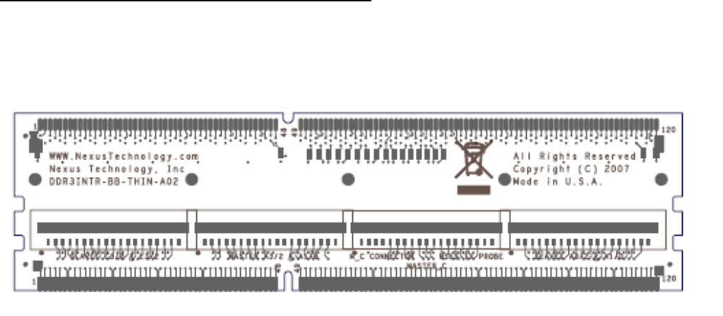
DDR3THIN-MN-XXX 87 Doc. Rev. 1.11
APPENDIX I – NEX-DDR3INTR-THIN Silkscreen
Front Silk-screen
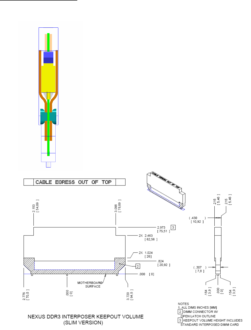
DDR3THIN-MN-XXX 88 Doc. Rev. 1.11
APPENDIX J – Keep out area
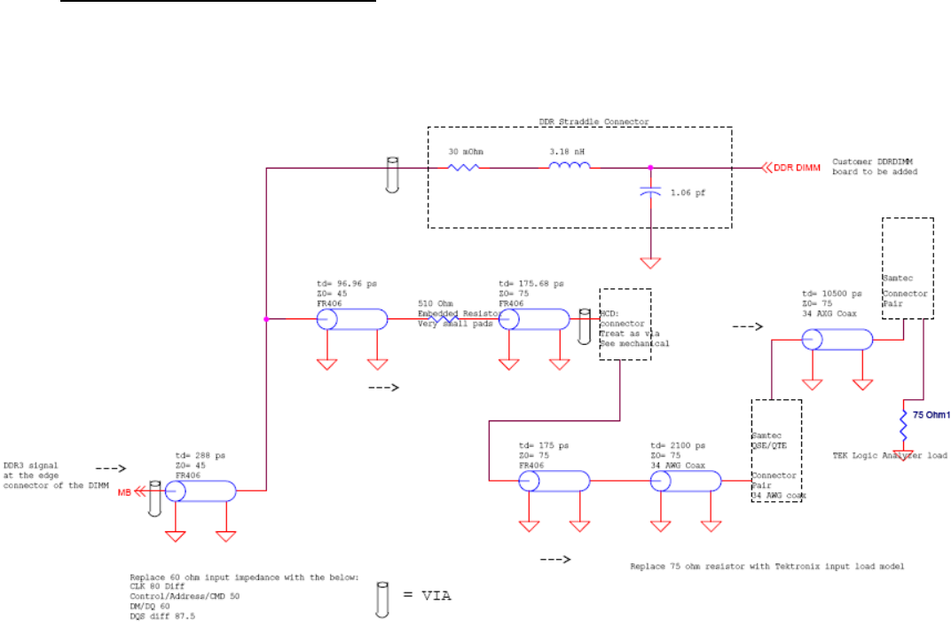
DDR3THIN-MN-XXX 89 Doc. Rev. 1.11
APPENDIX K – Simulation Model
Double this if you are using two Interposers on the same memory channel

DDR3THIN-MN-XXX 90 Doc. Rev. 1.11
APPENDIX L - References
JEDEC PC3-6400/PC3-8500-10660 DDR3 SDRAM Unbuffered DIMM Design Specification
Revision 0.1 March 20, 2006.
Tektronix TLA7000 Series Installation Manual
Tek part number 071-1747-03
Tektronix TLA7000 Series Technical Reference Manual
Tektronix part number 071-1764-00
Nexus Low Profile Distributed Probe Manual—
Part number LowProfileProbes-MN-XXX
JEDEC DDR3 SDRAM Standard
JESD79-3 June 2007

DDR3THIN-MN-XXX 91 Doc. Rev. 1.11
APPENDIX M - Support
About Nexus Technology, Inc.
Established in 1991, Nexus Technology, Inc. is dedicated to developing, marketing, and
supporting Bus Analysis applications for Tektronix Logic Analyzers.
We can be reached at:
Nexus Technology, Inc.
P.O. Box 6575
Nashua, NH 03063
TEL: 877-595-8116
FAX: 877-595-8118
Web site: http://www.nexustechnology.com
Support Contact Information
Technical Support techsupport@nexustechnology.com
General Information support@nexustechnology.com
Quote Requests quotes@nexustechnology.com
We will try to respond within one business day.
If Problems Are Found
Document the problem and e-mail the information to us. If at all possible please forward
a Saved System Setup (with acquired data) that shows the problem. Please do not send a
text listing alone as that does not contain enough data for analysis. To prevent corruption
during the mailing process it is strongly suggested that the Setup be zipped before
transmission.
