Nikon If Not Then NWL860
User Manual: Nikon If not then Manual: ://www.nikoninstruments.com/images/stories/PDFs/NWL860
Open the PDF directly: View PDF ![]() .
.
Page Count: 5
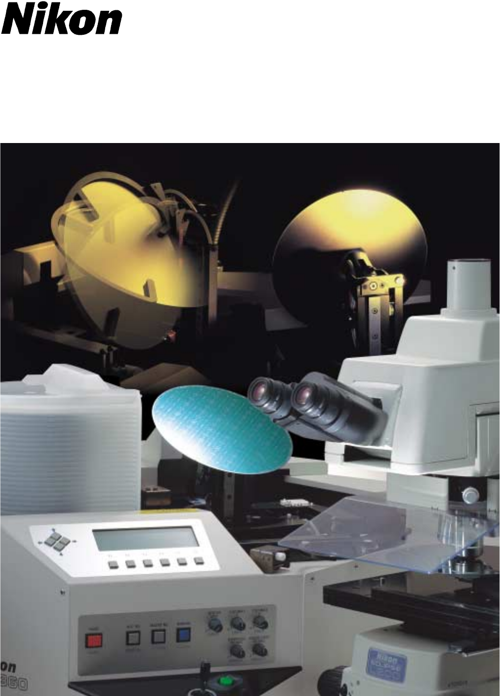
IC Inspection Wafer Loaders
NWL860/641
Series
NWL-Series 03.1.21 9:01 AM ページ1
IC Inspection Wafer Loaders
NWL-860 Series
NWL-860TMB
NWL-860TMB SP
NWL-860TMB INX
Macro inspections of 8- to 6-inch wafers
Dust-free, stainless-steel body
SMIF elevator model
The perfect answer to macro inspection tasks
Back side macro inspection
Non-contact pre-alignment function
Ergonomic design
High reliability Simple, easy operation
High throughput
Communication function (option)
Back side center inspection
Pattern side macro inspection
Back side periphery inspection
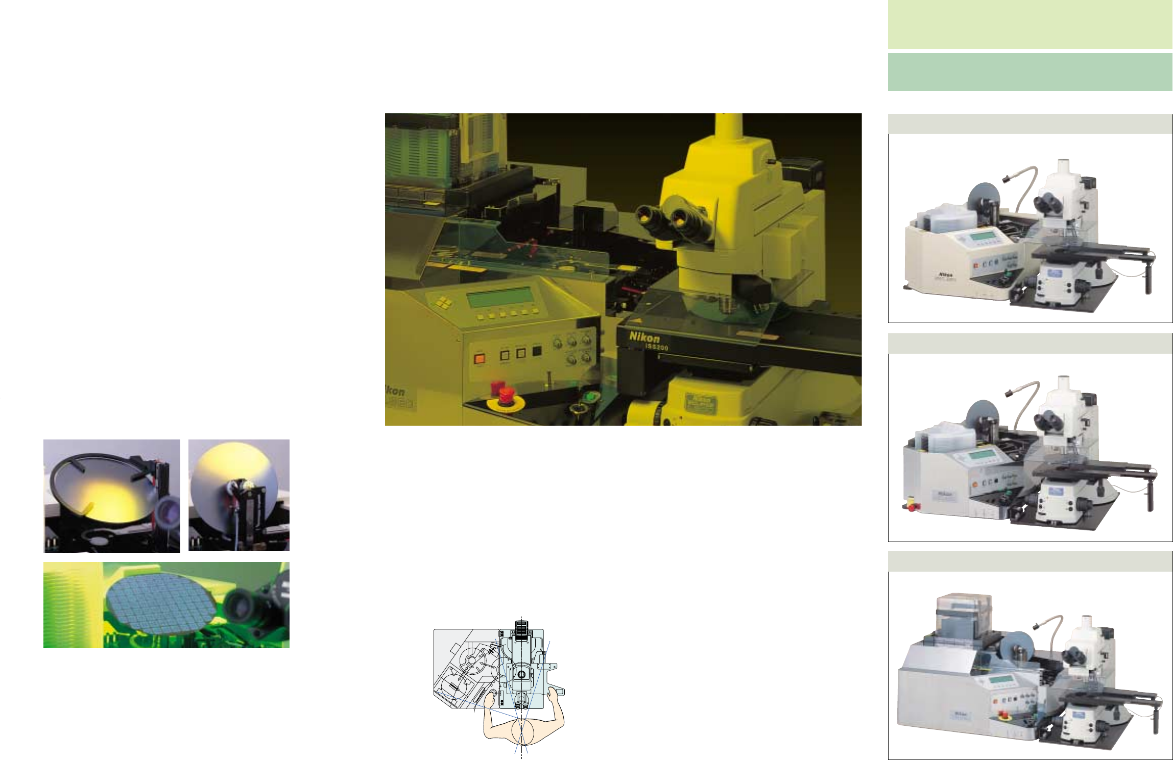
The NWL-860 series provides a full range of macro inspection
capabilities—one of the features considered most essential
for inspecting semiconductor patterns with progressively
higher steps and ever-increasing layers.
A single cassette wafer loader capable of handling 8- and 6-
inch (200 and 150 mm) wafers, this series of wafer loaders
not only comes standard with pattern side macro inspection
capability, but also with the ability to perform back side
periphery and center macro inspections as well.
The NWL-860TMB SP comes in a stainless-steel body and
generates no static electricity, preventing particulate from
attaching to the wafers. The NWL-860TMB INX comes with an
SMIF elevator and both models feature a stop switch for
greater safeguards against abnormalities. MB-type models are
also available exclusively for macro inspections.
Besides pattern side macro inspection, the NWL-860 series
can perform back side periphery and center macro
inspections. Macro inspection parameters, such as wafer
rotation speed and tilt angle, can be set automatically or
manually. Use the macro setting knobs to preset initial
settings and make later adjustments using the joystick.
(Joystick adjustments not possible during back side center
macro inspections)
Prevention of wafer contamination is a vital issue when
inspecting semiconductors. To avoid any chance of
contamination, the NWL-860 series employs non-contact
pre-alignment using photoelectric sensors to center wafers,
avoiding all contact during orientation flat/notch operations.
Furthermore, the whole system is configured, so that the
entire inspection process can be performed without
disturbing the downflow air stream in the cleanroom.
Should an error occur, an error message appears on the
LCD panel with a wafer recovery feature. Even when the
power is turned OFF, the vacuum chuck stays ON, and the
wafer is automatically returned to the cassette when the
power is switched ON again. For even greater safety, the
SP and INX types both feature an emergency button.
To assure operation in a natural posture, ergonomics
surround every aspect of this system’s design. Operation
keys and knobs are located at the front and close to the
operator, so that operation requires a minimum movement
of the hand or eye. The wafer cassette is set at the front and
35° to the left of the operator, enhancing cassette setting
and streamlining visual wafer inspections.
The NWL-860 series uses a dialog-type operating
system with an LCD panel, in which display
information is logically classified, allowing settings
for each step to be made easily on a single screen.
Sophisticated functions such as file management
for cassettes and wafer samples further enhance
operational ease. A dedicated input keypad for
setting inspection processes and programming
wafers to be checked is also available as an option.
Not only is the speed of the elevator surprisingly
fast, but the use of a non-contact centering
mechanism makes it possible to perform alignment
operations quickly and accurately. A multi-arm
system also allows loading and unloading of wafers
with the utmost precision, increasing the overall
efficiency of transfer and wafer exchange
operations. This dramatically decreases cycle
times, providing levels of throughput never seen
before in any other system.
A data communication function conforming to SEMI
(SECS) standards can be added optionally,
enabling transfer of inspection data via the RS-
232C interface or by remote control. This proves
handy when expanding the system or incorporating
it into a total network.
2 3
NWL-Series 03.1.20 4:53 PM ページ3
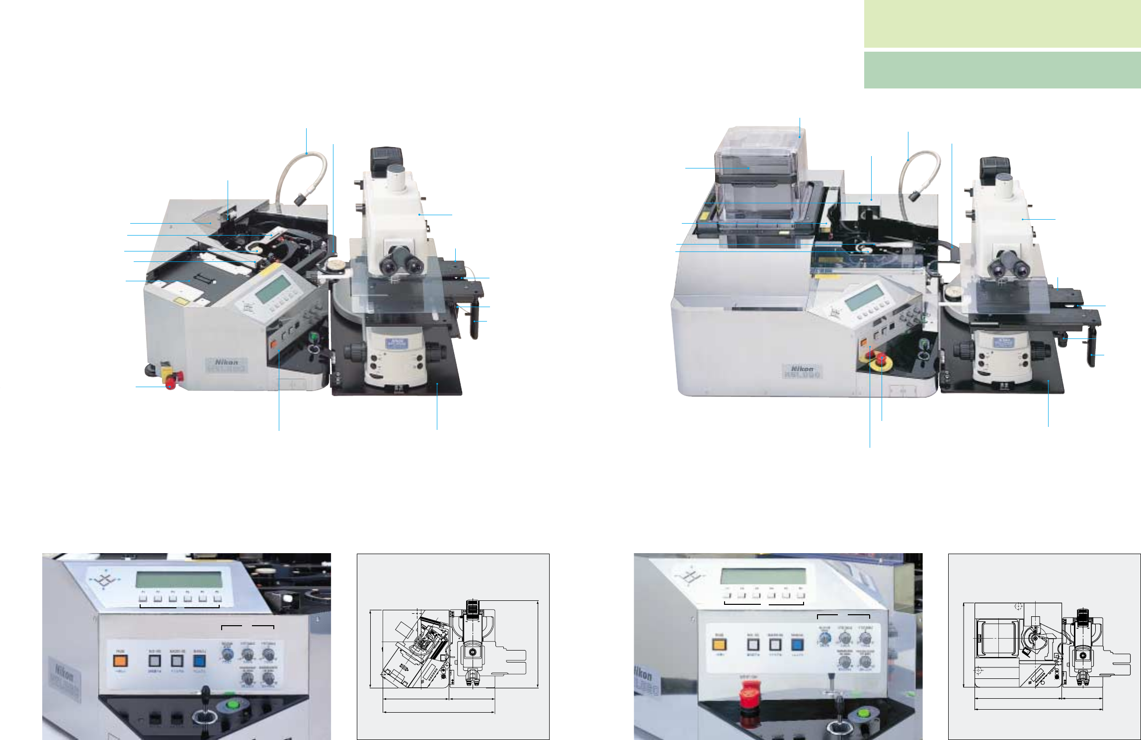
NWL-860TMB SP + ECLIPSE L200 Fiber illumination (option)
Orientation flat/notch detector
Wafer position detector
Feeder arm
Buffer section (syringe)
Pre-alignment sensor
Elevator section
Stop switch
Operation/display section Dedicated microscope base plate
Exchange arm
Dedicated stage (NWL-860 stage)
Rotation dial
Fine movement knob
Driving handle
IC inspection microscope
(ECLIPSE L200)
NWL-860TMB SP Control Panel
1. Cursor keys
2. LCD display
3. Function keys
4. Stop key
5. Micro Reject key
6. Macro Reject key
7. Manual key
8. Macro setting knobs
9. Pattern side macro inspection rotation speed
10. Pattern side macro inspection X tilt angle
11. Pattern side macro inspection Y tilt angle
12. Back side periphery inspection tilt angle
13. Back side center inspection rotation angle
14. Joystick
15. Start switch
625 (24.6)
535 (21.1) 375 (14.8)
918 (36.1)
838-856 (33.0-33.7)
Dimensional Diagram
NWL-860TMB SP + ECLIPSE L200
Unit: mm (inch)
1
2
3
4567
8
910
12 13
14
15
11
IC Inspection Wafer Loaders
NWL-860 Series
Nikon’s IC inspection microscope and the NWL-860
series constitute a highly efficient IC external
inspection system
NWL-860TMB INX + ECLIPSE L200 Fiber illumination (option)
Orientation flat/notch
detector
SMIF pod™
Wafer position detector
Feeder arm
Buffer section (syringe)
Pre-alignment sensor
SMIF elevator
Operation/display section
Exchange arm
Stop switch
NWL-860TMB INX Control Panel
1. Cursor keys
2. LCD display
3. Function keys
4. Stop key
5. Micro Reject key
6. Macro Reject key
7. Manual key
8. Macro setting knobs
9. Pattern side macro inspection rotation speed
10. Pattern side macro inspection X tilt angle
11. Pattern side macro inspection Y tilt angle
12. Back side periphery inspection tilt angle
13. Back side center inspection rotation angle
14. Stop switch
15. Joystick
16. Start switch
785 (30.1) 375 (14.8)
1168 (46.0)
760 (30.0)
Dimensional Diagram
NWL-860TMB INX + ECLIPSE L200
1
2
3
456
7
8
910
12 13
1514
16
11
Unit: mm (inch)
4 5
Dedicated stage
(NWL-860 stage)
Rotation dial
Fine movement knob
Driving handle
IC inspection microscope
(ECLIPSE L200)
Dedicated microscope base plate
NWL-Series 03.1.20 4:54 PM ページ5
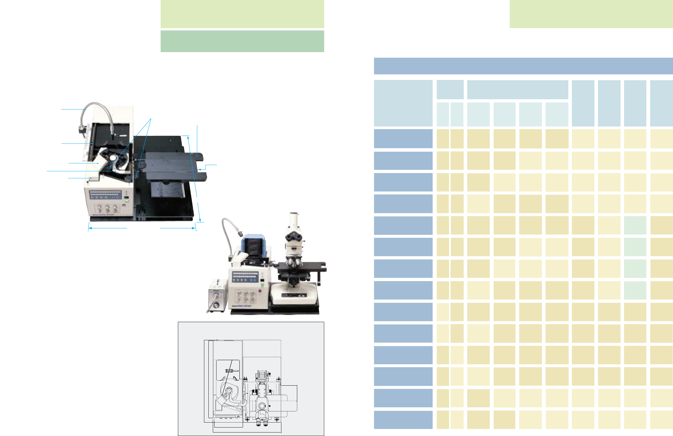
For 6- to 4-inch Wafer Inspection
685 (655)/27.0˝ (25.8˝)
730 (730)/28.7˝ (28.7˝)
10.5˝ (9.7˝)
266 (246)/
MAX 220/8.7˝
598/23.5˝
Dimensional Diagram
NWL-641M + OPTIPHOT 150
Unit: mm/inch
IC Inspection Wafer Loaders
NWL-641M/641
IC Inspection Wafer Loaders
Simple, speedy wafer exchange
Operation is a breeze, thanks to the logical arrangement of keys on
the control panel. The NWL-641 series can memorize up to 10
combinations of wafer channels to be inspected. The orientation flat
detector allows the wafer direction to be set in four directions
(0°, 90°, 180°, 270°) individually during wafer loading onto the
microscope or during wafer unloading. Wafer exchange takes a
short two seconds.
360° rotation vacuum wafer chuck
The vacuum wafer chuck on the stage draws and holds a wafer
transferred by the loader, and if necessary, the wafer can be rotated
360°by using the syringe rotation knob, allowing the loaders to
meet the varying needs of microscopic inspection.
Enhanced macro observations with unique
fluttering mode (641M only)
The 641M incorporates sophisticated macro observation
movements, including Nikon’s original fluttering mode, tilt macro
rotation, and fluttering + tilt macro rotation.
Irregular-shaped wafer cassette capability
The loader in the NWL-641 series uses transmission-type laser
wafer sensors. These sensors check the presence of wafers in the
cassette, wafer tilt, as well as wafer deformation, to determine
automatically the ideal position in which to take the wafers in and
out, thus ensuring secure transfer.
Anti-contamination design
To significantly curtail dust generation from the equipment and the
attachment of particles to wafers, Nikon adopted a special design,
whereby the motor unit in the macro mechanism is located as far
apart as possible from the wafer under inspection.
NWL-641M
Figures in parentheses
are those for Type 641
Quick Reference Chart
NWL-860TMB
NWL-860TM
NWL-860T
NWL-860MB*
Wafer
size
6-
inch
8-
inch
Inspection mode
Micro Macro
Back side
macro
(center)
Back side
macro
(periphery)
Stop
switch
SMIF
elevator
SECS2
Stainless
steel
body &
peek
chuck
NWL-860TMB SP
NWL-860TM SP*
NWL-860T SP*
NWL-860MB SP
NWL-860TMB INX
NWL-641
NWL-641M
NWL-860MB INX
NWL-860TMB INX*
NWL-860MB INX*
Models
●
●
●
●
●
●
●
●
●
●
●
●
●
●
●
●
●
●
●
●
●
●
●
●
●
●
●
●
●
●
●
●
●
●
●
●●
●
●
●
●
●
●
●
●
●
●
●●
●
●
●
●
●
●
●
●
●
●
●
●
●
●
●
●
●
●
●
●
●
●
●
●
●
●
●
●
●
●
●
●
●
●
Option
Option
Option
Option
Note: Models with asterisks are available on a special order basis.
(6-inch only)
(6-inch only)
Macro illumination
unit (option)
Setting switches
(hidden switches)
Orientation flat detector
Wafer position detector
Feeder arm
Dual exchange arms
Operation handle
Stage (rotatable 360°, with
vacuum wafer chuck)
598 mm (23.3 in.)
730 mm (28.7 in.)
6 7
NWL-Series 03.1.20 4:54 PM ページ7
WARNING TO ENSURE CORRECT USAGE, READ THE CORRESPONDING
MANUALS CAREFULLY BEFORE USING YOUR EQUIPMENT.
Specifications and equipment are subject to change without any notice or
obligation on the part of the manufacturer. September 2000.
ISO 14001 Certified
NIKON CORPORATION
Yokohama Plant
ISO 9001 Certified
NIKON CORPORATION
Instruments Company
ISO 9001
Accredited by the
Dutch Council for
Accreditation
ISO 14001
©2000 NIKON CORPORATION
NWL-641 NWL-641M
Wafer size 6, 5 and 4 inches
Wafer cassette Fluoroware®H-BAR type housing
Number of wafers 25 wafers
Inspection mode 1. Micro inspection 1. Micro inspection
2. Tilt macro inspection
Wafer transfer Robotic transfer with vacuum chuck
Orientation flat/notch By transmitted-type sensor
detection
Wafer angle before and after inspection can be specified in increments of 90
°
degrees
Stage Dedicated stage (rotatable 360°; with vacuum chuck)
Compatible microscopes
Nikon OPTIPHOT 300/200C/150, ECLIPSE L200
Dimensions (WxDxH) 246 x 655 x 245 mm, 266 x 655 x 245 mm,
and weight (Approx.) 21 kg 23.5 kg
Vacuum Pressure: –600 mmHg (–80 kPa) or less, Displacement: 10 nl/min. or more
Power source AC 100V/120V ±10%, 50/60 Hz, 1.7A max.
AC 220V/240V ±10%, 50/60 Hz, 0.85A max.
NWL-860TMB/860TMB SP NWL-860MB/860MB SP NWL-860TM/860TM SP NWL-860T/860T SP
NWL-860TMB INX NWL-860MB INX
Wafer size 8 to 6 inches (conforms to both SEMI and JEIDA)
Wafer cassette Fluoroware®PA182-60MB, Fluoroware®PA192-80M
Number of wafers 25 wafers (6-inch), 25 or 26 wafers (8-inch)
Inspection mode
Wafer transfer Robotic transfer with vacuum chuck
Pre-alignment Non-contact pre-alignment
Orientation flat/notch By transmitted-type sensor
detection Wafer angle before and after inspection can be specified in increments of 90° degrees
Stage Dedicated stage (rotatable 360°; with vacuum chuck)
Compatible microscopes
Nikon OPTIPHOT 300/200C/150, ECLIPSE L200
Dimensions (WxDxH) Main unit: 530 x 620 x 275 mm, 50 kg (INX type: 786 x 752 x 442 mm, 60 kg)
and weight (Approx.) Footprint (WxD): 900 x 620 mm (INX type: 1450 x 800 mm)
Vacuum Pressure: –600 mmHg (–80 kPa) or less, Displacement:10 nl/min. or more
Power source AC 100V/120V, 220V/240V ±10%, 50/60 Hz, 3.5A max.
Note: Class 1 laser equipment
Specifications
1. Micro inspection
2. Tilt macro inspection
3.
Back side center macro inspection
4.
Back side periphery macro inspection
1. Tilt macro inspection
2.
Back side center macro inspection
3.
Back side periphery macro inspection
1. Micro inspection
2. Tilt macro inspection 1. Micro inspection
*All models listed here are UL/CE approved.
Printed in Japan (0009-10)T Code No. 2CE-KXTH-3 E
This brochure is printed on recycled paper made from 40% used material.
NIKON CANADA INC.
CANADA Phone: +1-905-625-9910 Fax: +1-905-625-0103
NIKON FRANCE S.A.
FRANCE Phone: +33-1-45-16-45-16 Fax: +33-1-45-16-00-33
NIKON GmbH
GERMANY Phone: +49-211-9414-0 Fax: +49-211-9414-322
NIKON INSTRUMENTS S.p.A.
ITALY Phone: + 39-55-3009601 Fax: + 39-55-300993
NIKON SINGAPORE PTE LTD
SINGAPORE Phone: +65-2978123 Fax: +65-2978131
NIKON AG
SWITZERLAND Phone: +41-1-913-62 00 Fax: +41-1-910-37 44
NIKON UK LTD.
UNITED KINGDOM Phone: +44-181-541-4440 Fax: +44-181-541-4584
NIKON CORPORATION
9-16, Ohi 3-chome, Shinagawa-ku, Tokyo 140-8505, Japan
Phone: +81-3-3773-8122 Fax: +81-3-3773-8115
http://www.nikon.com/
http://www.nikon.co.jp/inst/
NIKON EUROPE B.V.
P.O. Box 222, 1170 AE Badhoevedorp, The Netherlands
Phone: +31-20-44-96-222 Fax: +31-20-44-96-298
NIKON INSTRUMENTS INC.
1300 Walt Whitman Road, Melville, N.Y. 11747-3064, U.S.A.
Phone: +1-631-547-8500 Fax: +1-631-547-0306
NWL-Series 03.1.21 9:01 AM ページ2
