Nikon If Not Then OST 3100
User Manual: Nikon If not then Manual: ://www.nikoninstruments.com/images/stories/PDFs/OST-3100
Open the PDF directly: View PDF ![]() .
.
Page Count: 2
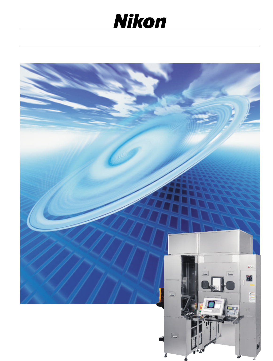
Wafer Inspection System
OP T I S TAT ION -3100
Compact solutionfor 300mm
wafer inspection in diverse
applications
OPTISTATION-3100
Compact solutionfor 300mm wafer inspection in diverse applications
Engineered to provide cost-effective support for 300mm wafers with a minimal footprint, the OPTISTATION-3100
features a new Micro/Macro system in a compact, flexible design. A new optical system offers brighter images,
and observation techniques can be programmed for each objective magnification and each substrate layer to
be inspected. This eliminates deviation from the inspection protocol and missed information through incorrect
optical technique. Its flexible design enables the load ports to be positioned in accordance with the fab layout
requirements. Clearly the best choice for factory automation, the OPTISTATION-3100 is ideal for inspection in
a production environment, advanced research and
development, and failure analysis applications.
Wafer size ø300mm
Microscope (micro)
inspection
Total magnification 25x to 1,500x
Inspection modes Brightfield, darkfield, DUV (option)
Autofocus LED illumination slit projection
Objectives CFI60 objectives
Macro inspection Surface Macro, center backside Macro,
perimeter backside Macro
Load port 1 FOUP (or 1 FOSB: option)
Position selectable from front, side or rear
Wafer transfer Robotic handling; vacuum chuck;
noncontact pre-alignment mechanism
Operation Touch panel GUI, mouse, keyboard
Options
DUV microscope Switchable to B/D
Online operation Via SECS-I or HSMS
Communication 300mm SEMI standards (Compliant with
with host computer E5, E7, E30, E37, E39, E40, E87, E90, E94)
Others FOSB compliance
ULPA boronless FFU (fan filter unit)
Video capture function
2nd user interface (UIF)
OHV (SEMI E84 compliance)
Review inspection
ADC
OCR
Safety S2-0200 compliance, CE marking
compliance
Ergonomic S8-1000 compliance
Dimensions (W x D x H)
1,785 x 1,650 x 2,300mm
(Rear load port) (70.1 x 65.0 x 90.6 in.)
Weight
Main body Approx. 760kg (1,676 lbs.)
FFU unit Approx. 160kg (353 lbs.)
Specifications
Main Features
• New optics
Nikon’s renowned CFI60 optics produce crisp, clear images with
high contrast and minimal flare. Longer working distances
throughout the magnification range ensure safer wafer inspection.
The darkfield signal-to-background ratio is three times higher than
in the past, ensuring significantly better imaging.
• Newly designed DUV microscope
The newly designed optional DUV microscope module offers
resolution to 0.1µm, supporting present and future design rules.
• Flexibility in load port positioning
With load port positions available in the front, side and rear,
the OPTISTATION-3100 is adaptable to diverse fab layouts and
300mm factory automation requirements.
What’s more, it features a smaller footprint and compact design.
• Contamination free inspection
An integrated environmental chamber and FFU (fan filter unit)
prevent contamination by particles, easily ensuring a class 1
inspection environment.
• Easy operation
Automated, motorized functions controlled by an easily accessible
touchscreen ensure comfortable operation while minimizing
contamination. Optimum observation settings, including aperture
and light intensity, can be preset according to objective lens or
wafer type.
• Built for factory automation
The OPTISTATION-3100 features a SEMI and SELETE compliant
design to enable easy adaptation to diverse 300mm factory
automation requirements.
• 3-mode Macro inspection with high-performance illuminators
Allows surface Macro, center backside Macro, and perimeter
backside Macro inspections. Furthermore, the wide illuminator
WIL-100 and the line illuminator LIL-100 have been newly
developed to detect various process defects.
OPTISTATION-3100
WARNING
Specifications and equipment are subject to change without any notice or obligation on the part of the manufacturer. July 2003
©2001 NIKON CORPORATION
The export of this product is controlled by the Japanese Foreign Exchange and Foreign Trade Law and international export control regime.
It should not be exported without authorization from the appropriate governmental authorities.
Printed in Japan Code No. 2CE-KWWH-1 (0307-0.65) K E
NIKON CORPORATION
Yokohama Plant
NIKON CORPORATION
Instruments Company
TO ENSURE CORRECT USAGE, READ THE CORRESPONDING
MANUALS CAREFULLY BEFORE USING YOUR EQUIPMENT.
NIKON CORPORATION http://www.nikon.com/
NIKON INSTECH CO., LTD.
Parale Mitsui Bldg., 8, Higashida-cho, Kawasaki-ku,
Kawasaki, Kanagawa 210-0005, Japan
phone: +81-44-223-2171 fax: +81-44-223-2159
E-mail: inspect.sokkenn@nikon.co.jp
http://www.ave.nikon.co.jp/inst/
NIKON INSTRUMENTS EUROPE B.V.
P.O. Box 222, 1170 AE Badhoevedorp, The Netherlands
phone: +31-20-44-96-222 fax: +31-20-44-96-298
http://www.nikon-instruments.com/
NIKON INSTRUMENTS INC.
Semiconductor Inspection Technologies Group
1430 W. Auto Drive, Suite 101, Tempe, AZ 85284
phone: +1-480-403-4100, +1-877-4-SITECH (474-8324) Toll Free in U.S.
fax: +1-480-403-4199
E-mail: info@nikonsitech.com
http://www.nikonusa.com/
