Nokia Solutions and Networks T5BR1 CDMA Cellular Base Station User Manual IHET5BR1 Part 1 of 3
Nokia Solutions and Networks CDMA Cellular Base Station IHET5BR1 Part 1 of 3
Contents
- 1. IHET5BR1 User Manual Part 1 of 3
- 2. IHET5BR1 User Manual Part 2 of 3
- 3. IHET5BR1 User Manual Part 3 of 3
IHET5BR1 User Manual Part 1 of 3
1X SCt4812ET Lite BTS
Optimization/ATP
Software Release 2.16.0.x and CDMA LMF Build 2.16.x.x
800 MHz and 1.9 GHz
CDMA
English
08/01/2001
68P09253A60–1
PRELIMINARY

FOA
Notice
While reasonable efforts have been made to assure the accuracy of this document, Motorola, Inc. assumes no liability resulting from any
inaccuracies or omissions in this document, or from use of the information obtained herein. The information in this document has been
carefully checked and is believed to be entirely reliable. However, no responsibility is assumed for inaccuracies or omissions. Motorola,
Inc. reserves the right to make changes to any products described herein and reserves the right to revise this document and to make
changes from time to time in content hereof with no obligation to notify any person of revisions or changes. Motorola, Inc. does not
assume any liability arising out of the application or use of any product, software, or circuit described herein; neither does it convey
license under its patent rights or the rights of others.
It is possible that this publication may contain references to, or information about Motorola products (machines and programs),
programming, or services that are not announced in your country. Such references or information must not be construed to mean
that Motorola intends to announce such Motorola products, programming, or services in your country.
Copyrights
This instruction manual, and the Motorola products described in this instruction manual may be, include or describe copyrighted
Motorola material, such as computer programs stored in semiconductor memories or other media. Laws in the United States and
other countries preserve for Motorola certain exclusive rights for copyrighted material, including the exclusive right to copy,
reproduce in any form, distribute and make derivative works of the copyrighted material. Accordingly, any copyrighted Motorola
material contained herein or in the Motorola products described in this instruction manual may not be copied, reproduced,
distributed, merged or modified in any manner without the express written permission of Motorola. Furthermore, the purchase of
Motorola products shall not be deemed to grant either directly or by implication, estoppel, or otherwise, any license under the
copyrights, patents or patent applications of Motorola, as arises by operation of law in the sale of a product.
Usage and Disclosure Restrictions
License Agreement
The software described in this document is the property of Motorola, Inc. It is furnished by express license agreement only and may
be used only in accordance with the terms of such an agreement.
Copyrighted Materials
Software and documentation are copyrighted materials. Making unauthorized copies is prohibited by law. No part of the software or
documentation may be reproduced, transmitted, transcribed, stored in a retrieval system, or translated into any language or
computer language, in any form or by any means, without prior written permission of Motorola, Inc.
High Risk Activities
Components, units, or third–party products used in the product described herein are NOT fault–tolerant and are NOT designed,
manufactured, or intended for use as on–line control equipment in the following hazardous environments requiring fail–safe
controls: the operation of Nuclear Facilities, Aircraft Navigation or Aircraft Communication Systems, Air Traffic Control, Life
Support, or Weapons Systems (“High Risk Activities”). Motorola and its supplier(s) specifically disclaim any expressed or implied
warranty of fitness for such High Risk Activities.
Trademarks
and Motorola are registered trademarks of Motorola, Inc.
Product and service names profiled herein are trademarks of Motorola, Inc. Other manufacturers’ products or services profiled
herein may be referred to by trademarks of their respective companies.
Copyright
Copyright 2001 Motorola, Inc.
All Rights Reserved
Printed on
Recyclable Paper
REV012501
SPECIFICATIONS SUBJECT TO CHANGE WITHOUT NOTICE

08/01/2001 i
1X SCt4812ET Lite BTS Optimization/ATP
PRELIMINARY
Table of Contents
1X SCt4812ET Lite BTS Optimization/ATP
Software Release 2.16.0.x and CDMA LMF Build 2.16.x.x
List of Figures iv. . . . . . . . . . . . . . . . . . . . . . . . . . . . . . . . . . . . . . . . . . . . . . . . . . .
List of Tables vii. . . . . . . . . . . . . . . . . . . . . . . . . . . . . . . . . . . . . . . . . . . . . . . . . . .
Foreword xii. . . . . . . . . . . . . . . . . . . . . . . . . . . . . . . . . . . . . . . . . . . . . . . . . . . . . . .
FCC Requirements xv. . . . . . . . . . . . . . . . . . . . . . . . . . . . . . . . . . . . . . . . . . . . . . .
General Safety xviii. . . . . . . . . . . . . . . . . . . . . . . . . . . . . . . . . . . . . . . . . . . . . . . . . . .
Revision History xx. . . . . . . . . . . . . . . . . . . . . . . . . . . . . . . . . . . . . . . . . . . . . . . . .
Patent Notification xxi. . . . . . . . . . . . . . . . . . . . . . . . . . . . . . . . . . . . . . . . . . . . . . .
Chapter 1: Introduction
Optimization Manual Scope and Layout 1-1. . . . . . . . . . . . . . . . . . . . . . . . . . . . . .
Purpose of the Optimization 1-3. . . . . . . . . . . . . . . . . . . . . . . . . . . . . . . . . . . . . . . .
When to Optimize 1-4. . . . . . . . . . . . . . . . . . . . . . . . . . . . . . . . . . . . . . . . . . . . . . . .
Required Test Equipment and Software 1-5. . . . . . . . . . . . . . . . . . . . . . . . . . . . . . .
Required Documents and Related Publications 1-12. . . . . . . . . . . . . . . . . . . . . . . . .
Terms and Abbreviations 1-13. . . . . . . . . . . . . . . . . . . . . . . . . . . . . . . . . . . . . . . . . .
BTS Equipment Identification 1-15. . . . . . . . . . . . . . . . . . . . . . . . . . . . . . . . . . . . . .
Cabinet Identification 1-17. . . . . . . . . . . . . . . . . . . . . . . . . . . . . . . . . . . . . . . . . . . . .
Internal Assembly Location and Identification 1-18. . . . . . . . . . . . . . . . . . . . . . . . .
BTS Sector Configurations 1-26. . . . . . . . . . . . . . . . . . . . . . . . . . . . . . . . . . . . . . . . .
Chapter 2: Preliminary Operations
Preliminary Operations: Overview 2-1. . . . . . . . . . . . . . . . . . . . . . . . . . . . . . . . . . .
Ethernet LAN 2-3. . . . . . . . . . . . . . . . . . . . . . . . . . . . . . . . . . . . . . . . . . . . . . . . . . .
Initial Power Up 2-4. . . . . . . . . . . . . . . . . . . . . . . . . . . . . . . . . . . . . . . . . . . . . . . . .
Chapter 3: Optimization/Calibration
Optimization/Calibration – Introduction 3-1. . . . . . . . . . . . . . . . . . . . . . . . . . . . . .
Preparing the LMF 3-4. . . . . . . . . . . . . . . . . . . . . . . . . . . . . . . . . . . . . . . . . . . . . . .
Span Lines – Interface and Isolation 3-14. . . . . . . . . . . . . . . . . . . . . . . . . . . . . . . . . .
LMF to BTS Connection 3-20. . . . . . . . . . . . . . . . . . . . . . . . . . . . . . . . . . . . . . . . . .
Using CDMA LMF 3-21. . . . . . . . . . . . . . . . . . . . . . . . . . . . . . . . . . . . . . . . . . . . . .

Table of Contents – continued
PRELIMINARY
1X SCt4812ET Lite BTS Optimization/ATP 08/01/2001
ii
Pinging the Processors 3-28. . . . . . . . . . . . . . . . . . . . . . . . . . . . . . . . . . . . . . . . . . . .
Download the BTS 3-31. . . . . . . . . . . . . . . . . . . . . . . . . . . . . . . . . . . . . . . . . . . . . . .
CSM System Time – GPS & LFR/HSO Verification 3-37. . . . . . . . . . . . . . . . . . . . .
Test Equipment Setup 3-47. . . . . . . . . . . . . . . . . . . . . . . . . . . . . . . . . . . . . . . . . . . . .
Test Set Calibration 3-55. . . . . . . . . . . . . . . . . . . . . . . . . . . . . . . . . . . . . . . . . . . . . . .
Bay Level Offset Calibration 3-64. . . . . . . . . . . . . . . . . . . . . . . . . . . . . . . . . . . . . . .
RFDS Setup and Calibration 3-76. . . . . . . . . . . . . . . . . . . . . . . . . . . . . . . . . . . . . . .
Alarms Testing 3-85. . . . . . . . . . . . . . . . . . . . . . . . . . . . . . . . . . . . . . . . . . . . . . . . . .
Chapter 4: Automated Acceptance Test Procedure (ATP)
Automated Acceptance Test Procedure – Introduction 4-1. . . . . . . . . . . . . . . . . . . .
Acceptance Tests – Test Set Up 4-3. . . . . . . . . . . . . . . . . . . . . . . . . . . . . . . . . . . . .
Abbreviated (All–inclusive) Acceptance Tests 4-4. . . . . . . . . . . . . . . . . . . . . . . . . .
Individual Acceptance Tests–Introduction 4-7. . . . . . . . . . . . . . . . . . . . . . . . . . . . .
TX Spectral Purity Transmit Mask Acceptance Test 4-9. . . . . . . . . . . . . . . . . . . . .
TX Waveform Quality (Rho) Acceptance Test 4-12. . . . . . . . . . . . . . . . . . . . . . . . . .
TX Pilot Time Offset Acceptance Test 4-13. . . . . . . . . . . . . . . . . . . . . . . . . . . . . . . .
TX Code Domain Power/Noise Floor Acceptance Test 4-15. . . . . . . . . . . . . . . . . . .
RX FER Acceptance Test 4-18. . . . . . . . . . . . . . . . . . . . . . . . . . . . . . . . . . . . . . . . . .
Generating an ATP Report 4-20. . . . . . . . . . . . . . . . . . . . . . . . . . . . . . . . . . . . . . . . .
Chapter 5: Leaving the Site
Updating Calibration Data Files 5-1. . . . . . . . . . . . . . . . . . . . . . . . . . . . . . . . . . . . .
Prepare to Leave the Site 5-3. . . . . . . . . . . . . . . . . . . . . . . . . . . . . . . . . . . . . . . . . .
Chapter 6: Basic Troubleshooting
Basic Troubleshooting Overview 6-1. . . . . . . . . . . . . . . . . . . . . . . . . . . . . . . . . . . .
Troubleshooting: Installation 6-2. . . . . . . . . . . . . . . . . . . . . . . . . . . . . . . . . . . . . . .
Troubleshooting: Download 6-7. . . . . . . . . . . . . . . . . . . . . . . . . . . . . . . . . . . . . . . .
Troubleshooting: Calibration 6-10. . . . . . . . . . . . . . . . . . . . . . . . . . . . . . . . . . . . . . .
Basic Troubleshooting – RF Path Fault Isolation 6-12. . . . . . . . . . . . . . . . . . . . . . . .
Troubleshooting: Transmit ATP 6-15. . . . . . . . . . . . . . . . . . . . . . . . . . . . . . . . . . . . .
Troubleshooting: Receive ATP 6-17. . . . . . . . . . . . . . . . . . . . . . . . . . . . . . . . . . . . . .
Troubleshooting: CSM Checklist 6-18. . . . . . . . . . . . . . . . . . . . . . . . . . . . . . . . . . . .
SCCP Backplane Troubleshooting 6-20. . . . . . . . . . . . . . . . . . . . . . . . . . . . . . . . . . .
RFDS – Fault Isolation 6-26. . . . . . . . . . . . . . . . . . . . . . . . . . . . . . . . . . . . . . . . . . . .
Module Front Panel LED Indicators and Connectors 6-28. . . . . . . . . . . . . . . . . . . . .
Basic Troubleshooting – Span Control Link 6-35. . . . . . . . . . . . . . . . . . . . . . . . . . .

Table of Contents – continued
08/01/2001 iii
1X SCt4812ET Lite BTS Optimization/ATP
PRELIMINARY
Appendix A: Data Sheets
Optimization (Pre–ATP) Data Sheets A-1. . . . . . . . . . . . . . . . . . . . . . . . . . . . . . . . .
Site Serial Number Check List A-13. . . . . . . . . . . . . . . . . . . . . . . . . . . . . . . . . . . . . .
Appendix B: FRU Optimization/ATP Test Matrix
FRU Optimization/ATP Test Matrix B-1. . . . . . . . . . . . . . . . . . . . . . . . . . . . . . . . . .
Appendix C: BBX Gain Set Point vs. BTS Output Considerations
BBX2 Gain Set Point vs. BTS Output Considerations C-1. . . . . . . . . . . . . . . . . . .
Appendix D: CDMA Operating Frequency Information
CDMA Operating Frequency Programming Information – North American PCS Bands .
D-1
Appendix E: PN Offset/I & Q Offset Register Programming Information
PN Offset Programming Information E-1. . . . . . . . . . . . . . . . . . . . . . . . . . . . . . . . .
Appendix F: Test Equipment Preparation
Test Equipment Preparation F-1. . . . . . . . . . . . . . . . . . . . . . . . . . . . . . . . . . . . . . . .
Manual Cable Calibration F-14. . . . . . . . . . . . . . . . . . . . . . . . . . . . . . . . . . . . . . . . . .
Appendix G: Download ROM Code
Downloading ROM Code with the LMF G-1. . . . . . . . . . . . . . . . . . . . . . . . . . . . . .
Appendix H: In–Service Calibration
Introduction H-1. . . . . . . . . . . . . . . . . . . . . . . . . . . . . . . . . . . . . . . . . . . . . . . . . . . . .
Power Delta Calibration H-3. . . . . . . . . . . . . . . . . . . . . . . . . . . . . . . . . . . . . . . . . . .
In–Service Calibration H-18. . . . . . . . . . . . . . . . . . . . . . . . . . . . . . . . . . . . . . . . . . . .
Index

PRELIMINARY
1X SCt4812ET Lite BTS Optimization/ATP 08/01/2001
iv
List of Figures
1X SCt4812ET Lite BTS Optimization/ATP
Software Release 2.16.0.x and CDMA LMF Build 2.16.x.x
Figure 1-1: SC4812ET Lite Logical BTS Span Cabling 1-16. . . . . . . . . . . . . . . . . .
Figure 1-2: SC4812ET Lite BTS Frame 1-17. . . . . . . . . . . . . . . . . . . . . . . . . . . . . .
Figure 1-3: Internal Assemblies and FRUs
(Cabinet doors not shown for clarity) 1-18. . . . . . . . . . . . . . . . . . . . . . . . . . . . . . . . .
Figure 1-4: 50–Pair Punchblock 1-20. . . . . . . . . . . . . . . . . . . . . . . . . . . . . . . . . . . . .
Figure 1-5: SCCP Shelf, IS–95A/B and 1X Devices 1-22. . . . . . . . . . . . . . . . . . . . .
Figure 1-6: RF Interface Panel, DRDCs Installed 1-23. . . . . . . . . . . . . . . . . . . . . . .
Figure 1-7: RF Interface Panel, TRDCs Installed 1-24. . . . . . . . . . . . . . . . . . . . . . .
Figure 1-8: RFDS, DRDC, and TRDC Details 1-25. . . . . . . . . . . . . . . . . . . . . . . . .
Figure 1-9: SC4812ET Lite LPA Configuration with Bandpass Filters
(Starter Frame Mapping Only) 1-27. . . . . . . . . . . . . . . . . . . . . . . . . . . . . . . . . . . . . .
Figure 2-1: Backplane DIP Switch Settings 2-2. . . . . . . . . . . . . . . . . . . . . . . . . . . .
Figure 2-2: External Ethernet LAN Connectors 2-3. . . . . . . . . . . . . . . . . . . . . . . . .
Figure 2-3: Frame Power Subassemblies, North American and
International Cabinets 2-5. . . . . . . . . . . . . . . . . . . . . . . . . . . . . . . . . . . . . . . . . . . . .
Figure 2-4: ACLC Circuit Breaker Panel – North American 2-6. . . . . . . . . . . . . . .
Figure 2-5: ACLC Circuit Breaker Panel – International 2-6. . . . . . . . . . . . . . . . . .
Figure 2-6: DC PDA 2-7. . . . . . . . . . . . . . . . . . . . . . . . . . . . . . . . . . . . . . . . . . . . . .
Figure 2-7: ACLC Voltage Measurement Probe Points – North American 2-11. . . .
Figure 2-8: ACLC Voltage Measurement Probe Points – International 2-12. . . . . . .
Figure 2-9: Meter Alarm Panel (MAP) 2-13. . . . . . . . . . . . . . . . . . . . . . . . . . . . . . .
Figure 2-10: Heat Exchanger Blower Assembly and Circuit Breakers 2-18. . . . . . .
Figure 3-1: CDMA LMF Folder Structure 3-9. . . . . . . . . . . . . . . . . . . . . . . . . . . . .
Figure 3-2: BTS Folder Name Syntax Example 3-10. . . . . . . . . . . . . . . . . . . . . . . . .
Figure 3-3: CAL File Name Syntax Example 3-10. . . . . . . . . . . . . . . . . . . . . . . . . .
Figure 3-4: CDF Name Syntax Example 3-10. . . . . . . . . . . . . . . . . . . . . . . . . . . . . .
Figure 3-5: Code Load File Name Syntax Example 3-12. . . . . . . . . . . . . . . . . . . . . .
Figure 3-6: DDS File Name Syntax Example 3-13. . . . . . . . . . . . . . . . . . . . . . . . . .
Figure 3-7: Disconnecting Span Lines 3-14. . . . . . . . . . . . . . . . . . . . . . . . . . . . . . . .
Figure 3-8: Rear and Front View of CSU Shelf 3-16. . . . . . . . . . . . . . . . . . . . . . . . .

List of Figures – continued
08/01/2001 v
1X SCt4812ET Lite BTS Optimization/ATP
PRELIMINARY
Figure 3-9: 50–Pair Punchblock 3-17. . . . . . . . . . . . . . . . . . . . . . . . . . . . . . . . . . . . .
Figure 3-10: LMF Connection Detail 3-20. . . . . . . . . . . . . . . . . . . . . . . . . . . . . . . . .
Figure 3-11: CDMA LMF Computer Common MMI Connections 3-27. . . . . . . . . .
Figure 3-12: BTS Ethernet LAN Interconnect Diagram 3-28. . . . . . . . . . . . . . . . . .
Figure 3-13: CSM MMI Terminal Connection 3-40. . . . . . . . . . . . . . . . . . . . . . . . . .
Figure 3-14: Cable Calibration Test Setup 3-50. . . . . . . . . . . . . . . . . . . . . . . . . . . . .
Figure 3-15: TX Calibration Test Setup (CyberTest and HP 8935) 3-51. . . . . . . . . .
Figure 3-16: TX Calibration Test Setup HP 8921A and Advantest 3-52. . . . . . . . . .
Figure 3-17: Optimization/ATP Test Setup Calibration (CyberTest, HP 8935 and
Advantest) 3-53. . . . . . . . . . . . . . . . . . . . . . . . . . . . . . . . . . . . . . . . . . . . . . . . . . . . . .
Figure 3-18: Optimization/ATP Test Setup HP 8921A 3-54. . . . . . . . . . . . . . . . . . .
Figure 3-19: Calibrating Test Equipment Setup for TX Cable Calibration
(Using Signal Generator and Spectrum Analyzer) 3-60. . . . . . . . . . . . . . . . . . . . . . .
Figure 3-20: Calibrating Test Equipment Setup for RX ATP Test
(Using Signal Generator and Spectrum Analyzer) 3-61. . . . . . . . . . . . . . . . . . . . . . .
Figure 3-21: Battery Over–Temperature Sensor 3-92. . . . . . . . . . . . . . . . . . . . . . . . .
Figure 3-22: MAP Connector J8 (Rear of MAP) 3-93. . . . . . . . . . . . . . . . . . . . . . . .
Figure 4-1: TX Mask Verification Spectrum Analyzer Display 4-11. . . . . . . . . . . . .
Figure 4-2: Code Domain Analyzer CD Power/Noise Floor Display Examples 4-17
Figure 6-1: TX Output Fault Isolation Flowchart 6-14. . . . . . . . . . . . . . . . . . . . . . .
Figure 6-2: CSM Front Panel Indicators & Monitor Ports 6-29. . . . . . . . . . . . . . . . .
Figure 6-3: GLI2 Front Panel Operating Indicators 6-32. . . . . . . . . . . . . . . . . . . . . .
Figure 6-4: MCC24 Front Panel LEDs and LED Indicators 6-34. . . . . . . . . . . . . . .
Figure 6-5: MGLI/GLI Board MMI Connection Detail 6-36. . . . . . . . . . . . . . . . . . .
Figure D-1: North America PCS Frequency Spectrum (CDMA Allocation) D-1. . .
Figure D-2: North American Cellular Telephone System Frequency Spectrum
(CDMA Allocation). D-4. . . . . . . . . . . . . . . . . . . . . . . . . . . . . . . . . . . . . . . . . . . . . .
Figure F-1: HP8921A/600 Cables Connection for 10 MHz Signal
and GPIB without Rubidium Reference F-2. . . . . . . . . . . . . . . . . . . . . . . . . . . . . . .
Figure F-2: HP8921A Cables Connection for 10 MHz Signal and GPIB
with Rubidium Reference F-4. . . . . . . . . . . . . . . . . . . . . . . . . . . . . . . . . . . . . . . . . .
Figure F-3: Cable Connections for Test Set without 10 MHz Rubidium
Reference F-7. . . . . . . . . . . . . . . . . . . . . . . . . . . . . . . . . . . . . . . . . . . . . . . . . . . . . .
Figure F-4: Cable Connections for Test Set with 10 MHz
Rubidium Reference F-8. . . . . . . . . . . . . . . . . . . . . . . . . . . . . . . . . . . . . . . . . . . . . .
Figure F-5: Power Meter Detail F-10. . . . . . . . . . . . . . . . . . . . . . . . . . . . . . . . . . . . .
Figure F-6: Gigatronics 8542C Power Meter Detail F-13. . . . . . . . . . . . . . . . . . . . .
Figure F-7: Cable Calibration Using HP8921 with PCS Interface F-17. . . . . . . . . . .
Figure F-8: Cable Calibration Using Advantest R3465 F-20. . . . . . . . . . . . . . . . . . .
Figure H-1: Delta Calibration Setup – Agilent E4432B to HP437 H-5. . . . . . . . . .

List of Figures – continued
PRELIMINARY
1X SCt4812ET Lite BTS Optimization/ATP 08/01/2001
vi
Figure H-2: Delta Calibration Setup – Agilent E4432B to Agilent E4406A H-5. . .
Figure H-3: Delta Calibration Setup – Advantest R3562 to HP437 H-8. . . . . . . . .
Figure H-4: Delta Calibration Setup – Advantest R3562 to R3267 H-8. . . . . . . . . .
Figure H-5: Delta Calibration Setup – E6380A to HP437 H-10. . . . . . . . . . . . . . . . .
Figure H-6: Delta Calibration Setup – E6380A to E6380A H-11. . . . . . . . . . . . . . . .
Figure H-7: Delta Calibration Setup – HP8921A to HP437 H-13. . . . . . . . . . . . . . .
Figure H-8: Delta Calibration Setup – HP8921A to HP8921A H-14. . . . . . . . . . . . .
Figure H-9: Delta Calibration Setup – R3561L to HP437 H-17. . . . . . . . . . . . . . . . .
Figure H-10: Delta Calibration Setup – R3561L to R3465 H-17. . . . . . . . . . . . . . . .
Figure H-11: Optimization/ATP Test Setup Using Directional Coupler –
Agilent Test Equipment H-20. . . . . . . . . . . . . . . . . . . . . . . . . . . . . . . . . . . . . . . . . . .
Figure H-12: Optimization/ATP Test Setup Using Directional Coupler –
Advantest R3267/R3562 Test Equipment H-21. . . . . . . . . . . . . . . . . . . . . . . . . . . . .
Figure H-13: Optimization/ATP Test Setup Using RFDS –
Agilent Test Equipment H-22. . . . . . . . . . . . . . . . . . . . . . . . . . . . . . . . . . . . . . . . . . .
Figure H-14: Optimization/ATP Test Setup Using RFDS –
Advantest R3267/R3562 Test Equipment H-23. . . . . . . . . . . . . . . . . . . . . . . . . . . . .

08/01/2001 vii
1X SCt4812ET Lite BTS Optimization/ATP
PRELIMINARY
List of Tables
1X SCt4812ET Lite BTS Optimization/ATP
Software Release 2.16.0.x and CDMA LMF Build 2.16.x.x
Table 1-1: Non–Standard Terms and Abbreviations 1-13. . . . . . . . . . . . . . . . . . . . . .
Table 1-2: SCCP Cage Module Device ID Numbers (Top Shelf) 1-16. . . . . . . . . . .
Table 1-3: SCCP Cage Module Device ID Numbers (Bottom Shelf) 1-16. . . . . . . .
Table 1-4: BTS Sector Configuration 1-26. . . . . . . . . . . . . . . . . . . . . . . . . . . . . . . . .
Table 1-5: Sector Configurations 1-27. . . . . . . . . . . . . . . . . . . . . . . . . . . . . . . . . . . .
Table 2-1: Initial Installation of Boards/Modules 2-1. . . . . . . . . . . . . . . . . . . . . . . .
Table 2-2: Initial Inspection and Setup 2-4. . . . . . . . . . . . . . . . . . . . . . . . . . . . . . . .
Table 2-3: DC Power System Pre–Power Application Test 2-7. . . . . . . . . . . . . . . .
Table 2-4: AC Voltage Measurements 2-9. . . . . . . . . . . . . . . . . . . . . . . . . . . . . . . .
Table 2-5: Applying Internal AC Power 2-12. . . . . . . . . . . . . . . . . . . . . . . . . . . . . . .
Table 2-6: DC Power Application and Tests 2-14. . . . . . . . . . . . . . . . . . . . . . . . . . .
Table 2-7: Battery Charge Test (Connected Batteries) 2-15. . . . . . . . . . . . . . . . . . . .
Table 2-8: Battery Discharge Test 2-16. . . . . . . . . . . . . . . . . . . . . . . . . . . . . . . . . . . .
Table 2-9: Power Removal 2-17. . . . . . . . . . . . . . . . . . . . . . . . . . . . . . . . . . . . . . . . .
Table 3-1: CD ROM Installation 3-4. . . . . . . . . . . . . . . . . . . . . . . . . . . . . . . . . . . .
Table 3-2: Copying CBSC CDF Files to the LMF Computer 3-5. . . . . . . . . . . . . .
Table 3-3: Create HyperTerminal Connection 3-7. . . . . . . . . . . . . . . . . . . . . . . . . .
Table 3-4: T1/E1 Span Isolation 3-15. . . . . . . . . . . . . . . . . . . . . . . . . . . . . . . . . . . . .
Table 3-5: Punchdown Location for 50–Pair Punch Block 3-18. . . . . . . . . . . . . . . .
Table 3-6: Connect the LMF to the BTS 3-20. . . . . . . . . . . . . . . . . . . . . . . . . . . . . .
Table 3-7: BTS GUI Login Procedure 3-23. . . . . . . . . . . . . . . . . . . . . . . . . . . . . . . .
Table 3-8: BTS CLI Login Procedure 3-24. . . . . . . . . . . . . . . . . . . . . . . . . . . . . . . .
Table 3-9: BTS GUI Logout Procedure 3-25. . . . . . . . . . . . . . . . . . . . . . . . . . . . . . .
Table 3-10: BTS CLI Logout Procedure 3-26. . . . . . . . . . . . . . . . . . . . . . . . . . . . . .
Table 3-11: Establishing MMI Communication 3-26. . . . . . . . . . . . . . . . . . . . . . . . .
Table 3-12: Pinging the Processors 3-29. . . . . . . . . . . . . . . . . . . . . . . . . . . . . . . . . . .
Table 3-13: Verify GLI ROM Code Loads 3-32. . . . . . . . . . . . . . . . . . . . . . . . . . . . .
Table 3-14: Download and Enable MGLI and GLI Devices 3-33. . . . . . . . . . . . . . .
Table 3-15: Download RAM Code and Data to Non–GLI Devices 3-34. . . . . . . . . .

List of Tables – continued
PRELIMINARY
1X SCt4812ET Lite BTS Optimization/ATP 08/01/2001
viii
Table 3-16: Select CSM Clock Source 3-34. . . . . . . . . . . . . . . . . . . . . . . . . . . . . . . .
Table 3-17: Enable CSMs 3-35. . . . . . . . . . . . . . . . . . . . . . . . . . . . . . . . . . . . . . . . . .
Table 3-18: Enable MCCs 3-36. . . . . . . . . . . . . . . . . . . . . . . . . . . . . . . . . . . . . . . . .
Table 3-19: Test Equipment Setup (GPS & LFR/HSO Verification) 3-39. . . . . . . . .
Table 3-20: GPS Initialization/Verification 3-41. . . . . . . . . . . . . . . . . . . . . . . . . . . .
Table 3-21: LORAN–C Initialization/Verification 3-45. . . . . . . . . . . . . . . . . . . . . . .
Table 3-22: Test Equipment Setup 3-48. . . . . . . . . . . . . . . . . . . . . . . . . . . . . . . . . . .
Table 3-23: Selecting Test Equipment Manually in a Serial Connection Tab 3-56. .
Table 3-24: Selecting Test Equipment Using Auto-Detect 3-57. . . . . . . . . . . . . . . . .
Table 3-25: Test Equipment Calibration 3-58. . . . . . . . . . . . . . . . . . . . . . . . . . . . . . .
Table 3-26: Cable Calibration 3-59. . . . . . . . . . . . . . . . . . . . . . . . . . . . . . . . . . . . . . .
Table 3-27: Calibrating TX Cables Using Signal Generator and
Spectrum Analyzer 3-60. . . . . . . . . . . . . . . . . . . . . . . . . . . . . . . . . . . . . . . . . . . . . . .
Table 3-28: Calibrating RX Cables Using a Signal Generator and
Spectrum Analyzer 3-61. . . . . . . . . . . . . . . . . . . . . . . . . . . . . . . . . . . . . . . . . . . . . . .
Table 3-29: Setting Cable Loss Values 3-62. . . . . . . . . . . . . . . . . . . . . . . . . . . . . . . .
Table 3-30: Setting TX Coupler Loss Values 3-63. . . . . . . . . . . . . . . . . . . . . . . . . . .
Table 3-31: BLO BTS.cal file Array Branch Assignments 3-66. . . . . . . . . . . . . . . .
Table 3-32: SC4812ET Lite BTS.cal File Array (Per Sector) 3-67. . . . . . . . . . . . . .
Table 3-33: Set Up Test Equipment (RF Path Calibration) 3-68. . . . . . . . . . . . . . . .
Table 3-34: All Cal/Audit Path Calibration 3-71. . . . . . . . . . . . . . . . . . . . . . . . . . . .
Table 3-35: TX Calibration Test 3-71. . . . . . . . . . . . . . . . . . . . . . . . . . . . . . . . . . . . .
Table 3-36: Download BLO 3-73. . . . . . . . . . . . . . . . . . . . . . . . . . . . . . . . . . . . . . . .
Table 3-37: TX Path Audit 3-74. . . . . . . . . . . . . . . . . . . . . . . . . . . . . . . . . . . . . . . . .
Table 3-38: Create CAL File 3-75. . . . . . . . . . . . . . . . . . . . . . . . . . . . . . . . . . . . . . .
Table 3-39: RFDS Parameter Settings 3-77. . . . . . . . . . . . . . . . . . . . . . . . . . . . . . . .
Table 3-40: Definition of Parameters 3-78. . . . . . . . . . . . . . . . . . . . . . . . . . . . . . . . .
Table 3-41: Valid NAM Field Ranges 3-79. . . . . . . . . . . . . . . . . . . . . . . . . . . . . . . .
Table 3-42: Set Antenna Map Data 3-80. . . . . . . . . . . . . . . . . . . . . . . . . . . . . . . . . . .
Table 3-43: Set RFDS Configuration Data 3-81. . . . . . . . . . . . . . . . . . . . . . . . . . . . .
Table 3-44: RFDS TSIC Calibration Channel Frequencies 3-82. . . . . . . . . . . . . . . .
Table 3-45: RFDS Calibration 3-83. . . . . . . . . . . . . . . . . . . . . . . . . . . . . . . . . . . . . .
Table 3-46: Program NAM Procedure 3-84. . . . . . . . . . . . . . . . . . . . . . . . . . . . . . . .
Table 3-47: Alarm Testing Preparation 3-86. . . . . . . . . . . . . . . . . . . . . . . . . . . . . . . .
Table 3-48: Heat Exchanger Alarm 3-86. . . . . . . . . . . . . . . . . . . . . . . . . . . . . . . . . .
Table 3-49: ACLC and Power Entry Door Alarm 3-86. . . . . . . . . . . . . . . . . . . . . . .
Table 3-50: AC Fail Alarm 3-87. . . . . . . . . . . . . . . . . . . . . . . . . . . . . . . . . . . . . . . . .

List of Tables – continued
08/01/2001 ix
1X SCt4812ET Lite BTS Optimization/ATP
PRELIMINARY
Table 3-51: Minor Alarm 3-87. . . . . . . . . . . . . . . . . . . . . . . . . . . . . . . . . . . . . . . . . .
Table 3-52: Single Rectifier Fail or Minor Alarm, Single–Carrier System 3-88. . . .
Table 3-53: Multiple Rectifier Failure or Major Alarm, Single–Carrier System 3-88
Table 3-54: Single Rectifier Fail or Minor Alarm, Two–Carrier System 3-89. . . . . .
Table 3-55: Multiple Rectifier Failure or Major Alarm, Two–Carrier System 3-90.
Table 3-56: Battery Over–Temperature Alarm 3-90. . . . . . . . . . . . . . . . . . . . . . . . . .
Table 3-57: Rectifier Over–Temperature Alarm 3-93. . . . . . . . . . . . . . . . . . . . . . . . .
Table 4-1: Set Up Test Equipment – TX Output Verify/Control Tests 4-3. . . . . . . .
Table 4-2: All TX/RX ATP Test Procedure 4-5. . . . . . . . . . . . . . . . . . . . . . . . . . . .
Table 4-3: All TX ATP Test Procedure 4-5. . . . . . . . . . . . . . . . . . . . . . . . . . . . . . . .
Table 4-4: All RX ATP Test Procedure 4-6. . . . . . . . . . . . . . . . . . . . . . . . . . . . . . .
Table 4-5: Test Spectral Purity Transmit Mask 4-10. . . . . . . . . . . . . . . . . . . . . . . . .
Table 4-6: Test Waveform Quality (Rho) 4-12. . . . . . . . . . . . . . . . . . . . . . . . . . . . . .
Table 4-7: Test Pilot Time Offset 4-13. . . . . . . . . . . . . . . . . . . . . . . . . . . . . . . . . . . .
Table 4-8: Test Code Domain Power/Noise Floor 4-16. . . . . . . . . . . . . . . . . . . . . . .
Table 4-9: Test FER 4-19. . . . . . . . . . . . . . . . . . . . . . . . . . . . . . . . . . . . . . . . . . . . . .
Table 4-10: Generating an ATP Report 4-20. . . . . . . . . . . . . . . . . . . . . . . . . . . . . . . .
Table 5-1: Copying CAL Files to a Diskette 5-1. . . . . . . . . . . . . . . . . . . . . . . . . . .
Table 5-2: Copying CAL Files from Diskette to the CBSC 5-1. . . . . . . . . . . . . . . .
Table 5-3: Remove External Test Equipment 5-3. . . . . . . . . . . . . . . . . . . . . . . . . . .
Table 5-4: Reset BTS Devices and Remote Site Initialization 5-3. . . . . . . . . . . . . .
Table 5-5: Bring Modules into Service 5-4. . . . . . . . . . . . . . . . . . . . . . . . . . . . . . . .
Table 5-6: Remove LMF 5-4. . . . . . . . . . . . . . . . . . . . . . . . . . . . . . . . . . . . . . . . . .
Table 5-7: Connect T1 or E1 Spans 5-5. . . . . . . . . . . . . . . . . . . . . . . . . . . . . . . . . .
Table 5-8: Check Before Leaving the Site 5-5. . . . . . . . . . . . . . . . . . . . . . . . . . . . .
Table 6-1: Login Failure Troubleshooting Procedures 6-2. . . . . . . . . . . . . . . . . . . .
Table 6-2: Force Ethernet LAN A to Active State as Primary LAN 6-2. . . . . . . . .
Table 6-3: GLI IP Address Setting 6-4. . . . . . . . . . . . . . . . . . . . . . . . . . . . . . . . . . .
Table 6-4: Troubleshooting a Power Meter Communication Failure 6-5. . . . . . . . .
Table 6-5: Troubleshooting a Communications Analyzer
Communication Failure 6-6. . . . . . . . . . . . . . . . . . . . . . . . . . . . . . . . . . . . . . . . . . .
Table 6-6: Troubleshooting Code Download Failure 6-7. . . . . . . . . . . . . . . . . . . . .
Table 6-7: Troubleshooting Data Download Failure 6-7. . . . . . . . . . . . . . . . . . . . .
Table 6-8: Troubleshooting Device Enable (INS) Failure 6-8. . . . . . . . . . . . . . . . .
Table 6-9: LPA Errors 6-9. . . . . . . . . . . . . . . . . . . . . . . . . . . . . . . . . . . . . . . . . . . . .
Table 6-10: Troubleshooting BLO Calibration Failure 6-10. . . . . . . . . . . . . . . . . . .
Table 6-11: Troubleshooting Calibration Audit Failure 6-11. . . . . . . . . . . . . . . . . . .

List of Tables – continued
PRELIMINARY
1X SCt4812ET Lite BTS Optimization/ATP 08/01/2001
x
Table 6-12: Troubleshooting TX Mask Measurement Failure 6-15. . . . . . . . . . . . . .
Table 6-13: Troubleshooting Rho and Pilot Time Offset Measurement Failure 6-15
Table 6-14: Troubleshooting Code Domain Power and Noise Floor
Measurement Failure 6-16. . . . . . . . . . . . . . . . . . . . . . . . . . . . . . . . . . . . . . . . . . . . .
Table 6-15: Troubleshooting Carrier Measurement Failure 6-16. . . . . . . . . . . . . . . .
Table 6-16: Troubleshooting Multi-FER Failure 6-17. . . . . . . . . . . . . . . . . . . . . . . .
Table 6-17: No GLI2 Control via LMF (all GLI2s) 6-21. . . . . . . . . . . . . . . . . . . . . .
Table 6-18: No GLI2 Control through Span Line Connection (Both GLI2s) 6-22. .
Table 6-19: MGLI2 Control Good – No Control over Co–located GLI2 6-22. . . . .
Table 6-20: MGLI2 Control Good – No Control over AMR 6-22. . . . . . . . . . . . . . .
Table 6-21: MGLI2 Control Good – No Control over Co–located BBX2s 6-23. . . .
Table 6-22: BBX2 Control Good – No (or Missing) Span Line Traffic 6-23. . . . . . .
Table 6-23: No MCC24/MCC8E Channel Elements 6-23. . . . . . . . . . . . . . . . . . . . .
Table 6-24: No DC Input Voltage to Power Supply Module 6-24. . . . . . . . . . . . . . .
Table 6-25: No DC Input Voltage to any SCCP Shelf Module 6-25. . . . . . . . . . . . .
Table 6-26: TX and RX Signal Routing Problems 6-25. . . . . . . . . . . . . . . . . . . . . . .
Table 6-27: RFDS Fault Isolation – All tests fail 6-26. . . . . . . . . . . . . . . . . . . . . . . .
Table 6-28: RFDS Fault Isolation – All tests fail on single antenna path 6-26. . . . .
Table 6-29: Troubleshoot Control Link Failure 6-35. . . . . . . . . . . . . . . . . . . . . . . . .
Table 6-30: Set BTS Span Parameter Configuration 6-37. . . . . . . . . . . . . . . . . . . . .
Table A-1: Verification of Test Equipment Used A-1. . . . . . . . . . . . . . . . . . . . . . . .
Table A-2: Site Checklist A-2. . . . . . . . . . . . . . . . . . . . . . . . . . . . . . . . . . . . . . . . . .
Table A-3: Preliminary Operations A-2. . . . . . . . . . . . . . . . . . . . . . . . . . . . . . . . . . .
Table A-4: GPS Receiver Operation A-5. . . . . . . . . . . . . . . . . . . . . . . . . . . . . . . . . .
Table A-5: LFR Receiver Operation A-6. . . . . . . . . . . . . . . . . . . . . . . . . . . . . . . . . .
Table A-6: LPA IM Reduction A-7. . . . . . . . . . . . . . . . . . . . . . . . . . . . . . . . . . . . . .
Table A-7: TX BLO Calibration (3–Sector: 1–Carrier and 2–Carrier
Non–adjacent Channels) A-8. . . . . . . . . . . . . . . . . . . . . . . . . . . . . . . . . . . . . . . . . . .
Table A-8: TX Bay Level Offset Calibration (3–Sector: 2–Carrier
Adjacent Channels) A-9. . . . . . . . . . . . . . . . . . . . . . . . . . . . . . . . . . . . . . . . . . . . . . .
Table A-9: TX Antenna VSWR A-10. . . . . . . . . . . . . . . . . . . . . . . . . . . . . . . . . . . . .
Table A-10: RX Antenna VSWR A-11. . . . . . . . . . . . . . . . . . . . . . . . . . . . . . . . . . . .
Table A-11: CDI Alarm Input Verification A-11. . . . . . . . . . . . . . . . . . . . . . . . . . . . .
Table B-1: When RF Optimization Is required on the BTS B-1. . . . . . . . . . . . . . . .
Table B-2: When to Optimize Inter–frame Cabling B-1. . . . . . . . . . . . . . . . . . . . . .
Table B-3: SC 4812ET Lite BTS Optimization and ATP Test Matrix B-3. . . . . . . .
Table C-1: BBX2 Gain Set Point vs. Actual BTS Output (in dBm) C-1. . . . . . . . .
Table D-1: 1900 MHz TX and RX Frequency vs. Channel D-2. . . . . . . . . . . . . . . .

List of Tables – continued
08/01/2001 xi
1X SCt4812ET Lite BTS Optimization/ATP
PRELIMINARY
Table D-2: 800 MHz TX and RX Frequency vs. Channel D-4. . . . . . . . . . . . . . . . .
Table E-1: PnMaskI and PnMaskQ Values for PilotPn E-3. . . . . . . . . . . . . . . . . . .
Table F-1: HP8921A/600 Communications Test Set Rear Panel
Connections Without Rubidium Reference F-1. . . . . . . . . . . . . . . . . . . . . . . . . . . .
Table F-2: HP8921A/600 Communications Test Set Rear Panel
Connections With Rubidium Reference F-3. . . . . . . . . . . . . . . . . . . . . . . . . . . . . . .
Table F-3: System Connectivity F-5. . . . . . . . . . . . . . . . . . . . . . . . . . . . . . . . . . . . .
Table F-4: Setting HP8921A GPIB Address F-6. . . . . . . . . . . . . . . . . . . . . . . . . . .
Table F-5: Pretest Setup for HP8921A F-6. . . . . . . . . . . . . . . . . . . . . . . . . . . . . . . .
Table F-6: Pretest Setup for HP8935 F-6. . . . . . . . . . . . . . . . . . . . . . . . . . . . . . . . .
Table F-7: Advantest R3465 GPIB Address and Clock Setup F-9. . . . . . . . . . . . . .
Table F-8: Pretest Setup for Advantest R346 F-9. . . . . . . . . . . . . . . . . . . . . . . . . . .
Table F-9: Power Meter Calibration Procedure F-10. . . . . . . . . . . . . . . . . . . . . . . . .
Table F-10: Calibrate Gigatronics 8542 Power Meter F-12. . . . . . . . . . . . . . . . . . . .
Table F-11: Calibrating Test Cable Setup (using the HP PCS Interface) F-14. . . . . .
Table F-12: Procedure for Calibrating Test Cable Setup Using
Advantest R3465 F-18. . . . . . . . . . . . . . . . . . . . . . . . . . . . . . . . . . . . . . . . . . . . . . . .
Table G-1: Download ROM and RAM Code to Devices G-2. . . . . . . . . . . . . . . . . .
Table H-1: Agilent E4406A Power Delta Calibration Procedure H-3. . . . . . . . . . . .
Table H-2: Advantest R3267 Power Delta Calibration Procedure H-6. . . . . . . . . . .
Table H-3: Agilent E6380A Power Delta Calibration Procedure H-9. . . . . . . . . . . .
Table H-4: HP8921A Power Delta Calibration Procedure H-12. . . . . . . . . . . . . . . . .
Table H-5: Advantest Power Delta Calibration Procedure H-15. . . . . . . . . . . . . . . . .
Table H-6: In–Service Calibration H-24. . . . . . . . . . . . . . . . . . . . . . . . . . . . . . . . . . .
Foreword
PRELIMINARY
1X SCt4812ET Lite BTS Optimization/ATP 08/01/2001
xii
Scope of manual
This manual is intended for use by cellular telephone system
craftspersons in the day-to-day operation of Motorola cellular system
equipment and ancillary devices. It is assumed that the user of this
information has a general understanding of telephony, as used in the
operation of the Public Switched Telephone Network (PSTN), and is
familiar with these concepts as they are applied in the cellular
mobile/portable radiotelephone environment. The user, however, is not
expected to have any detailed technical knowledge of the internal
operation of the equipment.
This document covers only the steps required to verify the functionality
of the RF Base Transceiver Subsystem (BTS) equipment prior to system
level testing, and is intended to supplement site specific application
instructions. It also should be used in conjunction with existing product
manuals. Additional steps may be required.
This manual is not intended to replace the system and equipment
training offered by Motorola, although it can be used to supplement or
enhance the knowledge gained through such training.
Text conventions
The following special paragraphs are used in this manual to point out
information that must be read. This information may be set-off from the
surrounding text, but is always preceded by a bold title in capital letters.
The four categories of these special paragraphs are:
Presents additional, helpful, non-critical information that
you can use.
NOTE
Presents information to help you avoid an undesirable
situation or provides additional information to help you
understand a topic or concept.
IMPORTANT
*
Presents information to identify a situation in which
equipment damage could occur, thus avoiding damage to
equipment.
CAUTION
Presents information to warn you of a potentially
hazardous situation in which there is a possibility of
personal injury.
WARNING

Foreword – continued
08/01/2001 xiii
1X SCt4812ET Lite BTS Optimization/ATP
PRELIMINARY
The following special paragraphs are used in tables in the manual to
point out information that must be read.
NOTE
Presents additional, helpful non-critical information that you can use.
* IMPORTANT
Presents information to help you avoid an undesirable situation or
provide additional information to help you understand a topic or
concept.
! CAUTION
Presents information to identify a situation where equipment damage
could occur and help you avoid damaging your equipment.
n WARNING
Presents information to warn you of a potentially hazardous situation
where there is a possibility of personal injury (serious or otherwise).
Changes to manual
Changes that occur after the printing date are incorporated into your
manual by Cellular Manual Revisions (CMRs). The information in this
manual is updated, as required, by a CMR when new options and
procedures become available for general use or when engineering
changes occur. The cover sheet(s) that accompany each CMR should be
retained for future reference. Refer to the Revision History page for a list
of all applicable CMRs contained in this manual.
Receiving updates
Technical Education & Documentation (TED) maintains a customer
database that reflects the type and number of manuals ordered or shipped
since the original delivery of your Motorola equipment. Also identified
in this database is a “key” individual (such as Documentation
Coordinator or Facility Librarian) designated to receive manual updates
from TED as they are released.
To ensure that your facility receives updates to your manuals, it is
important that the information in our database is correct and up-to-date.
Therefore, if you have corrections or wish to make changes to the
information in our database (i.e., to assign a new “key” individual),
please contact Technical Education & Documentation at:
MOTOROLA, INC.
Technical Education & Documentation
1 Nelson C. White Parkway
Mundelein, Illinois 60060
U.S.A.
Phone:
Within U.S.A. and Canada 800-872-8225. . . . .
Outside of U.S.A. and Canada +1-847-435–5700. .
FAX: +1-847-435–5541. . . . . . . . . . . . . . . . . . . . . .

Foreword – continued
PRELIMINARY
1X SCt4812ET Lite BTS Optimization/ATP 08/01/2001
xiv
Reporting manual errors
In the event that you locate an error or identify a deficiency in your
manual, please take time to write to us at the address above. Be sure to
include your name and address, the complete manual title and part
number (located on the manual spine, cover, or title page), the page
number (found at the bottom of each page) where the error is located,
and any comments you may have regarding what you have found. We
appreciate any comments from the users of our manuals.
FCC Requirements
08/01/2001 xv
1X SCt4812ET Lite BTS Optimization/ATP
PRELIMINARY
Content
This section presents Federal Communications Commission (FCC)
Rules Parts 15 and 68 requirements and compliance information for the
SCt4812T/ET/ET Lite series RF Base Transceiver Stations (BTS).
FCC Part 15 Requirements
Part 15.19a(3) – INFORMATION TO USER
This device complies with Part 15 of the FCC Rules.
Operation is subject to the following two conditions:
(1) this device may not cause harmful interference, and
(2) this device must accept any interference received,
including interference that may cause undesired operation.
NOTE
Part 15.21 – INFORMATION TO USER
Changes or modifications not expressly approved by
Motorola could void your authority to operate the
equipment.
CAUTION

FCC Requirements – continued
PRELIMINARY
1X SCt4812ET Lite BTS Optimization/ATP 08/01/2001
xvi
15.105(b) – INFORMATION TO USER
This equipment has been tested and found to comply with
the limits for a Class B digital device, pursuant to Part 15
of the FCC Rules. These limits are designed to provide
reasonable protection against harmful interference in a
residential installation. This equipment generates, uses and
can radiate radio frequency energy and, if not installed and
used in accordance with the instructions, may cause
harmful interference to radio communications. However,
there is no guarantee that interference will not occur in a
particular installation. If this equipment does cause harmful
interference to radio or television reception, which can be
determined by turning the equipment OFF and ON, the
user is encouraged to try to correct the interference by one
or more of the following measures:
–Reorient or relocate the receiving antenna.
–Increase the separation between the equipment and re-
ceiver.
–Connect the equipment into an outlet on a circuit differ-
ent from that to which the receiver is connected.
–Consult the dealer or an experienced radio/TV technician
for help.
NOTE
FCC Part 68 Requirements
This equipment complies with Part 68 of the Federal Communications
Commission (FCC) Rules. A label inside the cabinet frame easily visible
with the door open in the upper portion of the cabinet contains, among
other information, the FCC Registration Number and Ringer
Equivalence Number (REN) for this equipment. If requested, this
information must be provided to the telephone company.
The REN is useful to determine the quantity of the devices which may
connect to the telephone line. Excessive RENs on the telephone line may
result in the devices not ringing in response to incoming calls. In most,
but not all areas, the sum of the RENs should not exceed five (5.0). To
be certain of the number of devices that may be connected to the line as
determined by the total RENs, contact the telephone company to
determine the maximum REN for the calling area.
If the dial–in site access modem causes harm to the telephone network,
the telephone company will notify you in advance that temporary
discontinuance of service may be required. If advance notice is not
practical, the telephone company will notify you of the discontinuance as
soon as possible. Also, you will be advised of your right to file a
complaint with the FCC if you believe it is necessary.
The telephone company may make changes in its facilities, equipment,
operations, or procedures that could affect the operation of your dial–in

FCC Requirements – continued
08/01/2001 xvii
1X SCt4812ET Lite BTS Optimization/ATP
PRELIMINARY
site access modem. If this happens, the telephone company will provide
advance notice so that you can modify your equipment as required to
maintain uninterrupted service.
If you experience trouble with the dial–in site access modem, please
contact:
Global Customer Network Resolution Center (CNRC)
1501 W. Shure Drive, 3436N
Arlington Heights, Illinois 60004
Phone Number: (847) 632–5390
for repair and/or warranty information. If the trouble is causing harm to
the telephone network, the telephone company may request you to
disconnect the equipment from the network until the problem is solved.
You should not attempt to repair this equipment yourself. This
equipment contains no customer or user–serviceable parts.
Changes or modifications not expressly approved by Motorola could
void your authority to operate this equipment.

General Safety
PRELIMINARY
1X SCt4812ET Lite BTS Optimization/ATP 08/01/2001
xviii
Remember! . . . Safety
depends on you!!
The following general safety precautions must be observed during all
phases of operation, service, and repair of the equipment described in
this manual. Failure to comply with these precautions or with specific
warnings elsewhere in this manual violates safety standards of design,
manufacture, and intended use of the equipment. Motorola, Inc. assumes
no liability for the customer’s failure to comply with these requirements.
The safety precautions listed below represent warnings of certain dangers
of which we are aware. You, as the user of this product, should follow
these warnings and all other safety precautions necessary for the safe
operation of the equipment in your operating environment.
Ground the instrument
To minimize shock hazard, the equipment chassis and enclosure must be
connected to an electrical ground. If the equipment is supplied with a
three-conductor ac power cable, the power cable must be either plugged
into an approved three-contact electrical outlet or used with a
three-contact to two-contact adapter. The three-contact to two-contact
adapter must have the grounding wire (green) firmly connected to an
electrical ground (safety ground) at the power outlet. The power jack and
mating plug of the power cable must meet International Electrotechnical
Commission (IEC) safety standards.
Do not operate in an explosive
atmosphere
Do not operate the equipment in the presence of flammable gases or
fumes. Operation of any electrical equipment in such an environment
constitutes a definite safety hazard.
Keep away from live circuits
Operating personnel must:
Snot remove equipment covers. Only Factory Authorized Service
Personnel or other qualified maintenance personnel may remove
equipment covers for internal subassembly, or component
replacement, or any internal adjustment.
Snot replace components with power cable connected. Under certain
conditions, dangerous voltages may exist even with the power cable
removed.
Salways disconnect power and discharge circuits before touching them.
Do not service or adjust alone
Do not attempt internal service or adjustment, unless another person,
capable of rendering first aid and resuscitation, is present.
General Safety – continued
08/01/2001 xix
1X SCt4812ET Lite BTS Optimization/ATP
PRELIMINARY
Use caution when exposing or
handling the CRT
Breakage of the Cathode–Ray Tube (CRT) causes a high-velocity
scattering of glass fragments (implosion). To prevent CRT implosion,
avoid rough handling or jarring of the equipment. The CRT should be
handled only by qualified maintenance personnel, using approved safety
mask and gloves.
Do not substitute parts or
modify equipment
Because of the danger of introducing additional hazards, do not install
substitute parts or perform any unauthorized modification of equipment.
Contact Motorola Warranty and Repair for service and repair to ensure
that safety features are maintained.
Dangerous procedure
warnings
Warnings, such as the example below, precede potentially dangerous
procedures throughout this manual. Instructions contained in the
warnings must be followed. You should also employ all other safety
precautions that you deem necessary for the operation of the equipment
in your operating environment.
Dangerous voltages, capable of causing death, are present in this
equipment. Use extreme caution when handling, testing, and
adjusting.
WARNING

Revision History
PRELIMINARY
1X SCt4812ET Lite BTS Optimization/ATP 08/01/2001
xx
Manual Number
68P09253A60
Manual Title
1X SCt4812ET Lite BTS Optimization/ATP
Software Release 2.16.0.x and CDMA LMF Build 2.16.x.x
Version Information
The following table lists the manual version, date of version, and
remarks on the version.
Version
Level Date of
Issue Remarks
1 08/2/2001 Preliminary version of manual for R2.16.0 1X BTS

Patent Notification
08/01/2001 xxi
1X SCt4812ET Lite BTS Optimization/ATP
PRELIMINARY
Patent numbers
This product is manufactured and/or operated under one or more of the
following patents and other patents pending:
4128740 4661790 4860281 5036515 5119508 5204876 5247544 5301353
4193036 4667172 4866710 5036531 5121414 5204977 5251233 5301365
4237534 4672657 4870686 5038399 5123014 5207491 5255292 5303240
4268722 4694484 4872204 5040127 5127040 5210771 5257398 5303289
4282493 4696027 4873683 5041699 5127100 5212815 5259021 5303407
4301531 4704734 4876740 5047762 5128959 5212826 5261119 5305468
4302845 4709344 4881082 5048116 5130663 5214675 5263047 5307022
4312074 4710724 4885553 5055800 5133010 5214774 5263052 5307512
4350958 4726050 4887050 5055802 5140286 5216692 5263055 5309443
4354248 4729531 4887265 5058136 5142551 5218630 5265122 5309503
4367443 4737978 4893327 5060227 5142696 5220936 5268933 5311143
4369516 4742514 4896361 5060265 5144644 5222078 5271042 5311176
4369520 4751725 4910470 5065408 5146609 5222123 5274844 5311571
4369522 4754450 4914696 5067139 5146610 5222141 5274845 5313489
4375622 4764737 4918732 5068625 5152007 5222251 5276685 5319712
4485486 4764849 4941203 5070310 5155448 5224121 5276707 5321705
4491972 4775998 4945570 5073909 5157693 5224122 5276906 5321737
4517561 4775999 4956854 5073971 5159283 5226058 5276907 5323391
4519096 4797947 4970475 5075651 5159593 5228029 5276911 5325394
4549311 4799253 4972355 5077532 5159608 5230007 5276913 5327575
4550426 4802236 4972432 5077741 5170392 5233633 5276915 5329547
4564821 4803726 4979207 5077757 5170485 5235612 5278871 5329635
4573017 4811377 4984219 5081641 5170492 5235614 5280630 5339337
4581602 4811380 4984290 5083304 5182749 5239294 5285447 D337328
4590473 4811404 4992753 5090051 5184349 5239675 5287544 D342249
4591851 4817157 4998289 5093632 5185739 5241545 5287556 D342250
4616314 4827507 5020076 5095500 5187809 5241548 5289505 D347004
4636791 4829543 5021801 5105435 5187811 5241650 5291475 D349689
4644351 4833701 5022054 5111454 5193102 5241688 5295136 RE31814
4646038 4837800 5023900 5111478 5195108 5243653 5297161
4649543 4843633 5028885 5113400 5200655 5245611 5299228
4654655 4847869 5030793 5117441 5203010 5245629 5301056
4654867 4852090 5031193 5119040 5204874 5245634 5301188

Patent Notification – continued
PRELIMINARY
1X SCt4812ET Lite BTS Optimization/ATP 08/01/2001
xxii
Notes

08/01/2001 1X SCt4812ET Lite BTS Optimization/ATP
PRELIMINARY
Chapter 1: Introduction
Table of Contents
Optimization Manual Scope and Layout 1-1. . . . . . . . . . . . . . . . . . . . . . . . . . . . . .
Manual Scope and Layout 1-1. . . . . . . . . . . . . . . . . . . . . . . . . . . . . . . . . . .
Assumptions and Prerequisites 1-1. . . . . . . . . . . . . . . . . . . . . . . . . . . . . . .
Document Composition 1-2. . . . . . . . . . . . . . . . . . . . . . . . . . . . . . . . . . . . .
Purpose of the Optimization 1-3. . . . . . . . . . . . . . . . . . . . . . . . . . . . . . . . . . . . . . . .
Why Optimize? 1-3. . . . . . . . . . . . . . . . . . . . . . . . . . . . . . . . . . . . . . . . . . .
What Is Optimization? 1-3. . . . . . . . . . . . . . . . . . . . . . . . . . . . . . . . . . . . . .
What Happens During Optimization 1-3. . . . . . . . . . . . . . . . . . . . . . . . . . .
When to Optimize 1-4. . . . . . . . . . . . . . . . . . . . . . . . . . . . . . . . . . . . . . . . . . . . . . . .
New Installations 1-4. . . . . . . . . . . . . . . . . . . . . . . . . . . . . . . . . . . . . . . . . .
Site Expansion 1-4. . . . . . . . . . . . . . . . . . . . . . . . . . . . . . . . . . . . . . . . . . . .
Periodic Optimization 1-4. . . . . . . . . . . . . . . . . . . . . . . . . . . . . . . . . . . . . .
Repaired Sites 1-4. . . . . . . . . . . . . . . . . . . . . . . . . . . . . . . . . . . . . . . . . . . .
Required Test Equipment and Software 1-5. . . . . . . . . . . . . . . . . . . . . . . . . . . . . . .
Policy 1-5. . . . . . . . . . . . . . . . . . . . . . . . . . . . . . . . . . . . . . . . . . . . . . . . . . .
Test Equipment Calibration 1-5. . . . . . . . . . . . . . . . . . . . . . . . . . . . . . . . . .
Test Cable Calibration 1-5. . . . . . . . . . . . . . . . . . . . . . . . . . . . . . . . . . . . . .
Equipment Warm–up 1-5. . . . . . . . . . . . . . . . . . . . . . . . . . . . . . . . . . . . . . .
Required Test Equipment and Software 1-6. . . . . . . . . . . . . . . . . . . . . . . .
Optional Equipment 1-10. . . . . . . . . . . . . . . . . . . . . . . . . . . . . . . . . . . . . . . .
Required Documents and Related Publications 1-12. . . . . . . . . . . . . . . . . . . . . . . . .
Required Documents 1-12. . . . . . . . . . . . . . . . . . . . . . . . . . . . . . . . . . . . . . .
Related Publications 1-12. . . . . . . . . . . . . . . . . . . . . . . . . . . . . . . . . . . . . . .
Terms and Abbreviations 1-13. . . . . . . . . . . . . . . . . . . . . . . . . . . . . . . . . . . . . . . . . .
Standard and Non–standard Terms and Abbreviations 1-13. . . . . . . . . . . . .
BTS Equipment Identification 1-15. . . . . . . . . . . . . . . . . . . . . . . . . . . . . . . . . . . . . .
Equipment Overview 1-15. . . . . . . . . . . . . . . . . . . . . . . . . . . . . . . . . . . . . . .
Logical BTS Numbering 1-15. . . . . . . . . . . . . . . . . . . . . . . . . . . . . . . . . . . .
Cabinet Identification 1-17. . . . . . . . . . . . . . . . . . . . . . . . . . . . . . . . . . . . . . . . . . . . .
Major Components 1-17. . . . . . . . . . . . . . . . . . . . . . . . . . . . . . . . . . . . . . . .
Internal Assembly Location and Identification 1-18. . . . . . . . . . . . . . . . . . . . . . . . .
Internal Assemblies and FRUs 1-18. . . . . . . . . . . . . . . . . . . . . . . . . . . . . . .
SCCP Cage Configuration and the 1X Devices 1-26. . . . . . . . . . . . . . . . . .
BTS Sector Configurations 1-27. . . . . . . . . . . . . . . . . . . . . . . . . . . . . . . . . . . . . . . . .
Sector Configuration 1-27. . . . . . . . . . . . . . . . . . . . . . . . . . . . . . . . . . . . . . .
1

Table of Contents – continued
PRELIMINARY
1X SCt4812ET Lite BTS Optimization/ATP 08/01/2001
Notes
1

Optimization Manual Scope and Layout
08/01/2001 1-1
1X SCt4812ET Lite BTS Optimization/ATP
PRELIMINARY
Manual Scope and Layout
This document provides information pertaining to the optimization and
audit tests of the Motorola SC4812ET Lite RF Base Transceiver Station
(BTS) equipment frame and its associated internal and external
interfaces. The following subjects are addressed: preliminary background
information; optimization, and alarm/redundancy tests; Acceptance Test
Procedures (ATP) to verify site operation and regulation compliance; site
turnover; troubleshooting.
Most applications use the same test procedure for all equipment
variations. However, decision break points are provided throughout the
procedure when equipment–specific tests are required. For example,
when tests using external test equipment are performed instead of those
using the RFDS, additional test procedures and illustrations are provided
to cover both applications.
This optimization procedure consists of a group of task-oriented tests.
Each major test category (Audit, Initial power–up, Calibration tests, etc.)
is described in chapters which are broken down into multi-page “maps.”
Each “map” typically consists of pages containing all the information
necessary to perform the test (including all required input levels, output
levels, CDMA Local Maintenance Facility (CDMA LMF) commands,
and test points required). Also described are some of the main concepts
you must understand in the test process. Whenever possible, graphics,
flowcharts, or other examples complement the information/steps.
Assumptions and Prerequisites
This document assumes that the BTS frames and cabling have been
installed per the Frame Mounting Guide Analog/CDMA/TDMA;
68P09226A18, which covers the physical “bolt down” of all SC series
equipment frames, and the SC4812ET Lite Installation; 68P09253A36,
which covers BTS–specific cabling configurations.
1

Optimization Manual Scope and Layout – continued
PRELIMINARY
1X SCt4812ET Lite BTS Optimization/ATP 08/01/2001
1-2
Document Composition
This document covers the following major areas:
SIntroduction, consisting of preliminary background information (such
as component and subassembly locations and frame layouts) to be
considered by the Cellular Field Engineer (CFE) before performing
optimization or tests.
SPreliminary Operations, consisting of jumper configuration of BTS
sub–assemblies, pre–power–up tests, initial application of power to
the BTS equipment frames, and initial power–up tests.
SOptimization/Calibration, consisting of procedures for downloading
all BTS processor boards, test equipment set–up, RF path verification,
BLO calibration and calibration audit, and Radio Frequency
Diagnostic System (RFDS) calibration.
SAcceptance Test Procedures (ATP), consisting of automated ATP tests,
executed by the CDMA LMF, and used to verify all major TX and RX
performance characteristics on all BTS equipment. This chapter also
covers generating an ATP report.
SPrepare to Leave the Site, discussing site turnover after ATP is
completed.
SBasic Troubleshooting, consisting of procedures to perform when an
ATP fails, as well as when incorrect results are obtained during logon,
test equipment operation, calibration, and GPS operation.
SAppendices that contain pertinent PN offset, frequency programming,
and output power data tables, along with additional data sheets that are
filled out manually by the CFE at the site.
1

Purpose of the Optimization
08/01/2001 1-3
1X SCt4812ET Lite BTS Optimization/ATP
PRELIMINARY
Why Optimize?
Proper optimization and calibration ensures that:
SAccurate downlink RF power levels are transmitted from the site.
SAccurate uplink signal strength determinations are made by the site.
What Is Optimization?
Optimization compensates for the site-specific cabling and normal
equipment variations. Site optimization guarantees that the combined
losses of the new cables and the gain/loss characteristics and built-in
tolerances of each BTS frame do not accumulate and cause improper site
operation.
What Happens During
Optimization
Optimization identifies the accumulated loss (or gain) for each receive
and transmit path at the BTS site, and stores these values in a database.
SA receive path (RX) starts at the Duplexer Directional Coupler
(DRDC) or Transmit & Receive Dual Directional Coupler (TRDC)
antenna feedline port and travels through the DRDC/TRDC, the
Multi–coupler Preselector Card (MPC) and additional splitter
circuitry, ending at a Broad Band Transceiver (BBX) backplane slot in
the Small CDMA Channel Processor (SCCP) shelf.
SA transmit path (TX) starts at the SCCP shelf BBX backplane slot, is
routed to the Linear Power Amplifier (LPA) Trunking Module,
through the LPAs, back through the LPA Trunking Module, through
the bandpass filter or 2–cavity combiner, and ends at the
DRDC/TRDC antenna feedline port.
Six of the seven BBX2 boards in each SCCP shelf are optimized to
specific RX and TX antenna ports. The seventh BBX2 board acts in a
redundant capacity for BBX2 boards 1 through 6, and is optimized to all
antenna ports. A single value is generated for each complete path,
thereby eliminating the accumulation of error that would occur from
individually measuring and summing the gain and loss of each element
in the path.
BTS equipment factors in these values internally, leaving only
site–specific antenna feed line loss and antenna gain characteristics to be
factored in by the CFE when determining site Effective Radiated Power
(ERP) output power requirements.
1
When to Optimize
PRELIMINARY
1X SCt4812ET Lite BTS Optimization/ATP 08/01/2001
1-4
New Installations
After the initial site installation, the BTS must be prepared for operation.
This preparation includes verifying hardware installation, initial
power–up, downloading of operating code, verifying GPS operation and
verifying transmit and receive paths.
Next, the optimization is performed. Optimization includes performance
verification and calibration of all transmit and receive RF paths, and
download of accumulated calibration data.
A calibration audit of all RF transmit paths may be performed any time
after optimization to verify BTS calibration.
After optimization, a series of manual pre–Acceptance Test Procedure
(ATP) verification tests are performed to verify alarm/redundancy
performance.
After manual pre–ATP verification tests, a series of ATPs are performed
to verify BTS performance. An ATP is also required before the site can
be placed in service.
Site Expansion
Optimization is also required after expansion of a site with additional,
interconnected BTS frames.
Periodic Optimization
Periodic optimization of a site may also be required, depending on the
requirements of the overall system.
Repaired Sites
Refer to Appendix B for a detailed FRU Optimization/ATP
Test Matrix outlining the minimum tests that must be
performed any time a BTS subassembly or RF cable
associated with it is replaced.
IMPORTANT
*
1

Required Test Equipment and Software
08/01/2001 1-5
1X SCt4812ET Lite BTS Optimization/ATP
PRELIMINARY
Policy
To ensure consistent, reliable, and repeatable optimization test results,
test equipment and software meeting the following technical criteria
should be used to optimize the BTS equipment. Test equipment can, of
course, be substituted with other test equipment models if the equipment
meets the same technical specifications.
It is the responsibility of the customer to account for any measurement
variances and/or additional losses/inaccuracies that can be introduced
as a result of these substitutions. Before beginning optimization or
troubleshooting, make sure that the test equipment needed is on hand
and operating properly.
Test Equipment Calibration
Optimum system performance and capacity depend on regular equipment
service, calibration, and characterization prior to BTS optimization.
Follow the original equipment manufacture (OEM) recommended
maintenance and calibration schedules closely.
Test Cable Calibration
Equipment test cables are very important in optimization. It is
recommended that the cable calibration be run at every BTS with the test
cables attached. This method compensates for test cable insertion loss
within the test equipment itself. No other allowance for test cable
insertion loss needs to be made during the performance of tests.
Another method is to account for the loss by entering it into the CDMA
LMF during the optimization procedure. This method requires accurate
test cable characterization in a shop. The cable should be tagged with the
characterization information prior to field optimization.
Equipment Warm–up
After arriving at a site, the test equipment should be plugged in and
turned on to allow warm up and stabilization to occur for as long as
possible. The following pieces of test equipment must be warmed up for
a minimum of 60 minutes prior to using for BTS optimization or RFDS
calibration procedures:
SCommunications test set.
SRubidium time base.
SPower meter.
1

Required Test Equipment and Software – continued
PRELIMINARY
1X SCt4812ET Lite BTS Optimization/ATP 08/01/2001
1-6
Required Test Equipment and
Software
The following test equipment and software is required for the
optimization procedure. Common assorted tools such as screwdrivers
and frame keys are also needed. Read the owner’s manual for all of the
test equipment to understand its individual operation before using the
tool in the optimization.
Always refer to specific OEM test equipment
documentation for detailed operating instructions.
NOTE
CDMA LMF Hardware Requirements
A CDMA LMF computer platform that meets the following
requirements (or better) is recommended:
SNotebook computer
S266 MHz (32 bit CPU) Pentium processor
S4 Gbyte internal hard disk drive
SSVGA 12.1–inch active matrix color display with 1024 x 768
(recommended) or 800 x 600 pixel resolution and capability to display
more than 265 colors
S64 MB RAM minimum (128 MB recommended)
S20X CD–ROM drive
S3 1/2 inch floppy drive
S56kbps V.90 modem
SSerial port (COM 1)
SParallel port (LPT 1)
SPCMCIA Ethernet interface card (for example, 3COM Etherlink III)
with a 10BaseT–to–coax adapter
SMSr Windows 98R Second Edition (SE) operating system
If 800 x 600 pixel resolution is used, the CDMA LMF
window must be maximized after it is displayed.
NOTE
CDMA LMF Software
The CDMA LMF is a graphical user interface (GUI) based Local
Maintenance Facility (LMF). This software product is specifically
designed to provide cellular communications field personnel with the
capability to support the following CDMA Base Transceiver Stations
(BTS) operations:
1

Required Test Equipment and Software – continued
08/01/2001 1-7
1X SCt4812ET Lite BTS Optimization/ATP
PRELIMINARY
SInstallation
SMaintenance
SCalibration
SOptimization
Ethernet LAN Transceiver (part of CGDSLMFCOMPAQNOV96)
SPCMCIA Ethernet Adpater + Ethernet UTP Adapter
3COM Model – Etherlink III 3C589B
used with
STransition Engineering Model E–CX–TBT–03 10BaseT/10Base2
Converter (or equivalent)
Xircom Model PE3–10B2 or its equivalent can also be used
to interface the CDMA LMF Ethernet connection to the
RFM frame.
NOTE
Ethernet LAN External In/Out Port Adapter
Trompeter Electronics, Inc., AD–BJ20–E1–PL75 or equivalent BNC (F)
to TRB (M) adapter is required if it is necessary to connect the CDMA
LMF computer to the LAN external interface triaxial connectors located
in the power entry compartment.
RS–232 to GPIB interface
SNational Instruments GPIB–232–CT with Motorola CGDSEDN04X
RS232 serial cable or equivalent; used to interface the CDMA LMF to
the test equipment.
SA standard RS–232 cable can be used with the following
modifications:
–Pin 8 (CTS) does not have to be jumpered/shorted to the others as it
is a driver output. The DTR is already a driver output signal. The
other pins are to receivers. Short pins 7, 1, 4, 6 on each cable end:
9–pin D (female) 9–pin D (female)
GND 5 5 GND
RX 3
3 RXTX 2
2 TX
RTS 7 7 RTS
RSD/DCD 1 1 RSD/DCD
DTR 4 4 DTR
DSR 6 6 DSR
1

Required Test Equipment and Software – continued
PRELIMINARY
1X SCt4812ET Lite BTS Optimization/ATP 08/01/2001
1-8
Model SLN2006A MMI interface kit
SMotorola Model TRN9666A null modem board. Connectors on
opposite sides of the board must be used as this performs a null
modem transformation between cables. This board can be used for
25–pin to 8–pin, 25–pin to 25–pin, and 10–pin to 10–pin conversions.
SMotorola 30–09786R01 MMI cable or equivalent; used to interface
the CDMA LMF serial port connection to the GLI, CSM, ETIB board,
and module debug serial ports.
Communications system analyzer CDMA/analog
The following communications system analyzers are supported by the
LMF:
SMotorola CyberTest
SAdvantest R3465 Analyzer with R3561L Signal Generator
SHewlett Packard Model HP 8921A/600 Analyzer including 83203B
CDMA Interface, manual control system card, and 83236A/B PCS
Interface for 1900 MHz BTSs.
SHewlett Packard Model HP 8935 Analyzer
or a combination of test equipment supported by the CDMA LMF and
used during optimization and testing of the RF communications portion
of BTS equipment.
The analyzer provides the following functions:
SFrequency counter.
SDeviation meter.
SRF power meter (average and code domain).
SRF signal generator (capable of DSAT/CDMA modulation).
SAudio signal generator.
SAC voltmeter (with 600–ohm balanced audio input and high
impedance input mode).
SNoise measurement meter.
SC–Message filter.
SSpectrum analyzer.
SCDMA code domain analyzer.
GPIB cables
Hewlett Packard 10833A or equivalent; one or two meters long, used to
interconnect test equipment and CDMA LMF terminal.
Power meter
SHewlett Packard Model HP437B with HP8481A power sensor capable
of measuring from –30 dBm to 20 dBm,
or
1

Required Test Equipment and Software – continued
08/01/2001 1-9
1X SCt4812ET Lite BTS Optimization/ATP
PRELIMINARY
SGigatronics 8542B power meter.
Timing reference cables
STwo Huber & Suhner 16MCX/11BNC/K02252D or equivalent; right
angle MCX–male to standard BNC–male RG316 cables; 10 ft. long
are required to interconnect the communications system analyzer to
SGLN4132A and SGLN1145A CSM board timing references,
or
STwo BNC–male to BNC–male RG316 cables; 3 meters (10 feet) long,
used to interconnect the communications system analyzer to
SGLN4132B and SGLN1145B (and later) CSM front panel timing
references in the RF Modem Frame.
Digital multimeter
Fluke Model 8062A with Y8134 test lead kit or equivalent; used for
precision DC and AC measurements to four decimal places.
Directional coupler
Narda Model 3020A 20 dB coupler terminated with two Narda Model
375BN–M loads, or equivalent.
RF attenuators
S20 dB Fixed attenuator, 20 Watt (Narda 768–20), used in conjunction
with calibration of test cables or during general troubleshooting
procedures.
S10 dB Fixed attenuator, 20 Watt (Narda 768–10), for cable calibration
with a Cybertest CDMA analyzer.
Clamp–on DC current probe
Amprobe CT600, or equivalent, 600 amp capability with jaw size which
accommodates 2/0 cable. Used with the DMM for back–up battery
charging testing.
Miscellaneous RF adapters, loads, etc.
As required to interface test cables and BTS equipment and for various
test setups. Should include at least (2) 50 Ohm loads (type N) for
calibration and (1) RF short.
RF load
100W non–radiating RF load used (as required) to provide dummy RF
loading during BTS transmit tests.
High–impedance conductive wrist strap
Motorola Model 42–80385A59; used to prevent damage from ESD when
handling or working with modules.
1

Required Test Equipment and Software – continued
PRELIMINARY
1X SCt4812ET Lite BTS Optimization/ATP 08/01/2001
1-10
Driver bit for tamper–resistant fasteners
Torx tamper–resistant insert bit set, Grainger 5F530 or equivalent, to
remove tamper–resistant fasteners securing the frame rear access cover.
Optional Equipment
This section provides a list of additional equipment that might be
required during maintenance and troubleshooting operations.
Not all optional equipment specified in this section will be
supported by the CDMA LMF in automated tests.
NOTE
Duplexer
Filtronics Low IM Duplexer (Cm035–f2) or equivalent; used during
Spectral Purity Receive band noise tests.
Frequency counter
Stanford Research Systems SR620 or equivalent; used if direct
measurement of the 3 MHz or 19.6608 MHz references is required.
Spectrum analyzer
Spectrum Analyzer (HP8594E with CDMA personality card) or
equivalent; required for manual tests other than standard Receive band
spectral purity and TX LPA IM reduction verification tests performed by
the CDMA LMF.
LAN tester
Model NETcat 800 LAN troubleshooter (or equivalent); used to
supplement LAN tests using the ohm meter.
Span line (T1/E1) verification equipment
As required for the local application.
RF test cable (if not provided with test equipment)
Motorola Model TKN8231A; used to connect test equipment to the BTS
transmitter output during optimization or during general troubleshooting
procedures.
Oscilloscope
Tektronics Model 2445 or equivalent; used for waveform viewing,
timing, and measurements, or during general troubleshooting procedures.
2–way splitter
Mini–Circuits Model ZFSC–2–2500 or equivalent; used to provide the
diversity receive input to the BTS.
1

Required Test Equipment and Software – continued
08/01/2001 1-11
1X SCt4812ET Lite BTS Optimization/ATP
PRELIMINARY
CDMA subscriber mobile or portable radiotelephone
Safco Model 2136–150 with power supply and antenna; used to provide
test transmission and reception during BTS maintenance and
troubleshooting. Do not substitute other models that do not feature
special test modes. Two radios will be required for system and
drive–around testing after optimization and BTS ATP are completed.
RF circulator
Circulator (FERROCOM 5809866C01) or equivalent; can substitute for
a duplexer during Receive sensitivity FER testing in conjunction with
Safco CDMA mobile.
High stability 10 MHz rubidium standard
Stanford Research Systems SR625 or equivalent. Required for CSM and
LFR/HSO frequency verification.
1

Required Documents and Related Publications
PRELIMINARY
1X SCt4812ET Lite BTS Optimization/ATP 08/01/2001
1-12
68P09253A60
Required Documents
The following documents are required to perform optimization of the
cell site equipment:
SSite Document (generated by Motorola Systems Engineering), which
includes:
–General site information
–Floor plan
–RF power levels
–Frequency plan (includes Site PN and operating frequencies)
–Channel allocation (paging, traffic, etc.)
–Board placement
–Site wiring list
–Site–specific CDF file
SDemarcation Document (Scope of Work Agreement)
SEquipment manuals for non-Motorola test equipment
Related Publications
Additional, detailed information about the installation, operation, and
maintenance of the SC4812ET Lite BTS and its components is included
in the following publications:
SCDMA RFDS User’s Guide; 68P64114A51
SLMF Help function
SLMF CLI Reference; 68P09253A56
SCDMA RFDS Hardware Installation; 68P64113A93
SSC4812ET Lite Installation; 68P09253A36
SSC4812ET Lite Field Replaceable Units; 68P09253A49
SSC4812T/ET/ET Lite Troubleshooting; 68P09252A93
SFrame Mounting Guide Analog/CDMA/TDMA; 68P09226A18
SCellular Glossary of Terms and Acronyms; 68P09213A95
SM–PATHt T1 Channel Service Unit User’s Guide, ADC Kentrox
part number 65–77538101
SM–PATHt E1 Channel Service Unit Installation Guide, ADC
Kentrox part number 1174662
S2–Slot Universal Shelf Installation Guide, ADC Kentrox part number
65–78070001
1

Terms and Abbreviations
08/01/2001 1-13
1X SCt4812ET Lite BTS Optimization/ATP
PRELIMINARY
Standard and Non–standard
Terms and Abbreviations
Standard terms and abbreviations used in this manual are defined in
Cellular Glossary of Terms and Acronyms; 68P09213A95. Any
non–standard terms or abbreviations included in this manual are listed in
Table 1-1.
Table 1-1: Non–Standard Terms and Abbreviations
Term or Abbreviation Definition
ACLC AC Load Center. An SC4812ET Lite RF Base Transceiver Station (BTS)
subassembly which provides the frame interface for external AC power
connection and internal AC circuit control and protection.
CCD Clock Combining and Distribution. SC4812–series BTS CDMA Channel
Processor (CCP) shelf module which accepts timing signals from the active
source and distributes them to other CCP shelf modules.
CIO Combiner Input/Output.
DMAC Digital Metering, Alarm, Control. Part of the Meter Alarm Panel (MAP) which
provides control of and status information for the AC power rectifiers as well as
back–up battery monitoring and test capability. Term is used interchangeably with
MAP (see below).
DRDC Duplexer, Receive Filter, Dual Directional Coupler. Provides duplexing of BTS
transmit and receive signals to a single antenna and antenna signal sampling in
either the forward (transmit) or reflected (receive) direction for use by an RF
Diagnostic Subsystem (RFDS).
EMPC Expansion Multi–coupler Preselector Card. BTS expansion frame MPC module
which is used to receive, amplify, and distribute RX signals from the starter frame
MPC.
ETIB External Trunked Interface Board. Module providing status indicators and MMI
interface connections for LPAs in SC4812ET and SC4812ET Lite BTS frames.
HSO High Stability Oscillator. Module providing backup timing source for a BTS when
the timing signal from the GPS or RGPS module is unavailable.
HSOX HSO Expansion. Module used in a BTS expansion frame to interface with the
starter frame HSO or LFR and distribute the timing signals to the expansion frame
CSM modules.
LPAC Linear Power Amplifier Controller
MAP Meter Alarm Panel. SC4812ET Lite Field Replaceable Unit (FRU) which
contains the functions of both the Temperature Compensation Panel (TCP) and
the DMAC. Term is used interchangeably with DMAC.
MPC Multi–coupler Preselector Card. BTS CCP shelf module used to amplify and
distribute RX signals to BBX modules.
PDA Power Distribution Assembly. Assembly in an SC4812ET Lite BTS providing
internal DC power distribution and circuit protection.
. . . continued on next page
1

Terms and Abbreviations – continued
PRELIMINARY
1X SCt4812ET Lite BTS Optimization/ATP 08/01/2001
1-14
Table 1-1: Non–Standard Terms and Abbreviations
Term or Abbreviation Definition
RGD Remote Global Positioning System (GPS) Distribution
SCCP Small CDMA Channel Processor. The type of CCP shelf used in the SC4812ET
Lite BTS.
test equipment set The CDMA LMF computer, communications test set, directional couplers,
attenuators, termination loads, associated test cables, and adapters needed for the
complete calibration and acceptance testing of a BTS. The test equipment set is
calibrated and maintained as a unit. When one component of a set is replaced, the
complete set must be recallibrated to ensure measurement errors are not
introduced during BTS optimization and ATP.
TCP Temperature Compensation Panel. A function of the SC4812ET Lite MAP which
provides the capability to adjust DC voltage output of the rectifiers to compensate
for variations resulting from temperature changes.
TRDC Transmit & Receive Dual Directional Coupler (Non–duplexed, Receive Filter).
TRDCs contains separate transmit and receive paths and bandpass filters which
are not connected electrically. Transmit and receive antenna signals are not
duplexed and must be handled by separate antennas. Each RF path contains a dual
directional coupler on the antenna port which allows sampling of antenna signals
in the forward (transmit) and reflected (receive) directions for use by an RFDS.
1

BTS Equipment Identification
08/01/2001 1-15
1X SCt4812ET Lite BTS Optimization/ATP
PRELIMINARY
Equipment Overview
The SC4812ET Lite BTS frame consists of a single, outdoor,
weatherized cabinet containing RF and power components. The BTS is
functionally similar to the two–cabinet SC4812ET, but provides more
flexibility in site selection because of its smaller footprint and lighter
weight. The BTS is powered by 240 Vac, rectified internally to +27 Vdc,
and can support up to two carriers in a 3–sector configuration. An
SC4812ET Lite starter frame with the maximum of one SC4812ET Lite
expansion frame can support a maximum of four carriers in a 3–sector
configuration. Six–sector operation is not supported with any SC4812ET
Lite configuration.
The BTS frame houses the fan modules, RF compartment heat
exchanger, Small CDMA Channel Processor shelf (SCCP), RF Linear
Power Amplifier (LPA) modules, LPA trunking modules, bandpass
filters or 2:1 combiners, and Duplexer Directional Couplers (DRDC) or
Triplexer Directional Couplers (TRDC). Power components include an
AC Load Center (ACLC), rectifiers, a +27 Vdc Power Distribution
Assembly (PDA), backup batteries, battery heaters, and one duplex
GFCI 115 Vac utility outlet.
Logical BTS Numbering
An SC4812ET Lite logical BTS can consist of up to two SC4812ET Lite
frames. In a logical BTS, all frames located at a site are identified as
parts of a single, numbered BTS (for example, BTS–812). Each frame is
assigned a unique frame number. The first, or starter, frame of a logical
BTS has a –1 suffix (for example, BTS–812–1) and the second, or
expansion, frame of the logical BTS is numbered with the suffix, –101
(e. g. BTS–812–101).
Figure 1-1 shows the frame configuration for a logical BTS consisting of
two SC4812ET Lite frames. The figure also shows the BTS–to–CBSC
Transcoder and inter–frame span configurations which can be employed
with an SC4812ET Lite logical BTS.
1
BTS Equipment Identification – continued
PRELIMINARY
1X SCt4812ET Lite BTS Optimization/ATP 08/01/2001
1-16
Figure 1-1: SC4812ET Lite Logical BTS Span Cabling
BTSSPAN 1
BTSSPAN 101
TO XC TO XC
(Optional)
BTSSPAN 102
(Optional)
AB A B
Frame 101
(Expansion
Frame)
Frame 1
(Starter
Frame)
SCCP Shelf Card/Module Device ID Numbers
All Ethernet LAN–addressable modules in the logical BTS frames at a
single site are also identified with unique Device ID numbers dependent
upon the Frame ID number in which they are located. Refer to Table 1-2,
Table 1-3, and Figure 1-5 for specific SCCP Shelf Device ID numbers.
Table 1-2: SCCP Cage Module Device ID Numbers (Top Shelf)
Frame Module ID Number (Left to Right)
#Power
(PS–1) Power
(PS–2) AMR
–1GLI2
–1MCC2 BBX2 BBX2–RMPC/
EMPC
–1
1– – 1 1 1 2 1 2 3 R1 –
101 – – 101 101 101 102 101 102 103 R101 –
Table 1-3: SCCP Cage Module Device ID Numbers (Bottom Shelf)
Frame Module ID Number (Left to Right)
#HSO/
LFR CSM
–1CSM
–2CCD
ACCD
BAMR
–2GLI2–
2MCC2 BBX2 SW MPC/
EMPC
–2
1–1 2 – – – 2 2 3 4 4 5 6 – –
101 –101 102 – – – 102 102 103 104 104 105 106 – –
1
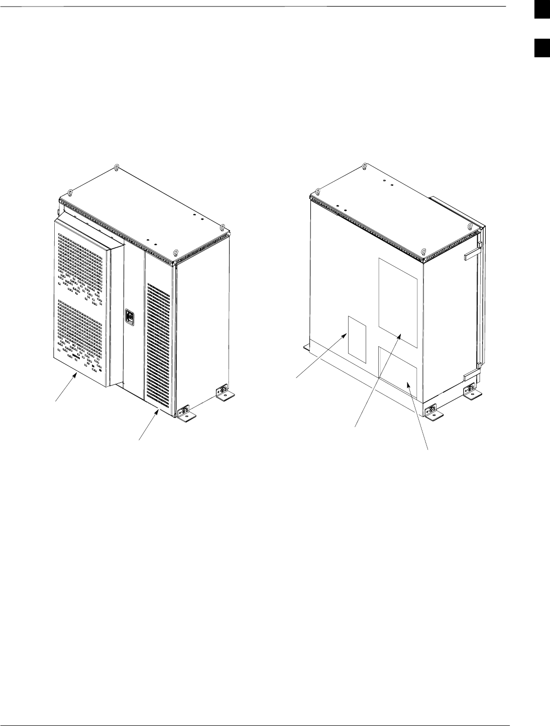
Cabinet Identification
08/01/2001 1-17
1X SCt4812ET Lite BTS Optimization/ATP
PRELIMINARY
Major Components
Figure 1-2 illustrates the features of the BTS frame, the single major
component of the Motorola SC4812ET Lite.
Figure 1-2: SC4812ET Lite BTS Frame
Battery Compartment Door
(Can only be opened after Main Door is open) RF Interface Panel
SCCP Shelf Backplane
Rear Access Panel
Power Entry
and
Network Interface Compartment
SC4812ETL0001–1
Main Door
with Heat Exchanger
1
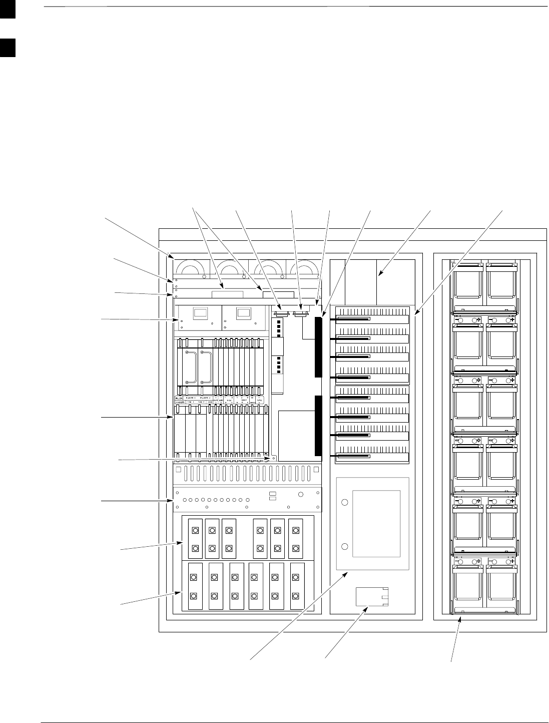
Internal Assembly Location and Identification
PRELIMINARY
1X SCt4812ET Lite BTS Optimization/ATP 08/01/2001
1-18
Internal Assemblies and FRUs
Figure 1-3 shows the location of the internal assemblies and Field
Replaceable Units (FRU). A brief description of each item is found in
the following paragraphs.
Figure 1-3: Internal Assemblies and FRUs
(Cabinet doors not shown for clarity)
LPAs
SCCP Fans
LPA Trunking
Module
RFDS
SCCP Shelf
Filter/Combiner
Shelf (Bandpass
filters shown)
ETIB
DRDC/TRDC
Shelf
CSU Shelf
MAP
Rectifiers
DC PDA
GFCI Utility
Outlet
LPAC
Back–up Batteries
(Heaters underneath batteries)
External
Blower
Assembly
SC4812ETL0002–4
ACLC
Span I/O
ASpan I/O
B
CSUs
ESD Grounding
Jack
1

Internal Assembly Location and Identification – continued
08/01/2001 1-19
1X SCt4812ET Lite BTS Optimization/ATP
PRELIMINARY
AC Load Center (ACLC)
The ACLC is the frame entry point for AC power. It incorporates AC
power control, distribution, and surge protection (Figure 1-3).
Back–up Batteries
The batteries (Figure 1-3) provide +24 Vdc back–up for the frame should
AC power be interrupted. The frame can accommodate a total of 12 12V
batteries grouped in six strings. Each string consists of two batteries
connected in series for 24 Vdc output. The six strings are connected in
parallel to meet the current–draw requirements of the frame. The
maximum time duration of the back–up capability depends on system
configuration.
Battery Heaters
The battery heater pads warm the batteries to provide improved
cold–weather performance. A separate heater pad is required for each
battery string and is located between each battery string and its
respective support shelf.
Channel Service Units (CSU) (Optional)
The SC4812ET Lite can be equipped with up to two M–PATH 537 CSU
or two M–PATH 437 CSU modules which install in the CSU shelf
(Figure 1-3). These modules allow monitoring of span performance and
provide capability for remote network management.
CSU Shelf
The CSU shelf is an ADC Kentrox 2–slot Universal Shelf which can
accommodate two M–PATH 537 or two M–PATH 437 CSU modules.
When the optional CSU modules are not installed, cover plates are
installed over the CSU card slots (Figure 1-3).
DC Power Distribution Assembly (PDA)
Both rectifier output voltage and back–up battery voltage are routed to
the PDA (Figure 1-3) where they are combined into system DC bus
voltage. The PDA provides distribution of DC power and system DC
bus protection from the loads with MAIN BREAKER and the smaller
post–distribution circuit breakers. MAIN BREAKER permits removal of
all frame loading from the bus. The 13 post–distribution circuit breakers
permit removal of individual loads.
Duplexer, Receive filter, Dual Directional Coupler (DRDC)
DRDCs permit duplexing of sector transmit and receive signals on a
single antenna. The DRDCs also incorporate a receive bandpass filter
and dual directional couplers which permit signal monitoring by the RF
Diagnostic Subsystem.
ET Interface Board (ETIB) and LPA Control (LPAC) Board
The ETIB is an interconnect module with status LEDs, MMI recepticles,
and secondary surge protection for the LPA modules. The LPAC board
provides the interface for the LPA connections (Figure 1-3).
1
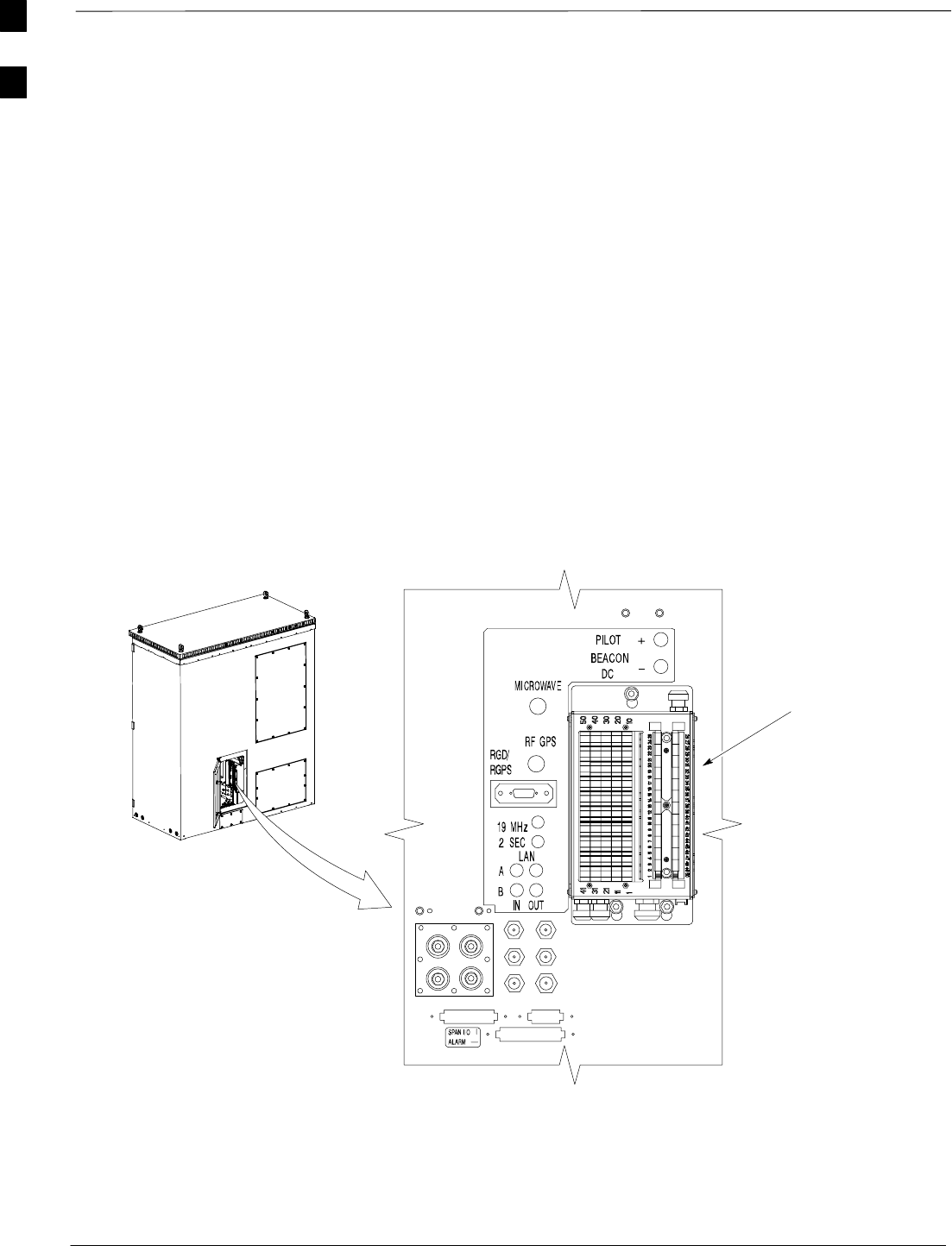
Internal Assembly Location and Identification – continued
PRELIMINARY
1X SCt4812ET Lite BTS Optimization/ATP 08/01/2001
1-20
Filter/Combiner Shelf (Bandpass Filters or 2:1 Combiners)
The filter/combiner shelf (Figure 1-3) holds the transmit bandpass filters
or 2:1 combiners, depending on system configuration.
Heat Exchanger
The heat exchanger provides cooling to the frame RF compartment. The
fan speed of the heat exchanger adjusts automatically with temperature.
The heat exchanger is located in the frame main door (Figure 1-2).
Punchblock
The punchblock (Figure 1-4) is the interface between the frame and the
T1/E1 span lines. It is located on the right–hand side of the power entry
compartment at the rear of the frame. The punchblock provides the
initial interconnection between the spans and the Customer–defined I/O,
alarms, multi–frame timing source (RGPS and RHSO), and pilot beacon
control (optional).
Figure 1-4: 50–Pair Punchblock
SC4812ETL0024–1
Rear of Frame
(Power Entry Compartment
Door Open)
Section of Network Interface Panel
(Rotated 30_ Right)
50–Pin
Punchblock
(Cabling not
shown for
clarity)
1

Internal Assembly Location and Identification – continued
08/01/2001 1-21
1X SCt4812ET Lite BTS Optimization/ATP
PRELIMINARY
Rectifiers
The rectifiers (Figure 1-3) convert AC power supplied to the frame to
+27.4 Vdc which powers the frame and maintains the charge of the
back–up batteries. Rectifier positions are numbered 1 through 4 from left
to right when facing the frame. Single–carrier frames are equipped with
three rectifiers installed in positions 1, 2, and 3. Two–carrier frames are
equipped with four rectifiers. The number of rectifiers supplied with
each configuration provides N+1 redundancy.
RF Diagnostic Subsystem (RFDS)
The RFDS (Figure 1-5) provides the capability for remotely monitoring
the status of the SC4812ET Lite transmit and receive paths. For
IS–95A/B operation, the RFDS is a COBRA model. To support 1X
operation, the RFDS must the 1X–capable COBRA–II.
Small CDMA Channel Processor (SCCP) Shelf
The SCCP shelf has provisions for the following types and quantities of
modules (Figure 1-3 and Figure 1-5):
SAlarm Monitoring and Reporting (AMR) cards (2)
SBroadband Transceiver (BBX2 or BBX–1X) cards, primary (6)
SBBX2 or BBX–1X card, redundant (1)
SCDMA Clock Distribution (CCD) cards (2)
SClock Synchronization Manager (CSM) on two cards (one with GPS
receiver, if ordered)
SCombiner Input/Output (CIO) card (1)
SFan modules (2)
SFiller panel (as required)
SGroup Line Interface (GLI2) cards (2)
SHigh Stability Oscillator (HSO)/Low Frequency Receiver (LFR) card
(Optional) (1)
SMulti–coupler Preselector Cards (MPC3) (2)
SMulti–Channel CDMA (MCC8E, MCC24, or MCC–1X) cards (4)
SPower supply cards (2)
SSwitch card (1)
1
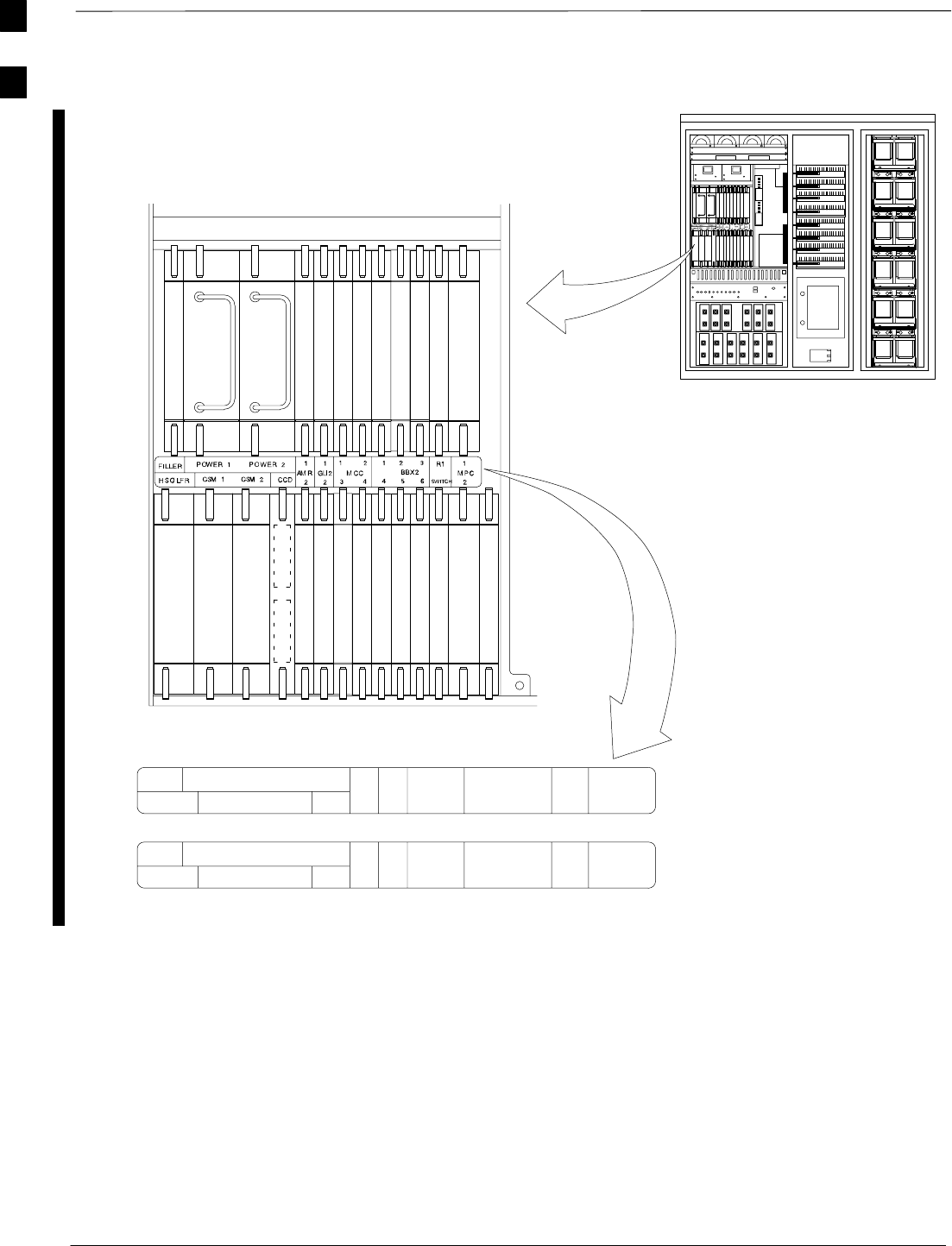
Internal Assembly Location and Identification – continued
PRELIMINARY
1X SCt4812ET Lite BTS Optimization/ATP 08/01/2001
1-22
FILLER POWER 1 POWER 2
HSO/LFR CSM 1 CSM 2 CCD AMR GLI2
1 2
3 4
MCC
1 2 3
4 5 6
BBX2 R1
SWITCH
1
2
1
2
1
2
MPC
FILLER POWER 1 POWER 2
HSO/LFR CSM 101 CSM 102 CCD AMR GLI2
101 102
MCC
101 102 103
BBX2 R101
SWITCH
102
1
2
MPC
101 101
102 103 104 104 105 106
MPC
CSM
Power Supply
Power Supply
MPC
CSM
CCDCCD
AMR
HSO
AMR
GLI2 GLI2
MCC8 E or MCC24
BBX2
BBX2
BBX2
BBX2
BBX2
BBX2
SWITCH
19mm Filler Panel
BBX2
CIO
FRAME 1
FRAME 101
(Expansion Frame)
MCC8 E or MCC24 MCC8 E or MCC24
MCC8 E or MCC24
Figure 1-5: SCCP Shelf, IS–95A/B and 1X Devices
SC4812ETL0003–4
NOTES:
1. MCCs may be MCC8Es, MCC24s, or
MCC–1Xx
2. BBXx may be BBX2s or BBX–1Xs
Span I/O Boards
The two span I/O boards, Span I/O A and Span I/O B (Figure 1-3),
provide the span line interface from the punchblock or the CSU
modules, if equipped, to the SCCP backplane.
Transmit & receive, non–duplexed, Receive filter, Dual
Directional Coupler (TRDC)
TRDCs provide separate, bandpass–filtered sector transmit and receive
paths. When TRDCs are used separate transmit and receive antennas are
required for each sector. As with DRDCs, TRDCs dual directional
couplers for each antenna path which permit signal monitoring by the
RFDS.
1
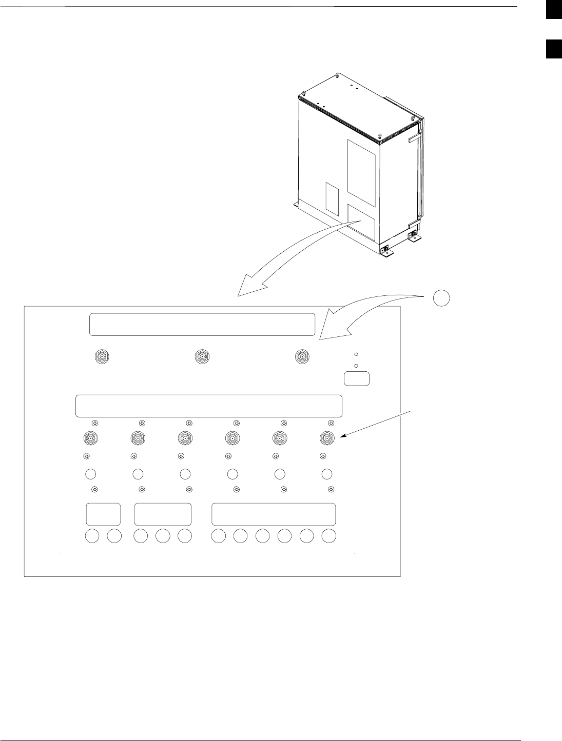
Internal Assembly Location and Identification – continued
08/01/2001 1-23
1X SCt4812ET Lite BTS Optimization/ATP
PRELIMINARY
Figure 1-6: RF Interface Panel, DRDCs Installed
TX IN
GROUND
123
1A 2A 3A 1B 2B 3B
ANTENNAS
REMOTE ASU
12
TX OUT
123 1A 2A 3A 1B 2B 3B
RX EXPANSION
SC4812ETL0018–2
NOTE: Plugs are installed
when TX IN combiners
are not fitted.
DUPLEXED TX &
RX PORTS
NOTES:
1. CARRIER 1 TX/RX
USES ANTENNA
PORTS 1A, 2A, 3A;
RX DIVERSITY
FROM PORTS 1B,
2B, 3B.
2. CARRIER 2 TX/RX
USES ANTENNA
PORTS 1B, 2B, 3B;
RX DIVERSITY
FROM PORTS 1A,
2A, 3A.
1
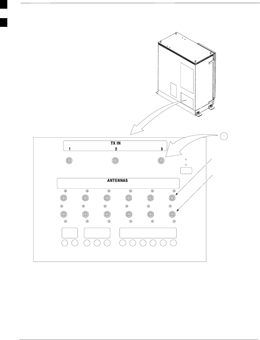
Internal Assembly Location and Identification – continued
PRELIMINARY
1X SCt4812ET Lite BTS Optimization/ATP 08/01/2001
1-24
Figure 1-7: RF Interface Panel, TRDCs Installed
GROUND
1A 2A 3A 1B 2B 3B
REMOTE ASU
1 2
TX OUT
1 2 3 1A 2A 3A 1B 2B 3B
RX EXPANSION
RX PORTS
TX PORTS
NOTES:
1. CARRIER 1 TX USES
TX PORTS 1A, 2A, 3A;
CARRIER 1 RX USES
RX PORTS 1A, 2A, 3A;
CARRIER 1 RX
DIVERSITY USES RX
PORTS 1B, 2B, 3B
2. CARRIER 2 TX USES
TX PORTS 1B, 2B, 3B;
CARRIER 2 RX USES
RX PORTS 1B, 2B, 3B;
CARRIER 2 RX
DIVERSITY USES RX
PORTS 1A, 2A, 3A
SC4812ETL0019–2
NOTE: Plugs are installed
when TX IN combiners
are not fitted.
1
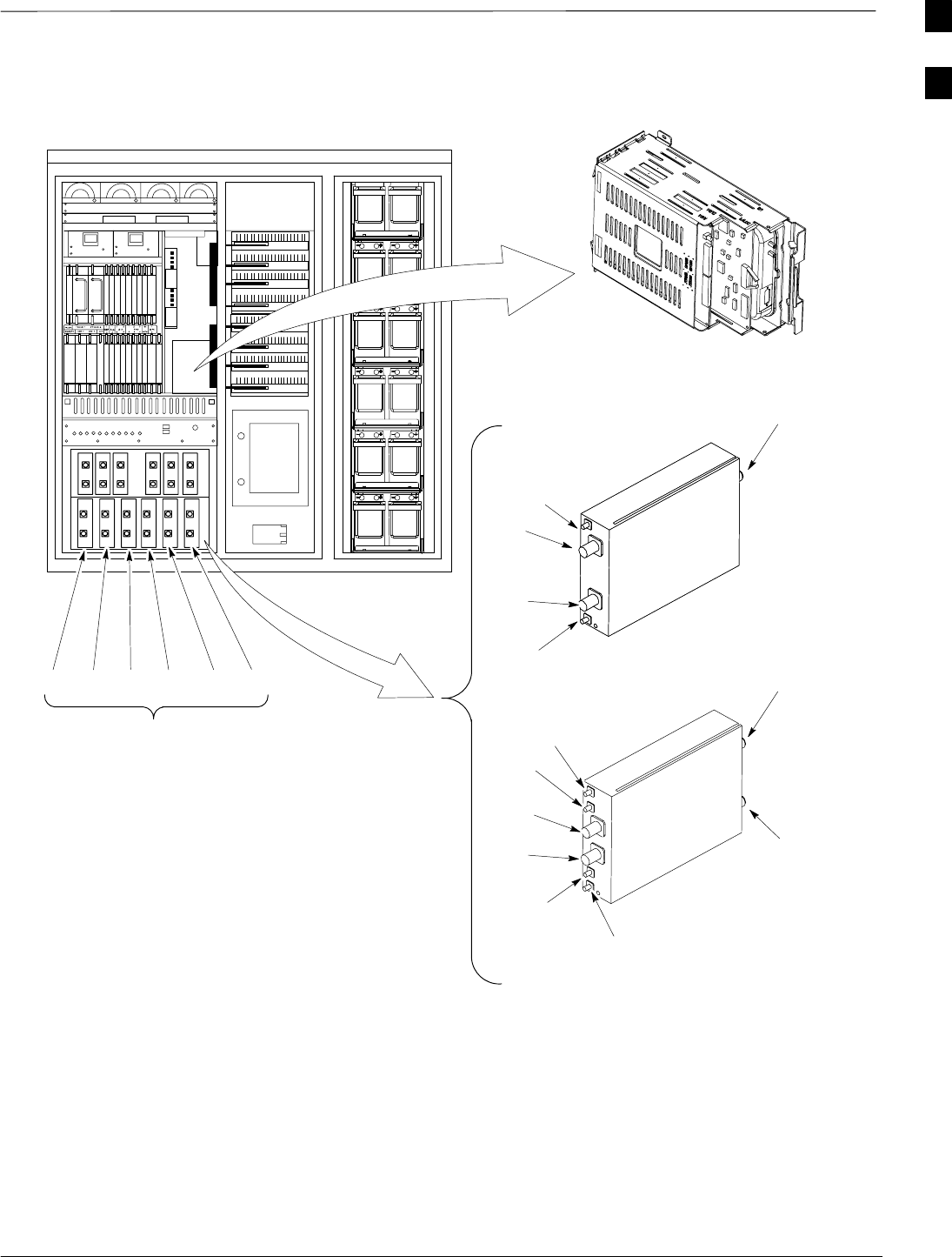
Internal Assembly Location and Identification – continued
08/01/2001 1-25
1X SCt4812ET Lite BTS Optimization/ATP
PRELIMINARY
Figure 1-8: RFDS, DRDC, and TRDC Details
BTS
CPLD
ANT
CPLD
DRDC
RFDS
SC4812ETL0005–3
TRDC
TX BTS
CPLD
RX BTS
CPLD
TX ANT
CPLD
RX ANT
CPLD
TX
RX
DUPLEXED
TX & RX ANTENNA
TX
ANTENNA
RX
ANTENNA
TX
RX
1A1B 2A2B3B 3A
DRDC/TRDC
ANTENNA CONNECTOR
ASSIGNMENTS
1

Internal Assembly Location and Identification – continued
PRELIMINARY
1X SCt4812ET Lite BTS Optimization/ATP 08/01/2001
1-26
SCCP Cage Configuration and
the 1X Devices
SC4812ET Lite frames have one SCCP cage which will support up to 4
MCC cards and 6 BBX cards.
MCC Cards
A BTS may be configured with a mix of MCC–8E, MCC–24, and
MCC–1X cards. Any MCC card slot will support any of the three MCC
types. For 1X capability under R16.0, at least one MCC card must be an
MCC–1X which can be installed in any MCC card slot.
BBX Cards
Up to 6 BBX cards of mixed BBX2s and BBX–1Xs can also be
supported. BBX card slots 1 through 6 are carrier– and
sector–dependent. As a result, the BBX slots dedicated to the sectors for
one carrier should be populated with the same type of cards. Refer to
Table 1-5 for BBX card slot carrier and sector correlations.
The BBX–R1 card slot is dedicated to the redundant BBX. This slot will
support either a BBX2 or a BBX–1X. If a cage has BBX–1X carriers,
the redundant BBX (BBXR) must be a BBX–1X card to provide 1X
redundancy support.
1

BTS Sector Configurations
08/01/2001 1-27
1X SCt4812ET Lite BTS Optimization/ATP
PRELIMINARY
Sector Configuration
There are a number of ways to configure the BTS frame. Table 1-4
outlines the basic requirements. For more detailed information also see
Table 1-5 and Figure 1-9. Bandpass filters are used for single–carrier
configurations and two–carrier systems when carriers are either adjacent
or not adjacent
Table 1-4: BTS Sector Configuration
Number of
Carriers Number of
Sectors Channel Spacing Filter/Combiner Requirements
1 3 N/A Bandpass Filter
2 3 Adjacent or
Non–adjacent Bandpass Filter
The matrix in Table 1-5 shows the correlation between the various sector
configurations and BBX cards.
1
BTS Sector Configurations – continued
PRELIMINARY
1X SCt4812ET Lite BTS Optimization/ATP 08/01/2001
1-28
Table 1-5: Sector Configurations
Configuration Description
3–Sector / 1 Carrier
The configuration below maps RX and TX with bandpass filters for a 3–sector/1–carrier frame.
ANT 1A ANT 2A ANT 3A ANT 1B ANT 2B ANT 3B
1TX1 / RX1A TX2 / RX2A TX3 / RX3A RX1B RX2B RX3B Carrier #
BBX2–1 BBX2–2 BBX2–3 BBX2–1
(diversity
RX)
BBX2–2
(diversity
RX)
BBX2–3
(diversity
RX)
1
3–Sector / 2–ADJACENT or 2–NON–ADJACENT Carriers
The configuration below maps RX and TX with bandpass filters for 3–sectors/2–carriers for both
adjacent and non–adjacent channels.
ANT 1A ANT 2A ANT 3A ANT 1B ANT 2B ANT 3B
TX1 / RX1A TX2 / RX2A TX3 / RX3A TX4 / RX1B TX5 / RX2B TX6 / RX3B Carrier #
2BBX2–1 BBX2–2 BBX2–3 BBX2–1
(diversity
RX)
BBX2–2
(diversity
RX)
BBX2–3
(diversity
RX)
1
BBX2–4
(RX) BBX2–5
(RX) BBX2–6
(RX) BBX2–4
(TX &
diversity
RX)
BBX2–5
(TX &
diversity
RX)
BBX2–6
(TX &
diversity
RX)
2
Figure 1-9: SC4812ET Lite LPA Configuration with Bandpass Filters
(Starter Frame Mapping Only)
Table 1-5
Configuration Numbers 1 and 2
3–Sector
Bandpass Filters
CARRIER 1
SECTOR 1, 2, 3
CARRIER 2
SECTOR 1, 2, 3
SC4812ETL0011–3
1

08/01/2001 1X SCt4812ET Lite BTS Optimization/ATP
PRELIMINARY
Chapter 2: Preliminary Operations
Table of Contents
Preliminary Operations: Overview 2-1. . . . . . . . . . . . . . . . . . . . . . . . . . . . . . . . . . .
Introduction 2-1. . . . . . . . . . . . . . . . . . . . . . . . . . . . . . . . . . . . . . . . . . . . . .
Cellsite Types 2-1. . . . . . . . . . . . . . . . . . . . . . . . . . . . . . . . . . . . . . . . . . . . .
CDF 2-1. . . . . . . . . . . . . . . . . . . . . . . . . . . . . . . . . . . . . . . . . . . . . . . . . . . .
Site Equipage Verification 2-1. . . . . . . . . . . . . . . . . . . . . . . . . . . . . . . . . . .
Initial Installation of Boards/Modules 2-1. . . . . . . . . . . . . . . . . . . . . . . . . .
Setting Frame SCCP Configuration Switch 2-2. . . . . . . . . . . . . . . . . . . . .
Ethernet LAN 2-3. . . . . . . . . . . . . . . . . . . . . . . . . . . . . . . . . . . . . . . . . . . . . . . . . . .
Ethernet LAN Termination 2-3. . . . . . . . . . . . . . . . . . . . . . . . . . . . . . . . . .
Initial Power Up 2-4. . . . . . . . . . . . . . . . . . . . . . . . . . . . . . . . . . . . . . . . . . . . . . . . .
Introduction 2-4. . . . . . . . . . . . . . . . . . . . . . . . . . . . . . . . . . . . . . . . . . . . . .
Required Tools 2-4. . . . . . . . . . . . . . . . . . . . . . . . . . . . . . . . . . . . . . . . . . . .
Cabling Inspection 2-4. . . . . . . . . . . . . . . . . . . . . . . . . . . . . . . . . . . . . . . . .
Initial Inspection and Setup 2-4. . . . . . . . . . . . . . . . . . . . . . . . . . . . . . . . . .
DC Power System Pre-Power Application Test 2-7. . . . . . . . . . . . . . . . . .
External AC Power Connection Verification 2-9. . . . . . . . . . . . . . . . . . . . .
Applying AC Power 2-12. . . . . . . . . . . . . . . . . . . . . . . . . . . . . . . . . . . . . . .
DC Power Application and Testing 2-14. . . . . . . . . . . . . . . . . . . . . . . . . . . .
Battery Charge Test (Connected Batteries) 2-15. . . . . . . . . . . . . . . . . . . . . .
Battery Discharge Test 2-16. . . . . . . . . . . . . . . . . . . . . . . . . . . . . . . . . . . . . .
Power Removal Procedure 2-17. . . . . . . . . . . . . . . . . . . . . . . . . . . . . . . . . . .
2

Table of Contents – continued
PRELIMINARY
1X SCt4812ET Lite BTS Optimization/ATP 08/01/2001
Notes
2
Preliminary Operations: Overview
08/01/2001 2-1
1X SCt4812ET Lite BTS Optimization/ATP
PRELIMINARY
Introduction
This section first verifies proper frame equipage. This includes verifying
module placement, jumper, and dual in–line package (DIP) switch
settings against the site-specific documentation supplied for each BTS
application. Next, pre-power up and initial power-up procedures are
presented.
Cellsite Types
Sites are configured as 3–sector with one or two carriers. Each type has
unique characteristics and must be optimized accordingly.
CDF
The Cell-site Data File (CDF) contains site type and equipage data
information and passes it directly to the CDMA Local Maintenance
Facility (LMF) during optimization. The number of BTS frames, BBX2
and MCC24 boards, and linear power amplifier assignments are some of
the equipage data included in the CDF.
Site Equipage Verification
Review the site documentation. Match the site engineering equipage data
to the actual boards and modules shipped to the site. Physically inspect
and verify the equipment provided for the frame.
Always wear a conductive, high impedance wrist strap
while handling any circuit card/module to prevent damage
by ESD. After removal, the card/module should be placed
on a conductive surface or back into the anti–static bag it
was shipped in.
CAUTION
Initial Installation of
Boards/Modules
Table 2-1: Initial Installation of Boards/Modules
Step Action
1Refer to the site documentation and, if it was not previously done, slide all boards and modules into
the appropriate shelves as required. DO NOT SEAT the boards and modules at this time.
2As the actual site hardware is installed, record the serial number of each module on a “Serial Number
Checklist” in the site logbook.
2
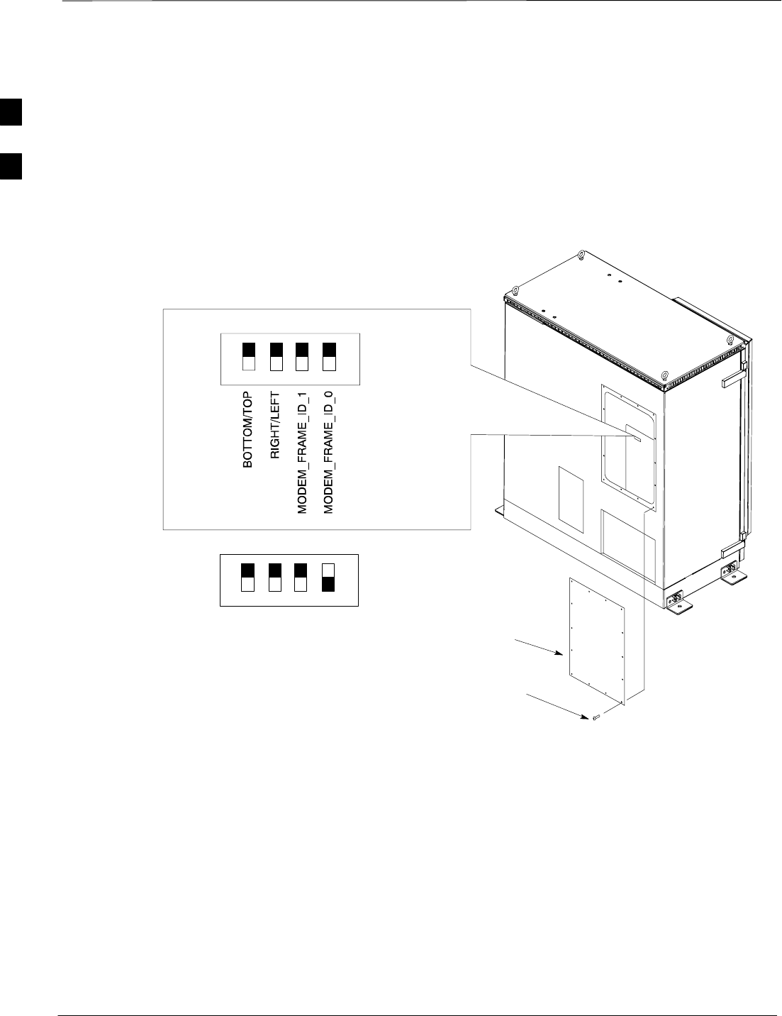
Preliminary Operations: Overview – continued
PRELIMINARY
1X SCt4812ET Lite BTS Optimization/ATP 08/01/2001
2-2
Setting Frame SCCP
Configuration Switch
The backplane configuration switch is located behind the frame rear
access panel. It must be set for the frame type as shown in Figure 2-1.
The switch setting must be verified and set before power is applied to the
BTS equipment.
Figure 2-1: Backplane DIP Switch Settings
SC4812ETL0022–1
ON
OFF
STARTER
FRAME SETTING
(FRAME 1)
ON
OFF
BOTTOM / TOP
RIGHT / LEFT
MODEM_FRAME_ID_1
MODEM_FRAME_ID_0
EXPANSION
FRAME SETTING
(FRAME 101)
REAR ACCESS
PANEL
T–27 BUTTON HEAD OR
T–30 PAN HEAD
TAMPER–RESISTANT
FASTENER (14)
2
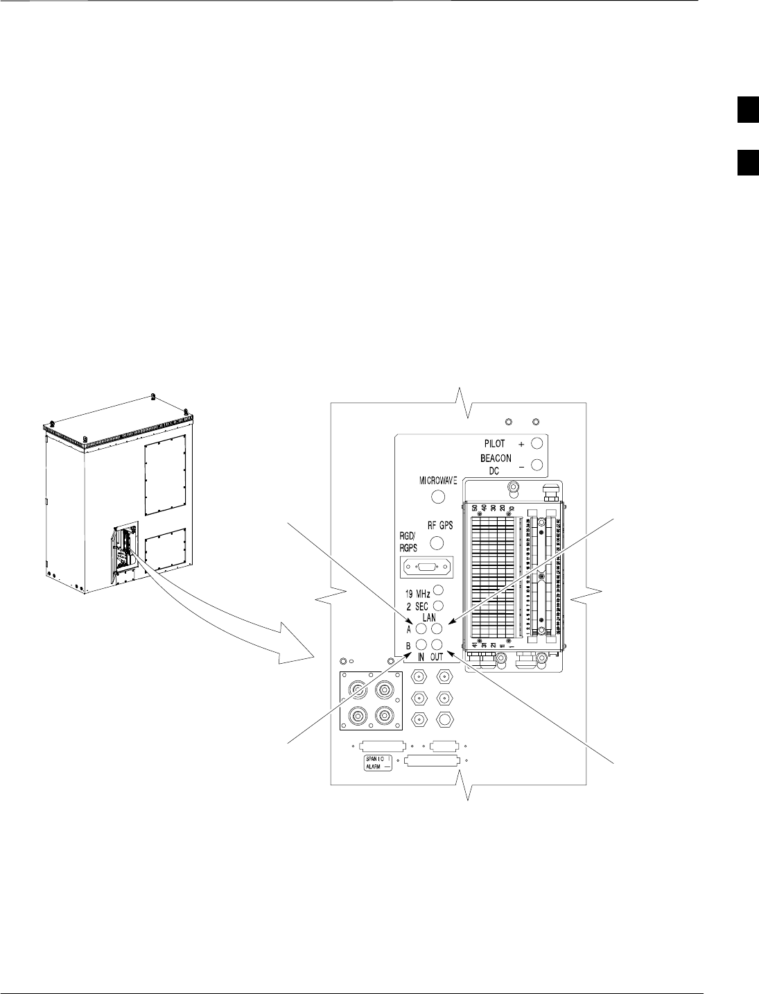
Ethernet LAN
08/01/2001 2-3
1X SCt4812ET Lite BTS Optimization/ATP
PRELIMINARY
Ethernet LAN Termination
For proper operation, each end of the primary and redundant BTS
Ethernet Local Area Networks (LAN) must be terminated with a
50–ohm load. For a BTS consisting of a single frame, this is done by
placing 50–ohm triaxial terminations on the LAN A and B external IN
and OUT connectors located in the power entry compartment
(Figure 2-2). When the LAN links multiple frames in a logical BTS, the
50–ohm triaxial terminations must be installed on all uncabled LAN A
and B external connectors on each frame.
Check the LAN A and B external IN and OUT connectors in the power
entry compartment of each frame, and be sure terminations are installed
on all the uncabled external LAN connectors.
Figure 2-2: External Ethernet LAN Connectors
SC4812ETL0024–2
Rear of Frame
(Power Entry Compartment
Door Open)
Section of Network Interface Panel
(Rotated 30_ Right)
LAN A OUT
LAN B OUT
LAN A IN
LAN B IN
2
Initial Power Up
PRELIMINARY
1X SCt4812ET Lite BTS Optimization/ATP 08/01/2001
2-4
Introduction
The following information is used to check for any electrical short
circuits and to verify the operation and tolerances of the cell site and
BTS power supply units before applying power for the first time. It
contains instructional information on the proper initial power up
procedures for the SC4812ET Lite for both the North American version
and the International version. If directions are different for either version,
they are called out within the procedure. Please pay attention to all
cautions and warning statements in order to prevent accidental injury to
personnel.
Required Tools
The following tools are used in the procedures.
SClamp–on DC current probe (600 amp capability with jaw size to
accommodate 2/0 cable).
SDigital Multimeter (DMM) with standard 2mm (.080”) tip probes
SHot Air Gun – (optional for part of the Alarm Verification)
Cabling Inspection
Using the site-specific documentation generated by Motorola Systems
Engineering, verify that the following cable systems are properly
connected:
SReceive RF cabling – up to six RX cables
STransmit RF cabling – up to six TX cables
For DC power applications (+27 V):
SThe positive power cable is red.
SThe negative power cable is black. (The black power
cable is at ground potential.)
IMPORTANT
*
Initial Inspection and Setup
Ensure all battery shelf circuit breakers (Figure 2-3) for
unused battery positions are off (pulled out) before and
during the entire power up process. Leave these breakers in
the off position when leaving the site.
CAUTION
Table 2-2: Initial Inspection and Setup
Step Action
1Be sure that the facility circuit breaker controlling external AC power supplied to the frame is set to
OFF.
2Be sure that all AC Load Center (ACLC), all DC Power Distribution Assembly (PDA), and all battery
shelf circuit breakers are turned OFF.
. . . continued on next page
2
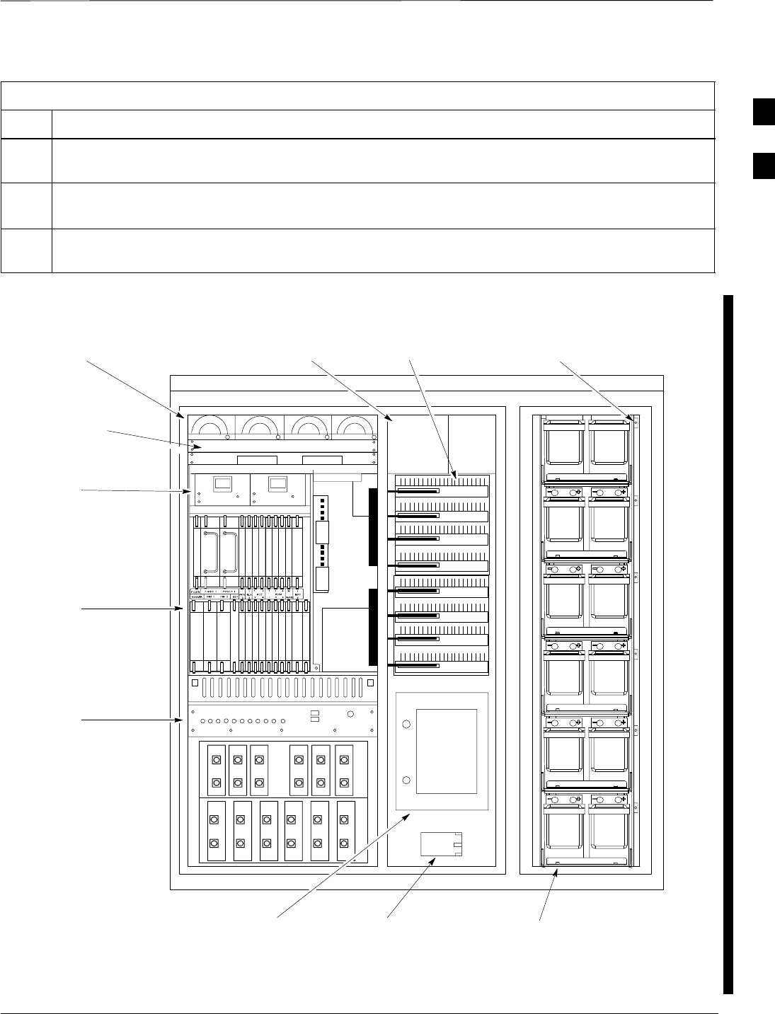
Initial Power Up – continued
08/01/2001 2-5
1X SCt4812ET Lite BTS Optimization/ATP
PRELIMINARY
Table 2-2: Initial Inspection and Setup
Step Action
3Confirm that the Meter Alarm Panel (MAP) POWER switch and all LEDs (Figure 2-9) are OFF. If
any LEDs are lighted, re–check and turn OFF all battery shelf circuit breakers.
4If a heat source was placed in the RF compartment to prevent condensation prior to BTS power–up,
turn off the heat source and remove it and any associated cabling from the BTS before proceeding.
5Confirm that the external 220 Vac supply is correctly connected to the ACLC input by performing the
procedure in Table 2-4.
Figure 2-3: Frame Power Subassemblies, North American and
International Cabinets
LPAs
SCCP Fans
RFDS
SCCP Shelf
ETIB
Meter Alarm
Panel (MAP)
With TCU
AC Rectifiers
DC PDA
Backup Batteries
(Heaters underneath batteries)
External Blower
Assembly
SC4812ETL0002–3
Battery Shelf
Circuit Breakers
(Between Bus Bar
and Cabinet Wall)
Utility
Outlet
ACLC Circuit Breaker
Access Door
NOTE:
GFCI capability is built into the Utility Outlet of the North American Cabinet.
GFCI capability is built into the circuit breakers of the International Cabinet
2
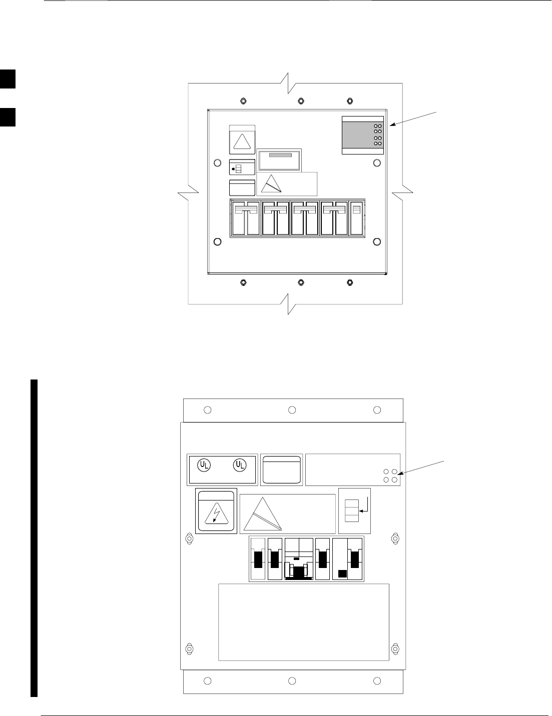
Initial Power Up – continued
PRELIMINARY
1X SCt4812ET Lite BTS Optimization/ATP 08/01/2001
2-6
Figure 2-4: ACLC Circuit Breaker Panel – North American
LEDs
SC4812ETL0008–1
ATTENTION
CAUTION
LIVE TERMINALS
RECT. 1/3 RECT. 2/4 GFIHEATERMAIN
ATTENTION
CAUTION
LIVE TERMINALS
Figure 2-5: ACLC Circuit Breaker Panel – International
LEDs
RECT 1/3 RECT 2/4 MAIN HEATER GFI
JOCYLN
ELECTRONIC SYSTEMS
2
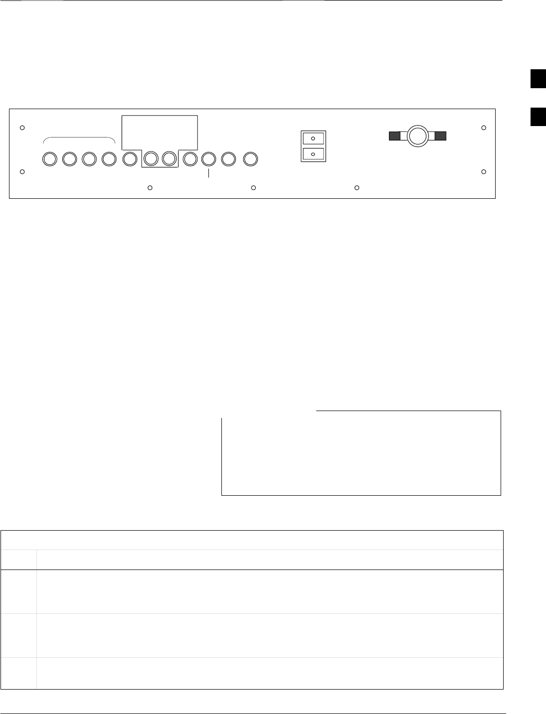
Initial Power Up – continued
08/01/2001 2-7
1X SCt4812ET Lite BTS Optimization/ATP
PRELIMINARY
Figure 2-6: DC PDA
SC4812ETL0009–3
LPA
1B 1D 3B 3D
1A 1C 3A 3C PS1 PS2
ETIB
OPTIONS
25 25
HEAT EXCHANGER
CAUTION
SHUT OFF BOTH BREAKERS
ONLY DURING HEAT EXCHANGER
MAINTENANCE OR REPAIR
LPA
BLOWERS
PUSH BUTTON
TO RESET
LPA BLOWERS
MAIN BREAKER
300
50 5010 1530 30 30 30 15
PILOT
BEACON
DC Power System Pre-Power
Application Test Before applying any power to the BTS frame, follow the procedure in
Table 2-3 to verify there are no shorts in the DC power distribution
system.
The procedure in Table 2-3 is required only on initial BTS
power–up or following maintenance when any major
power components (e.g., ACLC, DC PDA, Meter Alarm
Panel) were replaced or internal DC power cables were
disconnected.
NOTE
Table 2-3: DC Power System Pre–Power Application Test
Step Action
1Physically verify all ACLC front–panel circuit breakers (Figure 2-4) are OFF (down), all DC PDA
circuit breakers (Figure 2-6) are set to OFF (pulled out), and all battery shelf circuit breakers
(Figure 2-3) are OFF (pulled out).
2Visually ensure that all AC rectifier modules (Figure 2-3) are not powered (DC, PWR, and bar graph
LEDs are not lighted), that the MAP power switch (Figure 2-9) is OFF, and that no LEDs on the
MAP are lighted.
3Inside the battery compartment, measure the voltage between the + (red) and – (black) battery bus
bars. There should be no 27 Vdc present.
. . . continued on next page
2

Initial Power Up – continued
PRELIMINARY
1X SCt4812ET Lite BTS Optimization/ATP 08/01/2001
2-8
Table 2-3: DC Power System Pre–Power Application Test
Step Action
4* IMPORTANT
Do not unseat the AC rectifier modules in the following step.
Perform the following:
SIn the frame RF compartment, unseat all circuit boards/ modules (except CCD and CIO cards) in the
SCCP shelf, but leave them in their respective slots.
SIn the frame LPA compartment, disconnect the Linear Power Amplifier (LPA) cables from the
compartment bulkhead feed through connector.
5Set the DMM to measure resistance, and inside the battery compartment, measure the resistance
between the + (red) and – (black) battery bus bars. The resistance should measure > 1 ΜΩ.
6Leave the DMM set to measure resistance, and insert the probes into the MAP VOLT and AMP TEST
POINTS (Figure 2-9). Place the (+) DMM probe into the (–) AMP TEST POINT. Place the (–) DMM
probe into the (–) VOLT TEST POINT. Resistance should measure greater than 750 Ω.
7On the DC PDA, set the MAIN BREAKER to the ON position by pushing it in. Resistance between
the MAP (–) VOLT TEST POINT and the (–) AMP TEST POINT should measure between 300 Ω.
minimum 900 Ω. maximum.
8Before proceeding, be sure the SCCP shelf power/converter modules PS1 and PS2 are correct by
verifying that the locking/retracting tabs appear as follows:
– (in +27 volt systems)
! CAUTION
Using the incorrect type of power/converter modules will damage the module, the SCCP shelf, and
other modules installed in the SCCP shelf.
9* IMPORTANT
In the following steps, if the DMM reads between 300 Ω minimum and 900 Ω maximum after
inserting any board/module, a low impedance problem probably exists in that board/module. Replace
the suspect board/module and repeat the test. If test still fails, isolate the problem before proceeding.
Insert and lock the PS1 DC–DC converter module into its slot, and and turn ON the PS1 DC circuit
breaker on the DC PDA.
10 Resistance between the MAP (–) VOLT TEST POINT and the (–) AMP TEST POINT should
typically increase as capacitors charge, finally measuring between 300 Ω minimum and 900 Ω.
maximum.
11 Repeat steps 9 and 10 for the PS2 converter module/circuit breaker and all other remaining modules in
the SCCP shelf.
12 On the DC PDA, set the LPA 1A–1B circuit breaker to the ON position by pushing it in, and repeat
step 10.
13 Repeat step 12 for each of the three remaining LPA circuit breakers.
. . . continued on next page
2
Initial Power Up – continued
08/01/2001 2-9
1X SCt4812ET Lite BTS Optimization/ATP
PRELIMINARY
Table 2-3: DC Power System Pre–Power Application Test
Step Action
14 Carefully reconnect each LPA cable one at a time. Repeat step 10 after reconnecting each cable.
SA typical response is that the ohmmeter will steadily climb in resistance as module input capacitors
charge, finally indicating between 300 Ω minimum and 900 Ω. maximum.
15 Set the Pilot Beacon, both Heat Exchanger, ETIB, and Options circuit breakers to ON one at a time.
Repeat step 10 after pushing in each circuit breaker.
16 Set all DC PDA circuit breakers to OFF (pulled out).
Failure to properly connect the external AC power cable
will damage the surge protection module inside the ACLC.
CAUTION
External AC Power Connection
Verification
Following verification of frame DC power system integrity, external AC
power connections must be verified. To accomplish this, the series of AC
voltage measurements specified in Table 2-4 is required.
Table 2-4: AC Voltage Measurements
Step Action
1NOTE
This procedure is required only after external AC power wiring has been initially connected or
removed and reconnected to the frame.
n WARNING
Ensure the frame is unpowered by setting the facility circuit breaker controlling external AC power
supplied to the frame to OFF.
Physically verify all DC PDA circuit breakers are set to OFF (pulled out), and all battery shelf circuit
breakers are OFF (pulled out).
2Open the ACLC circuit breaker access door, and set all ACLC circuit breakers to OFF (down).
3Remove the four screws securing the ACLC front panel assembly, and remove the ACLC front panel
assembly to gain access to the AC circuit breaker input terminals (Figure 2-8).
4Apply external AC power to the frame by setting the facility circuit breaker to ON.
. . . continued on next page
2

Initial Power Up – continued
PRELIMINARY
1X SCt4812ET Lite BTS Optimization/ATP 08/01/2001
2-10
Table 2-4: AC Voltage Measurements
Step Action
5! CAUTION
North AMERICAN Cabinet only:
If the AC voltages measured in the following steps exceed 120 V when measuring from terminals L1
or L2 to neutral or ground, STOP and DO NOT proceed until the cause of the higher voltages are
determined. The frame will be damaged if the Main breaker is turned on with excessive voltage on the
inputs.
Measure the AC voltage from terminal L1 to neutral.
North American Cabinet:
SVoltage should be in the nominal range of 115 to 120 Vac.
International Cabinet:
SVoltage should be in the nominal range of 210 to 240 Vac.
6Measure the AC voltage from terminal L1 to ground.
North American Cabinet:
SVoltage should be in the nominal range of 115 to 120 Vac.
International Cabinet:
SVoltage should be in the nominal range of 210 to 240 Vac.
7Steps 7a through 7c apply to the North American cabinet only. If working on a International cabinet
continue to step 8.
7a Measure the AC voltage from terminal L2 to neutral on the North American cabinet.
SVoltage should be in the nominal range of 115 to 120 Vac.
7b Measure the AC voltage from terminal L2 to ground on the North American cabinet.
SVoltage should be in the nominal range of 115 to 120 Vac.
7c ! CAUTION
If the AC voltages measured (on the North American cabinet) in the following step exceeds 240 V
when measuring between terminals L1 and L2, STOP and DO NOT proceed until the cause of the
higher voltages are determined. The frame will be damaged if the Main breaker is turned on with
excessive voltage on the inputs.
Measure from terminal L1 to terminal L2.
SVoltage should be in the nominal range from 208 to 240 Vac.
8Remove external AC power from the frame by setting the facility circuit breaker to OFF.
9Install the ACLC front panel assembly and secure with the four screws removed in step 1.
10 Apply external AC power to the frame by setting the facility circuit breaker to ON.
2
Initial Power Up – continued
08/01/2001 2-11
1X SCt4812ET Lite BTS Optimization/ATP
PRELIMINARY
Figure 2-7: ACLC Voltage Measurement Probe Points – North American
G= Ground
N = Neutral
L1 = Line 1
L2 = Line 2
GN
L2 L1
(ACLC front panel assembly
removed.)
2
Initial Power Up – continued
PRELIMINARY
1X SCt4812ET Lite BTS Optimization/ATP 08/01/2001
2-12
Figure 2-8: ACLC Voltage Measurement Probe Points – International
G= Ground
N = Neutral
L1 = Line 1
GN
L1
(ACLC front panel assembly
removed.)
Applying AC Power
Once the external AC power connections are verified, AC power may be
applied internally to the frame. Table 2-5 provides the procedure for
applying internal AC power.
Table 2-5: Applying Internal AC Power
Step Action
1Be sure the requirements of Table 2-4 for AC input power connection verification have been met.
2Be sure all DC PDA circuit breakers are set to OFF (pulled out), all ACLC front–panel circuit
breakers are OFF (down), and all battery shelf circuit breakers are OFF (pulled out).
. . . continued on next page
2
Initial Power Up – continued
08/01/2001 2-13
1X SCt4812ET Lite BTS Optimization/ATP
PRELIMINARY
Table 2-5: Applying Internal AC Power
Step Action
3Be sure the MAP power switch, TCP switch, and BATT TEST switch are all set to OFF.
4If it has not already been done, set the facility circuit breaker supplying AC power to the frame
to ON.
5Set the ACLC MAIN circuit breaker ON.
SFor the North American cabinet:
Observe that all eight (8) green LEDs on the front of the ACLC are illuminated (Figure 2-4).
SFor the International cabinet:
Observe that all four (4) green LEDs on the front of the ACLC are illuminated (Figure 2-4).
6On the ACLC, set RECT. 1/3 and RECT. 2/4 branch circuit breakers ON. All the installed rectifier
modules (Figure 2-3) will start up, and the green DC and PWR LEDs should light on each.
7Set the MAP power switch to ON. The MAP VOLT display should read 27.4 + 0.2 VDC with the
TCP switch OFF.
! CAUTION
Once power is applied to the MAP, be careful not to short either of the VOLT TEST POINTS to
ground. Failure to comply will result in severe damage to the MAP.
8On the MAP, set the TCP switch (Figure 2-9) to ON. Verify no alarm LEDs are lighted on the MAP.
NOTE
Depending on battery compartment temperature, the rectifier voltage displayed on the MAP VOLT
indicator may change by as much as +1.5 V when the TCP is set to on.
9Check the rectifier current bar graph displays (green LED display on the rectifier module). None
should be lighted at this time.
10 If batteries are fitted, set the ACLC HEATER circuit breaker to ON.
NOTE
The GFCI AC circuit breaker should remain OFF unless the GFCI outlet is in use.
Figure 2-9: Meter Alarm Panel (MAP)
POWER
SWITCH
POWER
INDICATOR
TCP
SWITCH VOLT TEST
POINTS
25_C SET
MASTER
VOLTAGE
ADJ.
BATT TEST
SWITCH
SC4812ETL0015–2
TO DISABLE
SENSOR FAIL
SENSOR 2
SENSOR 1
COMM
2

Initial Power Up – continued
PRELIMINARY
1X SCt4812ET Lite BTS Optimization/ATP 08/01/2001
2-14
DC Power Application and
Testing
Table 2-6 lists the step–by–step instructions for applying DC power and
ensuring the DC power system components are correctly functioning.
Table 2-6: DC Power Application and Tests
Step Action
1Be sure all DC PDA and battery shelf circuit breakers are OFF (pulled out).
2Be sure the procedures in Table 2-3 (if applicable) and Table 2-5 have been performed.
3! CAUTION
When measuring voltage at the VOLT TEST POINTS, be careful not to short either of the test points
to ground. Failure to comply will result in severe damage to the MAP.
Measure voltage at the MAP VOLT TEST POINTS while pressing the 25° C SET button
(Figure 2-9). The voltage should read 27.4 + 0.2 Vdc. Adjust with the MASTER VOLTAGE ADJ. on
the MAP, if necessary, to obtain an indicated 27.4+0.2 Vdc. Release the 25° C SET button.
4Depending on the ambient temperature, the voltage reading may now change by up to + 1.5 V
compared to the reading just measured. If it is cooler than 25_C, the voltage will be higher, and if it is
warmer than 25_C, the voltage will be lower.
5Inside the battery compartment, measure the voltage between the cable connection point at the bottom
of the + (red) battery bus bar and chassis ground, observing that the polarity is correct. The voltage
should be the same as the measurement in step 4.
6Measure the voltage between the + (red) and – (black) battery bus bars in the battery compartment.
Place the probe at the bottom of the bus bars where the cables are connected. The DC voltage should
measure the same as in step 4.
7Close (push in) DC PDA MAIN BREAKER.
8On the DC PDA(Figure 2-6), set the PS1 and PS2 circuit breakers to the ON position by pushing
them in one at a time while observing the rectifier output current indicated on the MAP AMP display.
–The display should indicate between 20 and 60 amps.
9On the DC PDA), set the remaining circuit breakers to the ON position by pushing them in one at a
time in the following sequence:
SLPA circuit breakers (four breakers, labeled 1A–1B through 3C–3D).
SHEAT EXCHANGER circuit breakers (two breakers)
SETIB circuit breaker
SPILOT BEACON circuit breaker
SOPTION circuit breaker
. . . continued on next page
2

Initial Power Up – continued
08/01/2001 2-15
1X SCt4812ET Lite BTS Optimization/ATP
PRELIMINARY
Table 2-6: DC Power Application and Tests
Step Action
10 Confirm that the MAP AMP display continues to indicate between 20 and 60 amps during the initial
power application.
NOTE
No battery charging or heavy RF loading is present at this point.
11 If the frame is not equipped with the pilot beacon option, set the PILOT BEACON circuit breaker
to OFF.
Battery Charge Test
(Connected Batteries)
Table 2-7 lists the step–by–step instructions for testing the battery
charging performance.
Table 2-7: Battery Charge Test (Connected Batteries)
Step Action
1Close the battery shelf circuit breakers (Figure 2-3) for connected batteries only. This process should
be completed quickly to avoid individual battery strings drawing excess charge current
NOTE
If the batteries are sufficiently discharged, the battery circuit breakers may not engage individually
due to the surge current. If this condition occurs, disconnect the batteries from the 27Vdc bus by
setting the MAP power switch to OFF, and then engage all the connected battery circuit breakers.
The MAP power switch should then be turned ON.
2Using the clamp–on DC current probe and DMM, measure the current in each of the battery string
connections to the battery bus bars. The charge current may initially be high but should quickly
reduce in a few minutes if the batteries have a typical new–battery charge level.
NOTE
The MAP AMP display will indicate the total current output of the rectifiers during this procedure.
As an alternative, the bar graph meters on the AC rectifier modules can be used as a rough estimate of
the total battery charge current. Each rectifier module bar graph has eight (8) LED elements to
represent the output current. Each illuminated LED element indicates that approximately 12.5% (1/8
or 8.75 Amps) of an individual rectifier’s maximum current output (70 Amps) is flowing.
RECTIFIER BAR GRAPH EXAMPLE:
Question: A system fitted with three (3) rectifier modules each have three bar graph LED elements
illuminated. What is the total output current into the batteries?
Answer: Each bar graph is indicating approximately 12.5% of 70 amps, therefore, 3 x 8.75 equals
26.25 amps per rectifier. As there are three rectifiers, the total charge current is equal to (3 x 26.25 A)
78.75 amps.
This charge current calculation is only valid when the RF and LPA compartment electronics are not
powered on, and the RF compartment heat exchanger is turned off. This can only be accomplished if
the DC PDA MAIN BREAKER is set to OFF.
. . . continued on next page
2

Initial Power Up – continued
PRELIMINARY
1X SCt4812ET Lite BTS Optimization/ATP 08/01/2001
2-16
Table 2-7: Battery Charge Test (Connected Batteries)
Step Action
3The current in each string should be approximately equal (within + 5 amps).
4Allow a few minutes to ensure that the battery charge current stabilizes before taking any further
action. Recheck the battery current in each string. If the batteries had a reasonable charge, the current
in each string should reduce to less than 5 amps.
5Recheck the DC output voltage. It should remain the same as measured in step 4 of the frame DC
Power Application and Test (Table 2-6).
NOTE
If discharged batteries are installed, the MAP AMP display may indicate approximately 288 amps for
a two–carrier frame (four rectifiers) or 216 amps for a single–carrier frame (three rectifiers).
Alternately, all bar graph elements may be lighted on the rectifiers during the charge test. Either
indication shows that the rectifiers are at full capacity and are rapidly charging the batteries. It is
recommended in this case that the batteries are allowed to charge and stabilize as in the above step
before commissioning the site. This could take several hours.
Battery Discharge Test
Perform the test procedure in Table 2-8 only when the battery current is
less than 5 Amps per string. Refer to Table 2-7 on the procedures for
checking current levels.
Table 2-8: Battery Discharge Test
Step Action
1Turn the BATT TEST switch on the MAP ON (Figure 2-9). The rectifier output voltage and current
should decrease by approximately 10% as the batteries assume the load. Alarms for the MAP may
occur.
2Measure the individual battery string current using the clamp–on DC current probe and DMM. The
battery discharge current in each string should be approximately the same (within + 5 amps).
3Turn BATT TEST switch OFF.
Failure to turn off the MAP BATT TEST switch before
leaving the site will result in low battery capacity and
reduce battery life.
CAUTION
2

Initial Power Up – continued
08/01/2001 2-17
1X SCt4812ET Lite BTS Optimization/ATP
PRELIMINARY
Power Removal Procedure
If it becomes necessary to remove power from the frame, follow the
procedure in Table 2-9.
Table 2-9: Power Removal
Step Action
1Set all DC PDA circuit breakers to OFF (pulled out) in the following sequence:
–LPAs
–Pilot beacon
–Heat exchanger
–ETIB
–Options
–PS1 and PS2
–MAIN BREAKER #1 (Internal)
2n WARNING
The surge capacitors in the DC PDA will store a large electrical charge for long periods of time.
Failure to discharge these capacitors as specified in this step could result in serious personal injury or
damage to equipment.
On the DC PDA, set the PS1 and PS2 circuit breakers to ON (pushed in), and wait at least 30
seconds.
3Set the DC PDA PS1 and PS2 circuit breakers to OFF.
4Set the MAP power switch to OFF.
5Set all ACLC circuit breakers to OFF (down) in the following sequence:
–GFI
–HEATER
–RECT. 1/3
–RECT. 2/4
–MAIN
6Set the facility circuit breaker controlling external power to the frame to OFF.
2
Initial Power Up – continued
PRELIMINARY
1X SCt4812ET Lite BTS Optimization/ATP 08/01/2001
2-18
Core
Heat Exchanger
Assembly
Blower
Power
Cord
Bottom (Ambient) Blower
Fan Module
T–30 Screw
Mounting
Bracket
Figure 2-10: Heat Exchanger Blower Assembly and Circuit
Breakers
DC PDA
Mounting
Bracket
T–30 Screw
Top (Internal) Blower
Fan Module
Blower
Power
Cord
OUT=OFF
IN=ON
Heat Exchanger
Blower Assembly
Circuit Breaker
Side View SC4812ETL0016–3
LPA
1B 1D 3B 3D
1A 1C 3A 3C PS1 PS2
ETIB
OPTIONS
25 25
HEAT EXCHANGER
CAUTION
SHUT OFF BOTH BREAKERS
ONLY DURING HEAT EXCHANGER
MAINTENANCE OR REPAIR
LPA
BLOWERS
PUSH BUTTON
TO RESET
LPA BLOWERS
MAIN BREAKER
300
50 5010 1530 30 30 30 15
PILOT
BEACON
2

08/01/2001 1X SCt4812ET Lite BTS Optimization/ATP
PRELIMINARY
Chapter 3: Optimization/Calibration
Table of Contents
Optimization/Calibration – Introduction 3-1. . . . . . . . . . . . . . . . . . . . . . . . . . . . . .
Introduction 3-1. . . . . . . . . . . . . . . . . . . . . . . . . . . . . . . . . . . . . . . . . . . . . .
Optimization Process Overview 3-1. . . . . . . . . . . . . . . . . . . . . . . . . . . . . .
Cell Site Types 3-2. . . . . . . . . . . . . . . . . . . . . . . . . . . . . . . . . . . . . . . . . . . .
Cell Site Data File (CDF) 3-2. . . . . . . . . . . . . . . . . . . . . . . . . . . . . . . . . . .
CDF Site Equipage Verification 3-3. . . . . . . . . . . . . . . . . . . . . . . . . . . . . .
BTS System Release Software Download 3-3. . . . . . . . . . . . . . . . . . . . . . .
Preparing the LMF 3-4. . . . . . . . . . . . . . . . . . . . . . . . . . . . . . . . . . . . . . . . . . . . . . .
Overview 3-4. . . . . . . . . . . . . . . . . . . . . . . . . . . . . . . . . . . . . . . . . . . . . . . .
LMF Installation and Update Procedures 3-4. . . . . . . . . . . . . . . . . . . . . . .
Copy CBSC CDF Files to the LMF Computer 3-5. . . . . . . . . . . . . . . . . . .
Creating a Named HyperTerminal Connection for
MMI Communication 3-7. . . . . . . . . . . . . . . . . . . . . . . . . . . . . . . . . . . . . .
Folder Structure Overview 3-9. . . . . . . . . . . . . . . . . . . . . . . . . . . . . . . . . . .
wlmf Folder 3-9. . . . . . . . . . . . . . . . . . . . . . . . . . . . . . . . . . . . . . . . . . . . . .
cdma Folder 3-9. . . . . . . . . . . . . . . . . . . . . . . . . . . . . . . . . . . . . . . . . . . . . .
bts–nnn Folders 3-9. . . . . . . . . . . . . . . . . . . . . . . . . . . . . . . . . . . . . . . . . . .
bts–nnn.cal File 3-10. . . . . . . . . . . . . . . . . . . . . . . . . . . . . . . . . . . . . . . . . . .
bts–nnn.cdf File 3-10. . . . . . . . . . . . . . . . . . . . . . . . . . . . . . . . . . . . . . . . . . .
cbsc File 3-11. . . . . . . . . . . . . . . . . . . . . . . . . . . . . . . . . . . . . . . . . . . . . . . . .
loads Folder 3-11. . . . . . . . . . . . . . . . . . . . . . . . . . . . . . . . . . . . . . . . . . . . . .
version Folder 3-11. . . . . . . . . . . . . . . . . . . . . . . . . . . . . . . . . . . . . . . . . . . .
code Folder 3-11. . . . . . . . . . . . . . . . . . . . . . . . . . . . . . . . . . . . . . . . . . . . . .
data Folder 3-12. . . . . . . . . . . . . . . . . . . . . . . . . . . . . . . . . . . . . . . . . . . . . . .
Span Lines – Interface and Isolation 3-14. . . . . . . . . . . . . . . . . . . . . . . . . . . . . . . . . .
T1/E1 Span Interface 3-14. . . . . . . . . . . . . . . . . . . . . . . . . . . . . . . . . . . . . . .
Isolate BTS from T1/E1 Spans 3-14. . . . . . . . . . . . . . . . . . . . . . . . . . . . . . .
T1/E1 Span Isolation 3-15. . . . . . . . . . . . . . . . . . . . . . . . . . . . . . . . . . . . . . .
Configure Optional Channel Service Units 3-15. . . . . . . . . . . . . . . . . . . . . .
Alarm and Span Line Cable Pin/Signal Information 3-17. . . . . . . . . . . . . . .
LMF to BTS Connection 3-20. . . . . . . . . . . . . . . . . . . . . . . . . . . . . . . . . . . . . . . . . .
LMF to BTS Connection 3-20. . . . . . . . . . . . . . . . . . . . . . . . . . . . . . . . . . . .
Using CDMA LMF 3-21. . . . . . . . . . . . . . . . . . . . . . . . . . . . . . . . . . . . . . . . . . . . . .
Basic CDMA LMF Operation 3-21. . . . . . . . . . . . . . . . . . . . . . . . . . . . . . . .
CDMA LMF and Logical BTS 3-21. . . . . . . . . . . . . . . . . . . . . . . . . . . . . . .
Logging Into a BTS 3-22. . . . . . . . . . . . . . . . . . . . . . . . . . . . . . . . . . . . . . . .
3

Table of Contents – continued
PRELIMINARY
1X SCt4812ET Lite BTS Optimization/ATP 08/01/2001
Logging Out 3-24. . . . . . . . . . . . . . . . . . . . . . . . . . . . . . . . . . . . . . . . . . . . . .
Establishing an MMI Communication Session 3-26. . . . . . . . . . . . . . . . . . .
Online Help 3-27. . . . . . . . . . . . . . . . . . . . . . . . . . . . . . . . . . . . . . . . . . . . . .
Pinging the Processors 3-28. . . . . . . . . . . . . . . . . . . . . . . . . . . . . . . . . . . . . . . . . . . .
Pinging the BTS 3-28. . . . . . . . . . . . . . . . . . . . . . . . . . . . . . . . . . . . . . . . . .
Download the BTS 3-31. . . . . . . . . . . . . . . . . . . . . . . . . . . . . . . . . . . . . . . . . . . . . . .
Overview 3-31. . . . . . . . . . . . . . . . . . . . . . . . . . . . . . . . . . . . . . . . . . . . . . . .
Verify GLI ROM Code Loads 3-32. . . . . . . . . . . . . . . . . . . . . . . . . . . . . . . .
Download RAM Code and Data to MGLI and GLI 3-33. . . . . . . . . . . . . . .
Download RAM Code and Data to Non–GLI Devices 3-33. . . . . . . . . . . . .
Select CSM Clock Source 3-34. . . . . . . . . . . . . . . . . . . . . . . . . . . . . . . . . . .
Enable CSMs 3-35. . . . . . . . . . . . . . . . . . . . . . . . . . . . . . . . . . . . . . . . . . . . .
Enable MCCs 3-36. . . . . . . . . . . . . . . . . . . . . . . . . . . . . . . . . . . . . . . . . . . . .
CSM System Time – GPS & LFR/HSO Verification 3-37. . . . . . . . . . . . . . . . . . . . .
Clock Synchronization Manager (CSM) System Time 3-37. . . . . . . . . . . . .
Low Frequency Receiver/
High Stability Oscillator 3-37. . . . . . . . . . . . . . . . . . . . . . . . . . . . . . . . . . . .
CSM Frequency Verification 3-39. . . . . . . . . . . . . . . . . . . . . . . . . . . . . . . . .
Test Equipment Setup
(GPS & LFR/HSO Verification) 3-39. . . . . . . . . . . . . . . . . . . . . . . . . . . . . .
GPS Initialization/Verification 3-40. . . . . . . . . . . . . . . . . . . . . . . . . . . . . . . .
LORAN–C Initialization/Verification 3-45. . . . . . . . . . . . . . . . . . . . . . . . . .
Test Equipment Setup 3-47. . . . . . . . . . . . . . . . . . . . . . . . . . . . . . . . . . . . . . . . . . . . .
Connecting Test Equipment to the BTS 3-47. . . . . . . . . . . . . . . . . . . . . . . .
Equipment Warm-up 3-49. . . . . . . . . . . . . . . . . . . . . . . . . . . . . . . . . . . . . . .
Test Set Calibration 3-55. . . . . . . . . . . . . . . . . . . . . . . . . . . . . . . . . . . . . . . . . . . . . . .
Background 3-55. . . . . . . . . . . . . . . . . . . . . . . . . . . . . . . . . . . . . . . . . . . . . .
Purpose 3-55. . . . . . . . . . . . . . . . . . . . . . . . . . . . . . . . . . . . . . . . . . . . . . . . .
Selecting Test Equipment 3-56. . . . . . . . . . . . . . . . . . . . . . . . . . . . . . . . . . .
Manually Selecting Test Equipment in a Serial Connection Tab 3-56. . . . .
Automatically Selecting Test Equipment in a Serial Connection Tab 3-57. .
Calibrating Test Equipment 3-58. . . . . . . . . . . . . . . . . . . . . . . . . . . . . . . . . .
Calibrating Cables – Overview 3-58. . . . . . . . . . . . . . . . . . . . . . . . . . . . . . .
Calibrating Cables with a CDMA Analyzer 3-59. . . . . . . . . . . . . . . . . . . . .
Calibrating TX Cables Using a Signal Generator and
Spectrum Analyzer 3-60. . . . . . . . . . . . . . . . . . . . . . . . . . . . . . . . . . . . . . . .
Calibrating RX Cables Using a Signal Generator and
Spectrum Analyzer 3-61. . . . . . . . . . . . . . . . . . . . . . . . . . . . . . . . . . . . . . . .
Setting Cable Loss Values 3-62. . . . . . . . . . . . . . . . . . . . . . . . . . . . . . . . . . .
Setting TX Coupler Loss Value 3-63. . . . . . . . . . . . . . . . . . . . . . . . . . . . . . .
Bay Level Offset Calibration 3-64. . . . . . . . . . . . . . . . . . . . . . . . . . . . . . . . . . . . . . .
Introduction 3-64. . . . . . . . . . . . . . . . . . . . . . . . . . . . . . . . . . . . . . . . . . . . . .
RF Path Bay Level Offset Calibration 3-64. . . . . . . . . . . . . . . . . . . . . . . . . .
When to Calibrate BLOs 3-64. . . . . . . . . . . . . . . . . . . . . . . . . . . . . . . . . . . .
TX Path Calibration 3-65. . . . . . . . . . . . . . . . . . . . . . . . . . . . . . . . . . . . . . . .
RX Path Calibration 3-65. . . . . . . . . . . . . . . . . . . . . . . . . . . . . . . . . . . . . . . .
3

Table of Contents – continued
08/01/2001 1X SCt4812ET Lite BTS Optimization/ATP
PRELIMINARY
BLO Calibration Data File 3-66. . . . . . . . . . . . . . . . . . . . . . . . . . . . . . . . . .
Test Equipment Setup: RF Path Calibration 3-68. . . . . . . . . . . . . . . . . . . . .
Transmit (TX) Path Calibration 3-69. . . . . . . . . . . . . . . . . . . . . . . . . . . . . . .
TX Calibration Test 3-71. . . . . . . . . . . . . . . . . . . . . . . . . . . . . . . . . . . . . . . .
Download BLO Procedure 3-72. . . . . . . . . . . . . . . . . . . . . . . . . . . . . . . . . . .
Calibration Audit Introduction 3-73. . . . . . . . . . . . . . . . . . . . . . . . . . . . . . .
Transmit (TX) Path Audit 3-73. . . . . . . . . . . . . . . . . . . . . . . . . . . . . . . . . . .
TX Audit Test 3-74. . . . . . . . . . . . . . . . . . . . . . . . . . . . . . . . . . . . . . . . . . . .
Create CAL File 3-75. . . . . . . . . . . . . . . . . . . . . . . . . . . . . . . . . . . . . . . . . . .
RFDS Setup and Calibration 3-76. . . . . . . . . . . . . . . . . . . . . . . . . . . . . . . . . . . . . . .
RFDS Description 3-76. . . . . . . . . . . . . . . . . . . . . . . . . . . . . . . . . . . . . . . . .
RFDS Parameter Settings 3-76. . . . . . . . . . . . . . . . . . . . . . . . . . . . . . . . . . .
RFDS TSU NAM Programming 3-78. . . . . . . . . . . . . . . . . . . . . . . . . . . . . .
Explanation of Parameters used when Programming the TSU NAM 3-78. .
Valid NAM Ranges 3-79. . . . . . . . . . . . . . . . . . . . . . . . . . . . . . . . . . . . . . . .
Set Antenna Map Data 3-80. . . . . . . . . . . . . . . . . . . . . . . . . . . . . . . . . . . . . .
Set RFDS Configuration Data 3-81. . . . . . . . . . . . . . . . . . . . . . . . . . . . . . . .
RFDS Calibration 3-82. . . . . . . . . . . . . . . . . . . . . . . . . . . . . . . . . . . . . . . . .
Program TSU NAM 3-84. . . . . . . . . . . . . . . . . . . . . . . . . . . . . . . . . . . . . . . .
Alarms Testing 3-85. . . . . . . . . . . . . . . . . . . . . . . . . . . . . . . . . . . . . . . . . . . . . . . . . .
Alarm Verification 3-85. . . . . . . . . . . . . . . . . . . . . . . . . . . . . . . . . . . . . . . . .
Alarm Reporting Display 3-85. . . . . . . . . . . . . . . . . . . . . . . . . . . . . . . . . . . .
Alarm Testing Set–up 3-86. . . . . . . . . . . . . . . . . . . . . . . . . . . . . . . . . . . . . .
Heat Exchanger Alarm Test 3-86. . . . . . . . . . . . . . . . . . . . . . . . . . . . . . . . . .
Door Alarm 3-86. . . . . . . . . . . . . . . . . . . . . . . . . . . . . . . . . . . . . . . . . . . . . .
AC Fail Alarm 3-87. . . . . . . . . . . . . . . . . . . . . . . . . . . . . . . . . . . . . . . . . . . .
Minor Alarm 3-87. . . . . . . . . . . . . . . . . . . . . . . . . . . . . . . . . . . . . . . . . . . . .
Rectifier Alarms 3-87. . . . . . . . . . . . . . . . . . . . . . . . . . . . . . . . . . . . . . . . . . .
Single Rectifier Failure
(Three Rectifier System) 3-87. . . . . . . . . . . . . . . . . . . . . . . . . . . . . . . . . . . .
Multiple Rectifier Failure
(Three Rectifier System) 3-88. . . . . . . . . . . . . . . . . . . . . . . . . . . . . . . . . . . .
Single Rectifier Failure
(Four Rectifier System) 3-89. . . . . . . . . . . . . . . . . . . . . . . . . . . . . . . . . . . . .
Multiple Rectifier Failure
(Four Rectifier System) 3-90. . . . . . . . . . . . . . . . . . . . . . . . . . . . . . . . . . . . .
Battery Over Temperature Alarm (Optional) 3-90. . . . . . . . . . . . . . . . . . . . .
Rectifier Over Temperature Alarm 3-93. . . . . . . . . . . . . . . . . . . . . . . . . . . .
Before Leaving the site 3-93. . . . . . . . . . . . . . . . . . . . . . . . . . . . . . . . . . . . .
3

Table of Contents – continued
PRELIMINARY
1X SCt4812ET Lite BTS Optimization/ATP 08/01/2001
Notes
3

Optimization/Calibration – Introduction
08/01/2001 3-1
1X SCt4812ET Lite BTS Optimization/ATP
PRELIMINARY
Introduction
This chapter provides procedures for downloading system operating
software, set up of the supported test equipment, CSM reference
verification/optimization, and transmit/receive path verification.
Before using the LMF, use an editor to view the
”CAVEATS” section in the ”readme.txt” file in the c:\wlmf
folder for any applicable information.
IMPORTANT
*
Optimization Process Overview
After a BTS is physically installed and the preliminary operations, such
as power up, have been completed, the CDMA LMF is used to calibrate
and optimize the BTS. The basic optimization process consists of the
following:
SDownload MGLI2 (GLI2–<bts#>–1) with application code and data
and then enable MGLI2.
SUse the CDMA LMF status function and verify that all of the installed
devices of the following types respond with status information:
CSM2, BBX2, GLI2, and MCC (and TSU if RFDS is installed). If a
device is installed and powered up but is not responding and is
colored gray in the BTS display, the device is not listed in the CDF
file. The CDF file will have to be corrected before the device can be
accessed by CDMA LMF.
SDownload device application code and data to all devices of the
following types:
–CSM2
–BBX2
–Remaining GLI2 (GLI2–<bts#>–2)
–MCC
SDownload the RFDS TSIC (if installed).
SVerify the operation of the GPS and HSO signals.
SEnable the following devices (in the order listed):
–Secondary CSM (slot 2)
–Primary CSM (slot 1)
–All MCCs
SUsing the CDMA LMF test equipment selection function, select the
test equipment to be used for the calibration.
SCalibrate the TX and RX test cables if they have not previously been
calibrated using the CDMA LMF that is going to be used for the
optimization/calibration. Cable calibration values can be entered
manually, if required.
SConnect the required test equipment for a full optimization.
3
Optimization/Calibration – Introduction – continued
PRELIMINARY
1X SCt4812ET Lite BTS Optimization/ATP 08/01/2001
3-2
SSelect all of the BBXs and all of the MCCs and use the full
optimization function. The full optimization function performs TX
calibration, BLO download, TX audit, all TX tests, and all RX tests
for all selected devices.
SIf the TX calibration fails, repeat the full optimization for any failed
paths.
SIf the TX calibration fails again, correct the problem that caused the
failure and repeat the full optimization for the failed path.
SIf the TX calibration and audit portion of the full optimization passes
for a path but some of the TX or RX tests fail, correct the problem that
caused the failure and run the individual tests as required until all TX
and RX tests have passed for all paths.
Cell Site Types
Sites are configured as Omni/Omni or Sector/Sector (TX/RX). Each type
has unique characteristics and must be optimized accordingly.
Cell Site Data File (CDF)
Before using the CDMA LMF for optimization/ATP, the
correct bts–#.cdf and cbsc–#.cdf files for the BTS must be
obtained from the CBSC and put in a bts–# folder in the
LMF. Failure to use the correct CDF files can cause
unreliable or improper site operation. Failure to use the
correct CDF files to log into a live (traffic carrying) site
can shut down the site.
IMPORTANT
*
The CDF includes the following information:
SDownload instructions and protocol
SSite specific equipage information
SSCCP shelf allocation plan
–BBX2 equipage (based on cell–site type) including redundancy
–CSM equipage including redundancy
–Multi Channel Card 24 or 8E (MCC24 or MCC8E) channel element
allocation plan. This plan indicates how the SCCP shelf is
configured, and how the paging, synchronization, traffic, and access
channel elements (and associated gain values) are assigned among
the (up to 4) MCC24s or MCC8Es in the shelf.
SCSM equipage including redundancy
SEffective Rated Power (ERP) table for all TX channels to antennas
respectively. Motorola System Engineering specifies the ERP of a
transmit antenna based on site geography, antenna placement, and
government regulations. Working from this ERP requirement, the
antenna gain, (dependent on the units of measurement specified) and
3