Nokia Solutions and Networks T5BR1 CDMA Cellular Base Station User Manual IHET5BR1 Part 2 of 3
Nokia Solutions and Networks CDMA Cellular Base Station IHET5BR1 Part 2 of 3
Contents
- 1. IHET5BR1 User Manual Part 1 of 3
- 2. IHET5BR1 User Manual Part 2 of 3
- 3. IHET5BR1 User Manual Part 3 of 3
IHET5BR1 User Manual Part 2 of 3
Optimization/Calibration – Introduction – continued
08/01/2001 3-3
1X SCt4812ET Lite BTS Optimization/ATP
PRELIMINARY
antenna feed line loss can be combined to determine the required
power at the frame antenna connections. The corresponding BBX2
output level required to achieve that power level on any channel/sector
can then be determined based on Bay Level Offset (BLO) data
determined during the optimization process.
Refer to the Figure 3-1 and the LMF Help function for
additional information on the layout of the LMF directory
structure (including CDF file locations and formats).
NOTE
The CDF is normally obtained from the CBSC on a DOS formatted
diskette, or through a file transfer protocol (ftp), if the LMF computer
has ftp capability. Refer to the LMF Help function, and the LMF Help
function, for more information.
CDF Site Equipage Verification
If it has not already been done, review and verify the site equipage data
in the CDF with the actual site hardware and the site engineering
documentation. Use a text editor to view the CDF contents.
Use extreme care not to make any changes to the CDF
content while viewing the file. Changes to the CDF can
cause the site to operate unreliably or render it incapable of
operation.
CAUTION
Always wear a conductive, high impedance wrist strap
while handling any circuit card/module to prevent damage
by ESD. Extreme care should be taken during the removal
and installation of any card/module. After removal, the
card/module should be placed on a conductive surface or
back into the anti–static bag in which it was shipped.
CAUTION
BTS System Release Software
Download
The System Release software (for example R2.15.x.x) being used by the
Base Station System (BSS) must be successfully downloaded to the BTS
processor boards before optimization can be performed. Device
initialization code is normally downloaded to the processor boards from
the CBSC. Device application code and data is loaded from the CDMA
LMF computer terminal.
3
Preparing the LMF
PRELIMINARY
1X SCt4812ET Lite BTS Optimization/ATP 08/01/2001
3-4
Overview
Before optimization can be performed, the CDMA LMF must be
installed and configured on a computer platform meeting
Motorola–specified requirements (see Recommended Test Equipment
and Software in Chapter 1).
For the CDMA LMF graphics to display properly, the
computer platform must be configured to display more
than 256 colors. See the operating system software
instructions for verifying and configuring the display
settings.
IMPORTANT
*
Software and files for installing and updating the CDMA LMF are
provided on CD ROM disks. The following items must be available:
SCDMA LMF Program on CD ROM
SCDMA LMF Binaries on CD ROM
SConfiguration Data File (CDF) for each supported BTS (on floppy
disk)
SCBSC File for each supported BTS (on floppy disk)
The following section provides information and instructions for
installing and updating CDMA LMF software and files.
LMF Installation and Update Procedures
First Time Installation Sequence:
1. Install Java Runtime Environment (JRE)
2. Install U/WIN K–shell emulator
3. Install LMF software
4. Install BTS Binaries
5. Install/create BTS folders
NOTE
Follow the procedure in Table 3-1 to:
1. Install the CDMA LMF program using the CDMA LMF CD ROM
2. Install binary files using the CDMA LMF CD ROM
Table 3-1: CD ROM Installation
nStep Action
1Insert the CDMA LMF CD ROM disk into your disk drive.
SIf the Setup screen appears, follow the instructions displayed on the screen.
SIf the Setup screen is not displayed, proceed to Step 2.
2Click on the Start button
3
Preparing the LMF – continued
08/01/2001 3-5
1X SCt4812ET Lite BTS Optimization/ATP
PRELIMINARY
Table 3-1: CD ROM Installation
nActionStep
3 Select Run.
4 Enter d:\autorun in the Open box and click OK.
NOTE
(If applicable, replace the letter d with the correct CD ROM drive letter.)
5Follow the directions displayed in the Setup screen.
Copy CBSC CDF Files to the
LMF Computer
Before logging on to a BTS with the CDMA LMF computer to execute
optimization/ATP procedures, the correct bts-#.cdf and
cbsc-#.cdf files must be obtained from the CBSC and put in a
bts-# folder in the CDMA LMF computer. This requires creating
versions of the CBSC CDF files on a DOS–formatted floppy diskette
and using the diskette to install the CDF files on the CDMA LMF
computer.
When copying CDF files, comply with the following to
prevent BTS login problems with the Windows LMF:
SThe numbers used in the bts-#.cdf and
cbsc-#.cdf filenames must correspond to the
locally–assigned numbers for each BTS and its
controlling CBSC.
SThe generic cbsc–1.cdf file supplied with the Windows
LMF will work with locally numbered BTS CDF files.
Using this file will not provide a valid optimization
unless the generic file is edited to replace default
parameters (e.g., channel numbers) with the operational
parameters used locally.
IMPORTANT
*
The procedure in Table 3-2 lists the steps required to transfer the CDF
files from the CBSC to the CDMA LMF computer. For any further
information, refer to the CDMA LMF Operator’s Guide (Motorola part
no. 68P64114A21) or the CDMA LMF Help screen.
Table 3-2: Copying CBSC CDF Files to the LMF Computer
Step Action
1Login to the CBSC workstation.
2Insert a DOS–formatted floppy diskette in the workstation drive.
3 Type eject –q and press the Enter key.
. . . continued on next page
3

Preparing the LMF – continued
PRELIMINARY
1X SCt4812ET Lite BTS Optimization/ATP 08/01/2001
3-6
Table 3-2: Copying CBSC CDF Files to the LMF Computer
Step Action
4 Type mount and press the Enter key.
NOTE
SLook for the “floppy/no_name” message on the last line displayed.
SIf the eject command was previously entered, floppy/no_name will be appended with a number.
Use the explicit floppy/no_name reference displayed when performing step 7.
5Change to the directory, where the files to be copied reside, by typing cd <directoryname>
(e.g., cd bts–248) and pressing the Enter key.
6 Type ls and press the Enter key to display the list of files in the directory.
7 With Solaris versions of Unix, create DOS–formatted versions of the bts–#.cdf and cbsc–#.cdf files on
the diskette by entering the following command:
unix2dos <source filename> /floppy/no_name/<target filename>
(e.g., unix2dos bts–248.cdf /floppy/no_name/bts–248.cdf).
NOTE
SOther versions of Unix do not support the unix2dos and dos2unix commands. In these cases, use
the Unix cp (copy) command. The copied files will be difficult to read with a DOS or Windows text
editor because Unix files do not contain line feed characters. Editing copied CDF files on the
CDMA LMF computer is, therefore, not recommended.
SUsing cp, multiple files can be copied in one operation by separating each filename to be copied
with a space and ensuring the destination directory (floppy/no_name) is listed at the end of the
command string following a space (e.g., cp bts–248.cdf cbsc–6.cdf /floppy/no_name).
8Repeat steps 5 through 7 for each bts–# which must be supported by the CDMA LMF computer.
9When all required files have been copied to the diskette type eject and press the Enter key.
10 Remove the diskette from the CBSC drive.
11 If it is not running, start the Windows operating system on the CDMA LMF computer.
12 Insert the diskette containing the bts–#.cdf and cbsc–#.cdf files into the CDMA LMF computer.
13 Using MS Windows Explorer, create a corresponding bts–# folder in the wlmf\cdma directory for each
bts–#.cdf/cbsc–#.cdf file pair copied from the CBSC.
14 Use MS Windows Explorer to transfer the cbsc–#.cdf and bts–#.cdf files from the diskette to the
corresponding wlmf\cdma\bts–# folders created in step 13.
3

Preparing the LMF – continued
08/01/2001 3-7
1X SCt4812ET Lite BTS Optimization/ATP
PRELIMINARY
Creating a Named
HyperTerminal Connection for
MMI Communication
Confirming or changing the configuration data of certain BTS Field
Replaceable Units (FRU) requires establishing an MMI communication
session between the CDMA LMF computer and the FRU. Using features
of the Windows operating system, the connection properties for an MMI
session can be saved on the CDMA LMF computer as a named Windows
HyperTerminal connection. This eliminates the need for setting up
connection parameters each time an MMI session is required to support
optimization.
Once the named connection is saved, a shortcut for it can be created on
the Windows desktop. Double–clicking the shortcut icon will start the
connection without the need to negotiate multiple menu levels.
Follow the procedures in Table 3-3 to establish a named HyperTerminal
connection and create a Windows desktop shortcut for it.
Table 3-3: Create HyperTerminal Connection
Step Action
1From the Windows Start menu, select:
Programs > Accessories
2 Select Communications, double click the Hyperterminal folder, and then double click on the
Hypertrm.exe icon in the window which opens.
NOTE
SIf a Location Information Window appears, enter the required information, then click on the
Close button. (This is required the first time, even if a modem is not to be used.)
SIf a You need to install a modem..... message appears, click on NO.
3When the Connection Description box opens:
–Type a name for the connection being defined (e.g., MMI Session) in the Name: window,
–Highlight any icon preferred for the named connection in the Icon: chooser window, and
–Click OK.
NOTE
For CDMA LMF computer configurations where COM1 is used by another interface such as test
equipment and a physical port is available for COM2, select COM2 in the following step to prevent
conflicts.
4From the Connect using: pick list in the Connect To box displayed, select Direct to Com 1 or Direct
to Com 2 for the RS–232 connection port, and click OK.
. . . continued on next page
3

Preparing the LMF – continued
PRELIMINARY
1X SCt4812ET Lite BTS Optimization/ATP 08/01/2001
3-8
Table 3-3: Create HyperTerminal Connection
Step Action
5In the Port Settings tab of the COM# Properties window displayed, configure the RS–232 port
settings as follows:
SBits per second: 9600
SData bits: 8
SParity: None
SStop bits: 1
SFlow control: None
6 Click OK.
7Save the defined connection by selecting:
File > Save
8Close the HyperTerminal window by selecting:
File > Exit
9Click the Yes button to disconnect when prompted.
10 If the Hyperterminal folder window is still open, proceed to step 12.
11 Select Communications and double click the Hyperterminal folder.
12 Highlight the newly–created connection icon by clicking on it.
13 Right click and drag the highlighted connection icon to the Windows desktop and release the right
mouse button.
14 From the popup menu which appears, select Create Shortcut(s) Here.
15 If desired, reposition the shortcut icon for the new connection by dragging it to another location on the
Windows desktop.
16 Close the Hyperterminal folder window by selecting:
File > Close
3

Preparing the LMF – continued
08/01/2001 3-9
1X SCt4812ET Lite BTS Optimization/ATP
PRELIMINARY
Folder Structure Overview
The CDMA LMF uses a wlmf folder that contains all of the essential
data for installing and maintaining the BTS. The following list outlines
the folder structure for CDMA LMF. Except for the bts-nnn folders,
these folders are created as part of the CDMA LMF installation.
Figure 3-1: CDMA LMF Folder Structure
version folder (A separate folder is
required for each different version; for
example, a folder name 2.8.1.1.1.5.)
loads folder
(C:)
wlmf folder
cdma folder
code folder
data folder
BTS–nnn folders (A separate folder is
required for each BTS where bts–nnn is the
unique BTS number; for example, bts–163.)
wlmf Folder
The wlmf folder contains the CDMA LMF program files.
cdma Folder
The cdma folder contains the bts–nnn folders and the loads folder. It also
contains a default cbsc–1.cdf file that can be copied to a bts–nnn folder
for use, if one cannot be obtained from the CBSC (Centralized Base
Station Controller) when needed.
bts–nnn Folders
Each bts–nnn folder contains a CAL file, a CDF file and a cbsc file for
the BTS. Other files required by CDMA LMF may also be located in the
bts–nnn folder. A bts–nnn folder must be created for each BTS that is to
be logged in to. The bts–nnn folder must be correctly named (for
example: bts–273) and must be placed in the cdma folder. Figure 3-2
shows an example of the file naming syntax for a BTS folder.
3

Preparing the LMF – continued
PRELIMINARY
1X SCt4812ET Lite BTS Optimization/ATP 08/01/2001
3-10
Figure 3-2: BTS Folder Name Syntax Example
bts–259
BTS Number
bts–nnn.cal File
The CAL (Calibration) file contains the bay level offset data (BLO) that
is used for BLO downloads to the BBX devices. The CAL file is
automatically created and updated by the CDMA LMF when TX
calibration is performed. Figure 3-3 details the file name syntax for the
CAL file.
Figure 3-3: CAL File Name Syntax Example
bts–259.cal
BTS Number
bts–nnn.cdf File
The CDF file contains data that defines the BTS and data that is used to
download data to the devices. A CDF file must be placed in the
applicable BTS folder before the CDMA LMF can be used to log into
that BTS. CDF files are normally obtained from the CBSC using a
floppy disk. A file transfer protocol (ftp) method can be used if the
CDMA LMF computer has that capability. Figure 3-4 details the file
name syntax for the CDF file.
Figure 3-4: CDF Name Syntax Example
bts–259.cdf
BTS Number
3
Preparing the LMF – continued
08/01/2001 3-11
1X SCt4812ET Lite BTS Optimization/ATP
PRELIMINARY
cbsc File
The cbsc–#.cdf (Centralized Base Station Controller) file contains data
for the BTS. If one is not obtained from the CBSC, a copy of the default
cbsc–1.cdf file located in the cdma folder can be used.
Using the generic cbsc–1.cdf file will not provide a valid
optimization unless the generic file is edited to replace
default parameters with local operational parameters (e.g.,
CDMA channel numbers must be changed from the default
“384” to those used locally by the BTS).
IMPORTANT
*
loads Folder
The loads folder contains the version folder(s). It does not contain any
files.
version Folder
The version folder(s) contains the code and data folders. It does not
contain any files. The name of version folders is the software version
number of the code files that are included in its code folder. Version
folders are created as part of the CDMA LMF installation and CDMA
LMF updates. Each time the CDMA LMF is updated, another version
folder will be created with the number of the software version for the
code files being installed.
code Folder
The code folder contains the binary files used to load code into the
devices. A unique binary code file is required for each device type in the
BTS to be supported with the CDMA LMF. Current version code files
for each supported device created in this folder from the CDMA LMF
CD ROM as part of the CDMA LMF installation/update process.
Figure 3-5 shows an example of the file naming syntax for a code load
file.
3

Preparing the LMF – continued
PRELIMINARY
1X SCt4812ET Lite BTS Optimization/ATP 08/01/2001
3-12
Figure 3-5: Code Load File Name Syntax Example
bbx_ram.bin.0600
Device Type Hardware bin number
If this number matches
the bin number of the
device, the code file will
automatically be used
for the download*
GLI=0100
LCI=0300
MCC=0C00
BBX=0600
BDC=0700
CSM=0800
TSU=0900
LPAC=0B00
MAWI=0D00
The device bin number can be determined by using the Status
function after logging into a BTS. If the device does not have a
bin number, one of the following default numbers must be used.
*
If a code file with the correct version and bin numbers is not found, a file
selection window will appear.
data Folder
The data folder contains a DDS (Device Definition Structure) data file
for each supported device type. The DDS files are used to specify the
CDF file data that is used to download data to a device. Current version
DDS files for each supported device type are created in this folder from
the CDMA LMF CD ROM as part of the CDMA LMF installation or
update process. Figure 3-6 shows an example of the file naming syntax
for a code load file.
3

Preparing the LMF – continued
08/01/2001 3-13
1X SCt4812ET Lite BTS Optimization/ATP
PRELIMINARY
Figure 3-6: DDS File Name Syntax Example
csm.dds.0800
Device Type Device Bin Type Number
If this number matches the bin
number of the device, the DDS file
will automatically be used for the
download*
GLI=0100
LCI=0300
MCC=0C00
BBX=0600
BDC=0700
CSM=0800
TSU=0900
LPAC=0B00
The device bin number can be determined by using the Status
function after logging into a BTS. If the device does not have a
bin number, one of the following default numbers must be used.
*
3
Span Lines – Interface and Isolation
PRELIMINARY
1X SCt4812ET Lite BTS Optimization/ATP 08/01/2001
3-14
T1/E1 Span Interface
At active sites, the OMC–R/CBSC must disable the BTS
and place it out of service (OOS). DO NOT remove the
span line cable conectors until the OMC–R/CBSC has
disabled the BTS.
IMPORTANT
*
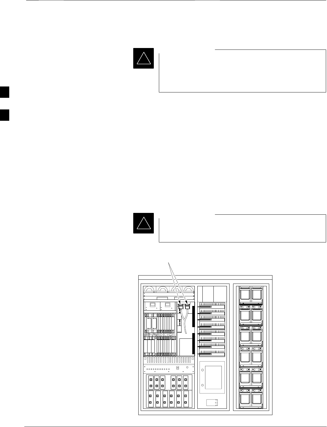
Each frame is equipped with one 50–pair punchblock for spans,
customer alarms, remote GPS, and BTS frame alarms. See Figure 3-9
and refer to Table 3-5 for the physical location and punchdown location
information.
Before connecting the LMF computer to the frame LAN, the
OMC–R/CBSC must disable the BTS and place it OOS to allow the
LMF to control the BTS. This prevents the CBSC from inadvertently
sending control information to the BTS during LMF–based tests.
Isolate BTS from T1/E1 Spans
Once the OMC–R/CBSC has disabled the BTS, the spans must be
disabled to ensure the LMF will maintain control of the BTS. To disable
the spans, disconnect the cable connector for the BTS–to–CBSC
Transcoder span at the Span I/O card (Figure 3-7).
If the BTS is a multi–frame logical BTS, do not disconnect
the inter–frame span.
IMPORTANT
*
Figure 3-7: Disconnecting Span Lines Span Line Cable
Connectors
4812ETL0020–1
3

Span Lines – Interface and Isolation – continued
08/01/2001 3-15
1X SCt4812ET Lite BTS Optimization/ATP
PRELIMINARY
T1/E1 Span Isolation
Table 3-4 describes the action required for span isolation.
Table 3-4: T1/E1 Span Isolation
Step Action
1Have the OMCR/CBSC place the BTS OOS.
2To disable the span lines, locate the connector for the span or spans which must be disabled and
remove the respective connector from the applicable SCCP cage Span I/O board (Figure 3-7).
Configure Optional Channel
Service Units
The M–PATH 537 Channel Service Unit (CSU) module provides
in–band SNMP–managed digital service access to T1 and fractional T1
lines. The M–PATH 437 Channel Service Unit (CSU) module provides
in–band SNMP–managed digital service access to E1 and fractional E1
lines. CSU modules units plug into the CSU shelf (see Figure 3-8).
The CSU shelf can support two M–PATH 537 or two M–PATH 437 CSU
modules. The 537 CSU module supports a single T1 span connection.
The 437 CSU module supports a single E1 span connection.
Remote M–PAT H management is available via SNMP over an in–band
data link on the span line (using a facility data link or 8–64 Kbps of a
DS0 channel). The unit at the near end of the management path can be
an SNMP manager or another M–PATH CSU.
Programming of the M–PATH is accomplished through the DCE 9–pin
connector on the front panel of the CSU shelf. Manuals and a Microsoft
Windows programming disk are supplied with each unit.
For more information refer to M–PATH T1 Channel Service Unit User’s
Guide, ADC Kentrox part number 65–77538101 or the M–PATH E1
Channel Service Unit User’s Guide, ADC Kentrox part number TBD.
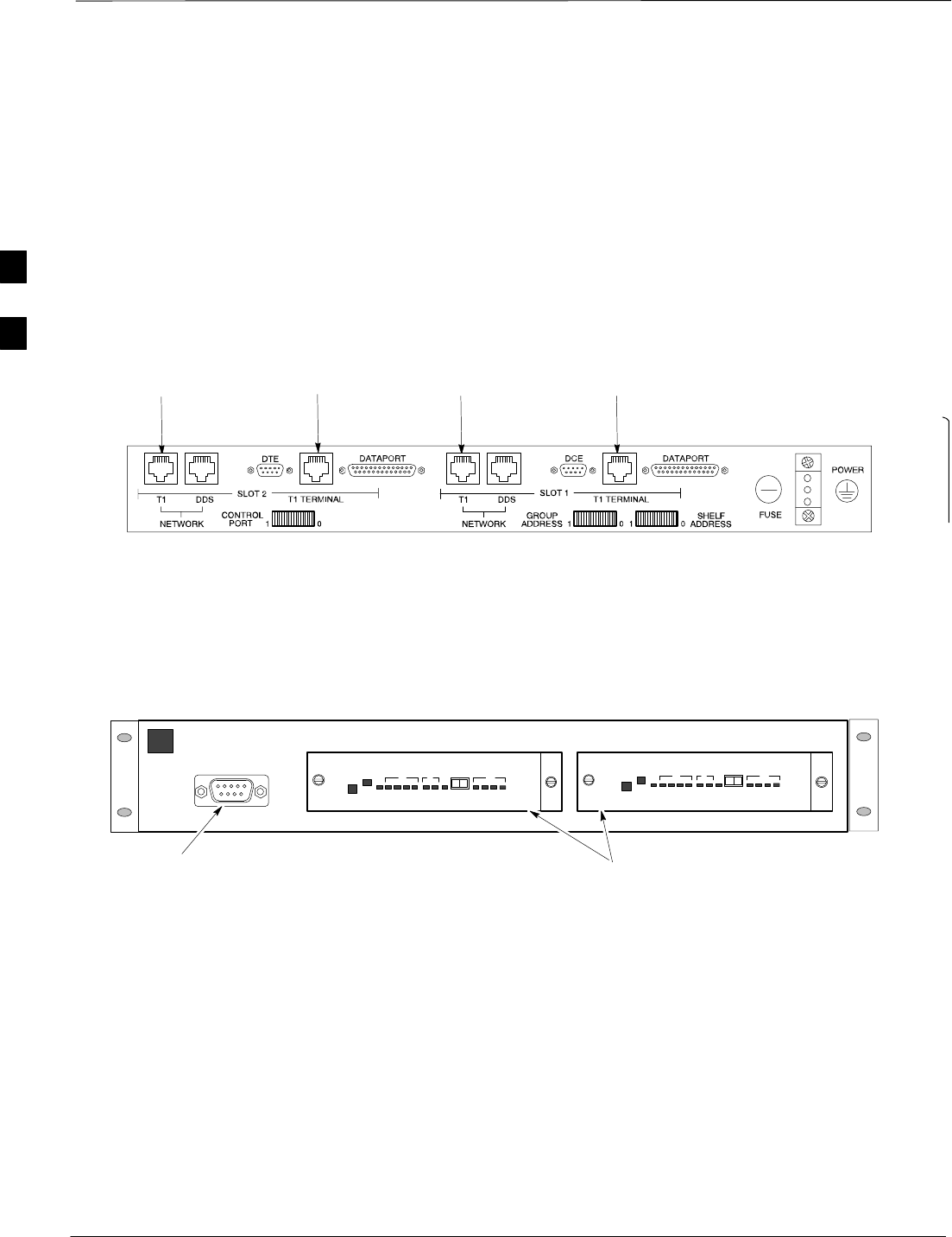
Setting the Control Port
Whichever control port is chosen, it must first be configured so the
control port switch settings match the communication parameters being
used by the control device. If using the rear–panel DTE control port, set
the SHELF ADDRESS switch SA5 to “up.” If using the rear–panel DCE
control port, position the SHELF ADDRESS switch down.
For more information, refer to the 2–Slot Universal Shelf Installation
Guide, ADC Kentrox part number 65–78070001.
Plug one of the cables listed below into the Control Port connectors:
Part Number Description of Cable
01–95006–022 (six feet) DB–9S to DB–9P
01–95010–022 (ten feet)
The control port cables can be used to connect the shelf to:
3
Span Lines – Interface and Isolation – continued
PRELIMINARY
1X SCt4812ET Lite BTS Optimization/ATP 08/01/2001
3-16
SA PC using the AT 9–pin interface
SA modem using the 9–pin connector
SOther shelves in a daisy chain
Figure 3-8: Rear and Front View of CSU Shelf
REF. FW00212
Front View
SLOT 1 SLOT 2
DCE Connector
(Craft Port)
Rear View
To/From
Network To/From
GLI2 To/From
Network To/From
GLI2
CSU Modules
3
Span Lines – Interface and Isolation – continued
08/01/2001 3-17
1X SCt4812ET Lite BTS Optimization/ATP
PRELIMINARY
Alarm and Span Line Cable
Pin/Signal Information
See Figure 3-9 and refer to Table 3-5 for the physical location and
punchdown location information for the 50–pair punchblock.
Figure 3-9: 50–Pair Punchblock
TOP VIEW OF PUNCHBLOCK
STRAIN RELIEVE INCOMING
CABLE TO BRACKET WITH
TIE WRAPS
2T
1T
1R
2T
2R
1
2
1R
2R
LEGEND
1T = PAIR 1 – TIP
1R = PAIR 1 –RING
” ”
” ”
” ”
Frame Power Entry
Compartment
50R
50T
49R
49T
1T
TO SPAN I/O
CONNECTOR
TO ALARM
CONNECTOR TO MODEM
CONNECTOR
TO RGD/RGPS
CONNECTOR
SC4812ETL0010–1
3

Span Lines – Interface and Isolation – continued
PRELIMINARY
1X SCt4812ET Lite BTS Optimization/ATP 08/01/2001
3-18
Table 3-5: Punchdown Location for 50–Pair Punch Block
Site Component Signal Name Punchdown Color
1T
1R
2T
2R
3T
3R
NOT 4T
USED 4R
5T
5R
6T
6R
7T
LFR_HSO_GND 7R Orange
EXT_IPPS_POS 8T Red
EXT_IPPS_NEG 8R White
LFR/HSO CAL_+ 9T Red
CAL_–9R Green
LORAN_ + 10T Red
LORAN_ –10R Blue
Pilot Beacon Alarm – Minor 11T
Pilot Beacon Alarm – Rtn 11R
Pilot Beacon Alarm – Major 12T
PILOT BEACON Pilot Beacon Control – NO 12R
Pilot Beacon Control–COM 13T
Pilot Beacon Control – NC 13R
Customer Outputs 1 – NO 14T
Customer Outputs 1 – COM 14R
Customer Outputs 1 – NC 15T
Customer Outputs 2 – NO 15R
Customer Outputs 2 – COM 16T
Customer Outputs 2 – NC 16R
Customer Outputs 3 – NO 17T
Customer Outputs 3 – COM 17R
Customer Outputs 3 – NC 18T
Customer Outputs 4 – NO 18R
Customer Outputs 4–COM 19T
Customer Outputs 4 – NC 19R
Customer Inputs 1 20T
CUSTOMER Cust_Rtn_A_1 20R
OUTPUTS / INPUTS Customer Inputs 2 21T
Cust_Rtn_A_2 21R
Customer Inputs 3 22T
Cust_Rtn_A_3 22R
Customer Inputs 4 23T
Cust_Rtn_A_4 23R
Customer Inputs 5 24T
Cust_Rtn_A_5 24R
Customer Inputs 6 25T
Cust_Rtn_A_6 25R
Customer Inputs 7 26T
Cust_Rtn_A_7 26R
Customer Inputs 8 27T
. . . continued on next page
3

Span Lines – Interface and Isolation – continued
08/01/2001 3-19
1X SCt4812ET Lite BTS Optimization/ATP
PRELIMINARY
Table 3-5: Punchdown Location for 50–Pair Punch Block
Site Component ColorPunchdownSignal Name
Cust_Rtn_A_8 27R
Customer Inputs 9 28T
CUSTOMER Cust_Rtn_A_9 28R
OUTPUTS / INPUTS Customer Inputs 10 29T
Cust_Rtn_A_10 29R
RVC_TIP_A 30T Red/Bk
RVC_RING_A 30R Red
XMIT_TIP_A 31T White/Bk
XMIT_RING_A 31R White
RVC_TIP_B 32T Green/Bk
RVC_RING_B 32R Green
XMIT_TIP_B 33T Blue/Bk
XMIT_RING_B 33R Blue
RVC_TIP_C 34T Yellow/Bk
RVC_RING_C 34R Yellow
XMIT_TIP_C 35T Brown/Bk
XMIT_RING_C 35R Brown
SPAN RVC_TIP_D 36T Orange/Bk
RVC_RING_D 36R Orange
XMIT_TIP_D 37T Violet/Bk
XMIT_RING_D 37R Violet
RVC_TIP_E 38T Gray/Bk
RVC_RING_E 38R Gray
XMIT_TIP_E 39T Pink/Bk
XMIT_RING_E 39R Pink
RVC_TIP_F 40T Tan/Bk
RVC_RING_F 40R Tan
XMIT_TIP_F 41T Bk/White
XMIT_RING_F 41R Bk
GPS_POWER_A+ 42T Blue
GPS_POWER_A–42R Blue/Bk
GPS_POWER_B+ 43T Yellow
GPS_POWER_B–43R Yellow/Bk
GPS_RX+ 44T White
GPS_RX–44R White/Bk
RGPS GPS_TX+ 45T Green
GPS_TX–45R Green/Bk
Signal Ground 46T Red
Master Frame 46R Red/Bk
GPS_lpps+ 47T Brown
GPS_lpps–47R Brown/Bk
Telco_Modem_T 48T
Phone Line Telco_Modem_R 48R
Chasis Ground 49T Cable Drain
Reserved 49R
Miscellaneous Reserved 50T
Reserved 50R
3
LMF to BTS Connection
PRELIMINARY
1X SCt4812ET Lite BTS Optimization/ATP 08/01/2001
3-20
68P09253A60
LMF to BTS Connection
The CDMA LMF computer may be connected to the LAN A or B
connector located behind the frame lower air intake grill. Figure 3-10
below shows the general location of these connectors. LAN A is
considered the primary LAN.
Table 3-6: Connect the LMF to the BTS
Step Action
1To gain access to the LAN connectors, open the LAN cable and utility shelf access panel, then pull
apart the hook–and–loop fabric covering the BNC “T” connector (see Figure 3-10). If desired, slide
out the utility shelf for the LMF computer.
2Connect the CDMA LMF computer to the LAN A (left–hand) BNC connector via PCMCIA Ethernet
Adapter.
NOTE
Xircom Model PE3–10B2 or equivalent can also be used to interface the CDMA LMF Ethernet
connection to the BTS frame connected to the PC parallel port, powered by an external AC/DC
transformer. In this case, the BNC cable must not exceed three feet in length.
* IMPORTANT
The LAN shield is isolated from chassis ground. The LAN shield (exposed portion of BNC connector)
must not touch the chassis during optimization.
LMF BNC “T” CONNECTIONS
ON LEFT SIDE OF FRAME
(ETHERNET “A” SHOWN;
ETHERNET “B” COVERED
WITH HOOK–AND–LOOP
FABRIC)
LMF COMPUTER
TERMINAL WITH
MOUSE PCMCIA ETHERNET
ADPATER & ETHERNET
UTP ADAPTER
UNIVERSAL TWISTED
PAIR (UTP) CABLE (RJ11
CONNECTORS)
10BASET/10BASE2
CONVERTER CONNECTS
DIRECTLY TO BNC T
115 VAC POWER
CONNECTION
NOTE:
Open LAN CABLE ACCESS
door. Pull apart hook–and–loop
fabric and gain access to the
LAN A or LAN B LMF BNC
connector.
Figure 3-10: LMF Connection Detail
SC4812ETL0012–2
3
Using CDMA LMF
08/01/2001 3-21
1X SCt4812ET Lite BTS Optimization/ATP
PRELIMINARY
Basic CDMA LMF Operation
The CDMA LMF allows the user to work in the two following operating
environments which are accessed using the specified desktop icons:
SGraphical User Interface (GUI) using the WinLMF icon
SCommand Line Interface (CLI) using the WinLMF CLI icon
The GUI is the primary optimization and acceptance testing operating
environment. The CLI environment provides additional capability to the
user to perform manually controlled acceptance tests and audit the
results of optimization and calibration actions.
Basic operation of the CDMA LMF in either environment includes
performing the following:
SSelecting and Deselecting BTS devices
SEnabling devices
SDisabling devices
SResetting devices
SObtaining device status
The following additional basic operation can be performed in a GUI
environment:
SSorting a status report window
For detailed information on performing these and other CDMA LMF
operations, refer to the LMF Help function and the LMF CLI Reference;
68P09253A56.
Unless otherwise noted, LMF procedures in this manual
are performed using the GUI environment.
IMPORTANT
*
CDMA LMF and Logical BTS
An SC4812ET Lite logical BTS can consist of up to two SC4812ET Lite
frames. When the CDMA LMF is connected to a frame 1 Ethernet port
of a logical BTS, access is available to all devices in all of the frames
that make up the logical BTS. A logical BTS CDF file that includes
equipage information for all of the logical BTS frames and their devices
is required for proper LMF interface. A CBSC CDF file that includes
channel data for all of the logical BTS frames is also required.
The first frame of a logical BTS has a –1 suffix (for example,
BTS–812–1) and the second frame of the logical BTS is numbered with
the suffix, –101 (e. g. BTS–812–101). When the CDMA LMF is logged
into a BTS, a FRAME tab is displayed for each frame. If there is only
one frame for the BTS, there will only be one tab (e.g., FRAME–282–1
for BTS–282). If a logical BTS has more than one frame, there will be a
3
Using CDMA LMF – continued
PRELIMINARY
1X SCt4812ET Lite BTS Optimization/ATP 08/01/2001
3-22
separate FRAME tab for each frame(for example, FRAME–438–1, and
FRAME–438–101 for BTS–438 that has both frames). If an RFDS is
included in the CDF file, an RFDS tab (e.g., RFDS–438–1) will be
displayed.
Actions, such as ATP tests, can be initiated for selected devices in one or
more frames of a logical BTS. Refer to the CDMA LMF Select devices
help screen for information on how to select devices.
Logging Into a BTS
Be sure that the correct bts–#.cdf and cbsc–#.cdf file is
used for the BTS. These should be the CDF files that are
provided for the BTS by the CBSC. Failure to use the
correct CDF files can result in invalid optimization.
Failure to use the correct CDF files to log into a live
(traffic–carrying) site can shut down the site.
CAUTION
Logging into a BTS establishes a communications link between the BTS
and the CDMA LMF. You may be logged into one or more BTSs at a
time, but only one CDMA LMF may be logged into each BTS.
Before attempting to start the CDMA LMF computer and the CDMA
LMF software, confirm the CDMA LMF computer is properly connected
to the BTS (see Table 3-6). Follow the procedures in Table 3-7 to log
into a BTS.
Prerequisites
Before attempting to log into a BTS, ensure the following have been
completed:
SThe CDMA LMF is correctly installed and prepared.
SA bts-nnn folder with the correct CDF and CBSC files exists.
SThe CDMA LMF computer was connected to the BTS before starting
the Windows operating system and the CDMA LMF software. If
necessary, restart the computer after connecting it to the BTS in
accordance with Table 3-6 and Figure 3-10.
3

Using CDMA LMF – continued
08/01/2001 3-23
1X SCt4812ET Lite BTS Optimization/ATP
PRELIMINARY
BTS Login from the GUI Environment
Follow the procedures in Table 3-7 to log into a BTS when using the
GUI environment.
Table 3-7: BTS GUI Login Procedure
nStep Action
1Start the CDMA LMF GUI environment by double–clicking on the WinLMF desktop icon (if the
LMF is not running).
NOTE
If a warning similar to the following is displayed, select No, shut down other LMF sessions which
may be running, and start the CDMA LMF GUI environment again:
The CLI handler is already running.
This may cause conflicts with the LMF.
Are you sure you want to start the application?
Yes No
2Click on Login tab (if not displayed).
3Double click on CDMA (in the Available Base Stations pick list).
4Click on the desired BTS number.
5Click on the Network Login tab (if not already in the forefront).
6Enter correct IP address (normally 128.0.0.2) for a field BTS, if not correctly displayed in the IP
Address box.
7Type in the correct IP Port number (normally 9216) if not correctly displayed in the IP Port box.
8Change the Multi-channel Preselector from the Multi-channel Preselector pick list (normally
MPC) to a device corresponding to your BTS configuration, if required.
9Use a Tower Top Amplifier is not applicable to the SC4812ET Lite.
10 Click on Login. (A BTS tab with the BTS is displayed.)
NOTE
SIf you attempt to log into a BTS that is already logged on, all devices will be gray.
SThere may be instances where the BTS initiates a log out due to a system error (i.e., a device
failure).
SIf the MGLI is OOS–ROM (blue), it must be downloaded with RAM code before other devices
can be seen.
SIf the MGLI is OOS–RAM (yellow), it must be enabled before other installed devices can be
seen.
3
Using CDMA LMF – continued
PRELIMINARY
1X SCt4812ET Lite BTS Optimization/ATP 08/01/2001
3-24
BTS Login from the CLI Environment
Follow the procedures in Table 3-8 to log into a BTS when using the
CLI environment.
If the CLI and GUI environments are to be used at the
same time, the GUI must be started first and BTS login
must be performed from the GUI. Refer to Table 3-7 to
start the GUI environment and log into a BTS.
IMPORTANT
*
Table 3-8: BTS CLI Login Procedure
nStep Action
1 Double–click the WinLMF CLI desktop icon (if the LMF CLI environment is not already
running).
NOTE
If a BTS was logged into under a GUI session before the CLI environment was started, the CLI
session will be logged into the same BTS, and step 2 is not required.
2At the /wlmf prompt, enter the following command:
login bts–<bts#> host=<host> port=<port>
where:
host = MGLI card IP address (defaults to address last logged into for this BTS or 128.0.0.2 if this
is first login to this BTS)
port = IP port of the BTS (defaults to port last logged into for this BTS or 9216 if this is first login
to this BTS)
A response similar to the following will be displayed:
LMF>
13:08:18.882 Command Received and Accepted
COMMAND=login bts–33
13:08:18.882 Command In Progress
13:08:21.275 Command Successfully Completed
REASON_CODE=”No Reason”
Logging Out Logging out of a BTS is accomplished differently for the GUI and CLI
operating environments.
3
Using CDMA LMF – continued
08/01/2001 3-25
1X SCt4812ET Lite BTS Optimization/ATP
PRELIMINARY
The GUI and CLI environments use the same connection to
a BTS. If a BTS is logged into in both the GUI and CLI
environments at the same time, logging out of the BTS in
either environment will log out of it for both. When either
a login or logout is performed in the CLI window, there is
no GUI indication that the login or logout has occurred.
IMPORTANT
*
Logging Out of a BTS from the GUI Environment
Follow the procedure in Table 3-9 to logout of a BTS when using the
GUI environment.
Table 3-9: BTS GUI Logout Procedure
nStep Action
1Click on Select on the BTS tab menu bar.
2Click the Logout item in the pulldown menu (a Confirm Logout pop-up message will appear).
3Click on Yes (or press the Enter key) to confirm logout. The Login tab will appear.
NOTE
If a logout was previously performed on the BTS from a CLI window running at the same time as
the GUI, a Logout Error popup message will appear stating the system could not log out of the
BTS. When this occurs, the GUI must be exited and restarted before it can be used for further
operations.
4If a Logout Error popup message appears stating that the system could not log out of the Base
Station because the given BTS is not logged in, click OK and proceed to step 5.
5 Select File > Exit in the window menu bar, click Yes in the Confirm Logout popup, and click
Yes in the Logout Error popup which appears again.
6If further work is to be done in the GUI, restart it.
NOTE
SThe Select menu on the BTS tab will only log you out of the displayed BTS.
SYou can also log out of all BTS sessions and exit CDMA LMF by clicking on the File selection
in the menu bar and selecting Exit from the File menu list. A Confirm Logout pop–up
message will appear.
3

Using CDMA LMF – continued
PRELIMINARY
1X SCt4812ET Lite BTS Optimization/ATP 08/01/2001
3-26
Logging Out of a BTS from the CLI Environment
Follow the procedure in Table 3-10 to logout of a BTS when using the
CLI environment.
Table 3-10: BTS CLI Logout Procedure
nStep Action
* IMPORTANT
If the BTS is also logged into from a GUI running at the same time and further work must be done
with it in the GUI, proceed to step 2.
1Logout of a BTS by entering the following command:
logout bts–<bts#>
A response similar to the following will be displayed:
LMF>
13:24:51.028 Command Received and Accepted
COMMAND=logout bts–33
13:24:51.028 Command In Progress
13:24:52.04 Command Successfully Completed
REASON_CODE=”No Reason”
2If desired, close the CLI interface by entering the following command:
exit
A response similar to the following will be displayed before the window closes:
Killing background processes....
Establishing an MMI
Communication Session
For those procedures which require MMI communication between the
CDMA LMF and BTS FRUs, follow the procedures in Table 3-11 to
initiate the communication session.
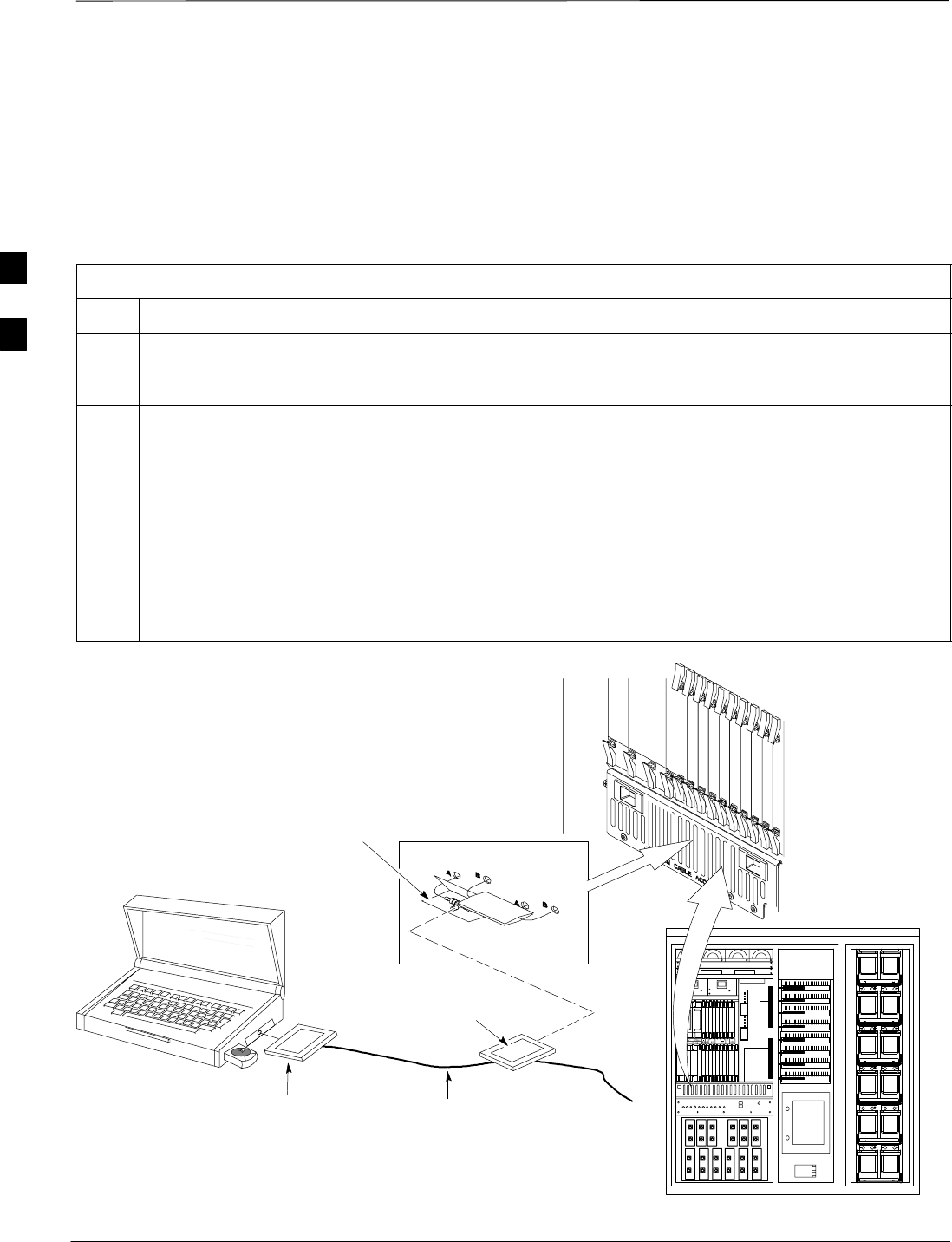
Figure 3-11 illustrates common equipment connections for the CDMA
LMF computer. For specific connection locations on FRUs, refer to the
illustration accompanying the procedures which require the MMI
communication session.
Table 3-11: Establishing MMI Communication
Step Action
1Connect the CDMA LMF computer to the equipment as detailed in the applicable procedure which
requires the MMI communication session.
2Start the named HyperTerminal connection for MMI sessions by double clicking on its Windows
desktop shortcut.
. . . continued on next page
3
Using CDMA LMF – continued
08/01/2001 3-27
1X SCt4812ET Lite BTS Optimization/ATP
PRELIMINARY
Table 3-11: Establishing MMI Communication
Step Action
NOTE
If a Windows desktop shortcut was not created for the MMI connection, access the connection from
the Windows Start menu by selecting:
Programs > Accessories > Hyperterminal > HyperTerminal > <Named HyperTerminal
Connection (e.g., MMI Session)>
3Once the connection window opens, establish MMI communication with the BTS FRU by pressing
the CDMA LMF computer Enter key until the prompt identified in the applicable procedure is
obtained.
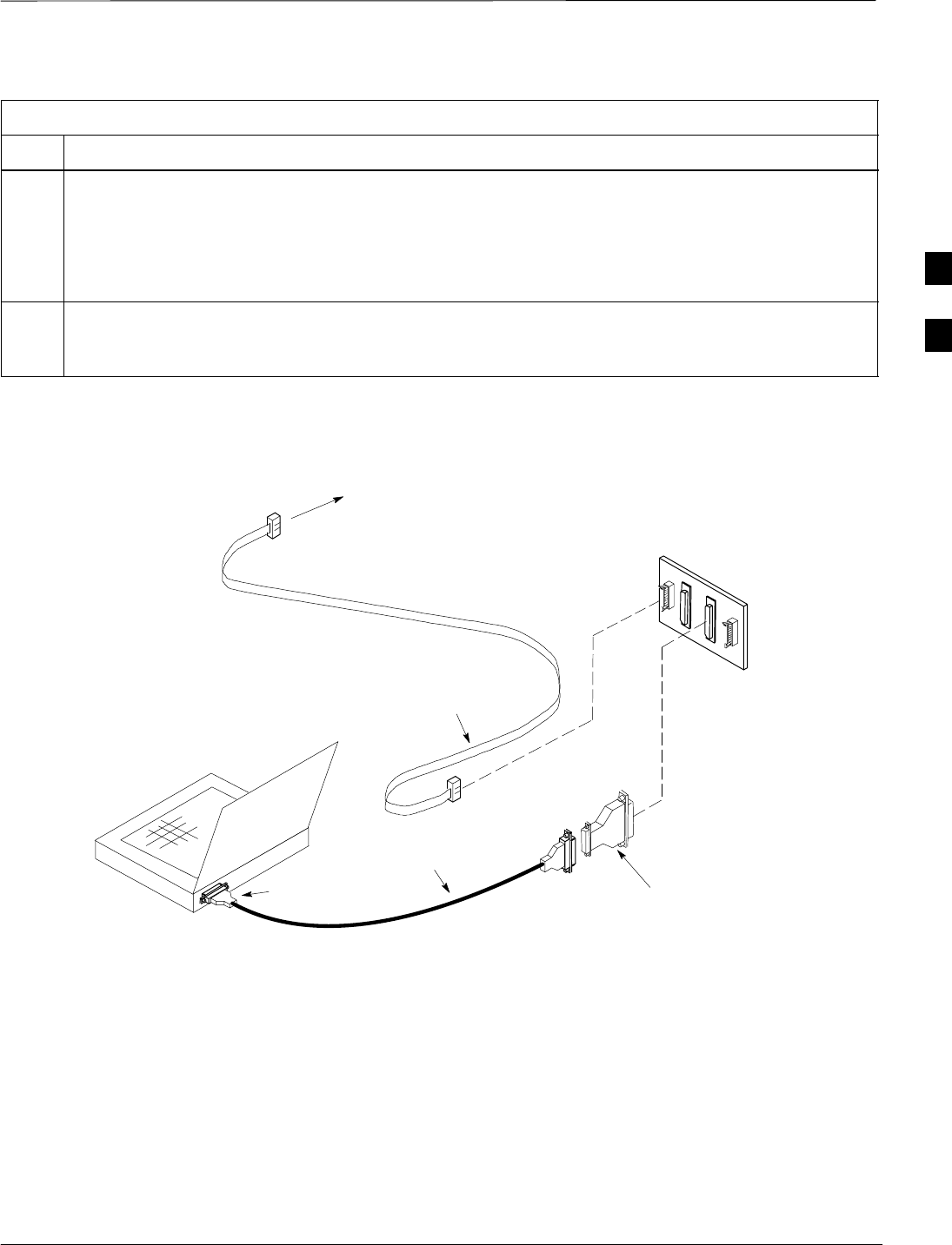
NULL MODEM
BOARD
(TRN9666A)
8–PIN TO 10–PIN
RS–232 CABLE (P/N
30–09786R01)
RS–232 CABLE
8–PIN
CDMA LMF
COMPUTER
To FRU MMI port
DB9–TO–DB25
ADAPTER
Figure 3-11: CDMA LMF Computer Common MMI Connections
COM1
OR
COM2
Online Help
Task oriented online help is available in CDMA LMF by clicking on
Help in the menu bar.
3
Pinging the Processors
PRELIMINARY
1X SCt4812ET Lite BTS Optimization/ATP 08/01/2001
3-28
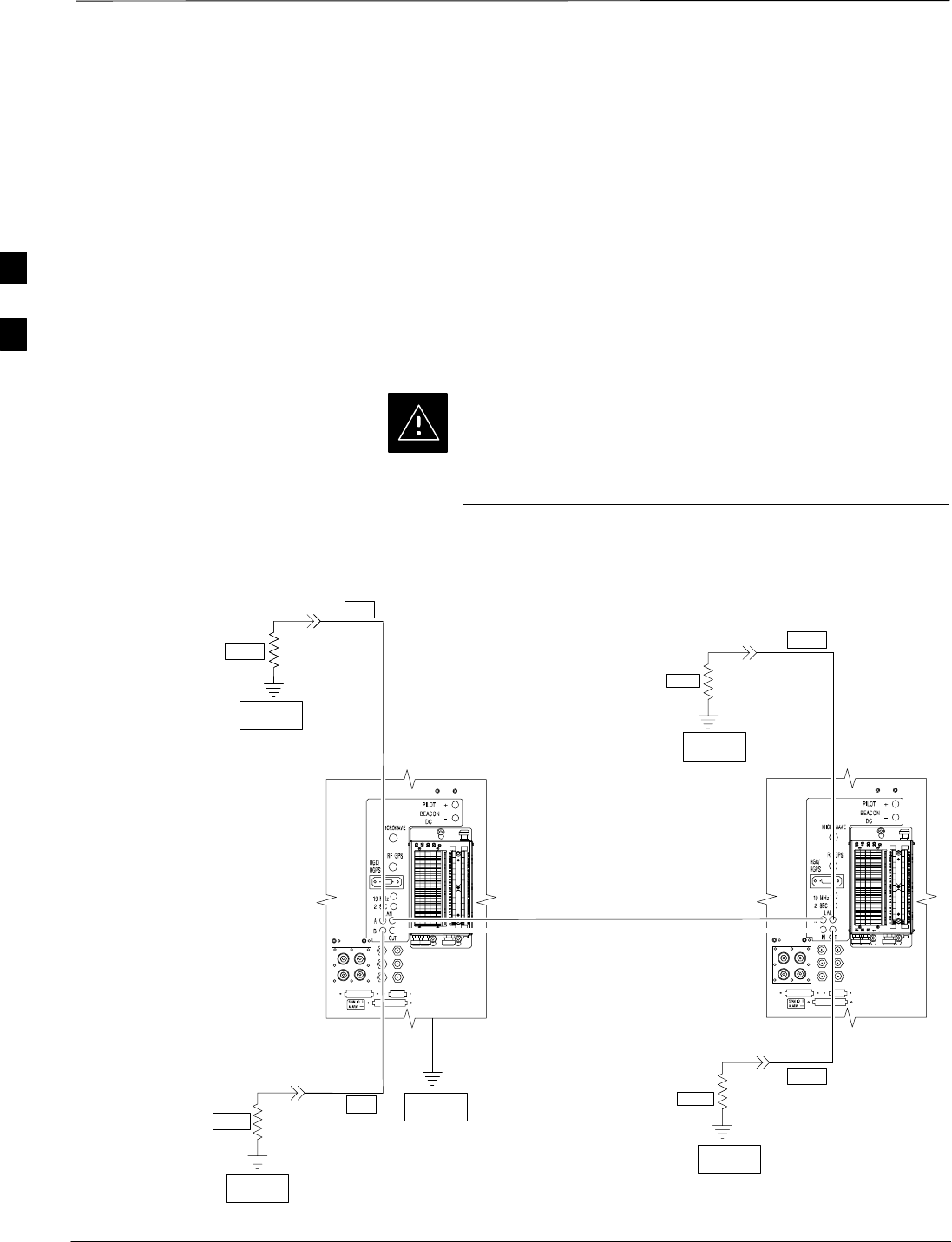
Pinging the BTS
For proper operation, the integrity of the Ethernet LAN A and B links
must be be verified. Figure 3-12 represents a typical BTS Ethernet
configuration for the SC4812ET Lite with an expansion frame. The
drawing depicts cabling and termination for both the A and B LANs.
Ping is a program that sends request packets to the LAN network
modules to get a response from the specified “target” module.
Follow the steps in Table 3-12 to ping each processor (on both LAN A
and LAN B) and verify LAN redundancy is working properly.
Always wear a conductive, high impedance wrist strap
while handling any circuit card/module to prevent damage
by Electro–Static Discharge (ESD).
CAUTION
SIGNAL
GROUND
SIGNAL
GROUND
50Ω
IN
SC4812ET Lite
(MASTER) SC4812ET Lite
(EXPANSION)
SIGNAL
GROUND
Figure 3-12: BTS Ethernet LAN Interconnect Diagram
50Ω
50Ω
SC4812ETL0013–4
SIGNAL
GROUND
50Ω
SIGNAL
GROUND
FRAME GROUND
TRIAX
TERMINATOR
TRIAX
TERMINATOR
TRIAX
TERMINATOR
TRIAX
TERMINATOR
IN
OUT
OUT
3

Pinging the Processors – continued
08/01/2001 3-29
1X SCt4812ET Lite BTS Optimization/ATP
PRELIMINARY
The Ethernet LAN A and B cables and/or terminations
must be installed on each frame/enclosure external LAN
connector before performing this test. All other processor
board LAN connections are made through the backplanes.
IMPORTANT
*
Table 3-12: Pinging the Processors
Step Action
1If this is a first–time communication with a newly–installed frame or a GLI2 which has been replaced,
perform the procedure in Table 6-3 and then return to step 2.
2Be sure uncabled LAN A and B IN and OUT connectors in the power entry compartment (rear of
frame – Figure 3-9 and Figure 3-12) are terminated with 50 Ω loads.
3If it has not already been done, interface the LMF computer to the BTS (refer to Table 3-6 and
Figure 3-10.)
4If it has not already been done, start a GUI LMF session and log into the BTS ( refer to Table 3-7).
5In the power entry compartment, remove the 50Ω termination on the frame LAN B IN connector. The
CDMA LMF session should remain active. Replace the 50Ω terminator on the BTS frame LAN B IN
connector.
6From the Windows desktop, click the Start button and select Run.
7In the Open box, type ping and the GLI2 IP address (for example, ping 128.0.0.2).
NOTE
128.0.0.2 is the default IP address for the GLI2 in field BTS units.
8Click on OK.
9If the targeted module responds, a DOS window will appear with a display similar to the following:
Reply from 128.0.0.2: bytes=32 time=3ms TTL=255
SIf the device responds, proceed to step 18.
If there is no response the following is displayed:
Request timed out
SIf the GLI2 fails to respond, it should be reset and re–pinged. If it still fails to respond, typical
problems would be: failure of the CDMA LMF to login, shorted BNC to inter-frame cabling, open
cables, crossed A and B link cables, or the GLI2 itself.
10 Logout of the BTS as described in Table 3-9, exit from the CDMA LMF program, and restart the
Windows operating system on the CDMA LMF computer.
11 Restart the CDMA LMF GUI program as described in LMF Help function, and log into the BTS as
described in Table 3-7.
12 Perform steps 6 through 9 again.
SIf the device responds, proceed to step 18.
If there is still no response,proceed to step 13.
. . . continued on next page
3

Pinging the Processors – continued
PRELIMINARY
1X SCt4812ET Lite BTS Optimization/ATP 08/01/2001
3-30
Table 3-12: Pinging the Processors
Step Action
13 If ping was unsuccessful after restarting the CDMA LMF computer, press the MGLI front panel reset
pushbutton and perform steps 6 through 9 again.
14 NOTE
Refer to Table 6-1 if ping was unsuccessful after resetting the MGLI.
15 After the BTS has been successfully pinged, be sure the 50Ω termination was replaced on the BTS
frame LAN B IN connector in the power entry compartment (Figure 3-12). Disconnect the LMF cable
from the LAN shelf LAN A connector, and connect it to LAN B (right–hand connector) using a
BNC–female–to–BNC–female adapter (refer to Figure 3-10).
16 In the power entry compartment, remove the 50Ω termination on the BTS frame LAN A IN connector.
17 Repeat steps 5 through 8 using LAN B.
18 After the BTS has been successfully pinged on the secondary LAN, replace the 50Ω termination on
the frame LAN A IN connector in the power entry compartment.
19 Disconnect the LMF cable from the LAN shelf LAN B and connect it to LAN A using a
BNC-female-to-BNC-female adapter.
20 Remove and replace the 50Ω termination on the LAN B IN connector to force the MGLI to switch to
primary LAN A.
21 Repeat steps 5 through 8 to ensure proper primary LAN operation.
3

Download the BTS
08/01/2001 3-31
1X SCt4812ET Lite BTS Optimization/ATP
PRELIMINARY
Overview
Before a BTS can operate, each equipped device must contain device
initialization (ROM) code. ROM code is loaded in all devices during
manufacture or factory repair. Device application (RAM) code and data
must be downloaded to each equipped device by the user before the BTS
can be made fully functional for the site where it is installed.
ROM Code
Downloading ROM code to BTS devices from the CDMA LMF is NOT
routine maintenance or a normal part of the optimization process. It is
only done in unusual situations where the resident ROM code in the
device does not match the release level of the site operating software
AND the CBSC can not communicate with the BTS to perform the
download. An example would be a BTS loaded with Release 9.2
software where a GLI loaded with Release 2.8.1 ROM code must be
installed to replace a malfunctioning MGLI.
Before ROM code can be downloaded from the CDMA LMF, the correct
ROM code file for each device to be loaded must exist on the LMF
computer. ROM code must be manually selected for download.
ROM code can be downloaded to a device that is in any state. After the
download is started, the device being downloaded will change to
OOS–ROM (blue). The device will remain OOS–ROM (blue) when the
download is completed. The same Revision–level RAM code must then
be downloaded to the device. For example, if Release 2.9.2.1.1 ROM
code is downloaded, Release 2.9.2.1.1 RAM code must be downloaded.
Procedures to load ROM code are located in Appendix G.
RAM Code
Before RAM code can be downloaded from the CDMA LMF, the correct
RAM code file for each device must exist on the LMF computer. RAM
code can be automatically or manually selected depending on the Device
menu item chosen and where the RAM code file for the device is stored
in the CDMA LMF file structure. The RAM code file will be selected
automatically if the file is in the \lmf\cdma\loads\n.n.n.n\code folder
(where n.n.n.n is the version number of the download code that matches
the “NextLoad” parameter of the CDF file). The RAM code file in the
code folder must have the correct hardware bin number.
RAM code can be downloaded to a device that is in any state. After the
download is started, the device being loaded will change to OOS-ROM
(blue). When the download is completed successfully, the device will
change to OOS-RAM (yellow). When code is downloaded to an MGLI
or GLI, the CDMA LMF automatically also downloads data and then
enables the MGLI. When enabled, the MGLI will change to INS (green).
For non–GLI devices, data must be downloaded after RAM code is
downloaded. To download data, the device state must be OOS–RAM
(yellow).
3
Download the BTS – continued
PRELIMINARY
1X SCt4812ET Lite BTS Optimization/ATP 08/01/2001
3-32
RAM code downloading requires a few minutes. After the download
starts, the non–GLI device being loaded changes to OOS–ROM (blue). If
the download is completed successfully, the non–GLI device changes to
OOS–RAM (yellow).
The devices to be loaded with RAM code and data are:
SMaster Group Line Interface (MGLI2)
SRedundant GLI (GLI2)
SClock Syncronization Module (CSM) (Only if new revision code must
be loaded)
SMulti Channel CDMA (MCC24 or MCC8E) card
SBroadband Transceiver (BBX2)
SRFDS Test Subscriber Interface Card (TSIC), if equipped
The MGLI must be successfully downloaded with RAM
code and data, and in INS (green) status before
downloading any other device. The RAM code download
process for an MGLI automatically downloads data and
then enables the MGLI.
IMPORTANT
*
Verify GLI ROM Code Loads
Devices should not be loaded with RAM code which is for a different
system release than the ROM code with which they are loaded. Before
downloading RAM code and data to the processor cards, follow the
procedure in Table 3-13 to verify the GLI devices are loaded with the
correct ROM code for the system release used by the BSS.
Table 3-13: Verify GLI ROM Code Loads
Step Action
1If it has not already been done, start a GUI LMF session and log into the BTS ( refer to Table 3-7).
2Select all GLI devices by clicking on them, and select Device > Status from the menu bar.
3In the status report window which opens, note the number in the ROM Ver column for each GLI2.
SThe system release number will be the first two decimal divisions of the number; for example, the
number 2.15.0.0.3 would be for System Release 2.15, and 2.9.2.2.34 would be for System Release
2.9.
4If the ROM code loaded in the GLIs is not for the correct system release, log out of the BTS,
disconnect the CDMA LMF computer, reconnect the span lines as described in Table 5-7, and have the
CBSC download the correct ROM code version to the BTS devices.
5When the GLIs have the correct ROM load for the system release being used, be sure the span lines
are disabled as outlined in Table 3-4 and proceed to downloading RAM code and data.
3
Download the BTS – continued
08/01/2001 3-33
1X SCt4812ET Lite BTS Optimization/ATP
PRELIMINARY
Download RAM Code and Data
to MGLI and GLI Follow the steps outlined in Table 3-14 to download the RAM code and
data to the MGLI and other installed GLI devices.
Prerequisites
SPrior to performing these procedures, ensure a code file exists for each
of the devices to be loaded.
SThe CDMA LMF computer is connected to the BTS (refer to
Table 3-6), and is logged in using the GUI environment (refer to
Table 3-7).
Table 3-14: Download and Enable MGLI and GLI Devices
Step Action
1From the Util pull down menu, select Tools, then Update NextLoad.
2Select the correct code version for the system release being used and click Save.
3Download code to the MGLI by clicking on the device.
4From the Device pull down menu, select Download Code.
A status report is displayed confirming change in the device(s) status. Click OK to close the status
window. (The MGLI will automatically be downloaded with data and enabled.)
5Once the MGLI is enabled, load and enable additional installed GLIs by clicking on the devices and
repeating step 4.
6 Click OK to close the status window for the additional GLI devices.
Download RAM Code and Data
to Non–GLI Devices
Downloads to non–GLI devices can be performed individually for each
device or all installed devices can be downloaded with one action. RAM
code and data are downloaded to non–GLI devices in separate steps.
CSM devices are RAM code–loaded at the factory. RAM
code is downloaded to CSMs only if a newer software
version needs to be loaded.
IMPORTANT
*
When downloading to multiple devices, the download may
fail for some of the devices (a time–out occurs). These
devices can be loaded individually after completing the
multiple download.
NOTE
Follow the steps in Table 3-15 to download RAM code and data to
non–GLI devices.
3

Download the BTS – continued
PRELIMINARY
1X SCt4812ET Lite BTS Optimization/ATP 08/01/2001
3-34
Table 3-15: Download RAM Code and Data to Non–GLI Devices
Step Action
1Select the target CSM, MCC, and BBX device(s).
2From the Device pull down menu, select Download Code.
A status report is displayed that shows the results of the download for each selected device.
3 Click OK to close the status report window when downloading is completed.
NOTE
After a BBX, CSM, or MCC device is successfully loaded with RAM code and has changed to the
OOS–RAM state (yellow), the status LED should be rapidly flashing GREEN.
4To download data, select the target CSM and MCC device(s).
5From the Device pull down menu, select Download Data.
A status report is displayed that shows the results of the download for each selected device.
6 Click OK to close the status report window when downloading is completed.
Select CSM Clock Source
A CSM can have three different clock sources. The Select CSM Source
function can be used to select the clock source for each of the three
inputs. This function is only used if the clock source for a CSM needs to
be changed. The Clock Source function provides the following clock
source options.
SLocal GPS
SRemote GPS
SHSO (only for source 2 & 3)
SLFR (only for source 2 & 3)
S10 MHz (only for source 2 & 3)
SNONE (only for source 2 & 3)
Prerequisites
MGLI=INS_ACT (green), CSM= OOS_RAM (yellow) or INS_ACT
(green)
Table 3-16: Select CSM Clock Source
Step Action
1Select the applicable CSM(s).
2Click on the Device menu.
3Click on the Clock Source menu item.
4Click on the Select menu item. A clock source selection window is displayed.
5Select the applicable clock source in the Clock Reference Source pick lists. Uncheck the related
check box if you do not want the displayed pick list item to be used.
. . . continued on next page
3
Download the BTS – continued
08/01/2001 3-35
1X SCt4812ET Lite BTS Optimization/ATP
PRELIMINARY
Table 3-16: Select CSM Clock Source
Step Action
6Click on the OK button. A status report window is displayed showing the results of the selection
action.
7Click on the OK button to close the status report window.
Enable CSMs
Each BTS CSM system features two CSM boards per site. In a typical
operation, the primary CSM locks its Digital Phase Locked Loop
(DPLL) circuits to GPS signals. These signals are generated by either an
on–board GPS module (RF–GPS) or a remote GPS receiver (R–GPS).
The GPS receiver interfaced to CSM 1 is used as the primary timing
reference and synchronizes the entire cellular system. CSM 2 provides
clock syncronization back–up, but does not have a GPS receiver.
The BTS may be equipped with a LORAN–C Low Frequency Receiver
(LFR), a High Stability Oscillator (HSO), or external 10 MHz Rubidium
source which the CSM can use as a secondary timing reference. In all
cases, the CSM monitors and determines what reference to use at a given
time.
For RF–GPS, verify the CSM configured with the GPS
receiver “daughter board” is installed in the frame’s CSM 1
slot before continuing.
IMPORTANT
*
Follow the steps outlined in Table 3-17 to enable the CSMs installed in
the SCCP shelves.
Table 3-17: Enable CSMs
Step Action
1NOTE
If equipped with two CSMs, enable CSM–2 first.
Click on the target CSM.
From the Device pull down, select Enable.
2A status report is displayed confirming change in the device(s) status.
Click OK to close the status report window.
NOTE
SCSM 1 houses the GPS receiver. The enable sequence can take up to one hour (see below).
SFAIL may be shown in the status report table for enable action. If Waiting For Phase Lock is shown
in the Description field, the CSM changes to the Enabled state after phase lock is achieved.
. . . continued on next page
3
Download the BTS – continued
PRELIMINARY
1X SCt4812ET Lite BTS Optimization/ATP 08/01/2001
3-36
Table 3-17: Enable CSMs
Step Action
* IMPORTANT
The GPS satellite system satellites are not in a geosynchronous orbit and are maintained and operated
by the United States Department of Defense (DOD). The DOD periodically alters satellite orbits;
therefore, satellite trajectories are subject to change. A GPS receiver that is INS contains an “almanac”
that is updated periodically to take these changes into account.
If a GPS receiver has not been updated for a number of weeks, it may take up to an hour for the GPS
receiver “almanac” to be updated.
Once updated, the GPS receiver must track at least four satellites and obtain (hold) a 3–D position fix
for a minimum of 45 seconds before the CSM will come in service. (In some cases, the GPS receiver
needs to track only one satellite, depending on accuracy mode set during the data load).
3NOTE
SIf equipped with two CSMs, CSM–1 should be bright green (INS–ACT) and CSM–2 should be
dark green(INS–STB)
SIf more than an hour has passed, refer to CSM Verification, see Figure 3-13 and Table 3-20 to
determine the cause.
After the CSMs have been successfully enabled, be sure the PWR/ALM LEDs are steady green
(alternating green/red indicates the card is in an alarm state).
Enable MCCs
This procedure configures the MCC and sets the “tx fine adjust”
parameter. The “tx fine adjust” parameter is not a transmit gain setting,
but a timing adjustment that compensates for the processing delay in the
BTS (approximately 3 mS).
Follow the steps outlined in Table 3-18 to enable the MCCs installed in
the SCCP shelves.
The MGLI and CSM must be downloaded and enabled,
prior to downloading and enabling the MCC.
IMPORTANT
*
Table 3-18: Enable MCCs
Step Action
1Click on the target MCC(s) or from the Select pull down menu choose All MCCs.
2From the Device menu, select Enable
A status report is displayed confirming change in the device(s) status.
3 Click OK to close the status report window.
3

CSM System Time – GPS & LFR/HSO Verification
08/01/2001 3-37
1X SCt4812ET Lite BTS Optimization/ATP
PRELIMINARY
Clock Synchronization
Manager (CSM) System Time
The primary function of the Clock Synchronization Manager (CSM)
cards is to maintain CDMA system time. The CSM card in SCCP shelf
slot CSM–1 is the primary timing source while the card in slot CSM–2
provides redundancy. The second generation CSM card (CSM2) is
required when using the remote GPS receiver (R–GPS). R–GPS uses a
GPS receiver in the antenna head that has a digital output to the CSM2
card. A CSM2 card can have a local GPS receiver daughter card to
support an RF–GPS signal.
Each CSM2 card features a temperature–stablized, crystal oscillator that
provides 19.6608 MHz clock, even second pulse, and 3 MHz reference
signals to the synchronization source selected from the following (refer
to Table 3-20 for source selection/verification procedures):
SGPS: local/RF–GPS or remote/R–GPS
SLORAN–C Low Frequency Receiver (LFR) or High Stability
Oscillator (HSO)
SExternal reference oscillator sources
CDMA Clock Distribution Cards (CCDs) buffer and distribute
even–second reference and 19.6608 MHz clock signals from the CSM
cards. CCD 1 is married to the card in slot CSM–1, and CCD 2 is
married to the card in slot CSM–2.
The BTS switches between the primary and redundant units (card slots
CSM–1 and CSM–2, respectively) upon failure or command. A failure
in CSM–1 or CCD 1 will cause the system to switch to the
CSM–2–CCD 2 redundant card pair.
Fault management has the capability of switching between the GPS
synchronization source and the LFR/HSO backup source in the event of
a GPS receiver failure in CSM–1. During normal operation, the card in
CSM–1 selects GPS as the primary timing source (Table 3-20). The
source selection can also be overridden via the CDMA LMF or by the
system software.
In addition to providing GPS synchronization to the LFR or HSO
back–up sources, synchronization between the primary and redundant
CSM–CCD pairs increases reliability.
Low Frequency Receiver/
High Stability Oscillator
The CSM performs the overall configuration and status monitoring
functions of the LFR/HSO. In the event of GPS failure, the LFR/HSO is
capable of maintaining synchronization initially established by the GPS
reference signal.
The LFR requires an active external antenna to receive LORAN–C RF
signals. Timing pulses are derived from this signal, which is
3

CSM System Time – GPS & LFR/HSO Verification – continued
PRELIMINARY
1X SCt4812ET Lite BTS Optimization/ATP 08/01/2001
3-38
synchronized to Universal Time Coordinates (UTC) and GPS time. The
LFR can maintain system time indefinately after initial GPS lock.
The HSO is a high stability 10 MHz oscillator with the necessary
interface to the CSMs. The HSO is typically installed in those
geographical areas not covered by the LORAN–C system. Since the
HSO is a free–standing oscillator, system time can only be maintained
for 24 hours after 24 hours of GPS lock.
Upgrades and Expansions: LFR2/HSO2/HSOX
LFR2/HSO2 (second generation cards) both export a timing signal to the
expansion or logical BTS frames. The associated expansion or logical
frames require an HSO–expansion (HSOX) whether the starter frame has
an LFR2 or an HSO2. The HSOX accepts input from the starter frame
and interfaces with the CSM cards in the expansion frame. LFR and
LFR2 use the same source code in source selection (Table 3-20). HSO,
HSO2, and HSOX use the same source code in source selection
(Table 3-20).
Allow the base site and test equipment to warm up for
60 minutes after any interruption in oscillator power. CSM
card warm-up allows the oscillator oven temperature and
oscillator frequency to stabilize prior to test. Test
equipment warm-up allows the Rubidium standard
timebase to stabilize in frequency before any measurements
are made.
NOTE
3
CSM System Time – GPS & LFR/HSO Verification – continued
08/01/2001 3-39
1X SCt4812ET Lite BTS Optimization/ATP
PRELIMINARY
CSM Frequency Verification
The objective of this procedure is the initial verification of the Clock
Synchronization Module (CSM) cards before performing the RF path
verification tests.
Test Equipment Setup
(GPS & LFR/HSO Verification)
Follow the steps outlined in Table 3-19 to set up test equipment.
Table 3-19: Test Equipment Setup (GPS & LFR/HSO Verification)
Step Action
1a For local GPS (RF–GPS): Verify a CSM card with a GPS receiver is installed in the primary CSM
slot, CSM–1, and that CSM–1 is INS.
NOTE
This is verified by checking the card ejectors for kit number SGLN1145 on the card in slot 1.
1b For Remote GPS (RGPS): Verify a CSM2 card is installed in primary slot CSM–1 and that CSM–1 is
INS.
NOTE
This is verified by checking the card ejectors for kit number SGLN4132CC or subsequent.
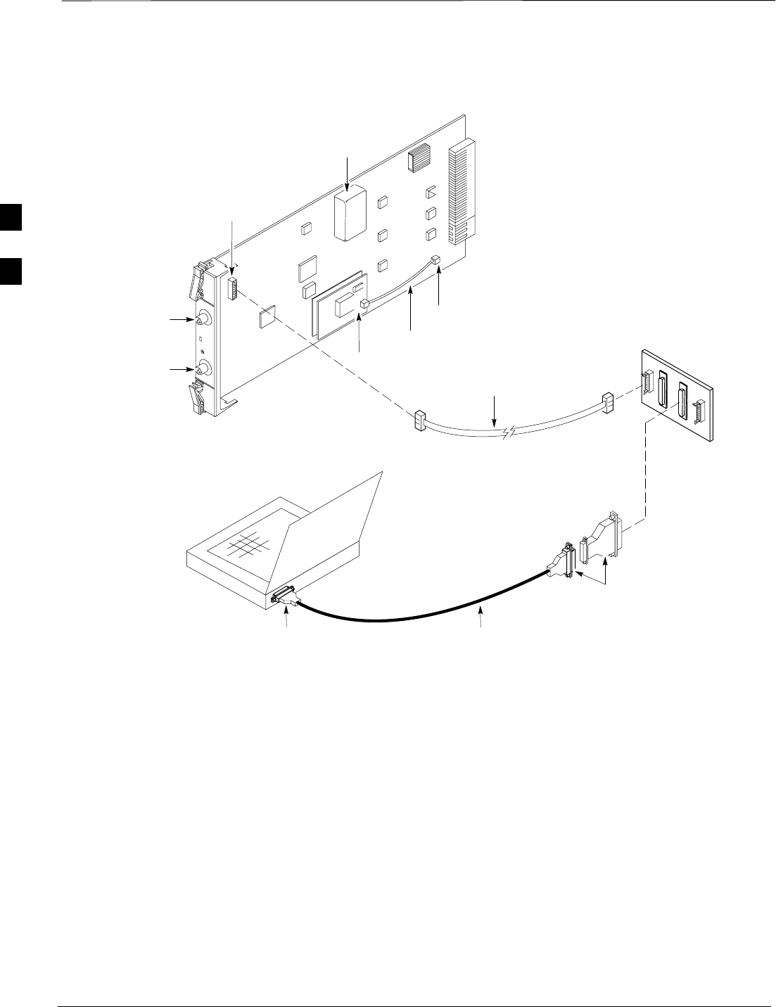
2Remove CSM–2 (if installed) and connect a serial cable from the LMF COM 1 port (via null modem
card) to the MMI port on CSM–1 (see Figure 3-13).
3Reinstall CSM–2.
4Start an MMI communication session with CSM–1 by using the Windows desktop shortcut icon (see
Table 3-11) .
5When the terminal screen appears press the Enter key until the CSM> prompt appears.
In the power entry compartment, connect the GPS antenna
to the RF GPS connector ONLY. Damage to the GPS
antenna and/or receiver can result if the GPS antenna is
inadvertently connected to any other RF connector.
CAUTION
3
CSM System Time – GPS & LFR/HSO Verification – continued
PRELIMINARY
1X SCt4812ET Lite BTS Optimization/ATP 08/01/2001
3-40
NULL MODEM
BOARD
(TRN9666A)
RS–232 SERIAL
MODEM CABLE
DB9–TO–DB25
ADAPTER
COM1
LMF
NOTEBOOK
Figure 3-13: CSM MMI Terminal Connection
FW00372
CSM card shown
removed from frame
19.6 MHZ TEST
POINT REFERENCE
(NOTE 1)
EVEN SECOND
TICK TEST POINT
REFERENCE
GPS RECEIVER
ANTENNA INPUT
GPS RECEIVER
MMI SERIAL
PORT
ANTENNA COAX
CABLE
REFERENCE
OSCILLATOR
9–PIN TO 9–PIN
RS–232 CABLE
NOTES:
1. One LED on each CSM:
Green = IN–SERVICE ACTIVE
Fast Flashing Green = OOS–RAM
Red = Fault Condition
Flashing Green & Red = Fault
GPS Initialization/Verification
Prerequisites
Ensure the following prerequisites have been met before proceeding:
SThe primary CSM and HSO (if equipped) has been warmed up for at
least 15 minutes.
SThe CDMA LMF computer is connected to the MMI port of the
primary CSM as shown in Figure 3-13.
SA HyperTerminal session has been started (Table 3-11), and the CSM>
prompt is present in the HyperTerminal window (Table 3-19).
Follow the steps outlined in Table 3-20 to initialize and verify proper
GPS receiver functioning.
3

CSM System Time – GPS & LFR/HSO Verification – continued
08/01/2001 3-41
1X SCt4812ET Lite BTS Optimization/ATP
PRELIMINARY
Table 3-20: GPS Initialization/Verification
Step Action
1To verify that Clock alarms (0000), Dpll is locked and has a reference source, and
GPS self test passed messages are displayed within the report, issue the following MMI
command
bstatus
–The system will display a response similiar to the following:
CSM Status INS:ACTIVE Slot A Clock MASTER.
BDC_MAP:000, This CSM’s BDC Map:0000
Clock Alarms (0000):
DPLL is locked and has a reference source.
GPS receiver self test result: passed
Time since reset 0:33:11, time since power on: 0:33:11
2Enter the following command at the CSM> prompt to display the current status of the Loran and GPS
receivers:
sources
–When equipped with LFR, the system will generate a response similar to the following:
N Source Name Type TO Good Status Last Phase Target Phase Valid
–––––––––––––––––––––––––––––––––––––––––––––––––––––––––––––––––––––––––
0LocalGPS Primary 4 YES Good 00Yes
1 LFR CHA Secondary 4 YES Good –2013177 –2013177 Yes
2 Not Used
Current reference source number: 0
–When equipped with HSO, the system will generate a response similar to the following:
Num Source Name Type TO Good Status Last Phase Target Phase Valid
––––––––––––––––––––––––––––––––––––––––––––––––––––––––––––––––––––––––––––
0 Local GPS Primary 4 Yes Good 3 0 Yes
1HSO Backup 4 No N/A timed–out* Timed–out* No
*NOTE “Timed–out” should only be displayed while the HSO is warming up. “Not–Present” or
“Faulty” should not be displayed. If the HSO does not appear as one of the sources, then configure the
HSO as a back–up source by entering the following command at the CSM> prompt:
ss 1 12
After a maximum of 15 minutes, the Rubidium oscillator should reach operational temperature and the
LED on the HSO should now have changed from red to green. After the HSO front panel LED has
changed to green, enter sources <cr> at the CSM> prompt. Verify that the HSO is now a valid source
by confirming that the bold text below matches the response of the “sources” command.
The HSO should be valid within one (1) minute, assuming the DPLL is locked and the HSO rubidium
oscillator is fully warmed.
Num Source Name Type TO Good Status Last Phase Target Phase Valid
––––––––––––––––––––––––––––––––––––––––––––––––––––––––––––––––––––––––––––
0 Local GPS Primary 4 Yes Good 3 0 Yes
1HSO Backup 4 Yes N/A xxxxxxxxxx xxxxxxxxxx Yes
. . . continued on next page
3

CSM System Time – GPS & LFR/HSO Verification – continued
PRELIMINARY
1X SCt4812ET Lite BTS Optimization/ATP 08/01/2001
3-42
Table 3-20: GPS Initialization/Verification
Step Action
3HSO information (underlined text above, verified from left to right) is usually the #1 reference source.
If this is not the case, have the OMCR determine the correct BTS timing source has been identified in
the database by entering the display bts csmgen command and correct as required using the edit
csm csmgen refsrc command.
* IMPORTANT
If any of the above areas fail, verify:
–If LED is RED, verify that HSO had been powered up for at least 5 minutes. After oscillator
temperature is stable, LED should go GREEN Wait for this to occur before continuing !
– If “timed out” is displayed in the Last Phase column, suspect the HSO output buffer or oscillator
is defective
–Verify the HSO is FULLY SEATED and LOCKED to prevent any possible card warpage
4Verify the following GPS information (underlined text above):
–GPS information is usually the 0 reference source.
–At least one Primary source must indicate “Status = good” and “Valid = yes” to bring site up.
. . . continued on next page
3

CSM System Time – GPS & LFR/HSO Verification – continued
08/01/2001 3-43
1X SCt4812ET Lite BTS Optimization/ATP
PRELIMINARY
Table 3-20: GPS Initialization/Verification
Step Action
5Enter the following command at the CSM> prompt to verify that the GPS receiver is in tracking mode.
gstatus
–Observe the following typical response:
24:06:08 GPS Receiver Control Task State: tracking satellites.
24:06:08 Time since last valid fix: 0 seconds.
24:06:08
24:06:08 Recent Change Data:
24:06:08 Antenna cable delay 0 ns.
24:06:08 Initial position: lat 117650000 msec, lon –350258000 msec, height 0 cm (GPS)
24:06:08 Initial position accuracy (0): estimated.
24:06:08
24:06:08 GPS Receiver Status:
24:06:08 Position hold: lat 118245548 msec, lon –350249750 msec, height 20270 cm
24:06:08 Current position: lat 118245548 msec, lon –350249750 msec, height 20270 cm
(GPS)
24:06:08 8 satellites tracked, receiving 8 satellites, 8 satellites visible.
24:06:08 Current Dilution of Precision (PDOP or HDOP): 0.
24:06:08 Date & Time: 1998:01:13:21:36:11
24:06:08 GPS Receiver Status Byte: 0x08
24:06:08 Chan:0, SVID: 16, Mode: 8, RSSI: 148, Status: 0xa8
24:06:08 Chan:1, SVID: 29, Mode: 8, RSSI: 132, Status: 0xa8
24:06:08 Chan:2, SVID: 18, Mode: 8, RSSI: 121, Status: 0xa8
24:06:08 Chan:3, SVID: 14, Mode: 8, RSSI: 110, Status: 0xa8
24:06:08 Chan:4, SVID: 25, Mode: 8, RSSI: 83, Status: 0xa8
24:06:08 Chan:5, SVID: 3, Mode: 8, RSSI: 49, Status: 0xa8
24:06:08 Chan:6, SVID: 19, Mode: 8, RSSI: 115, Status: 0xa8
24:06:08 Chan:7, SVID: 22, Mode: 8, RSSI: 122, Status: 0xa8
24:06:08
24:06:08 GPS Receiver Identification:
24:06:08 COPYRIGHT 1991–1996 MOTOROLA INC.
24:06:08 SFTW P/N # 98–P36830P
24:06:08 SOFTWARE VER # 8
24:06:08 SOFTWARE REV # 8
24:06:08 SOFTWARE DATE 6 AUG 1996
24:06:08 MODEL # B3121P1115
24:06:08 HDWR P/N # _
24:06:08 SERIAL # SSG0217769
24:06:08 MANUFACTUR DATE 6B07
24:06:08 OPTIONS LIST IB
24:06:08 The receiver has 8 channels and is equipped with TRAIM.
6Verify the following GPS information (shown above in underlined text):
–At least 4 satellites are tracked, and 4 satellites are visible.
–GPS Receiver Control Task State is “tracking satellites”. Do not continue until this occurs!
–Dilution of Precision indication is not more that 30.
Record the current position base site latitude, longitude, height and height reference (height reference
to Mean Sea Level (MSL) or GPS height (GPS). (GPS = 0 MSL = 1).
. . . continued on next page
3
CSM System Time – GPS & LFR/HSO Verification – continued
PRELIMINARY
1X SCt4812ET Lite BTS Optimization/ATP 08/01/2001
3-44
Table 3-20: GPS Initialization/Verification
Step Action
7If steps 1 through 6 pass, the GPS is good.
* IMPORTANT
If any of the above mentioned areas fail, verify that:
– If Initial position accuracy is “estimated” (typical), at least 4 satellites must be tracked and
visible (1 satellite must be tracked and visible if actual lat, log, and height data for this site has
been entered into CDF file).
– If Initial position accuracy is “surveyed,” position data currently in the CDF file is assumed to be
accurate. GPS will not automatically survey and update its position.
–The GPS antenna is not obstructed or misaligned.
–GPS antenna connector center conductor measureS approximately +5 Vdc with respect to the
shield.
–There is no more than 4.5 dB of loss between the GPS antenna OSX connector and the BTS frame
GPS input.
–Any lightning protection installed between GPS antenna and BTS frame is installed correctly.
8Enter the following commands at the CSM> prompt to verify that the CSM is warmed up and that GPS
acquisition has taken place.
debug dpllp
Observe the following typical response if the CSM is not warmed up (15 minutes from application of
power) (If warmed–up proceed to step 9)
CSM>DPLL Task Wait. 884 seconds left.
DPLL Task Wait. 882 seconds left.
DPLL Task Wait. 880 seconds left. ...........etc.
NOTE
The warm command can be issued at the MMI port used to force the CSM into warm–up, but the
reference oscillator will be unstable.
9Observe the following typical response if the CSM is warmed up.
c:17486 off: –11, 3, 6 TK SRC:0 S0: 3 S1:–2013175,–2013175
c:17486 off: –11, 3, 6 TK SRC:0 S0: 3 S1:–2013175,–2013175
c:17470 off: –11, 1, 6 TK SRC:0 S0: 1 S1:–2013175,–2013175
c:17486 off: –11, 3, 6 TK SRC:0 S0: 3 S1:–2013175,–2013175
c:17470 off: –11, 1, 6 TK SRC:0 S0: 1 S1:–2013175,–2013175
c:17470 off: –11, 1, 6 TK SRC:0 S0: 1 S1:–2013175,–2013175
10 Verify the following GPS information (underlined text above, from left to right):
–Lower limit offset from tracked source variable is not less than –60 (equates to 3µs limit).
–Upper limit offset from tracked source variable is not more than +60 (equates to 3µs limit).
–TK SRC: 0 is selected, where SRC 0 = GPS.
11 Enter the following commands at the CSM> prompt to exit the debug mode display.
debug dpllp
3

CSM System Time – GPS & LFR/HSO Verification – continued
08/01/2001 3-45
1X SCt4812ET Lite BTS Optimization/ATP
PRELIMINARY
LORAN–C
Initialization/Verification
Table 3-21: LORAN–C Initialization/Verification
Step Action Note
1At the CSM> prompt, enter lstatus <cr> to verify that the LFR is in tracking
mode. A typical response is:
CSM> lstatus <cr>
LFR St ti St t
LFR Station Status:
Clock coherence: 512 >
5930M 51/60 dB 0 S/N Flag:
5930X 52/64 dn –1 S/N Flag:
5990 47/55 dB –6 S/N Flag:
7980M 62/66 dB 10 S/N Fl
This must be greater
than 100 before LFR
becomes a valid source.
7980M 62/66 dB 10 S/N Flag:
7980W 65/69 dB 14 S/N Flag: . PLL Station . >
7980X 48/54 dB –4 S/N Flag:
7980Y 46/58 dB –8 S/N Flag:E
7980Z 60/67 dB 8 S/N Flag:
8290M 50/65 dB 0 S/N Flag
This shows the LFR is
locked to the selected
PLL station.
8290M 50/65 dB 0 S/N Flag:
8290W 73/79 dB 20 S/N Flag:
8290W 58/61 dB 6 S/N Flag:
8290W 58/61 dB 6 S/N Flag:
8970M 89/95 dB 29 S/N Flag:
8970W 62/66 dB 10 S/N Flag:
8970X 73/79 dB 22 S/N Flag:
8970X 73/79 dB 22 S/N Fl
ag:
8970Y 73/79 dB 19 S/N Flag:
8970Z 62/65 dB 10 S/N Flag:
9610M 62/65 dB 10 S/N Fl
g
9610M 62/65 dB 10 S/N Flag:
9610V 58/61 dB 8 S/N Flag:
9610W 47
/
49 dB –4S
/
N Fla
g
:E
9610W 47/49 dB –4 S/N Flag:E
9610X 46/57 dB –5 S/N Flag:E
9610Y 48/54 dB –5 S/N Flag:E
9610Z 65/69 dB 12 S/N Flag
9610Z 65/69 dB 12 S/N Flag:
9940M 50/53 dB –1 S/N Flag:S
9940W 49/56 dB –4 S/N Flag:E
9940W 49/56 dB 4 S/N Flag:E
9940Y 46/50 dB–10 S/N Flag:E
9960M 73/79 dB 22 S/N Flag:
9960W 51/60 dB 0 S/N Flag:
9960W 51/60 dB 0 S/N Fl
ag:
9960X 51/63 dB –1 S/N Flag:
9960Y 59/67 dB 8 S/N Flag:
9960Z 89/96 dB 29 S/N Fl
9960Z 89/96 dB 29 S/N Flag:
LFR Task State: lfr locked to station 7980W
LFR Recent Change Data:
Search List: 5930 5990 7980 8290 8970 9940 9610 9960 >
PLL GRI: 7980W
LFR Master, reset not needed, not the reference source.
CSM>
This search list and PLL
data must match the
configuration for the
geographical location
of the cell site.
. . . continued on next page
3

CSM System Time – GPS & LFR/HSO Verification – continued
PRELIMINARY
1X SCt4812ET Lite BTS Optimization/ATP 08/01/2001
3-46
Table 3-21: LORAN–C Initialization/Verification
Step NoteAction
2Verify the following LFR information (highlighted above in boldface type):
–Locate the “dot” that indicates the current phase locked station assignment (assigned by MM).
–Verify that the station call letters are as specified in site documentation as well as M X Y Z
assignment.
–Verify the S/N ratio of the phase locked station is greater than 8.
3At the CSM> prompt, enter sources <cr> to display the current status of the the LORAN receiver.
–Observe the following typical response.
Num Source Name Type TO Good Status Last Phase Target Phase Valid
––––––––––––––––––––––––––––––––––––––––––––––––––––––––––––––––––––––––––––
0 Local GPS Primary 4 Yes Good –3 0 Yes
1 LFR ch A Secondary 4 Yes Good –2013177 –2013177 Yes
2 Not used
Current reference source number: 1
*NOTE “Timed–out” should only be displayed while the LFR is warming up. “Not–Present” or
“Faulty” should not be displayed. If the LFR does not appear as one of the sources, then configure the
LFR as a back–up source by entering the following command at the CSM> prompt:
ss 1 2
4LORAN LFR information (highlighted above in boldface type) is usually the #1 reference source
(verified from left to right).
* IMPORTANT
If any of the above mentioned areas fail, verify:
–The LFR antenna is not obstructed or misaligned.
–The antenna pre–amplifier power and calibration twisted pair connections are intact and < 91.4 m
(300 ft) in length.
–A dependable connection to suitable Earth Ground is in place.
–The search list and PLL station for cellsite location are correctly configured .
NOTE
LFR functionality should be verified using the “source” command (as shown in Step 3). Use the
underlined responses on the LFR row to validate correct LFR operation.
5Close the hyperterminal window.
3

Test Equipment Setup
08/01/2001 3-47
1X SCt4812ET Lite BTS Optimization/ATP
PRELIMINARY
Connecting Test Equipment to
the BTS
All test equipment is controlled by the LMF through an IEEE–488/GPIB
bus. The LMF requires each piece of test equipment to have a factory set
GPIB address. If there is a communications problem between the LMF
and any piece of test equipment, verify that the GPIB addresses have
been set correctly as follows:
SPower meter address should be 13
SCommunications test set should be 18
The following test equipment is required to perform optimization,
calibration and ATP tests:
SCDMA LMF
SCommunications test set model supported by the CDMA LMF
SPower meter model supported by the CDMA LMF (required when
using the HP 8921A/600 and Advantest R3465 test sets)
SNon–radiating transmit line termination load
SDirectional coupler and in–line attenuator
SRF cables and adapters
Refer to Table 3-22 for an overview of connections for test equipment
currently supported by the CDMA LMF. In addition, see the following
figures:
SFigure 3-15 and Figure 3-16 show the test set connections for TX
calibration
SFigure 3-17 and Figure 3-18 show the test set connections for
optimization/ATP tests
Supported Test Equipment
Optimization and ATP testing may be performed using the following test
equipment:
SCyberTest
SAdvantest R3465 and HP–437B or Gigatronics Power Meter
SHewlett–Packard HP 8935
SHewlett–Packard HP 8921 (W/CDMA and PCS Interface (1.9 GHz))
and HP–437B or Gigatronics Power Meter
SSpectrum Analyzer (HP8594E) – optional
SRubidium Standard Timebase – optional
To prevent damage to the test equipment, all transmit (TX)
test connections must be through a 30 dB directional
coupler plus a 20 dB in-line attenuator for both the 800
MHz and 1.9 GHz BTSs.
CAUTION
3
Test Equipment Set–up – continued
PRELIMINARY
1X SCt4812ET Lite BTS Optimization/ATP 08/01/2001
3-48
Test Equipment Preparation
For specific steps to prepare each type of test set and power meter to
perform calibration and ATP, see Appendix F.
Test Equipment Connection
Chart
Table 3-22 depicts the current test equipment available meeting Motorola
standards.
To identify the connection ports, locate the test equipment presently
being used in the TEST SETS columns, and read down the column.
Where a ball appears in the column, connect one end of the test cable to
that port. Follow the horizontal line to locate the end connection(s),
reading up the column to identify the appropriate equipment/BTS port.
Table 3-22: Test Equipment Setup
TEST SETS ADDITIONAL TEST EQUIPMENT
SIGNAL Cyber–
Test Ad-
vantest HP
8935 HP
8921A
HP
8921
W/PCS Power
Meter
GPIB
Inter-
face LMF Directional
Coupler & Pad* BTS
EVEN SECOND
SYNCHRONIZATION EVEN
SEC REF EVEN SEC
SYNC IN
EVEN
SECOND
SYNC IN
EVEN
SECOND
SYNC IN
EVEN
SECOND
SYNC IN
19.6608 MHZ
CLOCK TIME
BASE IN
CDMA
TIME BASE
IN EXT
REF IN
CDMA
TIME BASE
IN
CDMA
TIME BASE
IN
CONTROL
IEEE 488 BUS IEEE
488 GPIB HP–IB HP–IB GPIB SERIAL
PORT
HP–IB HP–IB
TX TEST
CABLES RF
IN/OUT INPUT
50–OHM RF
IN/OUT TX1–6
RF
IN/OUT RF
IN/OUT 20 DB
PAD BTS
PORT
RX TEST
CABLES RF IN/
OUT RF OUT
50–OHM DUPLEX RX1–12
DUPLEX
OUT RF OUT
ONLY
SYNC
MONITOR
FREQ
MONITOR
3
Test Equipment Set–up – continued
08/01/2001 3-49
1X SCt4812ET Lite BTS Optimization/ATP
PRELIMINARY
Equipment Warm-up
Warm-up BTS equipment for a minimum of 60 minutes
prior to performing the BTS optimization procedure. This
assures BTS site stability and contributes to optimization
accuracy. (Time spent running initial power-up,
hardware/firmware audit, and BTS download counts as
warm-up time.)
IMPORTANT
*
Before installing any test equipment directly to any BTS
TX OUT connector, verify there are no CDMA BBX
channels keyed. At active sites, have the OMC-R/CBSC
place the antenna (sector) assigned to the LPA under test
OOS. Failure to do so can result in serious personal injury
and/or equipment damage.
WARNING
Automatic Cable Calibration
Set–up
Figure 3-14 shows the cable calibration setup for various supported test
sets. The left side of the diagram depicts the location of the input and
output ports of each test set, and the right side details the set up for each
test. Table 3-26 provides a procedure for calibrating cables.
3
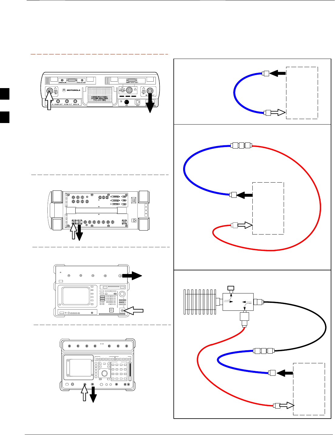
Test Equipment Set–up – continued
PRELIMINARY
1X SCt4812ET Lite BTS Optimization/ATP 08/01/2001
3-50
Motorola CyberTest
Hewlett–Packard Model HP 8935
Advantest Model R3465
DUPLEX
OUT
RF OUT
50–OHM
INPUT
50–OHM
RF GEN OUTANT IN
ANT
IN
SUPPORTED TEST SETS
100–WATT (MIN)
NON–RADIATING
RF LOAD
TEST
SET
A. SHORT CABLE CAL
SHORT
CABLE
B. RX TEST SETUP
TEST
SET
C. TX TEST SETUP
20 DB IN–LINE
ATTENUATOR
FOR 1.9 GHZ
CALIBRATION SET UP
N–N FEMALE
ADAPTER
TX
CABLE
TX
CABLE
SHORT
CABLE
Note: The Directional Coupler is not used with the
Cybertest Test Set. The TX cable is connected
directly to the Cybertest Test Set.
A 10dB attenuator must be used with the short test
cable for cable calibration with the CyberTest Test
Set. The 10dB attenuator is used only for the cable
calibration procedure, not with the test cables for
TX calibration and ATP tests.
TEST
SET
RX
CABLE
SHORT
CABLE
Figure 3-14: Cable Calibration Test Setup
FW00089
Note: For 800 MHZ only. The HP8921A cannot
be used to calibrate cables for PCS frequencies.
Hewlett–Packard Model HP 8921A
DIRECTIONAL
COUPLER
(30 DB)
N–N FEMALE
ADAPTER
50 Ω
ΤERM.
3
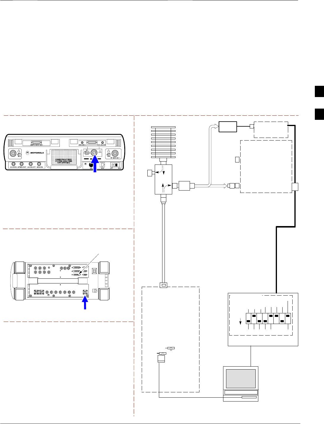
Test Equipment Set–up – continued
08/01/2001 3-51
1X SCt4812ET Lite BTS Optimization/ATP
PRELIMINARY
Manual Cable Calibration
If manual cable calibration is required, refer to the procedures in
Appendix F.
Set–up for TX Calibration
Figure 3-15 and Figure 3-16 show the test set connections for TX
calibration.
Motorola CyberTest
Hewlett–Packard Model HP 8935
TEST SETS TRANSMIT (TX) SET UP
FRONT PANEL RF
IN/OUT
RF IN/OUT
HP–IB
TO GPIB
BOX
RS232–GPIB
INTERFACE BOX
INTERNAL PCMCIA
ETHERNET CARD
GPIB
CABLE
COMMUNICATIONS
TEST SET
CONTROL
IEEE 488
GPIB BUS
UNIVERSAL TWISTED
PAIR (UTP) CABLE
(RJ45 CONNECTORS)
RS232
NULL
MODEM
CABLE
OUT
S MODE
DATA FORMAT
BAUD RATE
GPIB ADRS
G MODE
ON
TEST SET
INPUT/
OUTPUT
PORTS
BTS
100–WATT (MIN)
NON–RADIATING
RF LOAD
IN
TX
TEST
CABLE
CDMA
LMF
DIP SWITCH
SETTINGS**
2O DB
IN–LINE
ATTENUATOR
10BASET/
10BASE2
CONVERTER
LAN
B
LAN
A
TX TEST
CABLE
TX ANTENNA
PORT OR TX
RFDS
DIRECTIONAL
COUPLERS
POWER
METER
(OPTIONAL)*
NOTE: THE DIRECTIONAL COUPLER IS NOT USED WITH THE
CYBERTEST TEST SET. THE TX CABLE IS CONNECTED DIRECTLY
TO THE CYBERTEST TEST SET.
* A POWER METER CAN BE USED IN PLACE
OF THE COMMUNICATIONS TEST SET FOR TX
CALIBRATION/AUDIT
POWER
SENSOR
Figure 3-15: TX Calibration Test Setup (CyberTest and HP 8935)
FW00094
DIRECTIONAL
COUPLER
(30 DB)
** BLACK PORTION OF THE
DIAGRAM REPRESENTS THE
RAISED PART OF THE
SWITCH
50 Ω
ΤERM.
3
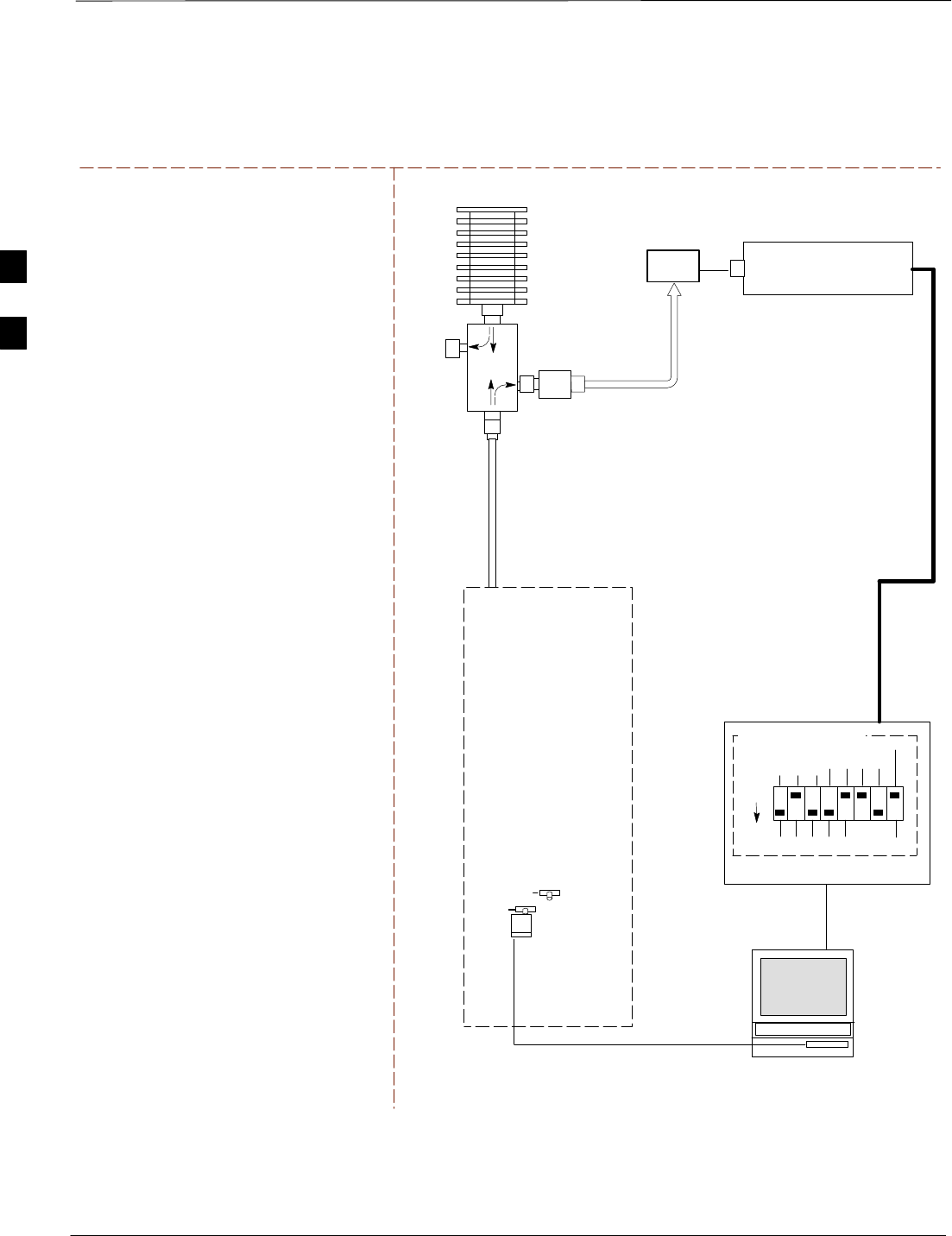
Test Equipment Set–up – continued
PRELIMINARY
1X SCt4812ET Lite BTS Optimization/ATP 08/01/2001
3-52
POWER METER
TEST SETS TRANSMIT (TX) SET UP
RS232–GPIB
INTERFACE BOX
INTERNAL PCMCIA
ETHERNET CARD
GPIB
CABLE
UNIVERSAL TWISTED
PAIR (UTP) CABLE
(RJ45 CONNECTORS)
RS232
NULL
MODEM
CABLE
S MODE
DATA FORMAT
BAUD RATE
GPIB ADRS G MODE
ON
BTS
100–WATT (MIN)
NON–RADIATING
RF LOAD
TX
TEST
CABLE
CDMA
LMF
DIP SWITCH
SETTINGS*
2O DB
IN–LINE
ATTENUATOR
10BASET/
10BASE2
CONVERTER
LAN
B
LAN
A
TX ANTENNA GROUP
OR TX RFDS DIRECTIONAL
COUPLERS
TX
TEST
CABLE
POWER
SENSOR
FW00095
NOTE: THE HP8921A AND ADVANTEST
CANNOT BE USED FOR TX CALIBRATION. A
POWER METER MUST BE USED.
Figure 3-16: TX Calibration Test Setup HP 8921A and Advantest
DIRECTIONAL COUPLER
(30 DB)
* BLACK PORTION OF THE
DIAGRAM REPRESENTS THE
RAISED PART OF THE
SWITCH
50 Ω
ΤERM.
3
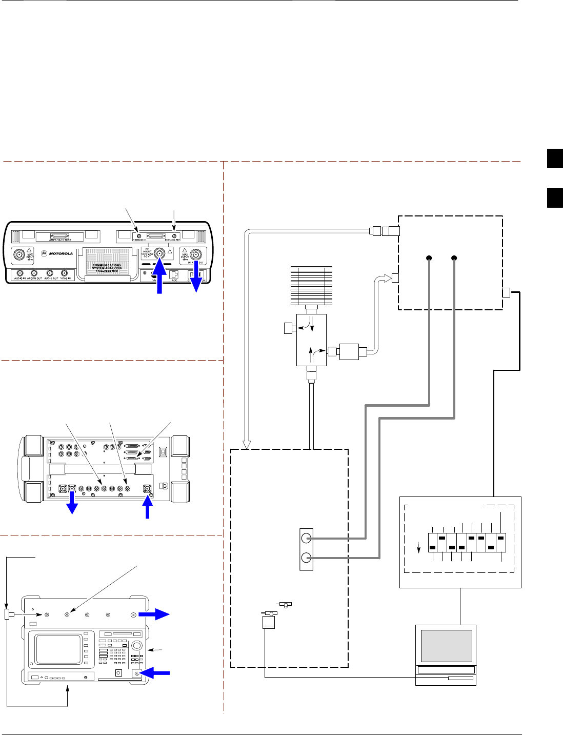
Test Equipment Set–up – continued
08/01/2001 3-53
1X SCt4812ET Lite BTS Optimization/ATP
PRELIMINARY
Setup for Optimization/ATP
Figure 3-17 and Figure 3-18 show the test set connections for
optimization/ATP tests.
Motorola CyberTest
Hewlett–Packard Model HP 8935
DUPLEX OUT
TEST SETS Optimization/ATP SET UP
RF
IN/OUT
SYNC MONITOR
EVEN SEC TICK
PULSE REFERENCE
FROM CSM BOARD
FREQ MONITOR
19.6608 MHZ CLOCK
REFERENCE FROM
CSM BOARD
RF IN/OUT
HP–IB
TO GPIB
BOX
Advantest Model R3465
INPUT
50–OHM
GPIB CONNECTS
TO BACK OF UNIT
NOTE: The Directional Coupler is not used
with the Cybertest Test Set. The TX cable is
connected directly to the Cybertest Test set.
RF OUT
RX ANTENNA
PORT OR RFDS
RX ANTENNA
DIRECTIONAL
COUPLER
TX ANTENNA
PORT OR RFDS
RX ANTENNA
DIRECTIONAL
COUPLER
RS232–GPIB
INTERFACE BOX
INTERNAL PCMCIA
ETHERNET CARD
GPIB
CABLE
UNIVERSAL TWISTED
PAIR (UTP) CABLE
(RJ45 CONNECTORS)
RS232 NULL
MODEM
CABLE
S MODE
DATA FORMAT
BAUD RATE
GPIB ADRS G MODE
ON
BTS
TX
TEST
CABLE
CDMA
LMF
DIPSWITCH SETTINGS*
10BASET/
10BASE2
CONVERTER
LAN
B
LAN
A
RX
TEST
CABLE
COMMUNICATIONS
TEST SET
IEEE 488
GPIB BUS
IN
TEST SET
INPUT/
OUTPUT
PORTS
OUT
NOTE: IF BTS RX/TX SIGNALS ARE
DUPLEXED, BOTH THE TX AND RX TEST
CABLES CONNECT TO THE DUPLEXED
ANTENNA GROUP AND USE THE 30 DB
DIRECTIONAL COUPLER AND 20 DB IN–LINE
ATTENUATOR.
100–WATT (MIN)
NON–RADIATING
RF LOAD
2O DB
IN–LINE
ATTENUATOR
DIRECTIONAL
COUPLER
(30 DB)
EVEN
SECOND/SYNC
IN (BNC “T”
WITH 50 OHM
TERMINATOR)
CDMA
TIMEBASE
IN
FREQ
MONITOR
SYNC
MONITOR
CSM
FW00096
Figure 3-17: Optimization/ATP Test Setup Calibration (CyberTest, HP 8935 and Advantest)
SYNC MONITOR
EVEN SEC TICK
PULSE REFERENCE
FROM CSM BOARD
FREQ MONITOR
19.6608 MHZ CLOCK
REFERENCE FROM
CSM BOARD
FREQ MONITOR
19.6608 MHZ CLOCK
REFERENCE FROM
CSM BOARD
RF
OUT
* BLACK PORTION OF THE
DIAGRAM REPRESENTS THE
RAISED PART OF THE
SWITCH
50 Ω
ΤERM.
SYNC MONITOR EVEN
SEC TICK PULSE
REFERENCE FROM
CSM BOARD
BNC
“T”
TO EXT TRIGGER CONNECTOR
ON REAR OF TEST SET
(FOR DETAILS, SEE FIGURE F-3)
3
Test Equipment Set–up – continued
PRELIMINARY
1X SCt4812ET Lite BTS Optimization/ATP 08/01/2001
3-54
RF OUT
ONLY
Hewlett–Packard Model HP 8921A W/PCS Interface
(for 1700 and 1900 MHz)
HP PCS
INTERFACE*
GPIB
CONNECTS
TO BACK OF
UNITS
SYNC MONITOR
EVEN SEC TICK
PULSE REFERENCE
FROM CSM BOARD
FREQ MONITOR
19.6608 MHZ CLOCK
REFERENCE FROM
CSM BOARD
TEST SETS Optimization/ATP SET UP
RX ANTENNA
PORT OR RFDS
RX ANTENNA
DIRECTIONAL
COUPLER
TX ANTENNA
PORT OR RFDS
RX ANTENNA
DIRECTIONAL
COUPLER
RS232–GPIB
INTERFACE BOX
INTERNAL PCMCIA
ETHERNET CARD
GPIB
CABLE
UNIVERSAL TWISTED
PAIR (UTP) CABLE
(RJ45 CONNECTORS)
RS232 NULL
MODEM
CABLE
S MODE
DATA FORMAT
BAUD RATE
GPIB ADRS G MODE
ON
BTS
TX
TEST
CABLE
CDMA
LMF
DIPSWITCH SETTINGS*
10BASET/
10BASE2
CONVERTER
LAN
B
LAN
A
RX
TEST
CABLE
COMMUNICATIONS
TEST SET
IEEE 488
GPIB BUS
IN
TEST SET
INPUT/
OUTPUT
PORTS
OUT
100–WATT (MIN)
NON–RADIATING
RF LOAD
2O DB
IN–LINE
ATTENUATOR
EVEN
SECOND/SYNC
IN (BNC “T”
WITH 50 OHM
TERMINATOR)
CDMA
TIMEBASE
IN
FREQ
MONITOR
SYNC
MONITOR
CSM
RF
IN/OUT
Figure 3-18: Optimization/ATP Test Setup HP 8921A
REF FW00097
GPIB
CONNECTS
TO BACK OF
UNIT
SYNC MONITOR
EVEN SEC TICK
PULSE REFERENCE
FROM CSM BOARD
FREQ MONITOR
19.6608 MHZ CLOCK
REFERENCE FROM
CSM BOARD
Hewlett–Packard Model HP 8921A
(for 800 MHz)
* FOR 1700 AND
1900 MHZ ONLY
DIRECTIONAL
COUPLER
(30 DB)
RF
IN/OUT
RF OUT
ONLY
* BLACK PORTION OF THE
DIAGRAM REPRESENTS THE
RAISED PART OF THE
SWITCH
50 Ω
ΤERM.
NOTE: IF BTS RX/TX SIGNALS ARE
DUPLEXED, BOTH THE TX AND RX TEST
CABLES CONNECT TO THE DUPLEXED
ANTENNA GROUP AND USE THE 30 DB
DIRECTIONAL COUPLER AND 20 DB IN–LINE
ATTENUATOR.
3
Test Set Calibration
PRELIMINARY
08/01/2001 3-55
1X SCt4812ET Lite BTS Optimization/ATP
Background
Proper test equipment set–up ensures that all measurements are correct
and the test equipment and associated test cables do not introduce
measurement errors.
If the test equipment set (see Chapter 1, Terms and
Abbreviations) being used to interface with the BTS has
been calibrated and maintained as a set, this procedure does
not need to be performed.
NOTE
This procedure must be performed before the optimization. Verify all test
equipment (including all associated test cables and adapters actually used
to interface all test equipment and the BTS) has been calibrated and
maintained as a set.
If any piece of test equipment, test cable, or RF adapter,
that makes up the calibrated test equipment set has been
replaced, the set must be re-calibrated. Failure to do so can
introduce measurement errors, resulting in incorrect
measurements and degradation to system performance.
Motorola recommends repeating cable calibration before
testing at each BTS site.
CAUTION
Calibration of the communications test set (or equivalent
test equipment) must be performed at the site before
calibrating the overall test set. Calibrate the test equipment
after it has been allowed to warm–up and stabilize for a
minimum of 60 minutes.
IMPORTANT
*
Purpose
These procedures access the CDMA LMF automated calibration routine
used to determine the path losses of the supported communications
analyzer, power meter, associated test cables, and (if used) antenna
switch that make up the overall calibrated test equipment set. After
calibration, the gain/loss offset values are stored in a test measurement
offset file on the CDMA LMF.
3

Test Set Calibration – continued
PRELIMINARY
1X SCt4812ET Lite BTS Optimization/ATP 08/01/2001
3-56
Manual cable calibration procedures using the HP8921A and Advantest
R3465 communications test sets are provided in Appendix F, if needed.
Manual power meter calibration procedures are also included in
Appendix F.
Selecting Test Equipment
Prerequisites
A Serial Connection and a Network Connection tab are provided for
test equipment selection. The Serial Connection tab is used when the
test equipment items are connected directly to the CDMA LMF
computer via a GPIB box (normal setup). The Network Connection tab
is used when the test equipment is to be connected remotely via a
network connection.
Ensure the following has been completed before selecting test
equipment:
STest equipment is correctly connected and turned on.
STest equipment GPIB addresses have been verified as correct.
SCDMA LMF computer serial port and test equipment are connected to
the GPIB box.
Selecting Test Equipment
Use Options > LMF Options in the menu bar to select test equipment
automatically (using the autodetect feature) or manually.
Manually Selecting Test
Equipment in a Serial
Connection Tab
Test equipment can be manually specified before, or after, the test
equipment is connected. CDMA LMF does not check to see if the test
equipment is actually detected for manual specification.
Table 3-23: Selecting Test Equipment Manually in a Serial Connection Tab
Step Action
1In the menu bar, click Options and select LMF Options... from the pulldown. The LMF Options
window appears.
2Click on the Serial Connection tab (if not in the forefront).
3Select the correct serial port in the COMM Port pick list (normally COM1).
4Click on the Manual Specification button (if not enabled).
5Click on the check box corresponding to the test item(s) to be used.
6Type the GPIB address in the corresponding GPIB address box. Addresses are:
13=Power Meter
18=CDMA Analyzer
. . . continued on next page
3

Test Set Calibration – continued
PRELIMINARY
08/01/2001 3-57
1X SCt4812ET Lite BTS Optimization/ATP
Table 3-23: Selecting Test Equipment Manually in a Serial Connection Tab
Step Action
7Click on Apply. (The button will darken until the selection has been recorded.)
NOTE
With manual selection, CDMA LMF does not detect the test equipment to see if it is connected and
communicating with CDMA LMF.
8Click on Dismiss to close the test equipment window.
Automatically Selecting Test
Equipment in a Serial
Connection Tab When using the auto-detection feature to select test equipment, the
CDMA LMF examines which test equipment items are actually
communicating with CDMA LMF. Follow the procedure in Table 3-24
to use the auto-detect feature.
Table 3-24: Selecting Test Equipment Using Auto-Detect
Step Action
1In the menu bar, click Options and select LMF Options... from the pulldown. The LMF Options
window appears.
2Click on the Serial Connection tab (if not in the forefront).
3Select the correct serial port in the COMM Port pick list (normally COM1).
4Click on Auto–Detection (if not enabled).
5Type in the GPIB addresses in the box labeled GPIB address to search (if not already displayed).
* IMPORTANT
When both a power meter and analyzer are selected, the first item listed in the GPIB addresses to
search box will be used for RF power measurements (i.e., TX calibration). The address for a power
meter is normally 13 and the address for a CDMA analyzer is normally 18. If 13,18 is included in the
GPIB addresses to search box, the power meter (13) will be used for RF power measurements. If the
test equipment items are manually selected the CDMA analyzer is used only if a power meter is not
selected.
6 Click Apply. The button will darken until the selection has been committed. A check mark will appear
in the Manual Configuration section for detected test equipment items.
7 Click Dismiss to close the LMF Options window.
3

Test Set Calibration – continued
PRELIMINARY
1X SCt4812ET Lite BTS Optimization/ATP 08/01/2001
3-58
Calibrating Test Equipment
The calibrate test equipment function zeros the power measurement level
of the test equipment item that is to be used for TX calibration and audit.
If both a power meter and an analyzer are connected (for example, an HP
437 and an HP8921A/600), only the power meter is zeroed.
Calibrate Test Equipment from the Util menu list is used to calibrate
test equipment item before being used for testing. The test equipment
must be selected before beginning calibration. Follow the procedure in
Table 3-25 to calibrate the test equipment.
Table 3-25: Test Equipment Calibration
Step Action
1From the Util menu, select Calibrate Test Equipment. A Directions window is displayed. Follow
the instructions provided.
2Follow the direction provided.
3Click on Continue to close the Directions window. A status window is displayed.
4Click on OK to close the status report window.
Calibrating Cables – Overview
The cable calibration function is used to measure the loss (in dB) for the
TX and RX cables that are to be used for testing. A CDMA analyzer is
used to measure the loss of each cable configuration (TX cable
configuration and RX cable configuration). The cable calibration
consists of the following steps.
SMeasure the loss of a short cable. This is done to compensate for any
measurement error of the analyzer. The short cable, which is used only
for the calibration process, is used in series with both the TX and RX
cable configuration when they are measured. The measured loss of the
short cable is deducted from the measured loss of the TX and RX
cable configuration to determine the actual loss of the TX and RX
cable configurations. This deduction is done so any error in the
analyzer measurement will be adjusted out of both the TX and RX
measurements.
SThe short cable plus the RX cable configuration loss is measured. The
RX cable configuration normally consists only of a coax cable with
type–N connectors that is long enough to reach from the BTS RX port
the test equipment. For BTSs with antenna ports carrying duplexed TX
and RX, a directional coupler and, if required by BTS type, an
additional attenuator are also used on the RX cable configuration and
must be included in the measurement.
SThe short cable plus the TX cable configuration loss is measured. The
TX cable configuration normally consists of two coax cables with
type–N connectors and a directional coupler, a load, and an additional
attenuator if required by the BTS type. The total loss of the path loss
3

Test Set Calibration – continued
PRELIMINARY
08/01/2001 3-59
1X SCt4812ET Lite BTS Optimization/ATP
of the TX cable configuration must be as required for the BTS
(normally 30 or 50 dB). The Motorola Cybertest analyzer is different
in that the required attenuation/load is built into the test set so the TX
cable configuration consists only of the required length coax cable.
Calibrating Cables with a
CDMA Analyzer
The Cable Calibration menu item from the Util menu list is used to
calibrate both TX and RX test cables for use with CDMA LMF.
LMF cable calibration cannot be accomplished with an
HP8921A analyzer for 1.9 MHz. A different analyzer type
or the signal generator and spectrum analyzer method must
be used (refer to Table 3-27 and Table 3-28). Cable
calibration values must be manually entered if the signal
generator and spectrum analyzer method is used. For the
HP8921A, refer to Appendix F.
NOTE
The test equipment must be selected before this procedure can be started.
Follow the procedure in Table 3-26 to calibrate the cables. Figure 3-14
illustrates the cable calibration test equipment setup.
Table 3-26: Cable Calibration
Step Action
1From the Util menu, select Cable Calibration. A Cable Calibration window is displayed.
2Enter a channel number(s) in the Channels box. Multiple channels numbers must be separated with a
comma, no space (i.e., 200,800). When two or more channels numbers are entered, the cables will be
calibrated for each channel. Interpolation will be accomplished for other channels as required for TX
calibration.
3 Select TX and RX CABLE CAL, TX CABLE CAL or RX CABLE CAL in the Cable Calibration
picklist.
4 Click OK. Follow the directions displayed for each step. A status report window will be displayed
with the results of the cable calibration.
3
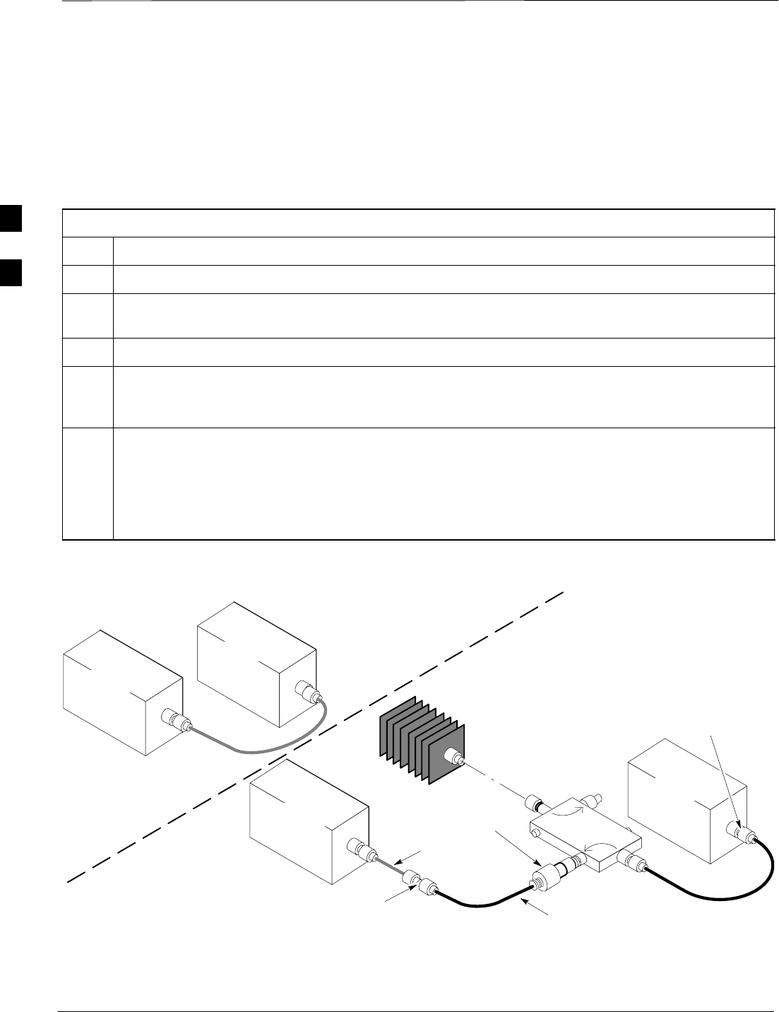
Test Set Calibration – continued
PRELIMINARY
1X SCt4812ET Lite BTS Optimization/ATP 08/01/2001
3-60
Calibrating TX Cables Using a
Signal Generator and Spectrum
Analyzer
Follow the procedure in Table 3-27 to calibrate the TX cables using the
signal generator and spectrum analyzer. Refer to Figure 3-19 for a
diagram of the signal generator and spectrum analyzer.
Table 3-27: Calibrating TX Cables Using Signal Generator and Spectrum Analyzer
Step Action
1Connect a short test cable between the spectrum analyzer and the signal generator.
2Set signal generator to 0 dBm at the customer frequency of the 869.7–893.31 MHz band for North
American cellular and 1930–1990 MHz band for North American PCS.
3Use spectrum analyzer to measure signal generator output (see Figure 3-19, “A”) and record the value.
4Connect the spectrum analyzer’s short cable to point “B”, as shown in the lower portion of the
diagram, to measure cable output at customer frequency (869.7–893.31 MHz band for North American
cellular and 1930–1990 MHz for North American PCS) and record the value at point “B”.
5Calibration factor = A – B Example: Cal = –1 dBm – (–53.5 dBm) = 52.5 dB
NOTE
The short cable is used for calibration only. It is not part of the final test setup. After calibration is
completed, do not re-arrange any cables. Use the equipment setup, as is, to ensure test procedures use
the correct calibration factor.
Figure 3-19: Calibrating Test Equipment Setup for TX Cable Calibration
(Using Signal Generator and Spectrum Analyzer)
50 OHM
TERMINATION
30 DB
DIRECTIONAL
COUPLER
Spectrum
Analyzer
Signal
Generator
A
Spectrum
Analyzer
40W NON–RADIATING
RF LOAD
B
SHORT TEST CABLE
Signal
Generator
THIS WILL BE THE CONNECTION TO THE
POWER METER DURING TX CALIBRATION
AND TO THE CDMA ANALYZER DURING TX
ATP TESTS.
SHORT
TEST
CABLE
THIS WILL BE THE CONNECTION
TO THE TX PORTS DURING TX
CALIBRATION AND TO THE TX/RX
PORTS DURING ATP TESTS.
SECOND RF
TEST CABLE.
ONE 20DB 20 W IN
LINE ATTENUATOR
(1.9 GHZ ONLY)
FW00293
3
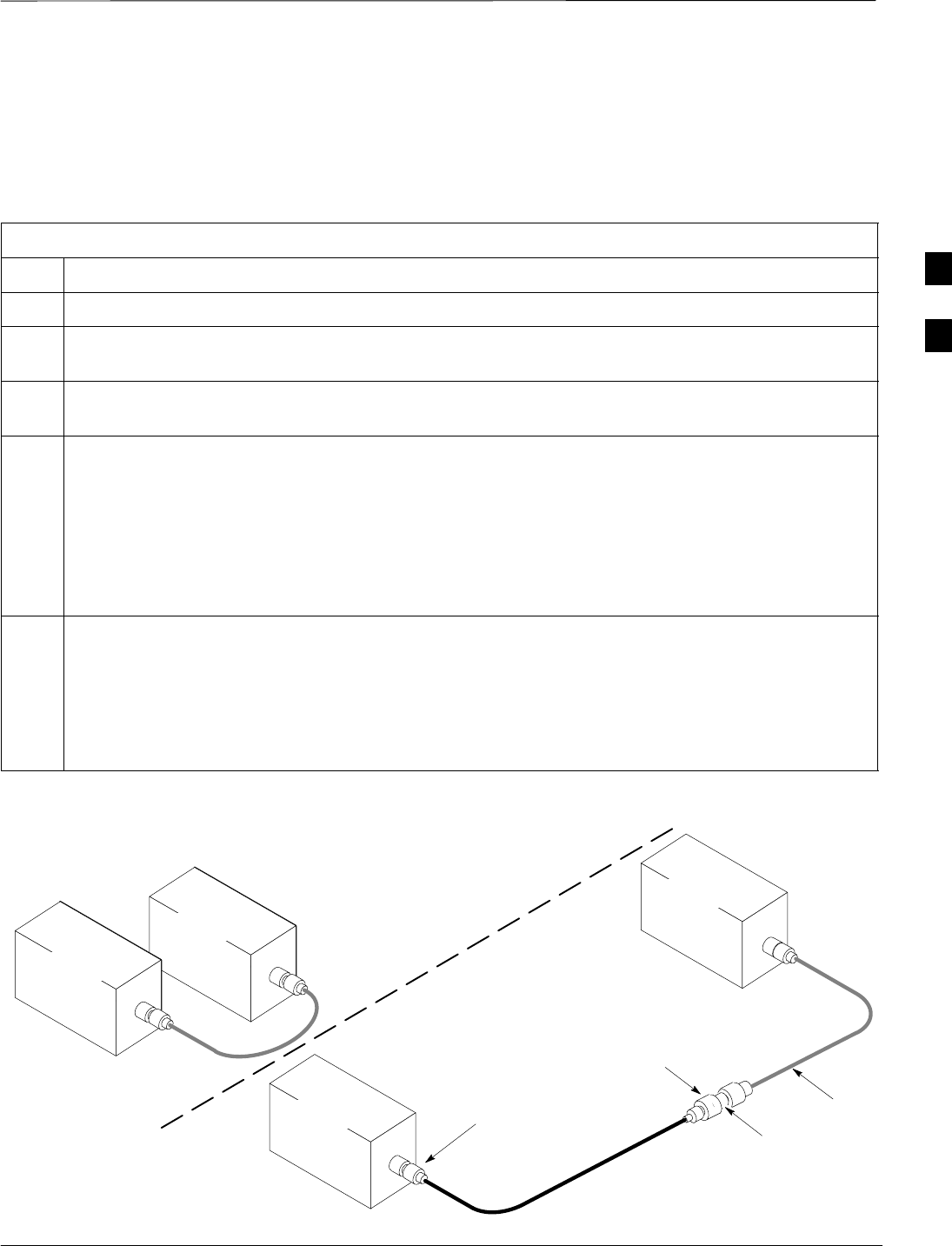
Test Set Calibration – continued
PRELIMINARY
08/01/2001 3-61
1X SCt4812ET Lite BTS Optimization/ATP
Calibrating RX Cables Using a
Signal Generator and Spectrum
Analyzer Follow the procedure in Table 3-28 to calibrate the RX cables using the
signal generator and spectrum analyzer. Refer to Figure 3-20, if required.
Table 3-28: Calibrating RX Cables Using a Signal Generator and Spectrum Analyzer
Step Action
1Connect a short test cable to the spectrum analyzer and connect the other end to the Signal Generator.
2Set signal generator to –10 dBm at the customer’s RX frequency of 824.7–848.31 MHz for North
American cellular or 1850–1910 MHz band for North American PCS.
3Use spectrum analyzer to measure signal generator output (see Figure 3-20, “A”) and record the value
for “A”.
4Connect the test setup, as shown in the lower portion of the diagram, to measure the output at the
customer’s RX frequency (824.7–848.31 MHz for North American cellular or 1850–1910 MHz band
for North American PCS). Record the value at point ‘‘B”.
* IMPORTANT
When preparing to calibrate a BTS with duplexed TX and RX the cable calibration setup must include
the 30 dB directional coupler and 20 dB in–line attenuator as in the TX cable calibration shown in
Figure 3-19.
5Calibration factor = A – B
Example: Cal = –12 dBm – (–14 dBm) = 2 dB
NOTE
The short test cable is used for test equipment setup calibration only. It is not part of the final test
setup. After calibration is completed, do not re-arrange any cables. Use the equipment setup, as is, to
ensure test procedures use the correct calibration factor.
Figure 3-20: Calibrating Test Equipment Setup for RX ATP Test
(Using Signal Generator and Spectrum Analyzer)
Spectrum
Analyzer
Signal
Generator
A
B
Spectrum
Analyzer
SHORT
TEST
CABLE
CONNECTION TO THE OUTPUT
PORT DURING RX MEASUREMENTS
Signal
Generator
BULLET
CONNECTOR
LONG
CABLE 2
SHORT TEST
CABLE
CONNECTION TO THE RX PORTS
DURING RX MEASUREMENTS.
IMPORTANT: IF BTS RX/TX SIGNALS ARE
DUPLEXED, THE RX TEST CABLE CONNECTS
TO THE DUPLEXED ANTENNA GROUP AND
MUST USE/BE CALIBRATED WITH THE 30 DB
DIRECTIONAL COUPLER AND 20 DB IN–LINE
ATTENUATOR. SEE FIGURE 3-19.
3
Test Set Calibration – continued
PRELIMINARY
1X SCt4812ET Lite BTS Optimization/ATP 08/01/2001
3-62
Setting Cable Loss Values Cable loss values for the TX and RX test cable configurations are
normally set by accomplishing automatic cable calibration with use of
the applicable test equipment. The resulting values are stored in the cable
loss files. The cable loss values can also be set/changed manually.
Cable loss values must be manually entered in the LMF
database if manual cable calibration was performed.
Failure to do this will result in inaccurate BTS calibration
and reduced site performance.
CAUTION
Prerequisites
SLogged into the BTS
Table 3-29: Setting Cable Loss Values
Step Action
1Click on the Util menu.
2 Select Edit > Cable Loss > TX or RX. A data entry pop–up window will appear.
3Click on the Add Row button to add a new channel number. Then click in the Channel # and Loss
(dBm) columns and enter the desired values.
4To edit existing values click in the data box to be changed and change the value.
5To delete a row, click on the row and then click on the Delete Row button.
6Click on the Save button to save displayed values.
7Click on the Dismiss button to exit the window. Values that were entered/changed after the Save
button was used will not be saved.
NOTE
SIf cable loss values exist for two different channels the LMF will interpolate for all other channels.
SEntered values will be used by the LMF as soon as they are saved. You do not have to logout and
login.
3

Test Set Calibration – continued
PRELIMINARY
08/01/2001 3-63
1X SCt4812ET Lite BTS Optimization/ATP
Setting TX Coupler Loss Value If an in–service TX coupler is installed the coupler loss (e.g., 30 dB)
must be manually entered so it will be included in the LMF TX
calibration and audit calculations.
Prerequisites
SLogged into the BTS
Table 3-30: Setting TX Coupler Loss Values
Step Action
1Click on the Util menu.
2 Select Edit > TX Coupler Loss. A data entry pop–up window will appear.
3Click in the Loss (dBm) column for each carrier that has a coupler and enter the appropriate value.
4To edit existing values click in the data box to be changed and change the value.
5Click on the Save button to save displayed values.
6Click on the Dismiss button to exit the window. Values that were entered/changed after the Save
button was used will not be saved.
NOTE
SThe In–Service Calibration check box in the Options > LMF Options > BTS Options tab must
checked before entered TX coupler loss values will be used by the TX calibration and audit
functions.
SEntered values will be used by the LMF as soon as they are saved. You do not have to logout and
login.
3

Bay Level Offset Calibration
PRELIMINARY
1X SCt4812ET Lite BTS Optimization/ATP 08/01/2001
3-64
Introduction
Calibration compensates for normal equipment variations within the
BTS and assures maximum measurement accuracy.
RF Path Bay Level Offset
Calibration
Bay Level Offset (BLO) calibration identifies the accumulated gain in
every transmit path (BBX2 slot) at the BTS site and stores that value in
the CDMA LMF CAL file. The BLOs are subsequently downloaded to
each BBX2.
Each transmit path starts at an SCCP shelf backplane BBX2 slot, travels
through the CIO card, trunking module, LPA, trunking module (again),
TX filter or TX filter combiner, DRDC or TRDC, and ends at a BTS TX
antenna port.
Each receive path starts at a BTS RX antenna port, travels through a
DRDC or TRDC, the MPC card, the CIO card, and terminates at a
backplane BBX2 slot.
Calibration identifies the accumulated gain in every transmit path ( by
BBX2 slot) at the BTS site and stores that value in the CAL file. When
the TX path calibration is performed, the RX path BLO will
automatically be set to the default value.
When to Calibrate BLOs Calibration of BLOs is required after initial BTS installation.
The BLO data of an operational BTS site must be re-calibrated once
each year. Motorola recommends re-calibrating the BLO data for all
associated RF paths after replacing any of the following components or
associated interconnecting RF cabling:
SBBX2 board
SSCCP shelf
SCIO card
SCIO–to–LPA trunking module RF cable
SLPA trunking module
SLPA
STrunking module–to–TX filter/filter combiner RF cable
STX filter or TX filter combiner
STX filter/filter combiner–to–DRDC/TRDC cable
SDRDC or TRDC
3
Bay Level Offset Calibration – continued
08/01/2001 3-65
1X SCt4812ET Lite BTS Optimization/ATP
PRELIMINARY
TX Path Calibration
The TX Path Calibration assures correct site installation, cabling, and the
first order functionality of all installed equipment. The proper function
of each RF path is verified during calibration. The external test
equipment is used to validate/calibrate the TX paths of the BTS.
Before installing any test equipment directly to any TX
OUT connector you must first verify that there are no
CDMA channels keyed. Have the OMC–R place the sector
assigned to the LPA under test OOS. Failure to do so can
result in serious personal injury and/or equipment damage.
WARNING
Always wear a conductive, high impedance wrist strap
while handling any circuit card/module. If this is not done,
there is a high probability that the card/module could be
damaged by ESD.
CAUTION
At new site installations, to facilitate the complete test of
each SCCP shelf (if the shelf is not already fully populated
with BBX2 boards), move BBX2 boards from shelves
currently not under test and install them into the empty
BBX2 slots of the shelf currently being tested to insure that
all BBX2 TX paths are tested.
–This procedure can be bypassed on operational sites
that are due for periodic optimization.
–Prior to testing, view the CDF file to verify the
correct BBX2 slots are equipped. Edit the file as
required to include BBX2 slots not currently
equipped (per Systems Engineering documentation).
IMPORTANT
*
RX Path Calibration
RX path calibration is not required or supported on CDMA BTS
systems. Default RX calibration values are written to the RX calibration
data files during the TX calibration routine. Functionality is verified
during Frame Erasure Rate (FER) testing.
3

Bay Level Offset Calibration – continued
PRELIMINARY
1X SCt4812ET Lite BTS Optimization/ATP 08/01/2001
3-66
BLO Calibration Data File
During the calibration process, the CDMA LMF creates a calibration
(CAL) data file where BLO values are stored. After calibration has been
completed, this offset data must be downloaded to the BBX2s using the
CDMA LMF Download BLO function. An explanation of the file is
shown below.
Due to the size of the file, Motorola recommends printing
out a copy of a bts.cal file and referring to it for the
following descriptions.
NOTE
The CAL file is subdivided into sections organized on a per–slot basis (a
slot Block).
The Slot 1 Block contains the calibration data for the six BBX2 slots.
The Slot 20 Block contains the calibration data for the redundant BBX2
(see Table 3-32). Each BBX2 slot Block header contains:
SA creation Date and Time – broken down into separate parameters of
createMonth, createDay, createYear, createHour, and createMin.
SThe number of calibration entries – fixed at 720 entries corresponding
to 360 calibration points of the CAL file – plus the slot Block format.
Within the slot Block body, the BBX2 calibration data (BayLevelCal) is
organized as a large flat array. The array is organized by branch, BBX2
SCCP cage slot, and calibration point.
SThe first breakdown of the array indicates which branch the contained
calibration points are for. The array covers transmit, main receive, and
diversity receive offsets as follows:
Table 3-31: BLO BTS.cal file Array Branch Assignments
Range Branch Assignment
C[1]–C[120] Transmit
C[121]–C[240] No SC4812ET Lite BLO cal
point entries (default only)
C[241]–C[360] Receive
C[361]–C[480] No SC4812ET Lite BLO cal
point entries (default only)
C[481]–C[600] Diversity Receive
C[601]–C[720] No SC4812ET Lite BLO cal
point entries (default only)
3
Bay Level Offset Calibration – continued
08/01/2001 3-67
1X SCt4812ET Lite BTS Optimization/ATP
PRELIMINARY
SThe second breakdown of the array is by BBX by sector. Three sectors
are allowed.
Table 3-32: SC4812ET Lite BTS.cal File Array (Per Sector)
BBX2 Sectorization TX Branch RX Branch RX Diversity
Branch
Slot[1] (Primary BBX2s 1 through 6)
1 (Omni) C[1]–C[20] C[241]–C[260] C[481]–C[500]
23–Sector, C[21]–C[40] C[261]–C[280] C[501]–C[520]
31st Carrier C[41]–C[60] C[281]–C[300] C[521]–C[540]
4 C[61]–C[80] C[301]–C[320] C[541]–C[560]
53–Sector, C[81]–C[100] C[321]–C[340] C[561]–C[580]
62nd Carrier C[101]–C[120] C[341]–C[360] C[581]–C[600]
C[121]–C[140] C[361]–C[380] C[601]–C[620]
C[141]–C[160] C[381]–C[400] C[621]–C[640]
Not Used in SC4812ET Lite
(CAL file entries are C[161]–C[180] C[401]–C[420] C[641]–C[660]
(CAL file entries are
Channel 0 with default C[181]–C[200] C[421]–C[440] C[661]–C[680]
power set level.) C[201]–C[220] C[441]–C[460] C[681]–C[700]
C[221]–C[240] C[461]–C[480] C[701]–C[720]
Slot[20] (Redundant BBX2–R1)
1 (Omni) C[1]–C[20] C[241]–C[260] C[481]–C[500]
23–Sector, C[21]–C[40] C[261]–C[280] C[501]–C[520]
31st Carrier C[41]–C[60] C[281]–C[300] C[521]–C[540]
4 C[61]–C[80] C[301]–C[320] C[541]–C[560]
53–Sector, C[81]–C[100] C[321]–C[340] C[561]–C[580]
62nd Carrier C[101]–C[120] C[341]–C[360] C[581]–C[600]
C[121]–C[140] C[361]–C[380] C[601]–C[620]
C[141]–C[160] C[381]–C[400] C[621]–C[640]
Not Used in SC4812ET Lite
(CAL file entries are C[161]–C[180] C[401]–C[420] C[641]–C[660]
(CAL file entries are
Channel 0 with default C[181]–C[200] C[421]–C[440] C[661]–C[680]
power set level.) C[201]–C[220] C[441]–C[460] C[681]–C[700]
C[221]–C[240] C[461]–C[480] C[701]–C[720]
SRefer to the CAL file print–out and Table 3-32. It can be seen that
there is one BBX2 slot per sector, and 10 calibration points for each
BBX2 (sector) are supported for each branch. Each “calibration point”
consists of two entries.
SThe first entry for a calibration point (all odd entries) identifies the
CDMA channel (frequency) where the BLO is measured. The second
calibration point entry (all even entries) is the power set level
(PwrLvlAdj). The valid range for PwrLvlAdj is from 2500 to 27500
3

Bay Level Offset Calibration – continued
PRELIMINARY
1X SCt4812ET Lite BTS Optimization/ATP 08/01/2001
3-68
(2500 corresponds to –125 dBm and 27500 corresponds to +125
dBm).
SThe 10 calibration points for each slot/branch combination must be
stored in order of increasing frequency. If less than 10 points
(frequencies) are calibrated, the BLO data for the highest frequency
calibrated is written into the remainder of the 10 points for that
slot/branch.
Example:
C[1]=384 (odd cal entry)
C[2]=19102 (even cal entry)
C[3]=777 (odd cal entry)
C[4]=19086 (even cal entry)
C[19]=777 (odd cal entry)
C[20]=19086 (even cal entry)
.
.
.
= 1 “calibration point”
In the example above, BLO was measured at only two frequencies
(channels 384 and 777) for SCCP slot BBX–1 transmit (Table 3-32).
The BLO data for the highest frequency measured (777) will be
written to the remaining eight transmit calibration points (defined by
entries C[5] through C[20]) for BBX2–1.
SWhen BLO data is downloaded to the BBXs, the data is downloaded
to the devices in the order it is stored in the CAL file. TxCal data
(C[1] – C[60]) is sent first. BBX2 slot 1’s 10 calibration points (C[1]
– C[20]) are sent initially, followed by BBX2 slot 2’s 10 calibration
points (C[21] – C[40]), and so on. The RxCal data is sent next,
followed by the RxDCal data.
STemperature compensation data (TempLevelCal) is also stored in the
CAL file for each slot Block.
Test Equipment Setup:
RF Path Calibration
Follow the steps outlined in Table 3-33 and refer as needed to
Figure 3-15 or Figure 3-16 to set up test equipment.
Table 3-33: Set Up Test Equipment (RF Path Calibration)
Step Action
1If it has not already been done, refer to the procedure in Table 3-6 to interface the CDMA LMF
computer terminal to the frame LAN A connector.
2If it has not already been done, refer to Table 3-7 to start a GUI LMF session.
3If required, calibrate the test equipment per the procedure in Table 3-25.
3
Bay Level Offset Calibration – continued
08/01/2001 3-69
1X SCt4812ET Lite BTS Optimization/ATP
PRELIMINARY
Table 3-33: Set Up Test Equipment (RF Path Calibration)
Step Action
! CAUTION
To prevent damage to the test equipment, all transmit (TX) test connections must be via the 30 dB
directional coupler for 800 MHz or via a 30 dB coupler with a 20 dB in–line attenuator for 1900
MHz.
4For TX path calibration, verify that the coaxial cable from the appropriate ANTENNA connector
(Figure 1-6 or Figure 1-7) is connected to the test equipment RF input port via the directional
coupler.
Transmit (TX) Path Calibration
The assigned channel frequency and desired power level at the frame TX
ports for transmit calibration are derived from the BTS CDF file. Each
BBX2 at the site is assigned to a sector and carrier. These are specified
respectively in the sector and carrier fields of the ParentCARRIER
parameter in each BBX2’s CDF file block. The channel frequency and
desired power for the assigned sector are specified respectively in the
ChannelList and SIFPilotPwr parameters of the CDF block for the
CARRIER to which the BBX2 is assigned.
The calibration procedure attempts to adjust the measured power to
within +0.5 dB of the desired power. The calibration will pass if the
error is less than +1.5 dB.
The TX BLO for the SC4812ET Lite is approximately 42.0 dB ±5.0 dB.
BLO is the gain in dB between the known power output of the BBX2
and the measured power at the TX port. BLO is derived by deducting the
known BBX2 power output from the power measured at the TX port or
(Measured Power) – (BBX2 TX Power Output).
Example:
Measured Power (at TX port) = 36.0 dBm
Known BBX TX Power Output = –6.0 dBm
BLO = (36.0) – (–6.0) = 42.0 dB gain
The CDMA LMF Tests menu list items TX Calibration and All
Cal/Audit perform TX BLO Calibration testing for installed BBX(s).
The All Cal/Audit menu item initiates a series of actions to perform TX
calibration, download BLO, and perform TX audit if the TX calibration
passes. The TX Calibration selection performs only the TX calibration.
When the TX Calibration selection is used, BLO download and TX
audit must be performed as separate activities. All measurements are
made through the appropriate antenna connector using the calibrated TX
cable setup.
In both the TX Calibration and All Cal/Audit dialog boxes, a Verify
BLO checkbox is provided and checked by default. After the actual TX
calibration is completed during either the TX Calibration or All
Cal/Audit process, the BLO derived from the calibration is compared to
a standard, acceptable BLO tolerance for the BTS. In some installations,
3
Bay Level Offset Calibration – continued
PRELIMINARY
1X SCt4812ET Lite BTS Optimization/ATP 08/01/2001
3-70
additional items may be installed in the transmit path. The additional
change in gain from these items could cause BLO verification failure
and, therefore, failure of the entire calibration. In these cases, either the
Verify BLO checkbox should be unchecked or the additional path losses
should be added into each applicable sector using the Util > Edit > TX
Coupler Loss... function.
Prerequisites
Before running this test, ensure that the following have been done:
SCSM–1, GLIs, MCCs, and BBX2s have correct code load and data
load.
SPrimary CSM and MGLI are INS.
SAll BBX2s are OOS_RAM.
STest equipment and test cables are calibrated and connected for TX
BLO calibration.
SLMF is logged into the BTS in the GUI environment.
Connect the test equipment as shown in Figure 3-15 and Figure 3-16
and follow the procedure in Table 3-34 to perform the TX calibration
test.
Before installing any test equipment directly to any TX
OUT connector, first verify there are no CDMA BBX2
channels keyed. Failure to do so can result in serious
personal injury and/or equipment damage.
WARNING
Verify all BBX2 boards removed and repositioned have
been returned to their assigned shelves/slots. Any BBX2
boards moved since they were downloaded will have to be
downloaded again.
IMPORTANT
*
3
Bay Level Offset Calibration – continued
08/01/2001 3-71
1X SCt4812ET Lite BTS Optimization/ATP
PRELIMINARY
Table 3-34: All Cal/Audit Path Calibration
Step Action
1Configure test equipment for TX path calibration per Table 3-33.
2Select the BBX2(s) to be calibrated.
3From the Tests menu, select All Cal/Audit.
4Select the appropriate carrier(s) displayed in the Channels/Carrier pick list.
Press and hold the <Shift> or <Ctrl> key to select multiple items.
5Type the appropriate channel number in the Carrier n Channels box.
6Click on OK.
7Follow the cable connection directions as they are displayed.
The test results will be displayed in the status report window.
8Click on Save Results or Dismiss to close the status report window.
TX Calibration Test
Prerequisites
Ensure the following prerequisites have been met before proceeding:
SMGLI and primary CSM and BDC are INS_ACT (CSM clock valid)
SAll BBXs are OOS–RAM (yellow)
STest equipment and test cables are calibrated and connected for TX
BLO calibration
SLMF is logged in to the BTS in the GUI environment
Verify all BBX boards removed and repositioned have been
returned to their assigned shelves/slots. Any BBX boards
moved since being downloaded will have to be
downloaded with code and data again.
IMPORTANT
*
If just a TX calibration must be run by itself, follow the procedures in
Table 3-35.
Table 3-35: TX Calibration Test
Step Action
1Configure test equipment for TX path calibration per Table 3-33.
2Click on the BBX(s) to be calibrated.
3From the Tests menu, select TX Calibration.
4Select the appropriate carrier(s) displayed in the Channels/Carrier pick list (press and hold the Shift
or Ctrl keyboard key to select multiple items).
. . . continued on next page
3
Bay Level Offset Calibration – continued
PRELIMINARY
1X SCt4812ET Lite BTS Optimization/ATP 08/01/2001
3-72
Table 3-35: TX Calibration Test
Step Action
5Enter the appropriate channel number in the Carrier n Channels box.
6 Click OK to display the status report window followed by a Directions pop-up window.
7Follow the cable connection directions as they are displayed. The test results will be displayed in the
status report window.
8 Click OK to close the status report window.
Exception Handling
In the event of a failure, the calibration procedure displays a FAIL
message in the status report window and provides information in the
Description field.
Recheck the test setup and connection and re–run the test. If the tests fail
again, note specifics about the failure, and refer to Chapter 6,
Troubleshooting.
Download BLO Procedure
After a successful TX path calibration, download the bay level offset
(BLO) calibration file data to the BBX2s. BLO data is extracted from the
CAL file for the Base Transceiver Subsystem (BTS) and downloaded to
the selected BBX2 devices.
If a successful All Cal/Audit was completed, this
procedure does not need to be performed, as BLO is
downloaded as part of the All Cal/Audit.
NOTE
Prerequisites
Ensure the following prerequisites have been met before proceeding.
SBBXs being downloaded are OOS–RAM (yellow).
STX calibration successfully completed
After a TX calibration has been performed using the procedure in
Table 3-35, follow the steps in Table 3-36 to download the BLO data to
the BBX2s.
3
Bay Level Offset Calibration – continued
08/01/2001 3-73
1X SCt4812ET Lite BTS Optimization/ATP
PRELIMINARY
Table 3-36: Download BLO
Step Action
1Select the BBX2(s) to be downloaded.
2From the Device menu, select Download BLO.
A status report window displays the result of the download.
NOTE
Selected device(s) do not change color when BLO is downloaded.
3 Click OK to close the status report window.
Calibration Audit Introduction
The BLO calibration audit procedure confirms the successful generation
and storage of the BLO calibrations. The calibration audit procedure
measures the path gain or loss of every BBX2 transmit path at the site.
In this test, actual system tolerances are used to determine the success or
failure of a test. The same external test equipment set up is used.
*RF path verification, BLO calibration, and BLO data
download to BBX2s must have been successfully
completed prior to performing the calibration audit.
IMPORTANT
Transmit (TX) Path Audit
Perform the calibration audit of the TX paths of all equipped BBX2
slots, per the steps in Table 3-37.
Before installing any test equipment directly to any TX
OUT connector, first verify there are no CDMA BBX2
channels keyed. Failure to do so can result in serious
personal injury and/or equipment damage.
WARNING
If a successful All Cal/Audit was completed, this
procedure does not need to be performed, as BLO is
downloaded as part of the All Cal/Audit.
NOTE
3

Bay Level Offset Calibration – continued
PRELIMINARY
1X SCt4812ET Lite BTS Optimization/ATP 08/01/2001
3-74
TX Audit Test
The Tests menu item, TX Audit, performs the TX BLO Audit test for a
BBX2(s). All measurements are made through the appropriate TX output
connector using the calibrated TX cable setup.
Prerequisites
Before running this test, the following should be done:
SCSM–1,GLI2s, BBX2s have correct code load.
SPrimary CSM and MGLI2 are INS.
SAll BBX2s are OOS_RAM.
STest equipment and test cables are calibrated and connected for TX
BLO calibration.
SLMF is logged into the BTS.
After a TX calibration has been performed using the procedure in
Table 3-35, or if verification of BLO data in the CAL file is required,
connect the test equipment as shown in Figure 3-15 or Figure 3-16 and
follow the procedure in Table 3-37 to perform the BTS TX Path Audit
test.
Table 3-37: TX Path Audit
Step Action
1Select the BBX2(s) to be audited. From the Tests menu, select TX Audit.
2Select the appropriate carrier(s) displayed in the Channels/Carrier pick list.
Press and hold the <Shift> or <Ctrl> key to select multiple items.
3Type the appropriate channel number in the Carrier n Channels box.
4Click on OK.
5Follow the cable connection directions as they are displayed.
A status report window displays the test results.
6Click on Save Results or Dismiss to close the status report window.
Exception Handling
In the event of a failure, the calibration procedure displays a FAIL
message in the status report window and provides information in the
Description field.
Recheck the test setup and connection and re–run the test. If the tests fail
again, note specifics about the failure, and refer to Chapter 6,
Troubleshooting.
3
Bay Level Offset Calibration – continued
08/01/2001 3-75
1X SCt4812ET Lite BTS Optimization/ATP
PRELIMINARY
Create CAL File
The Create Cal File function gets the BLO data from BBXs and
creates/updates the CAL file for the BTS. If a CAL file does not exist a
new one is created. If a CAL file already exists it is updated. After a
BTS has been fully optimized a copy of the CAL file must exist so it can
be transferred to the CBSC. If TX calibration has been successfully
performed for all BBXs and BLO data has been downloaded, a CAL file
will exist. Note the following:
SThe Create Cal File function only applies to selected (highlighted)
BBXs.
Editing the CAL file is not encouraged as this action can
cause interface problems between the BTS and the LMF.
To manually edit the CAL file you must first logout of the
BTS. If you manually edit the CAL file and then use the
Create Cal File function the edited information will be lost.
CAUTION
Prerequisites
Before running this test, the following should be done:
SLMF is logged into the BTS
SBBX2s are OOS_RAM with BLO downloaded
Table 3-38: Create CAL File
Step Action
1Select the applicable BBX2s. The CAL file will only be updated for the selected BBX2s.
2Click on the Device menu.
3Click on the Create Cal File menu item. The status report window displays the results of the action.
4 Click OK.
3

RFDS Setup and Calibration
PRELIMINARY
1X SCt4812ET Lite BTS Optimization/ATP 08/01/2001
3-76
RFDS Description
The optional RFDS is used to perform RF tests of the site from the
CBSC or from the LMF. The RFDS contains the following FRUs:
SAntenna Select Unit (ASU)
SFWT Interface Card (FWTIC)
SSubscriber Unit Assembly (SUA)
For complete information regarding the RFDS, refer to the CDMA
CDMA RFDS Hardware Installation; 68P64113A93, CDMA RFDS
User’s Guide; 68P64114A51, and the LMF Help function.
RFDS Parameter Settings
The bts-#.cdf file includes RFDS parameter settings that must
match the installed RFDS equipment. The paragraphs below describe the
editable parameters and their defaults. Table 3-39 explains how to edit
the parameter settings.
SRfdsEquip – valid inputs are 0 through 2.
0 = (default) RFDS is not equipped
1 = Non-Cobra/Patzer box RFDS
2 = Cobra RFDS
STsuEquip – valid inputs are 0 or 1
0 = (default) TSU not equipped
1 = TSU is equipped in the system
SMC1....4 – valid inputs are 0 or 1
0 = (default) Not equipped
1 = Multicouplers equipped in RFDS system
(SC9600 internal RFDS only)
SAsu1/2Equip – valid inputs are 0 or 1
0 = (default) Not equipped
1 = Equipped
STestOrigDN – valid inputs are ’’’ (default) or a numerical string up to
15 characters. (This is the phone number the RFDS dials when
originating a call. A dummy number needs to be set up by the switch,
and is to be used in this field.)
Any text editor may be used to open the bts–#.cdf file
to verify, view, or modify data.
NOTE
3

RFDS Setup and Calibration – continued
08/01/2001 3-77
1X SCt4812ET Lite BTS Optimization/ATP
PRELIMINARY
Table 3-39: RFDS Parameter Settings
Step Action
* IMPORTANT
Log out of the BTS prior to performing this procedure.
1Using a text editor, verify the following fields are set correctly in the bts–#.cdf file (1 = GLI based
RFDS; 2 = Cobra RFDS).
EXAMPLE:
RfdsEquip = 2
TsuEquip = 1
MC1Equip = 0
MC2Equip = 0
MC3Equip = 0
MC4Equip = 0
Asu1Equip = 1
Asu2Equip = 0 (1 if system is non-duplexed)
TestOrigDN = ’123456789’
NOTE
The above is an example of the bts-#.cdf file that should have been generated by the OMC–R and
copied to the LMF. These fields will have been set by the OMC–R if the RFDSPARM database is
modified for the RFDS.
2Save and/or quit the editor. If any changes were made to these fields data will need to be downloaded
to the GLI2 (see Step 3, otherwise proceed to Step 4).
3To download to the GLI2, click on the Device menu and select the Download Data menu item
(selected devices do not change color when data is downloaded). A status report window is displayed
showing status of the download. Click OK to close the status report window.
! CAUTION
After downloading data to the GLI2 the RFDS LED will slowly begin flashing red and green for
approximately 2–3 minutes. DO NOT attempt to perform any functions with the RFDS until the LED
remains green.
4Status the RFDS TSU. A status report is displayed showing the software version number for the TSIC
and SUA.
* IMPORTANT
If the LMF yields an error message, check the following:
SEnsure AMR cable is correctly connected from the BTS to the RFDS.
SVerify RFDS has power.
SVerify RFDS status LED is green.
SVerify fields in the bts-#.cdf file are correct (see Step 1).
SStatus the GLI2 and ensure the device is communicating (via Ethernet) with the LMF, and the
device is in the proper state (INS).
3

RFDS Setup and Calibration – continued
PRELIMINARY
1X SCt4812ET Lite BTS Optimization/ATP 08/01/2001
3-78
RFDS TSU NAM Programming
The NAM (number assignment module) information needs to be
programmed into the TSU before it can receive and process test calls, or
be used for any type of RFDS test. The RFDS TSU NAM must be
programmed with the appropriate system parameters and phone number
during hardware installation. The TSU phone and TSU MSI must be
recorded for each BTS used for OMC–R RFDS software configuration.
The user will only need to program the NAM for the initial
install of the RFDS.
NOTE
Explanation of Parameters
used when Programming the
TSU NAM
Table 3-40 defines the parameters used when editing the tsu.nam file.
Table 3-40: Definition of Parameters
Access Overload Code
Slot Index
System ID
Network ID
These parameters are obtained from the switch.
Primary Channel A
Primary Channel B
Secondary Channel A
Secondary Channel B
These parameters are the channels which are to be used in operation
of the system.
Lock Code
Security Code
Service Level
Station Class Mark
Do NOT change.
IMSI MCC
IMSI 11 12 These fields are obtained at the OMC using the following command:
OMC000>disp bts–# imsi
If the fields are blank, replace the IMSI fields in the NAM file to 0,
otherwise use the values displayed by the OMC.
MIN Phone Number These fields are the phone number assigned to the mobile. The ESN
and MIN must be entered into the switch as well.
NOTE
This field is different from the TODN field in the bts-#.cdf file.
The MIN is the phone number of the RFDS subscriber, and the
TODN is the number the subscriber calls.
3

RFDS Setup and Calibration – continued
08/01/2001 3-79
1X SCt4812ET Lite BTS Optimization/ATP
PRELIMINARY
Valid NAM Ranges Table 3-41 provides the valid NAM field ranges. If any of the fields are
missing or out-of–range, the RFDS will error out.
Table 3-41: Valid NAM Field Ranges
Valid Range
NAM Field Name Minimum Maximum
Access Overload Code 0 15
Slot Index 0 7
System ID 0 32767
Network ID 0 32767
Primary Channel A 25 1175
Primary Channel B 25 1175
Secondary Channel A 25 1175
Secondary Channel B 25 1175
Lock Code 0 999
Security Code 0 999999
Service Level 0 7
Station Class Mark 0 255
IMSI 11 12 0 99
IMSI MCC 0 999
MIN Phone Number N/A N/A
3

RFDS Setup and Calibration – continued
PRELIMINARY
1X SCt4812ET Lite BTS Optimization/ATP 08/01/2001
3-80
Set Antenna Map Data
The antenna map data must be entered manually if an RFDS is installed.
Antenna map data does not have to be entered if an RFDS is not
installed. The antenna map data is only used for RFDS tests and is
required if a RFDS is installed.
Prerequisite
SLogged into the BTS
Table 3-42: Set Antenna Map Data
Step Action
1Click on the Util menu.
2 Select Edit > Antenna Map > TX or RX. A data entry pop–up window will appear.
3Enter/edit values as required for each carrier.
NOTE
Refer to the Util > Edit–antenna map LMF help screen for antenna map examples.
4Click on the Save button to save displayed values.
5Click on the Dismiss button to exit the window. Values that were entered/changed after the Save
button was used will not be saved.
NOTE
Entered values will be used by the LMF as soon as they are saved. You do not have to logout and
login.
3
RFDS Setup and Calibration – continued
08/01/2001 3-81
1X SCt4812ET Lite BTS Optimization/ATP
PRELIMINARY
Set RFDS Configuration Data
If an RFDS is installed the RFDS configuration data must be manually
entered.
Prerequisite
SLogged into the BTS
The entered antenna# index numbers must correspond to
the antenna# index numbers used in the antenna maps.
IMPORTANT
*
Table 3-43: Set RFDS Configuration Data
Step Action
1Click on the Util menu.
2 Select Edit > RFDS Configuration > TX or RX. A data entry pop–up window will appear.
3Click on the Add Row button to add a new antenna number. Then click in the other columns and enter
the desired data.
4To edit existing values click in the data box to be changed and change the value.
NOTE
Refer to the Util > Edit–RFDS Configuration LMF help screen for RFDS configuration data
examples.
5To delete a row, click on the row and then click on the Delete Row button.
6Click on the Save button to save displayed values.
7Click on the Dismiss button to exit the window. Values that were entered/changed after the Save
button was used will not be saved.
NOTE
Entered values will be used by the LMF as soon as they are saved. You do not have to logout and
login.
3
RFDS Setup and Calibration – continued
PRELIMINARY
1X SCt4812ET Lite BTS Optimization/ATP 08/01/2001
3-82
RFDS Calibration
The RFDS Calibration option is used to calibrate the RFDS TX and RX
paths. For a TX antenna path calibration the BTS XCVR is keyed at a
pre–determined power level and the BTS power output level is measured
by the RFDS. The power level is then measured at the TX antenna
directional coupler by the power measuring test equipment item being
used (power meter or analyzer). The difference (offset) between the
power level at the RFDS and the power level at the TX antenna
directional coupler is used as the TX RFDS calibration offset value.
For an RX antenna path calibration the RFDS is keyed at a
pre–determined power level and the power input level is measured by the
BTS XCVR. A CDMA signal at the same power level measured by the
BTS XCVR is then injected at the RX antenna directional coupler by the
CDMA communications analyzer. The difference (offset) between the
RFDS keyed power level and power level measured at the BTS XCVR is
the RFDS RX calibration offset value.
The TX and RX RFDS calibration offset values are written to the CAL
file.
For each RFDS TSIC, the channel frequency is determined at the lower
third and upper third of the appropriate band using the frequencies listed
in Table 3-44.
Table 3-44: RFDS TSIC Calibration Channel Frequencies
System Channel Calibration Points
800 MHz (A and B) 341 and 682
1.9 GHz 408 and 791
Before installing any test equipment directly to any TX
OUT connector, verify that there are no CDMA BBX
channels keyed. Failure to do so can result in serious
personal injury and/or equipment damage.
WARNING
Prerequisites
SBBX2s are INS_TEST
SCable calibration has been performed
STX calibration has been performed and BLO has been downloaded for
the BTS
STest equipment has been connected correctly for a TX calibration
STest equipment has been selected and calibrated
3

RFDS Setup and Calibration – continued
08/01/2001 3-83
1X SCt4812ET Lite BTS Optimization/ATP
PRELIMINARY
Table 3-45: RFDS Calibration
Step Action
1Select the RFDS tab.
2Click on the RFDS menu.
3Click on the RFDS Calibration menu item.
4Select the appropriate direction (TX/RX) in the Direction pick list.
5Enter the appropriate channel number(s) in the Channels box. Separate the channel numbers with a
comma or a dash if more than one channel number is entered (e.g., 247,585,742 or 385–395 for
through).
6 Select the appropriate carrier(s) in the Carriers pick list (use the Shift or Ctrl key to select multiple
carriers).
7Select the appropriate RX branch (Both, Main, or Diversity) in the RX Branch pick list.
8Select the appropriate baud rate (1=9600, 2=14400) in the Rate Set pick list.
9Click on the OK button. A status report window is displayed, followed by a Directions pop–up
window.
10 Follow the cable connection directions as they are displayed. Test results are displayed in the status
report window.
11 Click on the OK button to close the status report window.
12 Click on the BTS tab.
13 Click on the MGLI.
14 Download the CAL file which has been updated with the RFDS offset data to the selected GLI device
by clicking on Device > Download Data from the tab menu bar and pulldown.
NOTE
The MGLI will automatically transfer the RFDS offset data from the CAL file to the RFDS.
3

RFDS Setup and Calibration – continued
PRELIMINARY
1X SCt4812ET Lite BTS Optimization/ATP 08/01/2001
3-84
Program TSU NAM
Follow the procedure in Table 3-46 to program the TSU NAM. The
NAM must be programmed before it can receive and process test calls,
or be used for any type of RFDS test.
Prerequisites
SMGLI is INS.
STSU is powered up and has a code load.
Table 3-46: Program NAM Procedure
Step Action
1Select the RFDS tab.
2Select the TSU tab.
3Click on the TSU menu.
4Click on the Program TSU NAM menu item.
5Enter the appropriate information in the boxes (see Table 3-40 and Table 3-41) .
6Click on the OK button to display the status report.
7Click on the OK button to close the status report window.
3

Alarms Testing
08/01/2001 3-85
1X SCt4812ET Lite BTS Optimization/ATP
PRELIMINARY
Alarm Verification
The alarms testing should be performed at a convenient point in the
optimization/ATP process, since the LMF is necessary to ensure that the
SC4812ET Lite is generating the appropriate alarms.
The SC 4812ET Lite is capable of concurrently monitoring 10 customer
defined input signals and four customer defined outputs, which interface
to the 50–pair punchblock. All alarms are defaulted to “Not Equipped”
during ATP testing. Testing of these inputs is achieved by triggering the
alarms and monitoring the LMF for state–transition messages from the
active MGLI2.
Alarm Reporting Display
The Alarm Monitor window can be displayed to list alarms that occur
after the window is displayed. To access the Alarm Monitor window,
select Util > Alarm Monitor.
The following buttons are included.
SThe Options button allows for a severity level (Warning, Minor,
Major, Critical, and Unknown) selection. The default is all levels.
To change the level of alarms reported click on the Options button
and highlight the desired alarm level(s). To select multiple levels press
the Ctrl key (for individual selections) or Shift key (for a range of
selections) while clicking on the desired levels.
SThe Pause button can be used to pause/stop the display of alarms.
When the Pause button is clicked the name of the button changes to
Continue. When the Continue button is click the display of alarms
will continue. Alarms that occur between the time the Pause button is
clicked and the Continue button is clicked will not be displayed.
SThe Clear button can be used to clear the Alarm Monitor display.
New alarms that occur after the Clear button is clicked will be
displayed.
SThe Dismiss button is used to dismiss/close the Alarm Monitor
display.
3

Alarms Testing – continued
PRELIMINARY
1X SCt4812ET Lite BTS Optimization/ATP 08/01/2001
3-86
Alarm Testing Set–up
Prepare for any alarm testing by following the procedures in Table 3-47.
Table 3-47: Alarm Testing Preparation
Step Action
1If it has not already been done, refer to the procedure in Table 3-6 to interface the CDMA LMF
computer terminal to the frame LAN A connector.
2If it has not already been done, refer to Table 3-7 to start a GUI LMF session.
3Click on Util in the menu bar and select Alarm Monitor... from the pulldown.
SAn Alarm Monitor window will open.
Heat Exchanger Alarm Test
Table 3-48 gives instructions on testing the Heat Exchanger alarm.
Table 3-48: Heat Exchanger Alarm
Step Action
1Set one of the two DC PDA heat exchanger circuit breakers to OFF. This will generate a heat
exchanger alarm. Be sure that the CDMA LMF reports the correct alarm condition.
2Alarm condition will be reported as BTS Relay #14, BTS Relay #15, BTS Relay #16, BTS Relay
#17, BTS Relay #18, with Contact Alarm Open*Clear*, respectively.
3Set the circuit breaker turned off in step 1 to ON. Ensure that the alarm conditions have cleared on
the CDMA LMF with Contact Alarm Closed*Clear* for each reported BTS relay.
NOTE
The heat exchanger will go through the start–up sequence.
Door Alarm
Table 3-49 gives instructions on testing the door alarms.
Table 3-49: ACLC and Power Entry Door Alarm
Step Action
1Close the ACLC and power entry compartment doors on the frame. Ensure that no alarms are reported
on the CDMA LMF.
2Individually open and then close the ACLC and power entry compartment door. Ensure that the
CDMA LMF reports an alarm when each door is opened.
3Alarm condition will be reported as BTS Relay #27 contact.
3

Alarms Testing – continued
08/01/2001 3-87
1X SCt4812ET Lite BTS Optimization/ATP
PRELIMINARY
AC Fail Alarm
Table 3-50 gives instructions on testing the AC Fail Alarm.
Table 3-50: AC Fail Alarm
Step Action
1* IMPORTANT
SBack–up batteries must be installed when performing this test.
STo prevent inadvertently shutting down the RF compartment electronics, the batteries should be
charged before performing this test.
Set the ACLC MAIN circuit breaker to OFF.
SThe CDMA LMF should report an alarm for an AC Fail condition as BTS Relay #21, BTS Relay
#23, BTS Relay #24, and BTS Relay #29 contacts, respectively.
SOn the MAP, the MAJOR ALARM (red), MINOR ALARM (amber), and RECTIFIER FAIL (red)
LEDs should light.
SOn the rectifiers, the DC and PWR LEDs should light red.
2Set the ACLC MAIN circuit breaker to ON.
SOn the CDMA LMF, the AC Fail alarm should clear.
SOn the MAP, the MAJOR ALARM, MINOR ALARM, and RECTIFIER FAIL LEDs should
extinguish.
SOn the rectifiers, the DC and PWR LEDs should change to green.
Minor Alarm
Table 3-51 gives instructions on performing a test to display a minor
alarm.
Table 3-51: Minor Alarm
Step Action
1Set the TCP switch on the MAP to OFF. This will generate a minor alarm.
SThe CDMA LMF should report the minor alarm as BTS Relay #24 contacts.
SThe TC DISABLE (red) and MINOR ALARM (amber) LEDs on the MAP should light.
2Set the TCP switch to ON. The alarm condition indications should clear.
Rectifier Alarms
The following series of tests are for single rectifier modules in a multiple
rectifier system. The systems include a three rectifier and a four rectifier
system.
Single Rectifier Failure
(Three Rectifier System)
Table 3-52 gives instructions on testing single rectifier failure or minor
alarm in a three (3) rectifier system (single–carrier system). Procedures
3

Alarms Testing – continued
PRELIMINARY
1X SCt4812ET Lite BTS Optimization/ATP 08/01/2001
3-88
in this test are for a frame configured for single carrier operation with
rectifiers installed in rectifier shelf positions 2, 3, and 4, from left to
right when facing the frame.
Table 3-52: Single Rectifier Fail or Minor Alarm, Single–Carrier System
Step Action
1! CAUTION
Only perform this test if the rectifier current load displayed on the AMP indicator on the MAP is
125 amps or less. Sufficient current capability to support a greater load may not be available when
one rectifier is removed from the bus.
On the ACLC, set the RECT. 2/4 circuit breaker to OFF.
SThe DC and PWR LEDs should light red on the rectifier in shelf position 2.
SThe MINOR ALARM (amber) and RECTIFIER FAIL (red) LEDs on the MAP should light.
SThe CDMA LMF should report an alarm condition as BTS Relay #21 and BTS Relay #24
contacts, respectively.
2Set the RECT. 2/4 circuit breaker on the ACLC to ON.
SAll alarm indications should clear on the rectifier, MAP, and CDMA LMF.
Multiple Rectifier Failure
(Three Rectifier System)
Table 3-53 gives instructions on testing multiple rectifier failure or major
alarm in a three (3) rectifier system (single–carrier system). Procedures
in this test are for a frame configured for single carrier operation with
rectifiers installed in rectifier shelf positions 2, 3, and 4, from left to
right when facing the frame.
Table 3-53: Multiple Rectifier Failure or Major Alarm, Single–Carrier System
Step Action
1! CAUTION
Only perform this test if the rectifier current load displayed on the AMP indicator on the MAP is 65
amps or less. Sufficient current capability to support a greater load may not be available when two
rectifiers are removed from the bus.
On the ACLC, set the RECT. 1/3 circuit breaker to OFF.
SThe DC and PWR LEDs should light red on the rectifiers in shelf positions 1 and 3.
SThe MAJOR ALARM (red), MINOR ALARM (amber), and RECTIFIER FAIL (red) LEDs on the
MAP should light.
SThe CDMA LMF should report an alarm condition as BTS Relay #21, BTS Relay #24, and BTS
Relay #29 contacts, respectively.
2Set the RECT. 1/3 circuit breaker on the ACLC to ON.
SAll alarm indications should clear on the rectifiers, MAP, and CDMA LMF.
3

Alarms Testing – continued
08/01/2001 3-89
1X SCt4812ET Lite BTS Optimization/ATP
PRELIMINARY
Single Rectifier Failure
(Four Rectifier System)
Table 3-54 gives instructions on testing single rectifier failure or minor
alarm in a four (4) rectifier system (two–carrier system).
Table 3-54: Single Rectifier Fail or Minor Alarm, Two–Carrier System
Step Action
1! CAUTION
Only perform this test if the rectifier current load displayed on the AMP indicator on the MAP is
125 amps or less. Sufficient current capability to support a greater load may not be available when
two rectifiers are removed from the bus in the following steps.
Unseat the rectifier in shelf position 4 from its connection at the rear of the shelf, but do not
completely remove it from the shelf.
SThe rectifier 4 DC and PWR LEDs may light red momentarily and extinguish. There should be no
other indications on the frame or CDMA LMF.
2On the ACLC, set the RECT. 2/4 circuit breaker to OFF.
SThe rectifier 2 DC and PWR LEDs should light red.
SThe MINOR ALARM (amber) and RECTIFIER FAIL (red) LEDs on the MAP should light.
SThe CDMA LMF should report an alarm condition as BTS Relay #21 and BTS Relay #24
contacts, respectively.
3 Re–seat the rectifier in shelf position 4 into its connection at the rear of the shelf.
4 On the ACLC, set the RECT. 2/4 circuit breaker to ON.
SThe rectifier DC and PWR LEDs should light green.
SAll alarm indications should clear on the rectifiers, MAP, and CDMA LMF.
3
Alarms Testing – continued
PRELIMINARY
1X SCt4812ET Lite BTS Optimization/ATP 08/01/2001
3-90
Multiple Rectifier Failure
(Four Rectifier System)
Table 3-55 gives instructions on testing multiple rectifier failure or major
alarm in a four (4) rectifier system (two–carrier system).
Table 3-55: Multiple Rectifier Failure or Major Alarm, Two–Carrier System
Step Action
1! CAUTION
Only perform this test if the rectifier current load displayed on the AMP indicator on the MAP is
125 amps or less. Sufficient current capability to support a greater load may not be available when
two rectifiers are removed from the bus.
On the ACLC, set the RECT. 2/4 circuit breaker to OFF.
SThe DC and PWR LEDs should light red on the rectifiers in shelf positions 2 and 4.
SThe MAJOR ALARM (red), MINOR ALARM (amber), and RECTIFIER FAIL (red) LEDs on the
MAP should light.
SThe CDMA LMF should report an alarm condition as BTS Relay #21, BTS Relay #24, and BTS
Relay #29 contacts, respectively.
2Set the RECT. 2/4 circuit breaker on the ACLC to ON.
SAll alarm indications should clear on the rectifiers, MAP, and CDMA LMF.
Battery Over Temperature
Alarm (Optional)
Use special care to avoid damaging insulation on cables, or
damaging battery cases when using a heat gun.
CAUTION
Table 3-56 gives instructions on testing the battery over–temperature
alarm system.
Table 3-56: Battery Over–Temperature Alarm
Step Action
1Use a low–powered heat gun to gently heat the battery over–temperature sensor (see location in
Figure 3-21).
! CAUTION
To avoid damaging the cable insulation, do not hold the hot air gun closer than three (3) inches from
the sensor.
3

Alarms Testing – continued
08/01/2001 3-91
1X SCt4812ET Lite BTS Optimization/ATP
PRELIMINARY
Table 3-56: Battery Over–Temperature Alarm
Step Action
2NOTE
When the over–temperature alarm point is reached, an audible click will sound as DC PDA relay K1
contacts engage and relay K2 contacts disengage (make–before–break operation).
When the sensor is heated to approximately 51° C, a battery over–temperature alarm is generated with
the following indications.
SOn the MAP, the CHARGE DISABLE LED (red) should light and the MAIN CONN. ENABLE
LED (green) should extinguish.
SThe CDMA LMF should display an alarm condition as BTS Relay #22 contacts.
3Switch the hot air gun to cool. Cool the sensor until the K1 and K2 contacts return to normal position
(K1 open and K2 closed). The following indications that alarms have cleared should occur:
SOn the MAP, the CHARGE DISABLE LED (red) should extinguish and the MAIN CONN.
ENABLE (green) LED should light.
SThe alarm reported on CDMA LMF will clear
3
Alarms Testing – continued
PRELIMINARY
1X SCt4812ET Lite BTS Optimization/ATP 08/01/2001
3-92
Figure 3-21: Battery Over–Temperature Sensor
Bus Bar
6 AWG Cables
Battery Overtemp Sensor
Negative Temperature Compensation Sensor
SC4812ETL0014–1
3
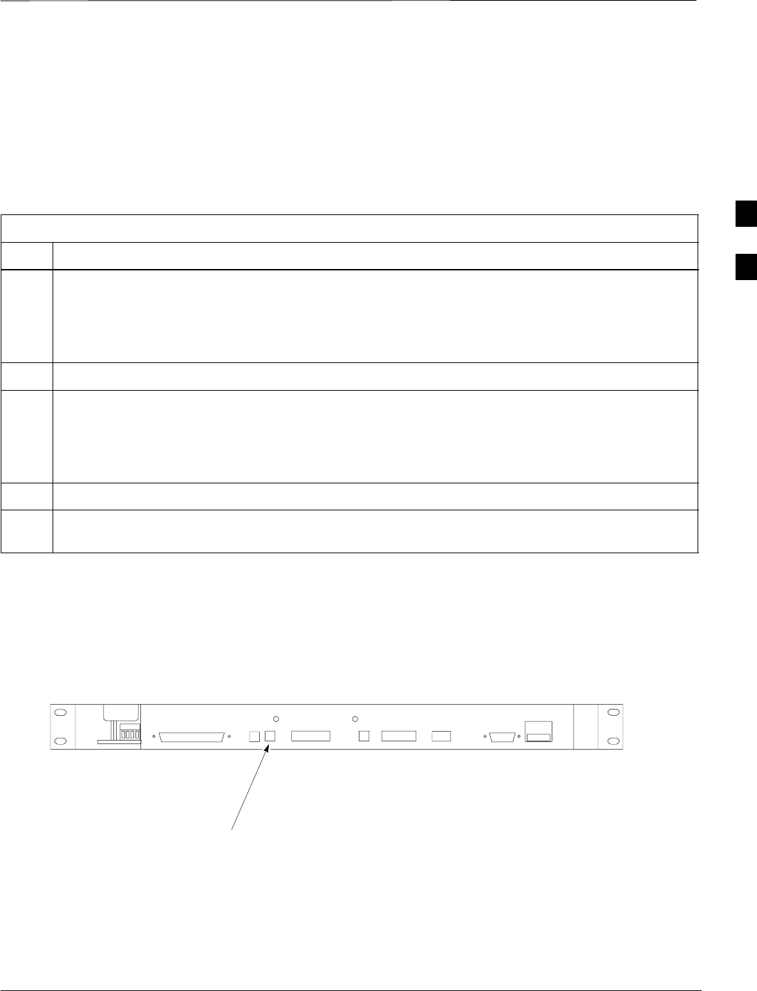
Alarms Testing – continued
08/01/2001 3-93
1X SCt4812ET Lite BTS Optimization/ATP
PRELIMINARY
Rectifier Over Temperature
Alarm
Table 3-57 gives instructions on testing the rectifier over–temperature
alarm system.
Table 3-57: Rectifier Over–Temperature Alarm
Step Action
1Remove the 14 tamper–resistant Torx fasteners securing the rear access panel to the rear of the frame
(Figure 2-1), and remove the rear access panel.
NOTE
Panel fastener type can be either T–27 button head or T–30 pan head.
2Looking up through the frame rear access opening, locate the rear of the MAP.
3Remove the jumper plug from connector J8 on the rear panel of the MAP (Figure 3-22). The
following conditions should occur:
SContacts on K1 and K2 change states (K1 now closed and K2 open).
SThe CDMA LMF reports an alarm condition as BTS Relay #26 contacts.
4Reinstall the jumper plug in connector J8, and verify that all alarm conditions have cleared.
5Reinstall the frame rear access panel, securing it with the 14 tamper–resistant Torx fasteners removed
in step 1.
Figure 3-22: MAP Connector J8 (Rear of MAP)
SC4812ETL0021–1
J4 J5 J1
J12
J3 J8 J9 J7
J2
CONNECTOR J8
Before Leaving the site
If no further operations are required after performing the alarm tests,
complete the requirements in Table 5-8 before leaving the site.
3

Alarms Testing – continued
PRELIMINARY
1X SCt4812ET Lite BTS Optimization/ATP 08/01/2001
3-94
Notes
3

08/01/2001 1X SCt4812ET Lite BTS Optimization/ATP
PRELIMINARY
Chapter 4: Automated Acceptance Test Procedure (ATP)
Table of Contents
Automated Acceptance Test Procedure – Introduction 4-1. . . . . . . . . . . . . . . . . . . .
Introduction 4-1. . . . . . . . . . . . . . . . . . . . . . . . . . . . . . . . . . . . . . . . . . . . . .
Prerequisites 4-2. . . . . . . . . . . . . . . . . . . . . . . . . . . . . . . . . . . . . . . . . . . . . .
TX/RX Antenna Connections 4-2. . . . . . . . . . . . . . . . . . . . . . . . . . . . . . . .
Acceptance Tests – Test Set Up 4-3. . . . . . . . . . . . . . . . . . . . . . . . . . . . . . . . . . . . .
Required Test Equipment 4-3. . . . . . . . . . . . . . . . . . . . . . . . . . . . . . . . . . .
Acceptance Test Equipment Set Up 4-3. . . . . . . . . . . . . . . . . . . . . . . . . . . .
Abbreviated (All–inclusive) Acceptance Tests 4-4. . . . . . . . . . . . . . . . . . . . . . . . . .
All–inclusive Tests 4-4. . . . . . . . . . . . . . . . . . . . . . . . . . . . . . . . . . . . . . . . .
All TX/RX ATP Test 4-5. . . . . . . . . . . . . . . . . . . . . . . . . . . . . . . . . . . . . . .
All TX ATP Test 4-5. . . . . . . . . . . . . . . . . . . . . . . . . . . . . . . . . . . . . . . . . .
All RX ATP Test 4-6. . . . . . . . . . . . . . . . . . . . . . . . . . . . . . . . . . . . . . . . . .
Individual Acceptance Tests–Introduction 4-7. . . . . . . . . . . . . . . . . . . . . . . . . . . . .
Individual Acceptance Tests 4-7. . . . . . . . . . . . . . . . . . . . . . . . . . . . . . . . .
Individual Tests 4-7. . . . . . . . . . . . . . . . . . . . . . . . . . . . . . . . . . . . . . . . . . .
TX Spectral Purity Transmit Mask Acceptance Test 4-9. . . . . . . . . . . . . . . . . . . . .
Background 4-9. . . . . . . . . . . . . . . . . . . . . . . . . . . . . . . . . . . . . . . . . . . . . .
Spectral Purity TX Mask Acceptance Test 4-10. . . . . . . . . . . . . . . . . . . . . .
TX Waveform Quality (Rho) Acceptance Test 4-12. . . . . . . . . . . . . . . . . . . . . . . . . .
Background 4-12. . . . . . . . . . . . . . . . . . . . . . . . . . . . . . . . . . . . . . . . . . . . . .
Waveform Quality (Rho) Acceptance Test 4-12. . . . . . . . . . . . . . . . . . . . . .
TX Pilot Time Offset Acceptance Test 4-13. . . . . . . . . . . . . . . . . . . . . . . . . . . . . . . .
Background 4-13. . . . . . . . . . . . . . . . . . . . . . . . . . . . . . . . . . . . . . . . . . . . . .
Pilot Time Offset Acceptance Test 4-13. . . . . . . . . . . . . . . . . . . . . . . . . . . .
TX Code Domain Power/Noise Floor Acceptance Test 4-15. . . . . . . . . . . . . . . . . . .
Background 4-15. . . . . . . . . . . . . . . . . . . . . . . . . . . . . . . . . . . . . . . . . . . . . .
Code Domain Power/Noise Floor Test 4-15. . . . . . . . . . . . . . . . . . . . . . . . .
RX FER Acceptance Test 4-18. . . . . . . . . . . . . . . . . . . . . . . . . . . . . . . . . . . . . . . . . .
Background 4-18. . . . . . . . . . . . . . . . . . . . . . . . . . . . . . . . . . . . . . . . . . . . . .
FER Acceptance Test 4-19. . . . . . . . . . . . . . . . . . . . . . . . . . . . . . . . . . . . . . .
Generating an ATP Report 4-20. . . . . . . . . . . . . . . . . . . . . . . . . . . . . . . . . . . . . . . . .
Background 4-20. . . . . . . . . . . . . . . . . . . . . . . . . . . . . . . . . . . . . . . . . . . . . .
ATP Report 4-20. . . . . . . . . . . . . . . . . . . . . . . . . . . . . . . . . . . . . . . . . . . . . .
4

Table of Contents – continued
PRELIMINARY
1X SCt4812ET Lite BTS Optimization/ATP 08/01/2001
Notes
4
Automated Acceptance Test Procedure – Introduction
08/01/2001 4-1
1X SCt4812ET Lite BTS Optimization/ATP
PRELIMINARY
Introduction
The automated Acceptance Test Procedure (ATP) allows Cellular Field
Engineers (CFEs) to run automated acceptance tests on all equipped BTS
subsystem devices using the CDMA LMF GUI environment and
supported test equipment.
The operator can choose to save the results of these tests to a report file,
from which ATP reports are generated for later printout.
Perform the ATP test on out-of-service sectors or sites only. Because all
tests are controlled via the CDMA LMF computer using the GPIB
interface from the CDMA LMF computer, only recommended test
equipment supported by the CDMA LMF can be used.
Before using the LMF, use an editor to view the
”CAVEATS” section in the ”readme.txt” file in the c:\wlmf
folder for any applicable information.
IMPORTANT
*
The ATP test is to be performed on out-of-service sectors
only.
DO NOT substitute test equipment with other models not
supported by the LMF.
IMPORTANT
*
Refer to Chapter 3 for detailed information on test set
connections for calibrating equipment, cables and other test
set components, if required.
NOTE
The CFE selects the appropriate ATP tests to run to satisfy customer and
regulatory requirements for verifying cell site performance. These tests
can be run individually or as one of the following groups:
SAll TX: TX tests verify the performance of the BTS transmit
elements. These include the GLI2, MCC, BBX2, BDC, and trunking
modules, the LPAs, and passive components including splitters,
combiners, bandpass filter(s), and RF cables.
SAll RX: RX tests verify the performance of the BTS receive elements.
These include the MPC (for starter frames), , BBX2, MCC, and GLI2
modules, and the passive components including RX filter (starter
frame only), and RF cables.
SAll TX/RX: Executes all TX and RX tests.
SFull Optimization: Executes the TX calibration, downloads BLO,
and executes the TX audit before running all TX and RX tests.
4
Automated Acceptance Test Procedure – Introduction – continued
PRELIMINARY
1X SCt4812ET Lite BTS Optimization/ATP 08/01/2001
4-2
Prerequisites
Before attempting to run any ATP tests, all applicable procedures
outlined in Chapter 3, Optimization/Calibration, must have been
completed successfully (i.e., code load and BLO calibration).
You cannot substitute test equipment with other models not
supported by the CDMA LMF.
NOTE
Before attempting to run any ATP tests, ensure the following:
SBTS has been optimized and calibrated (see Chapter 3).
SLMF is logged into the BTS
SCSMs, GLI2s, BBX2s, MCCs and TSU (if the RFDS is installed)
have correct code load and data load
SPrimary CSM and GLI2 are INS_ACT
SMCCs are INS_ACT
SBBX2s are OOS-RAM
SBBX2s are calibrated and BLOs are downloaded
STest cables are calibrated
STest equipment is selected
STest equipment is connected for ATP tests
STest equipment has been warmed up 60 minutes and calibrated
SGPIB is on
Before the FER is run, be sure that all LPAs are turned
OFF (circuit breakers pulled) or that all transmitter
connectors are properly terminated.
All transmit connectors must be properly terminated for all
ATP tests.
Failure to observe these warnings may result in bodily
injury or equipment damage.
WARNING
TX/RX Antenna Connections
Refer to Figure 1-6 or Figure 1-7 for identification of the transmit and
receive antenna connections where measurement are to be taken.
Directional couplers for signal sampling by the RFDS, if installed, are
integral to the SC4812ET Lite transmit and receive paths in the DRDCs
and TRDCs. As a result, all ATP measurement connections are made at
the antenna connectors on the RF interface panel.
4
Acceptance Tests – Test Set Up
08/01/2001 4-3
68P09253A60
1X SCt4812ET Lite BTS Optimization/ATP
PRELIMINARY
Required Test Equipment
The following test equipment is required:
SLMF
SPower meter (used with HP8921A/600 and Advantest R3465)
SCommunications test set
Before installing any test equipment directly to any TX
OUT connector, verify that there are no CDMA channels
keyed.
At active sites, have the OMCR/CBSC place the carrier
assigned to the LPAs under test OOS. Failure to do so can
result in serious personal injury and/or equipment damage.
WARNING
You must recalibrate the test equipment before using it to
perform the TX Acceptance Tests.
NOTE
Acceptance Test Equipment
Set Up
Follow the steps in Table 4-1 to set up test equipment for all tests.
Table 4-1: Set Up Test Equipment – TX Output Verify/Control Tests
Step Action
1If it has not already been done, interface the LMF computer to the BTS (refer to Table 3-6 and
Figure 3-10).
2If it has not already been done, refer to Table 3-7 to start a GUI LMF session and log into the BTS.
3If it has not already been done, refer to Figure 3-17 or Figure 3-18, as applicable for the test
equipment being used, to connect test equipment for acceptance testing.
* IMPORTANT
CDMA LMF–based measurement commands factor in TX test cable loss between the RFM frame and
test equipment. No additional attenuation can be inserted as the additional losses would not be
factored in.
4

Abbreviated (All–inclusive) Acceptance Tests
PRELIMINARY
1X SCt4812ET Lite BTS Optimization/ATP 08/01/2001
4-4
All–inclusive Tests
The all–inclusive acceptance tests are performed from the LMF GUI
environment. These tests execute various combinations of individual
acceptance tests with a single command. This allows verification of
multiple aspects of BTS performance while minimizing time needed for
individual test set up and initiation.
There are three abbreviated acceptance tests which evaluate different
performance aspects of the BTS. This allows the CFE to select testing to
meet the specific requirements for individual maintenance and
performance verification situations. The following summarizes the
coverage of each abbreviated test:
SAll TX/RX. Performs all transmit and receive ATPs on the selected
MCCs and BBX2s.
SAll TX. Performs complete set of transmit ATPs on the selected
MCCs and BBX2s. Testing is the equivalent of performing all of the
following individual tests:
–TX Mask Test
–Rho Test
–Pilot Time Offset Test
–Code Domain Power Test
SAll RX. Performs complete receive ATP on the selected MCCs and
BBX2s. Testing is the equivalent of performing the following:
–FER Test
4

Abbreviated (All–inclusive) Acceptance Tests – continued
08/01/2001 4-5
1X SCt4812ET Lite BTS Optimization/ATP
PRELIMINARY
All TX/RX ATP Test Follow the procedures in Table 4-2 to perform the abbreviated,
all–inclusive transmit and receive test.
Table 4-2: All TX/RX ATP Test Procedure
Step Action
1Set up the test equipment initially for abbreviated tests per Table 4-1.
2Select the BBX2s and MCCs to be tested.
3From the Tests menu, select All TX/RX.
4Select the appropriate carrier(s) (carrier-bts#-sector#-carrier#) displayed in the Channels/Carrier pick
list.
NOTE
To select multiple items, hold down the Shift or Ctrl key while making the selections.
5Enter the appropriate channel number in the Carrier n Channels box.
6 Click OK. The status report window is displayed and a Directions pop-up is displayed.
7Follow the cable connection directions as they are displayed. The test results are displayed in the
status report window.
8 Click Save Results or Dismiss.
NOTE
If Dismiss is used, the test results will not be saved in the test report file.
All TX ATP Test Follow the procedures in Table 4-3 to perform the abbreviated,
all–inclusive transmit test.
Table 4-3: All TX ATP Test Procedure
Step Action
1Set up the test equipment for abbreviated tests per Table 4-1.
2Select the BBX2s and MCCs to be tested.
3From the Tests menu, select All TX.
4Select the appropriate carrier(s) (carrier-bts#-sector#-carrier#) displayed in the Channels/Carrier pick
list.
NOTE
To select multiple items, hold down the Shift or Ctrl key while making the selections.
5Enter the appropriate channel number in the Carrier n Channels box.
6 Click OK. The status report window is displayed and a Directions pop-up is displayed.
7Follow the cable connection directions as they are displayed. The test results are displayed in the
status report window.
. . . continued on next page
4

Abbreviated (All–inclusive) Acceptance Tests – continued
PRELIMINARY
1X SCt4812ET Lite BTS Optimization/ATP 08/01/2001
4-6
Table 4-3: All TX ATP Test Procedure
Step Action
8 Click Save Results or Dismiss.
NOTE
If Dismiss is used, the test results will not be saved in the test report file.
All RX ATP Test Follow the procedures in Table 4-4 to perform the abbreviated,
all–inclusive receive test.
Table 4-4: All RX ATP Test Procedure
Step Action
1Set up the test equipment for abbreviated tests per Table 4-1.
2Select the BBX2s and MCCs to be tested.
3From the Tests menu, select All RX.
4Select the appropriate carrier(s) (carrier-bts#-sector#-carrier#) displayed in the Channels/Carrier pick
list.
NOTE
To select multiple items, hold down the Shift or Ctrl key while making the selections.
5Enter the appropriate channel number in the Carrier n Channels box.
6 Click OK. The status report window is displayed and a Directions pop-up is displayed.
7Follow the cable connection directions as they are displayed. The test results are displayed in the
status report window.
8 Click Save Results or Dismiss.
NOTE
If Dismiss is used, the test results will not be saved in the test report file.
4

Individual Acceptance Tests–Introduction
08/01/2001 4-7
1X SCt4812ET Lite BTS Optimization/ATP
PRELIMINARY
Individual Acceptance Tests
The following individual ATP tests can be used to evaluate specific
aspects of BTS operation against individual performance requirements.
All testing is performed using the CDMA LMF GUI environment.
TX Testing
TX tests verify any given transmit antenna path and output power
control. All tests are performed using the external calibrated test set. All
measurements are via the appropriate TX OUT connector.
TX tests verify TX operation of the entire CDMA Forward Link using
all BBX2s assigned to all respective sector/antennas. Each BBX2 is
keyed up to generate a CDMA carrier (using both bbx level and bay
level offsets) at the CDF file carrier output power level (as specified in
the site documentation).
RX Testing
RX testing verifies any given receive antenna path. All tests are
performed using the external calibrated test set to inject a CDMA RF
carrier with all zero longcode at the specified RX frequency via the
appropriate RX IN connector.
RX tests verify RX operation of the entire CDMA Reverse Link using
all equipped MCCs assigned to all respective sector/antennas.
Individual Tests
Spectral Purity TX Mask
This test verifies that the transmitted CDMA carrier waveform generated
on each sector meets the transmit spectral mask specification (as defined
in IS–97) with respect to the assigned cdf file values.
Waveform Quality (Rho)
This test verifies that the transmitted Pilot channel element digital
waveform quality (rho) exceeds the minimum specified value in IS–97.
Rho represents the correlation between the actual and perfect CDMA
modulation spectrums. 1.0000 represents 100% (or perfect correlation).
Pilot Time Offset
The Pilot Time Offset is the difference between the CDMA analyzer
measurement interval (based on the BTS system time reference) and the
incoming block of transmitted data from the BTS (Pilot only, Walsh
code 0).
Code Domain Power/Noise Floor
This test verifies the code domain power levels, which have been set for
all ODD numbered Walsh channels, using the OCNS command. This is
4

Individual Acceptance Tests–Introduction – continued
PRELIMINARY
1X SCt4812ET Lite BTS Optimization/ATP 08/01/2001
4-8
done by verifying that the ratio of PILOT divided by OCNS is equal to
10.2 + 2 dB, and, that the noise floor of all EVEN numbered “OFF”
Walsh channels measures < –27 dB (with respect to total CDMA channel
power).
BTS Frame Error Rate
This test verifies the BTS receive Frame Error Rate (FER) on all Traffic
Channel elements currently configured on all equipped MCCs (fullrate at
one percent FER) at an RF input level of –119 dBm on the main RX
antenna paths using all equipped MCCs and BBX2s at the site. The
diversity RX antenna paths are also tested using the lowest equipped
MCC/CE ONLY.
There are no pass/fail criteria associated with FER readings
taken at level below –119 dBm, other than to verify that
the FER measurement reflects changes in the RX input
signal level.
NOTE
4

TX Spectral Purity Transmit Mask Acceptance Test
08/01/2001 4-9
1X SCt4812ET Lite BTS Optimization/ATP
PRELIMINARY
Background
This test verifies the spectral purity of each BBX carrier keyed up at a
specific frequency per the current CDF file assignment. All tests are
performed using the external calibrated test set controlled by the same
command. All measurements are via the appropriate TX OUT connector.
Pilot gain will be set to 541 for each antenna, and the forward link will
be disabled for all Traffic CHannel (TCH) elements from the MCCs. The
BBX2 will be keyed up using both bbxlvl and bay level offsets, to
generate a CDMA carrier (with pilot channel element only). RF output
will be set at 40 dBm as measured at the appropriate TX output.
The calibrated communications test set will measure and return the
attenuation level of all spurious and IM products with respect to the
mean power of the CDMA channel measured in a 1.23 MHz bandwidth,
in dB, verifying that results meet system tolerances at the following test
points (see also Figure 4-1):
SFor 800 MHz:
–At least –45 dB @ + 750 kHz from center frequency
–At least –45 dB @ – 750 kHz from center frequency
–At least –60 dB @ –1980 kHz from center frequency
–At least –60 dB @ + 1980 kHz from center frequency
SFor 1.9 GHz:
–At least –45 dB @ + 900 kHz from center frequency
–At least –45 dB @ – 900 kHz from center frequency
The BBX2 will then dekey, and if selected, the redundant BBX2 will be
assigned to the current TX antenna path under test. The test will then be
repeated.
4

TX Spectral Purity Transmit Mask Acceptance Test – continued
PRELIMINARY
1X SCt4812ET Lite BTS Optimization/ATP 08/01/2001
4-10
Spectral Purity TX Mask
Acceptance Test
Follow the steps in Table 4-5 to verify the transmit spectral mask
specification on all TX antenna paths using all BBXs equipped at the
BTS.
Table 4-5: Test Spectral Purity Transmit Mask
Step Action
1Set up the test equipment for TX acceptance tests per Table 4-1.
2Select the BBX2s to be tested.
3From the Tests menu, select TX Mask.
4Select the appropriate carrier(s) (carrier-bts#-sector#-carrier#) displayed in the Channels/Carrier pick
list.
NOTE
To select multiple items, hold down the Shift or Ctrl key while making the selections.
5Enter the appropriate channel number in the Carrier n Channels box.
6 Click OK. The status report window is displayed and a Directions pop-up is displayed.
7Follow the cable connection directions as they are displayed. The test results are displayed in the
status report window.
8 Click Save Results or Dismiss.
NOTE
If Dismiss is used, the test results will not be saved in the test report file.
4
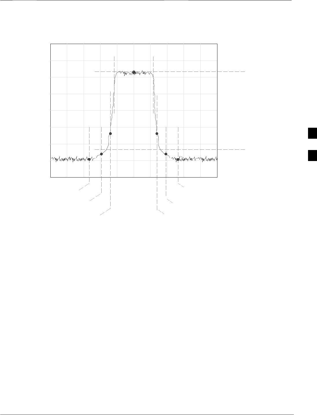
TX Spectral Purity Transmit Mask Acceptance Test – continued
08/01/2001 4-11
1X SCt4812ET Lite BTS Optimization/ATP
PRELIMINARY
Figure 4-1: TX Mask Verification Spectrum Analyzer Display
– 900 kHz + 900 kHz
Center Frequency Reference
Attenuation level of all
spurious and IM products
with respect to the mean
power of the CDMA channel
.5 MHz Span/Div
Ampl 10 dB/Div
Mean CDMA Bandwidth
Power Reference
– 1980 kHz
+750 kHz
+ 1980 kHz
– 750 kHz
4

TX Waveform Quality (Rho) Acceptance Test
PRELIMINARY
1X SCt4812ET Lite BTS Optimization/ATP 08/01/2001
4-12
Background
This test verifies the transmitted pilot channel element digital waveform
quality of each BBX carrier keyed up at a specific frequency per the
current CDF file assignment. All tests are performed using the external
calibrated test set controlled by the same command. All measurements
are via the appropriate TX OUT connector.
Pilot gain will be set to 262 for each antenna, and all TCH elements
from the MCCs will be forward link disabled. The BBX2 will be keyed
up using both bbxlvl and bay level offsets to generate a CDMA carrier
(with pilot channel element only, Walsh code 0). RF output power is set
at 40 dBm as measured at the appropriate TX output.
The calibrated communications test set will measure and return the pilot
channel element digital waveform quality (rho) percentage, verifying
that the result meets system tolerances:
Waveform quality (Rho) should be > 0.912.
The BBX2 will then dekey, and if selected, the redundant BBX2 will be
assigned to the current TX antenna path under test. The test will then be
repeated.
Waveform Quality (Rho)
Acceptance Test
Follow the steps in Table 4-6 to verify the pilot channel element
waveform quality (rho) on the specified TX antenna paths using BBXs
equipped at the BTS.
Table 4-6: Test Waveform Quality (Rho)
Step Action
1Set up the test equipment for TX acceptance tests per Table 4-1.
2Select the BBX2s to be tested.
3From the Tests menu, select Rho.
4Select the appropriate carrier(s) (carrier-bts#-sector#-carrier#) displayed in the Channels/Carrier pick
list.
NOTE
To select multiple items, hold down the Shift or Ctrl key while making the selections.
5Enter the appropriate channel number in the Carrier n Channels box.
6 Click OK. The status report window is displayed and a Directions pop-up is displayed.
7Follow the cable connection directions as they are displayed. The test results are displayed in the
status report window.
8 Click Save Results or Dismiss.
NOTE
If Dismiss is used, the test results will not be saved in the test report file.
4

TX Pilot Time Offset Acceptance Test
08/01/2001 4-13
1X SCt4812ET Lite BTS Optimization/ATP
PRELIMINARY
Background
This test verifies the transmitted pilot channel element Pilot Time Offset
of each BBX carrier keyed up at a specific frequency per the current
CDF file assignment. All tests will be performed using the external
calibrated test set controlled by the same command. All measurements
will be via the TX OUT connector.
The pilot gain will be set to 262 for each antenna and all TCH elements
from the MCCs will be forward link disabled. The BBX2 will be keyed
up using both bbxlvl and bay level offsets to generate a CDMA carrier
(with pilot channel element only, Walsh code 0). TX power output is set
at 40 dBm as measured at the TX output.
The calibrated communications test set will measure and return the Pilot
Time Offset in ms, verifying that results meet system tolerances:
Pilot Time Offset should be within 3 ms of the target PT Offset
(zero ms).
The BBX2 will then dekey, and if selected, the redundant BBX2 will be
assigned to the current TX antenna path under test. The test will then be
repeated.
This test also executes and returns the TX Frequency and
TX Waveform Quality (rho) ATP tests, however, only Pilot
Time Offset results are written to the ATP test report.
NOTE
Pilot Time Offset Acceptance
Test
Follow the steps in Table 4-7 to verify the Pilot Time Offset on the
specified TX antenna paths using BBXs and BDCs equipped at the BTS.
Table 4-7: Test Pilot Time Offset
Step Action
1Set up the test equipment for TX acceptance tests per Table 4-1.
2Select the BBX2s to be tested.
3From the Tests menu, select Pilot Time Offset.
4Select the appropriate carrier(s) (carrier-bts#-sector#-carrier#) displayed in the Channels/Carrier pick
list.
NOTE
To select multiple items, hold down the Shift or Ctrl key while making the selections.
5Enter the appropriate channel number in the Carrier n Channels box.
6 Click OK. The status report window is displayed and a Directions pop-up is displayed.
. . . continued on next page
4

TX Pilot Time Offset Acceptance Tests – continued
PRELIMINARY
1X SCt4812ET Lite BTS Optimization/ATP 08/01/2001
4-14
Table 4-7: Test Pilot Time Offset
Step Action
7Follow the cable connection directions as they are displayed. The test results are displayed in the
status report window.
8 Click Save Results or Dismiss.
NOTE
If Dismiss is used, the test results will not be saved in the test report file.
4

TX Code Domain Power/Noise Floor Acceptance Test
08/01/2001 4-15
1X SCt4812ET Lite BTS Optimization/ATP
PRELIMINARY
Background
This test verifies the Code Domain Power and Noise Floor of each BBX
carrier keyed up at a specific frequency per the current CDF file
assignment. All tests are performed using the external calibrated test set
controlled by the same command. All measurements are via the
appropriate TX OUT connector.
Pilot gain will be set to 262 for each antenna and all equipped MCCs
will be configured to supply all odd–numbered Walsh code Traffic
channel elements by enabling Orthagonal Channel Noise Source
(OCNS) on all odd MCC/CEs, (maximum 32 full rate channels with an
OCNS gain of 81). All even–numbered Walsh code Traffic channel
elements will not have OCNS enabled, and are considered “OFF”. All
equipped MCCs will be forward–link enabled for the antenna/sector
under test.
The BBX2 will be keyed up using both bbxlvl and bay level offsets, to
generate a CDMA carrier consisting of pilot and OCNS channels. RF
output power is set at 40 dBm as measured at the appropriate TX output.
The calibrated communications test set will measure and return the
channel element power (dB) of all specified Walsh channels within the
CDMA spectrum. Additional calculations will be performed to verify the
following parameters are met (Figure 4-2):
STraffic channel element power level will be verified by calculating the
ratio of PILOT power to OCNS gain of all traffic channels (root sum
of the square (RSS) of each OCNS gain divided by the Pilot power).
This value should be 10.2 dB + 2.0 dB.
SNoise floor (unassigned “OFF” even numbered Walsh channels) are
verified to be < –27 dB (with respect to total CDMA channel power).
The BBX2 will then dekey, and if selected, the redundant BBX2 will be
assigned to the current TX antenna path under test. The test will then be
repeated. Upon completion of the test, OCNS channels will be disabled
on the specified MCC/CEs.
Code Domain Power/Noise
Floor Test
Follow the steps in Table 4-8 to verify the Code Domain Power/Noise
floor of each BBX carrier keyed up at a specific frequency.
4

TX Code Domain Power/Noise Floor Acceptance Test – continued
PRELIMINARY
1X SCt4812ET Lite BTS Optimization/ATP 08/01/2001
4-16
Table 4-8: Test Code Domain Power/Noise Floor
Step Action
1Set up the test equipment for TX acceptance tests per Table 4-1.
2Select the BBX2s and MCCs to be tested.
3From the Tests menu, select TX Mask.
4Select the appropriate carrier(s) (carrier-bts#-sector#-carrier#) displayed in the Channels/Carrier pick
list.
NOTE
To select multiple items, hold down the Shift or Ctrl key while making the selections.
5Enter the appropriate channel number in the Carrier n Channels box.
6 Click OK. The status report window is displayed and a Directions pop-up is displayed.
7Follow the cable connection directions as they are displayed. The test results are displayed in the
status report window.
8 Click Save Results or Dismiss.
NOTE
If Dismiss is used, the test results will not be saved in the test report file.
4
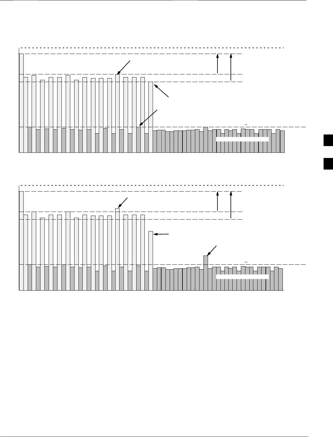
TX Code Domain Power/Noise Floor Acceptance Test – continued
08/01/2001 4-17
1X SCt4812ET Lite BTS Optimization/ATP
PRELIMINARY
Pilot Channel
Active channels
PILOT LEVEL
MAX OCNS SPEC.
MIN OCNS SPEC.
MAXIMUM NOISE FLOOR:
< –27 dB SPEC.
Inactive channels
Walsh 0 1 2 3 4 5 6 7 ... 64
MAX OCNS
CHANNEL
MIN OCNS
CHANNEL
8.2 dB 12.2 dB
MAX NOISE
FLOOR
Pilot Channel
Active channels
PILOT LEVEL
MAX OCNS SPEC.
MIN OCNS SPEC.
MAXIMUM NOISE FLOOR:
< –27 dB
Inactive channels
Walsh 0 1 2 3 4 5 6 7 ... 64
FAILURE – DOES NOT
MEET MIN OCNS SPEC.
FAILURE – EXCEEDS
MAX OCNS SPEC. 8.2 dB 12.2 dB
FAILURE – EXCEEDS MAX
NOISE FLOOR SPEC.
Code Domain Power/Noise Floor (OCNS Pass) Example
Figure 4-2: Code Domain Analyzer CD Power/Noise Floor Display Examples
Code Domain Power/Noise Floor (OCNS Failure) Example
4

RX FER Acceptance Test
PRELIMINARY
1X SCt4812ET Lite BTS Optimization/ATP 08/01/2001
4-18
Background
This test verifies the BTS Frame Erasure Rate (FER) on all TCHs
currently configured on all equipped MCCs (fullrate at 1% FER) at –119
dBm on the main RX antenna paths. The test is performed on all
diversity RX antenna path using only the lowest equipped MCC/CE. All
tests are performed using the external calibrated test set as the signal
source controlled by the same command. All measurements are via the
LMF.
Pilot gain will be set to 262 for each TX antenna, and the forward link
for all TCH elements from the MCCs will be disabled. The BBX2 will
be keyed up using only bbxlvl level offsets, to generate a CDMA
carrier (with pilot channel element only). TX power output is set at +10
dBm. (The BBX must be keyed in order to enable the RX receive
circuitry.)
The LMF will prompt the MCC/CE under test to measure all–zero
longcode and provide the Frame Erasure Rate (FER) report on the
selected active MCC on the Reverse Link for both the main and diversity
RX antenna paths, verifying results meet the following specification:
FER returned less than 1% and Total Frames measured is 1500.
The BBX2 will then dekey, and if selected, the redundant BBX2 will be
assigned to the current RX antenna paths under test. The test will then be
repeated.
4

RX FER Acceptance Test – continued
08/01/2001 4-19
1X SCt4812ET Lite BTS Optimization/ATP
PRELIMINARY
FER Acceptance Test
Follow the steps in Table 4-9 to verify the FER on all RX antenna paths
using all BBXs equipped at the BTS.
Table 4-9: Test FER
Step Action
1Set up the test equipment for RX acceptance tests per Table 4-1.
2Select the BBX2s and MCCs to be tested.
3From the Tests menu, select FER.
4Select the appropriate carrier(s) (carrier-bts#-sector#-carrier#) displayed in the Channels/Carrier pick
list.
NOTE
To select multiple items, hold down the Shift or Ctrl key while making the selections.
5Enter the appropriate channel number in the Carrier n Channels box.
6From the RX Branch pick list, select the branch/branches to be tested.
7Select the desired rate from the Rate Set pick list (1 = 9600, 2 = 14400).
8 Click OK. The status report window is displayed and a Directions pop-up is displayed.
9Follow the cable connection directions as they are displayed. The test results are displayed in the
status report window.
10 Click Save Results or Dismiss.
NOTE
If Dismiss is used, the test results will not be saved in the test report file.
4

Generating an ATP Report
PRELIMINARY
1X SCt4812ET Lite BTS Optimization/ATP 08/01/2001
4-20
Background
Each time an ATP test is run, an ATP report is updated and must be
saved using the Save Results button to close the status report window.
The ATP report will not be updated if the status reports window is closed
using the Dismiss button.
ATP Report
A separate report is created for each BTS and includes the following for
each test:
STest name
SPASS or FAIL
SDescription information (if applicable)
SBBX number
SChannel number
SCarrier number
SSector number
SUpper test limit
SLower test limit
STest result
STime stamp
SDetails/Warning information (if applicable)
Follow the procedures in the Table 4-10 to view and create a printable
file for the ATP report.
Table 4-10: Generating an ATP Report
Step Action
1Click on the Login tab (if not in the forefront).
2Select the desired BTS from the available Base Station pick list.
3Click on the Report button.
4Click on a column heading to start the report.
5If not desiring a printable file copy, click on the Dismiss button.
6If requiring a printable file copy, select the desired file, type in the pick list and click on the Save
button.
4

08/01/2001 1X SCt4812ET Lite BTS Optimization/ATP
PRELIMINARY
Chapter 5: Leaving the Site
Table of Contents
Updating Calibration Data Files 5-1. . . . . . . . . . . . . . . . . . . . . . . . . . . . . . . . . . . . .
Updating CBSC Calibration Data Files 5-1. . . . . . . . . . . . . . . . . . . . . . . . .
Prepare to Leave the Site 5-3. . . . . . . . . . . . . . . . . . . . . . . . . . . . . . . . . . . . . . . . . .
Removing External Test Equipment 5-3. . . . . . . . . . . . . . . . . . . . . . . . . . .
Reset All Devices and Initialize Site Remotely 5-3. . . . . . . . . . . . . . . . . . .
Bringing Modules into Service with the CDMA LMF 5-3. . . . . . . . . . . . .
Terminating LMF Session/Removing Terminal 5-4. . . . . . . . . . . . . . . . . .
Connecting BTS T1/E1 Spans 5-5. . . . . . . . . . . . . . . . . . . . . . . . . . . . . . . .
Before Leaving the site 5-5. . . . . . . . . . . . . . . . . . . . . . . . . . . . . . . . . . . . . 5

Table of Contents – continued
PRELIMINARY
1X SCt4812ET Lite BTS Optimization/ATP 08/01/2001
Notes
5

Updating Calibration Data Files
08/01/2001 5-1
1X SCt4812ET Lite BTS Optimization/ATP
PRELIMINARY
Updating CBSC Calibration
Data Files
After completing the TX calibration and audit, updated CAL file
information must be moved from the LMF Windows environment back
to the CBSC, a Unix environment. The following procedures detail
moving files from one environment to the other.
Copying CAL files from LMF to a Disk
Follow the procedures in Table 5-1 to copy the CAL files from a CDMA
LMF computer to a 3.5 diskette.
Table 5-1: Copying CAL Files to a Diskette
Step Action
1With Windows running on the CDMA LMF computer, insert a disk into Drive A:.
2Launch the Windows Explorer Program from your Programs menu list.
3Select the applicable wlmf/cdma/bts–# folder.
4Drag the bts–#.cal file to Drive A.
5Repeat Steps 3 and 4, as required, for other bts–# folders.
Copying CAL Files from Diskette to the CBSC
Follow the procedures in Table 5-2 to copy CAL files from a diskette to
the CBSC.
Table 5-2: Copying CAL Files from Diskette to the CBSC
Step Action
1Log in to the CBSC on the OMC–R Unix workstation using your account name and password.
2Place your diskette containing calibration file(s) in the workstation diskette drive.
3Type in eject –q and press the Enter key.
4Type in mount and press the Enter key.
NOTE
SCheck to see that the message “floppy/no_name” is displayed on the last line.
SIf the eject command was previously entered, floppy/no_name will be appended with a number.
Use the explicit floppy/no_name reference displayed.
5Type in cd /floppy/no_name and press the Enter key.
6Type in ls –lia and press the Enter key. Verify that the bts–#.cal file is on the diskette.
7Type in cd and press the Enter key.
8Type in pwd and press the Enter key. Verify you are in your home directory (/home/<name>).
. . . continued on next page
5

Back Up Calibration Data Files – continued
PRELIMINARY
1X SCt4812ET Lite BTS Optimization/ATP 08/01/2001
5-2
68P09253A60
Table 5-2: Copying CAL Files from Diskette to the CBSC
Step Action
9 With Solaris versions of Unix, create a Unix–formatted version of the bts–#.cal file in your home
directory by entering the following command:
dos2unix /floppy/no_name/bts–#.cal bts–#.cal and press the Enter key (where # is BTS
number).
NOTE
Other versions of Unix do not support the dos2unix command. In these cases, use the Unix cp
(copy) command. The copied files will contain DOS line feed characters which must be edited out
with a Unix text editor.
10 Type in ls –l *.cal and press the Enter key. Verify the cal files have been copied.
11 Type in eject and press the Enter key.
12 Remove the diskette from the workstation.
5
Prepare to Leave the Site
08/01/2001 5-3
1X SCt4812ET Lite BTS Optimization/ATP
PRELIMINARY
Removing External Test
Equipment Perform the procedure in Table 5-3 to disconnect the test equipment and
configure the BTS for active service.
Table 5-3: Remove External Test Equipment
Step Action
1Disconnect all external test equipment from all TX and RX connectors at the rear of the frame.
2Reconnect and visually inspect all TX and RX antenna feed lines at the frame RF interface panel.
! CAUTION
Verify that all sector antenna feed lines are connected to the correct ports on the frame. Crossed
antenna cables will cause system degradation of call processing.
Reset All Devices and Initialize
Site Remotely
Generally, devices in the BTS should not be left with data and code
loaded from the CDMA LMF. The configuration data and code loads
used for normal operation could be different from those stored in the
CDMA LMF files. By resetting all devices, the required data and code
can be loaded from the CBSC when spans are again active.
To reset all devices and have the OMCR/CBSC bring up the site
remotely, perform the procedure in Table 5-4.
Table 5-4: Reset BTS Devices and Remote Site Initialization
Step Action
1Terminate the CDMA LMF session by following the procedures in Table 5-6.
2NOTE
In the following step, performing Table 2-6 DC voltage measurements other than those using the MAP
VOLT and AMP indicators is not necessary if DC power system components have not been replaced
during the optimization and/or ATP process.
Cycle BTS power off, as specified in Table 2-9, and on, as specified in Table 2-5, Table 2-6, and step 1
of Table 2-7, respectively.
3Reconnect spans by following the procedure in Table 5-7.
4Notify the OMCR/CBSC to take control of the site and download code and data to the BTS.
5Verify the CBSC can communicate with the GLIs.
Bringing Modules into Service
with the CDMA LMF
Whenever possible, have the CBSC/MM bring up the site
and enable all devices at the BTS.
IMPORTANT
*
5

Prepare to Leave the Site – continued
PRELIMINARY
1X SCt4812ET Lite BTS Optimization/ATP 08/01/2001
5-4
If there is a reason code and/or data should or could not be loaded
remotely from the CBSC, follow the steps outlined in Table 5-5 as
required to bring BTS processor modules from OOS to INS state.
Table 5-5: Bring Modules into Service
Step Action
1In the CDMA LMF GUI environment, select the device(s) you wish to enable.
NOTE
SThe MGLI, CSM, and applicable BDC must be INS before an MCC can be enabled to INS.
SProcessors which must be enabled and the order of enabling are as follows:
– MGLI
– GLI
– CSMs
– MCCs
2Click on Device from the menu bar.
3Click on Enable from the Device menu. A status report window is displayed.
NOTE
If a BBX is selected, a transceiver parameters window is displayed to collect keying information. Do
not enable the BBX.
4 Click Cancel to close the transceiver parameters window, if applicable.
5 Click OK to close the status report window.
The selected devices that successfully change to INS change color to green.
Terminating LMF
Session/Removing Terminal
Perform the procedure in Table 5-6 as required to terminate the LMF
GUI session and remove the CDMA LMF computer.
Table 5-6: Remove LMF
Step Action
! CAUTION
Do not power down the CDMA LMF terminal without performing the procedure below.
Corrupted/lost data files may result.
1Log out of all BTS sessions and exit CDMA LMF by clicking on the File selection in the menu bar
and selecting Exit from the File menu list.
2 Click Yes in the Confirm Logout pop–up message which appears.
3In the Windows Task Bar, click Start and select Shutdown.
4 Click Yes when the Shut Down Windows message appears
5Wait for the system to shut down and the screen to go blank.
. . . continued on next page
5