Nokia Solutions and Networks T5DJ1 SC4812T Lite @ 800 MHz CDMA BTS User Manual TLite
Nokia Solutions and Networks SC4812T Lite @ 800 MHz CDMA BTS TLite
UserManual.wiki
>
Nokia Solutions and Networks
>
T5DJ1 User Manual
>
Users manual 1 of 2
Contents
1.
Users manual 1 of 2
2.
Users manual 2 of 2
Users manual 1 of 2
Navigation menu
Upload a User Manual
Namespaces
Wiki Guide
HTML
PDF
Info
Views
User Manual
Discussion / Help
Navigation

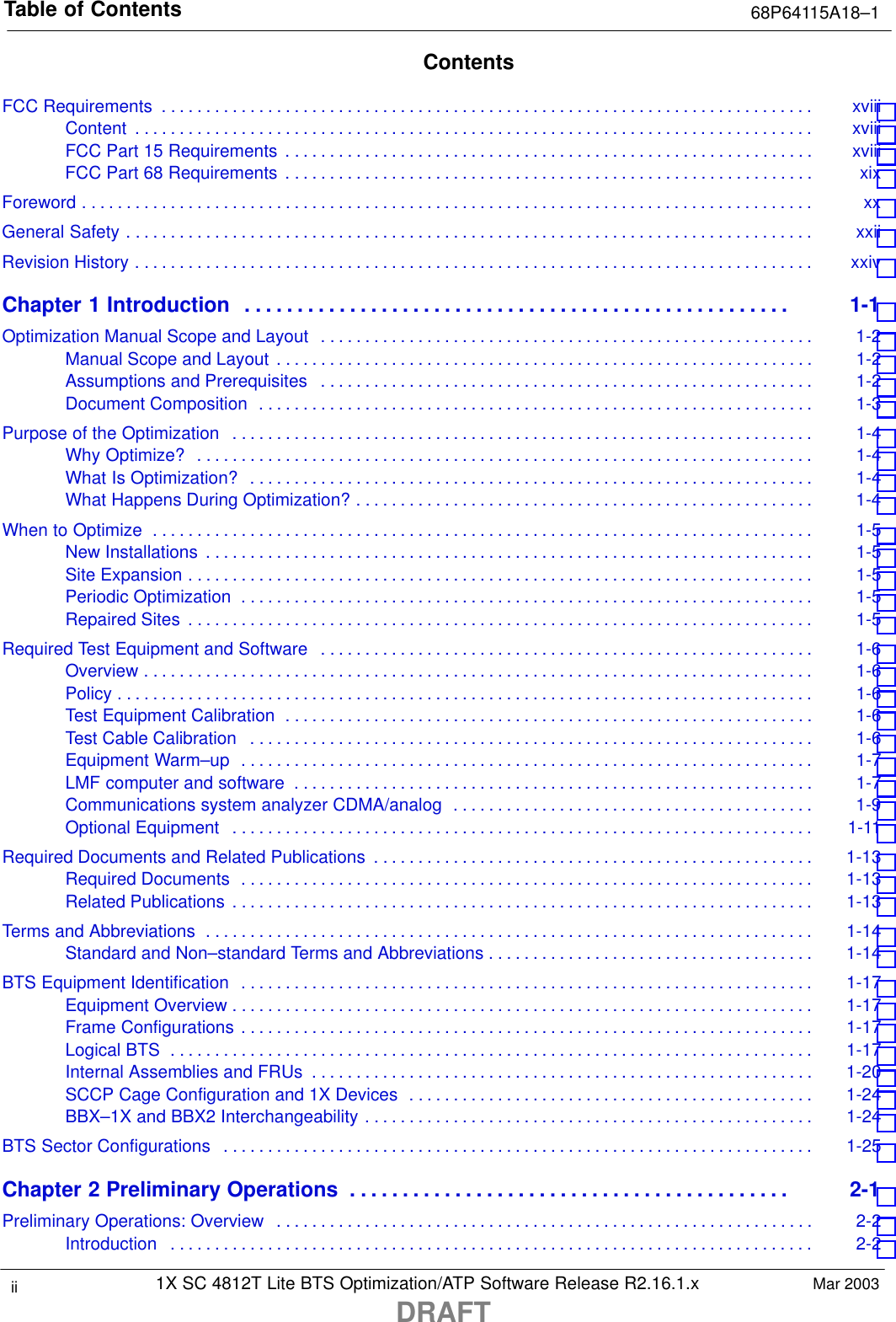
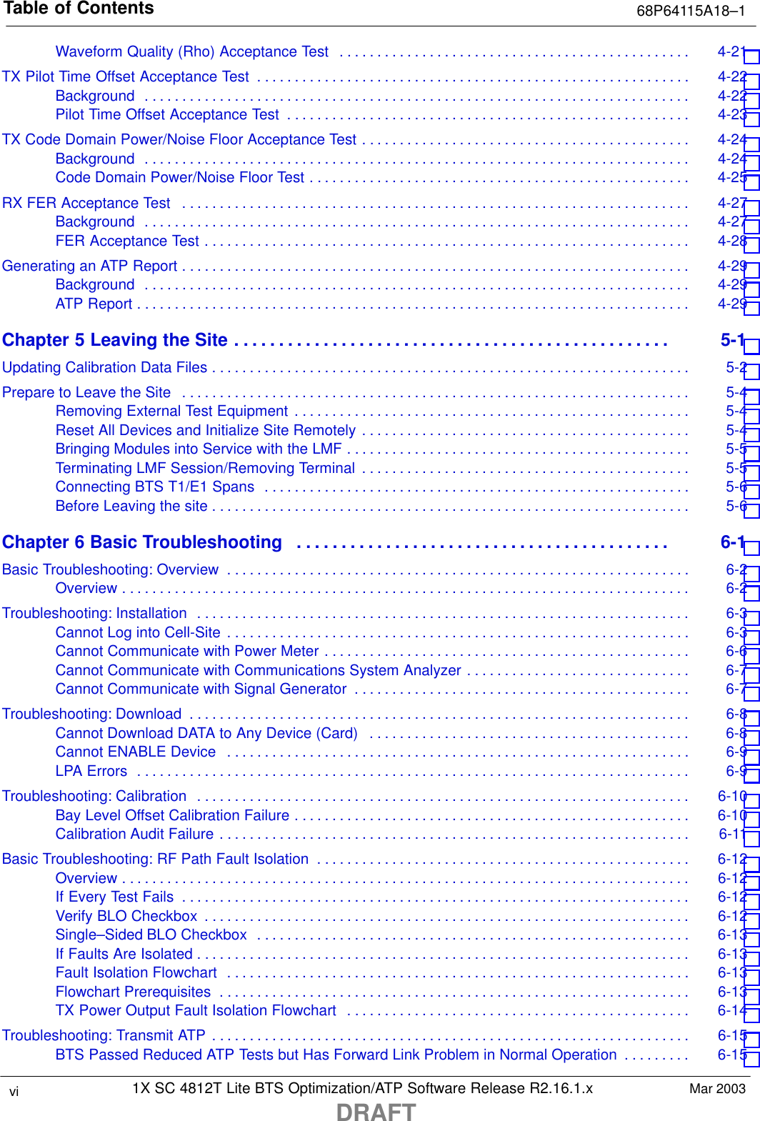
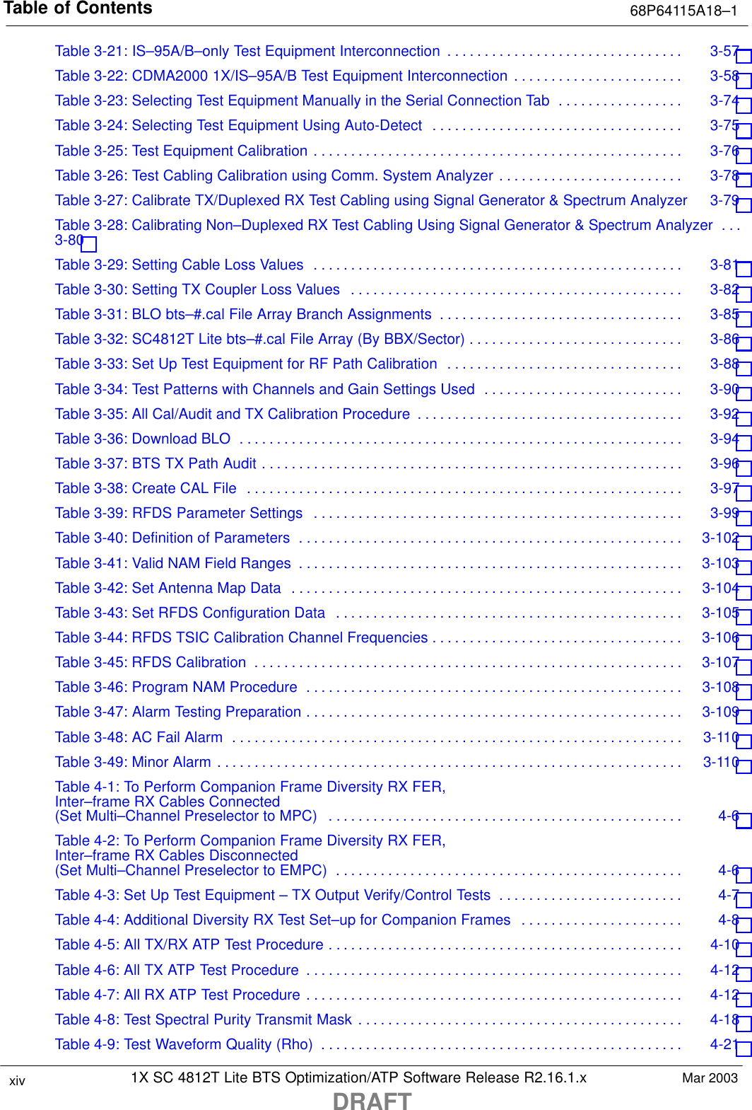
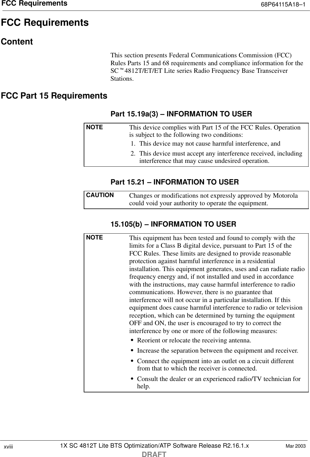
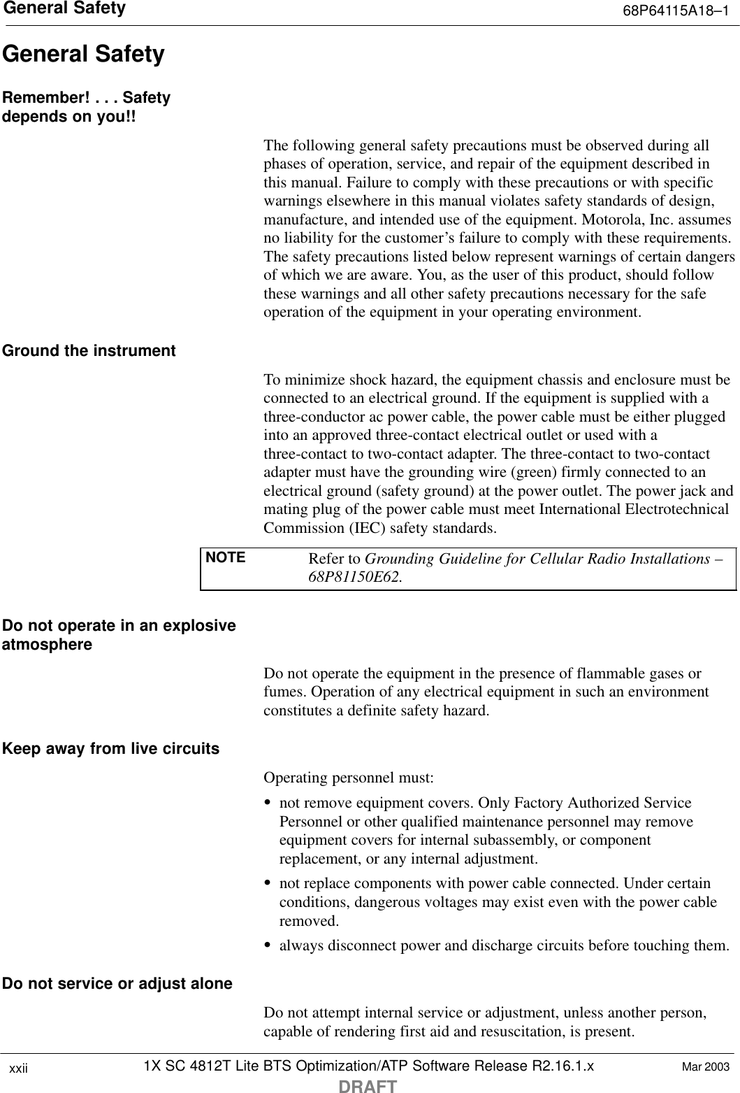
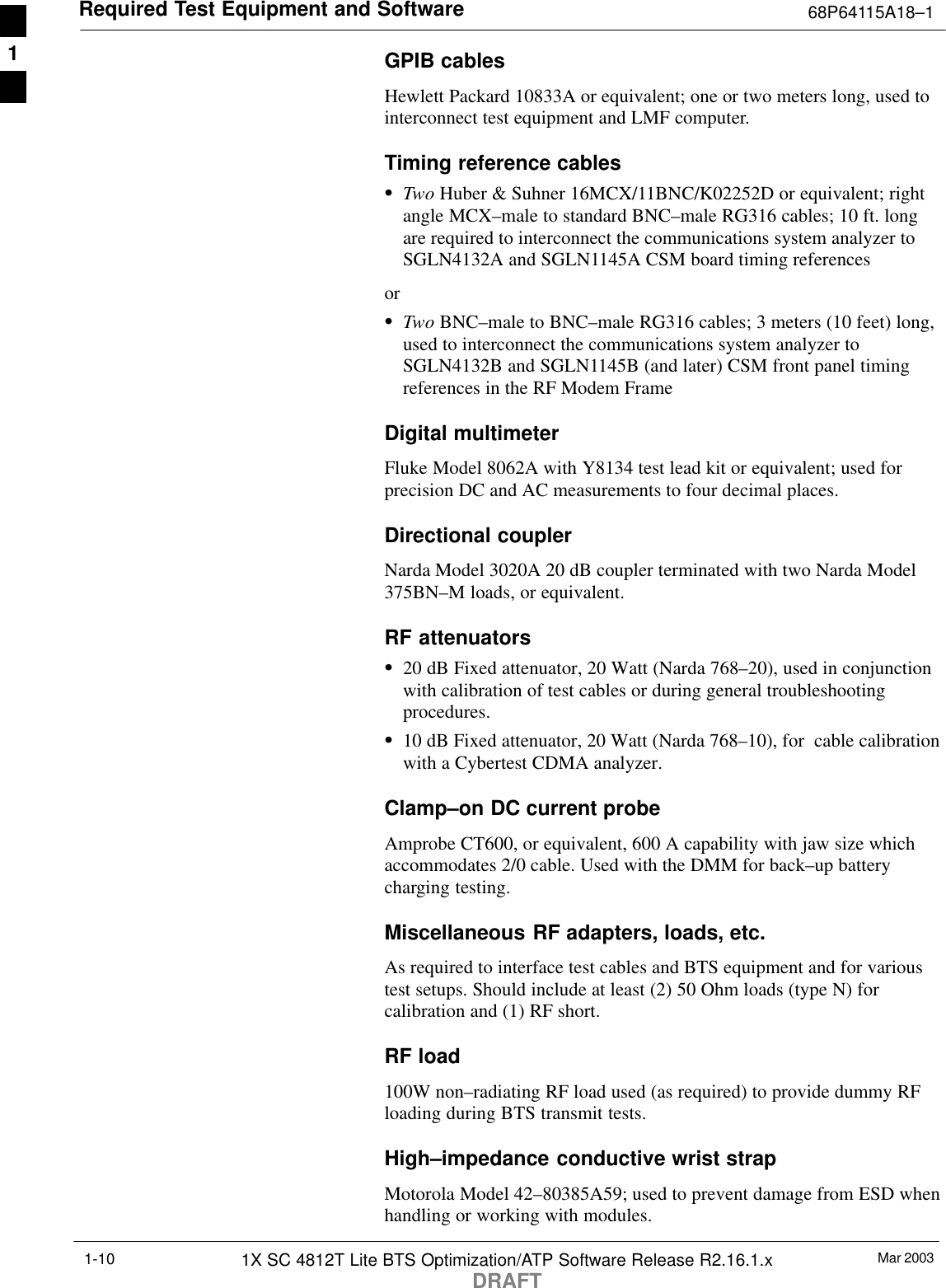
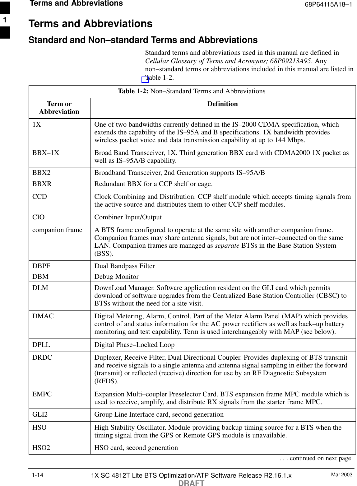
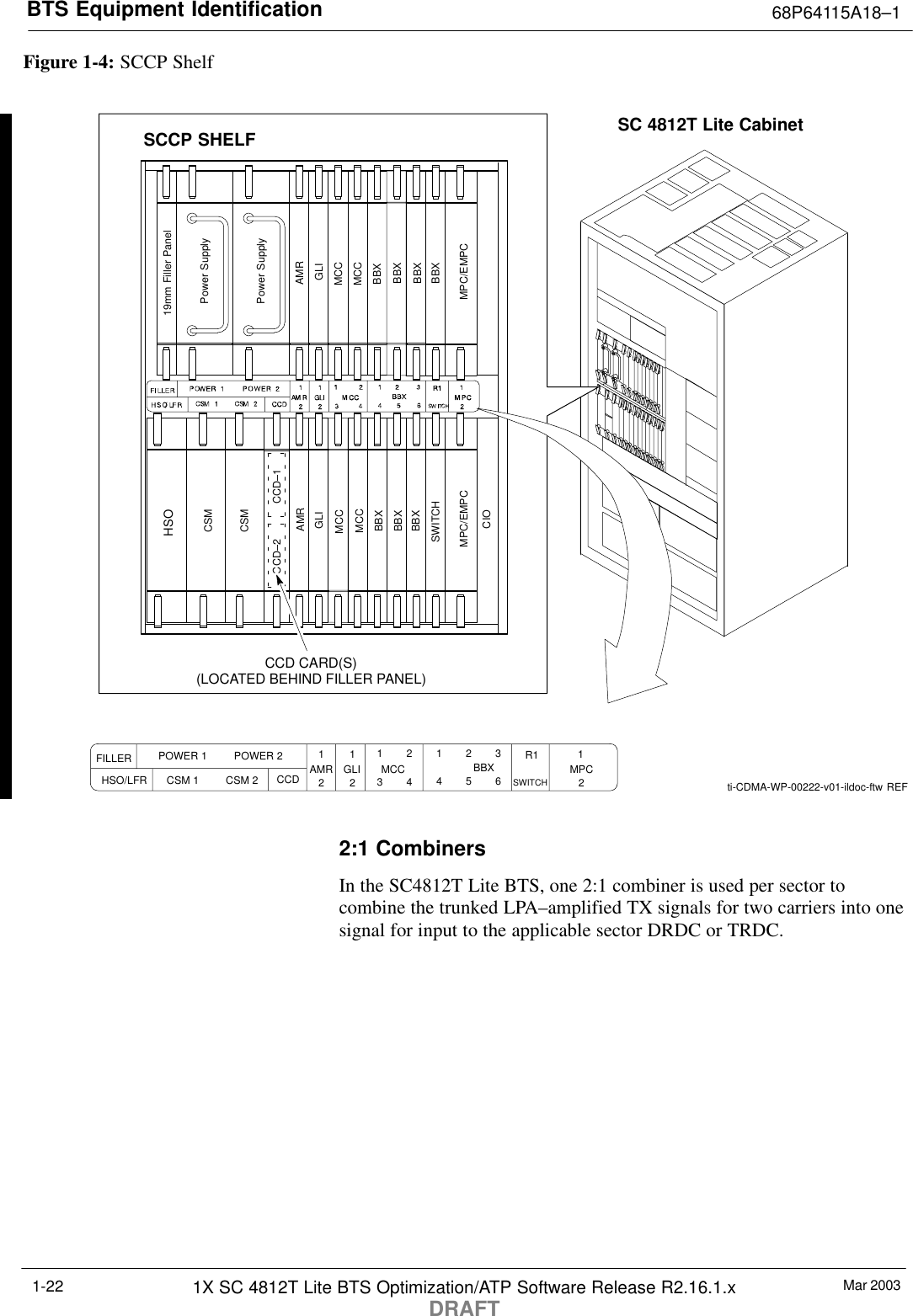
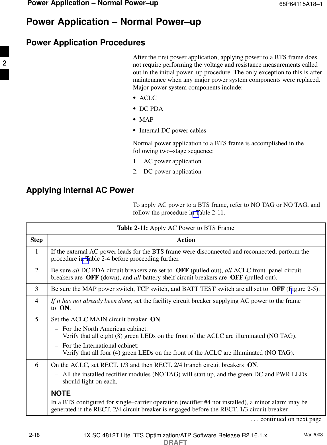
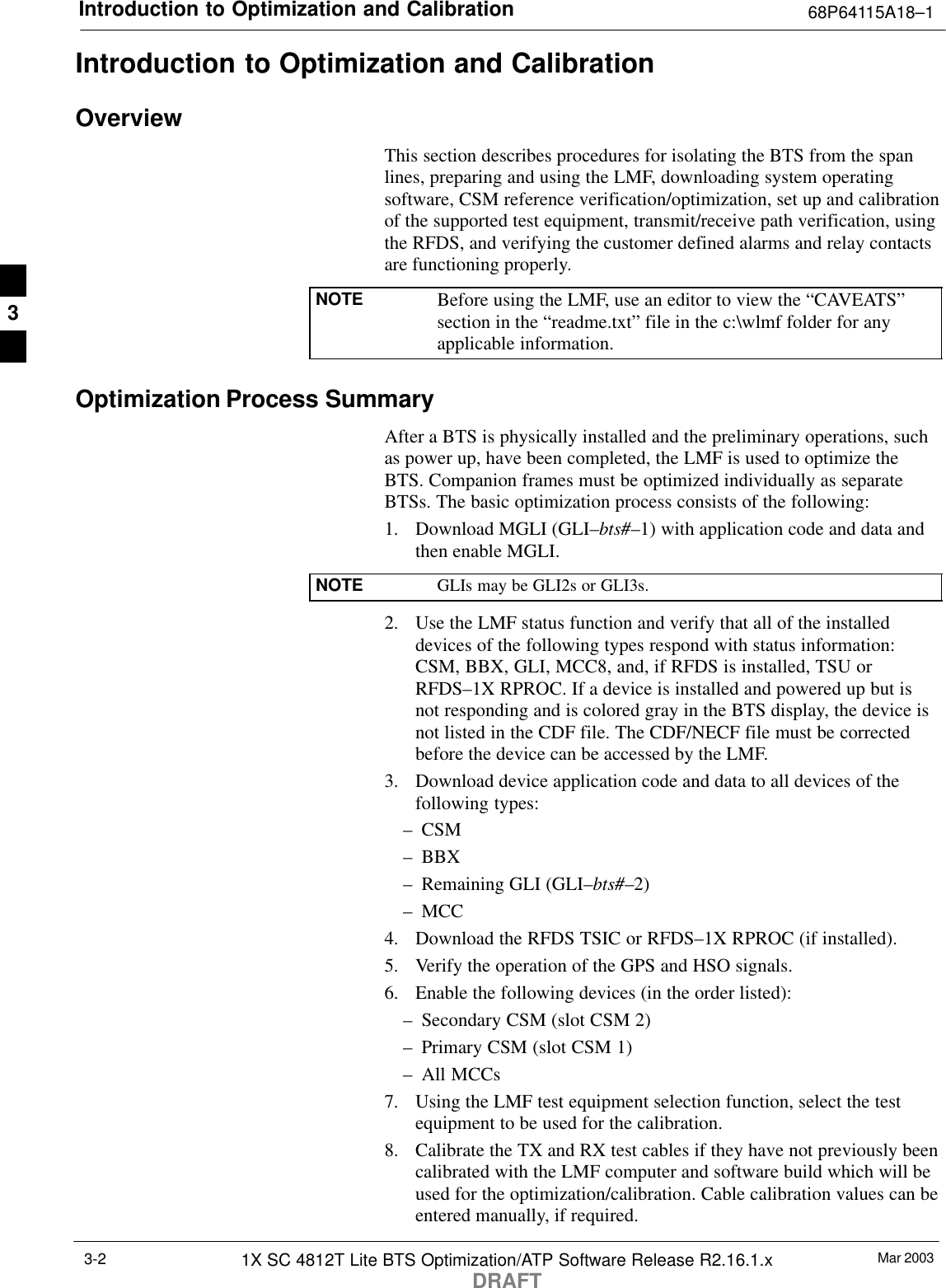
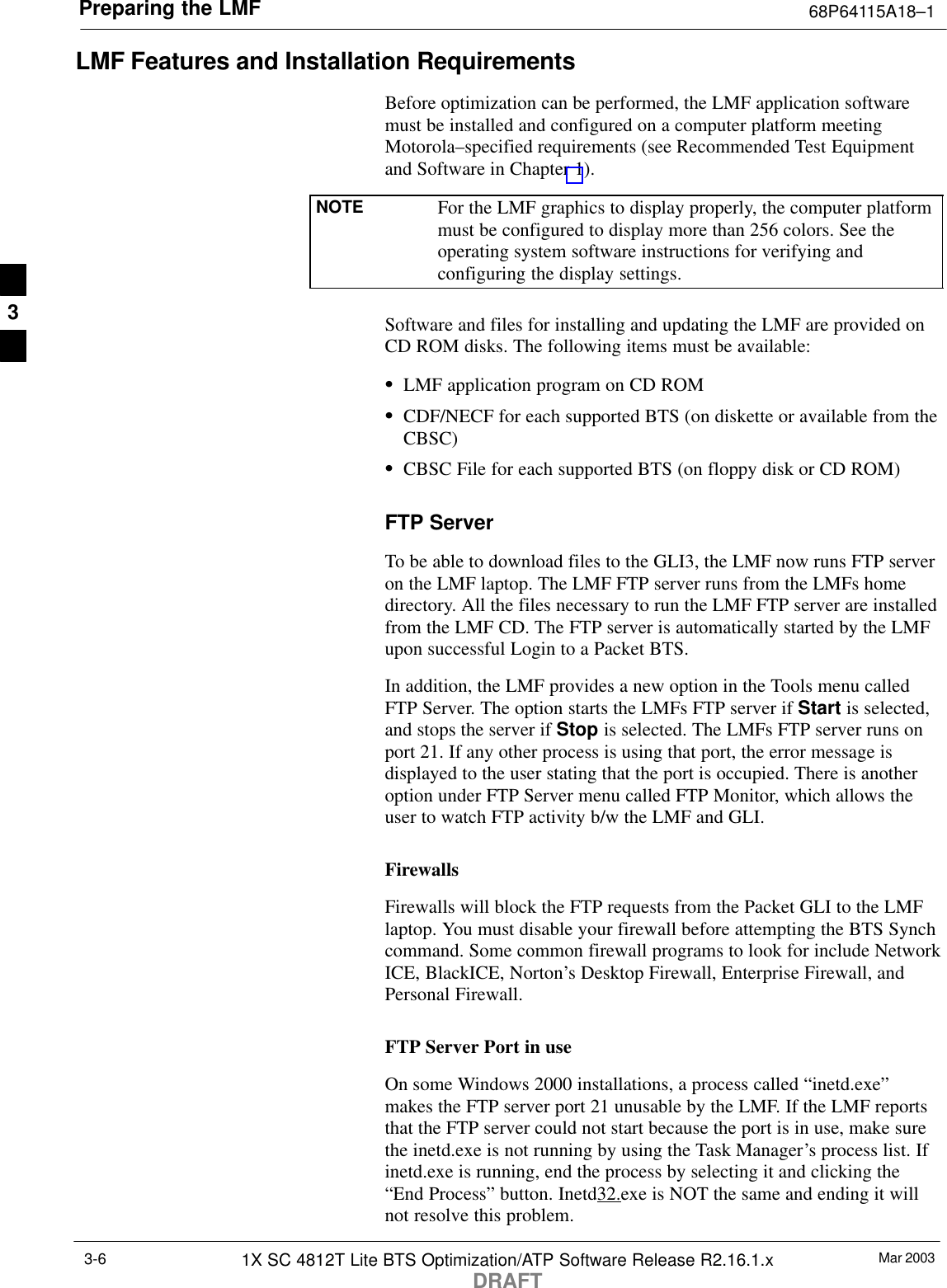
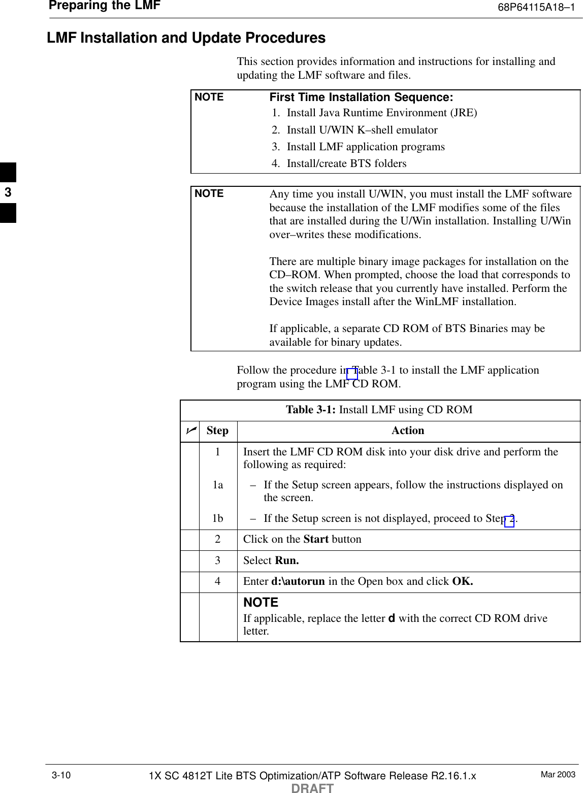
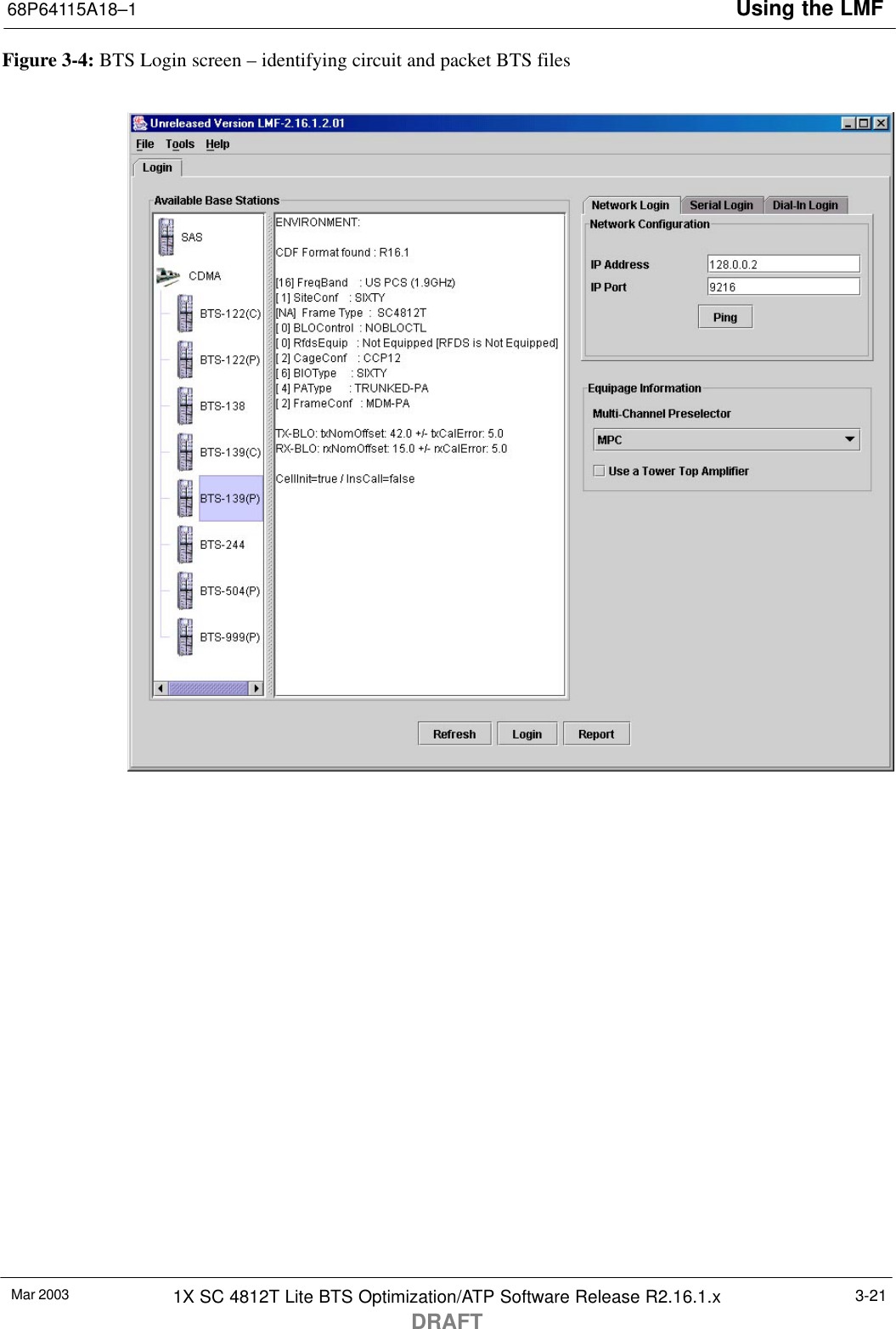
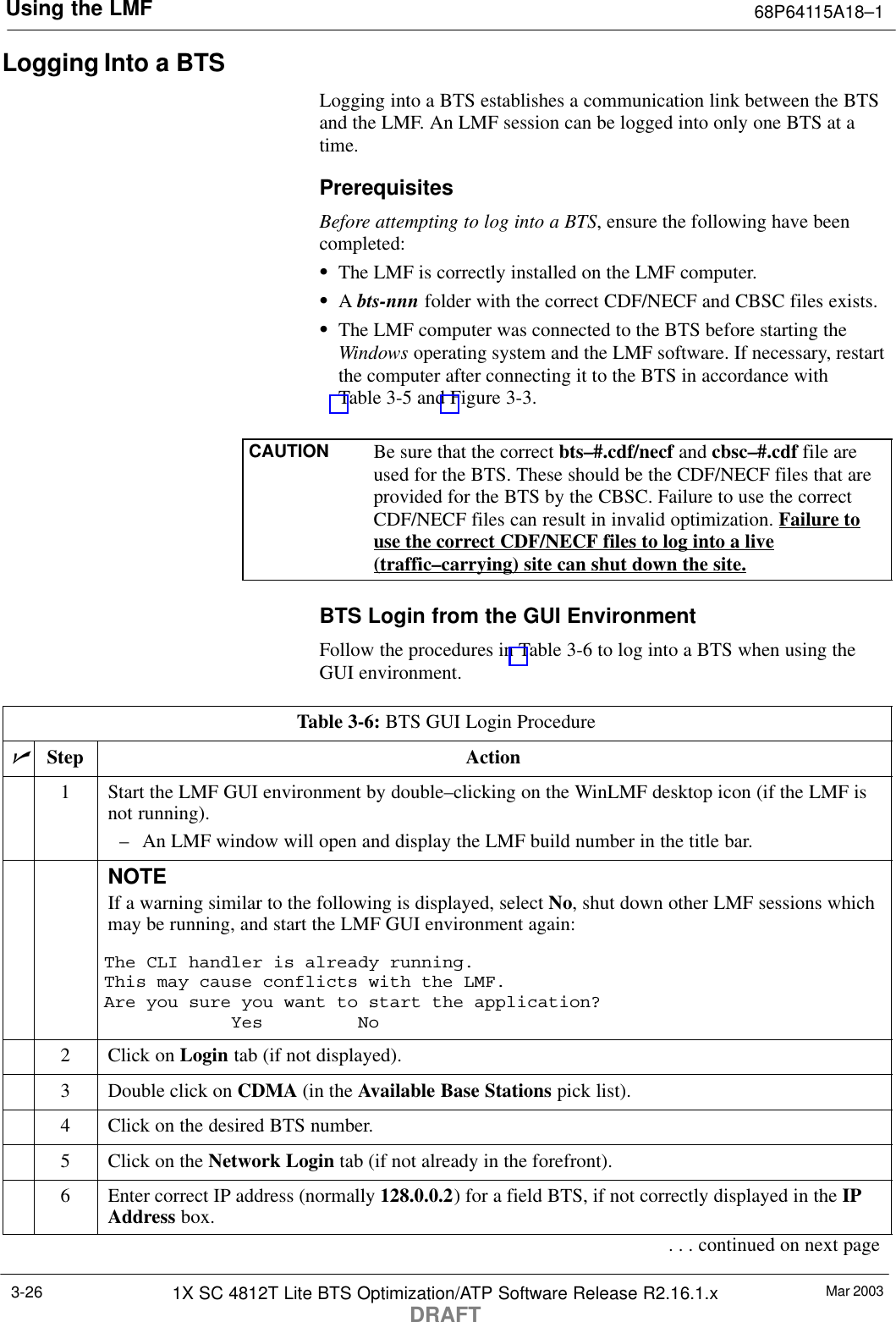
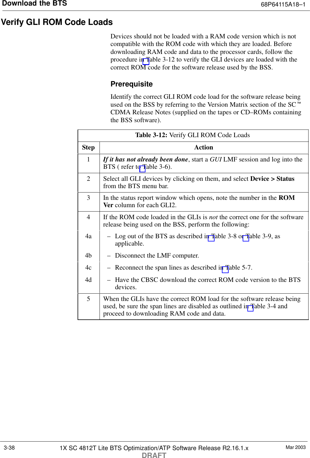
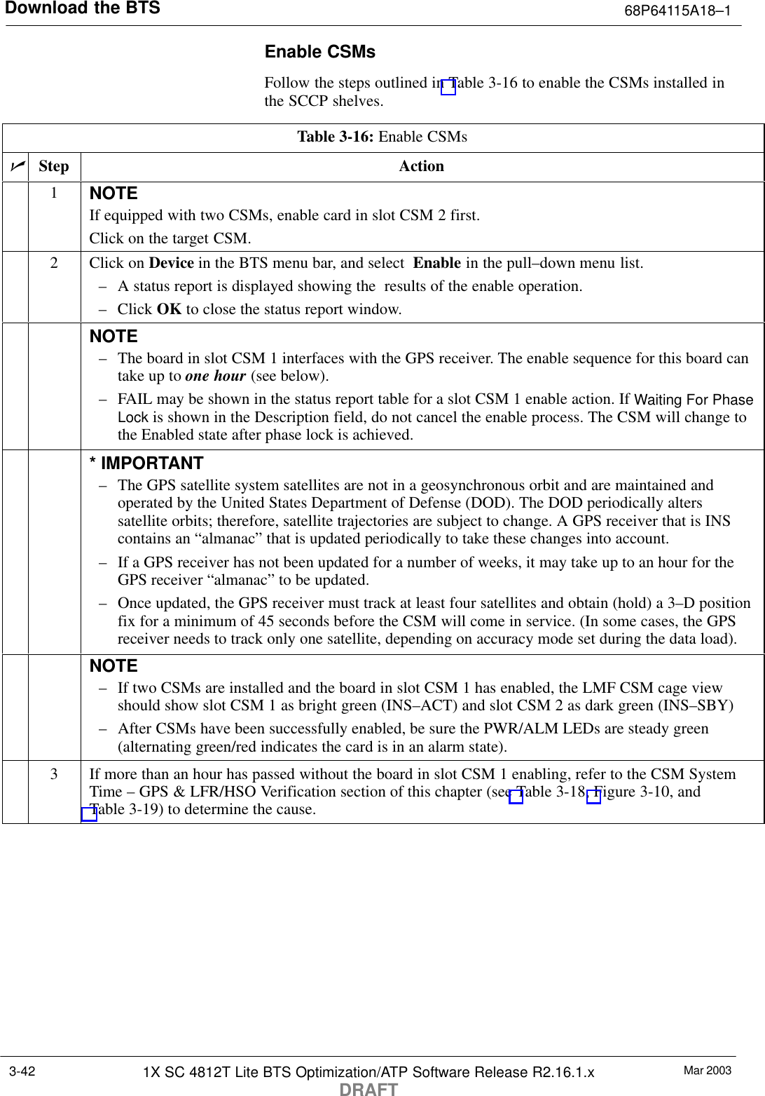
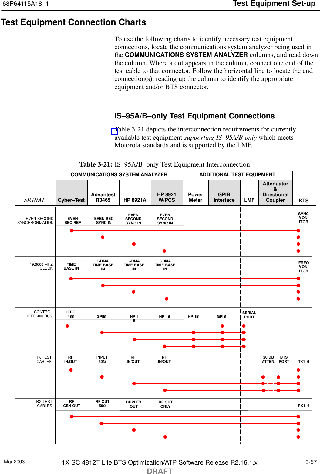
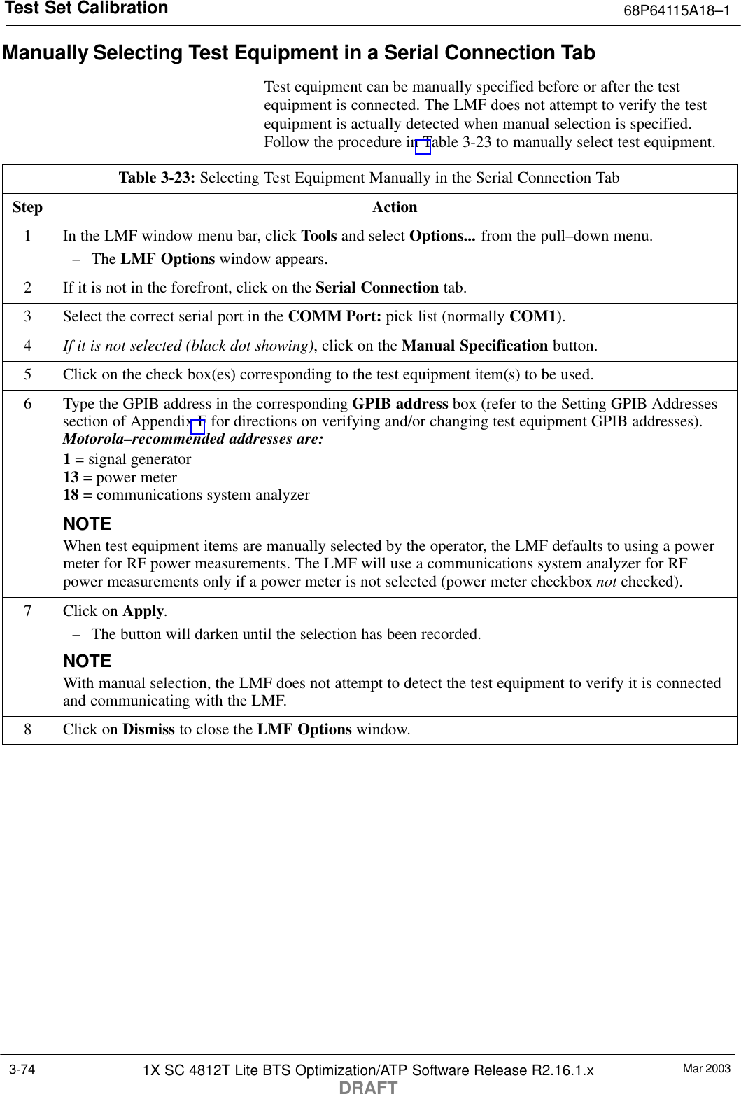
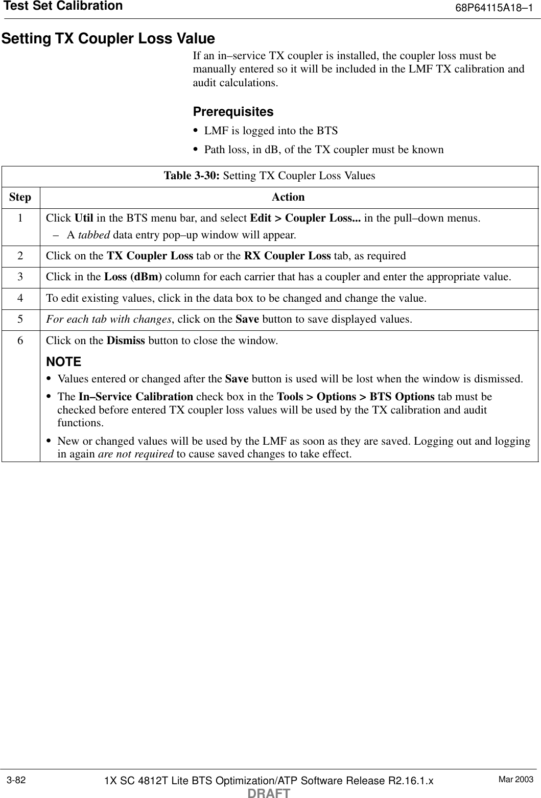
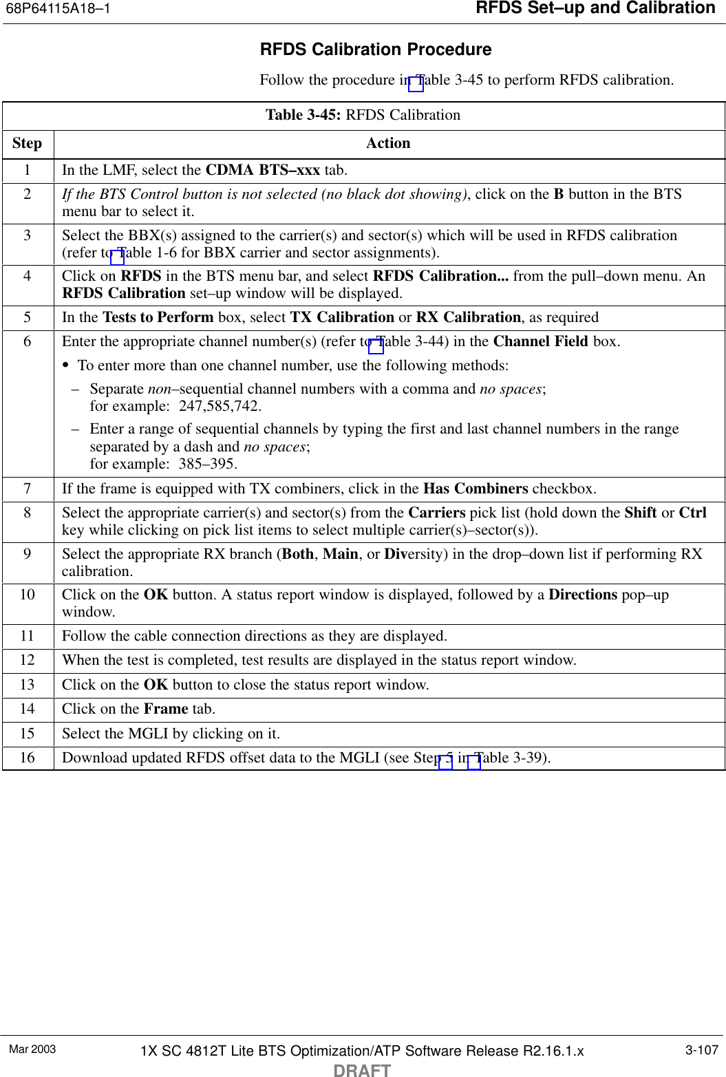
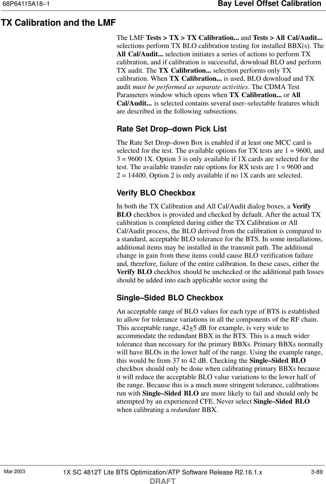
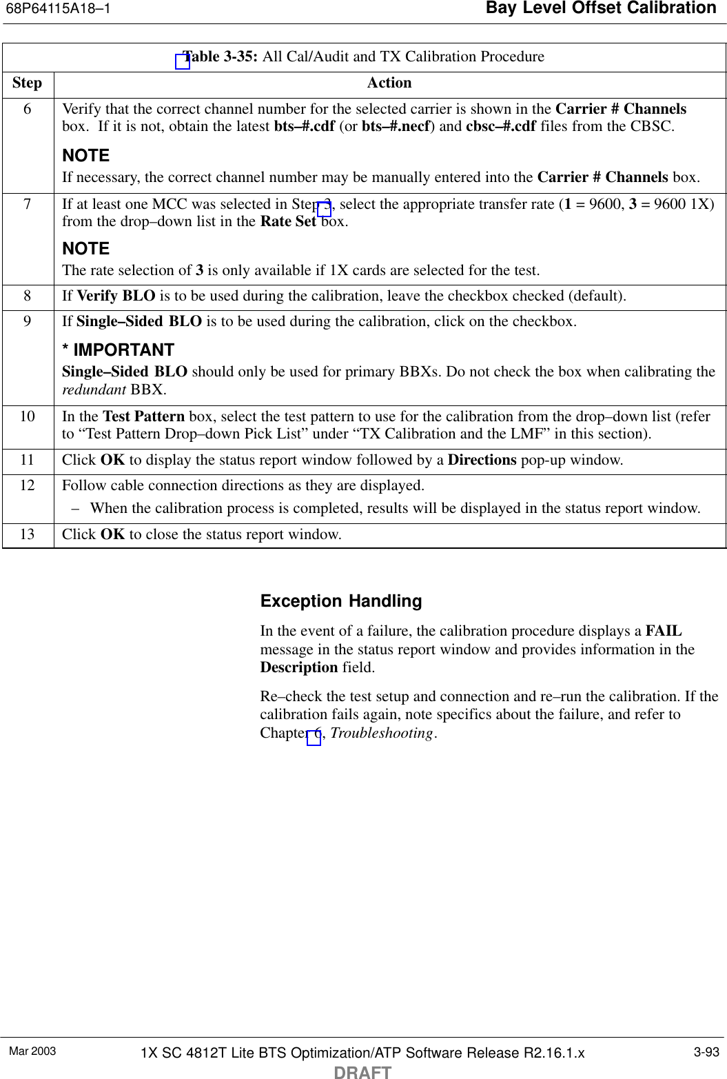
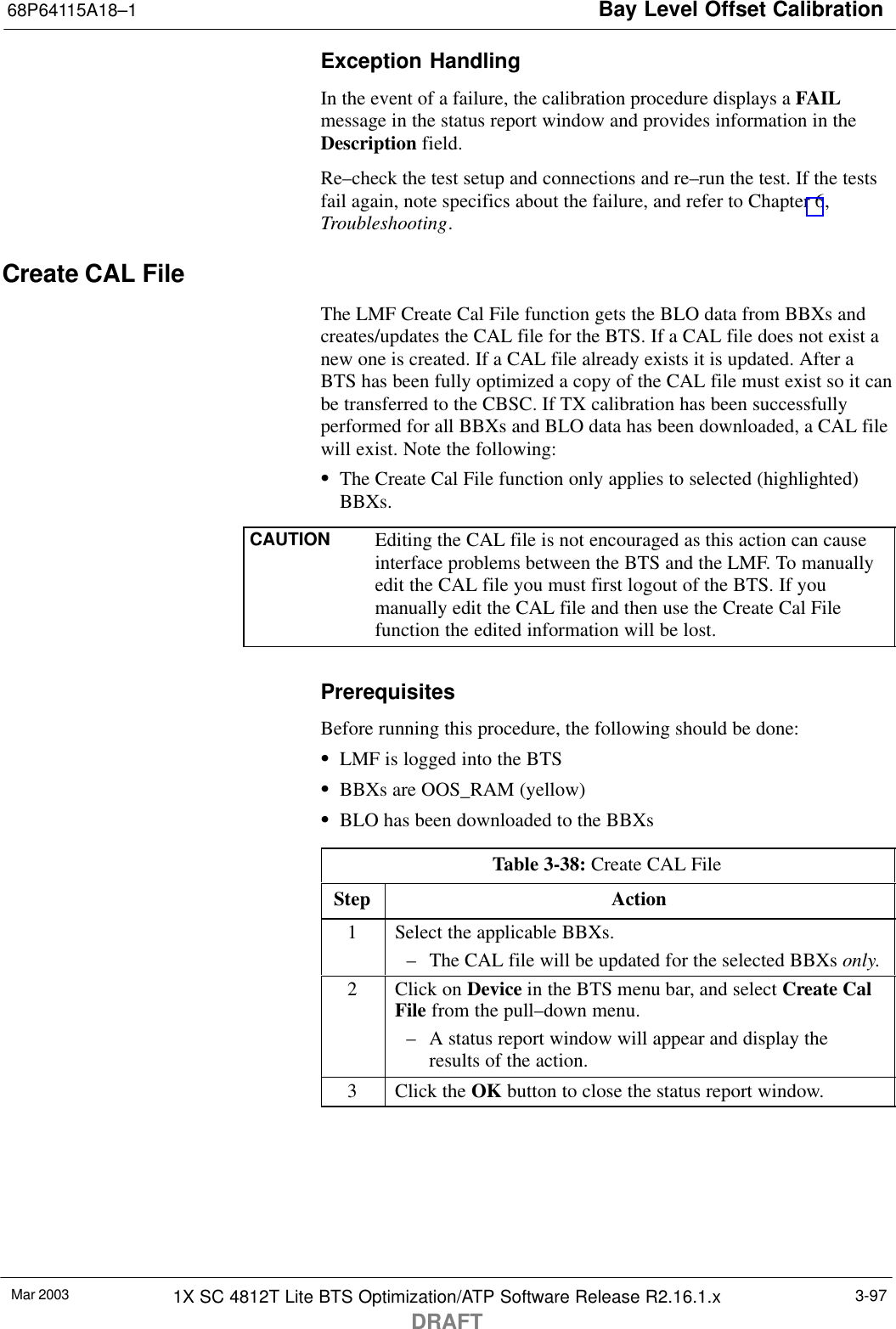
![Bay Level Offset Calibration68P64115A18–1Mar 2003 1X SC 4812T Lite BTS Optimization/ATP Software Release R2.16.1.xDRAFT3-85NOTE Due to the size of the file, Motorola recommends printing out acopy of a bts–#.cal file and referring to it for the followingdescriptions.CAL File OrganizationThe CAL file is subdivided into three sections called “slot Blocks”.These are:1. Slot[1] Block which contains the calibration data for the six primaryBBX slots.2. Slot[20] Block which contains the calibration data for the redundantBBX (see Table 3-32).3. Slot[385] Block which contains the calibration data for the RFDS.BBX Slot Block PartsBBX slot Blocks are further subdivided into the parts described in thefollowing:Slot Block Header – Each BBX slot Block has a header section (slotheader) which contains:SA creation Date and Time – broken down into separate parameters ofcreateMonth, createDay, createYear, createHour, and createMin.SThe number of calibration entries in the file – the numBayLevelPtsparameter. The parameter is fixed at 720 entries for SC4812–seriesframes. These 720 entries are combined to define the 360 calibrationpoints of the CAL file.SThe slot Block format parameter.Slot Block Bay Level Calibration Data – Each BBX slot Block has aBay Level Calibration data section (BayLevelCal) which is organized asa large flat array. The array is organized by branch, SCCP cage BBXslot, and calibration entries. There are several ways to look at the arraycontents. Two different views are provided in the following to illustratethe significant features of BayLevelCal section content and organization:SThe first view of the array is shown in Table 3-31. This view showsthe three branches of the array, transmit, main receive, and diversityreceive offsets, and the calibration entry ranges which apply to each.Table 3-31: BLO bts–#.cal File Array Branch AssignmentsRange Branch AssignmentC[1]–C[120] TransmitC[121]–C[240] No SC4812T Lite BLO cal pointentries (default only)C[241]–C[360] ReceiveC[361]–C[480] No SC4812T Lite BLO cal pointentries (default only)C[481]–C[600] Diversity ReceiveC[601]–C[720] No SC4812T Lite BLO cal pointentries (default only)](https://usermanual.wiki/Nokia-Solutions-and-Networks/T5DJ1.Users-manual-1-of-2/User-Guide-320001-Page-161.png)
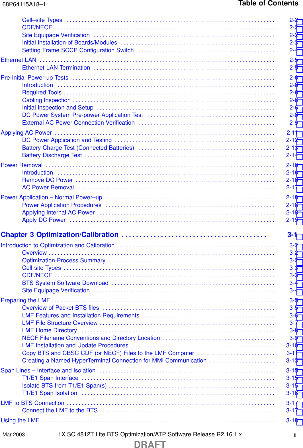
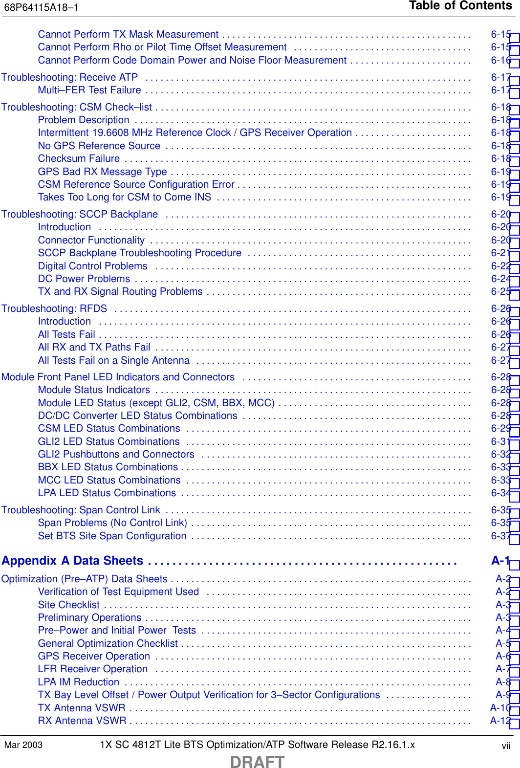
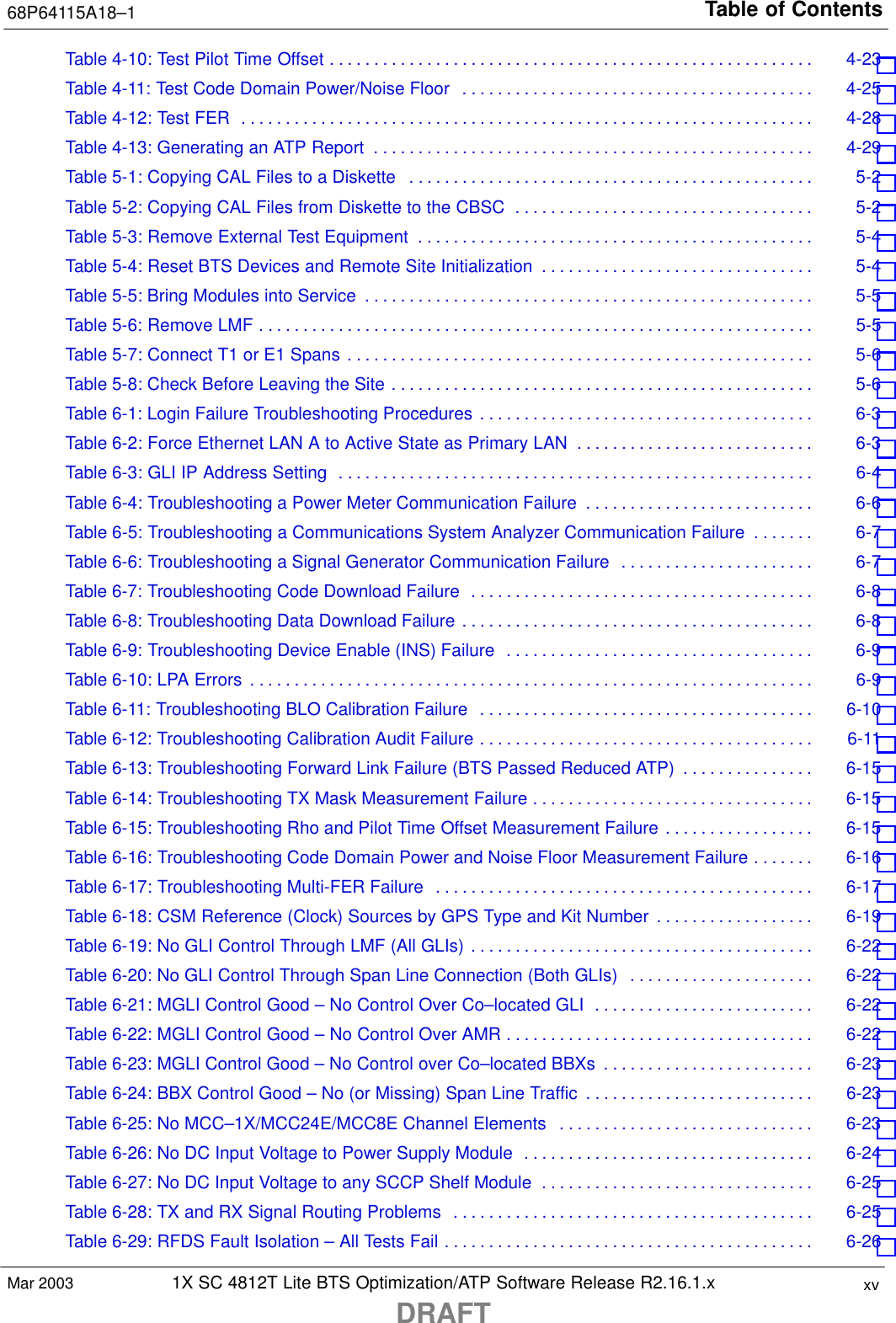
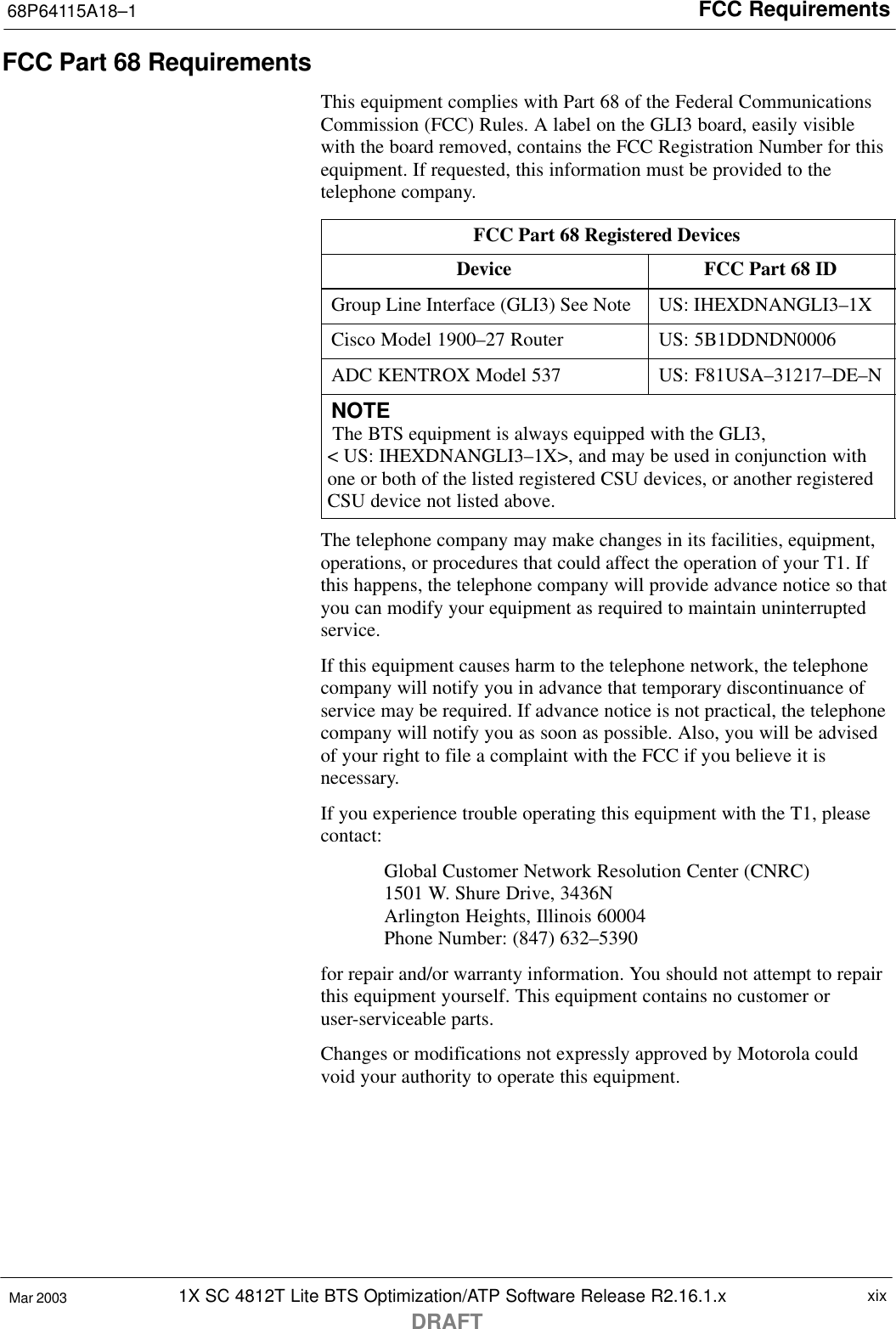
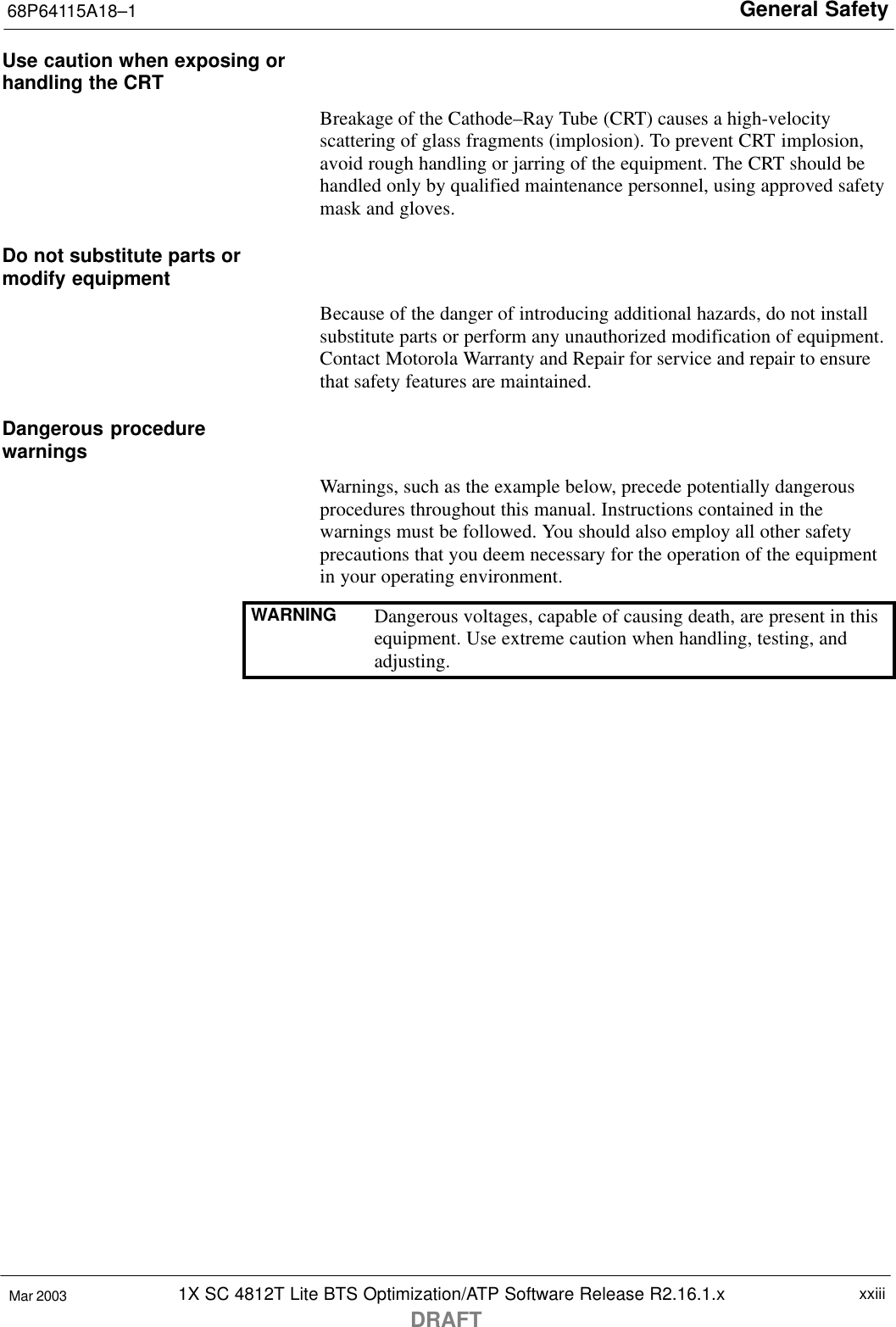
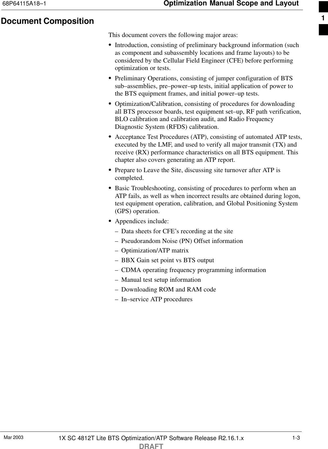
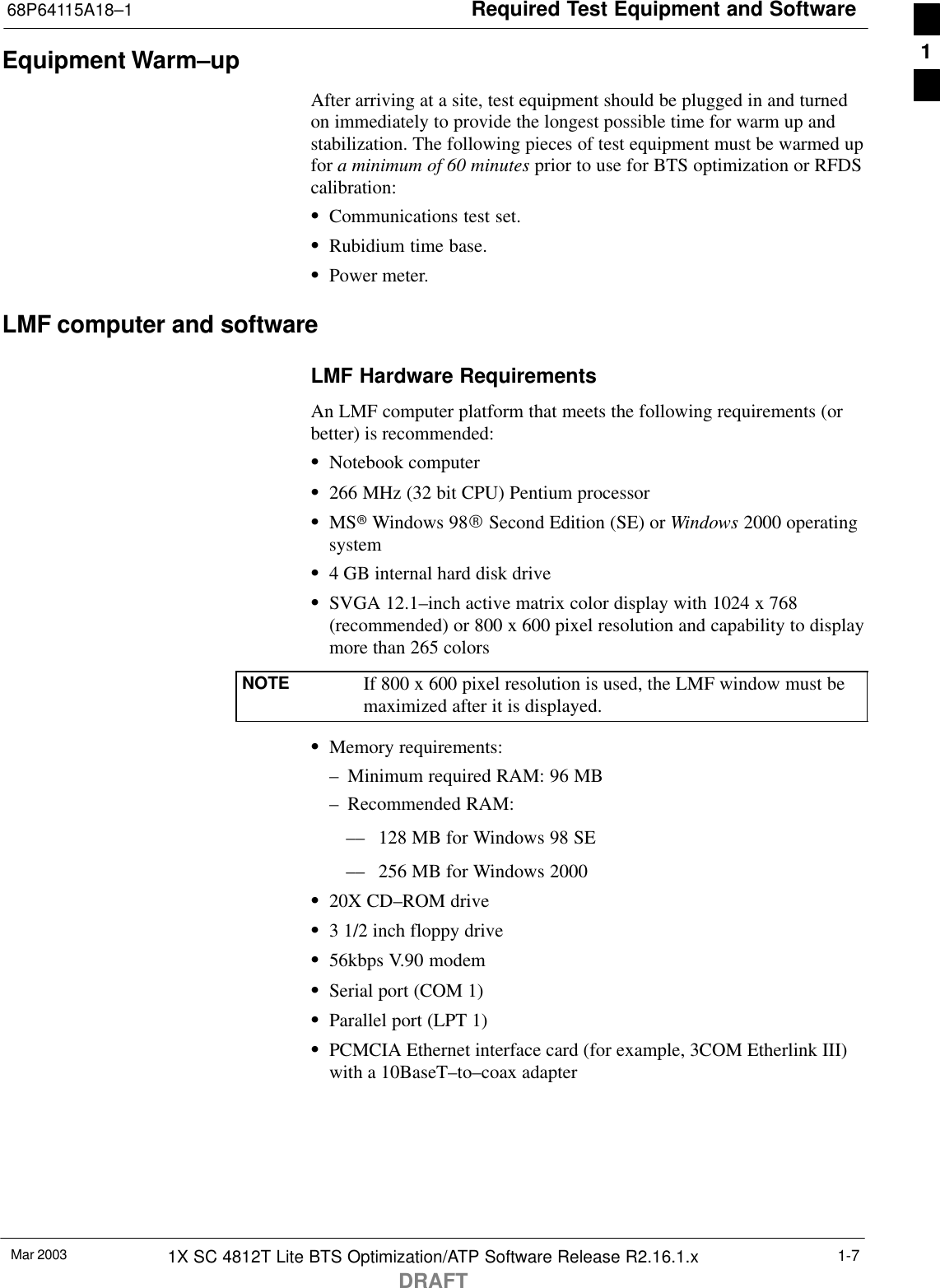
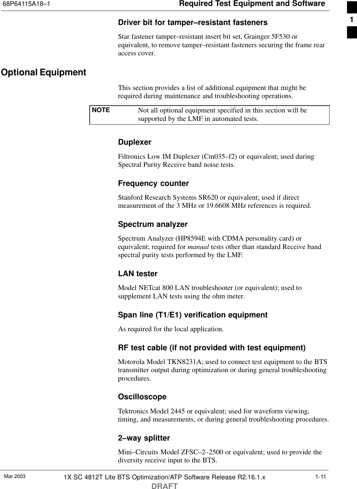
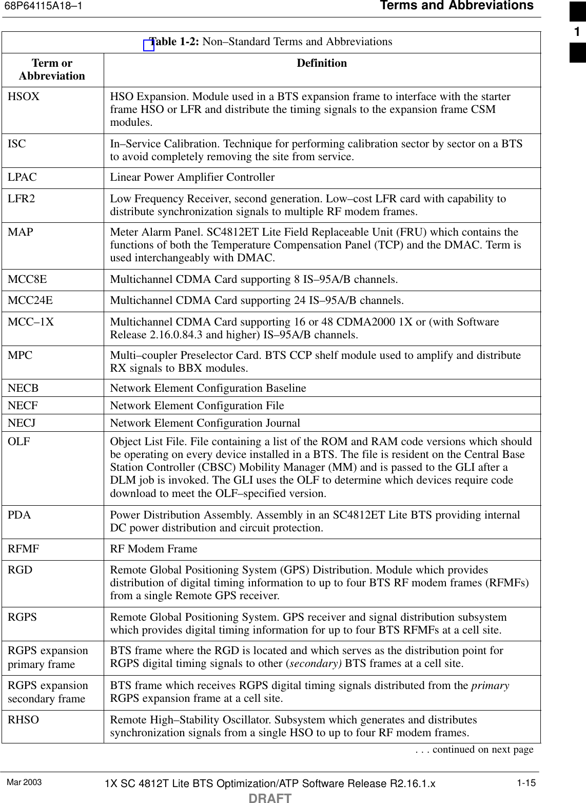
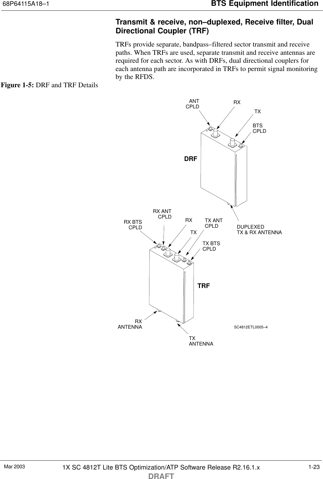
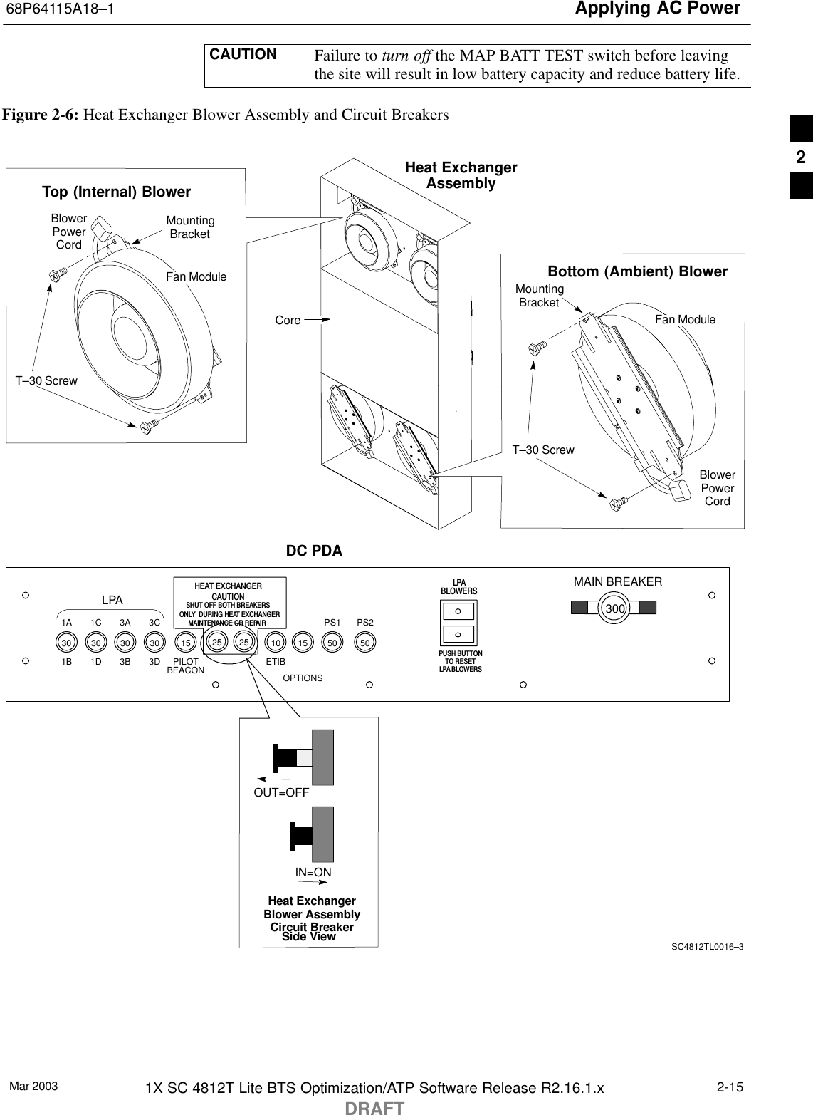
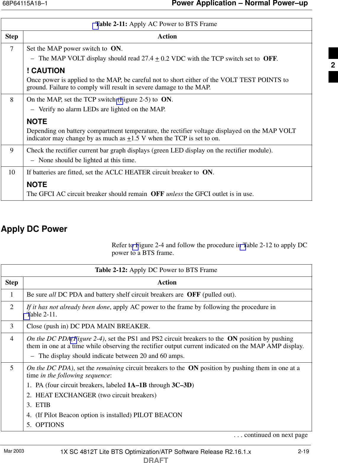
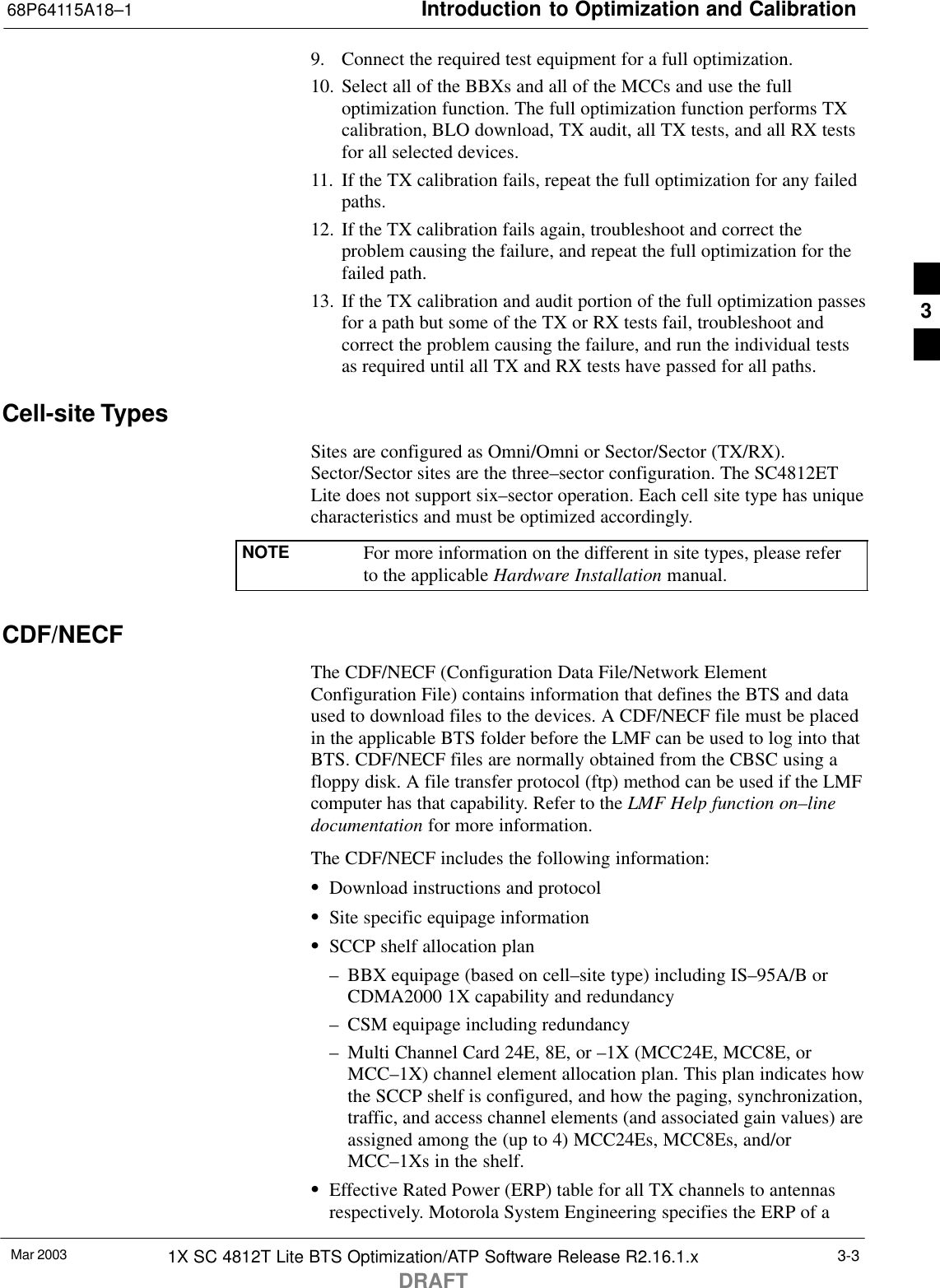
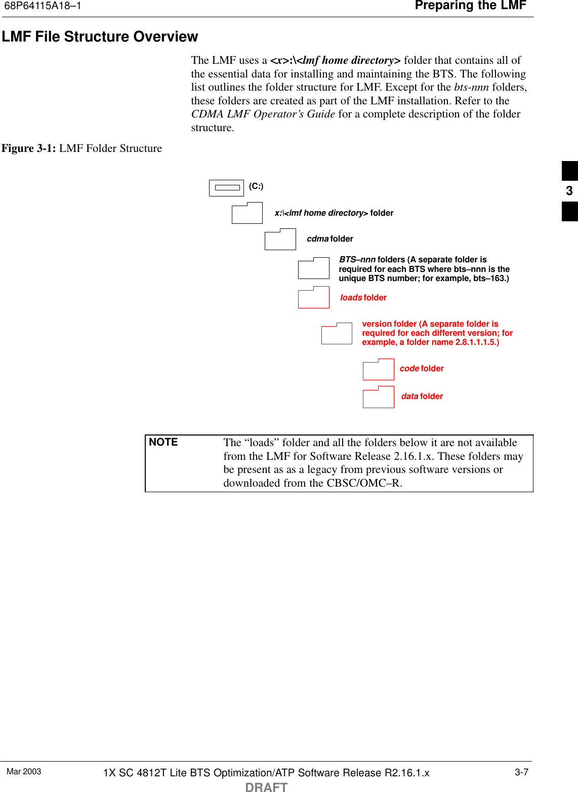
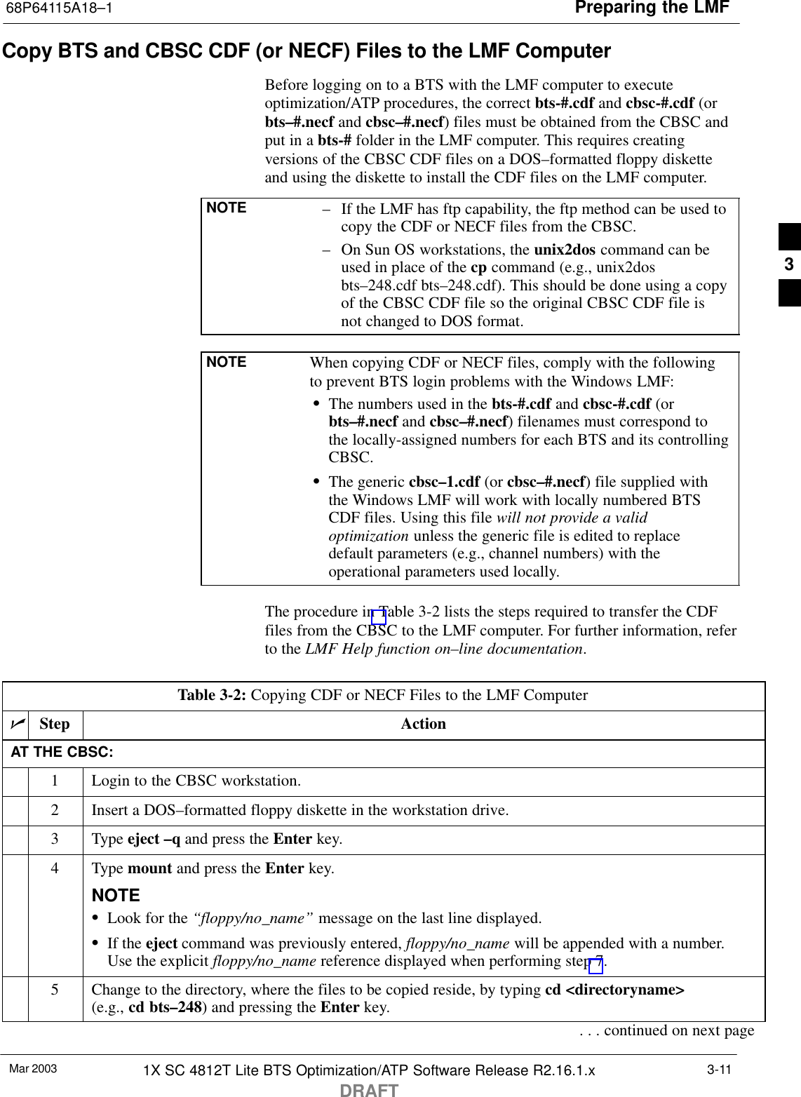
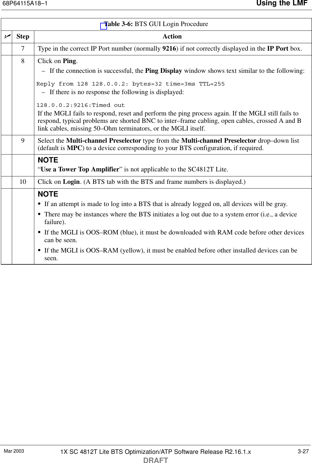
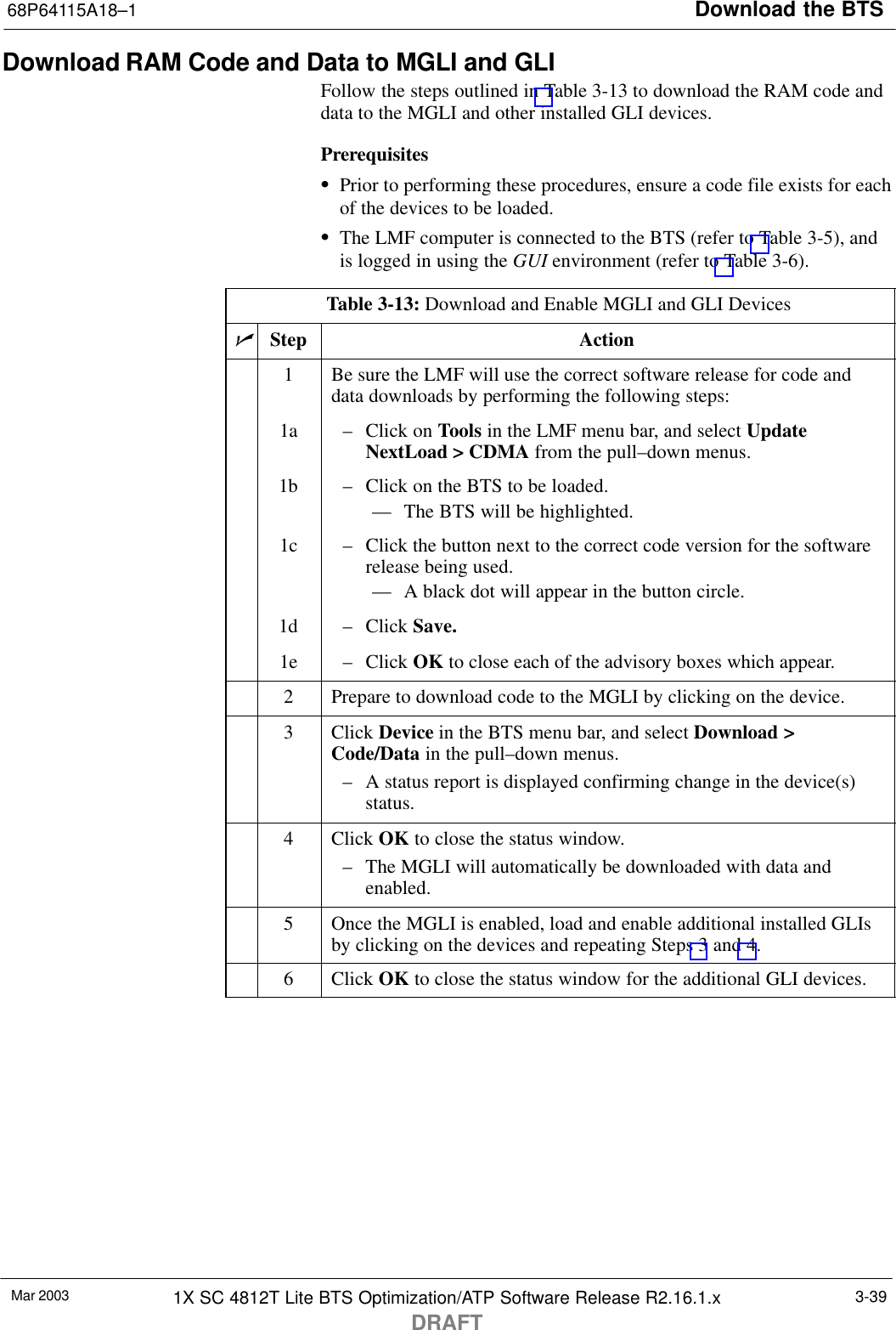
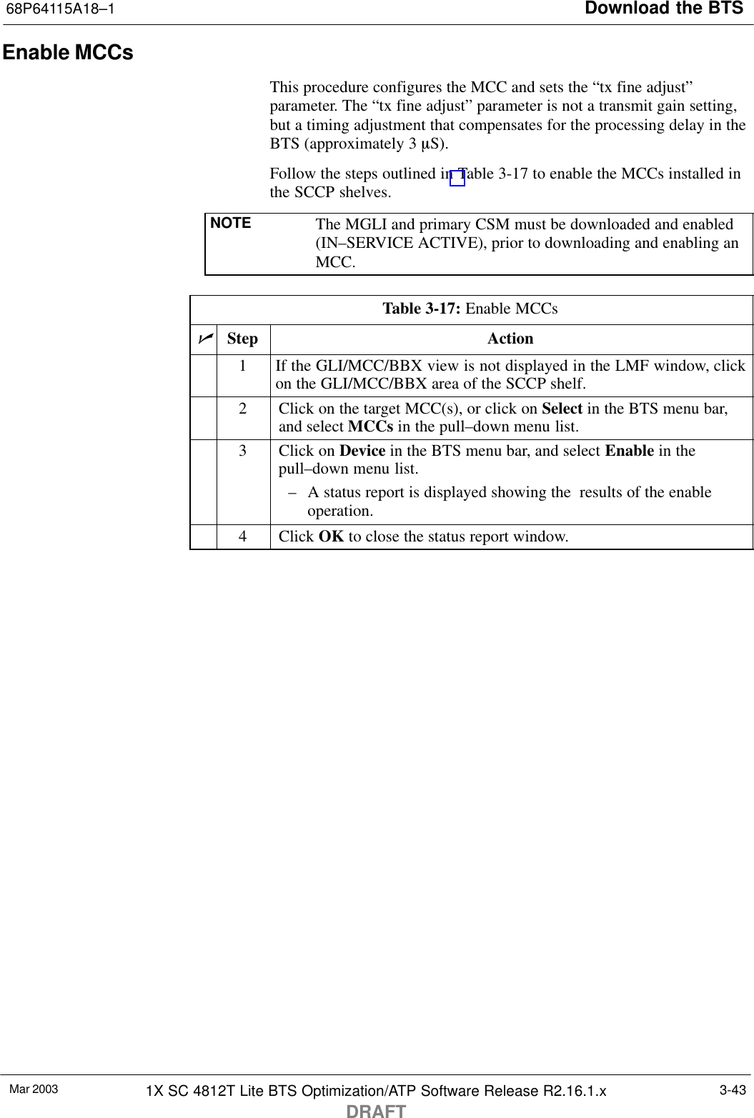
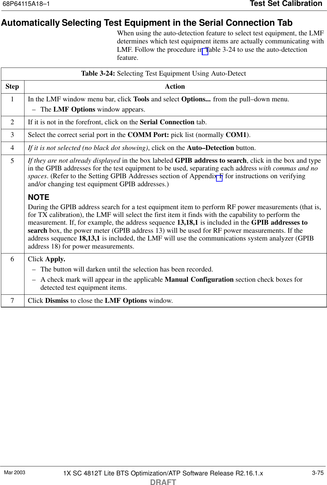
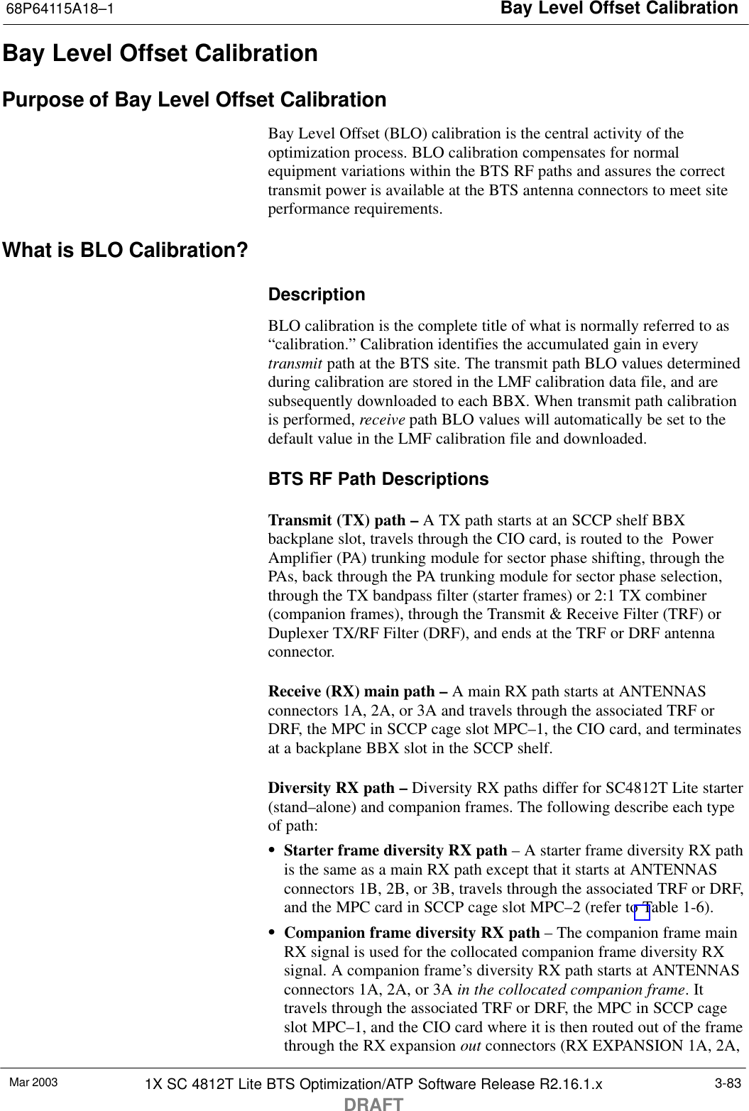
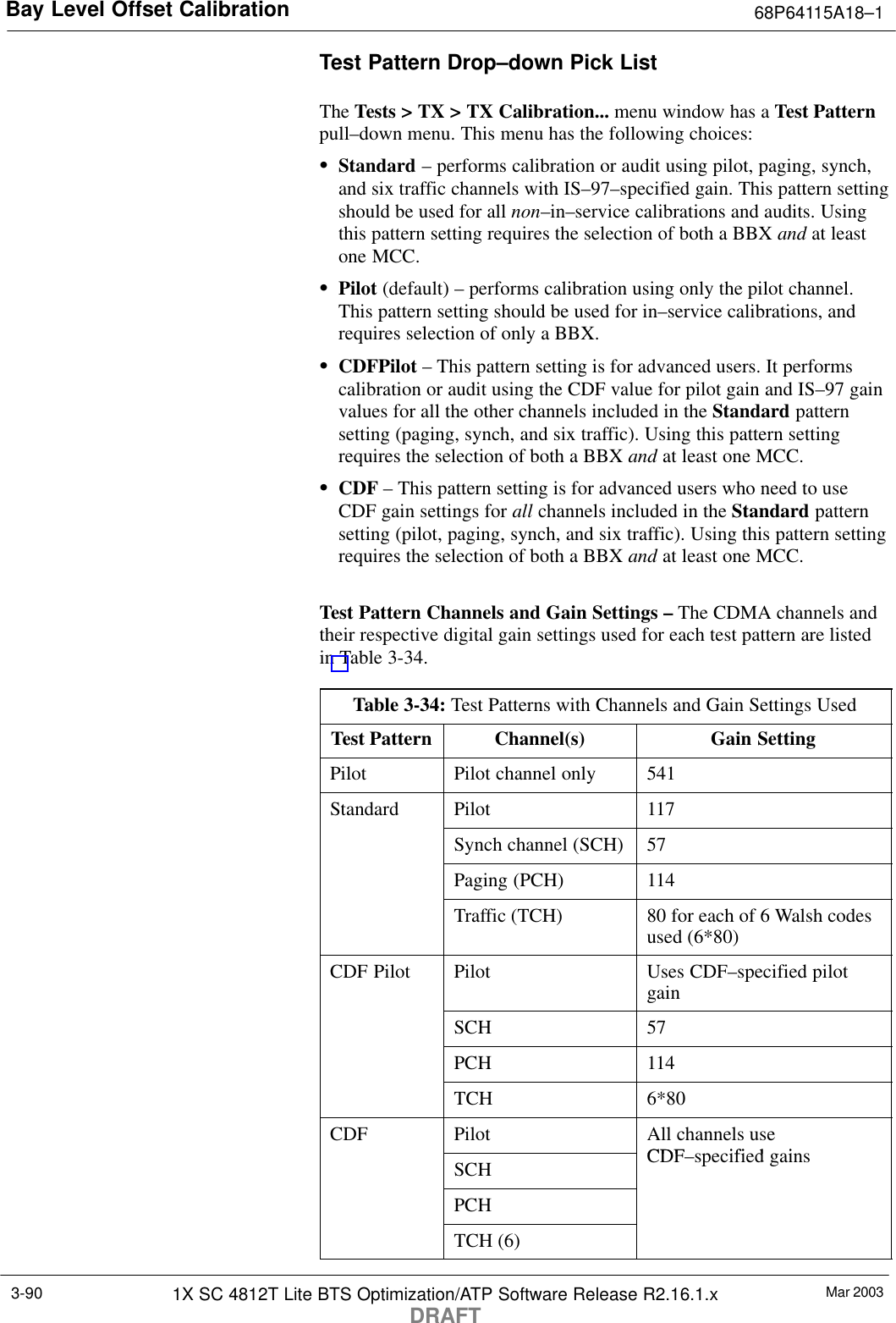
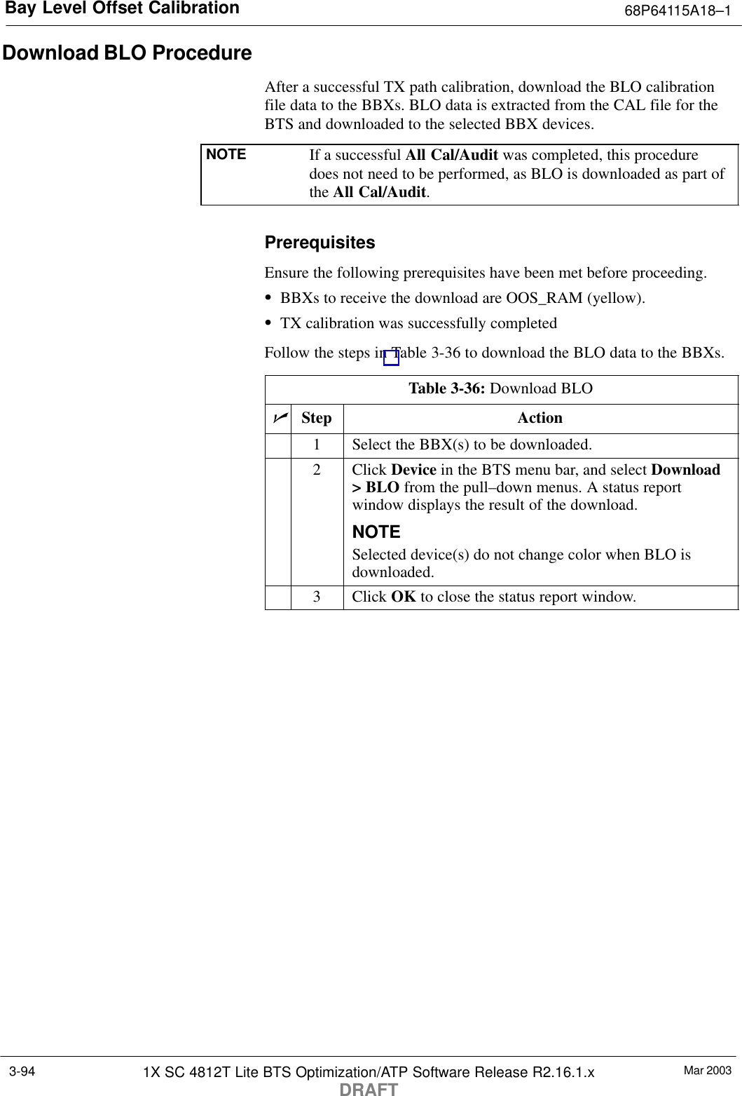
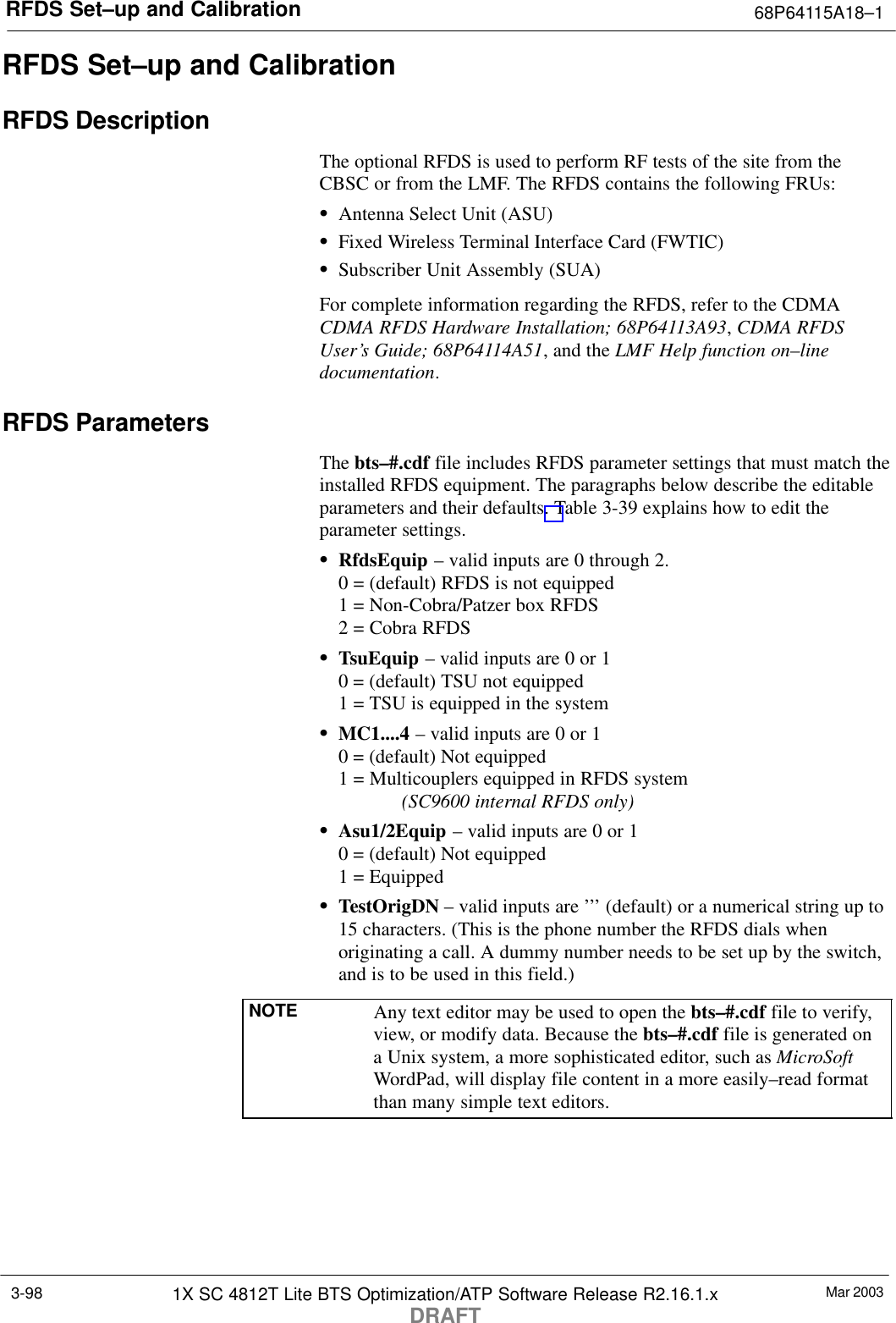
![Bay Level Offset Calibration 68P64115A18–1Mar 20031X SC 4812T Lite BTS Optimization/ATP Software Release R2.16.1.xDRAFT3-86SThe second view of the array is shown in Table 3-32. This view showsthe assignment of calibration entries in each branch to each BBX slot,carrier, and sectorization. Three sectors are allowed for an SC4812TLite frame.Table 3-32: SC4812T Lite bts–#.cal File Array (By BBX/Sector)BBX Sectorization TX Branch RX Branch RX DiversityBranchSlot[1] (Primary BBXs 1 through 6)1 (Omni)3S tC[1]–C[20] C[241]–C[260] C[481]–C[500]23–Sector,1st CarrierC[21]–C[40] C[261]–C[280] C[501]–C[520]31st CarrierC[41]–C[60] C[281]–C[300] C[521]–C[540]43S tC[61]–C[80] C[301]–C[320] C[541]–C[560]53–Sector,2nd CarrierC[81]–C[100] C[321]–C[340] C[561]–C[580]62nd CarrierC[101]–C[120] C[341]–C[360] C[581]–C[600]C[121]–C[140] C[361]–C[380] C[601]–C[620]Not Used in SC4812T LiteC[141]–C[160] C[381]–C[400] C[621]–C[640]Not Used in SC4812T Lite(CAL file entries are C[161]–C[180] C[401]–C[420] C[641]–C[660](CAL file entries are Channel 0 with default t l l )C[181]–C[200] C[421]–C[440] C[661]–C[680]power set level.) C[201]–C[220] C[441]–C[460] C[681]–C[700]C[221]–C[240] C[461]–C[480] C[701]–C[720]Slot[20] (Redundant BBX–R1)1 (Omni)3S tC[1]–C[20] C[241]–C[260] C[481]–C[500]23–Sector,1st CarrierC[21]–C[40] C[261]–C[280] C[501]–C[520]31st CarrierC[41]–C[60] C[281]–C[300] C[521]–C[540]43S tC[61]–C[80] C[301]–C[320] C[541]–C[560]53–Sector,2nd CarrierC[81]–C[100] C[321]–C[340] C[561]–C[580]62nd CarrierC[101]–C[120] C[341]–C[360] C[581]–C[600]C[121]–C[140] C[361]–C[380] C[601]–C[620]Not Used in SC4812T LiteC[141]–C[160] C[381]–C[400] C[621]–C[640]Not Used in SC4812T Lite(CAL file entries are C[161]–C[180] C[401]–C[420] C[641]–C[660](CAL file entries are Channel 0 with default t l l )C[181]–C[200] C[421]–C[440] C[661]–C[680]power set level.) C[201]–C[220] C[441]–C[460] C[681]–C[700]C[221]–C[240] C[461]–C[480] C[701]–C[720]SWhen referring to the CAL file print–out and Table 3-32, it can beseen that there is one BBX slot per sector with 20 “calibration entries”per BBX (sector) for each branch. Two calibration entries define asingle “calibration point;” therefore there are ten calibration points ineach branch for each BBX.– The first entry for a calibration point (all odd entries) identifies theCDMA channel (frequency) where the BLO is measured. Thesecond calibration entry (all even entries) is the power set level(PwrLvlAdj) for that frequency. The valid range for PwrLvlAdj is](https://usermanual.wiki/Nokia-Solutions-and-Networks/T5DJ1.Users-manual-1-of-2/User-Guide-320001-Page-162.png)
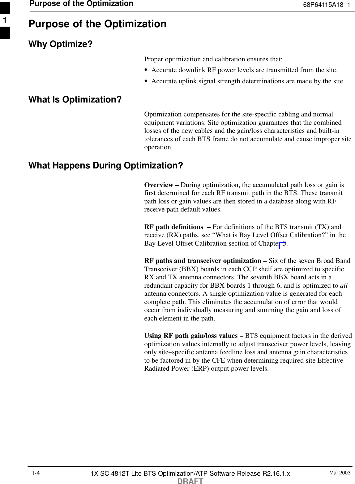
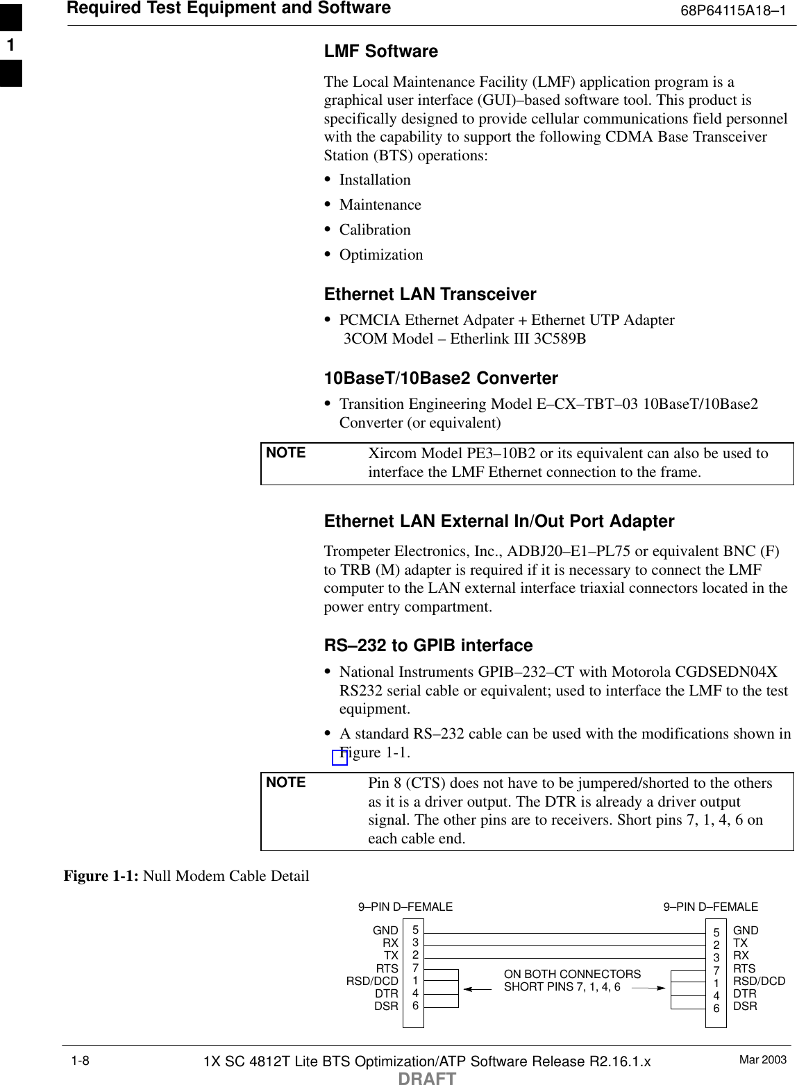
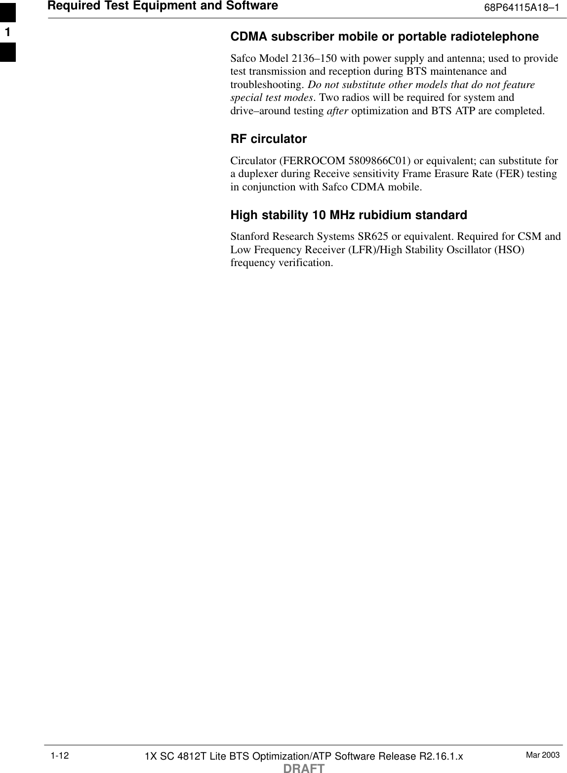
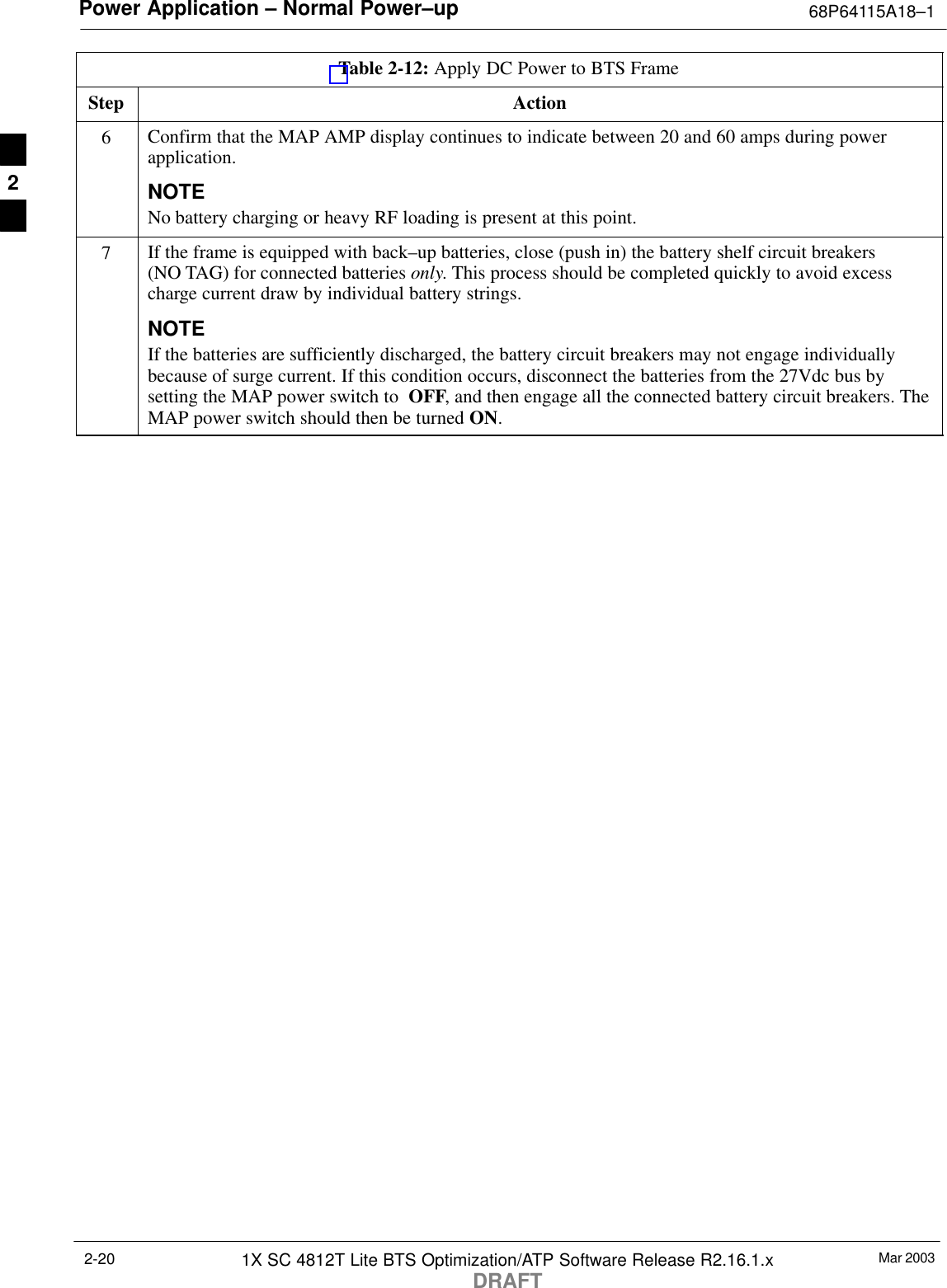
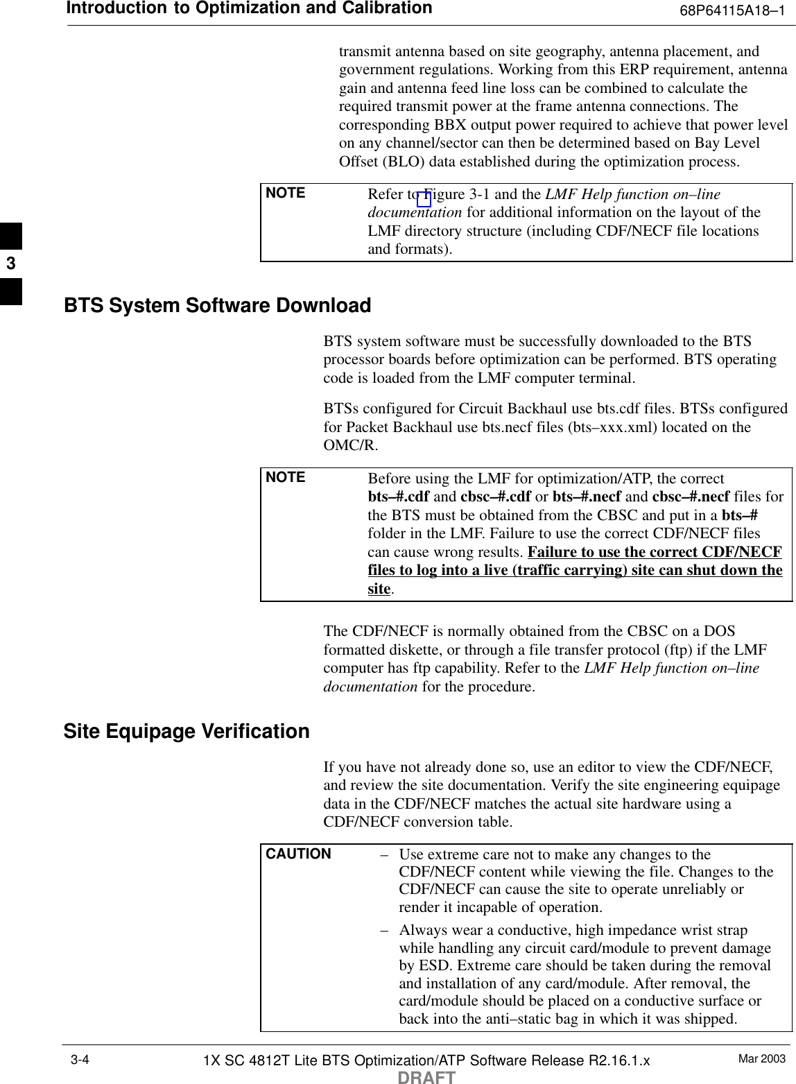
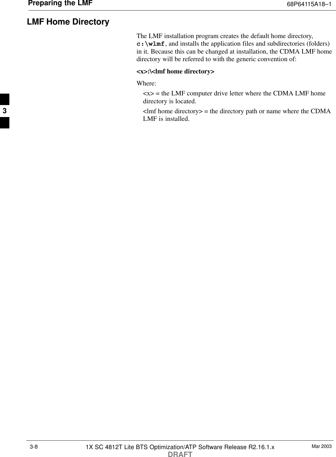
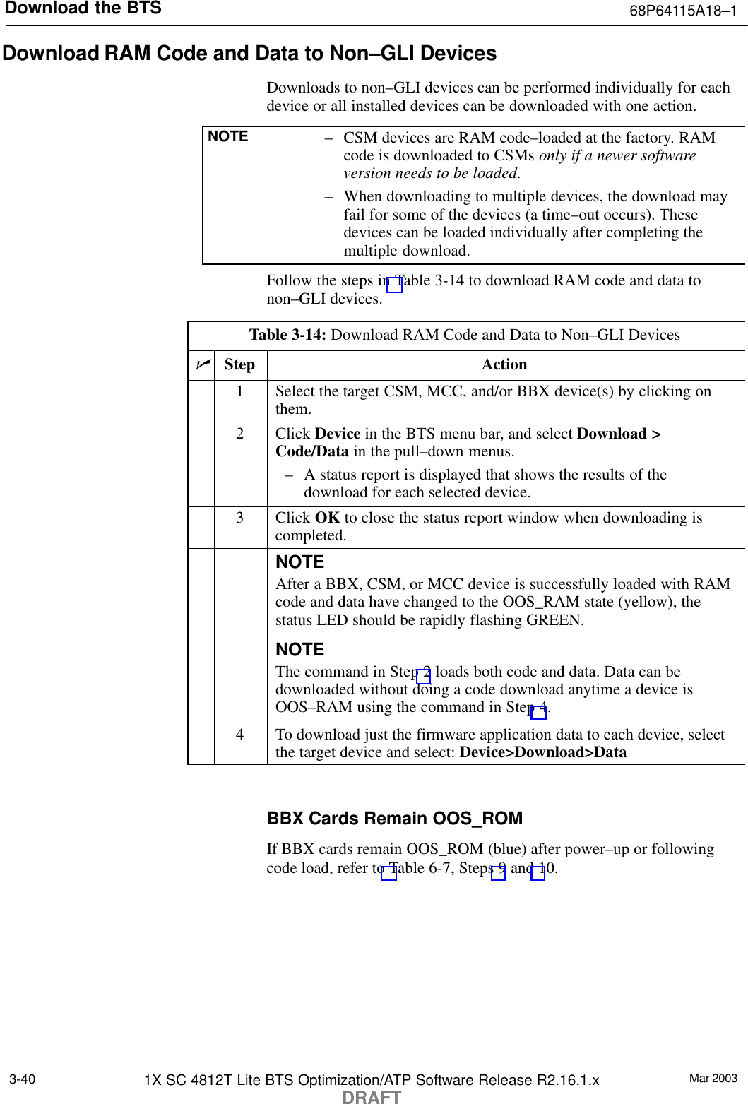
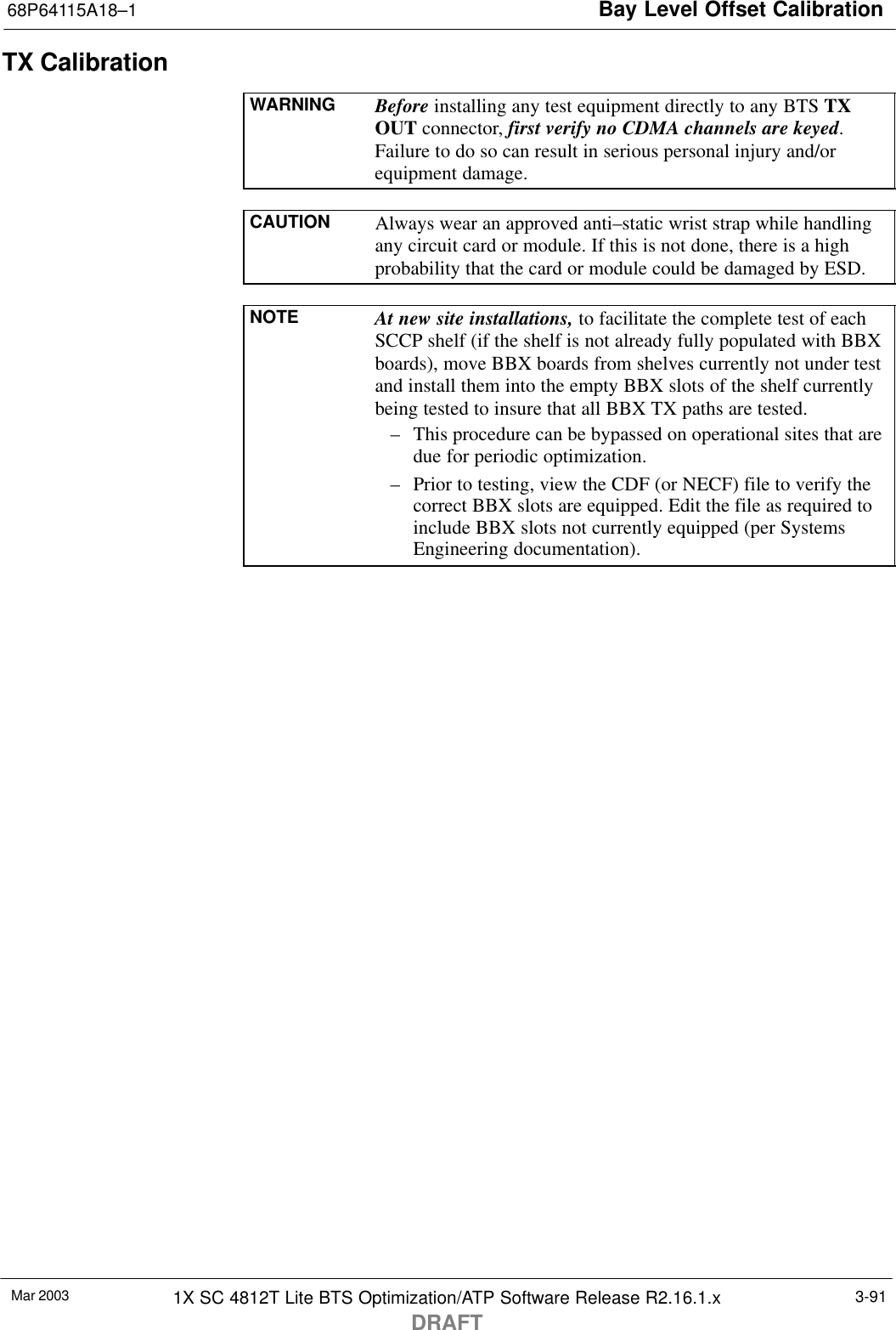
![Bay Level Offset Calibration68P64115A18–1Mar 2003 1X SC 4812T Lite BTS Optimization/ATP Software Release R2.16.1.xDRAFT3-87from 2500 to 27500 (2500 corresponds to –125 dBm and 27500corresponds to +125 dBm).– The ten calibration points for each slot–branch combination must bestored in order of increasing frequency. If less than ten points(frequencies) are calibrated, the BLO data for the highest frequencycalibrated is written into the remainder of the ten points for thatslot–branch.Example:C[1]=384 (odd cal entry)C[2]=19102 (even cal entry)C[3]=777 (odd cal entry)C[4]=19086 (even cal entry)C[19]=777 (odd cal entry)C[20]=19086 (even cal entry)...= 1 “calibration point”= 1 “calibration point”= 1 “calibration point”In the example above, BLO was measured at only two frequencies(channels 384 and 777) for SCCP slot BBX–1 transmit (Table 3-32).The BLO data for the highest frequency measured (channel 777) willbe written to the remaining eight transmit calibration points (definedby entries C[5] through C[20]) for BBX–1.Slot Block Temperature Compensation – Each BBX slot Block alsohas a temperature compensation data section (TempLevelCal) wherepower level compensation factors for temperature variations are stored.CAL File and BLO Data DownloadWhen BLO data is downloaded to the BBXs after calibration, the data isdownloaded to the devices in the order it is stored in the CAL file. TXcalibration data (entries C[1] – C[60]) are sent first. Data for the tenBBX slot 1 calibration points (entries C[1] – C[20]) are sent initially,followed by data for the ten BBX slot 2 calibration points (entries C[21]– C[40]), and so on. The RX calibration data is sent next in BBX slotsequence, followed by RX Diversity calibration data.](https://usermanual.wiki/Nokia-Solutions-and-Networks/T5DJ1.Users-manual-1-of-2/User-Guide-320001-Page-163.png)
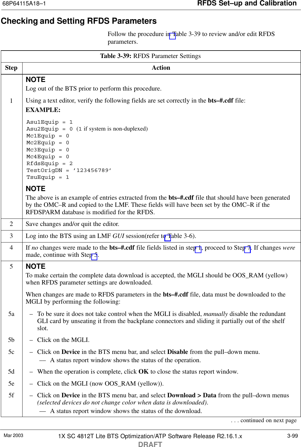
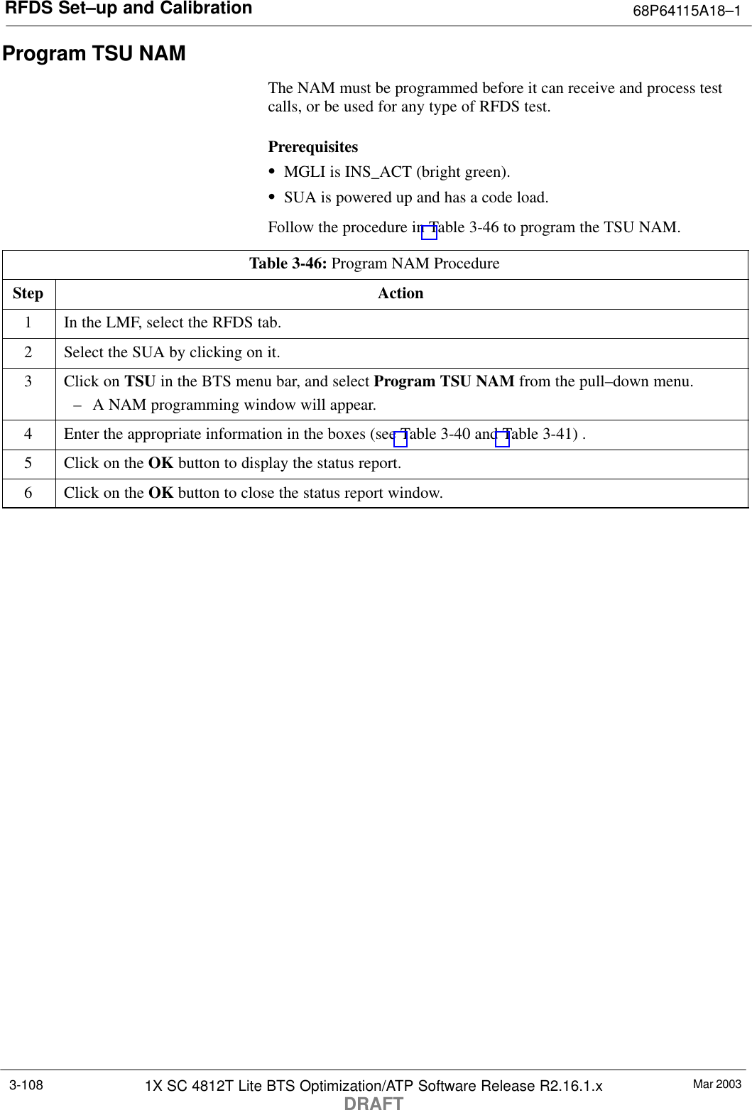
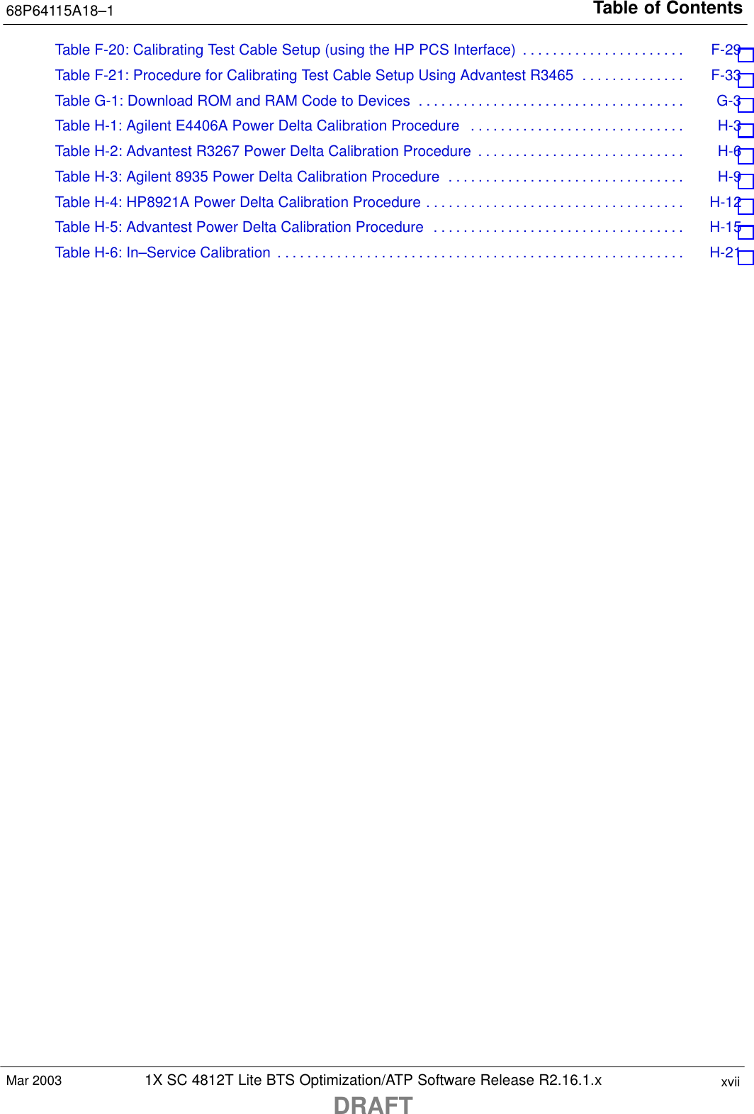
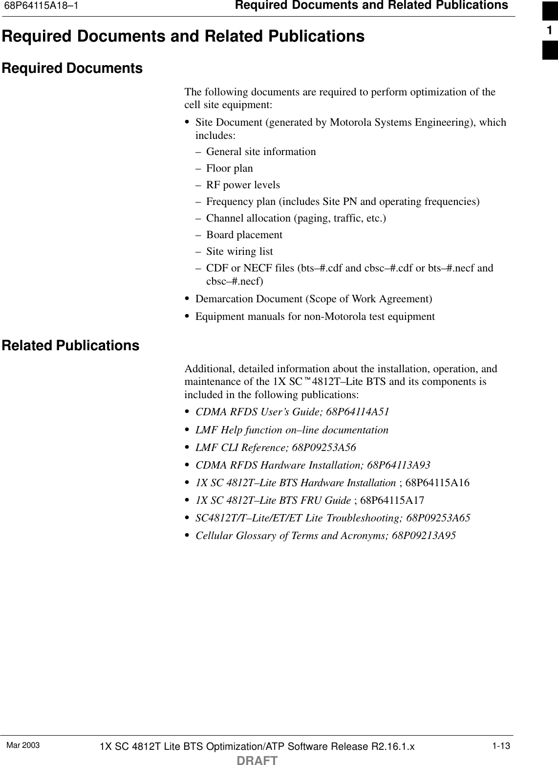
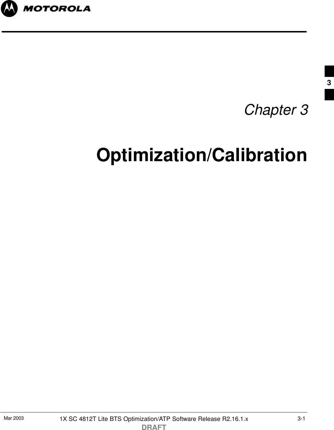
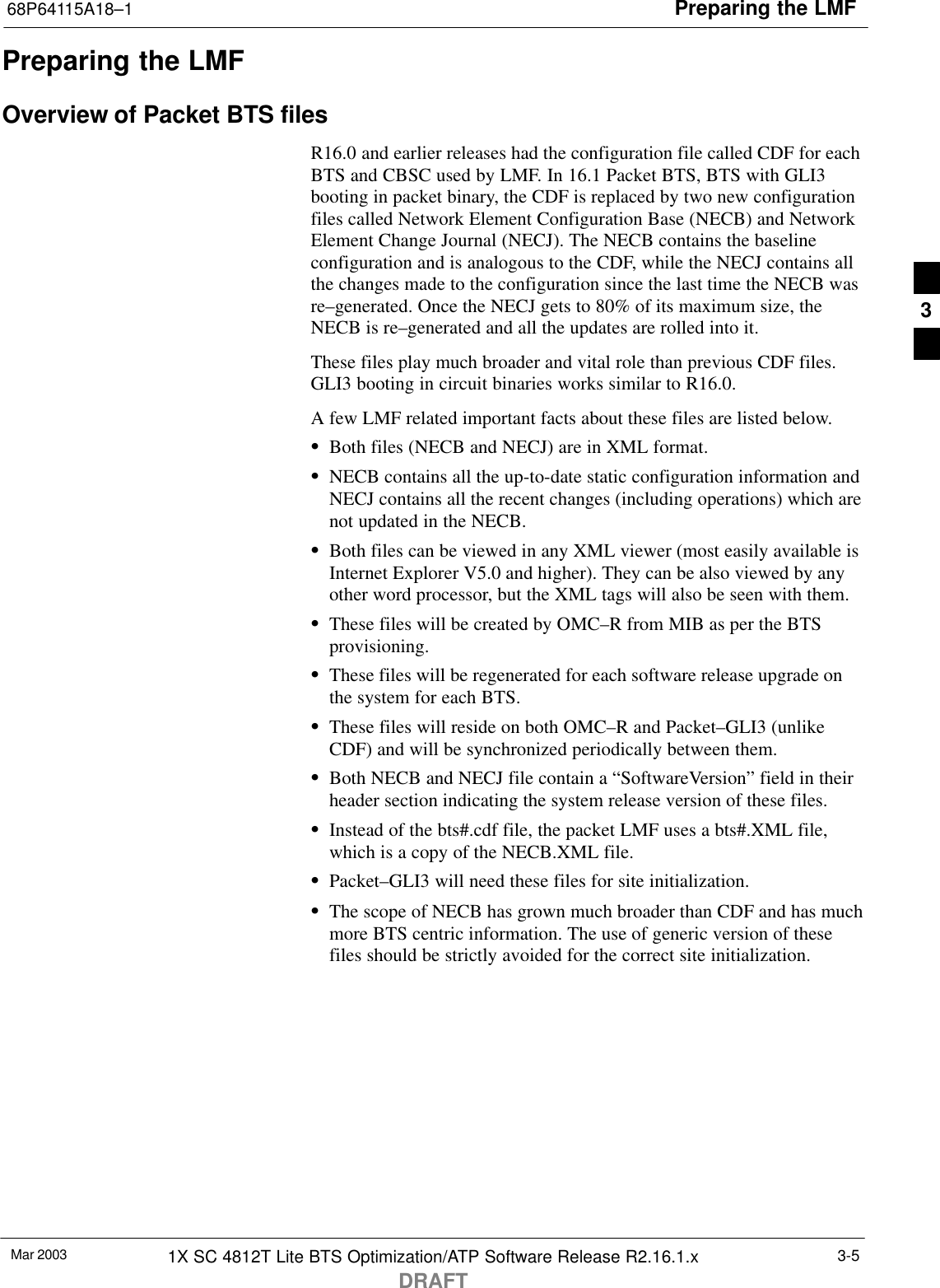
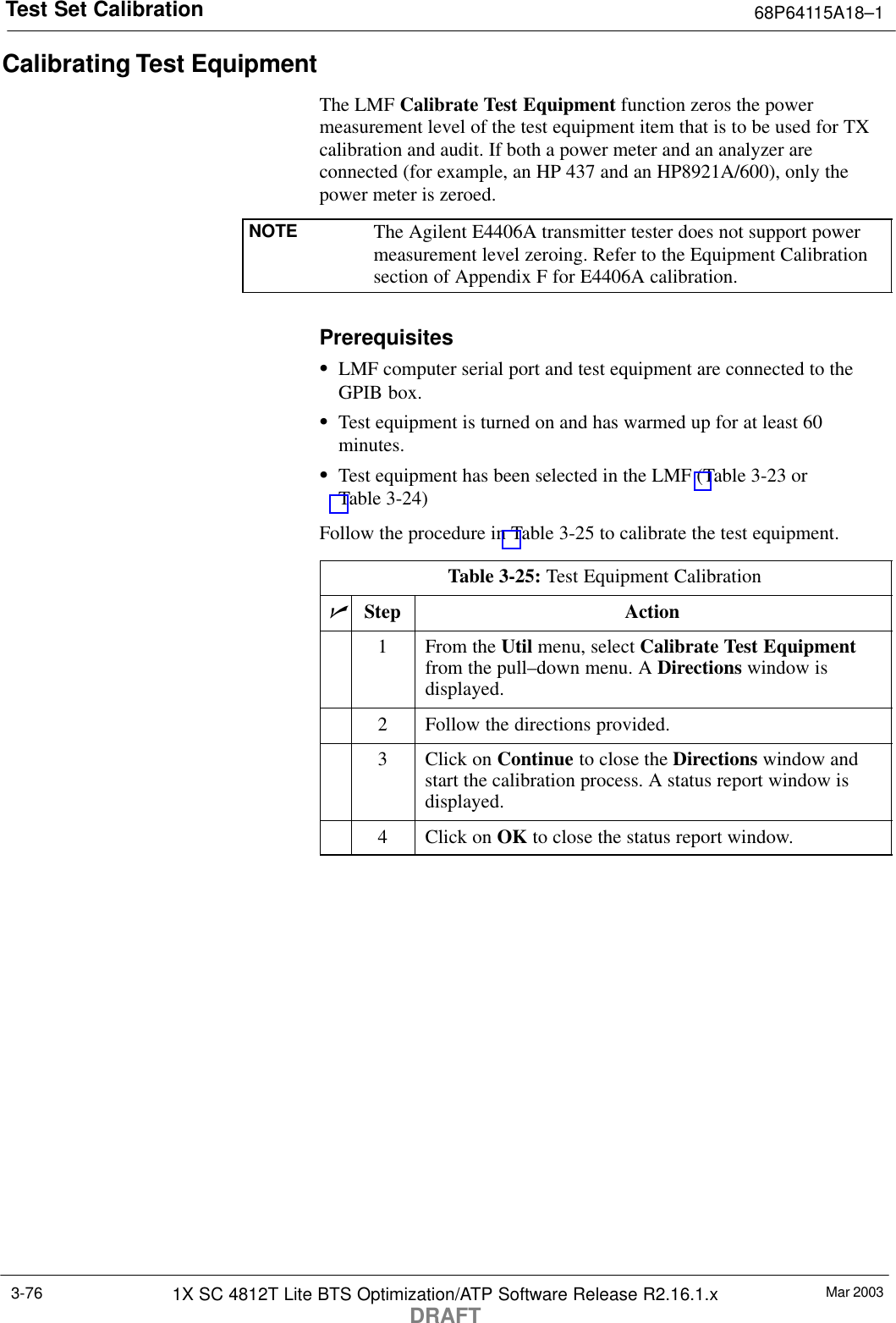
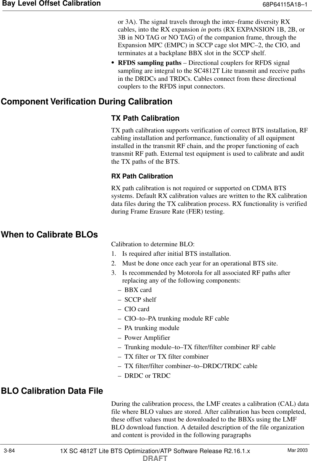
![RFDS Set–up and Calibration68P64115A18–1Mar 2003 1X SC 4812T Lite BTS Optimization/ATP Software Release R2.16.1.xDRAFT3-105Set RFDS Configuration DataIf an RFDS is installed, the RFDS configuration data must be manuallyentered.PrerequisiteSLMF is logged into the BTSNOTE The entered antenna# index numbers must correspond to theantenna# index numbers used in the antenna maps.Follow the procedure in Table 3-43 to set RFDS configuration data.Table 3-43: Set RFDS Configuration DataStep Action1Click on Util in the BTS menu bar, and select Edit > RFDS Configuration... from the pull–downmenus.–A tabbed data entry pop–up window will appear.2In the data entry pop–up window, click on the TX RFDS Configuration or RX RFDS Configurationtab, as required.3To add a new antenna number, perform the following:3a – Click on the Add Row button.3b – Click in the Antenna #, Cal Antenna, Scap Antenna, or Populate [Y/N] columns, as required.3c – Enter the desired data.4To edit existing values click in the data box to be changed and change the value.NOTERefer to the CDMA Help > Utility Menu > Edit–RFDS Configuration... section of LMF Helpfunction on–line documentation for RFDS configuration data examples.5To delete a row, click on the row and then click on the Delete Row button.6For each tab with changes, click on the Save button to save displayed values.7Click on the Dismiss button to close the window.NOTESValues entered or changed after the Save button was used will be lost when the window isdismissed.SEntered values will be used by the LMF as soon as they are saved. It is not necessary to log out andlog back into the LMF for changes to take effect.](https://usermanual.wiki/Nokia-Solutions-and-Networks/T5DJ1.Users-manual-1-of-2/User-Guide-320001-Page-181.png)
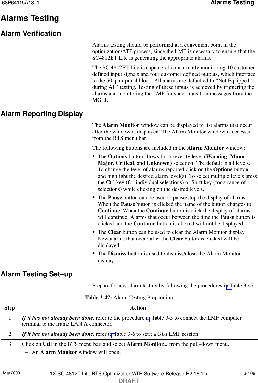
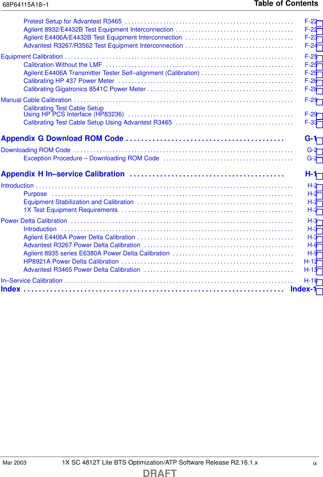
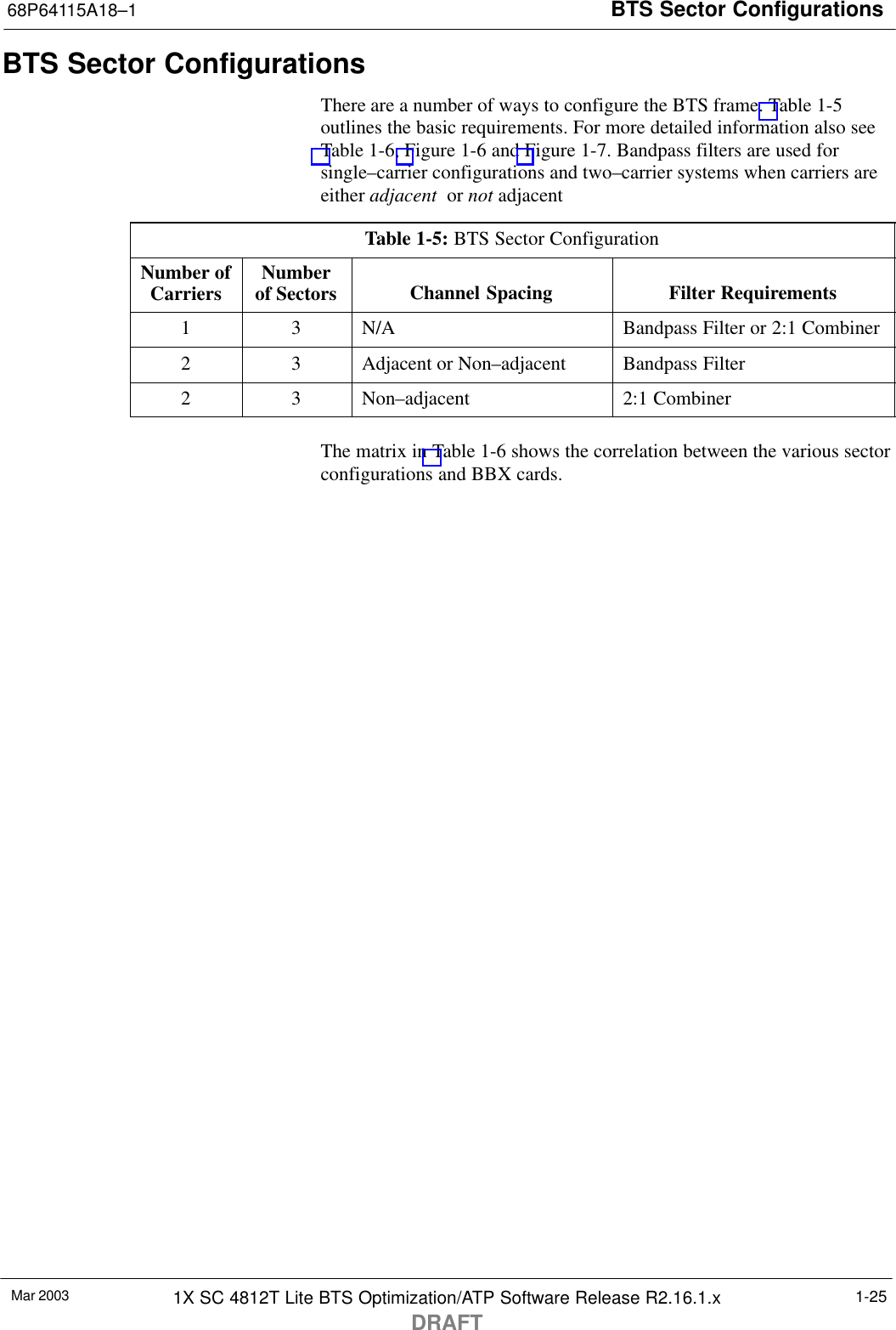
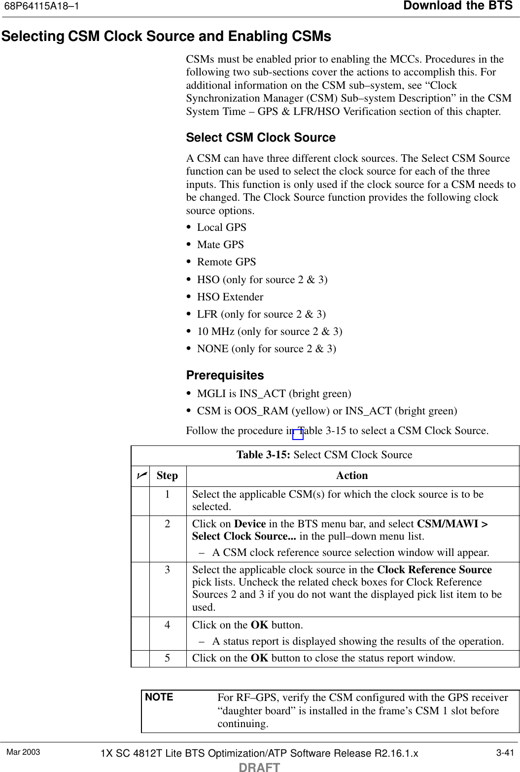
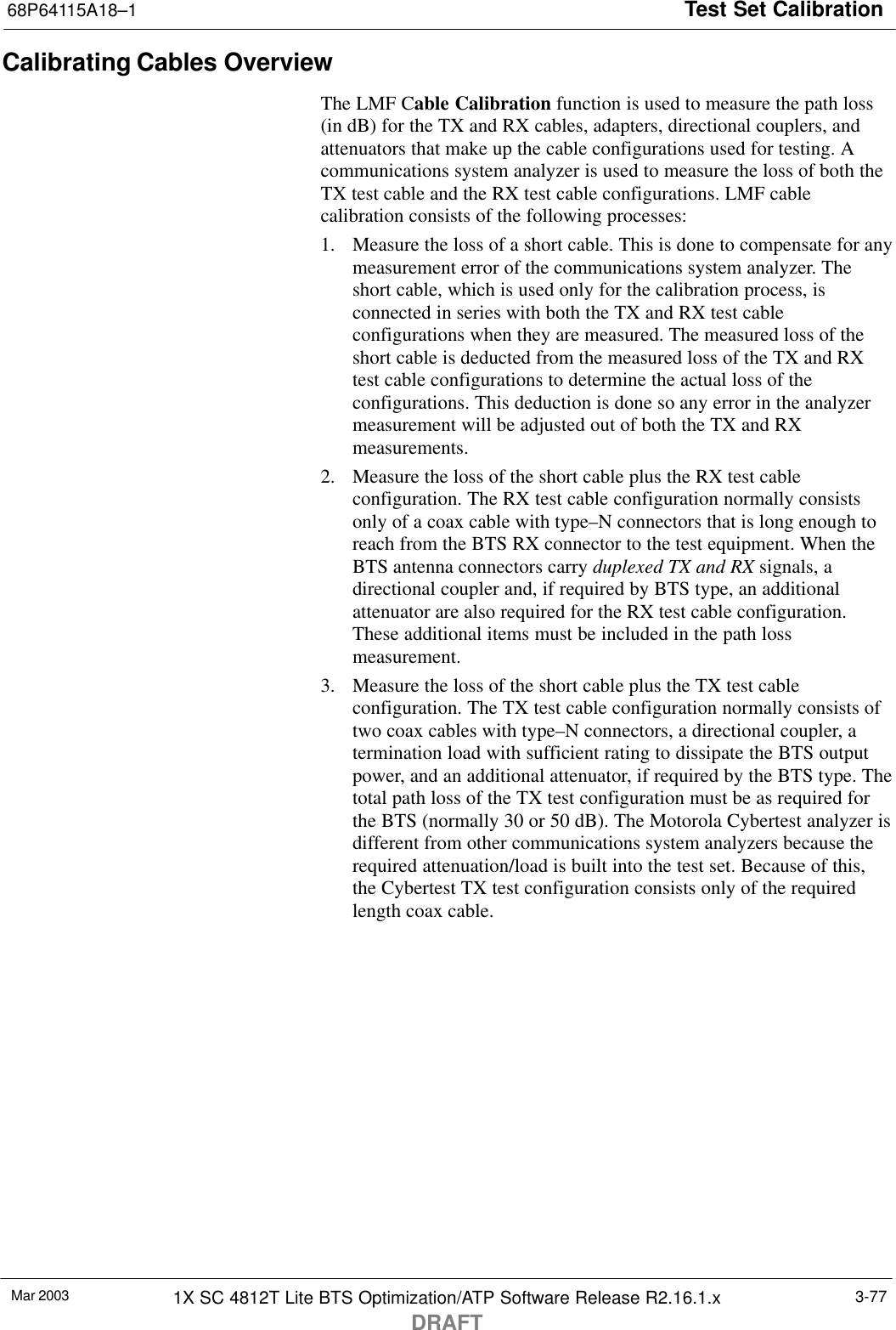
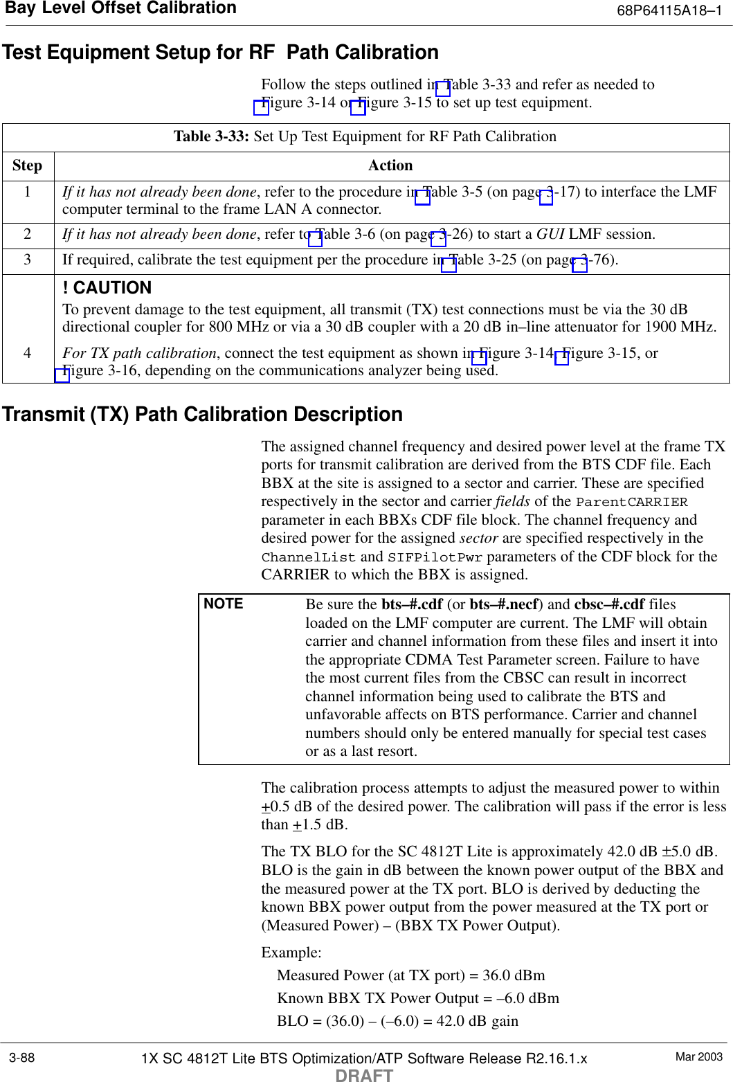
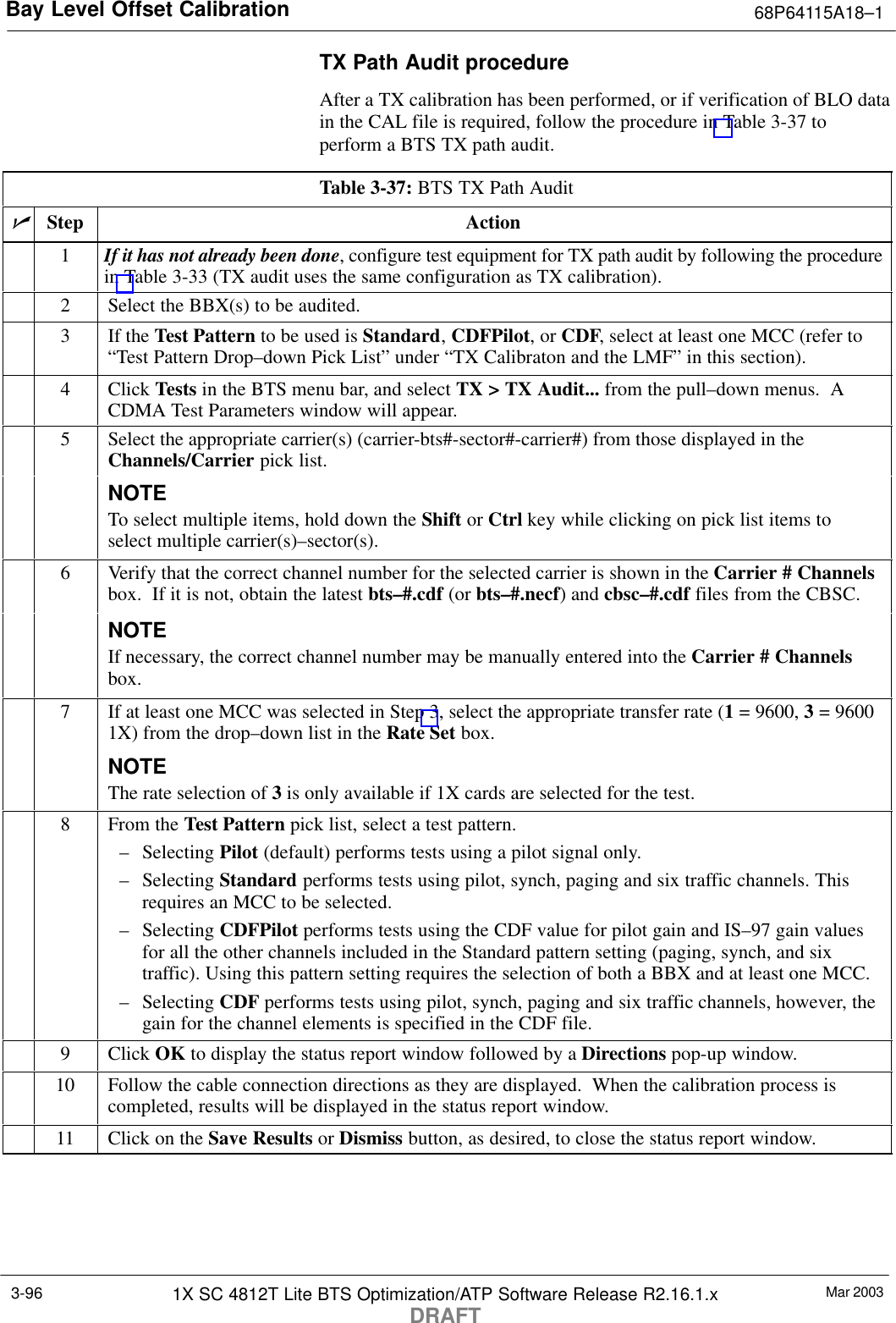
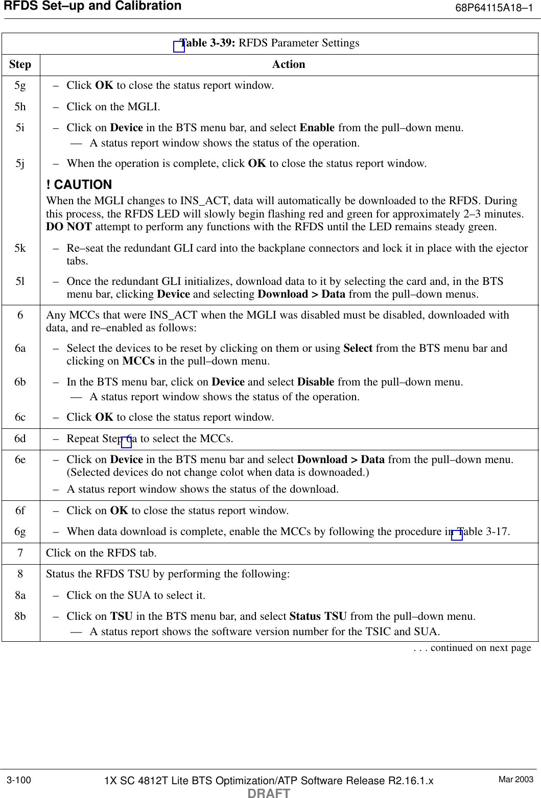
![RFDS Set–up and Calibration 68P64115A18–1Mar 20031X SC 4812T Lite BTS Optimization/ATP Software Release R2.16.1.xDRAFT3-106RFDS CalibrationThe RFDS Calibration option is used to calibrate the RFDS TX and RXpaths.TX Path Calibration – For a TX antenna path calibration the BTSXCVR is keyed at a pre–determined power level and the BTS poweroutput level is measured by the RFDS. The power level is then measuredat the TX antenna directional coupler by the power measuring testequipment item being used (power meter or analyzer). The difference(offset) between the power level at the RFDS and the power level at theTX antenna directional coupler is used as the TX RFDS calibrationoffset value.RX Path Calibration – For an RX antenna path calibration the RFDS iskeyed at a pre–determined power level and the power input level ismeasured by the BTS BBX. A CDMA signal at the same power levelmeasured by the BTS BBX is then injected at the RX antenna directionalcoupler by the communications system analyzer. The difference (offset)between the RFDS–keyed power level and power level measured at theBTS BBX is the RFDS RX calibration offset value.RFDS calibration and the CAL file – The TX and RX RFDScalibration offset values are written to the CAL file in the slot[385]Block.TSIC channel frequency – For each RFDS TSIC, the channelfrequency is determined at the lower third and upper third of theappropriate band using the frequencies listed in Table 3-44.Table 3-44: RFDS TSIC Calibration Channel FrequenciesSystem Channel Calibration Points800 MHz (A and B) 341 and 6821.9 GHz 408 and 791WARNING Before installing any test equipment directly to any TX OUTconnector, verify that there are no CDMA channels keyed.Failure to do so can result in serious personal injury and/orequipment damage.PrerequisitesSTest equipment has been selected.STest equipment and test cables have been calibrated.STX calibration has been performed and BLO data has beendownloaded to the BBXs.STest equipment and test cables are connected for TX calibration.SAntenna map data has been entered for the site.SBBXs are OOS–RAM.](https://usermanual.wiki/Nokia-Solutions-and-Networks/T5DJ1.Users-manual-1-of-2/User-Guide-320001-Page-182.png)