Nokia Solutions and Networks T5DJ1 SC4812T Lite @ 800 MHz CDMA BTS User Manual TLite
Nokia Solutions and Networks SC4812T Lite @ 800 MHz CDMA BTS TLite
Contents
- 1. Users manual 1 of 2
- 2. Users manual 2 of 2
Users manual 1 of 2

DRAFT
68P64115A18–1
Mar 2003
ENGLISH
CDMA
Software Release R2.16.1.x
Technical
Information
1X SC 4812T Lite BTS Optimization/ATP
800 Mhz
DRAFT
SPECIFICATIONS SUBJECT TO CHANGE WITHOUT NOTICE
Notice
While reasonable efforts have been made to assure the accuracy of this document, Motorola, Inc. assumes no liability resulting from any
inaccuracies or omissions in this document, or from use of the information obtained herein. The information in this document has been
carefully checked and is believed to be entirely reliable. However, no responsibility is assumed for inaccuracies or omissions. Motorola,
Inc. reserves the right to make changes to any products described herein and reserves the right to revise this document and to make
changes from time to time in content hereof with no obligation to notify any person of revisions or changes. Motorola, Inc. does not
assume any liability arising out of the application or use of any product, software, or circuit described herein; neither does it convey
license under its patent rights or the rights of others.
It is possible that this publication may contain references to, or information about Motorola products (machines and programs),
programming, or services that are not announced in your country. Such references or information must not be construed to mean
that Motorola intends to announce such Motorola products, programming, or services in your country.
Copyrights
This instruction manual, and the Motorola products described in this instruction manual may be, include or describe copyrighted
Motorola material, such as computer programs stored in semiconductor memories or other media. Laws in the United States and
other countries preserve for Motorola certain exclusive rights for copyrighted material, including the exclusive right to copy,
reproduce in any form, distribute and make derivative works of the copyrighted material. Accordingly, any copyrighted Motorola
material contained herein or in the Motorola products described in this instruction manual may not be copied, reproduced,
distributed, merged or modified in any manner without the express written permission of Motorola. Furthermore, the purchase of
Motorola products shall not be deemed to grant either directly or by implication, estoppel, or otherwise, any license under the
copyrights, patents or patent applications of Motorola, as arises by operation of law in the sale of a product.
Usage and Disclosure Restrictions
License Agreement
The software described in this document is the property of Motorola, Inc. It is furnished by express license agreement only and may
be used only in accordance with the terms of such an agreement.
Copyrighted Materials
Software and documentation are copyrighted materials. Making unauthorized copies is prohibited by law. No part of the software or
documentation may be reproduced, transmitted, transcribed, stored in a retrieval system, or translated into any language or
computer language, in any form or by any means, without prior written permission of Motorola, Inc.
High Risk Activities
Components, units, or third–party products used in the product described herein are NOT fault–tolerant and are NOT designed,
manufactured, or intended for use as on–line control equipment in the following hazardous environments requiring fail–safe
controls: the operation of Nuclear Facilities, Aircraft Navigation or Aircraft Communication Systems, Air Traffic Control, Life
Support, or Weapons Systems (“High Risk Activities”). Motorola and its supplier(s) specifically disclaim any expressed or implied
warranty of fitness for such High Risk Activities.

DRAFT
SPECIFICATIONS SUBJECT TO CHANGE WITHOUT NOTICE
Trademarks
and Motorola are registered trademarks of Motorola, Inc.
Product and service names profiled herein are trademarks of Motorola, Inc. Other manufacturers’ products or services profiled
herein may be referred to by trademarks of their respective companies.
Copyright 2003 Motorola, Inc.
Printed on
Recyclable Paper
REV012501

1X SC 4812T Lite BTS Optimization/ATP Software Release R2.16.1.x
DRAFT
i
Mar 2003
1X SC 4812T Lite BTS
Optimization/ATP
Table of Contents
.
.
.

Table of Contents 68P64115A18–1
1X SC 4812T Lite BTS Optimization/ATP Software Release R2.16.1.x
DRAFT
ii Mar 2003
Contents
FCC Requirements xviii . . . . . . . . . . . . . . . . . . . . . . . . . . . . . . . . . . . . . . . . . . . . . . . . . . . . . . . . . . . . . . . . . . . . . . . . . .
Content xviii . . . . . . . . . . . . . . . . . . . . . . . . . . . . . . . . . . . . . . . . . . . . . . . . . . . . . . . . . . . . . . . . . . . . . . . . . . . . .
FCC Part 15 Requirements xviii . . . . . . . . . . . . . . . . . . . . . . . . . . . . . . . . . . . . . . . . . . . . . . . . . . . . . . . . . . . .
FCC Part 68 Requirements xix . . . . . . . . . . . . . . . . . . . . . . . . . . . . . . . . . . . . . . . . . . . . . . . . . . . . . . . . . . . .
Foreword xx . . . . . . . . . . . . . . . . . . . . . . . . . . . . . . . . . . . . . . . . . . . . . . . . . . . . . . . . . . . . . . . . . . . . . . . . . . . . . . . . . . .
General Safety xxii . . . . . . . . . . . . . . . . . . . . . . . . . . . . . . . . . . . . . . . . . . . . . . . . . . . . . . . . . . . . . . . . . . . . . . . . . . . . . .
Revision History xxiv . . . . . . . . . . . . . . . . . . . . . . . . . . . . . . . . . . . . . . . . . . . . . . . . . . . . . . . . . . . . . . . . . . . . . . . . . . . . .
Chapter 1 Introduction 1-1 . . . . . . . . . . . . . . . . . . . . . . . . . . . . . . . . . . . . . . . . . . . . . . . . . . . .
Optimization Manual Scope and Layout 1-2 . . . . . . . . . . . . . . . . . . . . . . . . . . . . . . . . . . . . . . . . . . . . . . . . . . . . . . . .
Manual Scope and Layout 1-2 . . . . . . . . . . . . . . . . . . . . . . . . . . . . . . . . . . . . . . . . . . . . . . . . . . . . . . . . . . . . .
Assumptions and Prerequisites 1-2 . . . . . . . . . . . . . . . . . . . . . . . . . . . . . . . . . . . . . . . . . . . . . . . . . . . . . . . .
Document Composition 1-3 . . . . . . . . . . . . . . . . . . . . . . . . . . . . . . . . . . . . . . . . . . . . . . . . . . . . . . . . . . . . . . .
Purpose of the Optimization 1-4 . . . . . . . . . . . . . . . . . . . . . . . . . . . . . . . . . . . . . . . . . . . . . . . . . . . . . . . . . . . . . . . . . .
Why Optimize? 1-4 . . . . . . . . . . . . . . . . . . . . . . . . . . . . . . . . . . . . . . . . . . . . . . . . . . . . . . . . . . . . . . . . . . . . . .
What Is Optimization? 1-4 . . . . . . . . . . . . . . . . . . . . . . . . . . . . . . . . . . . . . . . . . . . . . . . . . . . . . . . . . . . . . . . .
What Happens During Optimization? 1-4 . . . . . . . . . . . . . . . . . . . . . . . . . . . . . . . . . . . . . . . . . . . . . . . . . . . .
When to Optimize 1-5 . . . . . . . . . . . . . . . . . . . . . . . . . . . . . . . . . . . . . . . . . . . . . . . . . . . . . . . . . . . . . . . . . . . . . . . . . . .
New Installations 1-5 . . . . . . . . . . . . . . . . . . . . . . . . . . . . . . . . . . . . . . . . . . . . . . . . . . . . . . . . . . . . . . . . . . . . .
Site Expansion 1-5 . . . . . . . . . . . . . . . . . . . . . . . . . . . . . . . . . . . . . . . . . . . . . . . . . . . . . . . . . . . . . . . . . . . . . . .
Periodic Optimization 1-5 . . . . . . . . . . . . . . . . . . . . . . . . . . . . . . . . . . . . . . . . . . . . . . . . . . . . . . . . . . . . . . . . .
Repaired Sites 1-5 . . . . . . . . . . . . . . . . . . . . . . . . . . . . . . . . . . . . . . . . . . . . . . . . . . . . . . . . . . . . . . . . . . . . . . .
Required Test Equipment and Software 1-6 . . . . . . . . . . . . . . . . . . . . . . . . . . . . . . . . . . . . . . . . . . . . . . . . . . . . . . . .
Overview 1-6 . . . . . . . . . . . . . . . . . . . . . . . . . . . . . . . . . . . . . . . . . . . . . . . . . . . . . . . . . . . . . . . . . . . . . . . . . . . .
Policy 1-6 . . . . . . . . . . . . . . . . . . . . . . . . . . . . . . . . . . . . . . . . . . . . . . . . . . . . . . . . . . . . . . . . . . . . . . . . . . . . . . .
Test Equipment Calibration 1-6 . . . . . . . . . . . . . . . . . . . . . . . . . . . . . . . . . . . . . . . . . . . . . . . . . . . . . . . . . . . .
Test Cable Calibration 1-6 . . . . . . . . . . . . . . . . . . . . . . . . . . . . . . . . . . . . . . . . . . . . . . . . . . . . . . . . . . . . . . . .
Equipment Warm–up 1-7 . . . . . . . . . . . . . . . . . . . . . . . . . . . . . . . . . . . . . . . . . . . . . . . . . . . . . . . . . . . . . . . . .
LMF computer and software 1-7 . . . . . . . . . . . . . . . . . . . . . . . . . . . . . . . . . . . . . . . . . . . . . . . . . . . . . . . . . . .
Communications system analyzer CDMA/analog 1-9 . . . . . . . . . . . . . . . . . . . . . . . . . . . . . . . . . . . . . . . . .
Optional Equipment 1-11 . . . . . . . . . . . . . . . . . . . . . . . . . . . . . . . . . . . . . . . . . . . . . . . . . . . . . . . . . . . . . . . . . .
Required Documents and Related Publications 1-13 . . . . . . . . . . . . . . . . . . . . . . . . . . . . . . . . . . . . . . . . . . . . . . . . . .
Required Documents 1-13 . . . . . . . . . . . . . . . . . . . . . . . . . . . . . . . . . . . . . . . . . . . . . . . . . . . . . . . . . . . . . . . . .
Related Publications 1-13 . . . . . . . . . . . . . . . . . . . . . . . . . . . . . . . . . . . . . . . . . . . . . . . . . . . . . . . . . . . . . . . . . .
Terms and Abbreviations 1-14 . . . . . . . . . . . . . . . . . . . . . . . . . . . . . . . . . . . . . . . . . . . . . . . . . . . . . . . . . . . . . . . . . . . . .
Standard and Non–standard Terms and Abbreviations 1-14 . . . . . . . . . . . . . . . . . . . . . . . . . . . . . . . . . . . . .
BTS Equipment Identification 1-17 . . . . . . . . . . . . . . . . . . . . . . . . . . . . . . . . . . . . . . . . . . . . . . . . . . . . . . . . . . . . . . . . .
Equipment Overview 1-17 . . . . . . . . . . . . . . . . . . . . . . . . . . . . . . . . . . . . . . . . . . . . . . . . . . . . . . . . . . . . . . . . . .
Frame Configurations 1-17 . . . . . . . . . . . . . . . . . . . . . . . . . . . . . . . . . . . . . . . . . . . . . . . . . . . . . . . . . . . . . . . . .
Logical BTS 1-17 . . . . . . . . . . . . . . . . . . . . . . . . . . . . . . . . . . . . . . . . . . . . . . . . . . . . . . . . . . . . . . . . . . . . . . . . .
Internal Assemblies and FRUs 1-20 . . . . . . . . . . . . . . . . . . . . . . . . . . . . . . . . . . . . . . . . . . . . . . . . . . . . . . . . .
SCCP Cage Configuration and 1X Devices 1-24 . . . . . . . . . . . . . . . . . . . . . . . . . . . . . . . . . . . . . . . . . . . . . .
BBX–1X and BBX2 Interchangeability 1-24 . . . . . . . . . . . . . . . . . . . . . . . . . . . . . . . . . . . . . . . . . . . . . . . . . . .
BTS Sector Configurations 1-25 . . . . . . . . . . . . . . . . . . . . . . . . . . . . . . . . . . . . . . . . . . . . . . . . . . . . . . . . . . . . . . . . . . .
Chapter 2 Preliminary Operations 2-1 . . . . . . . . . . . . . . . . . . . . . . . . . . . . . . . . . . . . . . . . . .
Preliminary Operations: Overview 2-2 . . . . . . . . . . . . . . . . . . . . . . . . . . . . . . . . . . . . . . . . . . . . . . . . . . . . . . . . . . . . .
Introduction 2-2 . . . . . . . . . . . . . . . . . . . . . . . . . . . . . . . . . . . . . . . . . . . . . . . . . . . . . . . . . . . . . . . . . . . . . . . . .

Table of Contents
68P64115A18–1
1X SC 4812T Lite BTS Optimization/ATP Software Release R2.16.1.x
DRAFT
iii
Mar 2003
Cell–site Types 2-2 . . . . . . . . . . . . . . . . . . . . . . . . . . . . . . . . . . . . . . . . . . . . . . . . . . . . . . . . . . . . . . . . . . . . . .
CDF/NECF 2-2 . . . . . . . . . . . . . . . . . . . . . . . . . . . . . . . . . . . . . . . . . . . . . . . . . . . . . . . . . . . . . . . . . . . . . . . . . .
Site Equipage Verification 2-2 . . . . . . . . . . . . . . . . . . . . . . . . . . . . . . . . . . . . . . . . . . . . . . . . . . . . . . . . . . . . .
Initial Installation of Boards/Modules 2-3 . . . . . . . . . . . . . . . . . . . . . . . . . . . . . . . . . . . . . . . . . . . . . . . . . . . .
Setting Frame SCCP Configuration Switch 2-4 . . . . . . . . . . . . . . . . . . . . . . . . . . . . . . . . . . . . . . . . . . . . . .
Ethernet LAN 2-5 . . . . . . . . . . . . . . . . . . . . . . . . . . . . . . . . . . . . . . . . . . . . . . . . . . . . . . . . . . . . . . . . . . . . . . . . . . . . . . .
Ethernet LAN Termination 2-5 . . . . . . . . . . . . . . . . . . . . . . . . . . . . . . . . . . . . . . . . . . . . . . . . . . . . . . . . . . . . .
Pre-Initial Power-up Tests 2-6 . . . . . . . . . . . . . . . . . . . . . . . . . . . . . . . . . . . . . . . . . . . . . . . . . . . . . . . . . . . . . . . . . . . .
Introduction 2-6 . . . . . . . . . . . . . . . . . . . . . . . . . . . . . . . . . . . . . . . . . . . . . . . . . . . . . . . . . . . . . . . . . . . . . . . . .
Required Tools 2-6 . . . . . . . . . . . . . . . . . . . . . . . . . . . . . . . . . . . . . . . . . . . . . . . . . . . . . . . . . . . . . . . . . . . . . . .
Cabling Inspection 2-6 . . . . . . . . . . . . . . . . . . . . . . . . . . . . . . . . . . . . . . . . . . . . . . . . . . . . . . . . . . . . . . . . . . . .
Initial Inspection and Setup 2-6 . . . . . . . . . . . . . . . . . . . . . . . . . . . . . . . . . . . . . . . . . . . . . . . . . . . . . . . . . . . .
DC Power System Pre-power Application Test 2-6 . . . . . . . . . . . . . . . . . . . . . . . . . . . . . . . . . . . . . . . . . . .
External AC Power Connection Verification 2-9 . . . . . . . . . . . . . . . . . . . . . . . . . . . . . . . . . . . . . . . . . . . . . .
Applying AC Power 2-11 . . . . . . . . . . . . . . . . . . . . . . . . . . . . . . . . . . . . . . . . . . . . . . . . . . . . . . . . . . . . . . . . . . . . . . . . . .
DC Power Application and Testing 2-12 . . . . . . . . . . . . . . . . . . . . . . . . . . . . . . . . . . . . . . . . . . . . . . . . . . . . . .
Battery Charge Test (Connected Batteries) 2-13 . . . . . . . . . . . . . . . . . . . . . . . . . . . . . . . . . . . . . . . . . . . . . .
Battery Discharge Test 2-14 . . . . . . . . . . . . . . . . . . . . . . . . . . . . . . . . . . . . . . . . . . . . . . . . . . . . . . . . . . . . . . . .
Power Removal 2-16 . . . . . . . . . . . . . . . . . . . . . . . . . . . . . . . . . . . . . . . . . . . . . . . . . . . . . . . . . . . . . . . . . . . . . . . . . . . . .
Introduction 2-16 . . . . . . . . . . . . . . . . . . . . . . . . . . . . . . . . . . . . . . . . . . . . . . . . . . . . . . . . . . . . . . . . . . . . . . . . .
Remove DC Power 2-16 . . . . . . . . . . . . . . . . . . . . . . . . . . . . . . . . . . . . . . . . . . . . . . . . . . . . . . . . . . . . . . . . . . .
AC Power Removal 2-17 . . . . . . . . . . . . . . . . . . . . . . . . . . . . . . . . . . . . . . . . . . . . . . . . . . . . . . . . . . . . . . . . . . .
Power Application – Normal Power–up 2-18 . . . . . . . . . . . . . . . . . . . . . . . . . . . . . . . . . . . . . . . . . . . . . . . . . . . . . . . . .
Power Application Procedures 2-18 . . . . . . . . . . . . . . . . . . . . . . . . . . . . . . . . . . . . . . . . . . . . . . . . . . . . . . . . .
Applying Internal AC Power 2-18 . . . . . . . . . . . . . . . . . . . . . . . . . . . . . . . . . . . . . . . . . . . . . . . . . . . . . . . . . . . .
Apply DC Power 2-19 . . . . . . . . . . . . . . . . . . . . . . . . . . . . . . . . . . . . . . . . . . . . . . . . . . . . . . . . . . . . . . . . . . . . .
Chapter 3 Optimization/Calibration 3-1 . . . . . . . . . . . . . . . . . . . . . . . . . . . . . . . . . . . . . . . . .
Introduction to Optimization and Calibration 3-2 . . . . . . . . . . . . . . . . . . . . . . . . . . . . . . . . . . . . . . . . . . . . . . . . . . . . .
Overview 3-2 . . . . . . . . . . . . . . . . . . . . . . . . . . . . . . . . . . . . . . . . . . . . . . . . . . . . . . . . . . . . . . . . . . . . . . . . . . . .
Optimization Process Summary 3-2 . . . . . . . . . . . . . . . . . . . . . . . . . . . . . . . . . . . . . . . . . . . . . . . . . . . . . . . .
Cell-site Types 3-3 . . . . . . . . . . . . . . . . . . . . . . . . . . . . . . . . . . . . . . . . . . . . . . . . . . . . . . . . . . . . . . . . . . . . . . .
CDF/NECF 3-3 . . . . . . . . . . . . . . . . . . . . . . . . . . . . . . . . . . . . . . . . . . . . . . . . . . . . . . . . . . . . . . . . . . . . . . . . . .
BTS System Software Download 3-4 . . . . . . . . . . . . . . . . . . . . . . . . . . . . . . . . . . . . . . . . . . . . . . . . . . . . . . .
Site Equipage Verification 3-4 . . . . . . . . . . . . . . . . . . . . . . . . . . . . . . . . . . . . . . . . . . . . . . . . . . . . . . . . . . . . .
Preparing the LMF 3-5 . . . . . . . . . . . . . . . . . . . . . . . . . . . . . . . . . . . . . . . . . . . . . . . . . . . . . . . . . . . . . . . . . . . . . . . . . . .
Overview of Packet BTS files 3-5 . . . . . . . . . . . . . . . . . . . . . . . . . . . . . . . . . . . . . . . . . . . . . . . . . . . . . . . . . .
LMF Features and Installation Requirements 3-6 . . . . . . . . . . . . . . . . . . . . . . . . . . . . . . . . . . . . . . . . . . . . .
LMF File Structure Overview 3-7 . . . . . . . . . . . . . . . . . . . . . . . . . . . . . . . . . . . . . . . . . . . . . . . . . . . . . . . . . . .
LMF Home Directory 3-8 . . . . . . . . . . . . . . . . . . . . . . . . . . . . . . . . . . . . . . . . . . . . . . . . . . . . . . . . . . . . . . . . .
NECF Filename Conventions and Directory Location 3-9 . . . . . . . . . . . . . . . . . . . . . . . . . . . . . . . . . . . . . .
LMF Installation and Update Procedures 3-10 . . . . . . . . . . . . . . . . . . . . . . . . . . . . . . . . . . . . . . . . . . . . . . . .
Copy BTS and CBSC CDF (or NECF) Files to the LMF Computer 3-11 . . . . . . . . . . . . . . . . . . . . . . . . . .
Creating a Named HyperTerminal Connection for MMI Communication 3-13 . . . . . . . . . . . . . . . . . . . . . .
Span Lines – Interface and Isolation 3-15 . . . . . . . . . . . . . . . . . . . . . . . . . . . . . . . . . . . . . . . . . . . . . . . . . . . . . . . . . . .
T1/E1 Span Interface 3-15 . . . . . . . . . . . . . . . . . . . . . . . . . . . . . . . . . . . . . . . . . . . . . . . . . . . . . . . . . . . . . . . . .
Isolate BTS from T1/E1 Span(s) 3-15 . . . . . . . . . . . . . . . . . . . . . . . . . . . . . . . . . . . . . . . . . . . . . . . . . . . . . . . .
T1/E1 Span Isolation 3-16 . . . . . . . . . . . . . . . . . . . . . . . . . . . . . . . . . . . . . . . . . . . . . . . . . . . . . . . . . . . . . . . . .
LMF to BTS Connection 3-17 . . . . . . . . . . . . . . . . . . . . . . . . . . . . . . . . . . . . . . . . . . . . . . . . . . . . . . . . . . . . . . . . . . . . . .
Connect the LMF to the BTS 3-17 . . . . . . . . . . . . . . . . . . . . . . . . . . . . . . . . . . . . . . . . . . . . . . . . . . . . . . . . . . .
Using the LMF 3-18 . . . . . . . . . . . . . . . . . . . . . . . . . . . . . . . . . . . . . . . . . . . . . . . . . . . . . . . . . . . . . . . . . . . . . . . . . . . . . .

Table of Contents 68P64115A18–1
1X SC 4812T Lite BTS Optimization/ATP Software Release R2.16.1.x
DRAFT
iv Mar 2003
Basic LMF Operation 3-18 . . . . . . . . . . . . . . . . . . . . . . . . . . . . . . . . . . . . . . . . . . . . . . . . . . . . . . . . . . . . . . . . .
The LMF Display and the BTS 3-19 . . . . . . . . . . . . . . . . . . . . . . . . . . . . . . . . . . . . . . . . . . . . . . . . . . . . . . . . .
Graphical User Interface Overview 3-19 . . . . . . . . . . . . . . . . . . . . . . . . . . . . . . . . . . . . . . . . . . . . . . . . . . . . .
Understanding GUI Operation 3-20 . . . . . . . . . . . . . . . . . . . . . . . . . . . . . . . . . . . . . . . . . . . . . . . . . . . . . . . . . .
Command Line Interface Overview 3-25 . . . . . . . . . . . . . . . . . . . . . . . . . . . . . . . . . . . . . . . . . . . . . . . . . . . . .
Logging Into a BTS 3-26 . . . . . . . . . . . . . . . . . . . . . . . . . . . . . . . . . . . . . . . . . . . . . . . . . . . . . . . . . . . . . . . . . . .
Logging Out 3-29 . . . . . . . . . . . . . . . . . . . . . . . . . . . . . . . . . . . . . . . . . . . . . . . . . . . . . . . . . . . . . . . . . . . . . . . . .
Establishing an MMI Communication Session 3-31 . . . . . . . . . . . . . . . . . . . . . . . . . . . . . . . . . . . . . . . . . . . .
Online Help 3-32 . . . . . . . . . . . . . . . . . . . . . . . . . . . . . . . . . . . . . . . . . . . . . . . . . . . . . . . . . . . . . . . . . . . . . . . . . .
Pinging the Processors 3-33 . . . . . . . . . . . . . . . . . . . . . . . . . . . . . . . . . . . . . . . . . . . . . . . . . . . . . . . . . . . . . . . . . . . . . . .
Pinging the BTS 3-33 . . . . . . . . . . . . . . . . . . . . . . . . . . . . . . . . . . . . . . . . . . . . . . . . . . . . . . . . . . . . . . . . . . . . .
Download the BTS 3-36 . . . . . . . . . . . . . . . . . . . . . . . . . . . . . . . . . . . . . . . . . . . . . . . . . . . . . . . . . . . . . . . . . . . . . . . . . .
Overview 3-36 . . . . . . . . . . . . . . . . . . . . . . . . . . . . . . . . . . . . . . . . . . . . . . . . . . . . . . . . . . . . . . . . . . . . . . . . . . . .
ROM Code 3-36 . . . . . . . . . . . . . . . . . . . . . . . . . . . . . . . . . . . . . . . . . . . . . . . . . . . . . . . . . . . . . . . . . . . . . . . . . .
RAM Code 3-36 . . . . . . . . . . . . . . . . . . . . . . . . . . . . . . . . . . . . . . . . . . . . . . . . . . . . . . . . . . . . . . . . . . . . . . . . . .
Verify GLI ROM Code Loads 3-38 . . . . . . . . . . . . . . . . . . . . . . . . . . . . . . . . . . . . . . . . . . . . . . . . . . . . . . . . . . .
Download RAM Code and Data to MGLI and GLI 3-39 . . . . . . . . . . . . . . . . . . . . . . . . . . . . . . . . . . . . . . . . .
Download RAM Code and Data to Non–GLI Devices 3-40 . . . . . . . . . . . . . . . . . . . . . . . . . . . . . . . . . . . . . .
Selecting CSM Clock Source and Enabling CSMs 3-41 . . . . . . . . . . . . . . . . . . . . . . . . . . . . . . . . . . . . . . . .
Enable MCCs 3-43 . . . . . . . . . . . . . . . . . . . . . . . . . . . . . . . . . . . . . . . . . . . . . . . . . . . . . . . . . . . . . . . . . . . . . . . .
CSM System Time – GPS & LFR/HSO Verification 3-44 . . . . . . . . . . . . . . . . . . . . . . . . . . . . . . . . . . . . . . . . . . . . . . .
Clock Synchronization Manager (CSM) Sub–system Description 3-44 . . . . . . . . . . . . . . . . . . . . . . . . . . . .
Front Panel LEDs 3-45 . . . . . . . . . . . . . . . . . . . . . . . . . . . . . . . . . . . . . . . . . . . . . . . . . . . . . . . . . . . . . . . . . . . .
Low Frequency Receiver/High Stability Oscillator (LFR/HSO) 3-46 . . . . . . . . . . . . . . . . . . . . . . . . . . . . . .
CSM Frequency Verification 3-47 . . . . . . . . . . . . . . . . . . . . . . . . . . . . . . . . . . . . . . . . . . . . . . . . . . . . . . . . . . .
Test Equipment Setup
(GPS & LFR/HSO Verification) 3-47 . . . . . . . . . . . . . . . . . . . . . . . . . . . . . . . . . . . . . . . . . . . . . . . . . . . . . . . . .
GPS Initialization/Verification 3-48 . . . . . . . . . . . . . . . . . . . . . . . . . . . . . . . . . . . . . . . . . . . . . . . . . . . . . . . . . .
LORAN–C Initialization/Verification 3-53 . . . . . . . . . . . . . . . . . . . . . . . . . . . . . . . . . . . . . . . . . . . . . . . . . . . . .
Test Equipment Set-up 3-55 . . . . . . . . . . . . . . . . . . . . . . . . . . . . . . . . . . . . . . . . . . . . . . . . . . . . . . . . . . . . . . . . . . . . . . .
Connecting Test Equipment to the BTS 3-55 . . . . . . . . . . . . . . . . . . . . . . . . . . . . . . . . . . . . . . . . . . . . . . . . . .
Supported Test Equipment 3-56 . . . . . . . . . . . . . . . . . . . . . . . . . . . . . . . . . . . . . . . . . . . . . . . . . . . . . . . . . . . .
Equipment Warm-up 3-59 . . . . . . . . . . . . . . . . . . . . . . . . . . . . . . . . . . . . . . . . . . . . . . . . . . . . . . . . . . . . . . . . . .
Test Set Calibration 3-72 . . . . . . . . . . . . . . . . . . . . . . . . . . . . . . . . . . . . . . . . . . . . . . . . . . . . . . . . . . . . . . . . . . . . . . . . . .
Background 3-72 . . . . . . . . . . . . . . . . . . . . . . . . . . . . . . . . . . . . . . . . . . . . . . . . . . . . . . . . . . . . . . . . . . . . . . . . .
Calibration Procedures Included 3-72 . . . . . . . . . . . . . . . . . . . . . . . . . . . . . . . . . . . . . . . . . . . . . . . . . . . . . . . .
GPIB Addresses 3-73 . . . . . . . . . . . . . . . . . . . . . . . . . . . . . . . . . . . . . . . . . . . . . . . . . . . . . . . . . . . . . . . . . . . . .
Selecting Test Equipment 3-73 . . . . . . . . . . . . . . . . . . . . . . . . . . . . . . . . . . . . . . . . . . . . . . . . . . . . . . . . . . . . .
Manually Selecting Test Equipment in a Serial Connection Tab 3-74 . . . . . . . . . . . . . . . . . . . . . . . . . . . . .
Automatically Selecting Test Equipment in the Serial Connection Tab 3-75 . . . . . . . . . . . . . . . . . . . . . . . .
Calibrating Test Equipment 3-76 . . . . . . . . . . . . . . . . . . . . . . . . . . . . . . . . . . . . . . . . . . . . . . . . . . . . . . . . . . . .
Calibrating Cables Overview 3-77 . . . . . . . . . . . . . . . . . . . . . . . . . . . . . . . . . . . . . . . . . . . . . . . . . . . . . . . . . . .
Calibrating Test Cabling using Communications System Analyzer 3-78 . . . . . . . . . . . . . . . . . . . . . . . . . . .
Calibrate Test Cabling Using Signal Generator & Spectrum Analyzer 3-79 . . . . . . . . . . . . . . . . . . . . . . . .
Setting Cable Loss Values 3-81 . . . . . . . . . . . . . . . . . . . . . . . . . . . . . . . . . . . . . . . . . . . . . . . . . . . . . . . . . . . . .
Setting TX Coupler Loss Value 3-82 . . . . . . . . . . . . . . . . . . . . . . . . . . . . . . . . . . . . . . . . . . . . . . . . . . . . . . . . .
Bay Level Offset Calibration 3-83 . . . . . . . . . . . . . . . . . . . . . . . . . . . . . . . . . . . . . . . . . . . . . . . . . . . . . . . . . . . . . . . . . .
Purpose of Bay Level Offset Calibration 3-83 . . . . . . . . . . . . . . . . . . . . . . . . . . . . . . . . . . . . . . . . . . . . . . . . .
What is BLO Calibration? 3-83 . . . . . . . . . . . . . . . . . . . . . . . . . . . . . . . . . . . . . . . . . . . . . . . . . . . . . . . . . . . . . .
Component Verification During Calibration 3-84 . . . . . . . . . . . . . . . . . . . . . . . . . . . . . . . . . . . . . . . . . . . . . . .
When to Calibrate BLOs 3-84 . . . . . . . . . . . . . . . . . . . . . . . . . . . . . . . . . . . . . . . . . . . . . . . . . . . . . . . . . . . . . .
BLO Calibration Data File 3-84 . . . . . . . . . . . . . . . . . . . . . . . . . . . . . . . . . . . . . . . . . . . . . . . . . . . . . . . . . . . . .

Table of Contents
68P64115A18–1
1X SC 4812T Lite BTS Optimization/ATP Software Release R2.16.1.x
DRAFT
v
Mar 2003
Test Equipment Setup for RF Path Calibration 3-88 . . . . . . . . . . . . . . . . . . . . . . . . . . . . . . . . . . . . . . . . . . .
Transmit (TX) Path Calibration Description 3-88 . . . . . . . . . . . . . . . . . . . . . . . . . . . . . . . . . . . . . . . . . . . . . . .
TX Calibration and the LMF 3-89 . . . . . . . . . . . . . . . . . . . . . . . . . . . . . . . . . . . . . . . . . . . . . . . . . . . . . . . . . . . .
TX Calibration 3-91 . . . . . . . . . . . . . . . . . . . . . . . . . . . . . . . . . . . . . . . . . . . . . . . . . . . . . . . . . . . . . . . . . . . . . . .
All Cal/Audit and TX Calibration Procedure 3-92 . . . . . . . . . . . . . . . . . . . . . . . . . . . . . . . . . . . . . . . . . . . . . .
Download BLO Procedure 3-94 . . . . . . . . . . . . . . . . . . . . . . . . . . . . . . . . . . . . . . . . . . . . . . . . . . . . . . . . . . . . .
Calibration Audit Introduction 3-95 . . . . . . . . . . . . . . . . . . . . . . . . . . . . . . . . . . . . . . . . . . . . . . . . . . . . . . . . . .
TX Path Audit 3-95 . . . . . . . . . . . . . . . . . . . . . . . . . . . . . . . . . . . . . . . . . . . . . . . . . . . . . . . . . . . . . . . . . . . . . . . .
TX Audit Test 3-95 . . . . . . . . . . . . . . . . . . . . . . . . . . . . . . . . . . . . . . . . . . . . . . . . . . . . . . . . . . . . . . . . . . . . . . . .
Create CAL File 3-97 . . . . . . . . . . . . . . . . . . . . . . . . . . . . . . . . . . . . . . . . . . . . . . . . . . . . . . . . . . . . . . . . . . . . . .
RFDS Set–up and Calibration 3-98 . . . . . . . . . . . . . . . . . . . . . . . . . . . . . . . . . . . . . . . . . . . . . . . . . . . . . . . . . . . . . . . . .
RFDS Description 3-98 . . . . . . . . . . . . . . . . . . . . . . . . . . . . . . . . . . . . . . . . . . . . . . . . . . . . . . . . . . . . . . . . . . . .
RFDS Parameters 3-98 . . . . . . . . . . . . . . . . . . . . . . . . . . . . . . . . . . . . . . . . . . . . . . . . . . . . . . . . . . . . . . . . . . . .
Checking and Setting RFDS Parameters 3-99 . . . . . . . . . . . . . . . . . . . . . . . . . . . . . . . . . . . . . . . . . . . . . . . .
RFDS TSU NAM Programming 3-102 . . . . . . . . . . . . . . . . . . . . . . . . . . . . . . . . . . . . . . . . . . . . . . . . . . . . . . . .
Explanation of Parameters Used When Programming the TSU NAM 3-102 . . . . . . . . . . . . . . . . . . . . . . . .
Valid NAM Ranges 3-103 . . . . . . . . . . . . . . . . . . . . . . . . . . . . . . . . . . . . . . . . . . . . . . . . . . . . . . . . . . . . . . . . . . .
Set Antenna Map Data 3-104 . . . . . . . . . . . . . . . . . . . . . . . . . . . . . . . . . . . . . . . . . . . . . . . . . . . . . . . . . . . . . . . .
Set RFDS Configuration Data 3-105 . . . . . . . . . . . . . . . . . . . . . . . . . . . . . . . . . . . . . . . . . . . . . . . . . . . . . . . . . .
RFDS Calibration 3-106 . . . . . . . . . . . . . . . . . . . . . . . . . . . . . . . . . . . . . . . . . . . . . . . . . . . . . . . . . . . . . . . . . . . .
Program TSU NAM 3-108 . . . . . . . . . . . . . . . . . . . . . . . . . . . . . . . . . . . . . . . . . . . . . . . . . . . . . . . . . . . . . . . . . . .
Alarms Testing 3-109 . . . . . . . . . . . . . . . . . . . . . . . . . . . . . . . . . . . . . . . . . . . . . . . . . . . . . . . . . . . . . . . . . . . . . . . . . . . . . .
Alarm Verification 3-109 . . . . . . . . . . . . . . . . . . . . . . . . . . . . . . . . . . . . . . . . . . . . . . . . . . . . . . . . . . . . . . . . . . . .
Alarm Reporting Display 3-109 . . . . . . . . . . . . . . . . . . . . . . . . . . . . . . . . . . . . . . . . . . . . . . . . . . . . . . . . . . . . . .
Alarm Testing Set–up 3-109 . . . . . . . . . . . . . . . . . . . . . . . . . . . . . . . . . . . . . . . . . . . . . . . . . . . . . . . . . . . . . . . . .
AC Fail Alarm 3-110 . . . . . . . . . . . . . . . . . . . . . . . . . . . . . . . . . . . . . . . . . . . . . . . . . . . . . . . . . . . . . . . . . . . . . . . .
Minor Alarm 3-110 . . . . . . . . . . . . . . . . . . . . . . . . . . . . . . . . . . . . . . . . . . . . . . . . . . . . . . . . . . . . . . . . . . . . . . . . .
Before Leaving the Site 3-110 . . . . . . . . . . . . . . . . . . . . . . . . . . . . . . . . . . . . . . . . . . . . . . . . . . . . . . . . . . . . . . .
Chapter 4 Automated Acceptance Test Procedures 4-1 . . . . . . . . . . . . . . . . . . . . . . . . . .
Automated Acceptance Test Procedure 4-2 . . . . . . . . . . . . . . . . . . . . . . . . . . . . . . . . . . . . . . . . . . . . . . . . . . . . . . . .
Introduction 4-2 . . . . . . . . . . . . . . . . . . . . . . . . . . . . . . . . . . . . . . . . . . . . . . . . . . . . . . . . . . . . . . . . . . . . . . . . .
Reduced ATP 4-2 . . . . . . . . . . . . . . . . . . . . . . . . . . . . . . . . . . . . . . . . . . . . . . . . . . . . . . . . . . . . . . . . . . . . . . . .
ATP Test Options 4-3 . . . . . . . . . . . . . . . . . . . . . . . . . . . . . . . . . . . . . . . . . . . . . . . . . . . . . . . . . . . . . . . . . . . .
ATP Prerequisites 4-3 . . . . . . . . . . . . . . . . . . . . . . . . . . . . . . . . . . . . . . . . . . . . . . . . . . . . . . . . . . . . . . . . . . . .
TX/RX Antenna Connections 4-4 . . . . . . . . . . . . . . . . . . . . . . . . . . . . . . . . . . . . . . . . . . . . . . . . . . . . . . . . . .
Acceptance Tests – Test Set–up 4-7 . . . . . . . . . . . . . . . . . . . . . . . . . . . . . . . . . . . . . . . . . . . . . . . . . . . . . . . . . . . . . . .
Required Test Equipment 4-7 . . . . . . . . . . . . . . . . . . . . . . . . . . . . . . . . . . . . . . . . . . . . . . . . . . . . . . . . . . . . . .
Acceptance Test Equipment Set Up 4-7 . . . . . . . . . . . . . . . . . . . . . . . . . . . . . . . . . . . . . . . . . . . . . . . . . . . . .
Abbreviated (All–inclusive) Acceptance Tests 4-9 . . . . . . . . . . . . . . . . . . . . . . . . . . . . . . . . . . . . . . . . . . . . . . . . . . .
All–inclusive Tests 4-9 . . . . . . . . . . . . . . . . . . . . . . . . . . . . . . . . . . . . . . . . . . . . . . . . . . . . . . . . . . . . . . . . . . . .
All TX/RX ATP Test 4-10 . . . . . . . . . . . . . . . . . . . . . . . . . . . . . . . . . . . . . . . . . . . . . . . . . . . . . . . . . . . . . . . . . . .
All TX ATP Test 4-12 . . . . . . . . . . . . . . . . . . . . . . . . . . . . . . . . . . . . . . . . . . . . . . . . . . . . . . . . . . . . . . . . . . . . . .
All RX ATP Test 4-12 . . . . . . . . . . . . . . . . . . . . . . . . . . . . . . . . . . . . . . . . . . . . . . . . . . . . . . . . . . . . . . . . . . . . . .
Individual Acceptance Tests 4-15 . . . . . . . . . . . . . . . . . . . . . . . . . . . . . . . . . . . . . . . . . . . . . . . . . . . . . . . . . . . . . . . . . .
Individual Tests 4-15 . . . . . . . . . . . . . . . . . . . . . . . . . . . . . . . . . . . . . . . . . . . . . . . . . . . . . . . . . . . . . . . . . . . . . .
TX Spectral Purity Transmit Mask Acceptance Test 4-17 . . . . . . . . . . . . . . . . . . . . . . . . . . . . . . . . . . . . . . . . . . . . . .
Background 4-17 . . . . . . . . . . . . . . . . . . . . . . . . . . . . . . . . . . . . . . . . . . . . . . . . . . . . . . . . . . . . . . . . . . . . . . . . .
Spectral Purity TX Mask Acceptance Test 4-18 . . . . . . . . . . . . . . . . . . . . . . . . . . . . . . . . . . . . . . . . . . . . . . .
TX Waveform Quality (Rho) Acceptance Test 4-20 . . . . . . . . . . . . . . . . . . . . . . . . . . . . . . . . . . . . . . . . . . . . . . . . . . .
Background 4-20 . . . . . . . . . . . . . . . . . . . . . . . . . . . . . . . . . . . . . . . . . . . . . . . . . . . . . . . . . . . . . . . . . . . . . . . . .

Table of Contents 68P64115A18–1
1X SC 4812T Lite BTS Optimization/ATP Software Release R2.16.1.x
DRAFT
vi Mar 2003
Waveform Quality (Rho) Acceptance Test 4-21 . . . . . . . . . . . . . . . . . . . . . . . . . . . . . . . . . . . . . . . . . . . . . . .
TX Pilot Time Offset Acceptance Test 4-22 . . . . . . . . . . . . . . . . . . . . . . . . . . . . . . . . . . . . . . . . . . . . . . . . . . . . . . . . . .
Background 4-22 . . . . . . . . . . . . . . . . . . . . . . . . . . . . . . . . . . . . . . . . . . . . . . . . . . . . . . . . . . . . . . . . . . . . . . . . .
Pilot Time Offset Acceptance Test 4-23 . . . . . . . . . . . . . . . . . . . . . . . . . . . . . . . . . . . . . . . . . . . . . . . . . . . . . .
TX Code Domain Power/Noise Floor Acceptance Test 4-24 . . . . . . . . . . . . . . . . . . . . . . . . . . . . . . . . . . . . . . . . . . . .
Background 4-24 . . . . . . . . . . . . . . . . . . . . . . . . . . . . . . . . . . . . . . . . . . . . . . . . . . . . . . . . . . . . . . . . . . . . . . . . .
Code Domain Power/Noise Floor Test 4-25 . . . . . . . . . . . . . . . . . . . . . . . . . . . . . . . . . . . . . . . . . . . . . . . . . . .
RX FER Acceptance Test 4-27 . . . . . . . . . . . . . . . . . . . . . . . . . . . . . . . . . . . . . . . . . . . . . . . . . . . . . . . . . . . . . . . . . . . .
Background 4-27 . . . . . . . . . . . . . . . . . . . . . . . . . . . . . . . . . . . . . . . . . . . . . . . . . . . . . . . . . . . . . . . . . . . . . . . . .
FER Acceptance Test 4-28 . . . . . . . . . . . . . . . . . . . . . . . . . . . . . . . . . . . . . . . . . . . . . . . . . . . . . . . . . . . . . . . . .
Generating an ATP Report 4-29 . . . . . . . . . . . . . . . . . . . . . . . . . . . . . . . . . . . . . . . . . . . . . . . . . . . . . . . . . . . . . . . . . . . .
Background 4-29 . . . . . . . . . . . . . . . . . . . . . . . . . . . . . . . . . . . . . . . . . . . . . . . . . . . . . . . . . . . . . . . . . . . . . . . . .
ATP Report 4-29 . . . . . . . . . . . . . . . . . . . . . . . . . . . . . . . . . . . . . . . . . . . . . . . . . . . . . . . . . . . . . . . . . . . . . . . . . .
Chapter 5 Leaving the Site 5-1 . . . . . . . . . . . . . . . . . . . . . . . . . . . . . . . . . . . . . . . . . . . . . . . . .
Updating Calibration Data Files 5-2 . . . . . . . . . . . . . . . . . . . . . . . . . . . . . . . . . . . . . . . . . . . . . . . . . . . . . . . . . . . . . . . .
Prepare to Leave the Site 5-4 . . . . . . . . . . . . . . . . . . . . . . . . . . . . . . . . . . . . . . . . . . . . . . . . . . . . . . . . . . . . . . . . . . . .
Removing External Test Equipment 5-4 . . . . . . . . . . . . . . . . . . . . . . . . . . . . . . . . . . . . . . . . . . . . . . . . . . . . .
Reset All Devices and Initialize Site Remotely 5-4 . . . . . . . . . . . . . . . . . . . . . . . . . . . . . . . . . . . . . . . . . . . .
Bringing Modules into Service with the LMF 5-5 . . . . . . . . . . . . . . . . . . . . . . . . . . . . . . . . . . . . . . . . . . . . . .
Terminating LMF Session/Removing Terminal 5-5 . . . . . . . . . . . . . . . . . . . . . . . . . . . . . . . . . . . . . . . . . . . .
Connecting BTS T1/E1 Spans 5-6 . . . . . . . . . . . . . . . . . . . . . . . . . . . . . . . . . . . . . . . . . . . . . . . . . . . . . . . . .
Before Leaving the site 5-6 . . . . . . . . . . . . . . . . . . . . . . . . . . . . . . . . . . . . . . . . . . . . . . . . . . . . . . . . . . . . . . . .
Chapter 6 Basic Troubleshooting 6-1 . . . . . . . . . . . . . . . . . . . . . . . . . . . . . . . . . . . . . . . . . .
Basic Troubleshooting: Overview 6-2 . . . . . . . . . . . . . . . . . . . . . . . . . . . . . . . . . . . . . . . . . . . . . . . . . . . . . . . . . . . . . .
Overview 6-2 . . . . . . . . . . . . . . . . . . . . . . . . . . . . . . . . . . . . . . . . . . . . . . . . . . . . . . . . . . . . . . . . . . . . . . . . . . . .
Troubleshooting: Installation 6-3 . . . . . . . . . . . . . . . . . . . . . . . . . . . . . . . . . . . . . . . . . . . . . . . . . . . . . . . . . . . . . . . . . .
Cannot Log into Cell-Site 6-3 . . . . . . . . . . . . . . . . . . . . . . . . . . . . . . . . . . . . . . . . . . . . . . . . . . . . . . . . . . . . . .
Cannot Communicate with Power Meter 6-6 . . . . . . . . . . . . . . . . . . . . . . . . . . . . . . . . . . . . . . . . . . . . . . . . .
Cannot Communicate with Communications System Analyzer 6-7 . . . . . . . . . . . . . . . . . . . . . . . . . . . . . .
Cannot Communicate with Signal Generator 6-7 . . . . . . . . . . . . . . . . . . . . . . . . . . . . . . . . . . . . . . . . . . . . .
Troubleshooting: Download 6-8 . . . . . . . . . . . . . . . . . . . . . . . . . . . . . . . . . . . . . . . . . . . . . . . . . . . . . . . . . . . . . . . . . . .
Cannot Download DATA to Any Device (Card) 6-8 . . . . . . . . . . . . . . . . . . . . . . . . . . . . . . . . . . . . . . . . . . .
Cannot ENABLE Device 6-9 . . . . . . . . . . . . . . . . . . . . . . . . . . . . . . . . . . . . . . . . . . . . . . . . . . . . . . . . . . . . . .
LPA Errors 6-9 . . . . . . . . . . . . . . . . . . . . . . . . . . . . . . . . . . . . . . . . . . . . . . . . . . . . . . . . . . . . . . . . . . . . . . . . . .
Troubleshooting: Calibration 6-10 . . . . . . . . . . . . . . . . . . . . . . . . . . . . . . . . . . . . . . . . . . . . . . . . . . . . . . . . . . . . . . . . . .
Bay Level Offset Calibration Failure 6-10 . . . . . . . . . . . . . . . . . . . . . . . . . . . . . . . . . . . . . . . . . . . . . . . . . . . . .
Calibration Audit Failure 6-11 . . . . . . . . . . . . . . . . . . . . . . . . . . . . . . . . . . . . . . . . . . . . . . . . . . . . . . . . . . . . . . .
Basic Troubleshooting: RF Path Fault Isolation 6-12 . . . . . . . . . . . . . . . . . . . . . . . . . . . . . . . . . . . . . . . . . . . . . . . . . .
Overview 6-12 . . . . . . . . . . . . . . . . . . . . . . . . . . . . . . . . . . . . . . . . . . . . . . . . . . . . . . . . . . . . . . . . . . . . . . . . . . . .
If Every Test Fails 6-12 . . . . . . . . . . . . . . . . . . . . . . . . . . . . . . . . . . . . . . . . . . . . . . . . . . . . . . . . . . . . . . . . . . . .
Verify BLO Checkbox 6-12 . . . . . . . . . . . . . . . . . . . . . . . . . . . . . . . . . . . . . . . . . . . . . . . . . . . . . . . . . . . . . . . . .
Single–Sided BLO Checkbox 6-13 . . . . . . . . . . . . . . . . . . . . . . . . . . . . . . . . . . . . . . . . . . . . . . . . . . . . . . . . . .
If Faults Are Isolated 6-13 . . . . . . . . . . . . . . . . . . . . . . . . . . . . . . . . . . . . . . . . . . . . . . . . . . . . . . . . . . . . . . . . . .
Fault Isolation Flowchart 6-13 . . . . . . . . . . . . . . . . . . . . . . . . . . . . . . . . . . . . . . . . . . . . . . . . . . . . . . . . . . . . . .
Flowchart Prerequisites 6-13 . . . . . . . . . . . . . . . . . . . . . . . . . . . . . . . . . . . . . . . . . . . . . . . . . . . . . . . . . . . . . . .
TX Power Output Fault Isolation Flowchart 6-14 . . . . . . . . . . . . . . . . . . . . . . . . . . . . . . . . . . . . . . . . . . . . . .
Troubleshooting: Transmit ATP 6-15 . . . . . . . . . . . . . . . . . . . . . . . . . . . . . . . . . . . . . . . . . . . . . . . . . . . . . . . . . . . . . . . .
BTS Passed Reduced ATP Tests but Has Forward Link Problem in Normal Operation 6-15 . . . . . . . . .

Table of Contents
68P64115A18–1
1X SC 4812T Lite BTS Optimization/ATP Software Release R2.16.1.x
DRAFT
vii
Mar 2003
Cannot Perform TX Mask Measurement 6-15 . . . . . . . . . . . . . . . . . . . . . . . . . . . . . . . . . . . . . . . . . . . . . . . . .
Cannot Perform Rho or Pilot Time Offset Measurement 6-15 . . . . . . . . . . . . . . . . . . . . . . . . . . . . . . . . . . .
Cannot Perform Code Domain Power and Noise Floor Measurement 6-16 . . . . . . . . . . . . . . . . . . . . . . . .
Troubleshooting: Receive ATP 6-17 . . . . . . . . . . . . . . . . . . . . . . . . . . . . . . . . . . . . . . . . . . . . . . . . . . . . . . . . . . . . . . . .
Multi–FER Test Failure 6-17 . . . . . . . . . . . . . . . . . . . . . . . . . . . . . . . . . . . . . . . . . . . . . . . . . . . . . . . . . . . . . . . .
Troubleshooting: CSM Check–list 6-18 . . . . . . . . . . . . . . . . . . . . . . . . . . . . . . . . . . . . . . . . . . . . . . . . . . . . . . . . . . . . . .
Problem Description 6-18 . . . . . . . . . . . . . . . . . . . . . . . . . . . . . . . . . . . . . . . . . . . . . . . . . . . . . . . . . . . . . . . . . .
Intermittent 19.6608 MHz Reference Clock / GPS Receiver Operation 6-18 . . . . . . . . . . . . . . . . . . . . . . .
No GPS Reference Source 6-18 . . . . . . . . . . . . . . . . . . . . . . . . . . . . . . . . . . . . . . . . . . . . . . . . . . . . . . . . . . . .
Checksum Failure 6-18 . . . . . . . . . . . . . . . . . . . . . . . . . . . . . . . . . . . . . . . . . . . . . . . . . . . . . . . . . . . . . . . . . . . .
GPS Bad RX Message Type 6-19 . . . . . . . . . . . . . . . . . . . . . . . . . . . . . . . . . . . . . . . . . . . . . . . . . . . . . . . . . . .
CSM Reference Source Configuration Error 6-19 . . . . . . . . . . . . . . . . . . . . . . . . . . . . . . . . . . . . . . . . . . . . . .
Takes Too Long for CSM to Come INS 6-19 . . . . . . . . . . . . . . . . . . . . . . . . . . . . . . . . . . . . . . . . . . . . . . . . . .
Troubleshooting: SCCP Backplane 6-20 . . . . . . . . . . . . . . . . . . . . . . . . . . . . . . . . . . . . . . . . . . . . . . . . . . . . . . . . . . . .
Introduction 6-20 . . . . . . . . . . . . . . . . . . . . . . . . . . . . . . . . . . . . . . . . . . . . . . . . . . . . . . . . . . . . . . . . . . . . . . . . .
Connector Functionality 6-20 . . . . . . . . . . . . . . . . . . . . . . . . . . . . . . . . . . . . . . . . . . . . . . . . . . . . . . . . . . . . . . .
SCCP Backplane Troubleshooting Procedure 6-21 . . . . . . . . . . . . . . . . . . . . . . . . . . . . . . . . . . . . . . . . . . . .
Digital Control Problems 6-22 . . . . . . . . . . . . . . . . . . . . . . . . . . . . . . . . . . . . . . . . . . . . . . . . . . . . . . . . . . . . . .
DC Power Problems 6-24 . . . . . . . . . . . . . . . . . . . . . . . . . . . . . . . . . . . . . . . . . . . . . . . . . . . . . . . . . . . . . . . . . .
TX and RX Signal Routing Problems 6-25 . . . . . . . . . . . . . . . . . . . . . . . . . . . . . . . . . . . . . . . . . . . . . . . . . . . .
Troubleshooting: RFDS 6-26 . . . . . . . . . . . . . . . . . . . . . . . . . . . . . . . . . . . . . . . . . . . . . . . . . . . . . . . . . . . . . . . . . . . . . .
Introduction 6-26 . . . . . . . . . . . . . . . . . . . . . . . . . . . . . . . . . . . . . . . . . . . . . . . . . . . . . . . . . . . . . . . . . . . . . . . . .
All Tests Fail 6-26 . . . . . . . . . . . . . . . . . . . . . . . . . . . . . . . . . . . . . . . . . . . . . . . . . . . . . . . . . . . . . . . . . . . . . . . . .
All RX and TX Paths Fail 6-27 . . . . . . . . . . . . . . . . . . . . . . . . . . . . . . . . . . . . . . . . . . . . . . . . . . . . . . . . . . . . . .
All Tests Fail on a Single Antenna 6-27 . . . . . . . . . . . . . . . . . . . . . . . . . . . . . . . . . . . . . . . . . . . . . . . . . . . . . .
Module Front Panel LED Indicators and Connectors 6-28 . . . . . . . . . . . . . . . . . . . . . . . . . . . . . . . . . . . . . . . . . . . . .
Module Status Indicators 6-28 . . . . . . . . . . . . . . . . . . . . . . . . . . . . . . . . . . . . . . . . . . . . . . . . . . . . . . . . . . . . . .
Module LED Status (except GLI2, CSM, BBX, MCC) 6-28 . . . . . . . . . . . . . . . . . . . . . . . . . . . . . . . . . . . . . .
DC/DC Converter LED Status Combinations 6-28 . . . . . . . . . . . . . . . . . . . . . . . . . . . . . . . . . . . . . . . . . . . . .
CSM LED Status Combinations 6-29 . . . . . . . . . . . . . . . . . . . . . . . . . . . . . . . . . . . . . . . . . . . . . . . . . . . . . . . .
GLI2 LED Status Combinations 6-31 . . . . . . . . . . . . . . . . . . . . . . . . . . . . . . . . . . . . . . . . . . . . . . . . . . . . . . . .
GLI2 Pushbuttons and Connectors 6-32 . . . . . . . . . . . . . . . . . . . . . . . . . . . . . . . . . . . . . . . . . . . . . . . . . . . . .
BBX LED Status Combinations 6-33 . . . . . . . . . . . . . . . . . . . . . . . . . . . . . . . . . . . . . . . . . . . . . . . . . . . . . . . . .
MCC LED Status Combinations 6-33 . . . . . . . . . . . . . . . . . . . . . . . . . . . . . . . . . . . . . . . . . . . . . . . . . . . . . . . .
LPA LED Status Combinations 6-34 . . . . . . . . . . . . . . . . . . . . . . . . . . . . . . . . . . . . . . . . . . . . . . . . . . . . . . . . .
Troubleshooting: Span Control Link 6-35 . . . . . . . . . . . . . . . . . . . . . . . . . . . . . . . . . . . . . . . . . . . . . . . . . . . . . . . . . . . .
Span Problems (No Control Link) 6-35 . . . . . . . . . . . . . . . . . . . . . . . . . . . . . . . . . . . . . . . . . . . . . . . . . . . . . . .
Set BTS Site Span Configuration 6-37 . . . . . . . . . . . . . . . . . . . . . . . . . . . . . . . . . . . . . . . . . . . . . . . . . . . . . . .
Appendix A Data Sheets A-1 . . . . . . . . . . . . . . . . . . . . . . . . . . . . . . . . . . . . . . . . . . . . . . . . . . .
Optimization (Pre–ATP) Data Sheets A-2 . . . . . . . . . . . . . . . . . . . . . . . . . . . . . . . . . . . . . . . . . . . . . . . . . . . . . . . . . . .
Verification of Test Equipment Used A-2 . . . . . . . . . . . . . . . . . . . . . . . . . . . . . . . . . . . . . . . . . . . . . . . . . . . .
Site Checklist A-3 . . . . . . . . . . . . . . . . . . . . . . . . . . . . . . . . . . . . . . . . . . . . . . . . . . . . . . . . . . . . . . . . . . . . . . . .
Preliminary Operations A-3 . . . . . . . . . . . . . . . . . . . . . . . . . . . . . . . . . . . . . . . . . . . . . . . . . . . . . . . . . . . . . . . .
Pre–Power and Initial Power Tests A-4 . . . . . . . . . . . . . . . . . . . . . . . . . . . . . . . . . . . . . . . . . . . . . . . . . . . . .
General Optimization Checklist A-5 . . . . . . . . . . . . . . . . . . . . . . . . . . . . . . . . . . . . . . . . . . . . . . . . . . . . . . . . .
GPS Receiver Operation A-6 . . . . . . . . . . . . . . . . . . . . . . . . . . . . . . . . . . . . . . . . . . . . . . . . . . . . . . . . . . . . . .
LFR Receiver Operation A-7 . . . . . . . . . . . . . . . . . . . . . . . . . . . . . . . . . . . . . . . . . . . . . . . . . . . . . . . . . . . . . .
LPA IM Reduction A-8 . . . . . . . . . . . . . . . . . . . . . . . . . . . . . . . . . . . . . . . . . . . . . . . . . . . . . . . . . . . . . . . . . . . .
TX Bay Level Offset / Power Output Verification for 3–Sector Configurations A-9 . . . . . . . . . . . . . . . . .
TX Antenna VSWR A-10 . . . . . . . . . . . . . . . . . . . . . . . . . . . . . . . . . . . . . . . . . . . . . . . . . . . . . . . . . . . . . . . . . . .
RX Antenna VSWR A-12 . . . . . . . . . . . . . . . . . . . . . . . . . . . . . . . . . . . . . . . . . . . . . . . . . . . . . . . . . . . . . . . . . . .

Table of Contents 68P64115A18–1
1X SC 4812T Lite BTS Optimization/ATP Software Release R2.16.1.x
DRAFT
viii Mar 2003
Alarm Verification A-12 . . . . . . . . . . . . . . . . . . . . . . . . . . . . . . . . . . . . . . . . . . . . . . . . . . . . . . . . . . . . . . . . . . . .
Site Serial Number Check List A-13 . . . . . . . . . . . . . . . . . . . . . . . . . . . . . . . . . . . . . . . . . . . . . . . . . . . . . . . . . . . . . . . .
A-13 . . . . . . . . . . . . . . . . . . . . . . . . . . . . . . . . . . . . . . . . . . . . . . . . . . . . . . . . . . . . . . . . . . . . . . . . . . . . . . . . . . . .
SCCP Shelf A-13 . . . . . . . . . . . . . . . . . . . . . . . . . . . . . . . . . . . . . . . . . . . . . . . . . . . . . . . . . . . . . . . . . . . . . . . . .
LPAs A-14 . . . . . . . . . . . . . . . . . . . . . . . . . . . . . . . . . . . . . . . . . . . . . . . . . . . . . . . . . . . . . . . . . . . . . . . . . . . . . . .
Appendix B PN Offset/I & Q Offset Register Programming Information B-1 . . . . . . . .
PN Offset Programming Information B-2 . . . . . . . . . . . . . . . . . . . . . . . . . . . . . . . . . . . . . . . . . . . . . . . . . . . . . . . . . . .
PN Offset Background B-2 . . . . . . . . . . . . . . . . . . . . . . . . . . . . . . . . . . . . . . . . . . . . . . . . . . . . . . . . . . . . . . . .
PN Offset Usage B-2 . . . . . . . . . . . . . . . . . . . . . . . . . . . . . . . . . . . . . . . . . . . . . . . . . . . . . . . . . . . . . . . . . . . . .
Appendix C FRU Optimization/ATP Test Matrix C-1 . . . . . . . . . . . . . . . . . . . . . . . . . . . . . .
FRU Optimization/ATP Test Matrix C-2 . . . . . . . . . . . . . . . . . . . . . . . . . . . . . . . . . . . . . . . . . . . . . . . . . . . . . . . . . . . . .
Usage & Background C-2 . . . . . . . . . . . . . . . . . . . . . . . . . . . . . . . . . . . . . . . . . . . . . . . . . . . . . . . . . . . . . . . . .
Detailed Optimization/ATP Test Matrix C-2 . . . . . . . . . . . . . . . . . . . . . . . . . . . . . . . . . . . . . . . . . . . . . . . . . .
Appendix D BBX Gain Set Point vs. BTS Output D-1 . . . . . . . . . . . . . . . . . . . . . . . . . . . . .
BBX Gain Set Point vs. BTS Output D-2 . . . . . . . . . . . . . . . . . . . . . . . . . . . . . . . . . . . . . . . . . . . . . . . . . . . . . . . . . . .
Usage & Background D-2 . . . . . . . . . . . . . . . . . . . . . . . . . . . . . . . . . . . . . . . . . . . . . . . . . . . . . . . . . . . . . . . . .
Appendix E CDMA Operating Frequency Information E-1 . . . . . . . . . . . . . . . . . . . . . . . .
CDMA Operating Frequency Programming Information E-2 . . . . . . . . . . . . . . . . . . . . . . . . . . . . . . . . . . . . . . . . . . .
Introduction E-2 . . . . . . . . . . . . . . . . . . . . . . . . . . . . . . . . . . . . . . . . . . . . . . . . . . . . . . . . . . . . . . . . . . . . . . . . .
1900 MHz PCS Channels E-2 . . . . . . . . . . . . . . . . . . . . . . . . . . . . . . . . . . . . . . . . . . . . . . . . . . . . . . . . . . . . .
Calculating 1900 MHz Center Frequencies E-3 . . . . . . . . . . . . . . . . . . . . . . . . . . . . . . . . . . . . . . . . . . . . . .
800 MHz CDMA Channels E-5 . . . . . . . . . . . . . . . . . . . . . . . . . . . . . . . . . . . . . . . . . . . . . . . . . . . . . . . . . . . . .
Calculating 800 MHz Center Frequencies E-5 . . . . . . . . . . . . . . . . . . . . . . . . . . . . . . . . . . . . . . . . . . . . . . . .
Appendix F Test Equipment Preparation F-1 . . . . . . . . . . . . . . . . . . . . . . . . . . . . . . . . . . . .
Test Equipment Preparation F-2 . . . . . . . . . . . . . . . . . . . . . . . . . . . . . . . . . . . . . . . . . . . . . . . . . . . . . . . . . . . . . . . . . .
Purpose F-2 . . . . . . . . . . . . . . . . . . . . . . . . . . . . . . . . . . . . . . . . . . . . . . . . . . . . . . . . . . . . . . . . . . . . . . . . . . . .
Verifying and Setting GPIB Addresses F-3 . . . . . . . . . . . . . . . . . . . . . . . . . . . . . . . . . . . . . . . . . . . . . . . . . . . . . . . . .
Agilent E4406A Transmitter Tester GPIB Address F-3 . . . . . . . . . . . . . . . . . . . . . . . . . . . . . . . . . . . . . . . .
Agilent E4432B Signal Generator GPIB Address F-4 . . . . . . . . . . . . . . . . . . . . . . . . . . . . . . . . . . . . . . . . .
Advantest R3267 Spectrum Analyzer GPIB Address F-5 . . . . . . . . . . . . . . . . . . . . . . . . . . . . . . . . . . . . . .
Advantest R3562 Signal Generator GPIB Address F-6 . . . . . . . . . . . . . . . . . . . . . . . . . . . . . . . . . . . . . . . .
Agilent 8935 Series E6380 (formerly HP 8935) Test Set GPIB Address F-7 . . . . . . . . . . . . . . . . . . . . . .
Hewlett Packard HP8921A and HP83236A/B GPIB Address F-8 . . . . . . . . . . . . . . . . . . . . . . . . . . . . . . .
Advantest R3465 Communications Test Set GPIB Address F-9 . . . . . . . . . . . . . . . . . . . . . . . . . . . . . . . .
Motorola CyberTest GPIB Address F-10 . . . . . . . . . . . . . . . . . . . . . . . . . . . . . . . . . . . . . . . . . . . . . . . . . . . . .
HP 437 Power Meter GPIB Address F-11 . . . . . . . . . . . . . . . . . . . . . . . . . . . . . . . . . . . . . . . . . . . . . . . . . . . .
Gigatronics 8541C Power Meter GPIB Address F-12 . . . . . . . . . . . . . . . . . . . . . . . . . . . . . . . . . . . . . . . . . .
RS232 GPIB Interface Adapter F-13 . . . . . . . . . . . . . . . . . . . . . . . . . . . . . . . . . . . . . . . . . . . . . . . . . . . . . . . . .
Test Equipment Inter–unit Connection, Testing, and Control F-14 . . . . . . . . . . . . . . . . . . . . . . . . . . . . . . . . . . . . . . .
Inter–unit Connection, Testing, and Control Settings F-14 . . . . . . . . . . . . . . . . . . . . . . . . . . . . . . . . . . . . . .
HP 8921A with PCS Interface Test Equipment Connections F-14 . . . . . . . . . . . . . . . . . . . . . . . . . . . . . . . .
HP 8921A with PCS Interface System Connectivity Test F-18 . . . . . . . . . . . . . . . . . . . . . . . . . . . . . . . . . . .
Pretest Setup for HP 8921A F-18 . . . . . . . . . . . . . . . . . . . . . . . . . . . . . . . . . . . . . . . . . . . . . . . . . . . . . . . . . . .
Pretest Setup for Agilent 8935 F-19 . . . . . . . . . . . . . . . . . . . . . . . . . . . . . . . . . . . . . . . . . . . . . . . . . . . . . . . . .
Advantest R3465 Connection F-20 . . . . . . . . . . . . . . . . . . . . . . . . . . . . . . . . . . . . . . . . . . . . . . . . . . . . . . . . . .
R3465 GPIB Clock Set–up F-21 . . . . . . . . . . . . . . . . . . . . . . . . . . . . . . . . . . . . . . . . . . . . . . . . . . . . . . . . . . . .

Table of Contents
68P64115A18–1
1X SC 4812T Lite BTS Optimization/ATP Software Release R2.16.1.x
DRAFT
ix
Mar 2003
Pretest Setup for Advantest R3465 F-22 . . . . . . . . . . . . . . . . . . . . . . . . . . . . . . . . . . . . . . . . . . . . . . . . . . . . .
Agilent 8932/E4432B Test Equipment Interconnection F-22 . . . . . . . . . . . . . . . . . . . . . . . . . . . . . . . . . . . . .
Agilent E4406A/E4432B Test Equipment Interconnection F-23 . . . . . . . . . . . . . . . . . . . . . . . . . . . . . . . . . .
Advantest R3267/R3562 Test Equipment Interconnection F-24 . . . . . . . . . . . . . . . . . . . . . . . . . . . . . . . . . .
Equipment Calibration F-25 . . . . . . . . . . . . . . . . . . . . . . . . . . . . . . . . . . . . . . . . . . . . . . . . . . . . . . . . . . . . . . . . . . . . . . . .
Calibration Without the LMF F-25 . . . . . . . . . . . . . . . . . . . . . . . . . . . . . . . . . . . . . . . . . . . . . . . . . . . . . . . . . . .
Agilent E4406A Transmitter Tester Self–alignment (Calibration) F-25 . . . . . . . . . . . . . . . . . . . . . . . . . . . . .
Calibrating HP 437 Power Meter F-26 . . . . . . . . . . . . . . . . . . . . . . . . . . . . . . . . . . . . . . . . . . . . . . . . . . . . . . .
Calibrating Gigatronics 8541C Power Meter F-28 . . . . . . . . . . . . . . . . . . . . . . . . . . . . . . . . . . . . . . . . . . . . . .
Manual Cable Calibration F-29 . . . . . . . . . . . . . . . . . . . . . . . . . . . . . . . . . . . . . . . . . . . . . . . . . . . . . . . . . . . . . . . . . . . . .
Calibrating Test Cable Setup
Using HP PCS Interface (HP83236) F-29 . . . . . . . . . . . . . . . . . . . . . . . . . . . . . . . . . . . . . . . . . . . . . . . . . . . .
Calibrating Test Cable Setup Using Advantest R3465 F-33 . . . . . . . . . . . . . . . . . . . . . . . . . . . . . . . . . . . . .
Appendix G Download ROM Code G-1 . . . . . . . . . . . . . . . . . . . . . . . . . . . . . . . . . . . . . . . . . .
Downloading ROM Code G-2 . . . . . . . . . . . . . . . . . . . . . . . . . . . . . . . . . . . . . . . . . . . . . . . . . . . . . . . . . . . . . . . . . . . . .
Exception Procedure – Downloading ROM Code G-2 . . . . . . . . . . . . . . . . . . . . . . . . . . . . . . . . . . . . . . . . .
Appendix H In–service Calibration H-1 . . . . . . . . . . . . . . . . . . . . . . . . . . . . . . . . . . . . . . . . .
Introduction H-2 . . . . . . . . . . . . . . . . . . . . . . . . . . . . . . . . . . . . . . . . . . . . . . . . . . . . . . . . . . . . . . . . . . . . . . . . . . . . . . . . .
Purpose H-2 . . . . . . . . . . . . . . . . . . . . . . . . . . . . . . . . . . . . . . . . . . . . . . . . . . . . . . . . . . . . . . . . . . . . . . . . . . . .
Equipment Stabilization and Calibration H-2 . . . . . . . . . . . . . . . . . . . . . . . . . . . . . . . . . . . . . . . . . . . . . . . . .
1X Test Equipment Requirements H-2 . . . . . . . . . . . . . . . . . . . . . . . . . . . . . . . . . . . . . . . . . . . . . . . . . . . . . .
Power Delta Calibration H-3 . . . . . . . . . . . . . . . . . . . . . . . . . . . . . . . . . . . . . . . . . . . . . . . . . . . . . . . . . . . . . . . . . . . . . .
Introduction H-3 . . . . . . . . . . . . . . . . . . . . . . . . . . . . . . . . . . . . . . . . . . . . . . . . . . . . . . . . . . . . . . . . . . . . . . . . .
Agilent E4406A Power Delta Calibration H-3 . . . . . . . . . . . . . . . . . . . . . . . . . . . . . . . . . . . . . . . . . . . . . . . . .
Advantest R3267 Power Delta Calibration H-6 . . . . . . . . . . . . . . . . . . . . . . . . . . . . . . . . . . . . . . . . . . . . . . .
Agilent 8935 series E6380A Power Delta Calibration H-9 . . . . . . . . . . . . . . . . . . . . . . . . . . . . . . . . . . . . . .
HP8921A Power Delta Calibration H-12 . . . . . . . . . . . . . . . . . . . . . . . . . . . . . . . . . . . . . . . . . . . . . . . . . . . . . .
Advantest R3465 Power Delta Calibration H-15 . . . . . . . . . . . . . . . . . . . . . . . . . . . . . . . . . . . . . . . . . . . . . . .
In–Service Calibration H-18 . . . . . . . . . . . . . . . . . . . . . . . . . . . . . . . . . . . . . . . . . . . . . . . . . . . . . . . . . . . . . . . . . . . . . . . .
Index Index-1 . . . . . . . . . . . . . . . . . . . . . . . . . . . . . . . . . . . . . . . . . . . . . . . . . . . . . . . . . . . . . . . . . . . . .

Table of Contents 68P64115A18–1
1X SC 4812T Lite BTS Optimization/ATP Software Release R2.16.1.x
DRAFT
xMar 2003
List of Figures
Figure 1-1: Null Modem Cable Detail 1-8 . . . . . . . . . . . . . . . . . . . . . . . . . . . . . . . . . . . . . . . . . . . . . . . . . . . .
Figure 1-2: 1X SCt4812T–Lite BTS Frame 1-19 . . . . . . . . . . . . . . . . . . . . . . . . . . . . . . . . . . . . . . . . . . . . . . .
Figure 1-3: I/O Interconnect Plate 1-20 . . . . . . . . . . . . . . . . . . . . . . . . . . . . . . . . . . . . . . . . . . . . . . . . . . . . . .
Figure 1-4: SCCP Shelf 1-22 . . . . . . . . . . . . . . . . . . . . . . . . . . . . . . . . . . . . . . . . . . . . . . . . . . . . . . . . . . . . . . .
Figure 1-5: DRF and TRF Details 1-23 . . . . . . . . . . . . . . . . . . . . . . . . . . . . . . . . . . . . . . . . . . . . . . . . . . . . . . .
Figure 1-6: SC4812T Lite Stand–alone PA Configuration with Bandpass Filters 1-27 . . . . . . . . . . . . . . .
Figure 1-7: SC4812T Lite Companion Frame LPA Configuration with 2:1 Combiners 1-27 . . . . . . . . . .
Figure 2-1: 800 MHz Configuration Switch Card 2-3 . . . . . . . . . . . . . . . . . . . . . . . . . . . . . . . . . . . . . . . . . .
Figure 2-2: Backplane DIP Switch Settings 2-4 . . . . . . . . . . . . . . . . . . . . . . . . . . . . . . . . . . . . . . . . . . . . . .
Figure 2-3: External Ethernet LAN Connectors 2-5 . . . . . . . . . . . . . . . . . . . . . . . . . . . . . . . . . . . . . . . . . . .
Figure 2-4: DC PDA 2-8 . . . . . . . . . . . . . . . . . . . . . . . . . . . . . . . . . . . . . . . . . . . . . . . . . . . . . . . . . . . . . . . . . .
Figure 2-5: Meter Alarm Panel (MAP) 2-12 . . . . . . . . . . . . . . . . . . . . . . . . . . . . . . . . . . . . . . . . . . . . . . . . . . .
Figure 2-6: Heat Exchanger Blower Assembly and Circuit Breakers 2-15 . . . . . . . . . . . . . . . . . . . . . . . . .
Figure 3-1: LMF Folder Structure 3-7 . . . . . . . . . . . . . . . . . . . . . . . . . . . . . . . . . . . . . . . . . . . . . . . . . . . . . . .
Figure 3-2: Span I/O Board T1 Span Isolation 3-15 . . . . . . . . . . . . . . . . . . . . . . . . . . . . . . . . . . . . . . . . . . . .
Figure 3-3: LMF Connection Detail 3-17 . . . . . . . . . . . . . . . . . . . . . . . . . . . . . . . . . . . . . . . . . . . . . . . . . . . . .
Figure 3-4: BTS Login screen – identifying circuit and packet BTS files 3-21 . . . . . . . . . . . . . . . . . . . . . .
Figure 3-5: Self–Managed Network Elements (NEs) state of a packet mode SC4812T 3-22 . . . . . . . . .
Figure 3-6: Available packet mode commands 3-23 . . . . . . . . . . . . . . . . . . . . . . . . . . . . . . . . . . . . . . . . . . .
Figure 3-7: Packet mode site with MCC–1 and BBX–1 under LMF control 3-24 . . . . . . . . . . . . . . . . . . . .
Figure 3-8: LMF Computer Common MMI Connections 3-32 . . . . . . . . . . . . . . . . . . . . . . . . . . . . . . . . . . . .
Figure 3-9: BTS Ethernet LAN Termination Diagram 3-33 . . . . . . . . . . . . . . . . . . . . . . . . . . . . . . . . . . . . . .
Figure 3-10: CSM MMI Terminal Connection 3-48 . . . . . . . . . . . . . . . . . . . . . . . . . . . . . . . . . . . . . . . . . . . . .
Figure 3-11: IS–95A/B Cable Calibration Test Setup –
CyberTest, Agilent 8935, Advantest R3465, and HP 8921A 3-60 . . . . . . . . . . . . . . . . . . . . . . . . . . . . . . . .
Figure 3-12: IS–95A/B and CDMA 2000 1X Cable Calibration Test Setup –
Agilent E4406A/E4432B and Advantest R3267/R3562 3-61 . . . . . . . . . . . . . . . . . . . . . . . . . . . . . . . . . . . . .
Figure 3-13: CDMA2000 1X Cable Calibration Test Setup –
Agilent 8935/E4432B and Agilent E7495A 3-62 . . . . . . . . . . . . . . . . . . . . . . . . . . . . . . . . . . . . . . . . . . . . . . .
Figure 3-14: TX Calibration Test Setup –
CyberTest (IS–95A/B) and Agilent 8935 (IS–95A/B and CDMA2000 1X) 3-63 . . . . . . . . . . . . . . . . . . . . .
Figure 3-15: TX Calibration Test Setup – Using Power Meter 3-64 . . . . . . . . . . . . . . . . . . . . . . . . . . . . . . .
Figure 3-16: TX Calibration Test Setup –
Agilent E4406A and Advantest R3567 (IS–95A/B and CDMA2000 1X) 3-65 . . . . . . . . . . . . . . . . . . . . . . .
Figure 3-17: IS–95A/B ATP Test Set–up, TRDC Shown –
CyberTest, Advantest R3465, and Agilent 8935 3-66 . . . . . . . . . . . . . . . . . . . . . . . . . . . . . . . . . . . . . . . . . . .
Figure 3-18: IS–95A/B ATP Test Setup – HP 8921A 3-67 . . . . . . . . . . . . . . . . . . . . . . . . . . . . . . . . . . . . . . .
Figure 3-19: IS–95A/B and CDMA2000 1X ATP Test Setup With DRDCs –
Agilent Test Equipment 3-68 . . . . . . . . . . . . . . . . . . . . . . . . . . . . . . . . . . . . . . . . . . . . . . . . . . . . . . . . . . . . . . . .
Figure 3-20: IS–95A/B and CDMA2000 1X ATP Test Setup With DRDCs –
Advantest R3267/3562 Test Equipment 3-69 . . . . . . . . . . . . . . . . . . . . . . . . . . . . . . . . . . . . . . . . . . . . . . . . .
Figure 3-21: IS–95A/B and CDMA2000 1X ATP Test Setup With TRDCs –
Agilent Test Equipment 3-70 . . . . . . . . . . . . . . . . . . . . . . . . . . . . . . . . . . . . . . . . . . . . . . . . . . . . . . . . . . . . . . . .

Table of Contents
68P64115A18–1
1X SC 4812T Lite BTS Optimization/ATP Software Release R2.16.1.x
DRAFT
xi
Mar 2003
Figure 3-22: IS–95A/B and CDMA2000 1X ATP Test Setup With TRDCs –
Advantest R3267/3562 Test Equipment, Agilent E7495A 3-71 . . . . . . . . . . . . . . . . . . . . . . . . . . . . . . . . . . .
Figure 3-23: Cal Setup for TX/Duplexed RX Test Cabling Using Signal Generator & Spectrum Analyzer . .
3-79
Figure 3-24: Cal Setup for Non–Duplexed RX Test Cabling Using Signal Generator & Spectrum Analyzer
3-80
Figure 4-1: SC4812ET Lite Companion Frame Diversity RX Simplified Interconnection Diagram 4-5
Figure 4-2: TX Mask Verification Spectrum Analyzer Display 4-19 . . . . . . . . . . . . . . . . . . . . . . . . . . . . . . .
Figure 4-3: Code Domain Analyzer CD Power/Noise Floor Display Examples 4-26 . . . . . . . . . . . . . . . . .
Figure 6-1: TX Output Fault Isolation Flowchart 6-14 . . . . . . . . . . . . . . . . . . . . . . . . . . . . . . . . . . . . . . . . . .
Figure 6-2: CSM Front Panel Indicators & Monitor Ports 6-29 . . . . . . . . . . . . . . . . . . . . . . . . . . . . . . . . . . .
Figure 6-3: GLI2 Front Panel Operating Indicators 6-32 . . . . . . . . . . . . . . . . . . . . . . . . . . . . . . . . . . . . . . . .
Figure 6-4: MCC24 and MCC–1X Front Panel LEDs and LED Indications 6-34 . . . . . . . . . . . . . . . . . . . .
Figure 6-5: MGLI/GLI Board MMI Connection Detail 6-36 . . . . . . . . . . . . . . . . . . . . . . . . . . . . . . . . . . . . . .
Figure E-1: North America PCS Frequency Spectrum (CDMA Allocation) E-2 . . . . . . . . . . . . . . . . . . . .
Figure E-2: North American Cellular Telephone System Frequency Spectrum (CDMA Allocation). E-5
Figure F-1: Setting Agilent E4406A GPIB Address F-3 . . . . . . . . . . . . . . . . . . . . . . . . . . . . . . . . . . . . . . . .
Figure F-2: Setting Agilent E4432B GPIB Address F-4 . . . . . . . . . . . . . . . . . . . . . . . . . . . . . . . . . . . . . . . .
Figure F-3: Setting Advantest R3267 GPIB Address F-5 . . . . . . . . . . . . . . . . . . . . . . . . . . . . . . . . . . . . . .
Figure F-4: Advantest R3562 GPIB Address Switch Setting F-6 . . . . . . . . . . . . . . . . . . . . . . . . . . . . . . . .
Figure F-5: Agilent 8935 Test Set F-7 . . . . . . . . . . . . . . . . . . . . . . . . . . . . . . . . . . . . . . . . . . . . . . . . . . . . . . .
Figure F-6: HP 8921A and HP 83236A/B F-8 . . . . . . . . . . . . . . . . . . . . . . . . . . . . . . . . . . . . . . . . . . . . . . . .
Figure F-7: R3465 Communications Test Set F-9 . . . . . . . . . . . . . . . . . . . . . . . . . . . . . . . . . . . . . . . . . . . . .
Figure F-8: HP 437 Power Meter F-11 . . . . . . . . . . . . . . . . . . . . . . . . . . . . . . . . . . . . . . . . . . . . . . . . . . . . . . .
Figure F-9: Gigatronics 8541C Power Meter Detail F-12 . . . . . . . . . . . . . . . . . . . . . . . . . . . . . . . . . . . . . . . .
Figure F-10: RS232 GPIB Interface Adapter F-13 . . . . . . . . . . . . . . . . . . . . . . . . . . . . . . . . . . . . . . . . . . . . .
Figure F-11: HP 8921A/600 Cable Connections for 10 MHz Signal and GPIB without Rubidium Reference
F-15
Figure F-12: HP 8921A Cable Connections for 10 MHz Signal and GPIB with Rubidium Reference . . . . . .
F-17
Figure F-13: Cable Connections for Test Set without 10 MHz Rubidium Reference F-20 . . . . . . . . . . . .
Figure F-14: Cable Connections for Test Set with 10 MHz Rubidium Reference F-21 . . . . . . . . . . . . . . .
Figure F-15: Agilent 8935/E4432B 10MHz Reference and Even Second Tick Connections F-22 . . . . .
Figure F-16: Agilent 10 MHz Reference Connections F-23 . . . . . . . . . . . . . . . . . . . . . . . . . . . . . . . . . . . . . .
Figure F-17: Advantest 10 MHz Reference and Serial I/O Connections F-24 . . . . . . . . . . . . . . . . . . . . . .
Figure F-18: Performing Agilent E4406A Self–alignment (Calibration) F-25 . . . . . . . . . . . . . . . . . . . . . . .
Figure F-19: Power Meter Detail F-26 . . . . . . . . . . . . . . . . . . . . . . . . . . . . . . . . . . . . . . . . . . . . . . . . . . . . . . . .
Figure F-20: Gigatronics 8541C Power Meter Detail F-28 . . . . . . . . . . . . . . . . . . . . . . . . . . . . . . . . . . . . . . .
Figure F-21: Cable Calibration Using HP8921 with PCS Interface F-32 . . . . . . . . . . . . . . . . . . . . . . . . . . .
Figure F-22: Cable Calibration Using Advantest R3465 F-35 . . . . . . . . . . . . . . . . . . . . . . . . . . . . . . . . . . . .
Figure H-1: Delta Calibration Setup – Agilent E4432B to HP437 H-5 . . . . . . . . . . . . . . . . . . . . . . . . . . . .
Figure H-2: Delta Calibration Setup – Agilent E4432B to Agilent E4406A H-5 . . . . . . . . . . . . . . . . . . . . .
Figure H-3: Delta Calibration Setup – Advantest R3562 to HP437 H-8 . . . . . . . . . . . . . . . . . . . . . . . . . . .

Table of Contents 68P64115A18–1
1X SC 4812T Lite BTS Optimization/ATP Software Release R2.16.1.x
DRAFT
xii Mar 2003
Figure H-4: Delta Calibration Setup – Advantest R3562 to HP437 H-8 . . . . . . . . . . . . . . . . . . . . . . . . . . .
Figure H-5: Delta Calibration Setup – Advantest R3562 to R3267 H-8 . . . . . . . . . . . . . . . . . . . . . . . . . . .
Figure H-6: Delta Calibration Setup – Agilent 8935 to HP437 H-10 . . . . . . . . . . . . . . . . . . . . . . . . . . . . . . .
Figure H-7: Delta Calibration Setup – Agilent 8935 to Agilent 8935 H-11 . . . . . . . . . . . . . . . . . . . . . . . . . .
Figure H-8: Delta Calibration Setup – HP8921A to HP437 H-13 . . . . . . . . . . . . . . . . . . . . . . . . . . . . . . . . .
Figure H-9: Delta Calibration Setup – HP8921A to HP8921A H-14 . . . . . . . . . . . . . . . . . . . . . . . . . . . . . . .
Figure H-10: Delta Calibration Setup – R3561L to HP437 H-17 . . . . . . . . . . . . . . . . . . . . . . . . . . . . . . . . . .
Figure H-11: Delta Calibration Setup – R3561L to R3465 H-17 . . . . . . . . . . . . . . . . . . . . . . . . . . . . . . . . . .
Figure H-12: TX Calibration Test Setup – Agilent E4406A, Advantest R3267, and Agilent 8935 with
Option 200 or R2K (IS–95A/B and 1X CDMA 2000) H-19 . . . . . . . . . . . . . . . . . . . . . . . . . . . . . . . . . . . . . . .
Figure H-13: TX Calibration Test Setup – HP 8921A/600 w/PCS Interface (1.9 GHz),
HP 8921A/600 (800 MHz), and Advantest R3465 (IS–95A/B only) H-20 . . . . . . . . . . . . . . . . . . . . . . . . . .

Table of Contents
68P64115A18–1
1X SC 4812T Lite BTS Optimization/ATP Software Release R2.16.1.x
DRAFT
xiii
Mar 2003
List of Tables
FCC Part 68 Registered Devices xix . . . . . . . . . . . . . . . . . . . . . . . . . . . . . . . . . . . . . . . . . . . . . . . . . . . . . . .
Table 1-1: CDMA LMF Test Equipment Support Table 1-9 . . . . . . . . . . . . . . . . . . . . . . . . . . . . . . . . . . . . .
Table 1-2: Non–Standard Terms and Abbreviations 1-14 . . . . . . . . . . . . . . . . . . . . . . . . . . . . . . . . . . . . . . .
Table 1-3: SCCP Shelf/Cage Card/Module Device ID Numbers (Top Shelf) 1-18 . . . . . . . . . . . . . . . . . . .
Table 1-4: SCCP Shelf/Cage Card/Module Device ID Numbers (Bottom Shelf) 1-18 . . . . . . . . . . . . . . . .
Table 1-5: BTS Sector Configuration 1-25 . . . . . . . . . . . . . . . . . . . . . . . . . . . . . . . . . . . . . . . . . . . . . . . . . . . .
Table 1-6: Sector Configurations 1-26 . . . . . . . . . . . . . . . . . . . . . . . . . . . . . . . . . . . . . . . . . . . . . . . . . . . . . . .
Table 2-1: Initial Installation of Boards/Modules 2-3 . . . . . . . . . . . . . . . . . . . . . . . . . . . . . . . . . . . . . . . . . . .
Table 2-2: Initial Inspection and Setup 2-6 . . . . . . . . . . . . . . . . . . . . . . . . . . . . . . . . . . . . . . . . . . . . . . . . . . .
Table 2-3: DC Power System Pre–Power Application Test 2-7 . . . . . . . . . . . . . . . . . . . . . . . . . . . . . . . . .
Table 2-4: AC Voltage Measurements 2-9 . . . . . . . . . . . . . . . . . . . . . . . . . . . . . . . . . . . . . . . . . . . . . . . . . . .
Table 2-5: Applying Internal AC Power 2-11 . . . . . . . . . . . . . . . . . . . . . . . . . . . . . . . . . . . . . . . . . . . . . . . . . .
Table 2-6: DC Power Application and Tests 2-12 . . . . . . . . . . . . . . . . . . . . . . . . . . . . . . . . . . . . . . . . . . . . . .
Table 2-7: Battery Charge Test (Connected Batteries) 2-13 . . . . . . . . . . . . . . . . . . . . . . . . . . . . . . . . . . . . .
Table 2-8: Battery Discharge Test 2-14 . . . . . . . . . . . . . . . . . . . . . . . . . . . . . . . . . . . . . . . . . . . . . . . . . . . . . . .
Table 2-9: DC Power Removal 2-16 . . . . . . . . . . . . . . . . . . . . . . . . . . . . . . . . . . . . . . . . . . . . . . . . . . . . . . . . .
Table 2-10: AC Power Removal 2-17 . . . . . . . . . . . . . . . . . . . . . . . . . . . . . . . . . . . . . . . . . . . . . . . . . . . . . . . .
Table 2-11: Apply AC Power to BTS Frame 2-18 . . . . . . . . . . . . . . . . . . . . . . . . . . . . . . . . . . . . . . . . . . . . . .
Table 2-12: Apply DC Power to BTS Frame 2-19 . . . . . . . . . . . . . . . . . . . . . . . . . . . . . . . . . . . . . . . . . . . . . .
Table 3-1: Install LMF using CD ROM 3-10 . . . . . . . . . . . . . . . . . . . . . . . . . . . . . . . . . . . . . . . . . . . . . . . . . . .
Table 3-2: Copying CDF or NECF Files to the LMF Computer 3-11 . . . . . . . . . . . . . . . . . . . . . . . . . . . . . .
Table 3-3: Create HyperTerminal Connection 3-13 . . . . . . . . . . . . . . . . . . . . . . . . . . . . . . . . . . . . . . . . . . . . .
Table 3-4: T1/E1 Span Isolation 3-16 . . . . . . . . . . . . . . . . . . . . . . . . . . . . . . . . . . . . . . . . . . . . . . . . . . . . . . . .
Table 3-5: Connecting the LMF to the BTS 3-17 . . . . . . . . . . . . . . . . . . . . . . . . . . . . . . . . . . . . . . . . . . . . . . .
Table 3-6: BTS GUI Login Procedure 3-26 . . . . . . . . . . . . . . . . . . . . . . . . . . . . . . . . . . . . . . . . . . . . . . . . . . .
Table 3-7: BTS CLI Login Procedure 3-28 . . . . . . . . . . . . . . . . . . . . . . . . . . . . . . . . . . . . . . . . . . . . . . . . . . . .
Table 3-8: BTS GUI Logout Procedure 3-29 . . . . . . . . . . . . . . . . . . . . . . . . . . . . . . . . . . . . . . . . . . . . . . . . . .
Table 3-9: BTS CLI Logout Procedure 3-30 . . . . . . . . . . . . . . . . . . . . . . . . . . . . . . . . . . . . . . . . . . . . . . . . . . .
Table 3-10: Establishing MMI Communication 3-31 . . . . . . . . . . . . . . . . . . . . . . . . . . . . . . . . . . . . . . . . . . . .
Table 3-11: Pinging the Processors 3-34 . . . . . . . . . . . . . . . . . . . . . . . . . . . . . . . . . . . . . . . . . . . . . . . . . . . . .
Table 3-12: Verify GLI ROM Code Loads 3-38 . . . . . . . . . . . . . . . . . . . . . . . . . . . . . . . . . . . . . . . . . . . . . . . .
Table 3-13: Download and Enable MGLI and GLI Devices 3-39 . . . . . . . . . . . . . . . . . . . . . . . . . . . . . . . . .
Table 3-14: Download RAM Code and Data to Non–GLI Devices 3-40 . . . . . . . . . . . . . . . . . . . . . . . . . . .
Table 3-15: Select CSM Clock Source 3-41 . . . . . . . . . . . . . . . . . . . . . . . . . . . . . . . . . . . . . . . . . . . . . . . . . . .
Table 3-16: Enable CSMs 3-42 . . . . . . . . . . . . . . . . . . . . . . . . . . . . . . . . . . . . . . . . . . . . . . . . . . . . . . . . . . . . .
Table 3-17: Enable MCCs 3-43 . . . . . . . . . . . . . . . . . . . . . . . . . . . . . . . . . . . . . . . . . . . . . . . . . . . . . . . . . . . . .
Table 3-18: Test Equipment Setup (GPS & LFR/HSO Verification) 3-47 . . . . . . . . . . . . . . . . . . . . . . . . . .
Table 3-19: GPS Initialization/Verification 3-49 . . . . . . . . . . . . . . . . . . . . . . . . . . . . . . . . . . . . . . . . . . . . . . . .
Table 3-20: LORAN–C Initialization/Verification 3-53 . . . . . . . . . . . . . . . . . . . . . . . . . . . . . . . . . . . . . . . . . . .

Table of Contents 68P64115A18–1
1X SC 4812T Lite BTS Optimization/ATP Software Release R2.16.1.x
DRAFT
xiv Mar 2003
Table 3-21: IS–95A/B–only Test Equipment Interconnection 3-57 . . . . . . . . . . . . . . . . . . . . . . . . . . . . . . . .
Table 3-22: CDMA2000 1X/IS–95A/B Test Equipment Interconnection 3-58 . . . . . . . . . . . . . . . . . . . . . . .
Table 3-23: Selecting Test Equipment Manually in the Serial Connection Tab 3-74 . . . . . . . . . . . . . . . . .
Table 3-24: Selecting Test Equipment Using Auto-Detect 3-75 . . . . . . . . . . . . . . . . . . . . . . . . . . . . . . . . . .
Table 3-25: Test Equipment Calibration 3-76 . . . . . . . . . . . . . . . . . . . . . . . . . . . . . . . . . . . . . . . . . . . . . . . . . .
Table 3-26: Test Cabling Calibration using Comm. System Analyzer 3-78 . . . . . . . . . . . . . . . . . . . . . . . . .
Table 3-27: Calibrate TX/Duplexed RX Test Cabling using Signal Generator & Spectrum Analyzer 3-79
Table 3-28: Calibrating Non–Duplexed RX Test Cabling Using Signal Generator & Spectrum Analyzer . . .
3-80
Table 3-29: Setting Cable Loss Values 3-81 . . . . . . . . . . . . . . . . . . . . . . . . . . . . . . . . . . . . . . . . . . . . . . . . . .
Table 3-30: Setting TX Coupler Loss Values 3-82 . . . . . . . . . . . . . . . . . . . . . . . . . . . . . . . . . . . . . . . . . . . . .
Table 3-31: BLO bts–#.cal File Array Branch Assignments 3-85 . . . . . . . . . . . . . . . . . . . . . . . . . . . . . . . . .
Table 3-32: SC4812T Lite bts–#.cal File Array (By BBX/Sector) 3-86 . . . . . . . . . . . . . . . . . . . . . . . . . . . . .
Table 3-33: Set Up Test Equipment for RF Path Calibration 3-88 . . . . . . . . . . . . . . . . . . . . . . . . . . . . . . . .
Table 3-34: Test Patterns with Channels and Gain Settings Used 3-90 . . . . . . . . . . . . . . . . . . . . . . . . . . .
Table 3-35: All Cal/Audit and TX Calibration Procedure 3-92 . . . . . . . . . . . . . . . . . . . . . . . . . . . . . . . . . . . .
Table 3-36: Download BLO 3-94 . . . . . . . . . . . . . . . . . . . . . . . . . . . . . . . . . . . . . . . . . . . . . . . . . . . . . . . . . . . .
Table 3-37: BTS TX Path Audit 3-96 . . . . . . . . . . . . . . . . . . . . . . . . . . . . . . . . . . . . . . . . . . . . . . . . . . . . . . . . .
Table 3-38: Create CAL File 3-97 . . . . . . . . . . . . . . . . . . . . . . . . . . . . . . . . . . . . . . . . . . . . . . . . . . . . . . . . . . .
Table 3-39: RFDS Parameter Settings 3-99 . . . . . . . . . . . . . . . . . . . . . . . . . . . . . . . . . . . . . . . . . . . . . . . . . .
Table 3-40: Definition of Parameters 3-102 . . . . . . . . . . . . . . . . . . . . . . . . . . . . . . . . . . . . . . . . . . . . . . . . . . . .
Table 3-41: Valid NAM Field Ranges 3-103 . . . . . . . . . . . . . . . . . . . . . . . . . . . . . . . . . . . . . . . . . . . . . . . . . . . .
Table 3-42: Set Antenna Map Data 3-104 . . . . . . . . . . . . . . . . . . . . . . . . . . . . . . . . . . . . . . . . . . . . . . . . . . . . .
Table 3-43: Set RFDS Configuration Data 3-105 . . . . . . . . . . . . . . . . . . . . . . . . . . . . . . . . . . . . . . . . . . . . . . .
Table 3-44: RFDS TSIC Calibration Channel Frequencies 3-106 . . . . . . . . . . . . . . . . . . . . . . . . . . . . . . . . . .
Table 3-45: RFDS Calibration 3-107 . . . . . . . . . . . . . . . . . . . . . . . . . . . . . . . . . . . . . . . . . . . . . . . . . . . . . . . . . .
Table 3-46: Program NAM Procedure 3-108 . . . . . . . . . . . . . . . . . . . . . . . . . . . . . . . . . . . . . . . . . . . . . . . . . . .
Table 3-47: Alarm Testing Preparation 3-109 . . . . . . . . . . . . . . . . . . . . . . . . . . . . . . . . . . . . . . . . . . . . . . . . . . .
Table 3-48: AC Fail Alarm 3-110 . . . . . . . . . . . . . . . . . . . . . . . . . . . . . . . . . . . . . . . . . . . . . . . . . . . . . . . . . . . . .
Table 3-49: Minor Alarm 3-110 . . . . . . . . . . . . . . . . . . . . . . . . . . . . . . . . . . . . . . . . . . . . . . . . . . . . . . . . . . . . . . .
Table 4-1: To Perform Companion Frame Diversity RX FER,
Inter–frame RX Cables Connected
(Set Multi–Channel Preselector to MPC) 4-6 . . . . . . . . . . . . . . . . . . . . . . . . . . . . . . . . . . . . . . . . . . . . . . . .
Table 4-2: To Perform Companion Frame Diversity RX FER,
Inter–frame RX Cables Disconnected
(Set Multi–Channel Preselector to EMPC) 4-6 . . . . . . . . . . . . . . . . . . . . . . . . . . . . . . . . . . . . . . . . . . . . . . .
Table 4-3: Set Up Test Equipment – TX Output Verify/Control Tests 4-7 . . . . . . . . . . . . . . . . . . . . . . . . .
Table 4-4: Additional Diversity RX Test Set–up for Companion Frames 4-8 . . . . . . . . . . . . . . . . . . . . . .
Table 4-5: All TX/RX ATP Test Procedure 4-10 . . . . . . . . . . . . . . . . . . . . . . . . . . . . . . . . . . . . . . . . . . . . . . . .
Table 4-6: All TX ATP Test Procedure 4-12 . . . . . . . . . . . . . . . . . . . . . . . . . . . . . . . . . . . . . . . . . . . . . . . . . . .
Table 4-7: All RX ATP Test Procedure 4-12 . . . . . . . . . . . . . . . . . . . . . . . . . . . . . . . . . . . . . . . . . . . . . . . . . . .
Table 4-8: Test Spectral Purity Transmit Mask 4-18 . . . . . . . . . . . . . . . . . . . . . . . . . . . . . . . . . . . . . . . . . . . .
Table 4-9: Test Waveform Quality (Rho) 4-21 . . . . . . . . . . . . . . . . . . . . . . . . . . . . . . . . . . . . . . . . . . . . . . . . .

Table of Contents
68P64115A18–1
1X SC 4812T Lite BTS Optimization/ATP Software Release R2.16.1.x
DRAFT
xv
Mar 2003
Table 4-10: Test Pilot Time Offset 4-23 . . . . . . . . . . . . . . . . . . . . . . . . . . . . . . . . . . . . . . . . . . . . . . . . . . . . . . .
Table 4-11: Test Code Domain Power/Noise Floor 4-25 . . . . . . . . . . . . . . . . . . . . . . . . . . . . . . . . . . . . . . . .
Table 4-12: Test FER 4-28 . . . . . . . . . . . . . . . . . . . . . . . . . . . . . . . . . . . . . . . . . . . . . . . . . . . . . . . . . . . . . . . . .
Table 4-13: Generating an ATP Report 4-29 . . . . . . . . . . . . . . . . . . . . . . . . . . . . . . . . . . . . . . . . . . . . . . . . . .
Table 5-1: Copying CAL Files to a Diskette 5-2 . . . . . . . . . . . . . . . . . . . . . . . . . . . . . . . . . . . . . . . . . . . . . .
Table 5-2: Copying CAL Files from Diskette to the CBSC 5-2 . . . . . . . . . . . . . . . . . . . . . . . . . . . . . . . . . .
Table 5-3: Remove External Test Equipment 5-4 . . . . . . . . . . . . . . . . . . . . . . . . . . . . . . . . . . . . . . . . . . . . .
Table 5-4: Reset BTS Devices and Remote Site Initialization 5-4 . . . . . . . . . . . . . . . . . . . . . . . . . . . . . . .
Table 5-5: Bring Modules into Service 5-5 . . . . . . . . . . . . . . . . . . . . . . . . . . . . . . . . . . . . . . . . . . . . . . . . . . .
Table 5-6: Remove LMF 5-5 . . . . . . . . . . . . . . . . . . . . . . . . . . . . . . . . . . . . . . . . . . . . . . . . . . . . . . . . . . . . . . .
Table 5-7: Connect T1 or E1 Spans 5-6 . . . . . . . . . . . . . . . . . . . . . . . . . . . . . . . . . . . . . . . . . . . . . . . . . . . . .
Table 5-8: Check Before Leaving the Site 5-6 . . . . . . . . . . . . . . . . . . . . . . . . . . . . . . . . . . . . . . . . . . . . . . . .
Table 6-1: Login Failure Troubleshooting Procedures 6-3 . . . . . . . . . . . . . . . . . . . . . . . . . . . . . . . . . . . . . .
Table 6-2: Force Ethernet LAN A to Active State as Primary LAN 6-3 . . . . . . . . . . . . . . . . . . . . . . . . . . .
Table 6-3: GLI IP Address Setting 6-4 . . . . . . . . . . . . . . . . . . . . . . . . . . . . . . . . . . . . . . . . . . . . . . . . . . . . . .
Table 6-4: Troubleshooting a Power Meter Communication Failure 6-6 . . . . . . . . . . . . . . . . . . . . . . . . . .
Table 6-5: Troubleshooting a Communications System Analyzer Communication Failure 6-7 . . . . . . .
Table 6-6: Troubleshooting a Signal Generator Communication Failure 6-7 . . . . . . . . . . . . . . . . . . . . . .
Table 6-7: Troubleshooting Code Download Failure 6-8 . . . . . . . . . . . . . . . . . . . . . . . . . . . . . . . . . . . . . . .
Table 6-8: Troubleshooting Data Download Failure 6-8 . . . . . . . . . . . . . . . . . . . . . . . . . . . . . . . . . . . . . . . .
Table 6-9: Troubleshooting Device Enable (INS) Failure 6-9 . . . . . . . . . . . . . . . . . . . . . . . . . . . . . . . . . . .
Table 6-10: LPA Errors 6-9 . . . . . . . . . . . . . . . . . . . . . . . . . . . . . . . . . . . . . . . . . . . . . . . . . . . . . . . . . . . . . . . .
Table 6-11: Troubleshooting BLO Calibration Failure 6-10 . . . . . . . . . . . . . . . . . . . . . . . . . . . . . . . . . . . . . .
Table 6-12: Troubleshooting Calibration Audit Failure 6-11 . . . . . . . . . . . . . . . . . . . . . . . . . . . . . . . . . . . . . .
Table 6-13: Troubleshooting Forward Link Failure (BTS Passed Reduced ATP) 6-15 . . . . . . . . . . . . . . .
Table 6-14: Troubleshooting TX Mask Measurement Failure 6-15 . . . . . . . . . . . . . . . . . . . . . . . . . . . . . . . .
Table 6-15: Troubleshooting Rho and Pilot Time Offset Measurement Failure 6-15 . . . . . . . . . . . . . . . . .
Table 6-16: Troubleshooting Code Domain Power and Noise Floor Measurement Failure 6-16 . . . . . . .
Table 6-17: Troubleshooting Multi-FER Failure 6-17 . . . . . . . . . . . . . . . . . . . . . . . . . . . . . . . . . . . . . . . . . . .
Table 6-18: CSM Reference (Clock) Sources by GPS Type and Kit Number 6-19 . . . . . . . . . . . . . . . . . .
Table 6-19: No GLI Control Through LMF (All GLIs) 6-22 . . . . . . . . . . . . . . . . . . . . . . . . . . . . . . . . . . . . . . .
Table 6-20: No GLI Control Through Span Line Connection (Both GLIs) 6-22 . . . . . . . . . . . . . . . . . . . . .
Table 6-21: MGLI Control Good – No Control Over Co–located GLI 6-22 . . . . . . . . . . . . . . . . . . . . . . . . .
Table 6-22: MGLI Control Good – No Control Over AMR 6-22 . . . . . . . . . . . . . . . . . . . . . . . . . . . . . . . . . . .
Table 6-23: MGLI Control Good – No Control over Co–located BBXs 6-23 . . . . . . . . . . . . . . . . . . . . . . . .
Table 6-24: BBX Control Good – No (or Missing) Span Line Traffic 6-23 . . . . . . . . . . . . . . . . . . . . . . . . . .
Table 6-25: No MCC–1X/MCC24E/MCC8E Channel Elements 6-23 . . . . . . . . . . . . . . . . . . . . . . . . . . . . .
Table 6-26: No DC Input Voltage to Power Supply Module 6-24 . . . . . . . . . . . . . . . . . . . . . . . . . . . . . . . . .
Table 6-27: No DC Input Voltage to any SCCP Shelf Module 6-25 . . . . . . . . . . . . . . . . . . . . . . . . . . . . . . .
Table 6-28: TX and RX Signal Routing Problems 6-25 . . . . . . . . . . . . . . . . . . . . . . . . . . . . . . . . . . . . . . . . .
Table 6-29: RFDS Fault Isolation – All Tests Fail 6-26 . . . . . . . . . . . . . . . . . . . . . . . . . . . . . . . . . . . . . . . . . .

Table of Contents 68P64115A18–1
1X SC 4812T Lite BTS Optimization/ATP Software Release R2.16.1.x
DRAFT
xvi Mar 2003
Table 6-30: RFDS Fault Isolation – All Tests Fail on Single Antenna Path 6-27 . . . . . . . . . . . . . . . . . . . .
Table 6-31: Troubleshoot Control Link Failure 6-35 . . . . . . . . . . . . . . . . . . . . . . . . . . . . . . . . . . . . . . . . . . . .
Table 6-32: Set BTS Span Parameter Configuration 6-37 . . . . . . . . . . . . . . . . . . . . . . . . . . . . . . . . . . . . . . .
Table A-1: Verification of Test Equipment Used A-2 . . . . . . . . . . . . . . . . . . . . . . . . . . . . . . . . . . . . . . . . . . .
Table A-2: Site Checklist A-3 . . . . . . . . . . . . . . . . . . . . . . . . . . . . . . . . . . . . . . . . . . . . . . . . . . . . . . . . . . . . . .
Table A-3: Preliminary Operations A-3 . . . . . . . . . . . . . . . . . . . . . . . . . . . . . . . . . . . . . . . . . . . . . . . . . . . . . .
Table A3a: Pre–power Checklist A-4 . . . . . . . . . . . . . . . . . . . . . . . . . . . . . . . . . . . . . . . . . . . . . . . . . . . . . . . .
Table A3b: General Optimization Checklist A-5 . . . . . . . . . . . . . . . . . . . . . . . . . . . . . . . . . . . . . . . . . . . . . . .
Table A-4: GPS Receiver Operation A-6 . . . . . . . . . . . . . . . . . . . . . . . . . . . . . . . . . . . . . . . . . . . . . . . . . . . . .
Table A-5: LFR Receiver Operation A-7 . . . . . . . . . . . . . . . . . . . . . . . . . . . . . . . . . . . . . . . . . . . . . . . . . . . . .
Table A-6: LPA IM Reduction A-8 . . . . . . . . . . . . . . . . . . . . . . . . . . . . . . . . . . . . . . . . . . . . . . . . . . . . . . . . . . .
Table A-7: TX BLO Calibration (3–Sector: 1–Carrier and 2–Carrier Non–adjacent Channels) A-9 . . . .
Table A-8: TX Bay Level Offset Calibration (3–Sector: 2–Carrier Adjacent Channels) A-10 . . . . . . . . . .
Table A-9: TX Antenna VSWR A-10 . . . . . . . . . . . . . . . . . . . . . . . . . . . . . . . . . . . . . . . . . . . . . . . . . . . . . . . . .
Table A-10: RX Antenna VSWR A-12 . . . . . . . . . . . . . . . . . . . . . . . . . . . . . . . . . . . . . . . . . . . . . . . . . . . . . . . .
Table A-11: CDI Alarm Input Verification A-12 . . . . . . . . . . . . . . . . . . . . . . . . . . . . . . . . . . . . . . . . . . . . . . . . .
Table B-1: PnMaskI and PnMaskQ Values for PilotPn B-3 . . . . . . . . . . . . . . . . . . . . . . . . . . . . . . . . . . . . .
Table C-1: SC 4812ET Lite BTS Optimization and ATP Test Matrix C-3 . . . . . . . . . . . . . . . . . . . . . . . . . .
Table D-1: BBX Gain Set Point vs. Actual BTS Output (in dBm) D-2 . . . . . . . . . . . . . . . . . . . . . . . . . . . .
Table E-1: 1900 MHz TX and RX Frequency vs. Channel E-3 . . . . . . . . . . . . . . . . . . . . . . . . . . . . . . . . . .
Table E-2: 800 MHz TX and RX Frequency vs. Channel E-5 . . . . . . . . . . . . . . . . . . . . . . . . . . . . . . . . . . .
Table F-1: Verify and Change Agilent E4406A GPIB Address F-3 . . . . . . . . . . . . . . . . . . . . . . . . . . . . . . .
Table F-2: Verify and Change Agilent E4432B GPIB Address F-4 . . . . . . . . . . . . . . . . . . . . . . . . . . . . . . .
Table F-3: Verify and Change Advantest R3267 GPIB Address F-5 . . . . . . . . . . . . . . . . . . . . . . . . . . . . .
Table F-4: Verify and/or Change Agilent 8935 (formerly HP 8935) GPIB Address F-7 . . . . . . . . . . . . . .
Table F-5: Verify and/or Change HP 8921A and HP 83236A GPIB Addresses F-8 . . . . . . . . . . . . . . . .
Table F-6: Verify and/or Change Advantest R3465 GPIB Address F-9 . . . . . . . . . . . . . . . . . . . . . . . . . . .
Table F-7: Verify and/or Change Motorola CyberTest GPIB Address F-10 . . . . . . . . . . . . . . . . . . . . . . . .
Table F-8: Verify and/or Change HP 437 Power Meter GPIB Address F-11 . . . . . . . . . . . . . . . . . . . . . . .
Table F-9: Verify and/or Change Gigatronics 8541C Power Meter GPIB Address F-12 . . . . . . . . . . . . . .
Table F-10: HP 8921A/600 Communications Test Set Rear Panel Connections Without Rubidium
Reference F-14 . . . . . . . . . . . . . . . . . . . . . . . . . . . . . . . . . . . . . . . . . . . . . . . . . . . . . . . . . . . . . . . . . . . . . . . . . . .
Table F-11: HP 8921A/600 Communications Test Set Rear Panel Connections With Rubidium Reference
F-16
Table F-12: System Connectivity F-18 . . . . . . . . . . . . . . . . . . . . . . . . . . . . . . . . . . . . . . . . . . . . . . . . . . . . . . .
Table F-13: Pretest Setup for HP 8921A F-18 . . . . . . . . . . . . . . . . . . . . . . . . . . . . . . . . . . . . . . . . . . . . . . . . .
Table F-14: Pretest Setup for Agilent 8935 F-19 . . . . . . . . . . . . . . . . . . . . . . . . . . . . . . . . . . . . . . . . . . . . . . .
Table F-15: Advantest R3465 Clock Setup F-21 . . . . . . . . . . . . . . . . . . . . . . . . . . . . . . . . . . . . . . . . . . . . . . .
Table F-16: Pretest Setup for Advantest R346 F-22 . . . . . . . . . . . . . . . . . . . . . . . . . . . . . . . . . . . . . . . . . . . .
Table F-17: Perform Agilent E4406A Self–alignment (Calibration) F-25 . . . . . . . . . . . . . . . . . . . . . . . . . . .
Table F-18: HP 437 Power Meter Calibration Procedure F-26 . . . . . . . . . . . . . . . . . . . . . . . . . . . . . . . . . . .
Table F-19: Calibrate Gigatronics 8541C Power Meter F-28 . . . . . . . . . . . . . . . . . . . . . . . . . . . . . . . . . . . . .

Table of Contents
68P64115A18–1
1X SC 4812T Lite BTS Optimization/ATP Software Release R2.16.1.x
DRAFT
xvii
Mar 2003
Table F-20: Calibrating Test Cable Setup (using the HP PCS Interface) F-29 . . . . . . . . . . . . . . . . . . . . . .
Table F-21: Procedure for Calibrating Test Cable Setup Using Advantest R3465 F-33 . . . . . . . . . . . . . .
Table G-1: Download ROM and RAM Code to Devices G-3 . . . . . . . . . . . . . . . . . . . . . . . . . . . . . . . . . . . .
Table H-1: Agilent E4406A Power Delta Calibration Procedure H-3 . . . . . . . . . . . . . . . . . . . . . . . . . . . . .
Table H-2: Advantest R3267 Power Delta Calibration Procedure H-6 . . . . . . . . . . . . . . . . . . . . . . . . . . . .
Table H-3: Agilent 8935 Power Delta Calibration Procedure H-9 . . . . . . . . . . . . . . . . . . . . . . . . . . . . . . . .
Table H-4: HP8921A Power Delta Calibration Procedure H-12 . . . . . . . . . . . . . . . . . . . . . . . . . . . . . . . . . . .
Table H-5: Advantest Power Delta Calibration Procedure H-15 . . . . . . . . . . . . . . . . . . . . . . . . . . . . . . . . . .
Table H-6: In–Service Calibration H-21 . . . . . . . . . . . . . . . . . . . . . . . . . . . . . . . . . . . . . . . . . . . . . . . . . . . . . . .

FCC Requirements 68P64115A18–1
1X SC 4812T Lite BTS Optimization/ATP Software Release R2.16.1.x
DRAFT
xviii Mar 2003
FCC Requirements
Content
This section presents Federal Communications Commission (FCC)
Rules Parts 15 and 68 requirements and compliance information for the
SCt4812T/ET/ET Lite series Radio Frequency Base Transceiver
Stations.
FCC Part 15 Requirements
Part 15.19a(3) – INFORMATION TO USER
NOTE This device complies with Part 15 of the FCC Rules. Operation
is subject to the following two conditions:
1. This device may not cause harmful interference, and
2. This device must accept any interference received, including
interference that may cause undesired operation.
Part 15.21 – INFORMATION TO USER
CAUTION Changes or modifications not expressly approved by Motorola
could void your authority to operate the equipment.
15.105(b) – INFORMATION TO USER
NOTE This equipment has been tested and found to comply with the
limits for a Class B digital device, pursuant to Part 15 of the
FCC Rules. These limits are designed to provide reasonable
protection against harmful interference in a residential
installation. This equipment generates, uses and can radiate radio
frequency energy and, if not installed and used in accordance
with the instructions, may cause harmful interference to radio
communications. However, there is no guarantee that
interference will not occur in a particular installation. If this
equipment does cause harmful interference to radio or television
reception, which can be determined by turning the equipment
OFF and ON, the user is encouraged to try to correct the
interference by one or more of the following measures:
SReorient or relocate the receiving antenna.
SIncrease the separation between the equipment and receiver.
SConnect the equipment into an outlet on a circuit different
from that to which the receiver is connected.
SConsult the dealer or an experienced radio/TV technician for
help.

FCC Requirements
68P64115A18–1
1X SC 4812T Lite BTS Optimization/ATP Software Release R2.16.1.x
DRAFT
xix
Mar 2003
FCC Part 68 Requirements
This equipment complies with Part 68 of the Federal Communications
Commission (FCC) Rules. A label on the GLI3 board, easily visible
with the board removed, contains the FCC Registration Number for this
equipment. If requested, this information must be provided to the
telephone company.
FCC Part 68 Registered Devices
Device FCC Part 68 ID
Group Line Interface (GLI3) See Note US: IHEXDNANGLI3–1X
Cisco Model 1900–27 Router US: 5B1DDNDN0006
ADC KENTROX Model 537 US: F81USA–31217–DE–N
NOTE
The BTS equipment is always equipped with the GLI3,
< US: IHEXDNANGLI3–1X>, and may be used in conjunction with
one or both of the listed registered CSU devices, or another registered
CSU device not listed above.
The telephone company may make changes in its facilities, equipment,
operations, or procedures that could affect the operation of your T1. If
this happens, the telephone company will provide advance notice so that
you can modify your equipment as required to maintain uninterrupted
service.
If this equipment causes harm to the telephone network, the telephone
company will notify you in advance that temporary discontinuance of
service may be required. If advance notice is not practical, the telephone
company will notify you as soon as possible. Also, you will be advised
of your right to file a complaint with the FCC if you believe it is
necessary.
If you experience trouble operating this equipment with the T1, please
contact:
Global Customer Network Resolution Center (CNRC)
1501 W. Shure Drive, 3436N
Arlington Heights, Illinois 60004
Phone Number: (847) 632–5390
for repair and/or warranty information. You should not attempt to repair
this equipment yourself. This equipment contains no customer or
user-serviceable parts.
Changes or modifications not expressly approved by Motorola could
void your authority to operate this equipment.

Foreword 68P64115A18–1
1X SC 4812T Lite BTS Optimization/ATP Software Release R2.16.1.x
DRAFT
xx Mar 2003
Foreword
Scope of manual
This manual is intended for use by cellular telephone system
craftspersons in the day-to-day operation of Motorola cellular system
equipment and ancillary devices.
This manual is not intended to replace the system and equipment
training offered by Motorola, although it can be used to supplement or
enhance the knowledge gained through such training.
Obtaining Manuals
To view, download, order manuals (original or revised), visit the
Motorola Lifecycles Customer web page at http://services.motorola.com,
or contact your Motorola account representative.
If Motorola changes the content of a manual after the original printing
date, Motorola publishes a new version with the same part number but a
different revision character.
Text conventions
The following special paragraphs are used in this manual to point out
information that must be read. This information may be set-off from the
surrounding text, but is always preceded by a bold title in capital letters.
The three categories of these special paragraphs are:
NOTE Presents additional, helpful, non-critical information that you can
use. Bold-text notes indicate information to help you avoid
an undesirable situation or provides additional information
to help you understand a topic or concept.
CAUTION Presents information to identify a situation in which equipment
damage could occur, thus avoiding damage to equipment.
WARNING Presents information to warn you of a potentially hazardous
situation in which there is a possibility of personal injury.
The following typographical conventions are used for the presentation of
software information:
SIn text, sans serif BOLDFACE CAPITAL characters (a type style
without angular strokes: i.e., SERIF versus SANS SERIF) are used to
name a command.
SIn text, typewriter style characters represent prompts and the
system output as displayed on an operator terminal or printer.
SIn command definitions, sans serif boldface characters represent those
parts of the command string that must be entered exactly as shown and
typewriter style characters represent command output responses
as displayed on an operator terminal or printer.
SIn the command format of the command definition, typewriter
style characters represent the command parameters.

Foreword
68P64115A18–1
1X SC 4812T Lite BTS Optimization/ATP Software Release R2.16.1.x
DRAFT
xxi
Mar 2003
Reporting manual errors
To report a documentation error, call the CNRC (Customer Network
Resolution Center) and provide the following information to enable
CNRC to open an MR (Modification Request):
– the document type
– the manual title, part number, and revision character
– the page number(s) with the error
– a detailed description of the error and if possible the proposed solution
Motorola appreciates feedback from the users of our manuals.
Contact us
Send questions and comments regarding user documentation to the email
address below:
cdma.documentation@motorola.com
Motorola appreciates feedback from the users of our information.
Manual banner definitions
A banner (oversized text on the bottom of the page, for example,
PRELIMINARY) indicates that some information contained in the
manual is not yet approved for general customer use.
24-hour support service
If you have problems regarding the operation of your equipment, please
contact the Customer Network Resolution Center for immediate
assistance. The 24 hour telephone numbers are:
NA CNRC +1–800–433–5202
EMEA CNRC +44– (0) 1793–565444
ASPAC CNRC +86–10–88417733
Japan & Korea CNRC +81–3–5463–3550
LAC CNRC +51–1–212–4020
For further CNRC contact information, contact your Motorola account
representative.

General Safety 68P64115A18–1
1X SC 4812T Lite BTS Optimization/ATP Software Release R2.16.1.x
DRAFT
xxii Mar 2003
General Safety
Remember! . . . Safety
depends on you!!
The following general safety precautions must be observed during all
phases of operation, service, and repair of the equipment described in
this manual. Failure to comply with these precautions or with specific
warnings elsewhere in this manual violates safety standards of design,
manufacture, and intended use of the equipment. Motorola, Inc. assumes
no liability for the customer’s failure to comply with these requirements.
The safety precautions listed below represent warnings of certain dangers
of which we are aware. You, as the user of this product, should follow
these warnings and all other safety precautions necessary for the safe
operation of the equipment in your operating environment.
Ground the instrument
To minimize shock hazard, the equipment chassis and enclosure must be
connected to an electrical ground. If the equipment is supplied with a
three-conductor ac power cable, the power cable must be either plugged
into an approved three-contact electrical outlet or used with a
three-contact to two-contact adapter. The three-contact to two-contact
adapter must have the grounding wire (green) firmly connected to an
electrical ground (safety ground) at the power outlet. The power jack and
mating plug of the power cable must meet International Electrotechnical
Commission (IEC) safety standards.
NOTE Refer to Grounding Guideline for Cellular Radio Installations –
68P81150E62.
Do not operate in an explosive
atmosphere
Do not operate the equipment in the presence of flammable gases or
fumes. Operation of any electrical equipment in such an environment
constitutes a definite safety hazard.
Keep away from live circuits
Operating personnel must:
Snot remove equipment covers. Only Factory Authorized Service
Personnel or other qualified maintenance personnel may remove
equipment covers for internal subassembly, or component
replacement, or any internal adjustment.
Snot replace components with power cable connected. Under certain
conditions, dangerous voltages may exist even with the power cable
removed.
Salways disconnect power and discharge circuits before touching them.
Do not service or adjust alone
Do not attempt internal service or adjustment, unless another person,
capable of rendering first aid and resuscitation, is present.

General Safety
68P64115A18–1
1X SC 4812T Lite BTS Optimization/ATP Software Release R2.16.1.x
DRAFT
xxiii
Mar 2003
Use caution when exposing or
handling the CRT
Breakage of the Cathode–Ray Tube (CRT) causes a high-velocity
scattering of glass fragments (implosion). To prevent CRT implosion,
avoid rough handling or jarring of the equipment. The CRT should be
handled only by qualified maintenance personnel, using approved safety
mask and gloves.
Do not substitute parts or
modify equipment
Because of the danger of introducing additional hazards, do not install
substitute parts or perform any unauthorized modification of equipment.
Contact Motorola Warranty and Repair for service and repair to ensure
that safety features are maintained.
Dangerous procedure
warnings
Warnings, such as the example below, precede potentially dangerous
procedures throughout this manual. Instructions contained in the
warnings must be followed. You should also employ all other safety
precautions that you deem necessary for the operation of the equipment
in your operating environment.
WARNING Dangerous voltages, capable of causing death, are present in this
equipment. Use extreme caution when handling, testing, and
adjusting.

Revision History 68P64115A18–1
1X SC 4812T Lite BTS Optimization/ATP Software Release R2.16.1.x
DRAFT
xxiv Mar 2003
Revision History
Manual Number
68P64115A18–1
Manual Title
1X SC 4812T Lite BTS Optimization/ATP Software Release R2.16.1.x
Version Information
The following table lists the manual version, date of version, and
remarks on the version. Revision bars printed in page margins (as shown
to the side) identify material which has changed from the previous
release of this publication.
Version
Level Date of Issue Remarks
1Mar 2003 Initial draft t

Mar 2003 1X SC 4812T Lite BTS Optimization/ATP Software Release R2.16.1.x
DRAFT
1-1
Chapter 1
Introduction
1

Optimization Manual Scope and Layout 68P64115A18–1
Mar 2003
1X SC 4812T Lite BTS Optimization/ATP Software Release R2.16.1.x
DRAFT
1-2
Optimization Manual Scope and Layout
Manual Scope and Layout
This document provides information pertaining to the optimization and
audit tests of the Motorola 1X SCt4812T–Lite BTS frame. The
following subjects are addressed: preliminary background information;
optimization and alarm/redundancy tests; Acceptance Test Procedures
(ATP) to verify site operation and regulation compliance; site turnover;
troubleshooting.
This optimization procedure consists of a group of task-oriented tests.
Each major test category (Audit, Initial power–up, Calibration, etc.) is
described in chapters which are broken down into multi-page
information “maps.”
Each “map” contains the information necessary to perform the test or
operation. Included are all required input levels, output levels, Local
Maintenance Facility (LMF) application software commands, and test
point identification. Also described are important test process concepts
and equipment operation which should be understood by the operator.
Whenever possible, graphics, flowcharts, or written examples
complement the information or procedural steps.
Assumptions and Prerequisites
This document assumes that the BTS frames and cabling have been
installed per the 1X SC 4812T–Lite BTS Hardware Installation ,
68P64115A16 which covers both the physical “bolt down” of the
SC 3812T–Lite frame and the specific cabling configurations.
1

Optimization Manual Scope and Layout68P64115A18–1
Mar 2003 1X SC 4812T Lite BTS Optimization/ATP Software Release R2.16.1.x
DRAFT
1-3
Document Composition
This document covers the following major areas:
SIntroduction, consisting of preliminary background information (such
as component and subassembly locations and frame layouts) to be
considered by the Cellular Field Engineer (CFE) before performing
optimization or tests.
SPreliminary Operations, consisting of jumper configuration of BTS
sub–assemblies, pre–power–up tests, initial application of power to
the BTS equipment frames, and initial power–up tests.
SOptimization/Calibration, consisting of procedures for downloading
all BTS processor boards, test equipment set–up, RF path verification,
BLO calibration and calibration audit, and Radio Frequency
Diagnostic System (RFDS) calibration.
SAcceptance Test Procedures (ATP), consisting of automated ATP tests,
executed by the LMF, and used to verify all major transmit (TX) and
receive (RX) performance characteristics on all BTS equipment. This
chapter also covers generating an ATP report.
SPrepare to Leave the Site, discussing site turnover after ATP is
completed.
SBasic Troubleshooting, consisting of procedures to perform when an
ATP fails, as well as when incorrect results are obtained during logon,
test equipment operation, calibration, and Global Positioning System
(GPS) operation.
SAppendices include:
– Data sheets for CFE’s recording at the site
– Pseudorandom Noise (PN) Offset information
– Optimization/ATP matrix
– BBX Gain set point vs BTS output
– CDMA operating frequency programming information
– Manual test setup information
– Downloading ROM and RAM code
– In–service ATP procedures
1

Purpose of the Optimization 68P64115A18–1
Mar 2003
1X SC 4812T Lite BTS Optimization/ATP Software Release R2.16.1.x
DRAFT
1-4
Purpose of the Optimization
Why Optimize?
Proper optimization and calibration ensures that:
SAccurate downlink RF power levels are transmitted from the site.
SAccurate uplink signal strength determinations are made by the site.
What Is Optimization?
Optimization compensates for the site-specific cabling and normal
equipment variations. Site optimization guarantees that the combined
losses of the new cables and the gain/loss characteristics and built-in
tolerances of each BTS frame do not accumulate and cause improper site
operation.
What Happens During Optimization?
Overview – During optimization, the accumulated path loss or gain is
first determined for each RF transmit path in the BTS. These transmit
path loss or gain values are then stored in a database along with RF
receive path default values.
RF path definitions – For definitions of the BTS transmit (TX) and
receive (RX) paths, see “What is Bay Level Offset Calibration?” in the
Bay Level Offset Calibration section of Chapter 3.
RF paths and transceiver optimization – Six of the seven Broad Band
Transceiver (BBX) boards in each CCP shelf are optimized to specific
RX and TX antenna connectors. The seventh BBX board acts in a
redundant capacity for BBX boards 1 through 6, and is optimized to all
antenna connectors. A single optimization value is generated for each
complete path. This eliminates the accumulation of error that would
occur from individually measuring and summing the gain and loss of
each element in the path.
Using RF path gain/loss values – BTS equipment factors in the derived
optimization values internally to adjust transceiver power levels, leaving
only site–specific antenna feedline loss and antenna gain characteristics
to be factored in by the CFE when determining required site Effective
Radiated Power (ERP) output power levels.
1

When to Optimize68P64115A18–1
Mar 2003 1X SC 4812T Lite BTS Optimization/ATP Software Release R2.16.1.x
DRAFT
1-5
When to Optimize
New Installations
The following operations and optimization/test actions should be
accomplished for a new BTS or frame installation:
1. After the initial site installation, it must be prepared for operation.
This preparation includes verifying hardware installation, initial
power–up, downloading of operating code, verifying GPS operation,
and verifying transmit and receive paths.
2. Next, the optimization is performed. Optimization includes
performance verification and calibration of all transmit and receive
RF paths, and download of accumulated calibration data.
3. A calibration audit of all RF transmit paths may be performed any
time after optimization to verify BTS calibration.
4. After optimization, a series of manual pre–Acceptance Test
Procedure (ATP) verification tests are performed to verify
alarm/redundancy performance.
5. After manual pre–ATP verification tests, an ATP is performed to
verify BTS performance. An ATP is also required to demonstrate
regulation compliance before the site can be placed in service.
Site Expansion
Optimization is required after expansion of a site with additional BTS
frames.
Periodic Optimization
Periodic optimization of a site may also be required, depending on the
requirements of the overall system.
Repaired Sites
Refer to Appendix C for a detailed FRU Optimization/ATP Test Matrix
outlining the minimum tests that must be performed any time a BTS RF
subassembly or cable associated with an RF path is replaced.
1
Required Test Equipment and Software 68P64115A18–1
Mar 2003
1X SC 4812T Lite BTS Optimization/ATP Software Release R2.16.1.x
DRAFT
1-6
Required Test Equipment and Software
Overview
Test equipment and software described in this section is required for the
optimization procedure. Common assorted tools such as screwdrivers
and frame keys are also needed. Read the owner’s manual for all of the
test equipment to understand its individual operation before using the
tool in the optimization.
Policy
To ensure consistent, reliable, and repeatable optimization test results,
test equipment and software meeting the following technical criteria
should be used to optimize the BTS equipment. Test equipment can, of
course, be substituted with other test equipment models if the equipment
meets the same technical specifications.
NOTE During manual testing, you can, of course, substitute test
equipment with other test equipment models not supported by
the LMF, but those models must meet the same technical
specifications.
It is the responsibility of the customer to account for any measurement
variances and/or additional losses/inaccuracies that can be introduced
as a result of these substitutions. Before beginning optimization or
troubleshooting, make sure that the test equipment needed is on–hand
and operating properly.
Test Equipment Calibration
Optimum system performance and capacity depend on regular equipment
service and calibration prior to BTS optimization. Follow the original
equipment manufacturer (OEM) recommended maintenance and
calibration schedules closely.
Test Cable Calibration
Test cables can make critical differences in optimization accuracy. It is
recommended that cable calibration be run at every BTS with the
complete test equipment set. This method compensates for test cable
insertion loss within the test equipment itself. No other allowance for
test cable insertion loss needs to be made during the performance of
tests.
Another method to account for cable loss is by entering it into the LMF
during the optimization procedure. This method requires accurate test
cable characterization using shop test equipment. Characterized cables
should be tagged with the characterization information, and the
measured losses entered into the LMF before field optimization.
1

Required Test Equipment and Software68P64115A18–1
Mar 2003 1X SC 4812T Lite BTS Optimization/ATP Software Release R2.16.1.x
DRAFT
1-7
Equipment Warm–up
After arriving at a site, test equipment should be plugged in and turned
on immediately to provide the longest possible time for warm up and
stabilization. The following pieces of test equipment must be warmed up
for a minimum of 60 minutes prior to use for BTS optimization or RFDS
calibration:
SCommunications test set.
SRubidium time base.
SPower meter.
LMF computer and software
LMF Hardware Requirements
An LMF computer platform that meets the following requirements (or
better) is recommended:
SNotebook computer
S266 MHz (32 bit CPU) Pentium processor
SMSr Windows 98R Second Edition (SE) or Windows 2000 operating
system
S4 GB internal hard disk drive
SSVGA 12.1–inch active matrix color display with 1024 x 768
(recommended) or 800 x 600 pixel resolution and capability to display
more than 265 colors
NOTE If 800 x 600 pixel resolution is used, the LMF window must be
maximized after it is displayed.
SMemory requirements:
– Minimum required RAM: 96 MB
– Recommended RAM:
–– 128 MB for Windows 98 SE
–– 256 MB for Windows 2000
S20X CD–ROM drive
S3 1/2 inch floppy drive
S56kbps V.90 modem
SSerial port (COM 1)
SParallel port (LPT 1)
SPCMCIA Ethernet interface card (for example, 3COM Etherlink III)
with a 10BaseT–to–coax adapter
1
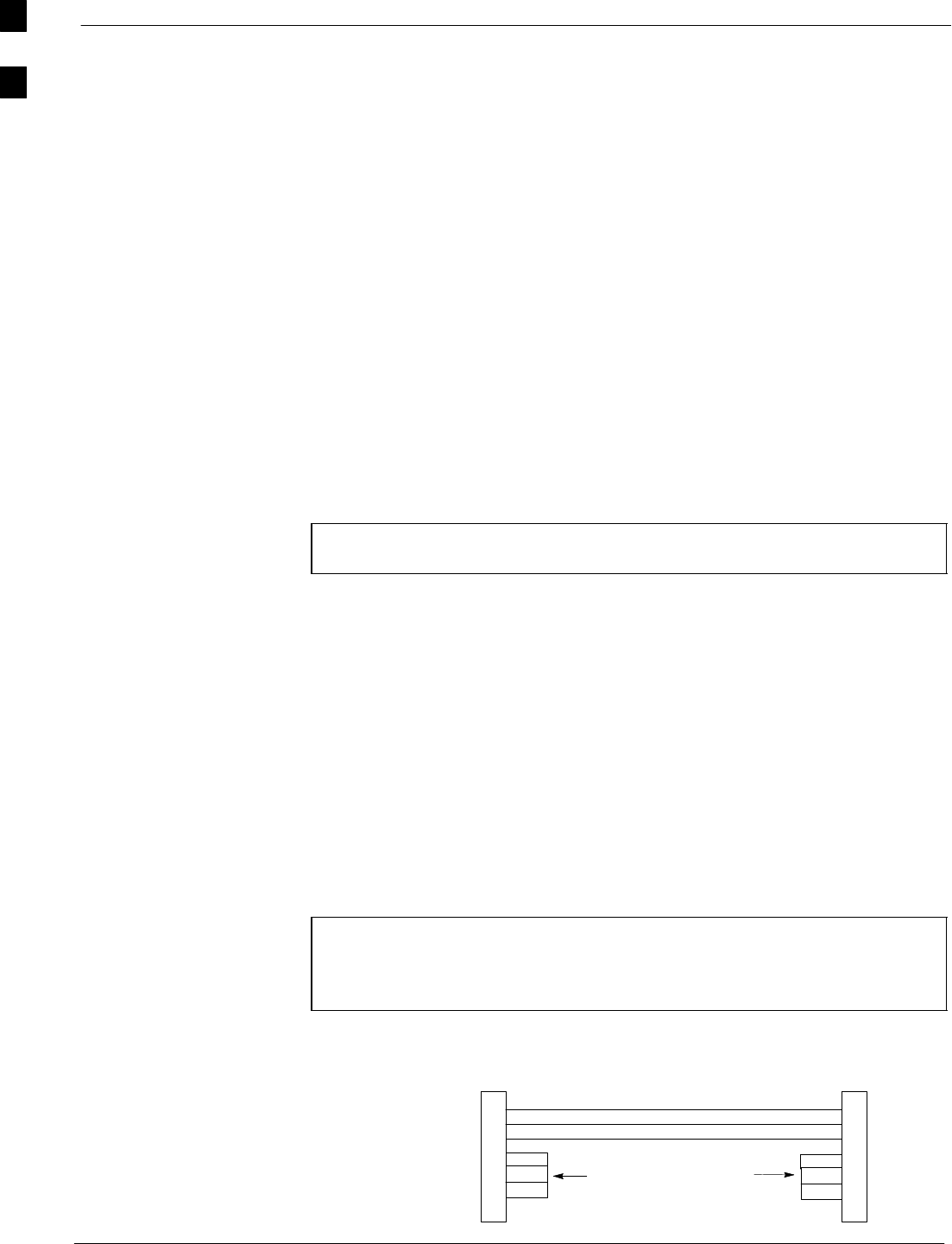
Required Test Equipment and Software 68P64115A18–1
Mar 2003
1X SC 4812T Lite BTS Optimization/ATP Software Release R2.16.1.x
DRAFT
1-8
LMF Software
The Local Maintenance Facility (LMF) application program is a
graphical user interface (GUI)–based software tool. This product is
specifically designed to provide cellular communications field personnel
with the capability to support the following CDMA Base Transceiver
Station (BTS) operations:
SInstallation
SMaintenance
SCalibration
SOptimization
Ethernet LAN Transceiver
SPCMCIA Ethernet Adpater + Ethernet UTP Adapter
3COM Model – Etherlink III 3C589B
10BaseT/10Base2 Converter
STransition Engineering Model E–CX–TBT–03 10BaseT/10Base2
Converter (or equivalent)
NOTE Xircom Model PE3–10B2 or its equivalent can also be used to
interface the LMF Ethernet connection to the frame.
Ethernet LAN External In/Out Port Adapter
Trompeter Electronics, Inc., ADBJ20–E1–PL75 or equivalent BNC (F)
to TRB (M) adapter is required if it is necessary to connect the LMF
computer to the LAN external interface triaxial connectors located in the
power entry compartment.
RS–232 to GPIB interface
SNational Instruments GPIB–232–CT with Motorola CGDSEDN04X
RS232 serial cable or equivalent; used to interface the LMF to the test
equipment.
SA standard RS–232 cable can be used with the modifications shown in
Figure 1-1.
NOTE Pin 8 (CTS) does not have to be jumpered/shorted to the others
as it is a driver output. The DTR is already a driver output
signal. The other pins are to receivers. Short pins 7, 1, 4, 6 on
each cable end.
Figure 1-1: Null Modem Cable Detail
5
3
2
7
1
4
6
GND
RX
TX
RTS
RSD/DCD
DTR
DSR
GND
TX
RX
RTS
RSD/DCD
DTR
DSR
ON BOTH CONNECTORS
SHORT PINS 7, 1, 4, 6
9–PIN D–FEMALE 9–PIN D–FEMALE
5
2
3
7
1
4
6
1

Required Test Equipment and Software68P64115A18–1
Mar 2003 1X SC 4812T Lite BTS Optimization/ATP Software Release R2.16.1.x
DRAFT
1-9
Model SLN2006A MMI interface kit
SMotorola Model TRN9666A null modem board. Connectors on
opposite sides of the board must be used as this performs a null
modem transformation between cables. This board can be used for
25–pin to 8–pin, 25–pin to 25–pin, and 10–pin to 10–pin conversions.
SMotorola 30–09786R01 MMI cable or equivalent; used to interface
the LMF computer serial port connection to the Group Line Interface
(GLI), Clock Synchronization Manager (CSM), External Trunked
Interface Board (ETIB), and module debug serial ports.
Communications system analyzer CDMA/analog
Table 1-1: CDMA LMF Test Equipment Support Table
Item Description Test Capability
Test Sets
Hewlett Packard, model
HP 8921A (with 83203B) Communications analyzer (includes 83203B
CDMA interface option) IS–95A/B only
Motorola CyberTest Communications analyzer IS–95A/B only
Advantest R3465 (with 3561L) Communications analyzer (with 3561 CDMA
option) IS–95A/B only
Agilent E4406A (with E4432B) Communications analyzer (with Generator) IS–95A/B and
CDMA 2000 testing
Advantest R3267 Analyzer (with
R3562) Communciations Analyzer with Advantest
R3562 Generator IS–95A/B and
CDMA 2000 testing
Agilent 8935 series E6380A
(formerly HP 8935) with option
200 or R2K
Communications test set IS–95A/B and
CDMA 2000 testing
Power Meters
Gigatronix 8541C Power meter
HP437B (with HP8481A sensor) Power meter with sensor – capable of measuring –30 dBm to 20 dBm
A combination of test equipment supported by the LMF may also be
used during optimization and testing of the RF communications portion
of BTS equipment when the communications system analyzer does not
perform all of the following functions:
SFrequency counter
SDeviation meter
SRF power meter (average and code domain)
SRF signal generator (capable of DSAT/CDMA modulation)
SAudio signal generator
SAC voltmeter (with 600–ohm balanced audio input and high
impedance input mode)
SNoise measurement meter
SC–Message filter
SSpectrum analyzer
SCDMA code domain analyzer
1

Required Test Equipment and Software 68P64115A18–1
Mar 2003
1X SC 4812T Lite BTS Optimization/ATP Software Release R2.16.1.x
DRAFT
1-10
GPIB cables
Hewlett Packard 10833A or equivalent; one or two meters long, used to
interconnect test equipment and LMF computer.
Timing reference cables
STwo Huber & Suhner 16MCX/11BNC/K02252D or equivalent; right
angle MCX–male to standard BNC–male RG316 cables; 10 ft. long
are required to interconnect the communications system analyzer to
SGLN4132A and SGLN1145A CSM board timing references
or
STwo BNC–male to BNC–male RG316 cables; 3 meters (10 feet) long,
used to interconnect the communications system analyzer to
SGLN4132B and SGLN1145B (and later) CSM front panel timing
references in the RF Modem Frame
Digital multimeter
Fluke Model 8062A with Y8134 test lead kit or equivalent; used for
precision DC and AC measurements to four decimal places.
Directional coupler
Narda Model 3020A 20 dB coupler terminated with two Narda Model
375BN–M loads, or equivalent.
RF attenuators
S20 dB Fixed attenuator, 20 Watt (Narda 768–20), used in conjunction
with calibration of test cables or during general troubleshooting
procedures.
S10 dB Fixed attenuator, 20 Watt (Narda 768–10), for cable calibration
with a Cybertest CDMA analyzer.
Clamp–on DC current probe
Amprobe CT600, or equivalent, 600 A capability with jaw size which
accommodates 2/0 cable. Used with the DMM for back–up battery
charging testing.
Miscellaneous RF adapters, loads, etc.
As required to interface test cables and BTS equipment and for various
test setups. Should include at least (2) 50 Ohm loads (type N) for
calibration and (1) RF short.
RF load
100W non–radiating RF load used (as required) to provide dummy RF
loading during BTS transmit tests.
High–impedance conductive wrist strap
Motorola Model 42–80385A59; used to prevent damage from ESD when
handling or working with modules.
1

Required Test Equipment and Software68P64115A18–1
Mar 2003 1X SC 4812T Lite BTS Optimization/ATP Software Release R2.16.1.x
DRAFT
1-11
Driver bit for tamper–resistant fasteners
Star fastener tamper–resistant insert bit set, Grainger 5F530 or
equivalent, to remove tamper–resistant fasteners securing the frame rear
access cover.
Optional Equipment
This section provides a list of additional equipment that might be
required during maintenance and troubleshooting operations.
NOTE Not all optional equipment specified in this section will be
supported by the LMF in automated tests.
Duplexer
Filtronics Low IM Duplexer (Cm035–f2) or equivalent; used during
Spectral Purity Receive band noise tests.
Frequency counter
Stanford Research Systems SR620 or equivalent; used if direct
measurement of the 3 MHz or 19.6608 MHz references is required.
Spectrum analyzer
Spectrum Analyzer (HP8594E with CDMA personality card) or
equivalent; required for manual tests other than standard Receive band
spectral purity tests performed by the LMF.
LAN tester
Model NETcat 800 LAN troubleshooter (or equivalent); used to
supplement LAN tests using the ohm meter.
Span line (T1/E1) verification equipment
As required for the local application.
RF test cable (if not provided with test equipment)
Motorola Model TKN8231A; used to connect test equipment to the BTS
transmitter output during optimization or during general troubleshooting
procedures.
Oscilloscope
Tektronics Model 2445 or equivalent; used for waveform viewing,
timing, and measurements, or during general troubleshooting procedures.
2–way splitter
Mini–Circuits Model ZFSC–2–2500 or equivalent; used to provide the
diversity receive input to the BTS.
1

Required Test Equipment and Software 68P64115A18–1
Mar 2003
1X SC 4812T Lite BTS Optimization/ATP Software Release R2.16.1.x
DRAFT
1-12
CDMA subscriber mobile or portable radiotelephone
Safco Model 2136–150 with power supply and antenna; used to provide
test transmission and reception during BTS maintenance and
troubleshooting. Do not substitute other models that do not feature
special test modes. Two radios will be required for system and
drive–around testing after optimization and BTS ATP are completed.
RF circulator
Circulator (FERROCOM 5809866C01) or equivalent; can substitute for
a duplexer during Receive sensitivity Frame Erasure Rate (FER) testing
in conjunction with Safco CDMA mobile.
High stability 10 MHz rubidium standard
Stanford Research Systems SR625 or equivalent. Required for CSM and
Low Frequency Receiver (LFR)/High Stability Oscillator (HSO)
frequency verification.
1

Required Documents and Related Publications68P64115A18–1
Mar 2003 1X SC 4812T Lite BTS Optimization/ATP Software Release R2.16.1.x
DRAFT
1-13
Required Documents and Related Publications
Required Documents
The following documents are required to perform optimization of the
cell site equipment:
SSite Document (generated by Motorola Systems Engineering), which
includes:
– General site information
– Floor plan
– RF power levels
– Frequency plan (includes Site PN and operating frequencies)
– Channel allocation (paging, traffic, etc.)
– Board placement
– Site wiring list
– CDF or NECF files (bts–#.cdf and cbsc–#.cdf or bts–#.necf and
cbsc–#.necf)
SDemarcation Document (Scope of Work Agreement)
SEquipment manuals for non-Motorola test equipment
Related Publications
Additional, detailed information about the installation, operation, and
maintenance of the 1X SCt4812T–Lite BTS and its components is
included in the following publications:
SCDMA RFDS User’s Guide; 68P64114A51
SLMF Help function on–line documentation
SLMF CLI Reference; 68P09253A56
SCDMA RFDS Hardware Installation; 68P64113A93
S1X SC 4812T–Lite BTS Hardware Installation ; 68P64115A16
S1X SC 4812T–Lite BTS FRU Guide ; 68P64115A17
SSC4812T/T–Lite/ET/ET Lite Troubleshooting; 68P09253A65
SCellular Glossary of Terms and Acronyms; 68P09213A95
1

Terms and Abbreviations 68P64115A18–1
Mar 2003
1X SC 4812T Lite BTS Optimization/ATP Software Release R2.16.1.x
DRAFT
1-14
Terms and Abbreviations
Standard and Non–standard Terms and Abbreviations
Standard terms and abbreviations used in this manual are defined in
Cellular Glossary of Terms and Acronyms; 68P09213A95. Any
non–standard terms or abbreviations included in this manual are listed in
Table 1-2.
Table 1-2: Non–Standard Terms and Abbreviations
Term or
Abbreviation Definition
1X One of two bandwidths currently defined in the IS–2000 CDMA specification, which
extends the capability of the IS–95A and B specifications. 1X bandwidth provides
wireless packet voice and data transmission capability at up to 144 Mbps.
BBX–1X Broad Band Transceiver, 1X. Third generation BBX card with CDMA2000 1X packet as
well as IS–95A/B capability.
BBX2 Broadband Transceiver, 2nd Generation supports IS–95A/B
BBXR Redundant BBX for a CCP shelf or cage.
CCD Clock Combining and Distribution. CCP shelf module which accepts timing signals from
the active source and distributes them to other CCP shelf modules.
CIO Combiner Input/Output
companion frame A BTS frame configured to operate at the same site with another companion frame.
Companion frames may share antenna signals, but are not inter–connected on the same
LAN. Companion frames are managed as separate BTSs in the Base Station System
(BSS).
DBPF Dual Bandpass Filter
DBM Debug Monitor
DLM DownLoad Manager. Software application resident on the GLI card which permits
download of software upgrades from the Centralized Base Station Controller (CBSC) to
BTSs without the need for a site visit.
DMAC Digital Metering, Alarm, Control. Part of the Meter Alarm Panel (MAP) which provides
control of and status information for the AC power rectifiers as well as back–up battery
monitoring and test capability. Term is used interchangeably with MAP (see below).
DPLL Digital Phase–Locked Loop
DRDC Duplexer, Receive Filter, Dual Directional Coupler. Provides duplexing of BTS transmit
and receive signals to a single antenna and antenna signal sampling in either the forward
(transmit) or reflected (receive) direction for use by an RF Diagnostic Subsystem
(RFDS).
EMPC Expansion Multi–coupler Preselector Card. BTS expansion frame MPC module which is
used to receive, amplify, and distribute RX signals from the starter frame MPC.
GLI2 Group Line Interface card, second generation
HSO High Stability Oscillator. Module providing backup timing source for a BTS when the
timing signal from the GPS or Remote GPS module is unavailable.
HSO2 HSO card, second generation
. . . continued on next page
1

Terms and Abbreviations68P64115A18–1
Mar 2003 1X SC 4812T Lite BTS Optimization/ATP Software Release R2.16.1.x
DRAFT
1-15
Table 1-2: Non–Standard Terms and Abbreviations
Term or
Abbreviation Definition
HSOX HSO Expansion. Module used in a BTS expansion frame to interface with the starter
frame HSO or LFR and distribute the timing signals to the expansion frame CSM
modules.
ISC In–Service Calibration. Technique for performing calibration sector by sector on a BTS
to avoid completely removing the site from service.
LPAC Linear Power Amplifier Controller
LFR2 Low Frequency Receiver, second generation. Low–cost LFR card with capability to
distribute synchronization signals to multiple RF modem frames.
MAP Meter Alarm Panel. SC4812ET Lite Field Replaceable Unit (FRU) which contains the
functions of both the Temperature Compensation Panel (TCP) and the DMAC. Term is
used interchangeably with DMAC.
MCC8E Multichannel CDMA Card supporting 8 IS–95A/B channels.
MCC24E Multichannel CDMA Card supporting 24 IS–95A/B channels.
MCC–1X Multichannel CDMA Card supporting 16 or 48 CDMA2000 1X or (with Software
Release 2.16.0.84.3 and higher) IS–95A/B channels.
MPC Multi–coupler Preselector Card. BTS CCP shelf module used to amplify and distribute
RX signals to BBX modules.
NECB Network Element Configuration Baseline
NECF Network Element Configuration File
NECJ Network Element Configuration Journal
OLF Object List File. File containing a list of the ROM and RAM code versions which should
be operating on every device installed in a BTS. The file is resident on the Central Base
Station Controller (CBSC) Mobility Manager (MM) and is passed to the GLI after a
DLM job is invoked. The GLI uses the OLF to determine which devices require code
download to meet the OLF–specified version.
PDA Power Distribution Assembly. Assembly in an SC4812ET Lite BTS providing internal
DC power distribution and circuit protection.
RFMF RF Modem Frame
RGD Remote Global Positioning System (GPS) Distribution. Module which provides
distribution of digital timing information to up to four BTS RF modem frames (RFMFs)
from a single Remote GPS receiver.
RGPS Remote Global Positioning System. GPS receiver and signal distribution subsystem
which provides digital timing information for up to four BTS RFMFs at a cell site.
RGPS expansion
primary frame BTS frame where the RGD is located and which serves as the distribution point for
RGPS digital timing signals to other (secondary) BTS frames at a cell site.
RGPS expansion
secondary frame BTS frame which receives RGPS digital timing signals distributed from the primary
RGPS expansion frame at a cell site.
RHSO Remote High–Stability Oscillator. Subsystem which generates and distributes
synchronization signals from a single HSO to up to four RF modem frames.
. . . continued on next page
1

Terms and Abbreviations 68P64115A18–1
Mar 2003
1X SC 4812T Lite BTS Optimization/ATP Software Release R2.16.1.x
DRAFT
1-16
Table 1-2: Non–Standard Terms and Abbreviations
Term or
Abbreviation Definition
SCCP Small CDMA Channel Processor. The type of CCP shelf used in the SC4812ET Lite
BTS.
TCP Temperature Compensation Panel. A function of the SC4812ET Lite MAP which
provides the capability to adjust DC voltage output of the rectifiers to compensate for
variations resulting from temperature changes.
TRDC Transmit & Receive Dual Directional Coupler (Non–duplexed, Receive Filter). TRDCs
contains separate transmit and receive paths and bandpass filters which are not connected
electrically. Transmit and receive antenna signals are not duplexed and must be handled
by separate antennas. Each RF path contains a dual directional coupler on the antenna
port which allows sampling of antenna signals in the forward (transmit) and reflected
(receive) directions for use by an RFDS.
1

BTS Equipment Identification68P64115A18–1
Mar 2003 1X SC 4812T Lite BTS Optimization/ATP Software Release R2.16.1.x
DRAFT
1-17
BTS Equipment Identification
Equipment Overview
The 1X SCt4812T–Lite BTS frame consists of a single cabinet
containing RF and power amplifier components. The BTS may be
powered powered by:
S220 Vac (rectified internally to +27 Vdc)
S–48 Vdc (power converted internally to +27Vdc)
S+27 Vdc
Each frame can support up to two carriers in a 3–sector configuration.
Six–sector operation is not supported with any SC4812T Lite
configuration.
Figure 1-2 illustrates the external features of the BTS frame, the single
major component of the Motorola SC4812T Lite. The frame cabinet is
identical for starter and expansion frames except for the I/O interconnect
plate.
Frame Configurations
The SC4812T Lite is available in starter and expansion frame
configurations. Following are brief descriptions of each.
Starter frame configuration supports one or two carriers, each with
separate antenna sets. It can operate as a stand–alone BTS, or can be
modified in the field to the expansion frame configuration.
Expansion Frame configuration supports one or two carriers using 2:1
TX combiners and a single antenna set for the frame. It operates with an
SC4812T Lite starter frame which has its own antennas and different
carriers. Expansion frames share RX signals to provide diversity RX for
the opposite frame. Expansion frames allow equipping a single SC4812T
Lite site with up to four carriers.
Logical BTS
The BTS software implements the logical BTS capability. Previously, all
BTS frames co–located at a single site had to be identified in the
network with separate and distinct BTS ID numbers. In the Logical BTS
feature, all frames located at a single BTS site are identified with unique
Frame ID numbers (Frame ID Numbers 1, 101, 201, 301) under a single
(site) BTS ID number. A logical BTS can consist of up to four
SC 4812T frames.When the LMF is connected to frame 1 of a logical
BTS, you can access all devices in all of the frames that make up the
logical BTS. A logical BTS requires a CDF/NECF file that includes
equipage information for all of the logical BTS frames and their devices
and a CBSC file that includes channel data for all of the logical BTS
frames.
BTS Equipment Identification 68P64115A18–1
Mar 2003
1X SC 4812T Lite BTS Optimization/ATP Software Release R2.16.1.x
DRAFT
1-18
Logical BTS Numbering
The first frame of a logical BTS has a –1 suffix (e.g., BTS–812–1).
Other frames of the logical BTS are numbered with suffixes, –101, –201,
and –301 (e. g. BTS–812–201). When you log into a BTS, a FRAME
tab is displayed for each frame. If there is only one frame for the BTS,
there is only one tab (e.g., FRAME–282–1) for BTS–282. If a logical
BTS has more than one frame, there is a separate FRAME tab for each
frame (e.g. FRAME–438–1, FRAME–438–101, and FRAME–438–201
for a BTS–438 that has three frames). If an RFDS is included in the
CDF/NECF file, an RFDS tab (e.g., RFDS–438–1) is displayed.
Actions (e.g., ATP tests) can be initiated for selected devices in one or
more frames of a logical BTS. Refer to the Select devices help screen for
information on how to select devices.
SCCP Shelf Card/Module Device ID Numbers
All cards/modules/boards in the frames at a single site, assigned to a
single BTS number, are also identified with unique Device ID numbers
dependent upon the Frame ID number in which they are located. Refer to
Table 1-3 and Table 1-4 and Figure 1-4 for specific device ID numbers.
Table 1-3: SCCP Shelf/Cage Card/Module Device ID Numbers (Top Shelf)
Card/Module ID Number (Left to Right)
Frame
#Power
(PS–1) Power
(PS–2) AMR–1 GLI2–1 MCC BBX BBX–R
(Optional) MPC/
EMPC–1
1 – – 1 1 1 2 1 2 3 R1 –
101 – – 101 101 101 102 101 102 103 R101 –
201 – – 201 201 201 202 201 202 203 R201 –
301 – – 301 301 301 302 301 302 303 R301 –
Table 1-4: SCCP Shelf/Cage Card/Module Device ID Numbers (Bottom Shelf)
Card/Module ID Number (Left to Right)
Frame
# HSO/
LFR CSM –1 CSM –2 CCD A CCD B AMR–2 GLI2–2 MCC BBX SW MPC/
EMPC–2
1 – 1 2 – – – 2 2 3 4 4 5 6 – –
101 –101 102 – – – 102 102 103 104 104 105 106 – –
201 –201 202 – – – 202 202 203 204 204 205 206 – –
301 –301 302 – – – 302 302 303 304 304 305 306 – –
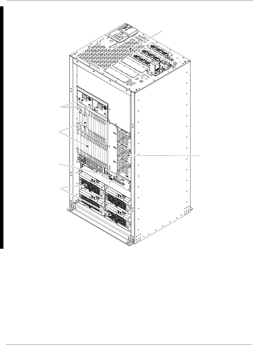
BTS Equipment Identification68P64115A18–1
Mar 2003 1X SC 4812T Lite BTS Optimization/ATP Software Release R2.16.1.x
DRAFT
1-19
Figure 1-2: 1X SCt4812T–Lite BTS Frame
For clarity, doors are not shown.
Power Supply
Modules
SCCP
Fan Module
ti-CDMA-WP-00213-v01-ildoc-ftw
Power
Breaker
Panel
Amplifiers
I/O Interconnect
Plate
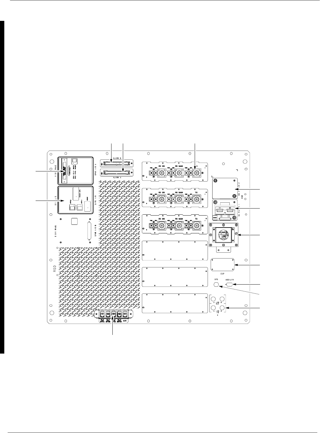
BTS Equipment Identification 68P64115A18–1
Mar 2003
1X SC 4812T Lite BTS Optimization/ATP Software Release R2.16.1.x
DRAFT
1-20
Internal Assemblies and FRUs
The BTS frame houses the fan modules, Small CDMA Channel
Processor (SCCP) shelf, RF Power Amplifier modules, PA trunking
modules, 2:1 combiners.
RF filtering includes: DRF – Duplexers with TX Filter, RX Filter, and
Diversity RX Filter and TRF – Non-Duplexed TX Filter, RX Filter, and
Diversity RX Filter.
Power system components include an AC Power Input/Filter, DC Filters,
+27 Vdc Power Distribution Assembly (PDA).
Figure 1-2 and Figure 1-3 show the location of the internal assemblies
and Field Replaceable Units (FRU). A brief description of each item is
found in the following paragraphs.
Figure 1-3: I/O Interconnect Plate
FRONT
SITE I/O
LAN
CONNECTIONS
GPS IN
HSO/LFR
RF FILTERING
POWER INPUT/
DC FILTER
ETHERNET ROUTER (IF USED;
OTHERWISE, FILLER PLATE)
EXP FILLER
PLATE
REAR
SPAN I/O
ti-CDMA-WP-00214-v01-ildoc-ftw
ALARM
CONNECTORS
POWER INPUT/
AC FILTER
FILLER PLATE
DC Power Distribution Assembly (PDA)
Both rectifier output voltage and back–up battery voltage are routed to
the PDA (Figure 1-3) where they are combined into system DC bus
voltage. The PDA provides distribution of DC power and system DC
bus protection from the loads with MAIN BREAKER and the smaller
post–distribution circuit breakers. MAIN BREAKER permits removal of
all frame loading from the bus. The 13 post–distribution circuit breakers
permit removal of individual loads.

BTS Equipment Identification68P64115A18–1
Mar 2003 1X SC 4812T Lite BTS Optimization/ATP Software Release R2.16.1.x
DRAFT
1-21
Filter/Combiner Shelf (Bandpass Filters or 2:1
Combiners)
The filter/combiner shelf (Figure 1-3) holds the transmit bandpass filters
or 2:1 combiners, depending on system configuration.
Span I/O Board
The span I/O board (Figure 1-3) provides the span line interface to the
SCCP backplane.
Small CDMA Channel Processor (SCCP) Shelf
The SCCP shelf has provisions for the following types and quantities of
modules (Figure 1-3 and Figure 1-4):
SAlarm Monitoring and Reporting (AMR) cards (2)
SBroad Band Transceiver, second generation or 1X, (BBX2 or
BBX–1X) cards, primary (6)
SBBX2 or BBX–1X card, redundant (1)
SCDMA Clock Distribution (CCD) cards (2)
SClock Synchronization Manager (CSM) on two cards (one with GPS
receiver, if ordered)
SCombiner Input/Output (CIO) card (1)
SFan modules (2)
SFiller panel (as required)
SGroup Line Interface, second generation, (GLI2) cards (2)
SHigh Stability Oscillator (HSO)/Low Frequency Receiver (LFR) card
(Optional) (1)
SMulti–coupler Preselector Cards (MPC) (2 per starter frame; 1 per
companion frame)
SExpansion Multi–coupler Preselector Card (EMPC) (1 per companion
frame)
SMulti–Channel CDMA (MCC8E, MCC24E, or MCC–1X) cards (4)
SPower supply cards (2)
SSwitch card (1)
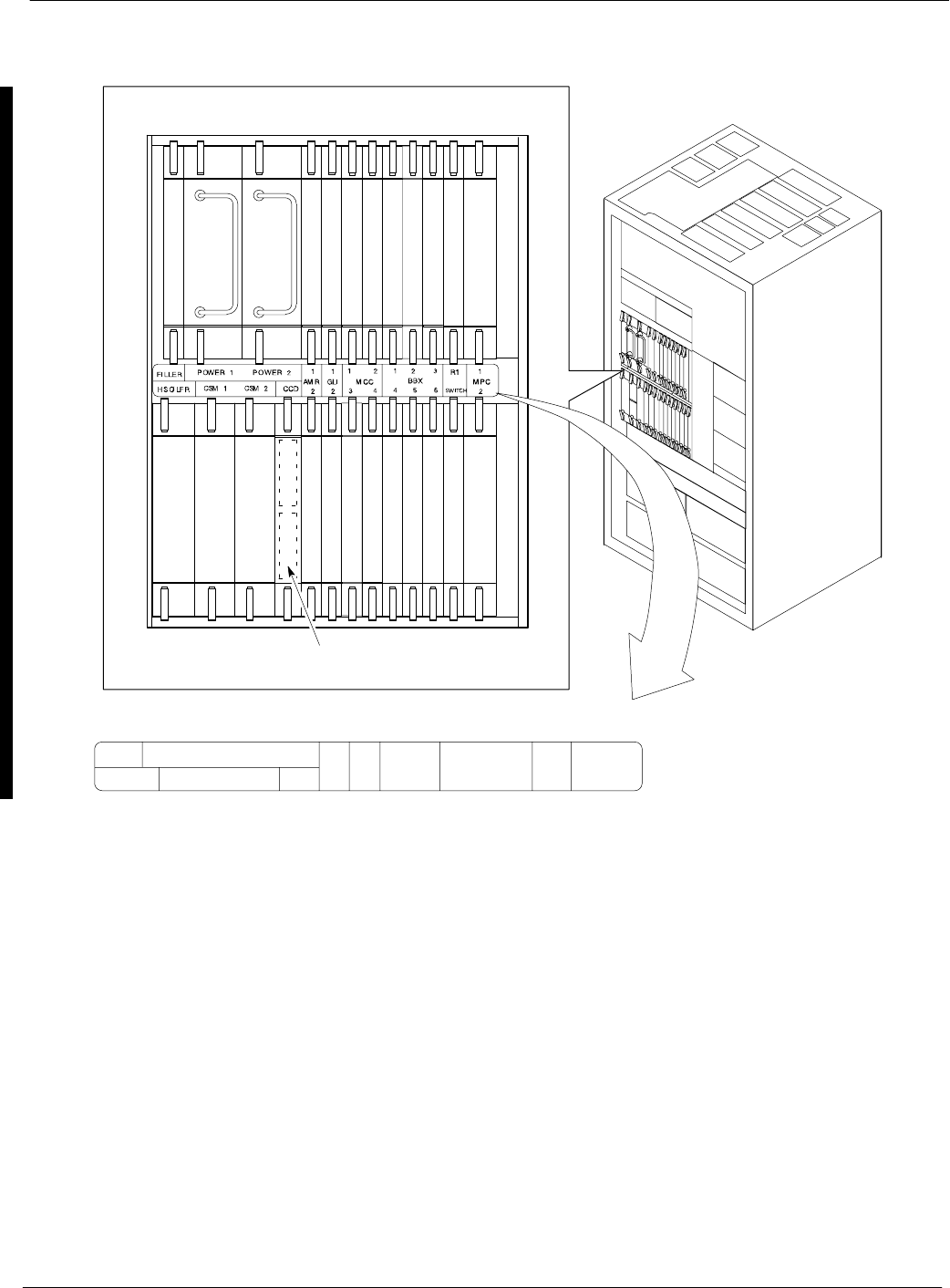
BTS Equipment Identification 68P64115A18–1
Mar 2003
1X SC 4812T Lite BTS Optimization/ATP Software Release R2.16.1.x
DRAFT
1-22
Figure 1-4: SCCP Shelf
ti-CDMA-WP-00222-v01-ildoc-ftw REF
SC 4812T Lite Cabinet
MPC/EMPC
CSM
Power Supply
Power Supply
MPC/EMPC
CSM
CCD–1CCD–2
AMR
HSO
AMR
GLI GLI
MCC
MCC
MCC
MCC
BBX
BBX
BBX
BBX
BBX
BBX
SWITCH
19mm Filler Panel
BBX
CIO
CCD CARD(S)
(LOCATED BEHIND FILLER PANEL)
SCCP SHELF
FILLER POWER 1 POWER 2
HSO/LFR CSM 1 CSM 2 CCD AMR GLI
1 2
3 4
MCC
1 2 3
4 5 6
BBX R1
SWITCH
1
2
1
2
1
2
MPC
2:1 Combiners
In the SC4812T Lite BTS, one 2:1 combiner is used per sector to
combine the trunked LPA–amplified TX signals for two carriers into one
signal for input to the applicable sector DRDC or TRDC.
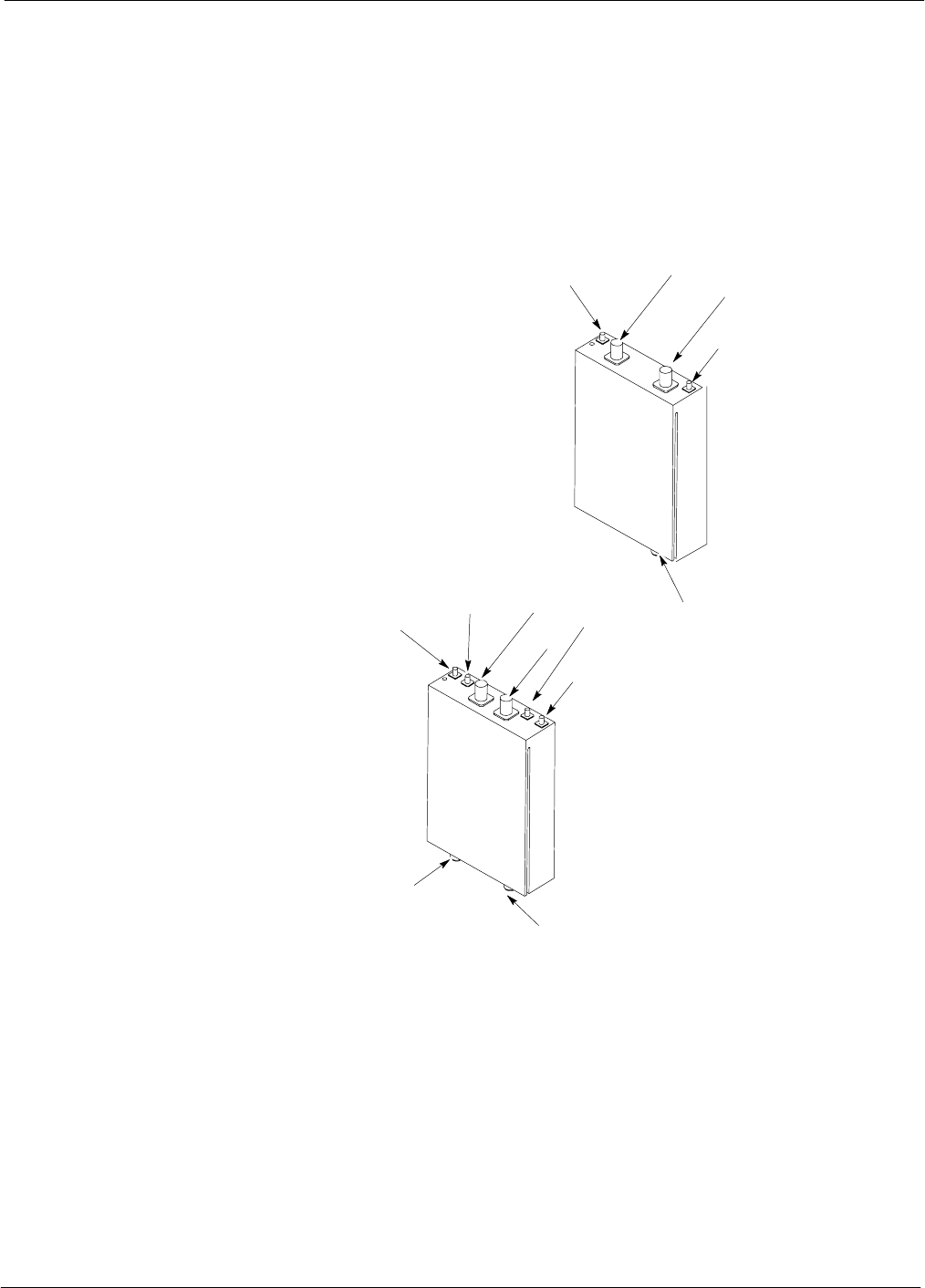
BTS Equipment Identification68P64115A18–1
Mar 2003 1X SC 4812T Lite BTS Optimization/ATP Software Release R2.16.1.x
DRAFT
1-23
Transmit & receive, non–duplexed, Receive filter, Dual
Directional Coupler (TRF)
TRFs provide separate, bandpass–filtered sector transmit and receive
paths. When TRFs are used, separate transmit and receive antennas are
required for each sector. As with DRFs, dual directional couplers for
each antenna path are incorporated in TRFs to permit signal monitoring
by the RFDS.
Figure 1-5: DRF and TRF Details
DRF
TRF
SC4812ETL0005–4
BTS
CPLD
TX
RX
ANT
CPLD
TX BTS
CPLD
TX ANT
CPLD
TX
RX
RX ANT
CPLD
RX BTS
CPLD
RX
ANTENNA
TX
ANTENNA
DUPLEXED
TX & RX ANTENNA

BTS Equipment Identification 68P64115A18–1
Mar 2003
1X SC 4812T Lite BTS Optimization/ATP Software Release R2.16.1.x
DRAFT
1-24
SCCP Cage Configuration and 1X Devices
SC 4812T Lite frames have one SCCP cage which will support up to
four MCC cards and six BBX cards.
MCC Cards
A BTS may be configured with a mix of MCC–8E, MCC–24E, and
MCC–1X cards. Any SCCP cage MCC card slot will support any of the
three MCC types. For 1X capability under R16.0, at least one MCC card
must be an MCC–1X which can be installed in any MCC card slot. In a
BSS operating with Software Release 2.16.0.84.3 and higher, MCC–1X
cards will support IS–95A and B traffic as well as CDMA2000 1X.
When operating with Software Release 2.16.0.5x.x, the MCC–1X cards
do not support IS–95A/B operation. For additional software release
compatibility and capability information, contact the local Motorola
account team.
BBX Cards
Up to six BBX cards of mixed BBX2s and BBX–1Xs can also be
supported. SCCP cage BBX2 card slots 1 through 6 are carrier– and
sector–dependent. As a result, the BBX slots dedicated to the sectors for
one carrier should be populated with the same type of cards. Refer to
Table 1-6 for BBX card slot carrier and sector correlations.
The SCCP cage R1 card slot is dedicated to the redundant BBX. This
slot will support either a BBX2 or a BBX–1X. If a cage has BBX–1X
carriers, the redundant BBX (BBXR) must be a BBX–1X card to provide
1X redundancy.
BBX–1X and BBX2 Interchangeability
In a BSS operating with R16.0 software, BBX–1X cards can be used as
direct replacements for BBX2 cards; however, different types of BBXs
should not be mixed on the same carrier. Therefore, if a BBX2 card is
replaced with a BBX–1X, all remaining BBX2 cards for the carrier
supported by the replaced card must also be replaced with BBX–1X
cards.

BTS Sector Configurations68P64115A18–1
Mar 2003 1X SC 4812T Lite BTS Optimization/ATP Software Release R2.16.1.x
DRAFT
1-25
BTS Sector Configurations
There are a number of ways to configure the BTS frame. Table 1-5
outlines the basic requirements. For more detailed information also see
Table 1-6, Figure 1-6 and Figure 1-7. Bandpass filters are used for
single–carrier configurations and two–carrier systems when carriers are
either adjacent or not adjacent
Table 1-5: BTS Sector Configuration
Number of
Carriers Number
of Sectors Channel Spacing Filter Requirements
1 3 N/A Bandpass Filter or 2:1 Combiner
2 3 Adjacent or Non–adjacent Bandpass Filter
2 3 Non–adjacent 2:1 Combiner
The matrix in Table 1-6 shows the correlation between the various sector
configurations and BBX cards.

BTS Sector Configurations 68P64115A18–1
Mar 2003
1X SC 4812T Lite BTS Optimization/ATP Software Release R2.16.1.x
DRAFT
1-26
Table 1-6: Sector Configurations
Configuration Description
3–Sector / 1 Carrier
The configuration below maps RX and TX with bandpass filters for a 3–sector/1–carrier frame.
1
ANT 1A ANT 2A ANT 3A ANT 1B ANT 2B ANT 3B
1
TX1 / RX1A TX2 / RX2A TX3 / RX3A RX1B RX2B RX3B Carrier #
BBX–1 BBX–2 BBX–3 BBX–1
(diversity RX) BBX–2
(diversity RX) BBX–3
(diversity RX) 1
3–Sector / 1 Carrier
The configuration below maps RX and TX with 2:1 combiners for 3–sector/1–carrier frames in
companion configuration.
ANT 1A ANT 2A ANT 3A ANT 1B ANT 2B ANT 3B
TX1 / RX1A TX2 / RX2A TX3 / RX3A Carrier #
2
BBX–1 BBX–2 BBX–3 1
2
NOTE
Diversity RX (RX1B, 2B, and 3B) is received from the opposite companion frame through RX
EXPANSION connectors 1B, 2B, and 3B.
Diversity RX is provided to the opposite companion frame from antenna connectors 1A, 2A, and 3A
through RX EXPANSION connectors 1A, 2A, and 3A.
3–Sector / 2–ADJACENT or 2–NON–ADJACENT Carriers
The configuration below maps RX and TX with bandpass filters for 3–sectors/2–carriers for both
adjacent and non–adjacent channels.
ANT 1A ANT 2A ANT 3A ANT 1B ANT 2B ANT 3B
3TX1 / RX1A TX2 / RX2A TX3 / RX3A TX4 / RX1B TX5 / RX2B TX6 / RX3B Carrier #
3
BBX–1 BBX–2 BBX–3 BBX–1
(diversity RX) BBX–2
(diversity RX) BBX–3
(diversity RX) 1
BBX–4
(RX) BBX–5
(RX) BBX–6
(RX) BBX–4
(TX & diversity
RX)
BBX–5
(TX & diversity
RX)
BBX–6
(TX & diversity
RX)
2
3–Sector / 2–NON–ADJACENT Carriers
The configuration below maps RX and TX with 2:1 combiners for 3–sectors/2–carriers for
non–adjacent channels for frames in companion configuration.
ANT 1A ANT 2A ANT 3A ANT 1B ANT 2B ANT 3B
TX1 & 4 /
RX1A & 4A TX2 & 5 /
RX2A & 5A TX3 & 6 /
RX3A & 6A Carrier #
4
BBX–1 BBX–2 BBX–3 1
4
BBX–4 BBX–5 BBX–6 2
NOTE
Diversity RX (RX1B, 2B, 3B and RX4B, 5B, 6B) is received from the opposite companion frame
through RX EXPANSION connectors 1B, 2B, and 3B (see NO TAG or NO TAG).
Diversity RX is provided to the opposite companion frame from antenna connectors 1A, 2A, and 3A
through RX EXPANSION connectors 1A, 2A, and 3A.
BTS Sector Configurations68P64115A18–1
Mar 2003 1X SC 4812T Lite BTS Optimization/ATP Software Release R2.16.1.x
DRAFT
1-27
Figure 1-6: SC4812T Lite Stand–alone PA Configuration with Bandpass Filters
NOTE See Table 1-6 Configuration Numbers 1 and 3.
3–Sector
Bandpass Filters
CARRIER 1
SECTOR 1, 2, 3
CARRIER 2
SECTOR 1, 2, 3
Figure 1-7: SC4812T Lite Companion Frame LPA Configuration with 2:1 Combiners
NOTE See Table 1-6 Configuration Numbers 2 and 4.
SC4812ETL0011–4
3–Sector
2:1 Combiners
CARRIER 1
SECTOR 1, 2, 3
CARRIER 2
SECTOR 1, 2, 3

BTS Sector Configurations 68P64115A18–1
Mar 2003
1X SC 4812T Lite BTS Optimization/ATP Software Release R2.16.1.x
DRAFT
1-28
Notes

Mar 2003 1X SC 4812T Lite BTS Optimization/ATP Software Release R2.16.1.x
DRAFT
2-1
Chapter 2
Preliminary Operations
2

Preliminary Operations: Overview 68P64115A18–1
Mar 2003
1X SC 4812T Lite BTS Optimization/ATP Software Release R2.16.1.x
DRAFT
2-2
Preliminary Operations: Overview
Introduction
This section first verifies proper frame equipage against the site-specific
documentation supplied for each BTS application. This includes
verifying module placement, jumper, and dual in–line package (DIP)
switch settings. Next, pre-power up and initial power-up procedures are
presented. Finally, power–down and normal power–up procedures are
covered.
Cell–site Types
Sites are configured as omni or up to 3–sectors – one or two carriers.
Each type has unique characteristics and must be optimized accordingly.
CDF/NECF
The Configuration Data File (CDF) or Network Element Configuration
File (NECF) contains site type and equipage data information and passes
it directly to the LMF during optimization. The number of modem
frames, number and types of BBX and MCC boards, and linear power
amplifier assignments are some of the equipage data included in the
CDF/NECF.
NOTE Be sure that the correct bts–#.cdf (or bts–#.necf) and cbsc–#.cdf
files are used for the BTS. These should be the CDF/NECF files
that are provided for the BTS by the CBSC. Failure to use the
correct CDF/NECF files can cause system errors. Failure to use
the correct CDF/NECF files to log into a live (traffic
carrying) site can shut down the site.
Site Equipage Verification
Review the site documentation. Match the site engineering equipage data
to the actual boards and modules shipped to the site. Physically inspect
and verify the equipment provided for the frame.
CAUTION Always wear an approved anti–static wrist strap while handling
any circuit card/module to prevent damage by ESD. After
removal, the card/module should be placed on a conductive
surface or back into the anti–static packaging in which it was
shipped.
2
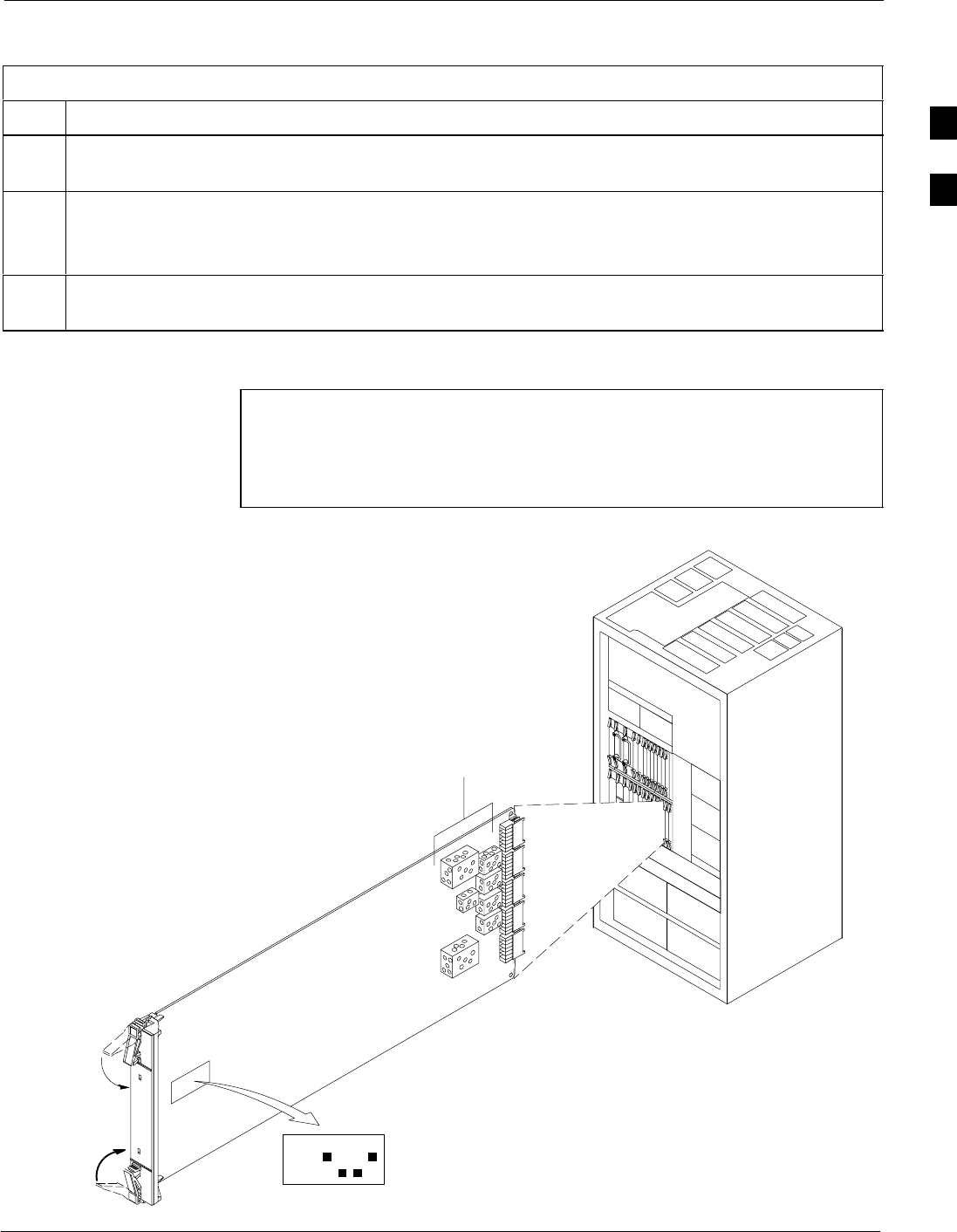
Preliminary Operations: Overview68P64115A18–1
Mar 2003 1X SC 4812T Lite BTS Optimization/ATP Software Release R2.16.1.x
DRAFT
2-3
Initial Installation of Boards/Modules
Table 2-1: Initial Installation of Boards/Modules
Step Action
1Refer to the site documentation and, if it was not previously done, slide all boards and modules into
the appropriate shelves as required. DO NOT SEAT the boards and modules at this time.
NOTE
On 800 MHz systems, the Switch Card has a configuration switch that must match the site
configuration (see Figure 2-1).
2As the actual site hardware is installed, record the serial number of each module on a “Serial Number
Checklist” in the site logbook.
Figure 2-1: 800 MHz Configuration Switch Card
NOTE Configuration Switch (shown in Figure 2-1) is a feature on the
newer versions of the 800 Mhz switch card (some earlier cards
do not have the switch). Configuration shown is for 3 Sector
BTS. Switch 1 chooses BTS or MF. Switch 4 chooses 3–sector
or 6 sector. Switches 2 and 3 are not used.
ti-CDMA-WP-00228-v01-ildoc-ftw REF
Switch Card
1234
ON
BTS
MF
3 Sector
6 Sector
J1
J2
J3
J4
J5
SHIELDS
Configuration
Switch
2
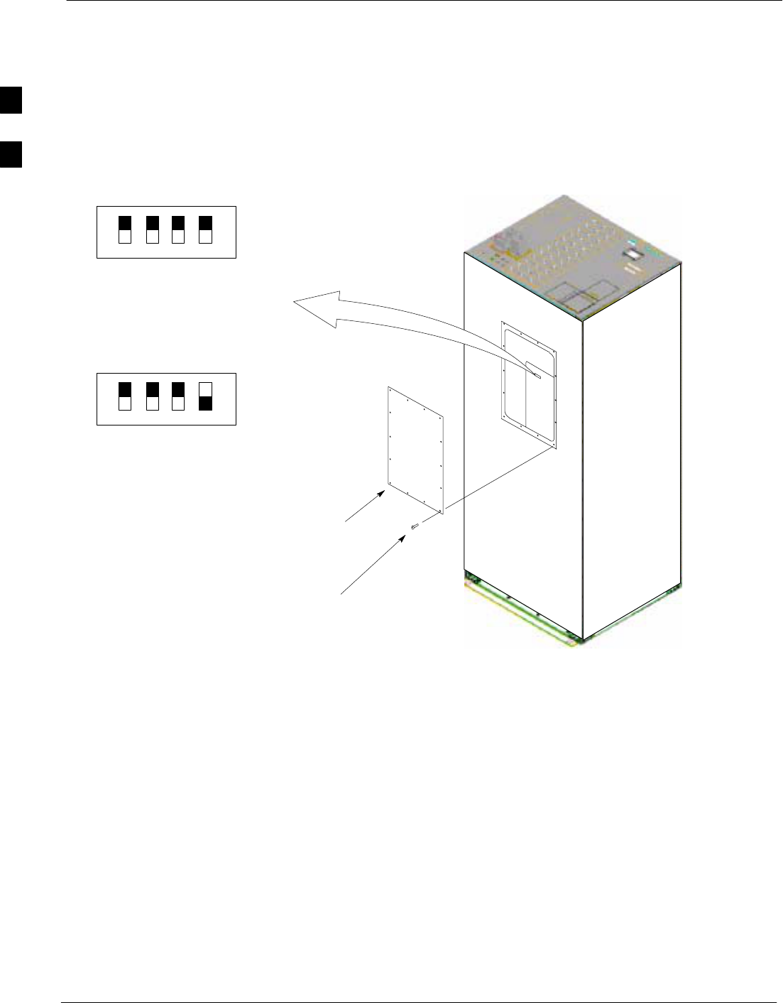
Preliminary Operations: Overview 68P64115A18–1
Mar 2003
1X SC 4812T Lite BTS Optimization/ATP Software Release R2.16.1.x
DRAFT
2-4
Setting Frame SCCP Configuration Switch
The backplane configuration switch is located behind the frame rear
access panel. It must be set for the frame type as shown in Figure 2-2.
The switch setting must be verified and set before power is applied to the
BTS equipment.
Figure 2-2: Backplane DIP Switch Settings
ON
OFF
STARTER
FRAME
SETTING
ON
OFF
EXPANSION
FRAME 1
SETTING
BOTTOM / TOP
RIGHT / LEFT
MODEM_FRAME_ID_1
MODEM_FRAME_ID_0
BOTTOM / TOP
RIGHT / LEFT
MODEM_FRAME_ID_1
MODEM_FRAME_ID_0
REAR ACCESS
PANEL
T–27 BUTTON HEAD OR
T–30 PAN HEAD
TAMPER–RESISTANT
FASTENER (14)
Rear of
SC–4812T–Lite
2
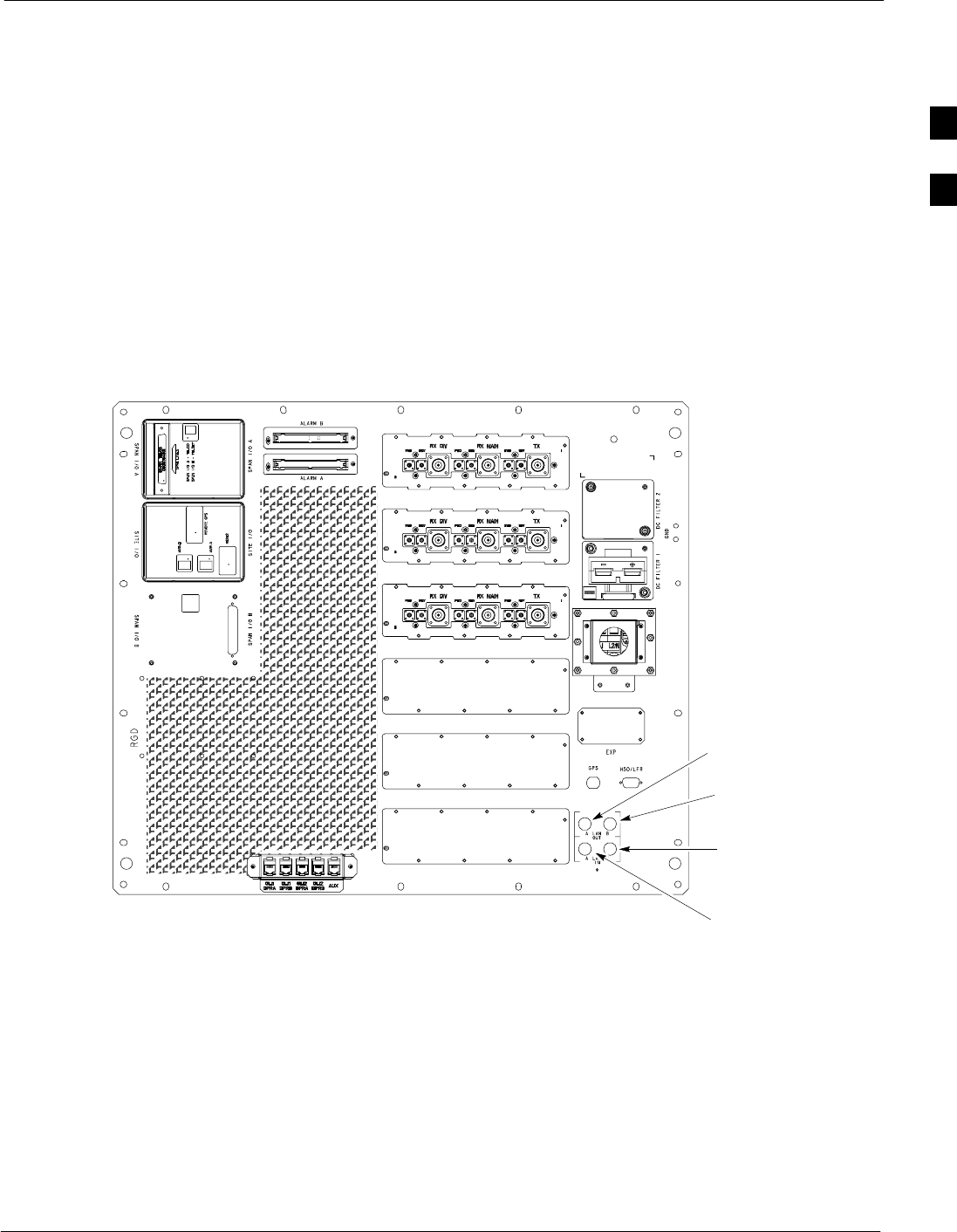
Ethernet LAN68P64115A18–1
Mar 2003 1X SC 4812T Lite BTS Optimization/ATP Software Release R2.16.1.x
DRAFT
2-5
Ethernet LAN
Ethernet LAN Termination
For proper operation, each end of the primary and redundant BTS
Ethernet Local Area Networks (LAN) must be terminated with a
50–ohm load. For a BTS consisting of a stand–alone or an expansion
frame, this is done by placing 50–ohm triaxial terminations on the LAN
A and B external IN and OUT connectors.
Check the LAN A and B external IN and OUT connectors on the I/O
plate of each frame (see Figure 2-3) and be sure terminations are
installed on all the uncabled external LAN connectors.
Figure 2-3: External Ethernet LAN Connectors
FRONT
LAN B IN
CONNECTION
REAR
ti-CDMA-WP-00214-v01-ildoc-ftw REF
LAN B OUT
CONNECTION
LAN A OUT
CONNECTION
LAN A IN
CONNECTION
2
Pre-Initial Power-up Tests 68P64115A18–1
Mar 2003
1X SC 4812T Lite BTS Optimization/ATP Software Release R2.16.1.x
DRAFT
2-6
Pre-Initial Power-up Tests
Introduction
The following information is used to check for any electrical short
circuits and to verify the operation and tolerances of each frame at the
site before applying power for the first time. It contains instructional
information on the proper initial power up procedures for the SC4812T
Lite stand–alone and expansion frames for both the North American
version and the International version. If directions are different for either
version, they are called out within the procedure. Please pay attention to
all cautions and warning statements in order to prevent accidental injury
to personnel.
NOTE Unless otherwise noted, all procedures in this section are to be
followed for each frame at a site.
Required Tools
The following tools are used in the procedures.
SClamp–on DC current probe (600 A capability with jaw size to
accommodate 2/0 cable).
SDigital Multimeter (DMM) with standard 2mm (.080”) tip probes
SHot Air Gun – (optional for part of the Alarm Verification)
Cabling Inspection
Using the site-specific documentation generated by Motorola Systems
Engineering, verify that the following cable systems are properly
connected:
SReceive RF cabling – up to six RX cables
STransmit RF cabling – up to six TX cables
SFor expansion frame installations, inter–frame RX diversity cabling –
six RX cables
NOTE For DC power applications (+27 V):
SThe positive power cable is red.
SThe negative power cable is black. (The black power cable is
at ground potential.)
Initial Inspection and Setup
Table 2-2: Initial Inspection and Setup
Step Action
1Be sure that the facility circuit breaker controlling external AC power supplied to the frame is set to
OFF.
2Verify that the external AC power supply is correctly connected to the ACLC input by performing the
procedure in Table 2-4.
DC Power System Pre-power Application Test
Before applying any power to the BTS frame, follow the procedure in
Table 2-3 to verify there are no shorts in the DC power distribution
system.
2
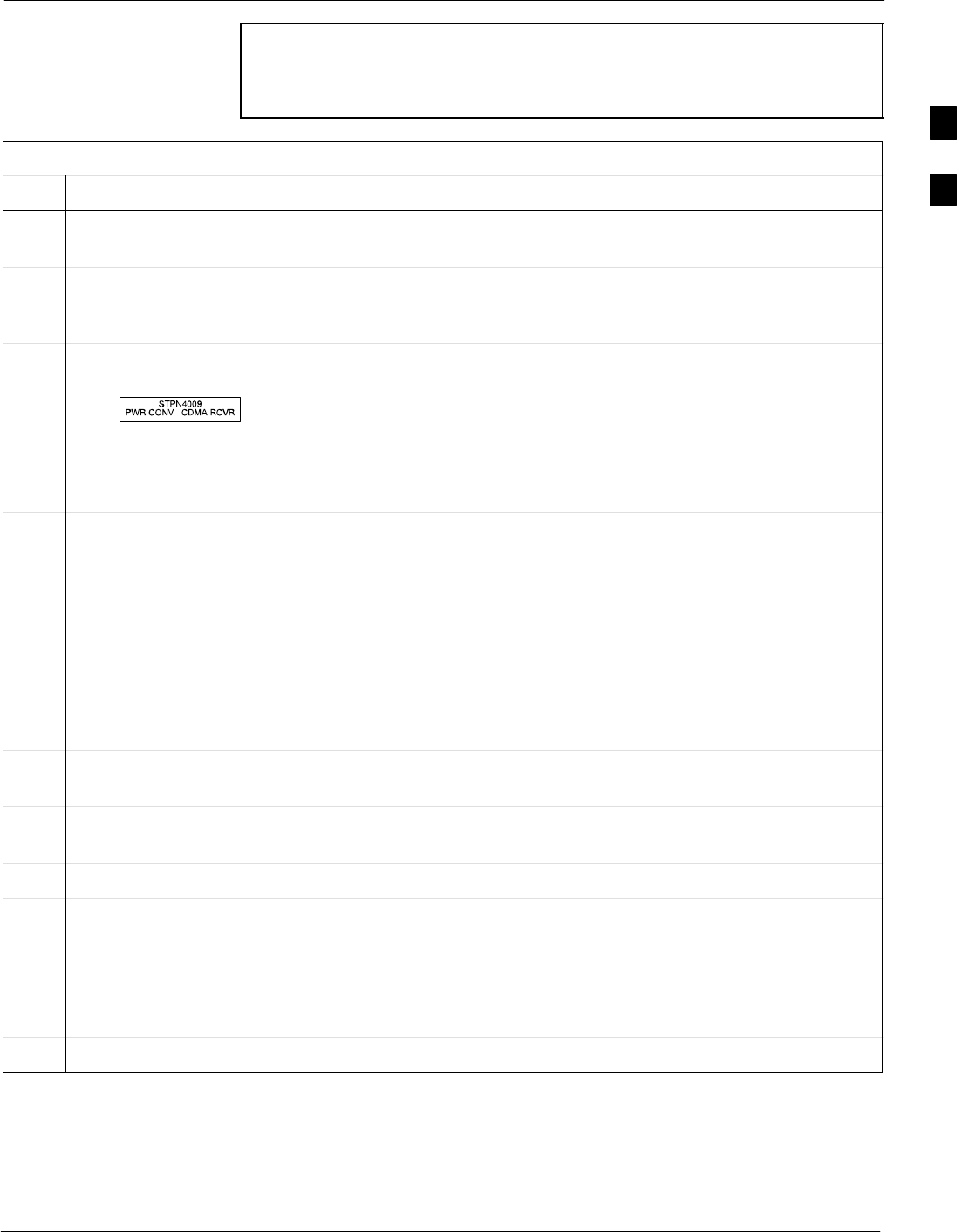
Pre-Initial Power-up Tests68P64115A18–1
Mar 2003 1X SC 4812T Lite BTS Optimization/ATP Software Release R2.16.1.x
DRAFT
2-7
NOTE The procedure in Table 2-3 is required only on initial frame
power–up or following maintenance when any major power
components (e.g., ACLC, DC PDA, Meter Alarm Panel) were
replaced or internal DC power cables were disconnected.
Table 2-3: DC Power System Pre–Power Application Test
Step Action
1Physically verify all AC power to the BTS is OFF and all DC PDA circuit breakers (Figure 2-4) are
set to OFF (pulled out).
2On the DC PDA, set the MAIN BREAKER to the ON position by pushing it in. Resistance between
the MAP (–) VOLT TEST POINT and the (–) AMP TEST POINT should measure between 300 Ω.
minimum 900 Ω. maximum.
3Before proceeding, be sure the SCCP shelf power/converter modules PS1 and PS2 are correct by
verifying that the locking/retracting tabs appear as follows:
– (in +27 volt systems)
! CAUTION
Using the incorrect type of power/converter modules will damage the module, the SCCP shelf, and
other modules installed in the SCCP shelf.
4NOTE
In the following steps, if the DMM reads between 300 Ω minimum and 900 Ω maximum after
inserting any board/module, a low impedance problem probably exists in that board/module. Replace
the suspect board/module and repeat the test. If test still fails, isolate the problem before proceeding.
Insert and lock the PS1 DC–DC converter module into its slot, and and turn ON the PS1 DC circuit
breaker on the DC PDA.
5Resistance between the MAP (–) VOLT TEST POINT and the (–) AMP TEST POINT should
typically increase as capacitors charge, finally measuring between 300 Ω minimum and 900 Ω.
maximum.
6Repeat steps 4 and 5 for the PS2 converter module/circuit breaker and all other remaining modules in
the SCCP shelf.
7On the DC PDA, set the PA 1A–1B circuit breaker to the ON position by pushing it in, and repeat step
5.
8Repeat step 7 for each of the three remaining PA circuit breakers.
9Carefully reconnect each PA cable one at a time. Repeat step 5 after reconnecting each cable.
– A typical response is that the ohmmeter will steadily climb in resistance as module input
capacitors charge, finally indicating between 300 Ω minimum and 900 Ω. maximum.
10 Set the Pilot Beacon, both Heat Exchanger, ETIB, and Options circuit breakers to ON one at a time.
Repeat step 5 after pushing in each circuit breaker.
11 Set all DC PDA circuit breakers to OFF (pulled out).
2
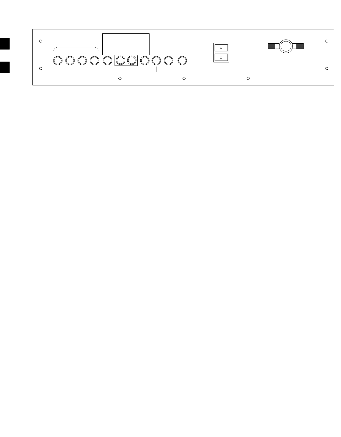
Pre-Initial Power-up Tests 68P64115A18–1
Mar 2003
1X SC 4812T Lite BTS Optimization/ATP Software Release R2.16.1.x
DRAFT
2-8
Figure 2-4: DC PDA
SC4812TL0009–3
LPA
1B 1D 3B 3D
1A 1C 3A 3C PS1 PS2
ETIB
OPTIONS
25 25
HEATEXCHANGER
CAUTION
SHUTOFFBOTHBREAKERS
ONLYDURINGHEATEXCHANGER
MAINTENANCEORREPAIR
LPA
BLOWERS
PUSHBUTTON
TORESET
LPABLOWERS
MAIN BREAKER
300
50 5010 1530 30 30 30 15
PILOT
BEACON
2

Pre-Initial Power-up Tests68P64115A18–1
Mar 2003 1X SC 4812T Lite BTS Optimization/ATP Software Release R2.16.1.x
DRAFT
2-9
External AC Power Connection Verification
Following verification of frame DC power system integrity, external AC
power connections must be verified. To accomplish this, the series of AC
voltage measurements specified in Table 2-4 is required.
CAUTION Failure to properly connect the external AC power cable will
damage the surge protection module inside the ACLC.
Table 2-4: AC Voltage Measurements
Step Action
1NOTE
This procedure is required only after external AC power wiring has been initially connected or
removed and reconnected to the frame.
n WARNING
Ensure the frame is unpowered by setting the facility circuit breaker controlling external AC power
supplied to the frame to OFF.
Physically verify all DC PDA circuit breakers are set to OFF (pulled out), and all battery shelf circuit
breakers are OFF (pulled out).
2Open the ACLC circuit breaker access door, and set all ACLC circuit breakers to OFF (down).
3Remove the four screws securing the ACLC front panel assembly, and remove the ACLC front panel
assembly to gain access to the AC circuit breaker input terminals (NO TAG).
4Apply external AC power to the frame by setting the facility circuit breaker to ON.
5n WARNING
Do not perform the following steps while wearing an anti–static wrist strap. Serious personal injury
can result from accidently shorting high voltage or high current circuits to ground.
! CAUTION
North AMERICAN Cabinet only:
If the AC voltages measured in the following steps exceed 120 V when measuring from terminals L1
or L2 to neutral or ground, STOP and DO NOT proceed until the cause of the higher voltages are
determined. The frame will be damaged if the Main breaker is turned on with excessive voltage on the
inputs.
Measure the AC voltage from terminal L1 to neutral.
North American Cabinet:
– Voltage should be in the nominal range of 115 to 120 Vac.
International Cabinet:
– Voltage should be in the nominal range of 210 to 240 Vac.
6Measure the AC voltage from terminal L1 to ground.
North American Cabinet:
– Voltage should be in the nominal range of 115 to 120 Vac.
International Cabinet:
– Voltage should be in the nominal range of 210 to 240 Vac.
7Steps 7a through 7c apply to the North American cabinet only. If working on a International cabinet
continue to step 8.
. . . continued on next page
2

Pre-Initial Power-up Tests 68P64115A18–1
Mar 2003
1X SC 4812T Lite BTS Optimization/ATP Software Release R2.16.1.x
DRAFT
2-10
Table 2-4: AC Voltage Measurements
Step Action
7a – Measure the AC voltage from terminal L2 to neutral on the North American cabinet.
–– Voltage should be in the nominal range of 115 to 120 Vac.
7b – Measure the AC voltage from terminal L2 to ground on the North American cabinet.
–– Voltage should be in the nominal range of 115 to 120 Vac.
7c ! CAUTION
If the AC voltages measured (on the North American cabinet) in the following step exceeds 240 V
when measuring between terminals L1 and L2, STOP and DO NOT proceed until the cause of the
higher voltages are determined. The frame will be damaged if the Main breaker is turned on with
excessive voltage on the inputs.
– Measure from terminal L1 to terminal L2.
–– Voltage should be in the nominal range from 208 to 240 Vac.
8Remove external AC power from the frame by setting the facility circuit breaker to OFF.
9Install the ACLC front panel assembly and secure with the four screws removed in step 1.
10 Apply external AC power to the frame by setting the facility circuit breaker to ON.
2

Applying AC Power68P64115A18–1
Mar 2003 1X SC 4812T Lite BTS Optimization/ATP Software Release R2.16.1.x
DRAFT
2-11
Applying AC Power
Once the external AC power connections are verified, AC power may be
applied internally to the frame. Table 2-5 provides the procedure for
applying internal AC power.
Table 2-5: Applying Internal AC Power
Step Action
1Be sure the requirements of Table 2-4 for AC input power connection verification have been met.
2Be sure all DC PDA circuit breakers are set to OFF (pulled out), all ACLC front–panel circuit
breakers are OFF (down), and all battery shelf circuit breakers are OFF (pulled out).
3Be sure the MAP power switch, TCP switch, and BATT TEST switch are all set to OFF.
4If it has not already been done, set the facility circuit breaker supplying AC power to the frame
to ON.
5Set the ACLC MAIN circuit breaker ON.
– For the North American cabinet:
Observe that all eight (8) green LEDs on the front of the ACLC are illuminated (NO TAG).
– For the International cabinet:
Observe that all four (4) green LEDs on the front of the ACLC are illuminated (NO TAG).
6On the ACLC, set RECT. 1/3 and then RECT. 2/4 branch circuit breakers ON. All the installed
rectifier modules (NO TAG) will start up, and the green DC and PWR LEDs should light on each.
7Set the MAP power switch to ON. The MAP VOLT display should read 27.4 + 0.2 VDC with the
TCP switch OFF.
! CAUTION
Once power is applied to the MAP, be careful not to short either of the VOLT TEST POINTS to
ground. Failure to comply will result in severe damage to the MAP.
8On the MAP, set the TCP switch (Figure 2-5) to ON. Verify no alarm LEDs are lighted on the MAP.
NOTE
Depending on battery compartment temperature, the rectifier voltage displayed on the MAP VOLT
indicator may change by as much as +1.5 V when the TCP is set to on.
9Check the rectifier current bar graph displays (green LED display on the rectifier module). None
should be lighted at this time.
10 If batteries are fitted, set the ACLC HEATER circuit breaker to ON.
NOTE
The GFCI AC circuit breaker should remain OFF unless the GFCI outlet is in use.
2
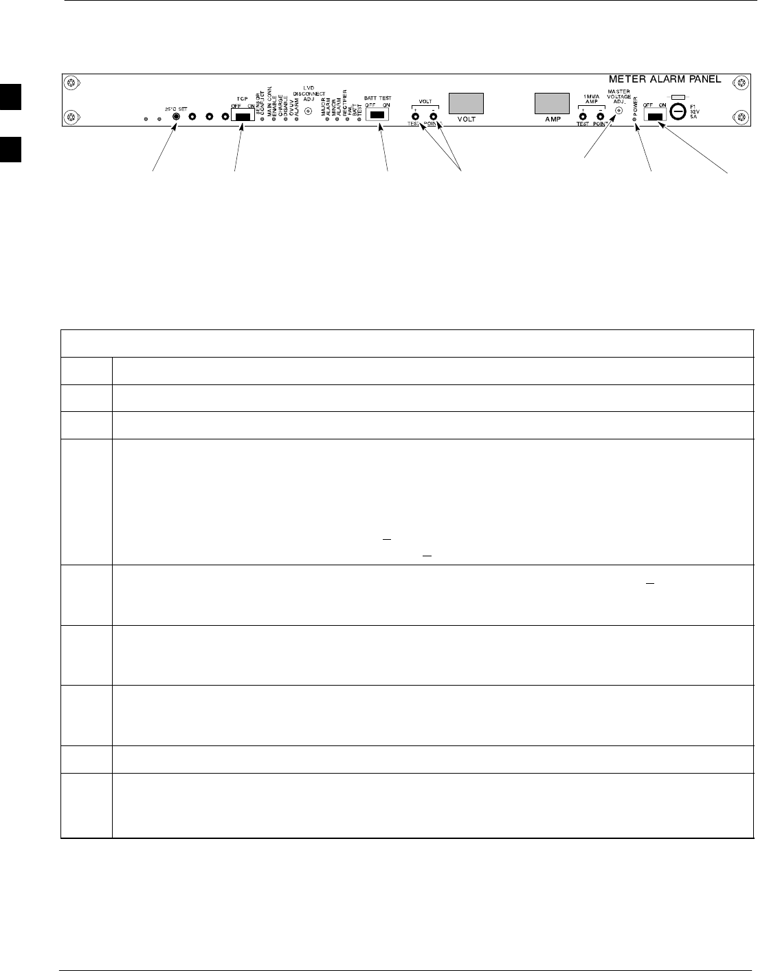
Applying AC Power 68P64115A18–1
Mar 2003
1X SC 4812T Lite BTS Optimization/ATP Software Release R2.16.1.x
DRAFT
2-12
Figure 2-5: Meter Alarm Panel (MAP)
POWER
SWITCH
POWER
INDICATOR
TCP
SWITCH VOLT TEST
POINTS
25_C SET
MASTER
VOLTAGE
ADJ.
BATT TEST
SWITCH
SC4812TL0015–2
TO DISABLE
SENSOR FAIL
SENSOR 2
SENSOR 1
COMM
DC Power Application and Testing
Table 2-6 lists the step–by–step instructions for applying DC power and
ensuring the DC power system components are correctly functioning.
Table 2-6: DC Power Application and Tests
Step Action
1Be sure all DC PDA and battery shelf circuit breakers are OFF (pulled out).
2Be sure the procedures in Table 2-3 (if applicable) and Table 2-5 have been performed.
3! CAUTION
When measuring voltage at the VOLT TEST POINTS, be careful not to short either of the test points
to ground. Failure to comply will result in severe damage to the MAP.
Measure voltage at the MAP VOLT TEST POINTS while pressing the 25° C SET button
(Figure 2-5). The voltage should read 27.4 + 0.2 Vdc. Adjust with the MASTER VOLTAGE ADJ. on
the MAP, if necessary, to obtain an indicated 27.4+0.2 Vdc. Release the 25° C SET button.
4Depending on the ambient temperature, the voltage reading may now change by up to + 1.5 V
compared to the reading just measured. If it is cooler than 25_C, the voltage will be higher, and if it is
warmer than 25_C, the voltage will be lower.
5Inside the battery compartment, measure the voltage between the cable connection point at the bottom
of the + (red) battery bus bar and chassis ground, observing that the polarity is correct. The voltage
should be the same as the measurement in step 4.
6Measure the voltage between the + (red) and – (black) battery bus bars in the battery compartment.
Place the probe at the bottom of the bus bars where the cables are connected. The DC voltage should
measure the same as in step 4.
7Close (push in) DC PDA MAIN BREAKER.
8On the DC PDA(Figure 2-4), set the PS1 and PS2 circuit breakers to the ON position by pushing
them in one at a time while observing the rectifier output current indicated on the MAP AMP display.
– The display should indicate between 20 and 60 amps.
. . . continued on next page
2

Applying AC Power68P64115A18–1
Mar 2003 1X SC 4812T Lite BTS Optimization/ATP Software Release R2.16.1.x
DRAFT
2-13
Table 2-6: DC Power Application and Tests
Step Action
9On the DC PDA), set the remaining circuit breakers to the ON position by pushing them in one at a
time in the following sequence:
1. PA (four circuit breakers, labeled 1A–1B through 3C–3D).
2. HEAT EXCHANGER (two circuit breakers)
3. ETIB
4. PILOT BEACON
5. OPTIONS
10 Confirm that the MAP AMP display continues to indicate between 20 and 60 amps during the initial
power application.
NOTE
No battery charging or heavy RF loading is present at this point.
11 If the frame is not equipped with the pilot beacon option, set the PILOT BEACON circuit breaker
to OFF.
Battery Charge Test (Connected Batteries)
Table 2-7 lists the step–by–step instructions for testing the battery
charging performance.
Table 2-7: Battery Charge Test (Connected Batteries)
Step Action
1Close the battery shelf circuit breakers (NO TAG) for connected batteries only. This process should be
completed quickly to avoid individual battery strings drawing excess charge current
NOTE
If the batteries are sufficiently discharged, the battery circuit breakers may not engage individually
due to the surge current. If this condition occurs, disconnect the batteries from the 27Vdc bus by
setting the MAP power switch to OFF, and then engage all the connected battery circuit breakers.
The MAP power switch should then be turned ON.
2Using the clamp–on DC current probe and DMM, measure the current in each of the battery string
connections to the battery bus bars. The charge current may initially be high but should quickly
reduce in a few minutes if the batteries have a typical new–battery charge level.
. . . continued on next page
2

Applying AC Power 68P64115A18–1
Mar 2003
1X SC 4812T Lite BTS Optimization/ATP Software Release R2.16.1.x
DRAFT
2-14
Table 2-7: Battery Charge Test (Connected Batteries)
Step Action
NOTE
The MAP AMP display will indicate the total current output of the rectifiers during this procedure.
As an alternative, the bar graph meters on the AC rectifier modules can be used as a rough estimate of
the total battery charge current. Each rectifier module bar graph has eight (8) LED elements to
represent the output current. Each illuminated LED element indicates that approximately 12.5% (1/8
or 8.75 Amps) of an individual rectifier’s maximum current output (70 Amps) is flowing.
RECTIFIER BAR GRAPH EXAMPLE:
Question: A system fitted with three (3) rectifier modules each have three bar graph LED elements
illuminated. What is the total output current into the batteries?
Answer: Each bar graph is indicating approximately 12.5% of 70 amps, therefore, 3 x 8.75 equals
26.25 amps per rectifier. As there are three rectifiers, the total charge current is equal to (3 x 26.25 A)
78.75 amps.
This charge current calculation is only valid when the RF and PA compartment electronics are not
powered on, and the RF compartment heat exchanger is turned off. This can only be accomplished if
the DC PDA MAIN BREAKER is set to OFF.
3The current in each string should be approximately equal (within + 5 amps).
4Allow a few minutes to ensure that the battery charge current stabilizes before taking any further
action. Recheck the battery current in each string. If the batteries had a reasonable charge, the current
in each string should reduce to less than 5 amps.
5Recheck the DC output voltage. It should remain the same as measured in step 4 of the frame DC
Power Application and Test (Table 2-6).
NOTE
If discharged batteries are installed, the MAP AMP display may indicate approximately 288 amps for
a two–carrier frame (four rectifiers) or 216 amps for a single–carrier frame (three rectifiers).
Alternately, all bar graph elements may be lighted on the rectifiers during the charge test. Either
indication shows that the rectifiers are at full capacity and are rapidly charging the batteries. It is
recommended in this case that the batteries are allowed to charge and stabilize as in the above step
before commissioning the site. This could take several hours.
Battery Discharge Test
Perform the test procedure in Table 2-8 only when the battery current is
less than 5 Amps per string. Refer to Table 2-7 on the procedures for
checking current levels.
Table 2-8: Battery Discharge Test
Step Action
1Turn the BATT TEST switch on the MAP ON (Figure 2-5). The rectifier output voltage and current
should decrease by approximately 10% as the batteries assume the load. Alarms for the MAP may
occur.
2Measure the individual battery string current using the clamp–on DC current probe and DMM. The
battery discharge current in each string should be approximately the same (within + 5 amps).
3Turn BATT TEST switch OFF.
2
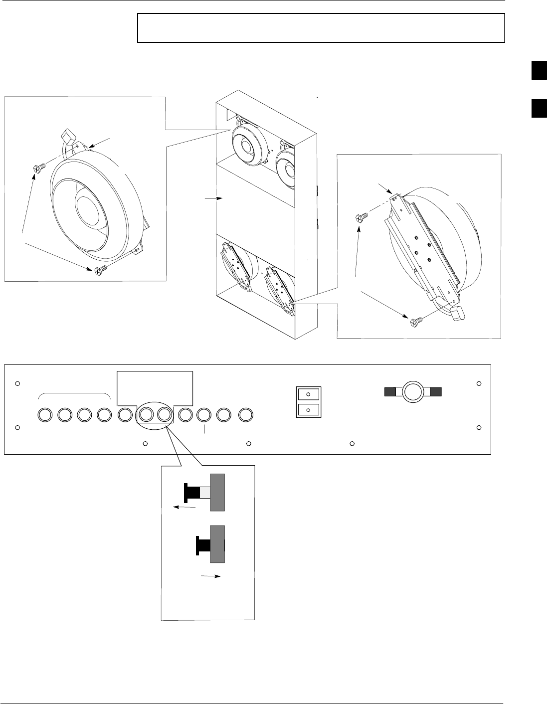
Applying AC Power68P64115A18–1
Mar 2003 1X SC 4812T Lite BTS Optimization/ATP Software Release R2.16.1.x
DRAFT
2-15
CAUTION Failure to turn off the MAP BATT TEST switch before leaving
the site will result in low battery capacity and reduce battery life.
Figure 2-6: Heat Exchanger Blower Assembly and Circuit Breakers
Core
Heat Exchanger
Assembly
Blower
Power
Cord
Bottom (Ambient) Blower
Fan Module
T–30 Screw
Mounting
Bracket
DC PDA
Mounting
Bracket
T–30 Screw
Top (Internal) Blower
Fan Module
Blower
Power
Cord
OUT=OFF
IN=ON
Heat Exchanger
Blower Assembly
Circuit Breaker
Side View SC4812TL0016–3
LPA
1B 1D 3B 3D
1A 1C 3A 3C PS1 PS2
ETIB
OPTIONS
25 25
HEATEXCHANGER
CAUTION
SHUTOFFBOTHBREAKERS
ONLYDURINGHEATEXCHANGER
MAINTENANCEORREPAIR
LPA
BLOWERS
PUSHBUTTON
TORESET
LPABLOWERS
MAIN BREAKER
300
50 5010 1530 30 30 30 15
PILOT
BEACON
2

Power Removal 68P64115A18–1
Mar 2003
1X SC 4812T Lite BTS Optimization/ATP Software Release R2.16.1.x
DRAFT
2-16
Power Removal
Introduction
Power removal from an SC4812T Lite BTS frame is accomplished in the
following two–stage sequence:
1. DC power removal
2. AC power removal
Some maintenance, upgrade, or other activities may only require
removing DC power. In those situations where all power must be
removed from a frame, shutting down AC power will also be required.
Remove DC Power
If it becomes necessary to remove DC power from the frame, refer to
Figure 2-4 and follow the procedure in Table 2-9.
Table 2-9: DC Power Removal
Step Action
1Set all DC PDA circuit breakers to OFF (pulled out) in the
following sequence:
1. PA (four circuit breakers, labeled 1A–1B through 3C–3D)
2. PILOT BEACON
3. HEAT EXCHANGER (two circuit breakers)
4. ETIB
5. OPTIONS
6. PS1 and PS2
7. MAIN BREAKER
2n WARNING
The surge capacitors in the DC PDA will store a large
electrical charge for long periods of time. Failure to discharge
these capacitors as specified in this step could result in serious
personal injury or damage to equipment.
On the DC PDA, set the PS1 and PS2 circuit breakers to ON
(pushed in), and wait at least 30 seconds.
3Set the DC PDA PS1 and PS2 circuit breakers to OFF.
4Set the MAP power switch to OFF.
2

Power Removal68P64115A18–1
Mar 2003 1X SC 4812T Lite BTS Optimization/ATP Software Release R2.16.1.x
DRAFT
2-17
AC Power Removal
If it is necessary to remove all power from a frame, refer to NO TAG or
NO TAG, and follow the procedure in Table 2-10.
Table 2-10: AC Power Removal
Step Action
1Remove DC power from the frame by following the
procedure in Table 2-9.
2Set all ACLC circuit breakers to OFF (down) in the following
sequence:
1. GFI
2. HEATER
3. RECT. 2/4
4. RECT. 1/3
5. MAIN
3Set the facility circuit breaker controlling external power to
the frame to OFF.
2

Power Application – Normal Power–up 68P64115A18–1
Mar 2003
1X SC 4812T Lite BTS Optimization/ATP Software Release R2.16.1.x
DRAFT
2-18
Power Application – Normal Power–up
Power Application Procedures
After the first power application, applying power to a BTS frame does
not require performing the voltage and resistance measurements called
out in the initial power–up procedure. The only exception to this is after
maintenance when any major power system components were replaced.
Major power system components include:
SACLC
SDC PDA
SMAP
SInternal DC power cables
Normal power application to a BTS frame is accomplished in the
following two–stage sequence:
1. AC power application
2. DC power application
Applying Internal AC Power
To apply AC power to a BTS frame, refer to NO TAG or NO TAG, and
follow the procedure in Table 2-11.
Table 2-11: Apply AC Power to BTS Frame
Step Action
1If the external AC power leads for the BTS frame were disconnected and reconnected, perform the
procedure in Table 2-4 before proceeding further.
2Be sure all DC PDA circuit breakers are set to OFF (pulled out), all ACLC front–panel circuit
breakers are OFF (down), and all battery shelf circuit breakers are OFF (pulled out).
3Be sure the MAP power switch, TCP switch, and BATT TEST switch are all set to OFF (Figure 2-5).
4If it has not already been done, set the facility circuit breaker supplying AC power to the frame
to ON.
5Set the ACLC MAIN circuit breaker ON.
– For the North American cabinet:
Verify that all eight (8) green LEDs on the front of the ACLC are illuminated (NO TAG).
– For the International cabinet:
Verify that all four (4) green LEDs on the front of the ACLC are illuminated (NO TAG).
6On the ACLC, set RECT. 1/3 and then RECT. 2/4 branch circuit breakers ON.
– All the installed rectifier modules (NO TAG) will start up, and the green DC and PWR LEDs
should light on each.
NOTE
In a BTS configured for single–carrier operation (rectifier #4 not installed), a minor alarm may be
generated if the RECT. 2/4 circuit breaker is engaged before the RECT. 1/3 circuit breaker.
. . . continued on next page
2

Power Application – Normal Power–up68P64115A18–1
Mar 2003 1X SC 4812T Lite BTS Optimization/ATP Software Release R2.16.1.x
DRAFT
2-19
Table 2-11: Apply AC Power to BTS Frame
Step Action
7Set the MAP power switch to ON.
– The MAP VOLT display should read 27.4 + 0.2 VDC with the TCP switch set to OFF.
! CAUTION
Once power is applied to the MAP, be careful not to short either of the VOLT TEST POINTS to
ground. Failure to comply will result in severe damage to the MAP.
8On the MAP, set the TCP switch (Figure 2-5) to ON.
– Verify no alarm LEDs are lighted on the MAP.
NOTE
Depending on battery compartment temperature, the rectifier voltage displayed on the MAP VOLT
indicator may change by as much as +1.5 V when the TCP is set to on.
9Check the rectifier current bar graph displays (green LED display on the rectifier module).
– None should be lighted at this time.
10 If batteries are fitted, set the ACLC HEATER circuit breaker to ON.
NOTE
The GFCI AC circuit breaker should remain OFF unless the GFCI outlet is in use.
Apply DC Power
Refer to Figure 2-4 and follow the procedure in Table 2-12 to apply DC
power to a BTS frame.
Table 2-12: Apply DC Power to BTS Frame
Step Action
1Be sure all DC PDA and battery shelf circuit breakers are OFF (pulled out).
2If it has not already been done, apply AC power to the frame by following the procedure in
Table 2-11.
3Close (push in) DC PDA MAIN BREAKER.
4On the DC PDA(Figure 2-4), set the PS1 and PS2 circuit breakers to the ON position by pushing
them in one at a time while observing the rectifier output current indicated on the MAP AMP display.
– The display should indicate between 20 and 60 amps.
5On the DC PDA), set the remaining circuit breakers to the ON position by pushing them in one at a
time in the following sequence:
1. PA (four circuit breakers, labeled 1A–1B through 3C–3D)
2. HEAT EXCHANGER (two circuit breakers)
3. ETIB
4. (If Pilot Beacon option is installed) PILOT BEACON
5. OPTIONS
. . . continued on next page
2

Power Application – Normal Power–up 68P64115A18–1
Mar 2003
1X SC 4812T Lite BTS Optimization/ATP Software Release R2.16.1.x
DRAFT
2-20
Table 2-12: Apply DC Power to BTS Frame
Step Action
6Confirm that the MAP AMP display continues to indicate between 20 and 60 amps during power
application.
NOTE
No battery charging or heavy RF loading is present at this point.
7If the frame is equipped with back–up batteries, close (push in) the battery shelf circuit breakers
(NO TAG) for connected batteries only. This process should be completed quickly to avoid excess
charge current draw by individual battery strings.
NOTE
If the batteries are sufficiently discharged, the battery circuit breakers may not engage individually
because of surge current. If this condition occurs, disconnect the batteries from the 27Vdc bus by
setting the MAP power switch to OFF, and then engage all the connected battery circuit breakers. The
MAP power switch should then be turned ON.
2

Mar 2003 1X SC 4812T Lite BTS Optimization/ATP Software Release R2.16.1.x
DRAFT
3-1
Chapter 3
Optimization/Calibration
3

Introduction to Optimization and Calibration 68P64115A18–1
Mar 2003
1X SC 4812T Lite BTS Optimization/ATP Software Release R2.16.1.x
DRAFT
3-2
Introduction to Optimization and Calibration
Overview
This section describes procedures for isolating the BTS from the span
lines, preparing and using the LMF, downloading system operating
software, CSM reference verification/optimization, set up and calibration
of the supported test equipment, transmit/receive path verification, using
the RFDS, and verifying the customer defined alarms and relay contacts
are functioning properly.
NOTE Before using the LMF, use an editor to view the “CAVEATS”
section in the “readme.txt” file in the c:\wlmf folder for any
applicable information.
Optimization Process Summary
After a BTS is physically installed and the preliminary operations, such
as power up, have been completed, the LMF is used to optimize the
BTS. Companion frames must be optimized individually as separate
BTSs. The basic optimization process consists of the following:
1. Download MGLI (GLI–bts#–1) with application code and data and
then enable MGLI.
NOTE GLIs may be GLI2s or GLI3s.
2. Use the LMF status function and verify that all of the installed
devices of the following types respond with status information:
CSM, BBX, GLI, MCC8, and, if RFDS is installed, TSU or
RFDS–1X RPROC. If a device is installed and powered up but is
not responding and is colored gray in the BTS display, the device is
not listed in the CDF file. The CDF/NECF file must be corrected
before the device can be accessed by the LMF.
3. Download device application code and data to all devices of the
following types:
– CSM
– BBX
– Remaining GLI (GLI–bts#–2)
– MCC
4. Download the RFDS TSIC or RFDS–1X RPROC (if installed).
5. Verify the operation of the GPS and HSO signals.
6. Enable the following devices (in the order listed):
– Secondary CSM (slot CSM 2)
– Primary CSM (slot CSM 1)
– All MCCs
7. Using the LMF test equipment selection function, select the test
equipment to be used for the calibration.
8. Calibrate the TX and RX test cables if they have not previously been
calibrated with the LMF computer and software build which will be
used for the optimization/calibration. Cable calibration values can be
entered manually, if required.
3

Introduction to Optimization and Calibration68P64115A18–1
Mar 2003 1X SC 4812T Lite BTS Optimization/ATP Software Release R2.16.1.x
DRAFT
3-3
9. Connect the required test equipment for a full optimization.
10. Select all of the BBXs and all of the MCCs and use the full
optimization function. The full optimization function performs TX
calibration, BLO download, TX audit, all TX tests, and all RX tests
for all selected devices.
11. If the TX calibration fails, repeat the full optimization for any failed
paths.
12. If the TX calibration fails again, troubleshoot and correct the
problem causing the failure, and repeat the full optimization for the
failed path.
13. If the TX calibration and audit portion of the full optimization passes
for a path but some of the TX or RX tests fail, troubleshoot and
correct the problem causing the failure, and run the individual tests
as required until all TX and RX tests have passed for all paths.
Cell-site Types
Sites are configured as Omni/Omni or Sector/Sector (TX/RX).
Sector/Sector sites are the three–sector configuration. The SC4812ET
Lite does not support six–sector operation. Each cell site type has unique
characteristics and must be optimized accordingly.
NOTE For more information on the different in site types, please refer
to the applicable Hardware Installation manual.
CDF/NECF
The CDF/NECF (Configuration Data File/Network Element
Configuration File) contains information that defines the BTS and data
used to download files to the devices. A CDF/NECF file must be placed
in the applicable BTS folder before the LMF can be used to log into that
BTS. CDF/NECF files are normally obtained from the CBSC using a
floppy disk. A file transfer protocol (ftp) method can be used if the LMF
computer has that capability. Refer to the LMF Help function on–line
documentation for more information.
The CDF/NECF includes the following information:
SDownload instructions and protocol
SSite specific equipage information
SSCCP shelf allocation plan
– BBX equipage (based on cell–site type) including IS–95A/B or
CDMA2000 1X capability and redundancy
– CSM equipage including redundancy
– Multi Channel Card 24E, 8E, or –1X (MCC24E, MCC8E, or
MCC–1X) channel element allocation plan. This plan indicates how
the SCCP shelf is configured, and how the paging, synchronization,
traffic, and access channel elements (and associated gain values) are
assigned among the (up to 4) MCC24Es, MCC8Es, and/or
MCC–1Xs in the shelf.
SEffective Rated Power (ERP) table for all TX channels to antennas
respectively. Motorola System Engineering specifies the ERP of a
3
Introduction to Optimization and Calibration 68P64115A18–1
Mar 2003
1X SC 4812T Lite BTS Optimization/ATP Software Release R2.16.1.x
DRAFT
3-4
transmit antenna based on site geography, antenna placement, and
government regulations. Working from this ERP requirement, antenna
gain and antenna feed line loss can be combined to calculate the
required transmit power at the frame antenna connections. The
corresponding BBX output power required to achieve that power level
on any channel/sector can then be determined based on Bay Level
Offset (BLO) data established during the optimization process.
NOTE Refer to Figure 3-1 and the LMF Help function on–line
documentation for additional information on the layout of the
LMF directory structure (including CDF/NECF file locations
and formats).
BTS System Software Download
BTS system software must be successfully downloaded to the BTS
processor boards before optimization can be performed. BTS operating
code is loaded from the LMF computer terminal.
BTSs configured for Circuit Backhaul use bts.cdf files. BTSs configured
for Packet Backhaul use bts.necf files (bts–xxx.xml) located on the
OMC/R.
NOTE Before using the LMF for optimization/ATP, the correct
bts–#.cdf and cbsc–#.cdf or bts–#.necf and cbsc–#.necf files for
the BTS must be obtained from the CBSC and put in a bts–#
folder in the LMF. Failure to use the correct CDF/NECF files
can cause wrong results. Failure to use the correct CDF/NECF
files to log into a live (traffic carrying) site can shut down the
site.
The CDF/NECF is normally obtained from the CBSC on a DOS
formatted diskette, or through a file transfer protocol (ftp) if the LMF
computer has ftp capability. Refer to the LMF Help function on–line
documentation for the procedure.
Site Equipage Verification
If you have not already done so, use an editor to view the CDF/NECF,
and review the site documentation. Verify the site engineering equipage
data in the CDF/NECF matches the actual site hardware using a
CDF/NECF conversion table.
CAUTION – Use extreme care not to make any changes to the
CDF/NECF content while viewing the file. Changes to the
CDF/NECF can cause the site to operate unreliably or
render it incapable of operation.
– Always wear a conductive, high impedance wrist strap
while handling any circuit card/module to prevent damage
by ESD. Extreme care should be taken during the removal
and installation of any card/module. After removal, the
card/module should be placed on a conductive surface or
back into the anti–static bag in which it was shipped.
3

Preparing the LMF68P64115A18–1
Mar 2003 1X SC 4812T Lite BTS Optimization/ATP Software Release R2.16.1.x
DRAFT
3-5
Preparing the LMF
Overview of Packet BTS files
R16.0 and earlier releases had the configuration file called CDF for each
BTS and CBSC used by LMF. In 16.1 Packet BTS, BTS with GLI3
booting in packet binary, the CDF is replaced by two new configuration
files called Network Element Configuration Base (NECB) and Network
Element Change Journal (NECJ). The NECB contains the baseline
configuration and is analogous to the CDF, while the NECJ contains all
the changes made to the configuration since the last time the NECB was
re–generated. Once the NECJ gets to 80% of its maximum size, the
NECB is re–generated and all the updates are rolled into it.
These files play much broader and vital role than previous CDF files.
GLI3 booting in circuit binaries works similar to R16.0.
A few LMF related important facts about these files are listed below.
SBoth files (NECB and NECJ) are in XML format.
SNECB contains all the up-to-date static configuration information and
NECJ contains all the recent changes (including operations) which are
not updated in the NECB.
SBoth files can be viewed in any XML viewer (most easily available is
Internet Explorer V5.0 and higher). They can be also viewed by any
other word processor, but the XML tags will also be seen with them.
SThese files will be created by OMC–R from MIB as per the BTS
provisioning.
SThese files will be regenerated for each software release upgrade on
the system for each BTS.
SThese files will reside on both OMC–R and Packet–GLI3 (unlike
CDF) and will be synchronized periodically between them.
SBoth NECB and NECJ file contain a “SoftwareVersion” field in their
header section indicating the system release version of these files.
SInstead of the bts#.cdf file, the packet LMF uses a bts#.XML file,
which is a copy of the NECB.XML file.
SPacket–GLI3 will need these files for site initialization.
SThe scope of NECB has grown much broader than CDF and has much
more BTS centric information. The use of generic version of these
files should be strictly avoided for the correct site initialization.
3

Preparing the LMF 68P64115A18–1
Mar 2003
1X SC 4812T Lite BTS Optimization/ATP Software Release R2.16.1.x
DRAFT
3-6
LMF Features and Installation Requirements
Before optimization can be performed, the LMF application software
must be installed and configured on a computer platform meeting
Motorola–specified requirements (see Recommended Test Equipment
and Software in Chapter 1).
NOTE For the LMF graphics to display properly, the computer platform
must be configured to display more than 256 colors. See the
operating system software instructions for verifying and
configuring the display settings.
Software and files for installing and updating the LMF are provided on
CD ROM disks. The following items must be available:
SLMF application program on CD ROM
SCDF/NECF for each supported BTS (on diskette or available from the
CBSC)
SCBSC File for each supported BTS (on floppy disk or CD ROM)
FTP Server
To be able to download files to the GLI3, the LMF now runs FTP server
on the LMF laptop. The LMF FTP server runs from the LMFs home
directory. All the files necessary to run the LMF FTP server are installed
from the LMF CD. The FTP server is automatically started by the LMF
upon successful Login to a Packet BTS.
In addition, the LMF provides a new option in the Tools menu called
FTP Server. The option starts the LMFs FTP server if Start is selected,
and stops the server if Stop is selected. The LMFs FTP server runs on
port 21. If any other process is using that port, the error message is
displayed to the user stating that the port is occupied. There is another
option under FTP Server menu called FTP Monitor, which allows the
user to watch FTP activity b/w the LMF and GLI.
Firewalls
Firewalls will block the FTP requests from the Packet GLI to the LMF
laptop. You must disable your firewall before attempting the BTS Synch
command. Some common firewall programs to look for include Network
ICE, BlackICE, Norton’s Desktop Firewall, Enterprise Firewall, and
Personal Firewall.
FTP Server Port in use
On some Windows 2000 installations, a process called “inetd.exe”
makes the FTP server port 21 unusable by the LMF. If the LMF reports
that the FTP server could not start because the port is in use, make sure
the inetd.exe is not running by using the Task Manager’s process list. If
inetd.exe is running, end the process by selecting it and clicking the
“End Process” button. Inetd32.exe is NOT the same and ending it will
not resolve this problem.
3
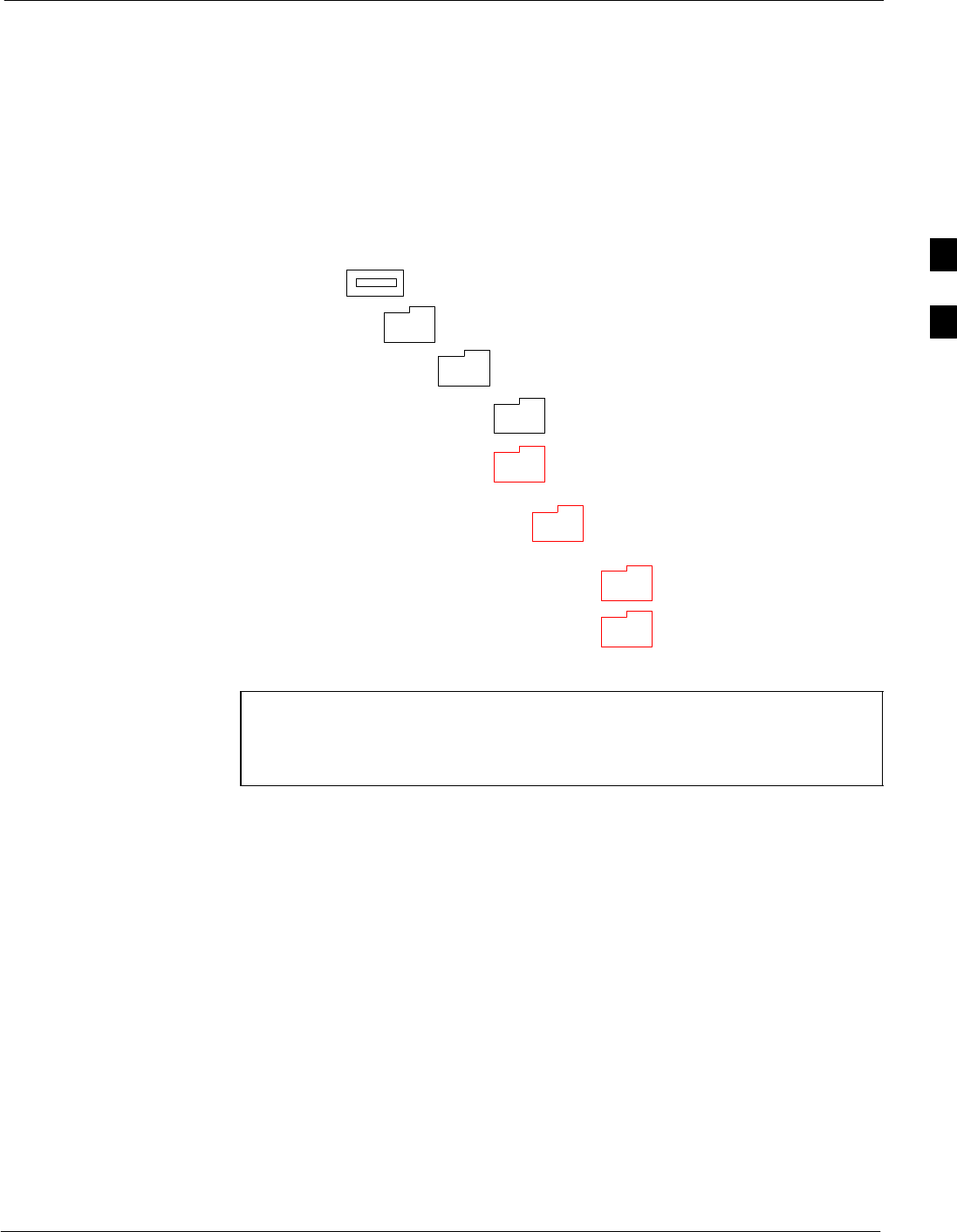
Preparing the LMF68P64115A18–1
Mar 2003 1X SC 4812T Lite BTS Optimization/ATP Software Release R2.16.1.x
DRAFT
3-7
LMF File Structure Overview
The LMF uses a <x>:\<lmf home directory> folder that contains all of
the essential data for installing and maintaining the BTS. The following
list outlines the folder structure for LMF. Except for the bts-nnn folders,
these folders are created as part of the LMF installation. Refer to the
CDMA LMF Operator’s Guide for a complete description of the folder
structure.
Figure 3-1: LMF Folder Structure
version folder (A separate folder is
required for each different version; for
example, a folder name 2.8.1.1.1.5.)
loads folder
(C:)
x:\<lmf home directory> folder
cdma folder
code folder
data folder
BTS–nnn folders (A separate folder is
required for each BTS where bts–nnn is the
unique BTS number; for example, bts–163.)
NOTE The “loads” folder and all the folders below it are not available
from the LMF for Software Release 2.16.1.x. These folders may
be present as as a legacy from previous software versions or
downloaded from the CBSC/OMC–R.
3

Preparing the LMF 68P64115A18–1
Mar 2003
1X SC 4812T Lite BTS Optimization/ATP Software Release R2.16.1.x
DRAFT
3-8
LMF Home Directory
The LMF installation program creates the default home directory,
c:\wlmf, and installs the application files and subdirectories (folders)
in it. Because this can be changed at installation, the CDMA LMF home
directory will be referred to with the generic convention of:
<x>:\<lmf home directory>
Where:
<x> = the LMF computer drive letter where the CDMA LMF home
directory is located.
<lmf home directory> = the directory path or name where the CDMA
LMF is installed.
3

Preparing the LMF68P64115A18–1
Mar 2003 1X SC 4812T Lite BTS Optimization/ATP Software Release R2.16.1.x
DRAFT
3-9
NECF Filename Conventions and Directory Location
NECF
The NECF actually consists of two files: the NECB and NECJ. The
naming convention for the NECB and NECJ is:
NECB*bts#.xml
NECJ*bts#.xml
Where:
* = any characters can be substituted there
# = the actual integer BTS number
The NECB and its corresponding NECJ must have the exact same name,
except for the “B” and “J” difference after the initial NEC characters.
The NECB and the NECJ must reside in the
<LMF_HOME>\cdma\bts–# directory corresponding to the BTS frame
they are for.
Load Information File (LIF)
The LIF contains all the devices binaries available for the specified
System Software Release. It is the functional equivalent of the OLF file
that was used pre–Packet.
The naming convention for the LIF is:
NE_LIF.xml
The LIF must reside in the <LMF_HOME>\cdma\loads\<Software
Release Number> directory, where <LMF_HOME> = the home
directory in which the LMF is installed, usually C:\wlmf <Software
Release Number> = the System Software Release Number (e.g.
2.16.1.0.10).
Cal File
The Cal File still resides in the <LMF_HOME>\cdma\bts–# directory
and is named bts–#.cal, where # is the actual integer number of the BTS.
3

Preparing the LMF 68P64115A18–1
Mar 2003
1X SC 4812T Lite BTS Optimization/ATP Software Release R2.16.1.x
DRAFT
3-10
LMF Installation and Update Procedures
This section provides information and instructions for installing and
updating the LMF software and files.
NOTE First Time Installation Sequence:
1. Install Java Runtime Environment (JRE)
2. Install U/WIN K–shell emulator
3. Install LMF application programs
4. Install/create BTS folders
NOTE Any time you install U/WIN, you must install the LMF software
because the installation of the LMF modifies some of the files
that are installed during the U/Win installation. Installing U/Win
over–writes these modifications.
There are multiple binary image packages for installation on the
CD–ROM. When prompted, choose the load that corresponds to
the switch release that you currently have installed. Perform the
Device Images install after the WinLMF installation.
If applicable, a separate CD ROM of BTS Binaries may be
available for binary updates.
Follow the procedure in Table 3-1 to install the LMF application
program using the LMF CD ROM.
Table 3-1: Install LMF using CD ROM
nStep Action
1Insert the LMF CD ROM disk into your disk drive and perform the
following as required:
1a – If the Setup screen appears, follow the instructions displayed on
the screen.
1b – If the Setup screen is not displayed, proceed to Step 2.
2Click on the Start button
3 Select Run.
4 Enter d:\autorun in the Open box and click OK.
NOTE
If applicable, replace the letter d with the correct CD ROM drive
letter.
3
Preparing the LMF68P64115A18–1
Mar 2003 1X SC 4812T Lite BTS Optimization/ATP Software Release R2.16.1.x
DRAFT
3-11
Copy BTS and CBSC CDF (or NECF) Files to the LMF Computer
Before logging on to a BTS with the LMF computer to execute
optimization/ATP procedures, the correct bts-#.cdf and cbsc-#.cdf (or
bts–#.necf and cbsc–#.necf) files must be obtained from the CBSC and
put in a bts-# folder in the LMF computer. This requires creating
versions of the CBSC CDF files on a DOS–formatted floppy diskette
and using the diskette to install the CDF files on the LMF computer.
NOTE – If the LMF has ftp capability, the ftp method can be used to
copy the CDF or NECF files from the CBSC.
– On Sun OS workstations, the unix2dos command can be
used in place of the cp command (e.g., unix2dos
bts–248.cdf bts–248.cdf). This should be done using a copy
of the CBSC CDF file so the original CBSC CDF file is
not changed to DOS format.
NOTE When copying CDF or NECF files, comply with the following
to prevent BTS login problems with the Windows LMF:
SThe numbers used in the bts-#.cdf and cbsc-#.cdf (or
bts–#.necf and cbsc–#.necf) filenames must correspond to
the locally-assigned numbers for each BTS and its controlling
CBSC.
SThe generic cbsc–1.cdf (or cbsc–#.necf) file supplied with
the Windows LMF will work with locally numbered BTS
CDF files. Using this file will not provide a valid
optimization unless the generic file is edited to replace
default parameters (e.g., channel numbers) with the
operational parameters used locally.
The procedure in Table 3-2 lists the steps required to transfer the CDF
files from the CBSC to the LMF computer. For further information, refer
to the LMF Help function on–line documentation.
Table 3-2: Copying CDF or NECF Files to the LMF Computer
nStep Action
AT THE CBSC:
1Login to the CBSC workstation.
2Insert a DOS–formatted floppy diskette in the workstation drive.
3 Type eject –q and press the Enter key.
4 Type mount and press the Enter key.
NOTE
SLook for the “floppy/no_name” message on the last line displayed.
SIf the eject command was previously entered, floppy/no_name will be appended with a number.
Use the explicit floppy/no_name reference displayed when performing step 7.
5Change to the directory, where the files to be copied reside, by typing cd <directoryname>
(e.g., cd bts–248) and pressing the Enter key.
. . . continued on next page
3

Preparing the LMF 68P64115A18–1
Mar 2003
1X SC 4812T Lite BTS Optimization/ATP Software Release R2.16.1.x
DRAFT
3-12
Table 3-2: Copying CDF or NECF Files to the LMF Computer
nActionStep
6 Type ls and press the Enter key to display the list of files in the directory.
7 With Solaris versions of Unix, create DOS–formatted versions of the bts-#.cdf and cbsc-#.cdf (or
bts–#.necf and cbsc–#.necf) files on the diskette by entering the following command:
unix2dos <source filename> /floppy/no_name/<target filename>
(e.g., unix2dos bts–248.cdf /floppy/no_name/bts–248.cdf).
NOTE
SOther versions of Unix do not support the unix2dos and dos2unix commands. In these cases, use
the Unix cp (copy) command. The copied files will be difficult to read with a DOS or Windows text
editor because Unix files do not contain line feed characters. Editing copied CDF files on the LMF
computer is, therefore, not recommended.
SUsing cp, multiple files can be copied in one operation by separating each filename to be copied
with a space and ensuring the destination directory (floppy/no_name) is listed at the end of the
command string following a space (e.g., cp bts–248.cdf cbsc–6.cdf /floppy/no_name).
8Repeat Steps 5 through 7 for each bts–# that must be supported by the LMF computer.
9When all required files have been copied to the diskette type eject and press the Enter key.
10 Remove the diskette from the CBSC drive.
AT THE LMF:
11 If it is not running, start the Windows operating system on the LMF computer.
12 Insert the diskette containing the bts-#.cdf and cbsc-#.cdf (or bts–#.necf and cbsc–#.necf) files into
the LMF computer.
13 Using MS Windows Explorer, create a corresponding bts–# folder in the <x>:\<lmf home
directory>\cdma directory for each bts–#.cdf/cbsc–#.cdf (or bts–#.necf/cbsc–#.cdf) file pair copied
from the CBSC.
14 Use MS Windows Explorer to transfer the bts-#.cdf and cbsc-#.cdf (or bts–#.necf and cbsc–#.necf)
files from the diskette to the corresponding <x>:\<lmf home directory>\cdma\bts–# folders created in
Step 13.
3

Preparing the LMF68P64115A18–1
Mar 2003 1X SC 4812T Lite BTS Optimization/ATP Software Release R2.16.1.x
DRAFT
3-13
Creating a Named HyperTerminal Connection for MMI Communication
Confirming or changing the configuration data of certain BTS Field
Replaceable Units (FRU) requires establishing an MMI communication
session between the LMF and the FRU. Using features of the Windows
operating system, the connection properties for an MMI session can be
saved on the LMF computer as a named Windows HyperTerminal
connection. This eliminates the need for setting up connection
parameters each time an MMI session is required to support
optimization.
Once the named connection is saved, a shortcut for it can be created on
the Windows desktop. Double–clicking the shortcut icon will start the
connection without the need to negotiate multiple menu levels.
Follow the procedures in Table 3-3 to establish a named HyperTerminal
connection and create a Windows desktop shortcut for it.
Table 3-3: Create HyperTerminal Connection
Step Action
1From the Windows Start menu, select:
Programs>Accessories>
2Perform one of the following:
SFor Win NT, select Hyperterminal and then click on HyperTerminal or
SFor Win 98, select Communications, double click the Hyperterminal folder, and then double click
on the Hyperterm.exe icon in the window that opens.
NOTE
SIf a Location Information Window appears, enter the required information, then click on the
Close button. (This is required the first time, even if a modem is not to be used.)
SIf a You need to install a modem..... message appears, click on NO.
3When the Connection Description box opens:
– Type a name for the connection being defined (e.g., MMI Session) in the Name: window,
– Highlight any icon preferred for the named connection in the Icon: chooser window, and
– Click OK.
4From the Connect using: pick list in the Connect To box displayed, select COM1 or COM2 (Win
NT) – or Direct to Com 1 or Direct to Com 2 (Win 98) for the RS–232 port connection and click OK.
NOTE
For LMF computer configurations where COM1 is used by another interface such as test equipment
and a physical port is available for COM2, select COM2 in the following step to prevent conflicts.
5In the Port Settings tab of the COM# Properties window displayed, configure the RS–232 port
settings as follows:
SBits per second: 9600
SData bits: 8
SParity: None
SStop bits: 1
SFlow control: None
. . . continued on next page
3

Preparing the LMF 68P64115A18–1
Mar 2003
1X SC 4812T Lite BTS Optimization/ATP Software Release R2.16.1.x
DRAFT
3-14
Table 3-3: Create HyperTerminal Connection
Step Action
6 Click OK.
7Save the defined connection by selecting:
File > Save
8Close the HyperTerminal window by selecting:
File > Exit
9Click the Yes button to disconnect when prompted.
10 Perform one of the following:
SIf the Hyperterminal folder window is still open (Win 98) proceed to step 12
SFrom the Windows Start menu, select Programs > Accessories.
11 Perform one of the following:
SFor Win NT, select Hyperterminal and release any pressed mouse buttons.
SFor Win 98, select Communications and double click the Hyperterminal folder.
12 Highlight the newly–created connection icon by clicking on it.
13 Right click and drag the highlighted connection icon to the Windows desktop and release the right
mouse button.
14 From the popup menu which appears, select Create Shortcut(s) Here.
15 If desired, reposition the shortcut icon for the new connection by dragging it to another location on the
Windows desktop.
16 Close the Hyperterminal folder window by selecting:
File > Close
3
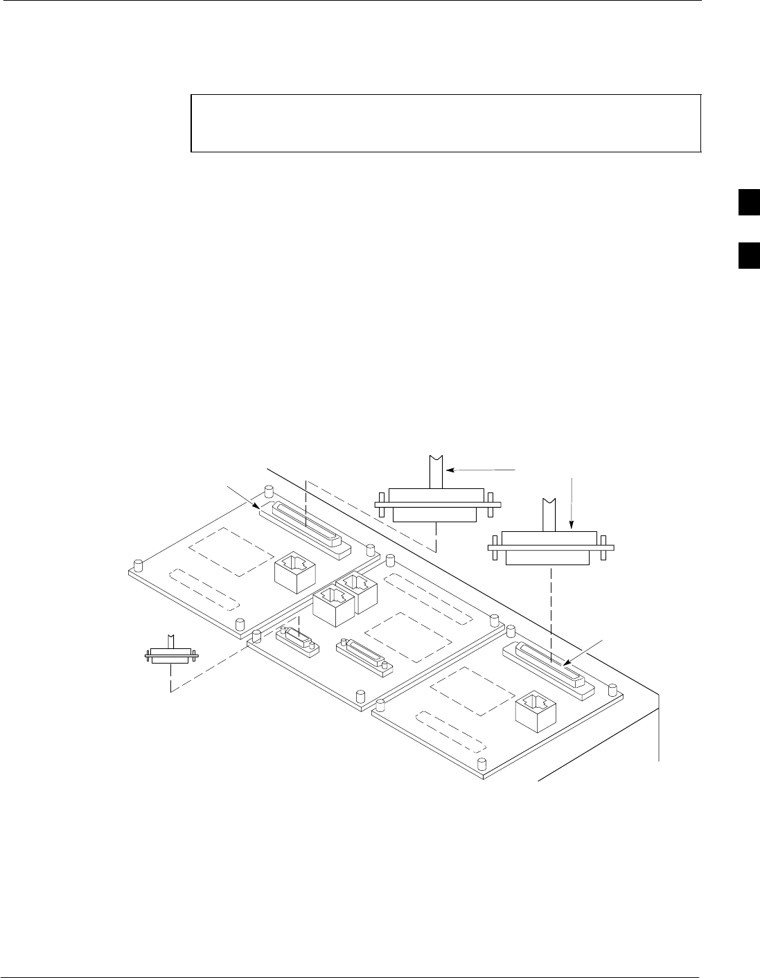
Span Lines – Interface and Isolation68P64115A18–1
Mar 2003 1X SC 4812T Lite BTS Optimization/ATP Software Release R2.16.1.x
DRAFT
3-15
Span Lines – Interface and Isolation
T1/E1 Span Interface
NOTE At active sites, the OMC–R/CBSC must disable the BTS and
place it out of service (OOS). DO NOT remove the span line
cable connectors until the OMC–R/CBSC has disabled the BTS.
Each frame is equipped with one 50–pair punchblock for spans,
customer alarms, remote GPS, and BTS frame alarms. See NO TAG and
refer to NO TAG for the physical location and punchdown location
information.
Before connecting the LMF computer to the frame LAN, the
OMC–R/CBSC must disable the BTS and place it OOS. This will allow
the LMF to control the BTS, and prevent the CBSC from inadvertently
sending control information to the BTS during LMF–based tests.
Isolate BTS from T1/E1 Span(s)
Once the OMC–R/CBSC has disabled the BTS, the span(s) must be
disabled to ensure the LMF will maintain control of the BTS. To disable
the spans, disconnect the BTS–to–CBSC Transcoder span cable
connectors from the Span I/O cards (Figure 3-2).
Figure 3-2: Span I/O Board T1 Span Isolation
50–PIN TELCO
CONNECTORS
REMOVED
SPAN B CONNECTOR
(TELCO) INTERFACE
TO SPAN LINES
(IF USED
SPAN A CONNECTOR
(TELCO) INTERFACE
TO SPAN LINES
TOP of Frame
(Site I/O and Span I/O boards)
RS–232 9–PIN SUB D
CONNECTOR SERIAL
PORT FOR EXTERNAL
DIAL UP MODEM
CONNECTION (IF USED)
FW00299 REF
3

Span Lines – Interface and Isolation 68P64115A18–1
Mar 2003
1X SC 4812T Lite BTS Optimization/ATP Software Release R2.16.1.x
DRAFT
3-16
T1/E1 Span Isolation
Table 3-4 describes the action required for span isolation.
Table 3-4: T1/E1 Span Isolation
Step Action
1Have the OMCR/CBSC place the BTS OOS.
2To disable the span lines, locate the connector for the span or
spans which must be disabled and remove the respective
connector from the applicable SCCP cage Span I/O board
(Figure 3-2).
3
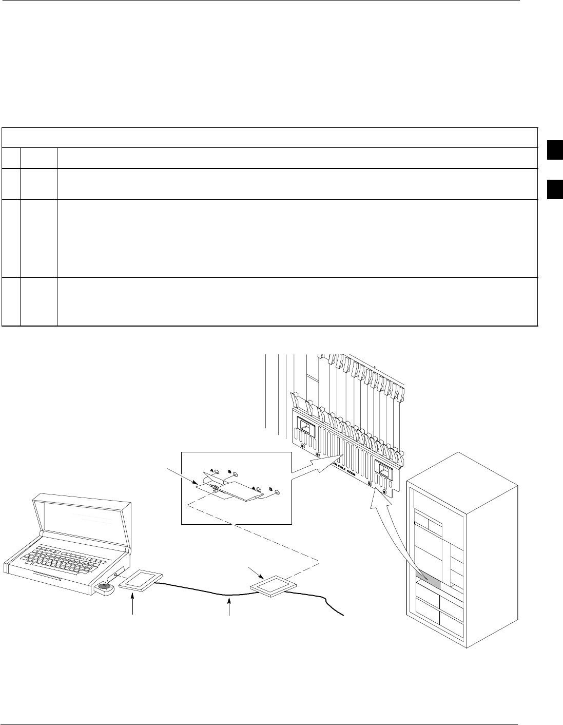
LMF to BTS Connection68P64115A18–1
Mar 2003 1X SC 4812T Lite BTS Optimization/ATP Software Release R2.16.1.x
DRAFT
3-17
LMF to BTS Connection
Connect the LMF to the BTS
The LMF computer may be connected to the LAN A or B connector
located behind the frame lower air intake grill. Figure 3-3 below shows
the general location of these connectors. LAN A is considered the
primary LAN.
Table 3-5: Connecting the LMF to the BTS
nStep Action
1To gain access to the LAN connectors, open the LAN cable access door, then pull apart the fabric
covering the BNC “T” connector and slide out the service tray, if desired (see Figure 3-3).
2Connect the LMF computer to the LAN A (left–hand) BNC connector via PCMCIA Ethernet Adapter.
NOTE
Xircom Model PE3–10B2 or equivalent can also be used to interface the LMF Ethernet connection to
the BTS frame connected to the PC parallel port, powered by an external AC/DC transformer. In this
case, the BNC cable must not exceed 91 cm (3 ft) in length.
* IMPORTANT
The LAN shield is isolated from chassis ground. The LAN shield (exposed portion of BNC connector)
must not touch the chassis during optimization.
Figure 3-3: LMF Connection Detail
10BaseT/10Base2
Converter Connects
Directly to BNC T
LMF BNC “T” Connections on
left side of frame (Ethernet
“A” shown; Ethernet “B”
covered with hook–and–loop
fabric)
LMF Computer
Terminal with Mouse
PCMCIA Ethernet
Adpater & Ethernet
UTP Adapter
Universal Twisted
Pair (UTP) cable
(RJ11 connectors)
115 VAC Power
Connection
NOTE:
Open LAN CABLE ACCESS door.
Pull apart hook–and–loop fabric
and gain access to the LAN A or
LAN B LMF BNC connector.
ti-CDMA-WP-00232-v01-ildoc-ftw
SC 4812T LITE
3

Using the LMF 68P64115A18–1
Mar 2003
1X SC 4812T Lite BTS Optimization/ATP Software Release R2.16.1.x
DRAFT
3-18
Using the LMF
Basic LMF Operation
LMF Coverage in This Publication – The LMF application program
supports maintenance of both CDMA and SAS BTSs. All references to
the LMF in this publication are to the CDMA portion of the program.
Operating Environments – The LMF application program allows the
user to work in the two following operating environments which are
accessed using the specified desktop icons:
SGraphical User Interface (GUI) using the WinLMF icon
SCommand Line Interface (CLI) using the WinLMF CDMA CLI icon
The GUI is the primary optimization and acceptance testing operating
environment. The CLI environment provides additional capability to the
user to perform manually controlled acceptance tests and audit the
results of optimization and calibration actions.
Basic Operation – Basic operation of the LMF in either environment
includes performing the following:
SSelecting and deselecting BTS devices
SEnabling devices
SDisabling devices
SResetting devices
SObtaining device status
The following additional basic operation can be performed in a GUI
environment:
SSorting a status report window
For detailed information on performing these and other LMF operations,
refer to the LMF Help function on–line documentation.
NOTE Unless otherwise noted, LMF procedures in this manual are
performed using the GUI environment.

Using the LMF68P64115A18–1
Mar 2003 1X SC 4812T Lite BTS Optimization/ATP Software Release R2.16.1.x
DRAFT
3-19
The LMF Display and the BTS
BTS Display – When the LMF is logged into a BTS, a frame tab is
displayed for each BTS frames. The frame tab will be labeled with
“CDMA” and the BTS number, a dash, and the frame number (for
example, BTS–812–1 for BTS 812, RFMF 1). If there is only one frame
for the BTS, there will only be one tab.
CDF/NECF Requirements – For the LMF to recognize the devices
installed in the BTS, a BTS CDF/NECF file which includes equipage
information for all the devices in the BTS must be located in the
applicable <x>:\<lmf home directory>\cdma\bts–# folder. To provide
the necessary channel assignment data for BTS operation, a CBSC CDF
file which includes channel data for all BTS RFMFs is also required in
the folder.
RFDS Display – If an RFDS is included in the CDF/NECF file, an
RFDS tab labeled with “RFDS,” a dash and the BTS number–frame
number combination (for example, RFDS–812–1) will be displayed.
Graphical User Interface Overview
The LMF uses a GUI, which works in the following way:
SSelect the device or devices.
SSelect the action to apply to the selected device(s).
SWhile action is in progress, a status report window displays the action
taking place and other status information.
SThe status report window indicates when the the action is complete
and displays other pertinent information.
SClicking the OK button closes the status report window.

Using the LMF 68P64115A18–1
Mar 2003
1X SC 4812T Lite BTS Optimization/ATP Software Release R2.16.1.x
DRAFT
3-20
Understanding GUI Operation
The following screen captures are provided to help understand how the
GUI operates:
– Figure 3-4 depicts the differences between packet and circuit
CDMA “cdf” file identification. Note that if there is a packet
version “bts” file, the “(P)” is added as a suffix. There is a
corresponding “(C)” for the circuit mode version.
– Figure 3-5 depicts the Self-Managed Network Elements (NEs) state
of a packet mode SC4812T. Note that an “X” is on the front of each
card that is under Self–Managed Network Elements (NEs) control
by the GLI3 card.
– Figure 3-6 depicts three of the available packet mode commands.
Normally the GLI3 has Self-Managed Network Elements (NEs)
control of all cards as shown in Figure 3-5 by an “(X)”. In that state
the LMF may only status a card. In order to download code or test a
card, the LMF must request Self-Managed Network Elements (NEs)
control of the card by using the shown dropdown menu. It also uses
this menu to release control of the card back to the GLI3. The GLI3
will also assume control of the cards after the LMF logs out of the
BTS. The packet mode GLI3 normally is loaded with a tape release
and NECB and NECJ files which point to a tape release stored on
the GLI3. When the GLI3 has control of a card it will maintain that
card with the code on that tape release.
– Figure 3-7 depicts a packet mode site that has the MCC–1 and the
BBX–1 cards under LMF control. Notice that the “X” is missing
from the front of these two cards.
For detailed information on performing these and other LMF operations,
refer to the LMF Help function on–line documentation.
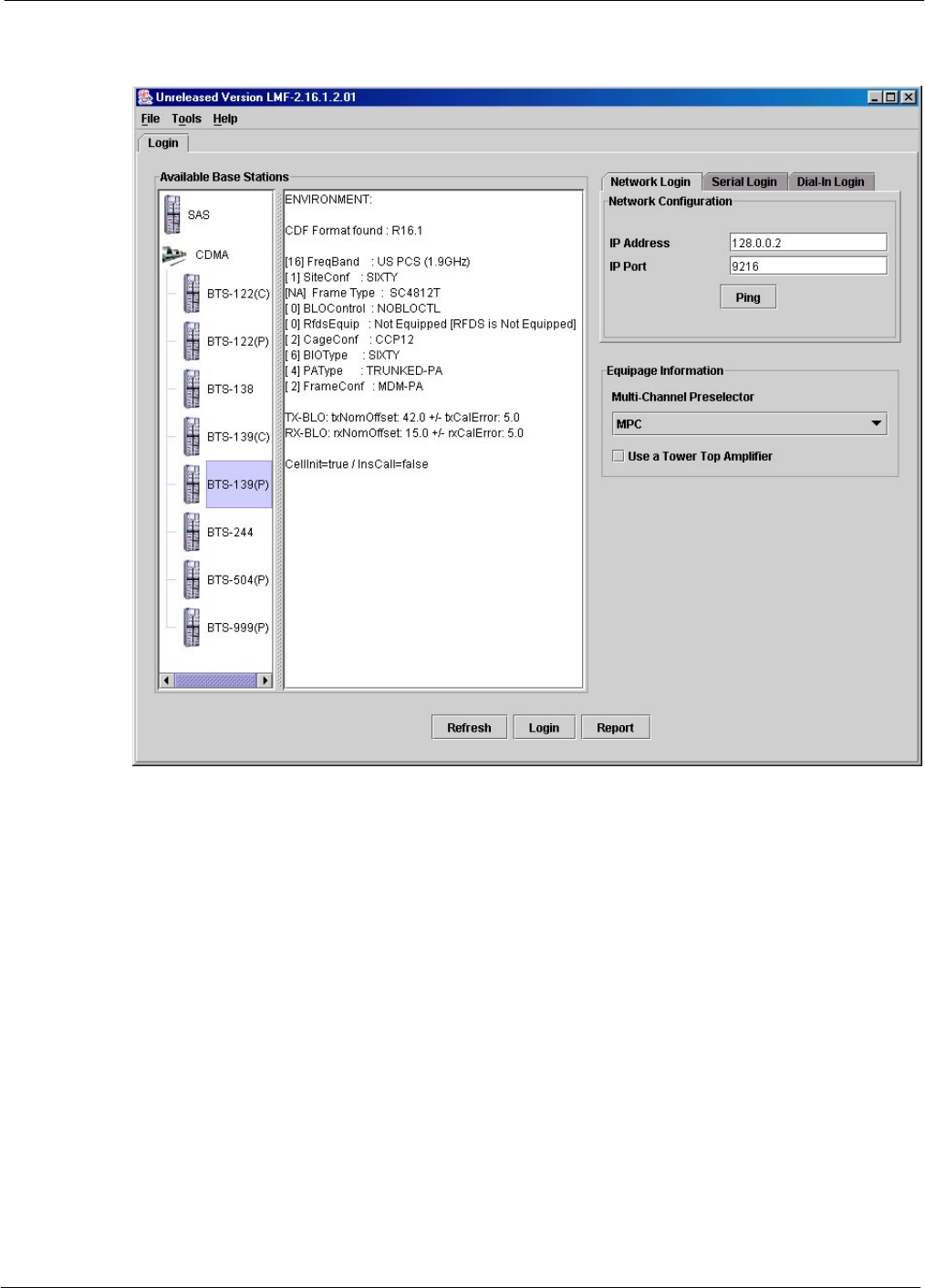
Using the LMF68P64115A18–1
Mar 2003 1X SC 4812T Lite BTS Optimization/ATP Software Release R2.16.1.x
DRAFT
3-21
Figure 3-4: BTS Login screen – identifying circuit and packet BTS files

Using the LMF 68P64115A18–1
Mar 2003
1X SC 4812T Lite BTS Optimization/ATP Software Release R2.16.1.x
DRAFT
3-22
Figure 3-5: Self–Managed Network Elements (NEs) state of a packet mode SC4812T
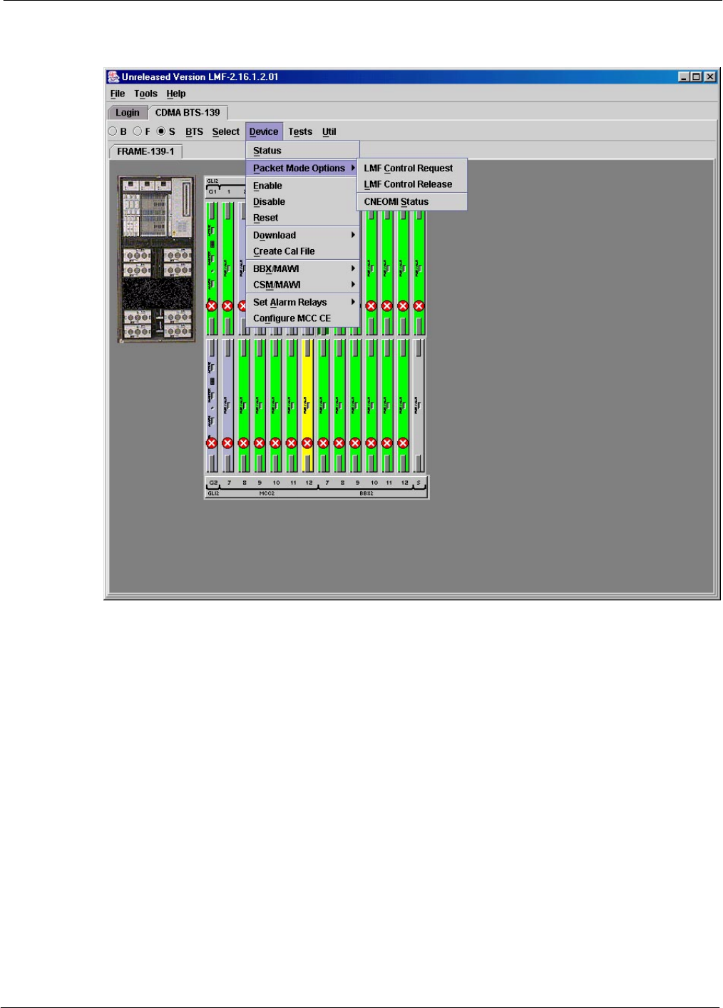
Using the LMF68P64115A18–1
Mar 2003 1X SC 4812T Lite BTS Optimization/ATP Software Release R2.16.1.x
DRAFT
3-23
Figure 3-6: Available packet mode commands
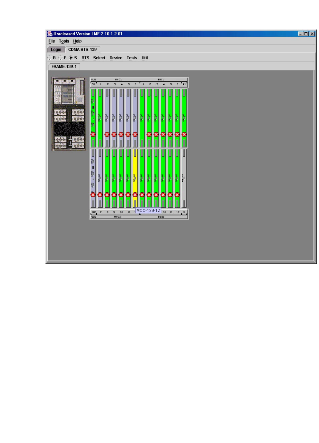
Using the LMF 68P64115A18–1
Mar 2003
1X SC 4812T Lite BTS Optimization/ATP Software Release R2.16.1.x
DRAFT
3-24
Figure 3-7: Packet mode site with MCC–1 and BBX–1 under LMF control

Using the LMF68P64115A18–1
Mar 2003 1X SC 4812T Lite BTS Optimization/ATP Software Release R2.16.1.x
DRAFT
3-25
Command Line Interface Overview
The LMF also provides Command Line Interface (CLI) capability.
Activate the CLI by clicking on a shortcut icon on the desktop. The CLI
can not be launched from the GUI, only from the desktop icon.
Both the GUI and the CLI use a program known as the handler. Only one
handler can be running at one time. The architectural design is such that
the GUI must be started before the CLI if you want the GUI and CLI to
use the same handler.
When the CLI is launched after the GUI, the CLI automatically finds and
uses an in–progress login session with a BTS initiated under the GUI.
This allows the use of the GUI and the CLI in the same BTS login
session.
If a CLI handler is already running when the GUI is launched (this
happens if the CLI window is already running when the user starts the
GUI, or if another copy of the GUI is already running when the user
starts the GUI), a dialog window displays the following warning
message:
The CLI handler is already running.
This may cause conflicts with the LMF.
Are you sure that you want to start the application?
This window also contains yes and no buttons. Selecting yes starts the
application. Selecting no terminates the application.
CLI Format Conventions
The CLI command can be broken down in the following way:
SVerb
SDevice including device identifier parameters
SSwitch
SOption parameters consisting of:
– Keywords
– Equals sign (=) between the keyword and the parameter value
– Parameter values
Spaces are required between the verb, device, switch, and option
parameters. A hyphen is required between the device and its identifiers.
Following is an example of a CLI command.
measure bbx–<bts_id>–<bbx_id> rssi channel=6 sector=5
Refer to the LMF CLI Commands for a complete explanation of the CLI
commands and their usage.

Using the LMF 68P64115A18–1
Mar 2003
1X SC 4812T Lite BTS Optimization/ATP Software Release R2.16.1.x
DRAFT
3-26
Logging Into a BTS
Logging into a BTS establishes a communication link between the BTS
and the LMF. An LMF session can be logged into only one BTS at a
time.
Prerequisites
Before attempting to log into a BTS, ensure the following have been
completed:
SThe LMF is correctly installed on the LMF computer.
SA bts-nnn folder with the correct CDF/NECF and CBSC files exists.
SThe LMF computer was connected to the BTS before starting the
Windows operating system and the LMF software. If necessary, restart
the computer after connecting it to the BTS in accordance with
Table 3-5 and Figure 3-3.
CAUTION Be sure that the correct bts–#.cdf/necf and cbsc–#.cdf file are
used for the BTS. These should be the CDF/NECF files that are
provided for the BTS by the CBSC. Failure to use the correct
CDF/NECF files can result in invalid optimization. Failure to
use the correct CDF/NECF files to log into a live
(traffic–carrying) site can shut down the site.
BTS Login from the GUI Environment
Follow the procedures in Table 3-6 to log into a BTS when using the
GUI environment.
Table 3-6: BTS GUI Login Procedure
nStep Action
1Start the LMF GUI environment by double–clicking on the WinLMF desktop icon (if the LMF is
not running).
– An LMF window will open and display the LMF build number in the title bar.
NOTE
If a warning similar to the following is displayed, select No, shut down other LMF sessions which
may be running, and start the LMF GUI environment again:
The CLI handler is already running.
This may cause conflicts with the LMF.
Are you sure you want to start the application?
Yes No
2Click on Login tab (if not displayed).
3Double click on CDMA (in the Available Base Stations pick list).
4Click on the desired BTS number.
5Click on the Network Login tab (if not already in the forefront).
6Enter correct IP address (normally 128.0.0.2) for a field BTS, if not correctly displayed in the IP
Address box.
. . . continued on next page

Using the LMF68P64115A18–1
Mar 2003 1X SC 4812T Lite BTS Optimization/ATP Software Release R2.16.1.x
DRAFT
3-27
Table 3-6: BTS GUI Login Procedure
nActionStep
7Type in the correct IP Port number (normally 9216) if not correctly displayed in the IP Port box.
8Click on Ping.
– If the connection is successful, the Ping Display window shows text similar to the following:
Reply from 128 128.0.0.2: bytes=32 time=3ms TTL=255
– If there is no response the following is displayed:
128.0.0.2:9216:Timed out
If the MGLI fails to respond, reset and perform the ping process again. If the MGLI still fails to
respond, typical problems are shorted BNC to inter–frame cabling, open cables, crossed A and B
link cables, missing 50–Ohm terminators, or the MGLI itself.
9Select the Multi-channel Preselector type from the Multi-channel Preselector drop–down list
(default is MPC) to a device corresponding to your BTS configuration, if required.
NOTE
“Use a Tower Top Amplifier” is not applicable to the SC4812T Lite.
10 Click on Login. (A BTS tab with the BTS and frame numbers is displayed.)
NOTE
SIf an attempt is made to log into a BTS that is already logged on, all devices will be gray.
SThere may be instances where the BTS initiates a log out due to a system error (i.e., a device
failure).
SIf the MGLI is OOS–ROM (blue), it must be downloaded with RAM code before other devices
can be seen.
SIf the MGLI is OOS–RAM (yellow), it must be enabled before other installed devices can be
seen.

Using the LMF 68P64115A18–1
Mar 2003
1X SC 4812T Lite BTS Optimization/ATP Software Release R2.16.1.x
DRAFT
3-28
BTS Login from the CLI Environment
Follow the procedures in Table 3-7 to log into a BTS when using the
CLI environment.
NOTE If the CLI and GUI environments are to be used at the same
time, the GUI must be started first and BTS login must be
performed from the GUI. Refer to Table 3-6 to start the GUI
environment and log into a BTS.
Table 3-7: BTS CLI Login Procedure
nStep Action
1Double–click the WinLMF CLI desktop icon (if the LMF CLI
environment is not already running).
NOTE
If a BTS was logged into under a GUI session before the CLI
environment was started, the CLI session will be logged into the same
BTS, and step 2 is not required.
2At the /wlmf prompt, enter the following command:
login bts–<bts#> host=<host> port=<port>
where:
host = MGLI card IP address (defaults to address last logged into for
this BTS or 128.0.0.2 if this is first login to this BTS)
port = IP port of the BTS (defaults to port last logged into for this
BTS or 9216 if this is first login to this BTS)
A response similar to the following will be displayed:
LMF>
13:08:18.882 Command Received and Accepted
COMMAND=login bts–33
13:08:18.882 Command In Progress
13:08:21.275 Command Successfully Completed
REASON_CODE=”No Reason”

Using the LMF68P64115A18–1
Mar 2003 1X SC 4812T Lite BTS Optimization/ATP Software Release R2.16.1.x
DRAFT
3-29
Logging Out
Logging out of a BTS is accomplished differently for the GUI and CLI
operating environments.
NOTE The GUI and CLI environments use the same connection to a
BTS. If a GUI and the CLI session are running for the same BTS
at the same time, logging out of the BTS in either environment
will log out of it for both. When either a login or logout is
performed in the CLI window, there is no GUI indication that the
login or logout has occurred.
Logging Out of a BTS from the GUI Environment
Follow the procedure in Table 3-8 to logout of a BTS when using the
GUI environment.
Table 3-8: BTS GUI Logout Procedure
nStep Action
1Click on BTS in the BTS menu bar.
2Click the Logout item in the pull–down menu (a Confirm Logout
pop-up message will appear).
3Click on Yes (or press the Enter key) to confirm logout. The Login
tab will appear.
NOTE
If a logout was previously performed on the BTS from a CLI window
running at the same time as the GUI, a Logout Error pop–up
message will appear stating the system could not log out of the BTS.
When this occurs, the GUI must be exited and restarted before it can
be used for further operations.
4If a Logout Error pop–up message appears stating that the system
could not log out of the Base Station because the given BTS is not
logged in, click OK and proceed to Step 5.
5 Select File > Exit in the window menu bar, click Yes in the Confirm
Logout pop–up, and click OK in the Logout Error pop–up which
appears again.
6If further work is to be done in the GUI, restart it.
NOTE
SThe Logout item on the BTS menu bar will only log you out of the
displayed BTS.
SYou can also log out of all BTS sessions and exit LMF by clicking
on the File selection in the menu bar and selecting Exit from the
File menu list. A Confirm Logout pop–up message will appear.

Using the LMF 68P64115A18–1
Mar 2003
1X SC 4812T Lite BTS Optimization/ATP Software Release R2.16.1.x
DRAFT
3-30
Logging Out of a BTS from the CLI Environment
Follow the procedure in Table 3-9 to logout of a BTS when using the
CLI environment.
Table 3-9: BTS CLI Logout Procedure
nStep Action
NOTE
If the BTS is also logged into from a GUI running at the same time
and further work must be done with it in the GUI, proceed to Step 2.
1Log out of a BTS by entering the following command:
logout bts–<bts#>
A response similar to the following will be displayed:
LMF>
13:24:51.028 Command Received and Accepted
COMMAND=logout bts–33
13:24:51.028 Command In Progress
13:24:52.04 Command Successfully Completed
REASON_CODE=”No Reason”
2If desired, close the CLI interface by entering the following
command:
exit
A response similar to the following will be displayed before the
window closes:
Killing background processes....

Using the LMF68P64115A18–1
Mar 2003 1X SC 4812T Lite BTS Optimization/ATP Software Release R2.16.1.x
DRAFT
3-31
Establishing an MMI Communication Session
Equipment Connection – Figure 3-8 illustrates common equipment
connections for the LMF computer. For specific connection locations on
FRUs, refer to the illustration accompanying the procedures which
require the MMI communication session.
Initiate MMI Communication – For those procedures which require
MMI communication between the LMF and BTS FRUs, follow the
procedures in Table 3-10 to initiate the communication session.
Table 3-10: Establishing MMI Communication
Step Action
1Connect the LMF computer to the equipment as detailed in the applicable procedure which requires
the MMI communication session.
2If the LMF computer has only one serial port (COM1) and the LMF is running, disconnect the LMF
from COM1 by performing the following:
2a – Click on Tools in the LMF window menu bar, and select Options from the pull–down menu list.
–– An LMF Options dialog box will appear.
2b – In the LMF Options dialog box, click the Disconnect Port button on the Serial Connection tab.
3Start the named HyperTerminal connection for MMI sessions by double clicking on its Windows
desktop shortcut.
NOTE
If a Windows desktop shortcut was not created for the MMI connection, access the connection from the
Windows Start menu by selecting:
Programs > Accessories > Hyperterminal > HyperTerminal > <Named HyperTerminal
Connection (e.g., MMI Session)>
4Once the connection window opens, establish MMI communication with the BTS FRU by pressing
the LMF computer <Enter>key until the prompt identified in the applicable procedure is obtained.
Using the LMF 68P64115A18–1
Mar 2003
1X SC 4812T Lite BTS Optimization/ATP Software Release R2.16.1.x
DRAFT
3-32
Figure 3-8: LMF Computer Common MMI Connections
NULL MODEM
BOARD
(TRN9666A)
8–PIN TO 10–PIN
RS–232 CABLE
(P/N 30–09786R01)
RS–232 CABLE
8–PIN
LMF
COMPUTER
To FRU MMI port
DB9–TO–DB25
ADAPTER
COM1
OR
COM2
FW00687
Online Help
Task oriented online help is available in the LMF by clicking on Help in
the window menu bar, and selecting LMF Help from the pull–down
menu.
Pinging the Processors68P64115A18–1
Mar 2003 1X SC 4812T Lite BTS Optimization/ATP Software Release R2.16.1.x
DRAFT
3-33
Pinging the Processors
Pinging the BTS
For proper operation, the integrity of the Ethernet LAN A and B links
must be verified. Figure 3-9 represents a typical BTS Ethernet
configuration for an SC4812T Lite stand–alone or companion frame.
The drawing depicts cabling and termination for both the A and B
LANs.
Ping is a program that sends request data packets to hosts on a network,
in this case GLI modules on the BTS LAN, to obtain a response from the
“target” host specified by an IP address.
Follow the steps in Table 3-11 to ping each processor (on both LAN A
and LAN B) and verify LAN redundancy is working properly.
CAUTION Always wear an approved anti–static wrist strap while handling
any circuit card/module to prevent damage by Electro–Static
Discharge (ESD).
Figure 3-9: BTS Ethernet LAN Termination Diagram
SIGNAL
GROUND
SIGNAL
GROUND
50Ω
IN
SIGNAL
GROUND
50Ω
50Ω
SIGNAL
GROUND
50Ω
SIGNAL
GROUND
FRAME GROUND
TRIAX
TERMINATOR
TRIAX
TERMINATOR
TRIAX
TERMINATOR
IN
OUT
OUT
SC4812TL0013–5
TRIAX
TERMINATOR
SC4812T- Lite I/O
Interconnect Panel

Pinging the Processors 68P64115A18–1
Mar 2003
1X SC 4812T Lite BTS Optimization/ATP Software Release R2.16.1.x
DRAFT
3-34
NOTE The Ethernet LAN A and B cables and/or terminations must be
installed on each frame/enclosure external LAN connector before
performing this test. All other processor board LAN connections
are made through the backplanes.
Table 3-11: Pinging the Processors
Step Action
1If this is a first–time communication with a newly–installed frame or a GLI card which has been
replaced, perform the procedure in Table 6-3 and then return to step 2.
2Be sure any uncabled LAN A and B IN and OUT connectors in the power entry compartment (rear of
frame – NO TAG and Figure 3-9) are terminated with 50 Ω loads.
3If it has not already been done, connect the LMF computer to the BTS (refer to Table 3-5 and
Figure 3-3.)
4If it has not already been done, start a GUI LMF session and log into the BTS ( refer to Table 3-6).
5In the power entry compartment, remove the 50Ω termination on the frame LAN B IN connector.
– The LMF session should remain active.
6Replace the 50Ω terminator on the BTS frame LAN B IN connector.
7From the Windows desktop, click the Start button and select Run.
8In the Open box, type ping and the MGLI IP address (for example, ping 128.0.0.2).
NOTE
128.0.0.2 is the default IP address for the GLI card in slot GLI–1 in field BTS units.
9Click on OK.
10 If the targeted module responds, a DOS window will appear with a display similar to the following:
Reply from 128.0.0.2: bytes=32 time=3ms TTL=255
– If the device responds, proceed to step 18.
If there is no response, the following is displayed:
Request timed out
– If the GLI fails to respond, it should be reset and re–pinged. If it still fails to respond, typical
problems would be: failure of the LMF to login, shorted BNC–to–inter-frame cabling, open
cables, crossed A and B link cables, or the GLI itself.
11 Logout of the BTS as described in Table 3-8, exit from the LMF program, and restart the Windows
operating system on the LMF computer.
12 Restart the LMF GUI program as described in LMF Help function on–line documentation, and log into
the BTS as described in Table 3-6.
13 Perform steps 7 through 10 again.
– If the device responds, proceed to step 18.
If there is still no response, proceed to step 14.
14 If ping was unsuccessful after restarting the LMF computer, press the MGLI front panel reset
pushbutton and perform steps 7 through 10 again.
NOTE
Refer to Table 6-1 if ping was unsuccessful after resetting the MGLI.
. . . continued on next page

Pinging the Processors68P64115A18–1
Mar 2003 1X SC 4812T Lite BTS Optimization/ATP Software Release R2.16.1.x
DRAFT
3-35
Table 3-11: Pinging the Processors
Step Action
15 After the BTS has been successfully pinged, be sure the 50Ω termination was replaced on the BTS
frame LAN B IN connector in the power entry compartment (Figure 3-9). Disconnect the LMF cable
from the LAN shelf LAN A connector, and connect it to LAN B (right–hand connector) (refer to
Figure 3-3).
16 In the power entry compartment, remove the 50Ω termination on the BTS frame LAN A IN connector.
17 Repeat steps 5 through 9 using LAN B.
18 After the BTS has been successfully pinged on the secondary LAN, replace the 50Ω termination on
the frame LAN A IN connector in the power entry compartment.
19 Disconnect the LMF cable from the LAN shelf LAN B and connect it to LAN A.
20 Remove and replace the 50Ω termination on the LAN B IN connector to force the MGLI to switch to
primary LAN A.
21 Repeat steps 5 through 9 to ensure proper primary LAN operation.

Download the BTS 68P64115A18–1
Mar 2003
1X SC 4812T Lite BTS Optimization/ATP Software Release R2.16.1.x
DRAFT
3-36
Download the BTS
Overview
Before a BTS can operate, each equipped device must contain device
initialization (ROM) code. ROM code is loaded in all devices during
manufacture, factory repair, or, for software upgrades, from the CBSC
using the DownLoad Manager (DLM). Device application (RAM) code
and data must be downloaded to each equipped device by the user before
the BTS can be made fully functional for the site where it is installed.
ROM Code
Downloading ROM code to BTS devices from the LMF is NOT routine
maintenance or a normal part of the optimization process. It is only
done in unusual situations where the resident ROM code release level in
the device is not compatible with the required release level of the site
operating software and the CBSC can not communicate with the BTS to
perform the download.
If you must download ROM code, the procedures are located in
Appendix G.
Before ROM code can be downloaded from the LMF, the correct ROM
code file for each device to be loaded must exist on the LMF computer.
ROM code must be manually selected for download.
NOTE The ROM code file is not available for GLI3s. GLI3s are ROM
code loaded at the factory.
ROM code can be downloaded to a device that is in any state. After the
download is started, the device being downloaded will change to
OOS_ROM (blue). The device will remain OOS_ROM (blue) when the
download is completed. A compatible revision–level RAM code must
then be downloaded to the device. Compatible code loads for ROM and
RAM must be used for the device type to ensure proper performance.
The compatible device code release levels for the BSS software release
being used are listed in the Version Matrix section of the SCt CDMA
Release Notes (supplied on the tape or CD–ROM containing the BSS
software).
RAM Code
Before RAM code can be downloaded from the LMF, the correct RAM
code file for each device must exist on the LMF computer. RAM code
can be automatically or manually selected depending on the Device
menu item chosen and where the RAM code file for the device is stored
in the LMF file structure. The RAM code file will be selected
automatically if the file is in the <x>:\<lmf home
directory>\cdma\loads\n.n.n.n\code folder (where n.n.n.n is the
download code version number that matches the “NextLoad” parameter
of the CDF file). The RAM code file in the code folder must have the
correct hardware bin number for the device to be loaded.
RAM code can be downloaded to a device that is in any state. After the
download is started, the device being loaded will change to OOS_ROM
(blue). When the download is completed successfully, the device will
change to OOS_RAM (yellow).
Download the BTS68P64115A18–1
Mar 2003 1X SC 4812T Lite BTS Optimization/ATP Software Release R2.16.1.x
DRAFT
3-37
When code is downloaded to an MGLI or GLI, the LMF automatically
also downloads data and then enables the MGLI. When enabled, the
MGLI will change to INS_ACT (bright green). A redundant GLI will
not be automatically enabled and will remain OOS_RAM (yellow).
When the redundant GLI is manually commanded to enable through the
LMF, it will change state to INS_SBY (olive green).
For non–GLI devices, data must be downloaded after RAM code is
downloaded. To download data, the device state must be OOS_RAM
(yellow).
The devices to be loaded with RAM code and data are:
SMaster Group Line Interface (MGLI2 or MGLI3)
SRedundant GLI (GLI2 or GLI3)
SClock Synchronization Module (CSM) (Only if new revision code
must be loaded)
SMulti Channel CDMA (MCC24E, MCC8E, or MCC–1X) cards
SBroadband Transceiver (BBX2 or BBX–1X) cards
SRFDS Test Subscriber Interface Card (TSIC) or RFDS–1X RFDS
PROCessor (RPROC) card, if RFDS is installed
NOTE The MGLI must be successfully downloaded with RAM code
and data, and in INS_ACT (bright green) status before
downloading any other device. The RAM code download
process for an MGLI automatically downloads data and then
enables the MGLI.

Download the BTS 68P64115A18–1
Mar 2003
1X SC 4812T Lite BTS Optimization/ATP Software Release R2.16.1.x
DRAFT
3-38
Verify GLI ROM Code Loads
Devices should not be loaded with a RAM code version which is not
compatible with the ROM code with which they are loaded. Before
downloading RAM code and data to the processor cards, follow the
procedure in Table 3-12 to verify the GLI devices are loaded with the
correct ROM code for the software release used by the BSS.
Prerequisite
Identify the correct GLI ROM code load for the software release being
used on the BSS by referring to the Version Matrix section of the SCt
CDMA Release Notes (supplied on the tapes or CD–ROMs containing
the BSS software).
Table 3-12: Verify GLI ROM Code Loads
Step Action
1If it has not already been done, start a GUI LMF session and log into the
BTS ( refer to Table 3-6).
2Select all GLI devices by clicking on them, and select Device > Status
from the BTS menu bar.
3In the status report window which opens, note the number in the ROM
Ver column for each GLI2.
4If the ROM code loaded in the GLIs is not the correct one for the software
release being used on the BSS, perform the following:
4a – Log out of the BTS as described in Table 3-8 or Table 3-9, as
applicable.
4b – Disconnect the LMF computer.
4c – Reconnect the span lines as described in Table 5-7.
4d – Have the CBSC download the correct ROM code version to the BTS
devices.
5When the GLIs have the correct ROM load for the software release being
used, be sure the span lines are disabled as outlined in Table 3-4 and
proceed to downloading RAM code and data.

Download the BTS68P64115A18–1
Mar 2003 1X SC 4812T Lite BTS Optimization/ATP Software Release R2.16.1.x
DRAFT
3-39
Download RAM Code and Data to MGLI and GLI
Follow the steps outlined in Table 3-13 to download the RAM code and
data to the MGLI and other installed GLI devices.
Prerequisites
SPrior to performing these procedures, ensure a code file exists for each
of the devices to be loaded.
SThe LMF computer is connected to the BTS (refer to Table 3-5), and
is logged in using the GUI environment (refer to Table 3-6).
Table 3-13: Download and Enable MGLI and GLI Devices
nStep Action
1Be sure the LMF will use the correct software release for code and
data downloads by performing the following steps:
1a – Click on Tools in the LMF menu bar, and select Update
NextLoad > CDMA from the pull–down menus.
1b – Click on the BTS to be loaded.
–– The BTS will be highlighted.
1c – Click the button next to the correct code version for the software
release being used.
–– A black dot will appear in the button circle.
1d – Click Save.
1e – Click OK to close each of the advisory boxes which appear.
2Prepare to download code to the MGLI by clicking on the device.
3 Click Device in the BTS menu bar, and select Download >
Code/Data in the pull–down menus.
– A status report is displayed confirming change in the device(s)
status.
4 Click OK to close the status window.
– The MGLI will automatically be downloaded with data and
enabled.
5Once the MGLI is enabled, load and enable additional installed GLIs
by clicking on the devices and repeating Steps 3 and 4.
6 Click OK to close the status window for the additional GLI devices.

Download the BTS 68P64115A18–1
Mar 2003
1X SC 4812T Lite BTS Optimization/ATP Software Release R2.16.1.x
DRAFT
3-40
Download RAM Code and Data to Non–GLI Devices
Downloads to non–GLI devices can be performed individually for each
device or all installed devices can be downloaded with one action.
NOTE – CSM devices are RAM code–loaded at the factory. RAM
code is downloaded to CSMs only if a newer software
version needs to be loaded.
– When downloading to multiple devices, the download may
fail for some of the devices (a time–out occurs). These
devices can be loaded individually after completing the
multiple download.
Follow the steps in Table 3-14 to download RAM code and data to
non–GLI devices.
Table 3-14: Download RAM Code and Data to Non–GLI Devices
nStep Action
1Select the target CSM, MCC, and/or BBX device(s) by clicking on
them.
2 Click Device in the BTS menu bar, and select Download >
Code/Data in the pull–down menus.
– A status report is displayed that shows the results of the
download for each selected device.
3 Click OK to close the status report window when downloading is
completed.
NOTE
After a BBX, CSM, or MCC device is successfully loaded with RAM
code and data have changed to the OOS_RAM state (yellow), the
status LED should be rapidly flashing GREEN.
NOTE
The command in Step 2 loads both code and data. Data can be
downloaded without doing a code download anytime a device is
OOS–RAM using the command in Step 4.
4To download just the firmware application data to each device, select
the target device and select: Device>Download>Data
BBX Cards Remain OOS_ROM
If BBX cards remain OOS_ROM (blue) after power–up or following
code load, refer to Table 6-7, Steps 9 and 10.

Download the BTS68P64115A18–1
Mar 2003 1X SC 4812T Lite BTS Optimization/ATP Software Release R2.16.1.x
DRAFT
3-41
Selecting CSM Clock Source and Enabling CSMs
CSMs must be enabled prior to enabling the MCCs. Procedures in the
following two sub-sections cover the actions to accomplish this. For
additional information on the CSM sub–system, see “Clock
Synchronization Manager (CSM) Sub–system Description” in the CSM
System Time – GPS & LFR/HSO Verification section of this chapter.
Select CSM Clock Source
A CSM can have three different clock sources. The Select CSM Source
function can be used to select the clock source for each of the three
inputs. This function is only used if the clock source for a CSM needs to
be changed. The Clock Source function provides the following clock
source options.
SLocal GPS
SMate GPS
SRemote GPS
SHSO (only for source 2 & 3)
SHSO Extender
SLFR (only for source 2 & 3)
S10 MHz (only for source 2 & 3)
SNONE (only for source 2 & 3)
Prerequisites
SMGLI is INS_ACT (bright green)
SCSM is OOS_RAM (yellow) or INS_ACT (bright green)
Follow the procedure in Table 3-15 to select a CSM Clock Source.
Table 3-15: Select CSM Clock Source
nStep Action
1Select the applicable CSM(s) for which the clock source is to be
selected.
2Click on Device in the BTS menu bar, and select CSM/MAWI >
Select Clock Source... in the pull–down menu list.
– A CSM clock reference source selection window will appear.
3Select the applicable clock source in the Clock Reference Source
pick lists. Uncheck the related check boxes for Clock Reference
Sources 2 and 3 if you do not want the displayed pick list item to be
used.
4Click on the OK button.
– A status report is displayed showing the results of the operation.
5Click on the OK button to close the status report window.
NOTE For RF–GPS, verify the CSM configured with the GPS receiver
“daughter board” is installed in the frame’s CSM 1 slot before
continuing.

Download the BTS 68P64115A18–1
Mar 2003
1X SC 4812T Lite BTS Optimization/ATP Software Release R2.16.1.x
DRAFT
3-42
Enable CSMs
Follow the steps outlined in Table 3-16 to enable the CSMs installed in
the SCCP shelves.
Table 3-16: Enable CSMs
nStep Action
1NOTE
If equipped with two CSMs, enable card in slot CSM 2 first.
Click on the target CSM.
2Click on Device in the BTS menu bar, and select Enable in the pull–down menu list.
– A status report is displayed showing the results of the enable operation.
– Click OK to close the status report window.
NOTE
– The board in slot CSM 1 interfaces with the GPS receiver. The enable sequence for this board can
take up to one hour (see below).
– FAIL may be shown in the status report table for a slot CSM 1 enable action. If Waiting For Phase
Lock is shown in the Description field, do not cancel the enable process. The CSM will change to
the Enabled state after phase lock is achieved.
* IMPORTANT
– The GPS satellite system satellites are not in a geosynchronous orbit and are maintained and
operated by the United States Department of Defense (DOD). The DOD periodically alters
satellite orbits; therefore, satellite trajectories are subject to change. A GPS receiver that is INS
contains an “almanac” that is updated periodically to take these changes into account.
– If a GPS receiver has not been updated for a number of weeks, it may take up to an hour for the
GPS receiver “almanac” to be updated.
– Once updated, the GPS receiver must track at least four satellites and obtain (hold) a 3–D position
fix for a minimum of 45 seconds before the CSM will come in service. (In some cases, the GPS
receiver needs to track only one satellite, depending on accuracy mode set during the data load).
NOTE
– If two CSMs are installed and the board in slot CSM 1 has enabled, the LMF CSM cage view
should show slot CSM 1 as bright green (INS–ACT) and slot CSM 2 as dark green (INS–SBY)
– After CSMs have been successfully enabled, be sure the PWR/ALM LEDs are steady green
(alternating green/red indicates the card is in an alarm state).
3If more than an hour has passed without the board in slot CSM 1 enabling, refer to the CSM System
Time – GPS & LFR/HSO Verification section of this chapter (see Table 3-18, Figure 3-10, and
Table 3-19) to determine the cause.

Download the BTS68P64115A18–1
Mar 2003 1X SC 4812T Lite BTS Optimization/ATP Software Release R2.16.1.x
DRAFT
3-43
Enable MCCs
This procedure configures the MCC and sets the “tx fine adjust”
parameter. The “tx fine adjust” parameter is not a transmit gain setting,
but a timing adjustment that compensates for the processing delay in the
BTS (approximately 3 mS).
Follow the steps outlined in Table 3-17 to enable the MCCs installed in
the SCCP shelves.
NOTE The MGLI and primary CSM must be downloaded and enabled
(IN–SERVICE ACTIVE), prior to downloading and enabling an
MCC.
Table 3-17: Enable MCCs
nStep Action
1If the GLI/MCC/BBX view is not displayed in the LMF window, click
on the GLI/MCC/BBX area of the SCCP shelf.
2Click on the target MCC(s), or click on Select in the BTS menu bar,
and select MCCs in the pull–down menu list.
3Click on Device in the BTS menu bar, and select Enable in the
pull–down menu list.
– A status report is displayed showing the results of the enable
operation.
4 Click OK to close the status report window.

CSM System Time – GPS & LFR/HSO Verification 68P64115A18–1
Mar 2003
1X SC 4812T Lite BTS Optimization/ATP Software Release R2.16.1.x
DRAFT
3-44
CSM System Time – GPS & LFR/HSO Verification
Clock Synchronization Manager (CSM) Sub–system Description
Overview – Each BTS CSM sub–system features two CSM boards per
RFMF. The primary function of the CSM cards is to maintain CDMA
system time. GPS is used as the primary timing reference and
synchronizes the entire cellular system. In typical operation, the primary
CSM locks its Digital Phase Locked Loop (DPLL) circuits to GPS
signals. These signals are provided by either an on–board GPS receiver
module (RF–GPS) or a remote GPS receiver (RGPS). RGPS uses a GPS
receiver in the antenna head that has a digital output. The second
generation CSM card (CSM–II) is required when using the RGPS. A
CSM–II card can also be equipped with a local GPS receiver daughter
card to support an RF–GPS signal.
SCCP Shelf CSM Card Slot Assignments – The GPS receiver is
interfaced to the board in SCCP shelf slot CSM 1. This card is the
primary timing source, while the card in slot CSM 2 provides
redundancy. The redundant card, does not have a GPS receiver.
CSM–II Card Type Description – Each CSM–II card features a
temperature–stabilized crystal oscillator that provides 19.6608 MHz
clock, even second pulse, and 3 MHz reference signals to the
synchronization source selected from the following (refer to Table 3-19
for source selection/verification procedures):
SGPS: local/RF–GPS or remote/RGPS
SLORAN–C Low Frequency Receiver (LFR) or High Stability
Oscillator (HSO)
SExternal reference oscillator sources
CDMA Clock Distribution Card (CCD) Description – CCD cards
buffer and distribute even–second reference and 19.6608 MHz clock
signals from the CSM cards. CCD 1 is married to the card in slot CSM
1, and CCD 2 is married to the card in slot CSM 2.
CSM Card Redundancy – The BTS switches between the primary and
redundant units (card slots CSM 1 and CSM 2, respectively) upon failure
or command. A failure in CSM 1 or CCD 1 will cause the system to
switch to the CSM 2–CCD 2 redundant card pair. GPS timing
synchronization is continually maintained between the primary and
redundant CSM–CCD pairs.
Secondary Timing References – The BTS may be equipped with a
LORAN–C Low Frequency Receiver (LFR), a High Stability Oscillator
(HSO), or external 10 MHz Rubidium source which the CSM can use as
a secondary timing reference. Continuous GPS synchronization is
maintained for the LFR or HSO secondary timing references. The CSM
monitors and determines what reference to use at a given time.

CSM System Time – GPS & LFR/HSO Verification68P64115A18–1
Mar 2003 1X SC 4812T Lite BTS Optimization/ATP Software Release R2.16.1.x
DRAFT
3-45
Timing Source Fault Management – Fault management has the
capability of switching between the GPS synchronization source and the
LFR/HSO backup source in the event of a GPS receiver failure. During
normal operation, the card in slot CSM 1 selects GPS as the primary
timing source (Table 3-19). The source selection can also be overridden
via the LMF or by the system software.
Front Panel LEDs
The status of the LEDs on the CSM boards are as follows:
SSteady Green – Master CSM locked to GPS or LFR (INS).
SRapidly Flashing Green – Standby CSM locked to GPS or LFR
(STBY).
SFlashing Green/Rapidly Flashing Red – CSM OOS–RAM attempting
to lock on GPS signal.
SRapidly Flashing Green and Red – Alarm condition exists. Trouble
Notifications (TNs) are currently being reported to the GLI.

CSM System Time – GPS & LFR/HSO Verification 68P64115A18–1
Mar 2003
1X SC 4812T Lite BTS Optimization/ATP Software Release R2.16.1.x
DRAFT
3-46
Low Frequency Receiver/High Stability Oscillator (LFR/HSO)
General
The CSM and the LFR/HSO – The CSM performs the overall
configuration and status monitoring functions for the LFR/HSO. In the
event of GPS failure, the LFR/HSO is capable of maintaining
synchronization initially established by the GPS reference signal.
LFR – The LFR requires an active external antenna to receive
LORAN–C RF signals. Timing pulses are derived from this signal,
which is synchronized to Universal Time Coordinates (UTC) and GPS
time. The LFR can maintain system time indefinitely after initial GPS
lock.
HSO – The HSO is a high stability 10 MHz oscillator with the necessary
interface to the CSMs. The HSO is typically installed in those
geographical areas not covered by the LORAN–C system. Since the
HSO is a free–standing oscillator, system time can only be maintained
for 24 hours after 24 hours of GPS lock
Upgrades and Expansions: LFR2/HSO2/HSOX
The LFR2 and HSO2 (second generation cards) both can export a timing
signal to other BTS frames located at a site. These secondary frames
require an HSO–expansion (HSOX) module whether the primary frame
has an LFR2 or an HSO2. The HSOX accepts input from the primary
frame and interfaces with the CSM cards in the secondary frames. LFR
and LFR2 use the same source code in source selection (Table 3-19).
HSO, HSO2, and HSOX use the same source code in source selection
(Table 3-19).
NOTE Allow the base site and test equipment to warm up for 60
minutes after any interruption in oscillator power. CSM card
warm-up allows the oscillator oven temperature and oscillator
frequency to stabilize prior to test. Test equipment warm-up
allows the Rubidium standard time base to stabilize in frequency
before any measurements are made.

CSM System Time – GPS & LFR/HSO Verification68P64115A18–1
Mar 2003 1X SC 4812T Lite BTS Optimization/ATP Software Release R2.16.1.x
DRAFT
3-47
CSM Frequency Verification
The objective of this procedure is the initial verification of the Clock
Synchronization Module (CSM) cards before performing the RF path
verification tests.
Test Equipment Setup
(GPS & LFR/HSO Verification)
Follow the steps outlined in Table 3-18 to set up test equipment.
Table 3-18: Test Equipment Setup (GPS & LFR/HSO Verification)
Step Action
1Perform one of the following as required by installed equipment:
1a – For local GPS (RF–GPS): Verify a CSM card with a GPS receiver is installed in the primary
CSM slot, CSM 1, and that the card is INS_ACT (bright green).
NOTE
Verify by checking the card ejectors for kit number SGLN1145 on the card in slot CSM 1.
1b – For Remote GPS (RGPS): Verify a CSM–II card is installed in primary slot CSM 1 and that the
card is INS_ACT (bright green).
NOTE
Verify by checking the card ejectors for kit number SGLN4132ED or subsequent.
2Remove the card from slot CSM 2 (if installed) and connect a serial cable from the LMF COM 1 port
(via null modem card) to the MMI port on the card in slot CSM 1 (see Figure 3-10).
3Reinstall the card removed from slot CSM 2.
4Start an MMI communication session with the card in slot CSM 1 by using the Windows desktop
shortcut icon (see Table 3-10) .
5When the terminal screen appears press the Enter key until the CSM> prompt appears.
CAUTION In the power entry compartment, connect the GPS antenna to the
RF GPS connector ONLY. Damage to the GPS antenna and/or
receiver can result if the GPS antenna is inadvertently connected
to any other RF connector.
CSM System Time – GPS & LFR/HSO Verification 68P64115A18–1
Mar 2003
1X SC 4812T Lite BTS Optimization/ATP Software Release R2.16.1.x
DRAFT
3-48
Figure 3-10: CSM MMI Terminal Connection
NULL MODEM
BOARD
(TRN9666A)
RS–232 SERIAL
MODEM CABLE
DB9–TO–DB25
ADAPTER
COM1
LMF
NOTEBOOK
FW00372
CSM card shown
removed from frame
19.6 MHZ TEST
POINT REFERENCE
(NOTE 1)
EVEN SECOND
TICK TEST POINT
REFERENCE
GPS RECEIVER
ANTENNA INPUT
GPS RECEIVER
MMI SERIAL
PORT
ANTENNA COAX
CABLE
REFERENCE
OSCILLATOR
9–PIN TO 9–PIN
RS–232 CABLE
NOTES:
1. One LED on each CSM:
Green = IN–SERVICE ACTIVE
Fast Flashing Green = OOS–RAM
Red = Fault Condition
Flashing Green & Red = Fault
GPS Initialization/Verification
Prerequisites
Ensure the following prerequisites have been met before proceeding:
SThe primary CSM and HSO (if equipped) has been warmed up for at
least 15 minutes.
SThe LMF computer is connected to the MMI port of the primary CSM
as shown in Figure 3-10.
SAn MMI communication session has been started (Table 3-10), and
the CSM> prompt is present in the HyperTerminal window
(Table 3-18).
Follow the steps outlined in Table 3-19 to initialize and verify proper
GPS receiver functioning.

CSM System Time – GPS & LFR/HSO Verification68P64115A18–1
Mar 2003 1X SC 4812T Lite BTS Optimization/ATP Software Release R2.16.1.x
DRAFT
3-49
Table 3-19: GPS Initialization/Verification
Step Action
1To verify that Clock alarms (0000), Dpll is locked and has a reference source, and
GPS self test passed messages are displayed within the report, issue the following MMI
command
bstatus
– The system will display a response similar to the following:
Clock Alarms (0000):
DPLL is locked and has a reference source.
GPS receiver self test result: passed
Time since reset 0:33:11, time since power on: 0:33:11
2Enter the following command at the CSM> prompt to display the current status of the Loran and GPS
receivers:
sources
– When equipped with LFR, the system will generate a response similar to the following:
N Source Name Type TO Good Status Last Phase Target Phase Valid
–––––––––––––––––––––––––––––––––––––––––––––––––––––––––––––––––––––––––
0LocalGPS Primary 4 YES Good 00Yes
1 LFR CHA Secondary 4 YES Good –2013177 –2013177 Yes
2 Not Used
Current reference source number: 0
– When equipped with HSO, the system will generate a response similar to the following:
Num Source Name Type TO Good Status Last Phase Target Phase Valid
––––––––––––––––––––––––––––––––––––––––––––––––––––––––––––––––––––––––––––
0 Local GPS Primary 4 Yes Good 3 0 Yes
1HSO Backup 4 No N/A timed–out* Timed–out* No
*NOTE “Timed–out” should only be displayed while the HSO is warming up. “Not–Present” or
“Faulty” should not be displayed. If the HSO does not appear as one of the sources, then configure the
HSO as a back–up source by entering the following command at the CSM> prompt:
ss 1 12
After a maximum of 15 minutes, the Rubidium oscillator should reach operational temperature and the
LED on the HSO should now have changed from red to green. After the HSO front panel LED has
changed to green, enter sources <cr> at the CSM> prompt. Verify that the HSO is now a valid source
by confirming that the bold text below matches the response of the “sources” command.
The HSO should be valid within one (1) minute, assuming the DPLL is locked and the HSO rubidium
oscillator is fully warmed.
Num Source Name Type TO Good Status Last Phase Target Phase Valid
––––––––––––––––––––––––––––––––––––––––––––––––––––––––––––––––––––––––––––
0 Local GPS Primary 4 Yes Good 3 0 Yes
1HSO Backup 4 Yes N/A xxxxxxxxxx xxxxxxxxxx Yes
. . . continued on next page

CSM System Time – GPS & LFR/HSO Verification 68P64115A18–1
Mar 2003
1X SC 4812T Lite BTS Optimization/ATP Software Release R2.16.1.x
DRAFT
3-50
Table 3-19: GPS Initialization/Verification
Step Action
3HSO information (underlined text above, verified from left to right) is usually the #1 reference source.
If this is not the case, have the OMCR determine the correct BTS timing source has been identified in
the database by entering the display bts csmgen command and correct as required using the edit
csm csmgen refsrc command.
NOTE
If any of the above areas fail, verify:
– If LED is RED, verify that HSO had been powered up for at least 5 minutes. After oscillator
temperature is stable, LED should go GREEN Wait for this to occur before continuing !
– If “timed out” is displayed in the Last Phase column, suspect the HSO output buffer or oscillator
is defective
– Verify the HSO is FULLY SEATED and LOCKED to prevent any possible card warpage
4Verify the following GPS information (underlined text above):
– GPS information is usually the 0 reference source.
– At least one Primary source must indicate “Status = good” and “Valid = yes” to bring site up.
. . . continued on next page

CSM System Time – GPS & LFR/HSO Verification68P64115A18–1
Mar 2003 1X SC 4812T Lite BTS Optimization/ATP Software Release R2.16.1.x
DRAFT
3-51
Table 3-19: GPS Initialization/Verification
Step Action
5Enter the following command at the CSM> prompt to verify that the GPS receiver is in tracking mode.
gstatus
– Observe the following typical response:
24:06:08 GPS Receiver Control Task State: tracking satellites.
24:06:08 Time since last valid fix: 0 seconds.
24:06:08
24:06:08 Recent Change Data:
24:06:08 Antenna cable delay 0 ns.
24:06:08 Initial position: lat 117650000 msec, lon –350258000 msec, height 0 cm (GPS)
24:06:08 Initial position accuracy (0): estimated.
24:06:08
24:06:08 GPS Receiver Status:
24:06:08 Position hold: lat 118245548 msec, lon –350249750 msec, height 20270 cm
24:06:08 Current position: lat 118245548 msec, lon –350249750 msec, height 20270 cm
(GPS)
24:06:08 8 satellites tracked, receiving 8 satellites, 8 satellites visible.
24:06:08 Current Dilution of Precision (PDOP or HDOP): 0.
24:06:08 Date & Time: 1998:01:13:21:36:11
24:06:08 GPS Receiver Status Byte: 0x08
24:06:08 Chan:0, SVID: 16, Mode: 8, RSSI: 148, Status: 0xa8
24:06:08 Chan:1, SVID: 29, Mode: 8, RSSI: 132, Status: 0xa8
24:06:08 Chan:2, SVID: 18, Mode: 8, RSSI: 121, Status: 0xa8
24:06:08 Chan:3, SVID: 14, Mode: 8, RSSI: 110, Status: 0xa8
24:06:08 Chan:4, SVID: 25, Mode: 8, RSSI: 83, Status: 0xa8
24:06:08 Chan:5, SVID: 3, Mode: 8, RSSI: 49, Status: 0xa8
24:06:08 Chan:6, SVID: 19, Mode: 8, RSSI: 115, Status: 0xa8
24:06:08 Chan:7, SVID: 22, Mode: 8, RSSI: 122, Status: 0xa8
24:06:08
24:06:08 GPS Receiver Identification:
24:06:08 COPYRIGHT 1991–1996 MOTOROLA INC.
24:06:08 SFTW P/N # 98–P36830P
24:06:08 SOFTWARE VER # 8
24:06:08 SOFTWARE REV # 8
24:06:08 SOFTWARE DATE 6 AUG 1996
24:06:08 MODEL # B3121P1115
24:06:08 HDWR P/N # _
24:06:08 SERIAL # SSG0217769
24:06:08 MANUFACTUR DATE 6B07
24:06:08 OPTIONS LIST IB
24:06:08 The receiver has 8 channels and is equipped with TRAIM.
6Verify the following GPS information (shown above in underlined text):
– At least 4 satellites are tracked, and 4 satellites are visible.
– GPS Receiver Control Task State is “tracking satellites”. Do not continue until this occurs!
– Dilution of Precision indication is not more that 30.
Record the current position base site latitude, longitude, height and height reference (height reference
to Mean Sea Level (MSL) or GPS height (GPS). (GPS = 0 MSL = 1).
. . . continued on next page
CSM System Time – GPS & LFR/HSO Verification 68P64115A18–1
Mar 2003
1X SC 4812T Lite BTS Optimization/ATP Software Release R2.16.1.x
DRAFT
3-52
Table 3-19: GPS Initialization/Verification
Step Action
7If steps 1 through 6 pass, the GPS is good.
NOTE
If any of the above mentioned areas fail, verify that:
– If Initial position accuracy is “estimated” (typical), at least 4 satellites must be tracked and
visible (1 satellite must be tracked and visible if actual lat, log, and height data for this site has
been entered into CDF file).
– If Initial position accuracy is “surveyed,” position data currently in the CDF file is assumed to be
accurate. GPS will not automatically survey and update its position.
– The GPS antenna is not obstructed or misaligned.
– GPS antenna connector center conductor measureS approximately +5 Vdc with respect to the
shield.
– There is no more than 4.5 dB of loss between the GPS antenna OSX connector and the BTS frame
GPS input.
– Any lightning protection installed between GPS antenna and BTS frame is installed correctly.
8Enter the following commands at the CSM> prompt to verify that the CSM is warmed up and that GPS
acquisition has taken place.
debug dpllp
Observe the following typical response if the CSM is not warmed up (15 minutes from application of
power) (If warmed–up proceed to step 9)
CSM>DPLL Task Wait. 884 seconds left.
DPLL Task Wait. 882 seconds left.
DPLL Task Wait. 880 seconds left. ...........etc.
NOTE
The warm command can be issued at the MMI port used to force the CSM into warm–up, but the
reference oscillator will be unstable.
9Observe the following typical response if the CSM is warmed up.
c:17486 off: –11, 3, 6 TK SRC:0 S0: 3 S1:–2013175,–2013175
c:17486 off: –11, 3, 6 TK SRC:0 S0: 3 S1:–2013175,–2013175
c:17470 off: –11, 1, 6 TK SRC:0 S0: 1 S1:–2013175,–2013175
c:17486 off: –11, 3, 6 TK SRC:0 S0: 3 S1:–2013175,–2013175
c:17470 off: –11, 1, 6 TK SRC:0 S0: 1 S1:–2013175,–2013175
c:17470 off: –11, 1, 6 TK SRC:0 S0: 1 S1:–2013175,–2013175
10 Verify the following GPS information (underlined text above, from left to right):
– Lower limit offset from tracked source variable is not less than –60 (equates to 3µs limit).
– Upper limit offset from tracked source variable is not more than +60 (equates to 3µs limit).
– TK SRC: 0 is selected, where SRC 0 = GPS.
11 Enter the following commands at the CSM> prompt to exit the debug mode display.
debug dpllp

CSM System Time – GPS & LFR/HSO Verification68P64115A18–1
Mar 2003 1X SC 4812T Lite BTS Optimization/ATP Software Release R2.16.1.x
DRAFT
3-53
LORAN–C Initialization/Verification
Table 3-20: LORAN–C Initialization/Verification
Step Action Note
1At the CSM> prompt, enter lstatus <cr> to verify that the LFR is in tracking
mode. A typical response is:
mode
.
A typical response is:
CSM> lstatus <cr>
LFR St ti St t
LFR Station Status:
Clock coherence: 512 >
5930M 51/60 dB 0 S/N Flag:
5930X 52/64 dn –1 S/N Flag:
5990 47/55 dB –6 S/N Flag:
7980M 62/66 dB 10 S/N Fl
This must be greater
than 100 before LFR
becomes a valid source.
7980M 62/66 dB 10 S/N Flag:
7980W 65/69 dB 14 S/N Flag: . PLL Station . >
7980X 48/54 dB –4 S/N Flag:
7980Y 46/58 dB –8 S/N Flag:E
7980Z 60/67 dB 8 S/N Flag:
8290M 50/65 dB 0 S/N Flag
This shows the LFR is
locked to the selected
PLL station.
8290M 50/65 dB 0 S/N Flag:
8290W 73/79 dB 20 S/N Flag:
8290W 58/61 dB 6 S/N Flag:
8290W 58/61 dB 6 S/N Flag:
8970M 89/95 dB 29 S/N Flag:
8970W 62/66 dB 10 S/N Flag:
8970X 73/79 dB 22 S/N Flag:
8970X 73/79 dB 22 S/N Fl
ag:
8970Y 73/79 dB 19 S/N Flag:
8970Z 62/65 dB 10 S/N Flag:
9610M 62/65 dB 10 S/N Fl
g
9610M 62/65 dB 10 S/N Flag:
9610V 58/61 dB 8 S/N Flag:
9610W 47
/
49 dB –4 S
/
N Fla
g
:E
9610W 47/49 dB –4 S/N Flag:E
9610X 46/57 dB –5 S/N Flag:E
9610Y 48/54 dB –5 S/N Flag:E
9610Z 65/69 dB 12 S/N Flag
9610Z 65/69 dB 12 S/N Flag:
9940M 50/53 dB –1 S/N Flag:S
9940W 49/56 dB –4 S/N Flag:E
9940W 49/56 dB 4 S/N Flag:E
9940Y 46/50 dB–10 S/N Flag:E
9960M 73/79 dB 22 S/N Flag:
9960W 51/60 dB 0 S/N Flag:
9960W 51/60 dB 0 S/N Fl
ag:
9960X 51/63 dB –1 S/N Flag:
9960Y 59/67 dB 8 S/N Flag:
9960Z 89/96 dB 29 S/N Fl
9960Z 89/96 dB 29 S/N Flag:
LFR Task State: lfr locked to station 7980W
LFR Recent Change Data:
Search List: 5930 5990 7980 8290 8970 9940 9610 9960 >
PLL GRI: 7980W
LFR Master, reset not needed, not the reference source.
CSM>
This search list and PLL
data must match the
configuration for the
geographical location
of the cell site.
. . . continued on next page

CSM System Time – GPS & LFR/HSO Verification 68P64115A18–1
Mar 2003
1X SC 4812T Lite BTS Optimization/ATP Software Release R2.16.1.x
DRAFT
3-54
Table 3-20: LORAN–C Initialization/Verification
Step NoteAction
2Verify the following LFR information (highlighted above in boldface type):
– Locate the “dot” that indicates the current phase locked station assignment (assigned by MM).
– Verify that the station call letters are as specified in site documentation as well as M X Y Z
assignment.
– Verify the S/N ratio of the phase locked station is greater than 8.
3At the CSM> prompt, enter sources <cr> to display the current status of the the LORAN receiver.
– Observe the following typical response.
Num Source Name Type TO Good Status Last Phase Target Phase Valid
––––––––––––––––––––––––––––––––––––––––––––––––––––––––––––––––––––––––––––
0 Local GPS Primary 4 Yes Good –3 0 Yes
1 LFR ch A Secondary 4 Yes Good –2013177 –2013177 Yes
2 Not used
Current reference source number: 1
*NOTE “Timed–out” should only be displayed while the LFR is warming up. “Not–Present” or
“Faulty” should not be displayed. If the LFR does not appear as one of the sources, then configure the
LFR as a back–up source by entering the following command at the CSM> prompt:
ss 1 2
4LORAN LFR information (highlighted above in boldface type) is usually the #1 reference source
(verified from left to right).
* IMPORTANT
If any of the above mentioned areas fail, verify:
– The LFR antenna is not obstructed or misaligned.
– The antenna pre–amplifier power and calibration twisted pair connections are intact and < 91.4 m
(300 ft) in length.
– A dependable connection to suitable Earth Ground is in place.
– The search list and PLL station for cellsite location are correctly configured .
NOTE
LFR functionality should be verified using the “source” command (as shown in Step 3). Use the
underlined responses on the LFR row to validate correct LFR operation.
5Close the HyperTerminal window.

Test Equipment Set-up68P64115A18–1
Mar 2003 1X SC 4812T Lite BTS Optimization/ATP Software Release R2.16.1.x
DRAFT
3-55
Test Equipment Set-up
Connecting Test Equipment to the BTS
The following types of test equipment are required to perform calibration
and ATP tests:
SLMF
SCommunications system analyzer model supported by the LMF
SPower meter model supported by the LMF (required when using the
HP 8921A/600 and Advantest R3465 analyzers)
SNon–radiating transmit line termination load
SDirectional coupler and in–line attenuator
SRF cables and adapters
Refer to Table 3-21 for an overview of connections for test equipment
currently supported by the LMF. In addition, see the following figures:
SFigure 3-14, Figure 3-15, and Figure 3-16 show the test set
connections for TX calibration
SFigure 3-17 through Figure 3-22 show the test set connections for
optimization/ATP tests
Test Equipment GPIB Address Settings
All test equipment is controlled by the LMF through an IEEE–488/GPIB
bus. To communicate on the bus, each piece of test equipment must have
a GPIB address set which the LMF will recognize. The standard address
settings used by the LMF for the various types of test equipment items
are as follows:
SSignal generator address: 1
SPower meter address: 13
SCommunications system analyzer: 18
Using the procedures included in the Verifying and Setting GPIB
Addresses section of Appendix F, verify and, if necessary, change the
GPIB address of each piece of employed test equipment to match the
applicable addresses above.

Test Equipment Set-up 68P64115A18–1
Mar 2003
1X SC 4812T Lite BTS Optimization/ATP Software Release R2.16.1.x
DRAFT
3-56
Supported Test Equipment
CAUTION To prevent damage to the test equipment, all transmit (TX) test
connections must be through a 30 dB directional coupler plus a
20 dB in-line attenuator for both the 800 MHz and 1.9 GHz
BTSs.
IS–95A/B Operation
Optimization and ATP testing for IS–95A/B sites or carriers may be
performed using the following test equipment:
SCyberTest
SAdvantest R3267 spectrum analyzer with R3562 signal generator
SAdvantest R3465 spectrum analyzer with R3561L signal generator
and HP–437B or Gigatronics Power Meter
SAgilent E4406A transmitter test set with E4432B signal generator
SAgilent 8935 series E6380A communications test set (formerly HP
8935)
SHewlett–Packard HP 8921 (with CDMA interface and, for 1.9 GHz,
PCS Interface) and HP–437B or Gigatronics Power Meter
SSpectrum Analyzer (HP8594E) – optional
SRubidium Standard Timebase – optional
CDMA2000 1X Operation
Optimization and ATP testing for CDMA2000 1X sites or carriers may
be performed using the following test equipment:
SAdvantest R3267 spectrum analyzer with R3562 signal generator
SAgilent E4406A transmitter test set with E4432B signal generator
SAgilent 8935 series E6380A communications test set (formerly HP
8935) with option 200 or R2K and with E4432B signal generator for
1X FER
Test Equipment Preparation
See Appendix F for specific steps to prepare each type of test set and
power meter to perform calibration and ATP .
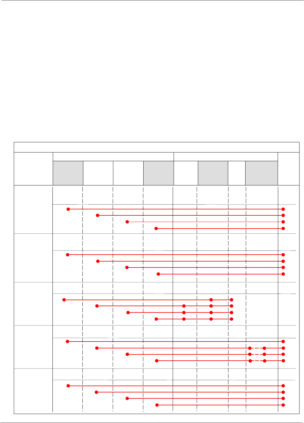
Test Equipment Set-up68P64115A18–1
Mar 2003 1X SC 4812T Lite BTS Optimization/ATP Software Release R2.16.1.x
DRAFT
3-57
Test Equipment Connection Charts
To use the following charts to identify necessary test equipment
connections, locate the communications system analyzer being used in
the COMMUNICATIONS SYSTEM ANALYZER columns, and read down
the column. Where a dot appears in the column, connect one end of the
test cable to that connector. Follow the horizontal line to locate the end
connection(s), reading up the column to identify the appropriate
equipment and/or BTS connector.
IS–95A/B–only Test Equipment Connections
Table 3-21 depicts the interconnection requirements for currently
available test equipment supporting IS–95A/B only which meets
Motorola standards and is supported by the LMF.
Table 3-21: IS–95A/B–only Test Equipment Interconnection
COMMUNICATIONS SYSTEM ANALYZER ADDITIONAL TEST EQUIPMENT
SIGNAL Cyber–Test Advantest
R3465 HP 8921A HP 8921
W/PCS Power
Meter GPIB
Interface LMF
Attenuator
&
Directional
Coupler BTS
EVEN SECOND
SYNCHRONIZATION EVEN
SEC REF EVEN SEC
SYNC IN
EVEN
SECOND
SYNC IN
EVEN
SECOND
SYNC IN
19.6608 MHZ
CLOCK TIME
BASE IN
CDMA
TIME BASE
IN
CDMA
TIME BASE
IN
CDMA
TIME BASE
IN
CONTROL
IEEE 488 BUS IEEE
488 GPIB GPIB SERIAL
PORT
HP–I
BHP–IB
TX TEST
CABLES RF
IN/OUT INPUT
50WTX1–6
RF
IN/OUT RF
IN/OUT 20 DB
ATTEN. BTS
PORT
RX TEST
CABLES RF
GEN OUT RF OUT
50WRX1–6
DUPLEX
OUT RF OUT
ONLY
SYNC
MON-
ITOR
FREQ
MON-
ITOR
HP–IB
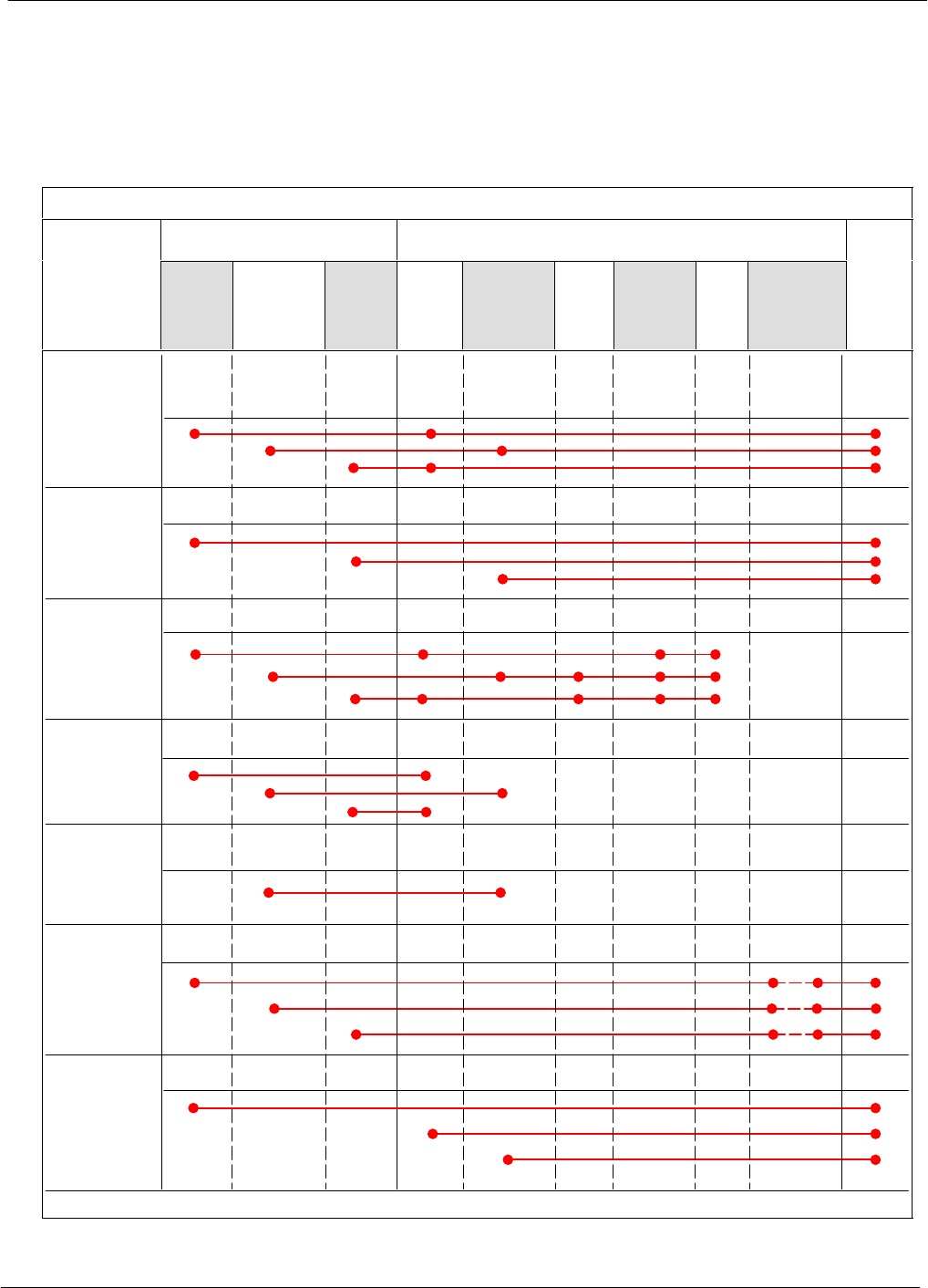
Test Equipment Set-up 68P64115A18–1
Mar 2003
1X SC 4812T Lite BTS Optimization/ATP Software Release R2.16.1.x
DRAFT
3-58
CDMA2000 1X/IS–95A/B–capable Test Equipment
Connections
Table 3-22 depicts the interconnection requirements for currently
available test equipment supporting both CDMA 2000 1X and
IS–95A/B which meets Motorola standards and is supported by the
LMF.
Table 3-22: CDMA2000 1X/IS–95A/B Test Equipment Interconnection
COMMUNICATIONS SYSTEM
ANALYZER ADDITIONAL TEST EQUIPMENT
SIGNAL
Agilent
8935
(Option
200 or
R2K) Advantest
R3267 Agilent
E4406A
Agilent
E4432
Signal
Gen.
Advantest
R3562
Signal
Generator Power
Meter GPIB
Interface LMF
Attenuator
&
Directional
Coupler BTS
EVEN SECOND
SYNCHRONIZATION
EVEN
SECOND
SYNC IN EXT TRIG
IN
19.6608 MHZ
CLOCK
EXT REF
IN MOD TIME
BASE IN
CONTROL
IEEE 488 BUS
10 MHZ
OUT
GP–IBHP–IB GP–IB GPIB SERIAL
PORT
GPIB GPIB
TX TEST
CABLES RF
IN/OUT INPUT
50 WTX1–6
20 DB
ATTEN. BTS
PORT
SYNC
MON-
ITOR
FREQ
MON-
ITOR
HP–IB
PATTERN
TRIG IN
EXT REF
IN
RF INPUT
50 W
RX TEST
CABLES RF OUT
50 W
RF OUTPUT
50 WRX1–6
10 MHZ
10 MHZ OUT
(SWITCHED) SYNTHE
REF IN
10 MHZ
IN
TRIGGER
IN
EXT TRIG
SIGNAL SOURCE
CONTROLLED
SERIAL I/O
SERIAL
I/O SERIAL
I/O
10 MHZ
REF
OUT
*
RF
IN/OUT

Test Equipment Set-up68P64115A18–1
Mar 2003 1X SC 4812T Lite BTS Optimization/ATP Software Release R2.16.1.x
DRAFT
3-59
Equipment Warm-up
NOTE Warm-up BTS equipment for a minimum of 60 minutes prior to
performing the BTS optimization procedure. This assures BTS
stability and contributes to optimization accuracy.
– Time spent running initial or normal power-up,
hardware/firmware audit, and BTS download counts as
warm-up time.
WARNING Before installing any test equipment directly to any BTS TX
OUT connector, verify there are no CDMA channels keyed.
– At active sites, have the OMC-R/CBSC place the antenna
(sector) assigned to the BBX under test OOS. Failure to do
so can result in serious personal injury and/or equipment
damage.
Automatic Cable Calibration Set–up
Figure 3-11 and Figure 3-12 show the cable calibration setup for the test
sets supported by the LMF. The left side of the diagram depicts the
location of the input and output connectors of each test equipment item,
and the right side details the connections for each test. Table 3-26
provides a procedure for performing automatic cable calibration.
Manual Cable Calibration
If manual cable calibration is required, refer to the procedures in
Appendix F.
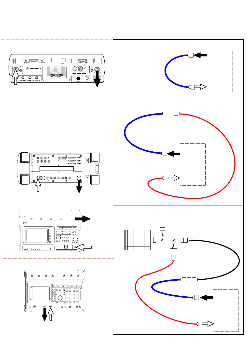
Test Equipment Set-up 68P64115A18–1
Mar 2003
1X SC 4812T Lite BTS Optimization/ATP Software Release R2.16.1.x
DRAFT
3-60
Figure 3-11: IS–95A/B Cable Calibration Test Setup –
CyberTest, Agilent 8935, Advantest R3465, and HP 8921A
Motorola CyberTest
Advantest Model R3465
RF OUT 50Ω
INPUT 50Ω
RF GEN OUTANT IN
SUPPORTED TEST SETS
100–WATT (MIN)
NON–RADIATING
RF LOAD
TEST
SET
A. SHORT CABLE CAL
SHORT
CABLE
B. RX TEST CAL SETUP FOR TRDC
TEST
SET
C. TX TEST AND DRDC RX TEST CAL SETUP
20 DB IN–LINE
ATTENUATOR
CALIBRATION SET UP
N–N FEMALE
ADAPTER
TX
CABLE
SHORT
CABLE
Note: The 30 dB directional coupler is not used
with the Cybertest test set. The TX cable is
connected directly to the Cybertest test set.
A 10dB attenuator must be used with the short test
cable for cable calibration with the CyberTest test
set. The 10dB attenuator is used only for the cable
calibration procedure, not with the test cables for
TX calibration and ATP tests.
TEST
SET
RX
CABLE
SHORT
CABLE
DIRECTIONAL
COUPLER
(30 DB)
N–N FEMALE
ADAPTER
50 Ω
ΤERM.
Agilent 8935 Series E6380A
(formerly HP 8935)
RF
IN/OUT
ANT
IN
Hewlett Packard Model HP 8921A
Note: For 800 MHZ only. The HP8921A cannot
be used to calibrate cables for PCS frequencies.
TX CABLE FOR
TX TEST CABLE
CALIBRATION
RX CABLE FOR
DRDC RX TEST
CABLE CALIBRATION
DUPLEX
OUT ANT
IN
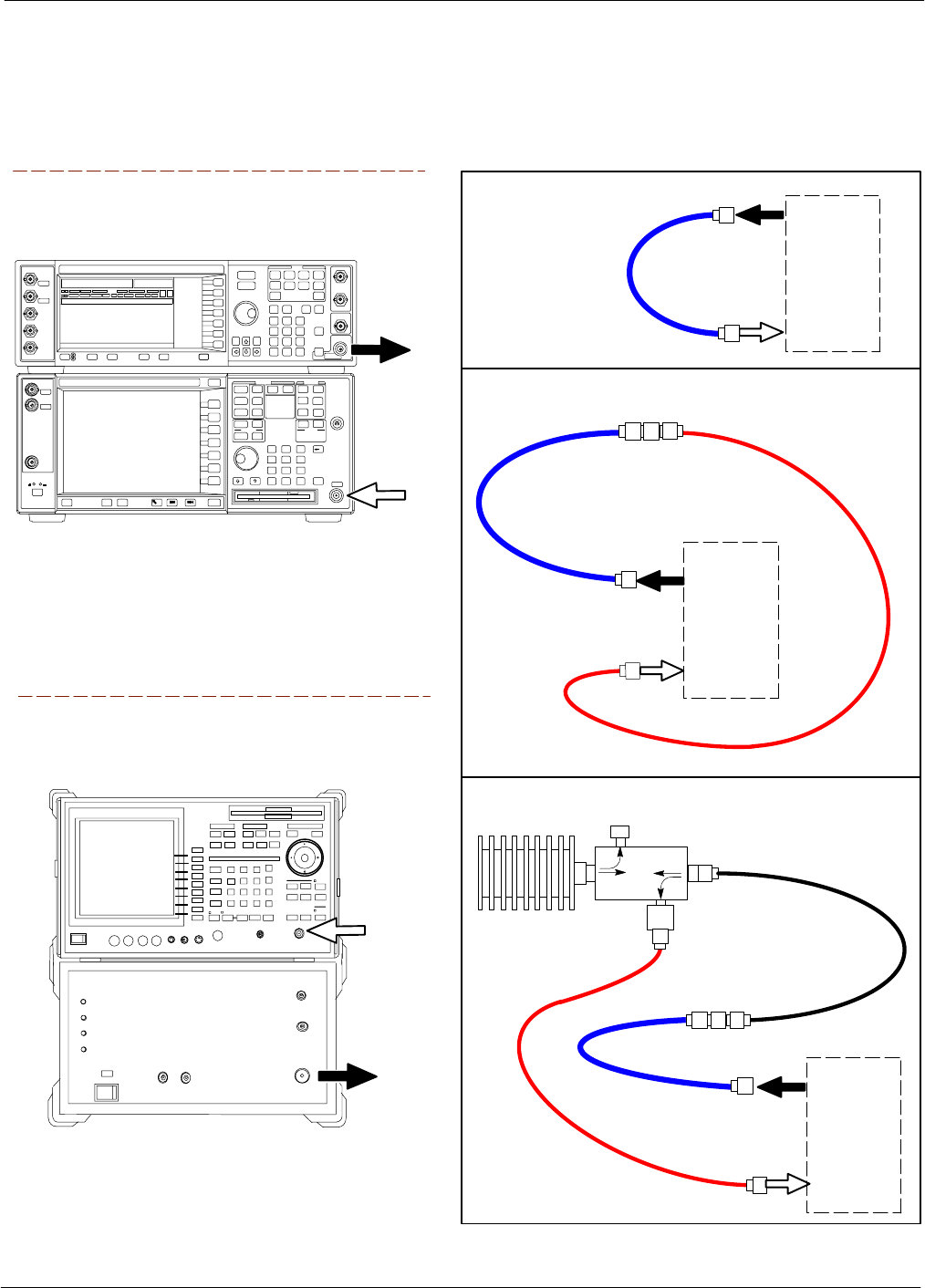
Test Equipment Set-up68P64115A18–1
Mar 2003 1X SC 4812T Lite BTS Optimization/ATP Software Release R2.16.1.x
DRAFT
3-61
Figure 3-12: IS–95A/B and CDMA 2000 1X Cable Calibration Test Setup –
Agilent E4406A/E4432B and Advantest R3267/R3562
TEST
SET
A. SHORT CABLE CAL
SHORT
CABLE
B. RX TEST SETUP FOR TRDC
CALIBRATION SET UP
TEST
SET
RX
CABLE
SHORT
CABLE
N–N FEMALE
ADAPTER
SUPPORTED TEST SETS
INPUT 50 Ω
RF OUT
50 Ω
Advantest R3267 (Top) and R3562 (Bottom)
NOTE:
SYNTHE REF IN ON REAR OF SIGNAL GENERATOR IS
CONNECTED TO 10 MHZ OUT ON REAR OF SPECTRUM
ANALYZER
Agilent E4432B (Top) and E4406A (Bottom)
NOTE:
10 MHZ IN ON REAR OF SIGNAL GENERATOR IS CONNECTED TO
10 MHZ OUT (SWITCHED) ON REAR OF TRANSMITTER TESTER
(FIGURE F-16).
RF INPUT
50 Ω
RF OUTPUT
50 Ω
100–WATT (MIN)
NON–RADIATING
RF LOAD
TEST
SET
D. TX TEST SETUP AND DRDC RX TEST SETUP
20 DB IN–LINE
ATTENUATOR
N–N FEMALE
ADAPTER
TX
CABLE
SHORT
CABLE
DIRECTIONAL
COUPLER
(30 DB)
50 Ω
ΤERM.
TX CABLE FOR
TX TEST CABLE
CALIBRATION
RX CABLE FOR
DRDC RX TEST
CABLE CALIBRATION
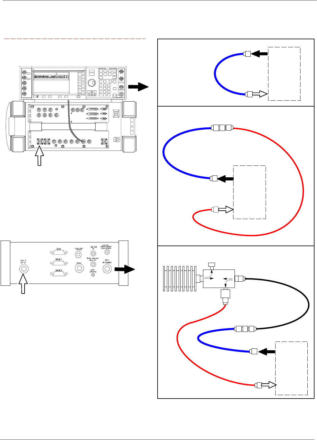
Test Equipment Set-up 68P64115A18–1
Mar 2003
1X SC 4812T Lite BTS Optimization/ATP Software Release R2.16.1.x
DRAFT
3-62
Figure 3-13: CDMA2000 1X Cable Calibration Test Setup –
Agilent 8935/E4432B and Agilent E7495A
TEST
SET
A. SHORT CABLE CAL
SHORT
CABLE
B. RX TEST SETUP FOR TRDC
CALIBRATION SET UP
TEST
SET
RX
CABLE
SHORT
CABLE
N–N FEMALE
ADAPTER
SUPPORTED TEST SETS
Agilent E4432B (Top) and 8935 Series
E6380A (Bottom)
NOTE:
10 MHZ IN ON REAR OF SIGNAL GENERATOR IS CONNECTED TO
10 MHZ REF OUT ON SIDE OF CDMA BASE STATION TEST SET
(FIGURE F-15).
RF OUTPUT
50 Ω
100–WATT (MIN)
NON–RADIATING
RF LOAD
TEST
SET
D. TX TEST SETUP AND DRDC RX TEST SETUP
20 DB IN–LINE
ATTENUATOR
N–N FEMALE
ADAPTER
TX
CABLE
SHORT
CABLE
DIRECTIONAL
COUPLER
(30 DB)
50 Ω
ΤERM.
TX CABLE FOR
TX TEST CABLE
CALIBRATION
RX CABLE FOR
DRDC RX TEST
CABLE CALIBRATION
ANT
IN
Agilent E7495A
RF
OUT
RF
IN
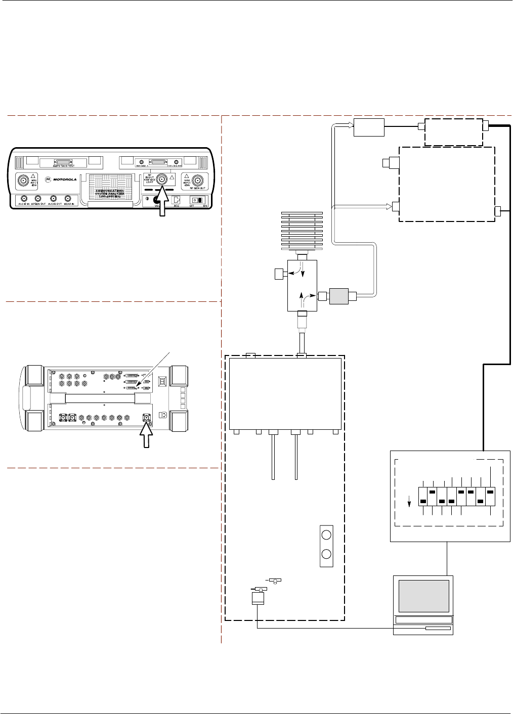
Test Equipment Set-up68P64115A18–1
Mar 2003 1X SC 4812T Lite BTS Optimization/ATP Software Release R2.16.1.x
DRAFT
3-63
Set-up for TX Calibration
Figure 3-14 and Figure 3-15 show the test set connections for TX
calibration.
Figure 3-14: TX Calibration Test Setup –
CyberTest (IS–95A/B) and Agilent 8935 (IS–95A/B and CDMA2000 1X)
Motorola CyberTest
Agilent 8935 Series E6380A (formerly HP 8935)
TEST SETS TRANSMIT (TX) SET UP
FRONT PANEL
RF
IN/OUT
RF
IN/OUT
HP–IB
TO GPIB
BOX
NOTE: THE 30 DB DIRECTIONAL COUPLER IS NOT USED WITH THE
CYBERTEST TEST SET. THE TX CABLE IS CONNECTED DIRECTLY
TO THE CYBERTEST TEST SET.
TO
MPC
TO PA
TRUNKING
MODULE
RS232–GPIB
INTERFACE BOX
INTERNAL PCMCIA
ETHERNET CARD
GPIB
CABLE
UNIVERSAL TWISTED PAIR (UTP)
CABLE (RJ45 CONNECTORS)
RS232 NULL
MODEM
CABLE
S MODE
DATA FORMAT
BAUD RATE
GPIB ADRS G MODE
ON
BTS
INTERNAL
TX
CABLE
CDMA
LMF
DIP SWITCH SETTINGS
10BASET/
10BASE2
CONVERTER
LAN
B
LAN
A
GPIB
RF IN/OUT
RX
ANTENNA
CONNECTOR
FREQ
MONITOR
SYNC
MONITOR
CSM
INTERNAL
RX
CABLE
TX
ANT
CPLD
RX
BTS
CPLD
TRDC
TX
BTS
CPLD
RX
ANT
CPLD
TX
ANTENNA
CONNECTOR
COMMUNICATIONS
SYSTEM ANALYZER
2O DB IN–LINE
ATTENUATOR
50 Ω
TERM
.
TX TEST
CABLE
DIRECTIONAL
COUPLER
(30 DB)
100–WATT (MIN.)
NON–RADIATING
RF LOAD
TX TEST
CABLE
* BLACK RECTANGLES
REPRESENT THE RAISED
PART OF SWITCHES
NOTE: IF BTS IS EQUIPPED
WITH DRDCS (DUPLEXED
RX/TX SIGNALS), CONNECT
THE TX TEST CABLE TO
THE DRDC ANTENNA
CONNECTOR.
POWER
METER
(OPTIONAL)*
POWER
SENSOR
* A POWER METER CAN BE USED IN
PLACE OF THE COMMUNICATIONS
TEST SET FOR TX CALIBRATION/
AUDIT
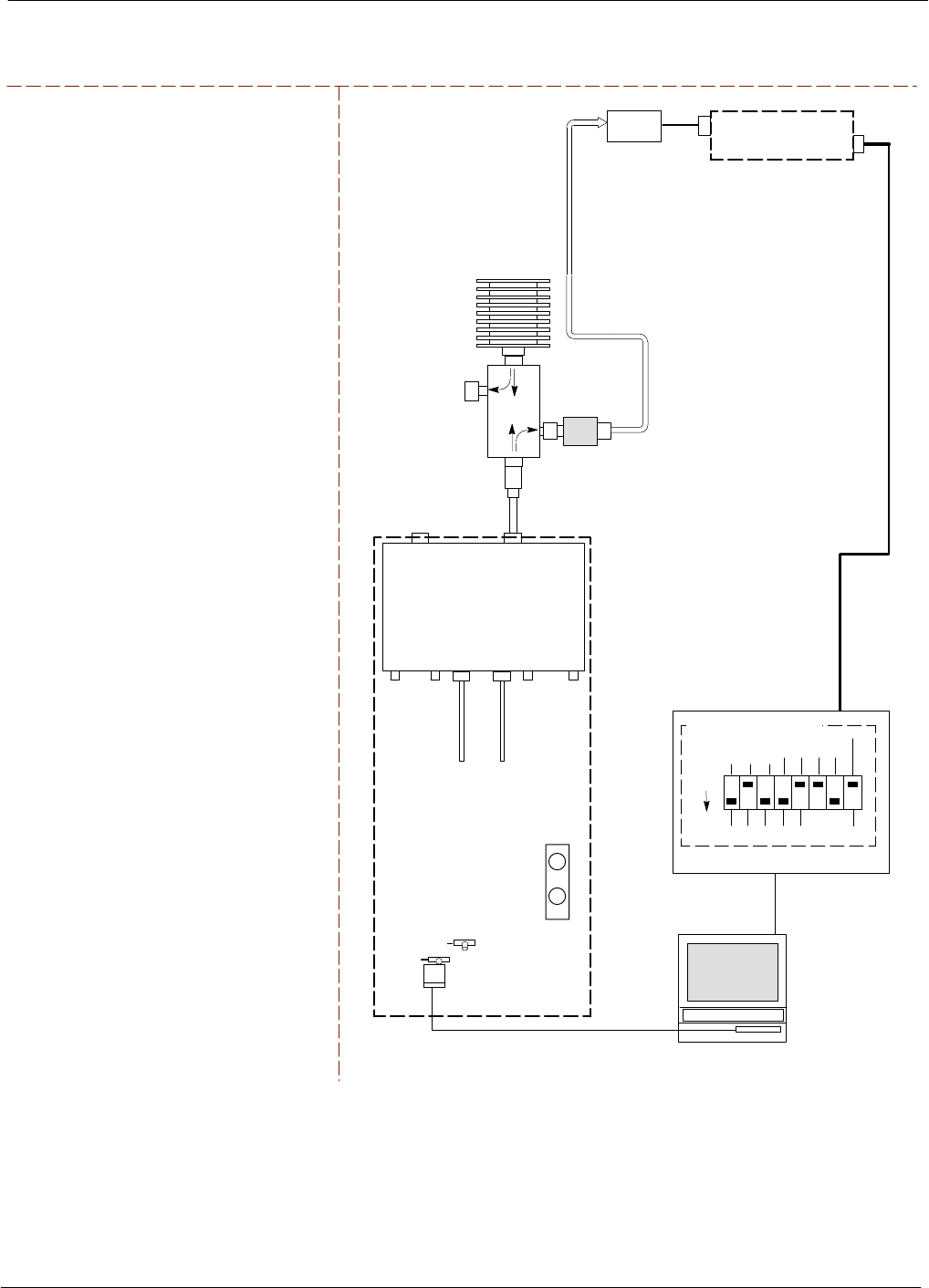
Test Equipment Set-up 68P64115A18–1
Mar 2003
1X SC 4812T Lite BTS Optimization/ATP Software Release R2.16.1.x
DRAFT
3-64
Figure 3-15: TX Calibration Test Setup – Using Power Meter
TEST SETS TRANSMIT (TX) SET UP
NOTE: THE HP8921A AND ADVANTEST
R3465 CANNOT BE USED FOR TX
CALIBRATION. A POWER METER MUST BE
USED.
TO
MPC
TO PA
TRUNKING
MODULE
RS232–GPIB
INTERFACE BOX
INTERNAL PCMCIA
ETHERNET CARD
GPIB
CABLE
UNIVERSAL TWISTED PAIR (UTP)
CABLE (RJ45 CONNECTORS)
RS232 NULL
MODEM
CABLE
S MODE
DATA FORMAT
BAUD RATE
GPIB ADRS G MODE
ON
BTS
INTERNAL
TX
CABLE
CDMA
LMF
DIP SWITCH SETTINGS
10BASET/
10BASE2
CONVERTER
LAN
B
LAN
A
RX
ANTENNA
CONNECTOR
FREQ
MONITOR
SYNC
MONITOR
CSM
INTERNAL
RX
CABLE
TX
ANT
CPLD
RX
BTS
CPLD
TRDC
TX
BTS
CPLD
RX
ANT
CPLD
TX
ANTENNA
CONNECTOR
50 Ω
TERM
.
TX TEST
CABLE
DIRECTIONAL
COUPLER
(30 DB)
100–WATT (MIN.)
NON–RADIATING
RF LOAD
TX TEST
CABLE
* BLACK RECTANGLES
REPRESENT THE RAISED
PART OF SWITCHES
NOTE: IF BTS IS EQUIPPED
WITH DRDCS (DUPLEXED
RX/TX SIGNALS), CONNECT
THE TX TEST CABLE TO
THE DRDC ANTENNA
CONNECTOR.
POWER
SENSOR POWER METER
2O DB IN–LINE
ATTENUATOR
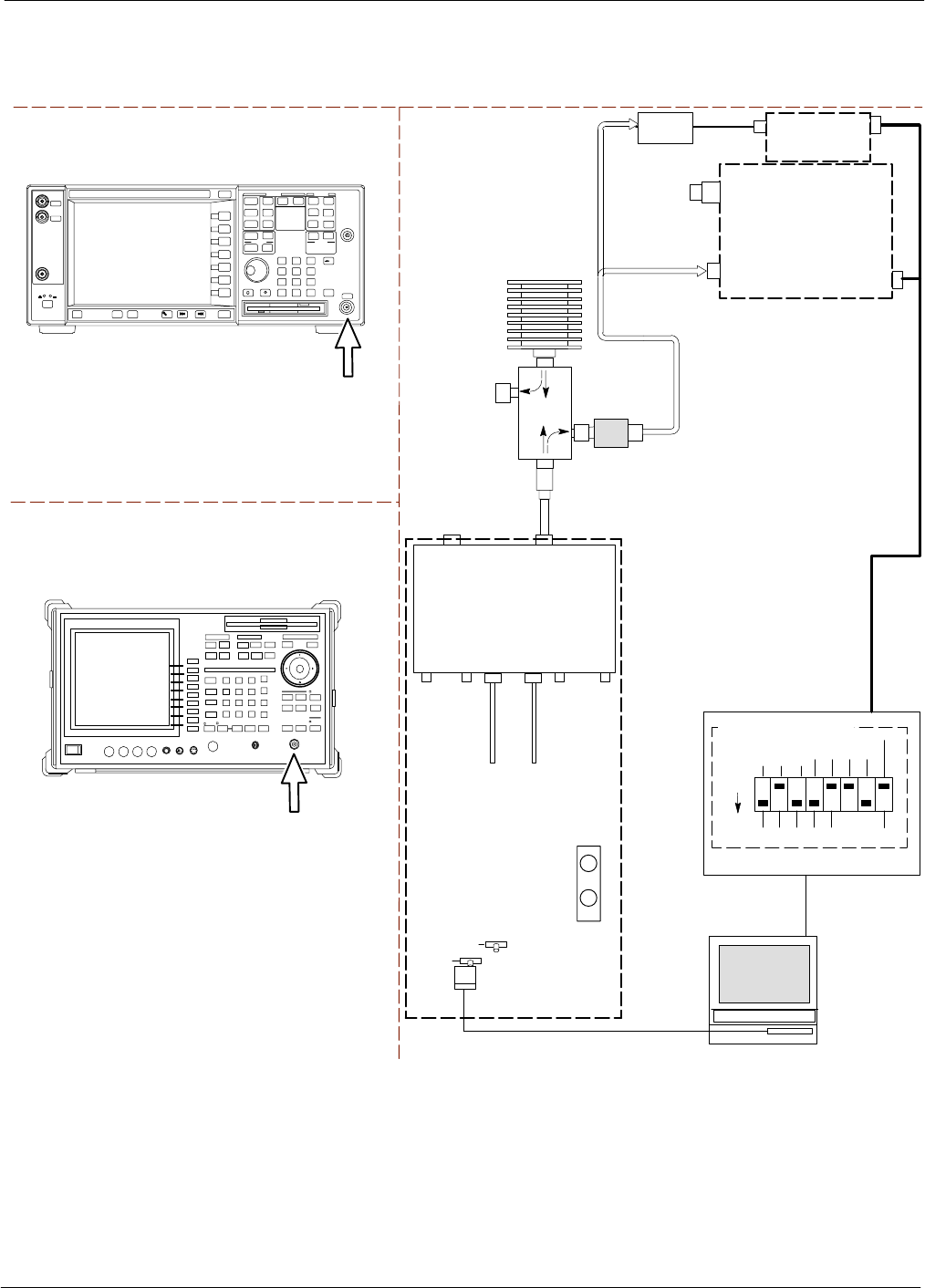
Test Equipment Set-up68P64115A18–1
Mar 2003 1X SC 4812T Lite BTS Optimization/ATP Software Release R2.16.1.x
DRAFT
3-65
Figure 3-16: TX Calibration Test Setup –
Agilent E4406A and Advantest R3567 (IS–95A/B and CDMA2000 1X)
TEST SETS TRANSMIT (TX) SET UP
TO
MPC
TO PA
TRUNKING
MODULE
RS232–GPIB
INTERFACE BOX
INTERNAL PCMCIA
ETHERNET CARD
GPIB
CABLE
UNIVERSAL TWISTED PAIR (UTP)
CABLE (RJ45 CONNECTORS)
RS232 NULL
MODEM
CABLE
S MODE
DATA FORMAT
BAUD RATE
GPIB ADRS G MODE
ON
BTS
INTERNAL
TX
CABLE
CDMA
LMF
DIP SWITCH SETTINGS
10BASET/
10BASE2
CONVERTER
LAN
B
LAN
A
GPIB
RF INPUT 50 Ω
OR INPUT 50 Ω
RX
ANTENNA
CONNECTOR
FREQ
MONITOR
SYNC
MONITOR
CSM
INTERNAL
RX
CABLE
TX
ANT
CPLD
RX
BTS
CPLD
TRDC
TX
BTS
CPLD
RX
ANT
CPLD
TX
ANTENNA
CONNECTOR
COMMUNICATIONS
SYSTEM ANALYZER
50 Ω
TERM
.
TX TEST
CABLE
DIRECTIONAL
COUPLER
(30 DB)
100–WATT (MIN.)
NON–RADIATING
RF LOAD
TX TEST
CABLE
* BLACK RECTANGLES
REPRESENT THE RAISED
PART OF SWITCHES
NOTE: IF BTS IS EQUIPPED
WITH DRDCS (DUPLEXED
RX/TX SIGNALS), CONNECT
THE TX TEST CABLE TO
THE DRDC ANTENNA
CONNECTOR.
POWER
METER
(OPTIONAL)*
POWER
SENSOR
* A POWER METER CAN BE USED IN
PLACE OF THE COMMUNICATIONS
TEST SET FOR TX CALIBRATION/
AUDIT
RF INPUT
50 Ω
Agilent E4406A
INPUT 50 Ω
Advantest R3267
2O DB IN–LINE
ATTENUATOR
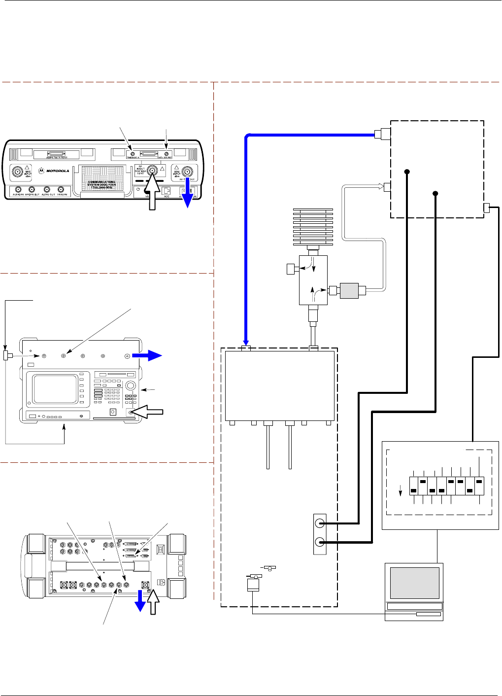
Test Equipment Set-up 68P64115A18–1
Mar 2003
1X SC 4812T Lite BTS Optimization/ATP Software Release R2.16.1.x
DRAFT
3-66
Set–up for ATP
Figure 3-17 and Figure 3-18 show the test set connections for ATP tests.
Figure 3-17: IS–95A/B ATP Test Set–up, TRDC Shown –
CyberTest, Advantest R3465, and Agilent 8935
Motorola CyberTest
TEST SETS Optimization/ATP SET UP
RF
IN/OUT
SYNC MONITOR
EVEN SEC TICK
PULSE REFERENCE
FROM CSM BOARD
FREQ MONITOR
19.6608 MHZ CLOCK
REFERENCE FROM
CSM BOARD
Advantest Model R3465
INPUT 50Ω
GPIB CONNECTS
TO BACK OF UNIT
NOTE: The 30 dB directional coupler is not
used with the Cybertest test set. The TX
cable is connected directly to the Cybertest
test set.
RF OUT 50Ω
FREQ MONITOR
19.6608 MHZ CLOCK
REFERENCE FROM
CSM BOARD
RF GEN
OUT
SYNC MONITOR EVEN
SEC TICK PULSE
REFERENCE FROM
CSM BOARD
BNC
“T”
TO EXT TRIGGER CONNECTOR
ON REAR OF TEST SET
(FOR DETAILS, SEE
FIGURE F-13)
TO
MPC
TO PA
TRUNKING
MODULE
RS232–GPIB
INTERFACE BOX
INTERNAL PCMCIA
ETHERNET CARD
GPIB
CABLE
UNIVERSAL TWISTED PAIR (UTP)
CABLE (RJ45 CONNECTORS)
RS232 NULL
MODEM
CABLE
S MODE
DATA FORMAT
BAUD RATE
GPIB ADRS G MODE
ON
BTS
INTERNAL
TX
CABLE
CDMA
LMF
DIP SWITCH SETTINGS
10BASET/
10BASE2
CONVERTER
LAN
B
LAN
A
RX TEST
CABLE
GPIB
RF IN/OUT
OR
INPUT 50 Ω
RF GEN OUT,
RF OUT 50Ω,
OR RF IN/OUT
RX
ANTENNA
CONNECTOR
FREQ
MONITOR
SYNC
MONITOR
CSM
INTERNAL
RX
CABLE
TX
ANT
CPLD
RX
BTS
CPLD
TRDC
TX
BTS
CPLD
RX
ANT
CPLD
TX
ANTENNA
CONNECTOR
COMMUNICATIONS
SYSTEM ANALYZER
50 Ω
TERM
.
TX TEST
CABLE
DIRECTIONAL
COUPLER
(30 DB)
100–WATT (MIN.)
NON–RADIATING
RF LOAD
TX TEST
CABLE
* BLACK RECTANGLES
REPRESENT THE RAISED
PART OF SWITCHES
CDMA
TIMEBASE
IN
EVEN
SECOND/
SYNC IN
NOTE: IF BTS IS EQUIPPED
WITH DRDCS (DUPLEXED RX/TX
SIGNALS), BOTH THE TX AND RX
TEST CABLES CONNECT TO THE
DRDC ANTENNA CONNECTOR.
(SEE FIGURE 3-19.)
2O DB IN–LINE
ATTENUATOR
IMPORTANT:
WHEN PERFORMING FER TEST ON COMPANION FRAME DIVERSITY RX, CONNECT
RX TEST CABLE TO RX ANTENNA PORT ON COLLOCATED COMPANION FRAME.
Agilent 8935 Series E6380A (formerly HP 8935)
RF IN/OUT
HP–IB
TO GPIB
BOX
SYNC MONITOR
EVEN SEC TICK
PULSE REFERENCE
FROM CSM BOARD
FREQ MONITOR
19.6608 MHZ CLOCK
REFERENCE FROM
CSM BOARD
10 MHZ
REF OUT
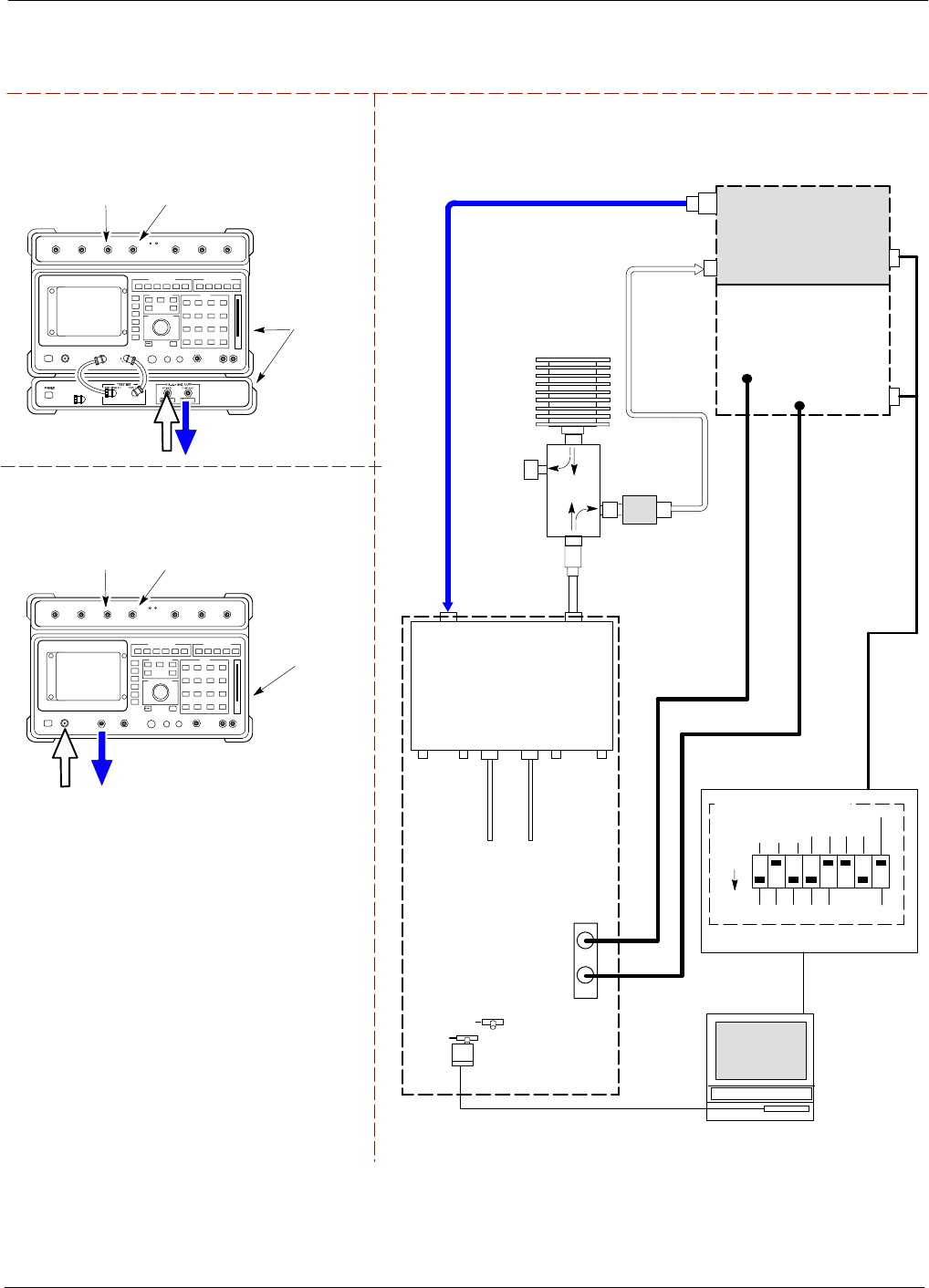
Test Equipment Set-up68P64115A18–1
Mar 2003 1X SC 4812T Lite BTS Optimization/ATP Software Release R2.16.1.x
DRAFT
3-67
Figure 3-18: IS–95A/B ATP Test Setup – HP 8921A
RF OUT
ONLY
Hewlett Packard Model HP 8921A W/PCS Interface
(for 1900 MHz)
GPIB
CONNECTS
TO BACK OF
UNITS
SYNC MONITOR
EVEN SEC TICK
PULSE REFERENCE
FROM CSM BOARD
FREQ MONITOR
19.6608 MHZ CLOCK
REFERENCE FROM
CSM BOARD
TEST SETS Optimization/ATP SET UP
RF
IN/OUT
GPIB
CONNECTS
TO BACK OF
UNIT
SYNC MONITOR
EVEN SEC TICK
PULSE REFERENCE
FROM CSM BOARD
FREQ MONITOR
19.6608 MHZ CLOCK
REFERENCE FROM
CSM BOARD
Hewlett Packard Model HP 8921A
(for 800 MHz)
RF
IN/OUT
DUPLEX
OUT
TO
MPC
TO PA
TRUNKING
MODULE
RS232–GPIB
INTERFACE BOX
INTERNAL PCMCIA
ETHERNET CARD
GPIB
CABLE
UNIVERSAL TWISTED PAIR (UTP)
CABLE (RJ45 CONNECTORS)
RS232 NULL
MODEM
CABLE
S MODE
DATA FORMAT
BAUD RATE
GPIB ADRS G MODE
ON
BTS
INTERNAL
TX
CABLE
CDMA
LMF
DIP SWITCH SETTINGS
10BASET/
10BASE2
CONVERTER
LAN
B
LAN
A
RX TEST
CABLE
GPIB
PCS INTERFACE
INPUT/OUTPUT
PORTS
RX
ANTENNA
CONNECTOR
FREQ
MONITOR
SYNC
MONITOR
CSM
INTERNAL
RX
CABLE
TX
ANT
CPLD
RX
BTS
CPLD
TRDC
TX
BTS
CPLD
RX
ANT
CPLD
TX
ANTENNA
CONNECTOR
COMMUNICATIONS
SYSTEM ANALYZER
50 Ω
TERM
.
TX TEST
CABLE
DIRECTIONAL
COUPLER
(30 DB)
100–WATT (MIN.)
NON–RADIATING
RF LOAD
TX TEST
CABLE
* BLACK RECTANGLES
REPRESENT THE RAISED
PART OF SWITCHES
CDMA
TIMEBASE
IN EVEN
SECOND/
SYNC IN
NOTE: IF BTS IS EQUIPPED
WITH DRDCS (DUPLEXED
RX/TX SIGNALS), BOTH THE
TX AND RX TEST CABLES
CONNECT TO THE DRDC
ANTENNA CONNECTOR.
(SEE FIGURE 3-19.)
HP PCS
INTERFACE*
2O DB IN–LINE
ATTENUATOR
* FOR 1900 MHZ
ONLY
RF OUT ONLY
RF IN/OUT
NOTE:
FOR 800 MHZ TESTING, CONNECT CABLES TO THE
HP 8921A AS FOLLOWS:
RX TEST CABLE TO DUPLEX OUT
TX TEST CABLE TO RF IN/OUT
IMPORTANT:
WHEN PERFORMING FER TEST ON COMPANION FRAME DIVERSITY RX,
CONNECT RX TEST CABLE TO RX ANTENNA PORT ON COLLOCATED COMPANION
FRAME.
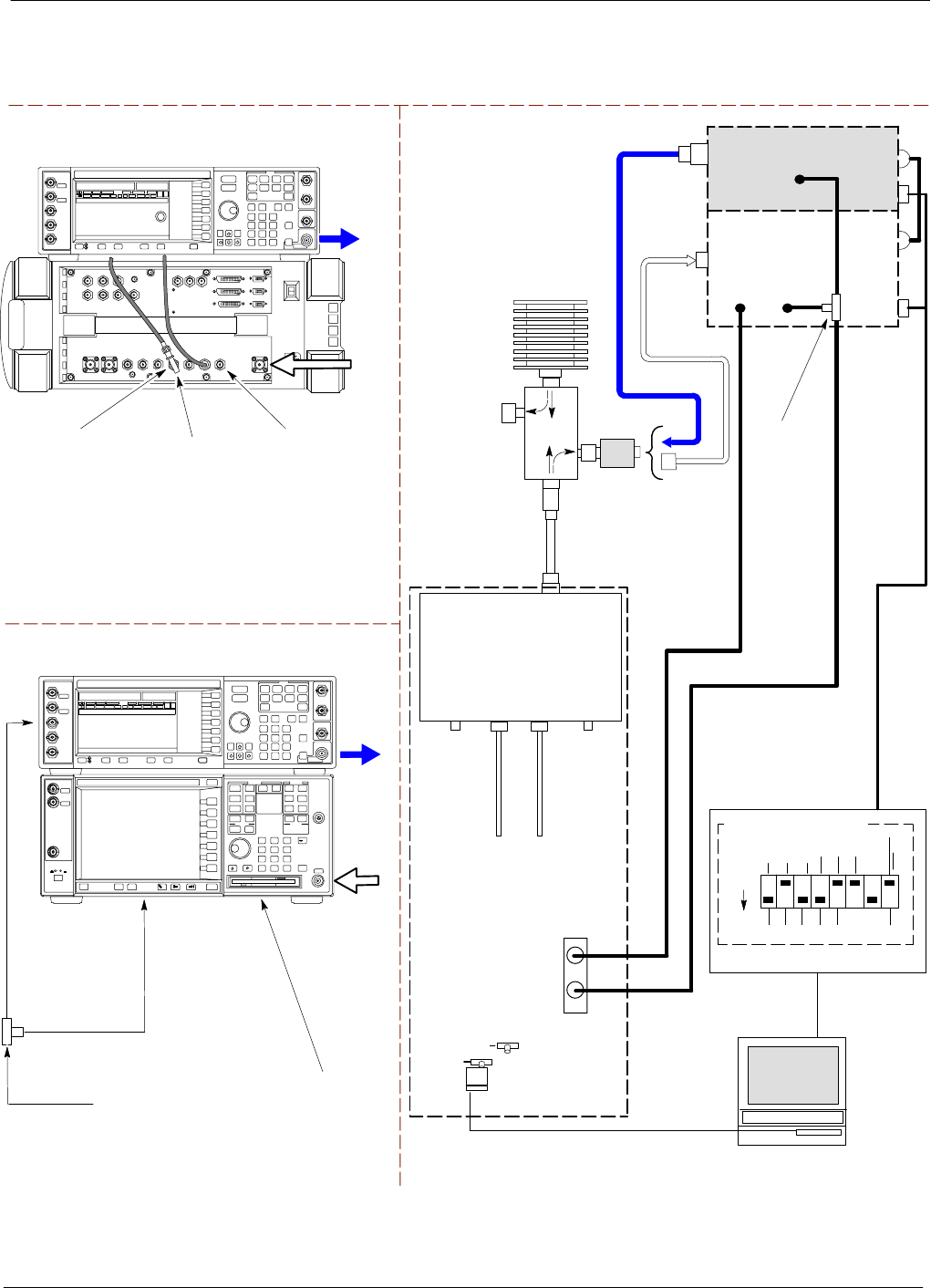
Test Equipment Set-up 68P64115A18–1
Mar 2003
1X SC 4812T Lite BTS Optimization/ATP Software Release R2.16.1.x
DRAFT
3-68
Figure 3-19: IS–95A/B and CDMA2000 1X ATP Test Setup With DRDCs –
Agilent Test Equipment
TEST SETS Optimization/ATP SET UP
RF INPUT
50 Ω
RF
OUTPUT
50 Ω
Agilent E4432B (Top) and E4406A (Bottom)
FREQ MONITOR
19.6608 MHZ CLOCK
REFERENCE FROM
CSM BOARD
SYNC MONITOR
EVEN SEC TICK
PULSE REFERENCE
FROM CSM BOARD
BNC
“T”
TO TRIGGER IN
ON REAR OF
TRANSMITTER
TESTER
TO PATTERN TRIG IN
ON REAR OF SIGNAL
GENERATOR
TO EXT REF IN
ON REAR OF
TRANSMITTER
TESTER
NOTE:
10 MHZ IN ON REAR OF SIGNAL GENERATOR IS CONNECTED TO
10 MHZ OUT (SWITCHED) ON REAR OF TRANSMITTER TESTER
(SEE FIGURE F-16).
TO
MPC
TO PA
TRUNKING
MODULE
RS232–GPIB
INTERFACE BOX
INTERNAL PCMCIA
ETHERNET CARD
GPIB
CABLE
UNIVERSAL TWISTED
PAIR (UTP) CABLE
(RJ45 CONNECTORS)
RS232 NULL
MODEM
CABLE
S MODE
DATA FORMAT
BAUD RATE
GPIB ADRS G MODE
ON
BTS
INTERNAL
TX
CABLE
CDMA
LMF
DIP SWITCH SETTINGS *
10BASET/
10BASE2
CONVERTER
LAN
B
LAN
A
COMMUNICATIONS
SYSTEM ANALYZER
HP–IB
OR
GPIB
FREQ
MONITOR
SYNC
MONITOR
CSM
INTERNAL
RX
CABLE
DRDC
BTS
CPLD
ANT
CPLD
SIGNAL GENERATOR
GPIB
10 MHZ
IN
10 MHZ
REF OUT
OR
10 MHZ
OUT
TRIGGER IN
OR
EVEN SEC
SYNCH IN
EXT
REF
IN
BNC
“T”
PATTERN
TRIG IN
* BLACK RECTANGLES
REPRESENT THE RAISED
PART OF SWITCHES
DUPLEXED
TX/RX
ANTENNA
CONNECTOR
RX TEST
CABLE
50 Ω
TERM
.
TX TEST
CABLE
DIRECTIONAL
COUPLER
(30 DB)
100–WATT (MIN.)
NON–RADIATING
RF LOAD
TX TEST
CABLE
2O DB IN–LINE
ATTENUATOR
RF IN/OUT
OR
RF INPUT
50 Ω
RF OUTPUT 50 Ω
IMPORTANT:
WHEN PERFORMING FER TEST ON
COMPANION FRAME DIVERSITY RX,
CONNECT RX TEST CABLE TO
ANTENNA PORT ON COLLOCATED
COMPANION FRAME.
Agilent E4432B (Top) and 8935 Series E6380A
(Bottom)
SYNC MONITOR
EVEN SEC TICK
PULSE REFERENCE
FROM CSM BOARD
FREQ MONITOR
19.6608 MHZ CLOCK
REFERENCE FROM
CSM BOARD
RF
OUTPUT
50 Ω
NOTES:
10 MHZ IN ON REAR OF SIGNAL GENERATOR IS CONNECTED TO
10 MHZ REF OUT ON SIDE OF CDMA BASE STATION TEST SET
PATTERN TRIG IN ON REAR OF SIGNAL GENERATOR IS
CONNECTED TO EVEN SECOND SYNC IN ON SIDE OF CDMA BASE
STATION TEST SET.
(SEE FIGURE F-15)
RF
IN/OUT
BNC
“T”
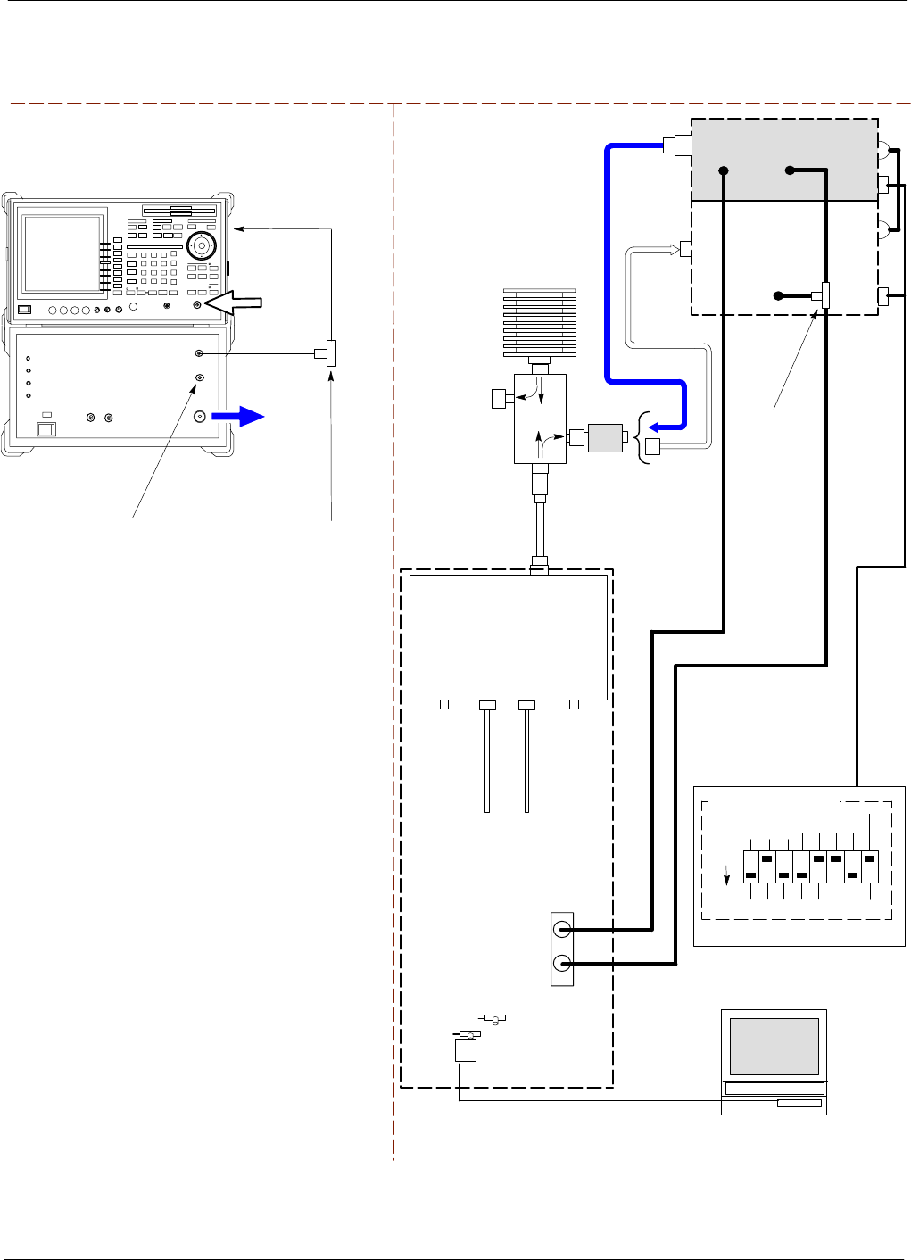
Test Equipment Set-up68P64115A18–1
Mar 2003 1X SC 4812T Lite BTS Optimization/ATP Software Release R2.16.1.x
DRAFT
3-69
Figure 3-20: IS–95A/B and CDMA2000 1X ATP Test Setup With DRDCs –
Advantest R3267/3562 Test Equipment
TEST SETS Optimization/ATP SET UP
INPUT 50 Ω
RF OUT
50 Ω
Advantest R3267 (Top) and R3562 (Bottom)
FREQ MONITOR
19.6608 MHZ CLOCK
REFERENCE FROM
CSM BOARD
SYNC MONITOR
EVEN SEC TICK
PULSE REFERENCE
FROM CSM BOARD
BNC
“T”
NOTE:
SYNTHE REF IN ON REAR OF SIGNAL GENERATOR IS
CONNECTED TO 10 MHZ REF OUT ON REAR OF
SPECTRUM ANALYZER (SEE FIGURE F-17)
TO EXT TRIG
ON REAR OF
SPECTRUM
ANALYZER
TO
MPC
TO PA
TRUNKING
MODULE
RS232–GPIB
INTERFACE BOX
INTERNAL PCMCIA
ETHERNET CARD
GPIB
CABLE
UNIVERSAL TWISTED
PAIR (UTP) CABLE
(RJ45 CONNECTORS)
RS232 NULL
MODEM
CABLE
S MODE
DATA FORMAT
BAUD RATE
GPIB ADRS G MODE
ON
BTS
INTERNAL
TX
CABLE
CDMA
LMF
DIP SWITCH SETTINGS
10BASET/
10BASE2
CONVERTER
LAN
B
LAN
A
INPUT
50 Ω
RF OUT
50 Ω
FREQ
MONITOR
SYNC
MONITOR
CSM
INTERNAL
RX
CABLE
DRDC
BTS
CPLD
ANT
CPLD
BNC
“T”
SPECTRUM
ANALYZER
GPIB
SIGNAL GENERATOR
GPIB
SYNTHE
REF
IN
10 MHZ
OUT
EXT
TRIG IN
MOD TIME
BASE IN
EXT TRIG
* BLACK RECTANGLES
REPRESENT THE RAISED
PART OF SWITCHES
DUPLEXED
TX/RX
ANTENNA
CONNECTOR
RX TEST
CABLE
50 Ω
TERM
.
TX TEST
CABLE
DIRECTIONAL
COUPLER
(30 DB)
100–WATT (MIN.)
NON–RADIATING
RF LOAD
TX TEST
CABLE
2O DB IN–LINE
ATTENUATOR
IMPORTANT:
WHEN PERFORMING FER TEST ON
COMPANION FRAME DIVERSITY RX,
CONNECT RX TEST CABLE TO
ANTENNA PORT ON COLLOCATED
COMPANION FRAME.
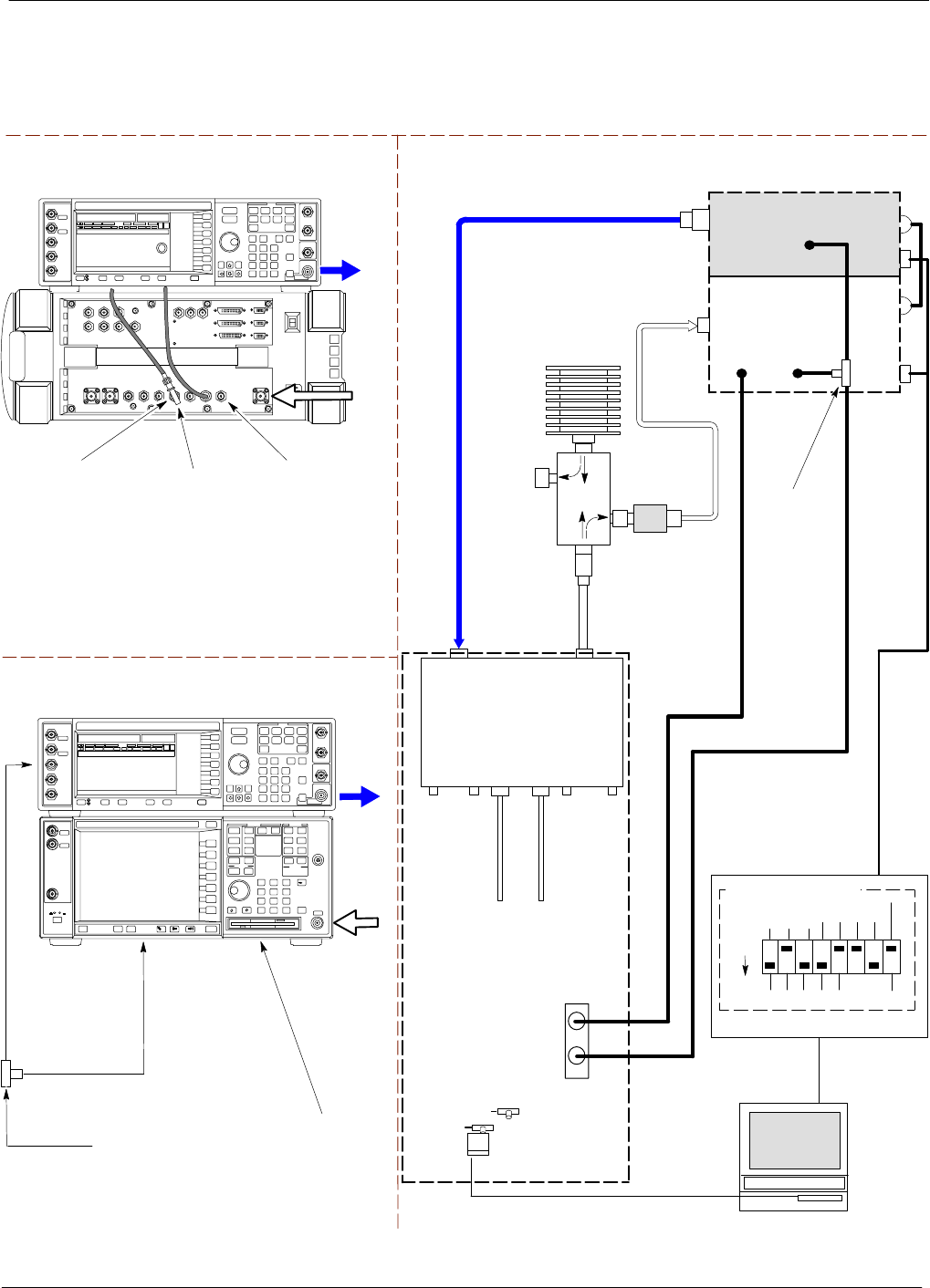
Test Equipment Set-up 68P64115A18–1
Mar 2003
1X SC 4812T Lite BTS Optimization/ATP Software Release R2.16.1.x
DRAFT
3-70
Figure 3-21: IS–95A/B and CDMA2000 1X ATP Test Setup With TRDCs –
Agilent Test Equipment
TEST SETS Optimization/ATP SET UP
TO
MPC
TO PA
TRUNKING
MODULE
RS232–GPIB
INTERFACE BOX
INTERNAL PCMCIA
ETHERNET CARD
GPIB
CABLE
UNIVERSAL TWISTED
PAIR (UTP) CABLE
(RJ45 CONNECTORS)
RS232 NULL
MODEM
CABLE
S MODE
DATA FORMAT
BAUD RATE
GPIB ADRS G MODE
ON
BTS
INTERNAL
TX
CABLE
CDMA
LMF
DIP SWITCH SETTINGS
10BASET/
10BASE2
CONVERTER
LAN
B
LAN
A
RX TEST
CABLE
COMMUNICATIONS
SYSTEM ANALYZER
GPIB
RF IN/OUT
OR RF INPUT 50 Ω
RF OUTPUT 50 Ω
RX
ANTENNA
CONNECTOR
FREQ
MONITOR
SYNC
MONITOR
CSM
INTERNAL
RX
CABLE
TX
ANT
CPLD
RX
BTS
CPLD
TRDC
TX
BTS
CPLD
RX
ANT
CPLD
TX
ANTENNA
CONNECTOR
RF INPUT
50 Ω
RF
OUTPUT
50 Ω
Agilent E4432B (Top) and E4406A (Bottom)
FREQ MONITOR
19.6608 MHZ CLOCK
REFERENCE FROM
CSM BOARD
SYNC MONITOR
EVEN SEC TICK
PULSE REFERENCE
FROM CSM BOARD
BNC
“T”
TO TRIGGER IN
ON REAR OF
TRANSMITTER
TESTER
TO PATTERN TRIG IN
ON REAR OF SIGNAL
GENERATOR
TO EXT REF IN
ON REAR OF
TRANSMITTER
TESTER
NOTE:
10 MHZ IN ON REAR OF SIGNAL GENERATOR IS CONNECTED TO
10 MHZ OUT (SWITCHED) ON REAR OF TRANSMITTER TESTER
(SEE FIGURE F-16).
SIGNAL GENERATOR
GPIB
10 MHZ
IN
10 MHZ
OUT
50 Ω
TERM
.
TX TEST
CABLE
DIRECTIONAL
COUPLER
(30 DB)
100–WATT (MIN.)
NON–RADIATING
RF LOAD
TRIGGER IN
OR
EVEN SEC
SYNCH IN
EXT
REF
IN
TX TEST
CABLE
BNC
“T”
PATTERN
TRIG IN
* BLACK RECTANGLES
REPRESENT THE RAISED
PART OF SWITCHES
2O DB IN–LINE
ATTENUATOR
IMPORTANT:
WHEN PERFORMING FER TEST ON COMPANION FRAME DIVERSITY RX, CONNECT RX TEST
CABLE TO RX ANTENNA PORT ON COLLOCATED COMPANION FRAME.
Agilent E4432B (Top) and 8935 Series E6380A
(Bottom)
SYNC MONITOR
EVEN SEC TICK
PULSE REFERENCE
FROM CSM BOARD
FREQ MONITOR
19.6608 MHZ CLOCK
REFERENCE FROM
CSM BOARD
RF
OUTPUT
50 Ω
NOTES:
10 MHZ IN ON REAR OF SIGNAL GENERATOR IS CONNECTED TO
10 MHZ REF OUT ON SIDE OF CDMA BASE STATION TEST SET
PATTERN TRIG IN ON REAR OF SIGNAL GENERATOR IS
CONNECTED TO EVEN SECOND SYNC IN ON SIDE OF CDMA BASE
STATION TEST SET.
(SEE FIGURE F-15)
RF
IN/OUT
BNC
“T”
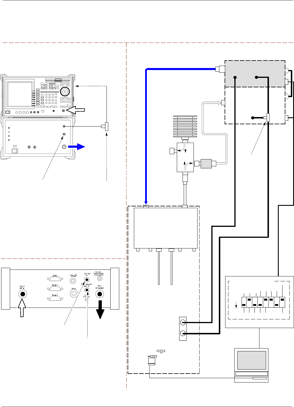
Test Equipment Set-up68P64115A18–1
Mar 2003 1X SC 4812T Lite BTS Optimization/ATP Software Release R2.16.1.x
DRAFT
3-71
Figure 3-22: IS–95A/B and CDMA2000 1X ATP Test Setup With TRDCs –
Advantest R3267/3562 Test Equipment, Agilent E7495A
TEST SETS Optimization/ATP SET UP
INPUT 50 Ω
RF OUT
50 Ω
Advantest R3267 (Top) and R3562 (Bottom)
FREQ MONITOR
19.6608 MHZ CLOCK
REFERENCE FROM
CSM BOARD
SYNC MONITOR
EVEN SEC TICK
PULSE REFERENCE
FROM CSM BOARD
BNC
“T”
NOTE:
SYNTHE REF IN ON REAR OF SIGNAL GENERATOR IS
CONNECTED TO 10 MHZ REF OUT ON REAR OF
SPECTRUM ANALYZER (SEE FIGURE F-17)
TO EXT TRIG
ON REAR OF
SPECTRUM
ANALYZER
TO
MPC
TO PA
TRUNKING
MODULE
RS232–GPIB
INTERFACE BOX
INTERNAL PCMCIA
ETHERNET CARD
GPIB
CABLE
UNIVERSAL TWISTED
PAIR (UTP) CABLE
(RJ45 CONNECTORS)
RS232 NULL
MODEM
CABLE
S MODE
DATA FORMAT
BAUD RATE
GPIB ADRS G MODE
ON
BTS
INTERNAL
TX
CABLE
CDMA
LMF
DIP SWITCH SETTINGS
10BASET/
10BASE2
CONVERTER
LAN
B
LAN
A
RX TEST
CABLE
SPECTRUM
ANALYZER
GPIB
INPUT
50 Ω
RF OUT
50 Ω
RX
ANTENNA
CONNECTOR
FREQ
MONITOR
SYNC
MONITOR
CSM
INTERNAL
RX
CABLE
TX
ANTENNA
CONNECTOR
SIGNAL GENERATOR
GPIB
SYNTHE
REF
IN
10 MHZ
OUT
50 Ω
TERM
.
TX TEST
CABLE
DIRECTIONAL
COUPLER
(30 DB)
100–WATT (MIN.)
NON–RADIATING
RF LOAD
EXT
TRIG IN
MOD TIME
BASE IN
TX TEST
CABLE
BNC
“T”
EXT TRIG
* BLACK RECTANGLES
REPRESENT THE RAISED
PART OF SWITCHES
TX
ANT
CPLD
RX
BTS
CPLD
TRDC
TX
BTS
CPLD
RX
ANT
CPLD
2O DB IN–LINE
ATTENUATOR
IMPORTANT:
WHEN PERFORMING FER TEST ON COMPANION FRAME DIVERSITY RX, CONNECT
RX TEST CABLE TO RX ANTENNA PORT ON COLLOCATED COMPANION FRAME.
Agilent E7495A
RF
OUT
RF
IN
SYNC MONITOR
EVEN SEC TICK
PULSE REFERENCE
FROM CSM BOARD
TO “EXT REF IN” –
FREQ MONITOR
19.6608 MHZ CLOCK
REFERENCE FROM
CSM BOARD

Test Set Calibration 68P64115A18–1
Mar 2003
1X SC 4812T Lite BTS Optimization/ATP Software Release R2.16.1.x
DRAFT
3-72
Test Set Calibration
Background
Proper test equipment calibration helps to ensure accurate BTS
optimization and acceptance testing by assuring that the test equipment
and associated cables do not introduce measurement errors.
NOTE If the test equipment set being used to optimize or test the BTS
has been calibrated and maintained as a set, this procedure does
not need to be performed.
This procedure must be performed prior to beginning the optimization.
Verify all test equipment (including all associated cables and adapters
actually used to interconnect test equipment items and the BTS) has been
calibrated and maintained as a set.
CAUTION If any piece of test equipment, test cable, or RF adapter that
makes up the calibrated test equipment set has been replaced, the
set must be re-calibrated. Failure to do so can introduce
measurement errors, resulting in incorrect measurements and
degradation to system performance. Motorola recommends
repeating cable calibration before testing at each BTS site.
NOTE Calibration of the communications system analyzer (or
equivalent test equipment) must be performed at the site before
calibrating the overall test equipment set. Calibrate the test
equipment after it has been allowed to warm–up and stabilize for
a a minimum of 60 minutes.
Calibration Procedures Included
Automatic
Procedures included in this section use the LMF automated calibration
routine to determine path losses of the supported communications
analyzer, power meter, associated test cables, adapters, and (if used)
antenna switch that make up the overall calibrated test equipment set.
After calibration, the gain/loss offset values are stored in a test
measurement offset file on the LMF computer.
Manual
Agilent E4406A Transmitter Tester – The E4406A does not support
the power level zeroing calibration performed by the LMF. If this
instrument is to be used for Bay Level Offset calibration and calibration
is attempted with the LMF Calibrate Test Equipment function, the
LMF will return a status window failure message stating that zeroing
power is not supported by the E4406A. Refer to the Equipment
Calibration section of Appendix F for instructions on using the
instrument’s self–alignment (calibration) function prior to performing
Bay Level Offset calibration.
Power Meters – Manual power meter calibration procedures to be
performed prior to automated calibration are included in the Equipment
Calibration section of Appendix F.

Test Set Calibration68P64115A18–1
Mar 2003 1X SC 4812T Lite BTS Optimization/ATP Software Release R2.16.1.x
DRAFT
3-73
Cable Calibration – Manual cable calibration procedures using the HP
8921A and Advantest R3465 communications system analyzers are
provided in the Manual Cable Calibration section of Appendix F, if
needed.
GPIB Addresses
GPIB addresses can range from 1 through 30. The LMF will accept any
address in that range, but the numbers entered in the LMF Options
window GPIB address boxes (Table 3-23 and Table 3-24) must match
the addresses set in the test equipment. Motorola recommends using 1
for a CDMA signal generator, 13 for a power meter, and 18 for a
communications system analyzer. To verify and, if necessary, change the
GPIB addresses of the test equipment, refer to the Setting GPIB
Addresses section of Appendix F.
Selecting Test Equipment
Serial Connection and Network Connection tabs are provided in the
LMF Options window to specify the test equipment connection method.
The Serial Connection tab is used when the test equipment items are
connected directly to the LMF computer through a GPIB box (normal
setup). The Network Connection tab is used when the test equipment is
to be connected remotely via a network connection.
Prerequisites
Be sure the following have been completed before selecting test
equipment:
STest equipment is turned on.
SGPIB addresses set in the test equipment have been verified as correct
using the applicable procedures in Appendix NO TAG.
SLMF computer serial port and test equipment are connected to the
GPIB box.
Selecting Test Equipment
Test equipment may be selected either manually with operator input or
automatically using the LMF autodetect feature.

Test Set Calibration 68P64115A18–1
Mar 2003
1X SC 4812T Lite BTS Optimization/ATP Software Release R2.16.1.x
DRAFT
3-74
Manually Selecting Test Equipment in a Serial Connection Tab
Test equipment can be manually specified before or after the test
equipment is connected. The LMF does not attempt to verify the test
equipment is actually detected when manual selection is specified.
Follow the procedure in Table 3-23 to manually select test equipment.
Table 3-23: Selecting Test Equipment Manually in the Serial Connection Tab
Step Action
1In the LMF window menu bar, click Tools and select Options... from the pull–down menu.
– The LMF Options window appears.
2If it is not in the forefront, click on the Serial Connection tab.
3Select the correct serial port in the COMM Port: pick list (normally COM1).
4If it is not selected (black dot showing), click on the Manual Specification button.
5Click on the check box(es) corresponding to the test equipment item(s) to be used.
6Type the GPIB address in the corresponding GPIB address box (refer to the Setting GPIB Addresses
section of Appendix F for directions on verifying and/or changing test equipment GPIB addresses).
Motorola–recommended addresses are:
1 = signal generator
13 = power meter
18 = communications system analyzer
NOTE
When test equipment items are manually selected by the operator, the LMF defaults to using a power
meter for RF power measurements. The LMF will use a communications system analyzer for RF
power measurements only if a power meter is not selected (power meter checkbox not checked).
7Click on Apply.
– The button will darken until the selection has been recorded.
NOTE
With manual selection, the LMF does not attempt to detect the test equipment to verify it is connected
and communicating with the LMF.
8Click on Dismiss to close the LMF Options window.

Test Set Calibration68P64115A18–1
Mar 2003 1X SC 4812T Lite BTS Optimization/ATP Software Release R2.16.1.x
DRAFT
3-75
Automatically Selecting Test Equipment in the Serial Connection Tab
When using the auto-detection feature to select test equipment, the LMF
determines which test equipment items are actually communicating with
LMF. Follow the procedure in Table 3-24 to use the auto-detection
feature.
Table 3-24: Selecting Test Equipment Using Auto-Detect
Step Action
1In the LMF window menu bar, click Tools and select Options... from the pull–down menu.
– The LMF Options window appears.
2If it is not in the forefront, click on the Serial Connection tab.
3Select the correct serial port in the COMM Port: pick list (normally COM1).
4If it is not selected (no black dot showing), click on the Auto–Detection button.
5If they are not already displayed in the box labeled GPIB address to search, click in the box and type
in the GPIB addresses for the test equipment to be used, separating each address with commas and no
spaces. (Refer to the Setting GPIB Addresses section of Appendix F for instructions on verifying
and/or changing test equipment GPIB addresses.)
NOTE
During the GPIB address search for a test equipment item to perform RF power measurements (that is,
for TX calibration), the LMF will select the first item it finds with the capability to perform the
measurement. If, for example, the address sequence 13,18,1 is included in the GPIB addresses to
search box, the power meter (GPIB address 13) will be used for RF power measurements. If the
address sequence 18,13,1 is included, the LMF will use the communications system analyzer (GPIB
address 18) for power measurements.
6 Click Apply.
– The button will darken until the selection has been recorded.
– A check mark will appear in the applicable Manual Configuration section check boxes for
detected test equipment items.
7 Click Dismiss to close the LMF Options window.

Test Set Calibration 68P64115A18–1
Mar 2003
1X SC 4812T Lite BTS Optimization/ATP Software Release R2.16.1.x
DRAFT
3-76
Calibrating Test Equipment
The LMF Calibrate Test Equipment function zeros the power
measurement level of the test equipment item that is to be used for TX
calibration and audit. If both a power meter and an analyzer are
connected (for example, an HP 437 and an HP8921A/600), only the
power meter is zeroed.
NOTE The Agilent E4406A transmitter tester does not support power
measurement level zeroing. Refer to the Equipment Calibration
section of Appendix F for E4406A calibration.
Prerequisites
SLMF computer serial port and test equipment are connected to the
GPIB box.
STest equipment is turned on and has warmed up for at least 60
minutes.
STest equipment has been selected in the LMF (Table 3-23 or
Table 3-24)
Follow the procedure in Table 3-25 to calibrate the test equipment.
Table 3-25: Test Equipment Calibration
nStep Action
1From the Util menu, select Calibrate Test Equipment
from the pull–down menu. A Directions window is
displayed.
2Follow the directions provided.
3Click on Continue to close the Directions window and
start the calibration process. A status report window is
displayed.
4Click on OK to close the status report window.

Test Set Calibration68P64115A18–1
Mar 2003 1X SC 4812T Lite BTS Optimization/ATP Software Release R2.16.1.x
DRAFT
3-77
Calibrating Cables Overview
The LMF Cable Calibration function is used to measure the path loss
(in dB) for the TX and RX cables, adapters, directional couplers, and
attenuators that make up the cable configurations used for testing. A
communications system analyzer is used to measure the loss of both the
TX test cable and the RX test cable configurations. LMF cable
calibration consists of the following processes:
1. Measure the loss of a short cable. This is done to compensate for any
measurement error of the communications system analyzer. The
short cable, which is used only for the calibration process, is
connected in series with both the TX and RX test cable
configurations when they are measured. The measured loss of the
short cable is deducted from the measured loss of the TX and RX
test cable configurations to determine the actual loss of the
configurations. This deduction is done so any error in the analyzer
measurement will be adjusted out of both the TX and RX
measurements.
2. Measure the loss of the short cable plus the RX test cable
configuration. The RX test cable configuration normally consists
only of a coax cable with type–N connectors that is long enough to
reach from the BTS RX connector to the test equipment. When the
BTS antenna connectors carry duplexed TX and RX signals, a
directional coupler and, if required by BTS type, an additional
attenuator are also required for the RX test cable configuration.
These additional items must be included in the path loss
measurement.
3. Measure the loss of the short cable plus the TX test cable
configuration. The TX test cable configuration normally consists of
two coax cables with type–N connectors, a directional coupler, a
termination load with sufficient rating to dissipate the BTS output
power, and an additional attenuator, if required by the BTS type. The
total path loss of the TX test configuration must be as required for
the BTS (normally 30 or 50 dB). The Motorola Cybertest analyzer is
different from other communications system analyzers because the
required attenuation/load is built into the test set. Because of this,
the Cybertest TX test configuration consists only of the required
length coax cable.

Test Set Calibration 68P64115A18–1
Mar 2003
1X SC 4812T Lite BTS Optimization/ATP Software Release R2.16.1.x
DRAFT
3-78
Calibrating Test Cabling using Communications System Analyzer
NOTE LMF cable calibration cannot be accomplished with an
HP8921A analyzer for 1.9 GHz. A different analyzer type or the
signal generator and spectrum analyzer method (Table 3-27 and
Table 3-28) must be used. Cable calibration values must be
manually entered into the LMF cable loss file if the signal
generator and spectrum analyzer method is used. To use the
HP8921A for manual test cable configuration calibration for 800
MHz BTSs, refer to the Manual Cable Calibration section of
Appendix F.
Prerequisites
STest equipment is turned on and has warmed up for at least 60
minutes.
STest equipment has been selected in the LMF (Table 3-23 or
Table 3-24).
STest equipment has been calibrated and correctly connected for the
type of test cable configuration to be calibrated.
Procedure
Refer to Figure 3-11, Figure 3-12, or Figure 3-13 and follow the
procedure in Table 3-26 to calibrate the test cable configurations.
Table 3-26: Test Cabling Calibration using Comm. System Analyzer
nStep Action
1 Click Util in the BTS menu bar, and select Cable
Calibration... in the pull–down menu. A Cable
Calibration window is displayed.
2Enter one or more channel numbers in the Channels box.
NOTE
Multiple channel numbers must be separated by a comma
with no spaces (for example, 200,800). When two or
more channel numbers are entered, the cables will be
calibrated for each channel. Interpolation will be
accomplished for other channels, as required, for TX
calibration.
3 Select TX and RX CABLE CAL, TX CABLE CAL or
RX CABLE CAL in the Cable Calibration picklist.
4 Click OK, and follow the directions displayed for each
step. A status report window will be displayed with the
results of the cable calibration.
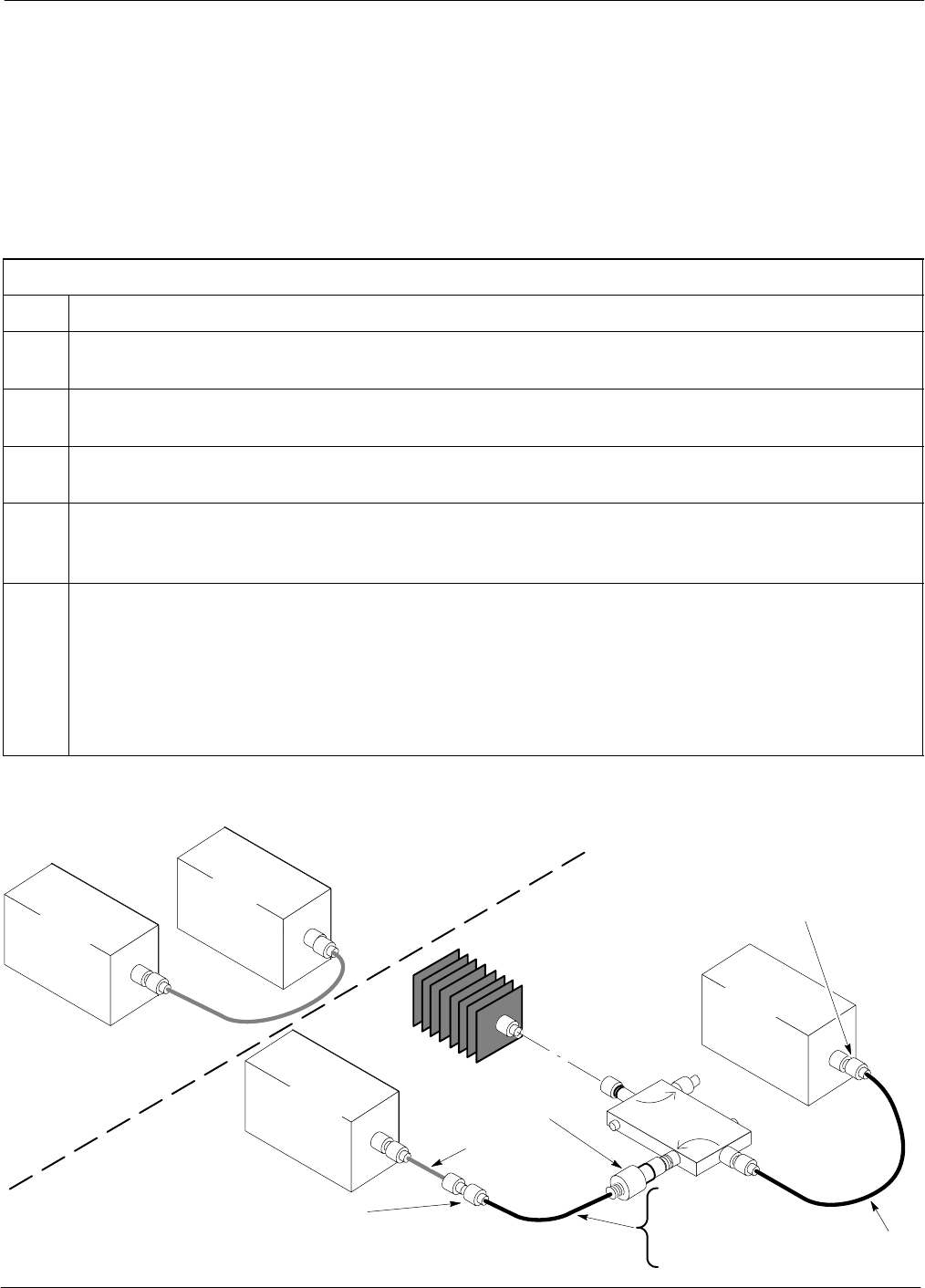
Test Set Calibration68P64115A18–1
Mar 2003 1X SC 4812T Lite BTS Optimization/ATP Software Release R2.16.1.x
DRAFT
3-79
Calibrate Test Cabling Using Signal Generator & Spectrum Analyzer
Refer to Figure 3-23 and follow the procedure in Table 3-27 to calibrate
the TX test cable configuration for all BTSs or the RX ATP test cable
configuration for BTSs with duplexed TX/RX using the signal generator
and spectrum analyzer. Refer to Figure 3-24 and follow the procedure in
Table 3-28 to calibrate the test cable configuration for non–duplexed RX
using the signal generator and spectrum analyzer.
TX and Duplexed RX Cable Calibration
Table 3-27: Calibrate TX/Duplexed RX Test Cabling using Signal Generator & Spectrum Analyzer
Step Action
1Connect a short test cable between the spectrum analyzer and the signal generator as shown in
Figure 3-23, detail “A” (top portion of figure).
2Set signal generator to 0 dBm at the customer frequency of the 869.7–893.31 MHz band for North
American cellular and 1930–1990 MHz band for North American PCS.
3Use spectrum analyzer to measure signal generator output and record the value for the detail “A”
setup.
4Change the test setup to the one shown in detail “B” (lower portion of Figure 3-23), to measure cable
output at customer frequency (869.7–893.31 MHz band for North American cellular and 1930–1990
MHz for North American PCS) and record the value measured using the detail “B” test setup.
5Calibration factor = (value measured with detail “A” setup) – (value measured with detail “B” setup)
Example: Cal factor = –1 dBm – (–53.5 dBm) = 52.5 dB
NOTE
The short cable is used for calibration only. It is not part of the final test setup. After calibration is
completed, do not re-arrange any cables. Use the test cable configuration as–is to ensure test
procedures use the correct calibration factor.
Figure 3-23: Cal Setup for TX/Duplexed RX Test Cabling Using Signal Generator & Spectrum Analyzer
50 OHM
TERMINATION
30 DB
DIRECTIONAL
COUPLER
Spectrum
Analyzer
Signal
Generator
A
Spectrum
Analyzer
40W NON–RADIATING
RF LOAD
B
SHORT TEST CABLE
Signal
Generator
THIS WILL CONNECT TO THE POWER METER OR
COMMUNICATIONS SYSTEM ANALYZER DURING TX
CALIBRATION AND TO THE COMMUNICATIONS
SYSTEM ANALYZER DURING TX AND RX ATP TESTS.
SHORT
TEST
CABLE
SECOND TX TEST CABLE
FOR TX CAL AND ATP
20DB 20 W IN–LINE
ATTENUATOR FOR
1.9 GHZ
THIS WILL CONNECT TO THE BTS TX
ANTENNA CONNECTOR DURING TX
CALIBRATION AND TO THE TX/RX ANTENNA
CONNECTORS DURING ATP TESTS.
TX TEST
CABLE
RX TEST CABLE
FOR RX ATP TEST
OR
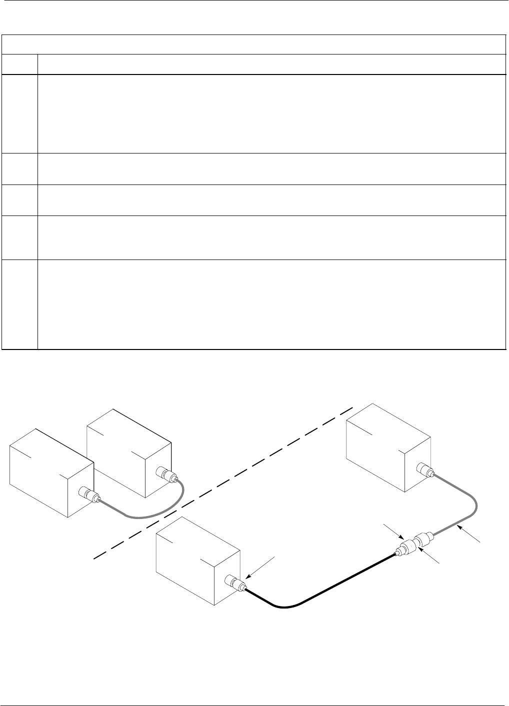
Test Set Calibration 68P64115A18–1
Mar 2003
1X SC 4812T Lite BTS Optimization/ATP Software Release R2.16.1.x
DRAFT
3-80
Non-Duplexed RX Cable Calibration
Table 3-28: Calibrating Non–Duplexed RX Test Cabling Using Signal Generator & Spectrum Analyzer
Step Action
1NOTE
When preparing to calibrate a BTS with duplexed TX and RX the RX cable calibration must be done
using calibration setup in Figure 3-23 and the procedure in Table 3-27.
Connect a short test cable between the spectrum analyzer and the signal generator as shown in
Figure 3-24, detail “A” (top portion of figure).
2Set signal generator to –10 dBm at the customer’s RX frequency of 824.7–848.31 MHz for North
American cellular or 1850–1910 MHz band for North American PCS.
3Use the spectrum analyzer to measure signal generator output and record the value for the detail “A”
setup.
4Change the test setup to the one shown in detail “B” (lower portion of Figure 3-24) to measure the
output at the customer’s RX frequency (824.7–848.31 MHz for North American cellular or 1850–1910
MHz band for North American PCS). Record the value measured with the detail “B” test setup.
5Calibration factor = (value measured with detail “A” setup) – (value measured with detail “B” setup)
Example: Cal factor = –12 dBm – (–14 dBm) = 2 dB
NOTE
The short test cable is used for test equipment setup calibration only. It is not part of the final test
setup. After calibration is completed, do not re-arrange any cables. Use the test cable configuration
as–is to ensure test procedures use the correct calibration factor.
Figure 3-24: Cal Setup for Non–Duplexed RX Test Cabling Using Signal Generator & Spectrum Analyzer
Spectrum
Analyzer
Signal
Generator
A
B
Spectrum
Analyzer
SHORT
TEST
CABLE
CONNECTION TO THE COMMUNICATIONS
SYSTEM ANALYZER RF OUTPUT
CONNECTOR DURING RX MEASUREMENTS
Signal
Generator
BULLET
CONNECTOR
RX TEST
CABLE
SHORT TEST
CABLE
CONNECTION TO THE BTS RX ANTENNA
CONNECTOR DURING RX ATP
IMPORTANT: IF BTS TX/RX SIGNALS ARE
DUPLEXED, THE RX TEST CABLE CONNECTS
TO THE DUPLEXED ANTENNA CONNECTOR
AND MUST USE/BE CALIBRATED WITH THE 30
DB DIRECTIONAL COUPLER AND 20 DB
IN–LINE ATTENUATOR. SEE FIGURE 3-23.

Test Set Calibration68P64115A18–1
Mar 2003 1X SC 4812T Lite BTS Optimization/ATP Software Release R2.16.1.x
DRAFT
3-81
Setting Cable Loss Values
Cable loss values for TX and RX test cable configurations are normally
set by accomplishing automatic cable calibration using the LMF and the
applicable test equipment. The LMF stores the measured loss values in
the cable loss files. The cable loss values can also be set or changed
manually.
CAUTION If cable calibration was performed without using the LMF, cable
loss values must be manually entered in the LMF database.
Failure to do this will result in inaccurate BTS calibration and
reduced site performance.
Prerequisites
SLMF is logged into the BTS
Table 3-29: Setting Cable Loss Values
Step Action
1 Click Util in the BTS menu bar, and select Edit > Cable Loss in the pull–down menus.
–A tabbed data entry pop–up window will appear.
2Click on the TX Cable Loss tab or the RX Cable Loss tab, as required.
3To add a new channel number, perform the following:
3a – Click on the Add Row button.
3b – Click in the Channel # or Loss (dBm) column, as required.
3c – Enter the desired value.
4To edit existing values, click in the data box to be changed and change the value.
5To delete a row, click on the row and then click on the Delete Row button.
6For each tab with changes, click on the Save button to save displayed values.
7Click on the Dismiss button to close the window.
NOTE
SValues entered or changed after the Save button was used will be lost when the window is
dismissed.
SIf cable loss values exist for two different channels the LMF will interpolate for all other channels.
SEntered values will be used by the LMF as soon as they are saved. It is not necessary to log out and
log back into the LMF for changes to take effect.

Test Set Calibration 68P64115A18–1
Mar 2003
1X SC 4812T Lite BTS Optimization/ATP Software Release R2.16.1.x
DRAFT
3-82
Setting TX Coupler Loss Value
If an in–service TX coupler is installed, the coupler loss must be
manually entered so it will be included in the LMF TX calibration and
audit calculations.
Prerequisites
SLMF is logged into the BTS
SPath loss, in dB, of the TX coupler must be known
Table 3-30: Setting TX Coupler Loss Values
Step Action
1 Click Util in the BTS menu bar, and select Edit > Coupler Loss... in the pull–down menus.
–A tabbed data entry pop–up window will appear.
2Click on the TX Coupler Loss tab or the RX Coupler Loss tab, as required
3Click in the Loss (dBm) column for each carrier that has a coupler and enter the appropriate value.
4To edit existing values, click in the data box to be changed and change the value.
5For each tab with changes, click on the Save button to save displayed values.
6Click on the Dismiss button to close the window.
NOTE
SValues entered or changed after the Save button is used will be lost when the window is dismissed.
SThe In–Service Calibration check box in the Tools > Options > BTS Options tab must be
checked before entered TX coupler loss values will be used by the TX calibration and audit
functions.
SNew or changed values will be used by the LMF as soon as they are saved. Logging out and logging
in again are not required to cause saved changes to take effect.

Bay Level Offset Calibration68P64115A18–1
Mar 2003 1X SC 4812T Lite BTS Optimization/ATP Software Release R2.16.1.x
DRAFT
3-83
Bay Level Offset Calibration
Purpose of Bay Level Offset Calibration
Bay Level Offset (BLO) calibration is the central activity of the
optimization process. BLO calibration compensates for normal
equipment variations within the BTS RF paths and assures the correct
transmit power is available at the BTS antenna connectors to meet site
performance requirements.
What is BLO Calibration?
Description
BLO calibration is the complete title of what is normally referred to as
“calibration.” Calibration identifies the accumulated gain in every
transmit path at the BTS site. The transmit path BLO values determined
during calibration are stored in the LMF calibration data file, and are
subsequently downloaded to each BBX. When transmit path calibration
is performed, receive path BLO values will automatically be set to the
default value in the LMF calibration file and downloaded.
BTS RF Path Descriptions
Transmit (TX) path – A TX path starts at an SCCP shelf BBX
backplane slot, travels through the CIO card, is routed to the Power
Amplifier (PA) trunking module for sector phase shifting, through the
PAs, back through the PA trunking module for sector phase selection,
through the TX bandpass filter (starter frames) or 2:1 TX combiner
(companion frames), through the Transmit & Receive Filter (TRF) or
Duplexer TX/RF Filter (DRF), and ends at the TRF or DRF antenna
connector.
Receive (RX) main path – A main RX path starts at ANTENNAS
connectors 1A, 2A, or 3A and travels through the associated TRF or
DRF, the MPC in SCCP cage slot MPC–1, the CIO card, and terminates
at a backplane BBX slot in the SCCP shelf.
Diversity RX path – Diversity RX paths differ for SC4812T Lite starter
(stand–alone) and companion frames. The following describe each type
of path:
SStarter frame diversity RX path – A starter frame diversity RX path
is the same as a main RX path except that it starts at ANTENNAS
connectors 1B, 2B, or 3B, travels through the associated TRF or DRF,
and the MPC card in SCCP cage slot MPC–2 (refer to Table 1-6).
SCompanion frame diversity RX path – The companion frame main
RX signal is used for the collocated companion frame diversity RX
signal. A companion frame’s diversity RX path starts at ANTENNAS
connectors 1A, 2A, or 3A in the collocated companion frame. It
travels through the associated TRF or DRF, the MPC in SCCP cage
slot MPC–1, and the CIO card where it is then routed out of the frame
through the RX expansion out connectors (RX EXPANSION 1A, 2A,

Bay Level Offset Calibration 68P64115A18–1
Mar 2003
1X SC 4812T Lite BTS Optimization/ATP Software Release R2.16.1.x
DRAFT
3-84
or 3A). The signal travels through the inter–frame diversity RX
cables, into the RX expansion in ports (RX EXPANSION 1B, 2B, or
3B in NO TAG or NO TAG) of the companion frame, through the
Expansion MPC (EMPC) in SCCP cage slot MPC–2, the CIO, and
terminates at a backplane BBX slot in the SCCP shelf.
SRFDS sampling paths – Directional couplers for RFDS signal
sampling are integral to the SC4812T Lite transmit and receive paths
in the DRDCs and TRDCs. Cables connect from these directional
couplers to the RFDS input connectors.
Component Verification During Calibration
TX Path Calibration
TX path calibration supports verification of correct BTS installation, RF
cabling installation and performance, functionality of all equipment
installed in the transmit RF chain, and the proper functioning of each
transmit RF path. External test equipment is used to calibrate and audit
the TX paths of the BTS.
RX Path Calibration
RX path calibration is not required or supported on CDMA BTS
systems. Default RX calibration values are written to the RX calibration
data files during the TX calibration process. RX functionality is verified
during Frame Erasure Rate (FER) testing.
When to Calibrate BLOs
Calibration to determine BLO:
1. Is required after initial BTS installation.
2. Must be done once each year for an operational BTS site.
3. Is recommended by Motorola for all associated RF paths after
replacing any of the following components:
– BBX card
– SCCP shelf
– CIO card
– CIO–to–PA trunking module RF cable
– PA trunking module
– Power Amplifier
– Trunking module–to–TX filter/filter combiner RF cable
– TX filter or TX filter combiner
– TX filter/filter combiner–to–DRDC/TRDC cable
– DRDC or TRDC
BLO Calibration Data File
During the calibration process, the LMF creates a calibration (CAL) data
file where BLO values are stored. After calibration has been completed,
these offset values must be downloaded to the BBXs using the LMF
BLO download function. A detailed description of the file organization
and content is provided in the following paragraphs

Bay Level Offset Calibration68P64115A18–1
Mar 2003 1X SC 4812T Lite BTS Optimization/ATP Software Release R2.16.1.x
DRAFT
3-85
NOTE Due to the size of the file, Motorola recommends printing out a
copy of a bts–#.cal file and referring to it for the following
descriptions.
CAL File Organization
The CAL file is subdivided into three sections called “slot Blocks”.
These are:
1. Slot[1] Block which contains the calibration data for the six primary
BBX slots.
2. Slot[20] Block which contains the calibration data for the redundant
BBX (see Table 3-32).
3. Slot[385] Block which contains the calibration data for the RFDS.
BBX Slot Block Parts
BBX slot Blocks are further subdivided into the parts described in the
following:
Slot Block Header – Each BBX slot Block has a header section (slot
header) which contains:
SA creation Date and Time – broken down into separate parameters of
createMonth, createDay, createYear, createHour, and createMin.
SThe number of calibration entries in the file – the numBayLevelPts
parameter. The parameter is fixed at 720 entries for SC4812–series
frames. These 720 entries are combined to define the 360 calibration
points of the CAL file.
SThe slot Block format parameter.
Slot Block Bay Level Calibration Data – Each BBX slot Block has a
Bay Level Calibration data section (BayLevelCal) which is organized as
a large flat array. The array is organized by branch, SCCP cage BBX
slot, and calibration entries. There are several ways to look at the array
contents. Two different views are provided in the following to illustrate
the significant features of BayLevelCal section content and organization:
SThe first view of the array is shown in Table 3-31. This view shows
the three branches of the array, transmit, main receive, and diversity
receive offsets, and the calibration entry ranges which apply to each.
Table 3-31: BLO bts–#.cal File Array Branch Assignments
Range Branch Assignment
C[1]–C[120] Transmit
C[121]–C[240] No SC4812T Lite BLO cal point
entries (default only)
C[241]–C[360] Receive
C[361]–C[480] No SC4812T Lite BLO cal point
entries (default only)
C[481]–C[600] Diversity Receive
C[601]–C[720] No SC4812T Lite BLO cal point
entries (default only)
Bay Level Offset Calibration 68P64115A18–1
Mar 2003
1X SC 4812T Lite BTS Optimization/ATP Software Release R2.16.1.x
DRAFT
3-86
SThe second view of the array is shown in Table 3-32. This view shows
the assignment of calibration entries in each branch to each BBX slot,
carrier, and sectorization. Three sectors are allowed for an SC4812T
Lite frame.
Table 3-32: SC4812T Lite bts–#.cal File Array (By BBX/Sector)
BBX Sectorization TX Branch RX Branch RX Diversity
Branch
Slot[1] (Primary BBXs 1 through 6)
1 (Omni)
3S t
C[1]–C[20] C[241]–C[260] C[481]–C[500]
23–Sector,
1st Carrier
C[21]–C[40] C[261]–C[280] C[501]–C[520]
3
1st Carrier
C[41]–C[60] C[281]–C[300] C[521]–C[540]
4
3S t
C[61]–C[80] C[301]–C[320] C[541]–C[560]
53–Sector,
2nd Carrier
C[81]–C[100] C[321]–C[340] C[561]–C[580]
6
2nd Carrier
C[101]–C[120] C[341]–C[360] C[581]–C[600]
C[121]–C[140] C[361]–C[380] C[601]–C[620]
Not Used in SC4812T Lite
C[141]–C[160] C[381]–C[400] C[621]–C[640]
N
o
t U
se
d i
n
SC4812T Lit
e
(
CAL file entries are C[161]–C[180] C[401]–C[420] C[641]–C[660]
(CAL file entries are
Channel 0 with default
t l l )
C[181]–C[200] C[421]–C[440] C[661]–C[680]
power set level.) C[201]–C[220] C[441]–C[460] C[681]–C[700]
C[221]–C[240] C[461]–C[480] C[701]–C[720]
Slot[20] (Redundant BBX–R1)
1 (Omni)
3S t
C[1]–C[20] C[241]–C[260] C[481]–C[500]
23–Sector,
1st Carrier
C[21]–C[40] C[261]–C[280] C[501]–C[520]
3
1st Carrier
C[41]–C[60] C[281]–C[300] C[521]–C[540]
4
3S t
C[61]–C[80] C[301]–C[320] C[541]–C[560]
53–Sector,
2nd Carrier
C[81]–C[100] C[321]–C[340] C[561]–C[580]
6
2nd Carrier
C[101]–C[120] C[341]–C[360] C[581]–C[600]
C[121]–C[140] C[361]–C[380] C[601]–C[620]
Not Used in SC4812T Lite
C[141]–C[160] C[381]–C[400] C[621]–C[640]
N
o
t U
se
d i
n
SC4812T Lit
e
(
CAL file entries are C[161]–C[180] C[401]–C[420] C[641]–C[660]
(CAL file entries are
Channel 0 with default
t l l )
C[181]–C[200] C[421]–C[440] C[661]–C[680]
power set level.) C[201]–C[220] C[441]–C[460] C[681]–C[700]
C[221]–C[240] C[461]–C[480] C[701]–C[720]
SWhen referring to the CAL file print–out and Table 3-32, it can be
seen that there is one BBX slot per sector with 20 “calibration entries”
per BBX (sector) for each branch. Two calibration entries define a
single “calibration point;” therefore there are ten calibration points in
each branch for each BBX.
– The first entry for a calibration point (all odd entries) identifies the
CDMA channel (frequency) where the BLO is measured. The
second calibration entry (all even entries) is the power set level
(PwrLvlAdj) for that frequency. The valid range for PwrLvlAdj is

Bay Level Offset Calibration68P64115A18–1
Mar 2003 1X SC 4812T Lite BTS Optimization/ATP Software Release R2.16.1.x
DRAFT
3-87
from 2500 to 27500 (2500 corresponds to –125 dBm and 27500
corresponds to +125 dBm).
– The ten calibration points for each slot–branch combination must be
stored in order of increasing frequency. If less than ten points
(frequencies) are calibrated, the BLO data for the highest frequency
calibrated is written into the remainder of the ten points for that
slot–branch.
Example:
C[1]=384 (odd cal entry)
C[2]=19102 (even cal entry)
C[3]=777 (odd cal entry)
C[4]=19086 (even cal entry)
C[19]=777 (odd cal entry)
C[20]=19086 (even cal entry)
.
.
.
= 1 “calibration point”
= 1 “calibration point”
= 1 “calibration point”
In the example above, BLO was measured at only two frequencies
(channels 384 and 777) for SCCP slot BBX–1 transmit (Table 3-32).
The BLO data for the highest frequency measured (channel 777) will
be written to the remaining eight transmit calibration points (defined
by entries C[5] through C[20]) for BBX–1.
Slot Block Temperature Compensation – Each BBX slot Block also
has a temperature compensation data section (TempLevelCal) where
power level compensation factors for temperature variations are stored.
CAL File and BLO Data Download
When BLO data is downloaded to the BBXs after calibration, the data is
downloaded to the devices in the order it is stored in the CAL file. TX
calibration data (entries C[1] – C[60]) are sent first. Data for the ten
BBX slot 1 calibration points (entries C[1] – C[20]) are sent initially,
followed by data for the ten BBX slot 2 calibration points (entries C[21]
– C[40]), and so on. The RX calibration data is sent next in BBX slot
sequence, followed by RX Diversity calibration data.

Bay Level Offset Calibration 68P64115A18–1
Mar 2003
1X SC 4812T Lite BTS Optimization/ATP Software Release R2.16.1.x
DRAFT
3-88
Test Equipment Setup for RF Path Calibration
Follow the steps outlined in Table 3-33 and refer as needed to
Figure 3-14 or Figure 3-15 to set up test equipment.
Table 3-33: Set Up Test Equipment for RF Path Calibration
Step Action
1If it has not already been done, refer to the procedure in Table 3-5 (on page 3-17) to interface the LMF
computer terminal to the frame LAN A connector.
2If it has not already been done, refer to Table 3-6 (on page 3-26) to start a GUI LMF session.
3If required, calibrate the test equipment per the procedure in Table 3-25 (on page 3-76).
! CAUTION
To prevent damage to the test equipment, all transmit (TX) test connections must be via the 30 dB
directional coupler for 800 MHz or via a 30 dB coupler with a 20 dB in–line attenuator for 1900 MHz.
4For TX path calibration, connect the test equipment as shown in Figure 3-14, Figure 3-15, or
Figure 3-16, depending on the communications analyzer being used.
Transmit (TX) Path Calibration Description
The assigned channel frequency and desired power level at the frame TX
ports for transmit calibration are derived from the BTS CDF file. Each
BBX at the site is assigned to a sector and carrier. These are specified
respectively in the sector and carrier fields of the ParentCARRIER
parameter in each BBXs CDF file block. The channel frequency and
desired power for the assigned sector are specified respectively in the
ChannelList and SIFPilotPwr parameters of the CDF block for the
CARRIER to which the BBX is assigned.
NOTE Be sure the bts–#.cdf (or bts–#.necf) and cbsc–#.cdf files
loaded on the LMF computer are current. The LMF will obtain
carrier and channel information from these files and insert it into
the appropriate CDMA Test Parameter screen. Failure to have
the most current files from the CBSC can result in incorrect
channel information being used to calibrate the BTS and
unfavorable affects on BTS performance. Carrier and channel
numbers should only be entered manually for special test cases
or as a last resort.
The calibration process attempts to adjust the measured power to within
+0.5 dB of the desired power. The calibration will pass if the error is less
than +1.5 dB.
The TX BLO for the SC 4812T Lite is approximately 42.0 dB ±5.0 dB.
BLO is the gain in dB between the known power output of the BBX and
the measured power at the TX port. BLO is derived by deducting the
known BBX power output from the power measured at the TX port or
(Measured Power) – (BBX TX Power Output).
Example:
Measured Power (at TX port) = 36.0 dBm
Known BBX TX Power Output = –6.0 dBm
BLO = (36.0) – (–6.0) = 42.0 dB gain

Bay Level Offset Calibration68P64115A18–1
Mar 2003 1X SC 4812T Lite BTS Optimization/ATP Software Release R2.16.1.x
DRAFT
3-89
TX Calibration and the LMF
The LMF Tests > TX > TX Calibration... and Tests > All Cal/Audit...
selections perform TX BLO calibration testing for installed BBX(s). The
All Cal/Audit... selection initiates a series of actions to perform TX
calibration, and if calibration is successful, download BLO and perform
TX audit. The TX Calibration... selection performs only TX
calibration. When TX Calibration... is used, BLO download and TX
audit must be performed as separate activities. The CDMA Test
Parameters window which opens when TX Calibration... or All
Cal/Audit... is selected contains several user–selectable features which
are described in the following subsections.
Rate Set Drop–down Pick List
The Rate Set Drop–down Box is enabled if at least one MCC card is
selected for the test. The available options for TX tests are 1 = 9600, and
3 = 9600 1X. Option 3 is only available if 1X cards are selected for the
test. The available transfer rate options for RX tests are 1 = 9600 and
2 = 14400. Option 2 is only available if no 1X cards are selected.
Verify BLO Checkbox
In both the TX Calibration and All Cal/Audit dialog boxes, a Verify
BLO checkbox is provided and checked by default. After the actual TX
calibration is completed during either the TX Calibration or All
Cal/Audit process, the BLO derived from the calibration is compared to
a standard, acceptable BLO tolerance for the BTS. In some installations,
additional items may be installed in the transmit path. The additional
change in gain from these items could cause BLO verification failure
and, therefore, failure of the entire calibration. In these cases, either the
Verify BLO checkbox should be unchecked or the additional path losses
should be added into each applicable sector using the
Single–Sided BLO Checkbox
An acceptable range of BLO values for each type of BTS is established
to allow for tolerance variations in all the components of the RF chain.
This acceptable range, 42+5 dB for example, is very wide to
accommodate the redundant BBX in the BTS. This is a much wider
tolerance than necessary for the primary BBXs. Primary BBXs normally
will have BLOs in the lower half of the range. Using the example range,
this would be from 37 to 42 dB. Checking the Single–Sided BLO
checkbox should only be done when calibrating primary BBXs because
it will reduce the acceptable BLO value variations to the lower half of
the range. Because this is a much more stringent tolerance, calibrations
run with Single–Sided BLO are more likely to fail and should only be
attempted by an experienced CFE. Never select Single–Sided BLO
when calibrating a redundant BBX.

Bay Level Offset Calibration 68P64115A18–1
Mar 2003
1X SC 4812T Lite BTS Optimization/ATP Software Release R2.16.1.x
DRAFT
3-90
Test Pattern Drop–down Pick List
The Tests > TX > TX Calibration... menu window has a Test Pattern
pull–down menu. This menu has the following choices:
SStandard – performs calibration or audit using pilot, paging, synch,
and six traffic channels with IS–97–specified gain. This pattern setting
should be used for all non–in–service calibrations and audits. Using
this pattern setting requires the selection of both a BBX and at least
one MCC.
SPilot (default) – performs calibration using only the pilot channel.
This pattern setting should be used for in–service calibrations, and
requires selection of only a BBX.
SCDFPilot – This pattern setting is for advanced users. It performs
calibration or audit using the CDF value for pilot gain and IS–97 gain
values for all the other channels included in the Standard pattern
setting (paging, synch, and six traffic). Using this pattern setting
requires the selection of both a BBX and at least one MCC.
SCDF – This pattern setting is for advanced users who need to use
CDF gain settings for all channels included in the Standard pattern
setting (pilot, paging, synch, and six traffic). Using this pattern setting
requires the selection of both a BBX and at least one MCC.
Test Pattern Channels and Gain Settings – The CDMA channels and
their respective digital gain settings used for each test pattern are listed
in Table 3-34.
Table 3-34: Test Patterns with Channels and Gain Settings Used
Test Pattern Channel(s) Gain Setting
Pilot Pilot channel only 541
Standard Pilot 117
Synch channel (SCH) 57
Paging (PCH) 114
Traffic (TCH) 80 for each of 6 Walsh codes
used (6*80)
CDF Pilot Pilot Uses CDF–specified pilot
gain
SCH 57
PCH 114
TCH 6*80
CDF Pilot All channels use
CDF ifi d i
SCH CDF–specified gains
PCH
TCH (6)

Bay Level Offset Calibration68P64115A18–1
Mar 2003 1X SC 4812T Lite BTS Optimization/ATP Software Release R2.16.1.x
DRAFT
3-91
TX Calibration
WARNING Before installing any test equipment directly to any BTS TX
OUT connector, first verify no CDMA channels are keyed.
Failure to do so can result in serious personal injury and/or
equipment damage.
CAUTION Always wear an approved anti–static wrist strap while handling
any circuit card or module. If this is not done, there is a high
probability that the card or module could be damaged by ESD.
NOTE At new site installations, to facilitate the complete test of each
SCCP shelf (if the shelf is not already fully populated with BBX
boards), move BBX boards from shelves currently not under test
and install them into the empty BBX slots of the shelf currently
being tested to insure that all BBX TX paths are tested.
– This procedure can be bypassed on operational sites that are
due for periodic optimization.
– Prior to testing, view the CDF (or NECF) file to verify the
correct BBX slots are equipped. Edit the file as required to
include BBX slots not currently equipped (per Systems
Engineering documentation).

Bay Level Offset Calibration 68P64115A18–1
Mar 2003
1X SC 4812T Lite BTS Optimization/ATP Software Release R2.16.1.x
DRAFT
3-92
All Cal/Audit and TX Calibration Procedure
The LMF All Cal/Audit and TX calibration procedures are essentially
identical, except for the step that selects the type of procedure desired
(Refer to Step 4 in Table 3-35).
Prerequisites
Before running this procedure, be sure that the following have been
done:
SThe card in slot CSM 1, GLIs, MCCs, and BBXs have correct code
and data loads.
SPrimary CSM and MGLI are INS_ACT (bright green).
SAll BBXs are OOS_RAM (yellow).
SIf running calibration or audit using a test pattern other than Pilot,
MCCs are INS_ACT (bright green).
STest equipment and test cables are calibrated and connected for TX
calibration.
SLMF is logged into the BTS in the GUI environment.
NOTE Verify all BBX boards removed and repositioned have been
returned to their assigned shelves/slots. Any BBX boards moved
since they were downloaded will have to be downloaded again.
Follow the procedure in Table 3-35 to perform BLO calibration on the
TX paths, download BLO values to the BBXs, and perform TX path
audit in one operation.
Table 3-35: All Cal/Audit and TX Calibration Procedure
Step Action
1If it has not already been done, configure test equipment for TX calibration by following the
procedure in Table 3-33.
2Click on the BBX(s) to be calibrated.
3If the Test Pattern to be used is Standard, CDFPilot, or CDF, select at least one MCC (refer to “Test
Pattern Drop–down Pick List” under “TX Calibration and the LMF” in this section).
4For All Cal Audit...
– Click Tests in the BTS menu bar, and select TX > All Cal/Audit... from the pull–down menus.
A CDMA Test Parameters window will appear.
For TX Calibration
– Click Tests in the BTS menu bar, and select TX > TX Calibration from the pull–down menus.
A CDMA Test Parameters window will appear.
5Select the appropriate carrier(s) and sector(s) (carrier-bts#-sector#-carrier#) from those displayed in the
Channels/Carrier pick list.
NOTE
To select multiple items, hold down the Shift or Ctrl key while clicking on pick list items to select
multiple carrier(s)–sector(s).
. . . continued on next page

Bay Level Offset Calibration68P64115A18–1
Mar 2003 1X SC 4812T Lite BTS Optimization/ATP Software Release R2.16.1.x
DRAFT
3-93
Table 3-35: All Cal/Audit and TX Calibration Procedure
Step Action
6Verify that the correct channel number for the selected carrier is shown in the Carrier # Channels
box. If it is not, obtain the latest bts–#.cdf (or bts–#.necf) and cbsc–#.cdf files from the CBSC.
NOTE
If necessary, the correct channel number may be manually entered into the Carrier # Channels box.
7If at least one MCC was selected in Step 3, select the appropriate transfer rate (1 = 9600, 3 = 9600 1X)
from the drop–down list in the Rate Set box.
NOTE
The rate selection of 3 is only available if 1X cards are selected for the test.
8 If Verify BLO is to be used during the calibration, leave the checkbox checked (default).
9If Single–Sided BLO is to be used during the calibration, click on the checkbox.
* IMPORTANT
Single–Sided BLO should only be used for primary BBXs. Do not check the box when calibrating the
redundant BBX.
10 In the Test Pattern box, select the test pattern to use for the calibration from the drop–down list (refer
to “Test Pattern Drop–down Pick List” under “TX Calibration and the LMF” in this section).
11 Click OK to display the status report window followed by a Directions pop-up window.
12 Follow cable connection directions as they are displayed.
– When the calibration process is completed, results will be displayed in the status report window.
13 Click OK to close the status report window.
Exception Handling
In the event of a failure, the calibration procedure displays a FAIL
message in the status report window and provides information in the
Description field.
Re–check the test setup and connection and re–run the calibration. If the
calibration fails again, note specifics about the failure, and refer to
Chapter 6, Troubleshooting.

Bay Level Offset Calibration 68P64115A18–1
Mar 2003
1X SC 4812T Lite BTS Optimization/ATP Software Release R2.16.1.x
DRAFT
3-94
Download BLO Procedure
After a successful TX path calibration, download the BLO calibration
file data to the BBXs. BLO data is extracted from the CAL file for the
BTS and downloaded to the selected BBX devices.
NOTE If a successful All Cal/Audit was completed, this procedure
does not need to be performed, as BLO is downloaded as part of
the All Cal/Audit.
Prerequisites
Ensure the following prerequisites have been met before proceeding.
SBBXs to receive the download are OOS_RAM (yellow).
STX calibration was successfully completed
Follow the steps in Table 3-36 to download the BLO data to the BBXs.
Table 3-36: Download BLO
nStep Action
1Select the BBX(s) to be downloaded.
2 Click Device in the BTS menu bar, and select Download
> BLO from the pull–down menus. A status report
window displays the result of the download.
NOTE
Selected device(s) do not change color when BLO is
downloaded.
3 Click OK to close the status report window.

Bay Level Offset Calibration68P64115A18–1
Mar 2003 1X SC 4812T Lite BTS Optimization/ATP Software Release R2.16.1.x
DRAFT
3-95
Calibration Audit Introduction
The BLO calibration audit procedure confirms the successful generation
and storage of the BLO calibration values. The calibration audit
procedure measures the path gain or loss of every BBX transmit path at
the site. In this test, actual system tolerances are used to determine the
success or failure of a test. The same external test equipment set–up
required for TX calibration is used for TX audit.
NOTE RF path verification, BLO calibration, and BLO data download
to BBXs must have been successfully completed prior to
performing the calibration audit.
TX Path Audit
Perform the calibration audit of the TX paths of all equipped BBX slots,
per the steps in Table 3-37.
WARNING Before installing any test equipment directly to any TX OUT
connector, first verify there are no CDMA BBX channels
keyed. Failure to do so can result in serious personal injury
and/or equipment damage.
NOTE If a successful All Cal/Audit was completed, this procedure
does not need to be performed, as BLO is downloaded as part of
the All Cal/Audit.
TX Audit Test
The Tests menu item, TX Audit, performs the TX BLO Audit test for
BBXs. All measurements are made through the appropriate TX output
connector using the TX calibration setup.
Prerequisites
Before running this test, the following should be done:
SThe card in slot CSM 1, GLIs, BBXs have correct code load.
SPrimary CSM and MGLI are INS_ACT (bright green).
SAll BBXs are OOS_RAM (yellow).
STest equipment and test cables are calibrated and connected for TX
BLO calibration.
SLMF is logged into the BTS.

Bay Level Offset Calibration 68P64115A18–1
Mar 2003
1X SC 4812T Lite BTS Optimization/ATP Software Release R2.16.1.x
DRAFT
3-96
TX Path Audit procedure
After a TX calibration has been performed, or if verification of BLO data
in the CAL file is required, follow the procedure in Table 3-37 to
perform a BTS TX path audit.
Table 3-37: BTS TX Path Audit
nStep Action
1If it has not already been done, configure test equipment for TX path audit by following the procedure
in Table 3-33 (TX audit uses the same configuration as TX calibration).
2Select the BBX(s) to be audited.
3If the Test Pattern to be used is Standard, CDFPilot, or CDF, select at least one MCC (refer to
“Test Pattern Drop–down Pick List” under “TX Calibraton and the LMF” in this section).
4 Click Tests in the BTS menu bar, and select TX > TX Audit... from the pull–down menus. A
CDMA Test Parameters window will appear.
5Select the appropriate carrier(s) (carrier-bts#-sector#-carrier#) from those displayed in the
Channels/Carrier pick list.
NOTE
To select multiple items, hold down the Shift or Ctrl key while clicking on pick list items to
select multiple carrier(s)–sector(s).
6Verify that the correct channel number for the selected carrier is shown in the Carrier # Channels
box. If it is not, obtain the latest bts–#.cdf (or bts–#.necf) and cbsc–#.cdf files from the CBSC.
NOTE
If necessary, the correct channel number may be manually entered into the Carrier # Channels
box.
7If at least one MCC was selected in Step 3, select the appropriate transfer rate (1 = 9600, 3 = 9600
1X) from the drop–down list in the Rate Set box.
NOTE
The rate selection of 3 is only available if 1X cards are selected for the test.
8From the Test Pattern pick list, select a test pattern.
– Selecting Pilot (default) performs tests using a pilot signal only.
– Selecting Standard performs tests using pilot, synch, paging and six traffic channels. This
requires an MCC to be selected.
– Selecting CDFPilot performs tests using the CDF value for pilot gain and IS–97 gain values
for all the other channels included in the Standard pattern setting (paging, synch, and six
traffic). Using this pattern setting requires the selection of both a BBX and at least one MCC.
– Selecting CDF performs tests using pilot, synch, paging and six traffic channels, however, the
gain for the channel elements is specified in the CDF file.
9 Click OK to display the status report window followed by a Directions pop-up window.
10 Follow the cable connection directions as they are displayed. When the calibration process is
completed, results will be displayed in the status report window.
11 Click on the Save Results or Dismiss button, as desired, to close the status report window.

Bay Level Offset Calibration68P64115A18–1
Mar 2003 1X SC 4812T Lite BTS Optimization/ATP Software Release R2.16.1.x
DRAFT
3-97
Exception Handling
In the event of a failure, the calibration procedure displays a FAIL
message in the status report window and provides information in the
Description field.
Re–check the test setup and connections and re–run the test. If the tests
fail again, note specifics about the failure, and refer to Chapter 6,
Troubleshooting.
Create CAL File
The LMF Create Cal File function gets the BLO data from BBXs and
creates/updates the CAL file for the BTS. If a CAL file does not exist a
new one is created. If a CAL file already exists it is updated. After a
BTS has been fully optimized a copy of the CAL file must exist so it can
be transferred to the CBSC. If TX calibration has been successfully
performed for all BBXs and BLO data has been downloaded, a CAL file
will exist. Note the following:
SThe Create Cal File function only applies to selected (highlighted)
BBXs.
CAUTION Editing the CAL file is not encouraged as this action can cause
interface problems between the BTS and the LMF. To manually
edit the CAL file you must first logout of the BTS. If you
manually edit the CAL file and then use the Create Cal File
function the edited information will be lost.
Prerequisites
Before running this procedure, the following should be done:
SLMF is logged into the BTS
SBBXs are OOS_RAM (yellow)
SBLO has been downloaded to the BBXs
Table 3-38: Create CAL File
Step Action
1Select the applicable BBXs.
– The CAL file will be updated for the selected BBXs only.
2Click on Device in the BTS menu bar, and select Create Cal
File from the pull–down menu.
– A status report window will appear and display the
results of the action.
3Click the OK button to close the status report window.

RFDS Set–up and Calibration 68P64115A18–1
Mar 2003
1X SC 4812T Lite BTS Optimization/ATP Software Release R2.16.1.x
DRAFT
3-98
RFDS Set–up and Calibration
RFDS Description
The optional RFDS is used to perform RF tests of the site from the
CBSC or from the LMF. The RFDS contains the following FRUs:
SAntenna Select Unit (ASU)
SFixed Wireless Terminal Interface Card (FWTIC)
SSubscriber Unit Assembly (SUA)
For complete information regarding the RFDS, refer to the CDMA
CDMA RFDS Hardware Installation; 68P64113A93, CDMA RFDS
User’s Guide; 68P64114A51, and the LMF Help function on–line
documentation.
RFDS Parameters
The bts–#.cdf file includes RFDS parameter settings that must match the
installed RFDS equipment. The paragraphs below describe the editable
parameters and their defaults. Table 3-39 explains how to edit the
parameter settings.
SRfdsEquip – valid inputs are 0 through 2.
0 = (default) RFDS is not equipped
1 = Non-Cobra/Patzer box RFDS
2 = Cobra RFDS
STsuEquip – valid inputs are 0 or 1
0 = (default) TSU not equipped
1 = TSU is equipped in the system
SMC1....4 – valid inputs are 0 or 1
0 = (default) Not equipped
1 = Multicouplers equipped in RFDS system
(SC9600 internal RFDS only)
SAsu1/2Equip – valid inputs are 0 or 1
0 = (default) Not equipped
1 = Equipped
STestOrigDN – valid inputs are ’’’ (default) or a numerical string up to
15 characters. (This is the phone number the RFDS dials when
originating a call. A dummy number needs to be set up by the switch,
and is to be used in this field.)
NOTE Any text editor may be used to open the bts–#.cdf file to verify,
view, or modify data. Because the bts–#.cdf file is generated on
a Unix system, a more sophisticated editor, such as MicroSoft
WordPad, will display file content in a more easily–read format
than many simple text editors.

RFDS Set–up and Calibration68P64115A18–1
Mar 2003 1X SC 4812T Lite BTS Optimization/ATP Software Release R2.16.1.x
DRAFT
3-99
Checking and Setting RFDS Parameters
Follow the procedure in Table 3-39 to review and/or edit RFDS
parameters.
Table 3-39: RFDS Parameter Settings
Step Action
NOTE
Log out of the BTS prior to perform this procedure.
1Using a text editor, verify the following fields are set correctly in the bts–#.cdf file:
EXAMPLE:
Asu1Equip = 1
Asu2Equip = 0 (1 if system is non-duplexed)
Mc1Equip = 0
Mc2Equip = 0
Mc3Equip = 0
Mc4Equip = 0
RfdsEquip = 2
TestOrigDN = ’123456789’
TsuEquip = 1
NOTE
The above is an example of entries extracted from the bts–#.cdf file that should have been generated
by the OMC–R and copied to the LMF. These fields will have been set by the OMC–R if the
RFDSPARM database is modified for the RFDS.
2Save changes and/or quit the editor.
3Log into the BTS using an LMF GUI session(refer to Table 3-6).
4 If no changes were made to the bts–#.cdf file fields listed in step 1, proceed to Step 7. If changes were
made, continue with Step 5.
5NOTE
To make certain the complete data download is accepted, the MGLI should be OOS_RAM (yellow)
when RFDS parameter settings are downloaded.
When changes are made to RFDS parameters in the bts–#.cdf file, data must be downloaded to the
MGLI by performing the following:
5a – To be sure it does not take control when the MGLI is disabled, manually disable the redundant
GLI card by unseating it from the backplane connectors and sliding it partially out of the shelf
slot.
5b – Click on the MGLI.
5c – Click on Device in the BTS menu bar, and select Disable from the pull–down menu.
–– A status report window shows the status of the operation.
5d – When the operation is complete, click OK to close the status report window.
5e – Click on the MGLI (now OOS_RAM (yellow)).
5f – Click on Device in the BTS menu bar, and select Download > Data from the pull–down menus
(selected devices do not change color when data is downloaded).
–– A status report window shows the status of the download.
. . . continued on next page

RFDS Set–up and Calibration 68P64115A18–1
Mar 2003
1X SC 4812T Lite BTS Optimization/ATP Software Release R2.16.1.x
DRAFT
3-100
Table 3-39: RFDS Parameter Settings
Step Action
5g – Click OK to close the status report window.
5h – Click on the MGLI.
5i – Click on Device in the BTS menu bar, and select Enable from the pull–down menu.
–– A status report window shows the status of the operation.
5j – When the operation is complete, click OK to close the status report window.
! CAUTION
When the MGLI changes to INS_ACT, data will automatically be downloaded to the RFDS. During
this process, the RFDS LED will slowly begin flashing red and green for approximately 2–3 minutes.
DO NOT attempt to perform any functions with the RFDS until the LED remains steady green.
5k – Re–seat the redundant GLI card into the backplane connectors and lock it in place with the ejector
tabs.
5l – Once the redundant GLI initializes, download data to it by selecting the card and, in the BTS
menu bar, clicking Device and selecting Download > Data from the pull–down menus.
6Any MCCs that were INS_ACT when the MGLI was disabled must be disabled, downloaded with
data, and re–enabled as follows:
6a – Select the devices to be reset by clicking on them or using Select from the BTS menu bar and
clicking on MCCs in the pull–down menu.
6b – In the BTS menu bar, click on Device and select Disable from the pull–down menu.
–– A status report window shows the status of the operation.
6c – Click OK to close the status report window.
6d – Repeat Step 6a to select the MCCs.
6e – Click on Device in the BTS menu bar and select Download > Data from the pull–down menu.
(Selected devices do not change colot when data is downoaded.)
– A status report window shows the status of the download.
6f – Click on OK to close the status report window.
6g – When data download is complete, enable the MCCs by following the procedure in Table 3-17.
7Click on the RFDS tab.
8Status the RFDS TSU by performing the following:
8a – Click on the SUA to select it.
8b – Click on TSU in the BTS menu bar, and select Status TSU from the pull–down menu.
–– A status report shows the software version number for the TSIC and SUA.
. . . continued on next page

RFDS Set–up and Calibration68P64115A18–1
Mar 2003 1X SC 4812T Lite BTS Optimization/ATP Software Release R2.16.1.x
DRAFT
3-101
Table 3-39: RFDS Parameter Settings
Step Action
8c – Click OK to close the status report window.
NOTE
If the LMF displays an error message, check the following:
SEnsure AMR cable is correctly connected from the BTS to the RFDS.
SVerify RFDS has power.
SVerify RFDS status LED is green.
SVerify entries in RFDS fields of the bts–#.cdf file are correct (refer to step 1).
SStatus the MGLI and ensure it is communicating (by Ethernet) with the LMF, and is in the proper
state (INS_ACT (bright green)).

RFDS Set–up and Calibration 68P64115A18–1
Mar 2003
1X SC 4812T Lite BTS Optimization/ATP Software Release R2.16.1.x
DRAFT
3-102
RFDS TSU NAM Programming
The Number Assignment Module (NAM) information needs to be
programmed into the TSU before it can receive and process test calls, or
be used for any type of RFDS test. The RFDS TSU NAM must be
programmed with the appropriate system parameters and phone number
during hardware installation. The TSU phone and TSU MSI must be
recorded for each BTS used for OMC–R RFDS software configuration.
NOTE The user will only need to program the NAM for the initial
installation of the RFDS.
Explanation of Parameters Used When Programming the TSU NAM
Table 3-40 defines the parameters used when editing the tsu.nam file.
Table 3-40: Definition of Parameters
Access Overload Code
Slot Index
System ID
Network ID
These parameters are obtained from the switch.
Primary Channel A
Primary Channel B
Secondary Channel A
Secondary Channel B
These parameters are the channels which are to be used in operation
of the system.
Lock Code
Security Code
Service Level
Station Class Mark
Do NOT change.
IMSI MCC
IMSI 11 12 These fields are obtained at the OMC using the following command:
OMC000>disp bts–# imsi
If the fields are blank, replace the IMSI fields in the NAM file to 0,
otherwise use the values displayed by the OMC.
MIN Phone Number These fields are the phone number assigned to the mobile. The ESN
and MIN must be entered into the switch as well.
NOTE
This field is different from the TODN field in the bts–#.cdf file. The
MIN is the phone number of the RFDS subscriber, and the TODN is
the number the subscriber calls.

RFDS Set–up and Calibration68P64115A18–1
Mar 2003 1X SC 4812T Lite BTS Optimization/ATP Software Release R2.16.1.x
DRAFT
3-103
Valid NAM Ranges
Table 3-41 provides the valid NAM field ranges. If any of the fields are
missing or out-of–range, the RFDS will error out.
Table 3-41: Valid NAM Field Ranges
Valid Range
NAM Field Name Minimum Maximum
Access Overload Code 0 15
Slot Index 0 7
System ID 0 32767
Network ID 0 32767
Primary Channel A 25 1175
Primary Channel B 25 1175
Secondary Channel A 25 1175
Secondary Channel B 25 1175
Lock Code 0 999
Security Code 0 999999
Service Level N/A N/A
Station Class Mark 0 255
IMSI 11 12 0 99
IMSI MCC 0 999
MIN Phone Number N/A N/A

RFDS Set–up and Calibration 68P64115A18–1
Mar 2003
1X SC 4812T Lite BTS Optimization/ATP Software Release R2.16.1.x
DRAFT
3-104
Set Antenna Map Data
The antenna map data must be entered manually if an RFDS is installed.
Antenna map data does not need to be entered if an RFDS is not
installed. The antenna map data is only used for RFDS tests and is
required if an RFDS is installed.
Prerequisite
SLMF is logged into the BTS
Follow the procedure in Table 3-42 to set antenna map data for the
RFDS.
Table 3-42: Set Antenna Map Data
Step Action
1Click on Util in the BTS menu bar, and select Edit > Antenna Map... from the pull–down menus.
–A tabbed data entry pop–up window will appear.
2In the data entry pop–up window, click on the TX Antenna Map or RX Antenna Map tab to select
the antenna map to be edited.
3Locate the carrier and sector number for which data is to be entered or edited, and click in the column
where entry or editing is needed.
4Enter/edit Antenna # and Antenna Label column data as needed for each carrier.
NOTE
Refer to the CDMA Help > Utility Menu > Edit–Antenna Map... section of LMF Help function
on–line documentation for antenna map examples.
5For each tab with changes, click on the Save button to save displayed values.
6Click on the Dismiss button to close the window.
NOTE
SValues entered or changed after the Save button was used will be lost when the window is
dismissed.
SEntered values will be used by the LMF as soon as they are saved. It is not necessary to log out and
log back into the LMF for changes to take effect.

RFDS Set–up and Calibration68P64115A18–1
Mar 2003 1X SC 4812T Lite BTS Optimization/ATP Software Release R2.16.1.x
DRAFT
3-105
Set RFDS Configuration Data
If an RFDS is installed, the RFDS configuration data must be manually
entered.
Prerequisite
SLMF is logged into the BTS
NOTE The entered antenna# index numbers must correspond to the
antenna# index numbers used in the antenna maps.
Follow the procedure in Table 3-43 to set RFDS configuration data.
Table 3-43: Set RFDS Configuration Data
Step Action
1Click on Util in the BTS menu bar, and select Edit > RFDS Configuration... from the pull–down
menus.
–A tabbed data entry pop–up window will appear.
2In the data entry pop–up window, click on the TX RFDS Configuration or RX RFDS Configuration
tab, as required.
3To add a new antenna number, perform the following:
3a – Click on the Add Row button.
3b – Click in the Antenna #, Cal Antenna, Scap Antenna, or Populate [Y/N] columns, as required.
3c – Enter the desired data.
4To edit existing values click in the data box to be changed and change the value.
NOTE
Refer to the CDMA Help > Utility Menu > Edit–RFDS Configuration... section of LMF Help
function on–line documentation for RFDS configuration data examples.
5To delete a row, click on the row and then click on the Delete Row button.
6For each tab with changes, click on the Save button to save displayed values.
7Click on the Dismiss button to close the window.
NOTE
SValues entered or changed after the Save button was used will be lost when the window is
dismissed.
SEntered values will be used by the LMF as soon as they are saved. It is not necessary to log out and
log back into the LMF for changes to take effect.
RFDS Set–up and Calibration 68P64115A18–1
Mar 2003
1X SC 4812T Lite BTS Optimization/ATP Software Release R2.16.1.x
DRAFT
3-106
RFDS Calibration
The RFDS Calibration option is used to calibrate the RFDS TX and RX
paths.
TX Path Calibration – For a TX antenna path calibration the BTS
XCVR is keyed at a pre–determined power level and the BTS power
output level is measured by the RFDS. The power level is then measured
at the TX antenna directional coupler by the power measuring test
equipment item being used (power meter or analyzer). The difference
(offset) between the power level at the RFDS and the power level at the
TX antenna directional coupler is used as the TX RFDS calibration
offset value.
RX Path Calibration – For an RX antenna path calibration the RFDS is
keyed at a pre–determined power level and the power input level is
measured by the BTS BBX. A CDMA signal at the same power level
measured by the BTS BBX is then injected at the RX antenna directional
coupler by the communications system analyzer. The difference (offset)
between the RFDS–keyed power level and power level measured at the
BTS BBX is the RFDS RX calibration offset value.
RFDS calibration and the CAL file – The TX and RX RFDS
calibration offset values are written to the CAL file in the slot[385]
Block.
TSIC channel frequency – For each RFDS TSIC, the channel
frequency is determined at the lower third and upper third of the
appropriate band using the frequencies listed in Table 3-44.
Table 3-44: RFDS TSIC Calibration Channel Frequencies
System Channel Calibration Points
800 MHz (A and B) 341 and 682
1.9 GHz 408 and 791
WARNING Before installing any test equipment directly to any TX OUT
connector, verify that there are no CDMA channels keyed.
Failure to do so can result in serious personal injury and/or
equipment damage.
Prerequisites
STest equipment has been selected.
STest equipment and test cables have been calibrated.
STX calibration has been performed and BLO data has been
downloaded to the BBXs.
STest equipment and test cables are connected for TX calibration.
SAntenna map data has been entered for the site.
SBBXs are OOS–RAM.

RFDS Set–up and Calibration68P64115A18–1
Mar 2003 1X SC 4812T Lite BTS Optimization/ATP Software Release R2.16.1.x
DRAFT
3-107
RFDS Calibration Procedure
Follow the procedure in Table 3-45 to perform RFDS calibration.
Table 3-45: RFDS Calibration
Step Action
1In the LMF, select the CDMA BTS–xxx tab.
2If the BTS Control button is not selected (no black dot showing), click on the B button in the BTS
menu bar to select it.
3Select the BBX(s) assigned to the carrier(s) and sector(s) which will be used in RFDS calibration
(refer to Table 1-6 for BBX carrier and sector assignments).
4Click on RFDS in the BTS menu bar, and select RFDS Calibration... from the pull–down menu. An
RFDS Calibration set–up window will be displayed.
5In the Tests to Perform box, select TX Calibration or RX Calibration, as required
6Enter the appropriate channel number(s) (refer to Table 3-44) in the Channel Field box.
STo enter more than one channel number, use the following methods:
– Separate non–sequential channel numbers with a comma and no spaces;
for example: 247,585,742.
– Enter a range of sequential channels by typing the first and last channel numbers in the range
separated by a dash and no spaces;
for example: 385–395.
7If the frame is equipped with TX combiners, click in the Has Combiners checkbox.
8Select the appropriate carrier(s) and sector(s) from the Carriers pick list (hold down the Shift or Ctrl
key while clicking on pick list items to select multiple carrier(s)–sector(s)).
9Select the appropriate RX branch (Both, Main, or Diversity) in the drop–down list if performing RX
calibration.
10 Click on the OK button. A status report window is displayed, followed by a Directions pop–up
window.
11 Follow the cable connection directions as they are displayed.
12 When the test is completed, test results are displayed in the status report window.
13 Click on the OK button to close the status report window.
14 Click on the Frame tab.
15 Select the MGLI by clicking on it.
16 Download updated RFDS offset data to the MGLI (see Step 5 in Table 3-39).

RFDS Set–up and Calibration 68P64115A18–1
Mar 2003
1X SC 4812T Lite BTS Optimization/ATP Software Release R2.16.1.x
DRAFT
3-108
Program TSU NAM
The NAM must be programmed before it can receive and process test
calls, or be used for any type of RFDS test.
Prerequisites
SMGLI is INS_ACT (bright green).
SSUA is powered up and has a code load.
Follow the procedure in Table 3-46 to program the TSU NAM.
Table 3-46: Program NAM Procedure
Step Action
1In the LMF, select the RFDS tab.
2Select the SUA by clicking on it.
3Click on TSU in the BTS menu bar, and select Program TSU NAM from the pull–down menu.
– A NAM programming window will appear.
4Enter the appropriate information in the boxes (see Table 3-40 and Table 3-41) .
5Click on the OK button to display the status report.
6Click on the OK button to close the status report window.

Alarms Testing68P64115A18–1
Mar 2003 1X SC 4812T Lite BTS Optimization/ATP Software Release R2.16.1.x
DRAFT
3-109
Alarms Testing
Alarm Verification
Alarms testing should be performed at a convenient point in the
optimization/ATP process, since the LMF is necessary to ensure that the
SC4812ET Lite is generating the appropriate alarms.
The SC 4812ET Lite is capable of concurrently monitoring 10 customer
defined input signals and four customer defined outputs, which interface
to the 50–pair punchblock. All alarms are defaulted to “Not Equipped”
during ATP testing. Testing of these inputs is achieved by triggering the
alarms and monitoring the LMF for state–transition messages from the
MGLI.
Alarm Reporting Display
The Alarm Monitor window can be displayed to list alarms that occur
after the window is displayed. The Alarm Monitor window is accessed
from the BTS menu bar.
The following buttons are included in the Alarm Monitor window:
SThe Options button allows for a severity level (Warning, Minor,
Major, Critical, and Unknown) selection. The default is all levels.
To change the level of alarms reported click on the Options button
and highlight the desired alarm level(s). To select multiple levels press
the Ctrl key (for individual selections) or Shift key (for a range of
selections) while clicking on the desired levels.
SThe Pause button can be used to pause/stop the display of alarms.
When the Pause button is clicked the name of the button changes to
Continue. When the Continue button is click the display of alarms
will continue. Alarms that occur between the time the Pause button is
clicked and the Continue button is clicked will not be displayed.
SThe Clear button can be used to clear the Alarm Monitor display.
New alarms that occur after the Clear button is clicked will be
displayed.
SThe Dismiss button is used to dismiss/close the Alarm Monitor
display.
Alarm Testing Set–up
Prepare for any alarm testing by following the procedures in Table 3-47.
Table 3-47: Alarm Testing Preparation
Step Action
1If it has not already been done, refer to the procedure in Table 3-5 to connect the LMF computer
terminal to the frame LAN A connector.
2If it has not already been done, refer to Table 3-6 to start a GUI LMF session.
3Click on Util in the BTS menu bar, and select Alarm Monitor... from the pull–down menu.
– An Alarm Monitor window will open.

Alarms Testing 68P64115A18–1
Mar 2003
1X SC 4812T Lite BTS Optimization/ATP Software Release R2.16.1.x
DRAFT
3-110
AC Fail Alarm
Table 3-48 gives instructions on testing the AC Fail Alarm.
Table 3-48: AC Fail Alarm
Step Action
1NOTE
– Back–up batteries must be installed when performing this test.
– To prevent inadvertently shutting down the RF compartment electronics, the batteries should be
charged before performing this test.
Set the ACLC MAIN circuit breaker to OFF.
– The LMF should report an alarm for an AC Fail condition as BTS Relay #21, BTS Relay #23,
BTS Relay #24, and BTS Relay #29 contacts, respectively.
– On the MAP, the MAJOR ALARM (red), MINOR ALARM (amber), and RECTIFIER FAIL
(red) LEDs should light.
– On the rectifiers, the DC and PWR LEDs should light red.
2Set the ACLC MAIN circuit breaker to ON.
– On the LMF, the AC Fail alarm should clear.
– On the MAP, the MAJOR ALARM, MINOR ALARM, and RECTIFIER FAIL LEDs should
extinguish.
– On the rectifiers, the DC and PWR LEDs should change to green.
Minor Alarm
Table 3-49 gives instructions on performing a test to display a minor
alarm.
Table 3-49: Minor Alarm
Step Action
1Set the TCP switch on the MAP to OFF. This will generate a minor alarm.
– The LMF should report the minor alarm as BTS Relay #24 contacts.
– The TC DISABLE (red) and MINOR ALARM (amber) LEDs on the MAP should light.
2Set the TCP switch to ON.
– The alarm condition indications should clear.
Before Leaving the Site
If no further operations are required after performing the alarm tests,
complete the requirements in Table 5-8 before leaving the site.

Mar 2003 1X SC 4812T Lite BTS Optimization/ATP Software Release R2.16.1.x
DRAFT
4-1
Chapter 4
Automated Acceptance Test
Procedures
4

Automated Acceptance Test Procedure 68P64115A18–1
Mar 2003
1X SC 4812T Lite BTS Optimization/ATP Software Release R2.16.1.x
DRAFT
4-2
Automated Acceptance Test Procedure
Introduction
The Acceptance Test Procedures (ATP) allow Cellular Field Engineers
(CFEs) to run automated acceptance tests on all BTS subsystem devices
equipped in the CDF using the LMF and the test equipment it supports.
The CFE can choose to save the results of ATP tests to a report file from
which ATP reports are generated for later printing. See the Generating an
ATP Report section in this chapter.
Because test equipment functions during acceptance testing are
controlled by the LMF through the GPIB, only the test equipment
models supported by the LMF can be used.
NOTE – Before using the LMF, read the Release Notes “Caveats”
section in the LMF Help function on–line documentation
for any applicable information.
– The ATP test is to be performed on out-of-service sectors
only.
– DO NOT substitute test equipment with other models not
supported by the LMF.
Refer to Chapter 3 for detailed interconnection information needed for
calibrating equipment, cables, and other test equipment set components.
Reduced ATP
NOTE Equipment has been factory–tested for FCC compliance. If
license–governing bodies require documentation supporting BTS
site compliance with regulations, a full ATP may be necessary.
Perform the Reduced ATP only if reports for the specific BTS
site are NOT required.
After downloading the proper operational software to the BTS, the CFE
must perform these procedures (minimum recommendation):
1. Verify the TX/RX paths by performing TX Calibration, TX Audit,
and FER tests.
2. Retrieve Calibration Data required for normal site operation.
Should failures occur while performing the specified tests, refer to the
Basic Troubleshooting section of this manual for help in determining the
failure point. Once the point of failure has been identified and corrected,
refer to the BTS Optimization and ATP Test Matrix (Table C-1) to
determine the applicable test that must be performed.
In the unlikely event that the BTS passes these tests but has a forward
link problem during normal operation, the CFE should then perform the
additional TX tests for troubleshooting: TX spectral mask, TX rho, and
TX code domain.
4

Automated Acceptance Test Procedure68P64115A18–1
Mar 2003 1X SC 4812T Lite BTS Optimization/ATP Software Release R2.16.1.x
DRAFT
4-3
ATP Test Options
ATP tests can be run individually or as one of the following groups:
SAll TX: TX tests verify the performance of the BTS transmit
elements. These include the GLI, MCC, BBX, trunking modules, the
LPAs, and passive components including splitters, combiners,
bandpass filter(s), and RF cables.
SAll RX: The RX test verifies the performance of the BTS receive
elements. These include the MPC, EMPC (for companion frames),
BBX, MCC, GLI modules, and the passive components including RX
filters and RF cables.
SAll TX/RX: Executes all TX and RX tests.
SFull Optimization: Executes the TX calibration, downloads BLO,
and executes the TX audit before running all TX and RX tests.
ATP Prerequisites
Before attempting to run any ATP tests, be sure the following have been
completed:
SBTS has been optimized (BBXs calibrated and BLOs downloaded)
(Chapter 3)
SThe carrier(s) and/or sector(s) to be tested have been taken out of
service at the CBSC.
SLMF is logged into the BTS.
SCSMs, GLIs, BBXs, MCCs and TSU (if the RFDS is installed) have
correct code and data loads.
SPrimary CSM and GLI are INS_ACT (bright green).
SMCCs are INS_ACT (bright green).
SNo BBXs are keyed (transmitting).
SBBXs are OOS_RAM (yellow).
STest cables are calibrated.
STest equipment has been selected, warmed up 60 minutes, and
calibrated.
SGPIB is on.
SBTS transmit connectors are properly terminated for the test(s) to be
performed.
WARNING 1. All transmit connectors must be properly terminated for all
ATP tests.
2. Before the FER is run, be sure that one of the following is
done:
– All transmitter connectors are properly terminated
OR
– All LPAs are turned OFF (circuit breakers pulled)
Failure to observe these warnings may result in bodily injury or
equipment damage.
4

Automated Acceptance Test Procedure 68P64115A18–1
Mar 2003
1X SC 4812T Lite BTS Optimization/ATP Software Release R2.16.1.x
DRAFT
4-4
TX/RX Antenna Connections
Starter (Stand–alone) Frames
Refer to NO TAG or NO TAG for identification of starter frame transmit
and receive antenna connections where measurements are to be taken.
All ATP test equipment connections for starter frames are made at the
ANTENNAS connectors on the RF interface panel.
Companion Frames
TX ATP Antenna Connections – Each companion frame at a site
connects independently to transmit antennas. Test equipment
connections for TX ATPs on each companion frame are made at the
ANTENNAS connectors as on starter frames. Companion frame
ANTENNAS connectors are shown in NO TAG and NO TAG.
Antenna Connections for RX main ATP – Each companion frame at a
site uses independent receive antennas for main RX signals. The main
RX signals are either routed through TRDC RX ANTENNAS
connectors (NO TAG) or duplexed with TX signals through the single
DRDC ANTENNAS connectors (NO TAG).
Antenna Connections for RX diversity ATP – Companion frame
diversity RX signals are obtained from the RX main antenna of the
collocated companion frame. The main RX signals are sent from the
collocated companion frame through inter–frame diversity RX cables to
the RX EXPANSION 1B, 2B, or 3B connectors of the frame where they
are used for diversity RX (refer to Figure 4-1). Diversity RX ATP test
equipment connections are made at one of two different locations
depending on whether or not the companion frame under test is
connected to a collocated companion frame. Connection points for each
situation are as follows:
SConnected companion frames: When inter–frame diversity RX
cables are connected, connect test equipment for diversity RX ATP at
the ANTENNAS connectors of the collocated companion frame as
shown in Figure 4-1 and listed in Table 4-1. Be sure MPC is selected
before logging the LMF into the frame or FER will fail.
4
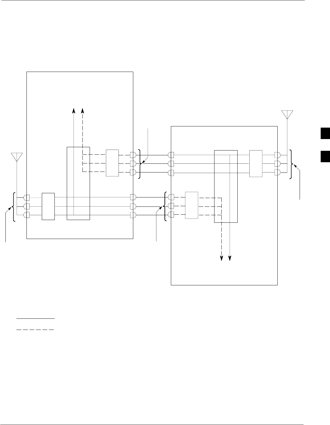
Automated Acceptance Test Procedure68P64115A18–1
Mar 2003 1X SC 4812T Lite BTS Optimization/ATP Software Release R2.16.1.x
DRAFT
4-5
SDisconnected companion frames: When inter–frame diversity RX
cables are disconnected, connect test equipment for diversity RX ATP
at the RX EXPANSION connectors 1B, 2B, or 3B on the frame under
test. Refer to Figure 4-1 and Table 4-2. Be sure EMPC is selected
before logging the LMF into the frame or FER will fail.
Figure 4-1: SC4812ET Lite Companion Frame Diversity RX Simplified Interconnection Diagram
MPC
1A
2A
3A
CIO
EMPC
INTER–FRAME
DIVERSITY RX
CABLES
1A
2A
3A
RX MAIN
(3 SECTORS) RX DIVERSITY
(3 SECTORS)
RX MAIN
(3)
TO
BBXS
ANTENNAS
CONNECTORS
(TRDC/DRDC)
RX EXPANSION
CONNECTORS
SC4812ET LITE COMPANION FRAME 1
MPC
1A
2A
3A
CIO
EMPC
1A
2A
3A
RX MAIN
(3)
TO
BBXS
SC4812ET LITE COMPANION FRAME 2
RX EXPANSION
CONNECTORS
ANTENNAS
CONNECTORS
(TRDC/DRDC)
SC4812ETL0045–1
SIGNALS: RX MAIN
RX DIVERSITY
NOTE: ANTENNAS connectors represent TRDC/DRDC portion of receive path.
RX DIVERSITY ATP CONNECTION POINTS:
1: For Companion Frame 1 when inter–frame diversity
RX cables are connected.
2: For Companion Frame 1 when inter–frame diversity
RX cables are disconnected.
3: For Companion Frame 2 when inter–frame diversity
RX cables are connected.
4: For Companion Frame 2 when inter–frame diversity
RX cables are disconnected.
1
2
34
RX EXPANSION
CONNECTORS
RX EXPANSION
CONNECTORS
3B
2B
1B
3B
2B
1B
RX MAIN
(3 SECTORS)
RX DIVERSITY
(3 SECTORS)
4

Automated Acceptance Test Procedure 68P64115A18–1
Mar 2003
1X SC 4812T Lite BTS Optimization/ATP Software Release R2.16.1.x
DRAFT
4-6
Table 4-1: To Perform Companion Frame Diversity RX FER,
Inter–frame RX Cables Connected
(Set Multi–Channel Preselector to MPC)
On Connect RX Test Cable to
Collocated Companion Frame
Carrier Sector
Collocated Companion Frame
RX or Duplexed TX/RX
ANTENNAS Connector
1 1A
12 2A
3 3A
1 1A
22 2A
3 3A
Table 4-2: To Perform Companion Frame Diversity RX FER,
Inter–frame RX Cables Disconnected
(Set Multi–Channel Preselector to EMPC)
On Connect RX Test Cable to
Frame Under Test
Carrier Sector
F
rame
U
n
d
er
T
est
RX EXPANSION Connector
1 1B
12 2B
3 3B
1 1B
22 2B
3 3B
4
Acceptance Tests – Test Set–up68P64115A18–1
Mar 2003 1X SC 4812T Lite BTS Optimization/ATP Software Release R2.16.1.x
DRAFT
4-7
Acceptance Tests – Test Set–up
Required Test Equipment
The following test equipment is required:
SLMF
SPower meter (used with HP8921A/600 and Advantest R3465)
SCommunications system analyzer
SSignal generator for FER testing (required for all communications
system analyzers for 1X FER)
WARNING –Before installing any test equipment directly to any BTS
TX OUT connector, verify that there are no CDMA
channels keyed.
– At active sites, have the OMCR/CBSC place the carrier
assigned to the LPAs under test OOS. Failure to do so can
result in serious personal injury and/or equipment damage.
NOTE The test equipment must be re–calibrated before using it to
perform the TX Acceptance Tests.
Acceptance Test Equipment Set Up
All ATP testing – Follow the steps in Table 4-3 to set up test equipment
for all tests.
Table 4-3: Set Up Test Equipment – TX Output Verify/Control Tests
Step Action
1If it has not already been done, interface the LMF computer to the BTS (refer to Table 3-5 and
Figure 3-3).
2If it has not already been done, refer to Table 3-6 to start a GUI LMF session and log into the BTS.
3If it has not already been done, refer to Figure 3-17, Figure 3-18, Figure 3-19, Figure 3-20,
Figure 3-21, or Figure 3-22, as applicable, for the test equipment and antenna duplexing being used, to
connect test equipment for acceptance testing.
NOTE
LMF–based measurements factor in TX test cable loss between the RFMF and test equipment. If
additional attenuation, such as external TX combiners, is inserted in the path, it must be identified to
the LMF by including it in the TX test cable calibration. If this is not possible, include the attenuation
in the TX path by editing cable loss values (refer to Table 3-29). Failure to do this will result in test
inaccuracies and potential for erroneous ATP failures because the additional losses would not be
compensated for in the test measurements.
4

Acceptance Tests – Test Set–up 68P64115A18–1
Mar 2003
1X SC 4812T Lite BTS Optimization/ATP Software Release R2.16.1.x
DRAFT
4-8
Companion frame All TX/RX, All RX, and FER for Diversity RX –
When performing All TX/RX, All RX, or FER ATP for companion
frame diversity RX, perform the additional test equipment set–up
procedures in Table 4-4.
Table 4-4: Additional Diversity RX Test Set–up for Companion Frames
Step Action
1If the LMF is logged into the BTS, log out of the BTS.
2If the inter–frame diversity RX cabling to a collocated companion frame is:
SConnected to the companion frame under test, proceed to step 3.
SDisconnected from the companion frame under test, proceed to step 7.
3For companion frames with inter–frame diversity RX cables connected, click on the LMF Login tab.
4In the Equipage Information box, select MPC from the Multi–Channel Preselector picklist.
5Make RX test cable connections for diversity RX FER according to Figure 4-1 and Table 4-1.
6Proceed to step 10.
7For companion frames with inter–frame diversity RX cables disconnected, click on the LMF Login
tab.
8In the Equipage Information box, select EMPC from the Multi–Channel Preselector picklist.
9Make RX test cable connections for diversity RX FER according to Figure 4-1 and Table 4-2.
10 Click on the LMF BTS# tab, and return to the procedure for the ATP being performed.
4

Abbreviated (All–inclusive) Acceptance Tests68P64115A18–1
Mar 2003 1X SC 4812T Lite BTS Optimization/ATP Software Release R2.16.1.x
DRAFT
4-9
Abbreviated (All–inclusive) Acceptance Tests
All–inclusive Tests
General – The all–inclusive acceptance tests are performed from the
LMF GUI environment. These all–inclusive tests are called abbreviated
ATPs because they execute various combinations of individual
acceptance tests with a single command. This allows verification of
multiple aspects of BTS performance while minimizing time needed for
individual test set up and initiation.
Abbreviated ATP Options – There are three abbreviated acceptance
tests which evaluate different performance aspects of the BTS. This
allows the CFE to select testing to meet the specific requirements for
individual maintenance and performance verification situations. The
following summarizes the coverage of each abbreviated test:
SAll TX/RX. Performs all transmit and receive ATPs on the selected
MCCs and BBXs.
SAll TX. Performs complete set of transmit ATPs on the selected
MCCs and BBXs. Testing is the equivalent of performing all of the
following individual tests:
–TX Mask Test
–Rho Test
–Pilot Time Offset Test
–Code Domain Power Test
SAll RX. Performs complete receive ATP on the selected MCCs and
BBXs. Testing is the equivalent of performing the following:
–FER Test
Abbreviated ATP Procedures – Procedures to accomplish each type of
abbreviated ATP are included in the following subsections.
4

Abbreviated (All–inclusive) Acceptance Tests 68P64115A18–1
Mar 2003
1X SC 4812T Lite BTS Optimization/ATP Software Release R2.16.1.x
DRAFT
4-10
All TX/RX ATP Test
Follow the procedures in Table 4-5 to perform the abbreviated,
all–inclusive transmit and receive test.
Table 4-5: All TX/RX ATP Test Procedure
Step Action
1Set up the test equipment initially for abbreviated tests as described in Table 4-3.
2If a companion frame is being tested and either BOTH or DIV is to be selected in step 7, perform the
additional test equipment set–up in Table 4-4 for the diversity RX portion of the ATP.
NOTE
If the LMF has been logged into the BTS with a different Multi–Channel Preselector setting than the
one to be used for this test, the LMF must be logged out of the BTS and logged in again with the new
Multi–Channel Preselector setting. Using the wrong MPC setting can cause a false test failure.
3Select the BBXs and MCCs to be tested.
4Click on Tests in the BTS menu bar, and select All TX/RX ATP... from the pull–down menu.
5Select the appropriate carrier(s) and sector(s) (carrier-bts#-sector#-carrier#) from those displayed in the
Channels/Carrier pick list.
NOTE
To select multiple items, hold down the Shift or Ctrl key while clicking on pick list items to select
multiple carrier(s)–sector(s).
6Verify that the correct channel number for the selected carrier is shown in the Carrier # Channels
box. If it is not, obtain the latest bts–#.cdf (or bts–#.necf) and cbsc–#.cdf files from the CBSC.
NOTE
If necessary, the correct channel number may be manually entered into the Carrier # Channels box.
7NOTE
If a companion frame with the inter–frame diversity RX cabling disconnected is being tested do not
select BOTH in this step. The RX main and diversity paths must be tested separately for this
configuration because each requires a different Multi–Coupler Preselector type to provide the proper
test signal gain.
Select the appropriate RX branch (BOTH, MAIN, or DIVersity) in the drop–down list.
8In the Rate Set box, select the appropriate data rate (1=9600 3=9600 1X) from the drop–down list.
NOTE
The Rate Set selection of 3 is only available if 1X cards are selected for the test.
9Enter the channel elements to be tested for the RX ATP in the Channel Element(s) box. By default,
all channel elements are specified.
Use one of thefollowing methods to enter more than one channel element:
– Enter non–sequential channel elements separated by a comma and no spaces (for example;
0,5,15).
– Enter a range of sequential channel elements by typing the first and last channel elements
separated by two periods (for example; 0..15).
NOTE
The channel element numbers are 0.based; that is the first channel element is 0.
. . . continued on next page
4

Abbreviated (All–inclusive) Acceptance Tests68P64115A18–1
Mar 2003 1X SC 4812T Lite BTS Optimization/ATP Software Release R2.16.1.x
DRAFT
4-11
Table 4-5: All TX/RX ATP Test Procedure
Step Action
10 In the Test Pattern box, select the test pattern to use for the acceptance tests from the drop–down list
(refer to “Test Pattern Drop–down Pick List” under “TX Calibration and the LMF” in the Bay Level
Offset Calibration section of Chapter 3).
11 Click OK to display a status bar followed by a Directions pop-up window.
12 NOTE
When testing diversity RX paths on companion frames, be sure to follow the RX test cable connection
information in Table 4-1 or Table 4-2, as applicable, during this step.
Follow cable connection directions as they are displayed, and click the Continue button to begin
testing.
– As the ATP process is completed, results will be displayed in the status report window.
13 Click the Save Results or Dismiss button.
NOTE
If Dismiss is used, the test results will not be saved in the test report file.
4

Abbreviated (All–inclusive) Acceptance Tests 68P64115A18–1
Mar 2003
1X SC 4812T Lite BTS Optimization/ATP Software Release R2.16.1.x
DRAFT
4-12
All TX ATP Test
Follow the procedures in Table 4-6 to perform the abbreviated,
all–inclusive transmit test.
Table 4-6: All TX ATP Test Procedure
Step Action
1Set up the test equipment for abbreviated tests per Table 4-3.
2Select the BBXs and MCCs to be tested.
3Click on Tests in the BTS menu bar, and select All TX ATP... from the pull–down menu.
4Select the appropriate carrier(s) and sector(s) (carrier-bts#-sector#-carrier#) from those displayed in the
Channels/Carrier pick list.
NOTE
To select multiple items, hold down the Shift or Ctrl key while clicking on pick list items to select
multiple carrier(s)–sector(s).
5Verify that the correct channel number for the selected carrier is shown in the Carrier # Channels
box. If it is not, obtain the latest bts–#.cdf (or bts–#.necf) and cbsc–#.cdf files from the CBSC.
NOTE
If necessary, the correct channel number may be manually entered into the Carrier # Channels box.
6In the Rate Set box, select the appropriate transfer rate (1 = 9600, 3 = 9600 1X) from the drop–down
list.
NOTE
The Rate Set Selection of 3 is only available if 1X cards are selected for the test.
7In the Test Pattern box, select the test pattern to use for the acceptance test from the drop–down list
(refer to “Test Pattern Drop–down Pick List” under “TX Calibration and the LMF” in the Bay Level
Offset Calibration section of Chapter 3).
8 Click OK to display a status bar followed by a Directions pop-up window.
9Follow cable connection directions as they are displayed, and click the Continue button to begin
testing.
– As the ATP process is completed, results will be displayed in the status report window.
10 Click the Save Results or Dismiss button.
NOTE
If Dismiss is used, the test results will not be saved in the test report file.
All RX ATP Test
Follow the procedure in Table 4-7 to perform the abbreviated,
all–inclusive receive test.
Table 4-7: All RX ATP Test Procedure
Step Action
1Set up the test equipment for abbreviated tests per Table 4-3.
. . . continued on next page
4

Abbreviated (All–inclusive) Acceptance Tests68P64115A18–1
Mar 2003 1X SC 4812T Lite BTS Optimization/ATP Software Release R2.16.1.x
DRAFT
4-13
Table 4-7: All RX ATP Test Procedure
Step Action
2If a companion frame is being tested and either BOTH or DIV is to be selected in step 7, perform the
additional test equipment set–up in Table 4-4 for the diversity RX portion of the ATP.
NOTE
If the LMF has been logged into the BTS with a different Multi–Channel Preselector setting than the
one to be used for this test, the LMF must be logged out of the BTS and logged in again with the new
Multi–Channel Preselector setting. Using the wrong MPC setting can cause a false test failure.
3Select the BBXs and MCCs to be tested.
4Click on Tests in the BTS menu bar, and select All RX ATP... from the pull–down menu.
5Select the appropriate carrier(s) and sector(s) (carrier-bts#-sector#-carrier#) from those displayed in the
Channels/Carrier pick list.
NOTE
To select multiple items, hold down the Shift or Ctrl key while clicking on pick list items to select
multiple carrier(s)–sector(s).
6Verify that the correct channel number for the selected carrier is shown in the Carrier # Channels
box. If it is not, obtain the latest bts–#.cdf (or bts–#.necf) and cbsc–#.cdf files from the CBSC.
NOTE
If necessary, the correct channel number may be manually entered into the Carrier # Channels box.
7NOTE
If a companion frame with the inter–frame diversity RX cabling disconnected is being tested do not
select BOTH in this step. The RX main and diversity paths must be tested separately for this
configuration because each requires a different Multi–Coupler Preselector type to provide the proper
test signal gain.
Select the appropriate RX branch (BOTH, MAIN, or DIVersity) in the drop–down list.
8In the Rate Set box, select the appropriate data rate (1=9600, 2=14400, 3=9600 1X) from the
drop–down list.
NOTE
The Rate Set selection of 1 is only available if non–1X cards are selected for the test.
The Rate Set selection of 3 is only available if 1X cards are selected for the test.
9Enter the channel elements to be tested for the RX ATP in the Channel Element(s) box. By default,
all channel elements are specified.
Use one of the following methods to enter more than one channel element:
– Enter non–sequential channel elements separated by a comma and no spaces (for example;
0,5,15).
– Enter a range of sequential channel elements by typing the first and last channel elements
separated by two periods (for example; 0..15).
NOTE
The channel element numbers are 0.based; that is the first channel element is 0.
10 Click OK to display a status bar followed by a Directions pop-up window.
. . . continued on next page
4