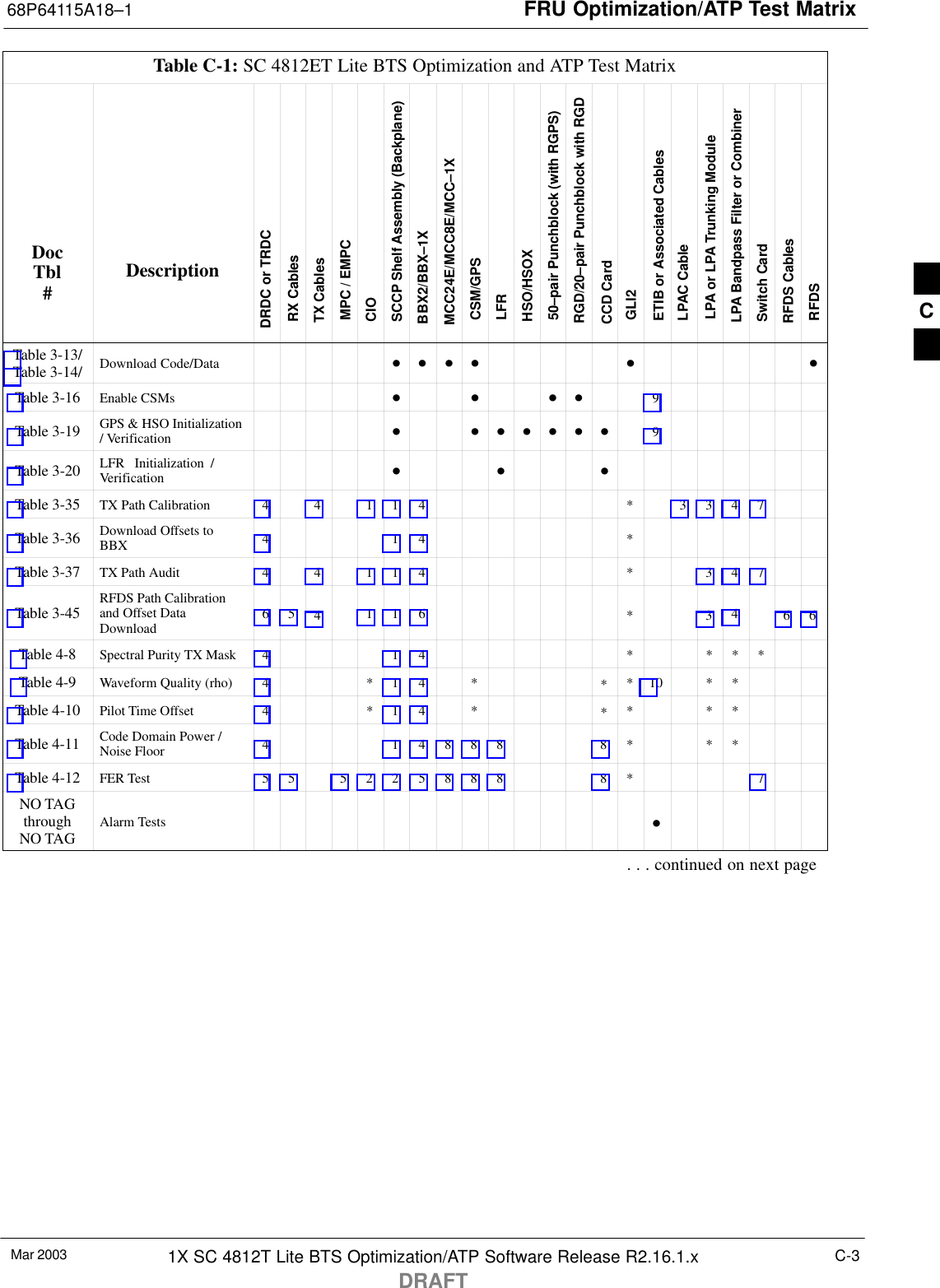
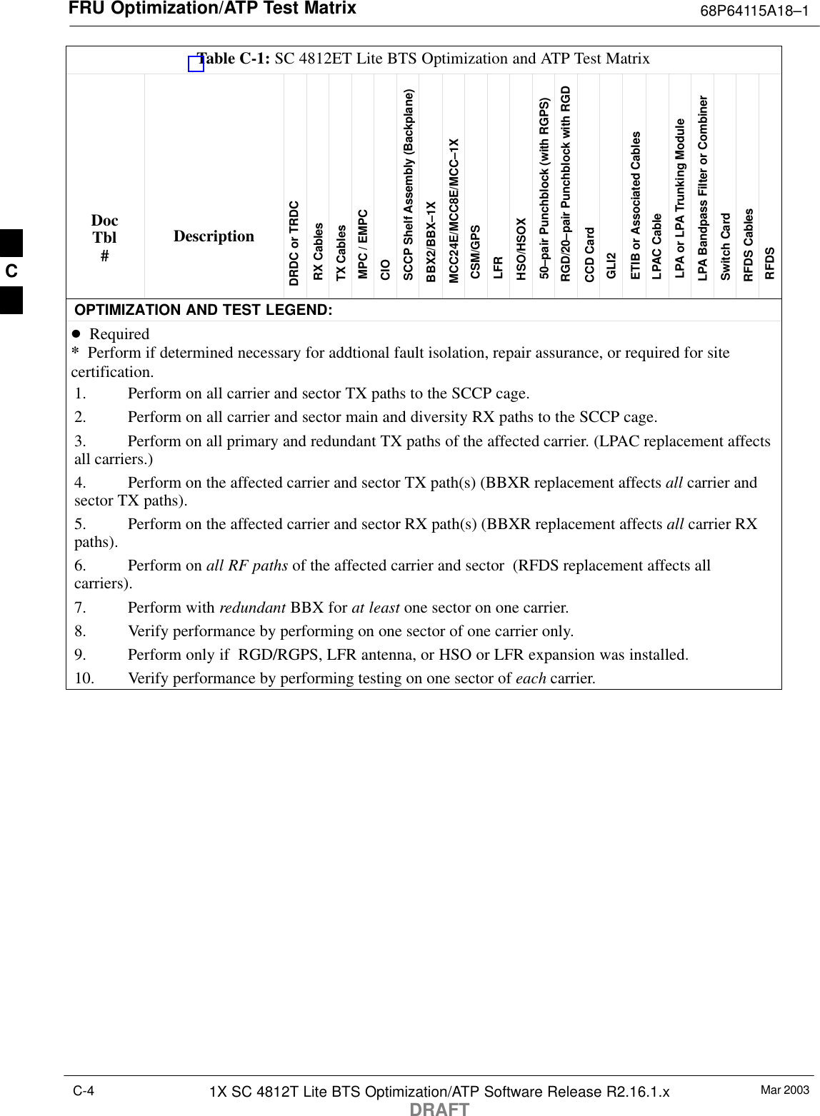
Nokia Solutions and Networks T5EE1 SC4812T Lite 1X/EVDO @ 800 MHz CDMA BTS User Manual TLite
Nokia Solutions and Networks SC4812T Lite 1X/EVDO @ 800 MHz CDMA BTS TLite
UserManual.wiki
>
Nokia Solutions and Networks
>
T5EE1 User Manual
>
Users Manual 2
Contents
1.
Users Manual 1
2.
Users Manual 2
Users Manual 2
Navigation menu
Upload a User Manual
Namespaces
Wiki Guide
HTML
PDF
Info
Views
User Manual
Discussion / Help
Navigation
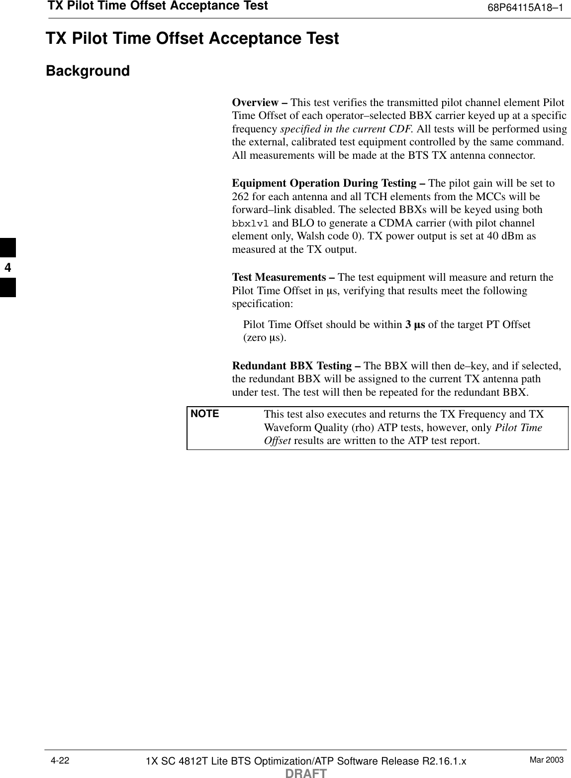
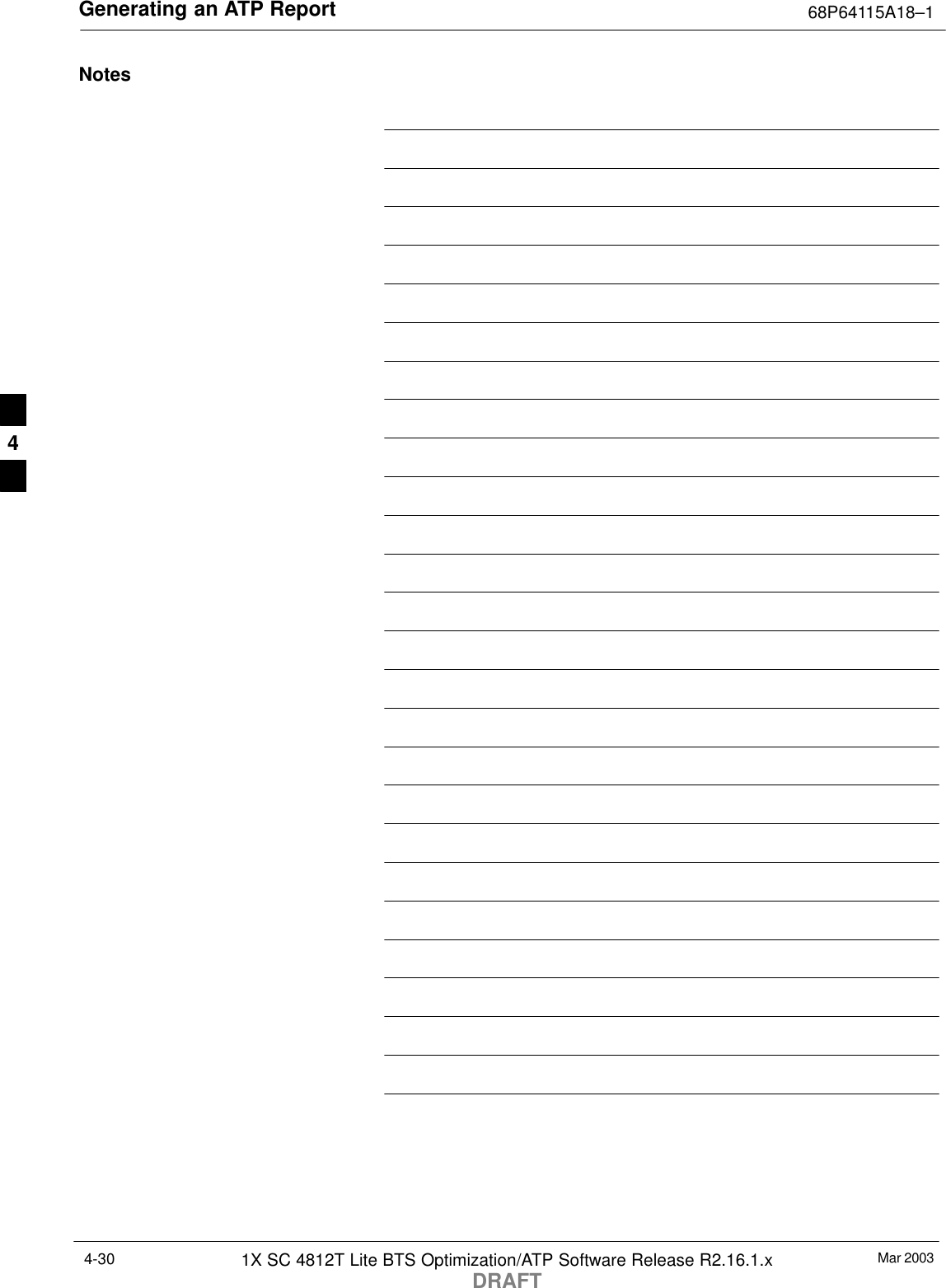
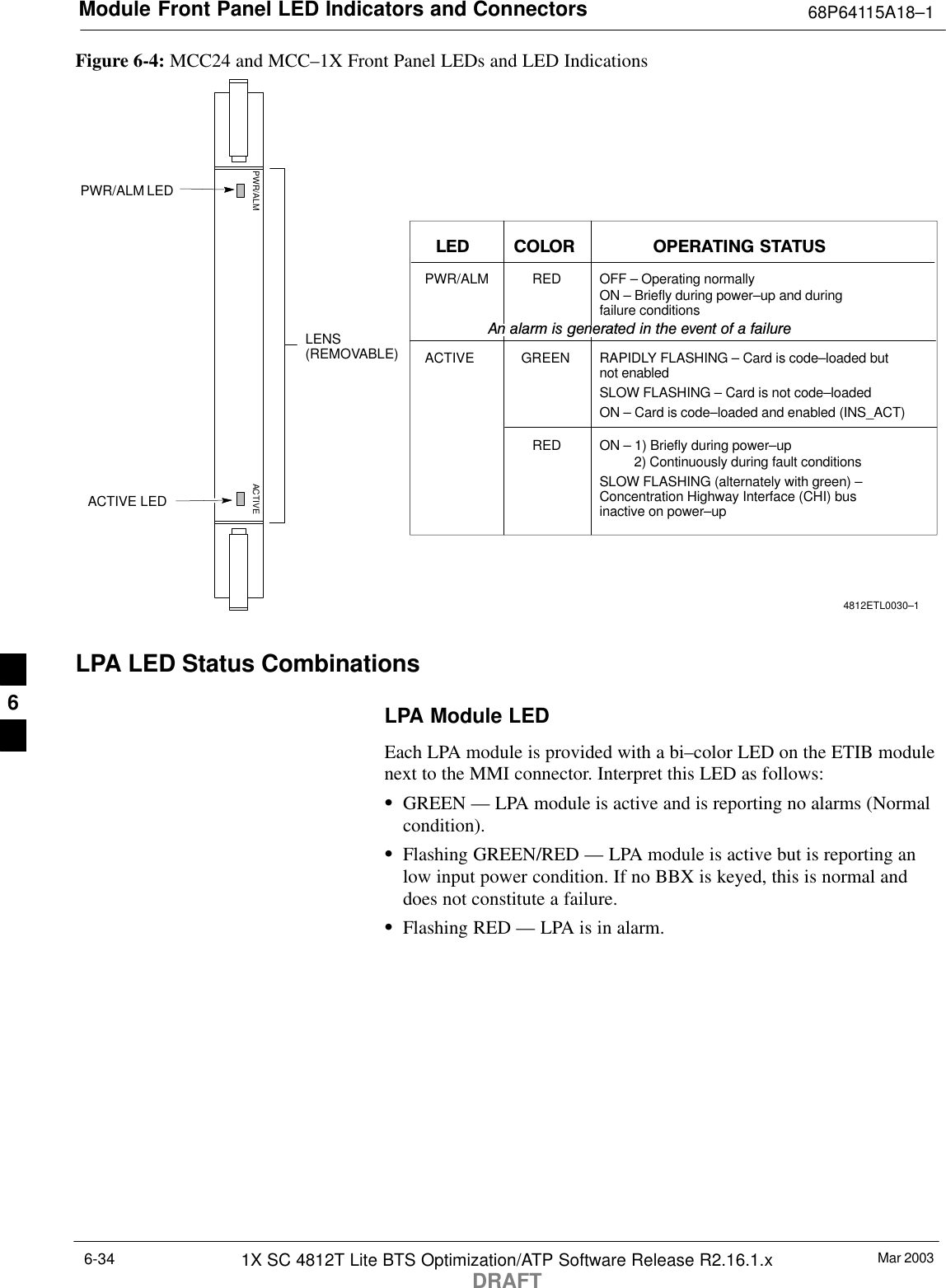


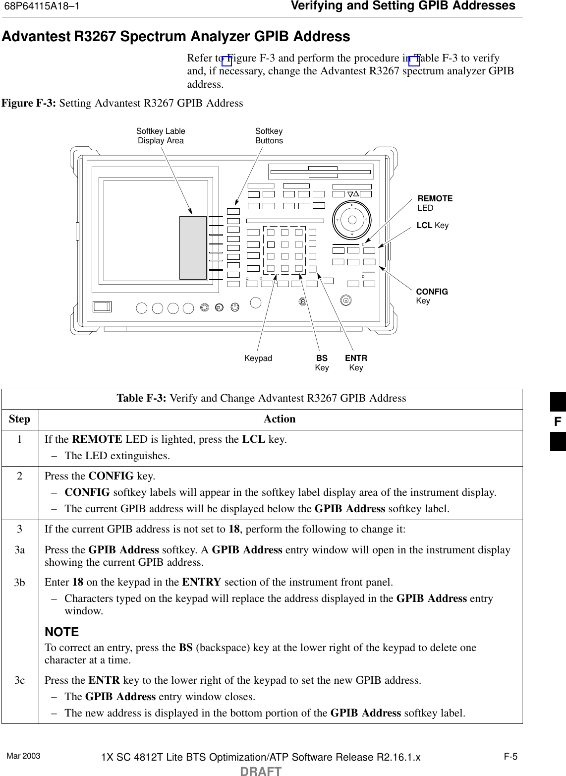
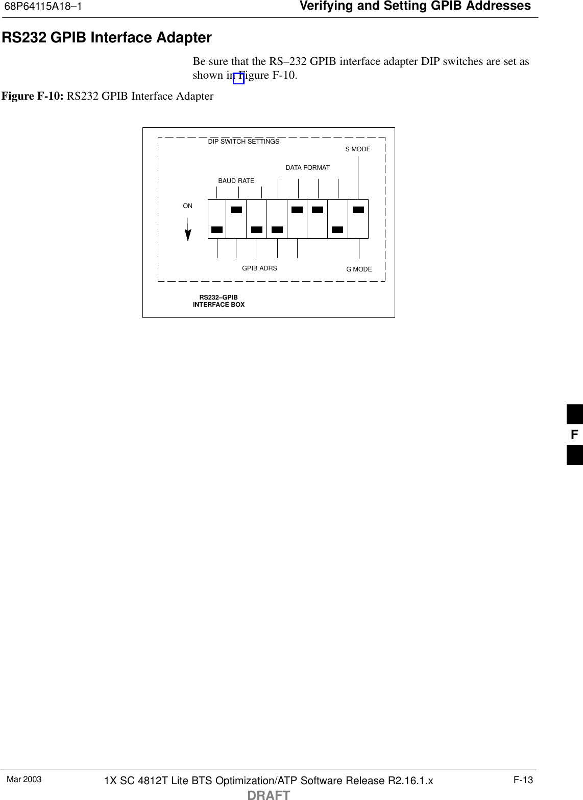
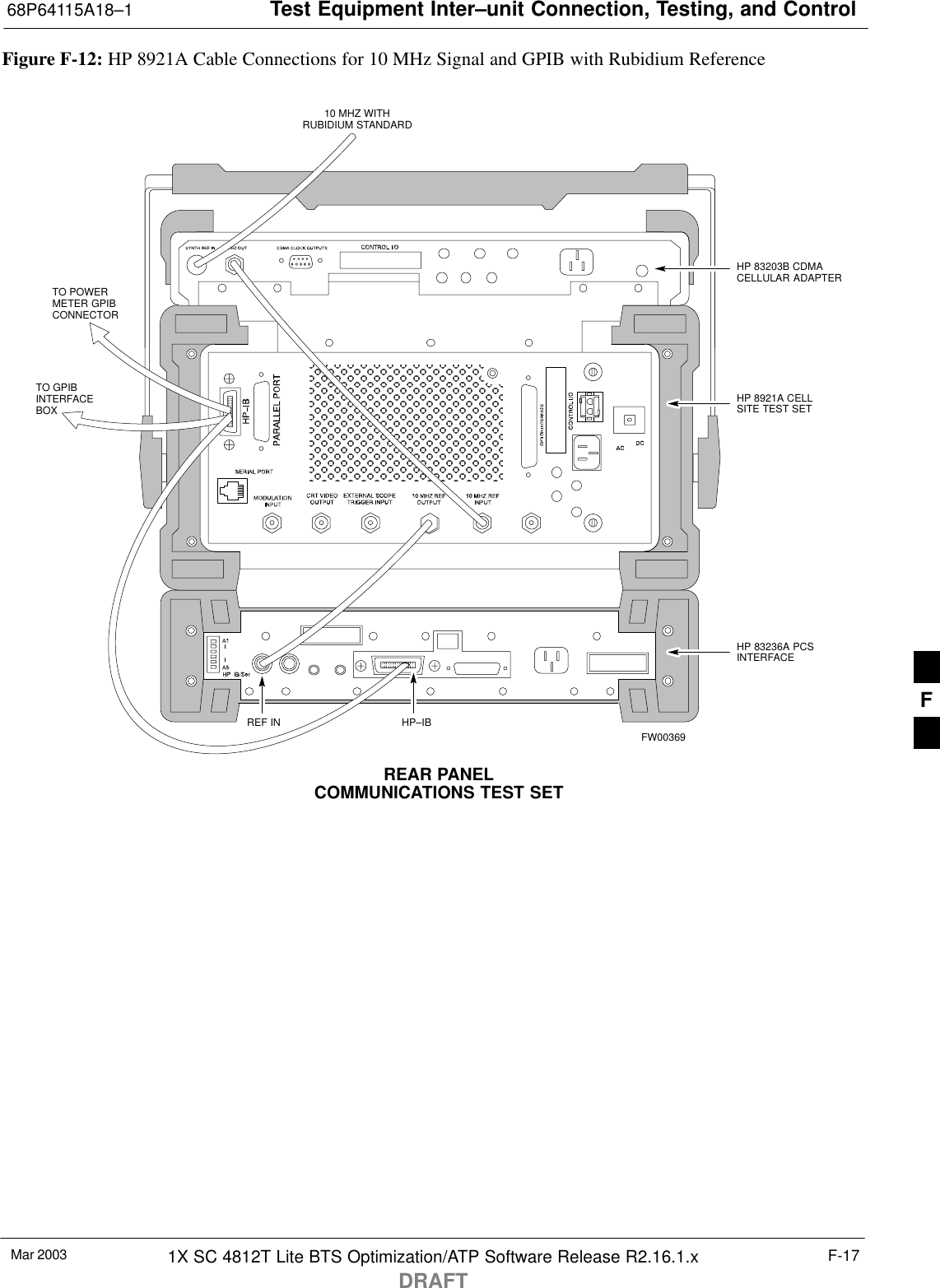
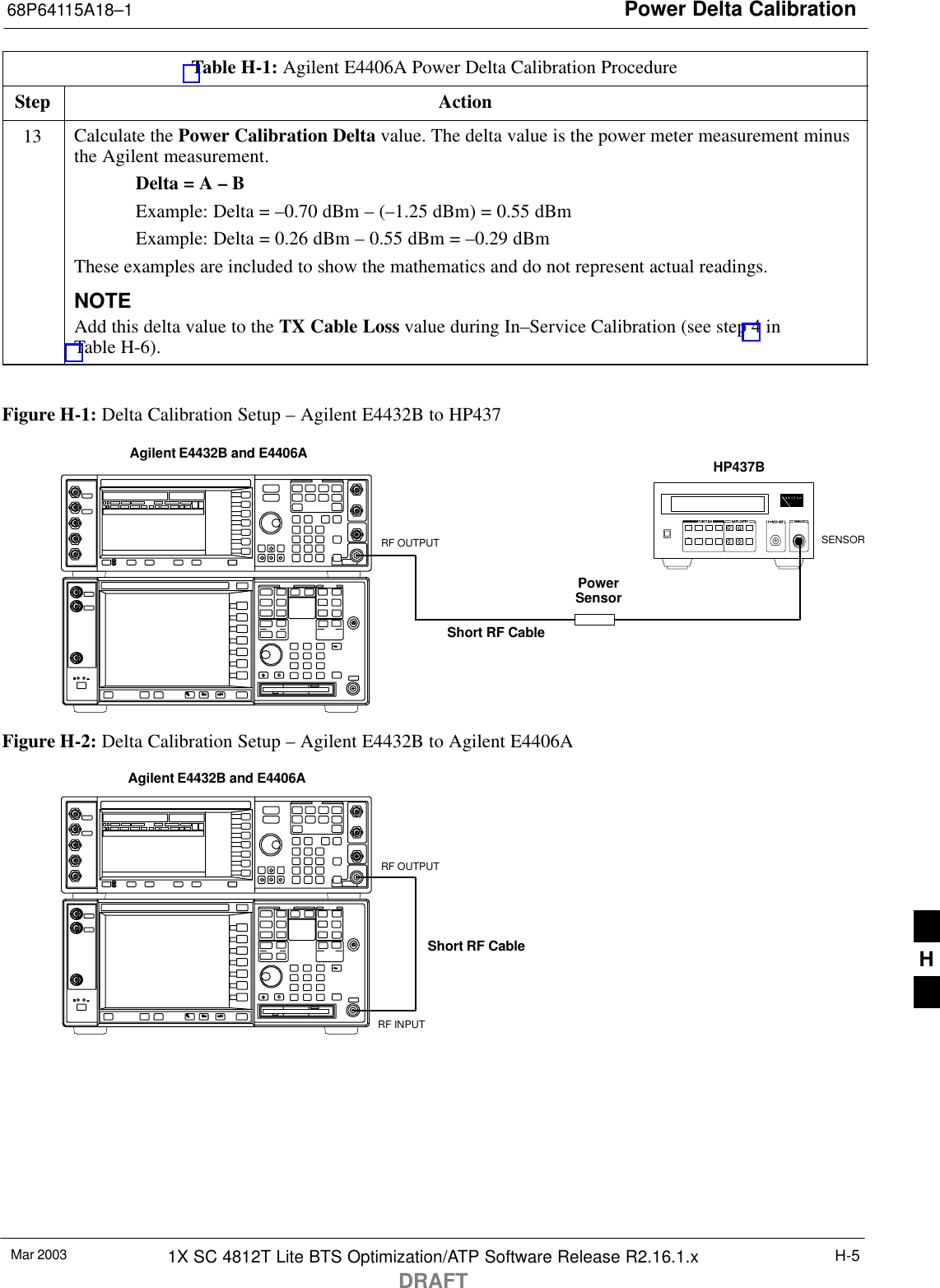
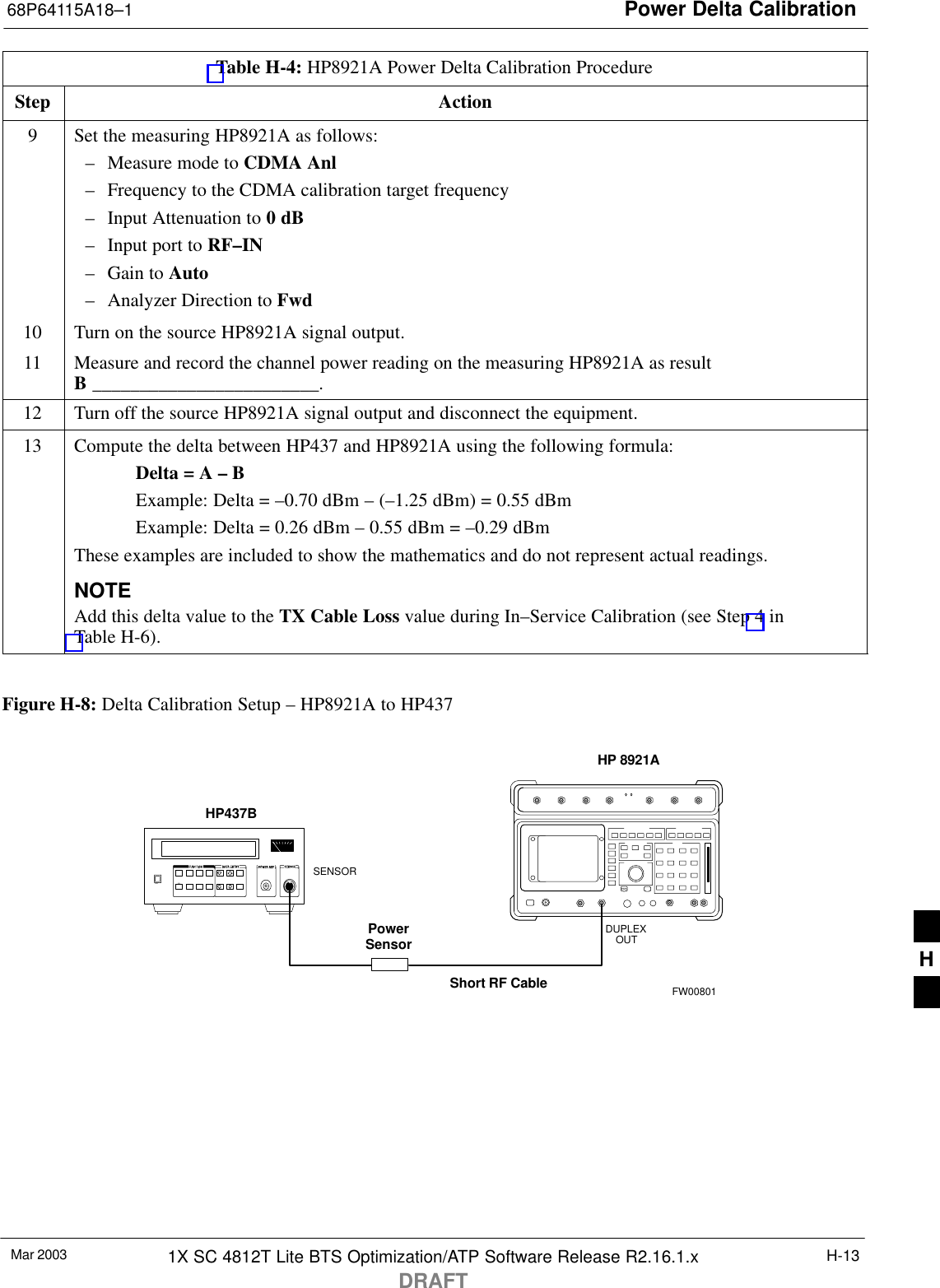
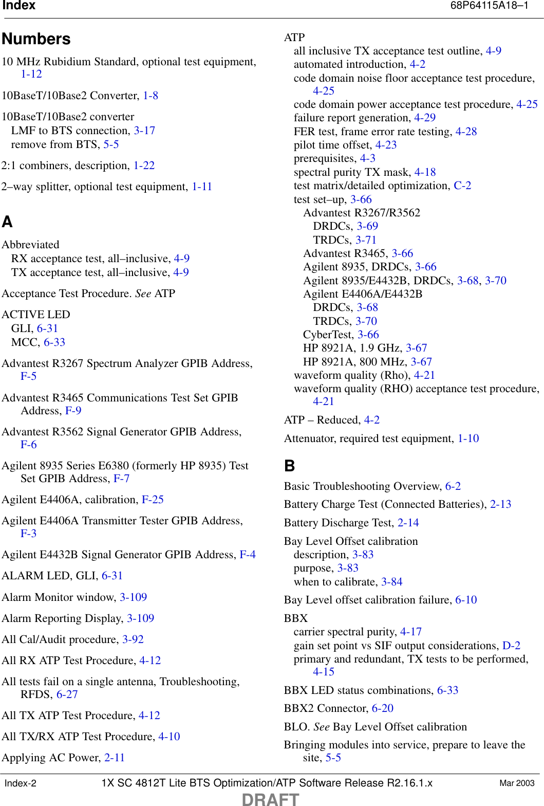
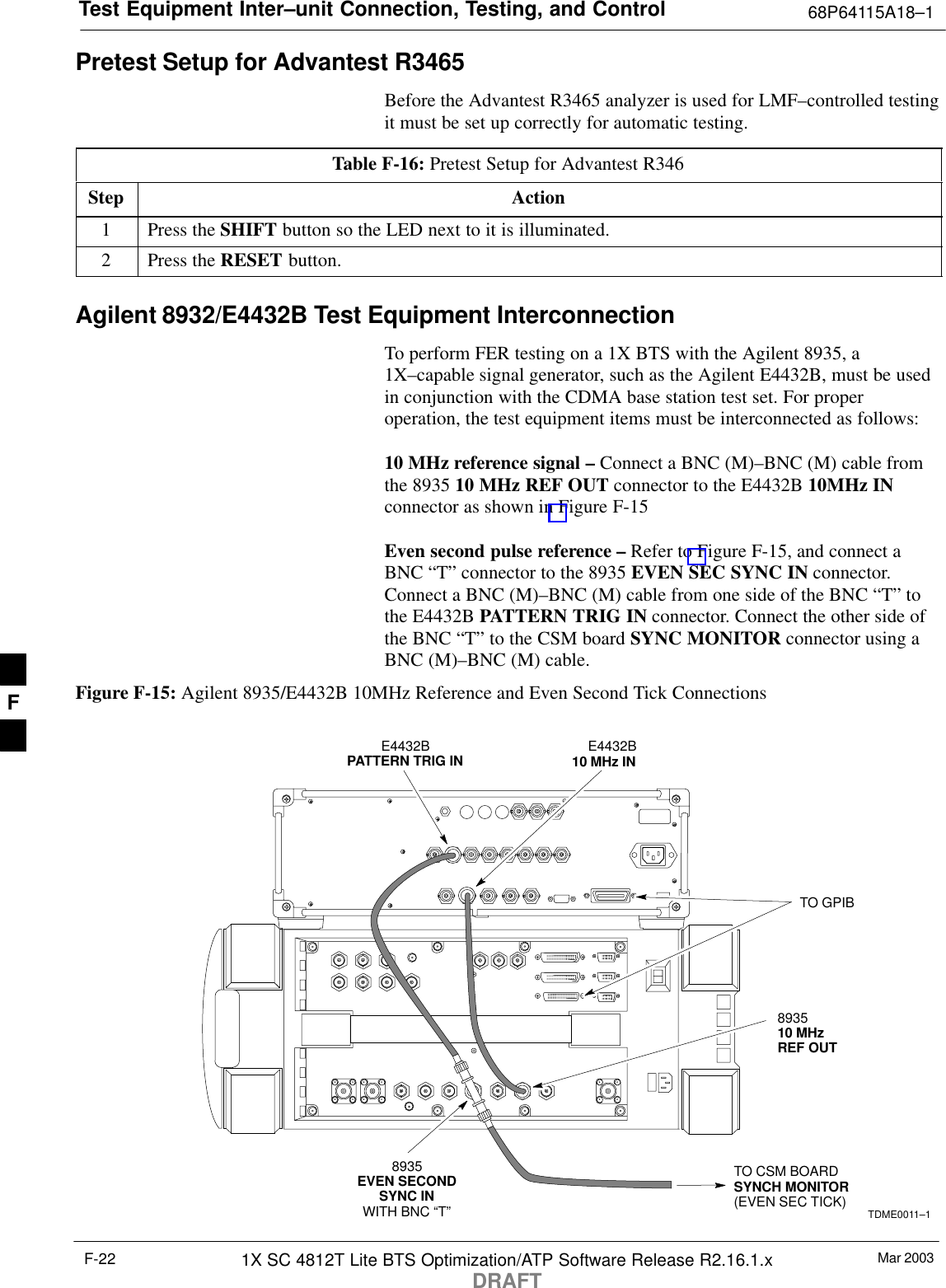
![Test Equipment Inter–unit Connection, Testing, and Control 68P64115A18–1Mar 20031X SC 4812T Lite BTS Optimization/ATP Software Release R2.16.1.xDRAFTF-18HP 8921A with PCS Interface System Connectivity TestFollow the steps outlined in Table F-12 to verify that the connectionsbetween the PCS Interface and the HP 8921A are correct and cables areintact. The software also performs basic functionality checks of eachinstrument.NOTE Table:note. Note 10pt HelveticaDisconnect other GPIB devices, especially system controllers,from the system before running the connectivity software.Table F-12: System ConnectivityStep ActionNOTE– Perform this procedure after test equipment has been allowed to warm–up and stabilize for aminimum of 60 minutes.1Insert HP 83236A Manual Control/System card into memory card slot.2Press the [PRESET] pushbutton.3Press the Screen Control [TESTS] pushbutton to display the “Tests” Main Menu screen.4Position the cursor at Select Procedure Location and select it by pressing the cursor control knob. Inthe Choices selection box, select Card.5Position the cursor at Select Procedure Filename and select it by pressing the cursor control knob. Inthe Choices selection box, select SYS_CONN.6Position the cursor at RUN TEST and select it. The software will provide operator prompts throughcompletion of the connectivity setup.7Do the following when the test is complete,Sposition cursor on STOP TEST and select itSOR press the [K5] pushbutton.8To return to the main menu, press the [K5] pushbutton.9Press the [PRESET] pushbutton.Pretest Setup for HP 8921ABefore the HP 8921A CDMA analyzer is used for LMF–controlledtesting it must be set up correctly for automatic testing.Table F-13: Pretest Setup for HP 8921AStep Action1Unplug the memory card if it is plugged in.2Press the CURSOR CONTROL knob.3Position the cursor at IO CONFIG (under To Screen and More) and select it.4Select Mode and set for Talk&Lstn.F](https://usermanual.wiki/Nokia-Solutions-and-Networks/T5EE1.Users-Manual-2/User-Guide-471764-Page-123.png)
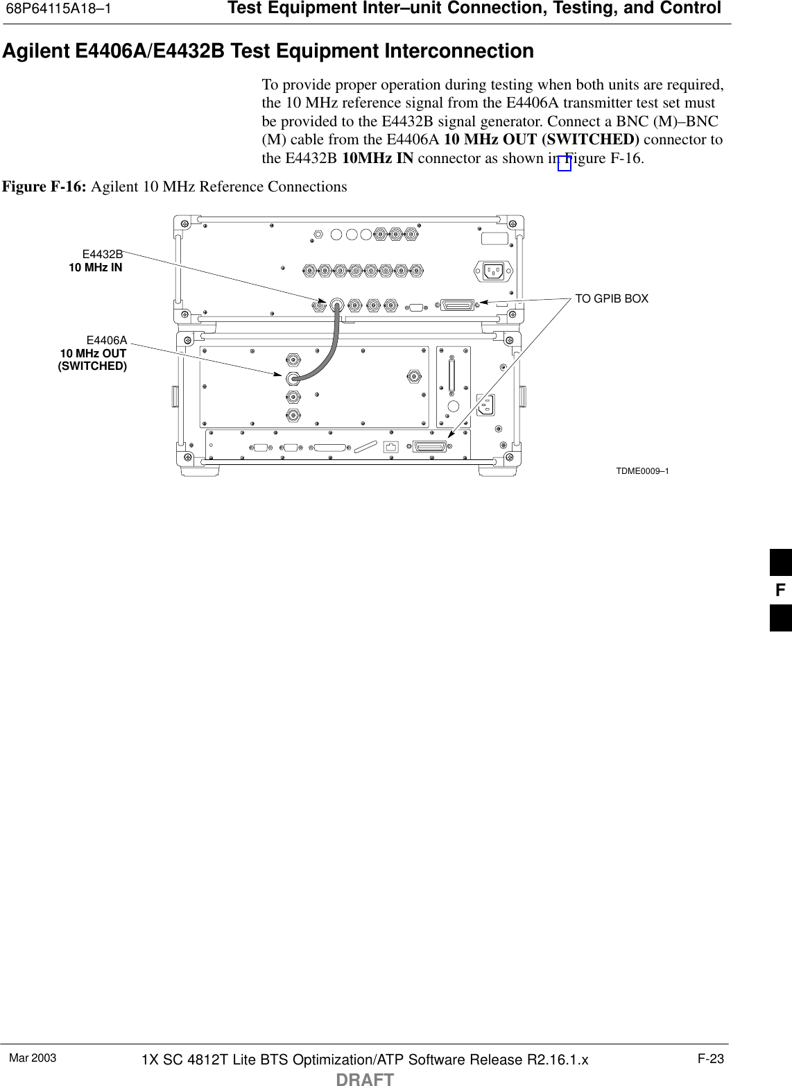
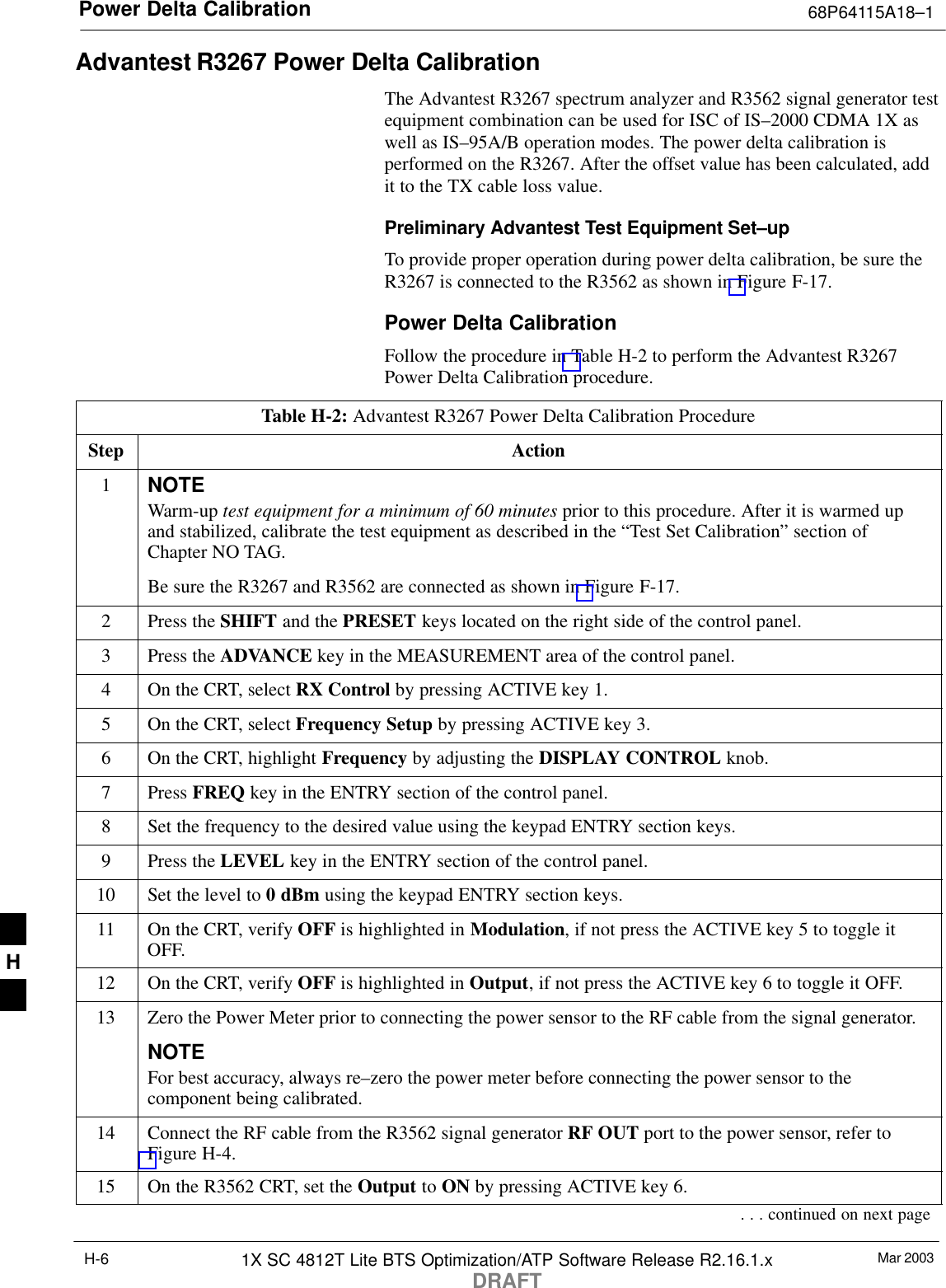
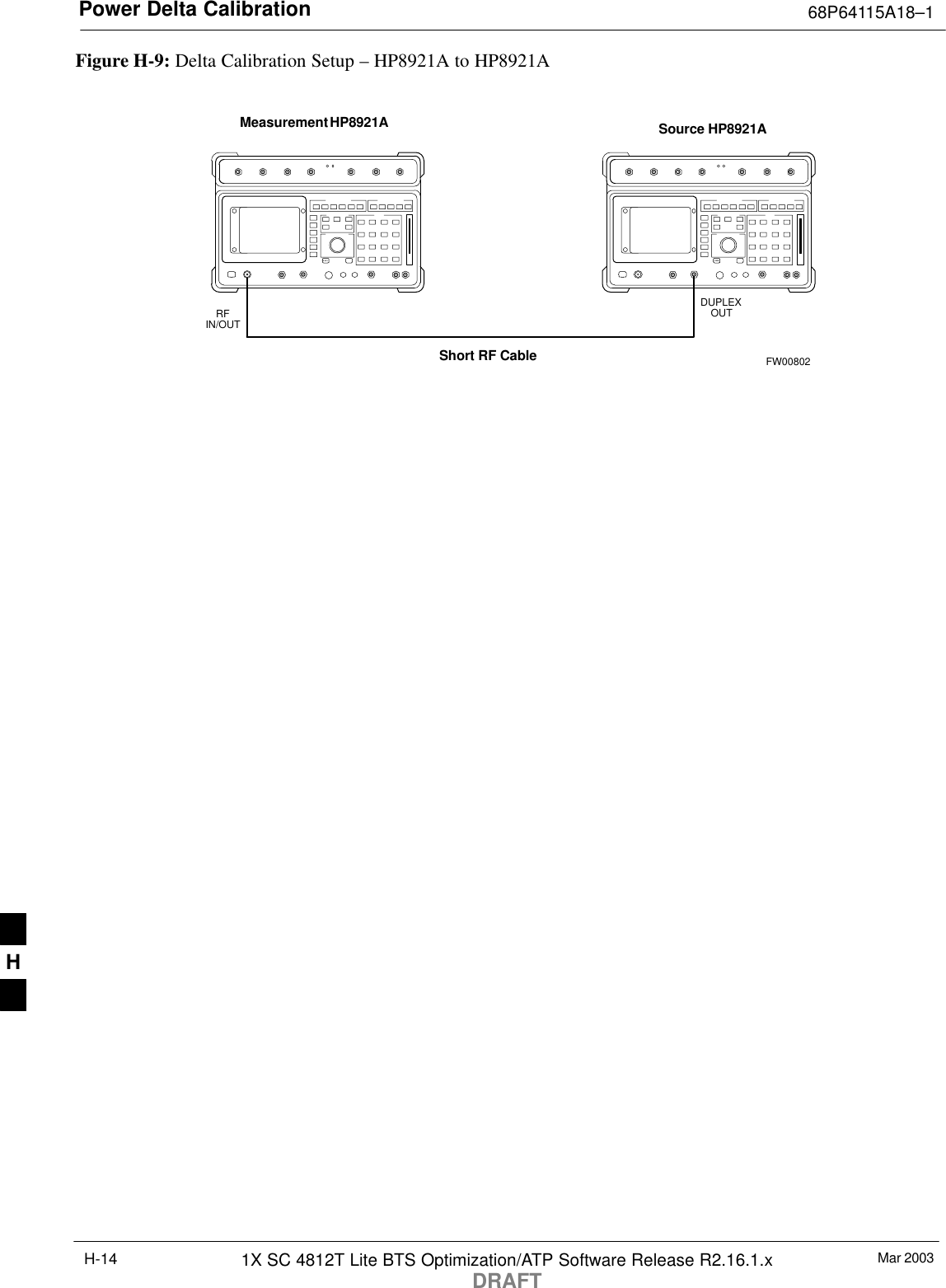
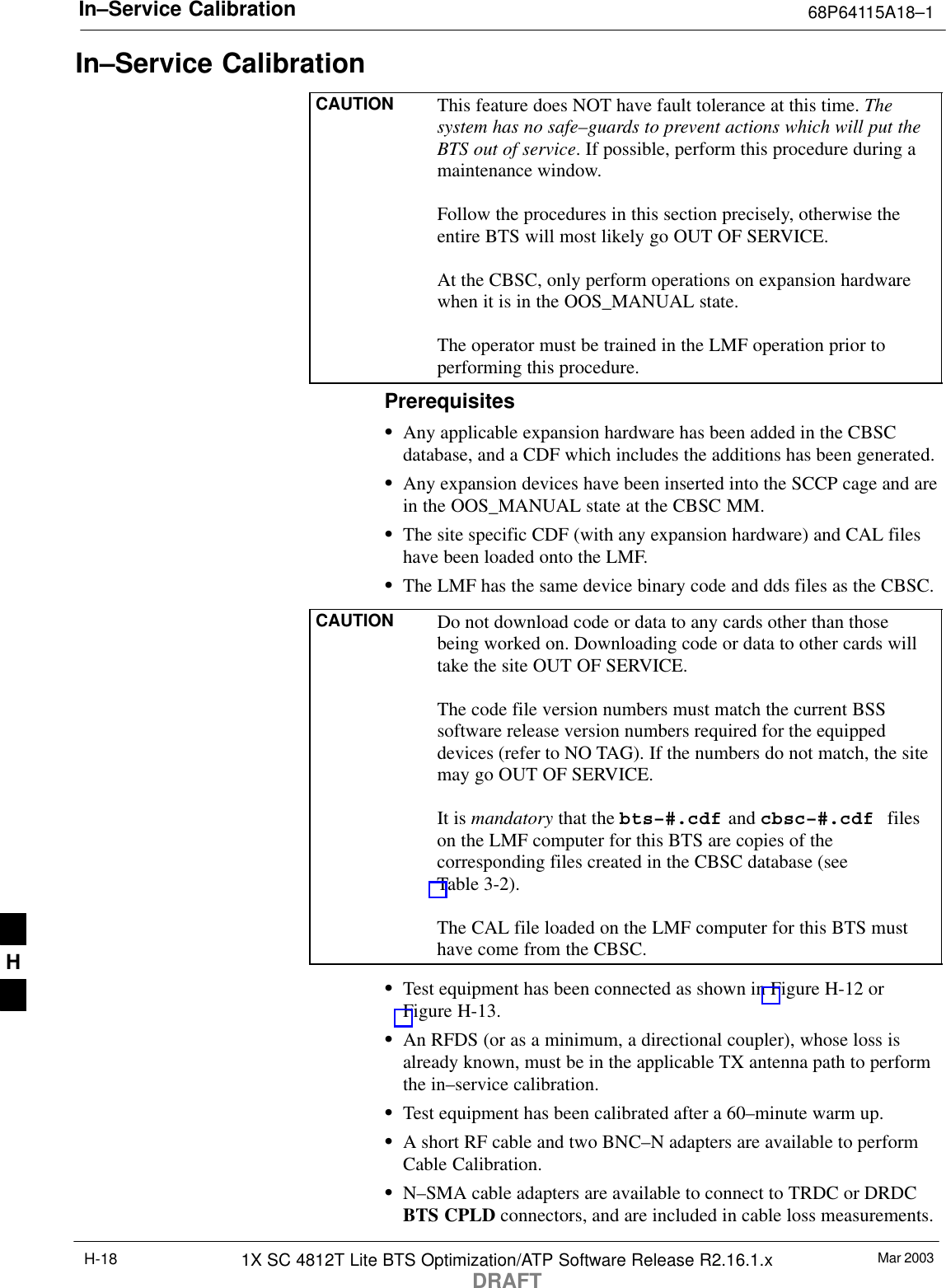
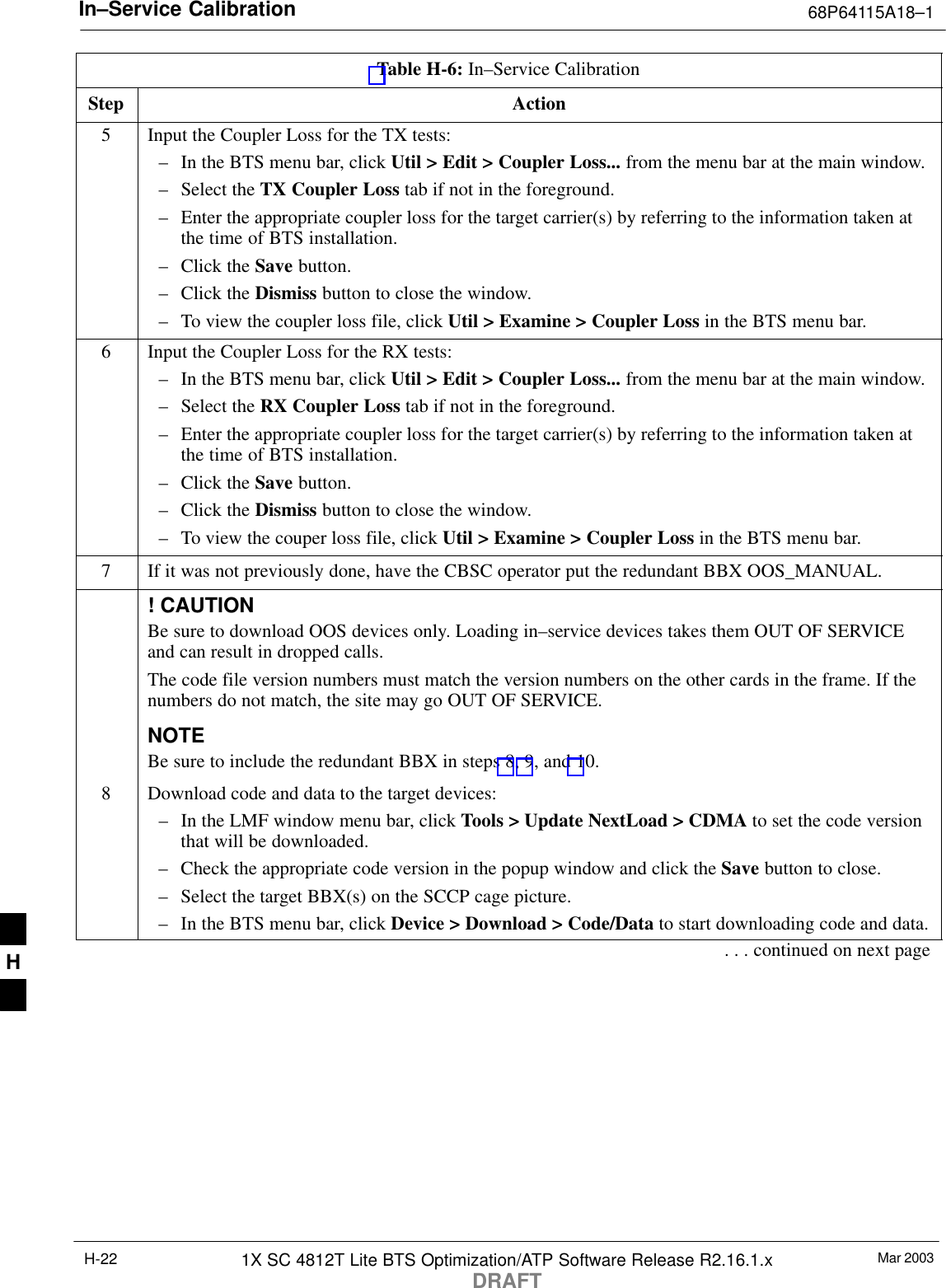
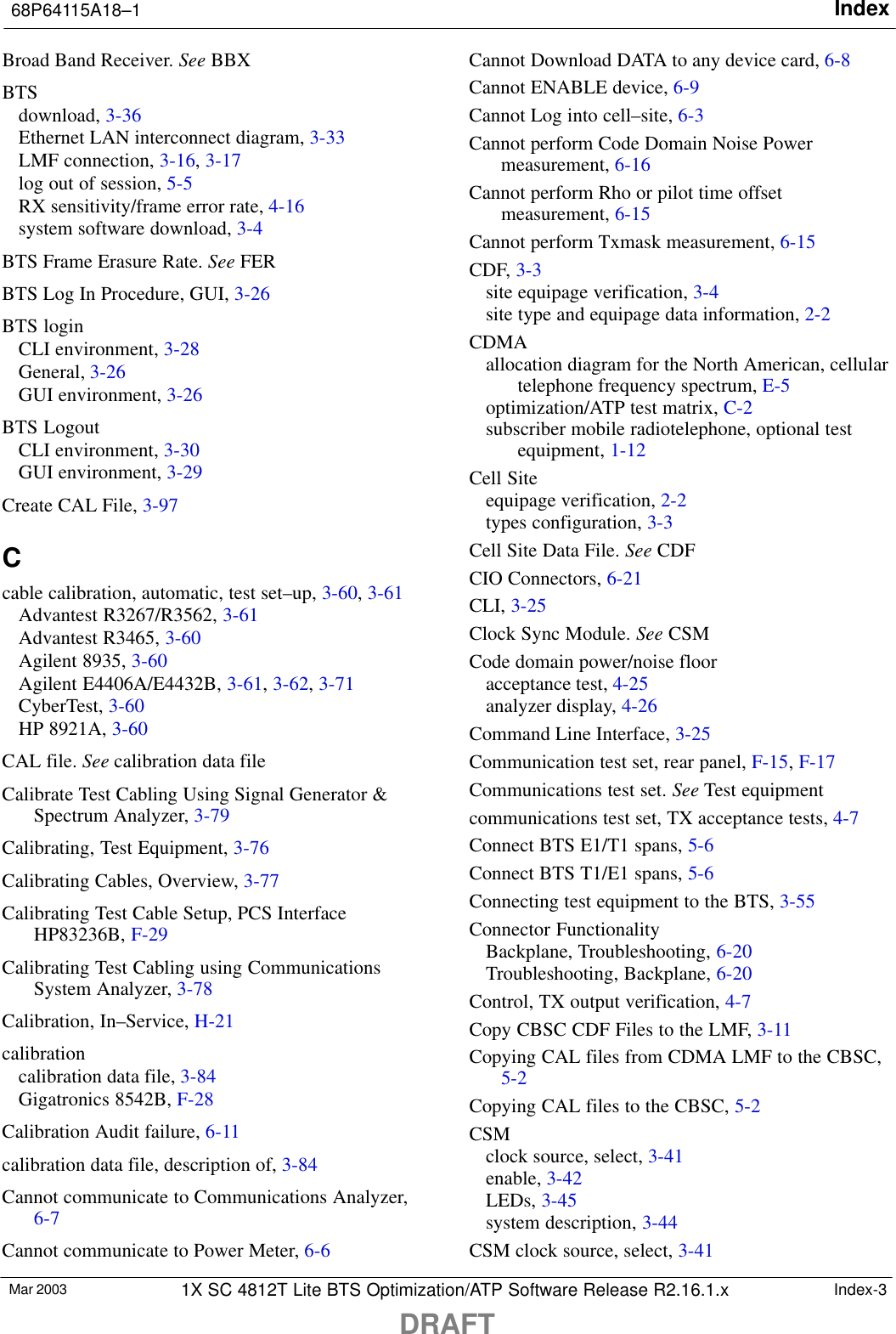
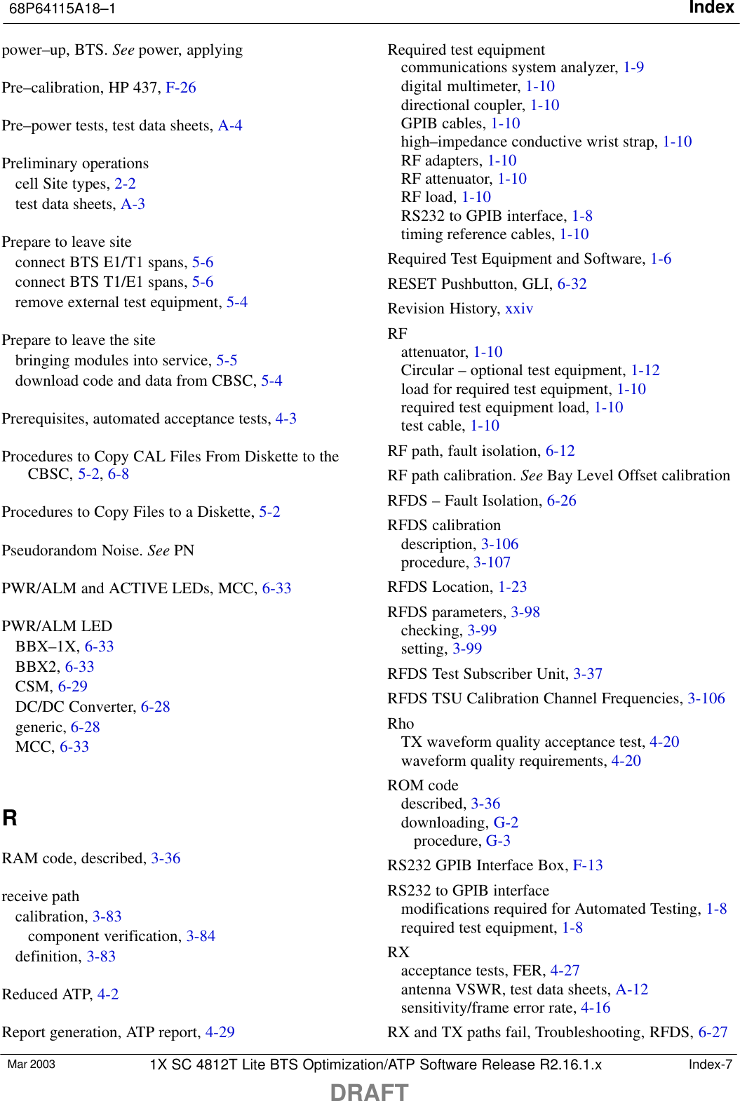
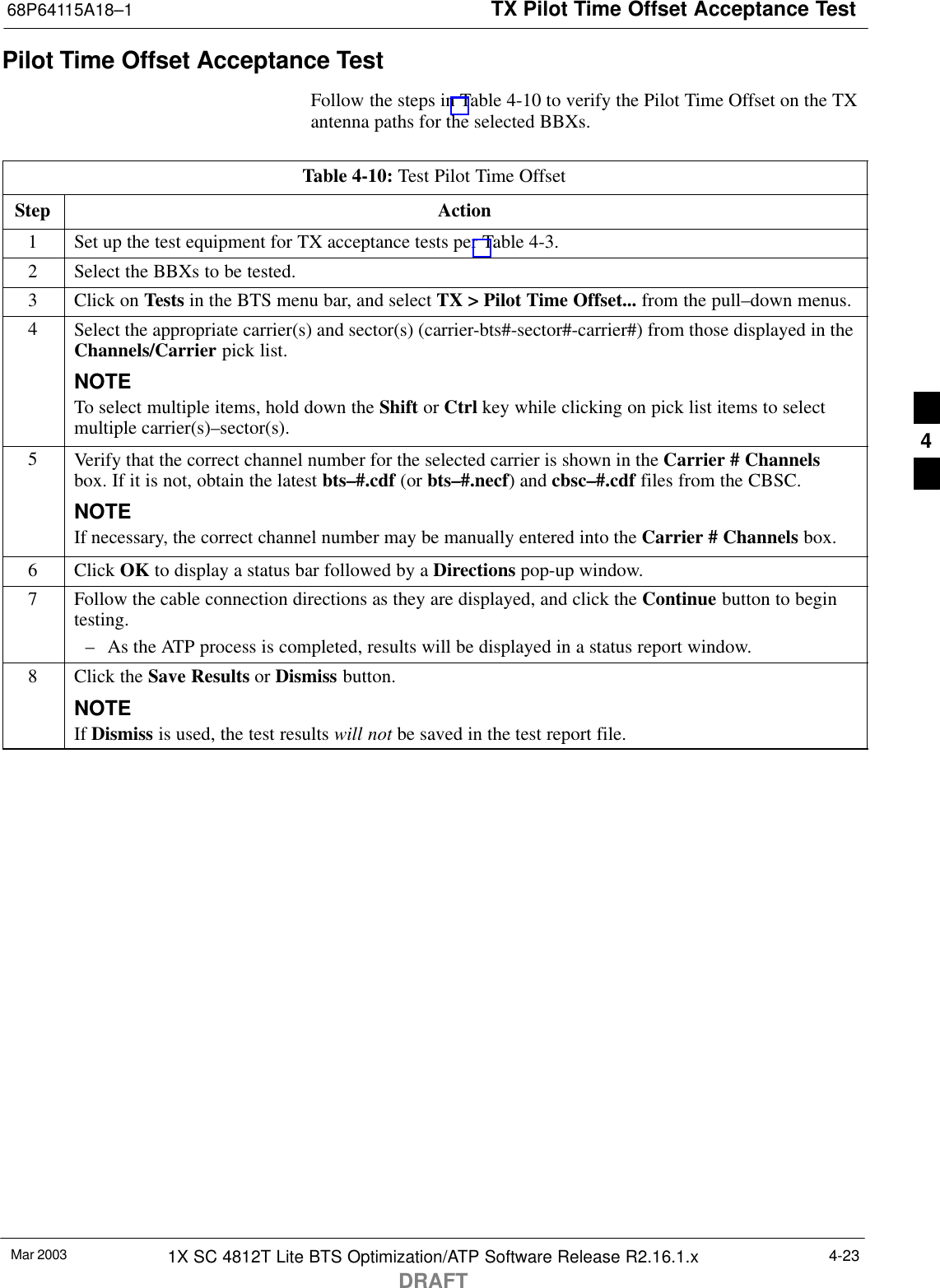
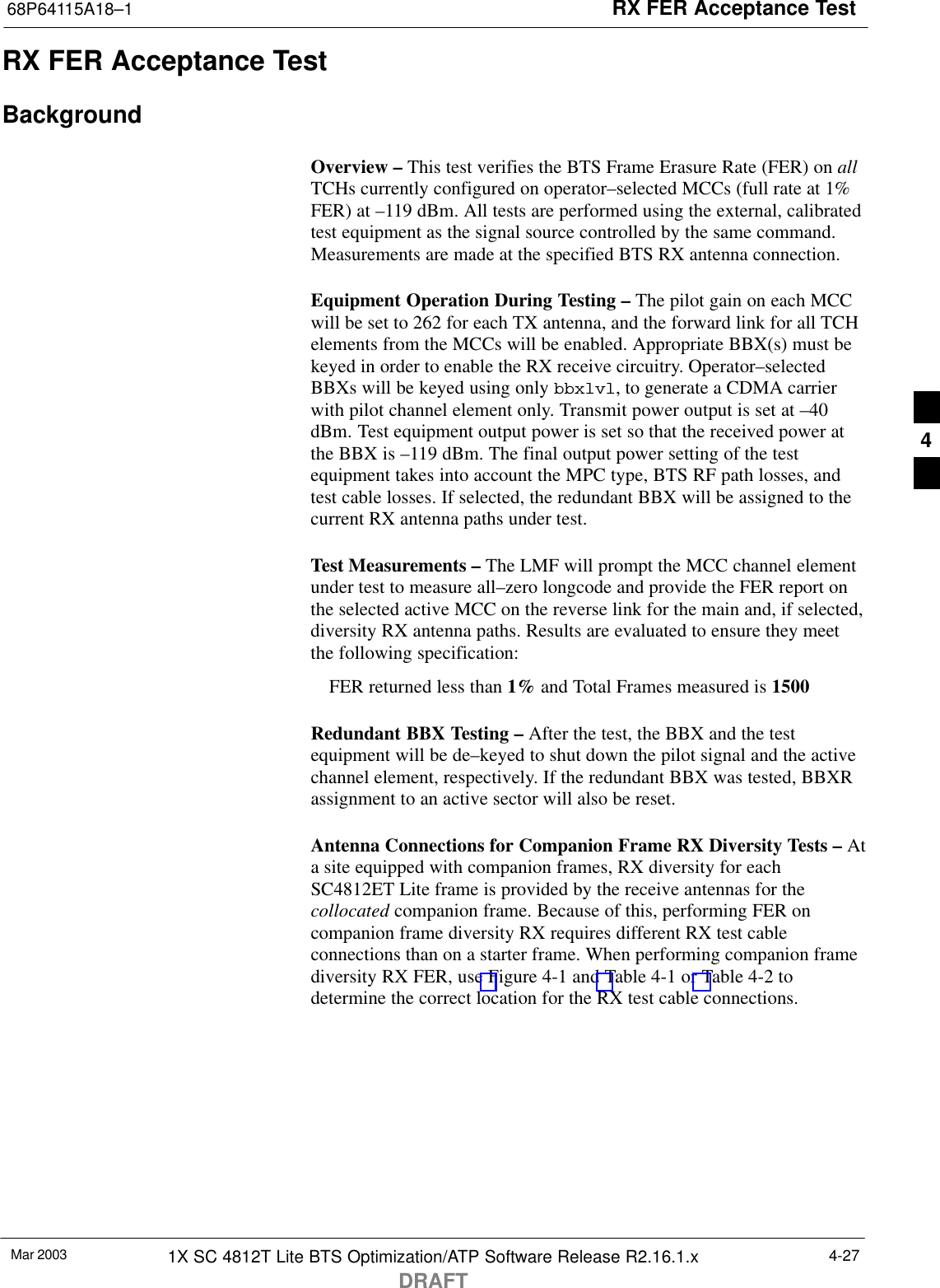
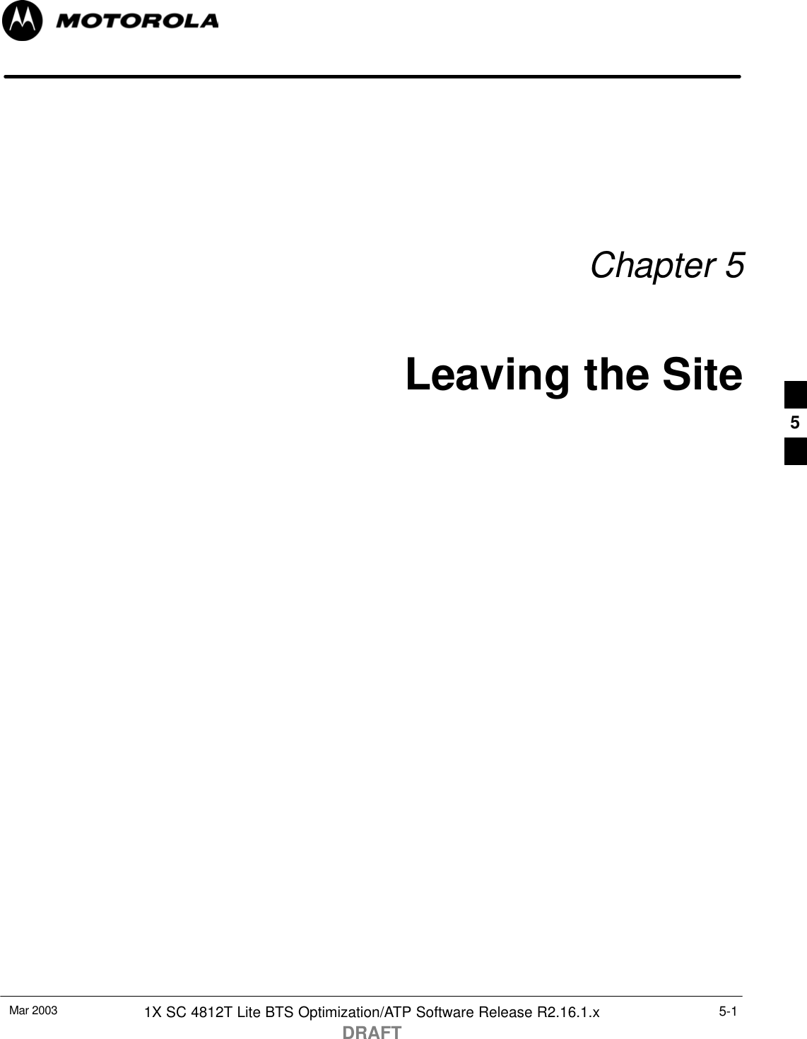
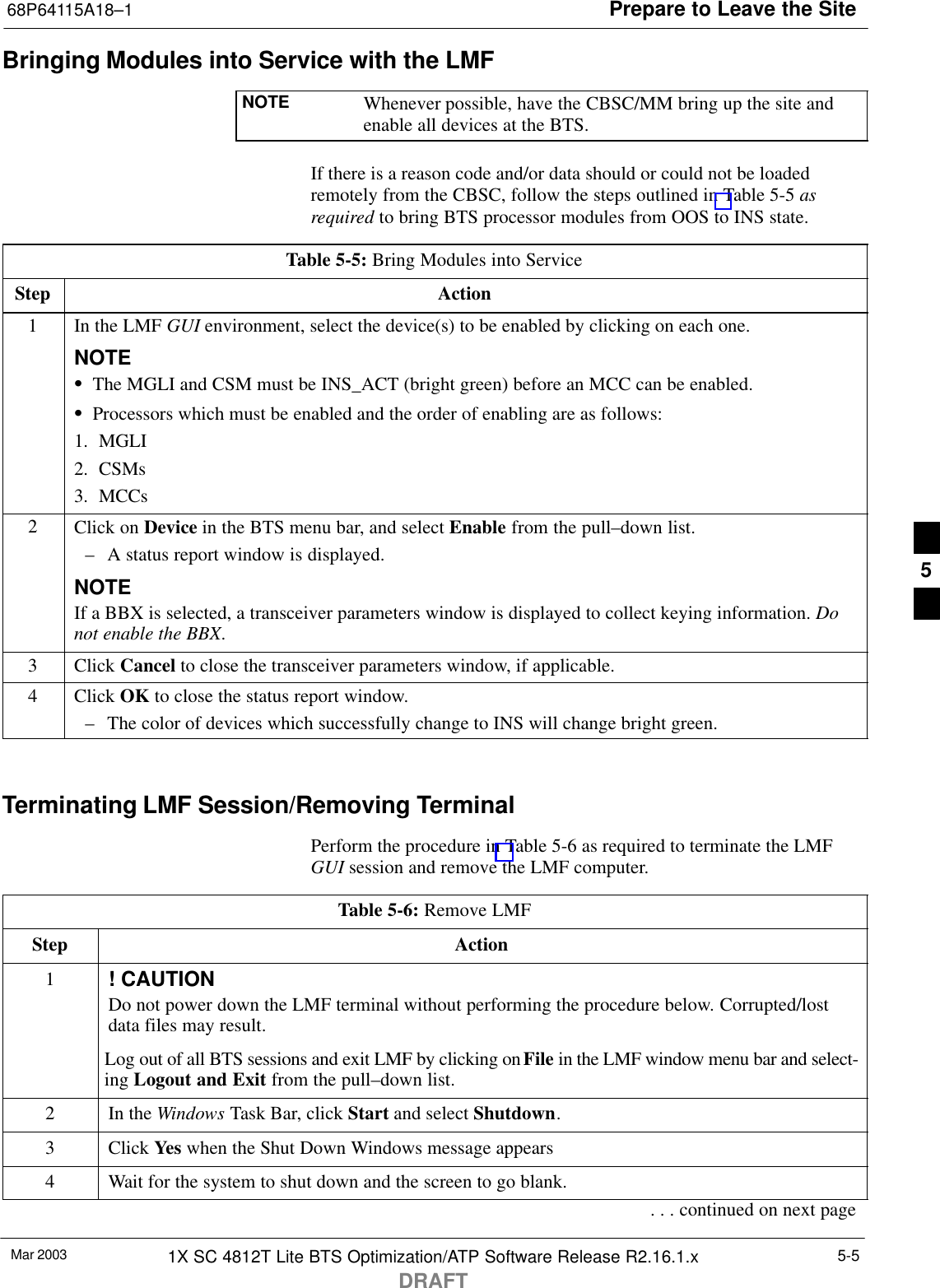
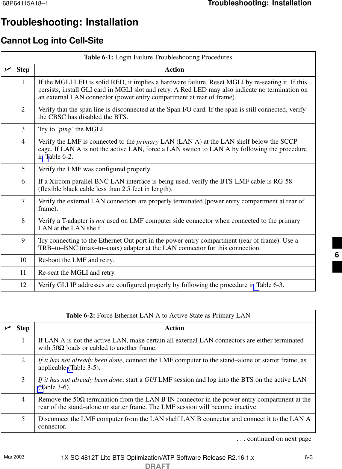
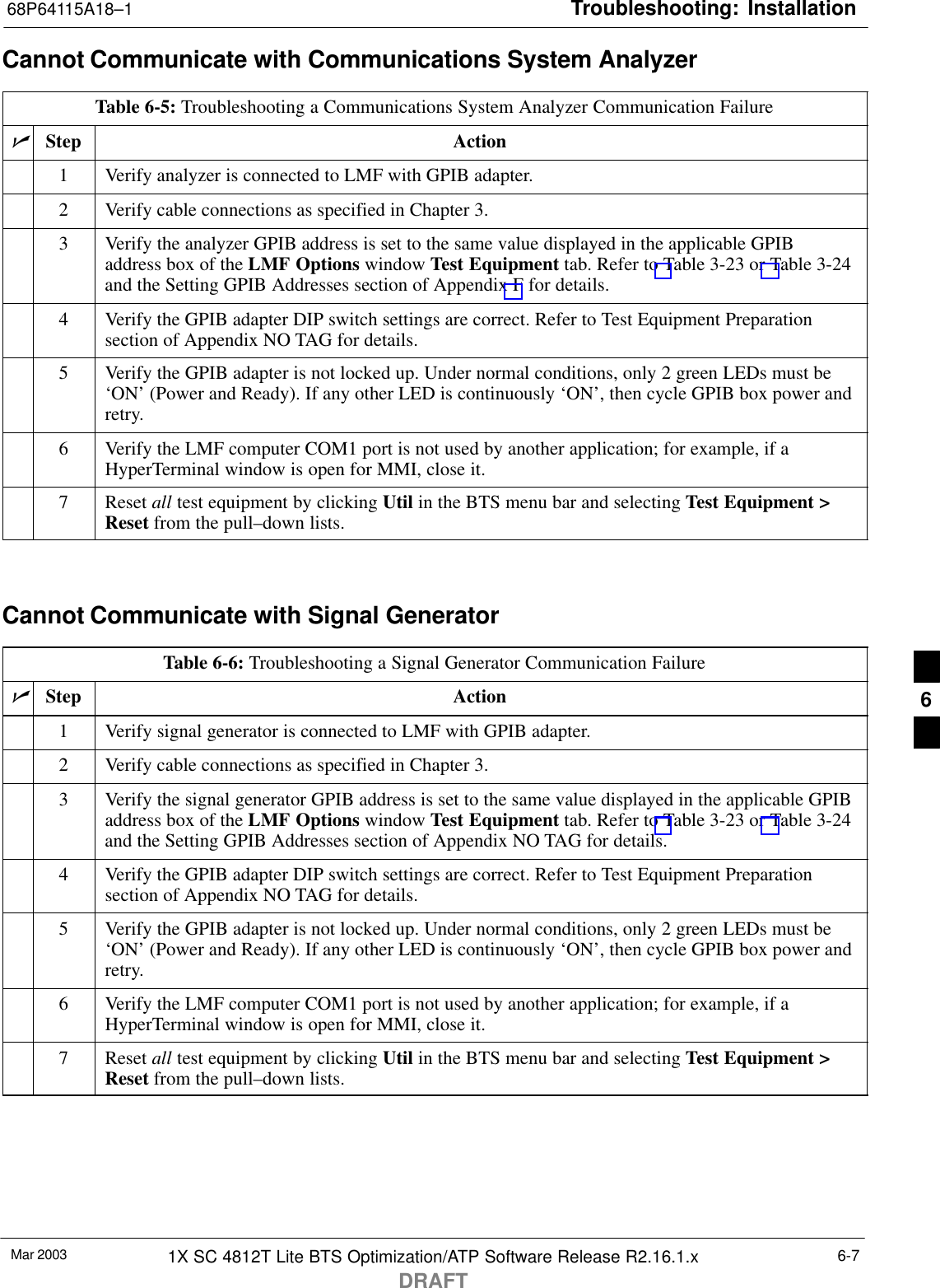
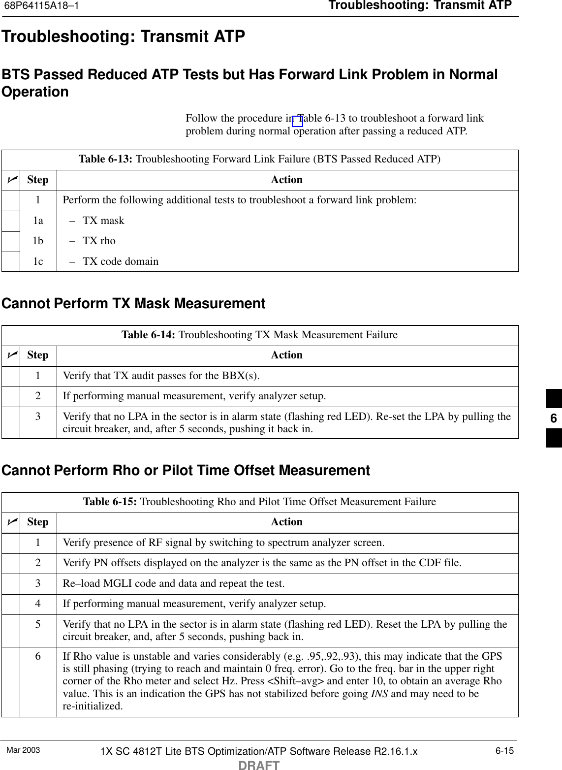
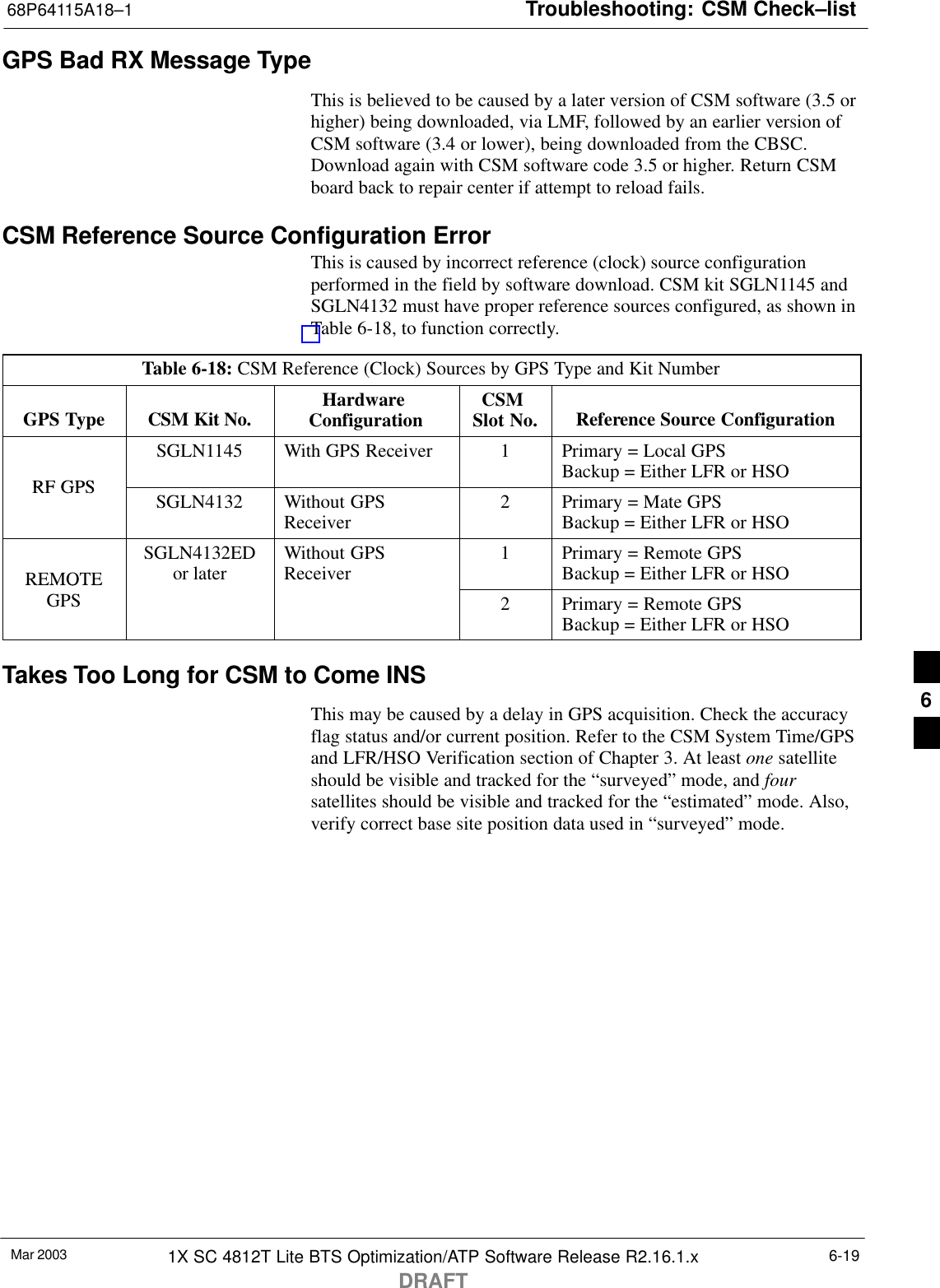
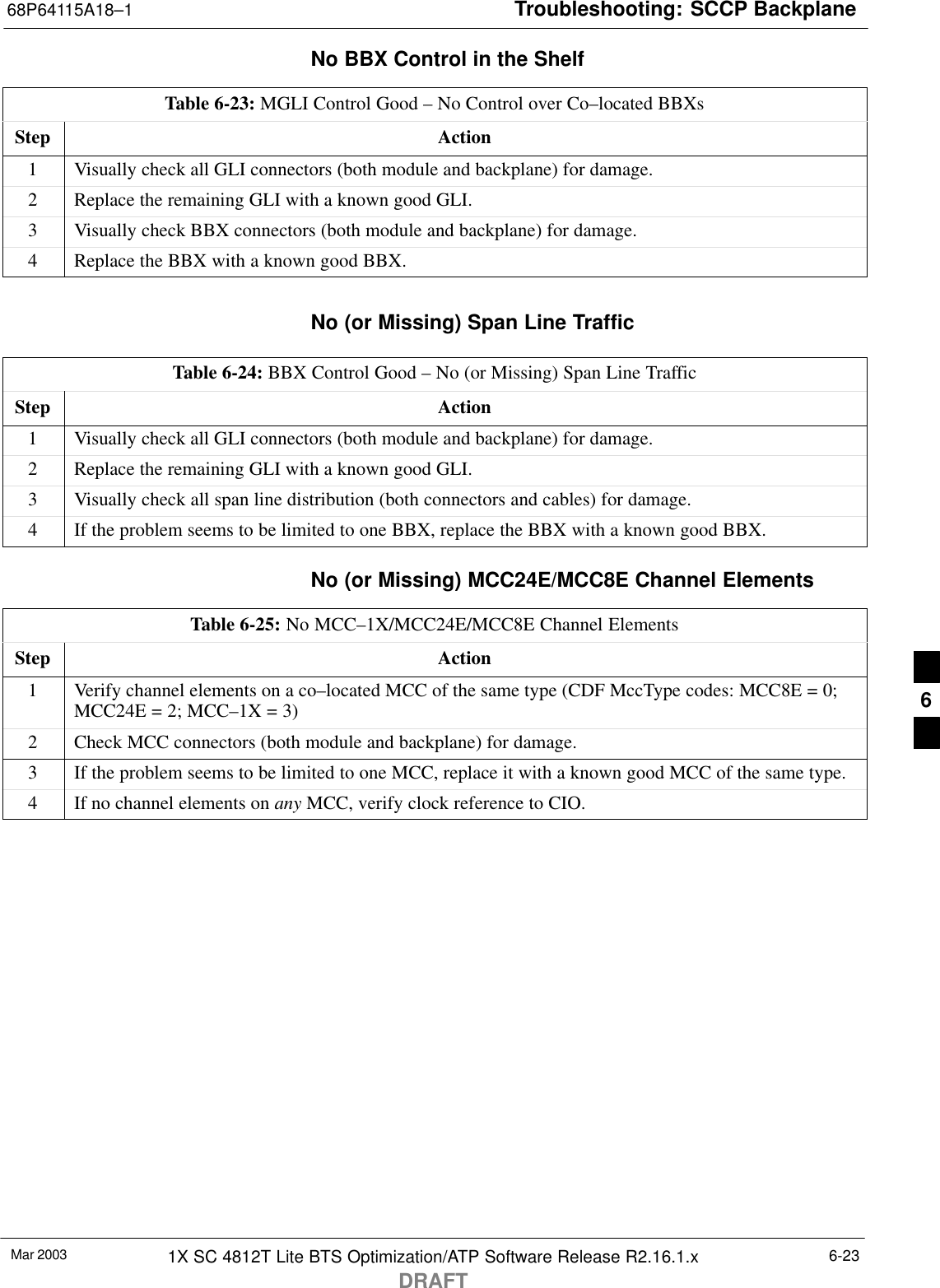
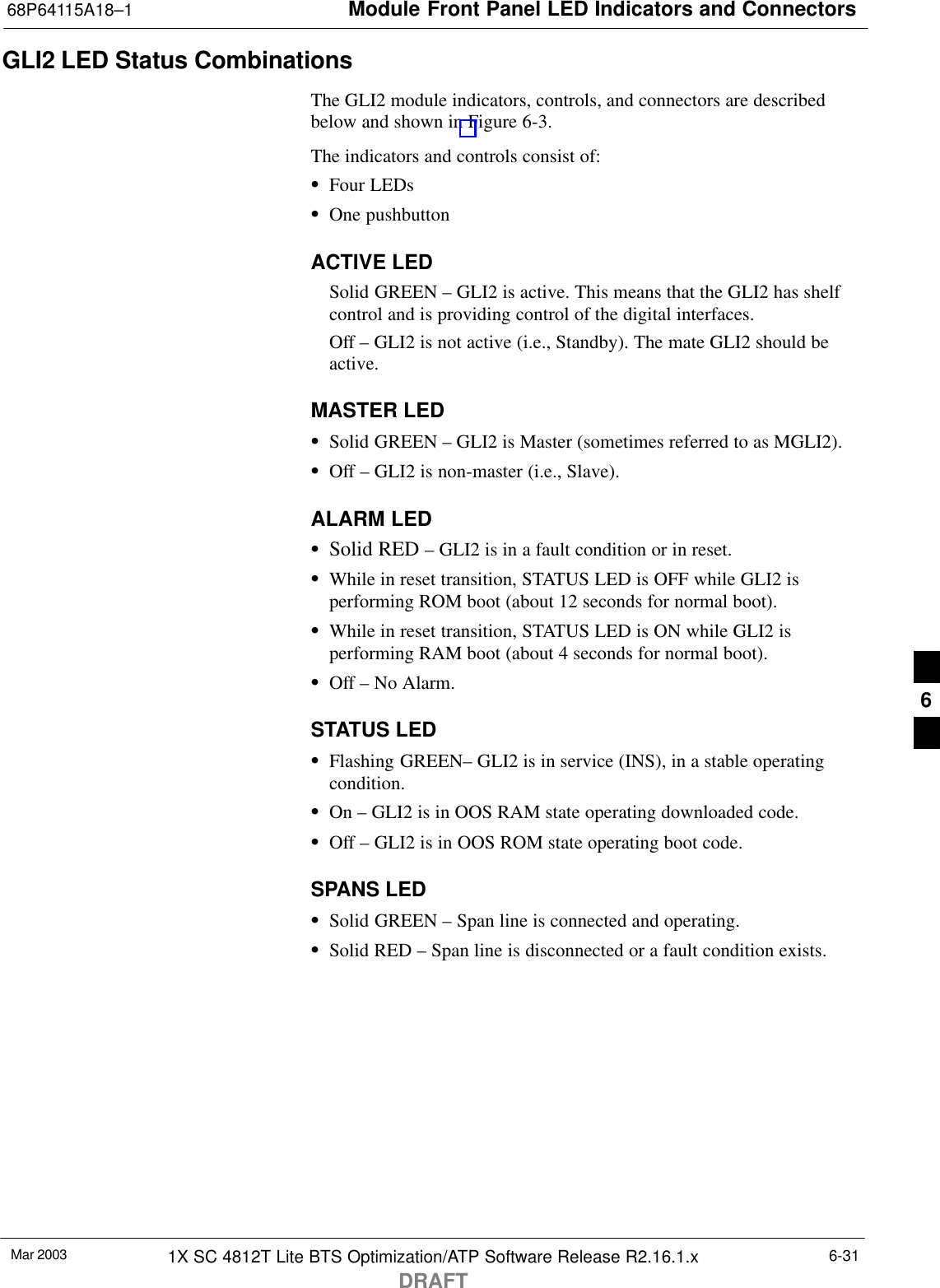
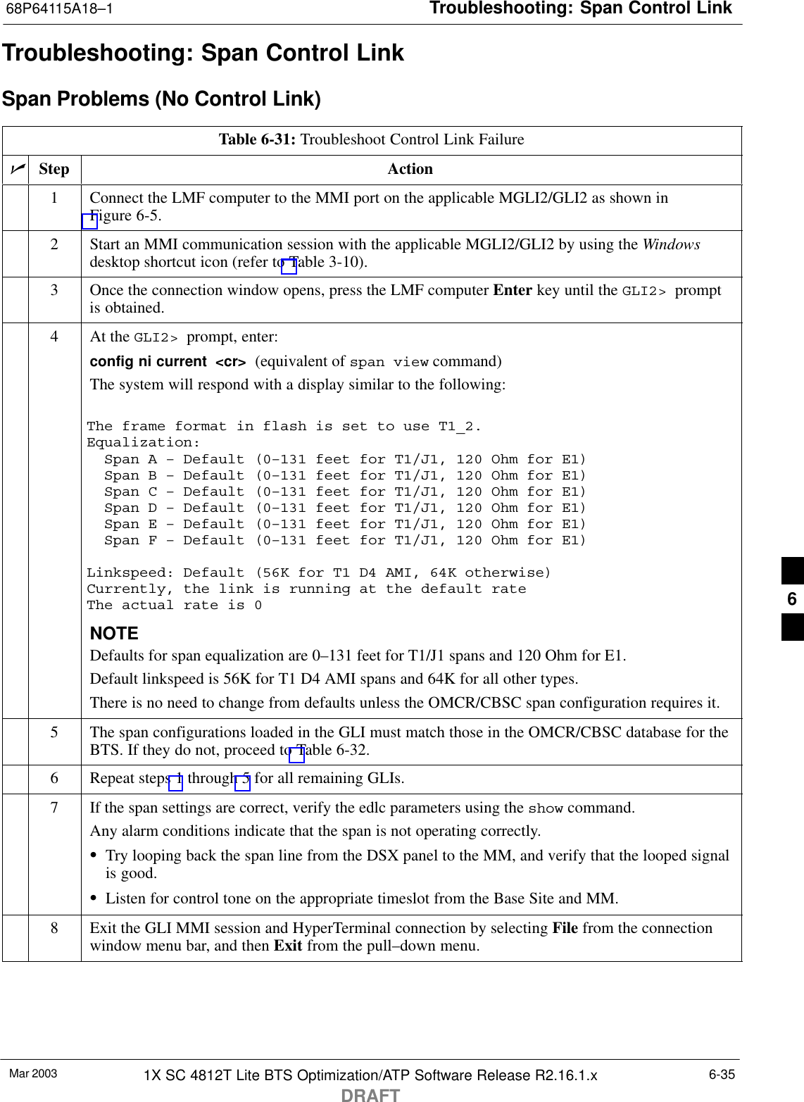
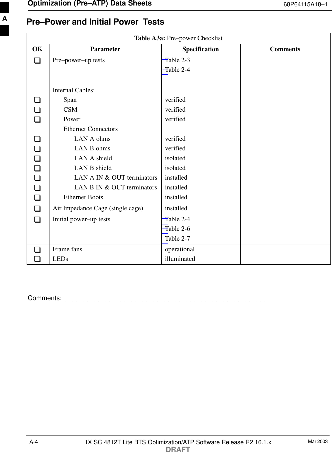
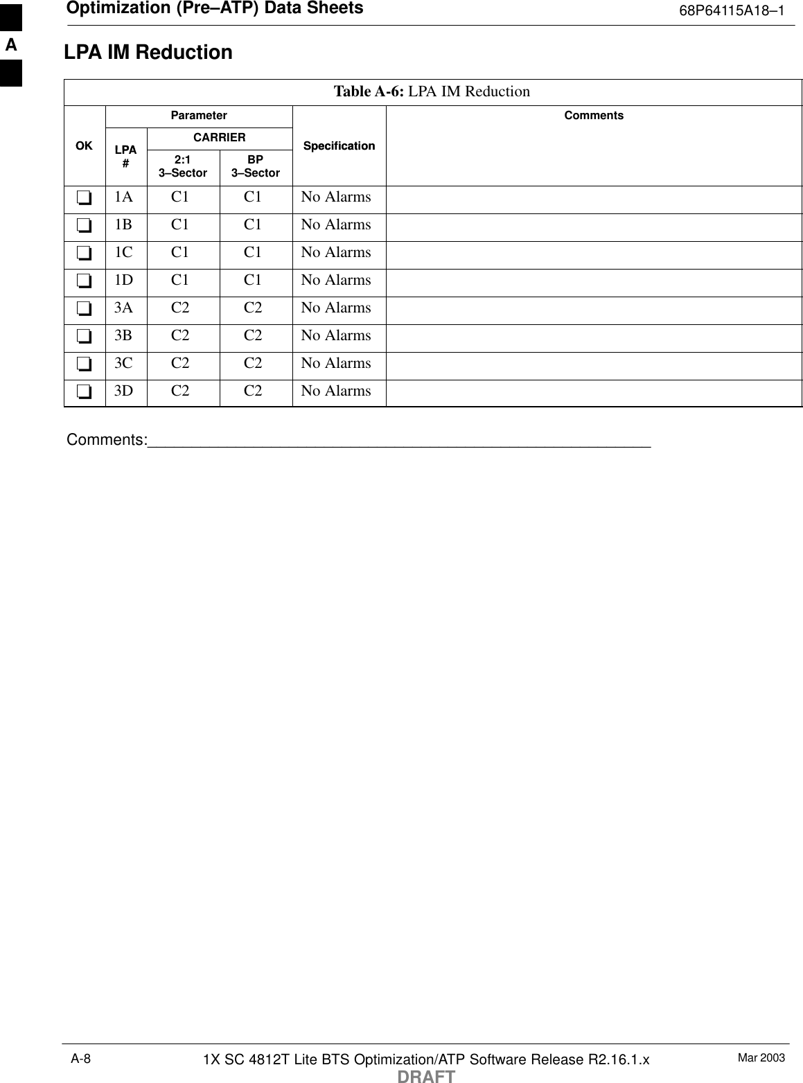
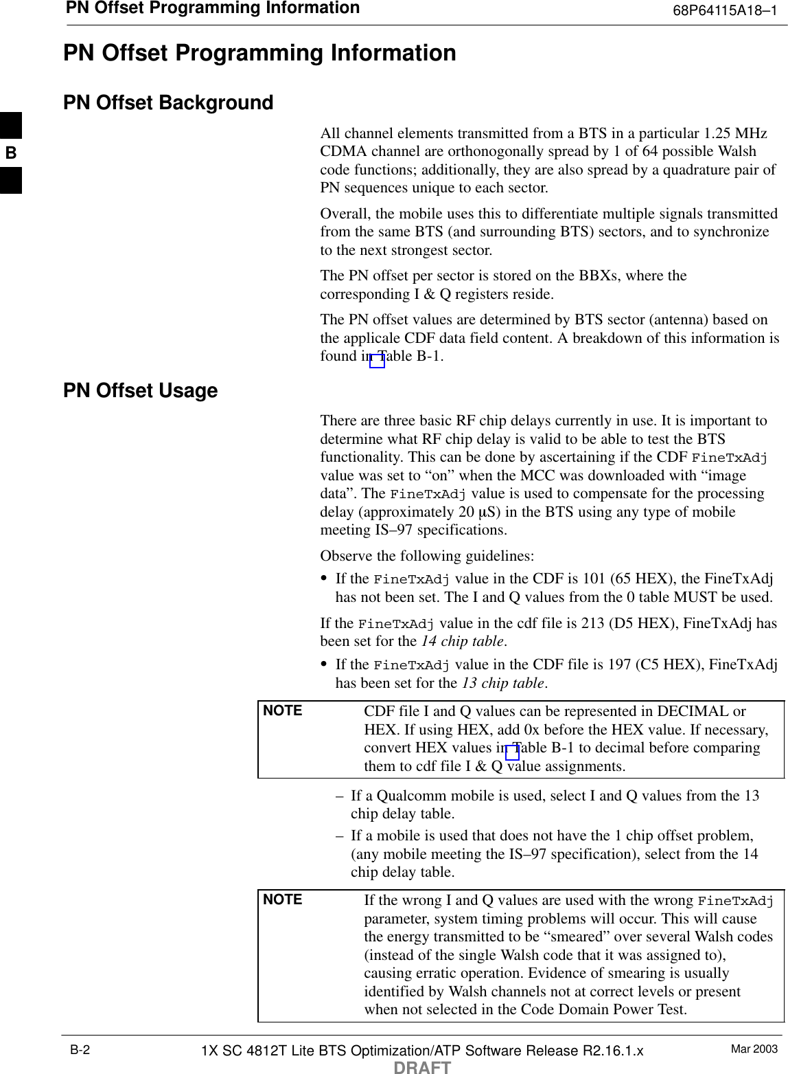
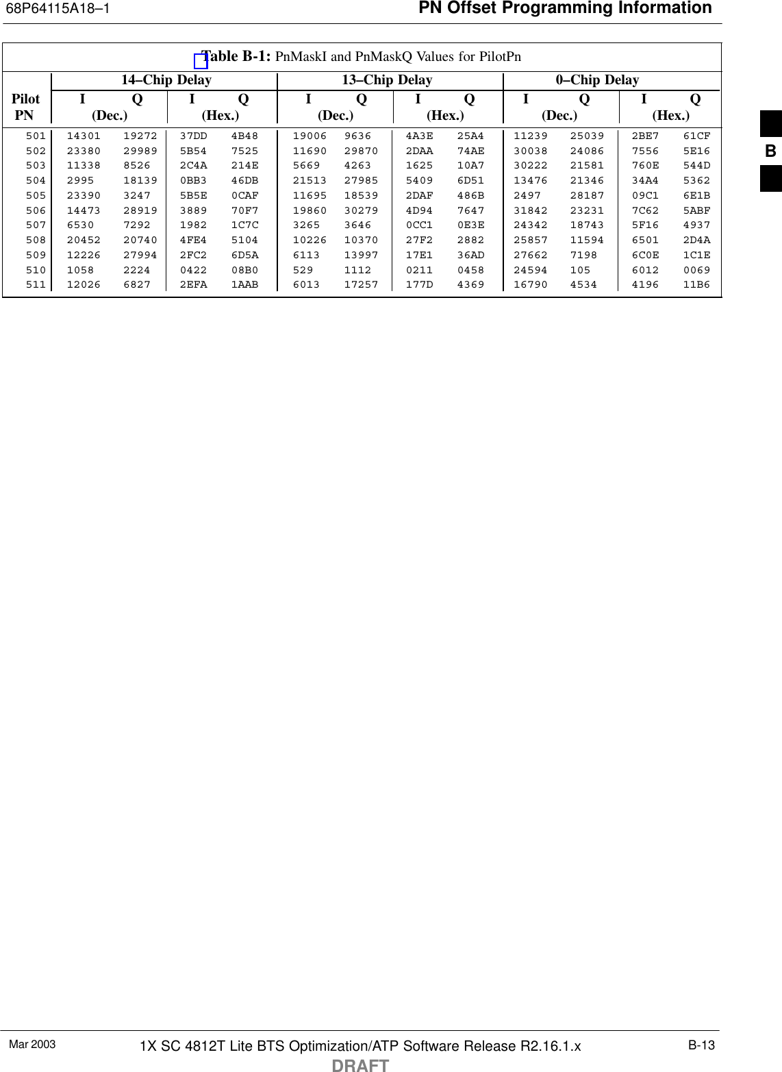
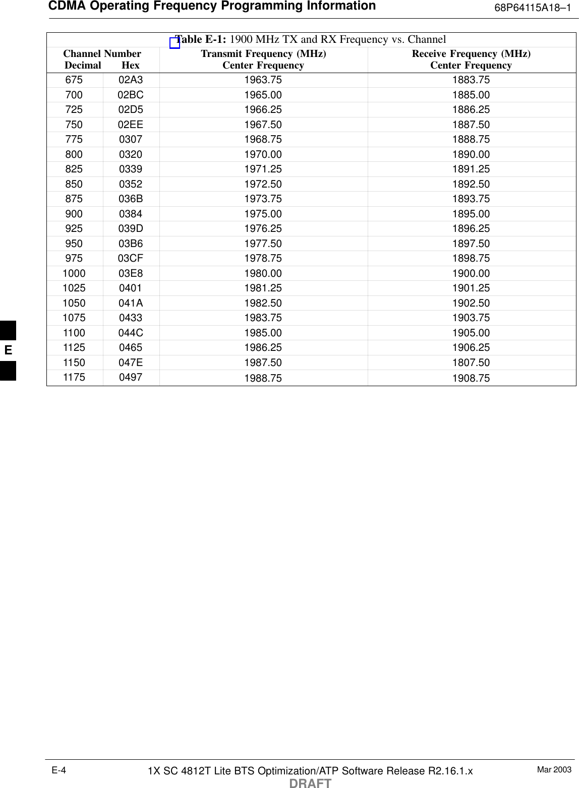
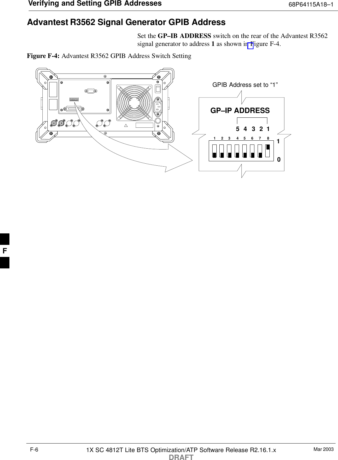
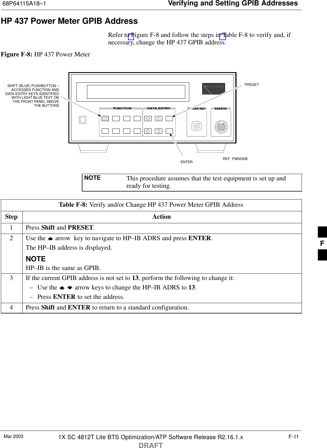
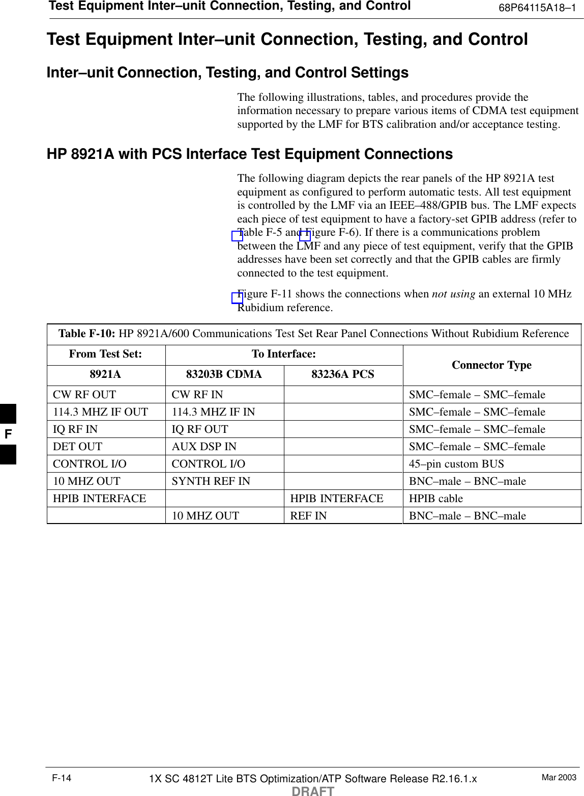
![Equipment Calibration 68P64115A18–1Mar 20031X SC 4812T Lite BTS Optimization/ATP Software Release R2.16.1.xDRAFTF-26Calibrating HP 437 Power MeterPrecise transmit output power calibration measurements are made usinga bolometer–type broadband power meter with a sensitive power sensor.Follow the steps outlined in Table F-18 to enter information unique tothe power sensor before calibrating the test setup. Refer to Figure F-19as required.NOTE This procedure must be done before the automated calibration toenter power sensor specific calibration values.Figure F-19: Power Meter DetailCONNECT POWERSENSOR WITH POWERMETER TURNED OFFCONNECT POWER SENSORTO POWER REFERENCEWHEN CALIBRATING UNIT.POWER REFERENCE ISENABLED USING THE SHIFT ’KEYSSHIFT (BLUE) PUSHBUTTON –ACCESSES FUNCTION ANDDATA ENTRY KEYS IDENTIFIEDWITH LIGHT BLUE TEXT ONTHE FRONT PANEL ABOVETHE BUTTONSFW00308Table F-18: HP 437 Power Meter Calibration ProcedureStep Action1! CAUTIONDo not connect/disconnect the power meter sensor cable with AC power applied to the meter.Disconnection could result in destruction of the sensing element or mis–calibration.Make sure the power meter AC LINE pushbutton is OFF.2Connect the power sensor cable to the SENSOR input.3Set the AC LINE pushbutton to ON.NOTEThe calibration should be performed only after the power meter and sensor have been allowed towarm–up and stabilize for a minimum of 60 minutes.4Perform the following to set or verify the correct power sensor model:4a – Press [SHIFT] then [a] to select SENSOR.4b – Identify the power sensor model number from the sensor label.4c – Use the [y] or [b] button to select the appropriate model; then press [ENTER].5Refer to the illustration for step 8, and perform the following to ensure the power reference output isOFF:5a – Observe the instrument display and determine if the triangular indicator over PWR REF isdisplayed.5b – If the triangular indicator is displayed, press [SHIFT] then [’] to turn it off.. . . continued on next pageF](https://usermanual.wiki/Nokia-Solutions-and-Networks/T5EE1.Users-Manual-2/User-Guide-471764-Page-131.png)
![Equipment Calibration68P64115A18–1Mar 2003 1X SC 4812T Lite BTS Optimization/ATP Software Release R2.16.1.xDRAFTF-27Table F-18: HP 437 Power Meter Calibration ProcedureStep Action6 Press [ZERO].– Display will show “Zeroing ******.”– Wait for process to complete.7Connect the power sensor to the POWER REF output.8Turn on the PWR REF by performing the following:8a – Press [SHIFT] then [’].8b – Verify that the triangular indicator (below) appears in the display above PWR REF.9Perform the following to set the REF CF%:9a – Press ([SHIFT] then [ZERO]) for CAL.9b – Enter the sensor’s REF CF% from the sensor’s decal using the arrow keys and press [ENTER].(The power meter will display ”CAL *****” for a few seconds.)NOTEIf the REF CAL FACTOR (REF CF) is not shown on the power sensor, assume it to be 100%.10 Perform the following to set the CAL FAC %:10a – Press [SHIFT] then [FREQ] for CAL FAC.10b – On the sensor’s decal, locate an approximate calibration percentage factor (CF%) at 2 GHz.10c – Enter the sensor’s calibration % (CF%) using the arrow keys and press [ENTER].–– When complete, the power meter will typically display 0.05 dBm. (Any reading between0.00 and 0.10 is normal.)11 To turn off the PWR REF, perform the following:11a – Press [SHIFT] then [’].11b – Disconnect the power sensor from the POWER REF output. F](https://usermanual.wiki/Nokia-Solutions-and-Networks/T5EE1.Users-Manual-2/User-Guide-471764-Page-132.png)
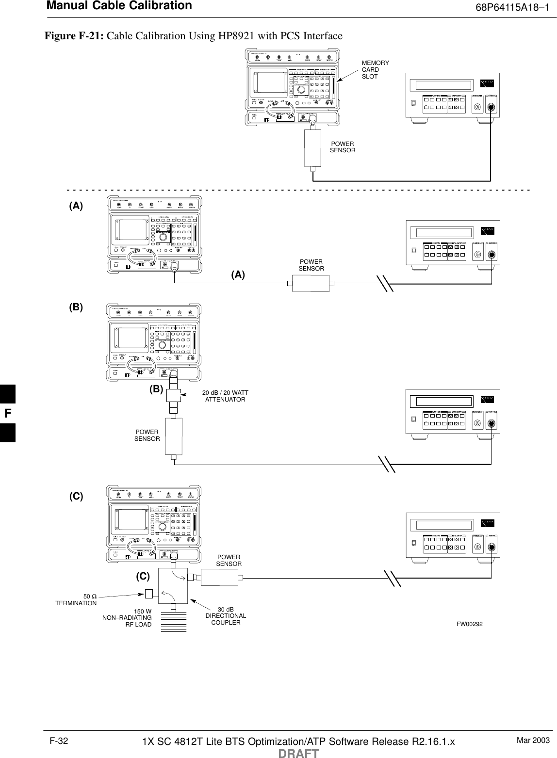
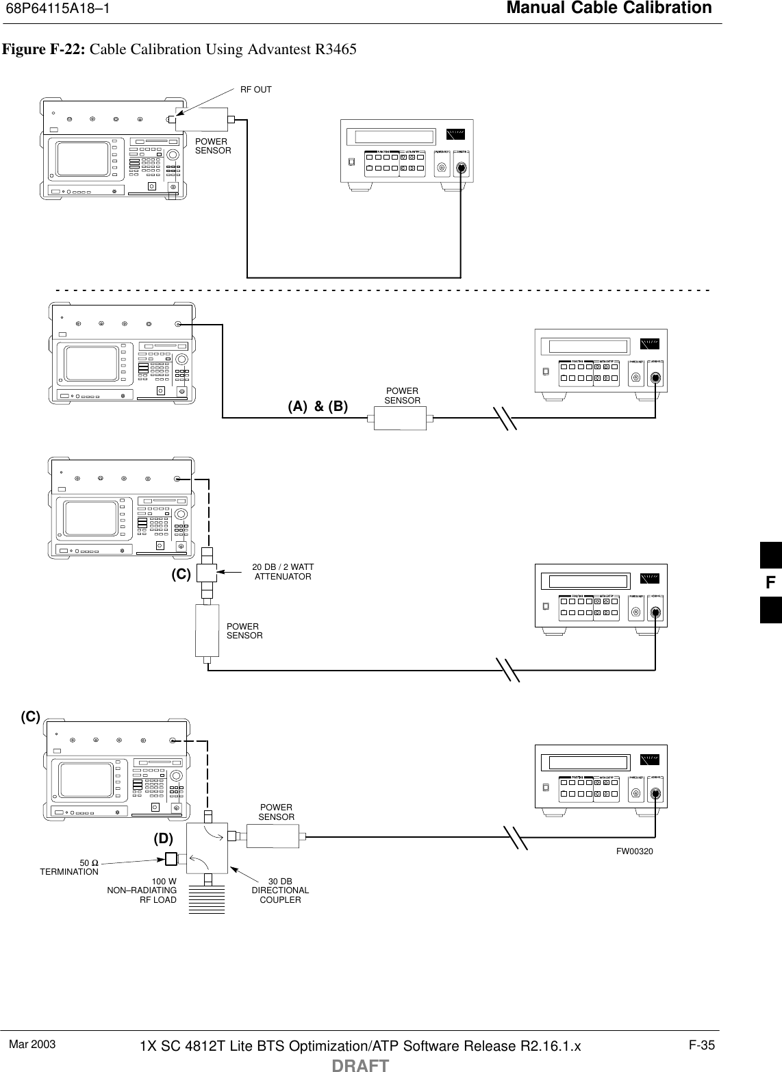
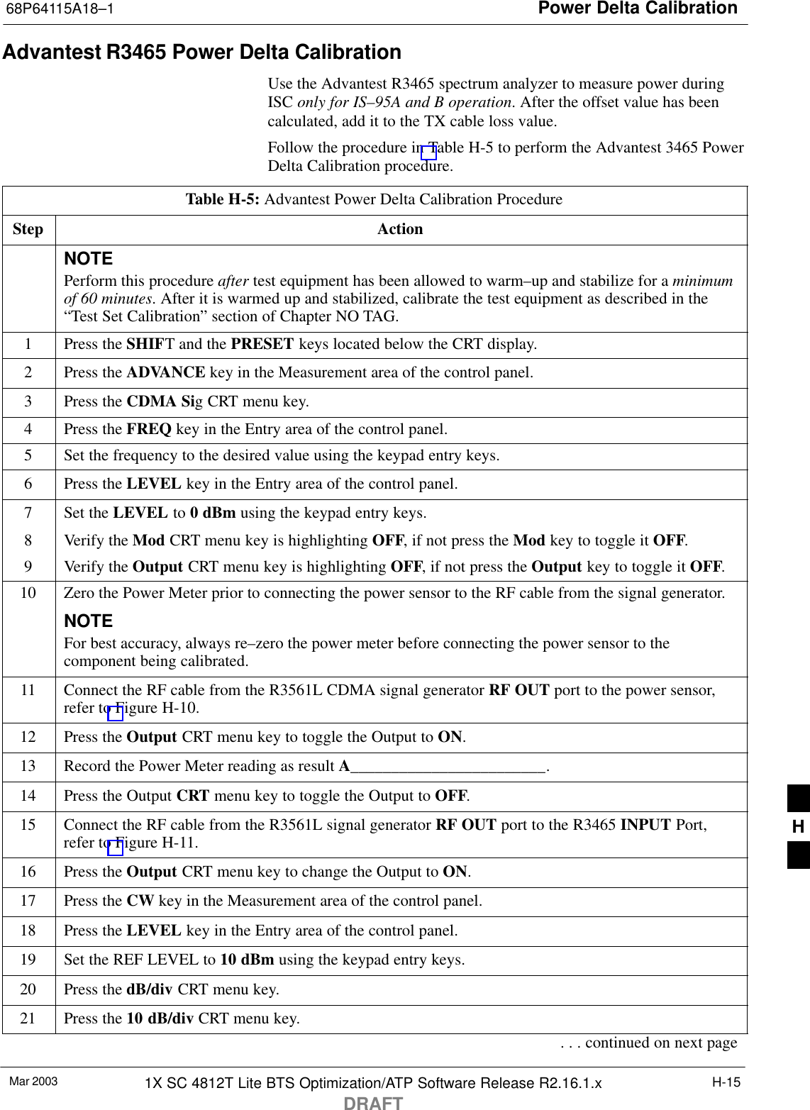
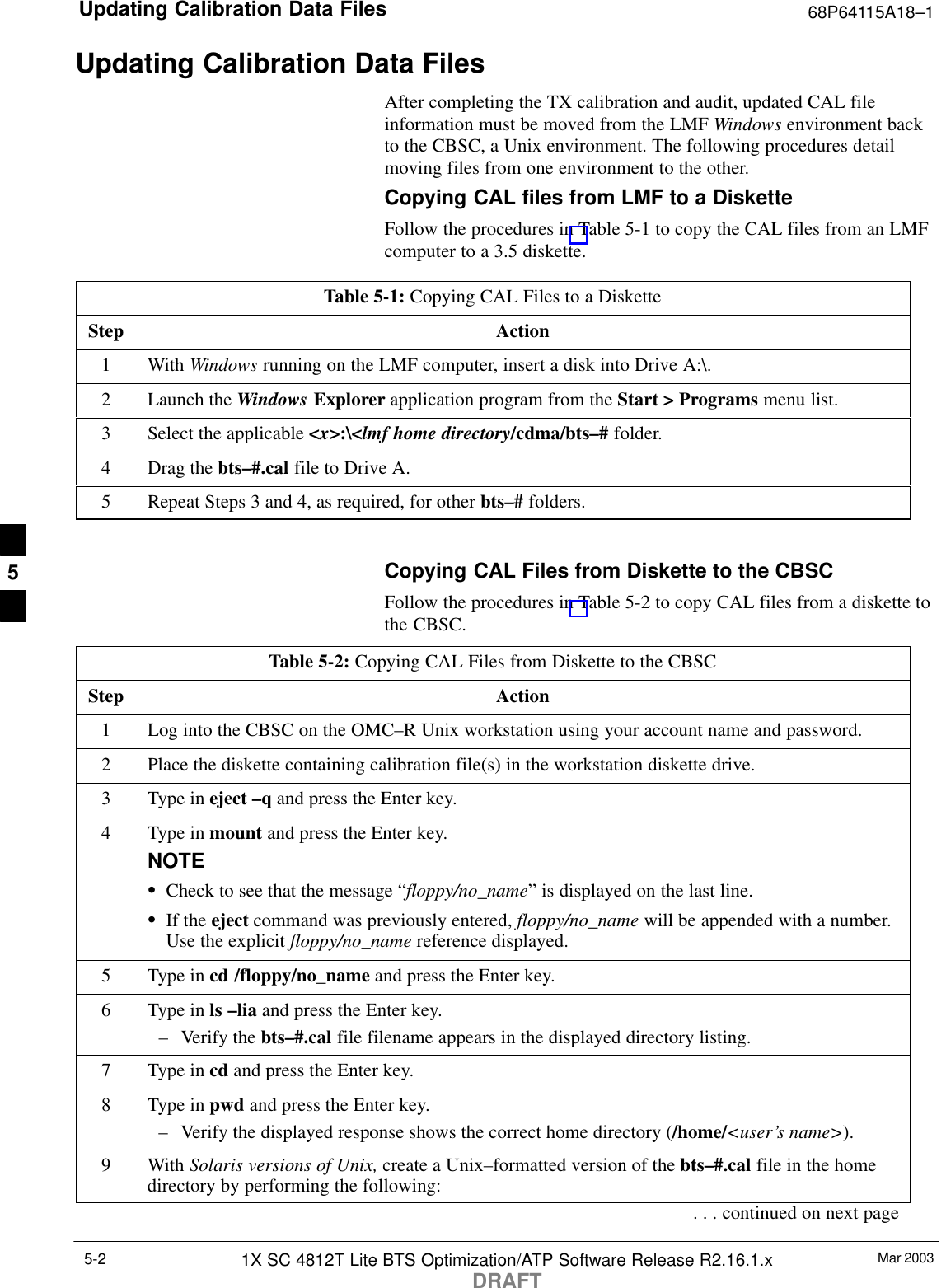
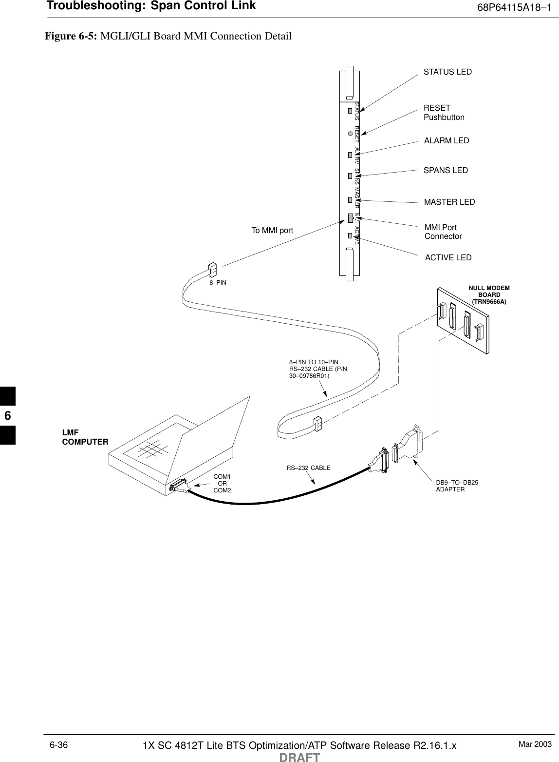
![Manual Cable Calibration68P64115A18–1Mar 2003 1X SC 4812T Lite BTS Optimization/ATP Software Release R2.16.1.xDRAFTF-29Manual Cable CalibrationCalibrating Test Cable SetupUsing HP PCS Interface (HP83236)Table F-20 covers the procedure to calibrate the test equipment using theHP8921 Cellular Communications Analyzer equipped with the HP83236PCS Interface.NOTE This calibration method must be executed with great care. Somelosses are measured close to the minimum limit of the powermeter sensor (–30 dBm).PrerequisitesEnsure the following prerequisites have been met before proceeding:STest equipment to be calibrated has been connected correctly for cablecalibration.STest equipment has been selected and calibrated.Table F-20: Calibrating Test Cable Setup (using the HP PCS Interface)Step ActionNOTEVerify that GPIB controller is turned off.1Insert HP83236 Manual Control System card into memory card slot.2Press the Preset pushbutton.3 Under Screen Controls, press the TESTS pushbutton to display the TESTS (Main Menu) screen.4Position the cursor at Select Procedure Location and select it. In the Choices selection box, selectCARD.5Position the cursor at Select Procedure Filename and select it. In the Choices selection box, selectMANUAL.6Position the cursor at RUN TEST and select it. HP must be in Control Mode Select YES.7If using HP83236A:Set channel number=<chan#>:– Position cursor at ChannelNumber and select it.– Enter the chan# using the numerickeypad; press [Enter] and thescreen will go blank.– When the screen reappears, thechan# will be displayed on thechannel number line.If using HP83236B:Set channel frequency:– Position cursor at Frequency Band and press Enter.– Select User Defined Frequency.– Go Back to Previous Menu.– Position the cursor to 83236 generator frequency andenter actual RX frequency.– Position the cursor to 83236 analyzer frequency andenter actual TX frequency.8Set RF Generator level:– Position the cursor at RF Generator Level and select it.– Enter –10 using the numeric keypad; press [Enter] and the screen will go blank.– When the screen reappears, the value –10 dBm will be displayed on the RF Generator Level line.. . . continued on next pageF](https://usermanual.wiki/Nokia-Solutions-and-Networks/T5EE1.Users-Manual-2/User-Guide-471764-Page-134.png)
![Manual Cable Calibration 68P64115A18–1Mar 20031X SC 4812T Lite BTS Optimization/ATP Software Release R2.16.1.xDRAFTF-30Table F-20: Calibrating Test Cable Setup (using the HP PCS Interface)Step Action9Set the user fixed Attenuation Setting to 0 dBm:– Position cursor at Analyzer Attenuation and select it– Position cursor at User Fixed Atten Settings and select it.– Enter 0 (zero) using the numeric keypad and press [Enter].10 Select Back to Previous Menu.11 Record the HP83236 Generator Frequency Level:Record the HP83236B Generator Frequency Level:– Position cursor at Show Frequency and Level Details and select it.– Under HP83236 Frequencies and Levels, record the Generator Level.– Under HP83236B Frequencies and Levels, record the Generator Frequency Level (1850 – 1910MHz).– Position cursor at Prev Menu and select it.12 Click on Pause for Manual Measurement.13 Connect the power sensor directly to the RF OUT ONLY port of the PCS Interface.14 On the HP8921A, under To Screen, select CDMA GEN.15 Move the cursor to the Amplitude field and click on the Amplitude value.16 Increase the Amplitude value until the power meter reads 0 dBm ±0.2 dB.NOTEThe Amplitude value can be increased coarsely until 0 dBM is reached; then fine tune the amplitudeby adjusting the Increment Set to 0.1 dBm and targeting in on 0 dBm.17 Disconnect the power sensor from the RF OUT ONLY port of the PCS Interface.NOTEThe Power Meter sensor’s lower limit is –30 dBm. Thus, only components having losses ≤30 dBshould be measured using this method. For further accuracy, always re-zero the power meterbefore connecting the power sensor to the component being calibrated. After connecting thepower sensor to the component, record the calibrated loss immediately.18 Disconnect all components in the test setup and calibrate each one separately by connecting eachcomponent, one-at-a-time, between the RF OUT ONLY PORT and the power sensor. Record thecalibrated loss value displayed on the power meter.SExample: (A) Test Cable(s) = –1.4 dB(B) 20 dB Attenuator = –20.1 dB(B) Directional Coupler = –29.8 dB19 After all components are calibrated, reassemble all components together and calculate the total testsetup loss by adding up all the individual losses:SExample: Total test setup loss = –1.4 –29.8 –20.1 = –51.3 dB.This calculated value will be used in the next series of tests.20 Under Screen Controls press the TESTS button to display the TESTS (Main Menu) screen.21 Select Continue (K2).22 Select RF Generator Level and set to –119 dBm.. . . continued on next pageF](https://usermanual.wiki/Nokia-Solutions-and-Networks/T5EE1.Users-Manual-2/User-Guide-471764-Page-135.png)
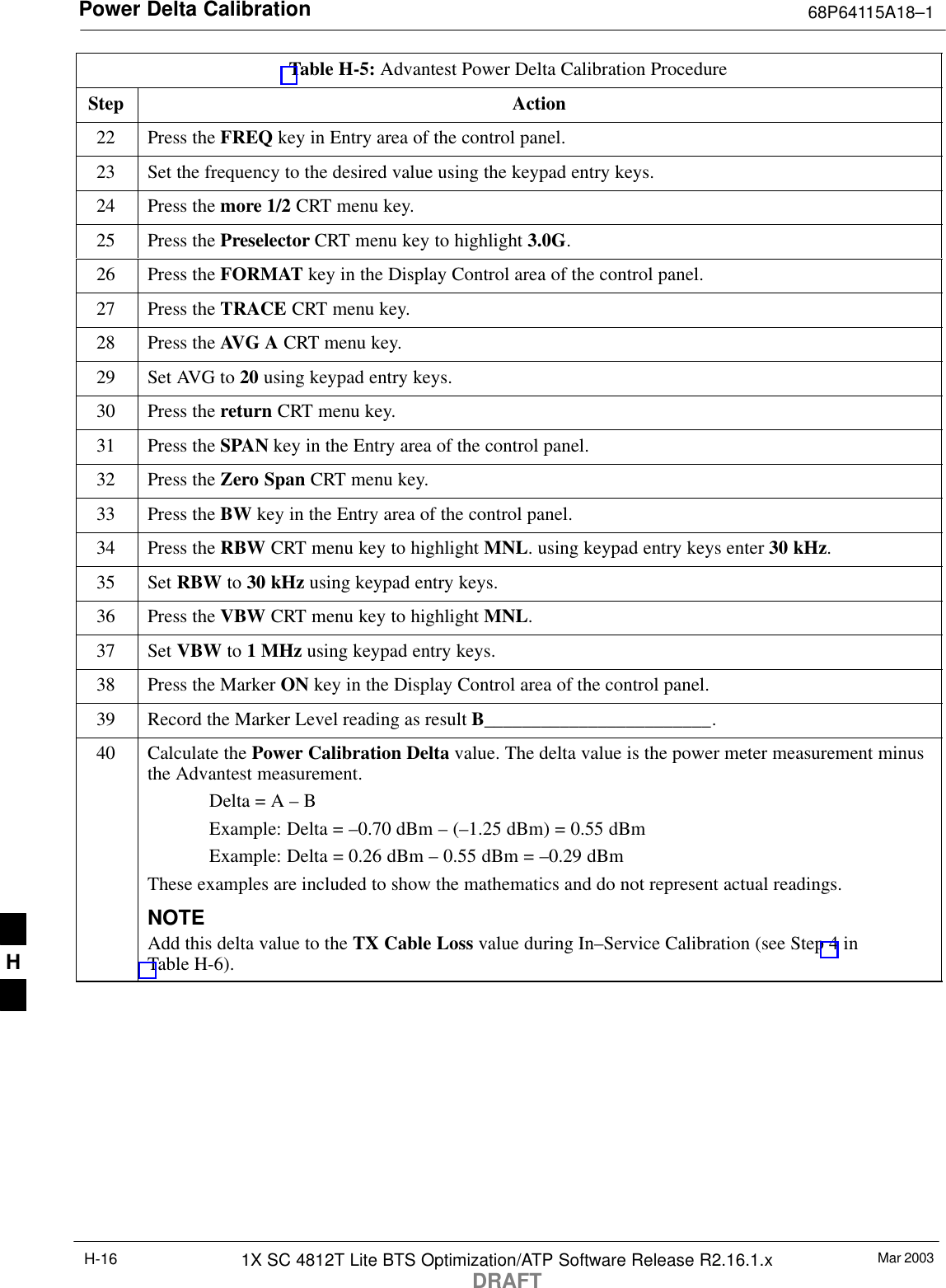
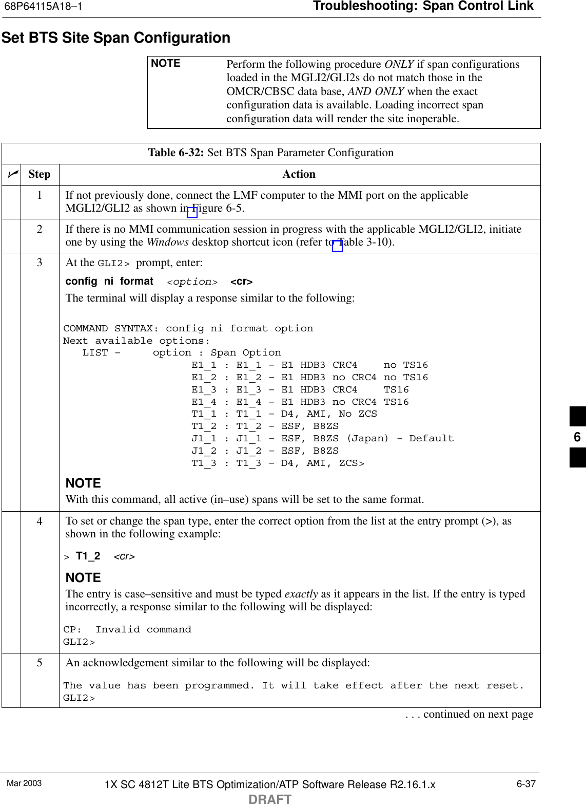
![Manual Cable Calibration68P64115A18–1Mar 2003 1X SC 4812T Lite BTS Optimization/ATP Software Release R2.16.1.xDRAFTF-31Table F-20: Calibrating Test Cable Setup (using the HP PCS Interface)Step Action23 Click on Pause for Manual Measurement.24 Verify the HP8921A Communication Analyzer/83203A CDMA interface setup is as follows (fieldsnot indicated remain at default):SVerify the GPIB (HP–IB) address:– under To Screen, select More– select IO CONFIG– Set HP–IB Adrs to 18– set Mode to Talk&LstnSVerify the HP8921A is displaying frequency (instead of RF channel)– Press the blue [SHIFT] button, then press the Screen Control [DUPLEX] button; this switches tothe CONFIG (CONFIGURE) screen.– Use the cursor control to set RF Display to Freq25 Refer toChapter 3 for assistance in setting the cable loss values into the LMF. F](https://usermanual.wiki/Nokia-Solutions-and-Networks/T5EE1.Users-Manual-2/User-Guide-471764-Page-136.png)