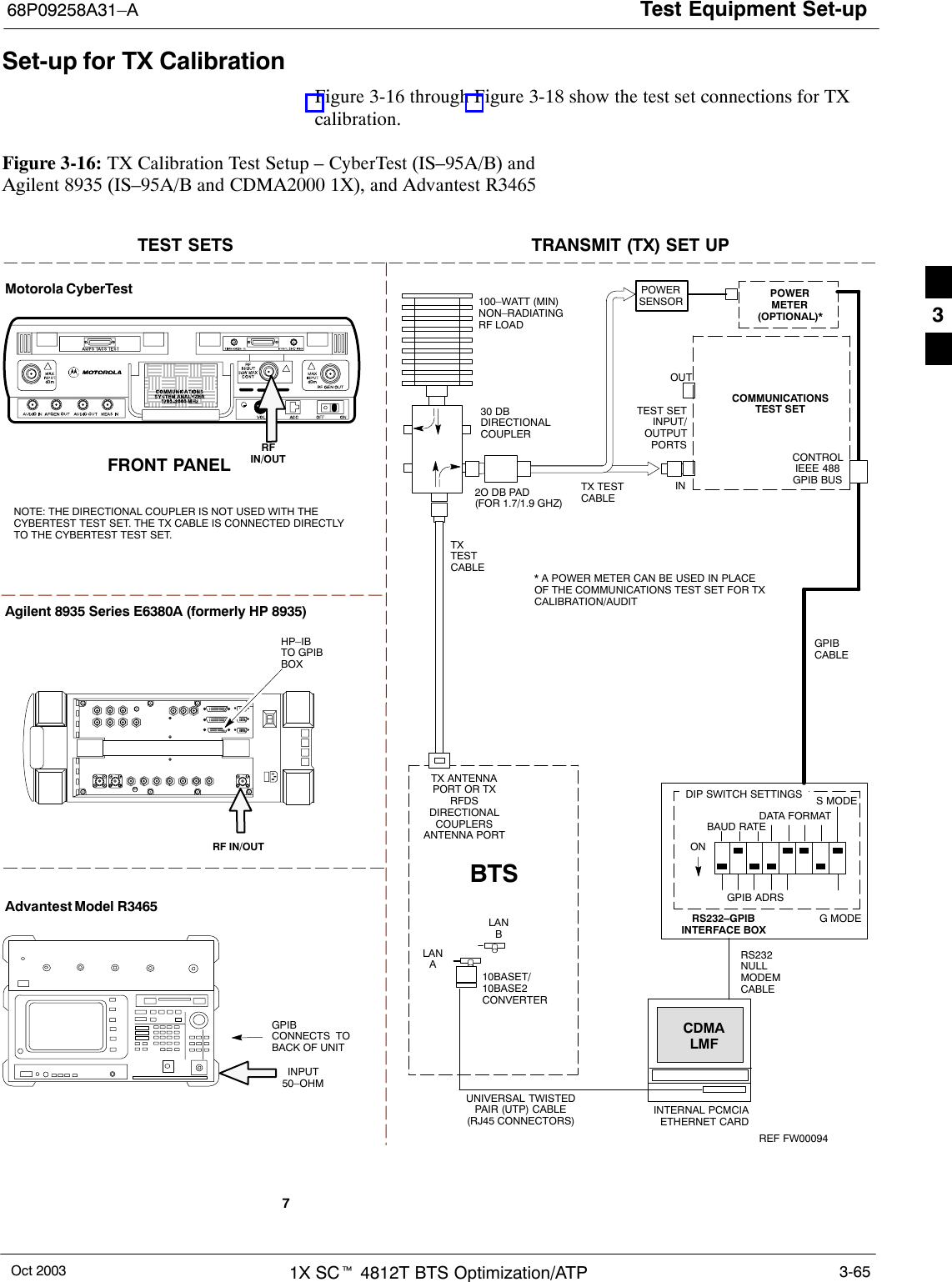
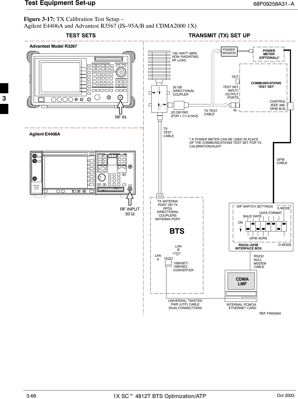
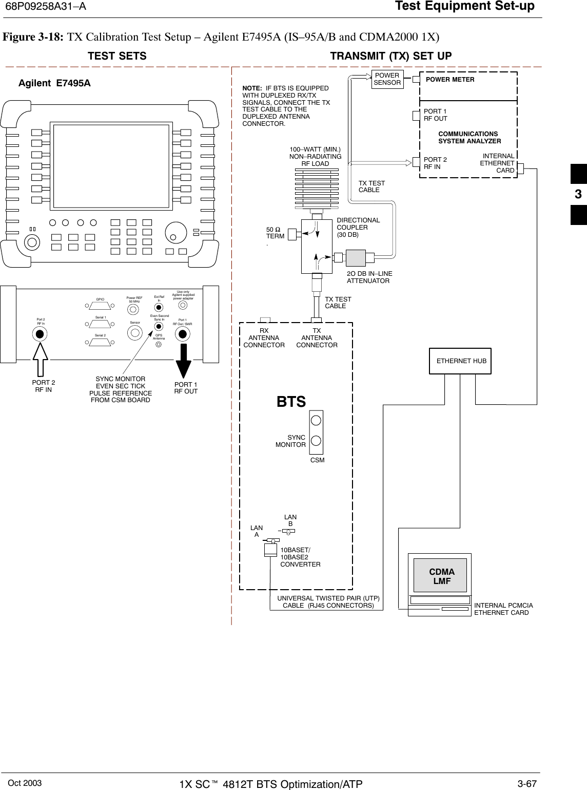
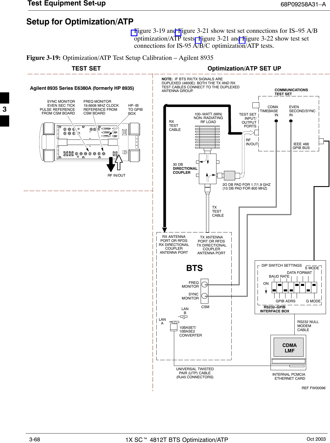
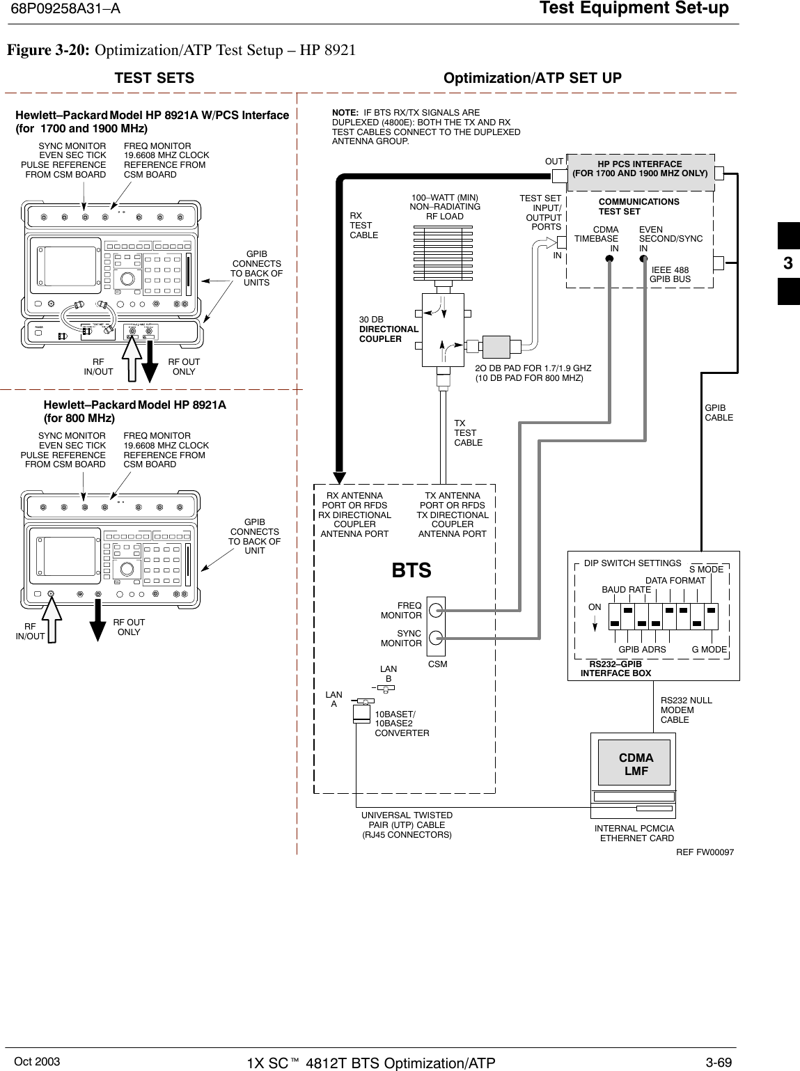
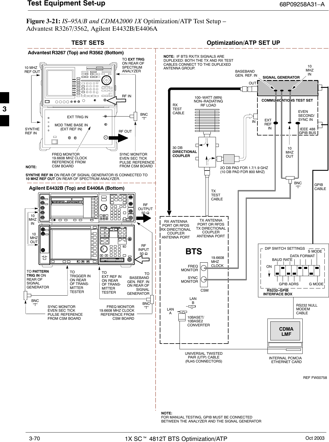
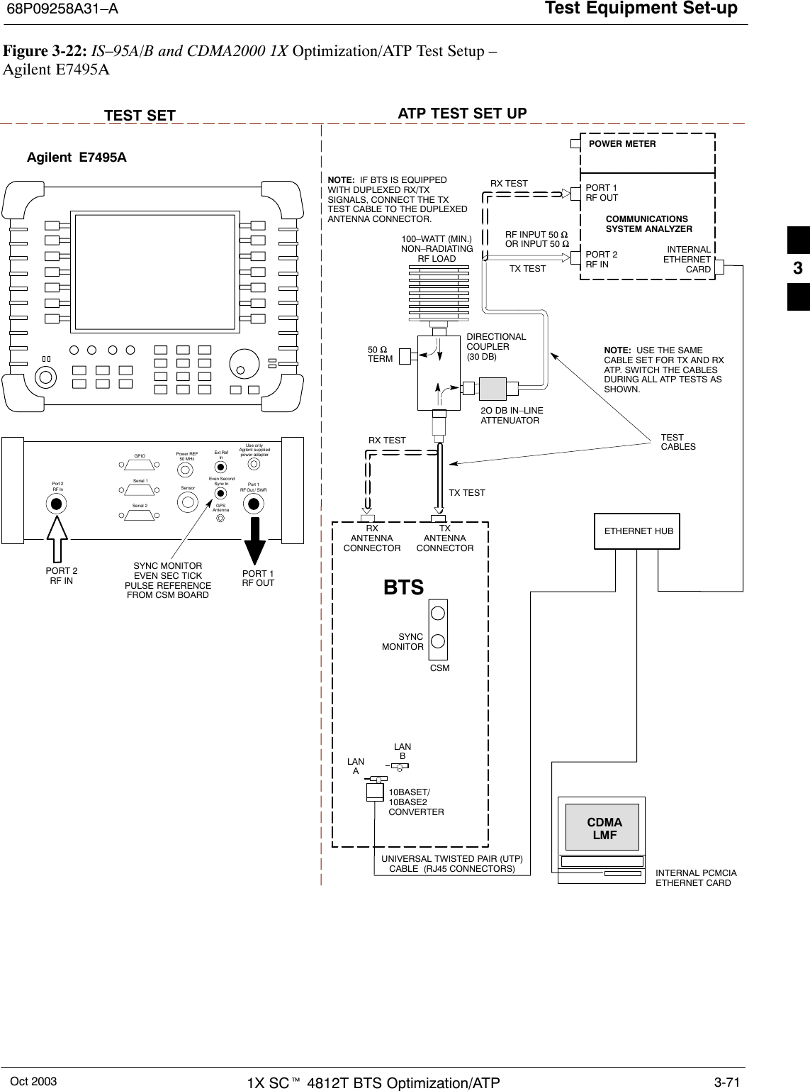
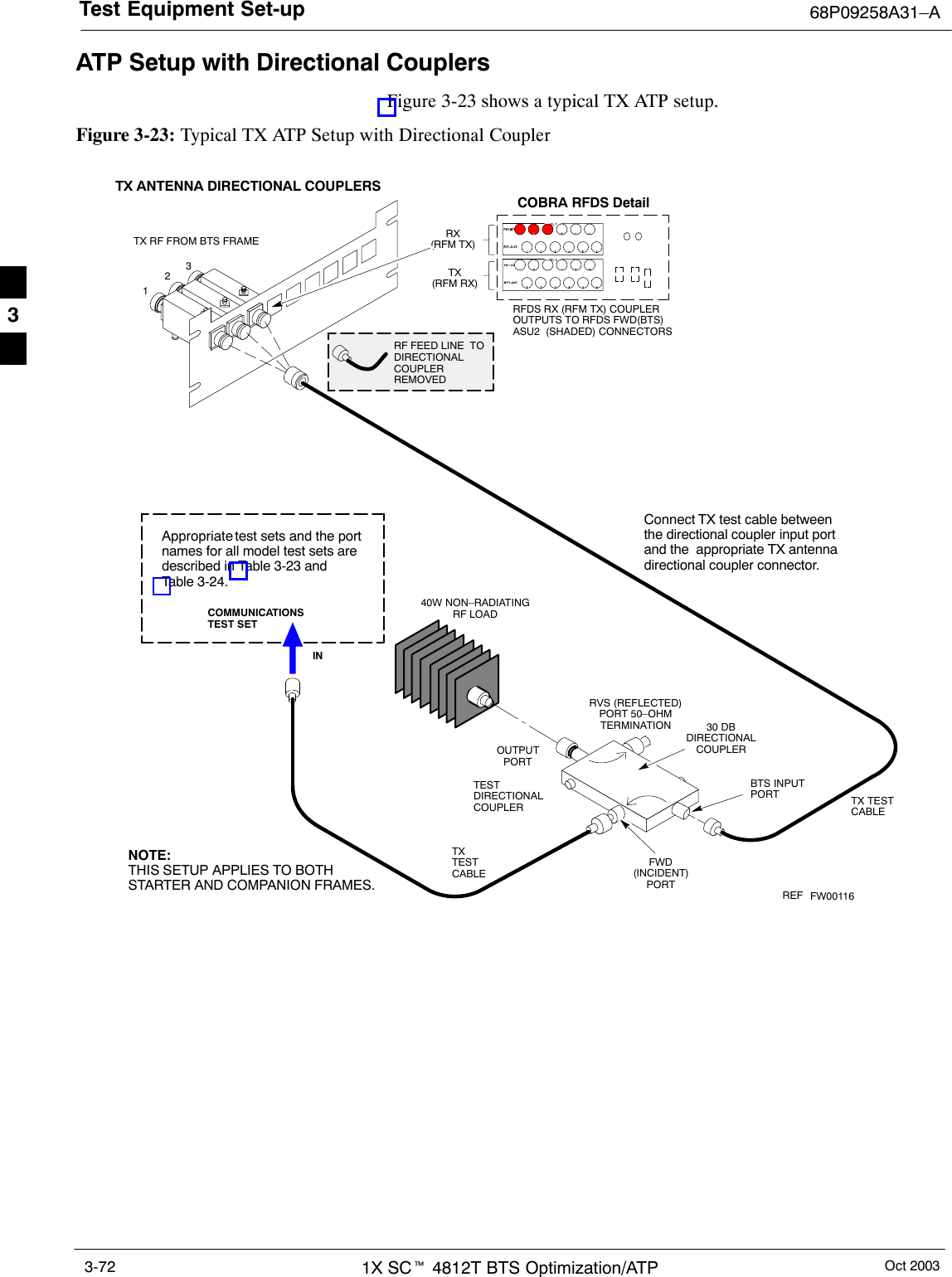
Nokia Solutions and Networks T5EL1 SC4812T-MF 1X/1X-EVDO @ 800 Mhz CDMA BTS User Manual 1X SC4812T BTS Optimization ATP Release 2 16 3 x
Nokia Solutions and Networks SC4812T-MF 1X/1X-EVDO @ 800 Mhz CDMA BTS 1X SC4812T BTS Optimization ATP Release 2 16 3 x
Contents
- 1. Users Manual A
- 2. Users Manual B
- 3. Users Manual C
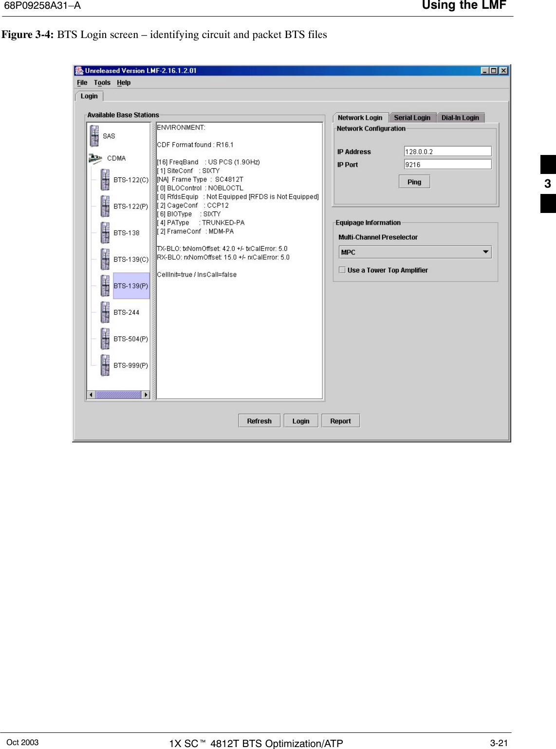
Users Manual B

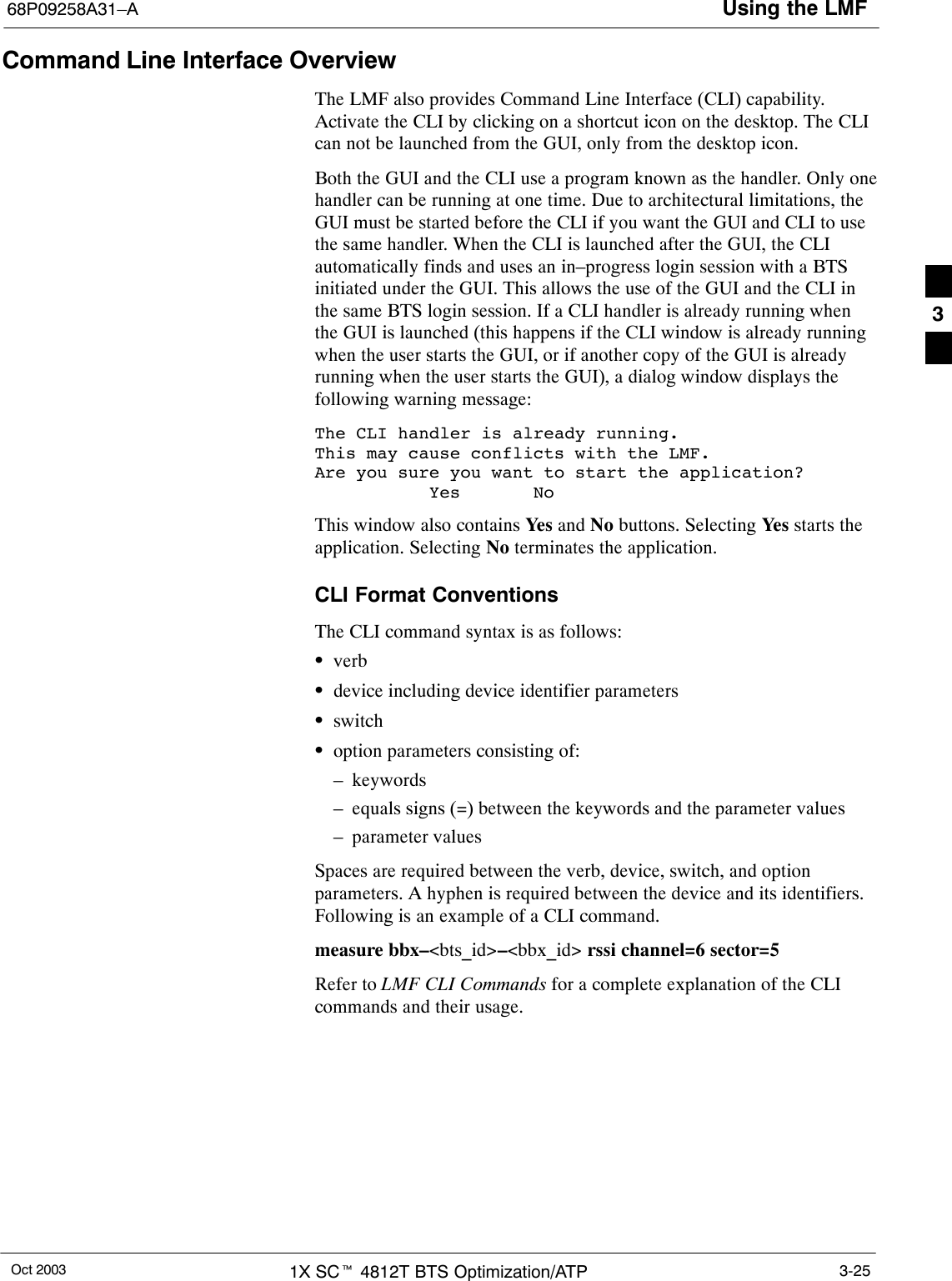
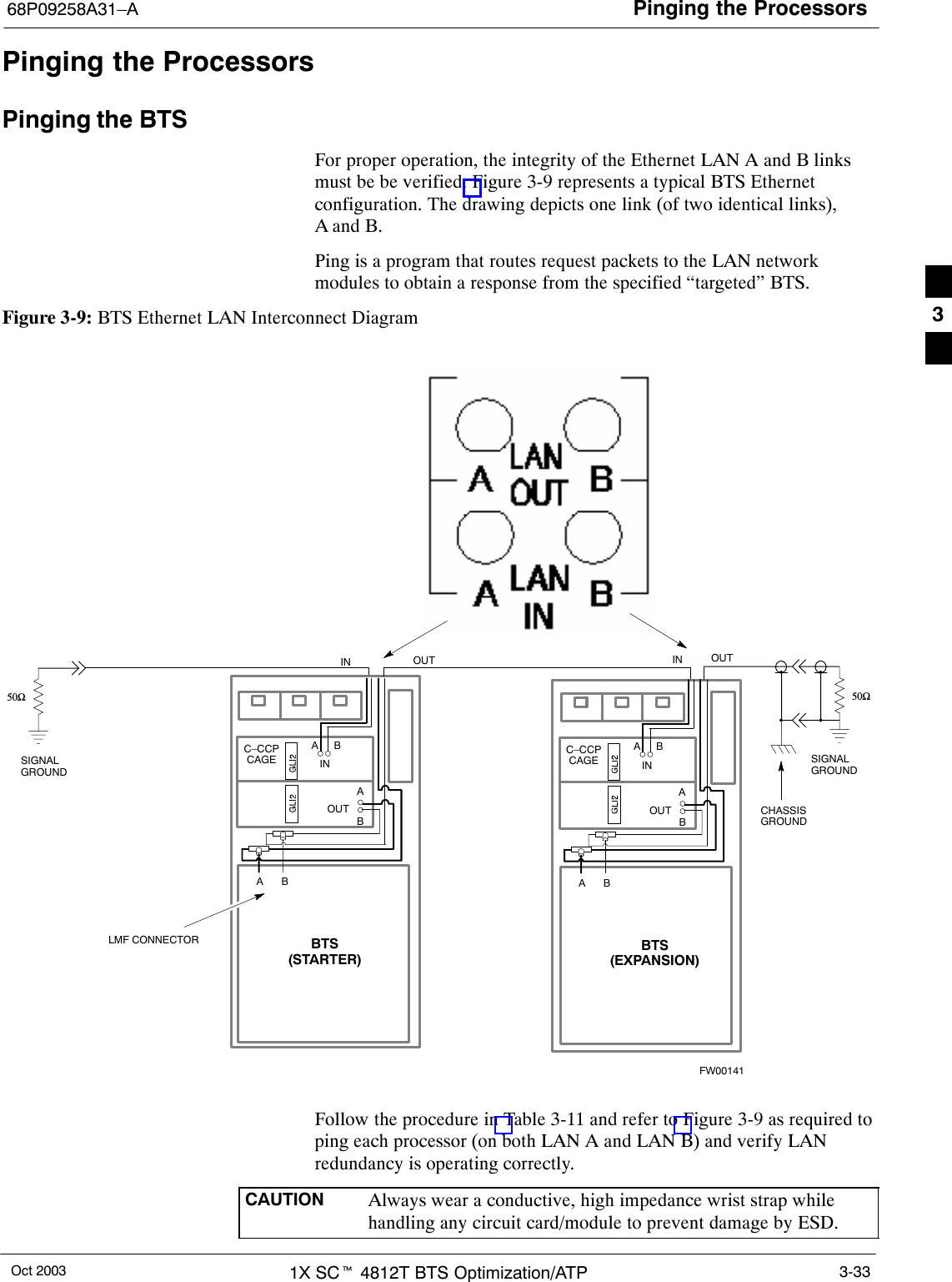
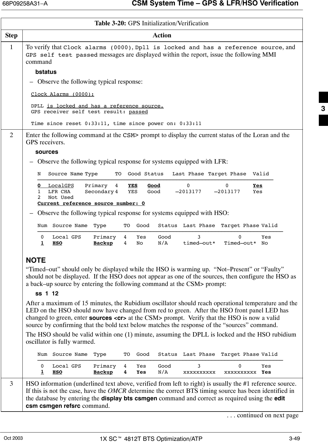
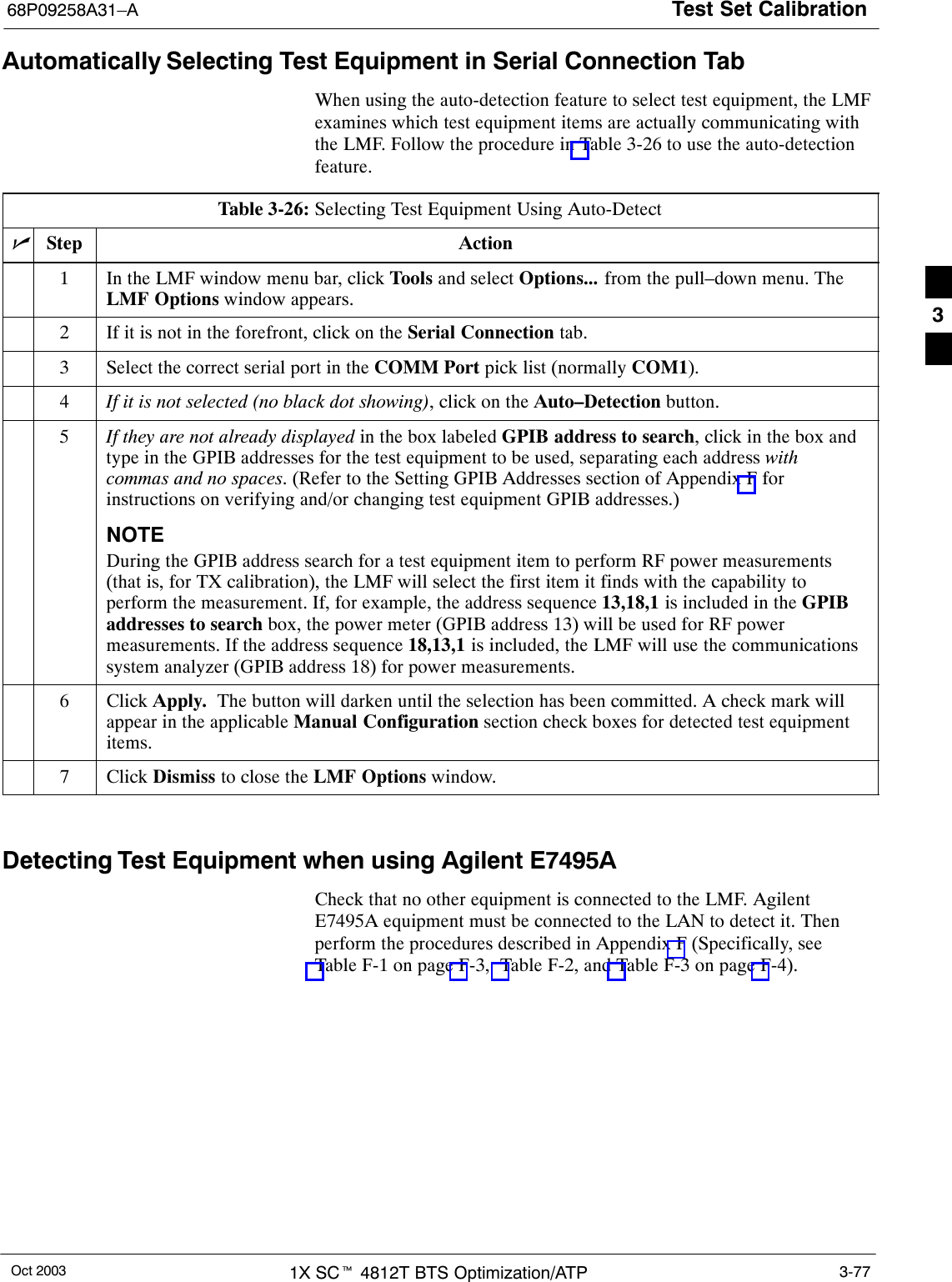
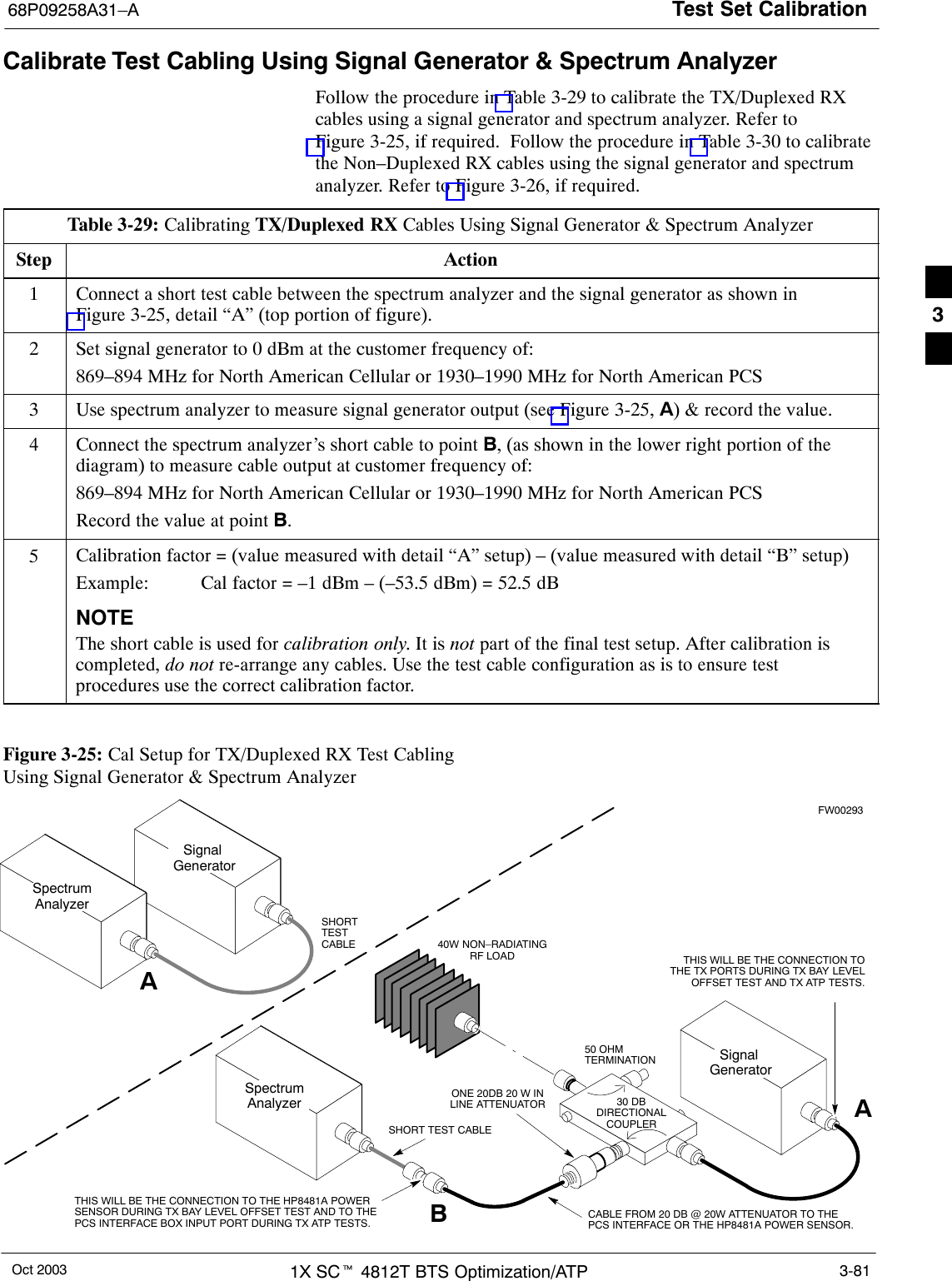
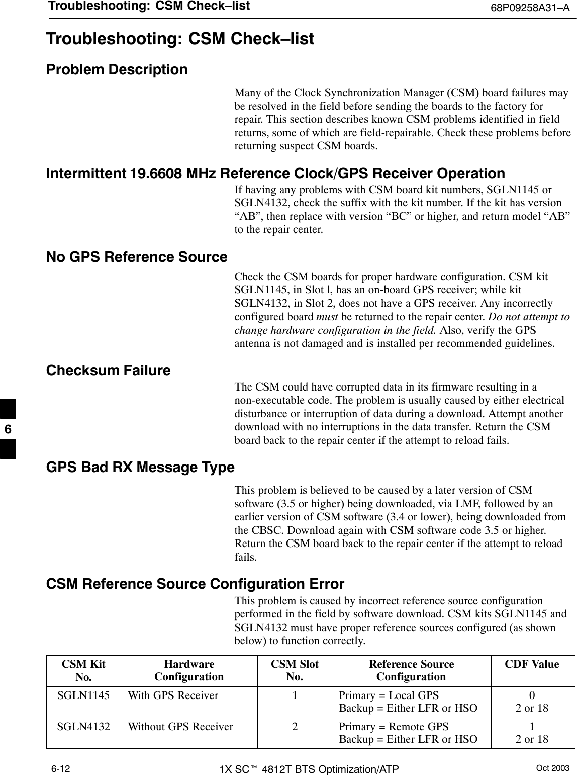
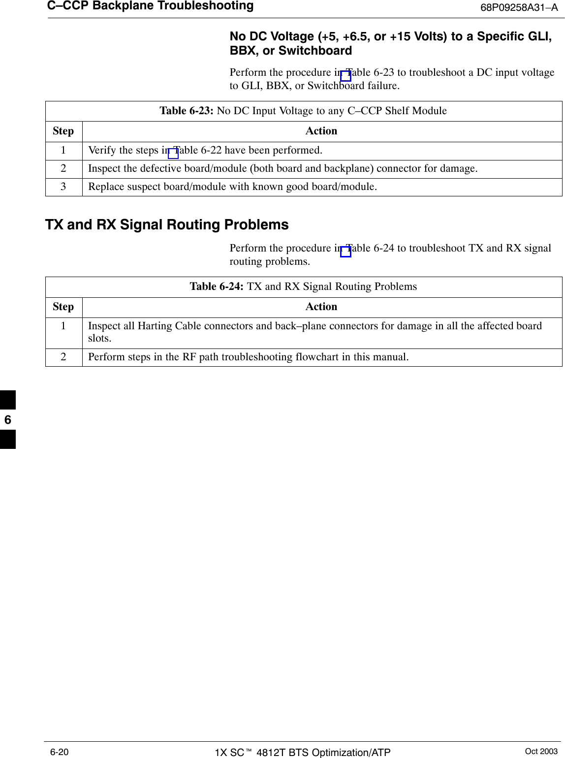
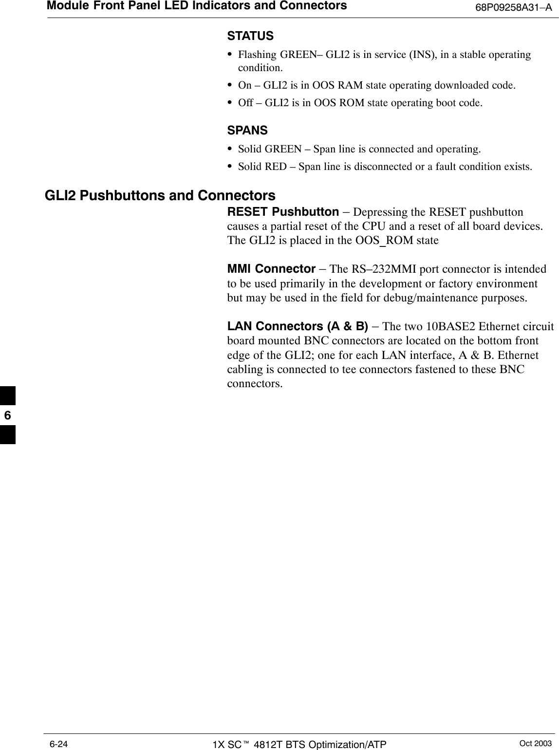
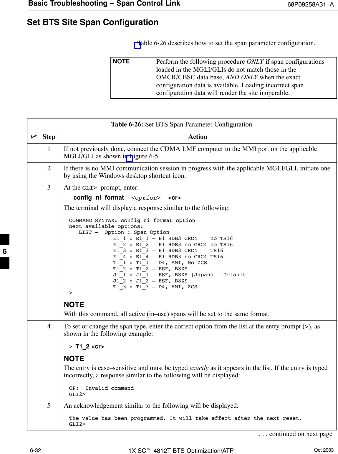
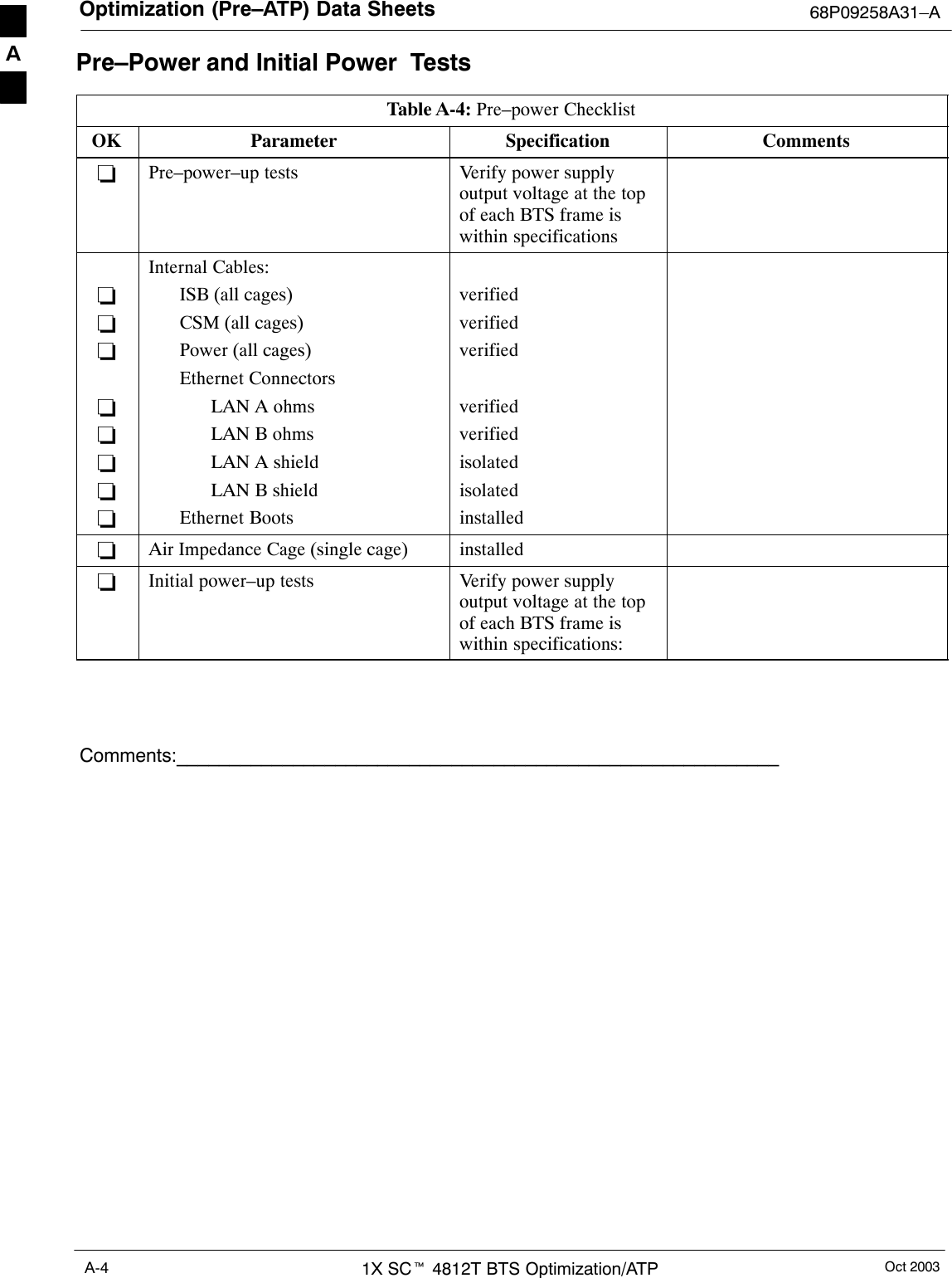
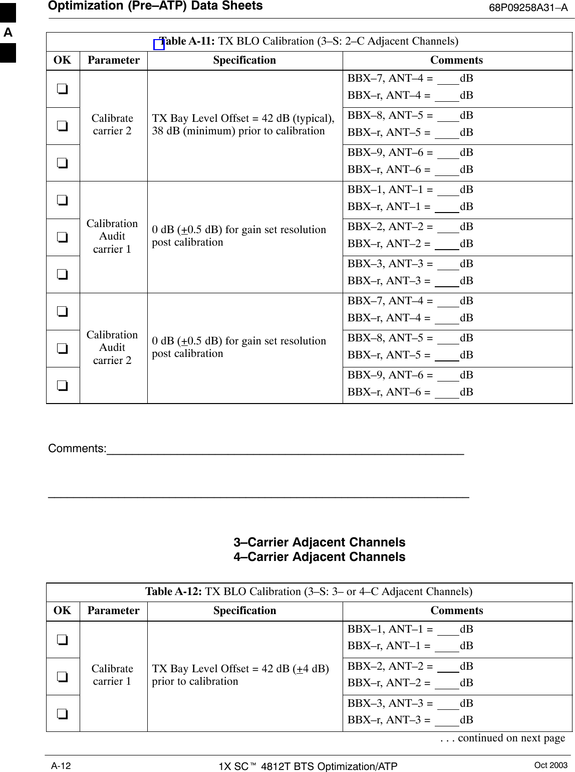
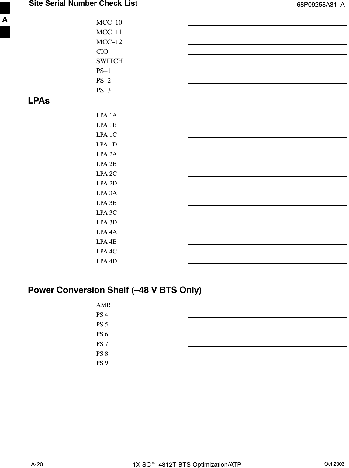
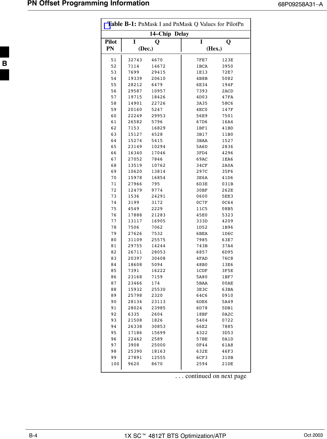
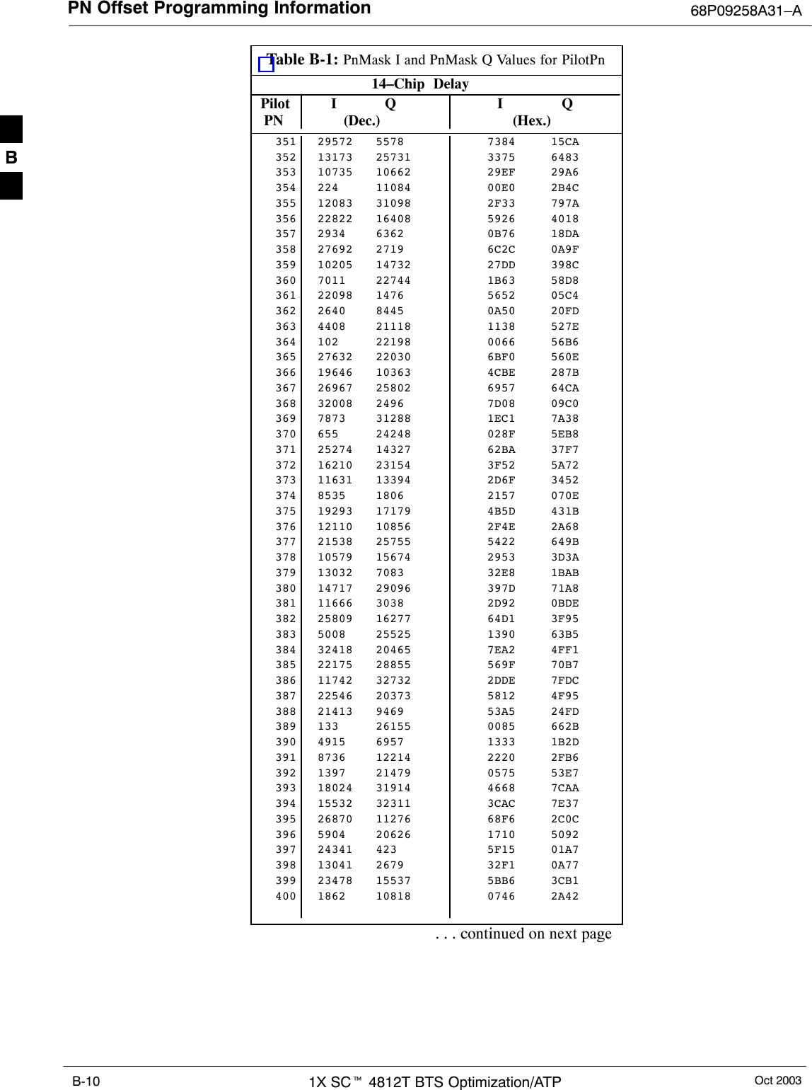
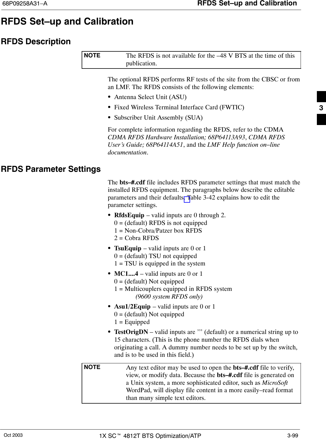
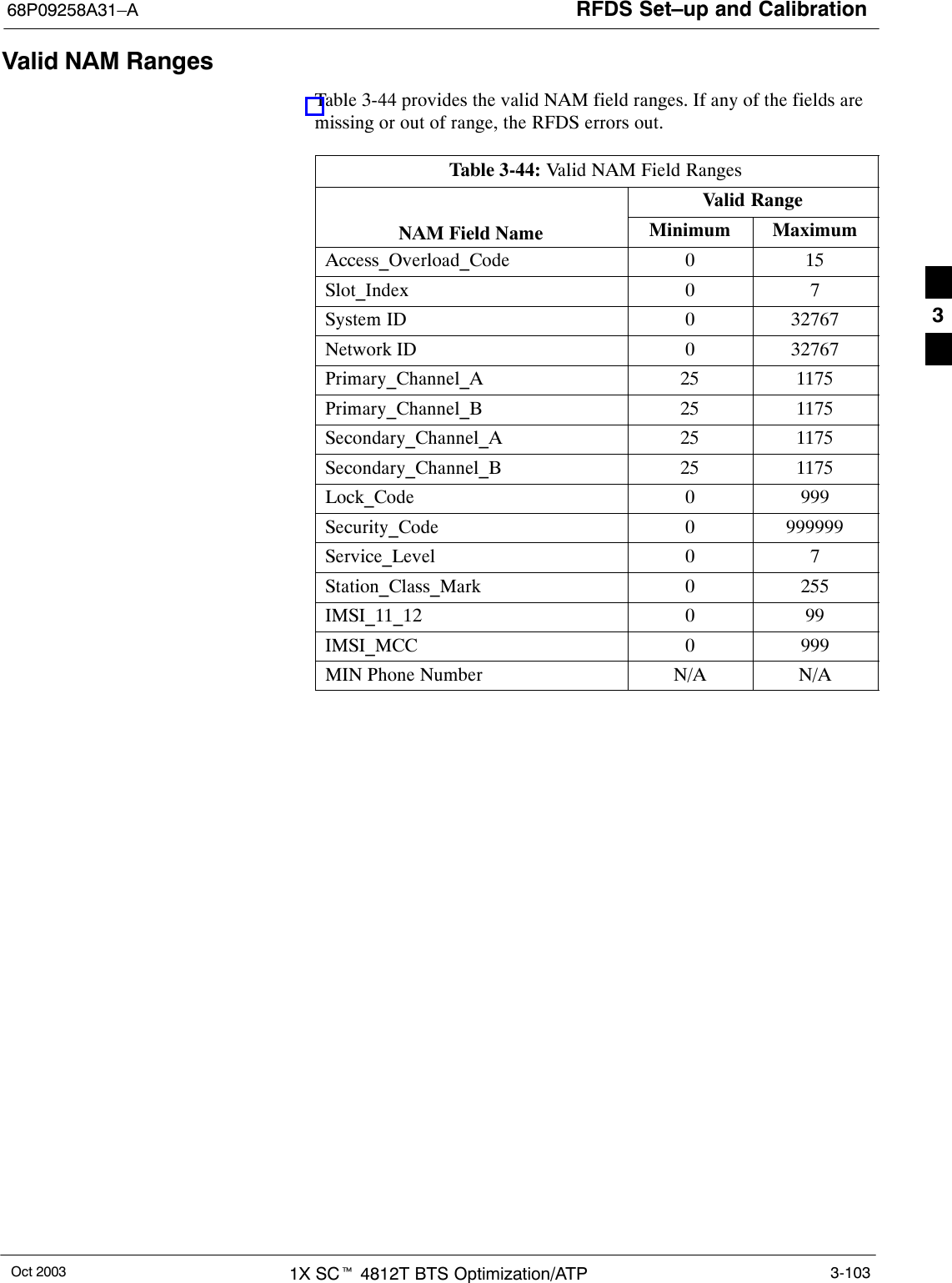
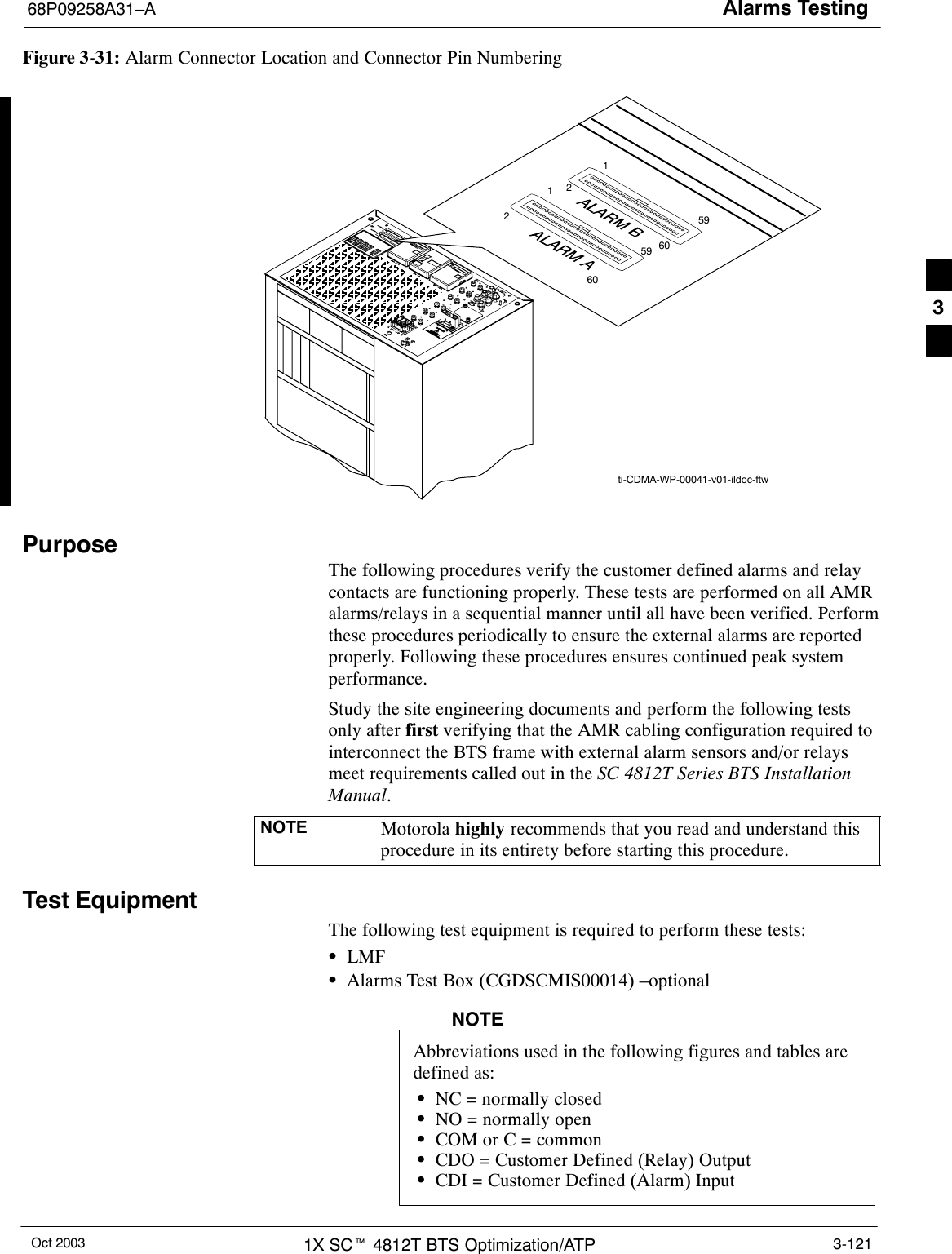
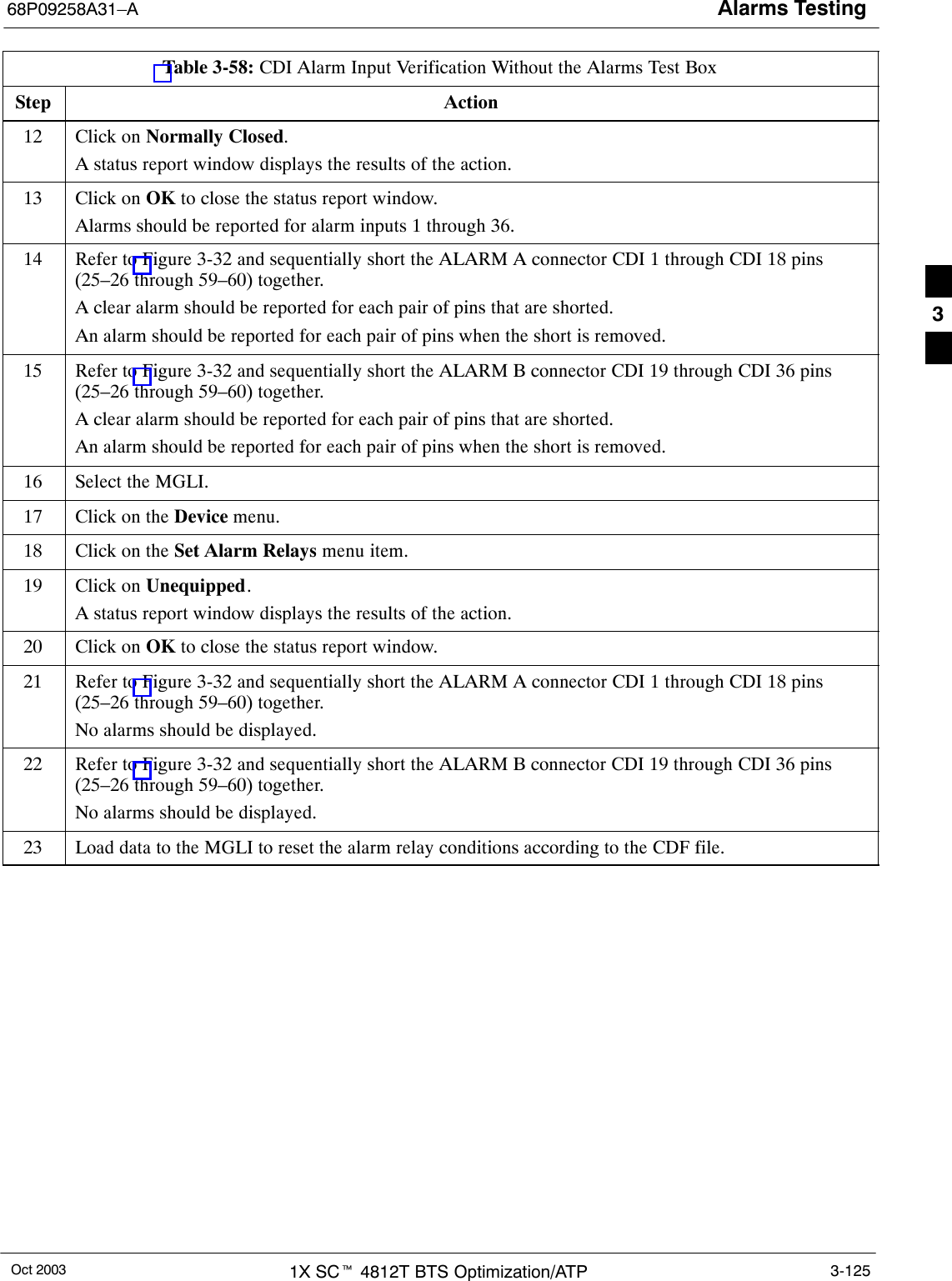
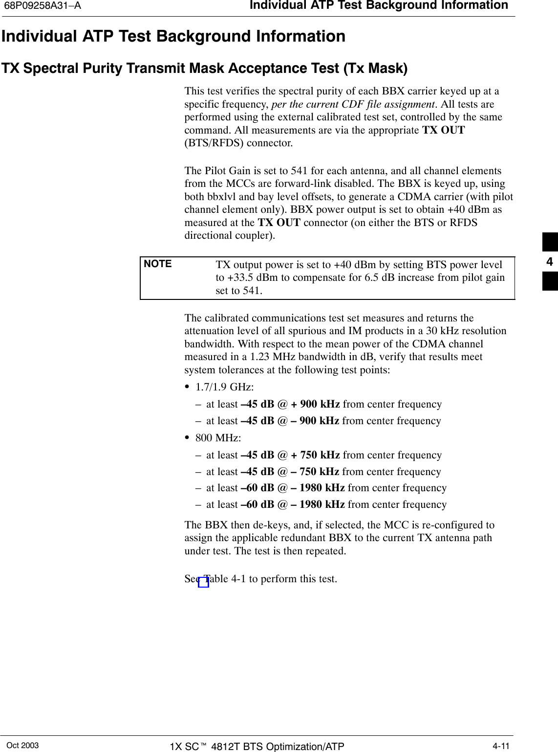
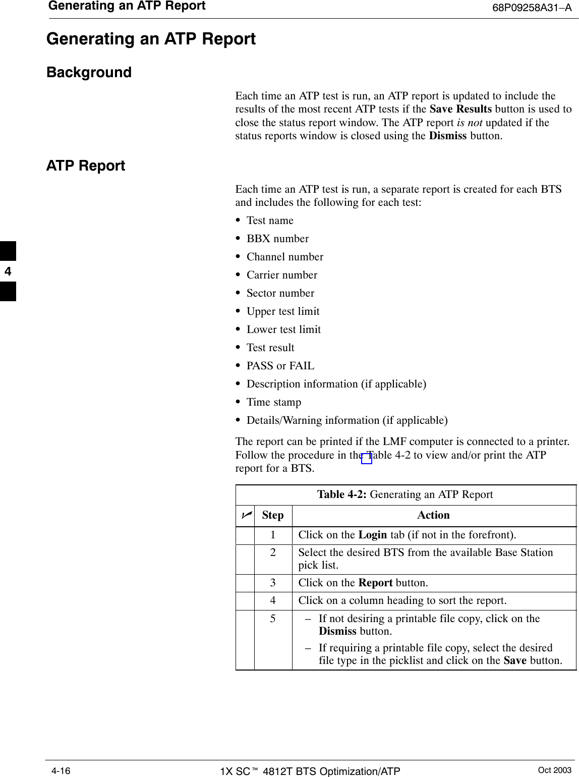
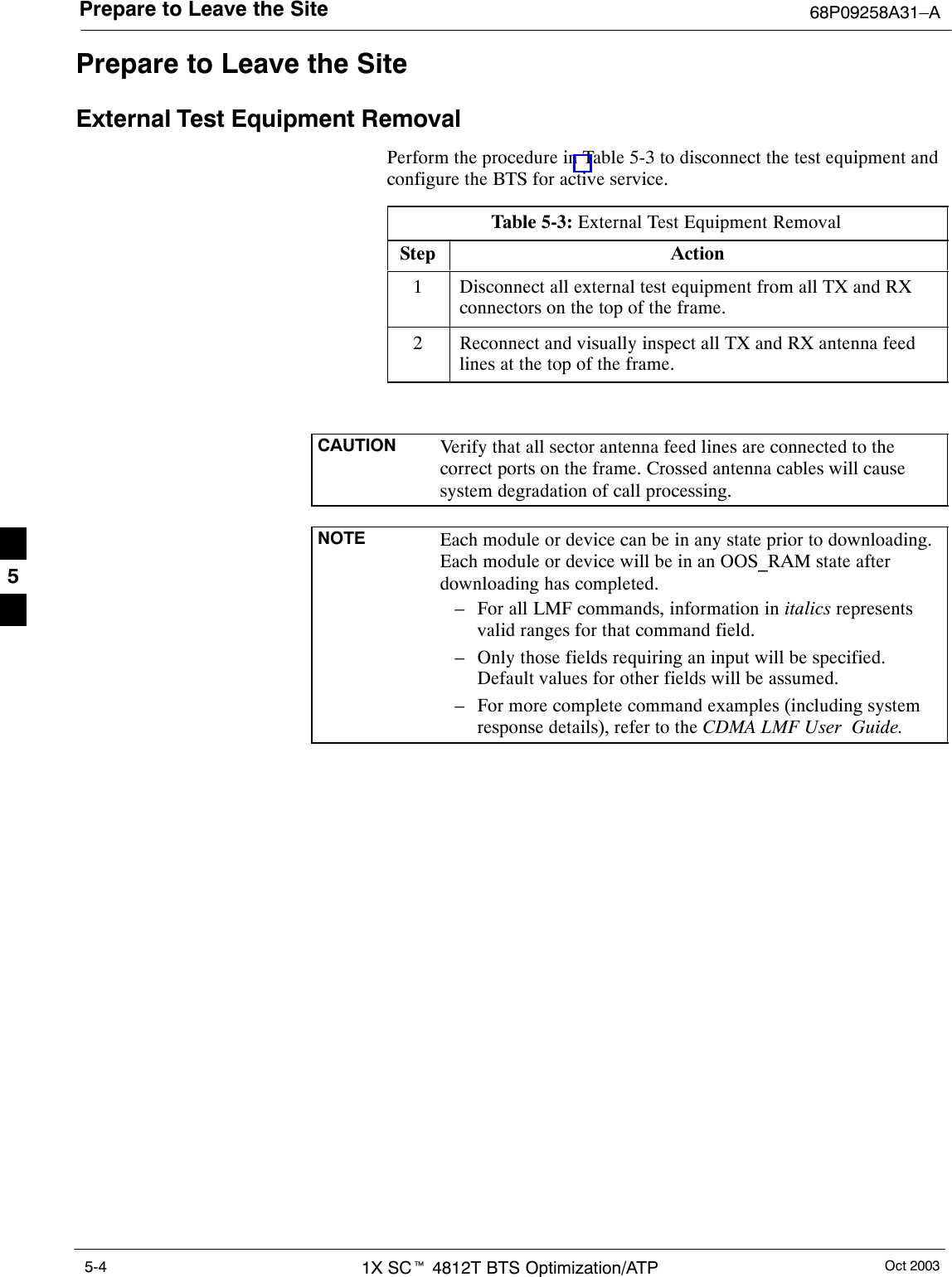
![Bay Level Offset Calibration68P09258A31–AOct 2003 1X SCt 4812T BTS Optimization/ATP 3-87SThe calibration data for a BBX is organized as a large flat array. Thearray is organized by branch, sector, and calibration point.– The first breakdown of the array indicates which branch thecontained calibration points are for. The array covers transmit, mainreceive and diversity receive offsets as follows:Table 3-33: BLO BTS.cal File Array AssignmentsRange AssignmentC[1]–C[240] TransmitC[241]–C[480] Main ReceiveC[481]–C[720] Diversity ReceiveNOTE Slot 385 is the BLO for the RFDS.– The second breakdown of the array is per sector. Configurationssupported are Omni, 3–sector or 6–sector.Table 3-34: BTS.cal File Array (Per Sector)BBX Sectorization TX RX RX DiversitySlot[1] (Primary BBXs 1 through 12)1 (Omni) 3–Sector,C[1]–C[20] C[241]–C[260] C[481]–C[500]23–Sector,1stCiC[21]–C[40] C[261]–C[280] C[501]–C[520]36 Sector,1stCarrier C[41]–C[60] C[281]–C[300] C[521]–C[540]41stCarrier 3–Sector,C[61]–C[80] C[301]–C[320] C[541]–C[560]5Carrier3–Sector,3rdCiC[81]–C[100] C[321]–C[340] C[561]–C[580]6Carrier C[101]–C[120] C[341]–C[360] C[581]–C[600]73–Sector,C[121]–C[140] C[361]–C[380] C[601]–C[620]83–Sector,2ndCiC[141]–C[160] C[381]–C[400] C[621]–C[640]96 Sector,2ndCarrier C[161]–C[180] C[401]–C[420] C[641]–C[660]102ndCarrier 3–Sector,C[181]–C[200] C[421]–C[440] C[661]–C[680]11Carrier3–Sector,4thCiC[201]–C[220] C[441]–C[460] C[681]–C[700]12 Carrier C[221]–C[240] C[461]–C[480] C[701]–C[720] . . . continued on next page3](https://usermanual.wiki/Nokia-Solutions-and-Networks/T5EL1.Users-Manual-B/User-Guide-455782-Page-67.png)
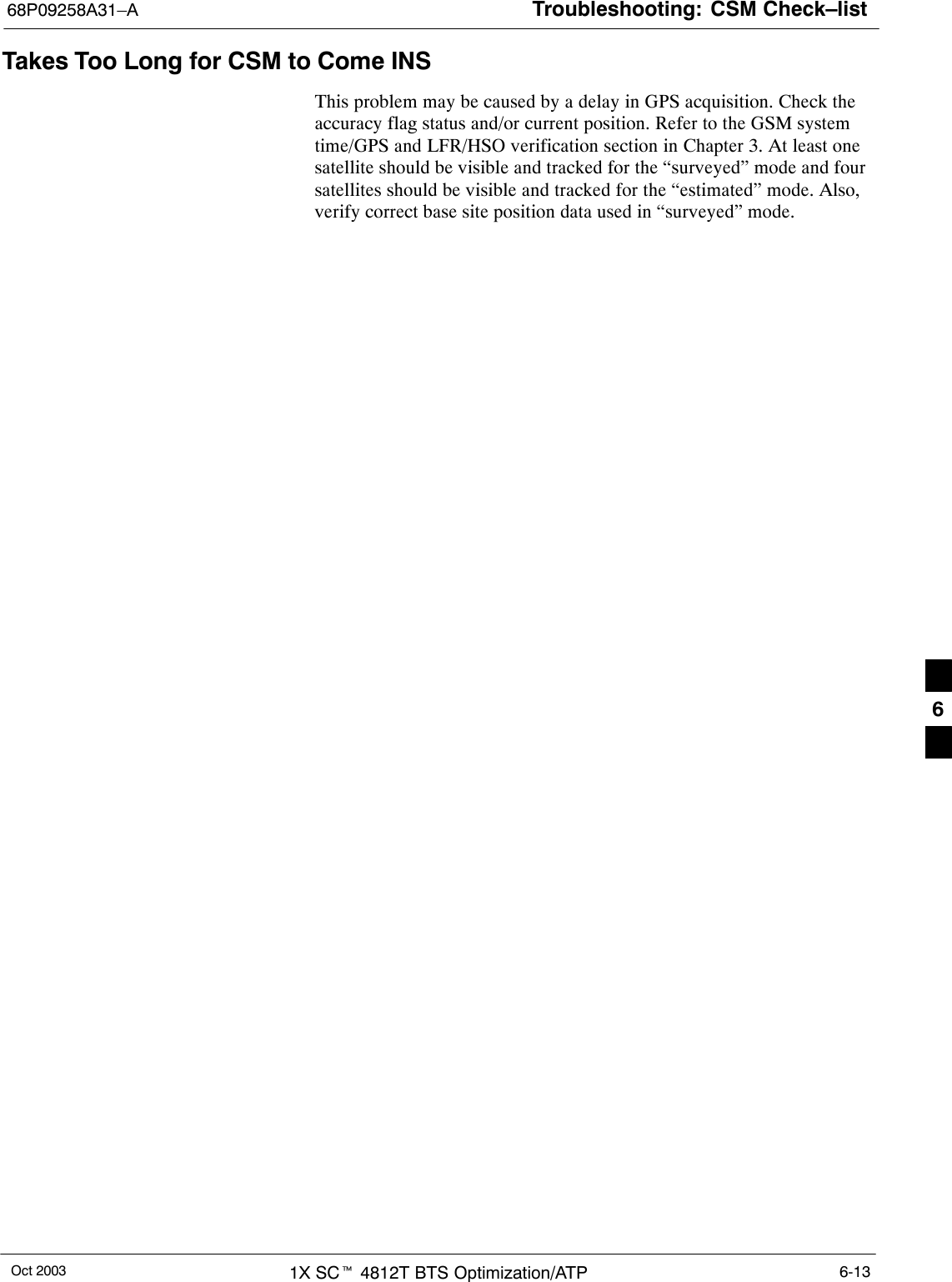
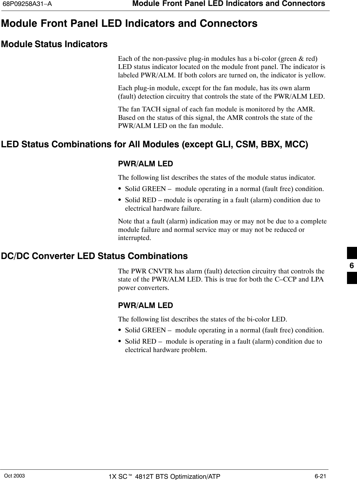
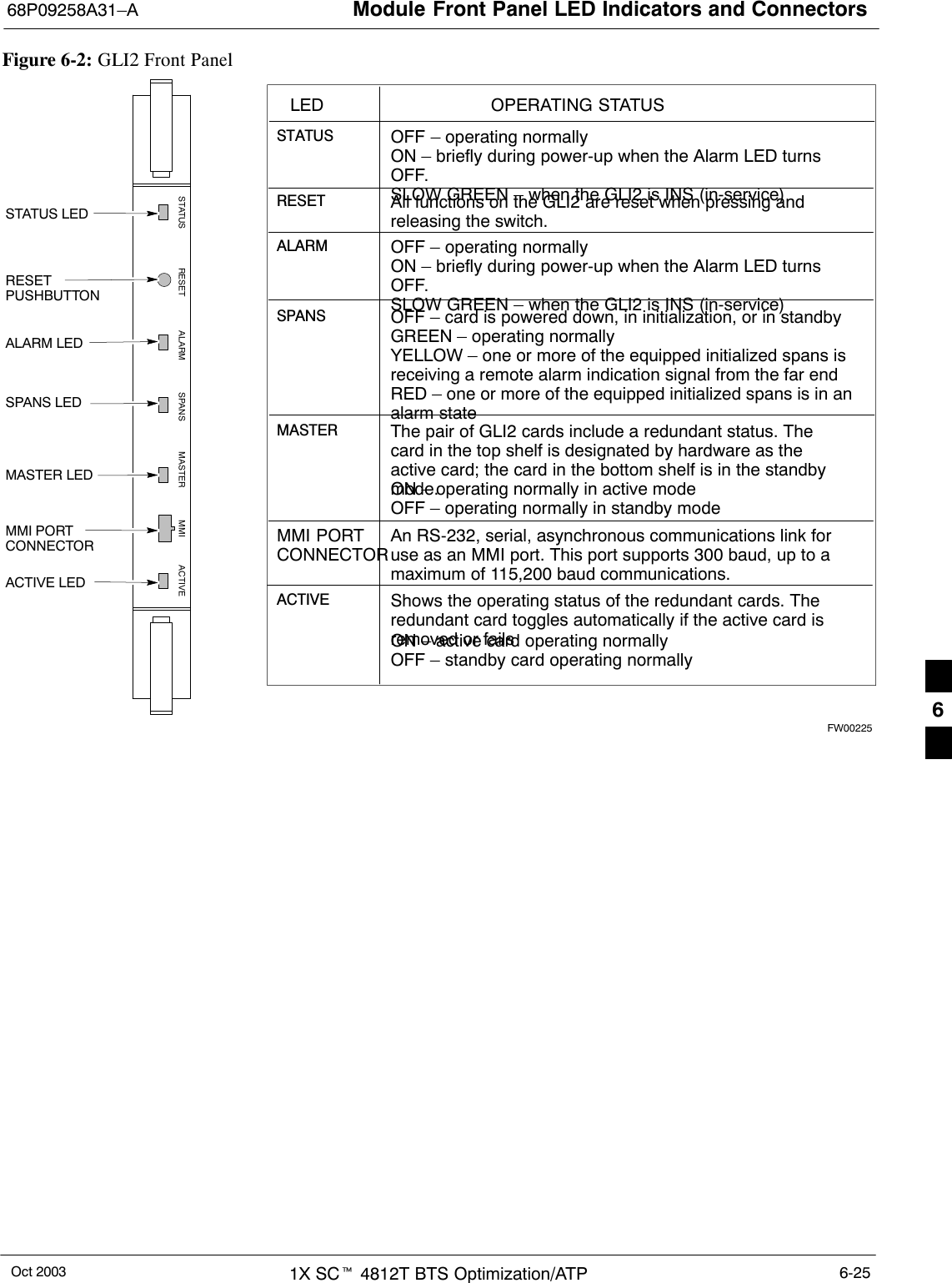
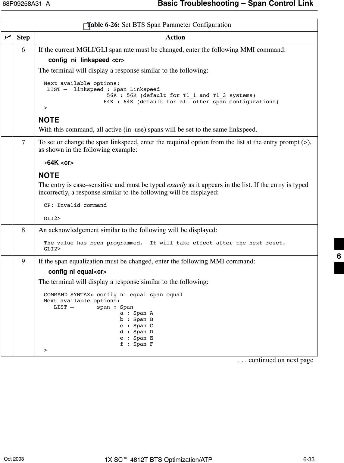
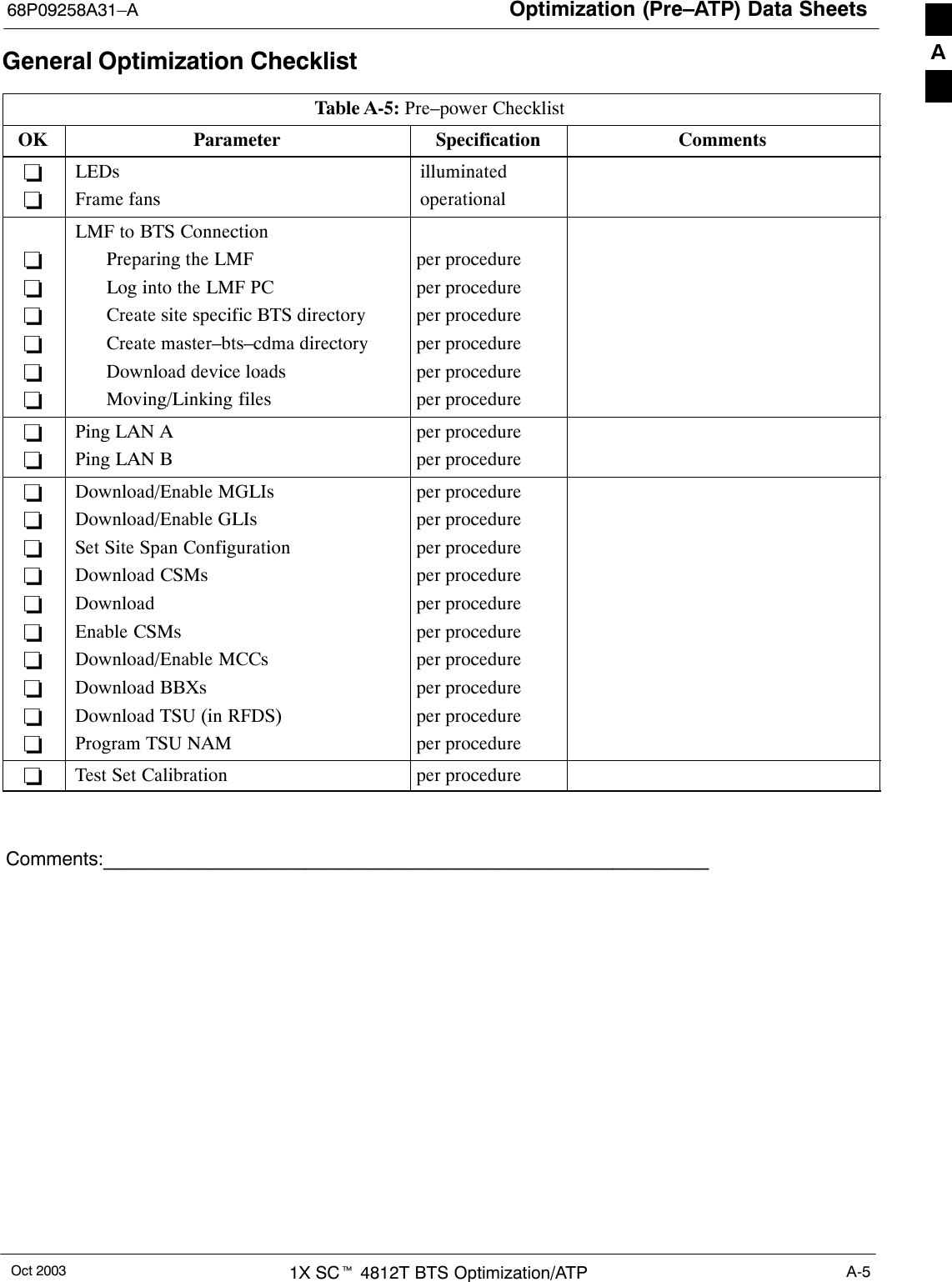
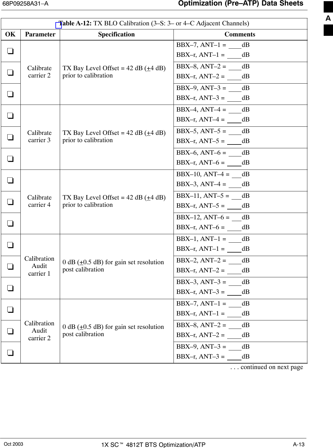
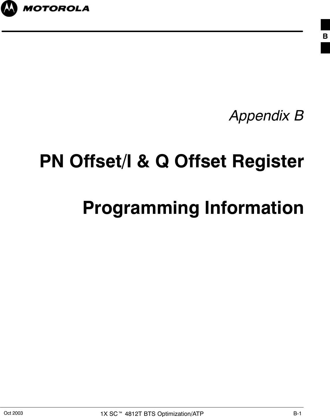
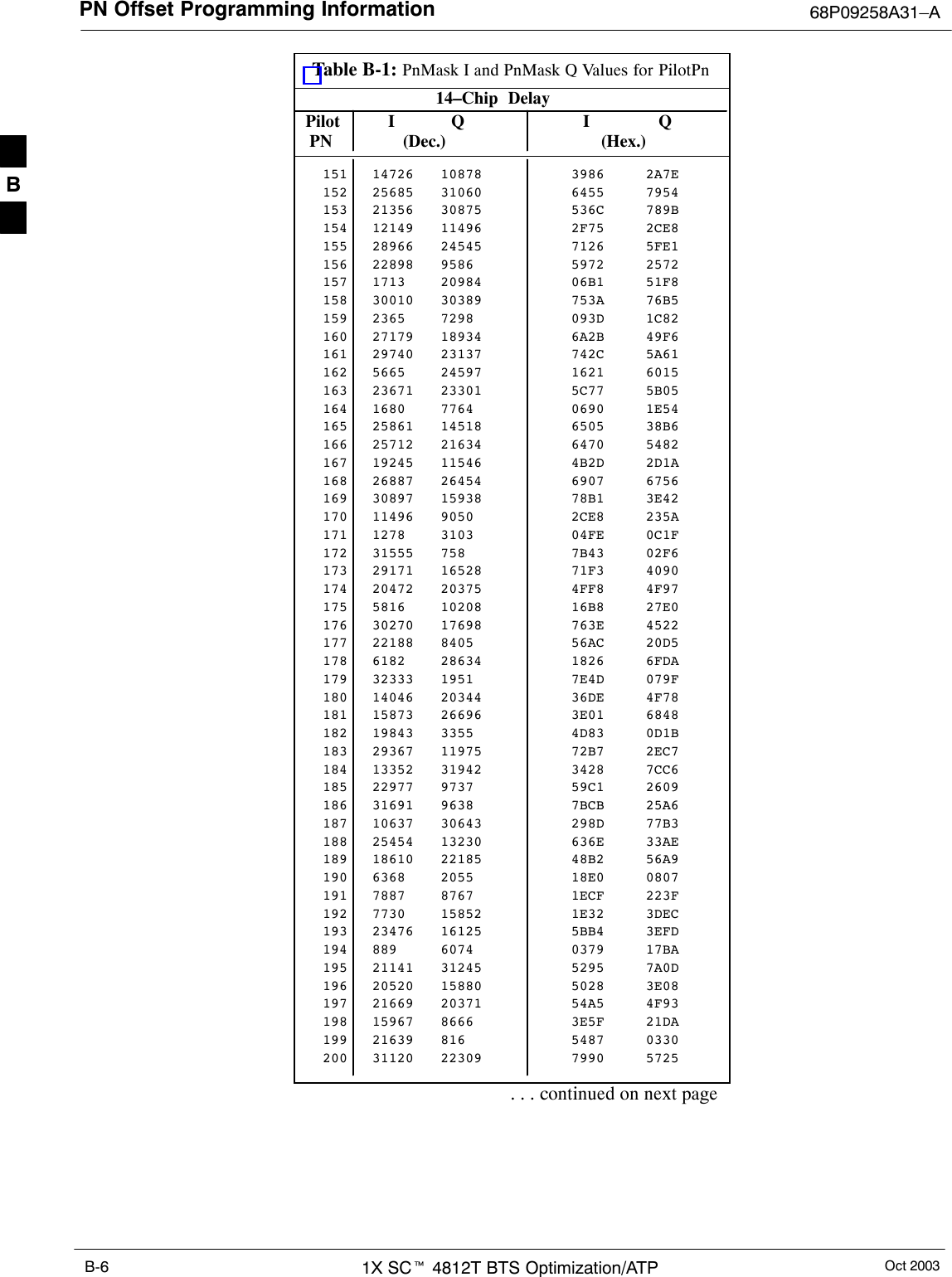
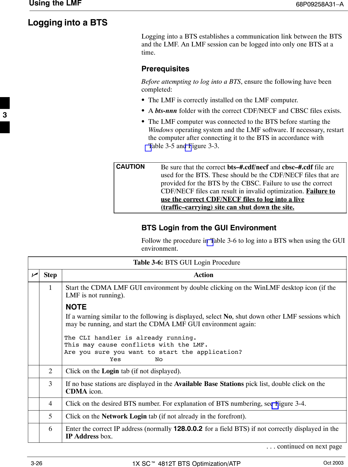
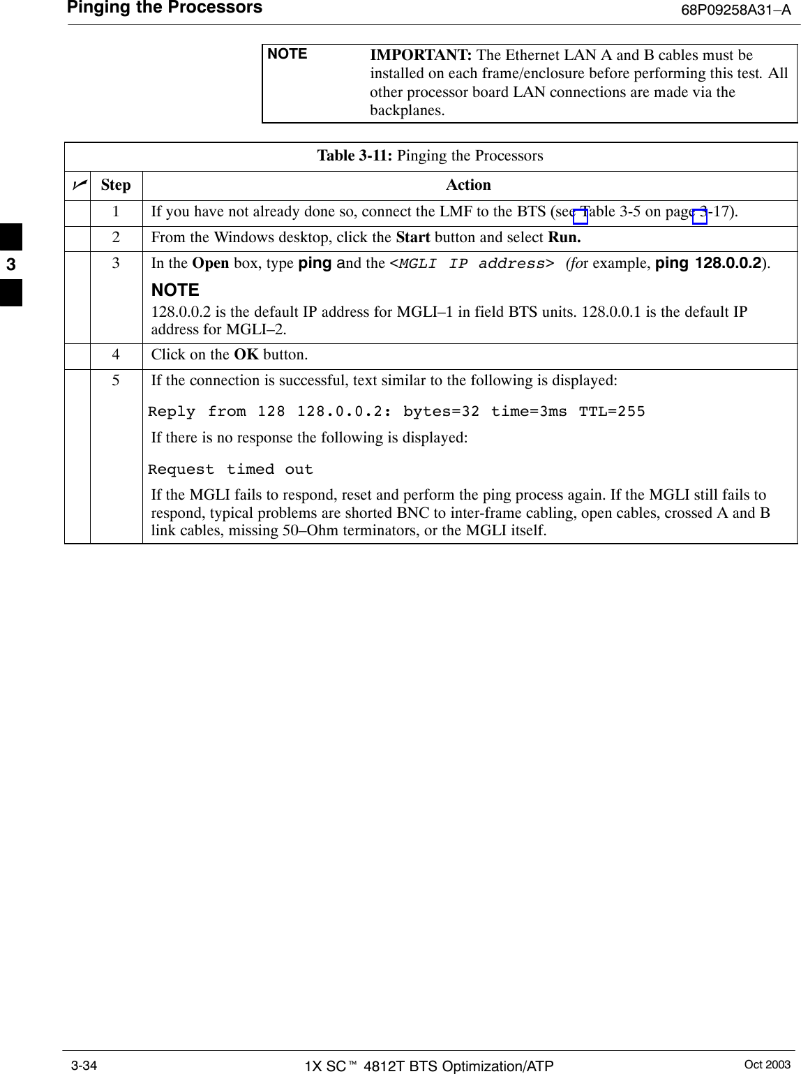
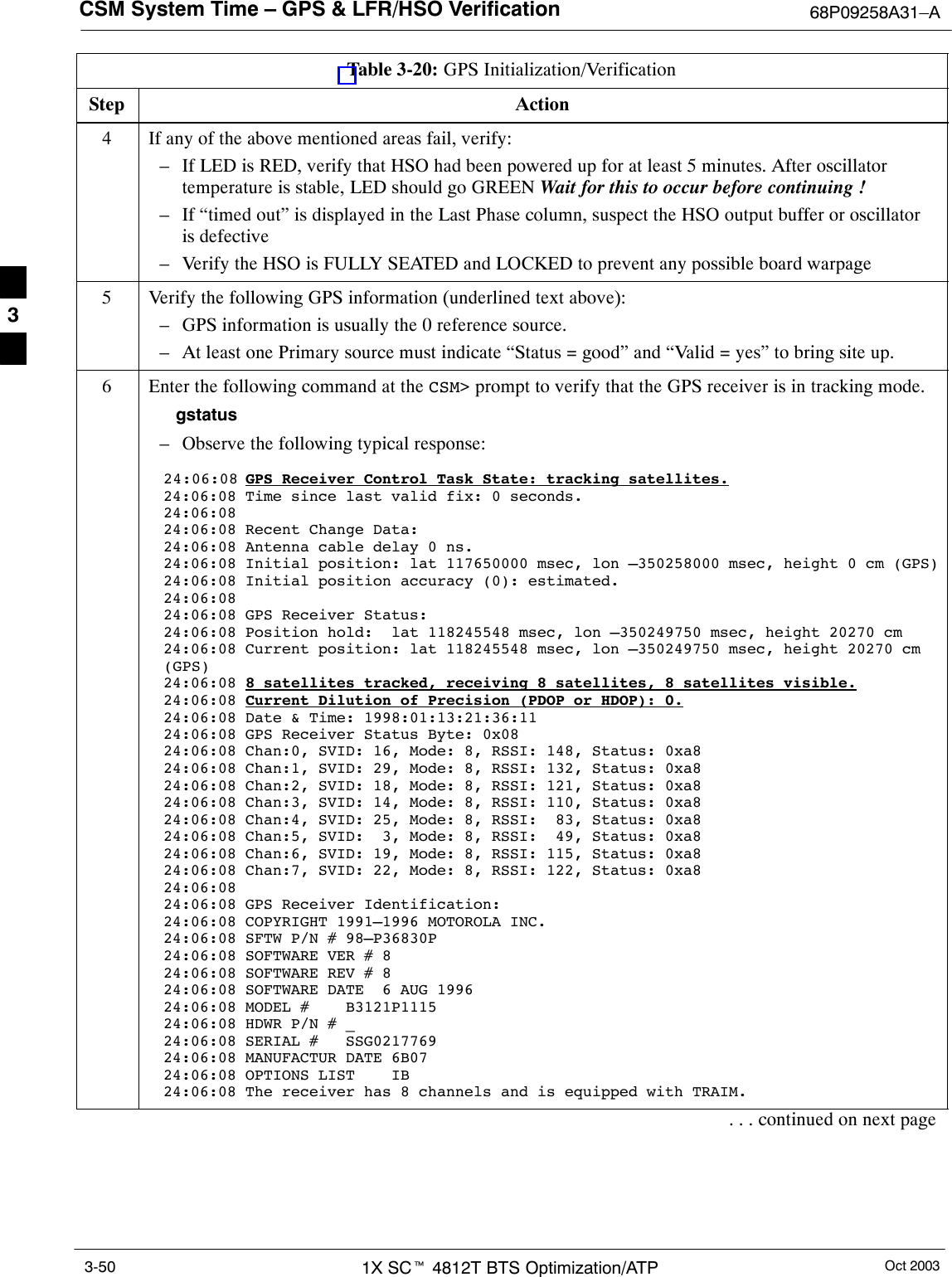
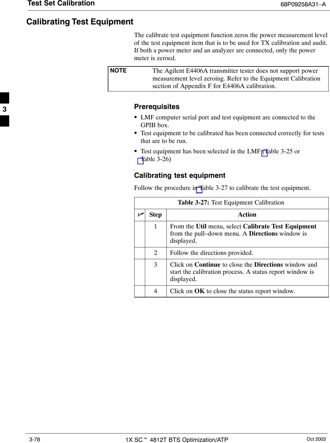
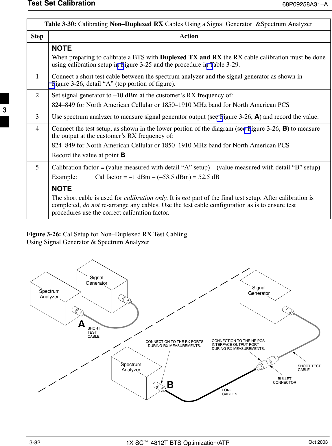
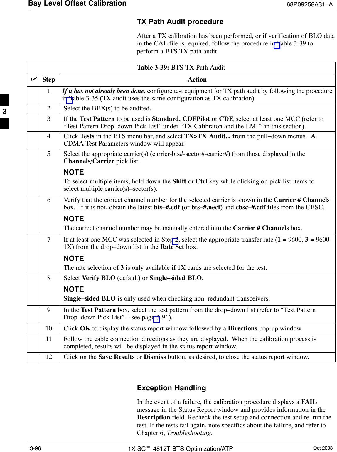
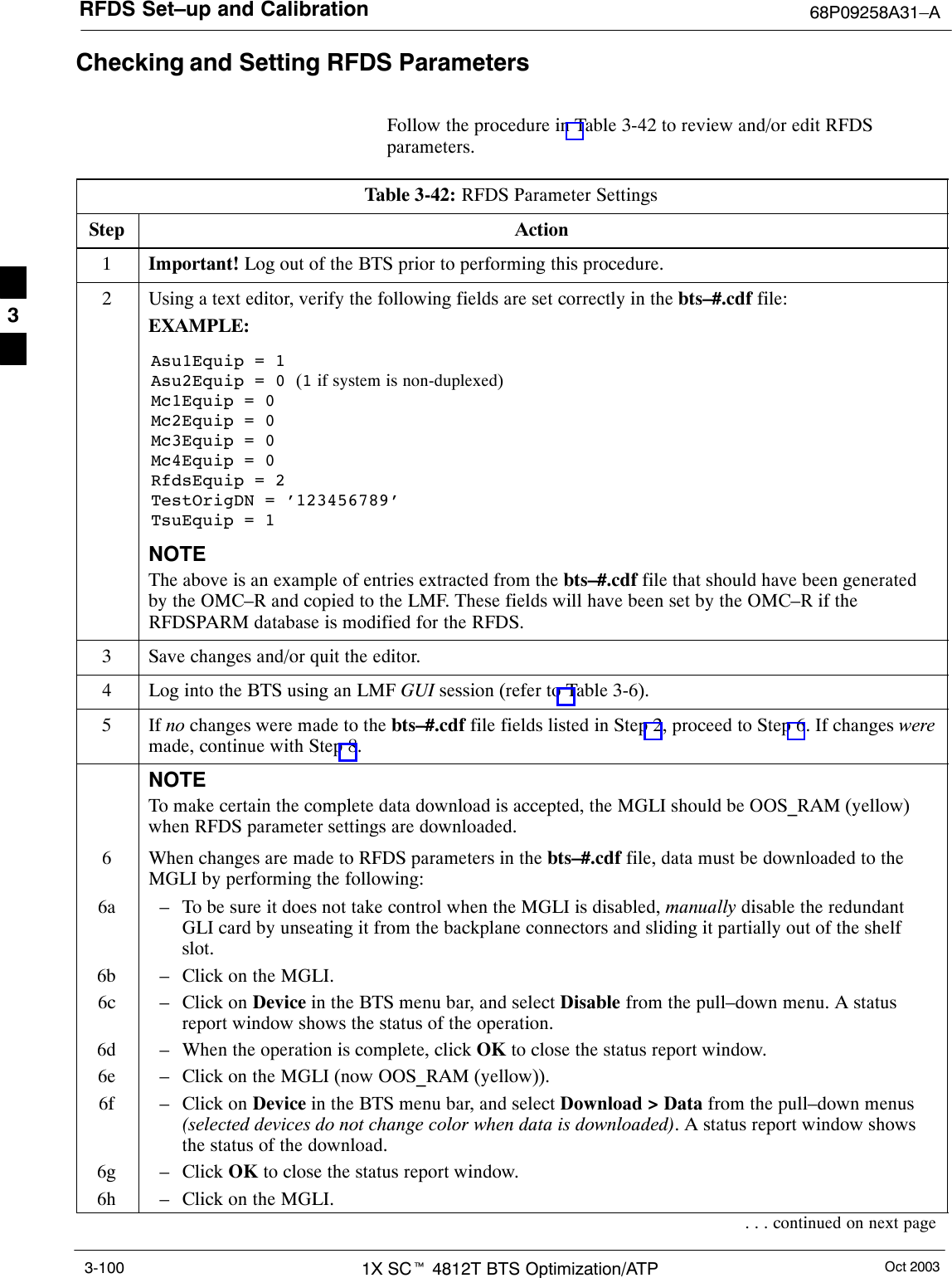
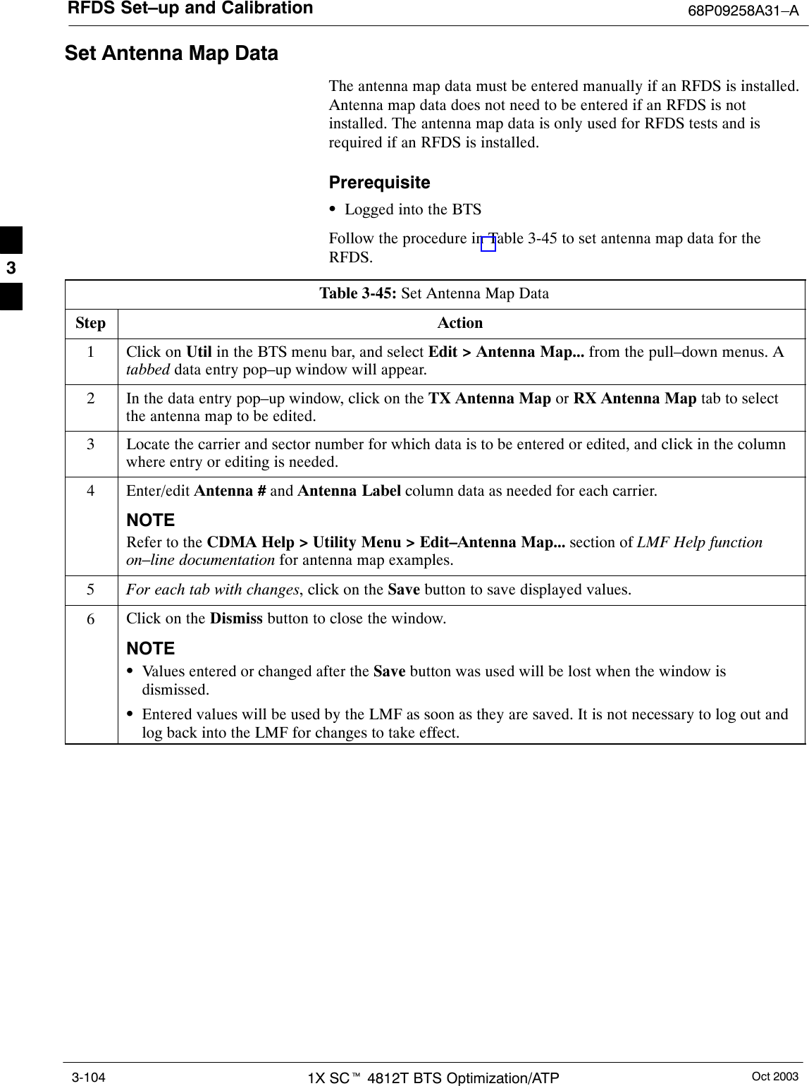
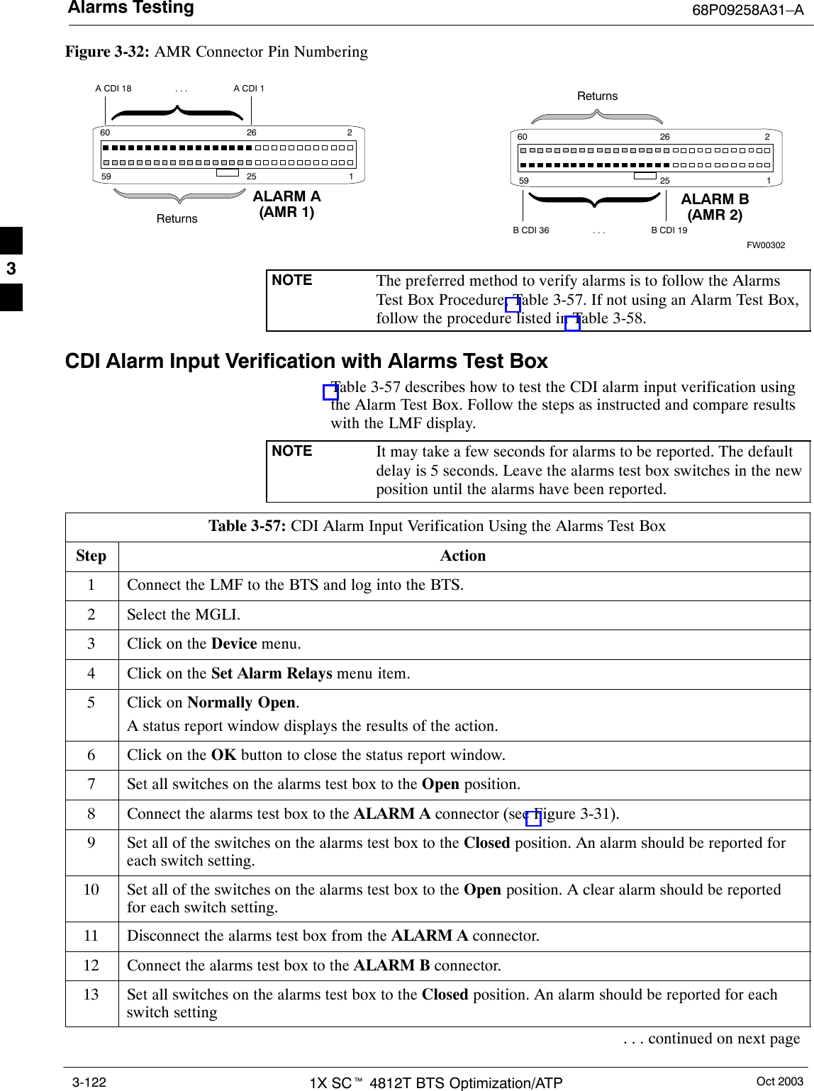
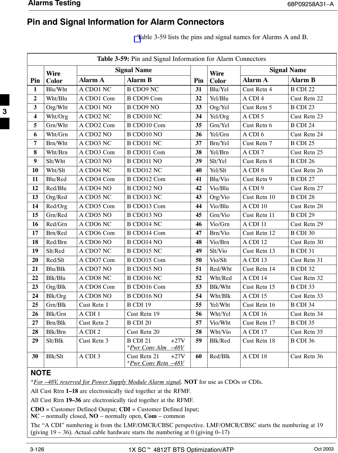
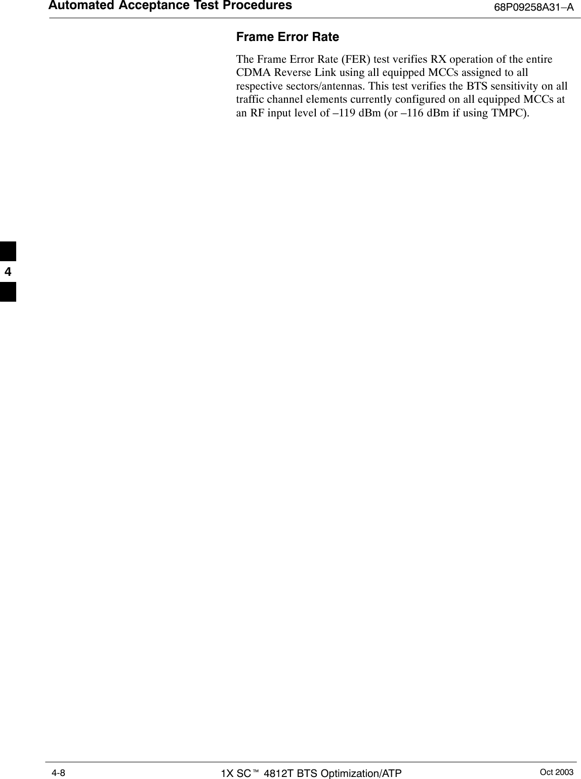
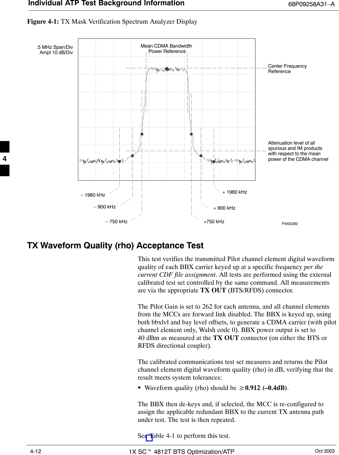
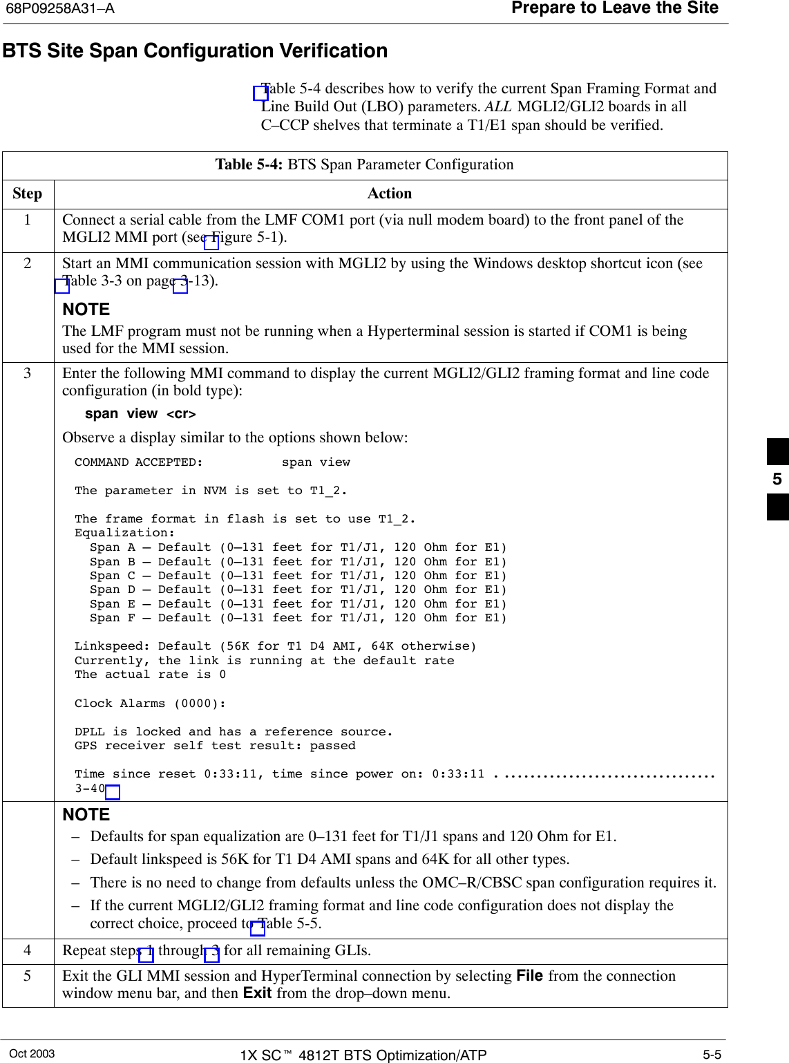
![Bay Level Offset Calibration 68P09258A31–AOct 20031X SCt 4812T BTS Optimization/ATP3-88Table 3-34: BTS.cal File Array (Per Sector)BBX RX DiversityRXTXSectorizationSlot[20] (Redundant BBX–13)1 (Omni) 3–Sector,C[1]–C[20] C[241]–C[260] C[481]–C[500]23–Sector,1stCiC[21]–C[40] C[261]–C[280] C[501]–C[520]36 Sector,1stCarrier C[41]–C[60] C[281]–C[300] C[521]–C[540]41stCarrier 3–Sector,C[61]–C[80] C[301]–C[320] C[541]–C[560]5Carrier3–Sector,3rdCiC[81]–C[100] C[321]–C[340] C[561]–C[580]6Carrier C[101]–C[120] C[341]–C[360] C[581]–C[600] . . . continued on next page73–Sector,C[121]–C[140] C[361]–C[380] C[601]–C[620]83–Sector,2ndCiC[141]–C[160] C[381]–C[400] C[621]–C[640]96 Sector,2ndCarrier C[161]–C[180] C[401]–C[420] C[641]–C[660]102ndCarrier 3–Sector,C[181]–C[200] C[421]–C[440] C[661]–C[680]11Carrier3–Sector,4thCiC[201]–C[220] C[441]–C[460] C[681]–C[700]12 Carrier C[221]–C[240] C[461]–C[480] C[701]–C[720]STen calibration points per sector are supported for each branch. Twoentries are required for each calibration point.SThe first value (all odd entries) refer to the CDMA channel(frequency) where the BLO is measured. The second value (all evenentries) is the power set level. The valid range for PwrLvlAdj is from2500 to 27500 (2500 corresponds to –125 dBm and 27500corresponds to +125 dBm).SThe 20 calibration entries for each sector/branch combination must bestored in order of increasing frequency. If less than 10 points(frequencies) are calibrated, the largest frequency that is calibrated isrepeated to fill out the 10 points.Example:C[1]=384, odd cal entry= 1 ‘‘calibration point”C[2]=19102, even cal entryC[3]=777,C[4]=19086,..C[19]=777,C[20]=19086, (since only two cal points were calibrated this would be repeated for the next 8 points)SWhen the BBX is loaded with image = data, the cal file data for theBBX is downloaded to the device in the order it is stored in the calfile. TxCal data is sent first, C[1] – C[240]. Sector 1’s ten calibrationpoints are sent (C[1] – C[20]) followed by sector 2’s ten calibrationpoints (C[21] – C[40]), etc. The RxCal data is sent next (C[241] –C[480]), followed by the RxDCal data (C[481] – C[720]).STemperature compensation data is also stored in the cal file for eachset.3](https://usermanual.wiki/Nokia-Solutions-and-Networks/T5EL1.Users-Manual-B/User-Guide-455782-Page-68.png)
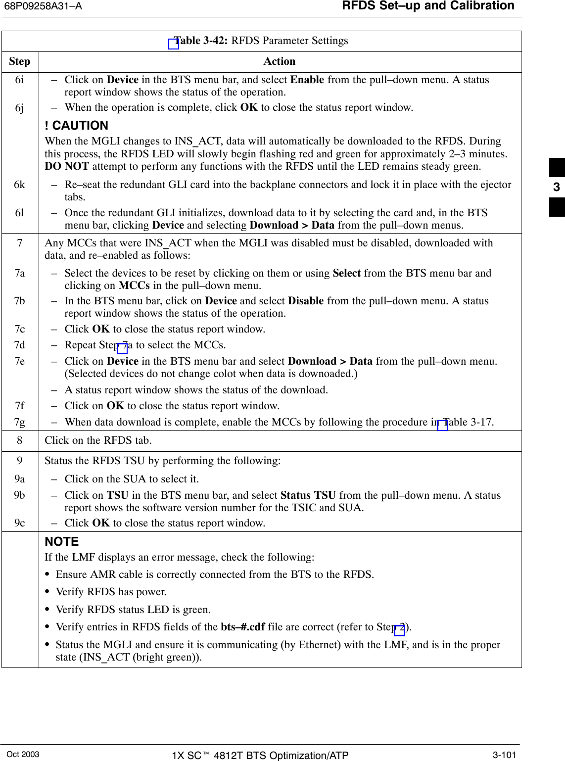
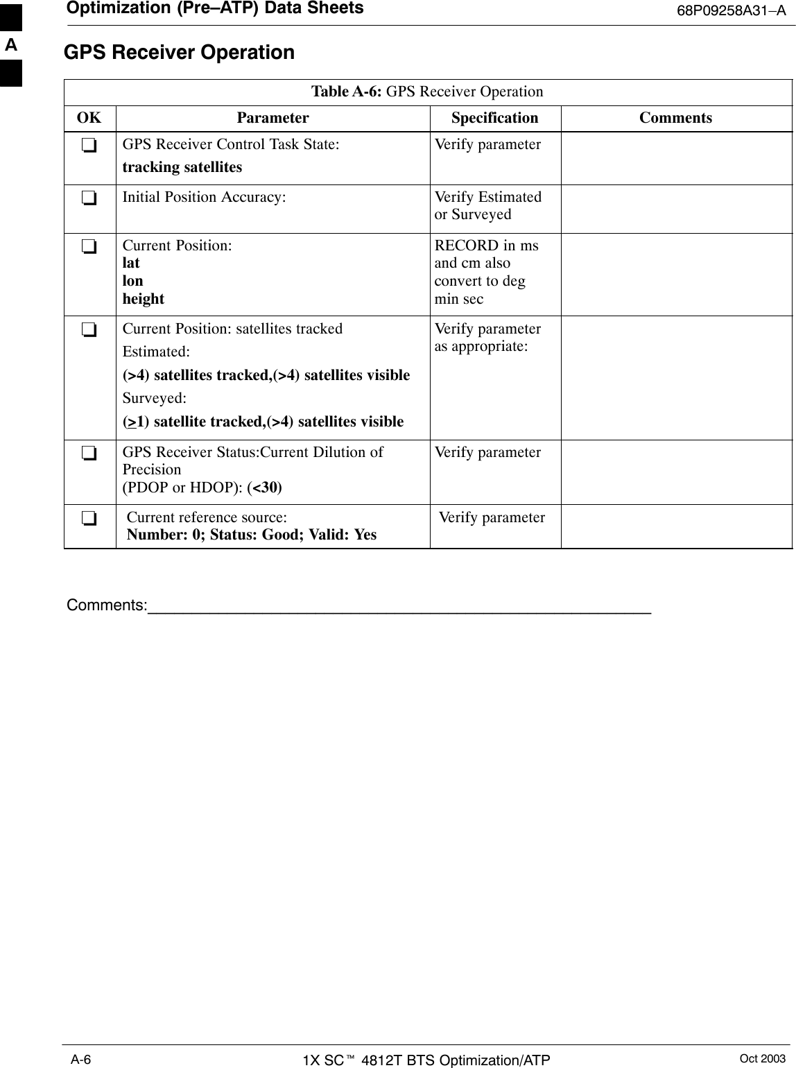
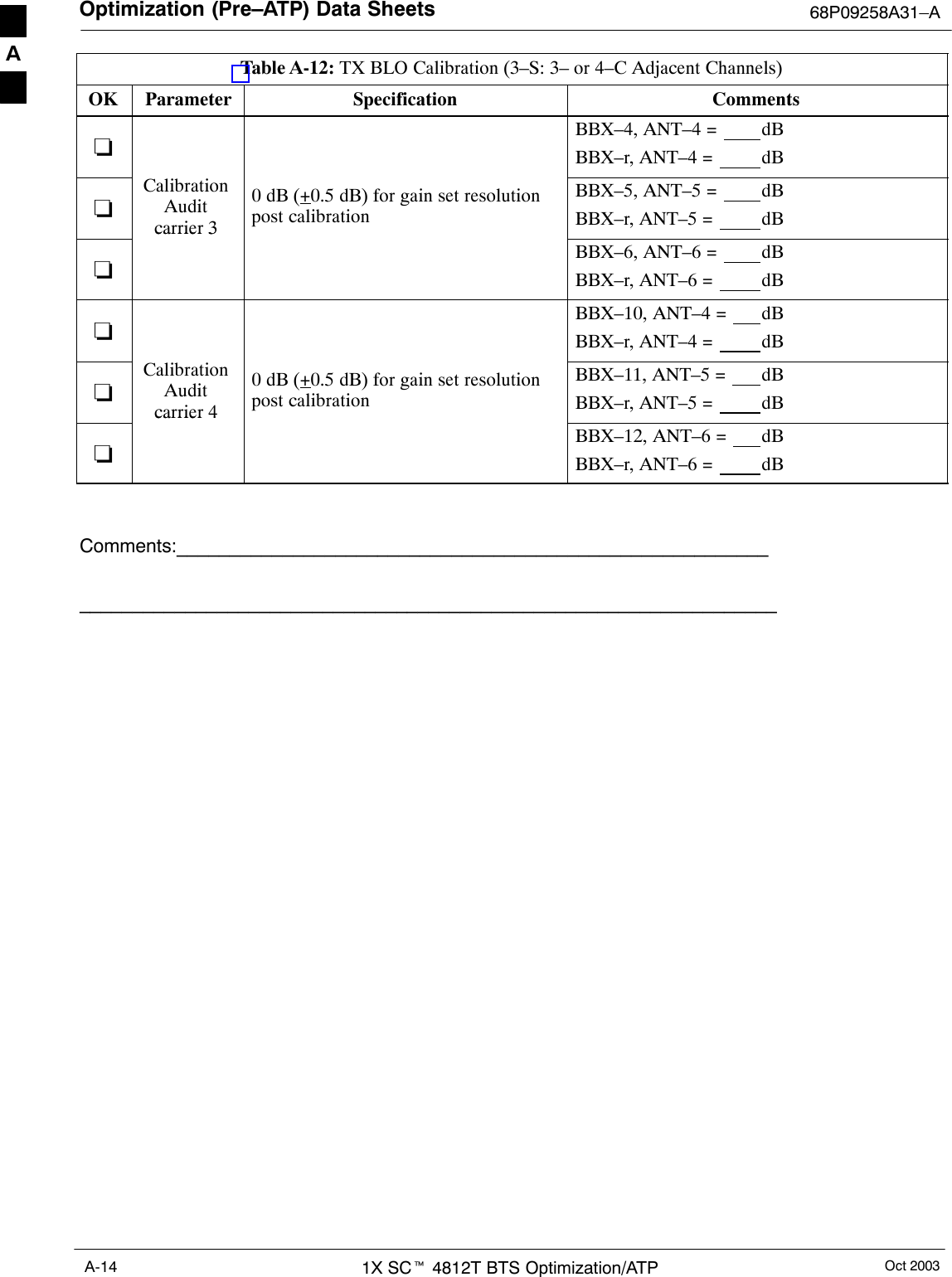
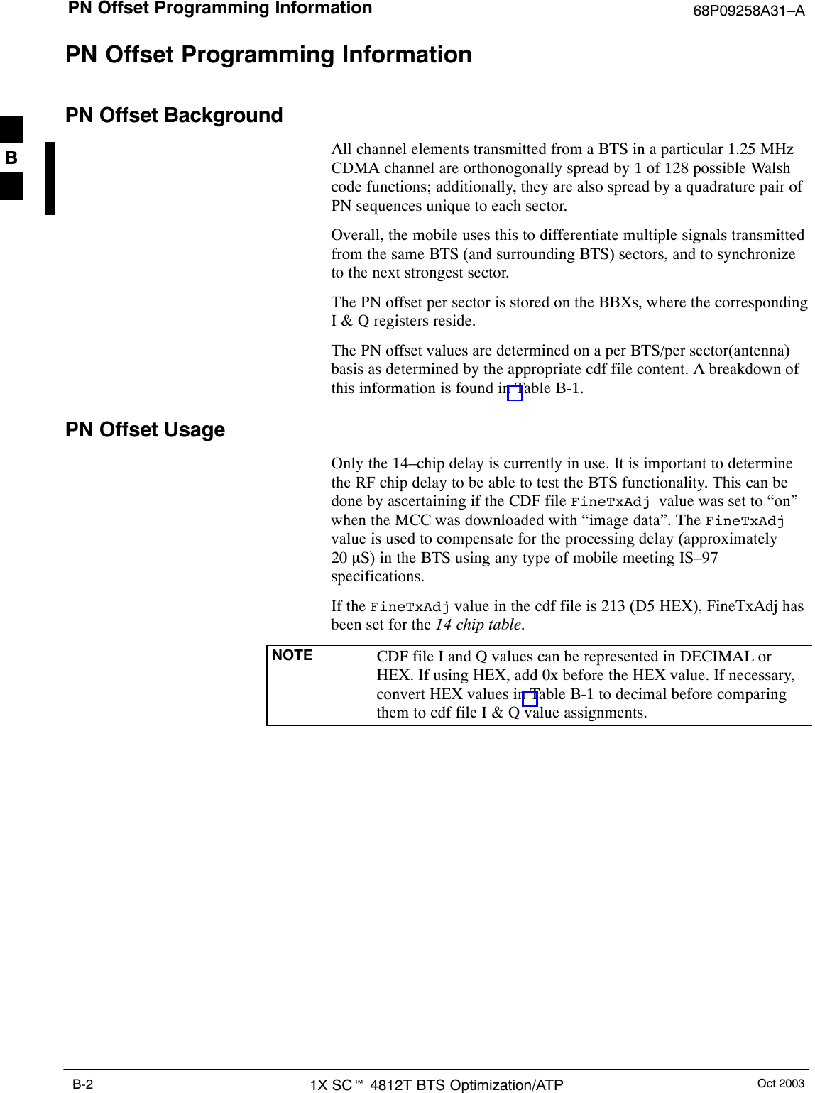
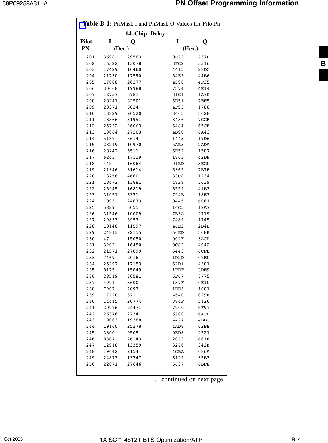
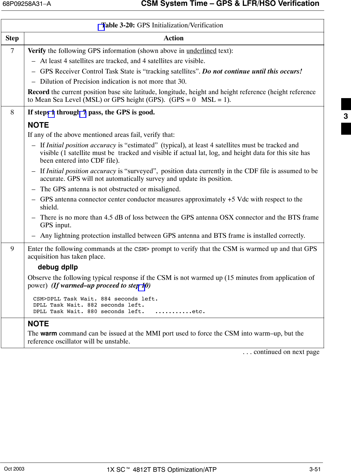
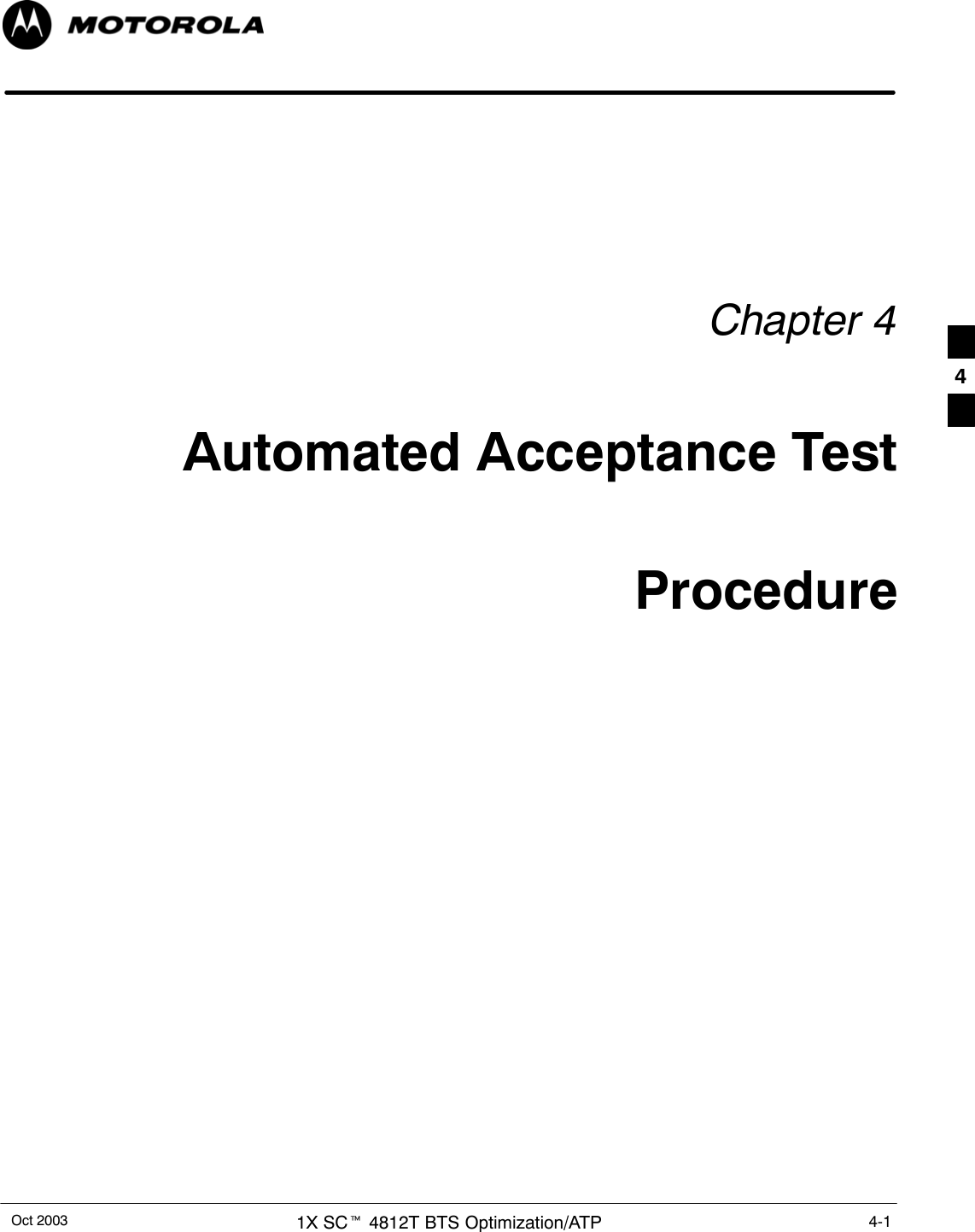
![RFDS Set–up and Calibration68P09258A31–AOct 2003 1X SCt 4812T BTS Optimization/ATP 3-105Set RFDS Configuration DataIf an RFDS is installed, the RFDS configuration data must be manuallyentered.PrerequisiteSLMF is logged into the BTSNOTE The entered antenna# index numbers must correspond to theantenna# index numbers used in the antenna maps.Follow the procedure in Table 3-46 to set the RFDS Configuration Data.Table 3-46: Set RFDS Configuration DataStep Action1Click on Util in the BTS menu bar, and select Edit > RFDS Configuration... from the pull–downmenus. A tabbed data entry pop–up window will appear.2In the data entry pop–up window, click on the TX RFDS Configuration or RX RFDS Configurationtab, as required.3To add a new antenna number, perform the following:3a – Click on the Add Row button.3b – Click in the Antenna #, Cal Antenna, Scap Antenna, or Populate [Y/N] columns, as required.3c – Enter the desired data.4To edit existing values, click in the data box to be changed and change the value.NOTERefer to the CDMA Help > Utility Menu > Edit–RFDS Configuration... section of LMF Helpfunction on–line documentation for RFDS configuration data examples.5To delete a row, click on the row and then click on the Delete Row button.6For each tab with changes, click on the Save button to save displayed values.7Click on the Dismiss button to close the window.NOTESValues entered or changed after the Save button was used will be lost when the window isdismissed.SEntered values will be used by the LMF as soon as they are saved. It is not necessary to log out andlog back into the LMF for changes to take effect.3](https://usermanual.wiki/Nokia-Solutions-and-Networks/T5EL1.Users-Manual-B/User-Guide-455782-Page-85.png)
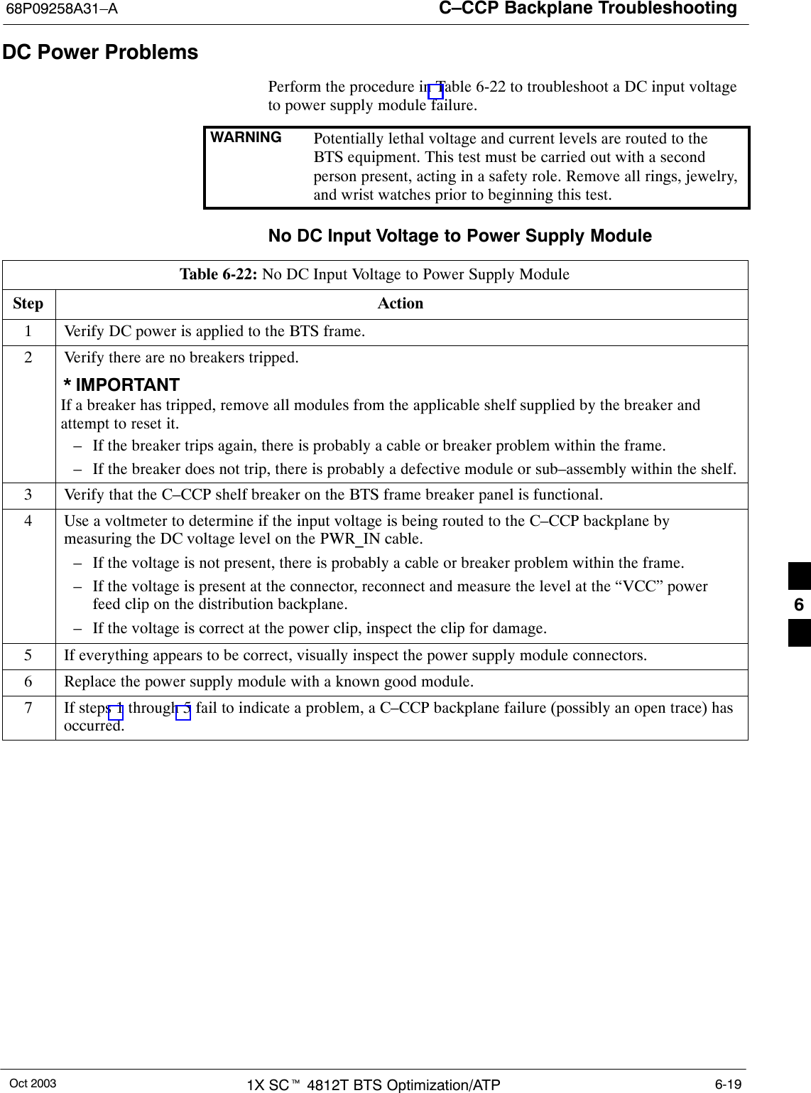
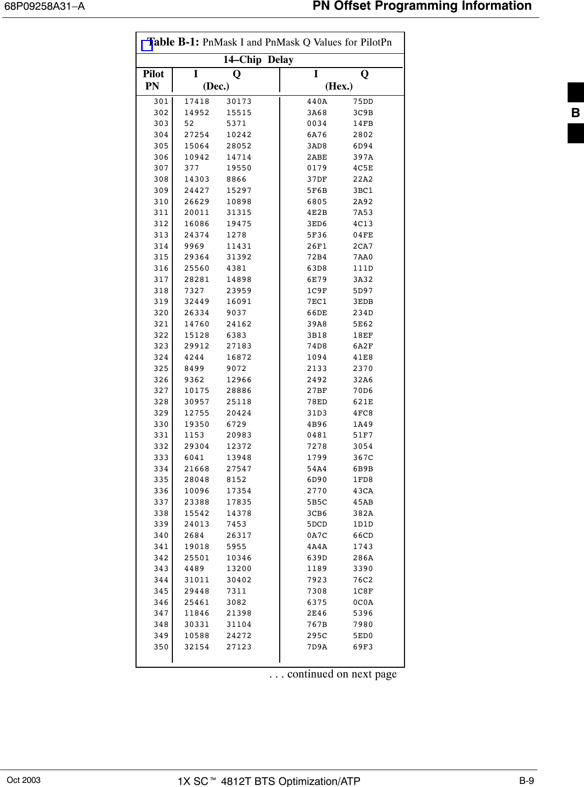
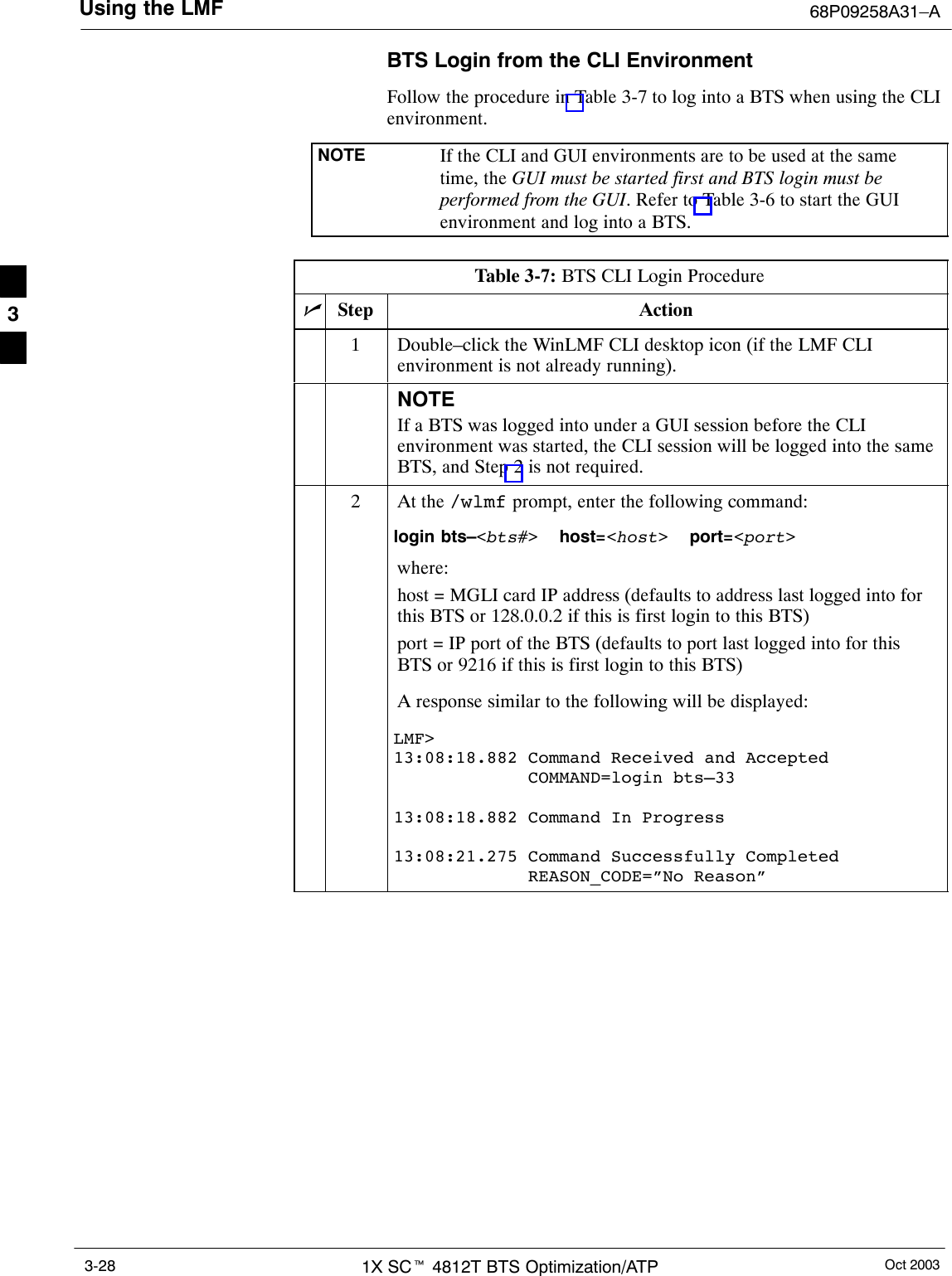
![RFDS Set–up and Calibration 68P09258A31–AOct 20031X SCt 4812T BTS Optimization/ATP3-106RFDS CalibrationThe RFDS Calibration option is used to calibrate the RFDS TX and RXpaths.TX Path Calibration – For a TX antenna path calibration the BTSXCVR is keyed at a pre–determined power level and the BTS poweroutput level is measured by the RFDS. The power level is then measuredat the TX antenna directional coupler by the power measuring testequipment item being used (power meter or analyzer). The difference(offset) between the power level at the RFDS and the power level at theTX antenna directional coupler is used as the TX RFDS calibrationoffset value.RX Path Calibration – For an RX antenna path calibration the RFDS iskeyed at a pre–determined power level and the power input level ismeasured by the BTS BBX. A CDMA signal at the same power levelmeasured by the BTS BBX is then injected at the RX antenna directionalcoupler by the communications system analyzer. The difference (offset)between the RFDS–keyed power level and power level measured at theBTS BBX is the RFDS RX calibration offset value.RFDS calibration and the CAL file – The TX and RX RFDScalibration offset values are written to the CAL file in the slot[385]Block.TSIC channel frequency – For each RFDS TSIC, the channelfrequency is determined at the lower third and upper third of theappropriate band using the frequencies listed in Table 3-47.Table 3-47: RFDS TSIC Calibration Channel FrequenciesSystem Channel Calibration Points800 MHz (A and B) 341 and 6821.9 GHz 408 and 791WARNING Before installing any test equipment directly to any TX OUTconnector, verify that there are no CDMA channels keyed.Failure to do so can result in serious personal injury and/orequipment damage.PrerequisitesSTest equipment has been selected.STest equipment and test cables have been calibrated.STX calibration has been performed and BLO data has beendownloaded to the BBXs.STest equipment and test cables are connected for TX calibration.SAntenna map data has been entered for the site.SBBXs are OOS–RAM.3](https://usermanual.wiki/Nokia-Solutions-and-Networks/T5EL1.Users-Manual-B/User-Guide-455782-Page-86.png)
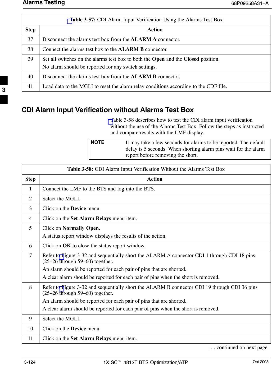
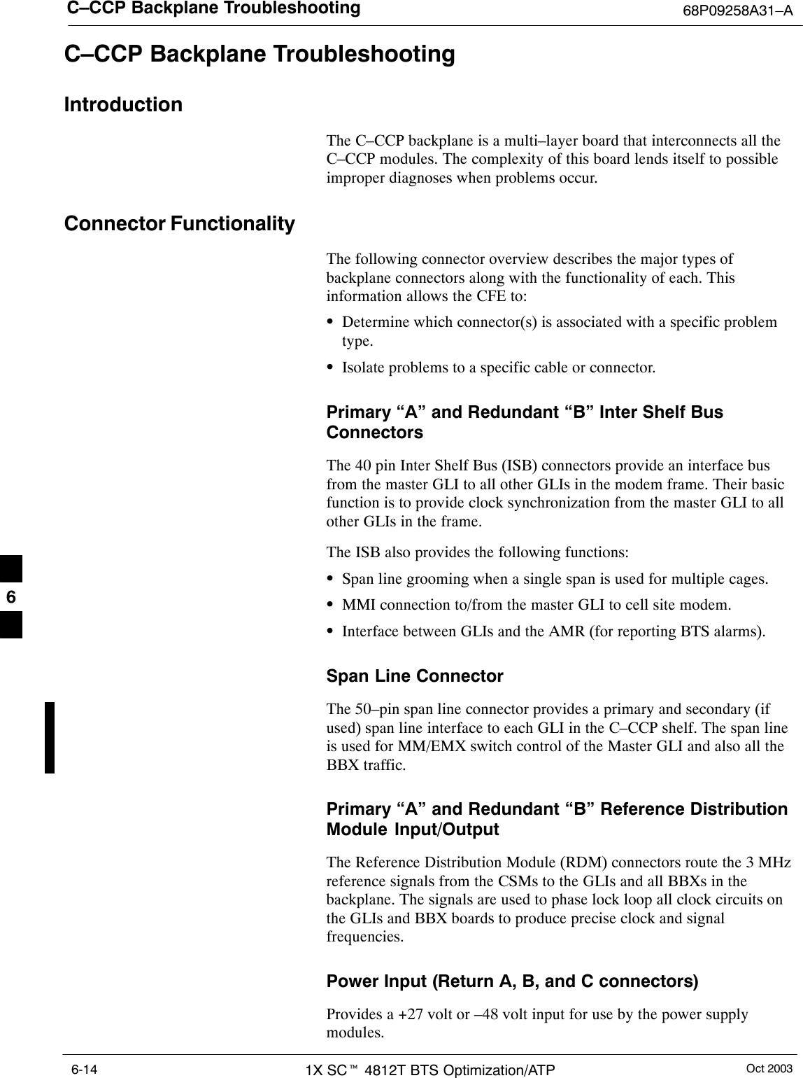
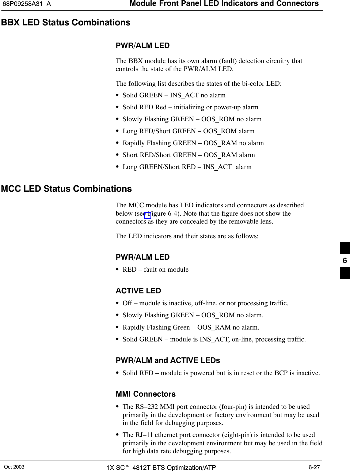
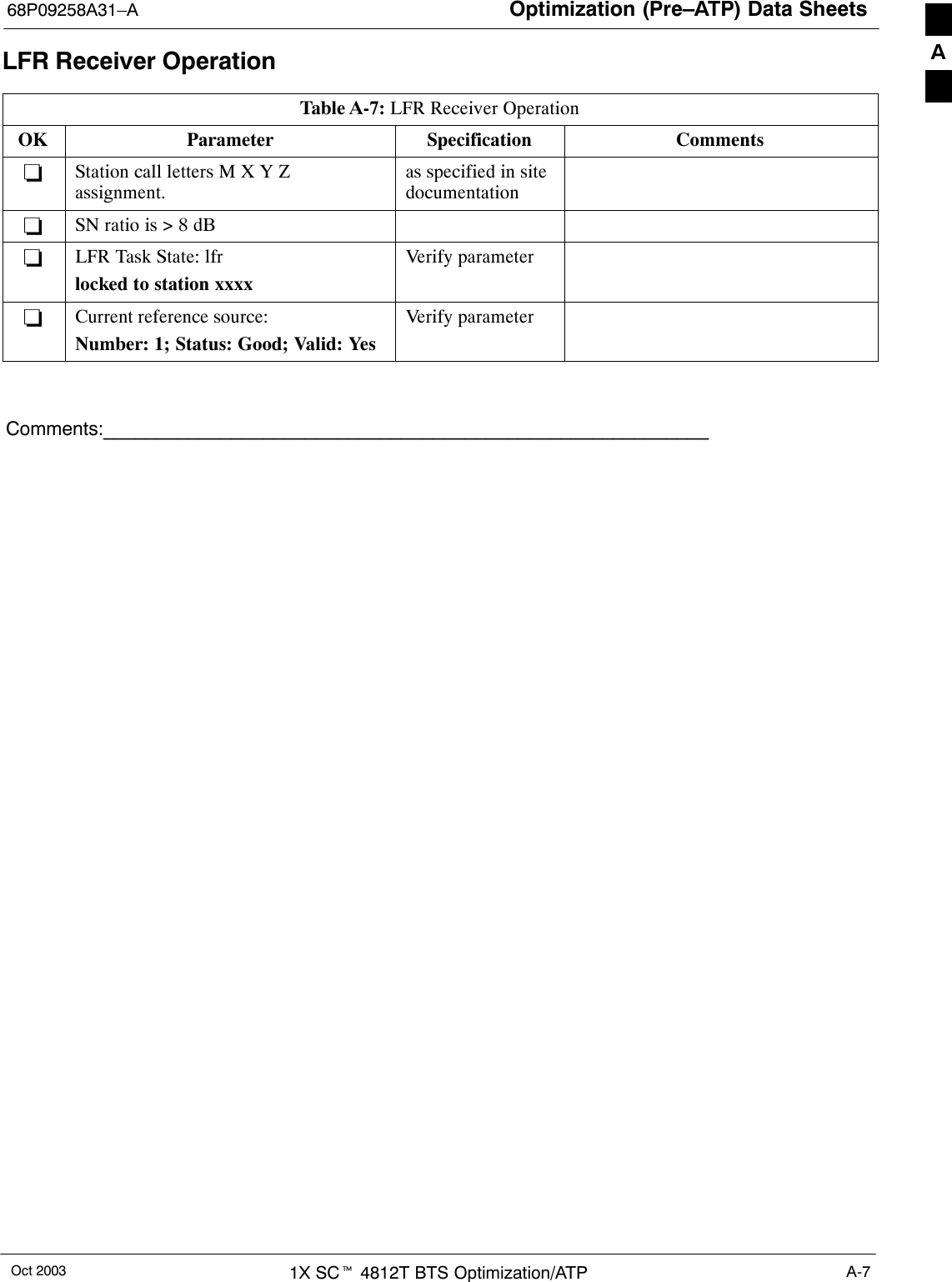
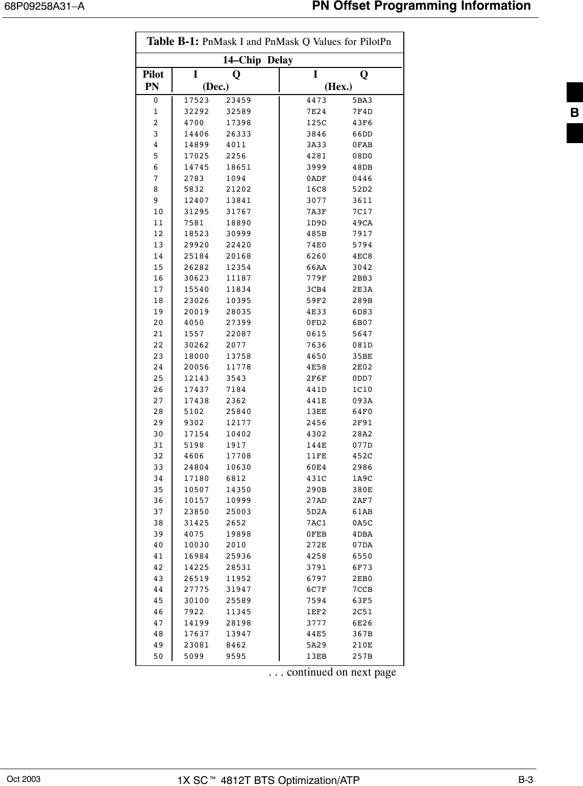
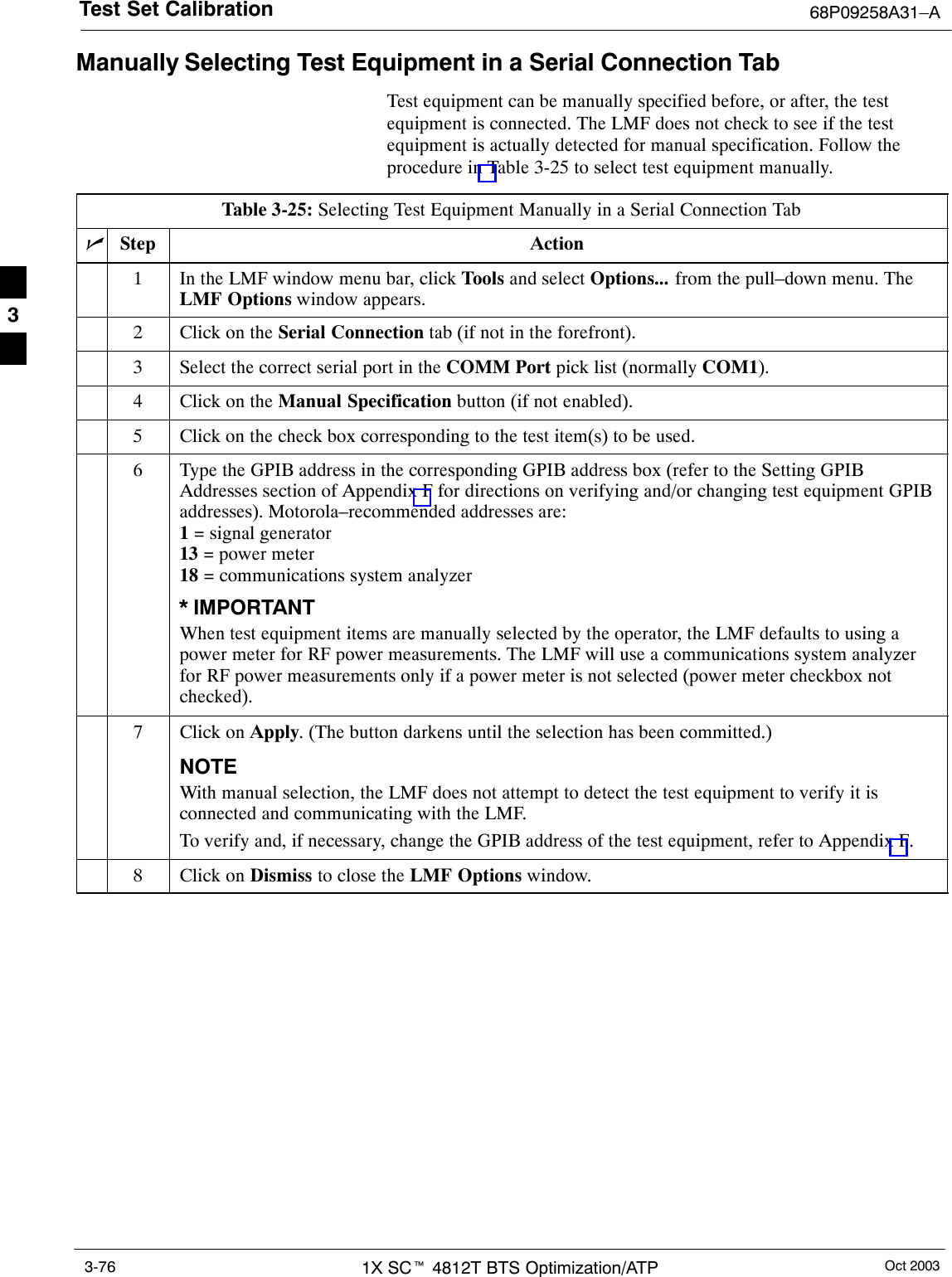
![Individual ATP Test Background Information 68P09258A31–AOct 20031X SCt 4812T BTS Optimization/ATP4-14The BBX then de-keys and, if selected, the MCC is re-configured toassign the applicable redundant BBX to the current TX antenna pathunder test. The test is then repeated. Upon completion of the test, theOCNS is disabled on the specified MCC/CE.See Table 4-1 to perform this test.Figure 4-2: Code Domain Power and Noise Floor LevelsPilot ChannelActive channelsPILOT LEVELMAX OCNS SPEC.MIN OCNS SPEC.MAXIMUM NOISE FLOOR: < –27 dB SPEC.Inactive channelsWalsh 0 1 2 3 4 5 6 7 ... 64MAX OCNSCHANNELMIN OCNSCHANNEL8.2 dB 12.2 dBMAX NOISEFLOORPilot ChannelActive channelsPILOT LEVELMAX OCNS SPEC.MIN OCNS SPEC.MAXIMUM NOISE FLOOR:< –27 dBInactive channelsWalsh 0 1 2 3 4 5 6 7 ... 64FAILURE – DOES NOTMEET MIN OCNS SPEC.FAILURE – EXCEEDSMAX OCNS SPEC. 8.2 dB 12.2 dBFAILURE – EXCEEDS MAXNOISE FLOOR SPEC. Showing all OCNS Passing Indicating Failures FW00283RX Frame Error Rate (FER) Acceptance TestThis test verifies the BTS FER on all traffic channel elements currentlyconfigured on all equipped MCCs (full rate at 1% FER) at an RF inputlevel of –119 dBm [or –116 dBm if using Tower TopAmplifier (TMPC)]. All tests are performed using the external calibratedtest set as the signal source controlled by the same command. Allmeasurements are via the LMF.The Pilot Gain is set to 262 for each TX antenna, and all channelelements from the MCCs are forward-link disabled. The BBX is keyed4](https://usermanual.wiki/Nokia-Solutions-and-Networks/T5EL1.Users-Manual-B/User-Guide-455782-Page-120.png)
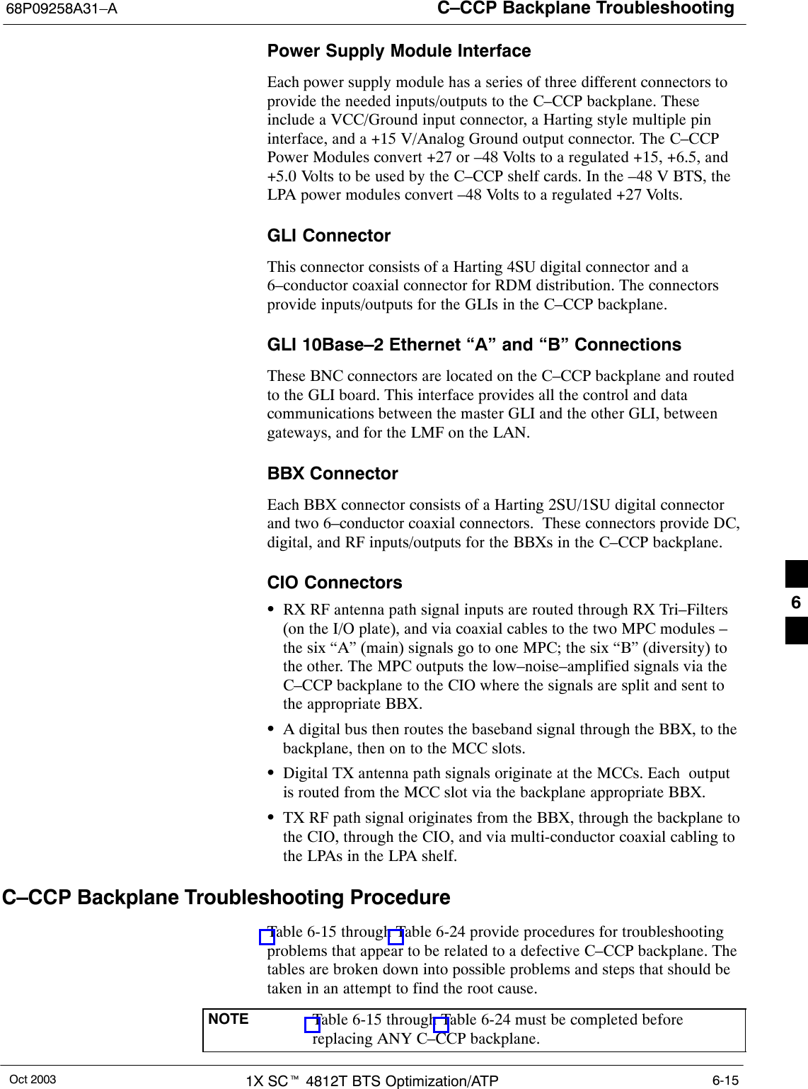
![Troubleshooting: Installation68P09258A31–AOct 2003 1X SCt 4812T BTS Optimization/ATP 6-3Troubleshooting: InstallationCannot Log into Cell-SiteFollow the procedure in Table 6-1 to troubleshoot a login failure.Table 6-1: Login Failure Troubleshooting ProceduresnStep Action1If the MGLI LED is solid RED, it implies a hardware failure. Reset the MGLI by re-seating it. Ifthis persists, install a known good MGLI card in the MGLI slot and retry. A Red LED may alsoindicate no Ethernet termination at top of frame.2Verify that T1 is disconnected (see Table 3-4 on page 3-16).If T1 is still connected, verify the CBSC has disabled the BTS.3Try pinging the MGLI (see Table 3-11 on page 3-34).4Verify the LMF is connected to the Primary LMF port (LAN A) in the front of the BTS (seeTable 3-5 on page 3-17).5Verify the LMF was configured properly (see Preparing the LMF section starting on page 3–6).6Verify the BTS-LMF cable is RG-58 [flexible black cable of less than 76 cm (2.5 feet) length].7Verify the Ethernet ports are terminated properly (see Figure 3-9 on page 3-33).8Verify a T-adapter is not used on the LMF side port if connected to the BTS front LMF primaryport.9Try connecting to the I/O panel (top of frame). Use BNC T-adapters at the LMF port for thisconnection.10 Re-boot the LMF and retry.11 Re-seat the MGLI and retry.12 Verify IP addresses are configured properly.Cannot Communicate to Power MeterFollow the procedure in Table 6-2 to troubleshoot a power metercommunication failure.Table 6-2: Troubleshooting a Power Meter Communication FailurenStep Action1Verify the Power Meter is connected to the LMF with a GPIB adapter.2Verify the cable setup as specified in Chapter 3.3Verify the GPIB address of the power meter is set to the same value displayed in the applicableGPIB address box of the LMF Options window Test Equipment tab. Refer to Table 3-25 orTable 3-26 and the GPIB Addresses section of Appendix F for details.4Verify the GPIB adapter DIP switch settings are correct. Refer to the CDMA 2000 Test EquipmentPreparation section of Appendix F for details.. . . continued on next page6](https://usermanual.wiki/Nokia-Solutions-and-Networks/T5EL1.Users-Manual-B/User-Guide-455782-Page-137.png)