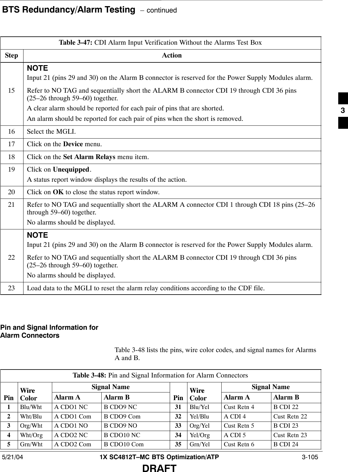
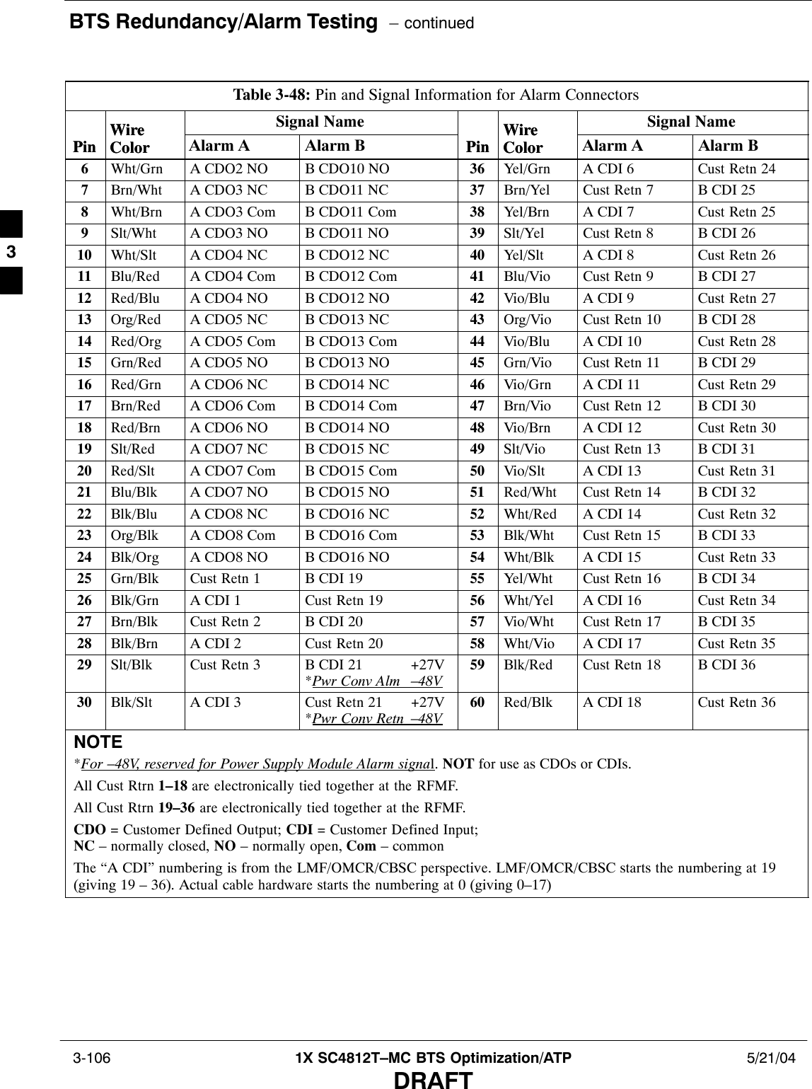
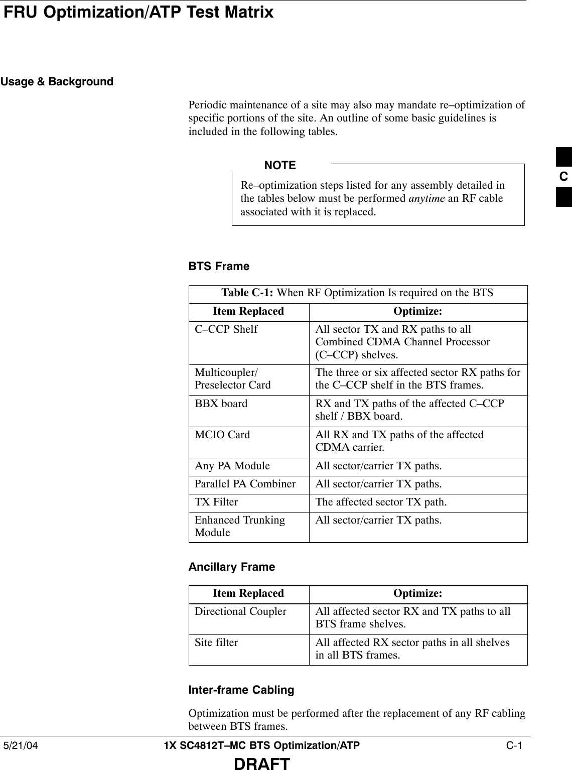
Nokia Solutions and Networks T6DY1 SC4812T-MC 1X/1X-DO @ 1.9GHz User Manual 1
Nokia Solutions and Networks SC4812T-MC 1X/1X-DO @ 1.9GHz 1
UserManual.wiki
>
Nokia Solutions and Networks
>
T6DY1 User Manual
>
Manual B
Contents
1.
Manual A
2.
Manual B
Manual B
Navigation menu
Upload a User Manual
Namespaces
Wiki Guide
HTML
PDF
Info
Views
User Manual
Discussion / Help
Navigation


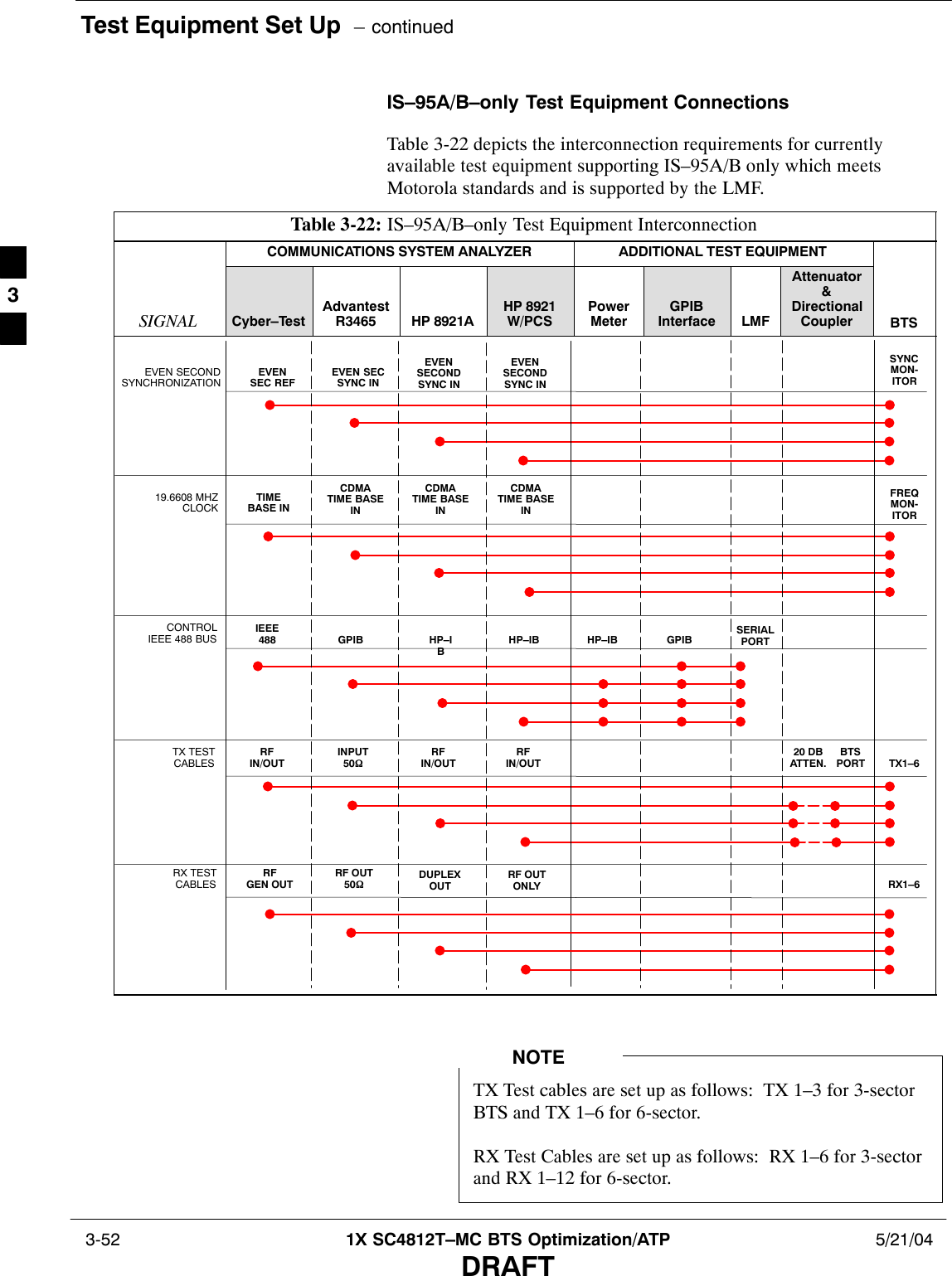

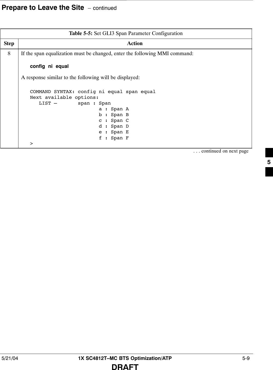
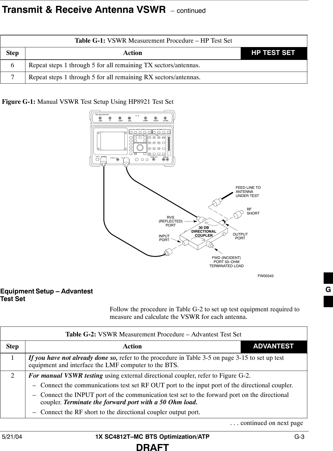
![Bay Level Offset Calibration – continued 3-80 1X SC4812T–MC BTS Optimization/ATP 5/21/04DRAFTBLO Calibration Data FileDuring the calibration process, the LMF creates a bts–#.calcalibration (BLO) offset data file (CAL file) in the bts–# folder. Aftercalibration has been completed, this offset data must be downloaded tothe BBXs using the LMF Download BLO function. An explanation ofthe file is shown below.Due to the size of the file, Motorola recommends printing ahard copy of a CAL file and refer to it for the followingdescriptions.NOTEThe CAL file is subdivided into sections organized on a per slot basis (aslot Block).Slot 1 contains the calibration data for the 12 BBX slots. Slot 20contains the calibration data for the redundant BBX. Each BBX slotheader block contains:SA creation Date and Time – broken down into separate parameters ofcreateMonth, createDay, createYear, createHour, and createMin.SThe number of calibration entries – fixed at 720 entries correspondingto 360 calibration points of the CAL file including the slot header andactual calibration data.SThe calibration data for a BBX is organized as a large flat array. Thearray is organized by branch, sector, and calibration point.– The first breakdown of the array indicates which branch thecontained calibration points are for. The array covers transmit, mainreceive and diversity receive offsets as follows:Table 3-32: BLO BTS.cal File Array AssignmentsRange AssignmentC[1]–C[240] TransmitC[241]–C[480] Main ReceiveC[481]–C[720] Diversity Receive– The second breakdown of the array is per sector. Configurationssupported are Omni, 3–sector or 6–sector.3](https://usermanual.wiki/Nokia-Solutions-and-Networks/T6DY1.Manual-B/User-Guide-427751-Page-101.png)
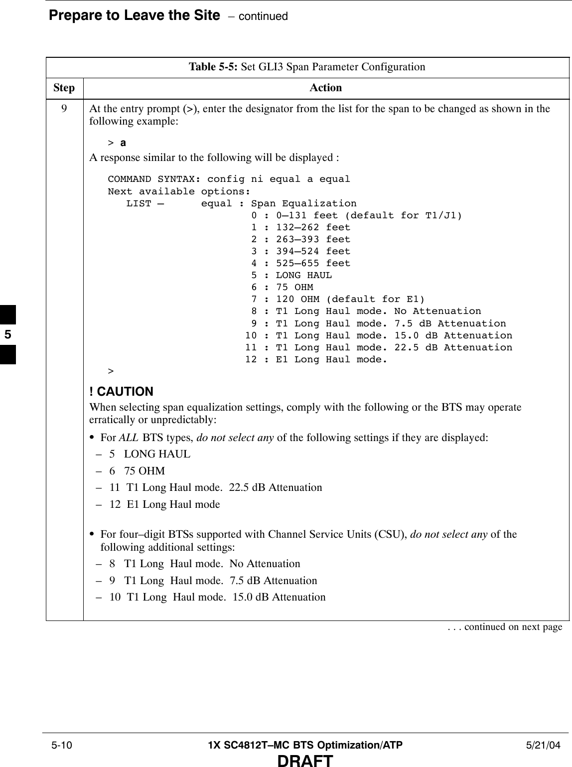
![Bay Level Offset Calibration – continued5/21/04 1X SC4812T–MC BTS Optimization/ATP 3-81DRAFTTable 3-33: BTS.cal File Array (Per Sector)BBX Sectorization TX RX RX DiversitySlot[1] (Primary BBXs 1 through 12)1 (Omni) 3–Sector,C[1]–C[20] C[241]–C[260] C[481]–C[500]23–Sector,1stCiC[21]–C[40] C[261]–C[280] C[501]–C[520]36 Sector,1stCarrier C[41]–C[60] C[281]–C[300] C[521]–C[540]41stCarrier 3–Sector,C[61]–C[80] C[301]–C[320] C[541]–C[560]5Carrier3–Sector,3rdCiC[81]–C[100] C[321]–C[340] C[561]–C[580]6Carrier C[101]–C[120] C[341]–C[360] C[581]–C[600]73–Sector,C[121]–C[140] C[361]–C[380] C[601]–C[620]83–Sector,2ndCiC[141]–C[160] C[381]–C[400] C[621]–C[640]96 Sector,2ndCarrier C[161]–C[180] C[401]–C[420] C[641]–C[660]102ndCarrier 3–Sector,C[181]–C[200] C[421]–C[440] C[661]–C[680]11Carrier3–Sector,4thCiC[201]–C[220] C[441]–C[460] C[681]–C[700]12 Carrier C[221]–C[240] C[461]–C[480] C[701]–C[720] . . . continued on next page3](https://usermanual.wiki/Nokia-Solutions-and-Networks/T6DY1.Manual-B/User-Guide-427751-Page-102.png)
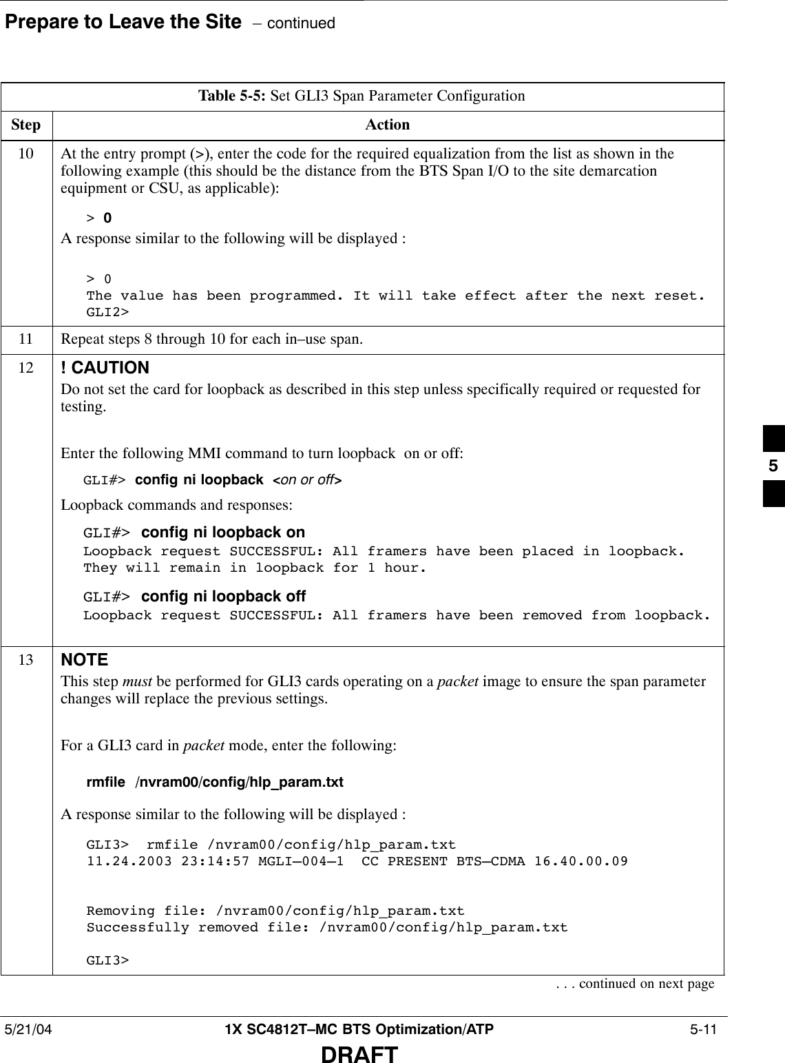
![Bay Level Offset Calibration – continued 3-82 1X SC4812T–MC BTS Optimization/ATP 5/21/04DRAFTTable 3-33: BTS.cal File Array (Per Sector)BBX RX DiversityRXTXSectorizationSlot[20] (Redundant BBX–13)1 (Omni) 3–Sector,C[1]–C[20] C[241]–C[260] C[481]–C[500]23–Sector,1stCiC[21]–C[40] C[261]–C[280] C[501]–C[520]36 Sector,1stCarrier C[41]–C[60] C[281]–C[300] C[521]–C[540]41stCarrier 3–Sector,C[61]–C[80] C[301]–C[320] C[541]–C[560]5Carrier3–Sector,3rdCiC[81]–C[100] C[321]–C[340] C[561]–C[580]6Carrier C[101]–C[120] C[341]–C[360] C[581]–C[600]73–Sector,C[121]–C[140] C[361]–C[380] C[601]–C[620]83–Sector,2ndCiC[141]–C[160] C[381]–C[400] C[621]–C[640]96 Sector,2ndCarrier C[161]–C[180] C[401]–C[420] C[641]–C[660]10 2ndCarrier3–Sector,C[181]–C[200] C[421]–C[440] C[661]–C[680]11Carrier3–Sector,4th C[201]–C[220] C[441]–C[460] C[681]–C[700]12 Carrier C[221]–C[240] C[461]–C[480] C[701]–C[720]STen calibration points per sector are supported for each branch. Twoentries are required for each calibration point:1. The first value (all odd entries) identifies the CDMA channel(frequency) where the BLO is measured.2. The second value (all even entries) is the power set level(PwrLvlAdj). The valid range for PwrLvlAdj is from 2500 to27500 (2500 corresponds to –125 dBm and 27500 correspondsto +125 dBm).SThe 20 calibration entries for each sector/branch combination must bestored in order of increasing frequency. If less than 10 points(frequencies) are calibrated, data for the highest frequency calibratedis repeated to fill out the remainder of the 10 points.Example:C[1]=384, odd cal entry= 1 ‘‘calibration point”C[2]=19102, even cal entryC[3]=777,C[4]=19086,..C[19]=777,C[20]=19086, (Since only two frequencies were calibrated, data forthis one, the highest, is repeated for the last eight calibration points of the sector/branch)SWhen the BBX is loaded with data, the CAL file data for the BBX isdownloaded to the device in the order it is stored in the CAL file.TxCal data is sent first, C[1] – C[240]. Sector 1’s ten calibrationpoints are sent (C[1] – C[20]) followed by sector 2’s ten calibration3](https://usermanual.wiki/Nokia-Solutions-and-Networks/T6DY1.Manual-B/User-Guide-427751-Page-103.png)
![Bay Level Offset Calibration – continued5/21/04 1X SC4812T–MC BTS Optimization/ATP 3-83DRAFTpoints (C[21] – C[40]), etc. The RxCal data is sent next (C[241] –C[480]), followed by the RxDCal data (C[481] – C[720]).STemperature compensation data is also stored in the cal file for eachset.Test Equipment Set-up forRF Path CalibrationFollow the procedure in Table 3-34 to set up test equipment.Table 3-34: Test Equipment Setup (RF Path Calibration)nStep Action1Verify the GPIB controller is properly connected and turned on (does not apply tothe Agilent E7495A).! CAUTIONTo prevent damage to the test equipment, all transmit (TX) test connections mustbe via the 30 dB directional coupler.2If it has not already been done, connect the LMF computer to the BTS LAN Aconnector on the BTS. Refer to the procedure in Table 3–2.SIf required, calibrate the test equipment using the procedure in Table 3-26.SConnect the test equipment as shown in Figure 3-15 throug Figure 3-17.Transmit (TX) Path CalibrationDescriptionThe assigned channel frequency and power level (as measured at the topof the frame) for transmit calibration are derived from the site CDF files.For each BBX, the channel frequency is specified in the [CdmaChans]in the cbsc–#.cdf file and the power is specified in the SIFPilotPwrCDF file parameter for the sector associated with the BBX (locatedunder the ParentSECTOR field of the ParentCARRIER CDF fileparameter).If both the bts–#.cdf and cbsc–#.cdf orNECB*bts#.xml and NECJ*bts#.xml files are current,all information will be correct on the LMF. If not, thecarrier and channel will have to be set for each test.NOTEThe calibration procedure attempts to adjust the power to within "0.5dB of the desired power. The calibration will pass if the error is less thanthe value set in the “TX Nominal offset” tolerance.3](https://usermanual.wiki/Nokia-Solutions-and-Networks/T6DY1.Manual-B/User-Guide-427751-Page-104.png)

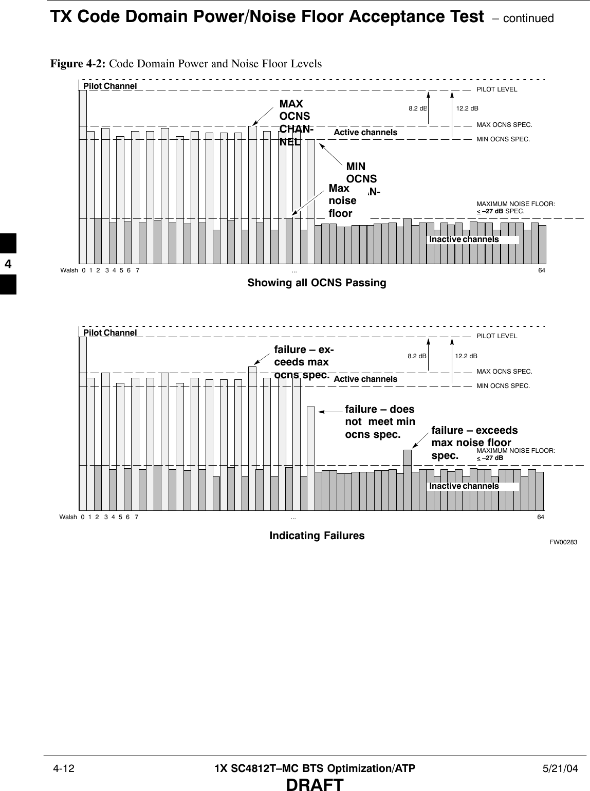
![Automated Acceptance Test Procedures – TX & RX – continued5/21/04 1X SC4812T–MC BTS Optimization/ATP 4-5DRAFTPilot Time OffsetThe Pilot Time Offset is the difference between the CDMA analyzermeasurement interval (based on the BTS system time reference) and theincoming block of transmitted data from the BTS (Pilot only, PilotGain = 262, PN Offset = 0).Code Domain Power (Primary & Redundant BBX)This test verifies the code domain power levels, which have been set forall ODD numbered Walsh channels, using the OCNS command. This isdone by verifying that the ratio of PILOT divided by OCNS is equal to10.2 + 2 dB, and, that the noise floor of all EVEN numbered “OFF”Walsh channels measures < –27 dB (with respect to total CDMA channelpower).Frame Error RateThe Frame Error Rate (FER) test verifies RX operation of the entireCDMA Reverse Link using all equipped MCCs assigned to allrespective sectors/antennas. This test verifies the BTS sensitivity on alltraffic channel elements currently configured on all equipped MCCs atan RF input level of –119 dBm (or –116 dBm if using TMPC).ATP Test ProcedureFollow the procedure in Table 4-1 to perform any ATP test.Table 4-1: ATP Test ProcedurenStep Action1Be sure that all prerequisites have been met.2Select the device(s) to be tested.IMPORTANT! Only one carrier can be tested at a time. All PAs must be INS during testing.NOTEIf the LMF has been logged into the BTS with a different Multi–Channel Preselector setting thanthe one to be used for this test, the LMF must be logged out of the BTS and logged in again withthe new Multi–Channel Preselector setting. Using the wrong MPC setting can cause a false testfailure.3From the Tests menu, select the test you want to run.4Select the appropriate carrier (carrier-bts#-sector#-carrier#) displayed in the Channels/Carrierpick list.NOTETo select multiple items, hold down the <Shift> or <Ctrl> key while making the selections.5Enter the appropriate channel number in the Carrier n Channels box.The default channel number displayed is determined by the CdmaChans[n] number in thecbsc–n.cdf file for the BTS.6If applicable, select Verify BLO (default) or Single–sided BLO.. . . continued on next page4](https://usermanual.wiki/Nokia-Solutions-and-Networks/T6DY1.Manual-B/User-Guide-427751-Page-134.png)
![RX Frame Error Rate (FER) Acceptance Test5/21/04 1X SC4812T–MC BTS Optimization/ATP 4-13DRAFTFER TestThis test verifies the BTS FER on all traffic channel elements currentlyconfigured on all equipped MCCs (full rate at 1% FER) at an RF inputlevel of –119 dBm [or –116 dBm if using Tower TopAmplifier (TMPC)]. All tests are performed using the external calibratedtest set as the signal source controlled by the same command. Allmeasurements are via the LMF.The Pilot Gain is set to 262 for each TX antenna, and all channelelements from the MCCs are forward-link disabled. The BBX is keyedup, using only bbxlvl level offsets, to generate a CDMA carrier (withpilot channel element only). BBX power output is set to –20 dBm asmeasured at the TX OUT connector. The BBX must be keyed to enablethe RX receive circuitry.The LMF prompts the MCC/CE under test to measure all zero longcodeand provide the FER report on the selected active MCC on the reverselink for both the main and diversity RX antenna paths, verifying thatresults meet the following specification:SFER returned less than 1% and total frames measured is 1500All MCC/CEs selected are tested on the specified RX antenna path. TheBBX then de-keys and, if selected, the MCC is re-configured to assignthe applicable redundant BBX to the current RX antenna paths undertest. The test is then repeated. See Table 4-1 to perform this test.4](https://usermanual.wiki/Nokia-Solutions-and-Networks/T6DY1.Manual-B/User-Guide-427751-Page-142.png)


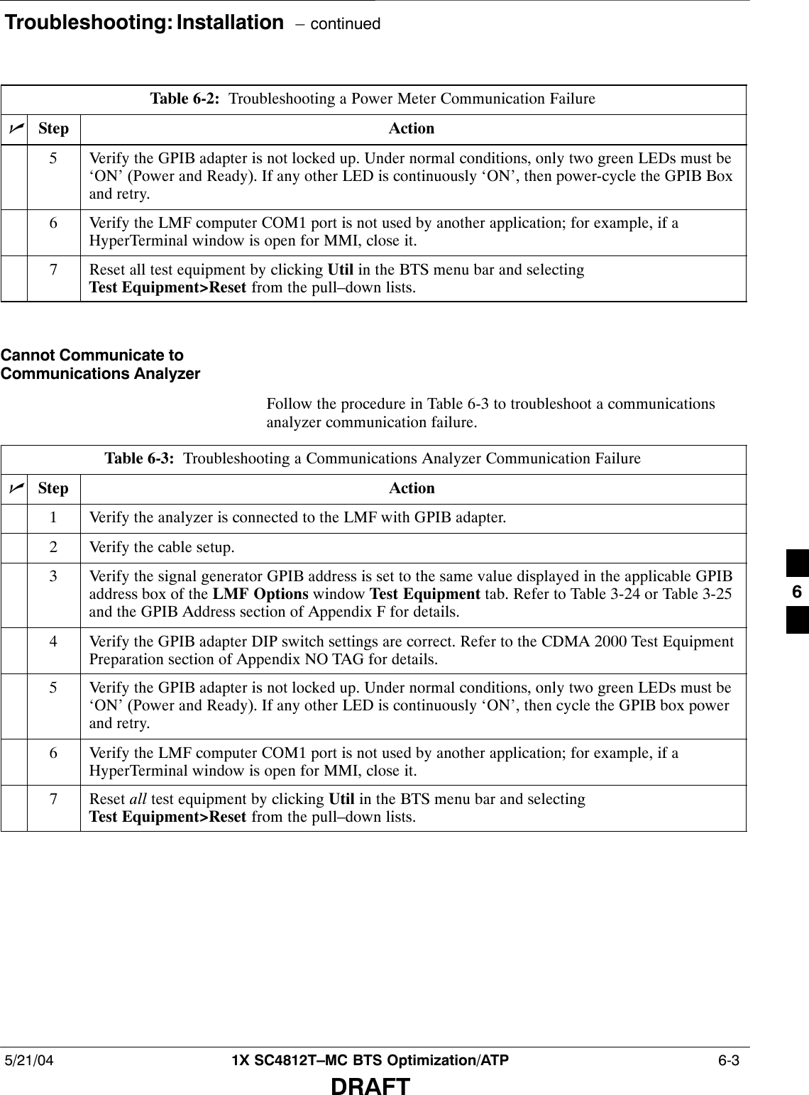
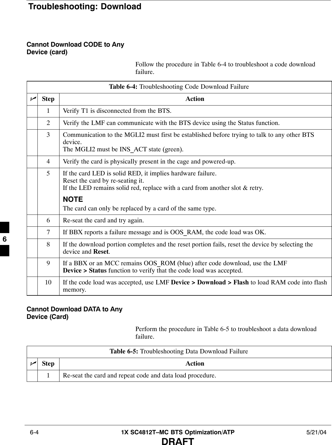
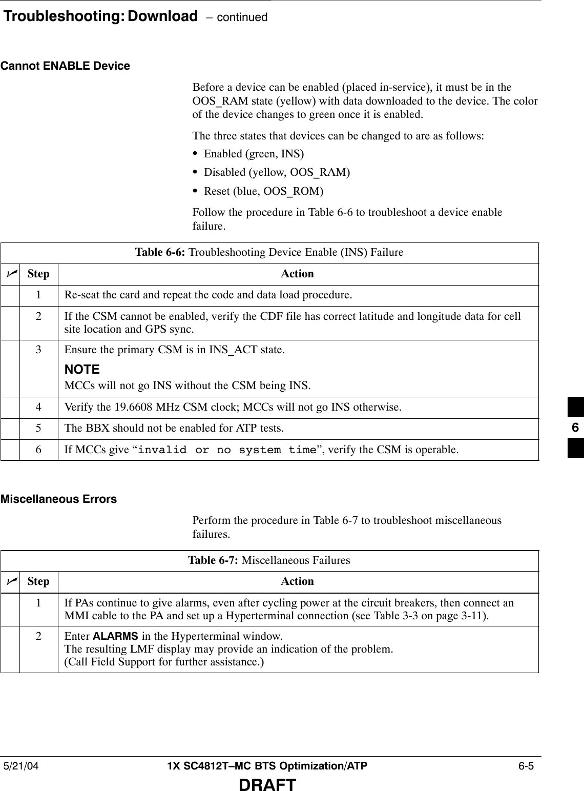
![Troubleshooting: Installation 6-2 1X SC4812T–MC BTS Optimization/ATP 5/21/04DRAFTCannot Log into Cell-SiteFollow the procedure in Table 6-1 to troubleshoot a login failure.Table 6-1: Login Failure Troubleshooting ProceduresnStep Action1If MGLI LED is solid RED, it implies a hardware failure. Reset MGLI by re-seating it. If thispersists, install a known good MGLI card in MGLI slot and retry. A Red LED may also indicateno Ethernet termination at top of frame.2Verify that T1 is disconnected (see Table 3-4 on page 3-14).If T1 is still connected, verify the CBSC has disabled the BTS.3Try pinging the MGLI (see Table 3-11 on page 3-32).4Verify the LMF is connected to the Primary LMF port (LAN A) in the front of the BTS (seeTable 3-5 on page 3-15).5Verify the LMF was configured properly (see Preparing the LMF section starting on page 3–6).6Verify the BTS-LMF cable is RG-58 [flexible black cable of less than 76 cm (2.5 feet) length].7Verify the Ethernet ports are terminated properly (see Figure 3-10).8Verify a T-adapter is not used on the LMF side port if connected to the BTS front LMF primaryport.9Try connecting to the I/O panel (top of frame). Use BNC T-adapters at the LMF port for thisconnection.10 Re-boot the LMF and retry.11 Re-seat the MGLI and retry.12 Verify IP addresses are configured properly.Cannot Communicate to PowerMeterFollow the procedure in Table 6-2 to troubleshoot a power metercommunication failure.Table 6-2: Troubleshooting a Power Meter Communication FailurenStep Action1Verify the Power Meter is connected to the LMF with a GPIB adapter.2Verify the cable setup as specified in Chapter 3.3Verify the GPIB address of the power meter is set to the same value displayed in the applicableGPIB address box of the LMF Options window Test Equipment tab. Refer to Table 3-24 orTable 3-25 and the GPIB Addresses section of Appendix F for details.4Verify the GPIB adapter DIP switch settings are correct.Refer to the Test Equipment setup section for details.. . . continued on next page6](https://usermanual.wiki/Nokia-Solutions-and-Networks/T6DY1.Manual-B/User-Guide-427751-Page-165.png)


![Verifying and Setting GPIB Addresses – continued5/21/04 1X SC4812T–MC BTS Optimization/ATP F-17DRAFTDisconnect other GPIB devices, especially systemcontrollers, from the system before running theconnectivity software.NOTETable F-13: System ConnectivityStep ActionNOTE– Perform this procedure after test equipment has been allowed to warm–up and stabilize for aminimum of 60 minutes.1Insert HP 83236A Manual Control/System card into memory card slot.2Press the [PRESET] pushbutton.3Press the Screen Control [TESTS] pushbutton to display the “Tests” Main Menu screen.4Position the cursor at Select Procedure Location and select by pressing the cursor control knob.In the Choices selection box, select Card.5Position the cursor at Select Procedure Filename and select by pressing the cursor control knob.In the Choices selection box, select SYS_CONN.6Position the cursor at RUN TEST and select it.The software will prompt you through the connectivity setup.7When the test is complete, position the cursor on STOP TEST and select it; OR press the [K5]pushbutton.8To return to the main menu, press the [K5] pushbutton.HP PCS Interface TestEquipment Setup for ManualTestingFollow the procedure in Table F-14 to setup the HP PCS Interface Boxfor manual testing.Table F-14: Manual Cable Calibration Test Equipment Setup (using the HP PCS Interface)nStep ActionNOTEVerify GPIB controller is turned off.1Insert HP83236B Manual Control/System card into the memory card slot.2 Under Screen Controls, press the [TESTS] push-button to display the TESTS (Main Menu)screen.3Position the cursor at Select Procedure Location and select. In the Choices selection box, selectCARD.4Position the cursor at Select Procedure Filename and select. In the Choices selection box, selectMANUAL.F](https://usermanual.wiki/Nokia-Solutions-and-Networks/T6DY1.Manual-B/User-Guide-427751-Page-268.png)
![Verifying and Setting GPIB Addresses – continued F-18 1X SC4812T–MC BTS Optimization/ATP 5/21/04DRAFTTable F-14: Manual Cable Calibration Test Equipment Setup (using the HP PCS Interface)nActionStep5Position the cursor at RUN TEST and select OR press the K1 push-button.6Set channel number=<chan#>:– Position cursor at Channel Number and select.– Enter the chan# using the numeric keypad and then press [Enter] (the screen will blank).– When the screen reappears, the chan# will be displayed on the channel number line.NOTE– If using a TMPC with Tower Top Amplifier (TTA) skip Step 7.7Set RF Generator level= –119 dBm + Cal factor Example: –119 dBm + 2 dB = –117 dBm– Continue with Step 9 (skip Step 8).8Set RF Generator level= –116 dBm + Cal factor. Example: –116 dBm + 2 dB = –114 dBm9Set the user fixed Attenuation Setting to 0 dB:– Position cursor at RF Generator Level and select.– Position cursor at User Fixed Atten Settings and select.– Enter 0 (zero) using the numeric keypad and press [Enter].10 Select Back to Previous Menu.11 Select Quit, then select Yes.Calibrating Test Cable Setupusing Advantest R3465Be sure the GPIB Interface is OFF for this procedure.NOTEPerform the procedure in Table F-15 to calibrate the test cable setupusing the Advantest R3465. Advantest R3465 Manual Test setup andcalibration must be performed at both the TX and RX frequencies.Table F-15: Procedure for Calibrating Test Cable Setup Using Advantest R3465Step ActionNOTE– This procedure can only be performed after test equipment has been allowed to warm–up andstabilize for a minimum of 60 minutes.1Press the SHIFT and the PRESET keys located below the display.2Press the ADVANCE key in the MEASUREMENT area of the control panel.3Select the CDMA Sig CRT menu key.4Select the Setup CRT menu key.. . . continued on next pageF](https://usermanual.wiki/Nokia-Solutions-and-Networks/T6DY1.Manual-B/User-Guide-427751-Page-269.png)
![Test Equipment Calibration – continued5/21/04 1X SC4812T–MC BTS Optimization/ATP F-23DRAFTThis procedure must be done before the automatedcalibration to enter power sensor specific calibrationvalues.NOTEFigure F-15: Power Meter DetailCONNECT POWERSENSOR WITH POWERMETER TURNED OFFCONNECT POWER SENSORTO POWER REFERENCEWHEN CALIBRATING UNIT.POWER REFERENCE ISENABLED USING THE SHIFT ’KEYSSHIFT (BLUE) PUSHBUTTON –ACCESSES FUNCTION ANDDATA ENTRY KEYS IDENTIFIEDWITH LIGHT BLUE TEXT ONTHE FRONT PANEL ABOVETHE BUTTONSFW00Table F-17: HP 437 Power Meter Calibration ProcedureStep Action1! CAUTIONDo not connect/disconnect the power meter sensor cable with AC power applied to the meter.Disconnection could result in destruction of the sensing element or mis–calibration.Make sure the power meter AC LINE pushbutton is OFF.2Connect the power sensor cable to the SENSOR input.3Set the AC LINE pushbutton to ON.NOTEThe calibration should be performed only after the power meter and sensor have been allowed towarm–up and stabilize for a minimum of 60 minutes.4Perform the following to set or verify the correct power sensor model:4a – Press [SHIFT] then [a] to select SENSOR.4b – Identify the power sensor model number from the sensor label.4c – Use the [y] or [b] button to select the appropriate model; then press [ENTER].5Refer to the illustration for step 8, and perform the following to ensure the power reference output isOFF:5a – Observe the instrument display and determine if the triangular indicator over PWR REF isdisplayed.5b – If the triangular indicator is displayed, press [SHIFT] then [’] to turn it off.. . . continued on next pageF](https://usermanual.wiki/Nokia-Solutions-and-Networks/T6DY1.Manual-B/User-Guide-427751-Page-274.png)
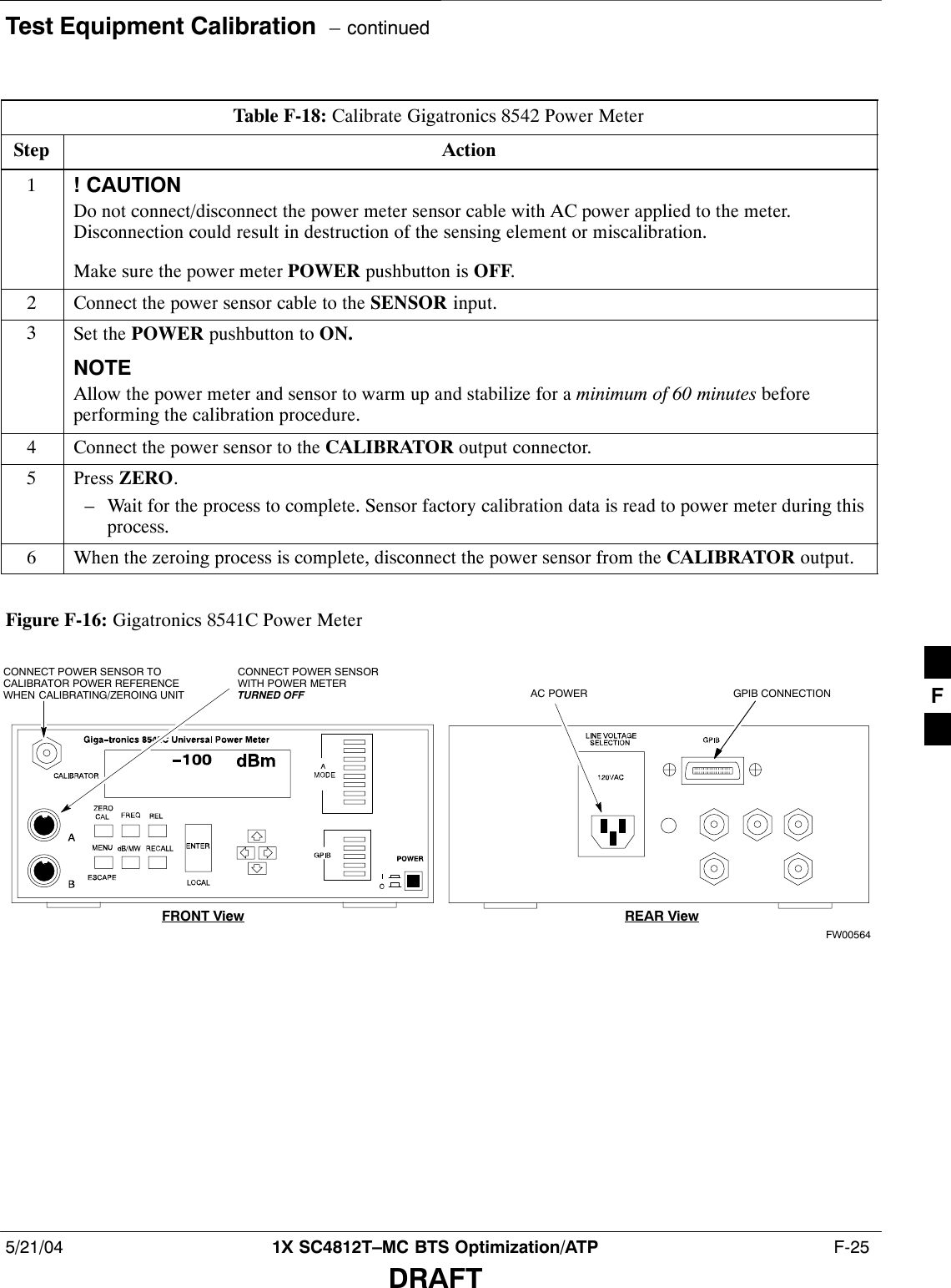
![Test Equipment Calibration – continued F-24 1X SC4812T–MC BTS Optimization/ATP 5/21/04DRAFTTable F-17: HP 437 Power Meter Calibration ProcedureStep Action6 Press [ZERO].– Display will show “Zeroing ******.”– Wait for process to complete.7Connect the power sensor to the POWER REF output.8Turn on the PWR REF by performing the following:8a – Press [SHIFT] then [’].8b – Verify that the triangular indicator (B) appears in the display above PWR REF as shown below.9Perform the following to set the REF CF%:9a – Press ([SHIFT] then [ZERO]) for CAL.9b – Enter the sensor’s REF CF% from the sensor’s decal using the arrow keys and press [ENTER].(The power meter will display ”CAL *****” for a few seconds.)NOTEIf the REF CAL FACTOR (REF CF) is not shown on the power sensor, assume it to be 100%.10 Perform the following to set the CAL FAC %:10a – Press [SHIFT] then [FREQ] for CAL FAC.10b – On the sensor’s decal, locate an approximate calibration percentage factor (CF%) at the testfrequency.10c – Enter the sensor’s calibration % (CF%) using the arrow keys and press [ENTER].–– When complete, the power meter will typically display 0.05 dBm. (Any reading between0.00 and 0.10 is normal.)11 To turn off the PWR REF, perform the following:11a – Press [SHIFT] then [’].11b – Disconnect the power sensor from the POWER REF output. Gigatronics 8542 power meter(Calibration)Precise transmit output power calibration measurements are made usinga bolometer–type broadband power meter with a sensitive power sensor.Follow the steps in Table F-18 to enter information unique to the powersensor. Refer to Figure F-16 as necessary.F](https://usermanual.wiki/Nokia-Solutions-and-Networks/T6DY1.Manual-B/User-Guide-427751-Page-275.png)


![Verify IOS Version and Install Canned Configuration – continued5/21/04 1X SC4812T–MC BTS Optimization/ATP I-23DRAFTTable I-6: BTS Router Power–up and Initial Ethernet ConfigurationStep Action4If a message similar to the following, is displayed type no and press the Enter key:Basic management setup configures only enough connectivityfor management of the system, extended setup will ask youto configure each interface on the systemWould you like to enter basic management setup? [yes/no]:A response similar to the following will be displayed:Would you like to enter basic management setup? [yes/no]: noCisco Internetwork Operating System SoftwareIOS (tm) 1900 Software (MWR1900–I–M), Version 12.2(20020127:101239Copyright (c) 1986–2002 by cisco Systems, Inc.Compiled Sun 27–Jan–02 06:08 by walrobinRouter> 5At the Router> user EXEC mode prompt, enter the following to access the privileged EXEC mode:enableA response similar to the following will be displayed:Router>enableRouter#6At the Router# privileged EXEC mode prompt, enter the following to access the configure submode:configure terminalA response similar to the following will be displayed:Router#conf tEnter configuration commands, one per line. End with CNTL/Z.Router(config)# The router is now in the global configuration mode and ready to accept configuration changes enteredfrom the keyboard.. . . continued on next pageI](https://usermanual.wiki/Nokia-Solutions-and-Networks/T6DY1.Manual-B/User-Guide-427751-Page-316.png)
![Verify IOS Version and Install Canned Configuration – continued I-28 1X SC4812T–MC BTS Optimization/ATP 5/21/04DRAFTTable I-7: Transfer Canned Configuration Files to the BTS Router Using a TFTP ServerStep Action6Direct the router to show the version information by entering the following:show versionA response similar to the following will be displayed:BTSRTR1#sh verCisco Internetwork Operating System Software IOS (tm) 1900 Software (MWR1900–I–M), Version 12.2(8)MC2a, EARLY DEPLOY-MENT RELEASE SOFTWARE (fc1)TAC Support: http://www.cisco.com/tacCopyright (c) 1986–2002 by cisco Systems, Inc.Compiled Mon 05–Aug–02 11:07 by nmasaImage text–base: 0x60008940, data–base: 0x60B54000ROM: System Bootstrap, Version 12.2(20020113:235343) [sbose–wilma 109],DEVELOPMENT SOFTWAREROM: 1900 Software (MWR1900–I–M), Version 12.2(8)MC2a, EARLY DEPLOYMENTRELEASE SOFTWARE (fc1)Router uptime is 1 minuteSystem returned to ROM by power–onSystem image file is ”slot0:mwr1900–i–mz.122–8.MC2a.bin”cisco mwr1900 (R7000) processor (revision 0.1) with 121856K/18432K bytesof memory.Processor board ID JMX0611K5TSR7000 CPU at 240Mhz, Implementation 39, Rev 3.3, 256KB L2 CacheBridging software.X.25 software, Version 3.0.0.Primary Rate ISDN software, Version 1.1.Toaster processor tmc is running.2 FastEthernet/IEEE 802.3 interface(s)2 Serial network interface(s)2 Channelized T1/PRI port(s)DRAM configuration is 64 bits wide with parity disabled.55K bytes of non–volatile configuration memory.31360K bytes of ATA Slot0 CompactFlash (Read/Write)Configuration register is 0x101BTSRTR1#7Compare the IOS filename returned in step 5 and the second line of the version information in step 6.Note the correspondence between the filename and IOS version information.* IMPORTANTMWR 1941 routers must be loaded with IOS version mwr1900–i–mz.122–8.MC2d.bin or later. Thisrouter model will not function properly with earlier IOS versions.. . . continued on next pageI](https://usermanual.wiki/Nokia-Solutions-and-Networks/T6DY1.Manual-B/User-Guide-427751-Page-321.png)
![Verify IOS Version and Install Canned Configuration – continued5/21/04 1X SC4812T–MC BTS Optimization/ATP I-29DRAFTTable I-7: Transfer Canned Configuration Files to the BTS Router Using a TFTP ServerStep Action8If the IOS filename from the CF memory card returned in step 5 is different than the filename of therequired IOS version loaded in the LMF computer default tftp directory, perform the procedure inTable I-8 to load the required version, and then return to step 9, below.9! CAUTIONThe file sequence on the CF memory card can not be verified with application programs which placethe listed file names in alphabetical order (for example, certain Unix telnet applications, Unixdirectory listing commands, and Windows file managers such as Windows Explorer). This portion ofthe procedure is intended for use only with applications, such as HyperTerminal, which do not listdirectory contents alphabetically.If the IOS version is correct and there is more than one file loaded on the CF memory card, be sure theIOS file is the first file listed in the directory content display. If it is not, perform the following:9a – Backup all files on the CF memory card to the LMF computer default tftp directory by performingsteps 3 through 10 of Table I-8.9b – Perform steps 25 through 29 of Table I-8, as applicable.9c – Type the following to delete a possible boot system line in the startup–config file, pressing theEnter key after the command and at each prompt to confirm the filename and deletion operation:del nvram:startup–configA response similar to the following will be displayed:BTSRTR1#del nvram:startup–configDelete filename [startup–config]? Delete nvram:startup–config? [confirm][OK]BTSRTR1#NOTEBe sure to include the colon (:) after nvram when typing the command.. . . continued on next pageI](https://usermanual.wiki/Nokia-Solutions-and-Networks/T6DY1.Manual-B/User-Guide-427751-Page-322.png)
![Verify IOS Version and Install Canned Configuration – continued I-30 1X SC4812T–MC BTS Optimization/ATP 5/21/04DRAFTTable I-7: Transfer Canned Configuration Files to the BTS Router Using a TFTP ServerStep Action9d – Verify the startup–config file size has been reduced to a minimum by entering the following:dir nvram:A response similar to the following will be displayed:Router#dir nvram:Directory of nvram:/ 53 –rw– 5 <no date> startup–config 54 –––– 5 <no date> private–config57336 bytes total (57274 bytes free)BTSRTR1#10 At the privileged EXEC mode prompt, enter the following:copy tftp:btsrtr_canned.color slot0:canned–configWhere color = blue or red, as applicable.A response similar to the following will be displayed:BTSRTR1#copy tftp:btsrtr_canned.blue slot0:canned–configAddress or name of remote host []?11 At the prompt for the remote host address or name, enter the IP address of the LMF computer NIC:100.100.100.1A response similar to the following will be displayed:BTSRTR1#copy tftp:btsrtr_canned.blue slot0:canned–configAddress or name of remote host []? 100.100.100.1Destination filename [canned–config]?12 At the prompt for the destination filename, press the Enter key.A response similar to the following will be displayed:BTSRTR1#copy tftp:btsrtr_canned.blue slot0:canned–configAddress or name of remote host []? 100.100.100.1Destination filename [canned–config]?Loading btsrtr_canned.blue from 100.100.100.1 (via Ethernet0/0): ![OK – 2457/4096 bytes]2457 bytes copied in 84.724 secs (29 bytes/sec)BTSRTR1#. . . continued on next pageI](https://usermanual.wiki/Nokia-Solutions-and-Networks/T6DY1.Manual-B/User-Guide-427751-Page-323.png)
![Verify IOS Version and Install Canned Configuration – continued5/21/04 1X SC4812T–MC BTS Optimization/ATP I-31DRAFTTable I-7: Transfer Canned Configuration Files to the BTS Router Using a TFTP ServerStep Action13 Verify that the canned configuration file is saved on the CF memory card by entering the following:dirA response similar to the following will be displayed:Directory of slot0:/ 1 –rw– 7051976 Mar 01 1993 00:11:34 mwr1900–i–mz.122–8.MC2a.bin 2 –rw– 2457 Mar 01 1993 00:14:48 canned–config31932416 bytes total (24877983 bytes free)BTSRTR1#14 To allow the BTS router to boot using the canned configuration, enter the following:copy canned–config startup–configA response similar to the following will be displayed:BTSRTR1#copy canned–config startDestination filename [startup–config]?15 When prompted for the destination file name, press the Enter key.A response similar to the following will be displayed:BTSRTR1#copy canned–config startDestination filename [startup–config]?2457 bytes copied in 3.52 secsBTSRTR1#16 Display and note the file size of startup–config by entering the following:dir nvram:A response similar to the following will be displayed:Directory of nvram:/ 26 –rw– 2457 <no date> startup–config 27 –––– 5 <no date> private–config29688 bytes total (24774 bytes free)BTSRTR1#. . . continued on next pageI](https://usermanual.wiki/Nokia-Solutions-and-Networks/T6DY1.Manual-B/User-Guide-427751-Page-324.png)
![Verify IOS Version and Install Canned Configuration – continued I-32 1X SC4812T–MC BTS Optimization/ATP 5/21/04DRAFTTable I-7: Transfer Canned Configuration Files to the BTS Router Using a TFTP ServerStep Action17 Scroll the HyperTerminal window back to the slot0: directory display obtained in step 13, above.18 Compare the file size of startup–config to the canned configuration file to verify the copy operation.File sizes should be the same.19 If desired, the contents of the startup–config file may be verified against the file listings at the end ofthis appendix for the blue or red canned configuration, as applicable, by entering the following:show startup–configNOTEPressing the space bar at the MORE prompt will scroll another screen–full of data. Pressing the Enterkey will scroll the screen one line at a time.20 Verify the router will boot properly on the IOS and revised startup–config files by entering thefollowing:reloadA response similar to the following will be displayed:BTSRTR1#reloadSystem configuration has been modified. Save? [yes/no]: nProceed with reload? [confirm]21 If prompted to save a modified configuration, enter n for “no,” and press the Enter key.22 When prompted to proceed with reload, press the Enter key to continue the reload operation.23 NOTEReloading the router with the revised startup–config file will change router FE port speed to 100. Ifthe router FE port speed was changed to 10 to communicate with the LMF computer NIC, thecomputer may indicate that the FE LAN connection has been lost at this point.Verify the router reboots without displaying the rommon 1 > prompt or error messages related to portconfigurations. If the router boots to the rommon prompt, proceed to the Recovery from BTS RouterBoot to rommon section of this appendix.24 Using the tagging materials, tag the router to clearly identify the installed configuration (blue(BTSRTR1) or red (BTSRTR2)).25 Remove the CF memory from the router following the procedure in Table I-13, mark the installedconfiguration (blue or red) on the card label, and install the card in the router following the procedurein Table I-14.26 If an additional router must have the canned configuration installed, perform the following:. . . continued on next pageI](https://usermanual.wiki/Nokia-Solutions-and-Networks/T6DY1.Manual-B/User-Guide-427751-Page-325.png)
![Change or Upgrade BTS Router IOS Version – continued I-36 1X SC4812T–MC BTS Optimization/ATP 5/21/04DRAFTupgrade the installed IOS version using the tftp server application, andensure the IOS file is first in the stored file sequence on the CF memorycard.Table I-8: Using a TFTP Server Application for Upgrading/Replacing Loaded IOS Version and Verifying File Sequence PositionStep Action* IMPORTANTThis procedure does not cover all aspects of BTS router operation and programming. Before performing thisprocedure, review BTS router initialization, operation, and programming information and procedures inMWR1900 Wireless Mobile Edge Router Software Configuration Guide; part number 78–13983–01. Have thispublication available for reference while performing this procedure.1This procedure assumes the LMF computer and BTS router are configured, connected, and operatingas they would be after performing the procedures in Table I-4, Table I-5, Table I-6, and steps 1 through8 of Table I-7. If necessary, perform these procedures now.2NOTEThe IOS present working directory defaults to the CF memory card (slot0:) directory unless thepresent working directory has been changed using the cd command. Determine the present workingdirectory by entering pwd. If the present working directory has been changed, enter the command cdslot0: to return to the default setting.Identify the filename of the currently loaded IOS which must be replaced by entering the following:dirA response similar to the following will be displayed:BTSRTR1#dirDirectory of slot0:/ 1 –rw– 7051844 Sep 23 2002 07:15:08 mwr1900–i–mz.07022002.bin 2 –rw– 2212 Mar 01 1993 00:11:00 canned–config31932416 bytes total (24878360 bytes free)BTSRTR1#3Begin to backup the currently installed version of the router’s IOS to the LMF computer’s default tftpdirectory by entering the following:copy old_IOS_filename tftp:Where old_IOS_filename = the filename of the IOS currently loaded on the BTS router CFmemory card.A response similar to the following will be displayed:BTSRTR1#copy mwr1900–i–mz.07022002.bin tftp:Address or name of remote host []?. . . continued on next pageI](https://usermanual.wiki/Nokia-Solutions-and-Networks/T6DY1.Manual-B/User-Guide-427751-Page-329.png)
![Change or Upgrade BTS Router IOS Version – continued5/21/04 1X SC4812T–MC BTS Optimization/ATP I-37DRAFTTable I-8: Using a TFTP Server Application for Upgrading/Replacing Loaded IOS Version and Verifying File Sequence PositionStep Action4At the remote host prompt, enter the following:100.100.100.1A response similar to the following will be displayed:Address or name of remote host []? 100.100.100.1Destination filename [mwr1900–i–mz.07022002.bin]?5If the default filename displayed in the prompt is correct, press the Enter key to accept it. If it ismissing or not correct, enter the correct filename.A response similar to the following will be displayed if the default filename is selected:Address or name of remote host []? 100.100.100.1Destination filename [mwr1900–i–mz.07022002.bin]?!!!!!!!!!!!!!!!!!!!!!!!!!!!!!!!!!!!!!!!!!!!!!!!!!!!!!!!!!!!!!!!!!!!!!!!!!!!!!!!!!!!!!!!!!!!!!!!!!!!!!!!!!!!!!!!!!!!!!!!!!!!!!!!!!!!!!!!!!!!!!!!!!!!!!!!!!!!!!!!!!!!!!!!!!!!!!!!!!!!!!!!!!!!!!!!!!!!!!!!!!!!!!!!!!!!!!!!!!!!!!!!!!!!!!!!!!!!!!!!!!!!!!!!!!!!!!!!!!!!!!!!!!!!!!!!!!!!!!!!!!!!!!!!!!!!!!!!!!!!!!!!!!!!!!!!!!!!!!!!!!!!!!!!!!!!!!!!!!!!!!!!!!!!!!!!!!!!!!!!!!!!!!!!!!!!!!!!!!!!!!!!!!!!!!!!!!!!!!!!!!!!!!!!!!!!!!!!!!!!!!!!!!!!!!!!!!!!!!!!!!!!!!!!!!!!!!!!!!!!!!!!!!!!!!!!!!!!!!!!!!!!!!!!!!!!!!!!!!!!!!!!!!!!!!!!!!!!!!!!!!!!!!!!!!!!!!!!!!!!!!!!!!!!!!!!!!!!!!!!!!!!!!!!!!!!!!!!!!!!!!!!!!!!!!!!!!!!!!!!!!!!!!!!!!!!!!!!!!!!!!!!!!!!!!!!!!!!!!!!!!!!!!!!!!!!!!!!!!!!!!!!!!!!!!!!!!!!!!!!!!!!!!!!!!!!!!!!!!!!!!!!!!!!!!!!!!!!!!!!!!!!!!!!!!!!!!!!!!!!!!!!!!!!!!!!!!!!!!!!!!!!!!!!!!!!!!!!!!!!!!!!!!!!!!!!!!!!!!!!!!!!!!!!!!!!!!!!!!!!!!!!!!!!!!!!!!!!!!!!!!!!!!!!!!!!!!!!!!!!!!!!!!!!!!!!!!!!!!!!!!!!!!!!!!!!!!!!!!!!!!!!!!!!!!!!!!!!!!!!!!!!!!!!!!!!!!!!!!!!!!!!!!!!!!!!!!!!!!!!!!!!!!!!!!!!!!!!!!!!!!!!!!!!!!!!!!!!!!!!!!!!!!!!!!!!!!!!!!!!!!!!!!!!!!!!!!!!!!!!!!!!!!!!!!!!!!!!!!!!!!!!!!!!!!!!!!!!!!!!!!!!!!!!!!!!!!!!!!!!!!!!!!!!!!!!!!!!!!!!!!!!!!!!!!!!!!!!!!!!!!!!!!!!!!!!!!!!!!!!!!!!!!!!!!!!!!!!!!!!!!!!!!!!!!!!!!!!!!!!!!!!!!!!!!!!!!!!!!!!!!!!!!!!!!!!!!!!!!!!!!!!!!!!!!!!!!!!!!!!!!!!!!!!!!!!!!!!!!!!!!!!!!!!!!!!!!!!!!!!!!!!!!!!!!!!!!!!!!!!!!!!!!!!!!!!!!!!!!!!!!!!!!!!!!!!!!!!!!!!!!!!!!!!!!!!!!!!!!!!7051844 bytes copied in 109.92 secs (64697 bytes/sec)BTSRTR1#. . . continued on next pageI](https://usermanual.wiki/Nokia-Solutions-and-Networks/T6DY1.Manual-B/User-Guide-427751-Page-330.png)
![Change or Upgrade BTS Router IOS Version – continued I-38 1X SC4812T–MC BTS Optimization/ATP 5/21/04DRAFTTable I-8: Using a TFTP Server Application for Upgrading/Replacing Loaded IOS Version and Verifying File Sequence PositionStep Action6If additional files are stored on the CF memory card, begin backing them up to the LMF computer’sdefault tftp directory by entering the following:copy additional_filename tftp:Where additional_filename = the filename of an additional file loaded on the BTS router CFmemory card.A response similar to the following will be displayed:BTSRTR1#copy canned–config tftp:Address or name of remote host [100.100.100.1]?7If the default IP address displayed in the prompt is correct, press the Enter key to accept it. If it ismissing or not correct, enter the correct IP address for the LMF computer.A response similar to the following will be displayed if the default filename is selected:Address or name of remote host [100.100.100.1]? Source filename [canned–config]?8If the default filename displayed in the prompt is correct, press the Enter key to accept it. If it ismissing or not correct, enter the correct filename.A response similar to the following will be displayed if the default filename is selected:Source filename [canned–config]? Destination filename [canned–config]?9If the default filename displayed in the prompt is correct, press the Enter key to accept it. If it ismissing or not correct, enter the correct filename.A response similar to the following will be displayed:Destination filename [canned–config]?![OK – 2212/4096 bytes]2212 bytes copied in 0.152 secsBTSRTR1#10 If more files are stored on the CF memory card, repeat steps 6 through 9 until all files have beenbacked up to the LMF computer.. . . continued on next pageI](https://usermanual.wiki/Nokia-Solutions-and-Networks/T6DY1.Manual-B/User-Guide-427751-Page-331.png)
![Change or Upgrade BTS Router IOS Version – continued5/21/04 1X SC4812T–MC BTS Optimization/ATP I-39DRAFTTable I-8: Using a TFTP Server Application for Upgrading/Replacing Loaded IOS Version and Verifying File Sequence PositionStep Action11 Delete all files from the CF memory card by entering the following command:format slot0:A response similar to the following will be displayed:BTSRTR1#format slot0:Format operation may take a while. Continue? [confirm]12 Press the Enter key to continue the format operation.A response similar to the following will be displayed:Format operation may take a while. Continue? [confirm]Format operation will destroy all data in ”slot0:”. Continue? [confirm]13 Press the Enter key to continue the format operation.A response similar to the following will be displayed:Format operation will destroy all data in ”slot0:”. Continue? [confirm]Format: Drive communication & 1st Sector Write OK...Writing Monlibsec-tors....................................................................................Monlib write complete.Format: All system sectors written. OK...Format: Total sectors in formatted partition: 62560Format: Total bytes in formatted partition: 32030720Format: Operation completed successfully.Format of slot0 completeBTSRTR1#. . . continued on next pageI](https://usermanual.wiki/Nokia-Solutions-and-Networks/T6DY1.Manual-B/User-Guide-427751-Page-332.png)
![Change or Upgrade BTS Router IOS Version – continued I-40 1X SC4812T–MC BTS Optimization/ATP 5/21/04DRAFTTable I-8: Using a TFTP Server Application for Upgrading/Replacing Loaded IOS Version and Verifying File Sequence PositionStep Action14 Verify all files have been deleted from the CF memory card by entering the following:dirA response similar to the following will be displayed:Directory of slot0:/No files in directory31932416 bytes total (31932416 bytes free)BTSRTR1#15 Begin to copy the required version of the IOS from the LMF computer to the BTS router by entering thefollowing:copy tftp:new_IOS_filename slot0:Where new_IOS_filename = the filename of the required IOS for the BTS router.A response similar to the following will be displayed:BTSRTR1#copy tftp:mwr1900–i–mz.122–8.MC2a.bin slot0:Address or name of remote host [100.100.100.1]?16 If the default IP address displayed in the prompt is correct, press the Enter key to accept it. If it ismissing or not correct, enter the correct IP address for the LMF computer.A response similar to the following will be displayed if the default filename is selected:Address or name of remote host [100.100.100.1]? Source filename [mwr1900–i–mz.122–8.MC2a.bin]?17 If the default filename displayed in the prompt is correct, press the Enter key to accept it. If it ismissing or not correct, enter the correct filename.A response similar to the following will be displayed if the default filename is selected:Source filename [mwr1900–i–mz.122–8.MC2a.bin]? Destination filename [mwr1900–i–mz.122–8.MC2a.bin]?. . . continued on next pageI](https://usermanual.wiki/Nokia-Solutions-and-Networks/T6DY1.Manual-B/User-Guide-427751-Page-333.png)
![Change or Upgrade BTS Router IOS Version – continued5/21/04 1X SC4812T–MC BTS Optimization/ATP I-41DRAFTTable I-8: Using a TFTP Server Application for Upgrading/Replacing Loaded IOS Version and Verifying File Sequence PositionStep Action18 If the default filename displayed in the prompt is correct, press the Enter key to accept it. If it is notcorrect, enter the correct filename.A response similar to the following will be displayed if the default filename is selected:Destination filename [mwr1900–i–mz.122–8.MC2a.bin]? Accessing tftp://100.100.100.1/mwr1900–i–mz.122–8.MC2a.bin...Loading mwr1900–i–mz.122–8.MC2a.bin from 100.100.100.1 (via FastEther-net0/0): !!!!Loading mwr1900–i–mz.122–8.MC2a.bin from 100.100.100.1 (via FastEther-net0/0):!!!!!!!!!!!!!!!!!!!!!!!!!!!!!!!!!!!!!!!!!!!!!!!!!!!!!!!!!!!!!!!!!!!!!!!!!!!!!!!!!!!!!!!!!!!!!!!!!!!!!!!!!!!!!!!!!!!!!!!!!!!!!!!!!!!!!!!!!!!!!!!!!!!!!!!!!!!!!!!!!!!!!!!!!!!!!!!!!!!!!!!!!!!!!!!!!!!!!!!!!!!!!!!!!!!!!!!!!!!!!!!!!!!!!!!!!!!!!!!!!!!!!!!!!!!!!!!!!!!!!!!!!!!!!!!!!!!!!!!!!!!!!!!!!!!!!!!!!!!!!!!!!!!!!!!!!!!!!!!!!!!!!!!!!!!!!!!!!!!!!!!!!!!!!!!!!!!!!!!!!!!!!!!!!!!!!!!!!!!!!!!!!!!!!!!!!!!!!!!!!!!!!!!!!!!!!!!!!!!!!!!!!!!!!!!!!!!!!!!!!!!!!!!!!!!!!!!!!!!!!!!!!!!!!!!!!!!!!!!!!!!!!!!!!!!!!!!!!!!!!!!!!!!!!!!!!!!!!!!!!!!!!!!!!!!!!!!!!!!!!!!!!!!!!!!!!!!!!!!!!!!!!!!!!!!!!!!!!!!!!!!!!!!!!!!!!!!!!!!!!!!!!!!!!!!!!!!!!!!!!!!!!!!!!!!!!!!!!!!!!!!!!!!!!!!!!!!!!!!!!!!!!!!!!!!!!!!!!!!!!!!!!!!!!!!!!!!!!!!!!!!!!!!!!!!!!!!!!!!!!!!!!!!!!!!!!!!!!!!!!!!!!!!!!!!!!!!!!!!!!!!!!!!!!!!!!!!!!!!!!!!!!!!!!!!!!!!!!!!!!!!!!!!!!!!!!!!!!!!!!!!!!!!!!!!!!!!!!!!!!!!!!!!!!!!!!!!!!!!!!!!!!!!!!!!!!!!!!!!!!!!!!!!!!!!!!!!!!!!!!!!!!!!!!!!!!!!!!!!!!!!!!!!!!!!!!!!!!!!!!!!!!!!!!!!!!!!!!!!!!!!!!!!!!!!!!!!!!!!!!!!!!!!!!!!!!!!!!!!!!!!!!!!!!!!!!!!!!!!!!!!!!!!!!!!!!!!!!!!!!!!!!!!!!!!!!!!!!!!!!!!!!!!!!!!!!!!!!!!!!!!!!!!!!!!!!!!!!!!!!!!!!!!!!!!!!!!!!!!!!!!!!!!!!!!!!!!!!!!!!!!!!!!!!!!!!!!!!!!!!!!!!!!!!!!!!!!!!!!!!!!!!!!!!!!!!!!!!!!!!!!!!!!!!!!!!!!!!!!!!!!!!!!!!!!!!!!!!!!!!!!!!!!!!!!!!!!!!!!!!!!!!!!!!!!!!!!!!!!!!!!!!!!!!!!!!!!!!!!!!!!!!!!!!!!!!!!!!!!!!!!!!!!!!!!!!!!!!!!!!!!!!!!!!!!!!!!!!!!!!!!!!!!!!!!!!!!!!![OK – 7051976/14103552 bytes]7051976 bytes copied in 145.108 secs (48634 bytes/sec)BTSRTR1#. . . continued on next pageI](https://usermanual.wiki/Nokia-Solutions-and-Networks/T6DY1.Manual-B/User-Guide-427751-Page-334.png)
![Change or Upgrade BTS Router IOS Version – continued I-42 1X SC4812T–MC BTS Optimization/ATP 5/21/04DRAFTTable I-8: Using a TFTP Server Application for Upgrading/Replacing Loaded IOS Version and Verifying File Sequence PositionStep Action19 Display the CF memory card directory to verify that the new IOS file is there by entering thefollowing:dirA response similar to the following will be displayed:BTSRTR1#dirDirectory of slot0:/ 1 –rw– 7051976 Sep 23 2002 07:25:36mwr1900–i–mz.122–8.MC2a.bin31932416 bytes total (24880440 bytes free)BTSRTR1#20 If any additional files previously stored on the CF memory card are to be copied to the card, performthe following:copy tftp:filename slot0:Where filename = the filename of the file to be copied to the CF memory cardA response similar to the following will be displayed:BTSRTR1#copy tftp:canned–config slot0:Address or name of remote host [100.100.100.1]?21 If the default IP address displayed in the prompt is correct, press the Enter key to accept it. If it ismissing or not correct, enter the correct IP address for the LMF computer.A response similar to the following will be displayed if the default IP address is selected:Address or name of remote host [100.100.100.1]? Destination filename [canned–config]? 22 If the default filename displayed in the prompt is correct, press the Enter key to accept it. If it ismissing or not correct, enter the correct filename.A response similar to the following will be displayed if the default filename is selected:Destination filename [canned–config]? Accessing tftp://100.100.100.1/canned–config...Loading basic_config from 100.100.100.1 (via FastEthernet0/0): ![OK – 2212/4096 bytes]2212 bytes copied in 0.152 secsBTSRTR1#. . . continued on next pageI](https://usermanual.wiki/Nokia-Solutions-and-Networks/T6DY1.Manual-B/User-Guide-427751-Page-335.png)
![Change or Upgrade BTS Router IOS Version – continued I-44 1X SC4812T–MC BTS Optimization/ATP 5/21/04DRAFTTable I-8: Using a TFTP Server Application for Upgrading/Replacing Loaded IOS Version and Verifying File Sequence PositionStep Action30 After making sure the IOS file is the first file on the CF memory card, restart the BTS router with thenew IOS version by entering the following:reloadA response similar to the following will be displayed:BTSRTR1#reloadSystem configuration has been modified. Save? [yes/no]: nProceed with reload? [confirm]31 If prompted to save a modified configuration, enter n for “no,” and press the Enter key.32 When prompted to proceed with reload, press the Enter key to continue the reload operation.33 Once the router has completed rebooting, change to the privileged EXEC mode and confirm thebooted IOS version is correct by entering the following:show versionA response similar to the following partial example will be displayed:BTSRTR1#sh verCisco Internetwork Operating System Software IOS (tm) 1900 Software (MWR1900–I–M), Version 12.2(8)MC2a, EARLY DEPLOY-MENT RELEASE SOFTWARE (fc1)...BTSRTR1#34 Verify the version number displayed in the second line of the version information is the correct IOSversion.35 If this procedure was entered from step 8 of Table I-7, return to Table I-7, step 9.36 If no other BTS router file operations or configuration actions are required, perform the following:36a – Remove power from the router and disconnect it from the power supply.36b – Disconnect all other cabling from the BTS router.36c – On the LMF computer, exit the HyperTerminal communications session.. . . continued on next pageI](https://usermanual.wiki/Nokia-Solutions-and-Networks/T6DY1.Manual-B/User-Guide-427751-Page-337.png)
![Verify and Upgrade ROMmon Version – continued5/21/04 1X SC4812T–MC BTS Optimization/ATP I-49DRAFTTable I-9: Verify and Upgrade/Replace Installed ROMmon Version Using a tftp ServerStep Action2Determine the currently installed ROMmon version by entering the following at the router privilegedEXEC mode prompt:show versionA response similar to the following will be displayed:BTSRTR1#sh verCisco Internetwork Operating System Software IOS (tm) 1900 Software (MWR1900–I–M), Version 12.2(8)MC2b, EARLY DEPLOY-MENT RELEASE SOFTWARE (fc3)TAC Support: http://www.cisco.com/tacCopyright (c) 1986–2002 by cisco Systems, Inc.Compiled Mon 05–Aug–02 11:07 by nmasaImage text–base: 0x60008940, data–base: 0x60B54000ROM: System Bootstrap, Version 12.2(20020113:235343) [sbose–wilma 109],DEVELOPMENT SOFTWAREROM: 1900 Software (MWR1900–I–M), Version 12.2(8)MC2b, EARLY DEPLOYMENTRELEASE SOFTWARE (fc3)Router uptime is 1 minuteSystem returned to ROM by power–onSystem image file is ”slot0:mwr1900–i–mz.122–8.MC2b.bin”cisco mwr1900 (R7000) processor (revision 0.1) with 121856K/18432K bytesof memory.Processor board ID JMX0611K5TSR7000 CPU at 240Mhz, Implementation 39, Rev 3.3, 256KB L2 CacheBridging software.X.25 software, Version 3.0.0.Primary Rate ISDN software, Version 1.1.Toaster processor tmc is running.2 FastEthernet/IEEE 802.3 interface(s)2 Serial network interface(s)2 Channelized T1/PRI port(s)DRAM configuration is 64 bits wide with parity disabled.55K bytes of non–volatile configuration memory.31360K bytes of ATA Slot0 CompactFlash (Read/Write)Configuration register is 0x101BTSRTR1#3To determine the currently installed ROMmon version, examine the ROM: System Bootstrap linein the response.. . . continued on next pageI](https://usermanual.wiki/Nokia-Solutions-and-Networks/T6DY1.Manual-B/User-Guide-427751-Page-342.png)
![Verify and Upgrade ROMmon Version – continued I-50 1X SC4812T–MC BTS Optimization/ATP 5/21/04DRAFTTable I-9: Verify and Upgrade/Replace Installed ROMmon Version Using a tftp ServerStep Action4Compare the installed ROMmon version information with the filename of the ROMmon versionrequired for the network.NOTE1. Rommon filename format is similar to the following:MWR1900_RM2.srec.122–8r.MC3.bin2. The ROMmon filename reflects the version number of the software (122–8r.MC3).5If the installed version is the one required for the network skip to step 26.6If the installed ROMmon version is not the one required for the network, backup the current BTSrouter configuration to the LMF computer by entering the following:copy nvram:startup–config tftpA response similar to the following will be displayed:BTSRTR1#copy nvram:start tftpAddress or name of remote host []?NOTEBe sure to include the colon (:) after nvram when typing the command.7At the prompt for the remote host address or name, enter the IP address of the LMF computer NIC:100.100.100.1A response similar to the following will be displayed:BTSRTR1#copy copy nvram:start tftpAddress or name of remote host []? 100.100.100.1Source filename [startup–config]?8If the default filename displayed in the prompt is correct, press the Enter key to accept it. If it ismissing or not correct, enter the correct filename.A response similar to the following will be displayed if the default filename is selected:Source filename [startup–config]? Destination filename [startup–config]?. . . continued on next pageI](https://usermanual.wiki/Nokia-Solutions-and-Networks/T6DY1.Manual-B/User-Guide-427751-Page-343.png)
![Verify and Upgrade ROMmon Version – continued5/21/04 1X SC4812T–MC BTS Optimization/ATP I-51DRAFTTable I-9: Verify and Upgrade/Replace Installed ROMmon Version Using a tftp ServerStep Action9If the default filename displayed in the prompt is correct, press the Enter key to accept it. If it ismissing or not correct, enter the correct filename.A response similar to the following will be displayed:Destination filename [startup–config]?![OK – 2212/4096 bytes]2212 bytes copied in 0.152 secsBTSRTR1#10 NOTEThe IOS defaults to the CF memory card (slot0:) directory unless the present working directory hasbeen changed using the cd command. Determine the present working directory by entering pwd. Ifthe present working directory has been changed, enter the command cd slot0: to return to the defaultsetting.Determine the amount of memory available (bytes free) on the CF memory card by entering thefollowing:dirA response similar to the following will be displayed:BTSRTR1#dirDirectory of slot0:/ 1 –rw– 7051976 Sep 23 2002 07:24:18mwr1900–i–mz.122–8.MC2b.bin 2 –rw– 2212 Mar 01 1993 00:14:48 canned–config31932416 bytes total (24885606 bytes free)Router#11 Be sure there is at least 1 MB (1048580) of free memory.NOTEA ROMmon version file requires approximately 0.7 MB.. . . continued on next pageI](https://usermanual.wiki/Nokia-Solutions-and-Networks/T6DY1.Manual-B/User-Guide-427751-Page-344.png)
![Verify and Upgrade ROMmon Version – continued I-52 1X SC4812T–MC BTS Optimization/ATP 5/21/04DRAFTTable I-9: Verify and Upgrade/Replace Installed ROMmon Version Using a tftp ServerStep Action12 Begin to copy the required version of the ROMmon file from the LMF computer to the BTS router by enter-ing the following:copy tftp:new_rommon_filename slot0:Where new_rommon_filename = the filename of the required ROMmon version for the BTSrouter.A response similar to the following will be displayed:BTSRTR1#copy tftp:MWR1900_RM2.srec.122–8r.MC3.bin slot0:Address or name of remote host [100.100.100.1]?13 If the default IP address displayed in the prompt is correct, press the Enter key to accept it. If it ismissing or not correct, enter the correct IP address for the LMF computer.A response similar to the following will be displayed if the default filename is selected:Address or name of remote host [100.100.100.1]? Source filename [MWR1900_RM2.srec.122–8r.MC3.bin]?14 If the default filename displayed in the prompt is correct, press the Enter key to accept it. If it ismissing or not correct, enter the correct filename.A response similar to the following will be displayed if the default filename is selected:Source filename [MWR1900_RM2.srec.122–8r.MC3.bin]? Destination filename [MWR1900_RM2.srec.122–8r.MC3.bin]?15 If the default filename displayed in the prompt is correct, press the Enter key to accept it. If it is notcorrect, enter the correct filename.A response similar to the following will be displayed if the default filename is selected:Destination filename [MWR1900_RM2.srec.122–8r.MC3.bin]? Accessing tftp://100.100.100.1/MWR1900_RM2.srec.122–8r.MC3.bin...Loading MWR1900_RM2.srec.122–8r.MC3.bin from 100.100.100.1 (via FastE-thernet0/0): !!!!Loading MWR1900_RM2.srec.122–8r.MC3.bin from 100.100.100.1 (via FastE-thernet0/0):!!!!!!!!!!!!!!!!!!!!!!!!!!!!!!!!!!!!!!!!!!!!!!!!!!!!!!!!!!!!!!!!!!!!!!!!!!!!!!!!!!!!!!!!!!!!!!!!!!!!!!!!!!!!!!!!!!!!!!!!!![OK – 614306/14103552 bytes]614306 bytes copied in 13.059 secs (48634 bytes/sec)BTSRTR1#. . . continued on next pageI](https://usermanual.wiki/Nokia-Solutions-and-Networks/T6DY1.Manual-B/User-Guide-427751-Page-345.png)
![Verify and Upgrade ROMmon Version – continued5/21/04 1X SC4812T–MC BTS Optimization/ATP I-53DRAFTTable I-9: Verify and Upgrade/Replace Installed ROMmon Version Using a tftp ServerStep Action16 Display the CF memory card directory to verify that the new ROMmon version file is there byentering the following:dirA response similar to the following will be displayed:BTSRTR1#dirDirectory of slot0:/ 1 –rw– 7051976 Sep 23 2002 07:25:36 mwr1900–i–mz.122–8.MC2b.bin 2 –rw– 2212 Mar 01 1993 00:09:06 canned–config 3 –rw– 614306 Dec 13 2002 14:59:36MWR1900_RM2.srec.122–8r.MC3.bin31932416 bytes total (24263922 bytes free)BTSRTR1#17 Replace the existing ROMmon version with the new one copied to the CF memory card by enteringthe following:upgrade rom–monitor file slot0:MWR1900_RM2.srec.122–8r.MC3A response similar to the following will be displayed:BTSRTR1#This command will reload the router. Continue?[yes/no]18 When prompted to continue, enter yes and press the Enter key.A response similar to the following will be displayed:BTSRTR1#This command will reload the router. Continue?[yes/no] yesROMMON image upgrade in progressErasing boot flasheeeeeeeeeeeeeeeeeeeeeeeeeeeeeeeeeeeeeeeeeeeeeeeeeeeeeeeeeeeeeeeeeeProgramming boot flash ppppNow reloading19 When the router has completed initialization, change to the router privileged EXEC mode by enteringthe following:enableA response similar to the following will be displayed:BTSRTR1>enableBTSRTR1#. . . continued on next pageI](https://usermanual.wiki/Nokia-Solutions-and-Networks/T6DY1.Manual-B/User-Guide-427751-Page-346.png)
![Verify and Upgrade ROMmon Version – continued I-54 1X SC4812T–MC BTS Optimization/ATP 5/21/04DRAFTTable I-9: Verify and Upgrade/Replace Installed ROMmon Version Using a tftp ServerStep Action20 Verify the router has initialized with the new ROMmon version by entering the following:show versionA response similar to the following partial response will be displayed:BTSRTR1#sh verCisco Internetwork Operating System Software IOS (tm) 1900 Software (MWR1900–I–M), Version 12.2(8)MC2b, EARLY DEPLOY-MENT RELEASE SOFTWARE (fc3)TAC Support: http://www.cisco.com/tacCopyright (c) 1986–2002 by cisco Systems, Inc.Compiled Mon 05–Aug–02 11:07 by nmasaImage text–base: 0x60008940, data–base: 0x60B54000ROM: System Bootstrap, Version 12.2(8r)MC3 RELEASE SOFTWARE (fc1)21 Compare the version displayed in the response ROM: System Bootstrap line to the filename of thenew ROMmon version file copied to the CF memory card.22 If the router successfully rebooted with the new ROMmon version, the ROMmon file can be deletedfrom the CF memory card by entering the following:delete slot0:new_rommon_filenameWhere new_rommon_filename = the filename of the required ROMmon version copied to the CFmemory card in steps 12 through 15, above.A response similar to the following will be displayed:BTSRTR1#del slot0:MWR1900_RM2.srec.122–8r.MC3.binDelete filename [MWR1900_RM2.srec.122–8r.MC3.bin]? 23 If the default filename displayed in the prompt is correct, press the Enter key to accept it. If it ismissing or not correct, enter the correct filename.A response similar to the following will be displayed if the default filename is selected:Delete filename [MWR1900_RM2.srec.122–8r.MC3.bin]? Delete slot0:MWR1900_RM2.srec.122–8r.MC3.bin? [confirm]. . . continued on next pageI](https://usermanual.wiki/Nokia-Solutions-and-Networks/T6DY1.Manual-B/User-Guide-427751-Page-347.png)
![Verify and Upgrade ROMmon Version – continued5/21/04 1X SC4812T–MC BTS Optimization/ATP I-55DRAFTTable I-9: Verify and Upgrade/Replace Installed ROMmon Version Using a tftp ServerStep Action24 Press the Enter key to confirm the deletion.A response similar to the following will be displayed if the default filename is selected:Delete filename [MWR1900_RM2.srec.122–8r.MC3.bin]? Delete slot0:MWR1900_RM2.srec.122–8r.MC3.bin? [confirm]BTSRTR1#25 ! CAUTIONIn this step, do not delete the IOS and canned–config files from the CF memory card. The BTSrouter must have these files on the card to properly boot or switch between packet and circuit mode.If additional unnecessary files, such as a backup of the startup–config file, are also on the CFmemory card, delete them by repeating steps 22 through 24 for each file.26 If no other BTS router file operations or configuration actions are required, perform the following:26a – Remove power from the router and disconnect it from the power supply.26b – Disconnect all cabling from the BTS router.26c – On the LMF computer, exit the HyperTerminal communications session.27 If no additional tftp transfer activities will be performed, change the NIC IP address and subnet maskback to those for LMF–BTS communication recorded in Table I-4, step 10b.! CAUTIONIf the BTS 10base–2 LAN IP address and subnet mask for the LMF computer’s NIC are not restored,the LMF can not log into a BTS when attempting to perform a BTS optimization or ATP. I](https://usermanual.wiki/Nokia-Solutions-and-Networks/T6DY1.Manual-B/User-Guide-427751-Page-348.png)
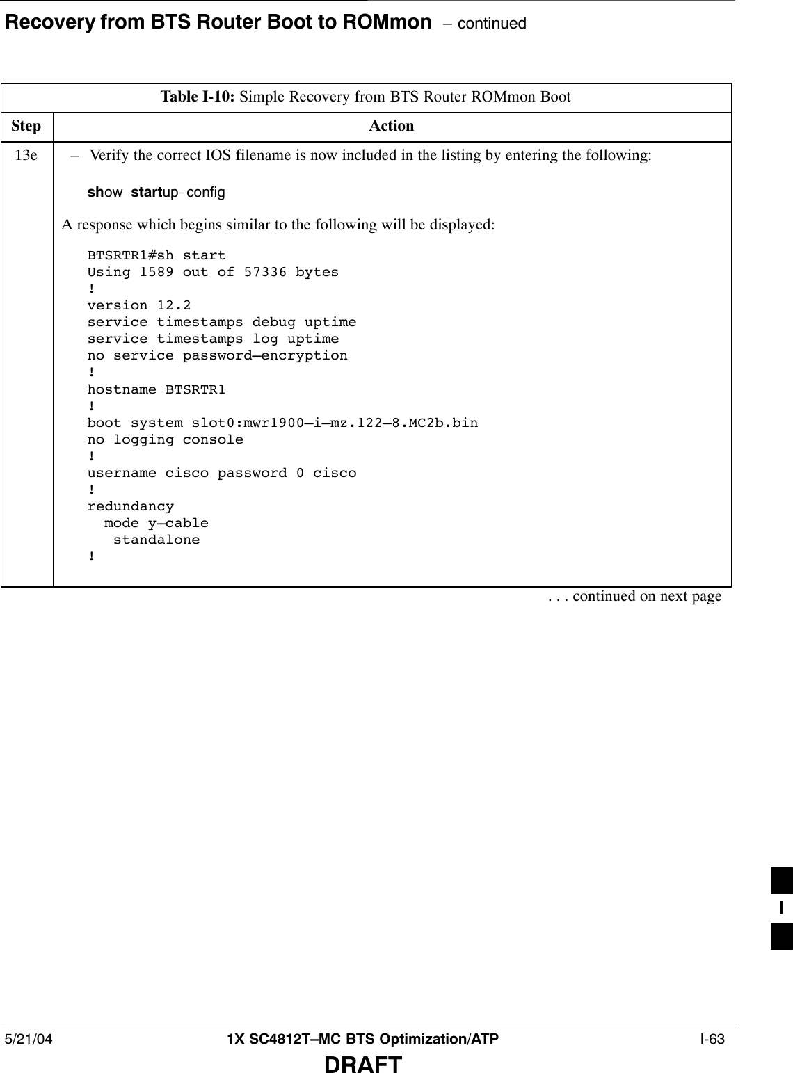
![Recovery from BTS Router Boot to ROMmon – continued5/21/04 1X SC4812T–MC BTS Optimization/ATP I-57DRAFTTable I-10: Simple Recovery from BTS Router ROMmon BootStep Action* IMPORTANTThis procedure does not cover all aspects of BTS router operation and programming. Before performing thisprocedure, review BTS router initialization, operation, and programming information and procedures inMWR1900 Wireless Mobile Edge Router Software Configuration Guide; part number 78–13983–01. Have thispublication available for reference while performing this procedure.1This procedure assumes the LMF computer is set up and connected to the BTS router with an activeHyperTerminal communication session. If it is not, follow the procedure in Table I-2 to establish aHyperTerminal communication session.2With the rommon 1 > prompt displayed in the HyperTerminal window, enter the following todetermine if the router’s configuration register is set to the factory default value:confregA response similar to the following will be displayed:rommon 4 > confreg Configuration Summary (Virtual Configuration Register: 0x100)enabled are:load rom after netboot failsconsole baud: 9600boot: image specified by the boot system commands or default to: cisco2–mwr1900do you wish to change the configuration? y/n [n]: NOTESThe configuration register setting is shown in the (Virtual Configuration Register: 0x____) lineS0x in the Virtual Configuration Register line indicates the numbers following are hexadecimal3If the value shown for the configuration register is 2102, skip to step 6.4If the value shown for the configuration register is not 2102, perform the following:4a Press the Return key to accept the default of n (for no).. . . continued on next pageI](https://usermanual.wiki/Nokia-Solutions-and-Networks/T6DY1.Manual-B/User-Guide-427751-Page-350.png)
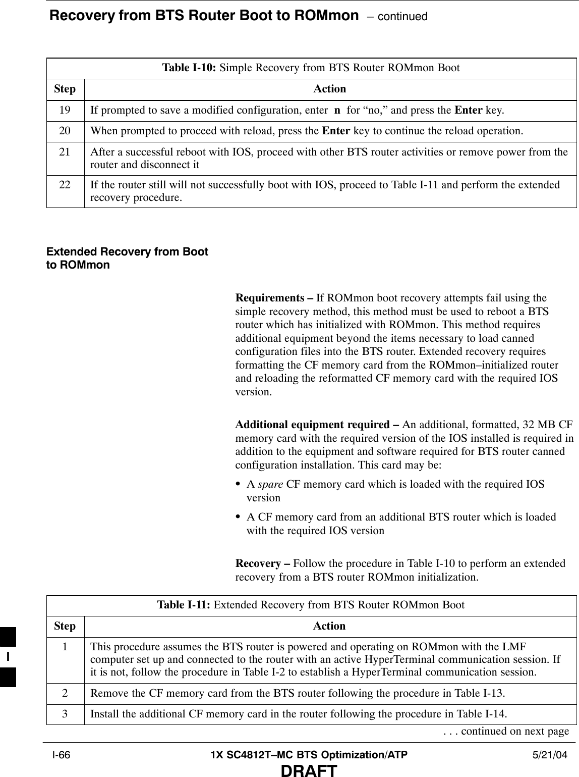
![Recovery from BTS Router Boot to ROMmon – continued I-58 1X SC4812T–MC BTS Optimization/ATP 5/21/04DRAFTTable I-10: Simple Recovery from BTS Router ROMmon BootStep Action4b Enter the following at the rommon prompt:confreg 0x2102A response similar to the following will be displayed:rommon 3 > confreg 0x2102You must reset or power cycle for new config to take effectrommon 4 >4c Enter the following at the rommon prompt:resetA response which begins and ends similar to the following will be displayed:rommon 4 > reset System Bootstrap, Version 12.2(20020113:235343) [sbose–wilma 109], DE-VELOPMENT SOFTWARECopyright (c) 1994–2002 by cisco Systems, Inc.mwr1900 processor with 131072 Kbytes of main memoryMain memory is configured to 64 bit mode with parity disabledReadonly ROMMON initialized....<output omitted>....Press RETURN to get started!5If the router reboots with the IOS, skip to step 21.. . . continued on next pageI](https://usermanual.wiki/Nokia-Solutions-and-Networks/T6DY1.Manual-B/User-Guide-427751-Page-351.png)
![Recovery from BTS Router Boot to ROMmon – continued I-60 1X SC4812T–MC BTS Optimization/ATP 5/21/04DRAFTTable I-10: Simple Recovery from BTS Router ROMmon BootStep Action8If an IOS file is found, note the IOS filename, and enter the following to begin recovery to an IOSboot:boot slot0:IOS_filenameWhere IOS_filename = the filename of the IOS noted in step 6, above.A successful IOS re–boot operation will result in display of a response which begins and ends similarto the following:rommon 2 > boot slot0:mwr1900–i–mz.122–8.MC2b.binprogram load complete, entry point: 0x80008000, size: 0xb2a0program load complete, entry point: 0x80008000, size: 0x6b99acSelf decompressing the image :################################################################### [OK]Smart Init is enabledsmart init is sizing iomem ID MEMORY_REQ TYPE00031A 0X005F3C00 MWR1900 Mainboard 0X000F3BB0 public buffer pools 0X00211000 public particle poolsTOTAL: 0X008F87B0....<output omitted>....Press RETURN to get started!9If the router successfully reboots with the IOS, skip to step 12.10 If the router does not reboot with the IOS, perform the following:10a – Scroll the HyperTerminal display down until the directory display from step 6, above, is visible.10b – Compare the IOS filename from the directory display with the filename entered when performingstep 8, above.10c – If the filename was typed incorrectly, repeat step 8, using care to type the filename correctly.. . . continued on next pageI](https://usermanual.wiki/Nokia-Solutions-and-Networks/T6DY1.Manual-B/User-Guide-427751-Page-353.png)
![Recovery from BTS Router Boot to ROMmon – continued I-64 1X SC4812T–MC BTS Optimization/ATP 5/21/04DRAFTTable I-10: Simple Recovery from BTS Router ROMmon BootStep Action14 Re–verify the router’s configuration register setting by entering the following:show versionA response similar to the following will be displayed:BTSRTR1#sh verCisco Internetwork Operating System Software IOS (tm) 1900 Software (MWR1900–I–M), Version 12.2(8)MC2b, EARLY DEPLOY-MENT RELEASE SOFTWARE (fc1)TAC Support: http://www.cisco.com/tacCopyright (c) 1986–2002 by cisco Systems, Inc.Compiled Mon 05–Aug–02 11:07 by nmasaImage text–base: 0x60008940, data–base: 0x60B54000ROM: System Bootstrap, Version 12.2(20020113:235343) [sbose–wilma 109],DEVELOPMENT SOFTWAREROM: 1900 Software (MWR1900–I–M), Version 12.2(8)MC2b, EARLY DEPLOYMENTRELEASE SOFTWARE (fc1)Router uptime is 1 minuteSystem returned to ROM by power–onSystem image file is ”slot0:mwr1900–i–mz.122–8.MC2b.bin”cisco mwr1900 (R7000) processor (revision 0.1) with 121856K/18432K bytesof memory.Processor board ID JMX0611K5TSR7000 CPU at 240Mhz, Implementation 39, Rev 3.3, 256KB L2 CacheBridging software.X.25 software, Version 3.0.0.Primary Rate ISDN software, Version 1.1.Toaster processor tmc is running.2 FastEthernet/IEEE 802.3 interface(s)2 Serial network interface(s)2 Channelized T1/PRI port(s)DRAM configuration is 64 bits wide with parity disabled.55K bytes of non–volatile configuration memory.31360K bytes of ATA Slot0 CompactFlash (Read/Write)Configuration register is 0x101BTSRTR1#NOTEThe configuration register value is shown in the last line of the show version response.15 If the value shown for the configuration register is 0x2102, skip to step 18.. . . continued on next pageI](https://usermanual.wiki/Nokia-Solutions-and-Networks/T6DY1.Manual-B/User-Guide-427751-Page-357.png)
![Recovery from BTS Router Boot to ROMmon – continued5/21/04 1X SC4812T–MC BTS Optimization/ATP I-65DRAFTTable I-10: Simple Recovery from BTS Router ROMmon BootStep Action16 If the value shown for the configuration register is not 0x2102, enter the following command in theorder shown to change it:configure terminalconfig–register 0x2102A response similar to the following will be displayed:BTSRTR1#conf tEnter configuration commands, one per line. End with CNTL/Z.BTSRTR1(config)#config–register 0x2102BTSRTR1(config)#17 Verify the change was entered properly by entering the following commands in the order shown:exitshow versionA response which begins and ends similar to the following will be displayed:BTSRTR1(config)#exitBTSRTR1#sh verCisco Internetwork Operating System Software IOS (tm) 1900 Software (MWR1900–I–M), Version 12.2(8)MC2b, EARLY DEPLOY-MENT RELEASE SOFTWARE (fc1)TAC Support: http://www.cisco.com/tacCopyright (c) 1986–2002 by cisco Systems, Inc.....<output omitted>....Configuration register is 0x101 (will be 0x2102 at next reload)BTSRTR1#18 If the filename is correctly written in the boot system line (step 13e) and the configuration register isproperly set to the factory default of 0x2102, enter the following to determine if the router will rebootto IOS:reloadA response similar to the following will be displayed:BTSRTR1#reloadSystem configuration has been modified. Save? [yes/no]: nProceed with reload? [confirm]. . . continued on next pageI](https://usermanual.wiki/Nokia-Solutions-and-Networks/T6DY1.Manual-B/User-Guide-427751-Page-358.png)
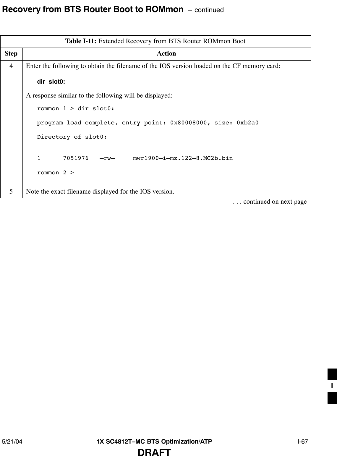
![Recovery from BTS Router Boot to ROMmon – continued I-68 1X SC4812T–MC BTS Optimization/ATP 5/21/04DRAFTTable I-11: Extended Recovery from BTS Router ROMmon BootStep Action6Enter the following to initialize the router with the IOS on the additional CF memory card:boot slot0:IOS_filenameWhere IOS_filename = the filename of the IOS noted in step 5, above.A successful IOS re–boot operation will result in display of a response which begins and ends similarto the following:rommon 2 > boot slot0:mwr1900–i–mz.122–8.MC2b.binprogram load complete, entry point: 0x80008000, size: 0xb2a0program load complete, entry point: 0x80008000, size: 0x6b99acSelf decompressing the image :################################################################### [OK]Smart Init is enabledsmart init is sizing iomem ID MEMORY_REQ TYPE00031A 0X005F3C00 MWR1900 Mainboard 0X000F3BB0 public buffer pools 0X00211000 public particle poolsTOTAL: 0X008F87B0... ––– System Configuration Dialog –––Would you like to enter the initial configuration dialog? [yes/no]: n7If the router prompts with a question to enter the initial dialog as shown in step 6, above, type no andpress the Enter key to obtain the user EXEC mode prompt.8If the router prompts with Press RETURN to get started!, press the Enter key to obtain theuser EXEC mode prompt.. . . continued on next pageI](https://usermanual.wiki/Nokia-Solutions-and-Networks/T6DY1.Manual-B/User-Guide-427751-Page-361.png)
![Recovery from BTS Router Boot to ROMmon – continued5/21/04 1X SC4812T–MC BTS Optimization/ATP I-69DRAFTTable I-11: Extended Recovery from BTS Router ROMmon BootStep Action9At the user EXEC mode prompt, enter the following to access the privileged EXEC mode:enableA response similar to the following will be displayed:Router> enableRouter#10 Remove the additional CF memory card from the BTS router following the procedure in Table I-13.11 Install the original CF memory card in the router following the procedure in Table I-14.12 Format the original CF memory card by entering the following:format slot0:A response similar to the following will be displayed:Router#format slot0:Format operation may take a while. Continue? [confirm]13 Press the Enter key to continue the format operation.A response similar to the following will be displayed:Format operation may take a while. Continue? [confirm]Format operation will destroy all data in ”slot0:”. Continue? [confirm]. . . continued on next pageI](https://usermanual.wiki/Nokia-Solutions-and-Networks/T6DY1.Manual-B/User-Guide-427751-Page-362.png)
![Recovery from BTS Router Boot to ROMmon – continued I-70 1X SC4812T–MC BTS Optimization/ATP 5/21/04DRAFTTable I-11: Extended Recovery from BTS Router ROMmon BootStep Action14 Press the Enter key to continue the format operation.A response similar to the following will be displayed:Format operation will destroy all data in ”slot0:”. Continue? [confirm]Format: Drive communication & 1st Sector Write OK...Writing Monlibsec-tors....................................................................................Monlib write complete.Format: All system sectors written. OK...Format: Total sectors in formatted partition: 62560Format: Total bytes in formatted partition: 32030720Format: Operation completed successfully.Format of slot0 completeRouter#15 Copy the required IOS version to the formatted original CF memory card using the LMF computerand a tftp server following the procedure in Table I-8.16 If applicable, perform IOS initialization troubleshooting as described in Table I-10, steps 12 through21. I](https://usermanual.wiki/Nokia-Solutions-and-Networks/T6DY1.Manual-B/User-Guide-427751-Page-363.png)
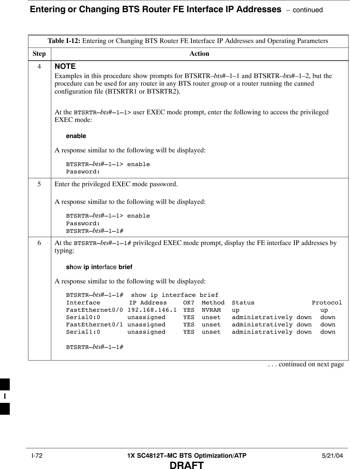
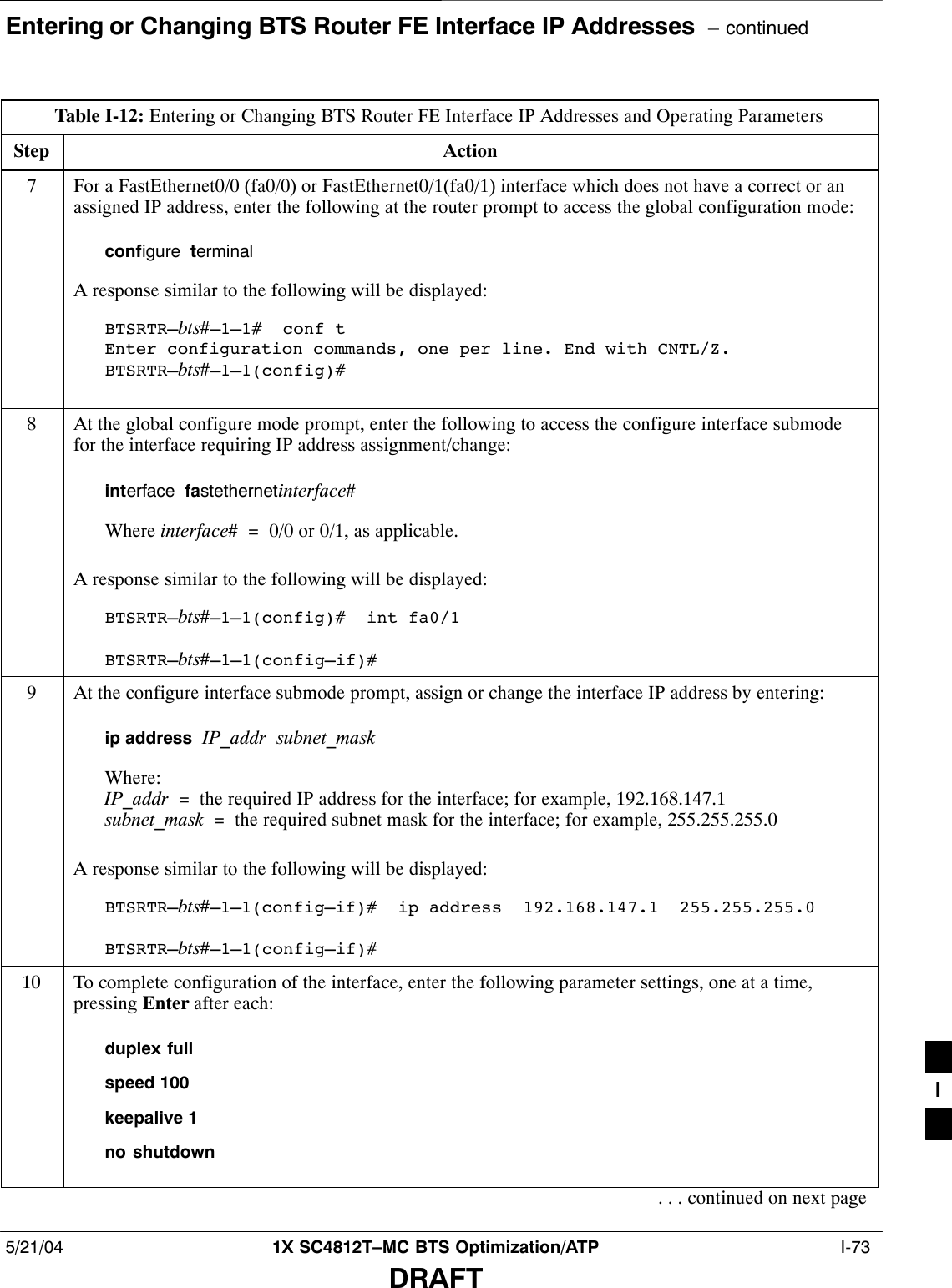
![Entering or Changing BTS Router FE Interface IP Addresses – continued I-74 1X SC4812T–MC BTS Optimization/ATP 5/21/04DRAFTTable I-12: Entering or Changing BTS Router FE Interface IP Addresses and Operating ParametersStep Action11 Return to the global configuration mode by entering the following:exitA response similar to the following will be displayed:BTSRTR–bts#–1–1(config–if)# exitBTSRTR–bts#–1–1(config)#12 If the IP address and/or parameters for the other FE interface on the router must be assigned orchanged at this time, repeat steps 8 through 11 for the other FE interface.13 Once the correct parameters have been set for all FE interfaces, return to the privileged EXEC modeprompt by holding down the Ctrl key and pressing z (Ctrl +z).A response similar to the following will be displayed:BTSRTR–bts#–1–1(config–if)# ^z01:11:27: %SYS–5–CONFIG_I: Configured from console by consoleBTSRTR–bts#–1–1# NOTEEntering exit twice, pressing the Enter key after each entry, will also complete the interfaceconfiguration and return the router to the privileged EXEC mode.14 Save the interface configuration changes to the startup configuration file on the CF memory card byentering the following:copy running–config startup–configA response similar to the following will be displayed:BTSRTR–bts#–1–1# copy run startBTSRTR–bts#–1–1# Destination filename [startup–config]?15 Press EnterA response similar to the following will be displayed:BTSRTR–bts#–1–1# copy run startBTSRTR–bts#–1–1# Destination filename [startup–config]?Building configuration...!!!!!!!!!!!!!!!!!!!!!!!!!!!!!!!!!!!!!!!!!!!!!!!!!!!!!!!!!!!!!!!!!!!!!!!!!!!!!!!!!![OK]BTSRTR–bts#–1–1# . . . continued on next pageI](https://usermanual.wiki/Nokia-Solutions-and-Networks/T6DY1.Manual-B/User-Guide-427751-Page-367.png)