Nokia Solutions and Networks T6DY1 SC4812T-MC 1X/1X-DO @ 1.9GHz User Manual 1
Nokia Solutions and Networks SC4812T-MC 1X/1X-DO @ 1.9GHz 1
Contents
- 1. Manual A
- 2. Manual B
Manual B
BTS Equipment Identification – continued
1-38 1X SC4812T–MC BTS Optimization/ATP 5/21/04
DRAFT
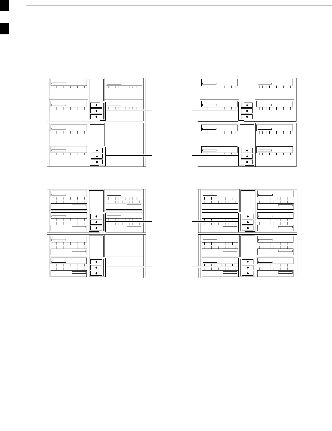
NOTE 1. Figure 1-17 identifies which BBXs are used for Omni and
2-Sector configurations.
2. The fourth PA quadrant (quadrant D) is populated with
CLPAs only when the 4x4 ETM is used.
3. PHYSICAL APPEARANCE OF FRAMES: The physical
appearance of the frame, especially the location of the
MCM, Power Amplifier cage, and Power
Distribution/Combiner cage, and the particular I/O plate
used, may differ on frames converted from early version
SC4812T BTSs. Functionally however, and for the purpose
of optimization and acceptance testing, those frames are
identical
4. For an SC4812T BTS frame which has been converted to
multicarrier capability, a fourth three–sector carrier, using
BBX–10 through BBX–12, is supported in R16.4 and later
software releases. In a converted multicarrier frame, PA slot
4 in all PA quadrants should never be populated. (see
Figure 1-21).
Figure 1-18: BBXs Used for Omni and Two–Sector Operation
BBX–1
BBX–4
BBX–R
BBX–7
BBX–10
BBX–1
BBX–2
BBX–4
BBX–5
BBX–R
BBX–7
BBX–8
BBX–10
BBX–11
C–CCP (Omni) C–CCP (2 Sector)
1
BTS Equipment Identification – continued
5/21/04 1X SC4812T–MC BTS Optimization/ATP 1-39
DRAFT
Figure 1-19: TX Filter and 50Ω Termination Requirements for Omni, Two–sector, and Three–sector
Configurations – OEM Multicarrier and Converted Multicarrier Frames (Minimum Power Configuration
Shown)
MCM
1
S1
S2
S3
CLPA
CLPACLPA
1C
1A 1B
Omni
MCM
1
S1
S2
S3
CLPA CLPA
CLPACLPA
1C 1D
1A 1B
Two–Sector
Three–Sector
TX FILTERS
TX FILTER
50W
TERMINATORS
TX FILTERS
50W
TERMINATOR
MCM
1
S1
S2
S3
CLPA
CLPACLPA
1C
1A 1B
1
BTS Equipment Identification – continued
1-40 1X SC4812T–MC BTS Optimization/ATP 5/21/04
DRAFT
Figure 1-20: Omni, Two–sector, and Three–sector PA Configurations – OEM Multicarrier Frame
MCM
1
S1
S2
S3
CLPA
CLPACLPA
1C
1A 1B
Minimum Power Configuration
3 x 3 ETM
MCM
1
S1
S2
S3
CLPA CLPA
CLPACLPA
1C 1D
1A 1B
Minimum Power Configuration
4 x 4 ETM
MCM
1
S1
S2
S3
CLPA
CLPA
CLPA
CLPA
CLPA CLPA
CLPACLPA
1C
2C
3C
4C
3A
2A
1A 1B
2B
3B
4B 4A
CLPA
CLPA
CLPA
CLPA
Maximum Power Configuration
3 x 3 ETM
MCM
1
S1
S2
S3
CLPA
CLPA
CLPA
CLPA
CLPA
CLPA
CLPA
CLPA
CLPA
CLPA
CLPACLPA
1C
2C
3C
4C
1D
2D
3D
4D
3A
2A
1A 1B
2B
3B
4B 4A
CLPA
CLPA
CLPA
CLPA
Maximum Power Configuration
4 x 4 ETM
50 W
TERMINATIONS
and/or
TX Filters
(See NO TAG)
50 W
TERMINATIONS
and/or
TX Filters
(See NO TAG)
50 W
TERMINATIONS
and/or
TX Filters
(See NO TAG)
50 W
TERMINATIONS
and/or
TX Filters
(See NO TAG)
50 W
TERMINATIONS
and/or
TX Filters
(See NO TAG)
50 W
TERMINATIONS
and/or
TX Filters
(See NO TAG)
1
BTS Equipment Identification – continued
5/21/04 1X SC4812T–MC BTS Optimization/ATP 1-41
DRAFT
Figure 1-21: Omni, Two–sector, and Three–sector PA Configurations – Converted Multicarrier Frame
MCM
1
S1
S2
S3
CLPA
CLPACLPA
1C
1A 1B
Minimum Power Configuration
3 x 3 ETM
MCM
1
S1
S2
S3
CLPA CLPA
CLPACLPA
1C 1D
1A 1B
Minimum Power Configuration
4 x 4 ETM
MCM
1
S1
S2
S3
CLPA
CLPA
CLPA
CLPA CLPA
CLPACLPA
1C
2C
3C
3A
2A
1A 1B
2B
3B
CLPA
CLPA
Maximum Power Configuration
3 x 3 ETM
MCM
1
S1
S2
S3
CLPA
CLPA
CLPA
CLPA
CLPA
CLPA
CLPA
CLPA
CLPACLPA
1C
2C
3C
1D
2D
3D
3A
2A
1A 1B
2B
3B
CLPA
CLPA
Maximum Power Configuration
4 x 4 ETM
50 W
TERMINATIONS
and/or
TX Filters
(See NO TAG)
50 W
TERMINATIONS
and/or
TX Filters
(See NO TAG)
50 W
TERMINATIONS
and/or
TX Filters
(See NO TAG)
50 W
TERMINATIONS
and/or
TX Filters
(See NO TAG)
50 W
TERMINATIONS
and/or
TX Filters
(See NO TAG)
50 W
TERMINATIONS
and/or
TX Filters
(See NO TAG)
1
BTS Equipment Identification – continued
1-42 1X SC4812T–MC BTS Optimization/ATP 5/21/04
DRAFT
Figure 1-22: Six–sector PA Configurations – OEM Multicarrier Frames Only
S4
MCM
1
S5
S6
S1
S2
S3
MCM
2
CLPA
CLPA
CLPA CLPA
CLPACLPA
1C
3C
3A
1A 1B
3B
S4
MCM
1
S5
S6
S1
S2
S3
MCM
2
CLPA
CLPA
CLPA
CLPA
CLPA
CLPA
CLPACLPA
1C
3C
1D
3D
3A
1A 1B
3B
Minimum Power Configuration
3 x 3 ETM
Minimum Power Configuration
4 x 4 ETM
TX FILTERS
TX FILTERS
S4
MCM
1
S5
S6
S1
S2
S3
MCM
2
CLPA
CLPA
CLPA
CLPA
CLPA CLPA
CLPACLPA
1C
2C
3C
4C
3A
2A
1A 1B
2B
3B
4B 4A
CLPA
CLPA
CLPA
CLPA
Maximum Power Configuration
3 x 3 ETM
S4
MCM
1
S5
S6
S1
S2
S3
MCM
2
CLPA
CLPA
CLPA
CLPA
CLPA
CLPA
CLPA
CLPA
CLPA
CLPA
CLPACLPA
1C
2C
3C
4C
1D
2D
3D
4D
3A
2A
1A 1B
2B
3B
4B 4A
CLPA
CLPA
CLPA
CLPA
Maximum Power Configuration
4 x 4 ETM
TX FILTERS
TX FILTERS
1

5/21/04 1X SC4812T–MC BTS Optimization/ATP
DRAFT
Chapter 2: Preliminary Operations
Table of Contents
Guide Book 1–2. . . . . . . . . . . . . . . . . . . . . . . . . . . . . . . . . . . . . . . . . . . . . . . . . . . . .
Document Overview 1–2. . . . . . . . . . . . . . . . . . . . . . . . . . . . . . . . . . . . . . . . . . . . . .
What Is In This Guide? 1–2. . . . . . . . . . . . . . . . . . . . . . . . . . . . . . . . . . . . .
Book Catalogs and Organization 1–3. . . . . . . . . . . . . . . . . . . . . . . . . . . . . . . . . . . .
Book Directory 1–3. . . . . . . . . . . . . . . . . . . . . . . . . . . . . . . . . . . . . . . . . . .
Special Catalogs 1–5. . . . . . . . . . . . . . . . . . . . . . . . . . . . . . . . . . . . . . . . . . .
Physical Page Layouts 1–6. . . . . . . . . . . . . . . . . . . . . . . . . . . . . . . . . . . . . . . . . . . .
A/A4 Page and Margin Sizes 1–6. . . . . . . . . . . . . . . . . . . . . . . . . . . . . . . . .
A/A4 Page Text Area 1–7. . . . . . . . . . . . . . . . . . . . . . . . . . . . . . . . . . . . . . .
A/A4 Page Components 1–9. . . . . . . . . . . . . . . . . . . . . . . . . . . . . . . . . . . .
Frame and Table Components 1–10. . . . . . . . . . . . . . . . . . . . . . . . . . . . . . . . . . . . . .
Frames With Tools 1–10. . . . . . . . . . . . . . . . . . . . . . . . . . . . . . . . . . . . . . . . .
Flow Charts and Block Diagrams 1–10. . . . . . . . . . . . . . . . . . . . . . . . . . . . .
Line Drawings 1–11. . . . . . . . . . . . . . . . . . . . . . . . . . . . . . . . . . . . . . . . . . . .
Table Types In This Template 1–12. . . . . . . . . . . . . . . . . . . . . . . . . . . . . . . .
Item/Description Table 1–12. . . . . . . . . . . . . . . . . . . . . . . . . . . . . . . . . . . . .
Step Table 1–13. . . . . . . . . . . . . . . . . . . . . . . . . . . . . . . . . . . . . . . . . . . . . . .
Step/Check Table 1–14. . . . . . . . . . . . . . . . . . . . . . . . . . . . . . . . . . . . . . . . . .
Component Descriptions 1–15. . . . . . . . . . . . . . . . . . . . . . . . . . . . . . . . . . . . . . . . . .
Conclusions 1–16. . . . . . . . . . . . . . . . . . . . . . . . . . . . . . . . . . . . . . . . . . . . . . . . . . . . .
Map Title Goes Here lkjsfdg Sfdkgj Msfd N lkas K lkjsdfl kB lkj fgcb 1–17. . . . . .
Block Label Goes Here 1–17. . . . . . . . . . . . . . . . . . . . . . . . . . . . . . . . . . . . .
Block Label Goes Here 1–17. . . . . . . . . . . . . . . . . . . . . . . . . . . . . . . . . . . . .
Block Label Goes Here 1–18. . . . . . . . . . . . . . . . . . . . . . . . . . . . . . . . . . . . .
Block Label Goes Here 1–19. . . . . . . . . . . . . . . . . . . . . . . . . . . . . . . . . . . . .
Map Title Goes Here 1–22. . . . . . . . . . . . . . . . . . . . . . . . . . . . . . . . . . . . . . . . . . . . . .
2

Table of Contents – continued
1X SC4812T–MC BTS Optimization/ATP 5/21/04
DRAFT
Notes
2

Overview
5/21/04 1X SC4812T–MC BTS Optimization/ATP 2-1
DRAFT
Introduction
This section first verifies proper frame equipage. This includes verifying
module placement, jumper, and dual in–line package (DIP) switch
settings against the site-specific documentation supplied for each BTS
application. Next, pre-power up and initial power-up procedures are
presented.
Cell Site Types
Sites are configured as Omni with a maximum of 4 carriers, 3–sectored
with a maximum of 4 carriers, and 6–sectored with a maximum of 2
carriers. Each type has unique characteristics and must be optimized
accordingly. For more information on the differences in site types, please
refer to the 1X SC 4812T-MC BTS Hardware Installation manual.
CDF or NEC
The Configuration Data File (CDF) (circuit BTS) or Network Element
Configuration (NEC) files (packet BTS) contains site type and equipage
data information and passes it directly to the LMF during optimization.
The number of modem frames, C–CCP shelves, BBX boards, MCC
boards (per cage), and power amplifier assignments are some of the
equipage data included in the CDF or NEC files.
Be sure that the correct bts–#.cdf and cbsc–#.cdf or
NECB*bts#.xml and NECJ*bts#.xml files are used for
the BTS. These should be the CDF or NEC files that are
provided for the BTS by the OMC–R. Failure to use the
correct CDF or NEC files can cause system errors. Failure
to use the correct CDF or NEC files to log into a live
(traffic carrying) site can shut down the site.
CAUTION
Site Equipage Verification
Review the site documentation. Match the site engineering equipage data
to the actual boards and modules shipped to the site. Physically inspect
and verify the equipment provided for the BTS or Modem frame and
ancillary equipment frame.
Always wear a conductive, high impedance wrist strap
while handling any circuit card/module to prevent damage
by ESD. After removal, the card/module should be placed
on a conductive surface or back into the anti–static
shipping bag.
CAUTION
2

Overview – continued
2-2 1X SC4812T–MC BTS Optimization/ATP 5/21/04
DRAFT
Initial Installation of
Boards/Modules
Follow the procedure in Table 2-1 to verify the initial installation of
boards/modules.
Table 2-1: Initial Installation of Boards/Modules
Step Action
1Refer to the site documentation and install all boards and modules into the appropriate shelves as
required. Verify they are NOT SEATED at this time.
NOTE
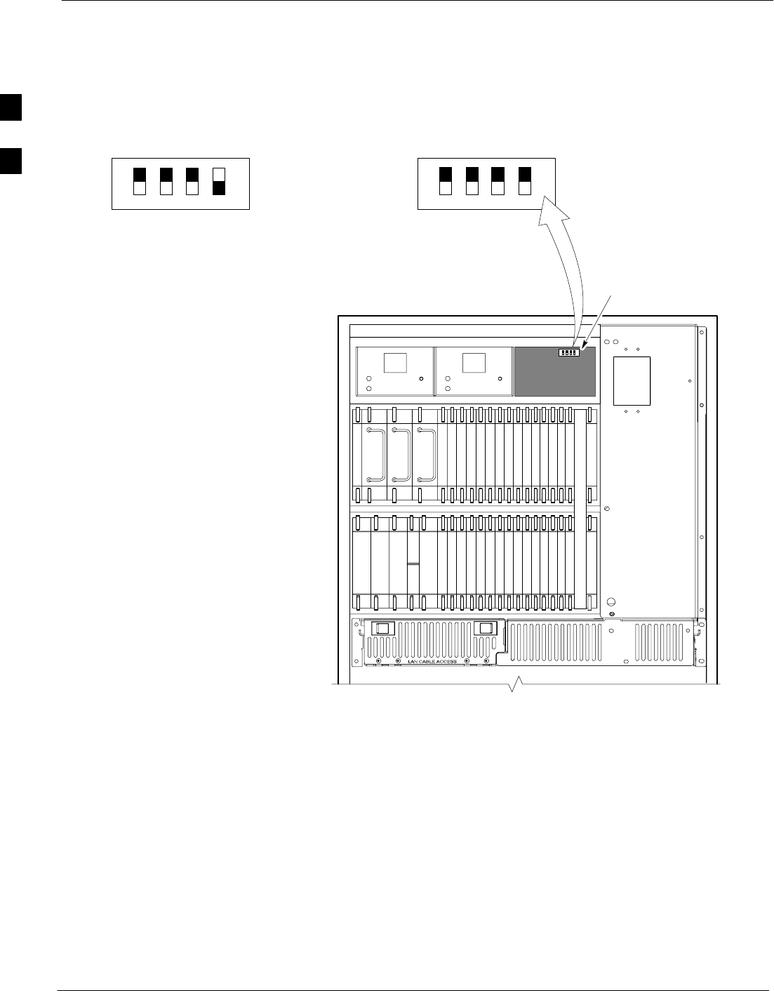
The Switch Card has a configuration switch that must match the site configuration (see Figure 2-1).
2As the actual site hardware is installed, record the serial number of each module on a “Serial Number
Checklist” in the site logbook.
Configuration Switch in Figure 2-1 shown for 3 Sector
Multicarrier BTS. (Switches 1 and 4 control configuration)
For Multicarrier, switch 1 should be Down; switch 4
depends on whether the frame supports 3 or 6 sector.
NOTE
2
Overview – continued
5/21/04 1X SC4812T–MC BTS Optimization/ATP 2-3
DRAFT
Figure 2-1: Switch Card
ti-CDMA-WP-00039-v01-ildoc-ftw
Switch Card
1234
ON
BTS
MF
3 Sector
6 Sector
J1
J2
J3
J4
J5
SHIELDS
Configuration
Switch
Setting Frame C–CCP Shelf
Configuration Switch
The backplane switch settings behind the fan module nearest the breaker
panel should be set as shown in Figure 2-2.
The switch setting must be verified and set before power is applied to the
BTS equipment.
SStarter Frame – all dip switches set to ON (UP)
SExpansion Frame – all dip switches ON (UP) except
MODEM_FRAME_ID_0 OFF (DOWN)
2
Overview – continued
2-4 1X SC4812T–MC BTS Optimization/ATP 5/21/04
DRAFT
Figure 2-2: Backplane DIP Switch Settings
19 mm Filter Panel
Power Supply
AMR / MACH
HSO
CSM
CSM
39 mm Filter Panel
AMR / MACH
GLI–1GLI–2
MCC–6
BBX–1
BBX–2
BBX–3
BBX–4
BBX–5
BBX–6
BBX–R
Switch
MPCMPC
MCIO
BBX–7
BBX–8
BBX–9
BBX–10
BBX–11
BBX–12
MCC–5
MCC–4
MCC–3
MCC–2
MCC–1
MCC–12
MCC–11
MCC–10
MCC–9
MCC–8
MCC–7
Power Supply
Power Supply
CCD CCD
ON
OFF
SC 4812T C–CCP SHELF
FAN MODULE
REMOVED
STARTER
FRAME
SETTING
ON
ALL SWITCHES ON (UP) EXCEPT MO-
DEM_FRAME_ID_0 OFF (DOWN)
EXPANSION
FRAME
SETTING
BOTTOM / TOP
RIGHT / LEFT
MODEM_FRAME_ID_1
MODEM_FRAME_ID_0
BOTTOM / TOP
RIGHT / LEFT
MODEM_FRAME_ID_1
MODEM_FRAME_ID_0
ti-CDMA-WP-00211-v01-ildoc-ftw REF
SPEED
CONTROLLED
FA N
MODULE
REAR
FRONT
PWR/ALM
SPEED
CONTROLLED
FA N
MODULE
REAR
FRONT
PWR/ALM
ALL SWITCHES ON (UP)
OFF
2
Pre–Power Up Tests
5/21/04 1X SC4812T–MC BTS Optimization/ATP 2-1
DRAFT
Objective
This procedure checks for any electrical short circuits and verifies the
operation and tolerances of the cellsite and BTS power supply units prior
to applying power for the first time.
Test Equipment
The following test equipment is required to complete the pre–power–up
tests:
SDigital Multimeter (DMM)
Always wear a conductive, high impedance wrist strap
while handling the any circuit card/module to prevent
damage by ESD.
CAUTION
Cabling Inspection
Using the site-specific documentation generated by Motorola Systems
Engineering, verify that the following cable systems are properly
connected:
SReceive RF cabling – up to 12 RX cables
STransmit RF cabling – up to six TX cables
SGPS
DC Power Pre-test (BTS Frame)
Before applying any power to the BTS frame, follow the procedure in
Table 2-2 while referring to Figure 2-3 to verify there are no shorts in the
BTS frame DC distribution system.
Table 2-2: DC Power Pre–test (BTS Frame)
Step Action
1Physically verify that all DC power sources supplying power to the frame are OFF or disabled.
2On each frame:
SUnseat all circuit boards (except CCD and CIO cards) in the C–CCP shelf and LPA shelves, but
leave them in their associated slots.
SSet C–CCP shelf breakers to the OFF position by pulling out power distribution breakers (labeled
C–CCP 1, 2, 3) located on the power distribution panel.
SSet LPA breakers to the OFF position by pulling out the LPA breakers (8 breakers, labeled 1A–1B
through 4C–4D) located on the power distribution panel.
Continue with Step 3 for –48 V or Step 4 for +27 V.
. . . continued on next page
2

Pre–Power Up Tests – continued
2-2 1X SC4812T–MC BTS Optimization/ATP 5/21/04
DRAFT
Table 2-2: DC Power Pre–test (BTS Frame)
Step Action
3For –48 V configurations ONLY:
Verify the resistance on the –48 V bus:
– Remove the Power Supply Modules (PSMs).
– Verify that the resistance from the power (–) feed terminal with respect to the ground terminal on
the top of the frame measures > 500 Ω (see Figure 2-3).
Verify the resistance on the +27 V bus:
– Remove PSM#1 or the filler panel.
! CAUTION
Do not put probes inside Elcon connectors.
– Place the Digital Multimeter probes on the mounting screws on the Elcon connector (bottom two
Elcon connectors).
– If reading is < 500 Ω, a short may exist somewhere in the DC distribution path supplied by the
breaker. Isolate the problem before proceeding. A reading > 3 MΩ could indicate an open (or
missing) bleeder resistor (installed across the filter capacitors behind the breaker panel).
4For +27 V configurations ONLY:
Verify that the resistance from the power (+ or –) feed terminals with respect to the ground terminal on
the top of the frame measures > 500 Ω (see Figure 2-3).
– If reading is < 500 Ω, a short may exist somewhere in the DC distribution path supplied by the
breaker. Isolate the problem before proceeding. A reading > 3 MΩ could indicate an open (or
missing) bleeder resistor (installed across the filter capacitors behind the breaker panel).
5Set the C–CCP breakers to the ON position by pushing them IN one at a time. Repeat Step 3 (for
–48 V) or Step 4 (for +27 V) after turning on each breaker.
NOTE
If the multimeter stays at 0 Ω after inserting any board/module, a short probably exists in that
board/module. Replace the suspect board/module and repeat the test. If test still fails, isolate the
problem before proceeding.
6Insert and lock the DC/DC converter modules for the C–CCP shelf and into their associated slots one
at a time. Repeat Step 3 (for –48 V) or Step 4 (for +27 V) after inserting each module.
– A typical response is that the ohmmeter steadily climbs in resistance as capacitors charge, finally
indicating approximately 500 Ω.
! CAUTION
Verify the correct power/converter modules by observing the locking/retracting tabs appear as follows:
STPN4009B
PWR C–CCP 4812 +27V
7Insert and lock all remaining circuit boards and modules into their associated slots in the C–CCP shelf.
Repeat Step 3 (for –48 V) or Step 4 (for +27 V) after inserting and locking each board or module.
– A typical response is that the ohmmeter steadily climbs in resistance as capacitors charge,
stopping at approximately 500 Ω..
. . . continued on next page
2

Pre–Power Up Tests – continued
5/21/04 1X SC4812T–MC BTS Optimization/ATP 2-3
DRAFT
Table 2-2: DC Power Pre–test (BTS Frame)
Step Action
8Set the LPA breakers ON by pushing them in. Repeat Step 3 (for –48 V) or Step 4 (for +27 V) after
turning on each breaker.
– A typical response is that the ohmmeter will steadily climb in resistance as capacitors charge,
stopping at approximately 500 Ω..
NOTE
Engage circuit breakers only for LPAs that are equipped.
9In the –48V BTS, insert PSMs one at a time in their associated slots, verifying that LED is green.
Repeat Step 3 after inserting each module.
10 Seat all LPA and associated LPA fan modules into their associated slots in the shelves one at a time.
Repeat Step 3 (for –48 V) or Step 4 (for +27 V) after seating each LPA and associated LPA fan
module.
SA typical response is that the ohmmeter will steadily climb in resistance as capacitors charge,
stopping at approximately 500 Ω..
2
Pre–Power Up Tests – continued
2-4 1X SC4812T–MC BTS Optimization/ATP 5/21/04
DRAFT
Figure 2-3: +27V Breaker Panel (–48V is similar)
GND
L
P
A
C
C
C
P
2A
4A
2B
4B
2C
4C
2D
4D
1A
3A
1B
3B
1C
3C
1D
3D
50
1
2
3
50 50 50 50 50 50 50 50 50 50
INPUT
TOP OF FRAME
FILLER
ti-CDMA-WP-00224-v01-ildoc-ftw
PLATE
DC FILTER
CONNECTOR/
DC FILTER 1 DC FILTER 2
2
Initial Power Up Tests & Procedures
5/21/04 1X SC4812T–MC BTS Optimization/ATP 2-5
DRAFT
Power-up Procedures
Potentially lethal voltage and current levels are routed to
the BTS equipment. This test must be performed with a
second person present, acting in a safety role. Remove all
rings, jewelry, and wrist watches prior to beginning this
test.
WARNING
DC Input Power
In the tests to follow, power will first be verified at the input to each
BTS frame. After power is verified, cards and modules within the frame
itself will be powered up and verified one at a time.
Before applying any power, verify the correct power feed and return
cables are connected between the power supply breakers and the power
connectors at the top of each BTS frame. Verify correct cable position
referring to Figure 2-3.
NOTE For positive power applications (+27 V):
SThe positive power cable is red.
SThe negative power cable is black.
For negative power applications (–48 V):
SThe negative power cable is red or blue.
SThe positive power cable (ground) is black.
Motorola recommends that the DC input power cable used to connect the
frame to the main DC power source conforms to the guidelines outlined
in Table 2-3.
Table 2-3: DC Input Power Cable Guidelines
Maximum Cable Length Wire Size
30.38 m (100 ft) 107 mm2 (AWG #4/0)
54.864 m (180 ft) 185 mm2 (350 kcmil)
Greater that 54.864 m (180 ft) Not recommended
Make sure the connector adapters are securely attached to
each of the BTS power feeds and returns. Also, make sure
the cables have been properly installed into each
connector.
NOTE
2

Initial Power Up Tests & Procedures – continued
2-6 1X SC4812T–MC BTS Optimization/ATP 5/21/04
DRAFT
Common Power Supply
Verification
The procedure in Table 2-4 must be performed on any BTS frame
connected to a common power supply at the site after the common power
supply has been installed and verified per the power supply OEM
suggested procedures.
Perform the following steps to verify the power input is within
specification before powering up the individual cards/modules with the
frames themselves.
While handling any circuit card/module, always wear a
conductive, high impedance wrist strap to prevent
damage by ESD. Extreme care should be taken during the
removal and installation of any card/module. After
removal, the card/module should be placed on a conductive
surface or back into the anti–static bag in which it was
shipped.
CAUTION
Table 2-4: Common Power Supply Verification
Step Action
1Physically verify that all DC power sources supplying the frame are OFF or disabled.
2On each frame:
SUnseat all circuit boards (except CCD and CIO cards) in the C–CCP shelf and LPA shelves, but
leave them in their associated slots.
SSet breakers to the OFF position by pulling out C–CCP and LPA breakers (see Figure 2-3 for
breaker panel layout if required).
– C–CCP shelf breakers are labeled CCCP–1, 2, 3.
– LPA breakers are labeled 1A–1B through 4C–4D.
3On –48 V BTS: Remove the –48 V to +27 V Power Supply Modules.
4Inspect input cables, verify correct input power polarity via decal on top of frame.
5Apply power to BTS frames, one at a time, by setting the appropriate breaker in the power supply that
supplies the frame to the ON position.
6After power is applied to each frame, use a digital voltmeter to verify power supply output voltages at
the top of each BTS frame are within specifications:
On –48 V BTS: –48 Vdc nominal
On +27 V BTS: +27 Vdc nominal
7On –48 V BTS: Plug in PSMs one at a time and verify ’Green’ LEDs on PSMs light.
Initial Power-up (BTS)
The procedure must be performed on each frame after input power from
the common power supply has been verified. Follow the steps in
Table 2-5 to apply initial power to the cards/modules within the frame
itself, verifying that each is operating within specification.
2

Initial Power Up Tests & Procedures – continued
5/21/04 1X SC4812T–MC BTS Optimization/ATP 2-7
DRAFT
Table 2-5: Initial Power–up (BTS)
Step Action
1At the BTS, set the C–CCP (POWER) power distribution breakers (see Figure 2-3) to the ON position
by pushing in the breakers.
2Insert the C–CCP fan modules. Observe that the fan modules come on line.
3! CAUTION
Verify the correct C–CCP power supplies by observing the locking/retracting tabs appear as follows:
Insert and lock the power supplies into their associated slots one at a time.
•If no boards have been inserted, all three PWR/ALM LEDs would indicate RED to notify the user
that there is no load on the power supplies.
– If the LED is RED, do not be alarmed. After Step 4 is performed, the LEDs should turn GREEN;
if not, then a faulty power supply is indicated and should be replaced before proceeding.
STPN 4009B
PWR C–CCP 4812 +27V
4Seat and lock all remaining circuit cards and modules in the C–CCP shelf into their associated slots.
5Seat the first equipped PA module pair into the assigned slot in the upper PA shelf including PA fan.
6Repeat Step 5 for all remaining PAs.
NOTE
Engage circuit breakers only for PAs that are equipped.
7Set the PA breakers to the ON position (per configuration) by pushing them IN. See NO TAG for
breaker panel layout.
Engage (push) PA circuit breakers.
SConfirm LEDs on PAs light.
8After all cards/modules have been seated and verified, use a digital voltmeter to verify power supply
output voltages at the top of the frame remain within specifications:
On –48 V BTS: –48 Vdc nominal
On +27 V BTS: +27 Vdc nominal
9Repeat Steps 1 through 8 for additional co–located frames (if equipped).
2

Initial Power Up Tests & Procedures – continued
2-8 1X SC4812T–MC BTS Optimization/ATP 5/21/04
DRAFT
Notes
2

5/21/04 1X SC4812T–MC BTS Optimization/ATP
DRAFT
Chapter 3: Optimization and Calibration
Table of Contents
Guide Book 1–2. . . . . . . . . . . . . . . . . . . . . . . . . . . . . . . . . . . . . . . . . . . . . . . . . . . . .
Document Overview 1–2. . . . . . . . . . . . . . . . . . . . . . . . . . . . . . . . . . . . . . . . . . . . . .
What Is In This Guide? 1–2. . . . . . . . . . . . . . . . . . . . . . . . . . . . . . . . . . . . .
Book Catalogs and Organization 1–3. . . . . . . . . . . . . . . . . . . . . . . . . . . . . . . . . . . .
Book Directory 1–3. . . . . . . . . . . . . . . . . . . . . . . . . . . . . . . . . . . . . . . . . . .
Special Catalogs 1–5. . . . . . . . . . . . . . . . . . . . . . . . . . . . . . . . . . . . . . . . . . .
Physical Page Layouts 1–6. . . . . . . . . . . . . . . . . . . . . . . . . . . . . . . . . . . . . . . . . . . .
A/A4 Page and Margin Sizes 1–6. . . . . . . . . . . . . . . . . . . . . . . . . . . . . . . . .
A/A4 Page Text Area 1–7. . . . . . . . . . . . . . . . . . . . . . . . . . . . . . . . . . . . . . .
A/A4 Page Components 1–9. . . . . . . . . . . . . . . . . . . . . . . . . . . . . . . . . . . .
Frame and Table Components 1–10. . . . . . . . . . . . . . . . . . . . . . . . . . . . . . . . . . . . . .
Frames With Tools 1–10. . . . . . . . . . . . . . . . . . . . . . . . . . . . . . . . . . . . . . . . .
Flow Charts and Block Diagrams 1–10. . . . . . . . . . . . . . . . . . . . . . . . . . . . .
Line Drawings 1–11. . . . . . . . . . . . . . . . . . . . . . . . . . . . . . . . . . . . . . . . . . . .
Table Types In This Template 1–12. . . . . . . . . . . . . . . . . . . . . . . . . . . . . . . .
Item/Description Table 1–12. . . . . . . . . . . . . . . . . . . . . . . . . . . . . . . . . . . . .
Step Table 1–13. . . . . . . . . . . . . . . . . . . . . . . . . . . . . . . . . . . . . . . . . . . . . . .
Step/Check Table 1–14. . . . . . . . . . . . . . . . . . . . . . . . . . . . . . . . . . . . . . . . . .
Component Descriptions 1–15. . . . . . . . . . . . . . . . . . . . . . . . . . . . . . . . . . . . . . . . . .
Conclusions 1–16. . . . . . . . . . . . . . . . . . . . . . . . . . . . . . . . . . . . . . . . . . . . . . . . . . . . .
Map Title Goes Here lkjsfdg Sfdkgj Msfd N lkas K lkjsdfl kB lkj fgcb 1–17. . . . . .
Block Label Goes Here 1–17. . . . . . . . . . . . . . . . . . . . . . . . . . . . . . . . . . . . .
Block Label Goes Here 1–17. . . . . . . . . . . . . . . . . . . . . . . . . . . . . . . . . . . . .
Block Label Goes Here 1–18. . . . . . . . . . . . . . . . . . . . . . . . . . . . . . . . . . . . .
Block Label Goes Here 1–19. . . . . . . . . . . . . . . . . . . . . . . . . . . . . . . . . . . . .
Map Title Goes Here 1–22. . . . . . . . . . . . . . . . . . . . . . . . . . . . . . . . . . . . . . . . . . . . . .
3

Table of Contents – continued
1X SC4812T–MC BTS Optimization/ATP 5/21/04
DRAFT
Notes
3

Introduction to Optimization & Calibration
5/21/04 1X SC4812T–MC BTS Optimization/ATP 3-1
DRAFT
Overview
This section describes procedures for isolating the BTS from the span
lines, preparing and using the LMF, downloading system operating
software, CSM reference verification/optimization, set up and calibration
of the supported test equipment, transmit/receive path verification, and
verifying the customer defined alarms and relay contacts are functioning
properly.
Before using the LMF, use an editor to view the
“CAVEATS” section in the “readme.txt” file in the c:\wlmf
folder for any applicable information.
NOTE
Optimization Process
Summary
After a BTS is physically installed and the preliminary operations, such
as power up, have been completed, the LMF is used to optimize the
BTS. The basic optimization process consists of the following:
1. Download MGLI–1 with code and data and then enable MGLI–1.
GLIs may be GLI2s or GLI3s.
NOTE
2. Use the status function and verify that all of the installed devices of
the following types respond with status information: CSM, BBX,
GLI, and MCC. If a device is installed and powered up but is not
responding and is colored gray in the BTS display, the device is not
listed in the CDF or NEC files. The CDF or NEC files must be
corrected before the device can be accessed by the LMF.
3. Download code and data to all devices of the following types:
– CSM
– BBX (multicarrier uses BBX–1X)
– GLI (other than MGLI–1)
– MCC (may be MCC–8E, MCC24, or MCC–1X)
4. Verify the operation of the GPS and HSO signals.
5. Enable the following devices (in the order listed):
– Secondary CSM
– Primary CSM
– All MCCs
6. Connect the required test equipment for a full optimization.
7. Select the test equipment.
3

Introduction to Optimization & Calibration – continued
3-2 1X SC4812T–MC BTS Optimization/ATP 5/21/04
DRAFT
8. Calibrate the TX and RX test cables if they have not previously been
calibrated using the CDMA LMF that will be used for the
optimization/calibration. The cable calibration values can also be
entered manually.
All PAs must be INS during any TX testing.
NOTE
9. If the TX calibration fails, repeat the optimization for any failed
paths.
10. If the TX calibration fails again, correct the problem that caused the
failure and repeat the optimization for the failed path.
11. If the TX calibration and audit portion of the optimization passes for
a path but some of the TX or RX tests fail, correct the problem that
caused the failure and run the individual tests as required until all
TX and RX tests have passed for all paths.
Cell Site Types
Sites are configured as Omni/Omni or Sector/Sector (TX/RX). Each type
has unique characteristics and must be optimized accordingly.
For more information on the differences in site types, refer
to the applicable BTS Hardware Installation manual.
NOTE
Configuration Files
The Configuration Data File (CDF) and the Network Element
Configuration (NEC) files contain information that defines the BTS and
data used to download files to the devices. The BTS CDF (bts–#.cdf)
and CBSC CDF (cbsc–#.cdf) files are used by circuit BTSs. The NEC
Base (NECB – NECB*bts#.xml) and NEC Journaling (NECJ –
NECJ*bts#.xml) files are used by packet BTSs. CDF or NEC files
must be placed in the applicable BTS folder before the LMF can be used
to log into that BTS. CDF and NEC files are normally obtained from the
CBSC using a floppy disk. A file transfer protocol (ftp) method can be
used if the LMF computer has that capability.
The CDF and NEC files include the following information:
SDownload instructions and protocol
SSite specific equipage information
SC–CCP shelf allocation plan
– BBX equipage (based on cell–site type) including redundancy
– CSM equipage including redundancy
– MCC (MCC24E, MCC8E, or MCC–1X) channel element allocation
plan. This plan indicates how the C–CCP shelf is configured, and
how the paging, synchronization, traffic, and access channel
elements (and associated gain values) are assigned among the (up to
12) MCCs in the shelf.
3
Introduction to Optimization & Calibration – continued
5/21/04 1X SC4812T–MC BTS Optimization/ATP 3-3
DRAFT
SCSM equipage including redundancy
SEffective Rated Power (ERP) table for all TX channels to antennas
respectively. Motorola System Engineering specifies the ERP of a
transmit antenna based on site geography, antenna placement, and
government regulations. Working from this ERP requirement, the
antenna gain, (dependent on the units of measurement specified) and
antenna feed line loss can be combined to determine the required
power at the top of the BTS frame. The corresponding BBX output
level required to achieve that power level on any channel/sector can
also be determined.
Refer to the LMF Help function on–line documentation for
additional information on the layout of the LMF directory
structure (including CDF or NEC file locations and
formats).
NOTE
BTS System Software
Download
BTS system software must be successfully downloaded to the BTS
processor boards before optimization can be performed. BTS operating
code is loaded from the LMF computer terminal.
Before using the LMF for optimization/ATP, the correct
bts–#.cdf and cbsc–#.cdf or NECB*bts#.xml and
NECJ*bts#.xml files for the BTS must be obtained from
the OMC–R and put in a bts–# folder in the LMF. Failure
to use the correct CDF or NEC files can cause improper or
unpredictable BTS operation. Failure to use the correct
CDF or NEC files to log into a live (traffic carrying) site
can shut down the site.
CAUTION
The CDF or NEC files are normally obtained from the OMC–R on a
DOS formatted diskette, or through a file transfer protocol (ftp) if the
LMF computer has ftp capability. Refer to the LMF Help function
on–line documentation for the procedure.
Site Equipage Verification
If it has not already done, use an editor to view the CDF or NEC files,
and review the site documentation. Verify the site engineering equipage
data in the CDF or NEC files matches the actual site hardware using a
CDF or NEC file conversion table.
3

Introduction to Optimization & Calibration – continued
3-4 1X SC4812T–MC BTS Optimization/ATP 5/21/04
DRAFT
Use extreme care not to make any changes to the CDF or
NEC file content while viewing the file. Changes to the
CDF or NEC file can cause the site to operate unreliably or
render it incapable of operation.
CAUTION
Always wear an approved anti–static wrist strap while
handling any circuit card/module to prevent damage by
ESD. Extreme care should be taken during the removal and
installation of any card/module. After removal, the
card/module should be placed on a conductive surface or
back into the anti–static container in which it was shipped.
CAUTION
3

Preparing the LMF
5/21/04 1X SC4812T–MC BTS Optimization/ATP 3-5
DRAFT
Overview
Before optimization can be performed, the LMF application software
must be installed and configured on a computer platform meeting
Motorola–specified requirements (see Recommended Test Equipment
and Software in Chapter 1).
Software and files for installation and updating of the LMF are provided
on CD ROM disks. The following installation items must be available:
SLMF Program on CD ROM (see page NO TAG for current supported
version of LMF)
SCDF or NEC files for each supported BTS (on diskette or available
from the CBSC)
SCBSC CDF file for each supported circuit BTS (on diskette or
available from the CBSC)
The following section provides information and instructions for
installing and updating the LMF software and files.
Overview of Packet BTS files
R16.0 and earlier software releases used the CDF configuration file for
each BTS and CBSC supported by the LMF. In a packet BTS operating
with Software Release 16.1 or later, the CDF is replaced by the NEC
files. There are two NEC files. These are:
SNEC Base (NECB) file
SNEC Journal (NECJ) file
The NECB contains the baseline configuration information and is
analogous to the CDF, while the NECJ contains all the changes made to
the configuration since the last time the NECB was re–generated. Once
the NECJ reaches 80% of its maximum size, the NECB is re–generated
by the OMC–R, and all updates from the NECJ file are rolled into it.
The NEC files play much more extensive role than the previously–used
CDF files.
Additional important, LMF–related facts about the the NEC files are:
SBoth files (NECB and NECJ) are in eXtensible Markup Language
(XML) format.
SNECB contains all the up-to-date static configuration information and
NECJ contains all the recent changes (including operations) which are
not updated in the NECB.
SBoth files can be viewed in any XML viewer (most easily available is
Internet Explorer V5.0 and higher). They can be also viewed by any
other word or text processor, but the XML tags will also be seen when
using these types of applications.
SThese files will be created by OMC–R from MIB and reflect the BTS
provisioning.
SThese files will be regenerated for each software release upgrade on
the system for each BTS.
3

Preparing the LMF – continued
3-6 1X SC4812T–MC BTS Optimization/ATP 5/21/04
DRAFT
SUnlike the CDF file, the NEC files will reside on both OMC–R and
GLI3s operating in packet mode. The NEC files will be synchronized
periodically between the OMC–R and GLI3s in each BTS.
SBoth the NECB and NECJ files contain a “SoftwareVersion” field in
their header section indicating the system release version of these
files.
SInstead of the bts–#.cdf file, the packet LMF uses
NECB*bts#.xml and NECJ*bts#.xml files, which are copies of the
NEC files.
SA GLI3 operating in packet mode will need the NECB and NECJ files
for site initialization.
SThe scope of the NEC files has grown much broader than that of the
CDF and has much more BTS–centric information. This is principally
because the role of the GLI card has expanded significantly with the
introduction of the GLI3 card and packet backhaul.
CAUTION Never use a generic NEC file. The specific, site–unique
information for the BTS must be included in the NEC file for the
site to operate properly.
LMF File Structure Overview
The LMF uses a <x>:\lmf home directory> folder that contains all of the
essential data for installing and maintaining the BTS. The following list
outlines the folder structure for LMF. Except for the bts–# folders, these
folders are created as part of the the LMF installation. Refer to the
CDMA LMF Operator’s Guide for a complete description of the folder
structure.
Figure 3-1: LMF Folder Structure
version folder (A separate folder is
required for each different version; for
example, a folder name 2.8.1.1.1.5.)
loads folder
(C:)
x:\<lmf home directory> folder
cdma folder
code folder
data folder
bts–# folders (A separate folder is required
for each BTS where bts–# is the unique BTS
number; for example, bts–163.)
3

Preparing the LMF – continued
5/21/04 1X SC4812T–MC BTS Optimization/ATP 3-7
DRAFT
The “loads” folder and all the folders below it are not
available from the LMF for Software Release R2.16.4.1.
These folders may be present as as a legacy from previous
software versions or downloaded from the CBSC/OMC–R.
Any existing code in the directory is not affected by an SR
16.1 installation.
The user will need to manually add the directories to a
newly installed LMF when they add the code loads to be
downloaded.
NOTE
LMF Home Directory
The CDMA LMF installation program creates the default home
directory, c:\wlmf, and installs the application files and subdirectories
(folders) in it. Because this can be changed at installation, the CDMA
LMF home directory will be referred to with the generic convention of:
<x>:\<lmf home directory>
Where:
<x> = the LMF computer drive letter where the CDMA LMF home
directory is located.
<lmf home directory> = the directory path or name where the CDMA
LMF is installed.
Filename Conventions and
Directory Location
NEC Files
The naming conventions for the NECB and NECJ files are:
NECB*bts#.xml
NECJ*bts#.xmlNECJ*bts#.xml
Where:
* = any characters can be substituted
# = the actual integer BTS number; for example,
NECB–2.16.4.1.40–bts480.xml
The NECB and its corresponding NECJ must have the exact same name,
except for the “B” and “J” after the initial NEC characters.
The NECB and the NECJ must reside in the
<LMF_HOME>\cdma\bts–# directory for the BTS to which they apply.
Load Information File (LIF)
The LIF contains all the devices binaries available for the specified
System Software Release. It is the functional equivalent of the Object
List File (OLF) file that was used pre–Packet.
3

Preparing the LMF – continued
3-8 1X SC4812T–MC BTS Optimization/ATP 5/21/04
DRAFT
The naming convention for the LIF is:
NE_LIF.xml
The LIF must reside in the <LMF_HOME>\cdma\loads\<Software
Release Number> directory, where <LMF_HOME> = the home
directory in which the LMF is installed, usually C:\wlmf <Software
Release Number> = the System Software Release Number (e.g.
2.16.1.0.10).
Cal File
The Cal File still resides in the <LMF_HOME>\cdma\bts–# directory
and is named bts–#.cal, where # is the actual integer number of the
BTS.
LMF Operating System
Installation
This section provides information and instructions for installing and
updating the LMF software and files.
NOTE First Time Installation Sequence:
1. Install Java Runtime Environment (JRE)
2. Install U/WIN K–shell emulator
3. Install LMF application programs
4. Install/create BTS folders
NOTE Any time U/WIN is installed, the LMF application software
must also be installed. This is because the LMF application
installation modifies some of the files that are installed during
the U/Win installation. These modifications are necessary for
proper LMF operation. Installing U/Win over–writes these
modifications.
There are multiple binary image packages for installation on the
CD–ROM. When prompted, choose the load that corresponds to
the software release currently installed in the network. Perform
the Device Images installation after the LMF installation.
If applicable, a separate CD ROM of BTS Binaries may be
available for binary updates.
Follow the procedure in Table 3-1 to install the LMF application
program using the LMF CD ROM.
Table 3-1: LMF Application Program Installation
nStep Action
1Insert the LMF Program CD ROM into the LMF CD
ROM drive.
1a – If the Setup screen appears, follow the instructions
displayed on the screen.
. . . continued on next page
3

Preparing the LMF – continued
5/21/04 1X SC4812T–MC BTS Optimization/ATP 3-9
DRAFT
Table 3-1: LMF Application Program Installation
nActionStep
1b – If the Setup screen is not displayed, proceed to Step
2.
2Click on the Start button.
3 Select Run.
4 Enter d:\autorun In the Open box and click OK.
NOTE
If applicable, replace the letter d with the correct
CD ROM drive letter.
Copy BTS and CBSC CDF or
NEC Files to the LMF Computer
Before logging on to a BTS with the LMF computer to execute
optimization/ATP procedures, the correct bts–#.cdf and cbsc–#.cdf
or NECB*bts#.xml and NECJ*bts#.xml files must be obtained from the
CBSC and put in a bts-# folder in the LMF computer. This requires
creating versions of the CBSC CDF files on a DOS–formatted floppy
diskette and using the diskette to install the CDF or NEC files on the
LMF computer.
NOTE – If the LMF has ftp capability, the ftp method can be used to
copy the CDF files from the CBSC.
– On Sun OS workstations, the unix2dos command can be
used in place of the cp command (for example,
unix2dos bts–248.cdf bts–248.cdf). This should be done
using a copy of the CBSC CDF file so the original CBSC
CDF file is not changed to DOS format.
NOTE When copying CDF or NEC files, comply with the following to
prevent BTS login problems with the LMF:
– The numbers used in the bts–#.cdf and cbsc–#.cdf or
NECB*bts#.xml and NECJ*bts#.xml filenames must
correspond to the locally assigned numbers for each BTS
and its controlling CBSC.
– The generic cbsc–1.cdf file supplied with the LMF
works with locally numbered circuit BTS CDF files. Using
this file will not provide a valid optimization unless the
generic file is edited to replace default parameters (for
example, channel numbers and corresponding set power
out) with the operational parameters used locally.
The procedure in Table 3-2 lists the steps required to transfer the CDF or
NEC files from the CBSC to the LMF computer. For further
information, refer to the LMF Help function on line documentation.
3

Preparing the LMF – continued
3-10 1X SC4812T–MC BTS Optimization/ATP 5/21/04
DRAFT
Table 3-2: Copying CBSC CDF or NEC Files to the LMF
nStep Action
AT THE CBSC:
1Login to the CBSC workstation.
2Insert a DOS formatted diskette in the workstation drive.
3 Type eject –q and press the <Enter> key.
4 Type mount and press the <Enter> key.
NOTE
SLook for the “floppy/no_name” message on the last line displayed.
SIf the eject command was previously entered, floppy/no_name will be appended with a
number. Use the explicit floppy/no_name reference displayed when performing step 7.
5Change to the directory containing the file by typing cd <directory name> (ex. cd
bts–248) and pressing <Enter>.
6 Type ls <Enter> to display the list of files in the directory.
7 With Solaris versions of Unix, create DOS–formatted versions of the bts–#.cdf and cbsc–#.cdf or
NECB*bts#.xml and NECJ*bts#.xml files on the diskette by entering the following command:
unix2dos <source filename> /floppy/no_name/<target filename>
For example, unix2dos bts–248.cdf or NECB–2.16.4.41–bts248.xml /floppy/
no_name/bts–248.cdf.
NOTE
SOther versions of Unix do not support the unix2dos and dos2unix commands. In these cases,
use the Unix cp (copy) command. The copied files will be difficult to read with a DOS or
Windows text editor because Unix files do not contain line feed characters. Editing copied CDF
or NEC files on the LMF computer is, therefore, not recommended.
SUsing cp, multiple files can be copied in one operation by separating each filename to be copied
with a space and ensuring the destination directory (floppy/no_name) is listed at the end of the
command string following a space (for example,
cp bts–248.cdf cbsc–6.cdf /floppy/no_name).
8Repeat steps 5 through 7 for each bts–# that must be supported by the LMF.
9When all required files have been copied to the diskette, type eject and press the <Enter> key.
10 Remove the diskette from the CBSC.
AT THE LMF:
11 Start the Windows operating system.
12 Insert the diskette into the LMF.
. . . continued on next page
3

Preparing the LMF – continued
5/21/04 1X SC4812T–MC BTS Optimization/ATP 3-11
DRAFT
Table 3-2: Copying CBSC CDF or NEC Files to the LMF
nActionStep
13 Using Windows Explorer (or equivalent program), create a corresponding bts–# folder in the
<lmf home directory>\cdma directory for each bts–#.cdf and cbsc–#.cdf or NECB*bts#.xml
and NECJ*bts#.xml file pair copied from the CBSC.
14 Use Windows Explorer (or equivalent program) to transfer the bts–#.cdf and cbsc–#.cdf or
NECB*bts#.xml and NECJ*bts#.xml files from the diskette to the corresponding
<lmf home directory>\cdma\bts–# folders created in step 13.
Creating a Named
HyperTerminal Connection for
MMI Sessions
Confirming or changing the configuration data of certain BTS Field
Replaceable Units (FRUs) requires establishing an MMI communication
session between the LMF and the FRU. Using features of the Windows
operating system, the connection properties for an MMI session can be
saved on the LMF computer as a named Windows HyperTerminal
connection. This eliminates the need for setting up connection
parameters each time an MMI session is required to support
optimization.
Once the named connection is saved, a shortcut for it can be created on
the Windows desktop. Double clicking the shortcut icon will start the
connection without the need to negotiate multiple menu levels.
Follow the procedure in Table 3-3 to establish a named HyperTerminal
connection and create a WIndows desktop shortcut for it.
Table 3-3: Creating a Named HyperTerminal Connection for MMI Sessions
Step Action
1From the Windows Start menu, select:
Programs>Accessories
2 Select Communications, double click the Hyperterminal folder, and then double click on the
Hyperterm.exe icon in the window that opens.
NOTE
SIf a Location Information Window appears, enter the required information, then click Close.
(This is required the first time, even if a modem is not to be used.)
SIf a You need to install a modem..... message appears, click NO.
3When the Connection Description box opens:
– Type a name for the connection being defined (for example, MMI Session) in the Name: window.
– Highlight any icon preferred for the named connection in the Icon: chooser window.
– Click OK.
. . . continued on next page
3

Preparing the LMF – continued
3-12 1X SC4812T–MC BTS Optimization/ATP 5/21/04
DRAFT
Table 3-3: Creating a Named HyperTerminal Connection for MMI Sessions
Step Action
4
NOTE
For LMF configurations where COM1 is used by another interface such as test equipment and a
physical port is available for COM2, select COM2 to prevent conflicts.
From the Connect using: pick list in the Connect To box displayed, select the RS–232 port to be used
for the connection (e.g., COM1 or COM2 (Win NT) – or Direct to Com 1 or Direct to Com 2 (Win
98), and click OK.
5In the Port Settings tab of the COM# Properties window displayed, configure the RS–232 port
settings as follows:
SBits per second: 9600
SData bits: 8
SParity: None
SStop bits: 1
SFlow control: None
6 Click OK.
7Save the defined connection by selecting:
File>Save
8Close the HyperTerminal window by selecting:
File>Exit
9 Click Yes to disconnect when prompted.
10 Perform one of the following:
SIf the Hyperterminal folder window is still open (Win 98) proceed to step 12
SFrom the Windows Start menu, select Programs > Accessories
11 Perform one of the following:
SFor Win NT, select Hyperterminal and release any pressed mouse buttons.
SFor Win 98, select Communications and double click the Hyperterminal folder.
12 Highlight the newly created connection icon by moving the cursor over it (Win NT) or clicking on it
(Win 98).
13 Right click and drag the highlighted connection icon to the Windows desktop and release the right
mouse button.
14 From the pop–up menu displayed, select Create Shortcut(s) Here.
15 If desired, reposition the shortcut icon for the new connection by dragging it to another location on the
Windows desktop.
3

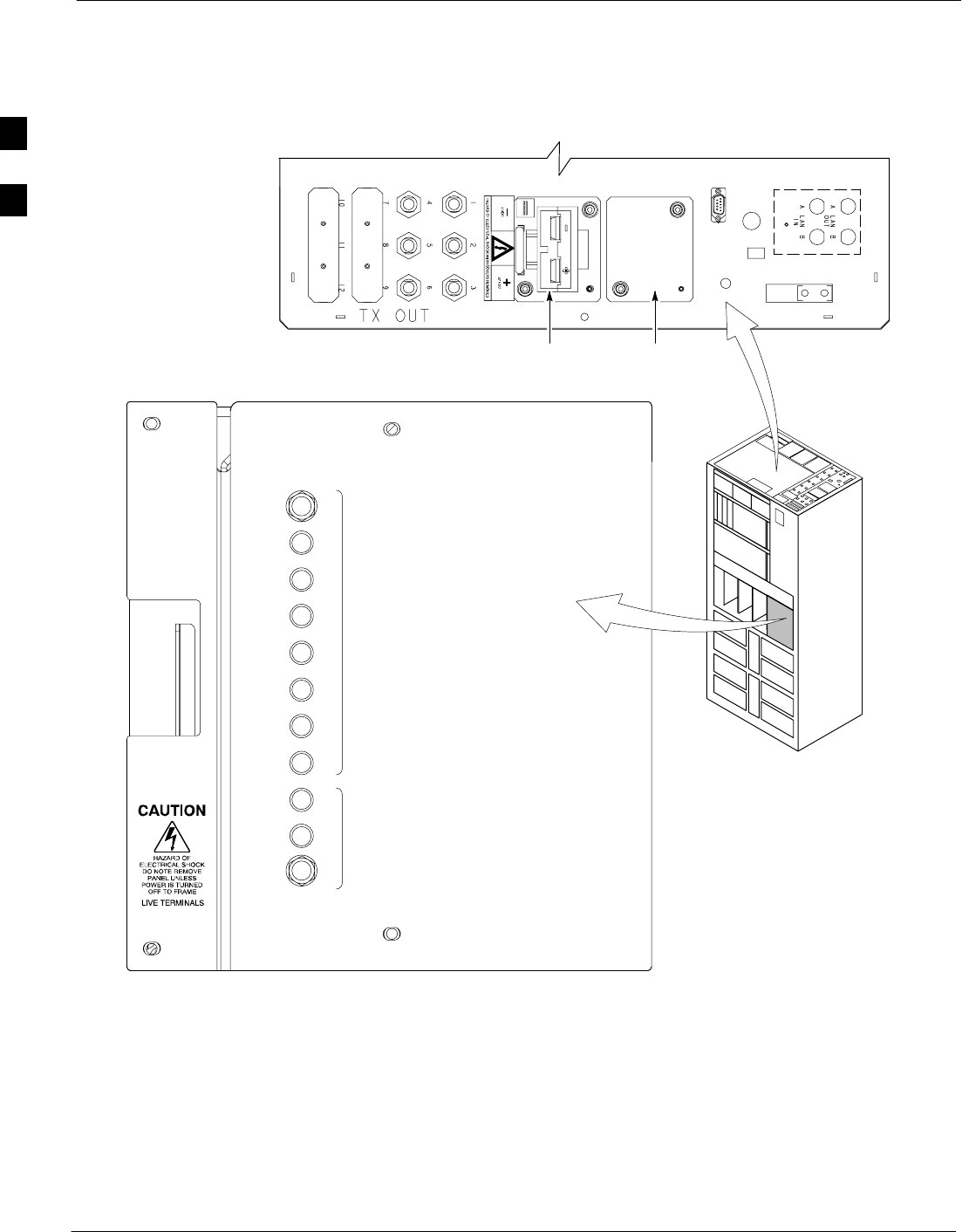
Span Lines – Interface & Isolation
5/21/04 1X SC4812T–MC BTS Optimization/ATP 3-13
DRAFT
T1/E1 Span Interface
At active sites, the OMC/CBSC must disable the BTS and
place it out of service (OOS). DO NOT remove the 50–pin
TELCO cable connected to the BTS frame site I/O board
J1 connector until the OMC/CBSC has disabled the BTS!
NOTE
Each frame is equipped with one Site I/O and two Span I/O boards. The
Span I/O J1 connector provides connection for 25 wire pairs. A GLI card
can support up to six spans. In SC4812T BTS frames, spans A, C, and E
terminate on the Span “A” I/O; and spans B, D, and F terminate on the
Span “B” I/O.
Span Lines will interface to the BTS through the Span I/O
cards only in circuit mode with either circuit or split
backhaul.
NOTE
Before connecting the LMF to the frame LAN, the OMC–R must disable
the BTS and place it OOS to allow the LMF to control the CDMA BTS.
This prevents the OMC–R from inadvertently sending control
information to the BTS during LMF–controlled tests. Refer toFigure 3-2
and Figure 3-3 as required.
3
Span Lines – Interface & Isolation – continued
3-14 1X SC4812T–MC BTS Optimization/ATP 5/21/04
DRAFT
Isolate BTS from T1/E1 Spans
To ensure the LMF will maintain control of the BTS, disable the BTS
and isolate the spans as described in Table 3-4.
Table 3-4: T1/E1 Span Isolation
Step Action
1Have the OMC/CBSC place the BTS OOS.
2Remove the T1/E1 span 50–pin TELCO cable connected to the SPAN I/O cards
(Figure 3-2).
NOTE
– If a third party is used for span connectivity, the third party must be informed
before disconnecting the span line.
– Verify that the SPAN cable connector is removed, not the “MODEM/TELCO”
connector.
Figure 3-2: Span I/O Board Span Isolation
50–PIN TELCO
CONNECTORS
REMOVED
SPAN A CONNECTOR
(TELCO) INTERFACE
TO SPAN LINES
SPAN B CONNECTOR
(TELCO) INTERFACE
TO SPAN LINES
TOP of Frame
(Site I/O and Span I/O boards)
RS–232 9–PIN SUB D
CONNECTOR SERIAL
PORT FOR EXTERNAL
DIAL UP MODEM
CONNECTION (IF USED)
FW00299
3

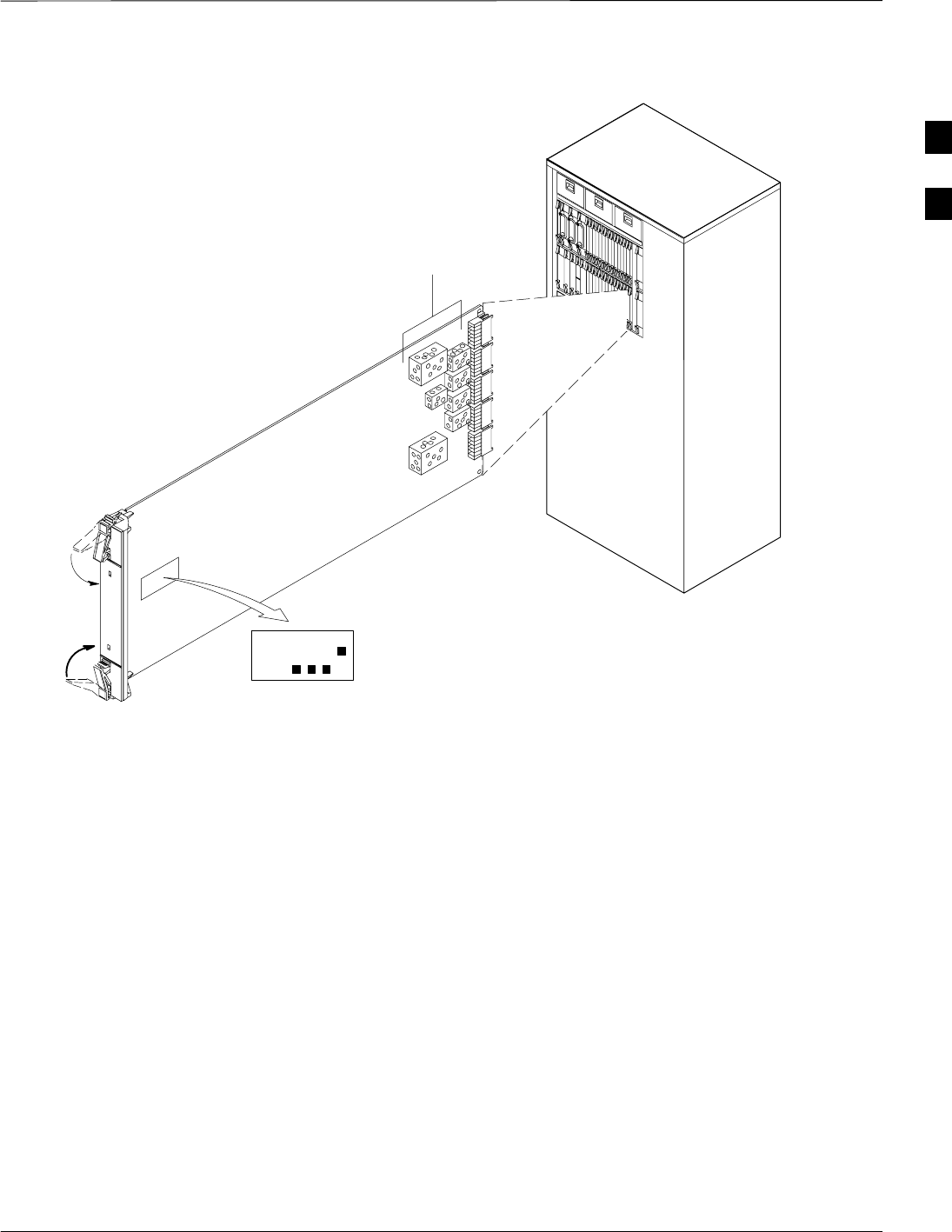
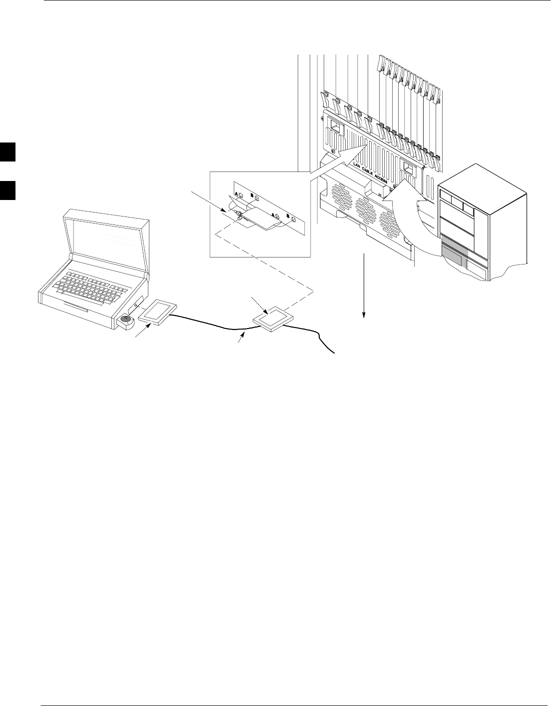
LMF to BTS Connection
5/21/04 1X SC4812T–MC BTS Optimization/ATP 3-15
DRAFT
Connect the LMF to the BTS
The LMF is connected to the LAN A or B connector located on the left
side of the frame’s lower air intake grill, behind the LAN Cable Access
door (see Figure 3-3).
Table 3-5: LMF to BTS Connection
Step Action
1To gain access to the connectors on the BTS, open the LAN Cable Access door, then pull apart the
Velcro® tape covering the BNC “T” connector (see Figure 3-3).
2Connect the LMF to the LAN A BNC connector via PCMCIA Ethernet Adapter with an unshielded
twisted–pair (UTP) Adapter and 10BaseT/10Base2 converter (powered by an external AC/DC
transformer).
3Start the LMF application (see Table 3-6 or Table 3-7) and test the connection.
– If there is no login response, connect the LMF to the LAN B connector.
– If there is still no login response, see Table 6-1, Login Failure Troubleshooting Procedures.
NOTE
– Xircom Model PE3–10B2 or equivalent can also be used to interface the LMF Ethernet
connection to the frame connected to the PC parallel port, powered by an external AC/DC
transformer. In this case, the BNC cable must not exceed 91 cm (3 ft) in length.
– The LAN shield is isolated from chassis ground. The LAN shield (exposed portion of BNC
connector) must not touch the chassis during optimization.
3
LMF to BTS Connection – continued
3-16 1X SC4812T–MC BTS Optimization/ATP 5/21/04
DRAFT
Figure 3-3: LMF Connection Detail
NOTE:
Open LAN CABLE ACCESS
door. Pull apart Velcro tape and
gain access to the LAN A or LAN
B LMF BNC connector.
LMF BNC “T” CONNECTIONS
ON LEFT SIDE OF FRAME
(ETHERNET “A” SHOWN;
ETHERNET “B” COVERED
WITH VELCRO TAPE)
LMF COMPUTER
TERMINAL WITH
MOUSE PCMCIA ETHERNET
ADAPTER & ETHERNET
UTP ADAPTER
10BASE–T/10BASE–2
CONVERTER CONNECTS
DIRECTLY TO BNC T
115 VAC POWER
CONNECTION
UNIVERSAL TWISTED PAIR (UTP)
CABLE (RJ45 CONNECTORS)
ti-CDMA-WP-00076-v01-ildoc-ftw
3

Using the LMF
5/21/04 1X SC4812T–MC BTS Optimization/ATP 3-17
DRAFT
Basic LMF Operation
LMF Coverage in This Publication – There are LMF application
programs to support maintenance of both CDMA and SAS BTSs. All
references to the LMF in this publication are for the CDMA application
program.
Operating Environments – The LMF application program allows the
user to work in the two following operating environments which are
accessed using the specified desktop icons:
SGraphical User Interface (GUI) using the WinLMF icon
SCommand Line Interface (CLI) using the WinLMF CLI icon
The GUI is the primary optimization and acceptance testing operating
environment. The CLI environment provides additional capability to the
user to perform manually controlled acceptance tests and audit the
results of optimization and calibration actions.
Basic Operation – Basic operation of the LMF in either environment
includes performing the following:
SSelecting and deselecting BTS devices
SEnabling devices
SDisabling devices
SResetting devices
SObtaining device status
The following additional basic operation can be performed in a GUI
environment:
SSorting a status report window
For detailed information on performing these and other LMF operations,
refer to the LMF On-Line Help, Software Release 2.16.4.x .
Unless otherwise noted, LMF procedures in this manual
are performed using the GUI environment.
NOTE
Online Help – Task oriented online help is available in the LMF by
clicking on Help from the menu bar.
The LMF Display and the BTS
BTS Display – When the LMF is logged into a BTS, a frame tab is
displayed for each BTS frames. The frame tab will be labeled with
“CDMA” and the BTS number, a dash, and the frame number (for
example, BTS–812–1 for BTS 812, RFMF 1). If there is only one frame
for the BTS, there will only be one tab.
3

Using the LMF – continued
3-18 1X SC4812T–MC BTS Optimization/ATP 5/21/04
DRAFT
CDF or NEC file Requirements – For the LMF to recognize the
devices installed in the BTS, a BTS CDF or NEC files which include
equipage information for all the devices in the BTS must be located in
the applicable <x>:\<lmf home directory>\cdma\bts–# folder. To
provide the necessary channel assignment data for circuit BTS operation,
a CBSC CDF file which includes channel data for all BTS RFMFs is
also required in the folder.
RFDS Display – If an RFDS is included in the CDF or NEC files, an
RFDS tab labeled with “RFDS,” a dash and the BTS number–frame
number combination (for example, RFDS–812–1) will be displayed.
Graphical User Interface
Overview
The LMF uses a Graphical User Interface (GUI), which supports the
following functions:
SSelecting a device or devices.
SSelecting an action to apply to selected device(s).
SStatus report window displaying progress of actions taking place and
related information.
SNotification when an action is complete and related information such
as indication of success or failure
SAn OK button to close the status report window.
Understanding GUI Operation
The following screen captures are provided to help understand how the
GUI operates:
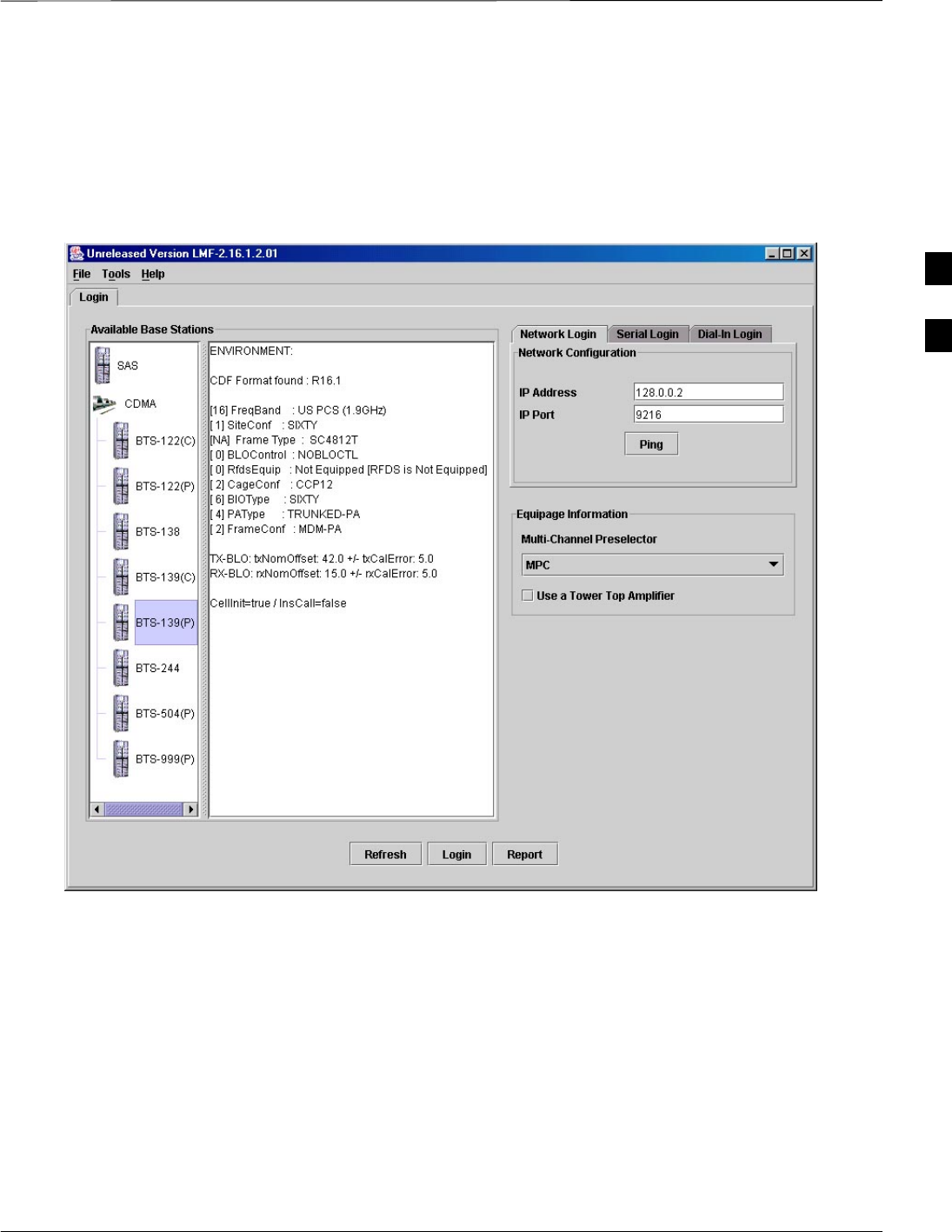
– Figure 3-4 shows the differences between packet and circuit BTS
representations on the LMF login screen. If there is a packet
configuration file (NEC) for the BTS, the “(P)” is added as a suffix
to the BTS number.
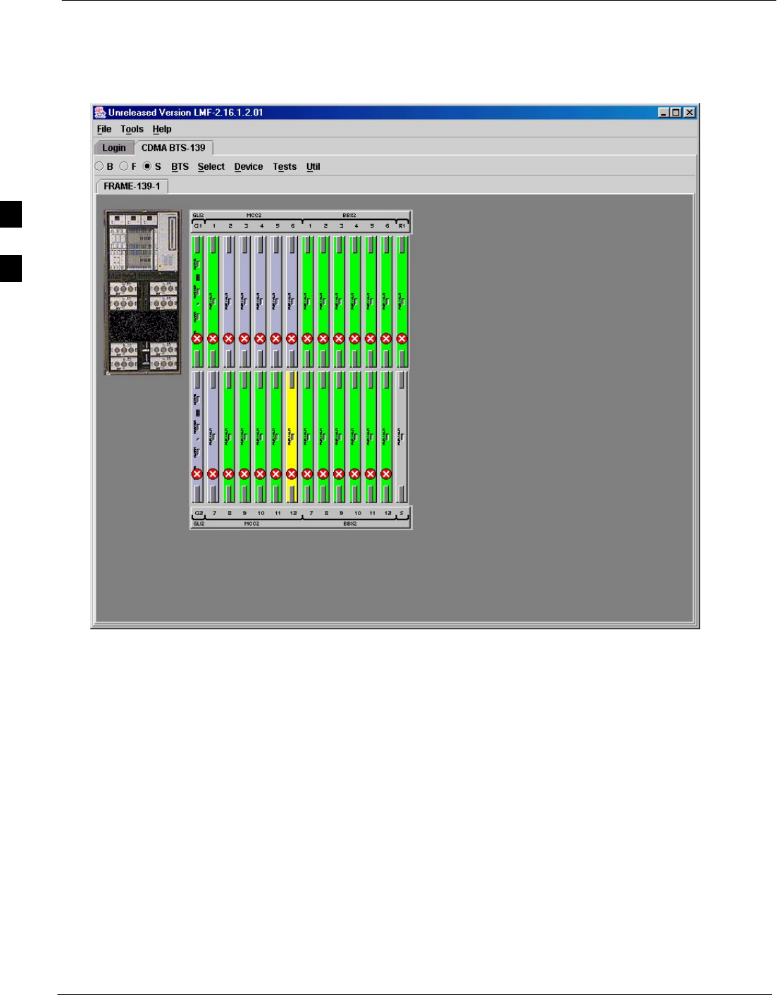
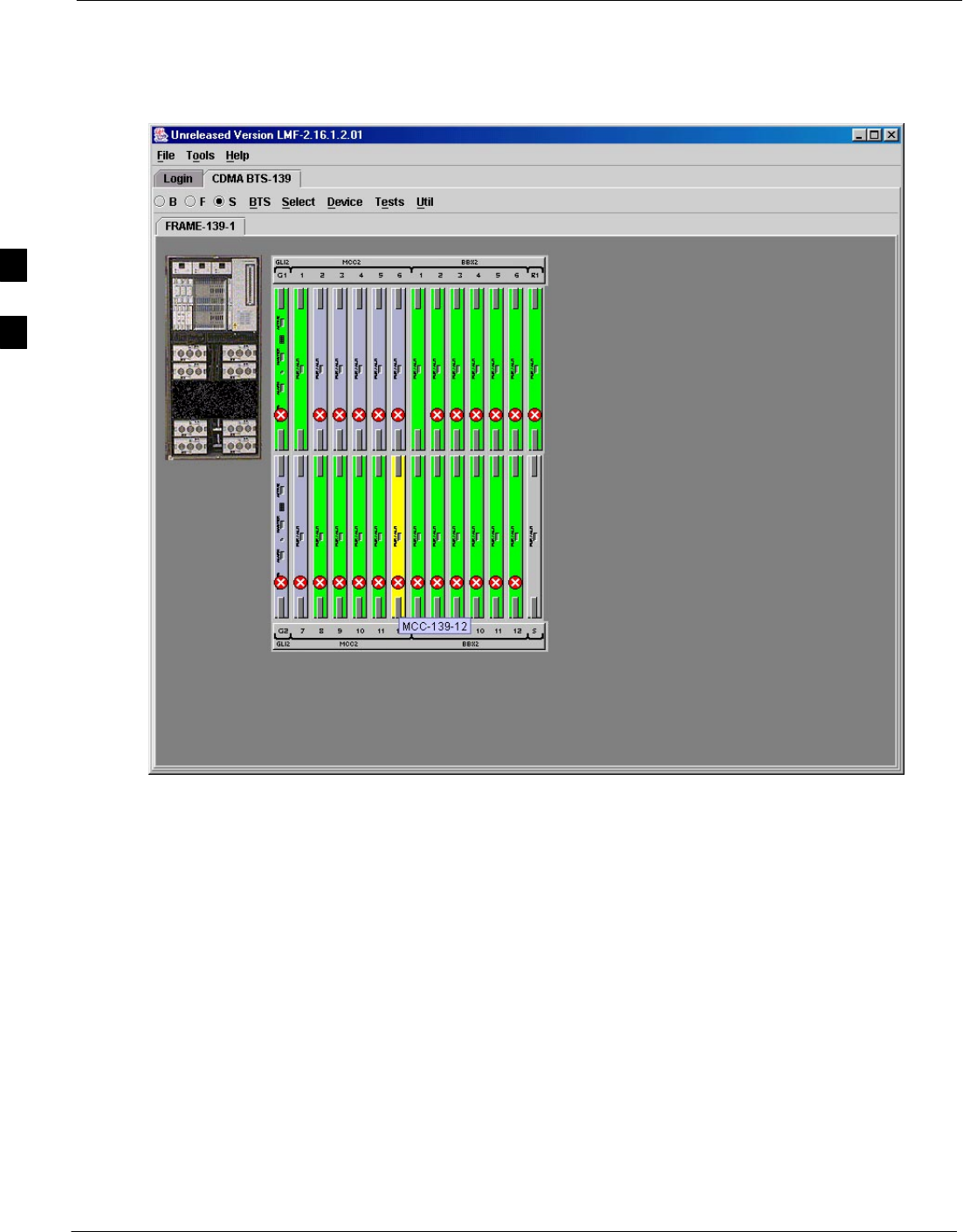
– Figure 3-5 shows the Self-Managed Network Elements (NE) state
of a packet–mode BTS (SC4812T shown). An “X” is displayed on
the front of each card that is under Self–Managed NE control by the
GLI3 card.
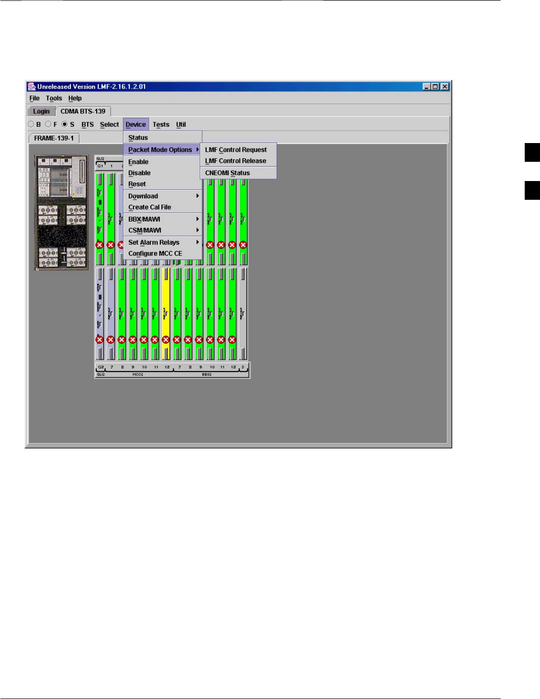
– Figure 3-6 shows three of the available packet mode commands.
Normally the GLI3 has Self-Managed NE control of all cards as
shown inFigure 3-6 identified with an “X”. In that state, the LMF
may only status a card. In order to download code or test a card, the
LMF must request Self-Managed NE control of the card by using
the dropdown menu shown. The LMF also uses this menu to release
control of the card back to the GLI3. The GLI3 will also assume
control of the cards after the LMF logs out of the BTS. The packet
mode GLI3 normally is loaded with a tape release and NECB and
NECJ files which point to a tape release stored on the GLI3. When
the GLI3 has control of a card it will maintain that card with the
code on that tape release.
3
Using the LMF – continued
5/21/04 1X SC4812T–MC BTS Optimization/ATP 3-19
DRAFT
– Figure 3-7 depicts a packet–mode BTS that has the MCC–1 and the
BBX–1 cards under LMF control. Notice that the “X” is missing
from the front of these two cards.
Figure 3-4: BTS Login screen – identifying circuit and packet BTS files
For detailed information on performing these and other LMF operations,
refer to the LMF Help function on–line documentation.
3
Using the LMF – continued
3-20 1X SC4812T–MC BTS Optimization/ATP 5/21/04
DRAFT
Figure 3-5: Self–Managed Network Elements (NEs) state of a packet mode SC4812T
3
Using the LMF – continued
5/21/04 1X SC4812T–MC BTS Optimization/ATP 3-21
DRAFT
Figure 3-6: Available packet mode commands
3
Using the LMF – continued
3-22 1X SC4812T–MC BTS Optimization/ATP 5/21/04
DRAFT
Figure 3-7: cket mode BTS with MCC–1 and BBX–1 under LMF control
Command Line Interface
Overview
The LMF also provides Command Line Interface (CLI) capability.
Activate the CLI by clicking on a shortcut icon on the desktop. The CLI
cannot be launched from the GUI, only from the desktop icon.
Both the GUI and the CLI use a program known as the handler. Only one
handler can be running at one time. Due to architectural limitations, the
GUI must be started before the CLI if it is desired that the GUI and CLI
to use the same handler. When the CLI is launched after the GUI, the
CLI automatically finds and uses an in–progress login session with a
BTS initiated under the GUI. This allows the use of the GUI and the CLI
in the same BTS login session. If a CLI handler is already running when
the GUI is launched (this happens if the CLI window is already running
when the user starts the GUI, or if another copy of the GUI is already
running when the user starts the GUI), a dialog window displays the
following warning message:
The CLI handler is already running.
This may cause conflicts with the LMF.
3

Using the LMF – continued
5/21/04 1X SC4812T–MC BTS Optimization/ATP 3-23
DRAFT
Are you sure that you want to start the application?
Yes No
Selecting the yes button starts the application. Selecting the no button
terminates the application.
CLI Format Conventions
The CLI command can be broken down in the following way:
Sverb
Sdevice including device identifier parameters
Sswitch
Soption parameters consisting of:
– keywords
– equals signs (=) between the keywords and the parameter values
– parameter values
Spaces are required between the verb, device, switch, and option
parameters. A hyphen is required between the device and its identifiers.
Following is an example of a CLI command.
measure bbx–<bts_id>–<bbx_id> rssi channel=6 sector=5
Refer to the LMF CDMA CLI Reference, Software Release 2.16.4.x
manual for a complete explanation of the CLI commands and their use.
Logging into a BTS
Logging into a BTS establishes a communications link between the BTS
and the LMF. An LMF session can be logged into only one BTS at a
time.
Prerequisites
Before attempting to log into the BTS,
Before attempting to login to a BTS, ensure the following have been
completed:
SThe LMF is properly connected to the BTS (see Figure 3-3).
SThe LMF application program is correctly installed and prepared.
SA bts-# folder with the correct CDF and CBSC files or NEC files
exists.
SThe LMF computer was connected to the BTS before starting the
Windows operating system and LMF software. If necessary, restart the
computer after connecting it to the BTS in accordance with Table 3-5
and Figure 3-3.
3

Using the LMF – continued
3-24 1X SC4812T–MC BTS Optimization/ATP 5/21/04
DRAFT
Be sure that the correct bts–#.cdf and cbsc–#.cdf or
NECB*bts#.xml and NECJ*bts#.xml files are used for the
BTS. These should be the CDF or NEC files that are
provided for the BTS by the OMC–R. Failure to use the
correct CDF or NEC files can result in invalid
optimization. Failure to use the correct CDF or NEC
files to log into a live (traffic carrying) site can shut
down the site.
NOTE
BTS Login from the GUI Environment
Follow the procedure in Table 3-6 to log into a BTS when using the GUI
environment.
Table 3-6: BTS GUI Login Procedure
nStep Action
1Start the CDMA LMF GUI environment by double clicking on the WinLMF desktop icon (if the
LMF is not running).
NOTE
If a warning similar to the following is displayed, select No, shut down other LMF sessions which
may be running, and start the CDMA LMF GUI environment again:
The CLI handler is already running.
This may cause conflicts with the LMF
Are you sure you want to start the application?
Yes No
2Click on the Login tab (if not displayed).
3If no base stations are displayed in the Available Base Stations pick list, double click on the
CDMA icon.
4Click on the desired BTS number.
5Click on the Network Login tab (if not already in the forefront).
6Enter the correct IP address (normally 128.0.0.2 for a field BTS) if not correctly displayed in the
IP Address box.
NOTE
128.0.0.2 is the default IP address for MGLI–1 in field BTS units. 128.0.0.1 is the default IP
address for MGLI–2.
7Type in the correct IP Port number (normally 9216) if not correctly displayed in the IP Port box.
. . . continued on next page
3

Using the LMF – continued
5/21/04 1X SC4812T–MC BTS Optimization/ATP 3-25
DRAFT
Table 3-6: BTS GUI Login Procedure
nActionStep
8Click on Ping.
– If the connection is successful, the Ping Display window shows text similar to the following:
Reply from 128 128.0.0.2: bytes=32 time=3ms TTL=255
– If there is no response the following is displayed:
128.0.0.2:9216:Timed out
If the MGLI fails to respond, reset and perform the ping process again. If the MGLI still fails to
respond, typical problems are shorted BNC to inter–frame cabling, open cables, crossed A and B
link cables, missing 50–Ohm terminators, or the MGLI itself.
9Change the Multi-Channel Preselector (from the Multi-Channel Preselector pick list) selection,
normally MPC, to correspond to the BTS configuration, if required.
NOTE
When performing RX tests on expansion frames, do not choose EMPC if the test equipment is
connected to the starter frame.
NOTE
“Use a Tower Top Amplifier” is not applicable to the SC4812T–MC.
10 Click on Login.
A BTS tab with a graphical representation of the BTS CCP cage is displayed.
NOTE
SIf login is attempted to a BTS that is already logged on, all devices will be gray.
SFor Software Release 2.16.4.0 and earlier, a Mode Selection box asking if the BTS is Trunked
or Multicarrier will pop up. Multicarrier must be selected for the SC4812T–MC BTS.
SThere may be instances where the BTS initiates a log out due to a system error (than is, a device
failure).
SIf the MGLI is OOS_ROM (blue), it will have to be downloaded with code before other devices
can be seen.
SIf the MGLI is OOS_RAM (yellow), it must be enabled before other installed devices can be
seen.
BTS Login from the CLI Environment
Follow the procedure in Table 3-7 to log into a BTS when using the CLI
environment.
3

Using the LMF – continued
3-26 1X SC4812T–MC BTS Optimization/ATP 5/21/04
DRAFT
If the CLI and GUI environments are to be used at the
same time, the GUI must be started first and BTS login
must be performed from the GUI. Refer to Table 3-6 to
start the GUI environment and log into a BTS.
NOTE
Table 3-7: BTS CLI Login Procedure
nStep Action
1Double click the WinLMF CLI desktop icon (if the LMF CLI
environment is not already running).
NOTE
If a BTS was logged into under a GUI session when the CLI
environment was started, the CLI session will be logged into the same
BTS, and step 2 is not required.
2At the /wlmf prompt, enter the following command:
login bts–<bts#> host=<host> port=<port>
where:
host = MGLI card IP address (defaults to address last logged into for
this BTS or 128.0.0.2 if this is first login to this BTS).
port = IP port of the BTS (defaults to port last logged into for this
BTS or 9216 if this is first login to this BTS).
A response similar to the following will be displayed:
LMF>
13:08:18.882 Command Received and Accepted
COMMAND=login bts–33
13:08:18.882 Command In Progress
13:08:21.275 Command Successfully Completed
REASON_CODE=”No Reason”
3
Logging Out
Logging out of a BTS is accomplished differently for the GUI and the
CLI operating environments.
3

Using the LMF – continued
5/21/04 1X SC4812T–MC BTS Optimization/ATP 3-27
DRAFT
The GUI and CLI environments use the same connection to
a BTS. If a GUI and the CLI session are running for the
same BTS at the same time, logging out of the BTS in
either environment will log out of it for both. When either
a login or logout is performed in the CLI window, there is
no GUI indication that logout has occurred.
NOTE
Logging Out of a BTS from the GUI Environment
Follow the procedure in Table 3-8 to logout of a BTS when using the
GUI environment.
Table 3-8: BTS GUI Logout Procedure
nStep Action
1Click on BTS on the BTS tab menu bar.
2Click the Logout item in the pull–down menu (a Confirm Logout
pop–up message appears).
3Click on Yes or press the <Enter> key to confirm logout.
The screen display returns to the Login tab.
NOTE
If a logout was previously performed on the BTS from a CLI window
running at the same time as the GUI, a Logout Error pop–up
message appears stating the system should not log out of the BTS.
When this occurs, the GUI must be exited and restarted before it can
be used for further operations.
4If a Logout Error pop–up message appears stating that the system
could not log out of the Base Station because the given BTS is not
logged in, perform the following actions:
– Click OK.
– Select File>Exit in the window menu bar.
– Click Yes in the Confirm Logout pop–up.
– Click Yes in the Logout Error pop–up which appears again.
5If further work is to be done in the GUI, restart it.
NOTE
SThe Logout item on the BTS menu bar will only log the LMF out
of the displayed BTS.
SLogging out of all BTS sessions and exiting the LMF can be done
by clicking on the File selection in the menu bar and selecting Exit
from the File menu list. A Confirm Logout pop–up message will
appear.
3

Using the LMF – continued
3-28 1X SC4812T–MC BTS Optimization/ATP 5/21/04
DRAFT
Logging Out of a BTS from the CLI Environment
Follow the procedure in Table 3-9 to logout of a BTS when using the
CLI environment.
Table 3-9: BTS CLI Logout Procedure
nStep Action
NOTE
If the BTS is also logged into from a GUI running at the same time
and further work must be done with it in the GUI, proceed to step 2.
1Logout of a BTS by entering the following command:
logout bts–<bts#>
A response similar to the following is displayed:
LMF>
12:22:58.028 Command Received and Accepted
Command=logout bts–33
12:22:58.028 Command Received and Accepted
12:22:58.028 Command Successfully Completed
REASON_CODE=”No Reason”
2 If desired, close the CLI interface by entering the following
command:
exit
A response similar to the following is displayed before the window
closes:
Killing background processes....
Establishing an MMI
Communication Session
For those procedures that require MMI communications between the
LMF and BTS FRUs, follow the procedure in Table 3-10 to initiate the
communication session.
Table 3-10: Establishing MMI Communication
Step Action
1Connect the LMF computer to the equipment as detailed in the applicable procedure that requires the
MMI communication session and Figure 3-8 or Figure 3-9.
2If the LMF computer has only one serial port (COM1) and the LMF is running, disconnect the LMF
from COM1 by performing the following:
2a – Click on Tools in the LMF window menu bar, and select Options from the pull–down menu list.
–– An LMF Options dialog box will appear.
2b – In the Test Equipment tab of the dialog box, select COM1 in the Comm Port pulldown on the
Serial Connection tab.
. . . continued on next page
3
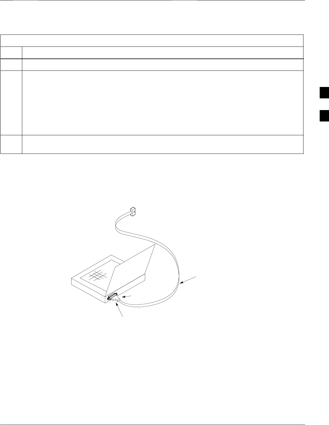
Using the LMF – continued
5/21/04 1X SC4812T–MC BTS Optimization/ATP 3-29
DRAFT
Table 3-10: Establishing MMI Communication
Step Action
2c – ,Click the Disconnect Port button on the Serial Connection tab.
3Start the named HyperTerminal connection for MMI sessions by double clicking on its Windows
desktop shortcut.
NOTE
If a Windows desktop shortcut was not created for the MMI connection, access the connection from the
Windows Start menu by selecting:
Programs > Accessories > Hyperterminal > HyperTerminal > <Named HyperTerminal
Connection (e.g., MMI Session)>
4Once the connection window opens, establish MMI communication with the BTS FRU by pressing
the LMF computer Enter key until the prompt identified in the applicable procedure is obtained.
Figure 3-8:CDMA LMF Computer Common MMI Connections – Cable CGDSMMICABLE219112 or
Fabricated MMI Cable
CABLE PART NUMBEr
CGDSMMICABLE219112
OR
FABRICATED MMI CABLE
(SEE APPENDIX J)
DB–9
CONNECTOR
8–PIN
LMF COMPUTER
To FRU MMI
Connector
COM1
OR
COM2
3
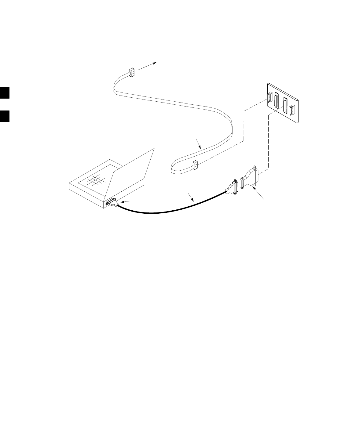
Using the LMF – continued
3-30 1X SC4812T–MC BTS Optimization/ATP 5/21/04
DRAFT
Figure 3-9: CDMA LMF Computer Common MMI Connections –
Motorola MMI Interface Kit, SLN2006A
NULL MODEM
BOARD
(TRN9666A)
8–PIN TO 10–PIN
RS–232 CABLE
(P/N 30–09786R01)
RS–232 CABLE
8–PIN
CDMA LMF
COMPUTER
To FRU MMI port
DB9–TO–DB25
ADAPTER
COM1
OR
COM2
FW00687
Online Help
Task oriented online help is available in the LMF by clicking on Help in
the window menu bar, and selecting LMF Help from the pull–down
menu.
3
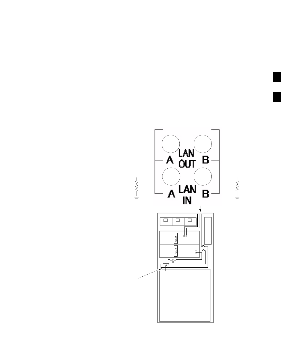
Pinging the Processor
5/21/04 1X SC4812T–MC BTS Optimization/ATP 3-31
DRAFT
Pinging the Processor
For proper operation, the integrity of the Ethernet LAN A and B links
must be be verified. Figure 3-10 represents a typical BTS Ethernet
configuration. The drawing depicts one (of two identical) links, A and B.
Ping is a program that routes request packets to the LAN network
modules to obtain a response from the specified “targeted” BTS.
Figure 3-10: BTS LAN Diagram
LMF
CONNECTOR
B
C–CCP
CAGE
AB
IN
A
B
A
OUT
BTS
(STARTER)
LAN “IN” PORTS MUST HAVE
GROUNDED 50 OHM TERMINATION
AT ALL TIMES IN A STARTER
FRAME.
IN EXPANSION FRAME AND
LOGICAL BTS, LAN “IN” PORTS ARE
NOT GROUNDED
UNUSED LAN “OUT” PORTS MUST
HAVE NON–GROUNDED 50 OHM BNC
TERMINATORS INSTALLED
OR
BE CONNECTED TO EXPANSION
FRAME (WHERE USED) VIA COAX
CABLES
Follow the procedure in Table 3-11 and refer to Figure 3-10, as required,
to ping each processor (on both LAN A and LAN B) and verify LAN
redundancy is operating correctly.
3

Pinging the Processor – continued
3-32 1X SC4812T–MC BTS Optimization/ATP 5/21/04
DRAFT
Always wear an approved anti–static wrist strap while
handling any circuit card/module to prevent damage by
ESD.
CAUTION
The Ethernet LAN A and B cables must be installed on
each frame/enclosure before performing this test. All other
processor board LAN connections are made via the
backplanes.
NOTE
Table 3-11: Pinging the Processors
nStep Action
1If it has not already been done, connect the LMF to the BTS (see Table 3-5 on page
3-15).
2From the Windows desktop, click the Start button and select Run.
3In the Open box, type ping and the <MGLI IP address> (for example, ping
128.0.0.2).
NOTE
128.0.0.2 is the default IP address for MGLI–1 in field BTS units. 128.0.0.1 is the
default IP address for MGLI–2.
4Click on the OK button.
5If the connection is successful, text similar to the following is displayed:
Reply from 128 128.0.0.2: bytes=32 time=3ms TTL=255
If there is no response the following is displayed:
Request timed out
If the MGLI fails to respond, reset and perform the ping process again. If the MGLI
still fails to respond, typical problems are shorted BNC–to–inter-frame cabling, open
cables, crossed A and B link cables, missing 50–Ohm terminators, or the MGLI itself.
3

Download the BTS
5/21/04 1X SC4812T–MC BTS Optimization/ATP 3-33
DRAFT
Overview
Before a BTS can operate, each equipped device must contain device
initialization (ROM) code. ROM code is loaded in all devices during
manufacture or factory repair. Device application (RAM) code and data
must be downloaded to each equipped device by the user before the BTS
can be made fully functional for the site where it is installed.
ROM Code
Downloading ROM code to BTS devices from the LMF is NOT routine
maintenance nor a normal part of the optimization process. It is only
done in unusual situations where the resident ROM code in the device
does not match the release level of the site operating software AND the
CBSC cannot communicate with the BTS to perform the download. If
ROM code must be downloaded, refer to Appendix H.
Before ROM code can be downloaded from the LMF, the correct ROM
code file for each device to be loaded must exist on the LMF computer.
ROM code must be manually selected for download.
The ROM code file is not available for GLI3s. GLI3s are
ROM code loaded at the factory.
NOTE
RAM Code
Before RAM code can be downloaded from the CDMA LMF, the correct
RAM code file for each device must exist on the LMF computer. RAM
code can be automatically or manually selected depending on the Device
menu item chosen and where the RAM code file for the device is stored
in the CDMA LMF file structure. The RAM code file is selected
automatically if the file is in the \lmf\cdma\loads\n.n.n.n\code folder
(where n.n.n.n is the version number of the download code). The RAM
code file in the code folder must have the correct hardware bin number.
RAM code can be downloaded to a device that is in any state. After the
download is started, the device being downloaded changes to OOS-ROM
(blue). When the download is completed successfully, the device
changes to OOS-RAM (yellow). When code is downloaded to an MGLI,
the LMF automatically also downloads data, and then enables the MGLI.
When enabled, the MGLI changes to INS (green).
For non–MGLI devices, data must be downloaded after RAM code is
downloaded. To download data, the device state must be OOS–RAM
(yellow).
Prior to downloading a device, a code file must exist. The code file is
selected automatically if the code file is in the /lmf/cdma/n.n.n.n/code
folder (where n.n.n.n is the version number of the download code that
matches the “NextLoad” parameter in the CDF or NEC files). The code
file in the code folder must have the correct hardware bin number. Code
can be automatically or manually selected.
3

Download the BTS – continued
3-34 1X SC4812T–MC BTS Optimization/ATP 5/21/04
DRAFT
The devices to be loaded with RAM code and data are::
SMaster Group Line Interface (MGLI)
SGroup Line Interface (GLI)
SClock Synchronization Module (CSM)
SMulti Channel Card (MCC24E, MCC8E or MCC–1X)
SBroadband Transceiver (BBX)
The MGLI must be successfully downloaded with code and
data, and put INS before downloading any other device.
The download code process for an MGLI automatically
downloads data and enables the MGLI before downloading
other devices. The other devices can be downloaded in any
order.
NOTE
Verify GLI ROM Code Loads
Devices should not be loaded with a RAM code version which is not
compatible with the ROM code with which they are loaded. Before
downloading RAM code and data to the processor cards, follow the
procedure in Table 3-12 to verify the GLI devices are loaded with the
correct ROM code for the software release used by the BSS.
Prerequisite
Identify the correct GLI ROM code load for the software release being
used on the BSS by referring to the Version Matrix section of the SCt
CDMA Release Notes (supplied on the tapes or CD–ROMs containing
the BSS software).
Table 3-12: Verify GLI ROM Code Loads
Step Action
1If it has not already been done, start a GUI LMF session and log into the
BTS ( refer to Table 3-6).
2Select all GLI devices by clicking on them, and select Device > Status
from the BTS menu bar.
3In the status report window which opens, note the number in the ROM
Ver column for each GLI.
4If the ROM code loaded in the GLIs is not the correct one for the software
release being used on the BSS, perform the following:
4a – Log out of the BTS as described in Table 3-8 or Table 3-9, as
applicable.
4b – Disconnect the LMF computer.
4c – Reconnect the span lines as described in Table 5-7.
. . . continued on next page
3

Download the BTS – continued
5/21/04 1X SC4812T–MC BTS Optimization/ATP 3-35
DRAFT
Table 3-12: Verify GLI ROM Code Loads
Step Action
4d – Have the CBSC download the correct ROM code version to the BTS
devices.
5When the GLIs have the correct ROM load for the software release being
used, be sure the span lines are disabled as outlined in Table 3-4 and
proceed to downloading RAM code and data.
Download RAM Code and Data
to MGLI Cards
Prerequisite
Prior to performing this procedure, ensure a code file exists for each of
the devices to be downloaded.
Procedure
Follow the procedure in Table 3-13 to download the firmware
application code for the MGLI. The download code action downloads
data and also enables the MGLI.
Table 3-13: Download and Enable MGLI
nStep Action
1Note the active LAN to which the LMF computer is connected.
2At the top of the frame, remove the 50 Ω termination from the LAN
OUT connector of the LAN to which the LMF is not connected.
3 Select Tools > Update Next Load > CDMA function to ensure the
Next Load parameter is set to the correct code version level.
4Note the LAN IP address in the Network Login section of the LMF
Login tab, and determine which GLI the LMF is logged into based on
the following IP addresses:
– Card in GLI slot 1: 128.0.0.2
– Card in GLI slot 2: 128.0.0.1
5Download code to the MGLI which the LMF is logged into by
clicking on the MGLI.
– From the Device pull down menu, select
Download > Code/Data.
A status report confirms change in the device(s) status.
– Click OK to close the status window. (The MGLI should
automatically be downloaded with data and enabled.)
6If the card accepts the download and enables, skip to step 10.
7If the BTS connection is lost during or after the download process,
click on the LMF Login tab and log into the BTS again using the
same IP address.
. . . continued on next page
3

Download the BTS – continued
3-36 1X SC4812T–MC BTS Optimization/ATP 5/21/04
DRAFT
Table 3-13: Download and Enable MGLI
nActionStep
8If the log–in attempt fails, set the LAN IP address to the GLI card
which was not downloaded and log into the BTS through the other
GLI card.
9Select the MGLI logged into in step 8, above, and download to it by
repeating step 5 for that card.
10 Select the remaining GLI card and download to it, but do not enable it
at this time.
11 Re–install the 50 Ω termination removed from the frame–top LAN
OUT connector in step 2, above.
Download Code and Data to
Non–GLI Devices
Non–GLI devices can be downloaded individually or all equipped
devices can be downloaded with one action. Follow the procedure in
Table 3-14 to download code and data to the non–GLI devices.
When downloading multiple devices, the download may
fail for some of the devices (a time out occurs). These
devices can be downloaded separately after completing the
multiple download.
CSM devices are RAM code–loaded at the factory. RAM
code is downloaded to CSMs only if updating to a newer
software version.
NOTE
Table 3-14: Download Code and Data to Non–GLI Devices
nStep Action
1Select all devices to be downloaded.
2From the Device pull down menu, select Download>Code/Data.
A status report displays the result of the download for each selected
device.
3 Click OK to close the status window when downloading is complete.
3

Download the BTS – continued
5/21/04 1X SC4812T–MC BTS Optimization/ATP 3-37
DRAFT
Table 3-14: Download Code and Data to Non–GLI Devices
nActionStep
NOTE
– After the download has started, the device being downloaded
changes to blue. If the download is completed successfully, the
device changes to yellow (OOS-RAM with code loaded).
– After a BBX, CSM or MCC is successfully downloaded with
code and has changed to OOS-RAM, the status LED should be
rapidly flashing GREEN.
– The command in Step 2 loads both code and data. Data can be
downloaded without doing a code download anytime a device is
OOS–RAM using the command in Step 4.
4To download the firmware application data to each device, select the
target device and select: Device>Download>Data
Select CSM Clock Source and
Enable CSMs
A CSM can have three different clock sources. The Clock Source
function can be used to select the clock source from each of the three
inputs. This function is only used if the clock source for a CSM needs to
be changed. The Clock Source function provides the following clock
source options:
SLocal GPS
SMate GPS
SRemote GPS
SHSO (only for sources 2 & 3)
SHSOX (only for sources 2 & 3)
S10 MHz (only for sources 2 & 3)
SNONE (only for sources 2 & 3)
Prerequisites
MGLI=INS_ACT
CSM= OOS_RAM or INS_ACT
Follow the procedure in Table 3-15 to select a CSM Clock Source.
Table 3-15: Select CSM Clock Source
nStep Action
1Select the applicable CSM(s).
2Click on Device in the BTS menu bar and select
CSM/MAWI > Select Clock Source... in the pull down menu – a
clock source selection window is displayed.
. . . continued on next page
3

Download the BTS – continued
3-38 1X SC4812T–MC BTS Optimization/ATP 5/21/04
DRAFT
Table 3-15: Select CSM Clock Source
nActionStep
3Select the applicable clock source in the Clock Reference Source
pick lists. Uncheck the related check boxes for Clock Reference
Sources 2 and 3 if the displayed pick list items should not be used.
4Click on the OK button – a status report window displays the results
of the selection action.
5Click on the OK button to close the status report window.
For non–RGPS sites only, verify the CSM configured with
the GPS receiver “daughter board” is installed in the
CSM–1 slot before continuing.
NOTE
Enable CSMs
CSMs are code loaded at the factory. This data is retained
in EEPROM. The download code procedure is required in
the event it becomes necessary to code load CSMs with
updated software versions. Use the status function to
determine the current code load versions.
The CSM(s) to be enabled must have been downloaded
with code (Yellow, OOS–RAM) and data.
NOTE
Each BTS CSM system features two CSM boards per site. In a typical
operation, the primary CSM locks its Digital Phase Locked Loop
(DPLL) circuits to GPS signals. These signals are generated by either an
on–board GPS module (RF–GPS) or a remote GPS receiver (R–GPS).
The CSM2 card is required when using the R–GPS. The GPS receiver
(mounted on CSM–1) is the primary timing reference and synchronizes
the entire cellular system. CSM–2 provides redundancy but does not
have a GPS receiver.
The BTS may be equipped with a remote GPS, LORAN–C, HSO 10
MHz Rubidium source, or HSOX for expansion frames, which the CSM
can use as a secondary timing reference. In all cases, the CSM monitors
and determines what reference to use at a given time.
Follow the procedure in Table 3-16 to enable the CSMs.
3

Download the BTS – continued
5/21/04 1X SC4812T–MC BTS Optimization/ATP 3-39
DRAFT
Table 3-16: Enable CSMs
nStep Action
1Verify the CSM(s) have been downloaded with code (Yellow, OOS–RAM) and data.
2Click on the target CSM.
From the Device pull down, select Enable.
NOTE
– If equipped with two CSMs, enable CSM–2 first and then CSM–1. A status report confirms
change in the device(s) status. Click OK to close the status window.
– FAIL may be shown in the status table for enable action. If Waiting For Phase Lock is shown
in the Description field, the CSM changes to the enabled state after phase lock is achieved.
CSM–1 houses the GPS receiver. The enable sequence can take up to one hour to complete.
– The GPS satellite system satellites are not in a geosynchronous orbit and are maintained and
operated by the United States Department of Defense (D.O.D.). The D.O.D. periodically
alters satellite orbits; therefore, satellite trajectories are subject to change. A GPS receiver that
is INS contains an “almanac” that is updated periodically to take these changes into account.
– If an installed GPS receiver has not been updated for a number of weeks, it may take up to
one hour for the GPS receiver “almanac” to be updated.
– Once updated, the GPS receiver must track at least four satellites and obtain (hold) a 3-D
position fix for a minimum of 45 seconds before the CSM will come in-service. (In some
cases, the GPS receiver needs to track only one satellite, depending on accuracy mode set
during the data load.)
– If equipped with two CSMs, the LMF should display CSM-1 as bright GREEN (INS–ACT)
and CSM–2 as dark green (INS–STB). After the CSMs have been successfully enabled, the
PWR/ALM LEDs are steady green (alternating green/red indicates the card is in an alarm
state).
3If more than an hour has passed, refer to Table 3-20 to determine the cause.
Enable MCCs
Follow the procedure in Table 3-17 to enable the MCCs.
The MGLI, and primary CSM must be downloaded and
enabled (IN–SERVICE ACTIVE), before downloading and
enabling the MCC.
NOTE
Table 3-17: Enable MCCs
nStep Action
1Verify the MCC(s) have been downloaded with code (Yellow,
OOS–RAM) and data.
2Select the MCCs to be enabled or from the Select pulldown menu
choose MCCs.
3From the Device menu, select Enable – a status report confirms
change in the device(s) status.
3

Download the BTS – continued
3-40 1X SC4812T–MC BTS Optimization/ATP 5/21/04
DRAFT
Table 3-17: Enable MCCs
nActionStep
4Click on OK to close the status report window.
Enable Redundant GLIs
Follow the procedure in Table 3-18 to enable the redundant GLI(s).
Table 3-18: Enable Redundant GLIs
nStep Action
1Select the target redundant GLI(s).
2From the Device menu, select Enable – a status report window
confirms the change in the device(s) status and the enabled GLI(s) is
green.
3Click on OK to close the status report window.
3

CSM System Time/GPS and HSO Verification
5/21/04 1X SC4812T–MC BTS Optimization/ATP 3-41
DRAFT
CSM & HSO Background
The primary function of the Clock Synchronization Manager (CSM)
boards (slots 1 and 2) is to maintain CDMA system time. The CSM in
slot 1 is the primary timing source while slot 2 provides redundancy. The
CSM2 card (CSM second generation) is required when using the remote
GPS receiver (R–GPS). R–GPS uses a GPS receiver in the antenna head
that has a digital output to the CSM2 card. CSM2 can have a daughter
card as a local GPS receiver to support an RF–GPS signal.
The CSM2 switches between the primary and redundant units (slots 1
and 2) upon failure or command. CDMA Clock Distribution
Cards (CCDs) buffer and distribute even–second reference and 19.6608
MHz clocks. CCD–1 is married to CSM–1 and CCD–2 is married to
CSM 2. A failure on CSM–1 or CCD–1 cause the system to switch to
redundant CSM–2 and CCD–2.
In a typical operation, the primary CSM locks its Digital Phase Locked
Loop (DPLL) circuits to GPS signals. These signals are generated by
either an on–board GPS module (RF–GPS) or a remote GPS receiver
(R–GPS). The CSM2 card is required when using the R–GPS. DPLL
circuits employed by the CSM provide switching between the primary
and redundant unit upon request. Synchronization between the primary
and redundant CSM cards, as well as the HSO back–up source, provides
excellent reliability and performance.
Each CSM board features an ovenized, crystal oscillator that provides
19.6608 MHz clock, even second tick reference, and 3 MHz sinewave
reference, referenced to the selected synchronization source (GPS,
Receiver, or High Stability Oscillator (HSO), T1 Span, or external
reference oscillator sources). The 3 MHz signals are also routed to the
RDM EXP 1A & 1B connectors on the top interconnect panel for
distribution to co–located frames at the site.
Fault management has the capability of switching between the GPS
synchronization source and the HSO backup source in the event of a
GPS receiver failure on CSM–1. During normal operation, the CSM–1
board selects GPS as the primary source (see Table 3-20). The source
selection can also be overridden via the LMF or by the system software.
All boards are mounted in the C–CCP shelf at the top of the BTS frame.
Figure 1-14 illustrates the location of the boards in the BTS frame.
Front Panel LEDs
The status of the LEDs on the CSM boards are as follows:
SSteady Green – Master CSM locked to GPS (INS).
SRapidly Flashing Green – Standby CSM locked to GPS (STBY).
SFlashing Green/Rapidly Flashing Red – CSM OOS_RAM attempting
to lock on GPS signal.
SRapidly Flashing Green and Red – Alarm condition exists. Trouble
Notifications (TNs) are currently being reported to the GLI.
3

CSM System Time/GPS and HSO Verification – continued
3-42 1X SC4812T–MC BTS Optimization/ATP 5/21/04
DRAFT
High Stability Oscillator
CSM and HSO – The CSM handles the overall configuration and status
monitoring functions of the HSO. In the event of GPS failure, the HSO
is capable of maintaining synchronization initially established by the
GPS reference signal.
HSO – The HSO is a high stability 10 MHz oscillator with the necessary
interface to the CSMs. The HSO is typically installed in those
geographical areas not covered by the LORAN–C system. Since the
HSO is a free–standing oscillator, system time can only be maintained
for 24 hours after 24 hours of GPS lock.
Upgrades and Expansions: HSO2/HSOX
HSO2 (second generation cards) both export a timing signal to the
expansion or logical BTS frames. The associated expansion or logical
frames require an HSO–expansion (HSOX). The HSOX accepts input
from the starter frame and interfaces with the CSM cards in the
expansion frame. HSO, HSO2, and HSOX use the same source code in
source selection (see Table 3-19).
Allow the base site and test equipment to warm up for
60 minutes after any interruption in oscillator power. CSM
board warm-up allows the oscillator oven temperature and
oscillator frequency to stabilize prior to test. Test
equipment warm-up allows the Rubidium standard
timebase to stabilize in frequency before any measurements
are made.
NOTE
CSM Frequency Verification
The objective of this procedure is the initial verification of the CSM
boards before performing the RF path verification tests. Parts of this
procedure will be repeated for final verification after the overall
optimization has been completed.
Null Modem Cable
A null modem cable is required. It is connected between the LMF
COM1 port and the RS232–GPIB Interface box. Figure 3-11 shows the
wiring detail for the null modem cable.
3

CSM System Time/GPS and HSO Verification – continued
5/21/04 1X SC4812T–MC BTS Optimization/ATP 3-43
DRAFT
Figure 3-11: Null Modem Cable Detail
5
3
2
7
8
1
4
6
GND
RX
TX
RTS
CTS
RSD/DCD
DTR
GND
TX
RX
RTS
CTS
RSD/DCD
DTR
ON BOTH CONNEC-
TORS SHORT PINS 7, 8;
SHORT PINS 1, 4, & 6
9–PIN D–FEMALE 9–PIN D–FEMALE
5
2
3
7
8
1
4
6
DSR DSR
FW00362
Prerequisites
Ensure the following prerequisites have been met before proceeding:
SThe LMF is NOT logged into the BTS.
SThe COM1 port is connected to the MMI port of the primary CSM via
a null modem board.
Test Equipment Setup: GPS &
HSO Verification
Follow the procedure in Table 3-19 to set up test equipment while
referring toFigure 3-12 as required.
Table 3-19: Test Equipment Setup (GPS & HSO Verification)
Step Action
1Perform one of the following operations:
– For local GPS (RF–GPS), verify a CSM board with a GPS receiver is installed in primary CSM
slot 1 and that CSM–1 is INS.
This is verified by checking the board ejectors for kit number SGLN1145 on the board in slot 1.
– For Remote GPS (RGPS), verify a CSM2 board is installed in primary slot 1 and that CSM–1 is
INS.
This is verified by checking the board ejectors for kit number SGLN4132ED (or later).
2Remove CSM–2 (if installed) and connect a serial cable from the LMF COM 1 port (via null modem
board) to the MMI port on CSM–1.
3Reinstall CSM–2.
4Start an MMI communication session with CSM–1 by using the Windows desktop shortcut icon (see
Table 3-3)
NOTE
The LMF program must not be running when a Hyperterminal session is started if COM1 is being
used for the MMI session.
5When the terminal screen appears, press the <Enter> key until the CSM> prompt appears.
3
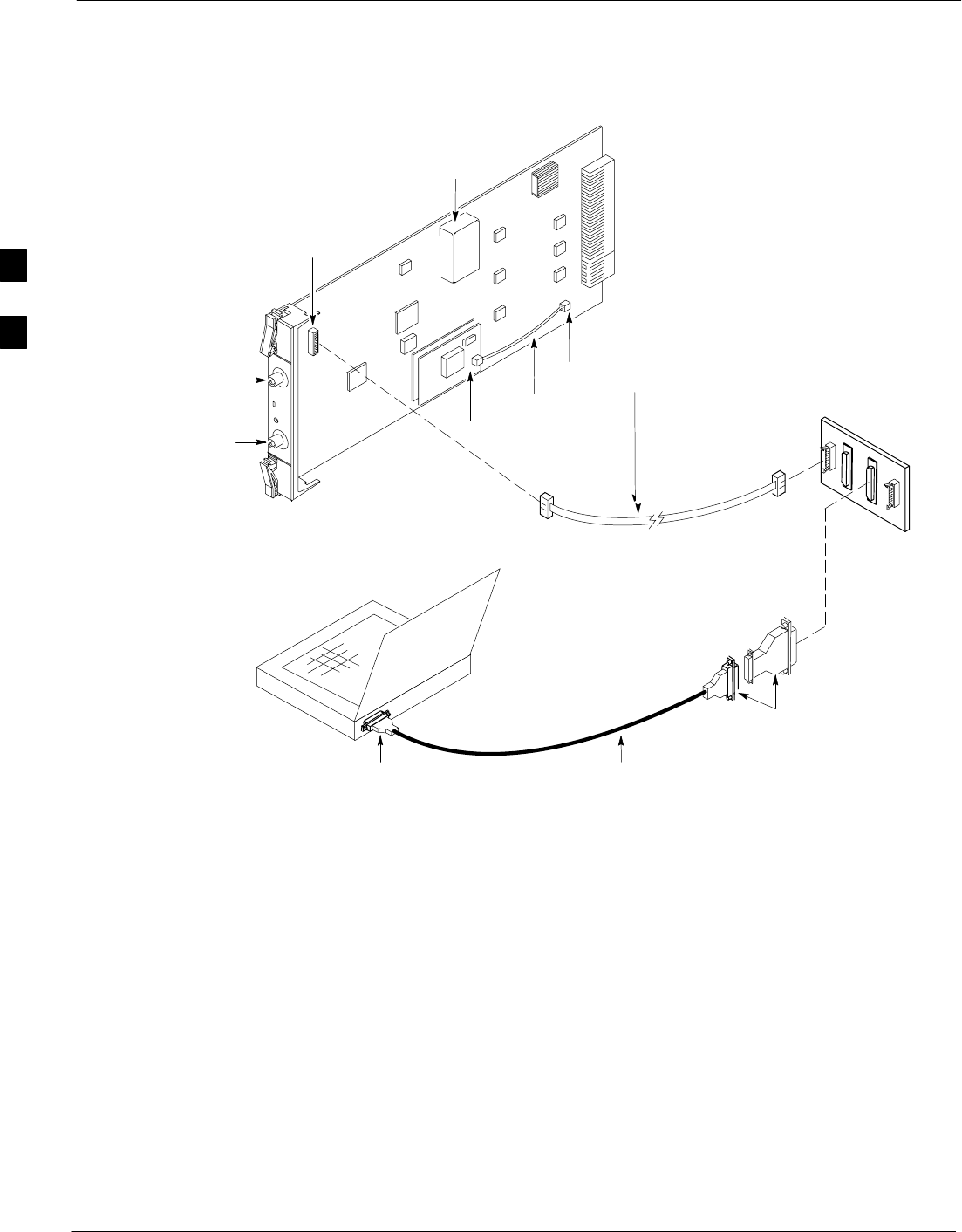
CSM System Time/GPS and HSO Verification – continued
3-44 1X SC4812T–MC BTS Optimization/ATP 5/21/04
DRAFT
Figure 3-12: CSM MMI terminal connection
NULL MODEM
BOARD
(TRN9666A)
RS–232 SERIAL
MODEM CABLE
DB9–TO–DB25
ADAPTER
COM1
LMF
NOTEBOOK
FW00372
CSM board shown
removed from frame
19.6 MHZ TEST
POINT REFERENCE
(NOTE 1)
EVEN SECOND
TICK TEST POINT
REFERENCE
GPS RECEIVER
ANTENNA INPUT
GPS RECEIVER
MMI SERIAL
PORT
ANTENNA COAX
CABLE
REFERENCE
OSCILLATOR
9–PIN TO 9–PIN
RS–232 CABLE
NOTES:
1. One LED on each CSM:
Green = IN–SERVICE ACTIVE
Fast Flashing Green = OOS–RAM
Red = Fault Condition
Flashing Green & Red = Fault
GPS Initialization/Verification
Follow the procedure in Table 3-20 to initialize and verify proper GPS
receiver operation.
Prerequisites
Ensure the following prerequisites have been met before proceeding:
SThe LMF is not logged into the BTS.
SThe COM1 port is connected to the MMI port of the primary CSM via
a null modem board (see Figure 3-12).
SThe primary CSM and HSO (if equipped) have been warmed up for at
least 15 minutes.
3

CSM System Time/GPS and HSO Verification – continued
5/21/04 1X SC4812T–MC BTS Optimization/ATP 3-45
DRAFT
Connect the GPS antenna to the GPS RF connector ONLY.
Damage to the GPS antenna and/or receiver can result if
the GPS antenna is inadvertently connected to any other
RF connector.
CAUTION
Table 3-20: GPS Initialization/Verification
Step Action
1To verify that Clock alarms (0000), Dpll is locked and has a reference source, and
GPS self test passed messages are displayed within the report, issue the following MMI
command
bstatus
– Observe the following typical response:
Clock Alarms (0000):
DPLL is locked and has a reference source.
GPS receiver self test result: passed
Time since reset 0:33:11, time since power on: 0:33:11
2Enter the following command at the CSM> prompt to display the current status of the Loran and the
GPS receivers.
sources
– Observe the following typical response for systems equipped with HSO:
Num Source Name Type TO Good Status Last Phase Target Phase Valid
––––––––––––––––––––––––––––––––––––––––––––––––––––––––––––––––––––––––––––
0 Local GPS Primary 4 Yes Good 3 0 Yes
1HSO Backup 4 No N/A timed–out* Timed–out* No
*NOTE “Timed–out” should only be displayed while the HSO is warming up. “Not–Present” or
“Faulty” should not be displayed. If the HSO does not appear as one of the sources, then configure the
HSO as a back–up source by entering the following command at the CSM> prompt:
ss 1 12
After a maximum of 15 minutes, the Rubidium oscillator should reach operational temperature and the
LED on the HSO should now have changed from red to green. After the HSO front panel LED has
changed to green, enter sources <cr> at the CSM> prompt. Verify that the HSO is now a valid
source by confirming that the bold text below matches the response of the “sources” command.
The HSO should be valid within one (1) minute, assuming the DPLL is locked and the HSO rubidium
oscillator is fully warmed.
Num Source Name Type TO Good Status Last Phase Target Phase Valid
––––––––––––––––––––––––––––––––––––––––––––––––––––––––––––––––––––––––––––
0 Local GPS Primary 4 Yes Good 3 0 Yes
1HSO Backup 4 Yes N/A xxxxxxxxxx xxxxxxxxxx Yes
3HSO information (underlined text above, verified from left to right) is usually the #1 reference source.
If this is not the case, have the OMCR determine the correct BTS timing source has been identified in
the database by entering the display bts csmgen command and correct as required using the edit
csm csmgen refsrc command.
. . . continued on next page
3

CSM System Time/GPS and HSO Verification – continued
3-46 1X SC4812T–MC BTS Optimization/ATP 5/21/04
DRAFT
Table 3-20: GPS Initialization/Verification
Step Action
4NOTE
If any of the above mentioned areas fail, verify:
– If LED is RED, verify that HSO had been powered up for at least 5 minutes. After oscillator
temperature is stable, LED should go GREEN Wait for this to occur before continuing !
– If “timed out” is displayed in the Last Phase column, suspect the HSO output buffer or oscillator
is defective
– Verify the HSO is FULLY SEATED and LOCKED to prevent any possible board warpage
5Verify the following GPS information (underlined text above):
– GPS information is usually the 0 reference source.
– At least one Primary source must indicate “Status = good” and “Valid = yes” to bring site up.
6Enter the following command at the CSM> prompt to verify that the GPS receiver is in tracking mode.
gstatus
– Observe the following typical response:
24:06:08 GPS Receiver Control Task State: tracking satellites.
24:06:08 Time since last valid fix: 0 seconds.
24:06:08
24:06:08 Recent Change Data:
24:06:08 Antenna cable delay 0 ns.
24:06:08 Initial position: lat 117650000 msec, lon –350258000 msec, height 0 cm (GPS)
24:06:08 Initial position accuracy (0): estimated.
24:06:08
24:06:08 GPS Receiver Status:
24:06:08 Position hold: lat 118245548 msec, lon –350249750 msec, height 20270 cm
24:06:08 Current position: lat 118245548 msec, lon –350249750 msec, height 20270 cm
(GPS)
24:06:08 8 satellites tracked, receiving 8 satellites, 8 satellites visible.
24:06:08 Current Dilution of Precision (PDOP or HDOP): 0.
24:06:08 Date & Time: 1998:01:13:21:36:11
24:06:08 GPS Receiver Status Byte: 0x08
24:06:08 Chan:0, SVID: 16, Mode: 8, RSSI: 148, Status: 0xa8
24:06:08 Chan:1, SVID: 29, Mode: 8, RSSI: 132, Status: 0xa8
24:06:08 Chan:2, SVID: 18, Mode: 8, RSSI: 121, Status: 0xa8
24:06:08 Chan:3, SVID: 14, Mode: 8, RSSI: 110, Status: 0xa8
24:06:08 Chan:4, SVID: 25, Mode: 8, RSSI: 83, Status: 0xa8
24:06:08 Chan:5, SVID: 3, Mode: 8, RSSI: 49, Status: 0xa8
24:06:08 Chan:6, SVID: 19, Mode: 8, RSSI: 115, Status: 0xa8
24:06:08 Chan:7, SVID: 22, Mode: 8, RSSI: 122, Status: 0xa8
24:06:08
24:06:08 GPS Receiver Identification:
24:06:08 COPYRIGHT 1991–1996 MOTOROLA INC.
24:06:08 SFTW P/N # 98–P36830P
24:06:08 SOFTWARE VER # 8
24:06:08 SOFTWARE REV # 8
24:06:08 SOFTWARE DATE 6 AUG 1996
24:06:08 MODEL # B3121P1115
24:06:08 HDWR P/N # _
24:06:08 SERIAL # SSG0217769
24:06:08 MANUFACTUR DATE 6B07
24:06:08 OPTIONS LIST IB
24:06:08 The receiver has 8 channels and is equipped with TRAIM.
. . . continued on next page
3

CSM System Time/GPS and HSO Verification – continued
5/21/04 1X SC4812T–MC BTS Optimization/ATP 3-47
DRAFT
Table 3-20: GPS Initialization/Verification
Step Action
7Verify the following GPS information (shown above in underlined text):
– At least 4 satellites are tracked, and 4 satellites are visible.
– GPS Receiver Control Task State is “tracking satellites”. Do not continue until this occurs!
– Dilution of Precision indication is not more that 30.
Record the current position base site latitude, longitude, height and height reference (height reference
to Mean Sea Level (MSL) or GPS height (GPS). (GPS = 0 MSL = 1).
8If steps 1 through 7 pass, the GPS is good.
NOTE
If any of the above mentioned areas fail, verify that:
– If Initial position accuracy is “estimated” (typical), at least 4 satellites must be tracked and
visible (1 satellite must be tracked and visible if actual lat, log, and height data for this site has
been entered into CDF or NEC files).
– If Initial position accuracy is “surveyed”, position data currently in the CDF or NEC files is
assumed to be accurate. GPS will not automatically survey and update its position.
– The GPS antenna is not obstructed or misaligned.
– GPS antenna connector center conductor measures approximately +5 Vdc with respect to the
shield.
– There is no more than 4.5 dB of loss between the GPS antenna OSX connector and the BTS frame
GPS input.
– Any lightning protection installed between GPS antenna and BTS frame is installed correctly.
9Enter the following commands at the CSM> prompt to verify that the CSM is warmed up and that GPS
acquisition has taken place.
debug dpllp
Observe the following typical response if the CSM is not warmed up (15 minutes from application of
power) (If warmed–up proceed to step 10)
CSM>DPLL Task Wait. 884 seconds left.
DPLL Task Wait. 882 seconds left.
DPLL Task Wait. 880 seconds left. ...........etc.
NOTE
The warm command can be issued at the MMI port used to force the CSM into warm–up, but the
reference oscillator will be unstable.
. . . continued on next page
3
CSM System Time/GPS and HSO Verification – continued
3-48 1X SC4812T–MC BTS Optimization/ATP 5/21/04
DRAFT
Table 3-20: GPS Initialization/Verification
Step Action
10 Observe the following typical response if the CSM is warmed up.
c:17486 off: –11, 3, 6 TK SRC:0 S0: 3 S1:–2013175,–2013175
c:17486 off: –11, 3, 6 TK SRC:0 S0: 3 S1:–2013175,–2013175
c:17470 off: –11, 1, 6 TK SRC:0 S0: 1 S1:–2013175,–2013175
c:17486 off: –11, 3, 6 TK SRC:0 S0: 3 S1:–2013175,–2013175
c:17470 off: –11, 1, 6 TK SRC:0 S0: 1 S1:–2013175,–2013175
c:17470 off: –11, 1, 6 TK SRC:0 S0: 1 S1:–2013175,–2013175
11 Verify the following GPS information (underlined text above, from left to right):
– Lower limit offset from tracked source variable is not less than –60 (equates to 3µs limit).
– Upper limit offset from tracked source variable is not more than +60 (equates to 3µs limit).
– TK SRC: 0 is selected, where SRC 0 = GPS.
12 Enter the following commands at the CSM> prompt to exit the debug mode display.
debug dpllp
HSO Initialization/Verification
The HSO module is a full–size card that resides in the C–CCP Shelf.
This completely self contained high stability 10 MHz oscillator
interfaces with the CSM via a serial communications link. The CSM
handles the overall configuration and status monitoring functions of the
HSO. In the event of GPS failure, the HSO is capable of maintaining
synchronization initially established by the GPS reference signal for a
limited time.
The HSO is typically installed in those geographical areas not covered
by the LORAN–C system and provides the following major functions:
SReference oscillator temperature and phase lock monitor circuitry
SGenerates a highly stable 10 MHz sine wave.
SReference divider circuitry converts 10 MHz sine wave to 10 MHz
TTL signal, which is divided to provide a 1 PPS strobe to the CSM.
Prerequisites
SThe LMF is not logged into the BTS.
SThe COM1 port is connected to the MMI port of the primary CSM via
a null modem board.
SThe primary CSM and the HSO (if equipped) have warmed up for 15
minutes.
If the BTS is equipped with an HSO, follow the procedure in Table 3-21
to configure the HSO.
3

CSM System Time/GPS and HSO Verification – continued
5/21/04 1X SC4812T–MC BTS Optimization/ATP 3-49
DRAFT
Table 3-21: HSO Initialization/Verification
Step Action
1At the BTS, slide the HSO card into the cage.
NOTE
The LED on the HSO should light red for no longer than 15-minutes, then switch to green. The CSM
must be locked to GPS.
2On the LMF at the CSM> prompt, enter sources <cr>.
– Observe the following typical response for systems equipped with HSO:
Num Source Name Type TO Good Status Last Phase Target Phase Valid
––––––––––––––––––––––––––––––––––––––––––––––––––––––––––––––––––––––––––––
0 Local GPS Primary 4 Yes Good 0 0 Yes
1 HSO Backup 4 Yes N/A xxxxxxx –69532 Yes
2 Not used
Current reference source number: 0
When the CSM is locked to GPS, verify that the HSO “Good” field is Yes and the “Valid” field is Yes.
3If source “1” is not configured as HSO, enter at the CSM> prompt: ss 1 12 <cr>
Check for Good in the Status field.
4At the CSM> prompt, enter sources <cr>.
Verify the HSO valid field is Yes. If not, repeat this step until the “Valid” status of Yes is returned. The
HSO should be valid within one (1) minute, assuming the DPLL is locked and the HSO Rubidium
oscillator is fully warmed.
3

Test Equipment Set Up
3-50 1X SC4812T–MC BTS Optimization/ATP 5/21/04
DRAFT
Connecting Test Equipment to
the BTS
The following equipment is required to perform optimization:
SLMF
STest set
SDirectional coupler and attenuator
SRF cables and connectors
SNull modem cable (see Figure 3-11)
SGPIB interface box
Refer to Table 3-22 and Table 3-23 for an overview of connections for
test equipment currently supported by the LMF. In addition, see the
following figures:
SFigure 3-15 and Figure 3-16 show the test set connections for TX
calibration.
SFigure 3-18 and Figure 3-19 show test set connections for IS–95 A/B
optimization/ATP tests.
SFigure 3-20 shows test set connections for IS–95 A/B and
CDMA 2000 optimization/ATP tests.
SFigure 3-22 and Figure 3-23 show typical TX and RX ATP setup with
a directional coupler.
Test Equipment GPIB Address
Settings
All test equipment is controlled by the LMF through an IEEE–488/GPIB
bus. To communicate on the bus, each piece of test equipment must have
a GPIB address set which the LMF will recognize. The standard address
settings used by the LMF for the various types of test equipment items
are as follows:
SSignal generator address: 1
SPower meter address: 13
SCommunications system analyzer: 18
SSignal generator address: 19
Using the procedures included in the Setting GPIB Addresses section of
Appendix F, verify and, if necessary, change the GPIB address of each
piece of test equipment used to match the above.
Supported Test Equipment
To prevent damage to the test equipment, all TX test
connections must be through the directional coupler and
in-line attenuator as shown in the test setup illustrations.
CAUTION
3

Test Equipment Set Up – continued
5/21/04 1X SC4812T–MC BTS Optimization/ATP 3-51
DRAFT
IS–95 A/B Testing
Optimization and ATP testing for IS–95A/B may be performed using
one of the following test sets:
SCyberTest
SHewlett–Packard HP 8935
SHewlett–Packard HP 8921 and HP 437B or Gigatronics Power Meter
SAdvantest R3465 and HP 437B or Gigatronics Power Meter
The equipment listed above cannot be used for CDMA 2000 testing.
CDMA 2000 Testing
IS–95 C is the same as CDMA 2000.
NOTE
Optimization and ATP testing for IS–95A/B and CDMA2000 1X sites or
carriers may be performed using the following test equipment:
SAdvantest R3267 Analyzer with Advantest R3562 Signal Generator
SAgilent E4406A with E4432B Signal Generator
SAgilent 8935 series E6380A communications test set (formerly HP
8935) with option 200 or R2K and with E4432B signal generator for
1X FER
SAgilent E7495A communications test set
The E4406A/E4432B pair, or the R3267/R3562 pair, should be
connected together using a GPIB cable. In addition, the R3562 and
R3267 should be connected with a serial cable from the Serial I/O to the
Serial I/O. This test equipment is capable of performing tests in both
IS–95 A/B mode and CDMA 2000 mode if the required options are
installed.
Optional test equipment
SSpectrum Analyzer (HP8594E) – can be used to perform cable
calibration.
Test Equipment Preparation
See Appendix F for specific steps to prepare each type of test set and
power meter to perform calibration and ATP.
The Agilent E7495A communications test set requires additional setup
and preparation. This is described in detail in Appendix F.
Test Equipment Connection
Charts
To use the following charts to identify necessary test equipment
connections, locate the communications system analyzer being used in
the COMMUNICATIONS SYSTEM ANALYZER columns, and read
down the column. Where a dot appears in the column, connect one end
of the test cable to that connector. Follow the horizontal line to locate the
end connection(s), reading up the column to identify the appropriate
equipment and/or BTS connector.
3
Test Equipment Set Up – continued
3-52 1X SC4812T–MC BTS Optimization/ATP 5/21/04
DRAFT
IS–95A/B–only Test Equipment Connections
Table 3-22 depicts the interconnection requirements for currently
available test equipment supporting IS–95A/B only which meets
Motorola standards and is supported by the LMF.
Table 3-22: IS–95A/B–only Test Equipment Interconnection
COMMUNICATIONS SYSTEM ANALYZER ADDITIONAL TEST EQUIPMENT
SIGNAL Cyber–Test
Advantest
R3465 HP 8921A
HP 8921
W/PCS
Power
Meter
GPIB
Interface LMF
Attenuator
&
Directional
Coupler BTS
EVEN SECOND
SYNCHRONIZATION
EVEN
SEC REF
EVEN SEC
SYNC IN
EVEN
SECOND
SYNC IN
EVEN
SECOND
SYNC IN
19.6608 MHZ
CLOCK
TIME
BASE IN
CDMA
TIME BASE
IN
CDMA
TIME BASE
IN
CDMA
TIME BASE
IN
CONTROL
IEEE 488 BUS
IEEE
488 GPIB GPIB SERIAL
PORT
HP–I
B
HP–IB
TX TEST
CABLES
RF
IN/OUT
INPUT
50WTX1–6
RF
IN/OUT
RF
IN/OUT
20 DB
ATTEN.
BTS
PORT
RX TEST
CABLES
RF
GEN OUT
RF OUT
50WRX1–6
DUPLEX
OUT
RF OUT
ONLY
SYNC
MON-
ITOR
FREQ
MON-
ITOR
HP–IB
TX Test cables are set up as follows: TX 1–3 for 3-sector
BTS and TX 1–6 for 6-sector.
RX Test Cables are set up as follows: RX 1–6 for 3-sector
and RX 1–12 for 6-sector.
NOTE
3
Test Equipment Set Up – continued
5/21/04 1X SC4812T–MC BTS Optimization/ATP 3-53
DRAFT
CDMA2000 1X/IS–95A/B–capable Test Equipment
Connections
Table 3-23 depicts the interconnection requirements for currently
available test equipment supporting both CDMA 2000 1X and IS–95A/B
which meets Motorola standards and is supported by the LMF.
Table 3-23: CDMA2000 1X/IS–95A/B Test Equipment Interconnection
COMMUNICATIONS SYSTEM ANALYZER ADDITIONAL TEST EQUIPMENT
SIGNAL
Agilent
8935 (Op-
tion 200
or R2K)
Agilent
E7495A
Advan
test
R3267
Agilent
E4406A
Agilent
E4432B
Signal
Generator
Advant-
est
R3562
Signal
Genera-
tor
Power
Meter
GPIB
Inter-
face LMF
30 dB
Directional
Coupler &
20 dB Pad* BTS
EVEN SECOND
SYNCHRONIZATION EXT
TRIG IN
EXT
TRIG
TRIGGER
IN
19.6608 MHZ
CLOCK
MOD TIME
BASE IN
EXT REF
IN
CONTROL
IEEE 488 BUS
IEEE
488 GPIB HP–IB GPIB
SERIAL
PORT
HP–IB
TX TEST
CABLES RF
IN/OUT RF IN TX1–6
RF INPUT
50 OHM
30 DB COUPLER
AND
20 DB ATTEN
RX TEST
CABLES RF OUT
50 OHM
RF OUT
50–OHM RX1–6
RF OUT
ONLY
SYNC
MONI
TOR
FREQ
MONITOR
PATTERN
TRIG IN
GPIB
RF OUTPUT
50 OHM
RF OUTPUT
50–OHM
10 MHZ IN
10 MHZ OUT
(SWITCHED) 10 MHZ IN
10 MHZ
OUT
10 MHZ
SERIAL
I/O
SERIAL
I/O
SIGNAL SOURCE
CONTROLLED
SERIAL I/O
EVEN
SECOND
SYNC IN
EXT REF
IN
HP–IB
RF IN/OUT
DUPLEX
OUT *
SYNTHE
REF IN
* WHEN USED ALONE, THE AGILENT 8935 WITH OPTION 200 OR R2K SUPPORTS IS–95A/B RX TESTING BUT NOT CDMA2000 1X RX TESTING.
EVEN
SECOND
SYNC IN
PORT 1
RF OUT
PORT 2
RF IN
3
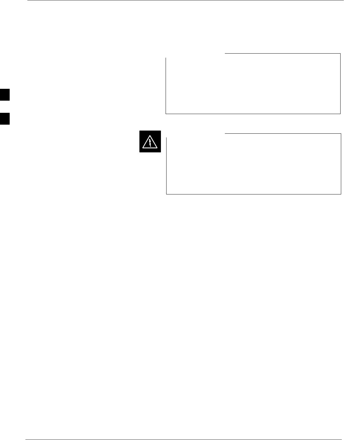
Test Equipment Set Up – continued
3-54 1X SC4812T–MC BTS Optimization/ATP 5/21/04
DRAFT
Equipment Warm-up
Warm-up BTS equipment for a minimum of 60 minutes
prior to performing the BTS optimization procedure. This
assures BTS site stability and contributes to optimization
accuracy. (Time spent running initial power-up,
hardware/firmware audit, and BTS download counts as
warm-up time.)
NOTE
Before installing any test equipment directly to any BTS
TX OUT connector, verify there are NO CDMA BBX
channels keyed. At active sites, have the OMC-R/CBSC
place the antenna (sector) assigned to the PA under test
OOS. Failure to do so can result in serious personal injury
and/or equipment damage.
WARNING
Automatic Cable Calibration
Set–up
Figure 3-13 and Figure 3-14 show the cable calibration setup for various
supported test sets. The left side of the diagram depicts the location of
the input and output ports of each test set, and the right side details the
set up for each test.
Manual Cable Calibration
If manual cable calibration is required, refer to the procedures in
Appendix F.
3
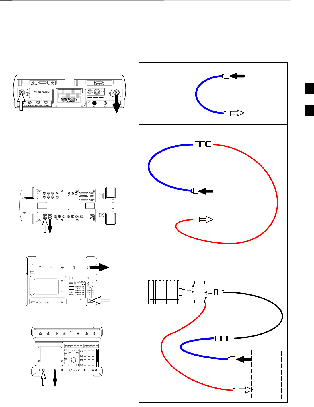
Test Equipment Set Up – continued
5/21/04 1X SC4812T–MC BTS Optimization/ATP 3-55
DRAFT
Figure 3-13: Cable Calibration Test Setup
Motorola CyberTest
Hewlett–Packard Model HP 8935
Advantest Model R3465
DUPLEX
OUT
RF OUTPUT
50–OHM
RF INPUT
50–OHM
RF GEN OUTANT IN
ANT
IN
SUPPORTED TEST SETS
100–WATT (MIN)
NON–RADIATING
RF LOAD
TEST
SET
A. SHORT CABLE CAL
SHORT
CABLE
B. RX TEST SETUP
TEST
SET
C. TX TEST SETUP
CALIBRATION SET UP
N–N FEMALE
ADAPTER
TX
CABLE
TX
CABLE
SHORT
CABLE
Note: The Directional Coupler is not used with the
Cybertest Test Set. The TX cable is connected
directly to the Cybertest Test Set.
A 10dB attenuator must be used with the short test
cable for cable calibration with the CyberTest Test
Set. The 10dB attenuator is used only for the cable
calibration procedure, not with the test cables for
TX calibration and ATP tests.
TEST
SET
RX
CABLE
SHORT
CABLE
FW00089
Hewlett–Packard Model HP 8921A
DIRECTIONAL COUPLER
(30 DB)
N–N FEMALE
ADAPTER
DUPLEX
OUT
RF IN/OUT
3
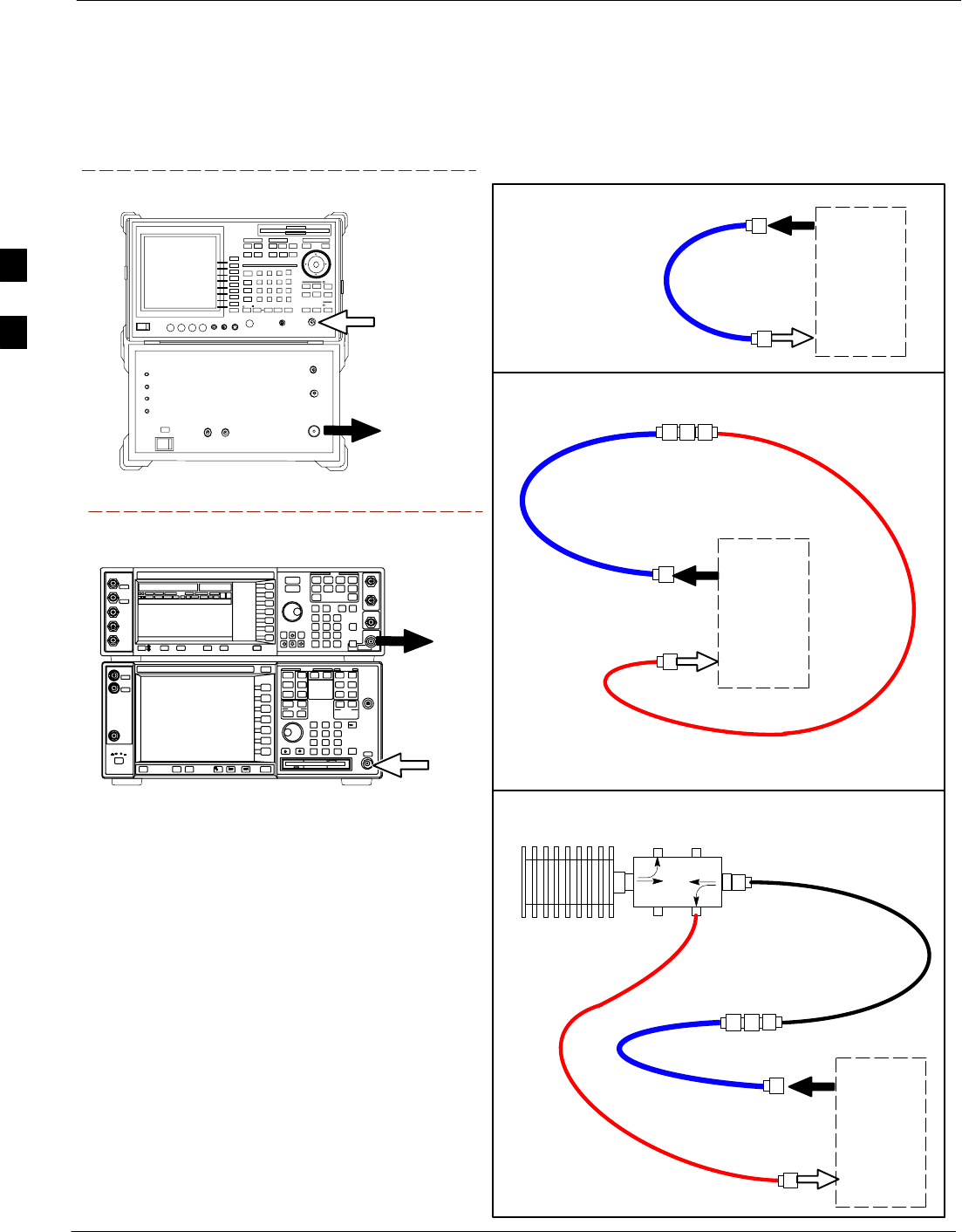
Test Equipment Set Up – continued
3-56 1X SC4812T–MC BTS Optimization/ATP 5/21/04
DRAFT
Figure 3-14: Cable Calibration Test Setup (Advantest R3267, Agilent E4406A)
SUPPORTED TEST SETS
100–WATT (MIN)
NON–RADIATING
RF LOAD
TEST
SET
A. SHORT CABLE CAL
SHORT
CABLE
B. RX TEST SETUP
TEST
SET
C. TX TEST SETUP
CALIBRATION SET UP
N–N FEMALE
ADAPTER
TX
CABLE
TX
CABLE
SHORT
CABLE
TEST
SET
RX
CABLE
SHORT
CABLE
REF FW00089
DIRECTIONAL COUPLER
(30 DB)
N–N FEMALE
ADAPTER
RF IN
RF OUT
Advantest R3267 (Top) and R3562 (Bottom)
EXT TRIG IN
MOD TIME BASE IN
(EXT REF IN)
RF
INPUT 50
OHM
RF
OUTPUT
50 OHM
Agilent E4432B (Top) and E4406A (Bottom)
3
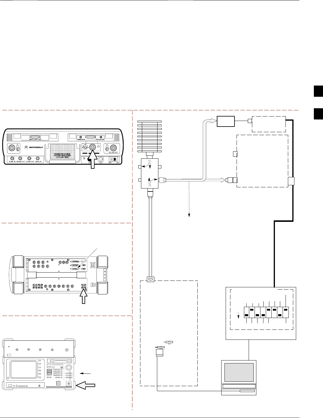
Test Equipment Set Up – continued
5/21/04 1X SC4812T–MC BTS Optimization/ATP 3-57
DRAFT
Set-up for TX Calibration
Figure 3-15 and Figure 3-16 show the test set connections for TX
calibration.
Figure 3-15: TX Calibration Test Setup (CyberTest, HP 8935, and Advantest)
Motorola CyberTest
Hewlett–Packard Model HP 8935
TEST SETS TRANSMIT (TX) SET UP
FRONT PANEL
RF
IN/OUT
RF IN/OUT
HP–IB
TO GPIB
BOX
RS232–GPIB
INTERFACE BOX
INTERNAL PCMCIA
ETHERNET CARD
GPIB
CABLE
COMMUNICATIONS
TEST SET
CONTROL
IEEE 488
GPIB BUS
UNIVERSAL TWISTED
PAIR (UTP) CABLE
(RJ45 CONNECTORS)
RS232
NULL
MODEM
CABLE
OUT
S MODE
DATA FORMAT
BAUD RATE
GPIB ADRS
G MODE
ON
TEST SET
INPUT/
OUTPUT
PORTS
BTS
100–WATT (MIN)
NON–RADIATING
RF LOAD
IN
TX
TEST
CABLE
CDMA
LMF
DIP SWITCH SETTINGS
10BASET/
10BASE2
CONVERTER
LAN
B
LAN
A
TX TEST
CABLE
TX ANTENNA
PORT
POWER
METER
(OPTIONAL)*
NOTE: THE DIRECTIONAL COUPLER IS NOT USED WITH THE
CYBERTEST TEST SET. THE TX CABLE IS CONNECTED DIRECTLY
TO THE CYBERTEST TEST SET.
Advantest Model R3465
INPUT
50–OHM
GPIB
CONNECTS TO
BACK OF UNIT
* A POWER METER CAN BE USED IN PLACE
OF THE COMMUNICATIONS TEST SET FOR TX
CALIBRATION/AUDIT
POWER
SENSOR
REF FW00094
30 DB
DIRECTIONAL
COUPLER
3
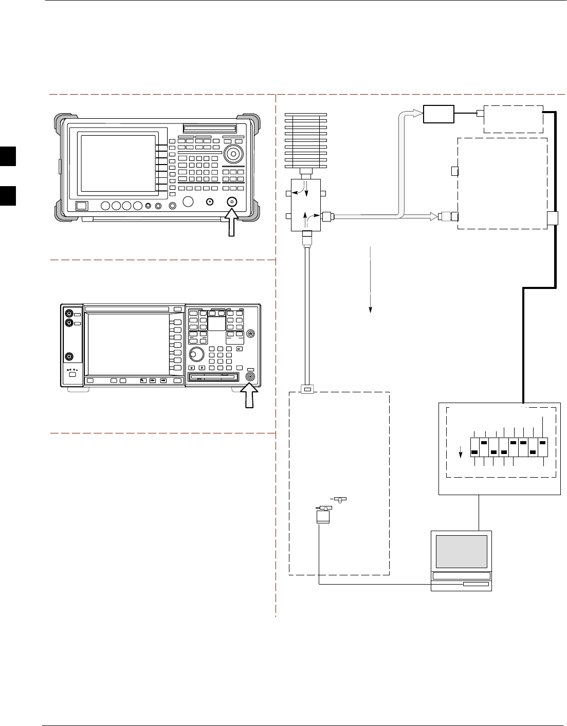
Test Equipment Set Up – continued
3-58 1X SC4812T–MC BTS Optimization/ATP 5/21/04
DRAFT
Figure 3-16: TX Calibration Test Setup (Advantest R3267 and Agilent E4406A)
TEST SETS TRANSMIT (TX) SET UP
RS232–GPIB
INTERFACE BOX
INTERNAL PCMCIA
ETHERNET CARD
GPIB
CABLE
COMMUNICATIONS
TEST SET
CONTROL
IEEE 488
GPIB BUS
UNIVERSAL TWISTED
PAIR (UTP) CABLE
(RJ45 CONNECTORS)
RS232
NULL
MODEM
CABLE
OUT
S MODE
DATA FORMAT
BAUD RATE
GPIB ADRS
G MODE
ON
TEST SET
INPUT/
OUTPUT
PORTS
BTS
100–WATT (MIN)
NON–RADIATING
RF LOAD
IN
TX
TEST
CABLE
CDMA
LMF
DIP SWITCH SETTINGS
10BASET/
10BASE2
CONVERTER
LAN
B
LAN
A
TX TEST
CABLE
TX ANTENNA
PORT
POWER
METER
(OPTIONAL)*
* A POWER METER CAN BE USED IN PLACE
OF THE COMMUNICATIONS TEST SET FOR TX
CALIBRATION/AUDIT
POWER
SENSOR
REF FW00094
30 DB
DIRECTIONAL
COUPLER
Agilent E4406A
Advantest Model R3267
RF IN
RF INPUT
50 Ω
3
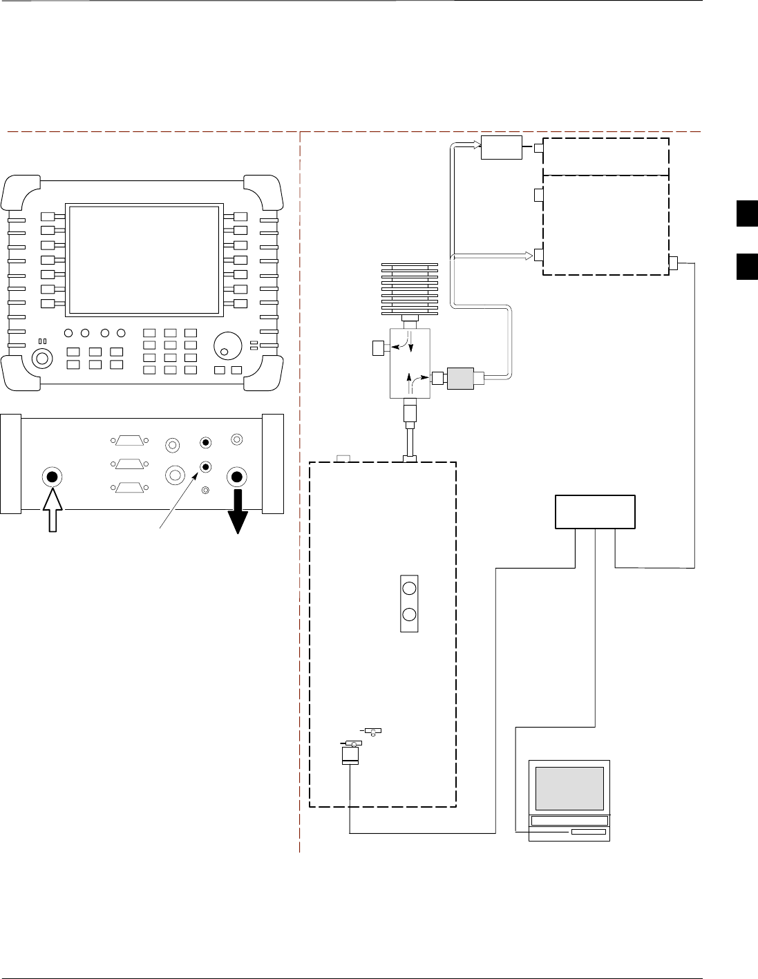
Test Equipment Set Up – continued
5/21/04 1X SC4812T–MC BTS Optimization/ATP 3-59
DRAFT
Figure 3-17: TX Calibration Test Setup – Agilent E7495A (IS–95A/B and CDMA2000 1X)
TEST SETS TRANSMIT (TX) SET UP
INTERNAL PCMCIA
ETHERNET CARD
BTS
CDMA
LMF
10BASET/
10BASE2
CONVERTER
LAN
B
LAN
A
RX
ANTENNA
CONNECTOR
SYNC
MONITOR
CSM
TX
ANTENNA
CONNECTOR
50 Ω
TERM
.
TX TEST
CABLE
DIRECTIONAL
COUPLER
(30 DB)
100–WATT (MIN.)
NON–RADIATING
RF LOAD
TX TEST
CABLE
NOTE: IF BTS IS EQUIPPED
WITH DUPLEXED RX/TX
SIGNALS, CONNECT THE TX
TEST CABLE TO THE
DUPLEXED ANTENNA
CONNECTOR.
POWER
SENSOR
2O DB IN–LINE
ATTENUATOR
ETHERNET HUB
UNIVERSAL TWISTED PAIR (UTP)
CABLE (RJ45 CONNECTORS)
Agilent E7495A
PORT 1
RF OUT
PORT 2
RF IN
SYNC MONITOR
EVEN SEC TICK
PULSE REFERENCE
FROM CSM BOARD
Use only
Agilent supplied
power adapter
GPS
GPIO
Serial 1
Serial 2
Power REF
50 MHz
Sensor
Ext Ref
In
Even Second
Sync In
Antenna
Port 1
RF Out / SWR
Port 2
RF In
INTERNAL
ETHERNET
CARD
COMMUNIC
ATIONS
system
analyzer
POWER METER
PORT 2
RF IN
PORT 1
RF OUT
3

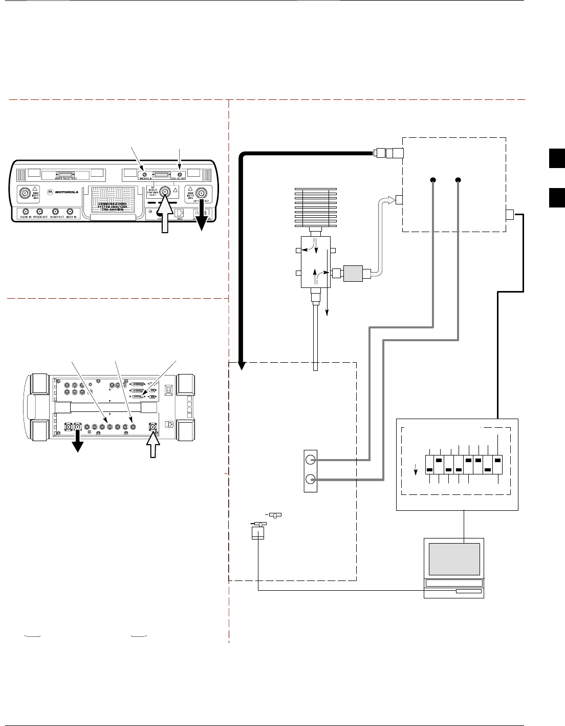
Test Equipment Set Up – continued
5/21/04 1X SC4812T–MC BTS Optimization/ATP 3-61
DRAFT
Figure 3-18: IS–95 A/B Optimization/ATP Test Setup Calibration Using Directional Coupler
(CyberTest, HP 8935 and Advantest)
Motorola CyberTest
Hewlett–Packard Model HP 8935
DUPLEX OUT
TEST SETS Optimization/ATP SET UP
RF
IN/OUT
SYNC MONITOR
EVEN SEC TICK
PULSE REFERENCE
FROM CSM BOARD
FREQ MONITOR
19.6608 MHZ CLOCK
REFERENCE FROM
CSM BOARD
RF IN/OUT
HP–IB
TO GPIB
BOX
Advantest Model R3465
INPUT
50–OHM
GPIB CONNECTS
TO BACK OF UNIT
NOTE: The Directional Coupler is not used
with the Cybertest Test Set. The TX cable is
connected directly to the Cybertest Test set.
RF OUT
SYNC MONITOR
EVEN SEC TICK
PULSE REFERENCE
FROM CSM BOARD
FREQ MONITOR
19.6608 MHZ CLOCK
REFERENCE FROM
CSM BOARD
SYNC MONITOR
EVEN SEC TICK
PULSE REFERENCE
FROM CSM BOARD
FREQ MONITOR
19.6608 MHZ CLOCK
REFERENCE FROM
CSM BOARD
RF
OUT
RX ANTENNA
PORT TX ANTENNA
PORT
RS232 NULL
MODEM
CABLE
BTS
TX
TEST
CABLE
10BASET/
10BASE2
CONVERTER
LAN
B
LAN
A
RX
TEST
CABLE
Communica
tions test
set
IEEE 488
GPIB BUS
IN
TEST SET
INPUT/
OUTPUT
PORTS
OUT
NOTE: IF BTS RX/TX SIGNALS ARE
DUPLEXED (4800E): BOTH THE TX AND RX
TEST CABLES CONNECT TO THE DUPLEXED
ANTENNA GROUP.
100–WATT (MIN)
NON–RADIATING
RF LOAD
10 DB PAD
EVEN
SECOND/SYNC
IN
CDMA
TIMEBASE
IN
FREQ
MONITOR
SYNC
MONITOR
CSM
30 DB
DIRECTIONAL
COUPLER
RS232–GPIB
INTERFACE BOX
S MODE
DATA FORMAT
BAUD RATE
GPIB ADRS G MODE
ON
DIP SWITCH SETTINGS
INTERNAL PCMCIA
ETHERNET CARD
UNIVERSAL TWISTED
PAIR (UTP) CABLE
(RJ45 CONNECTORS)
CDMA
LMF
REF FW00096
ADVANTEST NOT SUPPORTED
3
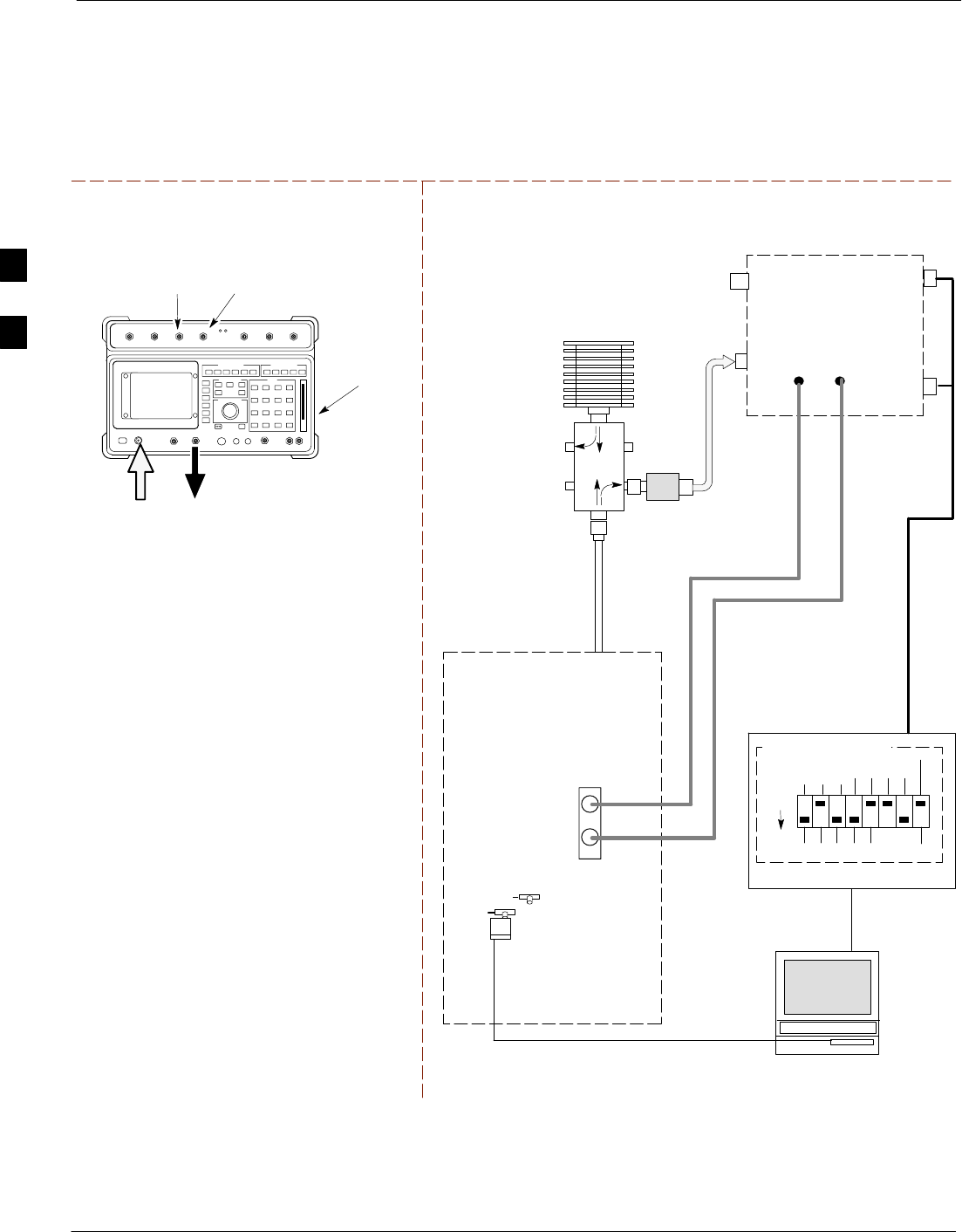
Test Equipment Set Up – continued
3-62 1X SC4812T–MC BTS Optimization/ATP 5/21/04
DRAFT
Figure 3-19: Optimization/ATP Test Setup HP 8921A
TEST SET Optimization/ATP SET UP
RX ANTENNA
PORT
TX ANTENNA
PORT
RS232–GPIB
INTERFACE BOX
INTERNAL PCMCIA
ETHERNET CARD
GPIB
CABLE
UNIVERSAL TWISTED
PAIR (UTP) CABLE
(RJ45 CONNECTORS)
RS232 NULL
MODEM
CABLE
S MODE
DATA FORMAT
BAUD RATE
GPIB ADRS G MODE
ON
BTS
TX
TEST
CABLE
CDMA
LMF
DIP SWITCH SETTINGS
10BASET/
10BASE2
CONVERTER
LAN
B
LAN
A
RX
TEST
CABLE
Communica
tions test
set
IEEE 488
GPIB BUS
IN
TEST SET
INPUT/
OUTPUT
PORTS
OUT
NOTE: IF BTS RX/TX SIGNALS ARE
DUPLEXED (4800E): BOTH THE TX AND RX
TEST CABLES CONNECT TO THE DUPLEXED
ANTENNA GROUP.
100–WATT (MIN)
NON–RADIATING
RF LOAD
10 DB PAD
EVEN
SECOND/SYNC
IN
CDMA
TIMEBASE
IN
FREQ
MONITOR
SYNC
MONITOR
CSM
REF FW00097
GPIB
CONNECTS
TO BACK OF
UNIT
SYNC MONITOR
EVEN SEC TICK
PULSE REFERENCE
FROM CSM BOARD
FREQ MONITOR
19.6608 MHZ CLOCK
REFERENCE FROM
CSM BOARD
Hewlett–Packard Model HP 8921A
30 DB
DIRECTIONAL
COUPLER
RF
IN/OUT
RF OUT
ONLY
3
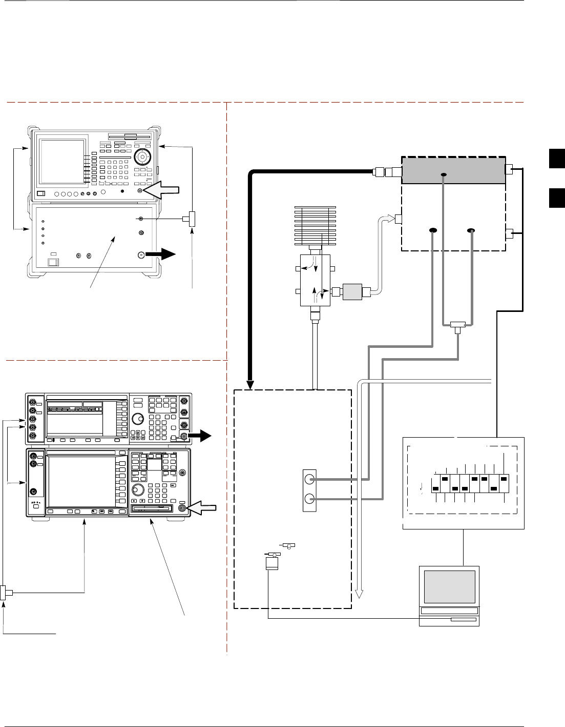
Test Equipment Set Up – continued
5/21/04 1X SC4812T–MC BTS Optimization/ATP 3-63
DRAFT
Figure 3-20: IS–95 A/B and CDMA 2000 Optimization/ATP Test Setup Using Directional Coupler
TEST SETS Optimization/ATP SET UP
RS232–GPIB
INTERFACE BOX
INTERNAL PCMCIA
ETHERNET CARD
GPIB
CABLE
UNIVERSAL TWISTED
PAIR (UTP) CABLE
(RJ45 CONNECTORS)
RS232 NULL
MODEM
CABLE
S MODE
DATA FORMAT
BAUD RATE
GPIB ADRS G MODE
ON
BTS
CDMA
LMF
DIP SWITCH SETTINGS
10BASET/
10BASE2
CONVERTER
LAN
B
LAN
A
Communications
test set
IEEE 488
GPIB BUS
IN
OUT
NOTE: IF BTS RX/TX SIGNALS ARE
DUPLEXED: BOTH THE TX AND RX TEST
CABLES CONNECT TO THE DUPLEXED
ANTENNA GROUP.
EVEN
SECOND/
SYNC IN
EXT
REF
IN
FREQ
MONITOR
SYNC
MONITOR
CSM
REF FW00758
RF
INPUT
50 Ω
RF
OUTPUT
50 Ω
Agilent E4432B (Top) and E4406A (Bottom)
FREQ MONITOR
19.6608 MHZ CLOCK
REFERENCE FROM
CSM BOARD
SYNC MONITOR
EVEN SEC TICK
PULSE REFERENCE
FROM CSM BOARD
BNC
“T”
TO TRIGGER IN
ON REAR OF
TRANSMITTER
TESTER
TO PATTERN TRIG IN
ON REAR OF SIGNAL
GENERATOR
EXT REF IN
ON REAR OF
TRANSMITTER
TESTER
RF IN
RF OUT
Advantest R3267 (Top) and R3562 (Bottom)
FREQ MONITOR
19.6608 MHZ CLOCK
REFERENCE FROM
CSM BOARD
SYNC MONITOR
EVEN SEC TICK
PULSE REFERENCE
FROM CSM BOARD
BNC
“T”
SYNTHE
REF IN
TO EXT TRIG
ON REAR OF
SPECTRUM
ANALYZER
sIGNAL
GENERATOR
RX ANTENNA
PORT
TX ANTENNA
PORT
RX
TEST
CABLE
100–WATT (MIN)
NON–RADIATING
RF LOAD
10 DB PAD
30 DB
DIRECTIONAL
COUPLER
TX
TEST
CABLE
BNC
“T”
19.6608
MHZ
CLOCK
EXT TRIG IN
MOD TIME BASE IN
(EXT REF IN)
10 MHZ
REF OUT
NOTE:
SYNTHE REF IN ON REAR OF SIGNAL GENERATOR IS
CONNECTED TO 10 MHZ REF OUT ON REAR OF
SPECTRUM ANALYZER.
10
MHZ
IN
10
MHZ
OUT
NOTE:
FOR MANUAL TESTING, GPIB MUST BE CONNECTED
BETWEEN THE ANALYZER AND THE SIGNAL
GENERATOR
3
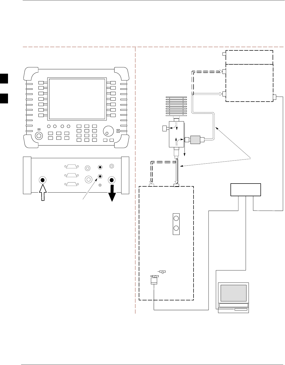
Test Equipment Set Up – continued
3-64 1X SC4812T–MC BTS Optimization/ATP 5/21/04
DRAFT
Figure 3-21: IS–95A/B and CDMA2000 1X Optimization/ATP Test Setup – Agilent E7495A
TEST SET ATP TEST SET UP
INTERNAL PCMCIA
ETHERNET CARD
UNIVERSAL TWISTED PAIR (UTP)
CABLE (RJ45 CONNECTORS)
BTS
CDMA
LMF
10BASET/
10BASE2
CONVERTER
LAN
B
LAN
A
INTERNAL
ETHERNET
CARD
RF INPUT 50 Ω
OR INPUT 50 Ω
SYNC
MONITOR
CSM
COMMUNIC
ATIONS
system
analyzer
50 Ω
TERM
TX TEST
DIRECTIONAL
COUPLER
(30 DB)
100–WATT (MIN.)
NON–RADIATING
RF LOAD
TX TEST
NOTE: IF BTS IS EQUIPPED
WITH DUPLEXED RX/TX
SIGNALS, CONNECT THE TX
TEST CABLE TO THE DUPLEXED
ANTENNA CONNECTOR.
2O DB IN–LINE
ATTENUATOR
ETHERNET HUB
RX TEST
RX TEST
RX
ANTENNA
CONNECTOR
TX
ANTENNA
CONNECTOR
TEST
CABLES
NOTE: USE THE SAME
CABLE SET FOR TX AND RX
ATP. SWITCH THE CABLES
DURING ALL ATP TESTS AS
SHOWN.
POWER METER
PORT 2
RF IN
PORT 1
RF OUT
Agilent E7495A
PORT 1
RF OUT
PORT 2
RF IN
SYNC MONITOR
EVEN SEC TICK
PULSE REFERENCE
FROM CSM BOARD
Use only
Agilent supplied
power adapter
GPS
GPIO
Serial 1
Serial 2
Power REF
50 MHz
Sensor
Ext Ref
In
Even Second
Sync In
Antenna
Port 1
RF Out / SWR
Port 2
RF In
TX ATP Setup
Figure 3-22 shows a typical TX ATP setup and Figure 3-23 shows a
typical RX ATP setup.
3
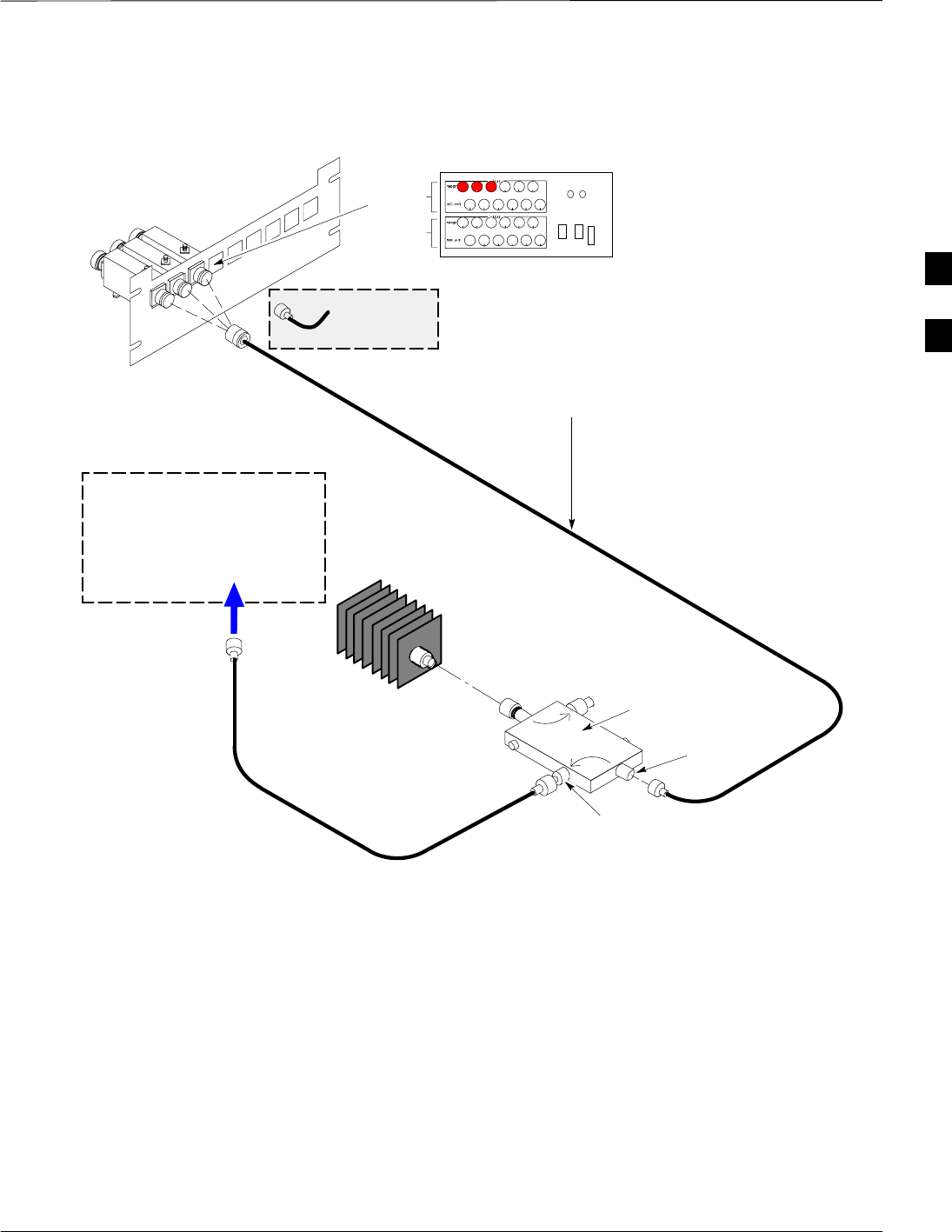
Test Equipment Set Up – continued
5/21/04 1X SC4812T–MC BTS Optimization/ATP 3-65
DRAFT
Figure 3-22: Typical TX ATP Setup with Directional Coupler (shown with and without RFDS)
30 DB
DIRECTIONAL
COUPLER
40W NON–RADIATING
RF LOAD
OUTPUT
PORT
RVS (REFLECTED)
PORT 50–OHM
TERMINATION
FWD
(INCIDENT)
PORT
BTS INPUT
PORT TX TEST
CABLE
Connect TX test cable between
the directional coupler input port
and the appropriate TX antenna
directional coupler connector.
TX ANTENNA DIRECTIONAL COUPLERS
RFDS RX (RFM TX) COUPLER
OUTPUTS TO RFDS FWD(BTS)
ASU2 (SHADED) CONNECTORS
RX
(RFM TX)
TX
(RFM RX)
COBRA RFDS Detail
1
2
3
RF FEED LINE TO
DIRECTIONAL
COUPLER
REMOVED
Communica
tions test
set IN
Appropriate test sets and the port
names for all model test sets are
described in Table 3-22.
TX
TEST
CABLE
TX RF FROM BTS FRAME
TEST
DIRECTIONAL
COUPLER
NOTE:
THIS SETUP APPLIES TO BOTH
STARTER AND EXPANSION FRAMES. ti-CDMA-WP-00121-v01-ildoc-ftw
3
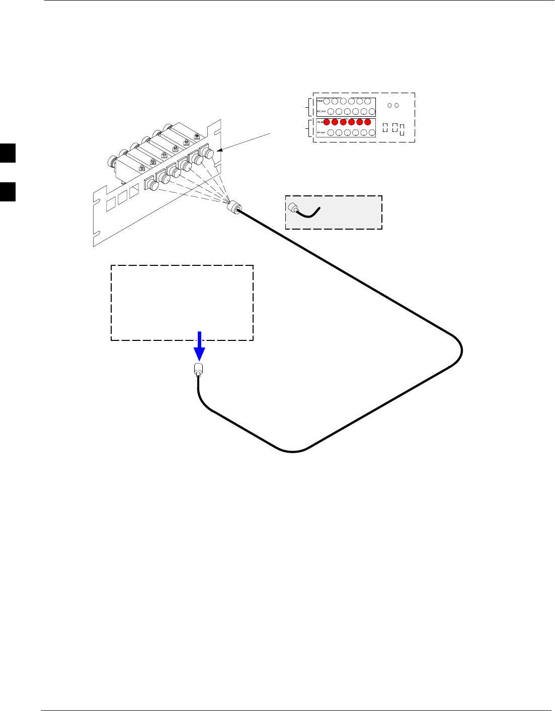
Test Equipment Set Up – continued
3-66 1X SC4812T–MC BTS Optimization/ATP 5/21/04
DRAFT
Figure 3-23: Typical RX ATP Setup with Directional Coupler (shown with or without RFDS)
RX RF FROM BTS
FRAME
3
4
1
2
5
6
Connect RX test cable between
the test set and the appropriate
RX antenna directional coupler.
RX ANTENNA DIRECTIONAL COUPLERS
RF FEED LINE TO
TX ANTENNA
REMOVED
Communica
tions test
set
RFDS TX (RFM RX) COUPLER
OUTPUTS TO RFDS FWD(BTS)
ASU1 (SHADED) CONNECTORS
RX
(RFM TX)
TX
(RFM RX)
COBRA RFDS Detail
OUT
Appropriate test sets and the port
names for all model test sets are
described in Table 3-22.
RX Test
Cable
NOTE:
THIS SETUP APPLIES TO BOTH
STARTER AND EXPANSION FRAMES.
FW00115
3
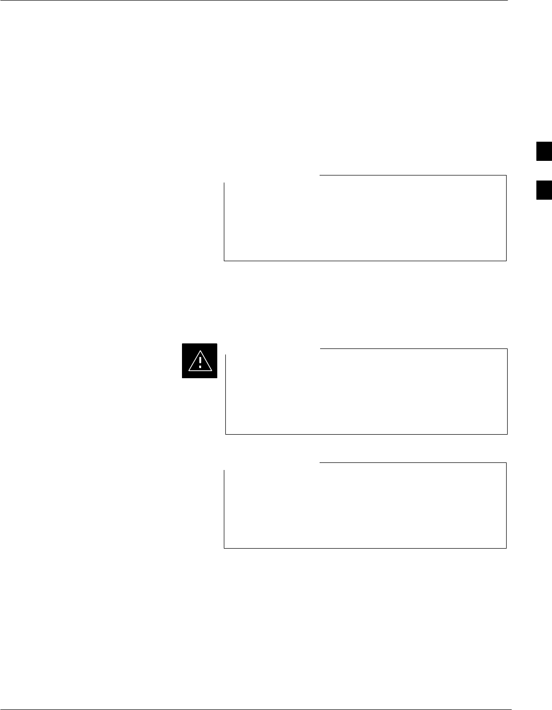
Test Set Calibration
5/21/04 1X SC4812T–MC BTS Optimization/ATP 3-67
DRAFT
Test Set Calibration
Background
Proper test equipment calibration ensures that the test equipment and
associated test cables do not introduce measurement errors, and that
measurements are correct.
If the test set being used to interface with the BTS has been
calibrated and maintained as a set, this procedure does not
need to be performed. (Test Set includes LMF terminal,
communications test set, additional test equipment,
associated test cables, and adapters.)
NOTE
This procedure must be performed prior to beginning the optimization.
Verify all test equipment (including all associated test cables and
adapters actually used to interface all test equipment and the BTS) has
been calibrated and maintained as a set.
If any piece of test equipment, test cable, or RF adapter,
that makes up the calibrated test equipment set, has been
replaced, re-calibration must be performed. Failure to do so
can introduce measurement errors, resulting in incorrect
measurements and degradation to system performance.
CAUTION
Calibration of the communications test set (or equivalent
test equipment) must be performed at the site before
calibrating the overall test set. Calibrate the test equipment
after it has been allowed to warm–up and stabilize for a
minimum of 60 minutes.
NOTE
Calibration Procedures
Included
Automatic
Procedures included in this section use the LMF automated calibration
routine to determine path losses of the supported communications
analyzer, power meter, associated test cables, adapters, and (if used)
antenna switch that make up the overall calibrated test equipment set.
After calibration, the gain/loss offset values are stored in a test
measurement offset file on the LMF computer.
3

Test Set Calibration – continued
3-68 1X SC4812T–MC BTS Optimization/ATP 5/21/04
DRAFT
Manual
Agilent E4406A Transmitter Tester – The E4406A does not support
the power level zeroing calibration performed by the LMF. If this
instrument is to be used for Bay Level Offset calibration and calibration
is attempted with the LMF Calibrate Test Equipment function, the
LMF will return a status window failure message stating that zeroing
power is not supported by the E4406A. Refer to the Equipment
Calibration section of Appendix F for instructions on using the
instrument’s self–alignment (calibration) function prior to performing
Bay Level Offset calibration.
Power Meters – Manual power meter calibration procedures to be
performed prior to automated calibration are included in the Equipment
Calibration section of Appendix F.
Cable Calibration – Manual cable calibration procedures using the HP
8921A and Advantest R3465 communications system analyzers are
provided in the Manual Cable Calibration section of Appendix F, if
needed.
GPIB Addresses
GPIB addresses can range from 1 through 30. The LMF will accept any
address in that range, but the numbers entered in the LMF Options
window GPIB address box must match the addresses of the test
equipment. Motorola recommends using 1 for a CDMA signal generator,
13 for a power meter, and 18 for a communications system analyzer. To
verify and, if necessary, change the GPIB addresses of the test
equipment, refer to the Setting GPIB Addresses section of Appendix F.
IP Addresses
The E7495A communications test set uses IP over Ethernet connections
for communication rather than the GPIB. For the Agilent E7495A, set
the IP address and complete initial setup as described in Appendix F,
Table F-1.
Selecting Test Equipment
Other Than Agilent E7495A
Open the LMF Options window from the Tools > Options menu list to
select test equipment automatically (using the autodetect feature) or
manually.
Serial Connection and Network Connection tabs are provided in the
LMF Options window to specify the test equipment connection method.
The Serial Connection tab is used when the test equipment items are
connected directly to the LMF computer through a GPIB box (normal
setup). The Network Connection tab is used when the test equipment is
to be connected remotely through a network connection.
Prerequisites
Ensure the following prerequisites have been met before proceeding:
3

Test Set Calibration – continued
5/21/04 1X SC4812T–MC BTS Optimization/ATP 3-69
DRAFT
STest equipment is correctly connected and turned on.
SGPIB addresses set in the test equipment have been verified as correct
using the applicable procedures in Appendix F.
SCDMA LMF computer serial port and test equipment are connected to
the GPIB box.
Selecting Test Equipment
Test equipment may be selected either manually with operator input or
automatically using the LMF autodetect feature.
Manually Selecting Test Equipment in a Serial Connection Tab –
Test equipment can be manually specified before, or after, the test
equipment is connected. The LMF does not check to see if the test
equipment is actually detected for manual specification. Follow the
procedure in Table 3-24 to select test equipment manually.
Table 3-24: Selecting Test Equipment Manually in a Serial Connection Tab
nStep Action
1From the Tools menu, select Options.
The LMF Options window appears.
2Click on the Serial Connection tab (if not in the forefront).
3Select the correct serial port in the COMM Port pick list (normally COM1).
4Click on the Manual Specification button (if not enabled).
5Click on the check box corresponding to the test item(s) to be used.
6NOTE
GPIB addresses can range from 1 through 30. The LMF will accept any address in that range, but
the numbers in the GPIB address boxes must match the addresses of the test equipment.
Motorola recommends using 1 for a CDMA signal generator, 13 for a power meter, and 18 for a
CDMA analyzer. To verify and, if necessary, change the GPIB addresses of the test equipment,
refer to Appendix F.
Type the GPIB address in the corresponding GPIB address box.
Recommended Addresses
1 = CDMA Signal generator
13 = Power Meter
18 = CDMA Analyzer
7Click on Apply. (The button darkens until the selection has been committed.)
NOTE
With manual selection, the LMF does not detect the test equipment to see if it is connected and
communicating with the LMF.
To verify and, if necessary, change the GPIB address of the test equipment, refer to Appendix
NO TAG.
. . . continued on next page
3

Test Set Calibration – continued
3-70 1X SC4812T–MC BTS Optimization/ATP 5/21/04
DRAFT
Table 3-24: Selecting Test Equipment Manually in a Serial Connection Tab
nActionStep
8Click on Dismiss to close the test equipment window.
Automatically Selecting Test Equipment in Serial Connection Tab –
When using the auto-detection feature to select test equipment, the LMF
examines which test equipment items are actually communicating with
the LMF. Follow the procedure in Table 3-25 to use the auto-detect
feature.
Table 3-25: Selecting Test Equipment Using Auto-Detect
nStep Action
1From the Tools menu, select Options.
The LMF Options window appears.
2Click on the Serial Connection tab (if not in the forefront).
3Select the correct serial port in the COMM Port pick list (normally COM1).
4Click on Auto–Detection (if not enabled).
NOTE
GPIB addresses can range from 1 through 30. The LMF will accept any address in that range, but
the numbers in the GPIB address to search box must match the addresses of the test equipment.
Motorola recommends using 1 for a CDMA signal generator, 13 for a power meter, and 18 for a
CDMA analyzer. To verify and, if necessary, change the GPIB addresses of the test equipment,
refer to Appendix NO TAG.
5Type the GPIB addresses in the box labeled GPIB address to search (if not already displayed).
NOTE
When both a power meter and an analyzer are selected, the LMF uses the first item that is capable
of performing the test and is listed in the GPIB addresses to search box for RF power
measurements (i.e., TX calibration). The address for a CDMA signal generator is normally 1, the
address for a power meter is normally 13, and the address for a CDMA analyzer is normally 18. If
1,13,18 is included in the GPIB addresses to search box, the power meter (13) is used for RF
power measurements. When the test equipment items are manually selected, the CDMA analyzer
is used only if a power meter is not selected.
6Click on Apply.
NOTE
The button darkens until the selection has been committed. A check mark appears in the Manual
Configuration section for detected test equipment items.
7 Click Dismiss to close the LMF Options window.
3

Test Set Calibration – continued
5/21/04 1X SC4812T–MC BTS Optimization/ATP 3-71
DRAFT
Detecting Test Equipment
When Using Agilent E7495A
Be sure that no other equipment is connected to the LMF. The Agilent
E7495A must be connected to the LAN to detect it. Then perform the
procedures described in Appendix F, Table F-1, Table F-2, and
Table F-3.
Calibrating Test Equipment
The calibrate test equipment function zeros the power measurement level
of the test equipment item that is to be used for TX calibration and audit.
If both a power meter and an analyzer are connected, only the power
meter is zeroed.
The Agilent E4406A transmitter tester does not support
power measurement level zeroing. Refer to the Equipment
Calibration section of Appendix F for E4406A calibration.
NOTE
Prerequisites
SLMF computer serial port and test equipment are connected to the
GPIB box.
STest equipment to be calibrated has been connected correctly for tests
that are to be run.
STest equipment has been selected in the LMF (Table 3-24 or
Table 3-25).
Calibrating test equipment
Follow the procedure in Table 3-26 to calibrate the test equipment.
Table 3-26: Test Equipment Calibration
nStep Action
1From the Util menu, select Calibrate Test Equipment
from the pull–down menu. A Directions window is
displayed.
2Follow the directions provided.
3Click on Continue to close the Directions window and
start the calibration process. A status report window is
displayed.
4Click on OK to close the status report window.
Calibrating Cables Overview
The cable calibration function measures the loss (in dB) for the TX and
RX cables that are to be used for testing. A CDMA analyzer is used to
3

Test Set Calibration – continued
3-72 1X SC4812T–MC BTS Optimization/ATP 5/21/04
DRAFT
measure the loss of each cable configuration (TX cable configuration and
RX cable configuration). The cable calibration consists of the following:
SMeasuring the loss of a short cable – This is required to compensate
for any measurement error of the analyzer. The short cable (used only
for the calibration process) is used in series with both the TX and RX
cable configuration when measuring. The measured loss of the short
cable is deducted from the measured loss of the TX and RX cable
configuration to determine the actual loss of the TX and RX cable
configurations. The result is then adjusted out of both the TX and RX
measurements to compensate for the measured loss.
SMeasuring the short cable plus the RX cable configuration loss –
The RX cable configuration normally consists only of a coax cable
with type-N connectors that is long enough to reach from the BTS RX
port of the test equipment.
SMeasuring the short cable plus the TX cable configuration loss –
The TX cable configuration normally consists of two coax cables with
type-N connectors and a directional coupler, a load, and an additional
attenuator (if required by the specified BTS). The total loss of the path
loss of the TX cable configuration must be as required for the BTS
(normally 30 or 50 dB).
Calibrate Test Cabling using
Communications System
Analyzer
Cable Calibration is used to calibrate both TX and RX test cables.
Appendix F covers the procedures for manual cable calibration.
Prerequisites
Ensure the following prerequisites have been met before proceeding:
SOne of the following:
– LMF computer serial port and test equipment are connected to the
GPIB box
– For E7495A, the LMF computer network card and the E7495 are
connected to the Ethernet hub (Appendix NO TAG, Agilent
E7495A Test Equipment Setup section, Connections subsection)
STest equipment is turned on and has warmed up for at least 60
minutes.
STest equipment has been selected in the LMF (Table 3-24, Table 3-25,
or Table F-2)
Calibrating cables
Refer to Figure 3-13 or Figure 3-14 and follow the procedure in
Table 3-27 to calibrate the test cable configurations.
Table 3-27: Cable Calibration
nStep Action
1From the Util menu, select Cable Calibration. A Cable
Calibration window is displayed.
3

Test Set Calibration – continued
5/21/04 1X SC4812T–MC BTS Optimization/ATP 3-73
DRAFT
Table 3-27: Cable Calibration
nActionStep
2Enter the channel number(s) in the Channels box.
NOTE
Multiple channel numbers must be separated with a
comma and no space (i.e.; 200,800). When two or more
channel numbers are entered, the cables are calibrated for
each channel. Interpolation is accomplished for other
channels as required for TX calibration.
3In the Cable Calibration pick list select one of the
following:
–TX and RX Cable Cal
–TX Cable Cal
–RX Cable Cal
4 Click OK and follow the direction displayed for each
step. A status report window displays the results of the
cable calibration.
Calibrate Test Cabling Using
Signal Generator & Spectrum
Analyzer
Follow the procedure in Table 3-28 to calibrate the TX/Duplexed RX
cables using a signal generator and spectrum analyzer. Refer to
Figure 3-24, if required. Follow the procedure in Table 3-29 to calibrate
the Non–Duplexed RX cables using the signal generator and spectrum
analyzer. Refer to Figure 3-25, if required.
TX and Duplexed RX Cable Calibration
Table 3-28: Calibrating TX and Duplexed RX Cables Using Signal Generator and Spectrum Analyzer
nStep Action
1Connect a short test cable between the spectrum analyzer and the signal generator.
2Set signal generator to 0 dBm at the customer frequency of 869–894 MHz.
3Use a spectrum analyzer to measure signal generator output (see Figure 3-24, A) and record the
value.
4Connect the spectrum analyzer’s short cable to point B, (as shown in the lower right portion of the
diagram) to measure cable output at customer frequency of 869–894 MHz. Record the value at
point B.
. . . continued on next page
3
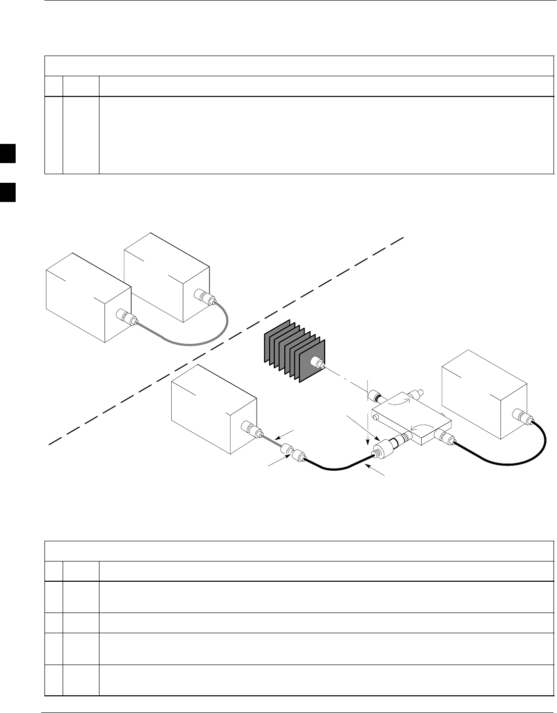
Test Set Calibration – continued
3-74 1X SC4812T–MC BTS Optimization/ATP 5/21/04
DRAFT
Table 3-28: Calibrating TX and Duplexed RX Cables Using Signal Generator and Spectrum Analyzer
nActionStep
5Calibration factor = A – B. Example: Cal = –1 dBm – (–53.5 dBm) = 52.5 dB
NOTE
The short cable is used for calibration only. It is not part of the final test setup. After calibration is
completed, do not re-arrange any cables. Use the equipment setup, as is, to ensure test procedures
use the correct calibration factor.
Figure 3-24: Calibrating Test Equipment Setup for TX BLO and TX ATP Tests
(using Signal Generator and Spectrum Analyzer)
50 OHM
TERMINATION
30 DB
DIRECTIONAL
COUPLER
Spectrum
Analyzer
Signal
Generator
A
Spectrum
Analyzer
40W NON–RADIATING
RF LOAD
B
SHORT TEST CABLE
Signal
Generator
THIS WILL BE THE CONNECTION TO THE HP8481A POWER
SENSOR DURING TX BAY LEVEL OFFSET TEST AND TO THE
PCS INTERFACE BOX INPUT PORT DURING TX ATP TESTS.
SHORT
TEST
CABLE
THIS WILL BE THE CONNECTION TO
THE TX PORTS DURING TX BAY LEVEL
OFFSET TEST AND TX ATP TESTS.
CABLE FROM 20 DB @ 20W ATTENUATOR TO THE
PCS INTERFACE OR THE HP8481A POWER SENSOR.
ONE 20DB 20 W IN
LINE ATTENUATOR
FW00293
Non-Duplexed RX Cable Calibration
Table 3-29: Calibrating RX Cables Using a Signal Generator and Spectrum Analyzer
nStep Action
1Connect a short test cable to the spectrum analyzer and connect the other end to the Signal
Generator.
2Set signal generator to –10 dBm at the customer’s RX frequency of 824–849 MHz.
3Use spectrum analyzer to measure signal generator output (see Figure 3-25, A) and record the
value for A.
4Connect the test setup, as shown in the lower portion of the diagram to measure the output at the
customer’s RX frequency of 824–849 MHz. Record the value at point B.
. . . continued on next page
3
Test Set Calibration – continued
5/21/04 1X SC4812T–MC BTS Optimization/ATP 3-75
DRAFT
Table 3-29: Calibrating RX Cables Using a Signal Generator and Spectrum Analyzer
nActionStep
5Calibration factor = A – B. Example: Cal = –12 dBm – (–14 dBm) = 2 dBm
NOTE
The short cable is used for calibration only. It is not part of the final test setup. After calibration is
completed, do not re-arrange any cables. Use the equipment setup, as is, to ensure test procedures
use the correct calibration factor.
Figure 3-25: Calibrating Test Equipment Setup for RX ATP Test
(using Signal Generator and Spectrum Analyzer)
Spectrum
Analyzer
Signal
Generator
a
b
Spectrum
Analyzer
SHORT
TEST
CABLE
SHORT TEST
CABLE
CONNECTION TO THE HP PCS
INTERFACE OUTPUT PORT
DURING RX MEASUREMENTS.
Signal
Generator
BULLET
CONNECTOR
LON
G
cable
2
CONNECTION TO THE RX PORTS
DURING RX MEASUREMENTS. FW00294
Setting Cable Loss Values
Cable loss values for the TX and RX test cable configurations are
normally set by accomplishing cable calibration using the applicable test
equipment. The resulting values are stored in the cable loss files. The
cable loss values can also be set/changed manually. Follow the procedure
in Table 3-30 to set cable loss values.
If cable calibration was performed without using the LMF,
cable loss values must be manually entered in the LMF
database. Failure to do this will result in inaccurate BTS
calibration and reduced site performance.
CAUTION
Prerequisites
SLogged into the BTS
3

Test Set Calibration – continued
3-76 1X SC4812T–MC BTS Optimization/ATP 5/21/04
DRAFT
Table 3-30: Setting Cable Loss Values
nStep Action
1Click on the Util menu.
2 Select Edit > Cable Loss.
3In the data entry pop–up window, select TX Cable Loss or RX Cable Loss.
4To add a new channel number, click on the Add Row button, then click in the Channel # and
Loss (dBm) columns and enter the desired values.
5To edit existing values, click in the data box to be changed and change the value.
6To delete a row, click on the row and then click on the Delete Row button.
7To save displayed values, click on the Save button.
8To exit the window, click on the Dismiss button.
Values entered/changed after the Save button was used are not saved.
NOTE
SIf cable loss values exist for two different channels, the LMF will interpolate for all other
channels.
SEntered values are used by the LMF as soon as they are saved. Logging out and logging in
again is not necessary.
Setting Coupler Loss Values
If an in–service coupler is installed, the coupler loss (e.g., 30 dB) must
be manually entered so it will be included in the LMF TX calibration
and audit calculations and RX FER Test. Follow the procedure in
Table 3-31 to set coupler loss values.
Prerequisites
SLogged into the BTS.
Table 3-31: Setting Coupler Loss Value
nStep Action
1Click on the Util menu.
2 Select Edit > Coupler Loss.
3In the data entry pop–up window, select one of the
following:
–TX Coupler Loss
–RX Coupler Loss.
4Click in the Loss (dBm) column for each carrier that has
a coupler and enter the appropriate value.
. . . continued on next page
3

Test Set Calibration – continued
5/21/04 1X SC4812T–MC BTS Optimization/ATP 3-77
DRAFT
Table 3-31: Setting Coupler Loss Value
nActionStep
5To edit existing values click in the data box to be changed
and change the value.
6Click on the Save button to save displayed values.
7Click on the Dismiss button to exit the window.
Values entered/changed after the Save button was used
are not saved.
NOTE
SThe In–Service Calibration check box in the
Tools > Options > BTS Options tab must checked
before entered coupler loss values are used by the TX
calibration and audit functions or RX FER test.
SEntered values are used by the LMF as soon as they are
saved. Logging out and logging in again is not
necessary.
3

Bay Level Offset Calibration
3-78 1X SC4812T–MC BTS Optimization/ATP 5/21/04
DRAFT
Introduction
Bay Level Offset (BLO) calibration is the central activity of the
optimization process. BLO calibration compensates for normal
equipment variations within the BTS RF paths and assures the correct
transmit power is available at the BTS antenna connectors to meet site
performance requirements.
RF Path Bay Level Offset
Calibration
Calibration identifies the accumulated gain in every transmit path (BBX
slot) at the BTS site and stores that value in a BLO database calibration
table in the LMF. The BLOs are subsequently downloaded to each BBX.
For starter frames, each receive path starts at a BTS RX antenna port and
terminates at a backplane BBX slot. Each transmit path starts at a BBX
backplane slot, travels through the Power Amplifier (PA), and terminates
at a BTS TX antenna port.
For expansion frames each receive path starts at the BTS RX port of the
cell site starter frame, travels through the frame-to-frame expansion
cable, and terminates at a backplane BBX slot of the expansion frame.
The transmit path starts at a BBX backplane slot of the expansion frame,
travels though the PA, and terminates at a BTS TX antenna port of the
same expansion frame.
Calibration identifies the accumulated gain in every transmit path (BBX
slot) at the BTS site and stores that value in a BLO database. Each
transmit path starts at a C–CCP shelf backplane BBX slot, travels
through the PA, and ends at a BTS TX antenna port. When the TX path
calibration is performed, the RX path BLO is automatically set to the
default value.
At omni sites, BBX slots 1 and 13 (redundant) are tested. At sector sites,
BBX slots 1 through 12, and 13 (redundant) are tested. Only those slots
(sectors) actually equipped in the current CDF or NEC file are tested,
regardless of physical BBX board installation in the slot.
When to Calibrate BLOs
Calibration of BLOs is required:
SAfter initial BTS installation
SOnce each year
SAfter replacing any of the following components or associated
interconnecting RF cabling:
– BBX board
– C–CCP shelf
– MCIO card
– MCIO to Power Amplifier backplane RF cable
– Parallel Linear Amplifier Combiner
3
Bay Level Offset Calibration – continued
5/21/04 1X SC4812T–MC BTS Optimization/ATP 3-79
DRAFT
– Power Amplifier
– TX filter
– Enhanced Trunking Module (ETM)
– TX thru-port cable to the top of frame
TX Path Calibration
The TX Path Calibration assures correct site installation, cabling, and the
first order functionality of all installed equipment. The proper function
of each RF path is verified during calibration. The external test
equipment is used to validate/calibrate the TX paths of the BTS.
Before installing any test equipment directly to any TX
OUT connector you must first verify that there are no
CDMA channels keyed. Have the OMC–R place the sector
assigned to the PA under test OOS. Failure to do so can
result in serious personal injury and/or equipment damage.
WARNING
Always wear an approved anti–static wrist strap while
handling any circuit card/module. If this is not done, there
is a high probability that the card/module could be
damaged by ESD.
CAUTION
At new site installations, to facilitate the complete test of
each CCP shelf (if the shelf is not already fully populated
with BBX boards), move BBX boards from shelves
currently not under test and install them into the empty
BBX slots of the shelf currently being tested to insure that
all BBX TX paths are tested.
This procedure can be bypassed on operational sites that
are due for periodic optimization.
Prior to testing, view the CDF file to verify the correct
BBX slots are equipped. Edit the file as required to include
BBX slots not currently equipped (per Systems
Engineering documentation).
NOTE
3

Bay Level Offset Calibration – continued
3-80 1X SC4812T–MC BTS Optimization/ATP 5/21/04
DRAFT
BLO Calibration Data File
During the calibration process, the LMF creates a bts–#.cal
calibration (BLO) offset data file (CAL file) in the bts–# folder. After
calibration has been completed, this offset data must be downloaded to
the BBXs using the LMF Download BLO function. An explanation of
the file is shown below.
Due to the size of the file, Motorola recommends printing a
hard copy of a CAL file and refer to it for the following
descriptions.
NOTE
The CAL file is subdivided into sections organized on a per slot basis (a
slot Block).
Slot 1 contains the calibration data for the 12 BBX slots. Slot 20
contains the calibration data for the redundant BBX. Each BBX slot
header block contains:
SA creation Date and Time – broken down into separate parameters of
createMonth, createDay, createYear, createHour, and createMin.
SThe number of calibration entries – fixed at 720 entries corresponding
to 360 calibration points of the CAL file including the slot header and
actual calibration data.
SThe calibration data for a BBX is organized as a large flat array. The
array is organized by branch, sector, and calibration point.
– The first breakdown of the array indicates which branch the
contained calibration points are for. The array covers transmit, main
receive and diversity receive offsets as follows:
Table 3-32: BLO BTS.cal File Array Assignments
Range Assignment
C[1]–C[240] Transmit
C[241]–C[480] Main Receive
C[481]–C[720] Diversity Receive
– The second breakdown of the array is per sector. Configurations
supported are Omni, 3–sector or 6–sector.
3

Bay Level Offset Calibration – continued
5/21/04 1X SC4812T–MC BTS Optimization/ATP 3-81
DRAFT
Table 3-33: BTS.cal File Array (Per Sector)
BBX Sectorization TX RX RX Diversity
Slot[1] (Primary BBXs 1 through 12)
1 (Omni) 3–Sector
,
C[1]–C[20] C[241]–C[260] C[481]–C[500]
2
3
–
Sector
,
1st
Ci
C[21]–C[40] C[261]–C[280] C[501]–C[520]
36 Sector,
1st
Carrier C[41]–C[60] C[281]–C[300] C[521]–C[540]
4
1
st
Carrier 3–Sector
,
C[61]–C[80] C[301]–C[320] C[541]–C[560]
5
Carrier
3
–
Sector
,
3rd
Ci
C[81]–C[100] C[321]–C[340] C[561]–C[580]
6Carrier C[101]–C[120] C[341]–C[360] C[581]–C[600]
73–Sector
,
C[121]–C[140] C[361]–C[380] C[601]–C[620]
8
3
–
Sector
,
2nd
Ci
C[141]–C[160] C[381]–C[400] C[621]–C[640]
96 Sector,
2nd
Carrier C[161]–C[180] C[401]–C[420] C[641]–C[660]
10
2
n
d
Carrier 3–Sector
,
C[181]–C[200] C[421]–C[440] C[661]–C[680]
11
Carrier
3
–
Sector
,
4th
Ci
C[201]–C[220] C[441]–C[460] C[681]–C[700]
12 Carrier C[221]–C[240] C[461]–C[480] C[701]–C[720]
. . . continued on next page
3

Bay Level Offset Calibration – continued
3-82 1X SC4812T–MC BTS Optimization/ATP 5/21/04
DRAFT
Table 3-33: BTS.cal File Array (Per Sector)
BBX RX DiversityRXTXSectorization
Slot[20] (Redundant BBX–13)
1 (Omni) 3–Sector
,
C[1]–C[20] C[241]–C[260] C[481]–C[500]
2
3
–
Sector
,
1st
Ci
C[21]–C[40] C[261]–C[280] C[501]–C[520]
36 Sector,
1st
Carrier C[41]–C[60] C[281]–C[300] C[521]–C[540]
4
1
st
Carrier 3–Sector
,
C[61]–C[80] C[301]–C[320] C[541]–C[560]
5
Carrier
3
–
Sector
,
3rd
Ci
C[81]–C[100] C[321]–C[340] C[561]–C[580]
6Carrier C[101]–C[120] C[341]–C[360] C[581]–C[600]
73–Sector
,
C[121]–C[140] C[361]–C[380] C[601]–C[620]
8
3
–
Sector
,
2nd
Ci
C[141]–C[160] C[381]–C[400] C[621]–C[640]
96 Sector,
2nd
Carrier C[161]–C[180] C[401]–C[420] C[641]–C[660]
10 2nd
Carrier
3
–
Sector,
C[181]–C[200] C[421]–C[440] C[661]–C[680]
11
Carrier
3
–
Sector
,
4th C[201]–C[220] C[441]–C[460] C[681]–C[700]
12 Carrier C[221]–C[240] C[461]–C[480] C[701]–C[720]
STen calibration points per sector are supported for each branch. Two
entries are required for each calibration point:
1. The first value (all odd entries) identifies the CDMA channel
(frequency) where the BLO is measured.
2. The second value (all even entries) is the power set level
(PwrLvlAdj). The valid range for PwrLvlAdj is from 2500 to
27500 (2500 corresponds to –125 dBm and 27500 corresponds
to +125 dBm).
SThe 20 calibration entries for each sector/branch combination must be
stored in order of increasing frequency. If less than 10 points
(frequencies) are calibrated, data for the highest frequency calibrated
is repeated to fill out the remainder of the 10 points.
Example:
C[1]=384, odd cal entry
= 1 ‘‘calibration point”
C[2]=19102, even cal entry
C[3]=777,
C[4]=19086,
.
.
C[19]=777,
C[20]=19086, (Since only two frequencies were calibrated, data for
this one, the highest, is repeated for the last eight
calibration points of the sector/branch)
SWhen the BBX is loaded with data, the CAL file data for the BBX is
downloaded to the device in the order it is stored in the CAL file.
TxCal data is sent first, C[1] – C[240]. Sector 1’s ten calibration
points are sent (C[1] – C[20]) followed by sector 2’s ten calibration
3

Bay Level Offset Calibration – continued
5/21/04 1X SC4812T–MC BTS Optimization/ATP 3-83
DRAFT
points (C[21] – C[40]), etc. The RxCal data is sent next (C[241] –
C[480]), followed by the RxDCal data (C[481] – C[720]).
STemperature compensation data is also stored in the cal file for each
set.
Test Equipment Set-up for
RF Path Calibration
Follow the procedure in Table 3-34 to set up test equipment.
Table 3-34: Test Equipment Setup (RF Path Calibration)
nStep Action
1Verify the GPIB controller is properly connected and turned on (does not apply to
the Agilent E7495A).
! CAUTION
To prevent damage to the test equipment, all transmit (TX) test connections must
be via the 30 dB directional coupler.
2If it has not already been done, connect the LMF computer to the BTS LAN A
connector on the BTS. Refer to the procedure in Table 3–2.
SIf required, calibrate the test equipment using the procedure in Table 3-26.
SConnect the test equipment as shown in Figure 3-15 throug Figure 3-17.
Transmit (TX) Path Calibration
Description
The assigned channel frequency and power level (as measured at the top
of the frame) for transmit calibration are derived from the site CDF files.
For each BBX, the channel frequency is specified in the [CdmaChans]
in the cbsc–#.cdf file and the power is specified in the SIFPilotPwr
CDF file parameter for the sector associated with the BBX (located
under the ParentSECTOR field of the ParentCARRIER CDF file
parameter).
If both the bts–#.cdf and cbsc–#.cdf or
NECB*bts#.xml and NECJ*bts#.xml files are current,
all information will be correct on the LMF. If not, the
carrier and channel will have to be set for each test.
NOTE
The calibration procedure attempts to adjust the power to within "0.5
dB of the desired power. The calibration will pass if the error is less than
the value set in the “TX Nominal offset” tolerance.
3

Bay Level Offset Calibration – continued
3-84 1X SC4812T–MC BTS Optimization/ATP 5/21/04
DRAFT
Transmit (TX) Bay Level Offset (BLO) Specifications –
SC4812T–MC TX BLO specifications for different BTS sector
configurations are as follows:
Table 3-35: Transmit (TX) Bay Level Offset (BLO) Specification
Single Sided Double Sided
800 MHz 3–Sector > 35dB 40dB +/– 5dB
800 MHz 6–Sector > 38dB 43dB +/– 5dB
1.9 GHz 3–Sector > 30dB 35dB +/– 5dB
1.9 GHz 6–Sector > 33dB 38dB +/– 5dB
To set the expected values see Table 3-36.
TX Calibration and the LMF
The LMF Tests > TX > TX Calibration... and Tests > All Cal/Audit...
selections perform TX BLO calibration testing for installed BBX(s). The
All Cal/Audit... selection initiates a series of actions to perform TX
calibration, and, if calibration is successful, download BLO and perform
TX audit. The TX Calibration... selection performs only TX
calibration. When TX Calibration... is used, BLO download and TX
audit must be performed as separate activities. The CDMA Test
Parameters window which opens when TX Calibration... or All
Cal/Audit... is selected contains several user–selectable features which
are described in the following subsections.
Rate Set Drop–down Pick List
The Rate Set drop–down box is enabled if at least one MCC card is
selected for the test. The available options for TX tests are 1 = 9600, and
3 = 9600 1X. Option 3 is only available if 1X cards are selected for the
test. The available transfer rate options for RX tests are 1 = 9600 and
2 = 14400. Option 2 is only available if no 1X cards are selected.
Verify BLO
In both the TX Calibration and All Cal/Audit dialog boxes, a Verify
BLO checkbox is provided and checked by default. After the actual TX
calibration is completed during either the TX Calibration or All
Cal/Audit process, the BLO derived from the calibration is compared to
a standard, acceptable BLO tolerance for the BTS. In some installations,
additional items may be installed in the transmit path. The additional
change in gain from these items could cause BLO verification failure
and, therefore, failure of the entire calibration. In these cases, either the
Verify BLO checkbox should be unchecked or the additional path losses
should be added into each applicable sector using the
Util > Edit > TX Coupler Loss... function.
3

Bay Level Offset Calibration – continued
5/21/04 1X SC4812T–MC BTS Optimization/ATP 3-85
DRAFT
Single–sided BLO Checkbox
Another option that appears in the pull–down menu is Single–sided
BLO. Normally valid BLO values are some value plus–or–minus some
offset. The ranges currently used for calibration are wider than necessary
to accommodate the redundant BBX. The lower half of the allowable
range is where non–redundant BBXs should function. Single–sided BLO
spec is >35dB. Double–sided BLO spec is 40+5dB. To get the more
stringent conditions, the operator checks Single–sided BLO when
calibrating non-redundant transceivers. Single–sided BLO carries the
likelihood of more failures. This option should only be used by
experienced CFEs.
The Tests > TX > TX Calibration... menu window has a Test Pattern
pull–down menu. This menu has the following choices:
SPilot (default) – performs tests using a pilot signal only. This pattern
should be used when running in–service tests. It only requires a BBX
to do the test.
SStandard – performs the tests using pilot, synch, paging and six
traffic channels. This pattern should be used on all non–in–service
tests. Standard requires a BBX and an MCC. Standard uses gain
values specified by the IS97 standard.
SCDFPilot –performs the tests using the pilot signal, however, the gain
is specified in the CDF file. Advanced users may use CDFPilot to
generate a Pilot pattern using the value specified by the PilotGain
parameter in the CDF file instead of a pre–determined value.
SCDF – performs the tests using pilot, synch, paging and six traffic
channels, however, the gain for the channel elements is specified in
the CDF file. Advanced users may use CDF to generate a standard
pattern. Instead of using the values specified by IS97, the settings for
the following CDF parameters are used:
– PilotGain
– PchGain
– SchGain
– NomGain1Way
3
Bay Level Offset Calibration – continued
3-86 1X SC4812T–MC BTS Optimization/ATP 5/21/04
DRAFT
TX Calibration
Before installing any test equipment directly to any TX
OUT connector, first verify there are no CDMA BBX
channels keyed. Failure to do so can result in serious
personal injury and/or equipment damage.
WARNING
Always wear an approved anti–static wrist strap while
handling any circuit card or module. If this is not done,
there is a high probability that the card or module could be
damaged by ESD.
CAUTION
3

TX BLO Calibration for MC
5/21/04 1X SC4812T–MC BTS Optimization/ATP 3-87
DRAFT
Overview
LMF software release described on page NO TAG may be used to
calibrate the Multicarrier trunked BTS running Software Release
R2.16.4.1 circuit or packet software. These unique procedures are
necessary due to the fact that the SC4812T–MC requires all equipped
PAs to be enabled during TX testing.
TX BLO is obtained with BBXs-under-test having pilot gain set at 262
LSB, while BBXs-not-under–test are keyed at low transmit power
(recommended pilot gain of 127 LSB and XCVR Power Gain set of –25
dBm).
The following procedure assumes that the SC4812T–MC frame is
equipped with 4 carriers and all modules have appropriate software
downloaded. The tasks required are:
SSet-up for TX Calibration
STX Calibration
SDownload TX BLO Data
SCopy TX BLO data for CBSC/OMCR
Set-up for TX Calibration
Table 3-36: Initial Set-up for Multicarrier TX Calibration
nStep Action
1On the LMF computer, delete the existing calibration file
(if any) from the BTS folder located at <x>:\<lmf home
directory\cdma\bts–#, where # is the number of the BTS
to be calibrated.
2Edit the nominal TX BLO
– From the Util menu, select Edit > TX Nominal
Offset.
–Change the value based on the BTS frequency band
and configuration in Table 3-35
3Download the data, which includes BLO values, to all the
BBXs. From the Device menu, select Download > Data
NOTE
Terminate all sector outputs on the frame, since more than
one sector will be keyed during the calibration procedure.
TX Calibration
Follow the procedures in Table 3-37 to perform TX Calibration. Be sure
to follow the primary If performing TX Calibration option in Step 2a.
3

TX BLO Calibration for MC – continued
3-88 1X SC4812T–MC BTS Optimization/ATP 5/21/04
DRAFT
Table 3-37: Procedure for TX Calibration and TX Audit
nStep Action
! CAUTION
1. This procedure will not work on an SC4812T–MC BTS operating
with Software Release 2.16.4.0 and earlier. To calibrate an
SC4812T–MC BTS operating on these earlier releases refer to the
manual offset calibration procedure in 1X SC4812T–MC BTS
Optimization/ATP; 68P09259A07.
2. This procedure requires the use of LMF application software
version 2.16.4.0.09 or later.
1Select the BBXs for the carrier to be calibrated and the
BBX–R by clicking on each card.
2Perform BLO calibration or TX audit by doing the
following:
2a – Perform one of the following:
–– If performing TX Calibration: Click Tests in
the BTS menu bar, and select TX > TX Cal-
ibration from the pull–down menus.
–– If performing TX Audit: Click Tests in the
BTS menu bar, and select TX > TX Audit from
the pull–down menus.
2b – Select the carrier’s channel number from those
displayed in the Channels/Carrier pick list.
2c – Select test to perform as TX Cal.
2d – Enter the selected carrier’s XCVR gain value of 40
(dBm).
2e – In the Test Pattern box, select the test pattern to use
as Pilot.
–– The LMF will automatically key the designated
BBX and ask the operator to move the test
equipment cable to appropriate TX path.
3Download BLO to all the calibrated BBXs. (See
Table 3-38 for details).
Save the carrier’s TX BLO calibration results.
Download TX BLO Data
Select all BBXs including the BBXR. From the Device menu, select
BBX >Download >BLO.
Copy TX BLO data for
CBSC/OMCR
Follow the procedure described in Create Cal file (see Table 3-39).
3
TX Calibration Audit
5/21/04 1X SC4812T–MC BTS Optimization/ATP 3-89
DRAFT
Introduction
RF path verification, BLO calibration, and BLO data
download to BBXs must have been successfully completed
prior to performing the calibration audit.
NOTE
The BLO calibration audit procedure confirms the successful generation
and storage of the BLO calibration offsets. The calibration audit
procedure measures the path gain or loss of every BBX transmit path at
the site. In this test, actual system tolerances are used to determine the
success or failure of a test. The same external test equipment set up is
used.
Before installing any test equipment directly to any TX
OUT connector, first verify there are no CDMA BBX
channels keyed. Failure to do so can result in serious
personal injury and/or equipment damage.
WARNING
The Tests menu item, TX Audit, performs the TX BLO Audit test for a
BBX(s). All measurements are made through the appropriate TX output
connector using the calibrated TX cable setup.
Prerequisites
Before running this test, ensure that the following have been done:
All PAs must be INS during any TX testing.
NOTE
SCSM–1, GLIs, and BBXs have correct code load and data load.
SPrimary CSM and MGLI are INS.
SAll BBXs are OOS_RAM.
STest equipment and test cables are calibrated and connected for TX
BLO calibration.
SLMF is logged into the BTS.
Test Procedure
Connect the test equipment as shown in Figure 3-15 or Figure 3-16.
Follow the procedure in Table 3-37 using the If performing TX Audit
alternate Step 1 to perform the BTS TX Path Audit test.
3

TX Calibration Audit – continued
3-90 1X SC4812T–MC BTS Optimization/ATP 5/21/04
DRAFT
Download BLO Procedure
After a successful TX path calibration, download the BLO calibration
file data to the BBXs. BLO data is extracted from the CAL file for the
BTS and downloaded to the selected BBX devices.
If a successful All Cal/Audit was completed, this
procedure does not need to be performed, as BLO is
downloaded as part of the All Cal/Audit.
NOTE
Prerequisites
Ensure the following prerequisites have been met before proceeding:
SBBXs being downloaded are OOS–RAM (yellow).
STX calibration is successfully completed.
Test Procedure
Follow the procedure in Table 3-38 to download the BLO data to the
BBXs.
Table 3-38: Download BLO
nStep Action
1Select the BBX(s) to be downloaded.
2Click Device in the BTS menu bar, and select
Download > BLO from the pull–down menus. A status
report window displays the result of the download.
NOTE
Selected device(s) do not change color when BLO is
downloaded.
3Click on OK to close the status report window.
Create CAL File
After downloading BLO data to the BBXs, the BLO data must also be
saved to a CAL file in the BTS folder on the LMF computer platform.
The CAL file must be created or updated so it can be transferred to the
OMC–R. If no CAL file is stored in the BTS folder (such as after the
first–time calibration of a new BTS), the Create Cal File function gets
the BLO data from the BBXs, creates the CAL file, and stores the BLO
data in it. If the CAL file already exists in the BTS folder, this function
will update it with the new BLO data. Note the following:
SCreate Cal File function only applies to selected (highlighted) BBXs.
3

TX Calibration Audit – continued
5/21/04 1X SC4812T–MC BTS Optimization/ATP 3-91
DRAFT
Motorola does not encourage the user to edit the CAL file
as this action can cause interface problems between the
BTS and the LMF. To manually edit the CAL file, the
LMF must first be logged out of the BTS. If the CAL file
is manually edited and then the Create Cal File function is
run, the edited information is lost.
CAUTION
Prerequisites
Before running this procedure, the following should be done:
SLMF is logged into the BTS.
SBBXs are OOS_RAM with BLO downloaded.
Creating a CAL File
Table 3-39: Create CAL File
nStep Action
1Select the applicable BBXs.
NOTE
The CAL file is only updated for the selected BBXs.
2Click on the Device menu.
3Click on the Create Cal File menu item.
A status report window displays the results of the action.
4 Click OK to close the status report window.
3

BTS Redundancy/Alarm Testing
3-92 1X SC4812T–MC BTS Optimization/ATP 5/21/04
DRAFT
Objective
This section tests the redundancy options that could be included in the
cell site. These tests verify, under a fault condition, that all modules
equipped with redundancy switch operations to their redundant partner
and resume operation. An example would be to pull the currently active
CSM and verify the standby CSM takes over distribution of the CDMA
reference signal.
Redundancy covers many BTS modules. Confirm the redundant options
included in the BTS, and proceed as required. If the BTS has only basic
power supply redundancy, the tests and procedures detailed in the
following tables should be bypassed.
STable 3-42. Miscellaneous Alarm Tests (BTS Frame)
STable 3-43. BBX Redundancy Tests (BTS Frame)
STable 3-44. CSM, GPS, and HSO Redundancy Alarm Tests
STable 3-45. MGLI/GLI Redundancy Test
During redundancy verification of the test, alarms reported by the master
GLI (displayed via the alarm monitor) will also be verified/noted.
Test Equipment
The following pieces of test equipment are required to perform this test:
SLMF
SCommunications Test Set
Redundancy/Alarm Test
Perform each of the following tests to verify BTS redundancy and to
confirm all alarms are received and reported by the BTS equipment. The
procedures should be performed on the following modules/boards:
SPower supply/converter modules in all frames
SDistribution shelf modules in the BTS frame
SC–CCP shelf modules in the BTS frame (except MCCs)
SPA modules in the BTS frame
SAMR Customer defined input/output tests
Test Equipment Setup
Follow the procedure in Table 3-40 to set up test equipment:
All alarm tests are preformed using TX antenna 1
NOTE
Table 3-40: Test Equipment Setup for Redundancy/Alarm Tests
Step Action
1Interface the LMF computer to the BTS LAN A connector on
the BTS frame (refer to Table 3-5, page 3-15).
2Login to the BTS.
3

BTS Redundancy/Alarm Testing – continued
5/21/04 1X SC4812T–MC BTS Optimization/ATP 3-93
DRAFT
Table 3-40: Test Equipment Setup for Redundancy/Alarm Tests
Step Action
3Set up test equipment for TX Calibration at TXOUT1 (see
Table 3-5).
NOTE
If site is not equipped for redundancy, remove all GLI and
BBX boards installed in any redundant slot positions at this
time.
4Display the alarm monitor by selecting Util>Alarm Monitor.
5Unequip all customer defined AMR alarms reported via the
AMR Alarm connector (A & B) by clicking on MGLI, then
selecting Device>Set Alarm Relays>Unequipped.
NOTE
During configuration of MGLI alarm reporting, spurious
alarms may report. Allow the BTS to stabilize for 10 seconds.
If any alarms are actively being reported after the BTS has
stabilized, determine the cause before proceeding further.
Power Supply Redundancy
Follow the steps in Table 3-41 to verify redundancy of the power supply
modules. Alarms reported by the master GLI (displayed via the alarm
monitor) are also verified.
Table 3-41: Power Supply/Converter Redundancy (BTS Frame)
Step Action
1Select the BBX–1 (highlight) and from the pulldown menu select:
Device>BBX/MAWI>Set Redundant Sector>Carrier–#–1–1
Device>BBX/MAWI>Set Pilot Only>Carrier–#–1-1
Device>BBX/MAWI>Set Pilot Gain>Carrier–#-1-1 and Pilot Gain = 262
2Select (highlight) BBX–1 and from the pulldown menu select Device>BBX/MAWI>Key.
3Set XCVR gain to 40 and enter the correct XCVR channel number.
4Remove PS–1 from the power distribution shelf (see Figure 3-26).
– Observe that an alarm message is reported via the MGLI as displayed on the alarm monitor.
– Verify no other modules went OOS.
5Re-install PS–1.
Observe the alarm clears on the alarm monitor.
6Repeat steps 4 and 5 for PS–2 and PS–3.
7Verify that all PWR/ALM LEDs are GREEN.
8Select BBX-1 and Device>BBX/MAWI>Dekey
3
BTS Redundancy/Alarm Testing – continued
3-94 1X SC4812T–MC BTS Optimization/ATP 5/21/04
DRAFT
Figure 3-26: C–CCP Shelf
19 mm Filler Panel
PS–3
AMR–1
CSM–1
CSM–2
38 mm Filler Panel
AMR–2
GLI–1GLI–2
MCC–6
BBX–1
BBX–2
BBX–3
BBX–4
BBX–5
BBX–6
BBX–RSwitch
MPC/EMPC–1MPC/EMPC–2
MCIO
BBX–7
BBX–8
BBX–9
BBX–10
BBX–11
BBX–12
MCC–5
MCC–4
MCC–3
MCC–2
MCC–1
MCC–12
MCC–11
MCC–10
MCC–9
MCC–8
MCC–7
PS–2
PS–1
CCD–2 CCD–1
NOTE: MCCs may be
MCC24Es, MCC8Es, or
MCC–1Xs. GLIs may be
GLI2s or GLI3s.
HSO/LFR
ti-CDMA-WP-00037-v01-ildoc-ftw
Miscellaneous
Alarm/Redundancy Tests
Follow steps in Table 3-42 to verify that alarms reported by the master
GLI are displayed via the alarm monitor if a BTS frame module failure
occurs.
Table 3-42: Miscellaneous Alarm Tests
Step Action
1 Select Util>Alarm Monitor to display the alarm monitor window.
2Perform the following to verify fan module alarms:
•Unseat a fan module (see Figure 3-27).
•Observe an alarm message was reported via the MGLI (as displayed on the alarm monitor).
•Replace fan module and verify the alarm monitor reports that the alarm clears.
•Repeat for all other fan modules in the BTS frame.
NOTE
Follow Step 3 for Starter Frames and Step 4 for Expansion Frames.
3Starter Frames Only: Perform the following to verify MPC module alarms.
•Unseat MPC modules (see Figure 3-26) one at a time.
•Observe that an alarm message was reported via the MGLI as displayed on the alarm monitor.
•Replace the MPC modules and verify the alarm monitor reports the alarm clears.
3
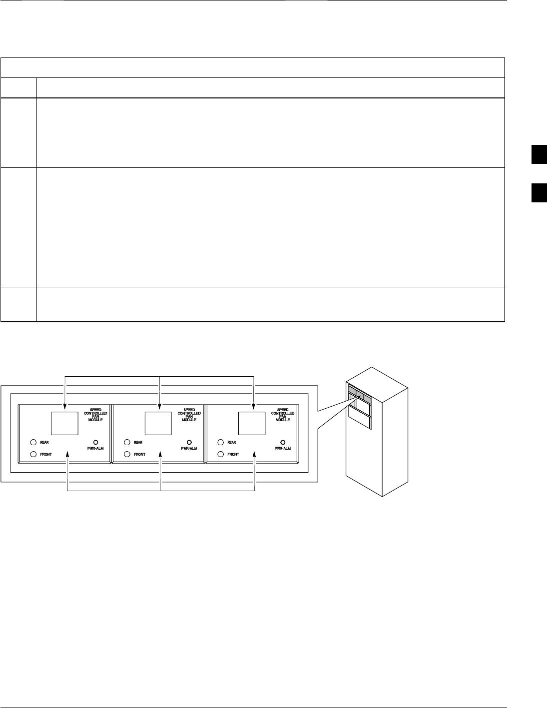
BTS Redundancy/Alarm Testing – continued
5/21/04 1X SC4812T–MC BTS Optimization/ATP 3-95
DRAFT
Table 3-42: Miscellaneous Alarm Tests
Step Action
4Expansion Frames Only: Perform the following to verify EMPC module alarms.
•Unseat EMPC modules (see Figure 3-26) one at a time
•Observe that an alarm message was reported via the MGLI as displayed on the alarm monitor.
•Replace the EMPC modules and verify the alarm monitor reports that the alarm clears.
5If equipped with AMR redundancy, perform the following to verify AMR module redundancy/alarms.
•Unseat AMR 2 (see Figure 3-26).
•Observe that an alarm message is reported via the MGLI (as displayed on the alarm monitor).
•Repeat Steps 1, 2 and 3 (starter frame) or Steps 1, 2 and 4 (expansion frame).
•Replace the AMR module and verify the alarm monitor reports that the alarm clears.
•Unseat AMR 1; observe alarm message was reported via MGLI (as displayed on the alarm monitor).
•Replace the AMR module and verify the LMF reports the alarm has cleared.
NOTE
All PWR/ALM LEDs should be GREEN at the completion of this test.
Figure 3-27: Fan Modules
ti-CDMA-WP-00139-v01-ildoc-ftw
LATCHES
FAN MODULES
BBX Redundancy
Follow the steps in Table 3-43 to verify redundancy of the BBXs in the
C–CCP shelf. Alarms reported by the master GLI (displayed via the
alarm monitor) are also verified. This test can be repeated for additional
sectors at the customer’s discretion.
3

BTS Redundancy/Alarm Testing – continued
3-96 1X SC4812T–MC BTS Optimization/ATP 5/21/04
DRAFT
Table 3-43: BBX Redundancy Alarms
Step Action
n WARNING
Any BBXs enabled will immediately key-up. Before enabling any BBX, always verify that the TX
output assigned to the BBX is terminated into a 50 W non-radiating RF load! Failure to do so could
result in serious personal injury and/or damage to the equipment.
1Enable the primary, then the redundant BBX assigned to ANT 1 by selecting the BBX and
Device>BBX/MAWI>Key.
2Observe that primary BBXs key up, and a carrier is present at each respective frequency.
3Remove the primary BBX.
4Observe a carrier is still present. The Redundant BBX is now the active BBX for Antenna 1.
5Replace the primary BBX and reload the BBX with code and data.
6Re-enable the primary BBX assigned to ANT 1 and observe that a carrier is present at each respective
frequency.
7Remove the redundant BBX and observe a carrier is still present.
8 The Primary BBX is now the active BBX for ANT 1.
9Replace the redundant BBX and reload the BBX with code and data.
10 Re-enable the redundant BBX assigned to ANT 1 and observe that a carrier is present at each
respective frequency:
11 De-key the Xcvr by selecting Device>BBX/MAWI>Dekey.
12 Repeat Steps 1 through 11 for additional BBXs/antennas, if equipped.
CSM, GPS, & HSO
Redundancy/Alarm Tests
Follow the procedure in Table 3-44 to verify the manual redundancy of
the CSM, GPS, and HSO boards. Verification of alarms reported is also
covered.
DO NOT perform the procedure in Table 3-44, unless the
site is configured with a HSO timebase as a backup for the
GPS.
NOTE
3

BTS Redundancy/Alarm Testing – continued
5/21/04 1X SC4812T–MC BTS Optimization/ATP 3-97
DRAFT
Table 3-44: CSM, GPS, & HSO, Redundancy/Alarm Tests
Step Action
n WARNING
Any BBXs enabled will immediately key-up. Before enabling any BBX, always verify that the TX
output assigned to the BBX is terminated into a 50 W non-radiating RF load! Failure to do so could
result in serious personal injury and/or damage to the equipment.
1Enable the primary, then the redundant BBXs assigned to ANT 1 by selecting the BBX and
Device>BBX/MAWI>Key.
2Disconnect the GPS antenna cable, located on top of the BTS frame. This forces the HSO board
timebase to become the CDMA timing source.
3Observe a CDMA timing reference alarm and source change is reported by the alarm monitor.
4Allow the HSO to become the active timing source.
SVerify the BBXs remain keyed and INS.
SVerify no other modules went OOS due to the transfer to HSO reference.
SObserve the PWR/ALM LEDs on the CSM 1 front panel are steady GREEN.
5Reconnect the GPS antenna cable.
6Allow the GPS to become the active timing source.
SVerify the BBXs remain keyed and INS.
SVerify no other modules went OOS due to the transfer back to the GPS reference.
SObserve the PWR/ALM LEDs on CSM 1 are steady GREEN.
7 Disable CSM 1 and enable CSM 2.
SVarious CSM source and clock alarms are now reported and the site comes down.
SAlarms clear when the site comes back up.
8Allow the CSM 2 board to go INS_ACT.
SVerify the BBXs are dekeyed and OOS, and the MCCs are OOS_RAM.
SVerify no other modules went OOS due to the transfer to CSM 2 reference.
SObserve the PWR/ALM LEDs on CSM 2 front panels are steady GREEN.
NOTE
It can take up to 20 minutes for the CSM to re-establish the GPS link and go INS. MCCs go
OOS_RAM.
9Key BBXs 1 and R and observe a carrier is present.
10 Repeat Steps 2 through 6 to verify CSM source redundancy with CSM 2.
NOTE
DO NOT ENABLE the redundant CSM.
. . . continued on next page
3
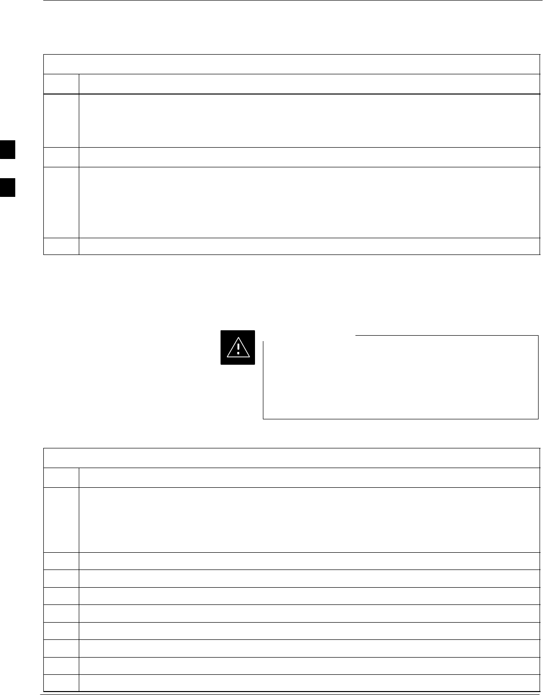
BTS Redundancy/Alarm Testing – continued
3-98 1X SC4812T–MC BTS Optimization/ATP 5/21/04
DRAFT
Table 3-44: CSM, GPS, & HSO, Redundancy/Alarm Tests
Step Action
11 Disable CSM 2 and enable CSM 1.
SVarious CSM Source and Clock alarms are reported and the site comes down.
SAlarms clear when the site comes back up.
12 De-key the Xcvr by selecting Device>BBX/MAWI>Dekey.
13 Allow the CSM 1 board to go INS_ACT.
SVerify the BBXs are de-keyed and OOS.
SVerify no other modules went OOS due to the transfer to CSM 1 reference.
SObserve PWR/ALM LEDs on the CSM 1 front panels are steady GREEN.
14 Disable the primary and redundant BBXs.
MGLI/GLI Redundancy Test
This test can only be performed when the MM path is
established by the MM (not just with LAPD link
connected). Attempting to force the GLIs to “hot swap”
under alarm monitor control, when isolated from the MM,
causes MGLIs to hang up.
CAUTION
Table 3-45: MGLI/GLI Redundancy Test (with MM Connection Established)
Step Action
NOTE
SThis test assumes the alarm monitor is NOT connected to the BTS and the T1/E1 span is connected
and communication is established with the MM.
SBOTH GLIs must be INS before continuing.
1Verify the BBXs are enabled and a CDMA carrier is present.
2Identify the primary and redundant MGLI pairs.
3Pull the MGLI that is currently INS–ACT and has cage control.
4Observe the BBX remains GREEN, and the redundant MGLI is now active.
5Verify no other modules go OOS due to the transfer of control to the redundant module.
6Verify that the BBXs are enabled and a CDMA carrier is present.
7Reinstall the MGLI and have the OMCR/CBSC place it back in-service.
8Repeat Steps 1 through 7 to verify the other MGLI/GLI board.
3

BTS Redundancy/Alarm Testing – continued
5/21/04 1X SC4812T–MC BTS Optimization/ATP 3-99
DRAFT
Alarms Testing
Alarm Verification
ALARM connectors provide Customer Defined Alarm Inputs and
Outputs. The customer can connect BTS site alarm input sensors and
output devices to the BTS, thus providing alarm reporting of active
sensors as well controlling output devices.
The SC 4812T is capable of concurrently monitoring 35 input signals.
These inputs are divided between 2 Alarm connectors marked ‘ALARM
A’ and ‘ALARM B’ located at the top of the frame (see Figure 3-28).
The ALARM A connector is always functional; ALARM B is
functional when an AMR module is equipped in the AMR 2 slot in the
distribution shelf. ALARM A port monitors input numbers 1 through
18, while ALARM B port monitors input numbers 19, 20, and 22
through 36 (see Figure 3-29). Alarm 21 is reserved for system use. State
transitions on these input lines are reported to the LMF and OMCR as
MGLI Input Relay alarms.
ALARM A and ALARM B connectors each provide 18 inputs and 8
outputs. If both A and B are functional, 36 inputs and 16 outputs are
available. They may be configured as redundant. The configuration is set
by the CBSC.
Alarm Reporting Display
The Alarm Monitor window can be displayed to list alarms that occur
after the window is displayed. To access the Alarm Monitor window,
select Util>Alarm Monitor.
The following buttons are included:
SThe Options button allows for a severity level (Warning, Minor, and
Major) selection. The default is all levels. To change the level of
alarms reported click on the Options button and highlight the desired
alarm level(s). To select multiple levels press the <Ctrl> key (for
individual selections) or <Shift> key (for a range of selections) while
clicking on the desired levels.
SThe Pause button pauses/stops the display of alarms. When the Pause
button is clicked the name of the button changes to Continue. When
the Continue button is clicked, the display of alarms continues.
Alarms that occur between the time the Pause button is clicked and
the Continue button is clicked are not displayed.
SThe Clear button clears the Alarm Monitor display. New alarms that
occur after the Clear button is clicked are displayed.
SThe Dismiss button dismisses/closes the Alarm Monitor display.
3
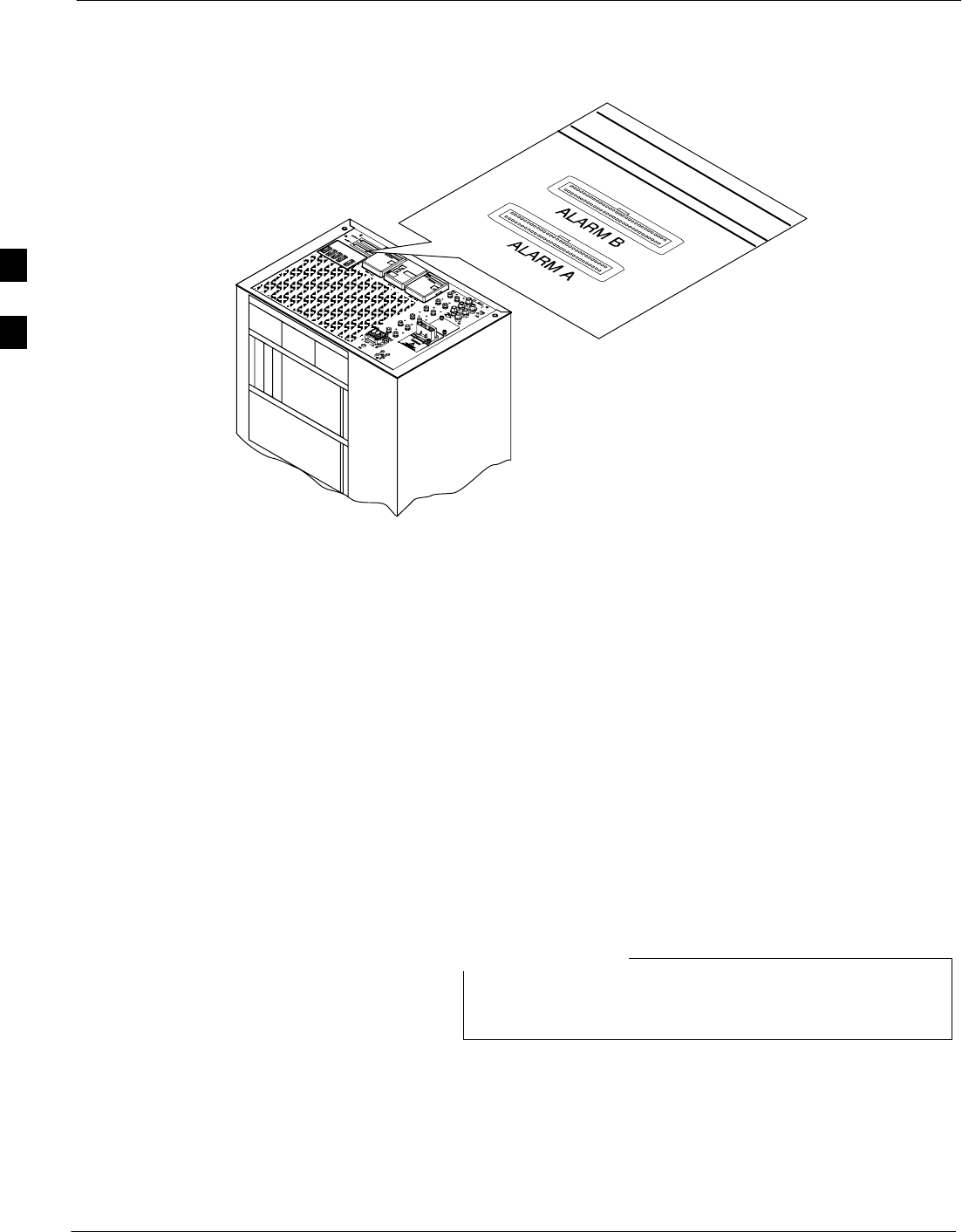
BTS Redundancy/Alarm Testing – continued
3-100 1X SC4812T–MC BTS Optimization/ATP 5/21/04
DRAFT
Figure 3-28: Alarm Connector Location and
Connector Pin Numbering
ti-CDMA-WP-00041-v01-ildoc-ftw
59
1
60
2
59
1
60
2
Purpose
The following procedures verify the customer defined alarms and relay
contacts are functioning properly. These tests are performed on all AMR
alarms/relays in a sequential manner until all have been verified. Perform
these procedures periodically to ensure the external alarms are reported
properly. Following these procedures ensures continued peak system
performance.
Study the site engineering documents and perform the following tests
only after first verifying that the AMR cabling configuration required to
interconnect the BTS frame with external alarm sensors and/or relays
meet requirements called out in the 1X SC 4812T-MC BTS Hardware
Installation .
Motorola highly recommends that you read and understand
this procedure in its entirety before starting this procedure.
NOTE
Test Equipment
The following test equipment is required to perform these tests:
SLMF
SAlarms Test Box (CGDSCMIS00014) –optional
3
BTS Redundancy/Alarm Testing – continued
5/21/04 1X SC4812T–MC BTS Optimization/ATP 3-101
DRAFT
Abbreviations used in the following figures and tables are
defined as:
SNC = normally closed
SNO = normally open
SCOM or C = common
SCDO = Customer Defined (Relay) Output
SCDI = Customer Defined (Alarm) Input
NOTE
Figure 3-29: Figure Title Goes Here
59 1
60 2
ALARM A
(AMR 1) ALARM B
(AMR 2)
Returns
25
26
A CDI 18 . . . A
CDI 1
59 1
60 2
Returns
25
26
B CDI 36 . . . B CDI
19 FW00302
The preferred method to verify alarms is to follow the
Alarms Test Box Procedure in Table 3-46. If not using an
Alarm Test Box, follow the procedure in Table 3-47.
NOTE
CDI Alarm Input Verification
with Alarms Test Box
Table 3-46 describes how to test the CDI alarm input verification using
the Alarm Test Box. Follow the steps as instructed and compare results
with the LMF display.
It may take a few seconds for alarms to be reported. The
default delay is 5 seconds. Leave the alarms test box
switches in the new position until the alarms have been
reported.
NOTE
3

BTS Redundancy/Alarm Testing – continued
3-102 1X SC4812T–MC BTS Optimization/ATP 5/21/04
DRAFT
Table 3-46: CDI Alarm Input Verification Using the Alarms Test Box
Step Action
1Connect the LMF to the BTS and log into the BTS.
2Select the MGLI.
3Click on the Device menu.
4Click on the Set Alarm Relays menu item.
5Click on Normally Open.
A status report window displays the results of the action.
6Click on the OK button to close the status report window.
7Set all switches on the alarms test box to the Open position.
8Connect the alarms test box to the ALARM A connector (see Figure 3-28).
9Set all of the switches on the alarms test box to the Closed position. An alarm should be reported for
each switch setting.
10 Set all of the switches on the alarms test box to the Open position. A clear alarm should be reported
for each switch setting.
11 Disconnect the alarms test box from the ALARM A connector.
12 Connect the alarms test box to the ALARM B connector.
13 Set all switches on the alarms test box to the Closed position. An alarm should be reported for each
switch setting
14 Set all switches on the alarms test box to the Open position. A clear alarm should be reported for each
switch setting.
15 Disconnect the alarms test box from the ALARM B connector.
16 Select the MGLI.
17 Click on the Device menu.
18 Click on the Set Alarm Relays menu item.
19 Click on Normally Closed. A status report window displays the results of the action.
20 Click OK to close the status report window.
Alarms should be reported for alarm inputs 1 through 36.
21 Set all switches on the alarms test box to the Closed position.
22 Connect the alarms test box to the ALARM A connector.
Alarms should be reported for alarm inputs 1 through 18.
23 Set all switches on the alarms test box to the Open position.
An alarm should be reported for each switch setting.
. . . continued on next page
3

BTS Redundancy/Alarm Testing – continued
5/21/04 1X SC4812T–MC BTS Optimization/ATP 3-103
DRAFT
Table 3-46: CDI Alarm Input Verification Using the Alarms Test Box
Step Action
24 Set all switches on the alarms test box to the Closed position.
A clear alarm should be reported for each switch setting.
25 Disconnect the alarms test box from the ALARM A connector.
NOTE
Input 21 (pins 29 and 30) on the Alarm B connector is reserved for the Power Supply Modules alarm.
26 Connect the alarms test box to the ALARM B connector.
A clear alarm should be reported for alarm inputs 19 through 36.
27 Set all switches on the alarms test box to the Open position.
An alarm should be reported for each switch setting.
28 Set all switches on the alarms test box to the Closed position.
A clear alarm should be reported for each switch setting.
29 Disconnect the alarms test box from the ALARM B connector.
30 Select the MGLI.
31 Click on the Device menu.
32 Click on the Set Alarm Relays menu item.
33 Click on Unequipped.
A status report window displays the results of the action.
34 Click on the OK button to close the status report window.
35 Connect the alarms test box to the ALARM A connector.
36 Set all switches on the alarms test box to both the Open and the Closed position.
No alarm should be reported for any switch settings.
37 Disconnect the alarms test box from the ALARM A connector.
38 Connect the alarms test box to the ALARM B connector.
39 Set all switches on the alarms test box to both the Open and the Closed position.
No alarm should be reported for any switch settings.
40 Disconnect the alarms test box from the ALARM B connector.
41 Load data to the MGLI to reset the alarm relay conditions according to the CDF file.
CDI Alarm Input Verification
without Alarms Test Box
Table 3-47 describes how to test the CDI alarm input verification
without the use of the Alarms Test Box. Follow the steps as instructed
and compare results with the LMF display.
3

BTS Redundancy/Alarm Testing – continued
3-104 1X SC4812T–MC BTS Optimization/ATP 5/21/04
DRAFT
It may take a few seconds for alarms to be reported. The
default delay is 5 seconds. When shorting alarm pins wait
for the alarm report before removing the short.
NOTE
Table 3-47: CDI Alarm Input Verification Without the Alarms Test Box
Step Action
1Connect the LMF to the BTS and log into the BTS.
2Select the MGLI.
3Click on the Device menu.
4Click on the Set Alarm Relays menu item.
5Click on Normally Open.
A status report window displays the results of the action.
6Click on OK to close the status report window.
7Refer to Figure 3-29 and sequentially short the ALARM A connector CDI 1 through CDI 18 pins
(25–26 through 59–60) together.
An alarm should be reported for each pair of pins that are shorted.
A clear alarm should be reported for each pair of pins when the short is removed.
NOTE
Input 21 (pins 29 and 30) on the Alarm B connector is reserved for the Power Supply Modules alarm.
8Refer to Figure 3-29 and sequentially short the ALARM B connector CDI 19 through CDI 36 pins
(25–26 through 59–60) together.
An alarm should be reported for each pair of pins that are shorted.
A clear alarm should be reported for each pair of pins when the short is removed.
9Select the MGLI.
10 Click on the Device menu.
11 Click on the Set Alarm Relays menu item.
12 Click on Normally Closed.
A status report window displays the results of the action.
13 Click on OK to close the status report window.
Alarms should be reported for alarm inputs 1 through 36.
14 Refer to Figure 3-29 and sequentially short the ALARM A connector CDI 1 through CDI 18 pins
(25–26 through 59–60) together.
A clear alarm should be reported for each pair of pins that are shorted.
An alarm should be reported for each pair of pins when the short is removed.
. . . continued on next page
3

BTS Redundancy/Alarm Testing – continued
5/21/04 1X SC4812T–MC BTS Optimization/ATP 3-105
DRAFT
Table 3-47: CDI Alarm Input Verification Without the Alarms Test Box
Step Action
NOTE
Input 21 (pins 29 and 30) on the Alarm B connector is reserved for the Power Supply Modules alarm.
15 Refer to NO TAG and sequentially short the ALARM B connector CDI 19 through CDI 36 pins
(25–26 through 59–60) together.
A clear alarm should be reported for each pair of pins that are shorted.
An alarm should be reported for each pair of pins when the short is removed.
16 Select the MGLI.
17 Click on the Device menu.
18 Click on the Set Alarm Relays menu item.
19 Click on Unequipped.
A status report window displays the results of the action.
20 Click on OK to close the status report window.
21 Refer to NO TAG and sequentially short the ALARM A connector CDI 1 through CDI 18 pins (25–26
through 59–60) together.
No alarms should be displayed.
NOTE
Input 21 (pins 29 and 30) on the Alarm B connector is reserved for the Power Supply Modules alarm.
22 Refer to NO TAG and sequentially short the ALARM B connector CDI 19 through CDI 36 pins
(25–26 through 59–60) together.
No alarms should be displayed.
23 Load data to the MGLI to reset the alarm relay conditions according to the CDF file.
Pin and Signal Information for
Alarm Connectors
Table 3-48 lists the pins, wire color codes, and signal names for Alarms
A and B.
Table 3-48: Pin and Signal Information for Alarm Connectors
Wire
Signal Name
Wire
Signal Name
Pin
Wire
Color Alarm A Alarm B Pin
Wire
Color Alarm A Alarm B
1Blu/Wht A CDO1 NC B CDO9 NC 31 Blu/Yel Cust Retn 4 B CDI 22
2Wht/Blu A CDO1 Com B CDO9 Com 32 Yel/Blu A CDI 4 Cust Retn 22
3Org/Wht A CDO1 NO B CDO9 NO 33 Org/Yel Cust Retn 5 B CDI 23
4Wht/Org A CDO2 NC B CDO10 NC 34 Yel/Org A CDI 5 Cust Retn 23
5Grn/Wht A CDO2 Com B CDO10 Com 35 Grn/Yel Cust Retn 6 B CDI 24
3

BTS Redundancy/Alarm Testing – continued
3-106 1X SC4812T–MC BTS Optimization/ATP 5/21/04
DRAFT
Table 3-48: Pin and Signal Information for Alarm Connectors
Pin
Signal Name
Wire
Color
Pin
Signal Name
Wire
Color
Pin Alarm BAlarm A
Wire
Color
Pin
Alarm BAlarm A
Wire
Color
6Wht/Grn A CDO2 NO B CDO10 NO 36 Yel/Grn A CDI 6 Cust Retn 24
7Brn/Wht A CDO3 NC B CDO11 NC 37 Brn/Yel Cust Retn 7 B CDI 25
8Wht/Brn A CDO3 Com B CDO11 Com 38 Yel/Brn A CDI 7 Cust Retn 25
9Slt/Wht A CDO3 NO B CDO11 NO 39 Slt/Yel Cust Retn 8 B CDI 26
10 Wht/Slt A CDO4 NC B CDO12 NC 40 Yel/Slt A CDI 8 Cust Retn 26
11 Blu/Red A CDO4 Com B CDO12 Com 41 Blu/Vio Cust Retn 9 B CDI 27
12 Red/Blu A CDO4 NO B CDO12 NO 42 Vio/Blu A CDI 9 Cust Retn 27
13 Org/Red A CDO5 NC B CDO13 NC 43 Org/Vio Cust Retn 10 B CDI 28
14 Red/Org A CDO5 Com B CDO13 Com 44 Vio/Blu A CDI 10 Cust Retn 28
15 Grn/Red A CDO5 NO B CDO13 NO 45 Grn/Vio Cust Retn 11 B CDI 29
16 Red/Grn A CDO6 NC B CDO14 NC 46 Vio/Grn A CDI 11 Cust Retn 29
17 Brn/Red A CDO6 Com B CDO14 Com 47 Brn/Vio Cust Retn 12 B CDI 30
18 Red/Brn A CDO6 NO B CDO14 NO 48 Vio/Brn A CDI 12 Cust Retn 30
19 Slt/Red A CDO7 NC B CDO15 NC 49 Slt/Vio Cust Retn 13 B CDI 31
20 Red/Slt A CDO7 Com B CDO15 Com 50 Vio/Slt A CDI 13 Cust Retn 31
21 Blu/Blk A CDO7 NO B CDO15 NO 51 Red/Wht Cust Retn 14 B CDI 32
22 Blk/Blu A CDO8 NC B CDO16 NC 52 Wht/Red A CDI 14 Cust Retn 32
23 Org/Blk A CDO8 Com B CDO16 Com 53 Blk/Wht Cust Retn 15 B CDI 33
24 Blk/Org A CDO8 NO B CDO16 NO 54 Wht/Blk A CDI 15 Cust Retn 33
25 Grn/Blk Cust Retn 1 B CDI 19 55 Yel/Wht Cust Retn 16 B CDI 34
26 Blk/Grn A CDI 1 Cust Retn 19 56 Wht/Yel A CDI 16 Cust Retn 34
27 Brn/Blk Cust Retn 2 B CDI 20 57 Vio/Wht Cust Retn 17 B CDI 35
28 Blk/Brn A CDI 2 Cust Retn 20 58 Wht/Vio A CDI 17 Cust Retn 35
29 Slt/Blk Cust Retn 3 B CDI 21 +27V
*Pwr Conv Alm –48V
59 Blk/Red Cust Retn 18 B CDI 36
30 Blk/Slt A CDI 3 Cust Retn 21 +27V
*Pwr Conv Retn –48V
60 Red/Blk A CDI 18 Cust Retn 36
NOTE
*For –48V, reserved for Power Supply Module Alarm signal. NOT for use as CDOs or CDIs.
All Cust Rtrn 1–18 are electronically tied together at the RFMF.
All Cust Rtrn 19–36 are electronically tied together at the RFMF.
CDO = Customer Defined Output; CDI = Customer Defined Input;
NC – normally closed, NO – normally open, Com – common
The “A CDI” numbering is from the LMF/OMCR/CBSC perspective. LMF/OMCR/CBSC starts the numbering at 19
(giving 19 – 36). Actual cable hardware starts the numbering at 0 (giving 0–17)
3

5/21/04 1X SC4812T–MC BTS Optimization/ATP
DRAFT
Chapter 4: Automated Acceptance Test Procedure
Table of Contents
Guide Book 1–2. . . . . . . . . . . . . . . . . . . . . . . . . . . . . . . . . . . . . . . . . . . . . . . . . . . . .
Document Overview 1–2. . . . . . . . . . . . . . . . . . . . . . . . . . . . . . . . . . . . . . . . . . . . . .
What Is In This Guide? 1–2. . . . . . . . . . . . . . . . . . . . . . . . . . . . . . . . . . . . .
Book Catalogs and Organization 1–3. . . . . . . . . . . . . . . . . . . . . . . . . . . . . . . . . . . .
Book Directory 1–3. . . . . . . . . . . . . . . . . . . . . . . . . . . . . . . . . . . . . . . . . . .
Special Catalogs 1–5. . . . . . . . . . . . . . . . . . . . . . . . . . . . . . . . . . . . . . . . . . .
Physical Page Layouts 1–6. . . . . . . . . . . . . . . . . . . . . . . . . . . . . . . . . . . . . . . . . . . .
A/A4 Page and Margin Sizes 1–6. . . . . . . . . . . . . . . . . . . . . . . . . . . . . . . . .
A/A4 Page Text Area 1–7. . . . . . . . . . . . . . . . . . . . . . . . . . . . . . . . . . . . . . .
A/A4 Page Components 1–9. . . . . . . . . . . . . . . . . . . . . . . . . . . . . . . . . . . .
Frame and Table Components 1–10. . . . . . . . . . . . . . . . . . . . . . . . . . . . . . . . . . . . . .
Frames With Tools 1–10. . . . . . . . . . . . . . . . . . . . . . . . . . . . . . . . . . . . . . . . .
Flow Charts and Block Diagrams 1–10. . . . . . . . . . . . . . . . . . . . . . . . . . . . .
Line Drawings 1–11. . . . . . . . . . . . . . . . . . . . . . . . . . . . . . . . . . . . . . . . . . . .
Table Types In This Template 1–12. . . . . . . . . . . . . . . . . . . . . . . . . . . . . . . .
Item/Description Table 1–12. . . . . . . . . . . . . . . . . . . . . . . . . . . . . . . . . . . . .
Step Table 1–13. . . . . . . . . . . . . . . . . . . . . . . . . . . . . . . . . . . . . . . . . . . . . . .
Step/Check Table 1–14. . . . . . . . . . . . . . . . . . . . . . . . . . . . . . . . . . . . . . . . . .
Component Descriptions 1–15. . . . . . . . . . . . . . . . . . . . . . . . . . . . . . . . . . . . . . . . . .
Conclusions 1–16. . . . . . . . . . . . . . . . . . . . . . . . . . . . . . . . . . . . . . . . . . . . . . . . . . . . .
Map Title Goes Here lkjsfdg Sfdkgj Msfd N lkas K lkjsdfl kB lkj fgcb 1–17. . . . . .
Block Label Goes Here 1–17. . . . . . . . . . . . . . . . . . . . . . . . . . . . . . . . . . . . .
Block Label Goes Here 1–17. . . . . . . . . . . . . . . . . . . . . . . . . . . . . . . . . . . . .
Block Label Goes Here 1–18. . . . . . . . . . . . . . . . . . . . . . . . . . . . . . . . . . . . .
Block Label Goes Here 1–19. . . . . . . . . . . . . . . . . . . . . . . . . . . . . . . . . . . . .
Map Title Goes Here 1–22. . . . . . . . . . . . . . . . . . . . . . . . . . . . . . . . . . . . . . . . . . . . . .
4

Table of Contents – continued
1X SC4812T–MC BTS Optimization/ATP 5/21/04
DRAFT
Notes
4
Automated Acceptance Test Procedures – TX & RX
5/21/04 1X SC4812T–MC BTS Optimization/ATP 4-1
DRAFT
Introduction
The Automated Acceptance Test Procedure (ATP) allows Cellular Field
Engineers (CFEs) to run automated acceptance tests on all equipped BTS
subsystem devices using the Local Maintenance Facility (LMF) and
supported test equipment per the current Cell Site Data File (CDF)
assignment.
The results of these tests (at the option of the operator) are written to a
file that can be printed. All tests are controlled from the LMF platform
using the GPIB interface, therefore, only recommended test equipment
supported by the LMF can be used.
This chapter describes the tests run from the GUI environment, which is
the recommended method. The GUI provides the advantages of
simplifying the LMF user interface, reducing the potential for miskeying
commmands and associated parameters, and speeding up the execution
of complex operations involving multiple command strings. If you feel
the command line interface (CLI) will provide additional insight into the
progress of ATPs and problems that could possibly be encountered, refer
to LMF CLI Commands.
Before performing any tests, use an editor to view the
“CAVEATS” section of the “readme.txt” file in the c:\wlmf
folder for any applicable information.
The ATP test is to be performed on out-of-service (OOS)
sectors only.
DO NOT substitute test equipment not supported by the
LMF.
CAUTION
Refer to Chapter 3 for detailed information on test set
connections for calibrating equipment, cables and other test
set components, if required.
NOTE
4
Automated Acceptance Test Procedures – TX & RX – continued
4-2 1X SC4812T–MC BTS Optimization/ATP 5/21/04
DRAFT
Reduced ATP
Equipment has been factory–tested for FCC compliance. If
license–governing bodies require documentation
supporting SITE compliance with regulations, a full ATP
may be necessary. Perform the Reduced ATP only if
reports for the specific BTS site are NOT required.
NOTE
After downloading the proper operational software to the BTS, the CFE
must perform these procedures (minimal recommendation):
SVerify the TX/RX paths by performing TX Calibration, TX Audit and
FER tests.
SRetrieve Calibration Data required for normal site operation.
Should failures occur while performing the specified tests, refer to the
Basic Troubleshooting section of this manual for help in determining the
failure point. Once the point of failure has been identified and corrected,
refer to the BTS Optimization and ATP Test Matrix (Table C-3, page
C-4) section to determine the applicable test that must be performed.
In the unlikely event that the BTS passes these tests but has a forward
link problem during normal operation, the CFE should then perform the
additional TX tests for troubleshooting: TX spectral mask, TX rho, and
TX code domain.
Required Test Equipment
The following test equipment is required:
SLMF
SPower meter (used with HP8921A/600 and Advantest R3465)
SCommunications system analyzer
SSignal generator for FER testing (required for all communications
system analyzers for 1X FER)
SBefore installing any test equipment directly to any
BTS TX OUT connector, verify that there are no
CDMA channels keyed.
SAt active sites, have the OMCR/CBSC place the carrier
assigned to the PAs under test OOS. Failure to do so
can result in serious personal injury and/or equipment
damage.
WARNING
The test equipment must be re–calibrated before using it to
perform the TX Acceptance Tests.
NOTE
4
Automated Acceptance Test Procedures – TX & RX – continued
5/21/04 1X SC4812T–MC BTS Optimization/ATP 4-3
DRAFT
ATP Test Prerequisites
All PAs must be INS during any TX testing.
NOTE
Before attempting to run any ATP tests, ensure the following have been
completed:
SBTS has been optimized and calibrated (see Chapter 3).
SLMF is logged into the BTS.
SCSMs, GLIs, BBXs, and MCCs have correct code load and data load.
SPrimary CSM, GLI, and MCCs are INS_ACT (bright green).
SBBXs are calibrated and BLOs are downloaded.
SNo BBXs are keyed (transmitting).
SBBXs are OOS_RAM (flashing green).
STest cables are calibrated.
STest equipment is connected for ATP tests (see Figure 3-18 through
Figure 3-23).
STest equipment has been warmed up 60 minutes and calibrated.
SGPIB is on.
SBTS transmit connectors are properly terminated for the test(s) to be
performed.
Before performing the FER, be sure that all PAs are turned
OFF (circuit breakers pulled) or that all transmitter ports
are properly terminated.
All transmit ports must be properly terminated for all ATP
tests.
Failure to observe these warnings may result in bodily
injury or equipment damage.
WARNING
TX OUT Connection
Many of the acceptance test procedures require taking
measurements at the TX OUT connector. All
measurements will be via the BTS TX OUT connector.
NOTE
4

Automated Acceptance Test Procedures – TX & RX – continued
4-4 1X SC4812T–MC BTS Optimization/ATP 5/21/04
DRAFT
ATP Test Options
All PAs must INS during any TX testing.
NOTE
The tests can be run individually or as one of the following groups:
SAll TX/RX: Executes all the TX and RX tests.
SAll TX: TX tests verify the performance of the BTS transmit line up.
These include the GLI, MCC, BBX, and MCIO cards, the PAs and
passive components including ETMs, (S)PLCs, TX filters, and RF
cables.
SAll RX: RX tests verify the performance of the BTS receiver line up.
These include the MPC (for starter frames), EMPC (for expansion
frames), MCIO, BBX, MCC, and GLI cards and the passive
components including RX filters (starter frame only), and RF cables.
SFull Optimization: Executes the TX calibration, downloads the BLO,
and executes the TX audit before running all of the TX and RX tests.
The Full Optimization test can be run if you want the TX
path calibrated before all the TX and RX tests are run.
If manual testing has been performed with the HP analyzer,
remove the manual control/system memory card from the
card slot and set the I/O Config to the Talk & Lstn mode
before starting the automated testing.
NOTE
The STOP button can be used to stop the testing process.
NOTE
Individual Acceptance Tests
The following individual tests can be used to verify the results of
specific tests.
Spectral Purity TX Mask (Primary & Redundant BBX)
This test verifies that the transmitted CDMA carrier waveform generated
on each sector meets the transmit spectral mask specification with
respect to the assigned CDF file values.
Waveform Quality (rho)
This test verifies that the transmitted Pilot channel element digital
waveform quality (rho) exceeds the minimum specified value in
ANSI–J_STD–019. “Rho” represents the correlation between actual and
perfect CDMA modulation spectrum. A rho value of 1.0000 represents
100% (or perfect correlation).
4

Automated Acceptance Test Procedures – TX & RX – continued
5/21/04 1X SC4812T–MC BTS Optimization/ATP 4-5
DRAFT
Pilot Time Offset
The Pilot Time Offset is the difference between the CDMA analyzer
measurement interval (based on the BTS system time reference) and the
incoming block of transmitted data from the BTS (Pilot only, Pilot
Gain = 262, PN Offset = 0).
Code Domain Power (Primary & Redundant BBX)
This test verifies the code domain power levels, which have been set for
all ODD numbered Walsh channels, using the OCNS command. This is
done by verifying that the ratio of PILOT divided by OCNS is equal to
10.2 + 2 dB, and, that the noise floor of all EVEN numbered “OFF”
Walsh channels measures < –27 dB (with respect to total CDMA channel
power).
Frame Error Rate
The Frame Error Rate (FER) test verifies RX operation of the entire
CDMA Reverse Link using all equipped MCCs assigned to all
respective sectors/antennas. This test verifies the BTS sensitivity on all
traffic channel elements currently configured on all equipped MCCs at
an RF input level of –119 dBm (or –116 dBm if using TMPC).
ATP Test Procedure
Follow the procedure in Table 4-1 to perform any ATP test.
Table 4-1: ATP Test Procedure
nStep Action
1Be sure that all prerequisites have been met.
2Select the device(s) to be tested.
IMPORTANT! Only one carrier can be tested at a time. All PAs must be INS during testing.
NOTE
If the LMF has been logged into the BTS with a different Multi–Channel Preselector setting than
the one to be used for this test, the LMF must be logged out of the BTS and logged in again with
the new Multi–Channel Preselector setting. Using the wrong MPC setting can cause a false test
failure.
3From the Tests menu, select the test you want to run.
4Select the appropriate carrier (carrier-bts#-sector#-carrier#) displayed in the Channels/Carrier
pick list.
NOTE
To select multiple items, hold down the <Shift> or <Ctrl> key while making the selections.
5Enter the appropriate channel number in the Carrier n Channels box.
The default channel number displayed is determined by the CdmaChans[n] number in the
cbsc–n.cdf file for the BTS.
6If applicable, select Verify BLO (default) or Single–sided BLO.
. . . continued on next page
4

Automated Acceptance Test Procedures – TX & RX – continued
4-6 1X SC4812T–MC BTS Optimization/ATP 5/21/04
DRAFT
Table 4-1: ATP Test Procedure
nActionStep
NOTE
Single–sided BLO is only used when checking non–redundant transceivers.
7If applicable, select a test pattern from the Test Pattern pick list.
NOTE
SSelecting Pilot (default) performs tests using only a pilot signal.
SSelecting Standard performs tests using pilot, synch, paging and 6 traffic channels. This
requires an MCC to be selected.
SSelecting CDFPilot performs tests using only a pilot signal, however, the gain for the channel
elements is specified in the CDF file.
SSelecting CDF performs tests using pilot, synch, paging and 6 traffic channels, however, the
gain for the channel elements is specified in the CDF file.
8Click on the OK button.
The status report window and a Directions pop-up are displayed.
9Follow the cable connection directions as they are displayed.
The test results are displayed in the status report window.
10 Click on Save Results or Dismiss.
NOTE
If Dismiss is used, the test results will not be saved in the test report file.
11 Refer to Steps NO TAG through sub-step NO TAG of Table 3-37 to dekey.
4

TX Spectral Purity Trasmit Mask Acceptance Test
5/21/04 1X SC4812T–MC BTS Optimization/ATP 4-7
DRAFT
Tx Mask Test
This test verifies the spectral purity of each BBX carrier keyed up at a
specific frequency, per the current CDF file assignment. All tests are
performed using the external calibrated test set, controlled by the same
command. All measurements are via the appropriate TX OUT connector.
The Pilot Gain is set to 541 for each antenna, and all channel elements
from the MCCs are forward-link disabled. The BBX is keyed up, using
both bbxlvl and bay level offsets, to generate a CDMA carrier (with pilot
channel element only). BBX power output is set to obtain +40 dBm as
measured at the TX OUT connector (on the BTS directional coupler).
TX output power is set to +40 dBm by setting BTS power
level to +33.5 dBm to compensate for 6.5 dB increase from
pilot gain set to 541.
NOTE
The calibrated communications test set measures and returns the
attenuation level of all spurious and IM products in a 30 kHz resolution
bandwidth. With respect to the mean power of the CDMA channel
measured in a 1.23 MHz bandwidth in dB, verify that results meet
system tolerances at the following test points:
– at least –45 dB @ + 750 kHz from center frequency
– at least –45 dB @ – 750 kHz from center frequency
– at least –60 dB @ – 1980 kHz from center frequency
– at least –60 dB @ – 1980 kHz from center frequency
The BBX then de-keys, and, if selected, the MCC is re-configured to
assign the applicable redundant BBX to the current TX antenna path
under test. The test is then repeated. See Table 4-1 to perform this test.
4

TX Spectral Purity Trasmit Mask Acceptance Test – continued
4-8 1X SC4812T–MC BTS Optimization/ATP 5/21/04
DRAFT
Figure 4-1: TX Mask Verification Spectrum Analyzer Display
– 900 kHz + 900 kHz
Center Frequency
Reference
Attenuation level of all
spurious and IM products
with respect to the mean
power of the CDMA channel
.5 MHz Span/Div
Ampl 10 dB/Div
Mean CDMA Bandwidth
Power Reference
+750 kHz
+ 1980 kHz
– 750 kHz
– 1980 kHz
FW00282
4

TX Waveform Quality (rho) Acceptance Test
5/21/04 1X SC4812T–MC BTS Optimization/ATP 4-9
DRAFT
Rho Test
This test verifies the transmitted Pilot channel element digital waveform
quality of each BBX carrier keyed up at a specific frequency per the
current CDF file assignment. All tests are performed using the external
calibrated test set controlled by the same command. All measurements
are via the appropriate TX OUT connector.
The Pilot Gain is set to 262 for each antenna, and all channel elements
from the MCCs are forward link disabled. The BBX is keyed up using
both bbxlvl and bay level offsets, to generate a CDMA carrier (with pilot
channel element only, Walsh code 0). BBX power output is set to
40 dBm as measured at the TX OUT connector (on the BTS directional
coupler).
The calibrated communications test set measures and returns the Pilot
channel element digital waveform quality (rho) in dB, verifying that the
result meets system tolerances:
SWaveform quality (rho) should be w 0.912 (–0.4 dB).
The BBX then de-keys and, if selected, the MCC is re-configured to
assign the applicable redundant BBX to the current TX antenna path
under test. The test is then be repeated. See Table 4-1 to perform this
test.
4

TX Pilot Time Offset Acceptance Test
4-10 1X SC4812T–MC BTS Optimization/ATP 5/21/04
DRAFT
Pilot Offset Acceptance Test
This test verifies the transmitted Pilot channel element Pilot Time Offset
of each BBX carrier keyed up at a specific frequency per the current
CDF file assignment. All tests are performed using the external
calibrated test set controlled by the same command. All measurements
are via the appropriate TX OUT connector.
The Pilot Gain is set to 262 for each antenna, and all TCH elements from
the MCCs are forward link disabled. The BBX is keyed up, using both
bbxlvl and bay level offsets, to generate a CDMA carrier (with pilot
channel element only, Walsh code 0). BBX power output is set to
40 dBm as measured at the TX OUT connector (on either the BTS or
RFDS directional coupler).
The calibrated communications test set measures and returns the Pilot
Time Offset in µs, verifying results meet system tolerances:
SPilot Time Offset should be within + 3 µs of the target PT
Offset (0 µs).
The BBX then de-keys, and if selected, the MCC is re-configured to
assign the applicable redundant BBX to the current TX antenna path
under test. The test is then repeated. See Table 4-1 to perform this test.
4

TX Code Domain Power/Noise Floor Acceptance Test
5/21/04 1X SC4812T–MC BTS Optimization/ATP 4-11
DRAFT
Code Domain Power Test
This test verifies the Code Domain Power/Noise of each BBX carrier
keyed up at a specific frequency per the current CDF file assignment.
All tests are performed using the external calibrated test set controlled by
the same command. All measurements are via the appropriate TX OUT
connector.
For each sector/antenna under test, the Pilot Gain is set to 262. All MCC
channel elements under test are configured to generate Orthogonal
Channel Noise Source (OCNS) on different odd Walsh codes and to be
assigned a full–rate gain of 81. The maximum number of MCC/CEs to
be tested at any one time is 32 (32 odd Walsh codes). If more than 32
CEs exist, then multiple sets of measurements are made; so all channel
elements are verified on all sectors.
BBX power output is set to 40 dBm as measured at the TX OUT
connector.
You verify the code domain power levels, which have been set for all
ODD numbered Walsh channels, using the OCNS command. This is
done by verifying that Pilot Power (dBm) minus OCNS Power (dBm) is
equal to 10.2 + 2 dB and that the noise floor of all “OFF” Walsh channels
measures < –27 dB (with respect to total CDMA channel power).
When performing this test using the LMF and the MCC is
an MCC8E or MCC24E, the redundant BBX may fail or
show marginal performance. This is due to a timing
mismatch that the LMF does not address. Performing this
test from the CBSC will not have this timing problem.
NOTE
The BBX then de-keys and, if selected, the MCC is re-configured to
assign the applicable redundant BBX to the current TX antenna path
under test. The test is then repeated. Upon completion of the test, OCNS
is disabled on the specified MCC/CE.
If using Advantest test equipment, Code Domain Test
MUST be configured in RC–1 mode.
NOTE
See Table 4-1 to perform this test.
4
TX Code Domain Power/Noise Floor Acceptance Test – continued
4-12 1X SC4812T–MC BTS Optimization/ATP 5/21/04
DRAFT
Figure 4-2: Code Domain Power and Noise Floor Levels
Pilot Channel
Active channels
PILOT LEVEL
MAX OCNS SPEC.
MIN OCNS SPEC.
MAXIMUM NOISE FLOOR:
< –27 dB SPEC.
Inactive channels
Walsh 0 1 2 3 4 5 6 7 ... 64
MAX
OCNS
CHAN-
NEL
MIN
OCNS
CHAN-
NEL
8.2 dB 12.2 dB
Max
noise
floor
Pilot Channel
Active channels
PILOT LEVEL
MAX OCNS SPEC.
MIN OCNS SPEC.
MAXIMUM NOISE FLOOR:
< –27 dB
Inactive channels
Walsh 0 1 2 3 4 5 6 7 ... 64
failure – does
not meet min
ocns spec.
failure – ex-
ceeds max
ocns spec.
8.2 dB 12.2 dB
failure – exceeds
max noise floor
spec.
Showing all OCNS Passing
Indicating Failures FW00283
4

RX Frame Error Rate (FER) Acceptance Test
5/21/04 1X SC4812T–MC BTS Optimization/ATP 4-13
DRAFT
FER Test
This test verifies the BTS FER on all traffic channel elements currently
configured on all equipped MCCs (full rate at 1% FER) at an RF input
level of –119 dBm [or –116 dBm if using Tower Top
Amplifier (TMPC)]. All tests are performed using the external calibrated
test set as the signal source controlled by the same command. All
measurements are via the LMF.
The Pilot Gain is set to 262 for each TX antenna, and all channel
elements from the MCCs are forward-link disabled. The BBX is keyed
up, using only bbxlvl level offsets, to generate a CDMA carrier (with
pilot channel element only). BBX power output is set to –20 dBm as
measured at the TX OUT connector. The BBX must be keyed to enable
the RX receive circuitry.
The LMF prompts the MCC/CE under test to measure all zero longcode
and provide the FER report on the selected active MCC on the reverse
link for both the main and diversity RX antenna paths, verifying that
results meet the following specification:
SFER returned less than 1% and total frames measured is 1500
All MCC/CEs selected are tested on the specified RX antenna path. The
BBX then de-keys and, if selected, the MCC is re-configured to assign
the applicable redundant BBX to the current RX antenna paths under
test. The test is then repeated. See Table 4-1 to perform this test.
4

Generate an ATP Report
4-14 1X SC4812T–MC BTS Optimization/ATP 5/21/04
DRAFT
Background
Each time an ATP test is run, an ATP report is updated to include the
results of the most recent ATP tests if the Save Results button is used to
close the status report window. The ATP report is not updated if the
status reports window is closed using the Dismiss button.
ATP Report
Each time an ATP test is run, a separate report is created for each BTS
and includes the following for each test:
STest name
SBBX number
SChannel number
SCarrier number
SSector number
SUpper test limit
SLower test limit
STest result
SPASS or FAIL
SDescription information (if applicable)
STime stamp
SDetails/Warning information (if applicable)
The report can be printed if the LMF computer is connected to a printer.
Follow the procedure in the Table 4-2 to view and/or print the ATP
report for a BTS.
Table 4-2: Generating an ATP Report
nStep Action
1Click on the Login tab (if not in the forefront).
2Select the desired BTS from the available Base Station
pick list.
3Click on the Report button.
4Click on a column heading to sort the report.
5– If not desiring a printable file copy, click on the
Dismiss button.
– If requiring a printable file copy, select the desired
file type in the picklist and click on the Save button.
4

5/21/04 1X SC4812T–MC BTS Optimization/ATP
DRAFT
Chapter 5: Prepare to Leave the Site
Table of Contents
Guide Book 1–2. . . . . . . . . . . . . . . . . . . . . . . . . . . . . . . . . . . . . . . . . . . . . . . . . . . . .
Document Overview 1–2. . . . . . . . . . . . . . . . . . . . . . . . . . . . . . . . . . . . . . . . . . . . . .
What Is In This Guide? 1–2. . . . . . . . . . . . . . . . . . . . . . . . . . . . . . . . . . . . .
Book Catalogs and Organization 1–3. . . . . . . . . . . . . . . . . . . . . . . . . . . . . . . . . . . .
Book Directory 1–3. . . . . . . . . . . . . . . . . . . . . . . . . . . . . . . . . . . . . . . . . . .
Special Catalogs 1–5. . . . . . . . . . . . . . . . . . . . . . . . . . . . . . . . . . . . . . . . . . .
Physical Page Layouts 1–6. . . . . . . . . . . . . . . . . . . . . . . . . . . . . . . . . . . . . . . . . . . .
A/A4 Page and Margin Sizes 1–6. . . . . . . . . . . . . . . . . . . . . . . . . . . . . . . . .
A/A4 Page Text Area 1–7. . . . . . . . . . . . . . . . . . . . . . . . . . . . . . . . . . . . . . .
A/A4 Page Components 1–9. . . . . . . . . . . . . . . . . . . . . . . . . . . . . . . . . . . .
Frame and Table Components 1–10. . . . . . . . . . . . . . . . . . . . . . . . . . . . . . . . . . . . . .
Frames With Tools 1–10. . . . . . . . . . . . . . . . . . . . . . . . . . . . . . . . . . . . . . . . .
Flow Charts and Block Diagrams 1–10. . . . . . . . . . . . . . . . . . . . . . . . . . . . .
Line Drawings 1–11. . . . . . . . . . . . . . . . . . . . . . . . . . . . . . . . . . . . . . . . . . . .
Table Types In This Template 1–12. . . . . . . . . . . . . . . . . . . . . . . . . . . . . . . .
Item/Description Table 1–12. . . . . . . . . . . . . . . . . . . . . . . . . . . . . . . . . . . . .
Step Table 1–13. . . . . . . . . . . . . . . . . . . . . . . . . . . . . . . . . . . . . . . . . . . . . . .
Step/Check Table 1–14. . . . . . . . . . . . . . . . . . . . . . . . . . . . . . . . . . . . . . . . . .
Component Descriptions 1–15. . . . . . . . . . . . . . . . . . . . . . . . . . . . . . . . . . . . . . . . . .
Conclusions 1–16. . . . . . . . . . . . . . . . . . . . . . . . . . . . . . . . . . . . . . . . . . . . . . . . . . . . .
Map Title Goes Here lkjsfdg Sfdkgj Msfd N lkas K lkjsdfl kB lkj fgcb 1–17. . . . . .
Block Label Goes Here 1–17. . . . . . . . . . . . . . . . . . . . . . . . . . . . . . . . . . . . .
Block Label Goes Here 1–17. . . . . . . . . . . . . . . . . . . . . . . . . . . . . . . . . . . . .
Block Label Goes Here 1–18. . . . . . . . . . . . . . . . . . . . . . . . . . . . . . . . . . . . .
Block Label Goes Here 1–19. . . . . . . . . . . . . . . . . . . . . . . . . . . . . . . . . . . . .
Map Title Goes Here 1–22. . . . . . . . . . . . . . . . . . . . . . . . . . . . . . . . . . . . . . . . . . . . . .
5

Table of Contents – continued
1X SC4812T–MC BTS Optimization/ATP 5/21/04
DRAFT
Notes
5

Updating Calibration Data Files
5/21/04 1X SC4812T–MC BTS Optimization/ATP 5-1
DRAFT
Software Release caveats
Software Release R2.16.4.1 allows the user to load the calibration file
from the LMF directly onto the MGLI. The MGLI will then ftp the new
calibration file to the OMC–R, thereby eliminating the need for the user
to place the calibration file at the OMC–R.
Copy and Load Cal File to to
CBSC
Updated calibration (CAL) file information must be moved from the
LMF Windows environment back to the CBSC, which resides in a Unix
environment. The procedures that follow detail how to move files from
one environment to the other.
Backup CAL Data to a Diskette
The BLO calibration files should be backed up to a diskette (per BTS).
Follow the procedure in Table 5-1 to copy CAL files from a CDMA
LMF computer to a diskette.
Table 5-1: Backup CAL Data to a Diskette
Step Action
1 With Windows running on the LMF computer, insert a disk
into Drive A:\.
2Launch the Windows Explorer application program from the
Start > Programs menu list.
3Select the applicable <x>:\<lmf home directory/cdma/bts–#
folder.
4Drag the bts–#.cal file to Drive A.
5Repeat Steps 3 and 4, as required, for other bts–# folders.
5

Updating Calibration Data Files – continued
5-2 1X SC4812T–MC BTS Optimization/ATP 5/21/04
DRAFT
Copying CAL Files from Diskette to the CBSC
Follow the procedure in Table 5-2 to copy CAL files from a diskette to
the CBSC.
Table 5-2: Procedures to Copy CAL Files from Diskette to the CBSC
Step Action
1Log into the CBSC on the OMC–R Unix workstation using
your account name and password.
2Place the diskette containing calibration files (cal files) in the
workstation diskette drive.
3 Type eject –q and press the Enter key.
4 Type mount and press the Enter key. Verify that
floppy/no_name is displayed.
NOTE
If the eject command has been previously entered,
floppy/no_name will be appended with a number. Use
the explicit floppy/no_name reference displayed.
5Type in cd /floppy/no_name and press the Enter key.
6Type in ls –lia and press the Enter key. Verify the bts–#.cal
file filename appears in the displayed directory listing.
7Type in cd and press the Enter key.
8Type in pwd and press the Enter key. Verify the displayed
response shows the correct home directory (/home/<user’s
name>).
9 With Solaris versions of Unix, create a Unix–formatted
version of the bts–#.cal file in the home directory by
performing the following:
9a – Type in dos2unix /floppy/no_name/bts–#.cal bts–#.cal
and press the Enter key.
Where: # = BTS number for which the CAL file was
created
NOTE
Other versions of Unix do not support the dos2unix
command. In these cases, use the Unix cp (copy) command.
The copied files will contain DOS line feed characters which
must be edited out with a Unix text editor.
10 Type in ls –l *.cal and press the Enter key. Verify the CAL
files have been copied. Verify all CAL files to be transferred
appear in the displayed listing.
. . . continued on next page
5

Prepare to Leave the Site
5-4 1X SC4812T–MC BTS Optimization/ATP 5/21/04
DRAFT
External Test Equipment
Removal
Perform the procedure in Table 5-3 to disconnect the test equipment and
configure the BTS for active service.
Table 5-3: External Test Equipment Removal
Step Action
1Disconnect all external test equipment from all TX and RX
connectors on the top of the frame.
2Reconnect and visually inspect all TX and RX antenna feed
lines at the top of the frame.
Verify that all sector antenna feed lines are connected to
the correct ports on the frame. Crossed antenna cables will
cause system degradation of call processing.
CAUTION
Each module or device can be in any state prior to
downloading. Each module or device will be in an
OOS_RAM state after downloading has completed.
SFor all LMF commands, information in italics
represents valid ranges for that command field.
SOnly those fields requiring an input will be specified.
Default values for other fields will be assumed.
SFor more complete command examples (including
system response details), refer to the CDMA LMF User
Guide.
NOTE
BTS Site Span Configuration
Verification
Perform the procedure in Table 5-4 to verify the current Span Framing
Format and Line Build Out (LBO) parameters. ALL MGLI/GLI boards
in all C–CCP shelves that terminate a T1/E1 span should be verified.
5

Prepare to Leave the Site – continued
5/21/04 1X SC4812T–MC BTS Optimization/ATP 5-5
DRAFT
Table 5-4: BTS Span Parameter Configuration
Step Action
1Connect a serial cable from the LMF COM1 port (via null modem board) to the front panel of the
MGLI MMI port (see Figure 5-1).
2Start an MMI communication session with MGLI by using the Windows desktop shortcut icon (see
Table 3-3 on page 3-11).
NOTE
The LMF program must not be running when a Hyperterminal session is started if COM1 is being
used for the MMI session.
3Verify the span parameter settings for frame format, equalization, and linkspeed for the span to be used
by entering the following at the GLI3> prompt:
config ni current
The system will respond with a display similar to the following:
The frame format in flash is set to use T1_2.
Equalization:
Span A – Default (0–131 feet for T1/J1, 120 Ohm for E1)
Span B – Default (0–131 feet for T1/J1, 120 Ohm for E1)
Span C – Default (0–131 feet for T1/J1, 120 Ohm for E1)
Span D – Default (0–131 feet for T1/J1, 120 Ohm for E1)
Span E – Default (0–131 feet for T1/J1, 120 Ohm for E1)
Span F – Default (0–131 feet for T1/J1, 120 Ohm for E1)
Linkspeed: Default (56K for T1 D4 AMI, 64K otherwise)
Currently, the link is running at the default rate
The actual rate is 0
NOTE
SDefaults for span equalization are 0–131 feet for T1/J1 spans and 120 Ohm for E1.
SDefault linkspeed is 56K for T1 D4 AMI spans and 64K for all other types.
SThere is no need to change from defaults unless the provisioned span configuration requires it.
4The span parameter settings in the GLI must match those provisioned in the OMC–R database for the
BTS. If they do not, proceed to Table 5-5 to change the span parameter settings.
5Repeat steps 1 through 4 for all remaining GLIs.
6Exit the GLI MMI session and HyperTerminal connection by selecting File from the connection
window menu bar, and then Exit from the drop–down menu.
5
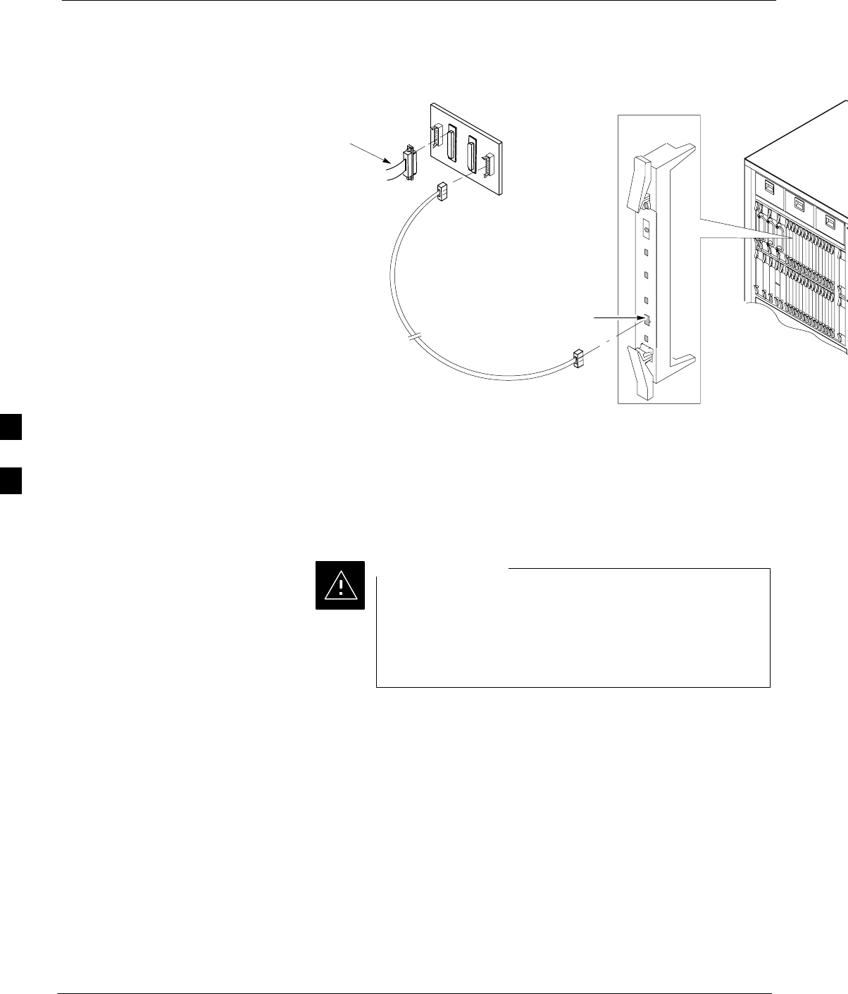
Prepare to Leave the Site – continued
5-6 1X SC4812T–MC BTS Optimization/ATP 5/21/04
DRAFT
Figure 5-1: MGLI/GLI MMI Port Connection
SERIAL CABLE
(P/N 3009786R01)
NULL MODEM BOARD
(PART# 8484877P01)
RS–232 CABLE
FROM LMF COM 1
PORT
MMI SERIAL PORT
GLI BOARD
Set BTS Site Span
Configuration
Perform the procedure in Table 5-5 to configure the Span Framing
Format and Line Build Out (LBO) parameters. ALL MGLI/GLI boards
in all C–CCP shelves that terminate a T1/E1 span must be configured.
Perform the following procedure ONLY if span
configurations loaded in the MGLI/GLIs do not match
those in the OMC–R data base, AND ONLY when the exact
configuration data is available. Loading incorrect span
configuration data will render the site inoperable.
CAUTION
5

Prepare to Leave the Site – continued
5/21/04 1X SC4812T–MC BTS Optimization/ATP 5-7
DRAFT
Table 5-5: Set GLI3 Span Parameter Configuration
Step Action
1If it has not been done, start a GLI3 MMI communication session on the LMF computer as described
in Table 3-10.
2At the GLI3> prompt, enter the following:
config ni format
The terminal will display a response similar to the following:
COMMAND SYNTAX: config ni format option
Next available options:
LIST – option : Span Option
E1_1 : E1_1 – E1 HDB3 CRC4 no TS16
E1_2 : E1_2 – E1 HDB3 no CRC4 no TS16
E1_3 : E1_3 – E1 HDB3 CRC4 TS16
E1_4 : E1_4 – E1 HDB3 no CRC4 TS16
T1_1 : T1_1 – D4, AMI, No ZCS
T1_2 : T1_2 – ESF, B8ZS
J1_1 : J1_1 – ESF, B8ZS (Japan) – Default
J1_2 : J1_2 – ESF, B8ZS
T1_3 : T1_3 – D4, AMI, ZCS
>
NOTE
With this command, all active (in–use) spans will be set to the same format.
3To set or change the span type, enter the correct option from the list at the entry prompt (>), as shown
in the following example:
> T1_2
NOTE
The entry is case–sensitive and must be typed exactly as it appears in the list. If the entry is typed
incorrectly, a response similar to the following will be displayed:
CP: Invalid command
01.061980 00:11’59 MGLI–000–2 INS–ACT BTS–CDMA 16.1.68.00
GLI3>
4An acknowledgement similar to the following will be displayed:
The value has been programmed. It will take effect after the next reset.
GLI3>
. . . continued on next page
5

Prepare to Leave the Site – continued
5-8 1X SC4812T–MC BTS Optimization/ATP 5/21/04
DRAFT
Table 5-5: Set GLI3 Span Parameter Configuration
Step Action
5If the current MGLI/GLI span rate must be changed, enter the following MMI command:
config ni linkspeed
A response similar to the following will be displayed :
Next available options:
LIST – linkspeed : Span Linkspeed
56K : 56K (default for T1_1 and T1_3 systems)
64K : 64K (default for all other span configurations)
>
NOTE
With this command, all active (in–use) spans will be set to the same linkspeed.
6To set or change the span linkspeed, enter the required option from the list at the entry prompt (>), as
shown in the following example:
> 64K
NOTE
The entry is case–sensitive and must be typed exactly as it appears in the list. If the entry is typed
incorrectly, a response similar to the following will be displayed:
CP: Invalid command
01.061980 00:12’04 MGLI–000–2 INS–ACT BTS–CDMA 16.1.68.00
GLI3>
7An acknowledgement similar to the following will be displayed:
The value has been programmed. It will take effect after the next reset.
GLI3>
. . . continued on next page
5

Prepare to Leave the Site – continued
5/21/04 1X SC4812T–MC BTS Optimization/ATP 5-9
DRAFT
Table 5-5: Set GLI3 Span Parameter Configuration
Step Action
8If the span equalization must be changed, enter the following MMI command:
config ni equal
A response similar to the following will be displayed:
COMMAND SYNTAX: config ni equal span equal
Next available options:
LIST – span : Span
a : Span A
b : Span B
c : Span C
d : Span D
e : Span E
f : Span F
>
. . . continued on next page
5

Prepare to Leave the Site – continued
5-10 1X SC4812T–MC BTS Optimization/ATP 5/21/04
DRAFT
Table 5-5: Set GLI3 Span Parameter Configuration
Step Action
9At the entry prompt (>), enter the designator from the list for the span to be changed as shown in the
following example:
> a
A response similar to the following will be displayed :
COMMAND SYNTAX: config ni equal a equal
Next available options:
LIST – equal : Span Equalization
0 : 0–131 feet (default for T1/J1)
1 : 132–262 feet
2 : 263–393 feet
3 : 394–524 feet
4 : 525–655 feet
5 : LONG HAUL
6 : 75 OHM
7 : 120 OHM (default for E1)
8 : T1 Long Haul mode. No Attenuation
9 : T1 Long Haul mode. 7.5 dB Attenuation
10 : T1 Long Haul mode. 15.0 dB Attenuation
11 : T1 Long Haul mode. 22.5 dB Attenuation
12 : E1 Long Haul mode.
>
! CAUTION
When selecting span equalization settings, comply with the following or the BTS may operate
erratically or unpredictably:
SFor ALL BTS types, do not select any of the following settings if they are displayed:
– 5 LONG HAUL
– 6 75 OHM
– 11 T1 Long Haul mode. 22.5 dB Attenuation
– 12 E1 Long Haul mode
SFor four–digit BTSs supported with Channel Service Units (CSU), do not select any of the
following additional settings:
– 8 T1 Long Haul mode. No Attenuation
– 9 T1 Long Haul mode. 7.5 dB Attenuation
– 10 T1 Long Haul mode. 15.0 dB Attenuation
. . . continued on next page
5

Prepare to Leave the Site – continued
5/21/04 1X SC4812T–MC BTS Optimization/ATP 5-11
DRAFT
Table 5-5: Set GLI3 Span Parameter Configuration
Step Action
10 At the entry prompt (>), enter the code for the required equalization from the list as shown in the
following example (this should be the distance from the BTS Span I/O to the site demarcation
equipment or CSU, as applicable):
> 0
A response similar to the following will be displayed :
> 0
The value has been programmed. It will take effect after the next reset.
GLI2>
11 Repeat steps 8 through 10 for each in–use span.
12 ! CAUTION
Do not set the card for loopback as described in this step unless specifically required or requested for
testing.
Enter the following MMI command to turn loopback on or off:
GLI#> config ni loopback <on or off>
Loopback commands and responses:
GLI#> config ni loopback on
Loopback request SUCCESSFUL: All framers have been placed in loopback.
They will remain in loopback for 1 hour.
GLI#> config ni loopback off
Loopback request SUCCESSFUL: All framers have been removed from loopback.
13 NOTE
This step must be performed for GLI3 cards operating on a packet image to ensure the span parameter
changes will replace the previous settings.
For a GLI3 card in packet mode, enter the following:
rmfile /nvram00/config/hlp_param.txt
A response similar to the following will be displayed :
GLI3> rmfile /nvram00/config/hlp_param.txt
11.24.2003 23:14:57 MGLI–004–1 CC PRESENT BTS–CDMA 16.40.00.09
Removing file: /nvram00/config/hlp_param.txt
Successfully removed file: /nvram00/config/hlp_param.txt
GLI3>
. . . continued on next page
5

Prepare to Leave the Site – continued
5-12 1X SC4812T–MC BTS Optimization/ATP 5/21/04
DRAFT
Table 5-5: Set GLI3 Span Parameter Configuration
Step Action
14 * IMPORTANT
SAfter executing the config ni format, config ni linkspeed, and/or config ni equal commands,
the affected MGLI/GLI board MUST be reset and reloaded for changes to take effect.
SAlthough defaults are shown in the software, always consult site–specific documentation for span
type, equalization, and linkspeed used at the site where the cards are to be installed.
Reset the card using the MMI reset command.
15 Once the card has completed resetting, execute the following command to verify span settings are as
required:
config ni current
A response similar to the following will be displayed :
The frame format in flash is set to use T1_2.
Equalization:
Span A – 0–131 feet
Span B – 0–131 feet
Span C – Default (0–131 feet for T1/J1, 120 Ohm for E1)
Span D – Default (0–131 feet for T1/J1, 120 Ohm for E1)
Span E – Default (0–131 feet for T1/J1, 120 Ohm for E1)
Span F – Default (0–131 feet for T1/J1, 120 Ohm for E1)
Linkspeed: 64K
Currently, the link is running at 64K
The actual rate is 0
16 If the span configuration is not correct, perform the applicable step from this table to change it and
repeat steps 14 and 15 to verify required changes have been programmed.
17 Repeat steps 1 through 16 for each GLI card requiring changes in the span parameter settings.
18 If no other MMI actions are required for the card, terminate the MMI communication session and
disconnect the LMF computer from the card.
LMF Removal
DO NOT power down the LMF without performing the
procedure below. Corrupted/lost data files may result, and
in some cases, the LMF may lock up.
NOTE
Follow the procedure in Table 5-6 to terminate the LMF session and
remove the terminal.
5

Prepare to Leave the Site – continued
5/21/04 1X SC4812T–MC BTS Optimization/ATP 5-13
DRAFT
Table 5-6: LMF Termination and Removal
nStep Action
1From the CDMA window select File>Exit.
NOTE
The “File > Exit” command will prompt you to confirm the logout proc
e
and Exit” command will not prompt you and continues to shut down L
M
2From the Windows Task Bar click Start>Shutdown.
Click Yes when the Shut Down Windows message appears.
3Disconnect the LMF terminal Ethernet connector from the BTS cabinet.
4Disconnect the LMF serial port, the RS-232 to GPIB interface box, and
required for equipment transport.
Re–connect BTS T1/E1 Spans
and Integrated Frame Modem
Before leaving the site, connect any T1 span TELCO connectors that
were removed to allow the LMF to control the BTS. Refer to Table 5-7
and Figure 5-2 as required.
Table 5-7: T1/E1 Span/IFM Connections
Step Action
1Connect the 50–pin TELCO cables to the BTS span I/O board 50–pin TELCO connectors.
2If used, connect the dial–up modem RS–232 serial cable to the Site I/O board RS–232 9–pin
sub D connector.
* IMPORTANT
Verify that you connect both SPAN cables (if removed previously), and the Integrated Frame
Modem (IFM) “TELCO” connector.
5
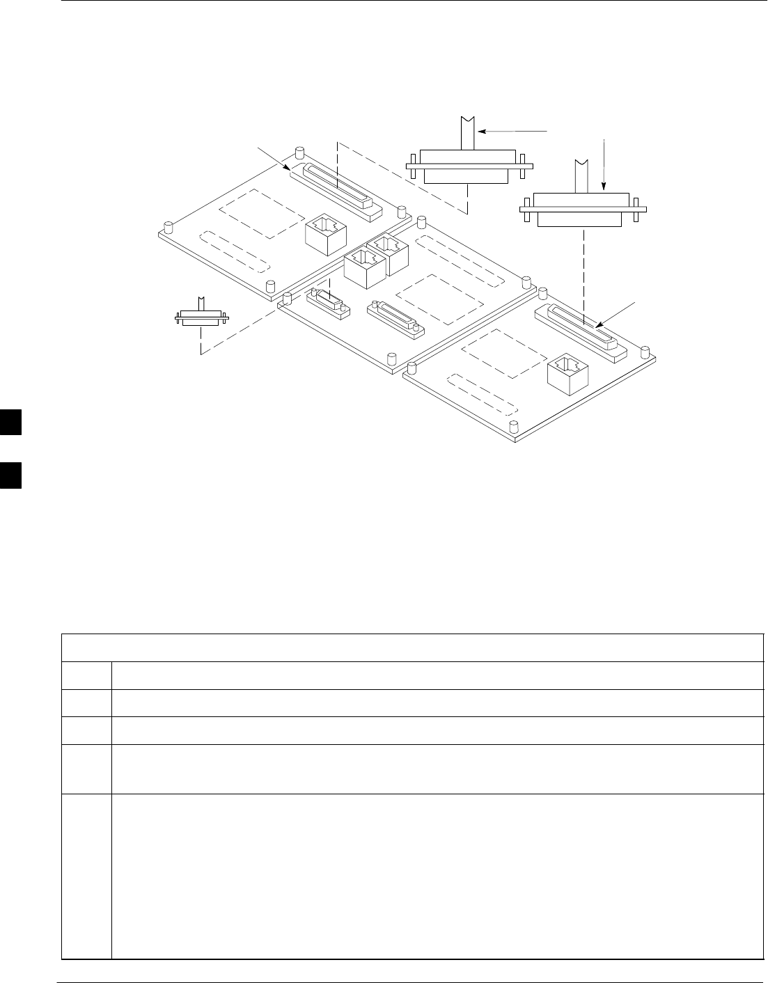
Prepare to Leave the Site – continued
5-14 1X SC4812T–MC BTS Optimization/ATP 5/21/04
DRAFT
Figure 5-2: Site and Span I/O Boards T1 Span Connections
50–PIN TELCO
CONNECTORS
REMOVED
SPAN A CONNECTOR
(TELCO) INTERFACE
TO SPAN LINES
SPAN B CONNECTOR
(TELCO) INTERFACE
TO SPAN LINES
TOP of Frame
(Site I/O and Span I/O boards)
RS–232 9–PIN SUB D
CONNECTOR SERIAL
PORT FOR EXTERNAL
DIAL UP MODEM
CONNECTION (IF USED)
FW00299
Reset All Devices and Initialize
Site Remotely
Devices in the BTS should not be left with data and code loaded from
the LMF. The configuration data and code loads used for normal
operation could be different from those stored in the LMF files. Perform
the procedure in Table 5-8 to reset all devices and initialize site remotely.
Table 5-8: Reset BTS Devices and Remote Site Initialization
Step Action
1Terminate the LMF session by following the procedures in Table 5-6.
2Reconnect spans by following the procedure in Table 5-7.
3– If BTS is configured for circuit operation, go to Step 4.
– If BTS is configured for packet operation, go to Step 5.
4Circuit BTS Procedure:
4a From the BTS site, contact the OMC–R and request the operator to perform a BTS reset.
or
At the BTS site:
– unseat one GLI card at a time and wait for 30 seconds;
– reseat the GLI and wait for it to complete its initialization (this takes about one minute);
– repeat for the second GLI.
. . . continued on next page
5

Prepare to Leave the Site – continued
5/21/04 1X SC4812T–MC BTS Optimization/ATP 5-15
DRAFT
Table 5-8: Reset BTS Devices and Remote Site Initialization
Step Action
4b Depending on the number of installed operational GLI cards, perform one of the following:
– With fully redundant GLIs, contact the OMC–R and request the operator to run the ACTIVATE
command for the BTS.
– For a non–redundant GLI or a frame where the redundant GLI is not operational, contact the
OMC–R and request the operator:
SACTIVATE the GLI to set the Nextload attribute for the GLI to the one for the current BSS
software version;
SDisable the GLI;
SEnable the GLI to allow the MM to load the software version specified by the Nextload
attribute;
SOnce the GLI is INS_ACT, contact the OMC–R and request the operator ACTIVATE the BTS.
– Once the GLI cards are loaded with the specified code version, the active GLI will verify and
update, as required, the RAM and, if it is necessary, ROM code loads for the installed CSM,
MCC, and BBX cards using the DLM.
5Packet BTS procedure:
5a From the BTS site, contact the OMC–R and request the operator to PREACTIVATE the BTS to the
required software version for the BSS. There are two types of PREACTIVATE load processes:
–Rolling Upgrade: This load process is only available when the BTS cards are populated for full
redundancy as applicable.
–Quick Reboot: This process is used when there is not full redundancy for the BTS cards. The
GLI3 will disable and reboot to the new load. This will cause all the other cards to go out of
service. Once it is rebooted, the GLI3 determines which cards require a new load and then
downloads the cards in the order which they establish communication with the GLI3 following
their reboot. The GLI3 can reload up to 16 devices simultaneously.
6Account for all tools used and parts removed from the frame during the operations, being sure none
were left inside the frame.
7Visually inspect the frame for any foreign objects left inside, and remove any discovered.
8Visually inspect all cable connections, ensuring they are connected as required for normal BTS
operation.
9Be sure all internal frame cables are routed and secured to prevent damage to them when the frame
doors are closed.
10 Close and secure the cabinet doors.
11 Verify no alarm conditions are being reported to the OMC–R with the frame doors closed.
12 After all activities at the site have been completed, contact the OMC–R and confirm that the BTS is
under OMC–R control.
5

Prepare to Leave the Site – continued
5-16 1X SC4812T–MC BTS Optimization/ATP 5/21/04
DRAFT
Notes
5

5/21/04 1X SC4812T–MC BTS Optimization/ATP
DRAFT
Chapter 6: Basic Troubleshooting
Table of Contents
Guide Book 1–2. . . . . . . . . . . . . . . . . . . . . . . . . . . . . . . . . . . . . . . . . . . . . . . . . . . . .
Document Overview 1–2. . . . . . . . . . . . . . . . . . . . . . . . . . . . . . . . . . . . . . . . . . . . . .
What Is In This Guide? 1–2. . . . . . . . . . . . . . . . . . . . . . . . . . . . . . . . . . . . .
Book Catalogs and Organization 1–3. . . . . . . . . . . . . . . . . . . . . . . . . . . . . . . . . . . .
Book Directory 1–3. . . . . . . . . . . . . . . . . . . . . . . . . . . . . . . . . . . . . . . . . . .
Special Catalogs 1–5. . . . . . . . . . . . . . . . . . . . . . . . . . . . . . . . . . . . . . . . . . .
Physical Page Layouts 1–6. . . . . . . . . . . . . . . . . . . . . . . . . . . . . . . . . . . . . . . . . . . .
A/A4 Page and Margin Sizes 1–6. . . . . . . . . . . . . . . . . . . . . . . . . . . . . . . . .
A/A4 Page Text Area 1–7. . . . . . . . . . . . . . . . . . . . . . . . . . . . . . . . . . . . . . .
A/A4 Page Components 1–9. . . . . . . . . . . . . . . . . . . . . . . . . . . . . . . . . . . .
Frame and Table Components 1–10. . . . . . . . . . . . . . . . . . . . . . . . . . . . . . . . . . . . . .
Frames With Tools 1–10. . . . . . . . . . . . . . . . . . . . . . . . . . . . . . . . . . . . . . . . .
Flow Charts and Block Diagrams 1–10. . . . . . . . . . . . . . . . . . . . . . . . . . . . .
Line Drawings 1–11. . . . . . . . . . . . . . . . . . . . . . . . . . . . . . . . . . . . . . . . . . . .
Table Types In This Template 1–12. . . . . . . . . . . . . . . . . . . . . . . . . . . . . . . .
Item/Description Table 1–12. . . . . . . . . . . . . . . . . . . . . . . . . . . . . . . . . . . . .
Step Table 1–13. . . . . . . . . . . . . . . . . . . . . . . . . . . . . . . . . . . . . . . . . . . . . . .
Step/Check Table 1–14. . . . . . . . . . . . . . . . . . . . . . . . . . . . . . . . . . . . . . . . . .
Component Descriptions 1–15. . . . . . . . . . . . . . . . . . . . . . . . . . . . . . . . . . . . . . . . . .
Conclusions 1–16. . . . . . . . . . . . . . . . . . . . . . . . . . . . . . . . . . . . . . . . . . . . . . . . . . . . .
Map Title Goes Here lkjsfdg Sfdkgj Msfd N lkas K lkjsdfl kB lkj fgcb 1–17. . . . . .
Block Label Goes Here 1–17. . . . . . . . . . . . . . . . . . . . . . . . . . . . . . . . . . . . .
Block Label Goes Here 1–17. . . . . . . . . . . . . . . . . . . . . . . . . . . . . . . . . . . . .
Block Label Goes Here 1–18. . . . . . . . . . . . . . . . . . . . . . . . . . . . . . . . . . . . .
Block Label Goes Here 1–19. . . . . . . . . . . . . . . . . . . . . . . . . . . . . . . . . . . . .
Map Title Goes Here 1–22. . . . . . . . . . . . . . . . . . . . . . . . . . . . . . . . . . . . . . . . . . . . . .
6

Table of Contents – continued
1X SC4812T–MC BTS Optimization/ATP 5/21/04
DRAFT
Notes
6

Troubleshooting Overview
5/21/04 1X SC4812T–MC BTS Optimization/ATP 6-1
DRAFT
Overview
The information in this section addresses some of the scenarios likely to
be encountered by Cellular Field Engineering (CFE) team members.
This troubleshooting guide was created as an interim reference document
for use in the field. It provides basic “what to do if” basic
troubleshooting suggestions when the BTS equipment does not perform
per the procedure documented in the manual.
Comments are consolidated from inputs provided by CFEs in the field
and information gained form experience in Motorola labs and
classrooms.
6

Troubleshooting: Installation
6-2 1X SC4812T–MC BTS Optimization/ATP 5/21/04
DRAFT
Cannot Log into Cell-Site
Follow the procedure in Table 6-1 to troubleshoot a login failure.
Table 6-1: Login Failure Troubleshooting Procedures
nStep Action
1If MGLI LED is solid RED, it implies a hardware failure. Reset MGLI by re-seating it. If this
persists, install a known good MGLI card in MGLI slot and retry. A Red LED may also indicate
no Ethernet termination at top of frame.
2Verify that T1 is disconnected (see Table 3-4 on page 3-14).
If T1 is still connected, verify the CBSC has disabled the BTS.
3Try pinging the MGLI (see Table 3-11 on page 3-32).
4Verify the LMF is connected to the Primary LMF port (LAN A) in the front of the BTS (see
Table 3-5 on page 3-15).
5Verify the LMF was configured properly (see Preparing the LMF section starting on page 3–6).
6Verify the BTS-LMF cable is RG-58 [flexible black cable of less than 76 cm (2.5 feet) length].
7Verify the Ethernet ports are terminated properly (see Figure 3-10).
8Verify a T-adapter is not used on the LMF side port if connected to the BTS front LMF primary
port.
9Try connecting to the I/O panel (top of frame). Use BNC T-adapters at the LMF port for this
connection.
10 Re-boot the LMF and retry.
11 Re-seat the MGLI and retry.
12 Verify IP addresses are configured properly.
Cannot Communicate to Power
Meter
Follow the procedure in Table 6-2 to troubleshoot a power meter
communication failure.
Table 6-2: Troubleshooting a Power Meter Communication Failure
nStep Action
1Verify the Power Meter is connected to the LMF with a GPIB adapter.
2Verify the cable setup as specified in Chapter 3.
3Verify the GPIB address of the power meter is set to the same value displayed in the applicable
GPIB address box of the LMF Options window Test Equipment tab. Refer to Table 3-24 or
Table 3-25 and the GPIB Addresses section of Appendix F for details.
4Verify the GPIB adapter DIP switch settings are correct.
Refer to the Test Equipment setup section for details.
. . . continued on next page
6

Troubleshooting: Installation – continued
5/21/04 1X SC4812T–MC BTS Optimization/ATP 6-3
DRAFT
Table 6-2: Troubleshooting a Power Meter Communication Failure
nActionStep
5Verify the GPIB adapter is not locked up. Under normal conditions, only two green LEDs must be
‘ON’ (Power and Ready). If any other LED is continuously ‘ON’, then power-cycle the GPIB Box
and retry.
6Verify the LMF computer COM1 port is not used by another application; for example, if a
HyperTerminal window is open for MMI, close it.
7Reset all test equipment by clicking Util in the BTS menu bar and selecting
Test Equipment>Reset from the pull–down lists.
Cannot Communicate to
Communications Analyzer
Follow the procedure in Table 6-3 to troubleshoot a communications
analyzer communication failure.
Table 6-3: Troubleshooting a Communications Analyzer Communication Failure
nStep Action
1Verify the analyzer is connected to the LMF with GPIB adapter.
2Verify the cable setup.
3Verify the signal generator GPIB address is set to the same value displayed in the applicable GPIB
address box of the LMF Options window Test Equipment tab. Refer to Table 3-24 or Table 3-25
and the GPIB Address section of Appendix F for details.
4Verify the GPIB adapter DIP switch settings are correct. Refer to the CDMA 2000 Test Equipment
Preparation section of Appendix NO TAG for details.
5Verify the GPIB adapter is not locked up. Under normal conditions, only two green LEDs must be
‘ON’ (Power and Ready). If any other LED is continuously ‘ON’, then cycle the GPIB box power
and retry.
6Verify the LMF computer COM1 port is not used by another application; for example, if a
HyperTerminal window is open for MMI, close it.
7 Reset all test equipment by clicking Util in the BTS menu bar and selecting
Test Equipment>Reset from the pull–down lists.
6

Troubleshooting: Download
6-4 1X SC4812T–MC BTS Optimization/ATP 5/21/04
DRAFT
Cannot Download CODE to Any
Device (card)
Follow the procedure in Table 6-4 to troubleshoot a code download
failure.
Table 6-4: Troubleshooting Code Download Failure
nStep Action
1Verify T1 is disconnected from the BTS.
2Verify the LMF can communicate with the BTS device using the Status function.
3Communication to the MGLI2 must first be established before trying to talk to any other BTS
device.
The MGLI2 must be INS_ACT state (green).
4Verify the card is physically present in the cage and powered-up.
5If the card LED is solid RED, it implies hardware failure.
Reset the card by re-seating it.
If the LED remains solid red, replace with a card from another slot & retry.
NOTE
The card can only be replaced by a card of the same type.
6Re-seat the card and try again.
7If BBX reports a failure message and is OOS_RAM, the code load was OK.
8If the download portion completes and the reset portion fails, reset the device by selecting the
device and Reset.
9If a BBX or an MCC remains OOS_ROM (blue) after code download, use the LMF
Device > Status function to verify that the code load was accepted.
10 If the code load was accepted, use LMF Device > Download > Flash to load RAM code into flash
memory.
Cannot Download DATA to Any
Device (Card)
Perform the procedure in Table 6-5 to troubleshoot a data download
failure.
Table 6-5: Troubleshooting Data Download Failure
nStep Action
1Re-seat the card and repeat code and data load procedure.
6

Troubleshooting: Download – continued
5/21/04 1X SC4812T–MC BTS Optimization/ATP 6-5
DRAFT
Cannot ENABLE Device
Before a device can be enabled (placed in-service), it must be in the
OOS_RAM state (yellow) with data downloaded to the device. The color
of the device changes to green once it is enabled.
The three states that devices can be changed to are as follows:
SEnabled (green, INS)
SDisabled (yellow, OOS_RAM)
SReset (blue, OOS_ROM)
Follow the procedure in Table 6-6 to troubleshoot a device enable
failure.
Table 6-6: Troubleshooting Device Enable (INS) Failure
nStep Action
1Re-seat the card and repeat the code and data load procedure.
2If the CSM cannot be enabled, verify the CDF file has correct latitude and longitude data for cell
site location and GPS sync.
3Ensure the primary CSM is in INS_ACT state.
NOTE
MCCs will not go INS without the CSM being INS.
4Verify the 19.6608 MHz CSM clock; MCCs will not go INS otherwise.
5The BBX should not be enabled for ATP tests.
6If MCCs give “invalid or no system time”, verify the CSM is operable.
Miscellaneous Errors
Perform the procedure in Table 6-7 to troubleshoot miscellaneous
failures.
Table 6-7: Miscellaneous Failures
nStep Action
1If PAs continue to give alarms, even after cycling power at the circuit breakers, then connect an
MMI cable to the PA and set up a Hyperterminal connection (see Table 3-3 on page 3-11).
2 Enter ALARMS in the Hyperterminal window.
The resulting LMF display may provide an indication of the problem.
(Call Field Support for further assistance.)
6

Troubleshooting: Calibration
6-6 1X SC4812T–MC BTS Optimization/ATP 5/21/04
DRAFT
Bay Level Offset Calibration
Failure
Perform the procedure in Table 6-8 to troubleshoot a BLO calibration
failure.
Only one carrier can be tested at a time. All PAs must be
INS during testing. For the carriers not under test, key one
BBX per carrier to a minimum power level. (Refer to
Table 3-37).
NOTE
Table 6-8: Troubleshooting BLO Calibration Failure
nStep Action
1Verify the Power Meter is configured correctly (see the test equipment setup section in Chapter 3)
and connection is made to the proper TX port.
2Verify the parameters in the bts–#.cdf file are set correctly for 800MHz:
Bandclass=0; Freq_Band=8; SSType=8
3Verify that no PA is in alarm state (flashing red LED).
Reset the PA by pulling the circuit breaker and, after 5 seconds, pushing back in.
4Re-calibrate the Power Meter and verify it is calibrated correctly with cal factors from the sensor
head.
5Verify the GPIB adapter is not locked up.
Under normal conditions, only two green LEDs must be ‘ON’ (Power and Ready).
If any other LED is continuously ‘ON’, power-cycle (turn power off and on) the GPIB Box and
retry.
6Verify the sensor head is functioning properly by checking it with the 1 mW (0 dBm) Power Ref
signal.
7If communication between the LMF and Power Meter is operatonal, the Meter display will show
“RES”.
Cannot Load BLO
For Load BLO failures see Table 6-7.
6

Troubleshooting: Calibration – continued
5/21/04 1X SC4812T–MC BTS Optimization/ATP 6-7
DRAFT
Calibration Audit Failure
Follow the procedure in Table 6-9 to troubleshoot a calibration audit
failure.
Only one carrier can be tested at a time. All PAs must be
INS during testing. For the carriers not under test, key one
BBX per carrier to a minimum power level. (Refer to
Table 3-37).
NOTE
Table 6-9: Troubleshooting Calibration Audit Failure
nStep Action
1Verify the Power Meter is configured correctly (refer to the test equipment setup section of
Chapter 3).
2Re-calibrate the Power Meter and verify it is calibrated correctly with cal factors from the sensor
head.
3Verify that no PA is in alarm state (rapidly flashing red LED).
Reset the PA by pulling the circuit breaker and, after 5 seconds, pushing back in.
4Verify that no sensor head is functioning properly by checking it with the 1 mW (0 dBm) Power
Ref signal.
5After calibration, the BLO data must be re-loaded to the BBXs before auditing.
Click on the BBX(s) and select Device>Download BLO.
Re-try the audit.
6Verify the GPIB adapter is not locked up.
Under normal conditions, only two green LEDs must be “ON” (Power and Ready).
If any other LED is continuously “ON”, power-cycle (turn power off and on) the GPIB Box and
retry.
6

Troubleshooting: Transmit ATP
6-8 1X SC4812T–MC BTS Optimization/ATP 5/21/04
DRAFT
BTS passed Reduced ATP tests
but has forward link problem
during normal operation
Follow the procedure in Table 6-10 to troubleshoot a Forward Link
problem during normal operation.
Table 6-10: Troubleshooting Forward Link Failure (BTS Passed Reduced ATP)
nStep Action
1Perform these additional TX tests to troubleshoot a forward link problem:
– TX mask
– TX rho
– TX code domain
Cannot Perform TX Mask
Measurement
Follow the procedure in Table 6-11 to troubleshoot a TX mask
measurement failure.
Only one carrier can be tested at a time. All PAs must be
INS during testing. For the carriers not under test, key one
BBX per carrier to a minimum power level. (Refer to
Table 3-37).
NOTE
Table 6-11: Troubleshooting TX Mask Measurement Failure
nStep Action
1Verify that TX audit passes for the BBX(s).
2If performing manual measurement, verify analyzer setup.
3Verify that no PA in the sector is in alarm state (flashing red LED).
Re-set the PA by pulling the circuit breaker and, after 5 seconds, pushing it back in.
Cannot Perform Rho or Pilot
Time Offset Measurement
Follow the procedure in Table 6-12 to troubleshoot a rho or pilot time
offset measurement failure.
Table 6-12: Troubleshooting Rho and Pilot Time Offset Measurement Failure
nStep Action
1Verify presence of RF signal by switching to spectrum analyzer screen.
2Verify PN offsets displayed on the analyzer is the same as the PN offset in the CDF file.
. . . continued on next page
6

Troubleshooting: Transmit ATP – continued
5/21/04 1X SC4812T–MC BTS Optimization/ATP 6-9
DRAFT
Table 6-12: Troubleshooting Rho and Pilot Time Offset Measurement Failure
nActionStep
3Re–load BBX data and repeat the test.
4If performing manual measurement, verify analyzer setup.
5Verify that no PA in the sector is in alarm state (flashing red LED). Reset the PA by pulling the
circuit breaker and, after 5 seconds, pushing back in.
6If Rho value is unstable and varies considerably (e.g. .95,.92,.93), this may indicate that the GPS
is still phasing (i.e., trying to reach and maintain 0 freq. error).
Go to the freq. bar in the upper right corner of the Rho meter and select Hz. Press <Shift–avg>
and enter 10, to obtain an average Rho value. This is an indication the GPS has not stabilized
before going INS and may need to be re-initialized.
Cannot Perform Code Domain
Power and Noise Floor
Measurement
Perform the procedure in Table 6-13 to troubleshoot a code domain and
noise floor measurement failure.
Table 6-13: Troubleshooting Code Domain Power and Noise Floor Measurement Failure
nStep Action
1Verify presence of RF signal by switching to spectrum analyzer screen.
2Verify PN offset displayed on analyzer is same as PN offset being used in the CDF file.
3Disable and re-enable MCC (one or more MCCs based on extent of failure).
6

Troubleshooting: Receive ATP
6-10 1X SC4812T–MC BTS Optimization/ATP 5/21/04
DRAFT
Multi–FER Test Failure
Perform the procedure in Table 6-14 to troubleshoot a Multi–FER
failure.
Table 6-14: Troubleshooting Multi-FER Failure
nStep Action
1Verify the test equipment set up is correct for an FER test.
2Verify the test equipment is locked to 19.6608 and even second clocks.
On the HP8921A test set, the yellow LED (REF UNLOCK) must be OFF.
3Verify the MCCs have been loaded with data and are INS–ACT.
4Disable and re-enable the MCC (one or more based on extent of failure).
5Disable, re-load code and data, and re-enable the MCC (one or more MCCs based on extent of
failure).
6Verify the antenna connections to frame are correct based on the directions messages.
6

Troubleshooting: CSM Checklist
5/21/04 1X SC4812T–MC BTS Optimization/ATP 6-11
DRAFT
Problem Description
Many of the Clock Synchronization Manager (CSM) board failures may
be resolved in the field before sending the boards to the factory for
repair. This section describes known CSM problems identified in field
returns, some of which are field-repairable. Check these problems before
returning suspect CSM boards.
Intermittent 19.6608 MHz
Reference Clock/GPS Receiver
Operation
If having any problems with CSM board kit numbers, SGLN1145 or
SGLN4132, check the suffix with the kit number. If the kit has version
“AB”, then replace with version “BC” or higher, and return model “AB”
to the repair center.
No GPS Reference Source
Check the CSM boards for proper hardware configuration. CSM kit
SGLN1145, in Slot l, has an on-board GPS receiver; while kit
SGLN4132, in Slot 2, does not have a GPS receiver. Any incorrectly
configured board must be returned to the repair center. Do not attempt to
change hardware configuration in the field. Also, verify the GPS
antenna is not damaged and is installed per recommended guidelines.
Checksum Failure
The CSM could have corrupted data in its firmware resulting in a
non-executable code. The problem is usually caused by either electrical
disturbance or interruption of data during a download. Attempt another
download with no interruptions in the data transfer. Return the CSM
board back to the repair center if the attempt to reload fails.
GPS Bad RX Message Type
This problem is believed to be caused by a later version of CSM
software (3.5 or higher) being downloaded, via LMF, followed by an
earlier version of CSM software (3.4 or lower), being downloaded from
the CBSC. Download again with CSM software code 3.5 or higher.
Return the CSM board back to the repair center if the attempt to reload
fails.
6

Troubleshooting: CSM Checklist – continued
6-12 1X SC4812T–MC BTS Optimization/ATP 5/21/04
DRAFT
CSM Reference Source
Configuration Error
This problem is caused by incorrect reference source configuration
performed in the field by software download. CSM kits SGLN1145 and
SGLN4132 must have proper reference sources configured (as shown
below) to function correctly.
CSM Kit
No.
Hardware
Configuration
CSM Slot
No.
Reference Source
Configuration
CDF Value
SGLN1145 With GPS Receiver 1Primary = Local GPS
Backup = HSO
0
2 or 18
SGLN4132 Without GPS Receiver 2Primary = Remote GPS
Backup = HSO
1
2 or 18
Takes Too Long for CSM to
Come INS
This problem may be caused by a delay in GPS acquisition. Check the
accuracy flag status and/or current position. Refer to the GSM system
time/GPS and HSO verification section in Chapter 3. At least one
satellite should be visible and tracked for the “surveyed” mode and four
satellites should be visible and tracked for the “estimated” mode. Also,
verify correct base site position data used in “surveyed” mode.
6

Troubleshooting: C–CCP Backplane
5/21/04 1X SC4812T–MC BTS Optimization/ATP 6-13
DRAFT
Introduction
The C–CCP backplane is a multi–layer board that interconnects all the
C–CCP modules. The complexity of this board lends itself to possible
improper diagnoses when problems occur.
Connector Functionality
The following connector overview describes the major types of
backplane connectors along with the functionality of each. This
information allows the CFE to:
SDetermine which connector(s) is associated with a specific problem
type.
SIsolate problems to a specific cable or connector.
Primary “A” and Redundant “B” Inter Shelf Bus Connectors
The 40 pin Inter Shelf Bus (ISB) connectors provide an interface bus
from the master GLI to all other GLIs in the modem frame. Their basic
function is to provide clock synchronization from the master GLI to all
other GLIs in the frame.
The ISB also provides the following functions:
SSpan line grooming when a single span is used for multiple cages.
SMMI connection to/from the master GLI to cell site modem.
SInterface between GLIs and the AMR (for reporting BTS alarms).
Span Line Connector
The 50–pin span line connector provides a primary and secondary (if
used) span line interface to each GLI in the C–CCP shelf. The span line
is used for MM/EMX switch control of the Master GLI and also all the
BBX traffic.
Primary “A” and Redundant “B” Reference Distribution
Module Input/Output
The Reference Distribution Module (RDM) connectors route the 3 MHz
reference signals from the CSMs to the GLIs and all BBXs in the
backplane. The signals are used to phase lock loop all clock circuits on
the GLIs and BBX boards to produce precise clock and signal
frequencies.
Power Input (Return A, B, and C connectors)
For –48 V configuration – Provides a –48 volt input for use by the
power supply modules.
For +27 V configuration – Provides input for regulated +27 Volts.
6

Troubleshooting: C–CCP Backplane – continued
6-14 1X SC4812T–MC BTS Optimization/ATP 5/21/04
DRAFT
Power Supply Interface
Each C–CCP power supply has a series of three different connectors to
provide the needed inputs/outputs to the C–CCP backplane. These
include a VCC/Ground input connector, a Harting style multiple pin
interface, and a +15 V/Analog Ground output connector. The C–CCP
Power Supplies convert +27 Volts to a regulated +15, +6.5, and +5.0
Volts to be used by the C–CCP shelf cards.
For –48V BTS only, the power supply modules convert –48 Volts to a
regulated +27 Volts.
GLI Connector
This connector consists of a Harting 4SU digital connector and a
6–conductor coaxial connector for RDM distribution. The connectors
provide inputs/outputs for the GLIs in the C–CCP backplane.
GLI 10Base–2 Ethernet “A” and “B” Connections
These BNC connectors are located on the C–CCP backplane and routed
to the GLI board. This interface provides all the control and data
communications between the master GLI and the other GLI, between
gateways, and for the LMF on the LAN.
BBX Connector
Each BBX connector consists of a Harting 2SU/1SU digital connector
and two 6–conductor coaxial connectors. These connectors provide DC,
digital, and RF inputs/outputs for the BBXs in the C–CCP backplane.
MCIO Connectors
SRX RF antenna path signal inputs are routed through RX Tri–Filters
(on the I/O plate), and via coaxial cables to the two MPC modules –
the six “A” (main) signals go to one MPC; the six “B” (diversity) to
the other. The MPC outputs the low–noise–amplified signals via the
C–CCP backplane to the MCIO where the signals are split and sent to
the appropriate BBX.
SA digital bus then routes the baseband signal through the BBX, to the
backplane, then on to the MCC slots.
SDigital TX antenna path signals originate at the MCCs. Each output
is routed from the MCC slot via the backplane appropriate BBX.
STX RF path signal originates from the BBX, through the backplane to
the MCIO, through the MCIO, and via multi-conductor coaxial
cabling to the PAs in the PA shelf.
C–CCP Backplane
Troubleshooting Procedure
Table 6-15 through Table 6-24 provide procedures for troubleshooting
problems that appear to be related to a defective C–CCP backplane. The
tables are broken down into possible problems and steps that should be
taken in an attempt to find the root cause.
6

Troubleshooting: C–CCP Backplane – continued
5/21/04 1X SC4812T–MC BTS Optimization/ATP 6-15
DRAFT
IMPORTANT: Table 6-15 through Table 6-24 must be
completed before replacing ANY C–CCP backplane.
NOTE
Digital Control Problems
No GLI Control via LMF (all GLIs)
Follow the procedure in Table 6-15 to troubleshoot a GLI control via
LMF failure.
Table 6-15: No GLI Control via LMF (all GLIs)
nStep Action
1Check the 10Base–2 ethernet connector for proper connection, damage, shorts, or opens.
2Verify the C–CCP backplane Shelf ID DIP switch is set correctly.
3Visually check the master GLI connector (both board and backplane) for damage.
4Replace the master GLI with a known good GLI.
No GLI Control through Span Line Connection (All GLIs)
Follow the procedures in Table 6-16 and Table 6-17 to troubleshoot GLI
control failures.
Table 6-16: No GLI Control through Span Line Connection (Both GLIs)
Step Action
1Verify the C–CCP backplane Shelf ID DIP switch is set correctly.
2Verify that the BTS and GLIs are correctly configured in the OMCR/CBSC data base.
3Visually check the master GLI connector (both board and backplane) for damage.
4Replace the master GLI with a known good GLI.
5Check the span line inputs from the top of the frame to the master GLI for proper connection and
damage.
6Check the span line configuration on the MGLI (see Table 5-4 on page 5-5).
Table 6-17: MGLI Control Good – No Control over Co–located GLI
Step Action
1Verify that the BTS and GLIs are correctly configured in the OMCR CBSC data base.
2Check the 10Base–2 ethernet connector for proper connection, damage, shorts, or opens.
3Visually check all GLI connectors (both board and backplane) for damage.
4Replace the remaining GLI with a known good GLI.
6

Troubleshooting: C–CCP Backplane – continued
6-16 1X SC4812T–MC BTS Optimization/ATP 5/21/04
DRAFT
No AMR Control (MGLI good)
Perform the procedure in Table 6-18 to troubleshoot an AMR control
failure when the MGLI control is good.
Table 6-18: MGLI Control Good – No Control over AMR
Step Action
1Visually check the master GLI connector (both board and backplane) for damage.
2Replace the master GLI with a known good GLI.
3Replace the AMR with a known good AMR.
No BBX Control in the Shelf – (No Control over Co–located
GLIs)
Perform the procedure in Table 6-19 to troubleshoot a BBX control in
the shelf failure.
Table 6-19: No BBX Control in the Shelf – No Control over Co–located GLIs
Step Action
1Visually check all GLI connectors (both board and backplane) for damage.
2Replace the remaining GLI with a known good GLI.
3Visually check BBX connectors (both board and backplane) for damage.
4Replace the BBX with a known good BBX.
No (or Missing) Span Line Traffic
Perform the procedure in Table 6-20 to troubleshoot a span line traffic
failure.
Table 6-20: MGLI Control Good – No (or Missing) Span Line Traffic
Step Action
1Visually check all GLI connectors (both board and backplane) for damage.
2Replace the remaining GLI with a known good GLI.
3Visually check all span line distribution (both connectors and cables) for damage.
4If the problem seems to be limited to one BBX, replace the MGLI with a known good MGLI.
5Perform the BTS Span Parameter Configuration ( see Table 5-4 on page 5-5).
6Ensure that ISB cabling is correct.
No (or Missing) MCC Channel Elements
Perform the procedure in Table 6-21 to troubleshoot a channel elements
failure.
6
Troubleshooting: C–CCP Backplane – continued
5/21/04 1X SC4812T–MC BTS Optimization/ATP 6-17
DRAFT
Table 6-21: No MCC Channel Elements
Step Action
1Verify CEs on a co–located MCC (MCC24 TYPE=2).
2If the problem seems to be limited to one MCC, replace the MCC with a known good MCC.
– Check connectors (both board and backplane) for damage.
3If no CEs on any MCC:
– Verify clock reference to MCIO.
4Check the CDF for MCCTYPE=2 (MCC24E); MCCTYPE=0 (MCC8E) or MCCTYPE=3 (MCC–1X)
DC Power Problems
Perform the procedure in Table 6-22 to troubleshoot a DC input voltage
to power supply module failure.
Potentially lethal voltage and current levels are routed to
the BTS equipment. This test must be carried out with a
second person present, acting in a safety role. Remove all
rings, jewelry, and wrist watches prior to beginning this
test.
WARNING
6

Troubleshooting: C–CCP Backplane – continued
6-18 1X SC4812T–MC BTS Optimization/ATP 5/21/04
DRAFT
No DC Input Voltage to Power Supply Module
Table 6-22: No DC Input Voltage to Power Supply Module
Step Action
1Verify DC power is applied to the BTS frame.
2Verify there are no breakers tripped.
* IMPORTANT
If a breaker has tripped, remove all modules from the applicable shelf supplied by the breaker and
attempt to reset it.
– If the breaker trips again, there is probably a cable or breaker problem within the frame.
– If the breaker does not trip, there is probably a defective module or sub–assembly within the shelf.
3Verify that the C–CCP shelf breaker on the BTS frame breaker panel is functional.
4Use a voltmeter to determine if the input voltage is being routed to the C–CCP backplane by
measuring the DC voltage level on the PWR_IN cable.
– If the voltage is not present, there is probably a cable or breaker problem within the frame.
– If the voltage is present at the connector, reconnect and measure the level at the “VCC” power
feed clip on the distribution backplane.
– If the voltage is correct at the power clip, inspect the clip for damage.
5–48 V configuration only – If everything appears to be correct, visually inspect the power supply
module and verify LEDs are green.
6–48 V configuration only – If LED is red, then replace the power suppy module with a known good
module and verify LEDs are green.
7If steps 1 through 5 fail to indicate a problem, a C–CCP backplane failure (possibly an open trace) has
occurred.
No DC Voltage (+5, +6.5, or +15 Volts) to a Specific GLI, BBX,
or Switchboard
Perform the procedure in Table 6-23 to troubleshoot a DC input voltage
to GLI, BBX, or Switchboard failure.
Table 6-23: No DC Input Voltage to any C–CCP Shelf Module
Step Action
1Verify the steps in Table 6-22 have been performed.
2Inspect the defective board/module (both board and backplane) connector for damage.
3Replace suspect board/module with known good board/module.
TX and RX Signal Routing
Problems
Perform the procedure in Table 6-24 to troubleshoot TX and RX signal
routing problems.
6

Troubleshooting: C–CCP Backplane – continued
5/21/04 1X SC4812T–MC BTS Optimization/ATP 6-19
DRAFT
Table 6-24: TX and RX Signal Routing Problems
Step Action
1Inspect all Harting Cable connectors and back–plane connectors for damage in all the affected board
slots.
2Perform steps in the RF path troubleshooting flowchart in this manual.
6

Troubleshooting: Span Control Link
6-20 1X SC4812T–MC BTS Optimization/ATP 5/21/04
DRAFT
Span Problems (No Control
Link)
Perform the procedure in Table 6-25 to troubleshoot a control link
failure.
Table 6-25: Troubleshoot Control Link Failure
nStep Action
1Connect the CDMA LMF computer to the MMI port on the applicable MGLI/GLI as shown in
Figure 6-1 or Figure 6-2.
2Start an MMI communication session with the applicable MGLI/GLI by using the Windows
desktop shortcut icon.
3Once the connection window opens, press the CDMA LMF computer Enter key until the GLI
prompt is obtained.
4At the GLI prompt, enter:
config ni current <cr> (equivalent of span view command)
The system will respond with a display similar to the following:
The frame format in flash is set to use T1_2.
Equalization:
Span A – Default (0–131 feet for T1/J1, 120 Ohm for E1)
Span B – Default (0–131 feet for T1/J1, 120 Ohm for E1)
Span C – Default (0–131 feet for T1/J1, 120 Ohm for E1)
Span D – Default (0–131 feet for T1/J1, 120 Ohm for E1)
Span E – Default (0–131 feet for T1/J1, 120 Ohm for E1)
Span F – Default (0–131 feet for T1/J1, 120 Ohm for E1)
Linkspeed: Default (56K for T1 D4 AMI, 64K otherwise)
Currently, the link is running at the default rate
The actual rate is 0
NOTE
Defaults for span equalization are 0–131 feet for T1/J1 spans and 120 Ohm for E1.
Default linkspeed is 56 kbps for T1 D4 AMI spans and 64 kbps for all other types.
There is no need to change from defaults unless the OMC–R/CBSC span configuration requires it.
5The span configurations loaded in the GLI must match those in the OMCR/CBSC database for the
BTS. If they do not, proceed to Table 6-26.
6Repeat steps 1 through 5 for all remaining GLIs.
7If the span settings are correct, verify the edlc parameters using the show command.
Any alarm conditions indicate that the span is not operating correctly.
STry looping back the span line from the DSX panel back to the MM, and verify that the looped
signal is good.
SListen for control tone on the appropriate timeslot from the Base Site and MM.
6
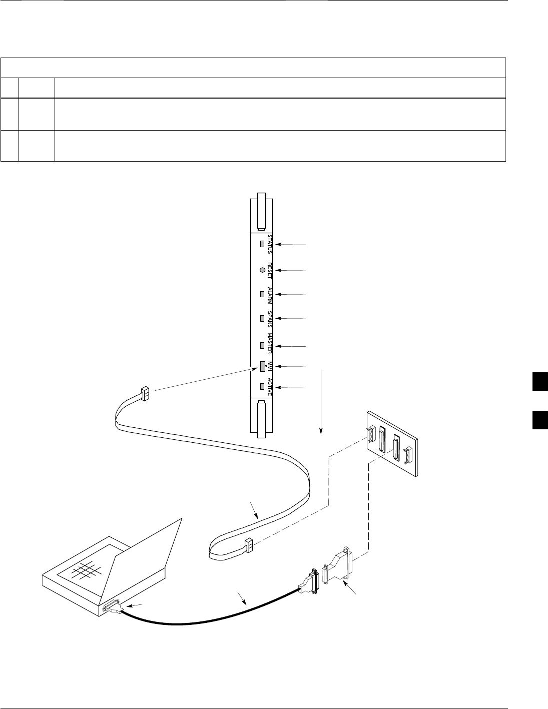
Troubleshooting: Span Control Link – continued
5/21/04 1X SC4812T–MC BTS Optimization/ATP 6-21
DRAFT
Table 6-25: Troubleshoot Control Link Failure
nActionStep
8Exit the GLI MMI session and HyperTerminal connection by selecting File from the connection
window menu bar, and then Exit from the dropdown menu.
9If no TCHs in groomed MCCs (or in whole SCCP shelf) can process calls, verify that the ISB
cabling is correct and that ISB A and ISB B cables are not swapped.
Figure 6-1: GLI2 Board MMI Connection Detail
NULL MODEM
BOARD
(TRN9666A)
8–PIN TO 10–PIN
RS–232 CABLE
(P/N 30–09786R01)
RS–232
CABLE
8–PIN
CDMA LMF
COMPUTER
To MMI port
DB9–TO–DB25
ADAPTER
COM1 or COM2
ACTIVE LED
STATUS LED
ALARM LED
MASTER LED
MMI Port
Connector
SPANS LED
RESET
Pushbutton
GLI2
ti-CDMA-WP-00079-v01-ildoc-ftw
MMI Port
Span (LED)
Alarm (LED)
Active (LED)
Status (LED)
6
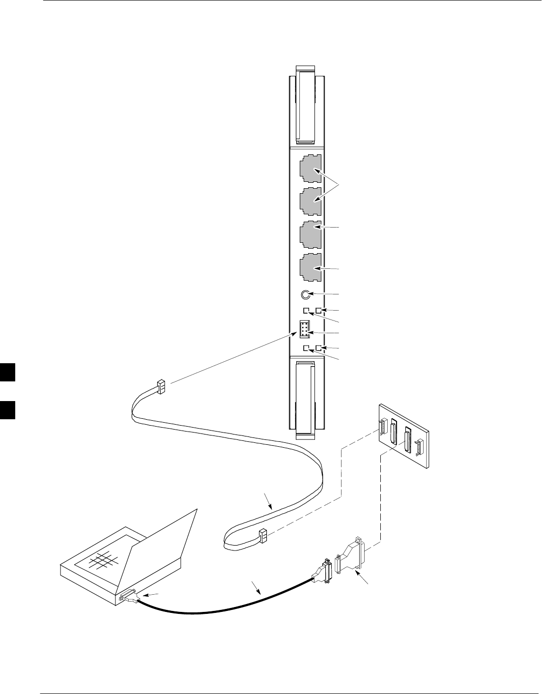
Troubleshooting: Span Control Link – continued
6-22 1X SC4812T–MC BTS Optimization/ATP 5/21/04
DRAFT
Figure 6-2: GLI3 Board MMI Connection Detail
NULL MODEM
BOARD
(TRN9666A)
8–PIN TO 10–PIN
RS–232 CABLE
(P/N 30–09786R01)
RS–232
CABLE
8–PIN
CDMA LMF
COMPUTER
To MMI port
DB9–TO–DB25
ADAPTER
COM1 or COM2
GLI3
MMI Port
Reset Switch
Dual 100BASE–T
in a single RJ45
to Redundant
(Mate) GLI3
100BASE–T
Auxiliary Monitor
Port
BPR B AUX RESET
SPAN
ALARM MMI
ACT
STA
100BASE–T to
BTS Packet Router
or Expansion cage
Span (LED)
Alarm (LED)
Active (LED)
Status (LED)
GLIBPR A
ti-CDMA-WP-00064-v01-ildoc-ftw
REF
Set BTS Site Span
Configuration
Perform the procedure in Table 6-26 to set the span parameter
configuration.
6

Troubleshooting: Span Control Link – continued
5/21/04 1X SC4812T–MC BTS Optimization/ATP 6-23
DRAFT
IMPORTANT: Perform the following procedure ONLY if
span configurations loaded in the MGLI/GLIs do not
match those in the OMCR/CBSC data base, AND ONLY
when the exact configuration data is available. Loading
incorrect span configuration data will render the site
inoperable.
NOTE
Table 6-26: Set BTS Span Parameter Configuration
nStep Action
1If not previously done, connect the CDMA LMF computer to the MMI port on the applicable
MGLI/GLI as shown in Figure 6-1.
2If there is no MMI communication session in progress with the applicable MGLI/GLI, initiate one
by using the Windows desktop shortcut icon.
3At the GLI prompt, enter:
config ni format <option> <cr>
The terminal will display a response similar to the following:
COMMAND SYNTAX: config ni format option
Next available options:
LIST – option : Span Option
E1_1 : E1_1 – E1 HDB3 CRC4 no TS16
E1_2 : E1_2 – E1 HDB3 no CRC4 no TS16
E1_3 : E1_3 – E1 HDB3 CRC4 TS16
E1_4 : E1_4 – E1 HDB3 no CRC4 TS16
T1_1 : T1_1 – D4, AMI, No ZCS
T1_2 : T1_2 – ESF, B8ZS
J1_1 : J1_1 – ESF, B8ZS (Japan) – Default
J1_2 : J1_2 – ESF, B8ZS
T1_3 : T1_3 – D4, AMI, ZCS
>
NOTE
With this command, all active (in–use) spans will be set to the same format.
4To set or change the span type, enter the correct option from the list at the entry prompt (>), as
shown in the following example:
> T1_2 <cr>
NOTE
The entry is case–sensitive and must be typed exactly as it appears in the list. If the entry is typed
incorrectly, a response similar to the following will be displayed:
CP: Invalid command
GLI>
. . . continued on next page
6

Troubleshooting: Span Control Link – continued
6-24 1X SC4812T–MC BTS Optimization/ATP 5/21/04
DRAFT
Table 6-26: Set BTS Span Parameter Configuration
nActionStep
5An acknowledgement similar to the following will be displayed:
The value has been programmed. It will take effect after the next re-
set.
GLI>
6If the current MGLI/GLI span rate must be changed, enter the following MMI command:
config ni linkspeed <cr>
The terminal will display a response similar to the following:
Next available options:
LIST – linkspeed : Span Linkspeed
56K : 56K (default for T1_1 and T1_3 systems)
64K : 64K (default for all other span configurations)
>
NOTE
With this command, all active (in–use) spans will be set to the same linkspeed.
7To set or change the span linkspeed, enter the required option from the list at the entry prompt (>),
as shown in the following example:
> 64K <cr>
NOTE
The entry is case–sensitive and must be typed exactly as it appears in the list. If the entry is typed
incorrectly, a response similar to the following will be displayed:
CP: Invalid command
GLI>
8An acknowledgement similar to the following will be displayed:
The value has been programmed. It will take effect after the next re-
set.
GLI>
. . . continued on next page
6

Troubleshooting: Span Control Link – continued
5/21/04 1X SC4812T–MC BTS Optimization/ATP 6-25
DRAFT
Table 6-26: Set BTS Span Parameter Configuration
nActionStep
9If the span equalization must be changed, enter the following MMI command:
config ni equal <cr>
The terminal will display a response similar to the following:
COMMAND SYNTAX: config ni equal span equal
Next available options:
LIST – span : Span
a : Span A
b : Span B
c : Span C
d : Span D
e : Span E
f : Span F
>
10 At the entry prompt (>), enter the designator from the list for the span to be changed as shown in
the following example:
> a <cr>
The terminal will display a response similar to the following:
COMMAND SYNTAX: config ni equal a equal
Next available options:
LIST – equal : Span Equalization
0 : 0–131 feet (default for T1/J1)
1 : 132–262 feet
2 : 263–393 feet
3 : 394–524 feet
4 : 525–655 feet
5 : LONG HAUL
6 : 75 OHM
7 : 120 OHM (default for E1)
>
11 At the entry prompt (>), enter the code for the required equalization from the list as shown in the
following example:
> 0 <cr>
The terminal will display a response similar to the following:
> 0
The value has been programmed. It will take effect after the next re-
set.
GLI>
12 Repeat steps 9 through 11 for each in–use span.
. . . continued on next page
6

Troubleshooting: Span Control Link – continued
6-26 1X SC4812T–MC BTS Optimization/ATP 5/21/04
DRAFT
Table 6-26: Set BTS Span Parameter Configuration
nActionStep
13 NOTE
After executing the config ni format, config ni linkspeed, and/or config ni equal
commands, the affected MGLI/GLI board MUST be reset and reloaded for changes to take effect.
Although defaults are shown, always consult site specific documentation for span type and
linkspeed used at the site.
Press the RESET button on the MGLI/GLI for changes to take effect.
14 Once the MGLI/GLI has reset, execute the following command to verify span settings are as
required:
config ni current <cr> (equivalent of span view command)
The system will respond with a display similar to the following:
The frame format in flash is set to use T1_2.
Equalization:
Span A – 0–131 feet
Span B – 0–131 feet
Span C – Default (0–131 feet for T1/J1, 120 Ohm for E1)
Span D – Default (0–131 feet for T1/J1, 120 Ohm for E1)
Span E – Default (0–131 feet for T1/J1, 120 Ohm for E1)
Span F – Default (0–131 feet for T1/J1, 120 Ohm for E1)
Linkspeed: 64K
Currently, the link is running at 64K
The actual rate is 0
15 If the span configuration is not correct, perform the applicable step from this table to change it and
repeat steps 13 and 14 to verify required changes have been programmed.
16 Return to step 6 of Table 6-25.
6

Module Front Panel LED Indicators and Connectors
5/21/04 1X SC4812T–MC BTS Optimization/ATP 6-27
DRAFT
Module Status Indicators
Each of the non-passive plug-in modules has a bi-color (green & red)
LED status indicator located on the module front panel. The indicator is
labeled PWR/ALM. If both colors are turned on, the indicator is yellow.
Each plug-in module, except for the fan module, has its own alarm
(fault) detection circuitry that controls the state of the PWR/ALM LED.
The fan TACH signal of each fan module is monitored by the AMR.
Based on the status of this signal, the AMR controls the state of the
PWR/ALM LED on the fan module.
LED Status Combinations for
All Modules (except GLI, CSM,
BBX, MCC)
PWR/ALM LED
The following list describes the states of the module status indicator.
SSolid GREEN – module operating in a normal (fault free) condition.
SSolid RED – module is operating in a fault (alarm) condition due to
electrical hardware failure.
Note that a fault (alarm) indication may or may not be due to a complete
module failure and normal service may or may not be reduced or
interrupted.
DC/DC Converter LED Status
Combinations
The PWR CNVTR has alarm (fault) detection circuitry that controls the
state of the PWR/ALM LED. This is true for both the C–CCP and PA
power converters.
PWR/ALM LED
The following list describes the states of the bi-color LED.
SSolid GREEN – module operating in a normal (fault free) condition.
SSolid RED – module is operating in a fault (alarm) condition due to
electrical hardware problem.
CSM LED Status Combinations
The CSMs include on-board alarm detection. Hardware and
software/firmware alarms are indicated via the front panel indicators (see
Figure 6-3).
6

Module Front Panel LED Indicators and Connectors – continued
6-28 1X SC4812T–MC BTS Optimization/ATP 5/21/04
DRAFT
Figure 6-3: CSM Front Panel Indicators & Monitor Ports
PWR/ALM
Indicator
FREQ
MONITOR
SYNC
MONITOR
FW00303
PWR/ALM LED
After the memory tests, the CSM loads OOS–RAM code from the Flash
EPROM, if available. If not available, the OOS–ROM code is loaded
from the Flash EPROM.
SSolid GREEN – module is INS_ACT or INS_STBY no alarm.
SSolid RED – Initial power up or module is operating in a fault (alarm)
condition.
SSlowly Flashing GREEN – OOS_ROM no alarm.
SLong RED/Short GREEN – OOS_ROM alarm.
SRapidly Flashing GREEN – OOS_RAM no alarm or INS_ACT in
DUMB mode.
SShort RED/Short GREEN – OOS_RAM alarm.
SLong GREEN/Short RED – INS_ACT or INS_STBY alarm.
SOff – no DC power or on-board fuse is open.
SSolid YELLOW – After a reset, the CSMs begin to boot. During
SRAM test and Flash EPROM code check, the LED is yellow. (If
SRAM or Flash EPROM fail, the LED changes to a solid RED and
the CSM attempts to reboot.)
FREQ Monitor Connector
A test port provided at the CSM front panel via a BNC receptacle allows
monitoring of the 19.6608 MHz clock generated by the CSM. When
both CSM 1 and CSM 2 are in an in-service (INS) condition, the CSM 2
clock signal frequency is the same as that output by CSM 1.
6

Module Front Panel LED Indicators and Connectors – continued
5/21/04 1X SC4812T–MC BTS Optimization/ATP 6-29
DRAFT
The clock is a sine wave signal with a minimum amplitude of +2 dBm
(800 mVpp) into a 50 Ω load connected to this port.
SYNC Monitor Connector
A test port provided at the CSM front panel via a BNC receptacle allows
monitoring of the “Even Second Tick” reference signal generated by the
CSMs.
At this port, the reference signal is a TTL active high signal with a pulse
width of 153 nanoseconds.
MMI Connector
Only accessible behind front panel. The RS–232 MMI port connector is
intended to be used primarily in the development or factory
environment, but may be used in the field for debug/maintenance
purposes.
GLI LED Status Combinations
GLIs may be GLI2 or GLI3. Either supports the 1X
SCt4812T–MC BTS.
NOTE
GLI
The GLI module has indicators, controls and connectors as described
below and shown in Table 6-27 (GLI2) and Table 6-28 (GLI3).
The operating states of the LEDs are:
ACTIVE
Solid GREEN – GLI is active. This means that the GLI has shelf
control and is providing control of the digital interfaces.
Off – GLI is not active (i.e., Standby). The mate GLI should be active.
MASTER (not on GLI3)
SSolid GREEN – GLI is Master (sometimes referred to as MGLI).
SOff – GLI is non-master (i.e., Slave).
ALARM
SSolid RED – GLI is in a fault condition or in reset.
SWhile in reset transition, STATUS LED is OFF while GLI is
performing ROM boot (about 12 seconds for normal boot).
SWhile in reset transition, STATUS LED is ON while GLI is
performing RAM boot (about 4 seconds for normal boot).
SOff – No Alarm.
6

Module Front Panel LED Indicators and Connectors – continued
6-30 1X SC4812T–MC BTS Optimization/ATP 5/21/04
DRAFT
STATUS
SFlashing GREEN– GLI is in service (INS), in a stable operating
condition.
SOn – GLI is in OOS RAM state operating downloaded code.
SOff – GLI is in OOS ROM state operating boot code.
SPANS
SSolid GREEN – Span line is connected and operating.
SSolid RED – Span line is disconnected or a fault condition exists.
GLI Pushbuttons and
Connectors
RESET Pushbutton – Depressing the RESET pushbutton causes a
partial reset of the CPU and a reset of all board devices. The GLI2 is
placed in the OOS_ROM state
MMI Connector – The RS–232MMI port connector is intended to be
used primarily in the development or factory environment but may be
used in the field for debug/maintenance purposes.
LAN Connectors (A & B) – The two 10BASE2 Ethernet circuit board
mounted BNC connectors are located on the bottom front edge of the
GLI2; one for each LAN interface, A & B. Ethernet cabling is connected
to tee connectors fastened to these BNC connectors.
GLI2 Front Panel
Table 6-27 shows the front panel of the GLI2 card and includes a
description of the components.
6
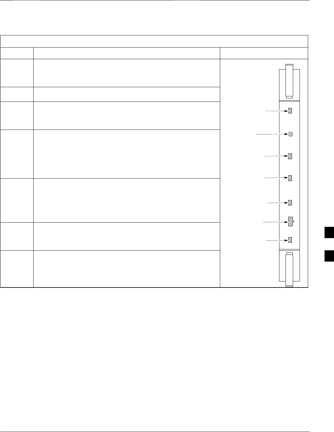
Module Front Panel LED Indicators and Connectors – continued
5/21/04 1X SC4812T–MC BTS Optimization/ATP 6-31
DRAFT
Table 6-27: GLI2 Front Panel
LED Operating Status Diagram
STATUS OFF – operating normally
ON – briefly during power-up when the Alarm LED turns OFF
SLOW GREEN – when the GLI2 is INS (in-service)
RESET Pressing and releasing the switch resets all functions on the GLI2.
ALARM OFF – operating normally
ON – briefly during power-up when the Alarm LED turns OFF
SLOW GREEN – when the GLI2 is INS (in-service)
STATUS
STATUS LED
SPANS OFF – card is powered down, in initialization, or in standby
GREEN – operating normally
YELLOW – one or more of the equipped initialized spans is receiving
a remote alarm indication signal from the far end
RED – one or more of the equipped initialized spans is in an alarm
state
RESET ALARM SP
A
RESET
PUSHBUTTON
ALARM LED
SPANS LED
MASTER The pair of GLI2 cards include a redundant status. The card in the top
shelf is designated by hardware as the active card; the card in the
bottom shelf is in the standby mode.
ON – operating normally in active card
OFF – operating normally in standby card
MMI PORT
P
ANS MASTER M
M
SPANS LED
MASTER LED
MMI An RS-232, serial, asynchronous communications link for use as an
MMI port. This port supports 300 baud, up to a maximum of 115,200
baud communications.
MMI PORT
CONNECTOR
ACTIVE LED
M
MI ACTIVE
ACTIVE Shows the operating status of the redundant cards. The redundant card
toggles automatically if the active card is removed or fails
ON – active card operating normally
OFF – standby card operating normally
GLI3 Front Panel
Table 6-28 shows the front panel of the GLI3 card and includes a
description of the components.
6
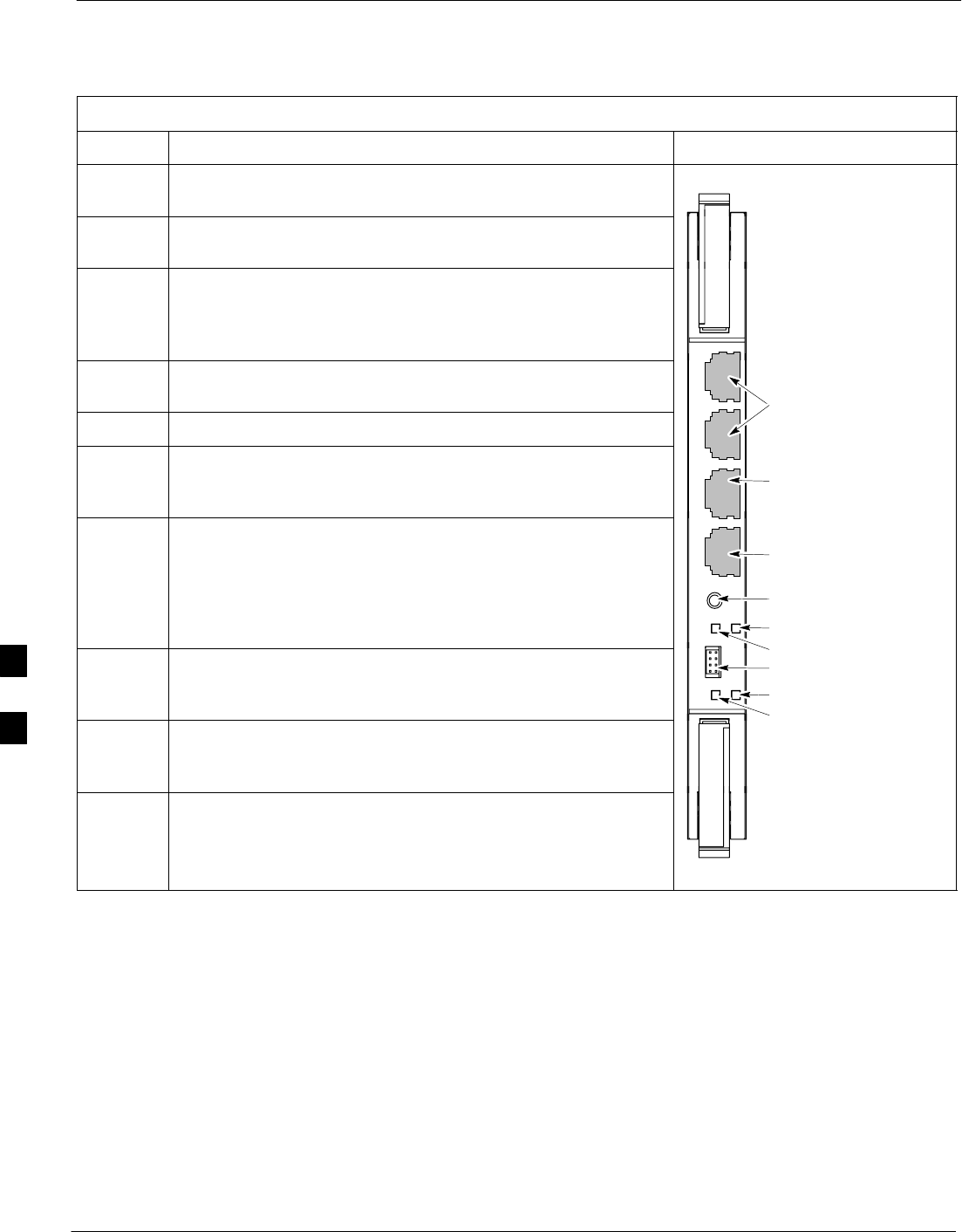
Module Front Panel LED Indicators and Connectors – continued
6-32 1X SC4812T–MC BTS Optimization/ATP 5/21/04
DRAFT
Table 6-28: GLI3 Front Panel
LED Operating Status Diagram
BPR A Connects to either a BPR or expansion cage and is wired as an
ethernet client.
BPR B Connects to either a BPR or expansion cage and is wired as an
ethernet client.
AUX Wired as an ethernet client for direct connection to a personal
computer with a standard ethernet cable. It allows connection of
ethernet “sniffer” when the ethernet switch is properly configured
for port monitoring.
GLI Supports the cross–coupled ethernet circuits to the mate GLI using
a double crossover cable. 100BASE–T to BTS Packet
BPR A
RESET Pressing and releasing the switch resets all functions on the GLI3.
BPR
100BASE T to BTS Packet
Router or Expansion cage
ALARM OFF – operating normally
ON – briefly during power-up when the Alarm LED turns OFF
SLOW GREEN – when the GLI3 is INS (in-service)
100BASE–T Auxiliary
Monitor Port
R
B AUX
SPAN OFF – card is powered down, in initialization, or in standby
GREEN – operating normally
YELLOW – one or more of the equipped initialized spans is
receiving a remote alarm indication signal from the far end
RED – one or more of the equipped initialized spans is in an alarm
state
Reset Switch
Dual 100BASE–T in a single
RJ45 to Redundant (Mate)
GLI3
RESET
SPAN
ALARM
Span (LED)
Ala (LED)
GLI
MMI An RS-232, serial, asynchronous communications link for use as an
MMI port. This port supports 300 baud, up to a maximum of
115,200 baud communications.
MMI Port
M
MMI
ACT
STA
Alarm (LED)
Active (LED)
Status (LED)
STATUS OFF – operating normally
ON – briefly during power-up when the Alarm LED turns OFF
SLOW GREEN – when the GLI3 is INS (in-service)
St
a
t
us
(LED)
ACTIVE Shows the operating status of the redundant cards. The redundant
card toggles automatically if the active card is removed or fails
ON – active card operating normally
OFF – standby card operating normally
ti-CDMA-WP-00064-v01-ildoc-ftw
BBX LED Status Combinations
PWR/ALM LED
The BBX module has its own alarm (fault) detection circuitry that
controls the state of the PWR/ALM LED.
The following list describes the states of the bi-color LED:
SSolid GREEN – INS_ACT no alarm
SSolid RED Red – initializing or power-up alarm
SSlowly Flashing GREEN – OOS_ROM no alarm
SLong RED/Short GREEN – OOS_ROM alarm
SRapidly Flashing GREEN – OOS_RAM no alarm
6

Module Front Panel LED Indicators and Connectors – continued
5/21/04 1X SC4812T–MC BTS Optimization/ATP 6-33
DRAFT
SShort RED/Short GREEN – OOS_RAM alarm
SLong GREEN/Short RED – INS_ACT alarm
PA Shelf LED Status
Combinations
PA Module LED
Each PA module contains a bi–color LED just above the MMI connector
on the front panel of the module. Interpret this LED as follows:
SGREEN — PA module is active and is reporting no alarms (Normal
condition).
SFlashing GREEN/RED — PA module is active but is reporting an low
input power condition. If no BBX is keyed, this is normal and does
not constitute a failure.
MCC LED Status Combinations
The MCC module has LED indicators and connectors as described
below (see Figure 6-4). Note that the figure does not show the
connectors as they are concealed by the removable lens.
The LED indicators and their states are as follows:
PWR/ALM LED
SRED – fault on module
ACTIVE LED
SOff – module is inactive, off-line, or not processing traffic.
SSlowly Flashing GREEN – OOS_ROM no alarm.
SRapidly Flashing Green – OOS_RAM no alarm.
SSolid GREEN – module is INS_ACT, on-line, processing traffic.
PWR/ALM and ACTIVE LEDs
SSolid RED – module is powered but is in reset or the BCP is inactive.
MMI Connectors
SThe RS–232 MMI port connector (four-pin) is intended to be used
primarily in the development or factory environment but may be used
in the field for debugging purposes.
SThe RJ–11 ethernet port connector (eight-pin) is intended to be used
primarily in the development environment but may be used in the field
for high data rate debugging purposes.
6
Module Front Panel LED Indicators and Connectors – continued
6-34 1X SC4812T–MC BTS Optimization/ATP 5/21/04
DRAFT
Figure 6-4: MCC Front Panel
PWR/ALM LED
LENS
(REMOVABLE)
ACTIVE LED
PWR/ALM ACTIVE
PWR/ALMOFF – operating normally
ON – briefly during power-up and dur-
ing failure conditions
ACTIVE
LED OPERATING STATUS
RAPIDLY BLINKING – Card is code-
loaded but not enabled
SLOW BLINKING – Card is not code-
loaded
ON – card is code-loaded and enabled
(INS_ACTIVE)
COLOR
GREEN
RED
REDON – fault condition
SLOW FLASHING (alternating with
green) – CHI bus inactive on power-up
An alarm is generated in the event of a fail-
ure
6

5/21/04 1X SC4812T–MC BTS Optimization/ATP
DRAFT
Appendix A: Chapter Title Goes Here
Appendix Content
THIS IS A SPECIAL APPENDIX TOC.
THIS APPENDIX TOC MUST BE USED FOR APPENDIX A.
AUTONUMBER STREAMS ARE RESET HERE.
DO NOT USE THIS APPENDIX TOC FOR ANY OTHER
APPENDIX.
Guide Book 1–2. . . . . . . . . . . . . . . . . . . . . . . . . . . . . . . . . . . . . . . . . . . . . . . . . . . . .
Document Overview 1–2. . . . . . . . . . . . . . . . . . . . . . . . . . . . . . . . . . . . . . . . . . . . . .
What Is In This Guide? 1–2. . . . . . . . . . . . . . . . . . . . . . . . . . . . . . . . . . . . .
Book Catalogs and Organization 1–3. . . . . . . . . . . . . . . . . . . . . . . . . . . . . . . . . . . .
Book Directory 1–3. . . . . . . . . . . . . . . . . . . . . . . . . . . . . . . . . . . . . . . . . . .
Special Catalogs 1–5. . . . . . . . . . . . . . . . . . . . . . . . . . . . . . . . . . . . . . . . . . .
Physical Page Layouts 1–6. . . . . . . . . . . . . . . . . . . . . . . . . . . . . . . . . . . . . . . . . . . .
A/A4 Page and Margin Sizes 1–6. . . . . . . . . . . . . . . . . . . . . . . . . . . . . . . . .
A/A4 Page Text Area 1–7. . . . . . . . . . . . . . . . . . . . . . . . . . . . . . . . . . . . . . .
A/A4 Page Components 1–9. . . . . . . . . . . . . . . . . . . . . . . . . . . . . . . . . . . .
Frame and Table Components 1–10. . . . . . . . . . . . . . . . . . . . . . . . . . . . . . . . . . . . . .
Frames With Tools 1–10. . . . . . . . . . . . . . . . . . . . . . . . . . . . . . . . . . . . . . . . .
Flow Charts and Block Diagrams 1–10. . . . . . . . . . . . . . . . . . . . . . . . . . . . .
Line Drawings 1–11. . . . . . . . . . . . . . . . . . . . . . . . . . . . . . . . . . . . . . . . . . . .
Table Types In This Template 1–12. . . . . . . . . . . . . . . . . . . . . . . . . . . . . . . .
Item/Description Table 1–12. . . . . . . . . . . . . . . . . . . . . . . . . . . . . . . . . . . . .
Step Table 1–13. . . . . . . . . . . . . . . . . . . . . . . . . . . . . . . . . . . . . . . . . . . . . . .
Step/Check Table 1–14. . . . . . . . . . . . . . . . . . . . . . . . . . . . . . . . . . . . . . . . . .
Component Descriptions 1–15. . . . . . . . . . . . . . . . . . . . . . . . . . . . . . . . . . . . . . . . . .
Conclusions 1–16. . . . . . . . . . . . . . . . . . . . . . . . . . . . . . . . . . . . . . . . . . . . . . . . . . . . .
Map Title Goes Here lkjsfdg Sfdkgj Msfd N lkas K lkjsdfl kB lkj fgcb 1–17. . . . . .
Block Label Goes Here 1–17. . . . . . . . . . . . . . . . . . . . . . . . . . . . . . . . . . . . .
Block Label Goes Here 1–17. . . . . . . . . . . . . . . . . . . . . . . . . . . . . . . . . . . . .
Block Label Goes Here 1–18. . . . . . . . . . . . . . . . . . . . . . . . . . . . . . . . . . . . .
Block Label Goes Here 1–19. . . . . . . . . . . . . . . . . . . . . . . . . . . . . . . . . . . . .
Map Title Goes Here 1–22. . . . . . . . . . . . . . . . . . . . . . . . . . . . . . . . . . . . . . . . . . . . . .
A

Table of Contents – continued
1X SC4812T–MC BTS Optimization/ATP 5/21/04
DRAFT
Notes
A

Optimization (Pre–ATP) Data Sheets for Multi–Carrier
5/21/04 1X SC4812T–MC BTS Optimization/ATP A-1
DRAFT
Verification of Test Equipment
Used
Table A-1: Verification of Test Equipment Used
Manufacturer Model Serial Number
Comments:
A

Optimization (Pre–ATP) Data Sheets for Multi–Carrier – continued
A-2 1X SC4812T–MC BTS Optimization/ATP 5/21/04
DRAFT
Site Checklist
Table A-2: Site Checklist
OK Parameter Specification Comments
−Deliveries Per established procedures
−Floor Plan Verified
−
−
−
Inter Frame Cables:
Ethernet
Frame Ground
Power
Per procedure
Per procedure
Per procedure
−
−
Factory Data:
BBX
Test Panel
Per procedure
Per procedure
−Site Temperature
−Dress Covers/Brackets
Comments:
Preliminary Operations
Table A-3: Preliminary Operations
OK Parameter Specification Comments
−Shelf ID Dip Switches Per site equipage
−BBX Jumpers Verified per procedure
−Ethernet LAN verification Verified per procedure
Comments:
A

Optimization (Pre–ATP) Data Sheets for Multi–Carrier – continued
5/21/04 1X SC4812T–MC BTS Optimization/ATP A-3
DRAFT
Pre–Power and Initial Power Tests
Table A-4: Pre–power Checklist
OK Parameter Specification Comments
−Pre–power–up tests Verify power supply
output voltage at the top
of each BTS frame is
within specifications
−
−
−
−
−
−
−
−
Internal Cables:
ISB (all cages)
CSM (all cages)
Power (all cages)
Ethernet Connectors
LAN A ohms
LAN B ohms
LAN A shield
LAN B shield
Ethernet Boots
verified
verified
verified
verified
verified
isolated
isolated
installed
−Air Impedance Cage (single cage) installed
−Initial power–up tests Verify power supply
output voltage at the top
of each BTS frame is
within specifications:
Comments:
A

Optimization (Pre–ATP) Data Sheets for Multi–Carrier – continued
A-4 1X SC4812T–MC BTS Optimization/ATP 5/21/04
DRAFT
General Optimization Checklist
Table A-5: Pre–power Checklist
OK Parameter Specification Comments
−
−
LEDs
Frame fans
illuminated
operational
−
−
−
−
−
−
LMF to BTS Connection
Preparing the LMF
Log into the LMF PC
Create site specific BTS directory
Create master–bts–cdma directory
Download device loads
Moving/Linking files
per procedure
per procedure
per procedure
per procedure
per procedure
per procedure
−
−
Ping LAN A
Ping LAN B
per procedure
per procedure
−
−
−
−
−
−
−
−
Download/Enable MGLIs
Download/Enable GLIs
Set Site Span Configuration
Download CSMs
Download
Enable CSMs
Download/Enable MCCs
Download BBXs
per procedure
per procedure
per procedure
per procedure
per procedure
per procedure
per procedure
per procedure
−Test Set Calibration per procedure
Comments:
A

Optimization (Pre–ATP) Data Sheets for Multi–Carrier – continued
5/21/04 1X SC4812T–MC BTS Optimization/ATP A-5
DRAFT
GPS Receiver Operation
Table A-6: GPS Receiver Operation
OK Parameter Specification Comments
−GPS Receiver Control Task State:
tracking satellites
Verify parameter
−Initial Position Accuracy: Verify Estimated
or Surveyed
−Current Position:
lat
lon
height
RECORD in ms
and cm also
convert to deg
min sec
−Current Position: satellites tracked
Estimated:
(>4) satellites tracked,(>4) satellites visible
Surveyed:
(>1) satellite tracked,(>4) satellites visible
Verify parameter
as appropriate:
−GPS Receiver Status:Current Dilution of
Precision
(PDOP or HDOP): (<30)
Verify parameter
−Current reference source:
Number: 0; Status: Good; Valid: Yes
Verify parameter
Comments:
A

Optimization (Pre–ATP) Data Sheets for Multi–Carrier – continued
A-6 1X SC4812T–MC BTS Optimization/ATP 5/21/04
DRAFT
PA IM Reduction
Table A-7: PA IM Reduction – TX Filter
OK
PA Carrier
Specification
Comments
OK
PA
# 3–Sector 6–Sector
S
pec
ifi
cat
i
on
−1A C1 C1 No Alarms
−1B C1 C1 No Alarms
−1C C1 C1 No Alarms
−1D C1 C1 No Alarms
−2A C2 C2 No Alarms
−2B C2 C2 No Alarms
−2C C2 C2 No Alarms
−2D C2 C2 No Alarms
−3A C3 C1 No Alarms
−3B C3 C1 No Alarms
−3C C3 C1 No Alarms
−3D C3 C1 No Alarms
−4A C4 C2 No Alarms
−4B C4 C2 No Alarms
−4C C4 C2 No Alarms
−4D C4 C2 No Alarms
Comments:
A

Optimization (Pre–ATP) Data Sheets for Multi–Carrier – continued
5/21/04 1X SC4812T–MC BTS Optimization/ATP A-7
DRAFT
PA Convergence
Table A-8: PA Convergence (Multicarrier grouping)
OK PA # Converged Specification Data
−1A Verify per procedure & upload
dt
−2A convergence data
−3A
−4A
−1B Verify per procedure & upload
dt
−2B convergence data
−3B
−4B
−1C Verify per procedure & upload
dt
−2C convergence data
−3C
−4C
−1D Verify per procedure & upload
dt
−2D convergence data
−3D
−4D
Comments:
A

Optimization (Pre–ATP) Data Sheets for Multi–Carrier – continued
A-8 1X SC4812T–MC BTS Optimization/ATP 5/21/04
DRAFT
TX Bay Level Offset/Power Output Verification for 3–Sector Configurations
1–Carrier
2–Carrier Non–adjacent Channels
4–Carrier Non–adjacent Channels
Table A-9: TX BLO Calibration (3–Sector: 1; 2; and 4–Carrier Non–adjacent Channels)
OK Parameter Specification Comments
−
TX Bay Level Offset =
BBX–1, ANT–1 = dB
BBX–r, ANT–1 = dB
−Calibrate
carrier 1
y
40 dB +/– 5 for 800 MHz
35 dB +/–5 for 1.9 GHz
BBX–2, ANT–2 = dB
BBX–r, ANT–2 = dB
−
prior to calibration BBX–3, ANT–3 = dB
BBX–r, ANT–3 = dB
−
TX Bay Level Offset =
BBX–7, ANT–1 = dB
BBX–r, ANT–1 = dB
−Calibrate
carrier 2
y
40 dB +/– 5 for 800 MHz
35 dB +/–5 for 1.9 GHz
BBX–8, ANT–2 = dB
BBX–r, ANT–2 = dB
−
prior to calibration BBX–9, ANT–3 = dB
BBX–r, ANT–3 = dB
−
TX Bay Level Offset =
BBX–4, ANT–1 = dB
BBX–r, ANT–1 = dB
−Calibrate
carrier 3
y
40 dB +/– 5 for 800 MHz
35 dB +/–5 for 1.9 GHz
BBX–5, ANT–2 = dB
BBX–r, ANT–2 = dB
−
prior to calibration BBX–6, ANT–3 = dB
BBX–r, ANT–3 = dB
−
TX Bay Level Offset =
BBX–10, ANT–1 = dB
BBX–r, ANT–1 = dB
−Calibrate
carrier 4
y
40 dB +/– 5 for 800 MHz
35 dB +/–5 for 1.9 GHz
BBX–11, ANT–2 = dB
BBX–r, ANT–2 = dB
−
prior to calibration BBX–12, ANT–3 = dB
BBX–r, ANT–3 = dB
−
TX Bay Level Offset =
BBX–1, ANT–1 = dB
BBX–r, ANT–1 = dB
−
Calibration
Audit
carrier 1
y
40 dB +/– 5 for 800 MHz
35 dB +/–5 for 1.9 GHz
BBX–2, ANT–2 = dB
BBX–r, ANT–2 = dB
−
carrier 1
prior to calibration BBX–3, ANT–3 = dB
BBX–r, ANT–3 = dB
. . . continued on next page
A
Optimization (Pre–ATP) Data Sheets for Multi–Carrier – continued
5/21/04 1X SC4812T–MC BTS Optimization/ATP A-9
DRAFT
Table A-9: TX BLO Calibration (3–Sector: 1; 2; and 4–Carrier Non–adjacent Channels)
OK CommentsSpecificationParameter
−BBX–7, ANT–1 = dB
BBX–r, ANT–1 = dB
−
Calibration
Audit
carrier 2
0 dB (+1.5 dB) for gain set resolution
post calibration
BBX–8, ANT–2 = dB
BBX–r, ANT–2 = dB
−
carrier 2
BBX–9, ANT–3 = dB
BBX–r, ANT–3 = dB
−BBX–4, ANT–1 = dB
BBX–r, ANT–1 = dB
−
Calibration
Audit
carrier 3
0 dB (+1.5 dB) for gain set resolution
post calibration
BBX–5, ANT–2 = dB
BBX–r, ANT–2 = dB
−
carrier 3
BBX–6, ANT–3 = dB
BBX–r, ANT–3 = dB
−BBX–10, ANT–1 = dB
BBX–r, ANT–1 = dB
−
Calibration
Audit
carrier 4
0 dB (+1.5 dB) for gain set resolution
post calibration
BBX–11, ANT–2 = dB
BBX–r, ANT–2 = dB
−
carrier 4
BBX–12, ANT–3 = dB
BBX–r, ANT–3 = dB
Comments:
A

Optimization (Pre–ATP) Data Sheets for Multi–Carrier – continued
A-10 1X SC4812T–MC BTS Optimization/ATP 5/21/04
DRAFT
2–Carrier Adjacent Channel
Table A-10: TX Bay Level Offset Calibration (3–Sector: 2–Carrier Adjacent Channels)
OK Parameter Specification Comments
−
TX Bay Level Offset =
BBX–1, ANT–1 = dB
BBX–r, ANT–1 = dB
−Calibrate
carrier 1
y
40 dB +/– 5 for 800 MHz
35 dB +/–5 for 1.9 GHz
BBX–2, ANT–2 = dB
BBX–r, ANT–2 = dB
−
prior to calibration BBX–3, ANT–3 = dB
BBX–r, ANT–3 = dB
−
TX Bay Level Offset =
BBX–7, ANT–4 = dB
BBX–r, ANT–4 = dB
−Calibrate
carrier 2
y
40 dB +/– 5 for 800 MHz
35 dB +/–5 for 1.9 GHz
BBX–8, ANT–5 = dB
BBX–r, ANT–5 = dB
−
prior to calibration BBX–9, ANT–6 = dB
BBX–r, ANT–6 = dB
−BBX–1, ANT–1 = dB
BBX–r, ANT–1 = dB
−
Calibration
Audit
carrier 1
0 dB (+1.5 dB) for gain set resolution
post calibration
BBX–2, ANT–2 = dB
BBX–r, ANT–2 = dB
−
carrier 1
BBX–3, ANT–3 = dB
BBX–r, ANT–3 = dB
−BBX–7, ANT–4 = dB
BBX–r, ANT–4 = dB
−
Calibration
Audit
carrier 2
0 dB (+1.5 dB) for gain set resolution
post calibration
BBX–8, ANT–5 = dB
BBX–r, ANT–5 = dB
−
carrier 2
BBX–9, ANT–6 = dB
BBX–r, ANT–6 = dB
Comments:
A

Optimization (Pre–ATP) Data Sheets for Multi–Carrier – continued
5/21/04 1X SC4812T–MC BTS Optimization/ATP A-11
DRAFT
3–Carrier Adjacent Channels
4–Carrier Adjacent Channels
Table A-11: TX Bay Level Offset Calibration (3–Sector: 3 or 4–Carrier Adjacent Channels)
OK Parameter Specification Comments
−TX Bay Level Offset =
BBX–1, ANT–1 = dB
BBX–r, ANT–1 = dB
−Calibrate
carrier 1
y
40 dB +/– 5 for 800 MHz
35 dB +/–5 for 1.9 GHz
BBX–2, ANT–2 = dB
BBX–r, ANT–2 = dB
−
prior to calibration BBX–3, ANT–3 = dB
BBX–r, ANT–3 = dB
−TX Bay Level Offset =
BBX–7, ANT–1 = dB
BBX–r, ANT–1 = dB
−Calibrate
carrier 2
y
40 dB +/– 5 for 800 MHz
35 dB +/–5 for 1.9 GHz
BBX–8, ANT–2 = dB
BBX–r, ANT–2 = dB
−
prior to calibration BBX–9, ANT–3 = dB
BBX–r, ANT–3 = dB
−TX Bay Level Offset =
BBX–4, ANT–4 = dB
BBX–r, ANT–4 = dB
−Calibrate
carrier 3
y
40 dB +/– 5 for 800 MHz
35 dB +/–5 for 1.9 GHz
BBX–5, ANT–5 = dB
BBX–r, ANT–5 = dB
−
prior to calibration BBX–6, ANT–6 = dB
BBX–r, ANT–6 = dB
−TX Bay Level Offset =
BBX–10, ANT–4 = dB
BBX–3, ANT–4 = dB
−Calibrate
carrier 4
y
40 dB +/– 5 for 800 MHz
35 dB +/–5 for 1.9 GHz
BBX–11, ANT–5 = dB
BBX–r, ANT–5 = dB
−
prior to calibration BBX–12, ANT–6 = dB
BBX–r, ANT–6 = dB
−BBX–1, ANT–1 = dB
BBX–r, ANT–1 = dB
−
Calibration
Audit
carrier 1
0 dB (+1.5 dB) for gain set resolution
post calibration
BBX–2, ANT–2 = dB
BBX–r, ANT–2 = dB
−
carrier 1
BBX–3, ANT–3 = dB
BBX–r, ANT–3 = dB
. . . continued on next page
A
Optimization (Pre–ATP) Data Sheets for Multi–Carrier – continued
A-12 1X SC4812T–MC BTS Optimization/ATP 5/21/04
DRAFT
Table A-11: TX Bay Level Offset Calibration (3–Sector: 3 or 4–Carrier Adjacent Channels)
OK CommentsSpecificationParameter
−BBX–7, ANT–1 = dB
BBX–r, ANT–1 = dB
−
Calibration
Audit
carrier 2
0 dB (+1.5 dB) for gain set resolution
post calibration
BBX–8, ANT–2 = dB
BBX–r, ANT–2 = dB
−
carrier 2
BBX–9, ANT–3 = dB
BBX–r, ANT–3 = dB
−BBX–4, ANT–4 = dB
BBX–r, ANT–4 = dB
−
Calibration
Audit
carrier 3
0 dB (+1.5 dB) for gain set resolution
post calibration
BBX–5, ANT–5 = dB
BBX–r, ANT–5 = dB
−
carrier 3
BBX–6, ANT–6 = dB
BBX–r, ANT–6 = dB
−BBX–10, ANT–4 = dB
BBX–r, ANT–4 = dB
−
Calibration
Audit
carrier 4
0 dB (+1.5 dB) for gain set resolution
post calibration
BBX–11, ANT–5 = dB
BBX–r, ANT–5 = dB
−
carrier 4
BBX–12, ANT–6 = dB
BBX–r, ANT–6 = dB
Comments:
A
Optimization (Pre–ATP) Data Sheets for Multi–Carrier – continued
5/21/04 1X SC4812T–MC BTS Optimization/ATP A-13
DRAFT
TX Bay Level Offset/Power Output Verification for 6–Sector Configurations
1–Carrier
2–Carrier Non–adjacent Channels
Table A-12: TX BLO Calibration (6–Sector: 1–Carrier, 2–Carrier Non–adjacent Channels)
OK Parameter Specification Comments
−BBX–1, ANT–1 = dB
BBX–r, ANT–1 = dB
−BBX–2, ANT–2 = dB
BBX–r, ANT–2 = dB
−
Calibrate
TX Bay Level Offset =
43 dB +/– 5 for 800 MHz
BBX–3, ANT–3 = dB
BBX–r, ANT–3 = dB
−
carrier 1 38 dB +/–5 for 1.9 GHz
prior to calibration
BBX–4, ANT–4 = dB
BBX–r, ANT–4 = dB
−BBX–5, ANT–5 = dB
BBX–r, ANT–5 = dB
−BBX–6, ANT–6 = dB
BBX–r, ANT–6 = dB
−BBX–7, ANT–1 = dB
BBX–r, ANT–1 = dB
−BBX–8, ANT–2 = dB
BBX–r, ANT–2 = dB
−
Calibrate TX Bay Level Offset = 43 dB +/– 5 for
800 MHz 38 dB +/–5 for 1 9 GHz prior
BBX–9, ANT–3 = dB
BBX–r, ANT–3 = dB
−
carrier 2
800 MH
z
38 dB
+
/
–
5 f
or
1
.
9 GH
z
pr
i
or
to calibration BBX–10, ANT–4 = dB
BBX–3, ANT–4 = dB
−BBX–11, ANT–5 = dB
BBX–r, ANT–5 = dB
−BBX–12, ANT–6 = dB
BBX–r, ANT–5 = dB
. . . continued on next page
A
Optimization (Pre–ATP) Data Sheets for Multi–Carrier – continued
A-14 1X SC4812T–MC BTS Optimization/ATP 5/21/04
DRAFT
Table A-12: TX BLO Calibration (6–Sector: 1–Carrier, 2–Carrier Non–adjacent Channels)
OK CommentsSpecificationParameter
−BBX–1, ANT–1 = dB
BBX–r, ANT–1 = dB
−BBX–2, ANT–2 = dB
BBX–r, ANT–2 = dB
−Calibration
Audit
0 dB (+1.5 dB) for gain set resolution
BBX–3, ANT–3 = dB
BBX–r, ANT–3 = dB
−
A
u
dit
carrier 1
()g
post calibration BBX–4, ANT–4 = dB
BBX–r, ANT–4 = dB
−BBX–5, ANT–5 = dB
BBX–r, ANT–5 = dB
−BBX–6, ANT–6 = dB
BBX–r, ANT–6 = dB
−BBX–7, ANT–1 = dB
BBX–r, ANT–1 = dB
−BBX–8, ANT–2 = dB
BBX–r, ANT–2 = dB
−Calibration
Audit
0 dB (+1.5 dB) for gain set resolution
BBX–9, ANT–3 = dB
BBX–r, ANT–3 = dB
−
A
u
dit
carrier 2
()g
post calibration BBX–10, ANT–4 = dB
BBX–r, ANT–4 = dB
−BBX–11, ANT–5 = dB
BBX–r, ANT–5 = dB
−BBX–12, ANT–6 = dB
BBX–r, ANT–6 = dB
Comments:
A

Optimization (Pre–ATP) Data Sheets for Multi–Carrier – continued
5/21/04 1X SC4812T–MC BTS Optimization/ATP A-15
DRAFT
BTS Redundancy/Alarm Tests
Table A-13: BTS Redundancy/Alarm Tests
OK Parameter Specification Data
−SIF: Misc. alarm tests Verify per procedure
−MGLI redundancy test Verify per procedure
−GLI redundancy test Verify per procedure
−Power supply/converter
redundancy
Verify per procedure
−Misc. alarm tests Verify per procedure
−CSM & GPS
redundancy/alarm tests
Verify per procedure
−PA redundancy test Verify per procedure
Comments:
TX Antenna VSWR
Table A-14: TX Antenna VSWR
OK Parameter Specification Data
−VSWR –
Antenna 1
< (1.5 : 1)
−VSWR –
Antenna 2
< (1.5 : 1)
−VSWR –
Antenna 3
< (1.5 : 1)
−VSWR –
Antenna 4
< (1.5 : 1)
−VSWR –
Antenna 5
< (1.5 : 1)
−VSWR –
Antenna 6
< (1.5 : 1)
Comments:
A

Optimization (Pre–ATP) Data Sheets for Multi–Carrier – continued
A-16 1X SC4812T–MC BTS Optimization/ATP 5/21/04
DRAFT
RX Antenna VSWR
Table A-15: RX Antenna VSWR
OK Parameter Specification Data
−VSWR –
Antenna 1
< (1.5 : 1)
−VSWR –
Antenna 2
< (1.5 : 1)
−VSWR –
Antenna 3
< (1.5 : 1)
−VSWR –
Antenna 4
< (1.5 : 1)
−VSWR –
Antenna 5
< (1.5 : 1)
−VSWR –
Antenna 6
< (1.5 : 1)
Comments:
AMR Verification
Table A-16: AMR CDI Alarm Input Verification
OK Parameter Specification Data
−
Verify CDI alarm input
operation (“ALARM A”
(numbers 1 –18)
BTS Relay #XX –
Contact Alarm
Sets/Clears
−
Verify CDI alarm input
operation (“ALARM B”
(numbers 19 –36)
BTS Relay #XX –
Contact Alarm
Sets/Clears
Comments:
A

Site Serial Number Checklist
5/21/04 1X SC4812T–MC BTS Optimization/ATP A-17
DRAFT
Date Site
C–CCP Shelf
Site I/O A & B
C–CCP Shelf
CSM–1
CSM–2
HSO
CCD–1
CCD–2
AMR–1
AMR–2
MPC–1
MPC–2
Fans 1–3
GLI–1
GLI–2
BBX–1
BBX–2
BBX–3
BBX–4
BBX–5
BBX–6
BBX–7
BBX–8
BBX–9
BBX–10
BBX–11
BBX–12
BBX–r
MCC–1
MCC–2
MCC–3
MCC–4
MCC–5
MCC–6
MCC–7
MCC–8
MCC–9
MCC–10
MCC–11
MCC–12
MCIO
SWITCH
C–CCP PS–1
C–CCP PS–2
C–CCP PS–3
A

Site Serial Number Checklist – continued
A-18 1X SC4812T–MC BTS Optimization/ATP 5/21/04
DRAFT
Notes
A

5/21/04 1X SC4812T–MC BTS Optimization/ATP
DRAFT
Appendix B: PN Offset/I & Q Offset Register Programming Information
Appendix Content
THIS IS THE GENERAL APPENDIX TOC. USE THIS FOR ALL
APPENDICES EXCEPT APPENDIX A.
Guide Book 1–2. . . . . . . . . . . . . . . . . . . . . . . . . . . . . . . . . . . . . . . . . . . . . . . . . . . . .
Document Overview 1–2. . . . . . . . . . . . . . . . . . . . . . . . . . . . . . . . . . . . . . . . . . . . . .
What Is In This Guide? 1–2. . . . . . . . . . . . . . . . . . . . . . . . . . . . . . . . . . . . .
Book Catalogs and Organization 1–3. . . . . . . . . . . . . . . . . . . . . . . . . . . . . . . . . . . .
Book Directory 1–3. . . . . . . . . . . . . . . . . . . . . . . . . . . . . . . . . . . . . . . . . . .
Special Catalogs 1–5. . . . . . . . . . . . . . . . . . . . . . . . . . . . . . . . . . . . . . . . . . .
Physical Page Layouts 1–6. . . . . . . . . . . . . . . . . . . . . . . . . . . . . . . . . . . . . . . . . . . .
A/A4 Page and Margin Sizes 1–6. . . . . . . . . . . . . . . . . . . . . . . . . . . . . . . . .
A/A4 Page Text Area 1–7. . . . . . . . . . . . . . . . . . . . . . . . . . . . . . . . . . . . . . .
A/A4 Page Components 1–9. . . . . . . . . . . . . . . . . . . . . . . . . . . . . . . . . . . .
Frame and Table Components 1–10. . . . . . . . . . . . . . . . . . . . . . . . . . . . . . . . . . . . . .
Frames With Tools 1–10. . . . . . . . . . . . . . . . . . . . . . . . . . . . . . . . . . . . . . . . .
Flow Charts and Block Diagrams 1–10. . . . . . . . . . . . . . . . . . . . . . . . . . . . .
Line Drawings 1–11. . . . . . . . . . . . . . . . . . . . . . . . . . . . . . . . . . . . . . . . . . . .
Table Types In This Template 1–12. . . . . . . . . . . . . . . . . . . . . . . . . . . . . . . .
Item/Description Table 1–12. . . . . . . . . . . . . . . . . . . . . . . . . . . . . . . . . . . . .
Step Table 1–13. . . . . . . . . . . . . . . . . . . . . . . . . . . . . . . . . . . . . . . . . . . . . . .
Step/Check Table 1–14. . . . . . . . . . . . . . . . . . . . . . . . . . . . . . . . . . . . . . . . . .
Component Descriptions 1–15. . . . . . . . . . . . . . . . . . . . . . . . . . . . . . . . . . . . . . . . . .
Conclusions 1–16. . . . . . . . . . . . . . . . . . . . . . . . . . . . . . . . . . . . . . . . . . . . . . . . . . . . .
Map Title Goes Here lkjsfdg Sfdkgj Msfd N lkas K lkjsdfl kB lkj fgcb 1–17. . . . . .
Block Label Goes Here 1–17. . . . . . . . . . . . . . . . . . . . . . . . . . . . . . . . . . . . .
Block Label Goes Here 1–17. . . . . . . . . . . . . . . . . . . . . . . . . . . . . . . . . . . . .
Block Label Goes Here 1–18. . . . . . . . . . . . . . . . . . . . . . . . . . . . . . . . . . . . .
Block Label Goes Here 1–19. . . . . . . . . . . . . . . . . . . . . . . . . . . . . . . . . . . . .
Map Title Goes Here 1–22. . . . . . . . . . . . . . . . . . . . . . . . . . . . . . . . . . . . . . . . . . . . . .
B

Table of Contents – continued
1X SC4812T–MC BTS Optimization/ATP 5/21/04
DRAFT
Notes
B

PN Offset Programming Information
5/21/04 1X SC4812T–MC BTS Optimization/ATP B-1
DRAFT
PN Offset Background
All channel elements transmitted from a BTS in a particular 1.25 MHz
CDMA channel are orthonogonally spread by 1 of 128 possible Walsh
code functions; additionally, they are also spread by a quadrature pair of
PN sequences unique to each sector.
Overall, the mobile uses this to differentiate multiple signals transmitted
from the same BTS (and surrounding BTS) sectors, and to synchronize
to the next strongest sector.
The PN offset per sector is stored on the BBXs, where the corresponding
I & Q registers reside.
The PN offset values are determined on a per BTS/per sector(antenna)
basis as determined by the appropriate cdf file content. A breakdown of
this information is found in Table B-1.
PN Offset Usage
Only the 14–chip delay is currently in use. It is important to determine
the RF chip delay to be able to test the BTS functionality. This can be
done by ascertaining if the CDF file FineTxAdj value was set to “on”
when the MCC was downloaded with “image data”. The FineTxAdj
value is used to compensate for the processing delay (approximately
20 mS) in the BTS using any type of mobile meeting IS–97
specifications.
If the FineTxAdj value in the cdf file is 213 (D5 HEX), FineTxAdj has
been set for the 14 chip table.
CDF file I and Q values can be represented in DECIMAL
or HEX. If using HEX, add 0x before the HEX value. If
necessary, convert HEX values in Table B-1 to decimal
before comparing them to cdf file I & Q value
assignments.
NOTE
B

PN Offset Programming Information – continued
B-2 1X SC4812T–MC BTS Optimization/ATP 5/21/04
DRAFT
Table B-1: PnMask I and PnMask Q Values for PilotPn
14–Chip Delay
Pilot I Q I Q
PN (Dec.) (Hex.)
0 17523 23459 4473 5BA3
1 32292 32589 7E24 7F4D
2 4700 17398 125C 43F6
3 14406 26333 3846 66DD
4 14899 4011 3A33 0FAB
5 17025 2256 4281 08D0
6 14745 18651 3999 48DB
7 2783 1094 0ADF 0446
8 5832 21202 16C8 52D2
9 12407 13841 3077 3611
10 31295 31767 7A3F 7C17
11 7581 18890 1D9D 49CA
12 18523 30999 485B 7917
13 29920 22420 74E0 5794
14 25184 20168 6260 4EC8
15 26282 12354 66AA 3042
16 30623 11187 779F 2BB3
17 15540 11834 3CB4 2E3A
18 23026 10395 59F2 289B
19 20019 28035 4E33 6D83
20 4050 27399 0FD2 6B07
21 1557 22087 0615 5647
22 30262 2077 7636 081D
23 18000 13758 4650 35BE
24 20056 11778 4E58 2E02
25 12143 3543 2F6F 0DD7
26 17437 7184 441D 1C10
27 17438 2362 441E 093A
28 5102 25840 13EE 64F0
29 9302 12177 2456 2F91
30 17154 10402 4302 28A2
31 5198 1917 144E 077D
32 4606 17708 11FE 452C
33 24804 10630 60E4 2986
34 17180 6812 431C 1A9C
35 10507 14350 290B 380E
36 10157 10999 27AD 2AF7
37 23850 25003 5D2A 61AB
38 31425 2652 7AC1 0A5C
39 4075 19898 0FEB 4DBA
40 10030 2010 272E 07DA
41 16984 25936 4258 6550
42 14225 28531 3791 6F73
43 26519 11952 6797 2EB0
44 27775 31947 6C7F 7CCB
45 30100 25589 7594 63F5
46 7922 11345 1EF2 2C51
47 14199 28198 3777 6E26
48 17637 13947 44E5 367B
49 23081 8462 5A29 210E
50 5099 9595 13EB 257B
. . . continued on next page
B

PN Offset Programming Information – continued
5/21/04 1X SC4812T–MC BTS Optimization/ATP B-3
DRAFT
Table B-1: PnMask I and PnMask Q Values for PilotPn
14–Chip Delay
Pilot I Q I Q
PN (Dec.) (Hex.)
51 32743 4670 7FE7 123E
52 7114 14672 1BCA 3950
53 7699 29415 1E13 72E7
54 19339 20610 4B8B 5082
55 28212 6479 6E34 194F
56 29587 10957 7393 2ACD
57 19715 18426 4D03 47FA
58 14901 22726 3A35 58C6
59 20160 5247 4EC0 147F
60 22249 29953 56E9 7501
61 26582 5796 67D6 16A4
62 7153 16829 1BF1 41BD
63 15127 4528 3B17 11B0
64 15274 5415 3BAA 1527
65 23149 10294 5A6D 2836
66 16340 17046 3FD4 4296
67 27052 7846 69AC 1EA6
68 13519 10762 34CF 2A0A
69 10620 13814 297C 35F6
70 15978 16854 3E6A 41D6
71 27966 795 6D3E 031B
72 12479 9774 30BF 262E
73 1536 24291 0600 5EE3
74 3199 3172 0C7F 0C64
75 4549 2229 11C5 08B5
76 17888 21283 45E0 5323
77 13117 16905 333D 4209
78 7506 7062 1D52 1B96
79 27626 7532 6BEA 1D6C
80 31109 25575 7985 63E7
81 29755 14244 743B 37A4
82 26711 28053 6857 6D95
83 20397 30408 4FAD 76C8
84 18608 5094 48B0 13E6
85 7391 16222 1CDF 3F5E
86 23168 7159 5A80 1BF7
87 23466 174 5BAA 00AE
88 15932 25530 3E3C 63BA
89 25798 2320 64C6 0910
90 28134 23113 6DE6 5A49
91 28024 23985 6D78 5DB1
92 6335 2604 18BF 0A2C
93 21508 1826 5404 0722
94 26338 30853 66E2 7885
95 17186 15699 4322 3D53
96 22462 2589 57BE 0A1D
97 3908 25000 0F44 61A8
98 25390 18163 632E 46F3
99 27891 12555 6CF3 310B
100 9620 8670 2594 21DE
. . . continued on next page
B

PN Offset Programming Information – continued
B-4 1X SC4812T–MC BTS Optimization/ATP 5/21/04
DRAFT
Table B-1: PnMask I and PnMask Q Values for PilotPn
14–Chip Delay
Pilot I Q I Q
PN (Dec.) (Hex.)
101 6491 1290 195B 050A
102 16876 4407 41EC 1137
103 17034 1163 428A 048B
104 32405 12215 7E95 2FB7
105 27417 7253 6B19 1C55
106 8382 8978 20BE 2312
107 5624 25547 15F8 63CB
108 1424 3130 0590 0C3A
109 13034 31406 32EA 7AAE
110 15682 6222 3D42 184E
111 27101 20340 69DD 4F74
112 8521 25094 2149 6206
113 30232 23380 7618 5B54
114 6429 10926 191D 2AAE
115 27116 22821 69EC 5925
116 4238 31634 108E 7B92
117 5128 4403 1408 1133
118 14846 689 39FE 02B1
119 13024 27045 32E0 69A5
120 10625 27557 2981 6BA5
121 31724 16307 7BEC 3FB3
122 13811 22338 35F3 5742
123 24915 27550 6153 6B9E
124 1213 22096 04BD 5650
125 2290 23136 08F2 5A60
126 31551 12199 7B3F 2FA7
127 12088 1213 2F38 04BD
128 7722 936 1E2A 03A8
129 27312 6272 6AB0 1880
130 23130 32446 5A5A 7EBE
131 594 13555 0252 34F3
132 25804 8789 64CC 2255
133 31013 24821 7925 60F5
134 32585 21068 7F49 524C
135 3077 31891 0C05 7C93
136 17231 5321 434F 14C9
137 31554 551 7B42 0227
138 8764 12115 223C 2F53
139 15375 4902 3C0F 1326
140 13428 1991 3474 07C7
141 17658 14404 44FA 3844
142 13475 17982 34A3 463E
143 22095 19566 564F 4C6E
144 24805 2970 60E5 0B9A
145 4307 23055 10D3 5A0F
146 23292 15158 5AFC 3B36
147 1377 29094 0561 71A6
148 28654 653 6FEE 028D
149 6350 19155 18CE 4AD3
150 16770 23588 4182 5C24
. . . continued on next page
B

PN Offset Programming Information – continued
5/21/04 1X SC4812T–MC BTS Optimization/ATP B-5
DRAFT
Table B-1: PnMask I and PnMask Q Values for PilotPn
14–Chip Delay
Pilot I Q I Q
PN (Dec.) (Hex.)
151 14726 10878 3986 2A7E
152 25685 31060 6455 7954
153 21356 30875 536C 789B
154 12149 11496 2F75 2CE8
155 28966 24545 7126 5FE1
156 22898 9586 5972 2572
157 1713 20984 06B1 51F8
158 30010 30389 753A 76B5
159 2365 7298 093D 1C82
160 27179 18934 6A2B 49F6
161 29740 23137 742C 5A61
162 5665 24597 1621 6015
163 23671 23301 5C77 5B05
164 1680 7764 0690 1E54
165 25861 14518 6505 38B6
166 25712 21634 6470 5482
167 19245 11546 4B2D 2D1A
168 26887 26454 6907 6756
169 30897 15938 78B1 3E42
170 11496 9050 2CE8 235A
171 1278 3103 04FE 0C1F
172 31555 758 7B43 02F6
173 29171 16528 71F3 4090
174 20472 20375 4FF8 4F97
175 5816 10208 16B8 27E0
176 30270 17698 763E 4522
177 22188 8405 56AC 20D5
178 6182 28634 1826 6FDA
179 32333 1951 7E4D 079F
180 14046 20344 36DE 4F78
181 15873 26696 3E01 6848
182 19843 3355 4D83 0D1B
183 29367 11975 72B7 2EC7
184 13352 31942 3428 7CC6
185 22977 9737 59C1 2609
186 31691 9638 7BCB 25A6
187 10637 30643 298D 77B3
188 25454 13230 636E 33AE
189 18610 22185 48B2 56A9
190 6368 2055 18E0 0807
191 7887 8767 1ECF 223F
192 7730 15852 1E32 3DEC
193 23476 16125 5BB4 3EFD
194 889 6074 0379 17BA
195 21141 31245 5295 7A0D
196 20520 15880 5028 3E08
197 21669 20371 54A5 4F93
198 15967 8666 3E5F 21DA
199 21639 816 5487 0330
200 31120 22309 7990 5725
. . . continued on next page
B

PN Offset Programming Information – continued
B-6 1X SC4812T–MC BTS Optimization/ATP 5/21/04
DRAFT
Table B-1: PnMask I and PnMask Q Values for PilotPn
14–Chip Delay
Pilot I Q I Q
PN (Dec.) (Hex.)
201 3698 29563 0E72 737B
202 16322 13078 3FC2 3316
203 17429 10460 4415 28DC
204 21730 17590 54E2 44B6
205 17808 20277 4590 4F35
206 30068 19988 7574 4E14
207 12737 6781 31C1 1A7D
208 28241 32501 6E51 7EF5
209 20371 6024 4F93 1788
210 13829 20520 3605 5028
211 13366 31951 3436 7CCF
212 25732 26063 6484 65CF
213 19864 27203 4D98 6A43
214 5187 6614 1443 19D6
215 23219 10970 5AB3 2ADA
216 28242 5511 6E52 1587
217 6243 17119 1863 42DF
218 445 16064 01BD 3EC0
219 21346 31614 5362 7B7E
220 13256 4660 33C8 1234
221 18472 13881 4828 3639
222 25945 16819 6559 41B3
223 31051 6371 794B 18E3
224 1093 24673 0445 6061
225 5829 6055 16C5 17A7
226 31546 10009 7B3A 2719
227 29833 5957 7489 1745
228 18146 11597 46E2 2D4D
229 24813 22155 60ED 568B
230 47 15050 002F 3ACA
231 3202 16450 0C82 4042
232 21571 27899 5443 6CFB
233 7469 2016 1D2D 07E0
234 25297 17153 62D1 4301
235 8175 15849 1FEF 3DE9
236 28519 30581 6F67 7775
237 4991 3600 137F 0E10
238 7907 4097 1EE3 1001
239 17728 671 4540 029F
240 14415 20774 384F 5126
241 30976 24471 7900 5F97
242 26376 27341 6708 6ACD
243 19063 19388 4A77 4BBC
244 19160 25278 4AD8 62BE
245 3800 9505 0ED8 2521
246 8307 26143 2073 661F
247 12918 13359 3276 342F
248 19642 2154 4CBA 086A
249 24873 13747 6129 35B3
250 22071 27646 5637 6BFE
. . . continued on next page
B

PN Offset Programming Information – continued
5/21/04 1X SC4812T–MC BTS Optimization/ATP B-7
DRAFT
Table B-1: PnMask I and PnMask Q Values for PilotPn
14–Chip Delay
Pilot I Q I Q
PN (Dec.) (Hex.)
251 13904 1056 3650 0420
252 27198 1413 6A3E 0585
253 3685 3311 0E65 0CEF
254 16820 4951 41B4 1357
255 22479 749 57CF 02ED
256 6850 6307 1AC2 18A3
257 15434 961 3C4A 03C1
258 19332 2358 4B84 0936
259 8518 28350 2146 6EBE
260 14698 31198 396A 79DE
261 21476 11467 53E4 2CCB
262 30475 8862 770B 229E
263 23984 6327 5DB0 18B7
264 1912 7443 0778 1D13
265 26735 28574 686F 6F9E
266 15705 25093 3D59 6205
267 3881 6139 0F29 17FB
268 20434 22047 4FD2 561F
269 16779 32545 418B 7F21
270 31413 7112 7AB5 1BC8
271 16860 28535 41DC 6F77
272 8322 10378 2082 288A
273 28530 15065 6F72 3AD9
274 26934 5125 6936 1405
275 18806 12528 4976 30F0
276 20216 23215 4EF8 5AAF
277 9245 20959 241D 51DF
278 8271 3568 204F 0DF0
279 18684 26453 48FC 6755
280 8220 29421 201C 72ED
281 6837 24555 1AB5 5FEB
282 9613 10779 258D 2A1B
283 31632 25260 7B90 62AC
284 27448 16084 6B38 3ED4
285 12417 26028 3081 65AC
286 30901 29852 78B5 749C
287 9366 14978 2496 3A82
288 12225 12182 2FC1 2F96
289 21458 25143 53D2 6237
290 6466 15838 1942 3DDE
291 8999 5336 2327 14D8
292 26718 21885 685E 557D
293 3230 20561 0C9E 5051
294 27961 30097 6D39 7591
295 28465 21877 6F31 5575
296 6791 23589 1A87 5C25
297 17338 26060 43BA 65CC
298 11832 9964 2E38 26EC
299 11407 25959 2C8F 6567
300 15553 3294 3CC1 0CDE
. . . continued on next page
B

PN Offset Programming Information – continued
B-8 1X SC4812T–MC BTS Optimization/ATP 5/21/04
DRAFT
Table B-1: PnMask I and PnMask Q Values for PilotPn
14–Chip Delay
Pilot I Q I Q
PN (Dec.) (Hex.)
301 17418 30173 440A 75DD
302 14952 15515 3A68 3C9B
303 52 5371 0034 14FB
304 27254 10242 6A76 2802
305 15064 28052 3AD8 6D94
306 10942 14714 2ABE 397A
307 377 19550 0179 4C5E
308 14303 8866 37DF 22A2
309 24427 15297 5F6B 3BC1
310 26629 10898 6805 2A92
311 20011 31315 4E2B 7A53
312 16086 19475 3ED6 4C13
313 24374 1278 5F36 04FE
314 9969 11431 26F1 2CA7
315 29364 31392 72B4 7AA0
316 25560 4381 63D8 111D
317 28281 14898 6E79 3A32
318 7327 23959 1C9F 5D97
319 32449 16091 7EC1 3EDB
320 26334 9037 66DE 234D
321 14760 24162 39A8 5E62
322 15128 6383 3B18 18EF
323 29912 27183 74D8 6A2F
324 4244 16872 1094 41E8
325 8499 9072 2133 2370
326 9362 12966 2492 32A6
327 10175 28886 27BF 70D6
328 30957 25118 78ED 621E
329 12755 20424 31D3 4FC8
330 19350 6729 4B96 1A49
331 1153 20983 0481 51F7
332 29304 12372 7278 3054
333 6041 13948 1799 367C
334 21668 27547 54A4 6B9B
335 28048 8152 6D90 1FD8
336 10096 17354 2770 43CA
337 23388 17835 5B5C 45AB
338 15542 14378 3CB6 382A
339 24013 7453 5DCD 1D1D
340 2684 26317 0A7C 66CD
341 19018 5955 4A4A 1743
342 25501 10346 639D 286A
343 4489 13200 1189 3390
344 31011 30402 7923 76C2
345 29448 7311 7308 1C8F
346 25461 3082 6375 0C0A
347 11846 21398 2E46 5396
348 30331 31104 767B 7980
349 10588 24272 295C 5ED0
350 32154 27123 7D9A 69F3
. . . continued on next page
B

PN Offset Programming Information – continued
5/21/04 1X SC4812T–MC BTS Optimization/ATP B-9
DRAFT
Table B-1: PnMask I and PnMask Q Values for PilotPn
14–Chip Delay
Pilot I Q I Q
PN (Dec.) (Hex.)
351 29572 5578 7384 15CA
352 13173 25731 3375 6483
353 10735 10662 29EF 29A6
354 224 11084 00E0 2B4C
355 12083 31098 2F33 797A
356 22822 16408 5926 4018
357 2934 6362 0B76 18DA
358 27692 2719 6C2C 0A9F
359 10205 14732 27DD 398C
360 7011 22744 1B63 58D8
361 22098 1476 5652 05C4
362 2640 8445 0A50 20FD
363 4408 21118 1138 527E
364 102 22198 0066 56B6
365 27632 22030 6BF0 560E
366 19646 10363 4CBE 287B
367 26967 25802 6957 64CA
368 32008 2496 7D08 09C0
369 7873 31288 1EC1 7A38
370 655 24248 028F 5EB8
371 25274 14327 62BA 37F7
372 16210 23154 3F52 5A72
373 11631 13394 2D6F 3452
374 8535 1806 2157 070E
375 19293 17179 4B5D 431B
376 12110 10856 2F4E 2A68
377 21538 25755 5422 649B
378 10579 15674 2953 3D3A
379 13032 7083 32E8 1BAB
380 14717 29096 397D 71A8
381 11666 3038 2D92 0BDE
382 25809 16277 64D1 3F95
383 5008 25525 1390 63B5
384 32418 20465 7EA2 4FF1
385 22175 28855 569F 70B7
386 11742 32732 2DDE 7FDC
387 22546 20373 5812 4F95
388 21413 9469 53A5 24FD
389 133 26155 0085 662B
390 4915 6957 1333 1B2D
391 8736 12214 2220 2FB6
392 1397 21479 0575 53E7
393 18024 31914 4668 7CAA
394 15532 32311 3CAC 7E37
395 26870 11276 68F6 2C0C
396 5904 20626 1710 5092
397 24341 423 5F15 01A7
398 13041 2679 32F1 0A77
399 23478 15537 5BB6 3CB1
400 1862 10818 0746 2A42
. . . continued on next page
B

PN Offset Programming Information – continued
B-10 1X SC4812T–MC BTS Optimization/ATP 5/21/04
DRAFT
Table B-1: PnMask I and PnMask Q Values for PilotPn
14–Chip Delay
Pilot I Q I Q
PN (Dec.) (Hex.)
401 5850 23074 16DA 5A22
402 5552 20250 15B0 4F1A
403 12589 14629 312D 3925
404 23008 29175 59E0 71F7
405 27636 13943 6BF4 3677
406 17600 11072 44C0 2B40
407 17000 29492 4268 7334
408 21913 5719 5599 1657
409 30320 7347 7670 1CB3
410 28240 12156 6E50 2F7C
411 7260 25623 1C5C 6417
412 17906 27725 45F2 6C4D
413 5882 28870 16FA 70C6
414 22080 31478 5640 7AF6
415 12183 28530 2F97 6F72
416 23082 24834 5A2A 6102
417 17435 9075 441B 2373
418 18527 32265 485F 7E09
419 31902 3175 7C9E 0C67
420 18783 17434 495F 441A
421 20027 12178 4E3B 2F92
422 7982 25613 1F2E 640D
423 20587 31692 506B 7BCC
424 10004 25384 2714 6328
425 13459 18908 3493 49DC
426 13383 25816 3447 64D8
427 28930 4661 7102 1235
428 4860 31115 12FC 798B
429 13108 7691 3334 1E0B
430 24161 1311 5E61 051F
431 20067 16471 4E63 4057
432 2667 15771 0A6B 3D9B
433 13372 16112 343C 3EF0
434 28743 21062 7047 5246
435 24489 29690 5FA9 73FA
436 249 10141 00F9 279D
437 19960 19014 4DF8 4A46
438 29682 22141 73F2 567D
439 31101 11852 797D 2E4C
440 27148 26404 6A0C 6724
441 26706 30663 6852 77C7
442 5148 32524 141C 7F0C
443 4216 28644 1078 6FE4
444 5762 10228 1682 27F4
445 245 23536 00F5 5BF0
446 21882 18045 557A 467D
447 3763 25441 0EB3 6361
448 206 27066 00CE 69BA
449 28798 13740 707E 35AC
450 32402 13815 7E92 35F7
. . . continued on next page
B

PN Offset Programming Information – continued
5/21/04 1X SC4812T–MC BTS Optimization/ATP B-11
DRAFT
Table B-1: PnMask I and PnMask Q Values for PilotPn
14–Chip Delay
Pilot I Q I Q
PN (Dec.) (Hex.)
451 13463 3684 3497 0E64
452 15417 23715 3C39 5CA3
453 23101 15314 5A3D 3BD2
454 14957 32469 3A6D 7ED5
455 23429 9816 5B85 2658
456 12990 4444 32BE 115C
457 12421 5664 3085 1620
458 28875 7358 70CB 1CBE
459 4009 27264 0FA9 6A80
460 1872 28128 0750 6DE0
461 15203 30168 3B63 75D8
462 30109 29971 759D 7513
463 24001 3409 5DC1 0D51
464 4862 16910 12FE 420E
465 14091 20739 370B 5103
466 6702 10191 1A2E 27CF
467 3067 12819 0BFB 3213
468 28643 19295 6FE3 4B5F
469 21379 10072 5383 2758
470 20276 15191 4F34 3B57
471 25337 27748 62F9 6C64
472 19683 720 4CE3 02D0
473 10147 29799 27A3 7467
474 16791 27640 4197 6BF8
475 17359 263 43CF 0107
476 13248 24734 33C0 609E
477 22740 16615 58D4 40E7
478 13095 20378 3327 4F9A
479 10345 25116 2869 621C
480 30342 19669 7686 4CD5
481 27866 14656 6CDA 3940
482 9559 27151 2557 6A0F
483 8808 28728 2268 7038
484 12744 25092 31C8 6204
485 11618 22601 2D62 5849
486 27162 2471 6A1A 09A7
487 17899 25309 45EB 62DD
488 29745 15358 7431 3BFE
489 31892 17739 7C94 454B
490 23964 12643 5D9C 3163
491 23562 32730 5C0A 7FDA
492 2964 19122 0B94 4AB2
493 18208 16870 4720 41E6
494 15028 10787 3AB4 2A23
495 21901 18400 558D 47E0
496 24566 20295 5FF6 4F47
497 18994 1937 4A32 0791
498 13608 17963 3528 462B
499 27492 7438 6B64 1D0E
500 11706 12938 2DBA 328A
. . . continued on next page
B

PN Offset Programming Information – continued
B-12 1X SC4812T–MC BTS Optimization/ATP 5/21/04
DRAFT
Table B-1: PnMask I and PnMask Q Values for PilotPn
14–Chip Delay
Pilot I Q I Q
PN (Dec.) (Hex.)
501 14301 19272 37DD 4B48
502 23380 29989 5B54 7525
503 11338 8526 2C4A 214E
504 2995 18139 0BB3 46DB
505 23390 3247 5B5E 0CAF
506 14473 28919 3889 70F7
507 6530 7292 1982 1C7C
508 20452 20740 4FE4 5104
509 12226 27994 2FC2 6D5A
510 1058 2224 0422 08B0
511 12026 6827 2EFA 1AAB
B

5/21/04 1X SC4812T–MC BTS Optimization/ATP
DRAFT
Appendix C: FRU Optimization/ATP Test Matrix
Appendix Content
THIS IS THE GENERAL APPENDIX TOC. USE THIS FOR ALL
APPENDICES EXCEPT APPENDIX A.
Guide Book 1–2. . . . . . . . . . . . . . . . . . . . . . . . . . . . . . . . . . . . . . . . . . . . . . . . . . . . .
Document Overview 1–2. . . . . . . . . . . . . . . . . . . . . . . . . . . . . . . . . . . . . . . . . . . . . .
What Is In This Guide? 1–2. . . . . . . . . . . . . . . . . . . . . . . . . . . . . . . . . . . . .
Book Catalogs and Organization 1–3. . . . . . . . . . . . . . . . . . . . . . . . . . . . . . . . . . . .
Book Directory 1–3. . . . . . . . . . . . . . . . . . . . . . . . . . . . . . . . . . . . . . . . . . .
Special Catalogs 1–5. . . . . . . . . . . . . . . . . . . . . . . . . . . . . . . . . . . . . . . . . . .
Physical Page Layouts 1–6. . . . . . . . . . . . . . . . . . . . . . . . . . . . . . . . . . . . . . . . . . . .
A/A4 Page and Margin Sizes 1–6. . . . . . . . . . . . . . . . . . . . . . . . . . . . . . . . .
A/A4 Page Text Area 1–7. . . . . . . . . . . . . . . . . . . . . . . . . . . . . . . . . . . . . . .
A/A4 Page Components 1–9. . . . . . . . . . . . . . . . . . . . . . . . . . . . . . . . . . . .
Frame and Table Components 1–10. . . . . . . . . . . . . . . . . . . . . . . . . . . . . . . . . . . . . .
Frames With Tools 1–10. . . . . . . . . . . . . . . . . . . . . . . . . . . . . . . . . . . . . . . . .
Flow Charts and Block Diagrams 1–10. . . . . . . . . . . . . . . . . . . . . . . . . . . . .
Line Drawings 1–11. . . . . . . . . . . . . . . . . . . . . . . . . . . . . . . . . . . . . . . . . . . .
Table Types In This Template 1–12. . . . . . . . . . . . . . . . . . . . . . . . . . . . . . . .
Item/Description Table 1–12. . . . . . . . . . . . . . . . . . . . . . . . . . . . . . . . . . . . .
Step Table 1–13. . . . . . . . . . . . . . . . . . . . . . . . . . . . . . . . . . . . . . . . . . . . . . .
Step/Check Table 1–14. . . . . . . . . . . . . . . . . . . . . . . . . . . . . . . . . . . . . . . . . .
Component Descriptions 1–15. . . . . . . . . . . . . . . . . . . . . . . . . . . . . . . . . . . . . . . . . .
Conclusions 1–16. . . . . . . . . . . . . . . . . . . . . . . . . . . . . . . . . . . . . . . . . . . . . . . . . . . . .
Map Title Goes Here lkjsfdg Sfdkgj Msfd N lkas K lkjsdfl kB lkj fgcb 1–17. . . . . .
Block Label Goes Here 1–17. . . . . . . . . . . . . . . . . . . . . . . . . . . . . . . . . . . . .
Block Label Goes Here 1–17. . . . . . . . . . . . . . . . . . . . . . . . . . . . . . . . . . . . .
Block Label Goes Here 1–18. . . . . . . . . . . . . . . . . . . . . . . . . . . . . . . . . . . . .
Block Label Goes Here 1–19. . . . . . . . . . . . . . . . . . . . . . . . . . . . . . . . . . . . .
Map Title Goes Here 1–22. . . . . . . . . . . . . . . . . . . . . . . . . . . . . . . . . . . . . . . . . . . . . .
C

Table of Contents – continued
1X SC4812T–MC BTS Optimization/ATP 5/21/04
DRAFT
Notes
C

FRU Optimization/ATP Test Matrix
5/21/04 1X SC4812T–MC BTS Optimization/ATP C-1
DRAFT
Usage & Background
Periodic maintenance of a site may also may mandate re–optimization of
specific portions of the site. An outline of some basic guidelines is
included in the following tables.
Re–optimization steps listed for any assembly detailed in
the tables below must be performed anytime an RF cable
associated with it is replaced.
NOTE
BTS Frame
Table C-1: When RF Optimization Is required on the BTS
Item Replaced Optimize:
C–CCP Shelf All sector TX and RX paths to all
Combined CDMA Channel Processor
(C–CCP) shelves.
Multicoupler/
Preselector Card
The three or six affected sector RX paths for
the C–CCP shelf in the BTS frames.
BBX board RX and TX paths of the affected C–CCP
shelf / BBX board.
MCIO Card All RX and TX paths of the affected
CDMA carrier.
Any PA Module All sector/carrier TX paths.
Parallel PA Combiner All sector/carrier TX paths.
TX Filter The affected sector TX path.
Enhanced Trunking
Module
All sector/carrier TX paths.
Ancillary Frame
Item Replaced Optimize:
Directional Coupler All affected sector RX and TX paths to all
BTS frame shelves.
Site filter All affected RX sector paths in all shelves
in all BTS frames.
Inter-frame Cabling
Optimization must be performed after the replacement of any RF cabling
between BTS frames.
C
FRU Optimization/ATP Test Matrix – continued
C-2 1X SC4812T–MC BTS Optimization/ATP 5/21/04
DRAFT
Table C-2: When to Optimize Inter–frame Cabling
Item Replaced Optimize:
Ancillary frame to BTS
frame (RX) cables
The affected sector/antenna RX
paths.
BTS frame to ancillary frame
(TX) cables
The affected sector/antenna TX paths.
Detailed Optimization/ATP Test
Matrix
Table C-3 outlines in more detail the tests that would need to be
performed if one of the BTS components were to fail and be replaced. It
is also assumed that all modules are placed OOS–ROM via the LMF
until full redundancy of all applicable modules is implemented.
The following guidelines should also be noted when using this table.
Not every procedure required to bring the site back on line
is indicated in Table C-3. It is meant to be used as a
guideline ONLY. The table assumes that the user is familiar
enough with the BTS Optimization/ATP procedure to
understand which test equipment set ups, calibrations, and
BTS site preparation will be required before performing the
Table # procedures referenced.
IMPORTANT
*
Various passive BTS components (such as the TX and RX directional
couplers, Preselector IO, MCIO, etc.) only call for a TX or RX
calibration audit to be performed in lieu of a full path calibration. If the
RX or TX path calibration audit fails, the entire RF path calibration will
need to be repeated. If the RF path calibration fails, further
troubleshooting is warranted.
Whenever any C–CCP BACKPLANE is replaced, it is assumed that
only power to the C–CCP shelf being replaced is turned off via the
breaker supplying that shelf.
Whenever any DISTRIBUTION BACKPLANE is replaced it is assumed
that the power to the entire RFM frame is removed and the Preselector
I/O is replaced. The modem frame should be brought up as if it were a
new installation.
If any significant change in signal level results from any
component being replaced in the RX or TX signal flow
paths, it would be identified by re–running the RX and TX
calibration audit command.
NOTE
C

FRU Optimization/ATP Test Matrix – continued
5/21/04 1X SC4812T–MC BTS Optimization/ATP C-3
DRAFT
When the MCIO is replaced, the C–CCP shelf remains powered up. The
BBX boards may need to be removed, then re–installed into their
original slots, and re–downloaded (code and BLO data). RX and TX
calibration audits should then be performed.
C

FRU Optimization/ATP Test Matrix – continued
C-4 1X SC4812T–MC BTS Optimization/ATP 5/21/04
DRAFT
Table C-3: SC 4812T–MC BTS Optimization and ATP Test Matrix
Doc Tbl # Page Description
Directional Coupler (RX)
Directional Coupler (TX)
RX Filter
RX Cables
TX Cables
Multicoupler/Preselector
MCIO
C–CCP Backplane
BBX
MCC
CSM
LFR/HSO
GPS
GLI
Power Amplifier
Power Converters (See Note)
Switch Card
TX Filter
Enhanced Trunking Module
PLC
Table 2-1 2-2
Initial Boards/ Modules Install,
Preliminary Operations, CDF Site
Equipage; etc.
DDDDDDDDDDDDDDDDDDDD
Table 2-2
Table 2-4
2-1
2-6 DC Power Pre-Test Physical Inspect D D
Table 2-5 2-7 Initial Power-up D D
Table 3-11 3-32 Ping Processors D D D D D D
Table 3-13 3-35 Download/Enable
MGLIs D D
Table 3-13 3-35 Download/Enable
GLIs D D
Table 3-14 3-36 Download CSMs D D D
Table 3-14 3-36 Download MCCs, D D D
Table 3-14 3-36 Download BBXs D D
Table 3-16 3-39 Enable CSMs D D
Table 3-17 3-39 Enable MCCs D D
Table 3-20 3-45 GPS Initialization / Verification D D D
Table 3-21 3-49 HSO Initialization/ Verification D D
Table 3-38 3-90 Download Offsets
to BBX D D D
Table 4-1 4-5 Spectral Purity
TX Mask ATP D D D D D D D
Table 4-1 4-5 Waveform Quality
(rho) ATP D D D D D D D D D
Table 4-1 4-5 Pilot Time Offset
ATP D D D D D D D D D
Table 4-1 4-5 Code Domain
Power/Noise Floor DDD
Table 4-1 4-5 FER Test DDDDD
NOTE
Replace power converters one card at a time so that power to the C–CCP or PA shelf is not lost. If power to the
C–CCP shelf is lost, all cards in the shelf must be downloaded again.
C

5/21/04 1X SC4812T–MC BTS Optimization/ATP
DRAFT
Appendix D: BBX Gain Set Point vs. BTS Output
Appendix Content
THIS IS THE GENERAL APPENDIX TOC. USE THIS FOR ALL
APPENDICES EXCEPT APPENDIX A.
Guide Book 1–2. . . . . . . . . . . . . . . . . . . . . . . . . . . . . . . . . . . . . . . . . . . . . . . . . . . . .
Document Overview 1–2. . . . . . . . . . . . . . . . . . . . . . . . . . . . . . . . . . . . . . . . . . . . . .
What Is In This Guide? 1–2. . . . . . . . . . . . . . . . . . . . . . . . . . . . . . . . . . . . .
Book Catalogs and Organization 1–3. . . . . . . . . . . . . . . . . . . . . . . . . . . . . . . . . . . .
Book Directory 1–3. . . . . . . . . . . . . . . . . . . . . . . . . . . . . . . . . . . . . . . . . . .
Special Catalogs 1–5. . . . . . . . . . . . . . . . . . . . . . . . . . . . . . . . . . . . . . . . . . .
Physical Page Layouts 1–6. . . . . . . . . . . . . . . . . . . . . . . . . . . . . . . . . . . . . . . . . . . .
A/A4 Page and Margin Sizes 1–6. . . . . . . . . . . . . . . . . . . . . . . . . . . . . . . . .
A/A4 Page Text Area 1–7. . . . . . . . . . . . . . . . . . . . . . . . . . . . . . . . . . . . . . .
A/A4 Page Components 1–9. . . . . . . . . . . . . . . . . . . . . . . . . . . . . . . . . . . .
Frame and Table Components 1–10. . . . . . . . . . . . . . . . . . . . . . . . . . . . . . . . . . . . . .
Frames With Tools 1–10. . . . . . . . . . . . . . . . . . . . . . . . . . . . . . . . . . . . . . . . .
Flow Charts and Block Diagrams 1–10. . . . . . . . . . . . . . . . . . . . . . . . . . . . .
Line Drawings 1–11. . . . . . . . . . . . . . . . . . . . . . . . . . . . . . . . . . . . . . . . . . . .
Table Types In This Template 1–12. . . . . . . . . . . . . . . . . . . . . . . . . . . . . . . .
Item/Description Table 1–12. . . . . . . . . . . . . . . . . . . . . . . . . . . . . . . . . . . . .
Step Table 1–13. . . . . . . . . . . . . . . . . . . . . . . . . . . . . . . . . . . . . . . . . . . . . . .
Step/Check Table 1–14. . . . . . . . . . . . . . . . . . . . . . . . . . . . . . . . . . . . . . . . . .
Component Descriptions 1–15. . . . . . . . . . . . . . . . . . . . . . . . . . . . . . . . . . . . . . . . . .
Conclusions 1–16. . . . . . . . . . . . . . . . . . . . . . . . . . . . . . . . . . . . . . . . . . . . . . . . . . . . .
Map Title Goes Here lkjsfdg Sfdkgj Msfd N lkas K lkjsdfl kB lkj fgcb 1–17. . . . . .
Block Label Goes Here 1–17. . . . . . . . . . . . . . . . . . . . . . . . . . . . . . . . . . . . .
Block Label Goes Here 1–17. . . . . . . . . . . . . . . . . . . . . . . . . . . . . . . . . . . . .
Block Label Goes Here 1–18. . . . . . . . . . . . . . . . . . . . . . . . . . . . . . . . . . . . .
Block Label Goes Here 1–19. . . . . . . . . . . . . . . . . . . . . . . . . . . . . . . . . . . . .
Map Title Goes Here 1–22. . . . . . . . . . . . . . . . . . . . . . . . . . . . . . . . . . . . . . . . . . . . . .
D

Table of Contents – continued
1X SC4812T–MC BTS Optimization/ATP 5/21/04
DRAFT
Notes
D

BBX Gain Set Point vs. BTS Output Considerations
5/21/04 1X SC4812T–MC BTS Optimization/ATP D-1
DRAFT
Usage & Background
Table D-1 outlines the relationship between the total of all code domain
channel element gain settings (digital root sum of the squares) and the
BBX Gain Set Point between 33.0 dBm and 44.0 dBm. The resultant RF
output (as measured at the top of the BTS in dBm) is shown in the table.
The table assumes that the BBX Bay Level Offset (BLO) values have
been calculated.
As an illustration, consider a BBX keyed up to produce a CDMA carrier
with only the Pilot channel (no MCCs forward link enabled). Pilot gain
is set to 262. In this case, the BBX Gain Set Point is shown to correlate
exactly to the actual RF output anywhere in the 33 to 44 dBm output
range. (This is the level used to calibrate the BTS).
Table D-1: BBX Gain Set Point vs. Actual BTS Output (in dBm)
dBm’
Gainb
44 43 42 41 40 39 38 37 36 35 34 33
541 – – – – – – – 43.3 42.3 41.3 40.3 39.3
533 – – – – – – – 43.2 42.2 41.2 40.2 39.2
525 – – – – – – 44 43 42 41 40 39
517 – – – – – – 43.9 42.9 41.9 40.9 39.9 38.9
509 – – – – – – 43.8 42.8 41.8 40.8 39.8 38.8
501 – – – – – – 43.6 42.6 41.6 40.6 39.6 38.6
493 – – – – – – 43.5 42.5 41.5 40.5 39.5 38.5
485 – – – – – – 43.4 42.4 41.4 40.4 39.4 38.4
477 – – – – – – 43.2 42.2 41.2 40.2 39.2 38.2
469 – – – – – – 43.1 42.1 41.1 40.1 39.1 38.1
461 – – – – – 43.9 42.9 41.9 40.9 39.9 38.9 37.9
453 – – – – – 43.8 42.8 41.8 40.8 39.8 38.8 37.8
445 – – – – – 43.6 42.6 41.6 40.6 39.6 38.6 37.6
437 – – – – – 43.4 42.4 41.4 40.4 39.4 38.4 37.4
429 – – – – – 43.3 42.3 41.3 40.3 39.3 38.3 37.3
421 – – – – – 43.1 42.1 41.1 40.1 39.1 38.1 37.1
413 – – – – 44 43 42 41 40 39 38 37
405 – – – – 43.8 42.8 41.8 40.8 39.8 38.8 37.8 36.8
397 – – – – 43.6 42.6 41.6 40.6 39.6 38.6 37.6 36.6
389 – – – – 43.4 42.4 41.4 40.4 39.4 38.4 37.4 36.4
. . . continued on next page
D

BBX Gain Set Point vs. BTS Output Considerations – continued
D-2 1X SC4812T–MC BTS Optimization/ATP 5/21/04
DRAFT
Table D-1: BBX Gain Set Point vs. Actual BTS Output (in dBm)
dBm’
Gainb
333435363738394041424344
381 – – – – 43.3 42.3 41.3 40.3 39.3 38.3 37.3 36.3
374 – – – – 43.1 42.1 41.1 40.1 39.1 38.1 37.1 36.1
366 – – – 43.9 42.9 41.9 40.9 39.9 38.9 37.9 36.9 35.9
358 – – – 43.7 42.7 41.7 40.7 39.7 38.7 37.7 36.7 35.7
350 – – – 43.5 42.5 41.5 40.5 39.5 38.5 37.5 36.5 35.5
342 – – – 43.3 42.3 41.3 40.3 39.3 38.3 37.3 36.3 35.3
334 – – – 43.1 42.1 41.1 40.1 39.1 38.1 37.1 36.1 35.1
326 – – 43.9 42.9 41.9 40.9 39.9 38.9 37.9 36.9 35.9 34.9
318 – – 43.7 42.7 41.7 40.7 39.7 38.7 37.7 36.7 35.7 34.7
310 – – 43.5 42.5 41.5 40.5 39.5 38.5 37.5 36.5 35.5 34.5
302 – – 43.2 42.2 41.2 40.2 39.2 38.2 37.2 36.2 35.2 34.2
294 – 44 43 42 41 40 39 38 37 36 35 34
286 – 43.8 42.8 41.8 40.8 39.8 38.8 37.8 36.8 35.8 34.8 33.8
278 – 43.5 42.5 41.5 40.5 39.5 38.5 37.5 36.5 35.5 34.5 33.5
270 – 43.3 42.3 41.3 40.3 39.3 38.3 37.3 36.3 35.3 34.3 33.3
262 44 43 42 41 40 39 38 37 36 35 34 33
254 43.7 42.7 41.7 40.7 39.7 38.7 37.7 36.7 35.7 34.7 33.7 –
246 43.4 42.4 41.4 40.4 39.4 38.4 37.4 36.4 35.4 34.4 33.4 –
238 43.2 42.2 41.2 40.2 39.2 38.2 37.2 36.2 35.2 34.2 33.2 –
230 42.9 41.9 40.9 39.9 38.9 37.9 36.9 35.9 34.9 33.9 – –
222 42.6 41.6 40.6 39.6 38.6 37.6 36.6 35.6 34.6 33.6 – –
214 42.2 41.2 40.2 39.2 38.2 37.2 36.2 35.2 34.2 33.2 – –
D

5/21/04 1X SC4812T–MC BTS Optimization/ATP
DRAFT
Appendix E: Chapter Title Goes Here
Appendix Content
THIS IS THE GENERAL APPENDIX TOC. USE THIS FOR ALL
APPENDICES EXCEPT APPENDIX A.
Guide Book 1–2. . . . . . . . . . . . . . . . . . . . . . . . . . . . . . . . . . . . . . . . . . . . . . . . . . . . .
Document Overview 1–2. . . . . . . . . . . . . . . . . . . . . . . . . . . . . . . . . . . . . . . . . . . . . .
What Is In This Guide? 1–2. . . . . . . . . . . . . . . . . . . . . . . . . . . . . . . . . . . . .
Book Catalogs and Organization 1–3. . . . . . . . . . . . . . . . . . . . . . . . . . . . . . . . . . . .
Book Directory 1–3. . . . . . . . . . . . . . . . . . . . . . . . . . . . . . . . . . . . . . . . . . .
Special Catalogs 1–5. . . . . . . . . . . . . . . . . . . . . . . . . . . . . . . . . . . . . . . . . . .
Physical Page Layouts 1–6. . . . . . . . . . . . . . . . . . . . . . . . . . . . . . . . . . . . . . . . . . . .
A/A4 Page and Margin Sizes 1–6. . . . . . . . . . . . . . . . . . . . . . . . . . . . . . . . .
A/A4 Page Text Area 1–7. . . . . . . . . . . . . . . . . . . . . . . . . . . . . . . . . . . . . . .
A/A4 Page Components 1–9. . . . . . . . . . . . . . . . . . . . . . . . . . . . . . . . . . . .
Frame and Table Components 1–10. . . . . . . . . . . . . . . . . . . . . . . . . . . . . . . . . . . . . .
Frames With Tools 1–10. . . . . . . . . . . . . . . . . . . . . . . . . . . . . . . . . . . . . . . . .
Flow Charts and Block Diagrams 1–10. . . . . . . . . . . . . . . . . . . . . . . . . . . . .
Line Drawings 1–11. . . . . . . . . . . . . . . . . . . . . . . . . . . . . . . . . . . . . . . . . . . .
Table Types In This Template 1–12. . . . . . . . . . . . . . . . . . . . . . . . . . . . . . . .
Item/Description Table 1–12. . . . . . . . . . . . . . . . . . . . . . . . . . . . . . . . . . . . .
Step Table 1–13. . . . . . . . . . . . . . . . . . . . . . . . . . . . . . . . . . . . . . . . . . . . . . .
Step/Check Table 1–14. . . . . . . . . . . . . . . . . . . . . . . . . . . . . . . . . . . . . . . . . .
Component Descriptions 1–15. . . . . . . . . . . . . . . . . . . . . . . . . . . . . . . . . . . . . . . . . .
Conclusions 1–16. . . . . . . . . . . . . . . . . . . . . . . . . . . . . . . . . . . . . . . . . . . . . . . . . . . . .
Map Title Goes Here lkjsfdg Sfdkgj Msfd N lkas K lkjsdfl kB lkj fgcb 1–17. . . . . .
Block Label Goes Here 1–17. . . . . . . . . . . . . . . . . . . . . . . . . . . . . . . . . . . . .
Block Label Goes Here 1–17. . . . . . . . . . . . . . . . . . . . . . . . . . . . . . . . . . . . .
Block Label Goes Here 1–18. . . . . . . . . . . . . . . . . . . . . . . . . . . . . . . . . . . . .
Block Label Goes Here 1–19. . . . . . . . . . . . . . . . . . . . . . . . . . . . . . . . . . . . .
Map Title Goes Here 1–22. . . . . . . . . . . . . . . . . . . . . . . . . . . . . . . . . . . . . . . . . . . . . .
E

Table of Contents – continued
1X SC4812T–MC BTS Optimization/ATP 5/21/04
DRAFT
Notes
E

CDMA Operating Frequency Programming Information
5/21/04 1X SC4812T–MC BTS Optimization/ATP E-1
DRAFT
Introduction
Programming of each of the BTS BBX synthesizers is performed by the
BTS GLI cards over the Concentration Highway Interface (CHI) bus.
This programming data determines the transmit and receive operating
frequencies (channels) for each BBX.
1900 MHz PCS Channels
Figure E-1 shows the valid channels for the North American PCS
1900 MHz frequency spectrum. There are 10 CDMA wireline or
non–wireline band channels used in a CDMA system (unique per
customer operating system).
FREQ (MHz)
RX TX
275
1175
CHANNEL
1863.75
925
1851.2525
1871.25425
675 1883.75
1896.25
1908.75
1943.75
1931.25
1951.25
1963.75
1976.25
1988.75
A
D
B
E
F
C
FW00463
Figure E-1: North America PCS Frequency Spectrum (CDMA Allocation)
E

CDMA Operating Frequency Programming Information – continued
E-2 1X SC4812T–MC BTS Optimization/ATP 5/21/04
DRAFT
Calculating 1900 MHz Center
Frequencies
Table E-1 shows selected 1900 MHz CDMA candidate operating
channels, listed in both decimal and hexadecimal, and the corresponding
transmit, and receive frequencies. Center frequencies (in MHz) for
channels not shown in the table may be calculated as follows:
STX = 1930 + 0.05 * Channel#
Example: Channel 262
TX = 1930 + 0.05 * 262 = 1943.10 MHz
SRX = TX – 80
Example: Channel 262
RX = 1943.10 – 50 = 1863.10 MHz
Actual frequencies used depend on customer CDMA system frequency
plan.
Each CDMA channel requires a 1.77 MHz frequency segment. The
actual CDMA carrier is 1.23 MHz wide, with a 0.27 MHz guard band on
both sides of the carrier.
Minimum frequency separation required between any CDMA carrier and
the nearest NAMPS/AMPS carrier is 900 kHz (center-to-center).
Table E-1: 1900 MHz TX and RX Frequency vs. Channel
Channel Number
Decimal Hex
Transmit Frequency (MHz)
Center Frequency
Receive Frequency (MHz)
Center Frequency
25 0019 1931.25 1851.25
50 0032 1932.50 1852.50
75 004B 1933.75 1853.75
100 0064 1935.00 1855.00
125 007D 1936.25 1856.25
150 0096 1937.50 1857.50
175 00AF 1938.75 1858.75
200 00C8 1940.00 1860.00
225 00E1 1941.25 1861.25
250 00FA 1942.50 1862.50
275 0113 1943.75 1863.75
300 012C 1945.00 1865.00
325 0145 1946.25 1866.25
350 015E 1947.50 1867.50
375 0177 1948.75 1868.75
400 0190 1950.00 1870.00
425 01A9 1951.25 1871.25
450 01C2 1952.50 1872.50
475 01DB 1953.75 1873.75
500 01F4 1955.00 1875.00
525 020D 1956.25 1876.25
550 0226 1957.50 1877.50
table continued next page
E

CDMA Operating Frequency Programming Information – continued
5/21/04 1X SC4812T–MC BTS Optimization/ATP E-3
DRAFT
Table E-1: 1900 MHz TX and RX Frequency vs. Channel
Channel Number
Decimal Hex
Receive Frequency (MHz)
Center Frequency
Transmit Frequency (MHz)
Center Frequency
575 023F 1958.75 1878.75
600 0258 1960.00 1880.00
625 0271 1961.25 1881.25
650 028A 1962.50 1882.50
675 02A3 1963.75 1883.75
700 02BC 1965.00 1885.00
725 02D5 1966.25 1886.25
750 02EE 1967.50 1887.50
775 0307 1968.75 1888.75
800 0320 1970.00 1890.00
825 0339 1971.25 1891.25
850 0352 1972.50 1892.50
875 036B 1973.75 1893.75
900 0384 1975.00 1895.00
925 039D 1976.25 1896.25
950 03B6 1977.50 1897.50
975 03CF 1978.75 1898.75
1000 03E8 1980.00 1900.00
1025 0401 1981.25 1901.25
1050 041A 1982.50 1902.50
1075 0433 1983.75 1903.75
1100 044C 1985.00 1905.00
1125 0465 1986.25 1906.25
1150 047E 1987.50 1807.50
1175 0497 1988.75 1908.75
E
CDMA Operating Frequency Programming Information – continued
E-4 1X SC4812T–MC BTS Optimization/ATP 5/21/04
DRAFT
800 MHz CDMA Channels
Figure E-2 shows the valid channels for the North American cellular
telephone frequency spectrum. There are 10 CDMA wireline or
non–wireline band channels used in a CDMA system (unique per
customer operating system).
Figure E-2: North American Cellular Telephone System Frequency Spectrum (CDMA Allocation).
RX FREQ
(MHz)
991
1023
1
333
334
666
667
716
717
799
CHANNEL
OVERALL NON–WIRELINE (A) BANDS
OVERALL WIRELINE (B) BANDS
824.040
825.000
825.030
834.990
835.020
844.980
845.010
846.480
846.510
848.970
869.040
870.000
870.030
879.990
880.020
889.980
890.010
891.480
891.510
893.970
TX FREQ
(MHz)
1013
694
689
311
356
644
739
777
CDMA NON–WIRELINE (A) BAND
CDMA WIRELINE (B) BAND
FW00402
Calculating 800 MHz Center
Frequencies
Table E-2 shows selected 800 MHz CDMA candidate operating
channels, listed in both decimal and hexadecimal, and the corresponding
transmit, and receive frequencies. Center frequencies (in MHz) for
channels not shown in the table may be calculated as follows:
SChannels 1–777
TX = 870 + 0.03 * Channel#
Example: Channel 262
TX = 870 + 0.03*262 = 877.86 MHz
SChannels 1013–1023
TX = 870 + 0.03 * (Channel# – 1023)
Example: Channel 1015
TX = 870 +0.03 *(1015 – 1023) = 869.76 MHz
SRX = TX – 45 MHz
Example: Channel 262
RX = 877.86 –45 = 832.86 MHz
Table E-2: 800 MHz TX and RX Frequency vs. Channel
Channel Number
Decimal Hex
Transmit Frequency (MHz)
Center Frequency
Receive Frequency (MHz)
Center Frequency
1 0001 870.0300 825.0300
25 0019 870.7500 825.7500
table continued next page
E

CDMA Operating Frequency Programming Information – continued
5/21/04 1X SC4812T–MC BTS Optimization/ATP E-5
DRAFT
Table E-2: 800 MHz TX and RX Frequency vs. Channel
Channel Number
Decimal Hex
Receive Frequency (MHz)
Center Frequency
Transmit Frequency (MHz)
Center Frequency
50 0032 871.5000 826.5000
75 004B 872.2500 827.2500
100 0064 873.0000 828.0000
125 007D 873.7500 828.7500
150 0096 874.5000 829.5000
175 00AF 875.2500 830.2500
200 00C8 876.0000 831.0000
225 00E1 876.7500 831.7500
250 00FA 877.5000 832.5000
275 0113 878.2500 833.2500
300 012C 879.0000 834.0000
325 0145 879.7500 834.7500
350 015E 880.5000 835.5000
375 0177 881.2500 836.2500
400 0190 882.0000 837.0000
425 01A9 882.7500 837.7500
450 01C2 883.5000 838.5000
475 01DB 884.2500 839.2500
500 01F4 885.0000 840.0000
525 020D 885.7500 840.7500
550 0226 886.5000 841.5000
575 023F 887.2500 842.2500
600 0258 888.0000 843.0000
625 0271 888.7500 843.7500
650 028A 889.5000 844.5000
675 02A3 890.2500 845.2500
700 02BC 891.0000 846.0000
725 02D5 891.7500 846.7500
750 02EE 892.5000 847.5000
775 0307 893.2500 848.2500
NOTE
Channel numbers 778 through 1012 are not used.
1013 03F5 869.7000 824.7000
1023 03FF 870.0000 825.0000
E

CDMA Operating Frequency Programming Information – continued
E-6 1X SC4812T–MC BTS Optimization/ATP 5/21/04
DRAFT
Notes
E

5/21/04 1X SC4812T–MC BTS Optimization/ATP
DRAFT
Appendix F: Test Equipment Preparation
Appendix Content
THIS IS THE GENERAL APPENDIX TOC. USE THIS FOR ALL
APPENDICES EXCEPT APPENDIX A.
Guide Book 1–2. . . . . . . . . . . . . . . . . . . . . . . . . . . . . . . . . . . . . . . . . . . . . . . . . . . . .
Document Overview 1–2. . . . . . . . . . . . . . . . . . . . . . . . . . . . . . . . . . . . . . . . . . . . . .
What Is In This Guide? 1–2. . . . . . . . . . . . . . . . . . . . . . . . . . . . . . . . . . . . .
Book Catalogs and Organization 1–3. . . . . . . . . . . . . . . . . . . . . . . . . . . . . . . . . . . .
Book Directory 1–3. . . . . . . . . . . . . . . . . . . . . . . . . . . . . . . . . . . . . . . . . . .
Special Catalogs 1–5. . . . . . . . . . . . . . . . . . . . . . . . . . . . . . . . . . . . . . . . . . .
Physical Page Layouts 1–6. . . . . . . . . . . . . . . . . . . . . . . . . . . . . . . . . . . . . . . . . . . .
A/A4 Page and Margin Sizes 1–6. . . . . . . . . . . . . . . . . . . . . . . . . . . . . . . . .
A/A4 Page Text Area 1–7. . . . . . . . . . . . . . . . . . . . . . . . . . . . . . . . . . . . . . .
A/A4 Page Components 1–9. . . . . . . . . . . . . . . . . . . . . . . . . . . . . . . . . . . .
Frame and Table Components 1–10. . . . . . . . . . . . . . . . . . . . . . . . . . . . . . . . . . . . . .
Frames With Tools 1–10. . . . . . . . . . . . . . . . . . . . . . . . . . . . . . . . . . . . . . . . .
Flow Charts and Block Diagrams 1–10. . . . . . . . . . . . . . . . . . . . . . . . . . . . .
Line Drawings 1–11. . . . . . . . . . . . . . . . . . . . . . . . . . . . . . . . . . . . . . . . . . . .
Table Types In This Template 1–12. . . . . . . . . . . . . . . . . . . . . . . . . . . . . . . .
Item/Description Table 1–12. . . . . . . . . . . . . . . . . . . . . . . . . . . . . . . . . . . . .
Step Table 1–13. . . . . . . . . . . . . . . . . . . . . . . . . . . . . . . . . . . . . . . . . . . . . . .
Step/Check Table 1–14. . . . . . . . . . . . . . . . . . . . . . . . . . . . . . . . . . . . . . . . . .
Component Descriptions 1–15. . . . . . . . . . . . . . . . . . . . . . . . . . . . . . . . . . . . . . . . . .
Conclusions 1–16. . . . . . . . . . . . . . . . . . . . . . . . . . . . . . . . . . . . . . . . . . . . . . . . . . . . .
Map Title Goes Here lkjsfdg Sfdkgj Msfd N lkas K lkjsdfl kB lkj fgcb 1–17. . . . . .
Block Label Goes Here 1–17. . . . . . . . . . . . . . . . . . . . . . . . . . . . . . . . . . . . .
Block Label Goes Here 1–17. . . . . . . . . . . . . . . . . . . . . . . . . . . . . . . . . . . . .
Block Label Goes Here 1–18. . . . . . . . . . . . . . . . . . . . . . . . . . . . . . . . . . . . .
Block Label Goes Here 1–19. . . . . . . . . . . . . . . . . . . . . . . . . . . . . . . . . . . . .
Map Title Goes Here 1–22. . . . . . . . . . . . . . . . . . . . . . . . . . . . . . . . . . . . . . . . . . . . . .
F

Table of Contents – continued
1X SC4812T–MC BTS Optimization/ATP 5/21/04
DRAFT
Notes
F

Test Equipment Preparation
5/21/04 1X SC4812T–MC BTS Optimization/ATP F-1
DRAFT
Purpose
Pre–testing set–up information covered includes verification and setting
GPIB addresses, inter–unit cabling, connectivity testing, pre–test control
settings, and equipment calibration for items which are not calibrated
with the Calibrate Test Equipment function of the LMF.
The following procedures include verification and changing GPIB
addresses for the various items of CDMA test equipment supported by
the LMF.
Prepare test sets
This appendix provides information on pre–testing set–up for the
following test equipment items (not required for the Cybertest test set):
SAgilent E7495A test equipment set–up
SAgilent E4406A transmitter test set
SAgilent E4432B signal generator
SAdvantest R3267 spectrum analyzer
SAdvantest R3562 signal generator
SAgilent 8935 analyzer (formerly HP 8935)
SHP 8921 with PCS interface analyzer
SAdvantest R3465 analyzer
SMotorola CyberTest
SHP 437 power meter
SGigatronics 8541C power meter
SGPIB adapter
Test Equipment Set-up
SHP8921A System Connectivity Test
SHP PCS Interface Test Equipment Setup for Manual Testing
SCalibrating Test Cable Set–up using Advantest R3465
Calibrating test sets
SAgilent E4406A Transmitter Tester Self-alignment (Calibration)
SHP 437 Power Meter (Calibration)
SGigatronics 8542 power meter (Calibration)
Agilent E7495A Test Equipment
Setup
This test equipment requires a warm-up period of at least 30 minutes
before BTS testing or calibration begins.
Using the Agilent E7495A with the LMF
The Agilent E7495A does not require the use of the 19MHz frequency
reference; if connected, it will be ignored. The Even Sec SYNC
connection is required.
F

Test Equipment Preparation – continued
F-2 1X SC4812T–MC BTS Optimization/ATP 5/21/04
DRAFT
The Agilent E7495A signal generator is only calibrated down to –80db.
In order to achieve accurate FER testing, be sure the RX setup includes
at least 40db of attenuation. This will ensure the signal generator will
output sufficient power to operate in the calibrated range.
Set the IP Address as described in Table F-1.
Table F-1: Set IP Address on Agilent E7495A test set
nStep Action
1Use the System Button > Controls >IPAdmin to set an
IP address on the E7495A as 128.0.0.49, and Netmask to
255.255.255.128.
Connections
Motorola recommends using a hub with BNC and RJ–45 connections.
Suggested models: Netgear model EN104 (4 port) or EN108 (8 port). Do
NOT use model numbers ending with “TP”; those have no BNC
connectors.
The LMF will connect to the hub which in turn is connected to the BTS
and to the Agilent E7495A.
Agilent E7495A to Hub – This is an Ethernet cable, RJ–45 to RJ–45.
LMF to Hub – Use one of the following cables to connect the LMF to
the Hub:
– Ethernet cable, RJ–45–to–RJ–45. Be sure the LAN card is set for
either AUTO or to use the RJ–45 only.
– Coax cable between LAN card and Hub. Use a BNC “T” connector
on the hub. If the hub does not have BNC connectors, use a
BNC–to–UTP adapter with the “T” connector. Connect a coaxial
cable between the LAN card and one end of the BNC “T” crossbar.
Hub to BTS – With a BNC “T” connector on the hub, connect a coaxial
cable between the open end of the “T” crossbar and the BTS LAN
connection.
Detecting Test Equipment
Be sure no other equipment is connected to the LMF. The E7495A must
be connected to the LAN, as described above, for the LMF to detect it.
Perform the procedures described in Table F-2.
Table F-2: Detecting Agilent E7495A Test Equipment
nStep Action
1Click the Tools Menu.
2 Choose Options.
. . . continued on next page
F

Test Equipment Preparation – continued
5/21/04 1X SC4812T–MC BTS Optimization/ATP F-3
DRAFT
Table F-2: Detecting Agilent E7495A Test Equipment
nActionStep
3 Check Agilent E7495A option in non–GPIB Test
Equipment and enter its IP number.
4 Click Apply and wait a moment.
5 Click Dismiss.
Power Sensor Calibration
Table F-3 describes the E7495A Power Sensor Calibration.
Table F-3: E7495A Power Sensor Calibration
nStep Action
1Display the power meter screen.
2Zero the power meter. Make sure equipment is connected
as shown in Figure F-1.
– Press the Zero softkey.
– Press the Continue softkey.
3Calibrate the power meter:
– Press Ref CF.
– Enter the reference cal factor, reading it off the label
on the power sensor head.
– Press Calibrate.
– Connect the power sensor (see Figure F-2).
– Press Continue.
– Press Cal Factor.
– Enter the cal factor from the label on the power
sensor head. Select a cal factor that is within the
operating frequency of the BTS being calibrated.
F
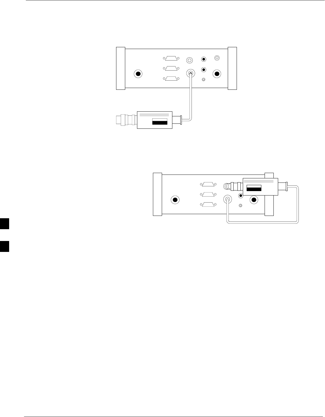
Test Equipment Preparation – continued
F-4 1X SC4812T–MC BTS Optimization/ATP 5/21/04
DRAFT
Figure F-1: Agilent E7495A Pre–Power Sensor Calibration connection
Use only
Agilent supplied
power adapter
GPS
GPIO
Serial 1
Serial 2
Power REF
50 MHz
Sensor
Ext Ref
In
Even Second
Sync In
Antenna
Port 1
RF Out / SWR
Port 2
RF In
POWER SENSOR
NOT CONNECTED
Figure F-2: Agilent E7495A Power Sensor Calibration connection
Use only
Agilent supplied
power adapter
GPS
GPIO
Serial 1
Serial 2
Power REF
50 MHz
Sensor
Ext Ref
In
Even Second
Sync In
Antenna
Port 1
RF Out / SWR
Port 2
RF In
POWER SENSOR
CONNECTED
Cable Calibration
Follow the directions in the LMF application program to calibrate
cables.
– Calibrate the short cable (see Figure 3-13) and two 10 dB
attenuators to establish a baseline and then calibrate the TX and RX
set–ups. Because at least 40 dB of attenuation is needed when
testing the FER, the set–up for RX is the same as for TX.
F
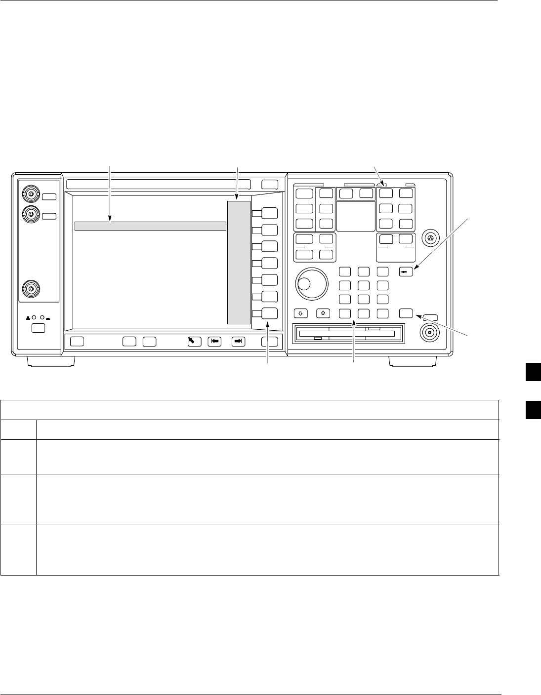
Verifying and Setting GPIB Addresses
5/21/04 1X SC4812T–MC BTS Optimization/ATP F-5
DRAFT
Agilent E4406A Transmitter
Tester GPIB Address
Follow the procedure in Table F-4 and refer to Figure F-3 to verify and,
if necessary, change the Agilent E4406A GPIB address.
Figure F-3: Setting Agilent E4406A GPIB Address
System Key
Bk Sp Key
Enter Key
Data Entry KeypadSoftkey Buttons
Softkey Label Display AreaActive Function Area
ti-CDMA-WP-00085-v01-ildoc-ftw
Table F-4: Verify and Change Agilent E4406A GPIB Address
Step Action
1In the SYSTEM section of the instrument front panel, press the System key.
– The softkey labels displayed on the right side of the instrument screen will change.
2Press the Config I/O softkey button to the right of the instrument screen.
– The softkey labels will change.
– The current instrument GPIB address will be displayed below the GPIB Address softkey label.
3If the current GPIB address is not set to 18, perform the following to change it:
3a Press the GPIB Address softkey button. In the on–screen Active Function Area, GPIB Address will
be displayed followed by the current GPIB address.
. . . continued on next page
F
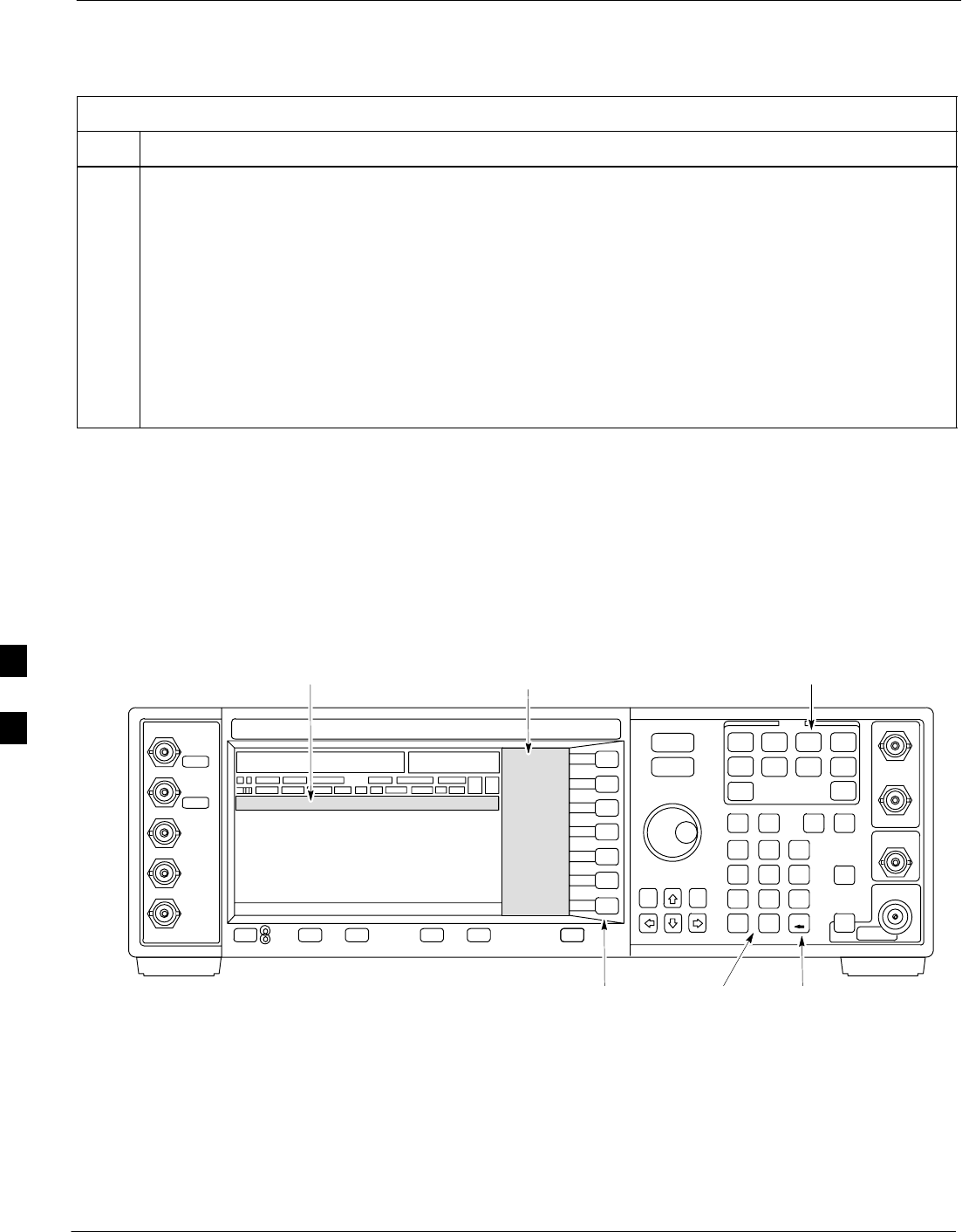
Verifying and Setting GPIB Addresses – continued
F-6 1X SC4812T–MC BTS Optimization/ATP 5/21/04
DRAFT
Table F-4: Verify and Change Agilent E4406A GPIB Address
Step Action
3b On the front panel Data Entry keypad, enter the communications system analyzer GPIB address of 18.
– The GPIB Address label will change to Enter.
– Digits entered with the keypad will replace the current GPIB address in the display.
NOTE
To correct an entry, press the Bk Sp key at the upper right of the keypad to delete one character at a
time.
3c Press the Enter softkey button or the keypad Enter key to set the new GPIB address.
– The Config I/O softkey labels will reappear.
– The new GPIB address will be displayed under the GPIB Address softkey label.
Agilent E4432B Signal
Generator GPIB Address
Follow the procedure in Table F-5 and refer to Figure F-4 to verify and,
if necessary, change the Agilent E4432B GPIB address.
Figure F-4: Setting Agilent E4432B GPIB Address
Numeric
Keypad
Softkey
Buttons
Softkey Label
Display Area
Active Entry
Area
Backspace
Key
Utility Key
ti-CDMA-WP-00086-v01-ildoc-ftw
F

Verifying and Setting GPIB Addresses – continued
5/21/04 1X SC4812T–MC BTS Optimization/ATP F-7
DRAFT
Table F-5: Verify and Change Agilent E4432B GPIB Address
Step Action
1In the MENUS section of the instrument front panel, press the Utility key.
– The softkey labels displayed on the right side of the instrument screen will change.
2Press the GPIB/RS232 softkey button to the right of the instrument screen.
– The softkey labels will change.
– The current instrument GPIB address will be displayed below the GPIB Address softkey label.
3If the current GPIB address is not set to 1, perform the following to change it:
3a Press the GPIB Address softkey button.
– The GPIB Address label and current GPIB address will change to boldface.
– In the on–screen Active Entry Area, Address: will be displayed followed by the current GPIB
address.
3b On the front panel Numeric keypad, enter the signal generator GPIB address of 1.
– The GPIB Address label will change to Enter.
– Digits entered with the keypad will replace the current GPIB address in the Active Entry display.
NOTE
To correct an entry, press the backspace key at the lower right of the keypad to delete one character at
a time.
3c Press the Enter softkey button to set the new GPIB address.
– The new GPIB address will be displayed under the GPIB Address softkey label.
Advantest R3267 Spectrum
Analyzer GPIB Address
Perform the procedure in Table F-6 and refer to Figure F-5 to verify and,
if necessary, change the Advantest R3267 spectrum analyzer GPIB
address.
F
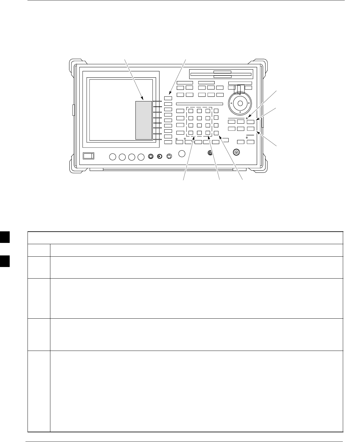
Verifying and Setting GPIB Addresses – continued
F-8 1X SC4812T–MC BTS Optimization/ATP 5/21/04
DRAFT
Figure F-5: Setting Advantest R3267 GPIB Address
onREMOTE LED
LCL Key
CONFIG Key
Softkey Lable
Display Area
Softkey
Buttons
Keypad BS Key ENTR Key ti-CDMA-WP-00083-v01-ildoc-ftw
Table F-6: Verify and Change Advantest R3267 GPIB Address
Step Action
1If the REMOTE LED is lighted, press the LCL key.
– The LED extinguishes.
2Press the CONFIG key.
– The CONFIG softkey labels will appear in the softkey label display area of the instrument
display.
– The current GPIB address will be displayed below the GPIB Address softkey label.
3If the current GPIB address is not set to 18, perform the following to change it:
3a Press the GPIB Address softkey. A GPIB Address entry window will open in the instrument display
showing the current GPIB address.
3b Enter 18 on the keypad in the ENTRY section of the instrument front panel. Characters typed on the
keypad will replace the address displayed in the GPIB Address entry window.
NOTE
To correct an entry, press the BS (backspace) key at the lower right of the keypad to delete one
character at a time.
3c Press the ENTR key to the lower right of the keypad to enter the address.
– The GPIB Address entry window closes.
– The new address is displayed in the bottom portion of the GPIB Address softkey label.
F
Verifying and Setting GPIB Addresses – continued
5/21/04 1X SC4812T–MC BTS Optimization/ATP F-9
DRAFT
Advantest R3562 Signal
Generator GPIB Address
Set the GP–IB ADDRESS switch on the rear of the Advantest R3562
signal generator to address 1 as shown in Figure F-6.
Figure F-6: Advantest R3562 GPIB Address Switch Setting
123 4567 8
54321
GP–IP ADDRESS
1
0
GPIB Address set to “1”
ti-CDMA-WP-00084-v01-ildoc-ftw
Agilent 8935 Series E6380
(formerly HP 8935) Test Set
GPIB Address
Follow the procedure in Table F-7 and refer to Figure F-7 to verify and,
if necessary, change the HP8935 GPIB address.
Figure F-7: HP8935 Test Set
FW00885
Preset
Cursor Control
Shift
Inst Config
Local
F

Verifying and Setting GPIB Addresses – continued
F-10 1X SC4812T–MC BTS Optimization/ATP 5/21/04
DRAFT
This procedure assumes that the test equipment is set up
and ready for testing.
NOTE
Table F-7: Verify and/or Change HP8935 GPIB Address
Step Action
NOTE
The HP I/O configuration MUST be set to Talk & Listen, or NO device on the GPIB bus will be
accessible. (Consult test equipment OEM documentation for additional information as required.)
1To verify that the GPIB addresses are set correctly, press Shift and LOCAL on the HP8935. The
current HP–IB address is displayed at the top of the screen.
NOTE
HP–IB is the same as GPIB.
2If the current GPIB address is not set to 18, perform the following to change it:
– Press Shift and Inst Config.
– Turn the Cursor Control knob to move the cursor to the HP–IB Adrs field.
– Press the Cursor Control knob to select the field.
– Turn the Cursor Control knob as required to change the address to 18.
– Press the Cursor Control knob to set the address.
3SPress Preset to return to normal operation.
Hewlett Packard HP8921A and
HP83236A/B GPIB Address
Follow the procedure in Table F-8 and refer to Figure F-8, to verify and,
if necessary, change the HP8921A HP83236A GPIB addresses.
F
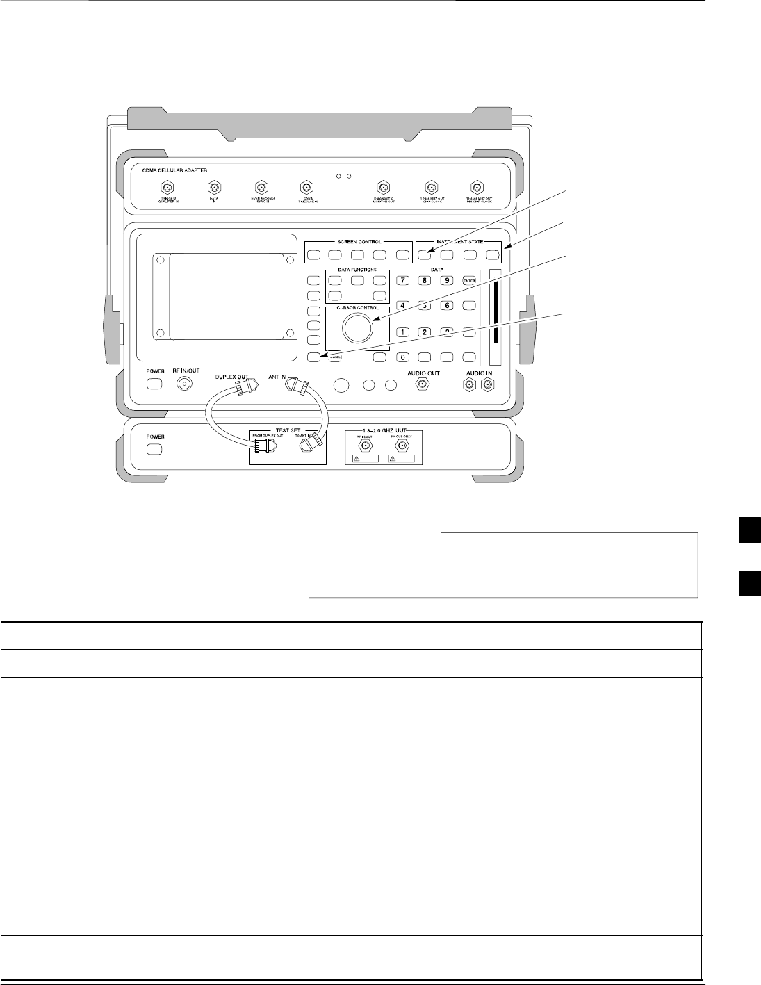
Verifying and Setting GPIB Addresses – continued
5/21/04 1X SC4812T–MC BTS Optimization/ATP F-11
DRAFT
Figure F-8: HP8921A and HP3236A/B
Preset
Cursor Control
Shift
Local
ti-CDMA-WP-00081-v01-ildoc-ftw
This procedure assumes that the test equipment is set up
and ready for testing.
NOTE
Table F-8: Verify and/or Change HP8921A and HP83236A GPIB Addresses
Step Action
1To verify that the GPIB addresses are set correctly, press Shift and LOCAL on the HP8921A. The
current HP–IB address is displayed at the top of the screen.
NOTE
HP–IB is the same as GPIB.
2If the current HP–IB address is not set to 18, perform the following to change it:
– Turn the Cursor Control knob to move the cursor to More and press the knob to select the field.
– Turn the Cursor Control knob to move the cursor to I/O Config and press the knob to select the
field.
– Turn the Cursor Control knob to move the cursor to Adrs and press the knob to select the field.
– Turn the Cursor Control knob to change the HP–IB address to 18 and press the knob to set the
address.
– Press Shift and Preset to return to normal operation.
3To set the HP83236A (or B) PCS Interface GPIB address=19, set the dip switches as follows:
– A1=1, A2=1, A3=0, A4=0, A5=1, HP–IB/Ser = 1
F
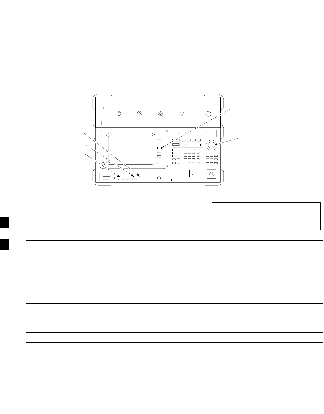
Verifying and Setting GPIB Addresses – continued
F-12 1X SC4812T–MC BTS Optimization/ATP 5/21/04
DRAFT
Advantest R3465
Communications Test Set GPIB
Address
Follow the steps in Table F-9 and refer to Figure F-9 to verify and, if
necessary, change the GPIB address for the Advantest R3465.
Figure F-9: R3465 Communications Test Set
BNC
“T”
REF UNLOCK EVEN
SEC/SYNC IN CDMA
TIME BASE IN
POWER
OFF ON
REF FW00337
LCL
Shift
Preset
GPIB and others
Vernier Knob
This procedure assumes that the test equipment is set up
and ready for testing.
NOTE
Table F-9: Verify and/or Change Advantest R3465 GPIB Address
Step Action
1To verify that the GPIB address is set correctly, perform the following procedure:
– Press SHIFT then PRESET.
– Press LCL.
– Press the GPIB and Others CRT menu key to view the current address.
2If the current GPIB address is not set to 18, perform the following to change it:
– Turn the vernier knob as required to select 18.
– Press the vernier knob to set the address.
3To return to normal operation, press Shift and Preset.
Motorola CyberTest GPIB
Address
Follow the steps in Table F-10 to verify and, if necessary, change the
GPIB address on the Motorola CyberTest. Changing the GPIB address
requires the following items:
SMotorola CyberTest communications analyzer.
SComputer running Windows 3.1/Windows 95.
F
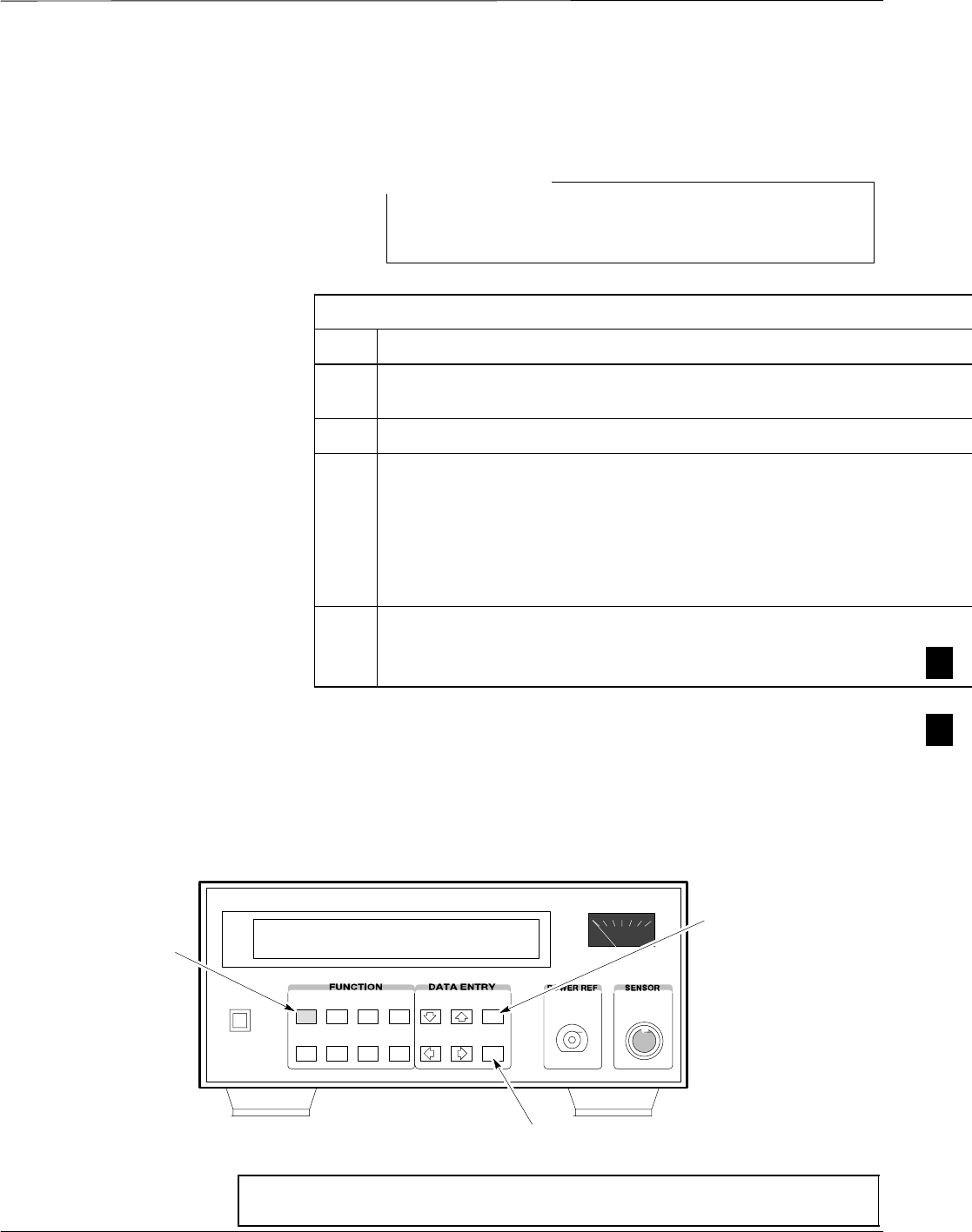
Verifying and Setting GPIB Addresses – continued
5/21/04 1X SC4812T–MC BTS Optimization/ATP F-13
DRAFT
SMotorola CyberTAME software program “TAME”.
SParallel printer port cable (shipped with CyberTest).
This procedure assumes that the test equipment is set up
and ready for testing.
NOTE
Table F-10: Verify and/or Change Motorola CyberTest GPIB
A
Step Action
1On the LMF desktop, locate the CyberTAME icon. Double click on the ico
n
application.
2In the CyberTAME window taskbar, under Special, select IEEE.488.2.
3CyberTAME software will query the CyberTest Analyzer for its current GP
I
open the IEEE 488.2 dialog box. If the current GPIB address is not 18, perf
o
procedure to change it:
– Use the up or down increment arrows, or double–click in the field and t
y
– Click on the OK button.
The new address will be written to the CyberTest via the parallel port a
n
NOTE
Verify that the address has been set by repeating steps 2 and 3. The new add
r
the IEEE 488.2 dialog box Address field.
HP437 Power Meter GPIB
Address
Follow the steps in Table F-11 and refer to Figure F-10 to verify and, if
necessary, change the HP437 GPIB address.
Figure F-10: HP437 Power Meter
ENTER
PRESET
SHIFT (BLUE) PUSHBUTTON –
ACCESSES FUNCTION AND
DATA ENTRY KEYS IDENTIFIED
WITH LIGHT BLUE TEXT ON
THE FRONT PANEL ABOVE
THE BUTTONS
FW00308REF
NOTE This procedure assumes that the test equipment is set up and
ready for testing.
F
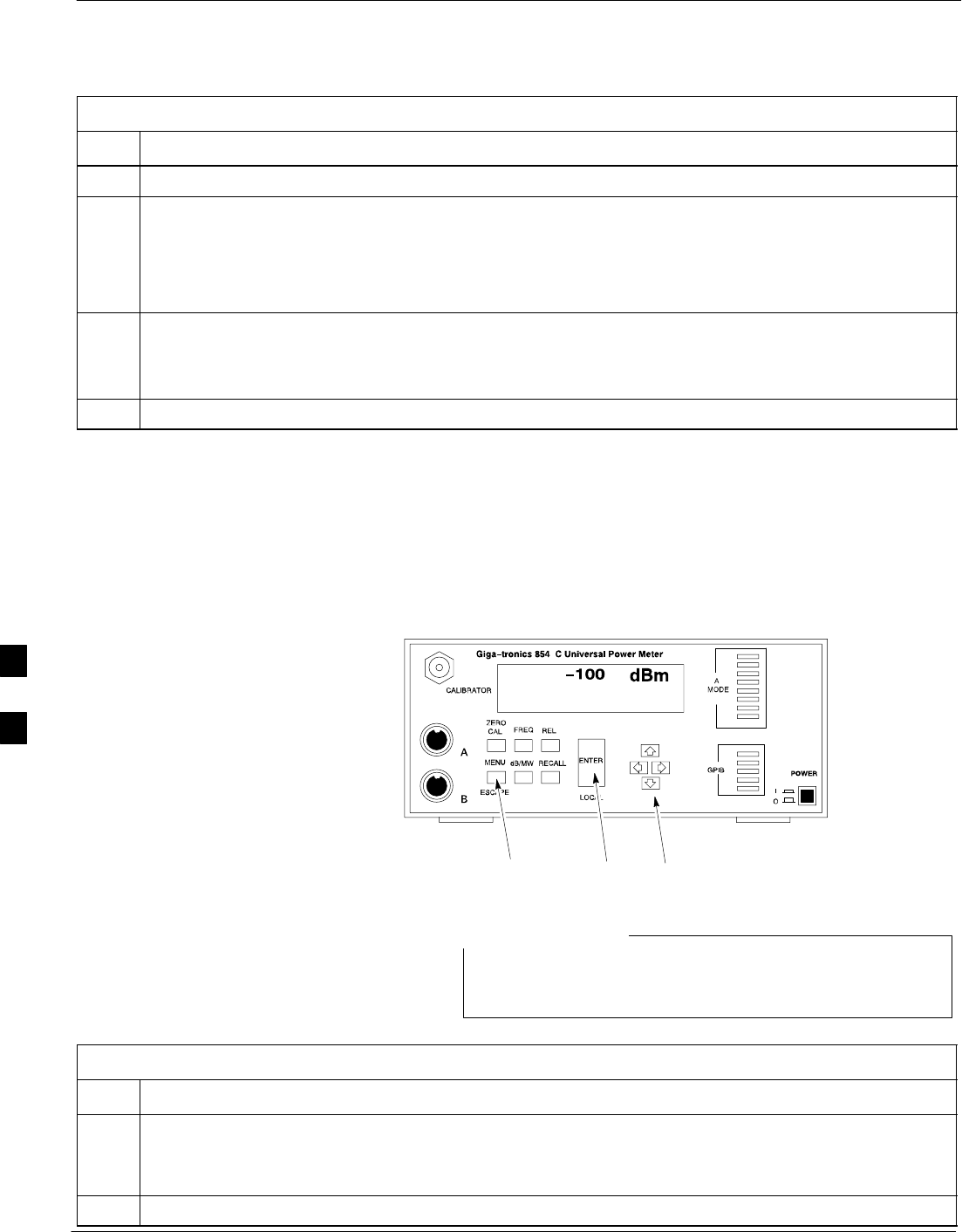
Verifying and Setting GPIB Addresses – continued
F-14 1X SC4812T–MC BTS Optimization/ATP 5/21/04
DRAFT
Table F-11: Verify and/or Change HP437 Power Meter GPIB Address
Step Action
1 Press Shift and PRESET.
2Use the y arrow key to navigate to HP–IB ADRS and press ENTER.
The HP–IB address is displayed.
NOTE
HP–IB is the same as GPIB.
3If the current GPIB address is not set to 13, perform the following to change it:
– Use the y b arrow keys to change the HP–IB ADRS to 13.
– Press ENTER to set the address.
4 Press Shift and ENTER to return to a standard configuration.
Gigatronics 8541C Power
Meter GPIB Address
Follow the steps in Table F-12 and refer to Figure F-11 to verify and, if
necessary, change the Gigatronics 8541C power meter GPIB address.
Figure F-11: Gigatronics 8541C Power Meter Detail
MENU ENTER ARROW
KEYS REF FW00564
1
This procedure assumes that the test equipment is set up
and ready for testing.
NOTE
Table F-12: Verify and/or Change Gigatronics 8541C Power Meter GPIB Address
Step Action
! CAUTION
Do not connect/disconnect the power meter sensor cable with AC power applied to the meter.
Disconnection could result in destruction of the sensing element or miscalibration.
1 Press MENU.
F
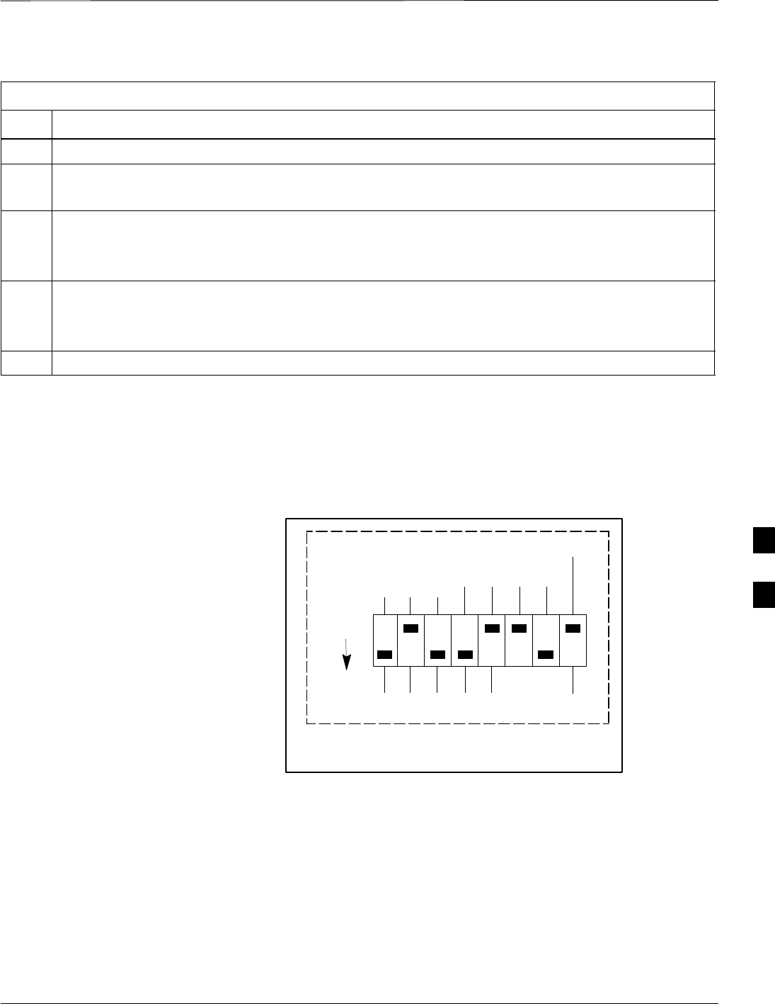
Verifying and Setting GPIB Addresses – continued
5/21/04 1X SC4812T–MC BTS Optimization/ATP F-15
DRAFT
Table F-12: Verify and/or Change Gigatronics 8541C Power Meter GPIB Address
Step Action
2Use the b arrow key to select CONFIG MENU and press ENTER.
3Use the b arrow key to select GPIB and press ENTER.
The current Mode and GPIB Address are displayed.
4If the Mode is not set to 8541C, perform the following to change it:
Use the a ’ arrow keys as required to select MODE.
Use the by arrow keys as required to set MODE to 8541C.
5If the GPIB address is not set to 13, perform the following to change it:
Use the ’ arrow key to select ADDRESS.
Use the by arrow keys as required to set the GPIB address to 13.
6 Press ENTER to return to normal operation.
RS232 GPIB Interface Box
Ensure that the RS232 GPIB interface box dip switches are set as shown
in Figure F-12.
Figure F-12: RS232 GPIB Interface Box
RS232–GPIB
Interface Box
S MODE
DATA FORMAT
BAUD RATE
GPIB ADRS
ON
DIP SWITCH SETTINGS
G MODE
ti-CDMA-WP-00082-v01-ildoc-ftw
F
Verifying and Setting GPIB Addresses – continued
F-16 1X SC4812T–MC BTS Optimization/ATP 5/21/04
DRAFT
Test Equipment Set-up
Purpose
This section covers other test equipment and peripherals not covered in
Chapter 3. Procedures for the manual testing are covered here, along
with procedures to calibrate the TX and RX cables using the signal
generator and spectrum analyzer.
Equipment Warm up
Warm-up BTS equipment for a minimum of 60 minutes
prior to performing the BTS optimization procedure. This
assures BTS site stability and contributes to optimization
accuracy. (Time spent running initial power-up,
hardware/firmware audit, and BTS download counts as
warm-up time.)
NOTE
If any piece of test equipment (i.e., test cable, RF adapter)
has been replaced, re-calibration must be performed.
Failure to do so could introduce measurement errors,
resulting in incorrect measurements and degradation to
system performance..
CAUTION
Calibration of the communications test set (or equivalent
test equipment) must be performed at the site before
calibrating the overall test set. Calibrate the test equipment
after it has been allowed to warm-up and stabilize for a
minimum of 60 minutes.
NOTE
Prerequisites
Prior to performing any of these procedures, all preparations for
preparing the LMF, updating LMF files, and any other pre-calibration
procedures, as stated in Chapter 3, must have been completed.
HP8921A System Connectivity
Test
Follow the steps in Table F-13 to verify that the connections between the
PCS Interface and the HP8921A are correct, and cables are intact. The
software also performs basic functionality checks of each instrument.
F

Verifying and Setting GPIB Addresses – continued
5/21/04 1X SC4812T–MC BTS Optimization/ATP F-17
DRAFT
Disconnect other GPIB devices, especially system
controllers, from the system before running the
connectivity software.
NOTE
Table F-13: System Connectivity
Step Action
NOTE
– Perform this procedure after test equipment has been allowed to warm–up and stabilize for a
minimum of 60 minutes.
1Insert HP 83236A Manual Control/System card into memory card slot.
2Press the [PRESET] pushbutton.
3Press the Screen Control [TESTS] pushbutton to display the “Tests” Main Menu screen.
4Position the cursor at Select Procedure Location and select by pressing the cursor control knob.
In the Choices selection box, select Card.
5Position the cursor at Select Procedure Filename and select by pressing the cursor control knob.
In the Choices selection box, select SYS_CONN.
6Position the cursor at RUN TEST and select it.
The software will prompt you through the connectivity setup.
7When the test is complete, position the cursor on STOP TEST and select it; OR press the [K5]
pushbutton.
8To return to the main menu, press the [K5] pushbutton.
HP PCS Interface Test
Equipment Setup for Manual
Testing
Follow the procedure in Table F-14 to setup the HP PCS Interface Box
for manual testing.
Table F-14: Manual Cable Calibration Test Equipment Setup (using the HP PCS Interface)
nStep Action
NOTE
Verify GPIB controller is turned off.
1Insert HP83236B Manual Control/System card into the memory card slot.
2 Under Screen Controls, press the [TESTS] push-button to display the TESTS (Main Menu)
screen.
3Position the cursor at Select Procedure Location and select. In the Choices selection box, select
CARD.
4Position the cursor at Select Procedure Filename and select. In the Choices selection box, select
MANUAL.
F

Verifying and Setting GPIB Addresses – continued
F-18 1X SC4812T–MC BTS Optimization/ATP 5/21/04
DRAFT
Table F-14: Manual Cable Calibration Test Equipment Setup (using the HP PCS Interface)
nActionStep
5Position the cursor at RUN TEST and select OR press the K1 push-button.
6Set channel number=<chan#>:
– Position cursor at Channel Number and select.
– Enter the chan# using the numeric keypad and then press [Enter] (the screen will blank).
– When the screen reappears, the chan# will be displayed on the channel number line.
NOTE
– If using a TMPC with Tower Top Amplifier (TTA) skip Step 7.
7Set RF Generator level= –119 dBm + Cal factor Example: –119 dBm + 2 dB = –117 dBm
– Continue with Step 9 (skip Step 8).
8Set RF Generator level= –116 dBm + Cal factor. Example: –116 dBm + 2 dB = –114 dBm
9Set the user fixed Attenuation Setting to 0 dB:
– Position cursor at RF Generator Level and select.
– Position cursor at User Fixed Atten Settings and select.
– Enter 0 (zero) using the numeric keypad and press [Enter].
10 Select Back to Previous Menu.
11 Select Quit, then select Yes.
Calibrating Test Cable Setup
using Advantest R3465
Be sure the GPIB Interface is OFF for this procedure.
NOTE
Perform the procedure in Table F-15 to calibrate the test cable setup
using the Advantest R3465. Advantest R3465 Manual Test setup and
calibration must be performed at both the TX and RX frequencies.
Table F-15: Procedure for Calibrating Test Cable Setup Using Advantest R3465
Step Action
NOTE
– This procedure can only be performed after test equipment has been allowed to warm–up and
stabilize for a minimum of 60 minutes.
1Press the SHIFT and the PRESET keys located below the display.
2Press the ADVANCE key in the MEASUREMENT area of the control panel.
3Select the CDMA Sig CRT menu key.
4Select the Setup CRT menu key.
. . . continued on next page
F

Verifying and Setting GPIB Addresses – continued
5/21/04 1X SC4812T–MC BTS Optimization/ATP F-19
DRAFT
Table F-15: Procedure for Calibrating Test Cable Setup Using Advantest R3465
Step Action
5Using the vernier knob and the cursor keys set the following parameters:
NOTE
Fields not listed remain at default.
Generator Mode: SIGNAL
Link: FORWARD
Level Unit: dBm
CalCorrection: ON
Level Offset: OFF
6Select the return CRT menu key.
7 Press FREQ key in the ENTRY area.
8Set the frequency to the desired value using the keypad entry keys.
9Verify that the Mod CRT menu key is highlighting OFF; if not, press the Mod key to toggle it OFF.
10 Verify that the Output CRT menu key is highlighting OFF; if not, press the Output key to toggle it
OFF.
11 Press the LEVEL key in the ENTRY area.
12 Set the LEVEL to 0 dBm using the key pad entry keys.
13 Zero power meter. Next connect the power sensor directly to the “RF OUT” port on the R3561L
CDMA Test Source Unit.
14 Press the Output CRT menu key to toggle Output to ON.
15 Record the power meter reading ________________________
16 Disconnect the power meter sensor from the R3561L RF OUT jack.
NOTE
The Power Meter sensor lower limit is –30 dBm. Thus, only components having losses < 30 dB
should be measured using this method. For best accuracy, always re–zero the power meter before
connecting the power sensor to the component being calibrated. Then, after connecting the
power sensor to the component, record the calibrated loss immediately.
17 Disconnect all components in the the test setup and calibrate each one separately. Connect each
component one–at–a–time between the “RF OUT” port and the power sensor (see Figure F-13,
“Setups A, B, and C”). Record the calibrated loss value displayed on the power meter for each
connection.
Example: (A) 1st Test Cable = –0.5 dB
(B) 2nd Test Cable = –1.4 dB
(C) 20 dB Attenuator = –20.1 dB
(D) 30 dB Directional Coupler = –29.8 dB
18 Press the Output CRT menu key to toggle Output OFF.
. . . continued on next page
F

Verifying and Setting GPIB Addresses – continued
F-20 1X SC4812T–MC BTS Optimization/ATP 5/21/04
DRAFT
Table F-15: Procedure for Calibrating Test Cable Setup Using Advantest R3465
Step Action
19 Calculate the total test setup loss by adding up all the individual losses:
Example: Total test setup loss = 0.5 + 1.4 + 20.1 + 29.8 = 51.8 dB
This calculated value will be used in the next series of tests.
20 Press the FREQ key in the ENTRY area.
21 Using the keypad entry keys, set the test frequency to the RX frequency.
22 Repeat steps 9 through 19 for the RX frequency.
23 Refer to Table 3-30 for assistance in manually setting the cable loss values into the LMF.
F
Verifying and Setting GPIB Addresses – continued
5/21/04 1X SC4812T–MC BTS Optimization/ATP F-21
DRAFT
Figure F-13: Cable Calibration using Advantest R3465
POWER
SENSOR
20 DB / 2 WATT
ATTENUATOR
(A)
(C)
POWER
SENSOR
(D)
30 DB
DIRECTIONAL
COUPLER
(C)
100 W
NON–RADIATING
RF LOAD
POWER
SENSOR
RF OUT
POWER
SENSOR
& (B)
FW00320
F
Test Equipment Calibration
F-22 1X SC4812T–MC BTS Optimization/ATP 5/21/04
DRAFT
Agilent E4406A Transmitter
Tester Self-alignment
(Calibration)
Refer to Figure F-14 and follow the procedure in Table F-16 to perform
the Agilent E4406A self–alignment (calibration).
Figure F-14: Agilent E4406A System
Key
Softkey
Buttons
Softkey Label
Display Area
ti-CDMA-WP-00080-v01-ildoc-ftw
Table F-16: Perform Agilent E4406A Self–alignment (Calibration)
Step Action
1In the SYSTEM section of the instrument front panel, press the System key.
– The softkey labels displayed on the right side of the instrument screen will change.
2Press the Alignments softkey button to the right of the instrument screen.
– The softkey labels will change.
3Press the Align All Now softkey button.
– All other instrument functions will be suspended during the alignment.
– The display will change to show progress and results of the alignments performed.
– The alignment will take less than one minute.
HP 437 Power Meter
(Calibration)
Precise transmit output power calibration measurements are made using
a bolometer–type broadband power meter with a sensitive power sensor.
Follow the steps in Table F-17 to enter information unique to the power
sensor before calibrating the test setup. Refer to Figure F-15 as required.
F
Test Equipment Calibration – continued
5/21/04 1X SC4812T–MC BTS Optimization/ATP F-23
DRAFT
This procedure must be done before the automated
calibration to enter power sensor specific calibration
values.
NOTE
Figure F-15: Power Meter Detail
CONNECT POWER
SENSOR WITH POWER
METER TURNED OFF
CONNECT POWER SENSOR
TO POWER REFERENCE
WHEN CALIBRATING UNIT.
POWER REFERENCE IS
ENABLED USING THE SHIFT ’
KEYS
SHIFT (BLUE) PUSHBUTTON –
ACCESSES FUNCTION AND
DATA ENTRY KEYS IDENTIFIED
WITH LIGHT BLUE TEXT ON
THE FRONT PANEL ABOVE
THE BUTTONS
FW0
0
Table F-17: HP 437 Power Meter Calibration Procedure
Step Action
1! CAUTION
Do not connect/disconnect the power meter sensor cable with AC power applied to the meter.
Disconnection could result in destruction of the sensing element or mis–calibration.
Make sure the power meter AC LINE pushbutton is OFF.
2Connect the power sensor cable to the SENSOR input.
3Set the AC LINE pushbutton to ON.
NOTE
The calibration should be performed only after the power meter and sensor have been allowed to
warm–up and stabilize for a minimum of 60 minutes.
4Perform the following to set or verify the correct power sensor model:
4a – Press [SHIFT] then [a] to select SENSOR.
4b – Identify the power sensor model number from the sensor label.
4c – Use the [y] or [b] button to select the appropriate model; then press [ENTER].
5Refer to the illustration for step 8, and perform the following to ensure the power reference output is
OFF:
5a – Observe the instrument display and determine if the triangular indicator over PWR REF is
displayed.
5b – If the triangular indicator is displayed, press [SHIFT] then [’] to turn it off.
. . . continued on next page
F
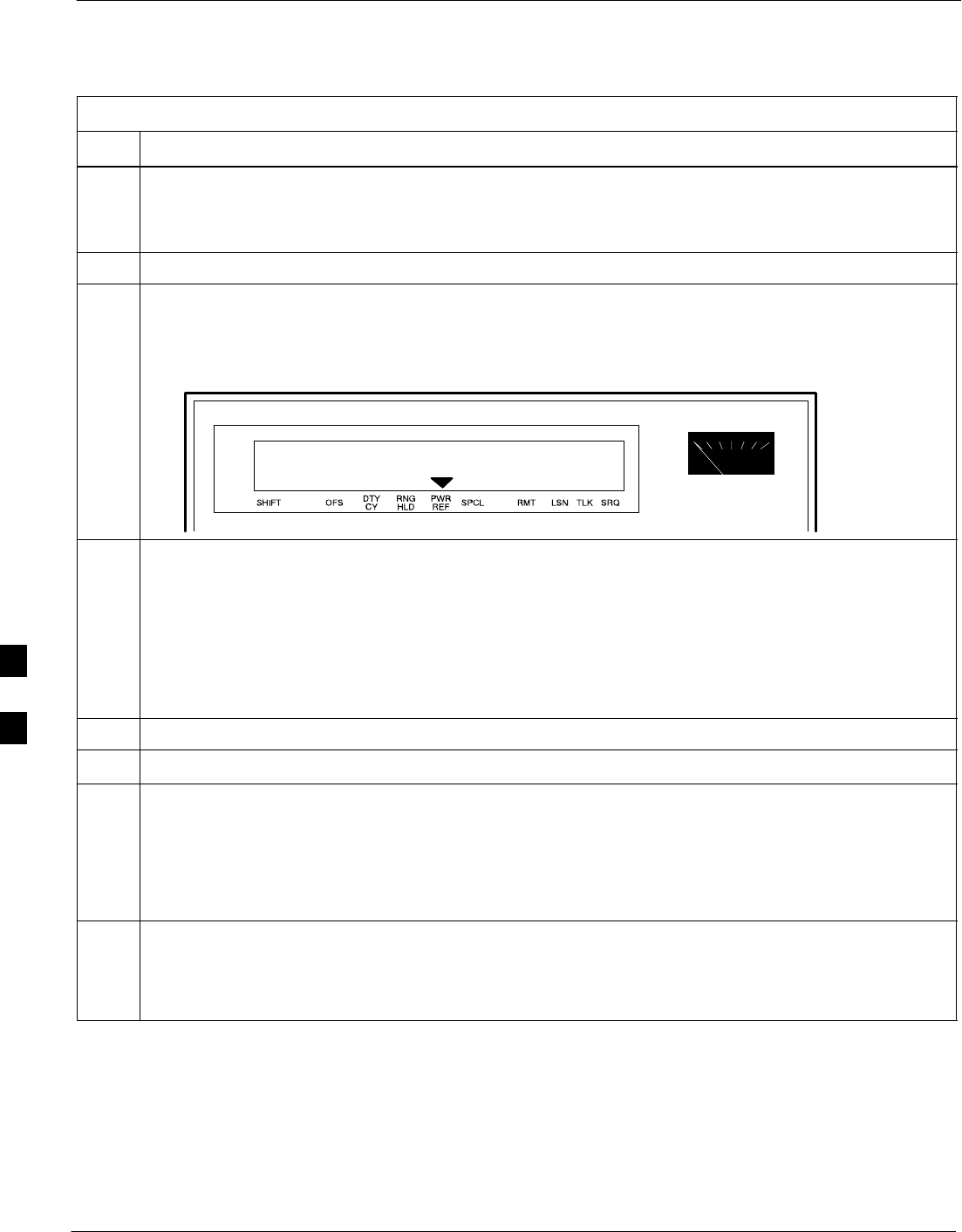
Test Equipment Calibration – continued
F-24 1X SC4812T–MC BTS Optimization/ATP 5/21/04
DRAFT
Table F-17: HP 437 Power Meter Calibration Procedure
Step Action
6 Press [ZERO].
– Display will show “Zeroing ******.”
– Wait for process to complete.
7Connect the power sensor to the POWER REF output.
8Turn on the PWR REF by performing the following:
8a – Press [SHIFT] then [’].
8b – Verify that the triangular indicator (B) appears in the display above PWR REF as shown below.
9Perform the following to set the REF CF%:
9a – Press ([SHIFT] then [ZERO]) for CAL.
9b – Enter the sensor’s REF CF% from the sensor’s decal using the arrow keys and press [ENTER].
(The power meter will display ”CAL *****” for a few seconds.)
NOTE
If the REF CAL FACTOR (REF CF) is not shown on the power sensor, assume it to be 100%.
10 Perform the following to set the CAL FAC %:
10a – Press [SHIFT] then [FREQ] for CAL FAC.
10b – On the sensor’s decal, locate an approximate calibration percentage factor (CF%) at the test
frequency.
10c – Enter the sensor’s calibration % (CF%) using the arrow keys and press [ENTER].
–– When complete, the power meter will typically display 0.05 dBm. (Any reading between
0.00 and 0.10 is normal.)
11 To turn off the PWR REF, perform the following:
11a – Press [SHIFT] then [’].
11b – Disconnect the power sensor from the POWER REF output.
Gigatronics 8542 power meter
(Calibration)
Precise transmit output power calibration measurements are made using
a bolometer–type broadband power meter with a sensitive power sensor.
Follow the steps in Table F-18 to enter information unique to the power
sensor. Refer to Figure F-16 as necessary.
F
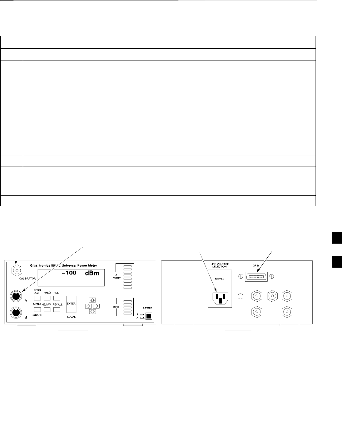
Test Equipment Calibration – continued
5/21/04 1X SC4812T–MC BTS Optimization/ATP F-25
DRAFT
Table F-18: Calibrate Gigatronics 8542 Power Meter
Step Action
1! CAUTION
Do not connect/disconnect the power meter sensor cable with AC power applied to the meter.
Disconnection could result in destruction of the sensing element or miscalibration.
Make sure the power meter POWER pushbutton is OFF.
2Connect the power sensor cable to the SENSOR input.
3Set the POWER pushbutton to ON.
NOTE
Allow the power meter and sensor to warm up and stabilize for a minimum of 60 minutes before
performing the calibration procedure.
4Connect the power sensor to the CALIBRATOR output connector.
5 Press ZERO.
– Wait for the process to complete. Sensor factory calibration data is read to power meter during this
process.
6When the zeroing process is complete, disconnect the power sensor from the CALIBRATOR output.
Figure F-16: Gigatronics 8541C Power Meter
CONNECT POWER SENSOR
WITH POWER METER
TURNED OFF
CONNECT POWER SENSOR TO
CALIBRATOR POWER REFERENCE
WHEN CALIBRATING/ZEROING UNIT
FRONT View REAR View
GPIB CONNECTIONAC POWER
FW00564
F

Test Equipment Calibration – continued
F-26 1X SC4812T–MC BTS Optimization/ATP 5/21/04
DRAFT
Notes
F

5/21/04 1X SC4812T–MC BTS Optimization/ATP
DRAFT
Appendix G: VSWR
Appendix Content
THIS IS THE GENERAL APPENDIX TOC. USE THIS FOR ALL
APPENDICES EXCEPT APPENDIX A.
Guide Book 1–2. . . . . . . . . . . . . . . . . . . . . . . . . . . . . . . . . . . . . . . . . . . . . . . . . . . . .
Document Overview 1–2. . . . . . . . . . . . . . . . . . . . . . . . . . . . . . . . . . . . . . . . . . . . . .
What Is In This Guide? 1–2. . . . . . . . . . . . . . . . . . . . . . . . . . . . . . . . . . . . .
Book Catalogs and Organization 1–3. . . . . . . . . . . . . . . . . . . . . . . . . . . . . . . . . . . .
Book Directory 1–3. . . . . . . . . . . . . . . . . . . . . . . . . . . . . . . . . . . . . . . . . . .
Special Catalogs 1–5. . . . . . . . . . . . . . . . . . . . . . . . . . . . . . . . . . . . . . . . . . .
Physical Page Layouts 1–6. . . . . . . . . . . . . . . . . . . . . . . . . . . . . . . . . . . . . . . . . . . .
A/A4 Page and Margin Sizes 1–6. . . . . . . . . . . . . . . . . . . . . . . . . . . . . . . . .
A/A4 Page Text Area 1–7. . . . . . . . . . . . . . . . . . . . . . . . . . . . . . . . . . . . . . .
A/A4 Page Components 1–9. . . . . . . . . . . . . . . . . . . . . . . . . . . . . . . . . . . .
Frame and Table Components 1–10. . . . . . . . . . . . . . . . . . . . . . . . . . . . . . . . . . . . . .
Frames With Tools 1–10. . . . . . . . . . . . . . . . . . . . . . . . . . . . . . . . . . . . . . . . .
Flow Charts and Block Diagrams 1–10. . . . . . . . . . . . . . . . . . . . . . . . . . . . .
Line Drawings 1–11. . . . . . . . . . . . . . . . . . . . . . . . . . . . . . . . . . . . . . . . . . . .
Table Types In This Template 1–12. . . . . . . . . . . . . . . . . . . . . . . . . . . . . . . .
Item/Description Table 1–12. . . . . . . . . . . . . . . . . . . . . . . . . . . . . . . . . . . . .
Step Table 1–13. . . . . . . . . . . . . . . . . . . . . . . . . . . . . . . . . . . . . . . . . . . . . . .
Step/Check Table 1–14. . . . . . . . . . . . . . . . . . . . . . . . . . . . . . . . . . . . . . . . . .
Component Descriptions 1–15. . . . . . . . . . . . . . . . . . . . . . . . . . . . . . . . . . . . . . . . . .
Conclusions 1–16. . . . . . . . . . . . . . . . . . . . . . . . . . . . . . . . . . . . . . . . . . . . . . . . . . . . .
Map Title Goes Here lkjsfdg Sfdkgj Msfd N lkas K lkjsdfl kB lkj fgcb 1–17. . . . . .
Block Label Goes Here 1–17. . . . . . . . . . . . . . . . . . . . . . . . . . . . . . . . . . . . .
Block Label Goes Here 1–17. . . . . . . . . . . . . . . . . . . . . . . . . . . . . . . . . . . . .
Block Label Goes Here 1–18. . . . . . . . . . . . . . . . . . . . . . . . . . . . . . . . . . . . .
Block Label Goes Here 1–19. . . . . . . . . . . . . . . . . . . . . . . . . . . . . . . . . . . . .
Map Title Goes Here 1–22. . . . . . . . . . . . . . . . . . . . . . . . . . . . . . . . . . . . . . . . . . . . . .
G

Table of Contents – continued
1X SC4812T–MC BTS Optimization/ATP 5/21/04
DRAFT
Notes
G

Transmit & Receive Antenna VSWR
5/21/04 1X SC4812T–MC BTS Optimization/ATP G-1
DRAFT
Purpose
The following procedures will verify that the Voltage Standing Wave
Ratio (VSWR) of all antennas and associated feed lines fall within
acceptable limits. The tests will be performed on all antennas in a
sequential manner (i.e., ANT 1, then ANT 2) until all antennas/feedlines
have been verified.
These procedures should be performed periodically by measuring each
respective antenna’s VSWR (reflected power) to verify that the antenna
system is within acceptable limits. This will ensure continued peak
system performance.
The antenna VSWR will be calculated at the CDMA carrier frequency
assigned to each antenna. Record and verify that they meet the test
specification of less than or equal to 1.5:1.
Motorola recommends that the installer be familiar with
the following procedure in its entirety before beginning the
actual procedure. Ensure that the entire site is currently not
in service.
This test is used to test RX antennas by substituting RX
frequencies for TX frequencies.
NOTE
Study the site engineering documents and perform the following tests
only after first verifying that the RF cabling configuration required to
interconnect the BTS frames and antennas meet requirements called out
in the BTS Installation Manual.
Test equipment
The following pieces of test equipment will be required to perform this
test:
SLMF
SDirectional coupler
SCommunications test set
Prior to performing antenna tests, insure that no CDMA
BBX channels are keyed. Failure to do so could result in
personal injury or serious equipment damage.
WARNING
Equipment Setup – HP Test Set
Follow the procedure in Table G-1 to set up test equipment required to
measure and calculate the VSWR for each antenna.
G

Transmit & Receive Antenna VSWR – continued
G-2 1X SC4812T–MC BTS Optimization/ATP 5/21/04
DRAFT
Table G-1: VSWR Measurement Procedure – HP Test Set
Step Action HP TEST SET
1For manual VSWR testing, using external directional coupler, refer to Figure G-1.
– Connect the communications test set RF IN/OUT port to the INPUT port of the directional
coupler.
– Connect the ANT IN port of the communication test set to the reverse (RVS) port on the
directional coupler. Terminate the forward port with a 50 ohm load.
– Install the antenna feed line to the output port on the directional coupler.
NOTE
Manual Communications Analyzer test setup (fields not indicated remain at default):
SSet screen to RF GEN.
– Set the RF Gen Freq to center frequency of actual CDMA carrier between 869–894 MHz for
TX and 824–849 MHz for RX.
– Set Amplitude to –30 dBm.
– Set Output Port to RF OUT.
– Set AFGen1 & AFGen2 to OFF.
2Remove the antenna feed line and install an “RF short” onto the directional coupler output port.
NOTE
Set–up communication test set as follows (fields not indicated remain at default):
SSet screen to SPEC ANL.
– Under Controls, set input port to ANT.
–Set Ref Level to –40 dBm.
– Under Controls, select Main, select Auxiliary.
– Under Controls, select AV G . Set Avg = 20.
3– Record the reference level on the communications analyzer and Note as PS for reference.
– Replace the short with the antenna feedline. Record the reference level on the communications
analyzer and Note for as P
A reference.
– Record the difference of the two readings in dB.
4Calculate the VSWR per the equation shown to the right.
Where:
RL(dB) =PA(dBm) – PS(dBm)
PA = Power reflected from antenna
PS = Power reflected from short
A calculated value of –13.98 dB equates to VSWR of better than 1.5:1.
VSWR +ȧ
ȧ
ȡ
Ȣ
1)10
RL
20
1–10
RL
20
ȧ
ȧ
ȣ
Ȥ
5If the readings indicate a potential problem, verify the physical integrity of all cables (including any
in–line components, pads, etc.) and associated connections up to the antenna. If problem still persists,
consult antenna OEM documentation for additional performance verification tests or replacement
information.
. . . continued on next page
G
Transmit & Receive Antenna VSWR – continued
5/21/04 1X SC4812T–MC BTS Optimization/ATP G-3
DRAFT
Table G-1: VSWR Measurement Procedure – HP Test Set
Step HP TEST SETAction
6Repeat steps 1 through 5 for all remaining TX sectors/antennas.
7Repeat steps 1 through 5 for all remaining RX sectors/antennas.
Figure G-1: Manual VSWR Test Setup Using HP8921 Test Set
FWD (INCIDENT)
PORT 50–OHM
TERMINATED LOAD
RVS
(REFLECTED)
PORT
FEED LINE TO
ANTENNA
UNDER TEST
RF
SHORT
30 DB
DIRECTIONAL
COUPLER OUTPUT
PORT
INPUT
PORT
FW00343
Equipment Setup – Advantest
Test Set
Follow the procedure in Table G-2 to set up test equipment required to
measure and calculate the VSWR for each antenna.
Table G-2: VSWR Measurement Procedure – Advantest Test Set
Step Action ADVANTEST
1If you have not already done so, refer to the procedure in Table 3-5 on page 3-15 to set up test
equipment and interface the LMF computer to the BTS.
2For manual VSWR testing using external directional coupler, refer to Figure G-2.
– Connect the communications test set RF OUT port to the input port of the directional coupler.
– Connect the INPUT port of the communication test set to the forward port on the directional
coupler. Terminate the forward port with a 50 Ohm load.
– Connect the RF short to the directional coupler output port.
. . . continued on next page
G

Transmit & Receive Antenna VSWR – continued
G-4 1X SC4812T–MC BTS Optimization/ATP 5/21/04
DRAFT
Table G-2: VSWR Measurement Procedure – Advantest Test Set
Step ADVANTESTAction
3Preform the following to instruct the calibrated test set to generate a CDMA RF carrier (RVL call)
with all zero longcode at the assigned RX frequency at –10 dBm:
SPush the ADVANCE Measurement key.
SPush the CDMA Sig CRT menu key.
SPush the FREQ Entry key:
– Set RF Gen Freq to center frequency of actual CDMA carrier between 869–894 MHz for TX
and 824–849 MHz for RX.
SPush the LEVEL Entry key; set to 0 dBm (by entering 0 and pushing the –dBm key).
SVerify that ON is active in the Output CRT menu key.
SVerify that OFF is active in the Mod CRT menu key.
SPush the CW Measurement key.
SPush the FREQ Entry key.
– Push the more 1/2 CRT menu key.
– Set Preselect CRT menu key to 3.0G.
SPush the Transient Measurement key.
– Push the Tx Power CRT menu key.
– Push the LEVEL entry key (set to 7 dBm by entering 7 and pushing the the dBm key).
– Set Avg Times CRT menu key to ON. Set to 20 (by entering 20 and pushing the Hz ENTER
key).
SPush the REPEAT Start key to take the measurement.
4Record the Burst Power display on the communications analyzer and Note as PS for reference.
5Install the antenna feedline to the output port of the directional coupler.
6SPush the Auto Level Set CRT menu key.
SPush the REPEAT Start key to take the measurement.
7Record the Burst Power on the communications analyzer and Note as PA level for reference.
Record the difference of the two readings in dBm.
8Calculate the VSWR per the equation shown to the right.
Where:
RL(dB) =PA(dBm) – PS(dBm)
PA = Power reflected from antenna
PS = Power reflected from short
A calculated value of –13.98 dB equates to VSWR of better than 1.5:1.
VSWR +ȧ
ȧ
ȡ
Ȣ
1)10
RL
20
1–10
RL
20
ȧ
ȧ
ȣ
Ȥ
9If the readings indicate a potential problem, verify the physical integrity of all cables (including any
in–line components, pads, etc.) and associated connections up to the antenna. If problem still persists,
consult antenna OEM documentation for additional performance verification tests or replacement
information.
. . . continued on next page
G
Transmit & Receive Antenna VSWR – continued
5/21/04 1X SC4812T–MC BTS Optimization/ATP G-5
DRAFT
Table G-2: VSWR Measurement Procedure – Advantest Test Set
Step ADVANTESTAction
10 Repeat steps 2 through 9 for all remaining TX sectors/antennas.
11 Repeat steps 2 through 9 for all remaining RX sectors/antennas.
Figure G-2: Manual VSWR Test Setup Using Advantest R3465
RVS
(REFLECTED)
PORT
FEED LINE TO
ANTENNA
UNDER TEST
RF
SHORT
30 DB
DIRECTIONAL
COUPLER
OUTPUT
PORT
FWD (INCIDENT)
PORT 50–OHM
TERMINATED LOAD
INPUT
PORT
RF OUT
RF IN
FW00332
G

Transmit & Receive Antenna VSWR – continued
G-6 1X SC4812T–MC BTS Optimization/ATP 5/21/04
DRAFT
Notes
G

5/21/04 1X SC4812T–MC BTS Optimization/ATP
DRAFT
Appendix H: Download ROM Code
Appendix Content
THIS IS THE GENERAL APPENDIX TOC. USE THIS FOR ALL
APPENDICES EXCEPT APPENDIX A.
Guide Book 1–2. . . . . . . . . . . . . . . . . . . . . . . . . . . . . . . . . . . . . . . . . . . . . . . . . . . . .
Document Overview 1–2. . . . . . . . . . . . . . . . . . . . . . . . . . . . . . . . . . . . . . . . . . . . . .
What Is In This Guide? 1–2. . . . . . . . . . . . . . . . . . . . . . . . . . . . . . . . . . . . .
Book Catalogs and Organization 1–3. . . . . . . . . . . . . . . . . . . . . . . . . . . . . . . . . . . .
Book Directory 1–3. . . . . . . . . . . . . . . . . . . . . . . . . . . . . . . . . . . . . . . . . . .
Special Catalogs 1–5. . . . . . . . . . . . . . . . . . . . . . . . . . . . . . . . . . . . . . . . . . .
Physical Page Layouts 1–6. . . . . . . . . . . . . . . . . . . . . . . . . . . . . . . . . . . . . . . . . . . .
A/A4 Page and Margin Sizes 1–6. . . . . . . . . . . . . . . . . . . . . . . . . . . . . . . . .
A/A4 Page Text Area 1–7. . . . . . . . . . . . . . . . . . . . . . . . . . . . . . . . . . . . . . .
A/A4 Page Components 1–9. . . . . . . . . . . . . . . . . . . . . . . . . . . . . . . . . . . .
Frame and Table Components 1–10. . . . . . . . . . . . . . . . . . . . . . . . . . . . . . . . . . . . . .
Frames With Tools 1–10. . . . . . . . . . . . . . . . . . . . . . . . . . . . . . . . . . . . . . . . .
Flow Charts and Block Diagrams 1–10. . . . . . . . . . . . . . . . . . . . . . . . . . . . .
Line Drawings 1–11. . . . . . . . . . . . . . . . . . . . . . . . . . . . . . . . . . . . . . . . . . . .
Table Types In This Template 1–12. . . . . . . . . . . . . . . . . . . . . . . . . . . . . . . .
Item/Description Table 1–12. . . . . . . . . . . . . . . . . . . . . . . . . . . . . . . . . . . . .
Step Table 1–13. . . . . . . . . . . . . . . . . . . . . . . . . . . . . . . . . . . . . . . . . . . . . . .
Step/Check Table 1–14. . . . . . . . . . . . . . . . . . . . . . . . . . . . . . . . . . . . . . . . . .
Component Descriptions 1–15. . . . . . . . . . . . . . . . . . . . . . . . . . . . . . . . . . . . . . . . . .
Conclusions 1–16. . . . . . . . . . . . . . . . . . . . . . . . . . . . . . . . . . . . . . . . . . . . . . . . . . . . .
Map Title Goes Here lkjsfdg Sfdkgj Msfd N lkas K lkjsdfl kB lkj fgcb 1–17. . . . . .
Block Label Goes Here 1–17. . . . . . . . . . . . . . . . . . . . . . . . . . . . . . . . . . . . .
Block Label Goes Here 1–17. . . . . . . . . . . . . . . . . . . . . . . . . . . . . . . . . . . . .
Block Label Goes Here 1–18. . . . . . . . . . . . . . . . . . . . . . . . . . . . . . . . . . . . .
Block Label Goes Here 1–19. . . . . . . . . . . . . . . . . . . . . . . . . . . . . . . . . . . . .
Map Title Goes Here 1–22. . . . . . . . . . . . . . . . . . . . . . . . . . . . . . . . . . . . . . . . . . . . . .
H

Table of Contents – continued
1X SC4812T–MC BTS Optimization/ATP 5/21/04
DRAFT
Notes
H
Download ROM Code
5/21/04 1X SC4812T–MC BTS Optimization/ATP H-1
DRAFT
Download ROM Code
ROM code can be downloaded to a device that is in any state. After the
download is started, the device being downloaded changes to
OOS_ROM (blue) and remains OOS_ROM (blue). The same R–level
RAM code must then be downloaded to the device. This procedure
includes steps for both the ROM code download and the RAM code
download.
ROM code files cannot be selected automatically. The ROM code file
must be selected manually. Follow the procedure in Table H-1 to
download ROM code.
Prerequisite
SROM and RAM code files exist for the device to be downloaded.
The R–level of the ROM code to be downloaded must be
the same as the R–level of the ROM code for other devices
in the BTS. Code must not be mixed in a BTS. This
procedure should only be used to upgrade replacement
devices for a BTS and it should not be used to upgrade all
devices in a BTS. If a BTS is to be upgraded from one
R–level to another, the optimization and ATP procedures
must first be performed with the BTS in the original
configuration. The upgrade should then be done by the
CBSC.
CAUTION
Table H-1: Download ROM Code
Step Action
1Click on the device to be downloaded.
NOTE
More than one device of the same type can be selected for download by either clicking on each one to
be downloaded or from the BTS menu bar Select pull–down menu, select the device item that applies.
Where: device = the type of device to be loaded (BBX, CSM, GLI, MCC)
2Click on the Device menu.
3Click on the Status menu item.
A status report window appears.
4Make a note of the number in the HW Bin Type column.
NOTE
“HW Bin Type” is the Hardware Binary Type for the device. This code is used as the last four digits in
the filename of a device’s binary ROM code file. Using this part of the filename, the ROM code file
can be matched to the device in which it is to be loaded.
. . . continued on next page
H

Download ROM Code – continued
H-2 1X SC4812T–MC BTS Optimization/ATP 5/21/04
DRAFT
Table H-1: Download ROM Code
Step Action
5Click on the OK button to dismiss the status report window.
NOTE
ROM code is automatically selected for download from the <x>:\<lmf home
directory>\version folder>\<code folder> specified by the NextLoad property in
the bts–#.cdf file. To check the value of the NextLoad property, click on
Util>Examine>Display Nextload. A pop–up message will show the value of the NextLoad.
6Click on the Download Code Manual menu item.
A file selection window appears.
7Double–click on the version folder that contains the desired ROM code file.
8Double–click on the Code folder.
A list of ROM and RAM code files is displayed.
! CAUTION
A ROM code file having the correct hardware binary type (HW Bin Type) needs to be chosen. The
hardware binary type (last four digits in the file name) was determined in step 4. Unpredictable results
can happen and the device may be damaged (may have to be replaced) if a ROM code file with wrong
binary type is downloaded.
9Choose a ROM code file having the correct hardware binary type (HW Bin Type).
The hardware binary type (last four digits in the file name) was determined in step 4.
10 Click on the ROM code file that matches the device type and HW Bin Type (e.g., bbx_rom.bin.0604
for a BBX having a HW Bin Type of 0604).
The file should be highlighted.
11 Click on the Load button.
A status report window displays the result of the download.
NOTE
If the ROM load failed for some devices, load them individually by clicking on one device, perform
steps 6 through 11 for it, and repeat the process for each remaining device.
12 Click on the Ok button to close the status report window.
13 Click on the Util menu.
14 Select the Tools menu item.
15 Click on the Update NextLoad>CDMA menu item.
16 Select the version number of the folder that was used for the ROM code download.
17 Click on the Save button.
A pop–up message indicates that the CDF file has been updated.
18 Click on the OK button to dismiss the pop–up message.
19 Click on the device that was downloaded with ROM code.
20 Click on the Device menu.
. . . continued on next page
H

Download ROM Code – continued
5/21/04 1X SC4812T–MC BTS Optimization/ATP H-3
DRAFT
Table H-1: Download ROM Code
Step Action
21 Click on the Download Code menu item to download RAM code.
A status report window displays the result of the download.
NOTE
Data is automatically downloaded to GLI devices when the RAM code is downloaded. Use the
Download Data procedure to download data to other device types after they have been upgraded.
22 Click on the Ok button to close the status report window.
The downloaded device should be OOS_RAM (yellow) unless it is a GLI in which case it should be
INS (green).
23 Click on the device that was downloaded.
24 Click on the Device menu.
25 Click on the Status menu item.
Verify that the status report window displays the correct ROM and RAM version numbers.
26 Click on the Ok button to close the status report window.
H

Download ROM Code – continued
H-4 1X SC4812T–MC BTS Optimization/ATP 5/21/04
DRAFT
Notes
H

5/21/04 1X SC4812T–MC BTS Optimization/ATP
DRAFT
Appendix I: Packet Backhaul Configuration
Appendix Content
THIS IS THE GENERAL APPENDIX TOC. USE THIS FOR ALL
APPENDICES EXCEPT APPENDIX A.
Guide Book 1–2. . . . . . . . . . . . . . . . . . . . . . . . . . . . . . . . . . . . . . . . . . . . . . . . . . . . .
Document Overview 1–2. . . . . . . . . . . . . . . . . . . . . . . . . . . . . . . . . . . . . . . . . . . . . .
What Is In This Guide? 1–2. . . . . . . . . . . . . . . . . . . . . . . . . . . . . . . . . . . . .
Book Catalogs and Organization 1–3. . . . . . . . . . . . . . . . . . . . . . . . . . . . . . . . . . . .
Book Directory 1–3. . . . . . . . . . . . . . . . . . . . . . . . . . . . . . . . . . . . . . . . . . .
Special Catalogs 1–5. . . . . . . . . . . . . . . . . . . . . . . . . . . . . . . . . . . . . . . . . . .
Physical Page Layouts 1–6. . . . . . . . . . . . . . . . . . . . . . . . . . . . . . . . . . . . . . . . . . . .
A/A4 Page and Margin Sizes 1–6. . . . . . . . . . . . . . . . . . . . . . . . . . . . . . . . .
A/A4 Page Text Area 1–7. . . . . . . . . . . . . . . . . . . . . . . . . . . . . . . . . . . . . . .
A/A4 Page Components 1–9. . . . . . . . . . . . . . . . . . . . . . . . . . . . . . . . . . . .
Frame and Table Components 1–10. . . . . . . . . . . . . . . . . . . . . . . . . . . . . . . . . . . . . .
Frames With Tools 1–10. . . . . . . . . . . . . . . . . . . . . . . . . . . . . . . . . . . . . . . . .
Flow Charts and Block Diagrams 1–10. . . . . . . . . . . . . . . . . . . . . . . . . . . . .
Line Drawings 1–11. . . . . . . . . . . . . . . . . . . . . . . . . . . . . . . . . . . . . . . . . . . .
Table Types In This Template 1–12. . . . . . . . . . . . . . . . . . . . . . . . . . . . . . . .
Item/Description Table 1–12. . . . . . . . . . . . . . . . . . . . . . . . . . . . . . . . . . . . .
Step Table 1–13. . . . . . . . . . . . . . . . . . . . . . . . . . . . . . . . . . . . . . . . . . . . . . .
Step/Check Table 1–14. . . . . . . . . . . . . . . . . . . . . . . . . . . . . . . . . . . . . . . . . .
Component Descriptions 1–15. . . . . . . . . . . . . . . . . . . . . . . . . . . . . . . . . . . . . . . . . .
Conclusions 1–16. . . . . . . . . . . . . . . . . . . . . . . . . . . . . . . . . . . . . . . . . . . . . . . . . . . . .
Map Title Goes Here lkjsfdg Sfdkgj Msfd N lkas K lkjsdfl kB lkj fgcb 1–17. . . . . .
Block Label Goes Here 1–17. . . . . . . . . . . . . . . . . . . . . . . . . . . . . . . . . . . . .
Block Label Goes Here 1–17. . . . . . . . . . . . . . . . . . . . . . . . . . . . . . . . . . . . .
Block Label Goes Here 1–18. . . . . . . . . . . . . . . . . . . . . . . . . . . . . . . . . . . . .
Block Label Goes Here 1–19. . . . . . . . . . . . . . . . . . . . . . . . . . . . . . . . . . . . .
Map Title Goes Here 1–22. . . . . . . . . . . . . . . . . . . . . . . . . . . . . . . . . . . . . . . . . . . . . .
I

Table of Contents – continued
1X SC4812T–MC BTS Optimization/ATP 5/21/04
DRAFT
Notes
I

BTS Router Initial Configuration
5/21/04 1X SC4812T–MC BTS Optimization/ATP I-1
DRAFT
Overview
This appendix contains information and operations related to loading an
MWR 1900 or MWR 1941 BTS router with the minimum standard
(canned) configuration necessary for network communications. Once the
router is communicating on the network, the full, site–specific,
operational configuration can be downloaded to the router over the
network. This appendix includes sections on:
SSetting up communications with a router using a Microsoftr
Windowsr–based computer
SDownloading BTS router canned configuration files from the OMC–R
STransferring the canned configuration files from the Windows–based
computer to the BTS router
SVerifying and replacing/upgrading the IOS version loaded on the CF
memory card
SVerifying and, if necessary, replacing/upgrading the ROM monitor
low–level operating system version loaded in the BTS router
SRecovery from BTS router initialization with the ROM monitor
low–level operating system and troubleshooting to locate and correct
the cause
SChanging the router FE interface IP addresses
SSample listings of the BTS router canned configuration files
I

Terminal Set Up
I-2 1X SC4812T–MC BTS Optimization/ATP 5/21/04
DRAFT
Creating a Terminal Session
General – This section provides the procedures to configure and save a
terminal session for communicating with the MWR 1900 BTS router.
Terminal settings are the same as those used for BTS card and module
Man–Machine Interface (MMI) communication sessions. The procedures
are for a Pentiumr processor–based computer operating with either
Windows 98 Second Edition (SE) or Windows 2000.
Using the LMF computer – LMF computer platforms can be used for
communicating with the routers, and the MMI terminal connection
created for BTS card/module optimization actions will operate with the
BTS routers. See the “Establishing a BTS Router Communication
Session” section of this appendix for additional interface hardware
required for BTS router communication.
Terminal Settings
Follow the procedure in Table I-1 to create a named HyperTerminal
connection for BTS router interface and generate a Windows desktop
shortcut for it.
There are differences between Windows 2000 and Windows
98 in the menus and screens used for creating a
HyperTerminal connection. In the following procedure,
items applicable to:
SWindows 2000 will be identified with Win2000
SWindows 98 will be identified with Win98
NOTE
Table I-1: Establish HyperTerminal Connection
Step Action
1From the Windows Start menu, select:
Programs > Accessories
2Perform one of the following:
SFor Win2000, select Hyperterminal and then click on HyperTerminal
SFor Win98, select Communications, double click the Hyperterminal folder, and then double click
on the Hypertrm.exe icon in the window which opens.
NOTE
SIf a Location Information Window appears, enter the required information, then click on the
Close button. (This is required the first time a HyperTerminal connection is configured, even if a
modem is not to be used.)
SIf a You need to install a modem..... message appears, click on NO.
. . . continued on next page
I

Terminal Set Up – continued
5/21/04 1X SC4812T–MC BTS Optimization/ATP I-3
DRAFT
Table I-1: Establish HyperTerminal Connection
Step Action
3When the Connection Description box opens:
– Type a name for the connection being defined (for example, BTSRTR Session, MMI) in the
Name: window,
– Highlight any icon preferred for the named connection in the Icon: chooser window, and
– Click OK.
4From the Connect using: pick list in the Connect To box displayed, select the RS–232 port to be
used for the connection (e.g., COM1 or COM2 – Win2000 or Direct to Com 1 or Direct to Com 2 –
Win98), and click OK.
5In the Port Settings tab of the COM# Properties window displayed, configure the RS–232 port
settings as follows:
SBits per second: 9600
SData bits: 8
SParity: None
SStop bits: 1
SFlow control: None
6 Click OK.
7With the HyperTerminal window still open and the connection running, select:
File > Properties
8Click the Settings tab, click the arrow in the Emulation window, and select VT100 from the
dropdown list.
9Click the ASCII Setup button, uncheck all boxes in the ASCII Setup window which appears, and
click OK.
10 Click OK for the connection Properties box.
11 Save the defined connection by selecting:
File > Save
12 Close the HyperTerminal window by selecting:
File > Exit
13 Click the Yes button to disconnect when prompted.
14 Perform one of the following:
SIf the Hyperterminal folder window is still open (Win98), proceed to step 16, or
SFrom the Windows Start menu, select Programs > Accessories
15 Perform one of the following:
SFor Win2000, select Hyperterminal and release any pressed mouse buttons.
SFor Win98, select Communications and double click the Hyperterminal folder.
. . . continued on next page
I

Terminal Set Up – continued
I-4 1X SC4812T–MC BTS Optimization/ATP 5/21/04
DRAFT
Table I-1: Establish HyperTerminal Connection
Step Action
16 Highlight the newly–created connection icon by moving the cursor over it (Win2000) or clicking on it
(Win98).
17 Right click and drag the highlighted connection icon to the Windows desktop and release the right
mouse button.
18 From the popup menu displayed, select Create Shortcut(s) Here.
19 If desired, reposition the shortcut icon for the new connection by dragging it to another location on the
Windows desktop.
NOTE
The shortcut icon can now be double–clicked to open a BTS router or BTS card/module MMI
HyperTerminal session without the need to negotiate multiple menu levels.
I

Establishing a BTS Router Communication Session
5/21/04 1X SC4812T–MC BTS Optimization/ATP I-5
DRAFT
BTS Router Serial
Communication
For those procedures which require serial communication with BTS
routers, follow the procedures in Table I-2 to initiate the communication
session. This procedure calls out the LMF computer platform, but any
VT100–equivalent terminal or computer equipped with terminal
emulation software and a hardware serial connector may be used.
Required Items
The following items are required to perform the verification:
SLMF computer platform or equivalent (see 1X SC4812T BTS
Optimization/ATP; 68P09260A62 for requirements)
SEight–conductor (four–pair, unshielded twisted pair is acceptable)
rollover cable, two 8–contact modular plugs (see Figure I-1 for cable
wiring requirements)
SAdapter, DB–9 plug–to–8–contact modular plug, Global Computer
Supplies C4717 or equivalent (see Figure I-2 for adapter wiring
requirements)
Figure I-1: Wiring Diagram, BTS Router Communication Rollover Cable
8–contact Plug
Contact Numbering
(Insertion End)
12345678
1
2
3
4
5
6
7
81
2
3
4
5
6
7
8
8–contact
Modular
Plug
8–contact
Modular
Plug
Locking
Clip
I

Establishing a BTS Router Communication Session – continued
I-6 1X SC4812T–MC BTS Optimization/ATP 5/21/04
DRAFT
Figure I-2: Wiring Diagram, DB–9 Plug–to–8–contact Modular Plug Adapter
Adapter
DB–9 Receptacle
Socket Numbering
(Mating Side)
Adapter
8–contact Receptacle
Contact Numbering
(Mating Side)
12345
6789
12345678
1
2
3
4
5
6
7
8
9
1
2
3
4
5
6
7
8
NC
NC
DB–9
Receptacle
8–contact
Modular
Receptacle
Table I-2: Establishing BTS Router Serial Communication
Step Action
1If it has not been done, start the computer and allow it to complete boot–up.
2If a named HyperTerminal connection for BTS router serial communication or BTS card/module MMI
communication has not been created on the LMF computer, create one as described in Table I-1 in the
“Terminal Set–up” section of this appendix.
3Connect the computer to the BTS router as shown in Figure I-3.
4Start the named HyperTerminal connection for BTS router communication sessions by double clicking
on its Windows desktop shortcut.
NOTE
If a Windows desktop shortcut was not created for the communication session, access the connection
from the Windows Start menu by selecting:
Programs > Accessories > Hyperterminal > HyperTerminal > <Named HyperTerminal
Connection (for example, BTSRTR)>
5Once the connection window opens, establish communication with the BTS router by pressing the
computer Enter key until the prompt identified in the applicable procedure is obtained.
I
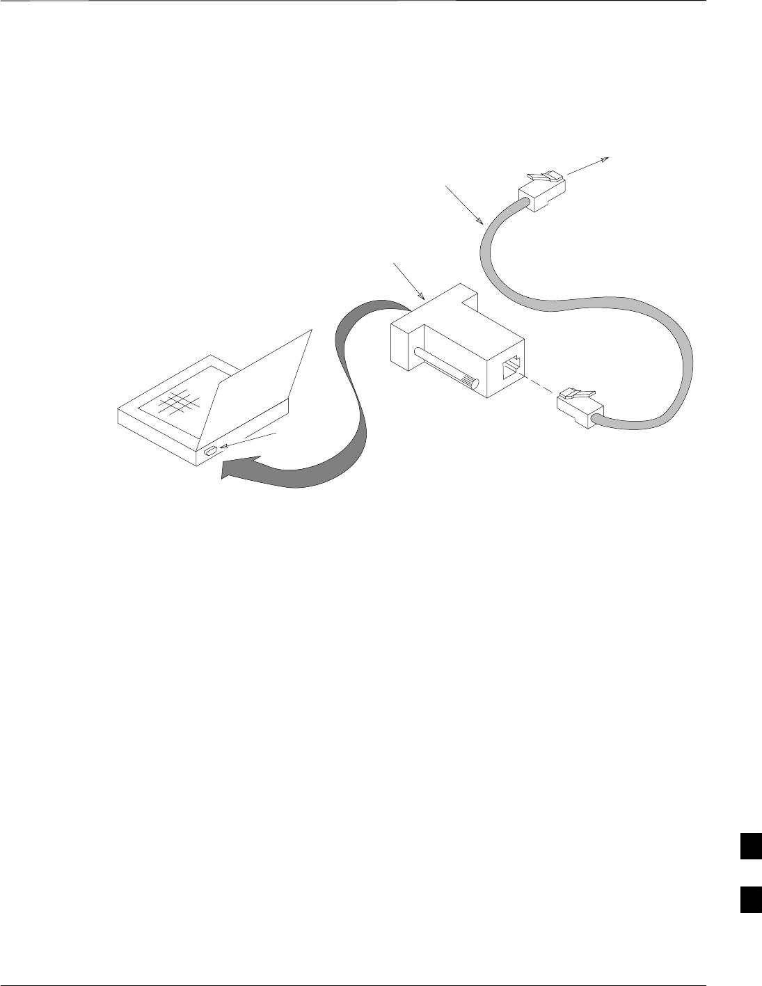
Establishing a BTS Router Communication Session – continued
5/21/04 1X SC4812T–MC BTS Optimization/ATP I-7
DRAFT
To BTS router
CONSOLE
receptacle
COM1
OR
COM2
LMF COMPUTER
OR EQUIVALENT
Figure I-3: LMF Computer Connections to BTS Router
OPTOATP0001–0
ROLLOVER
CABLE
DB9–TO–RJ48C
ADAPTER
I

Download Canned Configuration Files from the OMC–R
I-8 1X SC4812T–MC BTS Optimization/ATP 5/21/04
DRAFT
Obtaining BTS Router
Minimum (Canned)
Configuration Files
After they are generated on the OMC–R, the BTS router canned
configuration files must be transfered to another computer platform from
which they can be installed into the BTS routers. A number of
procedures may be used to move the canned configuration files from the
OMC–R to a platform from which they can be loaded into the routers.
Some alternatives are:
1. If a floppy diskette drive is available at the OMC–R, such as the one
for UNO workstations, the configuration files can be transferred to
an LMF computer or similar machine using the CDF file transfer
procedure in the Preparing the LMF section of 1X SC4812T BTS
Optimization/ATP; 68P09260A62. Directories identified in Table I-3
must be used rather than those in the CDF file transfer procedure.
2. If a Windows–based server connection is available in the operator’s
network and it can provide an FTP or telnet connection to the
OMC–R, files may be transferred by either the FTP or telnet
methods.
3. If a dial–up connection is available for accessing the OMC–R, an
FTP or telnet session may be possible to transfer files to the
computer used to load the CF memory cards.
The procedure provided in this section covers FTP transfer using a
Windows–based server in the operator’s network. Coordinate with the
local network administrator to determine the method and procedure to
use on a specific network.
Prerequisites
The following must be obtained from the local network administrator
before performing the canned configuration file FTP procedure in
Table I-3:
SUser ID and password to log onto the OMC–R
SName of the sub–directory where the specific BTS router group
canned configuration files to be downloaded were created
FTP File Transfer from the
OMC–R
This procedure uses the Windows–based LMF computer platform to
download BTS router canned configuration files from the OMC–R.
Follow the procedure in Table I-3.
I

Download Canned Configuration Files from the OMC–R – continued
5/21/04 1X SC4812T–MC BTS Optimization/ATP I-9
DRAFT
Table I-3: BTS Router Canned Configuration File FTP Transfer from the OMC–R
Step Action
1If it has not been done, create a directory on the LMF computer where the BTS router canned
configuration files will be stored.
2If it has not been done, obtain the OMC–R logon user ID and password from the local network
administrator.
3Connect the LMF computer to the local network and log on.
4NOTE
This procedure uses the command line FTP client supplied with Windows 98, Second Edition (Win98
SE) and Windows 2000 (Win2K); however, any commercially available FTP client application can be
used. Follow the manufacturer’s instructions for operation of an alternative application.
Open a command line (MS DOS) window by clicking on Start > Programs > Command Prompt.
5When the command line window opens, change to the directory where the canned configuration files
will be stored on the LMF computer by entering:
cd pathname
Where pathname = the path to the required directory
A response similar to the following will be displayed:
C:\> cd Can_Cfg
C:\Can_Cfg>
6Check the contents of the directory by entering the following:
dir
A response similar to the following will be displayed:
C:\Can_Cfg>dir
Volume in drive C is MAIN
Volume Serial Number is F2AA–1721
Directory of C:\Can_Cfg>
08/22/2002 03:46p <DIR> .
08/22/2002 03:46p <DIR> ..
08/22/2002 03:46p 2,223 btsrtr_canned.blue
08/22/2002 03:47p 2,223 btsrtr_canned.red
2 File(s) 4,644 bytes
2 Dir(s) 2,556,045,312 bytes free
C:\Can_Cfg>
. . . continued on next page
I

Download Canned Configuration Files from the OMC–R – continued
I-10 1X SC4812T–MC BTS Optimization/ATP 5/21/04
DRAFT
Table I-3: BTS Router Canned Configuration File FTP Transfer from the OMC–R
Step Action
7If either or both of the following files are found in the directory, delete them or move them to another
directory:
Sbtsrtr_config.blue
Sbtsrtr_config.red
8Begin the FTP session by entering the following:
ftp hostname
Where hostname = the OMC–R hostname or IP address
A response similar to the following will be displayed:
C:\Can_Cfg> ftp OMCR–1
C:\Can_Cfg>
Connected to OMCR–1.
220 OMCR–1 FTP server (SunOS 5.6) ready.
User (OMCR–1:(none)):
9Enter the User ID and password when prompted, pressing the Enter key after each.
A response similar to the following will be displayed:
User (OMCR–1:(none)): scadm
331 Password required for scadm.
Password:
230 User scadm logged in.
ftp>
10 Change to the directory where the BTS router canned configuration file sub–directories are created and
verify the present working directory by entering the following, pressing the Enter key after each:
cd /home/scadm/btsrtr_canned_configs
pwd
A response similar to the following will be displayed:
ftp> cd /home/scadm/btsrtr_canned_configs
240 CWD command successful.
ftp> pwd
245 ”/home/scadm/btsrtr_canned_configs” is current directory.
. . . continued on next page
I

Download Canned Configuration Files from the OMC–R – continued
5/21/04 1X SC4812T–MC BTS Optimization/ATP I-11
DRAFT
Table I-3: BTS Router Canned Configuration File FTP Transfer from the OMC–R
Step Action
11 Enter the following to list the contents of the directory and be sure the specific canned configuration
directory name provided by the administrator exists:
ls
A response similar to the following will be displayed:
ftp> ls
200 PORT command successful.
150 ASCII data connection for /bin/ls (10.182.29.117,80) (0 bytes).
Mon_Jul_2_01:55:07_CDT_2002
Wed_Jul_24_09:35:41_CDT_2002
Tue_Aug_04_10:35:22_CDT_2002
226 ASCII Transfer complete.
ftp: 30 bytes received in 0.02Seconds 1.50Kbytes/sec.
ftp>
NOTE
Directory names where canned configuration files are located will consist of the
weekday_month_day_time_year when the canned configuration files were created on the OMC–R.
12 Change to the directory specified for the BTS router group to be configured and list the directory
contents by entering the following, pressing the Enter key after each command:
cd weekday_month_day_time_year
ls
A response similar to the following will be displayed:
ftp> cd Wed_Jul_24_09:35:41_CDT_2002
250 CWD command successful.
ftp> ls
200 PORT command successful.
150 ASCII data connection for /bin/ls (10.182.29.117,80) (0 bytes).
btsrtr_canned.blue
btsrtr_canned.red
226 ASCII Transfer complete.
ftp: 39 bytes received in 0.05Seconds 0.78Kbytes/sec.
ftp>
. . . continued on next page
I

Download Canned Configuration Files from the OMC–R – continued
I-12 1X SC4812T–MC BTS Optimization/ATP 5/21/04
DRAFT
Table I-3: BTS Router Canned Configuration File FTP Transfer from the OMC–R
Step Action
13 Change to the binary transfer mode and, if desired, turn on hash mark printing for transfer progress by
entering the following, pressing the Enter key after each command:
bin
hash
A response similar to the following will be displayed:
ftp> bin
200 Type set to I.
ftp> hash
Hash mark printing On ftp: (2048 bytes/hash mark) .
ftp>
NOTE
With Win98 SE, turning on hash mark printing can slow down file transfer in certain circumstances,
but the canned configuration files are quite small (approximately 2.5 KB) so there should be little
noticeable effect.
14 Download the BTS router canned configuration files to the LMF computer by performing the follow-
ing:
14a – Enter the following to download the first canned configuration file:
get btsrtr_canned.blue
A response similar to the following will be displayed:
ftp> get btsrtr_canned.blue
200 PORT command successful.
150 Binary data connection for btsrtr_canned.blue (10.182.29.117,80)
(2223 bytes).
#
226 Binary Transfer complete.
ftp: 2223 bytes received in 0.59Seconds 3.76Kbytes/sec.
ftp>
. . . continued on next page
I

Download Canned Configuration Files from the OMC–R – continued
5/21/04 1X SC4812T–MC BTS Optimization/ATP I-13
DRAFT
Table I-3: BTS Router Canned Configuration File FTP Transfer from the OMC–R
Step Action
14b – Enter the following to download the second BTS router canned configuration file:
get btsrtr_canned.red
A response similar to the following will be displayed:
ftp> get btsrtr_canned.red
200 PORT command successful.
150 Binary data connection for btsrtr_canned.red (10.182.29.117,80) (2223
bytes).
#
226 Binary Transfer complete.
ftp: 2223 bytes received in 0.59Seconds 3.76Kbytes/sec.
ftp>
15 Before terminating the FTP session, open Windows Explorer and view the contents of the directory
where the canned configuration files are to be stored to be sure the files are present. Perform the
following:
15a – Click Start > Programs > Windows Explorer.
15b – In the left–hand pane of Windows Explorer, perform one of the following depending on the LMF
computer operating system:
–– Win98 SE: If necessary, expand the directory display for the drive where the canned configu-
ration file storage directory is located by clicking on the + next to the drive icon.
–– Win2K: Expand the user profile and directory display for the drive where the canned configu-
ration file storage directory is located by clicking on the + next to each icon, respectively.
15c – Expand any sub–directories as required to display the directory folder where the canned
configuration files are to be stored.
15d – Click on the directory folder icon where the canned configuration files are to be stored.
15e – In the right–hand pane, verify that the files btsrtr_canned.blue and btsrtr_canned.red
appear.
15f – If the files appear, proceed to step 16.
15g – If the files do not appear, repeat step 14, its sub–steps, step 15 and its sub–steps.
16 Close Windows Explorer, and, in the command line window, enter the following to terminate the FTP
session:
bye
A response similar to the following will be displayed:
ftp> bye
221 Goodbye.
C:\Can_Cfg>
. . . continued on next page
I

Download Canned Configuration Files from the OMC–R – continued
I-14 1X SC4812T–MC BTS Optimization/ATP 5/21/04
DRAFT
Table I-3: BTS Router Canned Configuration File FTP Transfer from the OMC–R
Step Action
17 Close the command line window by entering the following:
exit
18 BTS router canned configuration files are now ready for transfer to a BTS router.
I

Verify IOS Version and Install Canned Configuration
5/21/04 1X SC4812T–MC BTS Optimization/ATP I-15
DRAFT
Introduction
Overview
This section covers the procedures and commands required to verify the
IOS version loaded on BTS router CF memory cards and copy standard
canned configuration files to the routers. Because of the set–up required
and the length of some of the procedures, Motorola recommends
performing the actions covered in this section at a central location to
prepare the BTS routers for installation prior to the site visit.
IOS Version Verification and File Sequence Position
Version verification – The IOS version loaded on the BTS router CF
memory card should be verified as the version required for operation on
the network where the routers will be installed. If the loaded IOS version
is not correct, it can be replaced with a different version. There are
several methods available to accomplish version verification. These
depend on the equipment and software applications the user selects to
use in installing the canned configuration files in the BTS routers.
Appropriate verification procedures are included in each of the two
canned configuration installation methods covered in this section.
Methods to change or upgrade the loaded IOS version are provided in
the Change or Upgrade BTS Router IOS Version section of this appendix
and are referenced at the appropriate places in the canned configuration
installation methods.
File sequence position – During initialization, the MWR 1900 or MWR
1941 router will first search the startup–config file for a boot system
command line telling it in what directory and file to find the boot loader.
If this line is not found, the router will default to attempting to boot from
the first file in its flash memory. Flash memory for the MWR 1900 or
MWR 1941 is the CF memory card (software identifier slot0:). The
canned configuration files used for BTS router installation do not
contain a boot system command line because of the need to maintain
flexibility for IOS version changes. Because of this, it is critical that the
IOS file is the first file listed on the CF memory card. The canned
configuration installation procedures contain steps to assure that this is
the case, and, if it is not, provide guidance to correct the condition. It is
important to remember that, if the router boots and displays a rommon 1
> prompt, the IOS file is missing, out of sequence, has a corrupted flash
memory image or the startup–config file contains a boot system line
which specifies a missing or incorrect IOS pathname/filename.
Canned Configuration File Installation
Filename and installation location requirements – The canned
configuration files for the BTS routers must be copied to the CF memory
card. The filename of the file on the CF memory card must be
canned–config. Canned configuration file location and filename
I
Verify IOS Version and Install Canned Configuration – continued
I-16 1X SC4812T–MC BTS Optimization/ATP 5/21/04
DRAFT
requirements are a result of Mobile Wireless Center (MWC) actions
during the process of switching a BTS from packet to circuit mode or
during BTS re–parenting to another OMC–R. In this process, the MWC
will query the BTS routers’ slot0: directory for a file named
canned–config. A missing or mis–named file will cause problems
with execution of the mode–switching process.
Installation Method – The startup–config configuration file used
by the BTS router during initialization is stored in NVRAM. This is a
memory device internal to the router and is separate from the CF
memory card. To install the canned configuration file so the router will
use it during boot–up, the file must be copied into the
startup–config file in NVRAM. This requires copying the canned
configuration file from the Windows–based LMF computer to the CF
memory card installed in a router, and then copying it to the
startup–config file in the router’s NVRAM. The only
Motorola–supported method to copy files to the BTS router CF memory
card is through tftp file transfer.
Motorola does not support using a CF memory card reader
to copy files to the BTS router CF memory card. Do not
use a CF memory card reader for either of the following
actions:
SFormatting a BTS router CF memory card
SCopying files to a BTS router CF memory card
CAUTION
Do not format BTS router CF memory cards using a CF
memory card reader. Only format CF memory cards in a
BTS router. Using a card reader to format the CF memory
card will result in improper BTS router initialization which
requires special recovery procedures.
CAUTION
Using a TFTP Server to Copy
Files to CF Memory Card
Required Equipment and Software
The following items are required to perform this procedure:
SA Windows–based computer which meets the requirements of the
LMF computer platform as specified in 1X SC4812T BTS
Optimization/ATP; 68P09260A62 original design frame, or 1X
SC4812T–CLPA BTS Optimization/ATP; 68P64115A06 for updated
design frames.
SOne of the following operating systems for the Windows–based
computer:
I

Verify IOS Version and Install Canned Configuration – continued
5/21/04 1X SC4812T–MC BTS Optimization/ATP I-17
DRAFT
–Windows 2000
–Windows 98 Second Edition (SE) using the FAT32 file system
BTS router CF memory cards loaded using computers
equipped with Windows 98 versions earlier than Windows
98 SE and using the FAT16 file system will not operate
properly, resulting in a complete site outage.
CAUTION
SOne of the following for the Windows–based computer:
– Internal 10/100baseT Network Interface Card (NIC)
– PCMCIA 10/100baseT NIC
SCable, rollover, as described in the Establishing a BTS Router
Communication Session section of this Appendix
SDB–9 plug–to–8–contact modular plug adapter as described in the
Establishing a BTS Router Communication Session section of this
Appendix
SCable, Ethernet crossover, Category 5E or better, unshielded twisted
pair, two 8–contact modular plugs, in one of the following lengths, as
determined necessary:
– 0.3 m (11.8 in) (Motorola pn 3088643C07)
– 0.6 m (23.6 in)(Motorola pn 3088643C13)
– 1.0 m (39.4 in) (Motorola pn 3088643C15)
– 2.1 m (84 in) (Motorola pn 3088643C08)
– 3.0 m (120 in) (Motorola pn 3088643C09)
SA +27 Vdc power supply to power the BTS router during
configuration file operations
SA tftp server software application (refer to the Setting Up the TFTP
Server – Procedure in Cellular System Administration – CDMA
OnLine Documentation, 68P09259A20) such as:
– Cisco tftp server
– PumpKIN tftp server
– Any other equivalent tftp server application
SA copy of the MWR 1900 or MWR 1941 router IOS version required
for the network where the routers are to be installed (contact the
network administrator or the Motorola account team for information
on obtaining the required MWR 1900 or MWR 1941 IOS version)
Required Materials
The following material is required to perform this method:
SMarking material to identify the BTS router and CF memory card with
the installed configuration (blue or red)
Required Publications
The following publications are required to perform procedures in this
section:
I
Verify IOS Version and Install Canned Configuration – continued
I-18 1X SC4812T–MC BTS Optimization/ATP 5/21/04
DRAFT
S1X SC4812T BTS Optimization/ATP; 68P09260A62 original frame
design or 1X SC4812T–CLPA BTS Optimization/ATP; 68P64115A06
for updated design frames
SCellular System Administration – CDMA OnLine Documentation,
68P09259A20
SMWR1900 Wireless Mobile Edge Router Software Configuration
Guide; part number 78–13983–01
Preparation for Canned Configuration File TFTP Transfer to CF
Memory Card
Preparation for a canned configuration file tftp transfer consists of the
following activities:
1. Determining the speed of the LMF computer NIC (10 or 100 MHz)
2. Setting the LMF computer NIC IP address
3. Creating a directory (folder) on the LMF computer to be used for all
tftp file transfers
4. Installing the tftp server application on the LMF computer, and
setting the tftp server application root directory to the directory
created in 2, above
5. Connecting the LMF computer to the BTS router for both
HyperTerminal (serial) and Ethernet communication
6. BTS router power–up and initial configuration for Ethernet
communication
The following procedures are used to accomplish all of these preparatory
actions.
Set LMF computer NIC TCP/IP address and create the default
TFTP directory – Follow the procedure in Table I-4 to set the NIC IP
address.
If the IP address for the LAN connection on an LMF
computer is being changed to support tftp downloads to a
BTS router, the BTS 10base–2 LAN IP address and subnet
mask for the NIC must be restored before the LMF can log
into a BTS to perform an optimization or ATP.
IMPORTANT
*
There are differences between Windows 2000 and Windows
98 in the menus and screens used for setting or changing a
NIC connection. In the following procedure, items
applicable to:
SWindows 2000 will be identified with Win2000
SWindows 98 will be identified with Win98
NOTE
I

Verify IOS Version and Install Canned Configuration – continued
5/21/04 1X SC4812T–MC BTS Optimization/ATP I-19
DRAFT
Table I-4: Determine LMF Computer NIC Speed, Set NIC IP Address, and Create a Default TFTP Directory
Step Action
1If it is not known, determine and record the speed of the LMF computer NIC (10 or 100 MHz) for use in
step 7 of Table I-6.
2Start the computer.
3Login and allow the computer to boot to the desktop.
4Depending on the installed operating system, from the Windows Start menu, select one of the
following:
SWin2000: Settings > Network and Dial–up Connections
SWin98: Settings > Control Panel and double–click Network.
5Perform one of the following as applicable for the installed operating system:
SFor Win2000, in the list of displayed connections, locate the Local Area Network connection for the
NIC to be used for BTS router Ethernet communication.
SFor Win98, in the Configuration tab of the Network dialog box, locate the TCP/IP connection for
the installed NIC.
– If TCP/IP does not appear in the displayed list of installed network components, refer to the
operating system documentation and install TCP/IP.
6Perform one of the following as applicable for the installed operating system:
SFor Win2000, highlight the connection for the NIC and right click the highlighted connection, and
select Properties from the pop–up menu.
SFor Win98:
– Highlight the TCP/IP NIC connection in the displayed list of installed network components.
– Click the Properties button.
– Skip to step 9.
7 For Win2000 , in the Local Area Connection Properties dialog box which appears, if Internet
Protocol (TCP/IP) is not showing in the Components checked are used by this connection: listbox,
refer to the operating system documentation and install TCP/IP.
8 For Win2000, if the checkbox next to the Internet Protocol (TCP/IP) entry is not checked, click in the
box to check it.
9Perform one of the following:
SWin2000: Highlight the Internet Protocol (TCP/IP) entry, and click on the Properties button below
the Components checked are used by this connection: listbox.
SWin98: From the tabs displayed in the TCP/IP Properties dialog box which opens, select the IP
Address tab if it is not at the front.
10 In the Internet Protocol (TCP/IP) Properties dialog box which appears (Win2000) or the IP Address
tab of the TCP/IP Properties dialog box (Win98), perform the following:
10a – If a black dot is not showing in the the radio button circle next to Use the following IP address:
(Win2000) or Specify an IP address (Win98), click on the radio button.
–– A black dot will appear in the circle.
. . . continued on next page
I

Verify IOS Version and Install Canned Configuration – continued
I-20 1X SC4812T–MC BTS Optimization/ATP 5/21/04
DRAFT
Table I-4: Determine LMF Computer NIC Speed, Set NIC IP Address, and Create a Default TFTP Directory
Step Action
10b – If using an LMF computer, record the IP address and subnet mask used for LMF–BTS
communication so they can be re–entered when tftp transfer activities for the BTS router are
completed.
10c – Enter 100.100.100.1 in the IP address: box.
10d – Enter 255.255.255.252 in the Subnet mask: box.
11 Click the OK button for the Internet Protocol (TCP/IP) Properties dialog box (Win2000) or the
TCP/IP Properties box (Win98).
12 Click the OK button for the Local Area Connection Properties box (Win2000) or the Network box
(Win98).
13 In Win98, click File > Close to close the Control Panel window.
14 Click Start > Programs > Windows Explorer to open Windows Explorer.
15 If the default tftp directory will be the same directory in which the files downloaded from the OMC–R
are stored, proceed to step 23.
16 In the left–hand pane of Windows Explorer, locate the icon for the drive where the default tftp
directory is to be created.
17 Highlight the drive icon and click Files > New > Folder.
18 While observing the new folder icon in the right–hand pane, type the name for the folder (for example,
tftp_files), and press the Enter key.
19 In Windows Explorer, locate the directory where the canned configuration files downloaded from the
OMC–R are stored.
20 In the left–hand pane, highlight the directory where the files are stored.
21 Scroll the left–hand pane until the newly–created default tftp directory is visible.
22 In the right–hand pane, highlight the canned configuration files and drag them to the default tftp
directory.
23 In the left–hand pane, click on the default tftp directory, and verify that the canned configuration files
appear in the right–hand pane.
24 Load a copy of the required BTS router IOS version into the default tftp directory using FTP, internet
download, or media such as a Zip disk (file size is over 7 MB).
25 Click Files > Close to close Windows Explorer.
Install and configure tftp server application – To obtain, install, and
configure the Cisco or PumpKIN tftp software applications, refer to the
Setting Up the TFTP Server – Procedure in Cellular System
Administration – CDMA OnLine Documentation, 68P09259A20 For
other tftp server applications, install and configure the application
according to the manufacturer’s instructions.
I
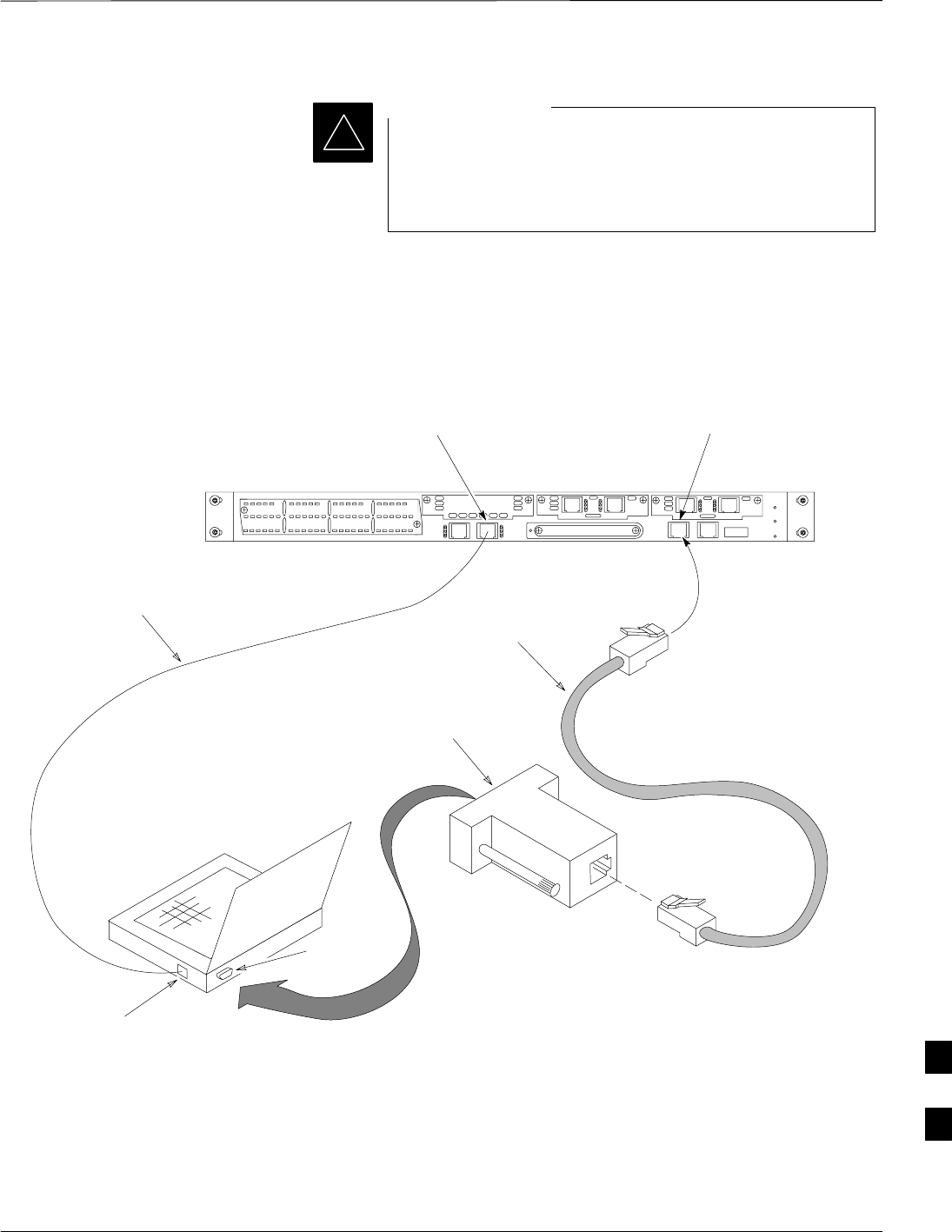
Verify IOS Version and Install Canned Configuration – continued
5/21/04 1X SC4812T–MC BTS Optimization/ATP I-21
DRAFT
When entering the name of the tftp server root directory
while configuring the tftp server application, be sure to use
the name of the directory identified in Table I-4, step 15, or
created in Table I-4, step 18, above.
IMPORTANT
*
Connect the LMF computer to the BTS router – Connect the LMF
computer to the BTS router by following the procedure in Table I-5 and
referring to Figure I-4.
To BTS router
CONSOLE
receptacle
COM1
OR
COM2
LMF COMPUTER
OR EQUIVALENT
Figure I-4: LMF Computer TFTP Connections to BTS Router
ROLLOVER
CABLE
DB9–TO–RJ48C
ADAPTER
BTSRTR0025
ETHERNET
CROSSOVER
CABLE
10/100BASE T
NIC PORT
FAST ETHERNET PORT FE 0
(SOFTWARE DESIGNATION FA0/0)
CONSOLE
PORT
I

Verify IOS Version and Install Canned Configuration – continued
I-22 1X SC4812T–MC BTS Optimization/ATP 5/21/04
DRAFT
Table I-5: Connecting the LMF Computer to the BTS Router for TFTP File Transfer
Step Action
1If the BTS router has not been connected to a power source, be sure the +27 Vdc power source is not
on, and connect it to the router.
2Connect the LMF computer to the BTS router as shown in Figure I-4, referring to the list of required
equipment in this section as required.
3If the LMF computer has not been started, turn it on, login, and allow it to boot to the desktop.
4Refer to the procedure in Table I-2 of this appendix, and start a HyperTerminal communication session
for the BTS router.
5Start the tftp server application as specified for the software (refer to the Setting Up the TFTP Server –
Procedure in Cellular System Administration – CDMA OnLine Documentation, 68P09259A20 or the
manufacturer’s instructions).
BTS router power–up and initial configuration for Ethernet
communication – Follow the procedure in Table I-6 to apply power to
the router and set an initial configuration for Ethernet communication.
SThe required version of the IOS is loaded on the CF memory card
SThe CF memory card is installed in the BTS router
Table I-6: BTS Router Power–up and Initial Ethernet Configuration
Step Action
* IMPORTANT
This procedure does not cover all aspects of BTS router operation and programming. Before performing this
procedure, review BTS router initialization, operation, and programming information and procedures in
MWR1900 Wireless Mobile Edge Router Software Configuration Guide; part number 78–13983–01. Have this
publication available for reference while performing this procedure.
1Be sure a CF memory card loaded with the Cisco IOS is installed in the BTS router (refer to the BTS Router
CF Memory Card Removal and Replacement section of this Appendix for instructions to access the CF
memory card slot).
2* IMPORTANT
In this step do not touch the computer keyboard until the router completes the boot process. The router
will buffer any keystrokes made during the boot process and interpret them as commands to be
executed immediately following boot completion.
Apply power to the router and allow it to complete boot–up.
3If a message similar to the following, is displayed, press the Enter key and proceed to step 5:
Press RETURN to get started!
. . . continued on next page
I

Verify IOS Version and Install Canned Configuration – continued
5/21/04 1X SC4812T–MC BTS Optimization/ATP I-23
DRAFT
Table I-6: BTS Router Power–up and Initial Ethernet Configuration
Step Action
4If a message similar to the following, is displayed type no and press the Enter key:
Basic management setup configures only enough connectivity
for management of the system, extended setup will ask you
to configure each interface on the system
Would you like to enter basic management setup? [yes/no]:
A response similar to the following will be displayed:
Would you like to enter basic management setup? [yes/no]: no
Cisco Internetwork Operating System Software
IOS (tm) 1900 Software (MWR1900–I–M), Version 12.2(20020127:101239
Copyright (c) 1986–2002 by cisco Systems, Inc.
Compiled Sun 27–Jan–02 06:08 by walrobin
Router>
5At the Router> user EXEC mode prompt, enter the following to access the privileged EXEC mode:
enable
A response similar to the following will be displayed:
Router>enable
Router#
6At the Router# privileged EXEC mode prompt, enter the following to access the configure submode:
configure terminal
A response similar to the following will be displayed:
Router#conf t
Enter configuration commands, one per line. End with CNTL/Z.
Router(config)#
The router is now in the global configuration mode and ready to accept configuration changes entered
from the keyboard.
. . . continued on next page
I

Verify IOS Version and Install Canned Configuration – continued
I-24 1X SC4812T–MC BTS Optimization/ATP 5/21/04
DRAFT
Table I-6: BTS Router Power–up and Initial Ethernet Configuration
Step Action
7At the global configuration mode prompt, type each of the following commands, pressing the Enter
key after each command:
hostname btsrtr1
interface fa0/0
ip address 100.100.100.2 255.255.255.252
speed 100 or 10 depending on the speed of the LMF computer NIC
duplex full
no shutdown
line con 0
exec–timeout 0 0
no login
line vty 0 4
no login
Responses similar to the following will be displayed:
Router(config)#hostname BTSRTR1
BTSRTR1(config)#interface fa0/0
BTSRTR1(config–if)#ip address 100.100.100.2 255.255.255.252
BTSRTR1(config–if)#speed 100
BTSRTR1(config–if)#duplex full
BTSRTR1(config–if)#no shutdown
BTSRTR1(config–if)#line con 0
BTSRTR1(config–line)#exec–timeout 0 0
BTSRTR1(config–line)#no login
BTSRTR1(config–line)#line vty 0 4
BTSRTR1(config–line)#no login
BTSRTR1(config–line)#
8Once the correct parameters have been set, return to the privileged EXEC mode prompt by holding
down the Ctrl key and pressing z (Ctrl+z).
A response similar to the following will be displayed:
BTSRTR1(config–line)# ^z
01:11:27: %SYS–5–CONFIG_I: Configured from console by console
BTSRTR1#
NOTE
Entering exit twice, pressing the Enter key after each entry, will also complete the configuration
process and return the router to the privileged EXEC mode.
. . . continued on next page
I
Verify IOS Version and Install Canned Configuration – continued
5/21/04 1X SC4812T–MC BTS Optimization/ATP I-25
DRAFT
Table I-6: BTS Router Power–up and Initial Ethernet Configuration
Step Action
9Verify port FE 0 (fa0/0) is configured with the correct IP address by entering the following:
show ip interface brief
A response similar to the following will be displayed:
BTSRTR1#sh ip int br
Interface IP Address OK? Method Status Protocol
FastEthernet0/0 100.100.100.2 YES manual up up
Serial0:0 unassigned YES unset administratively down down
FastEthernet0/1 unassigned YES unset administratively down down
Serial1:0 unassigned YES unset administratively down down
BTSRTR1#
10 The router is now configured for Ethernet communication on FE 0, and the canned configuration file
can be transferred by tftp. Proceed to Table I-7.
Verifying IOS Version and Canned Configuration File TFTP
Transfer to the BTS Router
Prerequisites – The following is required prior to performing this
procedure:
SA copy of the required MWR 1900 or MWR 1941 router IOS version
file is installed in the default tftp directory (transfer the file to the
LMF computer using FTP, internet download, or media such as a Zip
disk; file size is approximately 7–8 MB)
MWR 1941 routers must be loaded with IOS version
mwr1900–i–mz.122–8.MC2d.bin or later. This router
model will not function properly with earlier IOS versions.
IMPORTANT
*
IOS verification and canned configuration file transfer – Follow the
procedure in Table I-7 to verify the loaded IOS version and transfer the
canned configuration files from the LMF computer to the BTS router CF
memory card.
I

Verify IOS Version and Install Canned Configuration – continued
I-26 1X SC4812T–MC BTS Optimization/ATP 5/21/04
DRAFT
This procedure does not cover all aspects of BTS router
operation and programming. Before performing this
procedure, review BTS router initialization, operation, and
programming information and procedures in MWR1900
Wireless Mobile Edge Router Software Configuration
Guide; part number 78–13983–01. Have this publication
available for reference while performing this procedure.
IMPORTANT
*
Table I-7: Transfer Canned Configuration Files to the BTS Router Using a TFTP Server
Step Action
! CAUTION
If personal firewall and/or intrusion detection software such as Black ICE is running on the LMF computer,
shut it down before performing this procedure. If this is not done, the tftp transfer process will not operate.
1On the LMF computer, if it has not been done, start the tftp server according to the manufacturer’s
directions (refer to the Setting Up the TFTP Server – Procedure in the Cellular System Administration
– CDMA OnLine Documentation, 68P09259A20).
2If a HyperTerminal communication session with the BTS router is not running, start one following the
procedure in Table I-2.
3In the HyperTerminal window, the router must be in the privileged EXEC mode, as indicated by a
number sign at the end of the prompt:
BTSRTR1#
4Be sure the Ethernet crossover cable is connected between the LMF computer NIC port and the BTS
router FE 0 port (Figure I-4).
. . . continued on next page
I

Verify IOS Version and Install Canned Configuration – continued
5/21/04 1X SC4812T–MC BTS Optimization/ATP I-27
DRAFT
Table I-7: Transfer Canned Configuration Files to the BTS Router Using a TFTP Server
Step Action
5Begin verification that the CF memory card contains the correct version of the Cisco IOS by entering
the following:
dir slot0:
A response similar to the following will be displayed:
BTSRTR1#dir slot0:
Directory of slot0:/
1 –rw– 7051976 Mar 01 1993 00:11:34 mwr1900–i–mz.122–8.MC2a.bin
31932416 bytes total (24879104 bytes free)
BTSRTR1#
NOTE
1. The IOS defaults to the CF memory card (slot0:) directory unless the present working directory has
been changed using the cd command. Determine the present working directory by entering pwd.
If the present working directory has been changed, enter the command cd slot0: to return to the
default setting.
2. If slot0: is included in the command, be sure to include the colon (:) after slot0 when typing the
command.
3. The IOS filename will be similar to the following:
mwr1900–i–mz.122–8.MC2a.bin
. . . continued on next page
I

Verify IOS Version and Install Canned Configuration – continued
I-28 1X SC4812T–MC BTS Optimization/ATP 5/21/04
DRAFT
Table I-7: Transfer Canned Configuration Files to the BTS Router Using a TFTP Server
Step Action
6Direct the router to show the version information by entering the following:
show version
A response similar to the following will be displayed:
BTSRTR1#sh ver
Cisco Internetwork Operating System Software
IOS (tm) 1900 Software (MWR1900–I–M), Version 12.2(8)MC2a, EARLY DEPLOY-
MENT RELEASE SOFTWARE (fc1)
TAC Support: http://www.cisco.com/tac
Copyright (c) 1986–2002 by cisco Systems, Inc.
Compiled Mon 05–Aug–02 11:07 by nmasa
Image text–base: 0x60008940, data–base: 0x60B54000
ROM: System Bootstrap, Version 12.2(20020113:235343) [sbose–wilma 109],
DEVELOPMENT SOFTWARE
ROM: 1900 Software (MWR1900–I–M), Version 12.2(8)MC2a, EARLY DEPLOYMENT
RELEASE SOFTWARE (fc1)
Router uptime is 1 minute
System returned to ROM by power–on
System image file is ”slot0:mwr1900–i–mz.122–8.MC2a.bin”
cisco mwr1900 (R7000) processor (revision 0.1) with 121856K/18432K bytes
of memory.
Processor board ID JMX0611K5TS
R7000 CPU at 240Mhz, Implementation 39, Rev 3.3, 256KB L2 Cache
Bridging software.
X.25 software, Version 3.0.0.
Primary Rate ISDN software, Version 1.1.
Toaster processor tmc is running.
2 FastEthernet/IEEE 802.3 interface(s)
2 Serial network interface(s)
2 Channelized T1/PRI port(s)
DRAM configuration is 64 bits wide with parity disabled.
55K bytes of non–volatile configuration memory.
31360K bytes of ATA Slot0 CompactFlash (Read/Write)
Configuration register is 0x101
BTSRTR1#
7Compare the IOS filename returned in step 5 and the second line of the version information in step 6.
Note the correspondence between the filename and IOS version information.
* IMPORTANT
MWR 1941 routers must be loaded with IOS version mwr1900–i–mz.122–8.MC2d.bin or later. This
router model will not function properly with earlier IOS versions.
. . . continued on next page
I

Verify IOS Version and Install Canned Configuration – continued
5/21/04 1X SC4812T–MC BTS Optimization/ATP I-29
DRAFT
Table I-7: Transfer Canned Configuration Files to the BTS Router Using a TFTP Server
Step Action
8If the IOS filename from the CF memory card returned in step 5 is different than the filename of the
required IOS version loaded in the LMF computer default tftp directory, perform the procedure in
Table I-8 to load the required version, and then return to step 9, below.
9! CAUTION
The file sequence on the CF memory card can not be verified with application programs which place
the listed file names in alphabetical order (for example, certain Unix telnet applications, Unix
directory listing commands, and Windows file managers such as Windows Explorer). This portion of
the procedure is intended for use only with applications, such as HyperTerminal, which do not list
directory contents alphabetically.
If the IOS version is correct and there is more than one file loaded on the CF memory card, be sure the
IOS file is the first file listed in the directory content display. If it is not, perform the following:
9a – Backup all files on the CF memory card to the LMF computer default tftp directory by performing
steps 3 through 10 of Table I-8.
9b – Perform steps 25 through 29 of Table I-8, as applicable.
9c – Type the following to delete a possible boot system line in the startup–config file, pressing the
Enter key after the command and at each prompt to confirm the filename and deletion operation:
del nvram:startup–config
A response similar to the following will be displayed:
BTSRTR1#del nvram:startup–config
Delete filename [startup–config]?
Delete nvram:startup–config? [confirm]
[OK]
BTSRTR1#
NOTE
Be sure to include the colon (:) after nvram when typing the command.
. . . continued on next page
I

Verify IOS Version and Install Canned Configuration – continued
I-30 1X SC4812T–MC BTS Optimization/ATP 5/21/04
DRAFT
Table I-7: Transfer Canned Configuration Files to the BTS Router Using a TFTP Server
Step Action
9d – Verify the startup–config file size has been reduced to a minimum by entering the following:
dir nvram:
A response similar to the following will be displayed:
Router#dir nvram:
Directory of nvram:/
53 –rw– 5 <no date> startup–config
54 –––– 5 <no date> private–config
57336 bytes total (57274 bytes free)
BTSRTR1#
10 At the privileged EXEC mode prompt, enter the following:
copy tftp:btsrtr_canned.color slot0:canned–config
Where color = blue or red, as applicable.
A response similar to the following will be displayed:
BTSRTR1#copy tftp:btsrtr_canned.blue slot0:canned–config
Address or name of remote host []?
11 At the prompt for the remote host address or name, enter the IP address of the LMF computer NIC:
100.100.100.1
A response similar to the following will be displayed:
BTSRTR1#copy tftp:btsrtr_canned.blue slot0:canned–config
Address or name of remote host []? 100.100.100.1
Destination filename [canned–config]?
12 At the prompt for the destination filename, press the Enter key.
A response similar to the following will be displayed:
BTSRTR1#copy tftp:btsrtr_canned.blue slot0:canned–config
Address or name of remote host []? 100.100.100.1
Destination filename [canned–config]?
Loading btsrtr_canned.blue from 100.100.100.1 (via Ethernet0/0): !
[OK – 2457/4096 bytes]
2457 bytes copied in 84.724 secs (29 bytes/sec)
BTSRTR1#
. . . continued on next page
I

Verify IOS Version and Install Canned Configuration – continued
5/21/04 1X SC4812T–MC BTS Optimization/ATP I-31
DRAFT
Table I-7: Transfer Canned Configuration Files to the BTS Router Using a TFTP Server
Step Action
13 Verify that the canned configuration file is saved on the CF memory card by entering the following:
dir
A response similar to the following will be displayed:
Directory of slot0:/
1 –rw– 7051976 Mar 01 1993 00:11:34 mwr1900–i–mz.122–8.MC2a.bin
2 –rw– 2457 Mar 01 1993 00:14:48 canned–config
31932416 bytes total (24877983 bytes free)
BTSRTR1#
14 To allow the BTS router to boot using the canned configuration, enter the following:
copy canned–config startup–config
A response similar to the following will be displayed:
BTSRTR1#copy canned–config start
Destination filename [startup–config]?
15 When prompted for the destination file name, press the Enter key.
A response similar to the following will be displayed:
BTSRTR1#copy canned–config start
Destination filename [startup–config]?
2457 bytes copied in 3.52 secs
BTSRTR1#
16 Display and note the file size of startup–config by entering the following:
dir nvram:
A response similar to the following will be displayed:
Directory of nvram:/
26 –rw– 2457 <no date> startup–config
27 –––– 5 <no date> private–config
29688 bytes total (24774 bytes free)
BTSRTR1#
. . . continued on next page
I

Verify IOS Version and Install Canned Configuration – continued
I-32 1X SC4812T–MC BTS Optimization/ATP 5/21/04
DRAFT
Table I-7: Transfer Canned Configuration Files to the BTS Router Using a TFTP Server
Step Action
17 Scroll the HyperTerminal window back to the slot0: directory display obtained in step 13, above.
18 Compare the file size of startup–config to the canned configuration file to verify the copy operation.
File sizes should be the same.
19 If desired, the contents of the startup–config file may be verified against the file listings at the end of
this appendix for the blue or red canned configuration, as applicable, by entering the following:
show startup–config
NOTE
Pressing the space bar at the MORE prompt will scroll another screen–full of data. Pressing the Enter
key will scroll the screen one line at a time.
20 Verify the router will boot properly on the IOS and revised startup–config files by entering the
following:
reload
A response similar to the following will be displayed:
BTSRTR1#reload
System configuration has been modified. Save? [yes/no]: n
Proceed with reload? [confirm]
21 If prompted to save a modified configuration, enter n for “no,” and press the Enter key.
22 When prompted to proceed with reload, press the Enter key to continue the reload operation.
23 NOTE
Reloading the router with the revised startup–config file will change router FE port speed to 100. If
the router FE port speed was changed to 10 to communicate with the LMF computer NIC, the
computer may indicate that the FE LAN connection has been lost at this point.
Verify the router reboots without displaying the rommon 1 > prompt or error messages related to port
configurations. If the router boots to the rommon prompt, proceed to the Recovery from BTS Router
Boot to rommon section of this appendix.
24 Using the tagging materials, tag the router to clearly identify the installed configuration (blue
(BTSRTR1) or red (BTSRTR2)).
25 Remove the CF memory from the router following the procedure in Table I-13, mark the installed
configuration (blue or red) on the card label, and install the card in the router following the procedure
in Table I-14.
26 If an additional router must have the canned configuration installed, perform the following:
. . . continued on next page
I

Verify IOS Version and Install Canned Configuration – continued
5/21/04 1X SC4812T–MC BTS Optimization/ATP I-33
DRAFT
Table I-7: Transfer Canned Configuration Files to the BTS Router Using a TFTP Server
Step Action
26a – Disconnect the cabling from the BTS router.
26b – Remove power from the router and disconnect it from the power supply.
26c – Repeat the procedures in Table I-5, Table I-6, and this table (Table I-7) using the additional router.
27 If no additional routers must be configured, perform steps 26a and 26b.
28 On the LMF computer, shut down the tftp server application and exit the HyperTerminal session.
29 If no additional tftp transfer activities will be performed, change the NIC IP address and subnet mask
back to those for LMF–BTS communication recorded in Table I-4, step 10b.
! CAUTION
If the BTS 10base–2 LAN IP address and subnet mask for the LMF computer’s NIC are not restored,
the LMF can not log into a BTS when attempting to perform a BTS optimization or ATP.
I
Change or Upgrade BTS Router IOS Version
I-34 1X SC4812T–MC BTS Optimization/ATP 5/21/04
DRAFT
Background
BTS routers are supplied with CF memory cards pre–loaded with a
version of the IOS. Prior to installing the routers in a BTS, the loaded
IOS version should be verified as being the one required for the network.
It is critical to also verify that the IOS file is the first file on the CF
memory card. If another file precedes the IOS file, the BTS router will
not boot properly and will not function in the network.
Equipment and Software
Required
The following items are required to perform this procedure:
SA Windows–based computer which meets the requirements of the
LMF computer platform as specified in 1X SC4812T BTS
Optimization/ATP; 68P09260A62 for original design frames or 1X
SC4812T–CLPA BTS Optimization/ATP; 68P64115A06 for updated
design frames.
SOne of the following operating systems for the Windows–based
computer:
–Windows 2000
–Windows 98 Second Edition (SE) using the FAT32 file system
BTS router CF memory cards loaded using computers
equipped with Windows 98 versions earlier than Windows
98 SE and using the FAT16 file system will not operate
properly, resulting in a complete site outage.
CAUTION
SCable, rollover, as described in the Establishing a BTS Router
Communication Session section of this Appendix
SDB–9 plug–to–8–contact modular plug adapter as described in the
Establishing a BTS Router Communication Session section of this
Appendix
SCable, Ethernet crossover, Category 5E or better, unshielded twisted
pair, two 8–contact modular plugs, in one of the following lengths, as
determined necessary:
– 0.3 m (11.8 in) (Motorola pn 3088643C07)
– 0.6 m (23.6 in)(Motorola pn 3088643C13)
– 1.0 m (39.4 in) (Motorola pn 3088643C15)
– 2.1 m (84 in) (Motorola pn 3088643C08)
– 3.0 m (120 in) (Motorola pn 3088643C09)
SA +27 Vdc power supply to power the BTS router during
configuration file operations
SA tftp server software application (refer to the Setting Up the TFTP
Server – Procedure in Cellular System Administration – CDMA
OnLine Documentation, 68P09259A20) such as:
I
Change or Upgrade BTS Router IOS Version – continued
5/21/04 1X SC4812T–MC BTS Optimization/ATP I-35
DRAFT
– Cisco tftp server
– PumpKIN tftp server
– Any other equivalent tftp server application
SA copy of the MWR 1900 or MWR 1941 router IOS version required
for the network where the routers are to be installed
Contact the network administrator or the Motorola Account
Team for assistance in determining and obtaining a copy of
the required IOS version.
NOTE
MWR 1941 routers must be loaded with IOS version
mwr1900–i–mz.122–8.MC2d.bin or later. This router
model will not function properly with earlier IOS versions.
IMPORTANT
*
Required Publications
The following publication is required to perform procedures in this
section:
SMWR1900 Wireless Mobile Edge Router Software Configuration
Guide; part number 78–13983–01
Upgrade/Replace Installed IOS
Version and Verify File
Sequence Position
Description – This procedure covers using an LMF computer equipped
with a tftp server application to perform the following activities:
1. Verify the IOS version loaded on a CF memory card and running on
a BTS router
2. Upgrade or replace the IOS version installed in a BTS router
3. Ensure the IOS file is the first file on the CF memory card
Prerequisites – The following are required prior to performing this
procedure:
SThe LMF computer and BTS router have been prepared for tftp file
transfer and are operating as they would be after performing the
procedures in Table I-4, Table I-5, Table I-6, and steps 1 through 8 of
Table I-7
SA copy of the required IOS version is loaded into the tftp default
directory of the LMF computer
Upgrading/replacing installed IOS version and verifying file
sequence position – Follow the procedure in Table I-8 to replace or
I

Change or Upgrade BTS Router IOS Version – continued
I-36 1X SC4812T–MC BTS Optimization/ATP 5/21/04
DRAFT
upgrade the installed IOS version using the tftp server application, and
ensure the IOS file is first in the stored file sequence on the CF memory
card.
Table I-8: Using a TFTP Server Application for Upgrading/Replacing Loaded IOS Version and
Verifying File Sequence Position
Step Action
* IMPORTANT
This procedure does not cover all aspects of BTS router operation and programming. Before performing this
procedure, review BTS router initialization, operation, and programming information and procedures in
MWR1900 Wireless Mobile Edge Router Software Configuration Guide; part number 78–13983–01. Have this
publication available for reference while performing this procedure.
1This procedure assumes the LMF computer and BTS router are configured, connected, and operating
as they would be after performing the procedures in Table I-4, Table I-5, Table I-6, and steps 1 through
8 of Table I-7. If necessary, perform these procedures now.
2NOTE
The IOS present working directory defaults to the CF memory card (slot0:) directory unless the
present working directory has been changed using the cd command. Determine the present working
directory by entering pwd. If the present working directory has been changed, enter the command cd
slot0: to return to the default setting.
Identify the filename of the currently loaded IOS which must be replaced by entering the following:
dir
A response similar to the following will be displayed:
BTSRTR1#dir
Directory of slot0:/
1 –rw– 7051844 Sep 23 2002 07:15:08 mwr1900–i–mz.07022002.bin
2 –rw– 2212 Mar 01 1993 00:11:00 canned–config
31932416 bytes total (24878360 bytes free)
BTSRTR1#
3Begin to backup the currently installed version of the router’s IOS to the LMF computer’s default tftp
directory by entering the following:
copy old_IOS_filename tftp:
Where old_IOS_filename = the filename of the IOS currently loaded on the BTS router CF
memory card.
A response similar to the following will be displayed:
BTSRTR1#copy mwr1900–i–mz.07022002.bin tftp:
Address or name of remote host []?
. . . continued on next page
I

Change or Upgrade BTS Router IOS Version – continued
5/21/04 1X SC4812T–MC BTS Optimization/ATP I-37
DRAFT
Table I-8: Using a TFTP Server Application for Upgrading/Replacing Loaded IOS Version and
Verifying File Sequence Position
Step Action
4At the remote host prompt, enter the following:
100.100.100.1
A response similar to the following will be displayed:
Address or name of remote host []? 100.100.100.1
Destination filename [mwr1900–i–mz.07022002.bin]?
5If the default filename displayed in the prompt is correct, press the Enter key to accept it. If it is
missing or not correct, enter the correct filename.
A response similar to the following will be displayed if the default filename is selected:
Address or name of remote host []? 100.100.100.1
Destination filename [mwr1900–i–mz.07022002.bin]?
!!!!!!!!!!!!!!!!!!!!!!!!!!!!!!!!!!!!!!!!!!!!!!!!!!!!!!!!!!!!!!!!!!!!!!!!!
!!!!!!!!!!!!!!!!!!!!!!!!!!!!!!!!!!!!!!!!!!!!!!!!!!!!!!!!!!!!!!!!!!!!!!!!!
!!!!!!!!!!!!!!!!!!!!!!!!!!!!!!!!!!!!!!!!!!!!!!!!!!!!!!!!!!!!!!!!!!!!!!!!!
!!!!!!!!!!!!!!!!!!!!!!!!!!!!!!!!!!!!!!!!!!!!!!!!!!!!!!!!!!!!!!!!!!!!!!!!!
!!!!!!!!!!!!!!!!!!!!!!!!!!!!!!!!!!!!!!!!!!!!!!!!!!!!!!!!!!!!!!!!!!!!!!!!!
!!!!!!!!!!!!!!!!!!!!!!!!!!!!!!!!!!!!!!!!!!!!!!!!!!!!!!!!!!!!!!!!!!!!!!!!!
!!!!!!!!!!!!!!!!!!!!!!!!!!!!!!!!!!!!!!!!!!!!!!!!!!!!!!!!!!!!!!!!!!!!!!!!!
!!!!!!!!!!!!!!!!!!!!!!!!!!!!!!!!!!!!!!!!!!!!!!!!!!!!!!!!!!!!!!!!!!!!!!!!!
!!!!!!!!!!!!!!!!!!!!!!!!!!!!!!!!!!!!!!!!!!!!!!!!!!!!!!!!!!!!!!!!!!!!!!!!!
!!!!!!!!!!!!!!!!!!!!!!!!!!!!!!!!!!!!!!!!!!!!!!!!!!!!!!!!!!!!!!!!!!!!!!!!!
!!!!!!!!!!!!!!!!!!!!!!!!!!!!!!!!!!!!!!!!!!!!!!!!!!!!!!!!!!!!!!!!!!!!!!!!!
!!!!!!!!!!!!!!!!!!!!!!!!!!!!!!!!!!!!!!!!!!!!!!!!!!!!!!!!!!!!!!!!!!!!!!!!!
!!!!!!!!!!!!!!!!!!!!!!!!!!!!!!!!!!!!!!!!!!!!!!!!!!!!!!!!!!!!!!!!!!!!!!!!!
!!!!!!!!!!!!!!!!!!!!!!!!!!!!!!!!!!!!!!!!!!!!!!!!!!!!!!!!!!!!!!!!!!!!!!!!!
!!!!!!!!!!!!!!!!!!!!!!!!!!!!!!!!!!!!!!!!!!!!!!!!!!!!!!!!!!!!!!!!!!!!!!!!!
!!!!!!!!!!!!!!!!!!!!!!!!!!!!!!!!!!!!!!!!!!!!!!!!!!!!!!!!!!!!!!!!!!!!!!!!!
!!!!!!!!!!!!!!!!!!!!!!!!!!!!!!!!!!!!!!!!!!!!!!!!!!!!!!!!!!!!!!!!!!!!!!!!!
!!!!!!!!!!!!!!!!!!!!!!!!!!!!!!!!!!!!!!!!!!!!!!!!!!!!!!!!!!!!!!!!!!!!!!!!!
!!!!!!!!!!!!!!!!!!!!!!!!!!!!!!!!!!!!!!!!!!!!!!!!!!!!!!!!!!!!!!!!!
7051844 bytes copied in 109.92 secs (64697 bytes/sec)
BTSRTR1#
. . . continued on next page
I

Change or Upgrade BTS Router IOS Version – continued
I-38 1X SC4812T–MC BTS Optimization/ATP 5/21/04
DRAFT
Table I-8: Using a TFTP Server Application for Upgrading/Replacing Loaded IOS Version and
Verifying File Sequence Position
Step Action
6If additional files are stored on the CF memory card, begin backing them up to the LMF computer’s
default tftp directory by entering the following:
copy additional_filename tftp:
Where additional_filename = the filename of an additional file loaded on the BTS router CF
memory card.
A response similar to the following will be displayed:
BTSRTR1#copy canned–config tftp:
Address or name of remote host [100.100.100.1]?
7If the default IP address displayed in the prompt is correct, press the Enter key to accept it. If it is
missing or not correct, enter the correct IP address for the LMF computer.
A response similar to the following will be displayed if the default filename is selected:
Address or name of remote host [100.100.100.1]?
Source filename [canned–config]?
8If the default filename displayed in the prompt is correct, press the Enter key to accept it. If it is
missing or not correct, enter the correct filename.
A response similar to the following will be displayed if the default filename is selected:
Source filename [canned–config]?
Destination filename [canned–config]?
9If the default filename displayed in the prompt is correct, press the Enter key to accept it. If it is
missing or not correct, enter the correct filename.
A response similar to the following will be displayed:
Destination filename [canned–config]?
!
[OK – 2212/4096 bytes]
2212 bytes copied in 0.152 secs
BTSRTR1#
10 If more files are stored on the CF memory card, repeat steps 6 through 9 until all files have been
backed up to the LMF computer.
. . . continued on next page
I

Change or Upgrade BTS Router IOS Version – continued
5/21/04 1X SC4812T–MC BTS Optimization/ATP I-39
DRAFT
Table I-8: Using a TFTP Server Application for Upgrading/Replacing Loaded IOS Version and
Verifying File Sequence Position
Step Action
11 Delete all files from the CF memory card by entering the following command:
format slot0:
A response similar to the following will be displayed:
BTSRTR1#format slot0:
Format operation may take a while. Continue? [confirm]
12 Press the Enter key to continue the format operation.
A response similar to the following will be displayed:
Format operation may take a while. Continue? [confirm]
Format operation will destroy all data in ”slot0:”. Continue? [confirm]
13 Press the Enter key to continue the format operation.
A response similar to the following will be displayed:
Format operation will destroy all data in ”slot0:”. Continue? [confirm]
Format: Drive communication & 1st Sector Write OK...
Writing Monlib
sec-
tors....................................................................
................
Monlib write complete
.
Format: All system sectors written. OK...
Format: Total sectors in formatted partition: 62560
Format: Total bytes in formatted partition: 32030720
Format: Operation completed successfully.
Format of slot0 complete
BTSRTR1#
. . . continued on next page
I

Change or Upgrade BTS Router IOS Version – continued
I-40 1X SC4812T–MC BTS Optimization/ATP 5/21/04
DRAFT
Table I-8: Using a TFTP Server Application for Upgrading/Replacing Loaded IOS Version and
Verifying File Sequence Position
Step Action
14 Verify all files have been deleted from the CF memory card by entering the following:
dir
A response similar to the following will be displayed:
Directory of slot0:/
No files in directory
31932416 bytes total (31932416 bytes free)
BTSRTR1#
15 Begin to copy the required version of the IOS from the LMF computer to the BTS router by entering the
following:
copy tftp:new_IOS_filename slot0:
Where new_IOS_filename = the filename of the required IOS for the BTS router.
A response similar to the following will be displayed:
BTSRTR1#copy tftp:mwr1900–i–mz.122–8.MC2a.bin slot0:
Address or name of remote host [100.100.100.1]?
16 If the default IP address displayed in the prompt is correct, press the Enter key to accept it. If it is
missing or not correct, enter the correct IP address for the LMF computer.
A response similar to the following will be displayed if the default filename is selected:
Address or name of remote host [100.100.100.1]?
Source filename [mwr1900–i–mz.122–8.MC2a.bin]?
17 If the default filename displayed in the prompt is correct, press the Enter key to accept it. If it is
missing or not correct, enter the correct filename.
A response similar to the following will be displayed if the default filename is selected:
Source filename [mwr1900–i–mz.122–8.MC2a.bin]?
Destination filename [mwr1900–i–mz.122–8.MC2a.bin]?
. . . continued on next page
I

Change or Upgrade BTS Router IOS Version – continued
5/21/04 1X SC4812T–MC BTS Optimization/ATP I-41
DRAFT
Table I-8: Using a TFTP Server Application for Upgrading/Replacing Loaded IOS Version and
Verifying File Sequence Position
Step Action
18 If the default filename displayed in the prompt is correct, press the Enter key to accept it. If it is not
correct, enter the correct filename.
A response similar to the following will be displayed if the default filename is selected:
Destination filename [mwr1900–i–mz.122–8.MC2a.bin]?
Accessing tftp://100.100.100.1/mwr1900–i–mz.122–8.MC2a.bin...
Loading mwr1900–i–mz.122–8.MC2a.bin from 100.100.100.1 (via FastEther-
net0/0): !!!!
Loading mwr1900–i–mz.122–8.MC2a.bin from 100.100.100.1 (via FastEther-
net0/0):
!!!!!!!!!!!!!!!!!!!!!!!!!!!!!!!!!!!!!!!!!!!!!!!!!!!!!!!!!!!!!!!!!!!!!!!!!
!!!!!!!!!!!!!!!!!!!!!!!!!!!!!!!!!!!!!!!!!!!!!!!!!!!!!!!!!!!!!!!!!!!!!!!!!
!!!!!!!!!!!!!!!!!!!!!!!!!!!!!!!!!!!!!!!!!!!!!!!!!!!!!!!!!!!!!!!!!!!!!!!!!
!!!!!!!!!!!!!!!!!!!!!!!!!!!!!!!!!!!!!!!!!!!!!!!!!!!!!!!!!!!!!!!!!!!!!!!!!
!!!!!!!!!!!!!!!!!!!!!!!!!!!!!!!!!!!!!!!!!!!!!!!!!!!!!!!!!!!!!!!!!!!!!!!!!
!!!!!!!!!!!!!!!!!!!!!!!!!!!!!!!!!!!!!!!!!!!!!!!!!!!!!!!!!!!!!!!!!!!!!!!!!
!!!!!!!!!!!!!!!!!!!!!!!!!!!!!!!!!!!!!!!!!!!!!!!!!!!!!!!!!!!!!!!!!!!!!!!!!
!!!!!!!!!!!!!!!!!!!!!!!!!!!!!!!!!!!!!!!!!!!!!!!!!!!!!!!!!!!!!!!!!!!!!!!!!
!!!!!!!!!!!!!!!!!!!!!!!!!!!!!!!!!!!!!!!!!!!!!!!!!!!!!!!!!!!!!!!!!!!!!!!!!
!!!!!!!!!!!!!!!!!!!!!!!!!!!!!!!!!!!!!!!!!!!!!!!!!!!!!!!!!!!!!!!!!!!!!!!!!
!!!!!!!!!!!!!!!!!!!!!!!!!!!!!!!!!!!!!!!!!!!!!!!!!!!!!!!!!!!!!!!!!!!!!!!!!
!!!!!!!!!!!!!!!!!!!!!!!!!!!!!!!!!!!!!!!!!!!!!!!!!!!!!!!!!!!!!!!!!!!!!!!!!
!!!!!!!!!!!!!!!!!!!!!!!!!!!!!!!!!!!!!!!!!!!!!!!!!!!!!!!!!!!!!!!!!!!!!!!!!
!!!!!!!!!!!!!!!!!!!!!!!!!!!!!!!!!!!!!!!!!!!!!!!!!!!!!!!!!!!!!!!!!!!!!!!!!
!!!!!!!!!!!!!!!!!!!!!!!!!!!!!!!!!!!!!!!!!!!!!!!!!!!!!!!!!!!!!!!!!!!!!!!!!
!!!!!!!!!!!!!!!!!!!!!!!!!!!!!!!!!!!!!!!!!!!!!!!!!!!!!!!!!!!!!!!!!!!!!!!!!
!!!!!!!!!!!!!!!!!!!!!!!!!!!!!!!!!!!!!!!!!!!!!!!!!!!!!!!!!!!!!!!!!!!!!!!!!
!!!!!!!!!!!!!!!!!!!!!!!!!!!!!!!!!!!!!!!!!!!!!!!!!!!!!!!!!!!!!!!!!!!!!!!!!
!!!!!!!!!!!!!!!!!!!!!!!!!!!!!!!!!!!!!!!!!!!!!!!!!!!!!!!!!!!!!!!!
[OK – 7051976/14103552 bytes]
7051976 bytes copied in 145.108 secs (48634 bytes/sec)
BTSRTR1#
. . . continued on next page
I

Change or Upgrade BTS Router IOS Version – continued
I-42 1X SC4812T–MC BTS Optimization/ATP 5/21/04
DRAFT
Table I-8: Using a TFTP Server Application for Upgrading/Replacing Loaded IOS Version and
Verifying File Sequence Position
Step Action
19 Display the CF memory card directory to verify that the new IOS file is there by entering the
following:
dir
A response similar to the following will be displayed:
BTSRTR1#dir
Directory of slot0:/
1 –rw– 7051976 Sep 23 2002 07:25:36
mwr1900–i–mz.122–8.MC2a.bin
31932416 bytes total (24880440 bytes free)
BTSRTR1#
20 If any additional files previously stored on the CF memory card are to be copied to the card, perform
the following:
copy tftp:filename slot0:
Where filename = the filename of the file to be copied to the CF memory card
A response similar to the following will be displayed:
BTSRTR1#copy tftp:canned–config slot0:
Address or name of remote host [100.100.100.1]?
21 If the default IP address displayed in the prompt is correct, press the Enter key to accept it. If it is
missing or not correct, enter the correct IP address for the LMF computer.
A response similar to the following will be displayed if the default IP address is selected:
Address or name of remote host [100.100.100.1]?
Destination filename [canned–config]?
22 If the default filename displayed in the prompt is correct, press the Enter key to accept it. If it is
missing or not correct, enter the correct filename.
A response similar to the following will be displayed if the default filename is selected:
Destination filename [canned–config]?
Accessing tftp://100.100.100.1/canned–config...
Loading basic_config from 100.100.100.1 (via FastEthernet0/0): !
[OK – 2212/4096 bytes]
2212 bytes copied in 0.152 secs
BTSRTR1#
. . . continued on next page
I

Change or Upgrade BTS Router IOS Version – continued
5/21/04 1X SC4812T–MC BTS Optimization/ATP I-43
DRAFT
Table I-8: Using a TFTP Server Application for Upgrading/Replacing Loaded IOS Version and
Verifying File Sequence Position
Step Action
23 After the additional file is copied to the CF memory card, display the CF memory card directory by
entering the following:
dir
A response similar to the following will be displayed:
BTSRTR1#dir
Directory of slot0:/
1 –rw– 7051976 Sep 23 2002 07:24:18
mwr1900–i–mz.122–8.MC2a.bin
2 –rw– 2212 Mar 01 1993 00:09:06 canned–config
24 The IOS file must be the first file listed for the BTS router to boot properly. If it is, proceed to step 29.
25 ! CAUTION
The file sequence on the CF memory card can not be verified with application programs which place
the listed file names in alphabetical order (for example, certain Unix telnet applications, Unix
directory listing commands, and Windows file managers such as Windows Explorer). This portion of
the procedure is intended for use only with applications, such as HyperTerminal, which do not list
directory contents alphabetically.
If another file is listed before the IOS file, delete the file by performing steps 11 through 13 and
display the directory of the CF memory card as described in step 23 to be sure the file is deleted.
26 Copy the file from the LMF computer to the CF memory card again by performing steps 20 through
23.
27 If the file is again listed before the IOS file in the CF memory card directory display, format the CF
memory card by performing steps 11 through 14 of this table.
28 Copy the IOS file and any other required file to the formatted CF memory card by performing steps 15
through 24.
29 If additional files are to be transferred to the CF memory card, perform steps 20 through 24 for each
one.
. . . continued on next page
I

Change or Upgrade BTS Router IOS Version – continued
I-44 1X SC4812T–MC BTS Optimization/ATP 5/21/04
DRAFT
Table I-8: Using a TFTP Server Application for Upgrading/Replacing Loaded IOS Version and
Verifying File Sequence Position
Step Action
30 After making sure the IOS file is the first file on the CF memory card, restart the BTS router with the
new IOS version by entering the following:
reload
A response similar to the following will be displayed:
BTSRTR1#reload
System configuration has been modified. Save? [yes/no]: n
Proceed with reload? [confirm]
31 If prompted to save a modified configuration, enter n for “no,” and press the Enter key.
32 When prompted to proceed with reload, press the Enter key to continue the reload operation.
33 Once the router has completed rebooting, change to the privileged EXEC mode and confirm the
booted IOS version is correct by entering the following:
show version
A response similar to the following partial example will be displayed:
BTSRTR1#sh ver
Cisco Internetwork Operating System Software
IOS (tm) 1900 Software (MWR1900–I–M), Version 12.2(8)MC2a, EARLY DEPLOY-
MENT RELEASE SOFTWARE (fc1)
.
.
.
BTSRTR1#
34 Verify the version number displayed in the second line of the version information is the correct IOS
version.
35 If this procedure was entered from step 8 of Table I-7, return to Table I-7, step 9.
36 If no other BTS router file operations or configuration actions are required, perform the following:
36a – Remove power from the router and disconnect it from the power supply.
36b – Disconnect all other cabling from the BTS router.
36c – On the LMF computer, exit the HyperTerminal communications session.
. . . continued on next page
I

Change or Upgrade BTS Router IOS Version – continued
5/21/04 1X SC4812T–MC BTS Optimization/ATP I-45
DRAFT
Table I-8: Using a TFTP Server Application for Upgrading/Replacing Loaded IOS Version and
Verifying File Sequence Position
Step Action
37 If no additional tftp transfer activities will be performed, change the NIC IP address and subnet mask
back to those for LMF–BTS communication recorded in Table I-4, step 10b.
! CAUTION
If the BTS 10base–2 LAN IP address and subnet mask for the LMF computer’s NIC are not restored,
the LMF can not log into a BTS when attempting to perform a BTS optimization or ATP.
I
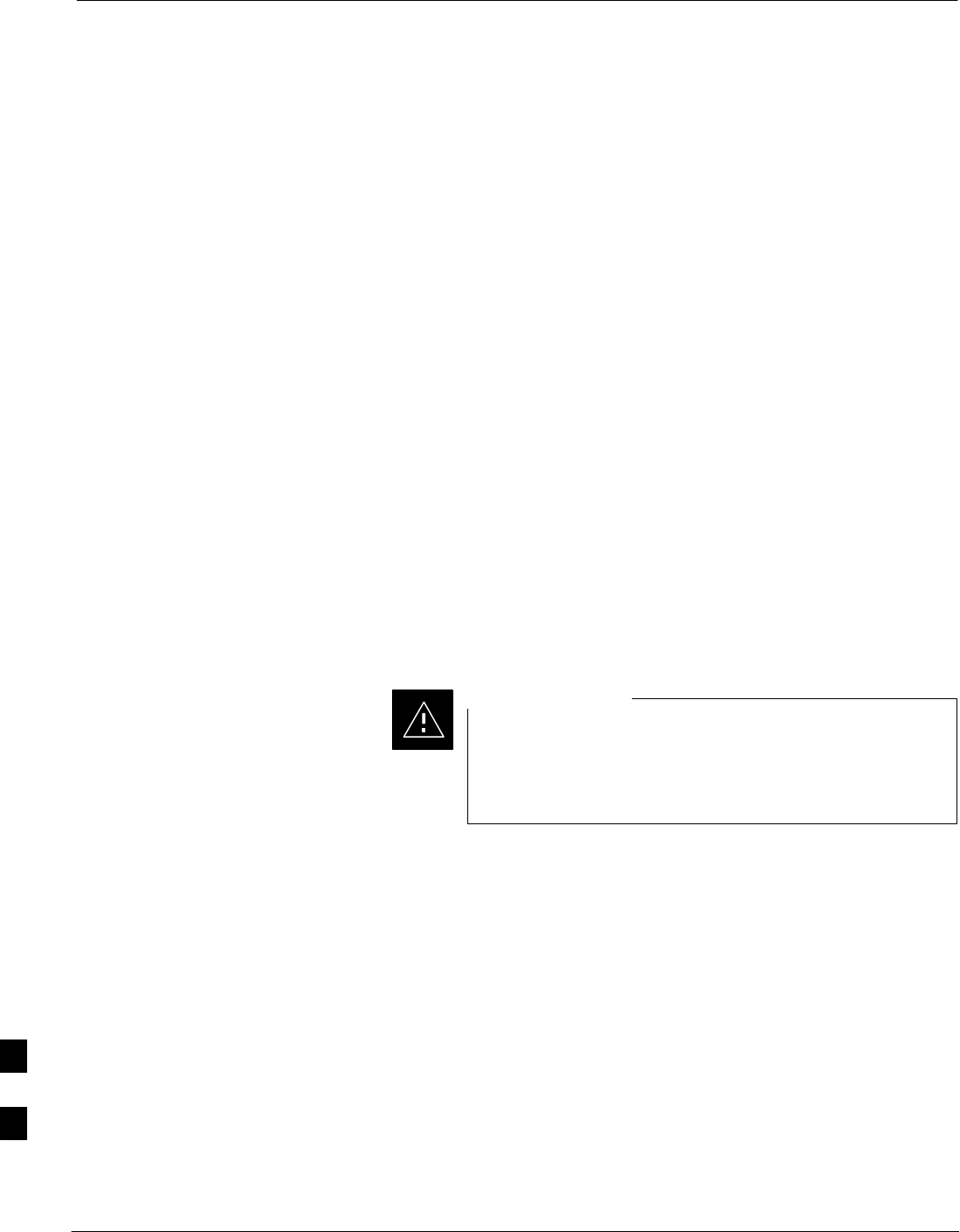
Verify and Upgrade ROMmon Version
I-46 1X SC4812T–MC BTS Optimization/ATP 5/21/04
DRAFT
Introduction
BTS routers are supplied pre–loaded with a version of the ROM monitor
(ROMmon) low–level operating system. Along with the IOS version, the
loaded ROMmon version should be verified as being the one required
for the network. Procedures in this section are used to verify the loaded
ROMmon version, and, if necessary, upgrade or change it to the required
version. Methods are provided for using either a tftp server or CF
memory card reader to transfer the required ROMmon version to a BTS
router’s CF memory card.
Required Equipment and
Software
The following items are required to perform ROMmon version
verification and upgrade for both verification/upgrade methods:
SA Windows–based computer which meets the requirements of the
LMF computer platform as specified in 1X SC4812T BTS
Optimization/ATP; 68P09260A62 original design frames or 1X
SC4812T–CLPA BTS Optimization/ATP; 68P64115A06 for updated
design frames.
SOne of the following operating systems for the Windows–based
computer:
–Windows 2000
–Windows 98 Second Edition (SE) using the FAT32 file system
BTS router CF memory cards loaded using computers
equipped with Windows 98 versions earlier than Windows
98 SE and using the FAT16 file system will not operate
properly, resulting in a complete site outage.
CAUTION
SCable, rollover, as described in the Establishing a BTS Router
Communication Session section of this Appendix
SDB–9 plug–to–8–contact modular plug adapter as described in the
Establishing a BTS Router Communication Session section of this
Appendix
SCable, Ethernet crossover, Category 5E or better, unshielded twisted
pair, two 8–contact modular plugs, in one of the following lengths, as
determined necessary:
– 0.3 m (11.8 in) (Motorola pn 3088643C07)
– 0.6 m (23.6 in)(Motorola pn 3088643C13)
– 1.0 m (39.4 in) (Motorola pn 3088643C15)
– 2.1 m (84 in) (Motorola pn 3088643C08)
– 3.0 m (120 in) (Motorola pn 3088643C09)
SA +27 Vdc power supply to power the BTS router during
configuration file operations
I

Verify and Upgrade ROMmon Version – continued
5/21/04 1X SC4812T–MC BTS Optimization/ATP I-47
DRAFT
SA tftp server software application (refer to the Setting Up the TFTP
Server – Procedure in Cellular System Administration – CDMA
OnLine Documentation, 68P09259A20) such as:
– Cisco tftp server
– PumpKIN tftp server
– Any other equivalent tftp server application
SA copy of the MWR 1900 or MWR 1941 router ROMmon version
required for the network where the routers are to be installed
Contact the network administrator or the Motorola Account
Team for assistance in determining and obtaining a copy of
the required ROMmon version.
NOTE
Required Publications
The following publication is required to perform procedures in this
section:
SMWR1900 Wireless Mobile Edge Router Software Configuration
Guide; part number 78–13983–01
Verification and
Upgrade/Replacement of
Installed ROMmon Version
Description – This procedure covers using an LMF computer equipped
with a tftp server application to perform the following activities:
1. Verify the ROMmon version loaded and running on a BTS router
2. Upgrade or replace the ROMmon version installed in a BTS router
Prerequisites – The following are required prior to performing this
procedure:
SThe LMF computer and BTS router have been prepared for tftp file
transfer and are operating as they would be after performing the
procedures in Table I-4, Table I-5, Table I-6, and steps 1 through 8 of
Table I-7
SA copy of the required ROMmon version is loaded into the tftp
default directory of the LMF computer
Verifying and Upgrading/replacing installed ROMmon version –
Follow the procedure in Table I-8 to verify and, if necessary, replace or
upgrade the installed ROMmon version using the tftp server application.
I

Verify and Upgrade ROMmon Version – continued
I-48 1X SC4812T–MC BTS Optimization/ATP 5/21/04
DRAFT
Table I-9: Verify and Upgrade/Replace Installed ROMmon Version Using a tftp Server
Step Action
* IMPORTANT
This procedure does not cover all aspects of BTS router operation and programming. Before performing this
procedure, review BTS router initialization, operation, and programming information and procedures in
MWR1900 Wireless Mobile Edge Router Software Configuration Guide; part number 78–13983–01. Have this
publication available for reference while performing this procedure.
1This procedure assumes the LMF computer and BTS router are configured, connected, and operating
as they would be after performing the procedures in Table I-4, Table I-5, Table I-6, and steps 1 through
4 of Table I-7. If necessary, perform these procedures now.
. . . continued on next page
I

Verify and Upgrade ROMmon Version – continued
5/21/04 1X SC4812T–MC BTS Optimization/ATP I-49
DRAFT
Table I-9: Verify and Upgrade/Replace Installed ROMmon Version Using a tftp Server
Step Action
2Determine the currently installed ROMmon version by entering the following at the router privileged
EXEC mode prompt:
show version
A response similar to the following will be displayed:
BTSRTR1#sh ver
Cisco Internetwork Operating System Software
IOS (tm) 1900 Software (MWR1900–I–M), Version 12.2(8)MC2b, EARLY DEPLOY-
MENT RELEASE SOFTWARE (fc3)
TAC Support: http://www.cisco.com/tac
Copyright (c) 1986–2002 by cisco Systems, Inc.
Compiled Mon 05–Aug–02 11:07 by nmasa
Image text–base: 0x60008940, data–base: 0x60B54000
ROM: System Bootstrap, Version 12.2(20020113:235343) [sbose–wilma 109],
DEVELOPMENT SOFTWARE
ROM: 1900 Software (MWR1900–I–M), Version 12.2(8)MC2b, EARLY DEPLOYMENT
RELEASE SOFTWARE (fc3)
Router uptime is 1 minute
System returned to ROM by power–on
System image file is ”slot0:mwr1900–i–mz.122–8.MC2b.bin”
cisco mwr1900 (R7000) processor (revision 0.1) with 121856K/18432K bytes
of memory.
Processor board ID JMX0611K5TS
R7000 CPU at 240Mhz, Implementation 39, Rev 3.3, 256KB L2 Cache
Bridging software.
X.25 software, Version 3.0.0.
Primary Rate ISDN software, Version 1.1.
Toaster processor tmc is running.
2 FastEthernet/IEEE 802.3 interface(s)
2 Serial network interface(s)
2 Channelized T1/PRI port(s)
DRAM configuration is 64 bits wide with parity disabled.
55K bytes of non–volatile configuration memory.
31360K bytes of ATA Slot0 CompactFlash (Read/Write)
Configuration register is 0x101
BTSRTR1#
3To determine the currently installed ROMmon version, examine the ROM: System Bootstrap line
in the response.
. . . continued on next page
I

Verify and Upgrade ROMmon Version – continued
I-50 1X SC4812T–MC BTS Optimization/ATP 5/21/04
DRAFT
Table I-9: Verify and Upgrade/Replace Installed ROMmon Version Using a tftp Server
Step Action
4Compare the installed ROMmon version information with the filename of the ROMmon version
required for the network.
NOTE
1. Rommon filename format is similar to the following:
MWR1900_RM2.srec.122–8r.MC3.bin
2. The ROMmon filename reflects the version number of the software (122–8r.MC3).
5If the installed version is the one required for the network skip to step 26.
6If the installed ROMmon version is not the one required for the network, backup the current BTS
router configuration to the LMF computer by entering the following:
copy nvram:startup–config tftp
A response similar to the following will be displayed:
BTSRTR1#copy nvram:start tftp
Address or name of remote host []?
NOTE
Be sure to include the colon (:) after nvram when typing the command.
7At the prompt for the remote host address or name, enter the IP address of the LMF computer NIC:
100.100.100.1
A response similar to the following will be displayed:
BTSRTR1#copy copy nvram:start tftp
Address or name of remote host []? 100.100.100.1
Source filename [startup–config]?
8If the default filename displayed in the prompt is correct, press the Enter key to accept it. If it is
missing or not correct, enter the correct filename.
A response similar to the following will be displayed if the default filename is selected:
Source filename [startup–config]?
Destination filename [startup–config]?
. . . continued on next page
I

Verify and Upgrade ROMmon Version – continued
5/21/04 1X SC4812T–MC BTS Optimization/ATP I-51
DRAFT
Table I-9: Verify and Upgrade/Replace Installed ROMmon Version Using a tftp Server
Step Action
9If the default filename displayed in the prompt is correct, press the Enter key to accept it. If it is
missing or not correct, enter the correct filename.
A response similar to the following will be displayed:
Destination filename [startup–config]?
!
[OK – 2212/4096 bytes]
2212 bytes copied in 0.152 secs
BTSRTR1#
10 NOTE
The IOS defaults to the CF memory card (slot0:) directory unless the present working directory has
been changed using the cd command. Determine the present working directory by entering pwd. If
the present working directory has been changed, enter the command cd slot0: to return to the default
setting.
Determine the amount of memory available (bytes free) on the CF memory card by entering the
following:
dir
A response similar to the following will be displayed:
BTSRTR1#dir
Directory of slot0:/
1 –rw– 7051976 Sep 23 2002 07:24:18
mwr1900–i–mz.122–8.MC2b.bin
2 –rw– 2212 Mar 01 1993 00:14:48 canned–config
31932416 bytes total (24885606 bytes free)
Router#
11 Be sure there is at least 1 MB (1048580) of free memory.
NOTE
A ROMmon version file requires approximately 0.7 MB.
. . . continued on next page
I

Verify and Upgrade ROMmon Version – continued
I-52 1X SC4812T–MC BTS Optimization/ATP 5/21/04
DRAFT
Table I-9: Verify and Upgrade/Replace Installed ROMmon Version Using a tftp Server
Step Action
12 Begin to copy the required version of the ROMmon file from the LMF computer to the BTS router by enter-
ing the following:
copy tftp:new_rommon_filename slot0:
Where new_rommon_filename = the filename of the required ROMmon version for the BTS
router.
A response similar to the following will be displayed:
BTSRTR1#copy tftp:MWR1900_RM2.srec.122–8r.MC3.bin slot0:
Address or name of remote host [100.100.100.1]?
13 If the default IP address displayed in the prompt is correct, press the Enter key to accept it. If it is
missing or not correct, enter the correct IP address for the LMF computer.
A response similar to the following will be displayed if the default filename is selected:
Address or name of remote host [100.100.100.1]?
Source filename [MWR1900_RM2.srec.122–8r.MC3.bin]?
14 If the default filename displayed in the prompt is correct, press the Enter key to accept it. If it is
missing or not correct, enter the correct filename.
A response similar to the following will be displayed if the default filename is selected:
Source filename [MWR1900_RM2.srec.122–8r.MC3.bin]?
Destination filename [MWR1900_RM2.srec.122–8r.MC3.bin]?
15 If the default filename displayed in the prompt is correct, press the Enter key to accept it. If it is not
correct, enter the correct filename.
A response similar to the following will be displayed if the default filename is selected:
Destination filename [MWR1900_RM2.srec.122–8r.MC3.bin]?
Accessing tftp://100.100.100.1/MWR1900_RM2.srec.122–8r.MC3.bin...
Loading MWR1900_RM2.srec.122–8r.MC3.bin from 100.100.100.1 (via FastE-
thernet0/0): !!!!
Loading MWR1900_RM2.srec.122–8r.MC3.bin from 100.100.100.1 (via FastE-
thernet0/0):
!!!!!!!!!!!!!!!!!!!!!!!!!!!!!!!!!!!!!!!!!!!!!!!!!!!!!!!!!!!!!!!!!!!!!!!!!
!!!!!!!!!!!!!!!!!!!!!!!!!!!!!!!!!!!!!!!!!!!!!!!!!
[OK – 614306/14103552 bytes]
614306 bytes copied in 13.059 secs (48634 bytes/sec)
BTSRTR1#
. . . continued on next page
I

Verify and Upgrade ROMmon Version – continued
5/21/04 1X SC4812T–MC BTS Optimization/ATP I-53
DRAFT
Table I-9: Verify and Upgrade/Replace Installed ROMmon Version Using a tftp Server
Step Action
16 Display the CF memory card directory to verify that the new ROMmon version file is there by
entering the following:
dir
A response similar to the following will be displayed:
BTSRTR1#dir
Directory of slot0:/
1 –rw– 7051976 Sep 23 2002 07:25:36 mwr1900–i–mz.122–8.MC2b.bin
2 –rw– 2212 Mar 01 1993 00:09:06 canned–config
3 –rw– 614306 Dec 13 2002 14:59:36
MWR1900_RM2.srec.122–8r.MC3.bin
31932416 bytes total (24263922 bytes free)
BTSRTR1#
17 Replace the existing ROMmon version with the new one copied to the CF memory card by entering
the following:
upgrade rom–monitor file slot0:MWR1900_RM2.srec.122–8r.MC3
A response similar to the following will be displayed:
BTSRTR1#This command will reload the router. Continue?[yes/no]
18 When prompted to continue, enter yes and press the Enter key.
A response similar to the following will be displayed:
BTSRTR1#This command will reload the router. Continue?[yes/no] yes
ROMMON image upgrade in progress
Erasing boot flash
eeeeeeeeeeeeeeeeeeeeeeeeeeeeeeeeeeeeeeeeeeeeeeeeeeeeeeeeeeeeeeeeee
Programming boot flash pppp
Now reloading
19 When the router has completed initialization, change to the router privileged EXEC mode by entering
the following:
enable
A response similar to the following will be displayed:
BTSRTR1>enable
BTSRTR1#
. . . continued on next page
I

Verify and Upgrade ROMmon Version – continued
I-54 1X SC4812T–MC BTS Optimization/ATP 5/21/04
DRAFT
Table I-9: Verify and Upgrade/Replace Installed ROMmon Version Using a tftp Server
Step Action
20 Verify the router has initialized with the new ROMmon version by entering the following:
show version
A response similar to the following partial response will be displayed:
BTSRTR1#sh ver
Cisco Internetwork Operating System Software
IOS (tm) 1900 Software (MWR1900–I–M), Version 12.2(8)MC2b, EARLY DEPLOY-
MENT RELEASE SOFTWARE (fc3)
TAC Support: http://www.cisco.com/tac
Copyright (c) 1986–2002 by cisco Systems, Inc.
Compiled Mon 05–Aug–02 11:07 by nmasa
Image text–base: 0x60008940, data–base: 0x60B54000
ROM: System Bootstrap, Version 12.2(8r)MC3 RELEASE SOFTWARE (fc1)
21 Compare the version displayed in the response ROM: System Bootstrap line to the filename of the
new ROMmon version file copied to the CF memory card.
22 If the router successfully rebooted with the new ROMmon version, the ROMmon file can be deleted
from the CF memory card by entering the following:
delete slot0:new_rommon_filename
Where new_rommon_filename = the filename of the required ROMmon version copied to the CF
memory card in steps 12 through 15, above.
A response similar to the following will be displayed:
BTSRTR1#del slot0:MWR1900_RM2.srec.122–8r.MC3.bin
Delete filename [MWR1900_RM2.srec.122–8r.MC3.bin]?
23 If the default filename displayed in the prompt is correct, press the Enter key to accept it. If it is
missing or not correct, enter the correct filename.
A response similar to the following will be displayed if the default filename is selected:
Delete filename [MWR1900_RM2.srec.122–8r.MC3.bin]?
Delete slot0:MWR1900_RM2.srec.122–8r.MC3.bin? [confirm]
. . . continued on next page
I

Verify and Upgrade ROMmon Version – continued
5/21/04 1X SC4812T–MC BTS Optimization/ATP I-55
DRAFT
Table I-9: Verify and Upgrade/Replace Installed ROMmon Version Using a tftp Server
Step Action
24 Press the Enter key to confirm the deletion.
A response similar to the following will be displayed if the default filename is selected:
Delete filename [MWR1900_RM2.srec.122–8r.MC3.bin]?
Delete slot0:MWR1900_RM2.srec.122–8r.MC3.bin? [confirm]
BTSRTR1#
25 ! CAUTION
In this step, do not delete the IOS and canned–config files from the CF memory card. The BTS
router must have these files on the card to properly boot or switch between packet and circuit mode.
If additional unnecessary files, such as a backup of the startup–config file, are also on the CF
memory card, delete them by repeating steps 22 through 24 for each file.
26 If no other BTS router file operations or configuration actions are required, perform the following:
26a – Remove power from the router and disconnect it from the power supply.
26b – Disconnect all cabling from the BTS router.
26c – On the LMF computer, exit the HyperTerminal communications session.
27 If no additional tftp transfer activities will be performed, change the NIC IP address and subnet mask
back to those for LMF–BTS communication recorded in Table I-4, step 10b.
! CAUTION
If the BTS 10base–2 LAN IP address and subnet mask for the LMF computer’s NIC are not restored,
the LMF can not log into a BTS when attempting to perform a BTS optimization or ATP.
I

Recovery from BTS Router Boot to ROMmon
I-56 1X SC4812T–MC BTS Optimization/ATP 5/21/04
DRAFT
ROM monitor boot conditions – Under certain circumstances the BTS
router will initialize with the ROM monitor (ROMmon) operating
system rather than the IOS. These circumstances include:
SThe hexadecimal value in the router’s configuration register has been
changed from the factory default (can change the location from where
the router attempts to load code for boot–up).
SIOS file is missing from the CF memory card
SIOS file is not the first file on the CF memory card
SStartup–config file contains an outdated boot system line specifying
an IOS file which has been replaced with an updated version
SStartup–config file contains boot system line with typographical
error(s) in the IOS filename
SIOS file image on the CF memory card is corrupted
Description – Router operation on ROMmon is signalled by the display
of the rommon # > prompt, where # is a number which increments
each time a command is issued. ROMmon is a low–level operating
system which provides limited capabilities for router testing and
troubleshooting operations, including viewing directory contents and
booting from a specified file.
Recovery methods – Two recovery methods are included in this section.
The first is the simplest and requires that a valid, uncorrupted IOS
version is installed on the CF memory card. The second method requires
additional equipment and must be used in instances such as when an IOS
file is not installed on the CF memory card or the installed IOS image is
corrupted.
Simple Recovery from Boot to
ROMmon
Requirements – Unless it is certain that the IOS image on the CF
memory card is corrupted, this method should always be the first tried
for router recovery from ROMmon initialization. This method does not
require any additional equipment beyond the items necessary to load
canned configuration files into the BTS router. To be effective, this
method does require that a valid, uncorrupted IOS image file is installed
on the router’s CF memory card.
Recovery – Follow the procedure in Table I-10 to attempt a simple
recovery from a BTS router ROMmon initialization.
I

Recovery from BTS Router Boot to ROMmon – continued
5/21/04 1X SC4812T–MC BTS Optimization/ATP I-57
DRAFT
Table I-10: Simple Recovery from BTS Router ROMmon Boot
Step Action
* IMPORTANT
This procedure does not cover all aspects of BTS router operation and programming. Before performing this
procedure, review BTS router initialization, operation, and programming information and procedures in
MWR1900 Wireless Mobile Edge Router Software Configuration Guide; part number 78–13983–01. Have this
publication available for reference while performing this procedure.
1This procedure assumes the LMF computer is set up and connected to the BTS router with an active
HyperTerminal communication session. If it is not, follow the procedure in Table I-2 to establish a
HyperTerminal communication session.
2With the rommon 1 > prompt displayed in the HyperTerminal window, enter the following to
determine if the router’s configuration register is set to the factory default value:
confreg
A response similar to the following will be displayed:
rommon 4 > confreg
Configuration Summary
(Virtual Configuration Register: 0x100)
enabled are:
load rom after netboot fails
console baud: 9600
boot: image specified by the boot system commands
or default to: cisco2–mwr1900
do you wish to change the configuration? y/n [n]:
NOTE
SThe configuration register setting is shown in the (Virtual Configuration Register: 0x____) line
S0x in the Virtual Configuration Register line indicates the numbers following are hexadecimal
3If the value shown for the configuration register is 2102, skip to step 6.
4If the value shown for the configuration register is not 2102, perform the following:
4a Press the Return key to accept the default of n (for no).
. . . continued on next page
I

Recovery from BTS Router Boot to ROMmon – continued
I-58 1X SC4812T–MC BTS Optimization/ATP 5/21/04
DRAFT
Table I-10: Simple Recovery from BTS Router ROMmon Boot
Step Action
4b Enter the following at the rommon prompt:
confreg 0x2102
A response similar to the following will be displayed:
rommon 3 > confreg 0x2102
You must reset or power cycle for new config to take effect
rommon 4 >
4c Enter the following at the rommon prompt:
reset
A response which begins and ends similar to the following will be displayed:
rommon 4 > reset
System Bootstrap, Version 12.2(20020113:235343) [sbose–wilma 109], DE-
VELOPMENT SOFTWARE
Copyright (c) 1994–2002 by cisco Systems, Inc.
mwr1900 processor with 131072 Kbytes of main memory
Main memory is configured to 64 bit mode with parity disabled
Readonly ROMMON initialized
.
...<output omitted>...
.
Press RETURN to get started!
5If the router reboots with the IOS, skip to step 21.
. . . continued on next page
I

Recovery from BTS Router Boot to ROMmon – continued
5/21/04 1X SC4812T–MC BTS Optimization/ATP I-59
DRAFT
Table I-10: Simple Recovery from BTS Router ROMmon Boot
Step Action
6If the configuration register is set properly and/or the router does not reboot with the IOS, enter the
following at the rommon # > prompt to identify the IOS file on the CF memory card:
dir slot0:
A response similar to the following will be displayed:
rommon 1 > dir slot0:
program load complete, entry point: 0x80008000, size: 0xb2a0
Directory of slot0:
2 2212 –rw– canned–config
3 7051976 –rw– mwr1900–i–mz.122–8.MC2b.bin
4 614306 –rw– MWR1900_RM2.srec.122–8r.MC3.bin
rommon 2 >
NOTE
The IOS filename will be similar to the following:
mwr1900–i–mz.122–8.MC2b.bin
7If there is no IOS file on the CF memory card, proceed to Table I-11 and perform the extended
recovery procedure.
. . . continued on next page
I

Recovery from BTS Router Boot to ROMmon – continued
I-60 1X SC4812T–MC BTS Optimization/ATP 5/21/04
DRAFT
Table I-10: Simple Recovery from BTS Router ROMmon Boot
Step Action
8If an IOS file is found, note the IOS filename, and enter the following to begin recovery to an IOS
boot:
boot slot0:IOS_filename
Where IOS_filename = the filename of the IOS noted in step 6, above.
A successful IOS re–boot operation will result in display of a response which begins and ends similar
to the following:
rommon 2 > boot slot0:mwr1900–i–mz.122–8.MC2b.bin
program load complete, entry point: 0x80008000, size: 0xb2a0
program load complete, entry point: 0x80008000, size: 0x6b99ac
Self decompressing the image :
################################################################### [OK]
Smart Init is enabled
smart init is sizing iomem
ID MEMORY_REQ TYPE
00031A 0X005F3C00 MWR1900 Mainboard
0X000F3BB0 public buffer pools
0X00211000 public particle pools
TOTAL: 0X008F87B0
.
...<output omitted>...
.
Press RETURN to get started!
9If the router successfully reboots with the IOS, skip to step 12.
10 If the router does not reboot with the IOS, perform the following:
10a – Scroll the HyperTerminal display down until the directory display from step 6, above, is visible.
10b – Compare the IOS filename from the directory display with the filename entered when performing
step 8, above.
10c – If the filename was typed incorrectly, repeat step 8, using care to type the filename correctly.
. . . continued on next page
I

Recovery from BTS Router Boot to ROMmon – continued
5/21/04 1X SC4812T–MC BTS Optimization/ATP I-61
DRAFT
Table I-10: Simple Recovery from BTS Router ROMmon Boot
Step Action
11 If the router still does not reboot with the IOS after typing the filename correctly, proceed to Table I-11
and perform the extended recovery procedure.
12 ! CAUTION
The file sequence on the CF memory card can not be verified with application programs which place
the listed file names in alphabetical order (for example, certain Unix telnet applications, Unix
directory listing commands, and Windows file managers such as Windows Explorer). This portion of
the procedure is intended for use only with applications, such as HyperTerminal, which do not list
directory contents alphabetically.
After a successful reboot with IOS, perform the following to correct the cause of the boot to
ROMmon:
12a – At the BTSRTR1> user EXEC mode prompt, enter the following to access the privileged EXEC
mode:
enable
A response similar to the following will be displayed:
BTSRTR1>enable
BTSRTR1#
12b – Enter the dir slot0: command to display the CF memory card directory, and, if the IOS file is
not the first file listed, perform the procedure in Table I-8, steps 25 through 32, to correct the
situation.
. . . continued on next page
I

Recovery from BTS Router Boot to ROMmon – continued
I-62 1X SC4812T–MC BTS Optimization/ATP 5/21/04
DRAFT
Table I-10: Simple Recovery from BTS Router ROMmon Boot
Step Action
12c – If the IOS file is the first file, enter the following command to display the contents of the
startup–config file:
show startup–config
A response which begins similar to the following will be displayed:
BTSRTR1#sh start
Using 1589 out of 57336 bytes
!
version 12.2
service timestamps debug uptime
service timestamps log uptime
no service password–encryption
!
hostname BTSRTR1
!
boot system slot0:mwr1900–i–mz.07132002.bin
no logging console
!
username cisco password 0 cisco
!
redundancy
mode y–cable
standalone
!
13 Review the startup–config file listing for a “boot system” line and perform the following:
13a – If the startup–config file does not contain a boot system line, skip to step 14.
13b – If the file listing contains a “boot system” line, examine it for the correct IOS filename.
13c – If the boot system slot0: filename is incorrect, enter the following, using care to type the filename
correctly:
boot system slot0:IOS_filename
Where IOS_filename = the filename of the IOS noted in step 6, above.
13d – Replace the boot system line in the startup–config file with the line entered in step 13c, above, by
entering the following:
copy runing–config startup–config
. . . continued on next page
I

Recovery from BTS Router Boot to ROMmon – continued
5/21/04 1X SC4812T–MC BTS Optimization/ATP I-63
DRAFT
Table I-10: Simple Recovery from BTS Router ROMmon Boot
Step Action
13e – Verify the correct IOS filename is now included in the listing by entering the following:
show startup–config
A response which begins similar to the following will be displayed:
BTSRTR1#sh start
Using 1589 out of 57336 bytes
!
version 12.2
service timestamps debug uptime
service timestamps log uptime
no service password–encryption
!
hostname BTSRTR1
!
boot system slot0:mwr1900–i–mz.122–8.MC2b.bin
no logging console
!
username cisco password 0 cisco
!
redundancy
mode y–cable
standalone
!
. . . continued on next page
I

Recovery from BTS Router Boot to ROMmon – continued
I-64 1X SC4812T–MC BTS Optimization/ATP 5/21/04
DRAFT
Table I-10: Simple Recovery from BTS Router ROMmon Boot
Step Action
14 Re–verify the router’s configuration register setting by entering the following:
show version
A response similar to the following will be displayed:
BTSRTR1#sh ver
Cisco Internetwork Operating System Software
IOS (tm) 1900 Software (MWR1900–I–M), Version 12.2(8)MC2b, EARLY DEPLOY-
MENT RELEASE SOFTWARE (fc1)
TAC Support: http://www.cisco.com/tac
Copyright (c) 1986–2002 by cisco Systems, Inc.
Compiled Mon 05–Aug–02 11:07 by nmasa
Image text–base: 0x60008940, data–base: 0x60B54000
ROM: System Bootstrap, Version 12.2(20020113:235343) [sbose–wilma 109],
DEVELOPMENT SOFTWARE
ROM: 1900 Software (MWR1900–I–M), Version 12.2(8)MC2b, EARLY DEPLOYMENT
RELEASE SOFTWARE (fc1)
Router uptime is 1 minute
System returned to ROM by power–on
System image file is ”slot0:mwr1900–i–mz.122–8.MC2b.bin”
cisco mwr1900 (R7000) processor (revision 0.1) with 121856K/18432K bytes
of memory.
Processor board ID JMX0611K5TS
R7000 CPU at 240Mhz, Implementation 39, Rev 3.3, 256KB L2 Cache
Bridging software.
X.25 software, Version 3.0.0.
Primary Rate ISDN software, Version 1.1.
Toaster processor tmc is running.
2 FastEthernet/IEEE 802.3 interface(s)
2 Serial network interface(s)
2 Channelized T1/PRI port(s)
DRAM configuration is 64 bits wide with parity disabled.
55K bytes of non–volatile configuration memory.
31360K bytes of ATA Slot0 CompactFlash (Read/Write)
Configuration register is 0x101
BTSRTR1#
NOTE
The configuration register value is shown in the last line of the show version response.
15 If the value shown for the configuration register is 0x2102, skip to step 18.
. . . continued on next page
I

Recovery from BTS Router Boot to ROMmon – continued
5/21/04 1X SC4812T–MC BTS Optimization/ATP I-65
DRAFT
Table I-10: Simple Recovery from BTS Router ROMmon Boot
Step Action
16 If the value shown for the configuration register is not 0x2102, enter the following command in the
order shown to change it:
configure terminal
config–register 0x2102
A response similar to the following will be displayed:
BTSRTR1#conf t
Enter configuration commands, one per line. End with CNTL/Z.
BTSRTR1(config)#config–register 0x2102
BTSRTR1(config)#
17 Verify the change was entered properly by entering the following commands in the order shown:
exit
show version
A response which begins and ends similar to the following will be displayed:
BTSRTR1(config)#exit
BTSRTR1#sh ver
Cisco Internetwork Operating System Software
IOS (tm) 1900 Software (MWR1900–I–M), Version 12.2(8)MC2b, EARLY DEPLOY-
MENT RELEASE SOFTWARE (fc1)
TAC Support: http://www.cisco.com/tac
Copyright (c) 1986–2002 by cisco Systems, Inc.
.
...<output omitted>...
.
Configuration register is 0x101 (will be 0x2102 at next reload)
BTSRTR1#
18 If the filename is correctly written in the boot system line (step 13e) and the configuration register is
properly set to the factory default of 0x2102, enter the following to determine if the router will reboot
to IOS:
reload
A response similar to the following will be displayed:
BTSRTR1#reload
System configuration has been modified. Save? [yes/no]: n
Proceed with reload? [confirm]
. . . continued on next page
I

Recovery from BTS Router Boot to ROMmon – continued
I-66 1X SC4812T–MC BTS Optimization/ATP 5/21/04
DRAFT
Table I-10: Simple Recovery from BTS Router ROMmon Boot
Step Action
19 If prompted to save a modified configuration, enter n for “no,” and press the Enter key.
20 When prompted to proceed with reload, press the Enter key to continue the reload operation.
21 After a successful reboot with IOS, proceed with other BTS router activities or remove power from the
router and disconnect it
22 If the router still will not successfully boot with IOS, proceed to Table I-11 and perform the extended
recovery procedure.
Extended Recovery from Boot
to ROMmon
Requirements – If ROMmon boot recovery attempts fail using the
simple recovery method, this method must be used to reboot a BTS
router which has initialized with ROMmon. This method requires
additional equipment beyond the items necessary to load canned
configuration files into the BTS router. Extended recovery requires
formatting the CF memory card from the ROMmon–initialized router
and reloading the reformatted CF memory card with the required IOS
version.
Additional equipment required – An additional, formatted, 32 MB CF
memory card with the required version of the IOS installed is required in
addition to the equipment and software required for BTS router canned
configuration installation. This card may be:
SA spare CF memory card which is loaded with the required IOS
version
SA CF memory card from an additional BTS router which is loaded
with the required IOS version
Recovery – Follow the procedure in Table I-10 to perform an extended
recovery from a BTS router ROMmon initialization.
Table I-11: Extended Recovery from BTS Router ROMmon Boot
Step Action
1This procedure assumes the BTS router is powered and operating on ROMmon with the LMF
computer set up and connected to the router with an active HyperTerminal communication session. If
it is not, follow the procedure in Table I-2 to establish a HyperTerminal communication session.
2Remove the CF memory card from the BTS router following the procedure in Table I-13.
3Install the additional CF memory card in the router following the procedure in Table I-14.
. . . continued on next page
I

Recovery from BTS Router Boot to ROMmon – continued
5/21/04 1X SC4812T–MC BTS Optimization/ATP I-67
DRAFT
Table I-11: Extended Recovery from BTS Router ROMmon Boot
Step Action
4Enter the following to obtain the filename of the IOS version loaded on the CF memory card:
dir slot0:
A response similar to the following will be displayed:
rommon 1 > dir slot0:
program load complete, entry point: 0x80008000, size: 0xb2a0
Directory of slot0:
1 7051976 –rw– mwr1900–i–mz.122–8.MC2b.bin
rommon 2 >
5Note the exact filename displayed for the IOS version.
. . . continued on next page
I

Recovery from BTS Router Boot to ROMmon – continued
I-68 1X SC4812T–MC BTS Optimization/ATP 5/21/04
DRAFT
Table I-11: Extended Recovery from BTS Router ROMmon Boot
Step Action
6Enter the following to initialize the router with the IOS on the additional CF memory card:
boot slot0:IOS_filename
Where IOS_filename = the filename of the IOS noted in step 5, above.
A successful IOS re–boot operation will result in display of a response which begins and ends similar
to the following:
rommon 2 > boot slot0:mwr1900–i–mz.122–8.MC2b.bin
program load complete, entry point: 0x80008000, size: 0xb2a0
program load complete, entry point: 0x80008000, size: 0x6b99ac
Self decompressing the image :
################################################################### [OK]
Smart Init is enabled
smart init is sizing iomem
ID MEMORY_REQ TYPE
00031A 0X005F3C00 MWR1900 Mainboard
0X000F3BB0 public buffer pools
0X00211000 public particle pools
TOTAL: 0X008F87B0
.
.
.
––– System Configuration Dialog –––
Would you like to enter the initial configuration dialog? [yes/no]: n
7If the router prompts with a question to enter the initial dialog as shown in step 6, above, type no and
press the Enter key to obtain the user EXEC mode prompt.
8If the router prompts with Press RETURN to get started!, press the Enter key to obtain the
user EXEC mode prompt.
. . . continued on next page
I

Recovery from BTS Router Boot to ROMmon – continued
5/21/04 1X SC4812T–MC BTS Optimization/ATP I-69
DRAFT
Table I-11: Extended Recovery from BTS Router ROMmon Boot
Step Action
9At the user EXEC mode prompt, enter the following to access the privileged EXEC mode:
enable
A response similar to the following will be displayed:
Router> enable
Router#
10 Remove the additional CF memory card from the BTS router following the procedure in Table I-13.
11 Install the original CF memory card in the router following the procedure in Table I-14.
12 Format the original CF memory card by entering the following:
format slot0:
A response similar to the following will be displayed:
Router#format slot0:
Format operation may take a while. Continue? [confirm]
13 Press the Enter key to continue the format operation.
A response similar to the following will be displayed:
Format operation may take a while. Continue? [confirm]
Format operation will destroy all data in ”slot0:”. Continue? [confirm]
. . . continued on next page
I

Recovery from BTS Router Boot to ROMmon – continued
I-70 1X SC4812T–MC BTS Optimization/ATP 5/21/04
DRAFT
Table I-11: Extended Recovery from BTS Router ROMmon Boot
Step Action
14 Press the Enter key to continue the format operation.
A response similar to the following will be displayed:
Format operation will destroy all data in ”slot0:”. Continue? [confirm]
Format: Drive communication & 1st Sector Write OK...
Writing Monlib
sec-
tors....................................................................
................
Monlib write complete
.
Format: All system sectors written. OK...
Format: Total sectors in formatted partition: 62560
Format: Total bytes in formatted partition: 32030720
Format: Operation completed successfully.
Format of slot0 complete
Router#
15 Copy the required IOS version to the formatted original CF memory card using the LMF computer
and a tftp server following the procedure in Table I-8.
16 If applicable, perform IOS initialization troubleshooting as described in Table I-10, steps 12 through
21.
I

Entering or Changing BTS Router FE Interface IP Addresses
5/21/04 1X SC4812T–MC BTS Optimization/ATP I-71
DRAFT
FE Interface IP Addresses and
Operating Parameters
It may be necessary to enter or change the IP addresses and/or operating
parameters for BTS router FE interfaces FE 0 and FE1 without making
other changes in the router configuration files. Procedures in this section
cover these operations.
Prerequisites
The following must be accomplished before entering or changing BTS
router FE port IP addresses and/or operating parameters:
SThe user has read and understands the content of MWR1900 Wireless
Mobile Edge Router Software Configuration Guide; part number
78–13983–01
SBTS routers must have the required version of the IOS saved on their
installed CF memory card
SBTS routers must have power applied, be operating without alarms
other than span alarms, and have completed boot–up to the user EXEC
mode prompt (BTSRTR–bts#–1–1>)
SThe BTS router privileged EXEC mode password has been obtained
from the network administrator
Entering or Changing FE
Interface IP Addresses
To enter or change FE interface IP addresses, follow the procedure in
Table I-12.
Table I-12: Entering or Changing BTS Router FE Interface IP Addresses and Operating Parameters
Step Action
* IMPORTANT
This procedure does not cover all aspects of BTS router operation and programming. Before performing this
procedure, review BTS router initialization, operation, and programming information and procedures in
MWR1900 Wireless Mobile Edge Router Software Configuration Guide; part number 78–13983–01. Have this
publication available for reference while performing this procedure.
1Obtain the correct IP addresses and subnet masks for the BTS router FE interfaces from the network
administrator.
2If a HyperTerminal connection for BTS card/module MMI or BTS router (BTSRTR) communication
has not been created, create one as described in Table I-1 of this appendix.
3Connect the LMF computer to the BTS router, and start a communication session as described in
Table I-2 in this appendix.
. . . continued on next page
I

Entering or Changing BTS Router FE Interface IP Addresses – continued
I-72 1X SC4812T–MC BTS Optimization/ATP 5/21/04
DRAFT
Table I-12: Entering or Changing BTS Router FE Interface IP Addresses and Operating Parameters
Step Action
4NOTE
Examples in this procedure show prompts for BTSRTR–bts#–1–1 and BTSRTR–bts#–1–2, but the
procedure can be used for any router in any BTS router group or a router running the canned
configuration file (BTSRTR1 or BTSRTR2).
At the BTSRTR–bts#–1–1> user EXEC mode prompt, enter the following to access the privileged
EXEC mode:
enable
A response similar to the following will be displayed:
BTSRTR–bts#–1–1> enable
Password:
5Enter the privileged EXEC mode password.
A response similar to the following will be displayed:
BTSRTR–bts#–1–1> enable
Password:
BTSRTR–bts#–1–1#
6At the BTSRTR–bts#–1–1# privileged EXEC mode prompt, display the FE interface IP addresses by
typing:
show ip interface brief
A response similar to the following will be displayed:
BTSRTR–bts#–1–1# show ip interface brief
Interface IP Address OK? Method Status Protocol
FastEthernet0/0 192.168.146.1 YES NVRAM up up
Serial0:0 unassigned YES unset administratively down down
FastEthernet0/1 unassigned YES unset administratively down down
Serial1:0 unassigned YES unset administratively down down
BTSRTR–bts#–1–1#
. . . continued on next page
I

Entering or Changing BTS Router FE Interface IP Addresses – continued
5/21/04 1X SC4812T–MC BTS Optimization/ATP I-73
DRAFT
Table I-12: Entering or Changing BTS Router FE Interface IP Addresses and Operating Parameters
Step Action
7For a FastEthernet0/0 (fa0/0) or FastEthernet0/1(fa0/1) interface which does not have a correct or an
assigned IP address, enter the following at the router prompt to access the global configuration mode:
configure terminal
A response similar to the following will be displayed:
BTSRTR–bts#–1–1# conf t
Enter configuration commands, one per line. End with CNTL/Z.
BTSRTR–bts#–1–1(config)#
8At the global configure mode prompt, enter the following to access the configure interface submode
for the interface requiring IP address assignment/change:
interface fastethernetinterface#
Where interface# = 0/0 or 0/1, as applicable.
A response similar to the following will be displayed:
BTSRTR–bts#–1–1(config)# int fa0/1
BTSRTR–bts#–1–1(config–if)#
9At the configure interface submode prompt, assign or change the interface IP address by entering:
ip address IP_addr subnet_mask
Where:
IP_addr = the required IP address for the interface; for example, 192.168.147.1
subnet_mask = the required subnet mask for the interface; for example, 255.255.255.0
A response similar to the following will be displayed:
BTSRTR–bts#–1–1(config–if)# ip address 192.168.147.1 255.255.255.0
BTSRTR–bts#–1–1(config–if)#
10 To complete configuration of the interface, enter the following parameter settings, one at a time,
pressing Enter after each:
duplex full
speed 100
keepalive 1
no shutdown
. . . continued on next page
I

Entering or Changing BTS Router FE Interface IP Addresses – continued
I-74 1X SC4812T–MC BTS Optimization/ATP 5/21/04
DRAFT
Table I-12: Entering or Changing BTS Router FE Interface IP Addresses and Operating Parameters
Step Action
11 Return to the global configuration mode by entering the following:
exit
A response similar to the following will be displayed:
BTSRTR–bts#–1–1(config–if)# exit
BTSRTR–bts#–1–1(config)#
12 If the IP address and/or parameters for the other FE interface on the router must be assigned or
changed at this time, repeat steps 8 through 11 for the other FE interface.
13 Once the correct parameters have been set for all FE interfaces, return to the privileged EXEC mode
prompt by holding down the Ctrl key and pressing z (Ctrl +z).
A response similar to the following will be displayed:
BTSRTR–bts#–1–1(config–if)# ^z
01:11:27: %SYS–5–CONFIG_I: Configured from console by console
BTSRTR–bts#–1–1#
NOTE
Entering exit twice, pressing the Enter key after each entry, will also complete the interface
configuration and return the router to the privileged EXEC mode.
14 Save the interface configuration changes to the startup configuration file on the CF memory card by
entering the following:
copy running–config startup–config
A response similar to the following will be displayed:
BTSRTR–bts#–1–1# copy run start
BTSRTR–bts#–1–1# Destination filename [startup–config]?
15 Press Enter
A response similar to the following will be displayed:
BTSRTR–bts#–1–1# copy run start
BTSRTR–bts#–1–1# Destination filename [startup–config]?
Building configuration...
!!!!!!!!!!!!!!!!!!!!!!!!!!!!!!!!!!!!!!!!!!!!!!!!!!!!!!!!!!!!!!!!!!!!!!!!!
!!!!!!!!![OK]
BTSRTR–bts#–1–1#
. . . continued on next page
I

Entering or Changing BTS Router FE Interface IP Addresses – continued
5/21/04 1X SC4812T–MC BTS Optimization/ATP I-75
DRAFT
Table I-12: Entering or Changing BTS Router FE Interface IP Addresses and Operating Parameters
Step Action
16 If all FE IP address entries/changes for the router are complete, enter the following to return the router
to user EXEC mode:
disable
A response similar to the following will be displayed:
BTSRTR–bts#–1–1# disable
BTSRTR–bts#–1–1>
17 If no other router requires the FE interfaces to be assigned/changed, proceed to step 20.
18 If FE interfaces on another router must be assigned/changed, disconnect the 8–contact modular plug
from the current router CONSOLE port and connect it to the CONSOLE port of the other router.
19 Press the Enter key, and when the router user EXEC mode prompt appears repeat steps 3 through 16
for the other router.
20 When the router is in user EXEC mode, close the HyperTerminal session and disconnect the LMF
computer and additional components from the BTS router.
I

Example BTS Router Canned Configuration Files
I-76 1X SC4812T–MC BTS Optimization/ATP 5/21/04
DRAFT
BTS Router Canned
Configuration File
This section presents listings of the blue and red router canned
configuration file contents for the MWR 1900 BTS routers. The blue
router is the primary router on the BTS LAN subnet 192.168.146.0, and
the red router is the primary on BTS LAN subnet 192.168.147.0. The
canned configuration files allow communication with the BTS routers
for both on–site FE cabling connectivity verification and for
downloading the routers from the network with the full, site–specific
operational configuration.
Obtaining the Latest
Configuration File Content
The files included here are for example only. The correct canned
configuration file content for each BTS router should be generated at the
OMC–R using the /screl/active/bin/gen_btsrtr_canned_config.ksh script.
Configuration File Examples
Examples of both configuration files are provided in the following
subsections.
I

Example BTS Router Canned Configuration Files – continued
5/21/04 1X SC4812T–MC BTS Optimization/ATP I-77
DRAFT
“Blue” BTS Router Canned
Configuration
! Canned Config file for BTSRTR1
version 12.2
service timestamps debug uptime
service timestamps log uptime
no service password–encryption
!
hostname BTSRTR1
!
no logging console
!
!
ip subnet–zero
ip classless
ip pim bidir–enable
!
disable–eadi
memory–size iomem 25
!
redundancy
mode y–cable
standby use–interface Loopback101 health
standby use–interface Loopback102 revertive
standby use–interface Multilink1 backhaul
interface loopback 101
description BTSRTR health loopback
no ip address
interface loopback 102
description BTSRTR revertive loopback
no ip address
!
! configure 1 DS0 for BTSRTRLINK
!
controller T1 0/0
description 1st span on BTSRTR
framing esf
linecode b8zs
cablelength short 133
clock source line
channel–group 0 timeslots 1–24 speed 64
! MLPPP bundle with BTSRTRLINK.
! This performs IPCP with RPM when BTSRTR is rebooted
interface Multilink 1
ip address negotiated
no ip route–cache
no cdp enable
ppp multilink
I

Example BTS Router Canned Configuration Files – continued
I-78 1X SC4812T–MC BTS Optimization/ATP 5/21/04
DRAFT
multilink–group 1
no shutdown
!
! Setup Serial Interface for PPP and IPCP, no MLPPP at this time
!
interface Serial0/0:0
no ip address
encapsulation ppp
keepalive 1
ppp multilink
multilink–group 1
no shutdown
!
! Setup Ethernet Interfaces and HSRP between them
!
interface FastEthernet0/0
ip address 192.168.146.1 255.255.255.0
keepalive 1
speed 100
full–duplex
standby 1 timers 1 3
standby 1 preempt
standby 1 priority 100
standby 1 ip 192.168.146.3
standby 1 name one
standby 1 track Fa0/1 10
standby 1 track Multilink1 10
! Track the router health interface
standby 1 track Loopback101 10
! Track the router revertive (compensation) interface
standby 1 track Loopback102 5
no shutdown
!
interface FastEthernet0/1
ip address 192.168.147.1 255.255.255.0
keepalive 1
speed 100
full–duplex
standby 2 timers 1 3
standby 2 preempt
standby 2 priority 100
standby 2 ip 192.168.147.3
standby 2 name two
standby 2 track Fa0/0 10
standby 2 track Multilink1 10
! Track the router health interface
standby 2 track Loopback101 10
! Track the router revertive (compensation) interface
standby 2 track Loopback102 5
no shutdown
!
! Set a default route to RPM thru BTSRTRLINK
!
ip route 0.0.0.0 0.0.0.0 Multilink 1
I

Example BTS Router Canned Configuration Files – continued
5/21/04 1X SC4812T–MC BTS Optimization/ATP I-79
DRAFT
!
line con 0
exec–timeout 15 0
password cisco
line aux 0
login
password cisco
line vty 0 4
login
password cisco
end
I

Example BTS Router Canned Configuration Files – continued
I-80 1X SC4812T–MC BTS Optimization/ATP 5/21/04
DRAFT
“Red” BTS Router Canned
Configuration
! Canned Config file for BTSRTR2
version 12.2
service timestamps debug uptime
service timestamps log uptime
no service password–encryption
!
hostname BTSRTR2
!
no logging console
!
!
ip subnet–zero
ip classless
ip pim bidir–enable
!
disable–eadi
memory–size iomem 25
!
redundancy
mode y–cable
standby use–interface Loopback101 health
standby use–interface Loopback102 revertive
standby use–interface Multilink1 backhaul
interface loopback 101
description BTSRTR health loopback
no ip address
interface loopback 102
description BTSRTR revertive loopback
no ip address
!
! configure 1 DS0 for BTSRTRLINK
!
controller T1 0/0
description 1st span on BTSRTR
framing esf
linecode b8zs
cablelength short 133
clock source line
channel–group 0 timeslots 1–24 speed 64
! MLPPP bundle with BTSRTRLINK.
! This performs IPCP with RPM when BTSRTR is rebooted
interface Multilink 1
ip address negotiated
no ip route–cache
no cdp enable
I

Example BTS Router Canned Configuration Files – continued
5/21/04 1X SC4812T–MC BTS Optimization/ATP I-81
DRAFT
ppp multilink
multilink–group 1
no shutdown
!
! Setup Serial Interface for PPP and IPCP, no MLPPP at this time
!
interface Serial0/0:0
no ip address
encapsulation ppp
keepalive 1
ppp multilink
multilink–group 1
no shutdown
!
! Setup Ethernet Interfaces and HSRP between them
!
interface FastEthernet0/0
ip address 192.168.146.2 255.255.255.0
keepalive 1
speed 100
full–duplex
standby 1 timers 1 3
standby 1 preempt
standby 1 priority 100
standby 1 ip 192.168.146.3
standby 1 name one
standby 1 track Fa0/1 10
standby 1 track Multilink1 10
! Track the router health interface
standby 1 track Loopback101 10
! Track the router revertive (compensation) interface
standby 1 track Loopback102 5
no shutdown
!
interface FastEthernet0/1
ip address 192.168.147.2 255.255.255.0
keepalive 1
speed 100
full–duplex
standby 2 timers 1 3
standby 2 preempt
standby 2 priority 100
standby 2 ip 192.168.147.3
standby 2 name two
standby 2 track Fa0/0 10
standby 2 track Multilink1 10
! Track the router health interface
standby 2 track Loopback101 10
! Track the router revertive (compensation) interface
standby 2 track Loopback102 5
no shutdown
!
! Set a default route to RPM thru BTSRTRLINK
!
I

Example BTS Router Canned Configuration Files – continued
I-82 1X SC4812T–MC BTS Optimization/ATP 5/21/04
DRAFT
ip route 0.0.0.0 0.0.0.0 Multilink 1
!
line con 0
exec–timeout 15 0
password cisco
line aux 0
login
password cisco
line vty 0 4
login
password cisco
end
I
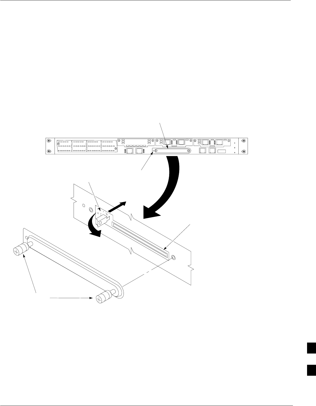
BTS Router CF Memory Card Removal and Replacement
5/21/04 1X SC4812T–MC BTS Optimization/ATP I-83
DRAFT
BTS Router CF Memory Card
Removal and Installation
The following procedures cover removal and installation of the CF
memory card used to store the IOS and configuration data for the BTS
router.
Figure I-5: Router CF Memory Card Removal
CF Memory
Card Cover
SC4812T0012
Captive
Screws
ACT
LED
ROTATE OUT
PUSH IN
Card Ejector
Lever
CF Memory
Card
Tools Required
The following tool is required to perform procedures included in this
section:
SNumber 2 cross–recess screwdriver
Removing a CF memory card – Refer to Figure I-5 and follow the
procedures in Table I-13 to remove the CF memory card from the BTS
router.
I

BTS Router CF Memory Card Removal and Replacement – continued
I-84 1X SC4812T–MC BTS Optimization/ATP 5/21/04
DRAFT
The CF memory card may be removed and installed while
power is applied to the router.
NOTE
Table I-13: Router Flash Memory Card Removal
Step Action
1Refer to MWR1900 Wireless Mobile Edge Router Hardware Installation Guide; part number
78–13982–01 for the latest information, cautions, and notes on BTS router CF memory card removal
and installation prior to proceeding with the following steps.
2! CAUTION
Do not remove the CF memory card while there are read or write operations occurring on the card.
Removing the card during these operations will cause the router to shut down and damage the file
system.
If power is applied to the router, be sure there are no read or write operations in progress for the card
by verifying the ACT indicator LED is not lighted or lighting intermittently.
3Using a cross–recess screwdriver, fully loosen the captive screws securing the flash memory card slot
cover to the router, and remove the cover.
4Remove the CF memory card by performing the following:
4a – Rotate the end of the card ejector lever until it is pointing out 90_ to the router front panel (see
Figure I-5).
4b – Push the card ejector lever straight into the router to unseat the CF memory card.
4c – Carefully pull the card out of the slot.
5Place the CF memory card on an anti–static surface or in an anti–static container.
Installing a Flash Memory Card – Refer to Figure I-5 and follow the
procedures in Table I-13 to install the CF memory card in a BTS router
Table I-14: Router Flash Memory Card Installation
Step Action
1Refer to MWR1900 Wireless Mobile Edge Router Hardware Installation Guide; part number
78–13982–01 for the latest information, cautions, and notes on BTS router CF memory card removal
and installation prior to proceeding with the following steps.
2If the flash memory slot cover is installed, use a cross–recess screwdriver to fully loosen the captive
screws securing the cover to the router, and remove the cover (see NO TAG).
3Install the CF memory card by performing the following:
3a – Hold the CF memory card with the label facing up and the connector end pointing toward the
router.
3b – Carefully insert the connector end into the flash memory card slot.
. . . continued on next page
I

BTS Router CF Memory Card Removal and Replacement – continued
5/21/04 1X SC4812T–MC BTS Optimization/ATP I-85
DRAFT
Table I-14: Router Flash Memory Card Installation
Step Action
3c – Push the CF memory card into the slot to seat it in the slot connector.
–– The card ejector lever will extend out of the router as the card is seated.
3d – Pull on the card ejector lever to fully extend it from the router, and rotate it to the left to its stowed
position to latch the card in the slot (see Figure I-5).
I

BTS Router CF Memory Card Removal and Replacement – continued
I-86 1X SC4812T–MC BTS Optimization/ATP 5/21/04
DRAFT
Notes
I

5/21/04 1X SC4812T–MC BTS Optimization/ATP
DRAFT
Appendix J: Chapter Title Goes Here
Appendix Content
THIS IS THE GENERAL APPENDIX TOC. USE THIS FOR ALL
APPENDICES EXCEPT APPENDIX A.
Guide Book 1–2. . . . . . . . . . . . . . . . . . . . . . . . . . . . . . . . . . . . . . . . . . . . . . . . . . . . .
Document Overview 1–2. . . . . . . . . . . . . . . . . . . . . . . . . . . . . . . . . . . . . . . . . . . . . .
What Is In This Guide? 1–2. . . . . . . . . . . . . . . . . . . . . . . . . . . . . . . . . . . . .
Book Catalogs and Organization 1–3. . . . . . . . . . . . . . . . . . . . . . . . . . . . . . . . . . . .
Book Directory 1–3. . . . . . . . . . . . . . . . . . . . . . . . . . . . . . . . . . . . . . . . . . .
Special Catalogs 1–5. . . . . . . . . . . . . . . . . . . . . . . . . . . . . . . . . . . . . . . . . . .
Physical Page Layouts 1–6. . . . . . . . . . . . . . . . . . . . . . . . . . . . . . . . . . . . . . . . . . . .
A/A4 Page and Margin Sizes 1–6. . . . . . . . . . . . . . . . . . . . . . . . . . . . . . . . .
A/A4 Page Text Area 1–7. . . . . . . . . . . . . . . . . . . . . . . . . . . . . . . . . . . . . . .
A/A4 Page Components 1–9. . . . . . . . . . . . . . . . . . . . . . . . . . . . . . . . . . . .
Frame and Table Components 1–10. . . . . . . . . . . . . . . . . . . . . . . . . . . . . . . . . . . . . .
Frames With Tools 1–10. . . . . . . . . . . . . . . . . . . . . . . . . . . . . . . . . . . . . . . . .
Flow Charts and Block Diagrams 1–10. . . . . . . . . . . . . . . . . . . . . . . . . . . . .
Line Drawings 1–11. . . . . . . . . . . . . . . . . . . . . . . . . . . . . . . . . . . . . . . . . . . .
Table Types In This Template 1–12. . . . . . . . . . . . . . . . . . . . . . . . . . . . . . . .
Item/Description Table 1–12. . . . . . . . . . . . . . . . . . . . . . . . . . . . . . . . . . . . .
Step Table 1–13. . . . . . . . . . . . . . . . . . . . . . . . . . . . . . . . . . . . . . . . . . . . . . .
Step/Check Table 1–14. . . . . . . . . . . . . . . . . . . . . . . . . . . . . . . . . . . . . . . . . .
Component Descriptions 1–15. . . . . . . . . . . . . . . . . . . . . . . . . . . . . . . . . . . . . . . . . .
Conclusions 1–16. . . . . . . . . . . . . . . . . . . . . . . . . . . . . . . . . . . . . . . . . . . . . . . . . . . . .
Map Title Goes Here lkjsfdg Sfdkgj Msfd N lkas K lkjsdfl kB lkj fgcb 1–17. . . . . .
Block Label Goes Here 1–17. . . . . . . . . . . . . . . . . . . . . . . . . . . . . . . . . . . . .
Block Label Goes Here 1–17. . . . . . . . . . . . . . . . . . . . . . . . . . . . . . . . . . . . .
Block Label Goes Here 1–18. . . . . . . . . . . . . . . . . . . . . . . . . . . . . . . . . . . . .
Block Label Goes Here 1–19. . . . . . . . . . . . . . . . . . . . . . . . . . . . . . . . . . . . .
Map Title Goes Here 1–22. . . . . . . . . . . . . . . . . . . . . . . . . . . . . . . . . . . . . . . . . . . . . .
J

Table of Contents – continued
1X SC4812T–MC BTS Optimization/ATP 5/21/04
DRAFT
Notes
J
MMI Cable Fabrication
5/21/04 1X SC4812T–MC BTS Optimization/ATP J-1
DRAFT
Purpose
When the Motorola SLN2006A MMI Interface Kit is not available, a
cable can be fabricated by the user to interface a nine–pin serial
connector on an LMF computer platform with an MMI connector on
GLI cards and other Motorola BTS assemblies. This section provides
information necessary for fabricating this cable.
Required Parts
Table J-1: Parts Required to Fabricate MMI Cable
Item Part Number Qty Description
AMotorola 3009786R01 1Ribbon cable assembly, 1.524 M, one 8–contact MMI
connector, one 10–contact connector
BAMP 749814–1,
Belkin A4B202BGC,
or equivalent
1Receptacle kit, unassembled, 9–position, socket contacts,
unshielded, metal or plastic shell, solder or crimp–type
contacts
Cable Details
Figure J-1 illustrates the details of the fabricated MMI cable.
Figure J-1: Fabricated MMI Cable Details
DB–9 Plug
Socket Numbering
(Mating Side)
12345
6789
1
2
3
4
5
6
7
8
8–Contact MMI Plug
Socket Numbering
(Mating Side)
Item A: Cable assembly 3009786R01 (with 10–contact plug removed)
MMIFAB001–0
FABRICATION NOTES:
1. Remove 10–contact connector from ribbon cable of cable assembly 3009786R01
2. Separate wires at unterminated end of ribbon cable as required to connect to DB–9
connector contacts
3. Dark wire on ribbon cable of cable assembly 3009786R01 connects to pin 1 of the
8–contact plug
4. Strip three ribbon cable wires with connections specified in Table J-2 and connect to
DB–9 plug contacts as specified in Table J-2
5. Shorten un–connected ribbon cable wires enough to prevent contacting DB–9
contacts, leaving enough wire to egage any strain relief in the DB–9 connector shell
Item B
J

MMI Cable Fabrication – continued
J-2 1X SC4812T–MC BTS Optimization/ATP 5/21/04
DRAFT
Wire Run List
Table J-2 provides the wire run/pin–out information for the fabricated
MMI cable.
Table J-2: Fabricated MMI Cable Wire Run List
8–CONTACT MMI
PLUG CONTACT
DB–9 PLUG
CONTACT
1 ––––––––––––––––– 5
2 ––––––––––––––––– 2
3 ––––––––––––––––– 3
4No Connection (NC)
5 NC
6 NC
7 NC
8 NC
J

5/21/04 1X SC4812T–MC BTS Optimization/ATP Index-1
DRAFT
Index
This index supports 4 levels–
Level 1 through Level 4 in a
2–column format.
B

Index – continued
Index-2 1X SC4812T–MC BTS Optimization/ATP 5/21/04
DRAFT
BBX
Adding, 3-48–3-50
Prerequisites, 3-48–3-50
Logical data, 4-79–4-81
*68P09260A64−B*
68P09260A64–B

DRAFT
68P09260A64–B
5/21/04
ENGLISH
CDMA2000 1X
SOFTWARE RELEASE 2.16.4.X
Technical
Information
1X SC4812T–MC BTS
OPTIMIZATION/ATP
800 MHZ & 1.9 GHZ
SOFTWARE RELEASE 2.16.4.X
800 MHZ & 1.9 GHZ
CDMA2000 1X
1X SC4812T–MC BTS OPTIMIZATION/ATP
ENGLISH
5/21/04
68P09260A64–B
DRAFT

Technical Information Products and Services
11
STANDARD MANUAL PRINTING INSTRUCTIONS
STANDARD SPECIFICATIONS – FOR REFERENCE–DO NOT MODIFY
Part Number: 68P09260A64–B APC:
Title: 1X SC4812T–MC BTS Optimization/ATP
PAPER:
Body: 70 lb.
Inside Cover: 65 lb. Cougar
Tabs: 110 lb. Index
Binder Cover: Standard TED
cover – 10 pt. Carolina
1st. LEVEL TABS:
Single Sided
5 Cuts
Clear Mylar
Pantone 2706–C
Black Ink
2nd. LEVEL TABS: FINISHING:
3–Ring Binder
Slant–D
3–Hole Punched
(5/16–in. dia.)
Shrink Wrap Body
Black ink for body, inside cover, and binder cover.
SPECIAL INSTRUCTIONS
TAB and SHEET SIZE/QUANTITY
7X9 8.5x11 11x17
NON–STANDARD SPECIFICATIONS
Tape Bound Corner Stitch
Other: Meet with manager to determine the deliverable.
Sheets = (Total Pages) / 2
Single Sided
7 Cuts
Clear Mylar
White
Black Ink
Filename:
1st Level Tabs 2nd Level Tabs
Volume 5/21/04of DatePrint Vendor: eDOC

Map Title Goes Here
MMM YYYY Manual Title -1
PRELIMINARY
B

Map Title Goes Here – continued
-2 Manual Title MMM YYYY
PRELIMINARY
B

Map Title Goes Here
MMM YYYY Manual Title -3
PRELIMINARY
B

Map Title Goes Here – continued
-4 Manual Title MMM YYYY
PRELIMINARY
B
-1
Using The Tabs
To use these tabs, simply cut or copy the tab catalog and paste in the chapter
book in the first postion (in front of the chaptoc document).
You will note that these are good for ten chapters. To build tabs for 11–20 or for
appendix A–J, open the catalogs for the proper tab position and edit the
microdocument for the proper number/letter. Number 11 or alpha A start in the
top tab_1 position.

CCCCCCCCCCCCCCCCC
DDDDDDDDDDDDDDDDD
EEEEEEEEEEEEEEEEEE
FFFFFFFFFFFFFFFFFFFF
GGGGGGGGGGGGGGG
HHHHHHHHHHHHHHHHH
IIIIIIIIIIIIIIIIIIIIIIIIIIIIIIIIIIIIIIIIIII
JJJJJJJJJJJJJJJJJJJJJJ
MANUAL TITLE
AAAAAAAAAAAAAAAAA
BBBBBBBBBBBBBBBBB
PART NUMBER
CLEAR MYLAR, COLOR–PANTONE 2706–C, INK–BLACK
CUT 1 – IN FRONT OF CHAPTER
OR
BETWEEN PAGES
For 8.5x11, use all tabs.
For 7x9, use just cuts 1–4
68P09248A54–D
SC 9640 BTS Install/Opto/ATP/FRU xxxxxxxx
*** DO NOT HAVE 3 OR MORE LINES OF TEXT ON A TAB ***
AND
CUT 2 – IN FRONT OF CHAPTER
OR
BETWEEN PAGES AND
CUT 3 – IN FRONT OF CHAPTER
OR
BETWEEN PAGES AND
CUT 4 – IN FRONT OF CHAPTER
OR
BETWEEN PAGES AND
CUT 5 – IN FRONT OF CHAPTER
OR
BETWEEN PAGES AND

AAAAAAAAAAAAAAA
AAAAAAAAAAAAAAA
BBBBBBBBBBBBBBB
BBBBBBBBBBBBBBB
CCCCCCCCCCCCCCC
CCCCCCCCCCCCCCC
DDDDDDDDDDDDDDD
DDDDDDDDDDDDDDD
EEEEEEEEEEEEEEEE
EEEEEEEEEEEEEEEE
FFFFFFFFFFFFFFFFFF
FFFFFFFFFFFFFFFFFF
GGGGGGGGGGGGGG
GGGGGGGGGGGGGG
MANUAL TITLE
PART NUMBER
CLEAR MYLAR, COLOR–WHITE, INK–BLACK
For 8.5x11, use all tabs.
For 7x9, use just cuts 1–5
68P09248A54–D
SC 9640 BTS Install/Opto/ATP/FRU xxxxxxxx
*** DO NOT HAVE 3 OR MORE LINES OF TEXT ON A TAB ***
CUT 1 – IN FRONT OF CHAPTER
OR
BETWEEN PAGES AND
CUT 2 – IN FRONT OF CHAPTER
OR
BETWEEN PAGES AND
CUT 3 – IN FRONT OF CHAPTER
OR
BETWEEN PAGES AND
CUT 4 – IN FRONT OF CHAPTER
OR
BETWEEN PAGES AND
CUT 5 – IN FRONT OF CHAPTER
OR
BETWEEN PAGES AND
CUT 6 – IN FRONT OF CHAPTER
OR
BETWEEN PAGES AND
CUT 7 – IN FRONT OF CHAPTER
OR
BETWEEN PAGES AND

Product Information
i Manual Title MMM YYYY
PRELIMINARY
Model Chart
Model Complement For Product A – Models X, Y, Z
Model Description Quantity
Options
Option Complement For Product A
Model Description Quantity
Specifications
General Specifications for Product A
Specification Description
Receiver Specifications for Product A
Specification Description
Transmitter Specifications for Product A
Specification Description
PRELIMINARY
SPECIFICATIONS SUBJECT TO CHANGE WITHOUT NOTICE
Notice
While reasonable efforts have been made to assure the accuracy of this document, Motorola, Inc. assumes no liability resulting from any
inaccuracies or omissions in this document, or from use of the information obtained herein. The information in this document has been
carefully checked and is believed to be entirely reliable. However, no responsibility is assumed for inaccuracies or omissions. Motorola,
Inc. reserves the right to make changes to any products described herein and reserves the right to revise this document and to make
changes from time to time in content hereof with no obligation to notify any person of revisions or changes. Motorola, Inc. does not
assume any liability arising out of the application or use of any product, software, or circuit described herein; neither does it convey
license under its patent rights or the rights of others.
It is possible that this publication may contain references to, or information about Motorola products (machines and programs),
programming, or services that are not announced in your country. Such references or information must not be construed to mean
that Motorola intends to announce such Motorola products, programming, or services in your country.
Copyrights
This instruction manual, and the Motorola products described in this instruction manual may be, include or describe copyrighted
Motorola material, such as computer programs stored in semiconductor memories or other media. Laws in the United States and
other countries preserve for Motorola and its licensors certain exclusive rights for copyrighted material, including the exclusive
right to copy, reproduce in any form, distribute and make derivative works of the copyrighted material. Accordingly, any
copyrighted material of Motorola and its licensors contained herein or in the Motorola products described in this instruction manual
may not be copied, reproduced, distributed, merged or modified in any manner without the express written permission of Motorola.
Furthermore, the purchase of Motorola products shall not be deemed to grant either directly or by implication, estoppel, or
otherwise, any license under the copyrights, patents or patent applications of Motorola, as arises by operation of law in the sale of a
product.
Usage and Disclosure Restrictions
License Agreement
The software described in this document is the property of Motorola, Inc and its licensors. It is furnished by express license
agreement only and may be used only in accordance with the terms of such an agreement.
Copyrighted Materials
Software and documentation are copyrighted materials. Making unauthorized copies is prohibited by law. No part of the software or
documentation may be reproduced, transmitted, transcribed, stored in a retrieval system, or translated into any language or
computer language, in any form or by any means, without prior written permission of Motorola, Inc.
High Risk Activities
Components, units, or third–party products used in the product described herein are NOT fault–tolerant and are NOT designed,
manufactured, or intended for use as on–line control equipment in the following hazardous environments requiring fail–safe
controls: the operation of Nuclear Facilities, Aircraft Navigation or Aircraft Communication Systems, Air Traffic Control, Life
Support, or Weapons Systems (“High Risk Activities”). Motorola and its supplier(s) specifically disclaim any expressed or implied
warranty of fitness for such High Risk Activities.

PRELIMINARY
SPECIFICATIONS SUBJECT TO CHANGE WITHOUT NOTICE
Trademarks
MOTOROLA and the Stylized M Logo are registered in the US Patent & Trademark Office. All other product or service names are
the property of their respective owners.
© Copyright 2002 Motorola, Inc.
Javat Technology and/or J2MEt: Java and all other Java–based marks are trademarks or registered trademarks of Sun
Microsystems, Inc. in the U.S. and other countries.
UNIXR: UNIX is a registered trademark of The Open Group in the United States and other countries.
INSERT CONTRACTUAL LANGUAGE HERE
REV073102