North Pole Engineering 1997 WIRELESS WLAN MODULE User Manual WiFi IT
North Pole Engineering, Inc. WIRELESS WLAN MODULE WiFi IT
UserManual.wiki
>
North Pole Engineering
>
1997 User Manual
USER MANUAL
Navigation menu
Upload a User Manual
Namespaces
Wiki Guide
HTML
PDF
Info
Views
User Manual
Discussion / Help
Navigation
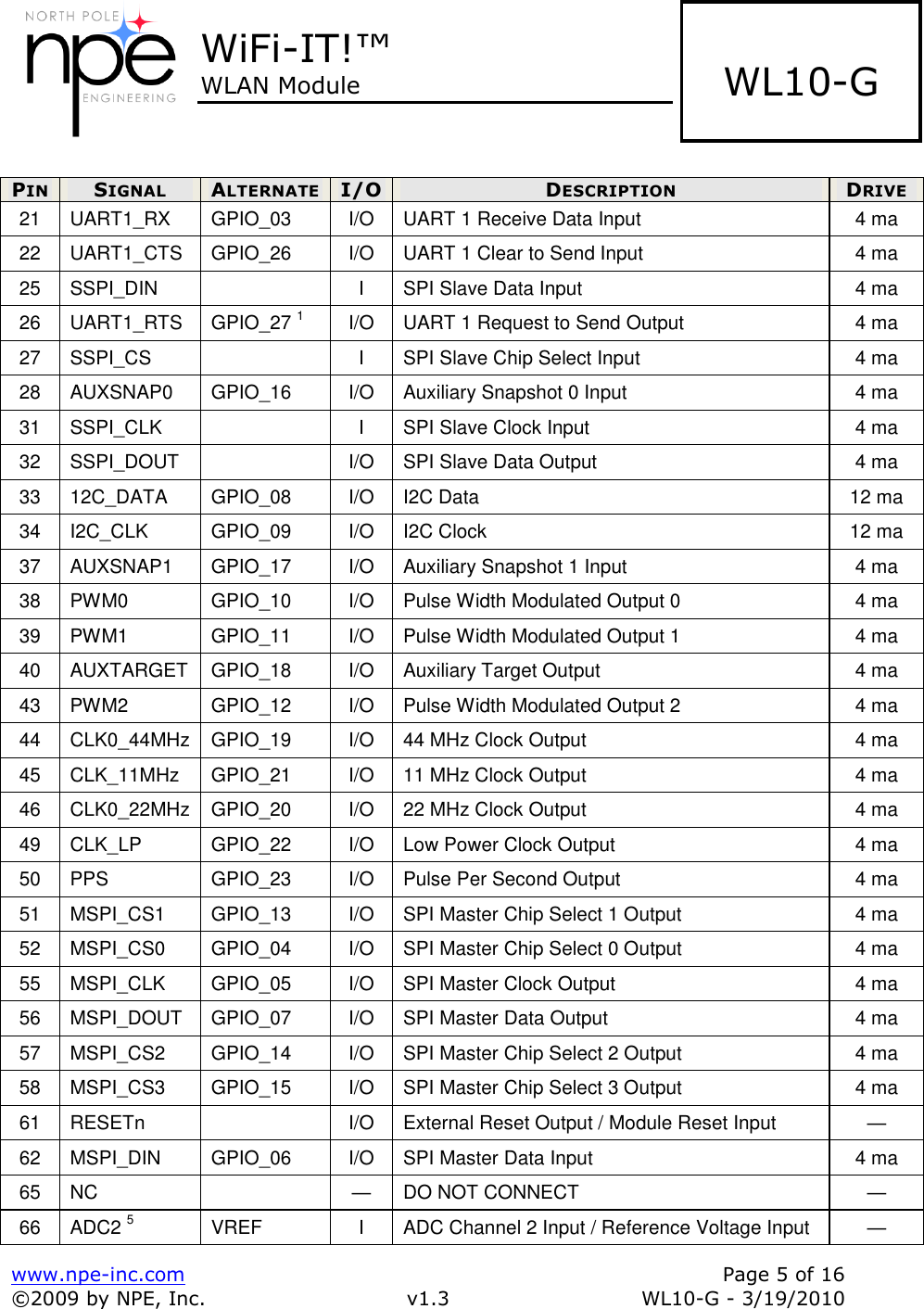
![WiFi-IT!™ WLAN Module www.npe-inc.com Page 12 of 16 ©2009 by NPE, Inc. v1.3 WL10-G - 3/19/2010 WL10-G ENGINEER’S DESIGN CHECKLIST This design checklist should be reviewed before committing a design to PCB fabrication. The checklist contains items that affect performance and/or operation of the WiFi-IT! module. ITEM DESCRIPTION Y/N 1 ALARM1 is pulled high or low through a pull up or pull down resistor. If pulled high, the signal must be pulled to VDD. 2 ALARM2 is pulled high or low through a pull up or pull down resistor. If pulled high, the signal must be pulled to VDD. 3 DC_DC_CNTRL is pulled low to GND. 4 EXT_RESETn is pulled high to VDD_IO. 5 JTAG_NTRST is pulled low to GND. 6 JTAG_TDI is pulled high to VDD_IO. 7 JTAG_TMS is pulled high to VDD_IO. 8 JTAG_TCK is pulled high to VDD_IO. 9 JTAG_TDO is pulled high to VDD_IO. 10 JTAG_CFG [0] (GPIO28) is pulled high to VDD_IO, or low to GND. 11 JTAG_CFG [1] (GPIO29) is pulled high to VDD_IO, or low to GND. 12 GPIO27 is pulled high to VDD_IO, and low to GND. 13 VDD traces and vias to the WiFi-IT! connector are sized to carry 200 mA per connector pin. Two vias per WiFi-IT! connector VDD pin may be necessary.](https://usermanual.wiki/North-Pole-Engineering/1997/User-Guide-1268659-Page-12.png)