North Pole Engineering 1997 WIRELESS WLAN MODULE User Manual WiFi IT
North Pole Engineering, Inc. WIRELESS WLAN MODULE WiFi IT
USER MANUAL
WiFi-IT!™
WLAN Module
www.npe-inc.com Page 1 of 16
©2009 by NPE, Inc. v1.3 WL10-G - 3/19/2010
WL10-G
WiFi-IT!
KEY FEATURES
Battery Operation (7.5 μA Sleep Current)
Small Form Factor (1.3” x 1.8”)
Timer and Event Triggered Auto-reporting Capability
Analog, Digital, Serial and PWM Interfaces
Multiple Active Interfaces
Real-Time Clock
Security: WEP128, WPA-PSK and WPA2-PSK (TKIP / AES)
Simple Wireless-Wire Mode
WLAN Stack Built-in
UART Interfaces Support Hardware Flow Control
-40 to +85 °C Operating Temperature Range
2.0 volts to 3.3 volts Operating Voltage
802.11b/g
Wireless
Network
Module
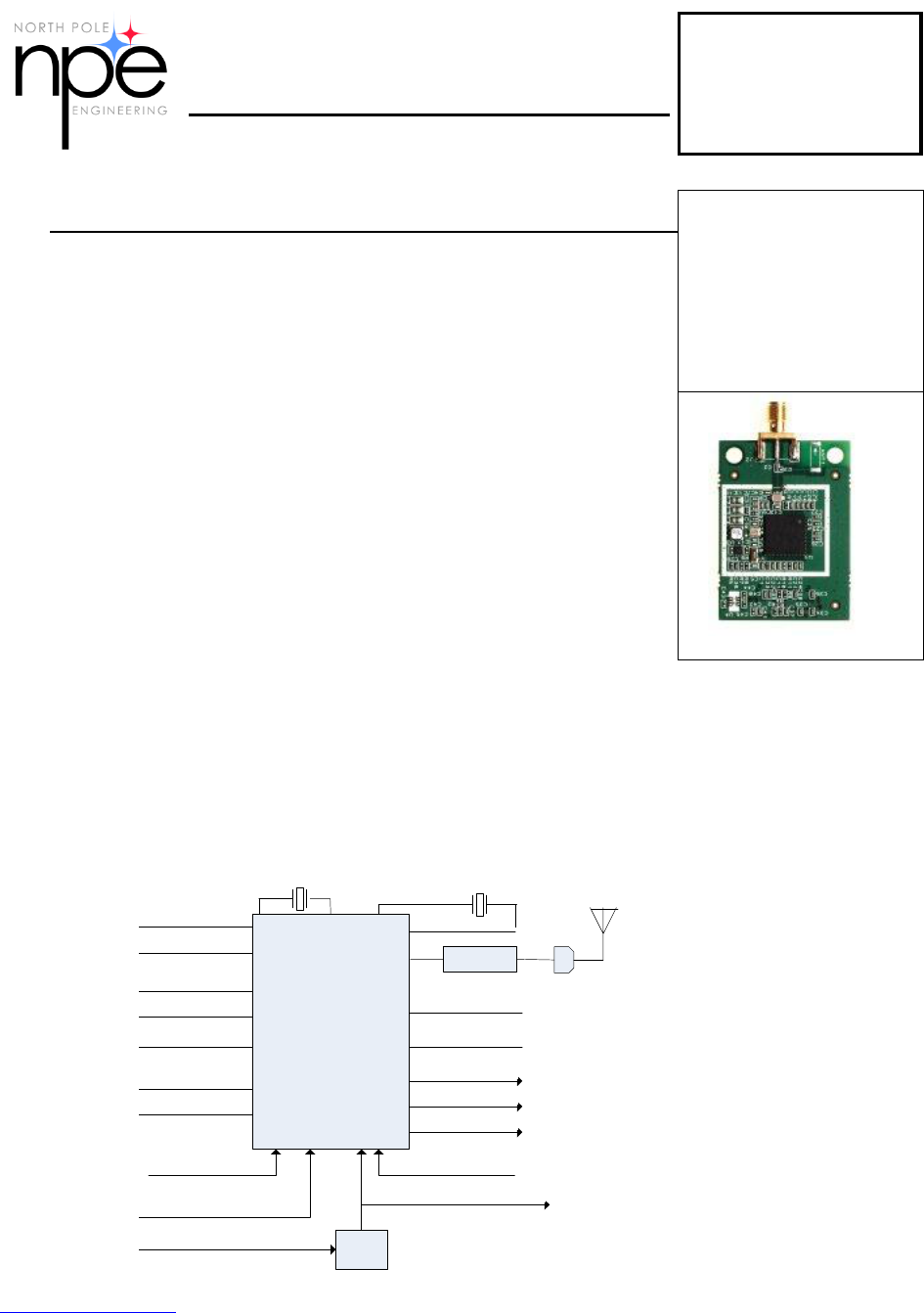
GENERAL INFORMATION
The WiFi-IT wireless module is a low cost, easy to integrate, robust solution for providing
low to mid-speed WLAN communication. WiFi-IT is perfectly suited for creating sensor-
based networks that require no additional programming. The module supports a wide range
of interfaces including, UART, SPI (master and slave), I2C, Digital, Analog and Pulse Width
Modulated (PWM). Multiple active interfaces are supported! WiFi-IT is compatible with
standard 802.11 b/g wireless access points.
MODULE BLOCK DIAGRAM
802.11 b/g
Transceiver
&
Processor
Balun
Alarm 0 Alarm 1
VDD 3.3v
1.8v
VDD_ADC
VDD_IO
SPI 0/GPIO
SPI 1/GPIO
UART 0/GPIO
UART 1/GPIO
I2C/GPIO
PWM 0
ADC 0 / DAC
ADC 1 PWM 1
PWM 2
GPIO
Ready
44 MHz 32 Khz

WiFi-IT!™
WLAN Module
www.npe-inc.com Page 2 of 16
©2009 by NPE, Inc. v1.3 WL10-G - 3/19/2010
WL10-G
HARDWARE DESCRIPTION
The WiFi-IT module operates in the 2.4 GHz ISM band and supports two standard 802.11
b/g data rates, 1 Mb/s and 2 Mb/s.
The module provides a variety of hardware interfaces that may be active at any time. There
are two UARTs, each providing an asynchronous communication interface supporting all
standard bit rates up to 921.6 kbps. Both UARTs support hardware flow control, if enabled.
Two SPI interfaces provide dual synchronous serial communication and operate in either
slave or master modes. SPI 0, when configured as a master device, provides up to four chip
selects. One I2C port is provided supporting bit rates of up to 392 kbps. Three Pulse-Width
Modulation (PWM) outputs are provided. The PWM outputs operate in two modes; as
independent function blocks providing an output signal with programmable frequency and
duty cycle, or as synchronized PWM function blocks with programmable phase delay
between each PWM output. Two ADC inputs provide 10-bit A-to-D conversions at up to 32
ksps. ADC 0 can be configured as a DAC providing 10-bit D-to-A conversions. When ADC 0
is used as a DAC, ADC 1 is disabled and should be left unconnected. Unused pins are
available as General Purpose I/O (GPIO), which may be programmed as Input (default),
Output or Bi-Directional.
Two Alarm inputs are provided to wake the WiFi-IT from the power conservation sleep
mode. The Alarm inputs have programmable polarity and are Schmidt-triggered logic. The
Ready output goes active when the module is ready to communicate.
FIRMWARE DESCRIPTION
The WiFi-IT module is available preloaded in two different configurations. The Wireless-Wire
(L1) configuration requires no programming, just use the configuration application to setup
your desired operation parameters.
The WiFi-IT Basic (L2) application provides a Basic language interpreter, enabling the
engineer to design, code and debug their own applications. Using the WiFi-IT! Module and
WiFi-IT Basic you can replace the microprocessor in many embedded designs!
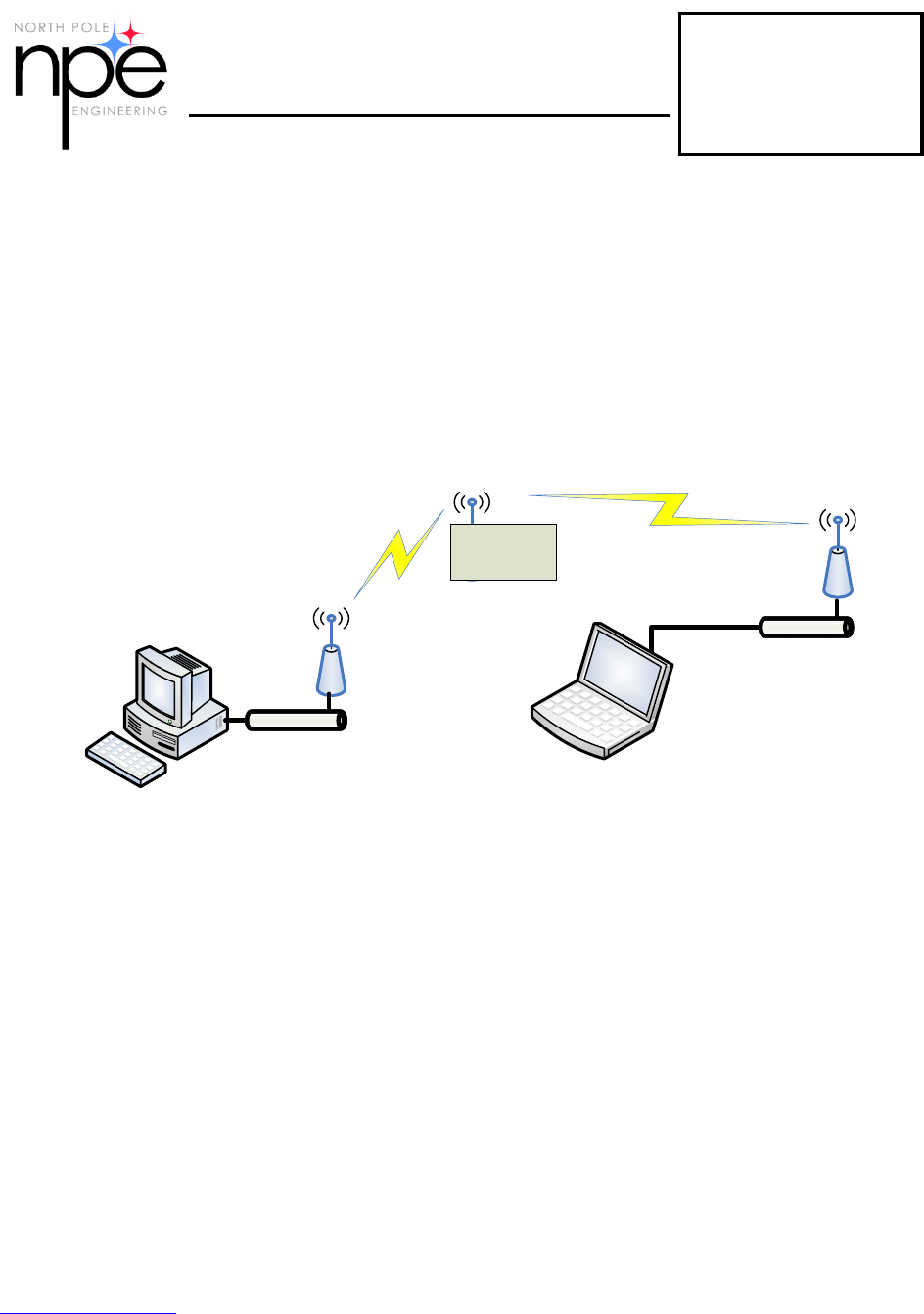
WIFI-IT! WIRELESS-WIRE
The Wireless-Wire application supports configuration of a nodes interface ports and control
engine. It is also used to setup the wireless communication parameters either remotely or
through an RS232/USB port on a Personal Computer.
Interface ports can be enabled and configured with the desired operating parameters. The
node control engine can me setup to operate in three unique modes:
1. Sleeping sensor node with timer or interrupt auto-reporting.
2. Sleeping data node with timer or interrupt auto-reporting.
3. Always-on node with interrupt, timer or continuous connection.
Once configured the WiFi-IT node permanently stores the settings and will operate, using
those settings, until they are changed. The Wireless-Wire Configuration application can
update node operating parameters over the wireless network at anytime.
WiFi-IT!™
WLAN Module
www.npe-inc.com Page 3 of 16
©2009 by NPE, Inc. v1.3 WL10-G - 3/19/2010
WL10-G
The Wireless-Wire protocol supports UDP communication between the node and an Access
Point. Communication between a Microsoft Windows® PC and the WiFi-IT nodes is directly
supported through a supplied virtual COM port (vCOM) driver. Once the vCOM port is
created the connection to the embedded system containing the WiFi-IT node operates just
as a wired connection. Data can be transferred from the embedded system or sent to the
embedded system through the vCOM port.
When operating with legacy RS232 equipment, no modifications to the legacy
communication protocol need to be made, in many instances. The Wireless-Wire wraps the
legacy communication messages in its own protocol for transmission and removes the
wrapper before forwarding the communication on to the legacy system.
`
Wireless-Wire Configuration
WiFi-IT!
Control Software
& vCOM
Figure 1: L1 System
When operating in one of the sleep modes there may be a latency period until the node
leaves the sleeping state and connects to the WLAN. The vCOM port can be configured to
buffer messages until the node is available.
WIFI-IT BASIC (L2) APPLICATION
The WiFi-IT Basic application provides a higher level of control requiring programming to
implement a solution. Using the WiFi-IT development environment with WiFi-IT Basic,
sophisticated programs can be written providing direct program control of an embedded
system. WiFi-IT Basic provides a simplified Application Programming Interface (API) to the
WLAN, special sleep modes and control of the hardware interfaces. The WiFi-IT development
environment provides tools to debug the application and download it to a module. Once the
application has been verified the code can be burned into as many WiFi-IT L2 modules as
desired.
A WiFi-IT L2 module may replace the microprocessor in many embedded systems, providing
a cost effective wireless solution for the embedded system designer.
WiFi-IT!™
WLAN Module
www.npe-inc.com Page 4 of 16
©2009 by NPE, Inc. v1.3 WL10-G - 3/19/2010
WL10-G
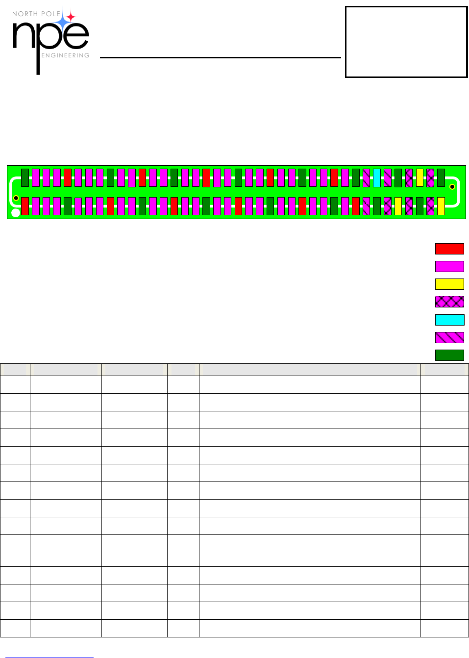
PIN-OUT AND SIGNAL DESCRIPTION
The following diagram lists the WL10-G signals. The signals are color-coded to indicate
functional groups according to their associated interfaces. For I/O signals that share
functionality with GPIO pins, the default functional state after reset is GPIO, with pins
configured as inputs.
VDD
VDDIO
VDDADC
VDDIO referenced signals
VDD referenced signals
VDDADC referenced signals
3 4
21
5 6
1211
7 8
910
14
15 16
13
1817
20
22
19
21
23 24
28
2625
27
3029
33 34
31 32
35 36
40
38
39
37
4241
43 44
4645
47 48
5251
5049
5453
55 56
57 58
64
60
6261
65 66
68
59
70
77 78
73
69
74
80
75
71
67
72
63
79
76
GND
KEY
PIN
SIGNAL
ALTERNATE
I/O
DESCRIPTION
DRIVE
3
TMS 3
I
JTAG Control Input
—
4
TRSTn 3
I
JTAG Reset Input (Active Low)
—
5
TDO
O
JTAG Data Output
4 ma
6
TDI 4
I
JTAG Data Input
—
7
CFG0
GPIO_28 2
I/O
JTAG Configuration 0 Input
4 ma
8
TCK 3
I
JTAG Clock Input
—
11
LED0
GPIO_30
I/O
High Drive Output 0
20 ma
12
CFG1
GPIO_29 2
I/O
JTAG Configuration 1 Input
4 ma
13
LED1
GPIO_31
I/O
High Drive Output 1
20 ma
14
UART0_CTS
\ READY
GPIO_24
I/O
UART 0 Clear to Send Input \
Alarm Wake-up Ready
4 ma
15
UART0_RX
GPIO_00
I/O
UART 0 Receive Data Input
4 ma
16
UART0_RTS
GPIO_25
I/O
UART 0 Request to Send Output
4 ma
19
UART1_TX
GPIO_02
I/O
UART 1 Transmit Data Output
4 ma
20
UART0_TX
GPIO_01
I/O
UART 0 Transmit Data Output
4 ma

WiFi-IT!™
WLAN Module
www.npe-inc.com Page 5 of 16
©2009 by NPE, Inc. v1.3 WL10-G - 3/19/2010
WL10-G
PIN
SIGNAL
ALTERNATE
I/O
DESCRIPTION
DRIVE
21
UART1_RX
GPIO_03
I/O
UART 1 Receive Data Input
4 ma
22
UART1_CTS
GPIO_26
I/O
UART 1 Clear to Send Input
4 ma
25
SSPI_DIN
I
SPI Slave Data Input
4 ma
26
UART1_RTS
GPIO_27 1
I/O
UART 1 Request to Send Output
4 ma
27
SSPI_CS
I
SPI Slave Chip Select Input
4 ma
28
AUXSNAP0
GPIO_16
I/O
Auxiliary Snapshot 0 Input
4 ma
31
SSPI_CLK
I
SPI Slave Clock Input
4 ma
32
SSPI_DOUT
I/O
SPI Slave Data Output
4 ma
33
12C_DATA
GPIO_08
I/O
I2C Data
12 ma
34
I2C_CLK
GPIO_09
I/O
I2C Clock
12 ma
37
AUXSNAP1
GPIO_17
I/O
Auxiliary Snapshot 1 Input
4 ma
38
PWM0
GPIO_10
I/O
Pulse Width Modulated Output 0
4 ma
39
PWM1
GPIO_11
I/O
Pulse Width Modulated Output 1
4 ma
40
AUXTARGET
GPIO_18
I/O
Auxiliary Target Output
4 ma
43
PWM2
GPIO_12
I/O
Pulse Width Modulated Output 2
4 ma
44
CLK0_44MHz
GPIO_19
I/O
44 MHz Clock Output
4 ma
45
CLK_11MHz
GPIO_21
I/O
11 MHz Clock Output
4 ma
46
CLK0_22MHz
GPIO_20
I/O
22 MHz Clock Output
4 ma
49
CLK_LP
GPIO_22
I/O
Low Power Clock Output
4 ma
50
PPS
GPIO_23
I/O
Pulse Per Second Output
4 ma
51
MSPI_CS1
GPIO_13
I/O
SPI Master Chip Select 1 Output
4 ma
52
MSPI_CS0
GPIO_04
I/O
SPI Master Chip Select 0 Output
4 ma
55
MSPI_CLK
GPIO_05
I/O
SPI Master Clock Output
4 ma
56
MSPI_DOUT
GPIO_07
I/O
SPI Master Data Output
4 ma
57
MSPI_CS2
GPIO_14
I/O
SPI Master Chip Select 2 Output
4 ma
58
MSPI_CS3
GPIO_15
I/O
SPI Master Chip Select 3 Output
4 ma
61
RESETn
I/O
External Reset Output / Module Reset Input
—
62
MSPI_DIN
GPIO_06
I/O
SPI Master Data Input
4 ma
65
NC
—
DO NOT CONNECT
—
66
ADC2 5
VREF
I
ADC Channel 2 Input / Reference Voltage Input
—
WiFi-IT!™
WLAN Module
www.npe-inc.com Page 6 of 16
©2009 by NPE, Inc. v1.3 WL10-G - 3/19/2010
WL10-G
PIN
SIGNAL
ALTERNATE
I/O
DESCRIPTION
DRIVE
69
DC_CTRL 6
O
DC-to-DC Regulator Control Output
4 ma
70
ADC1 5
DAC
I/O
ADC Channel 1 Input / DAC Output
—
73
RTC_OUT2 6
CLK_OUT
O
Sensor Wake Real-Time Clock Output 2 / Low
Power Clock
4 ma
74
ALARM2 6
I
Wake-Up Input 2
—
77
ALARM1 6
I
Wake-Up Input 1
—
78
RTC_OUT1 6
O
Sensor Wake Real-Time Clock Output 1
4 ma
Table 1: Interface Signal Description
NOTES
1. If GPIO_27 is pulled high during boot, the module will enter program update mode
and wait for FLASH download via SSPI or UART 0.
2. GPIO_28 and GPIO_29 are sampled at reset to establish the JTAG configuration for
debugging. These signals should only be used as outputs and not be driven by an
external device.
3. Configured as input with pull-up active.
4. JTAG TDI is not equipped with a pull-up or pull-down resistor. It should not be left
floating.
5. Referenced to VDD_ADC.
6. Referenced to VDD.
GENERAL NOTES
All I/O signals are configured as inputs with pull-down active after power-up or reset.
Unless otherwise noted all signals are referenced to VDD_IO.
WL10-G ABSOLUTE MAXIMUM RATINGS
RATING
VALUE
UNITS
VDD IO Supply Voltage Range
3.0 to 3.6
V
VDD Supply Voltage Range
1.8 to 3.0
V
Operating Ambient Temperature Range
-40 to +85
°C
Storage Temperature
-55 to +125
°C
WL10-G ELECTRICAL CHARACTERISTICS
RATING
SYM
MINIMUM
TYPICAL
MAXIMUM
UNITS
NOTES
Supply Voltage Range
VDD_IO
3.0
3.3
3.6
V
1,3
VDD
2.0
2.7
3.0
V
1,2
VDD_ADC
0
1.9
V
4
VDD_IO
VOH
VDD_IO - 0.4
VDD_IO
V
5

WiFi-IT!™
WLAN Module
www.npe-inc.com Page 7 of 16
©2009 by NPE, Inc. v1.3 WL10-G - 3/19/2010
WL10-G
VDD_IO
VOL
0
0.4
V
5
VDD_IO
VIH
0.8 VDD_IO
V
5
VDD_IO
VIL
0.25 VDD_IO
V
5
VDD
VOH
VDD - 0.4
VDD
V
6
VDD
VOL
0
0.4
V
6
VDD
VIH
0.8 VDD
V
6
VDD
VIL
0.25 VDD
V
6
VDD_ADC
VI
0
VDD_ADC - 0.036
7,8
Receive Mode Current
150
mA
Transmit Mode Current
200
mA
Sleep Mode Current
7.5
μA
NOTES:
1. VDD_IO and VDD are generated by the host board.
2. The values of VDD minimum maybe higher in some applications depending on the
required value for VIH of the VDD_IO power supply enable.
3. Lower VDD_IO voltages are possible in some applications. Contact NPE, Inc. for
further information.
4. VDD_ADC is generated on the WL10-G and has a nominal value of 1.8v.
5. See Table 1 for signals referenced to VDD_IO.
6. See Table 1 for signals referenced to VDD.
7. See Table 1 for signals referenced to VDD_ADC.
8. An external resistor divider can be used to expand the input range of the ADC inputs.
WL10-G RF CHARACTERISTICS
RATING
MINIMUM
TYPICAL
MAXIMUM
UNITS
NOTES
Operating Frequency Range
2412
2484
MHz
RF Data Rates
1 to 2
Mb/s
Number of RF Channels
14
RF Transmit Power
10
mW
Receiver Sensitivity:
1 Mb/S Data Rate
2 Mb/S Data Rate
dBm
-92
-90
Antenna Impedence
50
Ω

WiFi-IT!™
WLAN Module
www.npe-inc.com Page 8 of 16
©2009 by NPE, Inc. v1.3 WL10-G - 3/19/2010
WL10-G
WIFI-IT MODULE PLACEMENT
The WiFi-IT module is available in two antenna configurations; internal chip antenna (WL10-
GC) and SMA antenna (WL10-GS) configuration. When using the WL10-GC care must be
taken to minimize signal loss. The chip antenna should be clear of any metallic components,
copper traces, internal layers and any ground or voltage planes. There should be at least a
5 mm clearance in all directions.
The WL10-GC module should not be enclosed in a metal enclosure.
FCC LABELING INSTRUCTIONS
When installing the WiFi-IT! module into equipment, the module FCC ID number must be
visible. If it is not visible then labeling that is clearly visible must be attached to the product
stating;
WL10-GS “Contains FCC ID: XRH-1997”
WL10-GC “Contains FCC ID: XRH-1997”
WIFI-IT MODULE CERTIFICATION
This device complies with part 15 of the FCC rules. Operation is subject to the following two conditions:
(1) this device may not cause harmful interference, and (2) this device must accept any interference
received, including interference that may cause undesired operation.
NOTE: The manufacturer is not responsible for any radio or TV interference caused by unauthorized
modifications to this equipment. Such modifications could void the user’s authority to operate the
equipment.
The WiFi-IT! module has been certified by the FCC as a module that may be used in OEM equipment
without requiring re-certification as an FCC Class C device. To maintain this certification the WiFi-IT!
module must use only one of the two following antennas.
MANUFACTURER
ANTENNA GAIN
PART NUMBER
DESCRIPTION
Taoglas
1.8 DbI
GW.11.A153
84 mm Hinged SMA Reverse Male
Straight Connector
Antenna Factor
0.5 DbI
ANT-2.45-CHP-x
2.45GHz Chip Antenna
WiFi-IT!™
WLAN Module
www.npe-inc.com Page 9 of 16
©2009 by NPE, Inc. v1.3 WL10-G - 3/19/2010
WL10-G
ORDERING INFORMATION
The WiFi-IT module can be ordered with or without firmware loaded in either of two antenna
configurations.
PART NUMBER
DESCRIPTION
WL10-GS
SMA antenna version (no firmware loaded).
WL10-GS-L1
SMA antenna version loaded with Wireless-Wire firmware.
WL10-GS-L2
SMA antenna version loaded with WiFi-IT Basic firmware.
WL10-GC
Chip antenna version (no firmware loaded).
WL10-GC-L1
Chip antenna version loaded with Wireless-Wire firmware.
WL10-GC-L2
Chip antenna version loaded with WiFi-IT Basic firmware.
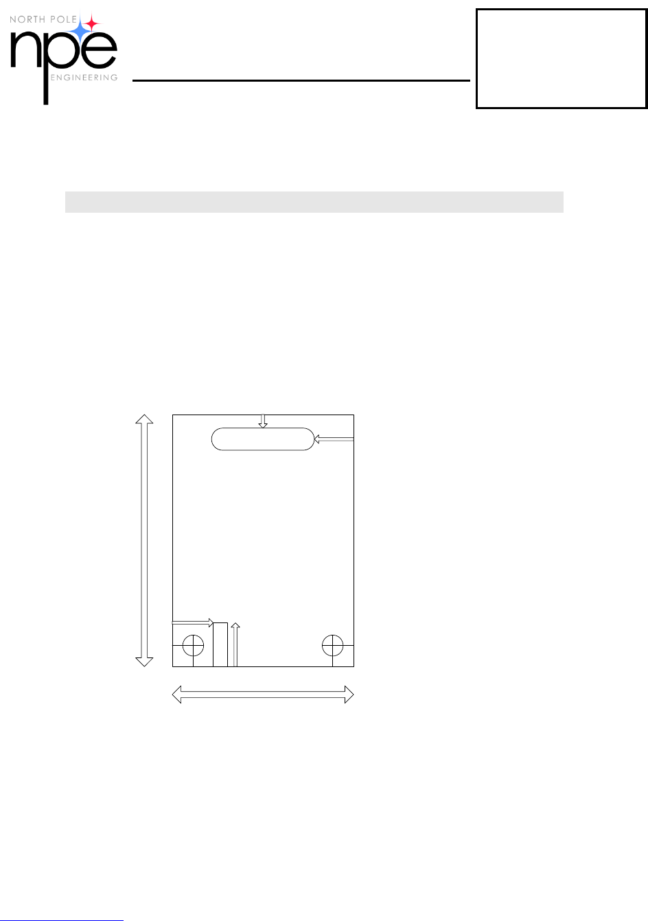
OUTLINE AND MOUNTING DIMENSIONS
The figure shown below displays the WL10-GC module dimensions in inches.
1.8
1.3
ANT1
J1
.150
.150 .150
.150
.294
.312
.096
.282
All Dimensions given in inches
WiFi-IT!™
WLAN Module
www.npe-inc.com Page 10 of 16
©2009 by NPE, Inc. v1.3 WL10-G - 3/19/2010
WL10-G
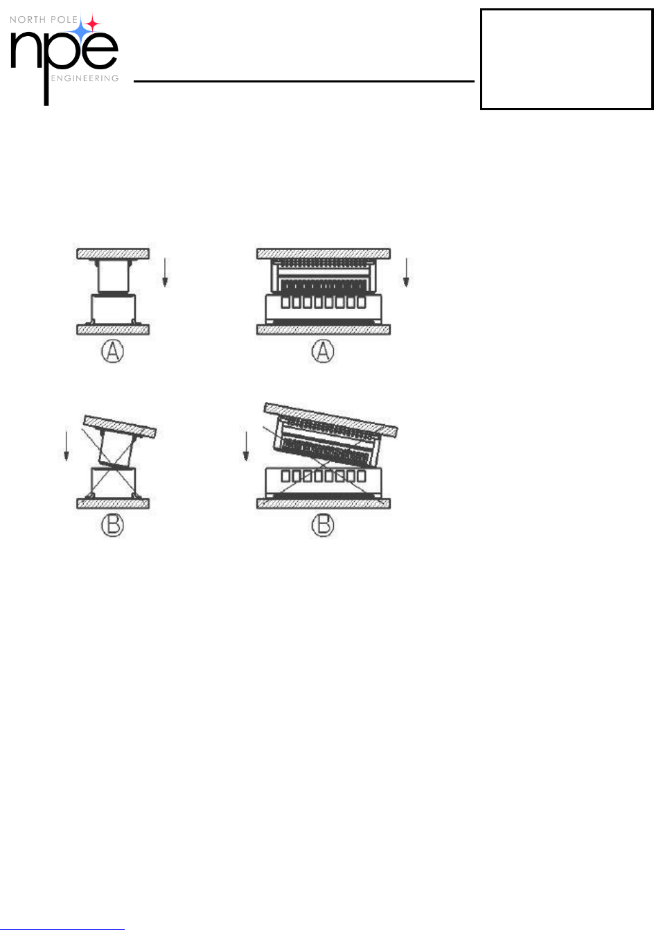
CONNECTOR PART NUMBERS
The WiFi-IT J1 connector is Molex part number 0544-770808. This connector mates to
Molex part number 0553-390808.
WIFI-IT CONNECTOR MATING
When attaching the module to the embedded system, please follow these instructions.
WiFi-IT!™
WLAN Module
www.npe-inc.com Page 11 of 16
©2009 by NPE, Inc. v1.3 WL10-G - 3/19/2010
WL10-G
TYPICAL CIRCUITS
The following schematic shows a typical example of a WiFi-IT! compatible power supply
designed for both battery and/or wall transformer operation. The power supply will operate
under control of the WiFi-IT! module, through the signal RTC_DC_DC_CNTL, to minimize
power usage.
The Bill of Materials (BOM) consists of:
IDENTIFIER
QTY
PART NO.
DESCRIPTION
U4
1
TPS2115A
TI Auto-switching Power Mux
U5
1
TPS62200DBV
TI DC-DC Step Down Converter
U6
1
TPS63031
TI Buck-Boost Converter
L3
1
LPS3010-103ML
Coilcraft Low Profile Shielded Inductor
L4
1
LPS3010-222ML
Coilcraft Low Profile Shielded Inductor
C1, C19,
2
0.1 uF
Capacitor
C23, C25
2
4.7 uF
Capacitor
C20
1
40 pF
Capacitor
C21
1
120 pF
Capacitor
C22, C24
2
10 uF
Capacitor
R2
1
499k
Resistor
R17
1
147k
Resistor

WiFi-IT!™
WLAN Module
www.npe-inc.com Page 12 of 16
©2009 by NPE, Inc. v1.3 WL10-G - 3/19/2010
WL10-G
ENGINEER’S DESIGN CHECKLIST
This design checklist should be reviewed before committing a design to PCB fabrication. The
checklist contains items that affect performance and/or operation of the WiFi-IT! module.
ITEM
DESCRIPTION
Y/N
1
ALARM1 is pulled high or low through a pull up or pull down resistor.
If pulled high, the signal must be pulled to VDD.
2
ALARM2 is pulled high or low through a pull up or pull down resistor.
If pulled high, the signal must be pulled to VDD.
3
DC_DC_CNTRL is pulled low to GND.
4
EXT_RESETn is pulled high to VDD_IO.
5
JTAG_NTRST is pulled low to GND.
6
JTAG_TDI is pulled high to VDD_IO.
7
JTAG_TMS is pulled high to VDD_IO.
8
JTAG_TCK is pulled high to VDD_IO.
9
JTAG_TDO is pulled high to VDD_IO.
10
JTAG_CFG [0] (GPIO28) is pulled high to VDD_IO, or low to GND.
11
JTAG_CFG [1] (GPIO29) is pulled high to VDD_IO, or low to GND.
12
GPIO27 is pulled high to VDD_IO, and low to GND.
13
VDD traces and vias to the WiFi-IT! connector are sized to carry 200
mA per connector pin. Two vias per WiFi-IT! connector VDD pin may
be necessary.

WiFi-IT!™
WLAN Module
www.npe-inc.com Page 13 of 16
©2009 by NPE, Inc. v1.3 WL10-G - 3/19/2010
WL10-G
14
At least six 0.1 uF bypass capacitors are placed within 0.250” of the
WiFi-IT! connector between VDD_IO and GND.
15
At least two 0.1 uF bypass capacitors are placed within 0.250” of the
WiFi-IT! connector between VDD and GND.
16
At least one 0.1 uF bypass capacitor(s) are placed within 0.250” of
the WiFi-IT! connector between 1.8V_ADC and GND.
17
A power supply capable of supplying 300 mA peak current to the
WiFi-IT! is provided over VDD.
18
A power supply capable of supplying 100 mA peak current at 3.3 volts
over VDD_IO, plus any other current requirements of the PCARD.
This power supply voltage must be enabled with the GainSpan
GS1010’s DC_DC_CNTRL signal.
19
All I/O connecting to VDD_IO referenced signals on the GS1010 are
held low whenever the GS1010 drives DC_DC_CNTRL low. This will
protect against possibility of causing latch-up in the GS1010.
20
All I/O connecting to VDD_IO referenced signals on the GS1010 meet
the minimum and maximum voltage specification of the GS1010.
WiFi-IT!™
WLAN Module
www.npe-inc.com Page 14 of 16
©2009 by NPE, Inc. v1.3 WL10-G - 3/19/2010
WL10-G
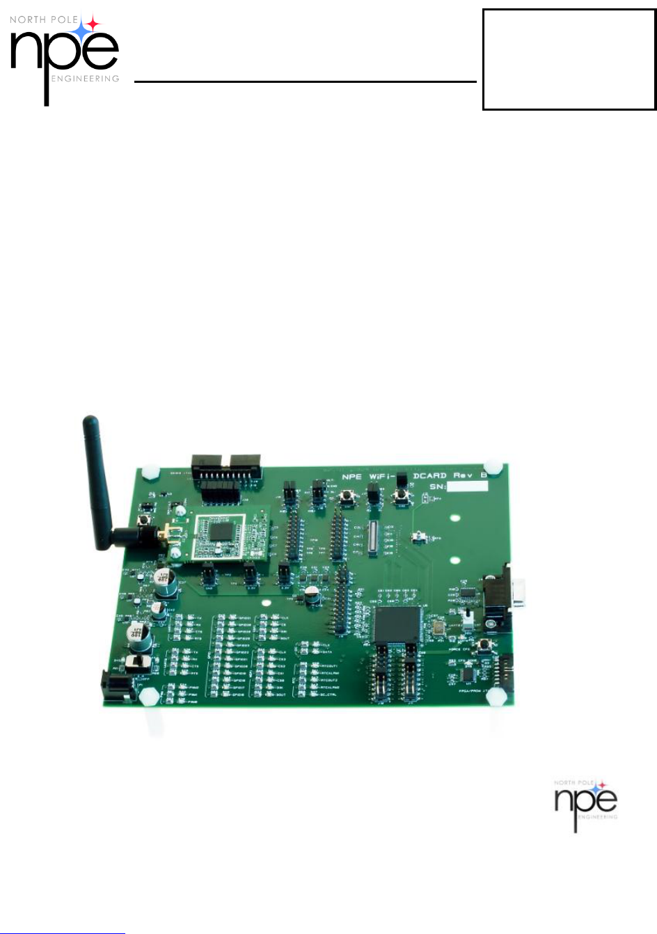
WIFI-IT! EDK - EVALUATION AND DEBUG DEVELOPMENT SYSTEM
The EDK evaluation and debug development system allows you to evaluate and develop
Wireless-Wire and WiFi-IT Basic applications using the WiFi-IT! module. Using a Microsoft
Windows® based application; you can configure WiFi-IT! modules, running Wireless-Wire
(L1) firmware and write and debug your own application code on modules running WiFi-IT
Basic (L2).
The EDK platform provides power, easy access to all of the WiFi-IT! interfaces and visual
indication of interface signaling, thereby reducing the need for an oscilloscope and/or logic
analyzer. In addition, the EDK supports access to the WiFi-IT!’s UART0 through the onboard
RS232 interface for setting configuration information, loading code and debugging
programs.
To evaluate the WiFi-IT! modules, NPE provides a configuration and administration program
which runs on Microsoft Windows based PCs and operates through a wired or wireless
connection. Configuration information is stored directly on the WiFi-IT! module, once
configured the node boots to that configuration when powered up.

WiFi-IT!™
WLAN Module
www.npe-inc.com Page 15 of 16
©2009 by NPE, Inc. v1.3 WL10-G - 3/19/2010
WL10-G
The EDK contains two WiFi-IT! Modules – WL10-GS and WL10-GC, the EDK platform board
and all cables and power adaptors. A full description of the EDK development system is
available from North Pole Engineering, Inc. at our website – www.npe-inc.com.
WiFi-IT!™
WLAN Module
www.npe-inc.com Page 16 of 16
©2009 by NPE, Inc. v1.3 WL10-G - 3/19/2010
WL10-G
REVISION HISTORY
VERSION
DATE
DESCRIPTION
1.0
Aug. 9, 2009
Initial release version.
1.1
Aug. 10, 2009
Added pin-out graphic. Other minor modifications.
1.2
Aug. 28, 2009
Update firmware description.
1.3
Sept. 25, 2009
Added FCC labeling instructions.
The information included here is provided by North Pole Engineering, Inc. (NPE) and is believed to be accurate and
reliable. However, NPE assumes no responsibility for its use, nor any infringement of patents or other rights of third
parties, which may result from its use. No license is granted by implication or otherwise under any patent rights of
NPE other than for circuitry embodied in NPE’s products. This document and described circuitry is subject to change
without notice.
The software described in this document is furnished under a license agreement and may be
used only in accordance with the terms of the license agreement. No part of this document
may be reproduced or transmitted in any form or by any means, electronic or mechanical,
without the express written consent of NPE.
Copyright 2009, North Pole Engineering, Inc. All Rights Reserved.