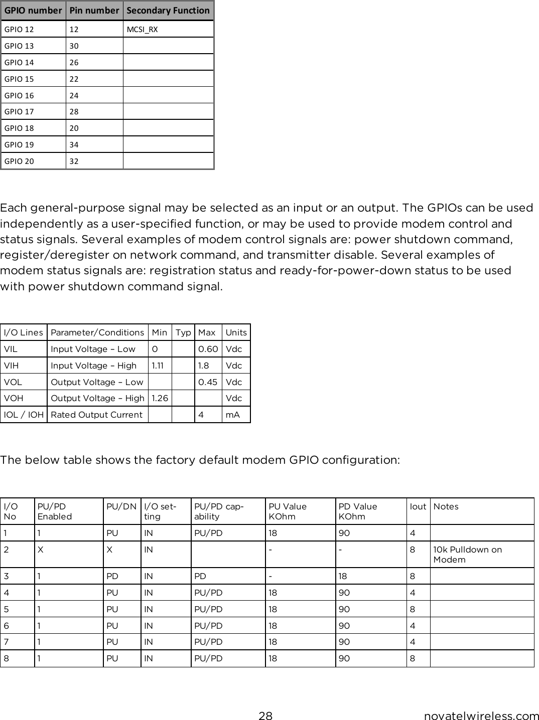
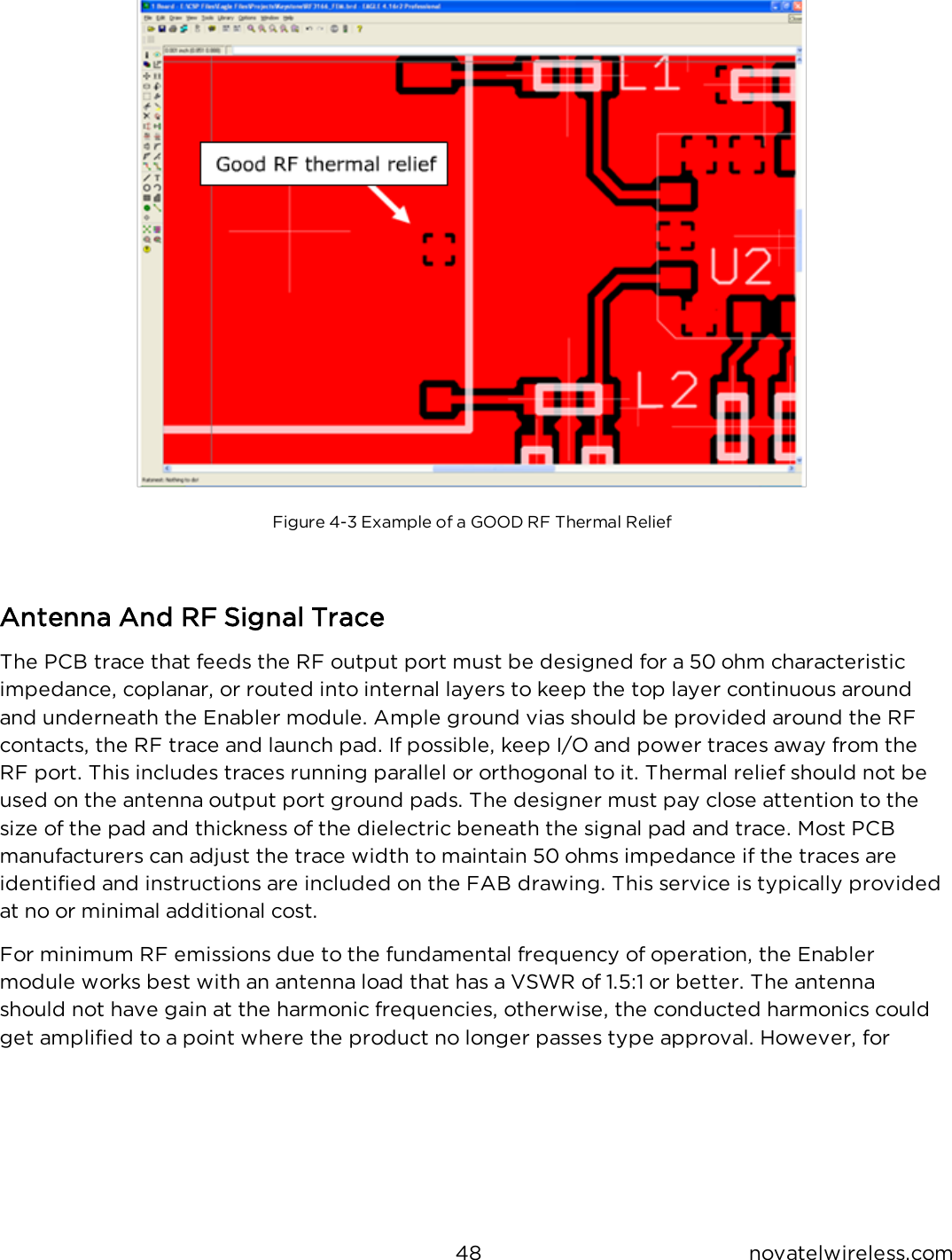
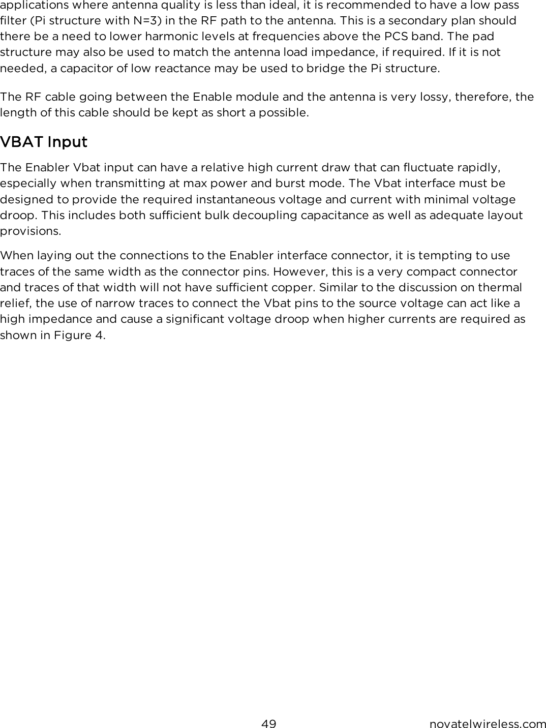
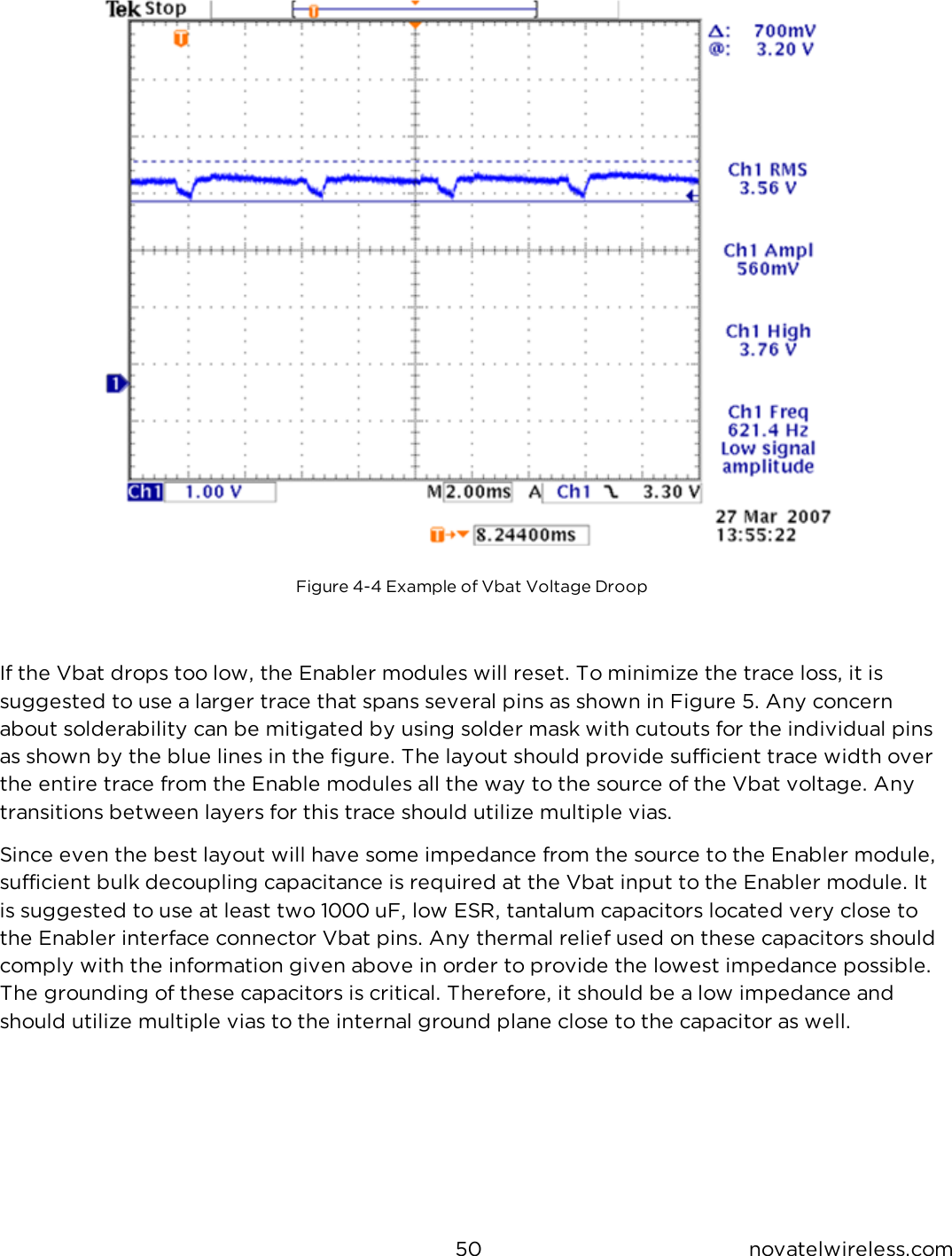
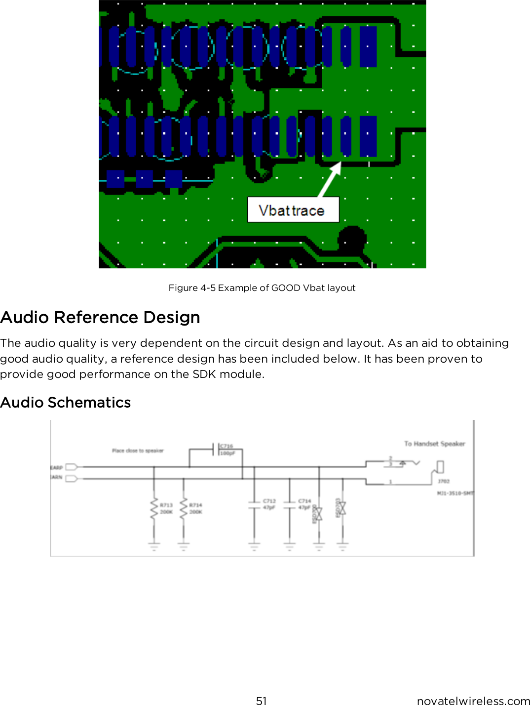
Novatel Wireless GSM0308 Wireless Modem User Manual Guide
Novatel Wireless Inc. Wireless Modem Guide
UserManual.wiki
>
Novatel Wireless
>
GSM0308 User Manual
>
User Manual
Contents
1.
Manual
2.
User Manual
User Manual
Navigation menu
Upload a User Manual
Namespaces
Wiki Guide
HTML
PDF
Info
Views
User Manual
Discussion / Help
Navigation
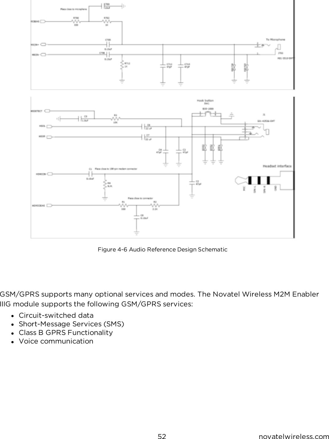
![iii novatelwireless.comWarranty Information[Revised: 11/11/2010]This warranty applies to (a) products sold directly by Novatel Wireless M2M, unless a different warranty is specified in a written agreement between Novatel Wireless M2M and the purchaser; and (b) products sold to end users through a distributor authorized by Novatel Wireless M2M, but only where the authorized distributor does not provide a separate warranty on such products, and Novatel Wireless M2M has agreed to provide this warranty to such end users. If you purchased the product from an authorized distributor, please check whether this warranty from Novatel Wireless M2M, or a separate warranty from the distributor, applies to your purchase. This warranty does not apply to any (i) accessories or batteries for the products; or (ii) demonstration samples or prototypes of the products. Unless otherwise provided in a written agreement between Novatel Wireless M2M and the purchaser, all such accessories, batteries, samples or prototypes are provided by Novatel Wireless M2M AS IS without any warranty of any kind.Novatel Wireless M2M warrants to the original purchaser of the product from Novatel Wireless M2M or its authorized distributor (as applicable) that, for a period of one (1) year from the date of shipment of the product from Novatel Wireless M2M, the product hardware will be substantially free from defects in material or workmanship under normal operation, and the product firmware will perform substantially in accordance with the product documentation provided by Novatel Wireless M2M. Novatel Wireless M2M does not warrant that (a) the product hardware or firmware will meet the purchaser's requirements; (b) the operation of the product hardware or firmware will be uninterrupted or error-free; or (c) the product, when integrated in, or combined with, other products or software not supplied by Novatel Wireless M2M, will continue to perform substantially in accordance with the product documentation. This limited warranty is for the benefit of the original purchaser, and is not transferable.During the warranty period, Novatel Wireless M2M, at its expense and in its sole discretion, will repair the product, or replace the product with a corresponding or equivalent product, if it is determined to have a covered defect, provided that the purchaser first notifies Novatel Wireless M2M (directly or through its authorized distributor from which the product was purchased) of any such defect, furnishes Novatel Wireless M2M with a proof of purchase (if required), requests and obtains a return merchandize authorization (RMA) number from Novatel Wireless M2M, and returns the product under that RMA to Novatel Wireless M2M (or, at Novatel Wireless M2M's option, to its authorized distributor), with the shipping charges being prepaid by purchaser. If, upon reasonable examination of the returned product, Novatel Wireless M2M does not substantiate the defect claimed by purchaser, or determines that the defect is not covered under this limited warranty, Novatel Wireless M2M will not be required to repair or replace the product, but may instead reship the product to the purchaser (or, at Novatel Wireless M2M's option, to its authorized distributor where the product can be made](https://usermanual.wiki/Novatel-Wireless/GSM0308.User-Manual/User-Guide-2157243-Page-4.png)