Novatel Wireless GSM0308 Wireless Modem User Manual Enabler II G Assiste GPS Integration Guide
Novatel Wireless Inc. Wireless Modem Enabler II G Assiste GPS Integration Guide
UserManual.wiki
>
Novatel Wireless
>
GSM0308 User Manual
>
Manual
Contents
1.
Manual
2.
User Manual
Manual
Navigation menu
Upload a User Manual
Namespaces
Wiki Guide
HTML
PDF
Info
Views
User Manual
Discussion / Help
Navigation
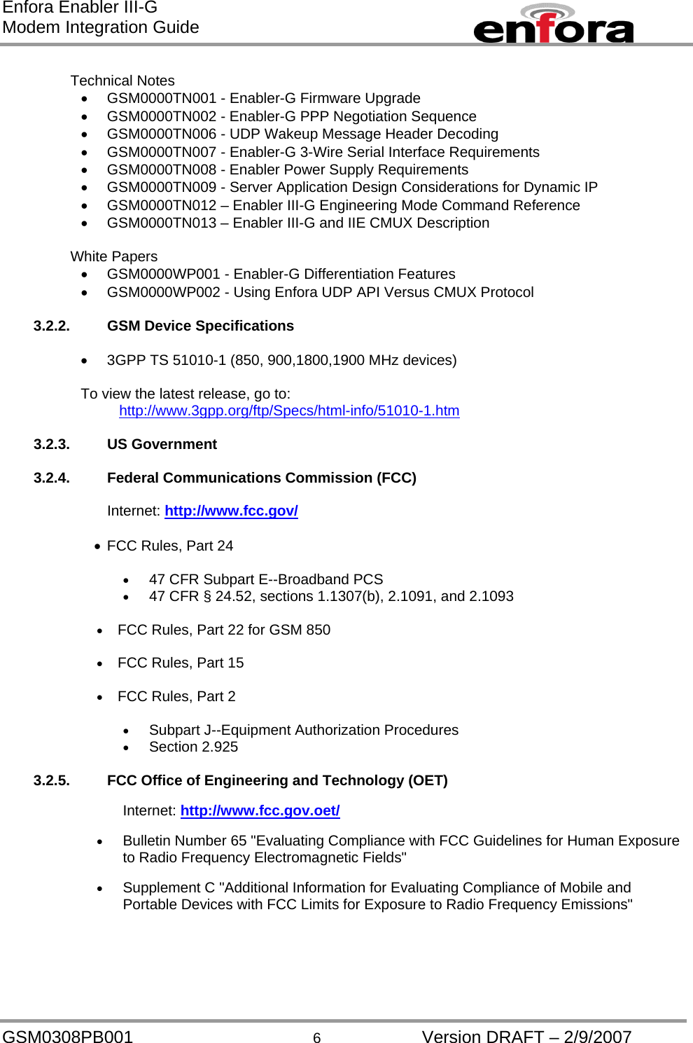
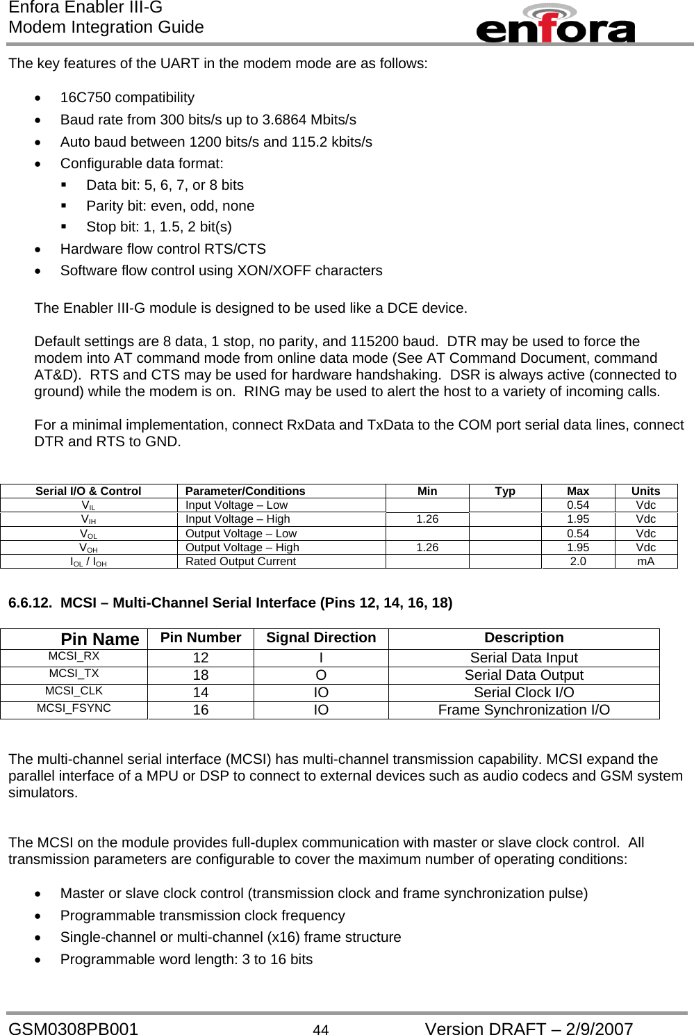
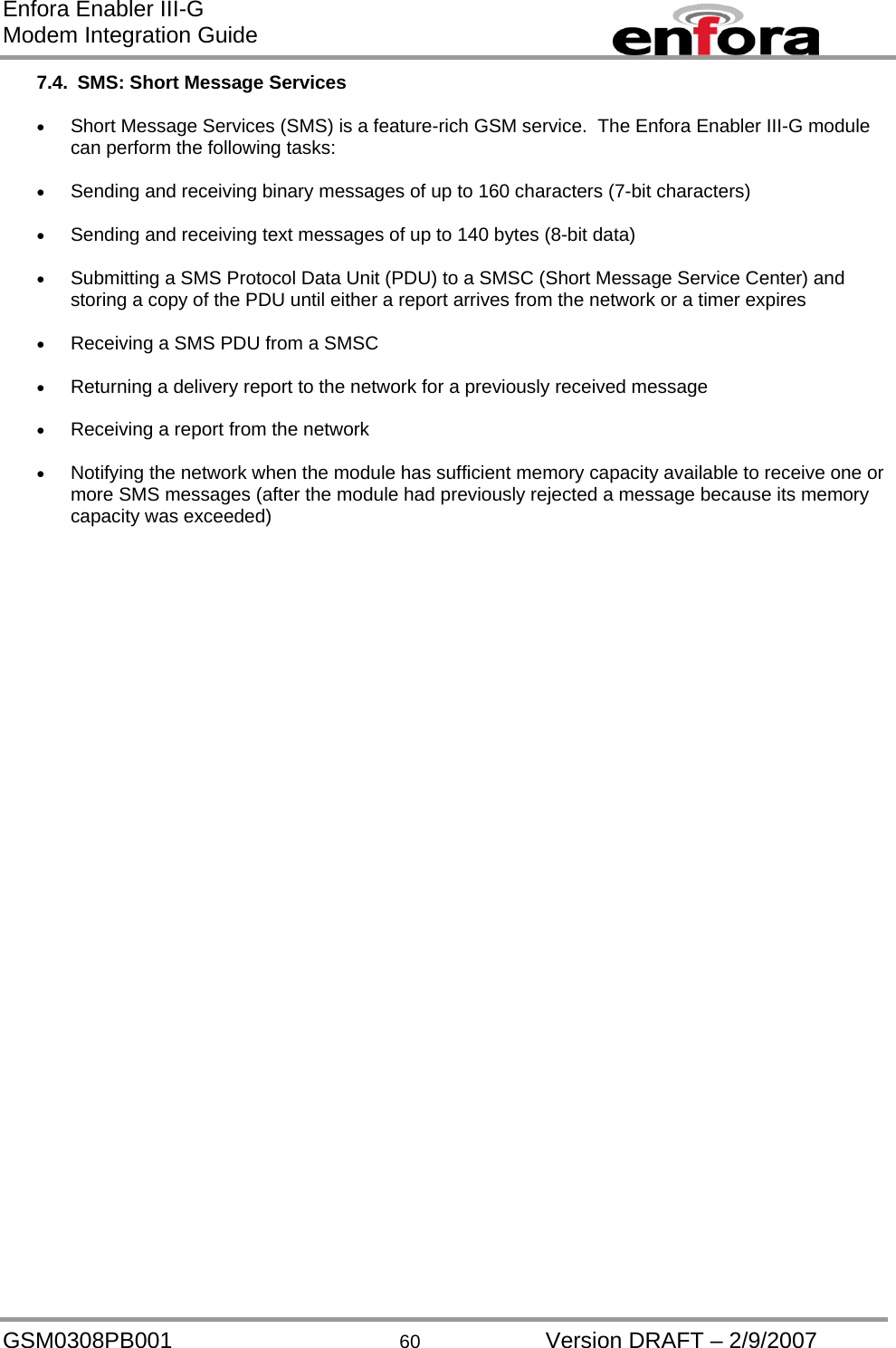
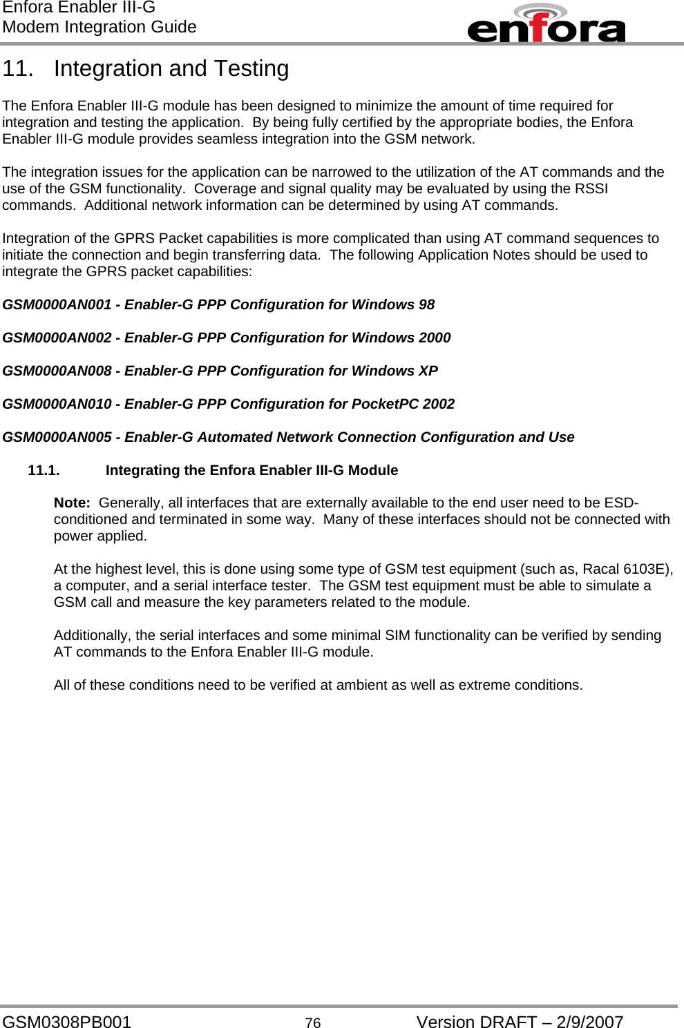
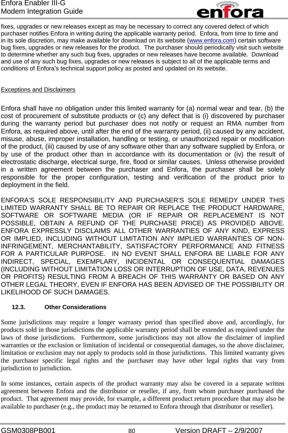
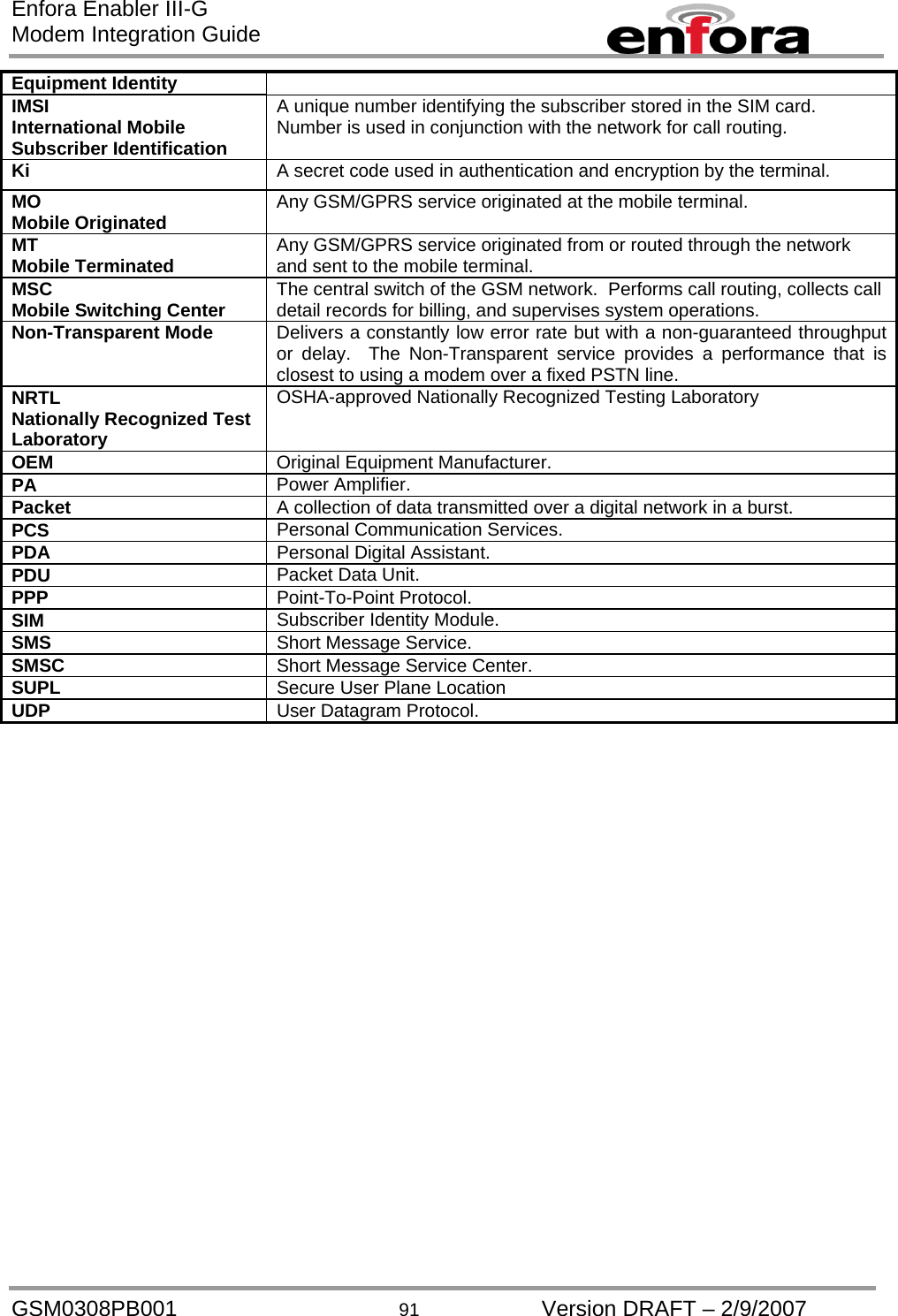
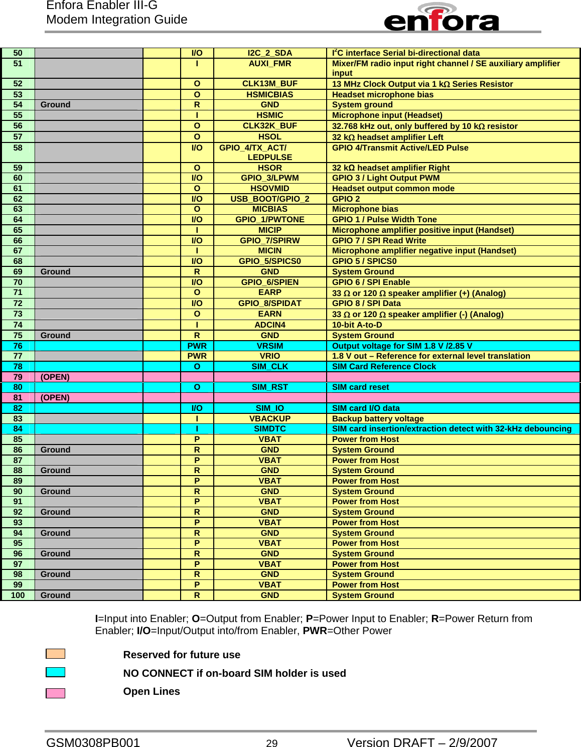
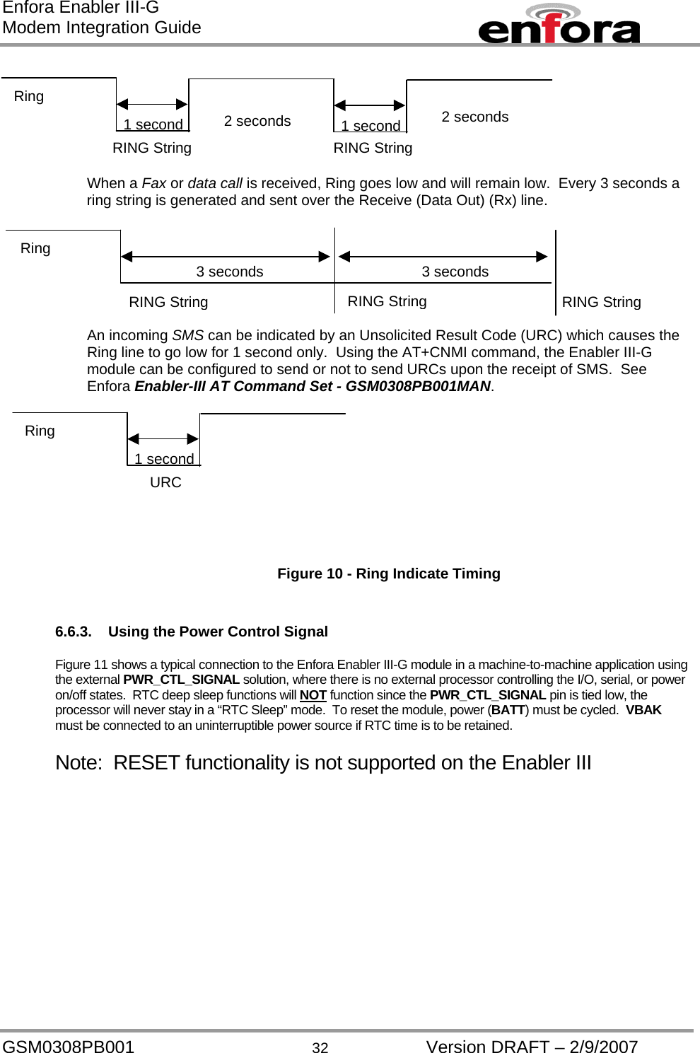
![Enfora Enabler III-G Modem Integration Guide 6.3.3. I/O Connector Pin Assignments The following table shows the pin assignments for the input/output connector. Table 2 - Enabler III-G Pin Assignments PIN # FUNCTION Serial Pin I/O ENABLER III-G Description/Comments (Default function / secondary function) 1 Power Input (USB) P VBUS USB power 2 Ground R GND System Ground 3 Power Input (USB) P VBUS USB power 4 Ground R GND System Ground 5 I/O USB_DP/RXD/MIC_R 5 V tolerant data plus pin in USB modes / Receive function in UART mode / Microphone or right speaker in AUDIO mode 6 I LED_B LED B sink 7 I/O USB_DM/TXD/SPKR_L 5 V tolerant data minus pin in USB modes / Transmit function in UART mode / Monaural speaker or left speaker in AUDIO mode 8 I LED_A LED A sink 9 I ID_USB USB connector identification 10 O VRWLED Output voltage for VRWLED regulator 11 Clear To Send 8 I UART_CTS UART Clear to send[MG1]12 I MCSI_RX/GPIO12 GPIO12 / MCSI Serial data input 13 Request To Send 7 O UART_RTS UART Request to send 14 I/O MCSI_CLK/GPIO9 GPIO9 / MCSI Serial Clock I/O 15 Serial Data Transmit 2 O UART_TX UART Serial data output 16 I/O MCSI_FSYNC/GPIO10 GPIO10 / MCSI Frame Synchronization I/O 17 Data Set Ready 6 I DSR_RXIR UART Data set ready/ IrDA Serial data input 18 O MCSI_TX / GPIO11 GPIO11 / MCSI Serial Data Output 19 Data Carrier Detect 1 O DCD_TXIR UART Data carrier detect/IrDA Serial data output 20 O SPI_\CS2 / GPIO18 GPIO18 / SPI Chip select 2 21 Serial Data Receive 3 I UART_RX UART Serial data input 22 I/O SPI_MOSI / GPIO15 GPIO15 / SPI Data master out/slave in 23 Ring Indicate 9 O UART_RING UART/Modem ring indicate 24 O SPI_\CS0/GPIO16 GPIO16 / SPI Chip select 0 25 Data Terminal Ready 4 O UART_DTR UART Data Terminal Ready 26 I/O SPI_MISO/GPIO14 GPIO14 / SPI Data master in/slave out 27 O KBC0/GPO25 Keyboard Matrix Column 0 / GPIO25 28 O SPI_\CS1/GPIO17 GPIO17 / SPI Chip select 1 29 O KBC2/GPO27 Keyboard Matrix Column 2 / GPIO27 30 I/O SPI_CLK/GPIO13 GPIO13 / SPI serial clock 31 O KBC3/GPO28 Keyboard Matrix Column 3 / GPIO28 32 O KBC4/GPIO20 Keyboard Matrix Column 4 / GPIO20 33 O KBC1/GPO26 Keyboard Matrix Column 1 / GPIO26 34 I KBR4/GPIO19 Keyboard Matrix Row 4 / GPIO19 35 I PWR_CTL External switch-on event (ON Button) with 32-kHz de-bouncing 36 I KBR3/GPI24 Keyboard Matrix Row 3 / GPI24 37 I RESERVED RESERVED 38 I KBR0/GPI21 Keyboard Matrix Row 0 / GPI21 39 (OPEN) 40 I KBR1/GPI22 Keyboard Matrix Row 1 / GPI22 41 (OPEN) 42 I KBR2/GPI23 Keyboard Matrix Row 2 / GPI23 43 (OPEN) 44 (OPEN) 45 (OPEN) 46 (OPEN) 47 I HST_DET Headset Detect 48 O I2C_2_SCL I2C interface Master serial clock 49 I FML Mixer/FM radio input left channel GSM0308PB001 28 Version DRAFT – 2/9/2007](https://usermanual.wiki/Novatel-Wireless/GSM0308.Manual/User-Guide-759332-Page-33.png)
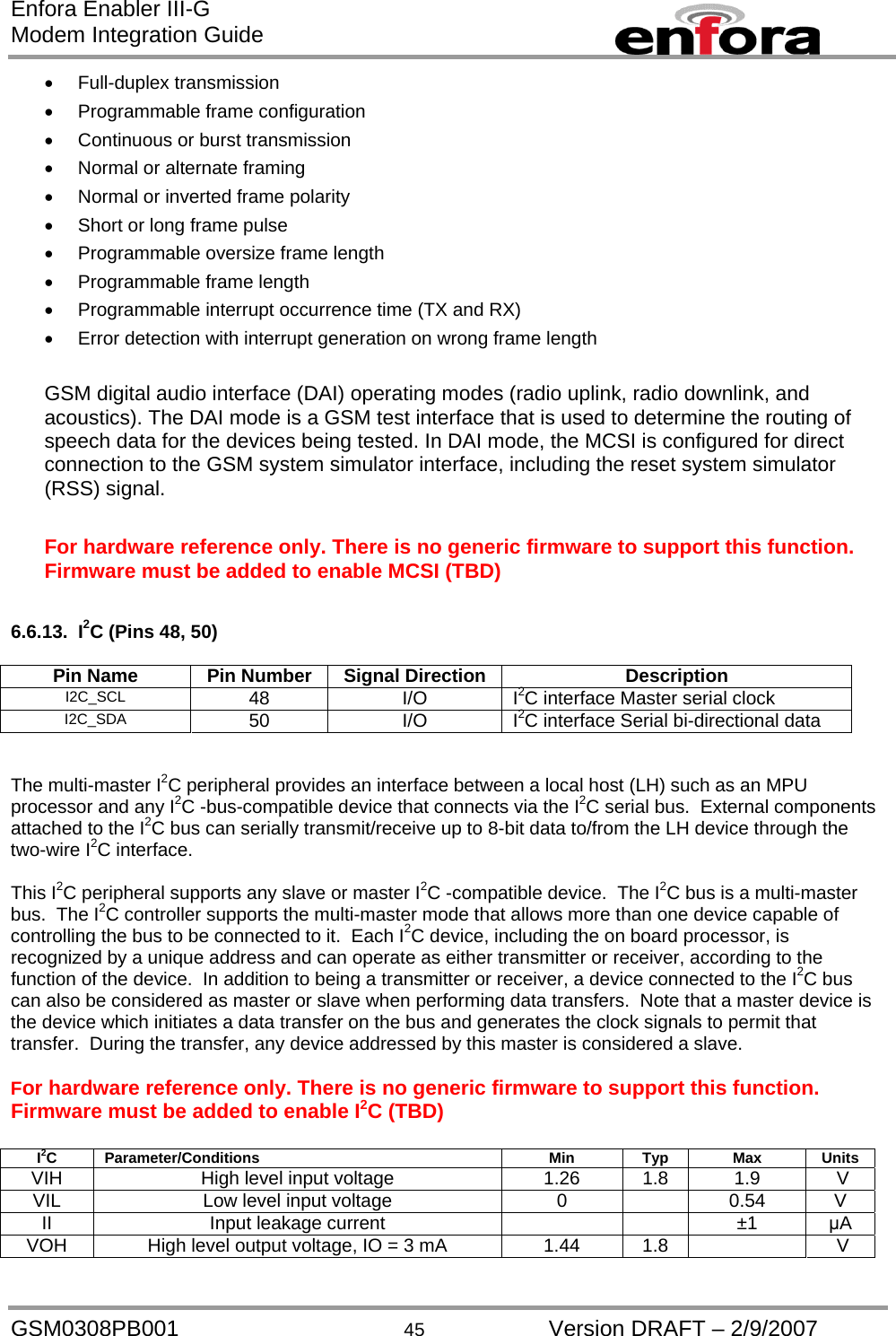
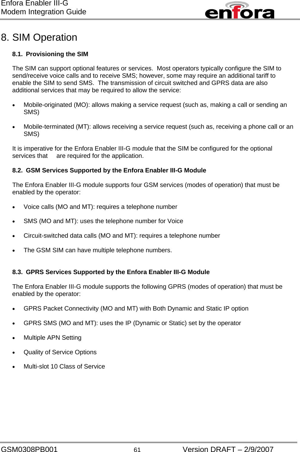
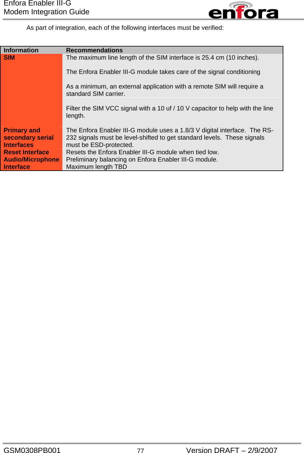
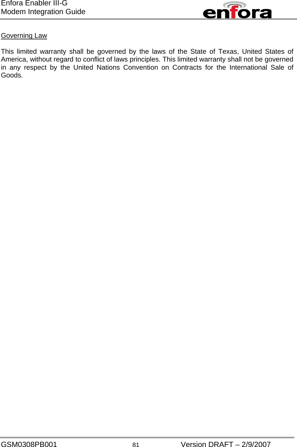
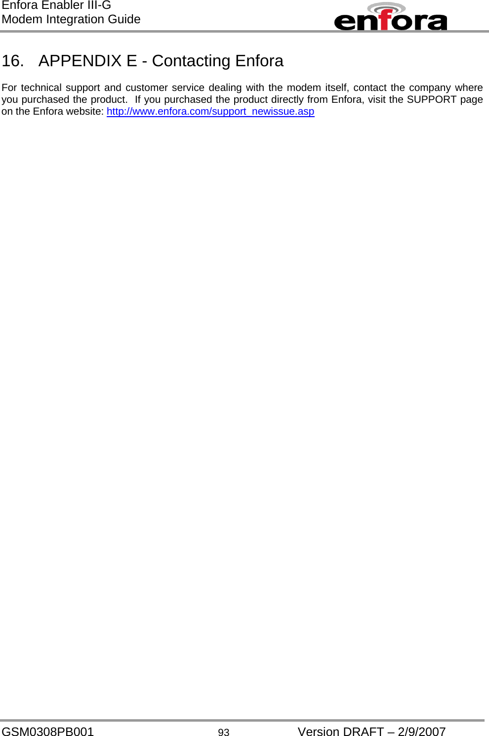
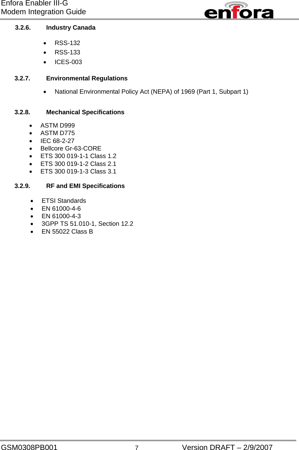
![Enfora Enabler III-G Modem Integration Guide 6.6.4. Level Translation Reference Power (Pin 77) To be used as a voltage reference source ONLY. Do not connect current loads to this pin. This pin must be decoupled to ground with at least a 0.1 μF capacitor at the output. Noise induced on this pin will affect the performance of the baseband. VR I/O Parameter/Conditions Min Typ Max Units Output voltage VOUT ON mode LOW POWER mode 1.65 1.65 1.8 1.8 1.95 1.95 Vdc Rated output current IOUT ON mode LOW POWER mode 20 mA 0.5 6.6.5. USB (Pins 1, 3, 5, 7, 9) Pin Name Pin Number Signal Direction Description USB_VBUS 1, 3 In 5 V tolerant power Supply VBUS line; Used only as a USB sense, not for powering the module. (optional connection) USB_DP/RXD/MIC_R 5 Analog I/O 5 V tolerant data plus pin in USB modes / Receive function in UART mode / Microphone or right speaker in AUDIO mode USB_DP 7 Analog I/O 5 V tolerant data minus pin in USB modes / Transmit function in UART mode / Monaural speaker or left speaker in AUDIO mode ID_USB 9 Analog I/O 5 V tolerant ID line, it defines the type of device connected to the phone’s USB port; And also the default state (host / device) at the cable connection; The transceiver senses the voltage of this pin to determine if the pin is either floating (typical),grounded or resistively connected to ground (102 kΩ, 200 kΩ, 440 kΩ); The universal serial bus (USB) device controller supports the implementation of a full-speed (FS) device compatible with the Universal Serial Bus Specification Revision 2.0 and the Universal Serial Bus Specification Revision 1.1. The module includes a Universal Serial Bus (USB) transceiver with a car-kit detection, able to support USB 12 Mb/s Full-Speed (FS) and USB 1.5 Mb/s Low-Speed (LS). When a USB cable is plugged into the USB receptacle, the transceiver detects the cable’s presence on VBUS (> 1.8 V) and ID ( float) pins, even if the module is switched off. The transceiver is fully operational only in phone’s Active mode. The modules device’s car kit is developed based on CEA-936-A rev.39 – Nov. 24th 2004 specification. Currently the device does not support other versions of this specification. Compared to the CEA-936-A rev.39 – Nov. 24th 2004 specification, the car-kit implementation in the module device does not support [1] a fully implemented hardware Phone State Machine, [2] the relative interrupts and registers for the proper behavior of the Phone State machine and [3] the Data-During- Audio signaling mode. GSM0308PB001 37 Version DRAFT – 2/9/2007](https://usermanual.wiki/Novatel-Wireless/GSM0308.Manual/User-Guide-759332-Page-42.png)