Novatel Wireless GSM0308 Wireless Modem User Manual Enabler II G Assiste GPS Integration Guide
Novatel Wireless Inc. Wireless Modem Enabler II G Assiste GPS Integration Guide
Contents
- 1. Manual
- 2. User Manual
Manual

GSM0308PB001
Enfora, Inc.
661 E. 18th Street Plano Texas 75074
www.enfora.com
Enfora Enabler III-G
Integration Guide
Version: DRAFT

Enfora Enabler III-G
Modem Integration Guide
Document Title: Enfora Enabler III-G Modem Integration Guide
Version: DRAFT
Date: 1/31/07
Status: DRAFT
Document Control ID: GSM0308PB001
General
All efforts have been made to ensure the accuracy of material provided in this document at the time
of release. However, the items described in this document are subject to continuous development
and improvement. All specifications are subject to change without notice and do not represent a
commitment on the part of Enfora, Inc. Enfora, Inc. will not be responsible for any loss or damages
incurred related to the use of information contained in this document.
This product is not intended for use in life support appliances, devices or systems where a
malfunction of the product can reasonably be expected to result in personal injury. Enfora, Inc.
customers using, integrating, and/or selling this product for use in such applications do so at their
own risk and agree to fully indemnify Enfora, Inc. for any damages resulting from illegal use or resale.
Copyright
Complying with all applicable copyright laws is the responsibility of the user. Without limiting the
rights under copyright, no part of this document may be reproduced, stored in or introduced into a
retrieval system, or transmitted in any form or by any means (electronic, mechanical, photocopying,
recording or otherwise), or for any purpose, without the express written permission of Enfora, Inc.
Enfora may have patents, patent applications, trademarks, copyrights or other intellectual property
rights covering subject matter in this document. Except as expressly provided in any written license
agreement from Enfora, the furnishing of this document does not give you any license to these
patents, trademarks, copyrights or other intellectual property.
©2002, 2003, 2004, 2005, 2006, 2007 Enfora, Inc. All rights reserved.
Enabler and Spider are either registered trademarks or trademarks of Enfora, Inc. in the United
States.
GSM0308PB001 Version DRAFT – 2/9/2007

Enfora Enabler III-G
Modem Integration Guide
Table of Contents
1. SAFETY PRECAUTIONS .................................................................................................................................1
1.1. IMPORTANT SAFETY INFORMATION................................................................................................................1
2. REGULATORY COMPLIANCE FCC.............................................................................................................1
2.1. INTEGRATION CONSIDERATIONS AND INSTALLATION REQUIREMENTS...........................................................1
2.2. DISCLAIMER ...................................................................................................................................................3
3. MANUAL OVERVIEW......................................................................................................................................4
3.1. REVISION HISTORY.........................................................................................................................................4
3.2. REFERENCE DOCUMENTS ...............................................................................................................................5
3.2.1. Enfora Enabler III-G Product Documentation......................................................................................5
3.2.2. GSM Device Specifications....................................................................................................................6
3.2.3. US Government......................................................................................................................................6
3.2.4. Federal Communications Commission (FCC).......................................................................................6
3.2.5. FCC Office of Engineering and Technology (OET) ..............................................................................6
3.2.6. Industry Canada ....................................................................................................................................7
3.2.7. Environmental Regulations....................................................................................................................7
3.2.8. Mechanical Specifications.....................................................................................................................7
3.2.9. RF and EMI Specifications....................................................................................................................7
4. INTRODUCTION ...............................................................................................................................................8
4.1. PRODUCT OVERVIEW......................................................................................................................................8
4.2. KEY FEATURES OF THE ENABLER III MODULE...............................................................................................8
4.3. PROVIDING MULTI-BAND OPERATION .........................................................................................................10
4.4. WIRELESS DATA APPLICATION POSSIBILITIES..............................................................................................10
4.5. GSM/GPRS SYSTEM OVERVIEW .................................................................................................................11
4.6. SUMMARY OF FEATURES FOR THE ENABLER III-G MODULE........................................................................13
4.7. GENERAL LAYOUT GUIDELINES FOR ENFORA GSM MODULES .....................................................................15
5. TECHNICAL SPECIFICATIONS..................................................................................................................16
5.1. ENABLER III-G MODULE BLOCK DIAGRAM .................................................................................................16
5.2. DETAILED PRODUCT SPECIFICATIONS ..........................................................................................................17
CLIMATIC: STORAGE AND TRANSPORTATION...........................................................................................................17
MECHANICAL: STORAGE AND TRANSPORTATION.....................................................................................................17
MECHANICAL: PROPOSED STANDARDS ....................................................................................................................17
ELECTROMAGNETIC EMISSIONS ...............................................................................................................................17
5.3. OPERATING POWER ......................................................................................................................................18
5.3.1. GSM Operating Power ........................................................................................................................18
5.3.2. GPRS Operating Power.......................................................................................................................18
5.3.3. Typical Input Current ..........................................................................................................................19
5.3.4. GSM Transmit Power ..........................................................................................................................19
5.3.5. GSM Receiver Sensitivity.....................................................................................................................20
6. MECHANICAL.................................................................................................................................................21
6.1. MODULE MOUNTING TO HOST BOARD (REFERENCE)...................................................................................25
6.2. CONNECTORS ...............................................................................................................................................27
6.3. RF CONNECTION OPTIONS ...........................................................................................................................27
6.3.1. Coaxial Connector Option...................................................................................................................27
6.3.2. RF Board-to-Board Connector Option................................................................................................27
6.3.3. I/O Connector Pin Assignments...........................................................................................................28
6.4. CIRCUIT PROTECTION...................................................................................................................................30
6.5. ANTENNA .....................................................................................................................................................30
GSM0308PB001 Version DRAFT – 2/9/2007

Enfora Enabler III-G
Modem Integration Guide
6.6. CONTROL CONNECTOR SIGNAL DESCRIPTIONS AND FUNCTIONS .................................................................31
6.6.1. Module Power (Pins 85, 87, 79, 91, 93, 95, 97, 99) ............................................................................31
6.6.2. Ring Indicate........................................................................................................................................31
6.6.3. Using the Power Control Signal..........................................................................................................32
6.6.4. Level Translation Reference Power (Pin 77).......................................................................................37
6.6.5. USB (Pins 1, 3, 5, 7, 9) ........................................................................................................................37
6.6.6. LED A (Pin 8) & B (Pin 6), VRWLED (Pin 10)...................................................................................39
6.6.7. LED VRW (Pin 10) ..............................................................................................................................41
6.6.8. General Purpose Input/Output Interface.............................................................................................42
6.6.9. Power Control (Pin 35) .......................................................................................................................43
6.6.10. RTC Sleep ............................................................................................................................................43
6.6.11. Serial Interfaces & Handshake (Pins 11, 13, 15, 17, 19, 21, 23, 25)...................................................43
6.6.12. MCSI – Multi-Channel Serial Interface (Pins 12, 14, 16, 18) .............................................................44
6.6.13. I2C (Pins 48, 50) ..................................................................................................................................45
6.6.14. Serial Port Interface (SPI) (Pins 20, 22, 24, 26, 28, 30)......................................................................46
6.6.15. Keyboard (Pins 27, 29, 31, 32, 33, 34, 36, 38, 40, 42 ) .......................................................................47
6.6.16. VBACKUP Input (Pin 83) .........................................................................................................................48
6.6.17. Using VBAK.........................................................................................................................................49
6.6.18. 32 kHz output (Pin 56).........................................................................................................................49
6.6.19. 13 MHz output (Pin 52).......................................................................................................................49
6.6.20. Analog-To-Digital Input (Pin 74) ........................................................................................................50
6.6.21. Handset Microphone Input (Pins 65, 67).............................................................................................50
6.6.22. Handset Microphone Bias Output (Pin 63) .........................................................................................50
6.6.23. Handset Speaker Output (Pins 71, 73).................................................................................................51
6.6.24. Headset Microphone Input (Pin 55) ....................................................................................................52
6.6.25. Headset Microphone Bias Output (Pin 53)..........................................................................................52
6.6.26. Headset Speaker Output Left & Right (Pins 57, 59)............................................................................53
6.6.27. Headset Output Common Mode (Pin 61).............................................................................................53
6.6.28. Headset Detect (Pin 47).......................................................................................................................54
6.6.29. Audio Mixer input (Pins 49, 56) ..........................................................................................................55
6.7. SUBSCRIBER IDENTITY MODULE (SIM) CARRIER ........................................................................................56
6.7.1. SIM Integration for the Enfora Enabler III-G Module ........................................................................56
6.7.2. Using a Remote SIM with the Enfora Enabler III-G Module (Pins 76, 78, 80, 82, 84).......................56
7. GSM/GPRS MODES OF OPERATION.........................................................................................................59
7.1. ENABLING THE TRANSMISSION MODES FOR THE GSM/GPRS SERVICES .....................................................59
7.2. VOICE COMMUNICATION..............................................................................................................................59
7.3. CIRCUIT-SWITCHED DATA ...........................................................................................................................59
7.4. SMS: SHORT MESSAGE SERVICES................................................................................................................60
8. SIM OPERATION ............................................................................................................................................61
8.1. PROVISIONING THE SIM ...............................................................................................................................61
8.2. GSM SERVICES SUPPORTED BY THE ENFORA ENABLER III-G MODULE ......................................................61
8.3. GPRS SERVICES SUPPORTED BY THE ENFORA ENABLER III-G MODULE .....................................................61
8.4. SELECTING THE GSM MODES OF OPERATION ..............................................................................................62
9. SOFTWARE INTERFACE..............................................................................................................................63
9.1. SOFTWARE INTERFACE.................................................................................................................................63
9.2. FORMAT FOR THE AT COMMANDS ...............................................................................................................64
9.3. ENFORA AT COMMAND SET ........................................................................................................................65
9.4. ENFORA PACKET APPLICATION PROGRAMMING INTERFACE ........................................................................65
9.4.1. UDP-API Architecture.........................................................................................................................65
9.5. ENFORA MODEM CONTROL LIBRARY ARCHITECTURE .................................................................................67
9.5.1. Using Port Library ..............................................................................................................................68
9.5.2. Using Messaging Library ....................................................................................................................68
GSM0308PB001 Version DRAFT – 2/9/2007

Enfora Enabler III-G
Modem Integration Guide
9.5.3. Using Modem Library..........................................................................................................................70
10. SETUP AND INITIALIZATION.................................................................................................................70
10.1. GENERAL SETUP.......................................................................................................................................70
10.1.1. HyperTerminal Configuration for Enabler III-G module....................................................................70
10.1.2. Initialization (AT Command Interface)................................................................................................72
10.1.3. Initial Response to the AT Command...................................................................................................73
10.1.4. Sending an Initialization String to the Enfora Enabler III-G Module .................................................73
10.1.5. Setting Up the Communication Mode for the Enfora Enabler III-G Module.......................................74
10.1.6. Querying the Status of the Enfora Enabler III-G Module....................................................................75
10.1.7. Setting Module Reporting Parameters for GSM and GPRS ................................................................75
10.2. GSM/SMS EXAMPLES .............................................................................................................................75
10.2.1. Initialize the Enfora Enabler III-G Module to Send and Receive SMS Text Messages........................75
10.2.2. Managing SMS Messages....................................................................................................................75
10.2.3. Data Call Configuration......................................................................................................................75
10.2.4. Voice Call Configuration.....................................................................................................................75
10.3. GPRS PACKET EXAMPLES .......................................................................................................................75
10.3.1. GPRS ATTACH and ACTIVATE..........................................................................................................75
10.3.2. Windows PPP Setup.............................................................................................................................75
11. INTEGRATION AND TESTING................................................................................................................76
11.1. INTEGRATING THE ENFORA ENABLER III-G MODULE ..............................................................................76
12. APPENDIX A................................................................................................................................................79
LIMITED WARRANTY...........................................................................................................................................79
12.1. SCOPE.......................................................................................................................................................79
12.1.1. Hardware.............................................................................................................................................79
12.2. SOFTWARE................................................................................................................................................79
12.3. OTHER CONSIDERATIONS .........................................................................................................................80
13. APPENDIX B - REGULATIONS AND COMPLIANCE ..........................................................................82
13.1. GCF/PTCRB APPROVAL (FORMERLY FTA)............................................................................................82
13.2. ELECTROMAGNETIC COMPATIBILITY (EMC) AND SAFETY REQUIREMENTS.............................................82
13.3. EMC/SAFETY REQUIREMENTS FOR THE USA ..........................................................................................82
13.4. HUMAN EXPOSURE COMPLIANCE STATEMENT.........................................................................................83
13.5. COMPLIANCE WITH FCC REGULATIONS...................................................................................................83
13.6. UNINTENTIONAL RADIATORS, PART 15....................................................................................................84
13.7. INTENTIONAL RADIATORS, PART 22 & 24................................................................................................84
13.8. INSTRUCTIONS TO THE ORIGINAL EQUIPMENT MANUFACTURER (OEM)..................................................85
13.8.1. OEM Responsibilities for All Products Containing the Enabler III-G module....................................87
13.8.2. Specific OEM Responsibilities for Portable Products and Applications.............................................88
13.8.3. Specific OEM Responsibilities for Mobile Products and Applications................................................88
13.8.4. Specific OEM Responsibilities for Fixed Products and Applications..................................................88
13.9. EMC/SAFETY REQUIREMENTS FOR THE COUNTRIES OF THE EUROPEAN UNION (EU)..............................89
13.10. EMC/SAFETY REQUIREMENTS FOR OTHER COUNTRIES ...........................................................................89
14. APPENDIX C - GLOSSARY AND ACRONYMS......................................................................................90
15. APPENDIX D – TABLES AND FIGURES.................................................................................................92
16. APPENDIX E - CONTACTING ENFORA.................................................................................................93
GSM0308PB001 Version DRAFT – 2/9/2007

Enfora Enabler III-G
Modem Integration Guide
1. Safety Precautions
1.1. Important Safety Information
The following information applies to the devices described in this manual. Always observe all standard and
accepted safety precautions and guidelines when handling any electrical device.
• Save this manual: it contains important safety information and operating instructions.
• Do not expose the Enfora Enabler III-G product to open flames.
• Ensure that liquids do not spill onto the devices.
• Do not attempt to disassemble the product: Doing so will void the warranty. With the
exception of the Subscriber Identification Module (SIM), this product does not contain
consumer-serviceable components.
2. Regulatory Compliance FCC
2.1. Integration Considerations and Installation Requirements
The Enabler III-G modem is designed for use in a variety of host units, "enabling" the host
platform to perform wireless data communications. However, there are certain criteria relative to
integrating the modem into a host platform such as a PC, laptop, handheld or PocketPC®, monitor
and control unit, etc. that must be considered to ensure continued compliance with FCC
compliance requirements.
• In order to use the Enabler III-G modem without additional FCC certification approvals, the
installation must meet the following conditions:
• Maximum RF output power and antenna gain to meet Maximum Permissible Exposure
Requirements: GSM850 mode: Power at antenna port is +32 dBm. The maximum gain
is 4.5 dBi(2.35 dBd). GSM1900 mode: Power at antenna port is 31.3 dBm. The
maximum gain is 2 dBi in order to meet the requirements of maximum 2 watts EIRP for
mobile transmitters.If RF power and/or antenna gain is desired, a separate FCC
certification is required.
• If used in a "portable" application such as a handheld or body worn device with the
antenna less than 20 cm (7.9 in.) from the human body when the device is operating,
then the integrator is responsible for passing additional "as installed" testing and the
device will require it’s own FCC ID:
• SAR (Specific Absorption Rate) testing, with results submitted to the FCC for
approval prior to selling the integrated unit. If unable to meet SAR requirements,
then the host unit must be restricted to "mobile" use (see below).
• Unintentional emissions, FCC Part 15; results do not have to be submitted to the
FCC unless requested, although the test provides substantiation for required labeling
(see below).
• ERP and EIRP measurements for FCC Parts 22 and 24, alternatively a full retest on
FCC Parts 22 and 24 can be performed
GSM0308PB001 1 Version DRAFT – 2/9/2007

Enfora Enabler III-G
Modem Integration Guide
• If used in a "mobile" application where the antenna is normally separated at least 20 cm
(7.9 in) from the human body during device operation, then an appropriate warning label
must be placed on the host unit adjacent to the antenna. The label should contain a
statement such as the following:
WARNING
RF exposure. Keep at least 20 cm
(7.9 in) separation distance from
the antenna and the human body.
• Host unit user manuals and other documentation must also include appropriate caution
and warning statements and information.
• If the FCCID for the modem is not visible when installed in the host platform, then a
permanently attached or marked label must be displayed on the host unit referring to the
enclosed modem.
For example, the label should contain wording such as:
Contains GSM/GPRS modem transmitter module
FCC ID: MIVGSM0308
This device complies with Part 15 of the FCC Rules.
Operation is subject to the following two conditions: (1)
This device may not cause harmful interference, and (2)
This device must accept any interference received,
including interference that may cause undesired
operation.
OR
Contains FCC ID: MIVGSM0308
This device complies with Part 15 of the FCC Rules.
Operation is subject to the following two conditions: (1)
This device may not cause harmful interference, and (2)
This device must accept any interference received,
including interference that may cause undesired
operation.
• Any antenna used with the modem must be approved by the FCC or as a Class II
Permissive Change (including MPEL or SAR data as applicable). The "professional
installation" provision of FCC Part 15.203 does not apply.
GSM0308PB001 2 Version DRAFT – 2/9/2007

Enfora Enabler III-G
Modem Integration Guide
• The transmitter and antenna must not be co-located or operating in conjunction with any
other antenna or transmitter. Violation of this would allow a user to plug another
transmitter in to the product and potentially create an RF exposure condition.
WARNING
The transmitter and antenna must not be collocated
or operating in conjunction with any
other antenna or transmitter. Failure to observe
this warning could produce an RF exposure
condition.
2.2. Disclaimer
The information and instructions contained within this publication comply with all FCC, GCF,
PTCRB, R&TTE, IMEI and other applicable codes that are in effect at the time of publication.
Enfora disclaims all responsibility for any act or omissions, or for breach of law, code or
regulation, including local or state codes, performed by a third party.
Enfora strongly recommends that all installations, hookups, transmissions, etc., be performed by
persons who are experienced in the fields of radio frequency technologies. Enfora acknowledges
that the installation, setup and transmission guidelines contained within this publication are
guidelines, and that each installation may have variables outside of the guidelines contained
herein. Said variables must be taken into consideration when installing or using the product, and
Enfora shall not be responsible for installations or transmissions that fall outside of the
parameters set forth in this publication.
Enfora shall not be liable for consequential or incidental damages, injury to any person or
property, anticipated or lost profits, loss of time, or other losses incurred by Customer or any third
party in connection with the installation of the Products or Customer's failure to comply with the
information and instructions contained herein.
The Enabler III-G platform is designed with features to
support a robust connection. There are instances
where the module performance is beyond the control
of the intended design. Integrated designs that require
24 by 7 operation must implement power control via an
external circuit or by implementing power management
as specified within this design guide.
GSM0308PB001 3 Version DRAFT – 2/9/2007
Enfora Enabler III-G
Modem Integration Guide
3. Manual Overview
This document describes the hardware interface of the Enabler III-G modem. The purpose of
this document is to define the electrical, mechanical and software interfaces while providing
detailed technical information in order to streamline the process of hardware and system
integration.
3.1. Revision History
Date Rev Author Description
01/17/07 1.00 Tom Cone Initial Release Draft
GSM0308PB001 4 Version DRAFT – 2/9/2007

Enfora Enabler III-G
Modem Integration Guide
3.2. Reference Documents
3.2.1. Enfora Enabler III-G Product Documentation
Overview
• GSM1000PB001MAN - Enfora Integrated GSM/GPRS Module
Manuals
• GSM0308PB001MAN - Enfora GSM/GPRS OEM Module AT Command Set Reference
• GSM0102PB002MAN - Enfora GSM-GPRS Family UDP-API Reference
• GSM0000PB006MAN - Enfora GSM-GPRS Family Modem Control Library Reference
Application Notes
• GSM0000AN001 - Enabler-G PPP Configuration for Windows 98
• GSM0000AN002 - Enabler-G PPP Configuration for Windows 2000
• GSM0000AN003 - Enabler-G Data Circuit Switched Call Configuration and Use
• GSM0000AN004 - Enabler-G SMS Configuration and Use
• GSM0000AN005 - Enabler-G Automated Network Connection Configuration and Use
• GSM0000AN006 - Enabler-G Module Status Query
• GSM0000AN007 - Enabler-G Status Reporting
• GSM0000AN008 - Enabler-G PPP Configuration for Windows XP
• GSM0000AN009 - Dynamic IP Assignment Support
• GSM0000AN010 - Enabler-G PPP Configuration for PocketPC 2002
• GSM0000AN011 - PAD Configuration and Use
• GSM0000AN012 - Network Transparency Configuration for PAD
• GSM0000AN013 - Enabler-G Sleep Mode Configuration and Use
• GSM0000AN014 - Anytime PPP API Access
• GSM0000AN015 - Event Monitor and Reporting Overview
• GSM0000AN016 - How to Send SMS Messages to an E-Mail Address
• GSM0000AN017 - SMTP Mail Access via TCP PAD
• GSM0000AN018 - USNO NTP Network Time Service TCP PAD
GSM0308PB001 5 Version DRAFT – 2/9/2007

Enfora Enabler III-G
Modem Integration Guide
Technical Notes
• GSM0000TN001 - Enabler-G Firmware Upgrade
• GSM0000TN002 - Enabler-G PPP Negotiation Sequence
• GSM0000TN006 - UDP Wakeup Message Header Decoding
• GSM0000TN007 - Enabler-G 3-Wire Serial Interface Requirements
• GSM0000TN008 - Enabler Power Supply Requirements
• GSM0000TN009 - Server Application Design Considerations for Dynamic IP
• GSM0000TN012 – Enabler III-G Engineering Mode Command Reference
• GSM0000TN013 – Enabler III-G and IIE CMUX Description
White Papers
• GSM0000WP001 - Enabler-G Differentiation Features
• GSM0000WP002 - Using Enfora UDP API Versus CMUX Protocol
3.2.2. GSM Device Specifications
• 3GPP TS 51010-1 (850, 900,1800,1900 MHz devices)
To view the latest release, go to:
http://www.3gpp.org/ftp/Specs/html-info/51010-1.htm
3.2.3. US Government
3.2.4. Federal Communications Commission (FCC)
Internet: http://www.fcc.gov/
• FCC Rules, Part 24
• 47 CFR Subpart E--Broadband PCS
• 47 CFR § 24.52, sections 1.1307(b), 2.1091, and 2.1093
• FCC Rules, Part 22 for GSM 850
• FCC Rules, Part 15
• FCC Rules, Part 2
• Subpart J--Equipment Authorization Procedures
• Section 2.925
3.2.5. FCC Office of Engineering and Technology (OET)
Internet: http://www.fcc.gov.oet/
• Bulletin Number 65 "Evaluating Compliance with FCC Guidelines for Human Exposure
to Radio Frequency Electromagnetic Fields"
• Supplement C "Additional Information for Evaluating Compliance of Mobile and
Portable Devices with FCC Limits for Exposure to Radio Frequency Emissions"
GSM0308PB001 6 Version DRAFT – 2/9/2007

Enfora Enabler III-G
Modem Integration Guide
3.2.6. Industry Canada
• RSS-132
• RSS-133
• ICES-003
3.2.7. Environmental Regulations
• National Environmental Policy Act (NEPA) of 1969 (Part 1, Subpart 1)
3.2.8. Mechanical Specifications
• ASTM D999
• ASTM D775
• IEC 68-2-27
• Bellcore Gr-63-CORE
• ETS 300 019-1-1 Class 1.2
• ETS 300 019-1-2 Class 2.1
• ETS 300 019-1-3 Class 3.1
3.2.9. RF and EMI Specifications
• ETSI Standards
• EN 61000-4-6
• EN 61000-4-3
• 3GPP TS 51.010-1, Section 12.2
• EN 55022 Class B
GSM0308PB001 7 Version DRAFT – 2/9/2007
Enfora Enabler III-G
Modem Integration Guide
4. Introduction
4.1. Product Overview
Enfora Enabler III-G modem is a compact, wireless OEM module that utilizes the Global System
for Mobile Communications (GSM) and GPRS (General Packet Radio Services) international
communications standard to provide two-way wireless capabilities via GSM services. The Enfora
Enabler III-G module is a fully Type-approved GSM/GPRS device, enabling application-specific,
two-way communication and control.
The small size of the Enfora Enabler III-G module allows it to be integrated easily into the
application and packaging.
4.2. Key Features of the Enabler III Module
The following table summarizes the main features of the Enfora Enabler III-G Radio Module.
Data input/output interface 100 position 0.4mm pitch connector
Primary serial port V.24 protocol, 1.8V levels, full 9-pin, UART
implementation
Secondary serial port V.24 protocol, 1.8V levels (debug only)
GPIO 20 pins available (feature specific on some lines)
USB USB full-speed (FS) device compatible with the
Universal Serial Bus Specification Revision 2.0
and the universal Serial Bus Specification
Revision 1.1.
I2C Multi- Master Serial Computer Bus
SPI Port Serial Peripheral Interface
Keyboard 5 x 5 keyboard support
Audio Digital audio via MCSI port
Voice Supports four vocoder modes: full-rate (FR),
enhanced full-rate (EFR), half-rate (HR), and
adaptive multi-rate (AMR)
Antenna Interface ultra Miniature Coaxial Interconnect or B2B Spring
contact
Command protocol Enfora Packet API, GSM AT command set
Subscriber Identification Module
(SIM) Optional 1.8/3 V mini-SIM carrier and interface on
board with SIM detect
Voltage backup Voltage backup pin available to maintain RTC,
battery capable
Reference clock 32kHz and 13 Mhz. output reference clocks
ADC 1 ADC port
Interface
Optional remote SIM Accessible via the 100-pin connector
Electrical power 3.3 to 4.5 Vdc Power Peak currents and average
power dissipation Refer to the Operating Power table in the
Technical Specifications for peak currents and
average power dissipation for various modes of
operation.
Frequency bands EGSM 900, GSM1800, GSM 850 and GSM 1900
capability.
Radio Features
GSM/GPRS features supported Provides for all GSM/GPRS authentication,
encryption, and frequency hopping algorithms.
GPRS Coding Schemes CS1-CS4 supported.
Multi-Slot Class 10 (4RX/2TX, Max 5 Slots).
GSM0308PB001 8 Version DRAFT – 2/9/2007

Enfora Enabler III-G
Modem Integration Guide
Regulatory Agency approvals • GCF Type Approval
• PTCRB Type Approval
• FCC Certification
• RTTE
• CE (European Community Certification)
• IC (Industry Canada) Approval
GSM/GPRS
Functionality • Mobile-originated and mobile-terminated SMS messages: up to 140 bytes or
up to 160 GSM 7-bit ASCII characters.
• Reception of Cell Broadcast Message
• SMS Receipt acknowledgement
• Circuit Switched Data (Transparent & Non-transparent up to 9.6 Kbps)
• Voice (EFR, FR, HR)
• Supports Unstructured Supplementary Service Data (USSD)
• Multi-Slot Class 10 Supported (4Rx/2TX), (5 Slot Max)
• PBCCH/PCCCH Supported
Audio Features • Handset Microphone biasing
• Headset Microphone biasing
• Headset Plug/Unplug detection
• Headset Hook detection (call answer/end button on equipped Headset
microphone device)
• High output dynamic differential Earphone mode, using Headset outputs
• Pop Noise attenuation circuitry implemented for all single-ended output
stages
• Mono Voice memo capability: Voice memo function is supported for both 8
kHz Narrowband and 16 kHz
• FM stereo audio mux input (FML pin, FMR/AUXI pin)
• FM mono audio mux input (FMR/AUXI pin only)
• Handset microphone input (MICIN, MICIP pins)
• Headset microphone input (HSMIC pin)
• Car kit microphone (D+ pin)
Outputs • Handset earphone outputs (EARP, EARN pins)
• Headset 32 stereo outputs (HSOL, HSOR pins)
• USB car kit stereo outputs (D+(right), D- (left) pins)
• USB car kit mono output (D- (left) pin)
SIM 1.8/3 V Mini-Subscriber Identity Module (SIM) compatible
Table 1 - Enabler III-G Key Features
GSM0308PB001 9 Version DRAFT – 2/9/2007

Enfora Enabler III-G
Modem Integration Guide
4.3. Providing Multi-Band Operation
The Enfora Enabler III-G module provides multi-band operation, with the operating frequency
selectable by AT Command:
• The 850/1900 MHz radio bands are available for integration and deployment for use
worldwide, with 850/1900 MHz support primarily in North America and regions where the
1900 MHz Personal Communication Services (PCS) band is allocated. The Enfora Enabler
III-G also supports GSM 850 for use in North America.
• The 900/1800 MHz Enfora Enabler III-G modules are available for deployment in Europe and the
rest of the world.
4.4. Wireless Data Application Possibilities
A variety of applications can use the Enfora Enabler III-G module for transmitting/receiving
data/voice, such as:
• Automated Meter Reading (AMR)
• Point of Sale Applications
• E-mail and Internet access
• Automated Vehicle Location (AVL)
• Machine to Machine communication (M2M)
• Telematics
• Telemetry
• Wireless Security
GSM0308PB001 10 Version DRAFT – 2/9/2007
Enfora Enabler III-G
Modem Integration Guide
Figure 1 – UDP API Architecture
4.5. GSM/GPRS System Overview
The Enfora Enabler III-G module is shown in Figure 1 is designed for easy integration with other
components and packaging by leveraging the existing GSM networks. Compare the Enfora Enabler
III-G to systems that require construction, operation, maintenance, and expense of a private network.
GSM0308PB001 11 Version DRAFT – 2/9/2007
Enfora Enabler III-G
Modem Integration Guide
Figure 2 - PAD Architecture
GSM0308PB001 12 Version DRAFT – 2/9/2007

Enfora Enabler III-G
Modem Integration Guide
4.6. Summary of Features for the Enabler III-G Module
The following summarizes the main features of the Enfora Enabler III-G Module.
Mechanical
Dimensions................................... 27.0 mm x 28.0 mm x 2.50 mm
Weight .......................................... 3.6g
Packet Data Transfer:
Protocol……………………………………………GPRS Release 97 and 99
Coding Schemes…………………………………CS1-CS4
Multi-Slot Capability: (Demonstrated @MS10)…….MS10 (4RX/2TX) (Max 5 Slots)
Packet Channel Support .............. ……………..PBCCH/PCCCH
Circuit Switched Data Transfer:
V110............................................. 300 bps/1200 bps/2400 bps/4800 bps/9600 bps/14,400 bps
Non-Transparent.......................... 300 bps/1200 bps/2400 bps/4800 bps/9600 bps/14,400 bps
Short Message Services:
GSM SMS .................................... MO, MT, CB, Text and PDU Modes
GPRS SMS .................................. MO, MT, CB, Text and PDU Modes
Voice Capability:
Speech Codec.............................. EFR, FR, HR, AMR
GSM/GPRS Radio Performance Multi-Band:
GSM0308 Radio Frequencies...... 850 MHz, 900 MHz, 1800 MHz, and 1900 MHz
Sensitivity ..................................... <-106 dBm (Typical GPRS CS1)
850 & 900 MHz Transmit Power .. Class 4 (2 W)
1800 & 1900 MHz
Transmit Power ......................... Class 1 (1 W)
System Requirements:
Host Interface............................... Serial Interface
DC Voltage................................... 3.3 to 4.5 Vdc
GSM0308PB001 13 Version DRAFT – 2/9/2007

Enfora Enabler III-G
Modem Integration Guide
Application Interface:
Host Protocol................................ Status API and AT Commands
Internal Protocols ......................... UDP stack, TCP/IP stack, PPP, PAD, and CMUX
Physical Interface......................... 1 serial (primary), I USB (debug) Default rate 115,200 baud,
MCSI, I2C, SPI, Keyboard (5x5)
Audio Interface.............................. FM stereo audio mux input (FML pin, FMR/AUXI pin), FM
mono (FMR/AUXI pin only), Handset microphone input
(MICIN, MICIP pins), Headset microphone input (HSMIC
pin), Car kit microphone (D+ pin), Handset earphone outputs
(EARP, EARN pins), Headset 32 stereo outputs (HSOL,
HSOR pins), USB car kit stereo outputs (D+, D- pins), USB
car kit mono output (D- pin)
SIM Interface:
Remote SIM Option 1.8/3-Volt SIM Capability
Environmental:
Compliant Temperature .............. -20 °C to 60 °C (Fully GSM Spec Compliant)
Operating Temperature ………….-30 °C to 70 °C
Storage Temperature................... -40 °C to 85 °C
Humidity ....................................... 5 to 95% non-condensing
EMC:
Emissions..................................... FCC Parts 15,22 & 24, Class B
3GPP TS 51010-1, Section 12.2
EN 55022 Class B
Operating Power (TYPICAL):
GSM Operation
GSM 850/900 (1 RX/1 TX, full power)………..TBD mA average, 1.6 A peak
GSM 1800 (1 RX/1 TX, full power)……………TBD mA average, 1.3 A peak
GSM 1900 (1 RX/1 TX, full power)……………TBD mA average, 1.2 A peak
Idle................................................ ………….. TBD mA
Shutdown ..................................... ……………≈ TBD uA
GPRS Operation Power
EGSM 850/900 (4 RX/1 TX, full power)…………… TBD mA average, 1.6 A peak
EGSM 850/900 (2 RX/2 TX, full power)…………... TBD mA average, 1.6 A peak
GSM 1800 (4 RX/1 TX, full power)………………… TBD mA average, A peak
GSM 1800 (2 RX/2 TX, full power) TBD mA average, A peak
GSM 1900 (4 RX/1 TX, full power)………………... TBD mA average, A peak
GSM 1900 (2 RX/2 TX, full power)………………… TBD mA average, A peak
Idle................................................ …………...…… TBD
Shutdown ..................................... …………….….≈ TBD uA
GSM0308PB001 14 Version DRAFT – 2/9/2007

Enfora Enabler III-G
Modem Integration Guide
GSM Transmit Power
1800/1900 MHz............................ GSM Power Class 1 (30 dBm ± 2 dB @ antenna connection)
850/900 MHz................................ GSM Power Class 4 (33 dBm ± 2 dB @ antenna connection)
GSM/GPRS Receiver Sensitivity (Typical)
1800/1900 MHz............................ <-106 dBm, GPRS Coding Scheme 1 (CS1)
850/900 MHz................................ <-106 dBm, GPRS Coding Scheme 1 (CS1)
4.7. General layout guidelines for Enfora GSM modules
To ensure lowest possible EMI emission, maximum thermal conduction and mechanical integrity, all
metal tabs on the GSM module shield must be soldered down on to a continuous ground plane. The
PCB trace that feeds the RF output port must be 50ohm characteristic impedance, coplanar, or
routed into internal layers to keep the top layer continuous around and underneath the device.
Provide ample ground vias around metal tabs, the RF trace and launch pad. If possible, keep I/O and
power traces away from the RF port.
GSM0308PB001 15 Version DRAFT – 2/9/2007
Enfora Enabler III-G
Modem Integration Guide
5. Technical Specifications
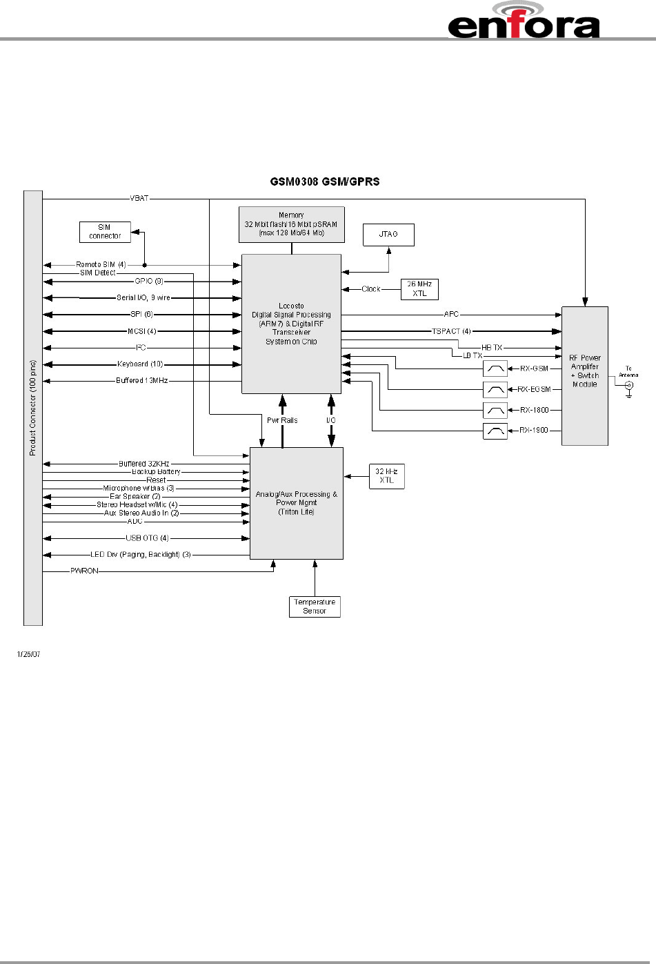
5.1. Enabler III-G Module Block Diagram
Figure 3 - Enabler III-G Module Block Diagram
GSM0308PB001 16 Version DRAFT – 2/9/2007
Enfora Enabler III-G
Modem Integration Guide
5.2. Detailed Product Specifications
Physical Dimensions and Weight
Size (L x W x H)
27.0 mm x 28.0 mm x 2.50 mm
Weight
(3.6 g)
Climatic: Operational
GSM Compliant temperature
Operating temperature -20°C to +60°C
-30°C to +70°C
Relative humidity
5 - 95%
Solar radiation Not Applicable
Air pressure (altitude) 70 kPa to 106 kPa (-400 m to 3000 m)
Climatic: Storage and Transportation
Duration 24 months
Ambient temperature -40C to +85C
Relative humidity 5% to 95%, non condensing (at 40C)
Thermal shock -50C to +23C, +70C to +23C; < 5 min
Altitude -400 m to 15,000 m
Mechanical: Operational
Operational vibration, sinusoidal
3.0 mm disp, 2 to 9 Hz; 1 m/s2 , 9 to 350 Hz
Operational vibration, random
0.1 m2 /s3 , 2 to 200 Hz
Mechanical: Storage and Transportation
Transportation vibration, packaged ASTM D999
Drop, packaged ASTM D775 method A, 10 drops
Shock, un-packaged 150 m/s2 , 11 ms, half-sine per IEC 68-2-27
Drop, un-packaged 4-inch drop per Bellcore GR-63-CORE
Mechanical: Proposed Standards
Transportation ETSI Standard ETS 300 019-1-2 Class 2.3
Transportation
Operational ETSI Standard ETS 300 019-1-3 Class 3.1
Operational
Storage ETSI Standard ETS 300 019-1-1 Class 1.2
Storage
Electromagnetic Emissions
Radiated spurious FCC Part 22 & 24 / Part 15 Class \ B
3GPP TS 51.010-1 Section 12.2
EN 55022 Class B
GSM0308PB001 17 Version DRAFT – 2/9/2007
Enfora Enabler III-G
Modem Integration Guide
5.3. Operating Power
The Enfora Enabler III-G module requires an input voltage of 3.3 Vdc to 4.5 Vdc.
5.3.1. GSM Operating Power
Enfora Enabler III-G (@ 3.76
Volts) Typical Current (mAmps) Typical Peak Current (Amps)
GSM 850
EGSM 900
GSM
1 TX 1 RX
1 RX
Idle
254 mA
104 mA
TBD mA
1.6 A @ 32.5 dBm
GSM 1800
GSM
1 TX 1 RX
1 RX
Idle
212 mA
104 mA
TBD mA
Error! Reference source not found.
A @ 29.5 dBm
GSM 1900
GSM
1 TX 1 RX
1 RX
Idle
200 mA
104 mA
TBD mA
Error! Reference source not found.
A @ 29.5 dBm
5.3.2. GPRS Operating Power
Enfora Enabler III-G (@ 3.76
Volts) Typical Current (mAmps) Typical Peak Current (Amps)
GSM 850
EGSM 900
GPRS
1 TX /1RX
2 TX/ 2RX
1 TX/ 2RX
1 TX/ 3RX
1 TX/ 4RX
1 RX
Idle
TBD mA
TBD mA
TBD mA
TBD mA
TBD mA
TBD mA
TBD mA
1.6 A @ 32.5 dBm
GSM 1800
GPRS
1 TX /1RX
2 TX/ 2RX
1 TX/ 2RX
1 TX/ 3RX
1 TX/ 4RX
1 RX
Idle
TBD mA
TBD mA
TBD mA
TBD mA
TBD mA
TBD mA
TBD mA
Error! Reference source not found.
A @ 29.5 dBm
GPRS
1 TX /1RX
2 TX/ 2RX
1 TX/ 2RX
1 TX/ 3RX
1 TX/ 4RX
1 RX
Idle
TBD mA
TBD mA
TBD mA
TBD mA
TBD mA
TBD mA
TBD mA
Error! Reference source not found.
A @ 29.5 dBm
GSM0308PB001 18 Version DRAFT – 2/9/2007
Enfora Enabler III-G
Modem Integration Guide
5.3.3. Typical Input Current
Test Conditions:
Typical Results @ 3.7 V with 2000 μF at connector input on VBAT terminated into a 50 Ω resistive load.
GSM Operation Input Current
Band Mode Low Nom/Avg High/Peak Units
1900 mA
1800 mA
900 mA
850
1 RX/1 TX, Full Power
mA
ALL Idle
N/A Shutdown
GPRS Operation Input Current
Band Mode Low Nom/Avg High/Peak Units
4 RX/1TX, Full Power mA
2 RX/2TX, Full Power mA
1900
1 RX/1TX, Full Power mA
4 RX/1TX, Full Power mA
2 RX/2TX, Full Power mA
1800
1 RX/1TX, Full Power mA
4 RX/1TX, Full Power mA
2 RX/2TX, Full Power mA
900
1 RX/1TX, Full Power mA
4 RX/1TX, Full Power mA
2 RX/2TX, Full Power mA
850
1 RX/1TX, Full Power mA
ALL Idle
N/A Shutdown
5.3.4. GSM Transmit Power
Enfora Enabler III-G module Power Class Transmit Power
1900 MHz
1800 MHz GSM Power Class 1 1-W conducted power maximum (30
dBm +/- 2 dB), measured at the
antenna port
850 MHz
900 MHz GSM Power Class 4 2-W conducted power
maximum (33 dBm +/- 2 dB),
measured at the antenna port
GSM0308PB001 19 Version DRAFT – 2/9/2007

Enfora Enabler III-G
Modem Integration Guide
5.3.5. GSM Receiver Sensitivity
Enfora Enabler III-G module Sensitivity Mode
1900 MHz
1800 MHz -106 dBm (typical) GPRS Coding Scheme 1 (CS1)
900 MHz
850 MHz -106 dBm (typical)
GPRS Coding Scheme 1 (CS1)
GSM0308PB001 20 Version DRAFT – 2/9/2007
Enfora Enabler III-G
Modem Integration Guide
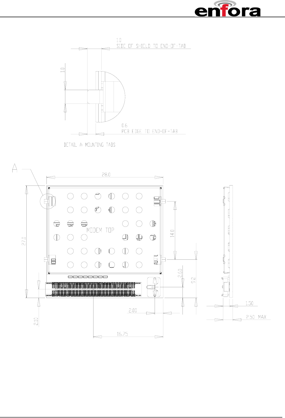
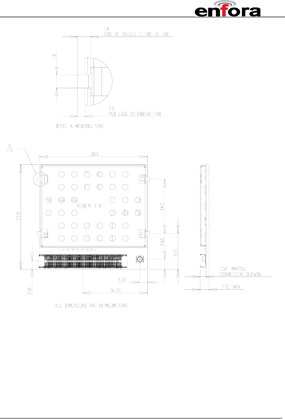
6. Mechanical
(Dimensions are in millimeters.)
Figure 4 – Front of Module (Board-to-Board RF Conn. Version)
GSM0308PB001 21 Version DRAFT – 2/9/2007
Enfora Enabler III-G
Modem Integration Guide
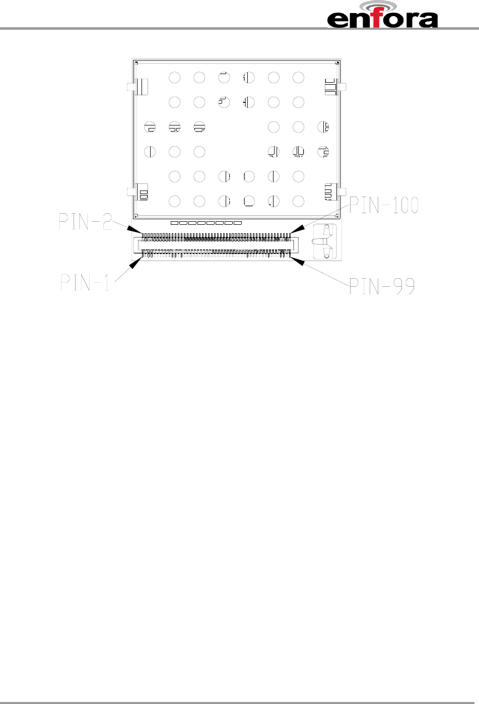
Figure 5 - Pin 1 Reference, 100-Pin I/O Connector
GSM0308PB001 22 Version DRAFT – 2/9/2007
Enfora Enabler III-G
Modem Integration Guide
Figure 6 – Front of Module (Coaxial RF Conn. Version)
GSM0308PB001 23 Version DRAFT – 2/9/2007
Enfora Enabler III-G
Modem Integration Guide
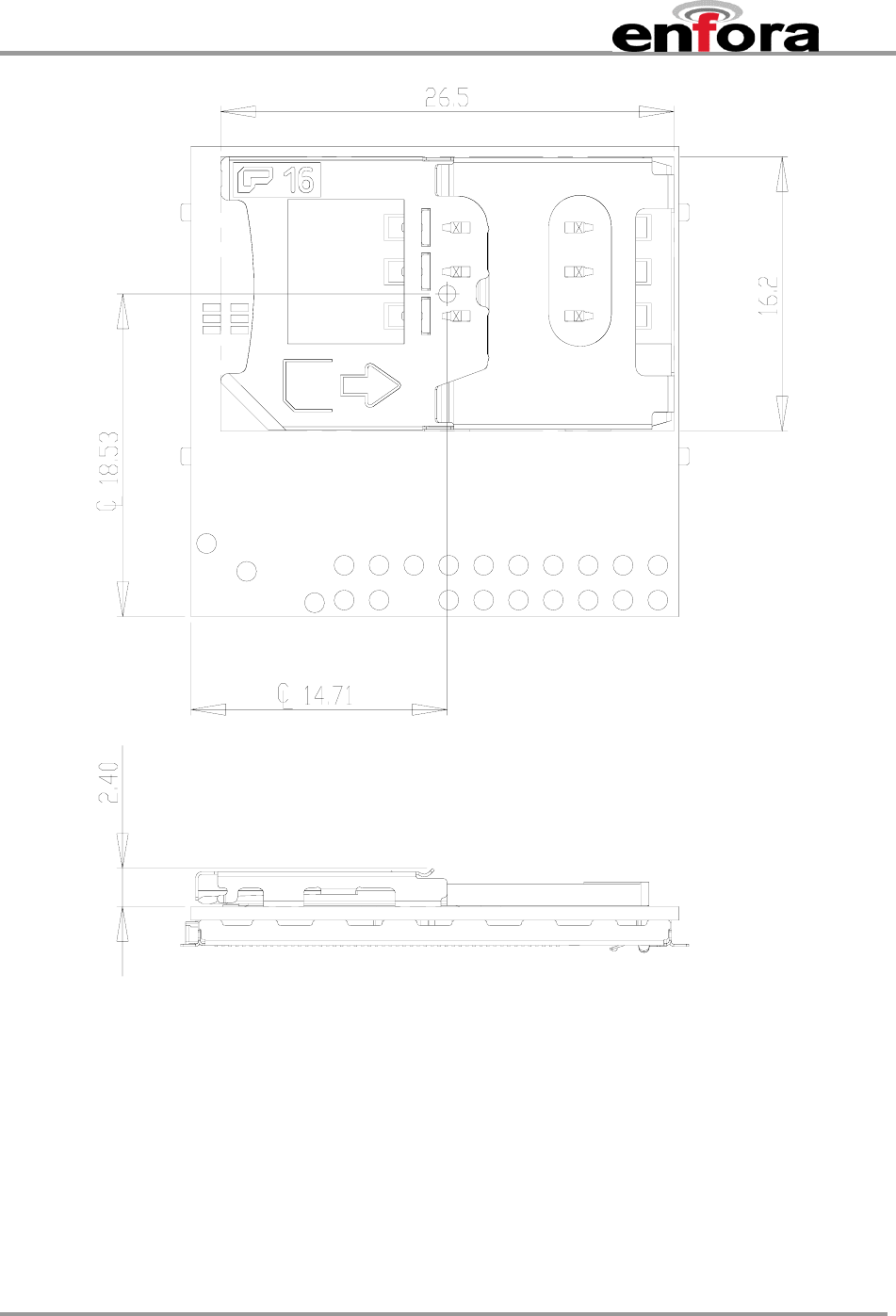
Figure 7 - Back of Module (Option SIM Shown)
GSM0308PB001 24 Version DRAFT – 2/9/2007
Enfora Enabler III-G
Modem Integration Guide
6.1. Module Mounting to Host Board (Reference)
The module provides mounting tabs that must be soldered to a PCB. These tabs provide circuit
grounding for the module.
Figure 8 – Module Mounting
GSM0308PB001 25 Version DRAFT – 2/9/2007
Enfora Enabler III-G
Modem Integration Guide
Figure 9 - Host Pads for Board-To-Board RF Connector
GSM0308PB001 26 Version DRAFT – 2/9/2007

Enfora Enabler III-G
Modem Integration Guide
6.2. Connectors
On The Modem: 100-Pin I/O Connector, Plug, SMT, Dual Row, 0.4 mm Pitch
Enfora PN = CON-1040-0100
Molex PN = 55909-1074
On The Host: 100-Pin I/O Connector, Socket, SMT, Dual Row, 0.4 mm Pitch
Enfora PN = CON-1040-0101
Molex PN = 51338-1074
The mated height of the two connectors is 1.50 mm.
6.3. RF Connection Options
6.3.1. Coaxial Connector Option
On The Modem:
Sunridge MCD Series – Ultimate Miniature Coaxial Interconnect, 1.55mm Mated Height
Contact Sunridge for mating cable options:
Enfora PN = CON-0009-0005
Sunridge PN = MCD-ST-00T
http://sunridgecorp.com/
Sunridge Corporation
2500 E. Foothill Blvd. Suite 107
Pasadena, CA 91107
U. S. A.
Tel: (626) 535-1780
Fax: (626) 535-1788
6.3.2. RF Board-to-Board Connector Option
On The Modem:
Enfora PN = CON-0009-0006
Sunridge PN = MCE-15A-G01
On The Host PCB:
No connector required. See Figure 9 for layout details.
GSM0308PB001 27 Version DRAFT – 2/9/2007
Enfora Enabler III-G
Modem Integration Guide
6.3.3. I/O Connector Pin Assignments
The following table shows the pin assignments for the input/output connector.
Table 2 - Enabler III-G Pin Assignments
PIN
# FUNCTION Serial
Pin I/O ENABLER III-G Description/Comments (Default function / secondary function)
1 Power Input (USB) P VBUS USB power
2 Ground R GND System Ground
3 Power Input (USB) P VBUS USB power
4 Ground R GND System Ground
5 I/O USB_DP/RXD/MIC_R 5 V tolerant data plus pin in USB modes /
Receive function in UART mode /
Microphone or right speaker in AUDIO mode
6 I LED_B LED B sink
7 I/O USB_DM/TXD/SPKR_L 5 V tolerant data minus pin in USB modes /
Transmit function in UART mode /
Monaural speaker or left speaker in AUDIO mode
8 I LED_A LED A sink
9 I ID_USB USB connector identification
10 O VRWLED Output voltage for VRWLED regulator
11 Clear To Send 8 I UART_CTS UART Clear to send[MG1]
12 I MCSI_RX/GPIO12 GPIO12 / MCSI Serial data input
13 Request To Send 7 O UART_RTS UART Request to send
14 I/O MCSI_CLK/GPIO9 GPIO9 / MCSI Serial Clock I/O
15 Serial Data Transmit 2 O UART_TX UART Serial data output
16 I/O MCSI_FSYNC/GPIO10 GPIO10 / MCSI Frame Synchronization I/O
17 Data Set Ready 6 I DSR_RXIR UART Data set ready/ IrDA Serial data input
18 O MCSI_TX / GPIO11 GPIO11 / MCSI Serial Data Output
19 Data Carrier Detect 1 O DCD_TXIR UART Data carrier detect/IrDA Serial data output
20 O SPI_\CS2 / GPIO18 GPIO18 / SPI Chip select 2
21 Serial Data Receive 3 I UART_RX UART Serial data input
22 I/O SPI_MOSI / GPIO15 GPIO15 / SPI Data master out/slave in
23 Ring Indicate 9 O UART_RING UART/Modem ring indicate
24 O SPI_\CS0/GPIO16 GPIO16 / SPI Chip select 0
25 Data Terminal Ready 4 O UART_DTR UART Data Terminal Ready
26 I/O SPI_MISO/GPIO14 GPIO14 / SPI Data master in/slave out
27 O KBC0/GPO25 Keyboard Matrix Column 0 / GPIO25
28 O SPI_\CS1/GPIO17 GPIO17 / SPI Chip select 1
29 O KBC2/GPO27 Keyboard Matrix Column 2 / GPIO27
30 I/O SPI_CLK/GPIO13 GPIO13 / SPI serial clock
31 O KBC3/GPO28 Keyboard Matrix Column 3 / GPIO28
32 O KBC4/GPIO20 Keyboard Matrix Column 4 / GPIO20
33 O KBC1/GPO26 Keyboard Matrix Column 1 / GPIO26
34 I KBR4/GPIO19 Keyboard Matrix Row 4 / GPIO19
35 I PWR_CTL External switch-on event (ON Button) with 32-kHz de-
bouncing
36 I KBR3/GPI24 Keyboard Matrix Row 3 / GPI24
37 I RESERVED RESERVED
38 I KBR0/GPI21 Keyboard Matrix Row 0 / GPI21
39 (OPEN)
40 I KBR1/GPI22 Keyboard Matrix Row 1 / GPI22
41 (OPEN)
42 I KBR2/GPI23 Keyboard Matrix Row 2 / GPI23
43 (OPEN)
44 (OPEN)
45 (OPEN)
46 (OPEN)
47 I HST_DET Headset Detect
48 O I2C_2_SCL I2C interface Master serial clock
49 I FML Mixer/FM radio input left channel
GSM0308PB001 28 Version DRAFT – 2/9/2007
Enfora Enabler III-G
Modem Integration Guide
50 I/O I2C_2_SDA I2C interface Serial bi-directional data
51 I AUXI_FMR Mixer/FM radio input right channel / SE auxiliary amplifier
input
52 O CLK13M_BUF 13 MHz Clock Output via 1 kΩ Series Resistor
53 O HSMICBIAS Headset microphone bias
54 Ground R GND System ground
55 I HSMIC Microphone input (Headset)
56 O CLK32K_BUF 32.768 kHz out, only buffered by 10 kΩ resistor
57 O HSOL 32 kΩ headset amplifier Left
58 I/O GPIO_4/TX_ACT/
LEDPULSE GPIO 4/Transmit Active/LED Pulse
59 O HSOR 32 kΩ headset amplifier Right
60 I/O GPIO_3/LPWM GPIO 3 / Light Output PWM
61 O HSOVMID Headset output common mode
62 I/O USB_BOOT/GPIO_2 GPIO 2
63 O MICBIAS Microphone bias
64 I/O GPIO_1/PWTONE GPIO 1 / Pulse Width Tone
65 I MICIP Microphone amplifier positive input (Handset)
66 I/O GPIO_7/SPIRW GPIO 7 / SPI Read Write
67 I MICIN Microphone amplifier negative input (Handset)
68 I/O GPIO_5/SPICS0 GPIO 5 / SPICS0
69 Ground R GND System Ground
70 I/O GPIO_6/SPIEN GPIO 6 / SPI Enable
71 O EARP 33 Ω or 120 Ω speaker amplifier (+) (Analog)
72 I/O GPIO_8/SPIDAT GPIO 8 / SPI Data
73 O EARN 33 Ω or 120 Ω speaker amplifier (-) (Analog)
74 I ADCIN4 10-bit A-to-D
75 Ground R GND System Ground
76 PWR VRSIM Output voltage for SIM 1.8 V /2.85 V
77 PWR VRIO 1.8 V out – Reference for external level translation
78 O SIM_CLK SIM Card Reference Clock
79 (OPEN)
80 O SIM_RST SIM card reset
81 (OPEN)
82 I/O SIM_IO SIM card I/O data
83 I VBACKUP Backup battery voltage
84 I SIMDTC SIM card insertion/extraction detect with 32-kHz debouncing
85 P VBAT Power from Host
86 Ground R GND System Ground
87 P VBAT Power from Host
88 Ground R GND System Ground
89 P VBAT Power from Host
90 Ground R GND System Ground
91 P VBAT Power from Host
92 Ground R GND System Ground
93 P VBAT Power from Host
94 Ground R GND System Ground
95 P VBAT Power from Host
96 Ground R GND System Ground
97 P VBAT Power from Host
98 Ground R GND System Ground
99 P VBAT Power from Host
100 Ground R GND System Ground
I=Input into Enabler; O=Output from Enabler; P=Power Input to Enabler; R=Power Return from
Enabler; I/O=Input/Output into/from Enabler, PWR=Other Power
Reserved for future use
NO CONNECT if on-board SIM holder is used
Open Lines
GSM0308PB001 29 Version DRAFT – 2/9/2007
Enfora Enabler III-G
Modem Integration Guide
6.4. Circuit Protection
Other than very low level ESD protection within the module’s integrated circuits, the module does
not have any protection against ESD events or other excursions that exceed the specified
operating parameters.
Generally, ESD protection (typically TVS/Transzorb devices) should be added to all signals that
leave the host board. This includes VBAT/VCC.
Series resistors (typically 47 Ω) can also be added in series with data lines to limit the peak
current during a voltage excursion.
Minimum ESD Protection Levels ESD/Input Voltage
Pin #’s ESD Test Method Min Nom/
Avg High/
Peak Units
Human Body Model
EIA/JEDEC22-A114-A 500 V Pins 11 – 24, 26-34,
36, 38, 40, 42, 48,
50, 52, 58, 60, 62,
64, 66,68, 70, 72,
78, 80, 82
Charge Device Model
EIA/JEDEC22-C101-A 200 V
Human Body Model EIA/JEDEC22-A114-A 2000 V Pins (all
VBUS/PWR), 5 – 10,
35, 37, 47, 49, 51,
52, 53, 55 – 57, 59,
61, 63, 65, 67
Charge Device Model EIA/JEDEC22-C101-A 500 V
Caution – It is the Integrator’s responsibility to protect
the Enabler III-G module from electrical disturbances
and excursions, which exceed the specified operating
parameters.
6.5. Antenna
The GSM0308-xx module has one RF antenna connection on the module. The connection is
for the GSM section of the module.
GSM0308PB001 30 Version DRAFT – 2/9/2007
Enfora Enabler III-G
Modem Integration Guide
6.6. Control Connector Signal Descriptions and Functions
Please note that the following descriptions are intended to
provide hardware-level definitions. In some cases, specific
lines will have no firmware functionality implemented.
Information for each hardware-specific feature will be noted
in the appropriate section.
6.6.1. Module Power (Pins 85, 87, 79, 91, 93, 95, 97, 99)
The Enfora Enabler III-G module uses a single voltage source of VCC=+3.3V to 4.5V. (The
exact values of the uplink currents are shown in Tables5.3.1 GSM Operating Power and
5.3.2 GPRS Operating Power).
VBAT Parameter/Conditions Min Typ Max Units
Main Battery Supply
Voltage In Regulation 3.3 4.5 Vdc
Peak Current 1000 μF on Host at Module
Connector
mA
The uplink burst will cause strong ripple on the voltage
lines and should be effectively filtered. It is recommended
that 1000 to 2000 F of capacitance be placed as close to
the modem I/O connector as possible.
It should be noted that the input voltage level should not
drop below the minimum voltage rating under any
circumstances, especially during the uplink burst period.
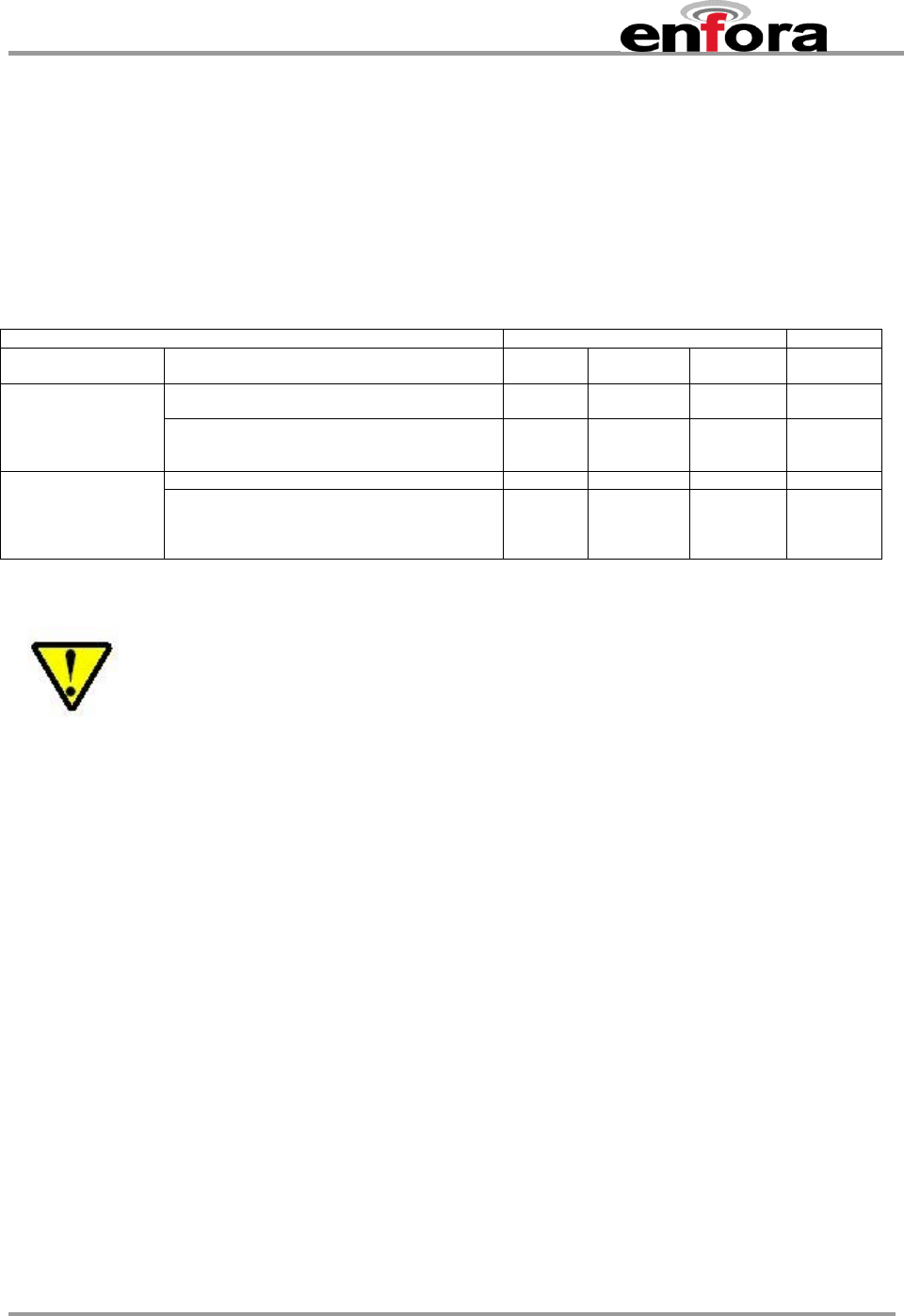
6.6.2. Ring Indicate
The Enabler III-G module is capable of using the Ring line to discern the type of incoming
call. The indicator can be monitored via a hardware line available on the 100-pin I/O signal
connector. The Ring Indicator pin is #49.
The function of the Ring line depends on the type of the call received.
When the module is receiving a voice call, the Ring line goes low for 1 second and high for
another 2 seconds. Every 3 seconds the ring string is generated and sent over the Receive
(Data Out) (Rx) line. If there is a call in progress and call waiting is activated for a connected
handset or hands free device, the Ring pin switches to ground in order to generate acoustic
signals that indicate the waiting call.
GSM0308PB001 31 Version DRAFT – 2/9/2007
Enfora Enabler III-G
Modem Integration Guide
When a Fax or data call is received, Ring goes low and will remain low. Every 3 seconds a
ring string is generated and sent over the Receive (Data Out) (Rx) line.
An incoming SMS can be indicated by an Unsolicited Result Code (URC) which causes the
Ring line to go low for 1 second only. Using the AT+CNMI command, the Enabler III-G
module can be configured to send or not to send URCs upon the receipt of SMS. See
Enfora Enabler-III AT Command Set - GSM0308PB001MAN.
1 second 2 seconds 1 second 2 seconds
RING Strin
g
RING Strin
g
Ring
3 seconds
RING Strin
g
RING Strin
g
Ring
3 seconds
RING Strin
g
1 second
URC
Ring
Figure 10 - Ring Indicate Timing
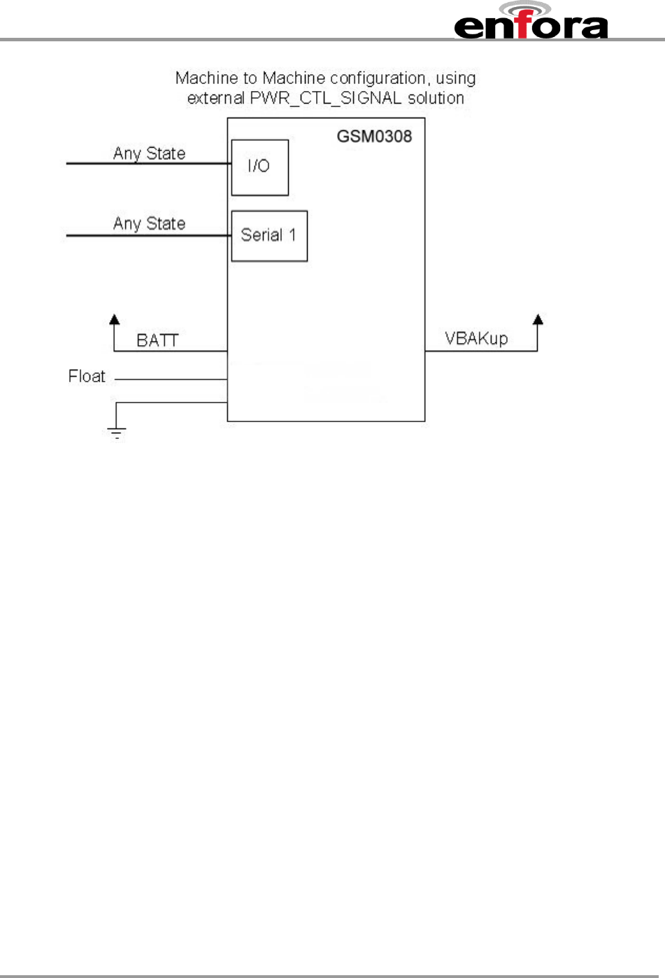
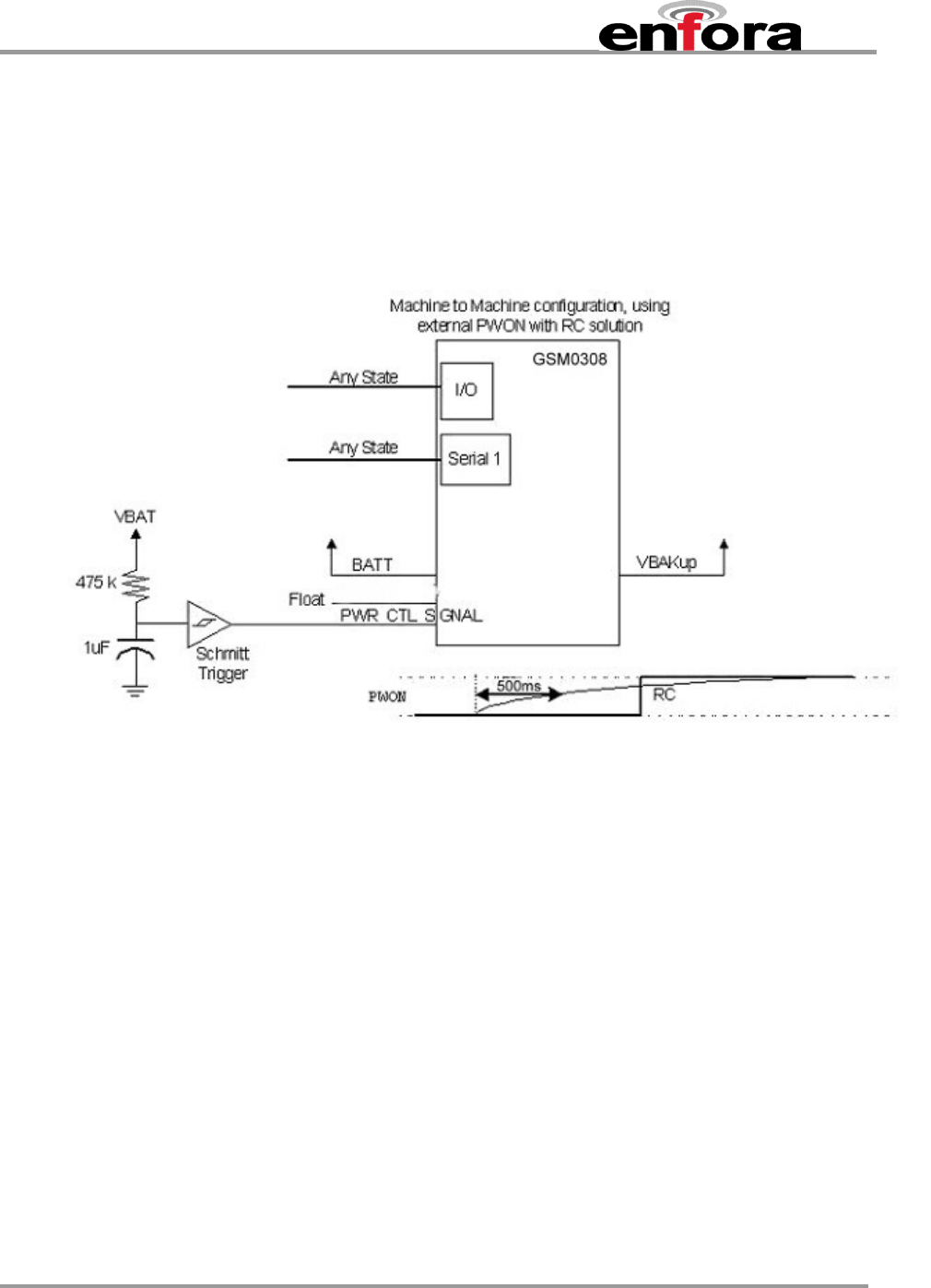
6.6.3. Using the Power Control Signal
Figure 11 shows a typical connection to the Enfora Enabler III-G module in a machine-to-machine application using
the external PWR_CTL_SIGNAL solution, where there is no external processor controlling the I/O, serial, or power
on/off states. RTC deep sleep functions will NOT function since the PWR_CTL_SIGNAL pin is tied low, the
processor will never stay in a “RTC Sleep” mode. To reset the module, power (BATT) must be cycled. VBAK
must be connected to an uninterruptible power source if RTC time is to be retained.
Note: RESET functionality is not supported on the Enabler III
GSM0308PB001 32 Version DRAFT – 2/9/2007
Enfora Enabler III-G
Modem Integration Guide
Figure 11 - External Power Control Signal (no external processor)
GSM0308PB001 33 Version DRAFT – 2/9/2007
Enfora Enabler III-G
Modem Integration Guide
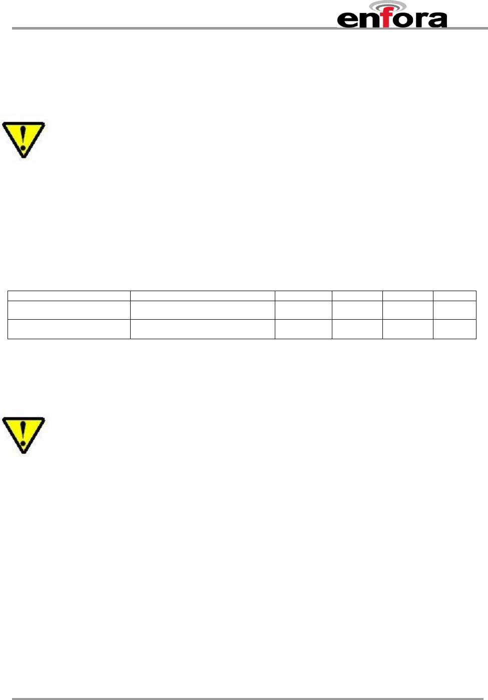
Figure 12 shows a variation of the connection in Figure 11 - External Power Control Signal (no external
processor) by using an external RC circuit to generate a pulse that will allow the processor to enter the
RTC deep sleep modes. This will keep the PWR_CTL_SIGNAL signal low for at least 500ms during
startup. To reset the module, power (BATT) must be cycled, and power must be removed long enough
for the RC to discharge.
Figure 12 - External Power Control Signal (using external RC circuit)
GSM0308PB001 34 Version DRAFT – 2/9/2007
Enfora Enabler III-G
Modem Integration Guide
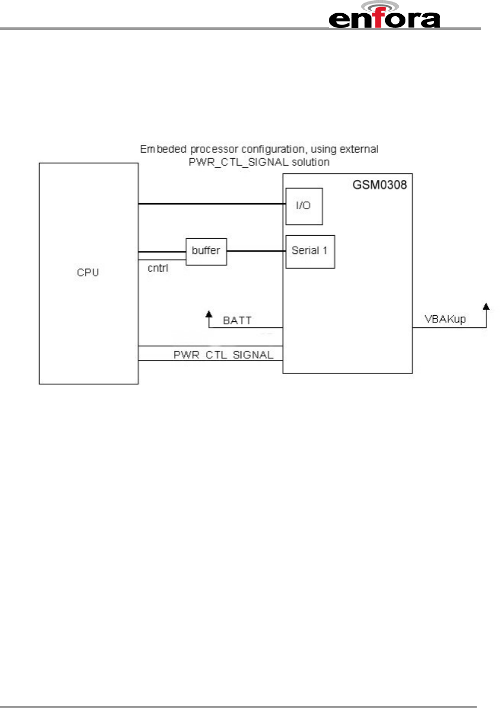
Figure 13 shows a typical connection from an external processor to the Enfora Enabler III-G module,
using the external PWR_CTL_SIGNAL solution. The Enfora Enabler III-G can be powered on by using
the PWR_CTL_SIGNAL signal. When using PWR_CTL_SIGNAL, the I/O or serial lines can be at any
voltage state desired. It is suggested that the I/O and serial lines be tri-stated or set low when the
GSM0308 is shutdown for an extended period of time to conserve power.
Figure 13 - Power Control Signal (using external processor)
GSM0308PB001 35 Version DRAFT – 2/9/2007
Enfora Enabler III-G
Modem Integration Guide
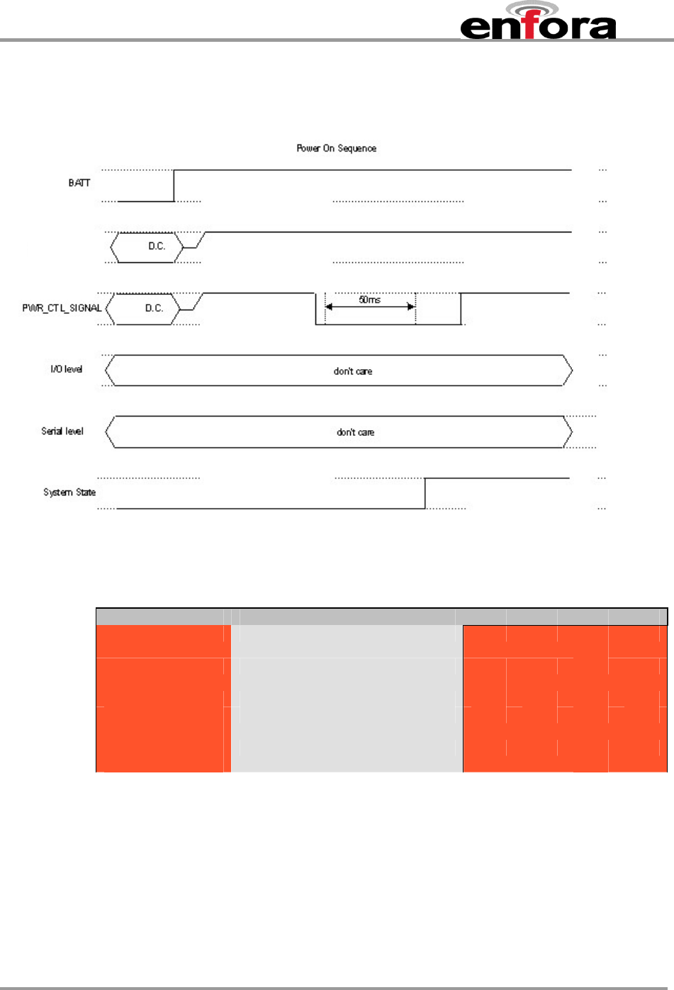
Figure 14 shows a typical power-on sequence for the CPU to Enfora Enabler III-G interface. Note that
Reset is not used, and the I/O and serial voltage levels are not a concern.
Figure 14 - Typical Power On Sequence (using external processor)
PARAMETER PARAMETER / CONDITIONS MIN TYP MAX UNIT
VIL Input Voltage – Low or float 0 0.3 x
VBAT
Vdc
VIH Input Voltage – High 0.7 x
VBAT
VBAT Vdc
ON Pulse
Duration 500 mS
OFF Pulse
Duration Programmable 1000 1000
0 mS
GSM0308PB001 36 Version DRAFT – 2/9/2007

Enfora Enabler III-G
Modem Integration Guide
6.6.4. Level Translation Reference Power (Pin 77)
To be used as a voltage reference source ONLY. Do not connect current loads to this pin. This pin
must be decoupled to ground with at least a 0.1 μF capacitor at the output. Noise induced on this pin
will affect the performance of the baseband.
VR I/O Parameter/Conditions Min Typ Max Units
Output voltage VOUT ON mode
LOW POWER mode
1.65
1.65 1.8
1.8 1.95
1.95 Vdc
Rated output current IOUT ON mode
LOW POWER mode
20 mA
0.5
6.6.5. USB (Pins 1, 3, 5, 7, 9)
Pin Name Pin
Number Signal
Direction Description
USB_VBUS 1, 3 In 5 V tolerant power Supply VBUS line;
Used only as a USB sense, not for powering the
module. (optional connection)
USB_DP/RXD/MIC_R 5 Analog
I/O 5 V tolerant data plus pin in USB modes /
Receive function in UART mode /
Microphone or right speaker in AUDIO mode
USB_DP 7 Analog
I/O 5 V tolerant data minus pin in USB modes /
Transmit function in UART mode /
Monaural speaker or left speaker in AUDIO
mode
ID_USB 9 Analog
I/O 5 V tolerant ID line, it defines the type of
device connected to the phone’s USB port;
And also the default state (host / device) at
the cable connection;
The transceiver senses the voltage of this
pin to determine if the pin is either floating
(typical),grounded or resistively connected
to ground (102 kΩ, 200 kΩ, 440 kΩ);
The universal serial bus (USB) device controller supports the implementation of a full-speed (FS) device
compatible with the Universal Serial Bus Specification Revision 2.0 and the Universal Serial Bus
Specification Revision 1.1.
The module includes a Universal Serial Bus (USB) transceiver with a car-kit detection, able to support
USB 12 Mb/s Full-Speed (FS) and USB 1.5 Mb/s Low-Speed (LS). When a USB cable is plugged into
the USB receptacle, the transceiver detects the cable’s presence on VBUS (> 1.8 V) and ID ( float) pins,
even if the module is switched off. The transceiver is fully operational only in phone’s Active mode.
The modules device’s car kit is developed based on CEA-936-A rev.39 – Nov. 24th 2004 specification.
Currently the device does not support other versions of this specification. Compared to the CEA-936-A
rev.39 – Nov. 24th 2004 specification, the car-kit implementation in the module device does not support
[1] a fully implemented hardware Phone State Machine, [2] the relative interrupts and registers for the
proper behavior of the Phone State machine and [3] the Data-During- Audio signaling mode.
GSM0308PB001 37 Version DRAFT – 2/9/2007
Enfora Enabler III-G
Modem Integration Guide
• USB transceiver full compliant (modes and registers);
• Supports data line (D+, D-, and VBUS pulsing session request (SRP);
• Supports UART signaling (From 9.6 kbaud up to 115.2 kbaud);
• Supports AUDIO (MONO / STEREO) signaling;
• Transceiver does not support USB High Speed (HS) mode signaling;
There are 3 signal modes available to the USB port that will allow the desired signal to be routed to the
physical USB pins. The functions that can be selected are USB mode, UART mode, and AUDIO mode.
UART Mode
When the UART mode is enabled, UART transactions can be achieved through the transceiver. In this
mode, the transceiver can be considered as simple levels translators. When UART mode is enabled, it
automatically switches off the other USB and AUDIO drivers.
AUDIO Modes
It is possible to select between the MONO and STEREO signaling modes. When enabling the AUDIO
drivers, the USB and UART drivers are turned off.
USB Power (pins 1,3) Parameter/Conditions Min Typ Max
Units
Filtering Capacitor Connected from VRUSB to GNDD 1.0 4.7 µF
Filtering Capacitor ESR 0 - 300 m
Input Voltage VIN ON mode, in regulation 2.7 5.0 5.25 Vdc
B-Device (SRP Capable,
Peripheral-Only)
Average
Current
0 V VBUS 5.25 V
8 mA
VBUS Wake-Up Threshold
1.6 1.8 2.0 V
5V Tolerant Transceiver
USB Parameter/Conditions Min Typ Max Units
Input Voltage 4.4
4.65 5.25 V
High (Driven) 2.8 3.3 3.6 Vdc Output voltage
Low 0.0
0.1 0.3 Vdc
Transceiver D+/- Leakage
Current -2
2 A
USB / UART mode
Input Levels Parameter/Conditions Min Typ Max Units
Serial Interface Input
High RXD Input High On
D+
2.0 Vdc
Serial Interface Input
Low RXD Input Low On
D+
0.8 Vdc
GSM0308PB001 38 Version DRAFT – 2/9/2007
Enfora Enabler III-G
Modem Integration Guide
Output Levels Parameter/Conditions Min Typ Max Units
Serial Interface Input
High RXD Input High On
D-
ISOURCE = 4 mA
2.4 3.3 3.6 Vdc
Serial Interface Input
Low RXD Input Low On
D-
ISOURCE = -4 mA
0.0 0.1 0.4 Vdc
USB port / Audio mode
Terminations Parameter/Conditions Min Typ Max Units
Phone Microphone Input
Impedance Freq = 1 kHz
10
kΩ
Phone Speaker Output
impedance Freq = 1 kHz
200
Ω
Current
Phone Speaker Source
Current D ± grounded 20 mA
Input Levels
Phone Microphone Input
Range 1.0 2.2 V
Output Levels
Phone Speaker Output Bias 0.7 1.6 V
Phone Speaker Output Range 2.2 V
6.6.6. LED A (Pin 8) & B (Pin 6), VRWLED (Pin 10)
Pin Name Pin Number Signal Direction Description
LED A 8 I LED A open drain input
LED B 6 I LED B open drain input
The LED ‘driver’ pins are able to operate as a general current sink, or use in conjunction with the built in
LED driver VRWLED.
Two white-LEDs drivers are available from the module.
The first driver, “LED_A” is dedicated for the screen backlight and can drive up to four white-LEDs in
series.
The second driver, “LED_B” is dedicated for the keypad and can drive up to four white-LEDs in series.
The two white-LEDs driver series are fed by a dedicated DC-DC step-up regulator VRWLED.
The maximum current delivered by this white-LEDs drivers is 63.75 mA, in order to have an average
maximum current within each white-LED of 21.25 mA . The 63.75 mA is switched among the three series
of LEDs as described in the below table, the corresponding timing scheme is reported in the below table.
Each series of LEDs has a maximum average current per frame of 21.25 mA ( 3
75.63 mA ). The frame
period is 3×TCK. TCK can be programmed via a register between 2 ms and 6 ms.
The current delivered to each series of white-LEDs is obtained from a dedicated 8-bit DAC-based system.
While the 4-LSBs contribution is generated starting from a PWM signal that modulates a 4 mA current
level as indicated in the below table.
GSM0308PB001 39 Version DRAFT – 2/9/2007
Enfora Enabler III-G
Modem Integration Guide
Input Code
Number Input Code Average
Current (mA)
255 (MAX) 11111111 21.25
254 11111110 21.17
… … …
240 11110000 20
239 11101111 19.92
… … …
15 00001111 1.25
14 00001110 1.17
13 00001101 1.08
12 00001100 1.00
11 00001011 0.92
10 00001010 0.83
9 00001001 0.75
8 00001000 0.67
7 00000111 0.58
6 00000110 0.50
5 00000101 0.42
4 00000100 0.33
3 00000011 0.25
2 00000010 0.17
1 00000001 0.83
0 (MIN) 00000000 0
White-LEDs Drivers 8-bit DAC Input Code, Output Current
The DC-DC step-up is based on a control loop, which is composed of a start-up circuit and an amplifier in
series with a comparator.
Another dedicated logic is capable to sense if one of the two white-LEDs series does not work properly
(open circuit): this logic prevents the divergence of the circuit, forcing a low-voltage level on the gate of
the power NMOS transistor in this case. During the normal operation, the NMOS transistors drivers,
which are part of the feedback system of the boost, remain saturated with a nominal drain-to-source
voltage closed to 1.2 V.
VBAT POUT 2 LEDs (mW) POUT 3 LEDs (mW) POUT 4 LEDs (mW)
5.5 586 873 824
5.4 586 831 834
5.2 586 812 767
5.0 586 799 710
4.8 586 755 645
4.6 586 683 572
4.4 586 637 523
4.2 586 606 487
4.0 586 583 457
3.8 586 535 424
3.6 586 468 377
3.4 586 425 330
3.3 586 401 304
GSM0308PB001 40 Version DRAFT – 2/9/2007
Enfora Enabler III-G
Modem Integration Guide
Max current (mA)
VBAT (V) 2 LEDs 3 LEDs 4 LEDs
3.6 64 40 25.5
6.6.7. LED VRW (Pin 10)
The VRWLED voltage regulator is a step-up DC-DC converter supplying the White LEDs (20.0V/60mA).
The regulated voltage depends on the number of series White-LEDs. The main battery directly supplies
VRWLED.
VRWLED Parameter/Conditions Min Typ Max Units
Voltage out 20 Vdc
Current 60 mA
L = 2.2 H ± 20%, RDC max = 100 mΩ, C = 2.2 µF ± 20% , Zener 20 V Iz typ = 5 mA (min: 4 mA, max: 10 mA), Pd typ = 0.3 W
(min: 0.25 W, max: 0.5 W);
Figure 15 – LED voltage driver circuit
GSM0308PB001 41 Version DRAFT – 2/9/2007
Enfora Enabler III-G
Modem Integration Guide
6.6.8. General Purpose Input/Output Interface
GPIO number Pin number Secondary function
GPIO 1 64 Pulse Width Tone
GPIO 2 62 USB Boot
GPIO 3 60 Light Output PWM
GPIO 4 58 Transmit active / LED Pulse Generator
GPIO 5 68 SPI Chip Select 0
GPIO 6 70 SPI Strobe Enable
GPIO 7 66 SPI RnW
GPIO 8 72 SPI Data/Control Select
Each general-purpose signal may be selected as inputs or outputs. GPIO1-GPIO8 may be used
independently as a user-specified function, or may be used to provide modem control and status signals.
Several examples of modem control signals are: power shutdown command, register/deregister on
network command, and transmitter disable. Several examples of modem status signals are: registration
status and ready-for-power-down status to be used with power shutdown command signal.
I/O Lines Parameter/Conditions Min Typ Max Units
VIL Input Voltage – Low 0 0.60 Vdc
VIH Input Voltage – High 1.11 1.8 Vdc
VOL Output Voltage – Low 0.45 Vdc
VOH Output Voltage – High 1.26 Vdc
IOL / IOH Rated Output Current 4 mA
Additional GPIO is available as alternate functions of the blocks listed. If the function is selected as a
GPIO block then all associated pins will become GPIO, the primary function will be disabled. Electrical
specifications for alternate GPIO functions will be the same as their primary pin function.
Primary Function Primary Function Name Pin Number GPIO Number
MCSI_CLK 14 GPIO 9
MCSI_FSYNC 16 GPIO 10
MCSI_TX 18 GPIO 11
MSCI
MCSI_RX 12 GPIO 12
SPI_CLK 30 GPIO 13
SPI_MISO 26 GPIO 14
SPI_MOSI 22 GPIO 15
SPI_CS0 24 GPIO 16
SPI_CS1 28 GPIO 17
SPI
SPI_CS2 20 GPIO 18
Some functions have a secondary output that can only be defined as either an input or an output.
Primary Function Primary Function
Name Pin number Signal Direction GPIO number
Keyboard KBR_0 38 IN GPI 21
KBR_1 40 IN GPI 22
KBR_2 42 IN GPI 23
KBR_3 36 IN GPI 24
KBR_4 34 IN/OUT GPIO 19
KBC_0 27 OUT GPO25
KBC_1 33 OUT GPO26
KBC_2 29 OUT GPO27
KBC_3 31 OUT GPO28
KBC_4 32 IN/OUT GPIO 20
*SPI, I2C, MCSI and Keyboard are for hardware reference only. There is no generic
firmware to support these functions. Firmware must be added to enable these functions
(TBD)
GSM0308PB001 42 Version DRAFT – 2/9/2007
Enfora Enabler III-G
Modem Integration Guide
6.6.9. Power Control (Pin 35)
The input is equivalent to the “phone ON-button”. A falling-edge on this Active-Low input will switch-ON
the module or switch-OFF the module after a delay. This input has a “weak pull-up” resistor internal to
the module. This input can be left grounded if the “RTC Sleep Function” is not required. If RTC Sleep is
required, see Section 6.6.10.
Module Reset Parameter/Conditions MIN TYP MAX UNIT
VIL Input Voltage – Low or float 0.9 Vdc
VIH Input Voltage – High 2.1 5.5 Vdc
IPU Internal Pull-Up Resistor -40 -31 -15 μA
ON Pulse Duration 25 mS
OFF Pulse Duration Programmable tbd mS
6.6.10. RTC Sleep
In this mode, the modem is off except for its Real-Time-Clock. When put into this mode, the modem
can wake itself up at a designated time/interval.
6.6.11. Serial Interfaces & Handshake (Pins 11, 13, 15, 17, 19, 21, 23, 25)
Pin Name Pin Number Signal Direction Description
UART_TX 15 O Serial data output
UART_RX 21 I Serial data input
UART_RTS 13 O Request to send
UART_CTS 11 I Clear to Send
UART_DSR 17 I Data set ready
UART_DTR 25 O Data terminal ready
UART_DCD 19 O Data carrier detect
UART_RING 23 O Ring detect output
Please note that Serial interface is now referenced as a DCE and the
naming of pins has changed since Enabler II products
GSM0308PB001 43 Version DRAFT – 2/9/2007

Enfora Enabler III-G
Modem Integration Guide
The key features of the UART in the modem mode are as follows:
• 16C750 compatibility
• Baud rate from 300 bits/s up to 3.6864 Mbits/s
• Auto baud between 1200 bits/s and 115.2 kbits/s
• Configurable data format:
Data bit: 5, 6, 7, or 8 bits
Parity bit: even, odd, none
Stop bit: 1, 1.5, 2 bit(s)
• Hardware flow control RTS/CTS
• Software flow control using XON/XOFF characters
The Enabler III-G module is designed to be used like a DCE device.
Default settings are 8 data, 1 stop, no parity, and 115200 baud. DTR may be used to force the
modem into AT command mode from online data mode (See AT Command Document, command
AT&D). RTS and CTS may be used for hardware handshaking. DSR is always active (connected to
ground) while the modem is on. RING may be used to alert the host to a variety of incoming calls.
For a minimal implementation, connect RxData and TxData to the COM port serial data lines, connect
DTR and RTS to GND.
Serial I/O & Control Parameter/Conditions Min Typ Max Units
VIL Input Voltage – Low 0.54 Vdc
VIH Input Voltage – High 1.26 1.95 Vdc
VOL Output Voltage – Low 0.54 Vdc
VOH Output Voltage – High 1.26 1.95 Vdc
IOL / IOH Rated Output Current 2.0 mA
6.6.12. MCSI – Multi-Channel Serial Interface (Pins 12, 14, 16, 18)
Pin Name Pin Number Signal Direction Description
MCSI_RX 12 I Serial Data Input
MCSI_TX 18 O Serial Data Output
MCSI_CLK 14 IO Serial Clock I/O
MCSI_FSYNC 16 IO Frame Synchronization I/O
The multi-channel serial interface (MCSI) has multi-channel transmission capability. MCSI expand the
parallel interface of a MPU or DSP to connect to external devices such as audio codecs and GSM system
simulators.
The MCSI on the module provides full-duplex communication with master or slave clock control. All
transmission parameters are configurable to cover the maximum number of operating conditions:
• Master or slave clock control (transmission clock and frame synchronization pulse)
• Programmable transmission clock frequency
• Single-channel or multi-channel (x16) frame structure
• Programmable word length: 3 to 16 bits
GSM0308PB001 44 Version DRAFT – 2/9/2007
Enfora Enabler III-G
Modem Integration Guide
• Full-duplex transmission
• Programmable frame configuration
• Continuous or burst transmission
• Normal or alternate framing
• Normal or inverted frame polarity
• Short or long frame pulse
• Programmable oversize frame length
• Programmable frame length
• Programmable interrupt occurrence time (TX and RX)
• Error detection with interrupt generation on wrong frame length
GSM digital audio interface (DAI) operating modes (radio uplink, radio downlink, and
acoustics). The DAI mode is a GSM test interface that is used to determine the routing of
speech data for the devices being tested. In DAI mode, the MCSI is configured for direct
connection to the GSM system simulator interface, including the reset system simulator
(RSS) signal.
For hardware reference only. There is no generic firmware to support this function.
Firmware must be added to enable MCSI (TBD)
6.6.13. I2C (Pins 48, 50)
Pin Name Pin Number Signal Direction Description
I2C_SCL 48 I/O I2C interface Master serial clock
I2C_SDA 50 I/O I2C interface Serial bi-directional data
The multi-master I2C peripheral provides an interface between a local host (LH) such as an MPU
processor and any I2C -bus-compatible device that connects via the I2C serial bus. External components
attached to the I2C bus can serially transmit/receive up to 8-bit data to/from the LH device through the
two-wire I2C interface.
This I2C peripheral supports any slave or master I2C -compatible device. The I2C bus is a multi-master
bus. The I2C controller supports the multi-master mode that allows more than one device capable of
controlling the bus to be connected to it. Each I2C device, including the on board processor, is
recognized by a unique address and can operate as either transmitter or receiver, according to the
function of the device. In addition to being a transmitter or receiver, a device connected to the I2C bus
can also be considered as master or slave when performing data transfers. Note that a master device is
the device which initiates a data transfer on the bus and generates the clock signals to permit that
transfer. During the transfer, any device addressed by this master is considered a slave.
For hardware reference only. There is no generic firmware to support this function.
Firmware must be added to enable I2C (TBD)
I2C Parameter/Conditions Min Typ Max Units
VIH High level input voltage 1.26 1.8 1.9 V
VIL Low level input voltage 0 0.54 V
II Input leakage current ±1 A
VOH High level output voltage, IO = 3 mA 1.44 1.8 V
GSM0308PB001 45 Version DRAFT – 2/9/2007
Enfora Enabler III-G
Modem Integration Guide
VOL Low level output voltage, IO = 3 mA 0 0.36 V
Iz Leakage current ± 20 A
6.6.14. Serial Port Interface (SPI) (Pins 20, 22, 24, 26, 28, 30)
Signal Direction
Pin Name
Pin
Number Master
mode Slave Mode Description
SPI_MOSI 22 O I Master Out / Slave In
SPI_MISO 26 I O Master In / Slave Out
SPI_CLK 30 O I Clock
SPI_nCS0 24 O I Chip select out / enable
SPI_nCS1 28 O I Chip select out / enable
SPI_nCS2 20 O I Chip select out / enable
The Master Slave SPI (MSSPI) is compliant with the SPI standard. It is a bidirectional, four-line interface
consisting of:
• Clock, used to shift-in and shift-out data;
• Device enable;
• Data input;
• Data output;
There is one MSSPI module available. It is based on a looped shift register, thus allowing both transmit
and receive modes. It can operate in master or in slave mode using MPU / DSP or DMA protocol. In
Master mode, the SPI provides up to 3 chip-selects: spi_ncs0, spi_ncs1 and spi_ncs2. In Slave mode,
spi_ncs0 is used as the SPI module chip select.
For hardware reference only. There is no generic firmware to support this function.
Firmware must be added to enable SPI (TBD)
SPI Parameter/Conditions Min Typ Max Units
VIH High level input voltage 1.17 1.8 1.9 V
VIL Low level input voltage 0.63 V
VOH High level output voltage, IO = 2 mA 1.35 1.8 V
VOL Low level output voltage, IO = 2 mA 0.45 V
II Input leakage current ±1 A
Iout Output current 8 mA
PU PU resistance 18 k
PD PD resistance 18 k
GSM0308PB001 46 Version DRAFT – 2/9/2007
Enfora Enabler III-G
Modem Integration Guide
6.6.15. Keyboard (Pins 27, 29, 31, 32, 33, 34, 36, 38, 40, 42 )
Pin Name Pin Number Signal Direction Description
KBC0 27 O Keyboard matrix column 0 output
KBC1 33 O Keyboard matrix column 1 output
KBC2 29 O Keyboard matrix column 2 output
KBC3 31 O Keyboard matrix column 3 output
KBC4 32 O Keyboard matrix column 4 output
KBR0 38 I Keyboard matrix Row 0 input
KBR1 40 I Keyboard matrix Row 1 input
KBR2 42 I Keyboard matrix Row 2 input
KBR3 36 I Keyboard matrix Row 3 input
KBR4 34 I Keyboard matrix Row 4 input
The module keyboard controller implements a built-in scanning algorithm for hardware-based key press
decoding and allows MPU software overhead reduction. The keyboard controller can handle up to 5 × 5
keyboards, operates on a 32 kHz clock, and can generate wake-up events when the device is in sleep
mode.
The keyboard controller includes the following main features:
• Support of multi-configuration keyboards up to 5 rows x 5 columns
• Integrated programmable timer
• Event detection on both key press and key release
• Multi-key press detection and decoding
• Long key detection on prolonged key press
• Programmable time-out on permanent key press or after keyboard release
For hardware reference only. There is no generic firmware to support this function.
Firmware must be added to enable Keyboard functions (TBD)
Keyboard Parameter/Conditions Min Typ Max Units
VIH High level input voltage 1.17 1.8 1.9 V
VIL Low level input voltage 0.63 V
VOH High level output voltage, IO = 4 mA 1.35 1.8 V
VOL Low level output voltage, IO = 4 mA 0.45 V
II Input leakage current ±1 µA
Iout Output current 8 mA
PU PU resistance 18 k
PD PD resistance 90 k
Iz Leakage current ± 20 µA
GSM0308PB001 47 Version DRAFT – 2/9/2007

Enfora Enabler III-G
Modem Integration Guide
6.6.16. VBACKUP Input (Pin 83)
The backup battery can be recharged from the main battery. A programmable voltage regulator powered
by the main battery allows recharging the backup battery. The backup battery charge starts when the
following conditions are met:
Backup battery charge is enabled by a control bit:
• Main Battery voltage > Backup Battery voltage
• Main battery > 2.8 Vdc
Note: If the backup battery is not present, the backup battery pin is connected to main battery pin
VBACKUP is a power input for the Real-Time-Clock when using RTC-Sleep Function (Section 6.6.10)
VBACKUP Parameter/Conditions Min Typ Max Units
ON mode 2.5 VCC1 5.5
BACKUP mode, VBAT=0v 1.9 VBACKUP 5.5
Input Voltage Range
BACKUP mode, VBACKUP=0v 1.9 VCC2 3.0
Vdc
Input Current 10 μA
GSM0308PB001 48 Version DRAFT – 2/9/2007
Enfora Enabler III-G
Modem Integration Guide
6.6.17. Using VBAK
VBAK is a backup voltage that can maintain the RTC clock and alarm functions. If VBAK is not present
in the system (intentionally or not) the RTC clock may still be powered if leakage voltage exists on VCC.
Otherwise, the RTC clock will lose power and be reset when VCC is restored.
VBAK had been tested in the above scenarios and does not contribute to leakage. It will properly provide
backup power to the RTC clock.
6.6.18. 32 kHz output (Pin 56)
A 32.768 kHz signal is available as an output from the module. This signal should only be used as an
input to a high impedance device. Additional loads or capacitance on the line may cause performance
issues with the module. If the line is not used, leave floating.
32kHz Clock-Out Parameter/Conditions Min Typ Max Units
VIH Vdc
VIL Vdc
Maximum capacitor load tbd pF
Maximum resistive load
Ω
Frequency ± 30 ppm 32.768 kHz
6.6.19. 13 MHz output (Pin 52)
A 13 MHz signal is available as an output from the module. This signal should only be used as an input
to a high impedance device. Additional loads or capacitance on the line may cause performance issues
with the module. If the line is not used, leave floating.
13 MHz Clock-Out Parameter/Conditions Min Typ Max Units
VIH TBD Vdc
VIL 0.3 Vdc
Maximum capacitor load TBD pF
Maximum resistive load TBD
Ω
Frequency ±0.1 ppm when registered on
GSM network;
±12 ppm typical when not
registered;
13.000 MHz
PARAMETER PARAMETER / CONDITIONS MIN TYP MAX UNIT
Backup Voltage (Real-Time-Clock)
VBACKUP Backup Voltage for Real-Time-Clock 2.7 3.0 4.5 Vdc
IBACKUP Input Current (VBACKUP = 3.2 V, VBAT = 0 V,
No Load on GPIO or Serial Port) 3.0 6.0 μAdc
GSM0308PB001 49 Version DRAFT – 2/9/2007
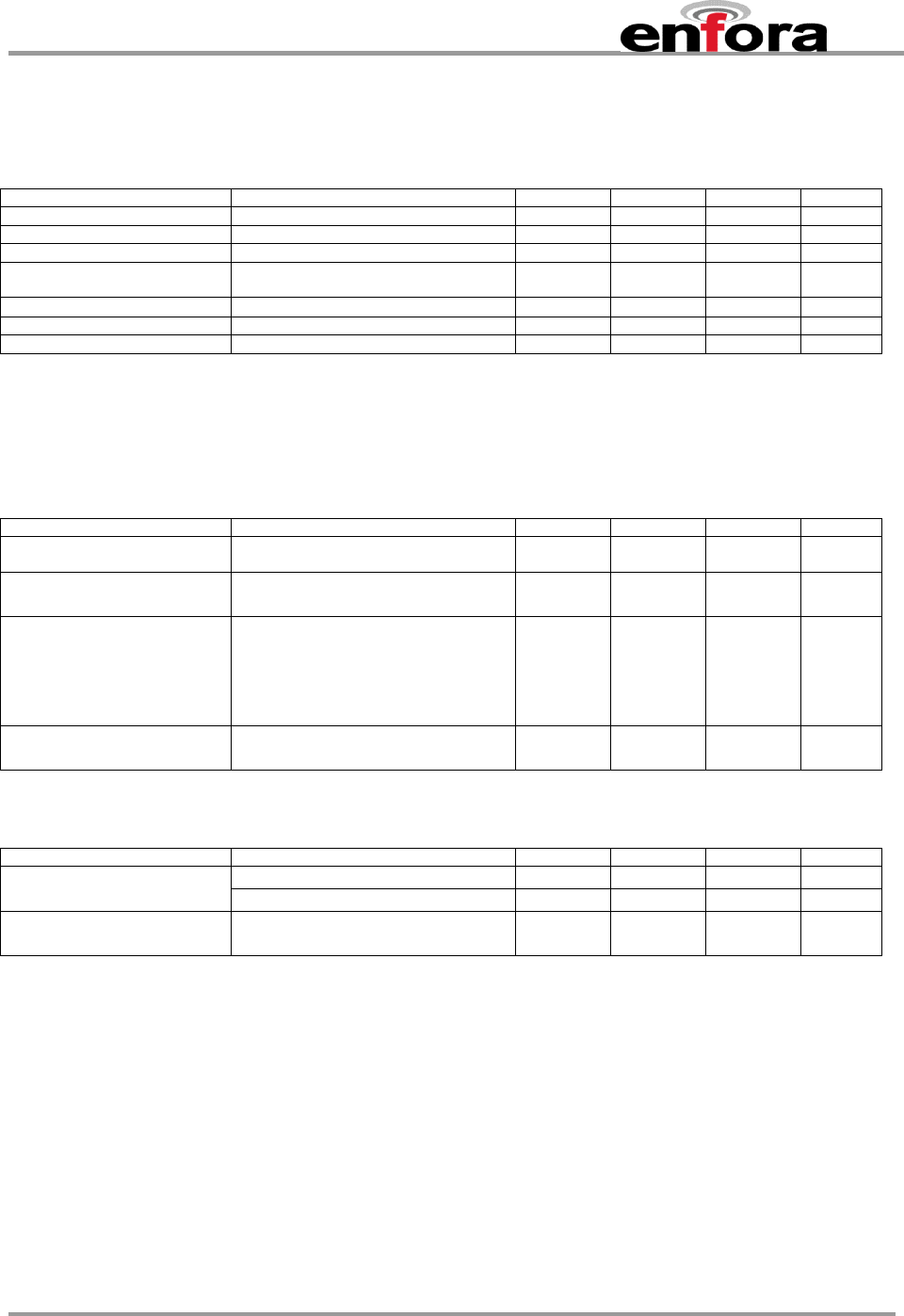
Enfora Enabler III-G
Modem Integration Guide
6.6.20. Analog-To-Digital Input (Pin 74)
The monitoring ADC (MADC) consists of a successive approximation 10–bit analog–to–digital converter
(ADC).
Analog-To-Digital Input Parameter/Conditions Min Typ Max Units
ADCBRES ADC Binary Resolution 10 Bits
ADCREF ADC Reference Voltage 1.75 Vdc
VADC ADC Range 0 1.75 Vdc
Integral/Differential Non-
Linearity -2 2 LSB
Input Leakage tbd μA
Retuning Frequency 1 MHz
6.6.21. Handset Microphone Input (Pins 65, 67)
The handset differential inputs MICIP and MICIN can be amplified by the differential handset microphone
amplifier. This amplifier has a gain of 25.6 dB and a bias generator MICBIAS provides an external voltage
of 2 V or 2.5 V to bias the microphone.
Handset Mic Input Parameter/Conditions Min Typ Max Units
Maximum Input Range –
Mic(+) to Mic(-) Inputs 3 dBm0 (Max. digital sample
amplitude when PGA gain set to 0 dB) 32.5 mVRMS
Nominal Ref. Level –
Mic(+) to Mic(-) Differential MIC
-10 dBm0
Differential Input Resistance –
Mic(+) to Mic(-) Differential MIC, MICAMP gain
= 25.6 dB
(INMODE = 0001)
36
kΩ
Microphone Pre-
Amplifier Gain Differential MIC
25.6 dB
6.6.22. Handset Microphone Bias Output (Pin 63)
Mic Bias Output Parameter/Conditions Min Typ Max Units
Set to 2.0 V 1.9 2.1 Vdc
Bias Voltage on Mic(+) Set to 2.5 V 2.4 2.6 Vdc
Mic Bias Current
Capability 2.0 mA
GSM0308PB001 50 Version DRAFT – 2/9/2007
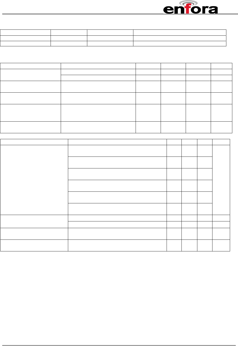
Enfora Enabler III-G
Modem Integration Guide
6.6.23. Handset Speaker Output (Pins 71, 73)
Pin Name Pin Number Signal Direction Description
EARP 71 O Earphone positive output
EARN 73 O Earphone negative output
The earphone amplifier provides a full differential signal on the terminals EARP and EARN (Earphone).
Handset Spkr Output Parameter/Conditions Min Typ Max Units
Output Swing 3.9 VPP 120 Ω
Maximum Differential
Resistive Load Output Swing 1.5 VPP 33
Ω
Maximum Differential
Capacitive Load
100 pF
Common Mode
Minimum Resistive Load At Internal Speaker (+) or (-) 200
kΩ
Common Mode
Maximum Capacitive
Load
At Internal Speaker (+) or (-) 50 pF
Amplifier Gain EARG = 1
EARG = 0
1
-11 DB
dB
Parameter Test Conditions Min Typ Max Units
Distortion 2% and 120 , VSP input
level = +3 dBm0, amp gain = -11 dB 0.98
Distortion 2% and 33 , VSP input level
= -5.34 dBm0, amp gain = -11 dB 0.38
Distortion 2% and 120 , I2S input level
= +3 dBm0, amp gain = -11 dB 0.93
Distortion 2% and 120 , VSP input
level = +3 dBm0, amp gain = 1 dB 3.1 3.92
Distortion 2% and 33 , VSP input level
= -5.34 dBm0, amp gain = 1 dB 1.2 1.5
Earphone output swing at
EARP-EARN
Distortion 2% and 120 , I2S input level
= +3 dBm0, amp gain = 1 dB 2.96 3.7
VP-P
EARG = 1 1 dB
Earphone amplifier gain
EARG = 0 -11 dB
Earphone amplifier state in
power down High
Z
Earphone amplifier power
supply rejection 1 kHz, 100 mVp-p
50 dB
An external audio amplifier should be used for loads of less than 16 Ω or if volume is inadequate.
GSM0308PB001 51 Version DRAFT – 2/9/2007

Enfora Enabler III-G
Modem Integration Guide
6.6.24. Headset Microphone Input (Pin 55)
The headset differential inputs
HSMIC and AUXI can be
amplified by the differential
handset microphone amplifier.
This amplifier has two different
gains 4.9 dB or 25.6 dB and a
bias generator HSMICBIAS
provides an external voltage of
2 V or 2.5 V to bias the
microphone.Headset Mic
Input
Parameter/Conditions Min Typ Max Units
Maximum Input Range Inputs 3 dBm0 (Maximum
digital sample amplitude with
PGA gain set to 0 dB),
AUXAMP gain = 18 dB, Single
HSMIC
78 mVRMS
Nominal Ref. Level -10 dBm0
Microphone Pre-
Amplifier Gain 18 dB
Input resistance at
HSMIC
HSMIC single input, AUXAMP
gain = 18 dB
(INMODE = 0101)
40.5 k
6.6.25. Headset Microphone Bias Output (Pin 53)
Mic Bias Output Parameter/Conditions Min Typ Max Units
Set to 2.0 V 1.9 2.1 Vdc Bias Voltage on Mic(+)
Set to 2.5 V 2.4 2.6 Vdc
Mic Bias Current
Capability 2.0 mA
GSM0308PB001 52 Version DRAFT – 2/9/2007

Enfora Enabler III-G
Modem Integration Guide
6.6.26. Headset Speaker Output Left & Right (Pins 57, 59)
Pin Name Pin Number Signal Direction Description
HSOL 57 O
Headset Out 32Ω Speaker Left
HSOR 59 O
Headset Out 32Ω Speaker Right
HSOVMID 61 I Headset Out pseudo ground return
The left and right headset amplifiers provide the stereo signal on terminals HSOL and HSOR. A pseudo
ground is provided on terminal HSOVMID to eliminate external capacitors. The mono audio signal can be
provided on the Right or the Right and Left headset outputs.
Headset Spkr Output Parameter/Conditions Min Typ Max Units
Distortion ≤ 2% and 32 Ω, VSP
input level = +3 dBm0
1.6 1.96
Maximum Swing
Distortion ≤ 2% and 32 Ω, I2S
input level = +3 dBm0
1.48 1.85
VP-P
Maximum Capacitive Load 100 pF
Minimum resistive load
at HSOL and HSOR:
Zload
32
Ω
Amplifier Gain -5 dB
HSOL/R amplifier Power
supply rejection
1 kHz, 100 mVpp
50 dB
Amplifier State in Power
Down High Z
The left and right channels of the headset speaker output are a single ended output. An external audio
amplifier should be used for loads of less than 32 Ω or if volume is inadequate.
6.6.27. Headset Output Common Mode (Pin 61)
The left and right headset amplifiers provide the stereo signal on terminals HSOL and HSOR. A pseudo
ground is provided on terminal HSOVMID to eliminate external capacitors.
HSOVMID Parameter/Conditions Min Typ Max Units
Maximum Capacitor Load 200 pF
DC Level 1.2 1.35 1.5 V
GSM0308PB001 53 Version DRAFT – 2/9/2007

Enfora Enabler III-G
Modem Integration Guide
6.6.28. Headset Detect (Pin 47)
Headset Plug/Unplug detection:
• 2 modes:
Module already ON (Battery connected, VRIO ON) and plug event;
Module OFF and plug event: the plug detection will be effective once VRIO is set ON
• Plug and unplug detections are digitally debounced (debouncing time = 8 ms).
• The jack plug detection feature is addressed through the HSDET pin. The integrated pull up,
connected to the pin, forces a high level (VBAT) when the headset load is not connected. At jack
insertion headset load connection (32 Ω) imposes a low level on that node (Headset left channel):
as an example HSDET = 1 mV after jack plug for VBAT = 4 V.
• Input comparator threshold voltages are defined as VTlow = VBAT/2 – 100 mV and VThigh =
VBAT/2 + 100 mV, VBATmin = 3.2 V. The plug and unplug detection remains functional if there is
no signal from HSOL amplifier output (stereo path is OFF) or if there is a signal from HSOL
(stereo path is ON): maximum level on HSOL when the stereo path is ON is 1 Vp-p which stays
far enough from the comparator threshold levels VBATmin/2 – 100 mV and VBATmin/2 +
100 mV.
• Jack plug detection is functional if a plug event occurs before the power up of the module or if the
plug event occurs after the power up of the module: analog detection part is always active if the
battery is connected. Detection interrupts will be generated once the VRIO regulator is power up
during the module power up sequence.
• A level change on HSDET pin is sensed by a Schmitt trigger to provide a jack detection signal to
the audio digital control. The audio digital control receives the detection signal and proceeds to a
digital debouncing (time: 8 ms = 256 * 32 kHz clock periods) before sensing that a plug event
happened on the jack connector.
Headset Detect Parameter/Conditions MIN TYP MAX UNIT
Low level input voltage VIL
related to VBAT
0.3 * VBAT V
High level input voltage VIH
related to VBAT
0.7 * VBAT V
Current with pull-up -40 -31 -15 A
GSM0308PB001 54 Version DRAFT – 2/9/2007

Enfora Enabler III-G
Modem Integration Guide
6.6.29. Audio Mixer input (Pins 49, 56)
The mono FM input (mono FM - VMID) can be amplified by the auxiliary amplifier. This amplifier has a
gain of 4.9 dB. The stereo FM inputs can be amplified as well. The FM right channel is amplified by the
auxiliary amplifier (FM R - VMID) and the left channel by the handset microphone amplifier (FM L - VMID).
The gains are of 4.9 dB. This output is not connected to the ADC input, like the other outputs, but to an
audio output stage through a logarithmic PGA gain stage.
If the analog input is a stereo signal, the FML input corresponds to the analog left channel input and the
FMR/AUXI input corresponds to the analog right channel input.
If the analog input is a mono signal, the FMR/AUXI input has to be used only.
PARAMETER Parameter/Conditions Min Typ Max Units
Maximum Input Range
FML
Inputs 3 dBm0 (Maximum
digital sample amplitude with
PGA gain set to 0 dB),
MICAMP gain = 4.9 dB, Single
FML
353 mVrms
Maximum Input Range
FMR (= AUXI)
Inputs 3 dBm0 (Maximum
digital sample amplitude with
PGA gain set to 0 dB),
AUXAMP gain = 4.9 dB, Single
FMR (AUXI)
353 mVrms
Nominal Reference
Level at FML Nominal reference level at FML -10 dBm0
Nominal Reference
Level at (AUXI/FMR) Single AUXI/FMR -10 dBm0
Micro Amplifier Gain for
FML input Single FML input for FM Stereo
(INMODE = 0100)
4.9 dB
Single AUXIFMR input for FM
Stereo (INMODE = 0100)
4.9 dB
Single AUXI input, low gain
(INMODE = 0110)
4.9 dB
Auxiliary Amplifier Gain
for AUXI/FMR input
Single AUXI input, high gain
(INMODE = 0111)
28.2 dB
Single AUXI input, AUXAMP
gain = 4.9 dB
130.5 kΩ
Single AUXI input, AUXAMP
gain = 28.2 dB (INMODE =
0111)
13.5 kΩ
FM Mono (INMODE = 1000),
AUXAMP gain = 4.9 dB
130.5 kΩ
Input Resistance at
AUXI/FMR
FM Stereo (INMODE = 0100),
AUXAMP gain from 2.9 dB to
18.9 dB
36
kΩ
Input resistance at FML
FM Stereo (INMODE = 0100),
MICAMP gain from 2.9dB to
18.9 dB
36
kΩ
GSM0308PB001 55 Version DRAFT – 2/9/2007

Enfora Enabler III-G
Modem Integration Guide
6.7. Subscriber Identity Module (SIM) Carrier
The SIM, an integral part of any GSM terminal device, is a “smart card” that is programmed with
subscriber information:
• The user information consists of an International Mobile Subscriber Identity (IMSI) number,
which is registered with the GSM provider, and an encryption Ki (pronounced "key"). This
information consists of a microprocessor and memory installed on a plastic card.
Note: The SIM is not provided with the Enfora Enabler III-G module. The SIM must be obtained from
the GSM service provider and must be provisioned by the operator for data and/or voice. Always take
care to protect the SIM: the GSM terminal will not operate without the SIM installed.
The SIM provides the IMSI for authentication. To gain access to the GSM network, the network must
recognize the IMSI number, and the terminal must be able to properly decrypt the data sent by the
network. The SIM also serves as a buffer for SMS messages, storing the message for transmission until
a radio link is available and buffering received messages until retrieved.
6.7.1. SIM Integration for the Enfora Enabler III-G Module
The Enabler III-G module default configuration does not include an on-board SIM carrier. Enfora
provides a separate product SKU for the Enabler III-G module with the integrated SIM carrier.
6.7.2. Using a Remote SIM with the Enfora Enabler III-G Module (Pins 76, 78, 80, 82, 84)
The Enabler III-G module default configuration does not include an on-board SIM carrier.
The module supports the use of 1.8 V and 3 V SIM cards. The module includes a hardware
interface module dedicated to Universal Subscriber Identity Module (USIM). All baud-rates
defined in ISO 7816-3 standard are supported for high-speed transmission.
The module optionally includes an on-board SIM carrier. All other modules require a remote SIM
carrier/connector. If the module is going to be integrated using a remote SIM, the following
guidelines are provided:
• To utilize a remote SIM, the integrator must provide a suitable SIM connector.
• The maximum distance from the module to the remote SIM connector must not exceed
25.4 cm (10 inches).
• External ESD Protection is Required;
15 kV Air Discharge;
8 kV Contact Discharge;
GSM0308PB001 56 Version DRAFT – 2/9/2007
Enfora Enabler III-G
Modem Integration Guide
SIM
_
CLK
<25.4 cm (10 in)
SIM
_
I/O
SIM
_
RST
SIM
_
VDD
SIM
_
DTC
Remote SIM
Enabler III-G
module
SIM
Interface
Figure 16 - Remote SIM Interface
Pin Name Pin Number Signal Direction Description
SIM_VDD 76 O SIM VDD
SIM_CLK 78 O Card Reference Clock
SIM_RST 80 O Card Reset
SIM_I/O 82 I/O Card I/O Data
SIMDTC 84 I Card detect
The module provides the regulated supply voltage for the SIM-card and the circuitry to detect the insertion
or extraction of the SIM-Card in or from the mobile.
When the SIM-card is inserted, a mechanical contact connected on the module terminal is tripped and
after debouncing, an interrupt is generated. The SIM-card presence detection logic must be active even
when the system is in idle mode. Thus, the debouncing logic is based on the 32 kHz low-activity clock.
GSM0308PB001 57 Version DRAFT – 2/9/2007
Enfora Enabler III-G
Modem Integration Guide
The signal from SIMDTC is pre-processed depending on the detection system and on the internal pull-
up/pull-down configuration.
USIM Parameter/Conditions Min Typ Max Units
1.65 1.8 1.95 V VDD SIM VDD voltage 2.7 2.85 2.95 V
VIH High level input voltage 1.15 V
VIL Low level input voltage 0.61 V
VOH High level output voltage, IO = 4 mA Vdd-0.45 V
VOL Low level output voltage, IO = 1 mA 0.4 V
II Input leakage current ±1 A
Iout Output current 4 mA
PU PU resistance 32 k
PD PD resistance 30 k
Iz Leakage current ± 30 A
Card Detect Debouncing time (SIM-card insertion) 0.5 8 mS
Time unit (SIM-card insertion) 0.5 mS
Debouncing time (SIM-card extraction) 0.5 8 mS
Time unit (SIM-card extraction) 0.5 mS
Pull-down resistor (resistor + resistive switch) 345 k
Pull-up resistor (resistor + resistive switch) 475 k
6.7.2.1. Remote SIM Component Information
A SIM carrier compatible for use on the Enabler III-G module is a Suyin
P/N: 254016MA006G103ZL
GSM0308PB001 58 Version DRAFT – 2/9/2007

Enfora Enabler III-G
Modem Integration Guide
7. GSM/GPRS Modes of Operation
GSM/GPRS supports many optional services and modes. The Enfora Enabler III-G module supports the
following GSM/GPRS services:
• Circuit-switched data
• Short-Message Services (SMS)
• Class B GPRS Functionality
• Voice communication
7.1. Enabling the Transmission Modes for the GSM/GPRS Services
Each of the GSM/GPRS services has two modes that can be enabled separately:
• Mobile-originated (MO): allows the making of a service request (such as, making a telephone call
or sending an SMS)
• Mobile-terminated (MT): allows receiving a service request (such as receiving a telephone call or
an SMS)
Note: Contact your local GSM operator to ensure that the services and modes have been
provisioned for the SIM.
7.2. Voice Communication
The Enfora Enabler III-G module has full voice capabilities, provided the necessary connections have
been made for the speaker and microphone pins on the 100-pin I/O connector. The Enfora Enabler-
III-G AT Command Set Reference - GSM0308PB001MAN has the entire list of commands that can
be used to control the voice functionality. The quick start guide in this manual provides a basic
command set that can be used to initialize and test the voice functionality.
The Enfora Enabler III-G module supports three vocoder compression algorithms for voice
communication: Full-Rate (FR), Enhanced Full-Rate (EFR), and Half-rate (HR).
7.3. Circuit-Switched Data
In this mode, the Enfora Enabler III-G module supports both of the connection modes of transmission
that are provided by GSM:
• Non-Transparent mode delivers a constantly low error rate but with a non-guaranteed throughput
or delay. The Non-Transparent service provides a performance that is closest to using a modem
over a fixed Public Switched Telephone Network (PSTN) line.
Note: All GSM service providers may not support transparent mode. In those cases, the Enfora
Enabler III-G module can be configured to switch automatically to Non-Transparent mode. This
capability depends on the settings in the AT+CBST command.
GSM0308PB001 59 Version DRAFT – 2/9/2007

Enfora Enabler III-G
Modem Integration Guide
7.4. SMS: Short Message Services
• Short Message Services (SMS) is a feature-rich GSM service. The Enfora Enabler III-G module
can perform the following tasks:
• Sending and receiving binary messages of up to 160 characters (7-bit characters)
• Sending and receiving text messages of up to 140 bytes (8-bit data)
• Submitting a SMS Protocol Data Unit (PDU) to a SMSC (Short Message Service Center) and
storing a copy of the PDU until either a report arrives from the network or a timer expires
• Receiving a SMS PDU from a SMSC
• Returning a delivery report to the network for a previously received message
• Receiving a report from the network
• Notifying the network when the module has sufficient memory capacity available to receive one or
more SMS messages (after the module had previously rejected a message because its memory
capacity was exceeded)
GSM0308PB001 60 Version DRAFT – 2/9/2007

Enfora Enabler III-G
Modem Integration Guide
8. SIM Operation
8.1. Provisioning the SIM
The SIM can support optional features or services. Most operators typically configure the SIM to
send/receive voice calls and to receive SMS; however, some may require an additional tariff to
enable the SIM to send SMS. The transmission of circuit switched and GPRS data are also
additional services that may be required to allow the service:
• Mobile-originated (MO): allows making a service request (such as, making a call or sending an
SMS)
• Mobile-terminated (MT): allows receiving a service request (such as, receiving a phone call or an
SMS)
It is imperative for the Enfora Enabler III-G module that the SIM be configured for the optional
services that are required for the application.
8.2. GSM Services Supported by the Enfora Enabler III-G Module
The Enfora Enabler III-G module supports four GSM services (modes of operation) that must be
enabled by the operator:
• Voice calls (MO and MT): requires a telephone number
• SMS (MO and MT): uses the telephone number for Voice
• Circuit-switched data calls (MO and MT): requires a telephone number
• The GSM SIM can have multiple telephone numbers.
8.3. GPRS Services Supported by the Enfora Enabler III-G Module
The Enfora Enabler III-G module supports the following GPRS (modes of operation) that must be
enabled by the operator:
• GPRS Packet Connectivity (MO and MT) with Both Dynamic and Static IP option
• GPRS SMS (MO and MT): uses the IP (Dynamic or Static) set by the operator
• Multiple APN Setting
• Quality of Service Options
• Multi-slot 10 Class of Service
GSM0308PB001 61 Version DRAFT – 2/9/2007

Enfora Enabler III-G
Modem Integration Guide
8.4. Selecting the GSM Modes of Operation
When provisioning the SIM for the Enfora Enabler III-G module, enable the following modes of
operation:
• Voice calls: configure the SIM for both MO and MT service (to send and receive)
• SMS: configure the SIM either for MT alone (to receive) or for both MO and MT (to send and
receive)
• Circuit Switched Data: configure the SIM either for MO alone (to send) or for both MO and MT (to
send and receive)
Voice SMS CS Data GPRS Function
MO/MT MT MO Voice calls, receive SMS, make data calls
MO/MT MO/MT MO Voice calls, receive / send SMS, make data calls
MO/MT MO/MT MO/MT Voice calls, receive / send SMS, make / receive data
calls
(requires an additional data telephone number)
GSM0308PB001 62 Version DRAFT – 2/9/2007

Enfora Enabler III-G
Modem Integration Guide
9. Software Interface
9.1. Software Interface
The application sends commands to the Enfora Enabler III-G module via the 100-pin I/O signal
connector. These commands use the Enfora AT Command Set and/or Enfora’s Packet API.
The Enfora Enabler III-G module operates in one of the following modes:
• Command mode: Used for configuring the Enfora Enabler III-G module, for interrogating the GSM
network, and for placing and receiving calls. It uses the AT command set via the serial port for
communication.
• On-line mode: Used after a circuit-switched data call has been established. Data is passed
between the Enfora Enabler III-G module and the controlling application without command
interpretation. The only AT command that is interpreted in On-line mode is the +++ command.
(This command places the Enfora Enabler III-G module in Command mode but does not
terminate the circuit-switched data call.)
• IP Packet /API Mode: Used to read/write modem parameters, interrogate network information,
and place and receive calls in real-time, multi-tasking mode. The Packet API mode is facilitated
over a PPP connection and the packets can be constructed according to the information provided
in the Enfora GSM-GPRS Family API Reference GSM0102PB002MAN. Enfora GSM-GPRS
Family Modem Control Library Reference GSM0000PB006MAN provides detail of the UDP
Modem Control Library that has three levels: port, messaging, and modem libraries. Each of the
three levels contains one or more libraries. For example, the port libraries layer has UDP PPP
Port, UDP Socket Port, and COM Port libraries. All libraries are provided as a part of the Enfora
Enabler III-G Module Integration Toolkit.
The AT command driver of the Enfora Enabler III-G module never exits the Command state, that is, it
never enters the On-line mode. Although the host interface may not be able to access the AT
command interpreter, it is always running and is available via the API Mode over a PPP connection
and/or via the RF interface.
• In the Command state, characters that are received from the Customer Premise Equipment
(CPE) are treated as AT commands by the Enfora Enabler III-G module.
• In response to the commands received from the CPE, the Enfora Enabler III-G module sends
characters (AT commands) to the CPE.
• Various events can also trigger the Enfora Enabler III-G module to send characters (AT
commands) to the CPE.
GSM0308PB001 63 Version DRAFT – 2/9/2007

Enfora Enabler III-G
Modem Integration Guide
9.2. Format for the AT Commands
The general format of the command line is: <prefix> <command> <CR>
<prefix> AT
<command> See AT Command
Manual
0X0D
<CR>
The prefix AT obtains synchronization, identifies the character parameters, and indicates that a
command may be in the following characters.
AT commands are not case sensitive: use either capital letters or lower-case letters for the AT
command.
Note: Some AT Command parameter values ARE case sensitive and are documented in the
Enfora Enabler-IIG AT Command Set Reference - GSM0107PB001MAN.
GSM0308PB001 64 Version DRAFT – 2/9/2007
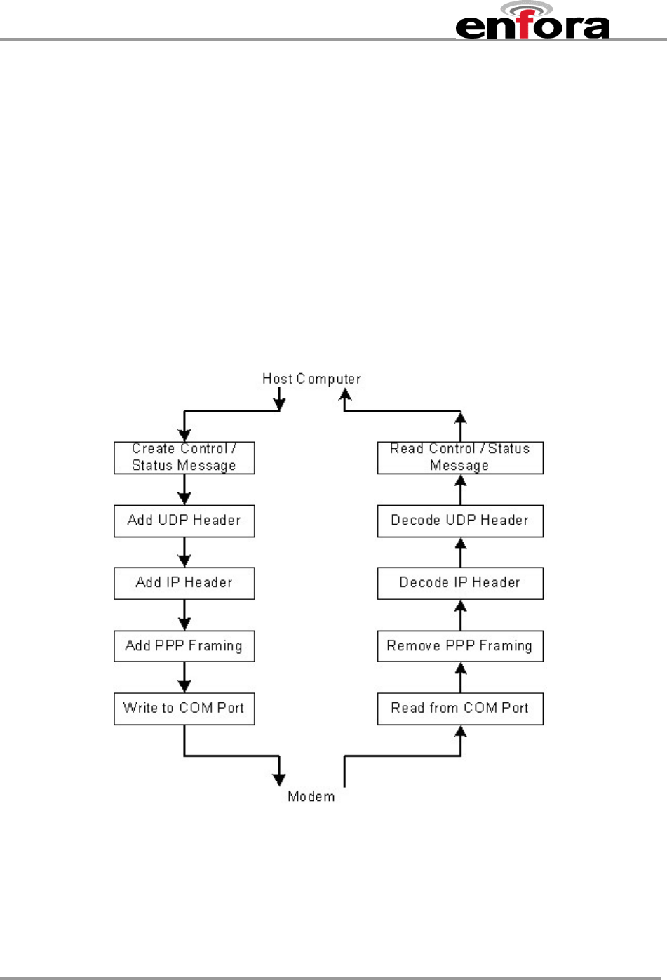
Enfora Enabler III-G
Modem Integration Guide
9.3. Enfora AT Command Set
For a full description of the AT commands, refer to the Enfora Enabler-III AT Command Set
GSM0308PB001MAN.
Note: A command description that includes an *asterisk denotes that the GSM service provider
must enable supplementary services functionality before the command is available.
9.4. Enfora Packet Application Programming Interface
9.4.1. UDP-API Architecture
The following information provides an overview of the Enfora UDP-based API architecture. Full
details are provided in the Enfora GSM-GPRS Family UDP-API Reference
GSM0102PB002MAN.
Figure 18 provides the general structure for the UDP-API.
Figure 17 - UDP-API Structure
GSM0308PB001 65 Version DRAFT – 2/9/2007
Enfora Enabler III-G
Modem Integration Guide
The following provides information related to the general construction of the UDP-API packet.
Other command structures are available and can be found in the API reference manual.
All AT commands listed in the GSM0308PB001MAN document are supported via this method.
To send an AT command via DUN or OTA, the user has to follow the following message
structure. This message structure sends the ATI command to the modem and receives Enfora,
Inc. response from the modem.
Data
Description Comments Bytes
0 – 19 IP Header
20 – 27 UDP Header
28 0x00
29 0x01 Sequence Number
30 0x04 AT Command Read/Write
31 0x00 Reserved
32 0x41
33 0x54 AT Command
(ATI)
34 0x49
Following data will be returned by the modem:
Data
Description Comments Bytes
0 – 19 IP Header
20 – 27 UDP Header
28 0x00
29 0x01 Sequence Number
30 0x05 AT Command Response
31 0x00 Reserved
32 0x0D
33 0x0A
34 0x45
35 0x6E
36 0x66
37 0x6F
38 0x72
39 0x61
40 0x2C
41 0x20
AT Command Response
(Enfora, Inc.)
42 0x49
43 0x6E
44 0x63
45 0x2E
46 0x0D
47 0x0A
GSM0308PB001 66 Version DRAFT – 2/9/2007
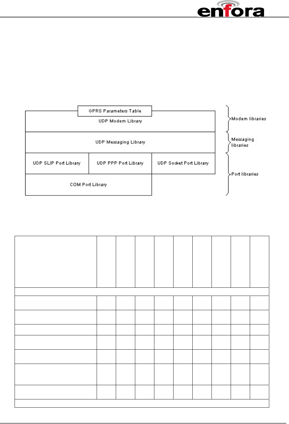
Enfora Enabler III-G
Modem Integration Guide
9.5. Enfora Modem Control Library Architecture
The following information provides an overview of the Enfora Modem Control Library architecture.
Full details are provided in the Enfora GSM-GPRS Family Modem Control Library Reference
GSM0000PB006MAN.
Figure provides the general embedded architecture for the Enabler III-G modem. There are various
levels of access provided to allow complete application design flexibility. SLIP access is not
currently available.
Figure 18 - Library Layout
The table below can be used to help decide which library configuration is the best for a project.
SLIP access is not currently available.
UDP SLIP Port
Library
UDP PPP Port
Library
UDP Socket
Port Library
UDP Messaging
Library with
S
UDP Messaging
Library with
UDP Messaging
Library with
S
UDP Modem
Library with
S
UDP Modem
Library with
UDP Modem
Library with
S
Benefits
Allows dynamic IP
assignment
Allows multiple application
to access the modem
Allow AT Commands
Allows modem control
message
Provide modem control
message formatting
Provides modem
parameters database
service
Suitable for microcontroller
programming
Requirements
GSM0308PB001 67 Version DRAFT – 2/9/2007
Enfora Enabler III-G
Modem Integration Guide
Requires TCP/IP stack
Memory usage Low Low Low Low Low Low High High High
Table 3 - Modem Library Configurations
9.5.1. Using Port Library
Figure provides the architecture for Port Library access.
Figure 19 - Using Port Library
Port Libraries provide the most basic modem access services. It converts modem control
messages to either UDP SLIP or UDP PPP, and vice versa. SLIP access is not currently
available.
Modem Control
Message
SLIP
Header IP
Header UDP
Header Modem Control
Message SLIP End
Or
PPP
Header IP Header UDP
Header Modem Control
Message PPP End
9.5.2. Using Messaging Library
Figure provides the architecture for Messaging Library access.
Figure 20 - Using Messaging Library
GSM0308PB001 68 Version DRAFT – 2/9/2007

Enfora Enabler III-G
Modem Integration Guide
Messaging Library provides some important modem access services. It builds a modem control
message and converts the message to either UDP SLIP or UDP PPP before sending the data to
the modem. It also parses the modem control messages from the modem. SLIP access is not
currently available.
Parameter,
Data
SLIP
Header IP
Header UDP
Header Modem Control Message SLIP End
Or
PPP
Header IP
Header PPP End
UDP
Header Modem Control Message
GSM0308PB001 69 Version DRAFT – 2/9/2007

Enfora Enabler III-G
Modem Integration Guide
9.5.3. Using Modem Library
Figure provides the architecture for Modem Library access.
Figure 21 - Using Modem Library
Modem Library provides the most complete modem access services. In addition to the features
already provided by the Messaging Library, the modem library maintains a modem parameter
database. In order to maintain the parameter database, the modem library requires more
memory than the other libraries. This makes the library unsuitable for some of the micro
controller programming. However, it is a good library to use by applications in a personal
computer or a PDA. It allows the programmer to develop host applications for the modem
quickly.
10. Setup and Initialization
10.1. General Setup
The GPRS modem is controlled through the Modem RS232 port on the development board.
Connect a nine pin straight through serial cable from the Modem RS232 connector to the serial port
on the controlling computer.
Hook up power supply, connect antenna, and install SIM into modem.
10.1.1. HyperTerminal Configuration for Enabler III-G module
The following provides an example for setting up a Windows HyperTerminal session that can be
used to experiment with various configurations on the Enabler III-G module for controlling
computer:
GSM0308PB001 70 Version DRAFT – 2/9/2007
Enfora Enabler III-G
Modem Integration Guide
1. Select the connection interface, Direct to Com 1 (or whatever port is the serial port).
Figure 22 - HyperTerminal Definition
GSM0308PB001 71 Version DRAFT – 2/9/2007
Enfora Enabler III-G
Modem Integration Guide
2. Configure the COM port as displayed below.
Figure 23 - COM Port Settings
10.1.2. Initialization (AT Command Interface)
In the GSM vocabulary, a call from GSM mobile to the PSTN is called a "mobile-originated call" or
"outgoing call". A call from the fixed network to a GSM mobile is called a "mobile-terminated call"
or "incoming call."
In the following examples, “Entry” refers to the application. The following convention describes
the direction of the data exchange:
• The data exchange from the customer application to the Enfora Enabler III-G module is
designated as:
Entry
The data exchange from the Enfora Enabler III-G module to the customer application is
designated as:
Response
Note: With the exception of the +++ command (Online Escape Sequence), all commands
must be preceded by the AT attention code (or command prefix) and terminated by
pressing the <CR> character.
GSM0308PB001 72 Version DRAFT – 2/9/2007
Enfora Enabler III-G
Modem Integration Guide
In the following examples, the <CR> and <CR><LF> are intentionally omitted for clarity and space.
10.1.3. Initial Response to the AT Command
After power is applied to the Enfora Enabler III-G module, the module performs a power-up self-
test. The self-test completes within one (1) second. When queried with the AT command, the
Enfora Enabler III-G module responds with one of the following result codes:
• OK signifies that the Enfora Enabler III-G module is ready, that it correctly interprets the AT
command, and that it has executed the command.
• ERROR signifies that the Enfora Enabler III-G module does not understand the command or
that the command is invalid.
AT
Entry
OK
Response Command valid: module is ready
The Enfora Enabler III-G module must be in AT Command mode (please refer to section
10.3 GPRS Packet Examples for packet mode initialization and setup) when any command
is entered (with the exception of the online escape sequence). Commands entered when
the module is in On-line mode are treated as data, and are transmitted as such to the
receiving module. i.e. If the module is in PPP or SLIP mode, AT commands cannot be
entered.
10.1.4. Sending an Initialization String to the Enfora Enabler III-G Module
The following example provides the sample AT commands and responses for the following
initialization tasks:
• Reset the module to the factory defaults
• Disable character echo
• Transmit Result Codes
• Set the module to Verbose mode (to display result codes as words)
• Set the DCD to match the state of remote modem
• Ignore the DTR
AT&FE0Q0V1&C1&d0 Initialization string
Entry
OK Command is valid
Response
ATSO=1 Auto answer on 1st ring
Entry
OK
Response Command is valid
GSM0308PB001 73 Version DRAFT – 2/9/2007

Enfora Enabler III-G
Modem Integration Guide
10.1.5. Setting Up the Communication Mode for the Enfora Enabler III-G Module
The following example sequence provides the AT command and response for setting the Enfora
Enabler III-G module for full phone functionality, automated operator selection, 9600 baud, non-
transparent mode.
AT+CFUN=1 FULL phone functionality
Entry
OK Command is valid
Response
AT+COPS=0 Automatic operator selection
Entry
OK Command is valid
Response
AT+CBST=7,0,1 9600 baud, non-transparent mode
Entry
OK
Response Command is valid
GSM0308PB001 74 Version DRAFT – 2/9/2007

Enfora Enabler III-G
Modem Integration Guide
10.1.6. Querying the Status of the Enfora Enabler III-G Module
This topic is addressed in the Enfora Application Note GSM0000AN006 – Enabler-G Module
Status Query.
10.1.7. Setting Module Reporting Parameters for GSM and GPRS
This topic is addressed in the Enfora Application Note GSM0000AN007 - Enabler-G Status
Reporting.
10.2. GSM/SMS Examples
10.2.1. Initialize the Enfora Enabler III-G Module to Send and Receive SMS Text Messages
This topic is addressed in the Enfora Application Note GSM0000AN004 - Enabler-G SMS
Configuration and Use.
10.2.2. Managing SMS Messages
This topic is addressed in the Enfora Application Note GSM0000AN004 - Enabler-G SMS
Configuration and Use.
10.2.3. Data Call Configuration
This topic is addressed in the Enfora Application Note GSM0000AN003 - Enabler-G Data Circuit
Switched Call Configuration and Use.
10.2.4. Voice Call Configuration
This topic is addressed in the Enfora Application Note GSM0000AN003 - Enabler-G Data Circuit
Switched Call Configuration and Use.
10.3. GPRS Packet Examples
10.3.1. GPRS ATTACH and ACTIVATE
This topic is addressed in the Enfora Application Note GSM0000AN005 - Enabler-G Automated
Network Connection Configuration and Use.
10.3.2. Windows PPP Setup
The Enabler III-G module can be used in a Windows operating system environment as a standard
serial modem device. The required setup and configuration process is contained in Enfora
Application Notes GSM0000AN001 - Enabler-G PPP Configuration for Windows 98 and
GSM0000AN002 - Enabler-G PPP Configuration for Windows 2000.
GSM0308PB001 75 Version DRAFT – 2/9/2007

Enfora Enabler III-G
Modem Integration Guide
11. Integration and Testing
The Enfora Enabler III-G module has been designed to minimize the amount of time required for
integration and testing the application. By being fully certified by the appropriate bodies, the Enfora
Enabler III-G module provides seamless integration into the GSM network.
The integration issues for the application can be narrowed to the utilization of the AT commands and the
use of the GSM functionality. Coverage and signal quality may be evaluated by using the RSSI
commands. Additional network information can be determined by using AT commands.
Integration of the GPRS Packet capabilities is more complicated than using AT command sequences to
initiate the connection and begin transferring data. The following Application Notes should be used to
integrate the GPRS packet capabilities:
GSM0000AN001 - Enabler-G PPP Configuration for Windows 98
GSM0000AN002 - Enabler-G PPP Configuration for Windows 2000
GSM0000AN008 - Enabler-G PPP Configuration for Windows XP
GSM0000AN010 - Enabler-G PPP Configuration for PocketPC 2002
GSM0000AN005 - Enabler-G Automated Network Connection Configuration and Use
11.1. Integrating the Enfora Enabler III-G Module
Note: Generally, all interfaces that are externally available to the end user need to be ESD-
conditioned and terminated in some way. Many of these interfaces should not be connected with
power applied.
At the highest level, this is done using some type of GSM test equipment (such as, Racal 6103E),
a computer, and a serial interface tester. The GSM test equipment must be able to simulate a
GSM call and measure the key parameters related to the module.
Additionally, the serial interfaces and some minimal SIM functionality can be verified by sending
AT commands to the Enfora Enabler III-G module.
All of these conditions need to be verified at ambient as well as extreme conditions.
GSM0308PB001 76 Version DRAFT – 2/9/2007

Enfora Enabler III-G
Modem Integration Guide
As part of integration, each of the following interfaces must be verified:
Information Recommendations
SIM The maximum line length of the SIM interface is 25.4 cm (10 inches).
The Enfora Enabler III-G module takes care of the signal conditioning
As a minimum, an external application with a remote SIM will require a
standard SIM carrier.
Filter the SIM VCC signal with a 10 uf / 10 V capacitor to help with the line
length.
Primary and
secondary serial
Interfaces
The Enfora Enabler III-G module uses a 1.8/3 V digital interface. The RS-
232 signals must be level-shifted to get standard levels. These signals
must be ESD-protected.
Reset Interface Resets the Enfora Enabler III-G module when tied low.
Audio/Microphone
Interface Preliminary balancing on Enfora Enabler III-G module.
Maximum length TBD
GSM0308PB001 77 Version DRAFT – 2/9/2007

Enfora Enabler III-G
Modem Integration Guide
Testing the following parameters verifies the RF parameters that may be affected by such things
as RF path loss, power supply noise, and external interference.
Functionality Parameters to be Tested
Transmitter Frequency Error
Phase Error
PA Ramp
Modulation Spectrum
RF Power Steps
Timing Advance
Receiver BER Based RX Tests (RXQUAL RXLEV)
BER Based Sensitivity
Testing the following GSM functionality verifies proper network communication.
Functionality Parameters to be Tested
Transmitter Frequency Error
Phase Error
PA Ramp
Modulation Spectrum
RF Power Steps
Timing Advance
Receiver BER Based RX Tests (RXQUAL RXLEV)
BER Based Sensitivity
Testing the following GSM functionality verifies proper network communication.
Functionality Parameters to be Tested
Network Function Synchronization and registration
Call set-up and call termination (both MT and MO calls)
SMS and/or data calls
GSM0308PB001 78 Version DRAFT – 2/9/2007

Enfora Enabler III-G
Modem Integration Guide
12. APPENDIX A
LIMITED WARRANTY
12.1. Scope
Enfora warrants to the original purchaser of the product that, for a period of one (1) year from
the date of product purchase, the product hardware, when used in conjunction with any
associated software (including any firmware and applications) supplied by Enfora, will be free
from defects in material or workmanship under normal operation. Enfora further warrants to
such original purchaser that, for a period of ninety (90) days from the date of product purchase,
any software associated with the product will perform substantially in accordance with the user
documentation provided by Enfora, and any software media provided with the product will be
free from defects in material or workmanship under normal operation. Enfora does not warrant
that (a) the product hardware or any associated software will meet the purchaser’s
requirements, (b) that the operation of the product hardware or software will be uninterrupted or
error-free, or (c) the product, when integrated in, or combined with, other products or software
not supplied by Enfora, will continue to perform substantially in accordance with the user
documentation. This limited warranty is only for the benefit of the original purchaser and is not
transferable. No other party may act on behalf of such purchaser for the purpose of claiming or
exercising any rights or benefits under or in connection with this limited warranty except as may
be provided in a written agreement between Enfora and such other party.
12.1.1. Hardware
During the warranty period applicable to the product hardware, Enfora, at its expense and in its
sole discretion, will repair or replace the product if it is determined to have a covered hardware
defect, provided that the purchaser first notifies Enfora of any such defect, furnishes Enfora with
a proof of purchase, requests and obtains a return merchandize authorization (RMA) number
from Enfora, and returns the product, shipping charges prepaid, to Enfora under that RMA. If,
upon reasonable examination of the returned product, Enfora does not substantiate the defect
claimed by purchaser, or determines that the defect is not covered under this limited warranty,
Enfora will not be required to repair or replace the product, but may instead reship the product
to the purchaser, in which case purchaser shall be responsible for paying Enfora’s usual
charges for unpacking, testing, and repacking the product for reshipment to purchaser.
Purchaser shall bear the risk of loss or damage in transit to any product returned by purchaser
to Enfora, or any returned product not found to be defective or covered under this warranty and
reshipped by Enfora to purchaser. In the event Enfora repairs or replaces a defective product,
the repaired or replacement product will be covered under this limited warranty for the
remainder of the original warranty period on the defective product. If Enfora is unable to repair
or replace a defective product, the purchaser’s exclusive remedy shall be a refund of the original
purchase price. Any returned and replaced product, or any product for which Enfora has
refunded the original purchase price, becomes the property of Enfora.
12.2. Software
During the warranty period applicable to the software or its media, Enfora, at its expense, will replace any
defective software or media if purchaser gives written notification of the defect to the technical support
department at Enfora during the applicable warranty period. Enfora will ship or otherwise transmit the
replacement software or media to purchaser, and purchaser shall be responsible for incorporating any
replacement software in the product. Enfora shall not have any obligation to provide any software bug
GSM0308PB001 79 Version DRAFT – 2/9/2007

Enfora Enabler III-G
Modem Integration Guide
fixes, upgrades or new releases except as may be necessary to correct any covered defect of which
purchaser notifies Enfora in writing during the applicable warranty period. Enfora, from time to time and
in its sole discretion, may make available for download on its website (www.enfora.com) certain software
bug fixes, upgrades or new releases for the product. The purchaser should periodically visit such website
to determine whether any such bug fixes, upgrades or new releases have become available. Download
and use of any such bug fixes, upgrades or new releases is subject to all of the applicable terms and
conditions of Enfora’s technical support policy as posted and updated on its website.
Exceptions and Disclaimers
Enfora shall have no obligation under this limited warranty for (a) normal wear and tear, (b) the
cost of procurement of substitute products or (c) any defect that is (i) discovered by purchaser
during the warranty period but purchaser does not notify or request an RMA number from
Enfora, as required above, until after the end of the warranty period, (ii) caused by any accident,
misuse, abuse, improper installation, handling or testing, or unauthorized repair or modification
of the product, (iii) caused by use of any software other than any software supplied by Enfora, or
by use of the product other than in accordance with its documentation or (iv) the result of
electrostatic discharge, electrical surge, fire, flood or similar causes. Unless otherwise provided
in a written agreement between the purchaser and Enfora, the purchaser shall be solely
responsible for the proper configuration, testing and verification of the product prior to
deployment in the field.
ENFORA’S SOLE RESPONSIBILITY AND PURCHASER’S SOLE REMEDY UNDER THIS
LIMITED WARRANTY SHALL BE TO REPAIR OR REPLACE THE PRODUCT HARDWARE,
SOFTWARE OR SOFTWARE MEDIA (OR IF REPAIR OR REPLACEMENT IS NOT
POSSIBLE, OBTAIN A REFUND OF THE PURCHASE PRICE) AS PROVIDED ABOVE.
ENFORA EXPRESSLY DISCLAIMS ALL OTHER WARRANTIES OF ANY KIND, EXPRESS
OR IMPLIED, INCLUDING WITHOUT LIMITATION ANY IMPLIED WARRANTIES OF NON-
INFRINGEMENT, MERCHANTABILITY, SATISFACTORY PERFORMANCE AND FITNESS
FOR A PARTICULAR PURPOSE. IN NO EVENT SHALL ENFORA BE LIABLE FOR ANY
INDIRECT, SPECIAL, EXEMPLARY, INCIDENTAL OR CONSEQUENTIAL DAMAGES
(INCLUDING WITHOUT LIMITATION LOSS OR INTERRUPTION OF USE, DATA, REVENUES
OR PROFITS) RESULTING FROM A BREACH OF THIS WARRANTY OR BASED ON ANY
OTHER LEGAL THEORY, EVEN IF ENFORA HAS BEEN ADVISED OF THE POSSIBILITY OR
LIKELIHOOD OF SUCH DAMAGES.
12.3. Other Considerations
Some jurisdictions may require a longer warranty period than specified above and, accordingly, for
products sold in those jurisdictions the applicable warranty period shall be extended as required under the
laws of those jurisdictions. Furthermore, some jurisdictions may not allow the disclaimer of implied
warranties or the exclusion or limitation of incidental or consequential damages, so the above disclaimer,
limitation or exclusion may not apply to products sold in those jurisdictions. This limited warranty gives
the purchaser specific legal rights and the purchaser may have other legal rights that vary from
jurisdiction to jurisdiction.
In some instances, certain aspects of the product warranty may also be covered in a separate written
agreement between Enfora and the distributor or reseller, if any, from whom purchaser purchased the
product. That agreement may provide, for example, a different product return procedure that may also be
available to purchaser (e.g., the product may be returned to Enfora through that distributor or reseller).
GSM0308PB001 80 Version DRAFT – 2/9/2007

Enfora Enabler III-G
Modem Integration Guide
Governing Law
This limited warranty shall be governed by the laws of the State of Texas, United States of
America, without regard to conflict of laws principles. This limited warranty shall not be governed
in any respect by the United Nations Convention on Contracts for the International Sale of
Goods.
GSM0308PB001 81 Version DRAFT – 2/9/2007

Enfora Enabler III-G
Modem Integration Guide
13. APPENDIX B - Regulations and Compliance
This section summarizes the responsibilities and actions required of manufacturers and integrators who
incorporate OEM versions of the Enfora Enabler III-G module into their products. In certain situations and
applications, these products will require additional FCC, CE, GCF, PTCRB or other regulatory approvals
prior to sale or operation. Appropriate instructions, documentation and labels are required for all
products. For more information concerning regulatory requirements, please contact Enfora.
13.1. GCF/PTCRB Approval (Formerly FTA)
The Enfora Enabler III-G module is type approved in accordance with the requirements of and
through the procedures set forth by the GSM industry association. The relevant conformance
specification is 3GPP TS 51010-1. Any OEM changes in the SIM interface, antenna port, software or
the physical makeup of the unit may require an incremental FTA to ensure continued compliance with
the above-mentioned standard. For more information concerning type approval, please contact
Enfora.
13.2. Electromagnetic Compatibility (EMC) and Safety Requirements
The Enfora Enabler III-G module has been tested and approved for application in the United States of
America (US) and the European Union (EU). The compliance details for each of these markets
follow. For other markets, additional or alternative regulatory approvals may be required. Always
ensure that all rules and regulations are complied with in every country that the OEM application is to
be operated. Regardless of the country or market, the OEM must comply with all applicable
regulatory requirements.
13.3. EMC/Safety Requirements for the USA
Compliance to the US rules and regulations falls under two categories:
• Radio approvals: Federal Communications Commission (FCC)
• Transmitter: FCC Rules, Part 22 & 24
• Unintentional emission: FCC Rules, Part 15
Although the Enfora Enabler III-G module has been authorized by the FCC and listed as a component
by an NRTL, products and applications that incorporate the Enfora Enabler III-G module will require
final verification of EM emission and product safety approval.
Note: Particular attention should be made to the following statements regarding RF Exposure:
GSM0308PB001 82 Version DRAFT – 2/9/2007

Enfora Enabler III-G
Modem Integration Guide
13.4. Human Exposure Compliance Statement
GSM0308 GSM/GPRS Module
Enfora certifies that the Enfora Enabler III-G 850/900/1800/1900 MHz GSM Radio Module (FCC ID:
MIVGSM0308) complies with the RF hazard requirements applicable to broadband PCS equipment
operating under the authority of 47 CFR Part 24, Subpart E and Part 22 of the FCC Rules and
Regulations. This certification is contingent upon installation, operation and use of the Enfora
Enabler III-G module and its host product in accordance with all instructions provided to both the
OEM and end user. When installed and operated in a manner consistent with the instructions
provided, the Enfora Enabler III-G module meets the maximum permissible exposure (MPE) limits for
general population / uncontrolled exposure at defined in Section 1.1310 of the FCC Rules and
Regulations.
Note: Installation and operation of this equipment must comply with all applicable FCC Rules
and Regulations, including those that implement the National Environmental Policy Act of 1969
(Part 1, Subpart I), with specific regard to antenna sitting and human exposure to radio frequency
radiation. For further guidance, consult the FCC Rules, a certified FCC test house, or Enfora.
13.5. Compliance with FCC Regulations
The Federal Communications Commission (FCC) is the agency of the Federal Government that
oversees all non-governmental radio frequency transmitters that operate within the United States.
Unintentional emissions from digital devices are regulated by Part 15 of the FCC Rules and
Regulations, which distinguishes between the environments in which these devices may operate.
Intentional radiators operating as a GSM-1900 radio transmitter are regulated under Part 22 & 24,
Subpart E—Broadband PCS of the FCC Rules and Regulations.
GSM0308PB001 83 Version DRAFT – 2/9/2007

Enfora Enabler III-G
Modem Integration Guide
13.6. Unintentional Radiators, Part 15
Equipment designated as Class A is intended for use in a commercial, industrial or business
environment. The Enfora Enabler III-G module has been tested and found to comply with the limits
for a Class A digital device and can be integrated into equipment or applications intended for use in
commercial, industrial or business environments.
The following statement must be included in the user manual for such products:
This equipment has been tested and found to comply with the limits for a Class A digital device,
pursuant to part 15 of the FCC rules. These limits are designed to provide reasonable protection
against harmful interference when the equipment is operated in a commercial environment. This
equipment generates, uses, and can radiate radio frequency energy and, if not installed and used in
accordance with the instruction manual, may cause harmful interference to radio communications.
Operation of this equipment in a residential area is likely to cause harmful interference in which case
the user will be required to correct the interference at his own expense.
Equipment intended for use in a residential environment (not-withstanding use in commercial,
industrial or business environments) is designated as Class B. The Enfora Enabler III-G module has
been tested and found to comply with the limits for a Class B digital device and can be integrated into
equipment or applications intended for use in residential environments.
The following statement must be included in the user manual for such products:
This equipment has been tested and found to comply with the limits for a Class B digital device,
pursuant to part 15 of the FCC rules. These limits are designed to provide reasonable protection
against harmful interference in a residential installation. This equipment generates, uses, and can
radiate radio frequency energy and, if not installed and used in accordance with the instructions, may
cause harmful interference to radio communications. However, there is no guarantee that
interference will not occur in a particular installation. If this equipment does cause harmful
interference to radio or television reception, which can be determined by turning the equipment off
and on the user is encouraged to try to correct the interference by one or more of the following
measures:
• Reorient or relocate the receiving antenna.
• Increase the separation between the equipment and receiver.
• Connect the equipment into an outlet on a circuit different from that to which the
receiver is connected.
• Consult the dealer or an experienced radio/TV technician for help.
13.7. Intentional Radiators, Part 22 & 24
Products incorporating the Enfora Enabler III-G transceiver operate as Personal Communications
Services (PCS) devices under the authority of Part 22 & Part 24, Subpart E—Broadband PCS, of the
FCC Rules and Regulations. All such transmitters must be authorized by the FCC through its
Certification process, as detailed in Part 2, Subpart J - Equipment Authorization Procedures.
Through the Certification process, the FCC verifies that the product complies with all applicable
regulatory and technical requirements, including those that address human exposure to radio
frequency radiation. In general, radio frequency transmitters cannot be sold or operated in the US
prior to FCC approval.
GSM0308PB001 84 Version DRAFT – 2/9/2007

Enfora Enabler III-G
Modem Integration Guide
13.8. Instructions to the Original Equipment Manufacturer (OEM)
To comply with the requirements of the National Environmental Policy Act (NEPA) of 1969, operation
of an FCC-regulated transmitter may not result in human exposure to radio frequency radiation in
excess of the applicable health and safety guidelines established by the FCC. Further information on
RF exposure issues may be found in the FCC's Office of Engineering and Technology (OET) Bulletin
Number 65, "Evaluating Compliance with FCC Guidelines for Human Exposure to Radio Frequency
Electromagnetic Fields" and Supplement C, "Additional Information for Evaluating Compliance of
Mobile and Portable devices with FCC Limits for Human Exposure to Radio Frequency Emissions.”
Both of these documents are available via the Internet at the OET web site: http://www.fcc.gov/oet
The Enfora Enabler III-G products are GSM radio transceivers, which operate under the authority of
47 CFR Part 24, Subpart E and Part 22 of the FCC Rules and Regulations. When installed and
operated in accordance with the instructions provided in this manual, these devices comply with
current FCC regulations regarding human exposure to radio frequency radiation.
The following installation and operation restrictions apply to all Enfora Enabler III-G products:
• This device may only be used in fixed and mobile applications.
• Portable applications, as defined by the FCC, are prohibited.
• The use of this device for desktop and other applications where the antenna can easily
be relocated are considered by the FCC to be mobile applications.
• A separation distance of at least 20 cm (7.87 inches) between the antenna and the body
of the user and other persons must be maintained at all times
• In FIXED applications, antenna gain is limited to a maximum of 7 dBi, with a
corresponding Equivalent Isotropic Radiated Power (EIRP) of 37 dBm / 5 W.
• In MOBILE applications, antenna gain is limited to a maximum of 3 dBi, with a
corresponding EIRP of 33 dBm / 2 W.
• End products must provide instructions to ensure compliance with radio frequency
radiation exposure requirements.
• A warning label visible to all persons exposed to the antenna and identical to that
described in this manual must be displayed on or next to the antenna.
• Separate FCC approval for RF exposure compliance is required for end products that do
not meet these conditions.
Antenna gain is defined as gain in dBi (dB referenced to an isotropic radiator) minus cabling loss.
GSM0308PB001 85 Version DRAFT – 2/9/2007

Enfora Enabler III-G
Modem Integration Guide
Note: Additional care must be taken by the installer and/or user of the Enfora Enabler III-G
products to ensure proper antenna selection and installation. Adherence to the above conditions
is necessary to comply with FCC requirements for safe operation regarding exposure to RF
radiation.
Depending upon the application and type of product into which the Enfora Enabler III-G module
has been incorporated, specific OEM actions and responsibilities required to meet these
conditions vary. However, in all cases the primary concern is to ensure compliance with current
FCC guidelines and regulations that limit human exposure to radio frequency radiation.
Definitions
For the purpose of determining compliance with current FCC rules addressing human
exposure to radio frequency radiation, the FCC has established the following three
categories of transmitting devices:
• Portable Devices – devices where the antenna is located within 20 cm (7.87
inches) of any person, including the user, if applicable. Portable devices
operating under the authority of Part 22 or 24 (broadband PCS) are limited to a
maximum of 2 W EIRP.
• Mobile Devices – devices designed to be used in other than fixed locations and
generally such that the antenna is located at a minimum of 20 cm (7.87 inches)
from any person, including the user, if applicable. Mobile devices operating
under the authority of Part 22 or 24 (broadband PCS) are limited to a maximum
of 2 W EIRP.
• Fixed devices – devices in which the antenna, either integral to the product or
remotely located, is physically secured at one location and is not able to be easily
moved to another location. The antenna for a fixed device is mounted on an outdoor,
permanent structure with a minimum separation distance of 2 meters (79 inches)
GSM0308PB001 86 Version DRAFT – 2/9/2007
Enfora Enabler III-G
Modem Integration Guide
13.8.1. OEM Responsibilities for All Products Containing the Enabler III-G module
In addition to any other regulatory requirements, OEMs and integrators must include or provide
the following information, instructions, warnings and labels with any device or product into which
the Enfora Enabler III-G GSM1900 GSM transceiver has been incorporated:
Information Description
Detailed
Operating
Instructions for
ensuring
compliance with
current FCC
guidelines which
limit human
exposure to radio
frequency
radiation
The OEM must provide an operating/installation manual with the final
product which clearly indicates that these operating conditions and
restrictions must be observed at all times to ensure compliance with current
FCC guidelines which limit human exposure to radio frequency radiation.
20 cm (7.87 inch) separation distance between the antenna and all persons
must be maintained at all times for all fixed and mobile products and
applications
Portable devices and applications are prohibited unless such devices and
products are specifically authorized by the FCC
Maximum antenna gain is limited to 2 dBi* in mobile products and
applications
For fixed applications (2 meter separation) the antenna gain can be as
much as 26 dBi.
Modifications and/or additions to the Enfora Enabler III-G GSM transceiver,
including use of antennas with higher gain than those authorized by the
FCC, are prohibited
*dBi = antenna gain in dB relative to an isotropic radiator
Antenna
Avoidance
Label
Attach the following warning label
directly to or displayed next to the
antenna. Furthermore, this label must
be visible to and easily readable by all
persons in the immediate vicinity of the
antenna
WARNING
To comply with FCC RF
exposure requirements, a
separation distance of 20 cm
(7.87”) or more must be
maintained between this
antenna and all persons
Human Exposure
Compliance
Statement
Include the following statement in the
instruction / operation manual. Enfora certifies that the Enfora
Enabler III-G ™ MHz GSM Radio
Module (FCC ID: MIVGSM0308)
complies with the RF hazard
requirements applicable to
broadband PCS equipment
operating under the authority of
47 CFR Part 22 or Part 24,
Subpart E of the FCC Rules and
Regulations.
This certification is contingent
upon installation, operation and
use of the
Enfora Enabler III-G module and
its host product in accordance
with all instructions provided to
both the OEM and end used.
When installed and operated in a
manner consistent with the
instructions provided, the Enfora
Enabler III-G module meets the
GSM0308PB001 87 Version DRAFT – 2/9/2007

Enfora Enabler III-G
Modem Integration Guide
maximum permissible exposure
(MPE) limits for general
population / uncontrolled
exposure at defined in Section
1.1310 of the FCC Rules and
Regulations.
13.8.2. Specific OEM Responsibilities for Portable Products and Applications
Each device or product, into which the Enfora Enabler III-G PCS-1900 GSM transceiver has been
incorporated, and which is intended to be used in an application that meets the definition of
"portable" MUST be separately authorized by the FCC for the purposes of determining
compliance with current FCC guidelines limiting human exposure to radio frequency radiation.
Portable devices must be evaluated for RF exposure based on Specific Absorption Rate (SAR)
limits; further information on such evaluations are available from the FCC via the Internet.
13.8.3. Specific OEM Responsibilities for Mobile Products and Applications
Separate or additional FCC approvals are NOT required for devices or products, into which the
Enfora Enabler III-G PCS-1900 GSM transceiver has been incorporated, that are used in
applications that meet the definition of "mobile."
For all end products, the OEM or integrator must provide instructions, warnings and labels to
ensure that the product complies with current FCC guidelines limiting human exposure to radio
frequency radiation.
Current FCC regulations limit the EIRP of mobile devices to 2 W. Because the nominal RF output
power of the Enfora Enabler III-G GSM1900 GSM transceiver is 1.0 W (30 dBm), antenna gain
for mobile products and applications cannot exceed 3 dBi.
13.8.4. Specific OEM Responsibilities for Fixed Products and Applications
Separate or additional FCC approvals are not required for devices or products, into which the
Enfora Enabler III-G GSM transceiver has been incorporated, that are used in applications that
meet the definition of "fixed.”
For all end products, the OEM or integrator must provide the instructions, warnings and labels to
ensure that the product complies with current FCC guidelines limiting human exposure to radio
frequency radiation.
Separate or additional FCC approvals are required for devices or end products used in fixed
applications where antenna gain in excess of 7dBi is desired.
GSM0308PB001 88 Version DRAFT – 2/9/2007

Enfora Enabler III-G
Modem Integration Guide
13.9. EMC/Safety Requirements for the Countries of the European Union (EU)
The European Union (EU) is comprised of fifteen countries that follow a harmonized set of standards,
utilizing the CE mark as a uniform mark of acceptance. The member countries are:
• Austria
• Belgium
• Denmark
• Finland
• France
• Germany
• Greece
• Ireland
• Italy
• Luxembourg
• The Netherlands
• Portugal
• Spain
• Sweden
• United Kingdom
13.10. EMC/Safety Requirements for Other Countries
In most other countries that have not been listed above there are similar rules and regulations that
must be met for importing the Enfora Enabler III-G module. Each may require a different mark of
approval (for example, the CB Scheme) as an acceptance requirement. For each of these cases the
country should identified, and the appropriate steps should be taken to meet the requirements set
forth in the intended market.
GSM0308PB001 89 Version DRAFT – 2/9/2007

Enfora Enabler III-G
Modem Integration Guide
14. APPENDIX C - Glossary and Acronyms
API Application Programming Interface.
App Application Refers to the Application which sends or receives commands/responses
from the Enfora Enabler III-G Module
AT Command Set Commands issued by intelligent device to a modem to perform functions,
such as to initiate call, to answer call, or to transmit data.
BER
Bit Error Rate Bit Error Rate
CMUX Multiplexer protocol that operates between an MS and a TE and allows a
number of simultaneous sessions over a normal serial asynchronous
interface
CPE
Customer Premise
Equipment
A terminal in fixed location on the customer’s premises.
CSD
Circuit Switched Data Data link from a terminal through the network allowing real-time, duplex
connectivity at 9600 bytes/second.
dBi Decibels referenced to an isotropic radiator
DCE
Data Communications
Equipment
Data Communications Equipment
DCS
Digital Cellular System A collection of services and capabilities providing flexibility of access and
mobility through a combination of wireless and wire-line networks, utilizing
the 1800 MHz bandwidth.
DTE
Data Terminal Equipment Data Terminal Equipment
EFR
Enhanced Full Rate Voice (vocoder) compression algorithms which offer the highest quality
voice communication.
EIR
Equipment Identity Register A database used to store International Mobile Equipment Identity (IMEI) of
a locally issued terminal.
EIRP
Equivalent Isotropic
Radiated
Power
In a given direction, the gain of a transmitting antenna multiplied by the net
power accepted by the antenna from the connected transmitter.
EMC
Electromagnetic
Compatibility
The ability of a device to function satisfactorily in its electromagnetic
environment without inducing intolerable disturbance to that environment
(or to other devices)
ESD
Electrostatic Discharge Static electricity that can damage electronic equipment.
EU
European Union An organization of 15 European states whose purpose is to organize
relations between the Member States and between their peoples.
FTA
Full Type Approval GSM Full Type Approval
GPRS
General Packet Radio
Service
Standard for packet communications utilizing Global Standard for Mobility
(GSM) infrastructure.
GSM
Global System for Mobile
Communications
Standard for digital communications. Allows consistent communications in
various parts of the world despite variations in RF spectrum allocations.
Transferring the SIM (see below) permits users to roam by changing
terminal equipment.
HLR
Home Location Register Stores the identity and user data for all subscribers belonging to the area
of the related MSC.
IMEI
International Mobile A unique number for each GSM Terminal tracked by the GSM operators in
their Equipment Identity Register (EIR) database.
GSM0308PB001 90 Version DRAFT – 2/9/2007

Enfora Enabler III-G
Modem Integration Guide
Equipment Identity
IMSI
International Mobile
Subscriber Identification
A unique number identifying the subscriber stored in the SIM card.
Number is used in conjunction with the network for call routing.
Ki A secret code used in authentication and encryption by the terminal.
MO
Mobile Originated Any GSM/GPRS service originated at the mobile terminal.
MT
Mobile Terminated Any GSM/GPRS service originated from or routed through the network
and sent to the mobile terminal.
MSC
Mobile Switching Center The central switch of the GSM network. Performs call routing, collects call
detail records for billing, and supervises system operations.
Non-Transparent Mode Delivers a constantly low error rate but with a non-guaranteed throughput
or delay. The Non-Transparent service provides a performance that is
closest to using a modem over a fixed PSTN line.
NRTL
Nationally Recognized Test
Laboratory
OSHA-approved Nationally Recognized Testing Laboratory
OEM Original Equipment Manufacturer.
PA Power Amplifier.
Packet A collection of data transmitted over a digital network in a burst.
PCS Personal Communication Services.
PDA Personal Digital Assistant.
PDU Packet Data Unit.
PPP Point-To-Point Protocol.
SIM Subscriber Identity Module.
SMS Short Message Service.
SMSC Short Message Service Center.
SUPL Secure User Plane Location
User Datagram Protocol.
UDP
GSM0308PB001 91 Version DRAFT – 2/9/2007

Enfora Enabler III-G
Modem Integration Guide
15. APPENDIX D – Tables and Figures
TABLES
Table 1 - Enabler III-G Key Features............................................................................................................9
Table 2 - Enabler III-G Pin Assignments.....................................................................................................28
Table 3 - Modem Library Configurations.....................................................................................................68
FIGURES
Figure 1 – UDP API Architecture ................................................................................................................11
Figure 2 - PAD Architecture ........................................................................................................................12
Figure 3 - Enabler III-G Module Block Diagram..........................................................................................16
Figure 4 – Front of Module (Board-to-Board RF Conn. Version)................................................................21
Figure 5 - Pin 1 Reference, 100-Pin I/O Connector....................................................................................22
Figure 6 – Front of Module (Coaxial RF Conn. Version) ............................................................................23
Figure 7 - Back of Module (Option SIM Shown) .........................................................................................24
Figure 8 – Module Mounting .......................................................................................................................25
Figure 9 - Host Pads for Board-To-Board RF Connector ...........................................................................26
Figure 10 - Ring Indicate Timing.................................................................................................................32
Figure 11 - External Power Control Signal (no external processor) ...........................................................33
Figure 12 - External Power Control Signal (using external RC circuit).......................................................34
Figure 13 - Power Control Signal (using external processor).....................................................................35
Figure 14 - Typical Power On Sequence (using external processor) .........................................................36
Figure 15 – LED voltage driver circuit.........................................................................................................41
Figure 16 - Remote SIM Interface...............................................................................................................57
Figure 17 - UDP-API Structure ...................................................................................................................65
Figure 18 - Library Layout...........................................................................................................................67
Figure 19 - Using Port Library.....................................................................................................................68
Figure 20 - Using Messaging Library..........................................................................................................68
Figure 21 - Using Modem Library ...............................................................................................................70
Figure 22 - HyperTerminal Definition..........................................................................................................71
Figure 23 - COM Port Settings....................................................................................................................72
GSM0308PB001 92 Version DRAFT – 2/9/2007

Enfora Enabler III-G
Modem Integration Guide
16. APPENDIX E - Contacting Enfora
For technical support and customer service dealing with the modem itself, contact the company where
you purchased the product. If you purchased the product directly from Enfora, visit the SUPPORT page
on the Enfora website: http://www.enfora.com/support_newissue.asp
GSM0308PB001 93 Version DRAFT – 2/9/2007