Novatel Wireless LPP0108 GSM/GPRS Embedded Module User Manual
Novatel Wireless Inc. GSM/GPRS Embedded Module Users Manual
UserManual.wiki
>
Novatel Wireless
>
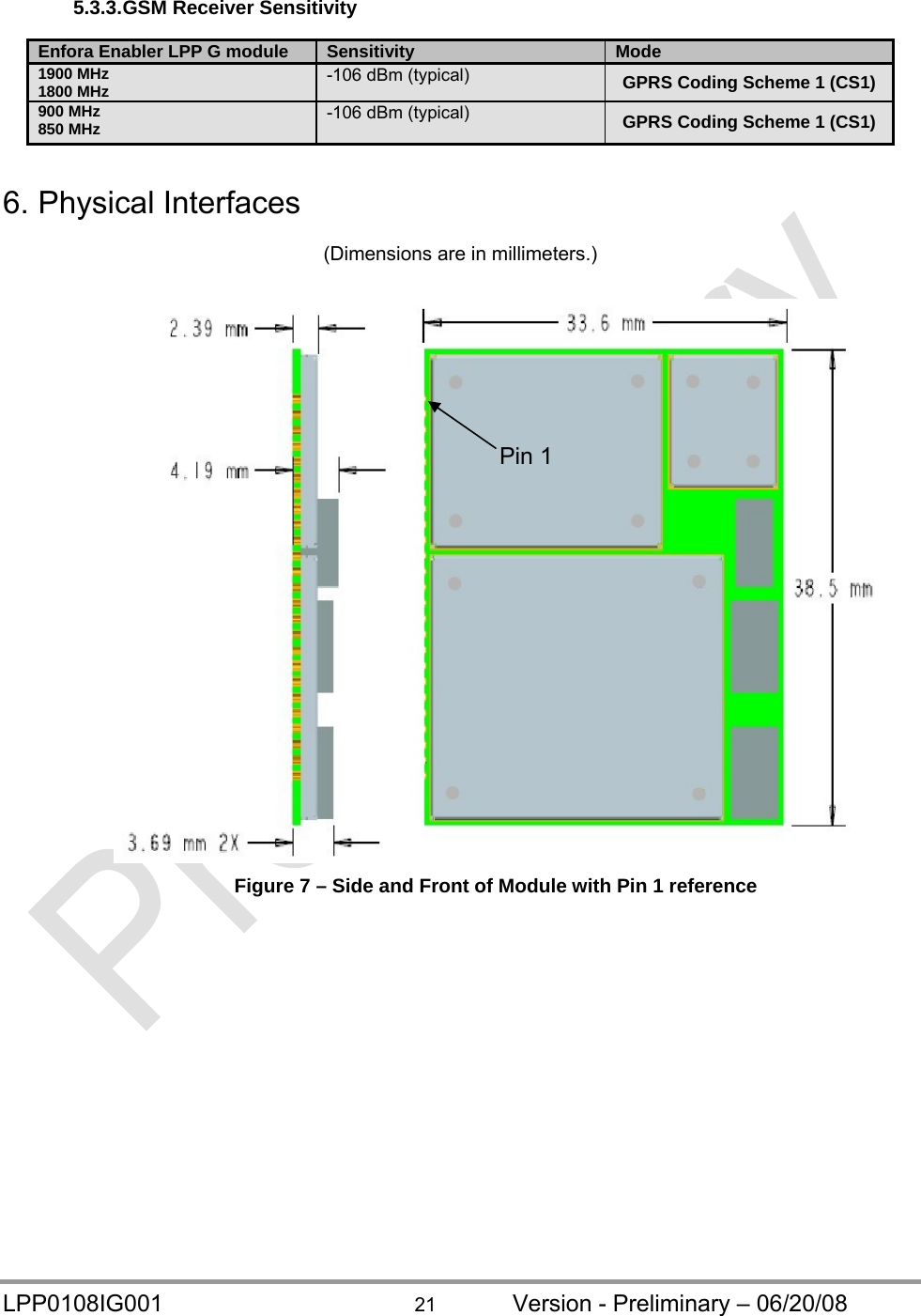
LPP0108 User Manual
Users Manual
Navigation menu
Upload a User Manual
Namespaces
Wiki Guide
HTML
PDF
Info
Views
User Manual
Discussion / Help
Navigation
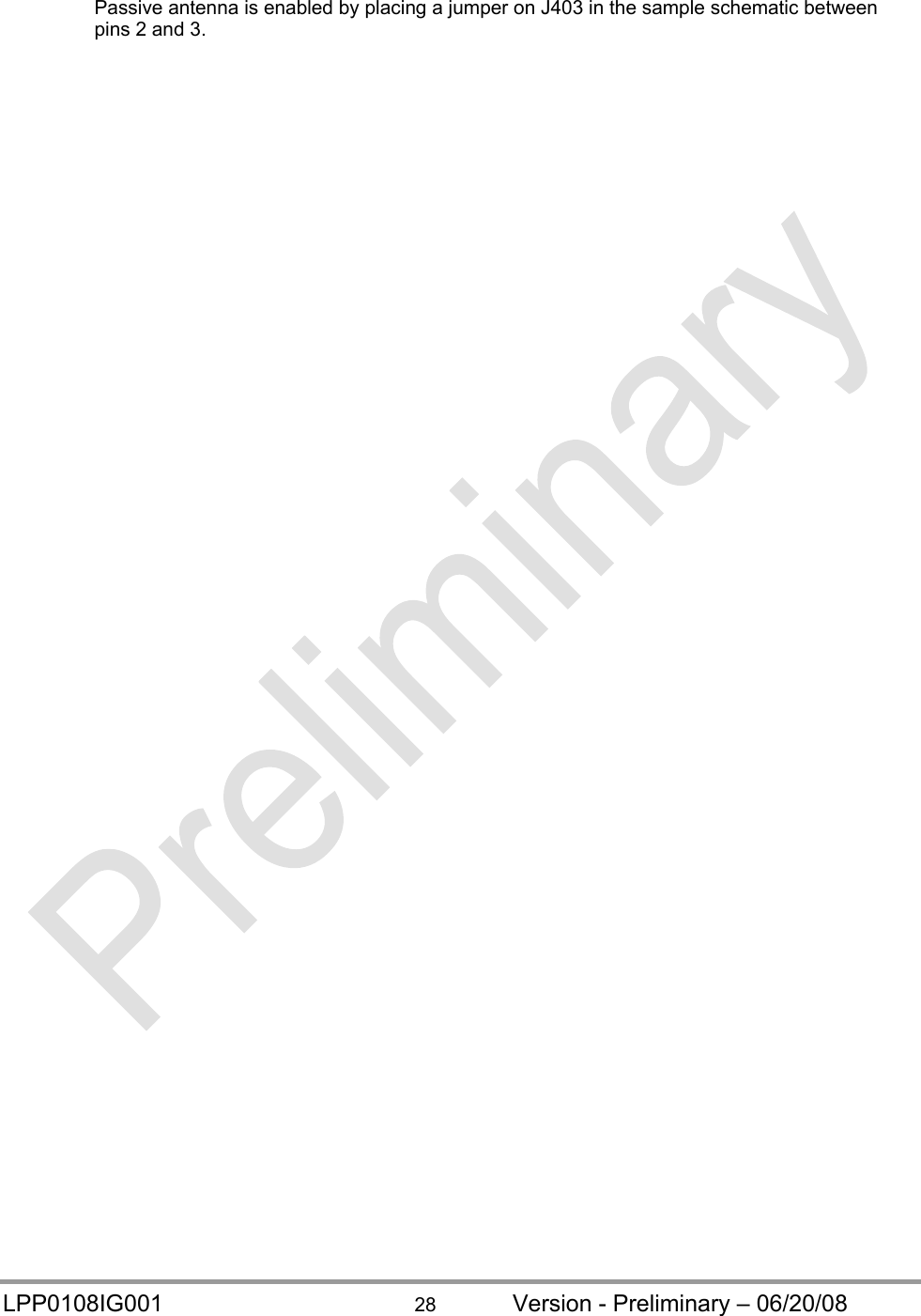
![LPP0108IG001 41 Version - Preliminary – 06/20/08 charging so charge current will take effect. AT$BCIOFF=0 11 Measure power supply current Read IBATSIM current. Iphy2 12 Record reported Ichg, after update. AT$BAT= 40,1,2,4,3956,<Ichg2> Ichg2 13 Calculate <adc_num>, <adc_offset> Note 1 Note 2 14 Set scaling factors AT$BCIISF=<adc_num>,<adc_offset> 15 Verify results. AT$BCICHG2= 1,32,6050,4725,5725 AT$BCIOFF=1, AT$BCIOFF=0 AT$BAT= 40,1,2,4,3956,<Ichg1> Read IBATSIM current. Iphy1=Ichg1 16 Verify results. AT$BCICHG2= 1,250,6050,4725,5725 AT$BCIOFF=1, AT$BCIOFF=0 AT$BAT= 40,1,2,4,3956,<Ichg2> Read IBATSIM current. Iphy2=Ichg2 17 Set final value AT$BCICHG2= 1,x,6050,4725,5725 18 Restore settings AT$BCIAVG=x,x,<previous> AT+CFUN=1 AT$AREG=1 AT$RESET Notes: 1. )21(800)21(_IchgIchgIphyIphynumadc 2. 1800_1_ IchgnumadcIphyoffsetadc 3. The strategy for production level calibration is to set an arbitrary low and high charge currents that will optimize accurate Ichg readings in most charging applications. 4. The strategy for customers in setting the low and high charging currents is to calibrate at the two most important points in the charge process, <ci_chgireg> and <IEOC>, thus ensuring the state transitions are accurate. <ci_chgireg> and <IEOC> are determined once as a system-level design. <ci_chgireg> = [0 to 255] such that the Ichg = Isys + 1*C (800mA max.). <IEOC> =Isys + C/20. For example, if the battery capacity is 1980mAh and the system current is 50mA, Ichg = 50+1980 = 2030mA => 800mA. <chgireg1>=255. <IEOC> =Isys + C/20 = 50+1980/20 = 149mA. Note: In the above example you will receive 2030mA as the answer. The physical limitation is 800mA.](https://usermanual.wiki/Novatel-Wireless/LPP0108/User-Guide-1009877-Page-46.png)
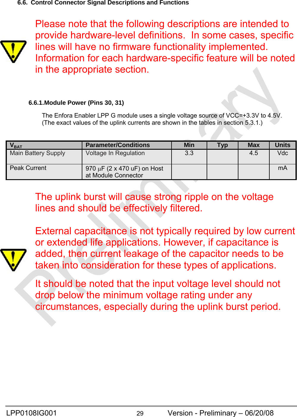
![LPP0108IG001 43 Version - Preliminary – 06/20/08 7.6.4. Set the desired CI charge current for the designated charger. Determining the charge current for the constant-current charging stage now will make the BCIMAP# <%> parameters more accurate. Typical limiting values are listed in the following table: Charger Max. charge current <ci_chgireg> [0-255] USB charger 500mA 160 Wall charger Limited by Triton-Lite maximum 255 Triton-Lite 800mA 255 Customer charger X Calculate1 Note: <ci_chgireg> = [ 0.22 * (CI + ISYS) * 10 + 0 ] * 255 / 1750. Max value is 255. Determine the charger # and <ci_chgireg> for that charger. Charger 1=BCICHG1 is dedicated for USB charging. Chargers 2-5=BCICHG(2-5) are for any general purpose charger. Set with: AT$BCICHG#=<type>,<ci_chgireg>,<ov_thr>,< id_low>,<id_high> Reset or cycle charging with AT$BCIOFF to make new <ci_chgireg> take effect. Example: Suppose it is desired to have a USB charge at 100mA when it is the charging source and a wall charger charge at 800mA when it is the charging source. The system nominal current Isys=50mA. <ci_chgireg1> = [ 0.22 * (100 + 50) * 10 + 0 ] * 255 / 1750 = 48 <ci_chgireg2> = [ 0.22 * (800 + 50) * 10 + 0 ] * 255 / 1750 = 272 => 255 AT$BCICHG1=<type>,48,<ov_thr>,< id_low>,<id_high> AT$BCICHG2=<type>,255,<ov_thr>,< id_low>,<id_high> 7.6.5. Charge empty battery in constant current with target <ci_chgireg>. Up to 5 different batteries can be independently defined with capacities using the BCIMAP# and BCIPCT#. 1. Completely discharge the battery n that will be associated with the BCIMAPn and BCIPCTn. 2. Plug in a charger. 3. When Vbat=3.2V, the Locosto powers on and the modem enumerates a port through USB. Start logging a text file while the charge state is still precharge 1(PRE). 4. Type the following commands: Command Detail AT$BCIDBG=2,0 Start debug traces AT$STOATEV=10,AT$BCIOFF=1 AT$STOATEV=11,AT$BCIDBG=2,0 AT$EVENT=10,0,85,6,6 AT$EVENT=10,3,44,10,0 AT$EVENT=10,3,44,11,0 Script to stop charging and report Vbat when the CI-CV transition occurs. 5. Let the battery charge to the CI-CV transition and stop charging. 6. Stop the log file.](https://usermanual.wiki/Novatel-Wireless/LPP0108/User-Guide-1009877-Page-48.png)
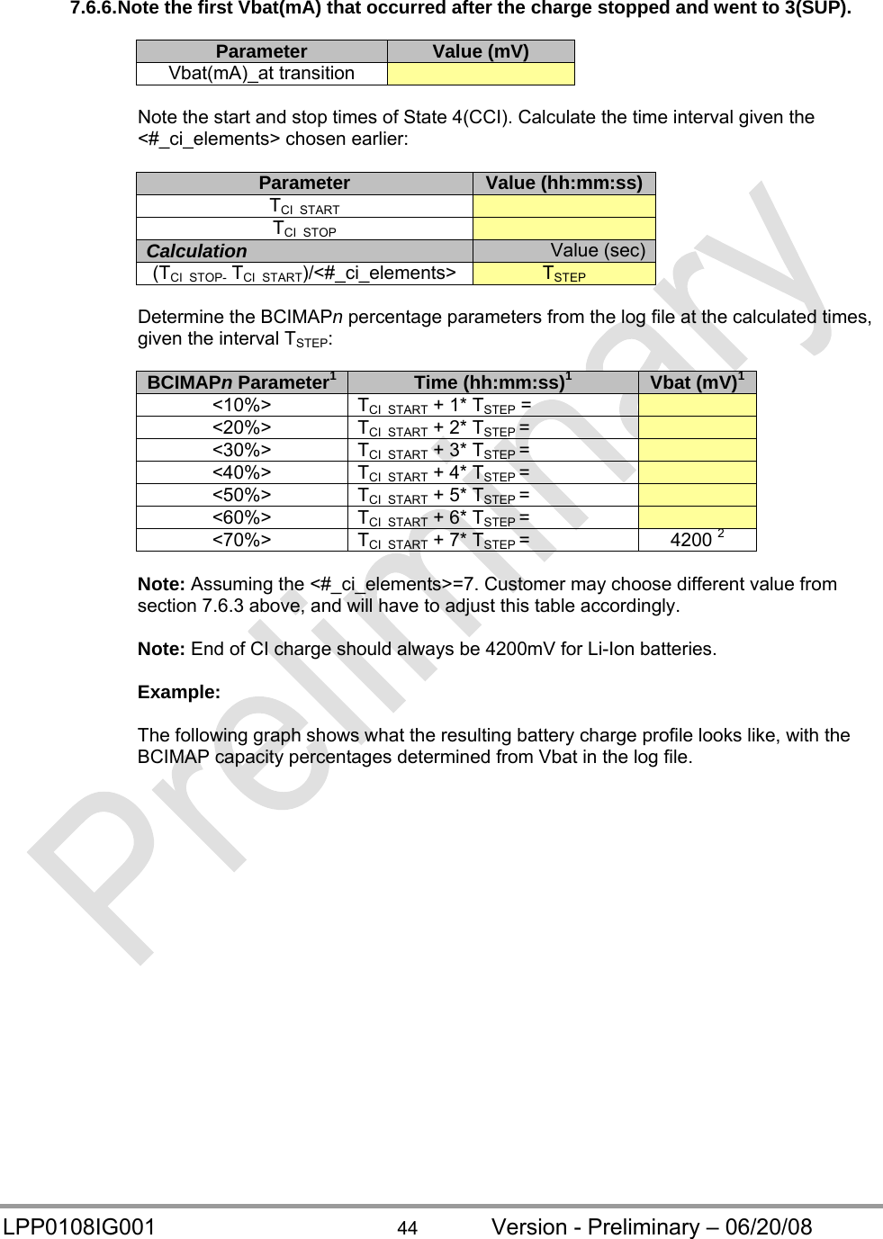
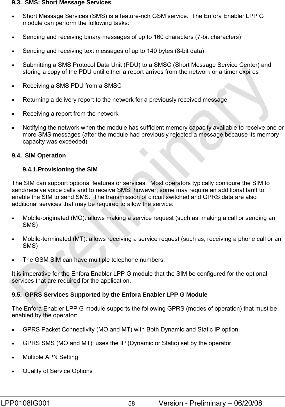
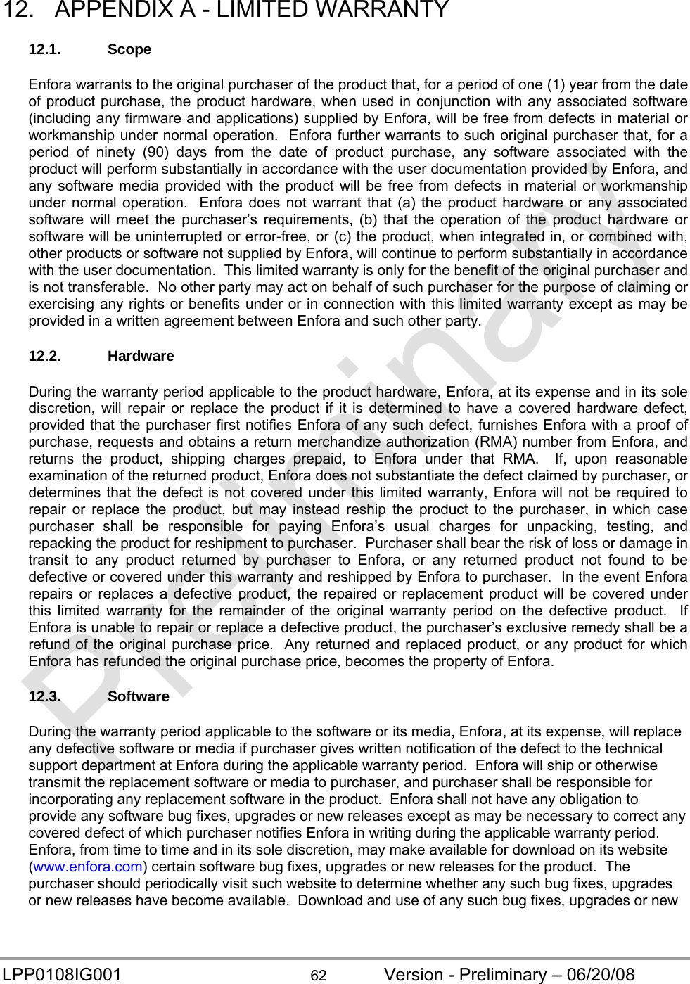
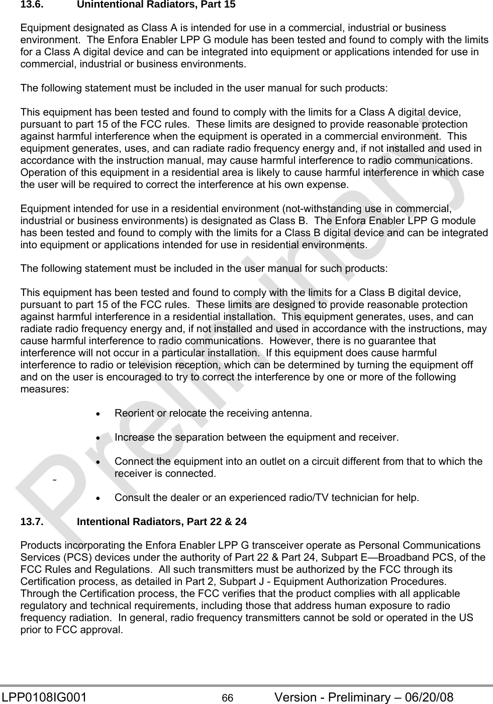
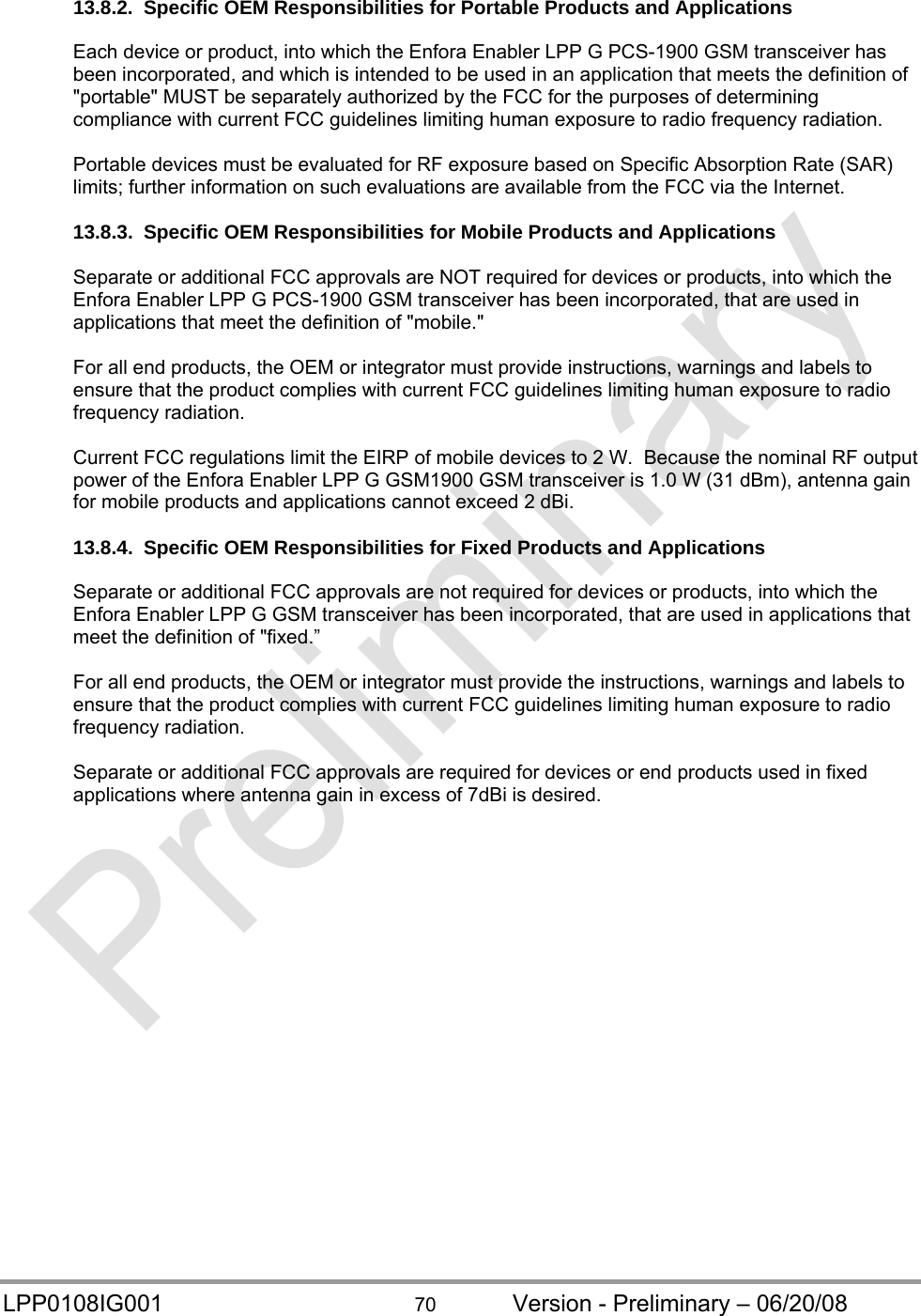
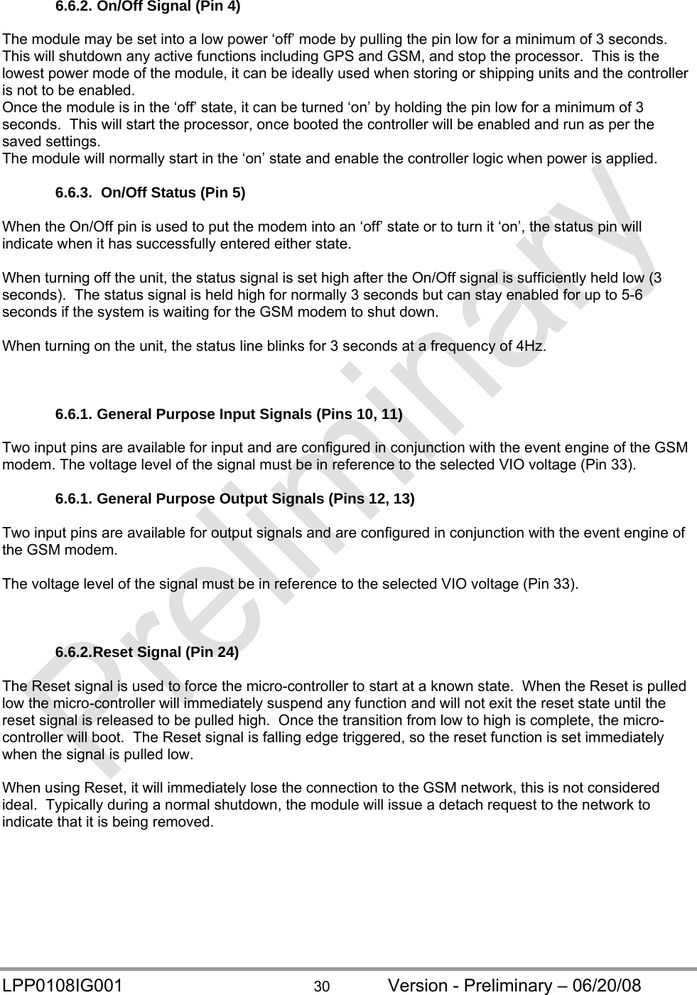
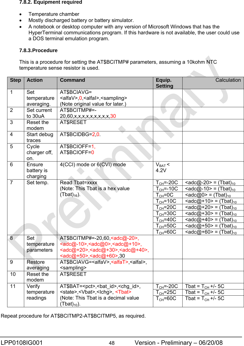
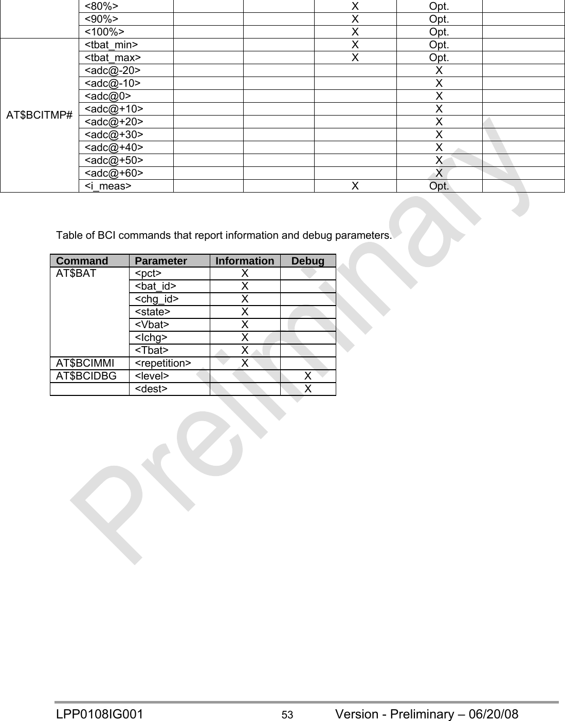
![LPP0108IG001 45 Version - Preliminary – 06/20/08 7.6.7. Calculate the BCIMAP# values for the parameters above the index. The remaining parameters are capacities determined from the Ichg current, since the battery voltage is fixed at 4.200V and is no longer an indication of capacity. BCIMAPn Parameter1Calculation Ichg (mA)1 <80%> [(CI - IEOC) * 2/3] + Isys 2 <90%> [(CI - IEOC) * 1/3] + Isys 2 <100%> Isys + C/20 = Note: Assuming the <#_ci_elements>=7. Customer may choose different value from 8.2.1 above, and will have to adjust this table accordingly. Note: Linear interpolation will introduce a slight error in the capacity. 7.6.8. Discharge the battery, determine the remaining BCIPCT# parameters. Determination of BCIPCT: 1. Start with a fully charged battery. 2. Monitor battery voltage over the full discharge cycle. This can done in-circuit or with a load. In-circuit is preferred because it will give a better representation of the CI-CV transition point, and the data can be logged to a text file. Discharging through a load will require a data-logger to record the discharge voltage, and may not give a clear indication of the CI-CV transition. 3. Note the start and stop times of State 4(CCI). Calculate the time interval given the <#_ci_elements> chosen earlier: 3.59533.83353.90153.93403.97464.03354.11584.22313.503.603.703.803.904.004.104.204.30090018002700360045005400630072008100900099001080Voltage (V)Time (sec)Battery ChargeConstant Current Stage 4(CCI)Vb…10%20%30%40%50%60%70%Tstart = 1939 secTstop = 10221 sec<#_ci_elements> = 7Tstep = 1183 sec](https://usermanual.wiki/Novatel-Wireless/LPP0108/User-Guide-1009877-Page-50.png)
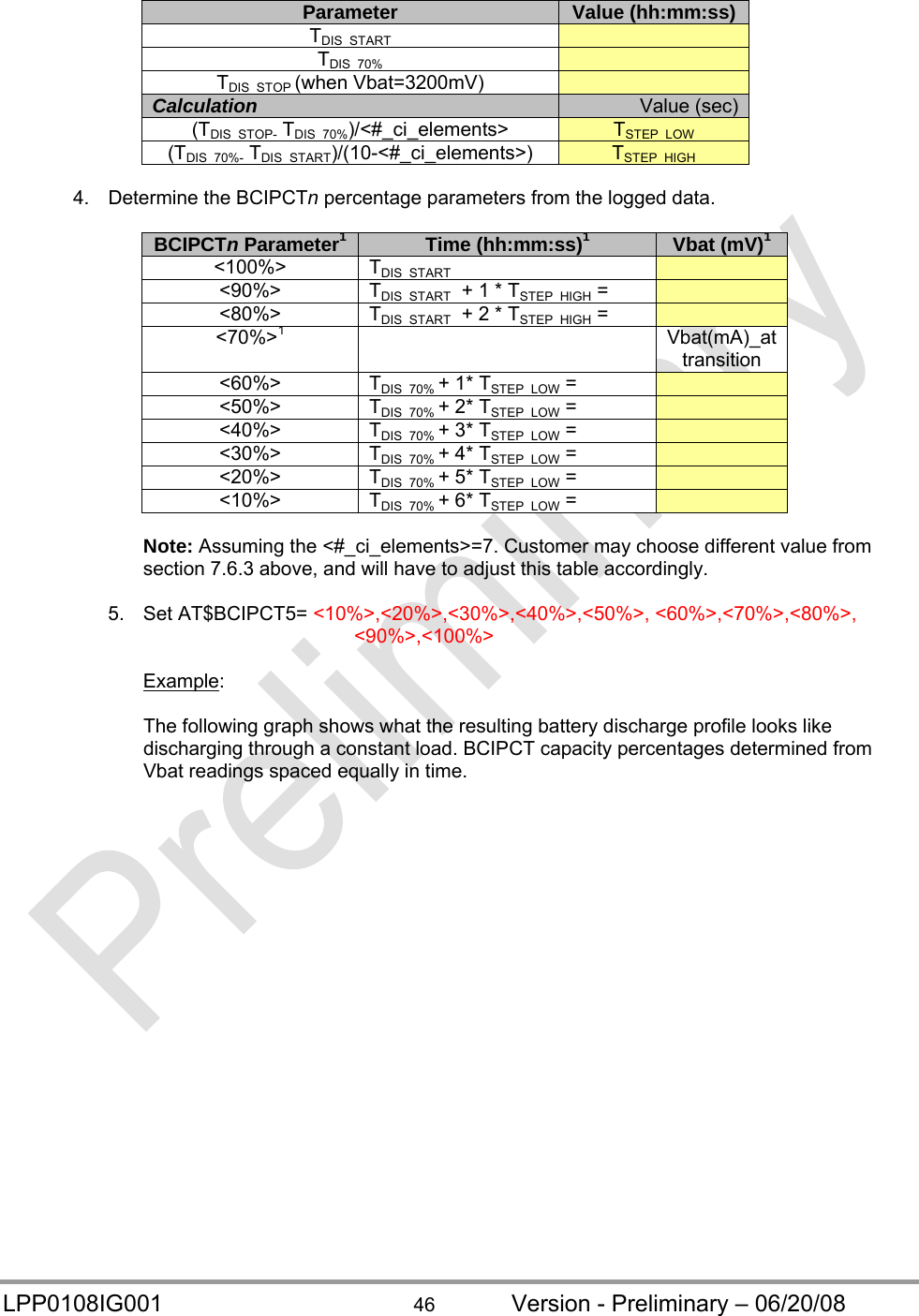
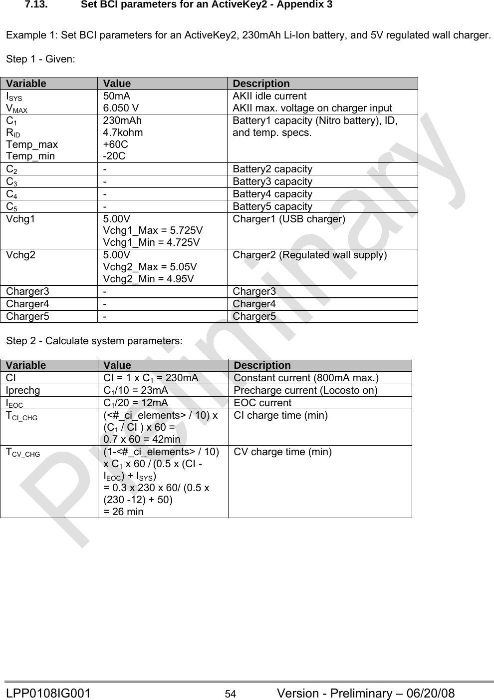
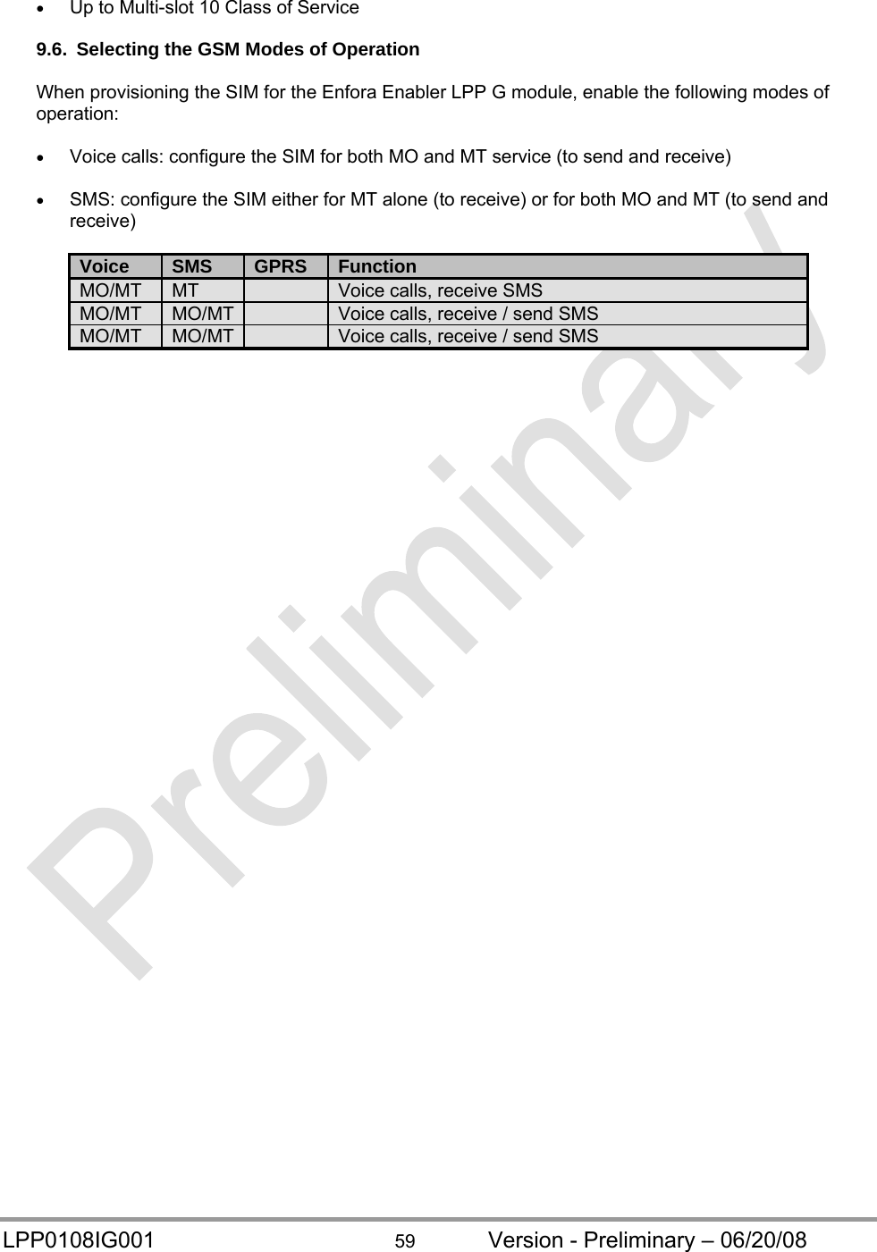
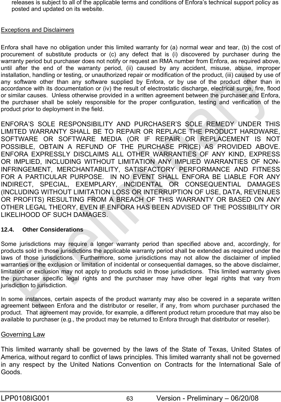
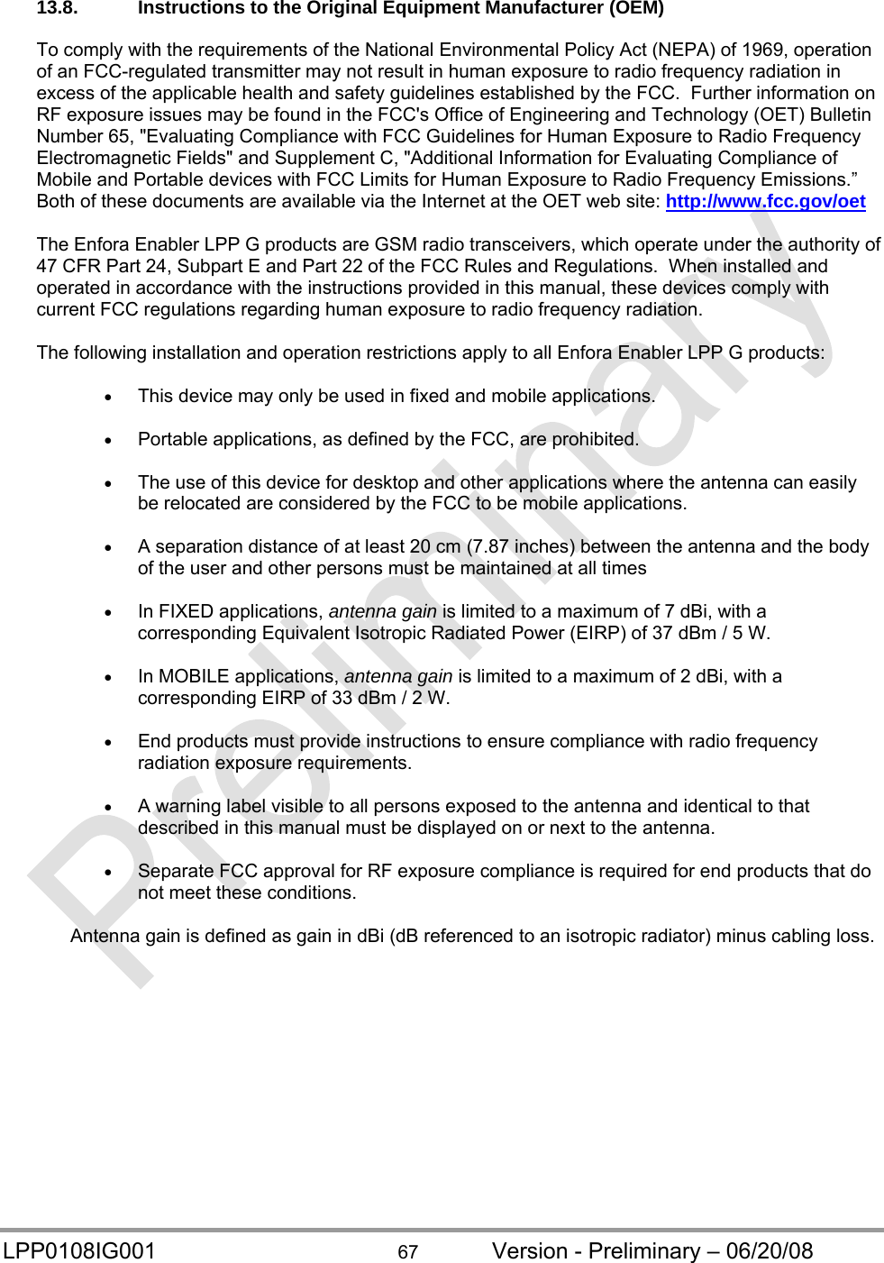
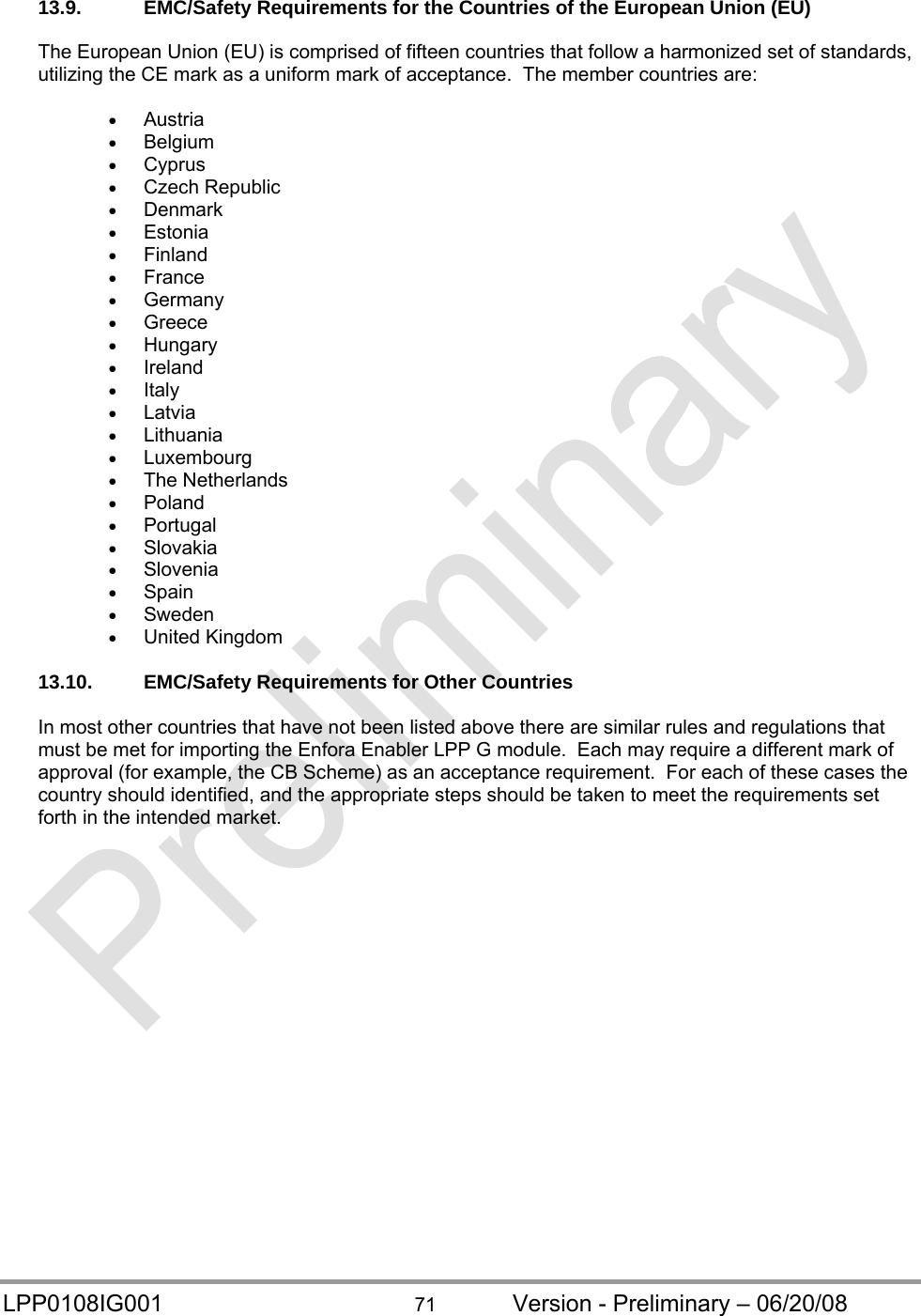
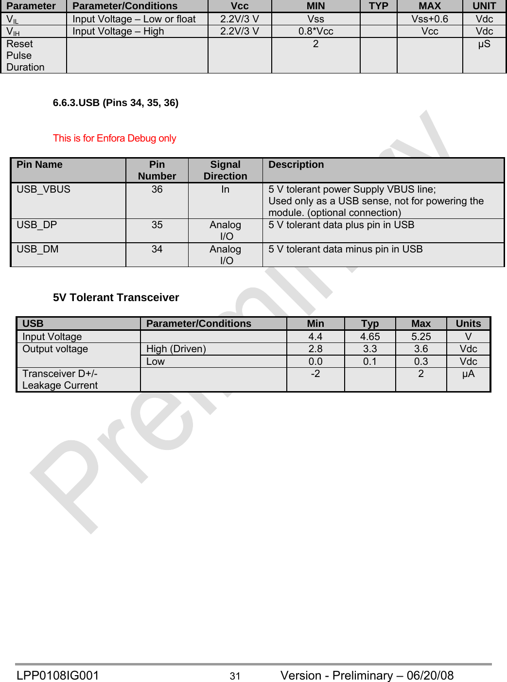
![LPP0108IG001 55 Version - Preliminary – 06/20/08 Step 3 - Calculate BCI parameters: Variable2 Formula Result AT$BCICHG2 <ci_chgireg> [ 0.22 x (CI + ISYS) x 10 + 0 ] x 255 / 1750 90 AT$BCICHG2 <ov_thr> <ov_thr> = VMAX x 1000 6050 AT$BCICHG2 <id_low> <id_low> = Vchg2_Min x 1000 4725 AT$BCICHG2 <id_high> <id_high> = Vchg2_Max x 1000 5725 AT$BCIISF <pre_chgireg> [ 0.22 x (IPRECHG + ISYS) x 10 + 0 ] x 255 / 1750 23 AT$BCIBAT1 <T1> By design, > (TCI CHG + TCI CHG) x 60 x 1000 4800000 AT$BCIBAT1 <T2> By design, > TCV CHG x 60 x 1000 1800000 AT$BCIBAT1 <chg_again_thr> By design 90 % AT$BCIBAT1 <id_low> (1023/1837.5) x (0.99 x RID) x 0.008 - 2 19 AT$BCIBAT1 <id_high> (1023/1662.5) x (1.01 x RID) x 0.012 +2 37 AT$BCIMAP1 <80%>1 [(ci_chgireg - IEOC) * 2/3] + Isys 102 mA AT$BCIMAP1 <90%>1 [(ci_chgireg - IEOC) * 1/3] + Isys 76 mA AT$BCIMAP1 <100%>1 IEOC + ISYS 62 mA AT$BCITMP1 <tbat_min> By design, or Temp_min -20 C AT$BCITMP1 <tbat_max> By design, or Temp_max 60 C AT$BCITMP1 <adc@-20> Set temp to –20C. <adc@-20>= dec(Tbat) Measure AT$BCITMP1 <adc@-10> Set temp to –10C. <adc@-10>= dec(Tbat) Measure AT$BCITMP1 <adc@0> Set temp to 0C. <adc@0>= dec(Tbat) Measure AT$BCITMP1 <adc@+10> Set temp to +10C. <adc@10>= dec(Tbat) Measure AT$BCITMP1 <adc@+20> Set temp to +20C. <adc@20>= dec(Tbat) Measure AT$BCITMP1 <adc@+30> Set temp to +30C. <adc@30>= dec(Tbat) Measure AT$BCITMP1 <adc@+40> Set temp to +40C. <adc@40>= dec(Tbat) Measure AT$BCITMP1 <adc@+50> Set temp to +50C. <adc@50>= dec(Tbat) Measure AT$BCITMP1 <adc@+60> Set temp to +60C. <adc@60>= dec(Tbat) Measure Note 1: Assuming the index is 7. If a different index is used, the CV capacities must be calculated differently. Note 2: This table is for a regulated wall-charger Charger2, and Battery1. Follow similar calculations for additional chargers and batteries.](https://usermanual.wiki/Novatel-Wireless/LPP0108/User-Guide-1009877-Page-60.png)