Novatel Wireless LPP0108 GSM/GPRS Embedded Module User Manual
Novatel Wireless Inc. GSM/GPRS Embedded Module Users Manual
Users Manual

Enfora Enabler LPP G
Integration Guide
Version: Preliminary
Integration Guide:
LPP0108IG001

Enfora Enabler LPP G
Integration Guide
LPP0108IG001 Version - Preliminary – 06/20/2008
Document Title: Enfora Enabler LPP G Integration Guide
Version: Preliminary
Date: 06/20/2008
Status: Preliminary
Document Control ID: LPP0108IG001
General
All efforts have been made to ensure the accuracy of material provided in this document at the time
of release. However, the items described in this document are subject to continuous development
and improvement. All specifications are subject to change without notice and do not represent a
commitment on the part of Enfora, Inc. Enfora, Inc. will not be responsible for any loss or damages
incurred related to the use of information contained in this document.
This product is not intended for use in life support appliances, devices or systems where a
malfunction of the product can reasonably be expected to result in personal injury. Enfora, Inc.
customers using, integrating, and/or selling this product for use in such applications do so at their
own risk and agree to fully indemnify Enfora, Inc. for any damages resulting from illegal use or resale.
Copyright
Complying with all applicable copyright laws is the responsibility of the user. Without limiting the
rights under copyright, no part of this document may be reproduced, stored in or introduced into a
retrieval system, or transmitted in any form or by any means (electronic, mechanical, photocopying,
recording or otherwise), or for any purpose, without the express written permission of Enfora, Inc.
Enfora may have patents, patent applications, trademarks, copyrights or other intellectual property
rights covering subject matter in this document. Except as expressly provided in any written license
agreement from Enfora, the furnishing of this document does not give you any license to these
patents, trademarks, copyrights or other intellectual property.
©2002, 2003, 2004, 2005, 2006, 2007, 2008 Enfora, Inc. All rights reserved.
Enabler and Spider are either registered trademarks or trademarks of Enfora, Inc. in the United
States.

Enfora Enabler LPP G
Integration Guide
LPP0108IG001 Version - Preliminary – 06/20/2008
Table of Contents
1.SAFETY PRECAUTIONS ................................................................................................................................. 1
1.1.IMPORTANT SAFETY INFORMATION ................................................................................................................ 1
2.REGULATORY COMPLIANCE FCC ............................................................................................................. 1
2.1.INTEGRATION CONSIDERATIONS AND INSTALLATION REQUIREMENTS ........................................................... 1
2.2.DISCLAIMER ................................................................................................................................................... 3
3.MANUAL OVERVIEW ...................................................................................................................................... 4
3.1.REVISION HISTORY ......................................................................................................................................... 4
H3.2.REFERENCES ................................................................................................................................................... 5
3.2.1.Enfora Enabler LPP G Product Documentation ................................................................................. 5
3.2.2.GSM Device Specifications .................................................................................................................. 5
3.2.3.US Government .................................................................................................................................... 5
3.2.4.Federal Communications Commission (FCC) ..................................................................................... 5
3.2.5.FCC Office of Engineering and Technology (OET) ............................................................................. 5
3.2.6.Industry Canada .................................................................................................................................. 6
3.2.7.Environmental Regulations .................................................................................................................. 6
3.2.8.Mechanical Specifications ................................................................................................................... 6
3.2.9.RF and EMI Specifications .................................................................................................................. 6
4.INTRODUCTION ............................................................................................................................................... 7
4.1.PRODUCT OVERVIEW...................................................................................................................................... 7
4.2.KEY FEATURES OF THE ENABLER LPP G MODULE ......................................................................................... 7
4.3.PROVIDING MULTI-BAND OPERATION ........................................................................................................... 9
4.4.SUMMARY OF FEATURES FOR THE ENABLER LPP G MODULE ........................................................................ 9
4.5.GENERAL DESIGN GUIDELINES FOR UTILIZING ENFORA GSM MODULES ...................................................... 12
4.5.1.Advanced tips for an RF friendly layout ............................................................................................ 13
4.5.1.1.Ground Plane ................................................................................................................................................... 13
4.5.1.2.Thermal Relief ................................................................................................................................................. 14
4.5.1.3.Antenna and RF Signal Trace .......................................................................................................................... 15
4.5.1.4.Vbat Input ........................................................................................................................................................ 16
4.5.2.Audio Reference Design ..................................................................................................................... 17
4.5.2.1.Audio Schematics ............................................................................................................................................ 17
4.5.2.2.Audio Layout ................................................................................................................................................... 17
4.6.HANDLING AND SOLDERING GUIDELINES ..................................................................................................... 17
5.TECHNICAL SPECIFICATIONS .................................................................................................................. 18
5.1.ENABLER LPP G MODULE BLOCK DIAGRAM ............................................................................................... 18
5.2.DETAILED PRODUCT SPECIFICATIONS .......................................................................................................... 19
CLIMATIC: STORAGE AND TRANSPORTATION ........................................................................................................... 19
MECHANICAL: STORAGE AND TRANSPORTATION ..................................................................................................... 19
MECHANICAL: PROPOSED STANDARDS .................................................................................................................... 19
ELECTROMAGNETIC EMISSIONS ............................................................................................................................... 19
5.3.OPERATING POWER ...................................................................................................................................... 20
5.3.1.Typical Input Current ........................................................................................................................ 20
5.3.2.GSM Transmit Power ........................................................................................................................ 20
5.3.3.GSM Receiver Sensitivity ................................................................................................................... 21
6.PHYSICAL INTERFACES .............................................................................................................................. 21
6.1.MODULE MOUNTING TO HOST BOARD (REFERENCE) ................................................................................... 22
6.2.I/O PIN ASSIGNMENTS .................................................................................................................................. 25
6.3.CIRCUIT PROTECTION ................................................................................................................................... 26
6.4.ANTENNA ..................................................................................................................................................... 27

Enfora Enabler LPP G
Integration Guide
LPP0108IG001 Version - Preliminary – 06/20/2008
6.4.1.GSM ................................................................................................................................................... 27
6.4.2.GPS .................................................................................................................................................... 27
6.5.CONTROL CONNECTOR SIGNAL DESCRIPTIONS AND FUNCTIONS ................................................................. 29
6.5.1.Module Power (Pins 30, 31) .............................................................................................................. 29
6.5.2.On/Off Signal (Pin 4) ......................................................................................................................... 30
6.5.3.On/Off Status (Pin 5) ......................................................................................................................... 30
6.5.1.General Purpose Input Signals (Pins 10, 11) .................................................................................... 30
6.5.1.General Purpose Output Signals (Pins 12, 13) .................................................................................. 30
6.5.2.Reset Signal (Pin 24) ......................................................................................................................... 30
6.5.3.USB (Pins 34, 35, 36) ........................................................................................................................ 31
6.5.4.RTC Sleep ............................................................................................ Error! Bookmark not defined.
6.5.5.Serial Interfaces ................................................................................................................................. 32
6.5.5.1.Main Serial Interface (Pins 17, 18) .................................................................................................................. 32
6.5.5.2.GPS Serial Interface (Pin 19) ........................................................................................................................... 33
6.5.6.Handset Microphone Input (Pins 39, 40) ........................................................................................... 34
6.5.7.Handset Speaker Output (Pins 37, 38) ............................................................................................... 34
6.6.SUBSCRIBER IDENTITY MODULE (SIM) (PINS 42, 43, 44, 45, 46) ................................................................. 35
6.6.1.Using a Remote SIM with the Enfora Enabler LPP G Module (Pins 42, 43, 44, 45, 46) .................. 36
6.6.1.1.Remote SIM Component Information .............................................................................................................. 37
7.BATTERY CHARGING CALIBRATION AND CONFIGURATION ........................................................ 38
7.1.OBJECTIVE .................................................................................................................................................... 38
7.2.SUPPORTED DEVICES .................................................................................................................................... 38
7.3.REFERENCES ................................................................................................................................................. 38
7.4.LIST OF BATTERY CHARGING COMMANDS ..................................................................................................... 38
7.4.1.Setting BCIVSF parameters ............................................................................................................... 39
7.4.2.Equipment required ........................................................................................................................... 39
7.4.3.Procedure .......................................................................................................................................... 39
7.4.4.Setting BCIISF Parameters ................................................................................................................ 40
7.4.5.Scope .................................................................................................................................................. 40
7.4.6.6.2 Equipment required ..................................................................................................................... 40
7.4.7.6.3 Calibration procedure ................................................................................................................. 40
7.5.SETTING BCIAVG PARAMETERS .................................................................................................................. 42
7.6.SETTING BCIMAP# PARAMETERS ................................................................................................................ 42
7.6.1.Scope .................................................................................................................................................. 42
7.6.2.Procedure .......................................................................................................................................... 42
7.6.3.Choose the BCIMAP# index .............................................................................................................. 42
7.6.4.Set the desired CI charge current for the designated charger. .......................................................... 43
7.6.5.Charge empty battery in constant current with target <ci_chgireg>. ............................................... 43
7.6.6.Note the first Vbat(mA) that occurred after the charge stopped and went to 3(SUP). ....................... 44
7.6.7.Calculate the BCIMAP# values for the parameters above the index. ................................................ 45
7.6.8.Discharge the battery, determine the remaining BCIPCT# parameters. ........................................... 45
7.7.SETTING BCIBAT# PARAMETERS ................................................................................................................ 47
7.7.1.Procedure to set the battery ID .......................................................................................................... 47
7.8.SETTING BCITMP# PARAMETERS ................................................................................................................ 47
7.8.1.Scope .................................................................................................................................................. 47
7.8.2.Equipment required ........................................................................................................................... 48
7.8.3.Procedure .......................................................................................................................................... 48
7.9.SETTING BCIDEL PARAMETERS................................................................................................................... 49
7.10.SETTING BCIOFF PARAMETERS ............................................................................................................... 49
7.11.BATTERY CHARGING CALIBRATION AND CONFIGURATION - APPENDIX 1 ................................................ 50
7.12.BCI COMMAND PARAMETERS - APPENDIX 2 ............................................................................................ 52
7.13.SET BCI PARAMETERS FOR AN ACTIVEKEY2 - APPENDIX 3 ..................................................................... 54
8.GPS PERFORMANCE ..................................................................................................................................... 56
9.GSM/GPRS MODES OF OPERATION ......................................................................................................... 57

Enfora Enabler LPP G
Integration Guide
LPP0108IG001 Version - Preliminary – 06/20/2008
9.1.ENABLING THE TRANSMISSION MODES FOR THE GSM/GPRS SERVICES ..................................................... 57
9.2.VOICE COMMUNICATION .............................................................................................................................. 57
9.3.SMS: SHORT MESSAGE SERVICES ................................................................................................................ 58
9.4.SIM OPERATION ........................................................................................................................................... 58
9.4.1.Provisioning the SIM ......................................................................................................................... 58
9.5.GPRS SERVICES SUPPORTED BY THE ENFORA ENABLER LPP G MODULE ................................................... 58
9.6.SELECTING THE GSM MODES OF OPERATION .............................................................................................. 59
10.SOFTWARE INTERFACE .......................................................................................................................... 60
10.1.SOFTWARE INTERFACE ............................................................................................................................. 60
10.2.FORMAT FOR THE AT COMMANDS ........................................................................................................... 60
10.3.ENFORA AT COMMAND SET ..................................................................................................................... 60
11.INTEGRATION AND TESTING ................................................................................................................ 61
12.APPENDIX A - LIMITED WARRANTY ................................................................................................... 62
12.1.SCOPE ....................................................................................................................................................... 62
12.2.HARDWARE .............................................................................................................................................. 62
12.3.SOFTWARE ................................................................................................................................................ 62
12.4.OTHER CONSIDERATIONS ......................................................................................................................... 63
13.APPENDIX B - REGULATIONS AND COMPLIANCE .......................................................................... 64
13.1.GCF/PTCRB APPROVAL (FORMERLY FTA) ............................................................................................ 64
13.2.ELECTROMAGNETIC COMPATIBILITY (EMC) AND SAFETY REQUIREMENTS ............................................. 64
13.3.EMC/SAFETY REQUIREMENTS FOR THE USA .......................................................................................... 64
13.4.HUMAN EXPOSURE COMPLIANCE STATEMENT ......................................................................................... 65
13.5.COMPLIANCE WITH FCC REGULATIONS ................................................................................................... 65
13.6.UNINTENTIONAL RADIATORS, PART 15 .................................................................................................... 66
13.7.INTENTIONAL RADIATORS, PART 22 & 24 ................................................................................................ 66
13.8.INSTRUCTIONS TO THE ORIGINAL EQUIPMENT MANUFACTURER (OEM) .................................................. 67
13.8.1.OEM Responsibilities for All Products Containing the Enabler LPP G module ............................... 69
13.8.2.Specific OEM Responsibilities for Portable Products and Applications ........................................... 70
13.8.3.Specific OEM Responsibilities for Mobile Products and Applications .............................................. 70
13.8.4.Specific OEM Responsibilities for Fixed Products and Applications ................................................ 70
13.9.EMC/SAFETY REQUIREMENTS FOR THE COUNTRIES OF THE EUROPEAN UNION (EU) .............................. 71
13.10.EMC/SAFETY REQUIREMENTS FOR OTHER COUNTRIES ........................................................................... 71
14.APPENDIX C - GLOSSARY AND ACRONYMS ...................................................................................... 72
15.APPENDIX D – TABLES AND FIGURES ................................................................................................. 74
16.APPENDIX E - CONTACTING ENFORA................................................................................................. 75

LPP0108IG001 1 Version - Preliminary – 06/20/08
1. Safety Precautions
1.1. Important Safety Information
The following information applies to the devices described in this manual. Always observe all standard and
accepted safety precautions and guidelines when handling any electrical device.
Save this manual: it contains important safety information and operating instructions.
Do not expose the Enfora Enabler LPP G product to open flames.
Ensure that liquids do not spill onto the devices.
Do not attempt to disassemble the product: Doing so will void the warranty. With the
exception of the Subscriber Identification Module (SIM), this product does not contain
consumer-serviceable components.
2. Regulatory Compliance FCC
2.1. Integration Considerations and Installation Requirements
The Enabler LPP G module is designed for use in a variety of host units, "enabling" the host
platform to perform wireless data communications. However, there are certain criteria relative to
integrating the Enabler LPP G module into a host platform such as a PC, laptop, handheld or
PocketPC®, monitor and control unit, etc. that must be considered to ensure continued
compliance with FCC compliance requirements.
Operation is subject to the following two conditions: (1) this device may not cause
interference, and (2) this device must accept any interference, including interference that may
cause undesired operation of the device.
In order to use the Enabler LPP G module without additional FCC certification approvals, the
installation must meet the following conditions:
Maximum RF output power and antenna gain to meet Maximum Permissible Exposure
Requirements: GSM850 mode: Power at antenna port is +33 dBm. The maximum gain
is 1.4 dBi. GSM1900 mode: Power at antenna port is 30 dBm. The maximum gain is 7
dBi in order to meet the requirements of maximum 2 watts EIRP for mobile transmitters. If
RF power and/or antenna gain is desired, a separate FCC certification is required.
If used in a "portable" application such as a handheld or body worn device with the
antenna less than 20 cm (7.9 in.) from the human body when the device is operating,
then the integrator is responsible for passing additional "as installed" testing and the
device will require its own FCC ID:
SAR (Specific Absorption Rate) testing, with results submitted to the FCC for
approval prior to selling the integrated unit. If unable to meet SAR requirements,
then the host unit must be restricted to "mobile" use (see below).
Unintentional emissions, FCC Part 15; results do not have to be submitted to the
FCC unless requested, although the test provides substantiation for required labeling
(see below).

LPP0108IG001 2 Version - Preliminary – 06/20/08
ERP and EIRP measurements for FCC Parts 22 and 24, alternatively a full retest on
FCC Parts 22 and 24 can be performed.
If used in a "mobile" application where the antenna is normally separated at least 20 cm
(7.9 in) from the human body during device operation, then an appropriate warning label
must be placed on the host unit adjacent to the antenna. The label should contain a
statement such as the following:
WARNING
RF exposure. Keep at least 20 cm
(7.9 in) separation distance from
the antenna and the human body.
Host unit user manuals and other documentation must also include appropriate caution
and warning statements and information.
If the FCCID for the Enabler LPP G module is not visible when installed in the host
platform, then a permanently attached or marked label must be displayed on the host unit
referring to the enclosed module.
For example, the label should contain wording such as:
Contains GSM/GPRS modem transmitter module
FCC ID: MIVLPP0108
This device complies with Part 15 of the FCC Rules.
Operation is subject to the following two conditions: (1)
This device may not cause harmful interference, and (2)
This device must accept any interference received,
including interference that may cause undesired
operation.
OR
Contains FCC ID: MIVLPP0108
This device complies with Part 15 of the FCC Rules.
Operation is subject to the following two conditions: (1)
This device may not cause harmful interference, and (2)
This device must accept any interference received,
including interference that may cause undesired
operation.
Any antenna used with the Enabler LPP G module must be approved by the FCC or as a
Class II Permissive Change (including MPEL or SAR data as applicable). The
"professional installation" provision of FCC Part 15.203 does not apply.

LPP0108IG001 3 Version - Preliminary – 06/20/08
The transmitter and antenna must not be co-located or operating in conjunction with any
other antenna or transmitter. Violation of this would allow a user to plug another
transmitter in to the product and potentially create an RF exposure condition.
WARNING
The transmitter and antenna must not be collocated
or operating in conjunction with any
other antenna or transmitter. Failure to observe
this warning could produce an RF exposure
condition.
2.2. Disclaimer
The information and instructions contained within this publication comply with all FCC, GCF,
PTCRB, R&TTE, IMEI and other applicable codes that are in effect at the time of publication.
Enfora disclaims all responsibility for any act or omissions, or for breach of law, code or
regulation, including local or state codes, performed by a third party.
Enfora strongly recommends that all installations, hookups, transmissions, etc., be performed by
persons who are experienced in the fields of radio frequency technologies. Enfora acknowledges
that the installation, setup and transmission guidelines contained within this publication are
guidelines, and that each installation may have variables outside of the guidelines contained
herein. Said variables must be taken into consideration when installing or using the product, and
Enfora shall not be responsible for installations or transmissions that fall outside of the
parameters set forth in this publication.
Enfora shall not be liable for consequential or incidental damages, injury to any person or
property, anticipated or lost profits, loss of time, or other losses incurred by Customer or any third
party in connection with the installation of the Products or Customer's failure to comply with the
information and instructions contained herein.
The Enabler LPP G platform is designed with features
to support a robust connection. There are instances
where the module performance is beyond the control
of the intended design. Integrated designs that require
24 by 7 operation must implement power control via an
external circuit or by implementing power management
as specified within this design guide.

LPP0108IG001 4 Version - Preliminary – 06/20/08
3. Manual Overview
This document describes the available hardware interface of the Enabler LPP G module. The
purpose of this document is to define the electrical, mechanical and software interfaces while
providing detailed technical information in order to streamline the process of hardware and
system integration.
3.1. Revision History
Date Rev Author Description
06/20/08 1.00 Chuck Todd Preliminary

LPP0108IG001 5 Version - Preliminary – 06/20/08
3.2. References
3.2.1. Enfora Enabler LPP G Product Documentation
Manuals
LPP0108AT001 - Enfora Enabler LPP G AT Command Set Reference
GSM0308UG001 - Enfora GSM-GPRS Family API Reference
LPP0108PR001 – Enfora Enabler LPP G Programming Reference
LPP0108SD001 – Enfora Enabler LPP G SDK Reference
LPP0108UG001 – Enfora Enabler LPP G Power Management Developer Tool Guide
3.2.2. GSM Device Specifications
3GPP TS 51010-1 (850, 900,1800,1900 MHz devices)
To view the latest release, go to:
http://www.3gpp.org/ftp/Specs/html-info/51010-1.htm
3.2.3. US Government
3.2.4. Federal Communications Commission (FCC)
Internet: http://www.fcc.gov/
FCC Rules, Part 24
47 CFR Subpart E--Broadband PCS
47 CFR § 24.52, sections 1.1307(b), 2.1091, and 2.1093
FCC Rules, Part 22 for GSM 850
FCC Rules, Part 15
FCC Rules, Part 2
Subpart J--Equipment Authorization Procedures
Section 2.925
3.2.5. FCC Office of Engineering and Technology (OET)
Internet: http://www.fcc.gov.oet/
Bulletin Number 65 "Evaluating Compliance with FCC Guidelines for Human Exposure
to Radio Frequency Electromagnetic Fields"
Supplement C "Additional Information for Evaluating Compliance of Mobile and
Portable Devices with FCC Limits for Exposure to Radio Frequency Emissions"

LPP0108IG001 6 Version - Preliminary – 06/20/08
3.2.6. Industry Canada
RSS-132
RSS-133
ICES-003
3.2.7. Environmental Regulations
National Environmental Policy Act (NEPA) of 1969 (Part 1, Subpart 1)
RoHS Compiant
3.2.8. Mechanical Specifications
ASTM D999
ASTM D775
IEC 68-2-27
Bellcore Gr-63-CORE
ETS 300 019-1-1 Class 1.2
ETS 300 019-1-2 Class 2.1
ETS 300 019-1-3 Class 3.1
3.2.9. RF and EMI Specifications
ETSI Standards
EN 61000-4-6
EN 61000-4-3
3GPP TS 51.010-1, Section 12.2

LPP0108IG001 7 Version - Preliminary – 06/20/08
4. Introduction
4.1. Product Overview
The Enfora Enabler LPP G module is a compact, wireless OEM module that utilizes the Global
System for Mobile Communications (GSM) and General Packet Radio Services (GPRS)
international communications standard to provide two-way wireless capabilities via GSM services.
This GSM/GPRS module is combined with a Global Positioning System (GPS) chipset to provide
physical location, a host processor to ensure very low power standby configurations, and
vibration sensor to detect movement of the module. The Enfora Enabler LPP G module is a fully
Type-approved GSM/GPRS device, enabling application-specific, two-way communication and
control.
The small size of the Enfora Enabler LPP G module allows it to be integrated easily into the
application and packaging.
4.2. Key Features of the Enabler LPP G Module
The following table summarizes the main features of the Enfora Enabler LPP G Radio Module.
Interface Data input/output interface 50 position 1.27mm pitch
Primary serial port 3.3V levels, ‘2-wire’ UART implementation
Secondary serial Port Single TX from GPS, NMEA data only.
USB port USB Debug and Configuration
Audio Digital audio
Command protocol Enfora Packet API, GSM AT command set, Enfora
MCP
Subscriber Identification Module
(SIM)
USIM port with SIM detect, Optional embedded
SIM.
Battery Charger Lithium Ion battery charger, temperature and
battery ID analog inputs
Power Electrical power 3.3 to 4.5 Vdc (vbat)
Peak currents and average
power dissipation
Refer to the Operating Power table in the
Technical Specifications for peak currents and
average power dissipation for various modes of
operation.
Radio Features Frequency bands EGSM 900, GSM1800, GSM 850 and GSM 1900
capability.
GSM/GPRS features supported Provides for all GSM/GPRS authentication,
encryption, and frequency hopping algorithms.
GPRS Coding Schemes CS1-CS4 supported.
Multi-Slot Class 10 (4RX/2TX, Max 5 Slots).
Regulatory Agency approvals
GCF Type Approval
PTCRB Type Approval
FCC Certification
RTTE
CE (European Community Certification)
IC (Industry Canada) Approval
GSM/GPRS
Functionality
Mobile-originated and mobile-terminated SMS messages: up to 140 bytes or
up to 160 GSM 7-bit ASCII characters.
Reception of Cell Broadcast Message
SMS Receipt acknowledgement
Voice (EFR, FR, HR, AMR)
Supports Unstructured Supplementary Service Data (USSD)
Multi-Slot Class 10 Supported (4Rx/2TX), (5 Slot Max) PBCCH/PCCCH
Supported

LPP0108IG001 8 Version - Preliminary – 06/20/08
Audio Features Handset Microphone biasing, internal
Handset microphone input (MICIN, MICIP pins)
Outputs Handset earphone outputs (EARP, EARN pins)
SIM 1.8/3 V Mini-Subscriber Identity Module (SIM) compatible
Software Free RTOS included
Table 1 - Enabler LPP G Key Features

LPP0108IG001 9 Version - Preliminary – 06/20/08
4.3. Providing Multi-Band Operation
The Enfora Enabler LPP G module provides 4 frequency bands for compatibility with worldwide
frequency standards. 850/1900 frequency bands are primarily used in North and South America,
while 900/1800 bands are used throughout the world. The Enabler LPP G offers all four bands for
use worldwide.
4.4. Summary of Features for the Enabler LPP G Module
The following summarizes the main features of the Enfora Enabler LPP G Module.
Mechanical
Dimensions ................................... 38.5 mm x 33.6 mm x 4.19 mm
Weight .......................................... 8.6g
Packet Data Transfer:
Protocol……………………………………………GPRS Release 97
Coding Schemes…………………………………CS1-CS4
Multi-Slot Capability: (Demonstrated @MS10)…….MS10 (4RX/2TX) (Max 5 Slots)
Packet Channel Support .............. ……………..PBCCH/PCCCH
Short Message Services:
GSM SMS .................................... MO, MT, CB, Text and PDU Modes
GPRS SMS .................................. MO, MT, CB, Text and PDU Modes
Voice Capability:
Speech Codec .............................. EFR, FR, HR, AMR
GSM/GPRS Radio Performance Multi-Band:
LPP0108 Radio Frequencies ....... 850 MHz, 900 MHz, 1800 MHz, and 1900 MHz
Sensitivity ..................................... <-106 dBm (Typical GPRS CS1)
850 & 900 MHz Transmit Power .. Class 4 (2 W)
1800 & 1900 MHz Transmit ......... PowerClass 1 (1 W)
System Requirements:
Host Interface ............................... Serial Interface
DC Voltage ................................... 3.3 to 4.5 Vdc

LPP0108IG001 10 Version - Preliminary – 06/20/08
Application Interface:
Host Protocol ................................ MCP Protocol, AT Commands, OTA Enfora Packet API and
USB.
Internal Protocols ......................... UDP stack and TCP/IP stack
Physical Interface ......................... 2 serial (primary - Default rate 115,200 baud; secondary -
rate 19,200 baud), 1 USB (debug)
Audio Interface .............................. Handset microphone input (MICIN, MICIP pins), Handset
earphone outputs (EARP, EARN pins).
SIM Interface:
Remote SIM…………………………1.8/3-Volt SIM Capability
Environmental:
Compliant Operating Temp. ......... -20 °C to 60 °C (Fully GSM Spec Compliant)
Operating Temperature ………….-30 °C to 70 °C (Not fully GSM Spec Compliant)
Storage Temperature ................... -40 °C to 85 °C
Humidity ....................................... 5 to 95% non-condensing
EMC:
Emissions ..................................... FCC Parts 15,22 & 24, Class B
3GPP TS 51010-1, Section 12.2
EN 55022 Class B

LPP0108IG001 11 Version - Preliminary – 06/20/08
Operating Power (TYPICAL):
NOTE: UART disabled during testing; data average taken for 5 minutes; Vbat = 3.7V.
Function
Block State Min
Current
A
verage
Current Peak
Current
MSP
Idle
2.2V TBD <2uA 22uA
3.3V TBD <2.5uA 25uA
Motion sensor on
(no movement)
2.2V TBD <7uA 40uA
3.3V TBD 3.5uA 21.5uA
Motion sensor
with movement
2.2V TBD 14uA 2250uA
3.3V TBD 25.5uA 3750uA
GSM only Power on to
modem register
TBD TBD TBD
Idle
TBD TBD TBD
GPS only GPS enable to
first 3D fix -
130dbm (~45sec)
TBD 56.6mA 247.5mA
Acquisition
TBD 76mA 80mA
Tracking
(@ -155dbm)
TBD 72mA 78mA
GSM &
GPS Shutdown
TBD TBD TBD
Acquisition
TBD TBD TBD
Tracking
TBD TBD TBD
Table 2: Typical Operating Power

LPP0108IG001 12 Version - Preliminary – 06/20/08
GSM Transmit Power
1800/1900 MHz ............................ GSM Power Class 1 (30 dBm 2 dB @ antenna connection)
850/900 MHz ................................ GSM Power Class 4 (33 dBm 2 dB @ antenna connection)
GSM/GPRS Receiver Sensitivity (Typical)
1800/1900 MHz ............................ <-106 dBm, GPRS Coding Scheme 1 (CS1)
850/900 MHz ................................ <-106 dBm, GPRS Coding Scheme 1 (CS1)
4.5. General design guidelines for utilizing Enfora GSM modules
The following guidelines are provided in an effort to allow Enabler LPP G module users to
successfully implement their PCB layout to obtain the best performance. This includes the lowest
possible EMI emissions, maximum thermal conduction, mechanical integrity, and voice quality. The
Enabler LPP G module is a very compact, high performance design, yet it is easy to interface into the
final product. In order to realize its full potential, designers should pay close attention to ground
structures, the routing of RF and Digital traces, and the size of the power supply lines.
These design tips are strictly guidelines and are not
meant to be a complete list of items that guarantee
actual performance. Each application is different and
may require variation from these guidelines; however,
care should be given to utilize these sound engineering
principles whenever possible.
LPP0108IG001 13 Version - Preliminary – 06/20/08
4.5.1. Advanced tips for an RF friendly layout
4.5.1.1. Ground Plane
To ensure the lowest possible EMI emissions and maximum thermal conductivity, it is
recommended that all metal tabs on the GSM module shield must be soldered down onto a
continuous ground plane that runs under the entire module. Ample ground vias should be
provided to create a low impedance ground. It is recommended to minimize the number of
I/O and power traces under the GSM module to allow for as much ground plane as possible.
An example of a good ground structure and pad layout is shown below in Figure 1 - Example
of good ground plane for GSM modules.
Figure 1 - Example of good ground plane for GSM modules
LPP0108IG001 14 Version - Preliminary – 06/20/08
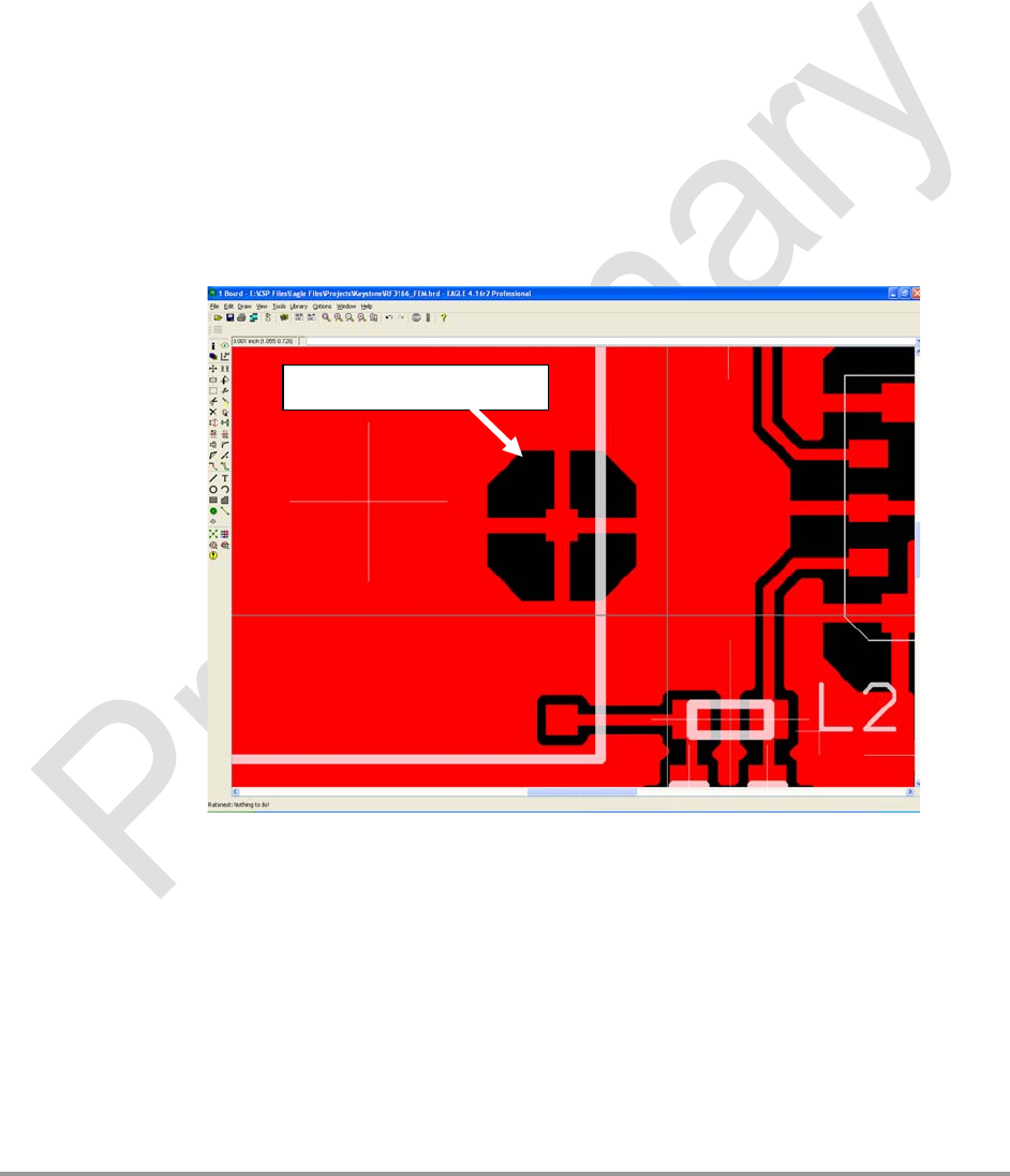
4.5.1.2. Thermal Relief
Because the ground plane acts as a large heat sink, it can affect the solderability of
components. A common method to reduce this effect is to use thermal relief around the pad
in question. However, great care must be taken when using thermal relief for high current or
high frequency applications
For example, a large thermal relief like the one shown in Figure 2 can serve the purpose for
general applications such as low current, low speed data lines, DC connections and audio
frequency applications. However, such thermal relief structures should be avoided for
applications where high current and/or high frequency is involved, such as those using the
Enabler Module. Depending on the frequency of operation, the long narrow thermal relief
traces between the pad and the ground plane act like an RF choke. These RF chokes
become higher impedance at harmonics of the fundamental frequency making it problematic
for high frequency suppression. This can make it difficult to pass type approval testing.
Figure 2 - Example of a POOR RF Thermal Relief
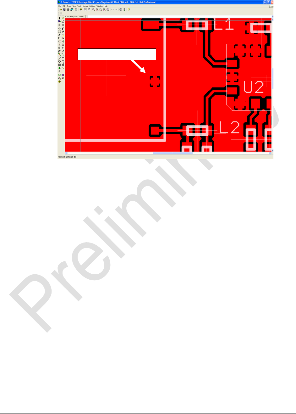
If thermal relief is necessary, it is recommended that you use short, fat traces similar to those
shown in Figure 3. This will still provide a solderable connection, while providing a better RF
connection. Making them shorter also allows for a more continuous ground plane due to less
copper being removed from the area. It is also recommended to have ground vias around all
thermal relief of critical ground pins.
POOR RF thermal relief
LPP0108IG001 15 Version - Preliminary – 06/20/08
Figure 3 - Example of a GOOD RF Thermal Relief
4.5.1.3. Antenna and RF Signal Trace
The PCB trace that feeds the RF output port must be designed for a 50 ohm characteristic
impedance, coplanar, or routed into internal layers to keep the top layer continuous around
and underneath the Enabler module. Ample ground vias should be provided around the RF
contacts, the RF trace and launch pad. If possible, keep I/O and power traces away from the
RF port. This includes traces running parallel or orthogonal to it. Thermal relief should not
be used on the antenna output port ground pads. The designer must pay close attention to
the size of the pad and thickness of the dielectric beneath the signal pad and trace. Most
PCB manufacturers can adjust the trace width to maintain 50 ohms impedance if the traces
are identified and instructions are included on the FAB drawing. This service is typically
provided at no or minimal additional cost.
For minimum RF emissions due to the fundamental frequency of operation, the Enabler
module works best with an antenna load that has a VSWR of 1.5:1 or better. The antenna
should not have gain at the harmonic frequencies, otherwise, the conducted harmonics could
get amplified to a point where the product no longer passes type approval. However, for
applications where antenna quality is less than ideal, it is recommended to have a low pass
filter (Pi structure with N=3) in the RF path to the antenna. This is a secondary plan should
there be a need to lower harmonic levels at frequencies above the PCS band. The pad
structure may also be used to match the antenna load impedance, if required. If it is not
needed, a capacitor of low reactance may be used to bridge the Pi structure.
The RF cable going between the Enable module and the antenna is very lossy, therefore, the
length of this cable should be kept as short as possible.
GOOD RF thermal relief
LPP0108IG001 16 Version - Preliminary – 06/20/08
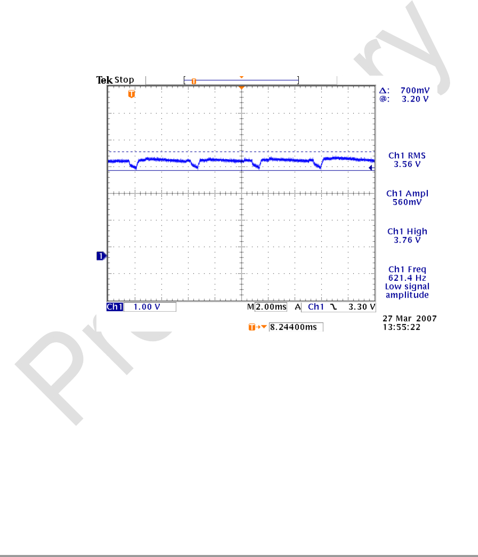
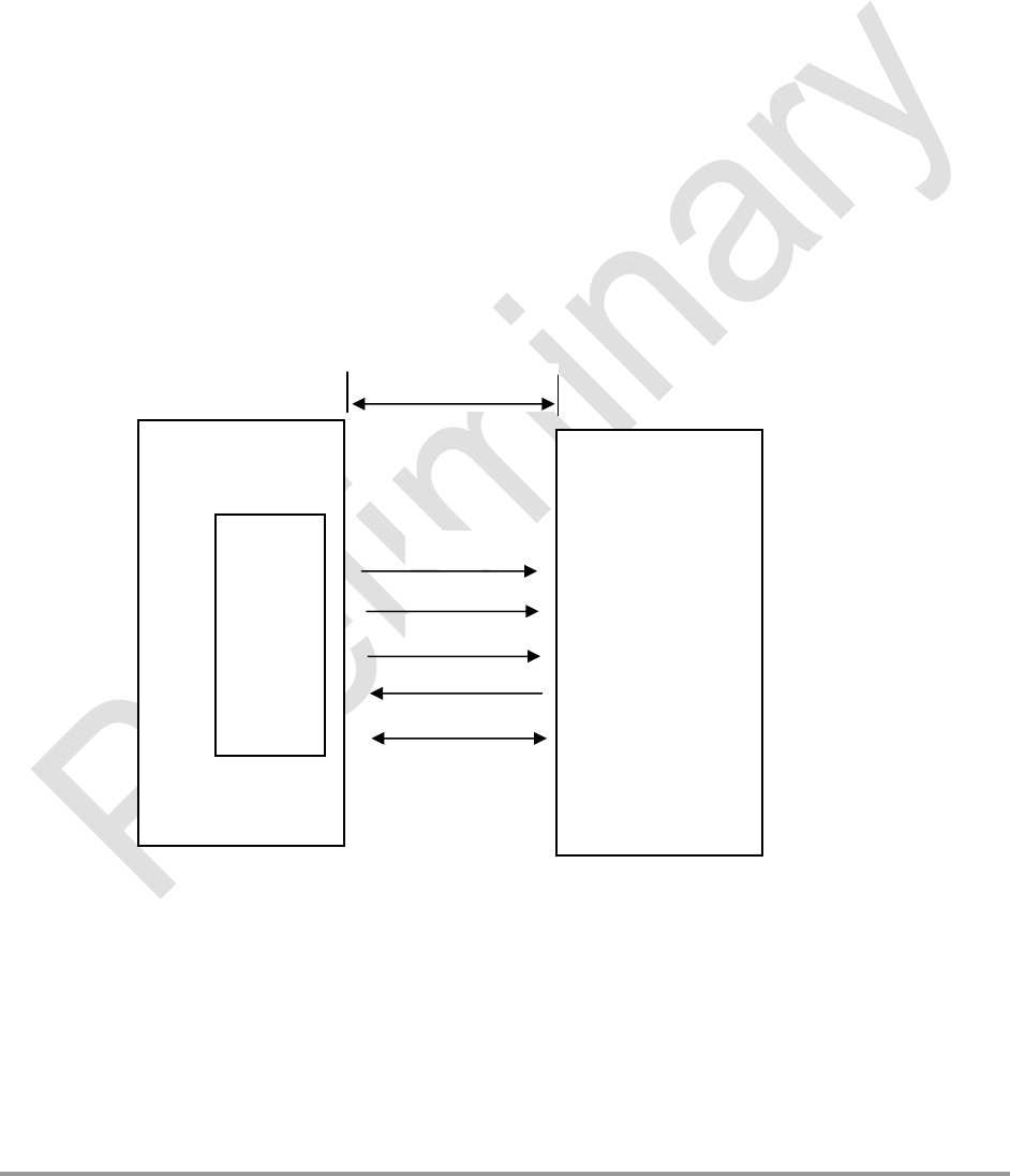
4.5.1.4. Vbat Input
The Enabler Vbat input can have a relative high current draw that can fluctuate rapidly,
especially when transmitting at max power and burst mode. The Vbat interface must be
designed to provide the required instantaneous voltage and current with minimal voltage
droop. This includes both sufficient bulk decoupling capacitance as well as adequate layout
provisions.
Similar to the discussion on thermal relief, the use of narrow traces to connect the Vbat pins
to the source voltage can act like a high impedance and cause a significant voltage droop
when higher currents are required as shown in Figure 4. If the Vbat drops too low, the
Enabler modules will reset. To minimize the trace loss, it is suggested to use a larger trace
that spans several pins. The layout should provide sufficient trace width over the entire trace
from the Enabler module all the way to the source of the Vbat voltage. Any transitions
between layers for this trace should utilize multiple vias.
Figure 4 - Example of Vbat Voltage Droop
Two 470 uF, low ESR, tantalum capacitors are included in the design to provide decoupling
of Vbat input voltage. Bulk decoupling capacitance is not required at the Vbat input external
to the Enabler module.
LPP0108IG001 17 Version - Preliminary – 06/20/08
4.5.2. Audio Reference Design
The audio quality is very dependent on the circuit design and layout. As an aid to obtaining good
audio quality, a reference design has been included below. It has been proven to provide good
performance on the SDK module.
4.5.2.1. Audio Schematics
Figure 5 - Audio Reference Design Schematic
4.5.2.2. Audio Layout
Layout plots for the audio section of the SDK are available upon request.
4.6. Handling and Soldering Guidelines
The guidelines presented in IPC/JEDEC J-STD-020C for handling, preparation, and reflow of
lead-free devices should be applied to the Enabler LPP G module. Care should be taken to
minimize module moisture exposure before reflow. The module is classified as a Type 3 MSL
(moisture sensitivity level).
Additional information forthcoming
LPP0108IG001 18 Version - Preliminary – 06/20/08
5. Technical Specifications
5.1. Enabler LPP G Module Block Diagram
50 pin edge connector
LPP0108 Module
Locosto/Triton Lite
Power Regulation
MSP430
GPS
TI 5350
(I2C mode)
16.368 MHz
TCXO
SIM
GSM Antenna
GPS Antenna
Battery
Motion Sensor
Serial Host Interface
Enfora
debug
interface
VIO
Reset
Handset Audio
Figure 6 - Enabler LPP G Module Block Diagram

LPP0108IG001 19 Version - Preliminary – 06/20/08
5.2. Detailed Product Specifications
Physical Dimensions and Weight
Size (L x W x H) 38.5 mm x 33.6 mm x 4.19 mm
Weight < 8.6 grams
Climatic: Operational
GSM Compliant temperature
Operating temperature
-20°C to +60°C
-30°C to +70°C
Relative humidity
5 - 95%
Air pressure (altitude) 70 kPa to 106 kPa (-400 m to 3000 m)
Climatic: Storage and Transportation
Duration 24 months
Ambient temperature -40°C to +85°C
Relative humidity 5% to 95%, non condensing (at 4C)
Thermal shock -50°C to +23°C, +70°C to +23°C; < 5 min
Altitude -400 m to 15,000 m
Mechanical: Operational
Operational vibration, sinusoidal 3.0 mm disp, 2 to 9 Hz; 1 m/s
2
, 9 to 350 Hz
Operational vibration, random 0.1 m
2
/s
3
, 2 to 200 Hz
Mechanical: Storage and Transportation
Transportation vibration, packaged ASTM D999
Drop, packaged ASTM D775 method A, 10 drops
Shock, un-packaged 150 m/s
2
, 11 ms, half-sine per IEC 68-2-27
Drop, un-packaged 4-inch drop per Bellcore GR-63-CORE
Mechanical: Proposed Standards
Transportation ETSI Standard ETS 300 019-1-2 Class 2.3
Transportation
Operational ETSI Standard ETS 300 019-1-3 Class 3.1
Operational
Storage ETSI Standard ETS 300 019-1-1 Class 1.2
Storage
Electromagnetic Emissions
Radiated spurious FCC Part 22 & 24 / Part 15 Class \ B
3GPP TS 51.010-1 Section 12.2
EN 55022 Class B
LPP0108IG001 20 Version - Preliminary – 06/20/08
5.3. Operating Power
The Enfora Enabler LPP G module requires an input voltage of 3.3 Vdc to 4.5 Vdc.
5.3.1. Typical Input Current
Test Conditions:
Typical Results @ 3.8V, 20 deg C, terminated into a 50 load.
GSM Operation Input Current
Band Mode Low Nom/Avg High/Peak Units
1900
1 RX/1 TX, Full Power
21 240 1180 mA
1800 21 245 1280 mA
900 21 287 1600 mA
850 21 265 1600 mA
ALL Idle 6.5
GPRS Operation Input Current
Band Mode Low Nom/Avg High/Peak Units
1900
4 RX/1TX, Full Power 15 269 1180 mA
2 RX/2TX, Full Power 15 375 1180 mA
1 RX/1TX, Full Power 15 227 1180 mA
1800
4 RX/1TX, Full Power 15 271 1280 mA
2 RX/2TX, Full Power 15 381 1280 mA
1 RX/1TX, Full Power 15 230 1280 mA
900
4 RX/1TX, Full Power 15 313 1600 mA
2 RX/2TX, Full Power 15 473 1600 mA
1 RX/1TX, Full Power 15 274 1600 mA
850
4 RX/1TX, Full Power 15 300 1600 mA
2 RX/2TX, Full Power 15 455 1600 mA
1 RX/1TX, Full Power 15 264 1600 mA
ALL Idle
7.3
mA
5.3.2. GSM Transmit Power
Enfora Enabler LPP G module Power Class Transmit Powe
r
1900 MHz
1800 MHz
GSM Power Class 1 1-W conducted power maximum (30
dBm +/- 2 dB), measured at the
antenna port
850 MHz
900 MHz
GSM Power Class 4 2-W conducted power
maximum (33 dBm +/- 2 dB),
measured at the antenna port
LPP0108IG001 21 Version - Preliminary – 06/20/08
5.3.3. GSM Receiver Sensitivity
Enfora Enabler LPP G module Sensitivity Mode
1900 MHz
1800 MHz -106 dBm (typical) GPRS Coding Scheme 1 (CS1)
900 MHz
850 MHz -106 dBm (typical)
GPRS Coding Scheme 1 (CS1)
6. Physical Interfaces
(Dimensions are in millimeters.)
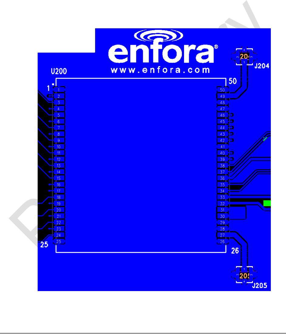
Figure 7 – Side and Front of Module with Pin 1 reference
Pin 1
LPP0108IG001 22 Version - Preliminary – 06/20/08
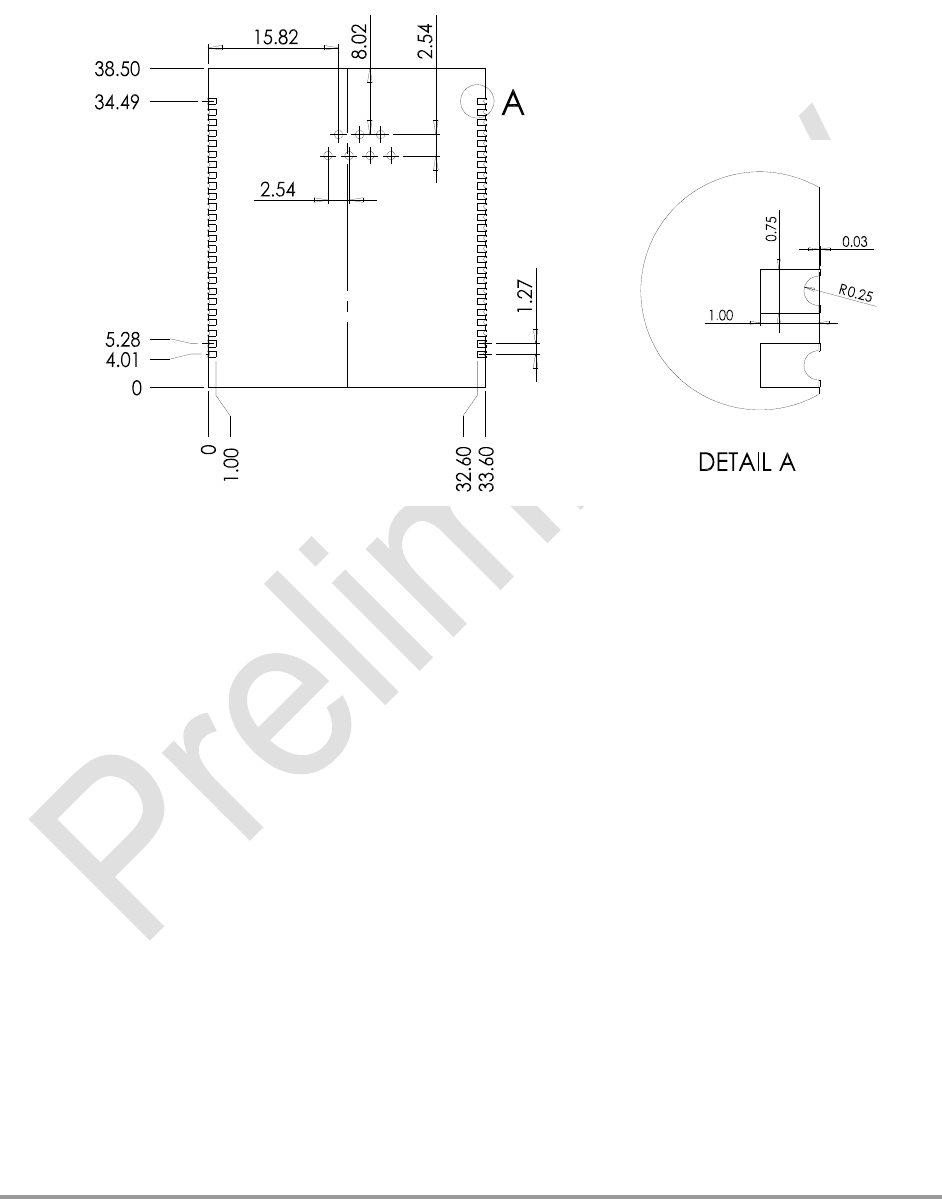
6.1. Module Mounting to Host Board (Reference)
Figure 8 - Module Footprint
LPP0108IG001 23 Version - Preliminary – 06/20/08
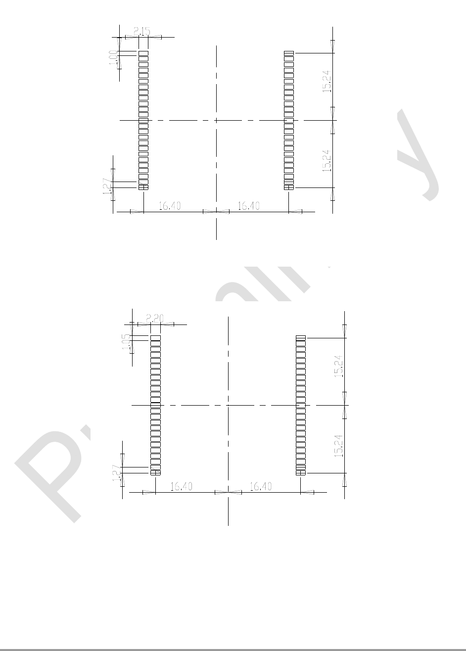
Figure 9 - Copper PADs (Recommended)
Figure 10 - Solder Mask (Reccomended)
LPP0108IG001 24 Version - Preliminary – 06/20/08
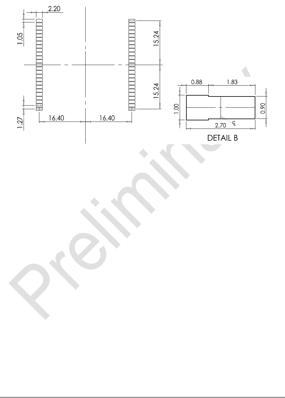
Figure 11 - Paste Mask (Reccomended) based on 0.004” stencil.

LPP0108IG001 25 Version - Preliminary – 06/20/08
6.2. I/O Pin Assignments
The following table shows the pin assignments for the input/output connector.
Pin # I/O Enabler LPP G Description/Comments (Default Function /
Secondary Function
1 P GND System Ground
2 R BATT_TEMP Battery Temperature Input
3 P BATT_ID Battery Identification Input
4 I POWER ON/OFF Power ON/OFF control Input
5 O STATUS Power ON/OFF status Output
6 Reserved
7 Reserved
8 Reserved
9 Reserved
10 I GPI1 General Purpose INPUT 1
11 I GPI2 General Purpose INPUT 2
12 O GPO1 General Purpose OUTPUT 1
13 O GPO2 General Purpose OUTPUT 2
14 Reserved
15 Reserved
16 Reserved
17 O MSP_UART_TX UART Serial Data Output From Module
18 I MSP_UART_RX UART Serial Data Input To Module
19 O GPS_TX UART Serial Data Output (NMEA data only)
20 Reserved
21 Reserved
22 Reserved
23 Reserved
24 I MSP_RESET Reset Input
25 R GND System Ground
26 R GND System Ground
27 O GSM_RF_ANT GSM RF Output
28 R GND System Ground
29 R GND System Ground
30 P
V
BAT_GSM Power for GSM radio
31 P
V
BAT Power for non-GSM systems
32 PWR
V
IN Battery Charger input power supply
33 O
V
IO 2.2 / 3.3 VDC Output
34 I
/
O USB_D- USB Data Bus (negative Terminal)
35 I
/
O USB_D+ USB Data Bus (Positive Terminal)
36 I USB_VBUS USB Power Supply Line
37 O EAR+ Earphone amplifier positive output
38 O EAR- Earphone amplifier negative output
39 I MIC+ Microphone amplifier positive input (Handset)
40 I MIC- Microphone amplifier negative input (Handset)
41 R GND System Ground
42 O SIM_RESET SIM Card Reset
43 I/O SIM_CL
K
SIM Card Reference Clock
44 I/O SIM_IO SIM Card I/O Data
45 PWR SIM_VDD SIM Output Voltage 1.8 V / 2.85 V
46 I SIM_DETECT SIM Card Detect
47 R GND System Ground
48 R GND System Ground
49 O GPS_RF_ANT GPS RF Output
50 R GND System Ground
Table 3 - Enabler LPP G Pin Assignments
LPP0108IG001 26 Version - Preliminary – 06/20/08
I = Input into Module P = Power Input to Module I/O = Input/Output to/from Module
O = Output from Module R = Power Return from Module PWR = Other Power
6.3. Circuit Protection
Other than very low level ESD protection within the module’s integrated circuits, the module does
not have any protection against ESD events or other excursions that exceed the specified
operating parameters.
Generally, ESD protection (typically TVS/Transorb devices) should be added to all signals that
leave the host board. This includes VBAT/VCC.
Series resistors (typically 47) can also be added in series with data lines to limit the peak
current during a voltage excursion.
NOTE: DO NOT ADD SERIES RESISTANCE TO THE SIM ELECTRICAL LINES.
Minimum ESD Protection Levels ESD/Input Voltage
Pin #’s ESD Test Method High/
Peak Units
Pins 4-16, 17,
18, 19, 34, 35
Human Body Model
EIA/JEDEC22-A114-A
500 V
Charge Device Model
EIA/JEDEC22-C101-A
200 V
Pins (all
VBUS/PWR),
37, 38, 42, 43,
44, 46
Human Body Model
EIA/JEDEC22-A114-A
2000 V
Charge Device Model
EIA/JEDEC22-C101-A
500 V
RF Antenna IEC 61000-4-2 8000 V
Table 4: ESD Protection Levels
Caution – It is the Integrator’s responsibility to protect
the Enabler LPP G module from electrical disturbances
and excursions, which exceed the specified operating
parameters.
LPP0108IG001 27 Version - Preliminary – 06/20/08
6.4. Power Button and Status LED
The power button is polled once per second. Once the power button press is detected, the
signal is debounced using Timer A. The button must be held for three (3) seconds to deactivate
the device. Once sufficient button press and hold occurs, the status LED is enabled for three (3)
seconds. If the modem is on at the time of deactivation, the status LED on-time is extended until
the modem turns off. Next the system enters LPM4 mode and the unit is deactivated.
The MSP exits LPM4 mode when the button is pressed again. The button signal is debounced
again using Timer A. The button must be held for three (3) seconds to activate the device. If the
button is not held long enough, the system re-enters LPM4. Once sufficient button press and
hold occurs, the status LED blinks (four times per second) for three seconds. The system is now
activated.
6.5. Antenna
The LPP0108 module has two RF antenna connections. One connection is for the GSM
section of the module and the other for GPS. Please be sure to follow proper RF design
practices when designing the antennas.
6.5.1. GSM
A GSM antenna should be designed from proper RF design practices.
6.5.2. GPS
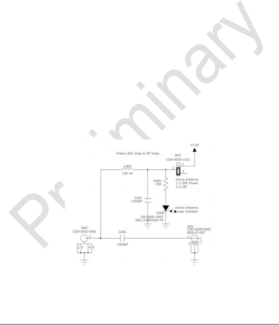
The GPS_ANT is the RF connection from the GPS antenna; no external LNA is required. The
LPP0108 can support both passive and active GPS antenna. However, external power supply
and circuitry is required for an active GPS antenna. See Figure 12 - GPS Antenna Sample
Schematic
Figure 12 - GPS Antenna Sample Schematic
Active antenna is enabled by placing a jumper on J403 in the sample schematic between pins
1 and 2.

LPP0108IG001 28 Version - Preliminary – 06/20/08
Passive antenna is enabled by placing a jumper on J403 in the sample schematic between
pins 2 and 3.
LPP0108IG001 29 Version - Preliminary – 06/20/08
6.6. Control Connector Signal Descriptions and Functions
6.6.1. Module Power (Pins 30, 31)
The Enfora Enabler LPP G module uses a single voltage source of VCC=+3.3V to 4.5V.
(The exact values of the uplink currents are shown in the tables in section 5.3.1.)
VBAT Parameter/Conditions Min Typ Max Units
Main Battery Supply
Voltage In Regulation 3.3 4.5 Vdc
Peak Current 970
F (2 x 470 uF) on Host
at Module Connector
mA
Please note that the following descriptions are intended to
provide hardware-level definitions. In some cases, specific
lines will have no firmware functionality implemented.
Information for each hardware-specific feature will be noted
in the appropriate section.
The uplink burst will cause strong ripple on the voltage
lines and should be effectively filtered.
External capacitance is not typically required by low current
or extended life applications. However, if capacitance is
added, then current leakage of the capacitor needs to be
taken into consideration for these types of applications.
It should be noted that the input voltage level should not
drop below the minimum voltage rating under any
circumstances, especially during the uplink burst period.

LPP0108IG001 30 Version - Preliminary – 06/20/08
6.6.2. On/Off Signal (Pin 4)
The module may be set into a low power ‘off’ mode by pulling the pin low for a minimum of 3 seconds.
This will shutdown any active functions including GPS and GSM, and stop the processor. This is the
lowest power mode of the module, it can be ideally used when storing or shipping units and the controller
is not to be enabled.
Once the module is in the ‘off’ state, it can be turned ‘on’ by holding the pin low for a minimum of 3
seconds. This will start the processor, once booted the controller will be enabled and run as per the
saved settings.
The module will normally start in the ‘on’ state and enable the controller logic when power is applied.
6.6.3. On/Off Status (Pin 5)
When the On/Off pin is used to put the modem into an ‘off’ state or to turn it ‘on’, the status pin will
indicate when it has successfully entered either state.
When turning off the unit, the status signal is set high after the On/Off signal is sufficiently held low (3
seconds). The status signal is held high for normally 3 seconds but can stay enabled for up to 5-6
seconds if the system is waiting for the GSM modem to shut down.
When turning on the unit, the status line blinks for 3 seconds at a frequency of 4Hz.
6.6.1. General Purpose Input Signals (Pins 10, 11)
Two input pins are available for input and are configured in conjunction with the event engine of the GSM
modem. The voltage level of the signal must be in reference to the selected VIO voltage (Pin 33).
6.6.1. General Purpose Output Signals (Pins 12, 13)
Two input pins are available for output signals and are configured in conjunction with the event engine of
the GSM modem.
The voltage level of the signal must be in reference to the selected VIO voltage (Pin 33).
6.6.2. Reset Signal (Pin 24)
The Reset signal is used to force the micro-controller to start at a known state. When the Reset is pulled
low the micro-controller will immediately suspend any function and will not exit the reset state until the
reset signal is released to be pulled high. Once the transition from low to high is complete, the micro-
controller will boot. The Reset signal is falling edge triggered, so the reset function is set immediately
when the signal is pulled low.
When using Reset, it will immediately lose the connection to the GSM network, this is not considered
ideal. Typically during a normal shutdown, the module will issue a detach request to the network to
indicate that it is being removed.

LPP0108IG001 31 Version - Preliminary – 06/20/08
Parameter Parameter/Conditions Vcc MIN TYP MAX UNIT
VIL Input Voltage – Low or float 2.2V/3 V Vss Vss+0.6 Vdc
VIH Input Voltage – High 2.2V/3 V 0.8*Vcc Vcc Vdc
Reset
Pulse
Duration
2 µS
6.6.3. USB (Pins 34, 35, 36)
This is for Enfora Debug only
5V Tolerant Transceiver
USB Parameter/Conditions Min Typ Max Units
Input Voltage 4.4 4.65 5.25 V
Output voltage High (Driven) 2.8 3.3 3.6 Vdc
Low 0.0 0.1 0.3 Vdc
Transceiver D+/-
Leakage Current
-2 2 A
Pin Name Pin
Number Signal
Direction Description
USB_VBUS 36 In 5 V tolerant power Supply VBUS line;
Used only as a USB sense, not for powering the
module. (optional connection)
USB_DP 35 Analog
I/O
5 V tolerant data plus pin in USB
USB_DM 34 Analog
I/O
5 V tolerant data minus pin in USB
LPP0108IG001 32 Version - Preliminary – 06/20/08
6.6.4. Serial Interfaces
6.6.4.1. Main Serial Interface (Pins 17, 18)
The pin naming for TX/RX is referenced as a DTE. The DTE device should match their input pins
to the Enfora outputs and vice-versa.
9 way D
Connector Pin
Number
Signal Signal
Direction Enfora Pin
Number Enfora
Module
Signal
Direction
1 N/A
2 Receive Data (RD) from DCE 18 Input
3 Transmit Data (TD) from DTE 17 Output
4 N/A
5 Signal Ground both
6 N/A
7 N/A
8 N/A
9 N/A
The key features of the UART in the Enabler LPP G module mode are as follows:
16C550 compatibility
Baud rate 115200 Kbits/s
Data format:
Data bit: 8 bits
Parity bit: none
Stop bit: 1bit
Flow Control: None

LPP0108IG001 33 Version - Preliminary – 06/20/08
6.6.4.2. GPS Serial Interface (Pin 19)
It is optional as to whether something should be connected to the RS232 GPS DEBUG OUT.
If streaming NMEA messages are needed for external processing, above and beyond the
NMEA sent to the server, then a serial cable can be connected between this serial connector
and a PC. The baud rate is fixed at 19200.
9 way D
Connector Pin
Number
Signal Enfora Pin
Number Enfora
Module
Signal
Direction
1 N/A
2 Transmit Data (TD) 19 Output
3 N/A
4 N/A
5 Signal Ground
6 N/A
7 N/A
8 N/A
9 N/A
The key features of the UART in the Enabler LPP G module mode are as follows:
Baud rate 19200 Kbits/s
Data format:
Data bit: 8 bits
Parity bit: none
Stop bit: 1bit
LPP0108IG001 34 Version - Preliminary – 06/20/08
6.6.5. Handset Microphone Input (Pins 39, 40)
The handset differential inputs MICIP and MICIN can be amplified by the differential handset
microphone amplifier. This amplifier has a gain of 25.6 dB.
Handset Mic Input Parameter/Conditions Min Typ Max Units
Maximum Input Range –
Mic(+) to Mic(-)
Inputs 3 dBm0 (Max. digital
sample amplitude when PGA
gain set to 0 dB)
32.5 mVRMS
Nominal Ref. Level –
Mic(+) to Mic(-)
Differential MIC
-10 dBm0
Differential Input
Resistance –
Mic(+) to Mic(-)
Differential MIC, MICAMP gain
= 25.6 dB
(INMODE = 0001)
36 k
Microphone Pre-
Amplifier Gain
Differential MIC
25.6 dB
6.6.6. Handset Speaker Output (Pins 37, 38)
Pin Name Pin Number Signal Direction Description
EARP 37 O Earphone positive output
EARN 38 O Earphone negative output
The earphone amplifier provides a full differential signal on the terminals EARP and EARN (Earphone).
Handset Spkr Output Parameter/Conditions Min Typ Max Units
Maximum Differential
Resistive Load
Output Swing 3.9 VPP 120
Output Swing 1.5 VPP 33
Maximum Differential
Capacitive Load
100 pF
Common Mode
Minimum Resistive Load
At Internal Speaker (+) or (-) 200 k
Common Mode
Maximum Capacitive
Load
At Internal Speaker (+) or (-) 50 pF
Amplifier Gain EARG = 1
EARG = 0
1
-11
DB
dB

LPP0108IG001 35 Version - Preliminary – 06/20/08
Parameter Test Conditions Min Typ Max Units
Earphone output swing at
EARP-EARN
Distortion 2% and 120 , VSP input
level = +3 dBm0, amp gain = -11 dB
0.98 VP-P
Distortion 2% and 33 , VSP input level
= -5.34 dBm0, amp gain = -11 dB
0.38
Distortion 2% and 120 , I2S input level
= +3 dBm0, amp gain = -11 dB
0.93
Distortion 2% and 120 , VSP input
level = +3 dBm0, amp gain = 1 dB
3.1 3.92
Distortion 2% and 33 , VSP input level
= -5.34 dBm0, amp gain = 1 dB
1.2 1.5
Distortion 2% and 120 , I2S input level
= +3 dBm0, amp gain = 1 dB
2.96 3.7
Earphone amplifier state in
power down
High
Z
Earphone amplifier power
supply rejection
1 kHz, 100 mVp-p
50
dB
An external audio amplifier should be used for loads of less than 16 or if volume is inadequate.
6.7. Subscriber Identity Module (SIM) (Pins 42, 43, 44, 45, 46)
The SIM, an integral part of any GSM terminal device, is a “smart card” that is programmed with
subscriber information:
The user information consists of an International Mobile Subscriber Identity (IMSI)
number, which is registered with the GSM provider, and an encryption Ki (pronounced
"key"). This information consists of a microprocessor and memory installed on a plastic
card.
Note: The SIM is not provided with the Enfora Enabler LPP G module. The SIM must be
obtained from the GSM service provider and must be provisioned by the operator for data
and/or voice. Always take care to protect the SIM: the GSM terminal will not operate without
the SIM installed.
The SIM provides the IMSI for authentication. To gain access to the GSM network, the network
must recognize the IMSI number, and the terminal must be able to properly decrypt the data sent
by the network. The SIM also serves as a buffer for SMS messages, storing the message for
transmission until a radio link is available and buffering received messages until retrieved.
LPP0108IG001 36 Version - Preliminary – 06/20/08
6.7.1. Using a Remote SIM with the Enfora Enabler LPP G Module (Pins 42, 43, 44, 45, 46)
The Enabler LPP G module does not include an on-board SIM carrier.
The module supports the use of 1.8 V and 3 V SIM cards. The module includes a hardware
interface module dedicated to Universal Subscriber Identity Module (USIM). All baud-rates
defined in ISO 7816-3 standard are supported for high-speed transmission.
The integrator must provide a suitable SIM connector.
The maximum distance from the module to the remote SIM connector must not exceed
25.4 cm (10 inches).
It is recommended to have Zero resistance between the SIM connector and the module.
External ESD Protection is Required;
15 kV Air Discharge;
8 kV Contact Discharge;
The transorb must have a low junction capacitance (typically < 10 pf) such as the following part:
Manufacturer: On Semi
Manufacturer PN: NSQA6V8AW5T2G
Figure 13 - Remote SIM Interface
SIM
_
CLK
25.4 cm (10 in max)
SIM
_
I/O
SIM
_
RST
SIM
_
VDD
Enabler LPP G
module
SIM
Interface
Remote SIM
SIM
_
DTC

LPP0108IG001 37 Version - Preliminary – 06/20/08
The module provides the regulated supply voltage for the SIM-card and the circuitry to detect the insertion
or extraction of the SIM-Card in or from the mobile.
The SIMDTC is disabled by default (see AT$SIMDTC in the EIII AT Command Manual for settings).
When enabled, the SIMDTC pin has an internal pull up to Vcc and can be configured to detect a SIM
insertion when the SIMDTC is either pulled to ground or left floating.
It can configured to detect either just a SIM removal or both removal and insertion.
When the module detects a SIM removal, it will de-register from the network. When the module is
configured to and detects a SIM insertion, it will reset the module and re-register on the network.
The SIM-card presence detection logic is active even when the system is in idle model.
USIM Parameter/Conditions Min Typ Max Units
VDD SIM VDD voltage 1.8V
3.3V
1.64 1.8 1.96 V
2.7 2.85 2.95 V
VIH High level input voltage 1.15 V
VIL Low level input voltage 0.61 V
VOH High level output voltage, IO = 4 mA Vdd-0.45 V
VOL Low level output voltage, IO = 1 mA 0.4 V
II Input leakage current ±1 A
Iout Output current 4 mA
PU PU resistance 32 k
PD PD resistance 30 k
Iz Leakage current ± 30 A
Card
Detect
Debouncing time (SIM-card insertion) 0.5 mS
Debouncing time (SIM-card extraction) 15 mS
Pull-up resistor (resistor + resistive switch) 475 k
6.7.1.1. Remote SIM Component Information
Any compatible SIM carrier can be used in conjunction with the Enabler LPP G module. For
example:
Lumberg P/N 8840_A_21.
or
Suyin P/N: 254016MA006G103ZL
Pin Name Pin Number Signal Direction Description
SIM_VDD 45 O SIM VDD
SIM_CLK 43 O Card Reference Clock
SIM_RST 42 O Card Reset
SIM_I/O 44 I/O Card I/O Data
SIMDTC 46 I Card detect

LPP0108IG001 38 Version - Preliminary – 06/20/08
7. Battery Charging Calibration and Configuration
7.1. Objective
The objective of this document is to outline how to configure the Enabler LPP G based battery charger for
specific batteries and chargers.
7.2. Supported Devices
Enabler LPP G
7.3. References
LPM0108AT001- Enabler LPP G AT Command Set
7.4. List of battery charging commands
The following is a list of Locosto/Triton-Lite battery charger AT commands, and who is responsible for
setting their parameters.
Enfora should set the default parameters so the overall charging scheme will work “out-of-the-box”.
However, it is the customer’s responsibility to configure the charging scheme to conform to their particular
battery(-ies) and charger(-s).
Command Information Calibrated
by Enfora Calibrated by
Customer Set by
Enfora Set by
Customer
AT$BAT X
AT$BCIDBG X
AT$BCIMNI X
AT$BCIN4A X (internal
only)
AT$BCIVSF X Opt.
AT$BCIISF X
AT$BCIAVG X Opt.
AT$BCIMAP#
(1,2,3,4,5)
X X
AT$BCIPCT#
(1,2,3,4,5)
X Opt.
AT$BCICHG#
(1,2,3,4,5)
X
AT$BCIBAT#
(1,2,3,4,5)
X
AT$BCITMP#
(1,2,3,4,5)
X
AT$BCIDEL X
AT$BCIOFF X

LPP0108IG001 39 Version - Preliminary – 06/20/08
7.4.1. Setting BCIVSF parameters
BCIVSF sets the scaling factor so the battery voltage reported by the Triton-Lite matches the real battery
voltage on the Vbat pin. This one-time calibration should be done at module production.
7.4.2. Equipment required
Programmable power supply with <10mV resolution and voltage sense lines.
A notebook or desktop computer with any version of Microsoft Windows that has the
HyperTerminal communications program. If this hardware is not available, the user could use a
DOS terminal emulation program.
7.4.3. Procedure
This procedure assumes an appropriate test fixture is used.
1. Disconnect battery (if connected), and connect power supply to Vbat test point.
2. Perform the following procedure:
Action Command Power
supply Calculation
1 Set power supply On, Voltage =
3700mV
2 Establish serial
communications with
device
3 Fill in default values.
This reads in the
parameters without
changing their values.
AT$BCIAVG=,
AT$BCIVSF=,
AT$BCIISF=,
4 Set voltage averaging to
0. Note original value for
later.
AT$BCIAVG=0,5,10,10000
5 Preset voltage scaling to
<num>=1700 and
<offset>=0.
AT$BCIVSF = 1700,0
6 Disable charging. AT$BCIOFF=1
7 Ensure State=3(SUP). AT$BCIDBG=2,0
8 Read Vbat (mV) after
trace update.
Vbat(mV)=xxxx
9 Calculate <new_num> <new_num> =
1700*3700 /
Vbat(mV)
10 Set voltage scaling factor AT$BCIVSF = <new_num>,0
11 Verify results after trace
update.
Vbat(mV)=3700
+/-10mV
12 Restore settings AT$BCIAVG=<previous>,5,10,10000
AT$BCIOFF=0
AT$BCIDBG=0,0
Off
Note: The values that are red indicate the values that will need to be set.

LPP0108IG001 40 Version - Preliminary – 06/20/08
7.4.4. Setting BCIISF Parameters
The charging current calibration requires measuring the current at 2 levels and determining the
adc_num and adc_offset based on the physical currents (Iphy) and reported charging currents
(Ichg_avg_mA). Two points are required to get accurate calibrations at both the high and low current
levels.
7.4.5. Scope
This calibration does not need to be done as part of a factory level production test on every device,
default values can be used to get ballpark readings. Customer level calibration is required if the
battery charge current and end-of-charge current are critical.
7.4.6. 6.2 Equipment required
1. Battery simulator, or mostly discharged battery.
2. Power supply with capability to measure current, 5-12V, 1A, to emulate wall charger. Agilent
3. A notebook or desktop computer with any version of Microsoft Windows that has the HyperTerminal
communications program. If this hardware is not available, the user could use a DOS terminal
emulation program.
7.4.7. 6.3 Calibration procedure
Step Action Command Power supply Calculation
1 Turn off
automatic
registration
AT+CFUN=0
AT$AREG=0
VPS=3.700V
VBATSIM=5.000V
2 Normalize
slope and
offset.
AT$BCIISF=800,0
3 Set voltage
averaging to
0. Note
original value
for later.
AT$BCIAVG=5,5,0,10000
4 Verify
charging state
4(LCI) and
charger #.
AT$BAT= 40,1,#,4,3956,839
Note: # must be 2,3,4, or 5.
Assumed 2 for the remainder of this
procedure
5 Set charging
current, low
AT$BCICHG2=
1,32,7450,4725,5725 3,4
6 Cycle
charging so
charge
current will
take effect.
AT$BCIOFF=1
AT$BCIOFF=0
7 Measure
power supply
current
Read IBATSIM
current.
Iphy1
8 Record
reported Ichg,
after update.
AT$BAT= 40,1,2,4,3956,<Ichg1> Ichg1
9 Set charging
current, high
AT$BCICHG2=
1,250,6050,4725,5725 3,4
10 Cycle AT$BCIOFF=1

LPP0108IG001 41 Version - Preliminary – 06/20/08
charging so
charge
current will
take effect.
AT$BCIOFF=0
11 Measure
power supply
current
Read IBATSIM
current.
Iphy2
12 Record
reported Ichg,
after update.
AT$BAT= 40,1,2,4,3956,<Ichg2> Ichg2
13 Calculate
<adc_num>,
<adc_offset>
Note 1
Note 2
14 Set scaling
factors
AT$BCIISF=<adc_num>,<adc_offset>
15 Verify results. AT$BCICHG2=
1,32,6050,4725,5725
AT$BCIOFF=1, AT$BCIOFF=0
AT$BAT= 40,1,2,4,3956,<Ichg1> Read IBATSIM
current.
Iphy1=Ichg1
16 Verify results. AT$BCICHG2=
1,250,6050,4725,5725
AT$BCIOFF=1, AT$BCIOFF=0
AT$BAT= 40,1,2,4,3956,<Ichg2> Read IBATSIM
current.
Iphy2=Ichg2
17 Set final value AT$BCICHG2= 1,x,6050,4725,5725
18 Restore
settings
AT$BCIAVG=x,x,<previous>
AT+CFUN=1
AT$AREG=1
AT$RESET
Notes:
1. )21(
800)21(
_IchgIchg
IphyIphy
numadc
2. 1
800
_
1_ Ichg
numadc
Iphyoffsetadc
3. The strategy for production level calibration is to set an arbitrary low and high charge currents
that will optimize accurate Ichg readings in most charging applications.
4. The strategy for customers in setting the low and high charging currents is to calibrate at the two
most important points in the charge process, <ci_chgireg> and <IEOC>, thus ensuring the state
transitions are accurate. <ci_chgireg> and <IEOC> are determined once as a system-level design.
<ci_chgireg> = [0 to 255] such that the Ichg = Isys + 1*C (800mA max.). <IEOC> =Isys + C/20. For
example, if the battery capacity is 1980mAh and the system current is 50mA, Ichg = 50+1980 =
2030mA => 800mA. <chgireg1>=255. <IEOC> =Isys + C/20 = 50+1980/20 = 149mA.
Note: In the above example you will receive 2030mA as the answer. The physical limitation is
800mA.

LPP0108IG001 42 Version - Preliminary – 06/20/08
7.5. Setting BCIAVG parameters
Averaging of the voltage, temperature, and current readings is used to reduce noise or spikes that could
otherwise trigger ill-timed state changes or inaccurate readings. It is up to the user’s comfort level what
values should be set. Setting any alfa=0 my give readings that are too noisy, especially in the case of
current readings. Setting alfa to a very large number will cause state transitions to occur later than
desired while the averaging “catches-up”.
7.6. Setting BCIMAP# parameters
The BCIMAP# command sets the maps battery voltage and charge current to battery capacity while the
battery is charging. Each battery n may be given a unique BCIMAPn, depending on the battery ID (if
required). Battery capacity is reported as a percentage in 10% steps, no interpolation is given.
When the battery is not charging, BCIPCT# maps battery voltage to battery capacity.
7.6.1. Scope
Default values are intended to be sufficient for general-purpose applications. However, if the battery
capacity mapping needs adjustment for per customer specification, this procedure is one empirical
approach to determining new values.
Production-level calibration not required.
7.6.2. Procedure
The following summary outlines a procedure that requires one complete battery charge and discharge
to determine the battery capacity mappings.
Choose the BCIMAP# index.
Set the desired CI charge current <ci_chgireg> for the designated charger.
Determine the BCIMAP# values up to the <#_ci_elements>.
Determine the BCIPCT# that corresponds to the BCIMAP index.
Calculate the BCIMAP# values for the parameters above the index.
Discharge the battery, determine the remaining BCIPCT# parameters.
Repeat for each battery and charger.
7.6.3. Choose the BCIMAP# index
Select a BCIMAP# index, <#_ci_elements>, that gives good resolution of capacities in the CI
and CV stages of the charge cycle. If the index is too low, the CI stage will have fewer,
disproportionately large capacity steps, and the CV stage will have more, smaller capacity
steps. If the index is too high, the CI stage will have more, disproportionately small capacity
steps, and the CV stage will have fewer, larger capacity steps. From empirical analysis,
<#_ci_elements> = 7 ± 1
is a good balance giving proportional intervals between the capacity steps in both the CI and
CV stages.
LPP0108IG001 43 Version - Preliminary – 06/20/08
7.6.4. Set the desired CI charge current for the designated charger.
Determining the charge current for the constant-current charging stage now will make the
BCIMAP# <%> parameters more accurate. Typical limiting values are listed in the following
table:
Charger Max. charge current <ci_chgireg> [0-255]
USB charger 500mA 160
Wall charger Limited by Triton-Lite
maximum
255
Triton-Lite 800mA 255
Customer charger X Calculate
1
Note: <ci_chgireg> = [ 0.22 * (CI + ISYS) * 10 + 0 ] * 255 / 1750.
Max value is 255.
Determine the charger # and <ci_chgireg> for that charger.
Charger 1=BCICHG1 is dedicated for USB charging.
Chargers 2-5=BCICHG(2-5) are for any general purpose charger. Set with:
AT$BCICHG#=<type>,<ci_chgireg>,<ov_thr>,< id_low>,<id_high>
Reset or cycle charging with AT$BCIOFF to make new <ci_chgireg> take effect.
Example:
Suppose it is desired to have a USB charge at 100mA when it is the charging source and a
wall charger charge at 800mA when it is the charging source. The system nominal current
Isys=50mA.
<ci_chgireg1> = [ 0.22 * (100 + 50) * 10 + 0 ] * 255 / 1750 = 48
<ci_chgireg2> = [ 0.22 * (800 + 50) * 10 + 0 ] * 255 / 1750 = 272 => 255
AT$BCICHG1=<type>,48,<ov_thr>,< id_low>,<id_high>
AT$BCICHG2=<type>,255,<ov_thr>,< id_low>,<id_high>
7.6.5. Charge empty battery in constant current with target <ci_chgireg>.
Up to 5 different batteries can be independently defined with capacities using the BCIMAP#
and BCIPCT#.
1. Completely discharge the battery n that will be associated with the BCIMAPn and
BCIPCTn.
2. Plug in a charger.
3. When Vbat=3.2V, the Locosto powers on and the modem enumerates a port through
USB. Start logging a text file while the charge state is still precharge 1(PRE).
4. Type the following commands:
Command Detail
AT$BCIDBG=2,0 Start debug traces
AT$STOATEV=10,AT$BCIOFF=1
AT$STOATEV=11,AT$BCIDBG=2,0
AT$EVENT=10,0,85,6,6
AT$EVENT=10,3,44,10,0
AT$EVENT=10,3,44,11,0
Script to stop charging and report Vbat
when the CI-CV transition occurs.
5. Let the battery charge to the CI-CV transition and stop charging.
6. Stop the log file.
LPP0108IG001 44 Version - Preliminary – 06/20/08
7.6.6. Note the first Vbat(mA) that occurred after the charge stopped and went to 3(SUP).
Parameter Value (mV)
Vbat(mA)_at transition
Note the start and stop times of State 4(CCI). Calculate the time interval given the
<#_ci_elements> chosen earlier:
Parameter Value (hh:mm:ss)
TCI START
TCI STOP
Calculation Value (sec)
(TCI STOP- TCI START)/<#_ci_elements> TSTEP
Determine the BCIMAPn percentage parameters from the log file at the calculated times,
given the interval TSTEP:
BCIMAPn Parameter
1
Time (hh:mm:ss)
1
Vbat (mV)
1
<10%> TCI START + 1* TSTEP =
<20%> TCI START + 2* TSTEP =
<30%> TCI START + 3* TSTEP =
<40%> TCI START + 4* TSTEP =
<50%> TCI START + 5* TSTEP =
<60%> TCI START + 6* TSTEP =
<70%> TCI START + 7* TSTEP = 4200
2
Note: Assuming the <#_ci_elements>=7. Customer may choose different value from
section 7.6.3 above, and will have to adjust this table accordingly.
Note: End of CI charge should always be 4200mV for Li-Ion batteries.
Example:
The following graph shows what the resulting battery charge profile looks like, with the
BCIMAP capacity percentages determined from Vbat in the log file.
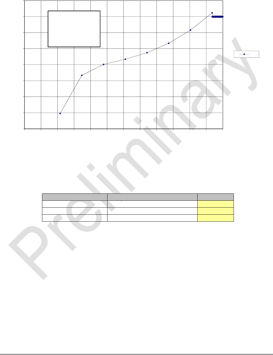
LPP0108IG001 45 Version - Preliminary – 06/20/08
7.6.7. Calculate the BCIMAP# values for the parameters above the index.
The remaining parameters are capacities determined from the Ichg current, since the battery
voltage is fixed at 4.200V and is no longer an indication of capacity.
BCIMAPn Parameter
1
Calculation Ichg (mA)
1
<80%> [(CI - IEOC) * 2/3] + Isys
2
<90%> [(CI - IEOC) * 1/3] + Isys
2
<100%> Isys + C/20 =
Note: Assuming the <#_ci_elements>=7. Customer may choose different value from
8.2.1 above, and will have to adjust this table accordingly.
Note: Linear interpolation will introduce a slight error in the capacity.
7.6.8. Discharge the battery, determine the remaining BCIPCT# parameters.
Determination of BCIPCT:
1. Start with a fully charged battery.
2. Monitor battery voltage over the full discharge cycle. This can done in-circuit or with a load.
In-circuit is preferred because it will give a better representation of the CI-CV transition point,
and the data can be logged to a text file. Discharging through a load will require a data-logger
to record the discharge voltage, and may not give a clear indication of the CI-CV transition.
3. Note the start and stop times of State 4(CCI). Calculate the time interval given the
<#_ci_elements> chosen earlier:
3.5953
3.8335
3.9015
3.9340
3.9746
4.0335
4.1158
4.2231
3.50
3.60
3.70
3.80
3.90
4.00
4.10
4.20
4.30
0
900
180
0
270
0
360
0
450
0
540
0
630
0
720
0
810
0
900
0
990
0
108
0
Voltage (V)
Time (sec)
Battery Charge
Constant Current Stage 4(CCI)
Vb
…
10%
20%
30%
40%
50%
60%
70%
Tstart = 1939 sec
Tstop = 10221 sec
<#_ci_elements> = 7
Tstep = 1183 sec
LPP0108IG001 46 Version - Preliminary – 06/20/08
Parameter Value (hh:mm:ss)
TDIS START
TDIS 70%
TDIS STOP (when Vbat=3200mV)
Calculation Value (sec)
(TDIS STOP- TDIS 70%)/<#_ci_elements> TSTEP LOW
(TDIS 70%- TDIS START)/(10-<#_ci_elements>) TSTEP HIGH
4. Determine the BCIPCTn percentage parameters from the logged data.
BCIPCTn Parameter
1
Time (hh:mm:ss)
1
Vbat (mV)
1
<100%> TDIS START
<90%> TDIS START + 1 * TSTEP HIGH =
<80%> TDIS START + 2 * TSTEP HIGH =
<70%>
1
Vbat(mA)_at
transition
<60%> TDIS 70% + 1* TSTEP LOW =
<50%> TDIS 70% + 2* TSTEP LOW =
<40%> TDIS 70% + 3* TSTEP LOW =
<30%> TDIS 70% + 4* TSTEP LOW =
<20%> TDIS 70% + 5* TSTEP LOW =
<10%> TDIS 70% + 6* TSTEP LOW =
Note: Assuming the <#_ci_elements>=7. Customer may choose different value from
section 7.6.3 above, and will have to adjust this table accordingly.
5. Set AT$BCIPCT5= <10%>,<20%>,<30%>,<40%>,<50%>, <60%>,<70%>,<80%>,
<90%>,<100%>
Example:
The following graph shows what the resulting battery discharge profile looks like
discharging through a constant load. BCIPCT capacity percentages determined from
Vbat readings spaced equally in time.

LPP0108IG001 47 Version - Preliminary – 06/20/08
Repeat for each battery (if multiple batteries of different capacities are to be used in the design).
7.7. Setting BCIBAT# parameters
7.7.1. Procedure to set the battery ID
1. Choose the bat_ID resistor (ohms) = RID from a table that maps battery capacity
range to a resistance.
2. Calculate the expected ADC reading. ADC4 = RID*.01*1023/1750.
3. Calculate <id_low> = (1023/1837.5) x (0.99 x RID) x 0.008 - 2; 0 if none
4. Calculate <id_high> = (1023/1662.5) x (1.01 x RID) x 0.012 +2; 1023 if none
5. Enter AT$BCIBAT#: <>,<>,<>,<>,<>,<>,<id_low>,<id_high>.
6. Enter AT$RESET: Reset the device, so changed parameters will take effect.
7. Read AT$BAT <>,<bat_id>.
8. Verify bat_id = # of the BCIBAT# corresponding to the range: <id_low>-<id_high>.
7.8. Setting BCITMP# parameters
7.8.1. Scope
Setting the BCITMP# parameters needs to be done by the customer, for each battery with a
thermistor installed. If no thermistor is installed in a battery, set all nine adc parameters to 0.
AT$BCITMP#=-20,60,0,0,0,0,0,0,0,0,0,30
This is a one-time system level design, no factory-level production test or calibration is required.
4.0215
100%
3.9131
90% 3.8300
80% 3.7667
70% 3.7154
60% 3.6785
50% 3.6515
40% 3.6307
30% 3.6017
20% 3.5589
10%
3.200
3.250
3.300
3.350
3.400
3.450
3.500
3.550
3.600
3.650
3.700
3.750
3.800
3.850
3.900
3.950
4.000
4.050
4.100
0
900
1800
2700
3600
4500
5400
6300
7200
8100
9000
9900
Voltage (V)
Time (sec)
Battery Discharge
w/constant load
Determination of BCIPCT# parameters
Vbat (V)

LPP0108IG001 48 Version - Preliminary – 06/20/08
7.8.2. Equipment required
Temperature chamber
Mostly discharged battery or battery simulator.
A notebook or desktop computer with any version of Microsoft Windows that has the
HyperTerminal communications program. If this hardware is not available, the user could use
a DOS terminal emulation program.
7.8.3. Procedure
This is a procedure for setting the AT$BCITMP# parameters, assuming a 10kohm NTC
temperature sense resistor is used.
Step Action Command Equip.
Setting Calculation
1 Set
temperature
averaging.
AT$BCIAVG=
<alfaV>,0,<alfaI>,<sampling>
(Note original value for later.)
2 Set current
to 30uA
AT$BCITMP#=-
20,60,x,x,x,x,x,x,x,x,x,30
3 Reset the
modem
AT$RESET
4 Start debug
traces
AT$BCIDBG=2,0.
5 Cycle
charger off,
on.
AT$BCIOFF=1,
AT$BCIOFF=0
6 Ensure
battery is
charging
4(CCI) mode or 6(CVI) mode VBAT <
4.2V
7 Set temp. Read Tbat=xxxx
(Note: This Tbat is a hex value
(Tbat)16).
TCH=-20C <adc@-20> = (Tbat)10
TCH=-10C <adc@-10> = (Tbat)10
TCH=0C <adc@0> = (Tbat)10
TCH=10C <adc@+10> = (Tbat)10
TCH=20C <adc@+20> = (Tbat)10
TCH=30C <adc@+30> = (Tbat)10
TCH=40C <adc@+40> = (Tbat)10
TCH=50C <adc@+50> = (Tbat)10
TCH=60C <adc@+60> = (Tbat)10
8 Set
temperature
parameters
AT$BCITMP#=-20,60,<adc@-20>,
<adc@-10>,<adc@0>,<adc@+10>,
<adc@+20>,<adc@+30>,<adc@+40>,
<adc@+50>,<adc@+60>,30
9 Restore
averaging
AT$BCIAVG=<alfaV>,<alfaT>,<alfaI>,
<sampling>
10 Reset the
modem
AT$RESET
11 Verify
temperature
readings
AT$BAT=<pct>,<bat_id>,<chg_id>,
<state>,<Vbat>,<Ichg>, <Tbat>
(Note: This Tbat is a decimal value
(Tbat)10).
TCH=-20C Tbat = TCH +/- 5C
TCH=25C Tbat = TCH +/- 5C
TCH=60C Tbat = TCH +/- 5C
Repeat procedure for AT$BCITMP2-AT$BCITMP5, as required.
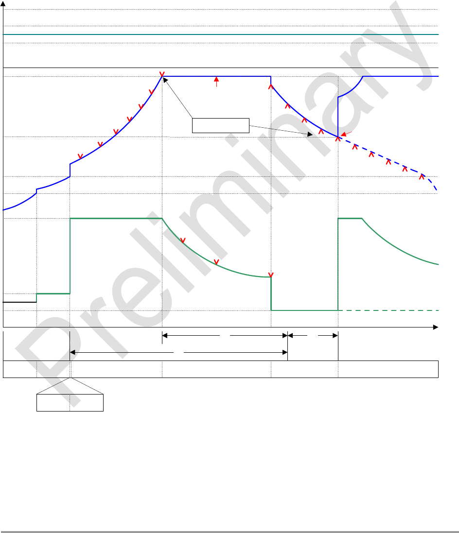
LPP0108IG001 49 Version - Preliminary – 06/20/08
4.2V
3.6V
3.2V
PRE 1(PRE) 4(CCI) 6(CCV) 3(SUP)
BAT OV Threshold
Recharge Curve
Discharge Curve
100%
90%
80%
70%
60% 50%
40% 30% 20%10%
90%
80%
70%, ci=7
60%
50%
40%
30%
20%
chg_again_thr
10%
100%
Isys
Iprechg
Iprechg
ci_chgireg
T1
T2 T3
STATE
2(INI) 3(SUP)
2.5V
cv_chgvreg
linked: recharge
ci/cv decision point
chg_ov_thr
chg_id_low
chg_id_low
Vchg
4.225V
7.9. Setting BCIDEL parameters
Self-explanatory. Customer may choose to delete chargers or batteries from the list.
7.10. Setting BCIOFF parameters
Self-explanatory. Customer may choose enable/disable the charging at any time.

LPP0108IG001 50 Version - Preliminary – 06/20/08
7.11. Battery Charging Calibration and Configuration - Appendix 1
Summary of all BCI commands and their parameters
General charging commands:
AT$BAT=<pct>,<bat_id>,<chg_id>,<state>,<Vbat>,<Ichg>,<Tbat>
AT$BCIAVG=<alfaV>,<alfaT>,<alfaI>,<sampling>
AT$BCIDBG=<level>,<dest>
AT$BCIDEL=<cmd>,<id>
AT$BCIISF=<adc_num>,<adc_offset>,<pre_chgireg>
AT$BCIMMI=<repetition>
AT$BCIN4A=<cmd>
AT$BCIOFF=<flag>
AT$BCIVSF=<num>,<offset>
Specific to Battery 1:
AT$BCIBAT1=<type>,<T1>,<T2>,<T3>,<chg_again_thr>,<cv_chgvreg>,<id_low>,<id_high>
AT$BCIMAP1=<#_ci_elements>,10%>,<20%>,<30%>,<40%>,<50%>,<60%>,<70%>,<80%>,<9
0%>,<100%>
AT$BCIPCT1=<10%>,<20%>,<30%>,<40%>,<50%>,<60%>,<70%>,<80%>,<90%>,<100%>
AT$BCITMP1=<tbat_min>,<tbat_max>,<adc@-20>,<adc@-10>,<adc@0>,<adc@+10>,
<adc@+20>,<adc@+30>, <adc@+40>, <adc@+50>,<adc@+60>,<i_meas>
Specific to Battery 2:
AT$BCIBAT2=<type>,<T1>,<T2>,<T3>,<chg_again_thr>,<cv_chgvreg>,<id_low>,<id_high>
AT$BCIMAP2=<#_ci_elements>,10%>,<20%>,<30%>,<40%>,<50%>,<60%>,<70%>,<80%>,<9
0%>,<100%>
AT$BCIPCT2=<10%>,<20%>,<30%>,<40%>,<50%>,<60%>,<70%>,<80%>,<90%>,<100%>
AT$BCITMP2=<tbat_min>,<tbat_max>,<adc@-20>,<adc@-10>,<adc@0>,<adc@+10>,
<adc@+20>,<adc@+30>, <adc@+40>, <adc@+50>,<adc@+60>,<i_meas>

LPP0108IG001 51 Version - Preliminary – 06/20/08
Specific to Battery 3:
AT$BCIBAT3=<type>,<T1>,<T2>,<T3>,<chg_again_thr>,<cv_chgvreg>,<id_low>,<id_high>
AT$BCIMAP3=<#_ci_elements>,10%>,<20%>,<30%>,<40%>,<50%>,<60%>,<70%>,<80%>,<9
0%>,<100%>
AT$BCIPCT3=<10%>,<20%>,<30%>,<40%>,<50%>,<60%>,<70%>,<80%>,<90%>,<100%>
AT$BCITMP3=<tbat_min>,<tbat_max>,<adc@-20>,<adc@-
10>,<adc@0>,<adc@+10>,<adc@+20>,<adc@+30>, <adc@+40>,
<adc@+50>,<adc@+60>,<i_meas>
Specific to Battery 4:
AT$BCIBAT4=<type>,<T1>,<T2>,<T3>,<chg_again_thr>,<cv_chgvreg>,<id_low>,<id_high>
AT$BCIMAP4=<#_ci_elements>,10%>,<20%>,<30%>,<40%>,<50%>,<60%>,<70%>,<80%>,<9
0%>,<100%>
AT$BCIPCT4=<10%>,<20%>,<30%>,<40%>,<50%>,<60%>,<70%>,<80%>,<90%>,<100%>
AT$BCITMP4=<tbat_min>,<tbat_max>,<adc@-20>,<adc@-10>,<adc@0>,<adc@+10>,
<adc@+20>,<adc@+30>,<adc@+40>, <adc@+50>,<adc@+60>,<i_meas>
Specific to Battery 5:
AT$BCIBAT5=<type>,<T1>,<T2>,<T3>,<chg_again_thr>,<cv_chgvreg>,<id_low>,<id_high>
AT$BCIMAP5=<#_ci_elements>,10%>,<20%>,<30%>,<40%>,<50%>,<60%>,<70%>,<80%>,<9
0%>,<100%>
AT$BCIPCT5=<10%>,<20%>,<30%>,<40%>,<50%>,<60%>,<70%>,<80%>,<90%>,<100%>
AT$BCITMP5=<tbat_min>,<tbat_max>,<adc@-20>,<adc@-10>,<adc@0>,
<adc@+10>,<adc@+20>,<adc@+30>,<adc@+40>, <adc@+50>,<adc@+60>,<i_meas>
Specific to Chargers:
AT$BCICHG1=<type>,<ci_chgireg>,<ov_thr>,< id_low>,<id_high>
AT$BCICHG2=<type>,<ci_chgireg>,<ov_thr>,< id_low>,<id_high>
AT$BCICHG3=<type>,<ci_chgireg>,<ov_thr>,< id_low>,<id_high>
AT$BCICHG4=<type>,<ci_chgireg>,<ov_thr>,< id_low>,<id_high>
AT$BCICHG5=<type>,<ci_chgireg>,<ov_thr>,< id_low>,<id_high>

LPP0108IG001 52 Version - Preliminary – 06/20/08
7.12. BCI Command Parameters - Appendix 2
Table of BCI command parameters relating to per-unit calibration and system-level configuration.
Calibration is required on every module.
Configuration is required once and all modules configured likewise.
Recommend leave all other parameters at default values.
Command Parameter Factory
Production
Calibration
Customer
Calibration Factory
Configuration Customer
Battery
Configuration
Customer
Charger
Configuration
AT$BCIVSF <num> X Opt.
<offset> X Opt.
AT$BCIISF <adc_num> X Opt.
<adc_offset> X Opt.
<pre_chgireg> X Opt.
AT$BCIAVG <alfaV> X Opt.
<alfaT> X Opt.
<alfaI> X Opt.
<sampling> X Opt.
AT$BCIDEL <cmd> Opt. Opt.
<id> Opt. Opt.
AT$BCIOFF <flag> Opt. Opt.
AT$BCICHG#
<type> X
<ci_chgireg> X
<ov_thr> X
< id_low> X
<id_high> X
AT$BCIBAT#
<type> X Opt.
<T1> X
<T2> X
<T3> X Opt.
<chg_again_thr> X
<cv_chgvreg> X Opt.
<id_low> X
<id_high> X
AT$BCIMAP#
<#_ci_elements> X Opt.
<10%> X Opt.
<20%> X Opt.
<30%> X Opt.
<40%> X Opt.
<50%> X Opt.
<60%> X Opt.
<70%> X Opt.
<80%> X
<90%> X
<100%> X
AT$BCIPCT#
<10%> X Opt.
<20%> X Opt.
<30%> X Opt.
<40%> X Opt.
<50%> X Opt.
<60%> X Opt.
<70%> X Opt.

LPP0108IG001 53 Version - Preliminary – 06/20/08
<80%> X Opt.
<90%> X Opt.
<100%> X Opt.
AT$BCITMP#
<tbat_min> X Opt.
<tbat_max> X Opt.
<adc@-20> X
<adc@-10> X
<adc@0> X
<adc@+10> X
<adc@+20> X
<adc@+30> X
<adc@+40> X
<adc@+50> X
<adc@+60> X
<i_meas> X Opt.
Table of BCI commands that report information and debug parameters.
Command Parameter Information Debug
AT$BAT <pct> X
<bat_id> X
<chg_id> X
<state> X
<Vbat> X
<Ichg> X
<Tbat> X
AT$BCIMMI <repetition> X
AT$BCIDBG <level> X
<dest> X

LPP0108IG001 54 Version - Preliminary – 06/20/08
7.13. Set BCI parameters for an ActiveKey2 - Appendix 3
Example 1: Set BCI parameters for an ActiveKey2, 230mAh Li-Ion battery, and 5V regulated wall charger.
Step 1 - Given:
Variable Value Description
ISYS
VMAX
50mA
6.050 V
AKII idle current
AKII max. voltage on charger input
C1
RID
Temp_max
Temp_min
230mAh
4.7kohm
+60C
-20C
Battery1 capacity (Nitro battery), ID,
and temp. specs.
C2 - Battery2 capacity
C3 - Battery3 capacity
C4 - Battery4 capacity
C5 - Battery5 capacity
Vchg1 5.00V
Vchg1_Max = 5.725V
Vchg1_Min = 4.725V
Charger1 (USB charger)
Vchg2 5.00V
Vchg2_Max = 5.05V
Vchg2_Min = 4.95V
Charger2 (Regulated wall supply)
Charger3 - Charger3
Charger4 - Charger4
Charger5 - Charger5
Step 2 - Calculate system parameters:
Variable Value Description
CI CI = 1 x C1 = 230mA Constant current (800mA max.)
Iprechg C1/10 = 23mA Precharge current (Locosto on)
IEOC C
1/20 = 12mA EOC current
TCI_CHG (<#_ci_elements> / 10) x
(C1 / CI ) x 60 =
0.7 x 60 = 42min
CI charge time (min)
TCV_CHG (1-<#_ci_elements> / 10)
x C1 x 60 / (0.5 x (CI -
IEOC) + ISYS)
= 0.3 x 230 x 60/ (0.5 x
(230 -12) + 50)
= 26 min
CV charge time (min)

LPP0108IG001 55 Version - Preliminary – 06/20/08
Step 3 - Calculate BCI parameters:
Variable2 Formula Result
AT$BCICHG2 <ci_chgireg> [ 0.22 x (CI + ISYS) x 10 + 0 ] x 255 / 1750 90
AT$BCICHG2 <ov_thr> <ov_thr> = VMAX x 1000 6050
AT$BCICHG2 <id_low> <id_low> = Vchg2_Min x 1000 4725
AT$BCICHG2 <id_high> <id_high> = Vchg2_Max x 1000 5725
AT$BCIISF <pre_chgireg> [ 0.22 x (IPRECHG + ISYS) x 10 + 0 ] x 255 / 1750 23
AT$BCIBAT1 <T1> By design, > (TCI CHG + TCI CHG) x 60 x 1000 4800000
AT$BCIBAT1 <T2> By design, > TCV CHG x 60 x 1000 1800000
AT$BCIBAT1 <chg_again_thr> By design 90 %
AT$BCIBAT1 <id_low> (1023/1837.5) x (0.99 x RID) x 0.008 - 2 19
AT$BCIBAT1 <id_high> (1023/1662.5) x (1.01 x RID) x 0.012 +2 37
AT$BCIMAP1 <80%>
1
[(ci_chgireg - IEOC) * 2/3] + Isys 102 mA
AT$BCIMAP1 <90%>
1
[(ci_chgireg - IEOC) * 1/3] + Isys 76 mA
AT$BCIMAP1 <100%>
1
I
EOC + ISYS 62 mA
AT$BCITMP1 <tbat_min> By design, or Temp_min -20 C
AT$BCITMP1 <tbat_max> By design, or Temp_max 60 C
AT$BCITMP1 <adc@-20> Set temp to –20C. <adc@-20>= dec(Tbat) Measure
AT$BCITMP1 <adc@-10> Set temp to –10C. <adc@-10>= dec(Tbat) Measure
AT$BCITMP1 <adc@0> Set temp to 0C. <adc@0>= dec(Tbat) Measure
AT$BCITMP1 <adc@+10> Set temp to +10C. <adc@10>= dec(Tbat) Measure
AT$BCITMP1 <adc@+20> Set temp to +20C. <adc@20>= dec(Tbat) Measure
AT$BCITMP1 <adc@+30> Set temp to +30C. <adc@30>= dec(Tbat) Measure
AT$BCITMP1 <adc@+40> Set temp to +40C. <adc@40>= dec(Tbat) Measure
AT$BCITMP1 <adc@+50> Set temp to +50C. <adc@50>= dec(Tbat) Measure
AT$BCITMP1 <adc@+60> Set temp to +60C. <adc@60>= dec(Tbat) Measure
Note 1: Assuming the index is 7. If a different index is used, the CV capacities must be calculated
differently.
Note 2: This table is for a regulated wall-charger Charger2, and Battery1. Follow similar calculations for
additional chargers and batteries.
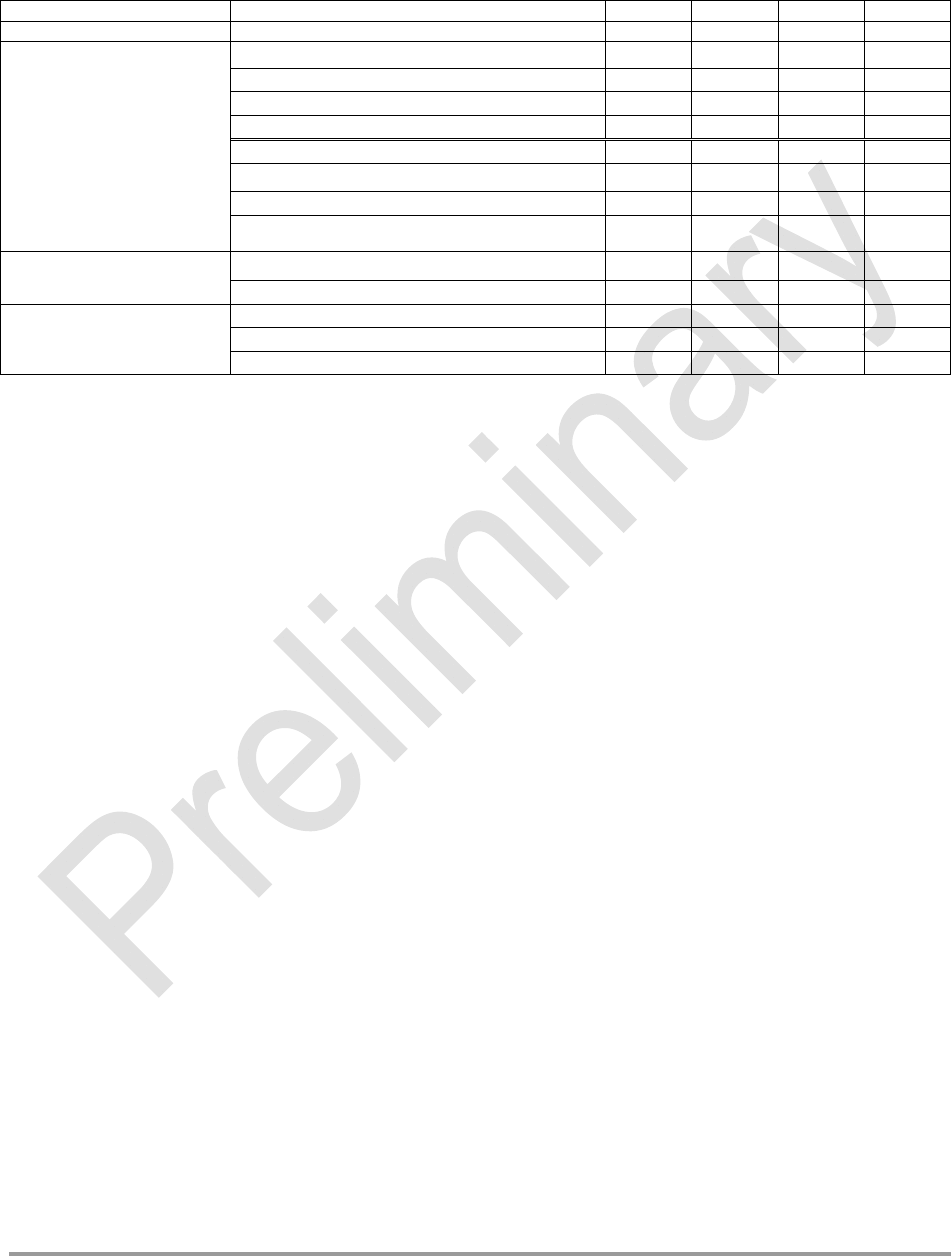
LPP0108IG001 56 Version - Preliminary – 06/20/08
8. GPS Performance
Specification Parameter/Conditions Min Typ Max Units
Maximum Update Rate 1 Hz
Accuracy
-130 dBm, Autonomous CEP (50%) 1 3 m
-140 dBm, Autonomous CEP (50%) 1.5 5 m
-150 dBm, Autonomous CEP (50%) 7 10 m
-155 dBm, Autonomous CEP (50%) 18 25 m
-130 dBm, Autonomous CEP (95%) 2.5 5 m
-140 dBm, Autonomous CEP (95%) 3 7 m
-150 dBm, Autonomous CEP (95%) 15 25 m
-155 dBm, Autonomous CEP (95%) 40 50 m
Acquisition Times
-130 dBm, 25 C
Cold Start TTFF 27 35 49 S
Reacquisition 3 5 S
Sensitivity Tracking - 157.5 -160 dBm
Reacquisition -157 dBm
Cold Start -144 dBm
CEP (50%): The radius of a horizontal circle centered at
the antenna’s true position that contains
50% of the fixes.
CEP (95%): The radius of a horizontal circle centered at
the antenna’s true position that contains
95% of the fixes.
TTFF (Time To First Fix (seconds)): The number of seconds to provide a
position fix (latitude & longitude).
Cold Start: The GPS receiver does not have valid
almanac or time data.
Assisted Cold Start: The modem supplies the GPS receiver any
valid time, ephemeris, almanac, and
position data, that the modem might have
stored.
Reacquisition: The GPS receiver has valid ephemeris,
almanac and time data.

LPP0108IG001 57 Version - Preliminary – 06/20/08
9. GSM/GPRS Modes of Operation
GSM/GPRS supports many optional services and modes. The Enfora Enabler LPP G module supports
the following GSM/GPRS services:
Short-Message Services (SMS)
Class B GPRS Functionality
Voice communication
9.1. Enabling the Transmission Modes for the GSM/GPRS Services
Each of the GSM/GPRS services has two modes that can be enabled separately:
Mobile-originated (MO): allows the making of a service request (such as, making a telephone call
or sending an SMS)
Mobile-terminated (MT): allows receiving a service request (such as receiving a telephone call or
an SMS)
Note: Contact your local GSM operator to ensure that the services and modes have been
provisioned for the SIM.
9.2. Voice Communication
The Enfora Enabler LPP G module has voice capabilities, provided the necessary connections have
been made for the speaker and microphone pins. The Enfora Enabler-LPP G AT Command Set
Reference – LPP0108AT001 has the entire list of commands that can be used to control the voice
functionality.
The Enfora Enabler LPP G module supports four vocoder compression algorithms for voice
communication: Full-Rate (FR), Enhanced Full-Rate (EFR), Half-rate (HR) and Adaptive Multi-rate
(AMR).

LPP0108IG001 58 Version - Preliminary – 06/20/08
9.3. SMS: Short Message Services
Short Message Services (SMS) is a feature-rich GSM service. The Enfora Enabler LPP G
module can perform the following tasks:
Sending and receiving binary messages of up to 160 characters (7-bit characters)
Sending and receiving text messages of up to 140 bytes (8-bit data)
Submitting a SMS Protocol Data Unit (PDU) to a SMSC (Short Message Service Center) and
storing a copy of the PDU until either a report arrives from the network or a timer expires
Receiving a SMS PDU from a SMSC
Returning a delivery report to the network for a previously received message
Receiving a report from the network
Notifying the network when the module has sufficient memory capacity available to receive one or
more SMS messages (after the module had previously rejected a message because its memory
capacity was exceeded)
9.4. SIM Operation
9.4.1. Provisioning the SIM
The SIM can support optional features or services. Most operators typically configure the SIM to
send/receive voice calls and to receive SMS; however, some may require an additional tariff to
enable the SIM to send SMS. The transmission of circuit switched and GPRS data are also
additional services that may be required to allow the service:
Mobile-originated (MO): allows making a service request (such as, making a call or sending an
SMS)
Mobile-terminated (MT): allows receiving a service request (such as, receiving a phone call or an
SMS)
The GSM SIM can have multiple telephone numbers.
It is imperative for the Enfora Enabler LPP G module that the SIM be configured for the optional
services that are required for the application.
9.5. GPRS Services Supported by the Enfora Enabler LPP G Module
The Enfora Enabler LPP G module supports the following GPRS (modes of operation) that must be
enabled by the operator:
GPRS Packet Connectivity (MO and MT) with Both Dynamic and Static IP option
GPRS SMS (MO and MT): uses the IP (Dynamic or Static) set by the operator
Multiple APN Setting
Quality of Service Options

LPP0108IG001 59 Version - Preliminary – 06/20/08
Up to Multi-slot 10 Class of Service
9.6. Selecting the GSM Modes of Operation
When provisioning the SIM for the Enfora Enabler LPP G module, enable the following modes of
operation:
Voice calls: configure the SIM for both MO and MT service (to send and receive)
SMS: configure the SIM either for MT alone (to receive) or for both MO and MT (to send and
receive)
Voice SMS GPRS Function
MO/MT MT Voice calls, receive SMS
MO/MT MO/MT Voice calls, receive / send SMS
MO/MT MO/MT Voice calls, receive / send SMS

LPP0108IG001 60 Version - Preliminary – 06/20/08
10. Software Interface
10.1. Software Interface
The application sends commands to the Enfora Enabler LPP G module via the 50-pin I/O signal
connector. These commands use the Enabler LPP G Menu System, Enfora AT Command Set and/or
Enfora GSM-GPRS Family API.
The Enfora Enabler LPP G module operates in one of the following modes:
Command Menu mode: Used for configuring the Enfora Enabler LPP G module. It uses menu
based commands via the serial port for communication. See LPP0108PR001 - Enfora Enabler
LPP G Programming Reference for more details on specific commands.
Modem Pass-Thru mode: Used to communicate directly with the modem. It uses the AT
command set via the serial port for communication. Entry to this mode is available via a menu
mode command.
10.2. Format for the AT Commands
The general format of the command line is: <prefix> <command> <CR>
<prefix> AT
<command> See AT Command
Manual
<CR> 0X0D
The prefix AT obtains synchronization, identifies the character parameters, and indicates that a
command may be in the following characters.
AT commands are not case sensitive; use either capital letters or lower-case letters for the AT
command.
Note: Some AT Command parameter values ARE case sensitive and are documented in the
Enfora Enabler-LPP G AT Command Set Reference – LPP0108AT001.
10.3. Enfora AT Command Set
For a full description of the AT commands, refer to the Enfora Enabler-LPP G AT Command Set
Reference – LPP0108AT001.
Note: A command description that includes an *asterisk denotes that the GSM service provider
must enable supplementary services functionality before the command is available.

LPP0108IG001 61 Version - Preliminary – 06/20/08
11. Integration and Testing
TBD

LPP0108IG001 62 Version - Preliminary – 06/20/08
12. APPENDIX A - LIMITED WARRANTY
12.1. Scope
Enfora warrants to the original purchaser of the product that, for a period of one (1) year from the date
of product purchase, the product hardware, when used in conjunction with any associated software
(including any firmware and applications) supplied by Enfora, will be free from defects in material or
workmanship under normal operation. Enfora further warrants to such original purchaser that, for a
period of ninety (90) days from the date of product purchase, any software associated with the
product will perform substantially in accordance with the user documentation provided by Enfora, and
any software media provided with the product will be free from defects in material or workmanship
under normal operation. Enfora does not warrant that (a) the product hardware or any associated
software will meet the purchaser’s requirements, (b) that the operation of the product hardware or
software will be uninterrupted or error-free, or (c) the product, when integrated in, or combined with,
other products or software not supplied by Enfora, will continue to perform substantially in accordance
with the user documentation. This limited warranty is only for the benefit of the original purchaser and
is not transferable. No other party may act on behalf of such purchaser for the purpose of claiming or
exercising any rights or benefits under or in connection with this limited warranty except as may be
provided in a written agreement between Enfora and such other party.
12.2. Hardware
During the warranty period applicable to the product hardware, Enfora, at its expense and in its sole
discretion, will repair or replace the product if it is determined to have a covered hardware defect,
provided that the purchaser first notifies Enfora of any such defect, furnishes Enfora with a proof of
purchase, requests and obtains a return merchandize authorization (RMA) number from Enfora, and
returns the product, shipping charges prepaid, to Enfora under that RMA. If, upon reasonable
examination of the returned product, Enfora does not substantiate the defect claimed by purchaser, or
determines that the defect is not covered under this limited warranty, Enfora will not be required to
repair or replace the product, but may instead reship the product to the purchaser, in which case
purchaser shall be responsible for paying Enfora’s usual charges for unpacking, testing, and
repacking the product for reshipment to purchaser. Purchaser shall bear the risk of loss or damage in
transit to any product returned by purchaser to Enfora, or any returned product not found to be
defective or covered under this warranty and reshipped by Enfora to purchaser. In the event Enfora
repairs or replaces a defective product, the repaired or replacement product will be covered under
this limited warranty for the remainder of the original warranty period on the defective product. If
Enfora is unable to repair or replace a defective product, the purchaser’s exclusive remedy shall be a
refund of the original purchase price. Any returned and replaced product, or any product for which
Enfora has refunded the original purchase price, becomes the property of Enfora.
12.3. Software
During the warranty period applicable to the software or its media, Enfora, at its expense, will replace
any defective software or media if purchaser gives written notification of the defect to the technical
support department at Enfora during the applicable warranty period. Enfora will ship or otherwise
transmit the replacement software or media to purchaser, and purchaser shall be responsible for
incorporating any replacement software in the product. Enfora shall not have any obligation to
provide any software bug fixes, upgrades or new releases except as may be necessary to correct any
covered defect of which purchaser notifies Enfora in writing during the applicable warranty period.
Enfora, from time to time and in its sole discretion, may make available for download on its website
(www.enfora.com) certain software bug fixes, upgrades or new releases for the product. The
purchaser should periodically visit such website to determine whether any such bug fixes, upgrades
or new releases have become available. Download and use of any such bug fixes, upgrades or new

LPP0108IG001 63 Version - Preliminary – 06/20/08
releases is subject to all of the applicable terms and conditions of Enfora’s technical support policy as
posted and updated on its website.
Exceptions and Disclaimers
Enfora shall have no obligation under this limited warranty for (a) normal wear and tear, (b) the cost of
procurement of substitute products or (c) any defect that is (i) discovered by purchaser during the
warranty period but purchaser does not notify or request an RMA number from Enfora, as required above,
until after the end of the warranty period, (ii) caused by any accident, misuse, abuse, improper
installation, handling or testing, or unauthorized repair or modification of the product, (iii) caused by use of
any software other than any software supplied by Enfora, or by use of the product other than in
accordance with its documentation or (iv) the result of electrostatic discharge, electrical surge, fire, flood
or similar causes. Unless otherwise provided in a written agreement between the purchaser and Enfora,
the purchaser shall be solely responsible for the proper configuration, testing and verification of the
product prior to deployment in the field.
ENFORA’S SOLE RESPONSIBILITY AND PURCHASER’S SOLE REMEDY UNDER THIS
LIMITED WARRANTY SHALL BE TO REPAIR OR REPLACE THE PRODUCT HARDWARE,
SOFTWARE OR SOFTWARE MEDIA (OR IF REPAIR OR REPLACEMENT IS NOT
POSSIBLE, OBTAIN A REFUND OF THE PURCHASE PRICE) AS PROVIDED ABOVE.
ENFORA EXPRESSLY DISCLAIMS ALL OTHER WARRANTIES OF ANY KIND, EXPRESS
OR IMPLIED, INCLUDING WITHOUT LIMITATION ANY IMPLIED WARRANTIES OF NON-
INFRINGEMENT, MERCHANTABILITY, SATISFACTORY PERFORMANCE AND FITNESS
FOR A PARTICULAR PURPOSE. IN NO EVENT SHALL ENFORA BE LIABLE FOR ANY
INDIRECT, SPECIAL, EXEMPLARY, INCIDENTAL OR CONSEQUENTIAL DAMAGES
(INCLUDING WITHOUT LIMITATION LOSS OR INTERRUPTION OF USE, DATA, REVENUES
OR PROFITS) RESULTING FROM A BREACH OF THIS WARRANTY OR BASED ON ANY
OTHER LEGAL THEORY, EVEN IF ENFORA HAS BEEN ADVISED OF THE POSSIBILITY OR
LIKELIHOOD OF SUCH DAMAGES.
12.4. Other Considerations
Some jurisdictions may require a longer warranty period than specified above and, accordingly, for
products sold in those jurisdictions the applicable warranty period shall be extended as required under the
laws of those jurisdictions. Furthermore, some jurisdictions may not allow the disclaimer of implied
warranties or the exclusion or limitation of incidental or consequential damages, so the above disclaimer,
limitation or exclusion may not apply to products sold in those jurisdictions. This limited warranty gives
the purchaser specific legal rights and the purchaser may have other legal rights that vary from
jurisdiction to jurisdiction.
In some instances, certain aspects of the product warranty may also be covered in a separate written
agreement between Enfora and the distributor or reseller, if any, from whom purchaser purchased the
product. That agreement may provide, for example, a different product return procedure that may also be
available to purchaser (e.g., the product may be returned to Enfora through that distributor or reseller).
Governing Law
This limited warranty shall be governed by the laws of the State of Texas, United States of
America, without regard to conflict of laws principles. This limited warranty shall not be governed
in any respect by the United Nations Convention on Contracts for the International Sale of
Goods.

LPP0108IG001 64 Version - Preliminary – 06/20/08
13. APPENDIX B - Regulations and Compliance
This section summarizes the responsibilities and actions required of manufacturers and integrators who
incorporate OEM versions of the Enfora Enabler LPP G module into their products. In certain situations
and applications, these products will require additional FCC, CE, GCF, PTCRB or other regulatory
approvals prior to sale or operation. Appropriate instructions, documentation and labels are required for
all products. For more information concerning regulatory requirements, please contact Enfora.
13.1. GCF/PTCRB Approval (Formerly FTA)
The Enfora Enabler LPP G module is type approved in accordance with the requirements of and
through the procedures set forth by the GSM industry association. The relevant conformance
specification is 3GPP TS 51010-1. Any OEM changes in the SIM interface, antenna port, software or
the physical makeup of the unit may require an incremental FTA to ensure continued compliance with
the above-mentioned standard. For more information concerning type approval, please contact
Enfora.
13.2. Electromagnetic Compatibility (EMC) and Safety Requirements
The Enfora Enabler LPP G module has been tested and approved for application in the United States
of America (US) and the European Union (EU). The compliance details for each of these markets
follow. For other markets, additional or alternative regulatory approvals may be required. Always
ensure that all rules and regulations are complied with in every country that the OEM application is to
be operated. Regardless of the country or market, the OEM must comply with all applicable
regulatory requirements.
13.3. EMC/Safety Requirements for the USA
Compliance to the US rules and regulations falls under two categories:
Radio approvals: Federal Communications Commission (FCC)
Transmitter: FCC Rules, Part 22 & 24
Unintentional emission: FCC Rules, Part 15
Although the Enfora Enabler LPP G module has been authorized by the FCC and listed as a
component by an NRTL, products and applications that incorporate the Enfora Enabler LPP G
module will require final verification of EM emission and product safety approval.
Note: Particular attention should be made to the following statements regarding RF Exposure:

LPP0108IG001 65 Version - Preliminary – 06/20/08
13.4. Human Exposure Compliance Statement
LPP0108 GSM/GPRS Module
Enfora certifies that the Enfora Enabler LPP G 850/900/1800/1900 MHz GSM Radio Module (FCC ID:
MIVLPP0108) complies with the RF hazard requirements applicable to broadband PCS equipment
operating under the authority of 47 CFR Part 24, Subpart E and Part 22 of the FCC Rules and
Regulations. This certification is contingent upon installation, operation and use of the Enfora
Enabler LPP G module and its host product in accordance with all instructions provided to both the
OEM and end user. When installed and operated in a manner consistent with the instructions
provided, the Enfora Enabler LPP G module meets the maximum permissible exposure (MPE) limits
for general population / uncontrolled exposure at defined in Section 1.1310 of the FCC Rules and
Regulations.
Note: Installation and operation of this equipment must comply with all applicable FCC Rules
and Regulations, including those that implement the National Environmental Policy Act of 1969
(Part 1, Subpart I), with specific regard to antenna sitting and human exposure to radio frequency
radiation. For further guidance, consult the FCC Rules, a certified FCC test house, or Enfora.
13.5. Compliance with FCC Regulations
The Federal Communications Commission (FCC) is the agency of the Federal Government that
oversees all non-governmental radio frequency transmitters that operate within the United States.
Unintentional emissions from digital devices are regulated by Part 15 of the FCC Rules and
Regulations, which distinguishes between the environments in which these devices may operate.
Intentional radiators operating as a GSM-1900 radio transmitter are regulated under Part 22 & 24,
Subpart E—Broadband PCS of the FCC Rules and Regulations.

LPP0108IG001 66 Version - Preliminary – 06/20/08
13.6. Unintentional Radiators, Part 15
Equipment designated as Class A is intended for use in a commercial, industrial or business
environment. The Enfora Enabler LPP G module has been tested and found to comply with the limits
for a Class A digital device and can be integrated into equipment or applications intended for use in
commercial, industrial or business environments.
The following statement must be included in the user manual for such products:
This equipment has been tested and found to comply with the limits for a Class A digital device,
pursuant to part 15 of the FCC rules. These limits are designed to provide reasonable protection
against harmful interference when the equipment is operated in a commercial environment. This
equipment generates, uses, and can radiate radio frequency energy and, if not installed and used in
accordance with the instruction manual, may cause harmful interference to radio communications.
Operation of this equipment in a residential area is likely to cause harmful interference in which case
the user will be required to correct the interference at his own expense.
Equipment intended for use in a residential environment (not-withstanding use in commercial,
industrial or business environments) is designated as Class B. The Enfora Enabler LPP G module
has been tested and found to comply with the limits for a Class B digital device and can be integrated
into equipment or applications intended for use in residential environments.
The following statement must be included in the user manual for such products:
This equipment has been tested and found to comply with the limits for a Class B digital device,
pursuant to part 15 of the FCC rules. These limits are designed to provide reasonable protection
against harmful interference in a residential installation. This equipment generates, uses, and can
radiate radio frequency energy and, if not installed and used in accordance with the instructions, may
cause harmful interference to radio communications. However, there is no guarantee that
interference will not occur in a particular installation. If this equipment does cause harmful
interference to radio or television reception, which can be determined by turning the equipment off
and on the user is encouraged to try to correct the interference by one or more of the following
measures:
Reorient or relocate the receiving antenna.
Increase the separation between the equipment and receiver.
Connect the equipment into an outlet on a circuit different from that to which the
receiver is connected.
Consult the dealer or an experienced radio/TV technician for help.
13.7. Intentional Radiators, Part 22 & 24
Products incorporating the Enfora Enabler LPP G transceiver operate as Personal Communications
Services (PCS) devices under the authority of Part 22 & Part 24, Subpart E—Broadband PCS, of the
FCC Rules and Regulations. All such transmitters must be authorized by the FCC through its
Certification process, as detailed in Part 2, Subpart J - Equipment Authorization Procedures.
Through the Certification process, the FCC verifies that the product complies with all applicable
regulatory and technical requirements, including those that address human exposure to radio
frequency radiation. In general, radio frequency transmitters cannot be sold or operated in the US
prior to FCC approval.

LPP0108IG001 67 Version - Preliminary – 06/20/08
13.8. Instructions to the Original Equipment Manufacturer (OEM)
To comply with the requirements of the National Environmental Policy Act (NEPA) of 1969, operation
of an FCC-regulated transmitter may not result in human exposure to radio frequency radiation in
excess of the applicable health and safety guidelines established by the FCC. Further information on
RF exposure issues may be found in the FCC's Office of Engineering and Technology (OET) Bulletin
Number 65, "Evaluating Compliance with FCC Guidelines for Human Exposure to Radio Frequency
Electromagnetic Fields" and Supplement C, "Additional Information for Evaluating Compliance of
Mobile and Portable devices with FCC Limits for Human Exposure to Radio Frequency Emissions.”
Both of these documents are available via the Internet at the OET web site: http://www.fcc.gov/oet
The Enfora Enabler LPP G products are GSM radio transceivers, which operate under the authority of
47 CFR Part 24, Subpart E and Part 22 of the FCC Rules and Regulations. When installed and
operated in accordance with the instructions provided in this manual, these devices comply with
current FCC regulations regarding human exposure to radio frequency radiation.
The following installation and operation restrictions apply to all Enfora Enabler LPP G products:
This device may only be used in fixed and mobile applications.
Portable applications, as defined by the FCC, are prohibited.
The use of this device for desktop and other applications where the antenna can easily
be relocated are considered by the FCC to be mobile applications.
A separation distance of at least 20 cm (7.87 inches) between the antenna and the body
of the user and other persons must be maintained at all times
In FIXED applications, antenna gain is limited to a maximum of 7 dBi, with a
corresponding Equivalent Isotropic Radiated Power (EIRP) of 37 dBm / 5 W.
In MOBILE applications, antenna gain is limited to a maximum of 2 dBi, with a
corresponding EIRP of 33 dBm / 2 W.
End products must provide instructions to ensure compliance with radio frequency
radiation exposure requirements.
A warning label visible to all persons exposed to the antenna and identical to that
described in this manual must be displayed on or next to the antenna.
Separate FCC approval for RF exposure compliance is required for end products that do
not meet these conditions.
Antenna gain is defined as gain in dBi (dB referenced to an isotropic radiator) minus cabling loss.

LPP0108IG001 68 Version - Preliminary – 06/20/08
Note: Additional care must be taken by the installer and/or user of the Enfora Enabler LPP G
products to ensure proper antenna selection and installation. Adherence to the above conditions
is necessary to comply with FCC requirements for safe operation regarding exposure to RF
radiation.
Depending upon the application and type of product into which the Enfora Enabler LPP G module
has been incorporated, specific OEM actions and responsibilities required to meet these
conditions vary. However, in all cases the primary concern is to ensure compliance with current
FCC guidelines and regulations that limit human exposure to radio frequency radiation.
Definitions
For the purpose of determining compliance with current FCC rules addressing human
exposure to radio frequency radiation, the FCC has established the following three
categories of transmitting devices:
Portable Devices – devices where the antenna is located within 20 cm (7.87
inches) of any person, including the user, if applicable. Portable devices
operating under the authority of Part 22 or 24 (broadband PCS) are limited to a
maximum of 2 W EIRP.
Mobile Devices – devices designed to be used in other than fixed locations and
generally such that the antenna is located at a minimum of 20 cm (7.87 inches)
from any person, including the user, if applicable. Mobile devices operating
under the authority of Part 22 or 24 (broadband PCS) are limited to a maximum
of 2 W EIRP.
Fixed devices – devices in which the antenna, either integral to the product or
remotely located, is physically secured at one location and is not able to be easily
moved to another location. The antenna for a fixed device is mounted on an
outdoor permanent structure with a minimum separation distance of 2 meters (79
inches)

LPP0108IG001 69 Version - Preliminary – 06/20/08
13.8.1. OEM Responsibilities for All Products Containing the Enabler LPP G module
In addition to any other regulatory requirements, OEMs and integrators must include or provide
the following information, instructions, warnings and labels with any device or product into which
the Enfora Enabler LPP G GSM1900 GSM transceiver has been incorporated:
Information Description
Detailed
Operating
Instructions for
ensuring
compliance with
current FCC
guidelines which
limit human
exposure to radio
frequency
radiation
The OEM must provide an operating/installation manual with the final product which clearly
indicates that these operating conditions and restrictions must be observed at all times to
ensure compliance with current FCC guidelines which limit human exposure to radio
frequency radiation.
20 cm (7.87 inch) separation distance between the antenna and all persons must be
maintained at all times for all fixed and mobile products and applications
Portable devices and applications are prohibited unless such devices and products are
specifically authorized by the FCC
Maximum antenna gain is limited to 2 dBi* in mobile products and applications
For fixed applications (2 meter separation) the antenna gain can be as much as 26 dBi.
Modifications and/or additions to the Enfora Enabler LPP G GSM transceiver, including use
of antennas with higher gain than those authorized by the FCC, are prohibited
*dBi = antenna gain in dB relative to an isotropic radiator
Antenna
Avoidance
Label
Attach the following warning label
directly to or displayed next to the
antenna. Furthermore, this label must
be visible to and easily readable by all
persons in the immediate vicinity of the
antenna
WARNING
To comply with FCC RF exposure
requirements, a separation distance of 20 cm
(7.87”) or more must be maintained between
this antenna and all persons
Human Exposure
Compliance
Statement
Include the following statement in the
instruction / operation manual.
Enfora certifies that the Enfora Enabler LPP G ™
MHz GSM Radio Module (FCC ID: MIVLPP0108)
complies with the RF hazard requirements
applicable to broadband PCS equipment
operating under the authority of 47 CFR Part 22 or
Part 24, Subpart E of the FCC Rules and
Regulations.
This certification is contingent upon installation,
operation and use of the
Enfora Enabler LPP G module and its host
product in accordance with all instructions
provided to both the OEM and end used. When
installed and operated in a manner consistent with
the instructions provided, the Enfora Enabler LPP
G module meets the maximum permissible
exposure (MPE) limits for general population /
uncontrolled exposure at defined in Section
1.1310 of the FCC Rules and Regulations.

LPP0108IG001 70 Version - Preliminary – 06/20/08
13.8.2. Specific OEM Responsibilities for Portable Products and Applications
Each device or product, into which the Enfora Enabler LPP G PCS-1900 GSM transceiver has
been incorporated, and which is intended to be used in an application that meets the definition of
"portable" MUST be separately authorized by the FCC for the purposes of determining
compliance with current FCC guidelines limiting human exposure to radio frequency radiation.
Portable devices must be evaluated for RF exposure based on Specific Absorption Rate (SAR)
limits; further information on such evaluations are available from the FCC via the Internet.
13.8.3. Specific OEM Responsibilities for Mobile Products and Applications
Separate or additional FCC approvals are NOT required for devices or products, into which the
Enfora Enabler LPP G PCS-1900 GSM transceiver has been incorporated, that are used in
applications that meet the definition of "mobile."
For all end products, the OEM or integrator must provide instructions, warnings and labels to
ensure that the product complies with current FCC guidelines limiting human exposure to radio
frequency radiation.
Current FCC regulations limit the EIRP of mobile devices to 2 W. Because the nominal RF output
power of the Enfora Enabler LPP G GSM1900 GSM transceiver is 1.0 W (31 dBm), antenna gain
for mobile products and applications cannot exceed 2 dBi.
13.8.4. Specific OEM Responsibilities for Fixed Products and Applications
Separate or additional FCC approvals are not required for devices or products, into which the
Enfora Enabler LPP G GSM transceiver has been incorporated, that are used in applications that
meet the definition of "fixed.”
For all end products, the OEM or integrator must provide the instructions, warnings and labels to
ensure that the product complies with current FCC guidelines limiting human exposure to radio
frequency radiation.
Separate or additional FCC approvals are required for devices or end products used in fixed
applications where antenna gain in excess of 7dBi is desired.

LPP0108IG001 71 Version - Preliminary – 06/20/08
13.9. EMC/Safety Requirements for the Countries of the European Union (EU)
The European Union (EU) is comprised of fifteen countries that follow a harmonized set of standards,
utilizing the CE mark as a uniform mark of acceptance. The member countries are:
Austria
Belgium
Cyprus
Czech Republic
Denmark
Estonia
Finland
France
Germany
Greece
Hungary
Ireland
Italy
Latvia
Lithuania
Luxembourg
The Netherlands
Poland
Portugal
Slovakia
Slovenia
Spain
Sweden
United Kingdom
13.10. EMC/Safety Requirements for Other Countries
In most other countries that have not been listed above there are similar rules and regulations that
must be met for importing the Enfora Enabler LPP G module. Each may require a different mark of
approval (for example, the CB Scheme) as an acceptance requirement. For each of these cases the
country should identified, and the appropriate steps should be taken to meet the requirements set
forth in the intended market.

LPP0108IG001 72 Version - Preliminary – 06/20/08
14. APPENDIX C - Glossary and Acronyms
API Application Programming Interface.
App Application Refers to the Application which sends or receives commands/responses
from the Enfora Enabler LPP G Module
AT Command Set Commands issued by intelligent device to a modem to perform functions,
such as to initiate call, to answer call, or to transmit data.
BER
Bit Error Rate Bit Error Rate
CEP
Circular Error Probable
CMUX Multiplexer protocol that operates between an MS and a TE and allows a
number of simultaneous sessions over a normal serial asynchronous
interface
CPE
Customer Premise
Equipment
A terminal in fixed location on the customer’s premises.
CSD
Circuit Switched Data Data link from a terminal through the network allowing real-time, duplex
connectivity at 9600 bytes/second.
dBi Decibels referenced to an isotropic radiator
DCE
Data Communications
Equipment
Data Communications Equipment
DCS
Digital Cellular System A collection of services and capabilities providing flexibility of access and
mobility through a combination of wireless and wire-line networks, utilizing
the 1800 MHz bandwidth.
DTE
Data Terminal Equipment Data Terminal Equipment
EFR
Enhanced Full Rate Voice (vocoder) compression algorithms which offer the highest quality voice
communication.
EIR
Equipment Identity Register A database used to store International Mobile Equipment Identity (IMEI) of a
locally issued terminal.
EIRP
Equivalent Isotropic
Radiated
Power
In a given direction, the gain of a transmitting antenna multiplied by the net
power accepted by the antenna from the connected transmitter.
EMC
Electromagnetic
Compatibility
The ability of a device to function satisfactorily in its electromagnetic
environment without inducing intolerable disturbance to that environment (or
to other devices)
ESD
Electrostatic Discharge Static electricity that can damage electronic equipment.
EU
European Union An organization of 15 European states whose purpose is to organize
relations between the Member States and between their peoples.
FTA
Full Type Approval GSM Full Type Approval
GPRS
General Packet Radio
Service
Standard for packet communications utilizing Global Standard for Mobility
(GSM) infrastructure.
GSM
Global System for Mobile
Communications
Standard for digital communications. Allows consistent communications in
various parts of the world despite variations in RF spectrum allocations.
Transferring the SIM (see below) permits users to roam by changing terminal
equipment.
GPS Global Positioning System

LPP0108IG001 73 Version - Preliminary – 06/20/08
HLR
Home Location Register Stores the identity and user data for all subscribers belonging to the area of
the related MSC.
IMEI
International Mobile
Equipment Identity
A unique number for each GSM Terminal tracked by the GSM operators in
their Equipment Identity Register (EIR) database.
IMSI
International Mobile
Subscriber Identification
A unique number identifying the subscriber stored in the SIM card. Number
is used in conjunction with the network for call routing.
Ki A secret code used in authentication and encryption by the terminal.
LPP
Low Power Platform
MCP
MO
Mobile Originated Any GSM/GPRS service originated at the mobile terminal.
MT
Mobile Terminated Any GSM/GPRS service originated from or routed through the network and
sent to the mobile terminal.
MSC
Mobile Switching Center The central switch of the GSM network. Performs call routing, collects call
detail records for billing, and supervises system operations.
Non-Transparent Mode Delivers a constantly low error rate but with a non-guaranteed throughput or
delay. The Non-Transparent service provides a performance that is closest
to using a modem over a fixed PSTN line.
NRTL
Nationally Recognized Test
Laboratory
OSHA-approved Nationally Recognized Testing Laboratory
OEM Original Equipment Manufacturer.
PA Power Amplifier.
Packet A collection of data transmitted over a digital network in a burst.
PCS Personal Communication Services.
PDA Personal Digital Assistant.
PDU Packet Data Unit.
PPP Point-To-Point Protocol.
RTC
Real Time Clock
SIM Subscriber Identity Module.
SMS Short Message Service.
SMSC Short Message Service Center.
SUPL Secure User Plane Location
TCP
Transfer Control Protocol
UDP User Datagram Protocol.

LPP0108IG001 74 Version - Preliminary – 06/20/08
15. APPENDIX D – Tables and Figures
TABLES
Table 1 - Enabler LPP G Key Features ........................................................................................................ 8
Table 2 - Enabler LPP G Pin Assignments ................................................................................................. 25
FIGURES
Figure 1 - Example of good ground plane for GSM modules ..................................................................... 13
Figure 2 - Example of a POOR RF Thermal Relief ..................................................................................... 14
Figure 3 - Example of a GOOD RF Thermal Relief .................................................................................... 15
Figure 4 - Example of Vbat Voltage Droop ................................................................................................. 16
Figure 5 - Audio Reference Design Schematic ........................................................................................... 17
Figure 6 - Enabler LPP G Module Block Diagram ...................................................................................... 18
Figure 7 – Side and Front of Module with Pin 1 reference ......................................................................... 21
Figure 8 - Module Footprint ......................................................................................................................... 22
Figure 9 - Copper PADs (Recommended) .................................................................................................. 23
Figure 10 - Solder Mask (Reccomended) ................................................................................................... 23
Figure 11 - Paste Mask (Reccomended) based on 0.004” stencil. ............................................................. 24
Figure 12 - GPS Antenna Sample Schematic ............................................................................................. 27
Figure 13 - Remote SIM Interface ............................................................................................................... 36

LPP0108IG001 75 Version - Preliminary – 06/20/08
16. APPENDIX E - Contacting Enfora
For technical support and customer service dealing with the modem itself, contact the company where
you purchased the product. If you purchased the product directly from Enfora, visit the SUPPORT page
on the Enfora website: http://www.enfora.com/support_newissue.asp