Novatel Wireless NRMUNDP-1D UNDP-1PCI EXPRESS MINI CARD User Manual UNDP 1 Universal Notebook Data Platform User Guide
Novatel Wireless, Inc. UNDP-1PCI EXPRESS MINI CARD UNDP 1 Universal Notebook Data Platform User Guide
Contents
- 1. User Manual
- 2. USER MANUAL
- 3. User Manual 1
- 4. User Manual 2
- 5. Host User Manual
- 6. WWAN portion of User manual
WWAN portion of User manual
UNDP-1 Universal Notebook Data Platform
User Guide
80-VF329-3 Rev. C
December 20, 2007
Submit technical questions at:
https://support.cdmatech.com
Restricted Distribution. Not to be distributed to anyone who is not an employee of either QUALCOMM or a
subsidiary of QUALCOMM without the express approval of QUALCOMM's Configuration Management.
Not to be used, copied, reproduced in whole or in part, nor its contents revealed in any manner to others without the
express written permission of QUALCOMM Incorporated.
QUALCOMM is a registered trademark of QUALCOMM Incorporated in the United States and may be registered in
other countries. Other product and brand names may be trademarks or registered trademarks of their respective
owners. CDMA2000 is a registered certification mark of the Telecommunications Industry Association, used under
license. ARM is a registered trademark of ARM Limited. QDSP is a registered trademark of QUALCOMM
Incorporated in the United States and other countries.
This technical data may be subject to U.S. export, re-export, or transfer ("export") laws. Diversion contrary to U.S.
law prohibited.
QUALCOMM Incorporated
5775 Morehouse Drive
San Diego, CA 92121-1714
U.S.A.
Copyright © 2007 QUALCOMM Incorporated.
All rights reserved.
QUALCOMM Confidential and Proprietary

80-VF329-3 Rev. C 2 QUALCOMM Confidential and Proprietary
MAY CONTAIN U.S. EXPORT CONTROLLED INFORMATION
1 Introduction
1.1 Documentation overview........................................................................................ 6
1.2 Application description .......................................................................................... 8
1.3 Terms and acronyms............................................................................................. 12
2 External Connections
3 DC Power and UNDP Operating Modes
3.1 DC power source .................................................................................................. 16
3.2 DC power states.................................................................................................... 17
3.3 UNDP operating modes........................................................................................ 17
3.4 Electrostatic discharge protection ........................................................................ 18
4 RF Integration
4.1 RF operating frequencies...................................................................................... 19
4.2 RF connections ..................................................................................................... 20
4.3 Ground connections.............................................................................................. 20
4.4 Shielding and interference.................................................................................... 21
4.5 Antenna considerations ........................................................................................ 22
5 Platform Communications
6 Standards and Regulatory Compliance
6.1 Standards and certification ................................................................................... 25
6.2 Regulatory information ........................................................................................ 26
6.2.1 Safety warnings.................................................................................... 26
6.2.2 North American compliance ................................................................ 27
6.2.3 EU compliance..................................................................................... 28
Contents

80-VF329-3 Rev. C 3 QUALCOMM Confidential and Proprietary
MAY CONTAIN U.S. EXPORT CONTROLLED INFORMATION
UNDP-1 Universal Notebook Data Platform User Guide Contents
Figures
Figure 1-1 UNDP-1 product deliverables.......................................................................... 9
Figure 1-2 Example application functional block diagram ............................................. 10
Figure 2-1 External connections...................................................................................... 15
Figure 3-1 DC power connections................................................................................... 16
Figure 4-1 UNDP shields ................................................................................................ 21
Figure 5-1 UNDP-1 communication interfaces............................................................... 23

80-VF329-3 Rev. C 4 QUALCOMM Confidential and Proprietary
MAY CONTAIN U.S. EXPORT CONTROLLED INFORMATION
UNDP-1 Universal Notebook Data Platform User Guide Contents
Tables
Table 1-1 UNDP-1 documentation .................................................................................. 6
Table 1-2 Reference documents....................................................................................... 7
Table 1-3 Terms and Acronyms ..................................................................................... 12
Table 2-1 PCI Express Mini Card connector pin assignments....................................... 14
Table 3-1 UNDP-1 DC power states.............................................................................. 17
Table 3-2 UNDP-1 operating modes and throughput rates............................................ 17
Table 4-1 RF operating frequencies ............................................................................... 19
Table 5-1 LED communications .................................................................................... 24

80-VF329-3 Rev. C 5 QUALCOMM Confidential and Proprietary
MAY CONTAIN U.S. EXPORT CONTROLLED INFORMATION
Revision history
Revision Date Description
A November 2007 Initial release
B November 2007 Added label information in compliance details (Section 6.2.2)
C December 2007 Updated Section 6.2.2
Added Section 6.2.3

80-VF329-3 Rev. C 6 QUALCOMM Confidential and Proprietary
MAY CONTAIN U.S. EXPORT CONTROLLED INFORMATION
1Introduction
1.1 Documentation overview
The UNDP-1 Universal Notebook Data Platform is a PCI Express™ Mini Card that
enables notebook computer wireless data connectivity. This datacard solution delivers
WWAN connectivity for the CDMA2000® 1x, 1x EV-DO, UMTS (HSDPA and HSUPA),
and GSM/GPRS/EDGE™ protocols, plus GPS position location, in a single package. The
complete UNDP-1 solution includes all hardware and software necessary for embedded
wireless connectivity in notebook PCs.
Technical UNDP-1 device information is distributed over the documents listed in
Table 1-1. All released UNDP-1 documents are posted at the CDMA Tech Support
website (https://support.cdmatech.com) and are available for download.
This UNDP-1 user guide is organized as follows:
Chapter 1 Provides an overview of UNDP-1 documentation, presents a functional
block diagram for an example application, gives a high-level functional
description of the UNDP-1 device, and defines terms and acronyms used
throughout this document.
Chapter 2 Provides pin assignments and detailed descriptions.
Chapter 3 Defines how to power and control the UNDP-1 platform and describes its
operating modes.
Chapter 4 Provides RF integration guidelines.
Chapter 5 Describes UNDP-1 methods for communicating with the host computer
and its user.
Chapter 6 Provides standards compliance and regulatory information.
Table 1-1 UNDP-1 documentation
Document Number Title/Description
80-VF329-1 UNDP-1 Universal Notebook Datacard Platform Device Specification
The primary objective of this document is to convey all UNDP-1 electrical
and mechanical specifications. Additional material includes pin assignment
definitions, packing methods and materials, and ordering information. This
document can be used by company purchasing departments to facilitate
procurement.
80-VF329-3
(this document)
UNDP-1 Universal Notebook Datacard Platform User Guide
This document describes all UNDP-1 functions and interfaces, defines how
to power and control the platform, and provides hardware integration
guidelines.

80-VF329-3 Rev. C 7 QUALCOMM Confidential and Proprietary
MAY CONTAIN U.S. EXPORT CONTROLLED INFORMATION
UNDP-1 Universal Notebook Data Platform User Guide Introduction
Table 1-2 lists documents referred to throughout the UNDP-1 document-set; consult them
for additional information.
Table 1-2 Reference documents
Ref No. Document
[1] QUALCOMM WWAN Connection Manager API (80-VF219-1)
[2] Supplement to Streaming Download Protocol (80-VF459-1)
[3] Antenna Design Guidelines for Laptop and Notebook Computers (80-H2929-1)
[4] FCC Regulations - CFR 47, Part1, 2, 15, 22 and 24
[5] PCI Express Mini Card Electromechanical Specification, Revision 1.1
[6] Universal Serial Bus Specification, Revision 2.0
[7] Protection of Electrical and Electronic Parts, Assemblies, and Equipment
(ANSI/ESD S20.20-1999)

80-VF329-3 Rev. C 8 QUALCOMM Confidential and Proprietary
MAY CONTAIN U.S. EXPORT CONTROLLED INFORMATION
UNDP-1 Universal Notebook Data Platform User Guide Introduction
1.2 Application description
The UNDP-1 platform (Figure 1-1) includes a universal embedded data-connectivity
modem in the form of a PCI Express Mini Card, plus the associated software suite for
notebook PC applications. Its supported airlinks are as follows:
■Dual-band CDMA2000 (1X and/or 1x EV-DO):
❒Cellular band
– Band class 0: 869 to 894 MHz reception; 824 to 849 MHz transmission
❒PCS band
– Band class 1: 1930 to 1990 MHz reception; 1850 to 1910 MHz transmission
■Tri-band UMTS (WCDMA R99, HSDPA, and/or HSUPA):
❒Cellular band
– Band V: 869 to 894 MHz reception; 824 to 849 MHz transmission
❒PCS band
– Band II: 1930 to 1990 MHz reception; 1850 to 1910 MHz transmission
❒IMT band
– Band I: 2110 to 2170 MHz reception; 1920 to 1980 MHz transmission
■Quad-band GSM (GSM, GPRS, and/or EDGE):
❒GSM850 band
– 869 to 894 MHz reception; 824 to 849 MHz transmission
❒GSM900 band
– 925 to 960 MHz reception; 880 to 915 MHz transission
❒GSM1800 band
– 1805 to 1880 MHz reception; 1710 to 1785 MHz transmission
❒GSM1900 band
– 1930 to 1990 MHz reception; 1850 to 1910 MHz transmission
■GPS reception centered at 1575.42 MHz (GPS L1 band)
80-VF329-3 Rev. C 9 QUALCOMM Confidential and Proprietary
MAY CONTAIN U.S. EXPORT CONTROLLED INFORMATION
UNDP-1 Universal Notebook Data Platform User Guide Introduction
Figure 1-1 UNDP-1 product deliverables
The on-board QUALCOMM ICs include:
■MDM1000™ Mobile Data Modem IC
■RTR6285™ RF Transceiver IC
■RFR6500™ RF Receiver IC
■PM6653™ Power Management IC
Key connectivity support includes:
■USB 2.0 high-speed
■Universal integrated circuit card (UICC) for RUIM/USIM
■Primary and secondary antenna connectors
■Status LED driver output
■DC power supply input and enable/disable control
PCI Express Mini CardUNDP SW Suite
!Mini Card Hardware Design
!Complete SW Suite & Tools
!Certification & Carrier Approvals
!Technical Support
Mobile Data MODEM
EV-DO
HSDPA
HSUPA
EDGE/GSM
GPS
RF
Memory
- DDR SDRAM
- NOR Flash
USB 2.0
UICC
Support
Firmware
Notebook OS
80-VF329-3 Rev. C 10 QUALCOMM Confidential and Proprietary
MAY CONTAIN U.S. EXPORT CONTROLLED INFORMATION
UNDP-1 Universal Notebook Data Platform User Guide Introduction
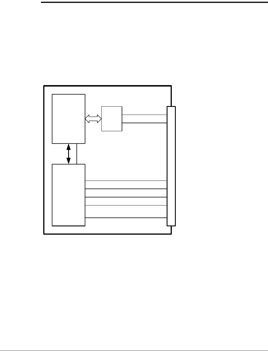
A high-level hardware block diagram is shown in Figure 1-2. Two Hirose (U.FL-R-SMT)
antenna connectors are provided for the following:
1. The primary connector supports transmission and reception by the active CDMA,
UMTS, or GSM transceiver.
2. The secondary connector supports diversity reception by the active CDMA or UMTS
link plus GPS reception.
Figure 1-2 Example application functional block diagram
The antenna elements are typically integrated into the notebook computer and connected
to the UNDP-1 module via flexible RF coaxial cables. This configuration, when adequate
antenna performance is achieved, satisfies the PCI-SIG® standard requirements for PCI
Express Mini Cards. Antenna performance requirements are defined in [3] and listed
within Table 1-2.
MDM1000
RTR6285
Quad-band GSM Tx
Quad-band UMTS Tx
Tx power detector
Quad-band GSM Rx
Quad-band UMTS Rx
(w/ Rx diversity)
GPS Rx
PM6653
Transmit
output
chains
Input power management
Voltage regulators
General housekeeping
User interfaces
IC interfaces
primary
antenna
connector
Primary RF
front -end
GSM Rx
filters
UMTS IMT
PRx filter
Secondary
RF front-end
w/ Rx BPFs
TX BB
RX0 BB
RX1 BB
VCTCXO
secondary
antenna
connector
RFR6500
Dual-band CDMA Rx
(w/ Rx diversity)
GPS Rx
CDMA Cell
& PCS
PRx filters
GPS filter
status &
control
status &
control
status & control
USB
USB
ULPI
PHY
USIM
ARM11
ARM9
DSP (x2)
DDR SDRAM
CDMA 1x, 1xEV-DO
UMTS
HSUPA & HSDPA
GSM/GPRS/EDGE
to RFICs & ULPI
supply
voltages
TRK_LO_ADJ
TCXO
USIM
VMAIN_3P3
LED_WWAN
mini card edge connector
VDD
LED driver
32 Mbit
NOR
UMTS IMT RX0
CDMA + UMTS PCS RX0
CDMA + UMTS Cell RX0
UMTS IMT RX1
GPS RX
C + U Cell RX1
C + U PCS RX1
W_DISABLE_N

80-VF329-3 Rev. C 11 QUALCOMM Confidential and Proprietary
MAY CONTAIN U.S. EXPORT CONTROLLED INFORMATION
UNDP-1 Universal Notebook Data Platform User Guide Introduction
The primary antenna is connected to its RF front-end circuits (a switch module, CDMA
and UMTS duplexers, etc). In the transmit direction, these front-end circuits are driven by
the transmit output chains: two chains support GSM low and high bands (GSM850 +
GSM900 and GSM1800 + GSM1900); three chains support CDMA (Cell + PCS) and
UMTS (Cell + PCS + IMT) operation. All baseband-to-RF processing - for all supported
bands - is performed within the RTR6285 IC.
The four GSM receive paths are filtered, then routed to the RTR6285 IC for processing.
The CDMA and UMTS primary receive filtering is achieved within the front-end
duplexers; the signals are then routed to either the RTR6285 IC (UMTS IMT) or the
RFR6500 IC (CDMA and UMTS Cell + PCS) for RF-to-baseband processing.
Like the primary antenna, the secondary antenna is connected to its own RF front-end
circuits (a switch module, CDMA/UMTS filters, GPS filter, etc). The filtered signals are
then routed to the appropriate RFIC for RF-to-baseband processing (RTR6285 IC for
UMTS IMT; RFR6500 for CDMA and UMTS Cell + PCS and GPS).
The MDM1000 device provides all the digital baseband processing, including modem
functions for all the supported airlinks. Integrated MDM1000 functions include the
ARM1136-J™ and ARM926EJ-S™ processor cores; two low-power, high-performance
digital signal processor (DSP) cores; and 32 MB stacked dual data rate (DDR)
synchronous dynamic random access memory (SDRAM).
UICC (RUIM/USIM) is supported via an offboard UICC connector that is implemented
per the PCI Express Mini Card specification, version 1.1. The UNDP-1 UICC interface is
compliant with GSM 11.12 and ISO/IEC 7816-3 standards.
In addition to the PCI Express Mini Card edge connector, board-level pads are provided
for interfacing to a JTAG fixture.
With its 4 MB of NOR flash memory and 32 MB of RAM (stacked DDR-SDRAM inside
the MDM1000), the UNDP-1 supports a new code storage architecture via the
QUALCOMM Data Loader (QDL). The Advanced Mobile Suscriber Software (AMSS)
image is stored on the PC file system and downloaded to the UNDP-1 device RAM at
system startup. NOR flash memory contains a boot image to support the initialization and
configuration of the UNDP-1 hardware system, including the RF calibration items. It then
enumerates on the USB, and the host computer downloads the embedded software and
configuration memory items over the USB using QDL.
Software interfaces that were developed for QUALCOMM chipsets are supported by the
UNDP-1 product. The QDL data card interface ISOD describes the C API functions that
PC software applications must use to interface with UNDP-1; see [1] listed within
Table 1-2 for details. The supplement to the streaming download protocol specification
describes the high-speed download protocol; see [2] within the same table for details.
The UNDP-1 platform includes the PM6653 power management IC to detect and validate
the applied DC power source, coordinate system powerup and powerdown actions,
generate all the required on-board supply voltages, implement the primary on-board clock
sources, and provide several secondary functions (such as driving the status LED).

80-VF329-3 Rev. C 12 QUALCOMM Confidential and Proprietary
MAY CONTAIN U.S. EXPORT CONTROLLED INFORMATION
UNDP-1 Universal Notebook Data Platform User Guide Introduction
1.3 Terms and acronyms
Table 1-3 defines the terms and acronyms used throughout this document.
Table 1-3 Terms and Acronyms
Term Definition
AMSS Advanced Mobile Suscriber Software
CAPI Computer Application Programmable Interface
CDMA Code Division Multiple Access
CE Mandatory conformity marking on many European products
Cell Cellular band
CTIA Cellular Telecommunications and Internet Association
DCS Digital Cellular System at 1800 MHz
DDR SDRAM Dual Data Rate Synchronous Dynamic Random Access Memory
EDGE Enhanced Data Rates for GSM Evolution
EMC Electromagnetic compatibility
ESD Electrostatic Discharge
FCC Federal Communications Commission
GPRS General Packet Radio Service
GPS Global Positioning System
GSM Global System for Mobile communications
HSDPA High Speed Downlink Packet Access
HSUPA High Speed Uplink Packet Access
IMT International Mobile Telecommunications
ISOD Interface Specification and Operational Description
JTAG Joint Test Action Group
MDM Mobile Data Modem
PA Power Amplifier
PCI Peripheral Component Interconnect
PCS Personal Communication System
PHY Physical layer (USB transceiver)
PM, PMIC Power Management, PM Integrated Circuit
QDL QUALCOMM Data Loader
RFR Radio Frequency Receiver
RoHS Restriction of Hazardous Substances
RTR Radio Frequency Transceiver
RUIM Removable User Identity Module
TIA/EIA Telecommunication Industry Association / Electronic Industries Alliance
TS Technical Specification

80-VF329-3 Rev. C 13 QUALCOMM Confidential and Proprietary
MAY CONTAIN U.S. EXPORT CONTROLLED INFORMATION
UNDP-1 Universal Notebook Data Platform User Guide Introduction
TXCO Temperature-compensated Crystal Oscillator
UICC Universal Integrated Circuit Card
ULPI USB transceiver macrocell interface + low pin interface
UMTS Universal Mobile Telecommunications System
UNDP, UNDP-1 Universal Notebook Data Platform, -1 refers to a particular QUALCOMM
product
USB Universal Serial Bus
USIM Universal Subscriber Identity Module
VCTCXO Voltage Controlled Temperature-compensated Crystal Oscillator
WCDMA Wideband Code Division Multiple Access
WLAN Wideband Local Area Network
WHQL Windows Hardware Quality Labs
WWAN Wireless Wide Area Network
Table 1-3 Terms and Acronyms (continued)
Term Definition

80-VF329-3 Rev. C 14 QUALCOMM Confidential and Proprietary
MAY CONTAIN U.S. EXPORT CONTROLLED INFORMATION
2External Connections
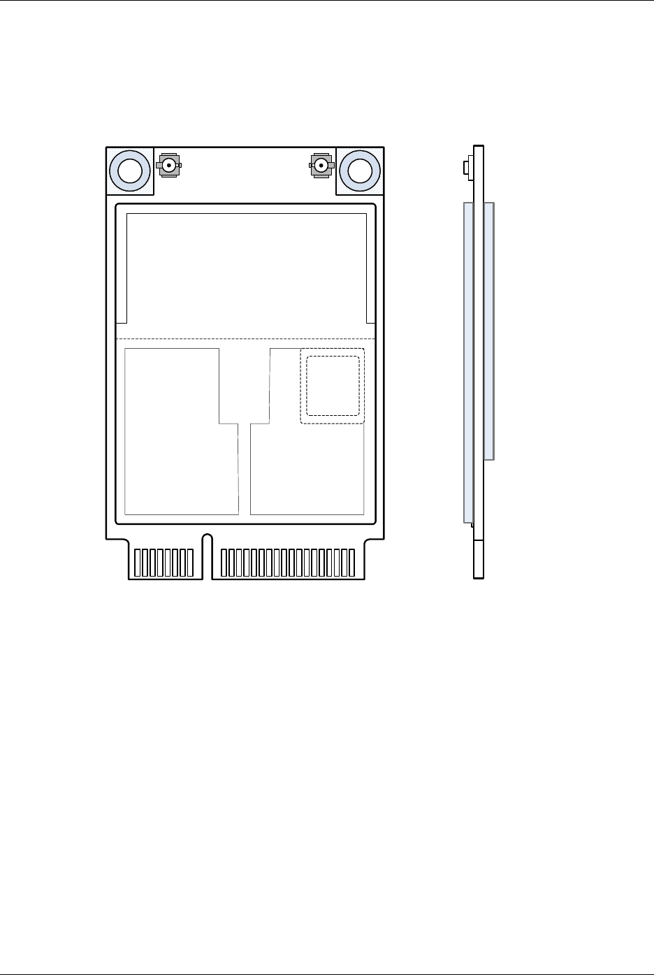
The UNDP-1 add-in card is compatible with the PCI Express Mini Card 52-pin card edge
type connector. The PCI Express Mini Card connector pin assignments are listed in
Table 2-1; pins used by the UNDP-1 platform are highlighted in PINK BOLD font.
Table 2-1 PCI Express Mini Card connector pin assignments
System connector interface
Pin # Name Pin # Name
51 N/C 52 +3.3 V
49 N/C 50 GND
47 N/C 48 N/C (+1.5 V)
45 N/C 46 N/C
43 GND 44 N/C
41 +3.3 Vaux 42 LED_WWAN#
39 +3.3 Vaux 40 GND
37 GND 38 USB_D_P
35 GND 36 USB_D_N
33 N/C 34 GND
31 N/C 32 N/C
29 GND 30 N/C
27 GND 28 N/C (+1.5 V)
25 N/C 26 GND
23 N/C 24 +3.3 Vaux
21 GND 22 N/C (PERST_N)
19 N/C 20 W_DISABLE_N
17 N/C 18 GND
Mechanical key
15 GND 16 N/C
13 N/C 14 UIM_RST_N
11 N/C 12 UIM_CLK
9 GND 10 UIM_DATA
7N/C8UIM_PWR
5 N/C (COEX2) 6 N/C (+1.5 V)
3 N/C (COEX1) 4GND
1 N/C (WAKE_N) 2 +3.3 V aux
80-VF329-3 Rev. C 15 QUALCOMM Confidential and Proprietary
MAY CONTAIN U.S. EXPORT CONTROLLED INFORMATION
UNDP-1 Universal Notebook Data Platform User Guide External Connections
The UNDP-1 platform also provides two RF connectors as antenna ports. Hirose model
number U.FL-R-SMT should be used to mate with each port. See Section 1.2 for
implementation and interconnection guidelines.
The final set of connections available are the board-level pads available as a JTAG
interface.
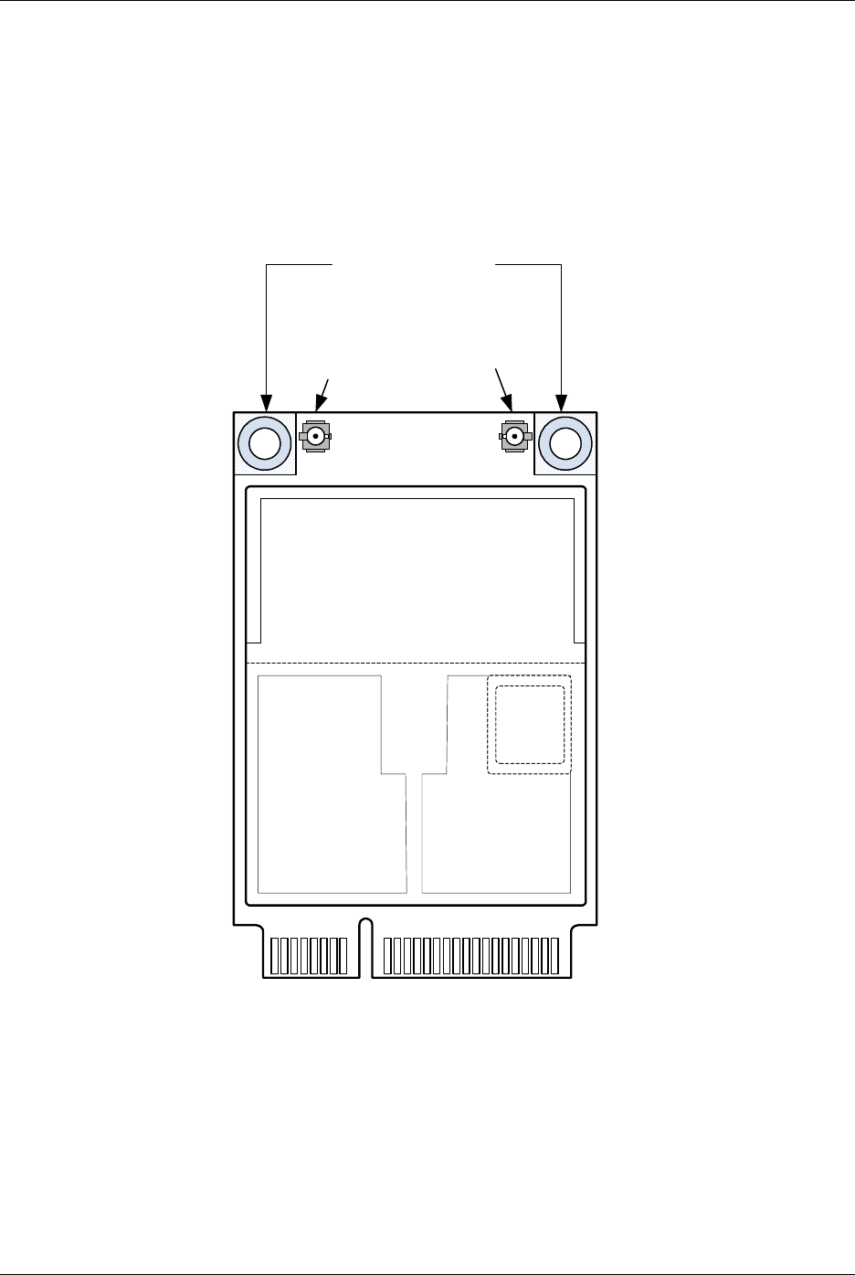
The EDGE card connector and RF connectors are highlighted in Figure 2-1.
Figure 2-1 External connections
Primary
Antenna
connector
Secondary
Antenna
connector
Mounting hole &
System ground
PCI Express Mini Card 52-pin edge connector
Top View
80-VF329-3 Rev. C 16 QUALCOMM Confidential and Proprietary
MAY CONTAIN U.S. EXPORT CONTROLLED INFORMATION
3DC Power and UNDP Operating
Modes
3.1 DC power source
The host computer provides the UNDP-1 power source via the 52-pin card edge connector
(Figure 3-1). A nominal supply voltage of 3.3 V is expected, as defined in the PCI Express
Mini Card Electromechanical Specification, Revision 1.1. UNDP-1 voltage and current
specifications are provided in the Universal Notebook Data Platform Device Specification
(80-VF329-1).
Figure 3-1 DC power connections
With a proper DC power source applied, the UNDP-1 platform is powered up and down as
directed by the W_DISABLE_N control signal from the host computer: logic low =
disabled; logic high = enabled.
MDM1000
PM6653
status &
control
on-board
supply
voltages
VMAIN_3P3
mini card edge connector
W_DISABLE_N
20
52
41
39
24
2

80-VF329-3 Rev. C 17 QUALCOMM Confidential and Proprietary
MAY CONTAIN U.S. EXPORT CONTROLLED INFORMATION
UNDP-1 Universal Notebook Data Platform User Guide DC Power and UNDP Operating Modes
3.2 DC power states
Based on applied DC power and control signals from the host computer, the UNDP-1
platform is set to one of four DC power states, as shown in Table 3-1.
3.3 UNDP operating modes
Example UNDP-1 platform operating modes and their expected data throughput rates are
summarized in Table 3-2. Operating modes are set by the host computer via the USB
interface.
Table 3-1 UNDP-1 DC power states 1
1Normal and low power states are set by the host computer via the USB interface.
State Description
Disconnected DC power is not applied to the UNDP-1 platform.
Off DC power is applied to the UNDP-1 platform, but the platform is disabled
via the W_DISABLE_N control signal.
Normal DC power is applied to the UNDP-1 platform, the platform is enabled via
the W_DISABLE_N control signal, its USB interface is active, and it is
operating in one of the following modes:
■One of the active airlink modes listed in Table 3-2 (with or without GPS
position location)
■Powerdown
■Sleep
Low power DC power is applied to the UNDP-1 platform, the platform is enabled via
the W_DISABLE_N control signal, and its USB interface is active.
However, the airlink (and all supporting RF, LO, and baseband circuits) is
disabled.
Table 3-2 UNDP-1 operating modes and throughput rates 1
1GPS position location can be enabled simultaneously with any airlink operating mode, or Rx
diversity can be enabled during any CDMA or WCDMA operating mode.
Operating mode Data throughput rate 2
2Target peak data rates are listed; actual throughput performance varies depending on
operating and RF environment conditions.
Forward link Reverse link
CDMA 1xRTT 153 kbps 153 kbps
CDMA 1xEV-DO 3.1 Mbps 1.8 Mbps
WCDMA R99 384 kbps 384 kbps
WCDMA - HSDPA 7.2 Mbps ---
WCDMA - HSUPA --- 2.0 Mbps
GSM 14.4 kbps 14.4 kbps
GPRS 115 kbps 115 kbps
EDGE 384 kbps 384 kbps

80-VF329-3 Rev. C 18 QUALCOMM Confidential and Proprietary
MAY CONTAIN U.S. EXPORT CONTROLLED INFORMATION
UNDP-1 Universal Notebook Data Platform User Guide DC Power and UNDP Operating Modes
3.4 Electrostatic discharge protection
Electrostatic discharge (ESD) occurs naturally in laboratory and factory environments. An
established high-voltage potential is always at risk of discharging to a lower potential. If
this discharge path is through a semiconductor device, destructive damage may result.
ESD countermeasures and handling methods must be developed and used to control the
UNDP-1 platform’s environment.
QUALCOMM products must be handled according to the ESD Association standard:
ANSI/ESD S20.20-1999, Protection of Electrical and Electronic Parts, Assemblies, and
Equipment.
UNDP-1 electrostatic discharge (ESD) performance is specified in UNDP-1 Universal
Notebook Data Platform Device Specification (80-VF329-1).

80-VF329-3 Rev. C 19 QUALCOMM Confidential and Proprietary
MAY CONTAIN U.S. EXPORT CONTROLLED INFORMATION
4RF Integration
4.1 RF operating frequencies
The UNDP-1 RF operating frequencies are summarized in Table 4-1.
Table 4-1 RF operating frequencies
Operating band Tx frequency range Rx frequency range
CDMA
Cell (band class 0)
PCS (band class 1)
824 to 849 MHz
1850 to 1910 MHz
869 to 894 MHz
1930 to 1990 MHz
UMTS (WCDMA)
Cell (band V)
PCS (band II)
IMT (band I)
824 to 849 MHz
1850 to 1910 MHz
1920 to 1980 MHz
869 to 894 MHz
1930 to 1990 MHz
2110 to 2170 MHz
GSM
GSM850
GSM900
GSM1800
GSM1900
824 to 849 MHz
880 to 915 MHz
1710 to 1785 MHz
1850 to 1910 MHz
869 to 894 MHz
925 to 960 MHz
1805 to 1880 MHz
1930 to 1990 MHz
GPS position location --- 1574.42 to 1576.42 MHz

80-VF329-3 Rev. C 20 QUALCOMM Confidential and Proprietary
MAY CONTAIN U.S. EXPORT CONTROLLED INFORMATION
UNDP-1 Universal Notebook Data Platform User Guide RF Integration
4.2 RF connections
The primary and secondary antenna connector locations are identified in Figure 2-1.
Integrated antenna elements are connected to the UNDP-1 module via flexible RF coaxial
cables with Hirose model number U.FL-R-SMT connectors. The UNDP-1 RF ports are
designed to operate in 50 Ω systems; their inband source and load characteristic
impedances are always 50 Ω nominal. A 10 dB return loss or better should be maintained
over all operating bands throughout the antenna plus cabling systems.
Three additional points are worth highlighting:
■Use short 50 Ω cables for host-to-UNDP RF interconnections to minimize loss.
Losses between an antenna and the receiver degrades sensitivity; loss in the transmit
path requires additional PA output power (more DC power consumption).
■Use an appropriate tool for antenna cable connections; the Hirose U.FL connector
removal tool is recommended.
■If Rx diversity and GPS position location are not supported, leave the unused
secondary antenna unconnected.
4.3 Ground connections
Grounding is extremely important to UNDP-1 performance. The main system ground
connections are mechanical, implemented by the mounting holes identified in Figure 2-1.
Use these mounting holes to fasten the module to the host’s ground system. In addition to
these primary ground connections, the card edge connector provides additional electrical
ground connections as listed in Table 2-1, and the RF cable assemblies provide the RF
return paths that are also connected to system ground.
80-VF329-3 Rev. C 21 QUALCOMM Confidential and Proprietary
MAY CONTAIN U.S. EXPORT CONTROLLED INFORMATION
UNDP-1 Universal Notebook Data Platform User Guide RF Integration
4.4 Shielding and interference
Shielding is an extension of the system ground and must be installed to prevent
interference between the host computer and the UNDP-1 platform. The platform is fully
shielded (Figure 4-1), in accordance with FCC regulations (see [4] listed in Table 1-2).
Figure 4-1 UNDP shields
NOTE These UNDP shields must not be removed.
The host PC is a hostile environment for RF transceivers, making the shields absolutely
necessary. Potential interference sources include the following:
■Noise or ripple on the DC power supply voltage input lines, including transients due to
switching-mode power supplies or host operating mode changes.
■High-speed digital logic transistions – The fast rising and falling edges include high
frequency harmonics that can fall into the UNDP Rx and/or Tx passbands. Host
circuits most likely to cause problems are the microprocessor, memory, and its
displays and display drivers.
■Clocks – Also due to their high-speed transitions
■Other wireless devices, whether integrated into the host PC or external, such as
WLAN (802.11) and Bluetooth devices. Transmit channels and their associated
wideband noise can jam the UNDP receivers, and even their LO frequencies, digital
logic, or clock signals can be disruptive.

80-VF329-3 Rev. C 22 QUALCOMM Confidential and Proprietary
MAY CONTAIN U.S. EXPORT CONTROLLED INFORMATION
UNDP-1 Universal Notebook Data Platform User Guide RF Integration
Careful design is required to minimize the interference. UNDP-1 performance parameters,
such as receiver sensitivity and transmitter spurious signals, should be evaluated to
confirm adequate grounding and shielding, location of the UNDP antennas, and perhaps
even placement and routing of other host computer functions. This evaluation should be
performed for all UNDP-1 operating bands.
4.5 Antenna considerations
As mentioned in Section 4.4, the location of the antenna elements is critical to UNDP-1
RF performance. Routing the connecting coaxial cables could also impact UNDP
performance; they should be routed away from corruptive noise sources (like the
switching-mode power supplies, LCD assemblies, microprocessor, memory, etc).
Additional suggestions are provided in Antenna Design Guidelines for Laptop and
Notebook Computers (80-H2929-1).
80-VF329-3 Rev. C 23 QUALCOMM Confidential and Proprietary
MAY CONTAIN U.S. EXPORT CONTROLLED INFORMATION
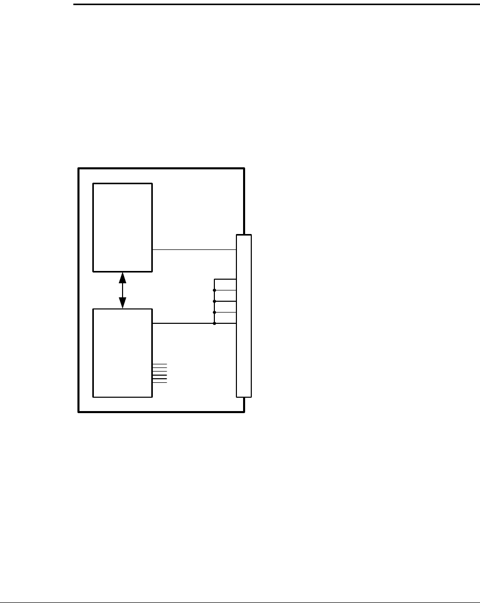
5Platform Communications
The main communications port between the host computer and the UNDP-1 platform
(Figure 5-1) is the high-speed USB interface. This two-wire interface enables software
downloads of boot, modem, and applications images, allows UNDP-1 status
communications, and provides the control link from the host computer to the UNDP-1
platform. An off-chip USB transceiver (the USB ULPI PHY) is used to coordinate USB
communications between the MDM1000 IC and the host computer.
Figure 5-1 UNDP-1 communication interfaces
USB
USB
ULPI
PHY
LED_WWAN
MDM1000
PM6653
status &
control
mini card edge connector
42
USIM
LED driver
UIM_PWR 8
UIM_DATA 10
UIM_CLK 12
UIM_RST_N 14
VREG_RUIM
level
translators
USB_D_N 36
USB_D_P 38

80-VF329-3 Rev. C 24 QUALCOMM Confidential and Proprietary
MAY CONTAIN U.S. EXPORT CONTROLLED INFORMATION
UNDP-1 Universal Notebook Data Platform User Guide Platform Communications
An external RUIM/USIM is supported via the off-board UICC. The PM6653 IC provides
the USIM power supply, thereby enabling support for both 1.8 V and 2.85 V UICCs. All
digital signals are buffered and level-translated by the PM6653 IC as well, ensuring
compatiblity between the external module and the MDM1000 IC.
The PMIC includes a programmable current driver (a current sink) that is used to drive an
off-board LED as required by the PCI Express Mini Card Electromechanical Specification
(key requirements are summarized in Table 5-1). The LED anode is expected to be
connected to a 3.3 V supply (with a current limiting resistor if needed); the cathode is
connected to the LED_WWAN pin that is driven by the PMIC current sink.
NOTE Any unused interface should be left unconnected.
Table 5-1 LED communications
LED state Message communicated
steady-state off UNDP-1 is not on.
steady-state on UNDP-1 is on and connected properly, but not transmitting
or receiving data.
flashing at a steady, slow rate 1
1The flash rate is p.
UNDP-1 is on, connected properly, and actively searching
for an airlink connection.
flashing intermittently 2
2The flash rate is proportional to data activity, a 50% duty cycle with a flash rate between 3 Hz and 20 Hz.
UNDP-1 is on, connected properly, and actively transmitting
or receiving data.

80-VF329-3 Rev. C 25 QUALCOMM Confidential and Proprietary
MAY CONTAIN U.S. EXPORT CONTROLLED INFORMATION
6Standards and Regulatory
Compliance
6.1 Standards and certification
The UNDP-1 platform conforms to the following standards and certification requirements:
■CDMA
❒TIA/EIA IS-98E (CDMA2000 1x)
❒TIA/EIA IS-866 (1xEV-DO)
■UMTS (WCDMA)
❒TS 25.101
■GSM
❒TS 45.005
■FCC
❒47 CFR Part 1 - RF radiation exposure limits
❒47 CFR Part 2 - Equipment authorization
❒47 CFR Part 15 - Unintentional radiators
❒47 CFR Part 22 - Cellular
❒47 CFR Part 24 - PCS
■CE
❒EMC protection requirements
– EN 301 489-1 - Common technical requirements
– EN 301 489-7 - GSM and DCS
– EN 301 489-24 - WCDMA 2100
– EN 301 489-25 - CDMA2000
❒Effective use of spectrum to avoid unwanted interference requirements
– EN 301 908-1 - General requirements
– EN 301 908-2 - WCDMA 2100
– EN 301 908-4 - CDMA2000
– EN 301 511 - GSM900/GSM1800
– EN 301 607-1 - GSM900/GSM1800

80-VF329-3 Rev. C 26 QUALCOMM Confidential and Proprietary
MAY CONTAIN U.S. EXPORT CONTROLLED INFORMATION
UNDP-1 Universal Notebook Data Platform User Guide Standards and Regulatory Compliance
■CTIA/GCF/PTCRB
■Safety
❒EN 50360/61 full carrier certification (carriers TBD)
■Microsoft® WHQL certification
■RoHS compliance
6.2 Regulatory information
6.2.1 Safety warnings
Do not operate the UNDP-1 platform in the following environments:
■In active blasting areas
■In potentially explosive environments such as refuelling points, fuel depots, or
chemical plants
■Near medical equipment, especially life support equipment that might be susceptible
to radio interference
■In an aircraft as follows:
❒UNDP-1 transmissions could interfere with aircraft electrical and communication
systems. Like cell phones, using the UNDP-1 platform in an aircraft is illegal in
some jurisdictions.
❒If cell phone usage is permitted while the aircraft is on the ground, normal UNDP
operation is permitted as well.

80-VF329-3 Rev. C 27 QUALCOMM Confidential and Proprietary
MAY CONTAIN U.S. EXPORT CONTROLLED INFORMATION
UNDP-1 Universal Notebook Data Platform User Guide Standards and Regulatory Compliance
6.2.2 North American compliance
The UNDP-1 platform has been authorized for mobile operation in North America. The
initial authorization grant does not permit end user installation.
A permissive change will be submitted to add end user installation and/or portable usage
conditions. The permissive change application includesdetailed information on UNDP-1’s
two-way authentication procedure preventing use of the module in unauthorized
notebooks.
For mobile applications, the following conditions must be met:
1. Maintain at least a 20 cm separation between the antenna and the user’s body.
2. Radiated transmit power must be equal to or lower than that specified in the FCC
Grant of Equipment Authorization for FCC ID: J9CUNDP-1.
3. To comply with FCC/IC regulations limiting both maximum RF output power and
human exposure to RF radiation, maximum antenna gain (including cable loss) must
not exceed:
❒Cellular band < 4 dBi
❒PCS band < 3.5 dBi
4. Independent UNDP-1 operation — the UNDP-1 platform must not be co-located or
jointly operated with any other transmitter or antenna within the host device.
5. A label with the following statements must be attached to the host end product:
This device contains Tx FCC ID: J9CUNDP-1
This equipment contains equipment certified under IC: 2723A-UNDP1
6. The host end product must include a user manual that clearly defines operating
requirements and conditions that must be observed to ensure compliance with current
FCC/IC RF exposure guidelines.
7. The host end product must also pass the FCC Part 15 unintentional emission testing
requirement and be properly authorized per FCC Part 15.
For portable devices, in addition to the conditions 3 through 6 described above, a separate
approval is required to satisfy the SAR requirements of FCC Part 2.1093 and IC RSS-102.

80-VF329-3 Rev. C 28 QUALCOMM Confidential and Proprietary
MAY CONTAIN U.S. EXPORT CONTROLLED INFORMATION
UNDP-1 Universal Notebook Data Platform User Guide Standards and Regulatory Compliance
6.2.3 EU compliance
The technical construction file of the UNDP-1 platform has been approved by the BABT
notify body. The product is in conformity with the following standards for mobile
operation in the EU:
■EN 301 489 -01
■EN 301 489 -07
■EN 301 489 -24
■EN 301 511
■EN 301 908 -01
■EN 301 908 -02
■EN 50360
For mobile applications, to comply with human exposure to RF radiation limits specified
in EN 50360 and Council Recommendation 1999/519/EC, the following must be met:
1. Maintain at least 20 cm separation between the antenna and the user’s body
2. The maximum antenna gain (including cable loss) must not exceed:
❒900 MHz band < 3 dBi
❒1800 MHz band < 9 dBi
❒IMT 2100 MHz band < 12 dBi
3. Independent UNDP-1 operation. The UNDP-1 platform must not be co-located or
jointly operated with any other transmitter or antenna within the host device.
A CE mark shall be attached to the product.