Oce Technologies 3010120604 RFID Module User Manual
Oce Display Graphics Inc RFID Module Users Manual
Users Manual

ENGINEERING SPECIFICATION DOCUMENT
Project: CALGARY
rfid-hardware_REV5
CONFIDENTIAL
Page 1 of 17
Design Specification
Radio Frequency Identification Board
Department: R&D Richmond
Document#: 301010xxxx
Authors:
Kevin Deane-Freeman
Yanchun Zhang
Darren Rafferty
Current Revision: 4
Revision
Description
Author
Date
1
Initial Need/Want documentation
Kevin Deane-Freeman
Yan chun Zhang, Darren Rafferty
27/02/07
10/05/07
2
Added RF Output plots, revised
features table
Kevin Deane-Freeman
19/06/07
3
Simply some logic implementation
Yan chun Zhang, Darren Rafferty
09/07/07
4
Add Functional Description and
Block Diagram
Kevin Deane-Freeman
14/07/09
Océ Display Graphics Systems
Richmond Office
13231 Delf Place, #501
Richmond, BC
V6V 2C3
Canada
Phone: 604-232-2310 or
604-232-2328
ENGINEERING SPECIFICATION DOCUMENT
Project: CALGARY
rfid-hardware_REV5
CONFIDENTIAL
Page 2 of 17
1.1
Functional Description ............................................................................................................... 4
1.2
Addressing ....................................................................................................................................... 5
1.2.1
RFID Board PCI Shadow Memory Address Map ............................................... 5
1.3
Hardware Capabilities ................................................................................................................. 6
1.3.1
Planned Features ............................................................................................................ 6
1.3.2
Standards Compliance ................................................................................................. 6
1.3.3
RF Output Characteristics .......................................................................................... 7
2.1
Hardware Control .......................................................................................................................... 8
2.1.1
I. CODE1 Label IC Memory Definition ............................................................................ 9
2.1.2
Register Definition ................................................................................................................. 9
2.1.3
Registers Initialization for Communication ............................................................... 10
2.1.4
Access the Reader Internal Registers ......................................................................... 11
2.1.5
I.CODE1 Commands ............................................................................................................ 11
2.1.6
Access Label IC memory ................................................................................................... 12
2.2. Appendix ............................................................................................................................................. 15
ENGINEERING SPECIFICATION DOCUMENT
Project: CALGARY
rfid-hardware_REV5
CONFIDENTIAL
Page 3 of 17
Figure 1.1 Block Diagram (Antenna 1 shown selected) ................................................... 4
Figure 1.2 RFID PCI Address Map ............................................................................................. 5
Figure 1.3 Features Table ............................................................................................................. 6
Figure 1.4 TX1 Output, No Load ................................................................................................ 7
Figure 1.5 TX2 Output, No Load ................................................................................................ 8
Figure 2.1 I.CODE1 Label ICs EEPROM Memory ................................................................ 9
Figure 2.2 Reader Registers Initialization ........................................................................... 11
ENGINEERING SPECIFICATION DOCUMENT
Project: CALGARY
rfid-hardware_REV5
CONFIDENTIAL
Page 4 of 17
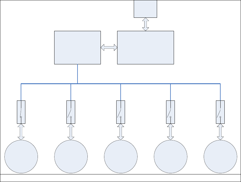
1.1
Functional Description
The design is based on the CL RC 632 Multi-Protocol reader IC from NXP.
The reader is able to access up to 8 antennas using an Intersil DG411 SPST
analog switch for each antenna. Antenna selection is enabled by a CPLD
that, based on the state of the SPI Chip Select signal, either sets one of the
eight switch control lines or passes the SPI communication through to the
reader IC.
Each antenna has its own passive impedance matching circuit and EMI filter
leading into the analog switch.
A block diagram is shown below.
RJ45
ANTENNA
1
RC632 RFID CPLD
READER (Serial Interface / Switch
Selection)
ANTENNA
ANTENNA
ANTENNA
2 3 4
ANTENNA
5
Figure 1.1 Block Diagram (Antenna 1 shown selected)

ENGINEERING SPECIFICATION DOCUMENT
Project: CALGARY
rfid-hardware_REV5
CONFIDENTIAL
Page 5 of 17
1.2
Addressing
1.2.1
RFID Board PCI Shadow Memory Address Map
HEAD
(15~11)
BID
8~6
MODULE SEL (BIT5~2)
REGISTER SEL (BIT1~0)
WR
RD
PCI
OFFSET
ID
10101/
10110
101
0000
PCI INTERFACE
00
BID WRITE
X
680
#1
01
RESERVED
682
10
RESET / WATCHDOG
X
684
11
LINK ACK CNTRL
X
X
686
101
101
0001
RFID
WRITE MEMORY
ACCESS
00
BLOCK ADDR REG
X
688
01
IRQ MASK
X
68A
10
WR DATA(L)
X
68C
11
WR DATA(H)
X
68E
101
0010
RFID
REGISTER
CONTROL
00
CONTROL REG
X
690
01
READ ADDR REG
X
692
10
WRITE ADDR REG
X
694
11
WRITE DATA REG
X
696
101
0011
RFID DATA READ
00
REGISTER DATA
X
698
01
INTERNAL EEPROM
RFU*
69A
10
MEM DATA (L)
X
69C
11
MEM DATA (H)
X
69E
101
0100
RFID
READ MEMORY
ACCESS
00
READ MEM ADDR
X
6A0
01
BLOCK NUMBER
X
6A2
10
READ DATA REQ
X
6A4
11
SPI BUSY FLAG (RFU)
X
6A6
101
0101
RFID READ
STATUS
00
MEM DATA READY
X
X
6A8
01
BMEM UPDATED
X
X
6AA
10
ANTENNA SELECT
X
6AC
11
MEM WRITE DONE
X
X
6AE
101
0110
RFU
00
X
6B0
01
X
6B2
10
X
6B4
11
X
6B6
101
0111
RFU
00
X
6B8
01
X
6BA
10
X
6BC
11
X
X
6BE
101
1000
RFU
00
X
6C0
01
X
X
6C2
10
X
6C4
11
X
X
6C6
101
1001
RFU
00
X
X
6C8
01
X
X
6CA
10
X
X
6CC
11
X
6CE
101
1010
RFU
00
X
6D0
01
X
6D2
10
X
6D4
11
X
6D6
101
1011
RFU
00
X
6D8
01
X
6DA
10
X
6DC
11
X
6DE
101
1100
RFU
00
X
6E0
01
X
X
6E2
10
X
6E4
11
X
6E6
101
1101
RFU
00
X
6E8
01
X
X
6EA
10
X
X
6EC
11
X
X
6EE
101
1110
RFU
00
X
6F0
01
X
6F2
10
X
6F4
11
X
6F6
101
1111
RFU
00
X
6F8
01
X
6FA
10
X
6FC
11
X
6FE
Figure 1.2 RFID PCI Address Map
*Reserved for future use

ENGINEERING SPECIFICATION DOCUMENT
Project: CALGARY
rfid-hardware_REV5
CONFIDENTIAL
Page 6 of 17
1.3
Hardware Capabilities
1.3.1
Planned Features
Feature
Minimum Required
Desired/Future Performance
Reader Channels
5
6
Polling speed
1channel per second
1channel per < 200ms
Ch. Read Range
1.25”
2”
Ch. Write Range
As above
As above
Write/Verify
No
Yes
Antenna Spacing
78mm
78mm
Figure 1.3 Features Table
1.3.2
Standards Compliance
The product is intended for a worldwide market. ODGS will test to FCC and
EU standards for CE mark. Operational companies will test to local
standards. Compliance with the following standards should meet the
requirements of all markets:
Equipment Tested RFID2 Radio Module
PMN: RFID Reader 2
HVIN: 3010120604
Model Number: 3010120604
FCC ID: U2P-3010120604
IC Certification Number: 6947A-3010120604
Manufacturer: Océ Display Graphics Systems
Generic Industrial Immunity:
EN61000-6-2: 2005
Emissions:
47 CFR Part 15 – Radio Frequency Devices, Subpart C – Intentional
Radiator
15.209: Radiated emission limits; general requirements
15.225: Operation within the band 13.110-14.010 MHz
RSS-210 Issue 9 – License-exempt Radio Apparatus (All Frequency
Bands): Category I Equipment
Annex A2.6: Band 13.110-14010 MHz
RSS-Gen Issue 4 – General Requirements and Information for the
Certification of Radio Apparatus
ETSI EN300300-1: 2010
ETSI EN300330-2: 2010
ENGINEERING SPECIFICATION DOCUMENT
Project: CALGARY
rfid-hardware_REV5
CONFIDENTIAL
Page 7 of 17
Warnings for FCC:
FCC Part 15
This device complies with FCC Rules Part 15 operation is subject to the following two
conditions:
1. This device may not cause harmful interference.
2. This device must accept any interference, including interference that may cause
undesired operation of the device.
Changes or modifications to this device, not expressly approved by XXXX. could void
the user’s authority to operate the equipment.
Warnings from RSS-Gen Issue 4 Section 8.4 and RSP-100 Issue 11 Section 4:
This device complies with Industry Canada’s license-exempt RSSs. Operation is
subject to the following two conditions:
(1) This device may not cause interference; and
(2) This device must accept any interference, including interference that may cause
undesired operation of the device.
Le présent appareil est conforme aux CNR d'Industrie Canada applicables aux
appareils radio exempts de licence. L'exploitation est autorisée aux deux conditions
suivantes :
(1) l'appareil ne doit pas produire de brouillage, et
(2) l'utilisateur de l'appareil doit accepter tout brouillage radioélectrique subi, même si
le brouillage est susceptible d'en compromettre le fonctionnement.
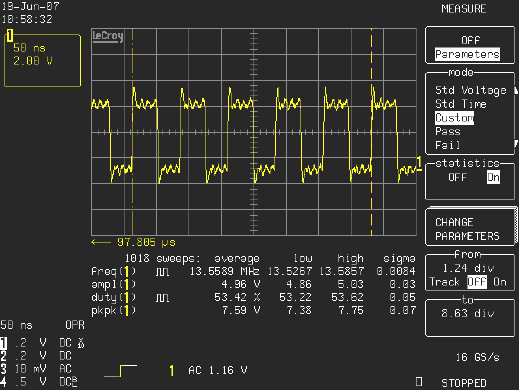
1.3.3
RF Output Characteristics
Figure 1.4 TX1 Output, No Load
ENGINEERING SPECIFICATION DOCUMENT
Project: CALGARY
rfid-hardware_REV5
CONFIDENTIAL
Page 8 of 17
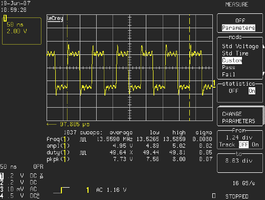
Figure 1.5 TX2 Output, No Load
2.1
Hardware Control
CL RC 632 is a new family of highly integrated reader ICs for contactless
communication at 13.56MHz, which includes 64 registers (8bits/each), 64 byte
FIFO, as well as 32*16 byte EEprom. I.CODE1 Label IC is a dedicated 512 bit
memory chip for electronic label applications such as detecting the presence of ink
bag. RFID system operates in a so called “reader talks first” principle. The reader
sends a command first, and the labels execute the instruction and send back their
response to the buffer of the reader.
Based on current Calgary structure, a RFID PCB board is designed to
communicate with the Data Relay Card using the fourth SPI generic port. It is
eventually intended to replace the third party board Smart RFID Multiplex Reader
Board. There is only one single reader with five antennas and one CPLD on the
PCB board. Due to current specific SPI interface is designed for the RFID board,
the fourth SPI port cannot be used as a generic SPI communication port any more.
CPLD is used to select which antenna will be communicated with the Reader.
Serial data clock is 4.16MHz. The bit decoding of Label IC is fast mode with a
13.56Mhz carrier: each command consists of a start pulse (18.88us modulation),
followed by one 8-bit instruction byte, five 8-bit parameter bytes, and two CRC
bytes (16-bit CRC).
The basic rules for software accessing Label IC is that software is required to first
select antenna, switch on the RF, enable CRC16, force the RFID reader state
machine back to idle, clear the reader buffer, and finally to set block start address
and block numbers which software needs read/write data from/to the Label IC.
Once software gets data back from the Label IC, software may need to issue a
switch off RF command so as to reduce the interference from RFID board, except
when software needs to hold the Label IC in selected condition.
While the protocol allows for communication with multiple tags, collision detection
and selection is not implemented. The reader will expect to communicate with the
first tag that responds on each channel.

ENGINEERING SPECIFICATION DOCUMENT
Project: CALGARY
rfid-hardware_REV5
CONFIDENTIAL
Page 9 of 17
2.1.1
I. CODE1 Label IC Memory Definition
The 512 bit EEprom memory is divided into 16 blocks. A block is the smallest
access unit. Each block consists of 4 bytes. Bit 0 in each byte represents the LSB
(least significant bit) and bit 7 the MSB (most significant bit). The following table
shows the definition for each block.
Block 0
Block 1
Block 2
Block 3
Block 4
Block 5
Block 6
Block 7
Block 8
Block 9
Block 10
Block 11
Block 12
Block 13
Block 14
Block 15
Byte0 Byte1 Byte2 Byte3
Serial Number
Write Access Conditions
Special Functions (EAS/QUIET)
User Data
.
.
.
.
.
.
.
.
.
User Data
Figure 2.1 I.CODE1 Label ICs EEPROM Memory
2.1.2
Register Definition
1. Antenna Select Register
There is only one single reader with five antennas (five Label ICs) on the PCB RFID
board; hence the defined antenna select register is used to select which antenna will
be communicated with data relay card (only one bit for each command is allowed to
be active). Allow 1ms for switch settling time.
Antenna Select Register
Bit
7~5
4
3
2
1
0
RFU
Antenna
5
Antenna
4
Antenna
3
Antenna
2
Antenna
1
2. Reader Internal Registers
SNR0
SNR1
SNR2
SNR3
SNR4
SNR5
SNR6
SNR7
F0
FF
FF
FF
x
x
x
x
x
x
x
x
x
x
x
x
x
x
x
x
x
x
x
x
x
x
x
x
x
x
x
x
x
x
x
x
x
x
x
x
x
x
x
x
x
x
x
x
x
x
x
x
x
x
x
x

ENGINEERING SPECIFICATION DOCUMENT
Project: CALGARY
rfid-hardware_REV5
CONFIDENTIAL
Page 10 of 17
The RFID register control (Module Sel Addr:0010) used in this module include:
CONTROL REG (12 bits): Command Register
WRITE ADDR REG (6 bits): Write register address
READ ADDR REG (6 bits): Read register address
WRITE DATA REG (8 bits): Write data register
Control Register
Bit
11
10
9
8
7~5
4
3
2
1
0
TX
Start
Rst
Quiet
Unsel
Rd
EAS
Test
RFU
Sel
En
Reg
Wr
Reg
Rd
Mem
Wr
Mem
Sel Rd
Bit0 (Mem Sel Rd): Label IC Memory Selected Read
Bit1 (Mem Wr): Label IC Memory Write Block X
Bit2 (Reg Rd): Reader Register Read
Bit3 (Reg Wr): Reader Register Write
Bit4 (Mem Sel Rd): Label IC Anticollision/Select
Bit 5~7 (RFU): Reserved for future use
Bit8 (EAS Test): Label IC EAS test
Bit9 (Unsel Rd): Label IC unselected memory read
Bit10 (Rst Quiet): Label IC Reset QUIET Bit
Bit11 (TX Start): Transmit Start, default should be set to high. It is used for
debugging, and once this bit is set to zero, the data in reader buffer cannot be
transmitted.
2.1.3
Registers Initialization for Communication
In order to enable the I.CODE1 functionality, the following table lists the reader
register initial values. Some of them may need change according to requirements
with different RFID boards.
Register Name
Register Address
Value
Page
10
00
TxControl
11
58
CWConductance
12
3F
ModConductance
13
01
CoderControl
14
35
ModWidth
15
3F
ModWidthSOF
16
73
TypeBFraming
17
00
Page
18
00
RxControl1
19
8B
DecoderControl
1A
00
BitPhase
1B
54
RxThreshold
1C
68
BPSKDemControl
1D
00
RXControl2
1E
41
ClockQControl
1F
00
Page
20
00
RxWait
21
08

ENGINEERING SPECIFICATION DOCUMENT
Project: CALGARY
rfid-hardware_REV5
CONFIDENTIAL
Page 11 of 17
ChannelRedundancy
22
0C
CRCPresetLSB
23
FE
CRCPresetMSB
24
FF
TimeSlotPeriod
25
00
MFOUTSelect
26
00
PreSet27
27
00
Page
28
00
FIFOLevel
29
3E
TimerClock
2A
0B
TimerControl
2B
02
TimerReload
2C
00
IRQPinConfig
2D
02
PreSet2E
2E
00
PreSet2F
2F
00
Figure 2.2 Reader Registers Initialization
2.1.4
Access the Reader Internal Registers
(1). When writing data to the reader internal register, the following three data packets
should be sent:
First data packet: write 694 to register address
Second data packet: write 696 to register data
Third data packet: write 690 to 08 (write command)
(2). When reading data from Reader internal register, the following three data
packets should be sent:
First data packet: write 692 to register address
Second data packet: write 690 to 04 (read command)
Third data packet: read register data from address 698
2.1.5
I.CODE1 Commands
A selection of the Label IC is necessary for valid execution of the following
commands:
Selected Read
Write
Halt (Reserved for future use)
Once an I.CODE1 Label IC is selected, it does not respond to the following
command:
Anticollision/Select
Unselected Read
The following commands work for both the selected and unselected states:
EAS
Reset QUIET Bit
ENGINEERING SPECIFICATION DOCUMENT
Project: CALGARY
rfid-hardware_REV5
CONFIDENTIAL
Page 12 of 17
After the Label IC has been selected, if the unselected command should be issued,
you need to re-enter Label IC or switch off the RF.
2.1.6
Access Label IC memory
Communication normally begins with the software sending a command and the Label
IC responding. Commands always initiate a response except Reset Quiet Bit
command. Some commands have prerequisite parameters such as memory
read/write.
Current RFID firmware code supports the following commands:
Reset QUIET Bit
Unselected Read
Anticollision/Select
Write Block X
Selected Read
EAS Test
Manufacturer delivers the Label IC with the following configuration:
(1) Serial number (block 0 and block 1) is unique, read only.
(2) Write Access Conditions determine if blocks 3 through 15 can be accessed for writing.
For Byte 0 in block 2:
If set bit5 and bit4 to 1|1: Write access enabled.
If set bit5 and bit4 to 0|0: Write access disabled.
Be aware that writing of bit pairs 1|0 or 0|1 to block 2 is not allowed! Also the label must
not be moved out of the communication field of the antenna during writing operation!
(3) EAS test mode default setting is not defined. If you want to do an EAS test, you have to
enable EAS test first by writing 1|1 to bit1 and bit0 in byte 0 of block 3.
(4) Quiet mode default setting is not defined at delivery. Reset Quiet Bit command should be
executed on the Label IC first, otherwise the Label IC does not respond to any command
(except EAS command if the EAS mode is enabled) if the two bits (bit2 and bit3 in byte0
of block 3) are set to one (quiet mode is enabled).
(5) Family Code/Application Identifier and User data memory is not defined.
In order to implement the above commands, an antenna select command should be
issued first by software so that hardware knows which antenna should be
communicated, and the data packages (See appendix) should be sent by sequence.
Since the internal register setting of the reader is similar for each command, firmware
FPGA will implement these setting packages (A, B, C, D, E, F, J/I) automatically
when it receives a command as described below from software.
Also be aware that before you send a memory write command or an
anticollision/select command, set Unselected Read command first, as the second
byte of the serial number is used to calculate a quit value as a result of critical timing
issue with SPI interface, this quit value is required when issuing an
anticollision/select or memory write command.
(1) Reset QUIET Bit

rfid-hardware_REV5
CONFIDENTIAL
Page 13 of 17
ENGINEERING SPECIFICATION DOCUMENT
Project: CALGARY
Action: QUIET bits are cleared for all I.CODE1 Label ICs in the antenna
field, which are in QUIT mode.
Parameters: None
Commands: N package
Response
:
None
(2) Unselected Read
Before issuing an unselected read command, software needs to set read block
start address and the number of blocks first. The Label IC will respond with its
required data bytes, which are stored to the buffer of the reader.
Action: Each of the unselected I.CODE1 Label ICs responds with the
requested number of block
Parameters: Required block start address of data to be read
Required number of blocks to be read
Commands: G, K package
Response
:
Data bits of X blocks, 16 bit CRC
There are 16*32bit dual port block memory locations for latching the data read
from the reader memory. After sending these packages, software needs to read
the busy flag status from the PCI shadow memory address 6A8. Once this bit
has been set to one, software needs to send a read data command (6A4) and
immediately clear the busy flag. The read data command definition is as follows:
Reading IC buffer data command (6A4)
Bit
4
3~0
Read Command
Block number
Once this command has been sent, the firmware will read 32 bits word data from
internal block memory to PCI shadow memory responding to this command.
When PCI shadow memory address 6AA (BMEM UPDATED) has been set to one,
software can get the 32bits data from PCI shadow memory address 69C, and
also software is required to clear this bit (BMEM UPDATED) as well.
For whole memory data read requires at least 25ms.
(3) Anticollision/Select
When firmware receives the serial numbers after issuing an Anticollision/Select
command, it will transmit a QUIT byte immediately. The Label IC will remain in
the timeslot chosen at this command for all further commands, such as memory
write and selected read, until it leaves (and re-enters) the RF field.
Action: Each of the unselected the Label IC responds with its 64 bits
serial number in different timeslots
Parameters: None
rfid-hardware_REV5
CONFIDENTIAL
Page 14 of 17
ENGINEERING SPECIFICATION DOCUMENT
Project: CALGARY
Commands: M package
Response
:
64 bit SNR (Serial Number), 16 bit CRC
(4) Write Block X
Remember that this command is required to a selection of the Label IC
(Anticollision/Select). Before issuing a write command, software needs to set the
block address and 4 bytes of data. Once each of the selected Label IC responds
with its 64 bit serial number, firmware will send a quit value immediately so that
the given 4 bytes of data are written to the address block if Label IC receives a
QUIT from the reader in its timeslot.
Action: Given 4 bytes of data are written to the address block if Label IC
receives a QUIT from the reader in its timeslot.
Parameters: Required block address of data to be written
Required 4 bytes data to be written
Commands: H, O package
Response
:
64 bit SNR (Serial Number), 16 bit CRC
In addition, a minimum delay time of 4852.16 s (included in ‘total time*’) is
required before the starting of a new command or switching off the RF due to
EEPROM programming in Label IC. After software issuing a memory write
command, firmware will send memory write done flag (6AE) to inform software,
this flag means that firmware already finished sending a QUIT value to Label IC,
therefore, the waiting time should be considered by software.
Total time: 18.88 + 2416.64 + n * (325.68 + 3020.8 + 269.04 + 311.52) + 4852.16 =
7287.68 + n * 3927.04
s
Here, n = number of timeslots
(5) Selected Read
The operation is similar to the Unselected Read except this command
is required to a selection of the Label IC (Anticollision/Select).
Each Label IC has his own antenna, and also the space between any two
antennas is big enough to prevent from the interference among them, therefore
this command is no necessary for current application.
Action: Each of the selected the Label IC responds with the given number
of blocks in its timeslot at which the Label IC was fixed with the
Anticollision/ Select command
Parameters: Required block start address of data to be read
Required number of blocks to be read
Commands: G, P package
rfid-hardware_REV5
CONFIDENTIAL
Page 15 of 17
ENGINEERING SPECIFICATION DOCUMENT
Project: CALGARY
Response
:
Data bits of X blocks, 16 bit CRC
(6) EAS Test
Once again, EAS test mode default setting is not defined by manufacture. Enable
EAS test is required by writing 1|1 to bit1 and bit0 in byte 0 of block 3 before
issuing EAS test.
Action: I.CODE1 Label IC responds with a special predefined EAS
pattern (256bits)
Parameters: None
Commands: Q package
Response
:
256 bit special EAS response
After Label IC receives this command, the corresponding 32 bytes in
hexadecimal notation as follows:
2F B3 62 70 D5 A7 90 7F
E8 B1 80 38 D2 81 49 76
82 DA 9A 86 6F AF 8B B0
F1 9C D1 12 A5 72 37
EF
2.2. Appendix
Antenna select should be issued first by software before the following package commands:
A package: switching on RF
Addr Data
694 11 (16bits); Tx Control register address
696 4B (16bits);
690 08 (16bits); Write command
B package: Enable 16bits CRC
Addr Data
694 22 (16bits);
696 0C (16bits);
690 08 (16bits);
rfid-hardware_REV5
CONFIDENTIAL
Page 16 of 17
ENGINEERING SPECIFICATION DOCUMENT
Project: CALGARY
C package: Preset LSB for the CRC register
Addr Data
694 23 (16bits);
696 FE (16bits);
690 08 (16bits);
D package: Preset MSB for the CRC register
Addr Data
694 24 (16bits);
696 FF (16bits);
690 08 (16bits);
E package: Force Reader back to idle state
Addr Data
694 01 (16bits)
696 00 (16bits)
690 08 (16bits)
F package: Clear buffer
Addr Data
694 09 (16bits)
696 01 (16bits)
690 08 (16bits)
G package: Set memory read start address and block numbers
Addr Data
6A0
X (16bits); Set memory start block address (x-1=0…15)
6A2
y (16bits); Set number of blocks (0…15)
H package: Set memory write address and data
Addr Data
688 x (16bits); Set memory block address (0…15)
68C x (32bits); Set writing data to Label IC
I package: Set time slot period
Addr Data
694 25 (16bits);
696 5F (16bits);
690 08 (16bits);
J package: clear time slot period
Addr Data
694 25 (16bits);
696 00 (16bits);
690 08 (16bits);
K package: Sending unselected read command
Addr Data
690 A0016bits);
L package: Switching off RF (preventing from interference)
Addr Data
694 11 (16bits);
rfid-hardware_REV5
CONFIDENTIAL
Page 17 of 17
ENGINEERING SPECIFICATION DOCUMENT
Project: CALGARY
696 58 (16bits);
690 08 (16bits);
M package: Sending Anticollision/Select command
Addr Data
690 810(16bits);
N package: Sending Reset Quiet Bit command (Respond, None)
Addr Data
690 C00 (16bits);
O package: Sending write block x command
Addr Data
690 802 (16bits);
P package: Sending selected read memory command (Responds memory data of
numbers of blocks)
Addr Data
690 801 (16bits);
Q package: Sending EAS test command (Corresponding 32 bytes data in
hexadecimal)
Addr Data
690 900 (16bits);