Omega Engineering Daq 12 Users Manual Word Pro 12.lwp
DAQ-12 M3453
DAQ-12 to the manual ec8ddff5-0c4f-50b4-c55e-fa369bad8d54
2015-02-02
: Omega-Engineering Omega-Engineering-Daq-12-Users-Manual-439843 omega-engineering-daq-12-users-manual-439843 omega-engineering pdf
Open the PDF directly: View PDF ![]() .
.
Page Count: 31


WARRANTY/DISCLAIMER
OMEGA ENGINEERING, INC., warrants this unit to be free of defects in materials and workmanship for a period of 13
months from the date of purchase. OMEGA warranty adds an additional one (1) month grace period to the normal one (1)
year product warranty to cover shipping and handling time. This ensures that OMEGA’s customers receive maximum
coverage on each product. If the unit should malfunction, it must be returned to the factory for evaluation. OMEGA’s
Customer Service Department will issue an Authorized Return (AR) number immediately upon phone or written request.
Upon examination by OMEGA, if the unit is found to be defective it will be repaired or replaced at no charge. OMEGA’s
warranty does not apply to defects resulting from any action of the purchaser, including but not limited to mishandling,
improper interfacing, operation outside design limits, improper repair or unauthorized modification. This WARRANTY is
VOID if the unit shows evidence of having been tampered with or shows evidence of being damaged as a result of excessive
corrosion; or current, heat, moisture or vibration; improper specification; misapplication; misuse or other operating
conditions outside of OMEGA’s control. Components which wear are not warranted, including but not limited to contact
points, fuses and triacs.
OMEGA is pleased to offer suggestions on the use of its various products. However, OMEGA neither assumes
responsibility for any omissions or errors nor assumes liability for any damages that result from the use of its products
in accordance with information provided from OMEGA, either verbal or written. OMEGA warrants only that the parts
manufactured by it will be as specified and free of defects. OMEGA MAKES NO OTHER WARRANTIES OR
REPRESENTATIONS OF ANY KIND WHATSOEVER, EXPRESSED OR IMPLIED, EXCEPT THAT OF TITLE, AND
ALL IMPLIED WARRANTIES INCLUDING ANY WARRANTY OF MERCHANTABILITY AND FITNESS FOR A
PARTICULAR PURPOSE ARE HEREBY DISCLAIMED. LIMITATION OF LIABILITY: The remedies of purchaser set
forth herein are exclusive and the total liability of OMEGA with respect to this order, whether based on contract,
warranty, negligence, indemnification, strict liability or otherwise, shall not exceed the purchase price of the component
upon which liability is based. In no event shall OMEGA be liable for consequential, incidental or special damages.
CONDITIONS: Equipment sold by OMEGA is not intended to be used, nor shall it be used: (1) as a “Basic Component”
under 10 CFR 21 (NRC), used in or with any nuclear installation or activity, medical application or used on humans.
Should any Product(s) be used in or with any nuclear installation or activity, medical application, used on humans or
misused in any way, OMEGA assumes no responsibility as set forth in our basic WARRANTY/DISCLAIMER language, and
additionally, purchaser will indemnify OMEGA and hold OMEGA harmless from any liability or damage whatsoever
arising out of the use of the Product(s) in such a manner.
RETURN REQUESTS/INQUIRIES
Direct all warranty and repair requests/inquiries to the OMEGA Customer Service Department. BEFORE RETURNING
ANY PRODUCT(S) TO OMEGA, PURCHASER MUST OBTAIN AN AUTHORIZED RETURN (AR) NUMBER FROM
OMEGA’S CUSTOMER SERVICE DEPARTMENT (IN ORDER TO AVOID PROCESSING DELAYS). THE ASSIGNED
NUMBER SHOULD THEN BE MARKED ON THE OUTSIDE OF THE RETURN PACKAGE AND ON ANY
CORRESPONDENCE. THE PURCHASER IS RESPONSIBLE FOR SHIPPING CHARGES, FREIGHT, INSURANCE AND
PROPER PACKAGING TO PREVENT BREAKAGE IN TRANSIT.
FOR WARRANTY RETURNS, please have the following information available BEFORE contacting OMEGA:
(1) P.O. Number under which the product was purchased,
(2) Model and serial number of the product under warranty, and
(3) Repair instructions and/or specific problems relative to the product.
FOR NON-WARRANTY REPAIRS, consult OMEGA for current repair charges. Have the following information available
BEFORE contacting OMEGA:
(1) P.O. Number to cover the cost of the repair,
(2) Model and serial number of the product, and
(3) Repair instructions relative to the product.
OMEGA’s policy is to make running changes, not model changes, whenever an improvement is possible. This affords our
customers the latest in technology and engineering. OMEGA is a registered trademark of OMEGA ENGINEERING, INC. ©
Copyright 1999 OMEGA ENGINEERING, INC. All rights reserved. This document may not be copied, photocopied,
reproduced, translated or reduced to any electronic medium or machine readable form, in whole or in part, without prior
written consent of OMEGA ENGINEERING, INC.
DAQ-12 Users Manual 2

Declaration of Conformity
Manufacturer's Name: Omega Engineering, Inc.
Manufacturer’s Address: One Omega Drive
Stamford, CT 06907-0047
Application of Council Directive: 89/336/EEC
Standards to which
Conformity is Declared: * EN50081-2
(EN55022, EN60555-2, EN60555-3)
* EN50082-1
(IEC 801-2, IEC 801-3, & IEC 801-4)
Type of Equipment: Information Technology Equipment
Equipment Class: Light Industrial Equipment
Product Name: ISA Data Acquisition Card
Model Number : DAQ-12
DAQ-12 Users Manual 3

OMEGAnet On-line Service: Internet e-mail:
http://www.omega.com info@omega.com
Servicing North America:
USA: One Omega Drive, Box 4047 E-mail: info@omega.com
ISO 9001 Certified Stamford, CT 06907-0047
Tel: (203) 359-1660 FAX: (203) 359-7700
Canada: 976 Bergar E-mail: info@omega.com
Laval (Quebec) H7L 5A1
Tel: (514) 856-6928 FAX: (514) 856-6886
For immediate technical or application assistance:
USA and Canada: Sales Service: 1-800-826-6342 / 1-800-TC-OMEGASM
Customer Service: 1-800-622-2378/ 1-800-622-BESTSM
Engineering Service: 1-800-872-9436 / 1-800-USA-WHENSM
TELEX: 996404 EASYLINK: 62968934 CABLE: OMEGA
Mexico and Latin America: Tel: (001) 800-826-6342 FAX: (001) 203-359-7807
En Espanol: (001) 203-359-7803 E-mail: espanol@omega.com
Servicing Europe:
Benelux: Postbus 8034, 1180 LA Amstelveen, The Netherlands
Tel: (31) 20 6418405
Toll Free in Benelux: 0800 0993344
E-mail: nl@omega.com
Czech Republic: ul.Rude armady 1868, 733 01 Karvina-Hraniee
Tel: 42 (69) 6311899 FAX: 42 (69) 6311114
Toll Free: 0800-1-66342 E-mail: czech@omega.com
France: 9, rue Denis Papin, 78190 Trappes
Tel: (33) 130-621-400
Toll Free in France: 0800-4-06342
E-mail: france@omega.com
Germany/Austria: Daimlerstrasse 26, D-75392 Deckenpfronn, Germany
Tel: 49 (07056) 3017
Toll Free in Germany: 0130 11 21 66
E-mail: germany@omega.com
DAQ-12 Users Manual 4

United Kingdom: One Omega Drive, River Bend Technology Drive
ISO 9002 Certified Northbank, Irlam, Manchester
M44 5EX, England
Tel: 44 (161) 777-6611
FAX: 44 (161) 777-6622
Toll Free in England: 0800-488-488
E-mail: info@omega.co.uk
It is the policy of OMEGA to comply with all worldwide safety and EMC/EMI regulations that apply.
OMEGA is constantly pursuing certification of it’s products to the European New Approach
Directives. OMEGA will add the CE mark to every appropriate device upon certification.
The information contained in this document is believed to be correct but OMEGA Engineering, Inc.
accepts no liability for any errors it contains, and reserves the right to alter specifications without
notice. WARNING: These products are not designed for use in, and should not be used for, patient
connected applications.
DAQ-12 Users Manual 5

Table of Contents
29
4.2 Programming the 8254 Counter/Timer
............................
28
4.1.9 8254 Control Word/Status Register
...................................
28
4.1.8 Multi-Function Timer Register
.......................................
28
4.1.7 Clock Rate Register (high word)
.....................................
28
4.1.6 Clock Rate Register (low word)
......................................
28
4.1.5 D/A Converter 1 Register
...........................................
28
4.1.4 D/A Converter 0 Register
...........................................
27
4.1.3 A/D Converter Data Register
.......................................
27
4.1.2 Start of Conversion Register
.........................................
25
4.1.1 Control Word Register
............................................. 25
4.1 Register Description
.............................................. 25
4. Register Description and Programming
.....................
23
3. External Connections
.............................................
22
2.8.1 External Interrupt
................................................. 22
2.8 Interrupts
........................................................ 21
2.7 Direct Memory Access
........................................... 20
2.6 Trigger Selection
.................................................
19
2.5.2 External Clock
....................................................
18
2.5.1 Internal Clock
..................................................... 17
2.5 Clock Selection
................................................... 16
2.4 Base Address
..................................................... 16
2.3 Digital Input/Output
............................................. 14
2.2 Digital to Analog Converters
..................................... 10
2.1 Analog to Digital Converter
...................................... 10
2. Circuit Board Description and Configuration
..............
9
1.2 DAQ-12 Specifications
............................................. 8
1.1 Installation
........................................................ 8
1. Introduction
.........................................................
DAQ-12 Users Manual 6

List of Figures and Tables
25
Table 4-1. DAQ-12 Address Map
...............................................
15
Table 2-3. D/A Converter Mode Selection Options
................................
14
Table 2-2. A/D Conversion Format Examples
....................................
12
Table 2-1. Recommended Input Ranges and Gain Settings
.........................
23
Figure 3-1. 62 Pin Connector Diagram
...........................................
22
Figure 2-11. Jumpers J10 and J11 Configuration
....................................
21
Figure 2-10. Jumpers J8 and J9 Configuration
......................................
20
Figure 2-9. Jumper J2 Configuration
.............................................
20
Figure 2-8. Pre-Divider External Clock Pulses
.....................................
19
Figure 2-7. Sampling Rate External Clock Pulses
..................................
17
Figure 2-6. Jumper J3 Configuration
.............................................
16
Figure 2-5. I/O Base Address Selection
..........................................
14
Figure 2-4. Jumper J4 Configuration
.............................................
13
Figure 2-3. Jumper J6 Configuration
.............................................
11
Figure 2-2. Jumper J7 Configuration
.............................................
10
Figure 2-1. Jumper J1 Configuration
.............................................
DAQ-12 Users Manual 7

1. Introduction
The DAQ-12 is a high speed data acquisition adapter for IBM AT and compatible machines
offering eight differential analog input channels with 16-bit resolution, two analog output
channels with 12-bit resolution and four digital input/output lines. Other features of the
DAQ-12 include:
Analog to Digital Converter
200 KHz maximum sampling rate
Bipolar input ranges from ±10mV to ±10 volts
Unipolar input ranges from 20mV to 10 volts
Programmable gain selection
Two DMA channels for continuous acquisition
Internal or external clock and trigger
Digital to Analog Converters
Two independent analog output channels
Output ranges of 0 to ±5 volts
Internal or external voltage reference
Two DMA channels for continuous output
Other Features
Interrupt on one of four sources including an external interrupt input
High density D-62 connector for reduced noise
1.1 Installation
1. Configure the DAQ-12 utilizing the instructions in Chapter 2: Circuit Board
Description and Configuration.
2. Ensure that power is not applied to the computer system.
3. Remove the cover according to the instructions provided by the system
manufacturer.
4. Insert the DAC-16 into any vacant ISA expansion slot. The board is secured to the
slot by installing the Option Retaining Bracket (ORB) screw.
5. Replace the system cover per manufacturer instructions.
DAQ-12 Users Manual 8
1.2 DAQ-12 Specifications
DACK 5, 6, 7
DRQ 5, 6, 7
DMA Levels:
IRQ 2, 3, 4. 5, 6, 7, 10, 11, 12, 14, 15
Interrupt Levels:
0000H - FFFFH
I/O Address Range:
ISA 16-bit
Bus Interface:
491.4mA
374.9 mA
+12 volts
---
---
-12 volts
1204.9mA
1069.0 mA
+5 volts
---
---
-5 volts
I(ms)
I(t)
Power Supply
Power Requirements:
I(t) = Typical Current / I(ms) = Maximum Statisical Current
DAQ-12 Users Manual 9
2. Circuit Board Description and Configuration
The base address of the DAQ-12 is selected using switches SW1 and SW2. The operating
mode of the DAQ-12 is controlled by jumpers J1 through J7, while DMA and interrupt
selections are set with jumpers J8 through J11. Connections to external equipment are made
through the high density 62-pin connector CN1.
2.1 Analog to Digital Converter
The analog to digital (A/D) section of the DAQ-12 accepts up to 8 differential or 16 single
ended inputs from the D-62 connector. These inputs pass through a multiplexer circuit which
selects the channel to be converted. The selected input is then amplified and presented to the
A/D converter to be digitized. The digital output of the A/D is latched into a buffer to be read
by the computer. The multiplexer circuit (MUX) selects one of the analog input channels to be
input to the A/D converter. The typical characteristics of the multiplexer circuit are:
switching time: 0.5 us
settling time: 3.0 us
Before operating the DAQ-12, the multiplexer circuit must be configured to accept either
differential or single-ended analog inputs. Single-ended mode measures the voltage
difference between the input signal and the analog ground reference of the DAQ-12 (e.g.
CH0+ and ground) while differential mode measures the voltage difference between two
input signals (e.g. CH0+ and CH0-).
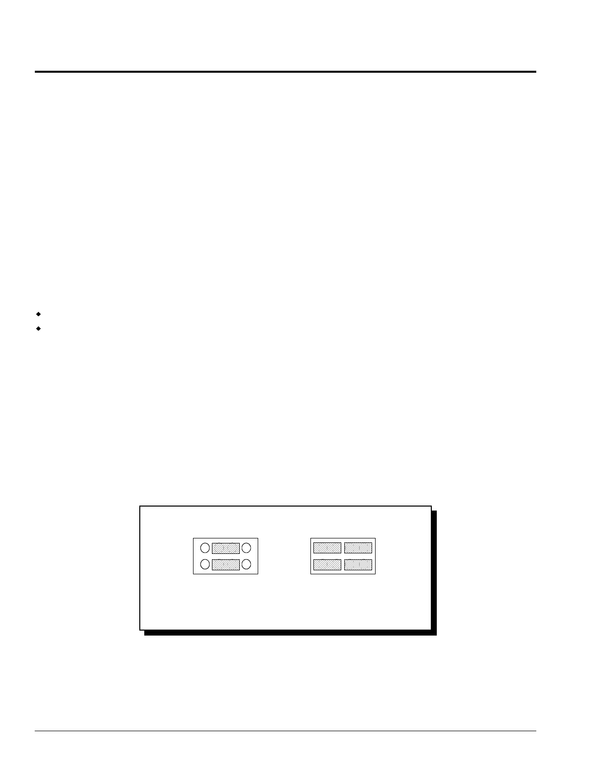
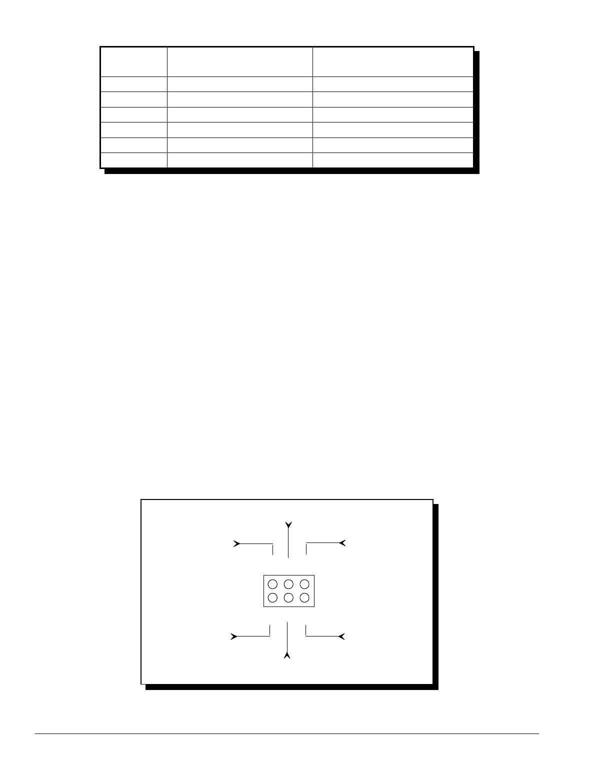
Jumper J1 is used to configure the DAQ-12 for either single ended or differential inputs a
shown in Figure 2-1. Once configured, the input channel is software selectable through the
control word register.
5 6 7 8
1 2 3 4
5 6 7 8
1 2 3 4
J1
8 Differential Channels 16 Single Ended Channels
Figure 2-1. Jumper J1 Configuration
DAQ-12 Users Manual 10
The amplifier stage of the A/D converter circuit performs two functions: (1) amplifies low
level input signals and (2) converts this input signal into a voltage range acceptable to the
A/D converter. Seven gain levels are software selectable for the amplifier stage of the A/D
circuit. To support high level input signals, the DAQ-12 provides input gain selections of
1, 2, 4 and 8. For signals requiring greater amplification, the DAQ-12 provides input gains
of 1, 10, 100 and 500. The gain setting is determined by the value written to the gain control
register.
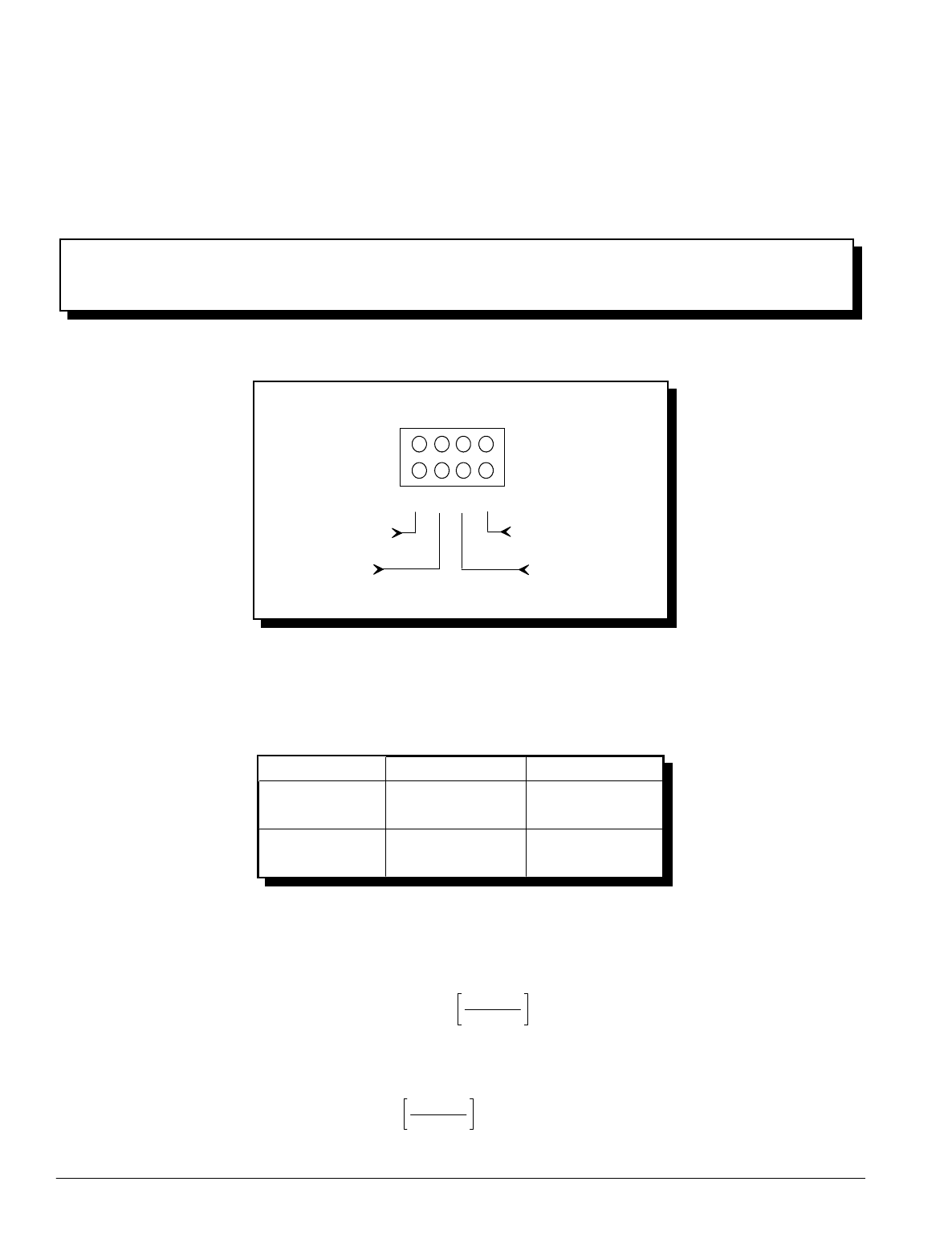
In order to provide a full +10 volt input range and for greater overall versatility, the
DAQ-12 is equipped with a 'divide by 2' pre-scaling circuit. With the pre-scaler enabled, the
resultant high level input gain selections become ½, 1, 2 and 4 and the low level input gain
selections become ½, 5, 50 and 250. Figure 2-2 illustrates jumper J7 (Pre-scaler) configuration
options.
NOTE: The unipolar / bipolar input selection is controlled by the A/D converter and is
selected independent of the single-ended or differential input mode configuration of the
multiplexer and amplifier circuits.
J7
Disable Pre-Scaler
(factory default) Enable Pre-Scaler
Figure 2-2. Jumper J7 Configuration
DAQ-12 Users Manual 11

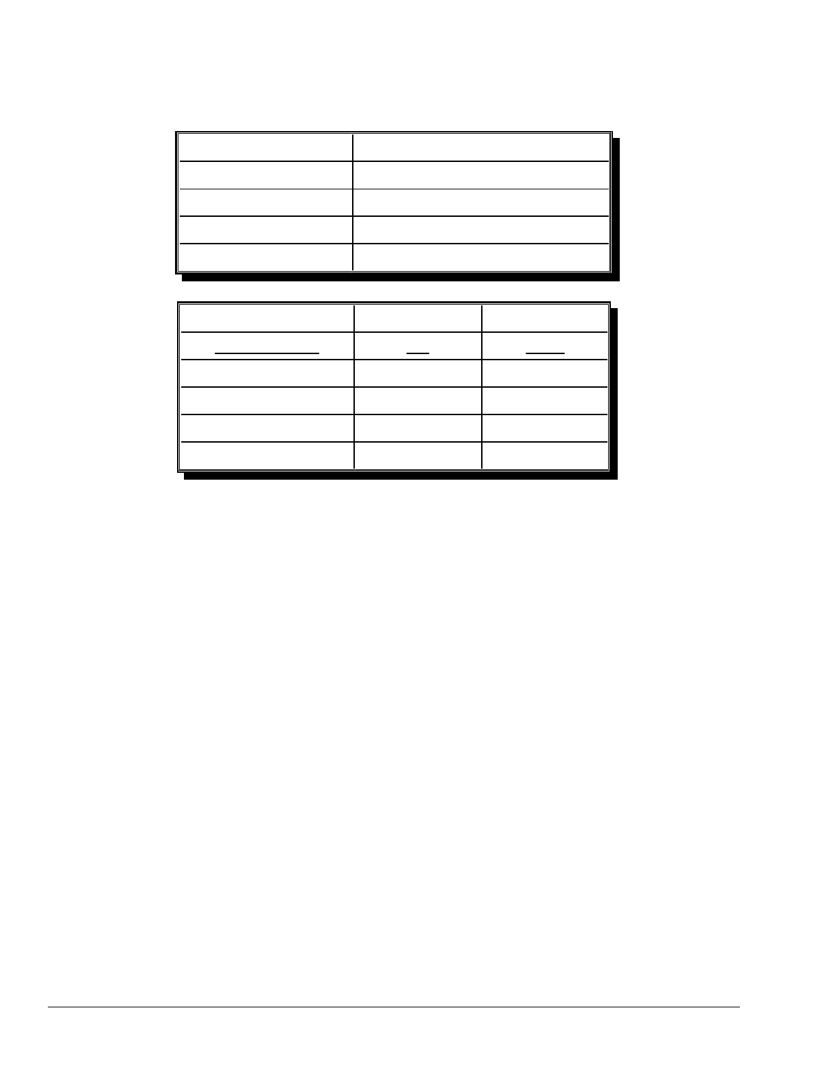
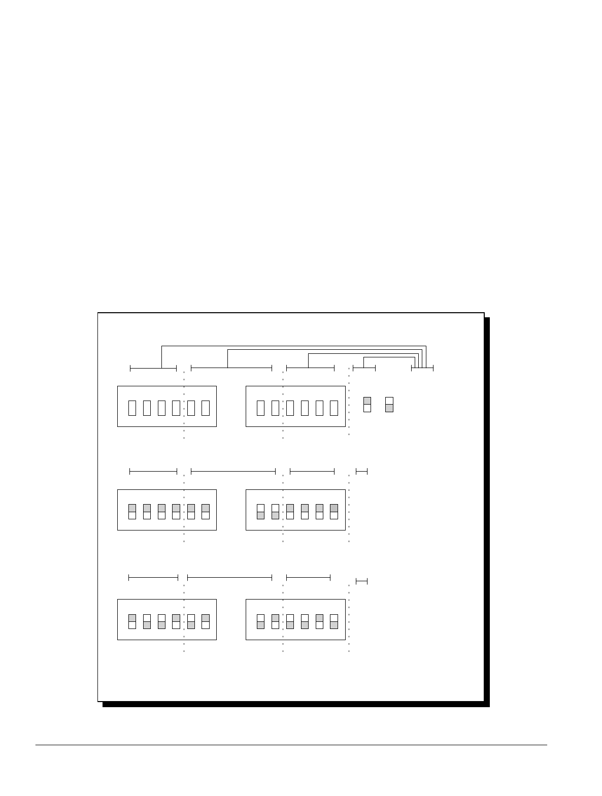
Table 2-1 details the available gain settings and resulting input ranges for the various
input configurations. Note that the 'gain byte' field in Table 2-1 is the value written to the
DAQ-12's gain control register. (* indicates unipolar mode not available with gain of ½ ).
83
2-3
4
+2.5/ ±1.25
82
2-3
2
+5/ ±2.5
81
2-3
1
+10/ ±5
80
2-3
½
N/A*/ ±10
03
2-3
250
+0.04/±0.02
02
2-3
50
+0.2/±0.1
01
2-3
5
+2/±1
00
2-3
½
N/A*/±10
83
1-2
8
+1.25/±0.625
82
1-2
4
+2.5/±1.25
81
1-2
2
+5/±2.5
80
1-2
1
+10/±5
03
1-2
500
+0.02/±0.01
02
1-2
100
+0.1/±0.05
01
1-2
10
+1/±0.5
00
1-2
1
+10/±5
---
---
Gain
Unipolar / Bipolar
Gain Byte (HEX)
J7
Amplifier
Maximum Input Voltage
Table 2-1. Recommended Input Ranges and Gain Settings
DAQ-12 Users Manual 12
The final stage of the A/D converter circuit is the A/D converter IC. The converter must be
configured for unipolar or bipolar input voltages as shown in Figure 2-3. When configured
for unipolar operation, the analog input multiplied by the gain setting must be in the range of
0 volts (analog ground) to +10 volts. When configured for bipolar operation, the analog
input multiplied by the gain setting must be in the range of -5 volts to +5 volts.
Bipolar
1 2 3
4 5 6
J6
Unipolar
1 2 3
4 5 6
J6
Figure 2-3. Jumper J6 Configuration
WARNING: The user must ensure that the maximum input voltage multiplied by the
amplifier gain does not exceed the range of 0 to +10 volts for unipolar operation or -5 to
+5 volts for bipolar operation.
Although the A/D converter produces 12-bit digital 'codes' to represent the input voltage, the
DAQ-12 converts these 'codes' into standard 16-bit signed integer values before returning
them to the PC. When the A/D converter is configured for unipolar operation, the DAQ-12
returns values in the range of 0 to 4095. When configured for bipolar operation, values in the
range of -2048 to +2047 are returned.
In order to calculate the actual input voltage from the value provided by the DAQ-12, the user
must know the configuration (unipolar / bipolar) and the gain setting used to acquire the
data. Given this information, the input voltage can be calculated using the following
equations:
Unipolar mode: input = *
CODE
4096 10V
GAIN
Bipolar mode: input = *
CODE
2048 5V
GAIN
DAQ-12 Users Manual 13
n/a
0000 1111 1111 1111
10
0000 0111 1111 1111
0000 1000 0000 0000
5
0000 0100 0000 0000
0000 0100 0000 0000
2.5
0000 0000 0000 0000
0000 0000 0000 0000
0
1111 1100 0000 0000
n/a
-2.5
1111 1000 0000 0000
n/a
-5
CodeCode BipolarUnipolarVoltage
Table 2-2. A/D Conversion Format Examples
NOTE: The 'voltage' column is the voltage applied to the A/D converter. This voltage is
equivalent to the input voltage multiplied by the amplifier gain.
2.2 Digital to Analog Converters
The digital to analog (D/A) section of the DAQ-12 consists of two independent 12-bit
multiplying D/A converters, and two independent two-stage output amplifiers. Digital data,
(output to the D/A converter by the CPU), is converted to an analog voltage by the D/A
converter, amplified by the output amplifiers and becomes output to the 62 pin connector at
CN1. The D/A converters used on the DAQ-12 are 12-bit resolution converters. Of the 16 bits
written to the D/A, only the 12 least significant bits (D0 - D11) are used for the conversion.
The 4 most significant bits (D12 - D15) are ignored.
The DAQ-12 implements multiplying D/A converters which makes the analog output
proportional to a reference voltage applied to the D/A. Under normal circumstances, the
reference voltage should be applied from the internal +5V reference source. An external
reference voltage may also be supplied to the D/A. This input from the D-62 connector should
not exceed 5 volts and has a typical input impedance of 7.5Kohms. The D/A reference voltage
source is selected using jumper J4 as illustrated in Figure 2-4.
4 5 6
1 2 3
D/A channel 0 reference
External SourceInternal Source
External SourceInternal Source
D/A channel 1 reference
J4
Figure 2-4. Jumper J4 Configuration
DAQ-12 Users Manual 14
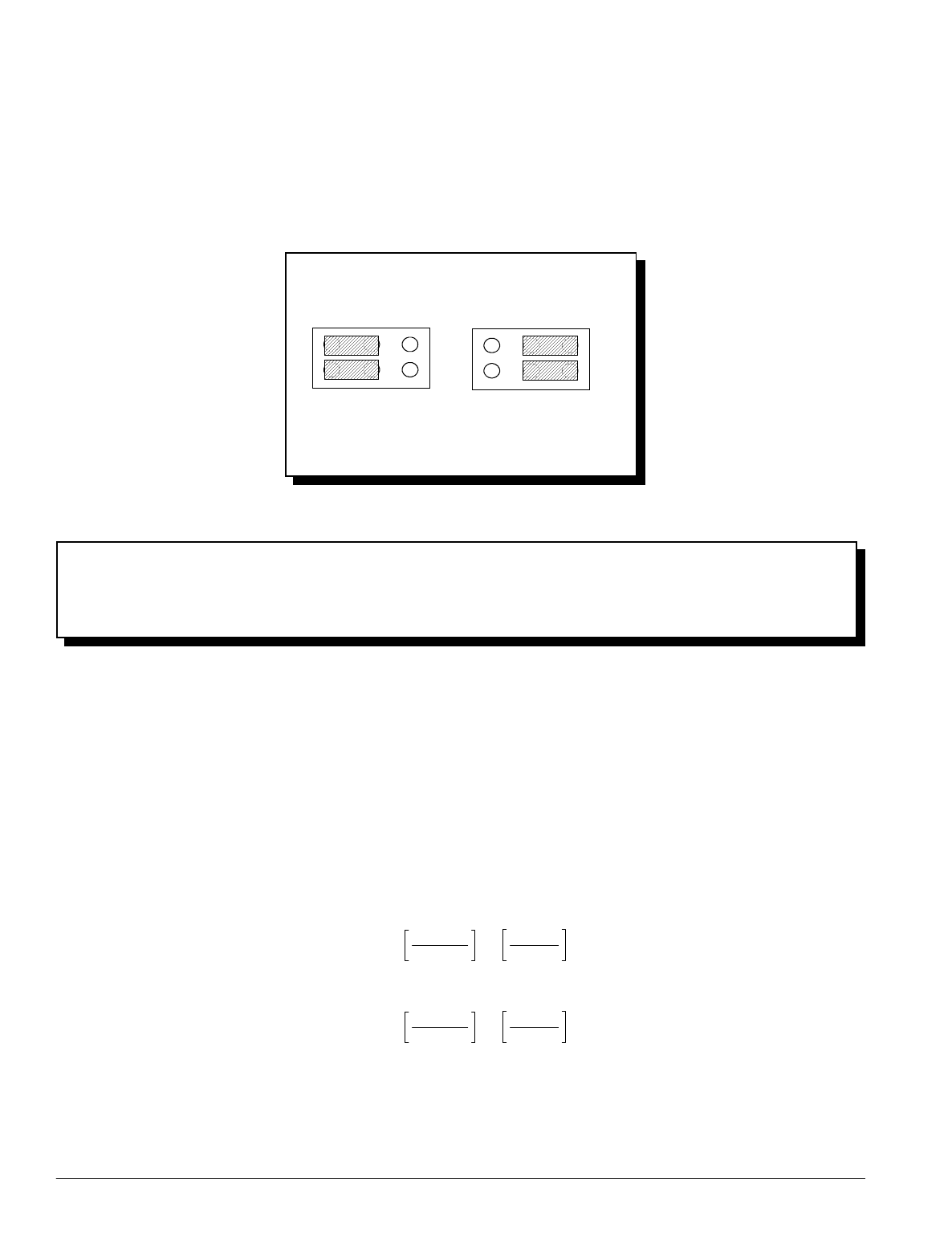
The D/A converter channels may also be operated in unipolar mode: 0 to +5 volts, or bipolar
mode: -5 to +5 volts. The output mode is selected using jumper J5 as shown in Figure 2-5. In
addition, a gain selection jumper is provided to select an output gain of 1 or 2. When using
an external voltage reference, this gain can be used to amplify the D/A output for small
reference voltages.
WARNING: When the internal voltage reference is used,the D/A gain MUST be set to the
gain = 1 position.
5 6 7 8
1 2 3 4
J5
Channel 1 gain
Channel 1 select
Channel 0 select
Channel 0 gain
Figure 2-5. Jumper J5 Configuration
Table 2-3 lists configuration options for jumper J5.
connect 4-8
open 4-8
connect 2-6
open 2-6
Gain = 1
Gain = 2
connect 3-7
open 3-7
connect 1-5
open 1-5
Bipolar
Unipolar
Channel 1Channel 0
Table 2-3. D/A Converter Mode Selection Options
When configured for unipolar operation, the output voltage can be calculated from the
equation: A = V * * gain
out ref CODE
4096
For bipolar operation, the equation becomes:
A = - 1 * V * gain
out CODE
2048 ref
DAQ-12 Users Manual 15
2.3 Digital Input/Output
The DAQ-12 offers four bits of digital output and four bits of digital input for
control/monitoring of external digital devices. The four digital output lines are LS TTL
compatible and will initialize low (0 volts) on power-up. The four digital inputs are also LS
TTL compatible. There is no termination provided on the digital input lines and a read of an
unused digital input will result in an indeterminate value.
2.4 Base Address
The DAQ-12 uses 16 consecutive I/O address locations in the range 0 to 0FFFFH. Two
six-position switches (SW1 and SW2) are used to select the base address. SW1 controls
address lines A15 - A10, and SW2 controls A9 - A4. Address lines A3 - A0 are used
internally by the DAQ-12 to select which register to access. When selecting a base address for
the DAQ-12, an address selection switch in the "OFF" position corresponds to an address
bit of "1" while a switch in the "ON" position corresponds to an address bit of "0". The base
address of the DAQ-12 must be set on a 16 byte boundary, meaning A3 - A0 are "0". The
address of the DAQ-12 as shipped from the factory is 0300H. This setting and other examples
are shown in the Figure 2-5.
O
N
123456
O
N
123456
00000 11 0000
03 00
Example1: Base I/O Address = 0300H
Bit=0 Bit=1
SW1 xxxx Hex
0000 : 0
0001 : 1
0010 : 2
0011 : 3
0100 : 4
0101 : 5
0110 : 6
0111 : 7
1000 : 8
1001 : 9
1010 : A
1011 : B
1100 : C
1101 : D
1110 : E
1111 : F
xxxxx 0000
O
N
123456 O
N
123456
SW2
xxxxxx
O
N
123456 O
N
123456
Example 2: Base I/O Address = 6AD0H
6AD0
11010 10 1110
A A A A A A A A A A AA
15 14 13 12 11 10 9 8 7 6 5 4
x
0
0
Figure 2-5. I/O Base Address Selection
DAQ-12 Users Manual 16
2.5 Clock Selection
The DAQ-12 is equipped with a programmable clock circuit to produce data sampling rates
independent from the clock rate of the host computer. An onboard 8254 programmable
interval timer, with a 10 MHz clock input and either two or three cascaded 16-bit timers,
provides the sampling rate. This enables the sampling rate to be adjusted from 5 us between
samples to almost a year between samples, in as small as 100ns increments.
The DAQ-12's sampling rate can also be generated from an external clock input. This external
clock can be connected directly to the A/D converter or through a 16-bit pre-divider, the
multi-function timer. Samples are taken on the low to high transition of the clock.
WARNING: For the DAQ-12, the maximum data sampling rate is 5us. This restricts
clock frequency to a maximum of 200 KHz. Sampling rates in excess of 200 KHz may
result in erratic operation and unpredictable results.
The clock source, internal or external clock, is software selectable through the DAQ-12's
control word register. The configuration of the clock source itself is controlled by jumper block
J3 as shown in Figure 2-6, (* indicates factory default).
5 6 7 8
1 2 3 4
J3 Internal Timer: 2 timers cascaded
connect 1-2, 4-8, 6-7*
3 timers cascaded
connect 1-5, 2-6, 7-8
External Timer: w/o pre-divider
connect 1-2, 3-7, 4-8
with pre-divider
connect 1-5, 2-3, 7-8
Figure 2-6. Jumper J3 Configuration
DAQ-12 Users Manual 17

2.5.1 Internal Clock
Sampling rates for the internal clock can be calculated using the following equation:
t = 100ns * [N1*N2] or
f = 10MHz / [N1*N2]
where N1 is the low 16-bits of the clock divider and N2 is the high 16-bits of the clock
divider. The following criteria must be met when selecting values for N1 and N2:
2 < N1 < 65,535
2 < N2 < 65,535
N1 * N2 > 50
Using the equations above, the minimum and maximum data sampling rates for the internal
clock can be calculated.
Maximum sampling rate: Minimum Sampling Rate:
N1 = 2, N2 = 25 N1 = 65535, N2 = 65535
t = 100 x 10 * [(2)*(25)] t = 100 x 10 * [(65535)*(65535)]
−9−9
t = 100 x 10 * 50 t = 100 x 10 * [4.295 x 10 ]
−9−99
t = 5 us t = 429.5 sec
f = 10 x 10 / [(2)*(25)] f = 10 x 10 / [(65535)*(65535)]
66
f = 10 x 10 / 50 f = 10 x 10 / [4.295 x 10 ]
669
f = 200 Khz f = 2.328 mHz
If extremely slow data sampling rates are needed, the third 8254 timer, the multi-function
timer, can be cascaded with the other two to produce a 48-bit clock divider. The sampling
rates are then calculated as follows:
t = 100ns * [N1*N2*N3] or
f = 10MHz / [N1*N2*N3]
where N1 is the low 16-bits of the clock divider, N2 is the intermediate 16-bits of the clock
divider, and N3 is the high 16-bits of the divider. The following criteria must be met when
selecting values for N1, N2, and N3:
2 < N1 < 65,535
2 < N2 < 65,535
2 < N3 < 65,535
N1 * N2 * N3 > 50
DAQ-12 Users Manual 18

When configured for a 48-bit divider, the first sampling period will be slightly longer than
the others because the first clock period is required to load the initial value of the
multi-function timer. The following equation calculates the additional time of the first period:
t = 100ns * [N1 * N2]
add
To minimize the amount of additional time required for the first sample, select clock dividers
such that N1 and N2 are as small as possible and N3 is as large as possible. Using the
equations above, the minimum and maximum data sampling rates and the amount of
additional time required for the first sample can be calculated.
Maximum sampling rate: Minimum sampling rate:
N1 = 2, N2 = 5, N3 = 5 N1 = 65535, N2 = 65535, N3 = 65535
t = 100 x 10 * [(2)*(5)*(5)] t = 100 x 10 * [(65535)*(65535)*(65535)]
−9−9
t = 100 x 10 * 50 t = 100 x 10 * [2.815 x 10 ]
−9−914
t = 5 us t = 28.146 x 10 sec
6
t = 325 days, 18 hours, 23 minutes, 29 sec
f = 10 x 10 / [(2)*(5)*(5)]
6
f = 10 x 10 / 50 f = 10 x 10 / [(65535)*(65535)*(65535 )]
66
f = 200 Khz f = 10 x 10 / [2.815 x 10 ]
614
f = 35.529 nHz
t = 100 x 10 * [2 * 5] t = 100 x 10 * [65535 * 65535]
add −9add −9
t = 100 x 10 * 10 t = 100 x 10 * [4.295 x 10 ]
add −9add −99
t = 1 us t = 429.5 sec
add add
2.5.2 External Clock
The external clock input to the DAQ-12 is a TTL level (0 - 5 volt) signal. This input may be
used to control the sampling rate directly, or it may be fed through a pre-divider (the
multi-function timer) with the timer output controlling the A/D sampling rate. When used to
control the sampling rate directly, the frequency of the external clock input may be varied
from DC to 100 KHz as long as the width of the low and high portions of the clock are a
minimum of 1 us each. The A/D conversion cycle will begin on each rising edge of the
external clock input. (See Figure 2-7).
5 usec
min
1 usec min 1 usec min
Figure 2-7. Sampling Rate External Clock Pulses
DAQ-12 Users Manual 19
When the multi-function timer is used as a pre-divider, the frequency of the external clock
input may be varied from DC to 10 MHz as long as the high portion of the clock is at least
30ns and the low portion is at least 50ns. Except for the first period, the sampling rate of the
DAQ-12 will be the external clock frequency divided by the count value written to the
multi-function timer. Since one clock pulse is required to load the initial count value into the
timer, the first sampling interval will be one clock cycle longer than the rest. The valid range
of count values for the multi-function timer is 2 < count < 65,535 but the resulting sampling
rate must be less than 200KHz to assure proper operation of the A/D converter circuitry.
(See Figure 2-8).
100 nsec
min
30 nsec min 50 nsec min
Figure 2-8. Pre-Divider External Clock Pulses
2.6 Trigger Selection
The DAQ-12 is capable of accepting an internal software trigger or an external hardware
trigger. The trigger selection and trigger level bits in the DAQ-12 control word register select
the trigger source and level. Upon reset, the trigger selection and trigger level bits default to
the internal software trigger. When the internal trigger is used, an output to the
start-of-conversion register will trigger the DAQ-12 to begin sampling the input. For
triggering off an external event, the DAQ-12 accepts a level sensitive, TTL compatible trigger
input from the D-62 connector. The trigger level bit in the DAQ-12 control word register
determines which TTL level is used to trigger the A/D converter to begin sampling.
When an internal clock source is used, a delay of not more than 225ns will occur between the
trigger and the first data sample. When an external clock is used, the delay will be dependent
on the frequency and duty cycle of the clock input. If these delays are unacceptable, the clock
and trigger circuitry can be bypassed and a start of conversion pulse can be input directly
into the A/D circuitry with a maximum delay of 25ns. If the user controls the start of
conversion pulse directly, the sample will be taken on the low to high transition of the pulse,
the pulse must have a duration of at least 5 us, and the duty cycle must be between 5 and 80
percent. Jumper J2, shown in Figure 2-9, configures start of conversion control.
1 2 3
J2 Start of Conversion:
DAQ-12 controlled: connect 1-2*
User controlled: connect 2-3
(* indicates factory default)
Figure 2-9. Jumper J2 Configuration
DAQ-12 Users Manual 20
2.7 Direct Memory Access
Direct Memory Access (DMA) transfers provide a way of transferring data from the
DAQ-12's A/D converter into the personal computer's memory without using the Central
Processing Unit (CPU). DMA capability enables other system software to be executed while
data is being input from the DAQ-12.
The DAQ-12 actually implements two DMA channels. The advantage of having two DMA
channels is that one channel can be transferring data while the second channel is being
programmed. When the first channel is finished, the second channel will automatically take
over and continue the data transfer. The first channel can then be re-programmed while the
second channel is transferring data. In this way, the DAQ-12 can acquire data continuously
until terminated by the user.
The DAQ-12 supports 16-bit DMA transfers on channels 5, 6, and 7. The DMA channel(s)
are selected by jumpers J8 and J9 as shown in Figure 2-10.
DRQ7
DACK7
DRQ6
DACK6
DRQ5
DACK5
DRQ6
DACK6
DRQ7
DACK7
DRQ5
DACK5
J8 J9
DMA Channel 1 DMA Channel 2
Figure 2-10. Jumpers J8 and J9 Configuration
WARNING: To properly implement the DMA capability, the DRQ and DACK of each
DMA channel must be jumpered to the same number, i.e. DRQ 5/DACK 5. If both DMA
channels are to be used, each channel must be jumpered to a different number, i.e.
channel 1 is jumpered to DRQ 5 /DACK 5 and channel 2 is jumpered to DRQ
7/DACK 7.
DAQ-12 Users Manual 21
2.8 Interrupts
The DAQ-12 is capable of generating an interrupt from one of four sources:
1. End of conversion signal
2. DMA terminal count
3. Multi-function timer output
4. External interrupt input
The interrupt source is software selected through the DAQ-12 control word register. The
interrupt level is selected using the jumpers J10 and J11 as shown in Figure 2-11.
IRQ 11
IRQ 14
IRQ 15
IRQ 12
IRQ 10
IRQ 2
IRQ 3
IRQ 4
IRQ 5
IRQ 6
IRQ 7
J11
J10
Factory default = IRQ 5
Figure 2-11. Jumpers J10 and J11 Configuration
2.8.1 External Interrupt
The external interrupt is a TTL compatible input from the D-62 connector. An interrupt
request is generated on a high to low transition of this input.
DAQ-12 Users Manual 22
3. External Connections
The DAQ-12 is equipped with a high density 62-pin connector as shown in Figure 3-1.
2 - CH1+
4 - CH2- (CH10+)
6 - CH4+
8 - CH5- (CH13+)
10 - CH7+
12 - AOUT0
14 - DOUT0
6 - DOUT3
18 - EXT TRIG
20 - DIN1
22 - CH0+
24 - CH1- (CH9+)
26 - CH3+
28 - CH4- (CH12+)
30 - CH6+
32 - CH7- (CH15+)
34 - AOUT1
36 - DOUT1
38 - EXT INT
40 - DIN3
42 - DIN0
43 - CH0- (CH8+)
45 - CH2+
47 - CH3- (CH11+)
49 - CH5+
51 - CH6- (CH14+)
53 - VREF0
55 - VREF1
57 - DOUT2
59 - EXT CLK
61 - DIN2
Figure 3-1. 62 Pin Connector Diagram
Analog Ground - 1, 3, 5, 7, 9, 11, 13, 44, 46, 48, 50, 52, 54
Digital Ground - 15, 17, 19, 21, 37, 39, 41, 56, 58, 60, 62
DAQ-12 Users Manual 23
1
2
3
4
5
6
7
8
9
10
11
12
13
14
15
16
17
18
19
20
21
22
23
24
25
26
27
28
29
30
31
32
33
34
35
36
37
38
39
40
41
42
43
44
45
46
47
48
49
50
51
52
53
54
55
56
57
58
59
60
61
62

CHx-, CHx+ : Analog inputs to the analog to digital converter. When using differential input
mode, eight input channels are available (CH0+ to CH7+). When using single-ended
inputs, 16 channels are available (CH0+ to CH15+). The first eight channels are input
through the connections marked CH0+ to CH7+ and the second eight channels through CH0-
to CH7-.
AOUT0, AOUT1: Analog outputs from the digital to analog converters. Polarity and
maximum amplitude depend on the jumper settings and voltage references. Output
resistance of the analog outputs is typically 70 ohms.
VREF0, VREF1: External voltage references for the digital to analog converters. Input range is
0 to 5.0 volts with a no-load input resistance of 7.5 Kohms typical.
EXT CLK, EXT TRG, EXT INT: External clock, trigger, and interrupt inputs respectively.
Inputs are TTL compatible.
DOUT0, DOUT1, DOUT2, DOUT3: TTL compatible digital output lines.
DIN0, DIN1, DIN2, DIN3: TTL compatible input lines.
DAQ-12 Users Manual 24

4. Register Description and Programming
The DAQ-12 uses 16 consecutive I/O address locations in the range 0 to FFFFH. The card
utilizes these addresses for the registers listed in Table 4-1. (* indicates registers located in
8254 counter).
Read/Write 8-bit 8254 Control Word/Status Register
Base F *
Read/Write 8-bit Multi-function Timer Register
Base E *
Read/Write 8-bit Clock Rate Register (high)
Base + D *
Read/Write 8-bit Clock Rate Register (low)
Base + C *
Reserved
Base A, B
Read/Write 8-bit Gain Control Register
Base 9
Read/Write 8-bit Digital Input/Output Register
Base + 8
Write only 16-bit D/A Channel 1 Register
Base + 6, 7
Write only 16-bit D/A Channel 0 Register
Base + 4, 5
Write only 16-bit Start Conversion Register
Read only 16-bit A/D Data Register
Base + 2, 3
Read/Write 16-bit Control Word Register
Base + 0, 1
Table 4-1. DAQ-12 Address Map
4.1 Register Description
4.1.1 Control Word Register
The control word register defines and controls many of the DAQ-12'S data conversion
functions. This register is 16-bit read/write.
Write Read Write Read
D15 INT2 INT2 D7 RUN RUN
D14 INT1 INT1 D6 0 EOC
D13 INT0 INT0 D5 0 VALID
D12 DMAEN DMAEN D4 DMASL DMASL
D11 DMACT DMACH D3 CHSL3 CHSL3
D10 LEVEL LEVEL D2 CHSL2 CHSL2
D9 TRIG TRIG D1 CHSL1 CHSL1
D8 CLK CLK D0 CHSL0 CHSL0
DAQ-12 Users Manual 25

INT2, INT1 and INT0 control the DAQ-12 interrupt source.
INT2 INT1 INT0 DESCRIPTION
0 0 0 Interrupt disabled
1 0 0 Interrupt timer 2
1 0 1 Interrupt on terminal count
1 1 0 External interrupt
1 1 1 Interrupt on end of conversion
DMAEN - enables / disables DMA. When set, logic 1, DMA transfers are enabled.
DMACT - enables the multi-channel DMA capability of the DAQ-12. When set, logic 1, a
terminal count on the active DMA channel causes DMA transfers to begin on the "stand-by"
channel. When cleared, logic 0, DMA transfers halt when the terminal count is reached on
the active channel.
DMACH - indicates which of the DAQ-12'S DMA channels is currently active to transfer
data. Logic 0 indicates DMA channel 0, logic 1 indicates DMA channel 1.
DMASL - When using differential input mode, eight input channels are available (CH0+
through CH7+). When using single-ended inputs, 16 channels are available (CH0+ through
CH15+). The first eight channels are input through the connections marked CH0+ through
CH7+ and the second eight channels through CH0- through CH7-.
LEVEL - selects the edge of the external trigger input. When set, logic 1, A/D conversions
will begin on the falling edge of the external trigger input. When cleared, logic 0,
conversions will begin on the rising edge of the external trigger. IMPORTANT: LEVEL
must be logic 0 when internal triggering is used.
TRIG - selects between internal and external triggers. When set, logic 1, the external trigger
is selected.
CLK - selects between internal and external clock sources. When set, logic 1, the external
clock source is selected.
RUN - when set, logic 1, the A/D converter is placed in the 'run' mode and will begin
converting data when a trigger is received. RUN may be cleared at any time by writing a
"0" to it. When using DMA transfers, RUN is automatically cleared when a terminal count is
received with DMACT set to "0".
EOC - when set, indicates an end of conversion has taken place and the data is available in
the A/D converter data register.
DAQ-12 Users Manual 26

VALID - when set, logic 1, indicates at least one data sample was lost because it was read by
the personal computer before the next sample was converted. Data was lost because the
sampling rate was too fast for the computer to acquire the data. VALID is reset by writing to
the start conversion register.
CHSL2, CHSL1, CHSL0 - select the multiplexer channel for the analog input signal. (*
denotes only available in single ended input mode).
CHSL3 CHSL2 CHSL1 CHSL0 MUX channel
0000channel 0
0001channel 1
0010channel 2
0011channel 3
0100channel 4
0 1 0 1 channel 5
0110channel 6
0111channel 7
1000channel 8*
1001channel 9*
1010channel 10*
1011channel 11*
1100channel 12*
1101channel 13*
1110channel 14*
1111channel 15*
4.1.2 Start of Conversion Register
The start of conversion register is 16-bit write only and performs two functions:
1. When configured for internal triggering, writing a "0" to this register generates the
software trigger, starting the data conversion process.
2. Writing a "0" to this register at any time resets the VALID bit in the control word
register. This allows the VALID bit to be reset at any time during the conversion
process or before the event of an external trigger.
4.1.3 A/D Converter Data Register
An input to this register returns the last digital value converted by the A/D converter. This
register is 16-bit read only.
DAQ-12 Users Manual 27

4.1.4 D/A Converter 0 Register
An output to this register causes the lower twelve bits of data to be converted to an analog
output on D/A converter channel 0. The four most significant bits of data are ignored. This
register is 16-bit write only.
4.1.5 D/A Converter 1 Register
An output to this register causes the lower twelve bits of data to be converted to an analog
output on D/A converter channel 1. The four most significant bits of data are ignored. This
register is 16-bit write only.
The remaining four registers are contained in an 8254 counter/timer.
4.1.6 Clock Rate Register (low word)
The low word of the clock divider is contained in counter 0 of an 8254 counter/timer. The
output of this counter is cascaded into the input of counter 1 to produce a 32-bit timer. Mode
2 must be selected for counter 0 with a minimum count of 2. This register is 8-bit read/write.
4.1.7 Clock Rate Register (high word)
The high word of the clock divider is contained in counter 1 of the 8254 counter/timer. Mode
2 must be selected for counter 1 with a minimum count of 2. This register is 8-bit read/write.
4.1.8 Multi-Function Timer Register
The multi-function timer is implemented using counter 2 of the 8254 counter/timer. Mode
2 must be selected for this timer with a minimum count of 2. This register is 8-bit
read/write.
4.1.9 8254 Control Word/Status Register
This register is used to program the mode and report the status of the 8254 counter/timer.
This register is 8-bit read/write.
DAQ-12 Users Manual 28

4.2 Programming the 8254 Counter/Timer
This section provides programming information for the 8254 counter/timer as implemented
on the DAQ-12. For more details on the 8254, consult the Intel Micro-processor and Peripheral
Handbook.
To program any of the counters contained in the 8254 counter/timer, three steps are required:
1. Write the configuration byte to the 8254 mode select/status register. This byte sets
the operating mode of the selected counter.
2. Write the least significant byte of the count value to the selected counter register.
3. Write the most significant byte of the count value to the selected counter register.
The following examples illustrate the programming sequence for each of the counters in the
8254. The variable 'base_address' is the base address of the DAQ-12 as defined by the address
selection switches.
Counter 0 - Clock rate register (low word)
operating mode: 2
minimum count value: 2
configuration byte: 0 / 0 / 1 / 1 / 0 / 1 / 0 / 0 = 34H
Example: Program the value 2675H into the low word of the clock rate register.
output 34H to base_address + 0FH
output 75H to base_address + 0CH
output 26H to base_address + 0CH
Example: Program the value 0008H into the low word of the clock rate register.
output 34H to base_address + 0FH
output 08H to base_address + 0CH
output 00H to base_address + 0CH
DAQ-12 Users Manual 29

Counter 1 - Clock rate register (high word)
operating mode: 2
minimum count value: 2
configuration byte: 0 / 1 / 1 / 1 / 0 / 1 / 0 / 0 = 74H
Example: Program the value 13A4H into the high word of the clock rate register.
output 74H to base_address + 0FH
output A4H to base_address + 0DH
output 13H to base_address + 0DH
Example: Program the value FFFFH into the high word of the clock rate register.
output 74H to base_address + 0FH
output FFH to base_address + 0DH
output FFH to base_address + 0DH
Counter 2 - Multi-function timer register
operating mode: 2
minimum count value: 2
configuration byte: 1 / 0 / 1 / 1 / 0 / 1 / 0 / 0 = B4H
Example: Program the value 000AH into the multi-function timer register.
output B4H to base_address + 0FH
output 0AH to base_address + 0EH
output 00H to base_address + 0EH
Example: Program the value 0100H into the multi-function timer register.
output B4H to base_address + 0FH
output 00H to base_address + 0EH
output 01H to base_address + 0EH
DAQ-12 Users Manual 30

DAQ-12 Users Manual
Version 2.20
January 28, 1999
Part No. 940-0030-220
