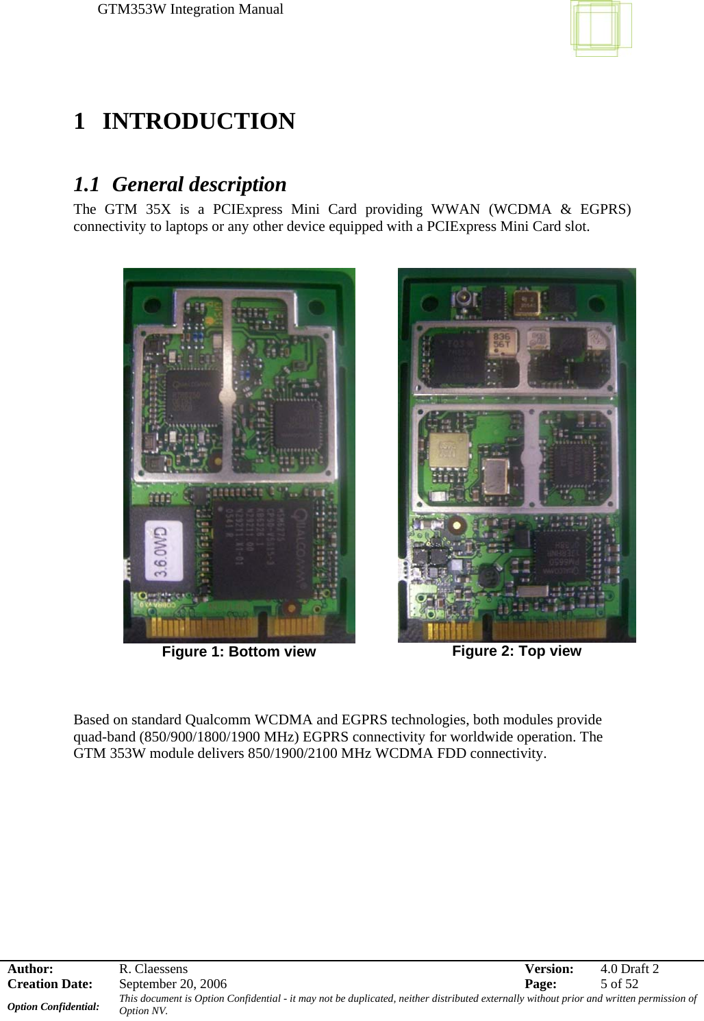
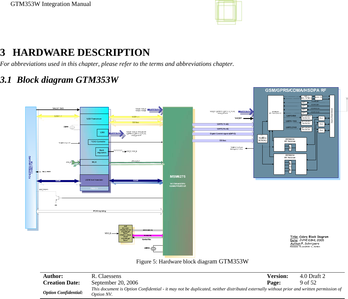
Option OGTM353-W GSM/GPRS/UMTS/HSDPA QUAD BAND PCI MINI CARD User Manual Integration Manual
Option NV GSM/GPRS/UMTS/HSDPA QUAD BAND PCI MINI CARD Integration Manual
Option >
Contents
- 1. Integration Manual
- 2. User Manual
Integration Manual
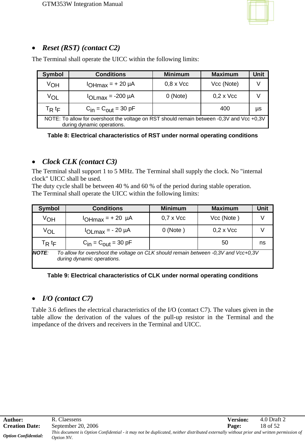
![GTM353W Integration Manual Author: R. Claessens Version: 4.0 Draft 2Creation Date: September 20, 2006 Page: 16 of 52 Option Confidential: This document is Option Confidential - it may not be duplicated, neither distributed externally without prior and written permission of Option NV. 3.3.3.1 Contact activation and deactivation The Terminal shall connect, activate and deactivate the UICC in accordance with the Operating Procedures specified in ISO/IEC 7816-3 [12]. For any voltage level, monitored during the activation sequence, or during the deactivation sequence following normal power-down, the order of the contact activation/deactivation shall be respected. It is recommended that whenever possible, the deactivation sequence defined in ISO/IEC 7816-3 [12] should be followed by the Terminal on all occasions when the Terminal is powered down. If the UICC clock is already stopped and is not restarted, the Terminal may deactivate all the contacts in any order, provided that all signals reach low level before Vcc leaves high level. If the UICC clock is already stopped and is restarted before the deactivation sequence, then the deactivation sequence specified in ISO/IEC 7816-3 [12] sub clause 5.4 shall be followed. 3.3.3.2 Inactive contacts The voltages on contacts C1, C2, C3, C6 and C7 of the Terminal shall be in the range 0 ± 0,4 volts referenced to ground (C5) when the Terminal is switched off with the power source connected to the Terminal. The measurement equipment shall have a resistance of 50 kohms when measuring the voltage on C2, C3, C6 and C7. The resistance shall be 10 kohms when measuring the voltage on C1. 3.3.3.3 Contact pressure The contact pressure shall be large enough to ensure reliable and continuous contact (e.g. to overcome oxidisation and to prevent interruption caused by vibration). The radius of any curvature of the contacting elements shall be greater than or equal to 0,8 mm over the contact area. Under no circumstances shall the contact force exceed 0,5 N per contact. Care shall be taken to avoid undue point pressure to the area of the UICC opposite to the contact area. Such pressure is potentially damaging to the components within the UICC.](https://usermanual.wiki/Option/OGTM353-W.Integration-Manual/User-Guide-715187-Page-16.png)
![GTM353W Integration Manual Author: R. Claessens Version: 4.0 Draft 2Creation Date: September 20, 2006 Page: 37 of 52 Option Confidential: This document is Option Confidential - it may not be duplicated, neither distributed externally without prior and written permission of Option NV. 6 AT COMMAND SET REFERENCE This section lists the AT commands available on the GTM module. Most of the AT commands supported are specified in 3GPP TS 27.007 and 3GPP TS 27.005. Details of these commands can be found in those 3GPP specifications. Only Option and/or Qualcomm proprietary AT commands are fully described in this section . Please note that this section is subject to change. Support for some commands still needs to be defined and will be updated in future versions of this document. 6.1 DTE-TA/DCE Interface Commands All these commands are specified in 3GPP TS27.007 [1] and or ITU-T V.25ter. Some of these commands may become meaningless on GTM because of the specific hardware design. For example, since GTM internally uses a USB interface towards the host commands to set the baud rate are no longer applicable. Where possible, this shall be indicated. Command Description Used S3 Command line termination character (S-parameter) Yes S4 Response formatting character (S-parameter) Yes S5 Command line editing character (S-parameter) Yes E Command Echo Yes Q Result code suppression Yes V DCE Response format Yes &C Circuit 109 behavior Yes &D Circuit 108 behavior Yes +IPR Fixed DTE rate Not applicable +ICF DTE-DEC character framing Not applicable +IFC DTE-DCE local flow control Yes &V Dump configuration parameters Yes 6.2 General commands All these commands are specified in 3GPP TS27.007 [1]. Command Description Used +CGMI Request manufacturer identification Yes +CGMM Request model identification Yes +CGMR Request revision identification Yes +CGSN Request product serial number identification Yes](https://usermanual.wiki/Option/OGTM353-W.Integration-Manual/User-Guide-715187-Page-37.png)
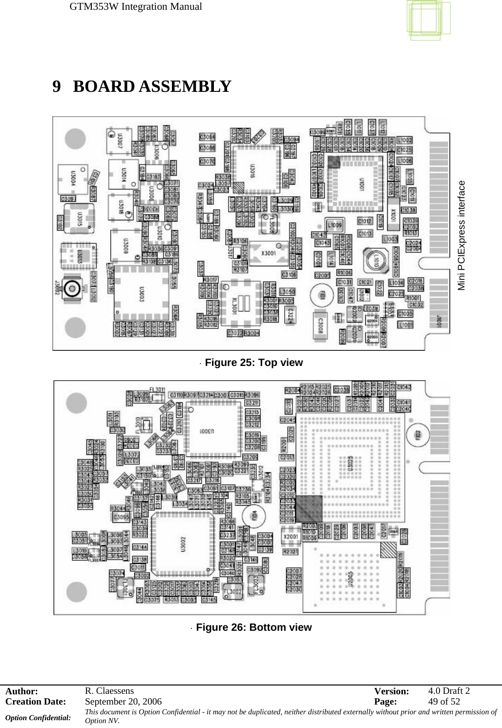
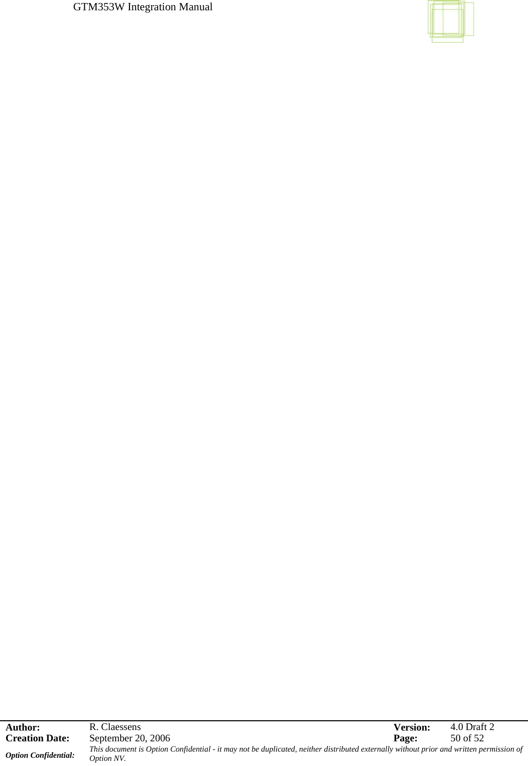
![GTM353W Integration Manual Author: R. Claessens Version: 4.0 Draft 2Creation Date: September 20, 2006 Page: 38 of 52 Option Confidential: This document is Option Confidential - it may not be duplicated, neither distributed externally without prior and written permission of Option NV. +CSCS Select TE character set Yes – but support for IRA character set only +CIMI Request international mobile subscriber identity Yes Z Reset to default configuration Yes &F Set to factory defined configuration Yes I Request identification information Yes +GMI Request manufacturer identification Yes +GMM Request manufacturer identification Yes +GMR Request revision identification Yes +GSN Request revision identification Yes +GCAP Request complete capabilities list Yes 6.3 Call control commands All these commands are specified in 3GPP TS27.007 [1]. Command Description Used +CSTA Select type of address TBD D Dial (using new dial modifiers, “>”, “I/i”, “G/g”, and “;” applicable to UMTS only) > = direct dial from phone bookI/i = override CLIR supplementary service default G/g = control CUG supplementary service for call ; = initiate voice call Yes +CHUP Hang up Yes – for voice call hangup +CBST Select bearer service type Yes +CRLP Radio link protocol Yes +CR Service reporting control Yes +CRC Cellular result codes Yes T Select tone dialing Yes – but does nothing P Select pulse dialing Yes – but does nothing A Answer Yes H Hook control Yes O Return to online data state Yes S0 Automatic answer Yes S6 Pause before blind dialing Yes – but does nothing S7 Connection completion timeout Yes – but does nothing S8 Comma dial modifier time Yes – but does nothing S10 Automatic connect delay Yes – but does nothing L Monitor speaker loudness Yes – but does nothing M Monitor speaker mode Yes – but does nothing +DS Data compression Yes +DR Data compression reporting Yes](https://usermanual.wiki/Option/OGTM353-W.Integration-Manual/User-Guide-715187-Page-38.png)
![GTM353W Integration Manual Author: R. Claessens Version: 4.0 Draft 2Creation Date: September 20, 2006 Page: 39 of 52 Option Confidential: This document is Option Confidential - it may not be duplicated, neither distributed externally without prior and written permission of Option NV. 6.4 Network service related commands All these commands are specified in 3GPP TS27.007 [1]. Command Description Used +CREG Network registration Yes +COPS Operator selection Yes +CLCK Facility lock Yes +CPWD Change password Yes +CLIP Calling line identification presentation TBD +CLIR Calling line identification restriction TBD +COLP Connected line identification presentation TBD +CCUG Closed user group TBD +CCFC Call Forwarding Number and Conditions TBD +CCWA Call waiting TBD +CHLD Call related supplementary services TBD +CTFR Call deflection TBD +CUSD Unstructured supplementary service data TBD +CAOC Advice of charge TBD +CSSN Supplementary service notifications TBD +CLCC List current calls TBD +CPOL Preferred operator list TBD +CAEMLPP eMLPP priority registration and Interrogation TBD 6.5 Mobile equipment commands All these commands are specified in 3GPP TS27.007 [1]. Command Description Used +CPAS Phone activity status Yes +CFUN Set phone functionality Yes +CPIN Enter PIN Yes +CBC Battery charge Yes – but not applicable +CSQ Signal quality Yes +CPBS Select phone book memory storage Yes +CPBR Read phone book entries Yes +CPBF Find phone book entries Yes +CPBW Write phone book entry Yes +CLVL Loudspeaker volume level Yes - but not applicable +CMEE Report mobile equipment error Yes](https://usermanual.wiki/Option/OGTM353-W.Integration-Manual/User-Guide-715187-Page-39.png)
![GTM353W Integration Manual Author: R. Claessens Version: 4.0 Draft 2Creation Date: September 20, 2006 Page: 40 of 52 Option Confidential: This document is Option Confidential - it may not be duplicated, neither distributed externally without prior and written permission of Option NV. 6.6 UMTS packet domain commands All these commands are specified in 3GPP TS27.007 [1]. Command Description Used +CGDCONT Define PDP context Yes +CGQREQ Requested quality of service profile Yes +CGQMIN Minimum acceptable quality of service profile Yes – Accepted but does nothing +CGEQREQ Requested 3G quality of service profile Yes +CGEQMIN Minimum acceptable 3G quality of service profile Yes – Accepted but does nothing +CGATT PS attach or detach Yes +CGACT PDP context activate or deactivate Yes +CGCLASS GPRS mobile station class (GPRS only) Yes +CGEREP Packet domain event reporting Yes – Accepted but does nothing +CGREG GPRS network registration status Yes +CGSMS Select service for MO SMS messages Yes 6.7 SMS Commands All these commands are specified in 3GPP TS27.005 [2]. Command Description Used +CSMS Select message service Yes +CPMS Preferred message storage Yes +CMGF Message format Yes +CSCA Service center address Yes +CSMP Set text mode parameters Yes +CSDH Show text mode parameters Yes +CNMI New message indications to TE Yes +CMGL List message Yes +CMGR Read message Yes +CNMA New message acknowledge to ME/TA Yes +CMGS Send message Yes +CMSS Send message from storage Yes +CMGW Write message to memory Yes +CMGD Delete message Yes](https://usermanual.wiki/Option/OGTM353-W.Integration-Manual/User-Guide-715187-Page-40.png)
![GTM353W Integration Manual Author: R. Claessens Version: 4.0 Draft 2Creation Date: September 20, 2006 Page: 42 of 52 Option Confidential: This document is Option Confidential - it may not be duplicated, neither distributed externally without prior and written permission of Option NV. 6.10.2 Preferred SYStem AT_OPSYS Command Possible Response(s) _OPSYS=[<mode>[,<domain>]] OK _OPSYS? _OPSYS: <mode>,<domain> _OPSYS=? _OPSYS: (0-5),(0-6) Description This command changes the preferred system, GSM/WCDMA, the acquisition order and the service domain preference PS/CS. Defined values <mode>: 0 GSM only 1 WCDMA only 2 GSM first 3 WCDMA first (default) 4 No change 5 Auto <domain>: 0 Acquire only circuit-switched systems 1 Acquire only packet-switched systems 2 Acquire circuit-and/or packet-switched systems (default) 3 Any domain will do; no preference 4 To be used by clients who do not want to change the service domain 5 PS attach on demand; note that this value of service domain preference is not saved in NV 6 PS detach on demand; note that this value of service domain preference is not saved in NV 6.10.3 Security “AT_OSEC” Command Possible Response(s) _OSEC=[<sec>] OK _ OSEC? _ OSEC: < sec > _ OSEC =? _ OSEC: (list of supported <sec>s) Description This command sets the RRC security setting. Please note that a hard reset of the GTM is required before the setting will take effect. Defined values <sec>: 0 None 1 Integrity 2 Ciphering 3 Fake Security 4 Integrity and Ciphering (default)](https://usermanual.wiki/Option/OGTM353-W.Integration-Manual/User-Guide-715187-Page-42.png)
![GTM353W Integration Manual Author: R. Claessens Version: 4.0 Draft 2Creation Date: September 20, 2006 Page: 43 of 52 Option Confidential: This document is Option Confidential - it may not be duplicated, neither distributed externally without prior and written permission of Option NV. 6.10.4 Selected System “AT_OSSYS” Command Possible Response(s) _OSSYS=[<n>] OK _OSSYS? _OSSYS: <n>,<AcT> _OSSYS=? _OSSYS: (0-1),(0,2) Description This command enables/disables the unsolicited result code _OSSYSI: <mode>. Defined values <n>: 0 Turns off unsolicited result code _OSSYSI: <mode> (default) 1 Turns on unsolicited result code _OSSYSI: <mode> <AcT>: 0 GSM 2 UTRAN 3 No service 6.10.5 Aircraft Mode “AT_OAIR” Command Possible response(s) _OAIR= < aircraft mode> OK _OAIR? _OAIR: < aircraft mode> _OAIR=? _OAIR: (list of supported <mode>’s) Description Allows the user to change the startup RF of the gsm/wcdma part (protocol stack) at power up setting or query its current state. Defined Values <Aircraft mode> 0 Off, the unit will startup protocol stack at power up (gsm/wcdma part). (default) 1 On, the unit will NOT startup the protocol stack at power up (gsm/wcdma part).](https://usermanual.wiki/Option/OGTM353-W.Integration-Manual/User-Guide-715187-Page-43.png)
![GTM353W Integration Manual Author: R. Claessens Version: 4.0 Draft 2Creation Date: September 20, 2006 Page: 44 of 52 Option Confidential: This document is Option Confidential - it may not be duplicated, neither distributed externally without prior and written permission of Option NV. 6.10.6 Enable/Disable CHAP “AT_OCHAP” Command Possible Response(s) _OCHAP=[<sec>] OK _ OCHAP? _ OCHAP: < sec > _ OCHAP =? _ OCHAP: (0-1) Description This command enables or disables CHAP Protocol security setting during activation of a PDP context. Value is stored in NVRAM. The default state is enabled. Defined values <sec>: 0 Disabled 1 Enabled (default) 6.10.7 SIM toolkit profile download “AT+STPD” Command Possible Response(s) +STPD=<length>, <profile> OK, ERROR +STPD? ERROR +STPD=? ERROR Description This command will send the given profile to SIM toolkit. Parameters <Length> = a number representing the length of the binary profile. <Profile> = the SIM toolkit profile in hexadecimal format (see 3GPP 11.14 [Structure and coding of TERMINAL PROFILE]) Example AT+STPD=1,03 Indicates that profile download and SMS-PP data download are supported by the ME (GTM in this case)](https://usermanual.wiki/Option/OGTM353-W.Integration-Manual/User-Guide-715187-Page-44.png)
![GTM353W Integration Manual Author: R. Claessens Version: 4.0 Draft 2Creation Date: September 20, 2006 Page: 52 of 52 Option Confidential: This document is Option Confidential - it may not be duplicated, neither distributed externally without prior and written permission of Option NV. 11 REFERENCES Ref Document [1] 3GPP TS 27.007 V3.7.0 (2000-12) AT Command set for User Equipment (UE) (Release 1999) [2] 3GPP TS 27.005 V3.1.0 (2000-01) Equipment (DTE-DCE) interface for Short Message Service (SMS) and Cell Broadcast Service (CBS)](https://usermanual.wiki/Option/OGTM353-W.Integration-Manual/User-Guide-715187-Page-52.png)