Option OGTM353-W GSM/GPRS/UMTS/HSDPA QUAD BAND PCI MINI CARD User Manual Integration Manual
Option NV GSM/GPRS/UMTS/HSDPA QUAD BAND PCI MINI CARD Integration Manual
Option >
Contents
- 1. Integration Manual
- 2. User Manual
Integration Manual

OPTION W ireless Technology, Kolonel Begaultlaan 45, B-3012 Leuven
Tel +32 16 317 411 Fax +32 16 207 164 http://www.option.com
Option Confidential
Globetrotter Module GTM353W
Integration Manual

OPTION W ireless Technology, Kolonel Begaultlaan 45, B-3012 Leuven
Tel +32 16 317 411 Fax +32 16 207 164 http://www.option.com
Option Confidential
About this document
Overview and Purpose
This document is meant for laptop manufacturers and other system integrators, to
allow for easy integration into their own product. The bulk of this document describes
the functional interfaces of the GlobeTrotter GTM353W Module on hardware,
firmware and software levels. At the end, a chapter concerning certification
requirements is added, which should be taken into account from the start of the
integration.
Please note that this is only a draft version and is subject to change.
Confidentiality
All data and information contained or disclosed by this document is confidential and
proprietary of Option NV, and all rights therein are expressly reserved. By accepting
this document, the recipient agrees that this information is held in confidence and in
trust and will not be used, copied, reproduced in whole or in part, nor its contents
revealed in any manner to others without prior and written permission of Option NV
Version History
Date Release Version Author(s) Revision(s) Remarks Phase
June 8, 2005 1 1-Draft R. Claessens S. Lodeweyckx Added general
overview diagram,
certification content,
quickstart guide,
general modifications
1.0.0
June 9, 2005 1 2-Draft R. Claessens Added revision
remarks 1.0.0
June 16, 2005 1 3-Draft R. Claessens Added revision
remarks 1.0.0
June 22, 2005 1 4-Final R. Claessens S. Lodeweyckx,
F. Nys,
J. Vercruysse
Added antenna
guidelines, product
pictures
1.0.0
July 8, 2005 2 1-Draft R. Claessens 1.0.0
September 14,
2005 2 4-Final R. Claessens D. Michiels Added default
settings for Option
AT commands
1.0.0
November 18,
2005 3 1-Final Johan De
Bisschop Pinout definition
adapted to newly
approved PCIExpress
Mini Card standard.
References to
GTM352U removed
January 16,
2005 4 1-Draft Johan De
Bisschop Update for
GTM353W
January 18,
2005 4 2-Draft Johan De
Bisschop Digital PCM
interface added

GTM353W Integration Manual
Author:
R
. Claessens Version: 4.0 Draft 2
Creation Date: September 20, 2006 Page: 3 of 52
Option Confidential: This document is Option Confidential - it may not be duplicated, neither distributed externally without prior and written permission of
Option NV.
Table of contents
1 INTRODUCTION .................................................................................................5
1.1 General description ........................................................................................5
1.2 Features..........................................................................................................6
1.2.1 WCDMA................................................................................................6
1.2.2 E-GPRS..................................................................................................6
1.2.3 Terminal Equipment Interfaces..............................................................7
1.2.4 Power Requirements..............................................................................7
1.2.5 Thermal Dissipation and derating..........................................................7
1.2.6 LED definition .......................................................................................7
2 GENERAL OVERVIEW DIAGRAM ..................................................................8
3 HARDWARE DESCRIPTION .............................................................................9
3.1 Block diagram GTM353W ............................................................................9
3.2 PCIExpress Mini Card interface....................................................................9
3.3 UICC interface guidelines..............................................................................9
3.3.1 Introduction............................................................................................9
3.3.2 UICC Interface.......................................................................................9
3.3.3 Electrical specifications of the UICC – Terminal interface...................9
3.3.4 Electrical interface .................................................................................9
3.3.5 Practical implementation .......................................................................9
3.4 Digital PCM interface....................................................................................9
3.4.1 Background............................................................................................9
3.4.2 Interfaces, Features & Functions ...........................................................9
3.5 Antenna guidelines.........................................................................................9
3.5.1 Antenna specifications...........................................................................9
3.5.2 WLAN Antenna Isolation......................................................................9
3.5.3 Antenna connector .................................................................................9
4 HOST CONTROL INTERFACES........................................................................9
4.1 USB interface.................................................................................................9
4.2 COM interface ...............................................................................................9
4.3 NDIS interface ...............................................................................................9
5 DEVICE DRIVER INTERFACE..........................................................................9
6 AT COMMAND SET REFERENCE....................................................................9
6.1 DTE-TA/DCE Interface Commands..............................................................9
6.2 General commands.........................................................................................9
6.3 Call control commands ..................................................................................9
6.4 Network service related commands...............................................................9
6.5 Mobile equipment commands........................................................................9
6.6 UMTS packet domain commands..................................................................9
6.7 SMS Commands ............................................................................................9
6.8 Synchronous data mode commands...............................................................9
6.9 SIM Toolkit commands .................................................................................9
6.10 Option proprietary commands .......................................................................9
6.10.1 Read hardware version _OHWV ...........................................................9
6.10.2 Preferred SYStem AT_OPSYS..............................................................9

GTM353W Integration Manual
Author:
R
. Claessens Version: 4.0 Draft 2
Creation Date: September 20, 2006 Page: 4 of 52
Option Confidential: This document is Option Confidential - it may not be duplicated, neither distributed externally without prior and written permission of
Option NV.
6.10.3 Security “AT_OSEC” ............................................................................9
6.10.4 Selected System “AT_OSSYS”............................................................9
6.10.5 Aircraft Mode “AT_OAIR”..................................................................9
6.10.6 Enable/Disable CHAP “AT_OCHAP”..................................................9
6.10.7 SIM toolkit profile download “AT+STPD”...........................................9
7 PHYSICAL CHARACTERISTICS.......................................................................9
7.1 Dimensions ....................................................................................................9
7.2 Power consumption........................................................................................9
7.3 Thermal dissipation requirements..................................................................9
7.4 Operating and Storage Environment..............................................................9
7.4.1 Shock......................................................................................................9
7.4.2 Vibration ................................................................................................9
7.4.3 Operating Temperature and Humidity...................................................9
7.4.4 Non-Operating Temperature and Humidity...........................................9
7.4.5 Altitude ..................................................................................................9
8 CERTIFICATION .................................................................................................9
9 BOARD ASSEMBLY ...........................................................................................9
10 ABBREVIATIONS ...........................................................................................9
11 REFERENCES ..................................................................................................9
GTM353W Integration Manual
Author:
R
. Claessens Version: 4.0 Draft 2
Creation Date: September 20, 2006 Page: 5 of 52
Option Confidential: This document is Option Confidential - it may not be duplicated, neither distributed externally without prior and written permission of
Option NV.
1 INTRODUCTION
1.1 General description
The GTM 35X is a PCIExpress Mini Card providing WWAN (WCDMA & EGPRS)
connectivity to laptops or any other device equipped with a PCIExpress Mini Card slot.
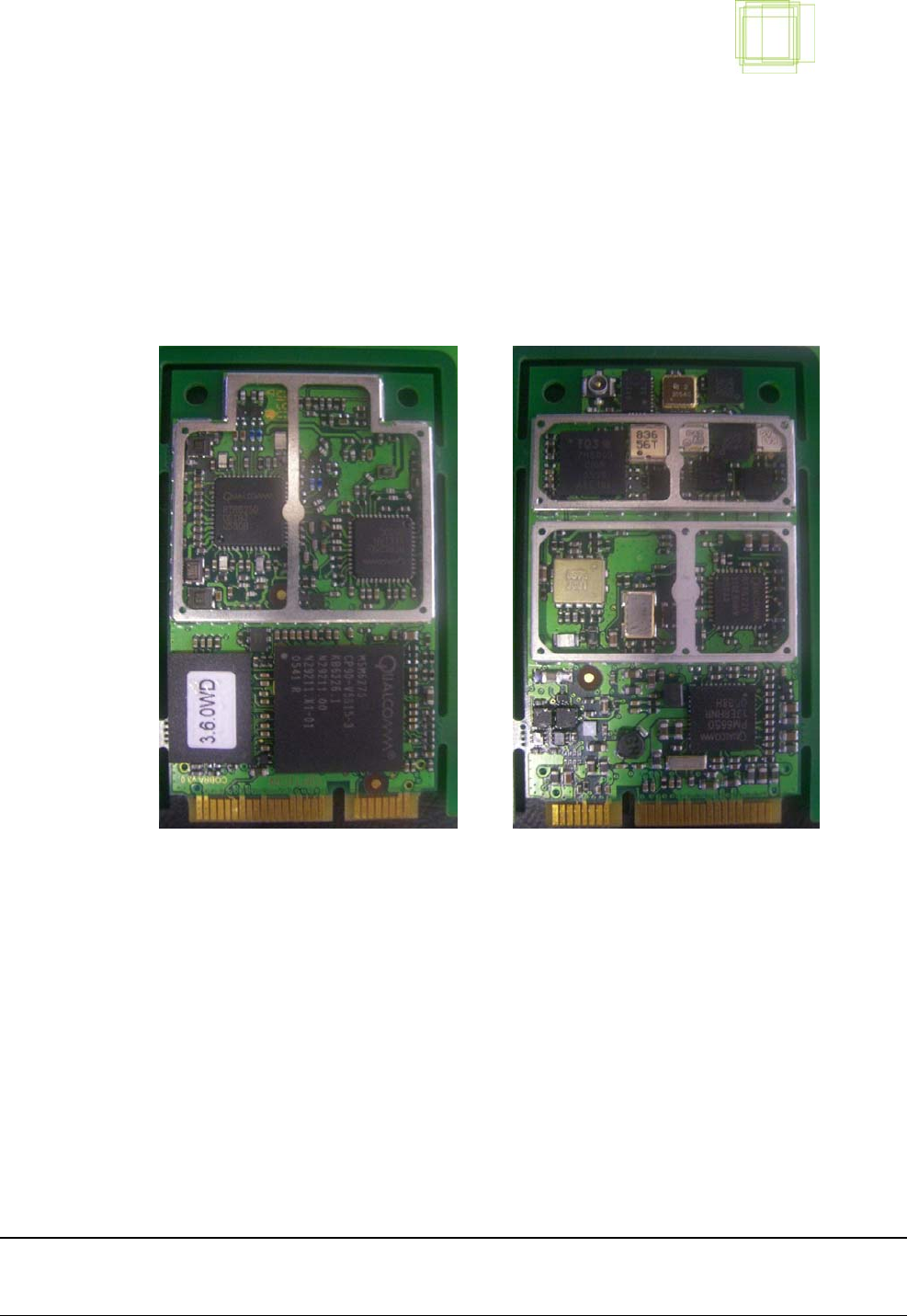
Figure 1: Bottom view
Figure 2: Top view
Based on standard Qualcomm WCDMA and EGPRS technologies, both modules provide
quad-band (850/900/1800/1900 MHz) EGPRS connectivity for worldwide operation. The
GTM 353W module delivers 850/1900/2100 MHz WCDMA FDD connectivity.

GTM353W Integration Manual
Author:
R
. Claessens Version: 4.0 Draft 2
Creation Date: September 20, 2006 Page: 6 of 52
Option Confidential: This document is Option Confidential - it may not be duplicated, neither distributed externally without prior and written permission of
Option NV.
1.2 Features
1.2.1 WCDMA
- Model GTM 353W Module (WORLD version)
• FDD 850/1900/2100 MHz
• Power Class 3 (+24dBm)
• 384/128 kbps downlink/uplink modem operation (potentially 384 kbps uplink)
• Supports UL and DL Compressed Modes
• Supports Circuit and Packet-Switched Data
• Upgradeable to HSDPA 1.8Mbps
1.2.2 E-GPRS
• 850/900/1800/1900 MHz
• GSM Power Class 4 (2W) for 850/900 bands, GSM
• Power Class 1 (1W) for 1800/1900 bands
• EDGE class E2 (+27 dBm in 850/900 bands, +26 dBm in 1800/1900 bands)
• GPRS/EGPRS Multislot Class 10 (4 slots Rx, 2 slots Tx, 5 max active)
• GPRS/EGPRS Class B Type 1 MT
• GPRS CS1-CS4; EGPRS MCS1-MCS9
• Circuit Switched Data: 14.4 and 9.6 kbps

GTM353W Integration Manual
Author:
R
. Claessens Version: 4.0 Draft 2
Creation Date: September 20, 2006 Page: 7 of 52
Option Confidential: This document is Option Confidential - it may not be duplicated, neither distributed externally without prior and written permission of
Option NV.
1.2.3 Terminal Equipment Interfaces
• Physical interface PCIExpress Mini Card 1.1
• USB 2.0 Full Speed (12Mbits/s) signalling
• NDIS and Modem interface drivers
• AT interface with standard modem emulation
• EAP-SIM / EAP-AKA support
• Operating Systems supported:
o Windows 2000/XP/XP Pro/Tablet
o Mac OS X Tiger
o Linux (on demand)
• Regulatory & Certifications
o R&TTE, FCC, GCF
o Mechanical and Environmental testing
1.2.4 Power Requirements
• Vcc 3.3V +/- 9%
• Peak Icc 2750 mA with max supply droop 50 mV
• Average Icc 850 mA
1.2.5 Thermal Dissipation and derating
• The maximum thermal dissipation directly from any PCI Express Mini Card add-in
card is 2.9 W peak
• See section 7.3 for details on actual thermal dissipation.
1.2.6 LED definition
The module can control one LED via the bus connector.
GTM353W Integration Manual
Author:
R
. Claessens Version: 4.0 Draft 2
Creation Date: September 20, 2006 Page: 8 of 52
Option Confidential: This document is Option Confidential - it may not be duplicated, neither distributed externally without prior and written permission of
Option NV.
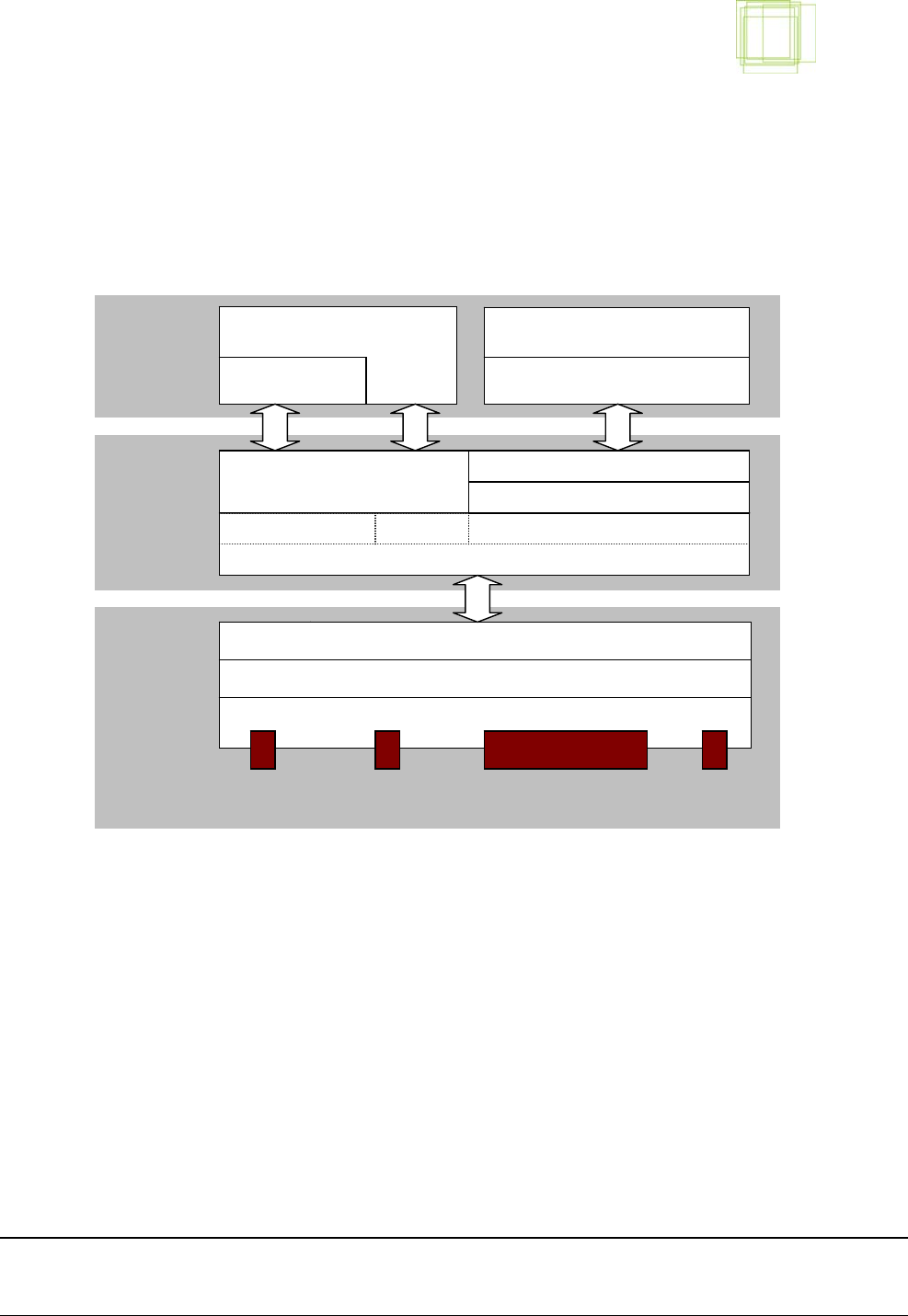
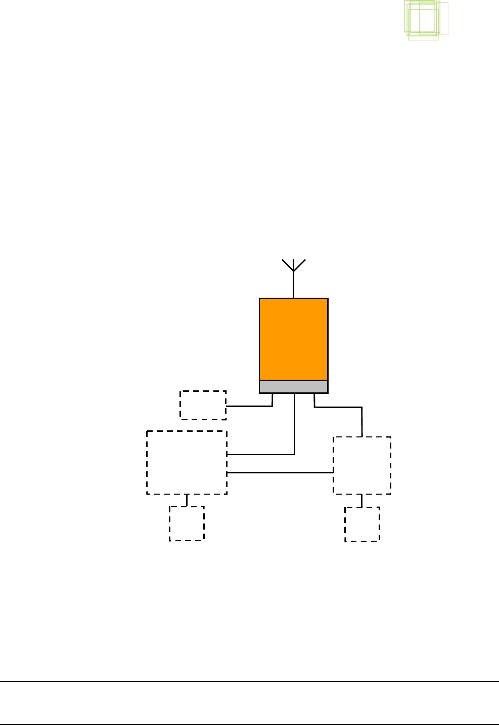
2 GENERAL OVERVIEW DIAGRAM
Figure 3 gives a high level system overview. Option provides the communication and
physical layer. On the physical layer, the bottom interfaces (in dark color) are explicit
notations to show the integrator which physical connection capabilities can be used.
Figure 3: High level system overview
The Communication Layer components are described in chapter 4 and chapter 5. An overview
of the supported AT commands is given in chapter 6
USER APPLICATION
(e-mail, http,...)
TCP
UDP / IP
PPP
USER APPLICATION
(SMS, signal strength,...)
AT commands
COM NDIS
USB
PCIExpress Mini Card
Embedded Stack
Hardware platform
Application
(eg. Hyper-
terminal,
SMS app.,
dashboard)
Communica-
tion Layer
Physical
Layer
(U)SIM
connector Mini PCIExpress
connector RF
connector
LED
APPLICATION DEBUG PPP
GTM353W Integration Manual
Author:
R
. Claessens Version: 4.0 Draft 2
Creation Date: September 20, 2006 Page: 9 of 52
Option Confidential: This document is Option Confidential - it may not be duplicated, neither distributed externally without prior and written permission of
Option NV.
3 HARDWARE DESCRIPTION
For abbreviations used in this chapter, please refer to the terms and abbreviations chapter.
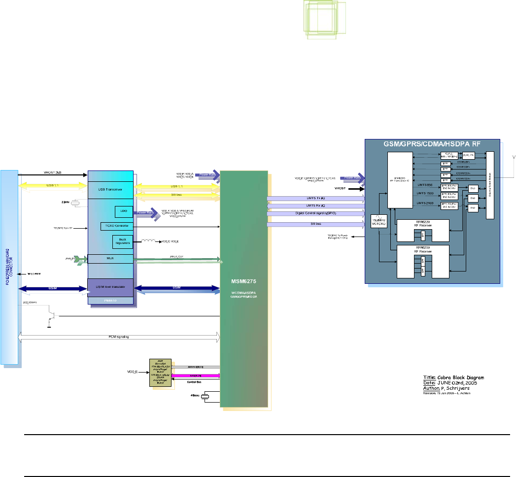
3.1 Block diagram GTM353W
Figure 5: Hardware block diagram GTM353W
GTM353W Integration Manual
Author:
R
. Claessens Version: 4.0 Draft 2
Creation Date: September 20, 2006 Page: 10 of 52
Option Confidential: This document is Option Confidential - it may not be duplicated, neither distributed externally without prior and written permission of
Option NV.
3.2 PCIExpress Mini Card interface
While the full PCI Express bus may be routed to the system connector from the host system,
the GTM card will only use the USB 2.0 Full Speed (12Mbit/s) interface (See Table 1 - NC is
Not Connected).
PIN
#
Pin assignment in
PCIExpress Mini
Card spec
Pin assignment on
GTM35x Additional Description
1 WAKE# NC WAKE functionality is NOT supported in USB
based Mini Cards per the PCI-SIG specification.
2 3.3Vaux 3.3V 3.3V DC supply rail from the host system. Further
description of the sourcing characteristics of this rail
is provided in this document.
3 RESERVED NC No Connect
4 GND GND Mini Card ground.
5 RESERVED NC No Connect.
6 1.5V NC 1.5V DC is not to be used
7 CLKREQ# NC As in the MINI Card Specification.
8 UIM_PWR UICC_PWR Power source for external UIM/SIM.
9 GND GND Mini Card ground.
10 UIM_DATA UICC_DATA External UIM/SIM data signal.
11 REFCLK- NC No Connect.
12 UIM_CLK UICC_CLK External UIM/SIM clock signal.
13 REFCLK+ NC No Connect.
14 UIM_RESET UICC_RESET External UIM/SIM reset signal.
15 GND GND Mini Card ground.
16 UIM_Vpp NC External UIM/SIM programming voltage.
17 RESERVED NC As in the Mini Card Specification.
18 GND GND Mini Card ground.
19 RESERVED NC As in the Mini Card Specification.
20 W_DISABLE# HW_RadioXMIT_Disable# Active low input from the platform to the card to
disable all the radios on the MPCI card from
transmitting.
21 GND GND Mini Card ground.
22 PERST# NC No Connect.
23 PERn0 NC No Connect.
24 3.3Vaux NC
25 PERp0 NC No Connect
26 GND GND Mini Card ground.
27 GND GND Mini Card ground.
28 1.5V NC 1.5V DC supply rail is not to be used
29 GND GND Mini Card ground.
30 SMB_CLK NC SMB support is not required for the WWAN Mini
Card module.
31 PETn0 NC No Connect.
32 SMB_DATA NC SMB support is not required for the WWAN Mini
Card module.
33 PETp0 NC No Connect.
GTM353W Integration Manual
Author:
R
. Claessens Version: 4.0 Draft 2
Creation Date: September 20, 2006 Page: 11 of 52
Option Confidential: This document is Option Confidential - it may not be duplicated, neither distributed externally without prior and written permission of
Option NV.
PIN
#
Pin assignment in
PCIExpress Mini
Card spec
Pin assignment on
GTM35x Additional Description
34 GND GND Mini Card ground.
35 GND GND Mini Card ground.
36 USB_D- USB_D- As in the Mini Card specification.
37 GND GND Mini Card ground
38 USB_D+ USB_D+ As in the Mini Card Specification.
39 3.3Vaux 3.3V 3.3V rail
40 GND GND Mini Card ground.
41 3.3Vaux 3.3V 3.3V rail
42 LED_WWAN# LED_WWAN_RadioState Active-low LED drive signal for indicating the state of
the WWAN Radio.
43 GND GND Mini Card GND
44 LED_WLAN# NC No Connect.
45 AUX_PCM_CLK NC AUX_PCM_CLK
46 LED_WPAN# NC No Connect.
47 AUX_PCM_DIN NC AUX_PCM_DIN
48 1.5V NC 1.5V DC is not to be used
49 AUX_PCM_DOUT NC AUX_PCM_DOUT
50 GND GND Mini Card Ground
51 AUX_PCM_SYNC NC AUX_PCM_SYNC
52 3.3Vaux 3.3V 3.3V DC supply rail from the host system. Further
description of the sourcing characteristics of this rail
is provided in this document.
· Table 1: PCIExpress Mini Card pinout
Remark: Increased electrical power and ground
Initial design reviews show that the current requirements exceed the limits set by the older
versions of the PCI Express Mini Card standard v. 1.1. In order to reduce impedances
additional pins are needed for power and grounding. Pins are required for supporting the
current 1.1A / 2.75A (average / peak) instead of 750mA / 1A. In the new version of the
standard, additional supply and grounding pins have been defined for this reason. Those pins
are pin 39/41 for additional 3.3V, and 37/43 for additional GND connections

GTM353W Integration Manual
Author:
R
. Claessens Version: 4.0 Draft 2
Creation Date: September 20, 2006 Page: 12 of 52
Option Confidential: This document is Option Confidential - it may not be duplicated, neither distributed externally without prior and written permission of
Option NV.
3.3 UICC interface guidelines
3.3.1 Introduction
This section describes how to design the UICC (USIM)-card interface for connection with the
GTM.
The baseband processor has an integrated UICC interface compatible with the ISO7816 IC
card standard. This is wired to the PCIExpress Mini Card connector (PCIE connector) in
order to be connected to an external UICC card holder (see Figure 5: (U)SIM pin assignment).
Five pins on the PCIE connector are reserved for the (U)SIM interface (pins 8,10,12, 14 and
15 - see Table 1 and Table 3).
The (U)SIM interface of a GSM/GPRS/EDGE/UMTS/HSDPA module needs some special
requirements. The (U)SIM card is connected with the digital part of the module. An RF
interference signal picked-up by the (U)SIM card reader can disturb normal operation of the
module and result in unexpected errors.
The (U)SIM card is accessible by the customer. In many cases an efficient RF-shielding of the
(U)SIM card is not possible. However, with some precautions problems caused by
interference signals picked up by the (U)SIM card can be significantly reduced.
3.3.2 UICC Interface
3.3.2.1 UICC Card Holder
The UICC Card interface has got 6 contacts. Officially according to 3GPP there are 8 pads,
so you will find eight (8) pads on the PCB-Layout picture (Figure 4) and in the specification
of the PCI Express Mini Card, numbered from C1 to C8. Contacting elements in positions C4
and C8 are not used. They shall present high impedance to the UICC. Figure 5 and Table 3
show the pin assignment of a UICC card.
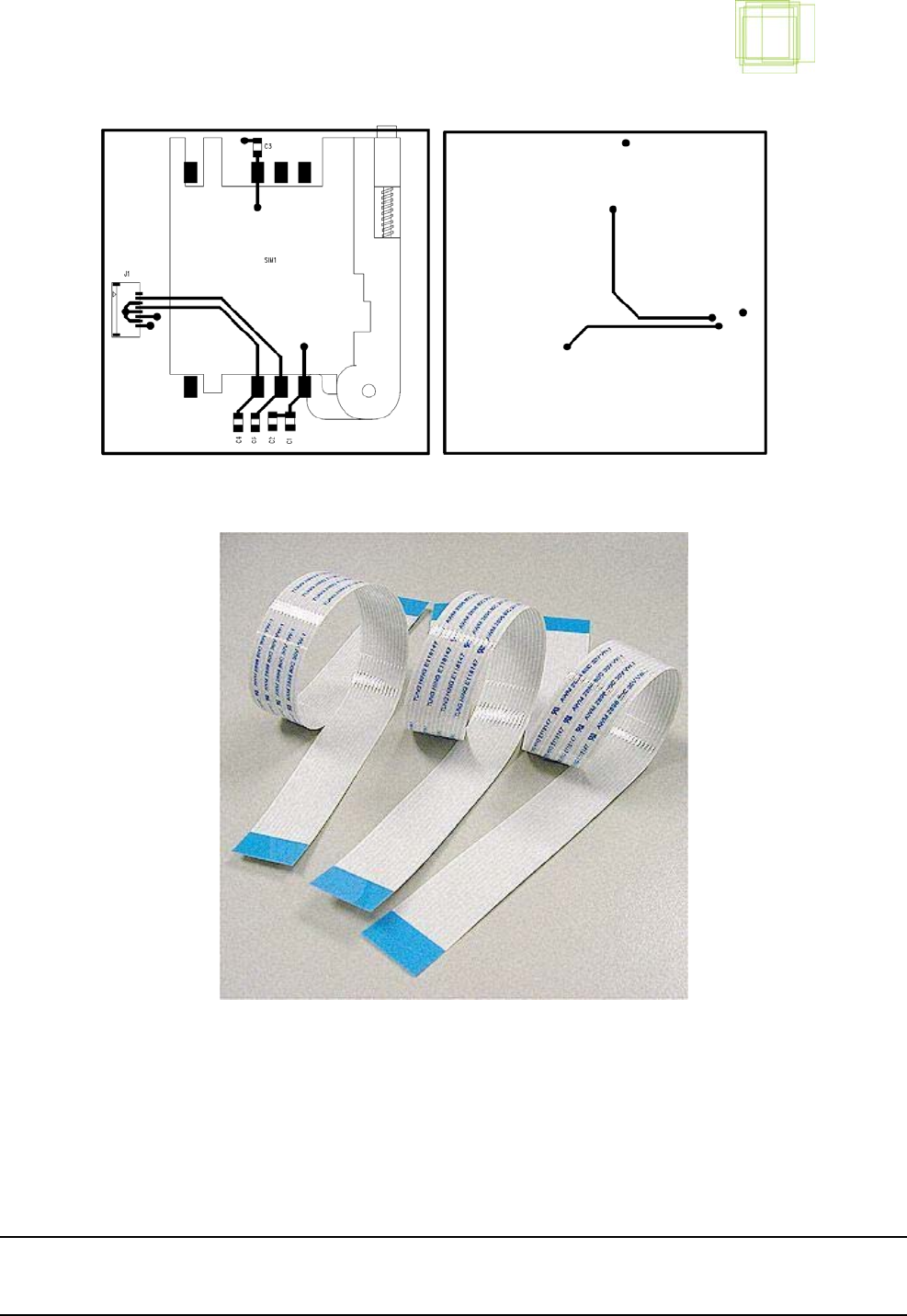
However as a way of an example “how to connect” the company JAE has introduced
(http://www.jae-connector.com/) 6 pins UICC connectors. These are numbered JAE-1
through JAE-6. For convenience the JAE numbering is added on the PCB-Layout picture
(Figure 4).
All the active circuitry is placed on the GTM. Only passives should be further applied.
GTM353W Integration Manual
Author:
R
. Claessens Version: 4.0 Draft 2
Creation Date: September 20, 2006 Page: 13 of 52
Option Confidential: This document is Option Confidential - it may not be duplicated, neither distributed externally without prior and written permission of
Option NV.
Figure 4: PCB layout pad assignment hosting a UICC
Contact
Element PCIE
pin number PCIE
Signal name Function
C1 Pin#08 UIM_PWR Power supply of the UICC
C2 Pin#14 UIM_RESET UICC reset, prompted by the GTM
C3 Pin#12 UIM_CLK Clock signal, generated by the GTM
C7 Pin#10 UIM_DATA Bi-directional data signal
Table 2: UICC mapped to B2B pinout
Figure 5: (U)SIM pin assignment
GTM353W Integration Manual
Author:
R
. Claessens Version: 4.0 Draft 2
Creation Date: September 20, 2006 Page: 14 of 52
Option Confidential: This document is Option Confidential - it may not be duplicated, neither distributed externally without prior and written permission of
Option NV.
Pin
no. Contact
Element Signal name (U)SIM
I/O Function
1 C1 VCC I Power supply of the SIM, generated by the GTM
2 C2 RST I SIM reset, prompted by the GTM
3 C3 CLK I clock signal, generated by the GTM
4 C5 GND I Ground
5 C6 PROG - Not Used
6 C7 I/O I/O bi-directional data signal, generated by either
GTM or (U)SIM
Table 3: (U)SIM pin description
The 3GPP standard defines 3 operation voltages for the supply voltage of the SIM card: 1.8V,
3V and 5V. The GTM module supports only 2 voltages, 1.8V and 3V. 5V only SIM cards
are barely used nowadays.
Note that the GTM does not have a UICC card holder. The UICC signals are connected with
the “PCI Express MiniCard” connector (the edge connector).
WAKE#
1+3.3V 2
Reserved
3Reserved
5UIM_PWR 8
UIM_DATA 10
UIM_CLK 12
UIM_RESET 14
UIM_VPP 16
UIM_C8
17 UIM_C4
19 W_DISABLE# 20
Reserved
37 Reserved
39 Reserved
41 Reserved
43 Reserved
45 Reserved
47 Reserved
49 Reserved
51
CLKREQ#
7GND
9REFCLK-
11 REFCLK+
13 GND
15
GND 4
+1.5V 6
GND 18
GND
21 PERn0
23 PERp0
25 GND
27 GND
29 PETn0
31 PETp0
33 GND
35
PERST# 22
+3.3Vaux 24
GND 26
+1.5V 28
SMB_CLK 30
SMB_DATA 32
GND 34
USB_D- 36
USB_D+ 38
GND 40
LED_WWAN# 42
LED_WLAN# 44
LED_WPAN# 46
+1.5V 48
GND 50
+3.3V 52
J1001
PCI_Ex_MiniCard_EdgeConnector
C1
A3
C2
B3
C3
C3 C4 C1
C5 B1
C6 A2
C7 C2
G
B2
U1002
EMIF03-SIM01
VREG_RUIM
UIM_DATA
UIM_RESET
UIM_CLK
VREG_RUIM
Figure 6: UICC Signal Routing on GTM
3.3.2.2 EMI filtering and ESD protection
The EMIF03-SIM01 (U1002 on Figure 6) is a highly integrated array designed to suppress
EMI/RFI noise. Greater than 25dB attenuation is obtained at frequencies from 800MHz to
GTM353W Integration Manual
Author:
R
. Claessens Version: 4.0 Draft 2
Creation Date: September 20, 2006 Page: 15 of 52
Option Confidential: This document is Option Confidential - it may not be duplicated, neither distributed externally without prior and written permission of
Option NV.
2.2GHz. Additionally, this filter includes an ESD protection circuitry which prevents the
protected device from destruction when subjected to ESD surges up to 8kV (Contact) and
15kV (Air).
· Figure 7: Schematic of EMIF03-SIM01
Figure 8: Insertion Loss Characteristic
3.3.3 Electrical specifications of the UICC – Terminal interface
This section is an excerpt from the standards, but it is very important that the integrator takes
care in the design phase to comply to these specifications, since they are essential to the final
certification of the integrated module (also see chapter 8 on certification).

GTM353W Integration Manual
Author:
R
. Claessens Version: 4.0 Draft 2
Creation Date: September 20, 2006 Page: 16 of 52
Option Confidential: This document is Option Confidential - it may not be duplicated, neither distributed externally without prior and written permission of
Option NV.
3.3.3.1 Contact activation and deactivation
The Terminal shall connect, activate and deactivate the UICC in accordance with the
Operating Procedures specified in ISO/IEC 7816-3 [12].
For any voltage level, monitored during the activation sequence, or during the deactivation
sequence following normal power-down, the order of the contact activation/deactivation shall
be respected.
It is recommended that whenever possible, the deactivation sequence defined in
ISO/IEC 7816-3 [12] should be followed by the Terminal on all occasions when the Terminal
is powered down.
If the UICC clock is already stopped and is not restarted, the Terminal may deactivate all the
contacts in any order, provided that all signals reach low level before Vcc leaves high level. If
the UICC clock is already stopped and is restarted before the deactivation sequence, then the
deactivation sequence specified in ISO/IEC 7816-3 [12] sub clause 5.4 shall be followed.
3.3.3.2 Inactive contacts
The voltages on contacts C1, C2, C3, C6 and C7 of the Terminal shall be in the range 0 ± 0,4
volts referenced to ground (C5) when the Terminal is switched off with the power source
connected to the Terminal. The measurement equipment shall have a resistance of 50 kohms
when measuring the voltage on C2, C3, C6 and C7. The resistance shall be 10 kohms when
measuring the voltage on C1.
3.3.3.3 Contact pressure
The contact pressure shall be large enough to ensure reliable and continuous contact (e.g. to
overcome oxidisation and to prevent interruption caused by vibration). The radius of any
curvature of the contacting elements shall be greater than or equal to 0,8 mm over the contact
area.
Under no circumstances shall the contact force exceed 0,5 N per contact.
Care shall be taken to avoid undue point pressure to the area of the UICC opposite to the
contact area. Such pressure is potentially damaging to the components within the UICC.
GTM353W Integration Manual
Author:
R
. Claessens Version: 4.0 Draft 2
Creation Date: September 20, 2006 Page: 17 of 52
Option Confidential: This document is Option Confidential - it may not be duplicated, neither distributed externally without prior and written permission of
Option NV.
3.3.3.4 Power Supply
The supply voltage of power supply is shown in Table 4.
Symbol Minimum Maximum Unit Voltage
Class
Vcc 2,7 3,3 V B
Vcc 1,62 1,98 V C
Table 4: Supply Voltage Classes indicated in ATR
• Power Consumption of the UICC during ATR
The maximum power consumption of the UICC during ATR is specified in Table 5
and Table 6. The UICC power consumption during the ATR shall conform to the
voltage class indicated in the ATR. If the UICC supports several supply voltage
classes, each class shall conform to the corresponding maximum ATR power
consumption, as specified in Table 5 and Table 6. This is required because the
terminal is not aware of the power consumption of the UICC until the ATR is
received and an application is selected.
Symbol Voltage Class Maximum Unit
Icc B 7.5 mA
Icc C 5 mA
Table 5: Power Consumption that applies during ATR at max. external clock
Symbol Voltage Class Maximum Unit
Icc B 6 mA
Icc C 4 mA
Table 6: Power Consumption that applies during ATR at 4 MHz
3.3.3.5 Specification of the 3V UICC – Terminal Interface
• Supply voltage Vcc (contact C1)
The Terminal shall operate the UICC within the following limits:
Symbol Minimum Maximum Unit
Vcc 2,7 3,3 V
Table 7: Electrical characteristics of Vcc under normal operating conditions
The module is capable of sourcing the maximum current as defined in Table 6. It is also able
to counteract spikes in the current consumption of the SIM card up to a maximum charge of
12 nAs with no more than 400 ns duration and an amplitude of at most 60 mA, ensuring that
the supply voltage stays in the specified range.
GTM353W Integration Manual
Author:
R
. Claessens Version: 4.0 Draft 2
Creation Date: September 20, 2006 Page: 18 of 52
Option Confidential: This document is Option Confidential - it may not be duplicated, neither distributed externally without prior and written permission of
Option NV.
• Reset (RST) (contact C2)
The Terminal shall operate the UICC within the following limits:
Symbol Conditions Minimum Maximum Unit
VOH I
OHmax = + 20 µA 0,8 x Vcc Vcc (Note) V
VOL I
OLmax = -200 µA 0 (Note) 0,2 x Vcc V
TR tF C
in = Cout = 30 pF 400 µs
NOTE: To allow for overshoot the voltage on RST should remain between -0,3V and Vcc +0,3V
during dynamic operations.
Table 8: Electrical characteristics of RST under normal operating conditions
• Clock CLK (contact C3)
The Terminal shall support 1 to 5 MHz. The Terminal shall supply the clock. No "internal
clock" UICC shall be used.
The duty cycle shall be between 40 % and 60 % of the period during stable operation.
The Terminal shall operate the UICC within the following limits:
Symbol Conditions Minimum Maximum Unit
VOH I
OHmax = + 20 µA 0,7 x Vcc Vcc (Note ) V
VOL I
OLmax = - 20 µA 0 (Note ) 0,2 x Vcc V
TR tF C
in = Cout = 30 pF 50 ns
NOTE: To allow for overshoot the voltage on CLK should remain between -0,3V and Vcc+0,3V
during dynamic operations.
Table 9: Electrical characteristics of CLK under normal operating conditions
• I/O (contact C7)
Table 3.6 defines the electrical characteristics of the I/O (contact C7). The values given in the
table allow the derivation of the values of the pull-up resistor in the Terminal and the
impedance of the drivers and receivers in the Terminal and UICC.
GTM353W Integration Manual
Author:
R
. Claessens Version: 4.0 Draft 2
Creation Date: September 20, 2006 Page: 19 of 52
Option Confidential: This document is Option Confidential - it may not be duplicated, neither distributed externally without prior and written permission of
Option NV.
Symbol Conditions Minimum Maximum Unit
VIH I
IHmax = ± 20 µA (Note 2) 0,7 x Vcc Vcc+0,3 V
VIL I
ILmax = + 1 mA - 0,3 0,2 x Vcc V
VOH (Note 1) I
OHmax = + 20 µA 0,7 x Vcc Vcc (Note 3) V
VOL I
OLmax = - 1mA 0 (Note 3) 0,4 V
TR tF C
in = Cout = 30 pF 1 µs
NOTE 1: It is assumed that a pull-up resistor is used on the interface device (recommended value:
20 k
Ω
).
NOTE 2: During static conditions (idle state) only the positive value can apply. Under dynamic
operating conditions (transmissions) short term voltage spikes on the I/O line may cause
a current reversal.
NOTE 3: To allow for overshoot the voltage on I/O shall remain between -0,3V and Vcc+0,3V
during dynamic operation.
Table 10: Electrical characteristics of I/O under normal operating conditions
3.3.3.6 Specification of the 1.8V UICC – Terminal Interface
• Supply voltage Vcc (contact C1)
The Terminal shall operate the UICC within the following limits:
Symbol Minimum Maximum Unit
Vcc 1,62 1,98 V
Table 11: Electrical characteristics of Vcc under normal operating conditions
The module is capable of sourcing the maximum current as defined in Table 6. It is also able
to counteract spikes in the current consumption of the SIM card up to a maximum charge of
12 nAs with no more than 400 ns duration and an amplitude of at most 60 mA, ensuring that
the supply voltage stays in the specified range.
• Reset (RST) (contact C2)
The Terminal shall operate the UICC within the following limits:
Symbol Conditions Minimum Maximum Unit
VOH I
OHmax = + 20 µA 0,8 x Vcc Vcc (Note) V
VOL I
OLmax = -200 µA 0 (Note) 0,2 x Vcc V
TR Tf C
in = Cout = 30 pF 400 µs
NOTE: To allow for overshoot the voltage on RST should remain between -0,3V and Vcc +0,3V
during dynamic operations.
Table 12: Electrical characteristics of RST under normal operating conditions
GTM353W Integration Manual
Author:
R
. Claessens Version: 4.0 Draft 2
Creation Date: September 20, 2006 Page: 20 of 52
Option Confidential: This document is Option Confidential - it may not be duplicated, neither distributed externally without prior and written permission of
Option NV.
• Clock CLK (contact C3)
The Terminal shall support 1 to 5 MHz. The Terminal shall supply the clock. No "internal
clock" UICC shall be used.
The duty cycle shall be between 40 % and 60 % of the period during stable operation.
The Terminal shall operate the UICC within the following limits:
Symbol Conditions Minimum Maximum Unit
VOH I
OHmax = + 20 µA 0,7 x Vcc Vcc (Note ) V
VOL I
OLmax = - 20 µA 0 (Note ) 0,2 x Vcc V
TR Tf C
in = Cout = 30 pF 50 ns
NOTE: To allow for overshoot the voltage on CLK should remain between -0,3V and Vcc+0,3V
during dynamic operations.
Table 13: Electrical characteristics of CLK under normal operating conditions
• I/O (contact C7)
Table 14 defines the electrical characteristics of the I/O (contact C7). The values given in the
table allow the derivation of the values of the pull-up resistor in the Terminal and the
impedance of the drivers and receivers in the Terminal and UICC.
Symbol Conditions Minimum Maximum Unit
VIH I
IHmax = ± 20 µA (Note 2) 0,7 x Vcc Vcc+0,3 V
VIL I
ILmax = + 1 mA - 0,3 0,2 x Vcc V
VOH (Note 1) IOHmax = + 20 µA 0,7 x Vcc Vcc (Note 3) V
VOL I
OLmax = - 1mA 0 (Note 3) 0,4 V
TR tF C
in = Cout = 30 pF 1 µs
NOTE 1: It is assumed that a pull-up resistor is used on the interface device (recommended value:
20 k
Ω
).
NOTE 2: During static conditions (idle state) only the positive value can apply. Under dynamic
operating conditions (transmissions) short term voltage spikes on the I/O line may cause
a current reversal.
NOTE 3: To allow for overshoot the voltage on I/O shall remain between -0,3V and Vcc+0,3V
during dynamic operation.
Table 14: Electrical characteristics of I/O under normal operating conditions
GTM353W Integration Manual
Author:
R
. Claessens Version: 4.0 Draft 2
Creation Date: September 20, 2006 Page: 21 of 52
Option Confidential: This document is Option Confidential - it may not be duplicated, neither distributed externally without prior and written permission of
Option NV.
3.3.4 Electrical interface
The (U)SIM card holder is connected with the module by means of long wires. The (U)SIM
card holder and wires are radiated on with different types of noisy signals, e.g. the radiation
signals of the module antenna. The SIM interface signals conduct this noise into the module
and radiate these signals into the module, with potential disasterous results.
This phenomenon can be significantly reduced by following design rules for EMC
interference minimisation:
1. Place noise suppression capacitors on the SIM card holder.
2. Route the SIM card holder signals carefully in relation to other signalling lines and
potential noise generation sources.
3. Limit the line length: a maximum length of 200mm is advised.
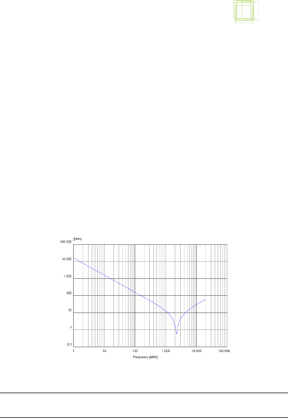
3.3.4.1 Noise suppression capacitors
On the module suppression capacitor are placed on the signals RTS, CLK and I/O. The value
of these suppression capacitors equals 17pF each.
Although the module foresees suppression capacitors it is important to place suppression on
the contacts of the SIM card holder. The value of these suppression capacitors must be equal
to 10pF. It is important to place the capacitors as short as possible to the SIM card reader.
Every mm PCB track (or FFC signalling line) counts. The size of the capacitor also matters. It
is advisable to use 0402 type capacitors.
Figure 9 shows the impedance graph of a 10pF capacitor.
Figure 9: Impedance of 10pF capacitor
GTM353W Integration Manual
Author:
R
. Claessens Version: 4.0 Draft 2
Creation Date: September 20, 2006 Page: 22 of 52
Option Confidential: This document is Option Confidential - it may not be duplicated, neither distributed externally without prior and written permission of
Option NV.
3.3.4.2 Maximum Trace Length
The maximum trace length depends on the trace capacitance, but on average it is advisable to
limit the length to a maximum of 200mm.
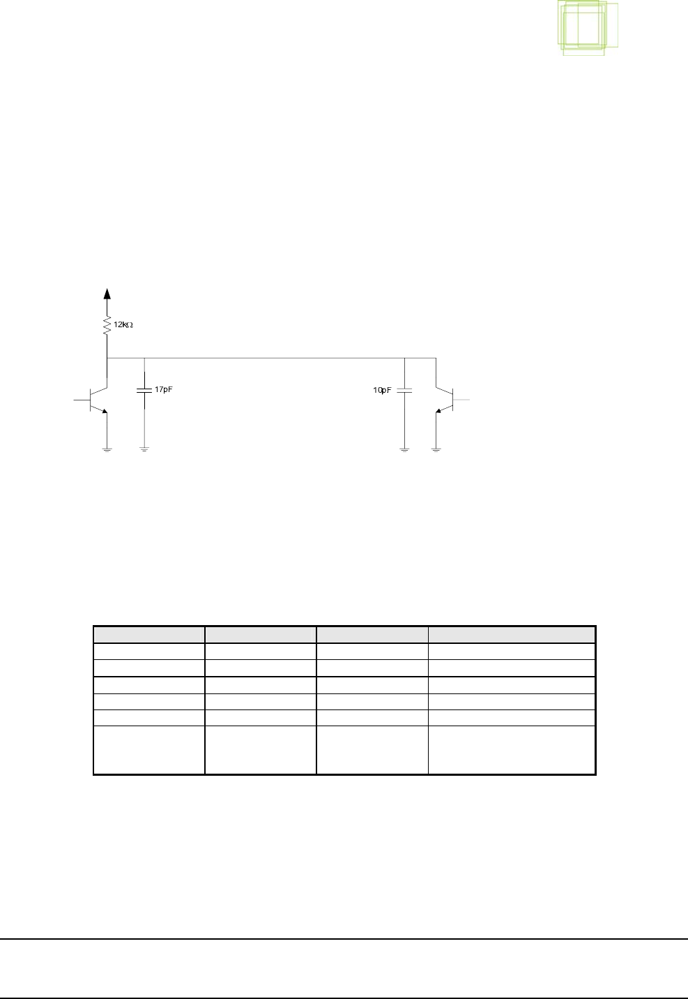
The module controls the signals RST and CLK. A totem-pole output drives these signals high
or low. The signal I/O is a bi-directional data line. The I/O interface is shown in Figure 10.
The module and the (U)SIM (in the SIM card holder), located on both ends of the lines,
control this data line. Either the module or the (U)SIM can pull this line low, through an
open-collector. The line is pulled-up by a resistor of 12kΩ.
Figure 10: I/O interface
During certification of the module the SIM interface is tested. A SIM card is simulated by the
test equipment. The test conditions are shown in Table 15 and Table 16. The test equipment
loads the I/O line with 30pF.
Contacts Low level High level Max. capacitive load
C1 (Vcc) --- I = 6 mA
C2 (RST) I = -200 µA I = +200 µA 30 pF
C3 (CLK) I = -20 µA I = +20 µA 30 pF
C5 (GND) --- ---
C6 ((Vpp) --- ---
C7 (I/O)
ME input
ME output
V = 0 V
I = -1 mA
I = +20 µA
I = +20 µA
30 pF
Table 15: Nominal test conditions on 3V SIM/ME interface
Module SIM card

GTM353W Integration Manual
Author:
R
. Claessens Version: 4.0 Draft 2
Creation Date: September 20, 2006 Page: 23 of 52
Option Confidential: This document is Option Confidential - it may not be duplicated, neither distributed externally without prior and written permission of
Option NV.
Contacts Low level High level Max. capacitive load
C1 (Vcc) --- I = 4 mA
C2 (RST) I = -200 µA I = +200 µA 30 pF
C3 (CLK) I = -20 µA I = +20 µA 30 pF
C5 (GND) --- ---
C6 ((Vpp) --- ---
C7 (I/O)
ME input
ME output
V = 0 V
I = -1 mA
I = +20 µA
I = +20 µA
30 pF
Table 16: Nominal test conditions on 1V8 SIM/ME interface
The maximum rise-time of I/O equals 1µs. This result in a maximum capacitive load of 70pF
on the I/O line. The maximum capacitance is the sum of all capacitors:
• Suppression capacitor on GTM, typical 17pF
• SIM driver logic on GTM, typical 5pF
• Suppression capacitor on SIM card holder, 10pF.
• Test equipment, maximum 30pF load.
• Connectors
The sum of al these capacitors, without the trace capacitance, equals 62pF. The trace
capacitance is 70pF minus all other capacitance. The maximum trace capacitance equals 70 –
62 = 8pF. This capacitance typically gives lead to a maximum length of 200mm in the worst
case.
GTM353W Integration Manual
Author:
R
. Claessens Version: 4.0 Draft 2
Creation Date: September 20, 2006 Page: 24 of 52
Option Confidential: This document is Option Confidential - it may not be duplicated, neither distributed externally without prior and written permission of
Option NV.
3.3.5 Practical implementation
The (U)SIM signals on the GTM are connected to the PCI Express MiniCard edge connector.
The method of routing the signals to the SIM card holder depends on which connecter is
used.
Note that only one of the two connectors can be used at once, the other needs to be left
floating.
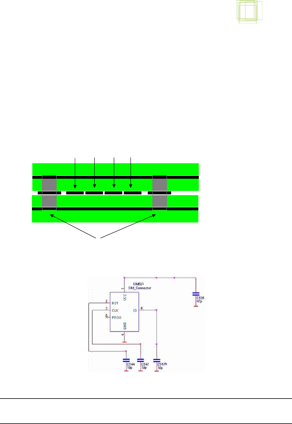
3.3.5.1 PCI Express MiniCard edge connector Signal Routing
When using this connector the SIM signals are routed throughout the PCB. In this
environment it is possible to shield the signals in an efficient way. An example of possible
PCB stackup is shown in Figure 11: PCB Stackup.
Figure 11: PCB Stackup
Note: Ground vias are placed every 2 – 3 mm along the signal traces.
Figure 12: Possible Schematic of a UICC cardholder
Note the 47pF suppression capacitor near contact C1 of the UICC cardholder.
GND Plane
GND Plane
Signal layer
Vias
RST
VCC I/O CLK
GTM353W Integration Manual
Author:
R
. Claessens Version: 4.0 Draft 2
Creation Date: September 20, 2006 Page: 25 of 52
Option Confidential: This document is Option Confidential - it may not be duplicated, neither distributed externally without prior and written permission of
Option NV.
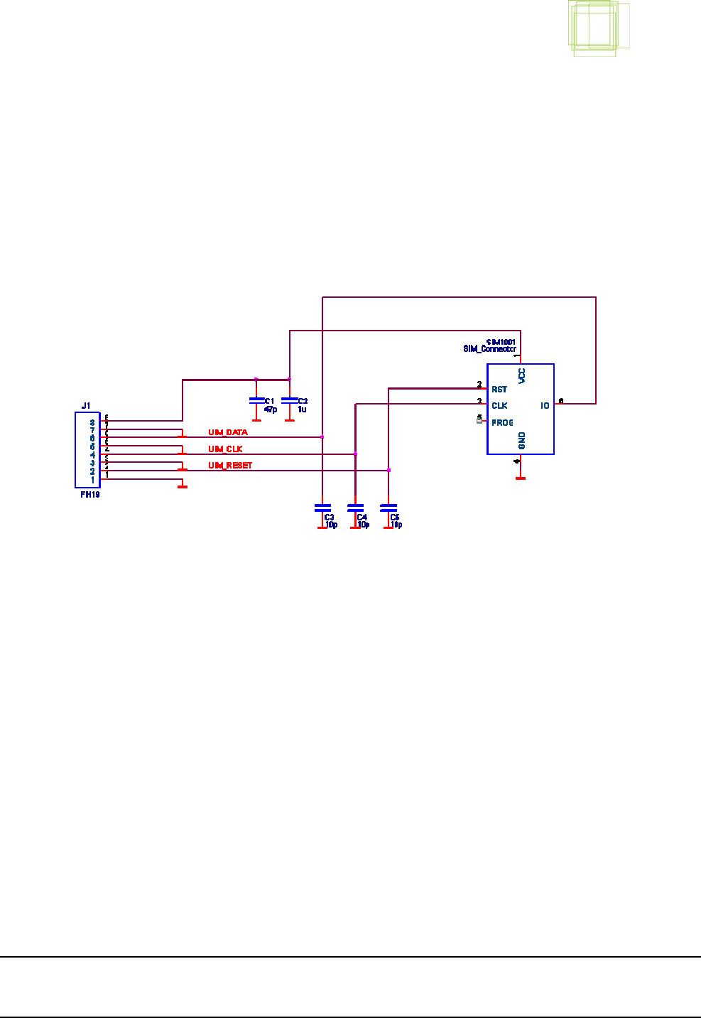
3.3.5.2 FH19 Signal Routing
The connection between the GTM and UICC cardholder is made by an FFC (flexible flat
cable). Shielding in this environment is much more problematic. In many cases the signals are
not shielded at all. However, the ground wires between every active signal grants certain
immunity against noise.
However an additional PCB board should be designed to host cardholder and some
decoupling capacitors.. The 8-contacts connector from Hirose’s FH19 Series is the same as on
the GTM module. Keep in mind the flat cable has a symmetrical usage.
Figures below show an example for an UICC card holder PCB board and interface. The
schematic and a layout are shown in these pictures.
· Figure 13: Possible Schematic of a UICC card holder PCB board
GTM353W Integration Manual
Author:
R
. Claessens Version: 4.0 Draft 2
Creation Date: September 20, 2006 Page: 26 of 52
Option Confidential: This document is Option Confidential - it may not be duplicated, neither distributed externally without prior and written permission of
Option NV.
Figure 14: Example of a (U)SIM card holder layout
Figure 15: Example of a FFC
GTM353W Integration Manual
Author:
R
. Claessens Version: 4.0 Draft 2
Creation Date: September 20, 2006 Page: 27 of 52
Option Confidential: This document is Option Confidential - it may not be duplicated, neither distributed externally without prior and written permission of
Option NV.
3.4 Digital PCM interface
3.4.1 Background
The module shall interface towards the main processor through the USB
interface and it shall also have an audio interface (PCM) towards the
SLIC/SLAC device. Although some signalling can de done in band over the
PCM interface, the application AT-command interface over the USB is to be
used for settings, dialling out, accepting voice calls and reply messages as
RING, BUSY and DISCONNECT.
Main
Processor
USB SLIC/
SLAC
RJ11
SPI
POTS
port
WCDMA
HSDPA
module
SIM card
holder
External
antenna
PCM
PHY
Ethernet
Connector

GTM353W Integration Manual
Author:
R
. Claessens Version: 4.0 Draft 2
Creation Date: September 20, 2006 Page: 28 of 52
Option Confidential: This document is Option Confidential - it may not be duplicated, neither distributed externally without prior and written permission of
Option NV.
3.4.1.1 Mechanical form factor for data and voice module
PRELIMINARY PINOUT :
The PCM interface (for voice) will be set on pin 45, 47, 49 and 51 of the PCIe
Express MiniCEM IO interface.
There are 4 pins defined PCM_CLK, for uplink voice PCM_UPLINK,
downlink voice PCM_DOWNLINK and PCM_SYNC. The PCM_CLK and
PCM_SYNC are generated by the module and therefore it act as MASTER.
The CODEC port supports 2.048MHz PCM clock and 8KHz sync timing for
linear, companded (A-law and µ-law) CODEC’s that match the sync timing.
3.4.2 Interfaces, Features & Functions
3.4.2.1 Telephony features
It is possible to originate and terminate calls via AT commands.
The module drives the PCM clock and sync (MASTER). When the module
goes to sleep, clock is lost and the PCM interface becomes inactive. Leaving
the PCM interface active on at all times would force standby time to be close
to talk time.
The AT-commands ATD and ATA will connect the PCM interface and makes
the PCM_DOWNLINK data-pin active by reversing the pin’s tri-state. The
ATH command disconnects the remote user: all calls are released (active, on-
hold and waiting calls).
3.4.2.1.1 PCM/Audio interface
The module has a PCM interface for a direct connection to an external
SLAC/SLIC that provides a single POTS port.
A 16-bit linear or 8-bit A-law or µ-law with padding can be selected for the
primary PCM interface. (See AT commands doc subsection ‘Voice’)
For all three, the format of the 16 bits on the PCM_UPLINK hardware line is
0xSDDD DDDD DDDD DDVV, where S is the signed bit, D is data, and V is
for volume padding. Also, for PCM_DOWNLINK, PCM has the 16-bit format
of 0xSDDD DDDD DDDD DVVV, where S is the signed bit, D is data, and V
is for volume padding.
Each interface path always accepts/outputs data in 20 millisecond frames.
This translates to 320 bytes per frame
(8 k samples/second * 16 bits/sample * 20 ms).
GTM353W Integration Manual
Author:
R
. Claessens Version: 4.0 Draft 2
Creation Date: September 20, 2006 Page: 29 of 52
Option Confidential: This document is Option Confidential - it may not be duplicated, neither distributed externally without prior and written permission of
Option NV.
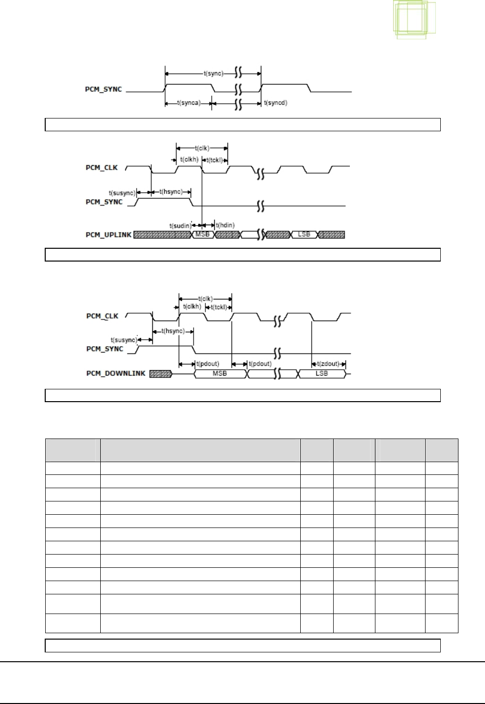
· Figure 16 PCM_SYNC timing
· Figure 17 PCM_UPLINK, Codec to Module timing
· Figure 18 PCM_DOWNLINK, Module to Codec timing
Parameter Description Min Typical Max Units
t(sync) PCM_SYNC cycle time -- 125 -- µs
t(synca) PCM_SYNC asserted time 62.4 62.5 -- µs
t(syncd) PCM_SYNC deasserted time 62.4 62.5 -- µs
t(clk) PCM_CLK cycle time -- 7.8 -- µs
t(clkh) PCM_CLK high time 3.8 3.9 -- µs
t(clkl) PCM_CLK low time 3.8 3.9 -- µs
t(susync) PCM_SYNC setup time to PCM_CLK rising ns
t(hsync) PCM_SYNC hold time after PCM_CLK rising ns
t(sudin) PCM_UPLINK setup time to PCM_CLK falling ns
t(hdin) PCM_UPLINK hold time after PCM_CLK falling ns
t(pdout) Delay from PCM_CLK rising to PCM_DOWNLINK
valid ns
t(zdout Delay from PCM_CLK falling to PCM_DOWNLINK
HIGH-Z ns
· Table 17 PCM Codec timing parameters

GTM353W Integration Manual
Author:
R
. Claessens Version: 4.0 Draft 2
Creation Date: September 20, 2006 Page: 30 of 52
Option Confidential: This document is Option Confidential - it may not be duplicated, neither distributed externally without prior and written permission of
Option NV.
3.4.2.1.2 Voice codecs
The module supports 1. Full Rate (FR), 2. Enhanced Full Rate (EFR), 3. Half
Rate (HR) and 4. Adaptive Multi-Rate (AMR) voice codecs.
3.4.2.1.3 Handling of Emergency Calls
It is possible to place an emergency call (i.e. 112 or 911) without having to
enter a PIN-code. SO the call should be set-up by the AT-command interface
either PCM interface.
3.4.2.1.4 Voice quality
The module will fulfil terminal acoustics according to 3GPP TS 26.131 Rel 5
and TS 26.132 Rel 5 (headset) if relevant.
Comment: The overall requirement for the module, is that it shall be possible
to achieve typical MOS 3.5 between a phone connected to the unit and a phone
connected to the PSTN (running AMR codec).
Algorithm Bit Rate
(kbits/s) MOS
(good network
conditions)
Framesize
(ms)
PCM G.711 64 4.3 0
GSM FR RPE-
LTP 13 3.7 (average) 20
GSM EFR 13 4 20
GSM HR VSELP 6.3 ~3.4 20
GSM AMR CELP adaptive 20
3.4.2.1.5 Message based DTMF transmission on the radio interface
The module is capable of transmitting DTMF on the radio interface as
received on the POTS interface using message based signalling on Layer 3 out
of ‘Voice’ band.
The module detects and suppresses DTMF tones generated on the POTS
interface according to applicable standards (when the voice service is being
used). (See AT commands doc subsection ‘Voice’)
3.4.2.1.6 Tones
The following tones are provided by the module over the POTS interface.
9 Call waiting tone:
A call waiting tone that is used to advise a subscriber who is engaged in

GTM353W Integration Manual
Author:
R
. Claessens Version: 4.0 Draft 2
Creation Date: September 20, 2006 Page: 31 of 52
Option Confidential: This document is Option Confidential - it may not be duplicated, neither distributed externally without prior and written permission of
Option NV.
a call that another subscriber is attempting to call. (The reader shouldn’t
get confused with the reply message over the AT-command channel
‘BUSY’.)
9 Cost warning tone:
During an advice of charge charging call the user can be informed about
the remaining credit during a call. This cost warning is a tone advising
the user that a limited credit (number of units) is left.
3.4.2.1.7 Ringing signals
The module indicates to the AT-command interface two (2) different call
types:
voice and voice line 2 (ALS).
3.4.2.1.8 CLI service
The module provides Caller Line Id (CLI) information to the main processor
via AT commands.
3.4.2.1.9 Alternate line service (ALS)
The module supports Alternate Line Service (ALS). This function is available
when a (U)SIM application providing this service is installed.
3.4.2.1.10 Fixed number dialling
The module supports Fixed Number Dialling. If enabled, this function allows
only calls to fixed numbers stored in (U)SIM. This function is available when
a (U)SIM providing this service is installed.
3.4.2.1.11 Supplementary services
The module supports below supplementary services in both GSM and UMTS
network as specified in applicable standards.
Supplementary service
Calling Line Identification Presentation (CLIP)
Calling Line Identification Restriction (CLIR)
Connected Line Identification Presentation (COLP)
Connected Line Identification Restriction (COLR)
Call Forwarding Unconditional
Call Forwarding on Mobile Subscriber Busy
Call Forwarding on No Reply
Call Forwarding on Mobile Subscriber Not Reachable
Call Waiting
Call Hold
Multi Party Service

GTM353W Integration Manual
Author:
R
. Claessens Version: 4.0 Draft 2
Creation Date: September 20, 2006 Page: 32 of 52
Option Confidential: This document is Option Confidential - it may not be duplicated, neither distributed externally without prior and written permission of
Option NV.
Supplementary service
Advice of Charge (Information)
Advice of Charge (Charging)
Barring of All Outgoing Calls
Barring of Outgoing International Calls
Barring of Outgoing International Calls except tho
s
directed to the Home PLMN Country
Barring of All Incoming Calls
Barring of Incoming Calls when Roaming Outside the Ho
m
PLMN Country
Explicit Call Transfer
Unstructured SS Data
3.5 Antenna guidelines
This section describes general guidelines for the design of multi-band antenna required for the
GTM module.
3.5.1 Antenna specifications
• Frequency range:
- GSM850 (824-894 MHz)
- EGSM900 (880-960 MHz)
- DCS1800 (1710-1880 MHz)
- PCS1900 (1850-1990 MHz)
- W UMTS 850/1900/2100 (830-885 / 1850-1990 / 1920-2170 MHz)
• Gain:
- Radiation pattern: omni-directional
- Gain averaged in space in all frequencies: > -3dBm
• Maximum VSWR: < 2.5:1 with 50Ω reference impedance
• Polarization: linear
3.5.2 WLAN Antenna Isolation
Based upon the known isolation and the lineair gain of the WLAN receiver there is a
minimum requirement for the out of band isolation in the GSM and UMTS bands. The
isolation is depending upon the antenna isolation WLAN and mobile standard, the output
power of the mobile, the linearity of the WLAN receiver IIP3 and the front-end filter
(blocking filter). Therefore it is preferred to use WLAN modules with blocking filter.
frequency PWR dBm Ant ISOL (dB) Attn front end
filter (dB)

GTM353W Integration Manual
Author:
R
. Claessens Version: 4.0 Draft 2
Creation Date: September 20, 2006 Page: 33 of 52
Option Confidential: This document is Option Confidential - it may not be duplicated, neither distributed externally without prior and written permission of
Option NV.
WLAN IIP3 2400-2500MHz -8
GSM PWR 880-915MHz 33 20 34
DCS PWR 1710-1785MHz 30 15 36
PCS PWR 1850-1910MHz 30 15 36
UMTS PWR 1920-1980MHz 24 12 33
· Table 18: Antenna isolation example
GTM353W Integration Manual
Author:
R
. Claessens Version: 4.0 Draft 2
Creation Date: September 20, 2006 Page: 34 of 52
Option Confidential: This document is Option Confidential - it may not be duplicated, neither distributed externally without prior and written permission of
Option NV.
3.5.3 Antenna connector
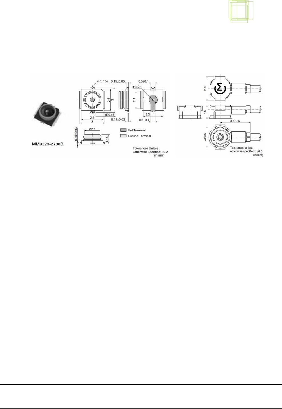
The connector type used is a muRata MM9329-2700B miniature microwave coaxial
connector.
· Figure 19: PCB connector (on GTM module)
· Figure 20: Jack connector
GTM353W Integration Manual
Author:
R
. Claessens Version: 4.0 Draft 2
Creation Date: September 20, 2006 Page: 35 of 52
Option Confidential: This document is Option Confidential - it may not be duplicated, neither distributed externally without prior and written permission of
Option NV.
4 HOST CONTROL INTERFACES
Figure 14 shows the NDIS interface via the TCP/IP stack as well as the COM interface via the
custom IOCTL interface. More details on the driver interface can be found in the following
chapter (Device Driver Interface)
· Figure 21: Host interface components
4.1 USB interface
The hardware USB interface is USB 2.0 compatible, USB 2.0 Full Speed (12Mbi/s) signalling
will be used.
4.2 COM interface
Three com ports are defined:
- application: This interface can be used for SMS and AT control commands and event
reporting
- modem: a second COM port provides the interface for the data channel and supports dial up
networking
-diagnostic: A third port is used for layer 1-3 stack tracing and debugging messages.
4.3 NDIS interface
The NDIS interface for the data channel provides an "auto start", "no click" way to get online
for a user. To the operating system, the card is represents itself as a network interface card,
hiding dial-up networking and AT commands.
One NDIS driver could also run the SMS and signal strength port. This data can be shipped to
an application via a custom IOCTL interface.
GTM353W Integration Manual
Author:
R
. Claessens Version: 4.0 Draft 2
Creation Date: September 20, 2006 Page: 36 of 52
Option Confidential: This document is Option Confidential - it may not be duplicated, neither distributed externally without prior and written permission of
Option NV.
5 DEVICE DRIVER INTERFACE
The figure below gives an overview of the driver structure which will be provided with the
GTM. Basically the module will manifest itself as a composite USB device which creates
stubs which the other higher level drivers hook into and provide their respective function. The
version number in gtmndisXXusb.sys denotes the operating system (XX= 50 for windows
2000, 51 for XP and 60 for Longhorn).
The “gtffbus.sys” driver is in fact a flip flop driver (type of mux) which chooses the interface
to use for data traffic: either the modem or the NDIS interface can be used.
For informational point of view it is illustrated that the mdm.exe service in fact controls the
“modem.sys” driver and the “tcpip.sys” is used for the TCP/IP stack interface towards the
application. These 2 drivers are default OS drivers.
Figure 22: Driver structure
The “connmgr.exe” is a service proposed by Option to control the functionality of the NDIS
driver (e.g. other PIN code, APN, …). The user space API will be available to aplication
developers.
gtmserusb.sys
Application interface
COM port
gtmserusb.sys
Diagnostics interface
COM port
gtptser.sys
Modem COM port
modem.sys
g
tmndisxxusb.s
y
s
g
t
f
fbus.s
y
s
connm
g
r.exe
Kernel mode
User mode (OS service)
g
tmusbbus.s
y
s
USB com
p
osite device
gtmusbbus.sys
usbohci.sys
USB root hub
usbohci.sys
pseries.sys
USB open host
controller
NDIS
mdm.exe
tcpip.sys
A
pp
lications: e.
g
. email, internet, ...
gtmserusb.sys
GTM353W Integration Manual
Author:
R
. Claessens Version: 4.0 Draft 2
Creation Date: September 20, 2006 Page: 37 of 52
Option Confidential: This document is Option Confidential - it may not be duplicated, neither distributed externally without prior and written permission of
Option NV.
6 AT COMMAND SET REFERENCE
This section lists the AT commands available on the GTM module. Most of the AT
commands supported are specified in 3GPP TS 27.007 and 3GPP TS 27.005. Details of these
commands can be found in those 3GPP specifications.
Only Option and/or Qualcomm proprietary AT commands are fully described in this section .
Please note that this section is subject to change. Support for some commands still needs to
be defined and will be updated in future versions of this document.
6.1 DTE-TA/DCE Interface Commands
All these commands are specified in 3GPP TS27.007 [1] and or ITU-T V.25ter.
Some of these commands may become meaningless on GTM because of the specific
hardware design. For example, since GTM internally uses a USB interface towards the host
commands to set the baud rate are no longer applicable. Where possible, this shall be
indicated.
Command Description Used
S3 Command line termination
character (S-parameter) Yes
S4 Response formatting
character (S-parameter) Yes
S5 Command line editing
character (S-parameter) Yes
E Command Echo Yes
Q Result code suppression Yes
V DCE Response format Yes
&C Circuit 109 behavior Yes
&D Circuit 108 behavior Yes
+IPR Fixed DTE rate Not applicable
+ICF DTE-DEC character framing Not applicable
+IFC DTE-DCE local flow control Yes
&V Dump configuration
parameters Yes
6.2 General commands
All these commands are specified in 3GPP TS27.007 [1].
Command Description Used
+CGMI Request manufacturer
identification Yes
+CGMM Request model identification Yes
+CGMR Request revision identification Yes
+CGSN Request product serial number
identification Yes
GTM353W Integration Manual
Author:
R
. Claessens Version: 4.0 Draft 2
Creation Date: September 20, 2006 Page: 38 of 52
Option Confidential: This document is Option Confidential - it may not be duplicated, neither distributed externally without prior and written permission of
Option NV.
+CSCS Select TE character set
Yes – but support for IRA
character set only
+CIMI Request international mobile
subscriber identity Yes
Z Reset to default configuration Yes
&F Set to factory defined
configuration Yes
I Request identification
information Yes
+GMI Request manufacturer
identification Yes
+GMM Request manufacturer
identification Yes
+GMR Request revision identification Yes
+GSN Request revision identification Yes
+GCAP Request complete capabilities
list Yes
6.3 Call control commands
All these commands are specified in 3GPP TS27.007 [1].
Command Description Used
+CSTA Select type of address TBD
D Dial
(using new dial modifiers,
“>”, “I/i”, “G/g”, and “;”
applicable to UMTS only)
> = direct dial from phone book
I/i = override CLIR
supplementary service default
G/g = control CUG supplementary
service for call
; = initiate voice call
Yes
+CHUP Hang up Yes – for voice call hangup
+CBST Select bearer service type Yes
+CRLP Radio link protocol Yes
+CR Service reporting control Yes
+CRC Cellular result codes Yes
T Select tone dialing Yes – but does nothing
P Select pulse dialing Yes – but does nothing
A Answer Yes
H Hook control Yes
O Return to online data state Yes
S0 Automatic answer Yes
S6 Pause before blind dialing Yes – but does nothing
S7 Connection completion
timeout Yes – but does nothing
S8 Comma dial modifier time Yes – but does nothing
S10 Automatic connect delay Yes – but does nothing
L Monitor speaker loudness Yes – but does nothing
M Monitor speaker mode Yes – but does nothing
+DS Data compression Yes
+DR Data compression reporting Yes
GTM353W Integration Manual
Author:
R
. Claessens Version: 4.0 Draft 2
Creation Date: September 20, 2006 Page: 39 of 52
Option Confidential: This document is Option Confidential - it may not be duplicated, neither distributed externally without prior and written permission of
Option NV.
6.4 Network service related commands
All these commands are specified in 3GPP TS27.007 [1].
Command Description Used
+CREG Network registration Yes
+COPS Operator selection Yes
+CLCK Facility lock Yes
+CPWD Change password Yes
+CLIP Calling line identification
presentation TBD
+CLIR Calling line identification restriction TBD
+COLP Connected line identification
presentation TBD
+CCUG Closed user group TBD
+CCFC Call Forwarding Number and
Conditions TBD
+CCWA Call waiting TBD
+CHLD Call related supplementary services TBD
+CTFR Call deflection TBD
+CUSD Unstructured supplementary service
data TBD
+CAOC Advice of charge TBD
+CSSN Supplementary service notifications TBD
+CLCC List current calls TBD
+CPOL Preferred operator list TBD
+CAEMLPP eMLPP priority registration and
Interrogation TBD
6.5 Mobile equipment commands
All these commands are specified in 3GPP TS27.007 [1].
Command Description Used
+CPAS Phone activity status Yes
+CFUN Set phone functionality Yes
+CPIN Enter PIN Yes
+CBC Battery charge Yes – but not applicable
+CSQ Signal quality Yes
+CPBS Select phone book memory storage Yes
+CPBR Read phone book entries Yes
+CPBF Find phone book entries Yes
+CPBW Write phone book entry Yes
+CLVL Loudspeaker volume level Yes - but not applicable
+CMEE Report mobile equipment error Yes
GTM353W Integration Manual
Author:
R
. Claessens Version: 4.0 Draft 2
Creation Date: September 20, 2006 Page: 40 of 52
Option Confidential: This document is Option Confidential - it may not be duplicated, neither distributed externally without prior and written permission of
Option NV.
6.6 UMTS packet domain commands
All these commands are specified in 3GPP TS27.007 [1].
Command Description Used
+CGDCONT Define PDP context Yes
+CGQREQ Requested quality of
service profile Yes
+CGQMIN Minimum acceptable
quality of service profile Yes – Accepted but does
nothing
+CGEQREQ Requested 3G quality of
service profile Yes
+CGEQMIN Minimum acceptable 3G
quality of service profile Yes – Accepted but does
nothing
+CGATT PS attach or detach Yes
+CGACT PDP context activate or
deactivate Yes
+CGCLASS GPRS mobile station
class (GPRS only) Yes
+CGEREP Packet domain event
reporting Yes – Accepted but does
nothing
+CGREG GPRS network
registration status Yes
+CGSMS Select service for MO
SMS messages Yes
6.7 SMS Commands
All these commands are specified in 3GPP TS27.005 [2].
Command Description Used
+CSMS Select message service Yes
+CPMS Preferred message storage Yes
+CMGF Message format Yes
+CSCA Service center address Yes
+CSMP Set text mode parameters Yes
+CSDH Show text mode
parameters Yes
+CNMI New message indications
to TE Yes
+CMGL List message Yes
+CMGR Read message Yes
+CNMA New message
acknowledge to ME/TA Yes
+CMGS Send message Yes
+CMSS Send message from
storage Yes
+CMGW Write message to memory Yes
+CMGD Delete message Yes
GTM353W Integration Manual
Author:
R
. Claessens Version: 4.0 Draft 2
Creation Date: September 20, 2006 Page: 41 of 52
Option Confidential: This document is Option Confidential - it may not be duplicated, neither distributed externally without prior and written permission of
Option NV.
6.8 Synchronous data mode commands
These commands are specified in ITU-T V.80ter.
Command Description Used
+ES Enables the synchronous
mode Yes
+ESA Preferred message storage Yes
These commands are not tested and probably will not work over the USB interface.
6.9 SIM Toolkit commands
There are no standard AT commands available in the GSM/GPRS/UMTS specifications to
manipulate the SIM Toolkit interface. See proprietary commands for SIM Toolkit in section
6.10.7.
6.10 Option proprietary commands
These are commands added by Option to accomplish things that cannot be done via the
standard AT commands available in the GSM/GPRS/UMTS specifications. This list of
proprietary commands will grow during the development of the module.
Command Description Used
_OHWV Read hardware version Yes
_OPSYS Preferred system Yes
_OSEC RRC Security Yes
_OSSYS Selected system Yes
_OAIR Aircraft mode Yes
_OCHAP enable/disable CHAP Yes
+STPD SIM toolkit profile
download Yes
6.10.1 Read hardware version _OHWV
Command Possible Response(s)
_OHWV _OHWV: <version>
Description
This command returns the version of the PCB and the version of the BOM (Bill Of
Materials).
Defined Values
<version> :
String type, indicates the PCB and BOM revision.
GTM353W Integration Manual
Author:
R
. Claessens Version: 4.0 Draft 2
Creation Date: September 20, 2006 Page: 42 of 52
Option Confidential: This document is Option Confidential - it may not be duplicated, neither distributed externally without prior and written permission of
Option NV.
6.10.2 Preferred SYStem AT_OPSYS
Command Possible Response(s)
_OPSYS=[<mode>[,<domain>]] OK
_OPSYS? _OPSYS: <mode>,<domain>
_OPSYS=? _OPSYS: (0-5),(0-6)
Description
This command changes the preferred system, GSM/WCDMA, the acquisition order and the
service domain preference PS/CS.
Defined values
<mode>:
0 GSM only
1 WCDMA only
2 GSM first
3 WCDMA first (default)
4 No change
5 Auto
<domain>:
0 Acquire only circuit-switched systems
1 Acquire only packet-switched systems
2 Acquire circuit-and/or packet-switched systems (default)
3 Any domain will do; no preference
4 To be used by clients who do not want to change the service domain
5 PS attach on demand; note that this value of service domain preference is not saved in NV
6 PS detach on demand; note that this value of service domain preference is not saved in NV
6.10.3 Security “AT_OSEC”
Command Possible Response(s)
_OSEC=[<sec>] OK
_ OSEC? _ OSEC: < sec >
_ OSEC =? _ OSEC: (list of supported <sec>s)
Description
This command sets the RRC security setting.
Please note that a hard reset of the GTM is required before the setting will take effect.
Defined values
<sec>:
0 None
1 Integrity
2 Ciphering
3 Fake Security
4 Integrity and Ciphering (default)
GTM353W Integration Manual
Author:
R
. Claessens Version: 4.0 Draft 2
Creation Date: September 20, 2006 Page: 43 of 52
Option Confidential: This document is Option Confidential - it may not be duplicated, neither distributed externally without prior and written permission of
Option NV.
6.10.4 Selected System “AT_OSSYS”
Command Possible Response(s)
_OSSYS=[<n>] OK
_OSSYS? _OSSYS: <n>,<AcT>
_OSSYS=? _OSSYS: (0-1),(0,2)
Description
This command enables/disables the unsolicited result code _OSSYSI: <mode>.
Defined values
<n>:
0 Turns off unsolicited result code _OSSYSI: <mode> (default)
1 Turns on unsolicited result code _OSSYSI: <mode>
<AcT>:
0 GSM
2 UTRAN
3 No service
6.10.5 Aircraft Mode “AT_OAIR”
Command Possible response(s)
_OAIR= < aircraft mode> OK
_OAIR? _OAIR: < aircraft mode>
_OAIR=? _OAIR: (list of supported <mode>’s)
Description
Allows the user to change the startup RF of the gsm/wcdma part (protocol stack) at power up
setting or query its current state.
Defined Values
<Aircraft mode>
0 Off, the unit will startup protocol stack at power up (gsm/wcdma part). (default)
1 On, the unit will NOT startup the protocol stack at power up (gsm/wcdma part).
GTM353W Integration Manual
Author:
R
. Claessens Version: 4.0 Draft 2
Creation Date: September 20, 2006 Page: 44 of 52
Option Confidential: This document is Option Confidential - it may not be duplicated, neither distributed externally without prior and written permission of
Option NV.
6.10.6 Enable/Disable CHAP “AT_OCHAP”
Command Possible Response(s)
_OCHAP=[<sec>] OK
_ OCHAP? _ OCHAP: < sec >
_ OCHAP =? _ OCHAP: (0-1)
Description
This command enables or disables CHAP Protocol security setting during activation of a PDP
context.
Value is stored in NVRAM. The default state is enabled.
Defined values
<sec>:
0 Disabled
1 Enabled (default)
6.10.7 SIM toolkit profile download “AT+STPD”
Command Possible Response(s)
+STPD=<length>, <profile> OK, ERROR
+STPD? ERROR
+STPD=? ERROR
Description
This command will send the given profile to SIM toolkit.
Parameters
<Length> = a number representing the length of the binary profile.
<Profile> = the SIM toolkit profile in hexadecimal format (see 3GPP 11.14 [Structure and coding
of TERMINAL PROFILE])
Example
AT+STPD=1,03
Indicates that profile download and SMS-PP data download are supported by the ME (GTM in this
case)
GTM353W Integration Manual
Author:
R
. Claessens Version: 4.0 Draft 2
Creation Date: September 20, 2006 Page: 45 of 52
Option Confidential: This document is Option Confidential - it may not be duplicated, neither distributed externally without prior and written permission of
Option NV.
7 PHYSICAL CHARACTERISTICS
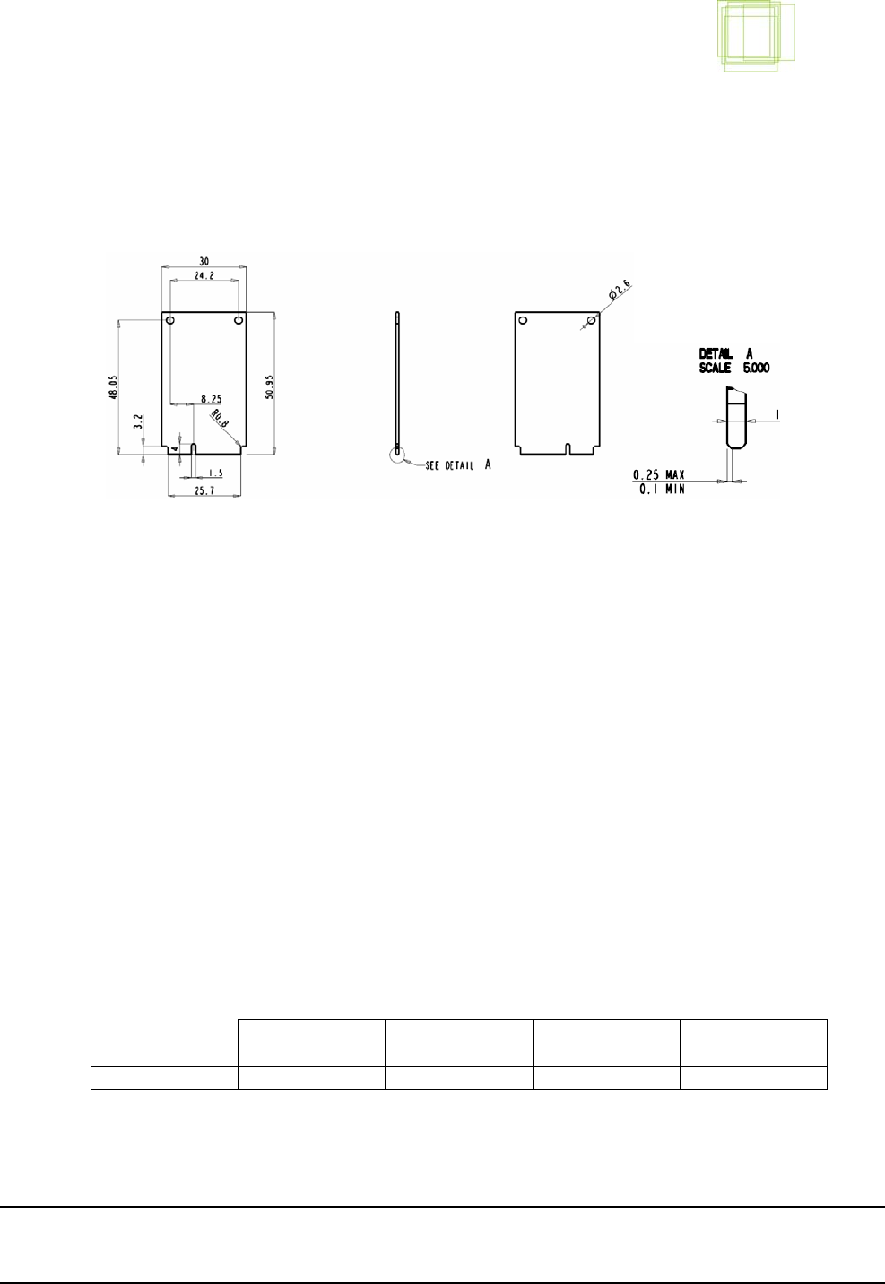
7.1 Dimensions
· Figure 23: card dimensions (in mm - not to scale)
7.2 Power consumption
( preliminary )
Vcc 3.3V +/- 9%
Peak Icc 2750 mA
with max supply droop 50mV
Average Icc 850mA
7.3 Thermal dissipation requirements
The GTM power dissipation in idle mode (slow clocking mode) is 80mW, under the condition
that the USB defined selective suspend is fully supported for USB Host Controllers (UHCI).
The maximum thermal dissipation directly from any PCI Express Mini Card add-in card is 2.9
W peak
• Total estimated power consumption (based on calculations; worst case: highest Tx):
GPRS
(2TX+4RX) 850 UMTS 2100 UMTS US 850 UMTS US 1900
Total power (mW) 1800 2750 2800 2900
GTM353W Integration Manual
Author:
R
. Claessens Version: 4.0 Draft 2
Creation Date: September 20, 2006 Page: 46 of 52
Option Confidential: This document is Option Confidential - it may not be duplicated, neither distributed externally without prior and written permission of
Option NV.
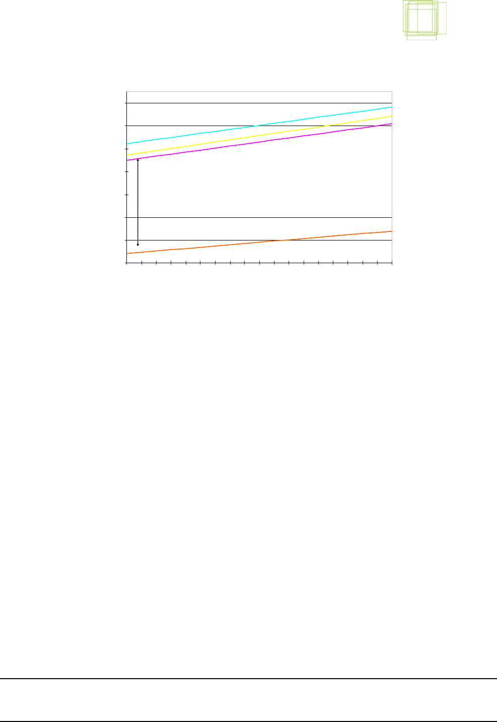
Heat Dissipation
1500
1700
1900
2100
2300
2500
2700
2900
-9% -8% -7% -6% -5% -4% -3% -2% -1% 0% 1% 2% 3% 4% 5% 6% 7% 8% 9%
Voltage Derating %
Heat in mWatt
=820mW
GPRS
HSDPA2100
HSDPA1900
HSDPA850
Figure 24: Thermal Design Profile (TDP) Worst Case
Figure 24 shows the (calculated) power consumtion versus voltage derating characteristic.
• Measured power consumption: to be determined.

GTM353W Integration Manual
Author:
R
. Claessens Version: 4.0 Draft 2
Creation Date: September 20, 2006 Page: 47 of 52
Option Confidential: This document is Option Confidential - it may not be duplicated, neither distributed externally without prior and written permission of
Option NV.
7.4 Operating and Storage Environment
These values should be considered preliminary and are to be investigated later.
7.4.1 Shock
Operating 15 G, 18 ms
Non-operating 30 G, 11 ms
7.4.2 Vibration
Operating Linear: 20-300 Hz, 0.75 G (0 to peak)
Random: 10-300 Hz, 0.004 g2/Hz
Non-operating 5-20 Hz, 0.195 inches (double amplitude)
20-500 Hz, 4.0 G (0 to peak) Sweep Rate 0.5 octave/minute minimum
7.4.3 Operating Temperature and Humidity
Temperature -10°C to 55°C (14°F to 131°F)
Humidity 5-95% RH non-condensing
33°C (maximum wet bulb)
Thermal Gradient 20°C/hour (maximum)
Humidity Gradient 20%/hour (maximum)
7.4.4 Non-Operating Temperature and Humidity
Temperature -40°C to 65°C (-40°F to 149°F)
Humidity 5-95% RH non-condensing
35°C (maximum wet bulb)
Thermal Gradient 30°C/hour (maximum)
Humidity Gradient 20%/hour (maximum)
7.4.5 Altitude
Operating -1000 feet to 10,000 feet (-305M to 3,050M)
Non-Operating -1000 feet to 40,000 feet (-305M to 12,200M)
These figures are valid in open air (not valid in e.g. planes since this is a pressurised room)

GTM353W Integration Manual
Author:
R
. Claessens Version: 4.0 Draft 2
Creation Date: September 20, 2006 Page: 48 of 52
Option Confidential: This document is Option Confidential - it may not be duplicated, neither distributed externally without prior and written permission of
Option NV.
8 CERTIFICATION
FCC certification:
If the FCC ID is not visible when this card is installed inside another device, then the outside
of the device into which this device is installed must also display a label referring to the
enclosed device. This exterior label can use wording such as the following: "Contains FCC
ID: NCMOGTM353-W". Any similar wording that expresses the same meaning may be used.
Other certification statements are to be added in a next revision of this document.
FCC Radiation Exposure Statement:
This equipment complies with FCC radiation exposure limits set forth for an uncontrolled
environment. This equipment should be installed and operated with minimum distance of
20cm between the radiator and your body.
This device is intended only for OEM integrators under the following conditions:
OEM integrator is still responsible for testing their end product for any additional compliance
requirements required with this module installed (for example, digital device emissions, PC
peripheral requirements, etc.).
In the event that these conditions cannot be met (for example certain laptop configurations or
co-location with another transmitter), then the FCC authorization is no longer considered
valid and the FCC ID cannot be used on the final product. In these circumstances, the OEM
integrator will be responsible for re-evaluating the end product (including the transmitter) and
obtaining a separate FCC authorization.
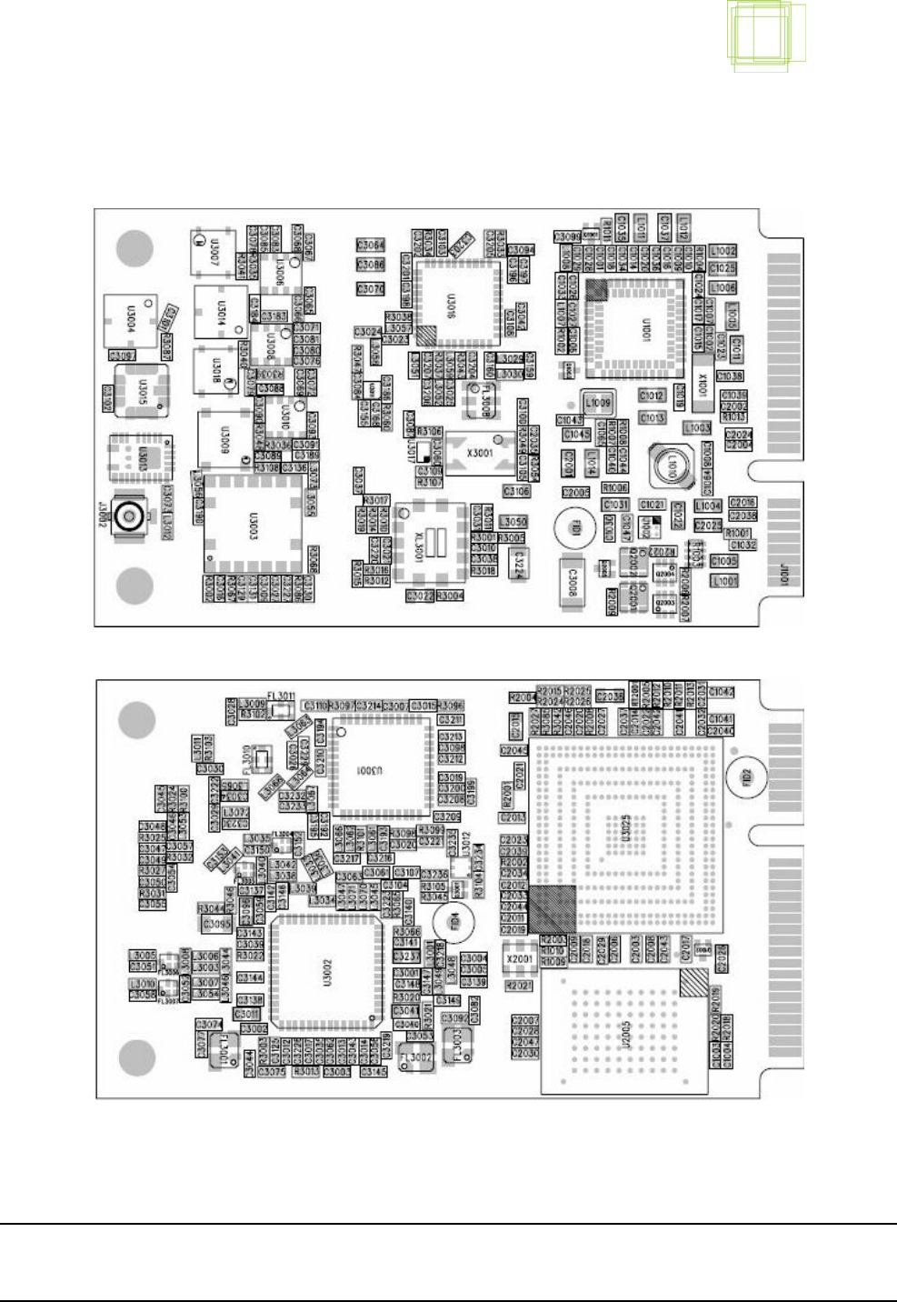
GTM353W Integration Manual
Author:
R
. Claessens Version: 4.0 Draft 2
Creation Date: September 20, 2006 Page: 49 of 52
Option Confidential: This document is Option Confidential - it may not be duplicated, neither distributed externally without prior and written permission of
Option NV.
9 BOARD ASSEMBLY
· Figure 25: Top view
· Figure 26: Bottom view
Mini PCIExpress interface

GTM353W Integration Manual
Author:
R
. Claessens Version: 4.0 Draft 2
Creation Date: September 20, 2006 Page: 50 of 52
Option Confidential: This document is Option Confidential - it may not be duplicated, neither distributed externally without prior and written permission of
Option NV.

GTM353W Integration Manual
Author:
R
. Claessens Version: 4.0 Draft 2
Creation Date: September 20, 2006 Page: 51 of 52
Option Confidential: This document is Option Confidential - it may not be duplicated, neither distributed externally without prior and written permission of
Option NV.
10 ABBREVIATIONS
Abbreviation Description
B2B Board-to-board connector
EDGE Enhanced Data Rates for Global Evolution
FFC Flexible Flat Cable
GND Ground
GPRS General Packet Radio Service
GSM Global Standard for Mobile Communications
HSDPA High Speed Data Packet Access
IEC International Electrotechnical Commission
ISO International Standards Organization
I/O Input/Output
ME Mobile Equipment
NDIS Network Driver Interface Specification
NVRAM Non volatile RAM
SIM Subscriber Identification Module
UICC UMTS Integrated Circuit Card
UMTS Universal Mobile Telephone Service
USB Universal Serial Bus
(U)SIM Universal Subscriber Identity Module

GTM353W Integration Manual
Author:
R
. Claessens Version: 4.0 Draft 2
Creation Date: September 20, 2006 Page: 52 of 52
Option Confidential: This document is Option Confidential - it may not be duplicated, neither distributed externally without prior and written permission of
Option NV.
11 REFERENCES
Ref Document
[1] 3GPP TS 27.007 V3.7.0 (2000-12) AT Command set for User Equipment (UE) (Release 1999)
[2] 3GPP TS 27.005 V3.1.0 (2000-01) Equipment (DTE-DCE) interface for Short Message
Service (SMS) and Cell Broadcast Service (CBS)