PARROT FC6100ASPEN WLAN Transceiver User Manual FC6100 ASPEN Datasheet 21fev2012
PARROT WLAN Transceiver FC6100 ASPEN Datasheet 21fev2012
PARROT >
user manual

PARROT PRODUCT DATASHEET
Parrot
FC6100 ASPEN
Version 1.1
MARCH 2012
Confidential information
DATASHEET Confidential Information 2/18
Ref: FC6100-Datasheet
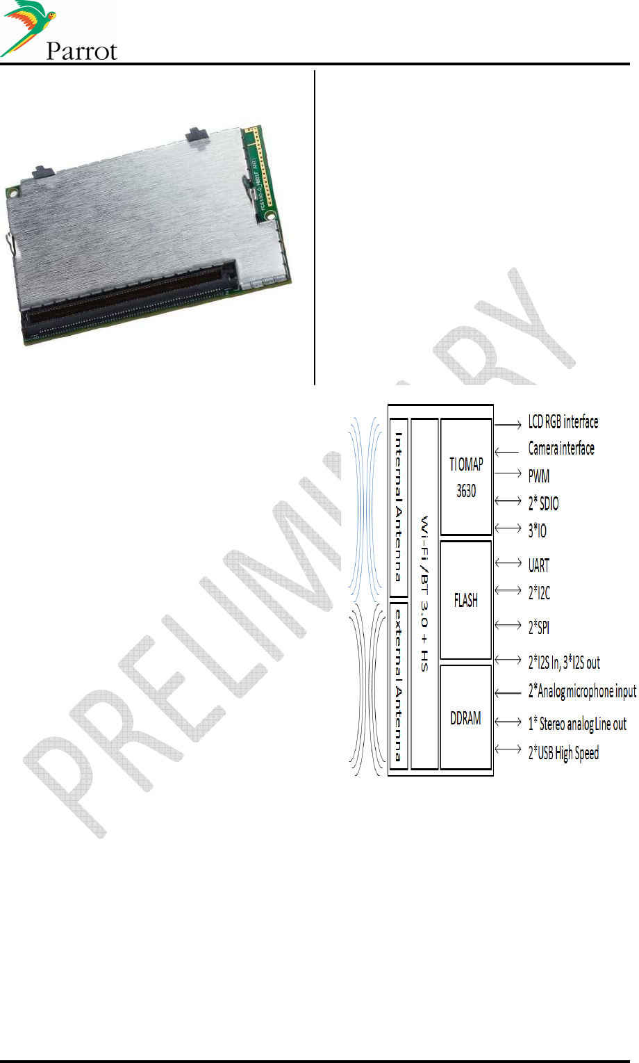
Parrot FC6100 ASPEN
Full connectivity module with Android OS.
Technical Features:
• LCD Management-LCD RGB/LVDS
• Wi-Fi module
• Piconet and scatternet support
• Standard single 3V3 supply
• UARTs, I²C
• 1*USB 2.0 High Speed
• Digital and analog audio in and out
• Analog Video output
• Module dimensions 72 x 44.3 x 4.60mm
• IPod chip management (optional)
• 2
nd
USB 2.0 connection (optional)
Applications:
• Smartphone Android Apps platform
• Navigation
• Telephony voice recognition
• Multimedia voice recognition
• Terminal mode
The FC6100 ASPEN platform provides a full
API, to access Parrot Libraries.
Description:
Parrot FC6100 ASPEN is a solution for
Multimedia systems. It integrates a large
variety of interfaces for easy integration of
most multimedia applications.

Confidential Information 3/18
Ref: FC6100ASPEN-
Datasheet
Table of contents
1 FC6100 ASPEN Overview .................................................................................................................... 4
2 Features List ....................................................................................................................................... 5
2.1 Connectivity ................................................................................................................................. 5
3 FC6100 ASPEN technology ................................................................................................................. 6
5 Wi-Fi Use Cases .................................................................................................................................. 7
5.1 Parrot’s FC6100 ASPEN provides the internet connection to Wi-Fi users .................................. 7
7 Hardware Overview ........................................................................................................................... 8
7.1 Memory ....................................................................................................................................... 8
7.2 Power domains ............................................................................................................................ 8
7.3 Power supplies ............................................................................................................................ 8
7.4 Digital communication links ........................................................................................................ 8
7.4.1 Control signals ................................................................................................................. 8
7.4.2 I2C .................................................................................................................................... 9
7.4.3 UART ................................................................................................................................ 9
7.4.4 Digital data bus ................................................................................................................ 9
7.4.5 Audio interface .............................................................................................................. 10
7.4.6 Video interface .............................................................................................................. 10
7.5 Pin Out Table (140 pins connector) ........................................................................................... 11
8 Mechanical Dimension (preliminary) ............................................................................................... 15
9 Absolute Maximum Ratings ............................................................................................................. 16
10 Electrical Specifications .................................................................................................................... 16
10.1 Power Consumption (preliminary) ............................................................................................ 16
10.2 Power Supplies .......................................................................................................................... 16
10.3 Hardware Reset Conditions ....................................................................................................... 16
10.4 Software Reset Input ................................................................................................................. 16
10.5 Digital IO Pins ............................................................................................................................ 17
11 FCC requirements for module application ....................................................................................... 18

Confidential Information 4/18
Ref: FC6100ASPEN-
Datasheet
1 FC6100 ASPEN Overview
FC6100 ASPEN is an easy to integrate module based on the Texas Instruments OMAP 3630
multimedia processor: Cortex A8 (1600 MIPS), 3D and video hardware accelerator. The FC6100
ASPEN offers the best of both worlds, the automotive-specific precision of Parrot automotive
libraries along with the market acceptance of the Android platform running on the ARM Architecture.
The ARM architecture includes a family of CPUs with FPU which are sold now in larger volumes than
Intel CPUs. They power products with huge market success such as the iPhone and Android phones.
The portfolio includes single, dual and quad-core CPUs.
FC6100
FC6100
TI OMAP ARM Cortex
-
A8 (1600 MIPS)
Display up to 10'' (1024x768 pixels)
Integrated OpenGL 3D Graphics Accelerator
Up to 4Gbits RAM, 8Gbits FLASH

Confidential Information 5/18
Ref: FC6100ASPEN-
Datasheet
2 Features List
2.1 Connectivity
• USB
Parrot FC6100 ASPEN embeds a USB 2.0 OTG high speed transceiver
Compliant with USB devices supporting Mass Storage Class
Supports USB hub
• Wi-Fi
IEEE 802.11b/g/i compliant
Data rates of 1–54 Mbps for 802.11g
Security support for WPS, WPA2, WPA
Ad hoc, station, or Access Point mode
Up to 8 devices can simultaneously be connected in Access Point mode

Confidential Information 6/18
Ref: FC6100ASPEN-
Datasheet
3 FC6100 ASPEN technology
FC6100 ASPEN Wi-Fi protocol summary
802.11a - 5GHz WiFi 54Mbps No
802.11b - 2.4GHz WiFi 11Mbps Yes
802.11d - "World Mode" No
802.11g - 2.4GHz WiFi 54Mbps Yes
802.11h - 5GHz interferrence avoid No
802.11i - Security Yes
802.11j - Japan Standard No
802.11n - 2.4GHz WiFi 150Mbps No
802.11y - High Power WiFi No
Access Point support on reset -frimware change
Ad-Hoc Yes
Client Yes
PAN - like Intel Cliffside multi point access No
WPA2 / WPA
Yes
2.4GHz
Supported
WLAN
Coexistence

Confidential Information 7/18
Ref: FC6100ASPEN-
Datasheet
5 Wi-Fi Use Cases
5.1 Parrot’s FC6100 ASPEN provides the internet connection to Wi-Fi users
The Parrot module can act as a Wi-Fi micro Access Point (AP). As an access point, up to 8
devices can be connected simultaneously. With this use case, the FC6100 ASPEN acts as the
gateway, using networking terminology.
The internet connection is provided by a HSDPA module or by a 3G+ USB dongle. The low-level
network control is handled by the FC6100 ASPEN.
From the Wi-Fi user perspective, connecting to the in-car network works the same as a standard
access point,
A software application running in the FC6100 ASPEN is used to set the Wi-Fi networking service:
enabling/disabling Wi-Fi
configuring the security level (WEP, WPA, WPA2), and associated passes
retrieving network information as needed (example: which users are connected)
Access
point
/
NIC

Confidential Information 8/18
Ref: FC6100ASPEN-
Datasheet
7 Hardware Overview
Here is an overview of FC6100 ASPEN Hardware design.
For more details, the FC6100 ASPEN Hardware Integration Guide can be sent upon request.
7.1 Memory
FC6100 ASPEN Memory configuration:
Up to 8Gbits NAND Flash and 4 Gbits mDDR RAM.
7.2 Power domains
FC6100 ASPEN’s processor’s digital I/O are mainly referenced to a 1.8V voltage.
Historically, Parrot interface uses 3.3V interface.
However, some customers might already use 1.8V signaling on their motherboard and level-shifting
would then become redundant.
The decision was then made to move level-shifting function on the motherboard to improve the
flexibility of the design and the module size.
Consequently, FC6100 ASPEN digital I/Os belong to 2 different power domains:
• 3.3V signaling
• 1.8V signaling
7.3 Power supplies
• 3V3_MAIN
To operate, the module requires a unique 3.3V voltage power supply called 3V3_MAIN with a 10%
precision and capable to deliver up to 1A.
3V3_MAIN is internally monitored and triggers power on and power down sequence of the module.
• VDD_PERM
In cases where RTC option is needed, for time-keeping, the motherboard must also supply the board
permanently with another 3.3V voltage called VDD_PERM.
• 1V8_IO
For customers that do not have any 1.8V voltage level power supply, the module outputs a 1V8_IO
power supply that can be used to power level-shifter and 1.8V external devices I/O pads.
7.4 Digital communication links
FC6100 ASPEN module uses several means to interface with the system it is integrated in.
7.4.1 Control signals
Some discrete signals are used by the module to interact with the rest of the system:
• RESET_HOSTn is the module’s reset input
• S_RESETOUTn & H_RESETOUTn inform the motherboard of the reset state of the
module
• BOOTS is an input which activates firmware update

Confidential Information 9/18
Ref: FC6100ASPEN-
Datasheet
• IT_HOSTn is the motherboard’s interruption signal to request communication with FC6100
ASPEN when slave.
7.4.2 I2C
• I2C_0
I2C 0 is a 1.8V signaling I2C link dedicated to be used on motherboard.
It can operate as a master or as a slave.
Note: On WB_FC6xxx development board, I2C_0 is used for Touch Panel Controller, external audio
codec & audio power amplifier interface.
• I2C_1
I2C 1 set as a master and is 3.3V signaling at the connector end.
It is also used internally for communication with the Audio Codec.
Its clock frequency is limited to 100 Khz in compliance with I2C default speed specification.
Note: On WB_FC6xxx board, I2C_1 is used for iPOD authentication chip communication.
7.4.3 UART
• UART_0
UART 0 is a standard UART interface with flow control signals.
7.4.4 Digital data bus
7.4.4.1 SDIO
• SDIO_0
SDIO_0 is a complete SD Card bus, capable of high speed operation (up to 48Mhz).
It is also used as secondary flash update interface.
• SDIO_1
SDIO_1 is a complete SD Card bus, capable of full speed operation (up to 48Mhz).
7.4.4.2 USB
• USB_0
USB_0 is a host or device USB interface compliant with USB2.0 High Speed Specifications.
It can also be used as OTG USB device.
• USB_1
USB_1 is a host or device USB interface compliant with USB2.0 High Speed Specifications.
7.4.4.3 SPI
• SPI_0
SPI_0 is a 1.8V SPI Bus operating as a master for up to 2 slaves. Its maximum clock frequency is
48Mhz.
• SPI_1
SPI_1 is a 1.8V SPI Bus operating as master or slave.
Its maximum clock frequency is 48MHz when master & 24Mhz when slave

Confidential Information 10/18
Ref: FC6100ASPEN-
Datasheet
7.4.5 Audio interface
FC6100 ASPEN module provides both digital and analog audio interface.
7.4.5.1 Analog Audio
• Analog audio inputs
FC6100 ASPEN provides 3 stereo analog audio inputs:
• 2 stereo Line inputs : LINEIN_1 & LINEIN_2
• 1 stereo Microphone input MIC* composed of 2 single-ended or differential Mic inputs
Those 3 channels are internally multiplexed so only one can be used at the same time.
• Analog audio output
FC6100 ASPEN provides one stereo line out: LINEOUT.
7.4.5.2 Digital Audio
FC6100 ASPEN module provides 2 bidirectional 1.8V I2S links.
Providing a complete I2S interface (bit clock, left/right clock & master clock), FC6100 ASPEN operates
as master of the bus for an external audio codec on motherboard.
If needed, FC6100 ASPEN I2S interface can be set as slave if your motherboard provides the needed
clock signals:
• Bit clock & Left/Right if using digital audio only
• Bit clock, left/right Clock & Master Clock if analog audio is also needed
7.4.6 Video interface
FC6100 ASPEN features input & output video flow management.
7.4.6.1 Display interface
• Digital video interface: LCD_*
FC6100 ASPEN features a 1.8V signaling 24-bit wide parallel video bus targeting LCD Panel use:
• It includes Horizontal & Vertical synchronization signals and can also be used with Data
Enable signal only.
• Max clock frequency is 74Mhz.
7.4.6.1.1 Analog video interface: TV*
The interface is an analog video output capable of:
• S-video
• AC-coupled Composite
7.4.6.1.2 Record interface: CAM_*
A parallel 1.8V signaling 8-bit wide parallel camera input bus is provided.
Confidential Information 11/18
Ref: FC6100ASPEN-
Datasheet
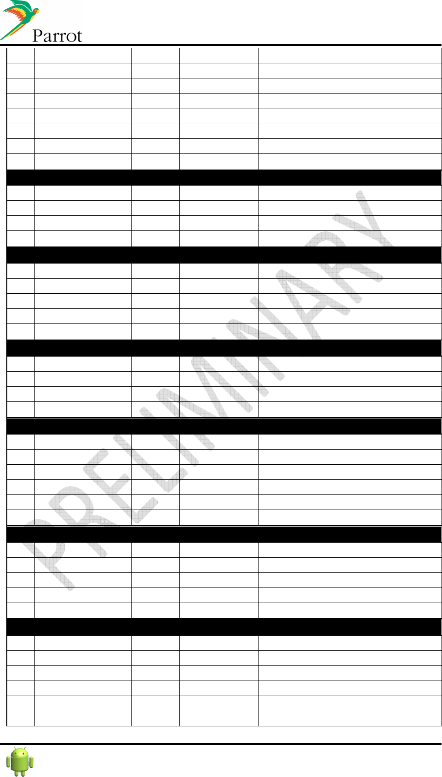
7.5 Pin Out Table (140 pins connector)
pin signal name pin type Pwr domain function
Analog Audio
2 MIC1_P I 3V3 Ana
Differential Microphone 1
-
Positive
Input
4 MIC1_N I 3V3 Ana
Differential Microphone 1
-
Negative
Input
8 MIC2_P I 3V3 Ana
Differential Microphone 2
-
Positive
Input
6 MIC2_N I 3V3 Ana
Differential Microphone 2
-
Negative
Input
1 MIC_BIAS O 3V3 Ana Microphone Bias Supply Output
3 LINEIN1_R I 3V3 Ana Stereo Line Input 1 - Right Channel
5 LINEIN1_L I 3V3 Ana Stereo Line Input 1 - Left Channel
9 LINEIN2_R I 3V3 Ana Stereo Line Input 2 - Right Channel
7 LINEIN2_L I 3V3 Ana Stereo Line Input 2 - Left Channel
12 LINEOUT1_R O 3V3 Ana Stereo Line Output 1 - Right Channel
14 LINEOUT1_L O 3V3 Ana Stereo Line Output 1 - Left Channel
Digital Audio
15 I2S_MCLK O 1V8 I2S Master Clock
24 I2S_FSYNC O 1V8 I2S Left/Right Clock
26 I2S_BCLK O 1V8 I2S Bit Clock
18 I2S_IN0 I 1V8 I2S Input 0
22 I2S_IN1 I 1V8 I2S Input 1
20 I2S_OUT0 O 1V8 I2S Output 0
28 I2S_OUT1 O 1V8 I2S Output 1
19 I2S_OUT2 O 1V8 I2S Output 1
I2C 0
21 I2C_0_SCL O 1V8 I2C 0 Serial Clock
23 I2C_0_SDA I/O 1V8 I2C 0 Serial Data
I2C 1
37 I2C_1_SCL O 3V3 I2C 1 Serial Clock
39 I2C_1_SDA I/O 3V3 I2C 1 Serial Data
SDIO 0 - SD Card Inteface
82 SDIO_0_CLK O 3V3 SD Card 0 - Clock output
88 SDIO_0_CMD O/I 3V3 SD Card 0 - Command line
84 SDIO_0_D0 O/I 3V3 SD Card 0 - Data 0
92 SDIO_0_D1 O/I 3V3 SD Card 0 - Data 1
90 SDIO_0_D2 O/I 3V3 SD Card 0 - Data 2
86 SDIO_0_D3 O/I 3V3 SD Card 0 - Data 3
123 SDIO_0_CDn I 3V3 SD Card 0 - Card Detect Input
125 SDIO_0_WPn I 3V3 SD Card 0 - Write Protect Input
SDIO 1 - SD Card Inteface
47 SDIO_1_CLK O 3V3 SD Card 1 - Clock Output
Confidential Information 12/18
Ref: FC6100ASPEN-
Datasheet
41 SDIO_1_CLKIN I 3V3 SD Card 1 - Clock Feedback Input
43 SDIO_1_CMD I/O 3V3 SD Card 1 - Command line
27 SDIO_1_D0 I/O 3V3 SD Card 1 - Data 0
29 SDIO_1_D1 I/O 3V3 SD Card 1 - Data 1
31 SDIO_1_D2 I/O 3V3 SD Card 1 - Data 2
33 SDIO_1_D3 I/O 3V3 SD Card 1 - Data 3
119 SDIO_1_CDn I 3V3 SD Card 1 - Card Detect Input
121 SDIO_1_WPn I 3V3 SD Card 1 - Write Protect Input
SPI 0
104 SPI_0_CLK O 1V8 SPI 0 Clock
106 SPI_0_MISO I 1V8 SPI 0 Master Input Slave Output
102 SPI_0_MOSI O 1V8 SPI 0 Master Output Slave Input
100 SPI_0_CS0n O 1V8 SPI 0 Slave 0 Select
SPI 1
70 SPI_1_CLK O 1V8 SPI 1 Clock
64 SPI_1_MISO I 1V8 SPI 1 Master Input Slave Output
66 SPI_1_MOSI O 1V8 SPI 1 Master Output Slave Input
68 SPI_1_CS0n O 1V8 SPI 1 Slave 0 Select
80 SPI_1_CS1n O 1V8 SPI 1 Slave 1 Select
UART 0
120 UART_0_TX O 1V8 UART 0 Ouput
110 UART_0_RTS O 1V8 UART 0 Request to Send
118 UART_0_RX I 1V8 UART 0 Input
112 UART_0_CTS I 1V8 UART 0 Clear to Send
USB 0
138 USB_0_DP IO USB USB 0 Diffrential signal - +
140 USB_0_DM IO USB USB 0 Diffrential signal --
137 USB_0_VBUS I USB USB 0 Vbus sense input
134 USB_0_CPEN O 3V3 USB 0 Vbus enable output
136 USB_0_ID IO 3V3 USB 0 ID input
135 USB_0_OCn I 3V3 USB 0 Vbus overcurrent flag
USB 1
130 USB_1_DP IO USB USB 1 Diffrential signal - +
128 USB_1_DM IO USB USB 1 Diffrential signal --
133 USB_1_VBUS I 3V3 USB 1 Vbus sense input
132 USB_1_CPEN O 3V3 USB 1 Vbus enable output
131 USB_1_OCn I 3V3 USB 1 Vbus overcurrent flag
LCD Display interface
95 LCD_RSTn O 1V8 LCD Display Reset
71 LCD_EN O 1V8 LCD Enable
65 LCD_CLK O 1V8 LCD Pixel Clock
51 LCD_HS O 1V8 LCD - Horizontal Synchronisation
61 LCD_VS O 1V8 LCD - Vertical Synchronisation
97 LCD_D0 O 1V8 LCD Data 0
Confidential Information 13/18
Ref: FC6100ASPEN-
Datasheet
93 LCD_D1 O 1V8 LCD Data 1
111 LCD_D2 O 1V8 LCD Data 2
109 LCD_D3 O 1V8 LCD Data 3
107 LCD_D4 O 1V8 LCD Data 4
105 LCD_D5 O 1V8 LCD Data 5
55 LCD_D6 O 1V8 LCD Data 6
53 LCD_D7 O 1V8 LCD Data 7
59 LCD_D8 O 1V8 LCD Data 8
57 LCD_D9 O 1V8 LCD Data 9
101 LCD_D10 O 1V8 LCD Data 10
103 LCD_D11 O 1V8 LCD Data 11
99 LCD_D12 O 1V8 LCD Data 12
87 LCD_D13 O 1V8 LCD Data 13
91 LCD_D14 O 1V8 LCD Data 14
89 LCD_D15 O 1V8 LCD Data 15
73 LCD_D16 O 1V8 LCD Data 16
63 LCD_D17 O 1V8 LCD Data 17
83 LCD_D18 O 1V8 LCD Data 18
85 LCD_D19 O 1V8 LCD Data 19
79 LCD_D20 O 1V8 LCD Data 20
81 LCD_D21 O 1V8 LCD Data 21
77 LCD_D22 O 1V8 LCD Data 22
75 LCD_D23 O 1V8 LCD Data 23
49 LCD_BKL_EN O 1V8 LCD Screen backlight Enable
67 LCD_BKL_PWM O 1V8 LCD Screen Backlight PWM control
Camera Input
50 CAM_ENn O 1V8 Camera interface Enable
48 CAM_PCLK I 1V8 Camera Pixel Clock
42 CAM_MCLK I 1V8 Camera MasterClock
32 CAM_HS I 1V8 Camera Horizontal Synchronization
34 CAM_VS I 1V8 Camera Vertical Synchronization
54 CAM_D0 I 1V8 Camera Data 0
52 CAM_D1 I 1V8 Camera Data 1
44 CAM_D2 I 1V8 Camera Data 2
40 CAM_D3 I 1V8 Camera Data 3
46 CAM_D4 I 1V8 Camera Data 4
30 CAM_D5 I 1V8 Camera Data 5
62 CAM_D6 I 1V8 Camera Data 6
60 CAM_D7 I 1V8 Camera Data 7
58 CAM_D8 I 1V8 Camera Data 8
56 CAM_D9 I 1V8 Camera Data 9
Module Control
127 RESET_HOSTn I 1V8 Main Software Reset Input
129 BOOTS I 1V8 Software Update Input Signal
45 S_RESETOUTn O 1V8 Software Reset state flag
Confidential Information 14/18
Ref: FC6100ASPEN-
Datasheet
122 H_RESETOUTn O 1V8 Hardware Reset state flag
Discrete Signals
78 GPIO_0_PWM IO 1V8
General
Purpose Input / Output
-
capable of PWM operations
72 GPIO_1_PWM IO 1V8
General Purpose Input / Output
-
capable of PWM operations
108 GPIO_2_CLK IO 1V8
General Purpose Input / Output
-
capable of Clock Ouput
11 IPOD_RESETn O 1V8 Ipod Authenfication chip reset output
21 IT_HOSTn I 1V8
Interruption for HOST communication
input
35 IT_TOUCHSCREENn I 1V8 Interruption for Touch pad activity Input
Analog TV out
96 TV_LUMA O 1V8 Ana Luminance output for S-Video
98 TV_CHROMA O 1V8 Ana Chrominance output for S-Video
Power Supplies
115 3V3_MAIN PI -
Main Power Supply Input : 3,3V
113 3V3_MAIN PI -
116 3V3_MAIN PI -
117 3V3_MAIN PI -
36 3V3_MAIN PI -
76 3V3_MAIN PI -
74 3V3_MAIN PI -
38 3V3_MAIN PI -
13 3V3_PERM PI - 3,3V permanent power supply for RTC
126 1V8_OUT PO -
1,8V Power Supply used for Level
Translation
124 1V8_OUT PO -
17 GND PO -
Voltage Reference for all module signals
16 GND PO -
10 GND PO -
139 GND PO -
94 GND PO -
114 GND PO -
69 GND PO -
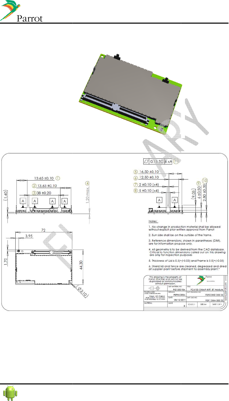
8 Mechanical
Dimension
Please find below the main dimensions for
The module’s interface is made through a 140
•
Module connector reference: MOLEX / 55091
•
Motherboard connector’s reference: MOLEX / 52885
Confidential Information
Dimension
(preliminary)
Please find below the main dimensions for
FC6100 ASPEN module.
The module’s interface is made through a 140
-
pin board to board connector with a 0.635mm pitch.
Module connector reference: MOLEX / 55091
-1472
Motherboard connector’s reference: MOLEX / 52885
-1474
15/18
Ref: FC6100ASPEN-
Datasheet
pin board to board connector with a 0.635mm pitch.
Confidential Information 16/18
Ref: FC6100ASPEN-
Datasheet
9 Absolute Maximum Ratings
Operating temperature range ............................................................................................ -40°C to +85°C
Storage temperature range .............................................................................................. -40°C to +125°C
DC input supply voltage.......................................................................................................... 3.2V to 3.6V
Maximum current drawn from 3V3_MAIN ........................................................................................... 1A
ESD sensitivity according to AEC Q100 : +/-2kV HBM | +/- 200V MM ................................................ TBD
10 Electrical Specifications
10.1 Power Consumption (preliminary)
Off mode ........................................................................................................................................ TBD µA
Software Reset mode ........................................................................................................................ 5 mA
Hands free mode ........................................................................................................................... TBD mA
Audio streaming mode .................................................................................................................. TBD mA
Video rendering mode .................................................................................................................. TBD mA
10.2 Power Supplies
Conditions unless otherwise-noted : over -40° / +85 ° C
Parameter
Conditions
Min.
Typ.
Max.
Unit
3V3_MAIN Operating conditions 3.2 3.3 3.4 V
VDD_PERM Operating conditions 2.5 - 5 V
1V8_OUT Current drawn on Host Board < 300mA 1.72 1.8 1.92 V
10.3 Hardware Reset Conditions
Conditions unless otherwise-noted : over -40° / +85 ° C
Parameter
Conditions
Min.
Typ.
Max.
Unit
3V3_MAIN considered as off - - - 0.5 V
3V3_MAIN “off” delay - 100 - - ms
10.4 Software Reset Input
Conditions unless otherwise noted,: over -40° / +8 5° C
Parameter
Conditions
Min.
Typ.
Max.
Unit
RESET_HOSTn – Activation delay - 100 - µs
RESET_HOSTn – ViL - - - 0.6 V
RESET_HOSTn – ViH - 1.45 - - V

Confidential Information 17/18
Ref: FC6100ASPEN-
Datasheet
10.5 Digital IO Pins
FC6100 ASPEN I/Os belong to 2 different digital power domains: 1.8V or 3.3V power supplies.
3,3V power domain
Conditions unless otherwise noted : over -40° / +85 ° C
Parameter
Conditions
Min.
Typ.
Max.
Unit
ViH - 2.2 - 3.5 V
ViL - -0.3 - 0.4 V
VoH - 3.07 - 3.6 V
VoL - -0.1 - 0.4 V
1,8V power domain
Conditions unless otherwise noted : Tamb.=25°C; Vdd =3V3
Parameter
Conditions
Min.
Typ.
Max.
Unit
ViH - 1.3 - 1.95 V
ViL - -0.3 - 0.55 V
VoH - 1.15 - 2.1 V
VoL - -0.1 - 0.45 V

Confidential Information 18/18
Ref: FC6100ASPEN-
Datasheet
11 FCC requirements for module application
FCC ID: RKXFC6100ASPEN
In accordance with FCC Part 15, the FC6100 ASPEN is listed as a Modular Transmitter device.
USA – User information
This intends to inform how to specify the FCC ID of our module “FC6100 ASPEN” on the product.
Based on the Public Notice from FCC, the host device should have a label which indicates that it
contains our module. The label should use wording such as: “Contains FCC ID: RKXFC6100ASPEN”
Any similar wording that expresses the same meaning may be used.
The label of the host device should also include the below FCC Statement. When it is not possible,
this information should be included in the User Manual of the host device.
“This device complies with part 15 of the FCC rules. Operation is subject to the following two
conditions.
(1) This device may not cause harmful interference
(2) this device must accept any interference received, including interference that may cause
undesired operation.
Caution: Changes or modifications not expressly approved by the party responsible for compliance
could void the user’s authority to operate the equipment.