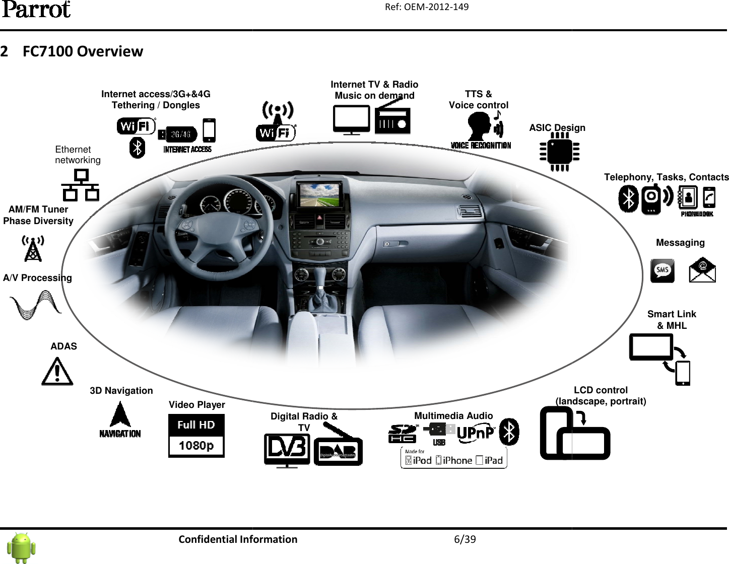
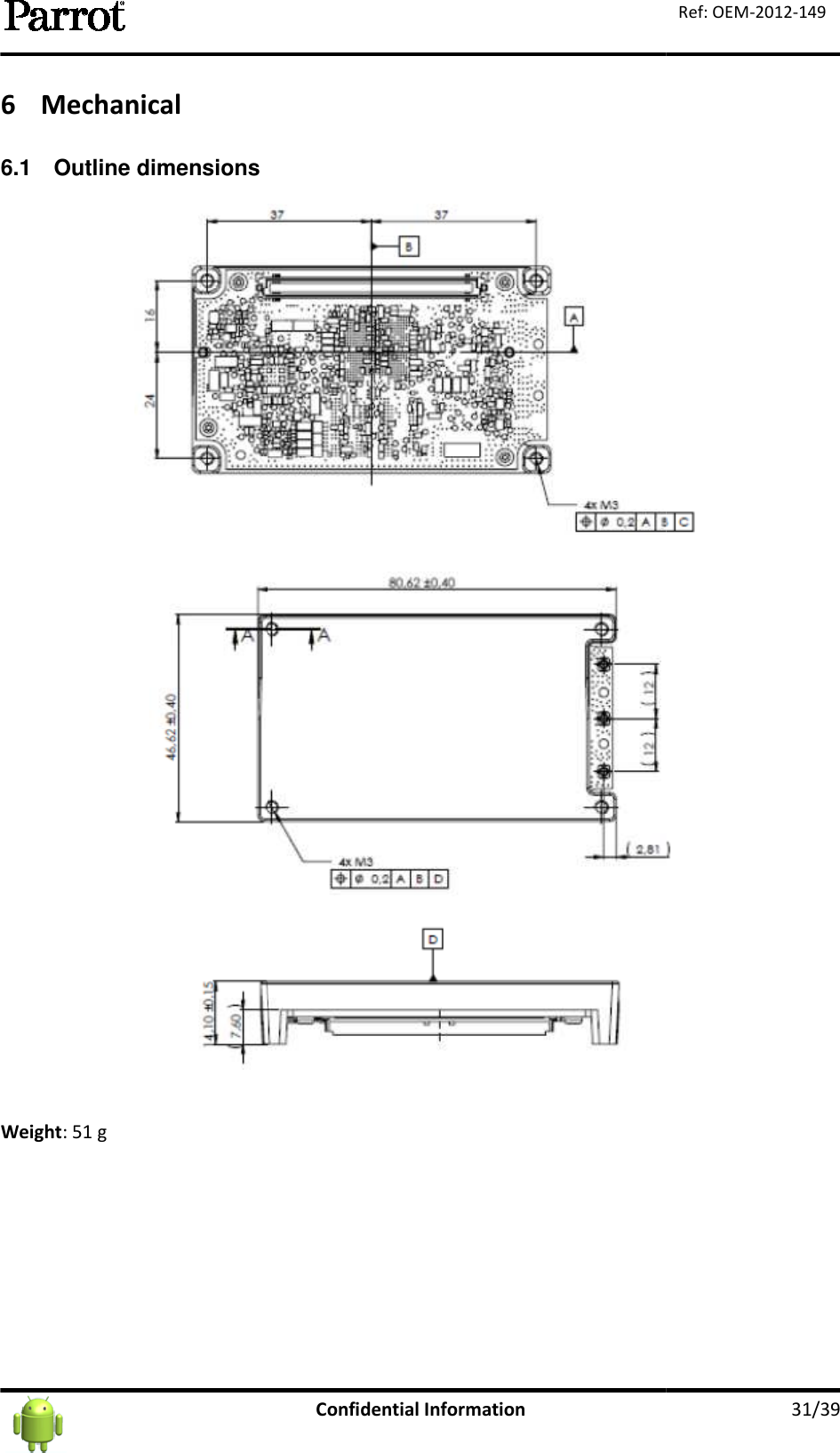
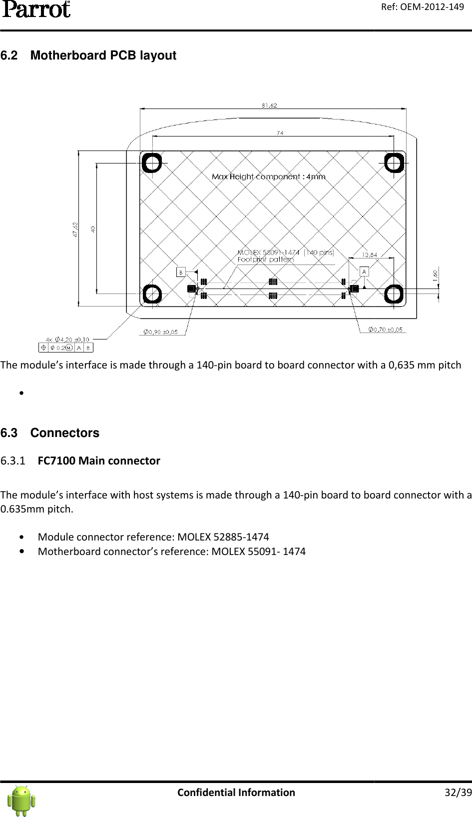
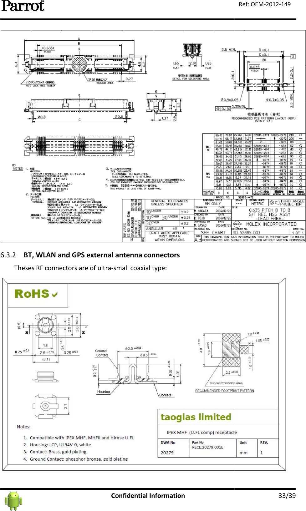
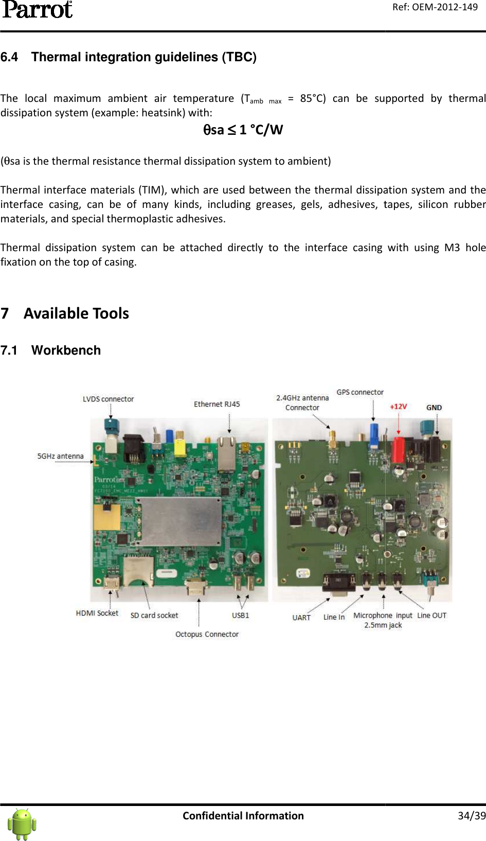
PARROT FC7100 Full connectivity module User Manual OEM 2012 149 FC7100 Datasheet v2 7
PARROT Full connectivity module OEM 2012 149 FC7100 Datasheet v2 7
UserManual.wiki
>
PARROT
>
FC7100 User Manual
>
User manual
Contents
1.
User manual
2.
User manual_Warning Statement
3.
User manual _Warning Statement
4.
User manual_1
5.
User manual_2
6.
User manual_3
User manual
Navigation menu
Upload a User Manual
Namespaces
Wiki Guide
HTML
PDF
Info
Views
User Manual
Discussion / Help
Navigation

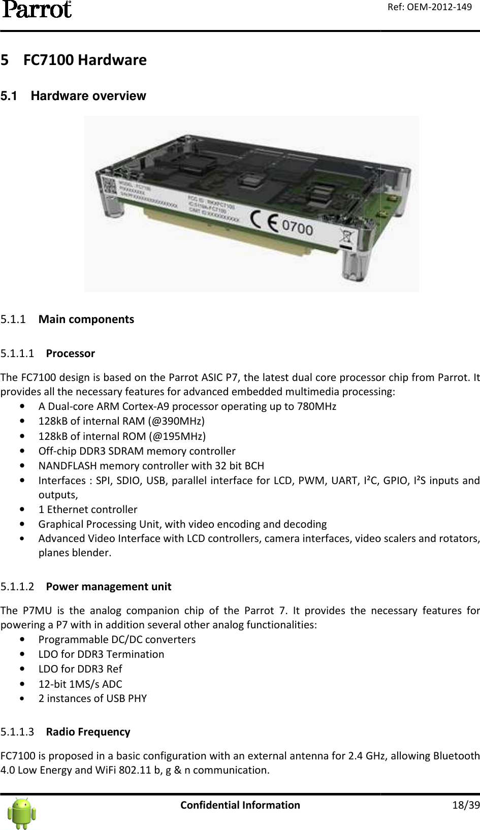
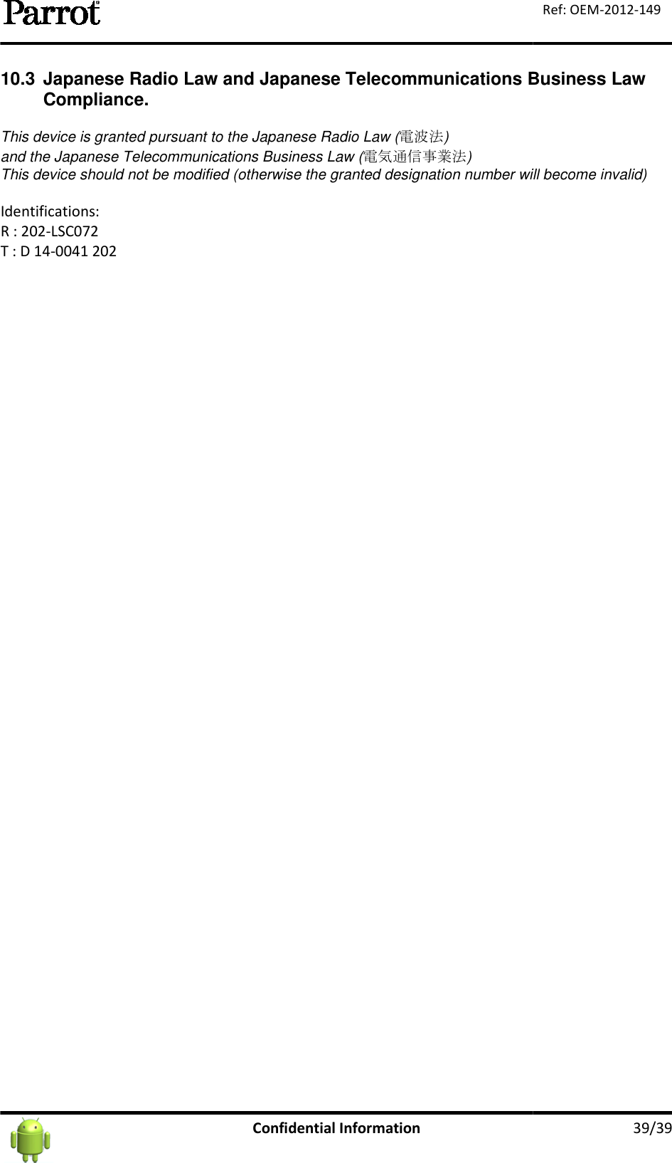
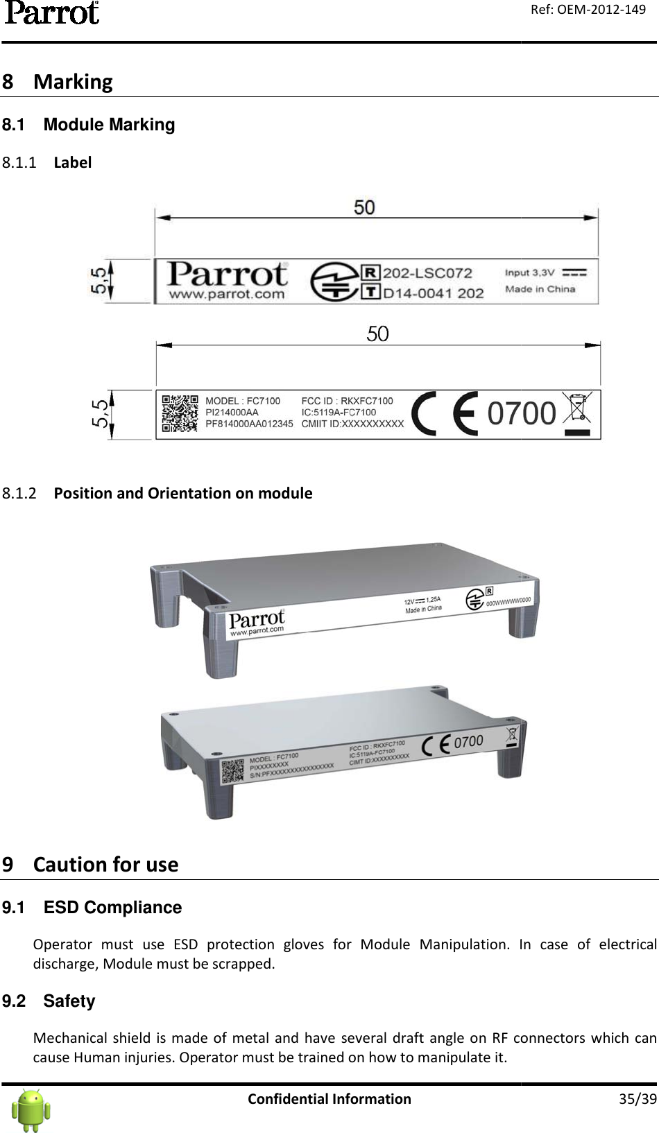
![5.1.4 Pin Out Table Here below the FC7100 main connector (140 pins): Pin1USB_0_DN3USB_0_DP5USB_0_VBUS7Wake_Up_LPO9VDD_SD1 UART_5/6/7 INPUT113V3_MAIN133V3_MAIN153V3_MAIN17Power_Good193v3_PERM21ETH_RGMII_TXD_00 / 23ETH_RGMII_TXD_02 / 25ETH_RGMII_RXD_00 / 27ETH_RGMII_RXD_02 / 29ETH_RGMII_RX_CTL /31ETH_RGMII_TX_CTL / 33ETH_RGMII_RX_CLK / 3537SPI_11 / GPIO_088 / 39SPI_10 / GPIO_087 / 41SPI_09 / GPIO_086 / 43SPI_08 / 4547SPI_07 / GPIO_084 / 49SPI_06 / 51SPI_05 / 53SPI_04 /55SPI_01 / 57SPI_00 / 59I2C_1_CLK / GPIO_06261I2C_2_CLK / GPIO_06063UART_0_CTS / GPIO_05865UART_0_RX / GPIO_05567UART_0_TX / GPIO_05669UART_0_RTS / GPIO_05771CAM_1_DAT15 / CAM_0_DAT07 / GPIO_21673CAM_1_DAT14 / CAM_0_DAT06 / GPIO_21575CAM_1_DAT13 / CAM_0_DAT05 / GPIO_21477CAM_1_DAT12 / CAM_0_DAT04 / GPIO_21379CAM_1_DAT11 / CAM_0_DAT03 / GPIO_21281CAM_5_DAT07 / GPIO_01483CAM_5_DAT06 / GPIO_01385CAM_5_DAT05 / GPIO_01287CAM_5_DAT03 / SD_2_DAT02 / GPIO_01089CAM_5_DAT01 / SD_2_DAT00 / GPIO_00891LCD_1_DAT00 / CAM_2_DAT02 / GPIO_18393LCD_1_DAT01 / CAM_2_DAT03 / GPIO_18495LCD_1_DAT02 / CAM_2_DAT04 / GPIO_18597LCD_1_DAT03 / CAM_2_DAT05 / GPIO_18699LCD_1_DAT04 / CAM_2_DAT06 / GPIO_187101LCD_1_DAT06 / CAM_3_CLK / GPIO_189103LCD_1_DAT08 / CAM_3_DAT01 / GPIO_191105LCD_1_DAT10 / CAM_3_DAT03 / GPIO_193107LCD_1_DAT12 / CAM_3_DAT05 / GPIO_195109111 LCD_1 CAM_2LCD_1_CLK / CAM_2_DAT01 / GPIO_182113115 CAM_3LCD_1_DAT14 / CAM_3_DAT07 / GPIO_197117LCD_1_DAT16 / CAM_4_DAT00 / GPIO_199119LCD_1_DAT18 / CAM_4_DAT02 / GPIO_201121LCD_1_DAT19 / CAM_4_DAT03 / GPIO_202123LCD_1_DAT20 / CAM_4_DAT04 / GPIO_203125LCD_1_DAT21 / CAM_4_DAT05 / GPIO_204127LCD_1_DAT22 / CAM_4_DAT06 / GPIO_205129LCD_1_DAT23 / CAM_4_DAT07 / GPIO_206131LCD_1_RSTn_Touch / CAM_0_VS / GPIO_154133LCD_1_IT_TouchScreen / CAM_0_HS / GPIO_155135LCD_1_BKL_En / CAM_5_VS / GPIO_160137LCD_1_RSTn / CAM_5_HS / GPIO_161139GNDCAM_4LCD_1 GPIOCAM_2CAM_3GNDGNDLCD_1CAM_5GPIOSD2LCD_1I2C_2UART 0 GPIOCAM_1 CAM_0 (16 bits)SPI [0:7]Part 1 AAII2C_1SPI[8:11] AAIGNDPower_Good3V3_PERMEthernet RGMII GPIOGNDWake_UpPowerVDD_SD1_UART_5_6_7 3V3_MAINUSB_0Confidential Information Here below the FC7100 main connector (140 pins): Function Type Power DomainUSB_0_DNI/O USB 0 Data -USB_0_DPI/O USB 0 Data +USB_0_VBUSI 5v USB 0 VBUSWake_Up_LPOI 3V3 Wake Up Low PowerVDD_SD1 UART_5/6/7 INPUTP 1v8 / 3v3Power Supply SDIO1 and UART 5/6/73V3_MAIN3V3_MAIN3V3_MAINPower_GoodO 3V3 Power Good3v3_PERMP3V3Power Supply Permanent : 3v3ETH_RGMII_TXD_00 / GPIO_139 I/O VDD_ETH GPIO or Ethernet RGMII Tx Data 0ETH_RGMII_TXD_02 / GPIO_141I/OVDD_ETH GPIO or Ethernet RGMII Tx Data 2ETH_RGMII_RXD_00 / GPIO_145I/OVDD_ETH GPIO or Ethernet RGMII Rx Data 0ETH_RGMII_RXD_02 / GPIO_147I/OVDD_ETH GPIO or Ethernet RGMII Rx Data 2ETH_RGMII_RX_CTL / GPIO_149I/OVDD_ETH GPIO or Ethernet RGMII Rx ControlETH_RGMII_TX_CTL / GPIO_143I/OVDD_ETH GPIO or Ethernet RGMII Tx ControlETH_RGMII_RX_CLK / GPIO_144 I/O VDD_ETH GPIO or Ethernet RGMII Rx ClockPGnd GroundSPI_11 / GPIO_088 / AAI_26I/O3V3GPIO or SPI or AAISPI_10 / GPIO_087 / AAI_25I/O3V3GPIO or SPI or AAISPI_09 / GPIO_086 / AAI_24I/O3V3GPIO or SPI or AAISPI_08 / GPIO_085 / AAI_23 I/O 3V3 GPIO or SPI or AAIPGnd GroundSPI_07 / GPIO_084 / AAI_22I/O3V3GPIO or SPI or AAISPI_06 / GPIO_083 / AAI_21I/O3V3GPIO or SPI or AAISPI_05 / GPIO_082 / AAI_20I/O3V3GPIO or SPI or AAISPI_04 / GPIO_081 / AAI_19 I/O 3V3 GPIO or SPI or AAISPI_01 / GPIO_078 / AAI_16 / CAN1_RXI/O3V3GPIO or SPI or AAISPI_00 / GPIO_077 / AAI_15 / CAN1_TX I/O 3V3 GPIO or SPI or AAII2C_1_CLK / GPIO_062I/O 3V3 I2C 1 Clock or GPIOI2C_2_CLK / GPIO_060I/O 3V3 I2C 2 Clock or GPIOUART_0_CTS / GPIO_058I/O 3V3 UART 0 CTS or GPIOUART_0_RX / GPIO_055I/O 3V3UART 0 RX or GPIOUART_0_TX / GPIO_056I/O 3V3 UART 0 TX or GPIOUART_0_RTS / GPIO_057I/O 3V3 UART 0 RTS or GPIOCAM_1_DAT15 / CAM_0_DAT07 / GPIO_216I/O 3V3 CAM 1 Data 7 or CAM 0 Data 7 CAM_1_DAT14 / CAM_0_DAT06 / GPIO_215I/O 3V3CAM 1 Data 6 or CAM 0 Data 6 CAM_1_DAT13 / CAM_0_DAT05 / GPIO_214I/O 3V3 CAM 1 Data 5 or CAM 0 Data 5 CAM_1_DAT12 / CAM_0_DAT04 / GPIO_213I/O 3V3 CAM 1 Data 4 or CAM 0 Data 4 CAM_1_DAT11 / CAM_0_DAT03 / GPIO_212I/O 3V3 CAM 1 Data 3 or CAM 0 Data 3 CAM_5_DAT07 / GPIO_014I/O VDD_SD2CAM 5 Data 7 or GPIOCAM_5_DAT06 / GPIO_013I/O VDD_SD2 CAM 5 Data 6 or GPIOCAM_5_DAT05 / GPIO_012I/O VDD_SD2 CAM 5 Data 5 or GPIOCAM_5_DAT03 / SD_2_DAT02 / GPIO_010I/O VDD_SD2CAM 5 Data 3 or SDIO 2 Data 2 CAM_5_DAT01 / SD_2_DAT00 / GPIO_008I/O VDD_SD2 CAM 5 Data 1 or SDIO 2 Data 0 LCD_1_DAT00 / CAM_2_DAT02 / GPIO_183I/O 3V3 LCD 1 Data 0 or CAM 2 Data 2 LCD_1_DAT01 / CAM_2_DAT03 / GPIO_184I/O 3V3 LCD 1 Data 1 or CAM 2 Data 3 LCD_1_DAT02 / CAM_2_DAT04 / GPIO_185I/O 3V3 LCD 1 Data 2 or CAM 2 Data 4 LCD_1_DAT03 / CAM_2_DAT05 / GPIO_186I/O 3V3 LCD 1 Data 3 or CAM 2 Data 5 LCD_1_DAT04 / CAM_2_DAT06 / GPIO_187I/O 3V3 LCD 1 Data 4 or CAM 2 Data 6 LCD_1_DAT06 / CAM_3_CLK / GPIO_189I/O 3V3LCD 1 Data 6 or CAM 3 Clock LCD_1_DAT08 / CAM_3_DAT01 / GPIO_191I/O 3V3LCD 1 Data 8 or CAM 3 Data 1 LCD_1_DAT10 / CAM_3_DAT03 / GPIO_193I/O 3V3LCD 1 Data 10 or CAM 3 Data 3 LCD_1_DAT12 / CAM_3_DAT05 / GPIO_195I/O 3V3 LCD 1 Data 12 or CAM 3 Data 5 PGnd GroundLCD_1_CLK / CAM_2_DAT01 / GPIO_182I/O 3V3 LCD 1 Clock or CAM 2 Data 1 PGnd GroundLCD_1_DAT14 / CAM_3_DAT07 / GPIO_197I/O 3V3 LCD 1 Data 14 or CAM 3 Data 7 LCD_1_DAT16 / CAM_4_DAT00 / GPIO_199I/O 3V3 LCD 1 Data 16 or CAM 4 Data 0 LCD_1_DAT18 / CAM_4_DAT02 / GPIO_201I/O 3V3 LCD 1 Data 18 or CAM 4 Data 2 LCD_1_DAT19 / CAM_4_DAT03 / GPIO_202I/O 3V3LCD 1 Data 19 or CAM 4 Data 3 LCD_1_DAT20 / CAM_4_DAT04 / GPIO_203I/O 3V3LCD 1 Data 20 or CAM 4 Data 4 LCD_1_DAT21 / CAM_4_DAT05 / GPIO_204I/O 3V3LCD 1 Data 21 or CAM 4 Data 5 LCD_1_DAT22 / CAM_4_DAT06 / GPIO_205I/O 3V3LCD 1 Data 22 or CAM 4 Data 6 LCD_1_DAT23 / CAM_4_DAT07 / GPIO_206I/O 3V3 LCD 1 Data 23 or CAM 4 Data 7 LCD_1_RSTn_Touch / CAM_0_VS / GPIO_154I/O 3V3LCD 1 Resetn_Touch Screen LCD_1_IT_TouchScreen / CAM_0_HS / GPIO_155I/O 3V3LCD 1 IT Touch Screen LCD_1_BKL_En / CAM_5_VS / GPIO_160I/O 3V3LCD 1 Backlight Enable LCD_1_RSTn / CAM_5_HS / GPIO_161I/O 3V3 LCD 1 Resetn or CAM_5_HS PGnd GroundGNDGNDGNDGNDGNDP3V3 Power supply : 3v3 21/39 Ref: OEM-2012-149 DescriptionPower Supply SDIO1 and UART 5/6/7Power Supply Permanent : 3v3Ethernet RGMII Tx Data 0 Ethernet RGMII Tx Data 2 Ethernet RGMII Rx Data 0 Ethernet RGMII Rx Data 2 Ethernet RGMII Rx Control Ethernet RGMII Tx Control Ethernet RGMII Rx Clock CAM 0 Data 7 or GPIO CAM 0 Data 6 or GPIO CAM 0 Data 5 or GPIO CAM 0 Data 4 or GPIO CAM 0 Data 3 or GPIO SDIO 2 Data 2 or GPIO SDIO 2 Data 0 or GPIO CAM 2 Data 2 or GPIO CAM 2 Data 3 or GPIO CAM 2 Data 4 or GPIO CAM 2 Data 5 or GPIO CAM 2 Data 6 or GPIO CAM 3 Clock or GPIO CAM 3 Data 1 or GPIO CAM 3 Data 3 or GPIO CAM 3 Data 5 or GPIO CAM 2 Data 1 or GPIO CAM 3 Data 7 or GPIO CAM 4 Data 0 or GPIO CAM 4 Data 2 or GPIO CAM 4 Data 3 or GPIO CAM 4 Data 4 or GPIO CAM 4 Data 5 or GPIO CAM 4 Data 6 or GPIO CAM 4 Data 7 or GPIOLCD 1 Resetn_Touch Screen or CAM 0 VS or GPIO LCD 1 IT Touch Screen or CAM 0 HS or GPIOLCD 1 Backlight Enable or CAM 5 VS or GPIO CAM_5_HS or GPIO](https://usermanual.wiki/PARROT/FC7100.User-manual/User-Guide-2462792-Page-21.png)
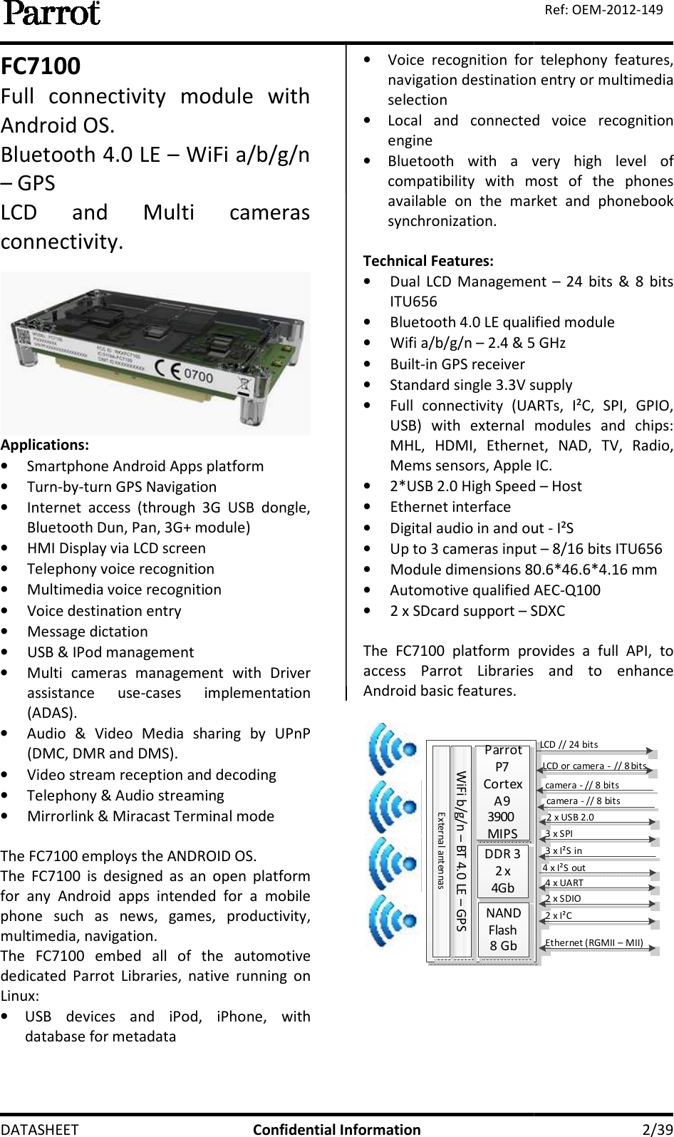
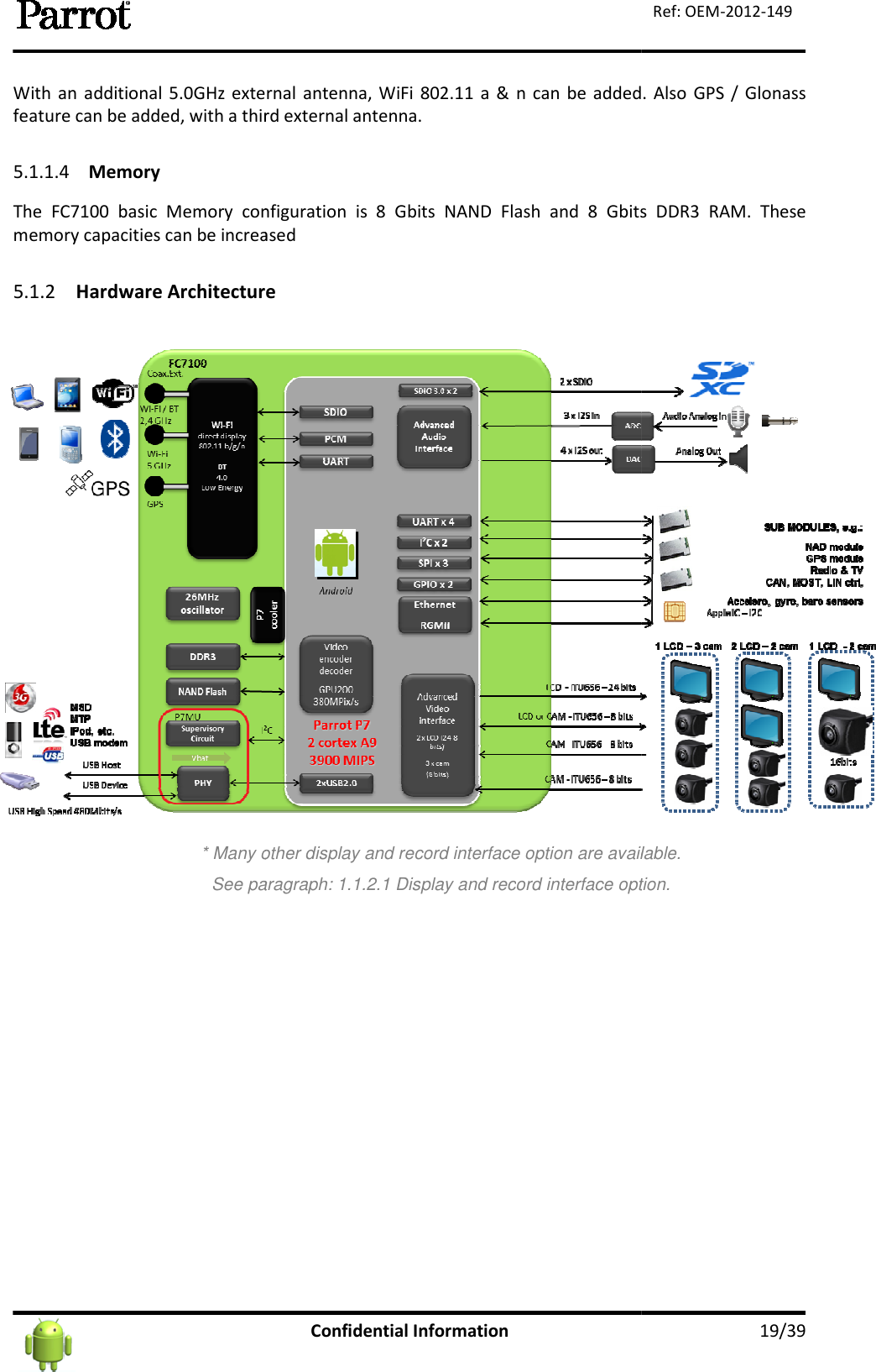
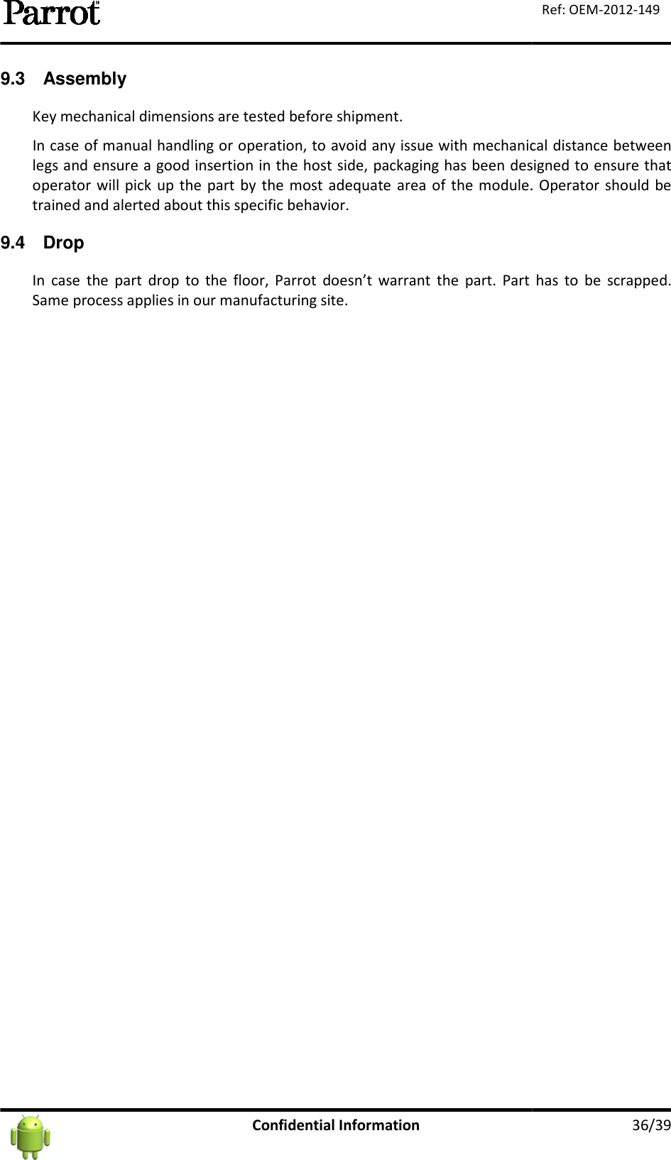
![Pin243V3_MAIN63V3_MAIN83V3_MAIN103V3_MAIN12USB_1_DP14USB_1_DN1618 BOOT20Power_En22VDD_ETH INPUT24ETH_RGMII_TXD_01 /26ETH_RGMII_TXD_03 / 28ETH_RGMII_RXD_01 /30ETH_RGMII_RXD_03 / 32ETH_RGMII_TX_CLK / 34ETH_MDC /36ETH_MDIO / 38SPI_16 / ETH_MII TXER / GPIO_13440SPI_17 / ETH_MII RXER / GPIO_13542SPI_18 / ETH_MII CRS / GPIO_13644SPI_19 / ETH_MII COL / GPIO_1374648AAI_14 / GPIO_133 / PWM_1450AAI_12 / GPIO_131 / PWM_1252AAI_11 / GPIO_130 / PWM_1154AAI_10 / GPIO_129 / PWM_1056SPI_03 / GPIO_080 / AAI_18 / CAN0_RX58SPI_02 / GPIO_079 / AAI_17 / CAN0_TX6062I2C_1_DAT / GPIO_06164I2C_2_DAT / GPIO_05966SD_1_CMD / UART_5_RX68SD_1_CLK / UART_5_TX70SD_1_DAT03 / UART_7_RX72SD_1_DAT02 / UART_7_TX74SD_1_DAT01 / UART_6_RX76SD_1_DAT00 / UART_6_TX7880CAM_1_DAT10 / CAM_0_DAT02 / GPIO_21182CAM_1_DAT09 / CAM_0_DAT01 / GPIO_21084CAM_1_DAT08 / CAM_0_DAT00 / GPIO_20986 GPIOCAM_1_CLK / GPIO_21788CAM_5_DAT04 / SD_2_DAT03 / GPIO_01190CAM_5_DAT02 / SD_2_DAT01 / GPIO_00992CAM_5_DAT00 / SD_2_CMD / GPIO_0079496 CAM_5 SD2CAM_5_CLK / SD_2_CLK / GPIO_00698VDD_SD2_CAM5 INPUT100 CAM_2LCD_1_DAT05 / CAM_2_DAT07 / GPIO_188102LCD_1_DAT07 / CAM_3_DAT00 / GPIO_190104LCD_1_DAT09 / CAM_3_DAT02 / GPIO_192106LCD_1_DAT11 / CAM_3_DAT04 / GPIO_194108LCD_1_DAT13 / CAM_3_DAT06 / GPIO_196110LCD_1_DAT15 / CAM_4_CLK / GPIO_198112LCD_1_DAT17 / CAM_4_DAT01 / GPIO_200114 GPIOLCD_1_DEN / GPIO_207116LCD_1_HS / CAM_2_CLK / GPIO_180118LCD_1_VS / CAM_2_DAT00 / GPIO_181120122CAM_0_CLK / LCD_0_CLK / GPIO_179124CAM_0_DAT08 / LCD_0_DAT08 / GPIO_163126CAM_0_DAT09 / LCD_0_DAT09 / GPIO_164128CAM_0_DAT10 / LCD_0_DAT10 / GPIO_165130CAM_0_DAT11 / LCD_0_DAT11 / GPIO_166132CAM_0_DAT12 / LCD_0_DAT12 / GPIO_167134CAM_0_DAT13 / LCD_0_DAT13 / GPIO_168136CAM_0_DAT14 / LCD_0_DAT14 / GPIO_169138CAM_0_DAT15 / LCD_0_DAT15 / GPIO_170140CAM_2CAM_0 LCD_0Power VDD_SD2 _CAM_5LCD_1CAM_3CAM_4UART 6CAM_1CAM_0 (16 bits)CAM_5 SD2I2C_1I2C_2SD1UART 5UART 7AAIPWMSPI [0:7] Part 2Ethernet MII SPI BOOTPWR_EnPower VDD_ETH & GPIOEthernetRGMII GPIOUSB_1 3V3_MAINConfidential Information Function Type Power Domain DescriptionPGnd Ground3V3_MAIN3V3_MAIN3V3_MAIN3V3_MAINUSB_1_DPI/OUSB 1 Data +USB_1_DNI/O USB 1 Data -PGnd GroundI3V3 Initial Flashing pin Power_EnI3V3Power EnableVDD_ETH INPUTI1v8 / 3v3Power Supply Ethernet 1v8 / 2v5 / 3v3 or GPIOETH_RGMII_TXD_01 / GPIO_140I/OVDD_ETH GPIO or Ethernet RGMII Tx Data 1ETH_RGMII_TXD_03 / GPIO_142I/OVDD_ETH GPIO or Ethernet RGMII Tx Data 3ETH_RGMII_RXD_01 / GPIO_146I/OVDD_ETH GPIO or Ethernet RGMII Rx Data 1ETH_RGMII_RXD_03 / GPIO_148I/OVDD_ETH GPIO or Ethernet RGMII Rx Data 3ETH_RGMII_TX_CLK / GPIO_138I/OVDD_ETH GPIO or Ethernet RGMII Tx ClockETH_MDC / GPIO_150 I/O VDD_ETH GPIO or Ethernet RGMII ETH_MDIO / GPIO_151 I/O VDD_ETH GPIO or Ethernet RGMIISPI_16 / ETH_MII TXER / GPIO_134I/O VDD_ETH SPI CLK or Ethernet MII SPI_17 / ETH_MII RXER / GPIO_135I/O VDD_ETH SPI MOSI or Ethernet MII SPI_18 / ETH_MII CRS / GPIO_136I/O VDD_ETH SPI SS or Ethernet MII SPI_19 / ETH_MII COL / GPIO_137I/O VDD_ETH SPI MISO or Ethernet MII PGnd GroundAAI_14 / GPIO_133 / PWM_14I/O 3V3GPIO or AAI AAI_12 / GPIO_131 / PWM_12I/O 3V3GPIO or AAI AAI_11 / GPIO_130 / PWM_11I/O 3V3GPIO or AAI AAI_10 / GPIO_129 / PWM_10I/O 3V3 GPIO or AAI SPI_03 / GPIO_080 / AAI_18 / CAN0_RXI/O 3V3GPIO or AAI SPI_02 / GPIO_079 / AAI_17 / CAN0_TXI/O 3V3 GPIO or AAI PGnd GroundI2C_1_DAT / GPIO_061I/O 3V3 I2C 1 Data orI2C_2_DAT / GPIO_059I/O 3V3 I2C 2 Data orSD_1_CMD / UART_5_RXI/O VDD_SD1 SDIO 1 Command SD_1_CLK / UART_5_TXI/O VDD_SD1 SDIO 1 Clock SD_1_DAT03 / UART_7_RXI/O VDD_SD1 SDIO 1 Data 3 SD_1_DAT02 / UART_7_TXI/O VDD_SD1 SDIO 1 Data 2 SD_1_DAT01 / UART_6_RXI/O VDD_SD1 SDIO 1 Data 1 SD_1_DAT00 / UART_6_TXI/O VDD_SD1 SDIO 1 Data 0 PGnd GroundCAM_1_DAT10 / CAM_0_DAT02 / GPIO_211I/O 3V3CAM 1 Data 2 CAM_1_DAT09 / CAM_0_DAT01 / GPIO_210I/O 3V3CAM 1 Data 1 CAM_1_DAT08 / CAM_0_DAT00 / GPIO_209I/O 3V3CAM 1 Data 0 CAM_1_CLK / GPIO_217I/O 3V3CAM 1 Clock CAM_5_DAT04 / SD_2_DAT03 / GPIO_011I/O VDD_SD2CAM_5_DAT04 CAM_5_DAT02 / SD_2_DAT01 / GPIO_009I/O VDD_SD2CAM_5_DAT02 CAM_5_DAT00 / SD_2_CMD / GPIO_007I/O VDD_SD2CAM_5_DAT00 PGnd GroundCAM_5_CLK / SD_2_CLK / GPIO_006I/O VDD_SD2CAM_5_CLK VDD_SD2_CAM5 INPUTP1v8 / 3v3Power Supply SDIO2 and Camera 5LCD_1_DAT05 / CAM_2_DAT07 / GPIO_188I/O 3V3LCD 1 Data 05 LCD_1_DAT07 / CAM_3_DAT00 / GPIO_190I/O 3V3LCD 1 Data 07 LCD_1_DAT09 / CAM_3_DAT02 / GPIO_192I/O 3V3LCD 1 Data 09 LCD_1_DAT11 / CAM_3_DAT04 / GPIO_194I/O 3V3LCD 1 Data 11 LCD_1_DAT13 / CAM_3_DAT06 / GPIO_196I/O 3V3LCD 1 Data 13 LCD_1_DAT15 / CAM_4_CLK / GPIO_198I/O 3V3LCD 1 Data 15 LCD_1_DAT17 / CAM_4_DAT01 / GPIO_200I/O 3V3LCD 1 Data 17 LCD_1_DEN / GPIO_207I/O 3V3LCD 1 Data Enable LCD_1_HS / CAM_2_CLK / GPIO_180I/O 3V3 LCD 1 HS or CAM 2 Clock LCD_1_VS / CAM_2_DAT00 / GPIO_181I/O 3V3 LCD 1 VS or CAM 2 Data 0 PGnd GroundCAM_0_CLK / LCD_0_CLK / GPIO_179I/O 3V3CAM 0 Clock CAM_0_DAT08 / LCD_0_DAT08 / GPIO_163I/O 3V3CAM 0 Data 08 CAM_0_DAT09 / LCD_0_DAT09 / GPIO_164I/O 3V3CAM 0 Data 09 CAM_0_DAT10 / LCD_0_DAT10 / GPIO_165I/O 3V3CAM 0 Data 10 CAM_0_DAT11 / LCD_0_DAT11 / GPIO_166I/O 3V3CAM 0 Data 11 CAM_0_DAT12 / LCD_0_DAT12 / GPIO_167I/O 3V3CAM 0 Data 12 CAM_0_DAT13 / LCD_0_DAT13 / GPIO_168I/O 3V3CAM 0 Data 13 CAM_0_DAT14 / LCD_0_DAT14 / GPIO_169I/O 3V3CAM 0 Data 14 CAM_0_DAT15 / LCD_0_DAT15 / GPIO_170I/O 3V3CAM 0 Data 15 PGnd GroundGNDGNDGNDGNDGNDGND3V3Power supply : 3v3GNDGNDP 22/39 Ref: OEM-2012-149 USB 1 Data + Initial Flashing pin Power EnablePower Supply Ethernet 1v8 / 2v5 / 3v3 or GPIO Ethernet RGMII Tx Data 1 Ethernet RGMII Tx Data 3 Ethernet RGMII Rx Data 1 Ethernet RGMII Rx Data 3 Ethernet RGMII Tx Clock Ethernet RGMII Ethernet RGMII Ethernet MII or GPIO Ethernet MII or GPIO Ethernet MII or GPIO Ethernet MII or GPIO AAI or PWM AAI or PWM AAI or PWM AAI or PWM AAI or SPI AAI or SPIor GPIOor GPIO SDIO 1 Command or UART 5 RX SDIO 1 Clock or UART 5 TX SDIO 1 Data 3 or UART 7 RX SDIO 1 Data 2 or UART 7 TX SDIO 1 Data 1 or UART 6 RX SDIO 1 Data 0 or UART 6 TXCAM 1 Data 2 or CAM 0 Data 2 or GPIOCAM 1 Data 1 or CAM 0 Data 1 or GPIOCAM 1 Data 0 or CAM 0 Data 0 or GPIOCAM 1 Clock or GPIOCAM_5_DAT04 or SDIO 2 Data 3 or GPIOCAM_5_DAT02 or SDIO 2 Data 1 or GPIOCAM_5_DAT00 or SDIO 2 Command or GPIOCAM_5_CLK or SDIO 2 Clock or GPIOPower Supply SDIO2 and Camera 5LCD 1 Data 05 or CAM 2 Data 7 or GPIOLCD 1 Data 07 or CAM 3 Data 0 or GPIOLCD 1 Data 09 or CAM 3 Data 2 or GPIOLCD 1 Data 11 or CAM 3 Data 4 or GPIOLCD 1 Data 13 or CAM 0 Data 6 or GPIOLCD 1 Data 15 or CAM 4 Clock or GPIOLCD 1 Data 17 or CAM 4 Data 1 or GPIOLCD 1 Data Enable or GPIO CAM 2 Clock or GPIO CAM 2 Data 0 or GPIOCAM 0 Clock or LCD 0 Clock or GPIOCAM 0 Data 08 or LCD 0 Data 0 or GPIOCAM 0 Data 09 or LCD 0 Data 1 or GPIOCAM 0 Data 10 or LCD 0 Data 2 or GPIOCAM 0 Data 11 or LCD 0 Data 3 or GPIOCAM 0 Data 12 or LCD 0 Data 4 or GPIOCAM 0 Data 13 or LCD 0 Data 5 or GPIOCAM 0 Data 14 or LCD 0 Data 6 or GPIOCAM 0 Data 15 or LCD 0 Data 7 or GPIOPower supply : 3v3](https://usermanual.wiki/PARROT/FC7100.User-manual/User-Guide-2462792-Page-22.png)
![cause harmful interference to radio or television reception, wich can be determined by turning the equipment off and on, the user is encouraged to try to correct the inmore of the following measures:1) Reorient or relocate the receiving antenna2) Increase the separation between the equipment and the receiver3) Connect the equipment into a an outlet on a circuit different from that to which the receiver is connected Consult the dealer or an experienced radio/TV technician for help CANADA – User information This intends to inform how to specify the Industry Canada (IC) ID of our module “FCfinal product: According to Canadian standards “RSSwhich indicates that it contains our module. The label should use wording such as: “Contains IC ID: 5119A-FC7100”. Any similar wording that expresses the same meaning may be used.The label of the host device should also include the below IC statements. When it is not possible, this information should be included in the User Manual of the host device:[English] “This device complies with Industry Canada licenceto the following two conditions:(1) This device may not cause interference, and(2) This device must accept any interference, including interference that may cause undesired operation of the device. This equipment complies with IC RF radiation exposure lienvironment. The antenna(s) used for this transmitter must be installed and operated to provide a separation distance of at least 20 cm from all persons, and must not be coconjunction with any other antenna or transmitter.separation distance of at least 20 cm [French] « Le présent appareil est conforme aux CNR d'Industrie Canada applicables aux appareiexempts de licence. L'exploitation est autorisée aux deux conditions suivantes : (1) L’appareil ne doit pas produire de brouillage, et (2) L’utilisateur de l'appareil doit accepter tout brouillage radioélectrique subi, même si le brouillage est susceptible d'en compromettre le fonctionnementCet appareil est conforme aux limites d’exposition auutilisation dans un environnement non contrôlé. Les antennes utilisées pour cet émetteur doivent être installées et doivent fonctionner à au moins 20 cm de distance des utilisateursplacées près d’autres antennes ou émetteursinstallateurs / intégrateurs doivent s’assurer qu’une distance deses antennes des utilisateurs. » Confidential Information cause harmful interference to radio or television reception, wich can be determined by turning the equipment off and on, the user is encouraged to try to correct the inmore of the following measures: Reorient or relocate the receiving antenna Increase the separation between the equipment and the receiver Connect the equipment into a an outlet on a circuit different from that to which the receiver is Consult the dealer or an experienced radio/TV technician for help.” User information This intends to inform how to specify the Industry Canada (IC) ID of our module “FCAccording to Canadian standards “RSS-210” and “RSS-Gen”, the host device should have a label which indicates that it contains our module. The label should use wording such as: “Contains IC 100”. Any similar wording that expresses the same meaning may be used.device should also include the below IC statements. When it is not possible, this information should be included in the User Manual of the host device: “This device complies with Industry Canada licence-exempt RSS standards.to the following two conditions: (1) This device may not cause interference, and (2) This device must accept any interference, including interference that may cause undesired This equipment complies with IC RF radiation exposure limits set forth for an uncontrolled environment. The antenna(s) used for this transmitter must be installed and operated to provide a separation distance of at least 20 cm from all persons, and must not be co-located or operated in r antenna or transmitter. Installers / integrators must ensureat least 20 cm exists between the device and its antenna and Le présent appareil est conforme aux CNR d'Industrie Canada applicables aux appareiL'exploitation est autorisée aux deux conditions suivantes : (1) L’appareil ne doit pas produire de brouillage, et L’utilisateur de l'appareil doit accepter tout brouillage radioélectrique subi, même si le susceptible d'en compromettre le fonctionnement » Cet appareil est conforme aux limites d’exposition aux rayonnements RF stipulées par utilisation dans un environnement non contrôlé. Les antennes utilisées pour cet émetteur doivent être lées et doivent fonctionner à au moins 20 cm de distance des utilisateurs, et ne doivent pas être placées près d’autres antennes ou émetteurs, ou fonctionner en conjonction doivent s’assurer qu’une distance de 20 cm au moins 38/39 Ref: OEM-2012-149 cause harmful interference to radio or television reception, wich can be determined by turning the equipment off and on, the user is encouraged to try to correct the interference by one or Connect the equipment into a an outlet on a circuit different from that to which the receiver is This intends to inform how to specify the Industry Canada (IC) ID of our module “FC7100” on the Gen”, the host device should have a label which indicates that it contains our module. The label should use wording such as: “Contains IC 100”. Any similar wording that expresses the same meaning may be used. device should also include the below IC statements. When it is not possible, exempt RSS standards. Operation is subject (2) This device must accept any interference, including interference that may cause undesired mits set forth for an uncontrolled environment. The antenna(s) used for this transmitter must be installed and operated to provide a located or operated in must ensure that a and users. Le présent appareil est conforme aux CNR d'Industrie Canada applicables aux appareils radio L'exploitation est autorisée aux deux conditions suivantes : L’utilisateur de l'appareil doit accepter tout brouillage radioélectrique subi, même si le s RF stipulées par IC pour une utilisation dans un environnement non contrôlé. Les antennes utilisées pour cet émetteur doivent être et ne doivent pas être en conjonction avec ceux-ci. Les au moins sépare l’appareil et](https://usermanual.wiki/PARROT/FC7100.User-manual/User-Guide-2462792-Page-38.png)