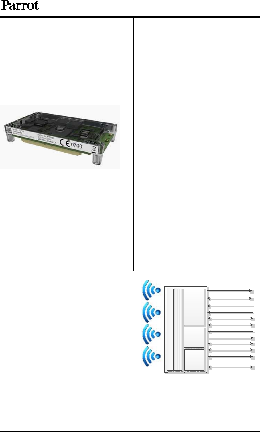
PARROT FC7100 Full connectivity module User Manual OEM 2012 149 FC7100 Datasheet v2 7
PARROT Full connectivity module OEM 2012 149 FC7100 Datasheet v2 7
PARROT >
Contents
User manual

Confidential information
PARROT PRODUCT DATASHEET
FC7100
Version 2.6
August 2014
DATASHEET
FC7100
Full connectivity module with
Android OS.
Bluetooth 4.0 LE –
WiFi
– GPS
LCD and Multi cameras
connectivity.
Applications:
•
Smartphone Android Apps platform
• Turn-by-
turn GPS Navigation
•
Internet access (through 3G USB dongle,
Bluetooth Dun, Pan, 3G+ module)
• HMI Display via LCD screen
• Telephony voice recognition
•
Multimedia voice recognition
• Voice destination entry
• Message dictation
• USB & IPod management
•
Multi cameras management with Driver
assistance use-
cases implementation
(ADAS).
•
Audio & Video Media sharing by UPnP
(DMC, DMR and DMS).
•
Video stream reception and decoding
•
Telephony & Audio streaming
• Mirrorlink & Mira
cast Terminal mode
The FC7100 employs the ANDROID OS
The FC7100 is designed as an open platform
for any Android apps intended for a mobile
phone such as news, games, productivity,
multimedia, navigation.
The FC7100 embed all of the automotive
dedicated
Parrot Libraries, native running on
Linux:
•
USB devices and iPod, iPhone, with
database for metadata
Confidential Information
Full connectivity module with
WiFi
a/b/g/n
LCD and Multi cameras
Smartphone Android Apps platform
turn GPS Navigation
Internet access (through 3G USB dongle,
Bluetooth Dun, Pan, 3G+ module)
Multimedia voice recognition
Multi cameras management with Driver
cases implementation
Audio & Video Media sharing by UPnP
Video stream reception and decoding
Telephony & Audio streaming
cast Terminal mode
The FC7100 employs the ANDROID OS
.
The FC7100 is designed as an open platform
for any Android apps intended for a mobile
phone such as news, games, productivity,
The FC7100 embed all of the automotive
Parrot Libraries, native running on
USB devices and iPod, iPhone, with
•
Voice recognition for telephony features,
navigation destination entry or multimedia
selection
•
Local and connected voice recognition
engine
• Bluetooth with
a very high level of
compatibility with most of the phones
available on the market and phonebook
synchronization.
Technical Features:
•
Dual LCD Management
ITU656
•
Bluetooth 4.0 LE qualified module
• Wifi a/b/g/n –
2.4 & 5 GHz
• Built-in GPS receiver
•
Standard single 3.3V supply
•
Full connectivity (UARTs, I²C, SPI, GPIO,
USB) with external modules and chips:
MHL, HDMI, Ethernet, NAD, TV, Radio,
Mems sensors, Apple IC.
•
2*USB 2.0 High Speed
• Ethernet interface
•
Digital audio in and out
•
Up to 3 cameras input
• Module dimensions
80.6*46.6*4.1
•
Automotive qualified AEC
• 2 x SDcard support –
SDXC
The FC7
100 platform provides a full API, to
access Parrot Libraries and
Android basic features.
Parrot
P7
Cortex
A9
3900
MIPS
DDR 3
2 x
4Gb
NAND
Flash
8 Gb
WiFi b/g/n – BT 4.0 LE – GPS
External anten nas
2/39
Ref: OEM-2012-149
Voice recognition for telephony features,
navigation destination entry or multimedia
Local and connected voice recognition
a very high level of
compatibility with most of the phones
available on the market and phonebook
Dual LCD Management
– 24 bits & 8 bits
Bluetooth 4.0 LE qualified module
2.4 & 5 GHz
Standard single 3.3V supply
Full connectivity (UARTs, I²C, SPI, GPIO,
USB) with external modules and chips:
MHL, HDMI, Ethernet, NAD, TV, Radio,
Mems sensors, Apple IC.
2*USB 2.0 High Speed
– Host
Digital audio in and out
- I²S
Up to 3 cameras input
– 8/16 bits ITU656
80.6*46.6*4.1
6 mm
Automotive qualified AEC
-Q100
SDXC
100 platform provides a full API, to
access Parrot Libraries and
to enhance
LCD // 24 bits
LCD or camera - // 8 bits
2 x USB 2.0
3 x SPI
3 x I²S in
4 x I²S out
4 x UART
2 x SDIO
2 x I²C
Ethernet (RGMII – MII)
camera - // 8 bits
camera - // 8 bits

DATASHEET
Table of contents
1 Introduction
................................
2 FC7100 Overview
................................
3 FC7100 technology
................................
4 Vehicle Integration
................................
4.1
FC7100 in a standalone ECU, interfaced to an entry headunit
4.2
FC7100 in a standalone ECU, interfaced to a premium headunit
4.3
Smart Display: the FC7100 is behind the LCD, in the same housing
4.4
FC7100 integrated into the headunit
4.5 Rear Seat
Entertainment network
4.6
Components Proposal for Vehicle Integration
5 FC7100 Hardware
................................
5.1 Hardware overview
................................
5.2
Power supplies & management
5.3
External communication interfaces
6 Mechanical
................................
6.1 Outline dimensions
................................
6.2 Motherboard PCB layout
6.3 Connectors
................................
6.4
Thermal integration guidelines (TBC)
7 Available Tools
................................
7.1 Workbench
................................
8 Marking ................................
................................
8.1 Module Marking
................................
9 Caution for use
................................
9.1 ESD Compliance
................................
9.2 Safety
................................
9.3 Assembly
................................
9.4 Drop
................................
10 APPROVAL / CERTIFICATIonS
................................
10.1 Normative informations
................................
10.2
FCC and IC requirements for module application
10.3
Japanese Radio Law and Japanese Telecommunications Business Law Compliance.
Confidential Information
Table of contents
................................
................................................................
................................
................................
................................
................................
................................
................................
................................
................................
................................
................................
FC7100 in a standalone ECU, interfaced to an entry headunit
................................
FC7100 in a standalone ECU, interfaced to a premium headunit
................................
Smart Display: the FC7100 is behind the LCD, in the same housing
................................
FC7100 integrated into the headunit
................................
................................
Entertainment network
................................
................................
Components Proposal for Vehicle Integration
................................
................................
................................
................................
................................
................................
................................
................................
Power supplies & management
................................................................
................................
External communication interfaces
................................
................................
................................
................................................................
................................
................................
................................
................................
................................................................
................................
................................
................................................................
................................
Thermal integration guidelines (TBC)
................................
................................
................................
................................................................
................................
................................
................................................................
................................
................................
................................
................................
................................
................................
................................
................................
................................................................
................................
................................
................................
................................
................................
................................................................
................................
................................
................................................................
................................
................................
................................................................
................................
................................
................................
................................
................................
................................
................................
FCC and IC requirements for module application
................................
................................
Japanese Radio Law and Japanese Telecommunications Business Law Compliance.
3/39
Ref: OEM-2012-149
................................
....... 4
................................
............................... 6
................................
............................. 7
................................
........................... 11
................................
................. 12
................................
............. 13
................................
......... 14
................................
........................ 15
................................
............................. 16
................................
.......... 17
................................
............................. 18
................................
................... 18
................................
24
................................
.......................... 25
................................
....... 31
................................
.................... 31
................................
........... 32
................................
32
................................
........................ 34
................................
. 34
................................
34
................................
............ 35
................................
........................ 35
................................
. 35
................................
......................... 35
................................
......... 35
................................
.... 36
................................
........... 36
................................
............ 37
................................
............ 37
................................
..... 37
Japanese Radio Law and Japanese Telecommunications Business Law Compliance.
.............. 39
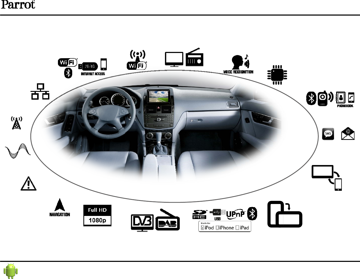
1 Introduction
Parrot has initiated the inte
gration of Android
use in their car
all the features they use today in
Internet and connected Apps.
Parrot’s Next Generation FC7
100
them into the vehicle. FC7
100 enables a true
Android. It is designed to run
Android Apps in an automotive environment
FC7100 brings also camera connectivity and automotive v
front line detection,
drowsiness detection).
FC7100 enhances
the voice recognition interface with
remote) allowing voice destination entry, messages dictation, multimed
launching and Text-To-S
peech (TTS)
Parrot has adapted the Android framework for automotive use cases. FC
standard suite of Parrot automotive libraries for connectivity
Recognition, and TTS etc.)
WiFi 802.11 b/g/n
+ BT 4.0 Combo
chip
WiFi Direct/Display
AP & STA
+ GPS
26 MHz
Oscillator
DDR3
Nand Flash
Video
Encoder/
Decoder
GPU400
380MPix/s
SDIO
PCM
UART
GPS
5 GHz2.4 GHz
The combination of the Android framework and the Parrot Automotive libraries provides a complete
ready solution for vehicle manufacturers to launch a
which is always connected (
Internet, connected Apps
new Android Apps,
update existing Apps
Android Apps will be now available to users in the vehicle.
With FC7100, Parrot provides a
time
Complete hardware and software
Reduced development time
and
Android ecosystem
Confidential Information
gration of Android
in an automotive environment.
all the features they use today in
their smartphones:
telephony, music, video,
100
delivers the best features of t
oday’s smartphones and integrates
100 enables a true
connected Infotainment open platform based on
Android Apps in an automotive environment
.
FC7100 brings also camera connectivity and automotive v
ideos treatments (bird view, rear camera,
drowsiness detection).
the voice recognition interface with
a
hybrid voice recognition engine (local and
remote) allowing voice destination entry, messages dictation, multimed
ia voice requests, apps
peech (TTS)
.
Parrot has adapted the Android framework for automotive use cases. FC
7
100 embeds also the
standard suite of Parrot automotive libraries for connectivity
(Bluetooth, USB, Wi
NFC
P7
2x CORTEX A9
3900 Mips
Advanced
video
interface
Advanced
audio
interface
2 PCM
3 I2S in
2 I2S out
SPDIF in/out
UART x 2
I2C x 2
SPI x 2
GPIO x 6
SDIO 3.0
USB2.0 x 2
Supervisor
circuit
PHY
VBAT
P7MU
I2S OUT
I2S IN
140 pin connector
RGMII (Ethernet)
The combination of the Android framework and the Parrot Automotive libraries provides a complete
ready solution for vehicle manufacturers to launch a
modern automotive infotainment platform
Internet, connected Apps
) and remains up-to-
date (
update existing Apps
, accessing to a customer app store
etc.)
Android Apps will be now available to users in the vehicle.
time
-to-
market solution to vehicle manufacturers:
Complete hardware and software
automotive open platform
and
engineering costs
4/39
Ref: OEM-2012-149
in an automotive environment.
Customers can now
telephony, music, video,
oday’s smartphones and integrates
connected Infotainment open platform based on
ideos treatments (bird view, rear camera,
hybrid voice recognition engine (local and
ia voice requests, apps
100 embeds also the
(Bluetooth, USB, Wi
-Fi, Voice
1 LCD
2 cameras
DAC
ADC
LVDS Ctrl
HDMI Ctrl
USB 2.0
SDIO
SPDIF
ITU 656
Sub Modules:
NAD, GPS,
Tuner, CAN/LIN
Ctrl, Ethernet, ...
2 x Analog
OUT
2 x Analog
IN
Mass storage ,
MTP
iPod, etc.
USB modem
The combination of the Android framework and the Parrot Automotive libraries provides a complete
modern automotive infotainment platform
date (
ability to download
etc.)
. The portfolio of
market solution to vehicle manufacturers:

Built-
in video hardware encoder and decoder, with Mali
playback and best-in-class HMI
Multiple video interfaces and Ethernet connectivity
screens interface.
Confidential Information
in video hardware encoder and decoder, with Mali
-
400 GPU embedded al
Multiple video interfaces and Ethernet connectivity
for
multiple cameras and multiple LCD
5/39
Ref: OEM-2012-149
400 GPU embedded al
lowing HD video
multiple cameras and multiple LCD
Confidential
Information
2 FC7100 Overview
ADAS
Internet access/3G+&4G
Tethering / Dongles
Ethernet
networking
3D Navigation
Video Player
AM/FM Tuner
Phase Diversity
A/V Processing
Information
6/39
Ref: OEM-2012-149
(landscape, portrait)
ASIC Design
Internet TV & Radio
Music on demand TTS &
Voice control
Multimedia Audio
Digital Radio &
TV
LCD control
(landscape, portrait)
Smart Link
& MHL
ASIC Design
Telephony, Tasks, Contacts
Messaging

3 FC7
100 technology
• Android 2.3 and 4.2
Linux based
Hardware independent
Large number of applications available
Web Browser included
Easy Specific HMI design with Android SDK
• Bluetooth connectivity
Bluetooth Power Class 2 Radio
Embedded Bluetooth V
Compatible with virtual
Pairing and connection with all Bluetooth Devices: Phones, Smartphones, PDA …
Multiple user support
Multiple connections (up to 3 devices connected at the same time)
Multiple profiles active simultaneously
Bluetooth Stack specification:
o
HCI (Host Controller interface)
o
L2CAP (Logical Link Control and Adaptation Protocol)
o RFCOMM
( Radio Frequency Communication)
o
SDP (Service Discovery Protocol)
o
OBEX (IrDA Object Exchange)
o
Channel manager, AMP Manager, HCI A
o
Enhanced Power Control
o
Unicast Connectionless Data
o
HCI Read Encryption Key Size command
Embedded Bluetooth profiles supported:
o
Generic Access Profile
o
Phone Management
o HFP 0.96 -
1.0
o HSP 1.0
o
SAP (SIM Access Profile)
o
Message Management
o MAP 1.0
o
Phone Book
o PBAP 1.0
o
SYNC 1.1 (IrMC SYNC over BT)
o SYNCML
o
OPP 1.0 Server/Client (Vcard 3.0)
o
GSM 07.07 AT Commands
o
Nokia synchronization protocol
o Multimedia
o
A2DP (Audio)
o
SBC decoding
o
MP3 decoding
o AVDTP
o
AVRCP1.0 / AVRCP1.3 / AVRCP1.
o SPP 1.1
o BNEP, PAN
Confidential Information
100 technology
Hardware independent
Large number of applications available
Web Browser included
Easy Specific HMI design with Android SDK
Bluetooth Power Class 2 Radio
Embedded Bluetooth V
4.0 Low Energy
Compatible with virtual
ly all Bluetooth phones
Pairing and connection with all Bluetooth Devices: Phones, Smartphones, PDA …
Multiple user support
: Up to 10 paired phones
Multiple connections (up to 3 devices connected at the same time)
Multiple profiles active simultaneously
Bluetooth Stack specification:
HCI (Host Controller interface)
L2CAP (Logical Link Control and Adaptation Protocol)
( Radio Frequency Communication)
SDP (Service Discovery Protocol)
OBEX (IrDA Object Exchange)
Channel manager, AMP Manager, HCI A
MP
Enhanced Power Control
Unicast Connectionless Data
HCI Read Encryption Key Size command
Embedded Bluetooth profiles supported:
Generic Access Profile
Phone Management
1.0
- 1.5
SAP (SIM Access Profile)
Message Management
Phone Book
SYNC 1.1 (IrMC SYNC over BT)
OPP 1.0 Server/Client (Vcard 3.0)
GSM 07.07 AT Commands
Nokia synchronization protocol
A2DP (Audio)
SBC decoding
MP3 decoding
- optional
AVRCP1.0 / AVRCP1.3 / AVRCP1.
4
7/39
Ref: OEM-2012-149
Pairing and connection with all Bluetooth Devices: Phones, Smartphones, PDA …
Multiple connections (up to 3 devices connected at the same time)

o FTP 1.0
o
Image transfer over OPP
o DUNP 1.1
o
Software update over SPP
o
Secure Simple Pairing
•
Digital Signal Processing
Microphone(s),
the module can manage two configurations:
o
Single microphone
o
Two microphones with AMS (Automatic Mic
driver and 1 for the front seat passenger. The best microphone is
automatically selected during the call.
Noise Reduction (NR)
o
Maximal NR is 25dB.
o
Typical NR is 15dB.
o
No musical noise
o
No fluctuation of the residual noise leve
o
Automatic adaptation of the Noise Reduction to the Signal
(SNR) to keep the best voice quality in idle and remove more noise in noisy
conditions.
Acoustic Echo Cancellation (AEC)
o
The level of echo attenuation, called ERLE is 45dB (measur
the VDA process).
o
Comfort Noise feature so that the background noise is adjusted after AEC
algorithm, in order to keep it constant for enhanced communication
experience.
o
Possibility to accept up to 100ms of delay in the speaker path for dig
amplifiers.
o
Full duplex
Automatic Level Control (ALC)
o
Different phones can have different Speaker volumes (up to 20dB of
difference). It adapts the signal level received from the phone to the target
level, quickly and precisely.
Equalizer :
o 7
bands e
Tuning :
o
Car independent tuning if the microphone position and characteristics are
the same.
o
Possibility to tune all parameters of the audio algorithms according to
Customer preferences.
Wideband speech
o Support
o
All speech processing algorithms will work @ 16 kHz.
• External Bluetooth
& WiFi
Confidential Information
Image transfer over OPP
Software update over SPP
Secure Simple Pairing
Digital Signal Processing
the module can manage two configurations:
Single microphone
Two microphones with AMS (Automatic Mic
rophone Selection): 1 for the
driver and 1 for the front seat passenger. The best microphone is
automatically selected during the call.
Noise Reduction (NR)
:
Maximal NR is 25dB.
Typical NR is 15dB.
No musical noise
No fluctuation of the residual noise leve
l
Automatic adaptation of the Noise Reduction to the Signal
(SNR) to keep the best voice quality in idle and remove more noise in noisy
conditions.
Acoustic Echo Cancellation (AEC)
:
The level of echo attenuation, called ERLE is 45dB (measur
the VDA process).
Comfort Noise feature so that the background noise is adjusted after AEC
algorithm, in order to keep it constant for enhanced communication
experience.
Possibility to accept up to 100ms of delay in the speaker path for dig
amplifiers.
Full duplex
Automatic Level Control (ALC)
:
Different phones can have different Speaker volumes (up to 20dB of
difference). It adapts the signal level received from the phone to the target
level, quickly and precisely.
bands e
qualizer for microphones and speaker paths.
Car independent tuning if the microphone position and characteristics are
the same.
Possibility to tune all parameters of the audio algorithms according to
Customer preferences.
Wideband speech
:
of HFP 1.6
All speech processing algorithms will work @ 16 kHz.
& WiFi
Antenna diagnostic
8/39
Ref: OEM-2012-149
rophone Selection): 1 for the
driver and 1 for the front seat passenger. The best microphone is
Automatic adaptation of the Noise Reduction to the Signal
-to-noise ratio
(SNR) to keep the best voice quality in idle and remove more noise in noisy
The level of echo attenuation, called ERLE is 45dB (measur
ed according to
Comfort Noise feature so that the background noise is adjusted after AEC
algorithm, in order to keep it constant for enhanced communication
Possibility to accept up to 100ms of delay in the speaker path for dig
ital
Different phones can have different Speaker volumes (up to 20dB of
difference). It adapts the signal level received from the phone to the target
Car independent tuning if the microphone position and characteristics are
Possibility to tune all parameters of the audio algorithms according to
• FC7100 Wi-
Fi protocol summary
802.11a - 5GHz WiFi 54Mbps
802.11b - 2.4GHz WiFi 11Mbps
802.11d - "World Mode"
802.11e - Quality Of Service
802.11g - 2.4GHz WiFi 54Mbps
802.11h - 5GHz interferrence avoid
802.11i - Security
802.11j - Japan Standard
802.11n - 2.4GHz WiFi 150Mbps
802.11r - Fast basic service set transition
802.11y - High Power WiFi
Access Point support
Ad-Hoc
Client
WPA2 / WPA
• Bluetooth 4.0+LE
use cases
The increased data transfer speed offered by BT
and use cases
Faster phonebook synchronization, especially contacts with photos.
Faster FTP Transfers
Faster PAN profile, for better internet connection
Due to the 2 radio connections available, it is possible to have se
same time for instance phonebook
simultaneously
Pairing additional
Energy.
• Audio Player
Multi Sources (Line
Call artists and albums by voice recognition
Multiple codecs and containers supported (External licences apply)
MPEG-
1 Layer III (mp3), 32
MPEG-
2 Layer III (mp3), 8
LPCM, 8-48kHz, 8-
32bit, mono/stereo
FLAC, 1-48kHz, 4-
24bit, VBR
AAC LC (MPEG-
4 part III Audio
HE-
AAC (aacPlus, MPEG
HD-AAC (MPEG-
4 part III Audio), 8
WMA/WMA9, up to 48kHz, mono/stereo, CBR/ABR/VBR
Vorbis, q0 to q10 quality classes, 8
AMR-WB
AMR-NB
Confidential Information
Fi protocol summary
802.11a - 5GHz WiFi 54Mbps
Yes
802.11b - 2.4GHz WiFi 11Mbps
Yes
802.11d - "World Mode"
Yes
802.11e - Quality Of Service
Yes
802.11g - 2.4GHz WiFi 54Mbps
Yes
802.11h - 5GHz interferrence avoid
Yes
Yes
802.11j - Japan Standard
No
802.11n - 2.4GHz WiFi 150Mbps
Yes
802.11r - Fast basic service set transition
Yes
802.11y - High Power WiFi
No
Access Point support
on reset -firmware change
Yes
Yes
Yes
WLAN
Coexistence
use cases
The increased data transfer speed offered by BT
4.0 LE en
hances existing Bluetooth profiles
Faster phonebook synchronization, especially contacts with photos.
Faster FTP Transfers
Faster PAN profile, for better internet connection
Due to the 2 radio connections available, it is possible to have se
same time for instance phonebook
synchronization
+ AD2P or HFP + PAN transfer
Pairing additional
wireless devices such as remote controller
, using Bluetooth Low
Multi Sources (Line
-In, USB, SD, iPod, iPhone, BT/Wi-Fi)
Call artists and albums by voice recognition
Multiple codecs and containers supported (External licences apply)
CODEC Audio
1 Layer III (mp3), 32
-
320kbit/s, 32/44.1/48kHz, CBR/VBR, mono/stereo.
2 Layer III (mp3), 8
-160kb
it/s, 16/22.05/24 kHz, CBR/VBR, mono/stereo
32bit, mono/stereo
.
24bit, VBR
, mono/stereo.
4 part III Audio
), 8-48KHz, CBR/VBR,mono/stereo.
AAC (aacPlus, MPEG
-4 part III Audio), 8-48KHz,CBR/VBR, HE-AAC v1/2.
4 part III Audio), 8
-48
KHz, CBR/VBR,mono/stereo, Only lossy AAC layer.
WMA/WMA9, up to 48kHz, mono/stereo, CBR/ABR/VBR
Vorbis, q0 to q10 quality classes, 8
-48kHz, VBR, mono/stereo.
9/39
Ref: OEM-2012-149
on reset -firmware change
hances existing Bluetooth profiles
Faster phonebook synchronization, especially contacts with photos.
Due to the 2 radio connections available, it is possible to have se
veral profiles at the
+ AD2P or HFP + PAN transfer
, using Bluetooth Low
Multiple codecs and containers supported (External licences apply)
320kbit/s, 32/44.1/48kHz, CBR/VBR, mono/stereo.
it/s, 16/22.05/24 kHz, CBR/VBR, mono/stereo
.
KHz, CBR/VBR,mono/stereo, Only lossy AAC layer.

Embedded MP3 decoder from Thomson Licensing (optional)
• Built-
in hardware video decoder
Multiple codecs and containers supported:
• Built-
in hardware video encoder
Encode H.264
MVC Stereo High
OpenMAX IL API support
• Video interface
Up to 3 cameras interfaces : 1x 16 bits + 1x8bits or 3x up to 8 bits, 720p, ITU
656 protocols
Up to 2 LCD interfaces : 1 up to
Several image signal processing
o C
hroma conversion,
o Scaling
(with some limitations, see “
Manual” §2.2.2),
o Rotation (
nx90° + mirror)
o D
einterlacing, contrast
conversion
Confidential Information
CONTAINER Audio
MP3.
ASF.
OGG.
WAV/WAVE.
MP4 (audio)
MP4A.
AAC.
Embedded MP3 decoder from Thomson Licensing (optional)
in hardware video decoder
Multiple codecs and containers supported:
CODEC Vidéo
H.264/MPEG-4 AVC.
VP8
CONTAINER Video
MPEG-TS.
MP4.
3GP/3G2.
in hardware video encoder
OpenMAX IL API support
Up to 3 cameras interfaces : 1x 16 bits + 1x8bits or 3x up to 8 bits, 720p, ITU
Up to 2 LCD interfaces : 1 up to
24 bits and 1 x 8 bits, 1080p, ITU-
601 or ITU
Several image signal processing
:
hroma conversion,
(with some limitations, see “
Hantro HW Post-
Processor API 1.1 User
Manual” §2.2.2),
nx90° + mirror)
einterlacing, contrast
and brightness control, image cropping
10/39
Ref: OEM-2012-149
Up to 3 cameras interfaces : 1x 16 bits + 1x8bits or 3x up to 8 bits, 720p, ITU
-601 or ITU-
601 or ITU
-656 protocols
Processor API 1.1 User
and brightness control, image cropping
YUV to RGB
Confidential
Information
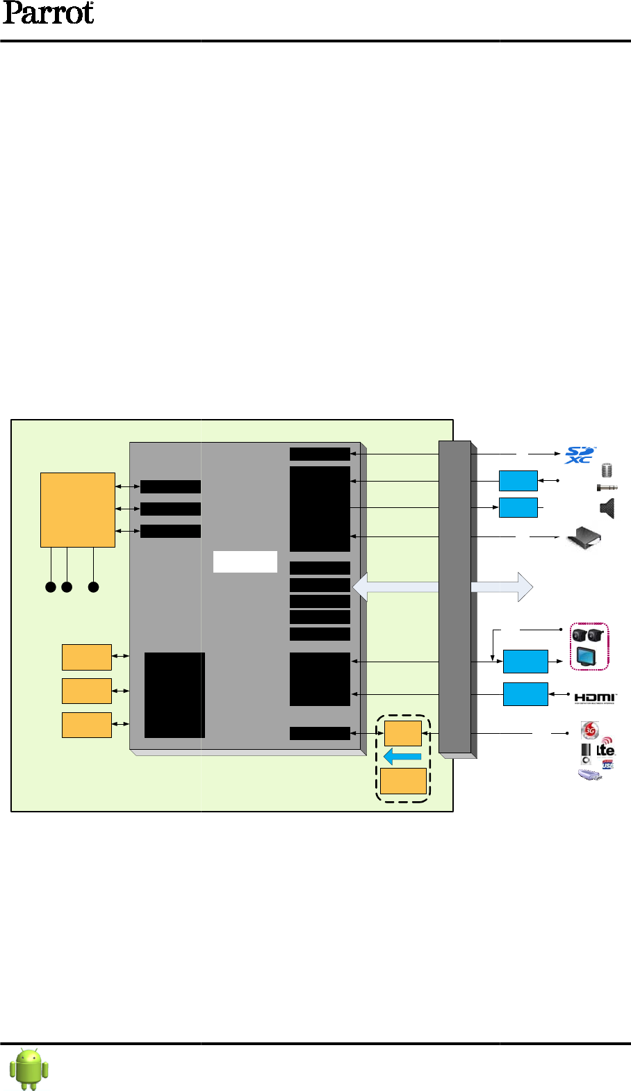
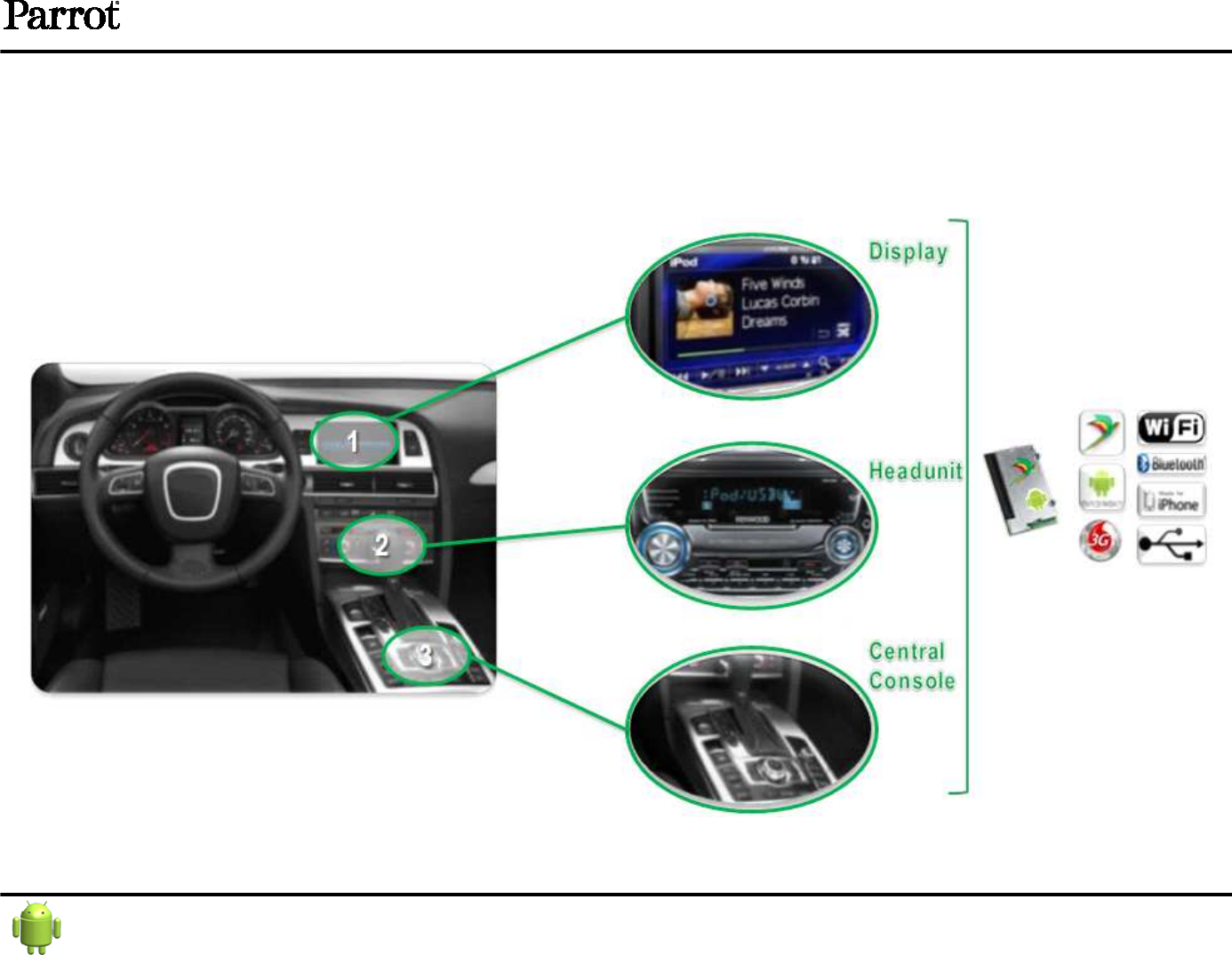
4 Vehicle Integration
The FC7100
module can be integrated behind the LCD display, inside the headunit, or in a standalone Electronic Control Unit (ECU) locate
the vehicle and co
nnected to the vehicle bus (e.g. CAN).
Information
11/39
Ref: OEM-2012-149
module can be integrated behind the LCD display, inside the headunit, or in a standalone Electronic Control Unit (ECU) locate
nnected to the vehicle bus (e.g. CAN).
module can be integrated behind the LCD display, inside the headunit, or in a standalone Electronic Control Unit (ECU) locate
d somewhere in
Confidential
Information
4.1
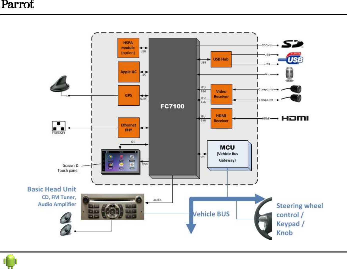
FC7100 in a standalone ECU, interfaced to an entry headunit
Information
12/39
Ref: OEM-2012-149
FC7100 in a standalone ECU, interfaced to an entry headunit
Confidential
Information
4.2
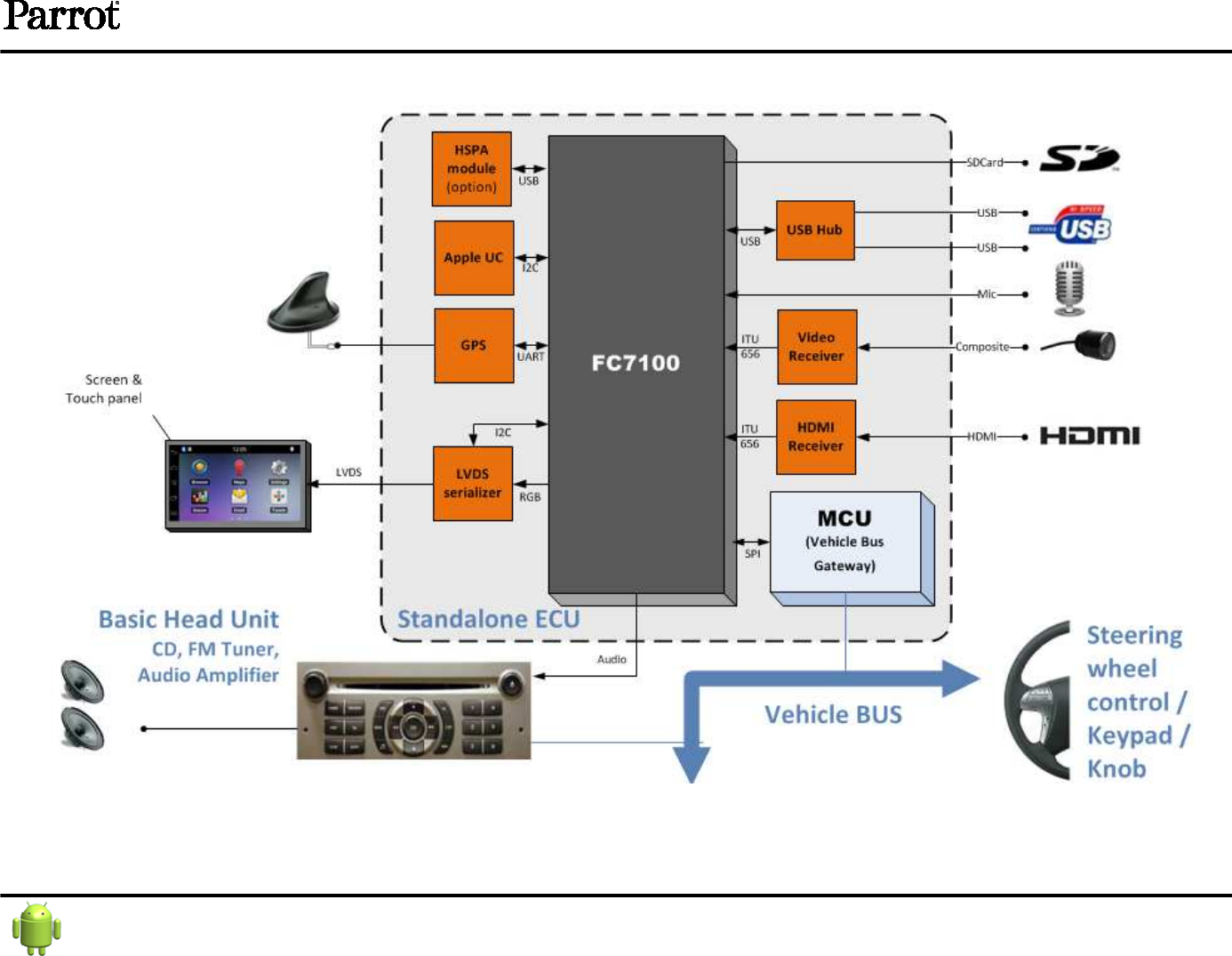
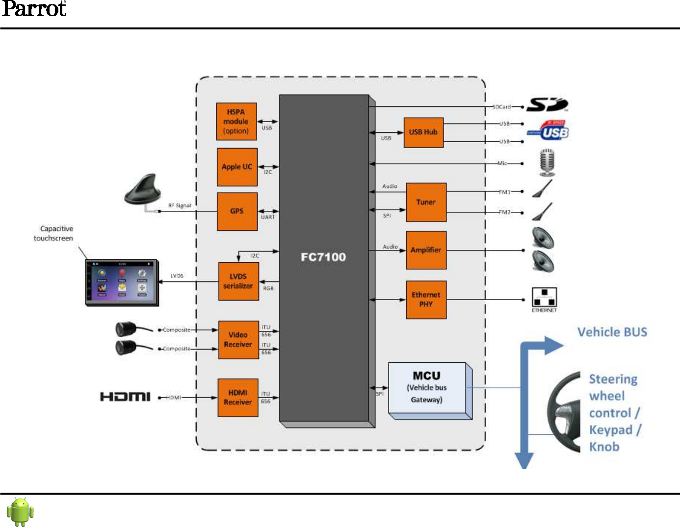
FC7100 in a standalone ECU, interfaced to a premium headunit
LVDS
out
LVDS
in
Smart Head Unit
CD, FM Tuner, Audio
Amplifier,
Touch screen
RF Signal
GPS antenna
Information
13/39
Ref: OEM-2012-149
FC7100 in a standalone ECU, interfaced to a premium headunit
FC7100
LVDS
switch
USB Hub
MCU
(Vehicle Bus
Gateway)
HSPA
module
(option)
Apple UC
Audio Vehicle BUS
SPI
RGB
I2C
USB
USB
I2C
LVDS
serializer
LVDS
HDMI
Receiver
ITU
656
Video
Receiver
ITU
656
ITU
656
Ethernet
PHY
ECU
Mic
SDCard
USB
USB
HDMI
Composite
Composite
Steering wheel
control /
Keypad /
Knob
Confidential
Information
4.3
Smart Display: the FC7100 is behind the LCD, in the same housing
Information
14/39
Ref: OEM-2012-149
Smart Display: the FC7100 is behind the LCD, in the same housing
Confidential
Information
4.4 FC7100 integrated into the headunit
Information
15/39
Ref: OEM-2012-149
Confidential
Information
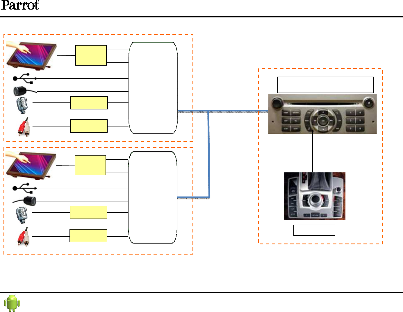
4.5 Rear Seat Entertainment network
LVDS
chip
RGB
LVDS
I²C
USB
RGB
ADC chip
ADC chip
I²S
I²S
LVDS
chip
RGB
LVDS
I²C
USB
RGB
ADC chip
ADC chip
I²S
I²S
Information
16/39
Ref: OEM-2012-149
FC7100
FC7100
RSE system #1
RSE system #2
ethernet
CD, FM t
uner, Audio Amplifier
Control
Head unit
uner, Audio Amplifier
Control

4.6 Components P
roposal for
• SPDIF transceiver :
SIRUS LOGIC
• LVDS Serializer : T
exas Instrument
• LVDS Serializer : Texa
s Instrument
• USB Hub : SMSC -
USB82514
• HDMI transceiver :
Analog Device
• Analog Video In :
Texas Instrument
Confidential Information
roposal for
Vehicle Integration
SIRUS LOGIC
- CF8406
exas Instrument
- DS90UB925Q
s Instrument
- DS90UB928Q
USB82514
Analog Device
- ADV7611
Texas Instrument
- TVP5151
17/39
Ref: OEM-2012-149

5 FC7100 Hardware
5.1 Hardware overview
5.1.1 Main components
5.1.1.1 Processor
The FC7100 design is based on the Parrot A
provides all the necessary features for advanced embedded multimedia processing:
• A Dual-
core ARM Cortex
•
128kB of internal RAM (@390MHz)
•
128kB of internal ROM (@195MH
• Off-
chip DDR3 SDRAM memory controller
•
NANDFLASH memory controller with 32 bit BCH
•
Interfaces : SPI, SDIO, USB, parallel interface for LCD, PWM, UART, I²C, GPIO, I²S inputs and
outputs,
• 1 Ethernet controller
•
Graphical Processing Unit, with video encodin
•
Advanced Video Interface with LCD controllers, camera interfaces, video scalers and rotators,
planes blender.
5.1.1.2
Power management unit
The P7MU is the analog companion chip of the Parrot 7. It provides the necessary features for
powering a P7
with in addition several other analog functionalities:
•
Programmable DC/DC converters
•
LDO for DDR3 Termination
• LDO for DDR3 Ref
• 12-bit 1MS/s ADC
• 2 instances of USB PHY
5.1.1.3 Radio Frequency
FC7100 is proposed in a basic configuration with an external antenna for
4.0 Low Energy and WiFi 802.11
Confidential Information
The FC7100 design is based on the Parrot A
SIC P
7, the latest dual core processor chip from Parrot. It
provides all the necessary features for advanced embedded multimedia processing:
core ARM Cortex
-A9 processor operating up to 780MHz
128kB of internal RAM (@390MHz)
128kB of internal ROM (@195MH
z)
chip DDR3 SDRAM memory controller
NANDFLASH memory controller with 32 bit BCH
Interfaces : SPI, SDIO, USB, parallel interface for LCD, PWM, UART, I²C, GPIO, I²S inputs and
Graphical Processing Unit, with video encodin
g and decoding
Advanced Video Interface with LCD controllers, camera interfaces, video scalers and rotators,
Power management unit
The P7MU is the analog companion chip of the Parrot 7. It provides the necessary features for
with in addition several other analog functionalities:
Programmable DC/DC converters
LDO for DDR3 Termination
FC7100 is proposed in a basic configuration with an external antenna for
2.4 GHz, allowing Bluetooth
b, g & n communication.
18/39
Ref: OEM-2012-149
7, the latest dual core processor chip from Parrot. It
provides all the necessary features for advanced embedded multimedia processing:
Interfaces : SPI, SDIO, USB, parallel interface for LCD, PWM, UART, I²C, GPIO, I²S inputs and
Advanced Video Interface with LCD controllers, camera interfaces, video scalers and rotators,
The P7MU is the analog companion chip of the Parrot 7. It provides the necessary features for
2.4 GHz, allowing Bluetooth
With an additional 5.0GHz external antenna,
feature can be added, with a third
5.1.1.4 Memory
The FC7100 basi
c Memory configuration is 8 Gbits NAND Flash and 8 Gbits DDR3 RAM. These
memory capacities can be increased
5.1.2
Hardware Architecture
* Many other display and record interface option are available.
See paragraph: 1.1.2.1 Display and rec
Confidential Information
With an additional 5.0GHz external antenna,
WiFi 802.11 a & n can be added. Also GPS / Glona
feature can be added, with a third
external antenna.
c Memory configuration is 8 Gbits NAND Flash and 8 Gbits DDR3 RAM. These
memory capacities can be increased
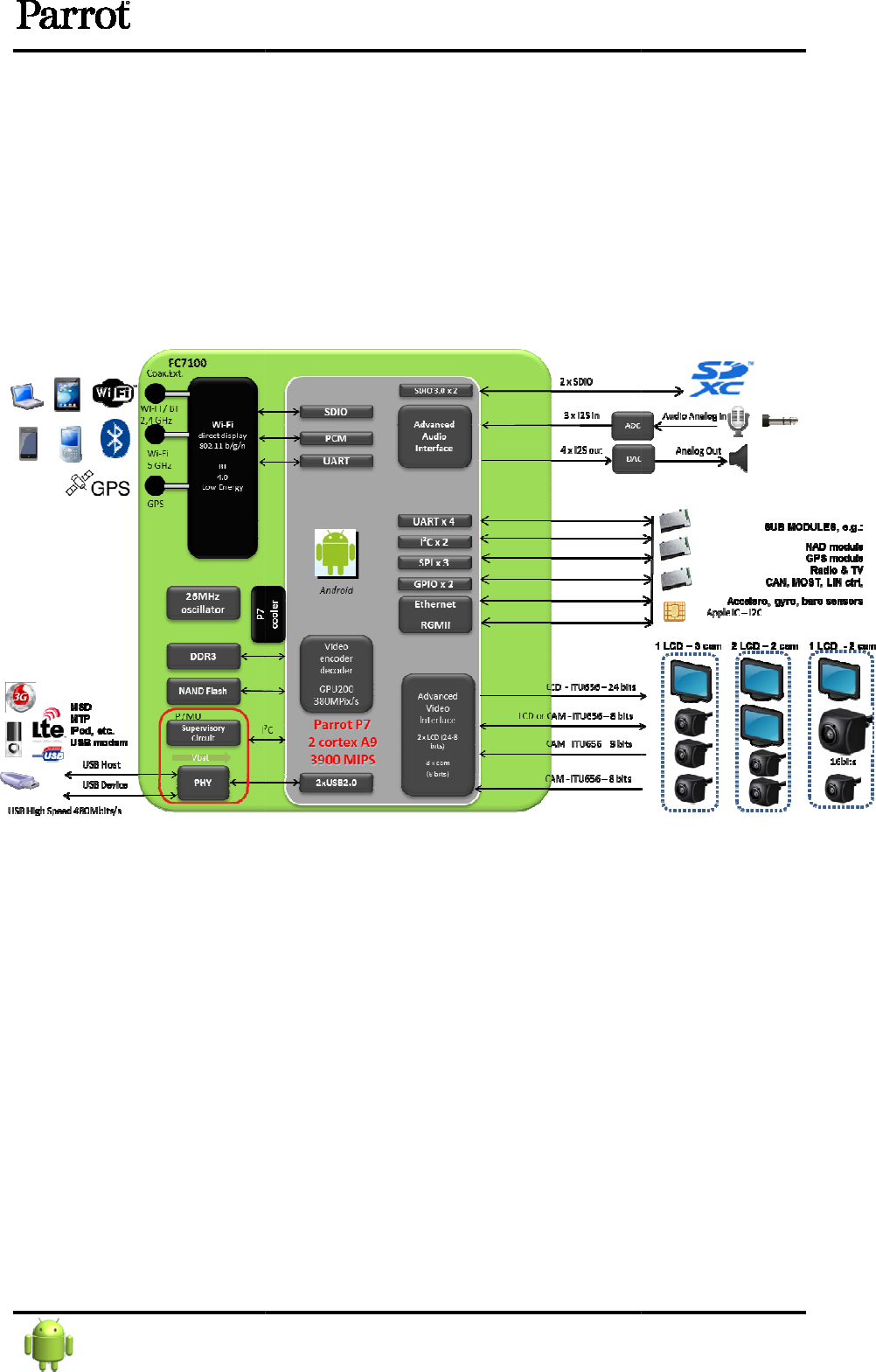
Hardware Architecture
* Many other display and record interface option are available.
See paragraph: 1.1.2.1 Display and rec
ord interface option.
19/39
Ref: OEM-2012-149
WiFi 802.11 a & n can be added. Also GPS / Glona
ss
c Memory configuration is 8 Gbits NAND Flash and 8 Gbits DDR3 RAM. These
* Many other display and record interface option are available.
ord interface option.
5.1.3
Electrical Specifications
Conditions unless otherwise noted: Tamb.= 25°C; Vcc = 3v3_Main = 3V3
5.1.3.1 Power Pin
Parameter
3V3_MAIN (=Vcc)
3V3_PERM
VDD_ETH
VDD_SD1
VDD_SD2
5.1.3.2 Power Consumption
•
3v3 Permanent (3V3_PERM):
Feature
Deep Low power
Low Power
Run/Standby mode
• 3v3 MAIN:
Feature
Low Power
Run/Standby mode
BT Hands Free or Audio streaming mode
Wifi Streaming
Video rendering
Inrush Current
Peak current at s
tartup (duration)
Confidential Information
Electrical Specifications
Conditions unless otherwise noted: Tamb.= 25°C; Vcc = 3v3_Main = 3V3
Min Typ Max
3,135 3,3 3,6
3,135 3,3 3,6
1,71 1,8 1,89
2,37 2,5 2,62
3,13 3,3 3,46
1,71 1,8 1,89
3,13 3,3 3,46
1,71 1,8 1,89
3,13 3,3 3,46
3v3 Permanent (3V3_PERM):
Min Typ Max
- 20 TBD
- 30 TBD
- 30 TBD
Min Typ Max
- 280 TBD
- 900
TBD
BT Hands Free or Audio streaming mode
- 980 TBD
- 1380 TBD
- 1140 TBD
- 9 TBD
tartup (duration)
- 74,8 TBD
20/39
Ref: OEM-2012-149
Unit
V
V
V
V
V
V
V
V
V
Unit
µA
µA
µA
Unit
mA
mA
mA
mA
mA
A
µs
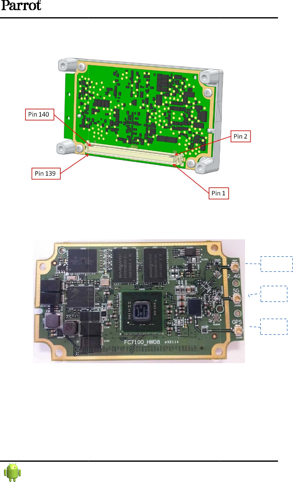
5.1.4 Pin Out Table
Here below the FC7100 main connector (140 pins):
Pin
1
USB_0_DN
3
USB_0_DP
5
USB_0_VBUS
7
Wake_Up_LPO
9
VDD_SD1 UART_5/6/7 INPUT
11
3V3_MAIN
13
3V3_MAIN
15
3V3_MAIN
17
Power_Good
19
3v3_PERM
21
ETH_RGMII_TXD_00 /
23
ETH_RGMII_TXD_02 /
25
ETH_RGMII_RXD_00 /
27
ETH_RGMII_RXD_02 /
29
ETH_RGMII_RX_CTL /
31
ETH_RGMII_TX_CTL /
33
ETH_RGMII_RX_CLK /
35
37
SPI_11 / GPIO_088 /
39
SPI_10 / GPIO_087 /
41
SPI_09 / GPIO_086 /
43
SPI_08 /
45
47
SPI_07 / GPIO_084 /
49
SPI_06 /
51
SPI_05 /
53
SPI_04 /
55
SPI_01 /
57
SPI_00 /
59
I2C_1_CLK / GPIO_062
61
I2C_2_CLK / GPIO_060
63
UART_0_CTS / GPIO_058
65
UART_0_RX / GPIO_055
67
UART_0_TX / GPIO_056
69
UART_0_RTS / GPIO_057
71
CAM_1_DAT15 / CAM_0_DAT07 / GPIO_216
73
CAM_1_DAT14 / CAM_0_DAT06 / GPIO_215
75
CAM_1_DAT13 / CAM_0_DAT05 / GPIO_214
77
CAM_1_DAT12 / CAM_0_DAT04 / GPIO_213
79
CAM_1_DAT11 / CAM_0_DAT03 / GPIO_212
81
CAM_5_DAT07 / GPIO_014
83
CAM_5_DAT06 / GPIO_013
85
CAM_5_DAT05 / GPIO_012
87
CAM_5_DAT03 / SD_2_DAT02 / GPIO_010
89
CAM_5_DAT01 / SD_2_DAT00 / GPIO_008
91
LCD_1_DAT00 / CAM_2_DAT02 / GPIO_183
93
LCD_1_DAT01 / CAM_2_DAT03 / GPIO_184
95
LCD_1_DAT02 / CAM_2_DAT04 / GPIO_185
97
LCD_1_DAT03 / CAM_2_DAT05 / GPIO_186
99
LCD_1_DAT04 / CAM_2_DAT06 / GPIO_187
101
LCD_1_DAT06 / CAM_3_CLK / GPIO_189
103
LCD_1_DAT08 / CAM_3_DAT01 / GPIO_191
105
LCD_1_DAT10 / CAM_3_DAT03 / GPIO_193
107
LCD_1_DAT12 / CAM_3_DAT05 / GPIO_195
109
111 LCD_1 CAM_2
LCD_1_CLK / CAM_2_DAT01 / GPIO_182
113
115 CAM_3
LCD_1_DAT14 / CAM_3_DAT07 / GPIO_197
117
LCD_1_DAT16 / CAM_4_DAT00 / GPIO_199
119
LCD_1_DAT18 / CAM_4_DAT02 / GPIO_201
121
LCD_1_DAT19 / CAM_4_DAT03 / GPIO_202
123
LCD_1_DAT20 / CAM_4_DAT04 / GPIO_203
125
LCD_1_DAT21 / CAM_4_DAT05 / GPIO_204
127
LCD_1_DAT22 / CAM_4_DAT06 / GPIO_205
129
LCD_1_DAT23 / CAM_4_DAT07 / GPIO_206
131
LCD_1_RSTn_Touch / CAM_0_VS / GPIO_154
133
LCD_1_IT_TouchScreen / CAM_0_HS / GPIO_155
135
LCD_1_BKL_En / CAM_5_VS / GPIO_160
137
LCD_1_RSTn / CAM_5_HS / GPIO_161
139
GND
CAM_4
LCD_1 GPIO
CAM_2
CAM_3
GND
GND
LCD_1
CAM_5
GPIO
SD2
LCD_1
I2C_2
UART 0 GPIO
CAM_1 CAM_0 (16
bits)
SPI [0:7]
Part 1 AAI
I2C_1
SPI[8:11] AAI
GND
Power_Good
3V3_PERM
Ethernet
RGMII GPIO
GND
Wake_Up
PowerVDD_SD1_UART_5_6_7
3V3_MAIN
USB_0
Confidential Information
Here below the FC7100 main connector (140 pins):
Function Type Power
Domain
USB_0_DN
I/O USB 0 Data -
USB_0_DP
I/O USB 0 Data +
USB_0_VBUS
I 5v USB 0 VBUS
Wake_Up_LPO
I 3V3 Wake Up Low Power
VDD_SD1 UART_5/6/7 INPUT
P 1v8 / 3v3
Power Supply SDIO1 and UART 5/6/7
3V3_MAIN
3V3_MAIN
3V3_MAIN
Power_Good
O 3V3 Power Good
3v3_PERM
P3V3
Power Supply Permanent : 3v3
ETH_RGMII_TXD_00 /
GPIO_139 I/O VDD_ETH GPIO or
Ethernet RGMII Tx Data 0
ETH_RGMII_TXD_02 /
GPIO_141
I/O
VDD_ETH
GPIO
or
Ethernet RGMII Tx Data 2
ETH_RGMII_RXD_00 /
GPIO_145
I/O
VDD_ETH
GPIO
or
Ethernet RGMII Rx Data 0
ETH_RGMII_RXD_02 /
GPIO_147
I/O
VDD_ETH
GPIO
or
Ethernet RGMII Rx Data 2
ETH_RGMII_RX_CTL /
GPIO_149
I/O
VDD_ETH
GPIO
or
Ethernet RGMII Rx Control
ETH_RGMII_TX_CTL /
GPIO_143
I/O
VDD_ETH
GPIO
or
Ethernet RGMII Tx Control
ETH_RGMII_RX_CLK /
GPIO_144 I/O VDD_ETH GPIO or
Ethernet RGMII Rx Clock
PGnd Ground
SPI_11 / GPIO_088 /
AAI_26
I/O
3V3
GPIO
or
SPI
or
AAI
SPI_10 / GPIO_087 /
AAI_25
I/O
3V3
GPIO
or
SPI
or
AAI
SPI_09 / GPIO_086 /
AAI_24
I/O
3V3
GPIO
or
SPI
or
AAI
SPI_08 /
GPIO_085 / AAI_23 I/O 3V3 GPIO or SPI or AAI
PGnd Ground
SPI_07 / GPIO_084 /
AAI_22
I/O
3V3
GPIO
or
SPI
or
AAI
SPI_06 /
GPIO_083 / AAI_21
I/O
3V3
GPIO
or
SPI
or
AAI
SPI_05 /
GPIO_082 / AAI_20
I/O
3V3
GPIO
or
SPI
or
AAI
SPI_04 /
GPIO_081 / AAI_19 I/O 3V3 GPIO or SPI or AAI
SPI_01 /
GPIO_078 / AAI_16 / CAN1_RX
I/O
3V3
GPIO
or
SPI
or
AAI
SPI_00 /
GPIO_077 / AAI_15 / CAN1_TX I/O 3V3 GPIO or SPI or AAI
I2C_1_CLK / GPIO_062
I/O 3V3 I2C 1 Clock or GPIO
I2C_2_CLK / GPIO_060
I/O 3V3 I2C 2 Clock or GPIO
UART_0_CTS / GPIO_058
I/O 3V3 UART 0 CTS or GPIO
UART_0_RX / GPIO_055
I/O 3V3
UART 0 RX
or
GPIO
UART_0_TX / GPIO_056
I/O 3V3 UART 0 TX or GPIO
UART_0_RTS / GPIO_057
I/O 3V3 UART 0 RTS or GPIO
CAM_1_DAT15 / CAM_0_DAT07 / GPIO_216
I/O 3V3 CAM 1 Data 7 or
CAM 0 Data 7
CAM_1_DAT14 / CAM_0_DAT06 / GPIO_215
I/O 3V3
CAM 1 Data 6
or
CAM 0 Data 6
CAM_1_DAT13 / CAM_0_DAT05 / GPIO_214
I/O 3V3 CAM 1 Data 5 or
CAM 0 Data 5
CAM_1_DAT12 / CAM_0_DAT04 / GPIO_213
I/O 3V3 CAM 1 Data 4 or
CAM 0 Data 4
CAM_1_DAT11 / CAM_0_DAT03 / GPIO_212
I/O 3V3 CAM 1 Data 3 or
CAM 0 Data 3
CAM_5_DAT07 / GPIO_014
I/O VDD_SD2
CAM 5 Data 7
or
GPIO
CAM_5_DAT06 / GPIO_013
I/O VDD_SD2 CAM 5 Data 6 or GPIO
CAM_5_DAT05 / GPIO_012
I/O VDD_SD2 CAM 5 Data 5 or GPIO
CAM_5_DAT03 / SD_2_DAT02 / GPIO_010
I/O VDD_SD2
CAM 5 Data 3
or
SDIO 2 Data 2
CAM_5_DAT01 / SD_2_DAT00 / GPIO_008
I/O VDD_SD2 CAM 5 Data 1 or
SDIO 2 Data 0
LCD_1_DAT00 / CAM_2_DAT02 / GPIO_183
I/O 3V3 LCD 1 Data 0 or
CAM 2 Data 2
LCD_1_DAT01 / CAM_2_DAT03 / GPIO_184
I/O 3V3 LCD 1 Data 1 or
CAM 2 Data 3
LCD_1_DAT02 / CAM_2_DAT04 / GPIO_185
I/O 3V3 LCD 1 Data 2 or
CAM 2 Data 4
LCD_1_DAT03 / CAM_2_DAT05 / GPIO_186
I/O 3V3 LCD 1 Data 3 or
CAM 2 Data 5
LCD_1_DAT04 / CAM_2_DAT06 / GPIO_187
I/O 3V3 LCD 1 Data 4 or
CAM 2 Data 6
LCD_1_DAT06 / CAM_3_CLK / GPIO_189
I/O 3V3
LCD 1 Data 6
or
CAM 3 Clock
LCD_1_DAT08 / CAM_3_DAT01 / GPIO_191
I/O 3V3
LCD 1 Data 8
or
CAM 3 Data 1
LCD_1_DAT10 / CAM_3_DAT03 / GPIO_193
I/O 3V3
LCD 1 Data 10
or
CAM 3 Data 3
LCD_1_DAT12 / CAM_3_DAT05 / GPIO_195
I/O 3V3 LCD 1 Data 12 or
CAM 3 Data 5
PGnd Ground
LCD_1_CLK / CAM_2_DAT01 / GPIO_182
I/O 3V3 LCD 1 Clock or
CAM 2 Data 1
PGnd Ground
LCD_1_DAT14 / CAM_3_DAT07 / GPIO_197
I/O 3V3 LCD 1 Data 14 or
CAM 3 Data 7
LCD_1_DAT16 / CAM_4_DAT00 / GPIO_199
I/O 3V3 LCD 1 Data 16 or
CAM 4 Data 0
LCD_1_DAT18 / CAM_4_DAT02 / GPIO_201
I/O 3V3 LCD 1 Data 18 or
CAM 4 Data 2
LCD_1_DAT19 / CAM_4_DAT03 / GPIO_202
I/O 3V3
LCD 1 Data 19
or
CAM 4 Data 3
LCD_1_DAT20 / CAM_4_DAT04 / GPIO_203
I/O 3V3
LCD 1 Data 20
or
CAM 4 Data 4
LCD_1_DAT21 / CAM_4_DAT05 / GPIO_204
I/O 3V3
LCD 1 Data 21
or
CAM 4 Data 5
LCD_1_DAT22 / CAM_4_DAT06 / GPIO_205
I/O 3V3
LCD 1 Data 22
or
CAM 4 Data 6
LCD_1_DAT23 / CAM_4_DAT07 / GPIO_206
I/O 3V3 LCD 1 Data 23 or
CAM 4 Data 7
LCD_1_RSTn_Touch / CAM_0_VS / GPIO_154
I/O 3V3
LCD 1 Resetn_Touch Screen
LCD_1_IT_TouchScreen / CAM_0_HS / GPIO_155
I/O 3V3
LCD 1 IT Touch Screen
LCD_1_BKL_En / CAM_5_VS / GPIO_160
I/O 3V3
LCD 1 Backlight Enable
LCD_1_RSTn / CAM_5_HS / GPIO_161
I/O 3V3 LCD 1 Resetn or
CAM_5_HS
PGnd Ground
GND
GND
GND
GND
GND
P3V3 Power supply : 3v3
21/39
Ref: OEM-2012-149
Description
Power Supply SDIO1 and UART 5/6/7
Power Supply Permanent : 3v3
Ethernet RGMII Tx Data 0
Ethernet RGMII Tx Data 2
Ethernet RGMII Rx Data 0
Ethernet RGMII Rx Data 2
Ethernet RGMII Rx Control
Ethernet RGMII Tx Control
Ethernet RGMII Rx Clock
CAM 0 Data 7
or GPIO
CAM 0 Data 6
or
GPIO
CAM 0 Data 5
or GPIO
CAM 0 Data 4
or GPIO
CAM 0 Data 3
or GPIO
SDIO 2 Data 2
or
GPIO
SDIO 2 Data 0
or GPIO
CAM 2 Data 2
or GPIO
CAM 2 Data 3
or GPIO
CAM 2 Data 4
or GPIO
CAM 2 Data 5
or GPIO
CAM 2 Data 6
or GPIO
CAM 3 Clock
or
GPIO
CAM 3 Data 1
or
GPIO
CAM 3 Data 3
or
GPIO
CAM 3 Data 5
or GPIO
CAM 2 Data 1
or GPIO
CAM 3 Data 7
or GPIO
CAM 4 Data 0
or GPIO
CAM 4 Data 2
or GPIO
CAM 4 Data 3
or
GPIO
CAM 4 Data 4
or
GPIO
CAM 4 Data 5
or
GPIO
CAM 4 Data 6
or
GPIO
CAM 4 Data 7
or GPIO
LCD 1 Resetn_Touch Screen
or
CAM 0 VS
or
GPIO
LCD 1 IT Touch Screen
or
CAM 0 HS
or
GPIO
LCD 1 Backlight Enable
or
CAM 5 VS
or
GPIO
CAM_5_HS
or GPIO
Pin
2
4
3V3_MAIN
6
3V3_MAIN
8
3V3_MAIN
10
3V3_MAIN
12
USB_1_DP
14
USB_1_DN
16
18 BOOT
20
Power_En
22
VDD_ETH INPUT
24
ETH_RGMII_TXD_01 /
26
ETH_RGMII_TXD_03 /
28
ETH_RGMII_RXD_01 /
30
ETH_RGMII_RXD_03 /
32
ETH_RGMII_TX_CLK /
34
ETH_MDC /
36
ETH_MDIO /
38
SPI_16 / ETH_MII TXER / GPIO_134
40
SPI_17 / ETH_MII RXER / GPIO_135
42
SPI_18 / ETH_MII CRS / GPIO_136
44
SPI_19 / ETH_MII COL / GPIO_137
46
48
AAI_14 / GPIO_133 / PWM_14
50
AAI_12 / GPIO_131 / PWM_12
52
AAI_11 / GPIO_130 / PWM_11
54
AAI_10 / GPIO_129 / PWM_10
56
SPI_03 / GPIO_080 / AAI_18 / CAN0_RX
58
SPI_02 / GPIO_079 / AAI_17 / CAN0_TX
60
62
I2C_1_DAT / GPIO_061
64
I2C_2_DAT / GPIO_059
66
SD_1_CMD / UART_5_RX
68
SD_1_CLK / UART_5_TX
70
SD_1_DAT03 / UART_7_RX
72
SD_1_DAT02 / UART_7_TX
74
SD_1_DAT01 / UART_6_RX
76
SD_1_DAT00 / UART_6_TX
78
80
CAM_1_DAT10 / CAM_0_DAT02 / GPIO_211
82
CAM_1_DAT09 / CAM_0_DAT01 / GPIO_210
84
CAM_1_DAT08 / CAM_0_DAT00 / GPIO_209
86 GPIO
CAM_1_CLK / GPIO_217
88
CAM_5_DAT04 / SD_2_DAT03 / GPIO_011
90
CAM_5_DAT02 / SD_2_DAT01 / GPIO_009
92
CAM_5_DAT00 / SD_2_CMD / GPIO_007
94
96 CAM_5 SD2
CAM_5_CLK / SD_2_CLK / GPIO_006
98
VDD_SD2_CAM5 INPUT
100 CAM_2
LCD_1_DAT05 / CAM_2_DAT07 / GPIO_188
102
LCD_1_DAT07 / CAM_3_DAT00 / GPIO_190
104
LCD_1_DAT09 / CAM_3_DAT02 / GPIO_192
106
LCD_1_DAT11 / CAM_3_DAT04 / GPIO_194
108
LCD_1_DAT13 / CAM_3_DAT06 / GPIO_196
110
LCD_1_DAT15 / CAM_4_CLK / GPIO_198
112
LCD_1_DAT17 / CAM_4_DAT01 / GPIO_200
114 GPIO
LCD_1_DEN / GPIO_207
116
LCD_1_HS / CAM_2_CLK / GPIO_180
118
LCD_1_VS / CAM_2_DAT00 / GPIO_181
120
122
CAM_0_CLK / LCD_0_CLK / GPIO_179
124
CAM_0_DAT08 / LCD_0_DAT08 / GPIO_163
126
CAM_0_DAT09 / LCD_0_DAT09 / GPIO_164
128
CAM_0_DAT10 / LCD_0_DAT10 / GPIO_165
130
CAM_0_DAT11 / LCD_0_DAT11 / GPIO_166
132
CAM_0_DAT12 / LCD_0_DAT12 / GPIO_167
134
CAM_0_DAT13 / LCD_0_DAT13 / GPIO_168
136
CAM_0_DAT14 / LCD_0_DAT14 / GPIO_169
138
CAM_0_DAT15 / LCD_0_DAT15 / GPIO_170
140
CAM_2
CAM_0 LCD_0
Power VDD_SD2 _CAM_5
LCD_1
CAM_3
CAM_4
UART 6
CAM_1
CAM_0 (16
bits)
CAM_5 SD2
I2C_1
I2C_2
SD1
UART 5
UART 7
AAI
PWM
SPI [0:7] Part 2
Ethernet
MII SPI
BOOT
PWR_En
Power VDD_ETH & GPIO
Ethernet
RGMII GPIO
USB_1
3V3_MAIN
Confidential Information
Function Type Power
Domain Description
PGnd Ground
3V3_MAIN
3V3_MAIN
3V3_MAIN
3V3_MAIN
USB_1_DP
I/O
USB 1 Data +
USB_1_DN
I/O USB 1 Data -
PGnd Ground
I3V3
Initial Flashing pin
Power_En
I3V3
Power Enable
VDD_ETH INPUT
I1v8 / 3v3
Power Supply Ethernet 1v8 / 2v5 / 3v3 or GPIO
ETH_RGMII_TXD_01 /
GPIO_140
I/O
VDD_ETH
GPIO
or
Ethernet RGMII Tx Data 1
ETH_RGMII_TXD_03 /
GPIO_142
I/O
VDD_ETH
GPIO
or
Ethernet RGMII Tx Data 3
ETH_RGMII_RXD_01 /
GPIO_146
I/O
VDD_ETH
GPIO
or
Ethernet RGMII Rx Data 1
ETH_RGMII_RXD_03 /
GPIO_148
I/O
VDD_ETH
GPIO
or
Ethernet RGMII Rx Data 3
ETH_RGMII_TX_CLK /
GPIO_138
I/O
VDD_ETH
GPIO
or
Ethernet RGMII Tx Clock
ETH_MDC /
GPIO_150 I/O VDD_ETH GPIO or
Ethernet RGMII
ETH_MDIO /
GPIO_151 I/O VDD_ETH GPIO or
Ethernet RGMII
SPI_16 / ETH_MII TXER / GPIO_134
I/O VDD_ETH
SPI CLK
or
Ethernet MII
SPI_17 / ETH_MII RXER / GPIO_135
I/O VDD_ETH
SPI MOSI
or
Ethernet MII
SPI_18 / ETH_MII CRS / GPIO_136
I/O VDD_ETH
SPI SS
or
Ethernet MII
SPI_19 / ETH_MII COL / GPIO_137
I/O VDD_ETH SPI MISO or
Ethernet MII
PGnd Ground
AAI_14 / GPIO_133 / PWM_14
I/O 3V3
GPIO
or
AAI
AAI_12 / GPIO_131 / PWM_12
I/O 3V3
GPIO
or
AAI
AAI_11 / GPIO_130 / PWM_11
I/O 3V3
GPIO
or
AAI
AAI_10 / GPIO_129 / PWM_10
I/O 3V3 GPIO or
AAI
SPI_03 / GPIO_080 / AAI_18 / CAN0_RX
I/O 3V3
GPIO
or
AAI
SPI_02 / GPIO_079 / AAI_17 / CAN0_TX
I/O 3V3 GPIO or
AAI
PGnd Ground
I2C_1_DAT / GPIO_061
I/O 3V3 I2C 1 Data
or
I2C_2_DAT / GPIO_059
I/O 3V3 I2C 2 Data
or
SD_1_CMD / UART_5_RX
I/O VDD_SD1
SDIO 1 Command
SD_1_CLK / UART_5_TX
I/O VDD_SD1
SDIO 1 Clock
SD_1_DAT03 / UART_7_RX
I/O VDD_SD1
SDIO 1 Data 3
SD_1_DAT02 / UART_7_TX
I/O VDD_SD1
SDIO 1 Data 2
SD_1_DAT01 / UART_6_RX
I/O VDD_SD1
SDIO 1 Data 1
SD_1_DAT00 / UART_6_TX
I/O VDD_SD1
SDIO 1 Data 0
PGnd Ground
CAM_1_DAT10 / CAM_0_DAT02 / GPIO_211
I/O 3V3
CAM 1 Data 2
CAM_1_DAT09 / CAM_0_DAT01 / GPIO_210
I/O 3V3
CAM 1 Data 1
CAM_1_DAT08 / CAM_0_DAT00 / GPIO_209
I/O 3V3
CAM 1 Data 0
CAM_1_CLK / GPIO_217
I/O 3V3
CAM 1 Clock
CAM_5_DAT04 / SD_2_DAT03 / GPIO_011
I/O VDD_SD2
CAM_5_DAT04
CAM_5_DAT02 / SD_2_DAT01 / GPIO_009
I/O VDD_SD2
CAM_5_DAT02
CAM_5_DAT00 / SD_2_CMD / GPIO_007
I/O VDD_SD2
CAM_5_DAT00
PGnd Ground
CAM_5_CLK / SD_2_CLK / GPIO_006
I/O VDD_SD2
CAM_5_CLK
VDD_SD2_CAM5 INPUT
P1v8 / 3v3
Power Supply SDIO2 and Camera 5
LCD_1_DAT05 / CAM_2_DAT07 / GPIO_188
I/O 3V3
LCD 1 Data 05
LCD_1_DAT07 / CAM_3_DAT00 / GPIO_190
I/O 3V3
LCD 1 Data 07
LCD_1_DAT09 / CAM_3_DAT02 / GPIO_192
I/O 3V3
LCD 1 Data 09
LCD_1_DAT11 / CAM_3_DAT04 / GPIO_194
I/O 3V3
LCD 1 Data 11
LCD_1_DAT13 / CAM_3_DAT06 / GPIO_196
I/O 3V3
LCD 1 Data 13
LCD_1_DAT15 / CAM_4_CLK / GPIO_198
I/O 3V3
LCD 1 Data 15
LCD_1_DAT17 / CAM_4_DAT01 / GPIO_200
I/O 3V3
LCD 1 Data 17
LCD_1_DEN / GPIO_207
I/O 3V3
LCD 1 Data Enable
LCD_1_HS / CAM_2_CLK / GPIO_180
I/O 3V3 LCD 1 HS or
CAM 2 Clock
LCD_1_VS / CAM_2_DAT00 / GPIO_181
I/O 3V3 LCD 1 VS or
CAM 2 Data 0
PGnd Ground
CAM_0_CLK / LCD_0_CLK / GPIO_179
I/O 3V3
CAM 0 Clock
CAM_0_DAT08 / LCD_0_DAT08 / GPIO_163
I/O 3V3
CAM 0 Data 08
CAM_0_DAT09 / LCD_0_DAT09 / GPIO_164
I/O 3V3
CAM 0 Data 09
CAM_0_DAT10 / LCD_0_DAT10 / GPIO_165
I/O 3V3
CAM 0 Data 10
CAM_0_DAT11 / LCD_0_DAT11 / GPIO_166
I/O 3V3
CAM 0 Data 11
CAM_0_DAT12 / LCD_0_DAT12 / GPIO_167
I/O 3V3
CAM 0 Data 12
CAM_0_DAT13 / LCD_0_DAT13 / GPIO_168
I/O 3V3
CAM 0 Data 13
CAM_0_DAT14 / LCD_0_DAT14 / GPIO_169
I/O 3V3
CAM 0 Data 14
CAM_0_DAT15 / LCD_0_DAT15 / GPIO_170
I/O 3V3
CAM 0 Data 15
PGnd GroundGND
GND
GND
GND
GND
GND
3V3
Power supply : 3v3
GND
GND
P
22/39
Ref: OEM-2012-149
USB 1 Data +
Initial Flashing pin
Power Enable
Power Supply Ethernet 1v8 / 2v5 / 3v3 or GPIO
Ethernet RGMII Tx Data 1
Ethernet RGMII Tx Data 3
Ethernet RGMII Rx Data 1
Ethernet RGMII Rx Data 3
Ethernet RGMII Tx Clock
Ethernet RGMII
Ethernet RGMII
Ethernet MII
or
GPIO
Ethernet MII
or
GPIO
Ethernet MII
or
GPIO
Ethernet MII
or GPIO
AAI
or
PWM
AAI
or
PWM
AAI
or
PWM
AAI
or PWM
AAI
or
SPI
AAI
or SPI
or
GPIO
or
GPIO
SDIO 1 Command
or
UART 5 RX
SDIO 1 Clock
or UART 5 TX
SDIO 1 Data 3
or UART 7 RX
SDIO 1 Data 2
or UART 7 TX
SDIO 1 Data 1
or
UART 6 RX
SDIO 1 Data 0
or UART 6 TX
CAM 1 Data 2
or CAM 0 Data 2 or GPIO
CAM 1 Data 1
or
CAM 0 Data 1
or
GPIO
CAM 1 Data 0
or CAM 0 Data 0 or GPIO
CAM 1 Clock
or GPIO
CAM_5_DAT04
or
SDIO 2 Data 3
or
GPIO
CAM_5_DAT02
or SDIO 2 Data 1 or GPIO
CAM_5_DAT00
or SDIO 2 Command or GPIO
CAM_5_CLK
or SDIO 2 Clock or GPIO
Power Supply SDIO2 and Camera 5
LCD 1 Data 05
or CAM 2 Data 7 or GPIO
LCD 1 Data 07
or
CAM 3 Data 0
or
GPIO
LCD 1 Data 09
or
CAM 3 Data 2
or
GPIO
LCD 1 Data 11
or
CAM 3 Data 4
or
GPIO
LCD 1 Data 13
or CAM 0 Data 6 or GPIO
LCD 1 Data 15
or CAM 4 Clock or GPIO
LCD 1 Data 17
or CAM 4 Data 1 or GPIO
LCD 1 Data Enable
or GPIO
CAM 2 Clock
or GPIO
CAM 2 Data 0
or GPIO
CAM 0 Clock
or
LCD 0 Clock
or
GPIO
CAM 0 Data 08
or
LCD 0 Data 0
or
GPIO
CAM 0 Data 09
or
LCD 0 Data 1
or
GPIO
CAM 0 Data 10
or
LCD 0 Data 2
or
GPIO
CAM 0 Data 11
or LCD 0 Data 3 or GPIO
CAM 0 Data 12
or
LCD 0 Data 4
or
GPIO
CAM 0 Data 13
or
LCD 0 Data 5
or
GPIO
CAM 0 Data 14
or
LCD 0 Data 6
or
GPIO
CAM 0 Data 15
or LCD 0 Data 7 or GPIO
Power supply : 3v3
5.1.4.1
Pin number definition
5.1.5
RF connectors location
Confidential Information
Pin number definition
RF connectors location
23/39
Ref: OEM-2012-149
GPS
5 GHz
2.4 GHz

5.2
Power supplies & management
FC7100’s processor’s digital I/O are mainly referenced to a 3
Ethernet interface can be configured either in 1,8V, 2,5V or 3,3V.
SDCard 1 & 2 can be configured either in 1,8Vor 3,3V voltage.
Camera 5 (CAM_5) can be configured either in 1,8Vor 3,3V voltage.
UART 5,6 & 7 can be configured either in 1,8Vor
5.2.1
Absolute maximum ratings
Operating temperature range
................................
Storage temperature range
................................
DC input supply voltage (3v3 power domain)
DC input supply voltage (2v5 power domain)
DC input supply voltage (1v8 power
5.2.2
External power supplies
• 3V3_MAIN
To operate, the module requires a unique 3V3 voltage power supply capable to deliver up to 4 A.
Recommendation on power management (3v3_MAIN) near the connector: 1x47uF and 1x22uF
capacitor.
3v3_PERM must alw
ays be present before (
• 3V3_PERM
In case where RTC (Real Time Clock) option is needed, for time
permanently supply the
3V3_PERM pin of the board
In case where
RTC option isn’t needed, the 3V3_PERM and the 3V3_MAIN can be connected
together on a same 3,3V supply on the motherboard.
• VDD_ETH
For customers who
want to configure the Ethernet interface with
module requires to be pow
ered with a
• VDD_SD1_UART_5_6_7
For customers who
want to configure the Ethernet interface with 1
module requires
to be powered with a
• VDD_SD2_CAM5
For customers who
want to configure the Ethernet interface with
module requires
to be powered with a
Confidential Information
Power supplies & management
FC7100’s processor’s digital I/O are mainly referenced to a 3
,3V voltage,
Ethernet interface can be configured either in 1,8V, 2,5V or 3,3V.
SDCard 1 & 2 can be configured either in 1,8Vor 3,3V voltage.
Camera 5 (CAM_5) can be configured either in 1,8Vor 3,3V voltage.
UART 5,6 & 7 can be configured either in 1,8Vor
3,3V voltage.
Absolute maximum ratings
................................
................................
............................
................................
................................
..............................
DC input supply voltage (3v3 power domain)
................................
................................
DC input supply voltage (2v5 power domain)
................................
................................
DC input supply voltage (1v8 power
domain) ................................
................................
External power supplies
To operate, the module requires a unique 3V3 voltage power supply capable to deliver up to 4 A.
Recommendation on power management (3v3_MAIN) near the connector: 1x47uF and 1x22uF
ays be present before (
and
during) 3v3_MAIN power supply.
In case where RTC (Real Time Clock) option is needed, for time
-
keeping, the motherboard must
3V3_PERM pin of the board
with an independent
3V3 voltage.
RTC option isn’t needed, the 3V3_PERM and the 3V3_MAIN can be connected
together on a same 3,3V supply on the motherboard.
want to configure the Ethernet interface with
1,8V
, 2,5V or 3,3V I/O voltage, the
ered with a
1,8V, 2,5V or 3,3V external power supply
.
want to configure the Ethernet interface with 1
,8V
, 2,5V or 3,3V I/O voltage, the
to be powered with a
1,8V, 2,5V or 3,3V external power supply
.
want to configure the Ethernet interface with
1,8V
, 2,5V or 3,3V I/O voltage, the
to be powered with a
1,8V, 2,5V or 3,3V external power supply
.
24/39
Ref: OEM-2012-149
............................
-40°C to +85°C
..............................
-40°C to +105°C
................................
.................... 3,6V
................................
.................. 2,75V
................................
.................. 1,95V
To operate, the module requires a unique 3V3 voltage power supply capable to deliver up to 4 A.
Recommendation on power management (3v3_MAIN) near the connector: 1x47uF and 1x22uF
during) 3v3_MAIN power supply.
keeping, the motherboard must
3V3 voltage.
RTC option isn’t needed, the 3V3_PERM and the 3V3_MAIN can be connected
, 2,5V or 3,3V I/O voltage, the
.
, 2,5V or 3,3V I/O voltage, the
.
, 2,5V or 3,3V I/O voltage, the
.
5.3
External communication interfaces
FC7100 module uses several means to interface with the system it is integrated in.
5.3.1 Digital IO Pins
The FC7100 I/Os belong to 3
different
The transmission line mu
st be adapted to 50 ohm, at all available frequencies
VDDO is the generic power supply name of the power domain. It can represent 3V3_MAIN,
VDD_ETH, VDD_SD1 or VDD_SD2.
5.3.1.1 3,3V power domain
(Condition: VDD = 3.3v)
Parameter
Input Low Voltage VIL
Input High Voltage VIH
Low Level Output Voltage VOL
High Level Output Voltage VOH
Max Output Current
Please note that it is forbidden to apply a VIH on an unpowered GPIO, so when its VDDO isn’
supplied.
5.3.1.2 2,5V power domain
(Condition: VDD = 2.5v)
Parameter
Input Low Voltage VIL
Input High Voltage VIH
Low Level Output Voltage VOL
High Level Output Voltage VOH
Max Output Current
Please note that it is forbidden to apply a VIH on an unpowered GPIO, so when its VDDO isn’t
supplied.
5.3.1.3 1,8V power domain
(Condition: VDD = 1.8v)
Parameter
Input Low Voltage VIL
Input High Voltage VIH
Low
Level Output Voltage VOL
High Level Output Voltage VOH
Max Output Current
Confidential Information
External communication interfaces
FC7100 module uses several means to interface with the system it is integrated in.
different
digitals power domains: 1,8V, 2,5V or 3,3V power supplies.
st be adapted to 50 ohm, at all available frequencies
VDDO is the generic power supply name of the power domain. It can represent 3V3_MAIN,
VDD_ETH, VDD_SD1 or VDD_SD2.
Min Typ
Max
0 -
0,8
2,0 -
VDDO
Low Level Output Voltage VOL
0 -
0,4
High Level Output Voltage VOH
2,4 -
VDDO
-
Please note that it is forbidden to apply a VIH on an unpowered GPIO, so when its VDDO isn’
Min Typ
Max
0 -
0,7
1,7 -
VDDO
Low Level Output Voltage VOL
0 -
0,4
High Level Output Voltage VOH
2 -
VDDO
-
Please note that it is forbidden to apply a VIH on an unpowered GPIO, so when its VDDO isn’t
Min Typ
Max
0 -
0,54
1,26 -
VDDO
Level Output Voltage VOL
0 -
0,4
High Level Output Voltage VOH
1,4 -
VDDO
-
25/39
Ref: OEM-2012-149
FC7100 module uses several means to interface with the system it is integrated in.
digitals power domains: 1,8V, 2,5V or 3,3V power supplies.
VDDO is the generic power supply name of the power domain. It can represent 3V3_MAIN,
Max
Unit
0,8
V
VDDO
V
0,4
V
VDDO
V
mA
Please note that it is forbidden to apply a VIH on an unpowered GPIO, so when its VDDO isn’
t
Max
Unit
0,7
V
VDDO
V
0,4
V
VDDO
V
mA
Please note that it is forbidden to apply a VIH on an unpowered GPIO, so when its VDDO isn’t
Max
Unit
0,54
V
VDDO
V
0,4
V
VDDO
V
mA

Please note that it is forbidden to apply a VIH on an unpowered GPIO, so when its VDDO isn’t
supplied.
5.3.2 I2C
Supports 100kb/s, 400kb/s, 1Mb/s and 3,4M
slave mode,
I2C is an Open Drain protocol. External pull
supplied if the corresponding VDDO to the I2C pads isn’t powered.
• I2C_1
I2C_1 is a 3,3V signaling I2
C link dedicated to be used on motherboard,
It can operate as a master or as a slave,
Note: On WB_FC7xxx development board, I2C_0 is used for Touch Panel Controller, external audio
codec & audio power amplifier interface,
• I2C_2
I2C_2 is 3,3V signaling at
the connector end,
It can operate as a master or as a slave,
Note: On WB_FC7xxx board, I2C_1 is used for iPOD authentication chip communication,
5.3.3 UART
The UARTs
are Universal Asynchronous Receiver
with communication standards such as EIA, RS
interface is 3MHz, with flow control signals.
• UART_0 :
UART 0 is a standard UART interface (Rx & Tx signals), with flow control signals
(RTS & CTS),
• UART_5, 6 and 7
have only Rx and Tx signals,
5.3.4
5.3.4
5.3.4
5.3.4
5.3.4
5.3.4
5.3.4
5.3.4 PWM
Up to 16 PWM outputs are available. They support frequencies from 0,06Hz to 65MHz with a
programmable duty cycle or from 3,97kHz to 130MHz with a 50% duty cycle.
5.3.5 SDIO
SDIO_1 is a complete SD Card
bus, compliant
It s
upports SD High Capacity (SDHC), SD High Speed (SDHS) and SD eXtended Capacity
standard.
It is also used as secondary flash update interface.
Confidential Information
Please note that it is forbidden to apply a VIH on an unpowered GPIO, so when its VDDO isn’t
Supports 100kb/s, 400kb/s, 1Mb/s and 3,4M
b/s speeds in master mode and 100kb/s, 400kb/s in
I2C is an Open Drain protocol. External pull
-
up to VDDO are needed. The pull
supplied if the corresponding VDDO to the I2C pads isn’t powered.
C link dedicated to be used on motherboard,
It can operate as a master or as a slave,
Note: On WB_FC7xxx development board, I2C_0 is used for Touch Panel Controller, external audio
codec & audio power amplifier interface,
the connector end,
It can operate as a master or as a slave,
Note: On WB_FC7xxx board, I2C_1 is used for iPOD authentication chip communication,
are Universal Asynchronous Receiver
-Transmitter, commonly use
d in conjunction
with communication standards such as EIA, RS
-232, RS-422 or RS-
485. The maximum speed of this
interface is 3MHz, with flow control signals.
UART 0 is a standard UART interface (Rx & Tx signals), with flow control signals
have only Rx and Tx signals,
Up to 16 PWM outputs are available. They support frequencies from 0,06Hz to 65MHz with a
programmable duty cycle or from 3,97kHz to 130MHz with a 50% duty cycle.
bus, compliant
with SDIO v3.0 specification part.
upports SD High Capacity (SDHC), SD High Speed (SDHS) and SD eXtended Capacity
It is also used as secondary flash update interface.
26/39
Ref: OEM-2012-149
Please note that it is forbidden to apply a VIH on an unpowered GPIO, so when its VDDO isn’t
b/s speeds in master mode and 100kb/s, 400kb/s in
up to VDDO are needed. The pull
-up shouldn’t be
Note: On WB_FC7xxx development board, I2C_0 is used for Touch Panel Controller, external audio
Note: On WB_FC7xxx board, I2C_1 is used for iPOD authentication chip communication,
d in conjunction
485. The maximum speed of this
UART 0 is a standard UART interface (Rx & Tx signals), with flow control signals
Up to 16 PWM outputs are available. They support frequencies from 0,06Hz to 65MHz with a
upports SD High Capacity (SDHC), SD High Speed (SDHS) and SD eXtended Capacity
(SDXC) cards

• SDIO_1
SDIO_1 is multiplexed
with UART_5, 6 and 7,
• SDIO_2
SDIO_2 is multiplexed
with CAM5.
SDIO_1 and S
DIO_2 are compliant Default speed,
To be compliant to UHS-
1 mode, an external power supply to
necessary. See section xx
for an architecture example.
The maximum bus speed dep
ends of the layout length and impedance.
The transmission line must be adapted to 50 ohm, at all available frequencies. It’s recommend
support maximum total
capacitor load
UHS50 card.
5.3.6 USB
5.3.6.1 USB_0
USB_0 is a
host or device USB interface compliant with USB2.0 High Speed Specifications.
The VBUS_0 pin is an input signal.
When USB_0 are host, the power Supply VBUS_0 (5V) must be generate by the motherboard.
The pin “5” USB_0_VBUS of main connector must be conne
5.3.6.2 USB_1
USB_1 is a host only USB interface compliant with USB2.0 High Speed Specifications.
The power Supply VBUS (5V) must be generate by the motherboard.
The module doesn’t need to receive this voltage.
5.3.7 SPI
FC7100 has 4 SPI interfaces.
5.3.7.1 SPI_0
SPI_0 is multiplexed
with the Ethernet
5.3.7.2 SPI_1, 2 and 3
SPI1,2 and 3 do operate
as a master
5.3.8 MPEG TS
FC7100 has 2 Transport Stream MPEG
Confidential Information
with UART_5, 6 and 7,
with CAM5.
DIO_2 are compliant Default speed,
High Speed, SDR12, SDR25, SD50
1 mode, an external power supply to
switch between 3v3 to 1v8
for an architecture example.
ends of the layout length and impedance.
The transmission line must be adapted to 50 ohm, at all available frequencies. It’s recommend
capacitor load
CL
of about 15pF for UHS104 card and about 30pF for
host or device USB interface compliant with USB2.0 High Speed Specifications.
The VBUS_0 pin is an input signal.
When USB_0 are host, the power Supply VBUS_0 (5V) must be generate by the motherboard.
The pin “5” USB_0_VBUS of main connector must be conne
ct to this external power supply VBUS.
USB_1 is a host only USB interface compliant with USB2.0 High Speed Specifications.
The power Supply VBUS (5V) must be generate by the motherboard.
The module doesn’t need to receive this voltage.
with the Ethernet
interface (same VDDO voltage).
as a master
or a slave on a 3,3V bus.
Its maximum clock frequency is 48 MHz
FC7100 has 2 Transport Stream MPEG
interfaces.
27/39
Ref: OEM-2012-149
High Speed, SDR12, SDR25, SD50
and DDR50 mode.
switch between 3v3 to 1v8
is
The transmission line must be adapted to 50 ohm, at all available frequencies. It’s recommend
of about 15pF for UHS104 card and about 30pF for
host or device USB interface compliant with USB2.0 High Speed Specifications.
When USB_0 are host, the power Supply VBUS_0 (5V) must be generate by the motherboard.
ct to this external power supply VBUS.
USB_1 is a host only USB interface compliant with USB2.0 High Speed Specifications.
Its maximum clock frequency is 48 MHz
.

5.3.9 Ethernet
Ethernet interface is compatible with a MII PHY interface from 802.3
from HP/Marvell specification version 2.6.
5.3.10 Audio interfaces
FC7100 module provides digital audio interface
The digital audio inter
face of the FC7100 is composed of 16 pads, that can be configured in various
combination, allowing the use of interfaces I2S input and output, TDM inputs and outputs, PCM
inputs and outputs, SPDIF inputs and outputs, The configuration cannot exceed the fol
•
I2S inputs: 8 Stereo (4 of them can be configured as SPDIF
• I2S outputs: 4 Stereo
•
TDM inputs: 1 Quad or 1 Octo
•
TDM outputs: 1 Quad or 1 Octo
• PCM inputs/outputs: 2
•
SPDIF inputs: 1 binary input (+ the 4 SPDIF/audio mentioned above)
• SPDIF outpu
ts: 1 binary output
Providing a complete I2S interface (bit clock, left/right clock & master clock), FC7100 operates as
master of the bus for an external audio codec on motherboard.
If needed, FC7100 I2S interface can be set as slave if the motherboard p
signals: master clock & Left/Right clock.
Note: If FC7100 is configured as slave, all the I2S I/O will be synchronized on the motherboard clock.
If another I2S master interface must be connected to FC7100, the FC7100 can synchroni
data with the left/right clock.
5.3.11 Video interfaces
FC7100 features input & output video flow management,
5.3.11.1 Display interfaces
FC7100 has two display interfaces:
• LCD_1:
o
24 bits, ITU_656 & ITU_601, 1080p,
o
16 or 8 bits, ITU_656 & ITU_601
o 3,3V signalling
synchronization signals and can also be used with Data Enable signal only,
•
LCD_0: 8 bits, ITU_656 & ITU_601, 720p
5.3.11.2 Record interfaces
FC7100 has three record interfaces
• CAM_0:
8 bits, ITU_656 & ITU_601, 720p
Confidential Information
Ethernet interface is compatible with a MII PHY interface from 802.3
-
2008 or a RGMII PHY interface
from HP/Marvell specification version 2.6.
FC7100 module provides digital audio interface
only.
face of the FC7100 is composed of 16 pads, that can be configured in various
combination, allowing the use of interfaces I2S input and output, TDM inputs and outputs, PCM
inputs and outputs, SPDIF inputs and outputs, The configuration cannot exceed the fol
I2S inputs: 8 Stereo (4 of them can be configured as SPDIF
-audio)
TDM inputs: 1 Quad or 1 Octo
TDM outputs: 1 Quad or 1 Octo
SPDIF inputs: 1 binary input (+ the 4 SPDIF/audio mentioned above)
ts: 1 binary output
Providing a complete I2S interface (bit clock, left/right clock & master clock), FC7100 operates as
master of the bus for an external audio codec on motherboard.
If needed, FC7100 I2S interface can be set as slave if the motherboard p
rovides the needed clock
signals: master clock & Left/Right clock.
Note: If FC7100 is configured as slave, all the I2S I/O will be synchronized on the motherboard clock.
If another I2S master interface must be connected to FC7100, the FC7100 can synchroni
FC7100 features input & output video flow management,
FC7100 has two display interfaces:
24 bits, ITU_656 & ITU_601, 1080p,
16 or 8 bits, ITU_656 & ITU_601
targeting LCD Panel use: It includes Horizontal & Vertical
synchronization signals and can also be used with Data Enable signal only,
LCD_0: 8 bits, ITU_656 & ITU_601, 720p
multiplexed with CAM_0,
FC7100 has three record interfaces
:
8 bits, ITU_656 & ITU_601, 720p
28/39
Ref: OEM-2012-149
2008 or a RGMII PHY interface
face of the FC7100 is composed of 16 pads, that can be configured in various
combination, allowing the use of interfaces I2S input and output, TDM inputs and outputs, PCM
inputs and outputs, SPDIF inputs and outputs, The configuration cannot exceed the fol
lowing:
Providing a complete I2S interface (bit clock, left/right clock & master clock), FC7100 operates as
rovides the needed clock
Note: If FC7100 is configured as slave, all the I2S I/O will be synchronized on the motherboard clock.
If another I2S master interface must be connected to FC7100, the FC7100 can synchroni
ze the I2S
targeting LCD Panel use: It includes Horizontal & Vertical
synchronization signals and can also be used with Data Enable signal only,
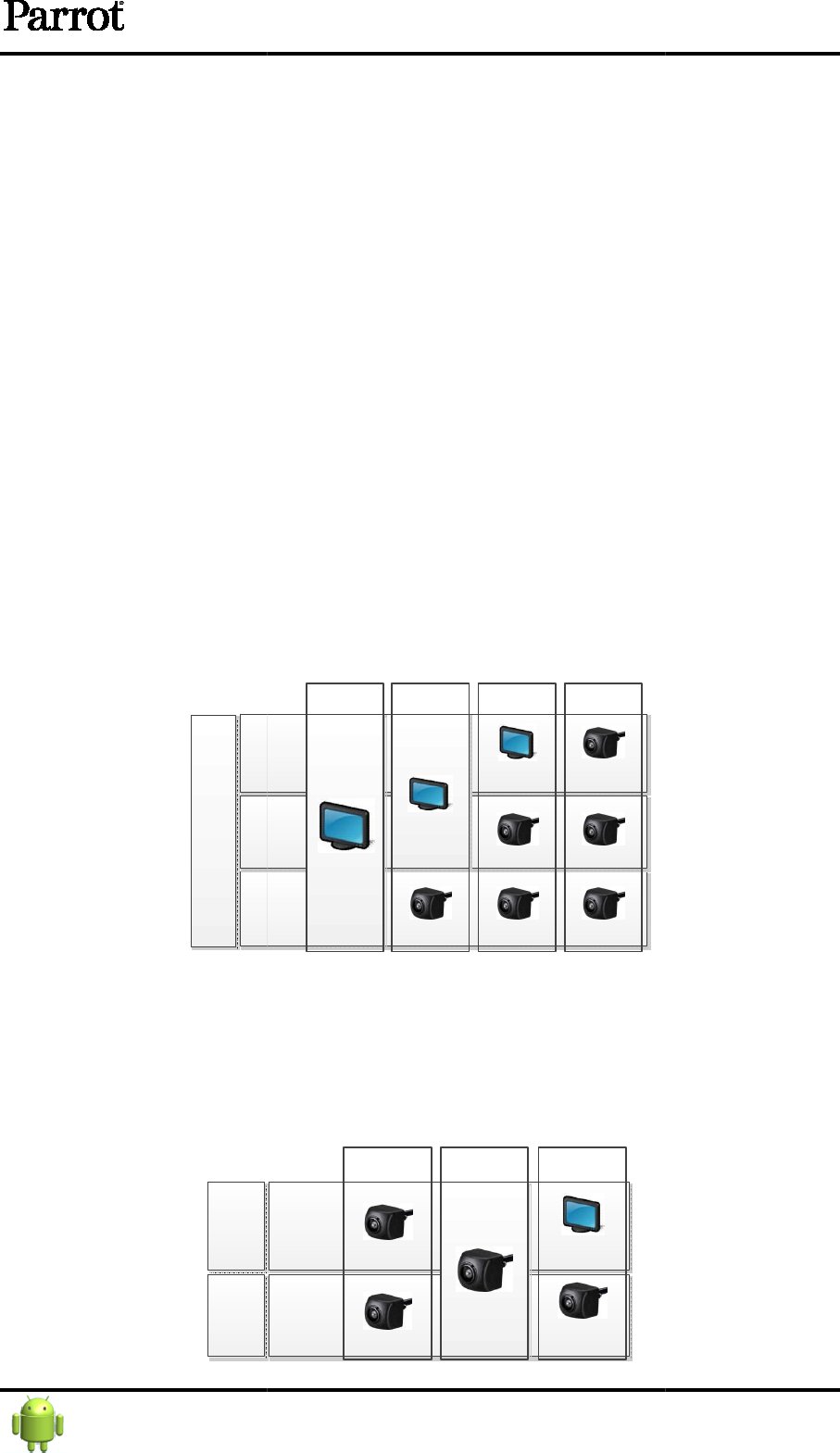
or
16 bits, ITU_656 & ITU_601, 1080p
(When CAM_0 is on 16 bits interface, CAM_1 cannot be used)
• CAM_1:
8 bits, ITU_656 & ITU_601, 720p
• CAM_5:
8 bits, ITU_656 & ITU_601, 720p
• CAM_2, CAM_3 and
CAM_4
8 bits, ITU_656, 720p
5.3.11.3
Display and record interface option.
The i
nput/ouput video interfaces are
1.1.4 Pinout Table)
• LCD_1 :
Many display and record interface option are available:
Config #1
: LCD 24 bits (1080p)
Config #2
: LCD 16 bits (1080p) + CAM 8 bits (720p)
Config #3
: LCD 8 bits (720p) + 2 x CAM 8 bits (720p)
Config #4
: 3 x CAM 8 bits (720p)
ITU
8
ITU
8
ITU
8
LCD_1
• CAM_0 and CAM_1 :
Many display and record interface
Config #a
: 2 x CAM 8 bits (720p)
Config #b
: 1 x CAM 16 bits (1080p)
Config #c
: LCD 8 bits (720p) + CAM 8 bits (720p)
CAM_0 can be used on ITU601.
CAM_0
CAM_1
Confidential Information
16 bits, ITU_656 & ITU_601, 1080p
(When CAM_0 is on 16 bits interface, CAM_1 cannot be used)
8 bits, ITU_656 & ITU_601, 720p
8 bits, ITU_656 & ITU_601, 720p
CAM_4
(when LCD_1 is not used)
Display and record interface option.
nput/ouput video interfaces are
multiplexed
on the main FC7100 connector. (See paragraph:
Many display and record interface option are available:
: LCD 24 bits (1080p)
: LCD 16 bits (1080p) + CAM 8 bits (720p)
: LCD 8 bits (720p) + 2 x CAM 8 bits (720p)
: 3 x CAM 8 bits (720p)
24 bits
ITU
656
bits
ITU
656
bits
ITU
656
bits
8 bits
8 bits
8 bits 8 bits
Config #1 Config #2 Config #3
16 bits
Config #4
8 bits
8 bits
8 bits
Many display and record interface
option are available:
: 2 x CAM 8 bits (720p)
: 1 x CAM 16 bits (1080p)
: LCD 8 bits (720p) + CAM 8 bits (720p)
ITU 656
8 bits
ITU656
8 bits
8 bits
16 bits
Config #a Config #b Config #c
8 bits
8 bits
8 bits
29/39
Ref: OEM-2012-149
on the main FC7100 connector. (See paragraph:
option are available:
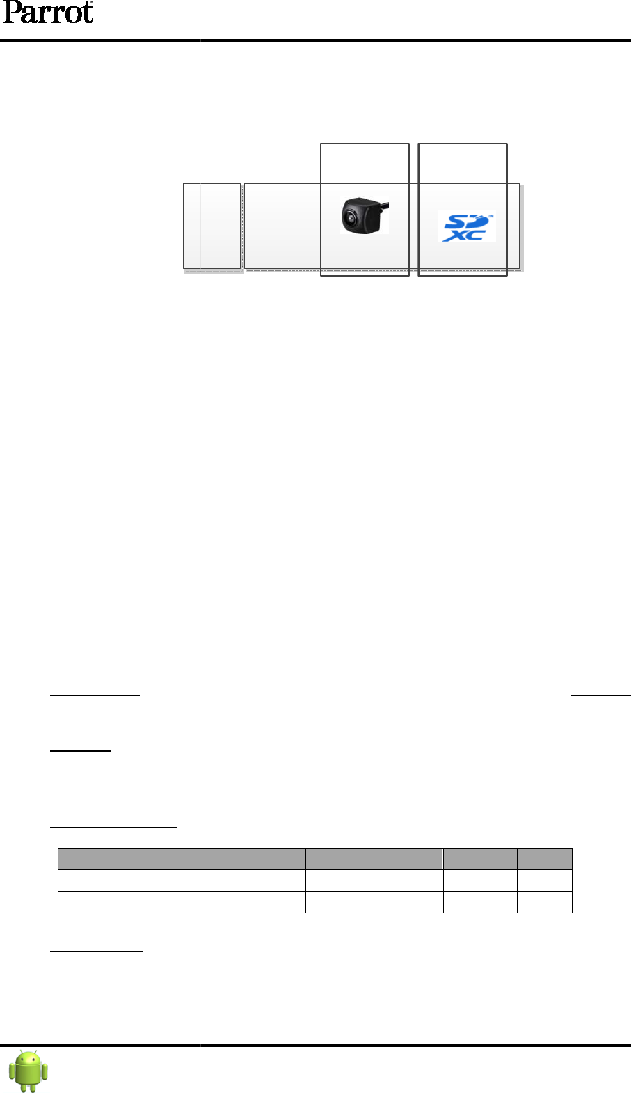
• CAM_5 :
Config #α
: 1 x CAM 8 bits (720p)
Config #β
: 1 x SDIO interface (SD XC compatible)
CAM
In summary, all option
s are below
•
LCD 24 bits (1080p) + 3xCAM 8 bits (720p)
•
LCD 24 bits (1080p) + LCD 8 bits (720p) + 2xCAM 8 bits (720p)
•
LCD 24 bits (1080p) + CAM 16 bits (1080p) +
•
LCD 16 bits (1080p) + 4 x CAM 8 bits (720p)
•
LCD 16 bits (1080p) + CAM 16 bits (1080p) + 2 x CAM 8 bits (720p)
•
LCD 16 bits (1080p) + LCD 8 bits (720p) + 3 x CAM 8 bits (720p)
•
LCD 8 bits (720p) + 5 x CAM 8 bits (720p)
•
LCD 8 bits (720p) + C
•
LCD 8 bits (720p) + LCD 8 bits (720p) + 4 x CAM8 bits (720p)
•
6 x CAM 8 bits (720p)
•
CAM 16 bits (1080p) + 4 x CAM 8 bits (720p)
5.3.12 IO configuration
The GPIO interface
provides programmable general input/output conf
available on any edge or polarity event. Each source can be selected among all the GPIOs.
Each pads have programmable :
• Drive strength
: can be programmed from 2.93mA to 17.24mA during pull
16.17mA during pull down
.
• Slew Rate
: The slew rate is defined as the maximum rate of change of the out
• Keeper
: enable or disable keeper mode. Holds last value on a tri
• Pull-down or Pull-up
: active an internal pull
Parameter
Pull Up impedance
Pull Down impedance
• Schmitt trigger
: enable or disable Schmitt Trigger.
Confidential Information
: 1 x CAM 8 bits (720p)
: 1 x SDIO interface (SD XC compatible)
ITU 656
8 bits
CAM
_5
8 bits
Config #α Config #β
s are below
:
LCD 24 bits (1080p) + 3xCAM 8 bits (720p)
LCD 24 bits (1080p) + LCD 8 bits (720p) + 2xCAM 8 bits (720p)
LCD 24 bits (1080p) + CAM 16 bits (1080p) +
CAM 8 bits (720p)
LCD 16 bits (1080p) + 4 x CAM 8 bits (720p)
LCD 16 bits (1080p) + CAM 16 bits (1080p) + 2 x CAM 8 bits (720p)
LCD 16 bits (1080p) + LCD 8 bits (720p) + 3 x CAM 8 bits (720p)
LCD 8 bits (720p) + 5 x CAM 8 bits (720p)
LCD 8 bits (720p) + C
AM 16 bits (1080p) + 3 x CAM 8 bits (720p)
LCD 8 bits (720p) + LCD 8 bits (720p) + 4 x CAM8 bits (720p)
6 x CAM 8 bits (720p)
CAM 16 bits (1080p) + 4 x CAM 8 bits (720p)
provides programmable general input/output conf
igurable. Interrupt lines
available on any edge or polarity event. Each source can be selected among all the GPIOs.
: can be programmed from 2.93mA to 17.24mA during pull
.
: The slew rate is defined as the maximum rate of change of the out
: enable or disable keeper mode. Holds last value on a tri
-
state bus.
: active an internal pull
-down or pull-up.
Min.
Typ
Max.
27
30 34
27
30 34
: enable or disable Schmitt Trigger.
30/39
Ref: OEM-2012-149
igurable. Interrupt lines
available on any edge or polarity event. Each source can be selected among all the GPIOs.
: can be programmed from 2.93mA to 17.24mA during pull
-up and 2.68mA to
: The slew rate is defined as the maximum rate of change of the out
put voltage.
state bus.
Unit
kOhm
KOhm
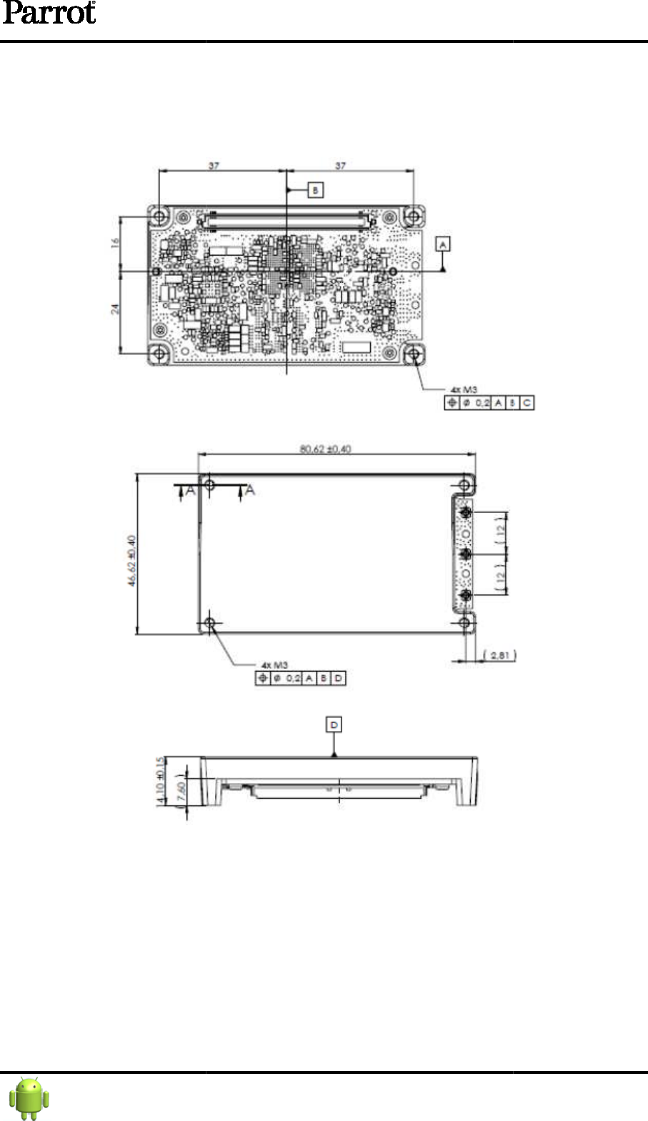
6 Mechanical
6.1 Outline dimensions
Weight: 51 g
Confidential Information
31/39
Ref: OEM-2012-149
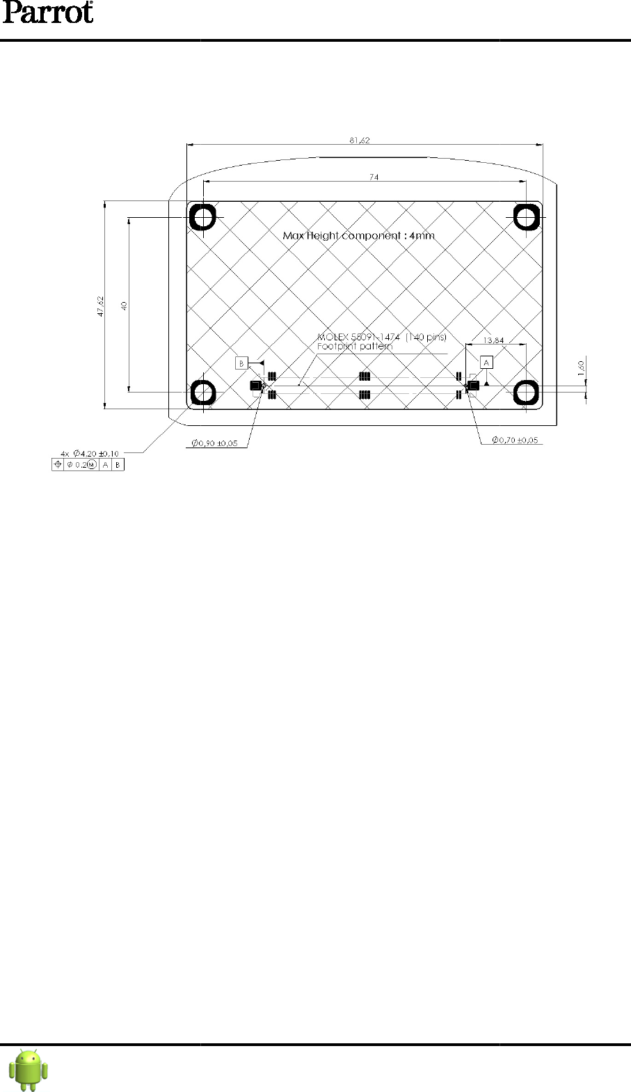
6.2
Motherboard PCB layout
The module’s interface is made through a 140
•
6.3 Connectors
6.3.1
FC7100 Main connector
The module’s interface with host systems is made through a 140
0.635mm pitch.
•
Module connector reference: MOLEX 52885
•
Motherboard connector’s
Confidential Information
Motherboard PCB layout
The module’s interface is made through a 140
-
pin board to board connector with a
FC7100 Main connector
The module’s interface with host systems is made through a 140
-
pin board to board connector with a
Module connector reference: MOLEX 52885
-1474
Motherboard connector’s
reference: MOLEX 55091- 1474
32/39
Ref: OEM-2012-149
pin board to board connector with a
0,635 mm pitch
pin board to board connector with a
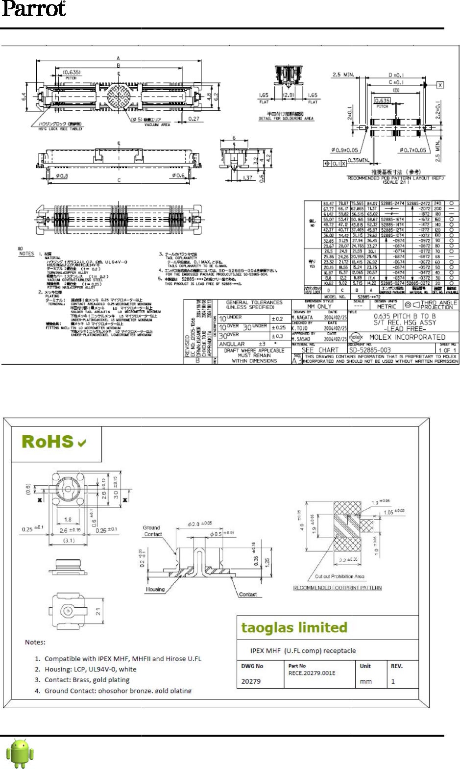
6.3.2 BT, WLAN and GPS
external antenna connector
Theses RF connectors are of
Confidential Information
external antenna connector
s
Theses RF connectors are of
ultra-small coaxial type:
33/39
Ref: OEM-2012-149
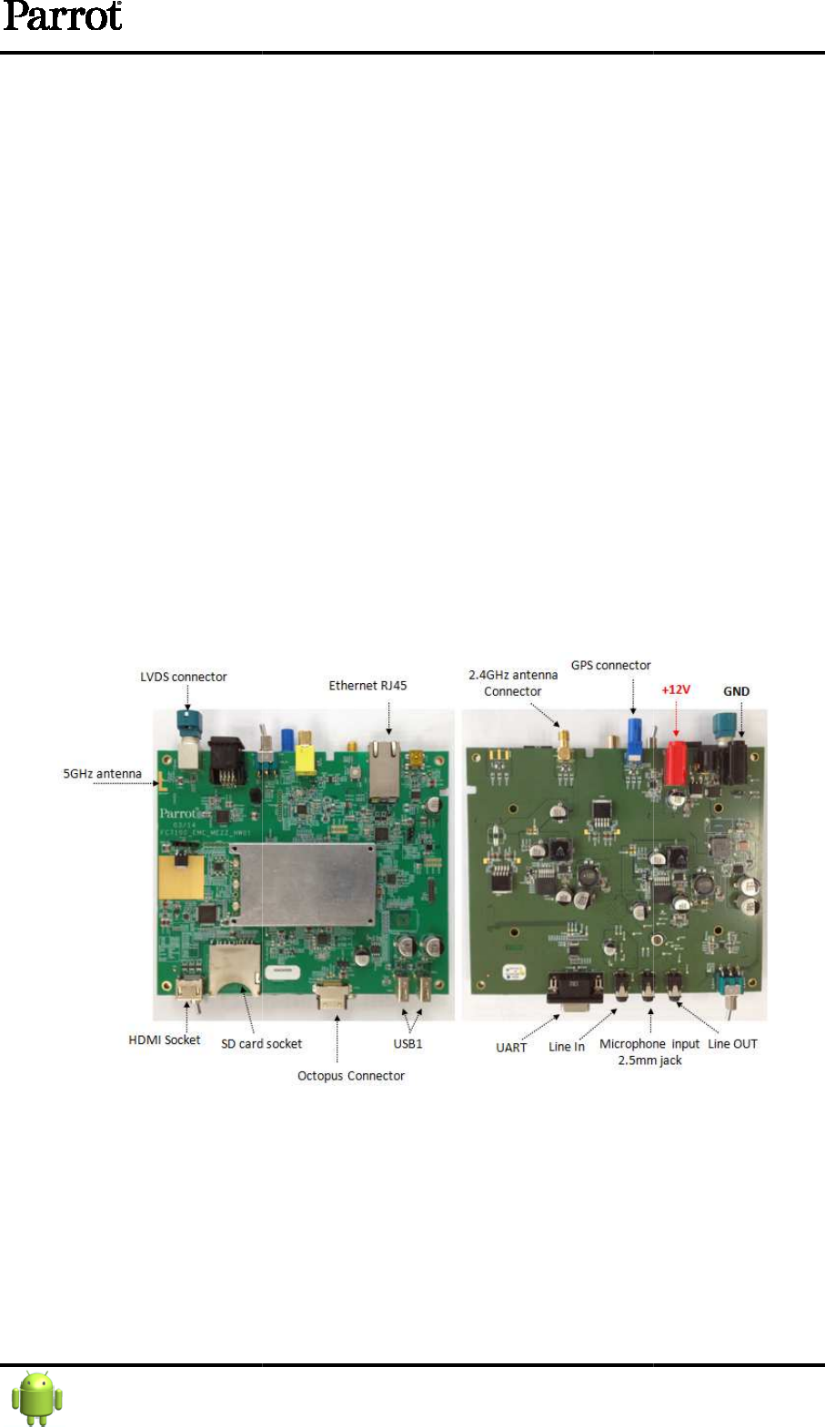
6.4
Thermal integration guidelines (TBC)
The local maximum ambient air temperature (T
dissipation system (example:
heatsink)
(θsa is the
thermal resistance thermal dissipation system to ambient)
Thermal interface materials (TIM), which are used between the thermal dissipation system and the
interface casing, can be of many kinds, i
materials, and special thermoplastic adhesives.
Thermal dissipation system can be attached directly to the interface casing with using M3 hole
fixation on the top of casing.
7 Available Tools
7.1 Workbench
Confidential Information
Thermal integration guidelines (TBC)
The local maximum ambient air temperature (T
amb max
= 85°C) can be supported by thermal
heatsink)
with:
θ
θθ
θsa ≤
≤≤
≤ 1 °C/W
thermal resistance thermal dissipation system to ambient)
Thermal interface materials (TIM), which are used between the thermal dissipation system and the
interface casing, can be of many kinds, i
ncluding greases, gels, adhesives, tapes, silicon rubber
materials, and special thermoplastic adhesives.
Thermal dissipation system can be attached directly to the interface casing with using M3 hole
34/39
Ref: OEM-2012-149
= 85°C) can be supported by thermal
Thermal interface materials (TIM), which are used between the thermal dissipation system and the
ncluding greases, gels, adhesives, tapes, silicon rubber
Thermal dissipation system can be attached directly to the interface casing with using M3 hole
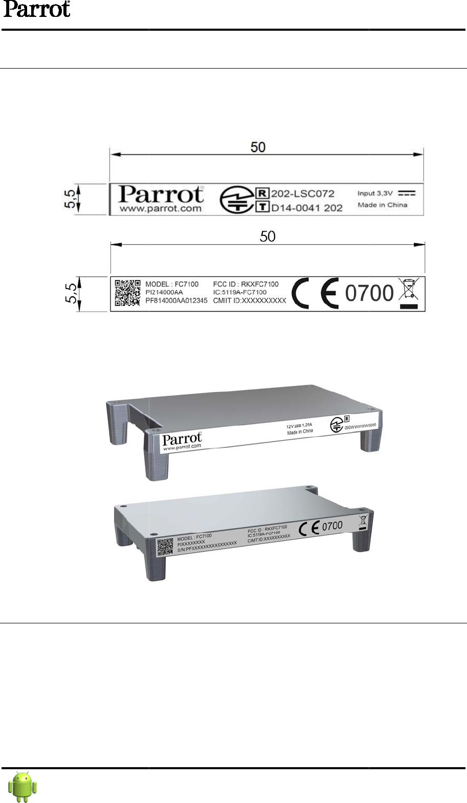
8 Marking
8.1 Module Marking
8.1.1 Label
8.1.2
Position and Orientation on m
9 Caution for use
9.1 ESD Compliance
Operator must use ESD protection gloves for Module Manipulation. In case of electrical
discharge, Module must be scrapped
9.2 Safety
Mechanical shield is made of metal and have several draft angle
cause Human injuries. Operator must be trained on how to manipulate it.
Confidential Information
Position and Orientation on m
odule
Operator must use ESD protection gloves for Module Manipulation. In case of electrical
discharge, Module must be scrapped
.
Mechanical shield is made of metal and have several draft angle
on RF connectors
cause Human injuries. Operator must be trained on how to manipulate it.
35/39
Ref: OEM-2012-149
Operator must use ESD protection gloves for Module Manipulation. In case of electrical
on RF connectors
which can

9.3 Assembly
Key mechanical dimensions are tested before shipment.
In case of manual ha
ndling or operation, to avoid any issue with mechanical distance between
legs and ensure a good insertion in the host side, packaging has been designed to ensure that
operator will pick up the part by the most adequate area of the module. Operator should b
trained and alerted about this specific behavior.
9.4 Drop
In case the part drop to the floor, Parrot doesn’t warrant the part. Part has to be scrapped.
Same process applies in our manufacturing site.
Confidential Information
Key mechanical dimensions are tested before shipment.
ndling or operation, to avoid any issue with mechanical distance between
legs and ensure a good insertion in the host side, packaging has been designed to ensure that
operator will pick up the part by the most adequate area of the module. Operator should b
trained and alerted about this specific behavior.
In case the part drop to the floor, Parrot doesn’t warrant the part. Part has to be scrapped.
Same process applies in our manufacturing site.
36/39
Ref: OEM-2012-149
ndling or operation, to avoid any issue with mechanical distance between
legs and ensure a good insertion in the host side, packaging has been designed to ensure that
operator will pick up the part by the most adequate area of the module. Operator should b
e
In case the part drop to the floor, Parrot doesn’t warrant the part. Part has to be scrapped.

10
APPROVAL / CERTIFICATIonS
10.1 Normative
informations
F7100
module certifications identifications :
CERTIFICATION
ID
Bluetooth
QD ID:
CE
CE 0700
FCC
RKXFCC
IC
5119A
TELEC
R
: 202
-
T
: D 14
10.2
FCC and IC requirements for module application
Identifications:
FCC ID: RKXFC7100
IC : 5119A-FC7100
In acco
rdance with FCC Part 15, the FC
USA – User information
This intends to inform how to specify the FCC ID of our module “FC
Based on the Public Notice from FCC, the host devic
contains our module.
The label should use wording such as: “Contains FCC ID: RKXFC
expresses the same meaning may be used.
The label of the host device should also include the bel
possible, this information should be included in the
“
This device complies with part 15 of the FCC rules. Operation is subject to the following two
conditions.
(1) This device may not cause h
(2) This device must accept any interference received, including interference that may cause
undesired operation.
Caution: Changes or modifications not expressly approved by the party responsible for
compliance could void the user’s aut
This equipment has been tested and found to comply with the limits for a class B digital device,
pursuant to part 15 of the FCC Rules. These limits are designed to provide a reasonable
protection against harmful interferenc
uses and can radiate radio frequency energy and, if not installed and uses in accordance with the
instructions, may cause harmful interference to radio communications. However, there is no
guarante
e that interference will not occur in a particular installation. If this equipment does
Confidential Information
APPROVAL / CERTIFICATIonS
informations
module certifications identifications :
QD ID:
CE 0700
RKXFCC
7100
5119A
-FC7100
-
LSC072
: D 14
-0041 202
FCC and IC requirements for module application
rdance with FCC Part 15, the FC
7
100 is listed as a limited Modular Transmitter device.
This intends to inform how to specify the FCC ID of our module “FC
7
100” on the final product:
Based on the Public Notice from FCC, the host devic
e should have a label which indicates that it
The label should use wording such as: “Contains FCC ID: RKXFC
7
100”. Any similar wording that
expresses the same meaning may be used.
The label of the host device should also include the bel
ow FCC statements When it is not
possible, this information should be included in the
User Manual of the host device
This device complies with part 15 of the FCC rules. Operation is subject to the following two
(1) This device may not cause h
armful interference
(2) This device must accept any interference received, including interference that may cause
Caution: Changes or modifications not expressly approved by the party responsible for
compliance could void the user’s aut
hority to operate the equipment.
This equipment has been tested and found to comply with the limits for a class B digital device,
pursuant to part 15 of the FCC Rules. These limits are designed to provide a reasonable
protection against harmful interferenc
e in a residential installation. This equipment generates,
uses and can radiate radio frequency energy and, if not installed and uses in accordance with the
instructions, may cause harmful interference to radio communications. However, there is no
e that interference will not occur in a particular installation. If this equipment does
37/39
Ref: OEM-2012-149
100 is listed as a limited Modular Transmitter device.
100” on the final product:
e should have a label which indicates that it
100”. Any similar wording that
ow FCC statements When it is not
User Manual of the host device
:
This device complies with part 15 of the FCC rules. Operation is subject to the following two
(2) This device must accept any interference received, including interference that may cause
Caution: Changes or modifications not expressly approved by the party responsible for
This equipment has been tested and found to comply with the limits for a class B digital device,
pursuant to part 15 of the FCC Rules. These limits are designed to provide a reasonable
e in a residential installation. This equipment generates,
uses and can radiate radio frequency energy and, if not installed and uses in accordance with the
instructions, may cause harmful interference to radio communications. However, there is no
e that interference will not occur in a particular installation. If this equipment does

cause harmful interference to radio or television reception, wich can be determined by turning
the equipment off and on, the user is encouraged to try to correct the in
more of the following measures:
1)
Reorient or relocate the receiving antenna
2)
Increase the separation between the equipment and the receiver
3)
Connect the equipment into a an outlet on a circuit different from that to which the receiver is
connected
Consult the dealer or an experienced radio/TV technician for help
CANADA –
User information
This intends to inform how to specify the Industry Canada (IC) ID of our module “FC
final product:
According to Canadian standards “RSS
which indicates that it contains our module. The label should use wording such as: “Contains IC
ID: 5119A-FC7
100”. Any similar wording that expresses the same meaning may be used.
The label of the host
device should also include the below IC statements. When it is not possible,
this information should be included in the User Manual of the host device:
[English]
“This device complies with Industry Canada licence
to the following two conditions:
(1) This device may not cause interference, and
(2) This device must accept any interference, including interference that may cause undesired
operation of the device.
This equipment complies with IC RF radiation exposure li
environment. The antenna(s) used for this transmitter must be installed and operated to provide a
separation distance of at least 20 cm from all persons, and must not be co
conjunction with any othe
r antenna or transmitter.
separation distance of
at least 20 cm
[French]
«
Le présent appareil est conforme aux CNR d'Industrie Canada applicables aux apparei
exempts de licence.
L'exploitation est autorisée aux deux conditions suivantes :
(1) L’appareil ne doit pas produire de brouillage, et
(2)
L’utilisateur de l'appareil doit accepter tout brouillage radioélectrique subi, même si le
brouillage est
susceptible d'en compromettre le fonctionnement
Cet appareil est conforme aux limites d’exposition au
utilisation dans un environnement non contrôlé. Les antennes utilisées pour cet émetteur doivent être
instal
lées et doivent fonctionner à au moins 20 cm de distance des utilisateurs
placées près d’autres antennes ou émetteurs
installateurs / intégrateurs
doivent s’assurer qu’une distance de
ses antennes des utilisateurs. »
Confidential Information
cause harmful interference to radio or television reception, wich can be determined by turning
the equipment off and on, the user is encouraged to try to correct the in
more of the following measures:
Reorient or relocate the receiving antenna
Increase the separation between the equipment and the receiver
Connect the equipment into a an outlet on a circuit different from that to which the receiver is
Consult the dealer or an experienced radio/TV technician for help
.”
User information
This intends to inform how to specify the Industry Canada (IC) ID of our module “FC
According to Canadian standards “RSS
-210” and “RSS-
Gen”, the host device should have a label
which indicates that it contains our module. The label should use wording such as: “Contains IC
100”. Any similar wording that expresses the same meaning may be used.
device should also include the below IC statements. When it is not possible,
this information should be included in the User Manual of the host device:
“This device complies with Industry Canada licence
-
exempt RSS standards.
to the following two conditions:
(1) This device may not cause interference, and
(2) This device must accept any interference, including interference that may cause undesired
This equipment complies with IC RF radiation exposure li
mits set forth for an uncontrolled
environment. The antenna(s) used for this transmitter must be installed and operated to provide a
separation distance of at least 20 cm from all persons, and must not be co
-
located or operated in
r antenna or transmitter.
Installers / integrators
must ensure
at least 20 cm
exists between the device and its antenna
and
Le présent appareil est conforme aux CNR d'Industrie Canada applicables aux apparei
L'exploitation est autorisée aux deux conditions suivantes :
(1) L’appareil ne doit pas produire de brouillage, et
L’utilisateur de l'appareil doit accepter tout brouillage radioélectrique subi, même si le
susceptible d'en compromettre le fonctionnement
»
Cet appareil est conforme aux limites d’exposition au
x rayonnement
s RF stipulées par
utilisation dans un environnement non contrôlé. Les antennes utilisées pour cet émetteur doivent être
lées et doivent fonctionner à au moins 20 cm de distance des utilisateurs
,
et ne doivent pas être
placées près d’autres antennes ou émetteurs
, ou fonctionner
en conjonction
doivent s’assurer qu’une distance de
20 cm
au moins
38/39
Ref: OEM-2012-149
cause harmful interference to radio or television reception, wich can be determined by turning
the equipment off and on, the user is encouraged to try to correct the in
terference by one or
Connect the equipment into a an outlet on a circuit different from that to which the receiver is
This intends to inform how to specify the Industry Canada (IC) ID of our module “FC
7100” on the
Gen”, the host device should have a label
which indicates that it contains our module. The label should use wording such as: “Contains IC
100”. Any similar wording that expresses the same meaning may be used.
device should also include the below IC statements. When it is not possible,
exempt RSS standards.
Operation is subject
(2) This device must accept any interference, including interference that may cause undesired
mits set forth for an uncontrolled
environment. The antenna(s) used for this transmitter must be installed and operated to provide a
located or operated in
must ensure
that a
and
users.
Le présent appareil est conforme aux CNR d'Industrie Canada applicables aux apparei
ls radio
L'exploitation est autorisée aux deux conditions suivantes :
L’utilisateur de l'appareil doit accepter tout brouillage radioélectrique subi, même si le
s RF stipulées par
IC pour une
utilisation dans un environnement non contrôlé. Les antennes utilisées pour cet émetteur doivent être
et ne doivent pas être
en conjonction
avec ceux-ci. Les
au moins
sépare l’appareil et

10.3
Japanese Radio Law and Japanese Telecommunications Business Law
Compliance.
This device is granted pursuant to the Japanese Radio Law (
and the Japanese Telecommunications Business Law (
This device should not be modified (otherwise the granted designation number will
Identifications:
R : 202-LSC072
T : D 14-0041 202
Confidential Information
Japanese Radio Law and Japanese Telecommunications Business Law
This device is granted pursuant to the Japanese Radio Law (
電波法)
and the Japanese Telecommunications Business Law (
電気通信事業法)
This device should not be modified (otherwise the granted designation number will
39/39
Ref: OEM-2012-149
Japanese Radio Law and Japanese Telecommunications Business Law
This device should not be modified (otherwise the granted designation number will
become invalid)