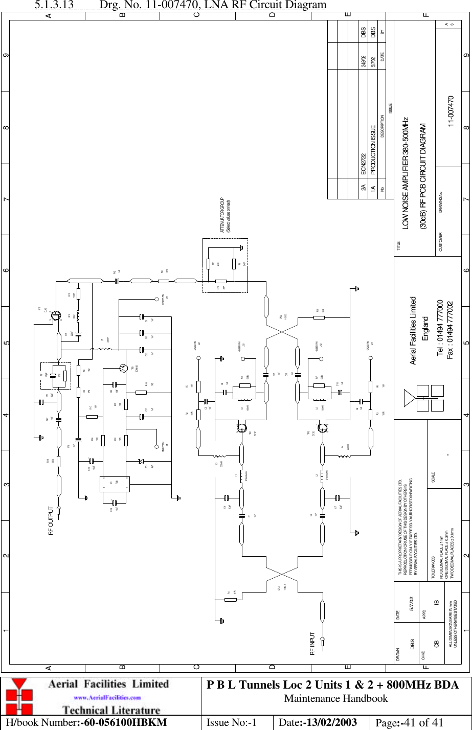
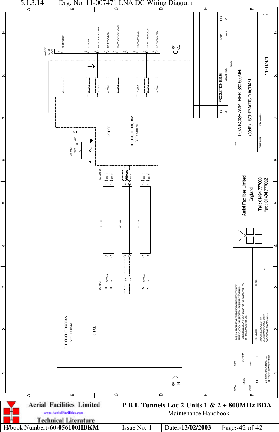
PBE Europe as Axell Wireless CCE-800N2 800MHz Signal Enhancer User Manual Manual
Axell Wireless 800MHz Signal Enhancer Manual
UserManual.wiki
>
PBE Europe as Axell Wireless
>
CCE 800N2 User Manual
Manual
Navigation menu
Upload a User Manual
Namespaces
Wiki Guide
HTML
PDF
Info
Views
User Manual
Discussion / Help
Navigation
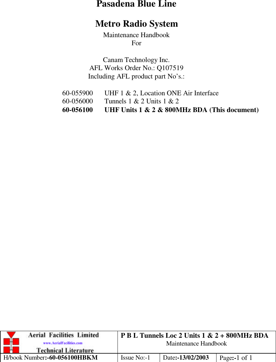
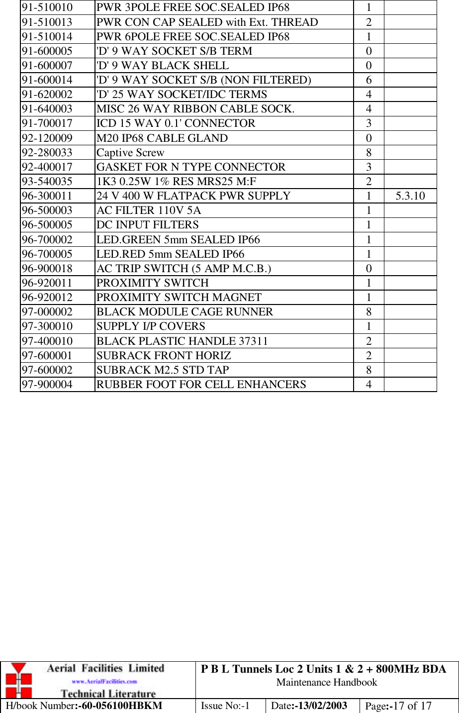
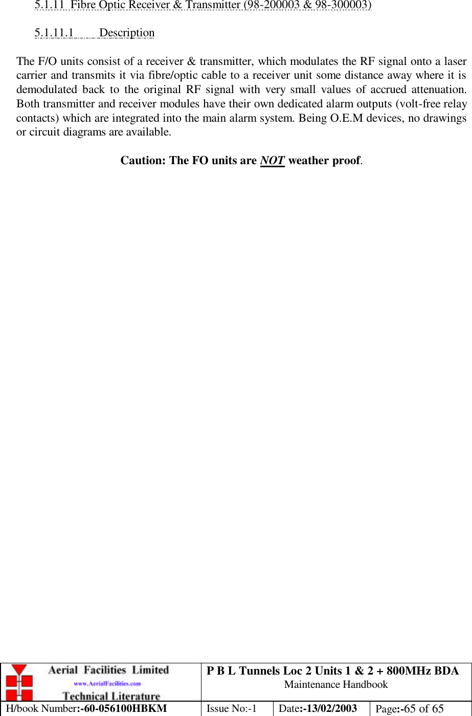
![P B L Tunnels Loc 2 Units 1 & 2 + 800MHz BDA Maintenance Handbook H/book Number:-60-056100HBKM Issue No:-1 Date:-13/02/2003 Page:-24 of 24 4. SYSTEM DRAWINGS 4.1 Drg. No. 60-056190, Location 2 Unit 1 Case Outline Drawing PASADENA BLUE LINE. LOCATION 2. BDA 470/473MHz. OUTLINE DRAWING60-0561901A1:8DBS 15/10/02250 [9.9"]620 [2'-0.4"]LOCKABLE DOORCATCHvoltageHighDANGERHeavyCAUTION500 [1'-7.7"]CE- / - NProduct ref :BPA 470/473MHzAerial FacilitiesLimitedBYDATEDESCRIPTIONNoISSUE1 2 345678 9ABCDEF1 2 3 4 5 6 7 8 9ABCDEFFax : 01494 777002Fax : 01494 777000Aerial Facilities LimitedTHIS IS A PROPRIETARY DESIGN OF AERIAL FACILITIES LTD.REPRODUCTION OR USE OF THIS DESIGN BY OTHERS ISPERMISSIBLE ONLY IF EXPRESSLY AUTHORISED IN WRITINGBY AERIAL FACILITIES LTD.NO DECIMAL PLACE ± 1mmONE DECIMAL PLACE ± 0.3mmTWO DECIMAL PLACES ± 0.1mmALL DIMENSIONS ARE IN mmUNLESS OTHERWISE STATEDCHKDDRAWN APPDDATETOLERANCES SCALEEnglandCUSTOMER DRAWING.NoTITLE3APRODUCTION ISSUE15/10/02DBS420 [1'-4.5"]709 [2'-3.9"]483MHz OUTPUTM6 EARTH STUD115V AC INPUTMATERIAL: MILD STEELFINISH: PAINTED TO RAL 9017 WALL FIXINGS: M8 (5/16")RF CONNECTORS: N TYPE FEMALEENVIRONMENTAL CLASS.: IP65SEMI-GLOSS TRAFFIC BLACK467 [1'-6.4"]460 [1'-6.1"]470/473MHz INPUT/OUTPUT485/486MHz INPUTCABLE GLANDS (FIBRE OPTICS)PSU ALARMDBSDECIMAL EQUIV'S21/10/021BDBSECN27472A30/10/02ALARMSPB GD](https://usermanual.wiki/PBE-Europe-as-Axell-Wireless/CCE-800N2/User-Guide-304830-Page-24.png)
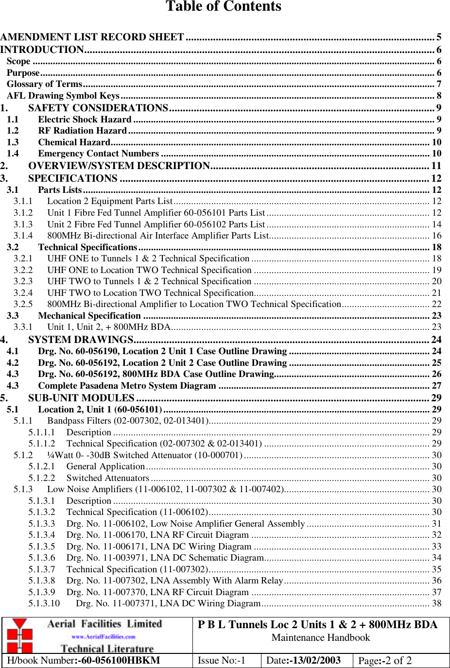
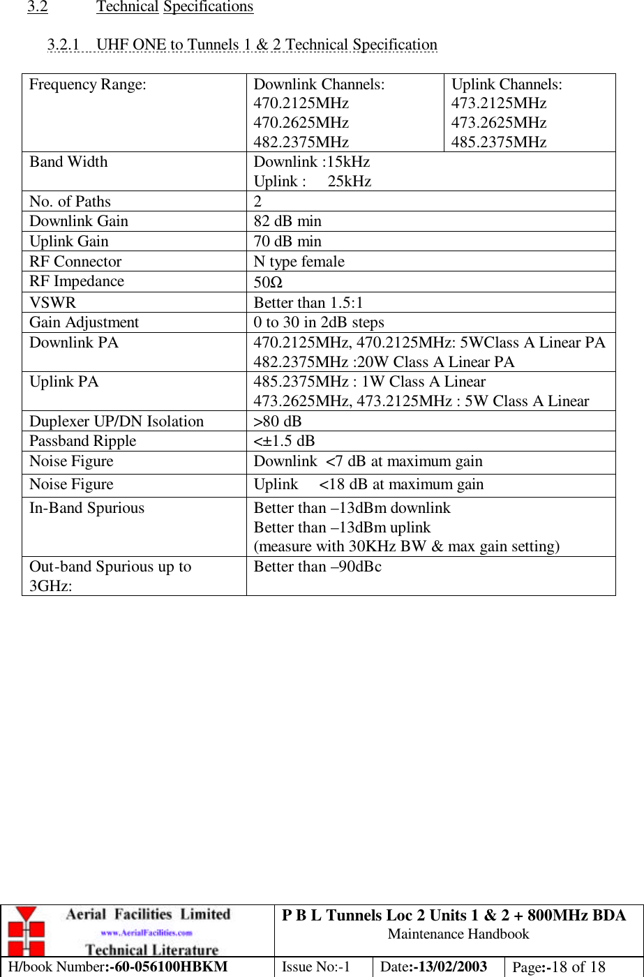
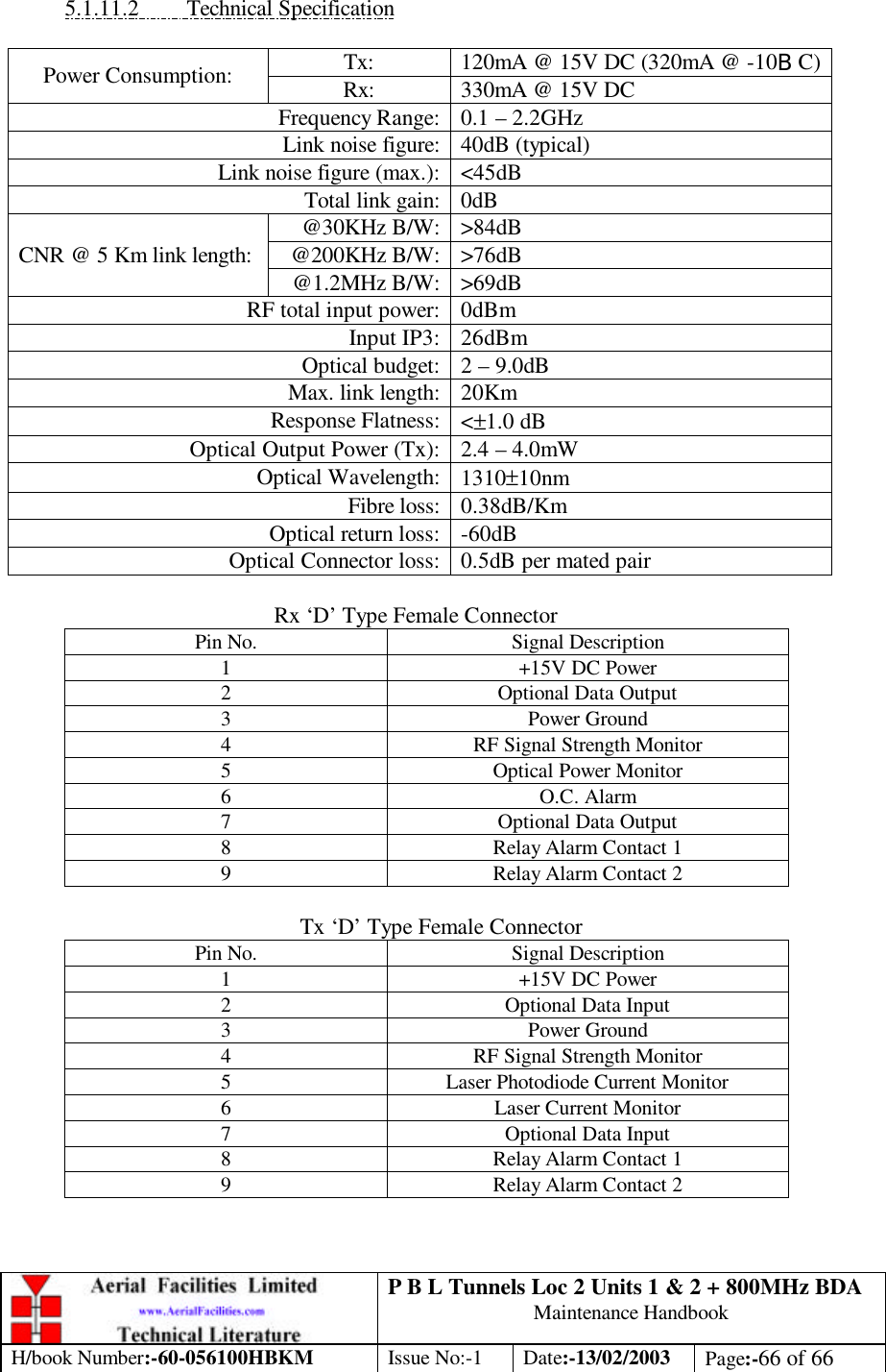
![P B L Tunnels Loc 2 Units 1 & 2 + 800MHz BDA Maintenance Handbook H/book Number:-60-056100HBKM Issue No:-1 Date:-13/02/2003 Page:-25 of 25 4.2 Drg. No. 60-056192, Location 2 Unit 2 Case Outline Drawing PASADENA BLUE LINE. LOCATION 2. BDA 483/485MHz. OUTLINE DRAWING60-0561911A1:8DBS 15/10/02250 [9.9"]620 [2'-0.4"]LOCKABLE DOORCATCHvoltageHighDANGERHeavyCAUTION500 [1'-7.7"]CE- / - NProduct ref :BPA 483/485MHzAerial FacilitiesLimitedBYDATEDESCRIPTIONNoISSUE1 2 345678 9ABCDEF1 2 3 4 5 6 7 8 9ABCDEFFax : 01494 777002Fax : 01494 777000Aerial Facilities LimitedTHIS IS A PROPRIETARY DESIGN OF AERIAL FACILITIES LTD.REPRODUCTION OR USE OF THIS DESIGN BY OTHERS ISPERMISSIBLE ONLY IF EXPRESSLY AUTHORISED IN WRITINGBY AERIAL FACILITIES LTD.NO DECIMAL PLACE ± 1mmONE DECIMAL PLACE ± 0.3mmTWO DECIMAL PLACES ± 0.1mmALL DIMENSIONS ARE IN mmUNLESS OTHERWISE STATEDCHKDDRAWN APPDDATETOLERANCES SCALEEnglandCUSTOMER DRAWING.NoTITLE3APRODUCTION ISSUE15/10/02DBS420 [1'-4.5"]709 [2'-3.9"]M6 EARTH STUD115V AC INPUTMATERIAL: MILD STEELFINISH: PAINTED TO RAL 9017 WALL FIXINGS: M8 (5/16")RF CONNECTORS: N TYPE FEMALEENVIRONMENTAL CLASS.: IP65SEMI-GLOSS TRAFFIC BLACK467 [1'-6.4"]497 [1'-7.6"]PSU ALARMDBSDECIMAL EQUIV'S21/10/021BLCX800MHz 485/486MHz OUTPUTVHF483MHz INPUT470/473MHz INPUTDBSECN27472A30/10/02ALARMSPB GD](https://usermanual.wiki/PBE-Europe-as-Axell-Wireless/CCE-800N2/User-Guide-304830-Page-25.png)
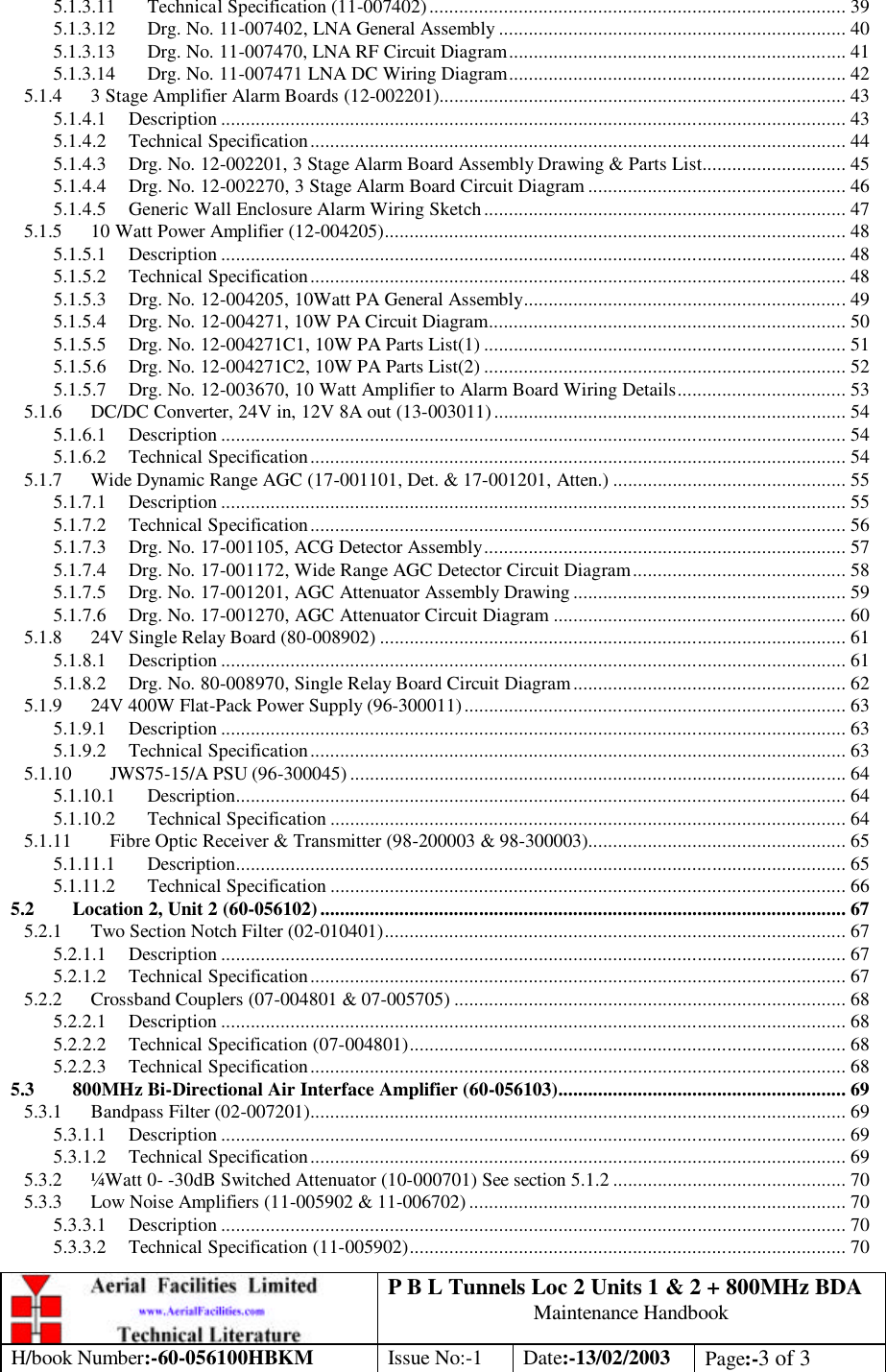
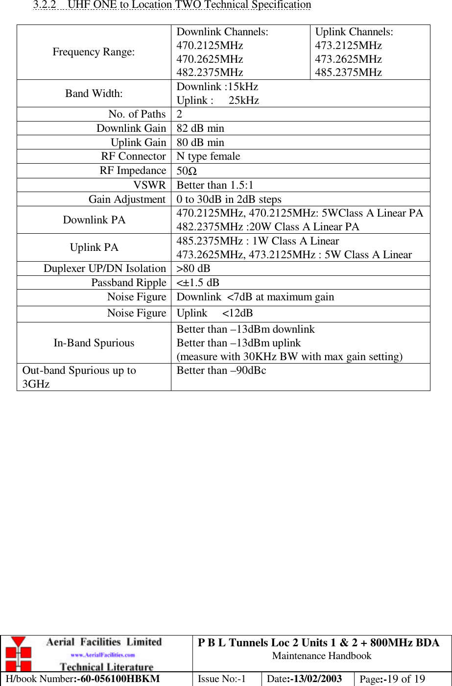
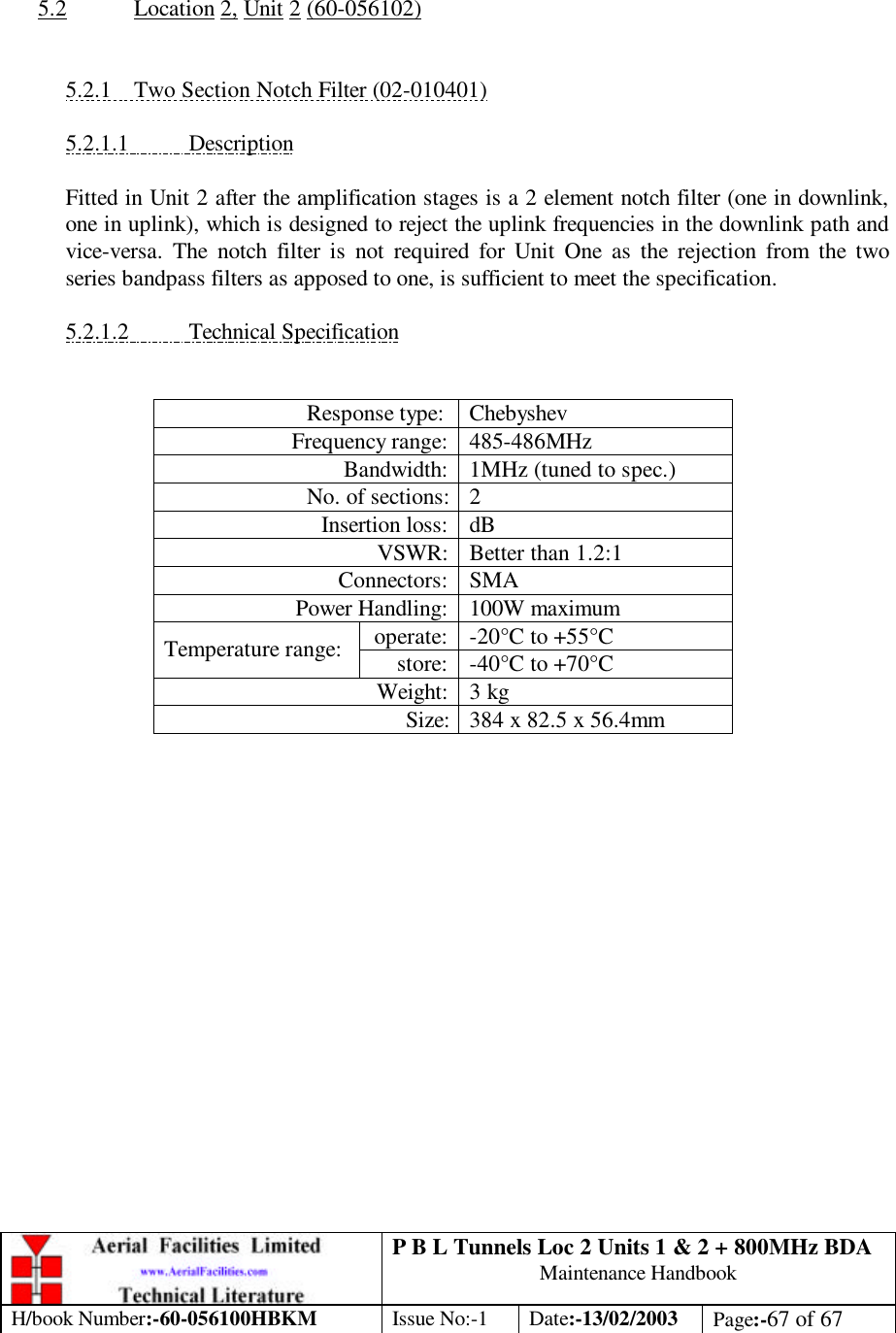
![P B L Tunnels Loc 2 Units 1 & 2 + 800MHz BDA Maintenance Handbook H/book Number:-60-056100HBKM Issue No:-1 Date:-13/02/2003 Page:-26 of 26 4.3 Drg. No. 60-056192, 800MHz BDA Case Outline Drawing PASADENA BLUE LINE. LOCATION 2. BDA 800MHz. OUTLINE DRAWING60-0561921A1:8DBS 15/10/02250 [9.9"]620 [2'-0.4"]LOCKABLE DOORCATCHvoltageHighDANGERHeavyCAUTION500 [1'-7.7"]CE- / - NProduct ref :BPA 800MHzAerial FacilitiesLimitedBYDATEDESCRIPTIONNoISSUE1 2 345678 9ABCDEF1 2 3 4 5 6 7 8 9ABCDEFFax : 01494 777002Fax : 01494 777000Aerial Facilities LimitedTHIS IS A PROPRIETARY DESIGN OF AERIAL FACILITIES LTD.REPRODUCTION OR USE OF THIS DESIGN BY OTHERS ISPERMISSIBLE ONLY IF EXPRESSLY AUTHORISED IN WRITINGBY AERIAL FACILITIES LTD.NO DECIMAL PLACE ± 1mmONE DECIMAL PLACE ± 0.3mmTWO DECIMAL PLACES ± 0.1mmALL DIMENSIONS ARE IN mmUNLESS OTHERWISE STATEDCHKDDRAWN APPDDATETOLERANCES SCALEEnglandCUSTOMER DRAWING.NoTITLE3APRODUCTION ISSUE15/10/02DBS420 [1'-4.5"]709 [2'-3.9"]M6 EARTH STUD115V AC INPUTMATERIAL: MILD STEELFINISH: PAINTED TO RAL 9017 WALL FIXINGS: M8 (5/16")RF CONNECTORS: N TYPE FEMALEENVIRONMENTAL CLASS.: IP65SEMI-GLOSS TRAFFIC BLACK467 [1'-6.4"]500 [1'-7.7"]PSU ALARMTO ANTENNACONNECTION TO BDAECN274730/10/02DBS2AALARMSPB GD](https://usermanual.wiki/PBE-Europe-as-Axell-Wireless/CCE-800N2/User-Guide-304830-Page-26.png)

![P B L Tunnels Loc 2 Units 1 & 2 + 800MHz BDA Maintenance Handbook H/book Number:-60-056100HBKM Issue No:-1 Date:-13/02/2003 Page:-91 of 91 7.1.2 Downlink Confirm that there is a signal at the expected frequency and strength from the base station. If this is not present then the fault may lay outside the system. To confirm this, inject a downlink frequency signal from a known source at the master site BTS input and check for output at the remote site feeder output. If a signal is not received at the output it will be necessary to follow the downlink path through the system to find a point at which the signal is lost. The expected downlink output for the given input can be found in the end-to-end test specification. 7.1.3 Uplink Testing the uplink involves a similar procedure to the downlink except that the frequencies used are those transmitted by the mobile equipment. 7.1.4 Fault repair Once a faulty component has been identified, a decision must be made on the appropriate course to carry out a repair. A competent engineer can quickly remedy typical faults such as faulty connections or cables. The exceptions to this are cable assemblies connecting bandpass filter assemblies that are manufactured to critical lengths to maintain a 50-ohm system. Care should be taken when replacing cables or connectors to ensure that items are of the correct specification. The repair of component modules such as amplifiers, tuned cavities or bandpass filters will not usually be possible in the field, as they frequently require specialist knowledge and test equipment to ensure correct operation. It is recommended that items of this type are replaced with a spare unit and the faulty unit returned to AFL for repair. If spare parts need to be ordered from AFL, be sure to quote the serial number of the Cell Enhancer/Repeater and the serial number [and frequencies] of the module(s) to be replaced.](https://usermanual.wiki/PBE-Europe-as-Axell-Wireless/CCE-800N2/User-Guide-304830-Page-91.png)