PBE Europe as Axell Wireless CCE-800N2 800MHz Signal Enhancer User Manual Manual
Axell Wireless 800MHz Signal Enhancer Manual
Manual

P B L Tunnels Loc 2 Units 1 & 2 + 800MHz BDA
Maintenance Handbook
H/book Number:-60-056100HBKM Issue No:-1 Date:-13/02/2003 Page:-1 of 1
Pasadena Blue Line
Metro Radio System
Maintenance Handbook
For
Canam Technology Inc.
AFL Works Order No.: Q107519
Including AFL product part No’s.:
60-055900 UHF 1 & 2, Location ONE Air Interface
60-056000 Tunnels 1 & 2 Units 1 & 2
60-056100 UHF Units 1 & 2 & 800MHz BDA (This document)

P B L Tunnels Loc 2 Units 1 & 2 + 800MHz BDA
Maintenance Handbook
H/book Number:-60-056100HBKM Issue No:-1 Date:-13/02/2003 Page:-2 of 2
Table of Contents
AMENDMENT LIST RECORD SHEET...........................................................................................5
INTRODUCTION................................................................................................................................6
Scope ................................................................................................................................................................ 6
Purpose............................................................................................................................................................. 6
Glossary of Terms............................................................................................................................................ 7
AFL Drawing Symbol Keys............................................................................................................................. 8
1. SAFETY CONSIDERATIONS.................................................................................................9
1.1 Electric Shock Hazard ........................................................................................................................ 9
1.2 RF Radiation Hazard.......................................................................................................................... 9
1.3 Chemical Hazard............................................................................................................................... 10
1.4 Emergency Contact Numbers ........................................................................................................... 10
2. OVERVIEW/SYSTEM DESCRIPTION................................................................................ 11
3. SPECIFICATIONS .................................................................................................................12
3.1 Parts Lists.......................................................................................................................................... 12
3.1.1 Location 2 Equipment Parts List...................................................................................................... 12
3.1.2 Unit 1 Fibre Fed Tunnel Amplifier 60-056101 Parts List .................................................................12
3.1.3 Unit 2 Fibre Fed Tunnel Amplifier 60-056102 Parts List .................................................................14
3.1.4 800MHz Bi-directional Air Interface Amplifier Parts List................................................................ 16
3.2 Technical Specifications.................................................................................................................... 18
3.2.1 UHF ONE to Tunnels 1 & 2 Technical Specification ....................................................................... 18
3.2.2 UHF ONE to Location TWO Technical Specification ...................................................................... 19
3.2.3 UHF TWO to Tunnels 1 & 2 Technical Specification ...................................................................... 20
3.2.4 UHF TWO to Location TWO Technical Specification...................................................................... 21
3.2.5 800MHz Bi-directional Amplifier to Location TWO Technical Specification................................... 22
3.3 Mechanical Specification .................................................................................................................. 23
3.3.1 Unit 1, Unit 2, + 800MHz BDA....................................................................................................... 23
4. SYSTEM DRAWINGS............................................................................................................24
4.1 Drg. No. 60-056190, Location 2 Unit 1 Case Outline Drawing ........................................................ 24
4.2 Drg. No. 60-056192, Location 2 Unit 2 Case Outline Drawing ........................................................ 25
4.3 Drg. No. 60-056192, 800MHz BDA Case Outline Drawing.............................................................. 26
4.3 Complete Pasadena Metro System Diagram .................................................................................... 27
5. SUB-UNIT MODULES........................................................................................................... 29
5.1 Location 2, Unit 1 (60-056101).......................................................................................................... 29
5.1.1 Bandpass Filters (02-007302, 02-013401)........................................................................................ 29
5.1.1.1 Description .............................................................................................................................. 29
5.1.1.2 Technical Specification (02-007302 & 02-013401) .................................................................. 29
5.1.2 ¼Watt 0- -30dB Switched Attenuator (10-000701) .......................................................................... 30
5.1.2.1 General Application................................................................................................................. 30
5.1.2.2 Switched Attenuators............................................................................................................... 30
5.1.3 Low Noise Amplifiers (11-006102, 11-007302 & 11-007402).......................................................... 30
5.1.3.1 Description .............................................................................................................................. 30
5.1.3.2 Technical Specification (11-006102)........................................................................................ 30
5.1.3.3 Drg. No. 11-006102, Low Noise Amplifier General Assembly ................................................. 31
5.1.3.4 Drg. No. 11-006170, LNA RF Circuit Diagram ....................................................................... 32
5.1.3.5 Drg. No. 11-006171, LNA DC Wiring Diagram ...................................................................... 33
5.1.3.6 Drg. No. 11-003971, LNA DC Schematic Diagram.................................................................. 34
5.1.3.7 Technical Specification (11-007302)........................................................................................ 35
5.1.3.8 Drg. No. 11-007302, LNA Assembly With Alarm Relay.......................................................... 36
5.1.3.9 Drg. No. 11-007370, LNA RF Circuit Diagram ....................................................................... 37
5.1.3.10 Drg. No. 11-007371, LNA DC Wiring Diagram................................................................... 38

P B L Tunnels Loc 2 Units 1 & 2 + 800MHz BDA
Maintenance Handbook
H/book Number:-60-056100HBKM Issue No:-1 Date:-13/02/2003 Page:-3 of 3
5.1.3.11 Technical Specification (11-007402).................................................................................... 39
5.1.3.12 Drg. No. 11-007402, LNA General Assembly ...................................................................... 40
5.1.3.13 Drg. No. 11-007470, LNA RF Circuit Diagram.................................................................... 41
5.1.3.14 Drg. No. 11-007471 LNA DC Wiring Diagram.................................................................... 42
5.1.4 3 Stage Amplifier Alarm Boards (12-002201).................................................................................. 43
5.1.4.1 Description .............................................................................................................................. 43
5.1.4.2 Technical Specification............................................................................................................ 44
5.1.4.3 Drg. No. 12-002201, 3 Stage Alarm Board Assembly Drawing & Parts List............................. 45
5.1.4.4 Drg. No. 12-002270, 3 Stage Alarm Board Circuit Diagram .................................................... 46
5.1.4.5 Generic Wall Enclosure Alarm Wiring Sketch......................................................................... 47
5.1.5 10 Watt Power Amplifier (12-004205)............................................................................................. 48
5.1.5.1 Description .............................................................................................................................. 48
5.1.5.2 Technical Specification............................................................................................................ 48
5.1.5.3 Drg. No. 12-004205, 10Watt PA General Assembly.................................................................49
5.1.5.4 Drg. No. 12-004271, 10W PA Circuit Diagram........................................................................ 50
5.1.5.5 Drg. No. 12-004271C1, 10W PA Parts List(1) ......................................................................... 51
5.1.5.6 Drg. No. 12-004271C2, 10W PA Parts List(2) ......................................................................... 52
5.1.5.7 Drg. No. 12-003670, 10 Watt Amplifier to Alarm Board Wiring Details.................................. 53
5.1.6 DC/DC Converter, 24V in, 12V 8A out (13-003011) ....................................................................... 54
5.1.6.1 Description .............................................................................................................................. 54
5.1.6.2 Technical Specification............................................................................................................ 54
5.1.7 Wide Dynamic Range AGC (17-001101, Det. & 17-001201, Atten.) ............................................... 55
5.1.7.1 Description .............................................................................................................................. 55
5.1.7.2 Technical Specification............................................................................................................ 56
5.1.7.3 Drg. No. 17-001105, ACG Detector Assembly......................................................................... 57
5.1.7.4 Drg. No. 17-001172, Wide Range AGC Detector Circuit Diagram........................................... 58
5.1.7.5 Drg. No. 17-001201, AGC Attenuator Assembly Drawing ....................................................... 59
5.1.7.6 Drg. No. 17-001270, AGC Attenuator Circuit Diagram ........................................................... 60
5.1.8 24V Single Relay Board (80-008902) .............................................................................................. 61
5.1.8.1 Description .............................................................................................................................. 61
5.1.8.2 Drg. No. 80-008970, Single Relay Board Circuit Diagram....................................................... 62
5.1.9 24V 400W Flat-Pack Power Supply (96-300011)............................................................................. 63
5.1.9.1 Description .............................................................................................................................. 63
5.1.9.2 Technical Specification............................................................................................................ 63
5.1.10 JWS75-15/A PSU (96-300045) .................................................................................................... 64
5.1.10.1 Description........................................................................................................................... 64
5.1.10.2 Technical Specification ........................................................................................................ 64
5.1.11 Fibre Optic Receiver & Transmitter (98-200003 & 98-300003).................................................... 65
5.1.11.1 Description........................................................................................................................... 65
5.1.11.2 Technical Specification ........................................................................................................ 66
5.2 Location 2, Unit 2 (60-056102).......................................................................................................... 67
5.2.1 Two Section Notch Filter (02-010401)............................................................................................. 67
5.2.1.1 Description .............................................................................................................................. 67
5.2.1.2 Technical Specification............................................................................................................ 67
5.2.2 Crossband Couplers (07-004801 & 07-005705) ............................................................................... 68
5.2.2.1 Description .............................................................................................................................. 68
5.2.2.2 Technical Specification (07-004801)........................................................................................ 68
5.2.2.3 Technical Specification............................................................................................................ 68
5.3 800MHz Bi-Directional Air Interface Amplifier (60-056103).......................................................... 69
5.3.1 Bandpass Filter (02-007201)............................................................................................................ 69
5.3.1.1 Description .............................................................................................................................. 69
5.3.1.2 Technical Specification............................................................................................................ 69
5.3.2 ¼Watt 0- -30dB Switched Attenuator (10-000701) See section 5.1.2 ............................................... 70
5.3.3 Low Noise Amplifiers (11-005902 & 11-006702) ............................................................................ 70
5.3.3.1 Description .............................................................................................................................. 70
5.3.3.2 Technical Specification (11-005902)........................................................................................ 70

P B L Tunnels Loc 2 Units 1 & 2 + 800MHz BDA
Maintenance Handbook
H/book Number:-60-056100HBKM Issue No:-1 Date:-13/02/2003 Page:-4 of 4
5.3.3.3 Drg. No. 11-005902 LNA General Assembly Drawing............................................................. 71
5.3.3.4 Drg. No. 11-005970, LNA Circuit Diagram (RF)..................................................................... 72
5.3.3.5 Drg. No. 11-005971, LNA Circuit Diagram (DC Wiring Layout)............................................. 73
5.3.3.6 Technical Specification (11-006702)........................................................................................ 74
5.3.3.7 Drg. No. 11-006702, LNA General Assembly Drawing............................................................ 75
5.3.3.8 Drg. No. 11-006770, LNA Circuit Diagram (RF Components)................................................. 76
5.3.3.9 Drg. No. 11-006771, LNA DC Wiring Diagram ...................................................................... 77
5.3.4 5Watt Power Amplifier (12-000201)................................................................................................ 78
5.3.4.1 Description .............................................................................................................................. 78
5.3.4.2 Technical Specification............................................................................................................ 78
5.3.4.3 Drg. No. 12-000201, LPA General Assembly Drawing ............................................................ 79
5.3.4.4 Drg. No. 12-000270, 5Watt LPA Circuit Diagram ................................................................... 80
5.3.4.5 Drg. No. 12-000270C1, LPA Parts List(1) ............................................................................... 81
5.3.4.6 Drg. No. 12-000270C2, LPA Parts List(2) ............................................................................... 82
5.3.4.7 Drg. No. 12-000270C3, LPA Parts List(3) ............................................................................... 83
5.3.4.8 Drg. No. 12-002450, LPA to Alarm Board DC Wiring Details................................................. 84
5.3.5 3 Stage Alarm Board (12-002201) See section 5.1.4 ........................................................................ 85
5.3.6 DC/DC Converter (13-003011) See section 5.1.6............................................................................. 85
5.3.7 Channel Control & Channel Selective Modules (17-002101 & 17-003002)...................................... 85
5.3.7.1 Channel Selective Module Description..................................................................................... 85
5.3.7.2 Drg. No. 17-003080, Generic Channel Module Block Diagram................................................ 86
5.3.7.3 Channel Control Module Description....................................................................................... 87
5.3.7.4 Channel Controller Frequencies............................................................................................... 87
5.3.7.5 Channel Module Settings Table (800MHz Unit)....................................................................... 87
6. INSTALLATION .................................................................................................................... 88
6.1 Initial Installation Record................................................................................................................. 88
6.2 General .............................................................................................................................................. 88
6.3 Electrical Connections....................................................................................................................... 88
6.4 Optical Connections .......................................................................................................................... 88
6.5 RF Connections.................................................................................................................................. 89
6.6 Commissioning................................................................................................................................... 89
7. MAINTENANCE.....................................................................................................................90
7.1 General Procedures........................................................................................................................... 90
7.1.1 Fault Finding................................................................................................................................... 90
7.1.2 Downlink ........................................................................................................................................ 91
7.1.3 Uplink ............................................................................................................................................. 91
7.1.4 Fault repair...................................................................................................................................... 91
7.1.5 Checking service ............................................................................................................................. 92
7.1.6 Service Support ............................................................................................................................... 92
7.2 Tools & Test Equipment.................................................................................................................... 92
7.3 Care of Modules ................................................................................................................................ 93
7.3.1 General Comments.......................................................................................................................... 93
7.3.2 Module Removal (LNA’s, general procedure):................................................................................. 93
7.3.3 Module Replacement (general): ....................................................................................................... 93
7.3.4 Power Amplifiers............................................................................................................................. 93
7.3.5 Low Power Amplifier Replacement.................................................................................................. 94
7.3.6 Module Transportation: ................................................................................................................... 94
APPENDIX A INITIAL EQUIPMENT SET-UP CALCULATIONS .......................................... 95

P B L Tunnels Loc 2 Units 1 & 2 + 800MHz BDA
Maintenance Handbook
H/book Number:-60-056100HBKM Issue No:-1 Date:-13/02/2003 Page:-5 of 5
AMENDMENT LIST RECORD SHEET
Issue
No. Date Incorporated
by Page No.’s
Amended Reason for new issue
1 CMH
Document Ref:-

P B L Tunnels Loc 2 Units 1 & 2 + 800MHz BDA
Maintenance Handbook
H/book Number:-60-056100HBKM Issue No:-1 Date:-13/02/2003 Page:-6 of 6
INTRODUCTION
Scope
This handbook is for use solely with the equipment identified by the AFL Part Number shown
on the front cover. It is not to be used with any other equipment unless specifically authorised
by Aerial Facilities Limited. This is a controlled release document and, as such, becomes a
part of Aerial Facilities’ Total Quality Management System. Alterations and modification may
therefore only be performed by Aerial Facilities Ltd.
Purpose
The purpose of this handbook is to provide the user/maintainer with sufficient information to
service and repair the equipment to the level agreed. Maintenance and adjustments to any
deeper level must be performed by AFL, normally at the company’s repair facility in
Chesham, England.
This handbook has been prepared in accordance with BS 4884, and AFL’s Quality
procedures, which maintain the company’s registration to ISO 9001: 1994 and to the
R&TTE Directive of the European Parliament. Copies of the relevant certificates and the
company Quality Manual can be supplied on application to the Quality Manager.
This document fulfils the relevant requirements of Article 6 of the R&TTE Directive.
Limitation of Information Notice
This manual is written for the use of technically competent operators/service persons. No
liability is accepted by AFL for use or misuse of this manual, the information contained
therein, or the consequences of any actions resulting from the use of the said information,
including, but not limited to, descriptive, procedural, typographical, arithmetical, or listing
errors.
Furthermore, AFL does not warrant the absolute accuracy of the information contained
within this manual, or it’s completeness, fitness for purpose, or scope.
AFL has a policy of continuous product development and enhancement, and as such, reserves
the right to amend, alter, update and generally change the contents, appearance and
pertinence of this document without notice.
All AFL products carry a twelve month warranty from date of shipment. The warranty is
expressly on a return to base repair or exchange basis and the warranty cover does not extend
to on-site repair or complete unit exchange.

P B L Tunnels Loc 2 Units 1 & 2 + 800MHz BDA
Maintenance Handbook
H/book Number:-60-056100HBKM Issue No:-1 Date:-13/02/2003 Page:-7 of 7
Glossary of Terms
Repeater or
Cell Enhancer A Radio Frequency (RF) amplifier which can simultaneously
amplify and re-broadcast Mobile Station (MS) and Base Transceiver
Station (BTS) signals.
Band Selective Repeater A Cell Enhancer designed for operation on a range of channels
within a specified frequency band.
Channel Selective
Repeater A Cell Enhancer, designed for operation on specified channel(s)
within a specified frequency band. Channel frequencies may be
factory set or on-site programmable.
BTS Base Transceiver Station
C/NR Carrier-to-Noise Ratio
Downlink (D.L.) RF signals transmitted from the BTS and to the MS
Uplink (U.L.) RF signals transmitted from the MS to the BTS
EMC Electromagnetic Compatibility
GND Ground
DC Direct Current
AC Alternating Current
ID Identification Number
OIP3 Output Third Order Intercept Point = RFout +(C/I)/2
LED Light Emitting Diode
M.S. Mobile Station
N/A Not Applicable
N/C No Connection
NF Noise Figure
RF Radio Frequency
Rx Receiver
Tx Transmitter
S/N Serial Number
P B L Tunnels Loc 2 Units 1 & 2 + 800MHz BDA
Maintenance Handbook
H/book Number:-60-056100HBKM Issue No:-1 Date:-13/02/2003 Page:-8 of 8
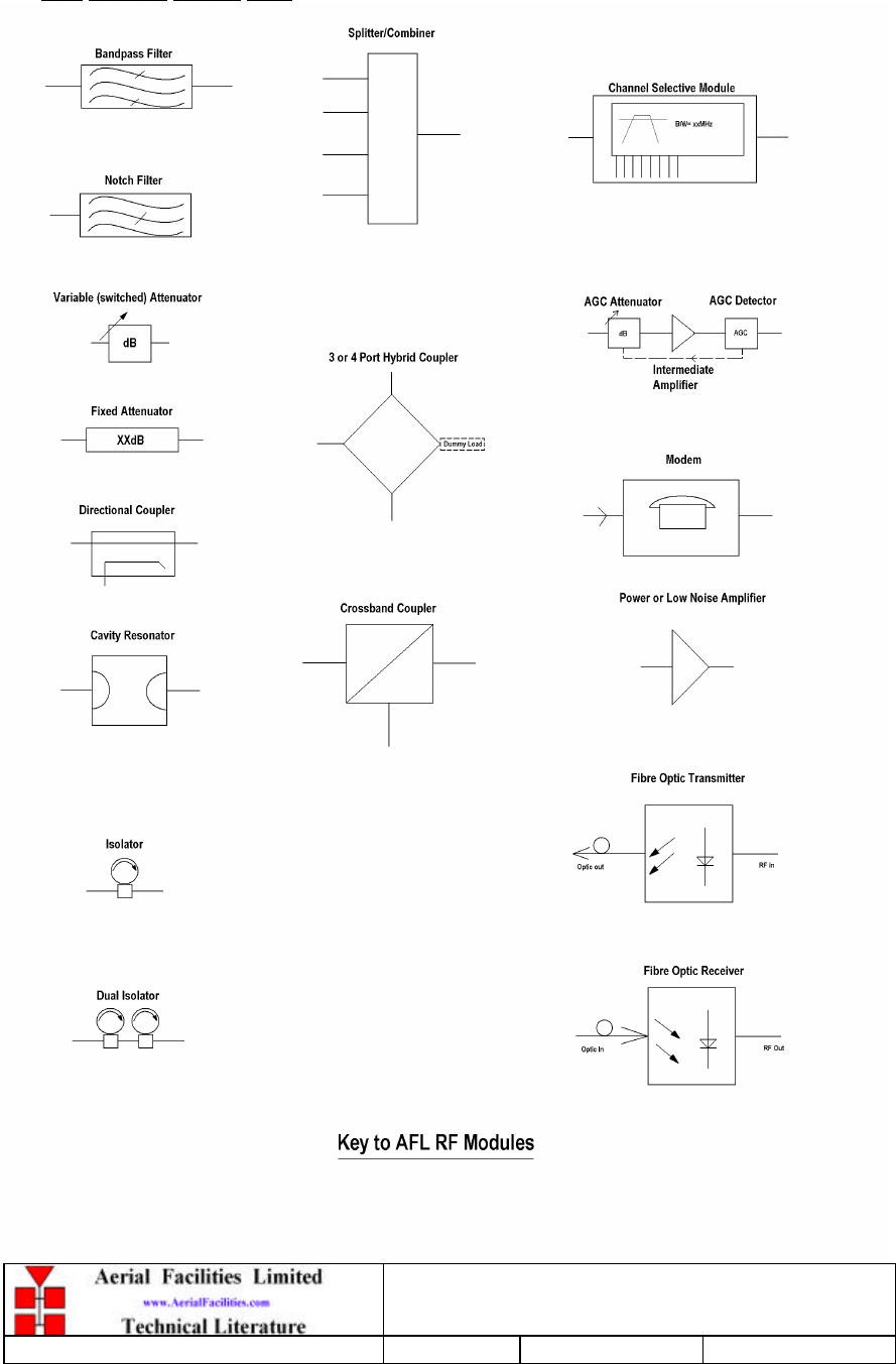
AFL Drawing Symbol Keys

P B L Tunnels Loc 2 Units 1 & 2 + 800MHz BDA
Maintenance Handbook
H/book Number:-60-056100HBKM Issue No:-1 Date:-13/02/2003 Page:-9 of 9
1. SAFETY CONSIDERATIONS
1.1 Electric Shock Hazard
Electrical shocks due to faulty mains driven power supplies.
Whilst ever potentially present in any electrical equipment, such a condition would be
minimised by quality installation practice and thorough testing at:
a) Original assembly.
b) Commissioning.
c) Regular intervals, thereafter.
All test equipment to be in good working order prior to its use. High current power supplies
can be dangerous because of the possibility of substantial arcing. Always switch off during
disconnection and reconnection.
1.2 RF Radiation Hazard
“CAUTION: This equipment is approved for antennas mounted on fixed outdoor permanent
structures. A minimum separation distance of 2 metres must be maintained between the
radiating elements and any nearby persons. A maximum antenna gain of 21 dBi may be used.
Operating this equipment without regard to these restrictions will result in RF exposure levels
above the limits allowed by FCC rules.”
This equipment complies with part 90 of the FCC rules. Any changes or modifications not
expressly approved by the manufacturer could void the user’s authority to operate the equipment.
RF radiation, (especially at UHF frequencies) arising from transmitter outputs connected to
AFL’s equipment, must be considered a safety hazard.
This condition might only occur in the event of cable disconnection, or because a ‘spare’
output has been left unterminated. Either of these conditions would impair the system’s
efficiency. No investigation should be carried out until all RF power sources have been
removed. This would always be a wise precaution, despite the severe mismatch between the
impedance of an N type connector at 50?, and that of free space at 377?, which would
severely mitigate against the efficient radiation of RF power. Radio frequency burns could also
be a hazard, if any RF power carrying components were to be carelessly touched!
Antenna positions should be chosen to comply with requirements (both local & statutory)
regarding exposure of personnel to RF radiation. When connected to an antenna, the unit is
capable of producing RF field strengths, which may exceed guideline safe values especially if
used with antennas having appreciable gain. In this regard the use of directional antennas with
backscreens and a strict site rule that personnel must remain behind the screen while the RF
power is on, is strongly recommended.
Where the equipment is used near power lines, or in association with temporary masts not
having lightning protection, the use of a safety earth connected to the case-earthing bolt is
strongly advised.
P B L Tunnels Loc 2 Units 1 & 2 + 800MHz BDA
Maintenance Handbook
H/book Number:-60-056100HBKM Issue No:-1 Date:-13/02/2003 Page:-10 of 10
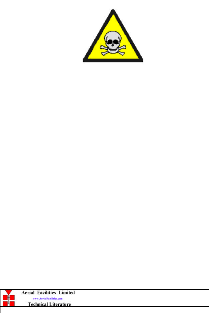
1.3 Chemical Hazard
Beryllium Oxide, also known as Beryllium Monoxide, or Thermalox™, is sometimes used in
devices within equipment produced by Aerial Facilities Ltd. Beryllium oxide dust can be toxic
if inhaled, leading to chronic respiratory problems. It is harmless if ingested or by contact.
Products that contain beryllium are load terminations (dummy loads) and some power
amplifiers. These products can be identified by a yellow and black “skull and crossbones”
danger symbol (shown above). They are marked as hazardous in line with international
regulations, but pose no threat under normal circumstances. Only if a component containing
beryllium oxide has suffered catastrophic failure, or exploded, will there be any danger of the
formation of dust. Any dust that has been created will be contained within the equipment
module as long as the module remains sealed. For this reason, any module carrying the yellow
and black danger sign should not be opened. If the equipment is suspected of failure, or is at
the end of its life-cycle, it must be returned to Aerial Facilities Ltd for disposal.
To return such equipment, please contact the Quality Department, who will give you a
Returned Materials Authorisation (RMA) number. Please quote this number on the packing
documents, and on all correspondence relating to the shipment.
PolyTetraFluoroEthylene, (P.T.F.E.) and P.T.F.E. Composite Materials
Many modules/components in AFL equipment contain P.T.F.E. as part of the RF insulation
barrier.
This material should never be heated to the point where smoke or fumes are evolved. Any
person feeling drowsy after coming into contact with P.T.F.E. especially dust or fumes should
seek medical attention.
1.4 Emergency Contact Numbers
The AFL Quality Department can be contacted on:
Telephone +44 (0)1494 777000
Fax +44 (0)1494 777002
e-mail qa@aerial.co.uk

P B L Tunnels Loc 2 Units 1 & 2 + 800MHz BDA
Maintenance Handbook
H/book Number:-60-056100HBKM Issue No:-1 Date:-13/02/2003 Page:-11 of 11
2. OVERVIEW/SYSTEM DESCRIPTION
The AFL Fibre feed Amplifiers for the Pasadena Blue line project are 2 way on-band RF
amplifiers. Their application is as an interface between the fibre optical link from the off air
amplifiers and the tunnel antenna/leaky feeder system. There are two units one designated
‘UNIT 1’ for the frequencies in the 470-473MHz range , the other ‘UNIT 2’ for the
frequencies in the 483-486MHz range.
Each unit is housed in an environmentally protected IP65 steel wall-mount case. Handles are
provided for carrying the unit and the door is fitted with locks. The unit interfaces with ‘N’
type female connectors for RF connections and heavy duty connectors for routing of AC
power supply input and alarm output wiring. Cable glands are provided for routing of the
Fibre optic cable in to the unit.
To provide adequate selectivity in the Downlink and Uplink paths, combline design duplexers
are used at the input and output ports. To provide the required gain to reach the required
signal levels, low-noise amplifiers (LNA’s) are used in each path, these being followed by
power amplifier modules in the uplink to provide the required intermodulation performance.
Gain adjustment is available locally using switched attenuators.
Note that “Downlink” refers to the RF path from FO receiver to the leaky feeder port and that
“Uplink” refers to the RF path from the leaky feeder port to the FO transmitter.
The AFL 800MHz Off Air Amplifier for the Pasadena Blue line project is a 2 way on-band RF
amplifier. It’s application is as an air interface between the donor radio site and the tunnel
leaky feeder system. Each unit is housed in an environmentally protected IP65 steel wall-
mount case. Handles are provided for carrying the unit and the door is fitted with locks. The
unit interfaces with ‘N’ type female connectors for RF connections and heavy duty connectors
for routing of AC power supply input and alarm output wiring.
P B L Tunnels Loc 2 Units 1 & 2 + 800MHz BDA
Maintenance Handbook
H/book Number:-60-056100HBKM Issue No:-1 Date:-13/02/2003 Page:-12 of 12
3. SPECIFICATIONS
3.1 Parts Lists
3.1.1 Location 2 Equipment Parts List
60-056101 PBL F/O BDA LOC2 470/473 MHz 1
60-056102 PBL F/O BDA LOC2 483/485 MHz 1
60-056103 PBL BDA LOC2 812/857MHz 1
3.1.2 Unit 1 Fibre Fed Tunnel Amplifier 60-056101 Parts List
AFL Part No. Description Qty.
Ref.
02-007302 SDF C/L5P 380MHzVAR.BW TOP SMA 4 5.1.1
02-013401 6P TETRA C/L FILT(NARROW) SMA 2 5.1.1
02-007339 02-0073(FOUR) MTG PLATE 1
10-000701 1/4W0-30dB SWITCHED ATTENUATOR 2 5.1.2
11-006102 LNA 380-500MHz 1W WITH RELAY 1 5.1.3
11-007302 LNA. 380-500MHz 20dB (C/W RELAY) GA 2 5.1.3
11-007402 LNA. 380-500MHz 30dB (C/W RELAY) GA 1 5.1.3
12-002201 3 STAGE AMPLIFIER ALARM BOARD 1 5.1.4
12-002220 3 STAGE ALARM PCB COVER 1
12-002826 ALARM BOARD ACRYLIC LENS 1
12-004205 PWR AMP.450MHz 10W version CLASS A 1 5.1.5
13-003011 DC/DC CONVERTER 24-12V 8A PCB 1 5.1.6
17-000126 CELL ENHANCER LABEL 6 DIGIT 1
17-001105 CE AGC UNIT LOG DET/AMP ASSY 1 5.1.7
17-001201 C/E AGC UNIT ATTENUATOR ASSY 1 5.1.7
17-001520 CASE620X420X250 HOFFMAN X2HS CUSTOM
1
17-001522 BASE PLATE 560x345mm 17-001520&9020 1
17-009720 EQUIP. MTG PLATE No.1 2
17-009723 EQUIP. MTG PLATE No.4 4
17-009726 EQUIP. MTG PLATE No.7 1
80-008902 24V RELAY PCB ASSEMBLY 1 5.1.8
80-031820 POWER AMP HEATSINK 20W 900MHz 1
80-032320 POWER AMP HEATSINK 10W 900MHz 1
80-032322 POWER SUPPLY HEATSINK 10W 1
90-010021 RF CABLE SUPFLEX SMA R/A MALE 100mm 0
90-010022 RF CABLE SUPFLEX SMA R/A MALE 200mm 3
90-010026 RF CABLE HIFLEX SMA R/A MALE 150mm 2
90-010130 RF CABLE SMA R/A-N PANEL JACK 100mm 1
90-010131 RF CABLE SMA R/A-N PANEL JACK 200mm 1
90-010132 RF CABLE SMA R/A-N PANEL JACK 250mm 1
91-030002 N ADAPTOR PANEL FEMALE:FEMALE 0

P B L Tunnels Loc 2 Units 1 & 2 + 800MHz BDA
Maintenance Handbook
H/book Number:-60-056100HBKM Issue No:-1 Date:-13/02/2003 Page:-13 of 13
91-500011 PWR 3POLE PNL PLUG SEALED IP68 1
91-500015 PWR CON CAP SEALED with INT. THREAD 2
91-500016 PWR 6POLE PNL PLUG SEALED IP68 1
91-510010 PWR 3POLE FREE SOC.SEALED IP68 1
91-510013 PWR CON CAP SEALED with Ext. THREAD 2
91-510014 PWR 6POLE FREE SOC.SEALED IP68 1
91-520003 POWER SWITCHD/FUSED MAINS INL. 0
91-600005 'D' 9 WAY SOCKET S/B TERM 0
91-600007 'D' 9 WAY BLACK SHELL 2
91-600014 'D' 9 WAY SOCKET S/B (NON FILTERED) 6
91-600015 'D' 9 WAY PLUG S/B (NON FILTERED) 1
91-700017 ICD 15 WAY 0.1' CONNECTOR 2
91-800014 3 WAY TERMINAL BLOCK 1
92-120009 M20 IP68 CABLE GLAND 2
92-400017 GASKET FOR N TYPE CONNECTOR 3
93-540035 1K3 0.25W 1% RES MRS25 M:F 2
96-300002 24V 6.25A 150W PSU Flatpac 1 5.1.9
96-300045 JWS75-15/A PSU (COUTANT LAMBDA) 1 5.1.10
96-500003 AC FILTER 110V 5A 1
96-500005 DC INPUT FILTERS 1
96-700002 LED.GREEN 5mm SEALED IP66 1
96-700005 LED.RED 5mm SEALED IP66 1
96-900018 AC TRIP SWITCH (5 AMP M.C.B.) 1
96-920011 PROXIMITY SWITCH 1
96-920012 PROXIMITY SWITCH MAGNET 1
97-300010 SUPPLY I/P COVERS 0
97-400010 BLACK PLASTIC HANDLE 37311 2
97-900004 RUBBER FOOT FOR CELL ENHANCERS 4
98-200003 FIBRE OPTIC Rx 6325 1310nm <2.2GHz 1 5.1.11
98-300003 FIBRE OPTIC Tx 6325 1310nm <2.2GHz 1

P B L Tunnels Loc 2 Units 1 & 2 + 800MHz BDA
Maintenance Handbook
H/book Number:-60-056100HBKM Issue No:-1 Date:-13/02/2003 Page:-14 of 14
3.1.3 Unit 2 Fibre Fed Tunnel Amplifier 60-056102 Parts List
AFL Part No.
Description Qty.
Ref.
02-007302 6P TETRA C/L FILT(NARROW) SMA 2
02-013401 SDF C/L5P 380MHzVAR.BW TOP SMA 2
02-010401 UHF 2 SECTION NOTCH FILTER SMA 2 5.2.1
02-007339 02-0073(FOUR) MTG PLATE 2
07-004801 500-800MHz CROSS BAND COUPLER 1 5.2.2
07-005705 CROSSBAND CPLR XC 250/380 SMA 1 5.2.2
10-000701 1/4W0-30dB SWITCHED ATTENUATOR 2
11-006102 LNA 380-500MHz 1W WITH RELAY 1
11-007301 LNA. 380-500MHz 20dB GA 0
11-007302 LNA. 380-500MHz 20dB (C/W RELAY) GA 3
12-002201 3 STAGE AMPLIFIER ALARM BOARD 1
12-002220 3 STAGE ALARM PCB COVER 1
12-002826 ALARM BOARD ACRYLIC LENS 1
12-004201 PWR AMP.450MHz 20W version CLASS A 1
13-003011 DC/DC CONVERTER 24-12V 8A PCB SUB-ASS 1
17-000126 CELL ENHANCER LABEL 6 DIGIT 1
17-001105 CE AGC UNIT LOG DET/AMP ASSY 1
17-001201 C/E AGC UNIT ATTENUATOR ASSY 1
17-001520 CASE620X420X250 HOFFMAN X2HS CUSTOM 1
17-001522 BASE PLATE 560x345mm 17-001520&9020 1
17-009720 EQUIP. MTG PLATE No.1 2
17-009723 EQUIP. MTG PLATE No.4 4
17-009726 EQUIP. MTG PLATE No.7 1
17-009727 EQUIP. MTG PLATE No.8 0
80-008902 24V RELAY PCB ASSEMBLY 1
80-031820 POWER AMP HEATSINK 20W 900MHz 1
80-032320 POWER AMP HEATSINK 10W 900MHz 0
80-032322 POWER SUPPLY HEATSINK 10W 1
90-010021 RF CABLE SUPFLEX SMA R/A MALE 100mm 6
90-010023 RF CABLE SUPFLEX SMA R/A MALE 300mm 1
90-010026 RF CABLE HIFLEX SMA R/A MALE 150mm 3
90-010027 RF CABLE HIFLEX SMA R/A MALE 250mm 1
90-010120 RF CABLE SMA R/A - N-TYPE (M) 100mm 1
90-010121 RF CABLE SMA R/A - N-TYPE (M) 200mm 1
90-010122 RF CABLE SMA R/A - N-TYPE (M) 250mm 1
90-010122 RF CABLE SMA R/A - N-TYPE (M) 250mm 1
90-010123 RF CABLE SMA R/A - N-TYPE (M) 300mm 1
90-010130 RF CABLE SMA R/A-N PANEL JACK 100mm 2
90-010132 RF CABLE SMA R/A-N PANEL JACK 250mm 1
90-010133 RF CABLE SMA R/A-N PANEL JACK 300mm 2
90-010134 RF CABLE SMA R/A-N PANEL JACK 400mm 1

P B L Tunnels Loc 2 Units 1 & 2 + 800MHz BDA
Maintenance Handbook
H/book Number:-60-056100HBKM Issue No:-1 Date:-13/02/2003 Page:-15 of 15
90-010520 RF CABLE N-TYPE(M)-N-TYPE(M)150MM 1
90-010522 RF CABLE N-TYPE(M)-N-TYPE(M)250MM 1
90-010523 RF CABLE N-TYPE(M)-N-TYPE(M)300MM 1
90-010524 RF CABLE N-TYPE(M)-N-TYPE(M)350MM 1
90-010525 RF CABLE N-TYPE(M)-N-TYPE(M)400MM 1
91-030002 N ADAPTOR PANEL FEMALE:FEMALE 3
91-500011 PWR 3POLE PNL PLUG SEALED IP68 1
91-500015 PWR CON CAP SEALED with INT. THREAD 2
91-500016 PWR 6POLE PNL PLUG SEALED IP68 1
91-510010 PWR 3POLE FREE SOC.SEALED IP68 1
91-510013 PWR CON CAP SEALED with Ext. THREAD 2
91-510014 PWR 6POLE FREE SOC.SEALED IP68 1
91-520003 POWER SWITCHD/FUSED MAINS INL. 0
91-600005 'D' 9 WAY SOCKET S/B TERM 6
91-600007 'D' 9 WAY BLACK SHELL 6
91-600014 'D' 9 WAY SOCKET S/B (NON FILTERED) 4
91-600015 'D' 9 WAY PLUG S/B (NON FILTERED) 1
91-700017 ICD 15 WAY 0.1' CONNECTOR 2
92-120009 M20 IP68 CABLE GLAND 2
92-400017 GASKET FOR N TYPE CONNECTOR 6
93-540035 1K3 0.25W 1% RES MRS25 M:F 2
96-300002 24V 6.25A 150W PSU Flatpac 1
96-500003 AC FILTER 110V 5A 1
96-500005 DC INPUT FILTERS 1
96-700002 LED.GREEN 5mm SEALED IP66 1
96-700005 LED.RED 5mm SEALED IP66 1
96-900018 AC TRIP SWITCH (5 AMP M.C.B.) 1
96-920011 PROXIMITY SWITCH 1
96-920012 PROXIMITY SWITCH MAGNET 1
97-300010 SUPPLY I/P COVERS 1
97-400010 BLACK PLASTIC HANDLE 37311 2
97-900004 RUBBER FOOT FOR CELL ENHANCERS 4

P B L Tunnels Loc 2 Units 1 & 2 + 800MHz BDA
Maintenance Handbook
H/book Number:-60-056100HBKM Issue No:-1 Date:-13/02/2003 Page:-16 of 16
3.1.4 800MHz Bi-directional Air Interface Amplifier Parts List
AFL Part No.
Description Qty.
Ref.
02-007201 900MHz 8POLE 10-20MHZ B/W SMA 4 5.3.1
05-002602 900MHz SPLITTER/COMBINER, 20W 4 5.3.2
10-000701 1/4W0-30dB SWITCHED ATTENUATOR 4 5.3.3
11-005902 900MHz LOW NOISE AMP WITH RELAY ASS 2 5.3.4
11-006702 GA 800-1000MHz LNA 29dB (WITH RELAY 2 5.3.4
12-000201 POWER AMP 900 MHz ALARMS (NO HSK) 2 5.3.5
12-002201 3 STAGE AMPLIFIER ALARM BOARD 2 5.3.6
12-002220 3 STAGE ALARM PCB COVER 2
12-002826 ALARM BOARD ACRYLIC LENS 2
13-003011 DC/DC CONVERTER 24-12V 8A PCB SUB-ASS 1 5.3.7
13-003020 DC/DC CONVERTER 24-12V HEATSINK 1
17-000126 CELL ENHANCER LABEL 6 DIGIT 1
17-001522 BASE PLATE 560x345mm 17-001520&9020 1
17-002101 CHANNEL CONTROL MODULE 2 5.3.8
17-002103 26WAY RIBBON CABLE LEAD 1
17-003002 CHAN MOD 890-915MHz UP LINK 4 5.3.8
17-003022 MODULE PATTERNED LEAVE 4
17-003023 SUBRACK SIDE PANEL 2
17-003024 SUBRACK REAR BRACKET 4
17-003025 BOTTOM MODULE GUIDE 4
17-003028 MODULE SQUARE LEAVE 4
17-003029 TOP MODULE GUIDE 4
17-009020 CASE620X420X250 HOFFMAN X3HS CUSTOM 1
17-009723 EQUIP. MTG PLATE No.4 4
17-009725 EQUIP. MTG PLATE No.6 2
80-008902 24V RELAY PCB ASSEMBLY 1 5.3.9
80-032320 POWER AMP HEATSINK 10W 900MHz 2
80-032320 POWER AMP HEATSINK 10W 900MHz 0
80-032322 POWER SUPPLY HEATSINK 10W 1
90-010021 RF CABLE SUPFLEX SMA R/A MALE 100mm 5
90-010022 RF CABLE SUPFLEX SMA R/A MALE 200mm 3
90-010026 RF CABLE HIFLEX SMA R/A MALE 150mm 4
90-010028 RF CABLE HIFLEX SMA R/A MALE 350mm 1
90-010029 RF CABLE HIFLEX SMA R/A MALE 450mm 1
90-010131 RF CABLE SMA R/A-N PANEL JACK 200mm 1
90-010135 RF CABLE SMA R/A-N PANEL JACK 500mm 1
91-030002 N ADAPTOR PANEL FEMALE:FEMALE 0
91-500011 PWR 3POLE PNL PLUG SEALED IP68 1
91-500011 PWR 3POLE PNL PLUG SEALED IP68 1
91-500015 PWR CON CAP SEALED with INT. THREAD 2
91-500016 PWR 6POLE PNL PLUG SEALED IP68 1

P B L Tunnels Loc 2 Units 1 & 2 + 800MHz BDA
Maintenance Handbook
H/book Number:-60-056100HBKM Issue No:-1 Date:-13/02/2003 Page:-17 of 17
91-510010 PWR 3POLE FREE SOC.SEALED IP68 1
91-510013 PWR CON CAP SEALED with Ext. THREAD 2
91-510014 PWR 6POLE FREE SOC.SEALED IP68 1
91-600005 'D' 9 WAY SOCKET S/B TERM 0
91-600007 'D' 9 WAY BLACK SHELL 0
91-600014 'D' 9 WAY SOCKET S/B (NON FILTERED) 6
91-620002 'D' 25 WAY SOCKET/IDC TERMS 4
91-640003 MISC 26 WAY RIBBON CABLE SOCK. 4
91-700017 ICD 15 WAY 0.1' CONNECTOR 3
92-120009 M20 IP68 CABLE GLAND 0
92-280033 Captive Screw 8
92-400017 GASKET FOR N TYPE CONNECTOR 3
93-540035 1K3 0.25W 1% RES MRS25 M:F 2
96-300011 24 V 400 W FLATPACK PWR SUPPLY 1 5.3.10
96-500003 AC FILTER 110V 5A 1
96-500005 DC INPUT FILTERS 1
96-700002 LED.GREEN 5mm SEALED IP66 1
96-700005 LED.RED 5mm SEALED IP66 1
96-900018 AC TRIP SWITCH (5 AMP M.C.B.) 0
96-920011 PROXIMITY SWITCH 1
96-920012 PROXIMITY SWITCH MAGNET 1
97-000002 BLACK MODULE CAGE RUNNER 8
97-300010 SUPPLY I/P COVERS 1
97-400010 BLACK PLASTIC HANDLE 37311 2
97-600001 SUBRACK FRONT HORIZ 2
97-600002 SUBRACK M2.5 STD TAP 8
97-900004 RUBBER FOOT FOR CELL ENHANCERS 4

P B L Tunnels Loc 2 Units 1 & 2 + 800MHz BDA
Maintenance Handbook
H/book Number:-60-056100HBKM Issue No:-1 Date:-13/02/2003 Page:-18 of 18
3.2 Technical Specifications
3.2.1 UHF ONE to Tunnels 1 & 2 Technical Specification
Frequency Range: Downlink Channels:
470.2125MHz
470.2625MHz
482.2375MHz
Uplink Channels:
473.2125MHz
473.2625MHz
485.2375MHz
Band Width Downlink :15kHz
Uplink : 25kHz
No. of Paths 2
Downlink Gain 82 dB min
Uplink Gain 70 dB min
RF Connector N type female
RF Impedance 50Ω
VSWR Better than 1.5:1
Gain Adjustment 0 to 30 in 2dB steps
Downlink PA 470.2125MHz, 470.2125MHz: 5WClass A Linear PA
482.2375MHz :20W Class A Linear PA
Uplink PA 485.2375MHz : 1W Class A Linear
473.2625MHz, 473.2125MHz : 5W Class A Linear
Duplexer UP/DN Isolation >80 dB
Passband Ripple <±1.5 dB
Noise Figure Downlink <7 dB at maximum gain
Noise Figure Uplink <18 dB at maximum gain
In-Band Spurious Better than –13dBm downlink
Better than –13dBm uplink
(measure with 30KHz BW & max gain setting)
Out-band Spurious up to
3GHz: Better than –90dBc

P B L Tunnels Loc 2 Units 1 & 2 + 800MHz BDA
Maintenance Handbook
H/book Number:-60-056100HBKM Issue No:-1 Date:-13/02/2003 Page:-19 of 19
3.2.2 UHF ONE to Location TWO Technical Specification
Frequency Range:
Downlink Channels:
470.2125MHz
470.2625MHz
482.2375MHz
Uplink Channels:
473.2125MHz
473.2625MHz
485.2375MHz
Band Width: Downlink :15kHz
Uplink : 25kHz
No. of Paths
2
Downlink Gain
82 dB min
Uplink Gain
80 dB min
RF Connector
N type female
RF Impedance
50Ω
VSWR
Better than 1.5:1
Gain Adjustment
0 to 30dB in 2dB steps
Downlink PA 470.2125MHz, 470.2125MHz: 5WClass A Linear PA
482.2375MHz :20W Class A Linear PA
Uplink PA 485.2375MHz : 1W Class A Linear
473.2625MHz, 473.2125MHz : 5W Class A Linear
Duplexer UP/DN Isolation
>80 dB
Passband Ripple
<±1.5 dB
Noise Figure
Downlink <7dB at maximum gain
Noise Figure
Uplink <12dB
In-Band Spurious Better than –13dBm downlink
Better than –13dBm uplink
(measure with 30KHz BW with max gain setting)
Out-band Spurious up to
3GHz Better than –90dBc

P B L Tunnels Loc 2 Units 1 & 2 + 800MHz BDA
Maintenance Handbook
H/book Number:-60-056100HBKM Issue No:-1 Date:-13/02/2003 Page:-20 of 20
3.2.3 UHF TWO to Tunnels 1 & 2 Technical Specification
Frequency Range:
Downlink Channels:
483.0625MHz
483.2875MHz
483.3125MHz
483.5625MHz
Uplink Channels:
486.0625MHz
486.2875MHz
486.3125MHz
486.5625MHz
Band Width: Downlink :15kHz
Uplink : 25kHz ,486.0625MHz, 486.5625MHz
15kHz ,486.2875MHz, 486.3125MHz
No. of Paths:
2
RF Connector:
N type female
RF Impedance:
50Ω
VSWR:
Better than 1.5:1
Downlink Gain:
90 dB min
Uplink Gain:
68 dB min
Gain Adjustment:
0 to 30 in 2dB steps
Downlink PA:
20W Class A Linear
Uplink PA:
20W Class A Linear
Duplexer UP/DN Isolation:
>80 dB
Passband Ripple:
<±1.5 dB
Noise Figure:
Downlink <5 dB at maximum gain
Noise Figure:
Uplink <12dB at maximum gain
In-Band Spurious: Better than –13dBm downlink
Better than –13dBm uplink
(measure with 30KHz BW with max gain setting)
Out-band Spurious up to 3GHz: Better than –90dBc

P B L Tunnels Loc 2 Units 1 & 2 + 800MHz BDA
Maintenance Handbook
H/book Number:-60-056100HBKM Issue No:-1 Date:-13/02/2003 Page:-21 of 21
3.2.4 UHF TWO to Location TWO Technical Specification
Frequency Range: Downlink Channels:
483.0625MHz
483.2875MHz
483.3125MHz
483.5625MHz
Uplink Channels:
486.0625MHz
486.2875MHz
486.3125MHz
486.5625MHz
Band Width: Downlink :15kHz
Uplink : 25kHz ,486.0625MHz, 486.5625MHz
15kHz ,486.2875MHz, 486.3125MHz
No. of Paths: 2
RF Connector: N type female
RF Impedance: 50Ω
VSWR: Better than 1.5:1
Downlink Gain: 90 dB min
Uplink Gain: 78 dB min
Gain Adjustment: 0 to 30 in 2dB steps
Downlink PA: 20W Class A Linear
Uplink PA: 20W Class A Linear
Duplexer UP/DN Isolation: >80 dB
Passband Ripple: <±1.5 dB
Noise Figure: Downlink <5 dB at maximum gain
Noise Figure: Uplink <12 dB at maximum gain
In-Band Spurious: Better than –13dBm downlink
Better than –13dBm uplink
(measure with 30KHz BW & max gain setting)
Out-band Spurious up to 3GHz: Better than –90dBc

P B L Tunnels Loc 2 Units 1 & 2 + 800MHz BDA
Maintenance Handbook
H/book Number:-60-056100HBKM Issue No:-1 Date:-13/02/2003 Page:-22 of 22
3.2.5 800MHz Bi-directional Amplifier to Location TWO Technical Specification
Frequency Range: Downlink Channels:
857.9375MHz
859.7625MHz
Uplink Channels:
812.9375MHz
814.7625MHz
Band Width: Downlink :15kHz
Uplink : 25kHz
No. of Paths: 2
No. of RF Ports: 2
No. of Fibre Connections: N/A
RF Connector: N type female
RF Impedance: 50Ω
VSWR: Better than 1.5:1
Downlink Gain: 78 dB min
Uplink Gain: 80 dB min
Gain Adjustment: 0 to 30 in 2dB steps
Downlink PA: 5W Class A Linear
Downlink Power: 2 Carriers at +18dBm
Uplink PA: 5W Class A Linear
Uplink Power: 2 Carriers at +18dBm
Duplexer UP/DN Isolation: >80 dB
Passband Ripple: <±1.5 dB
Noise Figure: Uplink <6 dB at maximum gain
Downlink <5 dB at maximum gain
In-Band Spurious: Better than –13dBm downlink
Better than –13dBm uplink
(measure with 30KHz BW with max gain setting)
MTBF: >50,000 hours
Supply Input Voltage: 110V AC
Alarms Fitted: Alarm: Volts free contacts
Alarm indicator- Red LED
Power Indicator-Green LED
P B L Tunnels Loc 2 Units 1 & 2 + 800MHz BDA
Maintenance Handbook
H/book Number:-60-056100HBKM Issue No:-1 Date:-13/02/2003 Page:-23 of 23
3.3 Mechanical Specification
3.3.1 Unit 1, Unit 2, + 800MHz BDA
height: 620 mm
width: 420 mm
Size:
depth: 250 mm
(excluding connectors, heatsinks, handles and feet)
Fixings: 4 holes on 500 mm (h) x 467 mm (w)
Weight: 50 kg (approx.)
operational: -20°C to +50°C
Temperature Range:
storage: -40°C to +70°C
Humidity: 10% to 95% non-condensing
Environmental Protection: IP65 (with door closed and all ports terminated)
Case: RAL 7032
Heatsinks: Black anodised
Finish:
Handles: Black (where fitted)
Supply Cable: Unit supplied with 3-pin IP68 connector for
customer interface with AC input.
P B L Tunnels Loc 2 Units 1 & 2 + 800MHz BDA
Maintenance Handbook
H/book Number:-60-056100HBKM Issue No:-1 Date:-13/02/2003 Page:-24 of 24
4. SYSTEM DRAWINGS
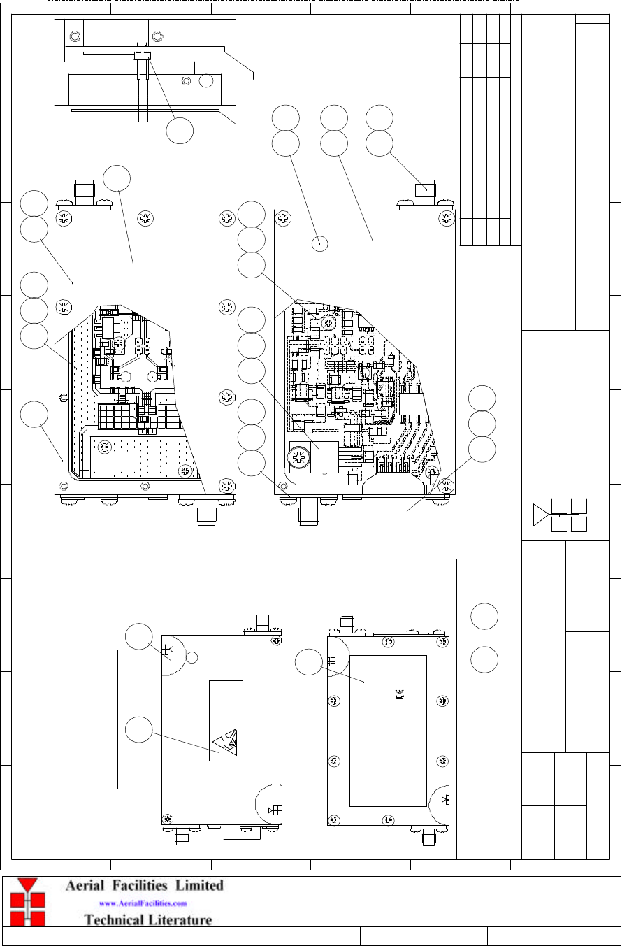
4.1 Drg. No. 60-056190, Location 2 Unit 1 Case Outline Drawing
PASADENA BLUE LINE. LOCATION 2.
BDA 470/473MHz. OUTLINE DRAWING
60-056190
1A
1:8
DBS 15/10/02
250 [9.9"]
620 [2'-0.4"]
LOCKABLE
DOOR
CATCH
voltage
High
DANGER
Heavy
CAUTION
500 [1'-7.7"]
CE- / - N
Product ref :
BPA 470/473MHz
Aerial Facilities
Limited
BYDATEDESCRIPTIONNo
ISSUE
1 2 345678 9
A
B
C
D
E
F
1 2 3 4 5 6 7 8 9
A
B
C
D
E
F
Fax : 01494 777002
Fax : 01494 777000
Aerial Facilities Limited
THIS IS A PROPRIETARY DESIGN OF AERIAL FACILITIES LTD.
REPRODUCTION OR USE OF THIS DESIGN BY OTHERS IS
PERMISSIBLE ONLY IF EXPRESSLY AUTHORISED IN WRITING
BY AERIAL FACILITIES LTD.
NO DECIMAL PLACE ± 1mm
ONE DECIMAL PLACE ± 0.3mm
TWO DECIMAL PLACES ± 0.1mm
ALL DIMENSIONS ARE IN mm
UNLESS OTHERWISE STATED
CHKD
DRAWN
APPD
DATE
TOLERANCES SCALE
England
CUSTOMER DRAWING.No
TITLE
3
A
PRODUCTION ISSUE
15/10/02
DBS
420 [1'-4.5"]
709 [2'-3.9"]
483MHz OUTPUT
M6 EARTH STUD
115V AC INPUT
MATERIAL: MILD STEEL
FINISH: PAINTED TO RAL 9017
WALL FIXINGS: M8 (5/16")
RF CONNECTORS: N TYPE FEMALE
ENVIRONMENTAL CLASS.: IP65
SEMI-GLOSS TRAFFIC BLACK
467 [1'-6.4"]
460 [1'-6.1"]
470/473MHz INPUT/OUTPUT
485/486MHz INPUT
CABLE GLANDS (FIBRE OPTICS)
PSU ALARM
DBSDECIMAL EQUIV'S
21/10/02
1B
DBSECN27472A
30/10/02
ALARMS
PB GD

P B L Tunnels Loc 2 Units 1 & 2 + 800MHz BDA
Maintenance Handbook
H/book Number:-60-056100HBKM Issue No:-1 Date:-13/02/2003 Page:-25 of 25
4.2 Drg. No. 60-056192, Location 2 Unit 2 Case Outline Drawing
PASADENA BLUE LINE. LOCATION 2.
BDA 483/485MHz. OUTLINE DRAWING
60-056191
1A
1:8
DBS 15/10/02
250 [9.9"]
620 [2'-0.4"]
LOCKABLE
DOOR
CATCH
voltage
High
DANGER
Heavy
CAUTION
500 [1'-7.7"]
CE- / - N
Product ref :
BPA 483/485MHz
Aerial Facilities
Limited
BYDATEDESCRIPTIONNo
ISSUE
1 2 345678 9
A
B
C
D
E
F
1 2 3 4 5 6 7 8 9
A
B
C
D
E
F
Fax : 01494 777002
Fax : 01494 777000
Aerial Facilities Limited
THIS IS A PROPRIETARY DESIGN OF AERIAL FACILITIES LTD.
REPRODUCTION OR USE OF THIS DESIGN BY OTHERS IS
PERMISSIBLE ONLY IF EXPRESSLY AUTHORISED IN WRITING
BY AERIAL FACILITIES LTD.
NO DECIMAL PLACE ± 1mm
ONE DECIMAL PLACE ± 0.3mm
TWO DECIMAL PLACES ± 0.1mm
ALL DIMENSIONS ARE IN mm
UNLESS OTHERWISE STATED
CHKD
DRAWN
APPD
DATE
TOLERANCES SCALE
England
CUSTOMER DRAWING.No
TITLE
3
A
PRODUCTION ISSUE
15/10/02
DBS
420 [1'-4.5"]
709 [2'-3.9"]
M6 EARTH STUD
115V AC INPUT
MATERIAL: MILD STEEL
FINISH: PAINTED TO RAL 9017
WALL FIXINGS: M8 (5/16")
RF CONNECTORS: N TYPE FEMALE
ENVIRONMENTAL CLASS.: IP65
SEMI-GLOSS TRAFFIC BLACK
467 [1'-6.4"]
497 [1'-7.6"]
PSU ALARM
DBSDECIMAL EQUIV'S
21/10/02
1B
LCX
800MHz
485/486MHz OUTPUT
VHF
483MHz INPUT
470/473MHz
INPUT
DBSECN27472A
30/10/02
ALARMS
PB GD
P B L Tunnels Loc 2 Units 1 & 2 + 800MHz BDA
Maintenance Handbook
H/book Number:-60-056100HBKM Issue No:-1 Date:-13/02/2003 Page:-26 of 26
4.3 Drg. No. 60-056192, 800MHz BDA Case Outline Drawing
PASADENA BLUE LINE. LOCATION 2.
BDA 800MHz. OUTLINE DRAWING
60-056192
1A
1:8
DBS 15/10/02
250 [9.9"]
620 [2'-0.4"]
LOCKABLE
DOOR
CATCH
voltage
High
DANGER
Heavy
CAUTION
500 [1'-7.7"]
CE- / - N
Product ref :
BPA 800MHz
Aerial Facilities
Limited
BYDATEDESCRIPTIONNo
ISSUE
1 2 345678 9
A
B
C
D
E
F
1 2 3 4 5 6 7 8 9
A
B
C
D
E
F
Fax : 01494 777002
Fax : 01494 777000
Aerial Facilities Limited
THIS IS A PROPRIETARY DESIGN OF AERIAL FACILITIES LTD.
REPRODUCTION OR USE OF THIS DESIGN BY OTHERS IS
PERMISSIBLE ONLY IF EXPRESSLY AUTHORISED IN WRITING
BY AERIAL FACILITIES LTD.
NO DECIMAL PLACE ± 1mm
ONE DECIMAL PLACE ± 0.3mm
TWO DECIMAL PLACES ± 0.1mm
ALL DIMENSIONS ARE IN mm
UNLESS OTHERWISE STATED
CHKD
DRAWN
APPD
DATE
TOLERANCES SCALE
England
CUSTOMER DRAWING.No
TITLE
3
A
PRODUCTION ISSUE
15/10/02
DBS
420 [1'-4.5"]
709 [2'-3.9"]
M6 EARTH STUD
115V AC INPUT
MATERIAL: MILD STEEL
FINISH: PAINTED TO RAL 9017
WALL FIXINGS: M8 (5/16")
RF CONNECTORS: N TYPE FEMALE
ENVIRONMENTAL CLASS.: IP65
SEMI-GLOSS TRAFFIC BLACK
467 [1'-6.4"]
500 [1'-7.7"]
PSU ALARM
TO ANTENNA
CONNECTION TO BDA
ECN2747
30/10/02
DBS2A
ALARMS
PB GD
P B L Tunnels Loc 2 Units 1 & 2 + 800MHz BDA
Maintenance Handbook
H/book Number:-60-056100HBKM Issue No:-1 Date:-13/02/2003 Page:-27 of 27
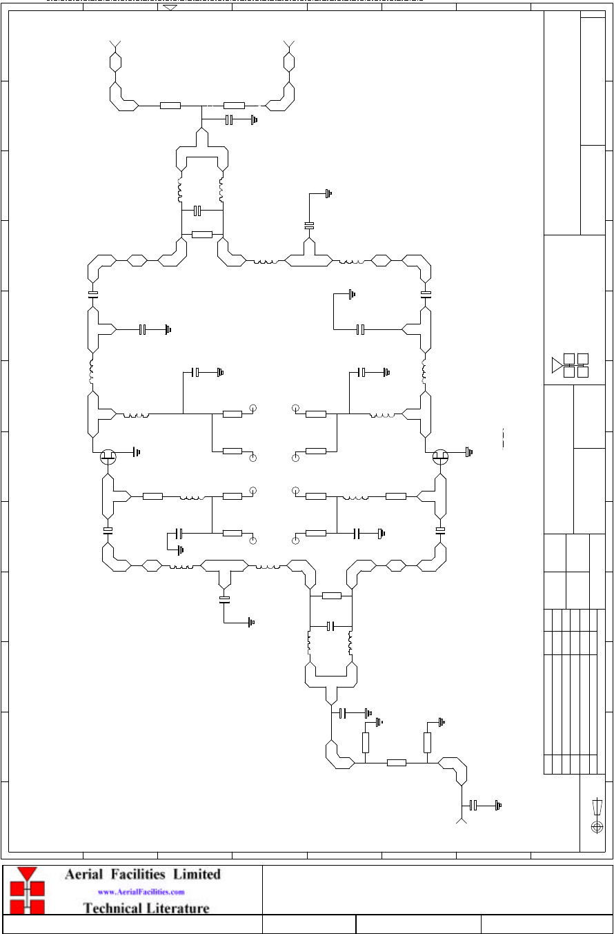
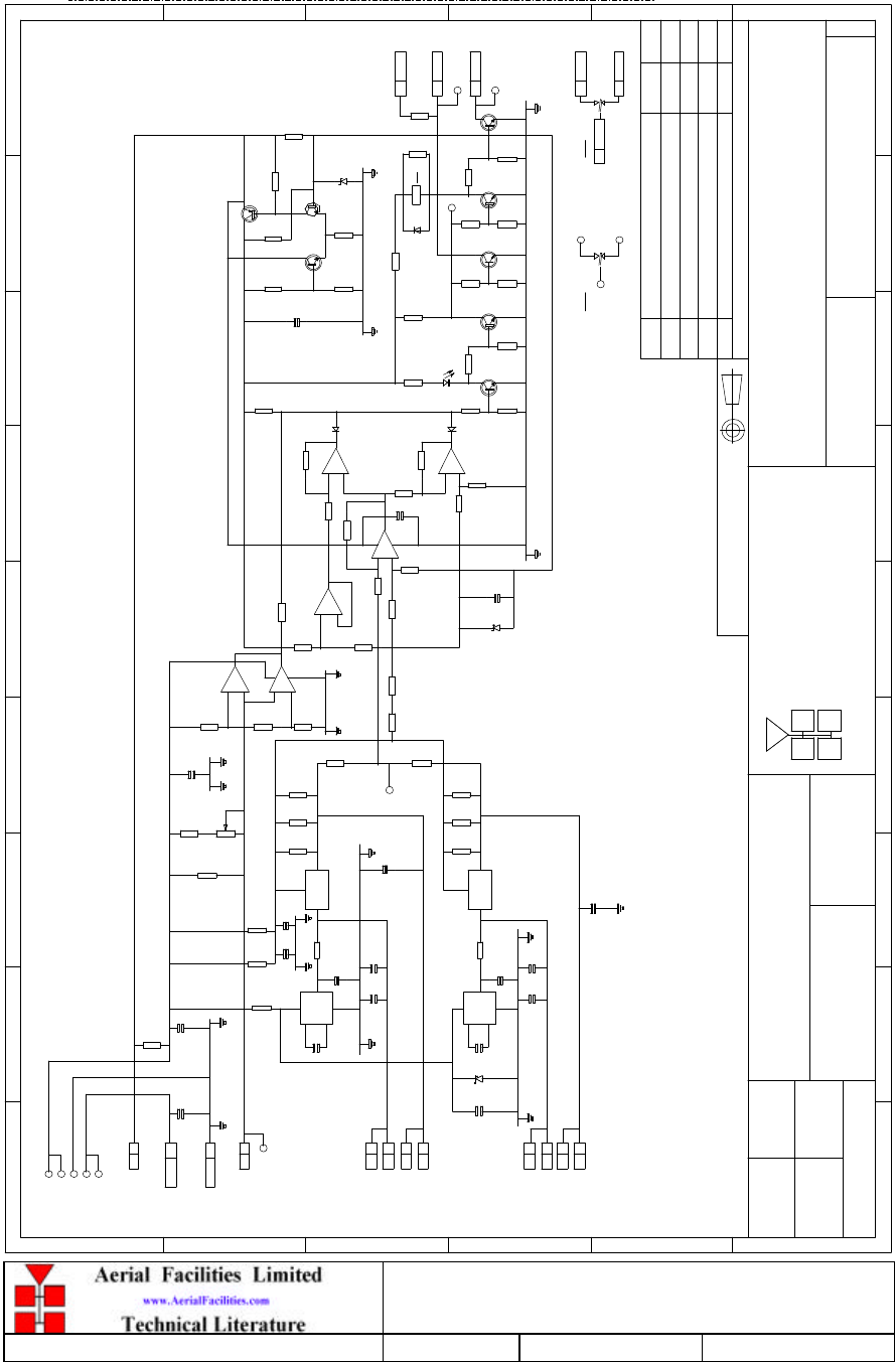
4.3 Complete Pasadena Metro System Diagram
dB
dB
857-860MHz
812-815MHz
857.9375MHz
859.7625MHz
812.9375MHz
814.7625MHz
800MHz
dB
dB
857-860MHz
812-815MHz
12-000201
12-000201 11-00670211-005902
11-00590211-006702
30dB 30dB
30dB 30dB
20dB
20dB
14dB
14dB
14dB
14dB
dB
dB
EO
470MHz
483MHz
473MHz
485-486MHz
UNIT 1
UNIT 2
470MHz
EO
AGC
AGC
DET
473MHz
dB
dB
483MHz
AGC
AGC
DET
485-486MHz
HL
VHF
LCX
02-007302
02-007302
02-007302
02-007302
02-013401
02-013401
02-013401
02-013401
12-00420511-007302
11-00740211-006102 11-007302
20dB 30dB
16dB 20dB 24dB
12-00420111-007302
11-00730111-006102 11-007302
20dB 30dB
16dB 20dB 20dB
HL
LCX
800MHz
LOCATION TWO
-15dBm
-15dBm
18dBm
20dBm
28dBm
26dBm
18dBm
21dBm
-60dBm
19dBm
-60dBm
-60dBm
-15dBm
-15dBm
25dBm
-65dBm
-17dBm
-65dBm
-62dBm
-63dBm
-65dBm
18dBm
60-056101
60-056102
60-056103
KL M
NOP
R
ST
J5
T8
T7
J6
-25dBm
-26dBm
483-486MHz
470-475MHz
02-007302
02-007302
T10
T11
3
dB
dB
dB
dB
dB
dB
dB
dB
dB
EO
EO
EO
482MHz
470MHz
473MHz
485MHz
483MHz
486MHz
482.2375MHz
470.2625MHz
470.2125MHz
473.2625MHz
473.2125MHz
485.2375MHz
483.3125MHz
483.2875MHz
483.0625MHz
483.5625MHz
486.3125MHz
486.2875MHz
486.0625MHz
486.5625MHz
UHF 1
UHF 2
02-013401
02-013401
02-013401
11-007401 11-007302
11-007401
11-007302
12-001801 11-007301
11-006101 11-007301
02-013401
02-013401
02-013401
32dB 20dB
32dB
20dB
20dB
20dB
30dB
16dB
15dB
20dB
20dB
5dB
5dB
15dB
11-007401
11-007401
32dB
32dB
12-004201 11-007301
20dB30dB
20dB
20dB
20dB
20dB
25dB
6dB
6dB
6dB
6dB
LOCATION ONE
-15dBm
11-007302
20dB
-11dBm
-3dBm
-62dBm
-72dBm
-82dBm
-72dBm
-3dBm
11-007401
32dB
11-007401
32dB
11-007401
32dB
-15dBm
-15dBm
-19dBm
+20dBm
-15dBm
+18dBm
-19dBm
-27dBm
60-055901
60-055902
B
C D
A
1
2
J1
J2
-23dBm
-23dBm
-23dBm
-22dBm
-22dBm
-12dBm
-35dBm
-35dBm
-35dBm
-35dBm
-20dBm
-20dBm
-20dBm
-20dBm
T1
T2
T3
T4
T9
5
6
dB
dB
EO
470MHz
483MHz
473MHz
485-486MHz
UNIT 1
UNIT 2
470MHz
EO
AGC
AGC
DET
473MHz
dB
dB
483MHz
AGC
AGC
DET
485-486MHz
HL
483-486MHz
470-475MHz
VHF
LCX
LCX
02-007302
02-007302
02-007302
02-007302
02-013401
02-013401
02-013401
02-013401
12-00180111-007302
11-007302
11-006102 11-007302
20dB 30dB
16dB 20dB 20dB
12-00420111-007302
11-00730211-006102 11-007302
20dB 30dB
16dB 20dB 20dB
02-007302
TUNNEL ONE & TWO
-15dBm
20dBm
20dBm
27dBm
30dBm
28dBm
18dBm
18dBm
-15dBm
-50dBm
-50dBm
-50dBm
-50dBm
-57dBm
-15dBm
-57dBm
-15dBm
-17dBm
60-056001
60-056002
EF G
H I J
3
4
J4
J3
U
T6
T5
02-007302
02-010401
02-010401

P B L Tunnels Loc 2 Units 1 & 2 + 800MHz BDA
Maintenance Handbook
H/book Number:-60-056100HBKM Issue No:-1 Date:-13/02/2003 Page:-28 of 28
P B L Tunnels Loc 2 Units 1 & 2 + 800MHz BDA
Maintenance Handbook
H/book Number:-60-056100HBKM Issue No:-1 Date:-13/02/2003 Page:-29 of 29
5. SUB-UNIT MODULES
5.1 Location 2, Unit 1 (60-056101)
5.1.1 Bandpass Filters (02-007302, 02-013401)
5.1.1.1 Description
The bandpass filters are multi-section designs with a bandwidth dependent upon the
passband frequencies, (both tuned to customer requirements). The response shape is
basically Chebyshev with a passband design ripple of 0.1dB. The filters are of combline
design, and are carefully aligned during manufacture in order to optimise the insertion loss,
VSWR and intermodulation characteristics of the unit. The tuned elements are silver-
plated to reduce surface ohmic losses and maintain a good VSWR figure and 50? load at
the input and output ports.
No adjustments should be attempted without full network sweep analysis facilities to
monitor both insertion loss and VSWR simultaneously.
5.1.1.2 Technical Specification (02-007302 & 02-013401)
PARAMETER SPECIFICATION
Response type:
Chebyshev
Frequency range:
350 – 500MHz (tuned to spec.)
<3.5 MHz (02-007302) Bandwidth:
0.5MHz (02-013401)
5 (02-007302)
Number of sections:
6 (02-013401)
Insertion loss:
2.7 dB (typical)
VSWR:
better than 1.2:1
Connectors:
SMA
Power handling:
100W max
operation:
-10°C to +55°C
Temperature range storage:
-40°C to +70°C
Weight:
3 kg (approximately)
Size:
266 x 143 x 39.5mm
P B L Tunnels Loc 2 Units 1 & 2 + 800MHz BDA
Maintenance Handbook
H/book Number:-60-056100HBKM Issue No:-1 Date:-13/02/2003 Page:-30 of 30
5.1.2 ¼Watt 0- -30dB Switched Attenuator (10-000701)
5.1.2.1 General Application
In many practical applications for Cell Enhancers etc., the gain in each path is found to be
excessive. Therefore, provision is made within the unit for the setting of attenuation in
each path, to reduce the gain.
5.1.2.2 Switched Attenuators
The AFL switched attenuators are available in two different types; 0 – 30dB in 2 dB steps
(as in this case), or 0 – 15dB in 1 dB steps. The attenuation is simply set using the four
miniature toggle switches on the top of each unit. Each switch is clearly marked with the
attenuation it provides, and the total attenuation in line is the sum of the values switched
in. They are designed to maintain an accurate 50? impedance over their operating
frequency at both input and output.
5.1.3 Low Noise Amplifiers (11-006102, 11-007302 & 11-007402)
5.1.3.1 Description
The low noise amplifiers used are double or triple stage solid-state low-noise amplifiers.
Class A circuitry is used in the units to ensure excellent linearity over a very wide dynamic
range. The active devices are very moderately rated to provide a long trouble-free working
life. There are no adjustments on these amplifiers, and in the unlikely event of failure then
the entire amplifier should be replaced. Note that all three amplifiers use similar DC power
circuit boards.
5.1.3.2 Technical Specification (11-006102)
Frequency range:
70 – 500MHz
Bandwidth:
<430MHz
Gain:
15.5dB (typical)
1dB Compression Point:
+31dBm (typical)
3rd order intercept:
+46dBm (typical)
Input return loss:
>20dB
Output return loss:
>20dB
VSWR:
Better than 1.5:1
Noise figure:
<4.8dB
Connectors:
SMA female
Supply:
530mA @ 10 to 24V DC (typical)
operational: -10°C to +60°C
Temperature range: storage: -40°C to +70°C
Weight:
260gms
P B L Tunnels Loc 2 Units 1 & 2 + 800MHz BDA
Maintenance Handbook
H/book Number:-60-056100HBKM Issue No:-1 Date:-13/02/2003 Page:-31 of 31
5.1.3.3 Drg. No. 11-006102, Low Noise Amplifier General Assembly
380-500MHz 1W AMPLIFIER
WITH RELAY ASSEMBLY
11-006102
1A
1.5:1
MNR 22/03/02
5 21
2
22
2
4 24
2
IN 2 PLACES
25
4
3
327
17 24
2
8 26 30 27
2
20
2
1533
2
27
5
16 23
5
1
6
IN 2 PLACES
2 25
10
34
see note 3
34
see note 2
35
see note 2
31
IN 4 PLACES
2819
BYDATEDESCRIPTIONNo
ISSUE
1 2 3 4 5 6 7 8 9
A
B
C
D
E
F
1
2
3
4
5
6
7
8
9
F
E
D
A
B
C
Fax : 01494 777002
Tel : 01494 777000
Aerial Facilities Ltd
TWO DECIMAL PLACES ± 0.1mm
ONE DECIMAL PLACE ± 0.3mm
NO DECIMAL PLACE ± 1mm
BY AERIAL FACILITIES LTD.
PERMISSIBLE ONLY IF EXPRESSLY AUTHORISED IN WRITING
REPRODUCTION OR USE OF THIS DESIGN BY OTHERS IS
THIS IS A PROPRIETARY DESIGN OF AERIAL FACILITIES LTD.
DRAWN
CHKD
ALL DIMENSIONS ARE IN mm
UNLESS OTHERWISE STATED
APPD
DATE
TOLERANCES SCALE
England
CUSTOMER DRG.No
TITLE
A
3
PRODUCTION ISSUE
22/03/02
MNR
J5
CON1
J4
REG3
ABC
R40 R50R51
R44R43
COMPONENTS TO BE ADDED TO 11-003912,ITEM 15,DC PCB SUB-ASSEMBLY
DC PCB
RF PCB
R45
R49
L12R12
R14
11-006125 Issue.1
L6
T2
L9
L10
C12
C14
C11
R13
L11
C15
R10
C9
R9
L13
R15
L14
C16
C17
R17
R16
RL1
AFL
S/N ********
IN
DATE **/**/20**
POWER
FREQ.
REF. 11-006102
1W 12-24vDC
380-500MHz
0086
AFL
OUT
SENSITIVE
DEVICES
ELECTROSTATIC
OBSERVE PRECAUTIONS
ATTENTION
FOR HANDLING
see note 2
AFL
LABEL DETAILS - SCALE 1:1
2. LIDS,ITEMS 2 & 3 AND LABELS,ITEMS 31,34 & 35,TO BE FITTED ON TEST
1. SOLDER JOINTS TO BE MADE USING OR
P B L Tunnels Loc 2 Units 1 & 2 + 800MHz BDA
Maintenance Handbook
H/book Number:-60-056100HBKM Issue No:-1 Date:-13/02/2003 Page:-32 of 32
5.1.3.4 Drg. No. 11-006170, LNA RF Circuit Diagram
C1
C2
C3
C7
R6
C8
R11 R12
R5
C5
C6
R7 R8
R1
R2
R3
R4
C4
R13 R14
R9 R10
C10
C14
C13
R15 C16
C17
380-500MHz 1W AMPLIFIER
(RF) CIRCUIT DIAGRAM
11-006170
1A
N.T.S
MNR 23/01/02
C9
C11 C12
R16
R17
C15
DATEDESCRIPTIONNo
ISSUE
THIRD ANGLE PROJECTION
1 2 3 4 5 6 7 8 9 10 11 12
A
B
C
D
E
F
G
H
1 2 3 4 5 6 7 8 9 10 11 12
A
B
C
D
E
F
G
H
PERMISSIBLE ONLY IF EXPRESSLY AUTHORISED IN WRITING
REPRODUCTION OR USE OF THIS DESIGN BY OTHERS IS
THIS IS A PROPRIETARY DESIGN OF AERIAL FACILITIES LTD.
UNLESS OTHERWISE STATED
ALL DIMENSIONS ARE IN mm
DATEDRAWN
CHKD APPD
TWO DECIMAL PLACES ± 0.1mm
NO DECIMAL PLACE ± 1mm
ONE DECIMAL PLACE ± 0.3mm
BY AERIAL FACILITIES LTD.
TOLERANCES SCALE
CUSTOMER DRAWING No
Fax : 01494 777002
Tel : 01494 777000
Aerial Facilities Limited
England
TITLE
2
A
910R
5R6
910R
8.2pF
L1
L2
3.3pF 100R
18nH
L3
18nH
18nH
18nH
L4
6.8pF
220pF
1nF
56R
56R
1nF
220pF
220pF
220pF
220pF
220pF
10K 0R0
10K 0R0
6.8nH
L5
6.8nH
L6
T1
CYL5
G
D
S
G
D
S
CYL5
T2
L7
180nH
180nH
L9
7.5nH
L8
7.5nH
L10
18nH
L11
L12
18nH
18nH
L13
18nH
L14
6.8pF
6.8pF
100R 3.3pF
8.2pF
RF OUT
RF IN
ANY COMPONENTS IN ARE NOT USED IN THIS BUILD
PRODUCTION ISSUE
23/01/02
MNR
0R0
RF OUT
(OPTIONAL)
6.8pF
CB IB
P B L Tunnels Loc 2 Units 1 & 2 + 800MHz BDA
Maintenance Handbook
H/book Number:-60-056100HBKM Issue No:-1 Date:-13/02/2003 Page:-33 of 33
5.1.3.5 Drg. No. 11-006171, LNA DC Wiring Diagram
380-500MHz 1W AMPLIFIER
SCHEMATIC DIAGRAM
11-006171
1A
MNR 23/01/02
BYDATEDESCRIPTIONNo
ISSUE
1 2 345678 9
A
B
C
D
E
F
1 2 3 4 5 6 7 8 9
A
B
C
D
E
F
Fax : 01494 777002
Tel : 01494 777000
Aerial Facilities Limited
THIS IS A PROPRIETARY DESIGN OF AERIAL FACILITIES LTD.
REPRODUCTION OR USE OF THIS DESIGN BY OTHERS IS
PERMISSIBLE ONLY IF EXPRESSLY AUTHORISED IN WRITING
BY AERIAL FACILITIES LTD.
NO DECIMAL PLACE ± 1mm
ONE DECIMAL PLACE ± 0.3mm
TWO DECIMAL PLACES ± 0.1mm
ALL DIMENSIONS ARE IN mm
UNLESS OTHERWISE STATED
CHKD
DRAWN
APPD
DATE
TOLERANCES SCALE
England
CUSTOMER DRAWING.No
TITLE
3
A
LM7808CT
REG3
G
IO
+6V 220mA
-ve
+6V 220mA
-ve
J4 1
CON2 - J5
CON2 - J4
J4 2
J5 1
J5 2
DC INPUT DC OUTPUT
RF PCB
FOR CIRCUIT DIAGRAM
SEE 11-006170
SEE 11-003971
FOR CIRCUIT DIAGRAM
DC PCB
+8V C
BA
RF
IN
PRODUCTION ISSUE
23/01/02
MNR
OUT
RF
OC GOOD/0v BAD9 CON1
9
RELAY CONTACT GOOD
RELAY COMMON
RELAY CONTACT BAD
PIN OUTS
9 WAY 'D'
TTL VOLTAGE SET
TTL ALARM/0v GOOD
GROUND
+12V DC I/P
7 CON1
8 CON1
5 CON1
4 CON1
6
8
7
5
4
A
3 CON1
2 CON1
3
2
CON1
1
*
*
*
= ONLY APPLIES TO 11-006802
*
CB IB
P B L Tunnels Loc 2 Units 1 & 2 + 800MHz BDA
Maintenance Handbook
H/book Number:-60-056100HBKM Issue No:-1 Date:-13/02/2003 Page:-34 of 34
5.1.3.6 Drg. No. 11-003971, LNA DC Schematic Diagram
DC PCB FOR LNA's AND LPA's,
CIRCUIT DIAGRAM
11-003971
DJL 24/09/01
R33
TR7
R32
R31
TR8
R34
R21
R20
TR1
R24
TR2
R23
R22
TR3
R25
R11
R12
R10
R9
C2
R6
R4
R8
R7
C8 R47
C4 C5
R43 R44 R45
C10C11
C15
C17 C16
R52
C14
R49R51 R50
C13
R46
R48
R39 R40
R38
R42
VR1
R41 R53
R54
R55
RL1
1
R35
TR4
TR6
R16 R17
R18
R19R15
C3
R14
R3
R2 R5
R29
R1
R36
R27
R13
C12
C9
R56
R57
C19
C1
C7
C6
C18
R58
R28
BYDATEDESCRIPTIONNo
ISSUE
1 2 345678 9
A
B
C
D
E
F
1 2 3 4 5 6 7 8 9
A
B
C
D
E
F
Chesham(01494)778301
Fax (01494)778910
Aerial Facilities Limited
TWO DECIMAL PLACES ± 0.1mm
ONE DECIMAL PLACE ± 0.3mm
NO DECIMAL PLACE ± 1mm
BY AERIAL FACILITIES LTD.
PERMISSIBLE ONLY IF EXPRESSLY AUTHORISED IN WRITING
REPRODUCTION OR USE OF THIS DESIGN BY OTHERS IS
THIS IS A PROPRIETARY DESIGN OF AERIAL FACILITIES LTD.
DRAWN
CHKD
UNLESS OTHERWISE STATED
ALL DIMENSIONS ARE IN mm
APPD
DATE
TOLERANCES SCALE
England
CUSTOMER DRAWING.No
TITLE
A
3
PROTOTYPE ISSUEAA
24/9/01
DJL
THIRD ANGLE PROJECTION
4K7
BCW71
10K
BCW71
4K7
10K
4K7
10K
BCW71
4K7
10K
4K7
10K
BCW71
120R
3K6
270K
1K
100n
100K
100K
270K
1K
2
+
REG1
I O
A
1K
+ +
+
100n
IC2
8
5
3
4
10u
+
100n
+
3
4
IC3
28
51K REG2
I O
A+
1K
1K
100R
+
-
1
2
3
-
+
5
6
7
-
2
+
3
1
1K
1K 2K2
22K
560R2K4
+
3K
100K
120R
100K
0R
1K8
4K7
56R
4K7
TR5
FZT751
BCW71
1U
BCW71
3V3
D3
9-
+
10
8
12 +
-
13
14
6-
+
5
7
IC1:C
IC1:B
IC1:D
11
4
LM324M
LM324M
LM324M
IC1:A
LM324M
ZD1
1.23V
LL4148
D2 LED1
IC4:B
IC4:A
+
1u
10u
+
10u
1u 1u
>12V DC I/P
10u
ZD3
5.1V 10u
470R
D1
LL4148
CON 1 1
J2 2
9 CON 1
CON 18
4 CON 1
5 CON 1
CON 13
RL1/1
ZD2
100n
4
8
LM337LM
10u
10u
LL4148
1. * IF APPLICABLE, VALUES WILL BE DETERMINED AT A HIGHER LEVEL BOM
ICL7660C
ICL7660C
LM337LM
2
J2 1
1J1
2J5
2J1
1J5
1J3
2J4
2J3
1J4
CON 1
+
1u
470p
+
10u
+
1u
2. CONNECTORS J1-5 TO BE FITTED AS NECESSARY PRODUCTION ISSUE(ECN2359)
26/11/01
TAS1A
V_OUT
V_IN
B
C
A
*
**
* * *
* * *
*
P3
*
7 CON 1
R59
1K
CB IB
2A ECN2518
17/4/02
DJL
P5
P4
RL1/2 P8
P6
P7
P1
P2
0R
*
*
*
*
*
*
*
*
3A ECN2686
25/7/02
DJL

P B L Tunnels Loc 2 Units 1 & 2 + 800MHz BDA
Maintenance Handbook
H/book Number:-60-056100HBKM Issue No:-1 Date:-13/02/2003 Page:-35 of 35
5.1.3.7 Technical Specification (11-007302)
Frequency range:
380-500MHz
Bandwidth:
<140MHz
Gain:
20-22dB
1dB Compression Point:
+23.5dB (typical)
3rd order intercept:
+36dB (typical)
Input/Output return loss:
>20dB
Noise figure:
<1.3dB
Connectors:
SMA female
Supply:
200-230mA @ 24V DC
operational: -10°C to +55°C
Temperature range: storage: -30°C to +70°C
Weight:
<300gms
Size:
90 x 55 x 30.2 (case only)
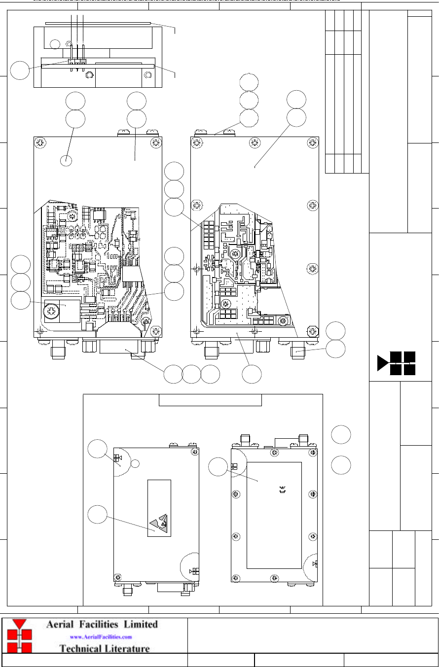
P B L Tunnels Loc 2 Units 1 & 2 + 800MHz BDA
Maintenance Handbook
H/book Number:-60-056100HBKM Issue No:-1 Date:-13/02/2003 Page:-36 of 36
5.1.3.8 Drg. No. 11-007302, LNA Assembly With Alarm Relay
BYDATEDESCRIPTIONNo
ISSUE
1
2
3
4
5
6
7
8
9
A
B
C
D
E
F
1
2
3
4
5
6
7
8
9
F
E
D
A
B
C
Fax : 01494 777002
Tel : 01494 777000
Aerial Facilities Ltd
TWO DECIMAL PLACES ± 0.1mm
ONE DECIMAL PLACE ± 0.3mm
NO DECIMAL PLACE ± 1mm
BY AERIAL FACILITIES LTD.
PERMISSIBLE ONLY IF EXPRESSLY AUTHORISED IN WRITING
REPRODUCTION OR USE OF THIS DESIGN BY OTHERS IS
THIS IS A PROPRIETARY DESIGN OF AERIAL FACILITIES LTD.
DRAWN
CHKD
ALL DIMENSIONS ARE IN mm
UNLESS OTHERWISE STATED
APPD
DATE
TOLERANCES SCALE
England
CUSTOMER DRG.No
TITLE
A
3
LOW NOISE AMPLIFIER 380-500MHz
(20dB) ASSEMBLY DRAWING (WITH RELAY)
11-007302
1A
1.5:1
DBS 9/7/02
PRODUCTION ISSUE
9/7/02
DBS
COMPONENTS TO BE ADDED TO 11-003912,ITEM 15,DC PCB SUB-ASSEMBLY
AFL
SENSITIVE
DEVICES
ELECTROSTATIC
OBSERVE PRECAUTIONS
ATTENTION
FOR HANDLING
AFL
AFL
********
11-007302
380-500MHz
20dB 10-24V DC
**/**/20**
REF.
FREQ.
GAIN
S/N
DATE
0086
IN
34
see note 2
LABEL DETAILS - SCALE 1:1
35
see note 2
see note 2
31
IN 4 PLACES
2. LIDS,ITEMS 2 & 3 AND LABELS,ITEMS 31,34 & 35,TO BE FITTED ON TEST
1. SOLDER JOINTS TO BE MADE USING OR
2819
OUT
6
IN 3 PLACES
3
DC PCB
25
4
7 32
RF PCB
15
W6
21
2
C2
1
22
2
CPL1
R1
C1
RF OUT
R19
W7
C21
5
C9
R2
R16
C5
L1
L3
C4 C8
+
R4
TR1
L5 C12
J31 J32
W5
W2 W1
2 25
10
17 24
2
33
2
27
5
27
2
20
2
16 23
5
24
2
IN 2 PLACES
4
268 30
R39
REG3
J3 J1J2
R50 R49
R44R43
RL1
CON1
CB IB
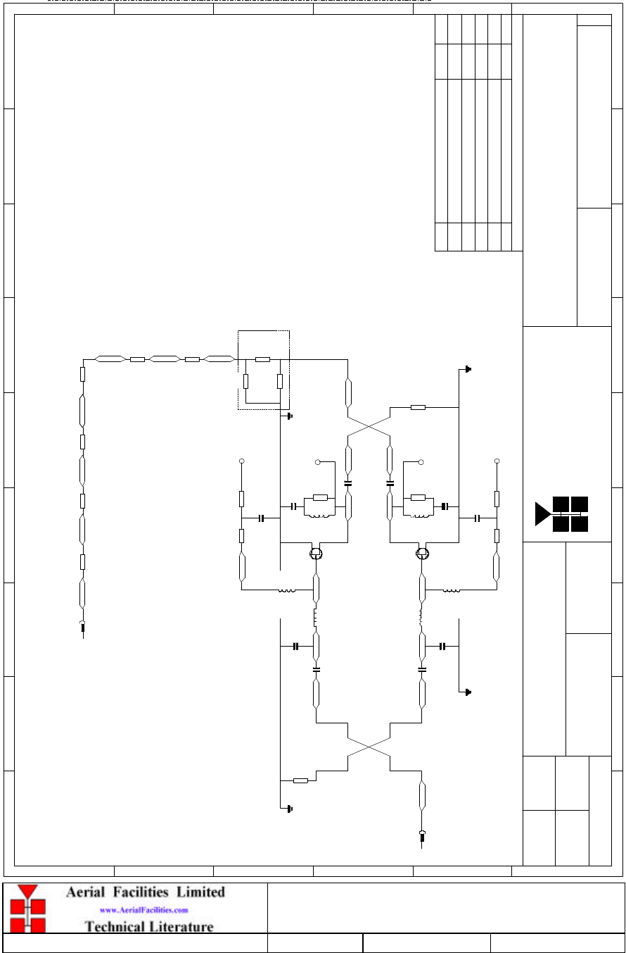
P B L Tunnels Loc 2 Units 1 & 2 + 800MHz BDA
Maintenance Handbook
H/book Number:-60-056100HBKM Issue No:-1 Date:-13/02/2003 Page:-37 of 37
5.1.3.9 Drg. No. 11-007370, LNA RF Circuit Diagram
BYDATEDESCRIPTIONNo
ISSUE
1 2 345678 9
A
B
C
D
E
1 2 3 4 5 6 7 8 9
A
B
C
D
E
F
Fax : 01494 777002
Tel : 01494 777000
Aerial Facilities Limited
THIS IS A PROPRIETARY DESIGN OF AERIAL FACILITIES LTD.
REPRODUCTION OR USE OF THIS DESIGN BY OTHERS IS
PERMISSIBLE ONLY IF EXPRESSLY AUTHORISED IN WRITING
BY AERIAL FACILITIES LTD.
NO DECIMAL PLACE ± 1mm
ONE DECIMAL PLACE ± 0.3mm
TWO DECIMAL PLACES ± 0.1mm
ALL DIMENSIONS ARE IN mm
UNLESS OTHERWISE STATED
CHKD
DRAWN
FAPPD
DATE
TOLERANCES SCALE
England
CUSTOMER DRAWING.No
TITLE
3
A
LOW NOISE AMPLIFIER 380-500MHz
(20dB) RF PCB CIRCUIT DIAGRAM
11-007370
1A
-
DBS 5/7/02
CLY2
TR2
RF INPUT
R1
51R
11303-3
CPL1
1nF
C3
Ø1.6x6 turns
L2
3.3pF
C7
L4
330nH
R3
100R 10K
R6
1nF
C6
1nF
C1
C4
3.3pF
Ø1.6x6 turns
L1
330nH
L3
100R
R2 R5
10K
J31
C5
1nF
TR1
CLY2
560R
R7
100nH
L6
C10
1nF
C9
1nF
R4
560R
100nH
L5
1nF
C13
1nF
C12
51R
R8
11303-3
CPL2
R9
R11
0R0
R10
0R0
W1
W5
0R0
RF OUTPUT
0R0
W6
0R0
R19
HEADER PIN
HEADER PIN
J32
HEADER PIN
J12
HEADER PIN
J11
PRODUCTION ISSUE
5/7/02
DBS
0R0
W2
0R0
W7
ATTENUATOR GROUP
(Select values on Test)
D
G S
D
G S
ECN2718 DBS
19/9/02
2A
CB IB
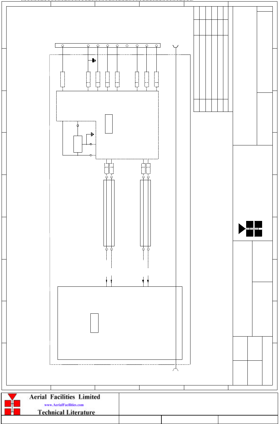
P B L Tunnels Loc 2 Units 1 & 2 + 800MHz BDA
Maintenance Handbook
H/book Number:-60-056100HBKM Issue No:-1 Date:-13/02/2003 Page:-38 of 38
5.1.3.10 Drg. No. 11-007371, LNA DC Wiring Diagram
BYDATEDESCRIPTIONNo
ISSUE
1 2 345678 9
A
B
C
D
E
F
1 2 3 4 5 6 7 8 9
A
B
C
D
E
F
Fax : 01494 777002
Tel : 01494 777000
Aerial Facilities Limited
THIS IS A PROPRIETARY DESIGN OF AERIAL FACILITIES LTD.
REPRODUCTION OR USE OF THIS DESIGN BY OTHERS IS
PERMISSIBLE ONLY IF EXPRESSLY AUTHORISED IN WRITING
BY AERIAL FACILITIES LTD.
NO DECIMAL PLACE ± 1mm
ONE DECIMAL PLACE ± 0.3mm
TWO DECIMAL PLACES ± 0.1mm
ALL DIMENSIONS ARE IN mm
UNLESS OTHERWISE STATED
CHKD
DRAWN
APPD
DATE
TOLERANCES SCALE
England
CUSTOMER DRAWING.No
TITLE
3
A
LOW NOISE AMPLIFIER. 380-500MHz
(20dB) RF SCHEMATIC DIAGRAM
11-007371
1A
-
DBS 8/7/02
LM7808CT
REG3
G
IO
-ve
J11 - J12
DC INPUT DC OUTPUT
RF PCB
FOR CIRCUIT DIAGRAM
SEE 11-007370
SEE 11-003971
FOR CIRCUIT DIAGRAM
DC PCB
+8V C
BA
RF
IN
PRODUCTION ISSUE
8/7/02
DBS
OUT
RF
OC GOOD/0v BAD9 CON1
9
RELAY CONTACT GOOD
RELAY COMMON
RELAY CONTACT BAD
PIN OUTS
9 WAY 'D'
TTL VOLTAGE SET
TTL ALARM/0v GOOD
GROUND
10-24V DC I/P
7 CON1
8 CON1
5 CON1
4 CON1
6
8
7
5
4
A
3 CON1
2 CON1
3
2
CON1
1
5V 75mA
-ve
J31 - J32
J31 1
J32 2
J12 2
J11 15V 75mA
CB IB
P B L Tunnels Loc 2 Units 1 & 2 + 800MHz BDA
Maintenance Handbook
H/book Number:-60-056100HBKM Issue No:-1 Date:-13/02/2003 Page:-39 of 39
5.1.3.11 Technical Specification (11-007402)
Frequency range:
380-500MHz
Bandwidth:
<140MHz
Gain:
30-32dB
1dB Compression Point:
+22dB (typical)
3rd order intercept:
+34dB (typical)
Input/Output return loss:
>19dB
Noise figure:
<1.3dB
Connectors:
SMA female
Supply:
300-330mA @ 10-24V DC
operational: -10°C to +55°C
Temperature range: storage: -30°C to +70°C
Weight:
<300gms
Size:
90 x 55 x 30.2 (case only)
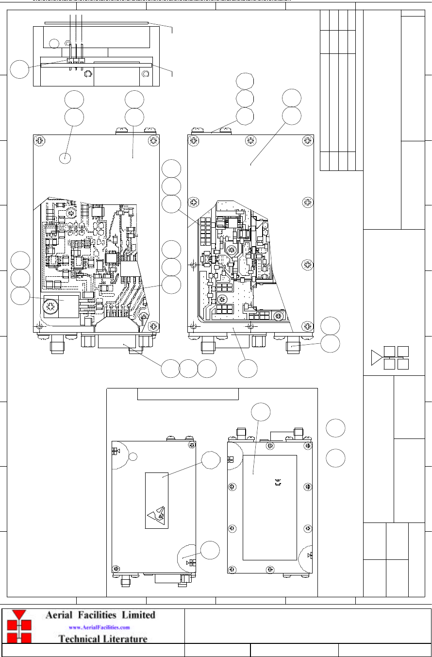
P B L Tunnels Loc 2 Units 1 & 2 + 800MHz BDA
Maintenance Handbook
H/book Number:-60-056100HBKM Issue No:-1 Date:-13/02/2003 Page:-40 of 40
5.1.3.12 Drg. No. 11-007402, LNA General Assembly
LOW NOISE AMPLIFIER 380-500MHz
(30dB) ASSEMBLY DRAWING (WITH RELAY)
11-007402
1A
1.5:1
DBS 9/7/02
2819
31
IN 4 PLACES
34
see note 2
35
see note 2
26
15
21
2
8
2 25
10
17 24
2
33
2
6
IN 3 PLACES
27
5
27
2
20
2
16 23
5
3 25
4
7 32
30
24
2
IN 2 PLACES
4
1
22
2
5
BYDATEDESCRIPTIONNo
ISSUE
1
2
3
4
5
6
7
8
9
A
B
C
D
E
F
1
2
3
4
5
6
7
8
9
F
E
D
A
B
C
Fax : 01494 777002
Tel : 01494 777000
Aerial Facilities Ltd
TWO DECIMAL PLACES ± 0.1mm
ONE DECIMAL PLACE ± 0.3mm
NO DECIMAL PLACE ± 1mm
BY AERIAL FACILITIES LTD.
PERMISSIBLE ONLY IF EXPRESSLY AUTHORISED IN WRITING
REPRODUCTION OR USE OF THIS DESIGN BY OTHERS IS
THIS IS A PROPRIETARY DESIGN OF AERIAL FACILITIES LTD.
DRAWN
CHKD
ALL DIMENSIONS ARE IN mm
UNLESS OTHERWISE STATED
APPD
DATE
TOLERANCES SCALE
England
CUSTOMER DRG.No
TITLE
A
3
PRODUCTION ISSUE
9/7/02
DBS
COMPONENTS TO BE ADDED TO 11-003912,ITEM 15,DC PCB SUB-ASSEMBLY
2. LIDS,ITEMS 2 & 3 AND LABELS,ITEMS 31,34 & 35,TO BE FITTED ON TEST
1. SOLDER JOINTS TO BE MADE USING OR
LABEL DETAILS - SCALE 1:1
AFL
S/N ********
DATE **/**/20**
see note 2
GAIN
FREQ.
REF.
30dB 10-24V DC
380-500MHz
11-007402
OUT
0086
AFL
IN
SENSITIVE
DEVICES
ELECTROSTATIC
OBSERVE PRECAUTIONS
ATTENTION
FOR HANDLING
AFL
W6
C2
CPL1
R1
C1
C23
TR3
C24
RF OUT
R19
C22
W7
C21
C9
R2
C15
R17C20
R16
C5
L1
L3
R18
C4 C8
+
R4
TR1
L5 C12
J31 J32
R15 R12
R13
L7 W5 W3
C19
W4
R14
W2
C18
C16
C17
ZD1
IC1
C14
W1 +
DC PCB RF PCB
R39
REG3
IC4
R41
J3 J1J2
R49R50
R57
R44R43
CON1
RL1
R53
R54
R55
ECN2722 DBS
24/9/02
2A
CB IB
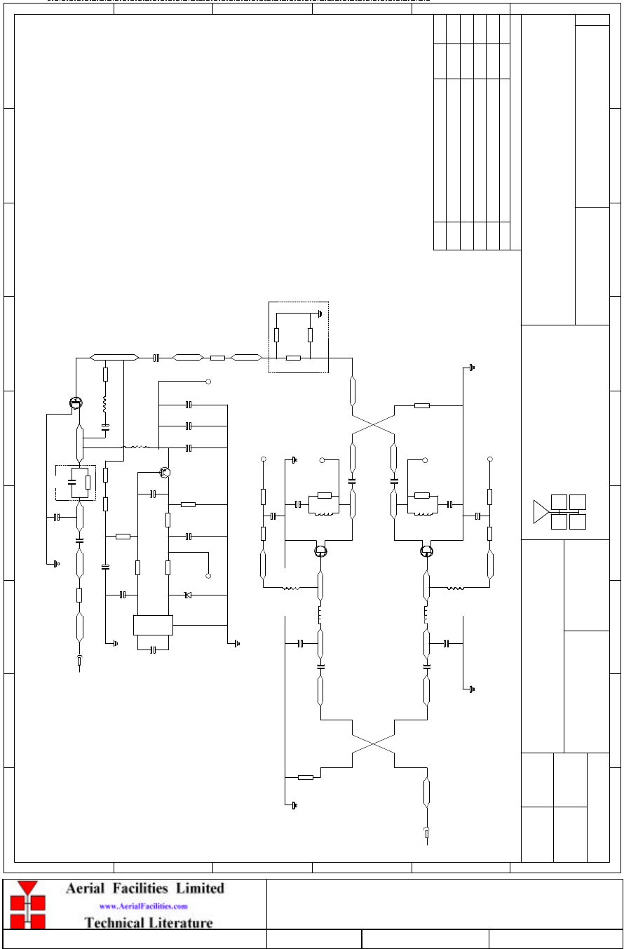
P B L Tunnels Loc 2 Units 1 & 2 + 800MHz BDA
Maintenance Handbook
H/book Number:-60-056100HBKM Issue No:-1 Date:-13/02/2003 Page:-41 of 41
5.1.3.13 Drg. No. 11-007470, LNA RF Circuit Diagram
LOW NOISE AMPLIFIER 380-500MHz
(30dB) RF PCB CIRCUIT DIAGRAM
11-007470
1A
-
DBS 5/7/02
BYDATEDESCRIPTIONNo
ISSUE
1 2 345678 9
A
B
C
D
E
1 2 3 4 5 6 7 8 9
A
B
C
D
E
F
Fax : 01494 777002
Tel : 01494 777000
Aerial Facilities Limited
THIS IS A PROPRIETARY DESIGN OF AERIAL FACILITIES LTD.
REPRODUCTION OR USE OF THIS DESIGN BY OTHERS IS
PERMISSIBLE ONLY IF EXPRESSLY AUTHORISED IN WRITING
BY AERIAL FACILITIES LTD.
NO DECIMAL PLACE ± 1mm
ONE DECIMAL PLACE ± 0.3mm
TWO DECIMAL PLACES ± 0.1mm
ALL DIMENSIONS ARE IN mm
UNLESS OTHERWISE STATED
CHKD
DRAWN
FAPPD
DATE
TOLERANCES SCALE
England
CUSTOMER DRAWING.No
TITLE
3
A
CLY2
G S
D
TR2
RF INPUT
R1
51R
11303-3
CPL1
1nF
C3
Ø1.6x6 turns
L2
3.3pF
C7
L4
330nH
R3
100R 10K
R6
1nF
C6
1nF
C1
C4
3.3pF
Ø1.6x6 turns
L1
330nH
L3
100R
R2 R5
10K
J31
C5
1nF
TR1
CLY2
560R
R7
100nH
L6
C10
1nF
C9
1nF
R4
560R100nH
L5
1nF
C13
1nF
C12
51R
R8
11303-3
CPL2
HEADER PIN
HEADER PIN
J32
HEADER PIN
J12
HEADER PIN
J11
PRODUCTION ISSUE
5/7/02
DBS
HEADER PIN
R11
22R
R10
R9
240R
240R
W1
0R0
1nF
W2
510R
R13
CLY2
W7
1nF
4 8
J22
HEADER PIN
ZD1
4V7
5
10uF
C14 +
7660
IC1
2
RF OUTPUT
+
C15
10uF
1K5
R12
10K
R16
C18
R19
0R0
1nF
BCW61B
C17
1nF
R18
1K5
TR3
C22C23
1nF 1nF
C2
1nF
C20
10nF
0R0
R15
1K2
10K
R17 1K2
R14 W3
1.5pF
W6
330nH
L7
220pF
C19
68nH
W4
S
D
G
2.2pF
C21
W5
J21
ATTENUATOR GROUP
(Select values on test)
SG
D
5R6
ECN2722 DBS
24/9/02
2A
CB IB
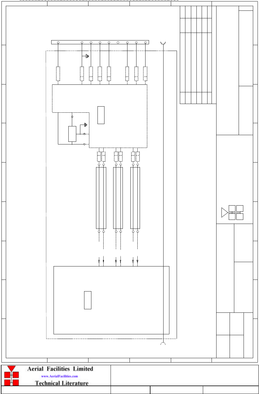
P B L Tunnels Loc 2 Units 1 & 2 + 800MHz BDA
Maintenance Handbook
H/book Number:-60-056100HBKM Issue No:-1 Date:-13/02/2003 Page:-42 of 42
5.1.3.14 Drg. No. 11-007471 LNA DC Wiring Diagram
LOW NOISE AMPLIFIER. 380-500MHz
(30dB) SCHEMATIC DIAGRAM
11-007471
1A
-
DBS 8/7/02
BYDATEDESCRIPTIONNo
ISSUE
1 2 345678 9
A
B
C
D
E
F
1 2 3 4 5 6 7 8 9
A
B
C
D
E
F
Fax : 01494 777002
Tel : 01494 777000
Aerial Facilities Limited
THIS IS A PROPRIETARY DESIGN OF AERIAL FACILITIES LTD.
REPRODUCTION OR USE OF THIS DESIGN BY OTHERS IS
PERMISSIBLE ONLY IF EXPRESSLY AUTHORISED IN WRITING
BY AERIAL FACILITIES LTD.
NO DECIMAL PLACE ± 1mm
ONE DECIMAL PLACE ± 0.3mm
TWO DECIMAL PLACES ± 0.1mm
ALL DIMENSIONS ARE IN mm
UNLESS OTHERWISE STATED
CHKD
DRAWN
APPD
DATE
TOLERANCES SCALE
England
CUSTOMER DRAWING.No
TITLE
3
A
LM7808CT
REG3
G
IO
8V
-ve
J11 - J12
J21 - J22
DC INPUT DC OUTPUT
RF PCB
FOR CIRCUIT DIAGRAM
SEE 11-007470
SEE 11-003971
FOR CIRCUIT DIAGRAM
DC PCB
+8V C
BA
RF
IN
PRODUCTION ISSUE
8/7/02
DBS
OUT
RF
OC GOOD/0v BAD9 CON1
9
RELAY CONTACT GOOD
RELAY COMMON
RELAY CONTACT BAD
PIN OUTS
9 WAY 'D'
TTL VOLTAGE SET
TTL ALARM/0v GOOD
GROUND
10-24V DC I/P
7 CON1
8 CON1
5 CON1
4 CON1
6
8
7
5
4
A
3 CON1
2 CON1
3
2
CON1
1
5V 75mA
-ve
J31 - J32
J31 1
J32 2
J22 2
J21 1
J12 2
J11 1
5V
5V 75mA
CB IB

P B L Tunnels Loc 2 Units 1 & 2 + 800MHz BDA
Maintenance Handbook
H/book Number:-60-056100HBKM Issue No:-1 Date:-13/02/2003 Page:-43 of 43
5.1.4 3 Stage Amplifier Alarm Boards (12-002201)
5.1.4.1 Description
Amplifier Alarm Boards are fitted to monitor the bias conditions of AFL Class A amplifiers
which remain constant in normal operation. Any departure from normal bias conditions is a
result of device failure, excess temperature, over-driving or oscillation (excessive power).
In normal operation, the Class A bias circuit of the amplifier develops a constant voltage of
1.20V across the collector current setting resistor. The Amplifier Alarm Board is a window
comparator device, which is adjusted to sense a departure from this condition. Several
different alarm outputs are provided to simplify interfacing, (Relay Contact, Open Collector,
and TTL Logic Levels)
The basic version of the Alarm Board (12-002801) monitors a single amplifier stage. A three-
stage version (12-002201) is used on complex amplifiers where three separate comparators
have their outputs logically combined to a common output stage. Failure of any one stage will
activate the alarms.
Note that the alarm board has a green Light Emitting Diode located near to the centre of the
printed circuit board, which is illuminated on ‘Good’, and extinguished on ‘Alarm’. It is
therefore a simple matter to identify an active module failure, by searching for an Alarm
Board which has its green LED extinguished. A simple test of the alarm board is possible by
shorting across the monitor inputs, pins 1 and 2, 3 and 4 or across pins 5 and 6. This last
monitor input is inactive if the board has been converted to a two way alarm board. (Refer to
relevant amplifier alarm wiring diagram.)
1) Volt-free change over relay contacts.
2) Open collector NPN transistor pulls low on alarm.
3) TTL driver.
The use of precision voltage sources and resistors has eliminated the need for initial
adjustment or calibration, and the board will function correctly with a wide variation in power
supply voltage (8 to 30 volts, nominal supply is 12 or 24Volts).
There are two selectable link options on the three-way board:
LINK1 - Removed to convert to two-way alarm board.
LINK2 - Removed to isolate 0V from chassis earth.
The one way alarm board only has the 0V isolation link (LINK2) fitted.
P B L Tunnels Loc 2 Units 1 & 2 + 800MHz BDA
Maintenance Handbook
H/book Number:-60-056100HBKM Issue No:-1 Date:-13/02/2003 Page:-44 of 44
5.1.4.2 Technical Specification
Operating voltage: 8 to 30V (floating earth)
Alarm Threshold: Vcc - 1.20 volt +15%
Alarm output relay contacts:
Max. switch current: 1.0Amp
Max. switch volts: 120Vdc/60VA
Max. switch power: 24W/60VA
Min. switch load: 10.0µA/10.0mV
Relay isolation: 1.5kV
Mechanical life: >2x10⁷ operations
Relay approval: BT type 56
Connector details: 15-way 0.1" pitch
operational: :-10°C to +55°C
Temperature range: storage: :-40°C to +70°C
74 x 56mm (3 stage)
PCB Size: 54 x 56mm (1 stage)
P B L Tunnels Loc 2 Units 1 & 2 + 800MHz BDA
Maintenance Handbook
H/book Number:-60-056100HBKM Issue No:-1 Date:-13/02/2003 Page:-45 of 45
5.1.4.3 Drg. No. 12-002201, 3 Stage Alarm Board Assembly Drawing & Parts List
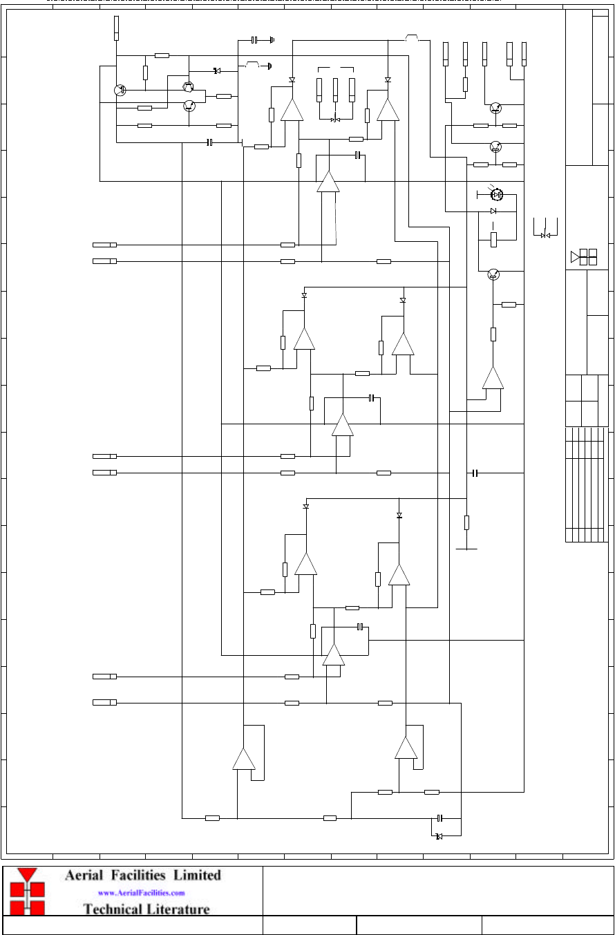
P B L Tunnels Loc 2 Units 1 & 2 + 800MHz BDA
Maintenance Handbook
H/book Number:-60-056100HBKM Issue No:-1 Date:-13/02/2003 Page:-46 of 46
5.1.4.4 Drg. No. 12-002270, 3 Stage Alarm Board Circuit Diagram
3 STAGE AMPLIFIER ALARM BOARD
CIRCUIT DIAGRAM
12-002270
1
N.T.S
MRB 11/8/93
BYDATEDESCRIPTIONNo
ISSUE
1 2 3 4 5 67 8 9 10 11 12 13 14 15 16 17 18
A
B
C
D
E
F
G
H
I
J
K
L
M
A
B
C
D
E
F
G
H
I
J
K
L
1 2 3 4 5 6 7 8 9 10 11 12 13 14 15 16
17
18
M
UNLESS OTHERWISE STATED
ALL DIMENSIONS ARE IN mm
DRAWN
CHKD
CUSTOMER DRAWING No
PERMISSIBLE ONLY IF EXPRESSLY AUTHORISED IN WRITING
THIS IS A PROPRIETARY DESIGN OF AERIAL FACILITIES LTD.
NO DECIMAL PLACE ± 1mm
TWO DECIMAL PLACES ± 0.1mm
ONE DECIMAL PLACE ± 0.3mm
BY AERIAL FACILITIES LTD.
REPRODUCTION OR USE OF THIS DESIGN BY OTHERS IS
APPD
DATE
TOLERANCES SCALE Tel : 01494 777000
Fax : 01494 777002
Aerial Facilities Limited
England
TITLE
1
A
+
-
IC1
+
-
IC1
+
-
IC1
+
-
IC1
CONN11
TTL ALARM
CONN
+5v TTL IN
12
CONN
0V
15
CONN
ALARM 0v
14
CONN
O/C ALARM
13
7
+8v TO +30v
CONN
1CONN
CONN2
CONN3
CONN4
CONN5
CONN6
MONITOR 1
INPUT
HI LOW HI
MONITOR 2
INPUT
LOW HI
MONITOR 3
INPUT
LOW
9 CONN
CONN10
CONN8
CONTACTS
ALARM
R1
1K8
+
-
IC3
5
6
7
R2
120R
R3
120R
R4
3K6
R6
100K
R5
100K
R7
100K
R9
1K
2
3
1
+
-
IC3
4
11
R11
1K
100K
R15
1K
R17
100K
R23
100K
R22
1K
R19
100K
R14
100K
R13
100K
R21
R25
1K
R27
1K
R37
2K4
R39
560R
R26
270K
270K
R18
R24
100K
R28
270K
R20
270K
R16
100K
R10
270K
R8
100K
R12
270K
R42
4K7
R29
4K7
R35
1K
R40
2K2
R41
22K
R38
1K
R36
3K
2K2
R30
4K7
R32 4K7
R34
10K
R33
10K
R31
TR3
BCW71BCW71
TR2
BCW71
TR1
6
5
7
+
-
IC2
10
9
8
+
-
IC3
3
2
4
11
1
12
13
14
+
-
IC3
+
-
IC2
12
13
14
10
9
8
3
2
4
1
11
+
-
IC2
+
-
IC2
5
6
7
10
9
8
12
13
14
D1
1.23v
SR12D
+C1
1uF
C2
100n
1u
C7
100n
C3
100n
C4
1.0
C8
3v3
D9
TR6
FZT751
TR4
BCW71 BCW71
TR4
100n
C6
LK2
D7
D6
LK1
D4
D5
D2
D3
D8
LED1
REL
-
RL1
+
OP AMP
6
7
RL1/2
8
+7.5v
+7.5v
2
+7.5v +7.5v
VCC VCC
0v 0v
CR0508 14/1/94 MRB
IC1 , IC2 & IC3 = LM324AM
ALL DIODES = LL4148 UNLESS MARKED OTHERWISE
4
RL2/2 3
2
NOT USED
VCC
PRODUCTION ISSUE 11/9/93 MRB
PRODUCTION ISSUE 29/8/00 MNR
2
2A
0v
RB RB
P B L Tunnels Loc 2 Units 1 & 2 + 800MHz BDA
Maintenance Handbook
H/book Number:-60-056100HBKM Issue No:-1 Date:-13/02/2003 Page:-47 of 47
5.1.4.5 Generic Wall Enclosure Alarm Wiring Sketch
P B L Tunnels Loc 2 Units 1 & 2 + 800MHz BDA
Maintenance Handbook
H/book Number:-60-056100HBKM Issue No:-1 Date:-13/02/2003 Page:-48 of 48
5.1.5 10 Watt Power Amplifier (12-004205)
5.1.5.1 Description
The power amplifier fitted in this unit is a multi-stage, solid state power amplifier. Class A
circuitry is employed throughout the device to ensure excellent linearity over a wide
dynamic frequency range. All the semi-conductor devices are very conservatively rated to
ensure low device junction temperatures and a long, trouble free working lifetime.
The power amplifier should require no maintenance over its operating life. Under no
circumstances should the cover be removed or the side adjustments disturbed unless it is
certain that the amplifier has failed; since it is critically aligned during manufacture and any
re-alignment will require extensive test equipment.
5.1.5.2 Technical Specification
Frequency range: 350 – 550MHz (tuned to spec.)
Bandwidth: 20MHz (tuned to spec.)
Maximum output power: >10W
Gain: 30dB
1dB compression point: <+43dBm
3rd Order intercept point: <+54dBm
VSWR: better than 1.45:1
Connectors: SMA female
Supply: 2.5A @ 24V DC
operational: -10°C to +55°C Temperature
range: storage: -40°C to +70°C
Size: 276 x 78 x 40mm (ex. connectors &
heatsink)
Weight: 1.5 kg(approximately, excluding
heatsink)
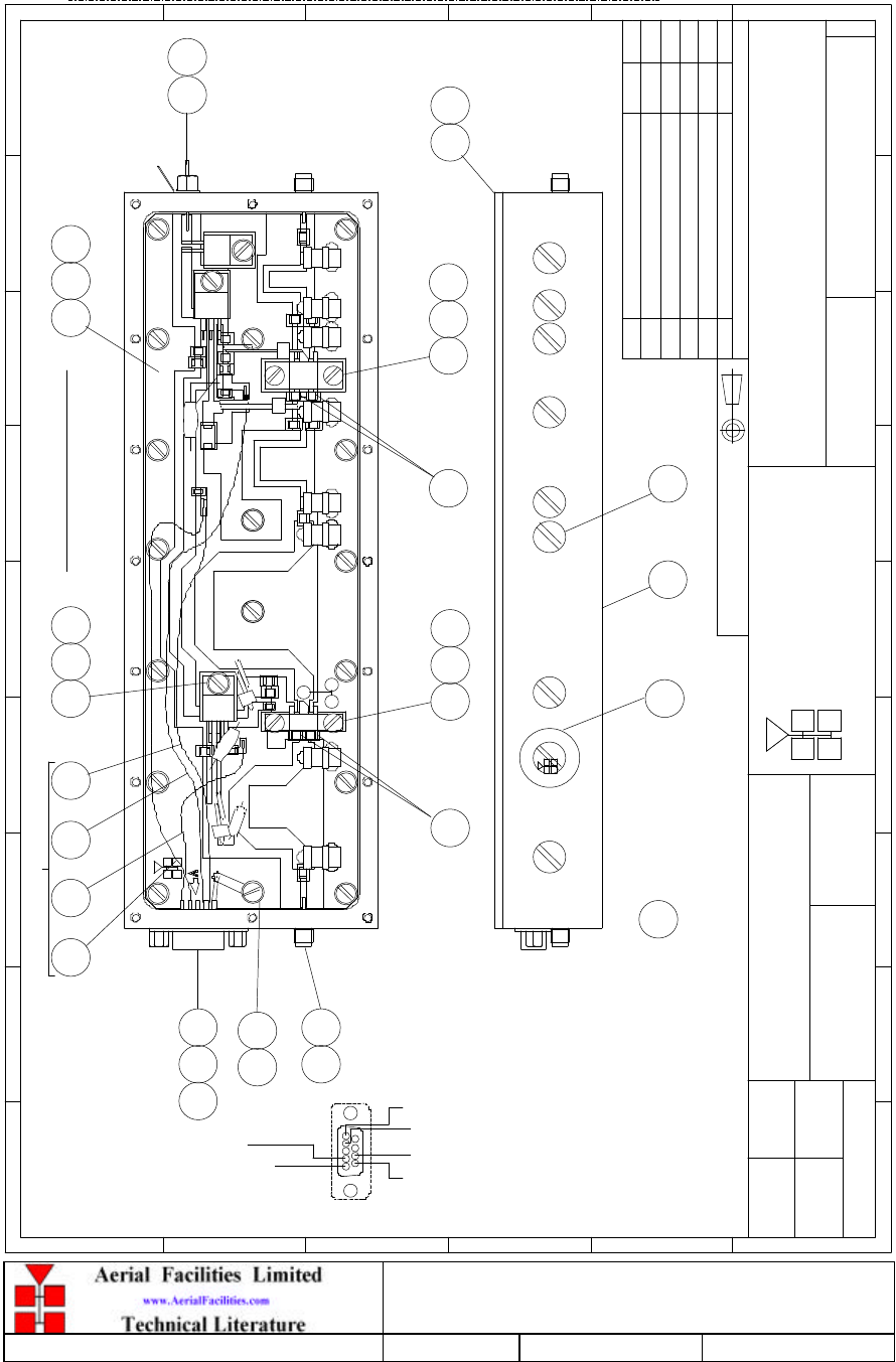
P B L Tunnels Loc 2 Units 1 & 2 + 800MHz BDA
Maintenance Handbook
H/book Number:-60-056100HBKM Issue No:-1 Date:-13/02/2003 Page:-49 of 49
5.1.5.3 Drg. No. 12-004205, 10Watt PA General Assembly
1 14
17
23
17
2314 22
11
2
7 23
2
13
4
6
17
16
4
1916
3 15
26
23
2
14
2
10 23
2
9 14
2
21
20
29302827
5
31 32
POWER AMPLIFIER, 450MHz 10W
CLASS A, GENERAL ASSEMBLY
12-004205
1:1
DBS 8/5/00
BYDATEDESCRIPTIONNo
ISSUE
THIRD ANGLE PROJECTION
1 2 345678 9
A
B
C
D
E
A
B
C
D
E
C9
L1
L2
12-004225
C2
C1
C5
C4
C6
C10
DET.1
C3
R2
TR1
C8
C7
L3
+
R1
REG 1
Aerial Facilities
Limited
C19
REG 2
C21
REF.
C12
C11
C16
C29
C13 C15
C17
C14
R3
C20
DET.2
TR2
L4
C28
+
R5
+
R4
C18
+
C22
C24
C25 C26
C23
L5
C30
C27
D1
+24V
IN 3 POSNS
IN 2 POSNS
IN 9 POSNS
2: COMPLETE ALL SOLDERING USING ITEM
CR1679+CR1719/20 MNR
8/5/00
SHOWN - - >
TAB IN DIRECTION
FIT WITH CHAMFERED
PLAN VIEW WITH LID REMOVED
SHOWN - - >
TAB IN DIRECTION
FIT WITH CHAMFERED
12345
6 7 8 9
GRN
YEL
VIO
BLU
REF DET2 REF DET1
VIEW ON ARROW A
SEE NOTE 1
1: CUT WIRE TO APPROX LENGTHS - BARE & TIN 3mm BOTH ENDS
PLAN VIEW
NOT SHOWN ON
+24v
ITEM 31,32
22SWG WIRE
AFL
IN 9 POSNS
3: IDENT LABEL TO BE SUPPLIED AND COMPLETED AT TEST
FIT CENTRALLY ON LID.
Fax : (01494)777002
Tel : (01494)777000
Aerial Facilities Limited
THIS IS A PROPRIETARY DESIGN OF AERIAL FACILITIES LTD.
REPRODUCTION OR USE OF THIS DESIGN BY OTHERS IS
PERMISSIBLE ONLY IF EXPRESSLY AUTHORISED IN WRITING
BY AERIAL FACILITIES LTD.
NO DECIMAL PLACE ± 1mm
ONE DECIMAL PLACE ± 0.3mm
TWO DECIMAL PLACES ± 0.1mm
ALL DIMENSIONS ARE IN mm
UNLESS OTHERWISE STATED
CHKD
DRAWN
F
1 2
APPD
DATE
TOLERANCES
3
SCALE
4 5
England
CUSTOMER DRAWING.No
6 7
TITLE
8 9
3
A
F
1A
GB BB
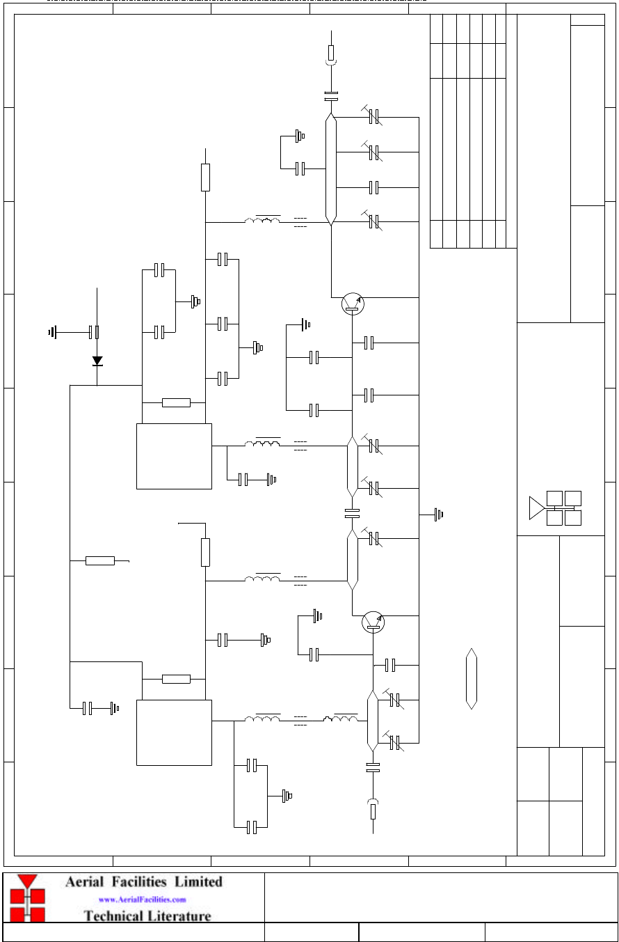
P B L Tunnels Loc 2 Units 1 & 2 + 800MHz BDA
Maintenance Handbook
H/book Number:-60-056100HBKM Issue No:-1 Date:-13/02/2003 Page:-50 of 50
5.1.5.4 Drg. No. 12-004271, 10W PA Circuit Diagram
1A
12-004271
POWER AMPLIFIER 450MHz 10W CLASS A
CIRCUIT DIAGRAM
-
17/5/00
DBS
BYDATEDESCRIPTIONNo
ISSUE
1 2 345678 9
A
B
C
D
E
F
1 2 3 4 5 6 7 8 9
A
B
C
D
E
F
PRODUCTION ISSUE DBS
17/5/00
+
RF INPUT
+
+
+
+
RF OUTPUT
ALARM
REF
ALARM
DET.1
ALARM
DET.2
R1
1R2
1KR
R2
R3
470R
REG.1
ADJ
OUT
IN
ADJ
REG.2
OUT
IN
C3
1uF
1nF
C7
1uF
C9
220pF
C8
L1 L3 L4 L5
FB4FB3FB2FB1
L2
47pF
C5
47pF
C6
1-14pF
C4
1-14pF
C2
C11
1-14pF
TR1
TP5012
PTB20031
TR2
C13
1-14pF
C15
1-14pF 1-14pF
C25 C26
1-14pF
C22
1-14pF
18pF
C28 27pF
C16
C17
27pF
C29
18pF
56pF
C12
4.7uF
C14
R5
R68
C19
56pF 1uF
C18
C20
1uF 56pF
C21
1000pF
C30
1KR
R4
1uH
C24
15pF
C23
15pF
56pF
C27
C1
56pF
LM337T LM337T
CONDUCTORS SHOWN THUS: ARE 50 ohm STRIPLINES
REFER TO 12-004211 FOR COMPONENT POSITIONS EXCEPT FOR THOSE MARKED
(THEY ARE SPECIFIED ON 12-004205)
*
*
*
*
**
*
*
Fax (01494)777002
Tel: (01494) 777000
Aerial Facilities Limited
THIS IS A PROPRIETARY DESIGN OF AERIAL FACILITIES LTD.
REPRODUCTION OR USE OF THIS DESIGN BY OTHERS IS
PERMISSIBLE ONLY IF EXPRESSLY AUTHORISED IN WRITING
BY AERIAL FACILITIES LTD.
NO DECIMAL PLACE ± 1mm
ONE DECIMAL PLACE ± 0.3mm
TWO DECIMAL PLACES ± 0.1mm
ALL DIMENSIONS ARE IN mm
UNLESS OTHERWISE STATED
CHKD
DRAWN
APPD
DATE
TOLERANCES SCALE
England
CUSTOMER DRAWING.No
TITLE
3
A
*
1nF
C31
2OCTQ45
D1
+24v
GB BB

P B L Tunnels Loc 2 Units 1 & 2 + 800MHz BDA
Maintenance Handbook
H/book Number:-60-056100HBKM Issue No:-1 Date:-13/02/2003 Page:-51 of 51
5.1.5.5 Drg. No. 12-004271C1, 10W PA Parts List(1)
CIRC. DESCRIPTIONAFL STOCK REF.
REF.
CHANGE NoCHANGE NoCHANGE No
CHANGE No DATEDATEDATEDATE ISSUEISSUEISSUE
ISSUE
1 2 3 4 5
5
4
3
2
1
A
B
C
D
E
F
G
A
B
C
D
E
F
G
Aerial Facilities Limited
DRAWN DATE APPD
CHKD CUSTOMER
TITLE
COMPONENT LIST FOR
POWER AMPLIFIER,450MHz,10W
CIRCUIT COMPONENT LIST
12-004271C1
1A
DBS
18/5/00
CR1679
C1
C2
C3
C4
C5
C6
C7
C8
C9
C10
C11
C12
C13
C14
C15
C16
C17
C18
C19
C20
C21
C22
C23
C24
C25
C26
C27
C28
C29
C30
93-200006 56pF CHIP CAP 10% TOL.(MIN)
56pF CHIP CAP 10% TOL.(MIN)93-200006
93-200006 56pF CHIP CAP 10% TOL.(MIN)
93-200006 56pF CHIP CAP 10% TOL.(MIN)
93-200006 56pF CHIP CAP 10% TOL.(MIN)
93-130023 PCB MOUNT AIR TRIMMER 1-14pF
93-130023 PCB MOUNT AIR TRIMMER 1-14pF
93-130023 PCB MOUNT AIR TRIMMER 1-14pF
93-130023 PCB MOUNT AIR TRIMMER 1-14pF
93-130023 PCB MOUNT AIR TRIMMER 1-14pF
93-130023 PCB MOUNT AIR TRIMMER 1-14pF
93-130023 PCB MOUNT AIR TRIMMER 1-14pF
93-240003 1uF TANTALUM CHIP CAP 35V
93-240004 1uF TANTALUM CHIP CAP 35V
93-240003 1uF TANTALUM CHIP CAP 35V
93-240004 1uF TANTALUM CHIP CAP 35V
REFER TO GA 12-004205 FOR DETAILS
93-200020 1nF CHIP CAP 63V 10%
93-200014 220pF CHIP CAP 10% TOL (MIN)
NOT FITTEDNOT FITTED
4.7uF TANTALUM CHIP CAP 35V93-240006
REFER TO GA 12-004205 FOR DETAILS
15pF CHIP CAP 10% TOL.(MIN)93-200005
93-200005 15pF CHIP CAP 10% TOL.(MIN)
93-200004 18pF CHIP CAP 10% TOL.(MIN)
18pF CHIP CAP 10% TOL.(MIN)93-200004
93-200016 1000pF (1nF) CHIP CAP 10% TOL.(MIN)
REFER TO GA 12-004205 FOR DETAILS
93-130023 PCB MOUNT AIR TRIMMER 1-14pF
REFER TO GA 12-004205 FOR DETAILS
18/5/00
C31 REFER TO GA 12-004205 FOR DETAILS
GB BB

P B L Tunnels Loc 2 Units 1 & 2 + 800MHz BDA
Maintenance Handbook
H/book Number:-60-056100HBKM Issue No:-1 Date:-13/02/2003 Page:-52 of 52
5.1.5.6 Drg. No. 12-004271C2, 10W PA Parts List(2)
CIRC. DESCRIPTIONAFL STOCK REF.
REF.
CHANGE NoCHANGE NoCHANGE No
CHANGE No DATEDATEDATEDATE ISSUEISSUEISSUE
ISSUE
1 2 3 4 5
5
4
3
2
1
A
B
C
D
E
F
G
A
B
C
D
E
F
G
Aerial Facilities Limited
DRAWN DATE APPD
CHKD CUSTOMER
TITLE
COMPONENT LIST FOR
POWER AMPLIFIER,450MHz,10W
CIRCUIT COMPONENT LIST
12-004271C2
1A
DBS
18/5/00
CR1679
REG1
REG2
94-300002 LM337T, VOLTAGE REGULATOR
LM337T, VOLTAGE REGULATOR94-300002
D1 94-120006 2OTQ45 45V DUAL SCHOTTKY DIODE
R1
R2
R4
R3
R5
93-540075 1R2 2.5W RESISTOR
1KR CHIP RESISTOR93-630037
68R 6W RESISTOR93-510036
1KR CHIP RESISTOR93-630037
470R CHIP RESISTOR93-630032
18/5/00
REFER TO GA 12-004205 FOR DETAILS
TR2
TR1
REFER TO GA 12-004205 FOR DETAILS
1.25 ENAMELLED COPPER WIRE
1.25 ENAMELLED COPPER WIRE
1.25 ENAMELLED COPPER WIRE
1.25 ENAMELLED COPPER WIRE
1.0uH CHOKE SIGMA SC10 SERIES
90-500012
93-910001
L5 FERRITE BEAD
90-500012
90-500012
90-500012
93-910001
93-910001
93-910001
93-400004
L4
L3
L2
L1
FERRITE BEAD
FERRITE BEAD
FERRITE BEAD
GB BB
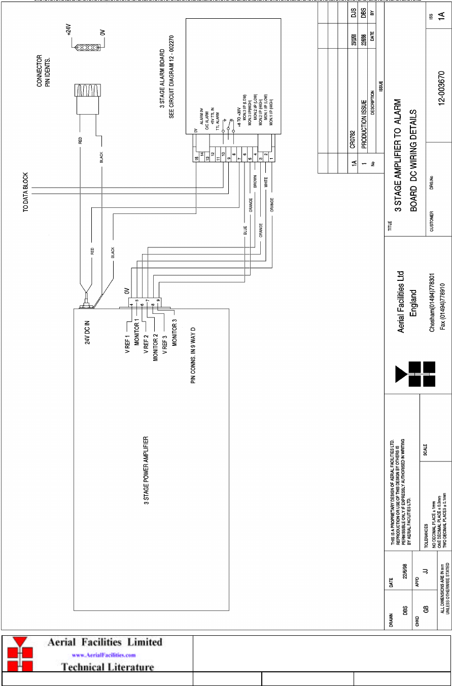
P B L Tunnels Loc 2 Units 1 & 2 + 800MHz BDA
Maintenance Handbook
H/book Number:-60-056100HBKM Issue No:-1 Date:-13/02/2003 Page:-53 of 53
5.1.5.7 Drg. No. 12-003670, 10 Watt Amplifier to Alarm Board Wiring Details
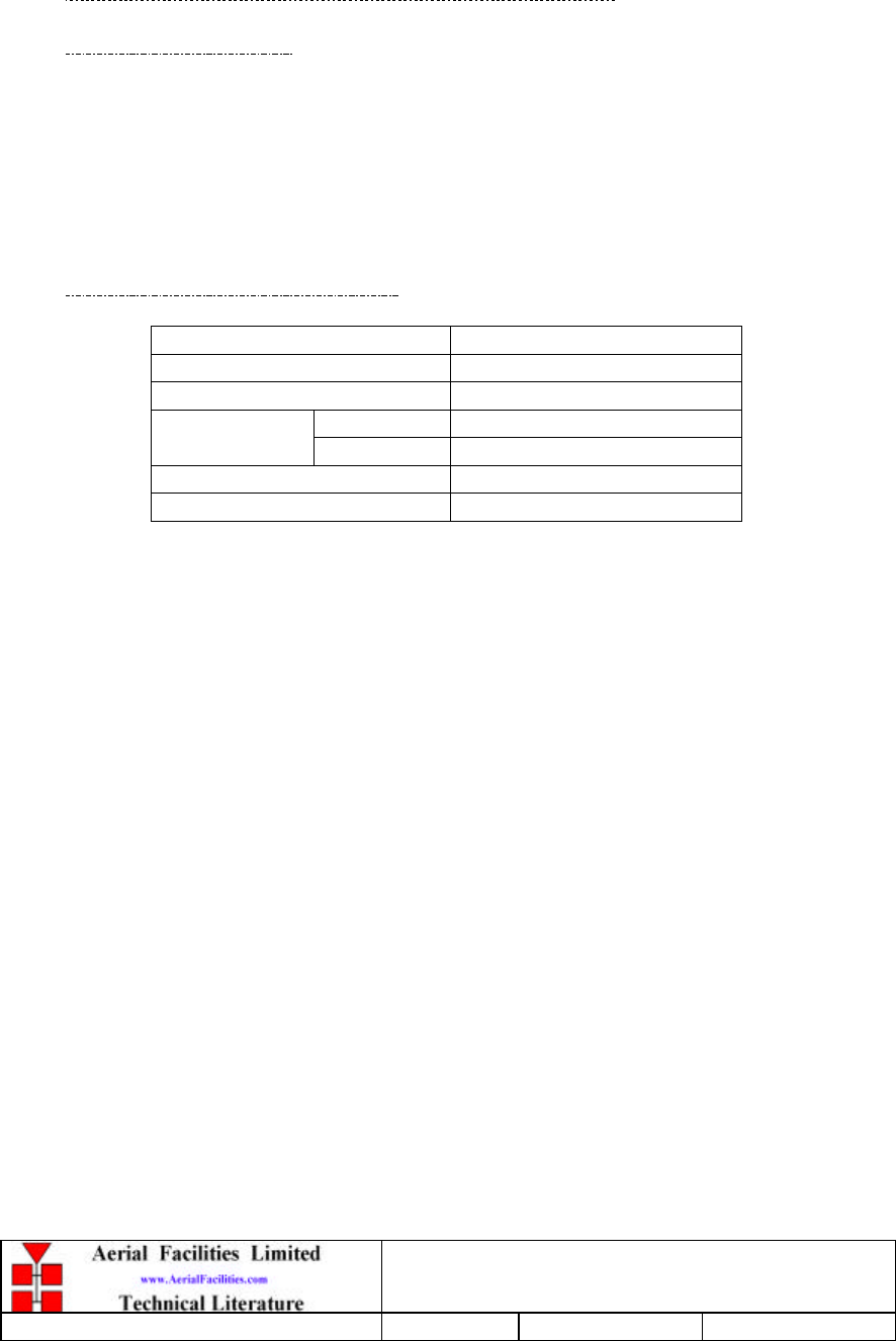
P B L Tunnels Loc 2 Units 1 & 2 + 800MHz BDA
Maintenance Handbook
H/book Number:-60-056100HBKM Issue No:-1 Date:-13/02/2003 Page:-54 of 54
5.1.6 DC/DC Converter, 24V in, 12V 8A out (13-003011)
5.1.6.1 Description
The DC/DC converter fitted is an AFL assembled, high power PCB unit with an 8 amp @
12V output capability. The circuit is basically an O.E.M semiconductor regulator (one side of
which has a heatsink mounting plate, that is usually bolted to the casing of a Cell Enhancer)
and smoothing components built onto a printed circuit board with screw block terminations.
Note: no circuit diagram of the O.E.M. regulator is available. This unit should not be
repaired, only replaced.
5.1.6.2 Technical Specification
Input Voltage Range: 18-28V DC
Output Voltage: 12V±0.5V
Max. Current Load: 8.0Amps
Operation: -10°C to +55°C Temperature
Range: Storage: -40°C to +70°C
Size(PCB): 190 x 63mm
Weight (Loaded PCB): 291gms

P B L Tunnels Loc 2 Units 1 & 2 + 800MHz BDA
Maintenance Handbook
H/book Number:-60-056100HBKM Issue No:-1 Date:-13/02/2003 Page:-55 of 55
5.1.7 Wide Dynamic Range AGC (17-001101, Det. & 17-001201, Atten.)
5.1.7.1 Description
The equipment is fitted with a wide dynamic range Automatic Gain Control (AGC)
system. This is generally fitted in the Uplink path (not usually needed in the downlink path,
as the signal here is at an almost constant level), to avoid overloading the amplifiers (with
the associated performance degradation) should a mobile be operated very close to the
unit.
The AFL wide dynamic range Automatic Gain Control system consists of two units, a
detector/amplifier and an attenuator. The detector/amplifier unit is inserted in the RF path
on the output of the power amplifier, and the attenuator is situated in the RF path between
the 1st and 2nd stages of amplification.
Normally the attenuator is at minimum attenuation. The detector/amplifier unit monitors
the RF level being delivered by the power amplifier, and when a certain threshold is
reached it begins to increase the value of the attenuator to limit the RF output to the
(factory set) threshold. Therefore overloading of the power amplifier is avoided.
The factory set threshold is 1dB below the Enhancer 1dB compression point. Some
adjustment of this AGC threshold level is possible, a 10dB range is mostly achieved. It is
not recommended under any circumstances to adjust the AGC threshold to a level greater
than the 1dB compression point as system degradation will occur.
The detector comprises of a 50? transmission line with a resistive tap which samples a
small portion of the mainline power. The sampled signal is amplified and fed to a
conventional half wave diode rectifier, the output of which is a DC voltage proportional to
the RF input signal.
This DC voltage is passed via an inverting DC amplifier with integrating characteristics, to
the output, which drives the attenuation control line of the corresponding AGC attenuator.
This unit is fitted at some earlier point in the RF circuit.
The unit contains a 12V DC regulator in the detector module, which supplies stabilised
voltage to the DC amplifier and via an external cableform to the AGC attenuator.
P B L Tunnels Loc 2 Units 1 & 2 + 800MHz BDA
Maintenance Handbook
H/book Number:-60-056100HBKM Issue No:-1 Date:-13/02/2003 Page:-56 of 56
For small signals, below AGC onset, the output control line will be close to 12V and the
AGC attenuator will have minimum attenuation. As the signal level increases the control line
voltage will fall, increasing the attenuator value and keeping the system output level at a
constant value.
The AGC onset level is adjusted by the choice of sampler resistor R1 and by the setting of
potentiometer VR1.
The attenuator comprises a 50? P.I.N diode, voltage-variable attenuator with a range of 3 to
30dB. The attenuation is controlled by a DC voltage which is derived from the associated
AGC detector unit.
5.1.7.2 Technical Specification
Frequency Range: up to 1000MHz
Attenuation Range: 3 to 30dB
Attenuation Steps: continuously variable
VSWR: better than 1.2:1
RF Connectors: SMA female
attenuator: 1W Power Handling:
detector/amp: >30W (or as required)
operation: -10°C to +55°C Temperature Range:
storage: -40°C to +70°C
attenuator pcb 50 x 42 x 21mm Size:
detector/amp pcb 54 x 42 x 21mm
attenuator: 90g Weight:
detector/amp
: 100g
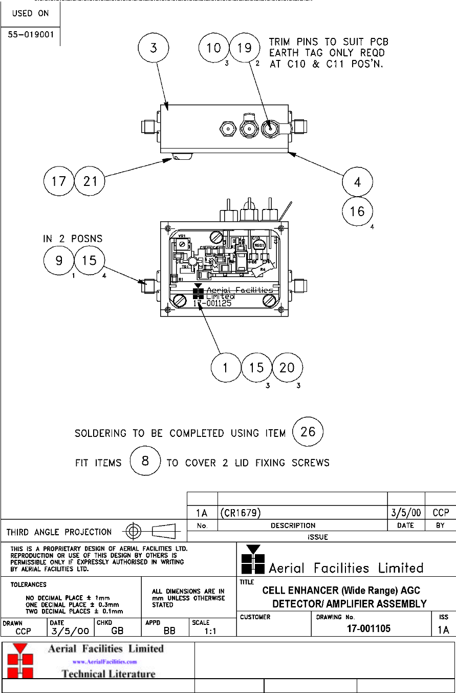
P B L Tunnels Loc 2 Units 1 & 2 + 800MHz BDA
Maintenance Handbook
H/book Number:-60-056100HBKM Issue No:-1 Date:-13/02/2003 Page:-57 of 57
5.1.7.3 Drg. No. 17-001105, ACG Detector Assembly
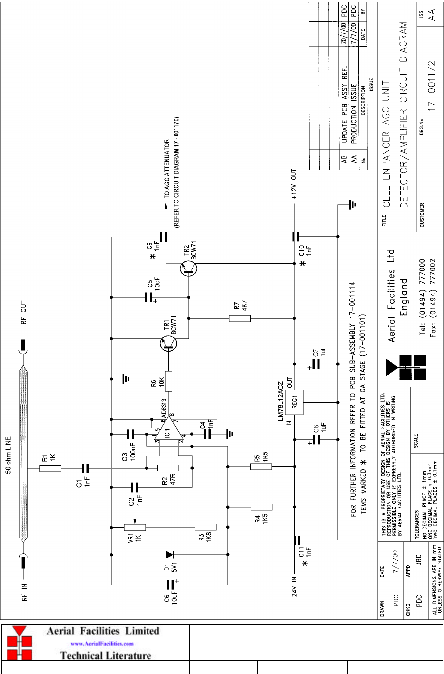
P B L Tunnels Loc 2 Units 1 & 2 + 800MHz BDA
Maintenance Handbook
H/book Number:-60-056100HBKM Issue No:-1 Date:-13/02/2003 Page:-58 of 58
5.1.7.4 Drg. No. 17-001172, Wide Range AGC Detector Circuit Diagram
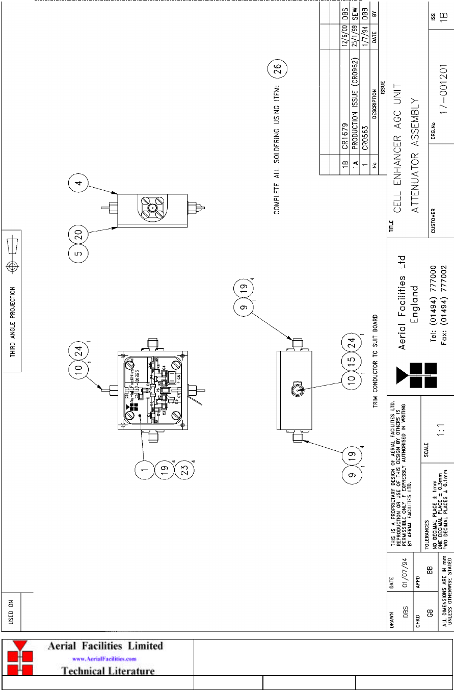
P B L Tunnels Loc 2 Units 1 & 2 + 800MHz BDA
Maintenance Handbook
H/book Number:-60-056100HBKM Issue No:-1 Date:-13/02/2003 Page:-59 of 59
5.1.7.5 Drg. No. 17-001201, AGC Attenuator Assembly Drawing
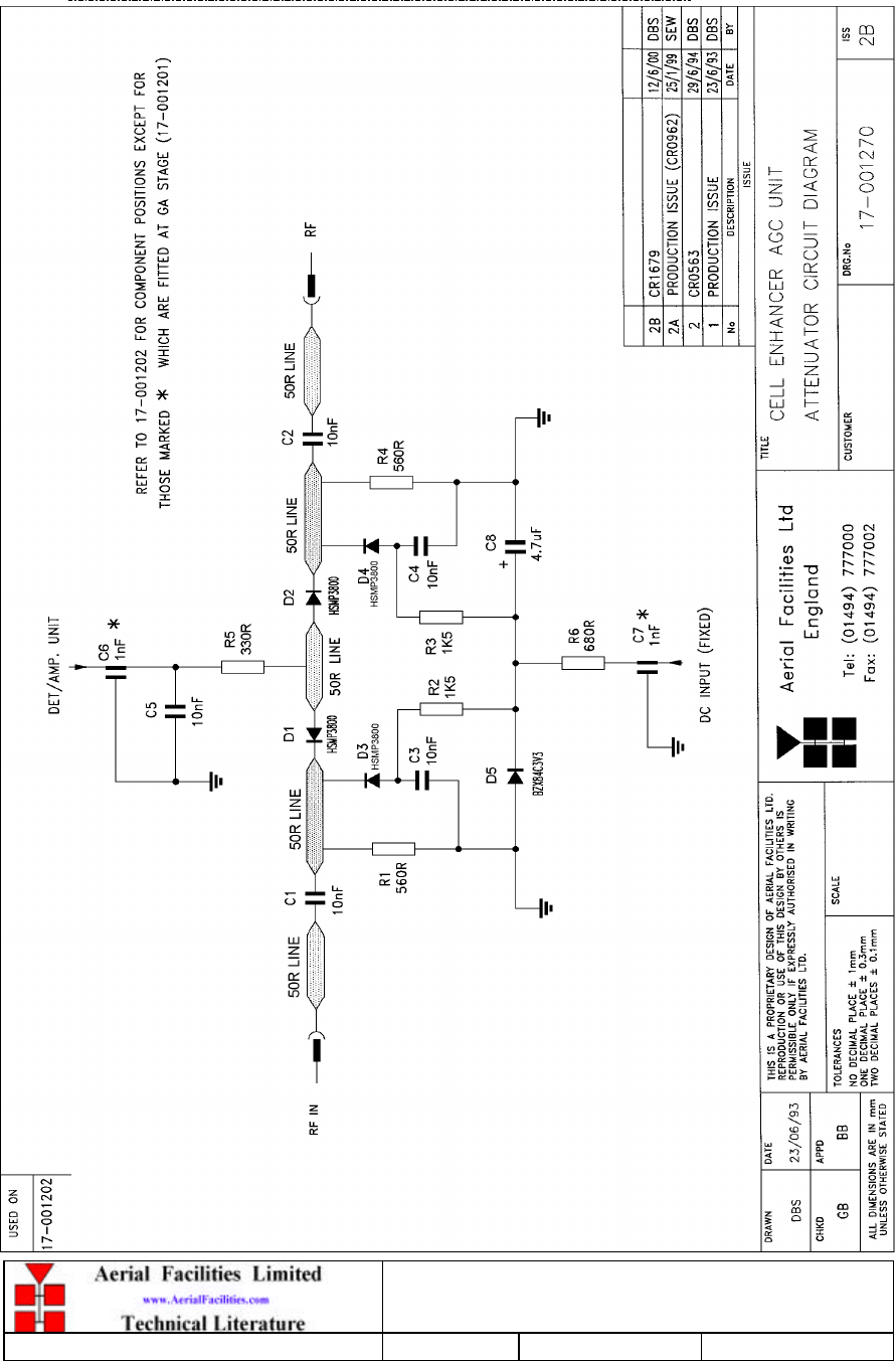
P B L Tunnels Loc 2 Units 1 & 2 + 800MHz BDA
Maintenance Handbook
H/book Number:-60-056100HBKM Issue No:-1 Date:-13/02/2003 Page:-60 of 60
5.1.7.6 Drg. No. 17-001270, AGC Attenuator Circuit Diagram

P B L Tunnels Loc 2 Units 1 & 2 + 800MHz BDA
Maintenance Handbook
H/book Number:-60-056100HBKM Issue No:-1 Date:-13/02/2003 Page:-61 of 61
5.1.8 24V Single Relay Board (80-008902)
5.1.8.1 Description
The General Purpose Relay Board allows the inversion of signals and the isolation of
circuits. It is equipped with a single dual pole change-over relay RL1, with completely
isolated wiring, accessed via a 15 way in-line connector.
The relay is provided with polarity protection diodes and diodes for suppressing the
transients caused by "flywheel effect" which can destroy switching transistors or induce
spikes on neighbouring circuits. It’s common use is to amalgamate all the alarm signals
into one, volts-free relay contact pair for the main alarm system.
Note that the board is available for different voltages (12 or 24V) depending on the type
of relay fitted at RL1.
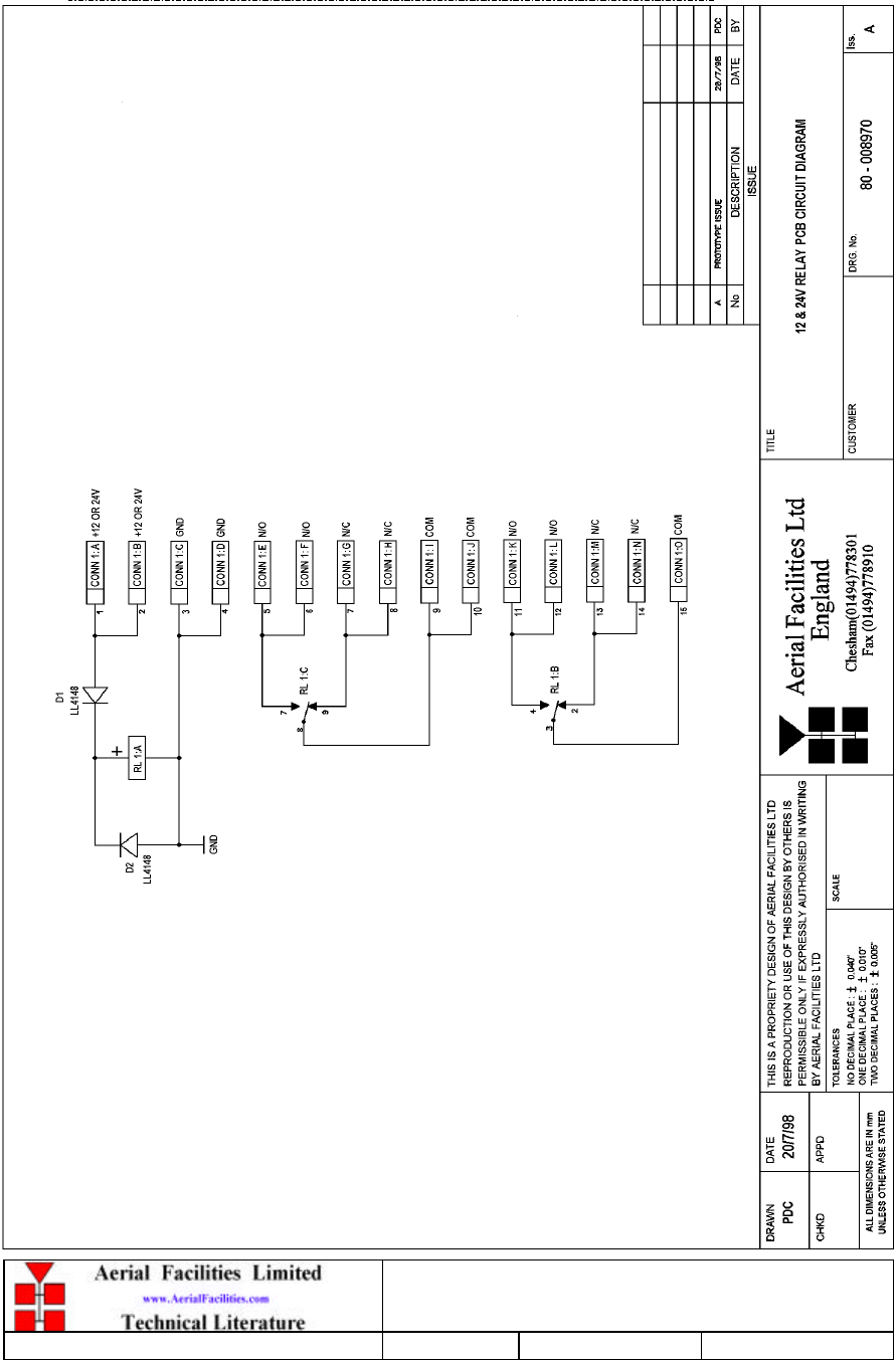
P B L Tunnels Loc 2 Units 1 & 2 + 800MHz BDA
Maintenance Handbook
H/book Number:-60-056100HBKM Issue No:-1 Date:-13/02/2003 Page:-62 of 62
5.1.8.2 Drg. No. 80-008970, Single Relay Board Circuit Diagram
P B L Tunnels Loc 2 Units 1 & 2 + 800MHz BDA
Maintenance Handbook
H/book Number:-60-056100HBKM Issue No:-1 Date:-13/02/2003 Page:-63 of 63
5.1.9 24V 400W Flat-Pack Power Supply (96-300011)
5.1.9.1 Description
The power supply unit is a switched-mode type capable of supplying 24V DC at 16.0Amps
continuously. Equipment of this type typically requires approximately 10.0 Amps at 24V
DC, so the PSU will be used conservatively ensuring a long operational lifetime.
No routine maintenance of the PSU is required. If a fault is suspected, then the output
voltage from the power supply may be measured on its output terminals. This is typically
set to 24.5V.
All the PSU’s used in AFL Cell Enhancers are capable of operation from either 110 or
220V nominal AC supplies. The line voltage is sensed automatically, so no adjustment or
link setting is needed by the operator. No drawings of the PSU are available.
5.1.9.2 Technical Specification
AC Input Supply:
Voltage:
110 or 220V nominal - 90 to 132 or 180 to
264V (single phase, absolute limits)
Frequency:
47 to 63Hz
DC Output Supply:
Voltage:
24V DC (nominal), 22 to 26V (absolute
limits)
Current:
16.0A
operational: -10BC to +55BC Temperature
range: storage: -40BC to +70BC
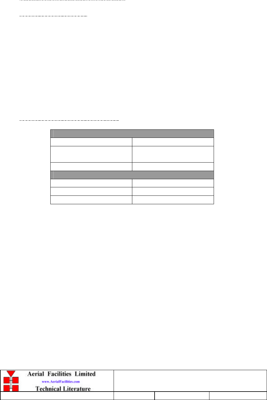
P B L Tunnels Loc 2 Units 1 & 2 + 800MHz BDA
Maintenance Handbook
H/book Number:-60-056100HBKM Issue No:-1 Date:-13/02/2003 Page:-64 of 64
5.1.10 JWS75-15/A PSU (96-300045)
5.1.10.1 Description
The power supply unit is a switched-mode type capable of supplying 24V DC at 6.25Amps
continuously. This PSU is used to provide power for the fibre optic modules which will
typically require approximately 3.0 Amps at 24V DC, so the PSU will be used conservatively
ensuring a long operational lifetime.
No routine maintenance of the PSU is required. If a fault is suspected, then the output
voltage from the power supply may be measured on its output terminals. This is typically set
to 24.5V.
All the PSU’s used in AFL Cell Enhancers are capable of operation from either 110 or 220V
nominal AC supplies. The line voltage is sensed automatically, so no adjustment or link
setting is needed by the operator.
5.1.10.2 Technical Specification
AC Input Supply:
Voltage: 110 or 220V nominal
90 to 132 or 180 to 264V
(absolute limits)
Frequency: 47 to 63Hz
DC Output Supply:
Voltage: 24V DC (nominal)
22 to 26V (absolute limits)
Current: 6.25A

P B L Tunnels Loc 2 Units 1 & 2 + 800MHz BDA
Maintenance Handbook
H/book Number:-60-056100HBKM Issue No:-1 Date:-13/02/2003 Page:-65 of 65
5.1.11 Fibre Optic Receiver & Transmitter (98-200003 & 98-300003)
5.1.11.1 Description
The F/O units consist of a receiver & transmitter, which modulates the RF signal onto a laser
carrier and transmits it via fibre/optic cable to a receiver unit some distance away where it is
demodulated back to the original RF signal with very small values of accrued attenuation.
Both transmitter and receiver modules have their own dedicated alarm outputs (volt-free relay
contacts) which are integrated into the main alarm system. Being O.E.M devices, no drawings
or circuit diagrams are available.
Caution: The FO units are NOT weather proof.
P B L Tunnels Loc 2 Units 1 & 2 + 800MHz BDA
Maintenance Handbook
H/book Number:-60-056100HBKM Issue No:-1 Date:-13/02/2003 Page:-66 of 66
5.1.11.2 Technical Specification
Tx: 120mA @ 15V DC (320mA @ -10BC)
Power Consumption: Rx: 330mA @ 15V DC
Frequency Range:
0.1 – 2.2GHz
Link noise figure:
40dB (typical)
Link noise figure (max.):
<45dB
Total link gain:
0dB
@30KHz B/W:
>84dB
@200KHz B/W:
>76dB
CNR @ 5 Km link length:
@1.2MHz B/W:
>69dB
RF total input power:
0dBm
Input IP3:
26dBm
Optical budget:
2 – 9.0dB
Max. link length:
20Km
Response Flatness:
<±1.0 dB
Optical Output Power (Tx):
2.4 – 4.0mW
Optical Wavelength:
1310±10nm
Fibre loss:
0.38dB/Km
Optical return loss:
-60dB
Optical Connector loss:
0.5dB per mated pair
Rx ‘D’ Type Female Connector
Pin No. Signal Description
1 +15V DC Power
2 Optional Data Output
3 Power Ground
4 RF Signal Strength Monitor
5 Optical Power Monitor
6 O.C. Alarm
7 Optional Data Output
8 Relay Alarm Contact 1
9 Relay Alarm Contact 2
Tx ‘D’ Type Female Connector
Pin No. Signal Description
1 +15V DC Power
2 Optional Data Input
3 Power Ground
4 RF Signal Strength Monitor
5 Laser Photodiode Current Monitor
6 Laser Current Monitor
7 Optional Data Input
8 Relay Alarm Contact 1
9 Relay Alarm Contact 2
P B L Tunnels Loc 2 Units 1 & 2 + 800MHz BDA
Maintenance Handbook
H/book Number:-60-056100HBKM Issue No:-1 Date:-13/02/2003 Page:-67 of 67
5.2 Location 2, Unit 2 (60-056102)
5.2.1 Two Section Notch Filter (02-010401)
5.2.1.1 Description
Fitted in Unit 2 after the amplification stages is a 2 element notch filter (one in downlink,
one in uplink), which is designed to reject the uplink frequencies in the downlink path and
vice-versa. The notch filter is not required for Unit One as the rejection from the two
series bandpass filters as apposed to one, is sufficient to meet the specification.
5.2.1.2 Technical Specification
Response type: Chebyshev
Frequency range:
485-486MHz
Bandwidth:
1MHz (tuned to spec.)
No. of sections:
2
Insertion loss:
dB
VSWR:
Better than 1.2:1
Connectors:
SMA
Power Handling:
100W maximum
operate:
-20°C to +55°C
Temperature range: store:
-40°C to +70°C
Weight:
3 kg
Size:
384 x 82.5 x 56.4mm
P B L Tunnels Loc 2 Units 1 & 2 + 800MHz BDA
Maintenance Handbook
H/book Number:-60-056100HBKM Issue No:-1 Date:-13/02/2003 Page:-68 of 68
5.2.2 Crossband Couplers (07-004801 & 07-005705)
5.2.2.1 Description
The purpose of a crossband coupler is to either combine/split transmission signals from
different parts of the frequency spectrum.
The crossband coupler fitted here, is the means by which the separate UHF & GSM frequency
band signals are mixed to form a composite RF signal.
It basically comprises of a 3 port device, two filters, one a low pass the other a high pass, that
are then mixed and fed to a common output. The couplers are built into a machined aluminium
casing having a centre screening wall between the filter sections and lid secured by screws at
frequent intervals over its perimeter to obtain a tight seal and to ensure linearity and stability
of response.
5.2.2.2 Technical Specification (07-004801)
Part No:
07-004801
390-490MHz
Passband:
700-900MHz
No. Of i/p ports:
2
No. Of o/p ports:
1
Insertion loss:
0.5dB (typical)
>40dB 390-490MHz
Isolation:
>40dB 700-900MHz
Impedance:
50O
Connectors:
SMA female
Power rating:
50Watts (CW)
5.2.2.3 Technical Specification
Passband 250 MHz
380 MHz 70-250 MHz
380-960 MHz
Power Rating
50 Watts (CW)
Number of Input ports
2
Number of Output ports
1
Insertion loss
0.5 dB
Isolation
> 50 dB 70-250 MHz
> 50 dB 380-960 MHz
(15 dB typical return loss 500-960)
Impedance
50 O
Connectors
SMA- female
All other modules in this unit are described elsewhere in this document.
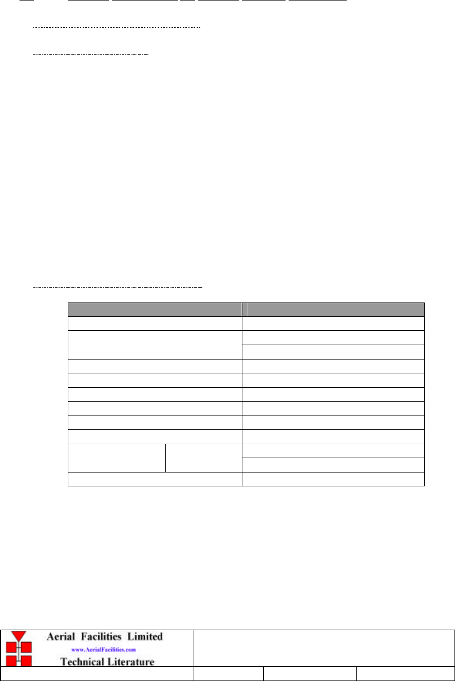
P B L Tunnels Loc 2 Units 1 & 2 + 800MHz BDA
Maintenance Handbook
H/book Number:-60-056100HBKM Issue No:-1 Date:-13/02/2003 Page:-69 of 69
5.3 800MHz Bi-Directional Air Interface Amplifier (60-056103)
5.3.1 Bandpass Filter (02-007201)
5.3.1.1 Description
The bandpass filters are multi-section designs with a bandwidth dependent upon the passband
frequencies, (both tuned to customer requirements). The response shape is basically
Chebyshev with a passband design ripple of 0.1dB. The filters are of slot coupled, folded
combline design, and are carefully aligned during manufacture in order to optimise the
insertion loss, VSWR and intermodulation characteristics of the unit. The tuned elements are
silver-plated to reduce surface ohmic losses and maintain a good VSWR figure and 50? load
at the input and output ports.
Being passive devices, the bandpass filters should have an extremely long operational life and
require no maintenance. Should a filter be suspect, it is usually most time efficient to replace
the module rather than attempt repair or re-tuning.
No adjustments should be attempted without full network sweep analysis facilities to monitor
both insertion loss and VSWR simultaneously.
5.3.1.2 Technical Specification
Parameter Specification
Response Type
Chebyshev
857-860MHz (downlink)
Frequency Range: 812-815MHz (uplink)
Bandwidth: 3MHz (tuned)
Number of Sections: 8
Insertion Loss: 1.2 dB
VSWR: better than 1.2:1
Connectors: SMA female
Power Handling: 100W max
-20°C to +60°C Temperature
range: operation:
storage: -40°C to +70°C
Weight:
3 3.0kg (typical)
P B L Tunnels Loc 2 Units 1 & 2 + 800MHz BDA
Maintenance Handbook
H/book Number:-60-056100HBKM Issue No:-1 Date:-13/02/2003 Page:-70 of 70
5.3.2 ¼Watt 0- -30dB Switched Attenuator (10-000701) See section 5.1.2
5.3.3 Low Noise Amplifiers (11-005902 & 11-006702)
5.3.3.1 Description
The Gallium-Arsenide low noise amplifier used in the unit is a double stage, solid-state low
noise amplifier. Class A circuitry is used throughout the units to ensure excellent linearity and
extremely low noise over a very wide dynamic range. The active devices are very moderately
rated to provide a long trouble-free working life. There are no adjustments on these
amplifiers, and in the unlikely event of a failure, then the complete amplifier should be
replaced. This amplifier features its own in-built alarm system which gives a volt-free relay
contact type alarm that is easily integrated into the main alarm system.
5.3.3.2 Technical Specification (11-005902)
Frequency Range: 800 – 960MHz
Bandwidth: <170MHz
Gain: 19.5dB (typical)
1dB Compression Point: 21dBm
OIP3: 33dBm
Input/Output Return Loss: >20dB
Noise Figure: 1dB (typical)
Power Consumption: 190mA @ 24V DC
Supply Voltage: 10-24V DC
Connectors: SMA female
operational: -10°C to +55°C
Temperature Range: storage: -40°C to +70°C
Size: 90 x 55 x 30.2mm
Weight: 280gms (approximately)
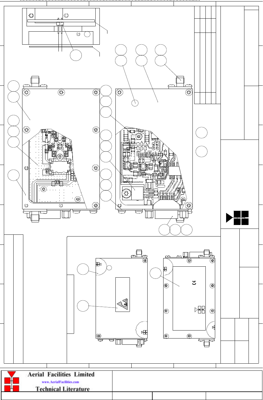
P B L Tunnels Loc 2 Units 1 & 2 + 800MHz BDA
Maintenance Handbook
H/book Number:-60-056100HBKM Issue No:-1 Date:-13/02/2003 Page:-71 of 71
5.3.3.3 Drg. No. 11-005902 LNA General Assembly Drawing
BYDATEDESCRIPTIONNo
ISSUE
1
2
3
4
5
6
7
8
9
A
B
C
D
E
F
1
2
3
4
5
6
7
8
9
F
E
D
A
B
C
Fax : 01494 777002
Tel : 01494 777000
Aerial Facilities Ltd
TWO DECIMAL PLACES ± 0.1mm
ONE DECIMAL PLACE ± 0.3mm
NO DECIMAL PLACE ± 1mm
BY AERIAL FACILITIES LTD.
PERMISSIBLE ONLY IF EXPRESSLY AUTHORISED IN WRITING
REPRODUCTION OR USE OF THIS DESIGN BY OTHERS IS
THIS IS A PROPRIETARY DESIGN OF AERIAL FACILITIES LTD.
DRAWN
CHKD
ALL DIMENSIONS ARE IN mm
UNLESS OTHERWISE STATED
APPD
DATE
TOLERANCES SCALE
England
CUSTOMER DRG.No
TITLE
A
3
900MHz LOW NOISE AMPLIFIER
WITH RELAY ASSEMBLY DRAWING
11-005902
AA
1.5:1
MNR 25/03/02
PRE-PRODUCTION ISSUE
25/03/02
MNR
R53
+
J5
R59
C5
RL1
R58
CON1
Limited
Aerial Facilities
VOUT R55
R54
D3
VR1
IC4
R41
R42
k
C19
C16
J4
J2 J1
C10
C6
+
+
C4
REG3
VIN
ABC
R39
+
ZD3
C14
+
IC3
R38
R40
+
C17
+
+
C15
C8
R52
C13
IC2
C7
C11
++
C9 R47
R50
J3
+C12
R51
R48
R44R43
REG1
R46
COMPONENTS TO BE ADDED TO 11-003912,ITEM 15,DC PCB SUB-ASSEMBLY
5
21
2
22
2
4 24
2
IN 2 PLACES
25
4
3
327
17 24
2
8 26 30 27
2
20
2
1533
2
27
5
16 23
5
1
6
IN 2 PLACES
2 25
10
DC PCB
RF PCB
R49
11-005925 ISS.1
R2
R4
C2
L2
L4
C10
TR2
L6
R6
R12
R11
C4
R5
C1
R3
R1
L5
R10
R15
CPL2
R13
R14
COMPONENTS TO BE ADDED TO 11-005911,ITEM 16,RF PCB SUB-ASSEMBLY
2. LIDS,ITEMS 2 & 3 AND LABELS,
1. SOLDER JOINTS TO BE MADE USING OR
2819
34
see note 2
LABEL DETAILS - SCALE 1:1
35
see note 2
see note 2
31
IN 4 PLACES
ITEMS 31,34 & 35,TO BE FITTED ON TEST
AFL
********
11-005902
800-1000MHz
20dB 12-24vDC
**/**/20**
Limited
Aerial Facilities
IN
REF.
FREQ.
GAIN
S/N
DATE
0086
OUT
AFL
SENSITIVE
DEVICES
ELECTROSTATIC
OBSERVE PRECAUTIONS
ATTENTION
FOR HANDLING
AFL
PRODUCTION ISSUE(ECN2539) MNR
08/04/02
1A
AC IB
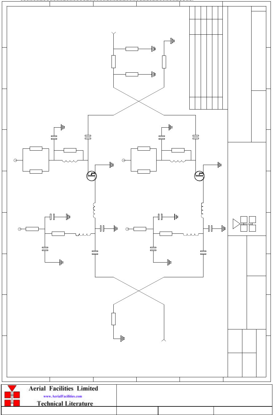
P B L Tunnels Loc 2 Units 1 & 2 + 800MHz BDA
Maintenance Handbook
H/book Number:-60-056100HBKM Issue No:-1 Date:-13/02/2003 Page:-72 of 72
5.3.3.4 Drg. No. 11-005970, LNA Circuit Diagram (RF)
900MHz LOW NOISE AMPLIFIER (RF)
CIRCUIT DIAGRAM
11-005970
AA
N.T.S
MNR 21/03/02
C8
TR2
R8
C4
C6
R12
R6
C2
R3 R4
C10
TR1
R11
C3
C7
C5
R7
R1 R2
R5
C9
C1
R9
R10
R13
R14 R15
C12
C11
BYDATEDESCRIPTIONNo
ISSUE
1 2 3 4 5 6 7 8 9
A
B
C
D
E
F
12 3 45 6 78 9
A
B
C
D
E
F
Fax : 01494 777002
Tel : 01494 777000
Aerial Facilities Limited
THIS IS A PROPRIETARY DESIGN OF AERIAL FACILITIES LTD.
REPRODUCTION OR USE OF THIS DESIGN BY OTHERS IS
PERMISSIBLE ONLY IF EXPRESSLY AUTHORISED IN WRITING
BY AERIAL FACILITIES LTD.
NO DECIMAL PLACE ± 1mm
ONE DECIMAL PLACE ± 0.3mm
TWO DECIMAL PLACES ± 0.1mm
ALL DIMENSIONS ARE IN mm
UNLESS OTHERWISE STATED
CHKD
DRAWN
APPD
DATE
TOLERANCES SCALE England
CUSTOMER DRAWING.No
TITLE
3
A
SG
D
S
G
D
CPL 1 CPL 2
-ve2 +ve2
-ve1 +ve1
RF IN
RF OUT
51R
51R
0R0(NOMI)
220pF
100pF
100pF
L2
L4
82nH
150R
10K 22R 22R
150R
12nH
L6
4.7pF
220pF
82nH
L3
L1
150R
10uF
100pF
10uF
10K
12nH
L5
4.7pF
150R
100pF
22R22R
PRE-PRODUCTION ISSUE
21/03/02
MNR
1.0pF
1.0pF
+
+
SAT
SAT SAT
1D1304-3 1D1304-3
FSU02LG
FSU02LG
PRODUCTION ISSUE(ECN2539) MNR
08/04/02
1A
AC IB
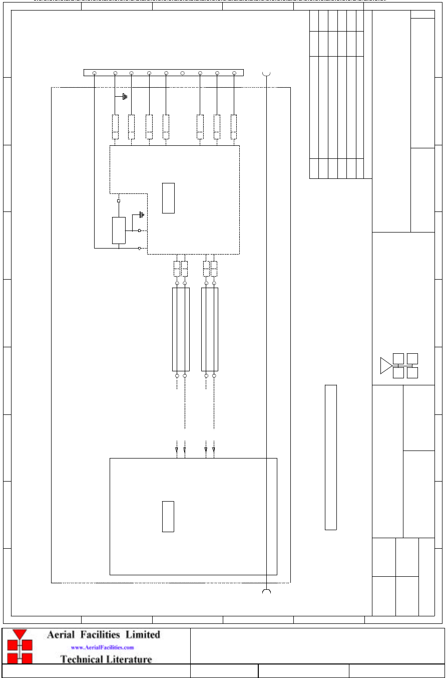
P B L Tunnels Loc 2 Units 1 & 2 + 800MHz BDA
Maintenance Handbook
H/book Number:-60-056100HBKM Issue No:-1 Date:-13/02/2003 Page:-73 of 73
5.3.3.5 Drg. No. 11-005971, LNA Circuit Diagram (DC Wiring Layout)
900MHz LOW NOISE AMPLIFIER
SCHEMATIC DIAGRAM
11-005971
AA
-
MNR 26/03/02
BYDATEDESCRIPTIONNo
ISSUE
1 2 3 4 5 6 7 8 9
A
B
C
D
E
F
12 3 45 6 78 9
A
B
C
D
E
F
Fax : 01494 777002
Tel : 01494 777000
Aerial Facilities Limited
THIS IS A PROPRIETARY DESIGN OF AERIAL FACILITIES LTD.
REPRODUCTION OR USE OF THIS DESIGN BY OTHERS IS
PERMISSIBLE ONLY IF EXPRESSLY AUTHORISED IN WRITING
BY AERIAL FACILITIES LTD.
NO DECIMAL PLACE ± 1mm
ONE DECIMAL PLACE ± 0.3mm
TWO DECIMAL PLACES ± 0.1mm
ALL DIMENSIONS ARE IN mm
UNLESS OTHERWISE STATED
CHKD
DRAWN
APPD
DATE
TOLERANCES SCALE England
CUSTOMER DRAWING.No
TITLE
3
A
LM7808CT
REG3
G
IO
+ve1 (6.75v @ 64mA)
-ve1
-ve2
J4 1
J5
J4
10-24V DC I/P
GROUND
2
1
7
TTL VOLTAGE SET
8
TTL ALARM/0v GOOD
9
OC GOOD/0v BAD
9 WAY 'D'
PIN OUTS
CON1
J4 2
J5 1
J5 2
DC INPUT DC OUTPUT
RF PCB
FOR CIRCUIT DIAGRAM
SEE 11-005970
SEE 11-003971
FOR CIRCUIT DIAGRAM
DC PCB
PRE-PRODUCTION ISSUE
26/03/02
MNR
+8V C
BA
7 CON1
8 CON1
9 CON1
2 CON1
RF
IN
RF
OUT
+ve2 (6.75v @ 64mA)
RELAY CONTACT GOOD *
RELAY COMMON *
RELAY CONTACT BAD *
5 CON1
4 CON1
3 CON1
5
4
3
6
* ONLY APPLIES TO 11-005902 AMPLIFIER
PRODUCTION ISSUE(ECN2539) MNR
08/04/02
1A
AC IB
P B L Tunnels Loc 2 Units 1 & 2 + 800MHz BDA
Maintenance Handbook
H/book Number:-60-056100HBKM Issue No:-1 Date:-13/02/2003 Page:-74 of 74
5.3.3.6 Technical Specification (11-006702)
Frequency Range:
800 – 1000MHz
Bandwidth:
<200MHz
Gain:
29dB (typical)
1dB Compression Point:
20dBm
OIP3:
33dBm
Input/Output Return Loss:
>18dB
Noise Figure:
1.3dB (typical)
Power Consumption:
180mA @ 24V DC
Supply Voltage:
10-24V DC
Connectors:
SMA female
operational: -10°C to +55°C
Temperature Range: storage: -40°C to +70°C
Size:
90 x 55 x 30.2mm
Weight:
290gms (approximately)
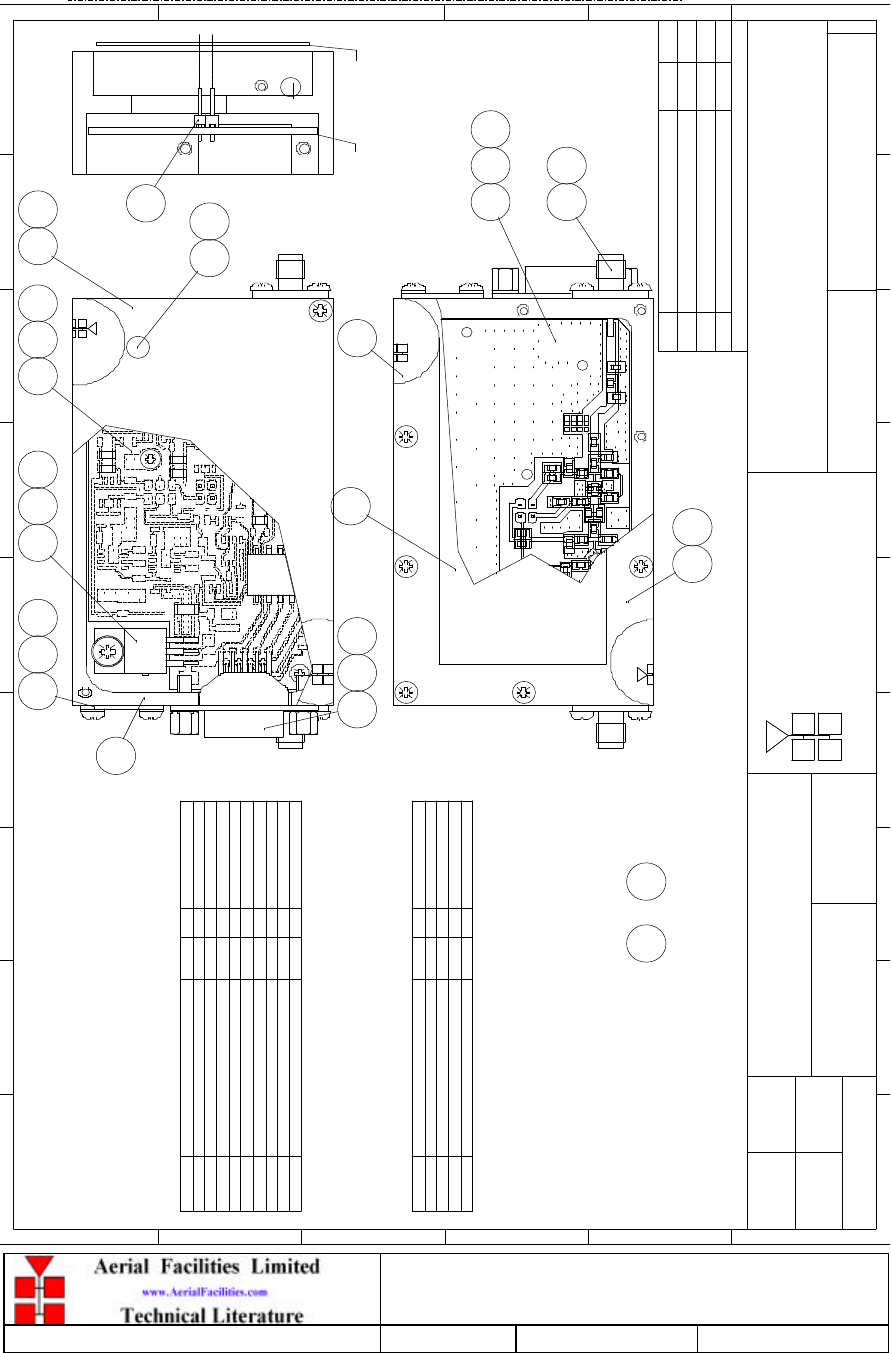
P B L Tunnels Loc 2 Units 1 & 2 + 800MHz BDA
Maintenance Handbook
H/book Number:-60-056100HBKM Issue No:-1 Date:-13/02/2003 Page:-75 of 75
5.3.3.7 Drg. No. 11-006702, LNA General Assembly Drawing
800-1000MHz LOW NOISE AMP. (RELAY)
(RF AND DC) 29dB GAIN. GENERAL ASSY
11-006702
AA
1.5:1
DBS 25/03/02
19 28
22
2
21
2
26
5
24
2
1
17 33
2
8 3
327
1530 27
2
20
2
6
IN 4 PLACES
25
4
see note 2
25
10
see note 2
31
IN 4 PLACES
2
34
see note 3
24
2
IN 2 PLACES
4
27
5
16 23
5
BYDATEDESCRIPTIONNo
ISSUE
1
2
3
4
5
6
7
8
9
A
B
C
D
E
F
1
2
3
4
5
6
7
8
9
F
E
D
A
B
C
Fax : 01494 777002
Tel : 01494 777000
Aerial Facilities Ltd
TWO DECIMAL PLACES ± 0.1mm
ONE DECIMAL PLACE ± 0.3mm
NO DECIMAL PLACE ± 1mm
BY AERIAL FACILITIES LTD.
PERMISSIBLE ONLY IF EXPRESSLY AUTHORISED IN WRITING
REPRODUCTION OR USE OF THIS DESIGN BY OTHERS IS
THIS IS A PROPRIETARY DESIGN OF AERIAL FACILITIES LTD.
DRAWN
CHKD
ALL DIMENSIONS ARE IN mm
UNLESS OTHERWISE STATED
APPD
DATE
TOLERANCES SCALE
England
CUSTOMER DRG.No
TITLE
A
3
PROTOTYPE ISSUE
19/2/02
DBS
1. SOLDER JOINTS TO BE MADE USING OR
2. LIDS,ITEMS 2 & 3 AND WARRANTY LABELS,ITEM 31,TO BE FITTED ON TEST
3. LABEL,ITEM 34,TO BE FITTED ON TEST.FOR LAYOUT SEE DRAWING 11-006790
COMPONENTS TO BE ADDED TO 11-003912,ITEM 15,DC PCB SUB-ASSEMBLY
AFL
O/P
CON1
RL1
REG3
A CB
R40
I/P
J4J5
R43 R44
R51 R50
AFL
DC PCB RF PCB
COMPONENTS TO BE ADDED TO 11-006711,ITEM 16,RF PCB SUB-ASSEMBLY
see note 2
R6
C9
I/P
R1
Issue B
C5
R4
C2 R3
L1 C4
R5
TR2
L2
-Ve2
C10
R7
+Ve2
R8
C7
C6
L3
R9
C11
CON2
OUTPUT
R12
R10
R11
11-006725
-Ve1 +Ve1
AFL
O/P
0R0 0.1W 2% 0805 CHIP RESISTOR93-630079
Select on test
Select on test
DESCRIPTIONDRG No.
R11 on 11-006711
CIRCUIT REF
6
ITEM No.
R101
1
2
R12
QTY
ICD 2 WAY 0.1" PITCH JUMPER HEADER
COMPONENTS TO BE ADDED TO 11-006711,ITEM 16,RF PCB SUB-ASSEMBLY
COMPONENTS TO BE ADDED TO 11-003912,ITEM 15,DC PCB SUB-ASSEMBLY
94-300018
93-630135
93-630018
93-630016
91-700072
93-630015
LM7808CT 8V VOLTAGE REGULATOR
56R 0.125W 2% RESISTOR CHIP
0R0 0.5W 1% 2010 RESISTOR CHIP
DESCRIPTION
33R 0.125W 2% RESISTOR CHIP
39R 0.125W 2% RESISTOR CHIP
DRG No.
REG3 on 11-003912
R40 on 11-003912
R50/51 on 11-003912
12
8
11
1
1
2
J4/J5
R44 on 11-003912
CIRCUIT REF
R43 on 11-003912
6
10
9
ITEM No.
2
1
1
QTY
96-910009 5V DPDT SMD G6H-2F LOW PROFILE 35 1 RL1 on 11-003912
4.7KR 0.125W 2% RESISTOR CHIP93-630049 36 1 R59 on 11-003912
R59
AC IB
MINOR CHANGE DBS
26/3/02
AB
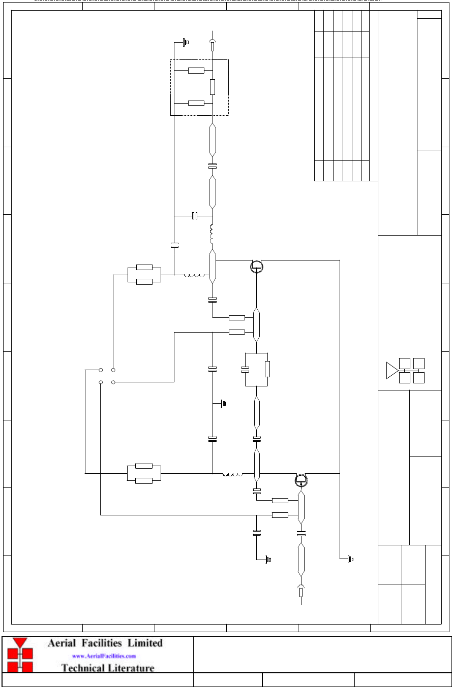
P B L Tunnels Loc 2 Units 1 & 2 + 800MHz BDA
Maintenance Handbook
H/book Number:-60-056100HBKM Issue No:-1 Date:-13/02/2003 Page:-76 of 76
5.3.3.8 Drg. No. 11-006770, LNA Circuit Diagram (RF Components)
800-1000MHz LOW NOISE AMP. 29dB
(RF) PCB CIRCUIT DIAGRAM
11-006770
AA
-
DBS 18/2/02
C1
C6
C3 C2
C9
C8
C4
C11
C10 C7C5
BYDATEDESCRIPTIONNo
ISSUE
1 2 3 4 5 6 7 8 9
A
B
C
D
E
F
12 3 45 6 78 9
A
B
C
D
E
F
Fax : 01494 777002
Tel : 01494 777000
Aerial Facilities Limited
THIS IS A PROPRIETARY DESIGN OF AERIAL FACILITIES LTD.
REPRODUCTION OR USE OF THIS DESIGN BY OTHERS IS
PERMISSIBLE ONLY IF EXPRESSLY AUTHORISED IN WRITING
BY AERIAL FACILITIES LTD.
NO DECIMAL PLACE ± 1mm
ONE DECIMAL PLACE ± 0.3mm
TWO DECIMAL PLACES ± 0.1mm
ALL DIMENSIONS ARE IN mm
UNLESS OTHERWISE STATED
CHKD
DRAWN
APPD
DATE
TOLERANCES SCALE England
CUSTOMER DRAWING.No
TITLE
3
A
CONNECTIONS TO DC BOARD
-Ve1 +Ve1
-Ve2 +Ve2
RF INPUT
RF OUTPUT
R11
R10 R12
R8 R9
R4 R5
R3
R6 R7
R1 R2
10nF 100pF
910R 470R
100pF ATF-33143
100pF
10R
15pF
82nH
100pF 10nF
430R 1K2
CLY2
82nH
100pF
6n8H
1.8pF
220pF
180R 180R 18R 22R
SELECT VALUES ON TEST
REFER TO CIRCUIT COMPONENT LIST FOR FURTHER INFORMATION
PROTOTYPE ISSUE
18/2/02
DBS
100pF
L3
L2
L1
G S
D
TR1
G S
D
TR2
PRODUCTION ISSUE(ECN2538) MNR
11/07/02
1A
AC IB
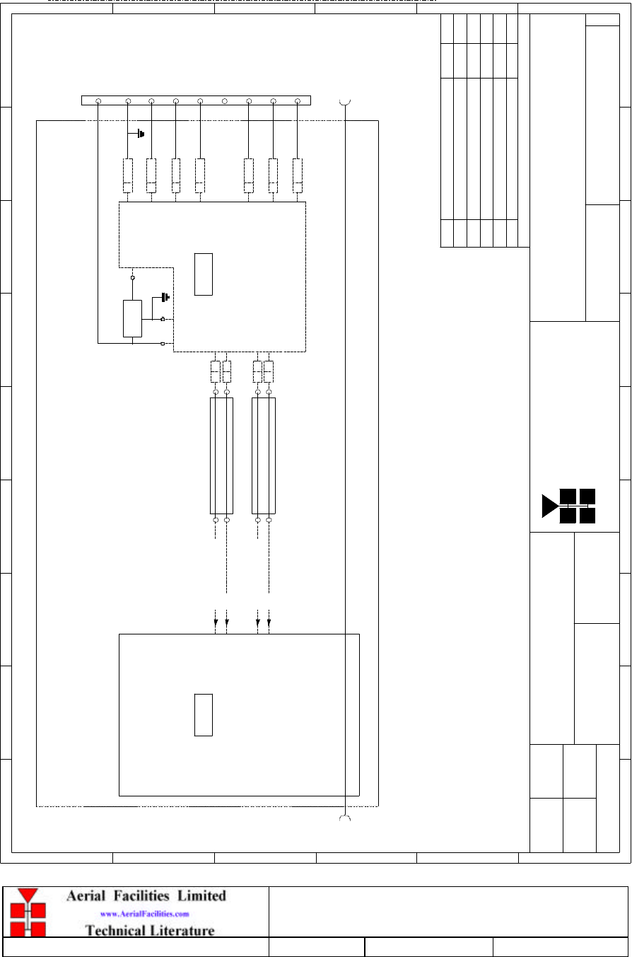
P B L Tunnels Loc 2 Units 1 & 2 + 800MHz BDA
Maintenance Handbook
H/book Number:-60-056100HBKM Issue No:-1 Date:-13/02/2003 Page:-77 of 77
5.3.3.9 Drg. No. 11-006771, LNA DC Wiring Diagram
BYDATEDESCRIPTIONNo
ISSUE
1 2 3 4 5 6 7 8 9
A
B
C
D
E
F
1
2
3
4
5
6
7
8
9
A
B
C
D
E
F
Fax : 01494 777002
Tel : 01494 777000
Aerial Facilities Limited
THIS IS A PROPRIETARY DESIGN OF AERIAL FACILITIES LTD.
REPRODUCTION OR USE OF THIS DESIGN BY OTHERS IS
PERMISSIBLE ONLY IF EXPRESSLY AUTHORISED IN WRITING
BY AERIAL FACILITIES LTD.
NO DECIMAL PLACE ± 1mm
ONE DECIMAL PLACE ± 0.3mm
TWO DECIMAL PLACES ± 0.1mm
ALL DIMENSIONS ARE IN mm
UNLESS OTHERWISE STATED
CHKD
DRAWN
APPD
DATE
TOLERANCES SCALE England
CUSTOMER DRAWING.No
TITLE
3
A
800-1000MHz LOW NOISE AMPLIFIER 29dB
(RF AND DC) SCHEMATIC DIAGRAM
11-006771
AA
-
DBS 19/2/02
LM7808CT
REG3
G
IO
+ve1 (6.75v @ 45mA)
-ve1
-ve2
J4 1
J5
J4
10-24V DC I/P
GROUND
2
1
7
TTL VOLTAGE SET
8
TTL ALARM/0v GOOD
9
OC GOOD/0v BAD
9 WAY 'D'
PIN OUTS
CON1
J4 2
J5 1
J5 2
DC INPUT DC OUTPUT
RF PCB
FOR CIRCUIT DIAGRAM
SEE 11-006770
SEE 11-003971
FOR CIRCUIT DIAGRAM
DC PCB
PROTOTYPE ISSUE
19/2/02
DBS
+8V C
BA
7 CON1
8 CON1
9 CON1
2 CON1
RF
IN
RF
OUT
+ve2 (6.75v @ 70mA)
RELAY CONTACT GOOD
RELAY COMMON
RELAY CONTACT BAD
5 CON1
4 CON1
3 CON1
5
4
3
6
*
*
*
= ONLY APPLIES TO 11-006702
*
AC IB
P B L Tunnels Loc 2 Units 1 & 2 + 800MHz BDA
Maintenance Handbook
H/book Number:-60-056100HBKM Issue No:-1 Date:-13/02/2003 Page:-78 of 78
5.3.4 5Watt Power Amplifier (12-000201)
5.3.4.1 Description
The power amplifier fitted to this unit is a multi-stage, solid state power amplifier. Class A
circuitry is employed throughout the device to ensure excellent linearity over a wide
dynamic frequency range. All the semi-conductor devices are very conservatively rated to
ensure low device junction temperatures and a long, trouble free working lifetime.
The power amplifier should require no maintenance over its operating life. Under no
circumstances should the cover be removed or the side adjustments disturbed unless it is
certain that the amplifier has failed; since it is critically aligned during manufacture and any
re-alignment will require extensive test equipment.
5.3.4.2 Technical Specification
PARAMETER SPECIFICATION
Frequency Range: 800 – 970MHz
Bandwidth: <200MHz
Gain: 34dB (typical)
Power Output: >5.0Watts
1dB Compression Point: +36dBm
OIP3: +47dBm
Input/Output Return Loss: >14dB
RF Connectors SMA female
Power Consumption: 1.5A @ 24V DC
Operation: -10°C to +55°C Temperature
Range Storage: -40°C to +70°C
Size 250 x 125 x 38.6mm
Weight 400gms (approximately)
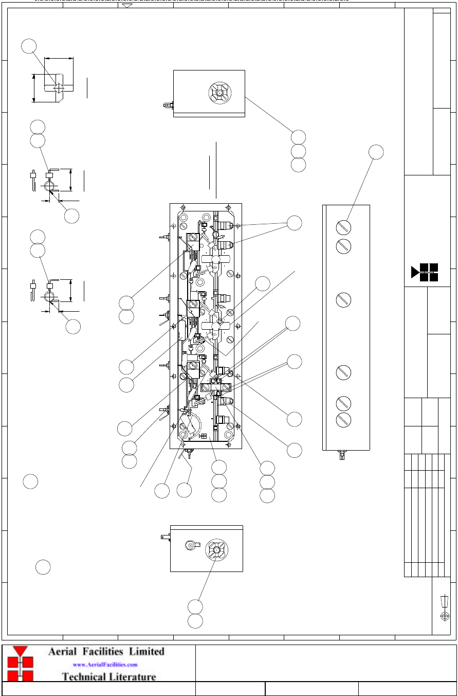
P B L Tunnels Loc 2 Units 1 & 2 + 800MHz BDA
Maintenance Handbook
H/book Number:-60-056100HBKM Issue No:-1 Date:-13/02/2003 Page:-79 of 79
5.3.4.3 Drg. No. 12-000201, LPA General Assembly Drawing
DATEDESCRIPTIONNo
ISSUE
THIRD ANGLE PROJECTION
1 2 3 45 6 7 8 9 10 11 12
A
B
C
D
E
F
G
H
1 2 3 4 5 6 7 8 9 10 11 12
A
B
C
D
E
F
G
H
THIS IS A PROPRIETARY DESIGN OF AERIAL FACILITIES LTD.
REPRODUCTION OR USE OF THIS DESIGN BY OTHERS IS
PERMISSIBLE ONLY IF EXPRESSLY AUTHORISED IN WRITING
ALL DIMENSIONS ARE IN mm
UNLESS OTHERWISE STATED
DRAWN DATE
CHKD APPD
TWO DECIMAL PLACES ± 0.1mm
BY AERIAL FACILITIES LTD.
ONE DECIMAL PLACE ± 0.3mm
NO DECIMAL PLACE ± 1mm
TOLERANCES SCALE
CUSTOMER DRAWING No
Aerial Facilities Limited
Chesham(01494)778301
Fax (01494)778910
England
TITLE
2
A
POWER AMPLIFIER,900MHz,ASSEMBLY
(WITHOUT HEATSINK)
12-000201
1:1
DJS 04/06/99
NOTES:-
1/. ALL SOLDERED JOINTS TO BE MADE USING ITEM .
2/. APPLY ITEM TO THE UNDERSIDE OF TRANSISTORS TR1,TR2 & TR3 BEFORE FITTING.
3/. GREAT CARE MUST BE TAKEN WHEN FITTING TR1 & TR2 IN ORDER TO PREVENT OVERTIGHTENING (USE TORQUE DRIVER SET TO 59cNm).
4/. FERRITE BEADS TO BE SECURED TO RESPECTIVE INDUCTORS USING NON-CORROSIVE SILICON RUBBER.
NOTE TURN ORIENTATION L1,L3 & L5 (DETAIL 1) ARE WOUND IN OPPOSITE DIRECTION TO L2,L4 & L6 (DETAIL 2).
5/. A THIN FILM OF ITEM 26 TO BE APPLIED TO MATING SURFACES OF ITEMS 1 & 3.
10
SEE NOTE 2
2036
2
30
2
35 429
26
19 POS
119
24
C37
C12
C13
C11 C9
Aerial Facilities
27
3 POS
14
C14
Limited
C33
1337
6 POS
C29
C36
L6
C30
R5
C10
TR3
+
C31
C28
L5
C8
C27
+
C26
REG3
TR2
L4
R4
C23
C25
R6
+
C24
12
6.5 I/D
23
SEE NOTE 4
DETAIL 1
VIEW WITH LID
R1
1.5 TURNS
8.00
20.00
C7
R2
C6
C4
9
22 25
C2
C3
C19 C18
L3
C5
C22 C21
+
REG2
C20
12-000225-2
+
L2
TR1
C34
R3
L1
17
16
4 POS
3631
C15
L7
C17
C1
+
REG1
C16
3 POS
629
4
2 POS
1A PRODUCTION ISSUE DJS
04/06/99
1232
14
SEE DETAIL 1
DETAIL 3
25.00
25.00
= =
= =
SEE DETAIL 3
AND HEATSINK REMOVED
20.00
8.00
1.5 TURNS
6.5 I/D
23
DETAIL 2
SEE NOTE 4
2522
33
(6 POSITIONS)
19
11
SEE DETAIL 2
9
(6 POSITIONS)
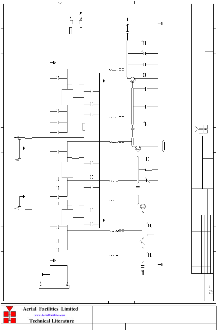
P B L Tunnels Loc 2 Units 1 & 2 + 800MHz BDA
Maintenance Handbook
H/book Number:-60-056100HBKM Issue No:-1 Date:-13/02/2003 Page:-80 of 80
5.3.4.4 Drg. No. 12-000270, 5Watt LPA Circuit Diagram
POWER AMPLIFIER,10W,CLASS AB,900MHz,
PCB SUB-ASSEMBLY,CIRCUIT DIAGRAM
12-000270
1A
DJS 03/06/99
DATEDESCRIPTIONNo
ISSUE
THIRD ANGLE PROJECTION
1 2 3 45 6 7 8 9 10 11 12
A
B
C
D
E
F
G
H
1 2 3 4 5 6 7 8 9 10 11 12
A
B
C
D
E
F
G
H
THIS IS A PROPRIETARY DESIGN OF AERIAL FACILITIES LTD.
REPRODUCTION OR USE OF THIS DESIGN BY OTHERS IS
PERMISSIBLE ONLY IF EXPRESSLY AUTHORISED IN WRITING
ALL DIMENSIONS ARE IN mm
UNLESS OTHERWISE STATED
DRAWN DATE
CHKD APPD
TWO DECIMAL PLACES ± 0.1mm
BY AERIAL FACILITIES LTD.
ONE DECIMAL PLACE ± 0.3mm
NO DECIMAL PLACE ± 1mm
TOLERANCES SCALE
CUSTOMER DRAWING No
Aerial Facilities Limited
Chesham(01494)778301
Fax (01494)778910
England
TITLE
2
A
REFER TO COMPONENTS LIST 12-00270 FOR FURTHER DETAILS
REFER TO 12-000201 & 12-000201 & FOR COMPONENT POSITIONS
CONDUCTORS SHOWN THUS: ARE 50 ohm STRIPLINES
470pF
RF INPUT
C1
TPV596A
TR1 56pF
R1
1KR
C5
RF OUTPUT
PRODUCTION ISSUE
03/06/99
DJS
1-14pF
C4C2
1-14pF
1.5-6pF
C3
R2
1KR
C6
1-14pF
TPV596A
TR2
TR3
C7
10pF 1-14pF
C9 15pF
C10 15pF
C11 10pF
C37 10pF
C36 1-14pF
C12 1-14pF
C13
TP3022A
C8
56pF
A
LM337T
REG1
I O
L7 L1 L2 L3 L4 L5 L6
C18
10nF 1uF
C19 10uF
C32 10nF
C24 1uF
C25 10uF
C33 C30
10nF 1uF
C31
I
A
O
REG2
I
A
REG3
O
LM337T LM337T
1uF
C17
10nF
C16
560pF
C15
24v dc
560pF
C21 C22
1uF10nF
C20
C34
560pF
C23
560pF 560pF
C29
560pF
C27 C28
1uF
C26
10nF
5R6
R4 R5
1R2
C14
10pF
R6
8R2
4K7
R9
C35
5R6
R3 1KR
R8
R7
1KR
1K
R11 1KR
R10
1nF 1nF 1nF
1nF
C38
+ + +
+++++
C40C41C42
1nF
C39
1nF

P B L Tunnels Loc 2 Units 1 & 2 + 800MHz BDA
Maintenance Handbook
H/book Number:-60-056100HBKM Issue No:-1 Date:-13/02/2003 Page:-81 of 81
5.3.4.5 Drg. No. 12-000270C1, LPA Parts List(1)
CIRC. DESCRIPTION
AFL STOCK REF.
REF.
CHANGE NoCHANGE NoCHANGE NoCHANGE No DATEDATEDATEDATE ISSUEISSUEISSUE
ISSUE
1 2 3 4 5
5
4
3
2
1
A
B
C
D
E
F
G
A
B
C
D
E
F
G
Aerial Facilities Limited
DRAWN DATE APPD
CHKD CUSTOMER
TITLE
COMPONENT LIST FOR
POWER AMPLIFIER,900MHz,PCB
CIRCUIT COMPONENT LIST (SHEET 1 OF 3)
12-000270C1
1A
DJS
04/06/99
04/06/99 PROD ISS.
C2
C4
C5
C3
93-200017C1 470pF CHIP CAPACITOR 10% TOL (MIN)
C9
C10
C7
C8
C6
C20
C18
C19
C17
C16
C14
C15
C12
C13
C11
C21
C23
C24
C22
1-14pF PCB MOUNT AIR TRIMMER CAPACITOR93-130023
1.5-6pF PCB CERAMIC AIR TRIMMER CAPACITOR93-130014
1-14pF PCB MOUNT AIR TRIMMER CAPACITOR93-130023
56pF CHIP CAPACITOR 10% TOL (MIN)93-200006
1-14pF PCB MOUNT AIR TRIMMER CAPACITOR
10pF CHIP CAPACITOR 10% TOL (MIN)93-200010
56pF CHIP CAPACITOR 10% TOL (MIN)93-200006
1-14pF PCB MOUNT AIR TRIMMER CAPACITOR
15pF CHIP CAPACITOR 10% TOL (MIN)93-200005
15pF CHIP CAPACITOR 10% TOL (MIN)93-200005
1-14pF PCB MOUNT AIR TRIMMER CAPACITOR
1-14pF PCB MOUNT AIR TRIMMER CAPACITOR
93-200010 10pF CHIP CAPACITOR 10% TOL (MIN)
93-200009 560pF CHIP CAPACITOR 10% TOL (MIN)
10nF 100V CERAMIC DISK CAPACITOR93-100049
1uF 35V TANTALUM CAPACITOR93-140001
10nF 100V CERAMIC DISK CAPACITOR
1uF 35V TANTALUM CAPACITOR
10nF 100V CERAMIC DISK CAPACITOR
560pF CHIP CAPACITOR 10% TOL (MIN)
560pF CHIP CAPACITOR 10% TOL (MIN)
1uF 35V TANTALUM CAPACITOR
C26
C25
C29
C28
C27
C30
C31
C33
C32
10nF 100V CERAMIC DISK CAPACITOR
1uF 35V TANTALUM CAPACITOR
10nF 100V CERAMIC DISK CAPACITOR
560pF CHIP CAPACITOR 10% TOL (MIN)
1uF 35V TANTALUM CAPACITOR
560pF CHIP CAPACITOR 10% TOL (MIN)
10nF 100V CERAMIC DISK CAPACITOR
1uF 35V TANTALUM CAPACITOR
93-110003 10uF 63V ELECTROLYTIC CAPACITOR
93-110003 10uF 63V ELECTROLYTIC CAPACITOR
93-130023
93-130023
93-130023
93-130023
93-100049
93-100049
93-100049
93-100049
93-100049
93-140001
93-140001
93-140001
93-140001
93-140001
93-200009
93-200009
93-200009
93-200009

P B L Tunnels Loc 2 Units 1 & 2 + 800MHz BDA
Maintenance Handbook
H/book Number:-60-056100HBKM Issue No:-1 Date:-13/02/2003 Page:-82 of 82
5.3.4.6 Drg. No. 12-000270C2, LPA Parts List(2)
CIRC. DESCRIPTION
AFL STOCK REF.
REF.
CHANGE NoCHANGE NoCHANGE NoCHANGE No DATEDATEDATEDATE ISSUEISSUEISSUE
ISSUE
1 2 3 4 5
5
4
3
2
1
A
B
C
D
E
F
G
A
B
C
D
E
F
G
Aerial Facilities Limited
DRAWN DATE APPD
CHKD CUSTOMER
TITLE
COMPONENT LIST FOR
POWER AMPLIFIER,900MHz,PCB
CIRCUIT COMPONENT LIST (SHEET 2 OF 3)
12-000270C2
1A
DJS
04/06/99
04/06/99 PROD ISS.
C34
C36
C35
C39
C38
C37
C40
C41
C42
93-200009 560pF CHIP CAPACITOR 10% TOL (MIN)
93-150001 1nF FEED THROUGH CAPACITOR
93-200010 10pF CHIP CAPACITOR 10% TOL (MIN)
10pF CHIP CAPACITOR 10% TOL (MIN)93-200010
93-150001 1nF FEED THROUGH CAPACITOR
1nF FEED THROUGH CAPACITOR
1nF FEED THROUGH CAPACITOR
1nF FEED THROUGH CAPACITOR
1nF FEED THROUGH CAPACITOR
R1 93-540033 1KR M:F 0.25W MRS25 RESISTOR
R2 1KR M:F 0.25W MRS25 RESISTOR
R4
R3
R8
R9
R7
R5
R11
R10
5R6 2.5W W:W V:E WELWYN W21 RESISTOR93-540079
93-540079 5R6 2.5W W:W V:E WELWYN W21 RESISTOR
93-540075 1R2 2.5W W:W V:E WELWYN W21 RESISTOR
1KR M:F 0.25W MRS25 RESISTOR
1KR M:F 0.25W MRS25 RESISTOR
1KR M:F 0.25W MRS25 RESISTOR
1KR M:F 0.25W MRS25 RESISTOR
470R M:F 0.25W MRS25 RESISTOR93-540028
8R2 2.5W W:W V:E WELWYN W21 RESISTOR93-540080R6
TPV596A/SD1439/TCC596 POWER TRANSISTOR
TP3022A/SD1423 POWER TRANSISTOR
TR1 94-010018
94-010016
94-010018
TR3
TR2 TPV596A/SD1439/TCC596 POWER TRANSISTOR
LM337T VOLTAGE REGULATOR94-300002REG1
REG3
REG2 LM337T VOLTAGE REGULATOR94-300002
LM337T VOLTAGE REGULATOR94-300002
FERROX BEAD(FX4008) + 1.5 TURNS OF 1.25 ENAM. COPPER WIRE(6.5 DIA.)
FERROX BEAD(FX4008) + 1.5 TURNS OF 1.25 ENAM. COPPER WIRE(6.5 DIA.)
93-910001 + 90-500012
L3
L2
L1
FERROX BEAD(FX4008) + 1.5 TURNS OF 1.25 ENAM. COPPER WIRE(6.5 DIA.)
93-150001
93-150001
93-150001
93-150001
93-540033
93-540033
93-540033
93-540033
93-540033
93-910001 + 90-500012
93-910001 + 90-500012

P B L Tunnels Loc 2 Units 1 & 2 + 800MHz BDA
Maintenance Handbook
H/book Number:-60-056100HBKM Issue No:-1 Date:-13/02/2003 Page:-83 of 83
5.3.4.7 Drg. No. 12-000270C3, LPA Parts List(3)
CIRC. DESCRIPTION
AFL STOCK REF.
REF.
CHANGE NoCHANGE NoCHANGE NoCHANGE No DATEDATEDATEDATE ISSUEISSUEISSUE
ISSUE
1 2 3 4 5
5
4
3
2
1
A
B
C
D
E
F
G
A
B
C
D
E
F
G
Aerial Facilities Limited
DRAWN DATE APPD
CHKD CUSTOMER
TITLE
COMPONENT LIST FOR
POWER AMPLIFIER,900MHz,PCB
CIRCUIT COMPONENT LIST (SHEET 3 OF 3)
12-000270C3
1A
DJS
04/06/99
04/06/99 PROD ISS.
L7
L4
93-910001 + 90-500012
FERROX BEAD(FX4008) + 1.5 TURNS OF 1.25 ENAM. COPPER WIRE(6.5 DIA.)
LOOP OF 20 SWG TINNED COPPER WIRE90-500007
FERROX BEAD(FX4008) + 1.5 TURNS OF 1.25 ENAM. COPPER WIRE(6.5 DIA.)
L5
L6
FERROX BEAD(FX4008) + 1.5 TURNS OF 1.25 ENAM. COPPER WIRE(6.5 DIA.)
93-910001 + 90-500012
93-910001 + 90-500012
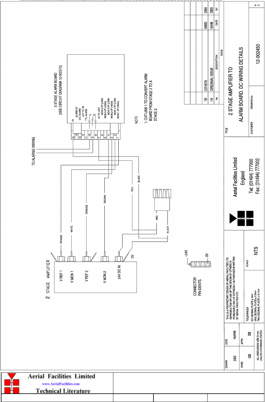
P B L Tunnels Loc 2 Units 1 & 2 + 800MHz BDA
Maintenance Handbook
H/book Number:-60-056100HBKM Issue No:-1 Date:-13/02/2003 Page:-84 of 84
5.3.4.8 Drg. No. 12-002450, LPA to Alarm Board DC Wiring Details

P B L Tunnels Loc 2 Units 1 & 2 + 800MHz BDA
Maintenance Handbook
H/book Number:-60-056100HBKM Issue No:-1 Date:-13/02/2003 Page:-85 of 85
5.3.5 3 Stage Alarm Board (12-002201) See section 5.1.4
5.3.6 DC/DC Converter (13-003011) See section 5.1.6
5.3.7 Channel Control & Channel Selective Modules (17-002101 & 17-003002)
5.3.7.1 Channel Selective Module Description
The channel selectivity module is employed when the Cell Enhancer requirement dictates that
very narrow bandwidths (single operating channels), must be selected from within the
operating passband. One channel selectivity module is required for each channel.
The Channel Selectivity Module is an Up/Down frequency converter that mixes the incoming
channel frequency with a synthesised local oscillator, so that it is down-converted to an
Intermediate Frequency (IF) in the upper HF range. An eight pole crystal filter in the IF
amplifier provides the required selectivity to define the operating passband of the Cell
Enhancer to a single PMR channel. The same local oscillator then converts the selected IF
signal back to the channel frequency.
Selectivity is obtained from a fixed bandwidth block filter operating at an intermediate
frequency (IF) in the low VHF range. This filter may be internal to the channel selectivity
module (Crystal or SAW filter) or an externally mounted bandpass filter, (LC or Helical
Resonator). Various IF bandwidths can therefore be accommodated. A synthesized Local
Oscillator is employed in conjunction with high performance frequency mixers, to translate
between the signal frequency and IF.
The operating frequency of each channel selectivity module is set by the programming of
channel selectivity module frequencies and is achieved digitally, via hard wired links, banks of
DIP switches, or via an onboard RS232 control module, providing the ability to remotely set
channel frequencies.
Automatic Level Control (ALC) is provided within each channel selectivity module such that
the output level is held constant for high level input signals. This feature prevents saturation of
the output mixer and of the associated amplifiers.
Alarms within the module inhibit the channel if the synthesised frequency is not locked. The
synthesiser will not usually go out of lock unless a frequency far out of band is programmed.
The channel selectivity module is extremely complex and, with the exception of channel
frequency programming within the design bandwidth, it cannot be adjusted or repaired without
extensive laboratory facilities and the necessary specialised personnel. If a fault is suspected
with any channel selectivity module it should be tested by substitution and the complete,
suspect module should then be returned to AFL for investigation.
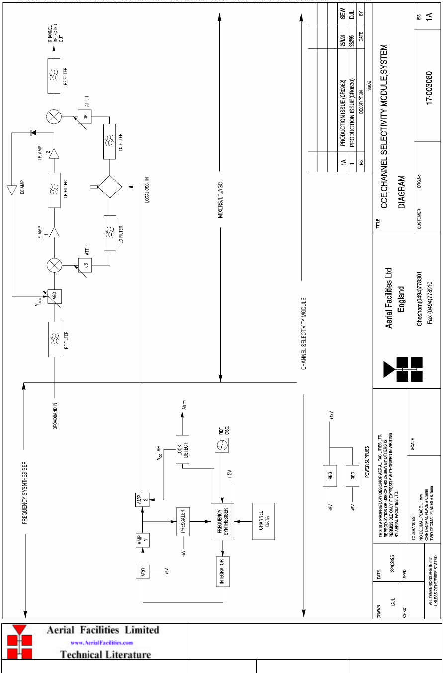
P B L Tunnels Loc 2 Units 1 & 2 + 800MHz BDA
Maintenance Handbook
H/book Number:-60-056100HBKM Issue No:-1 Date:-13/02/2003 Page:-86 of 86
5.3.7.2 Drg. No. 17-003080, Generic Channel Module Block Diagram

P B L Tunnels Loc 2 Units 1 & 2 + 800MHz BDA
Maintenance Handbook
H/book Number:-60-056100HBKM Issue No:-1 Date:-13/02/2003 Page:-87 of 87
5.3.7.3 Channel Control Module Description
The control module consists of a bank of four, in-line data switches each of which control
one channel module frequency setting. One controller unit can therefore control four
channel modules. The following list shows the frequencies available for each switch
setting.
5.3.7.4 Channel Controller Frequencies
IDC PIN 25-way Connector Function
1 13 Freq. bit 1 (12.5kHz)
2 25 Freq. bit 2 (25kHz)
3 12 Freq. bit 3 (50kHz)
4 24 Freq. bit 4 (100kHz)
5 11 Freq. bit 5 (200kHz)
6 23 Freq. bit 6 (400kHz)
7 10 Freq. bit 7 (800kHz)
8 22 Freq. bit 8 (1.6MHz)
9 9 Freq. bit 9 (3.2MHz)
10 21 Freq. bit 10 (6.4MHz)
11 8 Freq. bit 11 (12.8MHz)
12 20 Freq. bit 12 (25.6MHz)
13 7 Freq. bit 13 (51.2MHz)
14 19 Freq. bit 14 (102.4MHz)
15 6 Freq. bit 15 (204.8MHz)
16 18 Freq. bit 16 (409.6MHz)
17 5 Module alarm
18 17 Gain bit 1
19 4 Gain bit 2
20 16 Gain bit 3
21 3 Gain bit 4
22 15 +5V
23 2 0V
24 14 Switched 12V
25 1 0V
26 --- ---
5.3.7.5 Channel Module Settings Table (800MHz Unit)
Setting D/L (1) D/L (2) U/L (1) U/L (2)
Frequency 879.3375MHz 881.1625MHz 812.9375MHz 836.1625MHz
DIP Switches (off) 2,3,6,7,9,12,16 1,2,3,4,6,8,9,12,1
6 2,3,4,5,7,10,16 1,2,3,6,8,10,16
ALC level -26dBm -26dBm -25dBm -25dBm
Gain 14dB 14dB 14dB 14dB
B/W 30KHz 30KHz 30KHz 30KHz
IF Freq. 21.4MHz 21.4MHz 21.4MHz 21.4MHz

P B L Tunnels Loc 2 Units 1 & 2 + 800MHz BDA
Maintenance Handbook
H/book Number:-60-056100HBKM Issue No:-1 Date:-13/02/2003 Page:-88 of 88
6. INSTALLATION
6.1 Initial Installation Record
When this equipment is initially commissioned, please use the equipment set-up record sheet
in Appendix A. This will help both the installation personnel and AFL should these figures be
needed for future reference or diagnosis.
6.2 General
The size and weight of the wall units mean that they represent a significant health hazard
unless they are mechanically installed in the correct manner. In the interests of safety this
should be done before any electrical, RF, or optical connections are made.
It is important in determining the location of the wall units that space is allowed for access to
the front and underneath of the equipment. To enable maintenance to be carried out, the door
must be able to fully open. The location must be served with a duct to allow the entry of
cables into the unit.
6.3 Electrical Connections
The mains power supply and the alarms are connected through an IP65 connector which
should need no further attention once connected. It is recommended that the AC power
connection is approved by a qualified electrician, who must satisfy himself that the supply will
be the correct voltage and of sufficient capacity.
All electrical and RF connection should be completed and checked prior to power being
applied for the first time.
6.4 Optical Connections
The optical input and output ports are be located on a bracket fixed to the lower inside of the
case. The optical fibres from the tunnels enter through a cable gland on the case underside
The ports are supplied with a green plastic cover, which must be removed prior to the
connection of the fibre cable. Ensure that transmitter and receiver fibre cable are identified to
prevent misconnection. At the master site, the fibre transmitters are in the downlink path with
the receivers in the uplink. At the remote sites the fibre transmitters are in the uplink with the
receivers in the downlink. Where some of the fibre optic transmitter outputs are split with
optical couplers to provide a connection to more than one remote site, care must be taken to
ensure that the correct connections are made.
Ensure that connections are kept clean and are fully tightened.

P B L Tunnels Loc 2 Units 1 & 2 + 800MHz BDA
Maintenance Handbook
H/book Number:-60-056100HBKM Issue No:-1 Date:-13/02/2003 Page:-89 of 89
6.5 RF Connections
All RF connections are made to the cable termination, located on the right-hand side of the
wall enclosure. Care must be taken to ensure that the correct connections are made with
particular attention made to the base station TX/RX ports. In the event that the base
transmitter is connected to the RX output of the rack, damage to the equipment may be done
if the base station transmitter is then keyed. If the environment where the equipment is
installed is deemed to be ‘wet’ i.e. water seepage through roofs or walls, then suitable
methods to seal the RF N type connectors should be used, for example self amalgamating
sealant tape.
Ensure that connections are kept clean and are fully tightened.
6.6 Commissioning
Once all connections are made the equipment is ready for commissioning.
To commission the system the test equipment detailed in section 7.2 will be required.
Using the system diagrams and the end-to-end test specification, the equipment should be
tested to ensure correct operation. Typical RF levels that are not listed in the end-to-end
specification, such as input levels to the fibre transmitters are detailed in the whole system
diagram in section 4.
On initial power up the system alarm indicators on the door of the equipment should be
checked. A red LED illuminated indicates a fault and that particular module must be
investigated before proceeding with the commissioning. A green LED illuminates, to indicate
that the power supply is connected and valid.
The individual fibre optic units are fitted with a pair of status indicators on their front panels.
One is a green LED, which indicates that the unit is connected to a 15 Volt power supply.
This indicator is common to both transmit and receive units. The second LED on the
transmitter indicates that the laser is operating. On the receive unit the second LED indicates
that a light signal is being received.
When all the fibre connections are completed and power to each site is connected each fibre
unit should show two illuminated indicators.
In the event that any part of the system does not function correctly as expected, check all
connections to ensure that they are to the correct port, that the interconnecting cables are not
faulty and that they are tightened. The majority of commissioning difficulties arise from
problems with the interconnecting cables and connectors.

P B L Tunnels Loc 2 Units 1 & 2 + 800MHz BDA
Maintenance Handbook
H/book Number:-60-056100HBKM Issue No:-1 Date:-13/02/2003 Page:-90 of 90
7. MAINTENANCE
7.1 General Procedures
7.1.1 Fault Finding
In the event that the performance of the system is suspect, a methodical and logical approach
to the problem will reveal the cause of the difficulty. The System consists of modules within a
wall mounted, environmentally protected enclosure.
Transmissions from the main base stations are passed though the system to the mobile radio
equipment; this could be a handheld walkie-talkie, mobile telephone or a transceiver in a
vehicle. This path is referred to as the downlink. The return signal path from the mobile radio
equipment to the base station is referred to as the uplink.
The first operation is to check the (optional) alarms of each of the active units and determine
that the power supplies to the equipment are connected and active.
This can be achieved remotely (via CEMS, the digital RS232 Cell Enhancer Management
System, if fitted), or locally with the front door LED’s. The green LED on the front door
should be illuminated, while the red alarm indicator should be off.
If an Alarm is on, then that individual module must be removed and tested against the original
test specification.
The individual amplifier units have a green LED showing through a hole in their piggy-back
alarm board (or directly through a hole in the the amplifier lid), which is illuminated if the unit
is working correctly.
If an amplifier is suspect, check the DC power supply to the unit. If no other fault is apparent
use a spectrum analyser to measure the incoming signal level at the input and then after
reconnecting the amplifier input, measure the output level. Consult with the system diagram
and amplifier specification to determine the expected gain and compare result.
In the event that there are no alarms on and all units appear to be functioning it will be
necessary to test the system in a logical manner to confirm correct operation.

P B L Tunnels Loc 2 Units 1 & 2 + 800MHz BDA
Maintenance Handbook
H/book Number:-60-056100HBKM Issue No:-1 Date:-13/02/2003 Page:-91 of 91
7.1.2 Downlink
Confirm that there is a signal at the expected frequency and strength from the base station. If
this is not present then the fault may lay outside the system. To confirm this, inject a
downlink frequency signal from a known source at the master site BTS input and check for
output at the remote site feeder output.
If a signal is not received at the output it will be necessary to follow the downlink path
through the system to find a point at which the signal is lost. The expected downlink output
for the given input can be found in the end-to-end test specification.
7.1.3 Uplink
Testing the uplink involves a similar procedure to the downlink except that the frequencies
used are those transmitted by the mobile equipment.
7.1.4 Fault repair
Once a faulty component has been identified, a decision must be made on the appropriate
course to carry out a repair. A competent engineer can quickly remedy typical faults such as
faulty connections or cables. The exceptions to this are cable assemblies connecting bandpass
filter assemblies that are manufactured to critical lengths to maintain a 50-ohm system. Care
should be taken when replacing cables or connectors to ensure that items are of the correct
specification. The repair of component modules such as amplifiers, tuned cavities or bandpass
filters will not usually be possible in the field, as they frequently require specialist knowledge
and test equipment to ensure correct operation. It is recommended that items of this type are
replaced with a spare unit and the faulty unit returned to AFL for repair. If spare parts need
to be ordered from AFL, be sure to quote the serial number of the Cell Enhancer/Repeater
and the serial number [and frequencies] of the module(s) to be replaced.

P B L Tunnels Loc 2 Units 1 & 2 + 800MHz BDA
Maintenance Handbook
H/book Number:-60-056100HBKM Issue No:-1 Date:-13/02/2003 Page:-92 of 92
7.1.5 Checking service
Following the repair of any part of the system it is recommended that a full end-to-end test is
carried out in accordance with the test specification and that the coverage is checked by
survey.
It is important to bear in mind that the system includes a radiating cable network and base
stations that may be faulty or may have been damaged.
7.1.6 Service Support
Advice and assistance with maintaining and servicing this system are available by contacting
Aerial Facilities Ltd.
7.2 Tools & Test Equipment
The minimum tools and test equipment needed to successfully service this AFL product are as
follows:-
Spectrum analyser: 100kHz to 2GHz (Dynamic range = 90dB).
Signal Generator: 30MHz to 2GHz (-120dBm to 0dBm o/p level).
Attenuator: 20dB, 10W, DC-2GHz, (N male – N female).
Test Antenna: Yagi or dipole for operating frequency.
Digital multi-meter: Universal Volt-Ohm-Amp meter.
Test cable x 2: N male – N male, 2M long RG214.
Test cable x 2: SMA male – N male, 1m long RG223.
Hand tools: Philips #1&2 tip screwdriver.
3mm flat bladed screwdriver.
SMA spanner and torque setter.

P B L Tunnels Loc 2 Units 1 & 2 + 800MHz BDA
Maintenance Handbook
H/book Number:-60-056100HBKM Issue No:-1 Date:-13/02/2003 Page:-93 of 93
7.3 Care of Modules
7.3.1 General Comments
Many of the active modules contain semiconductor devices utilising MOS technology, which
can be damaged by electrostatic discharge. Correct handling of such modules is mandatory to
ensure their long-term reliability.
To prevent damage to a module, it must be withdrawn/inserted with care. The module may
have connectors on its underside, which might not be visible to the service operative.
7.3.2 Module Removal (LNA’s, general procedure):
The following general rules should be followed to remove a module:
1 Remove power to the unit
2 Remove all visible connectors (RF, DC & alarm)
3 Release module retaining screws.
4 Slowly but firmly, pull the module straight out of its position. Take care not to twist/turn
the module during withdrawal. (When the module is loose, care may be needed, as there
may be concealed connections underneath).
7.3.3 Module Replacement (general):
1 Carefully align the module into its location then slowly push the module directly straight
into its position, taking care not to twist/turn it during insertion.
2 Reconnect all connectors, RF, alarm, power etc.,(concealed connectors may have to be
connected first).
3 Replace retaining screws (if any).
4 Double-check all connections before applying power.
7.3.4 Power Amplifiers
1) Remove power to the unit. (Switch off @ mains/battery, or remove DC in connector)
2) Remove alarm wires from alarm screw terminal block or disconnect multi-way alarm
connector.
3) Carefully disconnect the RF input and output coaxial connectors (usually SMA)
If alarm board removal is not required, go to step 5.
4) There is (usually) a plate attached to the alarm board which fixes it to the amplifier,
remove its retaining screws and the alarm board can be withdrawn from the amplifier in its
entirety. On certain types of amplifier the alarm board is not mounted on a dedicated
mounting plate; in this case it will have to firstly be removed by unscrewing it from the
mounting pillars, in most cases, the pillars will not have not have to be removed before
lifting the amplifier.

P B L Tunnels Loc 2 Units 1 & 2 + 800MHz BDA
Maintenance Handbook
H/book Number:-60-056100HBKM Issue No:-1 Date:-13/02/2003 Page:-94 of 94
5) If the amplifier to be removed has a heatsink attached, there may be several different ways
it can have been assembled. The most commonly used method, is screws through the front
of the heatsink to threaded screw holes (or nuts and bolts), into the amplifier within the
main case. If the heatsink is mounted on the rear of the main case (e.g., against a wall in
the case of wall mounted enclosures), then the fixing method for the heatsink will be from
within the case, (otherwise the enclosure would have to be removed from the wall in order
to remove the heatsink).
When the heatsink has been removed, the amplifier may be unscrewed from the main
casing by its four corner fixings and gently withdrawn.
Fitting a new power amplifier module will be the exact reverse of the above.
Note: Do not forget to apply fresh heatsink compound to the heatsink/main case
joint and also between the amplifier and the main case.
7.3.5 Low Power Amplifier Replacement
1 Disconnect the mains power supply and disconnect the 24V dc supply connector for the
LPA.
2 Disconnect the RF input and output cables from the LPA.
3 Disconnect the alarm connector.
4 Remove the alarm monitoring wires from (D type connector) pins 9 and 10.
5 Remove the LPA module by removing the four retaining screws, replace with a new LPA
module and secure it with the screws.
6 Connect the RF cables to the LPA input and output connectors. Reconnect the wires to
the alarm board connector pins 9 and 10.
7 Reconnect the DC supply connector and turn the mains switch on.
Note: Tighten SMA connectors using only a dedicated SMA torque spanner. If
SMA connectors are over-tightened, irreparable damage will occur. . Do not use
adjustable pliers to loosen/tighten SMA connectors.
Also take care not to drop or knock the module as this can damage (or misalign in the
case of tuned passive modules) sensitive internal components. Always store the modules
in an environmentally friendly location
7.3.6 Module Transportation:
To maintain the operation, performance and reliability of any module it must be stored and
transported correctly. Any module not installed in a whole system must be kept in an anti-
static bag or container. These bags or containers are normally identified by being pink or
black, and are often marked with an ESD label. Any module sent back to AFL for
investigation/repair must be so protected. Please contact AFL’s quality department before
returning a module.
P B L Tunnels Loc 2 Units 1 & 2 + 800MHz BDA
Maintenance Handbook
H/book Number:-60-056100HBKM Issue No:-1 Date:-13/02/2003 Page:-95 of 95
APPENDIX A INITIAL EQUIPMENT SET-UP CALCULATIONS
GENERAL INFORMATION
Site Name: Client Name:
Date: AFL Equip. Model No.
ANTENNA SYSTEMS
Model Gain Azimuth Comments
A - Service Antenna
B – Donor Antenna
Type Loss Length Comments
C – Service Feeder
D – Donor Feeder
INITIAL PARAMETERS
E – CE Output Power dBm
F – Antenna Isolation dB
G – Input signal level from donor BTS dBm
Operating Voltage V
DOWNLINK CALCULATIONS
Parameter Comments Value
Input signal level (G)
dBm
CE max. o/p power (E)
dBm
Gain setting
E - G dB
Isolation required
(Gain + 10dB) dB
Service antenna gain (A)
dB
Service antenna feeder loss (C)
dB
Effective radiated power (ERP)
E+A-C dBm
Attenuator setting
CE gain-gain setting dB
If the input signal level in the uplink path is known and steady, use the following calculation
table to determine the gain setting. If the CE features Automatic Gain Control the attenuator
should be set to zero and if not, then the attenuation setting for both uplink and downlink
should be similar.
UPLINK CALCULATIONS
Parameter Comments Value
Input signal level
dBm
CE max. o/p power (E)
dBm
Gain setting
dB
Required isolation
dB
Donor antenna gain (B)
dB
Donor antenna feeder loss (D)
dB
Effective radiated power (ERP)
E+B-D dBm
Attenuator setting
(CE gain-gain setting) dB