Panasonic of North America SC-HTB8 BT Module User Manual SPEC BM830 V0 2 20130803
Panasonic Corporation of North America BT Module SPEC BM830 V0 2 20130803
User Manual
Product Specification
Spec-BM830-V0.2 Page 1 of 10 www.sunitec-cn.com
®
Features:
z Bluetooth Spec 4.0 Compliant
z Class 2 type Output Power
z Support A2DP 1.2,AVRCP V1.4 Profiles
z Secure simple pairing, CSR's proximity pairing
and CSR's proximity connection
z Support for multi-language programmable audio
prompts
z OS battery status monitoring and smart apps
z Wired audio support (USB and analogue)
z SBC, MP3, and AAC decoder support
z 5-band fully configurable EQ
z Integrated dual switch-mode regulators, linear
regulators and battery charger
z Size: 21±0.5mm x 13.5±0.5 mm x 2.35±0.5mm
z Weight: 0.8g
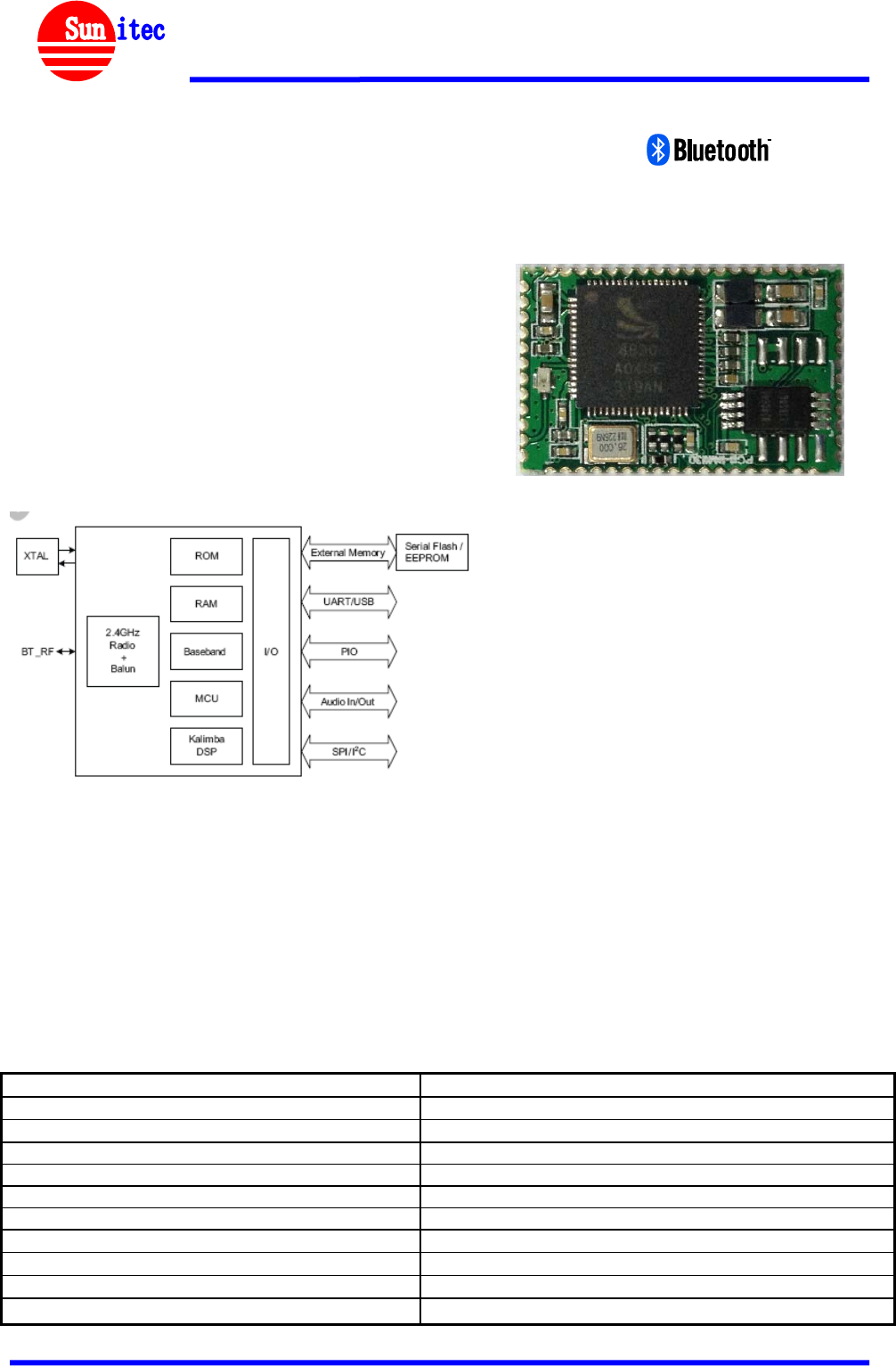
System Architecture
BM830 Stereo Solution Module
CSR8630A04
July 2013
Product Description:
The BM830 is a Class 2 Bluetooth sub-system
using CSR8630 chipset from leading Bluetooth
chipset supplier Cambridge Silicon Radio.
It is a single-chip radio and baseband IC for
Bluetooth 2.4GHz systems.The integrated
peripherals reduce the number of external
components required, including no
requirement for external codec, battery charger,
SMPS, LDOs, balun or external program
memory, ensuring minimum production costs.
Applications:
• Wireless speaker
Specifications:
Operating Frequency Band 2.4GHz ~ 2.48GHz unlicensed ISM band
Bluetooth Specification V4.0
Output Power Class Class 2
Max. Output Power 2.5mW
Date Rate 3Mbps
Channel No. 79
Modulation Type GFSK π/4 DQPSK 8DPSK
Operating Voltage 3.3V
Host Interface USB 1.1
Audio Interface Analogue and USB audio
Dimension 21±0.5mm x 13.5±0.5 mm x 2.35±0.5mm
Specifications are subject to change without prior notice
Qualified
Product Specification
Spec-BM830-V0.2 Page 2 of 10 www.sunitec-cn.com
®
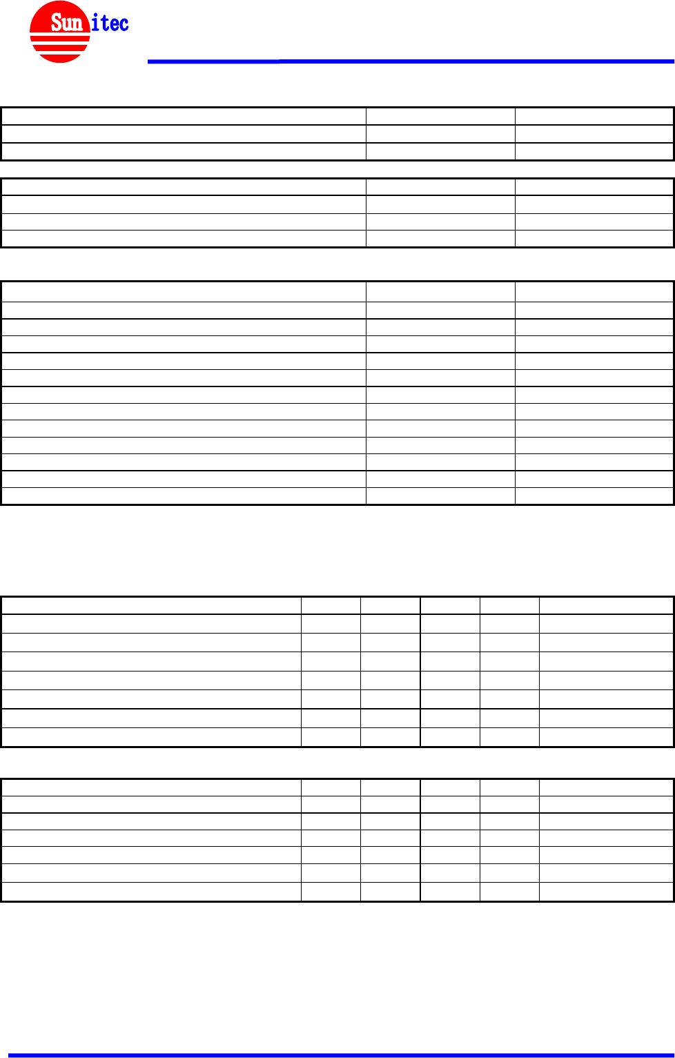
Electrical Characteristics
Absolute Maximum Rating Min Max
Storage Temperature -40°C +105°C
Supply Voltage, (V_CHG) -0.30V +5.75V
Recommended Operating Conditions Min Max
Operating Temperature Range -40°C +85°C
Supply Voltage, (V_BAT) 2.5V 4.2V
Supply Voltage, (V_CHG) 4.75V 5.25V
Power Consumption Units Average
Slave
SCO Connection HV3 mA 11.0
SCO Connection EV3 mA 11.8
SCO Connection 2EV3 mA 9.2
Stereo high quality SBC mA 13.3
Stereo high quality MP3 mA 12.5
Master
SCO Connection HV3 mA 10.8
SCO Connection EV3 mA 11.2
SCO Connection 2EV3 mA 8.8
Stereo high quality SBC mA 13.2
Stereo high quality MP3 mA 11.8
VBAT = 4.2V; f = 2.441GHz; T=20°C
RF Characteristics
Receiver Units Min Typ Max Bluetooth Spec
Sensitivity at 0.1% BER dBm - -90 -85 ≤-70
Maximum Receiver Signal dBm -20 -10 - ≥ -20
C/I Co-Channel dB - 6 11 ≤11
Adjacent Channel Selectivity C/I -1MHz dB - -6 0 ≤0
2nd Adjacent Channel Selectivity C/I -2MHz dB - -38 -30 ≤-30
3rd Adjacent Channel Selectivity C/I -3MHz dB - -45 -40 ≤-40
Image Rejection C/I dB - -16 -9 ≤-9
VBAT = 4.2V; f = 2.4441GHz; T=20°C
Transmitter Units Min Typ Max Bluetooth Spec
RF Output Power dBm 4 8 - -6 to +4
RF Power Control Range dB 16 24 - > 16
RF Power Range Control Resolution dB - 0.5 - -
20dB Bandwidth for Modulated Carrier KHz - 940 1000 <1000
2nd Adjacent Channel Power (+/- 2MHz) dBm - -36 -20 ≤-20
3rd Adjacent Channel Power (+/- 3MHz) dBm - -45 -40 ≤-40
VBAT = 4.2V; f = 2.4441GHz; T=20°C
All specifications including pinouts and electrical specifications may be changed without prior notice

Product Specification
Spec-BM830-V0.2 Page 3 of 10 www.sunitec-cn.com
®
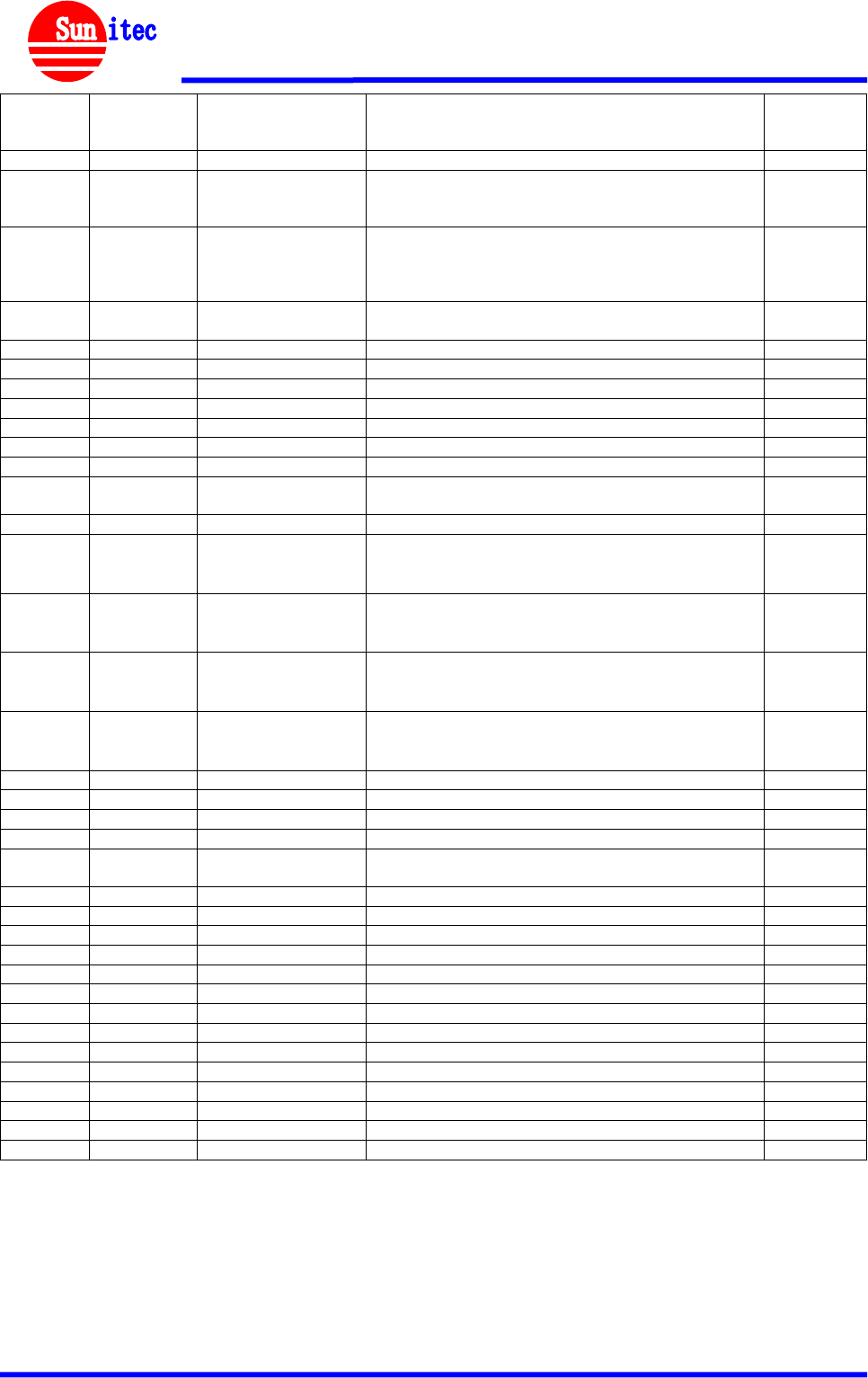
Pin Configurations
PIN NO. NAME TYPE FUNCTION RE-MARK
1 GND GND Ground
2 AIO0 Bi-directional Analogue programmable input / output line
3 PIO14 Bi-directional Programmable input / output line 14.
Alternative function:
■ UART_RX: UART data input
4 PIO15 Bi-directional Programmable input / output line 15.
Alternative function:
■ UART_TX: UART data output
5 PIO16 Bi-directional Programmable input / output line 16.
Alternative function:
■ UART_RTS: UART request to send, active low
6 PIO17 Bi-directional Programmable input / output line 17.
Alternative function:
■ UART_CTS: UART clear to send, active low
7 PIO10 Bi-directional Programmable input / output line 10.
Alternative function:
■ QSPI_FLASH_CLK: SPI flash clock
■ I2C_SCL: I²C serial clock line
8 SCL Bi-directional Internal EEPROM SCL
9 PIO11 Bi-directional Programmable input / output line 11.
Alternative function:
■ QSPI_IO[0]: SPI flash data bit 0
■ I2C_SDA: I²C serial data line
10 PIO12 Bi-directional Programmable input / output line 12.
Alternative function:
■ QSPI_FLASH_CS#: SPI flash chip select
■ I2C_WP: I²C bus memory write protect line
11 PIO13 Bi-directional Programmable input / output line 13.
Alternative function:
■ QSPI_IO[1]: SPI flash data bit 1
12 SPI_PCM# Bidirectional with
weak
pull-down
SPI/PCM select input:
■0 = PCM/PIO interface
■1 = SPI
13 GND GND Ground
14 PIO3 Bi-directional Programmable input / output line 3.
Alternative function:
■ SPI_MISO: SPI data output
■ PCM1_OUT: PCM1 synchronous data output
15 PIO2 Bi-directional Programmable input / output line 2.
Alternative function:
■ SPI_MOSI: SPI data input
■ PCM1_IN: PCM1 synchronous data input
16 PIO5 Bi-directional Programmable input / output line 5.
Alternative function:
■ SPI_CLK: SPI clock
■ PCM1_CLK: PCM1 synchronous data clock
17 PIO4 Bi-directional Programmable input / output line 4.
Alternative function:
■ SPI_CS#: chip select for SPI, active low
■ PCM1_SYNC: PCM1 synchronous data sync
18 GND GND Ground
19 GND GND Ground
20 RST# Input with strong
pull-up
Reset if low. Pull low for minimum 5ms to cause a
reset.
21 GND GND Ground
22 LED1 Bi-directional LED driver.
Alternative function: programmable output PIO[30].
23 LED0 Bi-directional LED driver.
Alternative function: programmable output PIO[29].
24 VREGENA
BLE
CMOS Input Regulator enable input
Can also be sensed as an input.
Regulator enable and multifunction button. A high
Product Specification
Spec-BM830-V0.2 Page 4 of 10 www.sunitec-cn.com
®
input (tolerant to VBAT) enables the on-chip
regulators, which can then be latched on internally
and the button used as a multifunction input
25 GND GND Ground
26 VBUS Power Input Charger input.
Typically connected to VBUS (USB supply) as
Section 12 shows.
27 CHG_EXT External battery charger control.
External battery charger transistor base control
when using external charger boost. Otherwise leave
unconnected.
28 VBAT_SEN
SE
Battery charger sense input.
Connect directly to the battery positive pin.
29 VBAT Power IN Battery positive terminal.
30 GND GND Ground
31 1V8_OUT Power out Serial Peripheral Interface Clock
32 VDD_PADS Power IN Positive supply input for input/output ports
33 3V3_OUT Power out 3.3V bypass linear regulator output.
34 GND GND Ground
35 USB_N Bi-directional USB data minus
36 USB_P Bi-directional USB data plus with selectable internal 1.5kΩ pull-up
resistor
37 GND GND Ground
38 PIO9 Bi-directional Programmable input / output line 9.
Alternative function:
■ UART_CTS: UART clear to send,active low
39 PIO0 Bi-directional Programmable input / output line 0.
Alternative function:
■ UART_RX: UART data input
40 PIO1 Bi-directional Programmable input / output line 1.
Alternative function:
■ UART_TX: UART data output
41 PIO8 Bi-directional Programmable input / output line 8.
Alternative function:
■ UART_RTS: UART request to send, active low
42 PIO7 Bi-directional Programmable Input/Output Line
43 PIO6 Bi-directional Programmable Input/Output Line
44 PIO21 Bi-directional Programmable Input/Output Line
45 PIO18 Bi-directional Programmable Input/Output Line
46 LED2 Bi-directional LED driver.
Alternative function: programmable output PIO[31]
47 GND GND Ground
48 MIC_BIAS Analogue out Microphone bias
49 LINE_AN Analogue in Line input negative, channel A
50 LINE_AP Analogue in Line input positive, channel A
51 LINE_BN Analogue in Line input negative, channel B
52 LINE_BP Analogue in Line input positive, channel B
53 AGND Analogue Ground connection for audio and audio driver.
54 SPK_RN Analogue out Speaker output negative, right
55 SPK_RP Analogue out Speaker output positive, right
56 SPK_LN Analogue out Speaker output negative, left
57 SPK_LP Analogue out Speaker output positive, left
58 GND GND Ground
59 RF_IN GND Bluetooth 50Ω transmitter output /receiver input
60 GND GND Ground
Product Specification
Spec-BM830-V0.2 Page 5 of 10 www.sunitec-cn.com
®
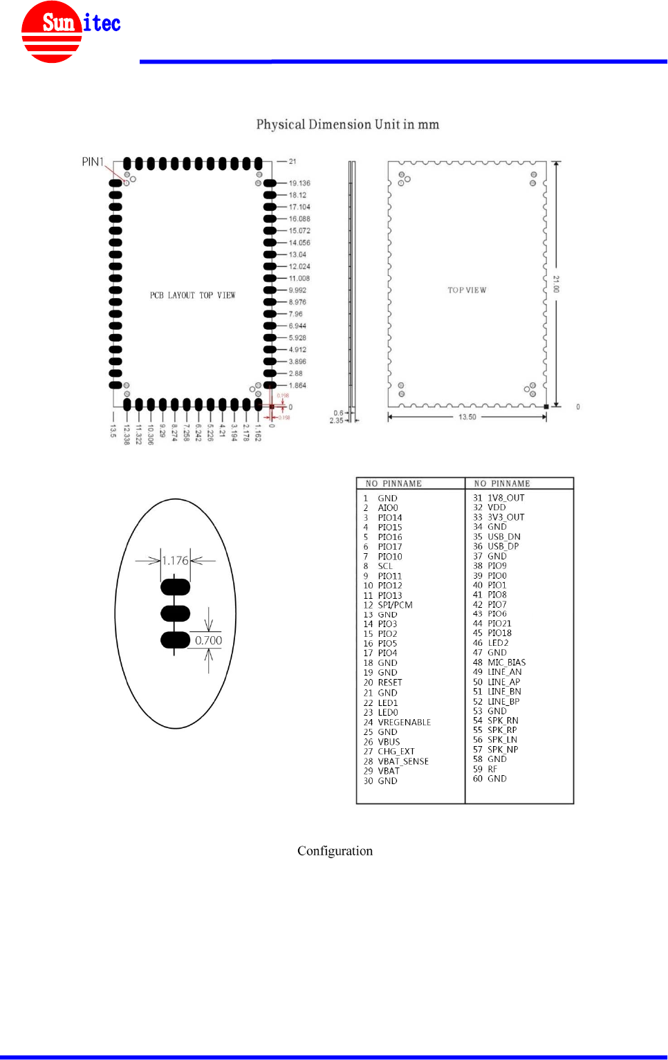
Recommended Layout patterns:
Product Specification
Spec-BM830-V0.2 Page 6 of 10 www.sunitec-cn.com
®
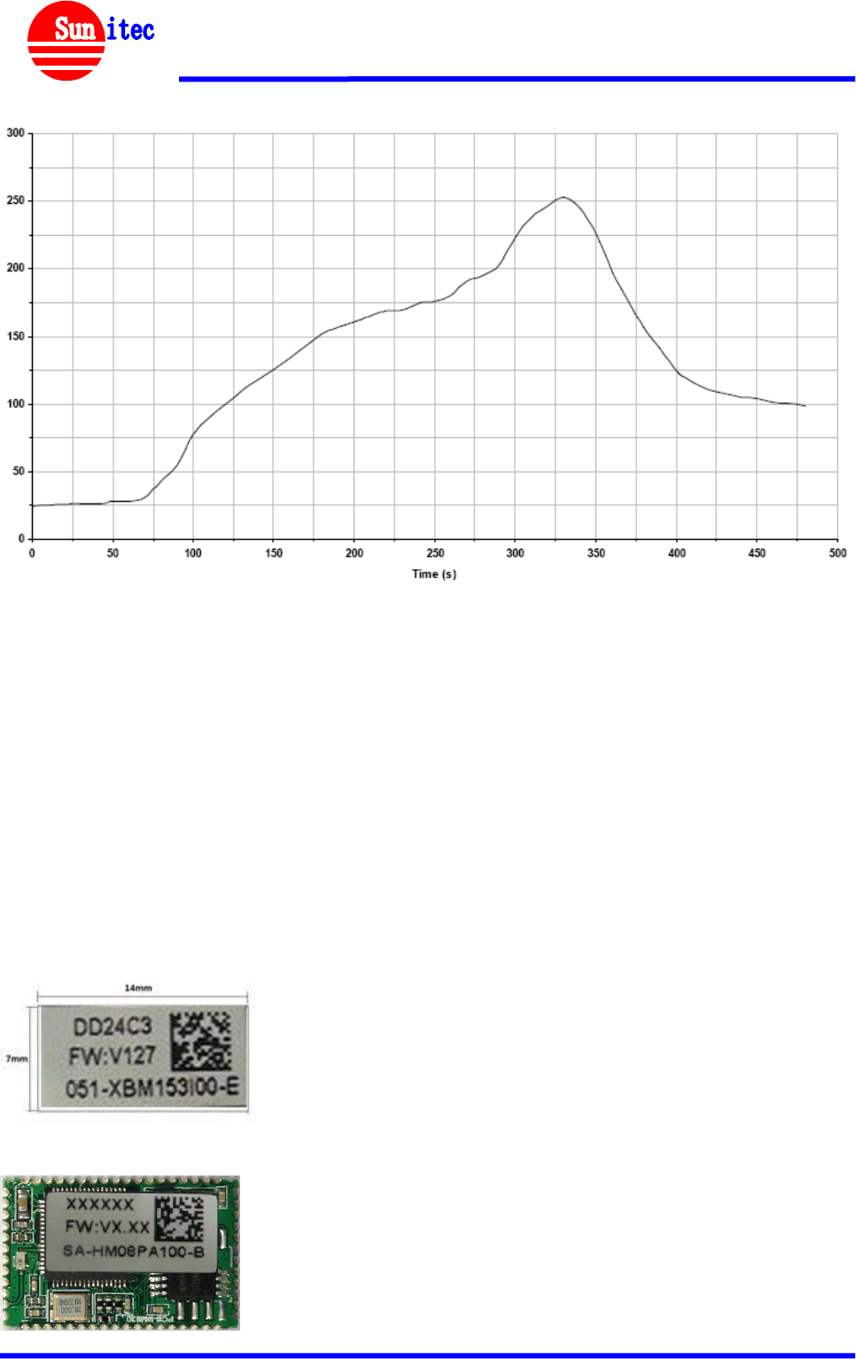
Recommended Reflow Temperature Profile:
Key features of the profile:
-Initial Ramp=1-2.5℃/sec to 175℃ equilibrium
-Equilibrium time=60 to 80 seconds
-Ramp to Maximum temperature (250℃)=3℃/sec Max
-Time above liquidus temperature(217℃): 45 - 90 seconds
-Device absolute maximum reflow temperature: 250℃
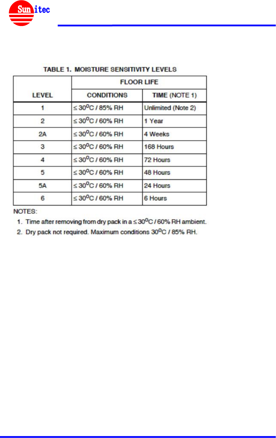
MAC Address:
Each Module has his MAC Address
00A6 94 XXXXXX
Concerning the dimension and printing content of the tab,:
1 line the last six letters of the LAP on the module
2 line the software version
3 line the customer material part number
Qr code area,with 12 letters(MAC Address)
(This Photos are for reference only)
The tab code pastes style:
(This Photos are for reference only)
Product Specification
Spec-BM830-V0.2 Page 7 of 10 www.sunitec-cn.com
®
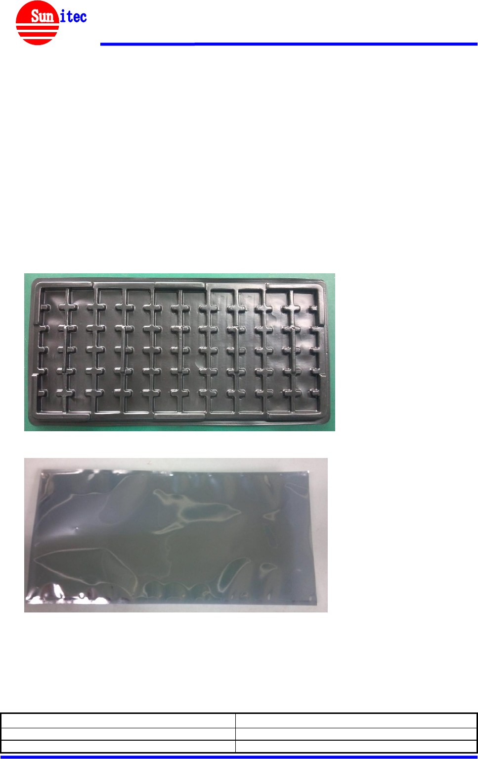
Moisture Sensitive Level
The MSL Rating of BM830 Module is 3.
Un-opened reels Shelf life:
BM830 has 12 months maximum from bag seal date when stored at < 40°C / 90%RH.
Product Specification
Spec-BM830-V0.2 Page 8 of 10 www.sunitec-cn.com
®
Standard Packing Information
Module packing Box (Max 3000pcs module per box)
60pcs per tray, 10trays per ESD bag, sealed in ESD PE bag.
Maximum modules per ESD bag is 600pcs
Module packing bag dimension: 350.0mm x 195.0mm
Delivering carton box
To hold two units of module carton boxes for shipment (Max 3000pcs modules per box)
Delivery Carton Box dimension: 320.0mm x 210.0mm x 170.0mm (W x D x H)
ESD tray dimension: 290.00mm x 145.00mm x 10mm(W x D x H)
ESD tray (to be packed in ESD PE bag).
ESD PE bag size: 350.0mm x 195mm
QDL Certificate
Document References
References Version
Specifications of the Bluetooth System V4.0, 17 Dec. 2009
BlueCore-CSR8630 Product Data Sheet CS-303724-DSP1

Product Specification
Spec-BM830-V0.2 Page 9 of 10 www.sunitec-cn.com
®
Federal Communication Commission Interference Statement
This equipment has been tested and found to comply with the limits for a Class B digital device, pursuant to Part 15 of the
FCC Rules. These limits are designed to provide reasonable protection against harmful interference in a residential installation.
This equipment generates, uses and can radiate radio frequency energy and, if not installed and used in accordance with the
instructions, may cause harmful interference to radio communications. However, there is no guarantee that interference will
not occur in a particular installation. If this equipment does cause harmful interference to radio or television reception, which
can be determined by turning the equipment off and on, the user is encouraged to try to correct the interference by one of the
following measures:
- Reorient or relocate the receiving antenna.
- Increase the separation between the equipment and receiver.
- Connect the equipment into an outlet on a circuit different from that to which the receiver is connected.
- Consult the dealer or an experienced radio/TV technician for help.
FCC Caution:
Any changes or modifications not expressly approved by the party responsible for compliance could void the user's authority
to operate this equipment.
This device complies with Part 15 of the FCC Rules. Operation is subject to the following two conditions:
(1) This device may not cause harmful interference, and
(2) This device must accept any interference received, including interference that may cause undesired operation.
FCC Radiation Exposure Statement:
This equipment complies with FCC radiation exposure limits set forth for an uncontrolled environment. This transmitter
module must not be co-located or operating in conjunction with any other antenna or transmitter.
The module must be installed in HOME THEATER AUDIO SYSTEM
IMPORTANT NOTE:
In the event that these conditions can not be met (for example certain laptop configurations or co-location with another
transmitter), then the FCC authorization is no longer considered valid and the FCC ID can not be used on the final product. In
these circumstances, the OEM integrator will be responsible for re-evaluating the end product (including the transmitter) and
obtaining a separate FCC authorization.
End Product Labeling
The final end product must be labeled in a visible area with the following:
“Contains FCC ID: ACJ-SC-HTB8.”
Manual Information to the End User
The OEM integrator has to be aware not to provide information to the end user regarding how to install or remove this RF
module in the user’s manual of the end product which integrates this module.
Document History
Revision Date History
V0.1 2013-08-02 First release
V0.2 2013-12-2 Add the packing information
Contact Information
Sunitec Enterprise Co., Ltd.
Head Office:
3F.,No.98-1,Mincyuan Rd Sindian City, Taipei
County 231,Taiwan
China Factory:
No.2,Qilin Road 2,Run Tang Ind., Dan-Keng Village Fu
Ming Community, Guan-lan Town, BaoAn District,

Product Specification
Spec-BM830-V0.2 Page 10 of 10 www.sunitec-
cn.com
®
Tel: 886-2-82191696
Fax: 886-2-82191676
Shenzhen GuangDong China
Tel: 86-755-29802983
Fax: 86-755-29802984
E-mail: sales@sunitec-cn.com or project@sunitec-cn.com
Http://www.sunitec-cn.com