Particle PHOTON PHOTON User Manual photon datasheet v011 FCC md
Spark Labs, Inc., PHOTON photon datasheet v011 FCC md
Particle >
Users Manual
Photon Datasheet
Model number: PHOTONH
void setup() {
Spark.publish("my-event","The internet just got smarter!");
}
1 of 35

Photon Datasheet v011
Contents
Photon Datasheet
Contents
1. Functional description
1.1 Overview
1.2 Features
2. Interfaces
2.1 Power
2.2 RF
2.3 FCC Approved Antennas
2.4 Peripherals and GPIO
2.5 JTAG
2.6 External Coexistence Interface
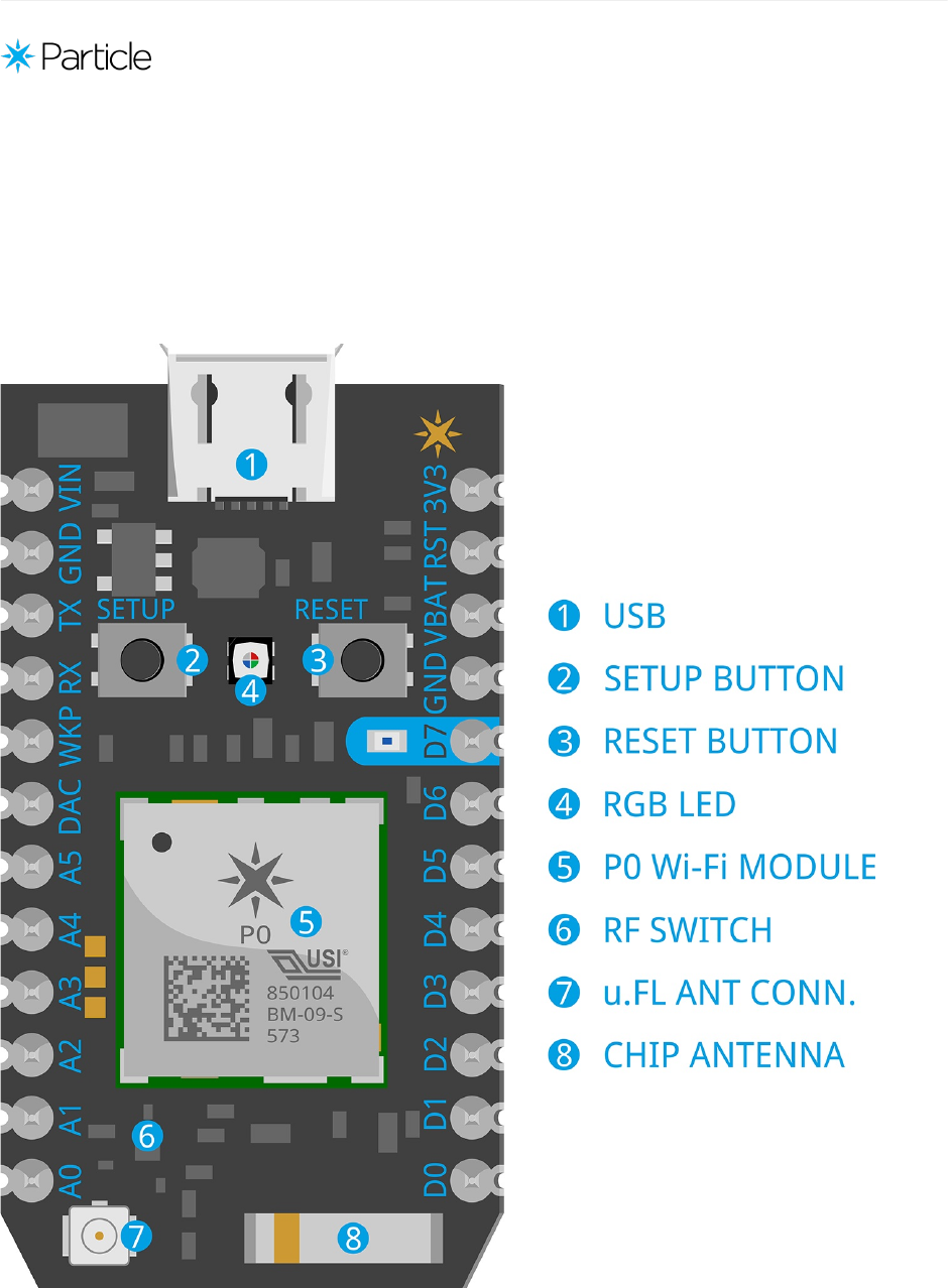
3. Pin and button def inition
3.1 Pin markings
3.2 Pin description
3.3 Pin out diagrams
4. Technical specif ication
4.1 Absolute maximum ratings
4.2 Recommended operating conditions
4.3 Wi-Fi Specif ications
4.4 I/O Characteristics
5. Mechanical specif ications
5.1 Dimensions and Weight
5.2 Mating connectors
5.3 Recommended pcb land pattern (Photon with headers)
5.4 Recommended pcb land pattern (Photon without headers)
6. Layout
6.1 Photon v1.0.0 Top Layer (GTL)
6.2 Photon v1.0.0 GND Layer (G2L)
6.3 Photon v1.0.0 3V3 Layer (G15L)
6.4 Photon v1.0.0 Bottom Layer (GBL)
7. Recommended solder reflow profile
8. Bill of Materials
Build your own design based on the Photon!
9. Ordering information
2 of 35

Photon Datasheet v011
1. Functional description
1.1 Overview
Particle’s Internet of Things hardware development kit, the Photon, provides everything you need to build a
connected product. Particle combines a powerful ARM Cortex M3 micro-controller with a Broadcom Wi-Fi chip in a tiny
thumbnail-sized module called the PØ (P-zero).
To get you started quickly, Particle adds a rock solid 3.3VDC SMPS power supply, RF and user interface components to
the PØ on a small single-sided PCB called the Photon. The design is open source, so when you’re ready to integrate
the Photon into your product, you can.
The Photon comes in two physical forms: with headers and without. Prototyping is easy with headers as the Photon
plugs directly into standard breadboards and perfboards, and may also be mounted with 0.1” pitch female headers on
a PCB. To minimize space required, the Photon f orm factor without headers has castellated edges. These make it
possible to surface mount the Photon directly onto your PCB.
1.2 Features
Particle PØ Wi-Fi module
Broadcom BCM43362 Wi-Fi chip
802.11b/g/n Wi-Fi
STM32F205 120Mhz ARM Cortex M3
1MB flash, 128KB RAM
On-board RGB status LED (ext. drive provided)
18 Mixed-signal GPIO and advanced peripherals
Open source desig n
Real-time operating system (FreeRTOS)
Sof t AP setup
FCC, CE and IC certified
4 of 35

Photon Datasheet v011
2. Interfaces
2.1 Power
Power to the Photon is supplied via the on-board USB Micro B connector or directly via the VIN pin. If power is supplied
directly to the VIN pin, the voltage should be reg ulated between 3.6VDC and 5.5VDC. When the Photon is powered via
the USB port, VIN will output a voltage of approximately 4 .8VDC due to a reverse polarity protection series schottky
diode between V+ of USB and VIN. When used as an output, the max load on VIN is 1A.
Typical current consumption is 80mA with a 5V input. Deep sleep quiescent current is 160uA. When powering the
Photon f rom the USB connector, make sure to use a quality cable to minimize IR drops (current x resistance = voltage)
in the wiring. If a high resistance cable (i.e., low current) is used, peak currents drawn from the Photon when
transmitting and receiving will result in voltage sag at the input which may cause a system brown out or intermittent
operation. Likewise, the power source should be suff icient enough to source 1A of current to be on the safe side.
2.2 RF
The RF section of the Photon is a finely tuned impedance controlled network of components that optimize the
efficiency and sensitivity of the Wi-Fi communications.
An RF feed line runs from the PØ module into a SPDT RF-switch. Log ic level control lines on the PØ module select which
of the two ports of the RF-switch is connected to the RF feed line. A 100pF decoupling capacitor is located on each
control line. One port is connected to a PCB ceramic chip antenna, and the other is connected to a u.FL connector for
external antenna adaptation. The def ault port will be set to the chip antenna.
Additionally, a user API is available to switch between internal, external and even an automatic mode which
continuously switches between each antenna and selects the best signal. All three RF ports on the RF-switch have a
10pF RF quality DC-blocking capacitor in series with them. These effectively pass 2.4GHz frequencies freely while
blocking unwanted DC voltages from damaging the RF-switch. All RF traces are considered as tiny transmission lines
that have a controlled 50 ohm impedance.
The chip antenna is impedance matched to the 50 ohm RF feed line via a Pi network comprised of three RF inductors (1
series, 2 shunt). These values are quite specific to the Photon due to the PCB construction and layout of the RF
section. Even if the Photon’s layout design is copied exactly, to achieve the best performance it would be worth re-
examining the Pi network values on actual samples of the PCB in question.
5 of 35

Photon Datasheet v011
2.3 FCC Approved Antennas
Antenna T ype Manuf acturer MFG. Part # Gain
Dipole antenna LumenRadio 104 -1001 2.15dBi
Chip antenna Advanced Ceramic X AT7020-E3R0HBA 1.3dBi
2.4 Peripherals and GPIO
The Photon has ton of capability in a small footprint, with analog, digital and communication interf aces.
Peripheral Type Qty Input(I) / Output(O) FT / 3V3
Digital 18 I/O FT/3V3
Analog (ADC) 8 I 3V3
Analog (DAC) 2 O 3V3
SPI 2 I/O 3V3
I2S 1 I/O 3V3
I2C 1 I/O FT
CAN 1 I/O FT
USB 1 I/O 3V3
PWM 9 O 3V3
Notes:
FT = 5.0V tolerant pins. All pins except A3 and DAC are 5V tolerant (when not in analog mode). If used as a 5V input
the pull-up/pull-down resistor must be disabled.
3V3 = 3.3V max pins.
PWM is available on D0, D1, D2, D3, A4, A5, WKP, RX, TX with a caveat: PWM timer peripheral is duplicated on two pins
(A5/D2) and (A4/D3) for 7 total independent PWM outputs. For example: PWM may be used on A5 while D2 is used as a
GPIO, or D2 as a PWM while A5 is used as an analog input. However A5 and D2 cannot be used as independently
controlled PWM outputs at the same time.
[1] [2]
3
[1]
[2]
[3]
6 of 35
Photon Datasheet v011
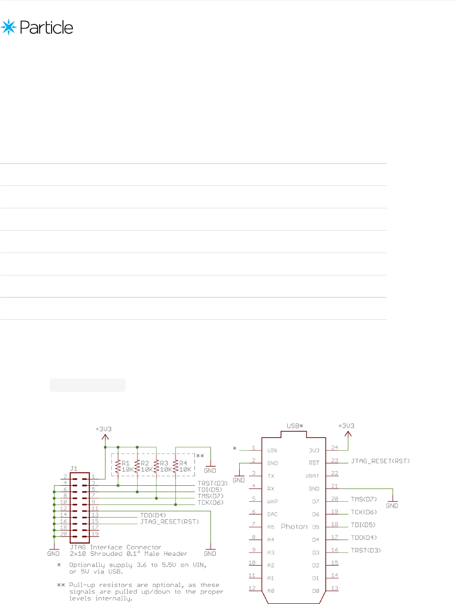
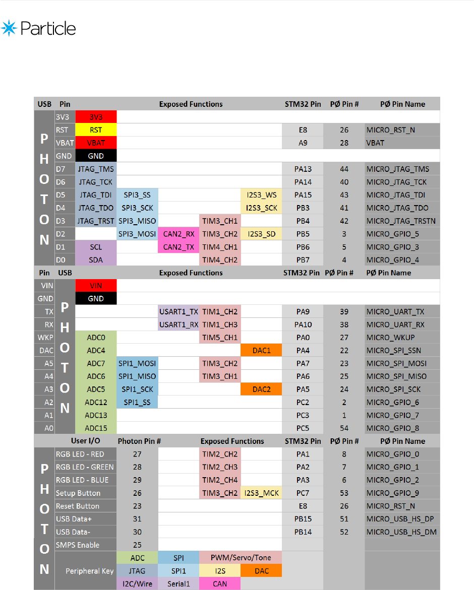
2.5 JTAG
Pin D3 through D7 are JTAG interface pins. These can be used to reprogram your Photon bootloader or user firmware
image with standard JTAG tools such as the ST-Link v2, J-Link, R-Link, OLIMEX ARM-USB-TINI-H, and also the FTDI-based
Particle JTAG Prog rammer.
Photon Pin Description ST M32 Pin PØ Pin # PØ Pin Name Default Internal
D7 JTAG_TMS PA13 44 MICRO_JTAG_TMS ~40k pull-up
D6 JTAG_TCK PA14 40 MICRO_JTAG_TCK ~40k pull-down
D5 JTAG_TDI PA15 43 MICRO_JTAG_TDI ~40k pull-up
D4 JTAG_TDO PB3 41 MICRO_JTAG_TDO Floating
D3 JTAG_TRST PB4 42 MICRO_JTAG_TRSTN ~4 0k pull-up
3V3 Power
GND Ground
RST Reset
Notes:
Default state after reset f or a short period of time before these pins are restored to GPIO (if JTAG debugging is not
required, i.e. USE_SWD_JTAG=y is not specified on the command line.
A standard 20-pin 0.1” shrouded male JTAG interf ace connector should be wired as f ollows:
[1]
[1]
7 of 35
Photon Datasheet v011
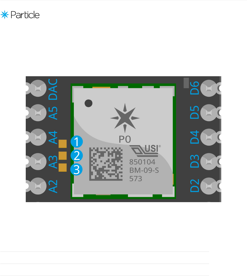
2.6 External Coexistence Interface
The Photon supports coexistence with Bluetooth and other external radios via the three gold pads on the top side of
the PCB near pin A3. These pads are 0.035” square, spaced 0.049” apart. This spacing supports the possibility of
tacking on a small 1.25mm - 1.27mm pitch 3-pin male header to make it somewhat easier to interface with.
When two radios occupying the same f requency band are used in the same system, such as Wi-Fi and Bluetooth, a
coexistence interface can be used to coordinate transmit activity, to ensure optimal performance by arbitrating
conflicts between the two radios.
Pad # PØ Pin Name PØ Pin # I/O Description
1 BTCX_RF_ACTIVE 9 I Sig nals Bluetooth is active
2 BTCX_STATUS 10 I Sig nals Bluetooth priority status and TX/RX direction
3 BTCX_TXCONF 11 O Output giving Bluetooth permission to TX
When these pads are programmed to be used as a Bluetooth coexistence interface, they’re set as high impedance on
power up and reset. Alternatively, they can be individually prog rammed to be used as GPIOs through sof tware control.
They can also be programmed to have an internal pull-up or pull-down resistor.
8 of 35
Photon Datasheet v011
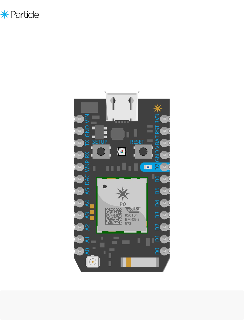
3. Pin and button definition
3.1 Pin markings
9 of 35
Photon Datasheet v011
3.2 Pin description
Pin Description
VIN This pin can be used as an input or output. As an input, supply 3.6 to 5.5VDC to power the Photon. When the
Photon is powered via the USB port, this pin will output a voltage of approximately 4.8VDC due to a
reverse polarity protection series schottky diode between VUSB and VIN. When used as an output, the max
load on VIN is 1A.
RST Active-low reset input. On-board circuitry contains a 1k ohm pull-up resistor between RST and 3V3, and
0.1uF capacitor between RST and GND.
VBAT Supply to the internal RTC, backup registers and SRAM when 3V3 not present (1.65 to 3.6VDC).
3V3 This pin is the output of the on-board regulator and is internally connected to the VDD of the WiFi module.
When powering the Photon via VIN or the USB port, this pin will output a voltage of 3.3VDC. This pin can
also be used to power the Photon directly (max input 3.3VDC). When used as an output, the max load on
3V3 is 100mA. NOTE: When powering the Photon via this pin, ensure power is disconnected from VIN and
USB.
WKP Active-hig h wakeup pin, wakes the module from sleep/standby modes. When not used as a WAKEUP, this
pin can also be used as a digital GPIO, ADC input or PWM.
D0~D7 Dig ital only GPIO pins.
A0~A9 12-bit Analog-to-Digital (A/D) inputs (0-4095), and also dig ital GPIOs. A6 and A7 are code convenience
mappings, which means pins are not actually labeled as such but you may use code like analogRead(A7) .
A6 maps to the DAC pin and A7 maps to the WKP pin.
DAC 12-bit Digital-to-Analog (D/A) output (0-4095), and also a digital GPIO. DAC is used as DAC1 in software,
and A5 is a second DAC output used as DAC2 in software.
RX Primarily used as UART RX, but can also be used as a digital GPIO or PWM.
TX Primarily used as UART TX, but can also be used as a digital GPIO or PWM.
10 of 35
Photon Datasheet v011
3.3 Pin out diagrams
11 of 35
Photon Datasheet v011
4. Technical specification
4.1 Absolute maximum ratings
Parameter Symbol Min Typ Max Unit
Supply Input Voltage V +6.5 V
Supply Output Current I 1 A
Supply Output Current I 100 mA
Storage Temperature T -4 0 +85 °C
Enable Voltage V V +0.6 V
ESD Susceptibility HBM (Human Body Mode) V 2 kV
IN-MAX
IN-MAX-L
3V3-MAX-L
s tg
EN IN
ES D
12 of 35
Photon Datasheet v011
4.2 Recommended operating conditions
Parameter Symbol Min Typ Max Unit
Supply Input Voltage V +3.6 +5.5 V
Supply Input Voltage V +3.0 +3.3 +3.6 V
Supply Output Voltage V +4 .8 V
Supply Output Voltage V +3.3 V
Supply Input Voltage V +1.65 +3.6 V
Supply Input Current (VBAT) I 19 uA
Operating Current (Wi-Fi on) I 80 100 mA
Operating Current (Wi-Fi on) I 235 430 mA
Operating Current (Wi-Fi on, w/powersave) I 18 100 mA
Operating Current (Wi-Fi off ) I 30 40 mA
Sleep Current (5V @ VIN) I 1 2 mA
Deep Sleep Current (5V @ VIN) I 80 100 uA
Operating Temperature T -20 +60 °C
Humidity Range Non condensing, relative humidity 95 %
Notes:
These numbers represent the extreme range of short peak current bursts when transmitting and receiving in
802.11b/g/n modes at dif ferent power levels. Averag e TX current consumption in will be 80-100mA.
These are very short average current bursts when transmitting and receiving. On average if minimizing f requency
of TX/RX events, current consumption in powersave mode will be 18mA
IN
3V3
IN
3V3
VBAT
VBAT
IN avg
IN pk [1] [1]
IN avg [2]
IN avg
Qs
Qds
op
[1]
[2]
13 of 35
Photon Datasheet v011
4.3 Wi-Fi Specifications
Feature Description
WLAN Standards IEEE 802 11b/g/n
Antenna Port Single Antenna
Frequency Band 2.4 12GHz – 2.462GHz (United States of America and Canada)
2.4 12GHz – 2.472GHz (EU)
Sub Channels 1 – 11 (United States of America and Canada)
1 – 13 (EU)
Modulation DSSS, CCK, OFDM, BPSK, QPSK,16QAM, 64QAM
PØ module Wi-Fi output power Typ. T ol. Unit
RF Average Output Power, 802.11b CCK Mode 1M Avail. upon request +/- 1.5 dBm
11M - +/- 1.5 dBm
RF Average Output Power, 802.11g OFDM Mode 6M - +/- 1.5 dBm
54M - +/- 1.5 dBm
RF Average Output Power, 802.11n OFDM Mode MCS0 - +/- 1.5 dBm
MCS7 - +/- 1.5 dBm
14 of 35
Photon Datasheet v011
4.4 I/O Characteristics
These specifications are based on the STM32F205RG datasheet, with reference to Photon pin nomenclature.
Parameter Symbol Conditions Min Typ Max Unit
Standard I/O input low level voltage V -0.3 0.28*(V -
2)+0.8
V
I/O FT input low level voltage V -0.3 0.32*(V -
2)+0.75
V
Standard I/O input hig h level voltage V 0.4 1*(V -
2)+1.3
V +0.3 V
I/O FT input hig h level voltage V V > 2V 0.42*(V -
2)+1
5.5 V
V V ≤ 2V 0.4 2*(V -
2)+1
5.2 V
Standard I/O Schmitt trigg er voltage
hysteresis
V 200 mV
I/O FT Schmitt trigger voltage
hysteresis
V 5% V mV
Input leakag e current I GND ≤ V ≤ V
GPIOs
±1 µA
Input leakag e current I R V = 5V, I/O
FT
3 µA
Weak pull-up equivalent resistor R V = GND 30 4 0 50 k Ω
Weak pull-down equivalent resistor R V = V 30 4 0 50 k Ω
I/O pin capacitance C 5 pF
Notes:
FT = Five-volt tolerant. In order to sustain a voltage hig her than V +0.3 the internal pull-up/pull-down resistors
must be disabled.
Hysteresis voltage between Schmitt trig g er switching levels. Based on characterization, not tested in production.
With a minimum of 100mV.
Leakage could be higher than max. if neg ative current is injected on adjacent pins.
IL 3V3
[1] IL 3V3
IH 3V3 3V3
[1] IH 3V3 3V3
IH 3V3 3V3
[2]
hys
[2]
hys 3V3[3]
[4] lkg io 3V3
[4] lkg PU io
[5] PU io
[5] PD io 3V3
IO
[1] 3V3
[2]
[3]
[4]
15 of 35

Photon Datasheet v011
Pull-up and pull-down resistors are desig ned with a true resistance in series with switchable PMOS/NMOS. This
PMOS/NMOS contribution to the series resistance is minimum (~10% order).
5. Mechanical specifications
5.1 Dimensions and Weight
Headers Dimensions in inches (mm) Weight
With 1.44 x 0.8 x 0.27 (36.58 x 20.32 x 6.86) 5 grams
Without 1.44 x 0.8 x 0.17 (36.58 x 20.32 x 4.32) 3.7 grams
5.2 Mating connectors
The Photon (with headers) can be mounted with (qty 2) 12-pin single row 0.1” female headers. Typically these are
0.335” (8.5mm) tall, but you may pick a taller one if desired. When you search for parts like these it can be difficult to
navigate the thousands of parts available.
On Digikey.com, this section Rectangular Connectors - Headers, Receptacles, Female Sockets
contains 36,000 of them. Narrow the search with: 12 positions, 1 row, 0.1” (2.54mm) pitch, Through Hole mounting
types (unless you want SMT), and sort by Price Ascending. You may f ind something like this:
Description MFG MFG Part Number
12-pin 0.1” Female Header (Tin) Sullins Connector Solutions PPTC121LFBN-RC
12-pin 0.1” Female Header (Gold) Sullins Connector Solutions PPPC121LFBN-RC
You may also search f or other types, such as reverse mounted (bottom side SMT) female headers, low profile types,
machine pin, etc..
[5]
16 of 35
Photon Datasheet v011
5.3 Recommended pcb land pattern (Photon with headers)
The Photon (with headers) can be mounted with 0.1” 12-pin female header receptacles using the following PCB land
pattern:
This land pattern can be found in the Spark.lbr Eagle library, as a Device named PHOTON . Note: Clone or Download
the complete repository as a ZIP file to avoid corrupted data in Eagle files.
17 of 35
Photon Datasheet v011
5.4 Recommended pcb land pattern (Photon without headers)
The Photon (without headers) can be surface mounted directly in an end application PCB using the following PCB land
pattern:
Solder mask around exposed copper pads should be 0.1mm (4 mils) larger in all directions. E.g., a 0.08” x 0.10” pad
would have a 0.088” x 0.108” solder mask.
This land pattern can be found in the Spark.lbr Eagle library, as a Device named PHOTON_SMD . Note: Clone or
Download the complete repository as a ZIP f ile to avoid corrupted data in Eagle f iles.
18 of 35
Photon Datasheet v011
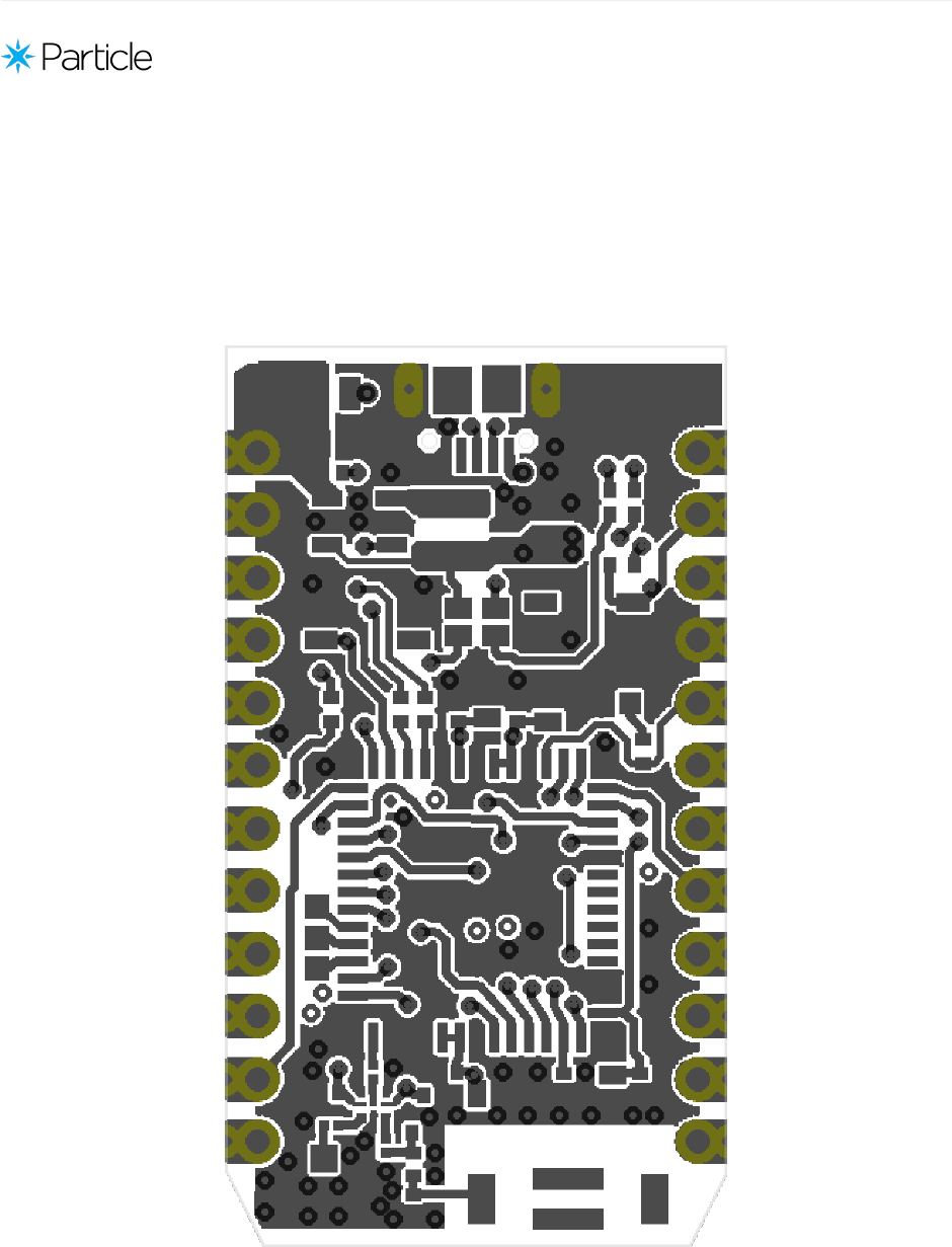
6. Layout
6.1 Photon v1.0.0 Top Layer (GTL)
19 of 35
Photon Datasheet v011
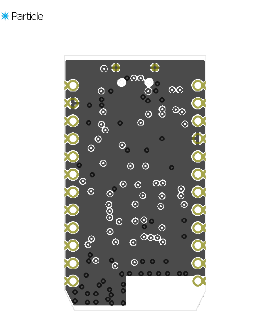
6.2 Photon v1.0.0 GND Layer (G2L)
20 of 35
Photon Datasheet v011
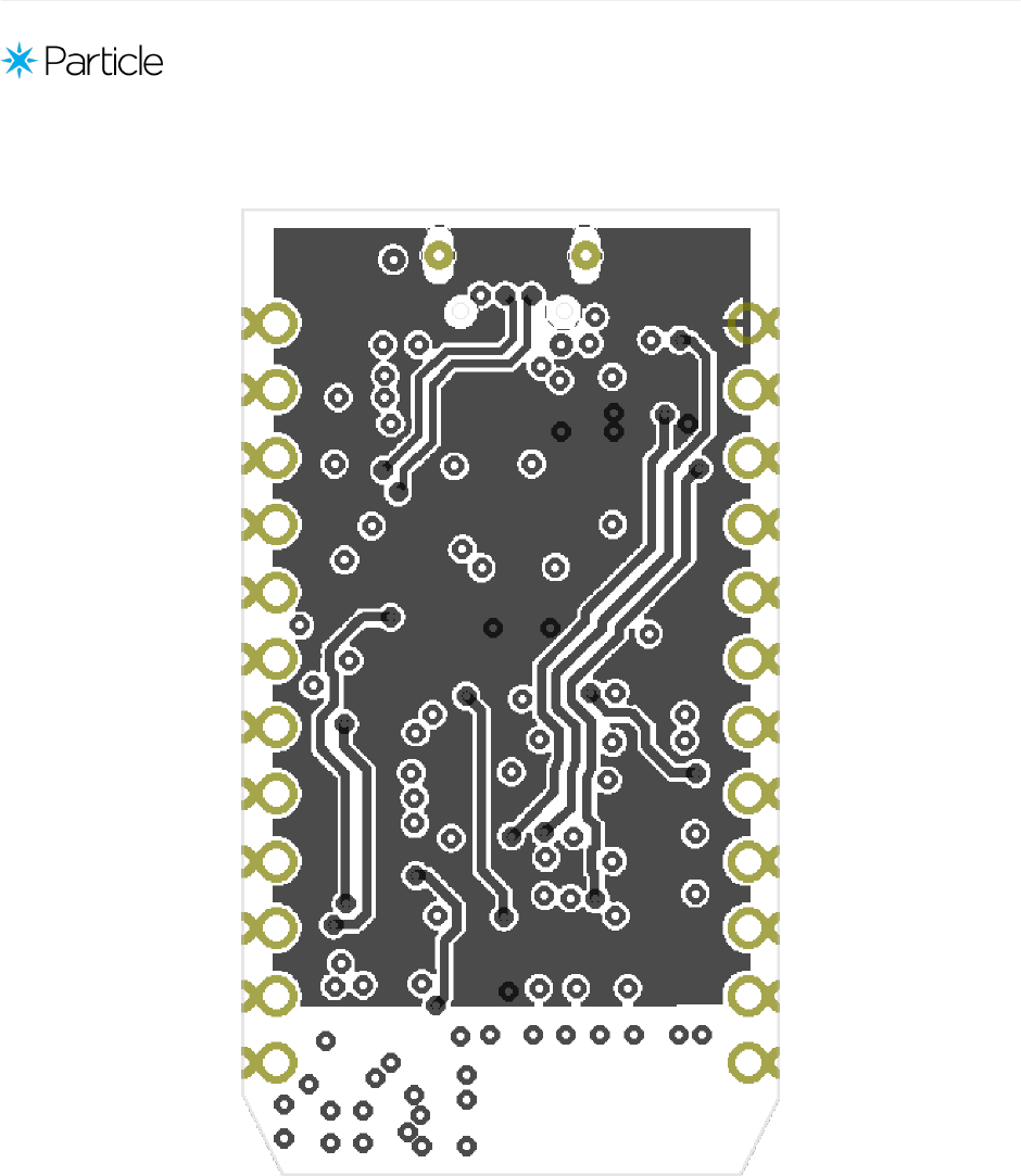
6.3 Photon v1.0.0 3V3 Layer (G15L)
21 of 35
Photon Datasheet v011
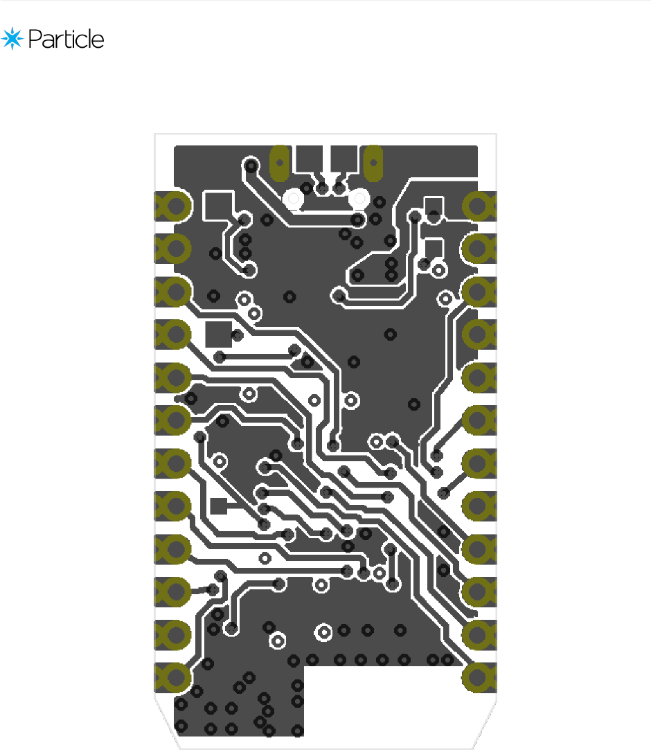
6.4 Photon v1.0.0 Bottom Layer (GBL)
22 of 35
Photon Datasheet v011
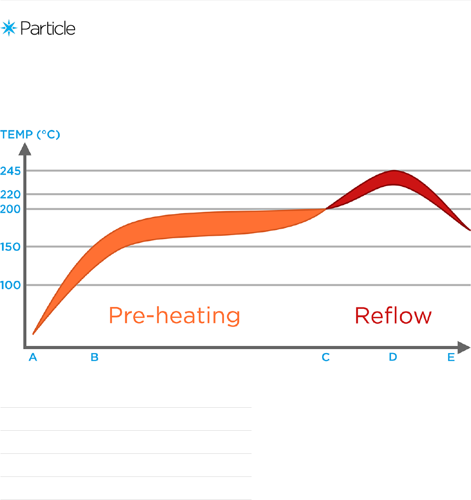
7. Recommended solder reflow profile
Phase T emperatures and Rates
A-B. Ambient~150°C, Heating rate: < 3°C/s
B-C. 150~200°C, soak time: 60~120 s
C-D. 200~245°C, Heating rate: < 3°C/s
D. Peak temp.: 235~24 5°C, Time above 220°C: 4 0~90 s
D-E. 245~220°C, Cooling rate: < 1°C/s
23 of 35

Photon Datasheet v011
8. Bill of Materials
Build your own design based on the Photon!
Qty Device
Minimum
Specification Package/Case Part Designator MFG. MFG. PN
1 ANTENNA 2.4 GHz
Ceramic
5.0mm ×
2.0mm x
2.6mm
ANT1 Advanced
Ceramic X
AT7020-E3R0HBA
2 CERAMIC
CAPACITOR
22uF Ceramic
6.3V 10% X5R
0603 C4,C5 Samsung CL10A226MQ8NRNC
6 CERAMIC
CAPACITOR
0.1uF Ceramic
6.3V 10% X5R
0402 C6,C7,C8,C11,C12,C16 RongFu 04 02B104K01A
2 CERAMIC
CAPACITOR
100pF
Ceramic 6.3V
10% X5R
0402 C2,C3 Fenghua 04 02CG101J500NT
4 CERAMIC
CAPACITOR
10uF Ceramic
6.3V 10% X5R
0603 C9,C11,C13,C15 Sumsung CL10A106MQ8NNNC
3 CERAMIC
CAPACITOR
(RF)
10pF Ceramic
6.3V 10% X5R
0402 C1,C14,C17 Murata GJM1555C1HR80BB01D
1 CONNECTOR USB Micro-B
w/tabs & slots
USB-MICROB X1 Kaweei CMCUSB-5BFM2G-01-D
1 CONNECTOR uFL
Connector
SMD X2 Kaweei P1163-0140R
2 HEADER Single String
1.2” Mating
Length
0.1” 12-pin JP1,JP2 Kaweei CP254 11-12G-S116-A
1 DIODE Diode
Schottky 30V
3A
DO-220AA D1 Vishay SS3P3-M3/84 A
24 of 35

1 DIODE (LED) Blue SMD 0603 LED1 Everlight 19-217/BHC-
ZL1M2RY/3T
1 DIODE (LED) LED RGB
Common
Anode
Dif f used SMD
4-PLCC
(2.0mm x
2.0mm)
LED2 Cree CLVBA-FKA-
CAEDH8BBB7A363
1 INDUCTOR 2.2uH 1.5A 3mm x 3mm L4 Taiyo
Yuden
NR3015T2R2M
1 INDUCTOR
(RF)
3.9nH RF
inductor
0402 L3 Johanson L-07C3N9SV6T
1 INDUCTOR
(RF)
4.7nH RF
inductor
0402 L1 Johanson L-07C4N7SV6T
1 INDUCTOR
(RF)
6.8nH RF
inductor
0402 L2 Johanson L-07C6N8JV6T
1 WI-FI + MCU Broadcom Wi-
FI + STM32
MCU
Custom USI
SMD
U1 USI WM-N-BM-09-S
1 RF SWITCH RF Switch
SPDT
UQFN-6
(1x1mm)
U3 Skyworks SKY13350-385LF
1 POWER
REGULATOR
3.3V 1.5MHz
600mA High
Ef f iciency
PWM Step-
Down DC/DC
Converter
SOT23-5 U2 Richtek RT8008-33GB
1 RESISTOR 100k 5% 0402 R4 Fenghua RC-02W104FT
2 RESISTOR 22R 5% 0402 R5,R6 Fenghua RC-02W220JT
1 RESISTOR 10k 5% 04 02 R8 Fenghua RC-02W103JT
4 RESISTOR 1k 5% 0402 R1,R2,R3,R7 Fenghua RC-02W102JT
2 SWITCH Button 160gf 3.6mm x
3.1mm
SETUP,RESET Haoyu TS-1185A-C
Qty Device
Minimum
Specification Package/Case Part Designator MFG. MFG. PN
25 of 35
Photon Datasheet v011
11. Product handling
11.1 Packaging
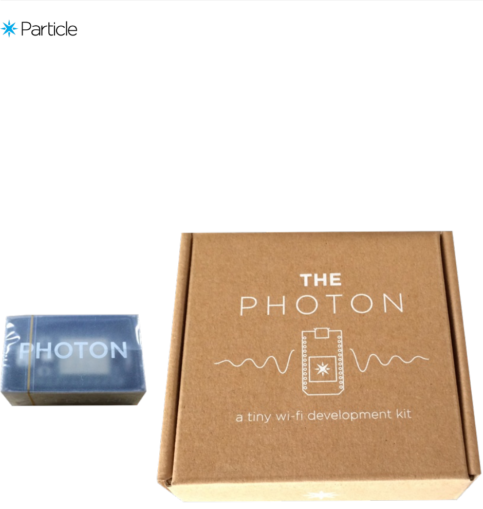
The Photon comes in two primary styles of packag ing: Matchbox and Kit Box. The Matchbox contains the bare
essentials to get you started, while the kit box contains a breadboard, Micro B USB cable, sticker, prototyping card and
a couple sensors to build your first internet connected project!
Photons without headers are also available in JEDEC style trays for automated pick and place machines. Request
more details f rom us on this in the Contact section below.
27 of 35
Photon Datasheet v011
11.2 Moisture sensitivity levels
The Moisture Sensitivity Level (MSL) relates to the packaging and handling precautions required. The PØ module on
the Photons dominate the MSL requirements and are rated level 3. In general, this precaution applies f or Photons
without headers. If ref lowing a Photon directly onto an application PCB, increased moisture levels prior to ref low can
damage sensitive electronics on the Photon. A bake process to reduce moisture may be required.
For more information regarding moisture sensitivity levels, labeling, storage and drying see the MSL standard see
IPC/JEDEC J-STD-020 (can be downloaded from www.jedec.org).
11.3 ESD Precautions
The photon contains highly sensitive electronic circuitry and is an Electrostatic Sensitive Device (ESD). Handling a
photon without proper ESD protection may destroy or damage it permanently. Proper ESD handling and packag ing
procedures must be applied throughout the processing, handling and operation of any application that incorporates
photons. ESD precautions should be implemented on the application board where the photon is mounted. Failure to
observe these precautions can result in severe damage to the photon!
28 of 35

Photon Datasheet v011
12. Default settings
The Photon comes preprogrammed with a bootloader and a user application called Tinker. This application works
with an iOS and Android app also named Tinker that allows you to very easily toggle digital pins, take analog and
digital readings and drive variable PWM outputs.
The bootloader allows you to easily update the user application via several dif f erent methods, USB, OTA, Serial Y-
Modem, and also internally via the Factory Reset procedure. All of these methods have multiple tools associated with
them as well.
You may use the online Web IDE Particle Build to code, compile and flash a user application OTA (Over The Air). Particle
Dev is a local tool that uses the Cloud to compile and flash OTA as well. There is also a packag e Spark DFU-UTIL for
Particle Dev that allows for Cloud compiling and local f lashing via DFU over USB. This requires dfu-util to be
installed on your system. ‘dfu-util’ can also be used with Particle CLI for Cloud compiling and local flashing via the
command line. Finally the lowest level of development is available via the GNU GCC toolchain for ARM, which offers
local compile and flash via dfu-util. This gives the user complete control of all source code and flashing methods. This
is an extensive list, however not exhaustive.
29 of 35

Photon Datasheet v011
13. Glossary
SMPS
Switched-Mode Power Supply
RF
Radio Frequency
Castellated
The edge of the PCB has plated holes that are cut in half which resemble the top of a castle. These make it
easy to solder the Photon down to another PCB with a SMT ref low process.
SMT
Surface Mount Technolog y (of ten associated with SMD which is a surface mount device).
AP
Access Point
LED
Light-Emitting Diode
RGB LED
Red green and blue LEDs combined and diff used in one packag e.
USB
Universal Serial Bus
Quiescent current
Current consumed in the deepest sleep state
FT
Five-tolerant; Refers to a pin being tolerant to 5V.
3V3
+3.3V; The regulated +3.3V supply rail. Also used to note a pin is only 3.3V tolerant.
RTC
Real Time Clock
OT A
Over The Air; describing how f irmware is transferred to the device.
30 of 35

Photon Datasheet v011
14. FCC IC CE Warnings and End Product
Labeling Requirements
Federal Communication Commission Interf erence Statement
This equipment has been tested and found to comply with the limits for a Class B digital device, pursuant to Part 15 of
the FCC Rules. These limits are designed to provide reasonable protection against harmf ul interference in a residential
installation. This equipment generates, uses and can radiate radio frequency energy and, if not installed and used in
accordance with the instructions, may cause harmf ul interference to radio communications. However, there is no
guarantee that interference will not occur in a particular installation. If this equipment does cause harmful
interf erence to radio or television reception, which can be determined by turning the equipment off and on, the user is
encourag ed to try to correct the interference by one of the following measures:
Reorient or relocate the receiving antenna.
Increase the separation between the equipment and receiver.
Connect the equipment into an outlet on a circuit dif ferent from that to which the receiver is connected.
Consult the dealer or an experienced radio/TV technician for help.
FCC Caution:
Any changes or modif ications not expressly approved by the party responsible for compliance could void the user’s
authority to operate this equipment.
This device complies with Part 15 of the FCC Rules. Operation is subject to the following two conditions:
1. This device may not cause harmful interference, and
2. This device must accept any interference received, including interference that may cause undesired operation.
FCC Radiation Exposure Statement:
This equipment complies with FCC radiation exposure limits set f orth for an uncontrolled environment. This
transmitter module must not be co-located or operating in conjunction with any other antenna or transmitter. This
End equipment should be installed and operated with a minimum distance of 20 centimeters between the radiator and
your body.
IMPORTANT NOT E:
In the event that these conditions can not be met (for example certain laptop conf igurations or co-location with
another transmitter), then the FCC authorization is no longer considered valid and the FCC ID can not be used on the
final product. In these circumstances, the OEM integrator will be responsible f or re-evaluating the end product
(including the transmitter) and obtaining a separate FCC authorization.
(continued on next page)
31 of 35

Photon Datasheet v011
End Product Labeling
The final end product must be labeled in a visible area with the following:
Contains FCC ID: 2AEMI-PHOTON
Manual Inf ormation to the End User
The OEM integrator has to be aware not to provide information to the end user regarding how to install or remove
this RF module in the user’s manual of the end product which integrates this module.
Canada Statement
This device complies with Industry Canada’s licence-exempt RSSs. Operation is subject to the following two
conditions:
1. This device may not cause interference; and
2. This device must accept any interference, including interference that may cause undesired operation of the
device.
Le présent appareil est conforme aux CNR d’Industrie Canada applicables aux appareils radio exempts de licence.
L’ exploitation est autorisée aux deux conditions suivantes:
1. l’appareil ne doit pas produire de brouillage;
2. l’utilisateur de l’appareil doit accepter tout brouillag e radioélectrique subi, même si le brouillage est susceptible
d’en compromettre le fonctionnement.
Caution Exposure:
This device meets the exemption from the routine evaluation limits in section 2.5 of RSS102 and users can obtain
Canadian information on RF exposure and compliance.
Le dispositif répond à l’exemption des limites d’évaluation de routine dans la section 2.5 de RSS102 et les utilisateurs
peuvent obtenir des renseignements canadiens sur l’exposition aux RF et le respect.
The final end product must be labelled in a visible area with the f ollowing:
The Industry Canada certif ication label of a module shall be clearly visible at all times when installed in the host device,
otherwise the host device must be labelled to display the Industry Canada certif ication number of the module,
preceded by the words “Contains transmitter module”, or the word “Contains”, or similar wording expressing the
same meaning, as follows:
Contains transmitter module IC: 20127-PHOTON
(continued on next page)
32 of 35

Photon Datasheet v011
This End equipment should be installed and operated with a minimum distance of 20 centimeters between the
radiator and your body.
Cet équipement devrait être installé et actionné avec une distance minimum de 20 centimètres entre le radiateur et
votre corps.
The end user manual shall include all required regulatory inf ormation/warning as shown in this manual.
15. Revision history
Revision Date Author Comments
- 30-
Mar-
2015
BW Initial release
v003 7-Apr-
2015
BW Updated template
v004 8-Apr-
2015
BW Updated Overview, Block diagram, Power, RF, and Pin markings sections
v005 9-Apr-
2015
BW Updated BOM
v006 21-
Apr-
2015
BW Added JTAG, BT CO-EX, I/O Characteristics, Schematic, Layout, Ref low Prof ile,
Glossary, Updated Operating Conditions
v007 28-
Apr-
2015
BW Added Layout, Updated analog pins, Land patterns, Packaging, Mating Connectors
v008 11-
May-
2015
BW Updated BT CO-EX, PWM info, Qualif ications
v009 31-
May-
2015
BW Updated Pinouts, DAC info, Height dimensions, Solder mask info, Recommended
operating conditions
33 of 35

v010 1-
June-
2015
BW Updated VBAT info
v011 22-
June-
2015
BW Added FCC IC CE Warnings and End Product Labeling Requirements, Updated power
output, removed block diagram and schematics, added approved antennas
Revision Date Author Comments
34 of 35
