Configuration Guide For Display Drivers (ACPI And XML) 80 NB116 2 ACPI ON WINDOWS
User Manual: Pdf
Open the PDF directly: View PDF ![]() .
.
Page Count: 110 [warning: Documents this large are best viewed by clicking the View PDF Link!]
- Configuration Guide for Display Drivers (ACPI and XML)
- Revision history
- Contents
- Figures
- Tables
- 1 Introduction
- 2 ACPI configuration for display drivers
- 3 Panel configuration format
- 4 Supported tag list
- 5 Panel configuration tag descriptions
- 6 Display hardware tag descriptions
- 7 Display features
- 8 Display interface-specific configurations
- 8.1 DSI interface configurations
- 8.1.1 Common DSI configurations
- 8.1.2 Display stream compression (DSC)
- 8.1.3 Init sequence timing
- 8.1.4 DSI DCS command configurations
- 8.1.5 Supported DCS commands
- 8.1.6 Special DCS commands
- 8.1.7 DSI interface timing overrides
- 8.1.8 DSI Video mode configuration
- 8.1.9 DSI Command mode configuration
- 8.1.10 DSI Command mode TE synchronization
- 8.1.11 Tear check threshold parameters
- 8.1.12 Dual DSI configuration
- 8.2 DSI Command mode configuration
- 8.3 eDP configuration
- 8.4 HDMI configuration
- 8.1 DSI interface configurations
- 9 Backlight configuration
- 10 ESD detection and recovery configuration
- 11 AD core configuration (preliminary)
- 12 Platform-specific GPIO configuration
- 13 Power-saving configuration
- 14 Sharpening configuration
- 15 Display-specific ACPI methods
- 15.1 _ROM method
- 15.2 ROM multipanel support
- 15.3 BLCP method
- 15.4 Panel calibration commands (PIGC, PPCC, PPGC, PGRT, PBRT, HSIC, PGMT)
- 15.4.1 Panel Inverse Gamma Correction (PIGC)
- 15.4.2 Panel Color Correction (PPCC)
- 15.4.3 Panel Gamma Correction (PGCT)
- 15.4.4 Panel Gamma Response Table (PGRT)
- 15.4.5 HSIC panel HSIC configuration table
- 15.4.6 Panel Gamut Mapping Table (PGMT)
- 15.4.7 Panel Backlight Response Table (PBRT)
- 15.4.8 Panel Linear Gamma Correction (PLGC)
- 15.4.9 Panel Wide Gamut Mapping Table (PWGM)
- 15.4.10 Panel Dithering Table (DITH)
- 16 Registry key entries
- 17 OLED power
- A Specifying the I2C connection in graphics.asl
- B Sample ACPI configuration for DCSbased backlight control
- C References
Qualcomm Technologies, Inc.
Confidential and Proprietary – Qualcomm Technologies, Inc.
NO PUBLIC DISCLOSURE PERMITTED: Please report postings of this document on public servers or websites to:
DocCtrlAgent@qualcomm.com.
Restricted Distribution: Not to be distributed to anyone who is not an employee of either Qualcomm Technologies, Inc. or its
affiliated companies without the express approval of Qualcomm Configuration Management.
Not to be used, copied, reproduced, or modified in whole or in part, nor its contents revealed in any manner to others without the
express written permission of Qualcomm Technologies, Inc.
Qualcomm is a trademark of Qualcomm Incorporated, registered in the United States and other countries. Other product and brand
names may be trademarks or registered trademarks of their respective owners.
This technical data may be subject to U.S. and international export, re-export, or transfer (“export”) laws. Diversion contrary to U.S.
and international law is strictly prohibited.
Qualcomm Technologies, Inc.
5775 Morehouse Drive
San Diego, CA 92121
U.S.A.
© 2013-2017 Qualcomm Technologies, Inc. All rights reserved.
Configuration Guide for Display Drivers
(ACPI and XML)
80-NB116-2 G
March 27, 2017
80-NB116-2 G Confidential and Proprietary – Qualcomm Technologies, Inc. 2
MAY CONTAIN U.S. AND INTERNATIONAL EXPORT CONTROLLED INFORMATION
Revision history
Revision Date Description
A June 2013 Initial release
B April 2014 Updated Section 3.3 and Tables 4-1, 5-2, 5-4, 5-5, 6-1, 8-4, 8-6, 8-7, 8-8,
9-2, and 11-1; added Sections 5.2.3, 8.2, 9.3, Table 10-2, and Chapters
13 and 14
C February 2015 Updated Section 2.1 and Tables 4-1, 8-1, 8-6, and 9-2; added
Chapter 17
D March 2015 Updated Tables 4-1, 7-1, 8-6, and 8-7; added Section 8.1.11
E February 2016 Updated Tables 4-1, 7-1, 8-1, 8-9, and 17-1
F August 2016 Updated Sections 2.1, 3.3 and Tables 4-1, 7-1, and 8-1; added Table 8-2
and Section 12.1.1
G March 2017 Updated Table 4-1, 6-1, 7-1, 8-1, 8-2, and 9-4
Updated Sections 15.4.1, 15.4.2, 15.4.3, and 15.4.6
Added Sections 15.4.8, 15.4.9, and 15.4.10

80-NB116-2 G Confidential and Proprietary – Qualcomm Technologies, Inc. 3
MAY CONTAIN U.S. AND INTERNATIONAL EXPORT CONTROLLED INFORMATION
Contents
1 Introduction ...................................................................................................... 8
1.1 Purpose.......................................................................................................................... 8
1.2 Conventions .................................................................................................................. 8
1.3 Technical assistance ...................................................................................................... 8
2 ACPI configuration for display drivers .......................................................... 9
2.1 Panel configuration in the boot sequence ..................................................................... 9
3 Panel configuration format ........................................................................... 10
3.1 Tag syntax ................................................................................................................... 10
3.2 Special keyword tags .................................................................................................. 10
3.3 Supported data types ................................................................................................... 11
3.4 Limitations .................................................................................................................. 12
4 Supported tag list .......................................................................................... 13
5 Panel configuration tag descriptions .......................................................... 24
5.1 Informational fields ..................................................................................................... 24
5.2 EDID fields ................................................................................................................. 24
5.2.1 Static EDID fields ............................................................................................ 24
5.2.2 Detailed timing fields ...................................................................................... 25
5.2.3 EDID information ............................................................................................ 26
5.2.4 Dynamic EDID fields ...................................................................................... 26
5.3 Panel timings configuration ........................................................................................ 28
6 Display hardware tag descriptions .............................................................. 30
6.1 Common hardware configuration parameters ............................................................. 30
7 Display features ............................................................................................. 33
7.1 Display feature flags ................................................................................................... 33
8 Display interface-specific configurations.................................................... 35
8.1 DSI interface configurations ....................................................................................... 35
8.1.1 Common DSI configurations ........................................................................... 35
8.1.2 Display stream compression (DSC) ................................................................. 42
8.1.3 Init sequence timing ......................................................................................... 43
8.1.4 DSI DCS command configurations ................................................................. 44
8.1.5 Supported DCS commands .............................................................................. 45
8.1.6 Special DCS commands .................................................................................. 45

Configuration Guide for Display Drivers (ACPI and XML) Contents
80-NB116-2 G Confidential and Proprietary – Qualcomm Technologies, Inc. 4
MAY CONTAIN U.S. AND INTERNATIONAL EXPORT CONTROLLED INFORMATION
8.1.7 DSI interface timing overrides ......................................................................... 46
8.1.8 DSI Video mode configuration ........................................................................ 47
8.1.9 DSI Command mode configuration ................................................................. 52
8.1.10 DSI Command mode TE synchronization ..................................................... 54
8.1.11 Tear check threshold parameters ................................................................... 55
8.1.12 Dual DSI configuration .................................................................................. 55
8.2 DSI Command mode configuration ............................................................................ 56
8.3 eDP configuration ....................................................................................................... 58
8.4 HDMI configuration ................................................................................................... 60
9 Backlight configuration................................................................................. 62
9.1 Common backlight configuration parameters ............................................................. 63
9.2 PWM (PMIC)-based backlight control ....................................................................... 64
9.3 Sample backlight configurations ................................................................................. 65
9.3.1 WLED configuration (1 WLED string) ........................................................... 65
9.3.2 LPG configuration ........................................................................................... 66
9.4 I2C-based backlight control ........................................................................................ 66
9.5 DSI DCS-based backlight control ............................................................................... 66
9.6 ACPI-based backlight control ..................................................................................... 67
9.7 CABL configuration ................................................................................................... 67
9.8 Advanced backlight configuration .............................................................................. 68
10 ESD detection and recovery configuration ............................................... 69
11 AD core configuration (preliminary) .......................................................... 70
12 Platform-specific GPIO configuration ........................................................ 71
12.1 GPIO configuration ................................................................................................... 74
13 Power-saving configuration ....................................................................... 75
14 Sharpening configuration ........................................................................... 78
15 Display-specific ACPI methods .................................................................. 79
15.1 _ROM method .......................................................................................................... 80
15.2 ROM multipanel support .......................................................................................... 80
15.3 BLCP method ........................................................................................................... 82
15.3.1 BLCP format for DSI DCS commands.......................................................... 83
15.3.2 BLCP format for I2C commands ................................................................... 83
15.4 Panel calibration commands (PIGC, PPCC, PPGC, PGRT, PBRT, HSIC, PGMT) 84
15.4.1 Panel Inverse Gamma Correction (PIGC) ..................................................... 85
15.4.2 Panel Color Correction (PPCC) ..................................................................... 86
15.4.3 Panel Gamma Correction (PGCT) ................................................................. 87
15.4.4 Panel Gamma Response Table (PGRT) ......................................................... 88
15.4.5 HSIC panel HSIC configuration table ........................................................... 90
15.4.6 Panel Gamut Mapping Table (PGMT) .......................................................... 90
15.4.7 Panel Backlight Response Table (PBRT) ...................................................... 92
15.4.8 Panel Linear Gamma Correction (PLGC) ..................................................... 94

Configuration Guide for Display Drivers (ACPI and XML) Contents
80-NB116-2 G Confidential and Proprietary – Qualcomm Technologies, Inc. 5
MAY CONTAIN U.S. AND INTERNATIONAL EXPORT CONTROLLED INFORMATION
15.4.9 Panel Gamut Mapping Table (PWGM) ......................................................... 94
15.4.10 Panel Dithering Table (DITH) ..................................................................... 96
16 Registry key entries .................................................................................... 98
16.1 CABL ........................................................................................................................ 98
16.2 SBC ........................................................................................................................... 98
16.3 AVI Info Frame Packet ............................................................................................. 98
16.4 HDCP ........................................................................................................................ 99
17 OLED power ............................................................................................... 100
A Specifying the I2C connection in graphics.asl ......................................... 102
B Sample ACPI configuration for DCS-based backlight control ................ 103
C References ................................................................................................... 109
C.1 Related documents ................................................................................................... 109
C.2 Acronyms and terms ................................................................................................ 109

Configuration Guide for Display Drivers (ACPI and XML) Contents
80-NB116-2 G Confidential and Proprietary – Qualcomm Technologies, Inc. 6
MAY CONTAIN U.S. AND INTERNATIONAL EXPORT CONTROLLED INFORMATION
Figures
Figure 2-1 Panel configuration role in the boot sequence ............................................................................ 9
Figure 5-1 Example phone dimensions and EDID population .................................................................. 26
Figure 5-2 Panel timings configuration ..................................................................................................... 28
Figure 8-1 Init sequence timing ................................................................................................................. 43
Figure 8-2 DSI DCS command configurations .......................................................................................... 44
Figure 8-3 DSI Command mode TE synchronization................................................................................ 54
Figure 8-4 DSI data transmission with respect to panel scanline .............................................................. 55
Figure 9-1 Backlight control under WDDM model ................................................................................... 62
Figure 12-1 Panel power-on reset .............................................................................................................. 71
Figure 17-1 PMIC IBB and LAB modules .............................................................................................. 100
Tables
Table 4-1 Supported tag list ....................................................................................................................... 13
Table 5-1 Informational fields ................................................................................................................... 24
Table 5-2 Static EDID fields ...................................................................................................................... 24
Table 5-3 Detailed timing fields ................................................................................................................ 25
Table 5-4 Dynamic EDID fields ................................................................................................................ 26
Table 5-5 Panel timing fields ..................................................................................................................... 28
Table 6-1 Common hardware configuration parameters ........................................................................... 30
Table 7-1 Feature flags that can be enabled or disabled ............................................................................ 33
Table 8-1 Common DSI configurations ..................................................................................................... 35
Table 8-2 Parameters to configure the DSC module for DSI .................................................................... 42
Table 8-3 DSI DCS command configuration tags ..................................................................................... 44
Table 8-4 Supported DCS commands ........................................................................................................ 45
Table 8-5 Special DCS commands ............................................................................................................ 45
Table 8-6 DSI interface timing overrides .................................................................................................. 46
Table 8-7 DSI Video mode configuration .................................................................................................. 47
Table 8-8 DSI Command mode configuration ........................................................................................... 52
Table 8-9 eDP configuration ...................................................................................................................... 58
Table 8-10 HDMI configuration ................................................................................................................ 60
Table 9-1 Common backlight configuration parameters ........................................................................... 63
Table 9-2 PWM (PMIC)-based backlight control ...................................................................................... 64
Table 9-3 CABL configuration .................................................................................................................. 67
Table 9-4 Backlight configuration ............................................................................................................. 68
Table 10-1 ESD Detection and Recovery tags ........................................................................................... 69
Table 10-2 Display recovery threshold ...................................................................................................... 69
Table 11-1 AD core tags ............................................................................................................................ 70
Table 12-1 Panel resources ........................................................................................................................ 72

Configuration Guide for Display Drivers (ACPI and XML) Contents
80-NB116-2 G Confidential and Proprietary – Qualcomm Technologies, Inc. 7
MAY CONTAIN U.S. AND INTERNATIONAL EXPORT CONTROLLED INFORMATION
Table 12-2 GPIO configuration tags .......................................................................................................... 74
Table 13-1 Power saving configuration ..................................................................................................... 76
Table 13-2 Power saving levels supported by the driver ........................................................................... 77
Table 14-1 Sharpening parameters ............................................................................................................ 78
Table 17-1 IBB/LAB management configuration.................................................................................... 101
Table A-1 XML tags and descriptions ..................................................................................................... 102

80-NB116-2 G Confidential and Proprietary – Qualcomm Technologies, Inc. 8
MAY CONTAIN U.S. AND INTERNATIONAL EXPORT CONTROLLED INFORMATION
1 Introduction
1.1 Purpose
This document is intended for display developers who are looking to customize the display-
specific Advanced Configuration and Power Interface (ACPI) entries for a particular display
device. Knowledge of display interfaces, Windows display driver model (WDDM) architecture,
and ACPI programming are prerequisites for this document. The XML syntax is common
between UEFI and ACPI, therefore this document applies to both configuration methods.
This document supports the MSM8974, MSM8x26, MSM8x62, MSM8084, MSM8x94,
MSM8996, and MSM8998 chipsets. Configurations mentioned in this document are specific to
these chipset families.
1.2 Conventions
Function declarations, function names, type declarations, and code samples appear in a different
font, e.g., #include.
Code variables appear in angle brackets, e.g., <number>.
Commands to be entered appear in a different font, e.g., copy a:*.* b:.
Button and key names appear in bold font, e.g., click Save or press Enter.
Shading indicates content that has been added or changed in this revision of the document.
1.3 Technical assistance
For assistance or clarification on information in this document, submit a case to Qualcomm
Technologies, Inc. (QTI) at https://createpoint.qti.qualcomm.com/.
If you do not have access to the CDMATech Support Service website, register for access or send
email to support.cdmatech@qti.qualcomm.com.
80-NB116-2 G Confidential and Proprietary – Qualcomm Technologies, Inc. 9
MAY CONTAIN U.S. AND INTERNATIONAL EXPORT CONTROLLED INFORMATION
2 ACPI configuration for display drivers
2.1 Panel configuration in the boot sequence
The role of the panel configuration in the boot sequence is shown in Figure 2-1.
Firmware (UEFI)
(xml binary configuration) HLOS Loader Kernel Mode Driver
Figure 2-1 Panel configuration role in the boot sequence
The following two-stage sequence is specific to HLOSes that use UEFI and ACPI:
Firmware (UEFI) boot – During UEFI boot, the panel configuration is loaded directly from a
panel configuration in the UEFI binary. This configuration is parsed and applied to the
display controller.
OS boot (graphics miniport) – During OS boot, the KMD parses the display configuration
from the ACPI (_ROM) method.
Both boot stages use similar XML configurations. However, the data is physically located in two
locations even though the data has many configurations that are identical. The reason for this is
that the UEFI does not directly process data from the ACPI tables, and therefore the data cannot
be shared between both boot sequences. The Figure 2-1 shows the role of panel configuration in
the boot sequence.

80-NB116-2 G Confidential and Proprietary – Qualcomm Technologies, Inc. 10
MAY CONTAIN U.S. AND INTERNATIONAL EXPORT CONTROLLED INFORMATION
3 Panel configuration format
The panel configuration format is XML-like, only certain data fields are parsed and only certain
tags are recognized.
3.1 Tag syntax
The tag syntax is similar to XML using braces for various tags.
<?xml version="1.0" encoding="utf-8"?>
<TagName comments=”any comments”>Tag Data</TagName>
<MultiLineTag>
Tag Data
More Data
</MultiLineTag>
All tags must be unique except for certain keyword tags that are ignored
All tags must end with a </TagName>
Tags are case-insensitive
Tags cannot be made from spaces or special characters
3.2 Special keyword tags
The <?xml xxxxxxxx ?> tag is ignored.
Tags that use the keyword Group are ignored. However, tags within the context of a group
branch are parsed, for example, Group xyz is ignored, but MyTagA is parsed.
<Group xyz>
<MyTagA> data </MyTagA>
</Group>
Comments are added as <!-- Comment -->. However, comments should be avoided because
they add extra parsing time and size to the configuration.
Data appears after the tag name is ignored, but can be used for comments or informational
purposes.
<MyTag this_data is ignored = “””> tag data </MyTag>

Configuration Guide for Display Drivers (ACPI and XML) Panel configuration format
80-NB116-2 G Confidential and Proprietary – Qualcomm Technologies, Inc. 11
MAY CONTAIN U.S. AND INTERNATIONAL EXPORT CONTROLLED INFORMATION
3.3 Supported data types
Parsing of data supports several data types.
Integer – Integer data can be in the form of decimal digits or hex digits. Depending on the
integer size, the range can vary; e.g., if the size is 1 byte, the range is 0x00-0xFF (0 to 255
decimal). Hex digits must be prefixed with “0x”, e.g., these are all valid integer values:
<MyIntegerTag>123456</MyIntegerTag>
<MyHexTag>0xFFEE23</MyHexTag>
Integer list – Integer lists are an ordered list of integers separated by spaces. Each entry is
interpreted as hex values regardless if it is prepended with 0x.
<MyIntergerList>0x1234 0x456 0xAA 0xBB</MyIntegerList>
String – String data can be any alphanumeric sequence including spaces, e.g.:
<MyStringTag>Same String Data 1234</MyStringTag>
Boolean – Boolean data consists of either the true or false keyword tag. The case does not
matter.
<MyBooleanTag>True</MyBooleanTag>
<MyBooleanTag>false</MyBooleanTag>
GUID – The GUID tag accepts a standard Windows GUID, e.g.:
<MyGUIDTag>{0xf9938f2d, 0x3756, 0x4760, 0xa0, 0x44, 0xcb, 0x29, 0xaf, 0xba,
0x5a, 0x69}</MyGUIDTag>
Binary – The binary field is a special field that is used to describe raw information, i.e.,
packet data. Each hex pair byte is separated by spaces and the “0x” prefix is not allowed.
Multiple packets can be formed by adding a new byte sequence on each line.
NOTE: This is an important differentiator. Multiple bytes in the same line represent a single sequence,
while multiple bytes on multiple lines represent multiple packet sequences.
<MyDataSequence>
23 b0 04 29 b3 00 87 29 b6 30 83
</MyDataSequence>
<MultiPacketSequence>
23 b0 04 29 b3 00
87 29 b6 30 83
</MultiPacketSequence >

Configuration Guide for Display Drivers (ACPI and XML) Panel configuration format
80-NB116-2 G Confidential and Proprietary – Qualcomm Technologies, Inc. 12
MAY CONTAIN U.S. AND INTERNATIONAL EXPORT CONTROLLED INFORMATION
3.4 Limitations
ASCII only – Only ASCII characters must be used. Unicode and double byte characters are
not supported.
Limited XML support – The format of the panel configuration is XML-like, and not all XML
tags are supported. Avoid using syntax that is not described in this document.
Configuration size – The panel configuration size is bounded by the amount of memory
allocated to store the configuration. Size limitations include all characters, including white
spaces, tags, and control characters (line feeds and carriage returns).
Firmware – Static structure, no limitations other than compile limitations

80-NB116-2 G Confidential and Proprietary – Qualcomm Technologies, Inc. 13
MAY CONTAIN U.S. AND INTERNATIONAL EXPORT CONTROLLED INFORMATION
4 Supported tag list
Table 4-1 provides a list of all of the currently supported panel configuration tags. This list is
subject to change.
Table 4-1 Supported tag list
NOTE: The following table has been updated.
Panel name Type
(size in bytes) Purpose Firmware
(UEFI)
supported
Graphics
KMD
supported
PanelName String(13) EDID reporting No Yes
PanelDescription String (128) EDID reporting No Yes
ManufactureID Integer(2) EDID reporting No Yes
ProductCode Integer(2) EDID reporting No Yes
SerialNumber Integer(4) EDID reporting No Yes
WeekofManufacture Integer(1) EDID reporting No Yes
YearofManufacture Integer(1) EDID reporting No Yes
EDIDVersion Integer(1) EDID reporting No Yes
EDIDRevision Integer(1) EDID reporting No Yes
VideoInputDefinition Integer(1) EDID reporting No Yes
HorizontalScreenSize Integer(1) EDID reporting No Yes
VerticalScreenSize Integer(1) EDID reporting No Yes
DisplayTransferCharacteristics Integer(1) EDID reporting No Yes
FeatureSupport Integer(1) EDID reporting No Yes
Red.GreenBits Integer(1) EDID reporting No Yes
Blue.WhiteBits Integer(1) EDID reporting No Yes
RedX Integer(1) EDID reporting No Yes
RedY Integer(1) EDID reporting No Yes
GreenX Integer(1) EDID reporting No Yes
GreenY Integer(1) EDID reporting No Yes
BlueX Integer(1) EDID reporting No Yes
BlueY Integer(1) EDID reporting No Yes
WhiteX Integer(1) EDID reporting No Yes
WhiteY Integer(1) EDID reporting No Yes
EstablishedTimingsI Integer(1) EDID reporting No Yes
EstablishedTimingsII Integer(1) EDID reporting No Yes
ManufacturesTiming Integer(1) EDID reporting No Yes

Configuration Guide for Display Drivers (ACPI and XML) Supported tag list
80-NB116-2 G Confidential and Proprietary – Qualcomm Technologies, Inc. 14
MAY CONTAIN U.S. AND INTERNATIONAL EXPORT CONTROLLED INFORMATION
Panel name Type
(size in bytes) Purpose Firmware
(UEFI)
supported
Graphics
KMD
supported
StandardTimings1 Integer(2) EDID reporting No Yes
StandardTimings2 Integer(2) EDID reporting No Yes
StandardTimings3 Integer(2) EDID reporting No Yes
StandardTimings4 Integer(2) EDID reporting No Yes
StandardTimings5 Integer(2) EDID reporting No Yes
StandardTimings6 Integer(2) EDID reporting No Yes
StandardTimings7 Integer(2) EDID reporting No Yes
StandardTimings8 Integer(2) EDID reporting No Yes
SignalTimingInterface Integer(1) EDID reporting No Yes
HorizontalScreenSizeMM Integer(1) EDID reporting No Yes
VerticalScreenSizeMM Integer(1) EDID reporting No Yes
HorizontalVerticalScreenSizeMM Integer(1) EDID reporting No Yes
Display Hardware Configuration
InterfaceType Integer(4) Display hardware
configuration Yes Yes
PanelOrientation Integer(4) Display hardware
configuration No No
InterfaceColorFormat Integer(4) Display hardware
configuration Yes Yes
ComponentOrdering Integer(4) Display hardware
configuration Yes Yes
PixelPacking Integer(4) Display hardware Yes Yes
PixelAlignment Integer(4) Configuration Yes Yes
HorizontalActive Integer(4) Configuration Yes Yes
HorizontalFrontPorch Integer(4) Display hardware Yes Yes
HorizontalBackPorch Integer(4) Configuration Yes Yes
HorizontalSyncPulse Integer(4) Display hardware Yes Yes
HorizontalSyncSkew Integer(4) Configuration Yes Yes
HorizontalLeftBorder Integer(4) Display hardware Yes Yes
HorizontalRightBorder Integer(4) Configuration Yes Yes
VerticalActive Integer(4) Display hardware Yes Yes
VerticalFrontPorch Integer(4) Configuration Yes Yes
VerticalBackPorch Integer(4) Display hardware Yes Yes
VerticalSyncPulse Integer(4) Configuration Yes Yes
VerticalTopBorder Integer(4) Display hardware Yes Yes
VerticalBottomBorder Integer(4) Configuration Yes Yes
InvertDataPolarity Boolean Display hardware Yes Yes
InvertVsyncPolairty Boolean Configuration Yes Yes
InvertHsyncPolarity Boolean Display hardware Yes Yes
BorderColor Integer(4) Configuration Yes Yes
UnderflowColor Integer(4) Configuration No Yes

Configuration Guide for Display Drivers (ACPI and XML) Supported tag list
80-NB116-2 G Confidential and Proprietary – Qualcomm Technologies, Inc. 15
MAY CONTAIN U.S. AND INTERNATIONAL EXPORT CONTROLLED INFORMATION
Panel name Type
(size in bytes) Purpose Firmware
(UEFI)
supported
Graphics
KMD
supported
DisplayPrimaryFlags Integer(4) Display
configuration No Yes
DisplayExternalFlags Integer(4) Display
configuration No Yes
ESDDetectionTime Integer(4) ESD detection
and recovery No Yes
ESDDetectionFailureRetry Integer(4) ESD detection
and recovery No Yes
DisplayRecoveryThreshold Integer(4) ESD detection
and recovery No Yes
DSI Hardware Configuration
DSIRefreshRate Integer(4) DSI hardware
configuration Yes Yes
DSIDynamicRefreshRates Integer list(16) DSI hardware
configuration No Yes
DSIBitClockFrequency Integer(4) DSI hardware
configuration Yes Yes
DSIDynamicBlankingRefreshRateList Integer list(16) DSI hardware
configuration No Yes
DSIDynamicVFrontPorchList Integer list(16) DSI hardware
configuration No Yes
DSIDynamicVBackPorchList Integer list(16) DSI hardware
configuration No Yes
DSIDynamicVSyncPulseList Integer list(16) DSI hardware
configuration No Yes
DSIDynamicHFrontPorchList Integer list(16) DSI hardware
configuration No Yes
DSIDynamicHBackPorchList Integer list(16) DSI hardware
configuration No Yes
DSIDynamicHSyncPulseList Integer list(16) DSI hardware
configuration No Yes
DSILanes Integer(4) DSI hardware
configuration Yes Yes
DSIChannelId Integer(4) DSI hardware
configuration Yes Yes
DSIVirtualId Integer(4) DSI hardware
configuration Yes Yes
DSIColorFormat Integer(4) DSI hardware
configuration Yes Yes
DSIPacketTransferHS Boolean DSI hardware
configuration Yes Yes
DSIClockHSForceRequest Integer(4) DSI hardware
configuration Yes Yes
DSIPixelXferTiming Integer(4) DSI hardware
configuration Yes Yes
DSIHostLaneMapping Integer(4) DSI hardware
configuration Yes Yes

Configuration Guide for Display Drivers (ACPI and XML) Supported tag list
80-NB116-2 G Confidential and Proprietary – Qualcomm Technologies, Inc. 16
MAY CONTAIN U.S. AND INTERNATIONAL EXPORT CONTROLLED INFORMATION
Panel name Type
(size in bytes) Purpose Firmware
(UEFI)
supported
Graphics
KMD
supported
DSILP11AtInit Integer(4) DSI hardware
configuration Yes Yes
DSIPhyDCDCMode Boolean DSI hardware
configuration Yes Yes
DSIEnterULPSPowerDown Boolean DSI hardware
configuration Yes Yes
DSIBitClkScalePercent Integer(4) DSI hardware
configuration No Yes
DSIBitClkScalePercent Integer(4) DSI hardware
configuration No Yes
DSIEscapeClockDivisor Integer(4) DSI hardware
configuration Yes Yes
DSIEscapeClockFrequency Integer(4) DSI hardware
configuration Yes Yes
DSITimingHSZeroOverride Boolean DSI hardware
configuration Yes Yes
DSITimingHSZeroValue Integer(4) DSI hardware
configuration Yes Yes
DSITimingHSExitOverride Boolean DSI hardware
configuration Yes Yes
DSITimingHSExitValue Integer(4) DSI hardware
configuration Yes Yes
DSITimingHSPrepareOverride Boolean DSI hardware
configuration Yes Yes
DSITimingHSPrepareValue Integer(4) DSI hardware
configuration Yes Yes
DSITimingHSTrailOverride Boolean DSI hardware
configuration Yes Yes
DSITimingHSTrailValue Integer(4) DSI hardware
configuration Yes Yes
DSITimingHSRequestOverride Boolean DSI hardware
configuration Yes Yes
DSITimingHSRequestValue Integer(4) DSI hardware
configuration Yes Yes
DSITimingCLKZeroOverride Boolean DSI hardware
configuration Yes Yes
DSITimingCLKZeroValue Integer(4) DSI hardware
configuration Yes Yes
DSITimingCLKTrailOverride Boolean DSI hardware
configuration Yes Yes
DSITimingCLKTrailValue Integer(4) DSI hardware
configuration Yes Yes
DSITimingCLKPrepareOverride Boolean DSI hardware
configuration Yes Yes
DSITimingCLKPrepareValue Integer(4) DSI hardware
configuration Yes Yes
DSITimingCLKPreOverride Boolean DSI hardware
configuration Yes Yes

Configuration Guide for Display Drivers (ACPI and XML) Supported tag list
80-NB116-2 G Confidential and Proprietary – Qualcomm Technologies, Inc. 17
MAY CONTAIN U.S. AND INTERNATIONAL EXPORT CONTROLLED INFORMATION
Panel name Type
(size in bytes) Purpose Firmware
(UEFI)
supported
Graphics
KMD
supported
DSITimingCLKPreValue Integer(4) DSI hardware
configuration Yes Yes
DSITimingCLKPostOverride Boolean DSI hardware
configuration Yes Yes
DSITimingCLKPostValue Integer(4) DSI hardware
configuration Yes Yes
DSITimingTASureOverride Boolean DSI hardware
configuration Yes Yes
DSITimingTASureValue Integer(4) DSI hardware
configuration Yes Yes
DSITimingTAGoOverride Boolean DSI hardware
configuration Yes Yes
DSITimingTAGoValue Integer(4) DSI hardware
configuration Yes Yes
DSITimingTAGetOverride Boolean DSI hardware
configuration Yes Yes
DSITimingTAGetValue Integer(4) DSI hardware
configuration Yes Yes
DSITrafficMode Integer(4) DSI hardware
configuration Yes Yes
DSIHsaHseAfterVsVe Boolean DSI hardware
configuration Yes Yes
DSILowPowerModeInHFP Boolean DSI hardware
configuration Yes Yes
DSILowPowerModeInHBP Boolean DSI hardware
configuration Yes Yes
DSILowPowerModeInHSA Boolean DSI hardware
configuration Yes Yes
DSILowPowerModeInBLLPEOF Boolean DSI hardware
configuration Yes Yes
DSIForceCmdInVideoHS Boolean DSI hardware
configuration Yes Yes
DSILowPowerModeInBLLP Boolean DSI hardware
configuration Yes Yes
DSICMDSwapInterface Boolean DSI hardware
configuration Yes Yes
DSICMDUsingTrigger Boolean DSI hardware
configuration Yes Yes
DSITECheckEnable Boolean DSI hardware
configuration Yes Yes
DSITEUsingDedicatedTEPin Boolean DSI hardware
configuration Yes Yes
DSITEvSyncStartPos Integer(4) DSI hardware
configuration Yes Yes
DSITEvSyncContinueLines Integer(4) DSI hardware
configuration Yes Yes
DSITEvSyncStartLineDivisor Integer(4) DSI hardware
configuration Yes Yes

Configuration Guide for Display Drivers (ACPI and XML) Supported tag list
80-NB116-2 G Confidential and Proprietary – Qualcomm Technologies, Inc. 18
MAY CONTAIN U.S. AND INTERNATIONAL EXPORT CONTROLLED INFORMATION
Panel name Type
(size in bytes) Purpose Firmware
(UEFI)
supported
Graphics
KMD
supported
DSITEvSyncPosSafetyMargin Integer(4) DSI hardware
configuration Yes Yes
DSITEvSyncBelowSafetyMargin Integer(4) DSI hardware
configuration Yes Yes
DSITEPercentVariance Integer(4) DSI hardware
configuration Yes Yes
DSITEvSyncRdPtrIrqLine Integer(4) DSI hardware
configuration Yes Yes
DSIDataStrengthLP Integer(4) DSI hardware
configuration Yes Yes
DSIDataStrengthHS Integer(4) DSI hardware
configuration Yes Yes
DSIClockStrengthHS Integer(4) DSI hardware
configuration Yes Yes
DSIEnableAutoRefresh Boolean DSI hardware
configuration Yes No
DSIAutoRefreshFrameNumDiv Integer(4) DSI hardware
configuration Yes No
DSIPhyDCDCMode Boolean DSI hardware
configuration Yes Yes
DSIInitSequence Binary DSI panel
configuration Yes Yes
DSITermSequence Binary DSI panel
configuration No Yes
DSIStatusSequence Binary DSI panel status
check No Yes
DSIDisableEoTAfterHSXfer Boolean DSI hardware
configuration Yes Yes
DSIInitMasterTime Integer(4) DSI hardware
configuration Yes Yes
DSIDmaDelayAfterVsync Integer(4) DSI DMA
scheduling No Yes
DSITEvSyncSelect Integer(4) DSI hardware
configuration Yes Yes
DSICmdModeIdleTime Integer(4) DSI hardware
configuration Yes Yes
DSIFBCEnable Boolean Display/DSI
hardware
configuration
Yes Yes
DSIFBCProfileID Integer(4) Display/DSI
hardware
configuration
Yes Yes
DSIControllerMapping Integer List(16) DSI hardware
configuration Yes Yes
DSISlaveControllerSkewLines Integer(4) DSI hardware
configuration Yes Yes
DSITransferRetryCntr Integer(4) DSI hardware
configuration Yes Yes
Configuration Guide for Display Drivers (ACPI and XML) Supported tag list
80-NB116-2 G Confidential and Proprietary – Qualcomm Technologies, Inc. 19
MAY CONTAIN U.S. AND INTERNATIONAL EXPORT CONTROLLED INFORMATION
Panel name Type
(size in bytes) Purpose Firmware
(UEFI)
supported
Graphics
KMD
supported
DSINullpacketInsertionBytes Integer(4) DSI hardware
configuration Yes Yes
DSIFlags Integer(4) DSI hardware
configuration Yes Yes
DSIDSCEnable Boolean DSI hardware
configuration Yes Yes
DSIDSCProfileId Integer(4) DSI hardware
configuration Yes Yes
DSIDSCSliceHeight Integer(4) DSI hardware
configuration Yes Yes
DSIDSCSliceWidth Integer(4) DSI hardware
configuration Yes Yes
DSIDSCMajorVersion Integer(4) DSI hardware
configuration Yes Yes
DSIDSCMinorVersion Integer(4) DSI hardware
configuration Yes Yes
DSIDSCScrVersion Integer(4) DSI hardware
configuration Yes Yes
eDP Configuration
EDPRefreshRate Integer(4) eDP hardware
configuration Yes Yes
EDPTraining Integer(4) eDP hardware
configuration Yes Yes
EDPPixelClockFrequency Integer(4) eDP hardware
configuration Yes Yes
EDPDPCDRead Boolean eDP hardware
configuration Yes Yes
EDPEDIDRead Boolean eDP hardware
configuration Yes Yes
EDPNumberOfLanes Integer(4) eDP hardware
configuration Yes Yes
EDPLinkRate Integer(4) eDP hardware
configuration Yes Yes
EDPASSREnable Boolean eDP hardware
configuration Yes Yes
EDPEnhancedFrameEnable Boolean eDP hardware
configuration Yes Yes
EDPMaxLinkRate Integer(4) eDP hardware
configuration Yes Yes
EDPRGBMap Integer(4) eDP hardware
configuration Yes Yes
EDPLaneMap Integer(4) eDP hardware
configuration Yes Yes
EDPHPDActiveLow Boolean eDP hardware
configuration Yes Yes
EDPDynamicRefreshRates Integer List eDP hardware
configuration No Yes

Configuration Guide for Display Drivers (ACPI and XML) Supported tag list
80-NB116-2 G Confidential and Proprietary – Qualcomm Technologies, Inc. 20
MAY CONTAIN U.S. AND INTERNATIONAL EXPORT CONTROLLED INFORMATION
Panel name Type
(size in bytes) Purpose Firmware
(UEFI)
supported
Graphics
KMD
supported
EDPStatusSequence Binary eDP panel status
check No Yes
EDPPowerUpWaitInMs Integer(4) eDP hardware
configuration Yes Yes
EDPMaxAuxRetry Integer(4) eDP hardware
configuration Yes Yes
HDMI Configuration
HDMIAviInfoFramePacketsDisable Boolean HDMI hardware
configuration No Yes
HDMIOutVoltageSwingCtrlEnable Boolean HDMI hardware
configuration No Yes
HDMIOutVoltageSwingCtrl Integer(4) HDMI hardware
configuration No Yes
HDMIMaxNumReAuthentication Integer(4) HDMI hardware
configuration No Yes
HDMIMaxModeWidth Integer(4) HDMI hardware
configuration No Yes
HDMIMaxModeHeight Integer(4) HDMI hardware
configuration No Yes
HDMIMaxModeRefreshRate Integer(4) HDMI hardware
configuration No Yes
HDMIMinModeWidth Integer(4) HDMI hardware
configuration No Yes
HDMIMinModeHeight Integer(4) HDMI hardware
configuration No Yes
HDMIMinModeRefreshRate Integer(4) HDMI hardware
configuration No Yes
HDMIInjectedModeList Integer List HDMI hardware
configuration No Yes
HDMIDDCTimeoutInMs Integer(4) HDMI hardware
configuration No Yes
Backlight Configuration
BacklightType Integer(4) Backlight
configuration No Yes
BacklightPmicModel Integer(4) Backlight
configuration No Yes
BacklightPMICNum Integer(4) Backlight
configuration No Yes
BacklightPmicControlType Integer(4) Backlight
configuration No Yes
BacklightPMICBankSelect Integer(4) Backlight
configuration No Yes
BacklightPMICPWMFrequency Integer(4) Backlight
configuration No Yes
BacklightSteps Integer(4) Backlight
configuration No Yes

Configuration Guide for Display Drivers (ACPI and XML) Supported tag list
80-NB116-2 G Confidential and Proprietary – Qualcomm Technologies, Inc. 21
MAY CONTAIN U.S. AND INTERNATIONAL EXPORT CONTROLLED INFORMATION
Panel name Type
(size in bytes) Purpose Firmware
(UEFI)
supported
Graphics
KMD
supported
BacklightDefault Integer(4) Backlight
configuration No Yes
BacklightLowPower Integer(4) Backlight
configuration No Yes
BacklightPmicAdvancedConfig Boolean Advance WLED
backlight
configuration
No Yes
BacklightPmicWledInternalModResol
ution Integer(4) Advance WLED
backlight
configuration
No Yes
BacklightPmicWledModulationClkSel Integer(4) Advance WLED
backlight
configuration
No Yes
BacklightPmicWledDimmingMethod Integer(4) Advance WLED
backlight
configuration
No Yes
BacklightPmicWledOvp Integer(4) Advance WLED
backlight
configuration
No Yes
BacklightPmicWledIlim Integer(4) Advance WLED
backlight
configuration
No Yes
BacklightPmicWledFeedbackCtrl Integer(4) Advance WLED
backlight
configuration
No Yes
BacklightPmicWlepLoopCompRes Integer(4) Advance WLED
backlight
configuration
No Yes
BacklightPmicWledVrefControl Integer(4) Advance WLED
backlight
configuration
No Yes
BacklightPmicWledFullScaleCurrent Integer(4) Advance WLED
backlight
configuration
No Yes
BacklightPmicWledModulatorSrcSel Integer(4) Advance WLED
backlight
configuration
No Yes
CABL Configuration
CABLMinUserLevel Integer(4) CABL
configuration No Yes
CABLMinBacklightLevel Integer(4) CABL
configuration No Yes
CABLFilterThreshold Integer(4) CABL
configuration No Yes
Platform Hardware Configuration
Display1Reset1Info String(64) Platform GPIO
configuration No Yes
Display1Power1Info String(64) Platform GPIO
configuration No Yes

Configuration Guide for Display Drivers (ACPI and XML) Supported tag list
80-NB116-2 G Confidential and Proprietary – Qualcomm Technologies, Inc. 22
MAY CONTAIN U.S. AND INTERNATIONAL EXPORT CONTROLLED INFORMATION
Panel name Type
(size in bytes) Purpose Firmware
(UEFI)
supported
Graphics
KMD
supported
Display1Power2Info String(64) Platform GPIO
configuration No Yes
Display1Power3Info String(64) Platform GPIO
configuration No Yes
Display1I2C1Info String(64) Platform I2C
configuration No Yes
Display1I2C2Info String(64) Platform I2C
configuration No Yes
Display1Special1Info String(64) Platform GPIO
configuration No Yes
Display4Reset1Info String(64) Platform GPIO
configuration No Yes
Display4Power1Info String(64) Platform GPIO
configuration No Yes
Display4Power2Info String(64) Platform GPIO
configuration No Yes
Display4Power3Info String(64) Platform GPIO
configuration No Yes
Display4Special1Info String(64) Platform GPIO
configuration No Yes
PMIPowerPmicModel Integer(4) PMIC Power
configuration Yes Yes
PMIPowerPmicNum Integer(4) PMIC Power
configuration Yes Yes
PMIPowerConfig Integer(4) PMIC Power
configuration Yes Yes
Dynamic EDID Configuration
DynamicEDIDEnabled Boolean Dynamic EDID
configuration Yes Yes
DynamicEDIDI2CSlaveAddress Integer(4) Dynamic EDID
configuration Yes No
DynamicEDIDI2CFrequency Integer(4) Dynamic EDID
configuration Yes No
DynamicEDIDI2CGSBIPort Integer(4) Dynamic EDID
configuration Yes No
DynamicEDIDPTM Integer(4) Dynamic EDID
configuration Yes Yes
DynamicEDIDStartAddress Integer(4) Dynamic EDID
configuration Yes Yes
Adaptive Brightness
AdaptiveBrightnessFeature Integer(4) Adaptive
brightness
configuration
No Yes
CABLEnable Boolean Adaptive
brightness
configuration
No Yes
Configuration Guide for Display Drivers (ACPI and XML) Supported tag list
80-NB116-2 G Confidential and Proprietary – Qualcomm Technologies, Inc. 23
MAY CONTAIN U.S. AND INTERNATIONAL EXPORT CONTROLLED INFORMATION
Panel name Type
(size in bytes) Purpose Firmware
(UEFI)
supported
Graphics
KMD
supported
SVIEnable Boolean Adaptive
brightness
configuration
No Yes
Assertive Display (AD)
ADEnable Boolean AD configuration No Yes
ADMaxIterations Integer(4) AD configuration No Yes
ADStrengthLimit Integer(4) AD configuration No Yes
ADBacklightMin Integer(4) AD configuration No Yes
ADBacklightMax Integer(4) AD configuration No Yes
ADAmbientLightMin Integer(4) AD configuration No Yes
ADCalibrationA Integer(4) AD configuration No Yes
ADCalibrationB Integer(4) AD configuration No Yes
ADCalibrationC Integer(4) AD configuration No Yes
ADCalibrationD Integer(4) AD configuration No Yes
ADFilterA Integer(4) AD configuration No Yes
ADFilterB Integer(4) AD configuration No Yes
ADTFilterControl Integer(4) AD configuration No Yes
ADAssymetry Binary AD configuration No Yes
ADColorCorrection Binary AD configuration No Yes
ADSensorLinearization Binary AD configuration No Yes
ADPrivateData Binary AD configuration No Yes
Power saving configuration
DisplayPowerSavingOverride Integer(4) Power saving No Yes
Sharpening Configuration
SharpeningEdgeThreshold Integer(4) Sharpening No Yes
SharpeningSmoothThreshold Integer(4) Sharpening No Yes
SharpeningNoiseThreshold Integer(4) Sharpening No Yes
GPIO Configuration
TLMMGPIODefaultLow Integer list(8) GPIO
configuration Yes No
TLMMGPIODefaultHigh Integer list(8) GPIO
configuration Yes No

80-NB116-2 G Confidential and Proprietary – Qualcomm Technologies, Inc. 24
MAY CONTAIN U.S. AND INTERNATIONAL EXPORT CONTROLLED INFORMATION
5 Panel configuration tag descriptions
5.1 Informational fields
The fields listed in Table 5-1 are used for informational purposes only. They are optional fields
that may or may not be parsed or used.
Table 5-1 Informational fields
Tag Description
PanelDescription Used for debugging purposes
5.2 EDID fields
The graphics KMD needs to report accurate EDID information about all monitors, internal and
external. For details, see VESA Enhanced Extended Display Identification Data – Implementation
Guide (Version 1.0 (June 2001)).
Only the first 128-byte block of the EDID is reported to the operating system. No extension
blocks are supported.
5.2.1 Static EDID fields
The following fields are statically defined in the panel configuration and reported as is to the
operating system as shown in Table 5-2. The OEM is responsible for populating these fields to
meet the panel definition.
Table 5-2 Static EDID fields
Tag EDID field
offset EDID field description
PanelName 58h Detailed timing #3 or display descriptor
ProductCode 0Ah ID product code
SerialNumber 0Ch ID serial number
WeekofManufacture 10h Week of manufacture
YearofManufacture 11h Year of manufacture
EDIDVersion 12h Version number
EDIDRevision 13h Revision number
VideoInputDefinition 14h Video input definition
HorizontalScreenSize 15h Horizontal screen size in cm of aspect ratio
VerticalScreenSize 16h Vertical screen size in cm of aspect ratio
DisplayTransferCharacteristics 17h Display transfer characteristics (gamma)
Configuration Guide for Display Drivers (ACPI and XML) Panel configuration tag descriptions
80-NB116-2 G Confidential and Proprietary – Qualcomm Technologies, Inc. 25
MAY CONTAIN U.S. AND INTERNATIONAL EXPORT CONTROLLED INFORMATION
Tag EDID field
offset EDID field description
FeatureSupport 18h Feature support
Red.GreenBits 19h Red/green low order bits
Blue.WhiteBits 1Ah Blue/white low order bits
RedX 1Bh Red-x high order bits
RedY 1Ch Red-y high order bits
GreenX 1Dh Green-x high order bits
GreenY 1Eh Green-y high order bits
BlueX 1Fh Blue-x high order bits
BlueY 20h Blue-y high order bits
WhiteX 21h White-x high order bits
WhiteY 22h White-y high order bits
EstablishedTimingsI 23h Established timings I
EstablishedTimingsII 24h Established timings I
ManufacturesTiming 25h Established timings I
StandardTimings1 26h Standard timing 1
StandardTimings2 28h Standard timing 2
StandardTimings3 2Ah Standard timing 3
StandardTimings4 2Ch Standard timing 4
StandardTimings5 2Eh Standard timing 5
StandardTimings6 30h Standard timing 6
StandardTimings7 32h Standard timing 7
StandardTimings8 34h Standard timing 8
5.2.2 Detailed timing fields
A single mode is populated in the detailed timing fields based on the EDID configuration given in
Table 5-3, which describes how fields can be overwritten from the detailed timing descriptors.
Table 5-3 Detailed timing fields
Tag Detailed timing
offset Detailed timing description
HorizontalScreenSizeMM 0Ch Horizontal addressable video image size in mm
(lower 8 bits)
VerticalScreenSizeMM 0Dh Vertical addressable video image size in mm
(lower 8 bits)
HorizontalVerticalScreenSizeMM 0Eh Vertical and horizontal upper 4 bits
Configuration Guide for Display Drivers (ACPI and XML) Panel configuration tag descriptions
80-NB116-2 G Confidential and Proprietary – Qualcomm Technologies, Inc. 26
MAY CONTAIN U.S. AND INTERNATIONAL EXPORT CONTROLLED INFORMATION
5.2.3 EDID information
Correct EDID information is important to the overall user experience. Inaccurate or invalid EDID
information could result in an overall unpleasant user experience. Specifically, screen dimensions
are important to the overall look and feel of the user interface.
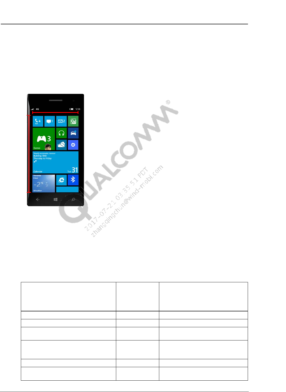
The screen size in both cm and mm must be reported, e.g., if the phone dimensions are 5.8 cm
and 10.3 cm, as shown in Figure 5-1, the EDID would be populated as shown below.
<Group id='EDID Configuration'>
<HorizontalScreenSize>5</HorizontalScreenSize>
<VerticalScreenSize>10</VerticalScreenSize>
</Group>
<Group id='Detailed Timing'>
<HorizontalScreenSizeMM>58</HorizontalScreenSizeMM>
<VerticalScreenSizeMM>103</VerticalScreenSizeMM>
</Group
5.8cm
10.3cm
Figure 5-1 Example phone dimensions and EDID population
5.2.4 Dynamic EDID fields
Only the Preferred Timing mode (see Section 3.10.2 in VESA Enhanced Extended Display
Identification Data Standard ((Defines EDID Structure Version 1, Revision 4) Release A,
Revision 2 (September 2006)) is populated by the driver dynamically based on the panel
configuration. Table 5-4 describes how each field in the detailed timing definition is populated.
Table 5-4 Dynamic EDID fields
Detailed timing field name
Detailed timing
specification
field offset
(size in bytes)
Derived from
(panel configuration field)
Pixel clock/10000 0 (2) DSIRefreshRate/LVDSRefreshRate
Horizontal addressable video (low 8 bits) 2 (1) HorizontalActive
Horizontal blanking (low 8 bits) 3 (1) HorizontalFrontPorch+Horizontal
BackPorch+HorizontalSyncPulse
Horizontal addressable video (high 4 bits)/
Horizontal blanking (high 4 bits) 4 (1) Horizontal Active/Horizontal
FrontPorch+HorizontalBackPorch+
HorizontalSyncPulse
Vertical addressable video (lower 8 bits) 5 (1) VerticalActive
Vertical blanking (low 8 bits) 6 (1) VerticalFrontPorch+
VerticalBackPorch+ VerticalSyncPulse

Configuration Guide for Display Drivers (ACPI and XML) Panel configuration tag descriptions
80-NB116-2 G Confidential and Proprietary – Qualcomm Technologies, Inc. 27
MAY CONTAIN U.S. AND INTERNATIONAL EXPORT CONTROLLED INFORMATION
Detailed timing field name
Detailed timing
specification
field offset
(size in bytes)
Derived from
(panel configuration field)
Vertical addressable video (high 4 bits)/
Vertical blanking (high 4 bits) 7 (1) VerticalActive/VerticalFrontPorch+
VerticalBackPorch+ VerticalSyncPulse
Horizontal Front Porch (HFP) (lower
8 bits) 8 (1) VerticalFrontPorch
Horizontal sync pulse width (lower 8 bits) 9 (1) VerticalSyncPulse
Vertical front porch (high 4 bits)/vertical
sync pulse width (high 4 bits) 10 (1) VerticalFrontPorch/VerticalFrontPorch
HFP/ sync pulse/vertical front
porch/vertical sync pulse width (upper
2 bits)
11 (1) HorizontalFrontPorch/HorizontalSync
Pulse/VerticalFrontPorch/VerticalSync
Pulse
Horizontal addressable video image size
(lower 8 bits) 12 (1) HorizontalScreenSize
Vertical addressable video image size
(lower 8 bits) 13 (1) VerticalScreenSize
Horizontal addressable video size (upper
4 bits)/vertical addressable video size
(upper 4 bits)
14 (1) HorizontalActive/VerticalActive
Right/left horizontal border 15 (1) Used to determine the total active
window width
Top/bottom vertical border 16 (1) Used to determine the total active
window height
Signal interface type 17 (1) InvertHsyncPolarity
InvertVsyncPolairty
Configuration Guide for Display Drivers (ACPI and XML) Panel configuration tag descriptions
80-NB116-2 G Confidential and Proprietary – Qualcomm Technologies, Inc. 28
MAY CONTAIN U.S. AND INTERNATIONAL EXPORT CONTROLLED INFORMATION
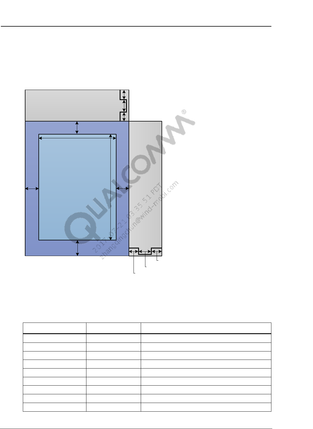
5.3 Panel timings configuration
All panel timings are derived from the following fields in the panel configuration as shown in
Figure 5-2. It is critical that the licensees populate these fields correctly to match their platform
configuration.
Border
Active Region
VerticalActive
VerticalTopBorder
VerticalBottomBorder
HorizontalLeftBorder
HorizontalRightBorder
Horizontal Blanking
Vertical Blanking
VerticalFrontPorch
VerticalSyncPulse
VerticalBackPorch
HorizontalActive
HorizontalFrontPorch
HorizontalSyncPulse
HorizontalBackPorch
Figure 5-2 Panel timings configuration
Table 5-5 lists the panel timing fields.
Table 5-5 Panel timing fields
Tag Units Notes
HorizontalActive Pixels –
HorizontalFrontPorch Pixels –
HorizontalBackPorch Pixels –
HorizontalSyncPulse Pixels –
HorizontalSyncSkew Pixels Not used
HorizontalLeftBorder Pixels Optional, if supported by hardware
HorizontalRightBorder Pixels Optional, if supported by hardware
VerticalActive Lines –
VerticalFrontPorch Lines –
Configuration Guide for Display Drivers (ACPI and XML) Panel configuration tag descriptions
80-NB116-2 G Confidential and Proprietary – Qualcomm Technologies, Inc. 29
MAY CONTAIN U.S. AND INTERNATIONAL EXPORT CONTROLLED INFORMATION
Tag Units Notes
VerticalBackPorch Lines –
VerticalSyncPulse Lines –
VerticalTopBorder Lines Optional, if supported by hardware
VerticalBottomBorder Lines Optional, if supported by hardware
InvertDataPolarity Boolean Inverts the data sync pulse polarity
InvertVsyncPolairty Boolean Inverts the vertical sync pulse polarity
InvertHsyncPolarity Boolean Inverts the horizontal sync pulse polarity
BorderColor ARGB8888 Defines the default border color when borders are
enabled
UnderflowColor ARGB8888 Defines the default color when underflow occurs
80-NB116-2 G Confidential and Proprietary – Qualcomm Technologies, Inc. 30
MAY CONTAIN U.S. AND INTERNATIONAL EXPORT CONTROLLED INFORMATION
6 Display hardware tag descriptions
6.1 Common hardware configuration parameters
Table 6-1 lists configuration tags that define the interface information for the display. These
settings are critical since they determine the basic interface and mode of communication with the
display.
Table 6-1 Common hardware configuration parameters
NOTE: The following table has been updated.
Tag Description
InterfaceType Integer defining the interface between the MSM™ and the panel, based on the
enumerated type QDI_DisplayConnectType
Value (decimal) Definition
0 None, reserved.
1 EBI2, reserved.
2 LCDC, reserved
3 MDDI, reserved
4 MDDI, reserved
5 TV, Analog TV, reserved
6 MDDI, reserved
7 DTV, HDMI, reserved.
8 QDI_DISPLAY_CONNECT_PRIMARY_DSI_VIDEO
9 QDI_DISPLAY_CONNECT_PRIMARY_DSI_CMD
10 DSI, reserved
11 DSI, reserved
12 LVDS, reserved
13 Frame buffer, reserved
14 QDI_DISPLAY_CONNECT_DP
15 DBI, reserved
16 MHL, reserved
All other values are invalid or not supported.
Configuration Guide for Display Drivers (ACPI and XML) Display hardware tag descriptions
80-NB116-2 G Confidential and Proprietary – Qualcomm Technologies, Inc. 31
MAY CONTAIN U.S. AND INTERNATIONAL EXPORT CONTROLLED INFORMATION
Tag Description
PanelOrientation Integer defining the physical panel orientation
Value (decimal) Definition
0 QDI_ROTATE_NONE
2 QDI_ROTATE_180
Currently only 0° rotation (none) is supported.
InterfaceColorFormat Integer defining the pixel format (pixel depth) between the MSM and the panel,
based on the enumerated type QDI_PixelFormatType
Value (decimal) Definition
1 QDI_PIXEL_FORMAT_RGB_565_16BPP
2 QDI_PIXEL_FORMAT_RGB_666_18BPP
3 QDI_PIXEL_FORMAT_RGB_888_24BPP
All other values are invalid or not supported.
ComponentOrdering Integer defining the pixel component ordering between the MSM and the panel,
based on the enumerated type QDI_ColorOrderingType
Value (decimal) Definition
0 QDI_COLOR_ORDERING_RGB
1 QDI_COLOR_ORDERING_RBG
2 QDI_COLOR_ORDERING_GRB
3 QDI_COLOR_ORDERING_GBR
4 QDI_COLOR_ORDERING_BRG
5 QDI_COLOR_ORDERING_BGR
All other values are invalid or not supported.
PixelPacking Integer defining the pixel packing format between the MSM and the panel; this is
based on the enumerated type QDI_ColorComponentsPackingType. Packing is
only valid for pixel depths that are not aligned on an 8-bit boundary, such as
18 bpp.
Value (decimal) Definition
0 QDI_COLOR_COMPONENTS_PACKING_TIGHT
1 QDI_COLOR_COMPONENTS_PACKING_LOOSE
All other values are invalid or not supported.

Configuration Guide for Display Drivers (ACPI and XML) Display hardware tag descriptions
80-NB116-2 G Confidential and Proprietary – Qualcomm Technologies, Inc. 32
MAY CONTAIN U.S. AND INTERNATIONAL EXPORT CONTROLLED INFORMATION
Tag Description
PixelAlignment Integer defining the pixel alignment between the MSM and the panel, based on
the enumerated type QDI_ColorComponentAlignmentType; alignment is only
valid for loose pixel packet format types
Value (decimal) Definition
0 QDI_COLOR_COMPONENT_ALIGNMENT_LSB
1 QDI_COLOR_COMPONENT_ALIGNMENT_MSB
All other values are invalid or not supported.

80-NB116-2 G Confidential and Proprietary – Qualcomm Technologies, Inc. 33
MAY CONTAIN U.S. AND INTERNATIONAL EXPORT CONTROLLED INFORMATION
7 Display features
7.1 Display feature flags
Individual display features can be configured based on the feature flags given in Table 7-1. These
are the feature flags that can be enabled or disabled.
Table 7-1 Feature flags that can be enabled or disabled
NOTE: The following table has been updated.
Tag Description
DisplayPrimaryFlags Integer defining with each bit representing a feature that can be enabled or
disabled on the primary panel. Multiple flags can be combined to enable/disable
multiple features.
Value
(decimal) Definition
0x0001 QDI_PANEL_FLAG_FORCE_DISPLAY_REINIT
This flag forces the display to be reinitialized during the
transition from the firmware (UEFI) to the KMD. The
default behavior is to skip initialization when the display is
detected as active after the firmware has completed
execution.
0x0002 QDI_PANEL_FLAG_DISABLE_SBC
This flag disables smooth brightness control. If the
licensee chooses not to support this feature, this can be
disabled with this flag.
0x0004 QDI_PANEL_FLAG_DISABLE_CABL
This flag disables content adaptive backlight leveling.
0x0008 QDI_PANEL_FLAG_DISABLE_HW_CURSOR
This flag disables hardware cursors and fallback to OS
rendered cursors (software cursors).
0x0010 QDI_PANEL_FLAG_DUAL_MODE_SUPPORT
This flag enables the cap to allow the driver to transition
between MIPI DSI command and video mode operation
when the display mode is being reinitialized.
0x0100 QDI_PANEL_FLAG_DSI_DCS_POLLING_TRANSFER
This flag disables the interrupted based notification of
MIPI DSI DCS packets and reverts to a polling-based
mechanism.
0x0200 QDI_PANEL_FLAG_DSI_DCS_DMA_ONLY
This flag is deprecated; do not use. See DSIFlags for
details on DCS configuration.
Configuration Guide for Display Drivers (ACPI and XML) Display features
80-NB116-2 G Confidential and Proprietary – Qualcomm Technologies, Inc. 34
MAY CONTAIN U.S. AND INTERNATIONAL EXPORT CONTROLLED INFORMATION
Tag Description
0x0400 QDI_PANEL_FLAG_DSI_DCS_FIFO_ONLY
This flag is deprecated; do not use. See DSIFlags for
details on DCS configuration.
0x0800 QDI_PANEL_FLAG_ENABLE_DFS_IDLESCREEN
This flag enables lowering of the refresh rate during idle
screen (Vsync off) for video mode panels. This is
applicable to configurations that enable dynamic refresh.
0x1000 QDI_PANEL_FLAG_MIRROR_DUAL_PIPE_CONFIG
This is an internal flag used to swap pixel data between
DSI 0 and DSI 1.
0x00002000 QDI_PANEL_FLAG_DISABLE_POST_PROCESSING
This flag disables the postprocessing pipeline within the
display controller. Pixels will not be modified post-
blending.
0x00004000 QDI_PANEL_FLAG_INJECT_DEFAULT_AUDIO_MODE
This flag is used to force the driver to inject a default
audio mode (LPCM, 44.1 kHz) when an external display
EDID is being parsed. This flag can be used to force
overrides for displays that report incorrect or missing
audio EDID information.
0x00008000 QDI_PANEL_FLAG_STEREO_MODE_SUPPORT
This flag is used to force the driver into a VR/AR
composition mode that breaks composition into a left and
right side frame by hardware layer mixer.
0x01000000 QDI_PANEL_FLAG_DISABLE_SEAMLESS_SPLASH
This flag disables the display after UEFI is complete. If
enabled, this flag disables the display from scanning out
after the HLOS image starts.
All other values Reserved
All other values are invalid or not supported.
DisplayExternalFlags Integer defining with each bit representing a feature that can be enabled or
disabled on external panel (HDMI). Multiple flags can be combined to
enable/disable multiple features.
Value (decimal) Definition
All values Reserved

80-NB116-2 G Confidential and Proprietary – Qualcomm Technologies, Inc. 35
MAY CONTAIN U.S. AND INTERNATIONAL EXPORT CONTROLLED INFORMATION
8 Display interface-specific configurations
8.1 DSI interface configurations
8.1.1 Common DSI configurations
These configuration parameters are common for both DSI Command mode and DSI Video mode
given in Table 8-1.
Table 8-1 Common DSI configurations
NOTE: The following table has been updated.
Tag Description
DSIRefreshRate The requested refresh rate in Q16.16 format. This parameter allows the
licensee to configure the rate at which the panel is updated.
The driver will be responsible for calculating the necessary DSI timings and
clock settings to achieve the requested refresh rate, for example:
60 Hz = 0x003C0000
50.5 Hz = 0x00328000
DSIBitClockFrequency This is an optional parameter that allows the licensee to configure an exact bit
clock frequency in Hz which represents the UIinst timing.
DSI Video mode
This setting overrides any value configured for DSIRefreshRate. The
actual DSI refresh rate is recalculated based on the formula:
Refresh rate = (#DSILanes x DSIBitClockFrequency)/ (HorizontalToal
x VerticalTotal x DSIBitsPerPixel)
DSI Command mode
This setting allows the bit clock to be independently configured from the
actual refresh rate, i.e., the transfer rate can be faster/slower than the
reported panel refresh rate.
If the DSIRefreshRate is specified, the driver reports this value to the OS
as the actual panel refresh rate and uses DSIBitClockFrequency to
determine the pixel transfer rate to the panel.
If the DSIRefreshRate is 0, the refresh rate will be calculated based on
DSIBitClockFrequency using the same equation as in
Section 8.1.8.
DSILanes This integer defines the number of DSI lanes. Valid values are 1 through 4.
However, some platforms and MSMs may limit the lanes to 1 to 2 lanes.
Configuration Guide for Display Drivers (ACPI and XML) Display interface-specific configurations
80-NB116-2 G Confidential and Proprietary – Qualcomm Technologies, Inc. 36
MAY CONTAIN U.S. AND INTERNATIONAL EXPORT CONTROLLED INFORMATION
Tag Description
DSIChannelId Integer defining the DSI interface used to communicate with the panel; this
must match the desired panel configuration. This setting is based on the
QDI_DSIChannelIDType enumeration.
The licensee must select the appropriate engine, either Video or Command
mode, depending on the type of DSI interface configured.
Value (decimal) Definition
1 QDI_DSIChannelID_Video0
2 QDI_DSIChannelID_CMD0
All other values are invalid or not supported.
DSIVirtualId Integer defining the virtual channel ID used when sending command and pixel
data; some devices may not support virtual channels. This setting is based on
the QDI_DSIDisplayVCType enumeration.
Value (decimal) Definition
0 QDI_DSIDisplayVC_0
1 QDI_DSIDisplayVC_1
All other values are invalid or not supported.
DSIColorFormat Integer defining the color format used to transfer data to the panel; this setting
is based on the QDI_DSIColorFormatType enumeration.
Value (decimal) Definition
18 QDI_DSICOLOR_RGB_565_16BPP
24 QDI_DSICOLOR_RGB_666_18BPP
30 QDI_DSICOLOR_RGB_666_24BPP
36 QDI_DSICOLOR_RGB_888_24BPP
All other values are invalid or not supported.
DSIPacketTransferHS This Boolean determines how the DMA command packets are sent to the
panel. When transferring command data to the panel, the packets can be sent
in either High Speed (HS) or Low Power (LP) mode. This setting determines
how packets are sent.
The exception to this rule occurs during initialization and termination sequences
sent to the panel. In these scenarios, the packets are always in LP mode.
Note: It is recommended that data always be sent in HS mode if the panel
supports it.
Value (Boolean) Definition
FALSE Sends DCS commands in LP mode
TRUE Sends DCS commands in HS mode
Configuration Guide for Display Drivers (ACPI and XML) Display interface-specific configurations
80-NB116-2 G Confidential and Proprietary – Qualcomm Technologies, Inc. 37
MAY CONTAIN U.S. AND INTERNATIONAL EXPORT CONTROLLED INFORMATION
Tag Description
DSIClockHSForceReq
uest This integer determines the state of the DSI clock lane. Some panels require
that the clock lane is always active in order to provide a continual clock signal
to the panel.
By default, this should not be used unless the panel requires an always active
clock lane.
Value (decimal) Definition
0 QDI_DSI_ClockLane_Default
DSI clock lane is in inactive (LP11) state
when transfers are not occurring.
1 QDI_DSI_ClockLane_ForceHS
DSI clock lane is always active regardless of
transfers occurring.
2 QDI_DSI_ClockLane_ForceHS_PostInit
DSI Clock lane is forced to HS after the init
sequence has been sent.
DSIHostLaneMapping This integer defines how the data lanes are mapped to the panel. Depending
on the platform, it may be required to map the individual DSI lanes. This
configuration is based on the QDI_DSILaneMapType enumeration.
The default mapping should be used unless the platform requires a special lane
mapping.
Value (decimal) Definition
0 QDI_PANEL_LANE0123MAP
1 QDI_PANEL_LANE3012MAP
2 QDI_PANEL_LANE2301MAP
3 QDI_PANEL_LANE1230MAP
4 QDI_PANEL_LANE0321MAP
5 QDI_PANEL_LANE1032MAP
6 QDI_PANEL_LANE2103MAP
7 QDI_PANEL_LANE3210MAP
All other values are invalid or not supported.
Configuration Guide for Display Drivers (ACPI and XML) Display interface-specific configurations
80-NB116-2 G Confidential and Proprietary – Qualcomm Technologies, Inc. 38
MAY CONTAIN U.S. AND INTERNATIONAL EXPORT CONTROLLED INFORMATION
Tag Description
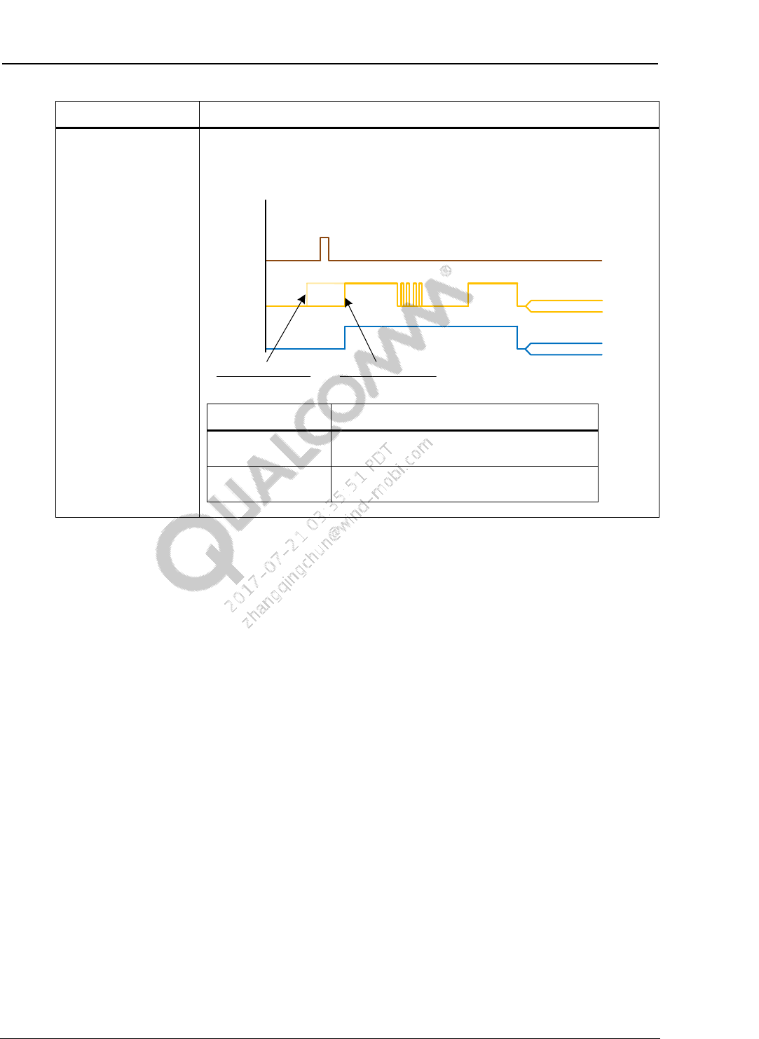
DSILP11AtInit This Boolean determines the status of the DSI clock and data lanes after
hardware initialization. Some panels may require that the DSI clock and lane
must enter LP11 prior to powering up and issuing the hardware reset line.
Panel Reset
Pin
Data Lanes HS Data
HS Clock
LP11 LP11
DSILP11AtInit=TRUE DSILP11AtInit=FALSE
Clock Lane
Value (Boolean) Definition
FALSE DSI data/clock lanes are in LP00 during the
power-on reset sequence
TRUE DSI data/clock lanes are in LP11 during the
power-on reset sequence
Configuration Guide for Display Drivers (ACPI and XML) Display interface-specific configurations
80-NB116-2 G Confidential and Proprietary – Qualcomm Technologies, Inc. 39
MAY CONTAIN U.S. AND INTERNATIONAL EXPORT CONTROLLED INFORMATION
Tag Description
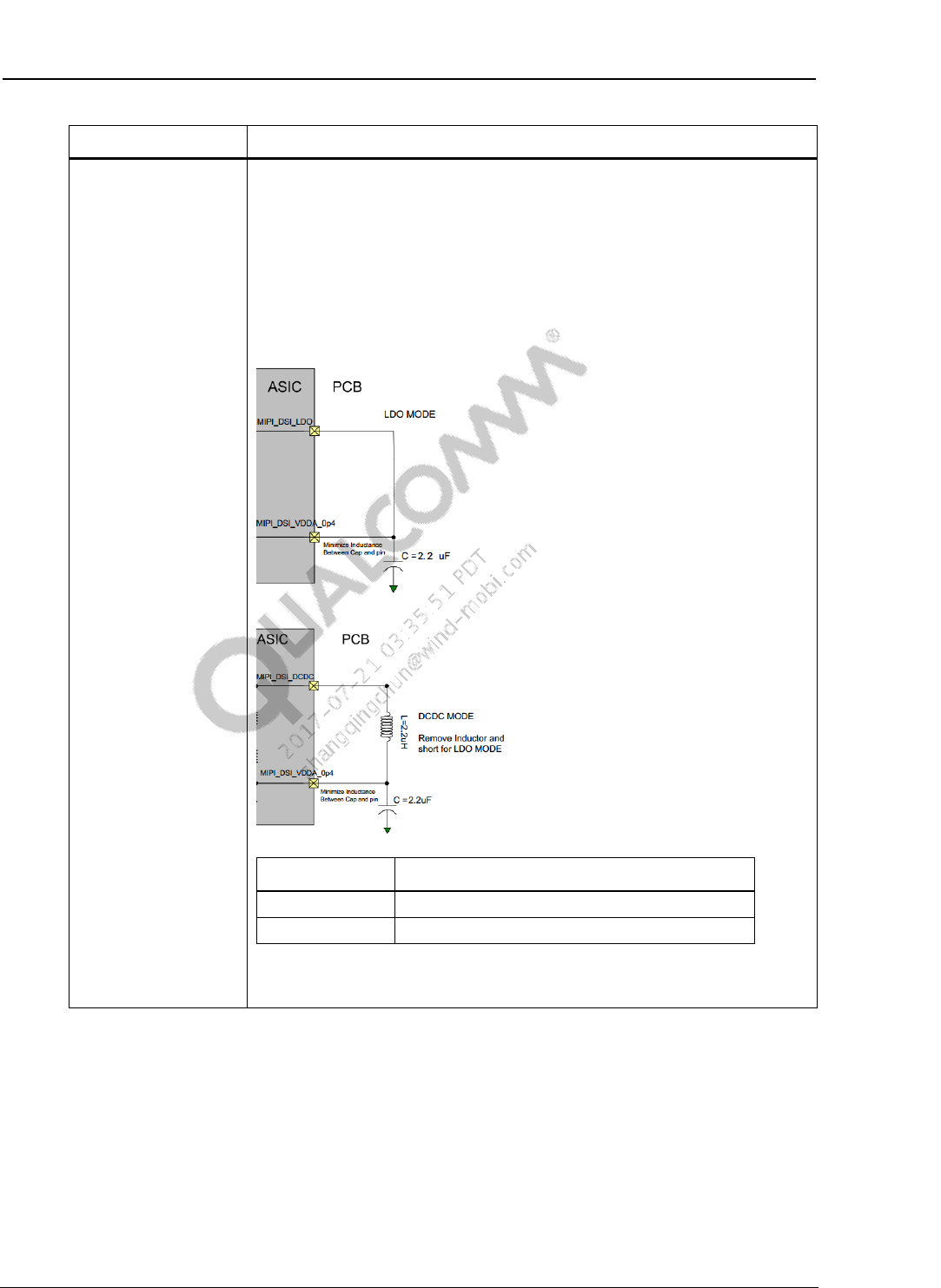
DSIPhyDCDCMode Note: This section is deprecated and no longer supported in the PHY.
DSI PHY supports two modes for generating required voltage for the HSTx
transmitters. One mode uses LDO Regulator and the other uses DCDC
Regulator.
See the diagrams below for details about the LDO vs. DCDC platform
configuration.
The default value is FALSE (LDO mode).
LDO mode
DCDC mode
Value (Boolean) Definition
FALSE DSI PHY regulator is in LDO mode
TRUE DSI PHY regulator is in DCDC mode
Configuration Guide for Display Drivers (ACPI and XML) Display interface-specific configurations
80-NB116-2 G Confidential and Proprietary – Qualcomm Technologies, Inc. 40
MAY CONTAIN U.S. AND INTERNATIONAL EXPORT CONTROLLED INFORMATION
Tag Description
DSIInitMasterTime This integer determines the tINIT_MASTER (as specified in MIPI Alliance
Specification for Display Serial Interface (Version 1.02.00 (June 2010)) before
any DSI activity is performed.
Minimum time is set to 2 ms. This default value can be extended by overwriting
this configuration. Units are given in milliseconds.
DSIEnterULPSPower
Down This Boolean flag forces the controller to enter ULPS mode prior to powering
down (suspend mode). The panel must support ULPS for this feature to be
enabled.
DSIFBCEnable
Note
: This feature is depreciated.
This Boolean flag determines whether to enable the Frame Buffer feature in
MDSS. This requires a DSI panel supporting FBC.
DSIFBCProfileID Note: This feature is depreciated.
This integer integer provides the FBC profile ID for MDSS to invoke different
compression algorithms. This profile ID should match the supported FBC profile
ID of the DSI panel.
DSIDataStrengthLP This setting adjusts the drive strength of the data lanes during LP transmission.
The driver has already been tuned for the optimal setting, other settings can be
overwritten for experimentation. Conformance is not guaranteed if these
settings are overwritten. Values range from 0x0 (weakest) to 0xf (strongest).
DSIDataStrengthHS This setting adjusts the drive strength of the data lanes during HS transmission.
The driver has already been tuned for the optimal setting, other settings can be
overwritten for experimentation. Conformance is not guaranteed if these
settings are overwritten. Values range from 0x0 (weakest) to 0xf (strongest).
DSIClockStrengthHS This setting adjusts the drive strength of the clock lanes during HS
transmission. The driver has already been tuned for the optimal setting, other
settings can be overwritten for experimentation. Conformance is not
guaranteed if these settings are overwritten. Values range from 0x0 (weakest)
to 0xf (strongest).
DSIEscapeClockDivis
or The escape clock is used to derive the MIPI DSI timings within the DSI
controller. The MIPI DSI specification requires Tlpx time to be a minimum of 50
ns which is a 20 MHz escape clock.
The default escape clock configuration is to source from the system CXO clock
which is 19.2 MHz. This, however, can be overwritten by adjusting this setting.
When DSIEscapeClockDivisor is greater than zero. the escape clock is derived
from the DSI PLL frequency (byte clock). The divisor defines how much the
PLL frequency is divided by to achieve the escape clock.
The exact division value varies by chipset, but it will typically be in 1 or 1.5
increments per integer. This field only supports integer values.
For example, on some chipsets, a division of 1.5 may use the following
configuration:
< DSIEscapeClockDivisor>2</ DSIEscapeClockDivisor>
Configuration Guide for Display Drivers (ACPI and XML) Display interface-specific configurations
80-NB116-2 G Confidential and Proprietary – Qualcomm Technologies, Inc. 41
MAY CONTAIN U.S. AND INTERNATIONAL EXPORT CONTROLLED INFORMATION
Tag Description
DSIEscapeClockFrequ
ency When DSIEscapeClockDivisor is used this fileld must be populated with the
expected escape clock frequency.
This expected clock frequency is used to adjust all of the other DSI D Phy
timings. As there is no feedback mechanism for the driver to know the exact
escape clock frequency if it is not derived from CXO (19.2 MHz), the user must
pass in the exact value in hertz.
Incorrectly enabling the escape clock divisor or not properly setting this
frequency will result in DSI timings that are out of specification.
For a 17 MHz escape clock:
< DSIEscapeClockFrequency>17000000</ DSIEscapeClockFrequency>
DSITransferRetryCntr When sending and receving DCS commands (BTA), the driver will attempt to
retry upon failure of the original command.
This field allows the OEM to adjust the number of attempts for any read or write
command before it gives up and returns an error.
The default value is 2 (meaning 2 total attempts), but this can be disabled or
increased based on the requirements.
DSINullpacketInsertion
Bytes During pixel data transmission, the controller idles the data lanes (LP00)
between pixel tranmissions. Enabling this configuration forces the controller to
insert NULL packets to keep the data lanes in HS.
The value represents the size of the NULL packets; a value of 0 means
disabled.
DSIFlags This field is an integer that represents a bitwise mask of DSI configuration
options.
The following table lists valid values.
Value
(decimal) Definition
0x0001 QDI_PANEL_DSI_FLAG_DSI_DCS_FIFO_ONLY
This flag forces the driver to use a FIFO to send DCS
packets instead of a DMA buffer. This option reduces
the latency for start of packet transmission but limits the
maximum packet size that can be sent to 64 bytes total
including headers.
0x0002 QDI_PANEL_DSI_FLAG_DSI_DISABLE_BURST_MOD
E
This flag disables Burst mode which allows DMA
packets to interleave between pixel data transfers. By
default the hardware is configured to burst all pixel data
together without interruption.
The default configuration is the most optimal and this
flag should typically not be needed.
0x0004 QDI_PANEL_DSI_FLAG_DISABLE_PPS_CMD
This flag disables sending of the PPS packets when
MIPI DSC is enabled. When disabled the driver will not
automatically send the PPS packets during panel
initialization. Some panels do not support PPS packets
and this flag should be set for those panels.
All other values Reserved
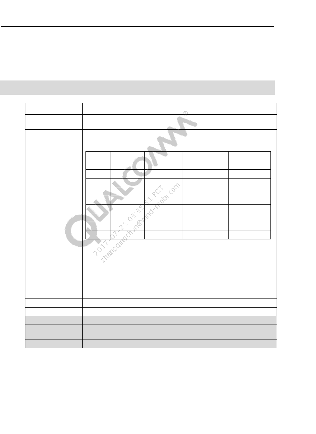
Configuration Guide for Display Drivers (ACPI and XML) Display interface-specific configurations
80-NB116-2 G Confidential and Proprietary – Qualcomm Technologies, Inc. 42
MAY CONTAIN U.S. AND INTERNATIONAL EXPORT CONTROLLED INFORMATION
8.1.2 Display stream compression (DSC)
Table 8-2 shows the parameters used to configure the DSC module for DSI.
Table 8-2 Parameters to configure the DSC module for DSI
NOTE: The following table has been updated.
Tag Description
DSIDSCEnable This Boolean flag determines whether to enable the DSC feature in MDSS. This
requires a DSI panel supporting DSC.
DSIDSCProfileID This integer specifies the index in the profile table that describes the DSC
configuration.
ID Encoder LM split Block
prediction Compression
ratio
0 1 No 1 2
1 1 Yes 1 2
2 2 No 1 2
3 2 Yes 1 2
4 1 No 1 3
5 1 Yes 1 3
6 2 No 1 3
7 2 Yes 1 3
Table definitions:
Encoder – Number of DSC instances (one per 4-lane controller).
LM split – MDSS layer mixer split configuration used
Block prediction – Enable block prediction
Compression ratio – DSC compression ratio
Slice height – DSC slice height
Slice width – DSC slice width
DSIDSCSliceHeight This integer specifies the DSC slice height in pixels.
DSIDSCSliceWidth This integer specificies the DSC slice width in pixels.
DSIDSCMajorVersion The DSC version specification supported by the panel. Must be 1 for v1.x
DSIDSCMinorVersion The DSC version specification supported by the panet. 0 (v1.0) and 1 (v1.1) are
supported.
DSIDSCScrVersion The rate control parameters configuration, default is 0, or 1 for rate control set 1.
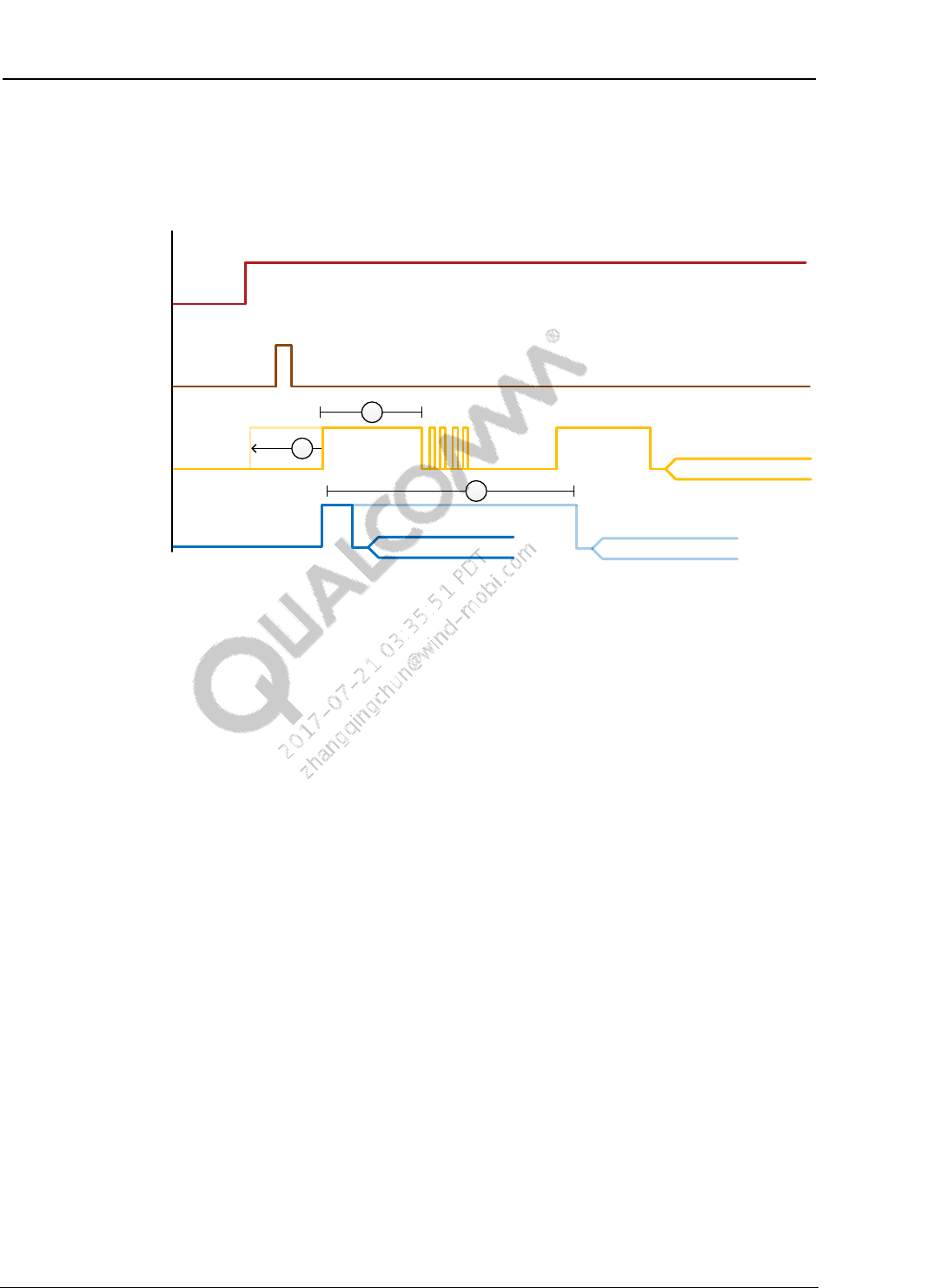
Configuration Guide for Display Drivers (ACPI and XML) Display interface-specific configurations
80-NB116-2 G Confidential and Proprietary – Qualcomm Technologies, Inc. 43
MAY CONTAIN U.S. AND INTERNATIONAL EXPORT CONTROLLED INFORMATION
8.1.3 Init sequence timing
To meet the requirements of varying panel hardware, the initialization sequence can be tuned
based on particular DSI parameters, shown in Figure 8-1.
Panel Power Rails
Panel Reset Pin
Data Lanes
Clock Lane
HS Data
HS Clock
LP Data
LP11 LP11
A
B
HS Clock
C
Figure 8-1 Init sequence timing
Init sequence timing depends on the following parameters:
a. DSILP11AtInit – MIPI Alliance Specification for Display Serial Interface (Version
1.03.00 (August 2011)) requires the data and clock lanes to be in the LP11 state after the
reset pin has been deasserted. In previous revisions of the specification, the lanes were
required to be in LP11 before the reset had been asserted. The DSILP11AtInit
configuration allows licensees to force the lanes to LP11 before the reset is asserted; the
default behavior is to assert LP11 after reset.
b. DSIInitMasterTime – After asserting LP11, the panel IC may require additional delay
times to complete initialization before the first DCS command can be recognized. By
default the minimum delay is 2 ms, however, the licensee can overwrite this to any value.
c. DSIClockHSForceRequest – Some panel ICs may require the host to drive the clock
lanes to HS. Typically this is done if the panel IC requires an external oscillator. This
configuration allows for three options:
– Clock lane is only transitioned into HS during a HS data transmission (default).
– Clock lane is always in HS.
– Clock lane is in HS after the init sequence is complete.
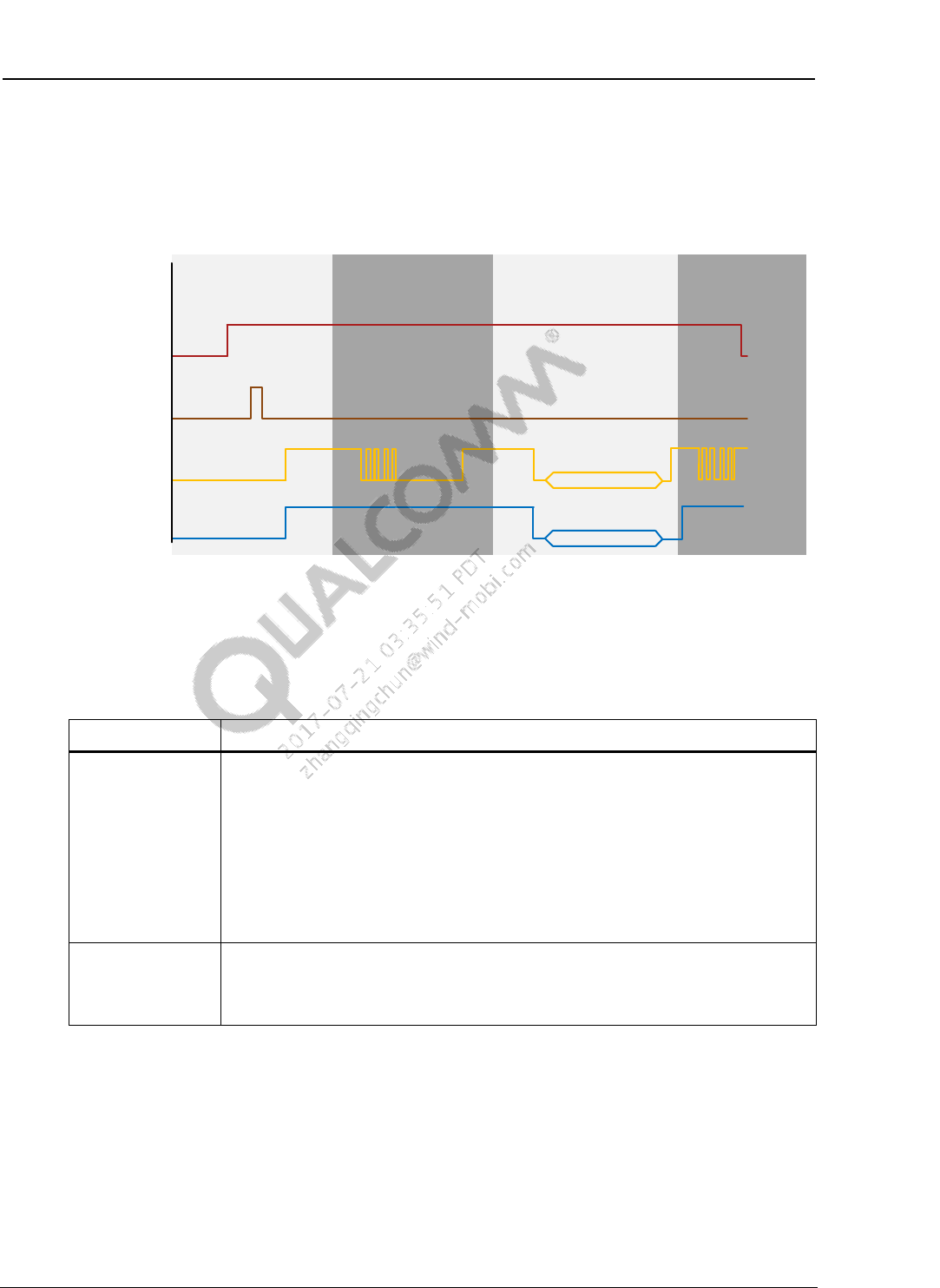
Configuration Guide for Display Drivers (ACPI and XML) Display interface-specific configurations
80-NB116-2 G Confidential and Proprietary – Qualcomm Technologies, Inc. 44
MAY CONTAIN U.S. AND INTERNATIONAL EXPORT CONTROLLED INFORMATION
8.1.4 DSI DCS command configurations
During panel initialization and shutdown, the licensee can send custom panel sequences to
initialize and shut down the panel. Figure 8-2 shows when these commands are sent.
DSI Term
Sequence
DSI ActiveDSI Init SequencePanel Power on Reset
Panel Power Rails
Panel Reset Pin
Data Lanes
Clock Lane
HS Data
HS Clock
LP Data
LP11 LP11
LP Data
Figure 8-2 DSI DCS command configurations
Table 8-5 shows the DSI DCS command configuration tags.
Table 8-3 DSI DCS command configuration tags
Tag Description
DSIInitSequence This is a binary data value that is used to send DCS commands to the panel during
panel initialization (display on). One or multiple packets can be sent using this
sequence; see the binary data type description of how to build a packet.
This data is always sent to the panel in LP mode, e.g.:
05 11 00 ; DCS command 5h, followed by two payload
; bytes 11h and 00h
DSITermSequence This is a binary data value that is used to send DCS commands to the panel during
panel termination (display off). One or multiple packets can be sent using this
sequence; see the binary data type description of how to build a packet.
This data is always sent to the panel in LP mode.
Configuration Guide for Display Drivers (ACPI and XML) Display interface-specific configurations
80-NB116-2 G Confidential and Proprietary – Qualcomm Technologies, Inc. 45
MAY CONTAIN U.S. AND INTERNATIONAL EXPORT CONTROLLED INFORMATION
8.1.5 Supported DCS commands
Any valid DCS command and payload can be sent. Table 8-4 provides examples of the valid DCS
commands supported. For more details, see MIPI Alliance Specification for D-PHY (Version
1.00.00 (May 2009)).
Table 8-4 Supported DCS commands
Command
(hex) Payload size
(bytes) Definition
03 2 Generic short write, no parameters
13 2 Generic short write, 1 parameter
23 2 Generic short write, 2 parameters
05 2 DCS short write, no parameters
15 2 DCS short write, 1 parameter
29 4 Generic long write
Other commands may not be supported or may be reserved.
8.1.6 Special DCS commands
There are certain reserved commands that can be used and are interpreted by the driver as having
a special meaning. These commands are not valid DCS commands but are intercepted by the
driver to have a special function as shown in Table 8-5.
Table 8-5 Special DCS commands
Command
(hex) Payload size
(bytes) Definition
FF 1 Stall between commands; payload is used to indicate the number of
milliseconds to stall between commands; valid range is 1 to 255; example:
05 11 00 – DCS command 5 h, with 11 h as payload
FF 5C – Wait for 92 ms
05 15 00 – DCS command 5 h, with 15 h as payload
FE 3 Configure MDP to output constant color to clear the display frame buffer
for smart panel. The payload is used to indicate the desired constant color
in RGB format. Valid range for each color component is 0 to 255. The
default color is black if no payload is specified, e.g.:
FE FF FF 00 – Configure MDP to output yellow constant color
If this command is used during panel initialization, then constant color will
be sent to the panel to clear the random garbage data in the display
module buffer.
If this command is used during display reset while MDP has already been
configured, the last frame in MDP is sent to the panel.
FD 1 Broadcast mask used to mask which controller(s) the command is sent to;
this is only valid for dual-DSI applications.
Mask (hex) Definition
0x1 Command is sent to controller 0; default
0x2 Command is sent to controller 1

Configuration Guide for Display Drivers (ACPI and XML) Display interface-specific configurations
80-NB116-2 G Confidential and Proprietary – Qualcomm Technologies, Inc. 46
MAY CONTAIN U.S. AND INTERNATIONAL EXPORT CONTROLLED INFORMATION
8.1.7 DSI interface timing overrides
The DSI timings are automatically calculated based on the required refresh rate/bit clock
frequency. If the panel has specific timing requirements, the adjustment for each timing can be
overridden. Table 8-6 lists of DSI interface timing overrides.
Table 8-6 DSI interface timing overrides
Tag Units Notes
DSITimingHSZeroOverride Boolean See MIPI Alliance Specification for D-PHY
(Version 1.00.00 (May 2009)) for details on each
timing parameter.
DSITimingHSZeroValue Integer
DSITimingHSExitOverride Boolean
DSITimingHSExitValue Integer
DSITimingHSPrepareOverride Boolean
DSITimingHSPrepareValue Integer
DSITimingHSTrailOverride Boolean
DSITimingHSTrailValue Integer
DSITimingHSRequestOverride Boolean
DSITimingHSRequestValue Integer
DSITimingCLKZeroOverride Boolean
DSITimingCLKZeroValue Integer
DSITimingCLKTrailOverride Boolean
DSITimingCLKTrailValue Integer
DSITimingCLKPrepareOverride Boolean
DSITimingCLKPrepareValue Integer
DSITimingCLKPreOverride Boolean
DSITimingCLKPreValue Integer
DSITimingCLKPostOverride Boolean
DSITimingCLKPostValue Integer
DSITimingTASureOverride Boolean
DSITimingTASureValue Integer
DSITimingTAGoOverride Boolean
DSITimingTAGoValue Integer
DSITimingTAGetOverride Boolean
DSITimingTAGetValue Integer

Configuration Guide for Display Drivers (ACPI and XML) Display interface-specific configurations
80-NB116-2 G Confidential and Proprietary – Qualcomm Technologies, Inc. 47
MAY CONTAIN U.S. AND INTERNATIONAL EXPORT CONTROLLED INFORMATION
8.1.8 DSI Video mode configuration
Table 8-7 lists configurations specific to DSI Video mode.
Table 8-7 DSI Video mode configuration
Tag Description
DSITrafficMode Integer defining the DSI Traffic mode for operation; this value is based
on the QDI_DSITrafficModeType enumeration.
Value
(decimal) Definition
0 QDI_DSIVideoTrafficMode_NonBurst_VSPulse
1 QDI_DSIVideoTrafficMode_NonBurst_VSEvent
2 QDI_DSIVideoTrafficMode_Burst
All other values are invalid or not supported.
DSIHsaHseAfterVsVe This Boolean determines whether the hardware should send horizontal
sync pulses during the vertical blanking period.
Value
(Boolean) Definition
FALSE Do not send a horizontal start/end packet after
the vertical sync/end
TRUE Send a horizontal start/end packet after the
vertical sync/end
DSILowPowerModeInHFP This Boolean determines the DSI lane state during a Horizontal Front
Porch (HFP) blanking period.
Note: It is recommended that this value be set to TRUE for LP mode if
the panel supports this feature. Forcing the lanes to HS during this
period will consume additional power and prevent DCS commands
from being sent during this period.
Value
(Boolean) Definition
FALSE The DSI clock and lanes should stay in HS
mode during the HFP blanking period. The
hardware will send blanking packets during this
period.
TRUE The DSI clock and lanes should enter LP mode
during the HFP blanking period.

Configuration Guide for Display Drivers (ACPI and XML) Display interface-specific configurations
80-NB116-2 G Confidential and Proprietary – Qualcomm Technologies, Inc. 48
MAY CONTAIN U.S. AND INTERNATIONAL EXPORT CONTROLLED INFORMATION
Tag Description
DSILowPowerModeInHBP This Boolean determines the DSI lane state during the Horizontal
Blanking Period (HBP).
Note: It is recommended that this value be set to TRUE for LP mode if
the panel supports this feature. Forcing the lanes to HS during this
period will consume additional power and prevent DCS commands
from being sent during this period.
Value (Boolean) Definition
FALSE The DSI clock and lanes should stay in HS
mode during the HBP. The hardware sends
blanking packets during this period.
TRUE The DSI clock and lanes should enter LP mode
during the HBP.
DSILowPowerModeInHSA This Boolean determines the DSI lane state during Horizontal Sync
Active (HSA).
Note: It is recommended that this value be set to TRUE for LP mode if
the panel supports this feature. Forcing the lanes to HS during this
period will consume additional power and prevent DCS commands
from being sent during this period.
Value (Boolean) Definition
FALSE The DSI clock and lanes should stay in HS
mode during the Horizontal Sync Period (HSP).
The hardware will send blanking packets during
this period.
TRUE The DSI clock and lanes should enter LP mode
during the HSP.
DSILowPowerModeInBLLPEOF This Boolean determines the DSI lane state during the last line of the
Blanking Low Power Period (BLLP).
Note: It is recommended that this value be set to TRUE for LP mode if
the panel supports this feature. Forcing the lanes to HS during this
period will consume additional power and prevent DCS commands
from being sent during this period.
Value (Boolean) Definition
FALSE The DSI clock and lanes should stay in HS
mode during the last line of the BLLP. The
hardware will send blanking packets during this
period.
TRUE The DSI clock and lanes should enter LP mode
during the last line of the BLLP.

Configuration Guide for Display Drivers (ACPI and XML) Display interface-specific configurations
80-NB116-2 G Confidential and Proprietary – Qualcomm Technologies, Inc. 49
MAY CONTAIN U.S. AND INTERNATIONAL EXPORT CONTROLLED INFORMATION
Tag Description
DSILowPowerModeInBLLP This Boolean determines the DSI lane state during BLLP.
Note: It is recommended that this value be set to TRUE for LP mode if
the panel supports this feature. Forcing the lanes to HS during this
period will consume additional power and prevent DCS commands
from being sent during this period.
Value (Boolean) Definition
FALSE The DSI clock and lanes should stay in HS
mode during the BLLP. The hardware will send
blanking packets during this period.
TRUE The DSI clock and lanes should enter LP mode
during the BLLP.
DSIDmaDelayAfterVsync This integer is used in the DSI DMA read/write scheduling in Video
mode. The software schedules the DSI DMA operations when the DSI
controller is busy transferring pixel data, and the DMA packets are sent
to the panel when pixel transfer is done by the hardware. This integer
decides the number of milliseconds after vsync that the software can
trigger the DMA packets transfer.
DSIPixelXferTiming (replacement for
DSIForceCmdInVideoHS) Integer defining the scenarios to enable/disable the video HS pixel data
transfer for initialization and termination sequence. This value is based
on the DSIPixelXferTiming enumeration.
Any combination of enumerations can be combined to meet the init and
termination sequence requirements. Disabling and enabling bits cannot
be combined together.
Value
(decimal) Definition
0 QDI_DSI_PIXEL_TX_DISABLED_DURING_INIT_TERM
High-speed video data is disabled during the init
sequence.
1 QDI_DSI_PIXEL_TX_ENABLED_DURING_INIT
High-speed video data is enabled during the init
sequence.
2 QDI_DSI_PIXEL_TX_ENABLED_DURING_TERM
High-speed video data is disabled during the termination
sequence.
3 QDI_DSI_PIXEL_TX_ENABLED_DURING_INIT_TERM
High-speed video data is enabled during the termination
sequence.
DSIForceCmdInVideoHS (to be
deprecated) Video HS pixel data will be started before the initialization sequence
from the OEM/ACPI has been sent to the panel. Video HS pixel data
transfer will be active even during the termination sequence from the
OEM/ACPI.

Configuration Guide for Display Drivers (ACPI and XML) Display interface-specific configurations
80-NB116-2 G Confidential and Proprietary – Qualcomm Technologies, Inc. 50
MAY CONTAIN U.S. AND INTERNATIONAL EXPORT CONTROLLED INFORMATION
Tag Description
DSIDynamicRefreshRates The refresh rates supported by the panel other than the default refresh
rate; this is a list of refresh rates in Q16.16 format, e.g.:
<DSIDynamicRefreshRates>0x3C0000
0x320000</DSIDynamicRefreshRates>
Adds 48 Hz and 50 Hz respectively to the list of supported refresh
rates.
The driver may prune refresh rates from this list based on the
capabilities of the display hardware. Not all interfaces and panel
configurations support dynamic refresh changes.
Note: The list of frequencies can be in any order, but the default
refresh rate must appear first.
DSIDynamicBlankingRefreshRateList Refresh rates supported by the panel by adjusting the panel blanking; it
is the licensee’s responsibility to calibrate and configure the blanking
configuration. This is a list of refresh rates in Q16.16 format, e.g.:
<DSIDynamicBlankingRefreshRateList>
0x3C0000
0x300000
0x320000
</DSIDynamicBlankingRefreshRateList>
Adds 48 Hz and 50 Hz respectively to the list of supported refresh rates
that can be achieved by adjusting the panel blanking.
Note: The list of frequencies can be in any order, but the default
refresh rate must appear first.
DSIDynamicVFrontPorchList Vertical front porch adjustment is part of the dynamic blanking
configuration required to achieve a particular refresh rate, e.g.:
<DSIDynamicVFrontPorchList>
0x07
0x09
0x05
</DSIDynamicVFrontPorchList>
These vertical front porch values correspond one to one with the
refresh rates in DSIDynamicBlankingRefreshRateList and must be in
the same order.
DSIDynamicVBackPorchList Vertical back porch adjustment is part of the dynamic blanking
configuration required to achieve a particular refresh rate, e.g.:
<DSIDynamicVBackPorchList>
0x06
0x07
0x05
</DSIDynamicVBackPorchList>
These vertical back porch values correspond one to one with the
refresh rates in DSIDynamicBlankingRefreshRateList and must be in
the same order.

Configuration Guide for Display Drivers (ACPI and XML) Display interface-specific configurations
80-NB116-2 G Confidential and Proprietary – Qualcomm Technologies, Inc. 51
MAY CONTAIN U.S. AND INTERNATIONAL EXPORT CONTROLLED INFORMATION
Tag Description
DSIDynamicVSyncPulseList Vsync pulse adjustment is part of the dynamic blanking configuration
required to achieve a particular refresh rate, e.g.:
<DSIDynamicVSyncPulseList>
0x03
0x04
0x02
<DSIDynamicVSyncPulseList>
These vsync pulse values correspond one to one with the refresh rates
in DSIDynamicBlankingRefreshRateList and must be in the same
order.
DSIDynamicHFrontPorchList Horizontal front porch adjustment is part of the dynamic blanking
configuration required to achieve a particular refresh rate, e.g.:
<DSIDynamicHBackPorchList>
0x03
0x04
0x03
</DSIDynamicHBackPorchList>
These horizontal front porch values correspond one to one with the
refresh rates in DSIDynamicBlankingRefreshRateList and must be in
the same order.
DSIDynamicHBackPorchList Horizontal back porch adjustment is part of the dynamic blanking
configuration required to achieve a particular refresh rate, e.g.:
<DSIDynamicHBackPorchList>
0x03
0x03
0x02
</DSIDynamicHBackPorchList>
These horizontal back porch values correspond one to one with the
refresh rates in DSIDynamicBlankingRefreshRateList and must be in
the same order.
DSIDynamicHSyncPulseList Hsync pulse adjustment is part of the dynamic blanking configuration
required to achieve a particular refresh rate, e.g.:
<DSIDynamicHSyncPulseList>
0x03
0x03
0x01
<DSIDynamicHSyncPulseList>
These hsync pulse values correspond one to one with the refresh rates
in DSIDynamicBlankingRefreshRateList and must be in the same
order.

Configuration Guide for Display Drivers (ACPI and XML) Display interface-specific configurations
80-NB116-2 G Confidential and Proprietary – Qualcomm Technologies, Inc. 52
MAY CONTAIN U.S. AND INTERNATIONAL EXPORT CONTROLLED INFORMATION
8.1.9 DSI Command mode configuration
Table 8-8 lists configurations specific to DSI Command mode.
Table 8-8 DSI Command mode configuration
Tag Description
DSICMDSwapInterface Reserved Boolean, must be FALSE or leave as undefined
DSICMDUsingTrigger Reserved Boolean, must be FALSE or leave as undefined
DSITECheckEnable This Boolean enables the TE check hardware block within MDP.
Value (Boolean) Definition
FALSE Tear check hardware block is disabled
TRUE Tear check hardware block is enabled
DSITEUsingDedicatedTEPin This Boolean enables the TE via an external GPIO or via an
embedded-TE signal.
Value (Boolean) Definition
FALSE TE uses an internal TE signal, embedded TE
TRUE TE uses a dedicated GPIO, external TE signal
DSITEvSyncStartPos Line number from which the TE kickoff condition is evaluated for vertical
synchronization
DSITEvSyncRdPtrIrqLine This integer configures the scanline number that the DSI pixel transfer
will start on. This should be retained at the default value of 0. Adjusting
this number to a higher value results in delaying the start of the pixel
transfer.
DSITEvSyncContinueLines This integer represents the difference in the number of lines between the
estimated read and write pointers to allow updating of all the lines except
the first line of the frame. This threshold is maintained only when Tear
Check block is enabled.
DSITEvSyncStartLineDivisor This integer represents the fraction of the total height from the top, within
which the read pointer should fall, so as to allow the first line update of
the frame. This threshold is maintained only when Tear Check block is
enabled.
For example, if this value is set to 4 and height is 100 lines, then only
when the internal read pointer falls between 0 to 25 (=100/4) lines is the
first line of the frame updated.
Valid range is from 2 to height, default value is 4 (25%)
See Section 8.1.10 for more details and examples.
DSITEPercentVariance This integer is the percent value by which the refresh rate would be
reduced so that the internal estimation of time taken by the panel to read
a line is increased. Fine-tuning of this value ensures that external TE
comes before the internal timer expires.
Valid range is 0 to 100, representing 0% to 100%, default value is 0 (0%)
See Section 8.1.10 for more details and examples.
Configuration Guide for Display Drivers (ACPI and XML) Display interface-specific configurations
80-NB116-2 G Confidential and Proprietary – Qualcomm Technologies, Inc. 53
MAY CONTAIN U.S. AND INTERNATIONAL EXPORT CONTROLLED INFORMATION
Tag Description
DSIEnableAutoRefresh This Boolean enables the auto-refresh hardware (if available). The
auto-refresh hardware is used to self-trigger the DSI Command mode
engine without software interaction.
Value (Boolean) Definition
FALSE Auto-refresh hardware is disabled
TRUE Auto-refresh hardware is enabled; hardware will
automatically trigger periodic updates based on an
internal counter
DSIAutoRefreshFrameNumDiv This integer defines the interval at which the auto-refresh hardware is
triggered. Values range from 1 to 4095.
The rate at which the hardware internal counter triggers the DSI
command mode update is based on the formula:
Auto-Refresh Rate = DSIRefreshRate/DSIAutoRefreshFrameNumDiv
DSITEvSyncSelect This integer defines the external vsync source. Default value is 0, which
indicates it is from the dedicated GPIO pin.
Value (Boolean) Definition
0 HAL_MDP_PINGPONG_VSYNC_SELECT_TYPE_
VSYNC_0_GPIO
1 HAL_MDP_PINGPONG_VSYNC_SELECT_TYPE_
VSYNC_1_GPIO
2 HAL_MDP_PINGPONG_VSYNC_SELECT_TYPE_
VSYNC_2_GPIO
3
HAL_MDP_PINGPONG_VSYNC_SELECT_TYPE_
TE_INTF_0
4
HAL_MDP_PINGPONG_VSYNC_SELECT_TYPE_
TE_INTF_1
5
HAL_MDP_PINGPONG_VSYNC_SELECT_TYPE_
TE_INTF_2
6
HAL_MDP_PINGPONG_VSYNC_SELECT_TYPE_
TE_INTF_3
DSICmdModeIdleTime This integer defines the number of idle cycles to insert in between pixel
data packets. If this configuration is used to enforce a stop state in
between pixel data packets in command demo, the delay must take into
consideration the time to enter and exit the stop state, which includes the
following timings:
t_clk_prepare + t_clk_zero + t_clk_pre + Tlpx +
t_hs_prepare + t_hs_zero + t_hs_sync +t_hs_exit +
t_hs_trail + t_clk_post + t_clk_trail
Valid range is 0 to 0x1FF clock cycles and the default value is 0
Configuration Guide for Display Drivers (ACPI and XML) Display interface-specific configurations
80-NB116-2 G Confidential and Proprietary – Qualcomm Technologies, Inc. 54
MAY CONTAIN U.S. AND INTERNATIONAL EXPORT CONTROLLED INFORMATION
Tag Description
DSIDisableEoTAfterHSXfer This Boolean disables the EoT packet after a HS data burst. The default
value is FALSE.
Value (Boolean) Definition
FALSE EoT packet is appended after a HS burst
TRUE EoT packet is not sent
DSIBitClkScalePercent In command mode operation, the data transfer rate is typically tuned to
meet the requested refresh rate (DSIRefreshRate). In most cases, this is
16.6 ms (60 fps).
Some margin must be added to this transfer rate to account for system
variances and leave room to transfer DCS commands. The
DSIBitClkScalePercent increases the bitrate by a specific percentage. By
default the variance is 5% but can be decreased or increased to the
required amount. The valid rate is from 1% to 100%. However, there may
be clock limitations that prevent a dramatic increase.
8.1.10 DSI Command mode TE synchronization
Figure 8-3 shows the DSI Command mode TE synchronization.
Panel
Module
Video
RAM
8x74
SOC
DSI Lanes
TE
Scan-out
Figure 8-3 DSI Command mode TE synchronization
MIPI DSI Command mode data transfer synchronization requires the TE signal from the panel
module. The TE signal is used to synchronize the internal data transfer to ensure a safe region
where an update can occur without causing tearing on the display.
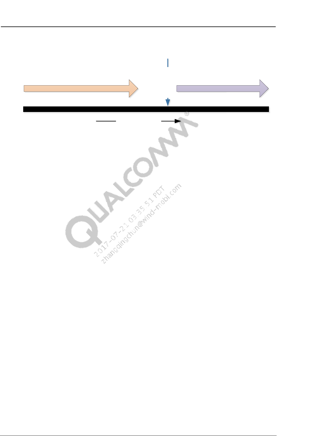
Configuration Guide for Display Drivers (ACPI and XML) Display interface-specific configurations
80-NB116-2 G Confidential and Proprietary – Qualcomm Technologies, Inc. 55
MAY CONTAIN U.S. AND INTERNATIONAL EXPORT CONTROLLED INFORMATION
Figure 8-4 shows the DSI data transmission with respect to the panel scanline.
Panel Scanline
Video Ram
Pixel 0
Pixel n
Direction of scan-out
DSI Data transmission (Using Tear Check)DSI Data transmission (No Tear Check)
Figure 8-4 DSI data transmission with respect to panel scanline
Two basic methods handle this synchronization:
Data transfer behind the scanline (not recommended) – This method requires the DSI link
rate (bitclock) to be configured to the panels refresh rate or faster. The tear check block must
be enabled in order to throttle the data transfer to ensure the write never crosses the current
scanline. The data transfer ahead of the scanline is recommended because it provides a much
simpler solution and increased efficiency on the bus.
Data transfer ahead of the scanline – This method requires the DSI link rate (bitclock) to be
configured equal to the panel’s refresh rate or faster. The teach check block must be disabled
in this configuration. The increased link rate will guarantee that the scanline never catches up
to the data transfer.
8.1.11 Tear check threshold parameters
DSITEPercentVariance
The DSITEPercentVariance represents the percent value by which refresh rate is to be reduced
for the internal timer to ensure that the external TE comes before the internal timer expires. This
can be used for fine-tuning the TE under the conditions when the frequency of the external TE
varies.
8.1.12 Dual DSI configuration
DSIControllerMapping
The DSIControllerMapping field configures the mapping from the logical DSI port to the
physical DSI port. In a single DSI 4-lane configuration, this allows for mapping of the primary
DSI to the secondary DSI port. For example:
<DSIControllerMapping>0x1</ DSIControllerMapping>
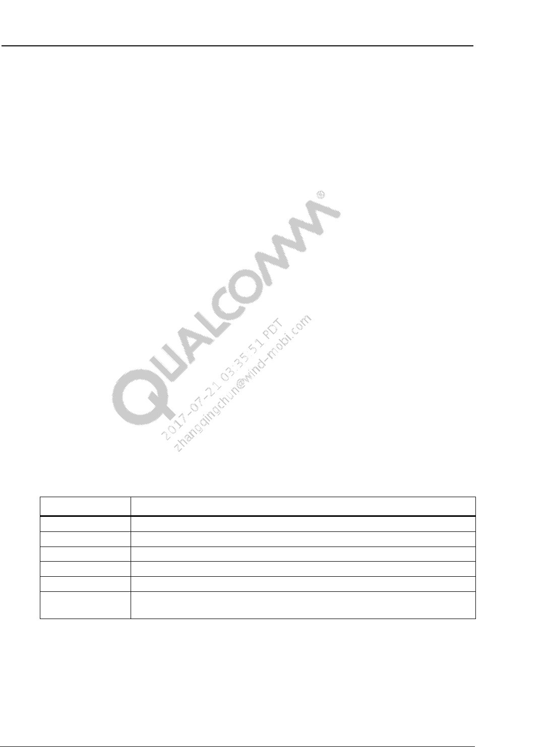
Configuration Guide for Display Drivers (ACPI and XML) Display interface-specific configurations
80-NB116-2 G Confidential and Proprietary – Qualcomm Technologies, Inc. 56
MAY CONTAIN U.S. AND INTERNATIONAL EXPORT CONTROLLED INFORMATION
Without this configuration, the default configuration maps the primary display to the primary DSI
port.
For dual DSI configurations, the mapping informs the driver that two DSI ports are needed and
how those ports should be mapped. The ID order applied in the mapping tag indicates what DSI
port should assigned to the primary and slave DSI ports.
For example, a typical 8-lane dual DSI solution should map the master to DSI port 0 and the slave
to DSI port 1.
<DSIControllerMapping>0x0 0x1</ DSIControllerMapping>
DSISlaveControllerSkewLines
In dual DSI configurations, the master and slave ports will send their pixel stream at the same
time. For a specific configuration, a skew may be needed. This configuration allows the
controllers to skew the transfers.
The field represents how many lines the slave should be skewed from the master.
To skew (delay) the slave tramission by 2 lines, the following configuration may be used:
<DSISlaveControllerSkewLines>2</DSISlaveControllerSkewLines>
To skew (delay) the master tramission by 2 lines, a negative value may be used:
<DSISlaveControllerSkewLines>-2</DSISlaveControllerSkewLines>
8.2 DSI Command mode configuration
8.2.1 Scenario A – Free run transfer (no tear check block)
Panel transfer should start at the start of the TE. It is desired to run the data transfer faster than the
TE, within 14 ms, to guarantee that the update is completed ahead of the TE. No tear check block
is required in such a configuration. Tearing was visible if the transfer was started at line 1, so the
transfer was adjusted to start on line 760.
Configuration Value
Mode Command code
Lanes 4
Resolution 768x1280
Bit depth 24 bpp
Refresh rate 60 Hz
Bitclock rate 354 MHz – For 16.6 ms transfer
419 MHz – For 14 ms transfer

Configuration Guide for Display Drivers (ACPI and XML) Display interface-specific configurations
80-NB116-2 G Confidential and Proprietary – Qualcomm Technologies, Inc. 57
MAY CONTAIN U.S. AND INTERNATIONAL EXPORT CONTROLLED INFORMATION
ACPI configuration
<DSIRefreshRate units='integer Q16.16'>0x3C0000</DSIRefreshRate>
<DSIBitClockFrequency>419991600</DSIBitClockFrequency>
<DSITECheckEnable units='Bool'>False</DSITECheckEnable>
<DSITEUsingDedicatedTEPin units='Bool'>True</DSITEUsingDedicatedTEPin>
<DSITEvSyncRdPtrIrqLine>760</DSITEvSyncRdPtrIrqLine>
8.2.2 Scenario B – Using tear check block (transfer throttling)
Panel transfer uses the tear check block to throttle the transfer. The bitclock is calculated by the
driver and is designed to complete the transfer in 16.6 ms (60 Hz).
The internal counter runs 10% slower (percent variance) than 60 Hz. The transfer must fall within
the first quarter of the panel height (start line divisor) and the transfer can be started after the TE
has reached line 2. The transfer should be 3 lines behind the TE (sync continue lines).
Configuration Value
Mode Command mode
Lanes 4
Resolution 768x1280
Bit depth 24 bpp
Refresh rate 60 Hz
ACPI configuration
<DSITECheckEnable units='Bool'>True</DSITECheckEnable>
<DSITEvSyncStartPos units='int'>2</DSITEvSyncStartPos>
<DSITEvSyncContinueLines units='int'>3</DSITEvSyncContinueLines>
<DSITEvSyncStartLineDivisor units='int'>4</DSITEvSyncStartLineDivisor>
<DSITEPercentVariance units='integer Q16.16'>0xa0000</DSITEPercentVariance>

Configuration Guide for Display Drivers (ACPI and XML) Display interface-specific configurations
80-NB116-2 G Confidential and Proprietary – Qualcomm Technologies, Inc. 58
MAY CONTAIN U.S. AND INTERNATIONAL EXPORT CONTROLLED INFORMATION
8.3 eDP configuration
The only required tag for eDP is to select interface 14 (DP) in the InterfaceType tag. Table 8-9
lists optional overrides that could serve to speed up boot time or to work around panel issues.
Table 8-9 eDP configuration
Tag Description
EDPRefreshRate This integer is used to specify the refresh rate of the panel in Q16.16
format. This tag allows the OEM to configure the exact refresh rate of the
panel. The driver configures the correct internal clocks to achieve the
requested refresh rate.
Example:
60 Hz = 0x003C0000
58 Hz = 0x003A0000
EDPTraining This integer can be used to specify the link training type through the AUX
channel.
Value (decimal) Definition
0 No link training
1 Full link training
2 Fast link training
By default, link training is disabled.
EDPPixelClockFrequency This allows the licensee to configure an exact pixel clock frequency. The
drive will then calculate the refresh rate based on the requested pixel
clock frequency and will override the value given through
EDPRefreshRate.
EDPDPCDRead This Boolean value can be used to enable (TRUE) or disable (FALSE)
reading DPCD during initialization of the panel.
If this tag is FALSE, link training is implicitly disabled and the following
tags must be provided:
EDPNumberOfLanes
EDPLinkRate
EDPASSREnable
EDPEnhancedFrameEnable
By default, DPCD reading is enabled.

Configuration Guide for Display Drivers (ACPI and XML) Display interface-specific configurations
80-NB116-2 G Confidential and Proprietary – Qualcomm Technologies, Inc. 59
MAY CONTAIN U.S. AND INTERNATIONAL EXPORT CONTROLLED INFORMATION
Tag Description
EDPEDIDRead This Boolean value can be used to enable (TRUE) or disable (FALSE)
reading EDID through the AUX channel.
If this tag is FALSE, the following tags must be provided:
EDPRefreshRate
HorizontalActive
HorizontalFrontPorch
HorizontalBackPorch
HorizontalSyncPulse
HorizontalSyncSkew
VerticalActive
VerticalFrontPorch
VerticalBackPorch
VerticalSyncPulse
InvertDataPolarity
InvertVsyncPolairty
InvertHsyncPolarity
By default, EDID reading is enabled.
EDPNumberOfLanes Number to specify number of lanes to use; valid values are 1, 2, and 4. If
this tag is provided, the EDPLinkRate must also be provided.
By default, the number of lanes is calculated programmatically.
EDPLinkRate Number to specify the link rate of each lane; valid values are 270000 and
162000.
If this tag is provided, the EDPNumberOfLanes must also be provided.
By default, the link rate is calculated programmatically.
EDPASSREnable This Boolean value can be used to enable (TRUE) or disable (FALSE)
Alternate Scrambler Seed Reset.
By default, this is enabled if both source and sink devices support eDP 1.2
or greater.
EDPEnhancedFrameEnable This Boolean value can be used to enable (TRUE) or disable (FALSE)
enhanced framing.
By default, this is enabled if both source and sink devices support eDP 1.2
or greater.
EDPHPDActiveLow This Boolean value can be used to specify if the HPD signal is active low
(TRUE) or active high (FALSE).
By default, HPD is active low.
EDPDynamicRefreshRates The refresh rates supported by the panel other than the default refresh
rate; this is a list of refresh rates in Q16.16 format.
The driver might prune refresh rates from this list based on the capabilities
of the display hardware.
EDPStatusSequence This is a binary data value that is used to send AUX read commands to
the panel to decide panel status. Syntax of each command is:
<AUX type> <Address lower 8 bits><Address high 8 bits>
<Expected Result>
AUX Type: 1->AUX/DPCD, 2->I2C/EDID
Example:
<EDPStatusSequence>
01 05 02 01
</EDPStatusSequence>

Configuration Guide for Display Drivers (ACPI and XML) Display interface-specific configurations
80-NB116-2 G Confidential and Proprietary – Qualcomm Technologies, Inc. 60
MAY CONTAIN U.S. AND INTERNATIONAL EXPORT CONTROLLED INFORMATION
Tag Description
EDPPowerUpWaitInMs Number to specify the time in milliseconds to wait after panel power up
and before next AUX read/write.
By default the number is 0, meaning no wait.
EDPMaxAuxRetry Number to specify the trial time after panel power up and before a
successful AUX read/write
The following logic shows the use of EDPPowerUpWaitInMs and
EDPMaxAuxRetry; it will be executed only once after panel power up.
While(loop++<EDPMaxAuxRetry)
{
Wait(EDPPowerUpWaitInMs);
If(Status_OK == AUX_Read/Write())
Break;
}
By default, the number is 20.
8.4 HDMI configuration
Table 8-10 lists the parameters that can be used to configure HDMI.
Table 8-10 HDMI configuration
Tag Description
HDMIDisable This Boolean value can be used to disable HDMI support.
By default, HDMI support is enabled.
HDMIAviInfoFramePacketsDisable This Boolean value can be used to disable the AVI information
frame packet.
By default, AVI information frame packet is enabled.
HDMIOutVoltageSwingCtrlEnable If this Boolean value is set to TRUE, HDMIOutVoltageSwingCtrl will
be used.
HDMIOutVoltageSwingCtrl HDMI PHY output voltage swing control value from 0 to 7; it will
only be used when HDMIOutVoltageSwingCtrlEnable is TRUE. If
HDMIOutVoltageSwingCtrlEnable is FALSE, the driver uses the
default value (0x2).
Note: The exact voltage produced by this setting is chip and
process dependent; however, 0 is the lowest swing voltage and 7 is
the highest.
HDMIHDCPEnable This Boolean value can be used to always enable HDCP. By
default, HDMIHDCPEnable is FALSE. HDCP will not be enabled
always. Windows will enable HDCP if necessary. It is not
recommended that the customer sets HDMIHDCPEnable to always
enable HDCP in the driver.
HDMIMaxNumReAuthentication This value overrides the maximum number of attempts to
reauthentication Phase 1 of HDCP before giving up.
Increasing this value may cause changes in user experience for
sinks that do not support HDCP.
The default value is 10 retries; setting this value to 0 enforces the
default number of retries.

Configuration Guide for Display Drivers (ACPI and XML) Display interface-specific configurations
80-NB116-2 G Confidential and Proprietary – Qualcomm Technologies, Inc. 61
MAY CONTAIN U.S. AND INTERNATIONAL EXPORT CONTROLLED INFORMATION
Tag Description
HDMIMaxModeWidth This parameter configures the HDMI mode filter. This value is the
maximum width that is allowed, anything larger is rejected.
This parameter can be used in conjunction with height and refresh
rate filters.
The default value is 0, which means no limit; units are in pixels.
HDMIMaxModeHeight This parameter configures the HDMI mode filter. This value is the
maximum height that is allowed; anything larger is rejected.
This parameter can be used in conjunction with width and refresh
rate filters.
The default value is 0, which means no limit; units are in pixels.
HDMIMaxModeRefreshRate This parameter configures the HDMI mode filter. This value is the
maximum refresh rate that is allowed; anything larger is rejected.
This parameter can be used in conjunction with width and height
rate filters.
The default value is 0, which means no limit; units are in hertz.
HDMIMinModeWidth This parameter configures the HDMI mode filter. This value is the
minimum width that is allowed; anything smaller is rejected.
This parameter can be used in conjunction with height and refresh
rate filters.
The default value is 0, which means no limit; units are in pixels.
HDMIMinModeHeight This parameter configures the HDMI mode filter. This value is the
minimum height that is allowed; anything smaller is rejected.
This parameter can be used in conjunction with width and refresh
rate filters.
The default value is 0 which means no limit; units are in pixels.
HDMIMinModeRefreshRate This parameter configures the HDMI mode filter. This value is the
minimum refresh that is allowed; anything smaller is rejected.
This parameter can be used in conjunction with width and height
rate filters.
The default value is 0, which means no limit; units are in hertz.
HDMIInjectedModeList Reserved
HDMIDDCTimeoutInMs This value overrides the default timeout for DDC reads and writes.
Setting the timeout too short could result in failures to communicate
with a sink device that has a slow response. A long timeout
increases the delay when communicating with a nonresponsive
sink.
If the value is unconfigured or 0, the default timeout is 5 ms. For
bridges that implement clock stretching to translate DDC
messaging across a slow link, a value of 10 ms to 30 ms is
recommended.
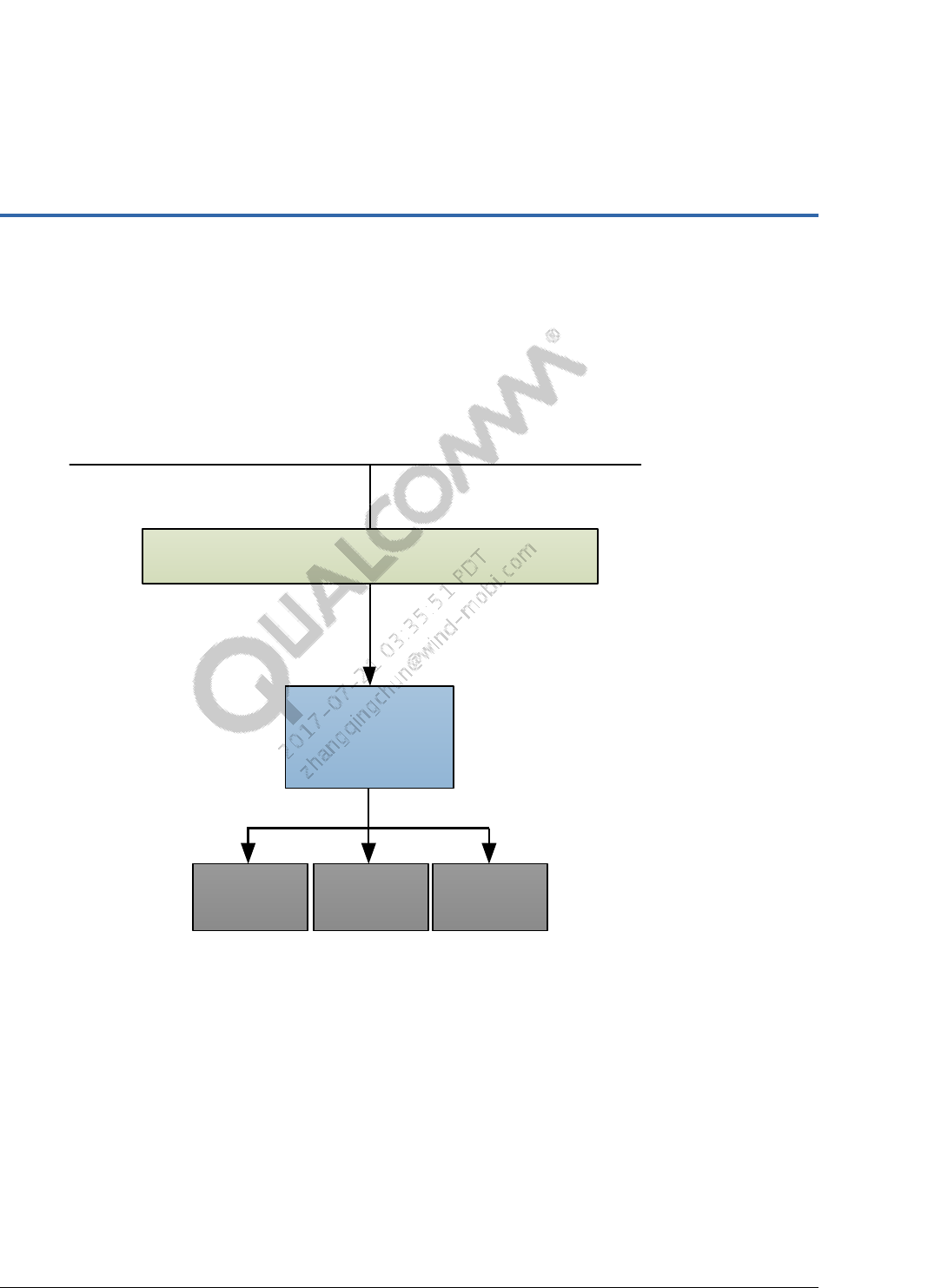
80-NB116-2 G Confidential and Proprietary – Qualcomm Technologies, Inc. 62
MAY CONTAIN U.S. AND INTERNATIONAL EXPORT CONTROLLED INFORMATION
9 Backlight configuration
One of the responsibilities of the Graphics KMD is to communicate with the backlight hardware
to correctly set a specific backlight level. Depending on the hardware interface used to control the
backlight, various configurations are required to support backlight adjustment. Figure 9-1 shows
how backlight is controlled in the WDDM model.
QCOM
Graphics Kernel
Mode Driver
User Mode
Kernel Mode
MSFT DirectX Graphics Kernel Subsystem (Dxgkrnl)
SetBrightness(%level)
DSI Driver
(DCS Based Control)
I2C Driver
(I2C Based Control)
PMIC Driver
(PWM Based Control)
Figure 9-1 Backlight control under WDDM model

Configuration Guide for Display Drivers (ACPI and XML) Backlight configuration
80-NB116-2 G Confidential and Proprietary – Qualcomm Technologies, Inc. 63
MAY CONTAIN U.S. AND INTERNATIONAL EXPORT CONTROLLED INFORMATION
9.1 Common backlight configuration parameters
Table 9-1 shows common backlight configuration parameters.
Table 9-1 Common backlight configuration parameters
Tag Description
BacklightType This integer is used to define the interface used to control the backlight on
the platform. This value is based on the QDI_Panel_BacklightType
enumeration.
Value (integer) Definition
0 QDI_PANEL_BACKLIGHTTYPE_NONE
1 QDI_PANEL_BACKLIGHTTYPE_PMIC
2 QDI_PANEL_BACKLIGHTTYPE_I2C
3 QDI_PANEL_BACKLIGHTTYPE_DSI
4 QDI_PANEL_BACKLIGHTTYPE_ACPI
All other values are invalid or unsupported.
BacklightSteps This integer defines the number of discrete backlight levels that are
supported on this platform. This information is reported back up to the OS
and is used to control the granularity in the UI controls for backlight. Valid
values are 1 to 100; examples are:
1% backlight granularity = 100 steps
10% backlight granularity = 10 steps
BacklightDefault This field is reserved and should not be used.
BacklightLowPower This field is reserved and should not be used.

Configuration Guide for Display Drivers (ACPI and XML) Backlight configuration
80-NB116-2 G Confidential and Proprietary – Qualcomm Technologies, Inc. 64
MAY CONTAIN U.S. AND INTERNATIONAL EXPORT CONTROLLED INFORMATION
9.2 PWM (PMIC)-based backlight control
If the platform uses a PWM signal generated from the PMIC to control the backlight level, the
fields listed in Table 9-2 are used to control the PMIC.
Table 9-2 PWM (PMIC)-based backlight control
Tag Description
BacklightPmicModel This integer is used to identify the QTI PMIC used to generate the
PWM signal on the platform. Currently, only QTI PMICs are supported.
The values are based on the QDI_PMICDeviceIdType enumeration.
Value (decimal) Definition
1 QDI_PMIC_DEVICEID_8921
2 QDI_PMIC_DEVICEID_8038
3 QDI_PMIC_DEVICEID_8941
4 QDI_PMIC_DEVICEID_8841
5 QDI_PMIC_DEVICEID_8026
6 QDI_PMIC_DEVICEID_8926
7 QDI_PMIC_DEVICEID_8084
8 QDI_PMIC_DEVICEID_8962
9 QDI_PMIC_DEVICEID_8994
10 QDI_PMIC_DEVICEID_8994I
11 QDI_PMIC_DEVICEID_8916
12 QDI_PMIC_DEVICEID_8110
13 QDI_PMIC_DEVICEID_8909
All other values are invalid or not supported.
BacklightPMICNum In systems that use more than one PMIC, this specifies the PMIC that
is being controlled; all settings apply to only that PMIC.
BacklightPmicControlType This field is used to specify the type of PMIC control interface used to
support backlight control.
The values are based on the QDI_PmicModuleControlType
enumeration.
Value (decimal) Definition
1 QDI_PMIC_MODULE_CONTROLTYPE_LPG
2 QDI_PMIC_MODULE_CONTROLTYPE_WLED
All other values are invalid or not supported.

Configuration Guide for Display Drivers (ACPI and XML) Backlight configuration
80-NB116-2 G Confidential and Proprietary – Qualcomm Technologies, Inc. 65
MAY CONTAIN U.S. AND INTERNATIONAL EXPORT CONTROLLED INFORMATION
Tag Description
BacklightPMICBankSelect This integer is used to specify the PMIC bank used for LPG-based
backlight control or the strings to use in WLED type control. The
interpretation of this field is based on the value set in
BacklightPmicControlType.
LPG (PWM)-based control – This number represents the PMIC LPG
bank number.
See the PMIC documentation for bank number to GPIO mapping.
WLED-based control – This number represents the LED strings to be
controlled.
Bit 0 – String 1
Bit 1 – String 2
Bit 2 – String 3
Etc.
Multiple strings can be controlled by combining bits, e.g., a value of
0x7 = String 0 | String 1 | String 2.
BacklightPMICPWMFrequency This integer is used to determine the PWM frequency in Hz for
controlling the backlight. Some PMICs support a range of PWM
frequencies, and check the backlight specification on the range of valid
PWM frequencies.
If the exact frequency is not available, the closest frequency will be
selected, e.g.:
2 kHz PWM frequency
< BacklightPMICPWMFrequency >2000</BacklightPMICPWM
Frequency>
This value configures either the WLED or PWM frequency depending
on the BacklightPmicControlType.
BacklightPmicAdvancedConfig This configuration enables all advanced configuration parameters.
Depending on the PMIC there are several advanced settings; for more
information, see the Advanced WLED configuration and/or PMIC
documentation.
9.3 Sample backlight configurations
9.3.1 WLED configuration (1 WLED string)
<BacklightType units='QDI_Panel_BacklightType'>1</BacklightType>
<BacklightPmicModel units='QDI_PMICDeviceIdType'>5</BacklightPmicModel>
<BacklightPmicControlType
units='QDI_PmicModuleControlType'>1</BacklightPmicControlType>
<BacklightPmicNum units='int'>0</BacklightPmicNum>
<BacklightPmicBankSelect units='int'>1</BacklightPmicBankSelect>
<BacklightPmicPWMFrequency units='kHz'>800000</BacklightPmicPWMFrequency>
<BacklightSteps units='Percentage'>100</BacklightSteps>
<BacklightDefault units='Percentage'>80</BacklightDefault>
<BacklightLowPower units='Percentage'>40</BacklightLowPower>
<BacklightPmicAdvancedConfig
units='Bool'>True</BacklightPmicAdvancedConfig>

Configuration Guide for Display Drivers (ACPI and XML) Backlight configuration
80-NB116-2 G Confidential and Proprietary – Qualcomm Technologies, Inc. 66
MAY CONTAIN U.S. AND INTERNATIONAL EXPORT CONTROLLED INFORMATION
<BacklightPmicWledInternalModResolution
units='int'>0</BacklightPmicWledInternalModResolution>
<BacklightPmicWledModulationClkSel
units='int'>3</BacklightPmicWledModulationClkSel>
<BacklightPmicWledDimmingMethod
units='int'>0</BacklightPmicWledDimmingMethod>
<BacklightPmicWledOvp units='int'>0</BacklightPmicWledOvp>
<BacklightPmicWledIlim units='int'>5</BacklightPmicWledIlim>
<BacklightPmicWledFeedbackCtrl
units='int'>0</BacklightPmicWledFeedbackCtrl>
<BacklightPmicWlepLoopCompRes units='int'>3</BacklightPmicWlepLoopCompRes>
<BacklightPmicWledVrefControl units='int'>2</BacklightPmicWledVrefControl>
<BacklightPmicWledFullScaleCurrent
units='mA'>25</BacklightPmicWledFullScaleCurrent>
<BacklightPmicWledModulatorSrcSel
units='int'>0</BacklightPmicWledModulatorSrcSel>
<BacklightPmicWledCabcEnable
units='Bool'>False</BacklightPmicWledCabcEnable>
9.3.2 LPG configuration
<BacklightType units='QDI_Panel_BacklightType'>1</BacklightType>
<BacklightPmicModel units='QDI_PMICDeviceIdType'>3</BacklightPmicModel>
<BacklightPmicControlType
units='QDI_PmicModuleControlType'>1</BacklightPmicControlType>
<BacklightPMICNum units='int'>0</BacklightPMICNum>
<BacklightPMICBankSelect units='int'>7</BacklightPMICBankSelect>
<BacklightPMICPWMFrequency units='kHz'>800000</BacklightPMICPWMFrequency>
<BacklightSteps units='Percentage'>100</BacklightSteps>
<BacklightDefault units='Percentage'>80</BacklightDefault>
<BacklightLowPower units='Percentage'>40</BacklightLowPower>
9.4 I2C-based backlight control
If the platform uses I2C to control the backlight level, the BLCP ACPI method is used for
controlling the commands sent to the backlight. See Section 15.2 for more details.
9.5 DSI DCS-based backlight control
If the platform uses a DSI DCS command to control the backlight level, the BLCP ACPI method
is used for controlling the commands sent to the backlight. See Section 15.2 for more details.

Configuration Guide for Display Drivers (ACPI and XML) Backlight configuration
80-NB116-2 G Confidential and Proprietary – Qualcomm Technologies, Inc. 67
MAY CONTAIN U.S. AND INTERNATIONAL EXPORT CONTROLLED INFORMATION
9.6 ACPI-based backlight control
If the licensee wishes to control backlight directly from ACPI, this method should be selected.
The BLCP ACPI method is used directly to control the backlight on the platform. The licensee
would be responsible for handling the incoming request within the ACPI BLCP method. An
example configuration is using the ACPI method to directly modify registers to adjust the
backlight.
9.7 CABL configuration
This section of configuration determines how the CABL algorithm behaves. CABL helps reduce
backlight level. However, it retains the apparent brightness of the screen by manipulating the
pixel values. This saves power.
The CABL algorithm is only used for the primary display.
Supplying these tags requires deep understanding on CABL. Documentation on CABL is outside
the scope of this document. All of the following tags are optional, and acceptable default values
are used when not supplied.
Table 9-3 CABL configuration
Tag Description
CABLMinUserLevel This defines the lowest level that can be configured as original backlight
level (before CABL algorithm processing) and still keep CABL active; any
level lower than this will deactivate CABL.
The range is 1 to 255, where 255 is 100% backlight level.
This item is important so that CABL can be configured when to deactivate
itself (basically turns off) to save processing power when CABL savings
are not significant.
The default value is 0, meaning algorithm default 75 (30%).
CABLMinBacklightLevel This defines the lowest backlight level CABL algorithm that will output
even when other calculations give a lower level.
The range is 1 to 255, where 255 is 100% backlight level.
This item limits CABL so that it does not go too low, which can cause
quality degradation. This number should be lower than
CABLMinUserLevel.
The default value is 0, meaning algorithm default of 30 (12%).
CABLFilterThreshold This configures the maximum backlight change that can happen on each
CABL iteration during regular CABL operation. This prevents huge
backlight changes that might be noticeable to the user.
The range is 1 to 255.
The default value is 0, meaning algorithm default 10 (4%).

Configuration Guide for Display Drivers (ACPI and XML) Backlight configuration
80-NB116-2 G Confidential and Proprietary – Qualcomm Technologies, Inc. 68
MAY CONTAIN U.S. AND INTERNATIONAL EXPORT CONTROLLED INFORMATION
9.8 Advanced backlight configuration
Table 9-4 defines the PMIC WLED parameters.
Table 9-4 Backlight configuration
NOTE: The following table has been updated.
Tag Description
BacklightPmicAdvancedConfig Set advance PMIC configuration for backlight control
BacklightPmicWledInternalModResolution Internal digital modulator configured
BacklightPmicWledModulationClkSel Digital modulator input clock frequency control
BacklightPmicWledDimmingMethod Modulator dimming mode control
BacklightPmicWledOvp Control for the over-voltage protection threshold
BacklightPmicWledIlim Current limit after soft start is complete
BacklightPmicWledFeedbackCtrl Forces selection of LED output as feedback node for the
boost
BacklightPmicWlepLoopCompRes Control to select the compensation resistor
BacklightPmicWledVrefControl Reference voltage for boost feedback
BacklightPmicWledFullScaleCurrent Select current sink for the LED
BacklightPmicWledModulatorSrcSel 1 – External PWM
0 – Internal digital modulator
BacklightPmicWledCabcEnable Enable content adaptive backlight control for current sinks
BacklightPmicOLEDWledAvddVoltage Configures the AVDD voltage for the WLED module in
AMOLED mode.

80-NB116-2 G Confidential and Proprietary – Qualcomm Technologies, Inc. 69
MAY CONTAIN U.S. AND INTERNATIONAL EXPORT CONTROLLED INFORMATION
10 ESD detection and recovery
configuration
ESD Detection and Recovery is configured using the tags given in Table 10-1 and Table 10-2.
Table 10-1 ESD Detection and Recovery tags
Tag Description
ESDDetectionTime This integer (in milliseconds) is used to schedule how fast the ESD detection
and recovery will be running. The default value in ACPI is 0, which means the
ESD Detection and Recovery feature is disabled.
ESDDetectionFailureRetry This integer is used as a retry count if ESD detection returns failure before
recovery is called. The default value is 5 if this parameter is omitted.
DSIStatusSequence This is a binary data value that is used to send DCS read commands to the
panel to decide panel status. Syntax of each command is:
<data type> <DCS command> <Expected Result>
Currently, only short DCS command with no parameter is supported, e.g.:
06 0a 1c ; Short DCS command to get panel power mode
; and expected panel response is 0x1C
Table 10-2 Display recovery threshold
Tag Description
DisplayRecoveryThreshold This configuration will set up the threshold for recovery configuration.
The value set in the field will determine the threshold beyond which
display recovery action will be triggered.
If the value is set to 0, the recovery feature is disabled.
Unit is in number of vsyncs. It is recommended that this should be less
than 120 (2 sec) to avoid a TDR from resetting the display before it can
self-recover.

80-NB116-2 G Confidential and Proprietary – Qualcomm Technologies, Inc. 70
MAY CONTAIN U.S. AND INTERNATIONAL EXPORT CONTROLLED INFORMATION
11 AD core configuration (preliminary)
The AD Core is configured using the tags given in Table 11-1.
Table 11-1 AD core tags
Tag Description
ADEnable This Boolean can be used as a master enable for the AD core.
Setting this tag as TRUE does not necessarily enable the core. Other
programmatic decisions might prevent the core from being enabled.
ADMaxIterations Number of iterations needed by the AD core to converge
ADStrengthLimit Number to program the strength limit obtained during calibration
ADBacklightMin Number to program the minimum backlight obtained during calibration
ADBacklightMax Number to program the maximum backlight obtained during calibration
ADAmbientLightMin Number to program the minimum ambient light level obtained during calibration
ADCalibrationA Number to program the CalibrationA value obtained during calibration
ADCalibrationB Number to program the CalibrationB value obtained during calibration
ADCalibrationC Number to program the CalibrationC value obtained during calibration
ADCalibrationD Number to program the CalibrationD value obtained during calibration
ADFilterA Number to program the ambient light filter; this value is obtained during calibration
ADFilterB Number to program the ambient light filter; this value is obtained during calibration
ADTFilterControl Number to program the ambient light filter; this value is obtained during calibration
ADAssymetry These binary tags are used to program tables obtained during calibration.
Each table consists of 33 entries. Each entry is 2 bytes long. Entries are in
hexadecimal notation, e.g.:
<ADAsymmetry>
00 00
01 01
02 02
…
31 31
32 32
</ADAsymmetry>
ADPrivateData Private data that must be filled with specific values
aPrivateData[11] – This field configures the BacklightScale. This can be set
depending on the number of bits that want to be used to represent the backlight
level, e.g., if backlight level will be 16 bits, then BacklightScale should be 0xFFFF,
if it is an 8-bit range, then BacklightScale should be set to 0x00FF; the maximum
value permitted is the default 0xFFFF. If this value is modified from the default,
the BacklightLevel input needs to be adjusted.
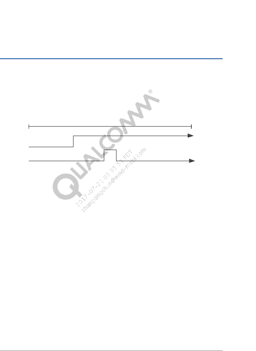
80-NB116-2 G Confidential and Proprietary – Qualcomm Technologies, Inc. 71
MAY CONTAIN U.S. AND INTERNATIONAL EXPORT CONTROLLED INFORMATION
12 Platform-specific GPIO configuration
A majority of the power rails and GPIOs (both TLMM (MSM) and PMIC) are configured by the
PEP component of Windows. However, panels often require specific timing and control of GPIOs
during boot. Table 12-1 gives details on additional configuration operations available.
Figure 12-1 shows panel power-on reset.
Power Rails
Panel Power on Reset
Reset Pin
Figure 12-1 Panel power-on reset
During the panel power-on reset sequence, additional GPIOs can be configured. All of these
configurations are optional. If PEP is sufficient to control these resources, these configurations
must be disabled.
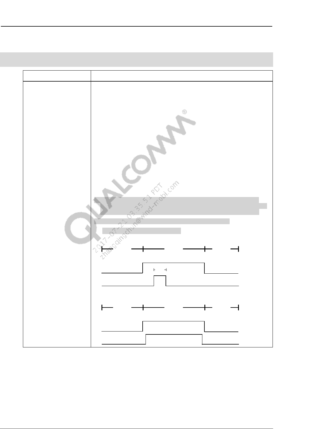
Configuration Guide for Display Drivers (ACPI and XML) Platform-specific GPIO configuration
80-NB116-2 G Confidential and Proprietary – Qualcomm Technologies, Inc. 72
MAY CONTAIN U.S. AND INTERNATIONAL EXPORT CONTROLLED INFORMATION
Table 12-1 Panel resources
NOTE: The following table has been updated.
Tag Description
Display1Reset1Info This string is used to configure the reset pin of all internal panel
(QDI_DISPLAY_PRIMARY, QDI_DISPLAY_SECONDARY, so on). The
following information is parsed in a comma-delimited format:
“ResourceName, Assert State, Pulse Width, Assert on Power Down”
Resource name – This is a string matching the resource (GPIO) name
assigned to the graphics KMD in graphics.asl.
Assert state – This is the state of the GPIO pin when being asserted.
This can be either of the following values:
0 – Active low; the GPIO is pulled low during assertion of the reset
1 – Active high; the GPIO is pulled high during the assertion of the
reset
Pulse width – This determines the pulse width of the reset in
microseconds (µs) when the reset is asserted. If the pulse width is 0, no
pulse is created and the line is directly deasserted when active.
Active-on power down – This Boolean allows for the reset to be asserted
during power-down. Depending on the panel configuration, this may be
required. Examples are DISPLAY_RESET_PIN, 0, 500, 0.
Primary panel configuration is specified by DSI_PANEL_RESET and
other internal configuration specified by DSI_PANELX_RESET, where X
= 2, 3, .., N. For example N = 2 for secondary, 3 for Third, and so on.
Reset pin configuration examples for primary panels are
DSI_PANEL_RESET, 0, 500, 0
Power Rails
Reset Line
Power Off Power On Power Off
500ms
DSI_PANEL_RESET, 0, 0, 1
Power Rails
Reset Line
Power Off Power On Power Off
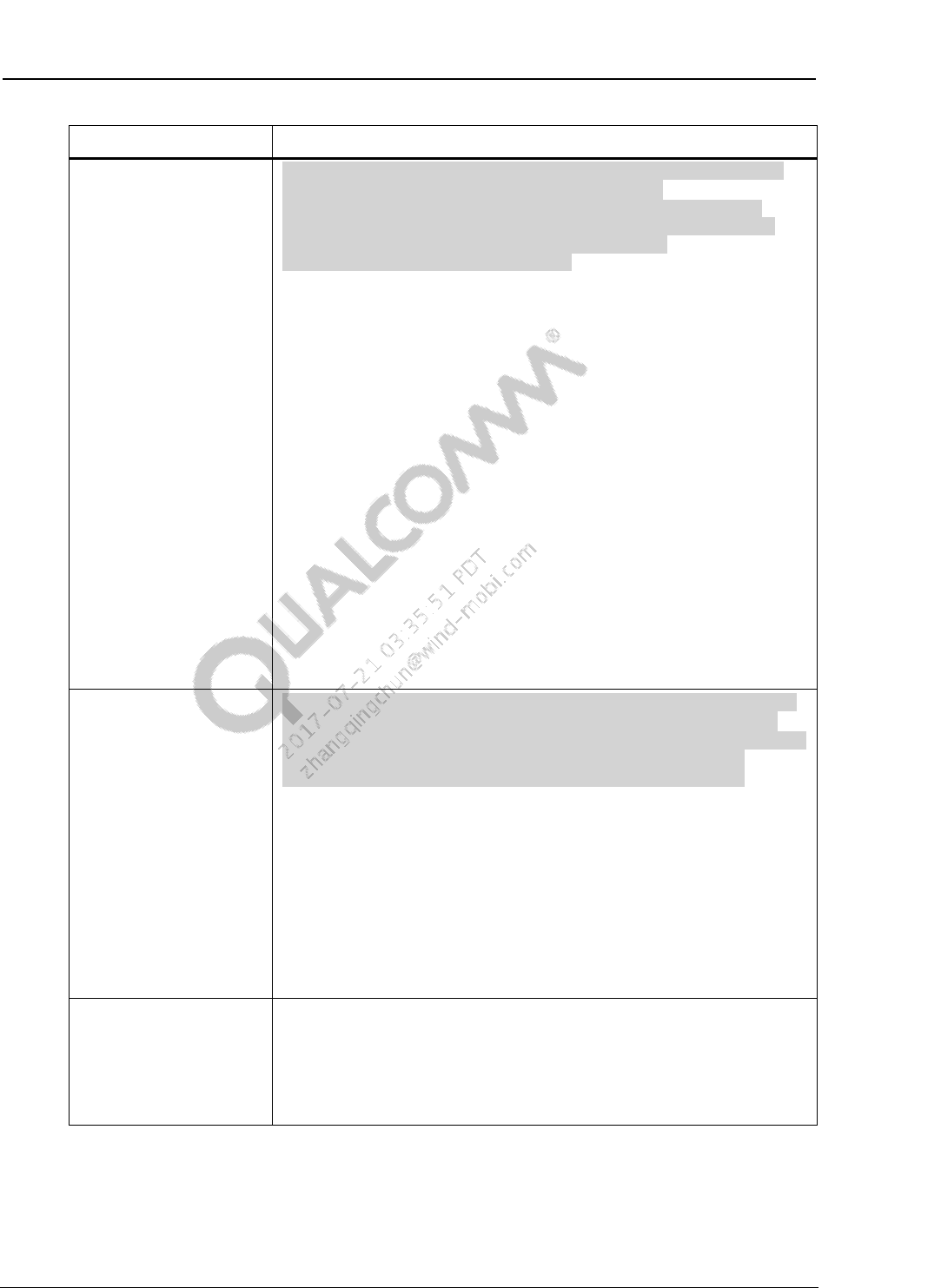
Configuration Guide for Display Drivers (ACPI and XML) Platform-specific GPIO configuration
80-NB116-2 G Confidential and Proprietary – Qualcomm Technologies, Inc. 73
MAY CONTAIN U.S. AND INTERNATIONAL EXPORT CONTROLLED INFORMATION
Tag Description
Display1Power1Info
Display1Power2Info
Display1Power3Info
Display4Power1Info
Display4Power2Info
Display4Power3Info
This string is used to configure the state of GPIOs during power-on/off of
the internal panels (Display1Power1Info is used for
QDI_DISPLAY_PRIMARY, QDI_DISPLAY_SECONDARY etc). Other
resources can be associated with external displays by using other tags;
Dislpay4Power1Info is for (QDI_DISPLAY_EXTERNAL,
QDI_DISPLAY_EXTERNAL2, and so on).
The following information is parsed in a comma-delimited format:
“ResourceName, AssertState, RefCount, ActiveDelay, InactiveDelay”
Up to three resources can be controlled, Power1, Power2, and Power3.
These are all optional and the licensee should remove these settings if they
are not used.
Resource name – This is a string matching the resource (GPIO) name
assigned to the graphics KMD in graphics.asl.
Assert state – This is the state of the GPIO pin when being asserted; this
can be one of the following values:
0 – Active low, the GPIO is pulled low during power-on
1 – Active high, the GPIO is pulled high during power-on
RefCount – If a resource is shared between one or multiple displays, the
resource is automatically ref counted by the driver. If the licensee wants
to specify a default refcount during boot, this field is used to set the
default refcount. A default refcount > 0 set during boot means the
resource will never be deasserted during power-off.
Active delay – This integer allows the driver to delay for a specific
number of microseconds after asserting this resource during power-on.
Inactive delay – This integer allows the driver to delay for a specific
number of microseconds after deasserting this resource during power-
off.
Display1Special1Info
Display4Special1Info
This string is used to configure special states of GPIOs during power-on of
the internal panels (Display1Special1Info=QDI_DISPLAY_PRIMARY,
QDI_DISPLAY_SECONDARY etc). Other resources can be associated with
external displays by using other tags; Display4Special1Info is for
(QDI_DISPLAY_EXTERNAL, QDI_DISPLAY_EXTERNAL2, so on).
The following information is parsed in a comma-delimited format:
“ResourceName, ChipId, OutBufferCfg, Voltage Source, Source,
BufferStrength”
Resource name – This is a PMIC GPIO number that needs the special
configuration.
ChipId – This value is specific to the PMIC.
Out Buffer Cfg – This value is specific to the PMIC.
Voltage source – This value is specific to the PMIC.
Source – This value is specific to the PMIC.
Buffer strength – This value is specific to the PMIC.
Display1I2C1Info
Display1I2C2Info
This parameter defines I2C connections used. There can be maximum of
two I2C connections. The following information is parsed in a comma-
delimited format:
“ResourceName, I2CSlaveType”
1 – I2C slave is for the backlight driver
2 – I2C slave is for the panel EDID EEPROM

Configuration Guide for Display Drivers (ACPI and XML) Platform-specific GPIO configuration
80-NB116-2 G Confidential and Proprietary – Qualcomm Technologies, Inc. 74
MAY CONTAIN U.S. AND INTERNATIONAL EXPORT CONTROLLED INFORMATION
12.1 GPIO configuration
Table 12-2 show the tags that allow for a default GPIO configuration to be applied prior to
initializing the display.
NOTE: This configuration is available only in boot loaders (UEFI).
Table 12-2 GPIO configuration tags
Tag Description
TLMMGPIODefaultLow This integer list provides the list of MSM GPIO numbers that should be
defaulted to high. Only confirgure GPIOs related to the display itself.
Note: This list is in hex, for example, GIO#91 should be written as 5B.
TLMMGPIODefaultHigh This integer list provides the list of MSM GPIO numbers that should be
defaulted to high. Only configure GPIOs related to the display itself.
Note: This list is in hex, for example, GIO#91 should be written as 5B.

80-NB116-2 G Confidential and Proprietary – Qualcomm Technologies, Inc. 75
MAY CONTAIN U.S. AND INTERNATIONAL EXPORT CONTROLLED INFORMATION
13 Power-saving configuration
The optional configuration shown in Table 13-1 is used for display power saving when a device
enters idle/static screen (vsync interrupt is masked off). There are various scenarios when a
device can enter idle screen, e.g., when a user reads webpage content.
There are different modes in which the power-saving feature operates. One of the modes is to
allow command data transfer between the panel and the MSM even though the device has entered
the power-saving configuration. The other mode is to block the command data transfer between
the MSM and the panel when the device enters the power-saving configuration.
If an OEM wants to configure the hardware or transmit commands to the panel using the OEM
panel driver, it is highly advisable to not configure the power-saving configuration to block data.
In addition to these modes, there are different power-saving levels that can be configured as well.
A higher power-saving level means greater savings can be attained.
Currently, the power-saving feature supports three power-saving levels. At power saving level 0,
there are no power savings and the device would be functioning normally with the power saving
configuration disabled. When the device transitions to level 2, maximum power savings can be
attained. By default, the device is allowed to transfer data when the device enters the power-
saving configuration with the power-saving level configured for maximum power savings.

Configuration Guide for Display Drivers (ACPI and XML) Power-saving configuration
80-NB116-2 G Confidential and Proprietary – Qualcomm Technologies, Inc. 76
MAY CONTAIN U.S. AND INTERNATIONAL EXPORT CONTROLLED INFORMATION
Table 13-1 lists the power saving configuration parameters.
Table 13-1 Power saving configuration
Tag Description
DisplayPowerSavingOverride The following optional ACPI configuration field is used to override the
default power saving mode and levels; flags can be combined where it
makes sense.
Value (in hex) Definition
0x1 This allows data transfer while power saving is
enabled. If both allow data and block data bits
are set, then allow data transfer takes
precedence over block data transfer; by default,
data transfer is allowed while power saving is
enabled.
0x2 Power-saving level is configured to level 0. No
other power-saving level transitions are allowed
when configured at level 0. This is equivalent to
power saving being disabled.
0x4 Power-saving level is configured to level 1. This
allows transitions between level 0 and level 1
power-saving levels. This power-saving level
provides conservative power saving with lower
latency. If both level 0 and level 1 power-saving
levels are configured, then level 1 power saving
takes precedence.
0x8 Power-saving level is configured to level 2. This
allows transitions between all the power-saving
levels. This power-saving level provides
aggressive power saving with higher latency. If
all three power-saving levels are configured, then
level 2 power-saving level takes precedence.
This is the default power-saving level.
0x10 This is block data transfer during power saving.

Configuration Guide for Display Drivers (ACPI and XML) Power-saving configuration
80-NB116-2 G Confidential and Proprietary – Qualcomm Technologies, Inc. 77
MAY CONTAIN U.S. AND INTERNATIONAL EXPORT CONTROLLED INFORMATION
Table 13-2 Power saving levels supported by the driver
Level Description
Level 0 (no power
savings) In level 0, the driver is expected to perform normal operation. By default,
when the display is turned on it transitions to level 0. Display power saving
can take effect any time by transitioning to either level 1 or level 2. Vsyncs
can be turned on/off.
Level 1 (conservative
power savings) In level 1, there is no actual data transfer happening between the MSM and
the panel. Vsyncs are turned off, but it is still necessary to maintain phase.
Latency to enter and exit from this mode is kept to a minimum. Expected
latency for transitioning to level 1 should be less than 2 ms. However,
transitioning from level 1 to other levels should be less than 5 ms. Due to
this restriction, there is a limit on what can be turned off. Entering this state
will lower clocks and possibly gate off, reducing bandwidth votes.
Level 2 (aggressive power
savings) In level 2, maximum display power saving can be achieved. Vsyncs are
turned off, and there is no need to maintain phase. Much higher latency is
allowed compared to level 1. Expected latency for transitioning to level 2
should be less than 2 ms. However, transitioning from level 2 to other levels
should be less than 16 ms. This limit gives flexibility to save more power by
turning off additional hardware components.
Entering this state includes all power savings from level 1, plus turning off
PLLs and enabling Deep Sleep states for peripherals, e.g., ULPS, where
applicable.
80-NB116-2 G Confidential and Proprietary – Qualcomm Technologies, Inc. 78
MAY CONTAIN U.S. AND INTERNATIONAL EXPORT CONTROLLED INFORMATION
14 Sharpening configuration
Table 14-1 lists the sharpening threshold configuration parameters.
Table 14-1 Sharpening parameters
Tag Description
SharpeningEdgeThreshold Sharpening edge threshold value; range is 1 to 1024
SharpeningSmoothThreshold Sharpening smoothness threshold value; range is 1 to 1024
SharpeningNoiseThreshold Sharpening noise threshold value; range is 1 to 256
80-NB116-2 G Confidential and Proprietary – Qualcomm Technologies, Inc. 79
MAY CONTAIN U.S. AND INTERNATIONAL EXPORT CONTROLLED INFORMATION
15 Display-specific ACPI methods
NOTE: Numerous changes were made in this chapter.
Display configuration data for all panels (internal and external) are stored in the ACPI as per the
following file structure.
External N Display
External2 Display
External Display
Internal N Display
Secondary Display
1...N External displays
1...N Internal displays
- Primary panel GPIO resources
- Secondary panel GPIO resources
- Internal panel N GPIO resources
ROM2
IGC2
PCC2
GCT2
GRT2
BRT2
HSI2
GMT2
BRT2
LGC2
WGM2
DIT2
_ROM
PIGC
PPCC
PGCT
PGRT
PBRT
HSIC
PGMT
PBRT
PLGC
PWGM
DITH
ROMN
IGCN
PCCN
GCTN
GRTN
BRTN
HSIN
GMTN
BRTN
LGCN
WGMN
DITN
display.asl
PCFG
PCF1
PCF2
panelcfg.asl
displayN.asl
display2.asl
BLCP
backlightcfg.asl
ROE1
displayext.asl
ROE2
displayext2.asl
PCFG
PCF1
PCF2
panelcfg2.asl
BLCP
backlightcfg2.asl
PCFG
panelcfgext.asl
PCFG
panelcfgext2.asl
ROEN
displayextN.asl
PCFG
panelcfgextN.asl
PCFG
PCF1
PCF2
panelcfgN.asl
BLCP
backlightcfgN.asl
Primary Display
graphics.asl
The power component configuration for all the panels are stored in graphics_resources.asl as
described in the diagram below. It is recommended that OEM should only update the F-State
component with power Grids, WLEDs, GPIOs, and so on and should not modify the P-State
component.
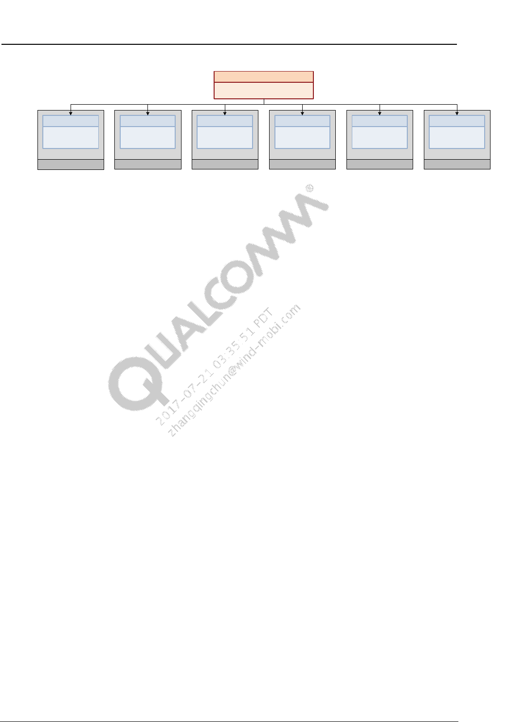
Configuration Guide for Display Drivers (ACPI and XML) Display-specific ACPI methods
80-NB116-2 G Confidential and Proprietary – Qualcomm Technologies, Inc. 80
MAY CONTAIN U.S. AND INTERNATIONAL EXPORT CONTROLLED INFORMATION
External N DisplayExternal2 DisplayExternal DisplayInternal N DisplaySecondary Display
Primary Display
1...N external display power component1...N Internal display power component
graphics_resource.asl
Display, graphics, video resources
F states
P states
F states
P states F states
P states
Power Component Power ComponentPower Component
F states
P states
Power Component
F states
P states
Power Component
F states
P states
Power Component
Note: F States for internal displays require platform specific customizations for the power grid.
The following sections describe each method with respect to primary panel. The configuration for
other panels should be followed in same way.
15.1 _ROM method
The _ROM method is a standard ACPI method to retrieve proprietary information. This method
is used by the graphics KMD to retrieve the panel configuration XML data from ACPI.
_ROM(offset, buffersize)
Parameters:
[in] offset : the offset in bytes to read from the panel configuration
file.
[in] buffersize : the size in bytes of the response buffer. Up to 4096
bytes can be read at a time.
Return:
Buffer : A response buffer containing the requested panel configuration
data. If a buffer of 1 byte is returned with a null byte the input offset
is out of range.
The _ROM method is found in display.asl and includes configuration data from panelcfg.asl.
15.2 ROM multipanel support
The _ROM method with three parameters is also supported by the driver. This extension will
allow multiple panel configurations to be stored in ACPI. The additional parameter is a unique
panel ID that is passed from the firmware (UEFI).
_ROM(offset, buffersize, panelid)
Parameters:
[in] offset : the offset in bytes to read from the panel configuration
file.
[in] buffersize : the size in bytes of the response buffer. Up to 4096
bytes can be read at a time.
[in] panelID : Unique panel ID passed from the firmware (DisplayDxe).
Return:

Configuration Guide for Display Drivers (ACPI and XML) Display-specific ACPI methods
80-NB116-2 G Confidential and Proprietary – Qualcomm Technologies, Inc. 81
MAY CONTAIN U.S. AND INTERNATIONAL EXPORT CONTROLLED INFORMATION
Buffer : A response buffer containing the requested panel configuration
data. If a buffer of 1 byte is returned with a null byte the input offset
is out of range.
Example of a three parameter ROM
///
// _ROM Method - Used to retrieve proprietary ROM data
//
Method (_ROM, 3, NotSerialized) {
Switch (Arg2)
{
// Panel with ID 0xC130B0
Case (0xC130B0) {
Store (PCF1, Local2);
}
// All others
Default {
Store (PCFG, Local2);
}
}
// Ensure offset does not exceed the buffer size
// otherwise return a Null terminated buffer
If (LGreaterEqual(Arg0, Sizeof(Local2)))
{
Return( Buffer(){0x0} )
}
Else
{
// Make a local copy of the offset
Store(Arg0, Local0)
}
// Ensure the size requested is less than 4k
If (LGreater(Arg1, 0x1000))
{
Store(0x1000, Local1)
}
else
{
Store(Arg1, Local1)
}

Configuration Guide for Display Drivers (ACPI and XML) Display-specific ACPI methods
80-NB116-2 G Confidential and Proprietary – Qualcomm Technologies, Inc. 82
MAY CONTAIN U.S. AND INTERNATIONAL EXPORT CONTROLLED INFORMATION
// Finaly ensure the total size does not exceed the size of the buffer
if (LGreater(Add(Local0, Local1), Sizeof(Local2)))
{
// Calculate the maximum size we can return
Subtract(Sizeof(Local2), Local0, Local1);
}
// Multiply offset and size by 8 to convert to bytes and create the RBuf
CreateField(Local2, Multiply(0x8, Local0), Multiply(0x8, Local1), RBUF)
Return(RBUF)
}
For more details on passing this ID from the firmware, refer to the MDPFirmwareEnvType
structure in the UEFI.
15.3 BLCP method
The BLCP method is a proprietary method used to return control packet information based on
changes on backlight. Licensees may customize this method to send control packet information to
the Graphics KMD.
BLCP(backlightLevel)
Parameters:
[in] backlight level : the current backlight level, valid range is 0-100
Return:
Buffer : A response buffer containing the requested panel configuration
data. The format of the buffer is specific to the backlight hardware
control method.
Buffer format
Packet Header Packet Payload
4 bytes Variable length
The format of the BLCP buffer consists of a 4-byte packet header followed by a variable-sized
payload. The packet header consists of a DWORD value with the length (in bytes) of the variable
packet payload.
Multiple packets can be combined by appending a packet header and payload together. No
padding is allowed between packet headers and payload. A final packet header contains the value
0x00000000 indicating the end of the packet sequence.
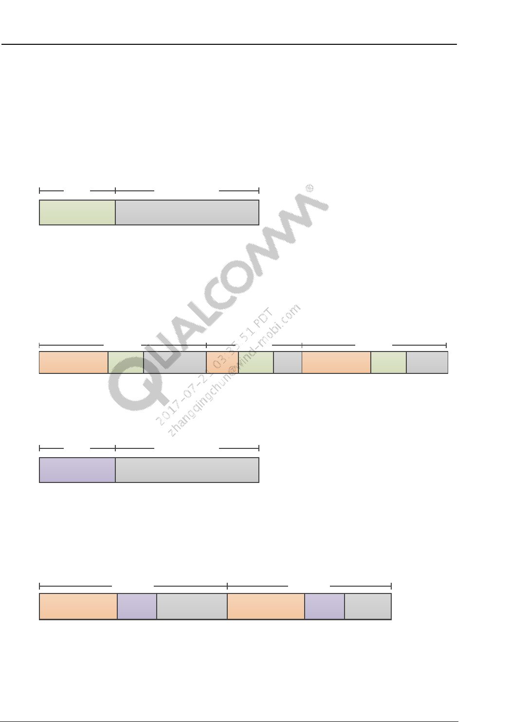
Configuration Guide for Display Drivers (ACPI and XML) Display-specific ACPI methods
80-NB116-2 G Confidential and Proprietary – Qualcomm Technologies, Inc. 83
MAY CONTAIN U.S. AND INTERNATIONAL EXPORT CONTROLLED INFORMATION
The contents of the payload packet depend on the control method for the backlight. The formats
for various packets are described in Section 15.3.1 and Section 15.3.2.
15.3.1 BLCP format for DSI DCS commands
The DCS command consists of one of the valid DCS commands. See Section 8.1 for details on
the supported DCS commands and special DCS commands. The payload size is variable. The
packet header must include both the size of the DCS command and the payload.
DCS Command DCS Payload
1 byte Variable length
Example
Send two DCS (+ payload) commands with a 10-ms delay between the two commands:
1. 11h + 01h 02h 03h 04h
2. FFh + 0Ah
3. 12h + 05h 06h
05 11h 01 02 03 04 02 FFh 0A 03 12h 05 06
Packet #1 Packet #2 Packet #3
15.3.2 BLCP format for I2C commands
The I2C packet consists of a 2-byte address followed by a variable-sized payload.
I2C Address I2C Payload
2 byte Variable length
Example
Send two I2C commands to address 1020h:
1. Command 01h 02h 03h 04 to address 1020h
2. Command 05h 06h to address 1020h
06 1020h 01 02 03 04 04 1020h 05 06
Packet #1 Packet #2
The BPCP method is found in backlight.asl.

Configuration Guide for Display Drivers (ACPI and XML) Display-specific ACPI methods
80-NB116-2 G Confidential and Proprietary – Qualcomm Technologies, Inc. 84
MAY CONTAIN U.S. AND INTERNATIONAL EXPORT CONTROLLED INFORMATION
15.4 Panel calibration commands (PIGC, PPCC, PPGC,
PGRT, PBRT, HSIC, PGMT)
The panel calibration data is stored in the ACPI table, and the data is read out during panel
initialization and then programmed into hardware blocks, which includes:
Panel inverse gamma correction
Panel color correction
Panel gamma correction
Panel gamma response table
Panel backlight response table
Panel HSIC table
Panel 3D gamut mapping table
These ACPI methods defined for the driver to retrieve the corresponding data are:
PIGC – Method to retrieve panel inverse gamma correction data
PPCC – Method to retrieve panel color correction data
PGCT – Method to retrieve segment panel gamma correction data
PGRT – Method to retrieve panel gamma response table
PBRT – Method to retrieve panel backlight response table
HSIC – Method to retrieve HSIC configuration data
PGMT – Method to retrieve panel gamut mapping data
PBRT – Method to retrieve panel backlight response data
PLGC – Method to retrieve panel linear gamma correction data
PWGM – Method to retrieve panel wide gamut mapping data
DITH – Method to reteive panel dithering data
The actual data should be represented by fix-point data with corresponding resolution that
matches the hardware. If the data is obtained from a QTI calibration tool, it is already in the
correct format. Otherwise, the data must be adjusted before it is stored in the buffer.
Configuration Guide for Display Drivers (ACPI and XML) Display-specific ACPI methods
80-NB116-2 G Confidential and Proprietary – Qualcomm Technologies, Inc. 85
MAY CONTAIN U.S. AND INTERNATIONAL EXPORT CONTROLLED INFORMATION
15.4.1 Panel Inverse Gamma Correction (PIGC)
The data for PIGC should be stored in the buffer inside the PIGC method. This buffer contains
data for three color components (Red, Green, and Blue), and each with 256 entries of 16-bit
integer in U12 format.
PIGC()
Parameters
None
Return
This returns Buffer, a response buffer containing the inverse gamma correction data.
NOTE: The following graphic has been updated.
Red[0]
16 bits
Red[1]
16 bits
... Red[255]
16 bits
Red[2]
16 bits
Green[0] Green[1] Green[2] ... Green[255]
Blue[0] Blue[1] Blue[2] ... Blue[255]
The buffer size should be 256*3*2 = 1536 bytes.
Configuration Guide for Display Drivers (ACPI and XML) Display-specific ACPI methods
80-NB116-2 G Confidential and Proprietary – Qualcomm Technologies, Inc. 86
MAY CONTAIN U.S. AND INTERNATIONAL EXPORT CONTROLLED INFORMATION
15.4.2 Panel Color Correction (PPCC)
The data for PCC should be stored in the buffer inside the PPCC method, and it is a 3x11 matrix
with each coefficient represented by a 64-bit integer (long long).
PPCC()
Parameters
None
Return
This returns Buffer, a response buffer containing the panel color correction data.
NOTE: The following graphic has been updated.
Red[0]
64 bits
Red[1]
64 bits
Red[10]
64 bits
Red[2]
64 bits
Green[0] Green[1] Green[2] ... Green[10]
Blue[0] Blue[1] Blue[2] ... Blue[10]
...
The buffer size should be 3*11*8 = 264 bytes.
Data representations for each coefficient are:
Coefficient index Representation
0 S13.3
1 S2.15
2 S2.15
3 S2.15
4 S1.27
5 S1.27
6 S1.27
7 S1.27
8 S1.27
9 S1.27
10 S1.39
Configuration Guide for Display Drivers (ACPI and XML) Display-specific ACPI methods
80-NB116-2 G Confidential and Proprietary – Qualcomm Technologies, Inc. 87
MAY CONTAIN U.S. AND INTERNATIONAL EXPORT CONTROLLED INFORMATION
15.4.3 Panel Gamma Correction (PGCT)
The data for PGCT should be stored in the buffer inside the PGCT method. It contains data for
the three color components with 16 segments for each. The segment is described by four integer
parameters, including enable flag, start, gain, and offset.
PGCT()
Parameters
None
Return
This returns Buffer, a A response buffer containing the panel gamma correction data.
Below is the data format of one segment:
NOTE: The following graphic has been updated.
Enable
32 bits
Start
32 bits
Gain
32 bits
Offs et
32 bits
Data representation for each parameter is:
Enable U1.0
Start U12
Gain U13.2
Offset U8.7
The complete data buffer for PGCT is:
Red_Seg[0]
128 bits
Red_Seg[1]
128 bits
... Red_Seg[15]
128 bits
Red_Seg[2]
128 bits
Green_Seg[0] Green_Seg[1] Green_Seg[2] ... Green_Seg[15]
Blue_Seg[0] Blue_Seg[1] Blue_Seg[2] ... Blue_Seg[15]
The buffer size is 3*16*4*4 = 768 bytes.

Configuration Guide for Display Drivers (ACPI and XML) Display-specific ACPI methods
80-NB116-2 G Confidential and Proprietary – Qualcomm Technologies, Inc. 88
MAY CONTAIN U.S. AND INTERNATIONAL EXPORT CONTROLLED INFORMATION
15.4.4 Panel Gamma Response Table (PGRT)
This method returns the gamma response table for a panel. The table is given in a 256-entry array,
where the first entry value represents the luminance (Y) achieved when displaying black on the
screen (shade value is 0 for all R, G, and B) and the last entry represents the luminance (Y)
achieved when displaying white on the screen (shade value is 255 for all R, G, and B).
The array must be 256 entries.
The range of each entry must be from 0 to 0xffff.
Values are least significant byte first, e.g., {0x01, 0x00} represents 0x1 and {0x02, 0x01}
represents 0x0102.
A linear mapping example (mainly for formatting sample) is:
Method (PGRT, 2, NotSerialized) {
Name (BUF1, Buffer() {
0x00, 0x00, 0x01, 0x01, 0x02, 0x02, 0x03, 0x03,
0x04, 0x04, 0x05, 0x05, 0x06, 0x06, 0x07, 0x07,
0x08, 0x08, 0x09, 0x09, 0x0a, 0x0a, 0x0b, 0x0b,
0x0c, 0x0c, 0x0d, 0x0d, 0x0e, 0x0e, 0x0f, 0x0f,
0x10, 0x10, 0x11, 0x11, 0x12, 0x12, 0x13, 0x13,
0x14, 0x14, 0x15, 0x15, 0x16, 0x16, 0x17, 0x17,
0x18, 0x18, 0x19, 0x19, 0x1a, 0x1a, 0x1b, 0x1b,
0x1c, 0x1c, 0x1d, 0x1d, 0x1e, 0x1e, 0x1f, 0x1f,
0x20, 0x20, 0x21, 0x21, 0x22, 0x22, 0x23, 0x23,
0x24, 0x24, 0x25, 0x25, 0x26, 0x26, 0x27, 0x27,
0x28, 0x28, 0x29, 0x29, 0x2a, 0x2a, 0x2b, 0x2b,
0x2c, 0x2c, 0x2d, 0x2d, 0x2e, 0x2e, 0x2f, 0x2f,
0x30, 0x30, 0x31, 0x31, 0x32, 0x32, 0x33, 0x33,
0x34, 0x34, 0x35, 0x35, 0x36, 0x36, 0x37, 0x37,
0x38, 0x38, 0x39, 0x39, 0x3a, 0x3a, 0x3b, 0x3b,
0x3c, 0x3c, 0x3d, 0x3d, 0x3e, 0x3e, 0x3f, 0x3f,
0x40, 0x40, 0x41, 0x41, 0x42, 0x42, 0x43, 0x43,
0x44, 0x44, 0x45, 0x45, 0x46, 0x46, 0x47, 0x47,
0x48, 0x48, 0x49, 0x49, 0x4a, 0x4a, 0x4b, 0x4b,
0x4c, 0x4c, 0x4d, 0x4d, 0x4e, 0x4e, 0x4f, 0x4f,
0x50, 0x50, 0x51, 0x51, 0x52, 0x52, 0x53, 0x53,
0x54, 0x54, 0x55, 0x55, 0x56, 0x56, 0x57, 0x57,
0x58, 0x58, 0x59, 0x59, 0x5a, 0x5a, 0x5b, 0x5b,
0x5c, 0x5c, 0x5d, 0x5d, 0x5e, 0x5e, 0x5f, 0x5f,
0x60, 0x60, 0x61, 0x61, 0x62, 0x62, 0x63, 0x63,
0x64, 0x64, 0x65, 0x65, 0x66, 0x66, 0x67, 0x67,
0x68, 0x68, 0x69, 0x69, 0x6a, 0x6a, 0x6b, 0x6b,
0x6c, 0x6c, 0x6d, 0x6d, 0x6e, 0x6e, 0x6f, 0x6f,
0x70, 0x70, 0x71, 0x71, 0x72, 0x72, 0x73, 0x73,
0x74, 0x74, 0x75, 0x75, 0x76, 0x76, 0x77, 0x77,

Configuration Guide for Display Drivers (ACPI and XML) Display-specific ACPI methods
80-NB116-2 G Confidential and Proprietary – Qualcomm Technologies, Inc. 89
MAY CONTAIN U.S. AND INTERNATIONAL EXPORT CONTROLLED INFORMATION
0x78, 0x78, 0x79, 0x79, 0x7a, 0x7a, 0x7b, 0x7b,
0x7c, 0x7c, 0x7d, 0x7d, 0x7e, 0x7e, 0x7f, 0x7f,
0x80, 0x80, 0x81, 0x81, 0x82, 0x82, 0x83, 0x83,
0x84, 0x84, 0x85, 0x85, 0x86, 0x86, 0x87, 0x87,
0x88, 0x88, 0x89, 0x89, 0x8a, 0x8a, 0x8b, 0x8b,
0x8c, 0x8c, 0x8d, 0x8d, 0x8e, 0x8e, 0x8f, 0x8f,
0x90, 0x90, 0x91, 0x91, 0x92, 0x92, 0x93, 0x93,
0x94, 0x94, 0x95, 0x95, 0x96, 0x96, 0x97, 0x97,
0x98, 0x98, 0x99, 0x99, 0x9a, 0x9a, 0x9b, 0x9b,
0x9c, 0x9c, 0x9d, 0x9d, 0x9e, 0x9e, 0x9f, 0x9f,
0xa0, 0xa0, 0xa1, 0xa1, 0xa2, 0xa2, 0xa3, 0xa3,
0xa4, 0xa4, 0xa5, 0xa5, 0xa6, 0xa6, 0xa7, 0xa7,
0xa8, 0xa8, 0xa9, 0xa9, 0xaa, 0xaa, 0xab, 0xab,
0xac, 0xac, 0xad, 0xad, 0xae, 0xae, 0xaf, 0xaf,
0xb0, 0xb0, 0xb1, 0xb1, 0xb2, 0xb2, 0xb3, 0xb3,
0xb4, 0xb4, 0xb5, 0xb5, 0xb6, 0xb6, 0xb7, 0xb7,
0xb8, 0xb8, 0xb9, 0xb9, 0xba, 0xba, 0xbb, 0xbb,
0xbc, 0xbc, 0xbd, 0xbd, 0xbe, 0xbe, 0xbf, 0xbf,
0xc0, 0xc0, 0xc1, 0xc1, 0xc2, 0xc2, 0xc3, 0xc3,
0xc4, 0xc4, 0xc5, 0xc5, 0xc6, 0xc6, 0xc7, 0xc7,
0xc8, 0xc8, 0xc9, 0xc9, 0xca, 0xca, 0xcb, 0xcb,
0xcc, 0xcc, 0xcd, 0xcd, 0xce, 0xce, 0xcf, 0xcf,
0xd0, 0xd0, 0xd1, 0xd1, 0xd2, 0xd2, 0xd3, 0xd3,
0xd4, 0xd4, 0xd5, 0xd5, 0xd6, 0xd6, 0xd7, 0xd7,
0xd8, 0xd8, 0xd9, 0xd9, 0xda, 0xda, 0xdb, 0xdb,
0xdc, 0xdc, 0xdd, 0xdd, 0xde, 0xde, 0xdf, 0xdf,
0xe0, 0xe0, 0xe1, 0xe1, 0xe2, 0xe2, 0xe3, 0xe3,
0xe4, 0xe4, 0xe5, 0xe5, 0xe6, 0xe6, 0xe7, 0xe7,
0xe8, 0xe8, 0xe9, 0xe9, 0xea, 0xea, 0xeb, 0xeb,
0xec, 0xec, 0xed, 0xed, 0xee, 0xee, 0xef, 0xef,
0xf0, 0xf0, 0xf1, 0xf1, 0xf2, 0xf2, 0xf3, 0xf3,
0xf4, 0xf4, 0xf5, 0xf5, 0xf6, 0xf6, 0xf7, 0xf7,
0xf8, 0xf8, 0xf9, 0xf9, 0xfa, 0xfa, 0xfb, 0xfb,
0xfc, 0xfc, 0xfd, 0xfd, 0xfe, 0xfe, 0xff, 0xff})
// Return the packet data
Return(BUF1)
}
Configuration Guide for Display Drivers (ACPI and XML) Display-specific ACPI methods
80-NB116-2 G Confidential and Proprietary – Qualcomm Technologies, Inc. 90
MAY CONTAIN U.S. AND INTERNATIONAL EXPORT CONTROLLED INFORMATION
15.4.5 HSIC panel HSIC configuration table
This method returns hue, saturation, intensity, and contrast table values to be applied to the panel.
The method must return five 32-bit values representing this table. HSIC values are 32-bit integer
values. Ranges from -100 to +100 are allowed.
Method (HSIC, 2, NotSerialized) {
Name (BUF1, Buffer() {
0x00, 0x00, 0x00, 0x01, // Enable HSIC table
0x00, 0x00, 0x00, 0x0A, // +10 Hue adjustment
0xFF, 0xFF, 0xFF, 0x01, // -15 Saturation adjustment
0x00, 0x00, 0x00, 0x00, // 0 Intensity adjustment
0x00, 0x00, 0x00, 0x02, // 2 Contrast adjustment
// Return the packet data
Return(BUF1)
}
15.4.6 Panel Gamut Mapping Table (PGMT)
This method returns a table that corresponds to the 3D gamut lookup table. The data is organized
into seven tables of varying lengths, each entry is 16-bits.
T VESA
Enhanced
Extended
Display
Identification
Data table
Number of entries
0 125
1 100
2 80
3 100
4 100
5 80
6 64
7 80
The component layout and ordering are shown here.
Configuration Guide for Display Drivers (ACPI and XML) Display-specific ACPI methods
80-NB116-2 G Confidential and Proprietary – Qualcomm Technologies, Inc. 91
MAY CONTAIN U.S. AND INTERNATIONAL EXPORT CONTROLLED INFORMATION
NOTE: The following graphic has been updated.
R ed _comp[0][0]
16 bits
R ed _comp[0][1]
16 bits
... R ed _comp[7][79]
16 bits
R ed _comp[0][2]
16 bits
Green_comp[0][0] Green_comp[0][1] Green_comp[0][2] ... Green_comp[7][79]
B lu e_comp[0][0] B lu e_comp[0][1] B lu e_comp[0][2] ... Blu e_comp[7][79]

Configuration Guide for Display Drivers (ACPI and XML) Display-specific ACPI methods
80-NB116-2 G Confidential and Proprietary – Qualcomm Technologies, Inc. 92
MAY CONTAIN U.S. AND INTERNATIONAL EXPORT CONTROLLED INFORMATION
15.4.7 Panel Backlight Response Table (PBRT)
This method returns the backlight response table for a panel. The table is given in a 256-entry
array, where the first entry value represents the backlight level to achieve 0 luminance, and the
last entry represents the highest backlight level to achieve the maximum desired luminance. In
other words, this array serves as a map from luminance to backlight levels, where the index is the
desired luminance level and the value (or output) is the backlight level to be sent to the hardware
(backlight controller).
The array must be 256 entries.
The range of each entry must be from 0 to 0xffff.
Values are least significant byte first, e.g., {0x01, 0x00} represents 0x1 and {0x02, 0x01}
represents 0x0102.
A linear mapping example (mainly for formatting sample) is:
Method (PBRT, 2, NotSerialized) {
Name (BUF1, Buffer() {
0x00, 0x00, 0x01, 0x01, 0x02, 0x02, 0x03, 0x03,
0x04, 0x04, 0x05, 0x05, 0x06, 0x06, 0x07, 0x07,
0x08, 0x08, 0x09, 0x09, 0x0a, 0x0a, 0x0b, 0x0b,
0x0c, 0x0c, 0x0d, 0x0d, 0x0e, 0x0e, 0x0f, 0x0f,
0x10, 0x10, 0x11, 0x11, 0x12, 0x12, 0x13, 0x13,
0x14, 0x14, 0x15, 0x15, 0x16, 0x16, 0x17, 0x17,
0x18, 0x18, 0x19, 0x19, 0x1a, 0x1a, 0x1b, 0x1b,
0x1c, 0x1c, 0x1d, 0x1d, 0x1e, 0x1e, 0x1f, 0x1f,
0x20, 0x20, 0x21, 0x21, 0x22, 0x22, 0x23, 0x23,
0x24, 0x24, 0x25, 0x25, 0x26, 0x26, 0x27, 0x27,
0x28, 0x28, 0x29, 0x29, 0x2a, 0x2a, 0x2b, 0x2b,
0x2c, 0x2c, 0x2d, 0x2d, 0x2e, 0x2e, 0x2f, 0x2f,
0x30, 0x30, 0x31, 0x31, 0x32, 0x32, 0x33, 0x33,
0x34, 0x34, 0x35, 0x35, 0x36, 0x36, 0x37, 0x37,
0x38, 0x38, 0x39, 0x39, 0x3a, 0x3a, 0x3b, 0x3b,
0x3c, 0x3c, 0x3d, 0x3d, 0x3e, 0x3e, 0x3f, 0x3f,
0x40, 0x40, 0x41, 0x41, 0x42, 0x42, 0x43, 0x43,
0x44, 0x44, 0x45, 0x45, 0x46, 0x46, 0x47, 0x47,
0x48, 0x48, 0x49, 0x49, 0x4a, 0x4a, 0x4b, 0x4b,
0x4c, 0x4c, 0x4d, 0x4d, 0x4e, 0x4e, 0x4f, 0x4f,
0x50, 0x50, 0x51, 0x51, 0x52, 0x52, 0x53, 0x53,
0x54, 0x54, 0x55, 0x55, 0x56, 0x56, 0x57, 0x57,
0x58, 0x58, 0x59, 0x59, 0x5a, 0x5a, 0x5b, 0x5b,
0x5c, 0x5c, 0x5d, 0x5d, 0x5e, 0x5e, 0x5f, 0x5f,
0x60, 0x60, 0x61, 0x61, 0x62, 0x62, 0x63, 0x63,
0x64, 0x64, 0x65, 0x65, 0x66, 0x66, 0x67, 0x67,
0x68, 0x68, 0x69, 0x69, 0x6a, 0x6a, 0x6b, 0x6b,
0x6c, 0x6c, 0x6d, 0x6d, 0x6e, 0x6e, 0x6f, 0x6f,

Configuration Guide for Display Drivers (ACPI and XML) Display-specific ACPI methods
80-NB116-2 G Confidential and Proprietary – Qualcomm Technologies, Inc. 93
MAY CONTAIN U.S. AND INTERNATIONAL EXPORT CONTROLLED INFORMATION
0x70, 0x70, 0x71, 0x71, 0x72, 0x72, 0x73, 0x73,
0x74, 0x74, 0x75, 0x75, 0x76, 0x76, 0x77, 0x77,
0x78, 0x78, 0x79, 0x79, 0x7a, 0x7a, 0x7b, 0x7b,
0x7c, 0x7c, 0x7d, 0x7d, 0x7e, 0x7e, 0x7f, 0x7f,
0x80, 0x80, 0x81, 0x81, 0x82, 0x82, 0x83, 0x83,
0x84, 0x84, 0x85, 0x85, 0x86, 0x86, 0x87, 0x87,
0x88, 0x88, 0x89, 0x89, 0x8a, 0x8a, 0x8b, 0x8b,
0x8c, 0x8c, 0x8d, 0x8d, 0x8e, 0x8e, 0x8f, 0x8f,
0x90, 0x90, 0x91, 0x91, 0x92, 0x92, 0x93, 0x93,
0x94, 0x94, 0x95, 0x95, 0x96, 0x96, 0x97, 0x97,
0x98, 0x98, 0x99, 0x99, 0x9a, 0x9a, 0x9b, 0x9b,
0x9c, 0x9c, 0x9d, 0x9d, 0x9e, 0x9e, 0x9f, 0x9f,
0xa0, 0xa0, 0xa1, 0xa1, 0xa2, 0xa2, 0xa3, 0xa3,
0xa4, 0xa4, 0xa5, 0xa5, 0xa6, 0xa6, 0xa7, 0xa7,
0xa8, 0xa8, 0xa9, 0xa9, 0xaa, 0xaa, 0xab, 0xab,
0xac, 0xac, 0xad, 0xad, 0xae, 0xae, 0xaf, 0xaf,
0xb0, 0xb0, 0xb1, 0xb1, 0xb2, 0xb2, 0xb3, 0xb3,
0xb4, 0xb4, 0xb5, 0xb5, 0xb6, 0xb6, 0xb7, 0xb7,
0xb8, 0xb8, 0xb9, 0xb9, 0xba, 0xba, 0xbb, 0xbb,
0xbc, 0xbc, 0xbd, 0xbd, 0xbe, 0xbe, 0xbf, 0xbf,
0xc0, 0xc0, 0xc1, 0xc1, 0xc2, 0xc2, 0xc3, 0xc3,
0xc4, 0xc4, 0xc5, 0xc5, 0xc6, 0xc6, 0xc7, 0xc7,
0xc8, 0xc8, 0xc9, 0xc9, 0xca, 0xca, 0xcb, 0xcb,
0xcc, 0xcc, 0xcd, 0xcd, 0xce, 0xce, 0xcf, 0xcf,
0xd0, 0xd0, 0xd1, 0xd1, 0xd2, 0xd2, 0xd3, 0xd3,
0xd4, 0xd4, 0xd5, 0xd5, 0xd6, 0xd6, 0xd7, 0xd7,
0xd8, 0xd8, 0xd9, 0xd9, 0xda, 0xda, 0xdb, 0xdb,
0xdc, 0xdc, 0xdd, 0xdd, 0xde, 0xde, 0xdf, 0xdf,
0xe0, 0xe0, 0xe1, 0xe1, 0xe2, 0xe2, 0xe3, 0xe3,
0xe4, 0xe4, 0xe5, 0xe5, 0xe6, 0xe6, 0xe7, 0xe7,
0xe8, 0xe8, 0xe9, 0xe9, 0xea, 0xea, 0xeb, 0xeb,
0xec, 0xec, 0xed, 0xed, 0xee, 0xee, 0xef, 0xef,
0xf0, 0xf0, 0xf1, 0xf1, 0xf2, 0xf2, 0xf3, 0xf3,
0xf4, 0xf4, 0xf5, 0xf5, 0xf6, 0xf6, 0xf7, 0xf7,
0xf8, 0xf8, 0xf9, 0xf9, 0xfa, 0xfa, 0xfb, 0xfb,
0xfc, 0xfc, 0xfd, 0xfd, 0xfe, 0xfe, 0xff, 0xff})
// Return the packet data
Return(BUF1)
}
Configuration Guide for Display Drivers (ACPI and XML) Display-specific ACPI methods
80-NB116-2 G Confidential and Proprietary – Qualcomm Technologies, Inc. 94
MAY CONTAIN U.S. AND INTERNATIONAL EXPORT CONTROLLED INFORMATION
15.4.8 Panel Linear Gamma Correction (PLGC)
NOTE: This section was added to this document revision.
The data for PLGC should be stored in the buffer inside the PlGC method for primary panel and
LGCX, where X = 2, 3, ..N for other internal panel. This buffer contains data for three color
components (Red, Green, and Blue), and each with 1024 entries of 16-bit integer in U12 format.
Primary Panel: PLGC()
Other internal display method:
LGCX(), where X = 2, 3…N. 2 for secondary, 3 for third etc
Parameters
None
Return
This method returns a response buffer containing the inverse gamma correction data.
Red[0]
16 bits
Red[1]
16 bits
... Red[1023]
16 bits
Red[2]
16 bits
Green[0] Green[1] Green[2] ... Green[1023]
Blue[0] Blue[1] Blue[2] ... Blue[1023]
The buffer size should be 1024*3*2 = 6144 bytes.
15.4.9 Panel Wide Gamut Mapping Table (PWGM)
NOTE: This section was added to this document revision.
The data for PWGM should be stored in the buffer inside the PWGM method for primary display
and WGMX, where X = 2, 3.. N for other internal panel. This panel gamut mapping data is for
hardware which supports 17×17×17 gamut mapping. It contains a data header and two tables, one
is 3D table and other is segment table.
Primary display method: PWGM()
Other internal display method: WGMX(), where X = 2, 3…N. 2 for secondary, 3
for third etc
Parameters
None
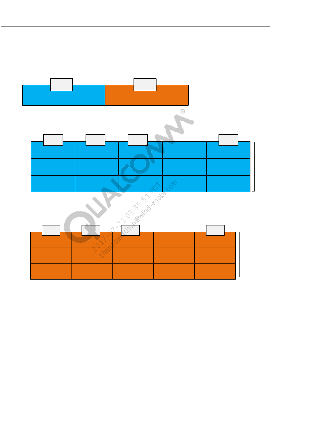
Configuration Guide for Display Drivers (ACPI and XML) Display-specific ACPI methods
80-NB116-2 G Confidential and Proprietary – Qualcomm Technologies, Inc. 95
MAY CONTAIN U.S. AND INTERNATIONAL EXPORT CONTROLLED INFORMATION
Return
This method returns a response buffer containing the panel gamut mapping table data.
Table data header:
NumSamplesPerColorComponent
32 bits
NumSegmentsPerColor
32 bits
3D Table:
Red_Comp[0]
16 bits
... Red_Comp[N*N*N-1]
16 bits
Red_Comp[2]
16 bits
Green_Comp[0] Green_Comp[2] ... Green_Comp[N*N*N-
1]
Blue_Comp[0] Blue_Comp[1] Blue_Comp[2] ... Blue_Comp[N*N*N-1]
Up to 17 entries.
173 * 2 Bytes per row
(Component)
Red_Comp[0]
Green_Comp[0]
16 bits
Segment Table:
Sg_Red_Comp[0]
32 bits
... Sg_Red_Comp[N-2]
32 bits
Sg_Green_Comp[0] Sg_Green_Comp[2] ... Sg_Green_Comp[N-2]
Sg_Blue_Comp[0] Sg_Blue_Comp[1] Sg_Blue_Comp[2] ... Sg_Blue_Comp[N-2]
Up to 16 segments (per 173 table)
16 * 4 bytes per row (color
componet)
Sg_Red_Comp[0]
Sg_Green_Comp[0]
32 bits
Sg_Red_Comp[2]
32 bits
The maximum buffer size is = 3 x(17 - 1) x 4 + 3 x 17 x 17 x 17 x 2 + 8 = 29678 bytes.
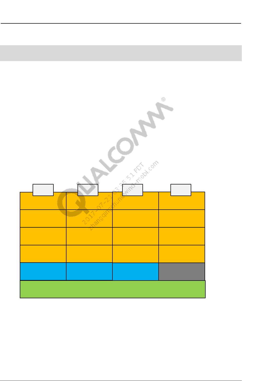
Configuration Guide for Display Drivers (ACPI and XML) Display-specific ACPI methods
80-NB116-2 G Confidential and Proprietary – Qualcomm Technologies, Inc. 96
MAY CONTAIN U.S. AND INTERNATIONAL EXPORT CONTROLLED INFORMATION
15.4.10 Panel Dithering Table (DITH)
NOTE: This section was added to this document revision.
The data for DITH should be stored in the buffer inside the DITH method for primary display and
DITX, where X = 2, 3.. N for other internal panel. Dithering matrix can have one of the two
formats.
Primary display method: DITH()
Other internal display method: DITX(), where X = 2, 3…N. 2 for secondary, 3
for third etc
Parameters
None
Return
This method returns a response buffer containing the panel dithering data.
Format 1:
Element[0,0]
8 Bits
Element[0,3]
Element[0,2]
8 Bits
Element[1,0]Element[1,2] Element[1,3]
Element[2,0] Element[2,1]Element[2,2] Element[2,3]
Element[0,1]
Element[1,1]
8 Bits 8 Bits
Element[3,0] Element[3,1] Element[3,2] Element[3,3]
Bit Depth C2 Bit Depth C1 Bit Depth C0 Reserved
Dithering mode (4 bytes) (0: reserved, 1:Spatial, 2:Temporal)
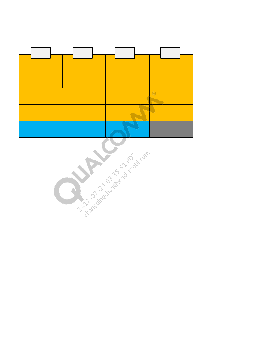
Configuration Guide for Display Drivers (ACPI and XML) Display-specific ACPI methods
80-NB116-2 G Confidential and Proprietary – Qualcomm Technologies, Inc. 97
MAY CONTAIN U.S. AND INTERNATIONAL EXPORT CONTROLLED INFORMATION
Format 2:
Element[0,1] Element[0,2]
Element[1,1]
Element[0,0]
8 Bits
Element[0,3]
8 Bits
Element[1,0] Element[1,2] Element[1,3]
Element[2,0] Element[2,1] Element[2,2] Element[2,3]
8 Bits 8 Bits
Element[3,0] Element[3,1] Element[3,2] Element[3,3]
Bit Depth C2 Bit Depth C1 Bit Depth C0 Reserved
There is no dithering mode in Format 2. Default dither mode: spatial.

80-NB116-2 G Confidential and Proprietary – Qualcomm Technologies, Inc. 98
MAY CONTAIN U.S. AND INTERNATIONAL EXPORT CONTROLLED INFORMATION
16 Registry key entries
The following Windows registry keys can be used to configure the display driver further.
NOTE: The following registry keys come into effect during bootup.
16.1 CABL
To disable CABL completely, use the following registry key, if this is set to 1, CABL cannot be
enabled in the software. When this entry is removed or is set to 0 then CABL can be enabled as
normal by the OS.
[HKEY_LOCAL_MACHINE\SOFTWARE\QCOM\Drivers\DxKMD\Miniport\BACKLIGHT]
"DisableCABL"=dword:00000001
16.2 SBC
To disable Smooth Backlight Control (SBC) completely, use the following registry key. Note that
after this entry is set to 1, SBC cannot be enabled in the software. When this entry is removed or
is set to 0, SBC can be enabled as normal by the OS.
[HKEY_LOCAL_MACHINE\SOFTWARE\QCOM\Drivers\DxKMD\Miniport\BACKLIGHT]
"DisableSBC"=dword:00000001
16.3 AVI info frame packet
The DisableAviInfoFramePacket registry key can be used to enable and disable AVI Info
Frame Packet. By default, AVI Info Frame Packet is enabled. After changing the register key
value, the system must be rebooted to ensure that the registry key takes effect. If both the ACPI
table and the registry key control the AVI Info Frame Packet enable/disable, the registry key will
come into effect.
[HKEY_LOCAL_MACHINE\SOFTWARE\QCOM\Drivers\DxKMD\Miniport\Display]
"DisableAviInfoFramePacket"=dword:00000001

Configuration Guide for Display Drivers (ACPI and XML) Registry key entries
80-NB116-2 G Confidential and Proprietary – Qualcomm Technologies, Inc. 99
MAY CONTAIN U.S. AND INTERNATIONAL EXPORT CONTROLLED INFORMATION
16.4 HDCP
The EnableHDCPInQDI registry key can be used to always enable HDCP. By default, HDCP is
not enabled, and it can be enabled by Microsoft’s video player. After changing the register key
value, the system must be rebooted to make this registry key take effect. If both the ACPI table
and the registry key control HDCP enable/disable, the registry key will come into effect.
[HKEY_LOCAL_MACHINE\SOFTWARE\QCOM\Drivers\DxKMD\Miniport\Display]
" EnableHDCPInQDI"=dword:00000001
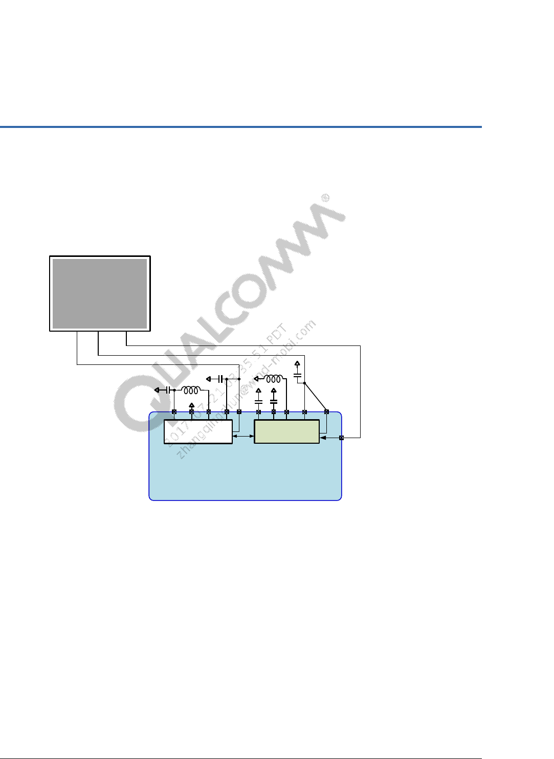
80-NB116-2 G Confidential and Proprietary – Qualcomm Technologies, Inc. 100
MAY CONTAIN U.S. AND INTERNATIONAL EXPORT CONTROLLED INFORMATION
17 OLED power
The display can be powered by the PMIC inverting buck boost (IBB) and LCD/AMOLD Boost
(LAB) modules, shown in Figure 17-1, which supply special voltages. More detailed information
and configuration of the PMIC IBB and LAB modules can be found in the LCD AMOLED Boost
(LAB) and Inverting Buck-Boost Module (80-NJ118-15).
LCD/AMOLED Boost
Converter (LAB)
PMIC
LCD/AMOLED
DISPLAY
VPH_PWR
VSWP
VDISP
Inverting Buck-Boost
Converter (IBB)
VDISN
VSWN
L1
C1 L2
VDISN_FB
VDISP_FB
C2
VPH_PWR
C3
VDISP
VDISN
SWIRE
CREF
CAP_REF
C4
SCTRL
Figure 17-1 PMIC IBB and LAB modules
Configuration Guide for Display Drivers (ACPI and XML) OLED power
80-NB116-2 G Confidential and Proprietary – Qualcomm Technologies, Inc. 101
MAY CONTAIN U.S. AND INTERNATIONAL EXPORT CONTROLLED INFORMATION
The display driver can be configured to manage these power supplies. Table 17-1 lists the
configuration for IBB/LAB management.
Table 17-1 IBB/LAB management configuration
Tag Description
PMIPowerPmicModel This selects the PMIC module ID that is used to manage IBB/LAB supplies.
Typically, this would be the PMI module that is paired with the PMIC, for
example, on the MSM8994, QDI_PMIC_DEVICEID_8994I (10) should be
used.
Value (decimal) Definition
1 QDI_PMIC_DEVICEID_8921
2 QDI_PMIC_DEVICEID_8038
3 QDI_PMIC_DEVICEID_8941
4 QDI_PMIC_DEVICEID_8841
5 QDI_PMIC_DEVICEID_8026
6 QDI_PMIC_DEVICEID_8926
7 QDI_PMIC_DEVICEID_8084
8 QDI_PMIC_DEVICEID_8962
9 QDI_PMIC_DEVICEID_8994
10 QDI_PMIC_DEVICEID_8994I (PMI8994)
11 QDI_PMIC_DEVICEID_8916
12 QDI_PMIC_DEVICEID_8110
13 QDI_PMIC_DEVICEID_8909
14 QDI_PMIC_DEVICEID_8950
15 QDI_PMIC_DEVICEID_8950I (PMI8950)
PMIPowerPmicNum This value is reserved and should not be used.
PMIPowerConfig This selects the configuration of the PMI module, as multiple configurations
can be used depending on the platform.
Warning: Selecting the wrong value can damage the panel and/or the
PMIC.
Value
(decimal) Definition
0 QDI_PMIC_INTERFACE_CONTROLTYPE_NONE
The module is not in use.
1 QDI_PMIC_INTERFACE_CONTROLTYPE_IBB_LAB_LCD
IBB/LAB power supplies are enabled, using LCD voltages.
2 QDI_PMIC_INTERFACE_CONTROLTYPE_IBB_LAB_OLED
IBB/LAB power supplies are enabled, using OLED voltages.

80-NB116-2 G Confidential and Proprietary – Qualcomm Technologies, Inc. 102
MAY CONTAIN U.S. AND INTERNATIONAL EXPORT CONTROLLED INFORMATION
A Specifying the I2C connection in
graphics.asl
To add the I2C connection resource in graphics.asl, the resource information is added in
platform.xml. The GfxXMLToACPI.pl script is used to generate the updated graphics.asl.
The example entry in platform.xml to specify the I2C connection configuration between the
MSM and the panel EEPROM for reading EDID is shown below.
<!-- Dynamic EDID I2c Slave -->
<Resource>
<Owner>DISPLAY</Owner>
<Name>I2C_DYNAMICEDID_SLAVE</Name>
<Type>I2C</Type>
<AddressingMode>AddressingMode7Bit</AddressingMode>
<ConnectionSpeed>100000</ConnectionSpeed>
<SlaveAddress>0x50</SlaveAddress>
<SlaveMode>ControllerInitiated</SlaveMode>
<ResourceSource>\\_SB.IC10</ResourceSource>
<Comment>I2C Slave used to read EDID information</Comment>
</Resource>
Table A-1 lists the XML tags and their corresponding descriptions.
Table A-1 XML tags and descriptions
Tag Description
Owner Display is the owner of this resource; this field should be used as is
Name Name of the I2C connection resource; this field should be used as is
Type
Resource type
AddressingMode To specify 7-bit or 10-bit addressing mode; refer to the ACPI Specification for
details
ConnectionSpeed
Maximum connection speed in Hertz
SlaveAddress I2C bus address for this connection
SlaveMode Can be either Controller initiated or Device initiated; see Advanced
Configuration and Power Interface Specification (Revision 5.0 (December
2011)) for more information
ResourceSource Indicates the GSBI port

80-NB116-2 G Confidential and Proprietary – Qualcomm Technologies, Inc. 103
MAY CONTAIN U.S. AND INTERNATIONAL EXPORT CONTROLLED INFORMATION
B Sample ACPI configuration for
DCS-based backlight control
///
// BLCP Method - Backlight control method, returns a
// command buffer for a specific backlight level
//
// Input Parameters
// Backlight level - Integer from 0% to 100%
//
// Output Parameters
//
// Packet format:
// +--32bits--+-----variable (8bit alignment)--+
// | Header | Packet payload |
// +----------+--------------------------------+
//
// For DSI Command packets, payload data must be in this format
//
// +-- 8 bits-+----variable (8bit alignment)----+
// | Cmd Type | Packet Data |
// +----------+---------------------------------+
//
// For I2C Command packets, payload data must be in this format
//
// +-- 16 bits-+----variable (8bit alignment)----+
// | Address | Command Data |
// +-----------+---------------------------------+
//
// All packets must follow with a DWORD header with 0x0
//
Method (BLCP, 1, NotSerialized) {
// Create Response buffer
Name(RBUF, Buffer(0x100){})

Configuration Guide for Display Drivers (ACPI and XML) Sample ACPI configuration for DCS-based...
80-NB116-2 G Confidential and Proprietary – Qualcomm Technologies, Inc. 104
MAY CONTAIN U.S. AND INTERNATIONAL EXPORT CONTROLLED INFORMATION
// Store the current byte index offset in local0
Store(0x0, LOCAL0)
// Create the packet header field
CreateField(RBUF, Multiply(LOCAL0, 8), 32, PKHR) // Create the packet
header
Add(LOCAL0, 4, LOCAL0) // Increment the data
pointer
// Create the packet payload field
CreateField(RBUF, Multiply(LOCAL0, 8), 32, PKPL) // Create the packet
payload
// Backlight programming packet
If (LEqual(Arg0, 0))
{
Name (BOFF, // Backlight off
Buffer() {0x15, // Command 15
0x53, 0x00}) // Turn off backlight
Store(Sizeof(BOFF), PKHR) // Store the size of the buffer in the
header
Store(BOFF, PKPL) // Store the packet payload
Add(LOCAL0, Sizeof(BOFF), LOCAL0) // Increment the offset
}
Else
{
If (LLessEqual(Arg0, 16)) // Level 0-16%
{
Name (BL1,
Buffer() {0x15,
0x51, 0x0C})

Configuration Guide for Display Drivers (ACPI and XML) Sample ACPI configuration for DCS-based...
80-NB116-2 G Confidential and Proprietary – Qualcomm Technologies, Inc. 105
MAY CONTAIN U.S. AND INTERNATIONAL EXPORT CONTROLLED INFORMATION
Store(Sizeof(BL1), PKHR) // Store the size of the buffer in the
header
Store(BL1, PKPL) // Store the packet payload
Add(LOCAL0, Sizeof(BL1), LOCAL0) // Increment the offset by the
packet size
}
ElseIf (LLessEqual(Arg0, 28)) // Level 17-28%
{
Name (BL2,
Buffer() {0x15,
0x51, 0x19})
Store(Sizeof(BL2), PKHR) // Store the size of the buffer in the
header
Store(BL2, PKPL) // Store the packet payload
Add(LOCAL0, Sizeof(BL2), LOCAL0) // Increment the offset by the
packet size
}
ElseIf (LLessEqual(Arg0, 40)) // Level 18-40%
{
Name (BL3,
Buffer() {0x15,
0x51, 0x33})
Store(Sizeof(BL3), PKHR) // Store the size of the buffer in the
header
Store(BL3, PKPL) // Store the packet payload
Add(LOCAL0, Sizeof(BL3), LOCAL0) // Increment the offset by the
packet size
}
ElseIf (LLessEqual(Arg0, 52)) // Level 41-52%
{
Name (BL4,
Buffer() {0x15,
0x51, 0x4C})

Configuration Guide for Display Drivers (ACPI and XML) Sample ACPI configuration for DCS-based...
80-NB116-2 G Confidential and Proprietary – Qualcomm Technologies, Inc. 106
MAY CONTAIN U.S. AND INTERNATIONAL EXPORT CONTROLLED INFORMATION
Store(Sizeof(BL4), PKHR) // Store the size of the buffer in the
header
Store(BL4, PKPL) // Store the packet payload
Add(LOCAL0, Sizeof(BL4), LOCAL0) // Increment the offset by the
packet size
}
ElseIf (LLessEqual(Arg0, 64)) // Level 53-64%
{
Name (BL5,
Buffer() {0x15,
0x51, 0x6D})
Store(Sizeof(BL5), PKHR) // Store the size of the buffer in the
header
Store(BL5, PKPL) // Store the packet payload
Add(LOCAL0, Sizeof(BL5), LOCAL0) // Increment the offset by the
packet size
}
ElseIf (LLessEqual(Arg0, 76)) // Level 65-76%
{
Name (BL6,
Buffer() {0x15,
0x51, 0x99})
Store(Sizeof(BL6), PKHR) // Store the size of the buffer in the
header
Store(BL6, PKPL) // Store the packet payload
Add(LOCAL0, Sizeof(BL6), LOCAL0) // Increment the offset by the
packet size
}
ElseIf (LLessEqual(Arg0, 88)) // Level 77-88%
{
Name (BL7,
Buffer() {0x15,
0x51, 0xD3})

Configuration Guide for Display Drivers (ACPI and XML) Sample ACPI configuration for DCS-based...
80-NB116-2 G Confidential and Proprietary – Qualcomm Technologies, Inc. 107
MAY CONTAIN U.S. AND INTERNATIONAL EXPORT CONTROLLED INFORMATION
Store(Sizeof(BL7), PKHR) // Store the size of the buffer in the
header
Store(BL7, PKPL) // Store the packet payload
Add(LOCAL0, Sizeof(BL7), LOCAL0) // Increment the offset by the
packet size
}
Else // Level 89-100%
{
Name (BL8,
Buffer() {0x15,
0x51, 0xFF})
Store(Sizeof(BL8), PKHR) // Store the size of the buffer in the
header
Store(BL8, PKPL) // Store the packet payload
Add(LOCAL0, Sizeof(BL8), LOCAL0) // Increment the offset by the
packet size
}
// Add additonal ON command
Name (BON, // Backlight on
Buffer() {0x15, // Command 15
0x53, 0x24}) // Manual backlight control
// Create the packet header field
CreateField(RBUF, Multiply(LOCAL0, 8), 32, PKH2) // Create the packet
header
Add(LOCAL0, 4, LOCAL0) // Increment the
data pointer
// Create the packet payload field
CreateField(RBUF, Multiply(LOCAL0, 8), 32, PKP2) // Create the packet
payload
Store(Sizeof(BON), PKH2) // Store the size of the buffer in
the header
Store(BON, PKP2) // Store the packet payload
Add(LOCAL0, Sizeof(BON), LOCAL0) // Increment the offset by the packet
size
}

Configuration Guide for Display Drivers (ACPI and XML) Sample ACPI configuration for DCS-based...
80-NB116-2 G Confidential and Proprietary – Qualcomm Technologies, Inc. 108
MAY CONTAIN U.S. AND INTERNATIONAL EXPORT CONTROLLED INFORMATION
// Add the End of Packet marker
CreateDWordField(RBUF, Multiply(LOCAL0, 8), EOP)
Store(0x0, EOP)
// Return the packet data
Return(RBUF)
}

80-NB116-2 G Confidential and Proprietary – Qualcomm Technologies, Inc. 109
MAY CONTAIN U.S. AND INTERNATIONAL EXPORT CONTROLLED INFORMATION
C References
C.1 Related documents
Title Number
Qualcomm Technologies, Inc.
LCD AMOLED Boost (LAB) and Inverting Buck-Boost Module
Hardware Software Application Note
80-NJ118-15
Resources
VESA Enhanced Extended Display Identification Data –
Implementation Guide Version 1.0 (June 2001)
VESA Enhanced Extended Display Identification Data Standard (Defines EDID Structure Version 1,
Revision 4) Release A, Revision 2
(September 2006)
MIPI Alliance Specification for D-PHY Version 1.00.00 (May 2009)
MIPI Alliance Specification for Display Serial Interface Version 1.02.00 (June 2010)
MIPI Alliance Specification for Display Serial Interface Version 1.03.00 (August 2011)
Advanced Configuration and Power Interface Specification Revision 5.0 (December 2011)
C.2 Acronyms and terms
Acronym or term Definition
ACPI Advanced Configuration and Power Interface
AD Assertive Display
BLLP Blanking low-power period
CABL Content adaptive backlight level
HBP Horizontal blanking period
HFP Horizontal front porch
HS High speed
HSA Horizontal sync active
HSIC High-Speed Inter-Chip Interface
HSP Horizontal sync period
KMD Kernel Mode Driver
PBRT Panel backlight response table
PGCT Panel gamma correction table
PGMT Panel gamut mapping table

Configuration Guide for Display Drivers (ACPI and XML) References
80-NB116-2 G Confidential and Proprietary – Qualcomm Technologies, Inc. 110
MAY CONTAIN U.S. AND INTERNATIONAL EXPORT CONTROLLED INFORMATION
Acronym or term Definition
PGRT Panel gamma response table
PIGC Panel inverse gamma correction
PPCC Panel color correction
PPGC Panel gamma correction
SBC Smooth backlight control
WDDM Windows Display Driver Model
