AN551 Crystal Selection Guide For Si5351
User Manual: Pdf
Open the PDF directly: View PDF ![]() .
.
Page Count: 16
Rev. 0.3 3/12 Copyright © 2012 by Silicon Laboratories AN551
AN551
CRYSTAL SELECTION GUIDE FOR Si5350/51 DEVICES
1. Introduction
The Si5350/51 Any-Frequency CMOS Clock Generator + VCXO features an onboard crystal oscillator and VCXO
that utilizes a standard, non-pullable 25/27 MHz crystal, PLLs, and MultiSynth fractional dividers to generate up to
eight unique non-integer-related frequencies with exact frequency (0 ppm error). The Si5350/51 also features
onboard crystal load capacitors ranging from 6 to 10 pF selectable through factory programming on the pin-
controlled Si5350 or via an I2C interface available on the Si5351.
This application note provides guidance on the selection of crystals that use the internal load capacitors or a
combination of internal and external load capacitors and describes the operation of the crystal oscillator and the
VCXO.
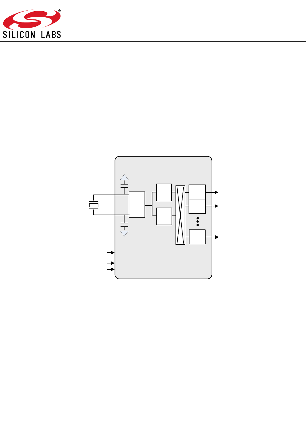
Figure 1. Si5351A Driven by a Standard, Non-Pullable Crystal
I2C
SSEN
OEB
XA
XB
OSC
Si5351A
Multi
Synth
N
Multi
Synth
0
Multi
Synth
1
PLLB
PLLA
CL1
L2
C
AN551
2 Rev. 0.3
2. Crystal Selection, Load Capacitors, and Layout Guidelines
2.1. Crystal Selection and Load Capacitors
The Si5350/51 supports both 25 MHz and 27 MHz crystals and has integrated crystal load capacitors, eliminating
the need for external components. Alternatively, the Si5350/51 can be configured to use a combination of internal
and external load capacitors.
2.1.1. Internal Load Capacitors
Since the Si5350/51 has onboard load capacitors, it is recommended to select crystals with load capacitance
specifications supported by the Si5350/51. For ease of use, Silicon Labs has qualified a number of crystals for use
with the Si5350/51.
Table 1 lists the crystals that have been qualified for use with the Si5350/51. The Si5350/51, however, can also
function with crystals that are not listed. In this case, select crystals with a load capacitance specification meeting
the Si5350/51 data sheet specifications, with an ESR rating less than 150, and housed in a 5x7 mm2 or smaller
package. Crystals packaged in an HC-49 metal can are not recommended for use with the Si5350/51.
2.1.2. External and Internal Load Capacitors
The Si5350/51 can use both internal and external load capacitors simultaneously to meet a crystal's load capacitor
requirement. When using both internal and external load capacitors, it is recommended that external load
capacitors of less than 2 pF and total load capacitance less than or equal to 12 pF be used to minimize additive
jitter associated with larger external capacitors.
Table 1. Si5350/51 Qualified Crystals
MFR PN Freq
(MHz) CL
(pF)
Accuracy
(ppm) Stability over Temp
(ppm)
Epson FA-238 25.0000MB-K 25 10 ±50 ±30
Kyocera CX3225SB25000D0FLJZ1 25 8 ±10 ±15
Kyocera CX3225SB27000D0FLJZ1 27 8 ±10 ±15
NDK NX3225GA-25.000M-STD-CRG-2 25 8 ±20 ±30
NDK NX3225GA-27.000M-STD-CRG-2 27 8 ±20 ±30
TXC 7M-27.000MEEQ 27 10 ±10 ±10
Sunny SP10115J6-25.000 MHz 25 10 ±15 ±30
Sunny SP10115J6-27.000 MHz 27 10 ±15 ±30
AN551
Rev. 0.3 3
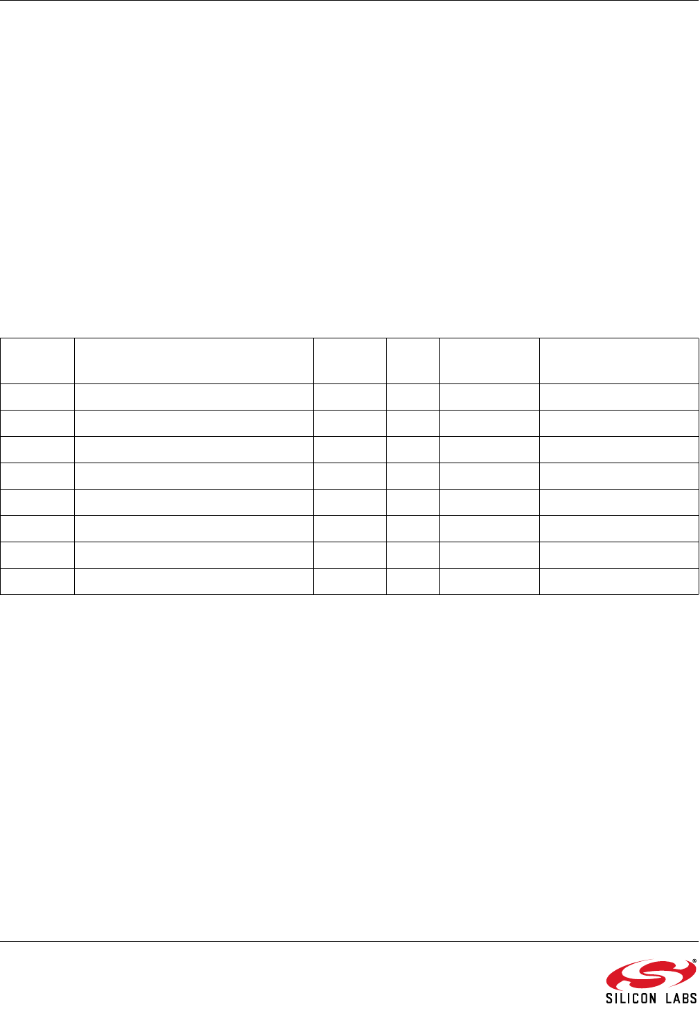
2.2. Layout Guidance
The Si5350/51's crystal oscillator is an analog circuit; so, layout of the crystal should follow analog rules. The
following is a list of general crystal layout guidelines.
1. Since the total load capacitance is the summation of PCB trace capacitance and pin capacitance at the XA and
XB pins, it is recommended that a crystal be placed as close to the Si5350/51 as possible to minimize parasitic
capacitance.
2. Minimize trace lengths to less than 9 mm.
3. Clocks and frequently switched signals should not be routed close to the crystal.
4. Crystal traces should be protected with ground traces and guard rings.
5. Guard rings should not be connected to other ground connections on the PCB.
6. When two-layer PCBs are used, digital signals should not be routed on the opposite side of the PCB directly
under the crystal.
7. It is recommended to fill the opposite side of the PCB under the crystal with a clean ground plane.
Figure 2. Si5350/51 Layout Example
1
2
3
4
5
6
7
8
9
10
15
14
13
12
11
20
19
18
17
16
GND
PAD
XA
XB
P0
P1
P2
P4
CLK3
CLK2
P3
CLK6
CLK5
CLK4
CLK1
CLK0
CLK7
VDD island for
the clock
Place crystal close to
the Si5350/51
Wide traces
VDD Decoupling Cap
Board Supply
VIAS GND
XTAL
AN551
4 Rev. 0.3
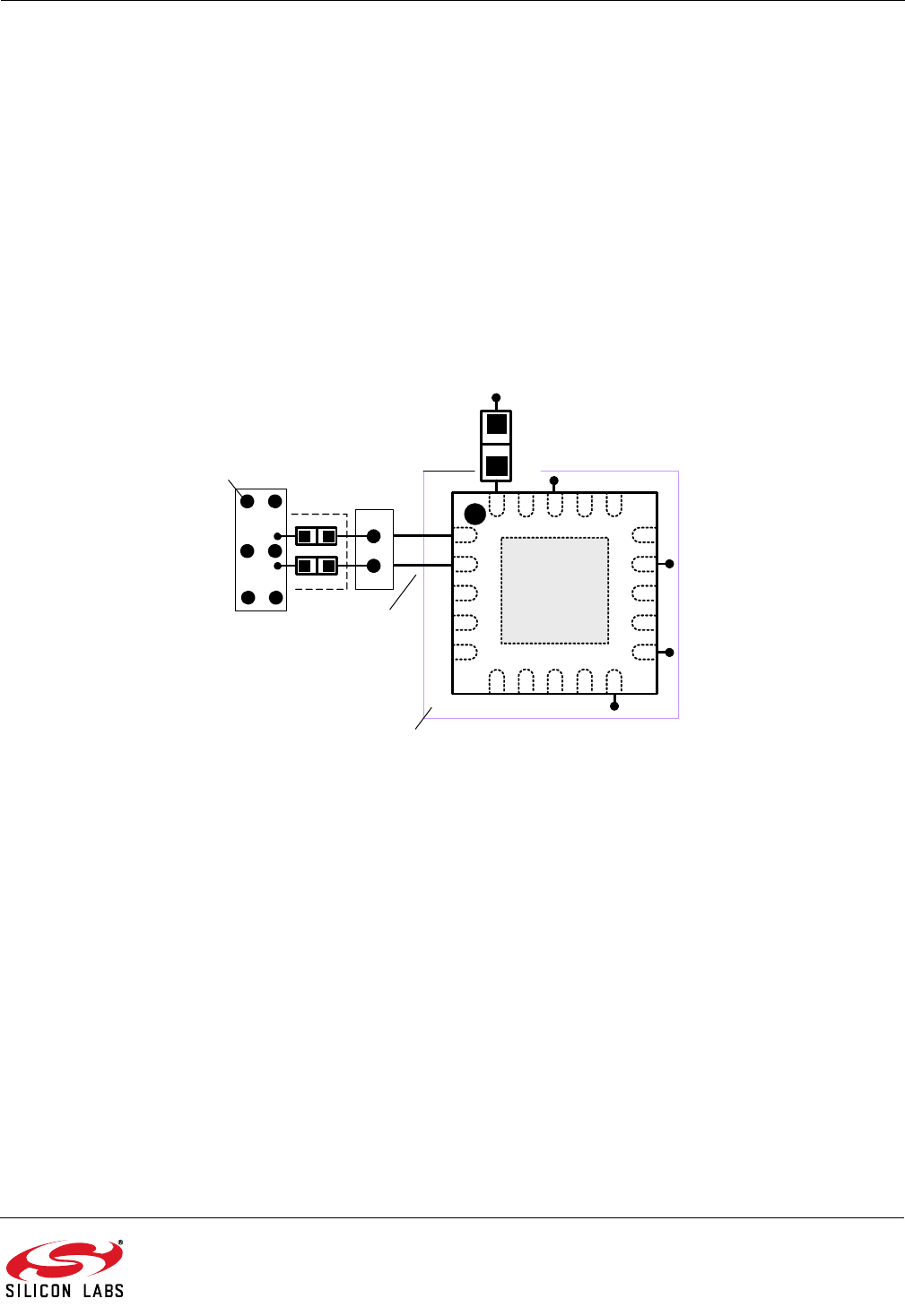
3. Crystal Oscillator
3.1. Oscillator Model
The Si5350/51 crystal oscillator is based on a Pierce Oscillator architecture as shown Figure 3. The oscillator
contains an Automatic Gain Control Circuit (AGC), which operates in high-gain and normal-gain modes. Upon
startup, the AGC is configured in high-gain mode and the amplifier generates a large negative resistance (–R) to
ensure crystal startup. Once a stable frequency of operation is achieved, the AGC is configured in normal gain
mode, and (–R) is lowered to maintain oscillation.
Figure 3. Si5350/51 Oscillator Circuit
When the crystal oscillator is in high-gain mode, the closed loop gain (GLP) around the loop is greater than 1 to
guarantee crystal start up. In normal gain mode, GLP is reduced to 1 to maintain oscillation.
Table 2. Crystal Oscillators Modes
Mode Gain Loop Gain
Startup High Gain, High (–R) GLP ≥ 1
Sustained Oscillation Normal Gain, Normal (–R) GLP =1
CL2
180
360
180
Amplifier
Loop Gain = 1
CL1
AN551
Rev. 0.3 5
3.2. Oscillator Accuracy
The Si5350/51 output accuracy depends on the reference clock, crystal, and mismatch between the external and
internal load capacitance. Accuracy does not depend on the Si5350/51 PLLs since it is able to generate any
combination of output frequencies exactly to (0 ppm) frequency synthesis error.
The generated output frequency accuracy can be modeled using a simple equivalent electrical circuit. The
motional inductance and motional capacitance determine the resonant frequency.
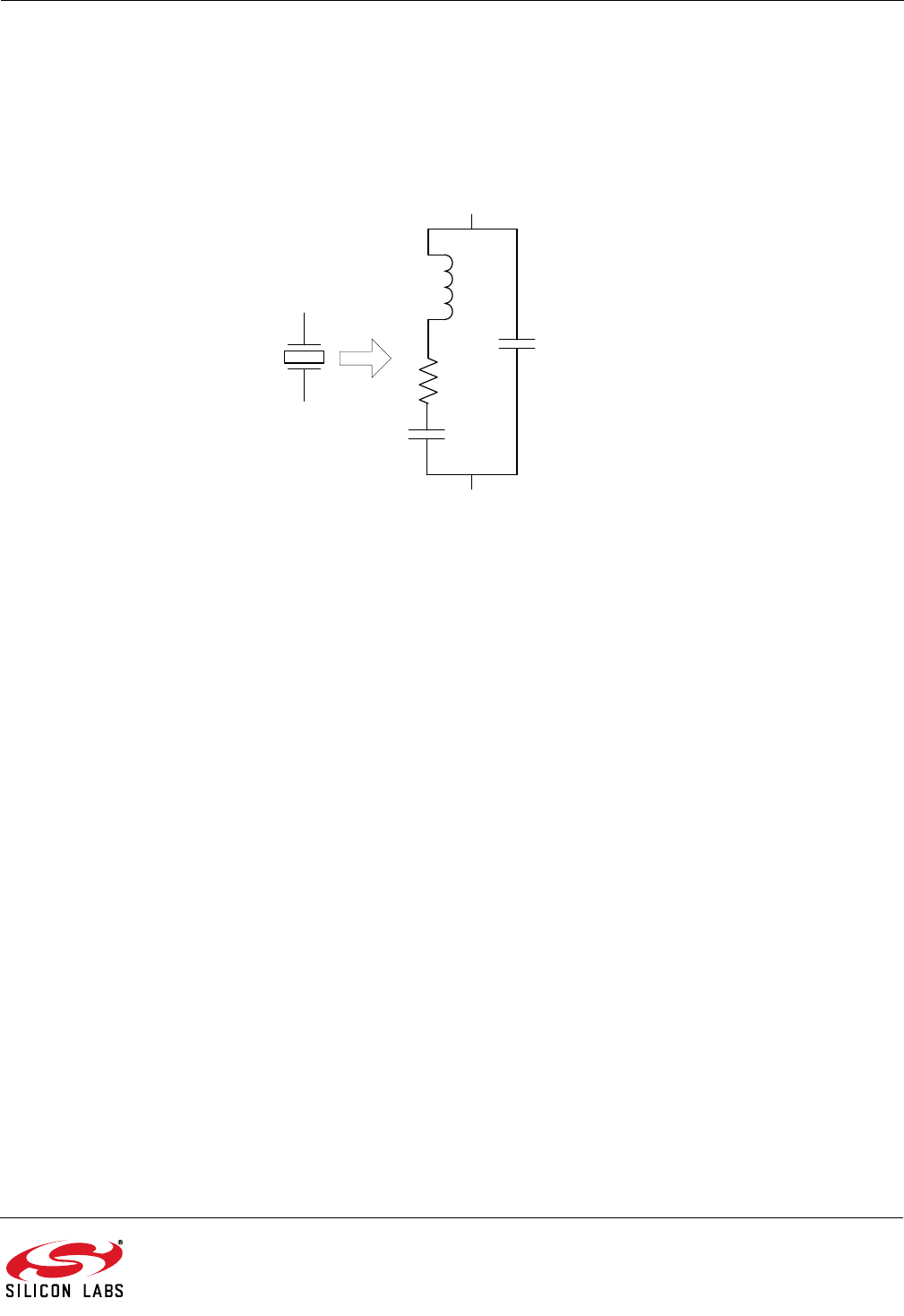
Figure 4. Equivalent Crystal Model
From this model, the frequency of the crystal oscillator can be modelled as Equation 1. Equation 1 accounts for the
inaccuracy caused by the mismatched capacitor loading and takes into account factors including packaging
capacitance and total load capacitance.
Equation 1. Crystal Oscillator Frequency
Based on this equation, when the total capacitance is less than a crystal’s load specification, the output frequency
is less than the target frequency. In addition, when the total capacitance is greater than a crystal’s load
specification, the output frequency is greater than its target frequency. Table 3 summarizes the various cases of
total load vs. accuracy.
C1
C0
Lm
R
Symbols:
Crystal Resistance: R
Motional Inductance/Capacitance: LM, C1
Packaging Capacitance: C0
fOUTPUT fCRYSTAL 1C1
2
-------1
C0CSPEC
+
------------------------------- 1
C0CCTL
+
---------------------------
+
–
Symbols:
Crystal Oscillator Frequency: fOUTPUT
Crystal Frequency: fCRYSTAL
Crystal Load Capacitance Specification: CSPEC
Total Crystal Load Capacitance: CTL
Package Capacitance: C0
Motional Capacitance: C1
=
AN551
6 Rev. 0.3
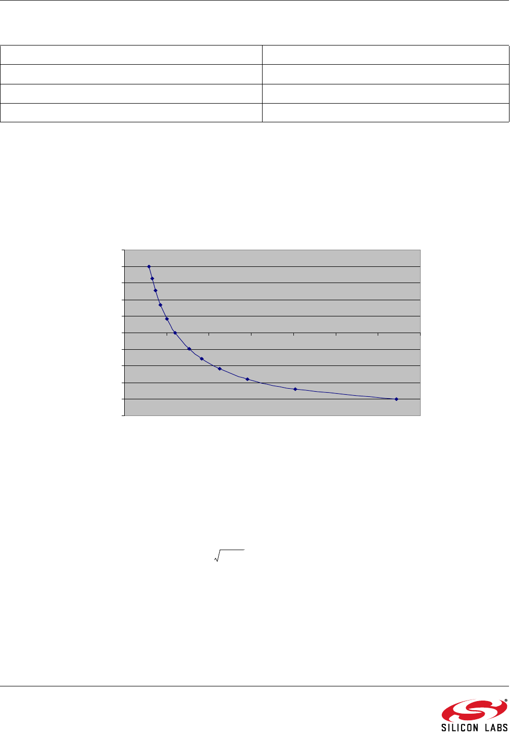
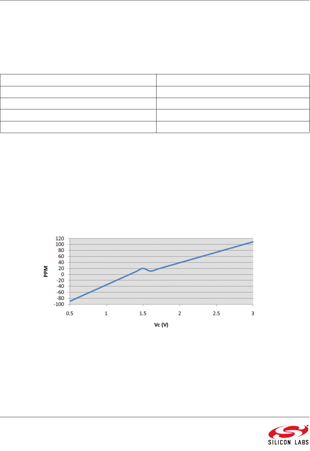
The following example illustrates this relationship. Figure 5 summarizes the measured crystal frequency results
when an Si5350/51 was tested with a 12 pF crystal. The load was varied, and the crystal frequency was
determined. When the total crystal load was 12 pF, the generated frequency was 0 ppm; when the total crystal load
was less than 12 pF, the generated frequency was greater than 0 ppm, and when the total crystal load was greater
than 12 pF, the generated frequency was less than 0 ppm. Further, it is recommended that crystals with a total
crystal load capacitance less than or equal 12 pF be used.
Figure 5. Crystal Driver Frequency vs. Crystal Load
3.3. Reactance
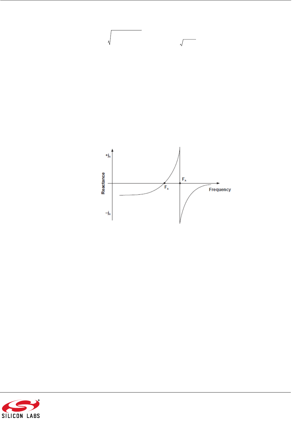
Electrically, a crystal is a series resonant circuit, and the reactance of the crystal is a function of its frequency. A
crystal's reactance is 0 at both the series resonant frequency (fS) and parallel resonant frequency (fP). fS
depends on C1 and LM, given by Equation 2.
Equation 2. Series Resonant Frequency
Table 3. Crystal Accuracy vs. Load Capacitance
Case Accuracy
CSPEC =C
TL 0ppm
CSPEC > CTL –ppm
CSPEC < CTL +ppm
ppm vs. CL
-250
-200
-150
-100
-50
0
50
100
150
200
250
0 10203040506070
CL(pF)
ppm
fs
1
2LmC1
---------------------------
""
Symbols:
Series Resonance Frequency: FS
Motional Inductance: LM
Motional Capacitance: C1
=
AN551
Rev. 0.3 7
FP is like FS, but FP takes into account the packaging capacitance, C0, and is given by Equation 3.
Equation 3. Parallel Resonant Frequency
As shown in Figure 6, negative reactance effectively looks inductive, and positive reactance effectively looks
capacitive.
Figure 6. Crystal Effective Reactance
3.4. ESR Value
When selecting a crystal, a crystal’s equivalent series resistance value (ESR) is an important parameter to
consider. ESR depends on RM, C0, and CL, where CL is the required load capacitance of a crystal and is calculated
by Equation 4. Note that the Si5350/51 can be used with crystals with an ESR greater than 150 .
Equation 4. Equivalent Series Resistance
fPfS1C1
C0CL
+
-------------------------
+ , where fS
1
2LMC1
--------------------------
Symbols:
Parallel/Series Resonant Frequency: fPfS
Motional Inductance/Capacitance: LMC1
Packaging Capacitance: C0
==
ESR RM1C0
CL
-------
+
2
Symbols:
Electrical Series Resistance: ESR
Packaging Resistance: RM
Packaging Capacitance: C0
Specified Load Capacitance: CL
=
AN551
8 Rev. 0.3
ESR represents the loss of the crystal oscillator. Smaller crystals (especially crystals housed in SMD packages)
tend to have larger ESR values. A higher ESR value represents higher loss. If the ESR value is too high, the crystal
oscillator may fail to start, become unstable, or even stop oscillating. The (–R) of the Si5350/51's crystal oscillator
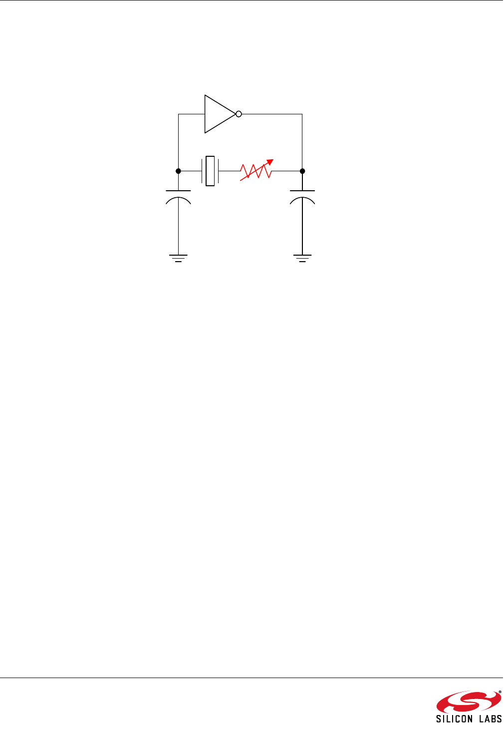
is used to overcome the ESR of a crystal. (–R) of the Si5350/51 can be determined by adding a resistor in series
with a crystal as show in Figure 7.
Figure 7. (–R) Test
In order to determine the (–R) of the crystal oscillator, the series resistance (RQ) is slowly increased until the
oscillator fails to start up or fails to sustain oscillation. RQ can be realized with an SMD potentiometer. The (–R) test
is performed by the startup and stop procedures described below.
3.4.1. Test 1: Startup Test Procedure
1. Place an SMD resistor (RQ) in series with the crystal.
2. Power-on the device, and check if oscillation begins. Then, repeat the test by slowly incrementing the resistor
value until the Si5350/51 fails to start.
3. The highest value resistor when the Si5350/51 fails to start is the startup value, RQ.
3.4.2. Test 2: Stop Test Procedure
1. While the Si5350/51 is running, increase the resistor value until oscillation stops.
2. Once oscillation stops, reduce RQ until oscillation starts.
3. The highest RQ value with which the oscillator runs is the stop value.
4. The stop value should be equal to the startup value, RQ.
Once RQ is determined, the Safety Factor (SF) shown in Equation 5 determines whether the crystal driver has
enough (–R) to start the crystal and sustain oscillation.
Equation 5. Safety Factor Equation
CL2
RQ
CL1
SF RQESR+
ESR
---------------------------
""
Symbols:
Safety: SF
Critical Resistance: RQ
Electrical Series Resistance: ESR
=
AN551
Rev. 0.3 9
An SF value of (SF > 5) is needed to ensure stable oscillation. In addition, because the Si5350/51 crystal oscillator
has an AGC, it is safe to operate the Si5350/51 with (SF >> 10). Table 4 summarizes the various ranges of SF
values.
3.5. Negative Resistance
The (–R) was determined for the Si5350/51 using various crystals with different packaging capacitance (C0). The
data below illustrates the (–R) as a function of C0.
3.5.1. CL = 6 pF
Table 4. Safety Factor Values
SF Value Qualification
SF ≥ 5 Minimum Safe Value
SF >> 10 Very Safe Value
Table 5. R1, C0 Requirement—27 MHz Crystal (Safety Factor = 1)
Startup and Steady State – C0 (pF) ESR ()
5337
4.5 385
4445
3.5 517
3606
2.5 716
2852
Table 6. R1, C0 Requirement—25 MHz Crystal (Safety Factor = 1)
Startup and Steady State – C0 (pF) ESR ()
5356
4.5 410
4476
3.5 557
3659
2.5 787
2948
AN551
10 Rev. 0.3
3.5.2. CL = 8 pF
Table 7. R1, C0 Requirement—27 MHz Crystal (Safety Factor = 1)
Startup and Steady State – C0 (pF) ESR ()
5333
4.5 368
4409
3.5 455
3508
2.5 568
2637
Table 8. R1, C0 Requirement—25 MHz Crystal (Safety Factor = 1)
Startup and Steady State – C0 (pF) ESR ()
5367
4.5 408
4456
3.5 510
3573
2.5 646
2730
AN551
Rev. 0.3 11
3.5.3. CL = 10 pF
Table 9. R1, C0 Requirement—27 MHz Crystal (Safety Factor = 1)
Startup and Steady State – C0 (pF) ESR ()
5288
4.5 311
4336
3.5 365
3396
2.5 430
2468
Table 10. R1, C0 Requirement—25 MHz Crystal (Safety Factor = 1)
Startup and Steady State – C0 (pF) ESR ()
5326
4.5 353
4384
3.5 418
3456
2.5 497
2543
AN551
12 Rev. 0.3
4. VCXO
The Si5350/51 VCXO is an advancement in VCXO technology because it modulates the PLL parameters instead
of pulling a crystal to generate the VCXO pull curve. Since the Si5350/51’s VCXO does not pull a crystal, the
Si5350/51 eliminates the need for high-cost, custom pullable crystals and provides multiple benefits outlined in
Table 11.
With competing VCXOs, the following crystal parameters must be considered:
1. C0/C1 ratio
2. Max drive level
3. Mechanical third overtone and location of associated harmonic spurs
It has been determined that, if a crystal does not have an adequate C0/C1 ratio (for competitor’s VCXO),
undesirable results can be generated as shown in Figure 8. In contrast, the Si5350/51 makes use of standard, non-
pullable, low-cost crystals; therefore, special consideration is not required. In addition, the Si5350/51 VCXO has
been designed so that the performance of the pull curve does not vary with temperature, supply voltage, or the
model of crystal used. Further, the VCXO pull curve can be generated directly from a clock signal on the Si535xC
since the Si5350/51 does not pull a crystal like competing devices.
Figure 8. Competitors VCXO “Bump”
Further, because the Si5350/51 VCXO function changes the PLL parameters, the resulting VCXO transfer function
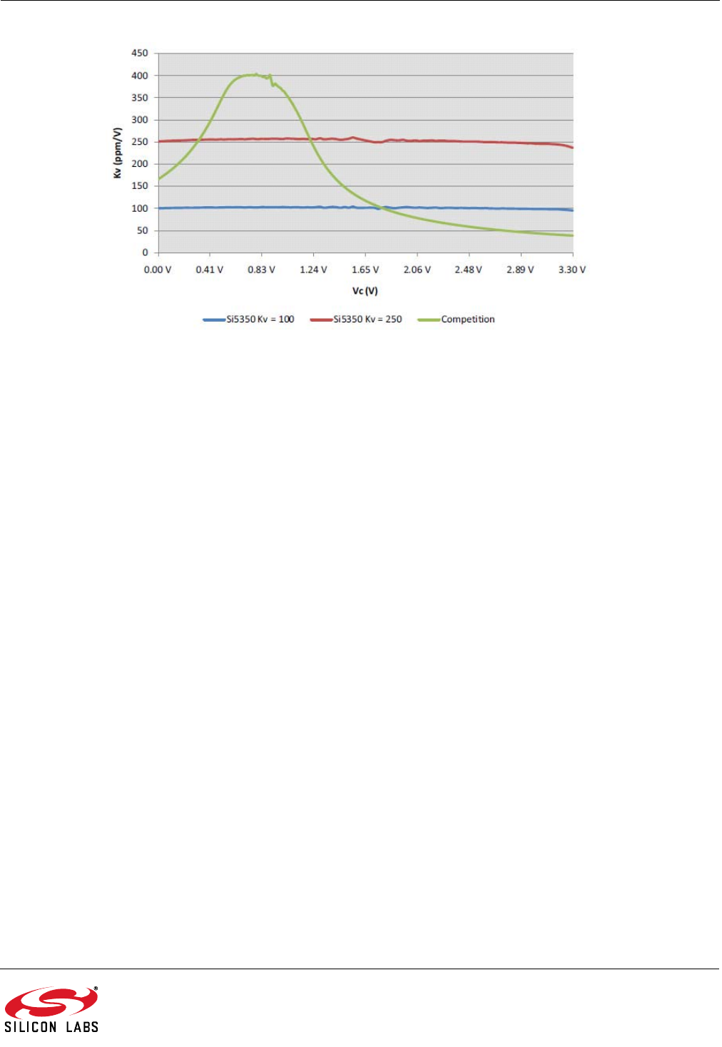
is substantially more linear than competing devices which "pull" the crystal. Figure 9 shows the actual measured
linearity of the Si5350/51 compared to the competition.
Table 11. Si5350/51 VCXOs vs Conventional VCXOs
Conventional VCXOs Si5350/51 VCXO
High cost, custom pullable crystal Standard, low cost, non-pullable crystal
Vactor-based non-linearity limits operating range Highly linear range: 10–90 VDD
Potential crystal startup issues Reliable startup and operation
Limited crystal sourcing options Simplified crystal sources
AN551
Rev. 0.3 13
Figure 9. KVCO Comparison of the Si5350/51 vs Competing Solutions
Equation 6. Equivalent Crystal Load Capacitance
4.1. Crystal Manufacturers
http://www.eea.epson.com
http://global.kyocera.com/index.html
http://www.ndk.com/en
http://www.txc.com.tw
http://www.sunny-usa.com
CL
CL1 CL2
CL1 CL2
+
--------------------------
=
AN551
14 Rev. 0.3
DOCUMENT CHANGE LIST
Revision 0.1 to Revision 0.2
Added "2.2. Layout Guidance" on page 3.
Added "3.1. Oscillator Model" on page 4 to illustrate
startup gain vs. sustained oscillation gain.
Updated "3.2. Oscillator Accuracy" on page 5.
Added "3.4. ESR Value" on page 7.
Revision 0.2 to Revision 0.3
In “3.5. Negative Resistance” text, replaced
“motional” with “packaging.”
AN551
Rev. 0.3 15
NOTES:
Disclaimer
Silicon Laboratories intends to provide customers with the latest, accurate, and in-depth documentation of all peripherals and modules available for system and software implementers
using or intending to use the Silicon Laboratories products. Characterization data, available modules and peripherals, memory sizes and memory addresses refer to each specific
device, and "Typical" parameters provided can and do vary in different applications. Application examples described herein are for illustrative purposes only. Silicon Laboratories
reserves the right to make changes without further notice and limitation to product information, specifications, and descriptions herein, and does not give warranties as to the accuracy
or completeness of the included information. Silicon Laboratories shall have no liability for the consequences of use of the information supplied herein. This document does not imply
or express copyright licenses granted hereunder to design or fabricate any integrated circuits. The products must not be used within any Life Support System without the specific
written consent of Silicon Laboratories. A "Life Support System" is any product or system intended to support or sustain life and/or health, which, if it fails, can be reasonably expected
to result in significant personal injury or death. Silicon Laboratories products are generally not intended for military applications. Silicon Laboratories products shall under no
circumstances be used in weapons of mass destruction including (but not limited to) nuclear, biological or chemical weapons, or missiles capable of delivering such weapons.
Trademark Information
Silicon Laboratories Inc., Silicon Laboratories, Silicon Labs, SiLabs and the Silicon Labs logo, CMEMS®, EFM, EFM32, EFR, Energy Micro, Energy Micro logo and combinations
thereof, "the world’s most energy friendly microcontrollers", Ember®, EZLink®, EZMac®, EZRadio®, EZRadioPRO®, DSPLL®, ISOmodem ®, Precision32®, ProSLIC®, SiPHY®,
USBXpress® and others are trademarks or registered trademarks of Silicon Laboratories Inc. ARM, CORTEX, Cortex-M3 and THUMB are trademarks or registered trademarks of
ARM Holdings. Keil is a registered trademark of ARM Limited. All other products or brand names mentioned herein are trademarks of their respective holders.
http://www.silabs.com
Silicon Laboratories Inc.
400 West Cesar Chavez
Austin, TX 78701
USA
ClockBuilder Pro
One-click access to Timing tools,
documentation, software, source
code libraries & more. Available for
Windows and iOS (CBGo only).
www.silabs.com/CBPro
Timing Portfolio
www.silabs.com/timing SW/HW
www.silabs.com/CBPro Quality
www.silabs.com/quality Support and Community
community.silabs.com
