ARM V7 M Architecture Application Level Reference Manual ARMv7
ARM-ARMv7-ReferenceManual
ARM-ARMv7-ReferenceManual
ARM-ARMv7-ReferenceManual
ARM-ARMv7-ReferenceManual
ARM-ARMv7-ReferenceManual
User Manual: Pdf
Open the PDF directly: View PDF ![]() .
.
Page Count: 534 [warning: Documents this large are best viewed by clicking the View PDF Link!]
- ARM v7-M Architecture Application Level Reference Manual
- Contents
- Preface
- Application
- Introduction
- Application Level Programmer’s Model
- ARM Architecture Memory Model
- A3.1 Address space
- A3.2 Alignment Support
- A3.3 Endian Support
- A3.4 Synchronization and semaphores
- A3.4.1 Exclusive access instructions and Non Shared memory regions
- A3.4.2 Exclusive access instructions and shared memory regions
- A3.4.3 Size of the tagged memory block
- A3.4.4 Context switch support
- A3.4.5 Load-Exclusive and Store-Exclusive usage restrictions
- A3.4.6 Synchronization primitives and the memory order model
- A3.5 Memory types
- A3.6 Access rights
- A3.7 Memory access order
- A3.7.1 Read and write definitions
- A3.7.2 Observability and completion
- A3.7.3 Ordering requirements for memory accesses
- A3.7.4 Program order for instruction execution
- A3.7.5 Memory barriers
- A3.7.6 Data Memory Barrier (DMB)
- A3.7.7 Data Synchronization Barrier (DSB)
- A3.7.8 Instruction Synchronization Barrier (ISB)
- A3.8 Caches and memory hierarchy
- A3.9 Bit banding
- The Thumb Instruction Set
- A4.1 Instruction set encoding
- A4.2 Instruction encoding for 16-bit Thumb instructions
- A4.3 Instruction encoding for 32-bit Thumb instructions
- A4.3.1 Data processing instructions: immediate, including bitfield and saturate
- A4.3.2 Data processing instructions, non-immediate
- A4.3.3 Load and store single data item, and memory hints
- A4.3.4 Load/store double and exclusive, and table branch
- A4.3.5 Load and store multiple
- A4.3.6 Branches, miscellaneous control instructions
- A4.3.7 Coprocessor instructions
- A4.4 Conditional execution
- A4.5 UNDEFINED and UNPREDICTABLE instruction set space
- A4.6 Usage of 0b1111 as a register specifier
- A4.7 Usage of 0b1101 as a register specifier
- Thumb Instructions
- A5.1 Format of instruction descriptions
- A5.2 Immediate constants
- A5.3 Constant shifts applied to a register
- A5.4 Memory accesses
- A5.5 Memory hints
- A5.6 NOP-compatible hints
- A5.7 Alphabetical list of Thumb instructions
- A5.7.1 ADC (immediate)
- A5.7.2 ADC (register)
- A5.7.3 ADD (immediate)
- A5.7.4 ADD (register)
- A5.7.5 ADD (SP plus immediate)
- A5.7.6 ADD (SP plus register)
- A5.7.7 ADR
- A5.7.8 AND (immediate)
- A5.7.9 AND (register)
- A5.7.10 ASR (immediate)
- A5.7.11 ASR (register)
- A5.7.12 B
- A5.7.13 BFC
- A5.7.14 BFI
- A5.7.15 BIC (immediate)
- A5.7.16 BIC (register)
- A5.7.17 BKPT
- A5.7.18 BL
- A5.7.19 BLX (register)
- A5.7.20 BX
- A5.7.21 CBNZ
- A5.7.22 CBZ
- A5.7.23 CDP, CDP2
- A5.7.24 CLREX
- A5.7.25 CLZ
- A5.7.26 CMN (immediate)
- A5.7.27 CMN (register)
- A5.7.28 CMP (immediate)
- A5.7.29 CMP (register)
- A5.7.30 CPS
- A5.7.31 CPY
- A5.7.32 DBG
- A5.7.33 DMB
- A5.7.34 DSB
- A5.7.35 EOR (immediate)
- A5.7.36 EOR (register)
- A5.7.37 ISB
- A5.7.38 IT
- A5.7.39 LDC, LDC2
- A5.7.40 LDMDB / LDMEA
- A5.7.41 LDMIA / LDMFD
- A5.7.42 LDR (immediate)
- A5.7.43 LDR (literal)
- A5.7.44 LDR (register)
- A5.7.45 LDRB (immediate)
- A5.7.46 LDRB (literal)
- A5.7.47 LDRB (register)
- A5.7.48 LDRBT
- A5.7.49 LDRD (immediate)
- A5.7.50 LDREX
- A5.7.51 LDREXB
- A5.7.52 LDREXH
- A5.7.53 LDRH (immediate)
- A5.7.54 LDRH (literal)
- A5.7.55 LDRH (register)
- A5.7.56 LDRHT
- A5.7.57 LDRSB (immediate)
- A5.7.58 LDRSB (literal)
- A5.7.59 LDRSB (register)
- A5.7.60 LDRSBT
- A5.7.61 LDRSH (immediate)
- A5.7.62 LDRSH (literal)
- A5.7.63 LDRSH (register)
- A5.7.64 LDRSHT
- A5.7.65 LDRT
- A5.7.66 LSL (immediate)
- A5.7.67 LSL (register)
- A5.7.68 LSR (immediate)
- A5.7.69 LSR (register)
- A5.7.70 MCR, MCR2
- A5.7.71 MCRR, MCRR2
- A5.7.72 MLA
- A5.7.73 MLS
- A5.7.74 MOV (immediate)
- A5.7.75 MOV (register)
- A5.7.76 MOV (shifted register)
- A5.7.77 MOVT
- A5.7.78 MRC, MRC2
- A5.7.79 MRRC, MRRC2
- A5.7.80 MRS
- A5.7.81 MSR (register)
- A5.7.82 MUL
- A5.7.83 MVN (immediate)
- A5.7.84 MVN (register)
- A5.7.85 NEG
- A5.7.86 NOP
- A5.7.87 ORN (immediate)
- A5.7.88 ORN (register)
- A5.7.89 ORR (immediate)
- A5.7.90 ORR (register)
- A5.7.91 PLD (immediate)
- A5.7.92 PLD (register)
- A5.7.93 PLI (immediate)
- A5.7.94 PLI (register)
- A5.7.95 POP
- A5.7.96 PUSH
- A5.7.97 RBIT
- A5.7.98 REV
- A5.7.99 REV16
- A5.7.100 REVSH
- A5.7.101 ROR (immediate)
- A5.7.102 ROR (register)
- A5.7.103 RRX
- A5.7.104 RSB (immediate)
- A5.7.105 RSB (register)
- A5.7.106 SBC (immediate)
- A5.7.107 SBC (register)
- A5.7.108 SBFX
- A5.7.109 SDIV
- A5.7.110 SEV
- A5.7.111 SMLAL
- A5.7.112 SMULL
- A5.7.113 SSAT
- A5.7.114 STC, STC2
- A5.7.115 STMDB / STMFD
- A5.7.116 STMIA / STMEA
- A5.7.117 STR (immediate)
- A5.7.118 STR (register)
- A5.7.119 STRB (immediate)
- A5.7.120 STRB (register)
- A5.7.121 STRBT
- A5.7.122 STRD (immediate)
- A5.7.123 STREX
- A5.7.124 STREXB
- A5.7.125 STREXH
- A5.7.126 STRH (immediate)
- A5.7.127 STRH (register)
- A5.7.128 STRHT
- A5.7.129 STRT
- A5.7.130 SUB (immediate)
- A5.7.131 SUB (register)
- A5.7.132 SUB (SP minus immediate)
- A5.7.133 SUB (SP minus register)
- A5.7.134 SVC (formerly SWI)
- A5.7.135 SXTB
- A5.7.136 SXTH
- A5.7.137 TBB
- A5.7.138 TBH
- A5.7.139 TEQ (immediate)
- A5.7.140 TEQ (register)
- A5.7.141 TST (immediate)
- A5.7.142 TST (register)
- A5.7.143 UBFX
- A5.7.144 UDIV
- A5.7.145 UMLAL
- A5.7.146 UMULL
- A5.7.147 USAT
- A5.7.148 UXTB
- A5.7.149 UXTH
- A5.7.150 WFE
- A5.7.151 WFI
- A5.7.152 YIELD
- System
- System Level Programmer’s Model
- System Address Map
- ARMv7-M System Instructions
- Debug
- Debug
- C1.1 Introduction to debug
- C1.2 The Debug Access Port (DAP)
- C1.3 Overview of the ARMv7-M debug features
- C1.4 Debug and reset
- C1.5 Debug event behavior
- C1.6 Debug register support in the SCS
- C1.7 Instrumentation Trace Macrocell (ITM) support
- C1.8 Data Watchpoint and Trace (DWT) support
- C1.9 Embedded Trace (ETM) support
- C1.10 Trace Port Interface Unit (TPIU)
- C1.11 Flash Patch and Breakpoint (FPB) support
- Pseudo-code definition
- AppxA.1 Instruction encoding diagrams and pseudo-code
- AppxA.2 Data Types
- AppxA.3 Expressions
- AppxA.4 Operators and built-in functions
- AppxA.5 Statements and program structure
- AppxA.6 Helper procedures and functions
- AppxA.6.1 ALUWritePC()
- AppxA.6.2 ArchVersion()
- AppxA.6.3 BadReg()
- AppxA.6.4 BigEndian()
- AppxA.6.5 BranchWritePC()
- AppxA.6.6 BreakPoint()
- AppxA.6.7 BXWritePC()
- AppxA.6.8 CallSupervisor()
- AppxA.6.9 ClearEventRegister()
- AppxA.6.10 ClearExclusiveMonitors()
- AppxA.6.11 ConditionPassed()
- AppxA.6.12 Coproc_Accepted()
- AppxA.6.13 Coproc_DoneLoading()
- AppxA.6.14 Coproc_DoneStoring()
- AppxA.6.15 Coproc_GetOneWord()
- AppxA.6.16 Coproc_GetTwoWords()
- AppxA.6.17 Coproc_GetWordToStore()
- AppxA.6.18 Coproc_InternalOperation()
- AppxA.6.19 Coproc_SendLoadedWord()
- AppxA.6.20 Coproc_SendOneWord()
- AppxA.6.21 Coproc_SendTwoWords()
- AppxA.6.22 DataMemoryBarrier()
- AppxA.6.23 DataSynchronizationBarrier()
- AppxA.6.24 DecodeImmShift(), DecodeRegShift()
- AppxA.6.25 EventRegistered()
- AppxA.6.26 EncodingSpecificOperations()
- AppxA.6.27 ExclusiveMonitorsPass()
- AppxA.6.28 Hint_Debug()
- AppxA.6.29 Hint_PreloadData()
- AppxA.6.30 Hint_PreloadInstr()
- AppxA.6.31 Hint_SendEvent()
- AppxA.6.32 Hint_Yield()
- AppxA.6.33 InITBlock()
- AppxA.6.34 InstructionSynchronizationBarrier()
- AppxA.6.35 IntegerZeroDivideTrappingEnabled()
- AppxA.6.36 LastInITBlock()
- AppxA.6.37 LoadWritePC()
- AppxA.6.38 MemA[]
- AppxA.6.39 MemAA[]
- AppxA.6.40 MemU[]
- AppxA.6.41 MemU_unpriv[]
- AppxA.6.42 R[]
- AppxA.6.43 RaiseCoprocessorException()
- AppxA.6.44 RaiseIntegerZeroDivide()
- AppxA.6.45 SetExclusiveMonitors()
- AppxA.6.46 Shift(), Shift_C()
- AppxA.6.47 StartITBlock()
- AppxA.6.48 ThisInstr()
- AppxA.6.49 ThumbExpandImm(), ThumbExpandImmWithC()
- AppxA.6.50 WaitForEvent()
- AppxA.6.51 WaitForInterrupt()
- Legacy Instruction Mnemonics
- CPUID
- Deprecated Features in ARMv7M
- Glossary

Copyright © 2006 ARM Limited. All rights reserved.
ARM DDI 0405A-01
ARM v7-M Architecture
Application Level
Reference Manual
Beta

ii Copyright © 2006 ARM Limited. All rights reserved. ARM DDI 0405A-01
Beta
ARM v7-M Architecture Application Level Reference Manual
Copyright © 2006 ARM Limited. All rights reserved.
Release Information
The following changes have been made to this document.
Proprietary Notice
ARM, the ARM Powered logo, Thumb, and StrongARM are registered trademarks of ARM Limited.
The ARM logo, AMBA, Angel, ARMulator, EmbeddedICE, ModelGen, Multi-ICE, PrimeCell, ARM7TDMI,
ARM7TDMI-S, ARM9TDMI, ARM9E-S, ETM7, ETM9, TDMI, STRONG, are trademarks of ARM Limited.
All other products or services mentioned herein may be trademarks of their respective owners.
The product described in this document is subject to continuous developments and improvements. All particulars of the
product and its use contained in this document are given by ARM in good faith.
1. Subject to the provisions set out below, ARM hereby grants to you a perpetual, non-exclusive, nontransferable, royalty
free, worldwide licence to use this ARM Architecture Reference Manual for the purposes of developing; (i) software
applications or operating systems which are targeted to run on microprocessor cores distributed under licence from ARM;
(ii) tools which are designed to develop software programs which are targeted to run on microprocessor cores distributed
under licence from ARM; (iii) integrated circuits which incorporate a microprocessor core manufactured under licence
from ARM.
2. Except as expressly licensed in Clause 1 you acquire no right, title or interest in the ARM Architecture Reference
Manual, or any Intellectual Property therein. In no event shall the licences granted in Clause 1, be construed as granting
you expressly or by implication, estoppel or otherwise, licences to any ARM technology other than the ARM Architecture
Reference Manual. The licence grant in Clause 1 expressly excludes any rights for you to use or take into use any ARM
patents. No right is granted to you under the provisions of Clause 1 to; (i) use the ARM Architecture Reference Manual
for the purposes of developing or having developed microprocessor cores or models thereof which are compatible in
whole or part with either or both the instructions or programmer's models described in this ARM Architecture Reference
Manual; or (ii) develop or have developed models of any microprocessor cores designed by or for ARM; or (iii) distribute
in whole or in part this ARM Architecture Reference Manual to third parties without the express written permission of
ARM; or (iv) translate or have translated this ARM Architecture Reference Manual into any other languages.
3.THE ARM ARCHITECTURE REFERENCE MANUAL IS PROVIDED "AS IS" WITH NO WARRANTIES
EXPRESS, IMPLIED OR STATUTORY, INCLUDING BUT NOT LIMITED TO ANY WARRANTY OF
SATISFACTORY QUALITY, NONINFRINGEMENT OR FITNESS FOR A PARTICULAR PURPOSE.
Change History
Date Issue Change
21-Mar-2006 A first beta release

ARM DDI 0405A-01 Copyright © 2006 ARM Limited. All rights reserved. iii
Beta
4. No licence, express, implied or otherwise, is granted to LICENSEE, under the provisions of Clause 1, to use the ARM
tradename, in connection with the use of the ARM Architecture Reference Manual or any products based thereon.
Nothing in Clause 1 shall be construed as authority for you to make any representations on behalf of ARM in respect of
the ARM Architecture Reference Manual or any products based thereon.
Copyright © 2005, 2006 ARM limited
110 Fulbourn Road Cambridge, England CB1 9NJ
Restricted Rights Legend: Use, duplication or disclosure by the United States Government is subject to the restrictions
set forth in DFARS 252.227-7013 (c)(1)(ii) and FAR 52.227-19
The right to use and copy this document is subject to the licence set out above.

iv Copyright © 2006 ARM Limited. All rights reserved. ARM DDI 0405A-01
Beta

ARM DDI 0405A-01 Copyright © 2006 ARM Limited. All rights reserved. v
Beta
Contents
ARM v7-M Architecture Application Level
Reference Manual
Preface
About this manual .................................................................................. x
Unified Assembler Language ................................................................ xi
Using this manual ................................................................................ xii
Conventions ........................................................................................ xiv
Further reading .................................................................................... xv
Feedback ............................................................................................ xvi
Part A Application
Chapter A1 Introduction
A1.1 The ARM Architecture – M profile .................................................... A1-2
A1.2 Introduction to Pseudocode ............................................................. A1-3
Chapter A2 Application Level Programmer’s Model
A2.1 The register model ........................................................................... A2-2
A2.2 Exceptions, faults and interrupts ...................................................... A2-5
A2.3 Coprocessor support ........................................................................ A2-6

Contents
vi Copyright © 2006 ARM Limited. All rights reserved. ARM DDI 0405A-01
Beta
Chapter A3 ARM Architecture Memory Model
A3.1 Address space ................................................................................. A3-2
A3.2 Alignment Support ........................................................................... A3-3
A3.3 Endian Support ................................................................................ A3-5
A3.4 Synchronization and semaphores .................................................... A3-8
A3.5 Memory types ................................................................................ A3-19
A3.6 Access rights .................................................................................. A3-26
A3.7 Memory access order .................................................................... A3-27
A3.8 Caches and memory hierarchy ...................................................... A3-32
A3.9 Bit banding ..................................................................................... A3-34
Chapter A4 The Thumb Instruction Set
A4.1 Instruction set encoding ................................................................... A4-2
A4.2 Instruction encoding for 16-bit Thumb instructions .......................... A4-3
A4.3 Instruction encoding for 32-bit Thumb instructions ........................ A4-12
A4.4 Conditional execution ..................................................................... A4-33
A4.5 UNDEFINED and UNPREDICTABLE instruction set space .......... A4-37
A4.6 Usage of 0b1111 as a register specifier ........................................ A4-39
A4.7 Usage of 0b1101 as a register specifier ........................................ A4-41
Chapter A5 Thumb Instructions
A5.1 Format of instruction descriptions .................................................... A5-2
A5.2 Immediate constants ........................................................................ A5-8
A5.3 Constant shifts applied to a register ............................................... A5-10
A5.4 Memory accesses .......................................................................... A5-13
A5.5 Memory hints ................................................................................. A5-14
A5.6 NOP-compatible hints .................................................................... A5-15
A5.7 Alphabetical list of Thumb instructions ........................................... A5-16
Part B System
Chapter B1 System Level Programmer’s Model
B1.1 Introduction to the system level ....................................................... B1-2
B1.2 System programmer’s model ........................................................... B1-3
Chapter B2 System Address Map
B2.1 The system address map ................................................................. B2-2
B2.2 Bit Banding ....................................................................................... B2-5
B2.3 System Control Space (SCS) .......................................................... B2-7
B2.4 System timer - SysTick .................................................................... B2-9
B2.5 Nested Vectored Interrupt Controller (NVIC) ................................. B2-10
B2.6 Protected Memory System Architecture ........................................ B2-12
Chapter B3 ARMv7-M System Instructions
B3.1 Alphabetical list of ARMv7-M system instructions ........................... B3-2

Contents
ARM DDI 0405A-01 Copyright © 2006 ARM Limited. All rights reserved. vii
Beta
Part C Debug
Chapter C1 Debug
C1.1 Introduction to debug ....................................................................... C1-2
C1.2 The Debug Access Port (DAP) ........................................................ C1-4
C1.3 Overview of the ARMv7-M debug features ...................................... C1-7
C1.4 Debug and reset .............................................................................. C1-8
C1.5 Debug event behavior ...................................................................... C1-9
C1.6 Debug register support in the SCS ................................................ C1-11
C1.7 Instrumentation Trace Macrocell (ITM) support ............................. C1-12
C1.8 Data Watchpoint and Trace (DWT) support ................................... C1-14
C1.9 Embedded Trace (ETM) support .................................................... C1-15
C1.10 Trace Port Interface Unit (TPIU) .................................................... C1-16
C1.11 Flash Patch and Breakpoint (FPB) support .................................... C1-17
Appendix A Pseudo-code definition
A.1 Instruction encoding diagrams and pseudo-code ...................... AppxA-2
A.2 Data Types ................................................................................. AppxA-4
A.3 Expressions ............................................................................... AppxA-8
A.4 Operators and built-in functions ............................................... AppxA-10
A.5 Statements and program structure ........................................... AppxA-18
A.6 Helper procedures and functions ............................................. AppxA-22
Appendix B Legacy Instruction Mnemonics
Appendix C CPUID
C.1 Core Feature ID Registers ......................................................... AppxC-2
Appendix D Deprecated Features in ARMv7M
Glossary

Contents
viii Copyright © 2006 ARM Limited. All rights reserved. ARM DDI 0405A-01
Beta

ARM DDI 0405A-01 Copyright © 2006 ARM Limited. All rights reserved. ix
Beta
Preface
This preface describes the contents of this manual, then lists the conventions and terminology it uses.
•About this manual on page x
•Unified Assembler Language on page xi
•Using this manual on page xii
•Conventions on page xiv
•Further reading on page xv
•Feedback on page xvi.

Preface
xCopyright © 2006 ARM Limited. All rights reserved. ARM DDI 0405A-01
Beta
About this manual
This manual documents the Microcontroller profile associated with version 7 of the ARM Architecture
(ARMv7-M). For short-form definitions of all the ARMv7 profiles see page A1-1.
The manual consists of three parts:
Part A The application level programming model and memory model information along with the
instruction set as visible to the application programmer.
This is the information required to program applications or to develop the toolchain
components (compiler, linker, assembler and disassembler) excluding the debugger. For
ARMv7-M, this is almost entirely a subset of material common to the other two profiles.
Instruction set details which differ between profiles are clearly stated.
Note
All ARMv7 profiles support a common procedure calling standard, the ARM Architecture
Procedure Calling Standard (AAPCS).
Part B The system level programming model and system level support instructions required for
system correctness. The system level supports the ARMv7-M exception model. It also
provides features for configuration and control of processor resources and management of
memory access rights.
This is the information in addition to Part A required for an operating system (OS) and/or
system support software. It includes details of register banking, the exception model,
memory protection (management of access rights) and cache support.
Part B is profile specific. ARMv7-M introduces a new programmer’s model and as such has
some fundamental differences at the system level from the other profiles. As ARMv7-M is
a memory-mapped architecture, the system memory map is documented here.
Part C The debug features to support the ARMv7-M debug architecture, and the programmer’s
interface to the debug environment.
This is the information required in addition to Parts A and B to write a debugger. Part C
covers details of the different types of debug:
• halting debug and the related debug state
• exception-based monitor debug
• non-invasive support for event generation and signalling of the events to an external
agent.
This part is profile specific and includes several debug features unique within the ARMv7
architecture to this profile.

Preface
ARM DDI 0405A-01 Copyright © 2006 ARM Limited. All rights reserved. xi
Beta
Unified Assembler Language
Unified Assembler Language (UAL) provides a canonical form for all ARM and Thumb instructions. This
replaces the earlier Thumb assembler language.
The syntax of Thumb instructions is now the same as the syntax of ARM instructions. For details on the
changes from the old Thumb syntax, see page AppxB-1.
UAL describes the syntax for the mnemonic and the operands of each instruction. In addition, it assumes
that instructions and data items can be given labels. It does not specify the syntax to be used for labels, nor
what assembler directives and options are available. See your assembler documentation for these details.
UAL includes instruction selection rules that specify which instruction encoding is selected when more than
one can provide the required functionality. For example, both 16-bit and 32-bit encodings exist for an
ADD R0,R1,R2 instruction.
The most common instruction selection rule is that when both a 16-bit encoding and a 32-bit encoding are
available, the 16-bit encoding is selected, to optimize code density.
Syntax options exist to override the normal instruction selection rules and ensure that a particular encoding
is selected. These are useful when disassembling code, to ensure that subsequent assembly produces the
original code, and in some other situations.
Note
The precise effects of each instruction are described, including any restrictions on its use. This information
is of primary importance to authors of compilers, assemblers, and other programs that generate Thumb
machine code.
This manual is restricted to UAL and not intended as tutorial material for ARM assembler language, nor
does it describe ARM assembler language at anything other than a very basic level. To make effective use
of ARM assembler language, consult the documentation supplied with the assembler being used. Different
assemblers vary considerably with respect to many aspects of assembler language, such as which assembler
directives are accepted and how they are coded.
Assembler syntax is given for the instructions described in this manual, allowing instructions to be specified
in textual form. This is of considerable use to assembly code writers, and also when debugging either
assembler or high-level language code at the single instruction level.

Preface
xii Copyright © 2006 ARM Limited. All rights reserved. ARM DDI 0405A-01
Beta
Using this manual
The information in this manual is organized into nine chapters and a set of supporting appendices, as
described below:
Chapter A1 Introduction
ARMv7 overview, the different architecture profiles and the background to the
Microcontroller (M) profile.
Chapter A2 Application Level Programmer’s Model
Details on the registers and status bits available at the application level along with a
summary of the exception support.
Chapter A3 ARM Architecture Memory Model
Details of the ARM architecture memory attributes and memory order model.
Chapter A4 The Thumb Instruction Set
Encoding diagrams for the Thumb instruction set along with general details on bit field
usage, UNDEFINED and UNPREDICTABLE terminology.
Chapter A5 Thumb Instructions
Contains detailed reference material on each Thumb instruction, arranged alphabetically by
instruction mnemonic. Summary information for system instructions is included and
referenced for detailed definition in Part B.
Chapter B1 System Level Programmer’s Model
Details of the registers, status and control mechanisms available at the system level.
Chapter B2 System Address Map
Overview of the system address map, and details of the architecturally defined features
within the Private Peripheral Bus region. This chapter includes details of the
memory-mapped support for a protected memory system.
Chapter B3 ARMv7-M System Instructions
Contains detailed reference material on the system level instructions.
Chapter C1 Debug
ARMv7-M debug support
Appendix A Pseudo-code definition
Definition of terms, format and helper functions used by the pseudo-code to describe the
memory model and instruction operations
Appendix B Legacy Instruction Mnemonics
A cross reference of Unified Assembler Language forms of the instruction syntax to the
Thumb format used in earlier versions of the ARM architecture.

Preface
ARM DDI 0405A-01 Copyright © 2006 ARM Limited. All rights reserved. xiii
Beta
Appendix C CPUID
A summary of the ID attribute registers used for ARM architecture feature identification.
Appendix D Deprecated Features in ARMv7M
Deprecated features that software is advised to avoid for future-proofing. It is ARM’s intent
to remove this functionality in a future version of the ARM architecture.
Glossary Glossary of terms - not including those associated with pseudo-code.

Preface
xiv Copyright © 2006 ARM Limited. All rights reserved. ARM DDI 0405A-01
Beta
Conventions
This manual employs typographic and other conventions intended to improve its ease of use.
General typographic conventions
typewriter Is used for assembler syntax descriptions, pseudo-code descriptions of instructions,
and source code examples. For more details of the conventions used in assembler
syntax descriptions see Assembler syntax on page A5-3. For more details of
pseudo-code conventions see Appendix A Pseudo-code definition.
The typewriter font is also used in the main text for instruction mnemonics and
for references to other items appearing in assembler syntax descriptions,
pseudo-code descriptions of instructions and source code examples.
italic Highlights important notes, introduces special terminology, and denotes internal
cross-references and citations.
bold Is used for emphasis in descriptive lists and elsewhere, where appropriate.
SMALL CAPITALS Are used for a few terms which have specific technical meanings.

Preface
ARM DDI 0405A-01 Copyright © 2006 ARM Limited. All rights reserved. xv
Beta
Further reading
This section lists publications that provide additional information on the ARM family of processors. This
manual provides architecture imformation. It is designed to be read in conjunction with a Technical
Reference Manual (TRM) for the implementation of interest. The TRM provides details of the
IMPLEMENTATION DEFINED architecture features in the ARM compliant core. The silicon partner’s device
specification should be used for additional system details.
ARM periodically provides updates and corrections to its documentation. For the latest information and
errata, some materials are published at http://www.arm.com. Alternatively, contact your distributor or
silicon partner who will have access to the latest published ARM information, as well as information
specific to the device of interest.
ARM publications
The first ARMv7-M implementation is described in the Cortex-M3 Technical Reference Manual (ARM DDI
0337).

Preface
xvi Copyright © 2006 ARM Limited. All rights reserved. ARM DDI 0405A-01
Beta
Feedback
ARM Limited welcomes feedback on its documentation.
Feedback on this book
If you notice any errors or omissions in this book, send email to errata@arm.com giving:
• the document title
• the document number
• the page number(s) to which your comments apply
• a concise explanation of the problem.
General suggestions for additions and improvements are also welcome.
Part A
Application

ARM DDI 0405A-01 Copyright © 2006 ARM Limited. All rights reserved. A1-1
Beta
Chapter A1
Introduction
Due to the explosive growth in recent years associated with the ARM architecture into many market areas,
along with the need to maintain high levels of architecture consistency, ARMv7 is documented as a set of
architecture profiles. The ARM architecture specification is re-structured accordingly. Three profiles have
been defined as follows:
ARMv7-A the application profile for systems supporting the ARM and Thumb instruction sets, and
requiring virtual address support in the memory management model.
ARMv7-R the realtime profile for systems supporting the ARM and Thumb instruction sets, and
requiring physical address only support in the memory management model
ARMv7-M the microcontroller profile for systems supporting only the Thumb instruction set, and
where overall size and deterministic operation for an implementation are more important
than absolute performance.
While profiles were formally introduced with the ARMv7 development, the A-profile and R-profile have
implicitly existed in earlier versions, associated with the Virtual Memory System Architecture (VMSA) and
Protected Memory System Architecture (PMSA) respectively.
Instruction Set Architecture (ISA)
ARMv7-M only supports Thumb instructions, and specifically a subset of the ARMv7
Thumb-2 instruction set, where Thumb-2 indicates general support of both 16-bit and 32-bit
instructions in the Thumb execution state.

Introduction
A1-2 Copyright © 2006 ARM Limited. All rights reserved. ARM DDI 0405A-01
Beta
A1.1 The ARM Architecture – M profile
The ARM architecture has evolved through several major revisions to a point where it supports
implementations across a wide spectrum of performance points, with over a billion parts per annum being
produced. The latest version (ARMv7) has seen the diversity formally recognised in a set of architecture
profiles, the profiles used to tailor the architecture to different market requirements. A key factor is that the
application level is consistent across all profiles, and the bulk of the variation is at the system level.
The introduction of Thumb-2 in ARMv6T2 provided a balance to the ARM and Thumb instruction sets, and
the opportunity for the ARM architecture to be extended into new markets, in particular the microcontroller
marketplace. To take maximum advantage of this opportunity a Thumb-only profile with a new
programmer’s model (a system level consideration) has been introduced as a unique profile, complementing
ARM’s strengths in the high performance and real-time embedded markets.
Key criteria for ARMv7-M implementations are as follows:
• Enable implementations with industry leading power, performance and area constraints
— Opportunities for simple pipeline designs offering leading edge system performance levels in
a broad range of markets and applications
• Highly deterministic operation
— Single/low cycle execution
— Minimal interrupt latency (short pipelines)
— Cacheless operation
• Excellent C/C++ target – aligns with ARM’s programming standards in this area
— Exception handlers are standard C/C++ functions, entered using standard calling conventions
• Designed for deeply embedded systems
— Low pincount devices
— Enable new entry level opportunities for the ARM architecture
• Debug and software profiling support for event driven systems
This manual is specific to the ARMv7-M profile.

Introduction
ARM DDI 0405A-01 Copyright © 2006 ARM Limited. All rights reserved. A1-3
Beta
A1.2 Introduction to Pseudocode
Pseudo-code is used to describe the exception model, memory system behaviour, and the instruction set
architecture. The general format rules for pseudo-code used throughout this manual are described in
Appendix A Pseudo-code definition. This appendix includes information on data types and the operations
(logical and arithmetic) supported by the ARM architecture.

Introduction
A1-4 Copyright © 2006 ARM Limited. All rights reserved. ARM DDI 0405A-01
Beta

ARM DDI 0405A-01 Copyright © 2006 ARM Limited. All rights reserved. A2-1
Beta
Chapter A2
Application Level Programmer’s Model
This chapter provides an application level view of the programmer’s model. This is the information
necessary for application development, as distinct from the system information required to service and
support application execution under an operating system. It contains the following sections:
•The register model on page A2-2
•Exceptions, faults and interrupts on page A2-5
•Coprocessor support on page A2-6
System related information is provided in overview form and/or with references to the system information
part of the architecture specification as appropriate.

Application Level Programmer’s Model
A2-2 Copyright © 2006 ARM Limited. All rights reserved. ARM DDI 0405A-01
Beta
A2.1 The register model
The application level programmer’s model provides details of the general-purpose and special-purpose
registers visible to the application programmer, the ARM memory model, and the instruction set used to
load to registers from memory, store registers to memory, or manipulate data (data operations) within the
registers.
Applications often interact with external events. A summary of the types of events recognized in the
architecture, along with the mechanisms provided in the architecture to interact with events, is included in
Exceptions, faults and interrupts on page A2-5). How events are handled is a system level topic described
in Exception model on page B1-9.
A2.1.1 Registers
There are thirteen general-purpose 32-bit registers (R0-R12), and an additional three 32-bit registers which
have special names and usage models.
SP stack pointer (R13), used as a pointer to the active stack. For usage restrictions see
Chapter A5 Thumb Instructions. This is preset to the top of the Main stack on reset. See The
SP registers on page B1-7 for additional information.
LR link register (R14), used to store a value (the Return Link) relating to the return address from
a subroutine which is entered using a Branch with Link instruction. This register is set to an
illegal value (all 1’s) on reset. The reset value will cause a fault condition to occur if a
subroutine return call is attempted from it.
PC program counter. For details on the usage model of the PC see Chapter A5 Thumb
Instructions. The PC is loaded with the Reset handler start address on reset.
Program status is reported in the 32-bit Application Program Status Register (APSR), where the defined bits
break down into a set of flags as follows:
APSR bit fields fall into two categories
• Reserved bits are allocated to system features or are available for future expansion. Further
information on currently allocated reserved bits is available in The special-purpose processor status
registers (xPSR) on page B1-7. Software must ignore values read from reserved bits, and preserve
their value on a write, to ensure future compatibility. The bits are defined as SBZP/UNP.
• User-writeable bits NZCVQ, collectively known as the flags
NZCV (the Negative, Zero, Carry and oVerflow flags) are sometimes referred to as the condition code flags,
and are written on execution of a flag-setting instruction:
• N is set to bit<31> of the result of the instruction. If this result is regarded as a two’s complement
signed integer, then N = 1 if the result is negative and N = 0 if the result is positive or zero.
31 30 29 28 27 26 0
NZCVQ RESERVED

Application Level Programmer’s Model
ARM DDI 0405A-01 Copyright © 2006 ARM Limited. All rights reserved. A2-3
Beta
• Z is set if the result of the instruction is zero, otherwise it is cleared.
• C is set in one of four ways on an instruction:
— For an addition, including the comparison instruction CMN, C is set if the addition produced a
carry (that is, an unsigned overflow), otherwise it is cleared.
— For a subtraction, including the comparison instruction CMP, C is cleared if the subtraction
produced a borrow (that is, an unsigned underflow), otherwise it is set.
— For non-additions/subtractions that include a shift, C is set or cleared to the last bit shifted out
of the value by the shifter.
— For other non-additions/subtractions, C is normally unchanged (special cases are listed as part
of the instruction definition).
• V is set in one of two ways on an instruction:
— For an addition or subtraction, V is set if a signed overflow occurred, regarding the operands
and result as two’s complement signed integers
— For non-additions/subtractions, V is normally unchanged (special cases are listed as part of the
instruction definition).
The Q flag is set if the result of an SSAT, SSAT16, USAT or USAT16 instruction changes (saturates) the
input value for the signed or unsigned range of results.
A2.1.2 Execution state support
ARMv7-M only executes Thumb instructions, and therefore always executes instructions in Thumb state.
See Chapter A5 Thumb Instructions for a list of the instructions supported.
In addition to normal program execution, there is a Debug state – see Chapter C1 Debug for more details.
A2.1.3 Privileged execution
Good system design practice requires the application developer to have a degree of knowledge of the
underlying system architecture and the services it offers. System support requires a level of access generally
referred to as privileged operation. The system support code determines whether applications run in a
privileged or unprivileged manner. Where both privileged and unprivileged support is provided by an
operating system, applications usually run unprivileged, allowing the operating system to allocate system
resources for sole or shared use by the application, and to provide a degree of protection with respect to other
processes and tasks.
Thread mode is the fundamental mode for application execution in ARMv7-M. Thread mode is selected on
reset, and can execute in a privileged or non-privileged manner depending on the system environment.
Privileged execution is required to manage system resources in many cases. When code is executing
unprivileged, Thread mode can execute an SVC instruction to generate a supervisor call exception.
Privileged execution in Thread mode can raise a supervisor call using SVC or handle system access and
control directly.

Application Level Programmer’s Model
A2-4 Copyright © 2006 ARM Limited. All rights reserved. ARM DDI 0405A-01
Beta
All exceptions execute as privileged code in Handler mode. See Exception model on page B1-9 for details.
Supervisor call handlers manage resources on behalf of the application such as memory allocation and
management of software stacks.

Application Level Programmer’s Model
ARM DDI 0405A-01 Copyright © 2006 ARM Limited. All rights reserved. A2-5
Beta
A2.2 Exceptions, faults and interrupts
An exception can be caused by the execution of an exception generating instruction or triggered as a
response to a system behavior such as an interrupt, memory management, alignment or bus fault, or a debug
event. Synchronous and asynchronous exceptions can occur within the architecture.
A2.2.1 System related events
The following types of exception are system related. Where there is direct correlation with an instruction,
reference to the associated instruction is made.
Supervisor calls are used by application code to request a service from the underlying operating system.
Using the SVC instruction, the application can instigate a supervisor call for a service requiring privileged
access to the system.
Several forms of Fault can occur:
• Instruction execution related errors
• Data memory access errors can occur on any load or store
• Usage faults from a variety of execution state related errors. Execution of an UNDEFINED instruction
is an example cause of a UsageFault exception.
• Debug events can generate a DebugMonitor exception.
Faults in general are synchronous with respect to the associated executing instruction. Some system errors
can cause an imprecise exception where it is reported at a time bearing no fixed relationship to the
instruction which caused it.
Interrupts are always treated as asynchronous events with respect to the program flow. System timer
(SysTick), a pended service call (PendSV), and an external interrupt controller (NVIC) are all defined.
A BKPT instruction generates a debug event – see Debug event behavior on page C1-9 for more information.
For power or performance reasons it can be desirable to either notify the system that an action is complete,
or provide a hint to the system that it can suspend operation of the current task. Instruction support is
provided for the following:
• Send Event and Wait for Event instructions. See WFE on page A5-317.
• Wait For Interrupt. See WFI on page A5-319.

Application Level Programmer’s Model
A2-6 Copyright © 2006 ARM Limited. All rights reserved. ARM DDI 0405A-01
Beta
A2.3 Coprocessor support
An ARMv7-M implementation can optionally support coprocessors. If it does not support them, it treats all
coprocessors as non-existent. Coprocessors 8 to 15 (CP8 to CP15) are reserved by ARM. Coprocessors 0 to
7 (CP0 to CP7) are IMPLEMENTATION DEFINED, subject to the coprocessor instruction constraints of the
instruction set architecture.
Where a coprocessor instruction is issued to a non-existent or disabled coprocessor, a NOCP UsageFault is
generated (see Fault behavior on page B1-14).
Unknown instructions issued to an enabled coprocessor generate an UNDEFINSTR UsageFault.

ARM DDI 0405A-01 Copyright © 2006 ARM Limited. All rights reserved. A3-1
Beta
Chapter A3
ARM Architecture Memory Model
This chapter covers the general principles which apply to the ARM memory model. The chapter contains
the following sections:
•Address space on page A3-2
•Alignment Support on page A3-3
•Endian Support on page A3-5
•Synchronization and semaphores on page A3-8
•Memory types on page A3-19
•Access rights on page A3-26
•Memory access order on page A3-27
•Caches and memory hierarchy on page A3-32
ARMv7-M is a memory-mapped architecture. The address map specific details that apply to ARMv7-M are
described in The system address map on page B2-2. The chapter includes one feature unique to the M
profile:
•Bit banding on page A3-34

ARM Architecture Memory Model
A3-2 Copyright © 2006 ARM Limited. All rights reserved. ARM DDI 0405A-01
Beta
A3.1 Address space
The ARM architecture uses a single, flat address space of 232 8-bit bytes. Byte addresses are treated as
unsigned numbers, running from 0 to 232 - 1.
This address space is regarded as consisting of 230 32-bit words, each of whose addresses is word-aligned,
which means that the address is divisible by 4. The word whose word-aligned address is A consists of the
four bytes with addresses A, A+1, A+2 and A+3. The address space can also be considered as consisting of
231 16-bit halfwords, each of whose addresses is halfword-aligned, which means that the address is divisible
by 2. The halfword whose halfword-aligned address is A consists of the two bytes with addresses A and
A+1.
While instruction fetches are always halfword-aligned, some load and store instructions support unaligned
addresses. This affects the access address A, such that A<1:0> in the case of a word access and A<0> in the
case of a halfword access can have non-zero values.
Address calculations are normally performed using ordinary integer instructions. This means that they
normally wrap around if they overflow or underflow the address space. This means that the result of the
calculation is reduced modulo 232.
Normal sequential execution of instructions effectively calculates:
(address_of_current_instruction) +(2 or 4) /*16- and 32-bit instr mix*/
after each instruction to determine which instruction to execute next. If this calculation overflows the top of
the address space, the result is UNPREDICTABLE. In ARMv7-M this condition cannot occur because the top
of memory is defined to always have the eXecute Never (XN) memory attribute associated with it. See The
system address map on page B2-2 for more details. An access violation will be reported if this scenario
occurs.
The above only applies to instructions that are executed, including those which fail their condition code
check. Most ARM implementations prefetch instructions ahead of the currently-executing instruction.
LDC, LDM, LDRD, POP, PUSH, STC, STRD, and STM instructions access a sequence of words at increasing
memory addresses, effectively incrementing a memory address by 4 for each register load or store. If this
calculation overflows the top of the address space, the result is UNPREDICTABLE.
Any unaligned load or store whose calculated address is such that it would access the byte at 0xFFFFFFFF
and the byte at address 0x00000000 as part of the instruction is UNPREDICTABLE.
A3.1.1 Virtual versus Physical Addressing
Virtual memory is not supported in ARMv7-M.

ARM Architecture Memory Model
ARM DDI 0405A-01 Copyright © 2006 ARM Limited. All rights reserved. A3-3
Beta
A3.2 Alignment Support
The system architecture can choose one of two policies for alignment checking in ARMv7-M:
• Support the unaligned access
• Generate a fault when an unaligned access occurs.
The policy varies with the type of access. An implementation can be configured to force alignment faults
for all unaligned accesses (see below).
Writes to the PC are restricted according to the rules outlined in Usage of 0b1111 as a register specifier on
page A4-39.
A3.2.1 Alignment Behavior
Address alignment affects data accesses and updates to the PC.
Alignment and data access
The following data accesses always generate an alignment fault:
• Non halfword-aligned LDREXH and STREXH
• Non word-aligned LDREX and STREX
• Non word-aligned LDRD, LDMIA, LDMDB, POP, and LDC
• Non word-aligned STRD, STMIA, STMDB, PUSH, and STC
The following data accesses support unaligned addressing, and only generate alignment faults when the
ALIGN_TRP bit is set (see The System Control Block (SCB) on page B2-8):
• Non halfword-aligned LDR{S}H{T} and STRH{T}
• Non halfword-aligned TBH
• Non word-aligned LDR{T} and STR{T}
Note
LDREXD and STREXD are not supported in ARMv7-M
Accesses to Strongly Ordered and Device memory types must always be naturally aligned (see Memory
access restrictions on page A3-24
Alignment and updates to the PC
All instruction fetches must be halfword-aligned. Any exception return irregularities are captured as an
INVSTATE or INVPC UsageFault by the exception return mechanism. See Fault behavior on page B1-14.

ARM Architecture Memory Model
A3-4 Copyright © 2006 ARM Limited. All rights reserved. ARM DDI 0405A-01
Beta
For exception entry and return:
• Exception entry using a vector with bit<0> clear causes an INVSTATE UsageFault
• A reserved EXC_RETURN value causes an INVPC Usagefault
• Loading an unaligned value from the stack into the PC on an exception return is UNPREDICTABLE
For all other cases where the PC is updated:
• If bit<0> of the value loaded to the PC using an ADD or MOV instruction is zero, the result is
UNPREDICTABLE
•A BLX, BX, LDR to the PC, POP or LDM including the PC instruction will cause an INVSTATE
UsageFault if bit<0> of the value loaded is zero
• Loading the PC with a value from a memory location whose address is not word aligned is
UNPREDICTABLE

ARM Architecture Memory Model
ARM DDI 0405A-01 Copyright © 2006 ARM Limited. All rights reserved. A3-5
Beta
A3.3 Endian Support
The address space rules (Address space on page A3-2) require that for a word-aligned address A:
• The word at address A consists of the bytes at addresses A, A+1, A+2 and A+3
• The halfword at address A consists of the bytes at addresses A and A+1
• The halfword at address A+2 consists of the bytes at addresses A+2 and A+3
• The word at address A therefore consists of the halfwords at addresses A and A+2
However, this does not fully specify the mappings between words, halfwords and bytes.A memory system
uses one of the following mapping schemes. This choice is known as the endianness of the memory system.
In a little-endian memory system:
• A byte or halfword at a word-aligned address is the least significant byte or halfword within the word
at that address
• A byte at a halfword-aligned address is the least significant byte within the halfword at that address
In a big-endian memory system:
• A byte or halfword at a word-aligned address is the most significant byte or halfword within the word
at that address
• A byte at a halfword-aligned address is the most significant byte within the halfword at that address
For a word-aligned address A, Table A3-1 and Table A3-2 show how the word at address A, the halfwords
at address A and A+2, and the bytes at addresses A, A+1, A+2 and A+3 map onto each other for each
endianness.
Table A3-1 Little-endian memory system
MSByte MSByte -1 LSByte + 1 LSByte
Word at Address A
Halfword at Address A+2 Halfword at Address A
Byte at Address A+3 Bye at Address A+2 Byte at Address A+1 Byte at Address A
Table A3-2 Big-endian memory system
MSByte MSByte -1 LSByte + 1 LSByte
Word at Address A
Halfword at Address A Halfword at Address A+2
Byte at Address A Bye at Address A+1 Byte at Address A+2 Byte at Address A +3

ARM Architecture Memory Model
A3-6 Copyright © 2006 ARM Limited. All rights reserved. ARM DDI 0405A-01
Beta
The big-endian and little-endian mapping schemes determines the order in which the bytes of a word or
half-word are interpreted.
As an example, a load of a word (4 bytes) from address 0x1000 will result in an access of the bytes
contained at memory locations 0x1000, 0x1001, 0x1002 and 0x1003, regardless of the mapping
scheme used. The mapping scheme determines the significance of those bytes.
A3.3.1 Control of the Endian Mapping in ARMv7-M
ARMv7-M supports a selectable endian model, that is configured to be big endian (BE-8) or little endian
(LE-8) by a control input on system reset. The endian mapping has the following restrictions:
• The endian setting only applies to data accesses, instruction fetches are always little endian
• Loads and stores to the System Control Space (System Control Space (SCS) on page B2-7) are always
little endian
Where big endian format instruction support is required, it can be implemented in the bus fabric. See Endian
support on page AppxG-2 for more details.
Instruction alignment and byte ordering
Thumb-2 enforces 16-bit alignment on all instructions. This means that 32-bit instructions are treated as two
halfwords, hw1 and hw2, with hw1 at the lower address.
In instruction encoding diagrams, hw1 is shown to the left of hw2. This results in the encoding diagrams
reading more naturally. The byte order of a 32-bit Thumb instruction is shown in Figure A3-1.
Figure A3-1 Instruction byte order in memory
32-bit Thumb instruction, hw1 32-bit Thumb instruction, hw2
Byte at Address A+3Byte at Address A+1 Byte at Address A+2Byte at Address A
Thumb 32-bit instruction order in memory
15 8 7 15 8 7 00

ARM Architecture Memory Model
ARM DDI 0405A-01 Copyright © 2006 ARM Limited. All rights reserved. A3-7
Beta
A3.3.2 Element size and Endianness
The effect of the endianness mapping on data applies to the size of the element(s) being transferred in the
load and store instructions. Table A3-3 shows the element size of each of the load and store instructions:.
A3.3.3 Instructions to reverse bytes in a general-purpose register
When an application or device driver has to interface to memory-mapped peripheral registers or
shared-memory structures that are not the same endianness as that of the internal data structures, or the
endianness of the Operating System, an efficient way of being able to explicitly transform the endianness of
the data is required.
Thumb-2 provides instructions for the following byte transformations (see the instruction definitions in
Chapter A5 Thumb Instructions for details):
REV Reverse word (four bytes) register, for transforming 32-bit representations.
REVSH Reverse halfword and sign extend, for transforming signed 16-bit representations.
REV16 Reverse packed halfwords in a register for transforming unsigned 16-bit representations.
Table A3-3 Load-store and element size association
Instruction class Instructions Element Size
Load/store byte LDR{S}B{T}, STRB{T},
LDREXB, STREXB
byte
Load/store halfword LDR{S}H{T}, STRH{T}, TBH,
LDREXH, STREXH
halfword
Load/store word LDR{T}, STR{T}, LDREX,
STREX
word
Load/store two words LDRD, STRD word
Load/store multiple words LDM{IA,DB}, STM{IA,DB},
PUSH, POP, LDC, STC
word

ARM Architecture Memory Model
A3-8 Copyright © 2006 ARM Limited. All rights reserved. ARM DDI 0405A-01
Beta
A3.4 Synchronization and semaphores
Exclusive access instructions support non-blocking shared-memory synchronization primitives that allow
calculation to be performed on the semaphore between the read and write phases, and scale for
multiple-processor system designs.
In ARMv7-M, the synchronization primitives provided are:
• Load-Exclusives:
—LDREX, see LDREX on page A5-119
—LDREXB, see LDREXB on page A5-121
—LDREXH, see LDREXH on page A5-123
• Store-Exclusives:
—STREX, see STREX on page A5-262
—STREXB, see STREXB on page A5-264
—STREXH, see STREXH on page A5-266
• Clear-Exclusive:
—CLREX, see CLREX on page A5-65.
Note
This section describes the operation of a Load-Exclusive/Store-Exclusive pair of synchronization primitives
using, as examples, the LDREX and STREX instructions. The same description applies to any other pair of
synchronization primitives:
•LDREXB used with STREXB
•LDREXH used with STREXH.
Each Load-Exclusive instruction must be used only with the corresponding Store-Exclusive instruction.
STREXD and LDREXD are not supported in ARMv7-M.
The model for the use of a Load-Exclusive/Store-Exclusive instruction pair, accessing memory address x is:
• The Load-Exclusive instruction always successfully reads a value from memory address x
• The corresponding Store-Exclusive instruction succeeds in writing back to memory address x only if
no other processor or process has performed a more recent Load-Exclusive of address x. The
Store-Exclusive operation returns a status bit that indicates whether the memory write succeeded.
A Load-Exclusive instruction tags a small block of memory for exclusive access. The size of the tagged
block is IMPLEMENTATION DEFINED, see Size of the tagged memory block on page A3-16. A Store-Exclusive
instruction to the same address clears the tag.
These instructions operate with an address monitor that provides the state machine and associated system
control for memory accesses. Two different monitor models exist, depending on whether the memory has
the sharable or non-sharable memory attribute, see Shared Normal memory on page A3-22. Uniprocessor
systems are only required to support the non-shared memory model. This means they can support
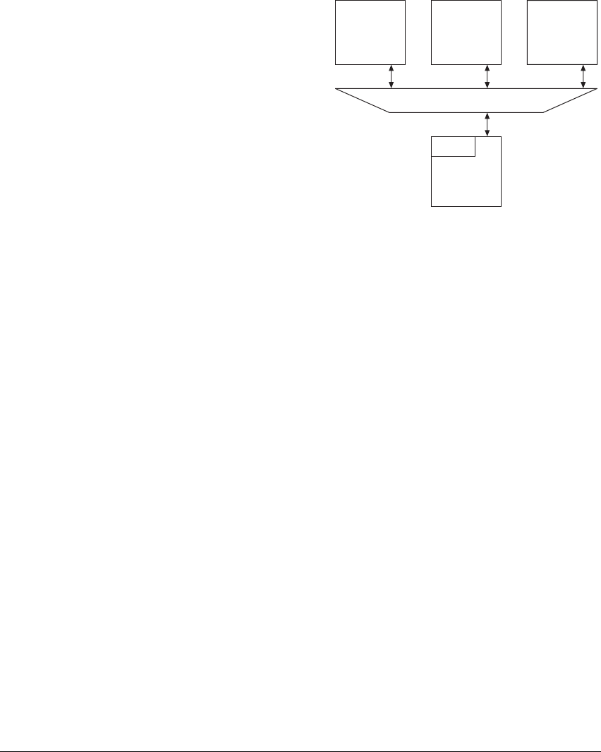
synchronization primitives with the minimum amount of hardware overhead. Figure A3-2 on page A3-9
shows an example minimal system.
ARM Architecture Memory Model
ARM DDI 0405A-01 Copyright © 2006 ARM Limited. All rights reserved. A3-9
Beta
Figure A3-2 Example uniprocessor system, with non-shared monitor
Multiprocessor systems are required to implement an address monitor for each processor. Logically, a
multiprocessor system must implement:
• A local monitor for each processor, that monitors Load-Exclusive and Store-Exclusive accesses to
Non Shared memory by that processor. A local monitor can be unaware of all Load-Exclusive and
Store-Exclusive accesses made by the other processors.
• A single global monitor, that monitors all Load-Exclusive and Store-Exclusive accesses to Shared
memory, by all processors. The global monitor must maintain an exclusive access state machine for
each processor.
However, it is IMPLEMENTATION DEFINED:
• where the monitors reside in the memory system hierarchy
• whether the monitors are implemented:
— as a single entity for each processor, visible to all shared accesses
— as a distributed entity.
L2 RAM L2 Cache
Routing matrix
Bridge to L3
CPU 1
Monitor
ARM Architecture Memory Model
A3-10 Copyright © 2006 ARM Limited. All rights reserved. ARM DDI 0405A-01
Beta
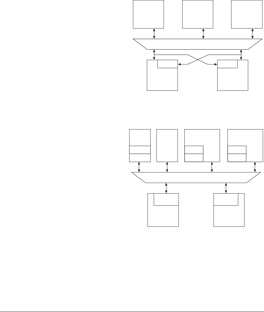
Figure A3-3 shows a single entity approach in which the monitor supports state machines for both Shared
and Non Shared memory accesses. Only the Shared memory case needs to snoop.
Figure A3-3 Global monitoring using write snoop monitor approach
Figure A3-4 shows a distributed model with a local monitors in each processor block, and global monitoring
distributed across the targets of interest.
Figure A3-4 Global monitoring using monitor-at-target approach
L2 RAM L2 Cache
Routing matrix
Bridge to L3
CPU 2
Monitor
CPU 1
Monitor
Shared
L2 RAM
L2 Cache
Routing matrix
Bridge to L3
CPU 1
Local
Monitor
CPU 2
Local
Monitor
Non-
shared
L2 RAM
Mon 1
Mon 2
Mon 1
Mon 2
Mon 1
Mon 2

ARM Architecture Memory Model
ARM DDI 0405A-01 Copyright © 2006 ARM Limited. All rights reserved. A3-11
Beta
A3.4.1 Exclusive access instructions and Non Shared memory regions
For memory regions that do not have the Shared attribute, the exclusive access instructions rely on a local
monitor that tags any address from which the processor executes a Load-Exclusive. Any non-aborted
attempt by the same processor to use a Store-Exclusive to modify any address is guaranteed to clear the tag.
Load-Exclusive performs a load from memory, and:
• the executing processor tags the fact that it has an outstanding tagged physical address to
non-sharable memory
• the local monitor of the executing processor transitions to its Exclusive Access state.
Store-Exclusive performs a conditional store to memory:
• if the local monitor of the executing processor is in its Exclusive Access state:
— the store takes place
— a status value of 0 is returned to a register
— the local monitor of the executing processor transitions to its Open Access state.
• if the local monitor of the executing processor is not in its Exclusive Access state:
— no store takes place
— a status value of 1 is returned to a register.
The Store-Exclusive instruction defined the register to which the status value is returned.
When a processor writes using any instruction other than a Store-Exclusive:
• if the write is to a physical address that is not covered by its local monitor the write does not affect
the state of the local monitor
• if the write is to a physical address that is covered by its local monitor is IMPLEMENTATION DEFINED
whether the write affects the state of the local monitor.
If the local monitor is in its Exclusive Access state and a processor performs a Store-Exclusive to any
address in Non Shared memory other than the last one from which it has performed a Load-Exclusive, it is
IMPLEMENTATION DEFINED whether the store succeeds. This mechanism:
• is used on a context switch, see Context switch support on page A3-16
• should be treated as a software programming error in all other cases.
Note
In non-shared memory, it is UNPREDICTABLE whether a store to a tagged physical address will cause a tag
to be cleared if that store is by a processor other than the one that caused the physical address to be tagged.
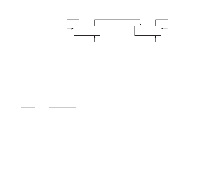
The state machine for the local monitor is shown in Figure A3-5 on page A3-12.

ARM Architecture Memory Model
A3-12 Copyright © 2006 ARM Limited. All rights reserved. ARM DDI 0405A-01
Beta
Figure A3-5 Local monitor state machine diagram
Note
The IMPLEMENTATION DEFINED options for the local monitor are consistent with the local monitor being
constructed so that it does not hold any physical address, but instead treats any access as matching the
address of the previous LDREX.
Table A3-4 shows the effect of the Load-Exclusive and Store-Exclusive instructions shown in Figure A3-5.
Figure A3-5 shows the behavior of the local address monitor associated with the processor issuing the
LDREX, STREX and STR instructions. It is UNPREDICTABLE whether the transition from Exclusive Access
to Open Access occurs when the STR or STREX is from a different processor. A local monitor
implementation can be unaware of Load-Exclusive and Store-Exclusive operations from other processors.
The operations in italics show possible alternative i
MPLEMENTATION
DEFINED
options.
CLREX
STREX(x)
STR(x) LDREX(x) LDREX(x1)
CLREX
STR(Tagged_address)
STREX(Tagged_address)
STREX(!Tagged_address)
Open Access Exclusive
Access
STR(!Tagged_address)
STR(Tagged_address)
Table A3-4 Effect of Exclusive instructions on local monitor
Initial state OperationaEffect Final state
Open access
CLREX
No effect Open access
Open access
STREX(x)
Does not update memory, returns status 1 Open access
Open access
LDREX(x)
Loads value from memory, tags address x Exclusive access
Exclusive access
CLREX
Clears tagged address Open access
Exclusive access
STREX(t)
Updates memory, returns status 0 Open access
Exclusive access
STREX(!t)
Updates memory, returns status 0 Open access
Exclusive access
LDREX(x1)
Loads value from memory, changes tag to address to x1 Exclusive access
a. STREX and LDREX are used as examples of the exclusive access instructions. t is the tagged address, bits[31:a] of
the address of the last Load-Exclusive instruction, see Size of the tagged memory block on page A3-16.

ARM Architecture Memory Model
ARM DDI 0405A-01 Copyright © 2006 ARM Limited. All rights reserved. A3-13
Beta
A3.4.2 Exclusive access instructions and shared memory regions
For memory regions that have the Shared attribute, exclusive access instructions rely on:
•A local monitor for each processor in the system, that tags any address from which the processor
executes a Load-Exclusive. The local monitor operates as described in Exclusive access instructions
and Non Shared memory regions on page A3-11, and can ignore exclusive accesses from other
processors in the system.
• A single global monitor that tags a physical address as exclusive access for a particular processor.
This tag is used later to determine whether an Store-Exclusive to that address can occur. Any
non-aborted attempt to modify the tagged address by any processor is guaranteed to clear the tag. For
each processor in the system, the global monitor:
— holds a single tagged address
— maintains a state machine.
The global monitor can either:
• reside in a processor block, as illustrated in Figure A3-3 on page A3-10
• exist as a secondary monitor at the memory interfaces, as shown in Figure A3-4 on page A3-10.
An implementation can combine the functionality of the global and local monitors into a single unit.
Operation of the global monitor
Load-Exclusive from shared memory performs a load from memory, and causes the physical address of the
access to be tagged as exclusive access for the requesting processor. This access also causes the exclusive
access tag to be removed from any other physical address that has been tagged by the requesting processor.
The global monitor only supports a single outstanding exclusive access to sharable memory per processor.
Store-Exclusive performs a conditional store to memory:
• The store is guaranteed to succeed only if the physical address accessed is tagged as exclusive access
for the requesting processor and both the local monitor and the global monitor state machine for the
requesting processor are in the Exclusive Access state. In this case:
— a status value of 0 is returned to a register to acknowledge the successful store
— the final state of the global for the requesting processor is implementation defined
— the global monitor for any other processor that has tagged the address accessed transitions to
Open Access.
• If no address is tagged as exclusive access for the requesting processor, the store does not succeed:
— a status value of 1 is returned to a register to indicate that the store failed
— the global monitor is not affected and remains Open Access for the requesting processor.
• If a different physical address is tagged as exclusive access for the requesting processor, it is
IMPLEMENTATION DEFINED whether the store succeeds or not:
— if the store succeeds a status value of 0 is returned to a register, otherwise a value of 1 is
returned
ARM Architecture Memory Model
A3-14 Copyright © 2006 ARM Limited. All rights reserved. ARM DDI 0405A-01
Beta
— if the global monitor for the processor was in the Open Access state before the Store-Exclusive
it remains in the Open Access state
— if the global monitor for the processor was in the Exclusive Access state before the
Store-Exclusive it is IMPLEMENTATION DEFINED whether the global monitor transitions to the
Open Access state.
The Store-Exclusive instruction defines the register to which the status value is returned.
In a shared memory system, the global monitor must implement a separate state machine for each processor
in the system. In this context, the term processor includes any independent DMA agent. The state machine
for Shared memory accesses by processor(n) can respond to all the Shared memory transactions visible to it:
• transactions generated by the associated processor (n)
• transactions generated by the other processors in the shared memory system (!n).
The state machine behavior is illustrated in Figure A3-6.
Figure A3-6 Global monitor state machine diagram for processor(n) in a multiprocessor system
Note
• Whether a Store-Exclusive successfully updates memory or not depends on whether the address
accessed matches the tagged shared memory address for the processor issuing the Store-Exclusive
instruction. For this reason, Figure A3-6 and Table A3-5 on page A3-15 only show how the (!n)
entries cause state transitions of the state machine for processor n.
• An Load-Exclusive can only update the tagged shared memory address for the processor issuing the
Load-Exclusive instruction.
•CLREX instructions do not affect the global monitor.
LDREX(x,n)
CLREX(n), CLREX(!n),
LDREX(x
1
,n)
Open Access Exclusive
Access
STREX(Tagged_Address,!n) only clears the monitor if the STREX updates memory
The operations in italics show possible alternative i
MPLEMENTATION
DEFINED
options.
CLREX(n), CLREX(!n),
STREX(x,n), STR(x,n),
LDREX(x,!n),
STREX(x,!n),STR(x,!n)
STREX(Tagged_address,!n)
STR(Tagged_address,!n)
STREX(Tagged_address,n)
STREX(!Tagged_address,n)
STR(Tagged_address,n)
STREX(Tagged_address,!n)
STR(!Tagged_address,n)
STREX(Tagged_address,n)
STREX(!Tagged_address,n)
STR(Tagged_address,n)
STREX(!Tagged_address,!n)
STR(!Tagged_address,!n)

ARM Architecture Memory Model
ARM DDI 0405A-01 Copyright © 2006 ARM Limited. All rights reserved. A3-15
Beta
Table A3-5 shows the effect of the Load-Exclusive and Store-Exclusive instructions shown in Figure A3-6
on page A3-14.
Table A3-5 Effect of Exclusive instructions on global monitor for processor n
Initial
stateaOperationbEffect Final
statea
Open
CLREX(n)
,
CLREX(!n)
None Open
Open
STREX(x,n)
Does not update memory, returns status 1 Open
Open
LDREX(x,!n)
Loads value from memory, no effect on tag address for processor n Open
Open
STREX(x,!n)
Depends on state machine and tag address for processor issuing
STREX
Open
Open
LDREX(x,n)
Loads value from memory, tags address x Exclusive
Exclusive
LDREX(x1,n)
Loads value from memory, tags address x1 Exclusive
Exclusive
CLREX(n)
,
CLREX(!n)
None Exclusive
Exclusive
STREX(t,!n)
Updates memory, returns status 0cOpen
Does not update memory, returns status 1cExclusive
Exclusive
STREX(t,n)
Updates memory, returns status 0d
Open
Exclusive
Exclusive
STREX(!t,n)
Updates memory, returns status 0e
Open
Exclusive
Does not update memory, returns status 1e
Open
Exclusive
Exclusive
STREX(!t,!n)
Depends on state machine and tag address for processor issuing
STREX
Exclusive
a. Open = Open access, Exclusive = Exclusive access.
b. STREX and LDREX are used as examples of the exclusive access instructions. t is the tagged address for processor n,
bits[31:a] of the address of the last LDREX instruction issued by processor n, see Size of the tagged memory block on
page A3-16.
c. The result of the STREX(t,!n) operation depends on the state machine and tagged address for the processor
issuing the STREX instruction. This table shows how each possible outcome affects the state machine for processor n.
d. After a successful STREX to the tagged address, the state of the state machine is IMPLEMENTATION DEFINED.
However, this state has no effect on the subsequent operation of the global monitor.

ARM Architecture Memory Model
A3-16 Copyright © 2006 ARM Limited. All rights reserved. ARM DDI 0405A-01
Beta
A3.4.3 Size of the tagged memory block
As shown in Figure A3-5 on page A3-12 and Figure A3-6 on page A3-14, when a LDREX instruction is
executed, the resulting tag address ignores the least significant bits of the memory address:
Tagged_address == Memory_address[31:a]
The value of a in this assignment is IMPLEMENTATION DEFINED, between a minimum value of 2 and a
maximum value of 7. For example, in an implementation where a = 4, a successful LDREX of address
0x000341B4 gives a tag value of bits [31:4] of the address, giving 0x000341B. This means that the four
words of memory from 0x000341B0 to 0x000341BF are tagged for exclusive access. Subsequently, a
valid STREX to any address in this block will remove the tag.
Therefore, the size of the tagged memory block is IMPLEMENTATION DEFINED between:
• one word, in an implementation with a = 2
• 32 words, in an implementation with a = 7.
A3.4.4 Context switch support
It is necessary to ensure that the local monitor is in the Open Access state after a context switch. In
ARMv7-M, the local monitor is changed to Open Access automatically as part of an exception entry or exit
sequence. The local monitor can also be forced to the Open Access state by a CLREX instruction.
Note
Context switching is not an application level operation. However, this information is included here to
complete the description of the exclusive operations.
The STREX or CLREX instruction following a context switch might cause a subsequent Store-Exclusive to
fail, requiring a load … store sequence to be replayed. To minimize the possibility of this happening, ARM
Limited recommends that the Store-Exclusive instruction is kept as close as possible to the associated
Load-Exclusive instruction, see Load-Exclusive and Store-Exclusive usage restrictions.
A3.4.5 Load-Exclusive and Store-Exclusive usage restrictions
The Load-Exclusive and Store-Exclusive instructions are designed to work together, as a pair, for example
a LDREX/STREX pair or a LDREXB/STREXB pair. As mentioned in Context switch support, ARM Limited
recommends that the Store-Exclusive instruction always follows within a few instructions of its associated
Load-Exclusive instructions. In order to support different implementations of these functions, software must
follow the notes and restrictions given here.
e. Effect is IMPLEMENTATION DEFINED. The table shows all permitted implementations.

ARM Architecture Memory Model
ARM DDI 0405A-01 Copyright © 2006 ARM Limited. All rights reserved. A3-17
Beta
These notes describe use of a LDREX/STREX pair, but apply equally to any other
Load-Exclusive/Store-Exclusive pair:
1. The exclusives are designed to support a single outstanding exclusive access for each processor
thread that is executed. The architecture makes use of this by not mandating an address or size check
as part of the IsExclusiveLocal() function. If the target address of an STREX is different from the
preceding LDREX within the same execution thread, behavior can be UNPREDICTABLE. As a result, an
LDREX/STREX pair can only be relied upon to eventually succeed if they are executed with the same
address. Where a context switch or exception might result in a change of execution thread, a CLREX
instruction or a dummy STREX instruction must be executed to avoid unwanted effects, as described
in Context switch support on page A3-16 Using an STREX in this way is the only occasion where
software can program an STREX with a different address from the previously executed LDREX.
2. An explicit store to memory can cause the clearing of exclusive monitors associated with other
processors, therefore, performing a store between the LDREX and the STREX can result in a livelock
situation. As a result, code must avoid placing an explicit store between an LDREX and an STREX
within a single code sequence.
3. Two STREX instructions executed without an intervening LDREX will also result in the second
STREX returning a status value of 1. As a result:
•each STREX must have a preceding LDREX associated with it within a given thread of
execution
• it is not necessary for each LDREX to have a subsequent STREX.
4. Implementations can cause apparently spurious clearing of the exclusive monitor between the
LDREX and the STREX, as a result of, for example, cache evictions. Code designed to run on such
implementations should avoid having any explicit memory transactions or cache maintenance
operations between the LDREX and STREX instructions.
5. Implementations can benefit from keeping the LDREX and STREX operations close together in a
single code sequence. This minimizes the likelihood of the exclusive monitor state being cleared
between the LDREX instruction and the STREX instruction. Therefore, ARM Limited strongly
recommends a limit of 128 bytes between LDREX and STREX instructions in a single code sequence,
for best performance.
6. Implementations that implement coherent protocols, or have only a single master, might combine the
local and global monitors for a given processor. The IMPLEMENTATION DEFINED and UNPREDICTABLE
parts of the definitions in are designed to cover this behavior.
7. The architecture sets an upper limit of 128 bytes on the regions that can be marked as exclusive.
Therefore, for performance reasons, ARM Limited recommends that software separates objects that
will be accessed by exclusive accesses by at least 128 bytes. This is a performance guideline rather
than a functional requirement.
8. LDREX and STREX operations must be performed only on memory with the Normal memory
attribute.

ARM Architecture Memory Model
A3-18 Copyright © 2006 ARM Limited. All rights reserved. ARM DDI 0405A-01
Beta
A3.4.6 Synchronization primitives and the memory order model
The synchronization primitives follow the memory ordering model of the memory type accessed by the
instructions. For this reason:
• Portable code for claiming a spinlock must include a DMB instruction between claiming the spinlock
and making any access that makes use of the spinlock.
• Portable code for releasing a spinlock must include a DMB instruction before writing to clear the
spinlock.
This requirement applies to code using the Load-Exclusive/Store-Exclusive instruction pairs, for example
LDREX/STREX.

ARM Architecture Memory Model
ARM DDI 0405A-01 Copyright © 2006 ARM Limited. All rights reserved. A3-19
Beta
A3.5 Memory types
ARMv7 defines a set of memory attributes with the characteristics required to support all memory and
devices in the system memory map. The ordering of accesses for regions of memory is also defined by the
memory attributes.
There are three mutually exclusive main memory type attributes to describe the memory regions:
• Normal
•Device
• Strongly Ordered.
Memory used for program execution and data storage generally complies with Normal memory. Examples
of Normal memory technology are:
• preprogrammed Flash (updating Flash memory can impose stricter ordering rules)
•ROM
•SRAM
• SDRAM and DDR memory
System peripherals (I/O) generally conform to different access rules; defined as Strongly Ordered or Device
memory. Examples of I/O accesses are:
• FIFOs where consecutive accesses add (write) or remove (read) queued values
• interrupt controller registers where an access can be used as an interrupt acknowledge changing the
state of the controller itself
• memory controller configuration registers that are used to set up the timing (and correctness) of areas
of normal memory
• memory-mapped peripherals where the accessing of memory locations causes side effects within the
system.
In addition, the Shared attribute indicates whether Normal or Device memory is private to a single processor,
or accessible from multiple processors or other bus master resources, for example, an intelligent peripheral
with DMA capability.
Strongly Ordered memory is required where it is necessary to ensure strict ordering of the access with
respect to what occurred in program order before the access and after it. Strongly Ordered memory always
assumes the resource is shared.

ARM Architecture Memory Model
A3-20 Copyright © 2006 ARM Limited. All rights reserved. ARM DDI 0405A-01
Beta
Table A3-6provides a summary of the memory attributes.
A3.5.1 Atomicity
The terms Atomic and Atomicity are used within computer science to describe a number of properties for
memory accesses. Within the ARM architecture, the following definitions are used:
Single-copy atomicity
The property of Single-copy atomicity is exhibited for read and write operations if the following conditions
are met:
1. After every two write operations to an operand, either the value of the first write operation or the value
of the second write operation remains in the operand. Thus, it is impossible for part of the value of
the first write operation and part of the second write operation to remain in the operand.
2. When a read operation and a write operation occur to the same operand, the value obtained by the
read operation is either the value of the operand before the write operation or the value of the operand
after the write operation. It is never the case that the value of the read operation is partly the value of
the operand before the write operation and partly the value of the operand after the write operation.
Table A3-6 Summary of memory attributes
Memory type attribute Shared attribute Other attribute Description
Strongly ordered All memory accesses to Strongly
Ordered memory occur in program
order. All Strongly Ordered
accesses are assumed to be Shared.
Device Shared Designed to handle memory
mapped peripherals that are shared
by several processors.
Non-shared Designed to handle memory
mapped peripherals that are used
only by a single processor.
Normal Shared Non-cacheable/Write-T
hrough
cacheable/Write-Back
cacheable
Designed to handle normal memory
which is shared between several
processors.
Non-shared Non-cacheable/Write-T
hrough
cacheable/Write-Back
cacheable
Designed to handle normal memory
which is used only by a single
processor.

ARM Architecture Memory Model
ARM DDI 0405A-01 Copyright © 2006 ARM Limited. All rights reserved. A3-21
Beta
The only ARMv7-M explicit accesses made by the ARM processor which exhibit single-copy atomicity are:
• All byte transactions
• All halfword transactions to 16-bit aligned locations
• All word transactions to 32-bit aligned locations
LDM, LDC, LDRD, STM, STC, STRD, PUSH and POP operations are seen to be a sequence of 32-bit
transactions aligned to 32 bits. Each of these 32-bit transactions are guaranteed to exhibit single-copy
atomicity. Sub-sequences of two or more 32-bit transactions from the sequence also do not exhibit
single-copy atomicity.
Where a transaction does not exhibit single-copy atomicity, it is seen as a sequence of transactions of bytes
which do exhibit single-copy atomicity.
For implicit accesses:
• Cache linefills/evictions are seen to be a sequence of 32-bit transactions aligned to 32 bits. Each of
these 32-bit transactions exhibits single-copy atomicity. Sub-sequences of two or more 32-bit
transactions from the sequence also do not exhibit single-copy atomicity
• Instruction fetches exhibit single-copy atomicity for the individual instructions being fetched; it must
be noted that 32-bit thumb instructions are comprised of 2 16-bit quantities.
Multi-copy atomicity
In a multiprocessing system, writes to a memory location exhibit Multi-copy atomicity if:
1. All writes to the same location are serialised that is they are observed in the same order to all copies
of the location.
2. The value of a write is not returned by a read until all copies of the location have seen that write
No writes to Normal memory exhibit Multi-copy atomicity
All writes to Device and Strongly-Ordered memory which exhibit Single-copy atomicity also exhibit
Multi-copy atomicity.
All write transactions to the same location are serialised. Write transactions to Normal memory can be
repeated up to the point that another write to the same address is observed.
Serialisation of writes does not prohibit the merging of writes for Normal memory.
A3.5.2 Normal memory attribute
Normal memory is idempotent, exhibiting the following properties:
• read transactions can be repeated with no side effects
• repeated read transactions return the last value written to the resource being read
• read transactions can prefetch additional memory locations with no side effects.

ARM Architecture Memory Model
A3-22 Copyright © 2006 ARM Limited. All rights reserved. ARM DDI 0405A-01
Beta
• write transactions can be repeated with no side effects, provided that the location is unchanged
between the repeated writes
• unaligned accesses can be supported
• transactions can be merged prior to accessing the target memory system
Normal memory can be read/write or read-only. The Normal memory attribute can be further defined as
being Shared or Non-Shared, and describes most memory used in a system.
Accesses to Normal Memory conform to the weakly-ordered model of memory ordering. A description of
the weakly-ordered model can be found in standard texts describing memory ordering issues. A
recommended text is chapter 2 of Memory Consistency Models for Shared Memory-Multiprocessors,
Kourosh Gharachorloo, Stanford University Technical Report CSL-TR-95-685.
All explicit accesses must correspond to the ordering requirements of accesses described in Memory access
order on page A3-27.
Instructions which conform to the 32-bit sequence of transactions classification as defined in Atomicity on
page A3-20 can be abandoned if a MemManage or BusFault exception occurs during the sequence of
transactions. The instruction will be restarted on return from the exception, and one or more of the memory
locations can be accessed multiple times. For Normal memory, this can result in repeated write transactions
to a location which has been changed between the repeated writes.
Non-shared Normal memory
The Non-Shared Normal memory attribute is designed to describe normal memory that can be accessed only
by a single processor.
A region of memory marked as Non-Shared Normal does not have any requirement to make the effect of a
cache transparent. For regions of memory marked as Non-shared Non-cacheable, a Data Synchronization
Barrier (DSB) instruction must be used in situations where previous accesses must be made visible to other
observers. See Memory barriers on page A3-30 for more details.
Shared Normal memory
The Shared Normal memory attribute is designed to describe normal memory that can be accessed by
multiple processors or other system masters.
A region of memory marked as Shared Normal is one in which the effect of interposing a cache (or caches)
on the memory system is entirely transparent to data accesses. Explicit software management is still
required to ensure coherency of instruction caches. Implementations can use a variety of mechanisms to
support this, from very simply not caching accesses in shared regions to more complex hardware schemes
for cache coherency for those regions.
Cacheable write-through, cacheable write-back and non-cacheable memory
In addition to marking a region of Normal memory as being Shared or Non-Shared, regions can also be
marked as being one of:
• cacheable write-through

ARM Architecture Memory Model
ARM DDI 0405A-01 Copyright © 2006 ARM Limited. All rights reserved. A3-23
Beta
• cacheable write-back
• non-cacheable.
This marking is independent of the marking of a region of memory as being Shared or Non-Shared. It
indicates the required handling of the data region for reasons other than those to handle the requirements of
shared data. As a result, it is acceptable for a region of memory that is marked as being cacheable and shared
not to be held in the cache in an implementation which handles shared regions as not caching the data.
A3.5.3 Device memory attribute
The Device memory attribute is defined for memory locations where an access to the location can cause side
effects, or where the value returned for a load can vary depending on the number of loads performed.
Memory mapped peripherals and I/O locations are typical examples of areas of memory that should be
marked as being Device.
Explicit accesses from the processor to regions of memory marked as Device occur at the size and order
defined by the instruction. The number of accesses that occur to such locations is the number that is specified
by the program. Implementations must not repeat accesses to such locations when there is only one access
in the program, that is, the accesses are not restartable. An example where an implementation might want
to repeat an access is before and after an interrupt, in order to allow the interrupt to cause a slow access to
be abandoned. Such implementation optimizations must not be performed for regions of memory marked
as Device.
In addition, address locations marked as Device are non-cacheable. While writes to device memory can be
buffered, writes shall only be merged where the correct number of accesses, order, and their size is
maintained. Multiple accesses to the same address cannot change the number or order of accesses to that
address. Coalescing of accesses is not permitted in this case.
Accesses to Device memory can exhibit side effects. Device memory operations that have side effects that
apply to Normal memory locations require Memory Barriers to ensure correct execution. An example is the
programming of the configuration registers of a memory controller with respect to the memory accesses it
controls.
All explicit accesses to memory marked as Device must correspond to the ordering requirements of accesses
described in Memory access order on page A3-27.
Shared attribute
The Shared attribute is defined by memory region and can be referred to as:
• memory marked as Shared Device
• memory marked as Non-Shared Device
Memory marked as Non-Shared Device is defined as only accessible by a single processor. An example of
a system supporting Shared and Non-shared Device memory is an implementation that supports a local bus
for its private peripherals, whereas system peripherals are situated on the main (Shared) system bus. Such a
system can have more predictable access times for local peripherals such as watchdog timers or interrupt
controllers.

ARM Architecture Memory Model
A3-24 Copyright © 2006 ARM Limited. All rights reserved. ARM DDI 0405A-01
Beta
A3.5.4 Strongly Ordered memory attribute
Accesses to memory marked as Strongly Ordered have a strong memory-ordering model for all explicit
memory accesses from that processor. An access to memory marked as Strongly Ordered is required to act
as if a DMB memory barrier instruction were inserted before and after the access from that processor. See
Data Memory Barrier (DMB) on page A3-31 for DMB details.
Explicit accesses from the processor to memory marked as Strongly Ordered occur at their program size,
and the number of accesses that occur to such locations is the number that are specified by the program.
Implementations must not repeat accesses to such locations when there is only one access in the program,
that is, the accesses are not restartable.
Address locations marked as Strongly Ordered are not held in a cache, and are always treated as Shared
memory locations.
All explicit accesses to memory marked as Strongly Ordered must correspond to the ordering requirements
of accesses described in Memory access order on page A3-27.
A3.5.5 Memory access restrictions
The following restrictions apply to memory accesses:
• For any access X, the bytes accessed by X must all have the same memory type attribute, otherwise,
the behavior of the access is UNPREDICTABLE. That is, unaligned accesses that span a boundary
between different memory types are UNPREDICTABLE.
• For any two memory accesses X and Y, such that X and Y are generated by the same instruction, X
and Y must all have the same memory type attribute, otherwise, the results are UNPREDICTABLE. For
example, an LDC, LDM, LDRD, STC, STM, or STRD that spans a boundary between Normal and
Device memory is UNPREDICTABLE.
• Instructions that generate unaligned memory accesses to Device or Strongly Ordered memory are
UNPREDICTABLE.
• For instructions that generate accesses to Device or Strongly Ordered memory, implementations do
not change the sequence of accesses specified by the pseudo-code of the instruction. This includes
not changing how many accesses there are, nor their time order, nor the data sizes and other properties
of each individual access. Furthermore, processor core implementations expect any attached memory
system to be able to identify accesses by memory type, and to obey similar restrictions with regard
to the number, time order, data sizes and other properties of the accesses.
Exceptions to this rule are:
— An implementation of a processor core can break this rule, provided that the information it
does supply to the memory system enables the original number, time order, and other details
of the accesses to be reconstructed. In addition, the implementation must place a requirement
on attached memory systems to do this reconstruction when the accesses are to Device or
Strongly Ordered memory.

ARM Architecture Memory Model
ARM DDI 0405A-01 Copyright © 2006 ARM Limited. All rights reserved. A3-25
Beta
For example, the word loads generated by an LDM can be paired into 64-bit accesses by an
implementation with a 64-bit bus. This is because the instruction semantics ensure that the
64-bit access is always a word load from the lower address followed by a word load from the
higher address, provided a requirement is placed on memory systems to unpack the two word
loads where the access is to Device or Strongly Ordered memory.
— Any implementation technique that produces results that cannot be observed to be different
from those described above is legitimate.
• Multi-access instructions that load or store the PC must only access normal memory. If they access
Device or Strongly Ordered memory the results are UNPREDICTABLE.
• Instruction fetches must only access normal memory. If they access Device or Strongly Ordered
memory, the results are UNPREDICTABLE. By example, instruction fetches must not be performed to
areas of memory containing read-sensitive devices, because there is no ordering requirement between
instruction fetches and explicit accesses.
Implementations can prefetch by an IMPLEMENTATION DEFINED amount down a sequential path from the
instruction currently being executed. To ensure correctness, read-sensitive locations must be marked as
non-executable (see User/privileged access and Read/Write access control for Instruction Accesses on
page A3-26).

ARM Architecture Memory Model
A3-26 Copyright © 2006 ARM Limited. All rights reserved. ARM DDI 0405A-01
Beta
A3.6 Access rights
Access rights split into two classes:
• Rights for data accesses
• Rights for instruction prefetching
Furthermore, the access right can be restricted to privileged execution only.
A3.6.1 User/privileged access and Read/Write access control for Data Accesses
The memory attributes are allowed to define for explicit reads and for explicit writes that a region of memory
is:
• Not accessible to any accesses
• Accessible only to Privileged accesses
• Accessible to Privileged and Non-Privileged accesses
Not all combinations of memory attributes for reads and writes are supported by all systems which define
the memory attributes.
If an attempt is made to read or write non-accessible data, a data access error will occur. Privileged accesses
are accesses made as a result of a load or store operation (other than LDRT, STRT, LDRBT, STRBT, LDRHT,
STRHT, LDRSHT, LDRSBT) during privileged execution.
Unprivileged accesses are accesses made as a result of a load or store operation when the processor is
executing unprivileged code, or any made as a result of the following instructions:
LDRT, STRT, LDRBT, STRBT, LDRHT, STRHT, LDRSHT, LDRSBT
A3.6.2 User/privileged access and Read/Write access control for Instruction Accesses
The memory attributes can define that a region of memory is:
• Not accessible for execution
Prefetching must not occur from locations marked as non-executable
• Accessible for execution by Privileged processes only
• Accessible for execution by Privileged and Non-Privileged processes
The mechanism by which this is described is that the region is described as accessible for reads by a
privileged read access (or by privileged and non-privileged read access) and is suitable for execution. As a
result, there is some linkage between the memory attributes which define the accessibility to explicit
memory accesses, and those which define that a region can be executed.
If execution is attempted to any memory locations for which the attributes are not permitted, an instruction
execution error will occur.

ARM Architecture Memory Model
ARM DDI 0405A-01 Copyright © 2006 ARM Limited. All rights reserved. A3-27
Beta
A3.7 Memory access order
The memory types defined in Memory types on page A3-19 have associated memory ordering rules to
provide system compatibility for software between different implementations. The rules are defined to
accommodate the increasing difficulty of ensuring linkage between the completion of memory accesses and
the execution of instructions within a complex high-performance system, while also allowing simple
systems and implementations to meet the criteria with predictable behaviour.
The memory order model determines:
• when side effects are guaranteed to be visible
• the requirements for memory consistency
Shared memory indicating whether a region of memory is shared between multiple processors (and
therefore requires an appearance of cache transparency in an ordering model) is supported. Implementations
remain free to choose the mechanisms to implement this functionality.
Additional attributes and behaviors relate to the memory system architecture. These features are defined in
other areas of this manual (see Access rights on page A3-26, Chapter C1 Debug and Chapter B1 System
Level Programmer’s Model on access permissions, the system memory map and the Protected Memory
System Architecture respectively).
A3.7.1 Read and write definitions
Memory accesses can be either reads or writes.
Reads
Reads are defined as memory operations that have the semantics of a load.For ARMv7-M and Thumb-2
these are:
•LDR{S}B{T}, LDR{S}H{T}, LDR{T}
•LDMIA, LDMDB, LDRD, POP, LDC
•LDREX{B,H}, STREX{B,H}
•TBB, TBH
Writes
Writes are defined as operations that have the semantics of a store.For ARMv7-M and Thumb-2 these are:
•STRB{T}, STRH{T}, STR{T}
•STMIA, STMDB, STRD, PUSH, STC, STREX{B,H}
Memory synchronization primitives
Synchronization primitives are required to ensure correct operation of system semaphores within the
memory order model. The memory synchronization primitive instructions are defined as those instructions
that are used to ensure memory synchronization:

ARM Architecture Memory Model
A3-28 Copyright © 2006 ARM Limited. All rights reserved. ARM DDI 0405A-01
Beta
LDREX{B,H}, STREX{B,H}
These instructions are supported to shared and non-shared memory. Non-shared memory can be used when
the processes to be synchronized are running on the same processor. When the processes to be synchronized
are running on different processors, shared memory must be used.
A3.7.2 Observability and completion
The concept of observability applies to all memory, however, the concept of global observability only
applies to shared memory. Normal, Device and Strongly Ordered memory are defined in Memory types on
page A3-19.
For all memory:
• A write to a location in memory is said to be observed by a memory system agent (the observer) when
a subsequent read of the location by the observer returns the value written by the write.
• A write to a location in memory is said to be globally observed when a subsequent read of the location
by any memory system agent returns the value written by the write.
• A read to a location in memory is said to be observed by a memory system agent (the observer) when
a subsequent write of the location by the observer has no effect on the value returned by the read.
• A read to a location in memory is said to be globally observed when a subsequent write of the location
by any memory system agent has no effect on the value returned by the read.
Additionally, for Strongly Ordered memory:
• A read or write to a memory mapped location in a peripheral which exhibits side-effects is said to be
observed, and globally observed, only when the read or write meets the general conditions listed, can
begin to affect the state of the memory-mapped peripheral, and can trigger any side effects that affect
other peripheral devices, cores and/or memory.
For all memory, a read or write is defined to be complete when it is globally observed:
• A branch predictor maintenance operation is defined to be complete when the effects of operation are
globally observed.
To determine when any side effects have completed, it is necessary to poll a location associated with the
device, for example, a status register.
Side effect completion in Strongly Ordered and Device memory
For all memory-mapped peripherals, where the side-effects of a peripheral are required to be visible to the
entire system, the peripheral must provide an IMPLEMENTATION DEFINED location which can be read to
determine when all side effects are complete.
This is a key element of the architected memory order model.

ARM Architecture Memory Model
ARM DDI 0405A-01 Copyright © 2006 ARM Limited. All rights reserved. A3-29
Beta
A3.7.3 Ordering requirements for memory accesses
ARMv7-M defines access restrictions in the memory ordering allowed, depending on the memory attributes
of the accesses involved. Table A3-7 shows the memory ordering between two explicit accesses A1 and A2,
where A1 (as listed in the first column) occurs before A2 (as listed in the first row) in program order.
The symbols used in Table A3-76-3 are as follows:
< Accesses must be globally observed in program order, that is, A1 must be globally observed
strictly before A2.
(blank) Accesses can be globally observed in any order, provided that the requirements of
uniprocessor semantics, for example respecting dependencies between instructions within a
single processor, are maintained.
There are no ordering requirements for implicit accesses to any type of memory.
A3.7.4 Program order for instruction execution
Program order of instruction execution is the order of the instructions in the control flow trace. Explicit
memory accesses in an execution can be either:
Strictly Ordered Denoted by <. Must occur strictly in order.
Ordered Denoted by <=. Must occur either in order, or simultaneously.
Multiple load and store instructions, such as LDM{IA || DB}, LDRD, POP, STM{IA || DB}, PUSH
and STRD, generate multiple word accesses, each of which is a separate access for the purpose of
determining ordering.
The rules for determining program order for two accesses A1 and A2 are:
Table A3-7 Memory order restrictions
A2 Normal Access Device Access Strongly Ordered
Access
A1 (Non-Shared) (Shared)
Normal Access <
Device Access
(Non-Shared)
<<
Device Access
(Shared)
<<
Strongly Ordered
Access
<<<<

ARM Architecture Memory Model
A3-30 Copyright © 2006 ARM Limited. All rights reserved. ARM DDI 0405A-01
Beta
If A1 and A2 are generated by two different instructions:
• A1 < A2 if the instruction that generates A1 occurs before the instruction that generates A2 in
program order
• A2 < A1 if the instruction that generates A2 occurs before the instruction that generates A1 in
program order.
If A1 and A2 are generated by the same instruction:
• If A1 and A2 are the load and store generated by a SWP or SWPB instruction:
— A1 < A2 if A1 is the load and A2 is the store
— A2 < A1 if A2 is the load and A1 is the store.
• If A1 and A2 are two word loads generated by an LDC, LDRD, or LDM instruction, or two word stores
generated by an STC, STRD, or STM instruction, excluding LDM or STM instructions whose register
list includes the PC:
— A1 <= A2 if the address of A1 is less than the address of A2
— A2 <= A1 if the address of A2 is less than the address of A1.
• If A1 and A2 are two word loads generated by an LDM instruction whose register list includes the PC
or two word stores generated by an STM instruction whose register list includes the PC, the program
order of the memory operations is not defined.
• If A1 and A2 are two word loads generated by an LDRD instruction or two word stores generated by
an STRD instruction whose register list includes the PC, the instruction is UNPREDICTABLE.
A3.7.5 Memory barriers
Memory barrier is the general term applied to an instruction, or sequence of instructions, used to force
synchronization events by a processor with respect to retiring load/store instructions in a processor core. A
memory barrier is used to guarantee completion of preceding load/store instructions to the programmer’s
model, flushing of any prefetched instructions prior to the event, or both. ARMv7-M includes three explicit
barrier instructions to support the memory order model. The instructions can execute from privileged or
unprivileged code.
• Data Memory Barrier (DMB) as described in Data Memory Barrier (DMB) on page A3-31
• Data Synchronization Barrier (DSB) as described in Data Synchronization Barrier (DSB) on
page A3-31
• Instruction Synchronization Barrier (ISB) as described in Instruction Synchronization Barrier (ISB)
on page A3-31
Explicit memory barriers affect reads and writes to the memory system generated by load and store
instructions being executed in the CPU. Reads and writes generated by DMA transactions and instruction
fetches are not explicit accesses.

ARM Architecture Memory Model
ARM DDI 0405A-01 Copyright © 2006 ARM Limited. All rights reserved. A3-31
Beta
A3.7.6 Data Memory Barrier (DMB)
DMB acts as a data memory barrier, exhibiting the following behavior:
• All explicit memory accesses by instructions occurring in program order before this instruction are
globally observed before any explicit memory accesses due to instructions occurring in program
order after this instruction are observed.
• The DMB instruction has no effect on the ordering of other instructions executing on the processor.
As such, DMB ensures the apparent order of the explicit memory operations before and after the instruction,
without ensuring their completion. For details on the DMB instruction, see Chapter A5 Thumb Instructions.
A3.7.7 Data Synchronization Barrier (DSB)
The DSB instruction operation acts as a special kind of Data Memory Barrier. The DSB operation completes
when all explicit memory accesses before this instruction complete.
In addition, no instruction subsequent to the DSB can execute until the DSB completes. For details on the
DSB instruction, see Chapter A5 Thumb Instructions.
A3.7.8 Instruction Synchronization Barrier (ISB)
The ISB instruction flushes the pipeline in the processor, so that all instructions following the pipeline flush
are fetched from memory after the instruction has been completed. It ensures that the effects of context
altering operations, such as branch predictor maintenance operations, as well as all changes to the
special-purpose registers where applicable (see The special-purpose control register on page B1-9)
executed before the ISB instruction are visible to the instructions fetched after the ISB.
In addition, the ISB instruction ensures that any branches which appear in program order after the ISB are
always written into the branch prediction logic with the context that is visible after the ISB. This is required
to ensure correct execution of the instruction stream.
Any context altering operations appearing in program order after the ISB only take effect after the ISB has
been executed. This is due to the behavior of the context altering instructions.
ARM implementations are free to choose how far ahead of the current point of execution they prefetch
instructions; either a fixed or a dynamically varying number of instructions. As well as being free to choose
how many instructions to prefetch, an ARM implementation can choose which possible future execution
path to prefetch along. For example, after a branch instruction, it can choose to prefetch either the instruction
following the branch or the instruction at the branch target. This is known as branch prediction.
A potential problem with all forms of instruction prefetching is that the instruction in memory can be
changed after it was prefetched but before it is executed. If this happens, the modification to the instruction
in memory does not normally prevent the already prefetched copy of the instruction from executing to
completion. The ISB and memory barrier instructions (DMB or DSB as appropriate) are used to force
execution ordering where necessary.
For details on the ISB instruction, see Chapter A5 Thumb Instructions.

ARM Architecture Memory Model
A3-32 Copyright © 2006 ARM Limited. All rights reserved. ARM DDI 0405A-01
Beta
A3.8 Caches and memory hierarchy
Support for caches in ARMv7-M is limited to memory attributes. These can be exported on a supporting bus
protocol such as AMBA (AHB or AXI protocols) to support system caches.
In situations where a breakdown in coherency can occur, software must manage the caches using cache
maintenance operations which are memory mapped and IMPLEMENTATION DEFINED.
A3.8.1 Introduction to caches
A cache is a block of high-speed memory locations containing both address information (commonly known
as a TAG) and the associated data. The purpose is to increase the average speed of a memory access. Caches
operate on two principles of locality:
Spatial locality an access to one location is likely to be followed by accesses from adjacent locations, for
example, sequential instruction execution or usage of a data structure
Temporal locality an access to an area of memory is likely to be repeated within a short time period, for
example, execution of a code loop
To minimise the quantity of control information stored, the spatial locality property is used to group several
locations together under the same TAG. This logical block is commonly known as a cache line. When data
is loaded into a cache, access times for subsequent loads and stores are reduced, resulting in overall
performance benefits. An access to information already in a cache is known as a cache hit, and other
accesses are called cache misses.
Normally, caches are self-managing, with the updates occurring automatically. Whenever the processor
wants to access a cacheable location, the cache is checked. If the access is a cache hit, the access occurs
immediately, otherwise a location is allocated and the cache line loaded from memory. Different cache
topologies and access policies are possible, however, they must comply with the memory coherency model
of the underlying architecture.
Caches introduce a number of potential problems, mainly because of:
• Memory accesses occurring at times other than when the programmer would normally expect them
• There being multiple physical locations where a data item can be held
A3.8.2 Implication of caches to the application programmer
Caches are largely invisible to the application programmer, but can become visible due to a breakdown in
coherency. Such a breakdown can occur:
• When memory locations are updated by other agents in the systems
• When memory updates made from the application code must be made visible to other agents in the
system
For example:

ARM Architecture Memory Model
ARM DDI 0405A-01 Copyright © 2006 ARM Limited. All rights reserved. A3-33
Beta
In systems with a DMA that reads memory locations which are held in the data cache of a processor, a
breakdown of coherency occurs when the processor has written new data in the data cache, but the DMA
reads the old data held in memory.
In a Harvard architecture of caches, a breakdown of coherency occurs when new instruction data has been
written into the data cache and/or to memory, but the instruction cache still contains the old instruction data.

ARM Architecture Memory Model
A3-34 Copyright © 2006 ARM Limited. All rights reserved. ARM DDI 0405A-01
Beta
A3.9 Bit banding
ARMv7-M supports bit-banding. This feature is designed to be used with on-chip RAM or peripherals. A
bit-band address space means that the address space supports bit-wise as well as (multi)byte accesses
through an aliased address range. Byte, halfword, word and multi-byte accesses are supported by the
primary address range associated with the bit-band memory in accordance with the memory type attribute
associated with the address range. The aliased address range maps a word of address space (four bytes) to
each bit.
For a detailed explanation of bit banding, see Bit Banding on page B2-5.
Note
Where a primary bit-band region is supported in the system memory map, the associated aliased bit-band
region must be supported. Where no primary region support exists, the corresponding aliased region must
also behave as non-existent memory.

ARM DDI 0405A-01 Copyright © 2006 ARM Limited. All rights reserved. A4-1
Beta
Chapter A4
The Thumb Instruction Set
This chapter describes the Thumb® instruction set. It contains the following sections:
•Instruction set encoding on page A4-2
•Instruction encoding for 32-bit Thumb instructions on page A4-12
•Conditional execution on page A4-33
•UNDEFINED and UNPREDICTABLE instruction set space on page A4-37
•Usage of 0b1111 as a register specifier on page A4-39
•Usage of 0b1101 as a register specifier on page A4-41

The Thumb Instruction Set
A4-2 Copyright © 2006 ARM Limited. All rights reserved. ARM DDI 0405A-01
Beta
A4.1 Instruction set encoding
Thumb instructions are either 16-bit or 32-bit. Bits<15:11> of the halfword that the PC points to determine
whether it is a 16-bit instruction, or whether the following halfword is the second part of a 32-bit instruction.
Table A4-1 shows how the instruction set space is divided between 16-bit and 32-bit instructions. An x in
the encoding indicates any bit, except that any combination of bits already defined is excluded.
Table A4-1 Determination of instruction length
hw1<15:11> Function
0b11100 Thumb 16-bit unconditional branch instruction, defined in all Thumb architectures.
0b111xx Thumb 32-bit instructions, defined in Thumb-2, see Instruction encoding for 32-bit
Thumb instructions on page A4-12.
0bxxxxx Thumb 16-bit instructions.

The Thumb Instruction Set
ARM DDI 0405A-01 Copyright © 2006 ARM Limited. All rights reserved. A4-3
Beta
A4.2 Instruction encoding for 16-bit Thumb instructions
Figure A4-1 shows the main divisions of the Thumb 16-bit instruction set space. An entry in square
brackets, for example [1], indicates a note below the table.
Figure A4-1 Thumb instruction set overview
1. opcode != 0b11.
2. cond != 0b111x.
3. See Miscellaneous instructions on page A4-9.
opcode Rdn
RdnRm
opcode [1] Rdn
PC-relative imm8
Shift by immediate, move register
Add/subtract register
Add/subtract immediate
Add/subtract/compare/move immediate
Data-processing register
Special data processing
Load from literal pool
Load/store word/byte immediate offset
Load/store halfword immediate offset
Load from or store to stack
Add to SP or PC
Load/store register offset
imm5
imm5
SP-relative imm8
15 14 13 12 11 10 9 8 7 6 5 4 3 2 1 0
opcode [1] imm5 Rm Rd000
000
000
001
010
010
010
011
100
110
111
000
opc Rm Rn Rd
opc Rn Rdimm3
imm8
opcode
RmDN
0Rd
1RmRnRd
B L Rn Rd
0 L Rn Rd
1001 L Rd
1 0 1 0 SP Rd imm8
010001
01000111L Rm
Branch/exchange
instruction set
1
opcode
Miscellaneous [3] 1011 xxxxx xx xxxxx
Load/store multiple
Conditional branch
Undefined instruction
Service (system) call
Unconditional branch
110
111
1 cond [2] imm8
xxxxx xx x1101101 1
1111 1 0 1 1 imm8
0 0 imm11
xxxx xx xxxx1111
1 1 0 0 L Rn register list
32-bit instruction 1110 1
32-bit instruction x x
xxxx xx xxxxx
(0) (0) (0)

The Thumb Instruction Set
A4-4 Copyright © 2006 ARM Limited. All rights reserved. ARM DDI 0405A-01
Beta
For further information about these instructions, see:
• Table A4-2 for shift (by immediate) and move (register) instructions
• Table A4-3 for add and subtract (register) instructions
• Table A4-4 on page A4-5 for add and subtract (3-bit immediate) instructions
• Table A4-5 on page A4-5 for add, subtract, compare and move (8-bit immediate) instructions
• Table A4-6 on page A4-6 for data processing (register) instructions
• Table A4-7 on page A4-6 for special data processing instructions
• Table A4-8 on page A4-7 for branch and exchange instruction set instructions
•LDR (literal) on page A5-105 for load from literal pool instructions
• Table A4-9 on page A4-7 for load and store (register offset) instructions
• Table A4-10 on page A4-7 for load and store, word or byte (immediate offset) instructions
• Table A4-11 on page A4-7 for load and store, halfword (immediate offset) instructions
• Table A4-12 on page A4-8 for load from or store to stack instructions
• Table A4-13 on page A4-8 for add 8-bit immediate to SP or PC instructions
•Miscellaneous instructions on page A4-9 for miscellaneous instructions
• Table A4-14 on page A4-8 for load and store multiple instructions
•B on page A5-40 for conditional branch instructions
•SVC (formerly SWI) on page A5-285 for service (system) call instructions
•B on page A5-40 for unconditional branch instructions.
Table A4-2 Shift by immediate and move (register) instructions
Function Instruction opcode imm5
Move register (not in IT block) MOV (register) on page A5-169 0b00 0b00000
Logical shift left LSL (immediate) on page A5-151 0b00 != 0b00000
Logical shift right LSR (immediate) on page A5-155 0b01 any
Arithmetic shift right ASR (immediate) on page A5-36 0b10 any
Table A4-3 Add and subtract (register) instructions
Function Instruction opc
Add register ADD (register) on page A5-24 0b0
Subtract register SUB (register) on page A5-279 0b1

The Thumb Instruction Set
ARM DDI 0405A-01 Copyright © 2006 ARM Limited. All rights reserved. A4-5
Beta
Table A4-4 Add and subtract (3-bit immediate) instructions
Function Instruction opc
Add immediate ADD (immediate) on page A5-21 0b0
Subtract immediate SUB (immediate) on page A5-276 0b1
Table A4-5 Add, subtract, compare, and move (8-bit immediate) instructions
Function Instruction opcode
Move immediate MOV (immediate) on page A5-167 0b00
Compare immediate CMP (immediate) on page A5-73 0b01
Add immediate ADD (immediate) on page A5-21 0b10
Subtract immediate SUB (immediate) on page A5-276 0b11

The Thumb Instruction Set
A4-6 Copyright © 2006 ARM Limited. All rights reserved. ARM DDI 0405A-01
Beta
Table A4-6 Data processing (register) instructions
Function Instruction opcode
Bitwise AND AND (register) on page A5-34 0b0000
Bitwise Exclusive OR EOR (register) on page A5-88 0b0001
Logical Shift Left LSL (register) on page A5-153 0b0010
Logical Shift Right LSR (register) on page A5-157 0b0011
Arithmetic shift right ASR (register) on page A5-38 0b0100
Add with carry ADC (register) on page A5-19 0b0101
Subtract with Carry SBC (register) on page A5-230 0b0110
Rotate Right ROR (register) on page A5-220 0b0111
Test TST (register) on page A5-301 0b1000
Reverse subtract (from zero) RSB (immediate) on page A5-224 0b1001
Compare CMP (register) on page A5-75 0b1010
Compare Negative CMN (register) on page A5-71 0b1011
Logical OR ORR (register) on page A5-196 0b1100
Multiply MUL on page A5-180 0b1101
Bit Clear BIC (register) on page A5-49 0b1110
Move Negative MVN (register) on page A5-184 0b1111
Table A4-7 Special data processing instructions
Function Instruction opcode
Add (register, including high registers) ADD (register) on page A5-24 0b00
Compare (register, including high registers) CMP (register) on page A5-75 0b01
Move (register, including high registers) MOV (register) on page A5-169 0b10

The Thumb Instruction Set
ARM DDI 0405A-01 Copyright © 2006 ARM Limited. All rights reserved. A4-7
Beta
Table A4-8 Branch and exchange instruction set instructions
Function Instruction L
Branch and Exchange BX on page A5-57 0b0
Branch with Link and Exchange BLX (register) on page A5-55 0b1
Table A4-9 Load and store (register offset) instructions
Function Instruction opcode
Store word STR (register) on page A5-252 0b000
Store halfword STRH (register) on page A5-270 0b001
Store byte STRB (register) on page A5-256 0b010
Load signed byte LDRSB (register) on page A5-137 0b011
Load word LDR (register) on page A5-107 0b100
Load unsigned halfword LDRH (register) on page A5-129 0b101
Load unsigned byte LDRB (register) on page A5-113 0b110
Load signed halfword LDRSH (register) on page A5-145 0b111
Table A4-10 Load and store, word or byte (5-bit immediate offset) instructions
Function Instruction B L
Store word STR (immediate) on page A5-250 0b0 0b0
Load word LDR (immediate) on page A5-102 0b0 0b1
Store byte STRB (immediate) on page A5-254 0b1 0b0
Load byte LDRB (immediate) on page A5-109 0b1 0b1
Table A4-11 Load and store halfword (5-bit immediate offset) instructions
Function Instruction L
Store halfword STRH (immediate) on page A5-268 0b0
Load halfword LDRH (immediate) on page A5-125 0b1

The Thumb Instruction Set
A4-8 Copyright © 2006 ARM Limited. All rights reserved. ARM DDI 0405A-01
Beta
Table A4-12 Load from stack and store to stack instructions
Function Instruction L
Store to stack STR (immediate) on page A5-250 0b0
Load from stack LDR (immediate) on page A5-102 0b1
Table A4-13 Add 8-bit immediate to SP or PC instructions
Function Instruction SP
Add (PC plus immediate) ADR on page A5-30 0b0
Add (SP plus immediate) ADD (SP plus immediate) on page A5-26 0b1
Table A4-14 Load and store multiple instructions
Function Instruction L
Store multiple STMIA / STMEA on page A5-248 0b0
Load multiple LDMIA / LDMFD on page A5-99 0b1
The Thumb Instruction Set
ARM DDI 0405A-01 Copyright © 2006 ARM Limited. All rights reserved. A4-9
Beta
A4.2.1 Miscellaneous instructions
Figure A4-2 lists miscellaneous Thumb instructions. An entry in square brackets, for example [1], indicates
a note below the figure.
Figure A4-2 Miscellaneous Thumb instructions
Note
Any instruction with bits<15:12> = 1011, that is not shown in Figure A4-2, is an UNDEFINED instruction.
For further information about these instructions, see:
• Table A4-15 on page A4-10 for adjust stack pointer instructions
• Table A4-16 on page A4-10 for sign or zero extend instructions
• Table A4-17 on page A4-10 for compare (non-)zero and branch instructions
• Table A4-18 on page A4-10 for push and pop instructions
•CPS on page A5-77 for the change processor state instruction
• Table A4-19 on page A4-11 for reverse bytes instructions
•BKPT on page A5-51 for the software breakpoint instruction
•IT on page A5-92 for the If-Then instruction
• Table A4-20 on page A4-11 for NOP-compatible hint instructions.
Adjust stack pointer
Push/pop register list
0001 0 1 1 0 opc imm7
1 0 1 1 L R register list10
1011
Change Processor State
Reverse bytes 1010 Rn Rdopc
Software breakpoint
1011
1 0 imm811
10im FI
1011 0 00 1 Rm Rd
opcSign/zero extend
1011
0011 01
00111011 01
00111011 01
UNPREDICTABLE
UNPREDICTABLE 00
x11
xxxx
xxx
15 14 13 12 11 10 9 8 7 6 5 4 3 2 1 0
Compare and Branch on (Non-)Zero 1 0 1 1 N 0 i1 imm5 Rn
If-Then instructions
NOP-compatible hints
11 11011
11 11011
1
1
cond mask (!= 0b0000)
0000hint
(0)

The Thumb Instruction Set
A4-10 Copyright © 2006 ARM Limited. All rights reserved. ARM DDI 0405A-01
Beta
Table A4-15 Adjust stack pointer instructions
Function Instruction opc
Increment stack pointer ADD (SP plus immediate) on page A5-26 0b0
Decrement stack pointer SUB (SP minus immediate) on page A5-281 0b1
Table A4-16 Sign or zero extend instructions
Function Instruction opc
Signed Extend Halfword SXTH on page A5-289 0b00
Signed Extend Byte SXTB on page A5-287 0b01
Unsigned Extend Halfword UXTH on page A5-315 0b10
Unsigned Extend Byte UXTB on page A5-313 0b11
Table A4-17 Compare and branch on (non-)zero instructions
Function Instruction N
Compare and branch on zero CBZ on page A5-61 0b0
Compare and branch on non-zero CBNZ on page A5-59 0b1
Table A4-18 Push and pop instructions
Function Instruction L
Push registers PUSH on page A5-208 0b0
Pop registers POP on page A5-206 0b1

The Thumb Instruction Set
ARM DDI 0405A-01 Copyright © 2006 ARM Limited. All rights reserved. A4-11
Beta
Table A4-19 Reverse byte instructions
Function Instruction opc
Byte-Reverse Word REV on page A5-212 0b00
Byte-Reverse Packed Halfword REV16 on page A5-214 0b01
UNDEFINED - 0b10
Byte-Reverse Signed Halfword REVSH on page A5-216 0b11
Table A4-20 NOP-compatible hint instructions
Function Instruction hint
No operation NOP on page A5-188 0b0000
Yield YIELD on page A5-321 0b0001
Wait For Event WFE on page A5-317 0b0010
Wait For Interrupt WFI on page A5-319 0b0011
Send event SEV on page A5-236 0b0100
The Thumb Instruction Set
A4-12 Copyright © 2006 ARM Limited. All rights reserved. ARM DDI 0405A-01
Beta
A4.3 Instruction encoding for 32-bit Thumb instructions
Figure A4-3 shows the main divisions of the Thumb 32-bit instruction set space.
The following sections give further details of each instruction type shown in Figure A4-3.
Figure A4-3 Thumb 32-bit instruction set summary
This section contains the following subsections:
•Data processing instructions: immediate, including bitfield and saturate on page A4-13
•Data processing instructions, non-immediate on page A4-18
•Load and store single data item, and memory hints on page A4-25
•Load/store double and exclusive, and table branch on page A4-27
•Load and store multiple on page A4-29
•Branches, miscellaneous control instructions on page A4-30
•Coprocessor instructions on page A4-32.
001
111
15 14 13 12 11 10 9 8 7 6 5 4 3 2 1 015 14 13 12 11 10 9 8 7 6 5 4 3 2 1 0
hw2hw1
Data processing,
no immediate operand
111
111
111
1111
Data processing: immediate,
including bitfield, and saturate
01
1
1
1
0
0
1
1
00
00
1
0
Load and store single data item,
memory hints
Load and Store Multiple,
RFE and SRS
Load and Store, Double and
Exclusive, and Table Branch
Coprocessor
Branches,
miscellaneous control 11110
111 1111
00
The Thumb Instruction Set
ARM DDI 0405A-01 Copyright © 2006 ARM Limited. All rights reserved. A4-13
Beta
A4.3.1 Data processing instructions: immediate, including bitfield and saturate
Figure A4-4 shows the encodings for:
• data processing instructions with an immediate operand
• data processing instructions with bitfield or saturating operations.
Figure A4-4 Data processing instructions: immediate, bitfield, and saturating
This section contains the following subsections:
•Data processing instructions with modified 12-bit immediate on page A4-14
•Data processing instructions with plain 12-bit immediate on page A4-16
•Data processing instructions with plain 16-bit immediate on page A4-16
•Data processing instructions, bitfield and saturate on page A4-17.
001
111
15 14 13 12 11 10 9 8 7 6 5 4 3 2 1 015 14 13 12 11 10 9 8 7 6 5 4 3 2 1 0
hw2hw1
Data processing, modified
12-bit immediate
111
111
i
111
1
111
General format
0
0
0
0
01
1
1
1
0
0
0
i
i1
1
10
0
0OP
0
O
P
O
P
OP2
OP21
OP 0
Rn
Rn
Rn
Rd
Rd
Rd
Rd
Add, Subtract, plain
12-bit immediate
Bit field operations,
Saturation with shift
Move, plain
16-bit immediate
S
imm5
01111 110 1Reserved
imm3
imm3
imm3
imm3
imm8
imm8
imm8
imm2
imm4
(0) (0)

The Thumb Instruction Set
A4-14 Copyright © 2006 ARM Limited. All rights reserved. ARM DDI 0405A-01
Beta
Data processing instructions with modified 12-bit immediate
Table A4-21 gives the opcodes and locations of further information about the data processing instructions
with modified 12-bit immediate data. For information about modified 12-bit immediate data, see Immediate
constants on page A5-8.
In these instructions, if the S bit is set, the instruction updates the condition code flags according to the
results of the instruction, see Conditional execution on page A4-33.
Table A4-21 Data processing instructions with modified 12-bit immediate
Function Instruction OP Notes
Add with carry ADC (immediate) on page A5-17 0b1010
Add ADD (immediate) on page A5-21 0b1000
Logical AND AND (immediate) on page A5-32 0b0000
Bit clear BIC (immediate) on page A5-47 0b0001
Compare negative CMN (immediate) on
page A5-69
0b1000 ADD with Rd == 0b1111, S == 1
Compare CMP (immediate) on page A5-73 0b1101 SUB with Rd == 0b1111, S == 1
Exclusive OR EOR (immediate) on page A5-86 0b0100
Move MOV (immediate) on
page A5-167
0b0010 ORR with Rn == 0b1111
Move negative MVN (immediate) on
page A5-182
0b0011 ORN with Rn == 0b1111
Logical OR NOT ORN (immediate) on
page A5-190
0b0011
Logical OR ORR (immediate) on
page A5-194
0b0010
Reverse subtract RSB (immediate) on
page A5-224
0b1110
Subtract with carry SBC (immediate) on
page A5-228
0b1011

The Thumb Instruction Set
ARM DDI 0405A-01 Copyright © 2006 ARM Limited. All rights reserved. A4-15
Beta
Instructions of this format using any other combination of the OP bits are UNDEFINED.
Subtract SUB (immediate) on
page A5-276
0b1101
Test equal TEQ (immediate) on
page A5-295
0b0100 EOR with Rd == 0b1111, S == 1
Test TST (immediate) on page A5-299 0b0000 AND with Rd == 0b1111, S == 1
Table A4-21 Data processing instructions with modified 12-bit immediate (continued)
Function Instruction OP Notes

The Thumb Instruction Set
A4-16 Copyright © 2006 ARM Limited. All rights reserved. ARM DDI 0405A-01
Beta
Data processing instructions with plain 12-bit immediate
Table A4-22 gives the opcodes and locations of further information about the data processing instructions
with plain 12-bit immediate data.
In these instructions, the immediate value is in i:imm3:imm8.
Instructions of this format using any other combination of the OP and OP2 bits are UNDEFINED.
Data processing instructions with plain 16-bit immediate
Table A4-23 gives the opcodes and locations of further information about the data processing instructions
with plain 16-bit immediate data.
In these instructions, the immediate value is in imm4:i:imm3:imm8.
Instructions of this format using any other combination of the OP and OP2 bits are UNDEFINED.
Table A4-22 Data processing instructions with plain 12-bit immediate
Function Instruction OP OP2
Add wide ADD (immediate) on page A5-21, encoding T4 0 0b00
Subtract wide SUB (immediate) on page A5-276, encoding T4 1 0b10
Address (before current instruction) ADR on page A5-30, encoding T2 0 0b10
Address (after current instruction) ADR on page A5-30, encoding T3 1 0b00
Table A4-23 Data processing instructions with plain 16-bit immediate
Function Instruction OP OP2
Move top MOVT on page A5-172 1 0b00
Move wide MOV (immediate) on page A5-167, encoding
T3
00b00

The Thumb Instruction Set
ARM DDI 0405A-01 Copyright © 2006 ARM Limited. All rights reserved. A4-17
Beta
Data processing instructions, bitfield and saturate
Table A4-24 gives the opcodes and locations of further information about saturation, bitfield extract, clear,
and insert instructions.
Instructions of this format using any other combination of the OP bits are UNDEFINED.
Table A4-24 Miscellaneous data processing instructions
Function Instruction OP Notes
Bit Field Clear BFC on page A5-43 0b011 Rn == 0b1111, meaning #0
Bit Field Insert BFI on page A5-45 0b011
Signed Bit Field extract SBFX on page A5-232 0b010
Signed saturate, LSL SSAT on page A5-242 0b000
Signed saturate, ASR SSAT on page A5-242 0b001
Unsigned Bit Field extract UBFX on page A5-303 0b110
Unsigned saturate, LSL USAT on page A5-311 0b100
Unsigned saturate, ASR USAT on page A5-311 0b101

The Thumb Instruction Set
A4-18 Copyright © 2006 ARM Limited. All rights reserved. ARM DDI 0405A-01
Beta
A4.3.2 Data processing instructions, non-immediate
Figure A4-5 shows the encodings for data processing instructions without an immediate operand.
In these instructions, if the S bit is set, the instruction updates the condition code flags according to the
results of the instruction, see Conditional execution on page A4-33.
Figure A4-5 Data processing instructions, non-immediate
This section contains the following subsections:
•Data processing instructions with constant shift on page A4-19
•Register-controlled shift instructions on page A4-20
•Signed and unsigned extend instructions with optional addition on page A4-21
•Other three-register data processing instructions on page A4-22
•32-bit multiplies, with or without accumulate on page A4-23
•64-bit multiply, multiply-accumulate, and divide instructions on page A4-24.
11
Other three register
data processing
1
0
1
Reserved
1
15 14 13 12 11 10 9 8 7 6 5 4 3 2 1 015 14 13 12 11 10 9 8 7 6 5 4 3 2 1 0
hw2hw1
111
11111
111 1
0
0111 1
1
1111
111 1
General format
1
1
1
1
1
0
0
1
1
0
0
1
1
01
0
0
0
0
0
111 1101
Rm
Rm
Rm
Rm
Rm
Rn
Rn
Rn
Rn
Rn
Rn
Rd
Rd
Rd
Rd
Rd
RdLo RdHi
OP
OP
OP
OP
OP
OP
1
1
0
0
1
1
111
111
111
1
1
1
1111
Not 1111
OP2
S
S
OP2
prefix
rot
OP20
1
0
1
Data processing:
constant shift
Register-controlled shift
Sign or zero extension,
with optional addition
SIMD
add or subtract
32-bit multiplies and Sum of absolute
differences, with or without accumulate
64-bit multiplies and
multiply-accumulates. Divides.
111 1
101 Rn RdOP01 OP2Racc Rm
Rm
imm3 imm2 type
(0)
(0)

The Thumb Instruction Set
ARM DDI 0405A-01 Copyright © 2006 ARM Limited. All rights reserved. A4-19
Beta
Data processing instructions with constant shift
Table A4-25 gives the opcodes and locations of further information about the data processing instructions
with a constant shift applied to the second operand register. For information about constant shifts, see
Constant shifts applied to a register on page A5-10.
In these instructions, if the S bit is set, the instruction updates the condition code flags according to the
results of the instruction, see Conditional execution on page A4-33.
The shift type is encoded in hw2<5:4>. The shift value is encoded in hw2<14:12,7:6>.
Instructions of this format using any other combination of the OP bits are UNDEFINED.
Instructions of this format with OP == 0b0110 are UNDEFINED if S == 1 or shift_type == 0b01 or
shift_type == 0b11.
Table A4-25 Data processing instructions with constant shift
Function Instruction OP Notes
Add with carry ADC (register) on page A5-19 0b1010
Add ADD (register) on page A5-24 0b1000
Logical AND AND (register) on page A5-34 0b0000
Bit clear BIC (register) on page A5-49 0b0001
Compare negative CMN (register) on page A5-71 0b1000 ADD with Rd == 0b1111, S == 1
Compare CMP (register) on page A5-75 0b1101 SUB with Rd == 0b1111, S == 1
Exclusive OR EOR (register) on page A5-88 0b0100
Move, and immediate shift Move, and immediate shift
instructions on page A4-20
0b0010 ORR with Rn == 0b1111
Move negative MVN (register) on page A5-184 0b0011 ORN with Rn == 0b1111
Logical OR NOT ORN (register) on page A5-192 0b0011
Logical OR ORR (register) on page A5-196 0b0010
Reverse subtract RSB (register) on page A5-226 0b1110
Subtract with carry SBC (register) on page A5-230 0b1011
Subtract SUB (register) on page A5-279 0b1101
Test equal TEQ (register) on page A5-297 0b0100 EOR with Rd == 0b1111, S == 1
Test TST (register) on page A5-301 0b0000 AND with Rd == 0b1111, S == 1

The Thumb Instruction Set
A4-20 Copyright © 2006 ARM Limited. All rights reserved. ARM DDI 0405A-01
Beta
Move, and immediate shift instructions
Table A4-26 gives the locations of further information about the move, and immediate shift instructions.
In these instructions, if the S bit is set, the instruction updates the condition code flags according to the
results of the instruction, see Conditional execution on page A4-33.
Register-controlled shift instructions
Table A4-27 gives the opcodes and locations of further information about the register-controlled shift
instructions.
In these instructions, if the S bit is set, the instruction updates the condition code flags according to the
results of the instruction, see Conditional execution on page A4-33.
Instructions of this format using any other combination of the OP and OP2 bits are UNDEFINED.
Table A4-26 Move, and immediate shift instructions
Function Instruction type imm5
Move MOV (register) on page A5-169 0b00 0b00000
Logical Shift Left LSL (immediate) on
page A5-151
0b00 not 0b00000
Logical Shift Right LSR (immediate) on
page A5-155
0b01 any
Arithmetic Shift Right ASR (immediate) on page A5-36 0b10 any
Rotate Right ROR (immediate) on
page A5-218
0b11 not 0b00000
Rotate Right with Extend RRX on page A5-222 0b11 0b00000
Table A4-27 Register-controlled shift instructions
Function Instruction type OP
Logical Shift Left LSL (register) on
page A5-153
0b00 0b000
Logical Shift Right LSR (register) on
page A5-157
0b01 0b000
Arithmetic Shift Right ASR (register) on page A5-38 0b10 0b000
Rotate Right ROR (register) on
page A5-220
0b11 0b000

The Thumb Instruction Set
ARM DDI 0405A-01 Copyright © 2006 ARM Limited. All rights reserved. A4-21
Beta
Signed and unsigned extend instructions with optional addition
Table A4-28 gives the opcodes and locations of further information about the signed and unsigned (zero)
extend instructions with optional addition.
Instructions of this format using any other combination of the OP bits are UNDEFINED.
Table A4-28 Signed and unsigned extend instructions with optional addition
Function Instruction OP Rn
Signed extend byte SXTB on page A5-287 0b100 0b1111
Signed extend halfword SXTH on page A5-289 0b000 0b1111
Unsigned extend byte UXTB on page A5-313 0b101 0b1111
Unsigned extend halfword UXTH on page A5-315 0b001 0b1111

The Thumb Instruction Set
A4-22 Copyright © 2006 ARM Limited. All rights reserved. ARM DDI 0405A-01
Beta
Other three-register data processing instructions
Table A4-29 gives the opcodes and locations of further information about other three-register data
processing instructions.
Instructions of this format using any other combination of the OP and OP2 bits are UNDEFINED.
Table A4-29 Other three-register data processing instructions
Function Instruction OP OP2
Count Leading Zeros CLZ on page A5-67 0b011 0b000
Reverse Bits RBIT on page A5-210 0b001 0b010
Byte-Reverse Word REV on page A5-212 0b001 0b000
Byte-Reverse Packed Halfword REV16 on page A5-214 0b001 0b001
Byte-Reverse Signed Halfword REVSH on page A5-216 0b001 0b011

The Thumb Instruction Set
ARM DDI 0405A-01 Copyright © 2006 ARM Limited. All rights reserved. A4-23
Beta
32-bit multiplies, with or without accumulate
Table A4-30 gives the opcodes and locations of further information about multiply and multiply-accumulate
instructions with 32-bit results, and absolute difference and accumulate absolute difference instructions.
Instructions of this format using any other combination of the OP and OP2 bits are UNDEFINED.
An instruction that matches the OP and OP2 fields, but not the Ra column, is UNPREDICTABLE under the
usage rules for R15.
Table A4-30 Other two-register data processing instructions
Function Instruction OP OP2 Ra
32 + 32 x 32-bit, least significant word MLA on page A5-163 0b000 0b0000 not R15
32 – 32 x 32-bit, least significant word MLS on page A5-165 0b000 0b0001 not R15
32 x 32-bit, least significant word MUL on page A5-180 0b000 0b0000 0b1111

The Thumb Instruction Set
A4-24 Copyright © 2006 ARM Limited. All rights reserved. ARM DDI 0405A-01
Beta
64-bit multiply, multiply-accumulate, and divide instructions
Table A4-31 gives the opcodes and locations of further information about multiply and multiply accumulate
instructions with 64-bit results, and divide instructions.
Instructions of this format using any other combination of the OP and OP2 bits are UNDEFINED.
Divide by Zero ARMv7-M supports signed and unsigned integer divide instructions SDIV and
UDIV.
The divide instructions can have divide-by-zero trapping enabled. Trapping is
controlled by the DIV_0_TRP bit (see The System Control Block (SCB) on
page B2-8).
• If DIV_0_TRP is clear, a division by zero produces a result of zero.
• If DIV_0_TRP is set, a division by zero causes a UsageFault exception to
occur on the SDIV or UDIV instruction.
Table A4-31 Other two-register data processing instructions
Function Instruction OP OP2
Signed 32 x 32 SMULL on page A5-240 0b000 0b0000
Signed divide SDIV on page A5-234 0b001 0b1111
Unsigned 32 x 32 UMULL on page A5-309 0b010 0b0000
Unsigned divide UDIV on page A5-305 0b011 0b1111
Signed 64 + 32 x 32 SMLAL on page A5-238 0b100 0b0000
Unsigned 64 + 32 x 32 UMLAL on page A5-307 0b110 0b0000
The Thumb Instruction Set
ARM DDI 0405A-01 Copyright © 2006 ARM Limited. All rights reserved. A4-25
Beta
A4.3.3 Load and store single data item, and memory hints
Figure A4-6 shows the encodings for loads and stores with single data items.
Figure A4-6 Load and store instructions, single data item
In these instructions:
L specifies whether the instruction is a load (L == 1) or a store (L == 0)
S specifies whether a load is sign extended (S == 1) or zero extended (S == 0)
U specifies whether the indexing is upwards (U == 1) or downwards (U == 0)
Rn cannot be r15 (if it is, the instruction is PC +/- imm12)
Rm cannot be r13 or r15 (if it is, the instruction is UNPREDICTABLE).
Table A4-32 gives the encoding and locations of further information about load and store single data item
instructions, and memory hints.
00
15 14 13 12 11 10 9 8 7 6 5 4 3 2 1 015 14 13 12 11 10 9 8 7 6 5 4 3 2 1 0
hw2hw1
111 11General format
00111 11
00111 11
00111 11
00111 11
00111 11
00111 11
00111 11
00111 11
Rn + shifted register
U
sizeSRt
Rt
Rt
Rt
imm12
imm12
0 Not 1111
Rn
Rn
Rn
S
S
S
size
size
size
1
0
0
L
L
L
10
0 Not 00000
00000
imm8
Rmshift
PC +/ imm1
Rn + imm12
Rn imm8
Rn post-indexed by +/ imm8
Rn
00111 11
0
11 11
Rn + imm8, User privilege
Rn pre-indexed by +/ imm8
S
S
S
0
0
0
0
1
L
L
L
size
size
size
Rt
Rt
RtRn
Rn
Not 1111
imm8
imm8
imm8
1
1
1
1
1
11
1
1
1
00
0
0
0
00111 1111110
RESERVED
RESERVED
RESERVED
Table A4-32 Load and store single data item, and memory hints
Instruction Format S size L Rt
LDR, LDRB, LDRSB, LDRH, LDRSH (immediate offset) 2 X 0b0X 1 Not R15
0 0b10 1 Any, including R15
LDR, LDRB, LDRSB, LDRH, LDRSH (negative
immediate offset)
3 X 0b0X 1 Not R15
0 0b10 1 Any, including R15
LDR, LDRB, LDRSB, LDRH, LDRSH (post-indexed) 5 X 0b0X 1 Not R15
0 0b10 1 Any, including R15

The Thumb Instruction Set
A4-26 Copyright © 2006 ARM Limited. All rights reserved. ARM DDI 0405A-01
Beta
Instruction encodings using any combination of Format, S, size, and L bits that is not covered by
Table A4-32 on page A4-25 are UNDEFINED.
An instruction that matches the Format, S, and L fields, but not the Rt column, is UNPREDICTABLE under the
usage rules for R15.
LDR, LDRB, LDRSB, LDRH, LDRSH (pre-indexed) 6 X 0b0X 1 Not R15
0 0b10 1 Any, including R15
LDR, LDRB, LDRSB, LDRH, LDRSH (register offset) 7 X 0b0X 1 Not R15
0 0b10 1 Any, including R15
LDR, LDRB, LDRSB, LDRH, LDRSH (PC-relative) 1 X 0b0X 1 Not R15
0 0b10 1 Any, including R15
LDRT, LDRBT, LDRSBT, LDRHT, LDRSHT 4 X 0b0X 1 Not R15
0 0b10 1 Not R15
PLD 1, 2, 3, 7 0 0b00 1 R15
PLI 1, 2, 3, 7 1 0b00 1 R15
Unallocated memory hints (execute as NOP) 1, 2, 3, 7 X 0b01 1 R15
UNPREDICTABLE 4, 5, 6 X 0b0X 1 R15
STR, STRB, STRH (immediate offset) on page 4-245 2 0 Not 0b11 0 Not R15
STR, STRB, STRH (negative immediate offset) on
page 4-247
3 0 Not 0b11 0 Not R15
STR, STRB, STRH (post-indexed) on page 4-249 5 0 Not 0b11 0 Not R15
STR, STRB, STRH (pre-indexed) on page 4-251 6 0 Not 0b11 0 Not R15
STR, STRB, STRH (register offset) on page 4-253 7 0 Not 0b11 0 Not R15
STRT, STRBT, STRHT on page 4-268 4 0 Not 0b11 0 Not R15
Table A4-32 Load and store single data item, and memory hints (continued)
Instruction Format S size L Rt
The Thumb Instruction Set
ARM DDI 0405A-01 Copyright © 2006 ARM Limited. All rights reserved. A4-27
Beta
A4.3.4 Load/store double and exclusive, and table branch
Figure A4-7 shows the encodings for load and store double, load and store exclusive, and table branch
instructions.
Figure A4-7 Load and store double, load and store exclusive, and table branch
In these instructions:
L specifies whether the instruction is a load (L == 1) or a store (L == 0)
P specifies pre-indexed addressing (P == 1) or post-indexed addressing (P == 0)
U specifies whether the indexing is upwards (U == 1) or downwards (U == 0)
W specifies whether the address is written back to the base register (W == 1) or not (W == 0).
For further details about the load and store double instructions, see:
•LDRD (immediate) on page A5-117
•STRD (immediate) on page A5-260.
For further details about the load and store exclusive word instructions, see:
•LDREX on page A5-119
•STREX on page A5-262.
Table A4-33 on page A4-28 gives details of the encoding of load and store exclusive byte and halfword, and
the table branch instructions.
0
1
11
0
1
0
Load and Store Double
(only if PW != 0b00)
15 14 13 12 11 10 9 8 7 6 5 4 3 2 1 015 14 13 12 11 10 9 8 7 6 5 4 3 2 1 0
hw2hw1
0111 1
000111 1
1
0
1
111
Load and Store Exclusive
General format
00
00
Load and Store Exclusive Byte,
Halfword, and Table Branch.
1
1
1
P
0
0
W
0
0
1
0
UL
L
L
Rn
Rn
Rn
Rt
Rt
Rt2 imm8
imm8
Rm
Rd
Rt OPRt2

The Thumb Instruction Set
A4-28 Copyright © 2006 ARM Limited. All rights reserved. ARM DDI 0405A-01
Beta
Instructions of this format using any other combination of the L and OP bits are UNDEFINED.
An instruction that matches the OP and L fields, but not the Rn, Rm, Rt, or Rt2 columns, is UNPREDICTABLE
under the usage rules for R15.
Table A4-33 Load and store exclusive byte, halfword, and doubleword, and table branch instructions
Instruction L OP Rn Rt Rt2 Rm
LDREXB on page A5-121 1 0b0100 Not R15 Not R15 SBO SBO
LDREXH on page A5-123 1 0b0101 Not R15 Not R15 SBO SBO
STREXB on page A5-264 0 0b0100 Not R15 Not R15 SBO Not R15
STREXH on page A5-266 0 0b0101 Not R15 Not R15 SBO Not R15
TBB on page A5-291 1 0b0000 Any including R15 SBO SBZ Not R15
TBH on page A5-293 1 0b0001 Any including R15 SBO SBZ Not R15
The Thumb Instruction Set
ARM DDI 0405A-01 Copyright © 2006 ARM Limited. All rights reserved. A4-29
Beta
A4.3.5 Load and store multiple
Figure A4-8 shows encodings for the load and store multiple instructions, together with the RFE and SRS
instructions.
Figure A4-8 Load and store multiple, RFE, and SRS
In these instructions:
L specifies whether the instruction is a load (L == 1) or a store (L == 0)
mask specifies which registers, in the range R0-R12, must be loaded or stored
M specifies whether R14 is to be loaded or stored
P specifies whether the PC is to be loaded (the PC cannot be stored)
U specifies whether the indexing is upwards (U == 1) or downwards (U == 0)
V is NOT U
W specifies whether the address is written back to the base register (W == 1) or not (W == 0).
For further details about these instructions, see:
•LDMDB / LDMEA on page A5-97 (Load Multiple Decrement Before / Empty Ascending)
•LDMIA / LDMFD on page A5-99 (Load Multiple Increment After / Full Descending)
•POP on page A5-206
•PUSH on page A5-208
•STMDB / STMFD on page A5-246 (Store Multiple Decrement Before / Full Descending)
•STMIA / STMEA on page A5-248 (Store Multiple Increment After / Empty Ascending).
11
00
1
0
Load and Store Multiple
15 14 13 12 11 10 9 8 7 6 5 4 3 2 1 015 14 13 12 11 10 9 8 7 6 5 4 3 2 1 0
hw2hw1
0111 1
000111 1
0100
RESERVED
0V U W L Rn P M mask
0UU
General format
(0)

The Thumb Instruction Set
A4-30 Copyright © 2006 ARM Limited. All rights reserved. ARM DDI 0405A-01
Beta
A4.3.6 Branches, miscellaneous control instructions
Figure A4-9 shows the encodings for branches and various control instructions.
Figure A4-9 Branches and miscellaneous control instructions
In these instructions:
I,F specifies which interrupt disable flags a CPS instruction must alter
I1,I2 contain bits<23:22> of the offset, exclusive ORed with the S bit
J1,J2 contain bits<19:18> of the offset
M specifies whether a CPS instruction modifies the mode (M == 1) or not (M == 0)
R specifies whether an MRS instruction accesses the SPSR (R== 1) or the CPSR (R == 0)
S contains the sign bit, duplicated to bits<31:24> of the offset, or to bits<31:20> of the offset
for conditional branches.
For further details about the No operation and hint instructions, see Table A4-34 on page A4-31.
For further details about the Special control operation instructions, see Table A4-35 on page A4-31.
0
General format
15 14 13 12 11 10 9 8 7 6 5 4 3 2 1 015 14 13 12 11 10 9 8 7 6 5 4 3 2 1 0
hw2hw1
Branch
1111
01111
S
0
1111 offset[21:12]
1
1
1J1 J21
Conditional
branch S offset[17:12]
offset[11:1]
offset[11:1]cond 0 0J1 J2
01111 0111 100011 Rd
Move to register
from status
01111 0111 10 001 0 0No operation, hints 0 hint
Branch with link S
0
1111 offset[21:12] 1 J1 J21 offset[11:1]1
0
01111 0111 10 0101Special control operations option
0
Permanently
UNDEFINED
OP
01111 11111001111 1111
(0)
(0)
(0)
(0)(1)(1) (1)(1)
(1)(1) (1)(1)
(1)(1) (1)(1)
(1)(1) (1) (1)
01111 0111 10 0Rn000
Move to status
from register (0)
SYSm
SYSm1000

The Thumb Instruction Set
ARM DDI 0405A-01 Copyright © 2006 ARM Limited. All rights reserved. A4-31
Beta
For further details about the other branch and miscellaneous control instructions, see:
•B on page A5-40 (Branch)
•BL on page A5-53 (Branch with Link)
•BLX (register) on page A5-55 (Branch with Link and eXchange)
•BX on page A5-57 (Branch eXchange)
•MRS on page A5-178 (Move from Special-purpose register to ARM Register)
•MSR (register) on page A5-179 (Move from ARM register to Special-purpose Register)
The remainder of this space is RESERVED. The instructions must execute as No Operations, and must not be
used.
Instructions of this format using any other combination of the OP bits are UNDEFINED.
Table A4-34 NOP-compatible hint instructions
Function Hint number For details see
No operation 0b00000000 NOP on page A5-188
Yield 0b00000001 YIELD on page A5-321
Wait for event 0b00000010 WFE on page A5-317
Wait for interrupt 0b00000011 WFI on page A5-319
Send event 0b00000100 SEV on page A5-236
Debug hint 0b1111xxxx DBG on page A5-80
Table A4-35 Special control operations
Function OP For details see
Clear Exclusive 0b0010 CLREX on page A5-65
Data Synchronization Barrier 0b0100 DSB on page A5-84
Data Memory Barrier 0b0101 DMB on page A5-82
Instruction Synchronization Barrier 0b0110 ISB on page A5-90

The Thumb Instruction Set
A4-32 Copyright © 2006 ARM Limited. All rights reserved. ARM DDI 0405A-01
Beta
A4.3.7 Coprocessor instructions
Figure A4-10 shows the encodings for coprocessor instructions.
Figure A4-10 Coprocessor instructions
General format
15 14 13 12 11 10 9 8 7 6 5 4 3 2 1 015 14 13 12 11 10 9 8 7 6 5 4 3 2 1 0
hw2hw1
111
0
C
111 11
11
P
0
C
111 11
C
111 11
0
01
C
111 11 01
U
opc2opc1
coprocLWN
L1
L
00
0
1
opc2opc1
coproc
Rn
Rt2 Rt
Rxf
CRn
CRn
CRd
CRd
imm8
opcode CRm
CRm
CRm
Load and store
coprocessor
MRRC and MCRR
coprocessor register transfers
Coprocessor
data processing
MRC and MCR
coprocessor register transfers
111 1111
RESERVED
coproc
coproc

The Thumb Instruction Set
ARM DDI 0405A-01 Copyright © 2006 ARM Limited. All rights reserved. A4-33
Beta
A4.4 Conditional execution
Most Thumb instructions are unconditional. Before Thumb-2, the only conditional Thumb instruction was
a 16-bit conditional branch instruction, B<cond>, with a branch range of –256 to +254 bytes.
Thumb-2 adds the following instructions:
• A 32-bit conditional branch, with a branch range of approximately ± 1MB, see B on page A5-40.
• A 16-bit If-Then instruction, IT. IT makes up to four following instructions conditional, see IT on
page A5-92. The instructions that are made conditional by an IT instruction are called its IT block.
• A 16-bit Compare and Branch on Zero instruction, with a branch range of +4 to +130 bytes, see CBZ
on page A5-61.
• A 16-bit Compare and Branch on Non-Zero instruction, with a branch range of +4 to +130 bytes, see
CBNZ on page A5-59.
The condition codes that the conditional branch and IT instructions use are shown in Table A4-36 on
page A4-34.
The conditions of the instructions in an IT block are either all the same, or some of them are the inverse of
the first condition.
A4.4.1 Assembly language syntax
Although Thumb instructions are unconditional, all instructions that are made conditional by an IT
instruction must be written with a condition. These conditions must match the conditions imposed by the
IT instruction. For example, an ITTEE EQ instruction imposes the EQ condition on the first two following
instructions, and the NE condition on the next two. Those four instructions must be written with EQ, EQ, NE
and NE conditions respectively.
Some instructions are not allowed to be made conditional by an IT instruction, or are only allowed to be if
they are the last instruction in the IT block.

The Thumb Instruction Set
A4-34 Copyright © 2006 ARM Limited. All rights reserved. ARM DDI 0405A-01
Beta
The branch instruction encodings that include a condition field are not allowed to be made conditional by
an IT instruction. If the assembler syntax indicates a conditional branch that correctly matches a preceding
IT instruction, it must be assembled using a branch instruction encoding that does not include a condition
field.
Table A4-36 Condition codes
Opcode Mnemonic
extension Meaning Condition flag state
0000 EQ Equal Z set
0001 NE Not equal Z clear
0010 CS aCarry set C set
0011 CC bCarry clear C clear
0100 MI Minus/negative N set
0101 PL Plus/positive or zero N clear
0110 VS Overflow V set
0111 VC No overflow V clear
1000 HI Unsigned higher C set and Z clear
1001 LS Unsigned lower or same C clear or Z set
1010 GE Signed greater than or equal N set and V set, or N clear and V
clear (N == V)
1011 LT Signed less than N set and V clear, or N clear and V
set (N != V)
1100 GT Signed greater than Z clear, and either N set and V set, or
N clear and V clear (Z == 0,N == V)
1101 LE Signed less than or equal Z set, or N set and V clear, or N clear
and V set (Z == 1 or N != V)
1110 AL Always (unconditional). AL can only be
used with IT instructions.
-
1111 - Alternative instruction, always
(unconditional).
-
a. HS (unsigned Higher or Same) is a synonym for CS.
b. LO (unsigned Lower) is a synonym for CC.

The Thumb Instruction Set
ARM DDI 0405A-01 Copyright © 2006 ARM Limited. All rights reserved. A4-35
Beta
A4.4.2 The IT execution state bits
The IT bits are a system level resource defined in The special-purpose processor status registers (xPSR) on
page B1-7. They are system level state bits associated with the IT instruction and conditional execution in
Thumb-2. Their behavior is described here alongside the other information associated with conditional
execution for completeness.
IT<7:5> encodes the base condition (that is, the top 3 bits of the condition specified by the IT instruction)
for the current IT block, if any. It contains 0b000 when no IT block is active.
IT<4:0> encodes the number of instructions that are due to be conditionally executed, and whether the
condition for each is the base condition code or the inverse of the base condition code. It contains 0b00000
when no IT block is active.
When an IT instruction is executed, these bits are set according to the condition in the instruction, and the
Then and Else (T and E) parameters in the instruction (see IT on page A5-92 for details).
During execution of an IT block, IT<4:0> is shifted:
• to reduce the number of instructions to be conditionally executed by one
• to move the next bit into position to form the least significant bit of the condition code.
See Table A4-37 for the way the shift operates.
Table A4-37 Shifting of IT execution state bits
Old state New state
IT[7:5] IT[4] IT[3] IT[2] IT[1] IT[0] IT[7:5] IT[4] IT[3] IT[2] IT[1] IT[0]
cond_base P1 P2 P3 P4 1 cond_base P2 P3 P4 1 0
cond_base P1 P2 P3 1 0 cond_base P2 P3 1 0 0
cond_base P1 P2 1 0 0 cond_base P2 1 0 0 0
cond_base P1 1 0 0 0 0b000 0 0 0 0 0

The Thumb Instruction Set
A4-36 Copyright © 2006 ARM Limited. All rights reserved. ARM DDI 0405A-01
Beta
See Table A4-38 for the effect of each state.
Table A4-38 Effect of IT execution state bits
Entry point for: IT[7:5] IT[4] IT[3] IT[2] IT[1] IT[0]
4-instruction IT
block
cond_base P1 P2 P3 P4 1 Next instruction has
condition cond_base, P1
3-instruction IT
block
cond_base P1 P2 P3 1 0 Next instruction has
condition cond_base, P1
2-instruction IT
block
cond_base P1 P2 1 0 0 Next instruction has
condition cond_base, P1
1-instruction IT
block
cond_base P1 1 0 0 0 Next instruction has
condition cond_base, P1
0b000 0 0 0 0 0 Normal execution (not in
an IT block)
non-zero 0 0 0 0 0 UNPREDICTABLE
0bxxx 1 0 0 0 0 UNPREDICTABLE

The Thumb Instruction Set
ARM DDI 0405A-01 Copyright © 2006 ARM Limited. All rights reserved. A4-37
Beta
A4.5 UNDEFINED and UNPREDICTABLE instruction set space
An attempt to execute an unallocated instruction results in either:
• Unpredictable behavior. The instruction is described as UNPREDICTABLE.
• An Undefined Instruction exception. The instruction is described as UNDEFINED.
This section describes the general rules that determine whether an unallocated instruction in the Thumb
instruction set space is UNDEFINED or UNPREDICTABLE.
Note
See Usage of 0b1111 as a register specifier on page A4-39 and Usage of 0b1101 as a register specifier on
page A4-41 for additional information on UNPREDICTABLE behavior.
A4.5.1 16-bit instruction set space
Instruction bits<15:6> are used for decode.
Instructions where bits<15:10> == 0b010001 are special data processing operations. Unallocated
instructions in this space are UNPREDICTABLE. In ARMv6 this is where bits<9:6> == 0b0000 or 0b0100. In
ARMv7 this is where bits<9:6> == 0b0100.
All other unallocated instructions are UNDEFINED.
Permanently undefined space
The part of the instruction set space where bits<15:8> == 0b11011110 is architecturally undefined. This
space is available for instruction emulation, or for other purposes where software wants to force an
Undefined Instruction exception to occur.
A4.5.2 32-bit instruction set space
The following general rules apply to all 32-bit Thumb instructions:
• The hw1<15:11> bit-field is always in the range 0b11101 to 0b11111 inclusive.
• Instruction classes are determined by hw1<15:8,6> and hw2<15>. For details see Figure A4-3 on
page A4-12.
• Instructions are made up of three types of bit field:
— opcode fields
— register specifiers
— immediate fields specifying shifts or immediate values.
• Opcode fields are defined in Figure A4-4 on page A4-13 to Figure A4-10 on page A4-32 inclusive.

The Thumb Instruction Set
A4-38 Copyright © 2006 ARM Limited. All rights reserved. ARM DDI 0405A-01
Beta
An instruction is UNDEFINED if:
• it corresponds to any Undefined or Reserved encoding in Figure A4-4 on page A4-13 to
Figure A4-10 on page A4-32 inclusive
• it corresponds to an opcode bit pattern that is missing from the tables associated with the figures (that
is, Table A4-21 on page A4-14 to Table A4-35 on page A4-31 inclusive), or noted in the subsection
text
• it is declared as UNDEFINED within an instruction description.
An instruction is UNPREDICTABLE if:
• a register specifier is 0b1111 or 0b1101 and the instruction does not specifically describe this case
• an SBZ bit or multi-bit field is not zero or all zeros
• an SBO bit or multi-bit field is not one or all ones
• it is declared as UNPREDICTABLE within an instruction description.

The Thumb Instruction Set
ARM DDI 0405A-01 Copyright © 2006 ARM Limited. All rights reserved. A4-39
Beta
A4.6 Usage of 0b1111 as a register specifier
When a value of 0b1111 is permitted as a register specifier in Thumb-2, a variety of meanings is possible.
For register reads, these meanings are:
• Read the PC value, that is, the address of the current instruction + 4. The base register of the table
branch instructions TBB and TBH is allowed to be the PC. This allows branch tables to be placed in
memory immediately after the instruction. (Some instructions read the PC value implicitly, without
the use of a register specifier, for example the conditional branch instruction B<cond>.)
Note
Use of the PC as the base register in the STC instruction is deprecated in ARMv7.
• Read the word-aligned PC value, that is, the address of the current instruction + 4, with bits<1:0>
forced to zero. The base register of LDC, STC, LDR, LDRB, LDRD (pre-indexed, no writeback),
LDRH, LDRSB, and LDRSH instructions are allowed to be the word-aligned PC. This allows
PC-relative data addressing. In addition, the ADDW and SUBW instructions allow their source registers
to be 0b1111 for the same purpose.
• Read zero. Where this occurs, the instruction can be a special case of another, more general
instruction, but with one operand zero. In these cases, the instructions are listed on separate pages.
This is the case for the following instructions:
BFC special case of BFI
MOV special case of ORR
MUL special case of MLA
MVN special case of ORN
For register writes, these meanings are:
• The PC can be specified as the destination register of an LDR instruction. This is done by encoding
Rt as 0b1111. The loaded value is treated as an address, and the effect of execution is a branch to that
address. Bit<0> of the loaded value determines the instruction execution state and must be 1.
Some other instructions write the PC in similar ways, either implicitly (for example, B<cond>) or
by using a register mask rather than a register specifier (LDM). The address to branch to can be a
loaded value (for example, LDM), a register value (for example, BX), or the result of a calculation (for
example, TBB or TBH).
• Discard the result of a calculation. This is done when one instruction is a special case of another, more
general instruction, but with the result discarded. In these cases, the instructions are listed on separate
pages, with Encoding notes for each instruction cross-referencing the other.
This is the case for the following instructions:
CMN special case of ADDS
CMP special case of SUBS
TEQ special case of EORS
TST special case of ANDS.

The Thumb Instruction Set
A4-40 Copyright © 2006 ARM Limited. All rights reserved. ARM DDI 0405A-01
Beta
• If the destination register specifier of an LDRB, LDRH, LDRSB, or LDRSH instruction is 0b1111, the
instruction is a memory hint instead of a load operation.
This is the case for the following instructions:
PLD uses LDRB encoding
PLI uses LDRSB encoding.
The unallocated memory hint instruction encodings (LDRH and LDRSH encodings) execute as NOP,
instead of being UNDEFINED or UNPREDICTABLE like most other unallocated instruction encodings.
See Memory hints on page A5-14 for further details.
• If the destination register specifier of an MRC instruction is 0b1111, bits<31:28> of the value
transferred from the coprocessor are written to the (N,Z,C,V) flags in the APSR, and bits<27:0> are
discarded.
A4.6.1 M profile interworking support
Thumb interworking uses bit<0> on some writes to the PC to determine the instruction execution state.
ARMv7-M only supports the Thumb instruction execution state, therefore the value must be 1 in
interworking instructions, otherwise a fault occurs. For 16-bit instructions, interworking behavior is as
follows:
•ADD (register) and MOV (register) branch within Thumb state ignoring bit<0>.
•B, or the B instruction, branches without interworking
•BKPT and SVC cause exceptions, the exception mechanism responsible for any state transition. They
are not considered to be interworking instructions.
•BLX (register) and BX interwork on the value in Rm
For 32-bit instructions, interworking behavior is as follows:
•B, or the B instruction, branches without interworking
•BL branches to Thumb state based on the instruction encoding, not due to bit<0> of the value written
to the PC.
•LDM and LDR support interworking using the value written to the PC.
•TBB and TBH branch without interworking.

The Thumb Instruction Set
ARM DDI 0405A-01 Copyright © 2006 ARM Limited. All rights reserved. A4-41
Beta
A4.7 Usage of 0b1101 as a register specifier
R13 is defined in Thumb-2 such that its usage model is required to be that of a stack pointer, aligning R13
with the ARM Architecture Procedure Call Standard (AAPCS), the architecture usage model supported by
the PUSH and POP instructions in the 16-bit instruction set.
In the 32-bit Thumb instruction set, if R13 is used as a general purpose register beyond the architecturally
defined constraints described in this section, the results are UNPREDICTABLE.
A4.7.1 R13<1:0> definition
For bits<1:0> of R13, software must adopt a SBZP (Should Be Zero or Preserved) write policy, that is, it is
permitted to write zeros or values read from them. Writing anything else to bits<1:0> results in
UNPREDICTABLE values. Reading bits<1:0> returns the value written earlier, unless the value read is
UNPREDICTABLE.
This definition means that R13 can be set to a word-aligned address. This supports ADD/SUB
R13,R13,#4 without either a requirement that R13<1:0> must always read as zero or a need to use
ADD/SUB Rt,R13,#4; BIC R13,Rt,#3 to force word-alignment of the write to R13.
A4.7.2 Thumb-2 ISA support for R13
R13 instruction support is restricted to the following:
• R13 as the source or destination register of a MOV instruction. Only register <=> register (no shift)
transfers are supported, with no flag setting:
MOV SP,Rm
MOV Rn,SP
• Adjusting R13 up or down by a multiple of its alignment:
ADD{W} SP,SP,#N ; For N a multiple of 4
SUB{W} SP,SP,#N ; For N a multiple of 4
ADD SP,SP,Rm,LSL #shft ; For shft=0,1,2,3
SUB SP,SP,Rm,LSL #shft ; For shft=0,1,2,3
• R13 as a base register <Rn> of any load or store instruction. This supports SP-based addressing for
load, store, or memory hint instructions, with positive or negative offsets, with and without writeback.
• R13 as the first operand <Rn> in any ADD{S}, ADDW, CMN, CMP, SUB{S}, or SUBW instruction.
The add/subtract instructions support SP-based address generation, with the address going into a
general-purpose register. CMN and CMP are useful for stack checking in some circumstances.
• R13 as the transferred register <Rt> in any LDR or STR instruction.
A4.7.3 Thumb-2 16-bit ISA support for R13
For 16-bit data processing instructions that affect registers other than R0-R7 (the high registers), R13 can
only be used as described in Thumb-2 ISA support for R13 on page A4-41. Any other use is deprecated. This
affects the high register form of CMP, where the use of R13 as <Rm> is deprecated.

The Thumb Instruction Set
A4-42 Copyright © 2006 ARM Limited. All rights reserved. ARM DDI 0405A-01
Beta

ARM DDI 0405A-01 Copyright © 2006 ARM Limited. All rights reserved. A5-1
Beta
Chapter A5
Thumb Instructions
This chapter describes Thumb® instruction support in ARMv7-M. It contains the following sections:
•Format of instruction descriptions on page A5-2
•Immediate constants on page A5-8
•Constant shifts applied to a register on page A5-10
•Memory accesses on page A5-13
•Memory hints on page A5-14
•Alphabetical list of Thumb instructions on page A5-16.

Thumb Instructions
A5-2 Copyright © 2006 ARM Limited. All rights reserved. ARM DDI 0405A-01
Beta
A5.1 Format of instruction descriptions
The instruction descriptions in the alphabetical lists of instructions in Alphabetical list of Thumb
instructions on page A5-16 normally use the following format:
• instruction section title
• introduction to the instruction
• instruction encoding(s)
• architecture version information
• assembler syntax
• pseudo-code describing how the instruction operates
• exception information
• notes (where applicable).
Each of these items is described in more detail in the following subsections.
A few instruction descriptions describe alternative mnemonics for other instructions and use an abbreviated
and modified version of this format.
A5.1.1 Instruction section title
The instruction section title gives the base mnemonic for the instructions described in the section. When one
mnemonic has multiple forms described in separate instruction sections, this is followed by a short
description of the form in parentheses. The most common use of this is to distinguish between forms of an
instruction in which one of the operands is an immediate value and forms in which it is a register.
Parenthesized text is also used to document the former mnemonic in some cases where a mnemonic has been
replaced entirely by another mnemonic in the assembler syntax.
A5.1.2 Introduction to the instruction
The instruction section title is followed by text that briefly describes the main features of the instruction.
This description is not necessarily complete and is not definitive. If there is any conflict between it and the
more detailed information that follows, the latter takes priority.

Thumb Instructions
ARM DDI 0405A-01 Copyright © 2006 ARM Limited. All rights reserved. A5-3
Beta
A5.1.3 Instruction encodings
The Encodings subsection contains a list of one or more instruction encodings. For reference purposes, each
Thumb instruction encoding is labelled, T1, T2, T3...
Each instruction encoding description consists of:
• An assembly syntax that ensures that the assembler selects the encoding in preference to any other
encoding. In some cases, multiple syntaxes are given. The correct one to use is sometimes indicated
by annotations to the syntax, such as Inside IT block and Outside IT block. In other cases, the correct
one to use can be determined by looking at the assembler syntax description and using it to determine
which syntax corresponds to the instruction being disassembled.
There is usually more than one syntax that ensures re-assembly to any particular encoding, and the
exact set of syntaxes that do so usually depends on the register numbers, immediate constants and
other operands to the instruction. For example, when assembling to the Thumb instruction set, the
syntax AND R0,R0,R8 ensures selection of a 32-bit encoding but AND R0,R0,R1 selects a 16-bit
encoding.
The assembly syntax documented for the encoding is chosen to be the simplest one that ensures
selection of that encoding for all operand combinations supported by that encoding. This often means
that it includes elements that are only necessary for a small subset of operand combinations. For
example, the assembler syntax documented for the 32-bit Thumb AND (register) encoding includes
the .W qualifier to ensure that the 32-bit encoding is selected even for the small proportion of operand
combinations for which the 16-bit encoding is also available.
The assembly syntax given for an encoding is therefore a suitable one for a disassembler to
disassemble that encoding to. However, disassemblers may wish to use simpler syntaxes when they
are suitable for the operand combination, in order to produce more readable disassembled code.
• An encoding diagram. This is half-width for 16-bit Thumb encodings and full-width for 32-bit
Thumb encodings. The 32-bit Thumb encodings use a double vertical line between the two halfwords
to act as a reminder that 32-bit Thumb encodings use the byte order of a sequence of two halfwords
rather than of a word, as described in Instruction alignment and byte ordering on page A3-6.
• Encoding-specific pseudo-code. This is pseudo-code that translates the encoding-specific instruction
fields into inputs to the encoding-independent pseudo-code in the later Operation subsection, and that
picks out any special cases in the encoding. For a detailed description of the pseudo-code used and
of the relationship between the encoding diagram, the encoding-specific pseudo-code and the
encoding-independent pseudo-code, see Appendix A Pseudo-code definition.
A5.1.4 Architecture version information
The Architecture versions subsection contains information about which architecture versions include the
instruction. This often differs between encodings.
A5.1.5 Assembler syntax
The Assembly syntax subsection describes the standard UAL syntax for the instruction.

Thumb Instructions
A5-4 Copyright © 2006 ARM Limited. All rights reserved. ARM DDI 0405A-01
Beta
Each syntax description consists of the following elements:
• One or more syntax prototype lines written in a typewriter font, using the conventions described in
Assembler syntax prototype line conventions. Each prototype line documents the mnemonic and
(where appropriate) operand parts of a full line of assembler code. When there is more than one such
line, each prototype line is annotated to indicate required results of the encoding-specific
pseudo-code. For each instruction encoding, this information can be used to determine whether any
instructions matching that encoding are available when assembling that syntax, and if so, which ones.
• The line where: followed by descriptions of all of the variable or optional fields of the prototype
syntax line.
Some syntax fields are standardized across all or most instructions. These fields are described in
Standard assembler syntax fields on page A5-6.
By default, syntax fields that specify registers (such as <Rd>, <Rn>, or <Rt>) are permitted to be
any of R0-R12 or LR in Thumb instructions. These require that the encoding-specific pseudo-code
should set the corresponding integer variable (such as d, n, or t) to the corresponding register number
(0-12 for R0-R12, 14 for LR). This can normally be done by setting the corresponding bitfield in the
instruction (named Rd, Rn, Rt...) to the binary encoding of that number. In the case of 16-bit Thumb
encodings, this bitfield is normally of length 3 and so the encoding is only available when one of
R0-R7 was specified in the assembler syntax. It is also common for such encodings to use a bitfield
name such as Rdn. This indicates that the encoding is only available if <Rd> and <Rn> specify the
same register, and that the register number of that register is encoded in the bitfield if they do.
The description of a syntax field that specifies a register sometimes extends or restricts the permitted
range of registers or document other differences from the default rules for such fields. Typical
extensions are to allow the use of the SP and/or the PC (using register numbers 13 and 15
respectively).
Note
The pre-UAL Thumb assembler syntax is incompatible with UAL and is not documented in the instruction
sections.
Assembler syntax prototype line conventions
The following conventions are used in assembler syntax prototype lines and their subfields:
< > Any item bracketed by < and > is a short description of a type of value to be supplied by the
user in that position. A longer description of the item is normally supplied by subsequent
text. Such items often correspond to a similarly named field in an encoding diagram for an
instruction. When the correspondence simply requires the binary encoding of an integer
value or register number to be substituted into the instruction encoding, it is not described
explicitly. For example, if the assembler syntax for a Thumb instruction contains an item
<Rn> and the instruction encoding diagram contains a 4-bit field named Rn, the number of
the register specified in the assembler syntax is encoded in binary in the instruction field.

Thumb Instructions
ARM DDI 0405A-01 Copyright © 2006 ARM Limited. All rights reserved. A5-5
Beta
If the correspondence between the assembler syntax item and the instruction encoding is
more complex than simple binary encoding of an integer or register number, the item
description or the encoding pseudocode indicates how it is encoded.
{ } Any item bracketed by { and } is optional. A description of the item and of how its presence
or absence is encoded in the instruction is normally supplied by subsequent text.
| This indicates an alternative character string. For example, LDM|STM is either LDM or STM.
spaces Single spaces are used for clarity, to separate items. When a space is obligatory in the
assembler syntax, two or more consecutive spaces are used.
+/- This indicates an optional + or - sign. If neither is coded, + is assumed.
* When used in a combination like <immed_8> * 4, this describes an immediate value
which must be a specified multiple of a value taken from a numeric range. In this instance,
the numeric range is 0 to 255 (the set of values that can be represented as an 8-bit immediate)
and the specified multiple is 4, so the value described must be a multiple of 4 in the range
4*0 = 0 to 4*255 = 1020.
All other characters must be encoded precisely as they appear in the assembler syntax. Apart from { and },
the special characters described above do not appear in the basic forms of assembler instructions
documented in this manual. The { and } characters need to be encoded in a few places as part of a variable
item. When this happens, the description of the variable item indicates how they must be used.

Thumb Instructions
A5-6 Copyright © 2006 ARM Limited. All rights reserved. ARM DDI 0405A-01
Beta
Standard assembler syntax fields
The following assembler syntax fields are standard across all or most instructions:
<c> Is an optional field. It specifies the condition under which the instruction is executed. If <c>
is omitted, it defaults to always (AL). For details see Conditional execution on page A4-33.
<q> Specifies optional assembler qualifiers on the instruction. The following qualifiers are
defined:
.N Meaning narrow, specifies that the assembler must select a 16-bit encoding for
the instruction. If this is not possible, an assembler error is produced.
.W Meaning wide, specifies that the assembler must select a 32-bit encoding for the
instruction. If this is not possible, an assembler error is produced.
If neither .W nor .N is specified, the assembler can select either 16-bit or 32-bit encodings.
If both are available, it must select a 16-bit encoding. In a few cases, more than one encoding
of the same length can be available for an instruction. The rules for selecting between such
encodings are instruction-specific and are part of the instruction description.
A5.1.6 Pseudo-code describing how the instruction operates
The Operation subsection contains encoding-independent pseudo-code that describes the main operation of
the instruction. For a detailed description of the pseudo-code used and of the relationship between the
encoding diagram, the encoding-specific pseudo-code and the encoding-independent pseudo-code, see
Appendix A Pseudo-code definition.

Thumb Instructions
ARM DDI 0405A-01 Copyright © 2006 ARM Limited. All rights reserved. A5-7
Beta
A5.1.7 Exception information
The Exceptions subsection contains a list of the exceptional conditions that can be caused by execution of
the instruction.
Processor exceptions are listed as follows:
• Resets and interrupts (including NMI, PendSV and SysTick) are not listed. They can occur before or
after the execution of any instruction, and in some cases during the execution of an instruction, but
they are not in general caused by the instruction concerned.
• MemManage and BusFault exceptions are listed for all instructions that perform explicit data
memory accesses.
All instruction fetches can cause MemManage and BusFault exceptions. These are not caused by
execution of the instruction and so are not listed.
• UsageFault exceptions can occur for a variety of reasons and are listed against instructions as
appropriate.
UsageFault exceptions also occur when pseudocode indicates that the instruction is UNEFINED. These
UsageFaults are not listed.
• The SVCall exception is listed for the SVC instruction.
• The DebugMonitor exception is listed for the BKPT instruction.
• HardFault exceptions can arise from escalation of faults listed against an instruction, but are not
themselves listed.
Note
For a summary of the different types of MemManage, BusFault and UsageFault exceptions see Fault
behavior on page B1-14.
A5.1.8 Notes
Where appropriate, additional notes about the instruction appear under further subheadings.

Thumb Instructions
A5-8 Copyright © 2006 ARM Limited. All rights reserved. ARM DDI 0405A-01
Beta
A5.2 Immediate constants
This section applies to those 32-bit data processing instruction encodings that use the
ThumbExpandImm() or ThumbExpandImmWithC() functions in their pseudocode to generate an
immediate value from 12 instruction bits.
The following classes of constant are available in Thumb-2:
• Any constant that can be produced by shifting an 8-bit value left by any number of bits. See Shifted
8-bit values for details of the encoding.
• Any replicated halfword constant of the form 0x00XY00XY. See Constants of the form 0x00XY00XY
for details of the encoding.
• Any replicated halfword constant of the form 0xXY00XY00. See Constants of the form 0xXY00XY00
for details of the encoding.
• Any replicated byte constant of the form 0xXYXYXYXY. See Constants of the form 0xXYXYXYXY on
page A5-9 for details of the encoding.
A5.2.1 Encoding
The assembler encodes the constant in an instruction into imm12, as described below. imm12 is mapped
into the instruction encoding in hw1[10] and hw2[14:12,7:0], in the same order.
Shifted 8-bit values
If the constant lies in the range 0-255, then imm12 is the unmodified constant.
Otherwise, the 32-bit constant is rotated left until the most significant bit is bit[7]. The size of the left
rotation is encoded in bits[11:7], overwriting bit[7]. imm12 is bits[11:0] of the result.
For example, the constant 0x01100000 has its most significant bit at bit position 24. To rotate this bit to
bit[7], a left rotation by 15 bits is required. The result of the rotation is 0b10001000. The 12-bit encoding of
the constant consists of the 5-bit encoding of the rotation amount 15 followed by the bottom 7 bits of this
result, and so is 0b011110001000.
Constants of the form 0x00XY00XY
Bits[11:8] of imm12 are set to 0b0001, and bits[7:0] are set to 0xXY.
This form is UNPREDICTABLE if bits[7:0] == 0x00.
Constants of the form 0xXY00XY00
Bits[11:8] of imm12 are set to 0b0010, and bits[7:0] are set to 0xXY.
This form is UNPREDICTABLE if bits[7:0] == 0x00.

Thumb Instructions
ARM DDI 0405A-01 Copyright © 2006 ARM Limited. All rights reserved. A5-9
Beta
Constants of the form 0xXYXYXYXY
Bits[11:8] of imm12 are set to 0b0011, and bits[7:0] are set to 0xXY.
This form is UNPREDICTABLE if bits[7:0] == 0x00.
A5.2.2 Operation
// ThumbExpandImm()
// ----------------
bits(32) ThumbExpandImm(bits(12) imm12)
(imm32, -) = ThumbExpandImmWithC(imm12);
return imm12;
// ThumbExpandImmWithC()
// ---------------------
(bits(32), bit) ThumbExpandImmWithC(bits(12) imm12)
if imm12<11:10> == '00' then
case imm12<9:8> of
when '00'
imm32 = ZeroExtend(imm12<7:0>, 32);
when '01'
if imm12<7:0> == '00000000' then UNPREDICTABLE;
imm32 = '00000000' : imm12<7:0> : '00000000' : imm12<7:0>;
when '10'
if imm12<7:0> == '00000000' then UNPREDICTABLE;
imm32 = imm12<7:0> : '00000000' : imm12<7:0> : '00000000';
when '11'
if imm12<7:0> == '00000000' then UNPREDICTABLE;
imm32 = imm12<7:0> : imm12<7:0> : imm12<7:0> : imm12<7:0>;
carry_out = APSR.C;
else
unrotated_value = ZeroExtend('1':imm12<6:0>, 32);
(imm32, carry_out) = ROR_C(unrotated_value, UInt(imm12<11:7>));
return (imm32, carry_out);

Thumb Instructions
A5-10 Copyright © 2006 ARM Limited. All rights reserved. ARM DDI 0405A-01
Beta
A5.3 Constant shifts applied to a register
<shift> is an optional shift to be applied to <Rm>. It can be any one of:
(omitted) Equivalent to LSL #0.
LSL #n
logical shift left n bits. 0 ≤ n ≤ 31.
LSR #n
logical shift right n bits. 1 ≤ n ≤ 32.
ASR #n
arithmetic shift right n bits. 1 ≤ n ≤ 32.
ROR #n
rotate right n bits. 1 ≤ n ≤ 31.
RRX rotate right one bit, with extend. Bit[0] is written to shifter_carry_out, bits[31:1] are
shifted right one bit, and the Carry Flag is shifted into bit[31].
A5.3.1 Encoding
The assembler encodes <shift> into two type bits and five immediate bits, as follows:
(omitted) type = 0b00, immediate = 0.
LSL #n
type = 0b00, immediate = n.
LSR #n
type = 0b01.
If n < 32, immediate = n.
If n == 32, immediate = 0.
ASR #n
type = 0b10.
If n < 32, immediate = n.
If n == 32, immediate = 0.
ROR #n
type = 0b11, immediate = n.
RRX type = 0b11, immediate = 0.

Thumb Instructions
ARM DDI 0405A-01 Copyright © 2006 ARM Limited. All rights reserved. A5-11
Beta
A5.3.2 Shift operations
enumeration SRType (SRType_None, SRType_LSL, SRType_LSR,
SRType_ASR, SRType_ROR, SRType_RRX);
// DecodeImmShift()
// ----------------
(SRType, integer) DecodeImmShift(bits(2) type, bits(5) imm5)
case type of
when '00'
shift_t = SRType_LSL;
shift_n = UInt(imm5);
when '01'
shift_t = SRType_LSR;
shift_n = if imm5 == '00000' then 32 else UInt(imm5);
when '10'
shift_t = SRType_ASR;
shift_n = if imm5 == '00000' then 32 else UInt(imm5);
when '11'
if imm5 == '00000' then
shift_t = SRType_RRX;
shift_n = 1;
else
shift_t = SRType_ROR;
shift_n = UInt(imm5);
return (shift_t, shift_n);
// DecodeRegShift()
// ----------------
SRType DecodeRegShift(bits(2) type)
case type of
when '00'
shift_t = SRType_LSL;
when '01'
shift_t = SRType_LSR;
when '10'
shift_t = SRType_ASR;
when '11'
shift_t = SRType_ROR;
return shift_t;
// Shift()
// -------

Thumb Instructions
A5-12 Copyright © 2006 ARM Limited. All rights reserved. ARM DDI 0405A-01
Beta
bits(N) Shift(bits(N) value, SRType type, integer n, bit carry_in)
(result, -) = Shift_C(value, type, n, carry_in);
return result;
// Shift_C()
// ---------
(bits(N), bit) Shift_C(bits(N) value, SRType type, integer n, bit carry_in)
case type of
when SRType_None // Identical to SRType_LSL with n == 0
(result, carry_out) = (value, carry_in);
when SRType_LSL
if n == 0 then
(result, carry_out) = (value, carry_in);
else
(result, carry_out) = LSL_C(value, n);
when SRType_LSR
(result, carry_out) = LSR_C(value, n);
when SRType_ASR
(result, carry_out) = ASR_C(value, n);
when SRType_ROR
(result, carry_out) = ROR_C(value, n);
when SRType_RRX
(result, carry_out) = RRX_C(value, carry_in);
return (result, carry_out);

Thumb Instructions
ARM DDI 0405A-01 Copyright © 2006 ARM Limited. All rights reserved. A5-13
Beta
A5.4 Memory accesses
Memory access instructions can use any of three addressing modes:
Offset addressing
The offset value is added to or subtracted from an address obtained from the base register.
The result is used as the address for the memory access. The base register is unaltered.
The assembly language syntax for this mode is:
[<Rn>,<offset>]
Pre-indexed addressing
The offset value is added to or subtracted from an address obtained from the base register.
The result is used as the address for the memory access, and written back into the base
register.
The assembly language syntax for this mode is:
[<Rn>,<offset>]!
Post-indexed addressing
The address obtained from the base register is used, unaltered, as the address for the memory
access. The offset value is added to or subtracted from the address, and written back into the
base register
The assembly language syntax for this mode is:
[<Rn>],<offset>
In each case, <Rn> is the base register. <offset> can be:
• an immediate constant, such as <imm8> or <imm12>
• an index register, <Rm>
• a shifted index register, such as <Rm>, LSL #<shift>.
For information about unaligned access, endianness, and exclusive access, see:
•Alignment Support on page A3-3
•Endian Support on page A3-5
•Synchronization and semaphores on page A3-8
A5.4.1 Memory stores and exclusive access
The Operation sections of instruction definitions, other than the exclusive stores, do not include
pseudo-code describing exclusive access support in multiprocessor systems with shared memory. If your
system has shared memory, all memory writes include the operations described by the following
pseudo-code:
If (Shared(address)) then
ClearExclusiveByAddress(physical_address, <size>)
For more information about exclusive access support, seeSynchronization and semaphores on page A3-8.

Thumb Instructions
A5-14 Copyright © 2006 ARM Limited. All rights reserved. ARM DDI 0405A-01
Beta
A5.5 Memory hints
Some load instructions with Rt == 0b1111 are memory hints. Memory hints allow you to provide advance
information to memory systems about future memory accesses, without actually loading or storing any data.
PLD and PLI are the only memory hint instructions currently provided. For details, see:
•PLD (immediate) on page A5-198
•PLD (register) on page A5-200
•PLI (immediate) on page A5-202
•PLI (register) on page A5-204.
Other memory hints are currently unallocated. Unallocated memory hints must be implemented as NOP, and
software must not use them.
See also Load and store single data item, and memory hints on page 3-26 and Usage of 0b1111 as a register
specifier in 32-bit encodings on page 3-38>.

Thumb Instructions
ARM DDI 0405A-01 Copyright © 2006 ARM Limited. All rights reserved. A5-15
Beta
A5.6 NOP-compatible hints
Hint instructions which are not associated with memory accesses are part of a separate category of hint
instructions known as NOP-compatible hints. NOP-compatible hints provide IMPLEMENTATION DEFINED
behavior or act as a NOP. Both 16-bit and 32-bit encodings have been reserved:
• For information on the 16-bit encodings see Miscellaneous instructions on page A4-9, specifically
Figure A4-2 on page A4-9 and NOP-compatible hint instructions on page A4-11.
• For information on the 32-bit encodings see Branches, miscellaneous control instructions on
page A4-30, specifically Figure A4-9 on page A4-30 and NOP-compatible hint instructions on
page A4-31.

Thumb Instructions
ARM DDI 0405A-01 Copyright © 2006 ARM Limited. All rights reserved. A5-17
Beta
A5.7.1 ADC (immediate)
Add with Carry (immediate) adds an immediate value and the carry flag value to a register value, and writes
the result to the destination register. It can optionally update the condition flags based on the result.
Encodings
d = UInt(Rd); n = UInt(Rn); setflags = (S == '1');
imm32 = ThumbExpandImm(i:imm3:imm8);
if BadReg(d) || BadReg(n) then UNPREDICTABLE;
Architecture versions
Encoding T1 All versions of the Thumb instruction set from Thumb-2 onwards.
T1 ADC{S}<c> <Rd>,<Rn>,#<const>
15141312111098765432101514131211109876543210
11110 i 01010S Rn 0 imm3 Rd imm8

Thumb Instructions
A5-18 Copyright © 2006 ARM Limited. All rights reserved. ARM DDI 0405A-01
Beta
Assembler syntax
ADC{S}<c><q> {<Rd>,} <Rn>, #<const>
where:
SIf present, specifies that the instruction updates the flags. Otherwise, the instruction does not
update the flags.
<c><q> See Standard assembler syntax fields on page A5-6.
<Rd> Specifies the destination register. If <Rd> is omitted, this register is the same as <Rn>.
<Rn> Specifies the register that contains the first operand.
<const> Specifies the immediate value to be added to the value obtained from <Rn>. See Immediate
constants on page A5-8 for the range of allowed values.
The pre-UAL syntax ADC<c>S is equivalent to ADCS<c>.
Operation
if ConditionPassed() then
EncodingSpecificOperations();
(result, carry, overflow) = AddWithCarry(R[n], imm32, APSR.C);
R[d] = result;
if setflags then
APSR.N = result<31>;
APSR.Z = IsZeroBit(result);
APSR.C = carry;
APSR.V = overflow;
Exceptions
None.

Thumb Instructions
ARM DDI 0405A-01 Copyright © 2006 ARM Limited. All rights reserved. A5-19
Beta
A5.7.2 ADC (register)
Add with Carry (register) adds a register value, the carry flag value, and an optionally-shifted register value,
and writes the result to the destination register. It can optionally update the condition flags based on the
result.
Encodings
d = UInt(Rdn); n = UInt(Rdn); m = UInt(Rm); setflags = !InITBlock();
(shift_t, shift_n) = (SRType_None, 0);
d = UInt(Rd); n = UInt(Rn); m = UInt(Rm); setflags = (S == '1');
(shift_t, shift_n) = DecodeImmShift(type, imm3:imm2);
if BadReg(d) || BadReg(n) || BadReg(m) THEN UNPREDICTABLE;
Architecture versions
Encoding T1 All versions of the Thumb instruction set
Encoding T2 All versions of the Thumb instruction set from Thumb-2 onwards.
T1 ADCS <Rdn>,<Rm> Outside IT block.
ADC<c> <Rdn>,<Rm> Inside IT block.
1514131211109876543210
0100000101 Rm Rdn
T2 ADC{S}<c>.W <Rd>,<Rn>,<Rm>{,<shift>}
151413121110987654321015141312111098 7 6 543210
11101011010S Rn (0) imm3 Rd imm2type Rm

Thumb Instructions
A5-20 Copyright © 2006 ARM Limited. All rights reserved. ARM DDI 0405A-01
Beta
Assembler syntax
ADC{S}<c><q> {<Rd>,} <Rn>, <Rm> {,<shift>}
where:
SIf present, specifies that the instruction updates the flags. Otherwise, the instruction does not
update the flags.
<c><q> See Standard assembler syntax fields on page A5-6.
<Rd> Specifies the destination register. If <Rd> is omitted, this register is the same as <Rn>.
<Rn> Specifies the register that contains the first operand.
<Rm> Specifies the register that is optionally shifted and used as the second operand.
<shift> Specifies the shift to apply to the value read from <Rm>. If <shift> is omitted, no shift is
applied and both encodings are permitted. If <shift> is specified, only encoding T2 is
permitted. The possible shifts and how they are encoded are described in Constant shifts
applied to a register on page A5-10.
A special case is that if ADC<c> <Rd>,<Rn>,<Rd> is written with <Rd> and <Rn> both in the range
R0-R7, it will be assembled using encoding T2 as though ADC<c> <Rd>,<Rn> had been written. To
prevent this happening, use the .W qualifier.
The pre-UAL syntax ADC<c>S is equivalent to ADCS<c>.
Operation
if ConditionPassed() then
EncodingSpecificOperations();
shifted = Shift(R[m], shift_t, shift_n, APSR.C);
(result, carry, overflow) = AddWithCarry(R[n], shifted, APSR.C);
R[d] = result;
if setflags then
APSR.N = result<31>;
APSR.Z = IsZeroBit(result);
APSR.C = carry;
APSR.V = overflow;
Exceptions
None.

Thumb Instructions
ARM DDI 0405A-01 Copyright © 2006 ARM Limited. All rights reserved. A5-21
Beta
A5.7.3 ADD (immediate)
This instruction adds an immediate value to a register value, and writes the result to the destination register.
It can optionally update the condition flags based on the result.
Encodings
d = UInt(Rd); n = UInt(Rn); setflags = !InITBlock();
imm32 = ZeroExtend(imm3, 32);
d = UInt(Rdn); n = UInt(Rdn); setflags = !InITBlock();
imm32 = ZeroExtend(imm8, 32);
d = UInt(Rd); n = UInt(Rn); setflags = (S == '1');
imm32 = ThumbExpandImm(i:imm3:imm8);
if d == 15 && setflags then SEE CMN (immediate) on page A5-69;
if n == 13 then SEE ADD (SP plus immediate) on page A5-26;
if BadReg(d) || n == 15 then UNPREDICTABLE;
T1 ADDS <Rd>,<Rn>,#<imm3> Outside IT block.
ADD<c> <Rd>,<Rn>,#<imm3> Inside IT block.
1514131211109876543210
0001110 imm3 Rn Rd
T2 ADDS <Rdn>,#<imm8> Outside IT block.
ADD<c> <Rdn>,#<imm8> Inside IT block.
1514131211109876543210
00110 Rdn imm8
T3 ADD{S}<c>.W <Rd>,<Rn>,#<const>
15141312111098765432101514131211109876543210
11110 i 01000S Rn 0 imm3 Rd imm8
T4 ADDW<c> <Rd>,<Rn>,#<imm12>
15141312111098765432101514131211109876543210
11110 i 100000 Rn 0 imm3 Rd imm8

Thumb Instructions
A5-22 Copyright © 2006 ARM Limited. All rights reserved. ARM DDI 0405A-01
Beta
d = UInt(Rd); n = UInt(Rn); setflags = FALSE;
imm32 = ZeroExtend(i:imm3:imm8, 32);
if n == 15 then SEE ADR on page A5-30;
if n == 13 then SEE ADD (SP plus immediate) on page A5-26;
if BadReg(d) then UNPREDICTABLE;
Architecture versions
Encodings T1, T2 All versions of the Thumb instruction set.
Encodings T3, T4 All versions of the Thumb instruction set from Thumb-2 onwards.
Assembler syntax
where:
SIf present, specifies that the instruction updates the flags. Otherwise, the instruction does not
update the flags.
<c><q> See Standard assembler syntax fields on page A5-6.
<Rd> Specifies the destination register. If <Rd> is omitted, this register is the same as <Rn>.
<Rn> Specifies the register that contains the first operand. If the SP is specified for <Rn>, see
ADD (SP plus immediate) on page A5-26. If the PC is specified for <Rn>, see ADR on
page A5-30.
<const> Specifies the immediate value to be added to the value obtained from <Rn>. The range of
allowed values is 0-7 for encoding T1, 0-255 for encoding T2 and 0-4095 for encoding T4.
See Immediate constants on page A5-8 for the range of allowed values for encoding T3.
When multiple encodings of the same length are available for an instruction, encoding T3
is preferred to encoding T4 (if encoding T4 is required, use the ADDW syntax). Encoding T1
is preferred to encoding T2 if <Rd> is specified and encoding T2 is preferred to encoding
T1 if <Rd> is omitted.
The pre-UAL syntax ADD<c>S is equivalent to ADDS<c>.
Operation
if ConditionPassed() then
EncodingSpecificOperations();
(result, carry, overflow) = AddWithCarry(R[n], imm32, '0');
R[d] = result;
if setflags then
APSR.N = result<31>;
ADD{S}<c><q> {<Rd>,} <Rn>, #<const> All encodings permitted
ADDW<c><q> {<Rd>,} <Rn>, #<const> Only encoding T4 permitted

Thumb Instructions
ARM DDI 0405A-01 Copyright © 2006 ARM Limited. All rights reserved. A5-23
Beta
APSR.Z = IsZeroBit(result);
APSR.C = carry;
APSR.V = overflow;
Exceptions
None.

Thumb Instructions
A5-24 Copyright © 2006 ARM Limited. All rights reserved. ARM DDI 0405A-01
Beta
A5.7.4 ADD (register)
This instruction adds a register value and an optionally-shifted register value, and writes the result to the
destination register. It can optionally update the condition flags based on the result.
Encodings
d = UInt(Rd); n = UInt(Rn); m = UInt(Rm); setflags = !InITBlock();
(shift_t, shift_n) = (SRType_None, 0);
d = UInt(DN:Rdn); n = UInt(DN:Rdn); m = UInt(Rm); setflags = FALSE;
(shift_t, shift_n) = (SRType_None, 0);
if d == 13 || m == 13 then SEE ADD (SP plus register) on page A5-28;
d = UInt(Rd); n = UInt(Rn); m = UInt(Rm); setflags = (S == '1');
(shift_t, shift_n) = DecodeImmShift(type, imm3:imm2);
if d == 15 && setflags then SEE CMN (register) on page A5-71;
if n == 13 then SEE ADD (SP plus register) on page A5-28;
if BadReg(d) || n == 15 || BadReg(m) then UNPREDICTABLE;
Architecture versions
Encodings T1, T2 All versions of the Thumb instruction set. Before Thumb-2, encoding T2 required
that either <Rdn>, or <Rm>, or both, had to be from {R8-R12, LR, PC}.
Encoding T3 All versions of the Thumb instruction set from Thumb-2 onwards.
T1 ADDS <Rd>,<Rn>,<Rm> Outside IT block.
ADD<c> <Rd>,<Rn>,<Rm> Inside IT block.
1514131211109876543210
0001100 Rm Rn Rd
T2 ADD<c> <Rdn>,<Rm>
15141312111098 7 6543210
01000100DN Rm Rdn
T3 ADD{S}<c>.W <Rd>,<Rn>,<Rm>{,<shift>}
151413121110987654321015141312111098 7 6 543210
11101011000S Rn (0) imm3 Rd imm2type Rm

Thumb Instructions
ARM DDI 0405A-01 Copyright © 2006 ARM Limited. All rights reserved. A5-25
Beta
Assembler syntax
ADD{S}<c><q> {<Rd>,} <Rn>, <Rm> {,<shift>}
where:
SIf present, specifies that the instruction updates the flags. Otherwise, the instruction does not
update the flags.
<c><q> See Standard assembler syntax fields on page A5-6.
<Rd> Specifies the destination register. If <Rd> is omitted, this register is the same as <Rn> and
encoding T2 is preferred to encoding T1 if both are available (this can only happen inside
an IT block). If <Rd> is specified, encoding T1 is preferred to encoding T2.
<Rn> Specifies the register that contains the first operand. If the SP is specified for <Rn>, see
ADD (SP plus register) on page A5-28.
<Rm> Specifies the register that is optionally shifted and used as the second operand.
<shift> Specifies the shift to apply to the value read from <Rm>. If <shift> is omitted, no shift is
applied and all encodings are permitted. If <shift> is specified, only encoding T3 is
permitted. The possible shifts and how they are encoded are described in Constant shifts
applied to a register on page A5-10.
A special case is that if ADD<c> <Rd>,<Rn>,<Rd> is written and cannot be encoded using encoding
T1, it is assembled using encoding T2 as though ADD<c> <Rd>,<Rn> had been written. To prevent this
happening, use the .W qualifier.
The pre-UAL syntax ADD<c>S is equivalent to ADDS<c>.
Operation
if ConditionPassed() then
EncodingSpecificOperations();
shifted = Shift(R[m], shift_t, shift_n, APSR.C);
(result, carry, overflow) = AddWithCarry(R[n], shifted, '0');
if d == 15 then
ALUWritePC(result); // setflags is always FALSE here
else
R[d] = result;
if setflags then
APSR.N = result<31>;
APSR.Z = IsZeroBit(result);
APSR.C = carry;
APSR.V = overflow;
Exceptions
None.

Thumb Instructions
A5-26 Copyright © 2006 ARM Limited. All rights reserved. ARM DDI 0405A-01
Beta
A5.7.5 ADD (SP plus immediate)
This instruction adds an immediate value to the SP value, and writes the result to the destination register.
Encodings
d = UInt(Rd); setflags = FALSE; imm32 = ZeroExtend(imm8:'00', 32);
d = 13; setflags = FALSE; imm32 = ZeroExtend(imm7:'00', 32);
d = UInt(Rd); setflags = (S == '1');
imm32 = ThumbExpandImm(i:imm3:imm8);
if d == 15 && setflags then SEE CMN (immediate) on page A5-69;
if d == 15 then UNPREDICTABLE;
d = UInt(Rd); setflags = FALSE; imm32 = ZeroExtend(i:imm3:imm8, 32);
if d == 15 then UNPREDICTABLE;
Architecture versions
Encodings T1, T2 All versions of the Thumb instruction set.
Encodings T3, T4 All versions of the Thumb instruction set from Thumb-2 onwards.
T1 ADD<c> <Rd>,SP,#<imm>
1514131211109876543210
10101 Rd imm8
T2 ADD<c> SP,SP,#<imm>
1514131211109876543210
101100000 imm7
T3 ADD{S}<c>.W <Rd>,SP,#<const>
15141312111098765432101514131211109876543210
11110 i 01000S11010 imm3 Rd imm8
T4 ADDW<c> <Rd>,SP,#<imm>
15141312111098765432101514131211109876543210
11110 i 10000011010 imm3 Rd imm8

Thumb Instructions
ARM DDI 0405A-01 Copyright © 2006 ARM Limited. All rights reserved. A5-27
Beta
Assembler syntax
where:
SIf present, specifies that the instruction updates the flags. Otherwise, the instruction does not
update the flags.
<c><q> See Standard assembler syntax fields on page A5-6.
<Rd> Specifies the destination register. If <Rd> is omitted, this register is SP.
<const> Specifies the immediate value to be added to the value obtained from <Rn>. Allowed values
are multiples of 4 in the range 0-1020 for encoding T1, multiples of 4 in the range 0-508 for
encoding T2 and any value in the range 0-4095 for encoding T4. See Immediate constants
on page A5-8 for the range of allowed values for encoding T3.
When both 32-bit encodings are available for an instruction, encoding T3 is preferred to
encoding T4 (if encoding T4 is required, use the ADDW syntax).
The pre-UAL syntax ADD<c>S is equivalent to ADDS<c>.
Operation
if ConditionPassed() then
EncodingSpecificOperations();
(result, carry, overflow) = AddWithCarry(SP, imm32, '0');
R[d] = result;
if setflags then
APSR.N = result<31>;
APSR.Z = IsZeroBit(result);
APSR.C = carry;
APSR.V = overflow;
Exceptions
None.
ADD{S}<c><q> {<Rd>,} SP, #<const> All encodings permitted
ADDW<c><q> {<Rd>,} SP, #<const> Only encoding T4 is permitted
Thumb Instructions
A5-28 Copyright © 2006 ARM Limited. All rights reserved. ARM DDI 0405A-01
Beta
A5.7.6 ADD (SP plus register)
This instruction adds an optionally-shifted register value to the SP value, and writes the result to the
destination register.
Encodings
d = UInt(DM:Rdm); m = UInt(DM:Rdm); setflags = FALSE;
(shift_t, shift_n) = (SRType_None, 0);
d = 13; m = UInt(Rm); setflags = FALSE;
(shift_t, shift_n) = (SRType_None, 0);
if m == 13 then SEE encoding T1
d = UInt(Rd); m = UInt(Rm); setflags = (S == '1');
(shift_t, shift_n) = DecodeImmShift(type, imm3:imm2);
if d == 15 || BadReg(m) then UNPREDICTABLE;
Architecture versions
Encodings T1, T2 All versions of the Thumb instruction set.
Encoding T3 All versions of the Thumb instruction set from Thumb-2 onwards.
T1 ADD<c> <Rdm>, SP, <Rdm>
15141312111098 7 6543210
01000100DM1101 Rdm
T2 ADD<c> SP,<Rm>
1514131211109876543210
010001001 Rm 101
T3 ADD{S}<c>.W <Rd>,SP,<Rm>{,<shift>}
15141312111098765432101514131211109876543210
11101011000S11010 imm3 Rd imm2type Rm

Thumb Instructions
ARM DDI 0405A-01 Copyright © 2006 ARM Limited. All rights reserved. A5-29
Beta
Assembler syntax
ADD{S}<c><q> {<Rd>,} SP, <Rm>{, <shift>}
where:
SIf present, specifies that the instruction updates the flags. Otherwise, the instruction does not
update the flags.
<c><q> See Standard assembler syntax fields on page A5-6.
<Rd> Specifies the destination register. If <Rd> is omitted, this register is SP.
<Rm> Specifies the register that is optionally shifted and used as the second operand.
<shift> Specifies the shift to apply to the value read from <Rm>. If <shift> is omitted, no shift is
applied and all encodings are permitted. If <shift> is specified, only encoding T3 is
permitted. The possible shifts and how they are encoded are described in Constant shifts
applied to a register on page A5-10.
The pre-UAL syntax ADD<c>S is equivalent to ADDS<c>.
Operation
if ConditionPassed() then
EncodingSpecificOperations();
shifted = Shift(R[m], shift_t, shift_n, APSR.C);
(result, carry, overflow) = AddWithCarry(SP, shifted, '0');
R[d] = result;
if setflags then
APSR.N = result<31>;
APSR.Z = IsZeroBit(result);
APSR.C = carry;
APSR.V = overflow;
Exceptions
None.
Thumb Instructions
A5-30 Copyright © 2006 ARM Limited. All rights reserved. ARM DDI 0405A-01
Beta
A5.7.7 ADR
Address to Register adds an immediate value to the PC value, and writes the result to the destination register.
Encodings
d = UInt(Rd); imm32 = ZeroExtend(imm8:'00', 32); add = TRUE;
d = UInt(Rd); imm32 = ZeroExtend(i:imm3:imm8, 32); add = FALSE;
if BadReg(d) then UNPREDICTABLE;
d = UInt(Rd); imm32 = ZeroExtend(i:imm3:imm8, 32); add = TRUE;
if BadReg(d) then UNPREDICTABLE;
Architecture versions
Encodings T1 All versions of the Thumb instruction set.
Encodings T2, T3 All versions of the Thumb instruction set from Thumb-2 onwards.
T1 ADR<c> <Rd>,<label>
1514131211109876543210
10100 Rd imm8
T2 ADR<c>.W <Rd>,<label> <label> before current instruction
SUB <Rd>,PC,#0 Special case for zero offset
15141312111098765432101514131211109876543210
11110 i 10101011110 imm3 Rd imm8
T3 ADR<c>.W <Rd>,<label> <label> after current instruction
15141312111098765432101514131211109876543210
11110 i 10000011110 imm3 Rd imm8

Thumb Instructions
ARM DDI 0405A-01 Copyright © 2006 ARM Limited. All rights reserved. A5-31
Beta
Assembler syntax
where:
<c><q> See Standard assembler syntax fields on page A5-6.
<Rd> Specifies the destination register.
<label> Specifies the label of an instruction or literal data item whose address is to be loaded into
<Rd>. The assembler calculates the required value of the offset from the Align(PC,4)
value of the ADR instruction to this label.
If the offset is positive, encodings T1 and T3 are permitted with imm32 equal to the offset.
Allowed values of the offset are multiples of four in the range 0 to 1020 for encoding T1 and
any value in the range 0 to 4095 for encoding T3.
If the offset is negative, encoding T2 is permitted with imm32 equal to minus the offset.
Allowed values of the offset are -4095 to -1.
In the alternative syntax forms:
<const> Specifies the offset value for the ADD form and minus the offset value for the SUB form.
Allowed values are multiples of four in the range 0 to 1020 for encoding T1 and any value
in the range 0 to 4095 for encodings T2 and T3.
Note
It is recommended that the alternative syntax forms are avoided where possible. However,
the only possible syntax for encoding T2 with all immediate bits zero is
SUB<c><q> <Rd>,PC,#0.
Operation
if ConditionPassed() then
EncodingSpecificOperations();
base = Align(PC, 4); // Word-aligned PC
R[d] = if add then (base + imm32) else (base - imm32);
Exceptions
None.
ADR<c><q> <Rd>, <label> Normal syntax
ADD<c><q> <Rd>, PC, #<const> Alternative for encodings T1, T3
SUB<c><q> <Rd>, PC, #<const> Alternative for encoding T2

Thumb Instructions
A5-32 Copyright © 2006 ARM Limited. All rights reserved. ARM DDI 0405A-01
Beta
A5.7.8 AND (immediate)
This instruction performs a bitwise AND of a register value and an immediate value, and writes the result
to the destination register.
Encodings
d = UInt(Rd); n = UInt(Rn); setflags = (S == '1');
(imm32, carry) = ThumbExpandImmWithC(i:imm3:imm8, APSR.C);
if d == 15 && setflags then SEE TST (immediate) on page A5-299;
if BadReg(d) || BadReg(n) then UNPREDICTABLE;
Architecture versions
Encoding T1 All versions of the Thumb instruction set from Thumb-2 onwards.
T1 AND{S}<c> <Rd>,<Rn>,#<const>
15141312111098765432101514131211109876543210
11110 i 00000S Rn 0 imm3 Rd imm8

Thumb Instructions
ARM DDI 0405A-01 Copyright © 2006 ARM Limited. All rights reserved. A5-33
Beta
Assembler syntax
AND{S}<c><q> {<Rd>,} <Rn>, #<const>
where:
SIf present, specifies that the instruction updates the flags. Otherwise, the instruction does not
update the flags.
<c><q> See Standard assembler syntax fields on page A5-6.
<Rd> Specifies the destination register. If <Rd> is omitted, this register is the same as <Rn>.
<Rn> Specifies the register that contains the first operand.
<const> Specifies the immediate value to be added to the value obtained from <Rn>. See Immediate
constants on page A5-8 for the range of allowed values.
The pre-UAL syntax AND<c>S is equivalent to ANDS<c>.
Operation
if ConditionPassed() then
EncodingSpecificOperations();
result = R[n] AND imm32;
R[d] = result;
if setflags then
APSR.N = result<31>;
APSR.Z = IsZeroBit(result);
APSR.C = carry;
// APSR.V unchanged
Exceptions
None.

Thumb Instructions
A5-34 Copyright © 2006 ARM Limited. All rights reserved. ARM DDI 0405A-01
Beta
A5.7.9 AND (register)
This instruction performs a bitwise AND of a register value and an optionally-shifted register value, and
writes the result to the destination register. It can optionally update the condition flags based on the result.
Encodings
d = UInt(Rdn); n = UInt(Rdn); m = UInt(Rm); setflags = !InITBlock();
(shift_t, shift_n) = (SRType_None, 0);
d = UInt(Rd); n = UInt(Rn); m = UInt(Rm); setflags = (S == '1');
(shift_t, shift_n) = DecodeImmShift(type, imm3:imm2);
if d == 15 && setflags then SEE TST (register) on page A5-301;
if BadReg(d) || BadReg(n) || BadReg(m) THEN UNPREDICTABLE;
Architecture versions
Encoding T1 All versions of the Thumb instruction set
Encoding T2 All versions of the Thumb instruction set from Thumb-2 onwards.
T1 ANDS <Rdn>,<Rm> Outside IT block.
AND<c> <Rdn>,<Rm> Inside IT block.
1514131211109876543210
0100000000 Rm Rdn
T2 AND{S}<c>.W <Rd>,<Rn>,<Rm>{,<shift>}
151413121110987654321015141312111098 7 6 543210
11101010000S Rn (0) imm3 Rd imm2type Rm

Thumb Instructions
ARM DDI 0405A-01 Copyright © 2006 ARM Limited. All rights reserved. A5-35
Beta
Assembler syntax
AND{S}<c><q> {<Rd>,} <Rn>, <Rm> {,<shift>}
where:
SIf present, specifies that the instruction updates the flags. Otherwise, the instruction does not
update the flags.
<c><q> See Standard assembler syntax fields on page A5-6.
<Rd> Specifies the destination register. If <Rd> is omitted, this register is the same as <Rn>.
<Rn> Specifies the register that contains the first operand.
<Rm> Specifies the register that is optionally shifted and used as the second operand.
<shift> Specifies the shift to apply to the value read from <Rm>. If <shift> is omitted, no shift is
applied and both encodings are permitted. If <shift> is specified, only encoding T2 is
permitted. The possible shifts and how they are encoded are described in Constant shifts
applied to a register on page A5-10.
A special case is that if AND<c> <Rd>,<Rn>,<Rd> is written with <Rd> and <Rn> both in the range
R0-R7, it will be assembled using encoding T2 as though AND<c> <Rd>,<Rn> had been written. To
prevent this happening, use the .W qualifier.
The pre-UAL syntax AND<c>S is equivalent to ANDS<c>.
Operation
if ConditionPassed() then
EncodingSpecificOperations();
(shifted, carry) = Shift_C(R[m], shift_t, shift_n, APSR.C);
result = R[n] AND shifted;
R[d] = result;
if setflags then
APSR.N = result<31>;
APSR.Z = IsZeroBit(result);
APSR.C = carry;
// APSR.V unchanged
Exceptions
None.

Thumb Instructions
A5-36 Copyright © 2006 ARM Limited. All rights reserved. ARM DDI 0405A-01
Beta
A5.7.10 ASR (immediate)
Arithmetic Shift Right (immediate) shifts a register value right by an immediate number of bits, shifting in
copies of its sign bit, and writes the result to the destination register. It can optionally update the condition
flags based on the result.
Encodings
d = UInt(Rd); m = UInt(Rm); setflags = !InITBlock();
(-, shift_n) = DecodeImmShift('10', imm5);
d = UInt(Rd); m = UInt(Rm); setflags = (S == '1');
(-, shift_n) = DecodeImmShift('10', imm3:imm2);
if BadReg(d) || BadReg(m) THEN UNPREDICTABLE;
Architecture versions
Encoding T1 All versions of the Thumb instruction set.
Encoding T2 All versions of the Thumb instruction set from Thumb-2 onwards.
T1 ASRS <Rd>,<Rm>,#<imm5> Outside IT block.
ASR<c> <Rd>,<Rm>,#<imm5> Inside IT block.
1514131211109876543210
00010 imm5 Rm Rd
T2 ASR{S}<c>.W <Rd>,<Rm>,#<imm5>
15 14 13 12 11 10 9 8 7 6 5 4 3 2 1 0 15 14 13 12 11 10 9 8 7 6 5 4 3 2 1 0
11101010010S1111(0) imm3 Rd imm210 Rm

Thumb Instructions
ARM DDI 0405A-01 Copyright © 2006 ARM Limited. All rights reserved. A5-37
Beta
Assembler syntax
ASR{S}<c><q> <Rd>, <Rm>, #<imm5>
where:
SIf present, specifies that the instruction updates the flags. Otherwise, the instruction does not
update the flags.
<c><q> See Standard assembler syntax fields on page A5-6.
<Rd> Specifies the destination register.
<Rm> Specifies the register that contains the first operand.
<imm5> Specifies the shift amount, in the range 1 to 32. See Constant shifts applied to a register on
page A5-10.
Operation
if ConditionPassed() then
EncodingSpecificOperations();
(result, carry) = Shift_C(R[m], SRType_ASR, shift_n, APSR.C);
R[d] = result;
if setflags then
APSR.N = result<31>;
APSR.Z = IsZeroBit(result);
APSR.C = carry;
// APSR.V unchanged
Exceptions
None.

Thumb Instructions
A5-38 Copyright © 2006 ARM Limited. All rights reserved. ARM DDI 0405A-01
Beta
A5.7.11 ASR (register)
Arithmetic Shift Right (register) shifts a register value right by a variable number of bits, shifting in copies
of its sign bit, and writes the result to the destination register. The variable number of bits is read from the
bottom byte of a register. It can optionally update the condition flags based on the result.
Encodings
d = UInt(Rdn); n = UInt(Rdn); m = UInt(Rm); setflags = !InITBlock();
d = UInt(Rd); n = UInt(Rn); m = UInt(Rm); setflags = (S == '1');
if BadReg(d) || BadReg(n) || BadReg(m) then UNPREDICTABLE;
Architecture versions
Encoding T1 All versions of the Thumb instruction set
Encoding T2 All versions of the Thumb instruction set from Thumb-2 onwards.
T1 ASRS <Rdn>,<Rm> Outside IT block.
ASR<c> <Rdn>,<Rm> Inside IT block.
1514131211109876543210
0100000100 Rm Rdn
T2 ASR{S}<c>.W <Rd>,<Rn>,<Rm>
15141312111098765432101514131211109876543210
11111010010S Rn 1111 Rd 0000 Rm

Thumb Instructions
ARM DDI 0405A-01 Copyright © 2006 ARM Limited. All rights reserved. A5-39
Beta
Assembler syntax
ASR{S}<c><q> <Rd>, <Rn>, <Rm>
where:
SIf present, specifies that the instruction updates the flags. Otherwise, the instruction does not
update the flags.
<c><q> See Standard assembler syntax fields on page A5-6.
<Rd> Specifies the destination register.
<Rn> Specifies the register that contains the first operand.
<Rm> Specifies the register whose bottom byte contains the amount to shift by.
Operation
if ConditionPassed() then
EncodingSpecificOperations();
shift_n = UInt(R[m]<7:0>);
(result, carry) = Shift_C(R[n], SRType_ASR, shift_n, APSR.C);
R[d] = result;
if setflags then
APSR.N = result<31>;
APSR.Z = IsZeroBit(result);
APSR.C = carry;
// APSR.V unchanged
Exceptions
None.
Thumb Instructions
A5-40 Copyright © 2006 ARM Limited. All rights reserved. ARM DDI 0405A-01
Beta
A5.7.12 B
Branch causes a branch to a target address.
Encodings
imm32 = SignExtend(imm8:'0', 32);
if cond == '1110' then SEE Permanently undefined space on page A4-37;
if cond == '1111' then SEE SVC (formerly SWI) on page A5-285;
if InITBlock() then UNPREDICTABLE;
imm32 = SignExtend(imm11:'0', 32);
if InITBlock() && !LastInITBlock() then UNPREDICTABLE;
imm32 = SignExtend(S:J2:J1:imm6:imm11:'0', 32);
if cond<3:1> == '111' then
SEE Branches, miscellaneous control instructions on page A4-30;
if InITBlock() then UNPREDICTABLE;
I1 = NOT(J1 EOR S); I2 = NOT(J2 EOR S);
imm32 = SignExtend(S:I1:I2:imm10:imm11:'0', 32);
if InITBlock() && !LastInITBlock() then UNPREDICTABLE;
T1 B<c> <label> Not allowed in IT block.
1514131211109876543210
1 1 0 1 cond imm8
T2 B<c> <label> Outside or last in IT block
1514131211109876543210
11100 imm11
T3 B<c>.W <label> Not allowed in IT block.
15141312111098765432101514131211109876543210
11110S cond imm6 10J10J2 imm11
T4 B<c>.W <label> Outside or last in IT block
15141312111098765432101514131211109876543210
11110S imm10 10J11J2 imm11

Thumb Instructions
ARM DDI 0405A-01 Copyright © 2006 ARM Limited. All rights reserved. A5-41
Beta
Architecture versions
Encodings T1, T2 All versions of the Thumb instruction set
Encodings T3, T4 All versions of the Thumb instruction set from Thumb-2 onwards.

Thumb Instructions
A5-42 Copyright © 2006 ARM Limited. All rights reserved. ARM DDI 0405A-01
Beta
Assembler syntax
B<c><q> <label>
where:
<c><q> See Standard assembler syntax fields on page A5-6.
Note
Encodings T1 and T3 are conditional in their own right, and do not require an IT instruction
to make them conditional.
For encodings T1 and T3, <c> is not allowed to be AL or omitted. The 4-bit encoding of the
condition is placed in the instruction and not in a preceding IT instruction, and the
instruction is not allowed to be in an IT block. As a result, encodings T1 and T2 are never
both available to the assembler, nor are encodings T3 and T4.
<label> Specifies the label of the instruction that is to be branched to. The assembler calculates the
required value of the offset from the PC value of the B instruction to this label, then selects
an encoding that will set imm32 to that offset.
Allowed offsets are even numbers in the range -256 to 254 for encoding T1, -2048 to 2046
for encoding T2, -1048576 to 1048574 for encoding T3, and -16777216 to 16777214 for
encoding T4.
Operation
if ConditionPassed() then
EncodingSpecificOperations();
BranchWritePC(PC + imm32);
Exceptions
None.
Thumb Instructions
ARM DDI 0405A-01 Copyright © 2006 ARM Limited. All rights reserved. A5-43
Beta
A5.7.13 BFC
Bit Field Clear clears any number of adjacent bits at any position in a register, without affecting the other
bits in the register.
Encodings
d = UInt(Rd); msbit = UInt(msb); lsbit = UInt(imm3:imm2);
if BadReg(d) then UNPREDICTABLE;
Architecture versions
Encoding T1 All versions of the Thumb instruction set from Thumb-2 onwards.
T1 BFC<c> <Rd>,#<lsb>,#<width>
151413121110987654321015141312111098 7 6 543210
11110(0)11011011110 imm3 Rd imm2(0) msb

Thumb Instructions
A5-44 Copyright © 2006 ARM Limited. All rights reserved. ARM DDI 0405A-01
Beta
Assembler syntax
BFC<c><q> <Rd>, #<lsb>, #<width>
where:
<c><q> See Standard assembler syntax fields on page A5-6.
<Rd> Specifies the destination register.
<lsb> Specifies the least significant bit that is to be cleared, in the range 0 to 31. This determines
the required value of lsbit.
<width> Specifies the number of bits to be cleared, in the range 1 to 32-<lsb>. The required value
of msbit is <lsb>+<width>-1.
Operation
if ConditionPassed() then
EncodingSpecificOperations();
if msbit >= lsbit then
R[d]<msbit:lsbit> = Replicate('0', msbit-lsbit+1);
// Other bits of R[d] are unchanged
else
UNPREDICTABLE;
Exceptions
None.

Thumb Instructions
ARM DDI 0405A-01 Copyright © 2006 ARM Limited. All rights reserved. A5-45
Beta
A5.7.14 BFI
Bit Field Insert copies any number of low order bits from a register into the same number of adjacent bits at
any position in the destination register.
Encodings
d = UInt(Rd); n = UInt(Rn); msbit = UInt(msb); lsbit = UInt(imm3:imm2);
if n == 15 then SEE BFC on page A5-43;
if BadReg(d) || n == 13 then UNPREDICTABLE;
Architecture versions
Encoding T1 All versions of the Thumb instruction set from Thumb-2 onwards.
T1 BFI<c> <Rd>,<Rn>,#<lsb>,#<width>
151413121110987654321015141312111098 7 6 543210
11110(0)110110 Rn 0 imm3 Rd imm2(0) msb

Thumb Instructions
A5-46 Copyright © 2006 ARM Limited. All rights reserved. ARM DDI 0405A-01
Beta
Assembler syntax
BFI<c><q> <Rd>, <Rn>, #<lsb>, #<width>
where:
<c><q> See Standard assembler syntax fields on page A5-6.
<Rd> Specifies the destination register.
<Rn> Specifies the source register.
<lsb> Specifies the least significant destination bit.
<width> Specifies the number of bits to be copied.
Operation
if ConditionPassed() then
EncodingSpecificOperations();
if msbit >= lsbit then
R[d]<msbit:lsbit> = R[n]<(msbit-lsbit):0>;
// Other bits of R[d] are unchanged
else
UNPREDICTABLE;
Exceptions
None.

Thumb Instructions
ARM DDI 0405A-01 Copyright © 2006 ARM Limited. All rights reserved. A5-47
Beta
A5.7.15 BIC (immediate)
Bit Clear (immediate) performs a bitwise AND of a register value and the complement of an immediate
value, and writes the result to the destination register. It can optionally update the condition flags based on
the result.
Encodings
d = UInt(Rd); n = UInt(Rn); setflags = (S == '1');
(imm32, carry) = ThumbExpandImmWithC(i:imm3:imm8, APSR.C);
if BadReg(d) || BadReg(n) then UNPREDICTABLE;
Architecture versions
Encoding T1 All versions of the Thumb instruction set from Thumb-2 onwards.
T1 BIC{S}<c> <Rd>,<Rn>,#<const>
15141312111098765432101514131211109876543210
11110 i 00001S Rn 0 imm3 Rd imm8

Thumb Instructions
A5-48 Copyright © 2006 ARM Limited. All rights reserved. ARM DDI 0405A-01
Beta
Assembler syntax
BIC{S}<c><q> {<Rd>,} <Rn>, #<const>
where:
SIf present, specifies that the instruction updates the flags. Otherwise, the instruction does not
update the flags.
<c><q> See Standard assembler syntax fields on page A5-6.
<Rd> Specifies the destination register. If <Rd> is omitted, this register is the same as <Rn>.
<Rn> Specifies the register that contains the operand.
<const> Specifies the immediate value to be added to the value obtained from <Rn>. See Immediate
constants on page A5-8 for the range of allowed values.
The pre-UAL syntax BIC<c>S is equivalent to BICS<c>.
Operation
if ConditionPassed() then
EncodingSpecificOperations();
result = R[n] AND NOT(imm32);
R[d] = result;
if setflags then
APSR.N = result<31>;
APSR.Z = IsZeroBit(result);
APSR.C = carry;
// APSR.V unchanged
Exceptions
None.

Thumb Instructions
ARM DDI 0405A-01 Copyright © 2006 ARM Limited. All rights reserved. A5-49
Beta
A5.7.16 BIC (register)
Bit Clear (register) performs a bitwise AND of a register value and the complement of an optionally-shifted
register value, and writes the result to the destination register. It can optionally update the condition flags
based on the result.
Encodings
d = UInt(Rdn); n = UInt(Rdn); m = UInt(Rm); setflags = !InITBlock();
(shift_t, shift_n) = (SRType_None, 0);
d = UInt(Rd); n = UInt(Rn); m = UInt(Rm); setflags = (S == '1');
(shift_t, shift_n) = DecodeImmShift(type, imm3:imm2);
if BadReg(d) || BadReg(n) || BadReg(m) THEN UNPREDICTABLE;
Architecture versions
Encoding T1 All versions of the Thumb instruction set
Encoding T2 All versions of the Thumb instruction set from Thumb-2 onwards.
T1 BICS <Rdn>,<Rm> Outside IT block.
BIC<c> <Rdn>,<Rm> Inside IT block.
1514131211109876543210
0100001110 Rm Rdn
T2 BIC{S}<c>.W <Rd>,<Rn>,<Rm>{,<shift>}
15 14 13 12 11 10 9 8 7 6 5 4 3 2 1 0 15 14 13 12 11 10 9 8 7 6 5 4 3 2 1 0
11101010001S Rn (0) imm3 Rd imm2type Rm

Thumb Instructions
A5-50 Copyright © 2006 ARM Limited. All rights reserved. ARM DDI 0405A-01
Beta
Assembler syntax
BIC{S}<c><q> {<Rd>,} <Rn>, <Rm> {,<shift>}
where:
SIf present, specifies that the instruction updates the flags. Otherwise, the instruction does not
update the flags.
<c><q> See Standard assembler syntax fields on page A5-6.
<Rd> Specifies the destination register. If <Rd> is omitted, this register is the same as <Rn>.
<Rn> Specifies the register that contains the first operand.
<Rm> Specifies the register that is optionally shifted and used as the second operand.
<shift> Specifies the shift to apply to the value read from <Rm>. If <shift> is omitted, no shift is
applied and both encodings are permitted. If <shift> is specified, only encoding T2 is
permitted. The possible shifts and how they are encoded are described in Constant shifts
applied to a register on page A5-10.
The pre-UAL syntax BIC<c>S is equivalent to BICS<c>.
Operation
if ConditionPassed() then
EncodingSpecificOperations();
(shifted, carry) = Shift_C(R[m], shift_t, shift_n, APSR.C);
result = R[n] AND NOT(shifted);
R[d] = result;
if setflags then
APSR.N = result<31>;
APSR.Z = IsZeroBit(result);
APSR.C = carry;
// APSR.V unchanged
Exceptions
None.

Thumb Instructions
ARM DDI 0405A-01 Copyright © 2006 ARM Limited. All rights reserved. A5-51
Beta
A5.7.17 BKPT
Breakpoint causes a DebugMonitor exception or a debug halt to occur depending on the configuration of the
debug support.
Encodings
imm32 = ZeroExtend(imm8, 32);
// imm32 is for assembly/disassembly only and is ignored by hardware.
Architecture versions
Encoding T1 All versions of the Thumb instruction set from v5 onwards.
T1 BKPT #<imm8>
1514131211109876543210
10111110 imm8

Thumb Instructions
A5-52 Copyright © 2006 ARM Limited. All rights reserved. ARM DDI 0405A-01
Beta
Assembler syntax
BKPT<q> #<imm8>
where:
<q> See Standard assembler syntax fields on page A5-6.
<imm8> Specifies an 8-bit value that is stored in the instruction. This value is ignored by the ARM
hardware, but can be used by a debugger to store additional information about the
breakpoint.
Operation
EncodingSpecificOperations();
Breakpoint();
Exceptions
DebugMonitor.
Thumb Instructions
ARM DDI 0405A-01 Copyright © 2006 ARM Limited. All rights reserved. A5-53
Beta
A5.7.18 BL
Branch with Link (immediate) calls a subroutine at a PC-relative address.
Encodings
I1 = NOT(J1 EOR S); I2 = NOT(J2 EOR S);
imm32 = SignExtend(S:I1:I2:imm10:imm11:'0', 32);
if InITBlock() && !LastInITBlock() then UNPREDICTABLE;
Architecture versions
Encoding T1 All versions of the Thumb instruction set.
Before Thumb-2, J1 and J2 were both 1, resulting in a smaller branch range. The
instructions could be executed as two separate 16-bit instructions, with the first
instruction instr1 setting LR to PC +
SignExtend(instr1<10:0>:'000000000000', 32) and the second
instruction completing the operation. This is no longer possible in Thumb-2.
T1 BL<c> <label> Outside or last in IT block
15141312111098765432101514131211109876543210
11110S imm10 11J11J2 imm11

Thumb Instructions
A5-54 Copyright © 2006 ARM Limited. All rights reserved. ARM DDI 0405A-01
Beta
Assembler syntax
BL<c><q> <label>
where:
<c><q> See Standard assembler syntax fields on page A5-6.
<label> Specifies the label of the instruction that is to be branched to.
The assembler calculates the required value of the offset from the PC value of the BL
instruction to this label, then selects an encoding that will set imm32 to that offset. Allowed
offsets are even numbers in the range -16777216 to 16777214.
Operation
if ConditionPassed() then
EncodingSpecificOperations();
next_instr_addr = PC;
LR = next_instr_addr<31:1> : '1';
SelectInstrSet(InstrSet_Thumb);
BranchWritePC(PC + imm32);
Exceptions
None.

Thumb Instructions
ARM DDI 0405A-01 Copyright © 2006 ARM Limited. All rights reserved. A5-55
Beta
A5.7.19 BLX (register)
Branch and Exchange calls a subroutine at an address and instruction set specified by a register. ARMv7-M
only supports the Thumb instruction set. An attempt to change the instruction execution state causes an
exception.
Encodings
m = UInt(Rm);
if m == 15 then UNPREDICTABLE;
if InITBlock() && !LastInITBlock() then UNPREDICTABLE;
Architecture versions
Encoding T1 All versions of the Thumb instruction set from v5 onwards.
T1 BLX<c> <Rm> Outside or last in IT block
1514131211109876543210
010001111 Rm (0)(0)(0)

Thumb Instructions
A5-56 Copyright © 2006 ARM Limited. All rights reserved. ARM DDI 0405A-01
Beta
Assembler syntax
BLX<c><q> <Rm>
where:
<c><q> See Standard assembler syntax fields on page A5-6.
<Rm> Specifies the register that contains the branch target address and instruction set selection bit.
Operation
if ConditionPassed() then
EncodingSpecificOperations();
next_instr_addr = PC - 2;
LR = next_instr_addr<31:1> : '1';
BXWritePC(R[m]);
Exceptions
UsageFault.

Thumb Instructions
ARM DDI 0405A-01 Copyright © 2006 ARM Limited. All rights reserved. A5-57
Beta
A5.7.20 BX
Branch and Exchange causes a branch to an address and instruction set specified by a register. ARMv7-M
only supports the Thumb instruction set. An attempt to change the instruction execution state causes an
exception.
Encodings
m = UInt(Rm);
if InITBlock() && !LastInITBlock() then UNPREDICTABLE;
Architecture versions
Encoding T1 All versions of the Thumb instruction set.
T1 BX<c> <Rm> Outside or last in IT block
1514131211109876543210
010001110 Rm (0)(0)(0)

Thumb Instructions
A5-58 Copyright © 2006 ARM Limited. All rights reserved. ARM DDI 0405A-01
Beta
Assembler syntax
BX<c><q> <Rm>
where:
<c><q> See Standard assembler syntax fields on page A5-6.
<Rm> Specifies the register that contains the branch target address and instruction set selection bit.
Operation
if ConditionPassed() then
EncodingSpecificOperations();
BXWritePC(R[m]);
Exceptions
UsageFault.

Thumb Instructions
ARM DDI 0405A-01 Copyright © 2006 ARM Limited. All rights reserved. A5-59
Beta
A5.7.21 CBNZ
Compare and Branch on Non-Zero compares the value in a register with zero, and conditionally branches
forward a constant value. It does not affect the condition flags.
Encodings
n = UInt(Rn); imm32 = ZeroExtend(i:imm5:'0', 32);
if InITBlock() then UNPREDICTABLE;
Architecture versions
Encoding T1 All versions of the Thumb instruction set from Thumb-2 onwards.
T1 CBNZ <Rn>,<label> Not allowed in IT block.
1514131211109876543210
101110 i 1 imm5 Rn

Thumb Instructions
A5-60 Copyright © 2006 ARM Limited. All rights reserved. ARM DDI 0405A-01
Beta
Assembler syntax
CBNZ<q> <Rn>, <label>
where:
<q> See Standard assembler syntax fields on page A5-6.
<Rn> Specifies the register that contains the first operand.
<label> Specifies the label of the instruction that is to be branched to. The assembler calculates the
required value of the offset from the PC value of the CBNZ instruction to this label, then
selects an encoding that will set imm32 to that offset. Allowed offsets are even numbers in
the range 0 to 126.
Operation
EncodingSpecificOperations();
if IsZeroBit(R[n]) == '0' then
BranchWritePC(PC + imm32);
Exceptions
None.

Thumb Instructions
ARM DDI 0405A-01 Copyright © 2006 ARM Limited. All rights reserved. A5-61
Beta
A5.7.22 CBZ
Compare and Branch on Zero compares the value in a register with zero, and conditionally branches forward
a constant value. It does not affect the condition flags.
Encodings
n = UInt(Rn); imm32 = ZeroExtend(i:imm5:'0', 32);
if InITBlock() then UNPREDICTABLE;
Architecture versions
Encoding T1 All versions of the Thumb instruction set from Thumb-2 onwards.
T1 CBZ <Rn>,<label> Not allowed in IT block.
1514131211109876543210
101100 i 1 imm5 Rn

Thumb Instructions
A5-62 Copyright © 2006 ARM Limited. All rights reserved. ARM DDI 0405A-01
Beta
Assembler syntax
CBZ<q> <Rn>, <label>
where:
<q> See Standard assembler syntax fields on page A5-6.
<Rn> Specifies the register that contains the first operand.
<label> Specifies the label of the instruction that is to be branched to. The assembler calculates the
required value of the offset from the PC value of the CBZ instruction to this label, then
selects an encoding that will set imm32 to that offset. Allowed offsets are even numbers in
the range 0 to 126.
Operation
EncodingSpecificOperations();
if IsZeroBit(R[n]) == '1' then
BranchWritePC(PC + imm32);
Exceptions
None.

Thumb Instructions
ARM DDI 0405A-01 Copyright © 2006 ARM Limited. All rights reserved. A5-63
Beta
A5.7.23 CDP, CDP2
Coprocessor Data Processing tells a coprocessor to perform an operation that is independent of ARM
registers and memory.
If no coprocessor can execute the instruction, a UsageFault exception is generated.
Encodings
cp = UInt(coproc); opc0 = C; // CDP if C == '0', CDP2 if C == '1'
Architecture versions
Encoding T1 All versions of the Thumb instruction set from Thumb-2 onwards.
T1 CDP<c> <coproc>,<opc1>,<CRd>,<CRn>,<CRm>,<opc2>
15141312111098765432101514131211109876543210
1 1 1 C 1 1 1 0 opc1 CRn CRd coproc opc2 0 CRm

Thumb Instructions
A5-64 Copyright © 2006 ARM Limited. All rights reserved. ARM DDI 0405A-01
Beta
Assembler syntax
CDP{2}<c><q> <coproc>, #<opc1>, <CRd>, <CRn>, <CRm> {,#<opc2>}
where:
2If specified, selects the C == 1 form of the encoding. If omitted, selects the C == 0 form.
<c><q> See Standard assembler syntax fields on page A5-6.
<coproc> Specifies the name of the coprocessor, and causes the corresponding coprocessor number to
be placed in the cp_num field of the instruction. The standard generic coprocessor names
are p0, p1, ..., p15.
<opc1> Is a coprocessor-specific opcode, in the range 0 to 15.
<CRd> Specifies the destination coprocessor register for the instruction.
<CRn> Specifies the coprocessor register that contains the first operand.
<CRm> Specifies the coprocessor register that contains the second operand.
<opc2> Is a coprocessor-specific opcode in the range 0 to 7. If it is omitted, <opc2> is assumed to
be 0.
Operation
if ConditionPassed() then
EncodingSpecificOperations();
if !Coproc_Accepted(cp, ThisInstr()) then
RaiseCoprocessorException();
else
Coproc_InternalOperation(cp, ThisInstr());
Exceptions
UsageFault.
Notes
Coprocessor fields Only instruction bits[31:24], bits[11:8], and bit[4] are architecturally defined. The
remaining fields are recommendations.
Thumb Instructions
ARM DDI 0405A-01 Copyright © 2006 ARM Limited. All rights reserved. A5-65
Beta
A5.7.24 CLREX
Clear Exclusive clears the local record of the executing processor that an address has had a request for an
exclusive access.
Encodings
// Do nothing
Architecture versions
Encoding T1 All versions of the Thumb instruction set from v6K onwards.
T1 CLREX<c>
15 14 13 12 11 10 9 8 7 6 5 4 3 2 1 0 15 14 13 12 11 10 9 8 7 6 5 4 3 2 1 0
1 1 1 1 0 0 1 1 1 0 1 1 (1) (1) (1) (1) 1 0 (0) 0 (1) (1) (1) (1) 0 0 1 0 (1) (1) (1) (1)

Thumb Instructions
ARM DDI 0405A-01 Copyright © 2006 ARM Limited. All rights reserved. A5-67
Beta
A5.7.25 CLZ
Count Leading Zeros returns the number of binary zero bits before the first binary one bit in a value.
Encoding
d = UInt(Rd); m = UInt(Rm); m2 = UInt(Rm2);
if BadReg(d) || BadReg(m) || m2 != m then UNPREDICTABLE;
Architecture versions
Encoding T1 All versions of the Thumb instruction set from Thumb-2 onwards.
T1 CLZ<c> <Rd>,<Rm>
15141312111098765432101514131211109876543210
111110101011 Rm2 1111 Rd 1000 Rm

Thumb Instructions
A5-68 Copyright © 2006 ARM Limited. All rights reserved. ARM DDI 0405A-01
Beta
Assembler syntax
CLZ<c><q> <Rd>, <Rm>
where:
<c><q> See Standard assembler syntax fields on page A5-6.
<Rd> Specifies the destination register.
<Rm> Specifies the register that contains the operand. Its number must be encoded twice in
encoding T1, in both the Rm and Rm2 fields.
Operation
if ConditionPassed() then
EncodingSpecificOperations();
result = 31 - HighestSetBit(R[m]); // = 32 if R[m] is zero
R[d] = result<31:0>;
Exceptions
None.

Thumb Instructions
ARM DDI 0405A-01 Copyright © 2006 ARM Limited. All rights reserved. A5-69
Beta
A5.7.26 CMN (immediate)
Compare Negative (immediate) adds a register value and an immediate value. It updates the condition flags
based on the result, and discards the result.
Encodings
n = UInt(Rn); imm32 = ThumbExpandImm(i:imm3:imm8);
if n == 15 then UNPREDICTABLE;
Architecture versions
Encoding T1 All versions of the Thumb instruction set from Thumb-2 onwards.
T1 CMN<c> <Rn>,#<const>
15141312111098765432101514131211109876543210
11110 i 010001 Rn 0 imm3 1111 imm8

Thumb Instructions
A5-70 Copyright © 2006 ARM Limited. All rights reserved. ARM DDI 0405A-01
Beta
Assembler syntax
CMN<c><q> <Rn>, #<const>
where:
<c><q> See Standard assembler syntax fields on page A5-6.
<Rn> Specifies the register that contains the operand. This register is allowed to be the SP.
<const> Specifies the immediate value to be added to the value obtained from <Rn>. See Immediate
constants on page A5-8 for the range of allowed values.
Operation
if ConditionPassed() then
EncodingSpecificOperations();
(result, carry, overflow) = AddWithCarry(R[n], imm32, '0');
APSR.N = result<31>;
APSR.Z = IsZeroBit(result);
APSR.C = carry;
APSR.V = overflow;
Exceptions
None.
Thumb Instructions
ARM DDI 0405A-01 Copyright © 2006 ARM Limited. All rights reserved. A5-71
Beta
A5.7.27 CMN (register)
Compare Negative (register) adds a register value and an optionally-shifted register value. It updates the
condition flags based on the result, and discards the result.
Encodings
n = UInt(Rn); m = UInt(Rm);
(shift_t, shift_n) = (SRType_None, 0);
n = UInt(Rn); m = UInt(Rm);
(shift_t, shift_n) = DecodeImmShift(type, imm3:imm2);
if n == 15 || BadReg(m) then UNPREDICTABLE;
Architecture versions
Encoding T1 All versions of the Thumb instruction set
Encoding T2 All versions of the Thumb instruction set from Thumb-2 onwards.
T1 CMN<c> <Rn>,<Rm>
1514131211109876543210
0100001011 Rm Rn
T2 CMN<c>.W <Rn>, <Rm> {,<shift>}
15 14 13 12 11 10 9 8 7 6 5 4 3 2 1 0 15 14 13 12 11 10 9 8 7 6 5 4 3 2 1 0
111010110001 Rn (0) imm3 1111imm2type Rm

Thumb Instructions
A5-72 Copyright © 2006 ARM Limited. All rights reserved. ARM DDI 0405A-01
Beta
Assembler syntax
CMN<c><q> <Rn>, <Rm> {,<shift>}
where:
<c><q> See Standard assembler syntax fields on page A5-6.
<Rn> Specifies the register that contains the first operand. This register is allowed to be the SP.
<Rm> Specifies the register that is optionally shifted and used as the second operand.
<shift> Specifies the shift to apply to the value read from <Rm>. If <shift> is omitted, no shift is
applied and both encodings are permitted. If <shift> is specified, only encoding T2 is
permitted. The possible shifts and how they are encoded are described in Constant shifts
applied to a register on page A5-10.
Operation
if ConditionPassed() then
EncodingSpecificOperations();
shifted = Shift(R[m], shift_t, shift_n, APSR.C);
(result, carry, overflow) = AddWithCarry(R[n], shifted, '0');
APSR.N = result<31>;
APSR.Z = IsZeroBit(result);
APSR.C = carry;
APSR.V = overflow;
Exceptions
None.

Thumb Instructions
ARM DDI 0405A-01 Copyright © 2006 ARM Limited. All rights reserved. A5-73
Beta
A5.7.28 CMP (immediate)
Compare (immediate) subtracts an immediate value from a register value. It updates the condition flags
based on the result, and discards the result.
Encodings
n = UInt(Rdn); imm32 = ZeroExtend(imm8, 32);
n = UInt(Rn); imm32 = ThumbExpandImm(i:imm3:imm8);
if n == 15 then UNPREDICTABLE;
Architecture versions
Encoding T1 All versions of the Thumb instruction set.
Encoding T2 All versions of the Thumb instruction set from Thumb-2 onwards.
T1 CMP<c> <Rn>,#<imm8>
1514131211109876543210
00101 Rn imm8
T2 CMP<c>.W <Rn>,#<const>
15141312111098765432101514131211109876543210
11110 i 011011 Rn 0 imm3 1111 imm8

Thumb Instructions
A5-74 Copyright © 2006 ARM Limited. All rights reserved. ARM DDI 0405A-01
Beta
Assembler syntax
CMP<c><q> <Rn>, #<const>
where:
<c><q> See Standard assembler syntax fields on page A5-6.
<Rn> Specifies the register that contains the operand. This register is allowed to be the SP.
<const> Specifies the immediate value to be added to the value obtained from <Rn>. The range of
allowed values is 0-255 for encoding T1. See Immediate constants on page A5-8 for the
range of allowed values for encoding T2.
Operation
if ConditionPassed() then
EncodingSpecificOperations();
(result, carry, overflow) = AddWithCarry(R[n], NOT(imm32), '1');
APSR.N = result<31>;
APSR.Z = IsZeroBit(result);
APSR.C = carry;
APSR.V = overflow;
Exceptions
None.

Thumb Instructions
ARM DDI 0405A-01 Copyright © 2006 ARM Limited. All rights reserved. A5-75
Beta
A5.7.29 CMP (register)
Compare (register) subtracts an optionally-shifted register value from a register value. It updates the
condition flags based on the result, and discards the result.
Encodings
n = UInt(Rn); m = UInt(Rm);
(shift_t, shift_n) = (SRType_None, 0);
n = UInt(N:Rn); m = UInt(Rm);
(shift_t, shift_n) = (SRType_None, 0);
if n < 8 && m < 8 then UNPREDICTABLE;
if n == 15 then UNPREDICTABLE;
n = UInt(Rn); m = UInt(Rm);
(shift_t, shift_n) = DecodeImmShift(type, imm3:imm2);
if n == 15 || BadReg(m) then UNPREDICTABLE;
Architecture versions
Encodings T1, T2 All versions of the Thumb instruction set.
Encoding T3 All versions of the Thumb instruction set from Thumb-2 onwards.
T1 CMP<c> <Rn>,<Rm> <Rn> and <Rm> both from R0-R7
1514131211109876543210
0100001010 Rm Rn
T2 CMP<c> <Rn>,<Rm> <Rn> and <Rm> not both from R0-R7
1514131211109876543210
01000101N Rm Rn
T3 CMP<c>.W <Rn>, <Rm> {,<shift>}
15 14 13 12 11 10 9 8 7 6 5 4 3 2 1 0 15 14 13 12 11 10 9 8 7 6 5 4 3 2 1 0
111010111011 Rn (0) imm3 1111imm2type Rm

Thumb Instructions
A5-76 Copyright © 2006 ARM Limited. All rights reserved. ARM DDI 0405A-01
Beta
Assembler syntax
CMN<c><q> <Rn>, <Rm> {,<shift>}
where:
<c><q> See Standard assembler syntax fields on page A5-6.
<Rn> Specifies the register that contains the first operand. This register is allowed to be the SP.
<Rm> Specifies the register that is optionally shifted and used as the second operand.
<shift> Specifies the shift to apply to the value read from <Rm>. If <shift> is omitted, no shift is
applied and all encodings are permitted. If shift is specified, only encoding T3 is permitted.
The possible shifts and how they are encoded are described in Constant shifts applied to a
register on page A5-10.
Operation
if ConditionPassed() then
EncodingSpecificOperations();
shifted = Shift(R[m], shift_t, shift_n, APSR.C);
(result, carry, overflow) = AddWithCarry(R[n], NOT(shifted), '1');
APSR.N = result<31>;
APSR.Z = IsZeroBit(result);
APSR.C = carry;
APSR.V = overflow;
Exceptions
None.

Thumb Instructions
ARM DDI 0405A-01 Copyright © 2006 ARM Limited. All rights reserved. A5-77
Beta
A5.7.30 CPS
Change Processor State. The instruction modifies the PRIMASK and FAULTMASK special-purpose
register values.
Encoding
Architecture versions
Encoding T1 ARMv7-M specific behaviour. The instruction was introduced in v6, and is present
in all versions of the Thumb instruction set from Thumb-2 onwards.
Note
CPS is a system level instruction. For the complete instruction definition see CPS on page B3-3.
T1 CPS<effect> <iflags> Not allowed in IT block.
1514131211109876543210
10110110011im0(0)IF

Thumb Instructions
A5-78 Copyright © 2006 ARM Limited. All rights reserved. ARM DDI 0405A-01
Beta
A5.7.31 CPY
Copy is a pre-UAL synonym for MOV (register).

Thumb Instructions
ARM DDI 0405A-01 Copyright © 2006 ARM Limited. All rights reserved. A5-79
Beta
Assembler syntax
CPY <Rd>, <Rn>
This is equivalent to:
MOV <Rd>, <Rn>
Exceptions
None.

Thumb Instructions
A5-80 Copyright © 2006 ARM Limited. All rights reserved. ARM DDI 0405A-01
Beta
A5.7.32 DBG
Debug Hint provides a hint to debug trace support and related debug systems. See debug architecture
documentation for what use (if any) is made of this instruction.
This is a NOP-compatible hint. See NOP-compatible hints on page A5-15 for general hint behavior.
Encodings
// Do nothing
Architecture versions
Encoding T1 All versions of the Thumb instruction set from v7 onwards.
T1 DBG<c> #<option>
151413121110987654321 01514131211109876543210
111100111010(1)(1)(1)(1)10(0)0(0)0001111 option

Thumb Instructions
ARM DDI 0405A-01 Copyright © 2006 ARM Limited. All rights reserved. A5-81
Beta
Assembler syntax
DBG<c><q> #<option>
where:
<c><q> See Standard assembler syntax fields on page A5-6.
<option> Provides extra information about the hint, and is in the range 0 to 15.
Operation
if ConditionPassed() then
EncodingSpecificOperations();
Hint_Debug(option);
Exceptions
None.

Thumb Instructions
A5-82 Copyright © 2006 ARM Limited. All rights reserved. ARM DDI 0405A-01
Beta
A5.7.33 DMB
Data Memory Barrier acts as a memory barrier. It ensures that all explicit memory accesses that appear in
program order before the DMB instruction are observed before any explicit memory accesses that appear in
program order after the DMB instruction. It does not affect the ordering of any other instructions executing
on the processor.
Encodings
// Do nothing
Architecture versions
Encoding T1 All versions of the Thumb instruction set from v7 onwards.
T1 DMB<c>
151413121110987654321 01514131211109876543210
111100111011(1)(1)(1)(1)10(0)0(1)(1)(1)(1)0101 option

Thumb Instructions
ARM DDI 0405A-01 Copyright © 2006 ARM Limited. All rights reserved. A5-83
Beta
Assembler syntax
DMB<c><q> {<opt>}
where:
<c><q> See Standard assembler syntax fields on page A5-6.
<opt> Specifies an optional limitation on the DMB operation. Allowed values are:
SY Full system DMB operation, encoded as option == '1111'. Can be omitted.
All other encodings of option are RESERVED. The corresponding instructions execute as full
system DMB operations, but should not be relied upon by software.
Operation
if ConditionPassed() then
EncodingSpecificOperations();
DataMemoryBarrier(option);
Exceptions
None.
Thumb Instructions
A5-84 Copyright © 2006 ARM Limited. All rights reserved. ARM DDI 0405A-01
Beta
A5.7.34 DSB
Data Synchronization Barrier acts as a special kind of memory barrier. No instruction in program order after
this instruction can execute until this instruction completes. This instruction completes when:
• All explicit memory accesses before this instruction complete.
• All Cache, Branch predictor and TLB maintenance operations before this instruction complete.
Encodings
// Do nothing
Architecture versions
Encoding T1 All versions of the Thumb instruction set from v7 onwards.
T1 DSB<c>
151413121110987654321 01514131211109876543210
111100111011(1)(1)(1)(1)10(0)0(1)(1)(1)(1)0100 option

Thumb Instructions
ARM DDI 0405A-01 Copyright © 2006 ARM Limited. All rights reserved. A5-85
Beta
Assembler syntax
DSB<c><q> {<opt>}
where:
<c><q> See Standard assembler syntax fields on page A5-6.
<opt> Specifies an optional limitation on the DSB operation. Allowed values are:
SY Full system DSB operation, encoded as option == '1111'. Can be omitted.
UN DSB operation only out to the point of unification, encoded as option == '0111'.
ST DSB operation that waits only for stores to complete, encoded as option ==
'1110'.
UNST DSB operation that waits only for stores to complete and only out to the point
of unification, encoded as option == '0110'.
All other encodings of option are RESERVED. The corresponding instructions execute as full
system DSB operations, but should not be relied upon by software.
Operation
if ConditionPassed() then
EncodingSpecificOperations();
DataSynchronizationBarrier(option);
Exceptions
None.

Thumb Instructions
A5-86 Copyright © 2006 ARM Limited. All rights reserved. ARM DDI 0405A-01
Beta
A5.7.35 EOR (immediate)
Exclusive OR (immediate) performs a bitwise Exclusive OR of a register value and an immediate value, and
writes the result to the destination register. It can optionally update the condition flags based on the result.
Encodings
d = UInt(Rd); n = UInt(Rn); setflags = (S == '1');
(imm32, carry) = ThumbExpandImmWithC(i:imm3:imm8, APSR.C);
if d == 15 && setflags then SEE TEQ (immediate) on page A5-295;
if BadReg(d) || BadReg(n) then UNPREDICTABLE;
Architecture versions
Encoding T1 All versions of the Thumb instruction set from Thumb-2 onwards.
T1 EOR{S}<c> <Rd>,<Rn>,#<const>
15141312111098765432101514131211109876543210
11110 i 00100S Rn 0 imm3 Rd imm8

Thumb Instructions
ARM DDI 0405A-01 Copyright © 2006 ARM Limited. All rights reserved. A5-87
Beta
Assembler syntax
EOR{S}<c><q> {<Rd>,} <Rn>, #<const>
where:
SIf present, specifies that the instruction updates the flags. Otherwise, the instruction does not
update the flags.
<c><q> See Standard assembler syntax fields on page A5-6.
<Rd> Specifies the destination register. If <Rd> is omitted, this register is the same as <Rn>.
<Rn> Specifies the register that contains the operand.
<const> Specifies the immediate value to be added to the value obtained from <Rn>. See Immediate
constants on page A5-8 for the range of allowed values.
The pre-UAL syntax EOR<c>S is equivalent to EORS<c>.
Operation
if ConditionPassed() then
EncodingSpecificOperations();
result = R[n] EOR imm32;
R[d] = result;
if setflags then
APSR.N = result<31>;
APSR.Z = IsZeroBit(result);
APSR.C = carry;
// APSR.V unchanged
Exceptions
None.

Thumb Instructions
A5-88 Copyright © 2006 ARM Limited. All rights reserved. ARM DDI 0405A-01
Beta
A5.7.36 EOR (register)
Exclusive OR (register) performs a bitwise Exclusive OR of a register value and an optionally-shifted
register value, and writes the result to the destination register. It can optionally update the condition flags
based on the result.
Encodings
d = UInt(Rdn); n = UInt(Rdn); m = UInt(Rm); setflags = !InITBlock();
(shift_t, shift_n) = (SRType_None, 0);
d = UInt(Rd); n = UInt(Rn); m = UInt(Rm); setflags = (S == '1');
(shift_t, shift_n) = DecodeImmShift(type, imm3:imm2);
if d == 15 && setflags then SEE TEQ (register) on page A5-297;
if BadReg(d) || BadReg(n) || BadReg(m) THEN UNPREDICTABLE;
Architecture versions
Encoding T1 All versions of the Thumb instruction set
Encoding T2 All versions of the Thumb instruction set from Thumb-2 onwards.
T1 EORS <Rdn>,<Rm> Outside IT block.
EOR<c> <Rdn>,<Rm> Inside IT block.
1514131211109876543210
0100000001 Rm Rdn
T2 EOR{S}<c>.W <Rd>,<Rn>,<Rm>{,<shift>}
15 14 13 12 11 10 9 8 7 6 5 4 3 2 1 0 15 14 13 12 11 10 9 8 7 6 5 4 3 2 1 0
11101010100S Rn (0) imm3 Rd imm2type Rm

Thumb Instructions
ARM DDI 0405A-01 Copyright © 2006 ARM Limited. All rights reserved. A5-89
Beta
Assembler syntax
EOR{S}<c><q> {<Rd>,} <Rn>, <Rm> {,<shift>}
where:
SIf present, specifies that the instruction updates the flags. Otherwise, the instruction does not
update the flags.
<c><q> See Standard assembler syntax fields on page A5-6.
<Rd> Specifies the destination register. If <Rd> is omitted, this register is the same as <Rn>.
<Rn> Specifies the register that contains the first operand.
<Rm> Specifies the register that is optionally shifted and used as the second operand.
<shift> Specifies the shift to apply to the value read from <Rm>. If <shift> is omitted, no shift is
applied and both encodings are permitted. If <shift> is specified, only encoding T2 is
permitted. The possible shifts and how they are encoded are described in Constant shifts
applied to a register on page A5-10.
A special case is that if EOR<c> <Rd>,<Rn>,<Rd> is written with <Rd> and <Rn> both in the range
R0-R7, it will be assembled using encoding T2 as though EOR<c> <Rd>,<Rn> had been written. To
prevent this happening, use the .W qualifier.
The pre-UAL syntax EOR<c>S is equivalent to EORS<c>.
Operation
if ConditionPassed() then
EncodingSpecificOperations();
(shifted, carry) = Shift_C(R[m], shift_t, shift_n, APSR.C);
result = R[n] EOR shifted;
R[d] = result;
if setflags then
APSR.N = result<31>;
APSR.Z = IsZeroBit(result);
APSR.C = carry;
// APSR.V unchanged
Exceptions
None.
Thumb Instructions
A5-90 Copyright © 2006 ARM Limited. All rights reserved. ARM DDI 0405A-01
Beta
A5.7.37 ISB
Instruction Synchronization Barrier flushes the pipeline in the processor, so that all instructions following
the ISB are fetched from cache or memory, after the instruction has been completed. It ensures that the
effects of context altering operations, such as changing the ASID, or completed TLB maintenance
operations, or branch predictor maintenance operations, as well as all changes to the CP15 registers,
executed before the ISB instruction are visible to the instructions fetched after the ISB.
In addition, the ISB instruction ensures that any branches that appear in program order after it are always
written into the branch prediction logic with the context that is visible after the ISB instruction. This is
required to ensure correct execution of the instruction stream.
Encodings
// Do nothing
Architecture versions
Encoding T1 All versions of the Thumb instruction set from v7 onwards.
T1 ISB<c>
151413121110987654321 01514131211109876543210
111100111011(1)(1)(1)(1)10(0)0(1)(1)(1)(1)0110 option

Thumb Instructions
ARM DDI 0405A-01 Copyright © 2006 ARM Limited. All rights reserved. A5-91
Beta
Assembler syntax
ISB<c><q> {<opt>}
where:
<c><q> See Standard assembler syntax fields on page A5-6.
<opt> Specifies an optional limitation on the ISB operation. Allowed values are:
SY Full system ISB operation, encoded as option == '1111'. Can be omitted.
All other encodings of option are RESERVED. The corresponding instructions execute as full
system ISB operations, but should not be relied upon by software.
Operation
if ConditionPassed() then
EncodingSpecificOperations();
InstructionSynchronizationBarrier(option);
Exceptions
None.

Thumb Instructions
A5-92 Copyright © 2006 ARM Limited. All rights reserved. ARM DDI 0405A-01
Beta
A5.7.38 IT
If Then makes up to four following instructions (the IT block) conditional. The conditions for the
instructions in the IT block can be the same, or some of them can be the inverse of others.
IT does not affect the condition code flags. Branches to any instruction in the IT block are not permitted,
apart from those performed by exception returns.
16-bit instructions in the IT block, other than CMP, CMN and TST, do not set the condition code flags. The
AL condition can be specified to get this changed behavior without conditional execution.
Encodings
if mask == '0000' then see NOP-compatible hints on page A5-15
if firstcond == '1111' then UNPREDICTABLE;
if firstcond == '1110' && BitCount(mask) != 1 then UNPREDICTABLE;
if InITBlock() then UNPREDICTABLE;
Architecture versions
Encoding T1 All versions of the Thumb instruction set from Thumb-2 onwards.
Assembler syntax
IT{x{y{z}}}<q> <firstcond>
where:
<x> Specifies the condition for the second instruction in the IT block.
<y> Specifies the condition for the third instruction in the IT block.
<z> Specifies the condition for the fourth instruction in the IT block.
<q> See Standard assembler syntax fields on page A5-6.
<firstcond> Specifies the condition for the first instruction in the IT block.
Each of <x>, <y>, and <z> can be either:
T Then. The condition attached to the instruction is <firstcond>.
T1 IT{x{y{z}}} <firstcond> Not allowed in IT block
1514131211109876543210
10111111 firstcond mask

Thumb Instructions
ARM DDI 0405A-01 Copyright © 2006 ARM Limited. All rights reserved. A5-93
Beta
E Else. The condition attached to the instruction is the inverse of <firstcond>. The
condition code is the same as <firstcond>, except that the least significant bit is
inverted. E must not be specified if <firstcond> is AL.
The values of <x>, <y>, and <z> determine the value of the mask field as shown in Table A5-1.
See also The IT execution state bits on page A4-35.
Operation
EncodingSpecificOperations();
StartITBlock(firstcond, mask);
Table A5-1 Determination of mask a field
<x> <y> <z> mask[3] mask[2] mask[1] mask[0]
omittedomittedomitted1000
Tomitted omitted firstcond[0] 1 0 0
Eomitted omitted NOT firstcond[0] 1 0 0
TTomitted firstcond[0] firstcond[0] 1 0
ETomitted NOT firstcond[0] firstcond[0] 1 0
TEomitted firstcond[0] NOT firstcond[0] 1 0
EEomitted NOT firstcond[0] NOT firstcond[0] 1 0
TTTfirstcond[0] firstcond[0] firstcond[0] 1
ETTNOT firstcond[0] firstcond[0] firstcond[0] 1
TETfirstcond[0] NOT firstcond[0] firstcond[0] 1
EETNOT firstcond[0] NOT firstcond[0] firstcond[0] 1
TTEfirstcond[0] firstcond[0] NOT firstcond[0] 1
ETENOT firstcond[0] firstcond[0] NOT firstcond[0] 1
TEEfirstcond[0] NOT firstcond[0] NOT firstcond[0] 1
EEENOT firstcond[0] NOT firstcond[0] NOT firstcond[0] 1
a. Note that at least one bit is always 1 in mask.

Thumb Instructions
A5-94 Copyright © 2006 ARM Limited. All rights reserved. ARM DDI 0405A-01
Beta
Exceptions
None.

Thumb Instructions
ARM DDI 0405A-01 Copyright © 2006 ARM Limited. All rights reserved. A5-95
Beta
A5.7.39 LDC, LDC2
Load Coprocessor loads memory data from a sequence of consecutive memory addresses to a coprocessor.
If no coprocessor can execute the instruction, a UsageFault exception is generated.
Encoding
n = UInt(Rn); cp = UInt(coproc); imm32 = ZeroExtend(imm8:'00', 32);
opc1 = N; opc0 = C; // LDC if C == '0', LDC2 if C == '1'
index = (P == '1'); add = (U == '1'); wback = (W == '1');
if P == '0' && U == '0' && N == '0' && W == '0' then UNDEFINED;
if P == '0' && U == '0' && N == '1' && W == '0' then
SEE MRRC, MRRC2 on page A5-176;
if n == 15 && wback then UNPREDICTABLE;
Architecture versions
Encoding T1 All versions of the Thumb instruction set from Thumb-2 onwards.
Assembler syntax
where:
2If specified, selects the C == 1 form of the encoding. If omitted, selects the C == 0 form.
LIf specified, selects the N == 1 form of the encoding. If omitted, selects the N == 0 form.
<c><q> See Standard assembler syntax fields on page A5-6.
<coproc> Specifies the name of the coprocessor. The standard generic coprocessor names are p0, p1,
..., p15.
T1 LDC{2}{L}<c> <coproc>,<CRd>,[<Rn>,#+/-<imm8>]
LDC{2}{L}<c> <coproc>,<CRd>,[<Rn>],#+/-<imm8>
LDC{2}{L}<c> <coproc>,<CRd>,[<Rn>,#+/-<imm8>]!
LDC{2}{L}<c> <coproc>,<CRd>,[<Rn>],<option>
15141312111098765432101514131211109876543210
1 1 1 C 1 1 0 P U N W 1 Rn CRd coproc imm8
LDC{2}{L}<c><q> <coproc>,<CRd>,[<Rn>{,#+/-<imm>}] index==TRUE, wback==FALSE
LDC{2}{L}<c><q> <coproc>,<CRd>,[<Rn>,#+/-<imm>]! index==TRUE, wback==TRUE
LDC{2}{L}<c><q> <coproc>,<CRd>,[<Rn>],#+/-<imm> index==FALSE, wback==TRUE
LDC{2}{L}<c><q> <coproc>,<CRd>,[<Rn>],<option> index==FALSE, wback==TRUE,
add==TRUE

Thumb Instructions
A5-96 Copyright © 2006 ARM Limited. All rights reserved. ARM DDI 0405A-01
Beta
<CRd> Specifies the coprocessor destination register.
<Rn> Specifies the base register. This register is allowed to be the SP or PC.
+/- Is + or omitted to indicate that the immediate offset is added to the base register value
(add == TRUE), or – to indicate that the offset is to be subtracted (add == FALSE).
Different instructions are generated for #0 and #-0.
<imm> Specifies the immediate offset added to or subtracted from the value of <Rn> to form the
address. Allowed values are multiples of 4 in the range 0-1020. For the offset addressing
syntax, <imm> can be omitted, meaning an offset of 0.
<option> Specifies additional instruction options to the coprocessor, as an integer in the range 0-255,
surrounded by { and }. This integer is encoded in the imm8 field of the instruction.
The pre-UAL syntax LDC<c>L is equivalent to LDCL<c>.
Operation
if ConditionPassed() then
EncodingSpecificOperations();
if !Coproc_Accepted(cp, ThisInstr()) then
RaiseCoprocessorException();
else
base = if n == 15 then Align(PC,4) else R(n);
offset_addr = if add then (base + imm32) else (base - imm32);
address = if index then offset_addr else base;
if wback then R[n] = offset_addr;
repeat
value = MemA[address,4];
Coproc_SendLoadedWord(value, cp, ThisInstr());
address = address + 4;
until Coproc_DoneLoading(cp, ThisInstr());
Exceptions
UsageFault, MemManage, BusFault.
Notes
Coprocessor fields Only instruction bits[31:23], bits[21:16], and bits[11:0] are ARM
architecture-defined. The remaining fields (bit[22] and bits[15:12]) are
recommendations,
In the case of the Unindexed addressing mode (P==0, U==1, W==0), instruction
bits[7:0] are also not defined by the ARM architecture, and can be used to specify
additional coprocessor options.
Thumb Instructions
ARM DDI 0405A-01 Copyright © 2006 ARM Limited. All rights reserved. A5-97
Beta
A5.7.40 LDMDB / LDMEA
Load Multiple Decrement Before (Load Multiple Empty Ascending) loads multiple registers from
sequential memory locations using an address from a base register. The sequential memory locations end
just below this address, and the address of the first of those locations can optionally be written back to the
base register.
The registers loaded can include the PC. If they do, the word loaded for the PC is treated as an address or
exception return value and a branch occurs. Bit[0] complies with the ARM architecture interworking rules
for branches to Thumb state execution and must be 1. If bit[0] is 0, a UsageFault exception occurs.
Encoding
n = UInt(Rn); registers = P:M:'0':register_list; wback = (W == '1');
if n == 15 || BitCount(registers) < 2 then UNPREDICTABLE;
if P == 1 && M == 1 then UNPREDICTABLE;
if registers<15> == 1 && InITBlock() && !LastInITBlock() then UNPREDICTABLE;
Architecture versions
Encoding T1 All versions of the Thumb instruction set from Thumb-2 onwards.
Assembler syntax
LDMDB<c><q> <Rn>{!}, <registers>
where:
<c><q> See Standard assembler syntax fields on page A5-6.
<Rn> Specifies the base register. This register is allowed to be the SP.
!Causes the instruction to write a modified value back to <Rn>. If ! is omitted, the
instruction does not change <Rn> in this way. (However, if <Rn> is included in
<registers>, it changes when a value is loaded into it.)
<registers>
Is a list of one or more registers, separated by commas and surrounded by { and }. It
specifies the set of registers to be loaded. The registers are loaded with the lowest-numbered
register from the lowest memory address, through to the highest-numbered register from the
highest memory address. If the PC is specified in the register list, the instruction causes a
branch to the address (data) loaded into the PC.
T1 LDMDB<c> <Rn>{!},<registers>
15141312111098765432101514131211109876543210
1110100100W1 Rn PM(0) register_list

Thumb Instructions
A5-98 Copyright © 2006 ARM Limited. All rights reserved. ARM DDI 0405A-01
Beta
Encoding T1 does not support a list containing only one register. If an LDMDB instruction
with just one register <Rt> in the list is assembled to Thumb, it is assembled to the
equivalent LDR<c><q> <Rt>,[<Rn>,#-4]{!} instruction.
The SP cannot be in the list.
If the PC is in the list, the LR must not be in the list and the instruction must either be outside
an IT block or the last instruction in an IT block.
LDMEA is a synonym for LDMDB, referring to its use for popping data from Empty Ascending stacks.
The pre-UAL syntaxes LDM<c>DB and LDM<c>EA are equivalent to LDMDB<c>.
Operation
if ConditionPassed() then
EncodingSpecificOperations();
originalRn = R[n];
address = R[n] - 4*BitCount(registers);
if wback then
if registers<n> == '0' then
R[n] = R[n] - 4*BitCount(registers);
else
R[n] = bits(32) UNKNOWN;
for i = 0 to 14
if registers<i> == '1' then
loadedvalue = MemA[address,4];
if !(i == n && wback) then
R[i] = loadedvalue;
// else R[i] set earlier to be bits[32] UNKNOWN
address = address + 4;
if registers<15> == '1' then
LoadWritePC(MemA[address,4]);
address = address + 4;
assert address == originalRn;
Exceptions
UsageFault, MemManage, BusFault.
Thumb Instructions
ARM DDI 0405A-01 Copyright © 2006 ARM Limited. All rights reserved. A5-99
Beta
A5.7.41 LDMIA / LDMFD
Load Multiple Increment After loads multiple registers from consecutive memory locations using an
address from a base register. The sequential memory locations start at this address, and the address just
above the last of those locations can optionally be written back to the base register.
The registers loaded can include the PC. If they do, the word loaded for the PC is treated as an address or
exception return value and a branch occurs. Bit[0] complies with the ARM architecture interworking rules
for branches to Thumb state execution and must be 1. If bit[0] is 0, a UsageFault exception occurs.
Encoding
n = UInt(Rn); registers = '00000000':register_list;
wback = (registers<n> == '0');
if BitCount(registers) < 1 then UNPREDICTABLE;
n = UInt(Rn); registers = P:M:'0':register_list; wback = (W == '1');
if n == 13 && wback then SEE POP on page A5-206;
if n == 15 || BitCount(registers) < 2 then UNPREDICTABLE;
if P == 1 && M == 1 then UNPREDICTABLE;
if registers<15> == 1 && InITBlock() && !LastInITBlock() then UNPREDICTABLE;
Architecture versions
Encoding T1 All versions of the Thumb instruction set.
Encoding T2 All versions of the Thumb instruction set from Thumb-2 onwards.
Assembler syntax
LDMIA<c><q> <Rn>{!}, <registers>
where:
<c><q> See Standard assembler syntax fields on page A5-6.
T1 LDMIA<c> <Rn>!,<registers> <Rn> not from <registers>
LDMIA<c> <Rn>,<registers> <Rn> from <registers>
1514131211109876543210
11001 Rn register_list
T2 LDMIA<c>.W <Rn>{!},<registers>
15141312111098765432101514131211109876543210
1110100010W1 Rn PM(0) register_list

Thumb Instructions
A5-100 Copyright © 2006 ARM Limited. All rights reserved. ARM DDI 0405A-01
Beta
<Rn> Specifies the base register. This register is allowed to be the SP. If it is the SP and !
is specified, it is treated as described in POP on page A5-206.
!Causes the instruction to write a modified value back to <Rn>. If ! is omitted, the
instruction does not change <Rn> in this way. (However, if <Rn> is included in
<registers>, it changes when a value is loaded into it.)
<registers> Is a list of one or more registers, separated by commas and surrounded by { and }.
It specifies the set of registers to be loaded by the LDM instruction. The registers are
loaded with the lowest-numbered register from the lowest memory address, through
to the highest-numbered register from the highest memory address. If the PC is
specified in the register list, the instruction causes a branch to the address (data)
loaded into the PC.
Encoding T2 does not support a list containing only one register. If an LDMIA
instruction with just one register <Rt> in the list is assembled to Thumb and
encoding T1 is not available, it is assembled to the equivalent LDR<c><q>
<Rt>,[<Rn>]{,#-4} instruction.
The SP cannot be in the list.
If the PC is in the list, the LR must not be in the list and the instruction must either
be outside an IT block or the last instruction in an IT block.
LDMFD is a synonym for LDMIA, referring to its use for popping data from Full Descending stacks.
The pre-UAL syntaxes LDM<c>IA and LDM<c>FD are equivalent to LDMIA<c>.
Operation
if ConditionPassed() then
EncodingSpecificOperations();
originalRn = R[n];
address = R[n];
if wback then
if registers<n> == '0' then
R[n] = R[n] + 4*BitCount(registers);
else
R[n] = bits(32) UNKNOWN;
for i = 0 to 14
if registers<i> == '1' then
loadedvalue = MemA[address,4];
if !(i == n && wback) then
R[i] = loadedvalue;
// else R[i] set earlier to be bits[32] UNKNOWN
address = address + 4;
if registers<15> == '1' then
LoadWritePC(MemA[address,4]);
address = address + 4;
assert address == originalRn + 4*BitCount(registers);

Thumb Instructions
ARM DDI 0405A-01 Copyright © 2006 ARM Limited. All rights reserved. A5-101
Beta
Exceptions
UsageFault, MemManage, BusFault.
Thumb Instructions
A5-102 Copyright © 2006 ARM Limited. All rights reserved. ARM DDI 0405A-01
Beta
A5.7.42 LDR (immediate)
Load Register (immediate) calculates an address from a base register value and an immediate offset, loads
a word from memory, and writes it to a register. It can use offset, post-indexed, or pre-indexed addressing.
See Memory accesses on page A5-13 for information about memory accesses.
The register loaded can be the PC. If it is, the word loaded for the PC is treated as an address or exception
return value and a branch occurs. Bit[0] complies with the ARM architecture interworking rules for
branches to Thumb state execution and must be 1. If bit[0] is 0, a UsageFault exception occurs.
Encoding
t = UInt(Rt); n = UInt(Rn); imm32 = ZeroExtend(imm5:'00', 32);
index = TRUE; add = TRUE; wback = FALSE;
t = UInt(Rt); n = 13; imm32 = ZeroExtend(imm8:'00', 32);
index = TRUE; add = TRUE; wback = FALSE;
t = UInt(Rt); n = UInt(Rn); imm32 = ZeroExtend(imm12, 32);
index = TRUE; add = TRUE; wback = FALSE;
if n == 15 then SEE LDR (literal) on page A5-105;
if t == 15 && InITBlock() && !LastInITBlock() then UNPREDICTABLE;
T1 LDR<c> <Rt>, [<Rn>, #<imm>]
1514131211109876543210
01101 imm5 Rn Rt
T2 LDR<c> <Rt>,[SP,#<imm>]
1514131211109876543210
10011 Rt imm8
T3 LDR<c>.W <Rt>,[<Rn>,#<imm12>]
15141312111098765432101514131211109876543210
111110001101 Rn Rt imm12
T4 LDR<c> <Rt>,[<Rn>,#-<imm8>]
LDR<c> <Rt>,[<Rn>],#+/-<imm8>
LDR<c> <Rt>,[<Rn>,#+/-<imm8>]!

Thumb Instructions
ARM DDI 0405A-01 Copyright © 2006 ARM Limited. All rights reserved. A5-103
Beta
t = UInt(Rt); n = UInt(Rn); imm32 = ZeroExtend(imm8, 32);
index = (P == '1'); add = (U == '1'); wback = (W == '1');
if n == 15 then SEE LDR (literal) on page A5-105;
if P == '1' && U == '1' && W == '0' then SEE LDRT on page A5-149;
if P == '0' && W == '0' then UNDEFINED;
if wback && n == t then UNPREDICTABLE;
if t == 15 && InITBlock() && !LastInITBlock() then UNPREDICTABLE;
Architecture versions
Encodings T1, T2 All versions of the Thumb instruction set.
Encodings T3, T4 All versions of the Thumb instruction set from Thumb-2 onwards.
Assembler syntax
where:
<c><q> See Standard assembler syntax fields on page A5-6.
<Rt> Specifies the destination register. This register is allowed to be the SP. It is also allowed to
be the PC, provided the instruction is either outside an IT block or the last instruction of an
IT block. If it is the PC, it causes a branch to the address (data) loaded into the PC.
<Rn> Specifies the base register. This register is allowed to be the SP. If this register is the PC, see
LDR (literal) on page A5-105.
+/- Is + or omitted to indicate that the immediate offset is added to the base register value
(add == TRUE), or – to indicate that the offset is to be subtracted (add == FALSE).
Different instructions are generated for #0 and #-0.
<imm> Specifies the immediate offset added to or subtracted from the value of <Rn> to form the
address. Allowed values are multiples of 4 in the range 0-124 for encoding T1, multiples of
4 in the range 0-1020 for encoding T2, any value in the range 0-4095 for encoding T3, and
any value in the range 0-255 for encoding T4. For the offset addressing syntax, <imm> can
be omitted, meaning an offset of 0.
15141312111098765432101514131211109876543210
111110000101 Rn Rt 1PUW imm8
LDR<c><q> <Rt>, [<Rn> {, #+/-<imm>}] Offset: index==TRUE, wback==FALSE
LDR<c><q> <Rt>, [<Rn>, #+/-<imm>]! Pre-indexed: index==TRUE, wback==TRUE
LDR<c><q> <Rt>, [<Rn>], #+/-<imm> Post-indexed: index==FALSE, wback==TRUE

Thumb Instructions
A5-104 Copyright © 2006 ARM Limited. All rights reserved. ARM DDI 0405A-01
Beta
Operation
if ConditionPassed() then
EncodingSpecificOperations();
offset_addr = if add then (R[n] + imm32) else (R[n] - imm32);
address = if index then offset_addr else R[n];
if wback then R[n] = offset_addr;
if t == 15 then
if address<1:0> != '00' then UNPREDICTABLE;
LoadWritePC(MemU[address,4]);
else
R[t] = MemU[address,4];
Exceptions
UsageFault, MemManage, BusFault.
Thumb Instructions
ARM DDI 0405A-01 Copyright © 2006 ARM Limited. All rights reserved. A5-105
Beta
A5.7.43 LDR (literal)
Load Register (literal) calculates an address from the PC value and an immediate offset, loads a word from
memory, and writes it to a register. See Memory accesses on page A5-13 for information about memory
accesses.
The register loaded can be the PC. If it is, the word loaded for the PC is treated as an address or exception
return value and a branch occurs. Bit[0] complies with the ARM architecture interworking rules for
branches to Thumb state execution and must be 1. If bit[0] is 0, a UsageFault exception occurs.
Encoding
t = UInt(Rt); imm32 = ZeroExtend(imm8:'00', 32); add = TRUE;
t = UInt(Rt); imm32 = ZeroExtend(imm12, 32); add = (U == '1');
if t == 15 && InITBlock() && !LastInITBlock() then UNPREDICTABLE;
Architecture versions
Encoding T1 All versions of the Thumb instruction set
Encoding T2 All versions of the Thumb instruction set from Thumb-2 onwards.
Assembler syntax
where:
<c><q> See Standard assembler syntax fields on page A5-6.
<Rt> Specifies the destination register. This register is allowed to be the SP. It is also allowed to
be the PC, provided the instruction is either outside an IT block or the last instruction of an
IT block. If it is the PC, it causes a branch to the address (data) loaded into the PC.
T1 LDR<c> <Rt>,[PC,#<imm>]
1514131211109876543210
01001 Rt imm8
T2 LDR<c>.W <Rt>,[PC,#+/-<imm12>]
15141312111098765432101514131211109876543210
11111000U1011111 Rt imm12
LDR<c><q> <Rt>, <label> Normal form
LDR<c><q> <Rt>, [PC, #+/-<imm>] Alternative form

Thumb Instructions
A5-106 Copyright © 2006 ARM Limited. All rights reserved. ARM DDI 0405A-01
Beta
<label> Specifies the label of the literal data item that is to be loaded into <Rt>. The assembler
calculates the required value of the offset from the Align(PC,4) value of this instruction
to the label.
If the offset is positive, encodings T1 and T2 are permitted with imm32 equal to the offset
and add == TRUE. Allowed values of the offset are multiples of four in the range 0 to 1020
for encoding T1 and any value in the range 0 to 4095 for encoding T2.
If the offset is negative, encoding T2 is permitted with imm32 equal to minus the offset and
add == FALSE. Allowed values of the offset are –4095 to –1.
In the alternative syntax form:
+/- Is + or omitted to indicate that the immediate offset is added to the Align(PC, 4) value
(add == TRUE), or - to indicate that the offset is to be subtracted (add == FALSE).
Different instructions are generated for #0 and #-0.
<imm> Specifies the immediate offset added to or subtracted from the Align(PC, 4) value of
the instruction to form the address. Allowed values are multiples of four in the range 0 to
1020 for encoding T1 and any value in the range 0 to 4095 for encoding T2.
Note
It is recommended that the alternative syntax form is avoided where possible. However, the
only possible syntax for encoding T2 with the U bit and all immediate bits zero is
LDR<c><q> <Rt>, [PC,#-0].
Operation
if ConditionPassed() then
EncodingSpecificOperations();
base = Align(PC,4);
address = if add then (base + imm32) else (base - imm32);
if t == 15 then
if address<1:0> != '00' then UNPREDICTABLE;
LoadWritePC(MemU[address,4]);
else
R[t] = MemU[address,4];
Exceptions
UsageFault, MemManage, BusFault.
Thumb Instructions
ARM DDI 0405A-01 Copyright © 2006 ARM Limited. All rights reserved. A5-107
Beta
A5.7.44 LDR (register)
Load Register (register) calculates an address from a base register value and an offset register value, loads
a word from memory, and writes it to a register. The offset register value can be shifted left by 0, 1, 2, or 3
bits. See Memory accesses on page A5-13 for information about memory accesses.
The register loaded can be the PC. If it is, the word loaded for the PC is treated as an address or exception
return value and a branch occurs. Bit[0] complies with the ARM architecture interworking rules for
branches to Thumb state execution and must be 1. If bit[0] is 0, a UsageFault exception occurs.
Encoding
t = UInt(Rt); n = UInt(Rn); m = UInt(Rm);
(shift_t, shift_n) = (SRType_None, 0);
t = UInt(Rt); n = UInt(Rn); m = UInt(Rm);
(shift_t, shift_n) = (SRType_LSL, UInt(shift));
if n == 15 then SEE LDR (literal) on page A5-105;
if BadReg(m) then UNPREDICTABLE;
if t == 15 && InITBlock() && !LastInITBlock() then UNPREDICTABLE;
Architecture versions
Encoding T1 All versions of the Thumb instruction set.
Encoding T2 All versions of the Thumb instruction set from Thumb-2 onwards.
T1 LDR<c> <Rt>,[<Rn>,<Rm>]
1514131211109876543210
0101100 Rm Rn Rt
T2 LDR<c>.W <Rt>,[<Rn>,<Rm>{,LSL #<shift>}]
15141312111098765432101514131211109876543210
111110000101 Rn Rt 000000shift Rm

Thumb Instructions
A5-108 Copyright © 2006 ARM Limited. All rights reserved. ARM DDI 0405A-01
Beta
Assembler syntax
LDR<c><q> <Rt>, [<Rn>, <Rm> {, LSL #<shift>}]
where:
<c><q> See Standard assembler syntax fields on page A5-6.
<Rt> Specifies the destination register. This register is allowed to be the SP. It is also allowed to
be the PC, provided the instruction is either outside an IT block or the last instruction of an
IT block. If it is the PC, it causes a branch to the address (data) loaded into the PC.
<Rn> Specifies the register that contains the base value. This register is allowed to be the SP.
<Rm> Contains the offset that is shifted left and added to the value of <Rn> to form the address.
<shift> Specifies the number of bits the value from <Rm> is shifted left, in the range 0-3. If this
option is omitted, a shift by 0 is assumed and both encodings are permitted. If this option is
specified, only encoding T2 is permitted.
Operation
if ConditionPassed() then
EncodingSpecificOperations();
address = R[n] + LSL(R[m], shift_n);
if t == 15 then
if address<1:0> != '00' then UNPREDICTABLE;
LoadWritePC(MemU[address,4]);
else
R[t] = MemU[address,4];
Exceptions
UsageFault, MemManage, BusFault.
Thumb Instructions
ARM DDI 0405A-01 Copyright © 2006 ARM Limited. All rights reserved. A5-109
Beta
A5.7.45 LDRB (immediate)
Load Register Byte (immediate) calculates an address from a base register value and an immediate offset,
loads a byte from memory, zero-extends it to form a 32-bit word, and writes it to a register. It can use offset,
post-indexed, or pre-indexed addressing. See Memory accesses on page A5-13 for information about
memory accesses.
Encoding
t = UInt(Rt); n = UInt(Rn); imm32 = ZeroExtend(imm5, 32);
index = TRUE; add = TRUE; wback = FALSE;
t = UInt(Rt); n = UInt(Rn); imm32 = ZeroExtend(imm12, 32);
index = TRUE; add = TRUE; wback = FALSE;
if t == 15 then SEE PLD (immediate) on page A5-198;
if n == 15 then SEE LDRB (literal) on page A5-111;
if t == 13 then UNPREDICTABLE;
t = UInt(Rt); n = UInt(Rn); imm32 = ZeroExtend(imm8, 32);
index = (P == '1'); add = (U == '1'); wback = (W == '1');
if n == 15 then SEE LDRB (literal) on page A5-111;
if t == 15 && P == '1' && U == '0' && W == '0' then
SEE PLD (immediate) on page A5-198;
if P == '1' && U == '1' && W == '0' then SEE LDRBT on page A5-115;
if P == '0' && W == '0' then UNDEFINED;
if BadReg(t) || (wback && n == t) then UNPREDICTABLE;
T1 LDRB<c> <Rt>,[<Rn>,#<imm>]
1514131211109876543210
01111 imm5 Rn Rt
T2 LDRB<c>.W <Rt,[<Rn>,#<imm12>]
15141312111098765432101514131211109876543210
111110001001 Rn Rt imm12
T3 LDRB<c> <Rt>,[<Rn>,#-<imm8>]
LDRB<c> <Rt>,[<Rn>],#+/-<imm8>
LDRB<c> <Rt>,[<Rn>,#+/-<imm8>]!
15141312111098765432101514131211109876543210
111110000001 Rn Rt 1PUW imm8

Thumb Instructions
A5-110 Copyright © 2006 ARM Limited. All rights reserved. ARM DDI 0405A-01
Beta
Architecture versions
Encodings T1 All versions of the Thumb instruction set.
Encodings T2, T3 All versions of the Thumb instruction set from Thumb-2 onwards.
Assembler syntax
where:
<c><q> See Standard assembler syntax fields on page A5-6.
<Rt> Specifies the destination register.
<Rn> Specifies the base register. This register is allowed to be the SP. If this register is the PC, see
LDRB (literal) on page A5-111.
+/- Is + or omitted to indicate that the immediate offset is added to the base register value
(add == TRUE), or – to indicate that the offset is to be subtracted (add == FALSE).
Different instructions are generated for #0 and #-0.
<imm> Specifies the immediate offset added to or subtracted from the value of <Rn> to form the
address. The range of allowed values is 0-31 for encoding T1, 0-4095 for encoding T2, and
0-255 for encoding T3. For the offset addressing syntax, <imm> can be omitted, meaning
an offset of 0.
The pre-UAL syntax LDR<c>B is equivalent to LDRB<c>.
Operation
if ConditionPassed() then
EncodingSpecificOperations();
offset_addr = if add then (R[n] + imm32) else (R[n] - imm32);
address = if index then offset_addr else R[n];
if wback then R[n] = offset_addr;
R[t] = ZeroExtend(MemU[address,1], 32);
Exceptions
MemManage, BusFault.
LDRB<c><q> <Rt>, [<Rn> {, #+/-<imm>}] Offset: index==TRUE, wback==FALSE
LDRB<c><q> <Rt>, [<Rn>, #+/-<imm>]! Pre-indexed: index==TRUE, wback==TRUE
LDRB<c><q> <Rt>, [<Rn>], #+/-<imm> Post-indexed: index==FALSE, wback==TRUE
Thumb Instructions
ARM DDI 0405A-01 Copyright © 2006 ARM Limited. All rights reserved. A5-111
Beta
A5.7.46 LDRB (literal)
Load Register Byte (literal) calculates an address from the PC value and an immediate offset, loads a byte
from memory, zero-extends it to form a 32-bit word, and writes it to a register. See Memory accesses on
page A5-13 for information about memory accesses.
Encoding
t = UInt(Rt); imm32 = ZeroExtend(imm12, 32); add = (U == '1');
if t == 15 then SEE PLD (immediate) on page A5-198;
if t == 13 then UNPREDICTABLE;
Architecture versions
Encoding T1 All versions of the Thumb instruction set from Thumb-2 onwards.
T1 LDRB<c> <Rt>,[PC,#+/-<imm12>]
15141312111098765432101514131211109876543210
11111000U0011111 Rt imm12

Thumb Instructions
A5-112 Copyright © 2006 ARM Limited. All rights reserved. ARM DDI 0405A-01
Beta
Assembler syntax
where:
<c><q> See Standard assembler syntax fields on page A5-6.
<Rt> Specifies the destination register.
<label> Specifies the label of the literal data item that is to be loaded into <Rt>. The assembler
calculates the required value of the offset from the Align(PC,4) value of this instruction
to the label.
If the offset is positive, encoding T1 is permitted with imm32 equal to the offset and
add == TRUE. Allowed values of the offset are 0 to 4095.
If the offset is negative, encoding T1 is permitted with imm32 equal to minus the offset and
add == FALSE. Allowed values of the offset are –4095 to –1.
In the alternative syntax form:
+/- Is + or omitted to indicate that the immediate offset is added to the Align(PC, 4) value
(add == TRUE), or - to indicate that the offset is to be subtracted (add == FALSE).
Different instructions are generated for #0 and #-0.
<imm> Specifies the immediate offset added to or subtracted from the Align(PC, 4) value of
the instruction to form the address.
Allowed values are 0 to 4095.
Note
It is recommended that the alternative syntax form is avoided where possible. However, the
only possible syntax for encoding T1 with the U bit and all immediate bits zero is
LDRB<c><q> <Rt>, [PC,#-0].
The pre-UAL syntax LDR<c>B is equivalent to LDRB<c>.
Operation
if ConditionPassed() then
EncodingSpecificOperations();
base = Align(PC,4);
address = if add then (base + imm32) else (base - imm32);
R[t] = ZeroExtend(MemU[address,1], 32);
Exceptions
MemManage, BusFault.
LDRB<c><q> <Rt>, <label> Normal form
LDRB<c><q> <Rt>, [PC, #+/-<imm>] Alternative form

Thumb Instructions
ARM DDI 0405A-01 Copyright © 2006 ARM Limited. All rights reserved. A5-113
Beta
A5.7.47 LDRB (register)
Load Register Byte (register) calculates an address from a base register value and an offset register value,
loads a byte from memory, zero-extends it to form a 32-bit word, and writes it to a register. The offset
register value can be shifted left by 0, 1, 2, or 3 bits. See Memory accesses on page A5-13 for information
about memory accesses.
Encoding
t = UInt(Rt); n = UInt(Rn); m = UInt(Rm);
(shift_t, shift_n) = (SRType_None, 0);
t = UInt(Rt); n = UInt(Rn); m = UInt(Rm);
(shift_t, shift_n) = (SRType_LSL, UInt(shift));
if t == 15 then SEE PLD (register) on page A5-200;
if n == 15 then SEE LDRB (literal) on page A5-111;
if t == 13 || BadReg(m) then UNPREDICTABLE;
Architecture versions
Encoding T1 All versions of the Thumb instruction set.
Encoding T2 All versions of the Thumb instruction set from Thumb-2 onwards.
T1 LDRB<c> <Rt>,[<Rn>,<Rm>]
1514131211109876543210
0101110 Rm Rn Rt
T2 LDRB<c>.W <Rt>,[<Rn>,<Rm>{,LSL #<shift>}]
15141312111098765432101514131211109876543210
111110000001 Rn Rt 000000shift Rm

Thumb Instructions
A5-114 Copyright © 2006 ARM Limited. All rights reserved. ARM DDI 0405A-01
Beta
Assembler syntax
LDRB<c><q> <Rt>, [<Rn>, <Rm> {, LSL #<shift>}]
where:
<c><q> See Standard assembler syntax fields on page A5-6.
<Rn> Specifies the register that contains the base value. This register is allowed to be the SP.
<Rm> Contains the offset that is shifted left and added to the value of <Rn> to form the address.
<shift> Specifies the number of bits the value from <Rm> is shifted left, in the range 0-3. If this
option is omitted, a shift by 0 is assumed and both encodings are permitted. If this option is
specified, only encoding T2 is permitted.
The pre-UAL syntax LDR<c>B is equivalent to LDRB<c>.
Operation
if ConditionPassed() then
EncodingSpecificOperations();
address = R[n] + LSL(R[m], shift_n);
R[t] = ZeroExtend(MemU[address,1], 32);
Exceptions
MemManage, BusFault.

Thumb Instructions
ARM DDI 0405A-01 Copyright © 2006 ARM Limited. All rights reserved. A5-115
Beta
A5.7.48 LDRBT
Load Register Byte Unprivileged calculates an address from a base register value and an immediate offset,
loads a byte from memory, zero-extends it to form a 32-bit word, and writes it to a register. See Memory
accesses on page A5-13 for information about memory accesses.
The memory access is restricted as if the processor were running unprivileged. (This makes no difference if
the processor is actually running unprivileged.)
Encoding
t = UInt(Rt); n = UInt(Rn); imm32 = ZeroExtend(imm8, 32);
if n == 15 then SEE LDRB (literal) on page A5-111;
if BadReg(t) then UNPREDICTABLE;
Architecture versions
Encoding T1 All versions of the Thumb instruction set from Thumb-2 onwards.
T1 LDRBT<c> <Rt>,[<Rn>,#<imm8>]
15141312111098765432101514131211109876543210
111110000001 Rn Rt 1110 imm8

Thumb Instructions
A5-116 Copyright © 2006 ARM Limited. All rights reserved. ARM DDI 0405A-01
Beta
Assembler syntax
LDRBT<c><q> <Rt>, [<Rn> {, #<imm>}]
where:
<c><q> See Standard assembler syntax fields on page A5-6.
<Rt> Specifies the destination register.
<Rn> Specifies the base register. This register is allowed to be the SP.
<imm> Specifies the immediate offset added to the value of <Rn> to form the address. The range
of allowed values is 0-255. <imm> can be omitted, meaning an offset of 0.
The pre-UAL syntax LDR<c>BT is equivalent to LDRBT<c>.
Operation
if ConditionPassed() then
EncodingSpecificOperations();
address = R[n] + imm32;
R[t] = ZeroExtend(MemU_unpriv[address,1],32);
Exceptions
MemManage, BusFault.

Thumb Instructions
ARM DDI 0405A-01 Copyright © 2006 ARM Limited. All rights reserved. A5-117
Beta
A5.7.49 LDRD (immediate)
Load Register Dual (immediate) calculates an address from a base register value and an immediate offset,
loads two words from memory, and writes them to two registers. It can use offset, post-indexed, or
pre-indexed addressing. See Memory accesses on page A5-13 for information about memory accesses.
Encoding
t = UInt(Rt); t2 = UInt(Rt2); n = UInt(Rn);
imm32 = ZeroExtend(imm8:'00', 32);
index = (P == '1'); add = (U == '1'); wback = (W == '1');
if P == '0' && W == '0' then
SEE Load/store double and exclusive, and table branch on page A4-27;
if wback && n == 15 then UNPREDICTABLE;
if BadReg(t) || BadReg(t2) || t1 == t2 then UNPREDICTABLE;
Architecture versions
Encoding T1 All versions of the Thumb instruction set from Thumb-2 onwards.
T1 LDRD<c> <Rt>,<Rt2>,[<Rn>,#+/-<imm>]{!}
LDRD<c> <Rt>,<Rt2>,[<Rn>],#+/-<imm>
15141312111098765432101514131211109876543210
1110100PU1W1 Rn Rt Rt2 imm8

Thumb Instructions
A5-118 Copyright © 2006 ARM Limited. All rights reserved. ARM DDI 0405A-01
Beta
Assembler syntax
where:
<c><q> See Standard assembler syntax fields on page A5-6.
<Rt> Specifies the first destination register.
<Rt2> Specifies the second destination register.
<Rn> Specifies the base register. This register is allowed to be the SP. In the offset addressing form
of the syntax, it is also allowed to be the PC.
+/- Is + or omitted to indicate that the immediate offset is added to the base register value
(add == TRUE), or – to indicate that the offset is to be subtracted (add == FALSE).
Different instructions are generated for #0 and #-0.
<imm> Specifies the immediate offset added to or subtracted from the value of <Rn> to form the
address. Allowed values are multiples of 4 in the range 0-1020. For the offset addressing
syntax, <imm> can be omitted, meaning an offset of 0.
The pre-UAL syntax LDR<c>D is equivalent to LDRD<c>.
Operation
if ConditionPassed() then
EncodingSpecificOperations();
base = if n == 15 then Align(PC,4) else R[n];
offset_addr = if add then (base + imm32) else (base - imm32);
address = if index then offset_addr else R[n];
if wback then R[n] = offset_addr;
R[t] = MemA[address,4];
R[t2] = MemA[address+4,4];
Exceptions
UsageFault, MemManage, BusFault.
LDRD<c><q> <Rt>,<Rt2>,[<Rn>{,#+/-<imm>}] Offset: index==TRUE, wback==FALSE
LDRD<c><q> <Rt>,<Rt2>,[<Rn>,#+/-<imm>]! Pre-indexed: index==TRUE, wback==TRUE
LDRD<c><q> <Rt>,<Rt2>,[<Rn>],#+/-<imm> Post-indexed: index==FALSE, wback==TRUE
Thumb Instructions
ARM DDI 0405A-01 Copyright © 2006 ARM Limited. All rights reserved. A5-119
Beta
A5.7.50 LDREX
Load Register Exclusive calculates an address from a base register value and an immediate offset, loads a
word from memory, writes it to a register and:
• if the address has the Shared Memory attribute, marks the physical address as exclusive access for
the executing processor in a shared monitor
• causes the executing processor to indicate an active exclusive access in the local monitor.
See Memory accesses on page A5-13 for information about memory accesses.
Encoding
t = UInt(Rt); n = UInt(Rn); imm32 = ZeroExtend(imm8:'00', 32);
if BadReg(t) || n == 15 then UNPREDICTABLE;
Architecture versions
Encoding T1 All versions of the Thumb instruction set from Thumb-2 onwards.
T1 LDREX<c> <Rt>,[<Rn>{,#<imm>}]
15141312111098765432101514131211109876543210
111010000101 Rn Rt 1111 imm8

Thumb Instructions
A5-120 Copyright © 2006 ARM Limited. All rights reserved. ARM DDI 0405A-01
Beta
Assembler syntax
LDREX<c><q> <Rt>, [<Rn> {,#<imm>}]
where:
<c><q> See Standard assembler syntax fields on page A5-6.
<Rt> Specifies the destination register.
<Rn> Specifies the base register. This register is allowed to be the SP.
<imm> Specifies the immediate offset added to the value of <Rn> to form the address. Allowed
values are multiples of 4 in the range 0-1020. <imm> can be omitted, meaning an offset of 0.
Operation
if ConditionPassed() then
EncodingSpecificOperations();
address = R[n] + imm32;
SetExclusiveMonitors(address,4);
R[t] = MemAA[address,4];
Exceptions
UsageFault, MemManage, BusFault.

Thumb Instructions
ARM DDI 0405A-01 Copyright © 2006 ARM Limited. All rights reserved. A5-121
Beta
A5.7.51 LDREXB
Load Register Exclusive Byte derives an address from a base register value, loads a byte from memory,
zero-extends it to form a 32-bit word, writes it to a register and:
• if the address has the Shared Memory attribute, marks the physical address as exclusive access for
the executing processor in a shared monitor
• causes the executing processor to indicate an active exclusive access in the local monitor.
See Memory accesses on page A5-13 for information about memory accesses.
Encoding
t = UInt(Rt); n = UInt(Rn);
if BadReg(t) || n == 15 then UNPREDICTABLE;
Architecture versions
Encoding T1 All versions of the Thumb instruction set from v6K onwards.
T1 LDREXB<c> <Rt>, [<Rn>]
15141312111098765432101514131211109876543210
111010001101 Rn Rt (1)(1)(1)(1)0100(1)(1)(1)(1)

Thumb Instructions
A5-122 Copyright © 2006 ARM Limited. All rights reserved. ARM DDI 0405A-01
Beta
Assembler syntax
LDREXB<c><q> <Rt>, [<Rn>]
where:
<c><q> See Standard assembler syntax fields on page A5-6.
<Rt> Specifies the destination register.
<Rn> Specifies the base register. This register is allowed to be the SP.
Operation
if ConditionPassed() then
EncodingSpecificOperations();
address = R[n];
SetExclusiveMonitors(address,1);
R[t] = MemAA[address,1];
Exceptions
MemManage, BusFault.

Thumb Instructions
ARM DDI 0405A-01 Copyright © 2006 ARM Limited. All rights reserved. A5-123
Beta
A5.7.52 LDREXH
Load Register Exclusive Halfword derives an address from a base register value, loads a halfword from
memory, zero-extends it to form a 32-bit word, writes it to a register and:
• if the address has the Shared Memory attribute, marks the physical address as exclusive access for
the executing processor in a shared monitor
• causes the executing processor to indicate an active exclusive access in the local monitor.
See Memory accesses on page A5-13 for information about memory accesses.
Encoding
t = UInt(Rt); n = UInt(Rn);
if BadReg(t) || n == 15 then UNPREDICTABLE;
Architecture versions
Encoding T1 All versions of the Thumb instruction set from v6K onwards.
T1 LDREXH<c> <Rt>, [<Rn>]
15141312111098765432101514131211109876543210
111010001101 Rn Rt (1)(1)(1)(1)0101(1)(1)(1)(1)

Thumb Instructions
A5-124 Copyright © 2006 ARM Limited. All rights reserved. ARM DDI 0405A-01
Beta
Assembler syntax
LDREXH<c><q> <Rt>, [<Rn>]
where:
<c><q> See Standard assembler syntax fields on page A5-6.
<Rt> Specifies the destination register.
<Rn> Specifies the base register. This register is allowed to be the SP.
Operation
if ConditionPassed() then
EncodingSpecificOperations();
address = R[n];
SetExclusiveMonitors(address,2);
R[t] = MemAA[address,2];
Exceptions
UsageFault, MemManage, BusFault.
Thumb Instructions
ARM DDI 0405A-01 Copyright © 2006 ARM Limited. All rights reserved. A5-125
Beta
A5.7.53 LDRH (immediate)
Load Register Halfword (immediate) calculates an address from a base register value and an immediate
offset, loads a halfword from memory, zero-extends it to form a 32-bit word, and writes it to a register. It
can use offset, post-indexed, or pre-indexed addressing. See Memory accesses on page A5-13 for
information about memory accesses.
Encoding
t = UInt(Rt); n = UInt(Rn); imm32 = ZeroExtend(imm5:'0', 32);
index = TRUE; add = TRUE; wback = FALSE;
t = UInt(Rt); n = UInt(Rn); imm32 = ZeroExtend(imm12, 32);
index = TRUE; add = TRUE; wback = FALSE;
if n == 15 then SEE LDRH (literal) on page A5-127;
if t == 15 then SEE Memory hints on page A5-14
if t == 13 then UNPREDICTABLE;
t = UInt(Rt); n = UInt(Rn); imm32 = ZeroExtend(imm8, 32);
index = (P == '1'); add = (U == '1'); wback = (W == '1');
if n == 15 then SEE LDRH (literal) on page A5-127;
if t == 15 && P == '1' && U == '0' && W == '0' then
SEE Memory hints on page A5-14
if P == '1' && U == '1' && W == '0' then SEE LDRHT on page A5-131;
if P == '0' && W == '0' then UNDEFINED;
if BadReg(t) || (wback && n == t) then UNPREDICTABLE;
T1 LDRH<c> <Rt>,[<Rn>,#<imm>]
1514131211109876543210
10001 imm5 Rn Rt
T2 LDRH<c>.W <Rt,[<Rn>,#<imm12>]
15141312111098765432101514131211109876543210
111110001011 Rn Rt imm12
T3 LDRH<c> <Rt>,[<Rn>,#-<imm8>]
LDRH<c> <Rt>,[<Rn>],#+/-<imm8>
LDRH<c> <Rt>,[<Rn>,#+/-<imm8>]!
15141312111098765432101514131211109876543210
111110000011 Rn Rt 1PUW imm8

Thumb Instructions
A5-126 Copyright © 2006 ARM Limited. All rights reserved. ARM DDI 0405A-01
Beta
Architecture versions
Encodings T1, T2 All versions of the Thumb instruction set.
Encodings T3, T4 All versions of the Thumb instruction set from Thumb-2 onwards.
Assembler syntax
where:
<c><q> See Standard assembler syntax fields on page A5-6.
<Rt> Specifies the destination register.
<Rn> Specifies the base register. This register is allowed to be the SP. If this register is the PC, see
LDRH (literal) on page A5-127.
+/- Is + or omitted to indicate that the immediate offset is added to the base register value
(add == TRUE), or – to indicate that the offset is to be subtracted (add == FALSE).
Different instructions are generated for #0 and #-0.
<imm> Specifies the immediate offset added to or subtracted from the value of <Rn> to form the
address. Allowed values are multiples of 2 in the range 0-62 for encoding T1, any value in
the range 0-4095 for encoding T2, and any value in the range 0-255 for encoding T3. For
the offset addressing syntax, <imm> can be omitted, meaning an offset of 0.
The pre-UAL syntax LDR<c>H is equivalent to LDRH<c>.
Operation
if ConditionPassed() then
EncodingSpecificOperations();
offset_addr = if add then (R[n] + imm32) else (R[n] - imm32);
address = if index then offset_addr else R[n];
if wback then R[n] = offset_addr;
R[t] = ZeroExtend(MemU[address,2], 32);
Exceptions
UsageFault, MemManage, BusFault.
LDRH<c><q> <Rt>, [<Rn> {, #+/-<imm>}] Offset: index==TRUE, wback==FALSE
LDRH<c><q> <Rt>, [<Rn>, #+/-<imm>]! Pre-indexed: index==TRUE, wback==TRUE
LDRH<c><q> <Rt>, [<Rn>], #+/-<imm> Post-indexed: index==FALSE, wback==TRUE

Thumb Instructions
ARM DDI 0405A-01 Copyright © 2006 ARM Limited. All rights reserved. A5-127
Beta
A5.7.54 LDRH (literal)
Load Register Halfword (literal) calculates an address from the PC value and an immediate offset, loads a
halfword from memory, zero-extends it to form a 32-bit word, and writes it to a register. See Memory
accesses on page A5-13 for information about memory accesses.
Encoding
t = UInt(Rt); imm32 = ZeroExtend(imm12, 32); add = (U == '1');
if t == 15 then SEE Memory hints on page A5-14;
if t == 13 then UNPREDICTABLE;
Architecture versions
Encoding T1 All versions of the Thumb instruction set from Thumb-2 onwards.
T1 LDRH<c> <Rt>,[PC,#+/-<imm12>]
15141312111098765432101514131211109876543210
11111000U0111111 Rt imm12

Thumb Instructions
A5-128 Copyright © 2006 ARM Limited. All rights reserved. ARM DDI 0405A-01
Beta
Assembler syntax
where:
<c><q> See Standard assembler syntax fields on page A5-6.
<Rd> Specifies the destination register.
<label> Specifies the label of the literal data item that is to be loaded into <Rt>. The assembler
calculates the required value of the offset from the Align(PC,4) value of the ADR
instruction to this label.
If the offset is positive, encoding T1 is permitted with imm32 equal to the offset and
add == TRUE. Allowed values of the offset are 0 to 4095.
If the offset is negative, encoding T1 is permitted with imm32 equal to minus the offset and
add == FALSE. Allowed values of the offset are -4095 to -1.
In the alternative syntax form:
+/- Is + or omitted to indicate that the immediate offset is added to the Align(PC, 4) value
(add == TRUE), or – to indicate that the offset is to be subtracted (add == FALSE).
Different instructions are generated for #0 and #-0.
<imm> Specifies the immediate offset added to or subtracted from the Align(PC, 4) value of
the instruction to form the address. Allowed values are 0 to 4095.
Note
It is recommended that the alternative syntax forms are avoided where possible. However,
the only possible syntax for encoding T1 with the U bit and all immediate bits zero is
LDRH<c><q> <Rt>,[PC,#0].
The pre-UAL syntax LDR<c>H is equivalent to LDRH<c>.
Operation
if ConditionPassed() then
EncodingSpecificOperations();
base = Align(PC,4);
address = if add then (base + imm32) else (base - imm32);
R[t] = ZeroExtend(MemU[address,2], 32);
Exceptions
UsageFault, MemManage, BusFault.
LDRH<c><q> <Rt>, <label> Normal form
LDRH<c><q> <Rt>, [PC, #+/-<imm>] Alternative form

Thumb Instructions
ARM DDI 0405A-01 Copyright © 2006 ARM Limited. All rights reserved. A5-129
Beta
A5.7.55 LDRH (register)
Load Register Halfword (register) calculates an address from a base register value and an offset register
value, loads a halfword from memory, zero-extends it to form a 32-bit word, and writes it to a register. The
offset register value can be shifted left by 0, 1, 2, or 3 bits. See Memory accesses on page A5-13 for
information about memory accesses.
Encoding
t = UInt(Rt); n = UInt(Rn); m = UInt(Rm);
(shift_t, shift_n) = (SRType_None, 0);
t = UInt(Rt); n = UInt(Rn); m = UInt(Rm);
(shift_t, shift_n) = (SRType_LSL, UInt(shift));
if n == 15 then SEE LDRH (literal) on page A5-127;
if t == 15 then SEE Memory hints on page A5-14;
if t == 13 || BadReg(m) then UNPREDICTABLE;;
Architecture versions
Encoding T1 All versions of the Thumb instruction set.
Encoding T2 All versions of the Thumb instruction set from Thumb-2 onwards.
T1 LDRH<c> <Rt>,[<Rn>,<Rm>]
1514131211109876543210
0101101 Rm Rn Rt
T2 LDRH<c>.W <Rt>,[<Rn>,<Rm>{,LSL #<shift>}]
15141312111098765432101514131211109876543210
111110000011 Rn Rt 000000shift Rm

Thumb Instructions
A5-130 Copyright © 2006 ARM Limited. All rights reserved. ARM DDI 0405A-01
Beta
Assembler syntax
LDRH<c><q> <Rt>, [<Rn>, <Rm> {, LSL #<shift>}]
where:
<c><q> See Standard assembler syntax fields on page A5-6.
<Rn> Specifies the register that contains the base value. This register is allowed to be the SP.
<Rm> Contains the offset that is shifted left and added to the value of <Rn> to form the address.
<shift> Specifies the number of bits the value from <Rm> is shifted left, in the range 0-3. If this
option is omitted, a shift by 0 is assumed and both encodings are permitted. If this option is
specified, only encoding T2 is permitted.
The pre-UAL syntax LDR<c>H is equivalent to LDRH<c>.
Operation
if ConditionPassed() then
EncodingSpecificOperations();
address = R[n] + LSL(R[m], shift_n);
R[t] = ZeroExtend(MemU[address,2], 32);
Exceptions
UsageFault, MemManage, BusFault.
Thumb Instructions
ARM DDI 0405A-01 Copyright © 2006 ARM Limited. All rights reserved. A5-131
Beta
A5.7.56 LDRHT
Load Register Halfword Unprivileged calculates an address from a base register value and an immediate
offset, loads a halfword from memory, zero-extends it to form a 32-bit word, and writes it to a register. See
Memory accesses on page A5-13 for information about memory accesses.
The memory access is restricted as if the processor were running unprivileged. (This makes no difference if
the processor is actually running unprivileged.)
Encoding
t = UInt(Rt); n = UInt(Rn); imm32 = ZeroExtend(imm8, 32);
if n == 15 then SEE LDRH (literal) on page A5-127;
if BadReg(t) then UNPREDICTABLE;
Architecture versions
Encoding T1 All versions of the Thumb instruction set from Thumb-2 onwards.
T1 LDRHT<c> <Rt>,[<Rn>,#<imm8>]
15141312111098765432101514131211109876543210
111110000011 Rn Rt 1110 imm8

Thumb Instructions
A5-132 Copyright © 2006 ARM Limited. All rights reserved. ARM DDI 0405A-01
Beta
Assembler syntax
LDRHT<c><q> <Rt>, [<Rn> {, #<imm>}]
where:
<c><q> See Standard assembler syntax fields on page A5-6.
<Rt> Specifies the destination register.
<Rn> Specifies the base register. This register is allowed to be the SP.
<imm> Specifies the immediate offset added to the value of <Rn> to form the address. The range
of allowed values is 0-255. <imm> can be omitted, meaning an offset of 0.
Operation
if ConditionPassed() then
EncodingSpecificOperations();
address = R[n] + imm32;
R[t] = ZeroExtend(MemU_unpriv[address,2], 32);
Exceptions
UsageFault, MemManage, BusFault.

Thumb Instructions
ARM DDI 0405A-01 Copyright © 2006 ARM Limited. All rights reserved. A5-133
Beta
A5.7.57 LDRSB (immediate)
Load Register Signed Byte (immediate) calculates an address from a base register value and an immediate
offset, loads a byte from memory, sign-extends it to form a 32-bit word, and writes it to a register. It can use
offset, post-indexed, or pre-indexed addressing. See Memory accesses on page A5-13 for information about
memory accesses.
Encoding
t = UInt(Rt); n = UInt(Rn); imm32 = ZeroExtend(imm12, 32); index = TRUE;
add = TRUE; wback = FALSE;
if t == 15 then SEE PLI (immediate) on page A5-202;
if n == 15 then SEE LDRSB (literal) on page A5-135;
if t == 13 then UNPREDICTABLE;
t = UInt(Rt); n = UInt(Rn); imm32 = ZeroExtend(imm8, 32); index = (P == '1');
add = (U == '1'); wback = (W == '1');
if n == 15 then SEE LDRSB (literal) on page A5-135;
if t == 15 && P == '1' && U == '0' && W == '0' then
SEE PLI (immediate) on page A5-202;
if P == '1' && U == '1' && W == '0' then SEE LDRSBT on page A5-139;
if P == '0' && W == '0' then UNDEFINED;
if BadReg(t) || (wback && n == t) then UNPREDICTABLE;
Architecture versions
Encodings T1, T2 All versions of the Thumb instruction set from Thumb-2 onwards.
T1 LDRSB<c> <Rt,[<Rn>,#<imm12>]
15141312111098765432101514131211109876543210
111110011001 Rn Rt imm12
T2 LDRSB<c> <Rt>,[<Rn>,#-<imm8>]
LDRSB<c> <Rt>,[<Rn>],#+/-<imm8>
LDRSB<c> <Rt>,[<Rn>,#+/-<imm8>]!
15141312111098765432101514131211109876543210
111110010001 Rn Rt 1PUW imm8

Thumb Instructions
A5-134 Copyright © 2006 ARM Limited. All rights reserved. ARM DDI 0405A-01
Beta
Assembler syntax
where:
<c><q> See Standard assembler syntax fields on page A5-6.
<Rt> Specifies the destination register.
<Rn> Specifies the base register. This register is allowed to be the SP. If this register is the PC, see
LDRSB (literal) on page A5-135.
+/- Is + or omitted to indicate that the immediate offset is added to the base register value
(add == TRUE), or – to indicate that the offset is to be subtracted (add == FALSE).
Different instructions are generated for #0 and #-0.
<imm> Specifies the immediate offset added to or subtracted from the value of <Rn> to form the
address. The range of allowed values is 0-4095 for encoding T1, and 0-255 for encoding T2.
For the offset addressing syntax, <imm> can be omitted, meaning an offset of 0.
The pre-UAL syntax LDR<c>SB is equivalent to LDRSB<c>.
Operation
if ConditionPassed() then
EncodingSpecificOperations();
offset_addr = if add then (R[n] + imm32) else (R[n] - imm32);
address = if index then offset_addr else R[n];
if wback then R[n] = offset_addr;
R[t] = SignExtend(MemU[address,1], 32);
Exceptions
MemManage, BusFault.
LDRSB<c><q> <Rt>, [<Rn> {, #+/-<imm>}] Offset: index==TRUE, wback==FALSE
LDRSB<c><q> <Rt>, [<Rn>, #+/-<imm>]! Pre-indexed: index==TRUE, wback==TRUE
LDRSB<c><q> <Rt>, [<Rn>], #+/-<imm> Post-indexed: index==FALSE, wback==TRUE

Thumb Instructions
ARM DDI 0405A-01 Copyright © 2006 ARM Limited. All rights reserved. A5-135
Beta
A5.7.58 LDRSB (literal)
Load Register Signed Byte (literal) calculates an address from the PC value and an immediate offset, loads
a byte from memory, sign-extends it to form a 32-bit word, and writes it to a register. See Memory accesses
on page A5-13 for information about memory accesses.
Encoding
t = UInt(Rt); imm32 = ZeroExtend(imm12, 32); add = (U == '1');
if t == 15 then SEE PLI (immediate) on page A5-202;
if t == 13 then UNPREDICTABLE;
Architecture versions
Encoding T1 All versions of the Thumb instruction set from Thumb-2 onwards.
T1 LDRSB<c> <Rt>,[PC,#+/-<imm12>]
15141312111098765432101514131211109876543210
11111001U0011111 Rt imm12

Thumb Instructions
A5-136 Copyright © 2006 ARM Limited. All rights reserved. ARM DDI 0405A-01
Beta
Assembler syntax
where:
<c><q> See Standard assembler syntax fields on page A5-6.
<Rd> Specifies the destination register.
<label> Specifies the label of the literal data item that is to be loaded into <Rt>. The assembler
calculates the required value of the offset from the Align(PC,4) value of the ADR
instruction to this label.
If the offset is positive, encoding T1 is permitted with imm32 equal to the offset and
add == TRUE. Allowed values of the offset are 0 to 4095.
If the offset is negative, encoding T1 is permitted with imm32 equal to minus the offset and
add == FALSE. Allowed values of the offset are -4095 to -1.
In the alternative syntax form:
+/- Is + or omitted to indicate that the immediate offset is added to the Align(PC, 4) value
(add == TRUE), or – to indicate that the offset is to be subtracted (add == FALSE).
Different instructions are generated for #0 and #-0.
<imm> Specifies the immediate offset added to or subtracted from the Align(PC,4)value of the
instruction to form the address. Allowed values are 0 to 4095.
Note
It is recommended that the alternative syntax forms are avoided where possible. However,
the only possible syntax for encoding T1 with the U bit and all immediate bits zero is
LDRSB<c><q> <Rt>,[PC,#0].
The pre-UAL syntax LDR<c>SB is equivalent to LDRSB<c>.
Operation
if ConditionPassed() then
EncodingSpecificOperations();
base = Align(PC,4);
address = if add then (base + imm32) else (base - imm32);
R[t] = SignExtend(MemU[address,1], 32);
Exceptions
MemManage, BusFault.
LDRSB<c><q> <Rt>, <label> Normal form
LDRSB<c><q> <Rt>, [PC, #+/-<imm>] Alternative form

Thumb Instructions
ARM DDI 0405A-01 Copyright © 2006 ARM Limited. All rights reserved. A5-137
Beta
A5.7.59 LDRSB (register)
Load Register Signed Byte (register) calculates an address from a base register value and an offset register
value, loads a byte from memory, sign-extends it to form a 32-bit word, and writes it to a register. The offset
register value can be shifted left by 0, 1, 2, or 3 bits. See Memory accesses on page A5-13 for information
about memory accesses.
Encoding
t = UInt(Rt); n = UInt(Rn); m = UInt(Rm);
(shift_t, shift_n) = (SRType_None, 0);
t = UInt(Rt); n = UInt(Rn); m = UInt(Rm);
(shift_t, shift_n) = (SRType_LSL, UInt(shift));
if t == 15 then SEE PLI (register) on page A5-204;
if n == 15 then SEE LDRSB (literal) on page A5-135;
if t == 13 || BadReg(m) then UNPREDICTABLE;
Architecture versions
Encoding T1 All versions of the Thumb instruction set.
Encoding T2 All versions of the Thumb instruction set from Thumb-2 onwards.
T1 LDRSB<c> <Rt>,[<Rn>,<Rm>]
1514131211109876543210
0101011 Rm Rn Rt
T2 LDRSB<c>.W <Rt>,[<Rn>,<Rm>{,LSL #<shift>}]
15141312111098765432101514131211109876543210
111110010001 Rn Rt 000000shift Rm

Thumb Instructions
A5-138 Copyright © 2006 ARM Limited. All rights reserved. ARM DDI 0405A-01
Beta
Assembler syntax
LDRSB<c><q> <Rt>, [<Rn>, <Rm> {, LSL #<shift>}]
where:
<c><q> See Standard assembler syntax fields on page A5-6.
<Rn> Specifies the register that contains the base value. This register is allowed to be the SP.
<Rm> Contains the offset that is shifted left and added to the value of <Rn> to form the address.
<shift> Specifies the number of bits the value from <Rm> is shifted left, in the range 0-3. If this
option is omitted, a shift by 0 is assumed and both encodings are permitted. If this option is
specified, only encoding T2 is permitted.
The pre-UAL syntax LDR<c>SB is equivalent to LDRSB<c>.
Operation
if ConditionPassed() then
EncodingSpecificOperations();
address = R[n] + LSL(R[m], shift_n);
R[t] = SignExtend(MemU[address,1], 32);
Exceptions
MemManage, BusFault.

Thumb Instructions
ARM DDI 0405A-01 Copyright © 2006 ARM Limited. All rights reserved. A5-139
Beta
A5.7.60 LDRSBT
Load Register Signed Byte Unprivileged calculates an address from a base register value and an immediate
offset, loads a byte from memory, sign-extends it to form a 32-bit word, and writes it to a register. See
Memory accesses on page A5-13 for information about memory accesses.
The memory access is restricted as if the processor were running unprivileged. (This makes no difference if
the processor is actually running unprivileged.)
Encoding
t = UInt(Rt); n = UInt(Rn); imm32 = ZeroExtend(imm8, 32);
if n == 15 then SEE LDRSB (literal) on page A5-135;
if BadReg(t) then UNPREDICTABLE;
Architecture versions
Encoding T1 All versions of the Thumb instruction set from Thumb-2 onwards.
T1 LDRSBT<c> <Rt>,[<Rn>,#<imm8>]
15141312111098765432101514131211109876543210
111110010001 Rn Rt 1110 imm8

Thumb Instructions
A5-140 Copyright © 2006 ARM Limited. All rights reserved. ARM DDI 0405A-01
Beta
Assembler syntax
LDRSBT<c><q> <Rt>, [<Rn> {, #<imm>}]
where:
<c><q> See Standard assembler syntax fields on page A5-6.
<Rt> Specifies the destination register.
<Rn> Specifies the base register. This register is allowed to be the SP.
<imm> Specifies the immediate offset added to the value of <Rn> to form the address. The range
of allowed values is 0-255. <imm> can be omitted, meaning an offset of 0.
Operation
if ConditionPassed() then
EncodingSpecificOperations();
address = R[n] + imm32;
R[t] = SignExtend(MemU_unpriv[address,1], 32);
Exceptions
MemManage, BusFault.
Thumb Instructions
ARM DDI 0405A-01 Copyright © 2006 ARM Limited. All rights reserved. A5-141
Beta
A5.7.61 LDRSH (immediate)
Load Register Signed Halfword (immediate) calculates an address from a base register value and an
immediate offset, loads a halfword from memory, sign-extends it to form a 32-bit word, and writes it to a
register. It can use offset, post-indexed, or pre-indexed addressing. See Memory accesses on page A5-13 for
information about memory accesses.
Encoding
t = UInt(Rt); n = UInt(Rn); imm32 = ZeroExtend(imm12, 32);
index = TRUE; add = TRUE; wback = FALSE;
if n == 15 then SEE LDRSH (literal) on page A5-143;
if t == 15 then SEE Memory hints on page A5-14;
if t == 13 then UNPREDICTABLE;
t = UInt(Rt); n = UInt(Rn); imm32 = ZeroExtend(imm8, 32);
index = (P == '1'); add = (U == '1'); wback = (W == '1');
if n == 15 then SEE LDRSH (literal) on page A5-143;
if t == 15 && P == '1' && U == '0' && W == '0' then
SEE Memory hints on page A5-14;
if P == '1' && U == '1' && W == '0' then SEE LDRSHT on page A5-147;
if P == '0' && W == '0' then UNDEFINED;
if BadReg(t) || (wback && n == t) then UNPREDICTABLE;
Architecture versions
Encodings T1, T2 All versions of the Thumb instruction set from Thumb-2 onwards.
T1 LDRSH<c> <Rt,[<Rn>,#<imm12>]
15141312111098765432101514131211109876543210
111110011011 Rn Rt imm12
T2 LDRSH<c> <Rt>,[<Rn>,#-<imm8>]
LDRSH<c> <Rt>,[<Rn>],#+/-<imm8>
LDRSH<c> <Rt>,[<Rn>,#+/-<imm8>]!
15141312111098765432101514131211109876543210
111110010011 Rn Rt 1PUW imm8

Thumb Instructions
A5-142 Copyright © 2006 ARM Limited. All rights reserved. ARM DDI 0405A-01
Beta
Assembler syntax
where:
<c><q> See Standard assembler syntax fields on page A5-6.
<Rt> Specifies the destination register.
<Rn> Specifies the base register. This register is allowed to be the SP. If this register is the PC, see
LDRSH (literal) on page A5-143.
+/- Is + or omitted to indicate that the immediate offset is added to the base register value
(add == TRUE), or – to indicate that the offset is to be subtracted (add == FALSE).
Different instructions are generated for #0 and #-0.
<imm> Specifies the immediate offset added to or subtracted from the value of <Rn> to form the
address. The range of allowed values is 0-4095 for encoding T1, and 0-255 for encoding T2.
For the offset addressing syntax, <imm> can be omitted, meaning an offset of 0.
The pre-UAL syntax LDR<c>SH is equivalent to LDRSH<c>.
Operation
if ConditionPassed() then
EncodingSpecificOperations();
offset_addr = if add then (R[n] + imm32) else (R[n] - imm32);
address = if index then offset_addr else R[n];
if wback then R[n] = offset_addr;
R[t] = SignExtend(MemU[address,2], 32);
Exceptions
UsageFault, MemManage, BusFault.
LDRSH<c><q> <Rt>, [<Rn> {, #+/-<imm>}] Offset: index==TRUE, wback==FALSE
LDRSH<c><q> <Rt>, [<Rn>, #+/-<imm>]! Pre-indexed: index==TRUE, wback==TRUE
LDRSH<c><q> <Rt>, [<Rn>], #+/-<imm> Post-indexed: index==FALSE, wback==TRUE

Thumb Instructions
ARM DDI 0405A-01 Copyright © 2006 ARM Limited. All rights reserved. A5-143
Beta
A5.7.62 LDRSH (literal)
Load Register Signed Halfword (literal) calculates an address from the PC value and an immediate offset,
loads a halfword from memory, sign-extends it to form a 32-bit word, and writes it to a register. See Memory
accesses on page A5-13 for information about memory accesses.
Encoding
t = UInt(Rt); imm32 = ZeroExtend(imm12, 32); add = (U == '1');
if t == 15 then SEE Memory hints on page A5-14;
if t == 13 then UNPREDICTABLE;
Architecture versions
Encoding T1 All versions of the Thumb instruction set from Thumb-2 onwards.
T1 LDRSH<c> <Rt>,[PC,#+/-<imm12>]
15141312111098765432101514131211109876543210
11111001U0111111 Rt imm12

Thumb Instructions
A5-144 Copyright © 2006 ARM Limited. All rights reserved. ARM DDI 0405A-01
Beta
Assembler syntax
where:
<c><q> See Standard assembler syntax fields on page A5-6.
<Rd> Specifies the destination register.
<label> Specifies the label of the literal data item that is to be loaded into <Rt>. The assembler
calculates the required value of the offset from the Align(PC,4) value of the ADR
instruction to this label.
If the offset is positive, encoding T1 is permitted with imm32 equal to the offset and
add == TRUE. Allowed values of the offset are 0 to 4095.
If the offset is negative, encoding T1 is permitted with imm32 equal to minus the offset and
add == FALSE. Allowed values of the offset are -4095 to -1.
In the alternative syntax form:
+/- Is + or omitted to indicate that the immediate offset is added to the Align(PC, 4) value
(add == TRUE), or – to indicate that the offset is to be subtracted (add == FALSE).
Different instructions are generated for #0 and #-0.
<imm> Specifies the immediate offset added to or subtracted from the Align(PC, 4)value of
the instruction to form the address. Allowed values are 0 to 4095.
Note
It is recommended that the alternative syntax forms are avoided where possible. However,
the only possible syntax for encoding T1 with the U bit and all immediate bits zero is
LDRSH<c><q> <Rt>,[PC,#0].
The pre-UAL syntax LDR<c>SH is equivalent to LDRSH<c>.
Operation
if ConditionPassed() then
EncodingSpecificOperations();
base = Align(PC,4);
address = if add then (base + imm32) else (base - imm32);
R[t] = SignExtend(MemU[address,2], 32);
Exceptions
UsageFault, MemManage, BusFault.
LDRSH<c><q> <Rt>, <label> Normal form
LDRSH<c><q> <Rt>, [PC, #+/-<imm>] Alternative form

Thumb Instructions
ARM DDI 0405A-01 Copyright © 2006 ARM Limited. All rights reserved. A5-145
Beta
A5.7.63 LDRSH (register)
Load Register Signed Halfword (register) calculates an address from a base register value and an offset
register value, loads a halfword from memory, sign-extends it to form a 32-bit word, and writes it to a
register. The offset register value can be shifted left by 0, 1, 2, or 3 bits. See Memory accesses on page A5-13
for information about memory accesses.
Encoding
t = UInt(Rt); n = UInt(Rn); m = UInt(Rm);
(shift_t, shift_n) = (SRType_None, 0);
t = UInt(Rt); n = UInt(Rn); m = UInt(Rm);
(shift_t, shift_n) = (SRType_LSL, UInt(shift));
if n == 15 then SEE LDRSH (literal) on page A5-143;
if t == 15 then SEE Memory hints on page A5-14;
if t == 13 || BadReg(m) then UNPREDICTABLE;
Architecture versions
Encoding T1 All versions of the Thumb instruction set.
Encoding T2 All versions of the Thumb instruction set from Thumb-2 onwards.
T1 LDRSH<c> <Rt>,[<Rn>,<Rm>]
1514131211109876543210
0101111 Rm Rn Rt
T2 LDRSH<c>.W <Rt>,[<Rn>,<Rm>{,LSL #<shift>}]
15141312111098765432101514131211109876543210
111110010011 Rn Rt 000000shift Rm

Thumb Instructions
A5-146 Copyright © 2006 ARM Limited. All rights reserved. ARM DDI 0405A-01
Beta
Assembler syntax
LDRSH<c><q> <Rt>, [<Rn>, <Rm> {, LSL #<shift>}]
where:
<c><q> See Standard assembler syntax fields on page A5-6.
<Rt> Specifies the destination register.
<Rn> Specifies the register that contains the base value. This register is allowed to be the SP.
<Rm> Contains the offset that is shifted left and added to the value of <Rn> to form the address.
<shift> Specifies the number of bits the value from <Rm> is shifted left, in the range 0-3. If this
option is omitted, a shift by 0 is assumed and both encodings are permitted. If this option is
specified, only encoding T2 is permitted.
The pre-UAL syntax LDR<c>SH is equivalent to LDRSH<c>.
Operation
if ConditionPassed() then
EncodingSpecificOperations();
address = R[n] + LSL(R[m], shift_n);
R[t] = SignExtend(MemU[address,2], 32);
Exceptions
UsageFault, MemManage, BusFault.

Thumb Instructions
ARM DDI 0405A-01 Copyright © 2006 ARM Limited. All rights reserved. A5-147
Beta
A5.7.64 LDRSHT
Load Register Signed Halfword Unprivileged calculates an address from a base register value and an
immediate offset, loads a halfword from memory, sign-extends it to form a 32-bit word, and writes it to a
register. See Memory accesses on page A5-13 for information about memory accesses.
The memory access is restricted as if the processor were running unprivileged. (This makes no difference if
the processor is actually running unprivileged.)
Encoding
t = UInt(Rt); n = UInt(Rn); imm32 = ZeroExtend(imm8, 32);
if n == 15 then SEE LDRSH (literal) on page A5-143;
if BadReg(t) then UNPREDICTABLE;
Architecture versions
Encoding T1 All versions of the Thumb instruction set from Thumb-2 onwards.
T1 LDRSHT<c> <Rt>,[<Rn>,#<imm8>]
15141312111098765432101514131211109876543210
111110010011 Rn Rt 1110 imm8

Thumb Instructions
A5-148 Copyright © 2006 ARM Limited. All rights reserved. ARM DDI 0405A-01
Beta
Assembler syntax
LDRSHT<c><q> <Rt>, [<Rn> {, #<imm>}]
where:
<c><q> See Standard assembler syntax fields on page A5-6.
<Rt> Specifies the destination register.
<Rn> Specifies the base register. This register is allowed to be the SP.
<imm> Specifies the immediate offset added to the value of <Rn> to form the address. The range
of allowed values is 0-255. <imm> can be omitted, meaning an offset of 0.
Operation
if ConditionPassed() then
EncodingSpecificOperations();
address = R[n] + imm32;
R[t] = SignExtend(MemU_unpriv[address,2], 32);
Exceptions
UsageFault, MemManage, BusFault.

Thumb Instructions
ARM DDI 0405A-01 Copyright © 2006 ARM Limited. All rights reserved. A5-149
Beta
A5.7.65 LDRT
Load Register Unprivileged calculates an address from a base register value and an immediate offset, loads
a word from memory, and writes it to a register. See Memory accesses on page A5-13 for information about
memory accesses.
The memory access is restricted as if the processor were running unprivileged. (This makes no difference if
the processor is actually running unprivileged.)
Encoding
t = UInt(Rt); n = UInt(Rn); imm32 = ZeroExtend(imm8, 32);
if n == 15 then SEE LDR (literal) on page A5-105;
if BadReg(t) then UNPREDICTABLE;
Architecture versions
Encoding T1 All versions of the Thumb instruction set from Thumb-2 onwards.
T1 LDRT<c> <Rt>,[<Rn>,#<imm8>]
15141312111098765432101514131211109876543210
111110000101 Rn Rt 1110 imm8

Thumb Instructions
A5-150 Copyright © 2006 ARM Limited. All rights reserved. ARM DDI 0405A-01
Beta
Assembler syntax
LDRT<c><q> <Rt>, [<Rn> {, #<imm>}]
where:
<c><q> See Standard assembler syntax fields on page A5-6.
<Rt> Specifies the destination register.
<Rn> Specifies the base register. This register is allowed to be the SP.
<imm> Specifies the immediate offset added to the value of <Rn> to form the address. The range
of allowed values is 0-255. <imm> can be omitted, meaning an offset of 0.
The pre-UAL syntax LDR<c>T is equivalent to LDRT<c>.
Operation
if ConditionPassed() then
EncodingSpecificOperations();
address = R[n] + imm32;
R[t] = MemU_unpriv[address,4];
Exceptions
UsageFault, MemManage, BusFault.

Thumb Instructions
ARM DDI 0405A-01 Copyright © 2006 ARM Limited. All rights reserved. A5-151
Beta
A5.7.66 LSL (immediate)
Logical Shift Left (immediate) shifts a register value left by an immediate number of bits, shifting in zeros,
and writes the result to the destination register. It can optionally update the condition flags based on the
result.
Encodings
d = UInt(Rd); m = UInt(Rm); setflags = !InITBlock();
if imm5 == '00000' then SEE MOV (register) on page A5-169;
(-, shift_n) = DecodeImmShift('00', imm5);
d = UInt(Rd); m = UInt(Rm); setflags = (S == '1');
if imm3:imm2 == '00000' then SEE MOV (register) on page A5-169;
(-, shift_n) = DecodeImmShift('00', imm3:imm2);
if BadReg(d) || BadReg(m) THEN UNPREDICTABLE;
Architecture versions
Encoding T1 All versions of the Thumb instruction set.
Encoding T2 All versions of the Thumb instruction set from Thumb-2 onwards.
T1 LSLS <Rd>,<Rm>,#<imm5> Outside IT block.
LSL<c> <Rd>,<Rm>,#<imm5> Inside IT block.
1514131211109876543210
00000 imm5 Rm Rd
T2 LSL{S}<c>.W <Rd>,<Rm>,#<imm5>
15 14 13 12 11 10 9 8 7 6 5 4 3 2 1 0 15 14 13 12 11 10 9 8 7 6 5 4 3 2 1 0
11101010010S1111(0) imm3 Rd imm200 Rm

Thumb Instructions
A5-152 Copyright © 2006 ARM Limited. All rights reserved. ARM DDI 0405A-01
Beta
Assembler syntax
LSL{S}<c><q> <Rd>, <Rm>, #<imm5>
where:
SIf present, specifies that the instruction updates the flags. Otherwise, the instruction does not
update the flags.
<c><q> See Standard assembler syntax fields on page A5-6.
<Rd> Specifies the destination register.
<Rm> Specifies the register that contains the first operand.
<imm5> Specifies the shift amount, in the range 0 to 31. See Constant shifts applied to a register on
page A5-10.
Operation
if ConditionPassed() then
EncodingSpecificOperations();
(result, carry) = Shift_C(R[m], SRType_LSL, shift_n, APSR.C);
R[d] = result;
if setflags then
APSR.N = result<31>;
APSR.Z = IsZeroBit(result);
APSR.C = carry;
// APSR.V unchanged
Exceptions
None.

Thumb Instructions
ARM DDI 0405A-01 Copyright © 2006 ARM Limited. All rights reserved. A5-153
Beta
A5.7.67 LSL (register)
Logical Shift Left (register) shifts a register value left by a variable number of bits, shifting in zeros, and
writes the result to the destination register. The variable number of bits is read from the bottom byte of a
register. It can optionally update the condition flags based on the result.
Encodings
d = UInt(Rdn); n = UInt(Rdn); m = UInt(Rm); setflags = !InITBlock();
d = UInt(Rd); n = UInt(Rn); m = UInt(Rm); setflags = (S == '1');
if BadReg(d) || BadReg(n) || BadReg(m) then UNPREDICTABLE;
Architecture versions
Encoding T1 All versions of the Thumb instruction set
Encoding T2 All versions of the Thumb instruction set from Thumb-2 onwards.
T1 LSLS <Rdn>,<Rm> Outside IT block.
LSL<c> <Rdn>,<Rm> Inside IT block.
1514131211109876543210
0100000010 Rm Rdn
T2 LSL{S}<c>.W <Rd>,<Rn>,<Rm>
15141312111098765432101514131211109876543210
11111010000S Rn 1111 Rd 0000 Rm

Thumb Instructions
A5-154 Copyright © 2006 ARM Limited. All rights reserved. ARM DDI 0405A-01
Beta
Assembler syntax
LSL{S}<c><q> <Rd>, <Rn>, <Rm>
where:
SIf present, specifies that the instruction updates the flags. Otherwise, the instruction does not
update the flags.
<c><q> See Standard assembler syntax fields on page A5-6.
<Rd> Specifies the destination register.
<Rn> Specifies the register that contains the first operand.
<Rm> Specifies the register whose bottom byte contains the amount to shift by.
Operation
if ConditionPassed() then
EncodingSpecificOperations();
shift_n = UInt(R[m]<7:0>);
(result, carry) = Shift_C(R[n], SRType_LSL, shift_n, APSR.C);
R[d] = result;
if setflags then
APSR.N = result<31>;
APSR.Z = IsZeroBit(result);
APSR.C = carry;
// APSR.V unchanged
Exceptions
None.

Thumb Instructions
ARM DDI 0405A-01 Copyright © 2006 ARM Limited. All rights reserved. A5-155
Beta
A5.7.68 LSR (immediate)
Logical Shift Right (immediate) shifts a register value right by an immediate number of bits, shifting in
zeros, and writes the result to the destination register. It can optionally update the condition flags based on
the result.
Encodings
d = UInt(Rd); m = UInt(Rm); setflags = !InITBlock();
(-, shift_n) = DecodeImmShift('01', imm5);
d = UInt(Rd); m = UInt(Rm); setflags = (S == '1');
(-, shift_n) = DecodeImmShift('01', imm3:imm2);
if BadReg(d) || BadReg(m) THEN UNPREDICTABLE;
Architecture versions
Encoding T1 All versions of the Thumb instruction set.
Encoding T2 All versions of the Thumb instruction set from Thumb-2 onwards.
T1 LSRS <Rd>,<Rm>,#<imm5> Outside IT block.
LSR<c> <Rd>,<Rm>,#<imm5> Inside IT block.
1514131211109876543210
00001 imm5 Rm Rd
T2 LSR{S}<c>.W <Rd>,<Rm>,#<imm5>
15 14 13 12 11 10 9 8 7 6 5 4 3 2 1 0 15 14 13 12 11 10 9 8 7 6 5 4 3 2 1 0
11101010010S1111(0) imm3 Rd imm201 Rm

Thumb Instructions
A5-156 Copyright © 2006 ARM Limited. All rights reserved. ARM DDI 0405A-01
Beta
Assembler syntax
LSR{S}<c><q> <Rd>, <Rm>, #<imm5>
where:
SIf present, specifies that the instruction updates the flags. Otherwise, the instruction does not
update the flags.
<c><q> See Standard assembler syntax fields on page A5-6.
<Rd> Specifies the destination register.
<Rm> Specifies the register that contains the first operand.
<imm5> Specifies the shift amount, in the range 1 to 32. See Constant shifts applied to a register on
page A5-10.
Operation
if ConditionPassed() then
EncodingSpecificOperations();
(result, carry) = Shift_C(R[m], SRType_LSR, shift_n, APSR.C);
R[d] = result;
if setflags then
APSR.N = result<31>;
APSR.Z = IsZeroBit(result);
APSR.C = carry;
// APSR.V unchanged
Exceptions
None.
Thumb Instructions
ARM DDI 0405A-01 Copyright © 2006 ARM Limited. All rights reserved. A5-157
Beta
A5.7.69 LSR (register)
Logical Shift Left (register) shifts a register value right by a variable number of bits, shifting in zeros, and
writes the result to the destination register. The variable number of bits is read from the bottom byte of a
register. It can optionally update the condition flags based on the result.
Encodings
d = UInt(Rdn); n = UInt(Rdn); m = UInt(Rm); setflags = !InITBlock();
d = UInt(Rd); n = UInt(Rn); m = UInt(Rm); setflags = (S == '1');
if BadReg(d) || BadReg(n) || BadReg(m) then UNPREDICTABLE;
Architecture versions
Encoding T1 All versions of the Thumb instruction set
Encoding T2 All versions of the Thumb instruction set from Thumb-2 onwards.
T1 LSRS <Rdn>,<Rm> Outside IT block.
LSR<c> <Rdn>,<Rm> Inside IT block.
1514131211109876543210
0100000011 Rm Rdn
T2 LSR{S}<c>.W <Rd>,<Rn>,<Rm>
15141312111098765432101514131211109876543210
11111010001S Rn 1111 Rd 0000 Rm

Thumb Instructions
A5-158 Copyright © 2006 ARM Limited. All rights reserved. ARM DDI 0405A-01
Beta
Assembler syntax
LSR{S}<c><q> <Rd>, <Rn>, <Rm>
where:
SIf present, specifies that the instruction updates the flags. Otherwise, the instruction does not
update the flags.
<c><q> See Standard assembler syntax fields on page A5-6.
<Rd> Specifies the destination register.
<Rn> Specifies the register that contains the first operand.
<Rm> Specifies the register whose bottom byte contains the amount to shift by.
Operation
if ConditionPassed() then
EncodingSpecificOperations();
shift_n = UInt(R[m]<7:0>);
(result, carry) = Shift_C(R[n], SRType_LSR, shift_n, APSR.C);
R[d] = result;
if setflags then
APSR.N = result<31>;
APSR.Z = IsZeroBit(result);
APSR.C = carry;
// APSR.V unchanged
Exceptions
None.
Thumb Instructions
ARM DDI 0405A-01 Copyright © 2006 ARM Limited. All rights reserved. A5-159
Beta
A5.7.70 MCR, MCR2
Move to Coprocessor from ARM Register passes the value of an ARM register to a coprocessor.
If no coprocessor can execute the instruction, a UsageFault exception is generated.
Encodings
t = UInt(Rt); cp = UInt(coproc); opc0 = C; // MCR if C == '0', MCR2 if C == '1'
if BadReg(t) then UNPREDICTABLE;
Architecture versions
Encoding T1 All versions of the Thumb instruction set from Thumb-2 onwards.
T1 MCR<c> <coproc>,<opc1>,<Rt>,<CRn>,<CRm>{,<opc2>}
15 14 13 12 11 10 9 8 7 6 5 4 3 2 1 0 15 14 13 12 11 10 9 8 7 6 5 4 3 2 1 0
1 1 1 C 1 1 1 0 opc1 0 CRn Rt coproc opc2 1 CRm

Thumb Instructions
A5-160 Copyright © 2006 ARM Limited. All rights reserved. ARM DDI 0405A-01
Beta
Assembler syntax
MCR{2}<c><q> <coproc>, #<opc1>, <Rt>, <CRn>, <CRm>{, #<opc2>}
where:
2If specified, selects the C == 1 form of the encoding. If omitted, selects the C == 0 form.
<c><q> See Standard assembler syntax fields on page A5-6.
<coproc> Specifies the name of the coprocessor. The standard generic coprocessor names are p0, p1,
..., p15.
<opc1> Is a coprocessor-specific opcode in the range 0 to 7.
<Rt> Is the ARM register whose value is transferred to the coprocessor.
<CRn> Is the destination coprocessor register.
<CRm> Is an additional destination coprocessor register.
<opc2> Is a coprocessor-specific opcode in the range 0-7. If it is omitted, <opc2> is assumed to be
0.
Operation
if ConditionPassed() then
EncodingSpecificOperations();
if !Coproc_Accepted(cp, ThisInstr()) then
RaiseCoprocessorException();
else
Coproc_SendOneWord(R[t], cp, ThisInstr());
Exceptions
UsageFault.
Notes
Coprocessor fields Only instruction bits[31:24], bit[20], bits[15:8], and bit[4] are defined by the ARM
architecture. The remaining fields are recommendations.
Thumb Instructions
ARM DDI 0405A-01 Copyright © 2006 ARM Limited. All rights reserved. A5-161
Beta
A5.7.71 MCRR, MCRR2
Move to Coprocessor from two ARM Registers passes the values of two ARM registers to a coprocessor.
If no coprocessor can execute the instruction, a UsageFault exception is generated.
Encodings
t = UInt(Rt); t2 = UInt(Rt2);
cp = UInt(coproc); opc0 = C; // MCRR if C == '0', MCRR2 if C == '1'
if BadReg(t) || BadReg(t2) then UNPREDICTABLE;
Architecture versions
Encoding T1 All versions of the Thumb instruction set from Thumb-2 onwards.
T1 MCRR<c> <coproc>,<opc1>,<Rt>,<Rt2>,<CRm>
15 14 13 12 11 10 9 8 7 6 5 4 3 2 1 0 15 14 13 12 11 10 9 8 7 6 5 4 3 2 1 0
111C11000100 Rt2 Rt coproc opc1 CRm

Thumb Instructions
A5-162 Copyright © 2006 ARM Limited. All rights reserved. ARM DDI 0405A-01
Beta
Assembler syntax
MCRR{2}<c><q> <coproc>, #<opc1>, <Rt>, <Rt2>, <CRm>
where:
2If specified, selects the C ==1 form of the encoding. If omitted, selects the C == 0 form.
<c><q> See Standard assembler syntax fields on page A5-6.
<coproc> Specifies the name of the coprocessor.
The standard generic coprocessor names are p0, p1, ..., p15.
<opc1> Is a coprocessor-specific opcode in the range 0 to 15.
<Rt> Is the first ARM register whose value is transferred to the coprocessor.
<Rt2> Is the second ARM register whose value is transferred to the coprocessor.
<CRm> Is the destination coprocessor register.
Operation
if ConditionPassed() then
EncodingSpecificOperations();
if !Coproc_Accepted(cp, ThisInstr()) then
RaiseCoprocessorException();
else
Coproc_SendTwoWords(R[t], R[t2], cp, ThisInstr());
Exceptions
UsageFault.

Thumb Instructions
ARM DDI 0405A-01 Copyright © 2006 ARM Limited. All rights reserved. A5-163
Beta
A5.7.72 MLA
Multiply Accumulate multiplies two register values, and adds a third register value. The least significant 32
bits of the result are written to the destination register. These 32 bits do not depend on whether signed or
unsigned calculations are performed.
Encodings
d = UInt(Rd); n = UInt(Rn); m = UInt(Rm); a = UInt(Ra);
if a == 15 then SEE MUL on page A5-180;
if BadReg(d) || BadReg(n) || BadReg(m) || a == 13 then UNPREDICTABLE;
Architecture versions
Encoding T1 All versions of the Thumb instruction set from Thumb-2 onwards.
T1 MLA<c> <Rd>,<Rn>,<Rm>,<Ra>
15 14 13 12 11 10 9 8 7 6 5 4 3 2 1 0 15 14 13 12 11 10 9 8 7 6 5 4 3 2 1 0
111110110000 Rn Ra Rd 0000 Rm

Thumb Instructions
A5-164 Copyright © 2006 ARM Limited. All rights reserved. ARM DDI 0405A-01
Beta
Assembler syntax
MLA<c><q> <Rd>, <Rn>, <Rm>, <Ra>
where:
<c><q> See Standard assembler syntax fields on page A5-6.
<Rd> Specifies the destination register.
<Rn> Specifies the register that contains the first operand.
<Rm> Specifies the register that contains the second operand.
<Ra> Specifies the register containing the accumulate value.
Operation
if ConditionPassed() then
EncodingSpecificOperations();
operand1 = SInt(R[n]); // or UInt(R[n]) without functionality change
operand2 = SInt(R[m]); // or UInt(R[m]) without functionality change
addend = SInt(R[a]); // or UInt(R[a]) without functionality change
result = operand1 * operand2 + addend;
R[d] = result<31:0>;
Exceptions
None.

Thumb Instructions
ARM DDI 0405A-01 Copyright © 2006 ARM Limited. All rights reserved. A5-165
Beta
A5.7.73 MLS
Multiply and Subtract multiplies two register values, and subtracts the least significant 32 bits of the result
from a third register value. These 32 bits do not depend on whether signed or unsigned calculations are
performed. The result is written to the destination register.
Encodings
d = UInt(Rd); n = UInt(Rn); m = UInt(Rm); a = UInt(Ra);
if BadReg(d) || BadReg(n) || BadReg(m) || BadReg(a) then UNPREDICTABLE;
Architecture versions
Encoding T1 All versions of the Thumb instruction set from Thumb-2 onwards.
T1 MLS<c> <Rd>,<Rn>,<Rm>,<Ra>
15 14 13 12 11 10 9 8 7 6 5 4 3 2 1 0 15 14 13 12 11 10 9 8 7 6 5 4 3 2 1 0
111110110000 Rn Ra Rd 0001 Rm

Thumb Instructions
A5-166 Copyright © 2006 ARM Limited. All rights reserved. ARM DDI 0405A-01
Beta
Assembler syntax
MLS<c><q> <Rd>, <Rn>, <Rm>, <Ra>
where:
<c><q> See Standard assembler syntax fields on page A5-6.
<Rd> Specifies the destination register.
<Rn> Specifies the register that contains the first operand.
<Rm> Specifies the register that contains the second operand.
<Ra> Specifies the register containing the accumulate value.
Operation
if ConditionPassed() then
EncodingSpecificOperations();
operand1 = SInt(R[n]); // or UInt(R[n]) without functionality change
operand2 = SInt(R[m]); // or UInt(R[m]) without functionality change
addend = SInt(R[a]); // or UInt(R[a]) without functionality change
result = addend - operand1 * operand2;
R[d] = result<31:0>;
Exceptions
None.
Thumb Instructions
ARM DDI 0405A-01 Copyright © 2006 ARM Limited. All rights reserved. A5-167
Beta
A5.7.74 MOV (immediate)
Move (immediate) writes an immediate value to the destination register. It can optionally update the
condition flags based on the value.
Encodings
d = UInt(Rd); setflags = !InITBlock();
(imm32, carry) = (ZeroExtend(imm8, 32), APSR.C);
d = UInt(Rd); setflags = (S == '1');
(imm32, carry) = ThumbExpandImmWithC(i:imm3:imm8, APSR.C);
if BadReg(d) then UNPREDICTABLE;
d = UInt(Rd); setflags = FALSE;
(imm32, carry) = (ZeroExtend(imm4:i:imm3:imm8, 32), APSR.C);
// carry is a "don't care" value
if BadReg(d) then UNPREDICTABLE;
Architecture versions
Encoding T1 All versions of the Thumb instruction set.
Encodings T2, T3 All versions of the Thumb instruction set from Thumb-2 onwards.
T1 MOVS <Rd>,#<imm8> Outside IT block.
MOV<c> <Rd>,#<imm8> Inside IT block.
1514131211109876543210
00100 Rd imm8
T2 MOV{S}<c>.W <Rd>,#<const>
15141312111098765432101514131211109876543210
11110 i 00010S11110 imm3 Rd imm8
T3 MOVW<c> <Rd>,#<imm16>
15141312111098765432101514131211109876543210
11110 i 100100 imm4 0 imm3 Rd imm8

Thumb Instructions
A5-168 Copyright © 2006 ARM Limited. All rights reserved. ARM DDI 0405A-01
Beta
Assembler syntax
where:
SIf present, specifies that the instruction updates the flags. Otherwise, the instruction does not
update the flags.
<c><q> See Standard assembler syntax fields on page A5-6.
<Rd> Specifies the destination register.
<const> Specifies the immediate value to be placed in <Rd>. The range of allowed values is 0-255
for encoding T1 and 0-65535 for encoding T3. See Immediate constants on page A5-8 for
the range of allowed values for encoding T2.
When both 32-bit encodings are available for an instruction, encoding T2 is preferred to
encoding T3 (if encoding T3 is required, use the MOVW syntax).
The pre-UAL syntax MOV<c>S is equivalent to MOVS<c>.
Operation
if ConditionPassed() then
EncodingSpecificOperations();
result = imm32;
R[d] = result;
if setflags then
APSR.N = result<31>;
APSR.Z = IsZeroBit(result);
APSR.C = carry;
// APSR.V unchanged
Exceptions
None.
MOV{S}<c><q> <Rd>, #<const> All encodings permitted
MOVW<c><q> <Rd>, #<const> Only encoding T3 permitted
Thumb Instructions
ARM DDI 0405A-01 Copyright © 2006 ARM Limited. All rights reserved. A5-169
Beta
A5.7.75 MOV (register)
Move (register) copies a value from a register to the destination register. It can optionally update the
condition flags based on the value.
Encodings
d = UInt(D:Rd); m = UInt(Rm); setflags = FALSE;
if d == 15 && InITBlock() && !LastInITBlock() then UNPREDICTABLE;
d = UInt(Rd); m = UInt(Rm); setflags = TRUE;
if InITBlock() then UNPREDICTABLE;
d = UInt(Rd); m = UInt(Rm); setflags = (S == '1');
if (BadReg(d) || BadReg(m)) && setflags THEN UNPREDICTABLE
if BadReg(d) && BadReg(m) then UNPREDICTABLE;
if d == 15 && InITBlock() && !LastInITBlock() then UNPREDICTABLE;
Architecture versions
Encoding T1 All versions of the Thumb instruction set. Before Thumb-2, encoding T1 required
that either <Rdn>, or <Rm>, or both, had to be from {R8-R12, SP, LR}.
Encoding T2 All versions of the Thumb instruction set. Before UAL, this encoding was
documented as an LSL instruction with an immediate shift by 0.
Encoding T3 All versions of the Thumb instruction set from Thumb-2 onwards.
T1 MOV<c> <Rd>,<Rm>
1514131211109876543210
01000110D Rm Rd
T2 MOVS <Rd>,<Rm> Not allowed inside IT block
1514131211109876543210
0000000000 Rm Rd
T3 MOV{S}<c>.W <Rd>,<Rm>
151413121110987654321015141312111098 7 6 543210
11101010010S1111(0)000 Rd 0 0 00 Rm

Thumb Instructions
A5-170 Copyright © 2006 ARM Limited. All rights reserved. ARM DDI 0405A-01
Beta
Assembler syntax
MOV{S}<c><q> <Rd>, <Rm>
where:
SIf present, specifies that the instruction updates the flags. Otherwise, the instruction does not
update the flags.
<c><q> See Standard assembler syntax fields on page A5-6.
<Rd> Specifies the destination register. This register is permitted to be SP or PC, provided S is not
specified and <Rm> is neither of SP and PC. If it is the PC, it causes a branch to the address
(data) moved to the PC, and the instruction must either be outside an IT block or the last
instruction of an IT block.
<Rm> Specifies the source register. This register is permitted to be SP or PC, provided S is not
specified and <Rd> is neither of SP and PC.
The pre-UAL syntax MOV<c>S is equivalent to MOVS<c>.
Operation
if ConditionPassed() then
EncodingSpecificOperations();
result = R[m]; if d == 15 then
ALUWritePC(result); // setflags is always FALSE here
else
R[d] = result;
if setflags then
APSR.N = result<31>;
APSR.Z = IsZeroBit(result);
APSR.C = carry;
// APSR.V unchanged
Exceptions
None.

Thumb Instructions
ARM DDI 0405A-01 Copyright © 2006 ARM Limited. All rights reserved. A5-171
Beta
A5.7.76 MOV (shifted register)
Move (shifted register) is a synonym for ASR, LSL, LSR, ROR, and RRX.
See the following sections for details:
•ASR (immediate) on page A5-36
•ASR (register) on page A5-38
•LSL (immediate) on page A5-151
•LSL (register) on page A5-153
•LSR (immediate) on page A5-155
•LSR (register) on page A5-157
•ROR (immediate) on page A5-218
•ROR (register) on page A5-220
•RRX on page A5-222.
Assembler syntax
Table A5-2 shows the equivalences between MOV (shifted register) and other instructions.
The canonical form of the instruction is produced on disassembly.
Exceptions
None.
Table A5-2 MOV (shift, register shift) equivalences)
MOV instruction Canonical form
MOV{S} <Rd>,<Rm>,ASR #<n> ASR{S} <Rd>,<Rm>,#<n>
MOV{S} <Rd>,<Rm>,LSL #<n> LSL{S} <Rd>,<Rm>,#<n>
MOV{S} <Rd>,<Rm>,LSR #<n> LSR{S} <Rd>,<Rm>,#<n>
MOV{S} <Rd>,<Rm>,ROR #<n> ROR{S} <Rd>,<Rm>,#<n>
MOV{S} <Rd>,<Rm>,ASR <Rs> ASR{S} <Rd>,<Rm>,<Rs>
MOV{S} <Rd>,<Rm>,LSL <Rs> LSL{S} <Rd>,<Rm>,<Rs>
MOV{S} <Rd>,<Rm>,LSR <Rs> LSR{S} <Rd>,<Rm>,<Rs>
MOV{S} <Rd>,<Rm>,ROR <Rs> ROR{S} <Rd>,<Rm>,<Rs>
MOV{S} <Rd>,<Rm>,RRX RRX{S} <Rd>,<Rm>
Thumb Instructions
A5-172 Copyright © 2006 ARM Limited. All rights reserved. ARM DDI 0405A-01
Beta
A5.7.77 MOVT
Move Top writes an immediate value to the top halfword of the destination register. It does not affect the
contents of the bottom halfword.
Encodings
d = UInt(Rd); imm16 = imm4:i:imm3:imm8;
if BadReg(d) then UNPREDICTABLE;
Architecture versions
Encoding T1 All versions of the Thumb instruction set from Thumb-2 onwards.
T1 MOVT<c> <Rd>,#<imm16>
15141312111098765432101514131211109876543210
11110 i 101100 imm4 0 imm3 Rd imm8

Thumb Instructions
ARM DDI 0405A-01 Copyright © 2006 ARM Limited. All rights reserved. A5-173
Beta
Assembler syntax
MOVT<c><q> <Rd>, #<imm16>
where:
<c><q> See Standard assembler syntax fields on page A5-6.
<Rd> Specifies the destination register.
<imm16> Specifies the immediate value to be written to <Rd>. It must be in the range 0-65535.
Operation
if ConditionPassed() then
EncodingSpecificOperations();
R[d]<31:16> = imm16;
// R[d]<15:0> unchanged
Exceptions
None.

Thumb Instructions
A5-174 Copyright © 2006 ARM Limited. All rights reserved. ARM DDI 0405A-01
Beta
A5.7.78 MRC, MRC2
Move to ARM Register from Coprocessor causes a coprocessor to transfer a value to an ARM register or to
the condition flags.
If no coprocessor can execute the instruction, a UsageFault exception is generated.
Encodings
t = UInt(Rt); cp = UInt(coproc);
opc0 = C; // MRC if C == '0', MRC2 if C == '1'
if t == 13 then UNPREDICTABLE;
Architecture versions
Encoding T1 All versions of the Thumb instruction set from Thumb-2 onwards.
T1 MRC{2}<c> <coproc>,<opc1>,<Rt>,<CRn>,<CRm>{,<opc2>}
151413121110987654321 01514131211109876543210
1 1 1 C 1 1 1 0 opc1 1 CRn Rt coproc opc2 1 CRm

Thumb Instructions
ARM DDI 0405A-01 Copyright © 2006 ARM Limited. All rights reserved. A5-175
Beta
Assembler syntax
MRC{2}<c><q> <coproc>, #<opc1>, <Rt>, <CRn>, <CRm>{, #<opc2>}
where:
2If specified, selects the C == 1 form of the encoding. If omitted, selects the C == 0 form.
<c><q> See Standard assembler syntax fields on page A5-6.
<coproc> Specifies the name of the coprocessor. The standard generic coprocessor names are p0, p1,
..., p15.
<opc1> Is a coprocessor-specific opcode in the range 0 to 7.
<Rt> Is the destination ARM register. This register is allowed to be R0-R14 or APSR_nzcv. The
last form writes bits[31:28] of the transferred value to the N, Z, C and V condition flags and
is specified by setting the Rt field of the encoding to 0b1111. In pre-UAL assembler syntax,
PC was written instead of APSR_nzcv to select this form.
<CRn> Is the coprocessor register that contains the first operand.
<CRm> Is an additional source or destination coprocessor register.
<opc2> Is a coprocessor-specific opcode in the range 0 to 7. If it is omitted, <opc2> is assumed to
be 0.
Operation
if ConditionPassed() then
EncodingSpecificOperations();
if !Coproc_Accepted(cp, ThisInstr()) then
RaiseCoprocessorException();
else
value = Coproc_GetOneWord(cp, ThisInstr());
if t != 15 then
R[t] = value;
else
APSR.N = value<31>;
APSR.Z = value<30>;
APSR.C = value<29>;
APSR.V = value<28>;
// value<27:0> are not used.
Exceptions
UsageFault.
Thumb Instructions
A5-176 Copyright © 2006 ARM Limited. All rights reserved. ARM DDI 0405A-01
Beta
A5.7.79 MRRC, MRRC2
Move to two ARM Registers from Coprocessor causes a coprocessor to transfer values to two ARM
registers.
If no coprocessor can execute the instruction, a UsageFault exception is generated.
Encodings
t = UInt(Rt); t2 = UInt(Rt2);
cp = UInt(coproc); opc0 = C; // MRRC if C == '0', MRRC2 if C == '1'
if BadReg(t) || BadReg(t2) || t1 == t2 then UNPREDICTABLE;
Architecture versions
Encoding T1 All versions of the Thumb instruction set from Thumb-2 onwards.
T1 MRRC<c> <coproc>,<opc>,<Rt>,<Rt2>,<CRm>
151413121110987654321 01514131211109876543210
111C11000101 Rt2 Rt coproc opc1 CRm

Thumb Instructions
ARM DDI 0405A-01 Copyright © 2006 ARM Limited. All rights reserved. A5-177
Beta
Assembler syntax
MRRC{2}<c><q> <coproc>, #<opc1>, <Rt>, <Rt2>, <CRm>
where:
2If specified, selects the C == 1 form of the encoding. If omitted, selects the C == 0 form.
<c><q> See Standard assembler syntax fields on page A5-6.
<coproc> Specifies the name of the coprocessor. The standard generic coprocessor names are p0, p1,
..., p15.
<opc1> Is a coprocessor-specific opcode in the range 0 to 15.
<Rt> Is the first destination ARM register.
<Rt2> Is the second destination ARM register.
<CRm> Is the coprocessor register that supplies the data to be transferred.
Operation
if ConditionPassed() then
EncodingSpecificOperations();
if !Coproc_Accepted(cp, ThisInstr()) then
RaiseCoprocessorException();
else
(R[t], R[t2]) = Coproc_GetTwoWords(cp, ThisInstr());
Exceptions
UsageFault.
Thumb Instructions
A5-178 Copyright © 2006 ARM Limited. All rights reserved. ARM DDI 0405A-01
Beta
A5.7.80 MRS
Move to Register from Special register moves the value from the selected special-purpose register into a
general-purpose ARM register.
Encodings
Architecture versions
Encoding T1 ARMv7-M specific behaviour. The instruction is present in all versions of the
Thumb instruction set from Thumb-2 onwards.
Note
MRS is a system level instruction except when accessing the APSR (SYSm = 0). For the complete instruction
definition see MRS on page B3-5.
T1 MRS<c> <Rd>,<spec_reg>
151413121110987654321 01514131211109876543210
111100111110(1)(1)(1)(1)10(0)0 Rd SYSm

Thumb Instructions
ARM DDI 0405A-01 Copyright © 2006 ARM Limited. All rights reserved. A5-179
Beta
A5.7.81 MSR (register)
Move to Special Register from ARM Register moves the value of a general-purpose ARM register to the
specified special-purpose register.
Encodings
Architecture versions
Encoding T1 ARMv7-M specific behaviour. The instruction is present in all versions of the
Thumb instruction set from Thumb-2 onwards.
Note
MSR(register) is a system level instruction except when accessing the APSR (SYSm = 0). For the complete
instruction definition see MSR (register) on page B3-9.
T1 MSR<c> <spec_reg>,<Rn>
15 14 13 12 11 10 9 8 7 6 5 4 3 2 1 0 15 14 13 12 11 10 9 8 7 6 5 4 3 2 1 0
11110011100R Rn 10(0)0 mask SYSm

Thumb Instructions
A5-180 Copyright © 2006 ARM Limited. All rights reserved. ARM DDI 0405A-01
Beta
A5.7.82 MUL
Multiply multiplies two register values. The least significant 32 bits of the result are written to the
destination register. These 32 bits do not depend on whether signed or unsigned calculations are performed.
It can optionally update the condition flags based on the result. This option is limited to only a few forms of
the instruction in the Thumb instruction set, and use of it will adversely affect performance on many
processor implementations.
Encodings
d = UInt(Rdm); n = UInt(Rn); m = UInt(Rdm); setflags = !InITBlock();
if ArchVersion() < 6 && d == m then UNPREDICTABLE;
d = UInt(Rd); n = UInt(Rn); m = UInt(Rm); setflags = FALSE;
if BadReg(d) || BadReg(n) || BadReg(m) then UNPREDICTABLE;
Architecture versions
Encoding T1 All versions of the Thumb instruction set.
Encoding T2 All versions of the Thumb instruction set from Thumb-2 onwards.
T1 MULS <Rdm>,<Rn>,<Rdm> Outside IT block.
MUL<c> <Rdm>,<Rn>,<Rdm> Inside IT block.
151413121110987654321 0
0100001101 Rn Rdm
T2 MUL<c> <Rd>,<Rn>,<Rm>
151413121110987654321 01514131211109876543210
111110110000 Rn 1111 Rd 0000 Rm

Thumb Instructions
ARM DDI 0405A-01 Copyright © 2006 ARM Limited. All rights reserved. A5-181
Beta
Assembler syntax
MUL<c><q> {<Rd>,} <Rn>, <Rm>
where:
<c><q> See Standard assembler syntax fields on page A5-6.
<Rd> Specifies the destination register. If <Rd> is omitted, this register is the same as <Rn>.
<Rn> Specifies the register that contains the first operand.
<Rm> Specifies the register that contains the second operand.
Operation
if ConditionPassed() then
EncodingSpecificOperations();
operand1 = SInt(R[n]); // or UInt(R[n]) without functionality change
operand2 = SInt(R[m]); // or UInt(R[m]) without functionality change
result = operand1 * operand2;
R[d] = result<31:0>;
if setflags then
APSR.N = result<31>;
APSR.Z = IsZeroBit(result);
if ArchVersion() == 4 then
APSR.C = UNKNOWN;
// else APSR.C unchanged
// APSR.V always unchanged
Exceptions
None.
Notes
Early termination
If the multiplier implementation supports early termination, it must be implemented on the
value of the <Rm> operand. The type of early termination used (signed or unsigned) is
IMPLEMENTATION DEFINED. This implies that MUL{S}<c> {<Rdn>,}<Rdn>,<Rm>
cannot be assembled correctly using encoding T1, unless <Rdn> and <Rm> are the same
register.

Thumb Instructions
A5-182 Copyright © 2006 ARM Limited. All rights reserved. ARM DDI 0405A-01
Beta
A5.7.83 MVN (immediate)
Move Negative (immediate) writes the logical ones complement of an immediate value to the destination
register. It can optionally update the condition flags based on the value.
Encodings
d = UInt(Rd); setflags = (S == '1');
(imm32, carry) = ThumbExpandImmWithC(i:imm3:imm8, APSR.C);
if BadReg(d) then UNPREDICTABLE;
Architecture versions
Encoding T1 All versions of the Thumb instruction set from Thumb-2 onwards.
T1 MVN{S}<c> <Rd>,#<const>
15141312111098765432101514131211109876543210
11110 i 00011S11110 imm3 Rd imm8

Thumb Instructions
ARM DDI 0405A-01 Copyright © 2006 ARM Limited. All rights reserved. A5-183
Beta
Assembler syntax
MVN{S}<c><q> <Rd>, #<const>
where:
SIf present, specifies that the instruction updates the flags. Otherwise, the instruction does not
update the flags.
<c><q> See Standard assembler syntax fields on page A5-6.
<Rd> Specifies the destination register.
<const> Specifies the immediate value to be added to the value obtained from <Rn>. See Immediate
constants on page A5-8 for the range of allowed values.
The pre-UAL syntax MVN<c>S is equivalent to MVNS<c>.
Operation
if ConditionPassed() then
EncodingSpecificOperations();
result = NOT(imm32);
R[d] = result;
if setflags then
APSR.N = result<31>;
APSR.Z = IsZeroBit(result);
APSR.C = carry;
// APSR.V unchanged
Exceptions
None.

Thumb Instructions
A5-184 Copyright © 2006 ARM Limited. All rights reserved. ARM DDI 0405A-01
Beta
A5.7.84 MVN (register)
Move Negative (register) writes the logical ones complement of a register value to the destination register.
It can optionally update the condition flags based on the result.
Encodings
d = UInt(Rd); m = UInt(Rm); setflags = !InITBlock();
(shift_t, shift_n) = (SRType_None, 0);
d = UInt(Rd); m = UInt(Rm); setflags = (S == '1');
(shift_t, shift_n) = DecodeImmShift(type, imm3:imm2);
if BadReg(d) || BadReg(m) THEN UNPREDICTABLE;
Architecture versions
Encoding T1 All versions of the Thumb instruction set.
Encoding T2 All versions of the Thumb instruction set from Thumb-2 onwards.
T1 MVNS <Rd>,<Rm> Outside IT block.
MVN<c> <Rd>,<Rm> Inside IT block.
1514131211109876543210
0100001111 Rm Rd
T2 MVN{S}<c>.W <Rd>,<Rm>{,shift>}
151413121110987654321015141312111098 7 6 543210
11101010011S1111(0) imm3 Rd imm2type Rm

Thumb Instructions
ARM DDI 0405A-01 Copyright © 2006 ARM Limited. All rights reserved. A5-185
Beta
Assembler syntax
MVN{S}<c><q> <Rd>, <Rm> {, <shift>}
where:
SIf present, specifies that the instruction updates the flags. Otherwise, the instruction does not
update the flags.
<c><q> See Standard assembler syntax fields on page A5-6.
<Rd> Specifies the destination register.
<Rm> Specifies the register that is optionally shifted and used as the source register.
<shift> Specifies the shift to apply to the value read from <Rm>. If <shift> is omitted, no shift is
applied and both encodings are permitted. If <shift> is specified, only encoding T2 is
permitted. The possible shifts and how they are encoded are described in Constant shifts
applied to a register on page A5-10.
The pre-UAL syntax MVN<c>S is equivalent to MVNS<c>.
Operation
if ConditionPassed() then
EncodingSpecificOperations();
(shifted, carry) = Shift_C(R[m], shift_t, shift_n, APSR.C);
result = NOT(shifted);
R[d] = result;
if setflags then
APSR.N = result<31>;
APSR.Z = IsZeroBit(result);
APSR.C = carry;
// APSR.V unchanged
Exceptions
None.


Thumb Instructions
ARM DDI 0405A-01 Copyright © 2006 ARM Limited. All rights reserved. A5-187
Beta
Assembler syntax
NEG<c><q> {<Rd>,} <Rm>
This is equivalent to:
RSBS<c><q> {<Rd>,} <Rm>, #0
Exceptions
None.
Thumb Instructions
A5-188 Copyright © 2006 ARM Limited. All rights reserved. ARM DDI 0405A-01
Beta
A5.7.86 NOP
No Operation does nothing.
This is a NOP-compatible hint (the architected NOP), see NOP-compatible hints on page A5-15.
Encodings
// Do nothing
// Do nothing
Architecture versions
Encodings T1, T2 All versions of the Thumb instruction set from Thumb-2 onwards.
T1 NOP<c>
1514131211109876543210
1011111100000000
T2 NOP<c>.W
151413121110987654321 01514131211109876543210
111100111010(1)(1)(1)(1)10(0)0(0)00000000000


Thumb Instructions
A5-190 Copyright © 2006 ARM Limited. All rights reserved. ARM DDI 0405A-01
Beta
A5.7.87 ORN (immediate)
Logical OR NOT (immediate) performs a bitwise (inclusive) OR of a register value and the complement of
an immediate value, and writes the result to the destination register. It can optionally update the condition
flags based on the result.
Encodings
d = UInt(Rd); n = UInt(Rn); setflags = (S == '1');
(imm32, carry) = ThumbExpandImmWithC(i:imm3:imm8, APSR.C);
if n == 15 then SEE MVN (immediate) on page A5-182;
if BadReg(d) || n == 13 then UNPREDICTABLE;
Architecture versions
Encoding T1 All versions of the Thumb instruction set from Thumb-2 onwards.
T1 ORN{S}<c> <Rd>,<Rn>,#<const>
15141312111098765432101514131211109876543210
11110 i 00011S Rn 0 imm3 Rd imm8

Thumb Instructions
ARM DDI 0405A-01 Copyright © 2006 ARM Limited. All rights reserved. A5-191
Beta
Assembler syntax
ORN{S}<c><q> {<Rd>,} <Rn>, #<const>
where:
SIf present, specifies that the instruction updates the flags. Otherwise, the instruction does not
update the flags.
<c><q> See Standard assembler syntax fields on page A5-6.
<Rd> Specifies the destination register. If <Rd> is omitted, this register is the same as <Rn>.
<Rn> Specifies the register that contains the operand.
<const> Specifies the immediate value to be added to the value obtained from <Rn>. See Immediate
constants on page A5-8 for the range of allowed values.
Operation
if ConditionPassed() then
EncodingSpecificOperations();
result = R[n] OR NOT(imm32);
R[d] = result;
if setflags then
APSR.N = result<31>;
APSR.Z = IsZeroBit(result);
APSR.C = carry;
// APSR.V unchanged
Exceptions
None.

Thumb Instructions
A5-192 Copyright © 2006 ARM Limited. All rights reserved. ARM DDI 0405A-01
Beta
A5.7.88 ORN (register)
Logical OR NOT (register) performs a bitwise (inclusive) OR of a register value and the complement of an
optionally-shifted register value, and writes the result to the destination register. It can optionally update the
condition flags based on the result.
Encodings
d = UInt(Rd); n = UInt(Rn); m = UInt(Rm); setflags = (S == '1');
(shift_t, shift_n) = DecodeImmShift(type, imm3:imm2);
if n == 15 then SEE MVN (register) on page A5-184;
if BadReg(d) || n == 13 || BadReg(m) THEN UNPREDICTABLE;
Architecture versions
Encoding T1 All versions of the Thumb instruction set from Thumb-2 onwards.
T1 ORN{S}<c> <Rd>,<Rn>,<Rm>{,<shift>}
15 14 13 12 11 10 9 8 7 6 5 4 3 2 1 0 15 14 13 12 11 10 9 8 7 6 5 4 3 2 1 0
11101010011S Rn (0) imm3 Rd imm2type Rm

Thumb Instructions
ARM DDI 0405A-01 Copyright © 2006 ARM Limited. All rights reserved. A5-193
Beta
Assembler syntax
ORN{S}<c><q> {<Rd>,} <Rn>, <Rm> {,<shift>}
where:
SIf present, specifies that the instruction updates the flags. Otherwise, the instruction does not
update the flags.
<c><q> See Standard assembler syntax fields on page A5-6.
<Rd> Specifies the destination register. If <Rd> is omitted, this register is the same as <Rn>.
<Rn> Specifies the register that contains the first operand.
<Rm> Specifies the register that is optionally shifted and used as the second operand.
<shift> Specifies the shift to apply to the value read from <Rm>. If <shift> is omitted, no shift is
applied. The possible shifts and how they are encoded are described in Constant shifts
applied to a register on page A5-10.
Operation
if ConditionPassed() then
EncodingSpecificOperations();
(shifted, carry) = Shift_C(R[m], shift_t, shift_n, APSR.C);
result = R[n] OR NOT(shifted);
R[d] = result;
if setflags then
APSR.N = result<31>;
APSR.Z = IsZeroBit(result);
APSR.C = carry;
// APSR.V unchanged
Exceptions
None.

Thumb Instructions
A5-194 Copyright © 2006 ARM Limited. All rights reserved. ARM DDI 0405A-01
Beta
A5.7.89 ORR (immediate)
Logical OR (immediate) performs a bitwise (inclusive) OR of a register value and an immediate value, and
writes the result to the destination register. It can optionally update the condition flags based on the result.
Encodings
d = UInt(Rd); n = UInt(Rn); setflags = (S == '1');
(imm32, carry) = ThumbExpandImmWithC(i:imm3:imm8, APSR.C);
if n == 15 then SEE MOV (immediate) on page A5-167;
if BadReg(d) || n == 13 then UNPREDICTABLE;
Architecture versions
Encoding T1 All versions of the Thumb instruction set from Thumb-2 onwards.
T1 ORR{S}<c> <Rd>,<Rn>,#<const>
15141312111098765432101514131211109876543210
11110 i 00010S Rn 0 imm3 Rd imm8

Thumb Instructions
ARM DDI 0405A-01 Copyright © 2006 ARM Limited. All rights reserved. A5-195
Beta
Assembler syntax
ORR{S}<c><q> {<Rd>,} <Rn>, #<const>
where:
SIf present, specifies that the instruction updates the flags. Otherwise, the instruction does not
update the flags.
<c><q> See Standard assembler syntax fields on page A5-6.
<Rd> Specifies the destination register. If <Rd> is omitted, this register is the same as <Rn>.
<Rn> Specifies the register that contains the operand.
<const> Specifies the immediate value to be added to the value obtained from <Rn>. See Immediate
constants on page A5-8 for the range of allowed values.
The pre-UAL syntax ORR<c>S is equivalent to ORRS<c>.
Operation
if ConditionPassed() then
EncodingSpecificOperations();
result = R[n] OR imm32;
R[d] = result;
if setflags then
APSR.N = result<31>;
APSR.Z = IsZeroBit(result);
APSR.C = carry;
// APSR.V unchanged
Exceptions
None.

Thumb Instructions
A5-196 Copyright © 2006 ARM Limited. All rights reserved. ARM DDI 0405A-01
Beta
A5.7.90 ORR (register)
Logical OR (register) performs a bitwise (inclusive) OR of a register value and an optionally-shifted register
value, and writes the result to the destination register. It can optionally update the condition flags based on
the result.
Encodings
d = UInt(Rdn); n = UInt(Rdn); m = UInt(Rm); setflags = !InITBlock();
(shift_t, shift_n) = (SRType_None, 0);
d = UInt(Rd); n = UInt(Rn); m = UInt(Rm); setflags = (S == '1');
(shift_t, shift_n) = DecodeImmShift(type, imm3:imm2);
if n == 15 then SEE MOV (register) on page A5-169;
if BadReg(d) || n == 13 || BadReg(m) THEN UNPREDICTABLE;
Architecture versions
Encoding T1 All versions of the Thumb instruction set
Encoding T2 All versions of the Thumb instruction set from Thumb-2 onwards.
T1 ORRS <Rdn>,<Rm> Outside IT block.
ORR<c> <Rdn>,<Rm> Inside IT block.
1514131211109876543210
0100001100 Rm Rdn
T2 ORR{S}<c>.W <Rd>,<Rn>,<Rm>{,<shift>}
15 14 13 12 11 10 9 8 7 6 5 4 3 2 1 0 15 14 13 12 11 10 9 8 7 6 5 4 3 2 1 0
11101010010S Rn (0) imm3 Rd imm2type Rm

Thumb Instructions
ARM DDI 0405A-01 Copyright © 2006 ARM Limited. All rights reserved. A5-197
Beta
Assembler syntax
ORR{S}<c><q> {<Rd>,} <Rn>, <Rm> {,<shift>}
where:
SIf present, specifies that the instruction updates the flags. Otherwise, the instruction does not
update the flags.
<c><q> See Standard assembler syntax fields on page A5-6.
<Rd> Specifies the destination register. If <Rd> is omitted, this register is the same as <Rn>.
<Rn> Specifies the register that contains the first operand.
<Rm> Specifies the register that is optionally shifted and used as the second operand.
<shift> Specifies the shift to apply to the value read from <Rm>. If <shift> is omitted, no shift is
applied and both encodings are permitted. If <shift> is specified, only encoding T2 is
permitted. The possible shifts and how they are encoded are described in Constant shifts
applied to a register on page A5-10.
A special case is that if ORR<c> <Rd>,<Rn>,<Rd> is written with <Rd> and <Rn> both in the range
R0-R7, it will be assembled using encoding T2 as though ORR<c> <Rd>,<Rn> had been written. To
prevent this happening, use the .W qualifier.
The pre-UAL syntax ORR<c>S is equivalent to ORRS<c>.
Operation
if ConditionPassed() then
EncodingSpecificOperations();
(shifted, carry) = Shift_C(R[m], shift_t, shift_n, APSR.C);
result = R[n] OR shifted;
R[d] = result;
if setflags then
APSR.N = result<31>;
APSR.Z = IsZeroBit(result);
APSR.C = carry;
// APSR.V unchanged
Exceptions
None.

Thumb Instructions
A5-198 Copyright © 2006 ARM Limited. All rights reserved. ARM DDI 0405A-01
Beta
A5.7.91 PLD (immediate)
Preload Data signals the memory system that data memory accesses from a specified address are likely in
the near future. The memory system can respond by taking actions that are expected to speed up the memory
accesses when they do occur, such as pre-loading the cache line containing the specified address into the
data cache.
Encodings
n = UInt(Rn); imm32 = ZeroExtend(imm12, 32); add = TRUE;
if n == 15 then SEE encoding T3;
n = UInt(Rn); imm32 = ZeroExtend(imm8, 32); add = FALSE;
if n == 15 then SEE encoding T3;
n = 15; imm32 = ZeroExtend(imm12, 32); add = (U == '1');
Architecture versions
Encodings T1, T2, T3
All versions of the Thumb instruction set from Thumb-2 onwards.
T1 PLD<c> [<Rn>,#<imm12>]
15141312111098765432101514131211109876543210
111110001001 Rn 1111 imm12
T2 PLD<c> [<Rn>,#-<imm8>]
15141312111098765432101514131211109876543210
111110000001 Rn 11111100 imm8
T3 PLD<c> [PC,#+/-<imm12>]
15141312111098765432101514131211109876543210
11111000U00111111111 imm12

Thumb Instructions
ARM DDI 0405A-01 Copyright © 2006 ARM Limited. All rights reserved. A5-199
Beta
Assembler syntax
PLD<c><q> [<Rn>, #+/-<imm>]
PLD<c><q> [PC, #+/-<imm>]
where:
<c><q> See Standard assembler syntax fields on page A5-6.
<Rn> Is the base register. This register is allowed to be the SP.
+/- Is + or omitted to indicate that the immediate offset is added to the base register value
(add == TRUE), or – to indicate that the offset is to be subtracted (add == FALSE).
Different instructions are generated for #0 and #-0.
<imm> Specifies the offset from the base register. It must be in the range:
• –4095 to 4095 if the base register is the PC
• –255 to 4095 otherwise.
Operation
if ConditionPassed() then
EncodingSpecificOperations();
base = if n == 15 then Align(PC,4) else R[n];
address = if add then (base + imm32) else (base - imm32);
Hint_PreloadData(address);
Exceptions
None.

Thumb Instructions
A5-200 Copyright © 2006 ARM Limited. All rights reserved. ARM DDI 0405A-01
Beta
A5.7.92 PLD (register)
Preload Data signals the memory system that data memory accesses from a specified address are likely in
the near future. The memory system can respond by taking actions that are expected to speed up the memory
accesses when they do occur, such as pre-loading the cache line containing the specified address into the
data cache.
Encodings
n = UInt(Rn); m = UInt(Rm);
(shift_t, shift_n) = (SRType_LSL, UInt(shift));
if n == 15 then SEE PLD (immediate) on page A5-198;
if BadReg(m) then UNPREDICTABLE;
Architecture versions
Encoding T1 All versions of the Thumb instruction set from Thumb-2 onwards.
T1 PLD<c> [<Rn>,<Rm>{,LSL #<shift>}]
15141312111098765432101514131211109876543210
111110000001 Rn 1111000000shift Rm

Thumb Instructions
ARM DDI 0405A-01 Copyright © 2006 ARM Limited. All rights reserved. A5-201
Beta
Assembler syntax
PLD<c><q> [<Rn>, <Rm> {, LSL #<shift>}]
where:
<c><q> See Standard assembler syntax fields on page A5-6.
<Rn> Is the base register. This register is allowed to be the SP.
<Rm> Is the optionally shifted offset register.
<shift> Specifies the shift to apply to the value read from <Rm>, in the range 0-3. If this option is
omitted, a shift by 0 is assumed.
Operation
if ConditionPassed() then
EncodingSpecificOperations();
address = R[n] + Shift(R[m], shift_t, shift_n, APSR.C);
Hint_PreloadData(address);
Exceptions
None.
Thumb Instructions
A5-202 Copyright © 2006 ARM Limited. All rights reserved. ARM DDI 0405A-01
Beta
A5.7.93 PLI (immediate)
Preload Instruction signals the memory system that instruction memory accesses from a specified address
are likely in the near future. The memory system can respond by taking actions that are expected to speed
up the memory accesses when they do occur, such as pre-loading the cache line containing the specified
address into the instruction cache.
Encodings
n = UInt(Rn); imm32 = ZeroExtend(imm12, 32); add = TRUE;
if n == 15 then SEE encoding T3;
n = UInt(Rn); imm32 = ZeroExtend(imm8, 32); add = FALSE;
if n == 15 then SEE encoding T3;
n = 15; imm32 = ZeroExtend(imm12, 32); add = (U == '1');
Architecture versions
Encodings T1, T2, T3
All versions of the Thumb instruction set from v7 onwards.
T1 PLI<c> [<Rn>,#<imm12>]
15141312111098765432101514131211109876543210
111110011001 Rn 1111 imm12
T2 PLI<c> [<Rn>,#-<imm8>]
15141312111098765432101514131211109876543210
111110010001 Rn 11111100 imm8
T3 PLI<c> [PC,#+/-<imm12>]
15141312111098765432101514131211109876543210
11111001U00111111111 imm12

Thumb Instructions
ARM DDI 0405A-01 Copyright © 2006 ARM Limited. All rights reserved. A5-203
Beta
Assembler syntax
PLI<c><q> [<Rn>, #+/-<imm>]
PLI<c><q> [PC, #+/-<imm>]
where:
<c><q> See Standard assembler syntax fields on page A5-6.
<Rn> Is the base register. This register is allowed to be the SP.
+/- Is + or omitted to indicate that the immediate offset is added to the base register value
(add == TRUE), or – to indicate that the offset is to be subtracted (add == FALSE).
Different instructions are generated for #0 and #-0.
<imm> Specifies the offset from the base register. It must be in the range:
• –4095 to 4095 if the base register is the PC
• –255 to 4095 otherwise.
Operation
if ConditionPassed() then
EncodingSpecificOperations();
base = if n == 15 then Align(PC,4) else R[n];
address = if add then (base + imm32) else (base - imm32);
Hint_PreloadInstr(address);
Exceptions
None.
Thumb Instructions
A5-204 Copyright © 2006 ARM Limited. All rights reserved. ARM DDI 0405A-01
Beta
A5.7.94 PLI (register)
Preload Instruction signals the memory system that instruction memory accesses from a specified address
are likely in the near future. The memory system can respond by taking actions that are expected to speed
up the memory accesses when they do occur, such as pre-loading the cache line containing the specified
address into the instruction cache.
Encodings
n = UInt(Rn); m = UInt(Rm);
(shift_t, shift_n) = (SRType_LSL, UInt(shift));
if n == 15 then SEE PLI (immediate) on page A5-202;
if BadReg(m) then UNPREDICTABLE;
Architecture versions
Encodings T1, T2 All versions of the Thumb instruction set from v7 onwards.
T1 PLI<c> [<Rn>,<Rm>{,LSL #<shift>}]
15141312111098765432101514131211109876543210
111110010001 Rn 1111000000shift Rm

Thumb Instructions
ARM DDI 0405A-01 Copyright © 2006 ARM Limited. All rights reserved. A5-205
Beta
Assembler syntax
PLI<c><q> [<Rn>, <Rm> {, LSL #<shift>}]
where:
<c><q> See Standard assembler syntax fields on page A5-6.
<Rn> Is the base register. This register is allowed to be the SP.
<Rm> Is the optionally shifted offset register.
<shift> Specifies the shift to apply to the value read from <Rm>, in the range 0-3. If this option is
omitted, a shift by 0 is assumed.
Operation
if ConditionPassed() then
EncodingSpecificOperations();
address = R[n] + Shift(R[m], shift_t, shift_n, APSR.C);
Hint_PreloadInstr(address);
Exceptions
None.

Thumb Instructions
A5-206 Copyright © 2006 ARM Limited. All rights reserved. ARM DDI 0405A-01
Beta
A5.7.95 POP
Pop Multiple Registers loads a subset (or possibly all) of the general-purpose registers R0-R12 and the PC
or the LR from the stack.
If the registers loaded include the PC, the word loaded for the PC is treated as an address or an exception
return value and a branch occurs. Bit[0] complies with the ARM architecture interworking rules for
branches to Thumb state execution and must be 1. If bit[0] is 0, a UsageFault exception occurs.
Encoding
registers = P:'0000000':register_list;
if BitCount(registers) < 1 then UNPREDICTABLE;
registers = P:M:'0':register_list;
if BitCount(registers) < 2 then UNPREDICTABLE;
if P == 1 && M == 1 then UNPREDICTABLE;
Architecture versions
Encoding T1 All versions of the Thumb instruction set.
Encoding T2 All versions of the Thumb instruction set from Thumb-2 onwards.
T1 POP<c> <registers>
1514131211109876543210
1011110P register_list
T2 POP<c>.W <registers>
15141312111098765432101514131211109876543210
1110100010111101PM(0) register_list

Thumb Instructions
ARM DDI 0405A-01 Copyright © 2006 ARM Limited. All rights reserved. A5-207
Beta
Assembler syntax
where:
<c><q> See Standard assembler syntax fields on page A5-6.
<registers>
Is a list of one or more registers, separated by commas and surrounded by { and }. It
specifies the set of registers to be loaded. The registers are loaded in sequence, the
lowest-numbered register from the lowest memory address, through to the
highest-numbered register from the highest memory address. If the PC is specified in the
register list, the instruction causes a branch to the address (data) loaded into the PC.
Encoding T2 does not support a list containing only one register. If a POP instruction with
just one register <Rt> in the list is assembled to Thumb and encoding T1 is not available,
it is assembled to the equivalent LDR<c><q> <Rt>,[SP],#-4 instruction.
The SP cannot be in the list.
If the PC is in the list, the LR must not be in the list.
Operation
if ConditionPassed() then
EncodingSpecificOperations();
originalSP = SP;
address = SP;
SP = SP + 4*BitCount(registers);
for i = 0 to 14
if registers<i> == '1' then
loadedvalue = MemA[address,4];
address = address + 4;
if registers<15> == '1' then
LoadWritePC(MemA[address,4]);
address = address + 4;
assert address == originalSP + 4*BitCount(registers);
Exceptions
UsageFault, MemManage, BusFault.
POP<c><q> <registers> Standard syntax
LDMIA<c><q> SP!, <registers> Equivalent LDM syntax
Thumb Instructions
A5-208 Copyright © 2006 ARM Limited. All rights reserved. ARM DDI 0405A-01
Beta
A5.7.96 PUSH
Push Multiple Registers stores a subset (or possibly all) of the general-purpose registers R0-R12 and the LR
to the stack.
Encoding
registers = '0':M:'000000':register_list;
if BitCount(registers) < 1 then UNPREDICTABLE;
registers = '0':M:'0':register_list;
if BitCount(registers) < 2 then UNPREDICTABLE;
Architecture versions
Encoding T1 All versions of the Thumb instruction set.
Encoding T2 All versions of the Thumb instruction set from Thumb-2 onwards.
T1 PUSH<c> <registers>
1514131211109876543210
1011010M register_list
T2 PUSH<c>.W <registers>
15141312111098765432101514131211109876543210
1110100100101101(0)M(0) register_list

Thumb Instructions
ARM DDI 0405A-01 Copyright © 2006 ARM Limited. All rights reserved. A5-209
Beta
Assembler syntax
where:
<c><q> See Standard assembler syntax fields on page A5-6.
<registers>
Is a list of one or more registers, separated by commas and surrounded by { and }. It
specifies the set of registers to be stored. The registers are stored in sequence, the
lowest-numbered register to the lowest memory address, through to the highest-numbered
register to the highest memory address.
Encoding T2 does not support a list containing only one register. If a PUSH instruction with
just one register <Rt> in the list is assembled to Thumb and encoding T1 is not available,
it is assembled to the equivalent STR<c><q> <Rt>,[SP,#-4]! instruction.
The SP and PC cannot be in the list.
Operation
if ConditionPassed() then
EncodingSpecificOperations();
originalSP = SP;
address = SP - 4*BitCount(registers);
SP = SP - 4*BitCount(registers);
for i = 0 to 14
if registers<i> == '1' then
MemA[address,4] = R[i];
address = address + 4;
assert address == originalSP;
Exceptions
UsageFault, MemManage, BusFault.
PUSH<c><q> <registers> Standard syntax
STMDB<c><q> SP!, <registers> Equivalent STM syntax
Thumb Instructions
A5-210 Copyright © 2006 ARM Limited. All rights reserved. ARM DDI 0405A-01
Beta
A5.7.97 RBIT
Reverse Bits reverses the bit order in a 32-bit register.
Encodings
d = UInt(Rd); m = UInt(Rm); m2 = UInt(Rm2);
if BadReg(d) || BadReg(m) || m2 != m then UNPREDICTABLE;
Architecture versions
Encoding T1 All versions of the Thumb instruction set from Thumb-2 onwards.
T1 RBIT<c> <Rd>,<Rm>
15141312111098765432101514131211109876543210
111110101001 Rm2 1111 Rd 1010 Rm

Thumb Instructions
ARM DDI 0405A-01 Copyright © 2006 ARM Limited. All rights reserved. A5-211
Beta
Assembler syntax
RBIT<c><q> <Rd>, <Rm>
where:
<c><q> See Standard assembler syntax fields on page A5-6.
<Rd> Specifies the destination register.
<Rm> Specifies the register that contains the operand. Its number must be encoded twice in
encoding T1, in both the Rm and Rm2 fields.
Operation
if ConditionPassed() then
EncodingSpecificOperations();
bits(32) result;
for i = 0 to 31 do
result<31-i> = R[m]<i>;
R[d] = result;
Exceptions
None.
Thumb Instructions
A5-212 Copyright © 2006 ARM Limited. All rights reserved. ARM DDI 0405A-01
Beta
A5.7.98 REV
Byte-Reverse Word reverses the byte order in a 32-bit register.
Encodings
d = UInt(Rd); m = UInt(Rm);
d = UInt(Rd); m = UInt(Rm); m2 = UInt(Rm2);
if BadReg(d) || BadReg(m) || m2 != m then UNPREDICTABLE;
Architecture versions
Encoding T1 All versions of the Thumb instruction set from ARMv6 onwards.
Encoding T2 All versions of the Thumb instruction set from Thumb-2 onwards.
T1 REV<c> <Rd>,<Rm>
1514131211109876543210
1011101000 Rm Rd
T2 REV<c>.W <Rd>,<Rm>
15141312111098765432101514131211109876543210
111110101001 Rm2 1111 Rd 1000 Rm

Thumb Instructions
ARM DDI 0405A-01 Copyright © 2006 ARM Limited. All rights reserved. A5-213
Beta
Assembler syntax
REV<c><q> <Rd>, <Rm>
where:
<c><q> See Standard assembler syntax fields on page A5-6.
<Rd> Specifies the destination register.
<Rm> Specifies the register that contains the operand. Its number must be encoded twice in
encoding T2, in both the Rm and Rm2 fields.
Operation
if ConditionPassed() then
EncodingSpecificOperations();
bits(32) result;
result<31:24> = R[m]<7:0>;
result<23:16> = R[m]<15:8>;
result<15:8> = R[m]<23:16>;
result<7:0> = R[m]<31:24>;
R[d] = result;
Exceptions
None.

Thumb Instructions
A5-214 Copyright © 2006 ARM Limited. All rights reserved. ARM DDI 0405A-01
Beta
A5.7.99 REV16
Byte-Reverse Packed Halfword reverses the byte order in each 16-bit halfword of a 32-bit register.
Encodings
d = UInt(Rd); m = UInt(Rm);
d = UInt(Rd); m = UInt(Rm); m2 = UInt(Rm2);
if BadReg(d) || BadReg(m) || m2 != m then UNPREDICTABLE;
Architecture versions
Encoding T1 All versions of the Thumb instruction set from ARMv6 onwards.
Encoding T2 All versions of the Thumb instruction set from Thumb-2 onwards.
T1 REV16<c> <Rd>,<Rm>
1514131211109876543210
1011101001 Rm Rd
T2 REV16<c>.W <Rd>,<Rm>
15141312111098765432101514131211109876543210
111110101001 Rm2 1111 Rd 1001 Rm

Thumb Instructions
ARM DDI 0405A-01 Copyright © 2006 ARM Limited. All rights reserved. A5-215
Beta
Assembler syntax
REV16<c><q> <Rd>, <Rm>
where:
<c><q> See Standard assembler syntax fields on page A5-6.
<Rd> Specifies the destination register.
<Rm> Specifies the register that contains the operand. Its number must be encoded twice in
encoding T2, in both the Rm and Rm2 fields.
Operation
if ConditionPassed() then
EncodingSpecificOperations();
bits(32) result;
result<31:24> = R[m]<23:16>;
result<23:16> = R[m]<31:24>;
result<15:8> = R[m]<7:0>;
result<7:0> = R[m]<15:8>;
R[d] = result;
Exceptions
None.

Thumb Instructions
A5-216 Copyright © 2006 ARM Limited. All rights reserved. ARM DDI 0405A-01
Beta
A5.7.100 REVSH
Byte-Reverse Signed Halfword reverses the byte order in the lower 16-bit halfword of a 32-bit register, and
sign extends the result to 32 bits.
Encodings
d = UInt(Rd); m = UInt(Rm);
d = UInt(Rd); m = UInt(Rm); m2 = UInt(Rm2);
if BadReg(d) || BadReg(m) || m2 != m then UNPREDICTABLE;
Architecture versions
Encoding T1 All versions of the Thumb instruction set from ARMv6 onwards.
Encoding T2 All versions of the Thumb instruction set from Thumb-2 onwards.
T1 REVSH<c> <Rd>,<Rm>
1514131211109876543210
1011101011 Rm Rd
T2 REVSH<c>.W <Rd>,<Rm>
15141312111098765432101514131211109876543210
111110101001 Rm2 1111 Rd 1011 Rm

Thumb Instructions
ARM DDI 0405A-01 Copyright © 2006 ARM Limited. All rights reserved. A5-217
Beta
Assembler syntax
REVSH<c><q> <Rd>, <Rm>
where:
<c><q> See Standard assembler syntax fields on page A5-6.
<Rd> Specifies the destination register.
<Rm> Specifies the register that contains the operand. Its number must be encoded twice in
encoding T2, in both the Rm and Rm2 fields.
Operation
if ConditionPassed() then
EncodingSpecificOperations();
bits(32) result;
result<31:8> = SignExtend(R[m]<7:0>, 24);
result<7:0> = R[m]<15:8>;
R[d] = result;
Exceptions
None.

Thumb Instructions
A5-218 Copyright © 2006 ARM Limited. All rights reserved. ARM DDI 0405A-01
Beta
A5.7.101 ROR (immediate)
Rotate Right (immediate) provides the value of the contents of a register rotated by a constant value. The
bits that are rotated off the right end are inserted into the vacated bit positions on the left. It can optionally
update the condition flags based on the result.
Encodings
d = UInt(Rd); m = UInt(Rm); setflags = (S == '1');
if imm3:imm2 == '00000' then SEE RRX on page A5-222;
(-, shift_n) = DecodeImmShift('11', imm3:imm2);
if BadReg(d) || BadReg(m) THEN UNPREDICTABLE;
Architecture versions
Encoding T1 All versions of the Thumb instruction set from Thumb-2 onwards.
T1 ROR{S}<c> <Rd>,<Rm>,#<imm5>
15 14 13 12 11 10 9 8 7 6 5 4 3 2 1 0 15 14 13 12 11 10 9 8 7 6 5 4 3 2 1 0
11101010010S1111(0) imm3 Rd imm211 Rm

Thumb Instructions
ARM DDI 0405A-01 Copyright © 2006 ARM Limited. All rights reserved. A5-219
Beta
Assembler syntax
ROR{S}<c><q> <Rd>, <Rm>, #<imm5>
where:
SIf present, specifies that the instruction updates the flags. Otherwise, the instruction does not
update the flags.
<c><q> See Standard assembler syntax fields on page A5-6.
<Rd> Specifies the destination register.
<Rm> Specifies the register that contains the first operand.
<imm5> Specifies the shift amount, in the range 1 to 31. See Constant shifts applied to a register on
page A5-10.
Operation
if ConditionPassed() then
EncodingSpecificOperations();
(result, carry) = Shift_C(R[m], SRType_ROR, shift_n, APSR.C);
R[d] = result;
if setflags then
APSR.N = result<31>;
APSR.Z = IsZeroBit(result);
APSR.C = carry;
// APSR.V unchanged
Exceptions
None.

Thumb Instructions
A5-220 Copyright © 2006 ARM Limited. All rights reserved. ARM DDI 0405A-01
Beta
A5.7.102 ROR (register)
Rotate Right (register) provides the value of the contents of a register rotated by a variable number of bits.
The bits that are rotated off the right end are inserted into the vacated bit positions on the left. The variable
number of bits is read from the bottom byte of a register. It can optionally update the condition flags based
on the result.
Encodings
d = UInt(Rdn); n = UInt(Rdn); m = UInt(Rm); setflags = !InITBlock();
d = UInt(Rd); n = UInt(Rn); m = UInt(Rm); setflags = (S == '1');
if BadReg(d) || BadReg(n) || BadReg(m) then UNPREDICTABLE;
Architecture versions
Encoding T1 All versions of the Thumb instruction set
Encoding T2 All versions of the Thumb instruction set from Thumb-2 onwards.
T1 RORS <Rdn>,<Rm> Outside IT block.
ROR<c> <Rdn>,<Rm> Inside IT block.
1514131211109876543210
0100000111 Rm Rdn
T2 ROR{S}<c>.W <Rd>,<Rn>,<Rm>
15141312111098765432101514131211109876543210
11111010011S Rn 1111 Rd 0000 Rm

Thumb Instructions
ARM DDI 0405A-01 Copyright © 2006 ARM Limited. All rights reserved. A5-221
Beta
Assembler syntax
ROR{S}<c><q> <Rd>, <Rn>, <Rm>
where:
SIf present, specifies that the instruction updates the flags. Otherwise, the instruction does not
update the flags.
<c><q> See Standard assembler syntax fields on page A5-6.
<Rd> Specifies the destination register.
<Rn> Specifies the register that contains the first operand.
<Rm> Specifies the register whose bottom byte contains the amount to rotate by.
Operation
if ConditionPassed() then
EncodingSpecificOperations();
shift_n = UInt(R[m]<7:0>);
(result, carry) = Shift_C(R[n], SRType_ROR, shift_n, APSR.C);
R[d] = result;
if setflags then
APSR.N = result<31>;
APSR.Z = IsZeroBit(result);
APSR.C = carry;
// APSR.V unchanged
Exceptions
None.

Thumb Instructions
A5-222 Copyright © 2006 ARM Limited. All rights reserved. ARM DDI 0405A-01
Beta
A5.7.103 RRX
Rotate Right with Extend provides the value of the contents of a register shifted right by one place, with the
carry flag shifted into bit[31].
RRX can optionally update the condition flags based on the result. In that case, bit[0] is shifted into the carry
flag.
Encodings
d = UInt(Rd); m = UInt(Rm); setflags = (S == '1');
if BadReg(d) || BadReg(m) THEN UNPREDICTABLE;
Architecture versions
Encoding T1 All versions of the Thumb instruction set from Thumb-2 onwards.
T1 RRX{S}<c> <Rd>,<Rm>
15 14 13 12 11 10 9 8 7 6 5 4 3 2 1 0 15 14 13 12 11 10 9 8 7 6 5 4 3 2 1 0
11101010010S1111(0)000 Rd 0 0 11 Rm

Thumb Instructions
ARM DDI 0405A-01 Copyright © 2006 ARM Limited. All rights reserved. A5-223
Beta
Assembler syntax
RRX{S}<c><q> <Rd>, <Rm>
where:
SIf present, specifies that the instruction updates the flags. Otherwise, the instruction does not
update the flags.
<c><q> See Standard assembler syntax fields on page A5-6.
<Rd> Specifies the destination register.
<Rm> Specifies the register that contains the operand.
Operation
if ConditionPassed() then
EncodingSpecificOperations();
(result, carry) = Shift_C(R[m], SRType_RRX, 1, APSR.C);
R[d] = result;
if setflags then
APSR.N = result<31>;
APSR.Z = IsZeroBit(result);
APSR.C = carry;
// APSR.V unchanged
Exceptions
None.
Thumb Instructions
A5-224 Copyright © 2006 ARM Limited. All rights reserved. ARM DDI 0405A-01
Beta
A5.7.104 RSB (immediate)
Reverse Subtract (immediate) subtracts a register value from an immediate value, and writes the result to
the destination register. It can optionally update the condition flags based on the result.
Encodings
d = UInt(Rd); n = UInt(Rn); setflags = !InITBlock();
imm32 = ZeroExtend('0', 32); // Implicit zero immediate
d = UInt(Rd); n = UInt(Rn); setflags = (S == '1');
imm32 = ThumbExpandImm(i:imm3:imm8);
if BadReg(d) || BadReg(n) then UNPREDICTABLE;
Architecture versions
Encoding T1 All versions of the Thumb instruction set.
Encoding T2 All versions of the Thumb instruction set from Thumb-2 onwards.
T1 RSBS <Rd>,<Rn>,#0 Outside IT block.
RSB<c> <Rd>,<Rn>,#0 Inside IT block.
1514131211109876543210
0100001001 Rn Rd
T2 RSB{S}<c>.W <Rd>,<Rn>,#<const>
15141312111098765432101514131211109876543210
11110 i 01110S Rn 0 imm3 Rd imm8

Thumb Instructions
ARM DDI 0405A-01 Copyright © 2006 ARM Limited. All rights reserved. A5-225
Beta
Assembler syntax
RSB{S}<c><q> {<Rd>,} <Rn>, #<const>
where:
SIf present, specifies that the instruction updates the flags. Otherwise, the instruction does not
update the flags.
<c><q> See Standard assembler syntax fields on page A5-6.
<Rd> Specifies the destination register. If <Rd> is omitted, this register is the same as <Rn>.
<Rn> Specifies the register that contains the first operand.
<const> Specifies the immediate value to be added to the value obtained from <Rn>. The only
allowed value for encoding T1 is 0. See Immediate constants on page A5-8 for the range of
allowed values for encoding T2.
The pre-UAL syntax RSB<c>S is equivalent to RSBS<c>.
Operation
if ConditionPassed() then
EncodingSpecificOperations();
(result, carry, overflow) = AddWithCarry(NOT(R[n]), imm32, '1');
R[d] = result;
if setflags then
APSR.N = result<31>;
APSR.Z = IsZeroBit(result);
APSR.C = carry;
APSR.V = overflow;
Exceptions
None.

Thumb Instructions
A5-226 Copyright © 2006 ARM Limited. All rights reserved. ARM DDI 0405A-01
Beta
A5.7.105 RSB (register)
Reverse Subtract (register) subtracts a register value from an optionally-shifted register value, and writes the
result to the destination register. It can optionally update the condition flags based on the result.
Encodings
d = UInt(Rd); n = UInt(Rn); m = UInt(Rm); setflags = (S == '1');
(shift_t, shift_n) = DecodeImmShift(type, imm3:imm2);
if BadReg(d) || BadReg(n) || BadReg(m) THEN UNPREDICTABLE;
Architecture versions
Encoding T1 All versions of the Thumb instruction set from Thumb-2 onwards.
T1 RSB{S}<c> <Rd>,<Rn>,<Rm>{,<shift>}
151413121110987654321015141312111098 7 6 543210
11101011110S Rn (0) imm3 Rd imm2type Rm

Thumb Instructions
ARM DDI 0405A-01 Copyright © 2006 ARM Limited. All rights reserved. A5-227
Beta
Assembler syntax
RSB{S}<c><q> {<Rd>,} <Rn>, <Rm> {,<shift>}
where:
SIf present, specifies that the instruction updates the flags. Otherwise, the instruction does not
update the flags.
<c><q> See Standard assembler syntax fields on page A5-6.
<Rd> Specifies the destination register. If <Rd> is omitted, this register is the same as <Rn>.
<Rn> Specifies the register that contains the first operand.
<Rm> Specifies the register that is optionally shifted and used as the second operand.
<shift> Specifies the shift to apply to the value read from <Rm>. If <shift> is omitted, no shift is
applied. The possible shifts and how they are encoded are described in Constant shifts
applied to a register on page A5-10.
The pre-UAL syntax RSB<c>S is equivalent to RSBS<c>.
Operation
if ConditionPassed() then
EncodingSpecificOperations();
shifted = Shift(R[m], shift_t, shift_n, APSR.C);
(result, carry, overflow) = AddWithCarry(NOT(R[n]), shifted, '1');
R[d] = result;
if setflags then
APSR.N = result<31>;
APSR.Z = IsZeroBit(result);
APSR.C = carry;
APSR.V = overflow;
Exceptions
None.
Thumb Instructions
A5-228 Copyright © 2006 ARM Limited. All rights reserved. ARM DDI 0405A-01
Beta
A5.7.106 SBC (immediate)
Subtract with Carry (immediate) subtracts an immediate value and the value of NOT(Carry flag) from a
register value, and writes the result to the destination register. It can optionally update the condition flags
based on the result.
Encodings
d = UInt(Rd); n = UInt(Rn); setflags = (S == '1');
imm32 = ThumbExpandImm(i:imm3:imm8);
if BadReg(d) || BadReg(n) then UNPREDICTABLE;
Architecture versions
Encoding T1 All versions of the Thumb instruction set from Thumb-2 onwards.
T1 SBC{S}<c> <Rd>,<Rn>,#<const>
15141312111098765432101514131211109876543210
11110 i 01011S Rn 0 imm3 Rd imm8

Thumb Instructions
ARM DDI 0405A-01 Copyright © 2006 ARM Limited. All rights reserved. A5-229
Beta
Assembler syntax
SBC{S}<c><q> {<Rd>,} <Rn>, #<const>
where:
SIf present, specifies that the instruction updates the flags. Otherwise, the instruction does not
update the flags.
<c><q> See Standard assembler syntax fields on page A5-6.
<Rd> Specifies the destination register. If <Rd> is omitted, this register is the same as <Rn>.
<Rn> Specifies the register that contains the first operand.
<const> Specifies the immediate value to be added to the value obtained from <Rn>. See Immediate
constants on page A5-8 for the range of allowed values.
The pre-UAL syntax SBC<c>S is equivalent to SBCS<c>.
Operation
if ConditionPassed() then
EncodingSpecificOperations();
(result, carry, overflow) = AddWithCarry(R[n], NOT(imm32), APSR.C);
R[d] = result;
if setflags then
APSR.N = result<31>;
APSR.Z = IsZeroBit(result);
APSR.C = carry;
APSR.V = overflow;
Exceptions
None.

Thumb Instructions
A5-230 Copyright © 2006 ARM Limited. All rights reserved. ARM DDI 0405A-01
Beta
A5.7.107 SBC (register)
Subtract with Carry (register) subtracts an optionally-shifted register value and the value of NOT(Carry flag)
from a register value, and writes the result to the destination register. It can optionally update the condition
flags based on the result.
Encodings
d = UInt(Rdn); n = UInt(Rdn); m = UInt(Rm); setflags = !InITBlock();
(shift_t, shift_n) = (SRType_None, 0);
d = UInt(Rd); n = UInt(Rn); m = UInt(Rm); setflags = (S == '1');
(shift_t, shift_n) = DecodeImmShift(type, imm3:imm2);
if BadReg(d) || BadReg(n) || BadReg(m) THEN UNPREDICTABLE;
Architecture versions
Encoding T1 All versions of the Thumb instruction set
Encoding T2 All versions of the Thumb instruction set from Thumb-2 onwards.
T1 SBCS <Rdn>,<Rm> Outside IT block.
SBC<c> <Rdn>,<Rm> Inside IT block.
1514131211109876543210
0100000110 Rm Rdn
T2 SBC{S}<c>.W <Rd>,<Rn>,<Rm>{,<shift>}
151413121110987654321015141312111098 7 6 543210
11101011011S Rn (0) imm3 Rd imm2type Rm

Thumb Instructions
ARM DDI 0405A-01 Copyright © 2006 ARM Limited. All rights reserved. A5-231
Beta
Assembler syntax
SBC{S}<c><q> {<Rd>,} <Rn>, <Rm> {,<shift>}
where:
SIf present, specifies that the instruction updates the flags. Otherwise, the instruction does not
update the flags.
<c><q> See Standard assembler syntax fields on page A5-6.
<Rd> Specifies the destination register. If <Rd> is omitted, this register is the same as <Rn>.
<Rn> Specifies the register that contains the first operand.
<Rm> Specifies the register that is optionally shifted and used as the second operand.
<shift> Specifies the shift to apply to the value read from <Rm>. If <shift> is omitted, no shift is
applied and both encodings are permitted. If <shift> is specified, only encoding T2 is
permitted. The possible shifts and how they are encoded are described in Constant shifts
applied to a register on page A5-10.
The pre-UAL syntax SBC<c>S is equivalent to SBCS<c>.
Operation
if ConditionPassed() then
EncodingSpecificOperations();
shifted = Shift(R[m], shift_t, shift_n, APSR.C);
(result, carry, overflow) = AddWithCarry(R[n], NOT(shifted), APSR.C);
R[d] = result;
if setflags then
APSR.N = result<31>;
APSR.Z = IsZeroBit(result);
APSR.C = carry;
APSR.V = overflow;
Exceptions
None.

Thumb Instructions
A5-232 Copyright © 2006 ARM Limited. All rights reserved. ARM DDI 0405A-01
Beta
A5.7.108 SBFX
Signed Bit Field Extract extracts any number of adjacent bits at any position from one register, sign extends
them to 32 bits, and writes the result to the destination register.
Encodings
d = UInt(Rd); n = UInt(Rn);
lsbit = UInt(imm3:imm2); widthminus1 = UInt(widthm1);
if BadReg(d) || BadReg(n) then UNPREDICTABLE;
Architecture versions
Encoding T1 All versions of the Thumb instruction set from Thumb-2 onwards.
T1 SBFX<c> <Rd>,<Rn>,#<lsb>,#<width>
151413121110987654321015141312111098 7 6 543210
11110(0)110100 Rn 0 imm3 Rd imm2(0) widthm1

Thumb Instructions
ARM DDI 0405A-01 Copyright © 2006 ARM Limited. All rights reserved. A5-233
Beta
Assembler syntax
SBFX<c><q> <Rd>, <Rn>, #<lsb>, #<width>
where:
<c><q> See Standard assembler syntax fields on page A5-6.
<Rd> Specifies the destination register.
<Rn> Specifies the register that contains the first operand.
<lsb> is the bit number of the least significant bit in the bitfield, in the range 0-31. This determines
the required value of lsbit.
<width> is the width of the bitfield, in the range 1 to 32-<lsb>. The required value of
widthminus1 is <width>-1.
Operation
if ConditionPassed() then
EncodingSpecificOperations();
msbit = lsbit + widthminus1;
if msbit <= 31 then
R[d] = SignExtend(R[n]<msbit:lsbit>, 32);
else
UNPREDICTABLE;
Exceptions
None.

Thumb Instructions
A5-234 Copyright © 2006 ARM Limited. All rights reserved. ARM DDI 0405A-01
Beta
A5.7.109 SDIV
Signed Divide divides a 32-bit signed integer register value by a 32-bit signed integer register value, and
writes the result to the destination register. The condition code flags are not affected.
Encodings
d = UInt(Rd); n = UInt(Rn); m = UInt(Rm);
if BadReg(d) || BadReg(n) || BadReg(m) then UNPREDICTABLE;
Architecture versions
Encoding T1 Specific profiles of ARMv7 onwards, including ARMv7-M
T1 SDIV<c> <Rd>,<Rn>,<Rm>
15141312111098765432101514131211109876543210
111110111001 Rn (1)(1)(1)(1) Rd 1111 Rm

Thumb Instructions
ARM DDI 0405A-01 Copyright © 2006 ARM Limited. All rights reserved. A5-235
Beta
Assembler syntax
SDIV<c><q> {<Rd>,} <Rn>, <Rm>
where:
<c><q> See Standard assembler syntax fields on page A5-6.
<Rd> Specifies the destination register. If <Rd> is omitted, this register is the same as <Rn>.
<Rn> Specifies the register that contains the dividend.
<Rm> Specifies the register that contains the divisor.
Operation
if ConditionPassed() then
EncodingSpecificOperations();
if SInt(R[m]) == 0 then
if IntegerZeroDivideTrappingEnabled() then
RaiseIntegerZeroDivide();
else
result = 0;
else
result = RoundTowardsZero(SInt(R[n]) / SInt(R[m]));
R[d] = result<31:0>;
Exceptions
UsageFault.
Notes
Overflow If the signed integer division 0x80000000 / 0xFFFFFFFF is performed, the
pseudo-code produces the intermediate integer result +231, which overflows the 32-bit
signed integer range. No indication of this overflow case is produced, and the 32-bit result
written to R[d] is required to be the bottom 32 bits of the binary representation of +231. So
the result of the division is 0x80000000.
Thumb Instructions
A5-236 Copyright © 2006 ARM Limited. All rights reserved. ARM DDI 0405A-01
Beta
A5.7.110 SEV
Send Event is a hint instruction. It causes an event to be signaled to all CPUs within the multiprocessor
system.
This is a NOP-compatible hint, see NOP-compatible hints on page A5-15.
Encodings
// Do nothing
// Do nothing
Architecture versions
Encodings T1, T2 All versions of the Thumb instruction set from v6K onwards.
T1 SEV<c>
1514131211109876543210
1011111101000000
T2 SEV<c>.W
151413121110987654321 01514131211109876543210
111100111010(1)(1)(1)(1)10(0)0(0)00000000100

Thumb Instructions
A5-238 Copyright © 2006 ARM Limited. All rights reserved. ARM DDI 0405A-01
Beta
A5.7.111 SMLAL
Signed Multiply Accumulate Long multiplies two signed 32-bit values to produce a 64-bit value, and
accumulates this with a 64-bit value.
Encodings
dLo = UInt(RdLo); dHi = UInt(RdHi); n = UInt(Rn); m = UInt(Rm);
if BadReg(dLo) || BadReg(dHi) || BadReg(n) || BadReg(m) then UNPREDICTABLE;
if dHi == dLo then UNPREDICTABLE;
Architecture versions
Encoding T1 All versions of the Thumb instruction set from Thumb-2 onwards.
T1 SMLAL<c> <RdLo>,<RdHi>,<Rn>,<Rm>
15141312111098765432101514131211109876543210
111110111100 Rn RdLo RdHi 0000 Rm

Thumb Instructions
ARM DDI 0405A-01 Copyright © 2006 ARM Limited. All rights reserved. A5-239
Beta
Assembler syntax
SMLAL<c><q> <RdLo>, <RdHi>, <Rn>, <Rm>
where:
<c><q> See Standard assembler syntax fields on page A5-6.
<RdLo> Supplies the lower 32 bits of the accumulate value, and is the destination register for the
lower 32 bits of the result.
<RdHi> Supplies the upper 32 bits of the accumulate value, and is the destination register for the
upper 32 bits of the result.
<Rn> Specifies the register that contains the first operand.
<Rm> Specifies the register that contains the second operand.
Operation
if ConditionPassed() then
EncodingSpecificOperations();
result = SInt(R[n])*Sint(R[m])+SInt(R[dHi]:R[dLo])
R[dHi] = result<63:32>;
R[dLo] = result<31:0>;
Exceptions
None.
Thumb Instructions
A5-240 Copyright © 2006 ARM Limited. All rights reserved. ARM DDI 0405A-01
Beta
A5.7.112 SMULL
Signed Multiply Long multiplies two 32-bit signed values to produce a 64-bit result.
Encodings
dLo = UInt(RdLo); dHi = UInt(RdHi); n = UInt(Rn); m = UInt(Rm);
if BadReg(dLo) || BadReg(dHi) || BadReg(n) || BadReg(m) then UNPREDICTABLE;
if dHi == dLo then UNPREDICTABLE;
Architecture versions
Encoding T1 All versions of the Thumb instruction set from Thumb-2 onwards.
T1 SMULL<c> <RdLo>,<RdHi>,<Rn>,<Rm>
15141312111098765432101514131211109876543210
111110111000 Rn RdLo RdHi 0000 Rm

Thumb Instructions
ARM DDI 0405A-01 Copyright © 2006 ARM Limited. All rights reserved. A5-241
Beta
Assembler syntax
SMULL<c><q> <RdLo>, <RdHi>, <Rn>, <Rm>
where:
<c><q> See Standard assembler syntax fields on page A5-6.
<RdLo> Stores the lower 32 bits of the result.
<RdHi> Stores the upper 32 bits of the result.
<Rn> Specifies the register that contains the first operand.
<Rm> Specifies the register that contains the second operand.
Operation
if ConditionPassed() then
EncodingSpecificOperations();
result = SInt(R[n]) * SInt(R[m]);
R[dHi] = result<63:32>;
R[dLo] = result<31:0>;
Exceptions
None.
Thumb Instructions
A5-242 Copyright © 2006 ARM Limited. All rights reserved. ARM DDI 0405A-01
Beta
A5.7.113 SSAT
Signed Saturate saturates an optionally-shifted signed value to a selectable signed range.
The Q flag is set if the operation saturates.
Encodings
d = UInt(Rd); n = UInt(Rn); saturate_to = UInt(sat_imm)+1;
if sh == 1 && imm3:imm2 == '00000' then UNDEFINED;
(shift_t, shift_n) = DecodeImmShift(sh:'0', imm3:imm2);
if BadReg(d) || BadReg(n) then UNPREDICTABLE;
Architecture versions
Encoding T1 All versions of the Thumb instruction set from Thumb-2 onwards.
T1 SSAT<c> <Rd>,#<imm>,<Rn>{,<shift>}
15141312111098765432101514131211109876543210
11110(0)1100sh0 Rn 0 imm3 Rd imm2(0) sat_imm

Thumb Instructions
ARM DDI 0405A-01 Copyright © 2006 ARM Limited. All rights reserved. A5-243
Beta
Assembler syntax
SSAT<c><q> <Rd>, #<imm>, <Rn> {,<shift>}
where:
<c><q> See Standard assembler syntax fields on page A5-6.
<Rd> Specifies the destination register.
<imm> Specifies the bit position for saturation, in the range 1 to 32.
<Rn> Specifies the register that contains the value to be saturated.
<shift> Specifies the optional shift. If present, it must be one of:
LSL #N
N must be in the range 0 to 31.
ASR #N
N must be in the range 1 to 31.
If <shift> is omitted, LSL #0 is used.
Operation
if ConditionPassed() then
EncodingSpecificOperations();
operand = Shift(R[n], shift_t, shift_n, APSR.C); // APSR.C ignored
(result, sat) = SignedSatQ(SInt(operand), saturate_to);
R[d] = SignExtend(result, 32);
if sat then
APSR.Q = '1';
Exceptions
None.

Thumb Instructions
A5-244 Copyright © 2006 ARM Limited. All rights reserved. ARM DDI 0405A-01
Beta
A5.7.114 STC, STC2
Store Coprocessor stores data from a coprocessor to a sequence of consecutive memory addresses.
If no coprocessor can execute the instruction, a UsageFault exception is generated.
Encoding
n = UInt(Rn); cp = UInt(coproc); imm32 = ZeroExtend(imm8:'00', 32);
opc1 = N; opc0 = C; // STC if C == '0', STC2 if C == '1'
index = (P == '1'); add = (U == '1'); wback = (W == '1');
if P == '0' && U == '0' && N == '0' && W == '0' then UNDEFINED;
if P == '0' && U == '0' && N == '1' && W == '0' then
SEE MCRR, MCRR2 on page A5-161;
if n == 15 && wback then UNPREDICTABLE;
Architecture versions
Encoding T1 All versions of the Thumb instruction set from Thumb-2 onwards.
Assembler syntax
where:
2If specified, selects the C == 1 form of the encoding. If omitted, selects the C == 0 form.
LIf specified, selects the N == 1 form of the encoding. If omitted, selects the N == 0 form.
<c><q> See Standard assembler syntax fields on page A5-6.
<coproc> Specifies the name of the coprocessor. The standard generic coprocessor names are p0, p1,
..., p15.
T1 STC{2}{L}<c> <coproc>,<CRd>,[<Rn>,#+/-<imm8>]
STC{2}{L}<c> <coproc>,<CRd>,[<Rn>],#+/-<imm8>
STC{2}{L}<c> <coproc>,<CRd>,[<Rn>,#+/-<imm8>]!
STC{2}{L}<c> <coproc>,<CRd>,[<Rn>],<option>
15141312111098765432101514131211109876543210
1 1 1 C 1 1 0 P U N W 0 Rn CRd coproc imm8
STC{2}{L}<c><q> <coproc>,<CRd>,[<Rn>{,#+/-<imm>}] index==TRUE, wback==FALSE
STC{2}{L}<c><q> <coproc>,<CRd>,[<Rn>,#+/-<imm>]! index==TRUE, wback==TRUE
STC{2}{L}<c><q> <coproc>,<CRd>,[<Rn>],#+/-<imm> index==FALSE, wback==TRUE
STC{2}{L}<c><q> <coproc>,<CRd>,[<Rn>],<option> index==FALSE, wback==TRUE,
add==TRUE

Thumb Instructions
ARM DDI 0405A-01 Copyright © 2006 ARM Limited. All rights reserved. A5-245
Beta
<CRd> Specifies the coprocessor source register.
<Rn> Specifies the base register. This register is allowed to be the SP.
+/- Is + or omitted to indicate that the immediate offset is added to the base register value
(add == TRUE), or – to indicate that the offset is to be subtracted (add == FALSE).
Different instructions are generated for #0 and #-0.
<imm> Specifies the immediate offset added to or subtracted from the value of <Rn> to form the
address. Allowed values are multiples of 4 in the range 0-1020. For the offset addressing
syntax, <imm> can be omitted, meaning an offset of 0.
<option> Specifies additional instruction options to the coprocessor, as an integer in the range 0-255,
surrounded by { and }. This integer is encoded in the imm8 field of the instruction.
The pre-UAL syntax STC<c>L is equivalent to STCL<c>.
Operation
if ConditionPassed() then
EncodingSpecificOperations();
if !Coproc_Accepted(cp, ThisInstr()) then
RaiseCoprocessorException();
else
offset_addr = if add then (R[n] + imm32) else (R[n] - imm32);
address = if index then offset_addr else R[n];
if wback then R[n] = offset_addr;
repeat
value = Coproc_GetWordToStore(cp, ThisInstr());
MemA[address,4] = value;
address = address + 4;
until Coproc_DoneStoring(cp, ThisInstr());
Exceptions
UsageFault, MemManage, BusFault.

Thumb Instructions
A5-246 Copyright © 2006 ARM Limited. All rights reserved. ARM DDI 0405A-01
Beta
A5.7.115 STMDB / STMFD
Store Multiple Decrement Before (Store Multiple Full Descending) stores multiple registers to sequential
memory locations using an address from a base register. The sequential memory locations end just below
this address, and the address of the first of those locations can optionally be written back to the base register.
Encoding
n = UInt(Rn); registers = '0':M:'0':register_list; wback = (W == '1');
if n == 13 && wback then SEE PUSH on page A5-208;
if n == 15 || BitCount(registers) < 2 then UNPREDICTABLE;
Architecture versions
Encoding T1 All versions of the Thumb instruction set from Thumb-2 onwards.
T1 STMDB<c> <Rn>{!},<registers>
15141312111098765432101514131211109876543210
1110100100W0 Rn (0)M(0) register_list

Thumb Instructions
ARM DDI 0405A-01 Copyright © 2006 ARM Limited. All rights reserved. A5-247
Beta
Assembler syntax
STMDB<c><q> <Rn>{!}, <registers>
where:
<c><q> See Standard assembler syntax fields on page A5-6.
<Rn> Specifies the base register. This register is allowed to be the SP. If it is the SP and ! is
specified, it is treated as described in PUSH on page A5-208.
!Sets the W bit to 1, causing the instruction to write a modified value back to <Rn>. If ! is
omitted, the instruction does not change <Rn>.
<registers>
Is a list of one or more registers, separated by commas and surrounded by { and }. It
specifies the set of registers to be stored. The registers are stored with the lowest-numbered
register to the lowest memory address, through to the highest-numbered register to the
highest memory address.
Encoding T1 does not support a list containing only one register. If an STMDB instruction
with just one register <Rt> in the list is assembled to Thumb, it is assembled to the
equivalent STR<c><q> <Rt>,[<Rn>,#-4]{!} instruction.
The SP and PC cannot be in the list.
STMFD is s synonym for STMDB, referring to its use for pushing data onto Full Descending stacks.
The pre-UAL syntaxes STM<c>DB and STM<c>FD are equivalent to STMDB<c>.
Operation
if ConditionPassed() then
EncodingSpecificOperations();
originalRn = R[n];
address = R[n] - 4*BitCount(registers);
if wback then R[n] = R[n] + 4*BitCount(registers);
for i = 0 to 14
if registers<i> == '1' then
if i == n && wback then
if i == LowestSetBit(registers) then
MemA[address,4] = originalRn;
else
MemA[address,4] = bits(32) UNKNOWN;
else
MemA[address,4] = R[i];
address = address + 4;
assert address == originalRn;
Exceptions
UsageFault, MemManage, BusFault.
Thumb Instructions
A5-248 Copyright © 2006 ARM Limited. All rights reserved. ARM DDI 0405A-01
Beta
A5.7.116 STMIA / STMEA
Store Multiple Increment After (Store Multiple Empty Ascending) stores multiple registers to consecutive
memory locations using an address from a base register. The sequential memory locations start at this
address, and the address just above the last of those locations can optionally be written back to the base
register.
Encoding
n = UInt(Rn); registers = '00000000':register_list; wback = TRUE;
if BitCount(registers) < 1 then UNPREDICTABLE;
n = UInt(Rn); registers = '0':M:'0':register_list; wback = (W == '1');
if n == 15 || BitCount(registers) < 2 then UNPREDICTABLE;
Architecture versions
Encoding T1 All versions of the Thumb instruction set.
Encoding T2 All versions of the Thumb instruction set from Thumb-2 onwards.
T1 STMIA<c> <Rn>!,<registers>
1514131211109876543210
11000 Rn register_list
T2 STMIA<c>.W <Rn>{!},<registers>
15141312111098765432101514131211109876543210
1110100010W0 Rn (0)M(0) register_list

Thumb Instructions
ARM DDI 0405A-01 Copyright © 2006 ARM Limited. All rights reserved. A5-249
Beta
Assembler syntax
STMIA<c><q> <Rn>{!}, <registers>
where:
<c><q> See Standard assembler syntax fields on page A5-6.
<Rn> Specifies the base register. This register is allowed to be the SP.
!Causes the instruction to write a modified value back to <Rn>. If ! is omitted, the
instruction does not change <Rn>.
<registers>
Is a list of one or more registers, separated by commas and surrounded by { and }. It
specifies the set of registers to be stored. The registers are stored with the lowest-numbered
register to the lowest memory address, through to the highest-numbered register to the
highest memory address.
Encoding T2 does not support a list containing only one register. If an STMIA instruction
with just one register <Rt> in the list is assembled to Thumb and encoding T1 is not
available, it is assembled to the equivalent STR<c><q> <Rt>,[<Rn>]{,#-4}
instruction.
The SP and PC cannot be in the list.
STMEA is a synonym for STMIA, referring to its use for pushing data onto Empty Ascending stacks.
The pre-UAL syntaxes STM<c>IA and STM<c>EA are equivalent to STMIA<c>.
Operation
if ConditionPassed() then
EncodingSpecificOperations();
originalRn = R[n];
address = R[n];
if wback then R[n] = R[n] + 4*BitCount(registers);
for i = 0 to 14
if registers<i> == '1' then
if i == n && wback then
if i == LowestSetBit(registers) then
MemA[address,4] = originalRn;
else
MemA[address,4] = bits(32) UNKNOWN;
else
MemA[address,4] = R[i];
address = address + 4;
assert address == originalRn + 4*BitCount(registers);
Exceptions
UsageFault, MemManage, BusFault.

Thumb Instructions
A5-250 Copyright © 2006 ARM Limited. All rights reserved. ARM DDI 0405A-01
Beta
A5.7.117 STR (immediate)
Store Register (immediate) calculates an address from a base register value and an immediate offset, and
stores a word from a register to memory. It can use offset, post-indexed, or pre-indexed addressing. See
Memory accesses on page A5-13 for information about memory accesses.
Encoding
t = UInt(Rt); n = UInt(Rn); imm32 = ZeroExtend(imm5:'00', 32);
index = TRUE; add = TRUE; wback = FALSE;
t = UInt(Rt); n = 13; imm32 = ZeroExtend(imm8:'00', 32);
index = TRUE; add = TRUE; wback = FALSE;
t = UInt(Rt); n = UInt(Rn); imm32 = ZeroExtend(imm12, 32);
index = TRUE; add = TRUE; wback = FALSE;
if n == 15 then UNDEFINED;
if t == 15 then UNPREDICTABLE;
T1 STR<c> <Rt>,[<Rn>,#<imm>]
1514131211109876543210
01100 imm5 Rn Rt
T2 STR<c> <Rt>,[SP,#<imm>]
1514131211109876543210
10010 Rt imm8
T3 STR<c>.W <Rt>,[<Rn>,#<imm12>]
15141312111098765432101514131211109876543210
111110001100 Rn Rt imm12
T4 STR<c> <Rt>,[<Rn>,#-<imm8>]
STR<c> <Rt>,[<Rn>],#+/-<imm8>
STR<c> <Rt>,[<Rn>,#+/-<imm8>]!
15141312111098765432101514131211109876543210
111110000100 Rn Rt 1PUW imm8

Thumb Instructions
ARM DDI 0405A-01 Copyright © 2006 ARM Limited. All rights reserved. A5-251
Beta
t = UInt(Rt); n = UInt(Rn); imm32 = ZeroExtend(imm8, 32);
index = (P == '1'); add = (U == '1'); wback = (W == '1');
if P == '1' && U == '1' && W == '0' then SEE STRT on page A5-274;
if n == 15 || (P == '0' && W == '0') then UNDEFINED;
if t == 15 || (wback && n == t) then UNPREDICTABLE;
Architecture versions
Encodings T1, T2 All versions of the Thumb instruction set.
Encodings T3, T4 All versions of the Thumb instruction set from Thumb-2 onwards.
Assembler syntax
where:
<c><q> See Standard assembler syntax fields on page A5-6.
<Rt> Specifies the source register. This register is allowed to be the SP.
<Rn> Specifies the base register. This register is allowed to be the SP.
+/- Is + or omitted to indicate that the immediate offset is added to the base register value
(add == TRUE), or – to indicate that the offset is to be subtracted (add == FALSE).
Different instructions are generated for #0 and #-0.
<imm> Specifies the immediate offset added to or subtracted from the value of <Rn> to form the
address. Allowed values are multiples of 4 in the range 0-124 for encoding T1, multiples of
4 in the range 0-1020 for encoding T2, any value in the range 0-4095 for encoding T3, and
any value in the range 0-255 for encoding T4. For the offset addressing syntax, <imm> can
be omitted, meaning an offset of 0.
Operation
if ConditionPassed() then
EncodingSpecificOperations();
offset_addr = if add then (R[n] + imm32) else (R[n] - imm32);
address = if index then offset_addr else R[n];
if wback then R[n] = offset_addr;
MemU[address,4] = R[t];
Exceptions
UsageFault, MemManage, BusFault.
STR<c><q> <Rt>, [<Rn> {, #+/-<imm>}] Offset: index==TRUE, wback==FALSE
STR<c><q> <Rt>, [<Rn>, #+/-<imm>]! Pre-indexed: index==TRUE, wback==TRUE
STR<c><q> <Rt>, [<Rn>], #+/-<imm> Post-indexed: index==FALSE, wback==TRUE

Thumb Instructions
A5-252 Copyright © 2006 ARM Limited. All rights reserved. ARM DDI 0405A-01
Beta
A5.7.118 STR (register)
Store Register (register) calculates an address from a base register value and an offset register value, stores
a word from a register to memory. The offset register value can be shifted left by 0, 1, 2, or 3 bits. See
Memory accesses on page A5-13 for information about memory accesses.
Encoding
t = UInt(Rt); n = UInt(Rn); m = UInt(Rm);
(shift_t, shift_n) = (SRType_None, 0);
t = UInt(Rt); n = UInt(Rn); m = UInt(Rm);
(shift_t, shift_n) = (SRType_LSL, UInt(shift));
if n == 15 then UNDEFINED;
if t == 15 || BadReg(m) then UNPREDICTABLE;
Architecture versions
Encoding T1 All versions of the Thumb instruction set.
Encoding T2 All versions of the Thumb instruction set from Thumb-2 onwards.
T1 STR<c> <Rt>,[<Rn>,<Rm>]
1514131211109876543210
0101000 Rm Rn Rt
T2 STR<c>.W <Rt>,[<Rn>,<Rm>{,LSL #<shift>}]
15141312111098765432101514131211109876543210
111110000100 Rn Rt 000000shift Rm

Thumb Instructions
ARM DDI 0405A-01 Copyright © 2006 ARM Limited. All rights reserved. A5-253
Beta
Assembler syntax
STR<c><q> <Rt>, [<Rn>, <Rm> {, LSL #<shift>}]
where:
<c><q> See Standard assembler syntax fields on page A5-6.
<Rt> Specifies the source register. This register is allowed to be the SP.
<Rn> Specifies the register that contains the base value. This register is allowed to be the SP.
<Rm> Contains the offset that is shifted left and added to the value of <Rn> to form the address.
<shift> Specifies the number of bits the value from <Rm> is shifted left, in the range 0-3. If this
option is omitted, a shift by 0 is assumed and both encodings are permitted. If this option is
specified, only encoding T2 is permitted.
Operation
if ConditionPassed() then
EncodingSpecificOperations();
address = R[n] + LSL(R[m], shift_n);
MemU[address,4] = R[t];
Exceptions
UsageFault, MemManage, BusFault.
Thumb Instructions
A5-254 Copyright © 2006 ARM Limited. All rights reserved. ARM DDI 0405A-01
Beta
A5.7.119 STRB (immediate)
Store Register Byte (immediate) calculates an address from a base register value and an immediate offset,
and stores a byte from a register to memory. It can use offset, post-indexed, or pre-indexed addressing. See
Memory accesses on page A5-13 for information about memory accesses.
Encoding
t = UInt(Rt); n = UInt(Rn); imm32 = ZeroExtend(imm5, 32);
index = TRUE; add = TRUE; wback = FALSE;
t = UInt(Rt); n = UInt(Rn); imm32 = ZeroExtend(imm12, 32);
index = TRUE; add = TRUE; wback = FALSE;
if n == 15 then UNDEFINED;
if BadReg(t) then UNPREDICTABLE;
t = UInt(Rt); n = UInt(Rn); imm32 = ZeroExtend(imm8, 32);
index = (P == '1'); add = (U == '1'); wback = (W == '1');
if P == '1' && U == '1' && W == '0' then SEE STRBT on page A5-258;
if n == 15 || (P == '0' && W == '0') then UNDEFINED;
if BadReg(t) || (wback && n == t) then UNPREDICTABLE;
Architecture versions
Encoding T1 All versions of the Thumb instruction set.
Encodings T2, T3 All versions of the Thumb instruction set from Thumb-2 onwards.
T1 STRB<c> <Rt>,[<Rn>,#<imm>]
1514131211109876543210
01110 imm5 Rn Rt
T2 STRB<c>.W <Rt,[<Rn>,#<imm12>]
15141312111098765432101514131211109876543210
111110001000 Rn Rt imm12
T3 STRB<c> <Rt>,[<Rn>,#-<imm8>]
STRB<c> <Rt>,[<Rn>],#+/-<imm8>
STRB<c> <Rt>,[<Rn>,#+/-<imm8>]!
15141312111098765432101514131211109876543210
111110000000 Rn Rt 1PUW imm8

Thumb Instructions
ARM DDI 0405A-01 Copyright © 2006 ARM Limited. All rights reserved. A5-255
Beta
Assembler syntax
where:
<c><q> See Standard assembler syntax fields on page A5-6.
<Rt> Specifies the source register.
<Rn> Specifies the base register. This register is allowed to be the SP.
+/- Is + or omitted to indicate that the immediate offset is added to the base register value
(add == TRUE), or – to indicate that the offset is to be subtracted (add == FALSE).
Different instructions are generated for #0 and #-0.
<imm> Specifies the immediate offset added to or subtracted from the value of <Rn> to form the
address. The range of allowed values is 0-31 for encoding T1, 0-4095 for encoding T2, and
0-255 for encoding T3. For the offset addressing syntax, <imm> can be omitted, meaning
an offset of 0.
The pre-UAL syntax STR<c>B is equivalent to STRB<c>.
Operation
if ConditionPassed() then
EncodingSpecificOperations();
offset_addr = if add then (R[n] + imm32) else (R[n] - imm32);
address = if index then offset_addr else R[n];
if wback then R[n] = offset_addr;
MemU[address,1] = R[t]<7:0>;
Exceptions
MemManage, BusFault.
STRB<c><q> <Rt>, [<Rn> {, #+/-<imm>}] Offset: index==TRUE, wback==FALSE
STRB<c><q> <Rt>, [<Rn>, #+/-<imm>]! Pre-indexed: index==TRUE, wback==TRUE
STRB<c><q> <Rt>, [<Rn>], #+/-<imm> Post-indexed: index==FALSE, wback==TRUE

Thumb Instructions
A5-256 Copyright © 2006 ARM Limited. All rights reserved. ARM DDI 0405A-01
Beta
A5.7.120 STRB (register)
Store Register Byte (register) calculates an address from a base register value and an offset register value,
and stores a byte from a register to memory. The offset register value can be shifted left by 0, 1, 2, or 3 bits.
See Memory accesses on page A5-13 for information about memory accesses.
Encoding
t = UInt(Rt); n = UInt(Rn); m = UInt(Rm);
(shift_t, shift_n) = (SRType_None, 0);
t = UInt(Rt); n = UInt(Rn); m = UInt(Rm);
(shift_t, shift_n) = (SRType_LSL, UInt(shift));
if n == 15 then UNDEFINED;
if BadReg(t) || BadReg(m) then UNPREDICTABLE;
Architecture versions
Encoding T1 All versions of the Thumb instruction set.
Encoding T2 All versions of the Thumb instruction set from Thumb-2 onwards.
T1 STRB<c> <Rt>,[<Rn>,<Rm>]
1514131211109876543210
0101010 Rm Rn Rt
T2 STRB<c>.W <Rt>,[<Rn>,<Rm>{,LSL #<shift>}]
15141312111098765432101514131211109876543210
111110000000 Rn Rt 000000shift Rm

Thumb Instructions
ARM DDI 0405A-01 Copyright © 2006 ARM Limited. All rights reserved. A5-257
Beta
Assembler syntax
STRB<c><q> <Rt>, [<Rn>, <Rm> {, LSL #<shift>}]
where:
<c><q> See Standard assembler syntax fields on page A5-6.
<Rn> Specifies the register that contains the base value. This register is allowed to be the SP.
<Rm> Contains the offset that is shifted left and added to the value of <Rn> to form the address.
<shift> Specifies the number of bits the value from <Rm> is shifted left, in the range 0-3. If this
option is omitted, a shift by 0 is assumed and both encodings are permitted. If this option is
specified, only encoding T2 is permitted.
The pre-UAL syntax STR<c>B is equivalent to STRB<c>.
Operation
if ConditionPassed() then
EncodingSpecificOperations();
address = R[n] + LSL(R[m], shift_n);
MemU[address,1] = R[t]<7:0>;
Exceptions
MemManage, BusFault.

Thumb Instructions
A5-258 Copyright © 2006 ARM Limited. All rights reserved. ARM DDI 0405A-01
Beta
A5.7.121 STRBT
Store Register Byte Unprivileged calculates an address from a base register value and an immediate offset,
and stores a byte from a register to memory. See Memory accesses on page A5-13 for information about
memory accesses.
The memory access is restricted as if the processor were running unprivileged. (This makes no difference if
the processor is actually running unprivileged.)
Encoding
t = UInt(Rt); n = UInt(Rn); imm32 = ZeroExtend(imm8, 32);
if n == 15 then UNDEFINED;
if BadReg(t) then UNPREDICTABLE;
Architecture versions
Encoding T1 All versions of the Thumb instruction set from Thumb-2 onwards.
T1 STRBT<c> <Rt>,[<Rn>,#<imm8>]
15141312111098765432101514131211109876543210
111110000000 Rn Rt 1110 imm8

Thumb Instructions
ARM DDI 0405A-01 Copyright © 2006 ARM Limited. All rights reserved. A5-259
Beta
Assembler syntax
STRBT<c><q> <Rt>, [<Rn> {, #<imm>}]
where:
<c><q> See Standard assembler syntax fields on page A5-6.
<Rt> Specifies the source register.
<Rn> Specifies the base register. This register is allowed to be the SP.
<imm> Specifies the immediate offset added to the value of <Rn> to form the address. The range
of allowed values is 0-255. <imm> can be omitted, meaning an offset of 0.
The pre-UAL syntax STR<c>BT is equivalent to STRBT<c>.
Operation
if ConditionPassed() then
EncodingSpecificOperations();
address = R[n] + imm32;
MemU_unpriv[address,1] = R[t]<7:0>;
Exceptions
MemManage, BusFault.
Thumb Instructions
A5-260 Copyright © 2006 ARM Limited. All rights reserved. ARM DDI 0405A-01
Beta
A5.7.122 STRD (immediate)
Store Register Dual (immediate) calculates an address from a base register value and an immediate offset,
and stores two words from two registers to memory. It can use offset, post-indexed, or pre-indexed
addressing. See Memory accesses on page A5-13 for information about memory accesses.
Encoding
t = UInt(Rt); t2 = UInt(Rt2); n = UInt(Rn);
imm32 = ZeroExtend(imm8:'00', 32);
index = (P == '1'); add = (U == '1'); wback = (W == '1');
if P == '0' && W == '0' then
SEE Load/store double and exclusive, and table branch on page A4-27;
if wback && t == n then UNPREDICTABLE;
if wback && t2 == n then UNPREDICTABLE;
if n == 15 || BadReg(t) || BadReg(t2) then UNPREDICTABLE;
Architecture versions
Encoding T1 All versions of the Thumb instruction set from Thumb-2 onwards.
T1 STRD<c> <Rt>,<Rt2>,[<Rn>,#+/-<imm>]{!}
STRD<c> <Rt>,<Rt2>,[<Rn>],#+/-<imm>
15141312111098765432101514131211109876543210
1110100PU1W0 Rn Rt Rt2 imm8

Thumb Instructions
ARM DDI 0405A-01 Copyright © 2006 ARM Limited. All rights reserved. A5-261
Beta
Assembler syntax
where:
<c><q> See Standard assembler syntax fields on page A5-6.
<Rt> Specifies the first source register.
<Rt2> Specifies the second source register.
<Rn> Specifies the base register. This register is allowed to be the SP.
+/- Is + or omitted to indicate that the immediate offset is added to the base register value
(add == TRUE), or – to indicate that the offset is to be subtracted (add == FALSE).
Different instructions are generated for #0 and #-0.
<imm> Specifies the immediate offset added to or subtracted from the value of <Rn> to form the
address. Allowed values are multiples of 4 in the range 0-1020. For the offset addressing
syntax, <imm> can be omitted, meaning an offset of 0.
The pre-UAL syntax STR<c>D is equivalent to STRD<c>.
Operation
if ConditionPassed() then
EncodingSpecificOperations();
offset_addr = if add then (R[n] + imm32) else (R[n] - imm32);
address = if index then offset_addr else R[n];
if wback then R[n] = offset_addr;
MemA[address,4] = R[t];
MemA[address+4,4] = R[t2];
Exceptions
UsageFault, MemManage, BusFault.
STRD<c><q> <Rt>,<Rt2>,[<Rn>{,#+/-<imm>}] Offset: index==TRUE, wback==FALSE
STRD<c><q> <Rt>,<Rt2>,[<Rn>,#+/-<imm>]! Pre-indexed: index==TRUE, wback==TRUE
STRD<c><q> <Rt>,<Rt2>,[<Rn>],#+/-<imm> Post-indexed: index==FALSE, wback==TRUE

Thumb Instructions
A5-262 Copyright © 2006 ARM Limited. All rights reserved. ARM DDI 0405A-01
Beta
A5.7.123 STREX
Store Register Exclusive calculates an address from a base register value and an immediate offset, and stores
a word from a register to memory if the executing processor has exclusive access to the memory addressed.
See Memory accesses on page A5-13 for information about memory accesses.
Encoding
d = UInt(Rd); t = UInt(Rt); n = UInt(Rn);
imm32 = ZeroExtend(imm8:'00', 32);
if BadReg(d) || BadReg(t) || n == 15 then UNPREDICTABLE;
if d == n || d == t then UNPREDICTABLE;
Architecture versions
Encoding T1 All versions of the Thumb instruction set from Thumb-2 onwards.
T1 STREX<c> <Rd>,<Rt>,[<Rn>{,#<imm>}]
15141312111098765432101514131211109876543210
111010000100 Rn Rt Rd imm8

Thumb Instructions
ARM DDI 0405A-01 Copyright © 2006 ARM Limited. All rights reserved. A5-263
Beta
Assembler syntax
STREX<c><q> <Rd>, <Rt>, [<Rn> {,#<imm>}]
where:
<c><q> See Standard assembler syntax fields on page A5-6.
<Rd> Specifies the destination register for the returned status value. The value returned is:
0 if the operation updates memory
1 if the operation fails to update memory.
<Rt> Specifies the source register.
<Rn> Specifies the base register. This register is allowed to be the SP.
<imm> Specifies the immediate offset added to the value of <Rn> to form the address. Allowed
values are multiples of 4 in the range 0-1020. <imm> can be omitted, meaning an offset of 0.
Operation
if ConditionPassed() then
EncodingSpecificOperations();
address = R[n] + imm32;
if ExclusiveMonitorsPass(address,4) then
MemAA[address,4] = R[t];
R[d] = 0;
else
R[d] = 1;
Exceptions
UsageFault, MemManage, BusFault.

Thumb Instructions
A5-264 Copyright © 2006 ARM Limited. All rights reserved. ARM DDI 0405A-01
Beta
A5.7.124 STREXB
Store Register Exclusive Byte derives an address from a base register value, and stores a byte from a register
to memory if the executing processor has exclusive access to the memory addressed.
See Memory accesses on page A5-13 for information about memory accesses.
Encoding
d = UInt(Rd); t = UInt(Rt); n = UInt(Rn);
if BadReg(d) || BadReg(t) || n == 15 then UNPREDICTABLE;
if d == n || d == t then UNPREDICTABLE;
Architecture versions
Encoding T1 All versions of the Thumb instruction set from v6K onwards.
T1 STREXB<c> <Rd>,<Rt>,[<Rn>]
15141312111098765432101514131211109876543210
111010001100 Rn Rt (1)(1)(1)(1)0100 Rd

Thumb Instructions
ARM DDI 0405A-01 Copyright © 2006 ARM Limited. All rights reserved. A5-265
Beta
Assembler syntax
STREXB<c><q> <Rd>, <Rt>, [<Rn>]
where:
<c><q> See Standard assembler syntax fields on page A5-6.
<Rd> Specifies the destination register for the returned status value. The value returned is:
0 if the operation updates memory
1 if the operation fails to update memory.
<Rt> Specifies the source register.
<Rn> Specifies the base register. This register is allowed to be the SP.
Operation
if ConditionPassed() then
EncodingSpecificOperations();
address = R[n];
if ExclusiveMonitorsPass(address,1) then
MemAA[address,1] = R[t];
R[d] = 0;
else
R[d] = 1;
Exceptions
MemManage, BusFault.

Thumb Instructions
A5-266 Copyright © 2006 ARM Limited. All rights reserved. ARM DDI 0405A-01
Beta
A5.7.125 STREXH
Store Register Exclusive Halfword derives an address from a base register value, and stores a halfword from
a register to memory if the executing processor has exclusive access to the memory addressed.
See Memory accesses on page A5-13 for information about memory accesses.
Encoding
d = UInt(Rd); t = UInt(Rt); n = UInt(Rn);
if BadReg(d) || BadReg(t) || n == 15 then UNPREDICTABLE;
if d == n || d == t then UNPREDICTABLE;
Architecture versions
Encoding T1 All versions of the Thumb instruction set from v6K onwards.
T1 STREXH<c> <Rd>,<Rt>,[<Rn>]
15141312111098765432101514131211109876543210
111010001100 Rn Rt (1)(1)(1)(1)0101 Rd

Thumb Instructions
ARM DDI 0405A-01 Copyright © 2006 ARM Limited. All rights reserved. A5-267
Beta
Assembler syntax
STREXH<c><q> <Rd>, <Rt>, [<Rn>]
where:
<c><q> See Standard assembler syntax fields on page A5-6.
<Rd> Specifies the destination register for the returned status value. The value returned is:
0 if the operation updates memory
1 if the operation fails to update memory.
<Rt> Specifies the source register.
<Rn> Specifies the base register. This register is allowed to be the SP.
Operation
if ConditionPassed() then
EncodingSpecificOperations();
address = R[n];
if ExclusiveMonitorsPass(address,2) then
MemAA[address,2] = R[t];
R[d] = 0;
else
R[d] = 1;
Exceptions
UsageFault, MemManage, BusFault.

Thumb Instructions
A5-268 Copyright © 2006 ARM Limited. All rights reserved. ARM DDI 0405A-01
Beta
A5.7.126 STRH (immediate)
Store Register Halfword (immediate) calculates an address from a base register value and an immediate
offset, and stores a halfword from a register to memory. It can use offset, post-indexed, or pre-indexed
addressing. See Memory accesses on page A5-13 for information about memory accesses.
Encoding
t = UInt(Rt); n = UInt(Rn); imm32 = ZeroExtend(imm5:'0', 32);
index = TRUE; add = TRUE; wback = FALSE;
t = UInt(Rt); n = UInt(Rn); imm32 = ZeroExtend(imm12, 32);
index = TRUE; add = TRUE; wback = FALSE;
if n == 15 then UNDEFINED;
if BadReg(t) then UNPREDICTABLE;
t = UInt(Rt); n = UInt(Rn); imm32 = ZeroExtend(imm8, 32);
index = (P == '1'); add = (U == '1'); wback = (W == '1');
if P == '1' && U == '1' && W == '0' then SEE STRHT on page A5-272;
if n == 15 || (P == '0' && W == '0') then UNDEFINED;
if BadReg(t) || (wback && n == t) then UNPREDICTABLE;
Architecture versions
Encoding T1 All versions of the Thumb instruction set.
Encodings T2, T3 All versions of the Thumb instruction set from Thumb-2 onwards.
T1 STRH<c> <Rt>,[<Rn>,#<imm>]
1514131211109876543210
10000 imm5 Rn Rt
T2 STRH<c>.W <Rt,[<Rn>,#<imm12>]
15141312111098765432101514131211109876543210
111110001010 Rn Rt imm12
T3 STRH<c> <Rt>,[<Rn>,#-<imm8>]
STRH<c> <Rt>,[<Rn>],#+/-<imm8>
STRH<c> <Rt>,[<Rn>,#+/-<imm8>]!
15141312111098765432101514131211109876543210
111110000010 Rn Rt 1PUW imm8

Thumb Instructions
ARM DDI 0405A-01 Copyright © 2006 ARM Limited. All rights reserved. A5-269
Beta
Assembler syntax
where:
<c><q> See Standard assembler syntax fields on page A5-6.
<Rt> Specifies the source register.
<Rn> Specifies the base register. This register is allowed to be the SP.
+/- Is + or omitted to indicate that the immediate offset is added to the base register value
(add == TRUE), or – to indicate that the offset is to be subtracted (add == FALSE).
Different instructions are generated for #0 and #-0.
<imm> Specifies the immediate offset added to or subtracted from the value of <Rn> to form the
address. Allowed values are multiples of 2 in the range 0-62 for encoding T1, any value in
the range 0-4095 for encoding T2, and any value in the range 0-255 for encoding T3. For
the offset addressing syntax, <imm> can be omitted, meaning an offset of 0.
The pre-UAL syntax STR<c>H is equivalent to STRH<c>.
Operation
if ConditionPassed() then
EncodingSpecificOperations();
offset_addr = if add then (R[n] + imm32) else (R[n] - imm32);
address = if index then offset_addr else R[n];
if wback then R[n] = offset_addr;
MemU[address,2] = R[t]<15:0>;
Exceptions
UsageFault, MemManage, BusFault.
STRH<c><q> <Rt>, [<Rn> {, #+/-<imm>}] Offset: index==TRUE, wback==FALSE
STRH<c><q> <Rt>, [<Rn>, #+/-<imm>]! Pre-indexed: index==TRUE, wback==TRUE
STRH<c><q> <Rt>, [<Rn>], #+/-<imm> Post-indexed: index==FALSE, wback==TRUE
Thumb Instructions
A5-270 Copyright © 2006 ARM Limited. All rights reserved. ARM DDI 0405A-01
Beta
A5.7.127 STRH (register)
Store Register Halfword (register) calculates an address from a base register value and an offset register
value, and stores a halfword from a register to memory. The offset register value can be shifted left by 0, 1,
2, or 3 bits. See Memory accesses on page A5-13 for information about memory accesses.
Encoding
t = UInt(Rt); n = UInt(Rn); m = UInt(Rm);
(shift_t, shift_n) = (SRType_None, 0);
t = UInt(Rt); n = UInt(Rn); m = UInt(Rm);
(shift_t, shift_n) = (SRType_LSL, UInt(shift));
if n == 15 then UNDEFINED;
if BadReg(t) || BadReg(m) then UNPREDICTABLE;
Architecture versions
Encoding T1 All versions of the Thumb instruction set.
Encoding T2 All versions of the Thumb instruction set from Thumb-2 onwards.
T1 STRH<c> <Rt>,[<Rn>,<Rm>]
1514131211109876543210
0101001 Rm Rn Rt
T2 STRH<c>.W <Rt>,[<Rn>,<Rm>{,LSL #<shift>}]
15141312111098765432101514131211109876543210
111110000010 Rn Rt 000000shift Rm

Thumb Instructions
ARM DDI 0405A-01 Copyright © 2006 ARM Limited. All rights reserved. A5-271
Beta
Assembler syntax
STRH<c><q> <Rt>, [<Rn>, <Rm> {, LSL #<shift>}]
where:
<c><q> See Standard assembler syntax fields on page A5-6.
<Rn> Specifies the register that contains the base value. This register is allowed to be the SP.
<Rm> Contains the offset that is shifted left and added to the value of <Rn> to form the address.
<shift> Specifies the number of bits the value from <Rm> is shifted left, in the range 0-3. If this
option is omitted, a shift by 0 is assumed and both encodings are permitted. If this option is
specified, only encoding T2 is permitted.
The pre-UAL syntax STR<c>H is equivalent to STRH<c>.
Operation
if ConditionPassed() then
EncodingSpecificOperations();
address = R[n] + LSL(R[m], shift_n);
MemU[address,2] = R[t]<15:0>;
Exceptions
UsageFault, MemManage, BusFault.

Thumb Instructions
A5-272 Copyright © 2006 ARM Limited. All rights reserved. ARM DDI 0405A-01
Beta
A5.7.128 STRHT
Store Register Halfword Unprivileged calculates an address from a base register value and an immediate
offset, and stores a halfword from a register to memory. See Memory accesses on page A5-13 for
information about memory accesses.
The memory access is restricted as if the processor were running unprivileged. (This makes no difference if
the processor is actually running unprivileged.)
Encoding
t = UInt(Rt); n = UInt(Rn); imm32 = ZeroExtend(imm8, 32);
if n == 15 then UNDEFINED;
if BadReg(t) then UNPREDICTABLE;
Architecture versions
Encoding T1 All versions of the Thumb instruction set from Thumb-2 onwards.
T1 STRHT<c> <Rt>,[<Rn>,#<imm8>]
15141312111098765432101514131211109876543210
111110000010 Rn Rt 1110 imm8

Thumb Instructions
ARM DDI 0405A-01 Copyright © 2006 ARM Limited. All rights reserved. A5-273
Beta
Assembler syntax
STRHT<c><q> <Rt>, [<Rn> {, #<imm>}]
where:
<c><q> See Standard assembler syntax fields on page A5-6.
<Rt> Specifies the source register.
<Rn> Specifies the base register. This register is allowed to be the SP.
<imm> Specifies the immediate offset added to the value of <Rn> to form the address. The range
of allowed values is 0-255. <imm> can be omitted, meaning an offset of 0.
Operation
if ConditionPassed() then
EncodingSpecificOperations();
address = R[n] + offset;
MemU_unpriv[address,2] = R[t]<15:0>;
Exceptions
UsageFault, MemManage, BusFault.
Thumb Instructions
A5-274 Copyright © 2006 ARM Limited. All rights reserved. ARM DDI 0405A-01
Beta
A5.7.129 STRT
Store Register Unprivileged calculates an address from a base register value and an immediate offset, and
stores a word from a register to memory. See Memory accesses on page A5-13 for information about
memory accesses.
The memory access is restricted as if the processor were running unprivileged. (This makes no difference if
the processor is actually running unprivileged.)
Encoding
t = UInt(Rt); n = UInt(Rn); imm32 = ZeroExtend(imm8, 32);
if n == 15 then UNDEFINED;
if BadReg(t) then UNPREDICTABLE;
Architecture versions
Encoding T1 All versions of the Thumb instruction set from Thumb-2 onwards.
T1 STRT<c> <Rt>,[<Rn>,#<imm8>]
15141312111098765432101514131211109876543210
111110000100 Rn Rt 1110 imm8

Thumb Instructions
ARM DDI 0405A-01 Copyright © 2006 ARM Limited. All rights reserved. A5-275
Beta
Assembler syntax
STRT<c><q> <Rt>, [<Rn> {, #<imm>}]
where:
<c><q> See Standard assembler syntax fields on page A5-6.
<Rt> Specifies the source register.
<Rn> Specifies the base register. This register is allowed to be the SP.
<imm> Specifies the immediate offset added to the value of <Rn> to form the address. The range
of allowed values is 0-255. <imm> can be omitted, meaning an offset of 0.
The pre-UAL syntax STR<c>T is equivalent to STRT<c>.
Operation
if ConditionPassed() then
EncodingSpecificOperations();
address = R[n] + imm32;
MemU_unpriv[address,4] = R[t];
Exceptions
UsageFault, MemManage, BusFault.

Thumb Instructions
A5-276 Copyright © 2006 ARM Limited. All rights reserved. ARM DDI 0405A-01
Beta
A5.7.130 SUB (immediate)
This instruction subtracts an immediate value from a register value, and writes the result to the destination
register. It can optionally update the condition flags based on the result.
Encodings
d = UInt(Rd); n = UInt(Rn); setflags = !InITBlock();
imm32 = ZeroExtend(imm3, 32);
d = UInt(Rdn); n = UInt(Rdn); setflags = !InITBlock();
imm32 = ZeroExtend(imm8, 32);
d = UInt(Rd); n = UInt(Rn); setflags = (S == '1');
imm32 = ThumbExpandImm(i:imm3:imm8);
if d == 15 && setflags then SEE CMP (immediate) on page A5-73;
if n == 13 then SEE SUB (SP minus immediate) on page A5-281;
if BadReg(d) || n == 15 then UNPREDICTABLE;
T1 SUBS <Rd>,<Rn>,#<imm3> Outside IT block.
SUB<c> <Rd>,<Rn>,#<imm3> Inside IT block.
1514131211109876543210
0001111 imm3 Rn Rd
T2 SUBS <Rdn>,#<imm8> Outside IT block.
SUB<c> <Rdn>,#<imm8> Inside IT block.
1514131211109876543210
00111 Rdn imm8
T3 SUB{S}<c>.W <Rd>,<Rn>,#<const>
15141312111098765432101514131211109876543210
11110 i 01101S Rn 0 imm3 Rd imm8
T4 SUBW<c> <Rd>,<Rn>,#<imm12>
15141312111098765432101514131211109876543210
11110 i 101010 Rn 0 imm3 Rd imm8

Thumb Instructions
ARM DDI 0405A-01 Copyright © 2006 ARM Limited. All rights reserved. A5-277
Beta
d = UInt(Rd); n = UInt(Rn); setflags = FALSE;
imm32 = ZeroExtend(i:imm3:imm8, 32);
if n == 15 then SEE ADR on page A5-30;
if n == 13 then SEE SUB (SP minus immediate) on page A5-281;
if BadReg(d) then UNPREDICTABLE;
Architecture versions
Encodings T1, T2 All versions of the Thumb instruction set.
Encodings T3, T4 All versions of the Thumb instruction set from Thumb-2 onwards.
Assembler syntax
where:
SIf present, specifies that the instruction updates the flags. Otherwise, the instruction does not
update the flags.
<c><q> See Standard assembler syntax fields on page A5-6.
<Rd> Specifies the destination register. If <Rd> is omitted, this register is the same as <Rn>.
<Rn> Specifies the register that contains the first operand. If the SP is specified for <Rn>, see SUB
(SP minus immediate) on page A5-281. If the PC is specified for <Rn>, see ADR on
page A5-30.
<const> Specifies the immediate value to be subtracted from the value obtained from <Rn>. The
range of allowed values is 0-7 for encoding T1, 0-255 for encoding T2 and 0-4095 for
encoding T4. See Immediate constants on page A5-8 for the range of allowed values for
encoding T3.
When multiple encodings of the same length are available for an instruction, encoding T3
is preferred to encoding T4 (if encoding T4 is required, use the SUBW syntax). Encoding T1
is preferred to encoding T2 if <Rd> is specified and encoding T2 is preferred to encoding
T1 if <Rd> is omitted.
The pre-UAL syntax SUB<c>S is equivalent to SUBS<c>.
Operation
if ConditionPassed() then
EncodingSpecificOperations();
(result, carry, overflow) = AddWithCarry(R[n], NOT(imm32), '1');
R[d] = result;
SUB{S}<c><q> {<Rd>,} <Rn>, #<const> All encodings permitted
SUBW<c><q> {<Rd>,} <Rn>, #<const> Only encoding T4 permitted

Thumb Instructions
A5-278 Copyright © 2006 ARM Limited. All rights reserved. ARM DDI 0405A-01
Beta
if setflags then
APSR.N = result<31>; APSR.Z = IsZeroBit(result);
APSR.C = carry; APSR.V = overflow;
Exceptions
None.

Thumb Instructions
ARM DDI 0405A-01 Copyright © 2006 ARM Limited. All rights reserved. A5-279
Beta
A5.7.131 SUB (register)
This instruction subtracts an optionally-shifted register value from a register value, and writes the result to
the destination register. It can optionally update the condition flags based on the result.
Encodings
d = UInt(Rd); n = UInt(Rn); m = UInt(Rm); setflags = !InITBlock();
(shift_t, shift_n) = (SRType_None, 0);
d = UInt(Rd); n = UInt(Rn); m = UInt(Rm); setflags = (S == '1');
(shift_t, shift_n) = DecodeImmShift(type, imm3:imm2);
if d == 15 && setflags then SEE CMP (register) on page A5-75;
if n == 13 then SEE SUB (SP minus register) on page A5-283;
if BadReg(d) || n == 15 || BadReg(m) then UNPREDICTABLE;
Architecture versions
Encoding T1 All versions of the Thumb instruction set.
Encoding T2 All versions of the Thumb instruction set from Thumb-2 onwards.
T1 SUBS <Rd>,<Rn>,<Rm> Outside IT block.
SUB<c> <Rd>,<Rn>,<Rm> Inside IT block.
1514131211109876543210
0001101 Rm Rn Rd
T2 SUB{S}<c>.W <Rd>,<Rn>,<Rm>{,<shift>}
151413121110987654321015141312111098 7 6 543210
11101011101S Rn (0) imm3 Rd imm2type Rm

Thumb Instructions
A5-280 Copyright © 2006 ARM Limited. All rights reserved. ARM DDI 0405A-01
Beta
Assembler syntax
SUB{S}<c><q> {<Rd>,} <Rn>, <Rm> {,<shift>}
where:
SIf present, specifies that the instruction updates the flags. Otherwise, the instruction does not
update the flags.
<c><q> See Standard assembler syntax fields on page A5-6.
<Rd> Specifies the destination register. If <Rd> is omitted, this register is the same as <Rn>.
<Rn> Specifies the register that contains the first operand. If the SP is specified for <Rn>, see SUB
(SP minus register) on page A5-283.
<Rm> Specifies the register that is optionally shifted and used as the second operand.
<shift> Specifies the shift to apply to the value read from <Rm>. If <shift> is omitted, no shift is
applied and both encodings are permitted. If <shift> is specified, only encoding T2 is
permitted. The possible shifts and how they are encoded are described in Constant shifts
applied to a register on page A5-10.
The pre-UAL syntax SUB<c>S is equivalent to SUBS<c>.
Operation
if ConditionPassed() then
EncodingSpecificOperations();
shifted = Shift(R[m], shift_t, shift_n, APSR.C);
(result, carry, overflow) = AddWithCarry(R[n], NOT(shifted), '1');
R[d] = result;
if setflags then
APSR.N = result<31>;
APSR.Z = IsZeroBit(result);
APSR.C = carry;
APSR.V = overflow;
Exceptions
None.
Thumb Instructions
ARM DDI 0405A-01 Copyright © 2006 ARM Limited. All rights reserved. A5-281
Beta
A5.7.132 SUB (SP minus immediate)
This instruction subtracts an immediate value from the SP value, and writes the result to the destination
register.
Encodings
d = 13; setflags = FALSE; imm32 = ZeroExtend(imm7:'00', 32);
d = UInt(Rd); setflags = (S == '1');
imm32 = ThumbExpandImm(i:imm3:imm8);
if d == 15 && setflags then SEE CMP (immediate) on page A5-73;
if d == 15 then UNPREDICTABLE;
d = UInt(Rd); setflags = FALSE; imm32 = ZeroExtend(i:imm3:imm8, 32);
if d == 15 then UNPREDICTABLE;
Architecture versions
Encoding T1 All versions of the Thumb instruction set.
Encodings T2, T3 All versions of the Thumb instruction set from Thumb-2 onwards.
T1 SUB<c> SP,SP,#<imm>
1514131211109876543210
101100001 imm7
T2 SUB{S}<c>.W <Rd>,SP,#<const>
15141312111098765432101514131211109876543210
11110 i 01101S11010 imm3 Rd imm8
T3 SUBW<c> <Rd>,SP,#<imm12>
15141312111098765432101514131211109876543210
11110 i 10101011010 imm3 Rd imm8

Thumb Instructions
A5-282 Copyright © 2006 ARM Limited. All rights reserved. ARM DDI 0405A-01
Beta
Assembler syntax
where:
SIf present, specifies that the instruction updates the flags. Otherwise, the instruction does not
update the flags.
<c><q> See Standard assembler syntax fields on page A5-6.
<Rd> Specifies the destination register. If <Rd> is omitted, this register is SP.
<const> Specifies the immediate value to be added to the value obtained from <Rn>. Allowed values
are multiples of 4 in the range 0-508 for encoding T1 and any value in the range 0-4095 for
encoding T3. See Immediate constants on page A5-8 for the range of allowed values for
encoding T2.
When both 32-bit encodings are available for an instruction, encoding T2 is preferred to
encoding T3 (if encoding T3 is required, use the SUBW syntax).
The pre-UAL syntax SUB<c>S is equivalent to SUBS<c>.
Operation
if ConditionPassed() then
EncodingSpecificOperations();
(result, carry, overflow) = AddWithCarry(SP, NOT(imm32), '1');
R[d] = result;
if setflags then
APSR.N = result<31>;
APSR.Z = IsZeroBit(result);
APSR.C = carry;
APSR.V = overflow;
Exceptions
None.
SUB{S}<c><q> {<Rd>,} SP, #<const> All encodings permitted
SUBW<c><q> {<Rd>,} SP, #<const> Only encoding T4 permitted
Thumb Instructions
ARM DDI 0405A-01 Copyright © 2006 ARM Limited. All rights reserved. A5-283
Beta
A5.7.133 SUB (SP minus register)
This instruction subtracts an optionally-shifted register value from the SP value, and writes the result to the
destination register.
Encodings
d = UInt(Rd); m = UInt(Rm); setflags = (S == '1');
(shift_t, shift_n) = DecodeImmShift(type, imm3:imm2);
if d == 15 || BadReg(m) then UNPREDICTABLE;
Architecture versions
Encoding T1 All versions of the Thumb instruction set from Thumb-2 onwards.
T1 SUB<c> <Rd>,SP,<Rm>{,<shift>}
15141312111098765432101514131211109876543210
11101011101S1101(0) imm3 Rd imm2type Rm

Thumb Instructions
A5-284 Copyright © 2006 ARM Limited. All rights reserved. ARM DDI 0405A-01
Beta
Assembler syntax
SUB{S}<c><q> {<Rd>,} SP, <Rm> {,<shift>}
where:
SIf present, specifies that the instruction updates the flags. Otherwise, the instruction does not
update the flags.
<c><q> See Standard assembler syntax fields on page A5-6.
<Rd> Specifies the destination register. If <Rd> is omitted, this register is SP.
<Rm> Specifies the register that is optionally shifted and used as the second operand.
<shift> Specifies the shift to apply to the value read from <Rm>. If <shift> is omitted, no shift is
applied. The possible shifts and how they are encoded are described in Constant shifts
applied to a register on page A5-10.
The pre-UAL syntax SUB<c>S is equivalent to SUBS<c>.
Operation
if ConditionPassed() then
EncodingSpecificOperations();
shifted = Shift(R[m], shift_t, shift_n, APSR.C);
(result, carry, overflow) = AddWithCarry(SP, NOT(shifted), '1');
R[d] = result;
if setflags then
APSR.N = result<31>;
APSR.Z = IsZeroBit(result);
APSR.C = carry;
APSR.V = overflow;
Exceptions
None.

Thumb Instructions
ARM DDI 0405A-01 Copyright © 2006 ARM Limited. All rights reserved. A5-285
Beta
A5.7.134 SVC (formerly SWI)
Generates a supervisor call. See Exceptions in the ARM Architecture Reference Manual.
Use it as a call to an operating system to provide a service.
Encodings
imm32 = ZeroExtend(imm24, 32);
// imm32 is for assembly/disassembly only and is ignored by hardware
Architecture versions
Encoding T1 All versions of the Thumb instruction set from Thumb-2 onwards.
Behavior modifed for the M profile exception model.
T1 SVC<c> #<imm8>
1514131211109876543210
11011111 imm8

Thumb Instructions
A5-286 Copyright © 2006 ARM Limited. All rights reserved. ARM DDI 0405A-01
Beta
Assembler syntax
SVC<c><q> #<imm>
where:
<c><q> See Standard assembler syntax fields on page A5-6.
<imm> Specifies an 8-bit immediate constant.
The pre-UAL syntax SWI<c> is equivalent to SVC<c>.
Operation
if ConditionPassed() then
EncodingSpecificOperations();
CallSupervisor();
Exceptions
SVCall.
Thumb Instructions
ARM DDI 0405A-01 Copyright © 2006 ARM Limited. All rights reserved. A5-287
Beta
A5.7.135 SXTB
Signed Extend Byte extracts an 8-bit value from a register, sign extends it to 32 bits, and writes the result to
the destination register. You can specify a rotation by 0, 8, 16, or 24 bits before extracting the 8-bit value.
Encodings
d = UInt(Rd); m = UInt(Rm); rotation = 0;
d = UInt(Rd); m = UInt(Rm); rotation = UInt(rotate:'000');
if BadReg(d) || BadReg(m) then UNPREDICTABLE;
Architecture versions
Encoding T1 All versions of the Thumb instruction set from ARMv6 onwards.
Encoding T2 All versions of the Thumb instruction set from Thumb-2 onwards.
T1 SXTB<c> <Rd>,<Rm>
1514131211109876543210
1011001001 Rm Rd
T2 SXTB<c>.W <Rd>,<Rm>{,<rotation>}
15141312111098765432101514131211109876543210
11111010010011111111 Rd 1(0)rotate Rm

Thumb Instructions
A5-288 Copyright © 2006 ARM Limited. All rights reserved. ARM DDI 0405A-01
Beta
Assembler syntax
SXTB<c><q> <Rd>, <Rm> {, <rotation>}
where:
<c><q> See Standard assembler syntax fields on page A5-6.
<Rd> Specifies the destination register.
<Rm> Specifies the register that contains the operand.
<rotation>
This can be any one of:
•ROR #8.
•ROR #16.
•ROR #24.
• Omitted.
Note
If your assembler accepts shifts by #0 and treats them as equivalent to no shift or LSL
#0, then it must accept ROR #0 here. It is equivalent to omitting <rotation>.
Operation
if ConditionPassed() then
EncodingSpecificOperations();
rotated = ROR(R[m], rotation);
R[d] = SignExtend(rotated<7:0>, 32);
Exceptions
None.

Thumb Instructions
ARM DDI 0405A-01 Copyright © 2006 ARM Limited. All rights reserved. A5-289
Beta
A5.7.136 SXTH
Signed Extend Halfword extracts a 16-bit value from a register, sign extends it to 32 bits, and writes the
result to the destination register. You can specify a rotation by 0, 8, 16, or 24 bits before extracting the 16-bit
value.
Encodings
d = UInt(Rd); m = UInt(Rm); rotation = 0;
d = UInt(Rd); m = UInt(Rm); rotation = UInt(rotate:'000');
if BadReg(d) || BadReg(m) then UNPREDICTABLE;
Architecture versions
Encoding T1 All versions of the Thumb instruction set from ARMv6 onwards.
Encoding T2 All versions of the Thumb instruction set from Thumb-2 onwards.
T1 SXTH<c> <Rd>,<Rm>
1514131211109876543210
1011001000 Rm Rd
T2 SXTH<c>.W <Rd>,<Rm>{,<rotation>}
15141312111098765432101514131211109876543210
11111010000011111111 Rd 1(0)rotate Rm

Thumb Instructions
A5-290 Copyright © 2006 ARM Limited. All rights reserved. ARM DDI 0405A-01
Beta
Assembler syntax
SXTH<c><q> <Rd>, <Rm> {, <rotation>}
where:
<c><q> See Standard assembler syntax fields on page A5-6.
<Rd> Specifies the destination register.
<Rm> Specifies the register that contains the operand.
<rotation>
This can be any one of:
•ROR #8.
•ROR #16.
•ROR #24.
• Omitted.
Note
If your assembler accepts shifts by #0 and treats them as equivalent to no shift or LSL
#0, then it must accept ROR #0 here. It is equivalent to omitting <rotation>.
Operation
if ConditionPassed() then
EncodingSpecificOperations();
rotated = ROR(R[m], rotation);
R[d] = SignExtend(rotated<15:0>, 32);
Exceptions
None.

Thumb Instructions
ARM DDI 0405A-01 Copyright © 2006 ARM Limited. All rights reserved. A5-291
Beta
A5.7.137 TBB
Table Branch Byte causes a PC-relative forward branch using a table of single byte offsets. A base register
provides a pointer to the table, and a second register supplies an index into the table. The branch length is
twice the value of the byte returned from the table.
Encodings
n = UInt(Rn); m = UInt(Rm);
if n == 13 || BadReg(m) then UNPREDICTABLE;
if InITBlock() && !LastInITBlock() then UNPREDICTABLE;
Architecture versions
Encoding T1 All versions of the Thumb instruction set from Thumb-2 onwards.
T1 TBB [<Rn>,<Rm>] Outside or last in IT block
15141312111098765432101514131211109876543210
111010001101 Rn (1)(1)(1)(1)(0)(0)(0)(0)0000 Rm

Thumb Instructions
A5-292 Copyright © 2006 ARM Limited. All rights reserved. ARM DDI 0405A-01
Beta
Assembler syntax
TBB<q> [<Rn>, <Rm>]
where:
<q> See Standard assembler syntax fields on page A5-6.
<Rn> Specifies the base register. This contains the address of the table of branch lengths. This
register is allowed to be the PC. If it is, the table immediately follows this instruction.
<Rm> Specifies the index register. This contains an integer pointing to a single byte within the
table. The offset within the table is the value of the index.
Operation
if ConditionPassed() then
EncodingSpecificOperations();
halfwords = MemU[R[n]+R[m], 1];
BranchWritePC(PC + ZeroExtend(halfwords:'0', 32));
Exceptions
MemManage, BusFault.
Thumb Instructions
ARM DDI 0405A-01 Copyright © 2006 ARM Limited. All rights reserved. A5-293
Beta
A5.7.138 TBH
Table Branch Halfword causes a PC-relative forward branch using a table of single halfword offsets. A base
register provides a pointer to the table, and a second register supplies an index into the table. The branch
length is twice the value of the halfword returned from the table.
Encodings
n = UInt(Rn); m = UInt(Rm);
if n == 13 || BadReg(m) then UNPREDICTABLE;
if InITBlock() && !LastInITBlock() then UNPREDICTABLE;
Architecture versions
Encoding T1 All versions of the Thumb instruction set from Thumb-2 onwards.
T1 TBH [<Rn>,<Rm>,LSL #1] Outside or last in IT block
15141312111098765432101514131211109876543210
111010001101 Rn (1)(1)(1)(1)(0)(0)(0)(0)0001 Rm

Thumb Instructions
A5-294 Copyright © 2006 ARM Limited. All rights reserved. ARM DDI 0405A-01
Beta
Assembler syntax
TBH<q> [<Rn>, <Rm>, LSL #1]
where:
<q> See Standard assembler syntax fields on page A5-6.
<Rn> Specifies the base register. This contains the address of the table of branch lengths. This
register is allowed to be the PC. If it is, the table immediately follows this instruction.
<Rm> Specifies the index register. This contains an integer pointing to a halfword within the table.
The offset within the table is twice the value of the index.
Operation
if ConditionPassed() then
EncodingSpecificOperations();
halfwords = MemU[R[n]+LSL(R[m],1), 2];
BranchWritePC(PC + ZeroExtend(halfwords:'0', 32));
Exceptions
UsageFault, MemManage, BusFault.

Thumb Instructions
ARM DDI 0405A-01 Copyright © 2006 ARM Limited. All rights reserved. A5-295
Beta
A5.7.139 TEQ (immediate)
Test Equivalence (immediate) performs an exclusive OR operation on a register value and an immediate
value. It updates the condition flags based on the result, and discards the result.
Encodings
n = UInt(Rn);
(imm32, carry) = ThumbExpandImmWithC(i:imm3:imm8, APSR.C);
if BadReg(n) then UNPREDICTABLE;
Architecture versions
Encoding T1 All versions of the Thumb instruction set from Thumb-2 onwards.
T1 TEQ<c> <Rn>,#<const>
15141312111098765432101514131211109876543210
11110 i 001001 Rn 0 imm3 1111 imm8

Thumb Instructions
A5-296 Copyright © 2006 ARM Limited. All rights reserved. ARM DDI 0405A-01
Beta
Assembler syntax
TEQ<c><q> <Rn>, #<const>
where:
<c><q> See Standard assembler syntax fields on page A5-6.
<Rn> Specifies the register that contains the operand.
<const> Specifies the immediate value to be added to the value obtained from <Rn>. See Immediate
constants on page A5-8 for the range of allowed values.
Operation
if ConditionPassed() then
EncodingSpecificOperations();
result = R[n] EOR imm32;
APSR.N = result<31>;
APSR.Z = IsZeroBit(result);
APSR.C = carry;
// APSR.V unchanged
Exceptions
None.
Thumb Instructions
ARM DDI 0405A-01 Copyright © 2006 ARM Limited. All rights reserved. A5-297
Beta
A5.7.140 TEQ (register)
Test Equivalence (register) performs an exclusive OR operation on a register value and an optionally-shifted
register value. It updates the condition flags based on the result, and discards the result.
Encodings
n = UInt(Rn); m = UInt(Rm);
(shift_t, shift_n) = DecodeImmShift(type, imm3:imm2);
if BadReg(n) || BadReg(m) THEN UNPREDICTABLE;
Architecture versions
Encoding T1 All versions of the Thumb instruction set from Thumb-2 onwards.
T1 TEQ<c> <Rn>, <Rm> {,<shift>}
15 14 13 12 11 10 9 8 7 6 5 4 3 2 1 0 15 14 13 12 11 10 9 8 7 6 5 4 3 2 1 0
111010101001 Rn (0) imm3 1111imm2type Rm

Thumb Instructions
A5-298 Copyright © 2006 ARM Limited. All rights reserved. ARM DDI 0405A-01
Beta
Assembler syntax
TEQ<c><q> <Rn>, <Rm> {,<shift>}
where:
<c><q> See Standard assembler syntax fields on page A5-6.
<Rn> Specifies the register that contains the first operand.
<Rm> Specifies the register that is optionally shifted and used as the second operand.
<shift> Specifies the shift to apply to the value read from <Rm>. If <shift> is omitted, no shift is
applied. The possible shifts and how they are encoded are described in Constant shifts
applied to a register on page A5-10.
Operation
if ConditionPassed() then
EncodingSpecificOperations();
(shifted, carry) = Shift_C(R[m], shift_t, shift_n, APSR.C);
result = R[n] EOR shifted;
APSR.N = result<31>;
APSR.Z = IsZeroBit(result);
APSR.C = carry;
// APSR.V unchanged
Exceptions
None.

Thumb Instructions
ARM DDI 0405A-01 Copyright © 2006 ARM Limited. All rights reserved. A5-299
Beta
A5.7.141 TST (immediate)
Test (immediate) performs a logical AND operation on a register value and an immediate value. It updates
the condition flags based on the result, and discards the result.
Encodings
n = UInt(Rn);
(imm32, carry) = ThumbExpandImmWithC(i:imm3:imm8, APSR.C);
if BadReg(n) then UNPREDICTABLE;
Architecture versions
Encoding T1 All versions of the Thumb instruction set from Thumb-2 onwards.
T1 TST<c> <Rn>,#<const>
15141312111098765432101514131211109876543210
11110 i 000001 Rn 0 imm3 1111 imm8

Thumb Instructions
A5-300 Copyright © 2006 ARM Limited. All rights reserved. ARM DDI 0405A-01
Beta
Assembler syntax
TST<c><q> <Rn>, #<const>
where:
<c><q> See Standard assembler syntax fields on page A5-6.
<Rn> Specifies the register that contains the operand.
<const> Specifies the immediate value to be added to the value obtained from <Rn>. See Immediate
constants on page A5-8 for the range of allowed values.
Operation
if ConditionPassed() then
EncodingSpecificOperations();
result = R[n] AND imm32;
APSR.N = result<31>;
APSR.Z = IsZeroBit(result);
APSR.C = carry;
// APSR.V unchanged
Exceptions
None.

Thumb Instructions
ARM DDI 0405A-01 Copyright © 2006 ARM Limited. All rights reserved. A5-301
Beta
A5.7.142 TST (register)
Test (register) performs a logical AND operation on a register value and an optionally-shifted register value.
It updates the condition flags based on the result, and discards the result.
Encodings
n = UInt(Rdn); m = UInt(Rm);
(shift_t, shift_n) = (SRType_None, 0);
n = UInt(Rn); m = UInt(Rm);
(shift_t, shift_n) = DecodeImmShift(type, imm3:imm2);
if BadReg(n) || BadReg(m) THEN UNPREDICTABLE;
Architecture versions
Encoding T1 All versions of the Thumb instruction set.
Encoding T2 All versions of the Thumb instruction set from Thumb-2 onwards.
T1 TST<c> <Rn>,<Rm>
1514131211109876543210
0100001000 Rm Rn
T2 TST<c>.W <Rn>,<Rm>{,<shift>}
15 14 13 12 11 10 9 8 7 6 5 4 3 2 1 0 15 14 13 12 11 10 9 8 7 6 5 4 3 2 1 0
111010100001 Rn (0) imm3 1111imm2type Rm

Thumb Instructions
A5-302 Copyright © 2006 ARM Limited. All rights reserved. ARM DDI 0405A-01
Beta
Assembler syntax
TST<c><q> <Rn>, <Rm> {,<shift>}
where:
<c><q> See Standard assembler syntax fields on page A5-6.
<Rn> Specifies the register that contains the first operand.
<Rm> Specifies the register that is optionally shifted and used as the second operand.
<shift> Specifies the shift to apply to the value read from <Rm>. If <shift> is omitted, no shift is
applied and both encodings are permitted. If <shift> is specified, only encoding T2 is
permitted. The possible shifts and how they are encoded are described in Constant shifts
applied to a register on page A5-10.
Operation
if ConditionPassed() then
EncodingSpecificOperations();
(shifted, carry) = Shift_C(R[m], shift_t, shift_n, APSR.C);
result = R[n] AND shifted;
APSR.N = result<31>;
APSR.Z = IsZeroBit(result);
APSR.C = carry;
// APSR.V unchanged
Exceptions
None.
Thumb Instructions
ARM DDI 0405A-01 Copyright © 2006 ARM Limited. All rights reserved. A5-303
Beta
A5.7.143 UBFX
Unsigned Bit Field Extract extracts any number of adjacent bits at any position from one register, zero
extends them to 32 bits, and writes the result to the destination register.
Encodings
d = UInt(Rd); n = UInt(Rn);
lsbit = UInt(imm3:imm2); widthminus1 = UInt(widthm1);
if BadReg(d) || BadReg(n) then UNPREDICTABLE;
Architecture versions
Encoding T1 All versions of the Thumb instruction set from Thumb-2 onwards.
T1 UBFX<c> <Rd>,<Rn>,#<lsb>,#<width>
151413121110987654321015141312111098 7 6 543210
11110(0)111100 Rn 0 imm3 Rd imm2(0) widthm1

Thumb Instructions
A5-304 Copyright © 2006 ARM Limited. All rights reserved. ARM DDI 0405A-01
Beta
Assembler syntax
UBFX<c><q> <Rd>, <Rn>, #<lsb>, #<width>
where:
<c><q> See Standard assembler syntax fields on page A5-6.
<Rd> Specifies the destination register.
<Rn> Specifies the register that contains the first operand.
<lsb> is the bit number of the least significant bit in the bitfield, in the range 0-31. This determines
the required value of lsbit.
<width> is the width of the bitfield, in the range 1 to 32-<lsb>). The required value of
widthminus1 is <width>-1.
Operation
if ConditionPassed() then
EncodingSpecificOperations();
msbit = lsbit + widthminus1;
if msbit <= 31 then
R[d] = ZeroExtend(R[n]<msbit:lsbit>, 32);
else
UNPREDICTABLE;
Exceptions
None.
Thumb Instructions
ARM DDI 0405A-01 Copyright © 2006 ARM Limited. All rights reserved. A5-305
Beta
A5.7.144 UDIV
Unsigned Divide divides a 32-bit unsigned integer register value by a 32-bit unsigned integer register value,
and writes the result to the destination register. The condition code flags are not affected.
Encodings
d = UInt(Rd); n = UInt(Rn); m = UInt(Rm);
if BadReg(d) || BadReg(n) || BadReg(m) then UNPREDICTABLE;
Architecture versions
Encoding T1 Specific profiles of ARMv7 onwards, including ARMv7-M.
T1 UDIV<c> <Rd>,<Rn>,<Rm>
15141312111098765432101514131211109876543210
111110111011 Rn (1)(1)(1)(1) Rd 1111 Rm

Thumb Instructions
A5-306 Copyright © 2006 ARM Limited. All rights reserved. ARM DDI 0405A-01
Beta
Assembler syntax
UDIV<c><q> {<Rd>,} <Rn>, <Rm>
where:
<c><q> See Standard assembler syntax fields on page A5-6.
<Rd> Specifies the destination register. If <Rd> is omitted, this register is the same as <Rn>.
<Rn> Specifies the register that contains the dividend.
<Rm> Specifies the register that contains the divisor.
Operation
if ConditionPassed() then
EncodingSpecificOperations();
if UInt(R[m]) == 0 then
if IntegerZeroDivideTrappingEnabled() then
RaiseIntegerZeroDivide();
else
result = 0;
else
result = RoundTowardsZero(UInt(R[n]) / UInt(R[m]));
R[d] = result<31:0>;
Exceptions
UsageFault.

Thumb Instructions
ARM DDI 0405A-01 Copyright © 2006 ARM Limited. All rights reserved. A5-307
Beta
A5.7.145 UMLAL
Unsigned Multiply Accumulate Long multiplies two unsigned 32-bit values to produce a 64-bit value, and
accumulates this with a 64-bit value.
Encodings
dLo = UInt(RdLo); dHi = UInt(RdHi); n = UInt(Rn); m = UInt(Rm);
if BadReg(dLo) || BadReg(dHi) || BadReg(n) || BadReg(m) then UNPREDICTABLE;
if dHi == dLo then UNPREDICTABLE;
Architecture versions
Encoding T1 All versions of the Thumb instruction set from Thumb-2 onwards.
T1 UMLAL<c> <RdLo>,<RdHi>,<Rn>,<Rm>
15141312111098765432101514131211109876543210
111110111110 Rn RdLo RdHi 0000 Rm

Thumb Instructions
A5-308 Copyright © 2006 ARM Limited. All rights reserved. ARM DDI 0405A-01
Beta
Assembler syntax
UMLAL<c><q> <RdLo>, <RdHi>, <Rn>, <Rm>
where:
<c><q> See Standard assembler syntax fields on page A5-6.
<RdLo> Supplies the lower 32 bits of the accumulate value, and is the destination register for the
lower 32 bits of the result.
<RdHi> Supplies the upper 32 bits of the accumulate value, and is the destination register for the
upper 32 bits of the result.
<Rn> Specifies the register that contains the first operand.
<Rm> Specifies the register that contains the second operand.
Operation
if ConditionPassed() then
EncodingSpecificOperations();
result = UInt(R[n]) * UInt(R[m]) + UInt(R[dHi]:R[dLo]);
R[dHi] = result<63:32>;
R[dLo] = result<31:0>;
Exceptions
None.

Thumb Instructions
ARM DDI 0405A-01 Copyright © 2006 ARM Limited. All rights reserved. A5-309
Beta
A5.7.146 UMULL
Unsigned Multiply Long multiplies two 32-bit unsigned values to produce a 64-bit result.
Encodings
dLo = UInt(RdLo); dHi = UInt(RdHi); n = UInt(Rn); m = UInt(Rm);
if BadReg(dLo) || BadReg(dHi) || BadReg(n) || BadReg(m) then UNPREDICTABLE;
if dHi == dLo then UNPREDICTABLE;
Architecture versions
Encoding T1 All versions of the Thumb instruction set from Thumb-2 onwards.
T1 UMULL<c> <RdLo>,<RdHi>,<Rn>,<Rm>
15141312111098765432101514131211109876543210
111110111010 Rn RdLo RdHi 0000 Rm

Thumb Instructions
A5-310 Copyright © 2006 ARM Limited. All rights reserved. ARM DDI 0405A-01
Beta
Assembler syntax
UMULL<c><q> <RdLo>, <RdHi>, <Rn>, <Rm>
where:
<c><q> See Standard assembler syntax fields on page A5-6.
<RdLo> Stores the lower 32 bits of the result.
<RdHi> Stores the upper 32 bits of the result.
<Rn> Specifies the register that contains the first operand.
<Rm> Specifies the register that contains the second operand.
Operation
if ConditionPassed() then
EncodingSpecificOperations();
result = UInt(R[n])*Uint(R[m]);
R[dHi] = result<63:32>;
R[dLo] = result<31:0>;
Exceptions
None.

Thumb Instructions
ARM DDI 0405A-01 Copyright © 2006 ARM Limited. All rights reserved. A5-311
Beta
A5.7.147 USAT
Unsigned Saturate saturates an optionally-shifted signed value to a selected unsigned range.
The Q flag is set if the operation saturates.
Encodings
d = UInt(Rd); n = UInt(Rn); saturate_to = UInt(sat_imm);
if sh == 1 && imm3:imm2 == '00000' then UNDEFINED;
(shift_t, shift_n) = DecodeImmShift(sh:'0', imm3:imm2);
if BadReg(d) || BadReg(n) then UNPREDICTABLE;
Architecture versions
Encoding T1 All versions of the Thumb instruction set from Thumb-2 onwards.
T1 USAT<c> <Rd>,#<imm>,<Rn>{,<shift>}
15141312111098765432101514131211109876543210
11110(0)1110sh0 Rn 0 imm3 Rd imm2(0) sat_imm

Thumb Instructions
A5-312 Copyright © 2006 ARM Limited. All rights reserved. ARM DDI 0405A-01
Beta
Assembler syntax
USAT<c><q> <Rd>, #<imm>, <Rn> {,<shift>}
where:
<c><q> See Standard assembler syntax fields on page A5-6.
<Rd> Specifies the destination register.
<imm> Specifies the bit position for saturation, in the range 0 to 31.
<Rn> Specifies the register that contains the value to be saturated.
<shift> Specifies the optional shift. If present, it must be one of:
LSL #N
N must be in the range 0 to 31.
ASR #N
N must be in the range 1 to 31.
If <shift> is omitted, LSL #0 is used.
Operation
if ConditionPassed() then
EncodingSpecificOperations();
operand = Shift(R[n], shift_t, shift_n, APSR.C); // APSR.C ignored
(result, sat) = UnsignedSatQ(SInt(operand), saturate_to);
R[d] = ZeroExtend(result, 32);
if sat then
APSR.Q = '1';
Exceptions
None.

Thumb Instructions
ARM DDI 0405A-01 Copyright © 2006 ARM Limited. All rights reserved. A5-313
Beta
A5.7.148 UXTB
Unsigned Extend Byte extracts an 8-bit value from a register, zero extends it to 32 bits, and writes the result
to the destination register. You can specify a rotation by 0, 8, 16, or 24 bits before extracting the 8-bit value.
Encodings
d = UInt(Rd); m = UInt(Rm); rotation = 0;
d = UInt(Rd); m = UInt(Rm); rotation = UInt(rotate:'000');
if BadReg(d) || BadReg(m) then UNPREDICTABLE;
Architecture versions
Encoding T1 All versions of the Thumb instruction set from ARMv6 onwards.
Encoding T2 All versions of the Thumb instruction set from Thumb-2 onwards.
T1 UXTB<c> <Rd>,<Rm>
1514131211109876543210
1011001011 Rm Rd
T2 UXTB<c>.W <Rd>,<Rm>{,<rotation>}
15141312111098765432101514131211109876543210
11111010010111111111 Rd 1(0)rotate Rm

Thumb Instructions
A5-314 Copyright © 2006 ARM Limited. All rights reserved. ARM DDI 0405A-01
Beta
Assembler syntax
UXTB<c><q> <Rd>, <Rm> {, <rotation>}
where:
<c><q> See Standard assembler syntax fields on page A5-6.
<Rd> Specifies the destination register.
<Rm> Specifies the register that contains the second operand.
<rotation>
This can be any one of:
•ROR #8.
•ROR #16.
•ROR #24.
• Omitted.
Note
If your assembler accepts shifts by #0 and treats them as equivalent to no shift or LSL
#0, then it must accept ROR #0 here. It is equivalent to omitting <rotation>.
Operation
if ConditionPassed() then
EncodingSpecificOperations();
rotated = ROR(R[m], rotation);
R[d] = ZeroExtend(rotated<7:0>, 32);
Exceptions
None.

Thumb Instructions
ARM DDI 0405A-01 Copyright © 2006 ARM Limited. All rights reserved. A5-315
Beta
A5.7.149 UXTH
Unsigned Extend Halfword extracts a 16-bit value from a register, zero extends it to 32 bits, and writes the
result to the destination register. You can specify a rotation by 0, 8, 16, or 24 bits before extracting the 16-bit
value.
Encodings
d = UInt(Rd); m = UInt(Rm); rotation = 0;
d = UInt(Rd); m = UInt(Rm); rotation = UInt(rotate:'000');
if BadReg(d) || BadReg(m) then UNPREDICTABLE;
Architecture versions
Encoding T1 All versions of the Thumb instruction set from ARMv6 onwards.
Encoding T2 All versions of the Thumb instruction set from Thumb-2 onwards.
T1 UXTH<c> <Rd>,<Rm>
1514131211109876543210
1011001010 Rm Rd
T2 UXTH<c>.W <Rd>,<Rm>{,<rotation>}
15141312111098765432101514131211109876543210
11111010000111111111 Rd 1(0)rotate Rm

Thumb Instructions
A5-316 Copyright © 2006 ARM Limited. All rights reserved. ARM DDI 0405A-01
Beta
Assembler syntax
UXTH<c><q> <Rd>, <Rm> {, <rotation>}
where:
<c><q> See Standard assembler syntax fields on page A5-6.
<Rd> Specifies the destination register.
<Rm> Specifies the register that contains the second operand.
<rotation>
This can be any one of:
•ROR #8.
•ROR #16.
•ROR #24.
• Omitted.
Note
If your assembler accepts shifts by #0 and treats them as equivalent to no shift or LSL
#0, then it must accept ROR #0 here. It is equivalent to omitting <rotation>.
Operation
if ConditionPassed() then
EncodingSpecificOperations();
rotated = ROR(R[m], rotation);
R[d] = ZeroExtend(rotated<15:0>, 32);
Exceptions
None.

Thumb Instructions
ARM DDI 0405A-01 Copyright © 2006 ARM Limited. All rights reserved. A5-317
Beta
A5.7.150 WFE
Wait For Event is a hint instruction. If the Event Register is clear, it suspends execution in the lowest power
state available consistent with a fast wakeup without the need for software restoration, until a reset,
exception or other event occurs. See WaitForEvent() on page AppxA-29 for more details.
For general hint behavior, see NOP-compatible hints on page A5-15.
Encodings
// Do nothing
// Do nothing
Architecture versions
Encodings T1, T2 All versions of the Thumb instruction set from v6K onwards.
T1 WFE<c>
1514131211109876543210
1011111100100000
T2 WFE<c>.W
15 14 13 12 11 10 9 8 7 6 5 4 3 2 1 0 15 14 13 12 11 10 9 8 7 6 5 4 3 2 1 0
111100111010(1)(1)(1)(1)10(0)0(0)00000000010

Thumb Instructions
A5-318 Copyright © 2006 ARM Limited. All rights reserved. ARM DDI 0405A-01
Beta
Assembler syntax
WFE<c><q>
where:
<c><q> See Standard assembler syntax fields on page A5-6.
Operation
if ConditionPassed() then
EncodingSpecificOperations();
if EventRegistered() then
ClearEventRegister();
else
WaitForEvent();
Exceptions
None.
Thumb Instructions
ARM DDI 0405A-01 Copyright © 2006 ARM Limited. All rights reserved. A5-319
Beta
A5.7.151 WFI
Wait For Interrupt is a hint instruction. It suspends execution, in the lowest power state available consistent
with a fast wakeup without the need for software restoration, until a reset, asynchronous exception or other
event occurs. See WaitForInterrupt() on page AppxA-29 for more details.
For general hint behavior, see NOP-compatible hints on page A5-15.
Encodings
// Do nothing
// Do nothing
Architecture versions
Encodings T1, T2 All versions of the Thumb instruction set from v6K onwards.
T1 WFI<c>
1514131211109876543210
1011111100110000
T2 WFI<c>.W
15 14 13 12 11 10 9 8 7 6 5 4 3 2 1 0 15 14 13 12 11 10 9 8 7 6 5 4 3 2 1 0
111100111010(1)(1)(1)(1)10(0)0(0)00000000011

Thumb Instructions
A5-320 Copyright © 2006 ARM Limited. All rights reserved. ARM DDI 0405A-01
Beta
Assembler syntax
WFI<c><q>
where:
<c><q> See Standard assembler syntax fields on page A5-6.
Operation
if ConditionPassed() then
EncodingSpecificOperations();
WaitForInterrupt();
Exceptions
None.
Notes
PRIMASK If PRIMASK is set and FAULTMASK is clear, an asynchronous exception that has a higher
group priority than any active exception and a higher group priority than BASEPRI results
in a WFI instruction exit. If the group priority of the exception is less than or equal to the
execution group priority, the exception is ignored.
Thumb Instructions
ARM DDI 0405A-01 Copyright © 2006 ARM Limited. All rights reserved. A5-321
Beta
A5.7.152 YIELD
YIELD is a hint instruction. It allows software with a multithreading capability to indicate to the hardware
that it is performing a task, for example a spinlock, that could be swapped out to improve overall system
performance. Hardware can use this hint to suspend and resume multiple code threads if it supports the
capability.
For general hint behavior, see NOP-compatible hints on page A5-15.
Encodings
// Do nothing
// Do nothing
Architecture versions
Encodings T1, T2 All versions of the Thumb instruction set from v6K onwards.
T1 YIELD<c>
1514131211109876543210
1011111100010000
T2 YIELD<c>.W
15 14 13 12 11 10 9 8 7 6 5 4 3 2 1 0 15 14 13 12 11 10 9 8 7 6 5 4 3 2 1 0
111100111010(1)(1)(1)(1)10(0)0(0)00000000001

Part B
System

ARM DDI 0405A-01 Copyright © 2006 ARM Limited. All rights reserved. B1-1
Beta
Chapter B1
System Level Programmer’s Model
This chapter provides a summary of the ARMv7-M system programmer’s model. It is designed to be read
in conjunction with a device Technical Reference Manual (TRM). The TRM provides specific details for
the device including the register interfaces and their programming models. The chapter is made up of the
following sections:
•Introduction to the system level on page B1-2
•System programmer’s model on page B1-3

System Level Programmer’s Model
B1-2 Copyright © 2006 ARM Limited. All rights reserved. ARM DDI 0405A-01
Beta
B1.1 Introduction to the system level
The ARM architecture is defined in a hierarchical manner, where the features are described in Chapter A2
Application Level Programmer’s Model at the application level, with underlying system support. What
features are available and how they are supported is defined in the architecture profiles, making the system
level support profile specific. Deprecated features can be found in an appendix to this manual. See
page AppxD-1.
As stated in Privileged execution on page A2-3, programs can execute in a privileged or unprivileged
manner. System level support requires privileged access, allowing it the access permissions to configure and
control the resources. This is typically supported by an operating system, which provides system services
to the applications, either transparently, or through application initiated service calls. The operating system
is also responsible for servicing interrupts and other system events, making exceptions a key component of
the system level programmer’s model.
In addition, ARMv7-M is a departure from the normal architecture evolution in that it has been designed to
take the ARM architecture to lower cost/performance points than previously supported as well as having a
strong migration path to ARMv7-R and the broad spectrum of embedded processing.
Note
In deeply embedded systems, particularly at low cost/performance points, the distinction between the
operating system and application is sometimes blurred, resulting in the software developed as a
homogeneous codebase.

System Level Programmer’s Model
ARM DDI 0405A-01 Copyright © 2006 ARM Limited. All rights reserved. B1-3
Beta
B1.2 System programmer’s model
ARMv7-M is a memory-mapped architecture, meaning physical addresses as well as processor registers are
architecturally assigned to provide event entry points (vectors), system control and configuration. Exception
handler entry points are maintained in a table of address pointers.
The address space 0xE0000000 to 0xFFFFFFFF is RESERVED for system level use. The first 1MB of the
system address space (0xE0000000 to 0xE00FFFFF) is reserved by ARM and known as the Private
Peripheral Bus (PPB), with the rest of the address space (from 0xE0100000) IMPLEMENTATION DEFINED
with some memory attribute restrictions. See The system address map on page B2-2 for more details.
Within the PPB address space, a 4kB block in the range 0xE000E000 to 0xE000EFFF is assigned for
system control and known as the System Control Space (SCS). The SCS supports:
• CPU ID registers
• General control and configuration (including the vector table base address)
• System handler support (for system interrupts and exceptions)
• A SysTick system timer
• A Nested Vectored Interrupt Controller (NVIC), supporting up to 496 discrete external interrupts. All
exceptions and interrupts share a common prioritization model
• Fault status and control registers
• The Protected Memory System Architecture (PMSAv7)
• Processor debug
See System Control Space (SCS) on page B2-7 for more details.
B1.2.1 System level operation and terminology overview
Several concepts are critical to the understanding of the system level architecture support.
Modes, Privilege and Stacks
Mode, privilege and stack pointer are key concepts used in ARMv7-M.
Mode The microcontroller profile supports two modes (Thread and Handler modes). Handler
mode is entered as a result of an exception. An exception return can only be issued in
Handler mode.
Thread mode is entered on Reset, and can be entered as a result of an exception return.
Privilege Code can execute as privileged or unprivileged. Unprivileged execution limits or excludes
access to some resources. Privileged execution has access to all resources. Handler mode is
always privileged. Thread mode can be privileged or unprivileged.

System Level Programmer’s Model
B1-4 Copyright © 2006 ARM Limited. All rights reserved. ARM DDI 0405A-01
Beta
Stack Pointer Two separate banked stack pointers exist, the Main Stack Pointer, and the Process Stack
pointer. The Main Stack Pointer can be used in either Thread or Handler mode. The Process
Stack Pointer can only be used in Thread mode. See The SP registers on page B1-7 for more
details.
Note
Resource space has been reserved but not defined in the ARMv7-M architecture for supporting a third level
stack in a future version of this architecture profile. A third stack provides an alternative stack (from Main)
for Handler mode.Table B1-19-1 shows the relationship between mode, privilege and stack pointer usage:
Exceptions
An exception is a condition that changes the normal flow of control in a program. Exception behavior splits
into two parts:
• Exception recognition when an exception event is generated and presented to the processor
Table B1-1 Mode, Privilege and stack relationship
Mode Privilege Stack Pointer Example (typical) usage model
Handler Privileged Main Exception handling
Handler Unprivileged Any Reserved combination (Handler is always
privileged)
Handler Any Process Reserved combination (Handler always uses the
Main stack)
Thread Privileged Main Execution of a privileged process/thread using a
common stack in a system that only supports
privileged access
Thread Privileged Process Execution of a privileged process/thread using a
stack reserved for that process/thread in a system
that only supports privileged access, or where a mix
of privileged and unprivileged threads exist.
Thread Unprivileged Main Execution of an unprivileged process/thread using a
common stack in a system that supports privileged
and unprivileged (User) access
Thread Unprivileged Process Execution of an unprivileged process/thread using a
stack reserved for that process/thread in a system
that supports privileged and unprivileged (User)
access

System Level Programmer’s Model
ARM DDI 0405A-01 Copyright © 2006 ARM Limited. All rights reserved. B1-5
Beta
• Exception processing (activation) when the processor is executing an exception entry, exception
return, or exception handler code sequence. Migration from exception recognition to processing can
be instantaneous.
Exceptions can be split into four categories
Reset Reset is a special form of exception which terminates current execution in a potentially
unrecoverable way when reset is asserted. When reset is de-asserted execution is restarted
from a fixed point.
Supervisor call A supervisor call is an exception which is explicitly caused by an instruction (SVC)
designed to generate an exception.
Fault A fault is an exception which results from an error condition due to instruction execution.
Faults can be reported synchronously or asynchronously to the instruction which caused
them. In general, faults are reported synchronously. The Imprecise BusFault is an
asynchronous fault supported in the ARMv7-M profile.
A synchronous fault is always reported with the instruction which caused the fault. An
asynchronous fault does not guarantee how it is reported with respect to the instruction
which caused the fault.
Debug monitor exceptions are classified as faults.
Interrupt An interrupt is an exception, other than a reset, fault or a supervisor call. All interrupts are
asynchronous to the instruction stream. Typically interrupts are used by other elements
within the system which wish to communicate with the processor, including software
running on other processors.
Each exception has:
• A priority level
• An exception number
• A vector in memory which defines the entry-point (address) for execution on taking the exception.
The associated code is described as the exception handler or the interrupt service routine (ISR).
Each exception, other than reset, is in one of three possible states:
• An Inactive exception is one which is not Pending or Active.
• A Pending exception is one where the exception event has been generated, and which has not yet
started being processed on the processor.
• An Active exception is one whose handler has been started on a processor, but processing is not
complete. An Active exception can be either running or pre-empted by a higher priority exception.
Asynchronous exceptions can be both Pending and Active at the same time, where one instance of the
exception is Active, and a second instance of the exception is Pending.

System Level Programmer’s Model
B1-6 Copyright © 2006 ARM Limited. All rights reserved. ARM DDI 0405A-01
Beta
Priority Levels and Execution Pre-emption
All exceptions are assigned a priority level, the exception priority. Three exceptions have fixed values, while
all others can be altered by privileged software. In addition, the instruction stream executing on the
processor has a priority level associated with it, the execution priority. An exception whose exception
priority is sufficiently1 higher than the execution priority will become active. In this case, the currently
running instruction stream is pre-empted, and the exception that is taken is activated.
When an instruction stream is pre-empted by an exception other than reset, key context information is saved
onto the stack automatically. Execution branches to the code pointed to by the exception vector that has been
activated.
Exception Return
When in handler state, an exception handler can return. If the exception is both Active and Pending (a second
instance of the exception has occurred while it is being serviced), it is re-entered or becomes Pending
according to the prioritization rules. If the exception is Active only, it becomes Inactive. The key information
that was stacked is restored, and execution returns to the code pre-empted by the exception. The target of
the exception return is determined by the Exception Return Link, a value stored in the link register on
exception entry.
Execution State
ARMv7-M only executes Thumb instructions, both 16-bit and 32-bit instructions and always executes in
Thumb state. Thumb state is indicated by an execution status bit (EPSR.T == 1) within the architecture, see
The special-purpose processor status registers (xPSR) on page B1-7. Setting EPSR.T to zero in ARMv7-M
causes a fault when the next instruction executes.
Debug State
Debug state is entered when a core is configured to halt on a debug event, and a debug event occurs. See
Chapter C1 Debug for more details.
The alternative debug mechanism (generate a DebugMonitor exception) does not use debug state.
B1.2.2 Registers
The ARMv7-M profile has the following registers closely coupled to the core.
• General Purpose registers R0-R12
• 2 Stack Pointer registers, SP_main and SP_process (banked versions of R13)
• The Link Register, LR (R14)
• The Program Counter, PC
• Status registers for flags, exception/interrupt level, and execution state bits
• Mask registers associated with managing the prioritization scheme for exceptions and interrupts
• A control register (CONTROL) to identify the current stack and privilege level
1. The concept of sufficiently higher relates to priority grouping within the exception prioritisation model.

System Level Programmer’s Model
ARM DDI 0405A-01 Copyright © 2006 ARM Limited. All rights reserved. B1-7
Beta
All other registers described in this specification are memory mapped.
The SP registers
There are two stacks supported in ARMv7-M, each with its own (banked) stack pointer register.
• The Main stack – SP_main
• The Process stack – SP_process
ARMv7-M implementations treat bits[1:0] as RAZ/WI. Software should treat bits[1:0] as SBZP for
maximum portability across ARMv7 profiles.
The special-purpose processor status registers (xPSR)
Processor status at the system level breaks down into three categories. They can be accessed as individual
registers, a combination of any two from three, or a combination of all three using the MRS and MSR
instructions.
• The Application Processor Status Register APSR - User writeable flags.
• The Interrupt Processor Status Register IPSR – Exception Number (for current execution)
• The Execution Processor Status Register EPSR - Execution state bits
• The APSR, IPSR and EPSR registers are allocated as mutually exclusive bitfields within a 32-bit
register. The combination of the APSR, IPSR and EPSR registers is referred to as the xPSR register,
for example in the pseudocode.
The APSR is modified by flag setting instructions and used to evaluate conditional execution in IT and
conditional branch instructions. The flags (NZCVQ) are as described in Registers on page B1-6. The flags
are UNPREDICTABLE on reset.
The IPSR is written on exception entry and exit. It can be read using an MRS instruction. Writes to the IPSR
by an MSR instruction are ignored. The IPSR Exception Number field is cleared on reset and defined as
follows:
• When in Thread mode, the value is 0.
Table B1-2 The xPSR register layout
31 30 29 28 27 26 25 24 23 16 15 10 9 8 0
APSR N Z C V Q
IPSR 0 or Exception Number
EPSR ICI/IT T ICI/IT

System Level Programmer’s Model
B1-8 Copyright © 2006 ARM Limited. All rights reserved. ARM DDI 0405A-01
Beta
• When in Handler mode, the value reflects the exception number as defined in Exception Number
Definition on page B1-11.
The EPSR contains the T-bit and overlaid IT/ICI execution state bits to support the IT instruction or
interrupt-continue load/store instructions. All fields read as zero using an MRS instruction. MSR writes are
ignored.
The EPSR T-bit supports the ARM architecture interworking model, however, as ARMv7-M only supports
execution of Thumb instructions, it must always be maintained with the value T-bit == 1. Updates to the PC
which comply with the Thumb instruction interworking rules must update the T-bit accordingly. The
execution of an instruction with the EPSR T-bit clear will cause an invalid state (INVSTATE) UsageFault.
The T-bit is set and the IT/ICI bits cleared on reset (see Reset Behavior on page B1-12 for details).
The ICI/IT bits are used for saved IT state or saved exception-continuable instruction state.
• The IT bits provide context information for the conditional execution of a sequence of instructions
such that it can be interrupted and restarted at the appropriate point. See the IT instruction definition
in Chapter A5 Thumb Instructions for more information.
• The ICI bits provide information on the outstanding register list for exception-continuable
multi-cycle load and store instructions.
The IT feature takes precedence over the ICI feature if an exception-continuable instruction is used within
an IT construct. In this situation, the multi-cycle load or store instruction is treated as restartable.
All unused bits in the individual or combined registers are reserved.
The special-purpose mask registers
There are three special-purpose registers associated with exception priority management.
• The exception mask register PRIMASK which has a 1 bit value
• The base priority mask BASEPRI which has an 8 bit value
• The fault escalation mask FAULTMASK which has a 1 bit value.
All registers are cleared on reset. All unprivileged writes are ignored.
The format of the registers is illustrated in Table B1-3.
Table B1-3 The Special-Purpose Mask RegistersW
31 87 1 0
PRIMASK RESERVED PM
FAULTMASK RESERVED FM
BASEPRI RESERVED BASEPRI

System Level Programmer’s Model
ARM DDI 0405A-01 Copyright © 2006 ARM Limited. All rights reserved. B1-9
Beta
These registers can be accessed using the MSR/MRS instructions. The CPS instruction can be used to modify
PRIMASK and FAULTMASK.
For more details see the appropriate ARM core or device documentation.
The special-purpose control register
The special-purpose CONTROL register is a 2-bit register defined as follows:
• Bit[0] defines the Thread mode privilege (Handler mode is always privileged)
• Bit[1] defines the Thread mode stack (Handler mode always uses SP_main)
• Bits[31:2] reserved
The CONTROL register is cleared on reset. The MRS instruction is used to read the register, and the MSR
instruction is used to write the register. An ISB barrier instruction is required to ensure a register write access
takes effect before the next instruction is executed. Unprivileged write accesses are ignored.
For more details see the appropriate ARM core or device documentation.
B1.2.3 Exception model
The exception model is central to the architecture and system correctness in the ARMv7-M profile. The
ARMv7-M profile uses hardware saving and restoring of key context state on exception entry and exit, and
a table of vectors to determine the exception entry points.
Overview of the Exceptions Supported
The following exceptions are supported by the ARMv7-M profile.
Reset Two levels of reset are supported by the ARMv7-M profile, covering different levels of reset
of the system state. The different levels of reset control which registers are forced to their
reset values on the de-assertion of reset.
• Power-On Reset (POR) which resets the core, System Control Space and debug logic
• Local reset which resets the core and System Control Space except some debug
associated resources
The Reset exception is permanently enabled, and has a fixed priority of -3.
NMI – Non Maskable Interrupt Non Maskable Interrupt is the highest priority exception other than reset.
It is permanently enabled and has a fixed priority of -2.
HardFault HardFault is the generic fault that exists for all classes of fault that cannot be handled by any
of the other exception mechanisms. HardFault will typically be used for unrecoverable
system failure situations, though this is not required, and some uses of HardFault might be
recoverable. HardFault is permanently enabled and has a fixed priority of -1.
HardFault is used for fault escalation,

System Level Programmer’s Model
B1-10 Copyright © 2006 ARM Limited. All rights reserved. ARM DDI 0405A-01
Beta
MemManage The MemManage fault handles memory protection related faults which are determined by
the Memory Protection Unit or by fixed memory protection constraints, for both instruction
and data generated memory transactions. The fault can be disabled (in this case, a
MemManage fault will escalate to HardFault). MemManage has a configurable priority.
BusFault The BusFault fault handles memory related faults other than those handled by the
MemManage fault for both instruction and data generated memory transactions. Typically
these faults will arise from errors detected on the system buses. Implementations are
permitted to report synchronous or asynchronous BusFaults according to the circumstances
that trigger the exceptions. The fault can be disabled (in this case, a BusFault will escalate
to HardFault). BusFault has a configurable priority.
UsageFault The UsageFault fault handles non-memory related faults caused by the instruction
execution. A number of different situations will cause usage faults, including:
• Undefined Instructions
• Invalid state on instruction execution
• Errors on exception return
• Disabled or unavailable coprocessor access
The following can cause usage faults when the core is configured to report them:
• Unaligned addresses on word and halfword memory accesses
• Division by zero
UsageFault has a configurable priority.
Debug Monitor Classified as a fault, debug monitor exceptions occur when halting debug is disabled, and
debug monitor support is enabled. DebugMonitor has a configurable priority.
SVCall This supervisor call handles the exception caused by the SVC instruction. SVCall is
permanently enabled and has a configurable priority.
Interrupts The ARMv7-M profile supports two system level interrupts – PendSV for software usage,
and SysTick for a Timer integral to the ARMv7-M profile – along with up to 496 external
interrupts. All interrupts have a configurable priority.
PendSV is permanently enabled. All other interrupts can be disabled. Interrupts can be set
to or cleared from the Pending state by software, and interrupts other than PendSV can be
set to the Pending state by hardware.

System Level Programmer’s Model
ARM DDI 0405A-01 Copyright © 2006 ARM Limited. All rights reserved. B1-11
Beta
Exception Number Definition
All exceptions have an associated exception number as defined in Table B1-4.
The vector table
The vector table contains the initialisation value for the stack pointer on reset, and the entry point addresses
for all exception handlers. The exception number (see above) defines the order of entries in the vector table
associated with exception handler entry as illustrated in Table B1-59-4.
Table B1-4 Exception Numbers
Exception number Exception
1 Reset
2NMI
3HardFault
4 MemManage
5 BusFault
6 UsageFault
7-10 RESERVED
11 SVCall
12 Debug Monitor
13 RESERVED
14 PendSV
15 SysTick
16 External Interrupt(0)
……
16 + N External Interrupt(N)
Table B1-5 Vector Table Format
word offset Description – all pointer address values
0 SP_main (reset value of the Main stack pointer)
Exception Number Exception using that Exception Number

System Level Programmer’s Model
B1-12 Copyright © 2006 ARM Limited. All rights reserved. ARM DDI 0405A-01
Beta
Exception priorities and pre-emption
The priority algorithm treats lower numbers as taking higher precedence, that is, the lower the assigned
value the higher the priority level. Exceptions assigned the same priority level adopt a fixed priority order
for selection within the architecture according to their exception number.
Reset, non-maskable interrupts (NMI) and HardFault execute at fixed priorities of -3, -2, and -1 respectively.
All other exception priorities can be set under software control and are cleared on reset.
The priorities of all exceptions are set in registers within the System Control Space (specifically, registers
within the system control block and NVIC).
When multiple exceptions have the same priority number, the pending exception with the lowest exception
number takes precedence. Once an exception is active, only exceptions with a higher priority (lower priority
number) can pre-empt it.
For further details on priority support including priority grouping, priority escalation and pre-emption see
the ARM core or device specification.
Reset Behavior
The assertion of reset causes the current execution state to be abandoned without being saved. On the
de-assertion of reset, all registers controlled by the reset asserted contain their reset values.
For more details see the appropriate ARM core or device documentation.
Exception Entry Behavior
On pre-emption of an instruction stream, context state is saved by the hardware onto a stack pointed to by
one of the SP registers (see The SP registers on page B1-7). The stack that is used depends on the mode of
the processor at the time of the exception.
The stacked context supports the ARM Architecture Procedure Calling Standard (AAPCS). The support
allows the exception handler to be an AAPCS-compliant procedure.
A full-descending stack format is used, where the stack pointer is decremented immediately before storing
a 32-bit word (when pushing context) onto the stack, and incremented after reading a 32-bit word (popping
context) from the stack. Eight 32-bit words are saved in descending order, with respect to their address in
memory, as listed:
xPSR, ReturnAddress(), LR (R14), R12, R3, R2, R1, and R0
ReturnAddress() is the address to which execution will return after handling of the exception as
defined below.
ReturnAddress() returns the following values based on the exception cause
NMI: Address of Next Instruction to be executed
HardFault (precise): Address of the Instruction causing fault
HardFault (imprecise): Address of Next Instruction to be executed
MemManage: Address of the Instruction causing fault
BusFault (precise): Address of the Instruction causing fault

System Level Programmer’s Model
ARM DDI 0405A-01 Copyright © 2006 ARM Limited. All rights reserved. B1-13
Beta
BusFault (imprecise): Address of Next Instruction to be executed
UsageFault: Address of the Instruction causing fault
SVC: Address of the Next Instruction after the SVC
DebugMonitor (precise): Address of the Instruction causing fault
DebugMonitor (imprecise): Address of Next Instruction to be executed
IRQ: Address of Next Instruction to be executed
Note
IRQ includes SysTick and PendSV
Exception Return Behavior
Exception returns occur when one of the following instructions loads a value of 0xFFFFFFFX into the PC
while in Handler mode:
•POP/LDM which includes loading the PC.
•LDR with PC as a destination.
•BX with any register.
When used in this way, the value written to the PC is intercepted and is referred to as the EXC_RETURN
value.
EXC_RETURN<28:4> are reserved with the special condition that all bits should be written as one or
preserved. Non-zero values are unpredictable.
When EXC_RETURN<31:4> are all ones, EXC_RETURN<3:0> provide return information as defined in
Table B1-6.
Table B1-6 Exception return behavior
EXC_RETURN
<3:0>
0bXXX0 RESERVED
0b0001 Return to Handler Mode;Exception return gets state from the Main stack;On return
execution uses the Main Stack
0b0011 RESERVED
0b01X1 RESERVED
0b1001 Return to Thread Mode;Exception return gets state from the Main stack;On return
execution uses the Main Stack
0b1101 Return to Thread Mode;Exception return gets state from the Process stack;On
return execution uses the Process Stack
0b1X11 RESERVED

System Level Programmer’s Model
B1-14 Copyright © 2006 ARM Limited. All rights reserved. ARM DDI 0405A-01
Beta
Exception status and control
The System Control Block within the System Control Space (The System Control Block (SCB) on
page B2-8) provides the register support required to manage the exception model.
For register details see the appropriate ARM core or device documentation.
Fault behavior
In accordance with the ARMv7-M exception priority scheme, precise fault exception handlers execute in
one of the following ways:
• Taking the specified exception handler
• Taking a HardFault exception
• Adopt a lockup behavior associated with unrecoverable faults.
For more details see the appropriate ARM core or device documentation.
Note
The ARMv7-M profile generally assumes that when the processor is running at priority -1 or above, any
faults or supervisor calls that occur are fatal and are entirely unexpected.
Reset management
For normal operation, the Application Interrupt and Reset Control register provides two mechanisms for a
system reset:
• The control bit SYSRESETREQ requests a reset by an external system resource. The system
components which are reset by this request are IMPLEMENTATION DEFINED, and in particular, it is
IMPLEMENTATION DEFINED whether or not this causes a Local Reset.
• The control bit VECTRESET causes a Local Reset. It is IMPLEMENTATION DEFINED whether other
parts of the system are reset as a result of this control.
In both cases, the reset is not guaranteed to take place immediately. A typical code sequence to synchronise
reset following a write to the relevant control bit is:
DSB
Loop B Loop
For more details see the appropriate ARM core or device documentation.
Reset and debug
Debug logic is fully reset by a Power-On Reset. Debug logic is only partially reset by a Local Reset. See
Debug and reset on page C1-8 for details. Debuggers must only use VECTRESET when the core is halted,
otherwise the effect is UNPREDICTABLE.

System Level Programmer’s Model
ARM DDI 0405A-01 Copyright © 2006 ARM Limited. All rights reserved. B1-15
Beta
Power management
The ARMv7-M profile supports the use of WFE and WFI hints to suspend execution while waiting for events
or interrupts. It is IMPLEMENTATION DEFINED what levels of power saving are used by implementations
while execution is suspended in this way, provided that the state of the system is maintained. Code using
WFE and WFI must handle spurious wakeup events as a result of a debug halt or other IMPLEMENTATION
DEFINED reasons..
The Application Interrupt and Reset Control register provides control and configuration features.
For information on the differences and system related behavior of the WFI and WFE instructions, see WFI
on page A5-319 and WFE on page A5-317.
For more details see the appropriate ARM core or device documentation.

System Level Programmer’s Model
B1-16 Copyright © 2006 ARM Limited. All rights reserved. ARM DDI 0405A-01
Beta

ARM DDI 0405A-01 Copyright © 2006 ARM Limited. All rights reserved. B2-1
Beta
Chapter B2
System Address Map
ARMv7-M is a memory mapped architecture. This chapter contains information on the system address map.
It is designed to be read in conjunction with a device Technical Reference Manual (TRM). The TRM
provides details for the device including the register definitions and their programming models. The chapter
is made up of the following sections:
•The system address map on page B2-2
•Bit Banding on page B2-5
•System Control Space (SCS) on page B2-7
•System timer - SysTick on page B2-9
•Nested Vectored Interrupt Controller (NVIC) on page B2-10
•Protected Memory System Architecture on page B2-12

System Address Map
B2-2 Copyright © 2006 ARM Limited. All rights reserved. ARM DDI 0405A-01
Beta
B2.1 The system address map
For ARMv7-M, the 32-bit address space is predefined, with subdivision for code, data, and peripherals, as
well as regions for on-chip (tightly coupled to the core) and off-chip resources.The address space supports
8 x 0.5GB primary partitions:
• Code
•SRAM
• Peripheral
• 2 x RAM regions
• 2 x Device regions
• System
Physical addresses are architecturally assigned for use as event entry points (vectors), system control, and
configuration. The event entry points are all with respect to a table base address, where the base address is
automatically set to 0x00000000 on reset, then maintained in an address space reserved for system
configuration and control. To meet this and other system needs, the address space 0xE0000000 to
0xFFFFFFFF is RESERVED for system level use.
Table B2-1 on page B2-3 describes the ARMv7-M default address map.
• XN refers to Execute Never for the region and will fault (MemManage exception) any attempt to
execute in the region.
• The Cache column indicates inner/outer cache policy to support system caches. The policy allows a
declared cache type to be demoted but not promoted.
WT: write through, can be treated as non-cached
WBWA: write-back, write allocate, can be treated as write-through or non-cached
• Shared indicates to the system that the access is intended to support shared use from multiple agents;
multiple processors and/or DMA agents within a coherent memory domain.
•It is IMPLEMENTATION DEFINED which portions of the overall address space are designated read-write,
which are read-only (for example Flash memory), and which are no-access (unpopulated parts of the
address map).
• An unaligned or multi-word access which crosses a 0.5GB address boundary is UNPREDICTABLE.

System Address Map
ARM DDI 0405A-01 Copyright © 2006 ARM Limited. All rights reserved. B2-3
Beta
For additional information on memory attributes and the memory model see Chapter A3 .
Table B2-1 ARMv7-M Address map
Start Name Device
Type XN Cache Description
0x00000000-
0x1FFFFFFF
Code Normal - WT flash or other code. Implementation can use
less, but must start this region at address
0x0.
0x20000000-
0x3FFFFFFF
SRAM Normal - WBWA on-chip RAM. SRAM should be from base,
other kinds can be offset
+0000000 SRAM_1M 1MB allocated as a primary bit-band region
+0100000 SRAM_31M normal SRAM when used
+2000000 SRAM_bit-
band
Internal 32MB aliased bit-band (bit-wise access)
region
+4000000 SRAM normal SRAM
0x40000000-
0x5FFFFFFF
Peripheral Device XN - on-chip peripheral address space
+0000000 Periph_1M 1MB allocated as a primary bit-band region
+0100000 Periph_31M normal peripheral space
+2000000 Periph_bit-
band
Internal 32MB aliased bit-band (bit-wise access)
region
+4000000 Peripheral normal peripheral
0x60000000-
0x7FFFFFFF
RAM Normal - WBWA memory with write-back, write allocate
cache attribute for L2/L3 cache support
0x80000000-
0x9FFFFFFF
RAM Normal - WT memory with write-thru cache attribute
0xA0000000-
0xBFFFFFFF
Device Device,
shared
XN - shared device space
0xC0000000-
0xDFFFFFFF
Device Device XN - non-shared device space

System Address Map
B2-4 Copyright © 2006 ARM Limited. All rights reserved. ARM DDI 0405A-01
Beta
To support a user (unprivileged) and supervisor (privileged) software model, a memory protection scheme
is required to control the access rights. The Protected memory System Architecture for ARMv7-M
(PMSAv7) is an optional system level feature described in Protected Memory System Architecture on
page B2-12. An implementation of PMSAv7 is known as a Memory Protection Unit (MPU).
The address map described in Table B2-1 on page B2-3 is the default map for an MPU when it is disabled,
and the only address map supported when no MPU is present. The default map can be enabled as a
background region for privileged accesses when the MPU is enabled.
Note
When an MPU is enabled, the MPU is restricted in how it can change the default memory map attributes
associated with System space (address 0xE0000000 or higher). System space is always marked as XN.
System space which defaults to Device can be changed to Strongly-Ordered, but cannot be mapped to
Normal memory. The PPB memory attributes cannot be remapped by an MPU.
0xE0000000-
0xFFFFFFFF
System - XN - system segment for the PPB and vendor
system peripherals
+0000000 PPB SO,
(shared)
XN 1MB region reserved as a Private Peripheral
Bus. The PPB supports key resources
including the System Control Space, and
debug features.
+0100000 Vendor_SYS Device XN vendor system. It is suggested that vendor
resources start at 0xF0000000 (+GB
offset).
Table B2-1 ARMv7-M Address map
Start Name Device
Type XN Cache Description

System Address Map
ARM DDI 0405A-01 Copyright © 2006 ARM Limited. All rights reserved. B2-5
Beta
B2.2 Bit Banding
The first 1MB of the SRAM and Peripheral partitions starting at addresses 0x20000000 and
0x40000000 respectively support the bit banding feature. The first 32MB of each partition supports
byte/halfword/word and multi-word accesses. The next 32MB of each region supports bit-wise access of the
first 1MB region. Within a partition, the offset address range 0x0-0xFFFFF is known as the primary
bit-band address region, while the offset address range 0x2000000 to 0x3FFFFFF is known as the
aliased bit-band address region.
Alias region accesses must use word, halfword or byte accesses from word-aligned addresses. All accesses
to the aliased regions not meeting the type and address criteria stated are UNPREDICTABLE.
The bit-band alias regions map 1 word-per-bit against the 1MB primary regions in the SRAM and Peripheral
partitions. That is, there are 8 words in the bit-band area for each byte in the lower SRAM and Peripheral
areas; each word in the bit-band alias region operates on 1 bit in the corresponding byte in the primary
bit-band region. The feature allows atomic access to each bit without special instructions. The bit-band
feature can be used directly from C/C++ using pointers, static variables, or casted constants.
A bit-band alias location can be accessed as a byte, half-word, or word. The underlying access will be a byte,
half-word, or word, aligned to the size of the access. This can be important for peripherals which can require
accesses of a given size to operate correctly, and also handles big-endian effects. If the underlying peripheral
bus does not support the access size, the bit-band operation is UNPREDICTABLE.
The mapping of a word address to a specific bit in memory can be calculated as follows.
For byte accesses:
bit_word_offset = (byte_offset * 32) + (bit_number * 4) (bit_number lies in the
range 0 to 7 inclusive)
For halfword accesses:
bit_word_offset = (halfword_offset * 64) + (bit_number * 4) (bit_number lies in
the range 0 to 15
inclusive)
For word accesses:
bit_word_offset = (word_offset * 128) + (bit_number * 4) (bit_number lies in
the range 0 to 31
inclusive)
In all cases:
bit_word_addr = bit_band_base + bit_word_offset
Bit_number is always in terms of the significance regardless of endianness. Bit_band_base is the starting
address of the bit-band area (SRAM or peripheral space).
The bit_number is the relative bit position and is a function of the size of the access. If the bit_number is 0,
it points to the least significant bit of the byte/haldword/word being accessed, while 7/15/31 point to the
most significant bit of the byte/halfword/word respectively, regardless of the endianness of memory.

System Address Map
B2-6 Copyright © 2006 ARM Limited. All rights reserved. ARM DDI 0405A-01
Beta
The following examples illustrate how the mapping is done.
Byte accesses:
• Word at 0x22000000 (offset 0 of bit-band for SRAM) references byte 0 bit 0 of the base data
SRAM.
• Word at 0x2200001C (7th word) references byte 0 bit 7 of the base data SRAM.
• Word at 0x42000020 (8th word) references byte 1 bit 0 of the Peripheral area.
Word accesses:
• Word at 0x22000000 (offset 0 of bit-band for SRAM) references word 0 bit 0 of the base data
SRAM.
• Word at 0x2200001C (7th word) references word 0 bit 7 of the base data SRAM.
• Word at 0x42000020 (8th word) references word 0 bit 8 of the Peripheral area.
The bit-band accesses are such that:
• A read of any bit-band location will return 0 or 1 (0x01, 0x0001, or 0x00000001).
• A write of any bit-band location will only use bit 0 of the written value and will apply that to the
corresponding bit of the targeted byte, half-word, or word. By example, a write of 1 or 0xF will write
a 1 to the addressed bit. A write of 0 or 0xE will write a 0 to the bit.
Writes to the bit-band are read-modify-write (atomic) with respect to the core. Atomic to the core means
that writing a bit will perform a read of the underlying byte, half-word or word, set or clear the bit, and then
write the modified byte, half-word or word back to the location read. The read-modify-write sequence is
non-interruptible by external agents other than reset. Faults generated due to the sequence can occur. When
a fault occurs the bit-band operation will not complete.
It is IMPLEMENTATION DEFINED if the operation is atomic in a multi-mastered system. Atomic in a
multi-master system means that no other master (processor, DMA, etc) can modify the byte (or half-word
or word) between the read and the write by the bit-band logic.
Note
Where a primary bit-band region is supported (in full or in part) in the system memory map, the associated
aliased bit-band region must be supported. Where no primary region support exists, the corresponding
aliased region must also be designated as non-existent memory.

System Address Map
ARM DDI 0405A-01 Copyright © 2006 ARM Limited. All rights reserved. B2-7
Beta
B2.3 System Control Space (SCS)
The System Control Space is a memory-mapped 4kB address space which is used along with the
special-purpose registers to provide arrays of 32-bit registers for configuration, status reporting and control.
The SCS breaks down into the following groups:
• System Control/ID
•CPUID space
• System control, configuration and status
• Fault reporting
• A SysTick system timer
• A Nested Vectored Interrupt Controller (NVIC).
• A Protected Memory System Architecture (PMSAv7) – see Protected Memory System Architecture
on page B2-12
• System debug – see Chapter C1 Debug
Table B2-2-2 defines the address space breakdown of the SCS register groups.
Table B2-2 SCS address space regions
System Control Space (address range 0xE000E000 to 0xE000EFFF)
Group Address Range(s) Notes
System Control/ID 0xE000E000-0xE000E00F includes the primary (CPUID) register and
Interrupt Type register
0xE000ED00-0xE000ED8F System control block
0xE000EF00-0xE000EFCF includes the SW Trigger Exception register
0xE000EFD0-0xE000EFFF Microcontroller-specific ID space
SysTick 0xE000E010-0xE000E0FF System Timer
NVIC 0xE000E100-0xE000ECFF External interrupt controller
MPU 0xE000ED90-0xE000EDEF Memory Protection Unit
Debug 0xE000EDF0-0xE000EEFF Debug control and configuration

System Address Map
B2-8 Copyright © 2006 ARM Limited. All rights reserved. ARM DDI 0405A-01
Beta
B2.3.1 The System Control Block (SCB)
Key control and status features of ARMv7-M are managed centrally in a System Control Block within the
SCS. The SCB provides support for the following features:
• Software reset control at various levels
• Base address management (table pointer control) for the exception model
• System exception management (excludes external interrupts handled by the NVIC)
• Miscellaneous control and status features including coprocessor access support
• Power management – sleep support.
• Fault status information – see Fault behavior on page B1-14 for an overview of fault handling
• Debug status information – supplemented with control and status in the debug specific register
region. See Chapter C1 Debug for debug details.

System Address Map
ARM DDI 0405A-01 Copyright © 2006 ARM Limited. All rights reserved. B2-9
Beta
B2.4 System timer - SysTick
ARMv7-M includes an architected system timer – SysTick.
SysTick provides a simple, 24-bit clear-on-write, decrementing, wrap-on-zero counter with a flexible
control mechanism. The counter can be used in several different ways, by example:
• An RTOS tick timer which fires at a programmable rate (for example 100Hz) and invokes a SysTick
routine.
• A high speed alarm timer using Core clock.
• A variable rate alarm or signal timer – the duration range dependent on the reference clock used and
the dynamic range of the counter.
• A simple counter. Software can use this to measure time to completion and time used.
• An internal clock source control based on missing/meeting durations. The COUNTFLAG bit-field in
the control and status register can be used to determine if an action completed within a set duration,
as part of a dynamic clock management control loop.
B2.4.1 Theory of operation
The timer consists of four registers:
• A control and status counter to configure its clock, enable the counter, enable the SysTick interrupt,
and determine counter status.
• The reload value for the counter, used to provide the counter’s wrap value.
• The current value of the counter.
• A calibration value register, indicating the preload value necessary for a 10ms (100Hz) system clock.
When enabled, the timer will count down from the reload value to zero, reload (wrap) to the value in the
SysTick Reload Value register on the next clock edge, then decrement on subsequent clocks. Writing a value
of zero to the Reload Value register disables the counter on the next wrap. When the counter reaches zero,
the COUNTFLAG status bit is set. The COUNTFLAG bit clears on reads.
Writing to the Current Value register will clear the register and the COUNTFLAG status bit. The write does
not trigger the SysTick exception logic. On a read, the current value is the value of the register at the time
the register is accessed.
If the core is in debug state (halted), the counter will not decrement. The timer is clocked with respect to a
reference clock. The reference clock can be the core clock or an external clock source.
B2.4.2 System timer register support in the SCS
For register details see the appropriate ARM core or device documentation.

System Address Map
B2-10 Copyright © 2006 ARM Limited. All rights reserved. ARM DDI 0405A-01
Beta
B2.5 Nested Vectored Interrupt Controller (NVIC)
ARMv7-M provides an interrupt controller as an integral part of the ARMv7-M exception model. The
interrupt controller operation aligns with ARM’s General Interrupt Controller (GIC) specification,
promoted for use with other architecture variants and ARMv7 profiles.
The ARMv7-M NVIC architecture supports up to 496 (IRQ[495:0]) discrete interrupts. The number of
external interrupt lines supported can be determined from the read-only Interrupt Controller Type Register
(ICTR) accessed at address 0xE000E004 in the System Control Space. The general registers associated with
the NVIC are all accessible from a block of memory in the System Control Space as described in System
Control Space (SCS) on page B2-7 .
B2.5.1 Theory of operation
ARMv7-M supports level-sensitive and pulse-sensitive interrupt behaviour. Pulse interrupt sources must be
held long enough to be sampled reliably by the core clock to ensure they are latched and become Pending.
A subsequent pulse can re-pend the interrupt while it is Active, however, multiple pulses which occur during
the Active period will only register as a single event for interrupt scheduling.
In summary:
• Pulses held for a clock period will act like edge-sensitive interrupts. These can re-pend when the
interrupt is Active.
• Level based interrupts will pend and activate the interrupt. The Interrupt Service Routine (ISR) can
then access the peripheral, causing the level to be de-asserted. If the interrupt is still asserted on return
from the interrupt, it will be pended again.
All NVIC interrupts have a programmable priority value and an associated exception number as part of the
ARMv7-M exception model and its prioritisation policy.
The NVIC supports the following features:
• NVIC interrupts can be enabled and disabled by writing to their corresponding Interrupt Set-Enable
or Interrupt Clear-Enable register bit-field. The registers use a write-1-to-enable and write-1-to-clear
policy, both registers reading back the current enabled state of the corresponding (32) interrupts.
When an interrupt is disabled, interrupt assertion will cause the interrupt to become Pending,
however, the interrupt will not activate. If an interrupt is Active when it is disabled, it remains in its
Active state until cleared by reset or an exception return. Clearing the enable bit prevents new
activations of the associated interrupt.
Interrupt enable bits can be hard-wired to zero where the associated interrupt line does not exist, or
hard-wired to one where the associated interrupt line cannot be disabled.
• NVIC interrupts can be pended/un-pended using a complementary pair of registers to those used to
enable/disable the interrupts, named the Set-Pending register and Clear-Pending register respectively.
The registers use a write-1-to-enable and write-1-to-clear policy, both registers reading back the
current pended state of the corresponding (32) interrupts. The Clear-Pending register has no effect on
the execution status of an Active interrupt.

System Address Map
ARM DDI 0405A-01 Copyright © 2006 ARM Limited. All rights reserved. B2-11
Beta
It is IMPLEMENTATION DEFINED for each interrupt line supported, whether an interrupt supports
setting and/or clearing of the associated pend bit under software control.
• Active bit status is provided to allow software to determine whether an interrupt is Inactive, Active,
Pending, or Active and Pending.
• NVIC interrupts are prioritised by updating an 8-bit field within a 32-bit register (each register
supporting four interrupts). Priorities are maintained according to the ARMv7-M prioritisation
scheme.
In addition to an external hardware event or setting the appropriate bit in the Set-Pending registers, an
interrupt can be pended from software by writing its Exception Number to the Software Trigger Interrupt
register.
B2.5.2 NVIC register support in the SCS
For register details see the appropriate ARM core or device documentation.

System Address Map
B2-12 Copyright © 2006 ARM Limited. All rights reserved. ARM DDI 0405A-01
Beta
B2.6 Protected Memory System Architecture
To support a user (unprivileged) and supervisor (privileged) software model, a memory protection scheme
is required to control the access rights. ARMv7-M supports the Protected Memory System Architecture
(PMSAv7). The system address space of a PMSAv7 compliant system is protected by a Memory Protection
Unit (MPU). The protected memory is divided up into a set of regions, with the number of regions supported
IMPLEMENTATION DEFINED. While PMSAv7 supports region sizes as low as 32 bytes, finite register
resources for the 4GB address space make the scheme inherently a coarse-grained protection scheme. The
protection scheme is 100% predictive with all control information maintained in registers closely-coupled
to the core. Memory accesses are only required for software control of the MPU register interface.
MPU support in ARMv7-M is optional, and co-exists with the system memory map described in The system
address map on page B2-2 as follows:
• MPU support provides access right control on physical addresses. No address translation occurs in
the MPU.
• When the MPU is disabled or not present, the system adopts the default system memory map listed
in Table B2-1 on page B2-3. When the MPU is enabled, the enabled regions are used to define the
system address map with the following provisos:
— Accesses to the Private Peripheral Bus (PPB) always uses the default system address map.
— Exception vector reads from the Vector Address Table always use the default system address
map.
— The MPU is restricted in how it can change the default memory map attributes associated with
System space (address 0xE0000000 or higher). System space is always marked as XN
(eXecute Never). System space which defaults to Device can be changed to Strongly-Ordered,
but cannot be mapped to Normal memory.
— Exceptions executing at a priority < 0 (NMI, HardFault, and FAULTMASK escalated
handlers) can be configured to run with the MPU enabled or disabled.
— The default system memory map can be configured to provide a background region for
privileged accesses.
— Accesses with an address match in more than one region use the highest matching region
number for the access attributes.
— Accesses which do not match the enabled regions generate a fault.
B2.6.1 PMSAv7 compliant MPU operation
ARMv7-M only supports a unified memory model with respect to MPU region support. All enabled regions
provide support for instruction and data accesses.
The base address, size and attributes of a region are all configurable, with the general rule that all regions
are naturally aligned. This can be stated as:
RegionBaseAddress[(N-1):0] = 0, where N is log2(SizeofRegion_in_bytes)

System Address Map
ARM DDI 0405A-01 Copyright © 2006 ARM Limited. All rights reserved. B2-13
Beta
Memory regions can vary in size as a power of 2. The supported sizes are 2N, where 5 =< N =< 32. Where
there is an overlap between two regions, the register with the highest region number takes priority.
Sub-region support
For regions of 256 bytes or larger, the region can be divided up into eight sub-regions of size 2(N-3).
Sub-regions within a region can be disabled on an individual basis (8 disable bits) with respect to the
associated region attribute register. When a sub-region is disabled, an access match is required from another
region, or background matching if enabled. If an access match does not occur a fault is generated. Region
sizes below 256 bytes do not support sub-regions. The sub-region disable field is SBZ/UNP for regions of
less than 256 bytes in size.
ARMv7-M specific support
ARMv7-M supports the standard PMSAv7 memory model, plus the following extensions:
• An optimised two register update model, where the region being updated can be selected by writing
to the MPU Region Base Address register. This optimisation applies to the first sixteen memory
regions (0 =< RegionNumber =< 0xF) only.
• The MPU Region Base Address register and the MPU Region Attribute and Size register pairs are
aliased in three consecutive dual-word locations. Using the two register update model, up to four
regions can be modified by writing the appropriate even number of words using a single STM
multi-word store instruction.
B2.6.2 Register support for PMSAv7 in the SCS
For register details see the appropriate ARM core or device documentation.

System Address Map
B2-14 Copyright © 2006 ARM Limited. All rights reserved. ARM DDI 0405A-01
Beta

ARM DDI 0405A-01 Copyright © 2006 ARM Limited. All rights reserved. B3-1
Beta
Chapter B3
ARMv7-M System Instructions
As previously stated, ARMv7-M only executes instructions in Thumb state. The full list of supported
instructions is provided in Alphabetical list of Thumb instructions on page A5-16. To support reading and
writing the special-purpose registers under software control, ARMv7-M provides three system instructions:
CPS
MRS
MSR

ARMv7-M System Instructions
ARM DDI 0405A-01 Copyright © 2006 ARM Limited. All rights reserved. B3-3
Beta
B3.1.1 CPS
Change Processor State changes one or more of the special-purpose register PRIMASK and FAULTMASK
values.
Encoding
enable = (im == '0'); disable = (im == '1');
affectPRI = (I == '1'); affectFAULT = (F == '1');
if InITBlock() then UNPREDICTABLE;
Architecture versions
Encoding T1 ARMv7-M specific encoding. The instruction exists in all versions of the Thumb
instruction set from v6.
Assembler syntax
CPS<effect><q> <iflags>
where:
<effect> Specifies the effect required on PRIMASK and FAULTMASK. This is one of:
IE Interrupt Enable. This sets the specified bits to 0.
ID Interrupt Disable. This sets the specified bits to 1.
<q> See Standard assembler syntax fields on page A5-6.
<iflags> Is a sequence of one or more of the following, specifying which masks are affected:
i PRIMASK. Raises the current priority to 0 when set to 1. This is a 1-bit register,
which supports privileged access only.
f FAULTMASK. Raises the current priority to -1 (the same as HardFault) when
it is set to 1. Thisis a 1-bit register, which can only be set by privileged code with
a lower priority than -1. The register self-clears on return from any exception
other than NMI.
T1 CPS<effect> <iflags> Not allowed in IT block.
1514131211109876543210
10110110011im0(0)IF

ARMv7-M System Instructions
B3-4 Copyright © 2006 ARM Limited. All rights reserved. ARM DDI 0405A-01
Beta
Operation
EncodingSpecificOperations();
if CurrentModeIsPrivileged() then
if enable then
if affectPRI then PRIMASK = '0';
if affectFAULT then FAULTMASK = '0';
if disable then
if affectPRI then PRIMASK = '1';
if affectFAULT and ExecutionPriority > -1 then FAULTMASK = '1';
Exceptions
None.
Notes
Privilege Any User mode code attempt to write the masks is ignored.
Masks and CPS
The CPSIE and CPSID instructions are equivalent to using an MSR instruction:
• The CPSIE i instruction is equivalent to writing a 0 into PRIMASK
• The CPSID i instruction is equivalent to writing a 1 into PRIMASK
• The CPSIE f instruction is equivalent to writing a 0 into FAULTMASK
• The CPSID f instruction is equivalent to writing a 1 into FAULTMASK.

ARMv7-M System Instructions
ARM DDI 0405A-01 Copyright © 2006 ARM Limited. All rights reserved. B3-5
Beta
B3.1.2 MRS
Move to Register from Special Register moves the value from the selected special-purpose register into a
general-purpose register.
Encodings
d = UInt(Rd);
if BadReg(d) then UNPREDICTABLE;
Architecture versions
Encoding T1 ARMv7-M specific encoding. The instruction exists in all architecture variants, and
in the Thumb instruction set from Thumb-2 onwards.
T1 MRS<c> <Rd>,<spec_reg>
15 14 13 12 11 10 9 8 7 6 5 4 3 2 1 0 15 14 13 12 11 10 9 8 7 6 5 4 3 2 1 0
111100111110(1)(1)(1)(1)10(0)0 Rd SYSm

ARMv7-M System Instructions
B3-6 Copyright © 2006 ARM Limited. All rights reserved. ARM DDI 0405A-01
Beta
Assembler syntax
MRS<c><q> <Rd>, <spec_reg>
where:
<c><q> See Standard assembler syntax fields on page A5-6.
<Rd> Specifies the destination register.
<spec_reg> Encoded in SYSm, specifies one of the following:
Special register Contents SYSm value
APSR The flags from previous instructions 0
IAPSR A composite of IPSR and APSR 1
EAPSR A composite of EPSR and APSR 2
XPSR A composite of all three PSR registers 3
IPSR The Interrupt status register 5
EPSR The execution status register 6
IEPSR A composite of IPSR and EPSR 7
MSP The Main Stack pointer 8
PSP The Process Stack pointer 9
PRIMASK Register to mask out configurable exceptions 16 a
a. Raises the current priority to 0 when set to 1. This is a 1-bit register.
BASEPRI The base priority register 17 b
b. Changes the current pre-emption priority mask to a value between 0 and N. 0 means the mask is disabled.
The register only has an effect when the value (1 to N) is lower (higher priority) than the non-masked
priority level of the executing instruction stream.
The register can have up to 8 bits (depending on the number of priorities supported), and it is formatted
exactly the same as other priority registers.
The register is affected by the PRIGROUP (binary point) field. See Exception priorities and pre-emption
on page B1-12 for more details. Only the pre-emption part of the priority is used by BASEPRI for
masking.
BASEPRI_MAX This acts as an alias of BASEPRI on reads 18 c
FAULTMASK Register to raise priority to the HardFault level 19 d
CONTROL The special-purpose control register 20 e
RSVD RESERVED unused

ARMv7-M System Instructions
ARM DDI 0405A-01 Copyright © 2006 ARM Limited. All rights reserved. B3-7
Beta
c. When used with the MSR instruction, it performs a conditional write.
d. This register raises the current priority to -1 (the same as HardFault) when it is set to 1. This can only be
set by privileged code with a priority below -1 (not NMI or HardFault), and self-clears on return from any
exception other than NMI. This is a 1-bit register.
e. The control register is composed of the following bits:
[0] = Thread mode privilege: 0 means privileged, 1 means unprivileged (User). This bit resets to 0 .
[1] = Current stack pointer: 0 is Main stack (MSP), 1 is alternate stack (PSP if Thread mode, RESERVED if
Handler mode). This bit resets to 0.

ARMv7-M System Instructions
B3-8 Copyright © 2006 ARM Limited. All rights reserved. ARM DDI 0405A-01
Beta
Operation
if ConditionPassed() then
R[d] = 0;
case SYSm<7:3> of
when '00000'
if SYSm<0> == '1' and CurrentModeIsPrivileged() then
R[d]<8:0> = IPSR;
if SYSm<1> == '1' then
R[d]<26:24> = '000'; /* EPSR reads as zero */
R[d]<15:10> = '000000';
if SYSm<2> == '0' then
R[d]<31:27> = APSR;
when '00001'
if CurrentModeIsPrivileged() then
case SYSm<2:0> of
when '000'
R[d] = MSP;
when '001'
R[d] = PSP;
when '00010'
case SYSm<2:0> of
when '000'
R[d]<0> = if CurrentModeIsPrivileged() then
PRIMASK else '0';
when '001'
R[d]<7:0> = if CurrentModeIsPrivileged() then
BASEPRI else '00000000';
when '010'
R[d]<7:0> = if CurrentModeIsPrivileged() then
BASEPRI else '00000000';
when '011'
R[d]<0> = if CurrentModeIsPrivileged() then
FAULTMASK else '0';
when `100`
R[d]<1:0> = CONTROL;
Exceptions
None.
Notes
Privilege If User code attempts to read any stack pointer or the IPSR, it returns 0s.
EPSR None of the EPSR bits are readable during normal execution. They all read as 0 when read
using MRS (Halting debug can read them via the register transfer mechanism).
Bit positions The PSR bit positions are defined in The special-purpose processor status registers (xPSR)
on page B1-7.
ARMv7-M System Instructions
ARM DDI 0405A-01 Copyright © 2006 ARM Limited. All rights reserved. B3-9
Beta
B3.1.3 MSR (register)
Move to Special Register from ARM Register moves the value of a general-purpose register to the selected
special-purpose register.
Encodings
n = UInt(Rn);
if BadReg(d) then UNPREDICTABLE;
Architecture versions
Encoding T1 ARMv7-M specific encoding. The instruction exists in all architecture variants, and
in the Thumb instruction set from Thumb-2 onwards.
Assembler syntax
MSR<c><q> <spec_reg>, <Rn>
where:
<c><q> See Standard assembler syntax fields on page A5-6.
<Rn> Is the general-purpose register to receive the special register contents.
<spec_reg> Encoded in SYSm, specifies one of the following:
T1 MSR<c> <spec_reg>,<Rn>
15 14 13 12 11 10 9 8 7 6 5 4 3 2 1 0 15 14 13 12 11 10 9 8 7 6 5 4 3 2 1 0
111100111000 Rn 10(0)01000 SYSm
Special register Contents SYSm value
APSR The flags from previous instructions 0
IAPSR A composite of IPSR and APSR 1
EAPSR A composite of EPSR and APSR 2
XPSR A composite of all three PSR registers 3
IPSR The Interrupt status register 5
EPSR The execution status register (reads as zero, see Notes) 6
IEPSR A composite of IPSR and EPSR 7

ARMv7-M System Instructions
B3-10 Copyright © 2006 ARM Limited. All rights reserved. ARM DDI 0405A-01
Beta
MSP The Main Stack pointer 8
PSP The Process Stack pointer 9
PRIMASK Register to mask out configurable exceptions 16 a
BASEPRI The base priority register 17 b
BASEPRI_MAX On writes, raises BASEPRI but does not lower it 18 c
FAULTMASK Register to raise priority to the HardFault level 19 d
CONTROL The special-purpose control register 20 e
RSVD RESERVED unused
a. Raises the current priority to 0 when set to 1. This is a 1-bit register.
b. Changes the current pre-emption priority mask to a value between 0 and N. 0 means the mask is disabled.
The register only has an effect when the value (1 to N) is lower (higher priority) than the non-masked
priority level of the executing instruction stream.
The register can have up to 8 bits (depending on the number of priorities supported), and it is formatted
exactly the same as other priority registers.
The register is affected by the PRIGROUP (binary point) field. See Exception priorities and pre-emption
on page B1-12 for more details. Only the pre-emption part of the priority is used by BASEPRI for
masking.
c. When used with the MSR instruction, it performs a conditional write. The BASEPRI value is only updated
if the new priority is higher (lower number) than the current BASEPRI value.
Zero is a special value for BASEPRI (it means disabled). If BASEPRI is 0, it always accepts the new value.
If the new value is 0, it will never accept it. This means BASEPRI_MAX can always enable BASEPRI but
never disable it. PRIGROUP has no effect on the values compared or written. All register bits are
compared and conditionally written.
d. This register raises the current priority to -1 (the same as HardFault) when it is enabled set to 1. This can
only be set by privileged code with a priority below -1 (not NMI or HardFault), and self-clears on return
from any exception other than NMI. This is a 1-bit register.
The CPS instruction can also be used to update the FAULTMASK register.
e. The control register is composed of the following bits:
[0] = Thread mode privilege: 0 means privileged, 1 means unprivileged (User). This bit resets to 0 .
[1] = Current stack pointer: 0 is Main stack (MSP), 1 is alternate stack (PSP if Thread mode, RESERVED if
Handler mode). This bit resets to 0.
Special register Contents SYSm value

ARMv7-M System Instructions
ARM DDI 0405A-01 Copyright © 2006 ARM Limited. All rights reserved. B3-11
Beta
Operation
if ConditionPassed() then
case SYSm<7:3> of
when '00000'
if SYSm<2> == '0' then
APSR = R[n]<31:27>;
when '00001'
if CurrentModeIsPrivileged() then
case SYSm<2:0> of
when '000'
MSP = R[n];
when '001'
PSP = R[n];
when '00010'
case SYSm<2:0> of
when '000'
if CurrentModeIsPrivileged() then PRIMASK = R[n]<0>;
when '001'
if CurrentModeIsPrivileged() then BASEPRI = R[n]<7:0>;
when '010'
if CurrentModeIsPrivileged() &&
(R[n]<7:0> != '00000000') &&
(R[n]<7:0> < BASEPRI || BASEPRI == '00000000') then
BASEPRI = R[n]<7:0>;
when '011'
if CurrentModeIsPrivileged() &&
(ExecutionPriority > -1) then
FAULTMASK = R[n]<0>;
when `100`
if CurrentModeIsPrivileged() then
CONTROL<0> = R[n]<1:0>;
If Mode == Thread then CONTROL<1> = R[n]<1>;
Exceptions
None.
Notes
Privilege Writes from unprivileged Thread mode to any stack pointer, the EPSR, the IPSR, the masks,
or CONTROL, will be ignored. If privileged Thread mode software writes a 0 into
CONTROL[0], the core will switch to unprivileged Thread mode (User) execution, and
inhibit further writes to special-purpose registers.
An ISB instruction is required to ensure instruction fetch correctness following a Thread
mode privileged => unprivileged transition.
IPSR The currently defined IPSR fields are not writable. Attempts to write them by Privileged
code is write-ignored (has no effect).

ARMv7-M System Instructions
B3-12 Copyright © 2006 ARM Limited. All rights reserved. ARM DDI 0405A-01
Beta
EPSR The currently defined EPSR fields are not writable. Attempts to write them by Privileged
code is write-ignored (has no effect).
Bit positions The PSR bits are positioned in each PSR according to their position in the larger xPSR
composite. This is defined in The special-purpose processor status registers (xPSR) on
page B1-7.
Part C
Debug

ARM DDI 0405A-01 Copyright © 2006 ARM Limited. All rights reserved. C1-1
Beta
Chapter C1
Debug
This chapter provides a summary of the debug features supported in ARMv7-M. It is designed to be read
in conjunction with a device Technical Reference Manual (TRM). The TRM provides details on the debug
provisions for the device including the register interfaces and their programming models. This chapter is
made up of the following sections:
•Introduction to debug on page C1-2
•The Debug Access Port (DAP) on page C1-4
•Overview of the ARMv7-M debug features on page C1-7
•Debug and reset on page C1-8
•Debug event behavior on page C1-9
•Debug register support in the SCS on page C1-11
•Instrumentation Trace Macrocell (ITM) support on page C1-12
•Data Watchpoint and Trace (DWT) support on page C1-14
•Embedded Trace (ETM) support on page C1-15
•Trace Port Interface Unit (TPIU) on page C1-16
•Flash Patch and Breakpoint (FPB) support on page C1-17.
This chapter is profile specific. ARMv7-M includes several debug features unique within the ARMv7
architecture to this profile.

Debug
C1-2 Copyright © 2006 ARM Limited. All rights reserved. ARM DDI 0405A-01
Beta
C1.1 Introduction to debug
Debug support is a key element of the ARM architecture. ARMv7-M provides a range of debug approaches,
both invasive and non-invasive techniques.
Invasive debug techniques are:
• the ability to halt the core, execute to breakpoints etc. (run-stop model)
• debug code using the DebugMonitor exception (less intrusive than halting the core).
Non-invasive debug techniques are:
• application trace by writing to the Instrumentation Trace Macrocell (ITM), a very low level of
intrusion
• non-intrusive hardware supported trace and profiling,
Debug is normally accessed via the DAP (see The Debug Access Port (DAP) on page C1-4), which allows
access to debug and system memory whether the processor is running, halted, or held in reset. When a core
is halted, the core is in debug state.
The software-based and non-intrusive hardware debug features supported are as follows:
• High level trace and logging using the Instrumentation Trace Macrocell (ITM). This uses a fixed
low-intrusion overhead (non-blocking register writes) which can be added to an RTOS, application
or exception handler/ISR. The instructions can be retained in product code avoiding probe effects
where necessary.
• Profiling a variety of system events including associated timing information. These include
monitoring core clock counts associated with interrupt and sleep functions.
• PC sampling and event counts associated with load/store, instruction folding, and CPI statistics.
• Data tracing.
As well as the Debug Control Block (DCB) within the System Control Space (SCS), other debug related
resources are allocated fixed 4kB address regions within the Private Peripheral Bus (PPB) region of the
ARMv7-M system address map:
• Instrumentation Trace Macrocell (ITM) for profiling software.
• Watchpoint support and embedded trace trigger control are supported by the Debug Watchpoint and
Trace (DWT) block. This block also provides program counter sampling support for performance
monitoring.
• A Flash Patch and Breakpoint (FPB) control block is defined that can remap sections of ROM (Flash
memory) to regions of RAM. This feature can be used for debug and provision of code and/or data
patches to applications where updates or corrections to product ROM(s) are required in the field.
• Additional regions for supporting trace management beyond trigger control.
• A table of entries providing an ID mechanism on the debug infrastructure supported by the
implementation.

Debug
ARM DDI 0405A-01 Copyright © 2006 ARM Limited. All rights reserved. C1-3
Beta
The address ranges for the ITM, DWT, FPB, DCB and trace support are listed in Table C1-1.
Notes on Table C1-1:
• The SCB is described in The System Control Block (SCB) on page B2-8.
• In addition to the DWT and ITM, a TPIU is needed for data trace, application trace, and profiling.
• The TPIU can be a shared resource in a complex debug system, or omitted where visibility of ITM
stimuli, or ETM and DWT trace event output is not required. Where the TPIU is a shared resource,
it can reside within the PPB memory map and under local cpu control, or be an external system
resource, controlled from elsewhere.
Table C1-1 PPB debug related regions
Private Peripheral Bus (address range 0xE0000000 to 0xE00FFFFF)
Group Address Offset
Range(s)
Notes
Instrumentation Trace Macrocell (ITM) 0x0000-0x0FFF profiling and performance monitor support
Data Watchpoint and Trace (DWT) 0x1000-0x1FFF includes control for trace support
Flash Patch and Breakpoint (FPB) 0x2000-0x2FFF
SCS: System Control Block (SCB) 0xED00-0xED8F SCB: generic control features
SCS: Debug Control Block (DCB) 0xEDF0-0xEEFF Debug control and configuration
Trace Port Interface Unit (TPIU) 0x40000-0x40FFF Optional trace and/or serial wire viewer
support (see notes).
Embedded Trace Macrocell (ETM) 0x41000-0x41FFF Optional instruction trace capability
ARMv7-M ROM table 0xFF000-0xFFFFF DAP accessible for autoconfiguration

Debug
C1-4 Copyright © 2006 ARM Limited. All rights reserved. ARM DDI 0405A-01
Beta
C1.2 The Debug Access Port (DAP)
Debug access is through the Debug Access Port (DAP). A JTAG Debug Port (JTAG-DP) or Serial Wire
Debug Port (SW-DP) can be used. The DAP specification includes details on how a system can be
interrogated to determine what debug resources are available, and how to access any ARMv7-M device(s)
within the debug fabric. A valid ARMv7-M system instantiation includes a ROM table of information as
described in Table C1-3. The general format of a ROM table entry is described in Table C1-2.
A debugger can use a DAP interface to interrogate a system for memory access ports (MEM-APs). The
BASE register in a memory access port provides the address of the ROM table (or a series of ROM tables
within a ROM table hierarchy). The memory access port can then be used to fetch the ROM table entries.
For ARMv7-M all address offsets are negative.
Table C1-2 ROM table entry format
Bits Name Description
[31:12] Address offset Signed base address offset of the component relative to the ROM base address
[11:2] Reserved SBZP/UNP
[1] Format 1: 32-bit format 0: 8-bit format (not used by ARMv7-M)
[0] Entry present Set if a valid entry, the last entry has 0x00000000 (reserved)
Table C1-3 ARMv7-M DAP accessible ROM table
Offset Value Name Description
0x000 0xFFF0F003 SCS Points to the SCS at 0xE000E000.
0x004 0xFFF02003 DWT Points to the Data Watchpoint and Trace block at 0xE0001000.
0x008 0xFFF03003 FPB Points to the Flash Patch and Breakpoint block at 0xE0002000.
0x00C 0xFFF01003 ITM Points to the Instrumentation Trace block at 0xE0000000.
0x010 0xFFF41002
or
0xFFF41003
TPIU Points to the TPIU. Bit[0] is set if a TPIU is fitted.
0x014 0xFFF42002
or
0xFFF42003
ETM Points to the ETM. Bit[0] is set if an ETM is fitted.
0x018 0 end End-of-table marker. It is IMPLEMENTATION DEFINED whether the
table is extended with pointers to other system debug resources.
The table entries always terminate with a null entry.

Debug
ARM DDI 0405A-01 Copyright © 2006 ARM Limited. All rights reserved. C1-5
Beta
The basic sequence of events to access and enable ARMv7-M debug using a DAP is as follows:
• Enable the power-up bits for the debug logic in the appropriate DAP control register.
• Ensure the correct DAP path is enabled for word accesses (this should be the default in a uniprocessor
system).
• Set the C_DEBUGEN bit in the Debug Halting Control and Status register (DHCSR) where halting
debug is required. Set the C_HALT bit in the same register if the requirement is for the target to halt
immediately.
• Read back the S_HALT bit in the DHCSR to ensure the target is halted in debug state.
• If using the trace features, set the TRCENA bit in the Debug Exception and Monitor Control register
(DEMCR). DebugMonitor exceptions are enabled in the DEMCR, subject to a precedence rule that
C_DEBUGEN is clear.
0xFCC Bit[0] MEMTYPE Bits[31:1] RAZ. Bit[0] is set when the system memory map is
accessible via the DAP. Bit[0] is clear when only debug resources
are accessible via the DAP.
0xFD0 IMP DEF PID4 CIDx values are fully defined for the ROM table, and are
CoreSight compliant.
PIDx values should be CoreSight compliant or RAZ.
CoreSight: ARM’s system debug architecture
0xFD4 0PID5
0xFD8 0PID6
0xFDC 0PID7
0xFE0 IMP DEF PID0
0xFE4 IMP DEF PID1
0xFE8 IMP DEF PID2
0xFEC IMP DEF PID3
0xFF0 0x0000000D CID0
0xFF4 0x00000010 CID1
0xFF8 0x00000005 CID2
0xFFC 0x000000B1 CID3
Table C1-3 ARMv7-M DAP accessible ROM table (continued)
Offset Value Name Description

Debug
C1-6 Copyright © 2006 ARM Limited. All rights reserved. ARM DDI 0405A-01
Beta
Warning
System control and configuration fields (in particular registers in the SCB) can be changed via the DAP
while software is executing. For example, resources designed for dynamic updates can be modified, but can
have undesirable side-effects if both the application and debugger are updating the same or related
resources. The consequences of updating a running system via a DAP in this manner have no guarantees,
and can be worse than UNPREDICTABLE with respect to system behavior.
In general, MPU or FPB address remapping changes should not be performed by a debugger while software
is running to avoid associated context problems.
C1.2.1 General rules applying to debug register access
The Private Peripheral Bus (PPB), address range 0xE0000000 to 0xE0100000, supports the following
general rules:
• The region is defined as Strongly Ordered memory – see Strongly Ordered memory attribute on
page A3-24 and Memory access restrictions on page A3-24.
• Registers are always accessed little endian regardless of the endian state of the processor.
• Registers can be accessed as byte, halfword, word, dual-word or mult-word quantities unless a
register definition specifically states otherwise. Several registers are a concatenation of byte aligned
bit fields affecting different resources. In these cases, registers can be declared as 8-bit or 16-bit
registers with an appropriate address offset within the 32-bit register base address.
• The term set means assigning the value to 1, and the term clear(ed) means assigning the value to 0.
Where the term applies to multiple bits, all bits assume the assigned value.
• The term disable means assigning the bit value to 0, the term enable means assigning the bit value to
1.
• A reserved register or bit field assumes the value SBZP/UNP.
Unprivileged (User) access to the PPB causes BusFault errors unless otherwise stated. Notable exceptions
are:
• Unprivileged accesses can be enabled to the Software Trigger Interrupt register in the System Control
Space by programming a control bit in the Configuration Control register.
• For debug related resources (DWT, ITM, FPB, ETM and TPIU blocks), user access reads are
UNKNOWN and writes are ignored unless stated otherwise.

Debug
ARM DDI 0405A-01 Copyright © 2006 ARM Limited. All rights reserved. C1-7
Beta
C1.3 Overview of the ARMv7-M debug features
ARMv7-M defines a purpose-built debug model with control and configuration integrated into the
ARMv7-M memory map. The Debug Access Port provides the interface to a host debugger. Debug
resources within ARMv7-M are as listed in Table C1-1 on page C1-3.
ARMv7-M supports the following debug related features:
• A Local Reset, see Overview of the Exceptions Supported on page B1-9. This resets the core and
supports debug of reset events.
• Core halt. Control register support to halt the core. This can occur asynchronously by assertion of an
external signal, execution of a BKPT instruction, or from a debug event (by example configured to
occur on reset, or on exit from or entry to an ISR).
• Step. ARMv7-M supports two step-instruction functions: with interrupts taken or chained to, and
without.
• Run, either with interrupts taken or chained to, or without.
• Register access. The DCB supports debug requests, including reading and writing core registers when
halted.
• Access to exception-related information through the SCS resources. Examples are the currently
executing exception (if any), the active list, the pended list, and the highest priority pending
exception.
• Breakpoint software control. The BKPT instruction is supported.
• Flash patch support for hardware breakpoints and/or remapping of memory locationss.
• Access to all memory can be provided through the DAP.
• Support of Profiling. A hardware-triggered PC-sampler is provided.
• Support of ETM Trace and the ability to add other system debug features such as a bus monitor or
cross-trigger facility. ETM trace requires a multiwire TPIU.
• A Serial Wire Viewer (SWV) can be used for application trace (ITM) support plus data tracing and
profiling (DWT resources).
Note
CoreSight is the name given to ARM’s system debug architecture, incorporating a range of debug control,
capture and system interface blocks. ARMv7-M does not require CoreSight compliance. The register
definitions and address space allocations for the DWT, ITM, TPIU and FPB blocks in this specification are
compatible. Blocks can be replaced or enhanced to support CoreSight topology detection and operation as
appropriate by extending them with CoreSight ID and management registers.

Debug
C1-8 Copyright © 2006 ARM Limited. All rights reserved. ARM DDI 0405A-01
Beta
C1.4 Debug and reset
ARMv7-M defines two levels of reset as stated in Overview of the Exceptions Supported on page B1-9.
Once the reset handler has started executing, the core can Halt (enter debug state). The vector catch control
bit (VC_CORESET) in the Debug Exception and Monitor Control register can be used to generate a debug
event when the core comes out of reset.
A Local Reset, caused by an application or debugger as described in Reset Behavior on page B1-12, will
take the processor out of debug state and clear the following debug register control bits:
• C_HALT in the Debug Halting Control and Status register (DHCSR).
• The MON_xxx bits in the Debug Exception and Monitor Control register (DEMCR).
Note
1. ARMv7-M does not provide a means to debug a Power-On Reset.
2. ARMv7-M does not provide a means to detect Power-On Reset vs. a Local Reset.
Support of the debug logic reset and power control signals described in the DAP recommended external
interface are IMPLEMENTATION DEFINED. Where the DAP signals are not present, the following behaviour is
defined for ARMv7-M:
• The debug logic is reset according to the ARMv7-M specific definitions.
• The debug logic is always powered up.

Debug
ARM DDI 0405A-01 Copyright © 2006 ARM Limited. All rights reserved. C1-9
Beta
C1.5 Debug event behavior
An event triggered for debug reasons is known as a debug event. A debug event will cause one of the
following to occur:
• Entry to debug state. If halting debug is enabled (C_DEBUGEN in the DHCSR is set), captured
events will halt the processor in debug state.
• A DebugMonitor exception. If halting debug is disabled (C_DEBUGEN is cleared) and the debug
monitor is enabled (MON_EN in the DEMCR is set), a debug event will cause a DebugMonitor
exception when the group priority of DebugMonitor is higher than the current active group priority.
If the DebugMonitor group priority is less than or equal to the current active group priority, a BKPT
instruction will escalate to a HardFault and other debug events (watchpoints and external debug
requests) are ignored.
Note
Software can put the DebugMonitor exception into the Pending state under this condition, and when
the DebugMonitor exception is disabled.
• If both halting debug and the monitor are disabled, a BKPT instruction will escalate to a HardFault
and other debug events (watchpoints and external debug requests) are ignored.
• A BKPT instruction in a HardFault or NMI handler is considered as unrecoverable.
The Debug Fault Status register (DFSR) contains status bits for each captured debug event. The bits are
write-one-to-clear. These bits are set when a debug event causes the processor to halt or generate an
exception. It is IMPLEMENTATION DEFINED if the bits are updated when an event is ignored.
A summary of halting and debug monitor support is provided in Table C1-4.
Table C1-4 Debug related faults
Fault
Cause
Exception
support(Halt
and
DebugMonito
r)
DFSR Bit Name Notes
Internal
halt
request
Yes HALTED Step command, core halt request, etc.
Breakpoint Yes BKPT SW breakpoint from patched instruction or FPB

Debug
C1-10 Copyright © 2006 ARM Limited. All rights reserved. ARM DDI 0405A-01
Beta
For a description of the vector catch feature, see Vector catch support on page C1-11.
C1.5.1 Debug stepping
ARMv7-M supports debug stepping in both halting debug and monitor debug. Stepping from debug state is
supported by writing to the C_STEP and C_HALT control bits in the Debug Halt Control and Status register
(DHCSR). See Table C1-5 for a summary of stepping control.
Modifying C_STEP or C_MASKINTS while the system is running with halting debug support enabled
(C_DEBUGEN == 1, S_HALT == 0) is UNPREDICTABLE.
Stepping in a debug monitor is supported by the MON_STEP control bit in the Debug Exception and
Monitor Control register (DEMCR). When MON_STEP is set (with C_DEBUGEN clear), the step request
will occur on return from the DebugMonitor handler to the code being debugged. After executing one
instruction, the DebugMonitor exception will be taken with the DFSR HALTED bit set.
Watchpoin
t
Yes DWTTRAP Watchpoint match in DWT
Vector
catch
Halt only VCATCH VC_xxx bit(s) or RESETVCATCH set
External Yes EXTERNAL EDBGRQ line asserted
Table C1-4 Debug related faults (continued)
Fault
Cause
Exception
support(Halt
and
DebugMonito
r)
DFSR Bit Name Notes
Table C1-5 Debug stepping control using the DHSCR
DHCSR writesa
a. assumes C_DEBUGEN == 1 and C_HALT == 1 when the write occurs (the system is halted).
C_HALT C_STEP C_MASKINTS Action
0 0 x debug state => system running
0 1 0 exit debug state, step instruction, and halt
0 1 1 exit debug state, execute instruction and
permitted activated exceptions, then halt
1 x x system remains in debug state - halted

Debug
ARM DDI 0405A-01 Copyright © 2006 ARM Limited. All rights reserved. C1-11
Beta
C1.6 Debug register support in the SCS
The debug provision in the System Control Block consists of two handler-related flag bits (ISRPREEMPT
and ISRPENDING) in the Interrupt Control State register (ICSR) and the Debug Fault Status register.
Additional debug registers are architected in the Debug Control Block as summarised in Table C1-6.
For register details see the appropriate ARM core or device documentation.
C1.6.1 Vector catch support
Vector catch support is the mechanism used to generate a debug event and enter debug state when a
particular exception occurs. Vector catching is semi-synchronous and only supported by halting debug.
If any of the fault status bits associated with an enabled vector catch is set, and the associated exception
activates, then a debug event occurs. This causes Debug state to be entered (execution halted) on the 1st
instruction of the exception handler.
Table C1-6 Debug register region of the SCS
Address R/W Function
0xE000EDF0 R/W Debug Halting Control and Status Register
0xE000EDF4 WO Debug Core Register Transfer Selector Register
0xE000EDF8 R/W Debug Core Register Data Register
0xE000EDFC R/W Debug Exception and Monitor Control Register
… to
0xE000EEFF
… Reserved for debug extensions

Debug
C1-12 Copyright © 2006 ARM Limited. All rights reserved. ARM DDI 0405A-01
Beta
C1.7 Instrumentation Trace Macrocell (ITM) support
The Instrumentation Trace Macrocell (ITM) provides a register-based interface to allow applications to
write logging/event words to the optional external interface (TPIU). The ITM also supports control and
generation of timestamp information packets.
The event words and timestamp information are formed into packets and multiplexed with hardware event
packets from the Data Watchpoint and Trace (DWT) block.
C1.7.1 Theory of operation
The ITM consists of stimulus registers, stimulus enable (Trace Enable) registers, a stimulus access (Trace
Privilege) register, and a general control (Trace Control) register. The number of stimulus registers is
IMPLEMENTATION DEFINED.
The Trace Privilege register defines whether the associated stimulus registers and their corresponding Trace
Enable register bits can be written by an unprivileged (User) access. User code can always read the stimulus
registers.
Stimulus registers are 32-bit registers that support word-aligned (address[1:0] == 0b00) byte (bits[7:0]),
halfword (bits[15:0]), or word accesses. Non-word-aligned accesses are UNPREDICTABLE. There is a global
enable in the control register and additional mask bits, which enable the stimulus registers individually, in
the Trace Enable register.
When an enabled stimulus register is written to, the identity of the register, the size of the write access, and
the data written are copied into a Stimulus Port FIFO for emission through a Trace Port Interface Unit
(TPIU).
Writes to the stimulus port are ignored when the FIFO is full. Reads of a stimulus port indicate the port’s
FIFO status. FIFO status reads as FIFO-FULL after a power-on reset, and when ITMENA or the Stimulus
port’s enable bit is clear.
Note
To ensure system correctness, a software polling scheme can use exclusive accesses to manage stimulus
register writes with respect to the Stimulus Port FIFO status.
The following example polled code ensures a stimulus is not lost when written to an enabled stimulus port:
; exclusive monitor cleared on exception entry
; R0 = ITM enabled/FIFO-full/exclusive status
; R1 = base of ITM stimulus ports
; R2 = value to be written LDR R0, [R1, #TraceControl_reg_offset];read
TCR (ITM control reg)
CBZ R0, continue ;check ITM (implicit TRCENA check) enabledretry
LDREX R0, [R1, #stim_reg_offset] ;read FIFO status and request exclusive lock
CBZ R0, retry ;FIFO not ready, try again
STREX R0, R2, [R1, #stim_reg_offset] ;store if FIFO !Full and exclusive lock
CBNZ R0, retry ;exclusive lock failed, try againcontinue

Debug
ARM DDI 0405A-01 Copyright © 2006 ARM Limited. All rights reserved. C1-13
Beta
All ITM registers can be read by unprivileged (User) and privileged code at all times. Privileged write
accesses are ignored unless ITMENA is set. Unprivileged write accesses to the Trace Control and Trace
Privilege registers are always ignored. Unprivileged write accesses to the Stimulus Port and Trace Enable
registers are allowed or ignored according to the setting in the Trace Privilege register. Trace Enable
registers are byte-wise enabled for user access, according to the Trace Privilege register setting.
Timestamp support
Timestamps provide information on the timing of event generation with respect to their visibility at a trace
output port. The timestamp counter size and clock frequency are IMPLEMENTATION DEFINED.
C1.7.2 Register support for the ITM
For register details see the appropriate ARM core or device documentation.

Debug
C1-14 Copyright © 2006 ARM Limited. All rights reserved. ARM DDI 0405A-01
Beta
C1.8 Data Watchpoint and Trace (DWT) support
The Data Watchpoint and Trace (DWT) component provides the following features:
• PC sampling.
• Comparators to support:
— Watchpoints – enters debug state
— Data tracing
— Signalling for use with an external resource, for example an ETM
— Cycle count matched PC sampling.
• Exception trace support.
• CPI calculation supportt.
C1.8.1 Theory of operation
Apart from exception tracing, DWT functionality is counter or comparator based. Exception tracing and
counter control is provided by the DWT Control register (DWT_CTRL). Watchpoint and data trace support
use a set of compare, mask and function registers (DWT_COMPx, DWT_MASKx, and
DWT_FUNCTIONx).
DWT generated events result in one of three actions:
• Generation of a hardware event packet. Packets are generated and combined with software event and
timestamp packets for transmission via a TPIU.
• A core halt – entry to debug state.
• Generation of a CMPMATCH{N} signal as a control input to an external debug resource.
Exception tracing is enabled using the EXCTRCENA bit in the DWT_CTRL register. When the bit is set,
the DWT emits an exception trace packet under the following conditions:
• Exception entry (from Thread mode or pre-emption of thread or handler).
• Exception exit when exiting a handler with an EXC_RETURN vector.
• Exception return when re-entering a pre-empted thread or handler code sequence.
C1.8.2 Register support for the DWT
For register details see the appropriate ARM core or device documentation.

Debug
ARM DDI 0405A-01 Copyright © 2006 ARM Limited. All rights reserved. C1-15
Beta
C1.9 Embedded Trace (ETM) support
ETM is an optional feature in ARMv7-M. Where it is supported, a TPIU port must be provided which is
capable of formatting an output packet stream from the ETM and DWT/ITM packet sources.
See the appropriate ARM core or device documentation for ETM support details.

Debug
C1-16 Copyright © 2006 ARM Limited. All rights reserved. ARM DDI 0405A-01
Beta
C1.10 Trace Port Interface Unit (TPIU)
Hardware events from the DWT block and software events from the ITM block are multiplexed with
time-stamp information into a packet stream. Control and Configuration of the timestamp information and
the packet stream is part of the DWT and ITM blocks. It is IMPLEMENTATION DEFINED whether the packets
are made visible to a debugger, either via a TPIU, Embedded Trace Buffer, or other means.
Direct visibility requires an implementation to provide a Trace Port Interface Unit (TPIU). For ARMv7-M
this can be an asynchronous Serial Wire Output (SWO) or a synchronous (multi-wire) trace port. The
combination of the DWT/ITM packet stream and a SWO is known as a Serial Wire Viewer (SWV).
The minimum TPIU support for ARMv7-M provides an output path for a DWT/ITM generated packet
stream of hardware and/or software generated event information. This is known as TPIU support for debug
trace with the TPIU operating in pass-through mode.
See the appropriate ARM core or device documentation for TPIU support details.

Debug
ARM DDI 0405A-01 Copyright © 2006 ARM Limited. All rights reserved. C1-17
Beta
C1.11 Flash Patch and Breakpoint (FPB) support
The Flash Patch and Breakpoint (FPB) component provides support for remapping of specific instruction or
literal locations from the Code region of system memory to an address in the SRAM region. See Table B2-1
on page B2-3 for information on address regions. For instruction fetches, the comparison can alternatively
be configured to act as a BKPT instruction instead of remapping it.
Note
The FPB is not restricted to debug use only. The FPB can be used to support product updates, as it behaves
the same under normal code execution conditions.
C1.11.1 Theory of operation
There are three types of register:
• A general control register FP_CTRL.
• A Remap address register FP_REMAP.
• FlashPatch comparator registers.
Separate comparators are used for instruction comparison and literal comparison. The number of each is
IMPLEMENTATION DEFINED, and can be read from the FP_CTRL register.
The instruction-matching FlashPatch Comparator registers can be configured to remap the instruction or
execute as a BKPT instruction.
The literal-matching comparators have fixed functionality, only supporting the remapping feature on data
read accesses. Literal matching on reads can be on a word, halfword or byte quantum of data. Matches will
fetch the appropriate data from the remapped location.
Each comparator has its own enable bit which comes into effect when the global enable bit is set.
C1.11.2 Register support for the FPB
For register details see the appropriate ARM core or device documentation.

Debug
C1-18 Copyright © 2006 ARM Limited. All rights reserved. ARM DDI 0405A-01
Beta

ARM DDI 0405A-01 Copyright © 2006 ARM Limited. All rights reserved. AppxA-1
Beta
Appendix A
Pseudo-code definition
This appendix provides a formal definition of the pseudo-code used in this book, and lists the helper
procedures and functions used by pseudo-code to perform useful architecture-specific jobs. It contains the
following sections:
•Instruction encoding diagrams and pseudo-code on page AppxA-2
•Data Types on page AppxA-4
•Expressions on page AppxA-8
•Operators and built-in functions on page AppxA-10
•Statements and program structure on page AppxA-18
•Helper procedures and functions on page AppxA-22.

Pseudo-code definition
AppxA-2 Copyright © 2006 ARM Limited. All rights reserved. ARM DDI 0405A-01
Beta
AppxA.1Instruction encoding diagrams and pseudo-code
Instruction descriptions in this book contain:
• An Encoding section, containing one or more encoding diagrams, each followed by some
encoding-specific pseudo-code that translates the fields of the encoding into inputs for the common
pseudo-code of the instruction, and picks out any encoding-specific special cases.
• An Operation section, containing common pseudo-code that applies to all of the encodings being
described. The Operation section pseudo-code contains a call to the
EncodingSpecificOperations() function, either at its start or after only a condition check
performed by if ConditionPassed() then.
An encoding diagram specifies each bit of the instruction as one of the following:
• An obligatory 0 or 1, represented in the diagram as 0 or 1. If this bit does not have this value, the
encoding corresponds to a different instruction.
•A should be 0 or 1, represented in the diagram as (0) or (1). If this bit does not have this value, the
instruction is UNPREDICTABLE.
• A named single bit or a bit within a named multi-bit field.
An encoding diagram matches an instruction if all obligatory bits are identical in the encoding diagram and
the instruction.
The execution model for an instruction is:
1. Find all encoding diagrams that match the instruction. It is possible that no encoding diagrams match.
In that case, abandon this execution model and consult the relevant instruction set chapter instead to
find out how the instruction is to be treated. (The bit pattern of such an instruction is usually reserved
and UNDEFINED, though there are some other possibilities. For example, unallocated hint instructions
are documented as being reserved and to be executed as NOPs.)
2. If the common pseudo-code for the matching encoding diagrams starts with a condition check,
perform that condition check. If the condition check fails, abandon this execution model and treat the
instruction as a NOP. (If there are multiple matching encoding diagrams, either all or none of their
corresponding pieces of common pseudo-code start with a condition check.)
3. Perform the encoding-specific pseudo-code for each of the matching encoding diagrams
independently and in parallel. Each such piece of encoding-specific pseudo-code starts with a
bitstring variable for each named bit or multi-bit field within its corresponding encoding diagram,
named the same as the bit or multi-bit field and initialized with the values of the corresponding bit(s)
from the bit pattern of the instruction.
If there are multiple matching encoding diagrams, all but one of the corresponding pieces of
pseudo-code must contain a special case that indicates that it does not apply. Discard the results of
all such pieces of pseudo-code and their corresponding encoding diagrams.

Pseudo-code definition
ARM DDI 0405A-01 Copyright © 2006 ARM Limited. All rights reserved. AppxA-3
Beta
There is now one remaining piece of pseudo-code and its corresponding encoding diagram left to
consider. This pseudo-code might also contain a special case (most commonly one indicating that it
is UNPREDICTABLE). If so, abandon this execution model and treat the instruction according to the
special case.
4. Check the should be bits of the encoding diagram against the corresponding bits of the bit pattern of
the instruction. If any of them do not match, abandon this execution model and treat the instruction
as UNPREDICTABLE.
5. Perform the rest of the common pseudo-code for the instruction description that contains the
encoding diagram. That pseudo-code starts with all variables set to the values they were left with by
the encoding-specific pseudo-code.
The ConditionPassed() call in the common pseudo-code (if present) performs step 2, and the
EncodingSpecificOperations() call performs steps 3 and 4.
AppxA.1.1Pseudo-code
The pseudo-code provides precise descriptions of what instructions do. Instruction fields are referred to by
the names shown in the encoding diagram for the instruction.
The pseudo-code is described in detail in the following sections.

Pseudo-code definition
AppxA-4 Copyright © 2006 ARM Limited. All rights reserved. ARM DDI 0405A-01
Beta
AppxA.2Data Types
This section describes:
•General data type rules
•Bitstrings
•Integers on page AppxA-5
•Reals on page AppxA-5
•Booleans on page AppxA-5
•Enumerations on page AppxA-5
•Lists on page AppxA-6
•Arrays on page AppxA-7.
AppxA.2.1General data type rules
ARM Architecture pseudo-code is a strongly-typed language. Every constant and variable is of one of the
following types:
• bitstring
•integer
• boolean
•real
• enumeration
•list
• array.
The type of a constant is determined by its syntax. The type of a variable is normally determined by
assignment to the variable, with the variable being implicitly declared to be of the same type as whatever is
assigned to it. For example, the assignments x = 1, y = '1', and z = TRUE implicitly declare the
variables x, y and z to have types integer, length-1 bitstring and boolean respectively.
Variables can also have their types declared explicitly by preceding the variable name with the name of the
type. This is most often done in function definitions for the arguments and the result of the function.
These data types are described in more detail in the following sections.
AppxA.2.2Bitstrings
A bitstring is a finite-length string of 0s and 1s. Each length of bitstring is a different type. The minimum
allowed length of a bitstring is 1.
The type name for bitstrings of length N is bits(N). A synonym of bits(1) is bit.
Bitstring constants are written as a single quotation mark, followed by the string of 0s and 1s, followed by
another single quotation mark. For example, the two constants of type bit are '0' and '1'.

Pseudo-code definition
ARM DDI 0405A-01 Copyright © 2006 ARM Limited. All rights reserved. AppxA-5
Beta
Every bitstring value has a left-to-right order, with the bits being numbered in standard little-endian order.
That is, the leftmost bit of a bitstring of length N is bit N-1 and its rightmost bit is bit 0. This order is used
as the most-significant-to-least-significant bit order in conversions to and from integers. For bitstring
constants and bitstrings derived from encoding diagrams, this order matches the way they are printed.
Bitstrings are the only concrete data type in pseudo-code, in the sense that they correspond directly to the
contents of registers, memory locations, instructions, and so on. All of the remaining data types are abstract.
AppxA.2.3Integers
Pseudo-code integers are unbounded in size and can be either positive or negative. That is, they are
mathematical integers rather than what computer languages and architectures commonly call integers.
Computer integers are represented in pseudo-code as bitstrings of the appropriate length, associated with
suitable functions to interpret those bitstrings as integers.
The type name for integers is integer.
Integer constants are normally written in decimal, such as 0, 15, -1234. They can also be written in C-style
hexadecimal, such as 0x55 or 0x80000000. Hexadecimal integer constants are treated as positive unless
they have a preceding minus sign. For example, 0x80000000 is the integer +231. If -231 needs to be
written in hexadecimal, it should be written as -0x80000000.
AppxA.2.4Reals
Pseudo-code reals are unbounded in size and precision. That is, they are mathematical real numbers, not
computer floating-point numbers. Computer floating-point numbers are represented in pseudo-code as
bitstrings of the appropriate length, associated with suitable functions to interpret those bitstrings as reals.
The type name for reals is real.
Real constants are written in decimal with a decimal point (so 0 is an integer constant, but 0.0 is a real
constant).
AppxA.2.5Booleans
A boolean is a logical true or false value.
The type name for booleans is boolean. This is not the same type as bit, which is a length-1 bitstring.
Boolean constants are TRUE and FALSE.
AppxA.2.6Enumerations
An enumeration is a defined set of symbolic constants, such as:
enumeration SRType (SRType_None, SRType_LSL, SRType_LSR,
SRType_ASR, SRType_ROR, SRType_RRX);
An enumeration always contains at least one symbolic constant, and symbolic constants are not allowed to
be shared between enumerations.

Pseudo-code definition
AppxA-6 Copyright © 2006 ARM Limited. All rights reserved. ARM DDI 0405A-01
Beta
Enumerations must be declared explicitly, though a variable of an enumeration type can be declared
implicitly as usual by assigning one of the symbolic constants to it. By convention, each of the symbolic
constants starts with the name of the enumeration followed by an underscore. The name of the enumeration
is its type name, and the symbolic constants are its possible constants.
Note
Booleans are basically a pre-declared enumeration:
enumeration boolean {FALSE, TRUE};
that does not follow the normal naming convention and that has a special role in some pseudo-code
constructs, such as if statements.
AppxA.2.7Lists
A list is an ordered set of other data items, separated by commas and enclosed in parentheses, such as:
(bits(32) shifter_result, bit shifter_carry_out)
A list always contains at least one data item.
Lists are often used as the return type for a function that returns multiple results. For example, this particular
list is the return type of the function Shift_C() that performs a standard ARM shift or rotation, when its
first operand is of type bits(32).
Some specific pseudo-code operators use lists surrounded by other forms of bracketing than parentheses.
These are:
• Bitstring extraction operators, which use lists of bit numbers or ranges of bit numbers surrounded by
angle brackets "<...>".
• Array indexing, which uses lists of array indexes surrounded by square brackets "[...]".
• Array-like function argument passing, which uses lists of function arguments surrounded by square
brackets "[...]".
Each combination of data types in a list is a separate type, with type name given by just listing the data types
(that is, (bits(32),bit) in the above example). The general principle that types can be declared by
assignment extends to the types of the individual list items within a list. For example:
(shift_t, shift_n) = ('00', 0);
implicitly declares shift_t, shift_n and (shift_t,shift_n) to be of types bits(2),
integer and (bits(2),integer) respectively.
A list type can also be explicitly named, with explicitly named elements in the list. For example:
type ShiftSpec is (bits(2) shift, integer amount);
After this definition and the declaration:

Pseudo-code definition
ARM DDI 0405A-01 Copyright © 2006 ARM Limited. All rights reserved. AppxA-7
Beta
ShiftSpec abc;
the elements of the resulting list can then be referred to as "abc.shift" and "abc.amount". This sort
of qualified naming of list elements is only permitted for variables that have been explicitly declared, not
for those that have been declared by assignment only.
Explicitly naming a type does not alter what type it is. For example, after the above definition of
ShiftSpec, ShiftSpec and (bits(2),integer) are two different names for the same type, not
the names of two different types. In order to avoid ambiguity in references to list elements, it is an error to
declare a list variable multiple times using different names of its type or to qualify it with list element names
not associated with the name by which it was declared.
An item in a list that is being assigned to may be written as "-" to indicate that the corresponding item of
the assigned list value is discarded. For example:
(shifted, -) = LSL_C(operand, amount);
List constants are written as a list of constants of the appropriate types, like ('00', 0) in the above
example.
AppxA.2.8Arrays
Pseudo-code arrays are indexed by either enumerations or integer ranges (represented by the lower inclusive
end of the range, then "..", then the upper inclusive end of the range). For example:
enumeration PhysReg {
PhysReg_R0, PhysReg_R1, PhysReg_R2, PhysReg_R3,
PhysReg_R4, PhysReg_R5, PhysReg_R6, PhysReg_R7,
PhysReg_R8, PhysReg_R9, PhysReg_R10, PhysReg_R11,
PhysReg_R12, PhysReg_SP_Process, PhysReg_SP_Main,
PhysReg_LR, PhysReg_PC};
array bits(32) _R[PhysReg];
array bits(8) _Memory[0..0xFFFFFFFF];
Arrays are always explicitly declared, and there is no notation for a constant array. Arrays always contain at
least one element, because enumerations always contain at least one symbolic constant and integer ranges
always contain at least one integer.
Arrays do not usually appear directly in pseudo-code. The items that syntactically look like arrays in
pseudo-code are usually array-like functions such as R[i], MemU[address,size] or
Element[i,type]. These functions package up and abstract additional operations normally performed
on accesses to the underlying arrays, such as register banking, memory protection, endian-dependent byte
ordering, exclusive-access housekeeping and vector element processing.

Pseudo-code definition
AppxA-8 Copyright © 2006 ARM Limited. All rights reserved. ARM DDI 0405A-01
Beta
AppxA.3Expressions
This section describes:
•General expression syntax
•Operators and functions - polymorphism and prototypes on page AppxA-9
•Precedence rules on page AppxA-9.
AppxA.3.1General expression syntax
An expression is one of the following:
• a constant
• a variable, optionally preceded by a data type name to declare its type
• the word UNKNOWN preceded by a data type name to declare its type
• the result of applying a language-defined operator to other expressions
• the result of applying a function to other expressions.
An expression like "bits(32) UNKNOWN" indicates that the result of the expression is a value of the
given type, but the architecture does not specify what value it is and software must not rely on such values.
The value produced must not constitute a security hole and must not be promoted as providing any useful
information to software. (This was called an UNPREDICTABLE value in previous ARM Architecture
documentation. It is related to but not the same as UNPREDICTABLE, which says that the entire
architectural state becomes similarly unspecified.)
A subset of expressions are assignable. That is, they can be placed on the left-hand side of an assignment.
This subset consists of:
• Variables
• The results of applying some operators to other expressions. The description of each
language-defined operator that can generate an assignable expression specifies the circumstances
under which it does so. (For example, those circumstances might include one or more of the
expressions the operator operates on themselves being assignable expressions.)
• The results of applying array-like functions to other expressions. The description of an array-like
function specifies the circumstances under which it can generate an assignable expression.
Every expression has a data type. This is determined by:
• For a constant, the syntax of the constant.
• For a variable, there are three possible sources for the type
— its optional preceding data type name
— a data type it was given earlier in the pseudo-code by recursive application of this rule
— a data type it is being given by assignment (either by direct assignment to it, or by assignment
to a list of which it is a member).
It is a pseudo-code error if none of these data type sources exists for a variable, or if more than one
of them exists and they do not agree about the type.

Pseudo-code definition
ARM DDI 0405A-01 Copyright © 2006 ARM Limited. All rights reserved. AppxA-9
Beta
• For a language-defined operator, the definition of the operator.
• For a function, the definition of the function.
AppxA.3.2Operators and functions - polymorphism and prototypes
Operators and functions in pseudo-code can be polymorphic, producing different functionality when applied
to different data types. Each of the resulting forms of an operator or function has a different prototype
definition. For example, the operator + has forms that act on various combinations of integers, reals and
bitstrings.
One particularly common form of polymorphism is between bitstrings of different lengths. This is
represented by using bits(N), bits(M), and so on, in the prototype definition.
AppxA.3.3Precedence rules
The precedence rules for expressions are:
1. Constants, variables and function invocations are evaluated with higher priority than any operators
using their results.
2. Expressions on integers follow the normal exponentiation before multiply/divide before add/subtract
operator precedence rules, with sequences of multiply/divides or add/subtracts evaluated left-to-right.
3. Other expressions must be parenthesized to indicate operator precedence if ambiguity is possible, but
need not be if all allowable precedence orders under the type rules necessarily lead to the same result.
For example, if i, j and k are integer variables, i > 0 && j > 0 && k > 0 is acceptable, but
i > 0 && j > 0 || k > 0 is not.

Pseudo-code definition
AppxA-10 Copyright © 2006 ARM Limited. All rights reserved. ARM DDI 0405A-01
Beta
AppxA.4Operators and built-in functions
This section describes:
•Operations on generic types
•Operations on booleans
•Bitstring manipulation
•Arithmetic on page AppxA-14.
AppxA.4.1Operations on generic types
The following operations are defined for all types.
Equality and non-equality testing
Any two values x and y of the same type can be tested for equality by the expression x == y and for
non-equality by the expression x != y. In both cases, the result is of type boolean.
Conditional selection
If x and y are two values of the same type and t is a value of type boolean, then if t then x else
y is an expression of the same type as x and y that produces x if t is TRUE and y if t is FALSE.
AppxA.4.2Operations on booleans
If x is a boolean, then !x is its logical inverse.
If x and y are booleans, then x && y is the result of ANDing them together. As in the C language, if x is
FALSE, the result is determined to be FALSE without evaluating y.
If x and y are booleans, then x || y is the result of ORing them together. As in the C language, if x is
TRUE, the result is determined to be TRUE without evaluating y.
If x and y are booleans, then x ^ y is the result of exclusive-ORing them together.
AppxA.4.3Bitstring manipulation
The following bitstring manipulation functions are defined:
Bitstring length and top bit
If x is a bitstring, the bitstring length function Len(x) returns its length as an integer, and TopBit(x) is
the leftmost bit of x (= x<Len(x)-1> using bitstring extraction.

Pseudo-code definition
ARM DDI 0405A-01 Copyright © 2006 ARM Limited. All rights reserved. AppxA-11
Beta
Bitstring concatenation and replication
If x and y are bitstrings of lengths N and M respectively, then x:y is the bitstring of length N+M constructed
by concatenating x and y in left-to-right order.
If x is a bitstring and n is an integer with n > 0, Replicate(x,n) is the bitstring of length n*Len(x)
consisting of n copies of x concatenated together.
Bitstring extraction
The bitstring extraction operator extracts a bitstring from either another bitstring or an integer. Its syntax is
x<integer_list>, where x is the integer or bitstring being extracted from, and <integer_list> is
a list of integers enclosed in angle brackets rather than the usual parentheses. The length of the resulting
bitstring is equal to the number of integers in <integer_list>.
In x<integer_list>, each of the integers in <integer_list> must be:
•>= 0
•< Len(x) if x is a bitstring.
The definition of x<integer_list> depends on whether integer_list contains more than one
integer. If it does, x<i,j,k,...,n> is defined to be the concatenation:
x<i> : x<j> : x<k> : ... : x<n>
If integer_list consists of just one integer i, x<i> is defined to be:
•if x is a bitstring, '0' if bit i of x is a zero and '1' if bit i of x is a one.
•if x is an integer, let y be the unique integer in the range 0 to 2^(i+1)-1 that is congruent to x
modulo 2^(i+1). Then x<i> is '0' if y < 2^i and '1' if y >= 2^i.
Loosely, this second definition treats an integer as equivalent to a sufficiently long 2's complement
representation of it as a bitstring.
In <integer_list>, the notation i:j with i >= j is shorthand for the integers in order from i down
to j, both ends inclusive. For example, instr<31:28> is shorthand for instr<31,30,29,28>.
The expression x<integer_list> is assignable provided x is an assignable bitstring and no integer
appears more than once in <integer_list>. In particular, x<i> is assignable if x is an assignable
bitstring and 0 <= i < Len(x).
Logical operations on bitstrings
If x is a bitstring, NOT(x) is the bitstring of the same length obtained by logically inverting every bit of x.
If x and y are bitstrings of the same length, x AND y, x OR y, and x EOR y are the bitstrings of that
same length obtained by logically ANDing, ORing, and exclusive-ORing corresponding bits of x and y
together.

Pseudo-code definition
AppxA-12 Copyright © 2006 ARM Limited. All rights reserved. ARM DDI 0405A-01
Beta
Bitstring count
If x is a bitstring, BitCount(x) produces an integer result equal to the number of bits of x that are ones.
Testing a bitstring for being all zero
If x is a bitstring, IsZero(x) produces TRUE if all of the bits of x are zeros and FALSE if any of them
are ones, and IsZeroBit(x) produces '1' if all of the bits of x are zeros and '0' if any of them are
ones. So:
IsZero(x) = (BitCount(x) == 0)
IsZeroBit(x) = if IsZero(x) then '1' else '0'
Lowest and highest set bits of a bitstring
If x is a bitstring:
•LowestSetBit(x) is the minimum bit number of any of its bits that are ones. If all of its bits are
zeros, LowestSetBit(x) = Len(x).
•HighestSetBit(x) is the maximum bit number of any of its bits that are ones. If all of its bits
are zeros, HighestSetBit(x) = -1.
Zero-extension and sign-extension of bitstrings
If x is a bitstring and i is an integer, then ZeroExtend(x,i) is x extended to a length of i bits, by
adding sufficient zero bits to its left. That is, if i == Len(x), then ZeroExtend(x,i) = x, and if i
> Len(x), then:
ZeroExtend(x,i) = Replicate('0', i-Len(x)) : x
If x is a bitstring and i is an integer, then SignExtend(x,i) is x extended to a length of i bits, by
adding sufficient copies of its leftmost bit to its left. That is, if i == Len(x), then SignExtend(x,i)
= x, and if i > Len(x), then:
SignExtend(x,i) = Replicate(TopBit(x), i-Len(x)) : x
It is a pseudo-code error to use either ZeroExtend(x,i) or SignExtend(x,i) in a context where it
is possible that i < Len(x).
Shifting and rotating bitstrings
Functions are defined to perform logical shift left, logical shift right, arithmetic shift right, rotate left, rotate
right and rotate right extended functions on bitstrings.
The first group of such functions are shifts producing a result bitstring of the same length as their bitstring
operand and a carry out bit, as follows:

Pseudo-code definition
ARM DDI 0405A-01 Copyright © 2006 ARM Limited. All rights reserved. AppxA-13
Beta
(bits(N), bit) LSL_C(bits(N) x, integer n)
assert n > 0;
extended_x = x : Replicate('0', n);
result = extended_x<Len(x)-1:0>;
c_out = extended_x<Len(x)>;
return (result, c_out);
(bits(N), bit) LSR_C(bits(N) x, integer n)
assert n > 0;
extended_x = Replicate('0', n) : x;
result = extended_x<n+Len(x)-1:n>;
c_out = extended_x<n-1>;
return (result, c_out);
(bits(N), bit) ASR_C(bits(N) x, integer n)
assert n > 0;
extended_x = Replicate(TopBit(x), n) : x;
result = extended_x<n+Len(x)-1:n>;
c_out = extended_x<n-1>;
return (result, c_out);
Versions of these functions that do not produce the carry out bit are:
bits(N) LSL(bits(N) x, integer n)
assert n >= 0;
if n == 0 then
result = x;
else
(result, -) = LSL_C(x, n);
return result;
bits(N) LSR(bits(N) x, integer n)
assert n >= 0;
if n == 0 then
result = x;
else
(result, -) = LSR_C(x, n);
return result;
bits(N) ASR(bits(N) x, integer n)
assert n >= 0;
if n == 0 then
result = x;
else
(result, -) = ASR_C(x, n);
return result;
The corresponding rotation functions are then defined by:
(bits(N), bit) ROR_C(bits(N) x, integer n)
m = n DIV Len(x);
result = if m == 0 then x else LSR(x,m) OR LSL(x,Len(x)-m);
c_out = result<Len(x)-1>;

Pseudo-code definition
AppxA-14 Copyright © 2006 ARM Limited. All rights reserved. ARM DDI 0405A-01
Beta
return (result, c_out);
(bits(N), bit) ROL_C(bits(N) x, integer n)
m = n DIV Len(x);
result = if m == 0 then x else LSL(x,m) OR LSR(x,Len(x)-m);
c_out = result<0>;
return (result, c_out);
(bits(N), bit) RRX_C(bits(N) x, bit c_in)
result = c_in : x<Len(x)-1:1>;
c_out = x<0>;
return (result, c_out);
bits(N) ROR(bits(N) x, integer n)
(result, -) = ROR_C(x, n);
return result;
bits(N) ROL(bits(N) x, integer n)
(result, -) = ROL_C(x, n);
return result;
bits(N) RRX(bits(N) x, bit c_in)
(result, -) = RRX_C(x, c_in);
return result;
Converting bitstrings to integers
If x is a bitstring, SInt(x) is the integer whose 2's complement representation is x:
integer SInt(bits(N) x)
integer result = 0;
for i = 0 to Len(x)-1
if x<i> == '1' then result = result + 2^i;
if x<Len(x)-1> == '1' then result = result - 2^Len(x);
return result;
UInt(x) is the integer whose unsigned representation is x:
integer SInt(bits(N) x)
integer result = 0;
for i = 0 to Len(x)-1
if x<i> == '1' then result = result + 2^i;
return result;
AppxA.4.4Arithmetic
Most pseudo-code arithmetic is performed on integer or real values, with operands being obtained by
conversions from bitstrings and results converted back to bitstrings afterwards. As these data types are the
unbounded mathematical types, no issues arise about overflow or similar errors.

Pseudo-code definition
ARM DDI 0405A-01 Copyright © 2006 ARM Limited. All rights reserved. AppxA-15
Beta
Unary plus, minus and absolute value
If x is an integer or real, then +x is x unchanged, -x is x with its sign reversed, and ABS(x) is the absolute
value of x. All three are of the same type as x.
Addition and subtraction
If x and y are integers or reals, x+y and x-y are their sum and difference. Both are of type integer if x
and y are both of type integer, and real otherwise.
Addition and subtraction are particularly common arithmetic operations in pseudo-code, and so it is also
convenient to have definitions of addition and subtraction acting directly on bitstring operands.
If x and y are bitstrings of the same length N = Len(x) = Len(y), then x+y and x-y are the least
significant N bits of the results of converting them to integers and adding or subtracting them. Signed and
unsigned conversions produce the same result:
x+y = (SInt(x) + SInt(y))<N-1:0>
= (UInt(x) + UInt(y))<N-1:0>
x-y = (SInt(x) - SInt(y))<N-1:0>
= (UInt(x) - UInt(y))<N-1:0>
If x is a bitstring of length N and y is an integer, x+y and x-y are the bitstrings of length N defined by x+y
= x + y<N-1:0> and x-y = x - y<N-1:0>. Similarly, if x is an integer and y is a bitstring of
length M, x+y and x-y are the bitstrings of length M defined by x+y = x<M-1:0> + y and x-y =
x<M-1:0> - y.
A function AddWithCarry() is also defined that returns unsigned carry and signed overflow information
as well as the result of a bitstring addition of two equal-length bitstrings and a carry-in bit:
(bits(N), bit, bit) AddWithCarry(bits(N) x, bits(N) y, bit carry_in)
unsigned_sum = UInt(x) + UInt(y) + UInt(carry_in);
signed_sum = SInt(x) + SInt(y) + UInt(carry_in);
result = unsigned_sum<N-1:0>; // = signed_sum<N-1:0>
carry_out = if UInt(result) == unsigned_sum then '0' else '1';
overflow = if SInt(result) == signed_sum then '0' else '1';
return (result, carry_out, overflow);
An important property of the AddWithCarry() function is that if:
(result, carry_out, overflow) = AddWithCarry(x, NOT(y), carry_in)
then:
• If carry_in == '1', then result == x-y with overflow == '1' if signed overflow
occurred during the subtraction and carry_out == '1' if unsigned borrow did not occur during
the subtraction (that is, if x >= y).
• If carry_in == '0', then result == x-y-1 with overflow == '1' if signed overflow
occurred during the subtraction and carry_out = '1' if unsigned borrow did not occur during
the subtraction (that is, if x > y).

Pseudo-code definition
AppxA-16 Copyright © 2006 ARM Limited. All rights reserved. ARM DDI 0405A-01
Beta
Together, these mean that the carry_in and carry_out bits in AddWithCarry() calls can act as
NOT borrow flags for subtractions as well as carry flags for additions. This is used extensively in the
definitions of the main addition/subtraction instructions.
Comparisons
If x and y are integers or reals, then x == y, x != y, x < y, x <= y, x > y, and x >= y are
equal, not equal, less than, less than or equal, greater than, and greater than or equal comparisons between
them, producing boolean results. In the case of == and !=, this extends the generic definition applying to
any two values of the same type to also act between integers and reals.
Multiplication
If x and y are integers or reals, then x * y is the product of x and y, of type integer if both x and y are
of type integer and otherwise of type real.
Division and modulo
If x and y are integers or reals, then x / y is the result of dividing x by y, and is always of type real.
If x and y are integers, then x DIV y and x MOD y are defined by:
x DIV y = RoundDown(x / y)
x MOD y = x - y * (x DIV y)
It is a pseudo-code error to use any x / y, x MOD y, or x DIV y in any context where y can be zero.
Rounding and aligning
If x is a real:
•RoundDown(x) produces the largest integer n such that n <= x.
•RoundUp(x) produces the smallest integer n such that n >= x.
•RoundTowardsZero(x) produces RoundDown(x) if x > 0.0, 0 if x == 0.0, and
RoundUp(x) if x < 0.0.
If x and y are integers, Align(x,y) = y * (x DIV y) is an integer.
If x is a bitstring and y is an integer, Align(x,y) = (Align(UInt(x),y))<Len(x)-1:0> is a
bitstring of the same length as x.
It is a pseudo-code error to use either form of Align(x,y) in any context where y can be 0. In practice,
Align(x,y) is only used with y a constant power of two, and the bitstring form used with y = 2^n has
the effect of producing its argument with its n low-order bits forced to zero.

Pseudo-code definition
ARM DDI 0405A-01 Copyright © 2006 ARM Limited. All rights reserved. AppxA-17
Beta
Scaling
If n is an integer, 2^n is the result of raising 2 to the power n and is of type real.
If x and n are integers, then:
•x << n = RoundDown(x * 2^n)
•x >> n = RoundDown(x * 2^(-n)).
Maximum and minimum
If x and y are integers or reals, then Max(x,y) and Min(x,y) are their maximum and minimum
respectively. Both are of type integer if both x and y are of type integer and of type real otherwise.
Saturation
If i and j are integers with j > 0, SignedSatQ(i,j) produces the j-bit 2's complement representation
of the result of saturating i to the j-bit signed range together with a boolean that indicates whether saturation
occurred:
(bits(j), boolean) SignedSatQ(integer i, integer j)
assert j > 0;
saturated_i = Min(Max(i, -(2^(j-1))), (2^(j-1))-1);
result = saturated_i<j-1:0>;
sat = (result != i); // (i < -(2^(j-1))) || (i >= 2^(j-1))
return (result, sat);
UnsignedSatQ(i,j) performs the corresponding unsigned saturation:
(bits(j), boolean) UnsignedSatQ(integer i, integer j)
assert j > 0;
saturated_i = Min(Max(i, 0), (2^j)-1);
result = saturated_i<j-1:0>;
sat = (result != i); // (i < 0) || (i >= 2^j)
return (result, sat);
SignedSat(i,j) and UnsignedSat(i,j) produce the equivalent operations without the boolean
result:
bits(j) SignedSat(integer i, integer j)
(result, -) = SignedSatQ(i, j);
return result;
bits(j) UnsignedSat(integer i, integer j)
(result, -) = UnsignedSatQ(i, j);
return result;

Pseudo-code definition
AppxA-18 Copyright © 2006 ARM Limited. All rights reserved. ARM DDI 0405A-01
Beta
AppxA.5Statements and program structure
This section describes the control statements used in the pseudo-code.
AppxA.5.1Simple statements
The following simple statements must all be terminated with a semicolon, as shown.
Assignments
An assignment statement takes the form:
<assignable_expression> = <expression>;
Procedure calls
A procedure call takes the form:
<procedure_name>(<arguments>);
Return statements
A procedure return takes the form:
return;
and a function return takes the form:
return <expression>;
where <expression> is of the type the function prototype line declared.
UNDEFINED
The statement:
UNDEFINED;
indicates a special case that replaces the behavior defined by the current pseudo-code (apart from behavior
required to determine that the special case applies). The replacement behavior is that the Undefined
Instruction exception is taken.
UNPREDICTABLE
The statement:
UNPREDICTABLE;

Pseudo-code definition
ARM DDI 0405A-01 Copyright © 2006 ARM Limited. All rights reserved. AppxA-19
Beta
indicates a special case that replaces the behavior defined by the current pseudo-code (apart from behavior
required to determine that the special case applies). The replacement behavior is not architecturally defined
and must not be relied upon by software. It must not constitute a security hole or halt or hang the system,
and must not be promoted as providing any useful information to software.
SEE...
The statement:
SEE <reference>;
indicates a special case that replaces the behavior defined by the current pseudo-code (apart from behavior
required to determine that the special case applies). The replacement behavior is that nothing occurs as a
result of the current pseudo-code because some other piece of pseudo-code defines the required behavior.
The <reference> indicates where that other pseudo-code can be found.
AppxA.5.2Compound statements
Indentation is normally used to indicate structure in compound statements. The statements contained in
structures such as if ... then ... else ... or procedure and function definitions are indented
more deeply than the statement itself, and their end is indicated by returning to the original indentation level
or less.
Indentation is normally done by four spaces for each level.
if ... then ... else ...
A multi-line if ... then ... else ... structure takes the form:
if <boolean_expression> then
<statement 1>
<statement 2>
...
<statement n>
else
<statement A>
<statement B>
...
<statement Z>
The else and its following statements are optional.
Abbreviated one-line forms can be used when there is just one simple statement in the then part and (if
present) the else part, as follows:
if <boolean_expression> then <statement 1>
if <boolean_expression> then <statement 1> else <statement A>

Pseudo-code definition
AppxA-20 Copyright © 2006 ARM Limited. All rights reserved. ARM DDI 0405A-01
Beta
Note
In these forms, <statement 1> and <statement A> are necessarily terminated by semicolons. This
and the fact that the else part is optional are differences from the if ... then ... else ...
expression.
repeat ... until ...
A repeat ... until ... structure takes the form:
repeat
<statement 1>
<statement 2>
...
<statement n>
until <boolean_expression>;
for ...
A for ... structure takes the form:
for <assignable_expression> = <integer_expr1> to <integer_expr2>
<statement 1>
<statement 2>
...
<statement n>
case ... of ...
A case ... of ... structure takes the form:
case <expression> of
when <constant values>
<statement 1>
<statement 2>
...
<statement n>
... more "when" groups ...
otherwise
<statement A>
<statement B>
...
<statement Z>
where <constant values> consists of one or more constant values of the same type as
<expression>, separated by commas.

Pseudo-code definition
ARM DDI 0405A-01 Copyright © 2006 ARM Limited. All rights reserved. AppxA-21
Beta
Procedure and function definitions
A procedure definition takes the form:
<procedure name>(<argument prototypes>)
<statement 1>
<statement 2>
...
<statement n>
where the <argument prototypes> consists of zero or more argument definitions, separated by
commas. Each argument definition consists of a type name followed by the name of the argument.
Note
This first prototype line is not terminated by a semicolon. This helps to distinguish it from a procedure call.
A function definition is similar, but also declares the return type of the function:
<return type> <function name>(<argument prototypes>)
<statement 1>
<statement 2>
...
<statement n>
AppxA.5.3Comments
Two styles of pseudo-code comment exist:
•// starts a comment that is terminated by the end of the line.
•/* starts a comment that is terminated by */.

Pseudo-code definition
AppxA-22 Copyright © 2006 ARM Limited. All rights reserved. ARM DDI 0405A-01
Beta
AppxA.6Helper procedures and functions
The functions described in this section are not part of the pseudo-code specification. They are helper
procedures and functions used by pseudo-code to perform useful architecture-specific jobs. Each has a brief
description and a pseudo-code prototype. Some have had a pseudo-code definition added.
AppxA.6.1ALUWritePC()
This procedure writes a value to the PC with the correct semantics for such a write by the ADD
(register) and MOV (register) data-processing instructions.
ALUWritePC(bits(32) value)
AppxA.6.2ArchVersion()
This function returns the major version number of the architecture.
integer ArchVersion()
AppxA.6.3BadReg()
This function performs the check for the register numbers 13 and 15 that are disallowed for many Thumb
register specifiers.
boolean BadReg(integer n)
return n == 13 || n == 15;
AppxA.6.4BigEndian()
This function returns TRUE if load/store operations are currently big-endian, and FALSE if they are
little-endian.
boolean BigEndian()
AppxA.6.5BranchWritePC()
This procedure writes a value to the PC with the correct semantics for such writes by simple branches - that
is, just a change to the PC in all circumstances.
BranchWritePC(bits(32) value)
AppxA.6.6BreakPoint()
This procedure causes a debug breakpoint to occur.

Pseudo-code definition
ARM DDI 0405A-01 Copyright © 2006 ARM Limited. All rights reserved. AppxA-23
Beta
AppxA.6.7BXWritePC()
This procedure writes a value to the PC with the correct semantics for such writes by interworking
instructions. That is, with BX-like interworking behavior in all circumstances.
BXWritePC(bits(32) value)
Note
The M profile only supports the Thumb execution state. An attempt to change the instruction execution state
causes an exception.
AppxA.6.8CallSupervisor()
In the M profile, this procedure causes an SVCall exception.
AppxA.6.9ClearEventRegister()
This procedure clears the event register on the current processor. See EventRegistered() on page AppxA-25
for details of the event register.
AppxA.6.10ClearExclusiveMonitors()
This procedure clears the monitors used by the load/store exclusive instructions.
AppxA.6.11ConditionPassed()
This function performs the condition test for an instruction, based on:
• the two Thumb conditional branch encodings (encodings T1 andT3 of the B instruction)
• the current values of the xPSR.IT[7:0] bits for other Thumb instructions.
boolean ConditionPassed()
AppxA.6.12Coproc_Accepted()
This function determines whether a coprocessor accepts an instruction.
boolean Coproc_Accepted(integer cp_num, bits(32) instr)
AppxA.6.13Coproc_DoneLoading()
This function determines for an LDC instruction whether enough words have been loaded.
boolean Coproc_DoneLoading(integer cp_num, bits(32) instr)

Pseudo-code definition
AppxA-24 Copyright © 2006 ARM Limited. All rights reserved. ARM DDI 0405A-01
Beta
AppxA.6.14Coproc_DoneStoring()
This function determines for an STC instruction whether enough words have been stored.
boolean Coproc_DoneStoring(integer cp_num, bits(32) instr)
AppxA.6.15Coproc_GetOneWord()
This function obtains the word for an MRC instruction from the coprocessor.
bits(32) Coproc_GetOneWord(integer cp_num, bits(32) instr)
AppxA.6.16Coproc_GetTwoWords()
This function obtains the two words for an MRRC instruction from the coprocessor.
(bits(32), bits(32)) Coproc_GetTwoWords(integer cp_num, bits(32) instr)
AppxA.6.17Coproc_GetWordToStore()
This function obtains the next word to store for an STC instruction from the coprocessor
bits(32) Coproc_GetWordToStore(integer cp_num, bits(32) instr)
AppxA.6.18Coproc_InternalOperation()
This procedure instructs a coprocessor to perform the internal operation requested by a CDP instruction.
Coproc_InternalOperation(integer cp_num, bits(32) instr)
AppxA.6.19Coproc_SendLoadedWord()
This procedure sends a loaded word for an LDC instruction to the coprocessor.
Coproc_SendLoadedWord(bits(32) word, integer cp_num, bits(32) instr)
AppxA.6.20Coproc_SendOneWord()
This procedure sends the word for an MCR instruction to the coprocessor.
Coproc_SendOneWord(bits(32) word, integer cp_num, bits(32) instr)
AppxA.6.21Coproc_SendTwoWords()
This procedure sends the two words for an MCRR instruction to the coprocessor.
Coproc_SendTwoWords(bits(32) word1, bits(32) word2, integer cp_num,
bits(32) instr)

Pseudo-code definition
ARM DDI 0405A-01 Copyright © 2006 ARM Limited. All rights reserved. AppxA-25
Beta
AppxA.6.22DataMemoryBarrier()
This procedure produces a Data Memory Barrier.
DataMemoryBarrier(bits(4) option)
AppxA.6.23DataSynchronizationBarrier()
This procedure produces a Data Synchronization Barrier.
DataSynchronizationBarrier(bits(4) option)
AppxA.6.24DecodeImmShift(), DecodeRegShift()
These functions perform the standard 2-bit type, 5-bit amount and 2-bit type decodes for immediate and
register shifts respectively. See Shift operations on page A5-11.
AppxA.6.25EventRegistered()
This function returns TRUE if the event register on the current processor is set and FALSE if it is clear. The
event register is set as a result of any of the following events:
• an IRQ interrupt, unless masked by the CPSR I-bit
• an FIQ interrupt, unless masked by the CPSR F-bit
• an Imprecise Data abort, unless masked by the CPSR A-bit
• a Debug Entry request, if Debug is enabled
• an event sent by any processor in the multi-processor system as a result of that processor executing a
Hint_SendEvent()
• an exception return
• implementation-specific reasons, that might be IMPLEMENTATION DEFINED but also might occur
arbitrarily.
The state of the event register is UNKNOWN at Reset.
AppxA.6.26EncodingSpecificOperations()
This procedure invokes the encoding-specific pseudo-code for an instruction encoding and checks the
’should be’ bits of the encoding, as described in Instruction encoding diagrams and pseudo-code on
page AppxA-2.
AppxA.6.27ExclusiveMonitorsPass()
This function determines whether a store exclusive instruction is successful. A store exclusive is successful
if it still has possession of the exclusive monitors.

Pseudo-code definition
AppxA-26 Copyright © 2006 ARM Limited. All rights reserved. ARM DDI 0405A-01
Beta
boolean ExclusiveMonitorsPass(bits(32) address, integer size)
AppxA.6.28Hint_Debug()
This procedure supplies a hint to the debug system.
Hint_Debug(bits(4) option)
AppxA.6.29Hint_PreloadData()
This procedure performs a preload data hint.
Hint_PreloadData(bits(32) address)
AppxA.6.30Hint_PreloadInstr()
This procedure performs a preload instructions hint.
Hint_PreloadInstr(bits(32) address)
AppxA.6.31Hint_SendEvent()
This procedure performs a send event hint.
AppxA.6.32Hint_Yield()
This procedure performs a Yield hint.
AppxA.6.33InITBlock()
This function returns TRUE if execution is currently in an IT block and FALSE otherwise.
boolean InITBlock()
AppxA.6.34InstructionSynchronizationBarrier()
This procedure produces an Instruction Synchronization Barrier.
InstructionSynchronizationBarrier(bits(4) option)
AppxA.6.35IntegerZeroDivideTrappingEnabled()
This function returns TRUE if the trapping of divisions by zero in the integer division instructions SDIV
and UDIV is enabled, and FALSE otherwise.
In the M profile, this is controlled by the DIV_0_TRP bit in the Configuration Control register. TRUE is
returned if the bit is 1 and FALSE if it is 0.

Pseudo-code definition
ARM DDI 0405A-01 Copyright © 2006 ARM Limited. All rights reserved. AppxA-27
Beta
AppxA.6.36LastInITBlock()
This function returns TRUE if the current instruction is the last instruction in an IT block, and FALSE
otherwise.
AppxA.6.37LoadWritePC()
This procedure writes a value to the PC with BX-like interworking behavior for writes by load instructions..
LoadWritePC(bits(32) value)
Note
The M profile only supports the Thumb execution state. An attempt to change the instruction execution state
causes an exception.
AppxA.6.38MemA[]
This array-like function performs a memory access that is required to be aligned, using the current privilege
level.
bits(8*size) MemA[bits(32) address, integer size]
MemA[bits(32) address, integer size] = bits(8*size) value
AppxA.6.39MemAA[]
This array-like function performs a memory access that is required to be aligned and atomic, using the
current privilege level.
bits(8*size) MemAA[bits(32) address, integer size]
MemAA[bits(32) address, integer size] = bits(8*size) value
AppxA.6.40MemU[]
This array-like function performs a memory access that is allowed to be unaligned, using the current
privilege level.
bits(8*size) MemU[bits(32) address, integer size]
MemU[bits(32) address, integer size] = bits(8*size) value
AppxA.6.41MemU_unpriv[]
This array-like function performs a memory access that is allowed to be unaligned, as an unprivileged access
regardless of the current privilege level.
bits(8*size) MemU_unpriv[bits(32) address, integer size]
MemU_unpriv[bits(32) address, integer size] = bits(8*size) value

Pseudo-code definition
AppxA-28 Copyright © 2006 ARM Limited. All rights reserved. ARM DDI 0405A-01
Beta
AppxA.6.42R[]
This array-like function reads or writes a register. Reading register 13, 14, or 15 reads the SP, LR or PC
respectively and writing register 13 or 14 writes the SP or LR respectively.
bits(32) R[integer n]
R[integer n] = bits(32) value;
AppxA.6.43RaiseCoprocessorException()
This procedure raises a UsageFault exception for a rejected coprocessor instruction.
AppxA.6.44RaiseIntegerZeroDivide()
This procedure raises the appropriate exception for a division by zero in the integer division instructions
SDIV and UDIV.
In the M profile, this is a UsageFault exception.
AppxA.6.45SetExclusiveMonitors()
This procedure sets the exclusive monitors for a load exclusive instruction.
SetExclusiveMonitors(bits(32) address, integer size)
AppxA.6.46Shift(), Shift_C()
These functions perform standard ARM shifts on values, returning a result value and in the case of
Shift_C(), a carry out bit. See Shift operations on page A5-11.
AppxA.6.47StartITBlock()
This procedure starts an IT block with specified first condition and mask values.
StartITBlock(bits(4) firstcond, bits(4) mask)
AppxA.6.48ThisInstr()
This function returns the currently-executing instruction. It is only used on 32-bit instruction encodings at
present.
bits(32) ThisInstr()
AppxA.6.49ThumbExpandImm(), ThumbExpandImmWithC()
These functions do the standard expansion of the 12 bits specifying an Thumb data-processing immediate
to its 32-bit value. The WithC version also produces a carry out bit. See Operation on page A5-9.

Pseudo-code definition
ARM DDI 0405A-01 Copyright © 2006 ARM Limited. All rights reserved. AppxA-29
Beta
AppxA.6.50WaitForEvent()
This procedure causes the processor to suspend execution until any processor in the multiprocessor system
executes a SEV instruction, or any of the following occurs for the processor itself:
• an event signalled by another processor using the SEV (Send Event) instruction
• any exception entering the Pending state if the SEVONPEND bit is set in the System Control register.
• an asynchronous exception at a priroity that pre-empts any currently active exceptions
• a Debug Event with debug enabled
• implementation-specific reasons, that might be IMPLEMENTATION DEFINED but also might occur
arbitrarily
• Reset.
If the Event Register is set, Wait For Event clears it and returns immediately.
It is IMPLEMENTATION DEFINED whether or not restarting execution after the period of suspension causes a
ClearEventRegister() to occur.
AppxA.6.51WaitForInterrupt()
This procedure causes the processor to suspend execution until any of the following occurs for that
processor:
• an asynchronous exception at a priroity that pre-empts any currently active exceptions
• a Debug Event with debug enabled
• implementation-specific reasons, that might be IMPLEMENTATION DEFINED but also might occur
arbitrarily
• reset.

Pseudo-code definition
AppxA-30 Copyright © 2006 ARM Limited. All rights reserved. ARM DDI 0405A-01
Beta

ARM DDI 0405A-01 Copyright © 2006 ARM Limited. All rights reserved. AppxB-1
Beta
Appendix B
Legacy Instruction Mnemonics
The following table shows the pre-UAL assembly syntax used for Thumb instructions before the
introduction of Thumb-2 and the equivalent UAL syntax for each instruction. It can be used to translate
correctly-assembling pre-UAL Thumb assembler code into UAL assembler code.
This table is not intended to be used for the reverse translation from UAL assembler code to pre-UAL
Thumb assembler code.
In this table, 3-operand forms of the equivalent UAL syntax are used, except in one case where a 2-operand
form needs to be used to ensure that the same instruction encoding is selected by a UAL assembler as was
selected by a pre-UAL Thumb assembler.
Table AppxB-1 Pre-UAL assembly syntax
Pre-UAL Thumb syntax Equivalent UAL syntax Notes
ADC <Rd>, <Rm> ADCS <Rd>, <Rd>, <Rm>
ADD <Rd>, <Rn>, #<imm> ADDS <Rd>, <Rn>, #<imm>
ADD <Rd>, #<imm> ADDS <Rd>, #<imm>
ADD <Rd>, <Rn>, <Rm> ADDS <Rd>, <Rn>, <Rm>
ADD <Rd>, SP ADD <Rd>, SP, <Rd>

Legacy Instruction Mnemonics
AppxB-2 Copyright © 2006 ARM Limited. All rights reserved. ARM DDI 0405A-01
Beta
ADD <Rd>, <Rm> ADD <Rd>, <Rd>, <Rm> If <Rd> or <Rm> is a high
register and <Rm> is not SP
ADD <Rd>, PC, #<imm> ADR
<Rd>, <label>
ADD <Rd>, PC, #<imm> ADR
<Rd>, <label>
ADR form preferred where
possible
ADD <Rd>, SP, #<imm> ADD <Rd>, SP, #<imm>
ADD SP, #<imm> ADD SP, SP, #<imm>
AND <Rd>, <Rm> ANDS <Rd>, <Rd>, <Rm>
ASR <Rd>, <Rm>, #<imm> ASRS <Rd>, <Rm>, #<imm>
ASR <Rd>, <Rs> ASRS <Rd>, <Rd>, <Rs>
B<cond> <label> B<cond> <label>
B <label> B <label>
BIC <Rd>, <Rm> BICS <Rd>, <Rd>, <Rm>
BKPT <imm> BKPT <imm>
BL <label> BL <label>
BLX <Rm> BLX <Rm> <Rm> can be a high register
BX <Rm> BX <Rm> <Rm> can be a high register
CMN <Rn>, <Rm> CMN <Rn>, <Rm>
CMP <Rn>, #<imm> CMP <Rn>, #<imm>
CMP <Rn>, <Rm> CMP <Rn>, <Rm> <Rd> and <Rm> can be high
registers.
CPS<effect> <iflags> CPS<effect> <iflags>
CPY <Rd>, <Rm> MOV <Rd>, <Rm>
EOR <Rd>, <Rm> EORS <Rd>, <Rd>, <Rm>
LDMIA <Rn>!, <registers> LDMIA <Rn>,
<registers>LDMIA <Rn>!,
<registers>
If <Rn> listed in
<registers>Otherwise
LDR <Rd>, [<Rn>, #<imm>] LDR <Rd>, [<Rn>, #<imm>] <Rn> can be SP
Table AppxB-1 Pre-UAL assembly syntax
Pre-UAL Thumb syntax Equivalent UAL syntax Notes

Legacy Instruction Mnemonics
ARM DDI 0405A-01 Copyright © 2006 ARM Limited. All rights reserved. AppxB-3
Beta
LDR <Rd>, [<Rn>, <Rm>] LDR <Rd>, [<Rn>, <Rm>]
LDR <Rd>, [PC, #<imm>] LDR
<Rd>, <label>
LDR <Rd>, [PC, #<imm>] LDR
<Rd>, <label>
<label> form preferred
where possible
LDRB <Rd>, [<Rn>, #<imm>] LDRB <Rd>, [<Rn>, #<imm>]
LDRB <Rd>, [<Rn>, <Rm>] LDRB <Rd>, [<Rn>, <Rm>]
LDRH <Rd>, [<Rn>, #<imm>] LDRH <Rd>, [<Rn>, #<imm>]
LDRH <Rd>, [<Rn>, <Rm>] LDRH <Rd>, [<Rn>, <Rm>]
LDRSB <Rd>, [<Rn>, <Rm>] LDRSB <Rd>, [<Rn>, <Rm>]
LDRSH <Rd>, [<Rn>, <Rm>] LDRSH <Rd>, [<Rn>, <Rm>]
LSL <Rd>, <Rm>, #<imm> LSLS <Rd>, <Rm>, #<imm>
LSL <Rd>, <Rs> LSLS <Rd>, <Rd>, <Rs>
LSR <Rd>, <Rm>, #<imm> LSRS <Rd>, <Rm>, #<imm>
LSR <Rd>, <Rs> LSRS <Rd>, <Rd>, <Rs>
MOV <Rd>, #<imm> MOVS <Rd>, #<imm>
MOV <Rd>, <Rm> ADDS <Rd>, <Rm>, #0MOV
<Rd>, <Rm>
If <Rd> and <Rm> are both
R0-R7Otherwise
MUL <Rd>, <Rm> MULS <Rd>, <Rm>, <Rd>
MVN <Rd>, <Rm> MVNS <Rd>, <Rm>
NEG <Rd>, <Rm> RSBS <Rd>, <Rm>, #0
ORR <Rd>, <Rm> ORRS <Rd>, <Rd>, <Rm>
POP <registers> POP <registers> <registers> can include PC
PUSH <registers> PUSH <registers> <registers> can include LR
REV <Rd>, <Rn> REV <Rd>, <Rn
REV16 <Rd>, <Rn> REV16 <Rd>, <Rn
REVSH <Rd>, <Rn> REVSH <Rd>, <Rn
ROR <Rd>, <Rs> RORS <Rd>, <Rd>, <Rs>
Table AppxB-1 Pre-UAL assembly syntax
Pre-UAL Thumb syntax Equivalent UAL syntax Notes

Legacy Instruction Mnemonics
AppxB-4 Copyright © 2006 ARM Limited. All rights reserved. ARM DDI 0405A-01
Beta
SBC <Rd>, <Rm> SBCS <Rd>, <Rd>, <Rm>
STMIA <Rn>!, <registers> STMIA <Rn>!, <registers>
STR <Rd>, [<Rn>, #<imm>] STR <Rd>, [<Rn>, #<imm>] <Rn> can be SP
STR <Rd>, [<Rn>, <Rm>] STR <Rd>, [<Rn>, <Rm>]
STRB <Rd>, [<Rn>, #<imm>] STRB <Rd>, [<Rn>, #<imm>]
STRB <Rd>, [<Rn>, <Rm>] STRB <Rd>, [<Rn>, <Rm>]
STRH <Rd>, [<Rn>, #<imm>] STRH <Rd>, [<Rn>, #<imm>]
STRH <Rd>, [<Rn>, <Rm>] STRH <Rd>, [<Rn>, <Rm>]
SUB <Rd>, <Rn>, #<imm> SUBS <Rd>, <Rn>, #<imm>
SUB <Rd>, #<imm> SUBS <Rd>, #<imm>
SUB <Rd>, <Rn>, <Rm> SUBS <Rd>, <Rn>, <Rm>
SUB SP, #<imm> SUB SP, SP, #<imm>
SWI <imm> SVC <imm>
SXTB <Rd>, <Rm> SXTB <Rd>, <Rm>
SXTH <Rd>, <Rm> SXTH <Rd>, <Rm>
TST <Rn>, <Rm> TST <Rn>, <Rm>
UXTB <Rd>, <Rm> UXTB <Rd>, <Rm>
UXTH <Rd>, <Rm> UXTH <Rd>, <Rm>
Table AppxB-1 Pre-UAL assembly syntax
Pre-UAL Thumb syntax Equivalent UAL syntax Notes

ARM DDI 0405A-01 Copyright © 2006 ARM Limited. All rights reserved. AppxC-1
Beta
Appendix C
CPUID
The CPUID scheme used on ARMv7-M aligns with the revised format ARM Architecture CPUID scheme.
An architecture variant of 0xF specified in The Main ID Register (CPUID<:19:16>) indicates the revised
format is being used. All ID registers are privileged access only. Privileged writes are ignored, and
unprivileged data accesses cause a BusFault error.

CPUID
AppxC-2 Copyright © 2006 ARM Limited. All rights reserved. ARM DDI 0405A-01
Beta
AppxC.1Core Feature ID Registers
.The Core Feature ID registers are decoded in the System Control Space as defined in Table AppxC-1.
Table AppxC-1 Core Feature ID register support in the SCS
Address Type Reset Value Function
0xE000ED00 Read Only IMPLEMENTATION
DEFINED
CPUID Base Register
0xE000ED40 Read Only IMPLEMENTATION
DEFINED
PFR0: Processor Feature register0
0xE000ED44 Read Only IMPLEMENTATION
DEFINED
PFR1: Processor Feature register1
0xE000ED48 Read Only IMPLEMENTATION
DEFINED
DFR0: Debug Feature register0
0xE000ED4C Read Only IMPLEMENTATION
DEFINED
AFR0: Auxiliary Feature register0
0xE000ED50 Read Only IMPLEMENTATION
DEFINED
MMFR0: Memory Model Feature register0
0xE000ED54 Read Only IMPLEMENTATION
DEFINED
MMFR1: Memory Model Feature register1
0xE000ED58 Read Only IMPLEMENTATION
DEFINED
MMFR2: Memory Model Feature register2
0xE000ED5C Read Only IMPLEMENTATION
DEFINED
MMFR3: Memory Model Feature register3
0xE000ED60 Read Only IMPLEMENTATION
DEFINED
ISAR0: ISA Feature register0
0xE000ED64 Read Only IMPLEMENTATION
DEFINED
ISAR1: ISA Feature register1
0xE000ED68 Read Only IMPLEMENTATION
DEFINED
ISAR2: ISA Feature register2
0xE000ED6C Read Only IMPLEMENTATION
DEFINED
ISAR3: ISA Feature register3
0xE000ED70 Read Only IMPLEMENTATION
DEFINED
ISAR4: ISA Feature register4

CPUID
ARM DDI 0405A-01 Copyright © 2006 ARM Limited. All rights reserved. AppxC-3
Beta
Two values of the version fields have special meanings:
Field[ ] == all 0’s the feature does not exist in this device, or the field is not allocated.
Field[ ] == all 1’s the field has overflowed, and is now defined elsewhere in the ID space.
Note
All RESERVED fields in the Core Feature ID registers Read-as-Zero (RAZ).
For details of the attribute registers see the technical reference manual for the ARM compliant core of
interest.
0xE000ED74 Read Only IMPLEMENTATION
DEFINED
ISAR5: ISA Feature register5
0xE000ED78 Read Only IMPLEMENTATION
DEFINED
RESERVED (RAZ)
0xE000ED7C Read Only IMPLEMENTATION
DEFINED
RESERVED (RAZ)
Table AppxC-1 Core Feature ID register support in the SCS
Address Type Reset Value Function

CPUID
AppxC-4 Copyright © 2006 ARM Limited. All rights reserved. ARM DDI 0405A-01
Beta

ARM DDI 0405A-01 Copyright © 2006 ARM Limited. All rights reserved. AppxD-1
Beta
Appendix D
Deprecated Features in ARMv7M
Some features of the Thumb instruction set are deprecated in ARMv7. Deprecated features affecting
instructions supported by ARMv7-M are as follows:
• Use of the PC as the base register in an STC instruction
• Use of the SP as Rm in a 16-bit CMP (register) instruction.

Deprecated Features in ARMv7M
AppxD-2 Copyright © 2006 ARM Limited. All rights reserved. ARM DDI 0405A-01
Beta

ARM DDI 0405A-01 Copyright © 2006 ARM Limited. All rights reserved. Glossary-1
Beta
Glossary
APSR See Application Program Status Register.
Application Program Status Register
The register containing those bits that deliver status information about the results of instructions. In this
manual, synonymous with the CPSR, but only the N, Z, C, V, Q and GE[3:0] bits of the CPSR are accessed
using the APSR name.
Clear Relates to registers or register fields. Indicates the bit has a value of zero (or bit field all 0s), or is being
written with zero or all 0s.
DCB Debug Control Block - a region within the System Control Space (see SCS) specifically assigned to register
support of debug features in ARMv7-M.
DWT Data Watchpoint and Trace - mandatory block in the ARMv7-M debug architecture.
ETM Embedded Trace Macrocell - optional block in the ARMv7-M debug architecture
IMPLEMENTATION DEFINED
Means that the behavior is not architecturally defined, but must be defined and documented by individual
implementations.
IT block An IT block is a block of up to four instructions following an If-Then (IT) instruction. Each instruction in
the block is conditional. The conditions for the instructions are either all the same, or some can be the inverse
of others. See IT on page A5-92 for additional information.
ITM Instrumentation Trace Macrocell - mandatory block in the ARMv7-M debug architecture

Glossary
Glossary-2 Copyright © 2006 ARM Limited. All rights reserved. ARM DDI 0405A-01
Beta
Memory hint
A memory hint instruction allows you to provide advance information to memory systems about future
memory accesses, without actually loading or storing any data. PLD and PLI are the only memory hint
instructions currently provided.
NRZ Non-Return-to-Zero - physical layer signalling scheme used on asynchronous communication ports.
Reserved
Relates to registers or register fields. The behavior is SBZP/UNP.
Return Link
a value relating to the return address
R/W1C register bits marked R/W1C can be read normally and support write-one-to-clear. A read then write of the
result back to the register will clear all bits set. R/W1C protects against read-modify-write errors occurring
on bits set between reading the register and writing the value back (since they are written as zero, they will
not be cleared).
RAZ/WI Relates to registers or register fields. Read as zero, ignore writes. RAZ can be used on its own.
RO Read only register or register field.
SBO Relates to registers or register fields. Should be written as one (or all 1s for bit fields) by software. Values
other than 1 produce UNPREDICTABLE results.
SBOP Relates to registers or register fields. Should be written as one (or all 1s for bit fields) to initialise the value,
otherwise the value should be preserved by software.
SBZ Relates to registers or register fields. Should be written as zero (or all 0s for bit fields) by software. Non-zero
values produce UNPREDICTABLE results.
SBZP Relates to registers or register fields. Should be written as zero (or all 0s for bit fields) to initialise the value,
otherwise the value should be preserved by software.
SBZP/UNP
Relates to registers or register fields. Should be written as zero (or all 0s for bit fields) to initialise the value,
otherwise the value should be preserved by software. Failing to do this produces UNPREDICTABLE results.
Software must not rely on the value read.
SCB System Control Block - an address region within the System Control Space used for key feature control and
configuration associated with the exception model.
SCS System Control Space - a 4kB region of the memory map reserved for ARMv7-M system control and
configuration.
Set Relates to registers or register fields. Indicates the bit has a value of 1 (or bit field all 1s), or is being written
with 1 or all 1s, unless explicitly stated otherwise.
SWO Single Wire Output - an asynchronous TPIU port supporting NRZ and/or Manchester encoding.
SWV Single Wire Viewer - the combination of an SWO and DWT/ITM data tracing capability

Glossary
ARM DDI 0405A-01 Copyright © 2006 ARM Limited. All rights reserved. Glossary-3
Beta
Thumb-2
the support of 16-bit and 32-bit atomic instruction execution in Thumb state
TPIU Trace Port Interface Unit - optional block in the ARMv7-M debug architecture
UAL See Unified Assembler Language.
UNDEFINED
An attempt to execute an UNDEFINED instruction causes an Undefined Instruction exception.
Unified Assembler Language
The new assembler language used in this document. See Unified Assembler Language on page xi for details.
UNKNOWN
The value associated with a bit field, register or memory resource is not known when it is read or updated.
No other side-effects occur.
UNPREDICTABLE
The result of an UNPREDICTABLE instruction cannot be relied upon. UNPREDICTABLE instructions or results
must not represent security holes. UNPREDICTABLE instructions must not halt or hang the processor, or any
parts of the system.
WO Write only register or register field.
WYSIWYG
What You See Is What You Get, an acronym for describing predictable behavior of the output generated.
Display to printed form and software source to executable code are examples of common use.

Glossary
Glossary-4 Copyright © 2006 ARM Limited. All rights reserved. ARM DDI 0405A-01
Beta
