Discovery Kit For LoRaWAN™ And LPWAN Protocols With STM32L0 B L072Z LRWAN1 User Manual
User%20Manual
User Manual: Pdf
Open the PDF directly: View PDF ![]() .
.
Page Count: 38
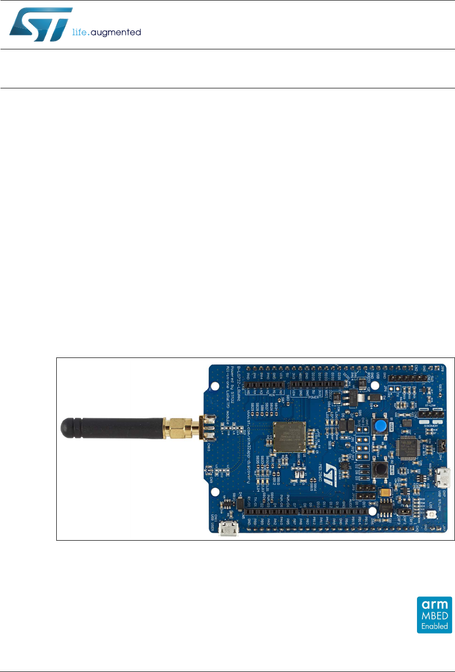
- Figure 1. B-L072Z-LRWAN1 LoRa® Discovery kit
- 1 Features
- 2 Product marking
- 3 Conventions
- 4 System requirements
- 5 Development toolchains
- 6 Demonstration software
- 7 Ordering and product information
- 8 Hardware layout and configuration
- Figure 2. Hardware block diagram
- Figure 3. B-L072Z-LRWAN1 top layout
- Figure 4. B-L072Z-LRWAN1 bottom layout
- 8.1 B-L072Z-LRWAN1 Discovery kit mechanical drawing
- 8.2 Embedded ST-LINK/V2-1
- 8.3 Power supply
- 8.4 IDD measurements
- 8.5 Clock sources
- 8.6 Reset sources
- 8.7 Antenna and RF connection
- 8.8 Virtual COM port
- 8.9 Buttons and LEDs
- 8.10 USB FS
- 9 Connectors
- 10 B-L072Z-LRWAN1 Discovery kit information
- Appendix A Schematic diagrams
- Appendix B Federal Communications Commission (FCC), Industry Canada (IC) Compliance and other Certifications
- B.1 FCC Compliance Statement
- B.2 IC Compliance Statement
- B.3 Other certifications
- B.3.1 EN 55032 (2012) / EN 55024 (2010) ETSI EN 301 489-1 (v1.9.2) / ETSI EN 301 489-3 (v1.6.1) EN 60950-1 (2006+A11/2009+A1/2010+A12/2011+A2/2013) CFR 47, FCC Part 15,Subpart B (Class B Digital Device) and Industry Canada ICES-003 (Issue 6/2016)
- B.3.2 Electrical Safety qualification for CE marking: EN 60950-1 (2006+A11/2009+A1/2010+A12/2011+A2/2013) IEC 60650-1 (2005+A1/2009+A2/2013)
- B.3.3 EMC qualification accordingly to standard CFR 47, FCC Part 15, Subpart B & Industry Canada ICES-003 (Issue 6/2016) Class B Digital Device
- B.3.4 CE qualification according to standards: ETSI EN 300 220-1 V2.4.1 (2012) / V3.1.1 (2017) ETSI EN 300 220-2 V2.4.1 (2012) / V3.1.1 (2017) RF Module already certified – Partial test only
- Revision history
September 2017 DocID029802 Rev 2 1/38
1
UM2115
User manual
Discovery kit for LoRaWAN™ and LPWAN protocols with STM32L0
Introduction
The B-L072Z-LRWAN1 Discovery kit embeds the CMWX1ZZABZ-091 LoRa® module
(Murata). This Discovery kit allows users to develop easily applications with the
STM32L072CZ and the LoRa® RF connectivity in one single module.
The B-L072Z-LRWAN1 Discovery kit has the full set of features available in the STM32L0
Series and offers ultra-low-power and LoRa® RF features. The B-L072Z-LRWAN1
Discovery kit is a low-cost and easy-to-use development kit to quickly evaluate and start a
development with an STM32L072CZ microcontroller.
The B-L072Z-LRWAN1 Discovery kit includes LoRa® RF interface, LEDs, push-buttons,
antenna, Arduino™ Uno V3 connectors, USB 2.0 FS connector in Micro-B format. The
integrated ST-LINK/V2-1 provides an embedded in-circuit debugger and programmer for the
STM32L0 MCUs.
The LoRaWAN™ stack is certified class A and C compliant. It is available inside the
I-CUBE-LRWAN firmware package.
To help users setting up a complete LoRaWAN™ node, the B-L072Z-LRWAN1 Discovery kit
comes with the STM32 comprehensive free software libraries and examples available with
the STM32Cube package, as well as a direct access to the Arm® Mbed Enabled™
resources at the http://mbed.org website.
Figure 1. B-L072Z-LRWAN1 LoRa® Discovery kit
1. Picture is not contractual.
www.st.com

Contents UM2115
2/38 DocID029802 Rev 2
Contents
1 Features . . . . . . . . . . . . . . . . . . . . . . . . . . . . . . . . . . . . . . . . . . . . . . . . . . . 6
2 Product marking . . . . . . . . . . . . . . . . . . . . . . . . . . . . . . . . . . . . . . . . . . . . 7
3 Conventions . . . . . . . . . . . . . . . . . . . . . . . . . . . . . . . . . . . . . . . . . . . . . . . . 7
4 System requirements . . . . . . . . . . . . . . . . . . . . . . . . . . . . . . . . . . . . . . . . 7
5 Development toolchains . . . . . . . . . . . . . . . . . . . . . . . . . . . . . . . . . . . . . . 8
6 Demonstration software . . . . . . . . . . . . . . . . . . . . . . . . . . . . . . . . . . . . . . 8
7 Ordering and product information . . . . . . . . . . . . . . . . . . . . . . . . . . . . . . 8
8 Hardware layout and configuration . . . . . . . . . . . . . . . . . . . . . . . . . . . . . 9
8.1 B-L072Z-LRWAN1 Discovery kit mechanical drawing . . . . . . . . . . . . . . . 12
8.2 Embedded ST-LINK/V2-1 . . . . . . . . . . . . . . . . . . . . . . . . . . . . . . . . . . . . . 13
8.2.1 Drivers . . . . . . . . . . . . . . . . . . . . . . . . . . . . . . . . . . . . . . . . . . . . . . . . . . 13
8.2.2 ST-LINK/V2-1 firmware upgrade . . . . . . . . . . . . . . . . . . . . . . . . . . . . . . 13
8.3 Power supply . . . . . . . . . . . . . . . . . . . . . . . . . . . . . . . . . . . . . . . . . . . . . . 14
8.4 IDD measurements . . . . . . . . . . . . . . . . . . . . . . . . . . . . . . . . . . . . . . . . . 15
8.5 Clock sources . . . . . . . . . . . . . . . . . . . . . . . . . . . . . . . . . . . . . . . . . . . . . . 15
8.6 Reset sources . . . . . . . . . . . . . . . . . . . . . . . . . . . . . . . . . . . . . . . . . . . . . 15
8.7 Antenna and RF connection . . . . . . . . . . . . . . . . . . . . . . . . . . . . . . . . . . . 16
8.8 Virtual COM port . . . . . . . . . . . . . . . . . . . . . . . . . . . . . . . . . . . . . . . . . . . . 16
8.9 Buttons and LEDs . . . . . . . . . . . . . . . . . . . . . . . . . . . . . . . . . . . . . . . . . . 16
8.10 USB FS . . . . . . . . . . . . . . . . . . . . . . . . . . . . . . . . . . . . . . . . . . . . . . . . . . 17
9 Connectors . . . . . . . . . . . . . . . . . . . . . . . . . . . . . . . . . . . . . . . . . . . . . . . 18
9.1 Arduino Uno V3 connectors . . . . . . . . . . . . . . . . . . . . . . . . . . . . . . . . . . . 18
9.2 B-L072Z-LRWAN1 Discovery kit CN2 and CN3 connectors . . . . . . . . . . 20
9.3 Other connectors . . . . . . . . . . . . . . . . . . . . . . . . . . . . . . . . . . . . . . . . . . . 22
9.3.1 Debug connector SWD . . . . . . . . . . . . . . . . . . . . . . . . . . . . . . . . . . . . . 22
9.3.2 SWD Interface . . . . . . . . . . . . . . . . . . . . . . . . . . . . . . . . . . . . . . . . . . . . 22

DocID029802 Rev 2 3/38
UM2115 Contents
3
9.3.3 External +3.3 V . . . . . . . . . . . . . . . . . . . . . . . . . . . . . . . . . . . . . . . . . . . 22
9.4 Description of the jumpers . . . . . . . . . . . . . . . . . . . . . . . . . . . . . . . . . . . . 22
9.5 Configuration of the solder bridges . . . . . . . . . . . . . . . . . . . . . . . . . . . . . 23
10 B-L072Z-LRWAN1 Discovery kit information . . . . . . . . . . . . . . . . . . . . 27
10.1 Identification . . . . . . . . . . . . . . . . . . . . . . . . . . . . . . . . . . . . . . . . . . . . . . . 27
10.2 Board revision history . . . . . . . . . . . . . . . . . . . . . . . . . . . . . . . . . . . . . . . . 27
10.3 Known limitations . . . . . . . . . . . . . . . . . . . . . . . . . . . . . . . . . . . . . . . . . . . 27
Appendix A Schematic diagrams . . . . . . . . . . . . . . . . . . . . . . . . . . . . . . . . . . . . . 28
Appendix B Federal Communications Commission (FCC),
Industry Canada (IC) Compliance and other Certifications . . . . . . 35
B.1 FCC Compliance Statement . . . . . . . . . . . . . . . . . . . . . . . . . . . . . . . . . . . 35
B.1.1 ANSI C63.4 (2014) American National Standard for Methods of
Measurement of Radio-Noise Emissions from Low-Voltage Electrical
and Electronic Equipment in the Range of 9 kHz to 40 GHz . . . . . . . . . 35
B.2 IC Compliance Statement . . . . . . . . . . . . . . . . . . . . . . . . . . . . . . . . . . . . . 35
B.2.1 Industry Canada Licence-Exempt Radio Apparatus. . . . . . . . . . . . . . . . 35
B.2.2 Radio Frequency (RF) Exposure Compliance of
Radiocommunication Apparatus. . . . . . . . . . . . . . . . . . . . . . . . . . . . . . . 36
B.3 Other certifications . . . . . . . . . . . . . . . . . . . . . . . . . . . . . . . . . . . . . . . . . . 36
B.3.1 EN 55032 (2012) / EN 55024 (2010) ETSI EN 301 489-1 (v1.9.2) /
ETSI EN 301 489-3 (v1.6.1) EN 60950-1
(2006+A11/2009+A1/2010+A12/2011+A2/2013) CFR 47,
FCC Part 15,Subpart B (Class B Digital Device) and
Industry Canada ICES-003 (Issue 6/2016). . . . . . . . . . . . . . . . . . . . . . . 36
B.3.2 Electrical Safety qualification for CE marking: EN 60950-1
(2006+A11/2009+A1/2010+A12/2011+A2/2013) IEC 60650-1
(2005+A1/2009+A2/2013) . . . . . . . . . . . . . . . . . . . . . . . . . . . . . . . . . . . 36
B.3.3 EMC qualification accordingly to standard CFR 47, FCC Part 15,
Subpart B & Industry Canada ICES-003 (Issue 6/2016)
Class B Digital Device . . . . . . . . . . . . . . . . . . . . . . . . . . . . . . . . . . . . . . 36
B.3.4 CE qualification according to standards:
ETSI EN 300 220-1 V2.4.1 (2012) / V3.1.1 (2017) ETSI EN
300 220-2 V2.4.1 (2012) / V3.1.1 (2017) RF Module already
certified – Partial test only. . . . . . . . . . . . . . . . . . . . . . . . . . . . . . . . . . . . 36
Revision history . . . . . . . . . . . . . . . . . . . . . . . . . . . . . . . . . . . . . . . . . . . . . . . . . . . . 37

List of tables UM2115
4/38 DocID029802 Rev 2
List of tables
Table 1. ON/OFF conventions . . . . . . . . . . . . . . . . . . . . . . . . . . . . . . . . . . . . . . . . . . . . . . . . . . . . . . 7
Table 2. Ordering information . . . . . . . . . . . . . . . . . . . . . . . . . . . . . . . . . . . . . . . . . . . . . . . . . . . . . . . 8
Table 3. IDD measurements and solder-bridge settings . . . . . . . . . . . . . . . . . . . . . . . . . . . . . . . . . 15
Table 4. Assignment of the control ports . . . . . . . . . . . . . . . . . . . . . . . . . . . . . . . . . . . . . . . . . . . . . 17
Table 5. Arduino Uno V3 connectors . . . . . . . . . . . . . . . . . . . . . . . . . . . . . . . . . . . . . . . . . . . . . . . . 18
Table 6. Connector CN2 . . . . . . . . . . . . . . . . . . . . . . . . . . . . . . . . . . . . . . . . . . . . . . . . . . . . . . . . . . 20
Table 7. Connector CN3 . . . . . . . . . . . . . . . . . . . . . . . . . . . . . . . . . . . . . . . . . . . . . . . . . . . . . . . . . . 21
Table 8. Debug connector SWD (CN12) . . . . . . . . . . . . . . . . . . . . . . . . . . . . . . . . . . . . . . . . . . . . . 22
Table 9. External +3.3 V (CN13). . . . . . . . . . . . . . . . . . . . . . . . . . . . . . . . . . . . . . . . . . . . . . . . . . . . 22
Table 10. Description of the jumpers . . . . . . . . . . . . . . . . . . . . . . . . . . . . . . . . . . . . . . . . . . . . . . . . . 22
Table 11. Configuration of the solder bridges . . . . . . . . . . . . . . . . . . . . . . . . . . . . . . . . . . . . . . . . . . . 23
Table 12. Document revision history . . . . . . . . . . . . . . . . . . . . . . . . . . . . . . . . . . . . . . . . . . . . . . . . . 37

DocID029802 Rev 2 5/38
UM2115 List of figures
5
List of figures
Figure 1. B-L072Z-LRWAN1 LoRa® Discovery kit. . . . . . . . . . . . . . . . . . . . . . . . . . . . . . . . . . . . . . . . 1
Figure 2. Hardware block diagram. . . . . . . . . . . . . . . . . . . . . . . . . . . . . . . . . . . . . . . . . . . . . . . . . . . . 9
Figure 3. B-L072Z-LRWAN1 top layout . . . . . . . . . . . . . . . . . . . . . . . . . . . . . . . . . . . . . . . . . . . . . . . 10
Figure 4. B-L072Z-LRWAN1 bottom layout . . . . . . . . . . . . . . . . . . . . . . . . . . . . . . . . . . . . . . . . . . . . 11
Figure 5. B-L072Z-LRWAN1 mechanical drawing . . . . . . . . . . . . . . . . . . . . . . . . . . . . . . . . . . . . . . . 12
Figure 6. USB composite device . . . . . . . . . . . . . . . . . . . . . . . . . . . . . . . . . . . . . . . . . . . . . . . . . . . . 13
Figure 7. RF signal path and connectors . . . . . . . . . . . . . . . . . . . . . . . . . . . . . . . . . . . . . . . . . . . . . . 16
Figure 8. B-L072Z-LRWAN1: location of the solder bridges (top view) . . . . . . . . . . . . . . . . . . . . . . . 25
Figure 9. B-L072Z-LRWAN1: location of the solder bridges (bottom view) . . . . . . . . . . . . . . . . . . . . 26
Figure 10. B-L072Z-LRWAN1 Discovery kit, Top view . . . . . . . . . . . . . . . . . . . . . . . . . . . . . . . . . . . . 29
Figure 11. Power . . . . . . . . . . . . . . . . . . . . . . . . . . . . . . . . . . . . . . . . . . . . . . . . . . . . . . . . . . . . . . . . . 30
Figure 12. ST-LINK/V2-1 . . . . . . . . . . . . . . . . . . . . . . . . . . . . . . . . . . . . . . . . . . . . . . . . . . . . . . . . . . . 31
Figure 13. LoRa module . . . . . . . . . . . . . . . . . . . . . . . . . . . . . . . . . . . . . . . . . . . . . . . . . . . . . . . . . . . 32
Figure 14. USB 2.0 FS and antenna . . . . . . . . . . . . . . . . . . . . . . . . . . . . . . . . . . . . . . . . . . . . . . . . . . 33
Figure 15. Connectors . . . . . . . . . . . . . . . . . . . . . . . . . . . . . . . . . . . . . . . . . . . . . . . . . . . . . . . . . . . . . 34

Features UM2115
6/38 DocID029802 Rev 2
1 Features
The B-L072Z-LRWAN1 Discovery kit offers the following features:
•CMWX1ZZABZ-091 LoRa® module (Murata)
– Embedded ultra-low-power STM32L072CZ Series MCUs, based on Arm®Cortex®
-M0+ core, with 192 Kbytes of Flash memory, 20 Kbytes of RAM, 20 Kbytes of
EEPROM
– USB 2.0 FS
– 4-channel,12-bit ADC, 2xDAC
– 6-bit timers, LP-UART, I2C and SPI
– Embedded SX1276 transceiver
– LoRa®, FSK, GFSK, MSK, GMSK and OOK modulations
– +14 dBm or +20 dBm selectable output power
– 157 dB maximum link budget
– Programmable bit rate up to 300 Kbit/s
– High sensitivity: down to -137 dBm
– Bullet-proof front end: IIP3 = -12.5 dBm
– 89 dB blocking immunity
– Low RX current of 10 mA, 200 nA register retention
– Fully integrated synthesizer with a resolution of 61 Hz
– Built-in bit synchronizer for clock recovery
– Sync word recognition
– Preamble detection
– 127 dB+ dynamic range RSSI
•Including 50 Ohm SMA RF antenna
•1 user and reset push-buttons
•Board connectors:
– USB FS connector
– SMA and U.FL RF
•Board expansion connectors:
– Arduino Uno V3
•7 LEDs:
– 4 general-purpose LEDs
– 5 V-power LED
– ST-LINK-communication LED
– Fault-power LED
•Flexible power-supply options: ST-LINK USB VBUS or external sources
•On-board ST-LINK/V2-1 debugger/programmer with USB re-enumeration capability:
mass storage, virtual COM port and debug port
•Comprehensive free software libraries and examples available with the STM32Cube
package
DocID029802 Rev 2 7/38
UM2115 Product marking
37
•Support of a wide choice of Integrated Development Environments (IDES) including
IAR™, Keil®, GCC-based IDEs, Arm® Mbed
•Arm® Mbed Enabled™ compliant
2 Product marking
Evaluation tools marked as "ES" or "E" are not yet qualified and are therefore not ready to
be used as reference designs or in production. Any consequences arising from such usage
will not be at ST’s charge. In no event will ST be liable for any customer usage of these
engineering sample tools as reference designs or in production.
"E" or "ES" marking examples of location:
•On the targeted microcontroller that is soldered on the board (for illustration of
microcontroller marking, refer to the section "Package information" of the
microcontroller datasheet at www.st.com).
•Next to the evaluation tool ordering part number, that is stuck or silkscreen printed on
the board
3 Conventions
Table 1 provides the definition of some conventions used in the present document.
4 System requirements
•Windows® OS (7, 8 and 10), Linux® 64-bit or macOS™
•USB Type-A to Micro-B cable
Table 1. ON/OFF conventions
Convention Definition
Jumper JPx ON Jumper fitted
Jumper JPx OFF Jumper not fitted
Solder bridge SBx ON SBx connections closed by solder
Solder bridge SBx OFF SBx connections left open
Development toolchains UM2115
8/38 DocID029802 Rev 2
5 Development toolchains
•Keil® MDK-ARM(a)
•IAR™ EWARM(a)
•GCC-based IDEs including free SW4STM32 from AC6
•Arm® Mbed Enabled™ online (see http://mbed.org)
6 Demonstration software
The demonstration software, included in the STM32Cube package, is preloaded in the
STM32 Flash memory for easy demonstration of the device peripherals in standalone mode.
The latest versions of the demonstration source code and associated documentation can be
downloaded from the www.st.com/i-cube-lrwan webpage.
7 Ordering and product information
Before installing and using the product, accept the Evaluation Product License Agreement
at the www.st.com/stm32app-discovery webpage.
For more information on the STM32L072 Discovery kit visit the www.st.com/stm32app-
discovery webpage.
To order the B-L072Z-LRWAN1 Discovery kit refer to Table 2.
a. On Windows® only.
Table 2. Ordering information
RPN Target STM32
B-L072Z-LRWAN1 STM32L072CZ
DocID029802 Rev 2 9/38
UM2115 Hardware layout and configuration
37
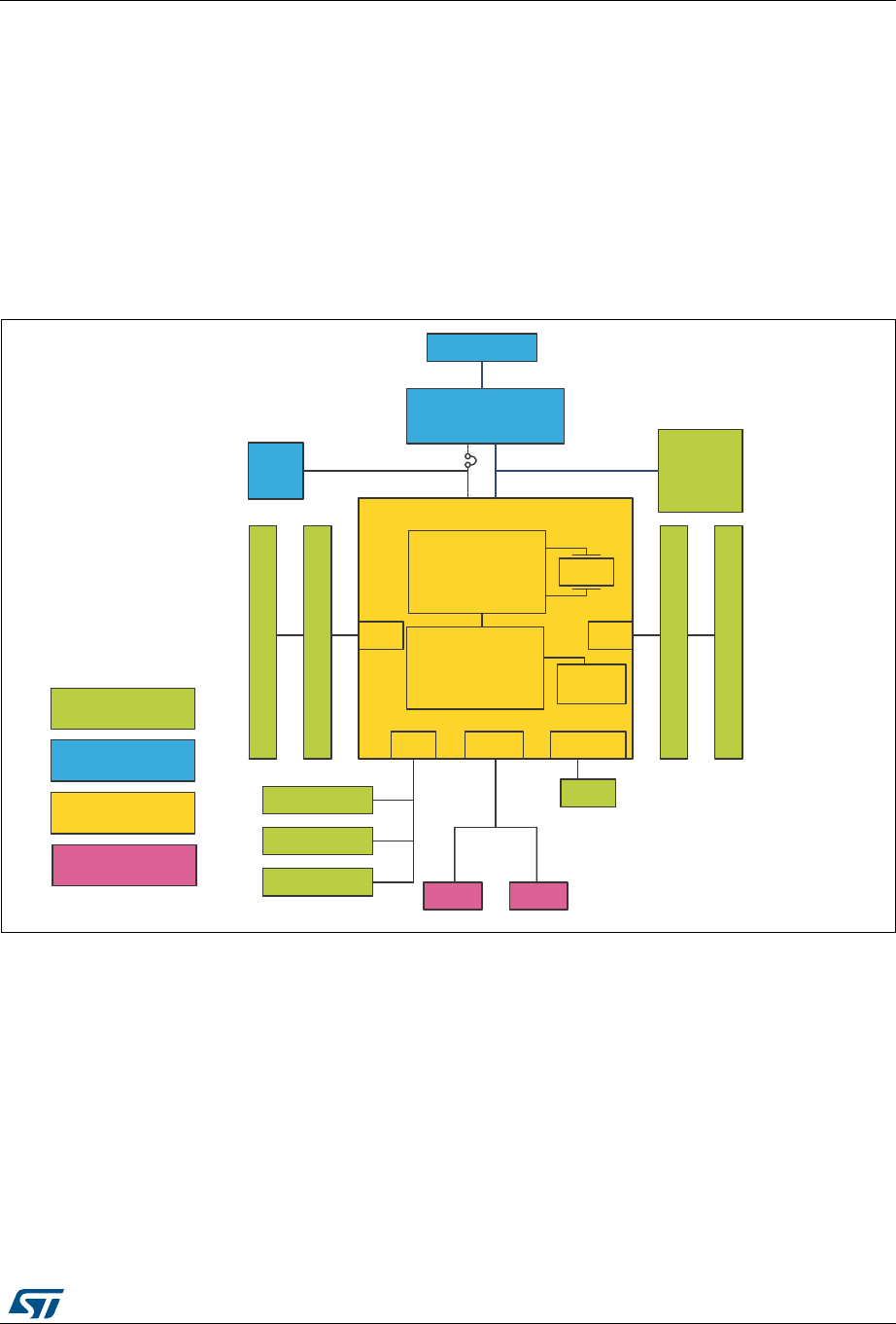
8 Hardware layout and configuration
The B-L072Z-LRWAN1 Discovery kit has been designed around the Murata LoRa® module
including the STM32L072CZ microcontroller in a 49-pin WLCSP package.
Figure 2 illustrates the connection between the Murata LoRa® module and the peripherals
(ST-LINK/V2, RF Antenna, LEDs, push-buttons, USB 2.0 FS Micro-B connector, 3xAAA
battery holder).
Figure 3 and Figure 4 help users to locate these features on the STM32L072 Discovery kit.
Figure 2. Hardware block diagram
06Y9
0LFUR86%
67/,1.9
&0:;==$%=
670/
6;
N
0
7&;2
6:'
*3,2+HDGHU
*3,2+HDGHU
5(6(7
,2 ,2
3%
/('V
,2
0LFUR86%
3%8VHU
$17
60$
[$$$
EDWWHU\
FDVH
X)O
$UGXLQRFRQQHFWRU
$UGXLQRFRQQHFWRU
)RUGHEXJ
SURJUDPSXUSRVHV
)RUXVHU¶V
SXUSRVHV
5)PRGXOH
5)FRQQHFWRUV
Hardware layout and configuration UM2115
10/38 DocID029802 Rev 2
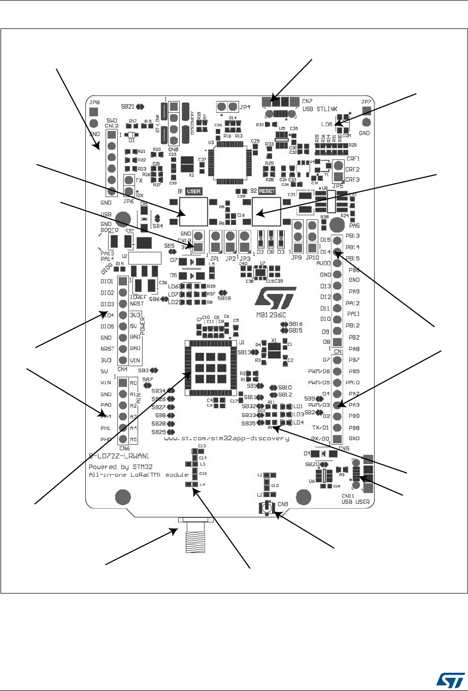
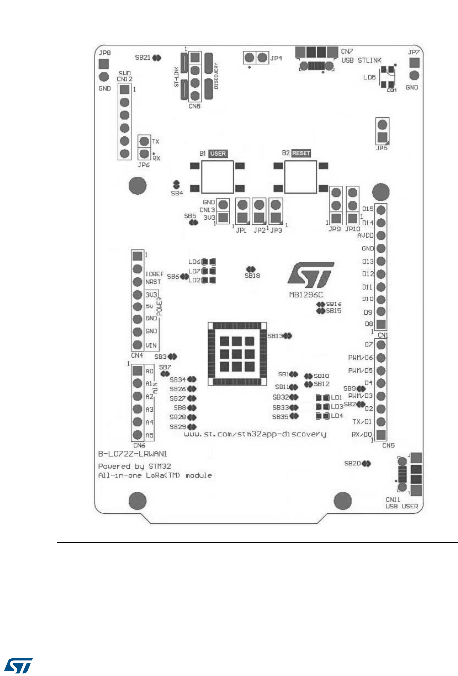
Figure 3. B-L072Z-LRWAN1 top layout
Micro-B ST-LINK USB
connector
ST-LINK COM LED
RESET push-button
A
rduino Uno V3
connectors
A
rduino Uno V3
connectors
Micro-B USB 2.0 FS
user connector
U.FL connector (option)
On-board Antenna matching
designed filter
RF SMA connector
LoRa module
CMWX1ZZABZ-091
with STM32L072CZ
Y
6
External +3.3V
power supply
User push-button
SWD connector
User LEDs
DocID029802 Rev 2 11/38
UM2115 Hardware layout and configuration
37
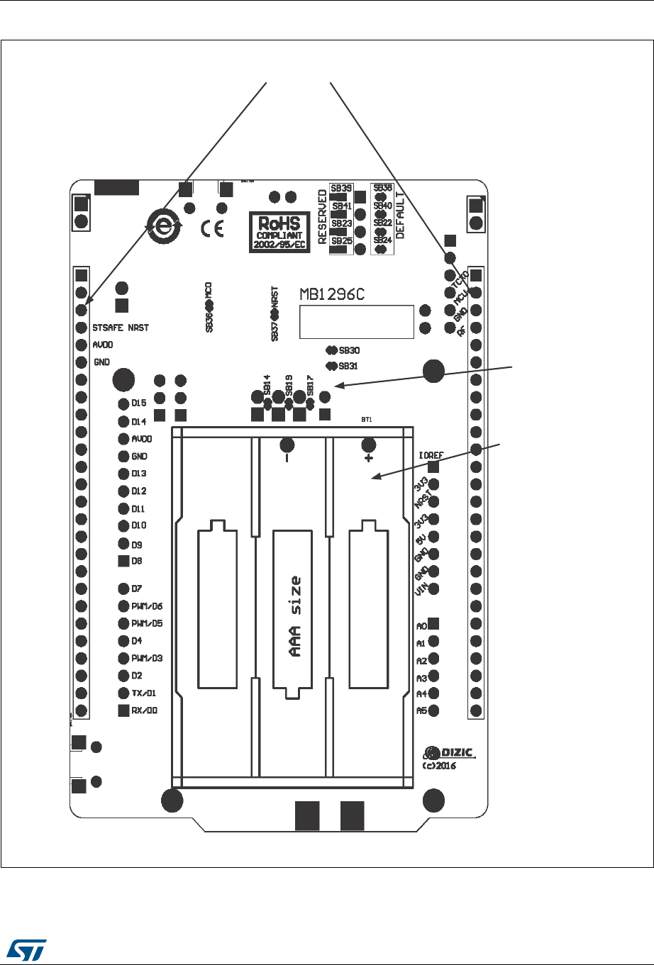
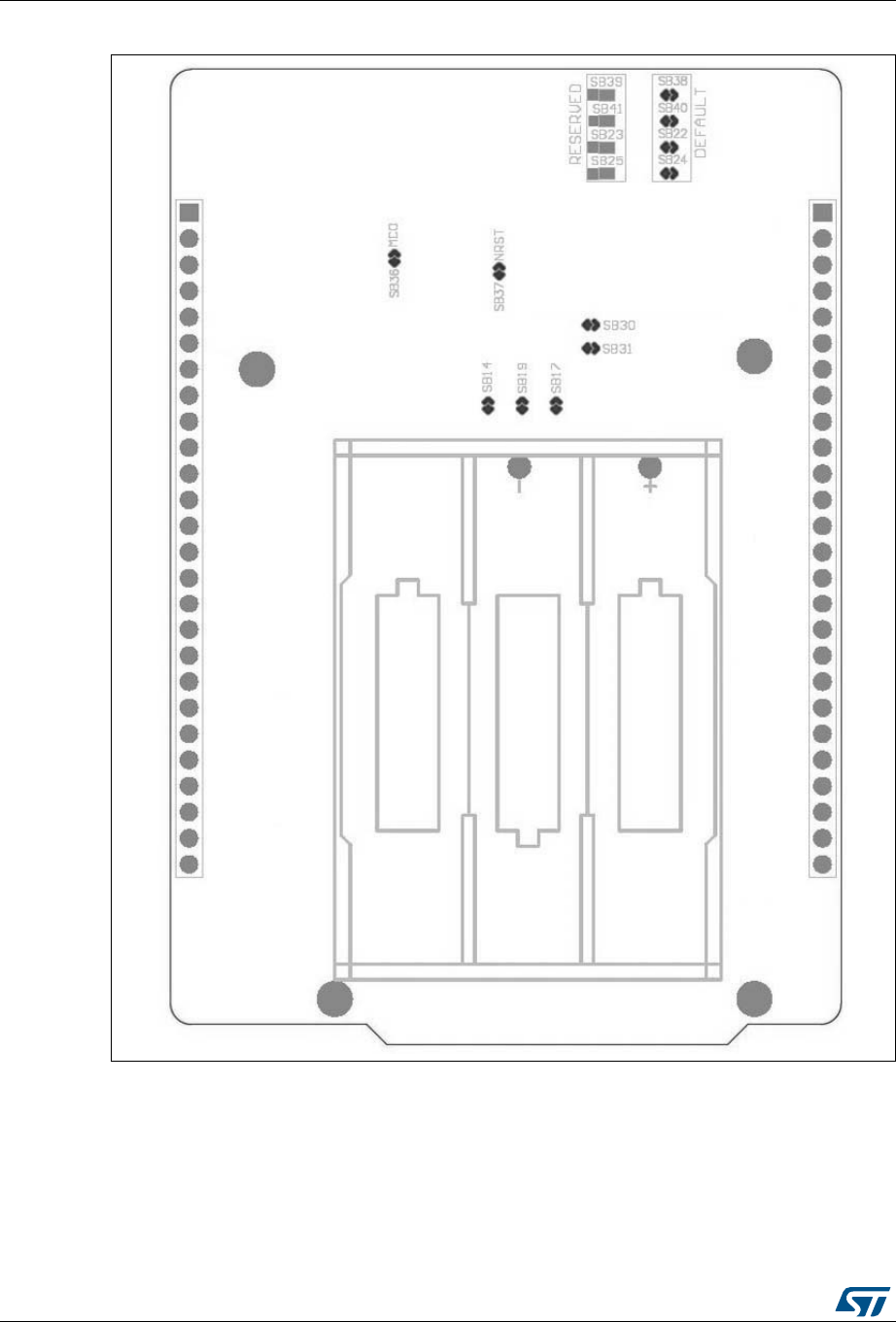
Figure 4. B-L072Z-LRWAN1 bottom layout
06Y9
0DQ\86(5FRQILJXUDEOH
VHWWLQJVE\6%V
[$$$VL]HEDWWHU\KROGHU
IRUIXOODXWRQRPRXV
RSHUDWLRQ
$OO*3,2VDYDLODEOHLQ[
6,/KHDGHUV
Hardware layout and configuration UM2115
12/38 DocID029802 Rev 2
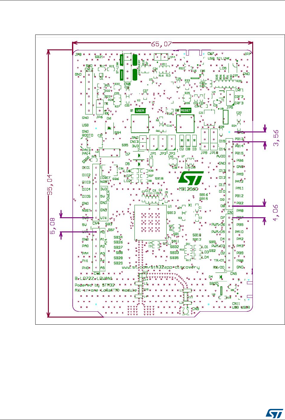
8.1 B-L072Z-LRWAN1 Discovery kit mechanical drawing
Figure 5. B-L072Z-LRWAN1 mechanical drawing
1. Plastic spacer height = 14 mm, overall height = 22 mm +/- 1 mm.
2. The overall dimensions of the B-L072Z-LRWAN1 is 106 x 65,07 mm including antenna and USB
connectors.
DocID029802 Rev 2 13/38
UM2115 Hardware layout and configuration
37
8.2 Embedded ST-LINK/V2-1
The ST-LINK/V2-1 programming and debugging tool is integrated on the B-L072Z-LRWAN1
Discovery kit. Compared to ST-LINK/V2 the changes are listed below.
The new features supported on ST-LINK/V2-1 are:
•USB software re-enumeration
•Virtual COM port interface on USB
•Mass storage interface on USB
•USB power management request for more than 100mA power on USB
These features are no more supported on ST-LINK/V2-1:
•SWIM interface
•Application voltage lower than 3 V
For general information concerning the debugging and programming features that are
common to both versions V2 and V2-1, refer to ST-LINK/V2 in-circuit debugger/programmer
for STM8 and STM32 User manual (UM1075).
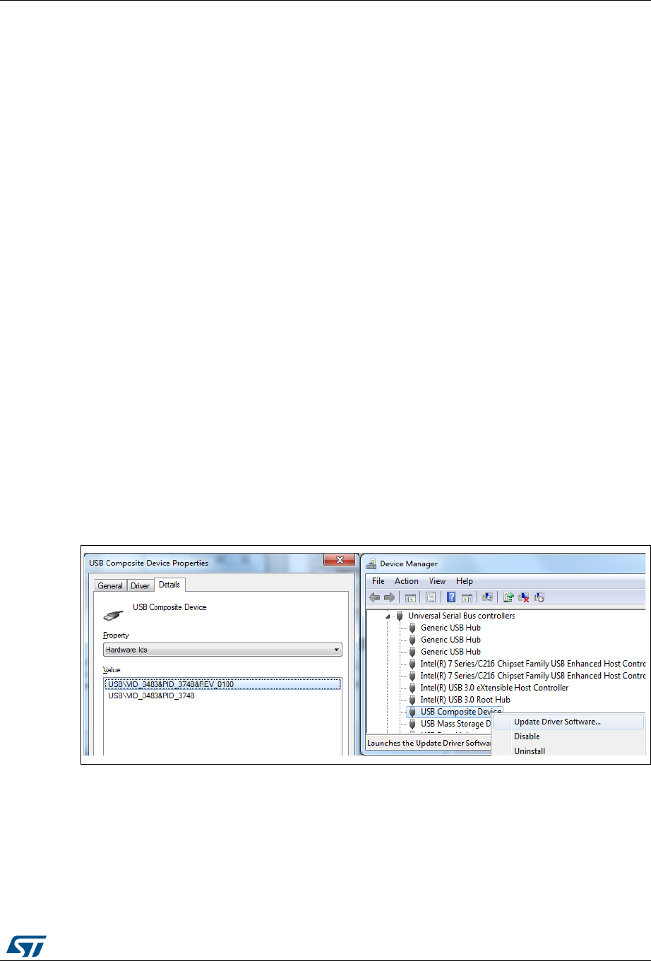
8.2.1 Drivers
The ST-LINK/V2-1 requires a dedicated USB driver, which, for Windows® 7, 8 and 10 is
available at the www.st.com website.
In case the B-L072Z-LRWAN1 Discovery kit is connected to the PC before the driver is
installed, some B-L072Z-LRWAN1 interfaces may be declared as "unknown" in the PC
device manager. In this case the user must install the driver files and update the driver of the
connected device from the device manager.
Note: Prefer using the "USB Composite Device" handle for a full recovery.
Figure 6. USB composite device
8.2.2 ST-LINK/V2-1 firmware upgrade
The ST-LINK/V2-1 embeds a firmware upgrade mechanism for in-situ upgrade through the
USB port. As the firmware may evolve during the life time of the ST-LINK/V2-1 product (for
example new functionalities, bug fixes, support for new microcontroller families), it is
recommended to visit the www.st.com website before starting to use the B-L072Z-LRWAN1
Discovery kit and periodically, to stay up-to-date with the latest firmware version.

Hardware layout and configuration UM2115
14/38 DocID029802 Rev 2
8.3 Power supply
The B-L072Z-LRWAN1 Discovery kit is designed to be powered in various ways. It can be
simply plugged on a USB PC port with a Micro-B USB cable. In this mode, the board is
programmed and debugged via the ST-LINK/V2-1 USB port on CN7. It is possible to use
one of the different following sources:
•External +3.3 V connected to CN13 (+3.3 V and GND pins of CN13 must be
connected).
•7-12 V DC power supply plugged on Arduino™ Uno V3 connectors: VIN on pin 8 and
GND on pin 7 of CN4 (VIN and GND pins must be both connected)
•USB 2.0 FS Micro-B on CN11 connector (Device mode). The power supply is provided
by the USB port connected to CN11.
•On-board 3xAAA-sized battery holder BT1 located on the bottom side of the Discovery
kit (batteries are not delivered inside the Discovery kit package). Respect the battery
polarities mentioned in the battery case.
•5V_ST_LINK DC power with limitation from ST-LINK USB connector. The USB type
Micro-B connector CN7 of ST-LINK/V2-1. If the USB enumeration succeeds (as
explained below), the ST-LINK 5 V link power is enabled, by asserting the PWR_ENn
signal. This pin is connected to a power switch ST890, which powers the board. This
power switch features also a current limitation to protect the PC in case of a short-
circuit on board (more than 625mA). The Discovery kit can be powered from the ST-
LINK USB connector, but only the ST-LINK circuit has the power before USB
enumeration, because the host PC only provides 100 mA to the board at that time.
During the USB enumeration, the Discovery kit requires 300 mA power from the host
PC. If the host is able to provide the required power, the enumeration finishes by a
"SetConfiguration" command and then, the power transistor ST890 is switched ON, the
red LED LD7 is turned ON, thus the Discovery kit can consume maximum 300 mA
current, but no more. If the host is not able to provide the requested current, the
enumeration fails. Therefore the ST890 remains OFF and the STM32 part including the
extension board is not powered. As a consequence the red LED LD7 remains turned
OFF. In this case it is mandatory to use an external power supply.
To further decrease the current consumption of the board, the LED7 must be disconnected
by opening SB18.
Users do not have to manage the different configurations with jumpers or switches. The
power supplies are internally managed by a set of diodes on the respective power supply
branches.
If the board is supplied by CN13, by battery or by CN11, SB37 must be removed to release
the RESET pin managed by ST-LINK. In that case the ST-LINK is no more powered.
The red LED LD7 (+5 V power supply) is turned on (with SB18 ON) as soon as one of the
power sources listed above is present.
Note: The Discovery kit must be powered by a power supply unit or by an auxiliary equipment
complying with the standard EN-60950-1: 2006+A11/2009, and must be Safety Extra Low
Voltage (SELV) with limited power capability.
DocID029802 Rev 2 15/38
UM2115 Hardware layout and configuration
37
8.4 IDD measurements
The B-L072Z-LRWAN1 Discovery kit power consumption is measured by mean of three
connectors (not fitted initially) JP1, JP2 and JP3. These three connectors are respectively
connected to the power-supply inputs VDD_RF_LRA, VDD_USB_LRA and
VDD_MCU_LRA of the LoRa® module. The purpose is to monitor separately the different
power consumptions by branches which are divided in three sections: RF, USB and MCU.
To be able to insert a multimeter in each branch where the measurements must take place,
users have to remove the associated solder bridge that initially shortcut the JPx connectors
in the default configuration.
The Table 3 below summarizes the possible configurations:
8.5 Clock sources
The Murata LoRa® module embeds its own TCXO running at 32 MHz when enabled.
The TCXO is either controlled by the STM32 pin PA12 (when pin 1 of JP9 is connected to
pin 2 of JP9) or always enabled (when pin 2 of JP9 is connected to pin 3 of JP9). For the
description of the jumpers refer to Table 10.
When an accurate external-high-speed clock is needed by the STM32, the TCXO_OUT
clock pin is supplied by the module pin PH0_OSC_IN by closing SB13.
The B-L072Z-LRWAN1 Discovery kit can be equipped, if needed, with an external crystal
oscillator. An 8 MHz oscillator with 20 pF capacitors can be added on the board (X1, C1 and
C2 are not fitted by default) for user needs.
8.6 Reset sources
The reset signal of the B-L072Z-LRWAN1 Discovery kit is active low and the reset sources
is one of the following:
•Reset button B2
•Arduino Uno V3 shield board from CN4
•LoRa® module internal reset coming either from STSAFE security IC or STM32L072CZ
(selectable by jumper JP10)
•Embedded ST-LINK/V2-1
Table 3. IDD measurements and solder-bridge settings
Jumper name Status IDD Measurement
JP1 VDD_RF_LRA
SB17 ON (default) N/A
SB17 OFF IDD VDD_RF_LRA
JP2 VDD_USB_LRA
SB19 ON (default) N/A
SB19 OFF IDD VDD_USB_LRA
JP3 VDD_MCU_LRA
SB14 ON (default) N/A
SB14 OFF IDD VDD_MCU_LRA
Hardware layout and configuration UM2115
16/38 DocID029802 Rev 2
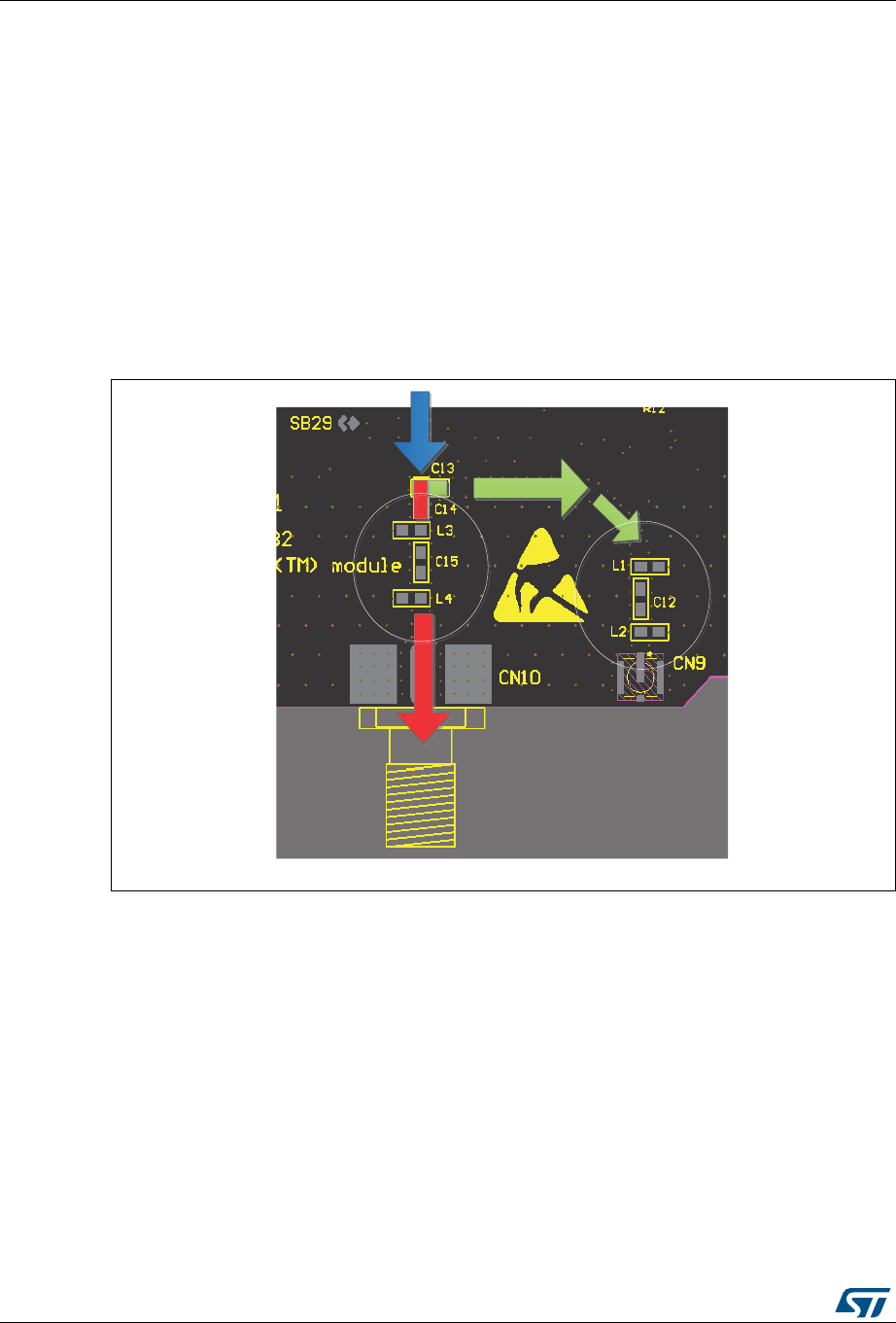
8.7 Antenna and RF connection
The B-L072Z-LRWAN1 Discovery kit includes a stubby straight 900 MHz 50 ohm antenna
that must be connected to the SMA connector CN10 for any RF communication purpose.
There are two paths designed for RF signal (the blue arrow in the Figure 7), the default path
is connected to the SMA connector output (the red arrow in the Figure 7) and the second
one is U.FL CN9 connector (the green arrow in the Figure 7). Each RF signal path includes
an antenna matching circuitry that can be mounted and adjusted by advanced users.
Initially, the default path connects the LoRa® module RF signal to the SMA connector
through 0 Ohm resistors that are fitted at the location of C14 and C15. Notice that C13 and
C14, as shown below in Figure 7, have a common pad on layout from antenna circuitry. If
the users want to connect the U.FL connector instead of the SMA, they need to redirect the
RF signal through C13 and then rotate the component on the expected footprint.
Figure 7. RF signal path and connectors
8.8 Virtual COM port
The serial interface USART2 is directly available as a virtual COM port of the PC, connected
to the ST-LINK/V2-1 USB connector CN7. For configuration details refer to “STM32 LoRa®
software expansion for STM32Cube” User manual (UM2073).
8.9 Buttons and LEDs
The black button B2 located at the top side of the Discovery kit, is the reset of the
microcontroller STM32L072CZ.
06Y9
^DƉĂƚŚ
h͘&>ƉĂƚŚ
60$
FRQQHFWRU
8)/
FRQQHFWRU
Z&ƉĂƚŚ
$QWHQQD
PDWFKLQJ
$QWHQQD
PDWFKLQJ
DocID029802 Rev 2 17/38
UM2115 Hardware layout and configuration
37
The blue button B1 located at the top side is available to be used as a digital input or as a
wakeup-alternate function. When the button is depressed the logic state is 1, otherwise the
logic state is 0.
By default the user button is connected to PB2, it can also be connected to PA0 as wakeup
source. In this case, SB31 must be removed and SB30 must be fitted.
Seven LEDs located at the top side are available, four of which are general purpose LEDs
for user needs. To light a LED write a high-logic state 1 in the corresponding GPIO register.
Table 4 shows the assignment of the control ports to the LED indicators.
8.10 USB FS
The B-L072Z-LRWAN1 board supports USB FS 2.0 communication via a USB Micro-B
connector. VBUS is powered by another USB host when B-L072Z-LRWAN1 board works as
a USB device.
Note: When the B-L072Z-LRWAN1 board is powered by an external power supply through USB
FS connector (CN11), in device mode, do not use a PC as power source if the current
consumption is greater than 100 mA, otherwise the PC can be damaged.
Table 4. Assignment of the control ports
Reference Color Name Comment/function
B1 Blue USER Alternate function wakeup
B2 Black RESET Microcontroller reset
LD1 Green GP User defined
LD2 Green GP User defined
LD3 Blue GP User defined
LD4 Red GP User defined
LD5 Red/Green ST-LINK COM Green when communication
LD6 Red Fault power Current upper than 625mA
LD7 Red 5 V Power 5 V present
Connectors UM2115
18/38 DocID029802 Rev 2
9 Connectors
9.1 Arduino Uno V3 connectors
Table 5. Arduino Uno V3 connectors
Connector Pin Pin name STM32 Pin Function
CN1
10 D15 PB8 I2C1_SCL
9 D14 PB9 I2C1_SDA
8 AVDD VREF+ VREF+
7 GND GND Ground
6 D13 PA5 or PB13 SPI1_SCK or
SPI2_SCK
5 D12 PB14 SPI2_MISO
4 D11 PB15 SPI2_MOSI
3 D10 PB6 LPTIM1_ETR
2 D9 PB12 SPI2_NSS
1 D8 PA9 USART1_TX
CN4
1NC- -
2 IOREF - +3.3 V Ref
3 RESET NRST MCU_nRST
4 +3.3 V - +3.3 V
input/output
5 +5 V - 5 V output
6 GND - Ground
7 GND - Ground
8 VIN - Power input
CN5
8D7PA8MCO
7 D6 PB2 LPTIM1_OUT
6 D5 PB7 LPTIM1_IN2
5 D4 PB5 LPTIM1_IN1
4 D3 PB13 or NC TIM21_CH1 or NC
3 D2 PA10 USART1_RX
2 D1 PA2 USART2_TX
1 D0 PA3 USART2_RX
DocID029802 Rev 2 19/38
UM2115 Connectors
37
CN6
1 A0 PA0 ADC_IN0
2 A1 NC or PA0 NC or ADC_IN0
3 A2 PA4 ADC_IN4
4 A3 NC or PA4 NC or ADC_IN4
5 A4 PH1 or PB9 OSC_IN or
I2C1_SDA
6 A5 PH0 or PB8 OSC_OUT or
I2C1_SCL
Table 5. Arduino Uno V3 connectors (continued)
Connector Pin Pin name STM32 Pin Function
Connectors UM2115
20/38 DocID029802 Rev 2
9.2 B-L072Z-LRWAN1 Discovery kit CN2 and CN3 connectors
Table 6. Connector CN2
Connector Pin Pin name STM32 Pin Function
CN2
1 TCXO_VCC - LoRa® module TCXO power
2 VDD_MCU_LRA - MCU section power supply
3 GND - Ground
4 VDD_RF_LRA - MCU section power supply
5 GND - Ground
6 VDD_USB_LRA - MCU section power supply
7 GND - Ground
8 BOOT0 BOOT0 BOOT0
9PA13PA13 SWDIO
10 PA14 PA14 SWCLK
11 SX1276_DIO0 - LoRa® module debug pin
12 SX1276_DIO1 - LoRa® module debug pin
13 SX1276_DIO2 - LoRa® module debug pin
14 SX1276_DIO3 - LoRa® module debug pin
15 SX1276_DIO4 - LoRa® module debug pin
16 SX1276_DIO5 - LoRa® module debug pin
17 GND - Ground
18 MCU_nRST NRST RESET
19 +3.3 V - +3.3 V power supply input/output
20 +5 V - +5 V power supply input
21 VIN - VIN power supply input (7-12Vdc)
22 GND - Ground
23 PA0 PA0 ADC_IN0
24 PA4 PA4 ADC_IN4
25 PH1 PH1 OSC_OUT
26 PH0 PH0 OSC_IN
DocID029802 Rev 2 21/38
UM2115 Connectors
37
Table 7. Connector CN3
Connector Pin Pin name STM32 Pin Function
CN3
1 CRF1 PA1 LoRa® module dedicated pin
2 CRF2 PC2 LoRa® module dedicated pin
3 CRF3 PC1 LoRa® module dedicated pin
4 STSAFE_nRST - STSAFE security IC reset pin
5 AVDD VREF+ VREF+
6 GND - Ground
7PA5PA5 ADC_IN5
8 PB13 PB13 SPI2_SCK
9 PB14 PB14 SPI2_MISO
10 PB15 PB15 SPI2_MOSI
11 PB6 PB6 LPTIM1_ETR
12 GND - Ground
13 PA9 PA9 USART1_TX
14 PA12 PA12 USB_DP
15 PA11 PA11 USB_DM
16 PB12 PB12 SPI2_NSS
17 PB2 PB2 LPTIM1_OUT
18 PA8 PA8 MCO
19 PB7 PB7 LPTIM1_IN2
20 PB5 PB5 LPTIM1_IN1
21 PA10 PA10 USART1_RX
22 PA2 PA2 ADC_IN2
23 PA3 PA3 ADC_IN3
24 PB9 PB9 I2C1_SDA
25 PB8 PB8 I2C1_SCL
26 GND - Ground
Connectors UM2115
22/38 DocID029802 Rev 2
9.3 Other connectors
9.3.1 Debug connector SWD
9.3.2 SWD Interface
It is very easy to use ST-LINK/V2-1 to program an STM32 microcontroller on an external
application. Simply remove the two jumpers from CN8 and connect the application to the
CN12 debug connector according to Table 8.
9.3.3 External +3.3 V
Caution: When using the external +3.3 V power supply input, SB6 must be OFF.
9.4 Description of the jumpers
Table 8. Debug connector SWD (CN12)
Connector Pin Pin name Function
CN12
1 VDD_TARGET VDD from application
2 SWCLK SWD clock
3 GND Ground
4 SWDIO SWD data input/output
5 NRST RESET of target MCU
6SWO Reserved
Table 9. External +3.3 V (CN13)
Connector Pin Pin name Function
CN13
1 +3.3 V external External +3.3 V power supply input
2 GND Ground
Table 10. Description of the jumpers
Jumper Pin
number Designation Default
state Function
JP1 2 VDD_RF_LRA OFF Allows IDD VDD_RF_LRA measurement
JP2 2 VDD_USB_LRA OFF Allows IDD VDD_USB_LRA measurement
JP3 2 VDD_MCU_LRA OFF Allows IDD VDD_MCU_LRA measurement
JP5 2 USB charger OFF USB charger
JP7,
JP8 2 GND ON Ground
JP6 2 ST-LINK TX/RX OFF ST-LINK TX/RX signals
DocID029802 Rev 2 23/38
UM2115 Connectors
37
9.5 Configuration of the solder bridges
Refer to Figure 8 and Figure 9 to locate the solder bridges.
JP9 3 TCXO selection 2-3 Selection TCXO to VDD or external TCXO
power
JP10 3 Reset source
selection 1-2 Reset source selection between STSAFE or
PA11
Table 10. Description of the jumpers (continued)
Jumper Pin
number Designation Default
state Function
Table 11. Configuration of the solder bridges
Solder
bridges Designation Default
state Function
SB19 Short VDD_USB_LRA ON Short VDD_USB_LRA connection
SB14 Short VDD_MCU_LRA ON Short VDD_MCU_LRA connection
SB17 Short VDD_RF_LRA ON Short VDD_RF_LRA connection
SB20 Short D4 OFF D4 bypass
SB4 Short D6 OFF D6 bypass
SB5 Short D7 OFF D7 bypass
SB18 +5 V LED ON +5 V power supply ON
SB6 +3.3 V regulator output ON Used to disconnect internal +3.3 V regulator when
external source applied on External 3.3 V pin
SB38,SB40,
SB22, SB24 ST-LINK default ON Reserved
SB39,
SB41,
SB23, SB25
ST-LINK reserved OFF Reserved
SB37 ST-LINK RESET ON Connection between ST-LINK reset signal and
LoRa® module reset
SB36 ST-LINK MCO OFF Optional ST-LINK MCO redirected to LoRa®
module input clock OSC_IN
SB6 ST-LINK +5 V power ON Optional ST-LINK regulator disconnected from +5 V
SB21 ST-LINK force RESET OFF Reserved
SB26 PA5 to DIO4 OFF Reserved to LoRa® module debug
SB27 PA4 to DIO5 OFF Reserved to LoRa® module debug
SB28 ST-LINK TX ON Virtual COM port TX
SB29 ST-LINK RX ON Virtual COM port RX
SB15 LRA_USB_DP OFF Optional USB_DP connection
SB16 LRA_USB_DM OFF Optional USB_DM connection
Connectors UM2115
24/38 DocID029802 Rev 2
SB13 TCXO_OUT to
OSC_IN OFF Allows connection of TXCO output to
STM32L072CZY6 OSC_IN input
SB31 USER button PB2 ON User push-button connected to PB2
SB30 USER button PA0 OFF User push-button connected to PA0
SB32 LED LD1 ON LD1 ON
SB33 LED LD3 ON LD3 ON
SB35 LED LD4 ON LD4 ON
SB34 LED LD2 ON LD2 ON
SB10 PH1 Arduino OFF Connection A5(CN6) Arduino to PH1
SB3 PA5 Arduino ON Connection D13(CN1) Arduino to PA5
SB9 PB13 Arduino ON Connection D3(CN5) Arduino to PB13
SB2 PB13 Arduino OFF Connection D13(CN5) Arduino to PB13
SB7 PA0 alias Arduino OFF Connection A1(CN6) Arduino to PA0
SB8 PA4 alias Arduino OFF Connection A3(CN6) Arduino to PA4
SB11 PB9 Arduino OFF Connection A4(CN6) Arduino to PB9
SB12 PB8 Arduino OFF Connection A54(CN6) Arduino to PB8
SB1 PH0 Arduino OFF Connection A4(CN6) Arduino to PH0
Table 11. Configuration of the solder bridges (continued)
Solder
bridges Designation Default
state Function
DocID029802 Rev 2 25/38
UM2115 Connectors
37
Figure 8. B-L072Z-LRWAN1: location of the solder bridges (top view)
Connectors UM2115
26/38 DocID029802 Rev 2
Figure 9. B-L072Z-LRWAN1: location of the solder bridges (bottom view)

DocID029802 Rev 2 27/38
UM2115 B-L072Z-LRWAN1 Discovery kit information
37
10 B-L072Z-LRWAN1 Discovery kit information
10.1 Identification
The sticker located on the bottom side of the PCB board shows the information about
the B-L072Z-LRWAN1 Discovery kit identification such as board reference, revision and
serial number. The format of the identification is the following:
•MBxxxx p-bb:
the board reference is MB1296, “p” corresponds to the PCB revision and “bb” to the
BOM revision: for example A-01.
•yywwnnnnn:
"yy" are the two last digits of the manufacturing year, "ww" identifies the manufacturing
week and "nnnnn" is the board serial number.
10.2 Board revision history
Revision C-01
The revision C-01 of the B-L072Z-LRWAN1 Discovery kit is the initial released version.
Revision D-01
The revision D-01 of the B-L072Z-LRWAN1 Discovery removes the limitations of the
revision C-01.
10.3 Known limitations
Revision C-01
The power current consumption on VDD_MCU_LRA and on VDD_USB_LRA cannot be
measured as independent branches.To measure the total power consumption including the
MCU LRA and the USB LRA currents, both SB14 and SB19 must be removed. A multimeter
can be placed indifferently where JP2 or JP3 connectors are located. No workaround is
available.
Revision D-01
No limitations. All VDD_MCU_LRA, VDD_USB_LRA, VDD_RF_LRA branches can be
measured separately.

Schematic diagrams UM2115
28/38 DocID029802 Rev 2
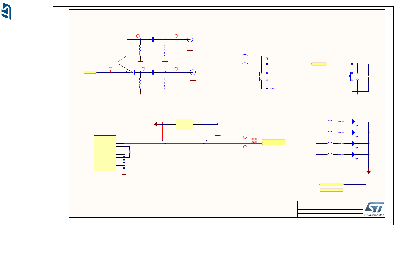
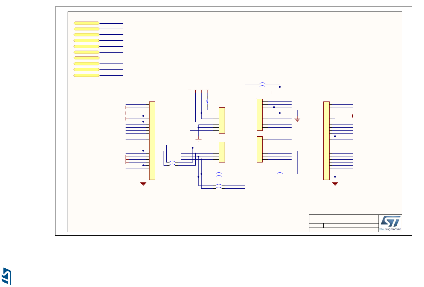
Appendix A Schematic diagrams
This section provides design schematics for the B-L072Z-LRWAN1 Discovery kit features:
•Top view of the Discovery kit, see Figure 10
•Internal/External Power Supply section, see Figure 11
•Embedded ST-LINK/V2-1, see Figure 12
•LoRa module connections, see Figure 13
•USB 2.0 FS antenna and miscellaneous features, see Figure 14
•Arduino Uno V3 extension connectors and headers, see Figure 15
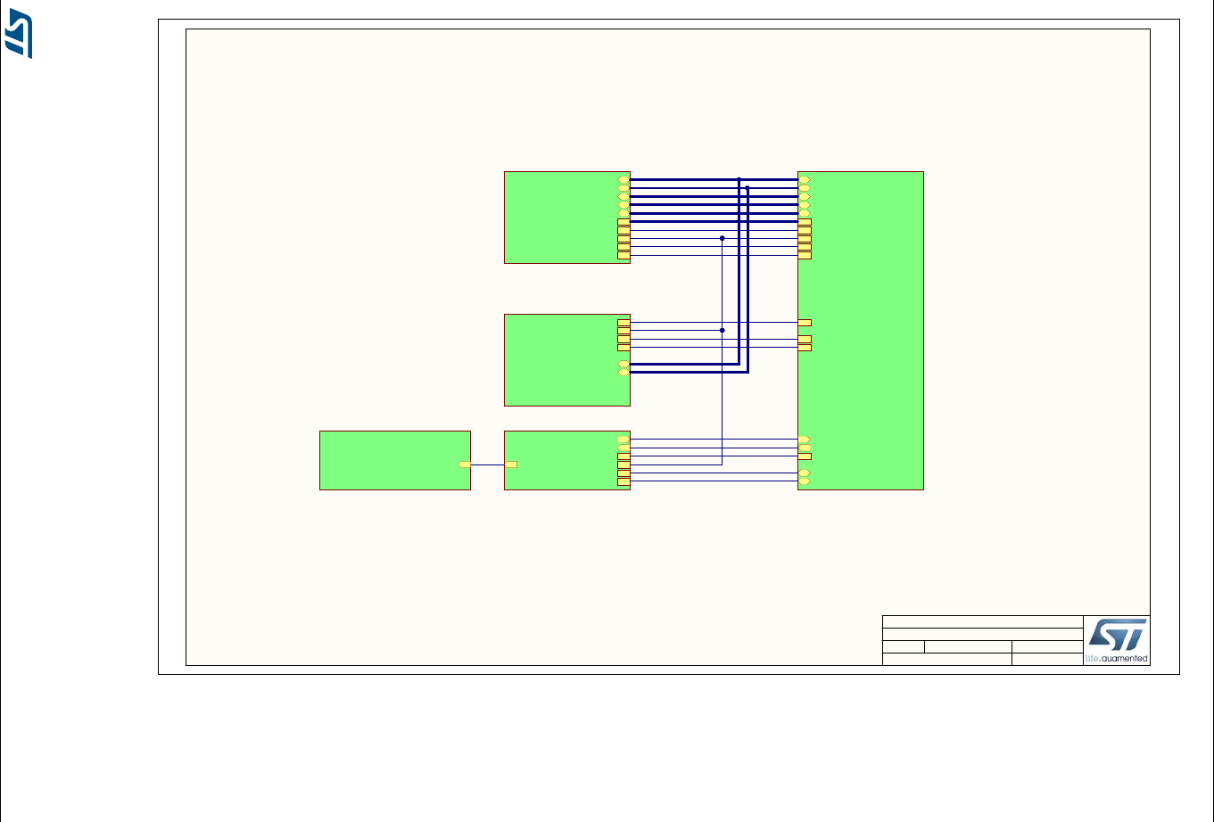
UM2115 Schematic diagrams
DocID029802 Rev 2 29/38
Figure 10. B-L072Z-LRWAN1 Discovery kit, Top view
16
Top
MB1296 D-01
25/01/2017
Title:
Size: Reference:
Date: Sheet: of
A4 Revision:
STM32 LoRa DiscoveryProject:
PA[0..15]
PB[0..15]
PC[0..15]
MCU_nRST
BOOT0
SX1276_DIO[0..5]
CRF[1..3]
TCXO_VCC
PH[0..1]
STSAFE_nRST
MB1296-Connectors
MB1296-Connectors.SchDoc
LRA_USB_N
LRA_USB_P
MCU_nRST
ANT
PA[0..15]
PB[0..15]
MB1296-USB_Antenna
MB1296-USB_Antenna.SchDoc
SWCLK
SWDIO
MCO
MCU_nRST
STLINK_RX
STLINK_TX
PWR_ENn
MB1296-STLINK
MB1296-STLINK.SchDoc
LRA_USB_P
LRA_USB_N
STLINK_TX
STLINK_RX
ANT
STSAFE_nRST
MCU_nRST
TCXO_VCC
MCO
PA[0..15]
PB[0..15]
PC[0..15]
SX1276_DIO[0..5]
CRF[1..3]
BOOT0
PH[0..1]
SWDIO
SWCLK
MB1296-LRA_Module
MB1296-LRA_Module.SchDoc
PWR_ENn
MB1296-Power
MB1296-Power.SchDoc
Schematic diagrams UM2115
30/38 DocID029802 Rev 2
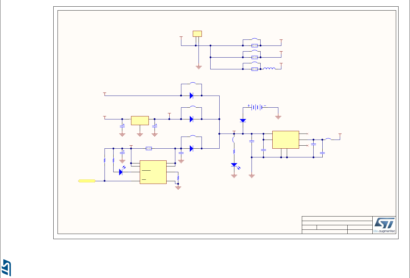
Figure 11. Power
26
Power
MB1296 D-01
25/01/2017
Title:
Size: Reference:
Date: Sheet: of
A4 Revision:
STM32 LoRa DiscoveryProject:
+3V3
VIN
+5V
SB6
BT1
3 x AAA Battery Holder
Power Section
Fitted
Power Switch to supply +5V
from STLINK USB
IN
1
IN
2
ON
3GND 4
SET 5
OUT 6
OUT 7
FAULT
8
U8
ST890CDR
U5V
C36
10uF(25V)
C37
10uF(25V)
Vin
3Vout 2
1
U2 LD1117S50TR
D5
STPS2L30A
R37
1K_5%_0603
AK
LD7
Red
A K
LD6
Red
C38
1uF_X5R_0603
C39
1uF_X5R_0603
C19
100nF
C40
100nF
EN
1
GND
2
VO 4
NC 5
GND
0
VI
6PG 3
U7
LD39050PU33R
C20
100nF
Fitted
R24
2K2
R39
1K
R38
10K
C21
4.7uF(25V)
SB18
Fitted
SB4
Not Fitted
Ilim = 625mA
1.2Ilim = 750mA < Isc
1.5Ilim = 938mA > Isc
PWR_ENn
VDD_USB_LRA
VDD_MCU_LRA
VDD_RF_LRA
+3V3
1
2
CN13
External 3V3
GND
L5
BLM15HG102SN1D
IDD jumpers
Internal/External Power Supply Selection
JP2VDD_USB_LRA
JP3VDD_MCU_LRA
JP1VDD_RF_LRA
SB5
Not Fitted
USB_LRA_5V
SB20
Not Fitted
D4
STPS2L30A
SB14
SB17
SB19 Fitted
Fitted
Fitted
Not Fitted
Not Fitted
Not Fitted
D6
STPS2L30A
D7
STPS2L30A
JP5
USB_CHARGER
VIN_REG_5V
UM2115 Schematic diagrams
DocID029802 Rev 2 31/38
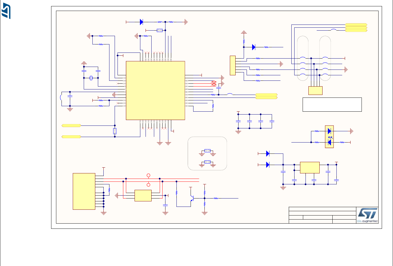
Figure 12. ST-LINK/V2-1
36
STLINK/V2-1
MB1296 D-01
25/01/2017
Title:
Size: Reference:
Date: Sheet: of
A4 Revision:
STM32 LoRa DiscoveryProject:
1 2
X2
8MHz(12pF)
STM_RST
T_JTCK
T_JTCK
T_JTMS
STM_JTMS
STM_JTCK
OSC_IN
OSC_OUT
T_NRST
AIN_1
COM
PWR
Jumpers ON --> Board Selected
Jumpers OFF --> ST-LINK Selected
Board Ident: PC13=0
T_JTCK
T_JTMS
SWD
1
2
3
4
CN8
SB38 SB39
SB40 SB41
SB22 SB23
SB24 SB25
STM_JTMS
STM_JTCK SWCLK
SWDIO
RESERVED
DEFAULT
T_SWDIO_IN
LED_STLINK
LED_STLINK
SWDIO
SWCLK
TCK/SWCLK
TMS/SWDIO
MCO MCO
AIN_1
T_NRST
T_SWO
MCU_nRST
SB37
T_NRST
D1
BAT60JFILM
TX
RX
STLK_RX
STLINK_RX
STLINK_TX
STLK_TX
R31
0
C23
20 pF
1
2
3
4
5
6
CN12
Header 6X1
USB_RENUMn
PWR_ENn
R13
2K7
+3V3_ST_LINK
+3V3_ST_LINK
+3V3_ST_LINK
+3V3_ST_LINK
+3V3_ST_LINK
+3V3_ST_LINK
+3V3_ST_LINK
PWR_EXT
+3V3_ST_LINK
+3V3
SB36
C33
10nF_X7R_0603
+3V3_ST_LINK
VBAT
1
PA7
17
PC13
2
PA12 33
PC14
3
PB0
18
PC15
4JTMS/SWDIO 34
OSCIN
5
PB1
19
OSCOUT
6
VSS_2 35
NRST
7
PB2/BOOT1
20
VSSA
8
VDD_2 36
VDDA
9
PB10
21
PA0
10
JTCK/SWCLK 37
PA1
11
PB11
22
PA2
12
PA15/JTDI 38
PA3
13
VSS_1
23
PA4
14
PB3/JTDO 39
PA5
15
VDD_1
24
PA6
16
PB4/JNTRST 40
PB12 25
PB5 41
PB13 26
PB6 42
PB14 27
PB7 43
PB15 28
BOOT0 44
PA8 29
PB8 45
PA9 30
PB9 46
PA10 31
VSS_3 47
PA11 32
VDD_3 48
U3
STM32F103CBT6
Not fitted
USB ST-LINK U5V
USB_STLK _N
USB_RENUMn
R36
36K
U5V
+3V3_ST_LINK
I/O1
1
GND
2
I/O2
3I/O2 4
Vbus 5
I/O1 6
U5
USBLC6-2SC6
U5V
3
1
2
T1
9013
USB_STLK _N
Wired on Bottom Side
ST-LINK SWD Interface
T_SWO
i
Diff Pair 90ohm
i
Diff Pair 90ohm
USB_STLK _P
USB_STLK _P
R26 4K7
R14
4K7
R27 4K7
R18
10K
R7
10K R17
10K
R34
10K
Not fitted
C22
20 pF
R16
100K
R32
100K
R28
100
R25 100
R29
100
R30
100
R35
100
R19
100
Not fitted
R20 22
R23 22
R22 22
R21 22
C35
100nF
C26
100nF
C27
100nF
C28
100nF
C29
100nF
C32
100nF
C34
100nF
C24
100nF
C25
100nF
Red
_Green
2 1
3 4
LD5
LD_BICOLOR_CMS
JP7
JP8
JP6
JP4
C30
1uF_X5R_0603
C31
1uF_X5R_0603
51
2
GND
3
4
BYPASS
INH
Vin Vout
U4 LD3985M33R
R33
1K5
VBUS 1
DM 2
DP 3
ID 4
GND 5
Shield 6
USB_Micro-B receptacle
Shield 7
Shield 8
Shield 9
EXP 10
EXP 11
CN7
1050170001
SB21
Not Fitted
D8
BAT60JFILM
+5V
D2
BAT60JFILM
D3
BAT60JFILM
U5V
VIN_REG_5V
POWER EXT
Schematic diagrams UM2115
32/38 DocID029802 Rev 2
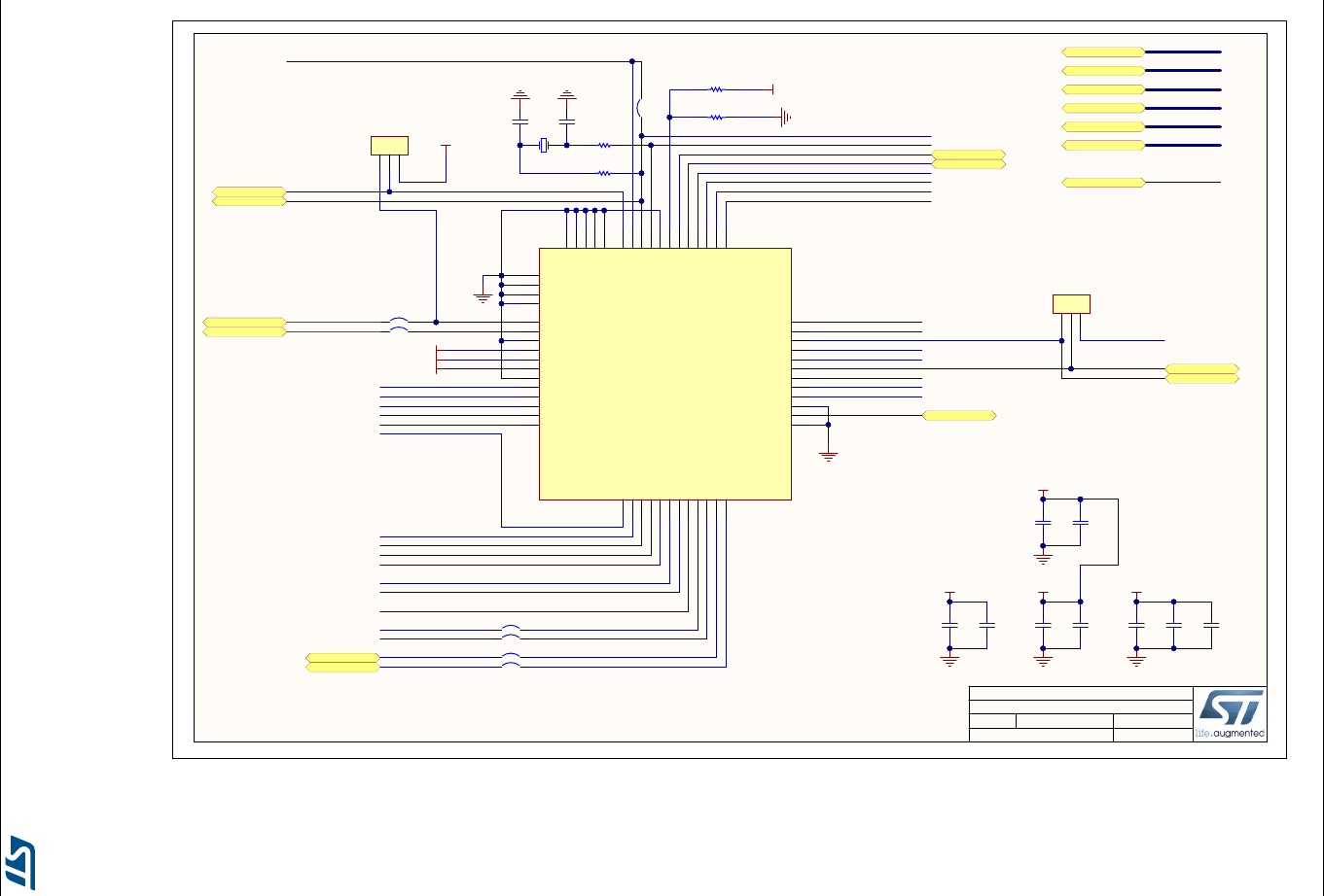
Figure 13. LoRa module
46
LoRa Module
MB1296 D-01
25/01/2017
Title:
Size: Reference:
Date: Sheet: of
A4 Revision:
STM32 LoRa DiscoveryProject:
SX1276_DIO2
SX1276_DIO3
SX1276_DIO4
SX1276_DIO5
SX1276_DIO1
SX1276_DIO0
PB15
PB14
PB13
PB12
PA10
PA9 VDD_USB_LRA
VDD_MCU_LRA
VDD_RF_LRA
ANT
CRF1
CRF3
CRF2
VDD_MCU_LRA
PA0
PB8
PB9
PB5
PB6
PB7
PB2
PA13
PA14
PA8
STLINK_TX
STLINK_RX SB29
SB26
SB27
SB28
SX1276_DIO4
SX1276_DIO5
PA5
PA4
PA3
PA2
VDD_RF_LRA
VDD_MCU_LRA
VDD_USB_LRA
1
2
3
JP10
RESET source selection
MCU_nRST
STSAFE_nRST
PA11
PA12
PA11
1
2
3
JP9
TCXO Selection
VDD_RF_LRA
R1
0R_0603 VDD_MCU_LRA
Not fitted
PH1
PH0
/USB_DP
/USB_DM
/SPI2_MOSI
/SPI2_MISO
/SPI2_SCK
/SPI2_NSS
/USART1_RX
/USART1_TX
/ADC5/DAC2
/ADC4/DAC1
/ADC3
/ADC2
/I2C1_SDA
/I2C1_SCL
/OSC_IN
/OSC_OUT
/SWCLK
/SWDIO
/LPTIM1_IN1
/LPTIM1_ETR
/LPTIM1_IN2
/LPTIM1_OUT
/MCO
BOOT0
Not fitted
Not fitted
Fitted
Fitted
TCXO_VCC
TCXO_OUT
SB15
SB16
LRA_USB_P
LRA_USB_N
Not fitted
Not fitted
LoRa Module (Murata)
Decoupling capacitors
LRA_USB_P
LRA_USB_N
STLINK_TX
STLINK_RX
ANT
STSAFE_nRST
MCU_nRST
/USB_DM
TCXO_VCC
MCO
PA[0..15]
PA[0..15]
PB[0..15]
PB[0..15]
PC[0..15]
PC[0..15]
SX1276_DIO[0..5] SX1276_DIO[0..5]
CRF[1..3] CRF[1..3]
BOOT0 BOOT0
PH[0..1]
PH[0..1]
SWDIO
SWCLK
PA12/USB_DP
1
PA11/USB_DM
2
GND
3
VDD_USB
4
VDD_MCU
5
VDD_RF
6
GND
7
DBG_SX1276_DIO2
8
DBG_SX1276_DIO3
9
SX1276_DIO4
10
DBG_SX1276_DIO5
11
DBG_SX1276_DIO1
12
DBG_SX1276_DIO0
13
PB15/SPI2_MOSI
14
PB14/SPI2_MISO
15
PB13/SPI2_SCK
16
PB12/SPI2_NSS
17
PA10/USART1_RX
18
PA9/USART1_TX
19
PA8/MCO
20
PA5/ADC5/DAC2
21
PA4/ADC4/DAC1
22
PA3/ADC3
23
PA2/ADC2
24
GND 25
ANT 26
GND 27
DBG_CRF1 28
DBG_CRF3 29
DBG_CRF2 30
STSAFE_nRST 31
VREF+ 32
GND
54
GND
55
GND
56
GND
57
GND 50
GND 51
GND 52
GND 53
GND 49
PA0/WKUP1 33
MCU_nRST 34
PB8/I2C1_SCL 35
PB9/I2C1_SDA 36
PB2/LPTIM1_OUT 37
PB7/LPTIM1_IN2 38
PB6/LPTIM1_ETR 39
PB5/LPTIM1_IN1 40
PA13/SWDIO 41
PA14/SWCLK 42
BOOT0 43
GND 44
PH1-OSC_OUT 45
PH0-OSC_IN 46
TCXO_OUT 47
TCXO_VCC 48
U1
LRA Module ES0
SB13
Not fitted
C1, C2, X1, R3, R4, SB13 and SB14 must be placed the closest as possible from U1
C2
20 pF
C1
20 pF
1 2
X1
NU/8MHz(12pF)
R2
100K
R3
0R_0603
R4
0R_0603
C8
100nF
C9
100nF
C11
100nF
C10
1uF
C5
10μF
C6
10μF
C7
10μF
C4
100nF
C3
1uF
Not fitted Not fitted
VDD_MCU_LRA
UM2115 Schematic diagrams
DocID029802 Rev 2 33/38
Figure 14. USB 2.0 FS and antenna
56
LoRa USB - Antenna
MB1296 D-01
25/01/2017
Title:
Size: Reference:
Date: Sheet: of
A4 Revision:
STM32 LoRa DiscoveryProject:
ANT
USB Interface LoRa module
USB_LRA_5V
LRA_USB_N
LRA_USB_P
i
Diff Pair 90ohm
i
Diff Pair 90ohm
1
4 3
2
B1
USER (Blue)
VDD_MCU_LRA
SB31PB2
A K
LD2
Red
SB34PA5
MCU_nRST
Antenna section with connectors General purpose User Button (or LoRa Wake Up)
RESET button
Not fitted
PB7
PB6
PB5
General purpose LEDs
LRA_USB_N
LRA_USB_P
MCU_nRST
ANT
PA[0..15]
PA[0..15]
PB[0..15]
PB[0..15]
SB32
SB33
SB35
Fitted
Fitted
Fitted
SB30PA0
To be placed on the opposite side of USB STLINK connector
L1
C13
C39 and C40 have a common pad
on Antenna side signal
C14 C15
C12
L2
L3 L4
Fitted
R5
4K7
C16
100nF
C17
100nF
1
4 3
2
B2
Reset (Black)
R9
100K
R6
100R
R11
510R
R10
680R
R12
680R
A K
LD1
Green
A K
LD3
Blue
A K
LD4
Red
CN9
U.FL-R-SMT
CN10
SMA
VBUS 1
DM 2
DP 3
ID 4
GND 5
Shield 6
USB_Micro-B receptacle
Shield 7
Shield 8
Shield 9
EXP 10
EXP 11
CN11
1050170001
I/O1
1
GND
2
I/O2
3I/O2 4
Vbus 5
I/O1 6
U6
USBLC6-2SC6
USB_LRA_5V
C18
100nF
i
50R
i
50R
i
50R
i
50R
i
50R
R8
510R
Not fitted
Not fitted
Not fittedNot fitted
Not fitted
C14 and C15 are temporarily replaced by 0OHm resistor
Not fitted
Not fitted
Fitted
Schematic diagrams UM2115
34/38 DocID029802 Rev 2
Figure 15. Connectors
66
Connectors
MB1296 D-01
26/04/2017
Title:
Size: Reference:
Date: Sheet: of
A4 Revision:
STM32 LoRa DiscoveryProject:
+3V3+5V
A0
A1
A2
A3
A4
A5 D0
D1
D2
D4
D3
D5
D6
D7
D8
D9
D10
D14
D15
PA0
PA2
PA4
PA5
PA10
PA3
PB8
PB9
PA9
PA8
PB5
PB6
1
2
3
4
5
6
CN6
Header 6X1_Female
1
2
3
4
5
6
7
8
CN4
Header 8X1_Female
1
2
3
4
5
6
7
8
CN5
Header 8X1_Female
1
2
3
4
5
6
7
8
9
10
CN1
Header 10X1_Female
MCU_nRST
VIN
PA[0..15]
PA[0..15]
PB[0..15]
PB[0..15]
PC[0..15]
PC[0..15]
MCU_nRST MCU_nRST
BOOT0 BOOT0
SB10 PH1
PH0
SB3
D13
D12
D11
Arduino ConnectorArduino Connector
Arduino ConnectorArduino
Connector
GND
AVDD
SB9PB13
PB7
PB2
PB13/NC
PB12
PB15
PB14
SB2PB13 Fitted
Fitted
Not fitted
PA5/PB13
A4
A5
VDD_MCU_LRA
PA13
PA14
SX1276_DIO0
SX1276_DIO1
SX1276_DIO2
SX1276_DIO3
SX1276_DIO4
SX1276_DIO5
BOOT0
CRF1
CRF2
CRF3
PA12
PA11
PB12
PB15
PB14
PB13
TCXO_VCC
VDD_RF_LRA
VDD_USB_LRA
SB7
SB8
STSAFE_nRST
Not fitted
Not fitted
Not fitted
PA0 Alias
PA4 Alias
Extension connectors
Arduino
SX1276_DIO[0..5] SX1276_DIO[0..5]
IOREF
+3V3
+5V
GND
GND
VIN
CRF[1..3] CRF[1..3]
TCXO_VCC TCXO_VCC
PH[0..1]
PH[0..1]
STSAFE_nRST STSAFE_nRST
SB11
SB12
Not fitted
Not fitted PB8
PB9
1
2
3
4
5
6
7
8
9
10
11
12
13
14
15
16
17
18
19
20
21
22
23
24
25
26
CN2
1
2
3
4
5
6
7
8
9
10
11
12
13
14
15
16
17
18
19
20
21
22
23
24
25
26
CN3
MCU_nRST
+3V3
+5V
VIN
PA0
PA4
PH1
PH0
PA5
PB6
PA9
PB2
PA8
PB7
PB5
PA10
PA2
PA3
PB9
PB8
SB1
R15
10K
Not fitted
+5V
VDD_MCU_LRA
VDD_MCU_LRA

DocID029802 Rev 2 35/38
UM2115Federal Communications Commission (FCC), Industry Canada (IC) Compliance and other
37
Appendix B Federal Communications Commission (FCC),
Industry Canada (IC) Compliance and other
Certifications
B.1 FCC Compliance Statement
B.1.1 ANSI C63.4 (2014) American National Standard for Methods of
Measurement of Radio-Noise Emissions from Low-Voltage Electrical
and Electronic Equipment in the Range of 9 kHz to 40 GHz
•FCC CFR 47, PART 15, Subpart B
•Industry Canada ICES-003 (Information Technology Equipment (ITE)) — Limits and
methods of measurement. Issue 6 (2016)
•FCC Part 15 compliance statement
This device complies with part 15 of the FCC Rules. Operation is subject to the following two
conditions: (1) This device may not cause harmful interference, and (2) this device must
accept any interference received, including interference that may cause undesired
operation. This equipment has been tested and found to comply with the limits for a Class B
digital device, pursuant to part 15 of the FCC Rules. These limits are designed to provide
reasonable protection against harmful interference in a residential installation. This
equipment generates, uses, radiates radio frequency energy and, if not installed and used in
accordance with the instruction, may cause harmful interference to radio communications.
However, there is no guarantee that interference will not occur in a particular installation. If
this equipment does cause harmful interference to radio or television reception which can
be determined by turning the equipment off and on, the user is encouraged to try to correct
interference by one or more of the following measures:
•Reorient or relocate the receiving antenna.
•Increase the separation between the equipment and receiver.
•Connect the equipment into an outlet on circuit different from that to which the receiver
is connected.
•Consult the dealer or an experienced radio/TV technician for help.
B.2 IC Compliance Statement
B.2.1 Industry Canada Licence-Exempt Radio Apparatus
This device complies with Industry Canada licence-exempt RSS standard(s). Operation is
subject to the following two conditions: (1) this device may not cause interference, and (2)
this device must accept any interference, including interference that may cause undesired
operation of the device.
Le présent appareil est conforme aux CNR d'Industrie Canada applicables aux appareils
radio exempts de licence.
L'exploitation est autorisée aux deux conditions suivantes : (1) l'appareil ne doit pas
produire de brouillage, et (2) l'utilisateur de l'appareil doit accepter tout brouillage
radioélectrique subi, même si le brouillage est susceptible d'en compromettre le
fonctionnement.

Federal Communications Commission (FCC), Industry Canada (IC) Compliance and other Certifi-
36/38 DocID029802 Rev 2
B.2.2 Radio Frequency (RF) Exposure Compliance of
Radiocommunication Apparatus
To satisfy FCC and IC RF Exposure requirements for mobile devices, a separation distance
of 20 cm or more should be maintained between the antenna of this device and persons
during operation. To ensure compliance, operation at closer than this distance is not
recommended. This transmitter must not be co-located or operating in conjunction with any
other antenna or transmitter.
Pour satisfaire aux exigences FCC et IC concernant l'exposition aux champs RF pour les
appareils mobiles, une distance de séparation de 20 cm ou plus doit être maintenue entre
l'antenne de ce dispositif et les personnes pendant le fonctionnement. Pour assurer la
conformité, il est déconseillé d'utiliser cet équipement à une distance inférieure. Cet
émetteur ne doit pas être co-situé ou fonctionner conjointement avec une autre antenne ou
un autre émetteur.
Measures and tests performed on the sample of the product B-L072Z-LRWAN1, show
compliance with standards FCC CFR 47, PART 15, Subpart B and ICES-003.
B.3 Other certifications
B.3.1 EN 55032 (2012) / EN 55024 (2010) ETSI EN 301 489-1 (v1.9.2) /
ETSI EN 301 489-3 (v1.6.1) EN 60950-1
(2006+A11/2009+A1/2010+A12/2011+A2/2013) CFR 47,
FCC Part 15,Subpart B (Class B Digital Device) and
Industry Canada ICES-003 (Issue 6/2016)
The sample examined is in conformance with the requirements of above standards.
Note: The sample examined shall be powered by a power supply unit or auxiliary equipment
complying with standard:
EN 60950-1: 2006+A11/2009+A1/2010+A12/2011+A2/2013, and shall be Safety Extra Low
Voltage (SELV) with limited power capability.
B.3.2 Electrical Safety qualification for CE marking: EN 60950-1
(2006+A11/2009+A1/2010+A12/2011+A2/2013) IEC 60650-1
(2005+A1/2009+A2/2013)
The appliance complies with requirements of above mentioned standards.
B.3.3 EMC qualification accordingly to standard CFR 47, FCC Part 15,
Subpart B & Industry Canada ICES-003 (Issue 6/2016)
Class B Digital Device
The appliance complies with requirements of above mentioned standards.
B.3.4 CE qualification according to standards:
ETSI EN 300 220-1 V2.4.1 (2012) / V3.1.1 (2017) ETSI EN
300 220-2 V2.4.1 (2012) / V3.1.1 (2017) RF Module already
certified – Partial test only
The appliance complies with requirements of above mentioned standards.

DocID029802 Rev 2 37/38
UM2115 Revision history
37
Revision history
Table 12. Document revision history
Date Revision Changes
14-Feb-2017 1 Initial version.
26-Sep-2017 2
Added Section Appendix A: Schematic diagrams.
Updated Section 10.2: Board revision history and Section 10.3:
Known limitations.
Updated Section Appendix A: Schematic diagrams with Rev. D
board schematics.

UM2115
38/38 DocID029802 Rev 2
IMPORTANT NOTICE – PLEASE READ CAREFULLY
STMicroelectronics NV and its subsidiaries (“ST”) reserve the right to make changes, corrections, enhancements, modifications, and
improvements to ST products and/or to this document at any time without notice. Purchasers should obtain the latest relevant information on
ST products before placing orders. ST products are sold pursuant to ST’s terms and conditions of sale in place at the time of order
acknowledgement.
Purchasers are solely responsible for the choice, selection, and use of ST products and ST assumes no liability for application assistance or
the design of Purchasers’ products.
No license, express or implied, to any intellectual property right is granted by ST herein.
Resale of ST products with provisions different from the information set forth herein shall void any warranty granted by ST for such product.
ST and the ST logo are trademarks of ST. All other product or service names are the property of their respective owners.
Information in this document supersedes and replaces information previously supplied in any prior versions of this document.
© 2017 STMicroelectronics – All rights reserved
