ARMv6 M Architecture Reference Manual DDI0419C Arm V6m
DDI0419C_arm_architecture_v6m_reference_manual
DDI0419C_arm_architecture_v6m_reference_manual
ARMv6-M_Architecture_Manual
armv6-M-architecture-rference-manual
User Manual: Pdf
Open the PDF directly: View PDF ![]() .
.
Page Count: 436 [warning: Documents this large are best viewed by clicking the View PDF Link!]
- ARMv6-M Architecture Reference Manual
- Contents
- List of Tables
- List of Figures
- Preface
- Application Level Architecture
- Introduction
- Application Level Programmers’ Model
- ARM Architecture Memory Model
- A3.1 Address space
- A3.2 Alignment support
- A3.3 Endian support
- A3.4 Synchronization and semaphores
- A3.5 Memory types and attributes and the memory order model
- A3.6 Access rights
- A3.7 Memory access order
- A3.8 Caches and memory hierarchy
- The ARMv6-M Instruction Set
- A4.1 About the instruction set
- A4.2 Unified Assembler Language
- A4.3 Branch instructions
- A4.4 Data-processing instructions
- A4.5 Status register access instructions
- A4.6 Load and store instructions
- A4.7 Load Multiple and Store Multiple instructions
- A4.8 Miscellaneous instructions
- A4.9 Exception-generating instructions
- The Thumb Instruction Set Encoding
- Thumb Instruction Details
- A6.1 Format of instruction descriptions
- A6.2 Standard assembler syntax fields
- A6.3 Conditional execution
- A6.4 Shifts applied to a register
- A6.5 Memory accesses
- A6.6 Hint Instructions
- A6.7 Alphabetical list of ARMv6-M Thumb instructions
- A6.7.1 ADC (register)
- A6.7.2 ADD (immediate)
- A6.7.3 ADD (register)
- A6.7.4 ADD (SP plus immediate)
- A6.7.5 ADD (SP plus register)
- A6.7.6 ADR
- A6.7.7 AND (register)
- A6.7.8 ASR (immediate)
- A6.7.9 ASR (register)
- A6.7.10 B
- A6.7.11 BIC (register)
- A6.7.12 BKPT
- A6.7.13 BL
- A6.7.14 BLX (register)
- A6.7.15 BX
- A6.7.16 CMN (register)
- A6.7.17 CMP (immediate)
- A6.7.18 CMP (register)
- A6.7.19 CPS
- A6.7.20 CPY
- A6.7.21 DMB
- A6.7.22 DSB
- A6.7.23 EOR (register)
- A6.7.24 ISB
- A6.7.25 LDM, LDMIA, LDMFD
- A6.7.26 LDR (immediate)
- A6.7.27 LDR (literal)
- A6.7.28 LDR (register)
- A6.7.29 LDRB (immediate)
- A6.7.30 LDRB (register)
- A6.7.31 LDRH (immediate)
- A6.7.32 LDRH (register)
- A6.7.33 LDRSB (register)
- A6.7.34 LDRSH (register)
- A6.7.35 LSL (immediate)
- A6.7.36 LSL (register)
- A6.7.37 LSR (immediate)
- A6.7.38 LSR (register)
- A6.7.39 MOV (immediate)
- A6.7.40 MOV (register)
- A6.7.41 MOV (shifted register)
- A6.7.42 MRS
- A6.7.43 MSR (register)
- A6.7.44 MUL
- A6.7.45 MVN (register)
- A6.7.46 NEG
- A6.7.47 NOP
- A6.7.48 ORR (register)
- A6.7.49 POP
- A6.7.50 PUSH
- A6.7.51 REV
- A6.7.52 REV16
- A6.7.53 REVSH
- A6.7.54 ROR (register)
- A6.7.55 RSB (immediate)
- A6.7.56 SBC (register)
- A6.7.57 SEV
- A6.7.58 STM, STMIA, STMEA
- A6.7.59 STR (immediate)
- A6.7.60 STR (register)
- A6.7.61 STRB (immediate)
- A6.7.62 STRB (register)
- A6.7.63 STRH (immediate)
- A6.7.64 STRH (register)
- A6.7.65 SUB (immediate)
- A6.7.66 SUB (register)
- A6.7.67 SUB (SP minus immediate)
- A6.7.68 SVC
- A6.7.69 SXTB
- A6.7.70 SXTH
- A6.7.71 TST (register)
- A6.7.72 UDF
- A6.7.73 UXTB
- A6.7.74 UXTH
- A6.7.75 WFE
- A6.7.76 WFI
- A6.7.77 YIELD
- System Level Architecture
- System Level Programmers’ Model
- B1.1 Introduction to the system level
- B1.2 About the ARMv6-M memory mapped architecture
- B1.3 Overview of system level terminology and operation
- B1.4 Registers
- B1.4.1 The ARM core registers
- B1.4.2 The special-purpose program status registers, xPSR
- B1.4.3 The special-purpose mask register, PRIMASK
- B1.4.4 The special-purpose CONTROL register
- B1.4.5 Reserved special-purpose register bits
- B1.4.6 Special-purpose register updates and the memory order model
- B1.4.7 Register-related definitions for pseudocode
- B1.5 ARMv6-M exception model
- B1.5.1 Overview of the exceptions supported
- B1.5.2 Exception number definition
- B1.5.3 The vector table
- B1.5.4 Exception priorities and preemption
- B1.5.5 Reset behavior
- B1.5.6 Exception entry behavior
- B1.5.7 Stack alignment on exception entry
- B1.5.8 Exception return behavior
- B1.5.9 Exceptions in single-word load operations
- B1.5.10 Exceptions in Load Multiple and Store Multiple operations
- B1.5.11 Exceptions on exception entry
- B1.5.12 Exceptions on exception return, and tail-chaining exceptions
- B1.5.13 Exception status and control
- B1.5.14 Fault behavior
- B1.5.15 Unrecoverable exception cases
- B1.5.16 Reset management
- B1.5.17 Power management
- B1.5.18 Wait For Event and Send Event
- B1.5.19 Wait For Interrupt
- System Memory Model
- System Address Map
- B3.1 The system address map
- B3.2 System Control Space (SCS)
- B3.2.1 About the System Control Block
- B3.2.2 System control and ID registers
- B3.2.3 CPUID Base Register
- B3.2.4 Interrupt Control State Register, ICSR
- B3.2.5 Vector Table Offset Register, VTOR
- B3.2.6 Application Interrupt and Reset Control Register, AIRCR
- B3.2.7 System Control Register, SCR
- B3.2.8 Configuration and Control Register, CCR
- B3.2.9 System Handler Priority Register 2, SHPR2
- B3.2.10 System Handler Priority Register 3, SHPR3
- B3.2.11 Fault Status Registers
- B3.2.12 The Auxiliary Control Register, ACTLR
- B3.3 The system timer, SysTick
- B3.4 Nested Vectored Interrupt Controller, NVIC
- B3.4.1 NVIC operation
- B3.4.2 NVIC register support in the SCS
- B3.4.3 Interrupt Set-Enable Register, NVIC_ISER
- B3.4.4 Interrupt Clear Enable Register, NVIC_ICER
- B3.4.5 Interrupt Set-Pending Register, NVIC_ISPR
- B3.4.6 Interrupt Clear-Pending Register, NVIC_ICPR
- B3.4.7 Interrupt Priority Registers, NVIC_IPR0 - NVIC_IPR7
- B3.5 Protected Memory System Architecture, PMSAv6
- ARMv6-M System Instructions
- Debug Architecture
- ARMv6-M Debug
- C1.1 Introduction to ARMv6-M debug
- C1.2 The Debug Access Port
- C1.3 Overview of the ARMv6-M debug features
- C1.4 Debug and reset
- C1.5 Debug event behavior
- C1.6 Debug register support in the SCS
- C1.6.1 System Handler Control and State Register, SHCSR
- C1.6.2 Debug Fault Status Register, DFSR
- C1.6.3 Debug Halting Control and Status Register, DHCSR
- C1.6.4 Debug Core Register Selector Register, DCRSR
- C1.6.5 Debug Core Register Data Register, DCRDR
- C1.6.6 Debug Exception and Monitor Control Register, DEMCR
- C1.7 The Data Watchpoint and Trace unit
- C1.8 Breakpoint Unit
- Appendices
- ARMv6-M CoreSight Infrastructure IDs
- Deprecated and Obsolete Features
- ARMv7-M Differences
- Legacy Instruction Mnemonics
- Pseudocode Definition
- E.1 Instruction encoding diagrams and pseudocode
- E.2 Limitations of pseudocode
- E.3 Data types
- E.4 Expressions
- E.5 Operators and built-in functions
- E.5.1 Operations on generic types
- E.5.2 Operations on booleans
- E.5.3 Bitstring manipulation
- Bitstring length and top bit
- Bitstring concatenation and replication
- Bitstring extraction
- Logical operations on bitstrings
- Bitstring count
- Testing a bitstring for being all zero or all ones
- Lowest and highest set bits of a bitstring
- Zero-extension and sign-extension of bitstrings
- Converting bitstrings to integers
- E.5.4 Arithmetic
- E.6 Statements and program structure
- E.7 Miscellaneous helper procedures and functions
- E.7.1 BigEndianReverse()
- E.7.2 BKPTInstrDebugEvent()
- E.7.3 BranchWritePC()
- E.7.4 BXWritePC()
- E.7.5 CallSupervisor()
- E.7.6 ClearExclusiveByAddress()
- E.7.7 ConditionPassed()
- E.7.8 DataMemoryBarrier()
- E.7.9 DataSynchronizationBarrier()
- E.7.10 EncodingSpecificOperations()
- E.7.11 Hint_SendEvent()
- E.7.12 Hint_Yield()
- E.7.13 InstructionSynchronizationBarrier()
- E.7.14 ProcessorID()
- E.7.15 ResetSCSRegisters()
- E.7.16 SCS_UpdateStatusRegs()
- Pseudocode Index
- Register Index
- Glossary

Copyright © 2007-2008, 2010 ARM Limited. All rights reserved.
ARM DDI 0419C (ID092410)
ARMv6-M Architecture
Reference Manual

ii Copyright © 2007-2008, 2010 ARM Limited. All rights reserved. ARM DDI 0419C
Non-Confidential ID092410
ARMv6-M Architecture Reference Manual
Copyright © 2007-2008, 2010 ARM Limited. All rights reserved.
Release Information
The following changes have been made to this document.
Proprietary Notice
This ARM Architecture Reference Manual is protected by copyright and the practice or implementation of the
information herein may be protected by one or more patents or pending applications. No part of this ARM Architecture
Reference Manual may be reproduced in any form by any means without the express prior written permission of ARM.
No license, express or implied, by estoppel or otherwise to any intellectual property rights is granted by this ARM
Architecture Reference Manual.
Your access to the information in this ARM Architecture Reference Manual is conditional upon your acceptance that you
will not use or permit others to use the information for the purposes of determining whether implementations of the ARM
architecture infringe any third party patents.
This ARM Architecture Reference Manual is provided “as is”. ARM makes no representations or warranties, either
express or implied, included but not limited to, warranties of merchantability, fitness for a particular purpose, or
non-infringement, that the content of this ARM Architecture Reference Manual is suitable for any particular purpose or
that any practice or implementation of the contents of the ARM Architecture Reference Manual will not infringe any third
party patents, copyrights, trade secrets, or other rights.
This ARM Architecture Reference Manual may include technical inaccuracies or typographical errors.
To the extent not prohibited by law, in no event will ARM be liable for any damages, including without limitation any
direct loss, lost revenue, lost profits or data, special, indirect, consequential, incidental or punitive damages, however
caused and regardless of the theory of liability, arising out of or related to any furnishing, practicing, modifying or any
use of this ARM Architecture Reference Manual, even if ARM has been advised of the possibility of such damages.
Words and logos marked with ® or TM are registered trademarks or trademarks of ARM Limited, except as otherwise
stated below in this proprietary notice. Other brands and names mentioned herein may be the trademarks of their
respective owners.
Copyright © 2007-2008, 2010 ARM Limited
110 Fulbourn Road Cambridge, England CB1 9NJ
Restricted Rights Legend: Use, duplication or disclosure by the United States Government is subject to the restrictions
set forth in DFARS 252.227-7013 (c)(1)(ii) and FAR 52.227-19.
Change History
Date Issue Confidentiality Change
March 2007 A Non-Confidential First release
September 2008 B Non-Confidential, Restricted Access Additions to the System Control Block, power management support,
corrections to errata and clarifications
September 2010 C Non-confidential Additions to describe the Unprivileged/Privileged Extension and the
Protected Memory System Architecture (PMSA) Extension. Also extensive
clarification and reorganization.

ARM DDI 0419C Copyright © 2007-2008, 2010 ARM Limited. All rights reserved. iii
ID092410 Non-Confidential
This document is Non-Confidential but any disclosure by you is subject to you providing notice to and the
acceptance by the recipient of, the conditions set out above.
In this document, where the term ARM is used to refer to the company it means “ARM or any of its subsidiaries as
appropriate”.
Note
The term ARM is also used to refer to versions of the ARM architecture, for example ARMv6 refers to version 6 of the
ARM architecture. The context makes it clear when the term is used in this way.

iv Copyright © 2007-2008, 2010 ARM Limited. All rights reserved. ARM DDI 0419C
Non-Confidential ID092410

ARM DDI 0419C Copyright © 2007-2008, 2010 ARM Limited. All rights reserved. v
ID092410 Non-Confidential
Contents
ARMv6-M Architecture Reference Manual
Preface
About this manual ............................................................................... xvi
Using this manual .............................................................................. xvii
Conventions ........................................................................................ xix
Additional reading ................................................................................ xx
Feedback ............................................................................................ xxi
Part A Application Level Architecture
Chapter A1 Introduction
A1.1 About the ARM architecture profiles .............................................. A1-26
A1.2 Privileged and unprivileged execution ............................................ A1-27
Chapter A2 Application Level Programmers’ Model
A2.1 About the application level programmers’ model ........................... A2-30
A2.2 ARM processor data types and arithmetic ..................................... A2-31
A2.3 Registers and execution state ........................................................ A2-36
A2.4 Exceptions, faults and interrupts .................................................... A2-39
A2.5 Coprocessor support ...................................................................... A2-40

Contents
vi Copyright © 2007-2008, 2010 ARM Limited. All rights reserved. ARM DDI 0419C
Non-Confidential ID092410
Chapter A3 ARM Architecture Memory Model
A3.1 Address space ............................................................................... A3-42
A3.2 Alignment support .......................................................................... A3-43
A3.3 Endian support ............................................................................... A3-44
A3.4 Synchronization and semaphores .................................................. A3-47
A3.5 Memory types and attributes and the memory order model .......... A3-48
A3.6 Access rights .................................................................................. A3-56
A3.7 Memory access order .................................................................... A3-58
A3.8 Caches and memory hierarchy ...................................................... A3-63
Chapter A4 The ARMv6-M Instruction Set
A4.1 About the instruction set ................................................................ A4-66
A4.2 Unified Assembler Language ......................................................... A4-68
A4.3 Branch instructions ........................................................................ A4-70
A4.4 Data-processing instructions .......................................................... A4-71
A4.5 Status register access instructions ................................................ A4-74
A4.6 Load and store instructions ............................................................ A4-75
A4.7 Load Multiple and Store Multiple instructions ................................ A4-77
A4.8 Miscellaneous instructions ............................................................. A4-78
A4.9 Exception-generating instructions .................................................. A4-79
Chapter A5 The Thumb Instruction Set Encoding
A5.1 Thumb instruction set encoding ..................................................... A5-82
A5.2 16-bit Thumb instruction encoding ................................................. A5-84
A5.3 32-bit Thumb instruction encoding ................................................. A5-91
Chapter A6 Thumb Instruction Details
A6.1 Format of instruction descriptions .................................................. A6-94
A6.2 Standard assembler syntax fields .................................................. A6-98
A6.3 Conditional execution ..................................................................... A6-99
A6.4 Shifts applied to a register ........................................................... A6-101
A6.5 Memory accesses ........................................................................ A6-103
A6.6 Hint Instructions ........................................................................... A6-104
A6.7 Alphabetical list of ARMv6-M Thumb instructions ........................ A6-105
Part B System Level Architecture
Chapter B1 System Level Programmers’ Model
B1.1 Introduction to the system level ................................................... B1-204
B1.2 About the ARMv6-M memory mapped architecture ..................... B1-205
B1.3 Overview of system level terminology and operation ................... B1-206
B1.4 Registers ...................................................................................... B1-211
B1.5 ARMv6-M exception model .......................................................... B1-218

Contents
ARM DDI 0419C Copyright © 2007-2008, 2010 ARM Limited. All rights reserved. vii
ID092410 Non-Confidential
Chapter B2 System Memory Model
B2.1 About the system memory model ................................................. B2-246
B2.2 Declarations and support functions .............................................. B2-247
B2.3 Memory accesses ........................................................................ B2-251
B2.4 Control of the endianness model in ARMv6-M ............................. B2-254
B2.5 Barrier support for system correctness ........................................ B2-255
Chapter B3 System Address Map
B3.1 The system address map ............................................................. B3-258
B3.2 System Control Space (SCS) ....................................................... B3-262
B3.3 The system timer, SysTick ........................................................... B3-275
B3.4 Nested Vectored Interrupt Controller, NVIC ................................. B3-281
B3.5 Protected Memory System Architecture, PMSAv6 ....................... B3-289
Chapter B4 ARMv6-M System Instructions
B4.1 About the ARMv6-M system instructions ..................................... B4-304
B4.2 ARMv6-M system instruction descriptions ................................... B4-305
Part C Debug Architecture
Chapter C1 ARMv6-M Debug
C1.1 Introduction to ARMv6-M debug .................................................. C1-316
C1.2 The Debug Access Port ............................................................... C1-318
C1.3 Overview of the ARMv6-M debug features .................................. C1-320
C1.4 Debug and reset .......................................................................... C1-323
C1.5 Debug event behavior .................................................................. C1-324
C1.6 Debug register support in the SCS .............................................. C1-328
C1.7 The Data Watchpoint and Trace unit ........................................... C1-341
C1.8 Breakpoint Unit ............................................................................ C1-351
Part D Appendices
Appendix A ARMv6-M CoreSight Infrastructure IDs
A.1 CoreSight infrastructure IDs for an ARMv6-M implementation .................
AppxA-360
Appendix B Deprecated and Obsolete Features
B.1 Deprecated features of the ARMv6-M architecture ................ AppxB-364
B.2 Obsolete features of the ARMv6-M architecture .................... AppxB-365
Appendix C ARMv7-M Differences
C.1 ARMv6-M and ARMv7-M compatibility .................................. AppxC-368
C.2 About the ARMv6-M and ARMv7-M architecture profiles ...... AppxC-369
C.3 Instruction support ................................................................. AppxC-370

Contents
viii Copyright © 2007-2008, 2010 ARM Limited. All rights reserved. ARM DDI 0419C
Non-Confidential ID092410
C.4 Programmers’ model support ................................................. AppxC-371
C.5 Memory model support .......................................................... AppxC-373
C.6 System Control Space register support ................................. AppxC-375
C.7 Debug support ....................................................................... AppxC-377
Appendix D Legacy Instruction Mnemonics
D.1 Thumb instruction mnemonics ............................................... AppxD-380
D.2 Pre-UAL pseudo-instruction NOP .......................................... AppxD-384
Appendix E Pseudocode Definition
E.1 Instruction encoding diagrams and pseudocode ................... AppxE-386
E.2 Limitations of pseudocode ..................................................... AppxE-388
E.3 Data types .............................................................................. AppxE-389
E.4 Expressions ........................................................................... AppxE-393
E.5 Operators and built-in functions ............................................. AppxE-395
E.6 Statements and program structure ........................................ AppxE-401
E.7 Miscellaneous helper procedures and functions .................... AppxE-406
Appendix F Pseudocode Index
F.1 Pseudocode operators and keywords .................................... AppxF-410
F.2 Pseudocode functions and procedures .................................. AppxF-414
Appendix G Register Index
G.1 ARM core registers ............................................................... AppxG-422
G.2 Memory mapped system registers ........................................ AppxG-423
G.3 Memory mapped debug registers ......................................... AppxG-424
Glossary

ARM DDI 0419C Copyright © 2007-2008, 2010 ARM Limited. All rights reserved. ix
ID092410 Non-Confidential
List of Tables
ARMv6-M Architecture Reference Manual
Change History .................................................................................................... ii
Table A3-1 Load-store and element size association ..................................................... A3-46
Table A3-2 Summary of memory attributes .................................................................... A3-49
Table A4-1 Branch instructions ....................................................................................... A4-70
Table A4-2 Standard data-processing instructions ......................................................... A4-71
Table A4-3 Shift instructions ........................................................................................... A4-72
Table A4-4 Packing and unpacking instructions ............................................................. A4-73
Table A4-5 Miscellaneous data-processing instructions ................................................. A4-73
Table A4-6 Load and store instructions .......................................................................... A4-75
Table A4-7 Load Multiple and Store Multiple instructions ............................................... A4-77
Table A4-8 Miscellaneous instructions ........................................................................... A4-78
Table A5-1 16-bit Thumb instruction encoding ............................................................... A5-84
Table A5-2 16-bit Thumb encoding ................................................................................ A5-85
Table A5-3 16-bit Thumb data processing instructions .................................................. A5-86
Table A5-4 Special data instructions and branch and exchange .................................... A5-87
Table A5-5 16-bit Thumb Load and store instructions .................................................... A5-88
Table A5-6 Miscellaneous 16-bit instructions ................................................................. A5-89
Table A5-7 Hint instructions ............................................................................................ A5-90
Table A5-8 Conditional branch and Supervisor Call instructions .................................... A5-90
Table A5-9 32-bit Thumb encoding ................................................................................ A5-91
Table A5-10 Branch and miscellaneous control instructions ............................................ A5-91
Table A5-11 Miscellaneous control instructions ............................................................... A5-92
Table A6-1 Condition codes ........................................................................................... A6-99

List of Tables
xCopyright © 2007-2008, 2010 ARM Limited. All rights reserved. ARM DDI 0419C
Non-Confidential ID092410
Table A6-2 MOV (shift, register shift) equivalences) .................................................... A6-157
Table B1-1 Mode, privilege and stack relationship ....................................................... B1-206
Table B1-2 Mnemonics for combinations of xPSR registers ........................................ B1-213
Table B1-3 Exception numbers .................................................................................... B1-220
Table B1-4 Vector table format ..................................................................................... B1-220
Table B1-5 Exception return behavior .......................................................................... B1-228
Table B1-6 List of supported faults ............................................................................... B1-237
Table B1-7 Lockup conditions ...................................................................................... B1-239
Table B3-1 ARMv6-M address map ............................................................................. B3-259
Table B3-2 Subdivision of the System region of the ARMv6-M address map .............. B3-260
Table B3-3 SCS address space regions ....................................................................... B3-262
Table B3-4 System control and ID register summary ................................................... B3-263
Table B3-5 CPUID Base Register bit assignments ...................................................... B3-265
Table B3-6 ICSR bit assignments ................................................................................. B3-266
Table B3-7 VTOR bit assignments ............................................................................... B3-268
Table B3-8 AIRCR bit assignments .............................................................................. B3-269
Table B3-9 SCR bit assignments .................................................................................. B3-270
Table B3-10 CCR bit assignments ................................................................................. B3-272
Table B3-11 SHPR2 Register bit assignments ............................................................... B3-273
Table B3-12 SHPR3 Register bit assignments ............................................................... B3-273
Table B3-13 SysTick register summary .......................................................................... B3-276
Table B3-14 SYST_CSR bit assignments ...................................................................... B3-277
Table B3-15 SYST_RVR bit assignments ...................................................................... B3-279
Table B3-16 SYST_CVR bit assignments ...................................................................... B3-279
Table B3-17 SYST_CALIB Register bit assignments ..................................................... B3-280
Table B3-18 NVIC register summary .............................................................................. B3-283
Table B3-19 NVIC_ISER bit assignments ...................................................................... B3-284
Table B3-20 NVIC_ICER bit assignments ...................................................................... B3-285
Table B3-21 NVIC_ISPR bit assignments ...................................................................... B3-286
Table B3-22 NVIC_ICPR bit assignments ...................................................................... B3-287
Table B3-23 NVIC_IPRn bit assignments ....................................................................... B3-288
Table B3-24 MPU register summary .............................................................................. B3-293
Table B3-25 MPU_TYPE Register bit assignments ....................................................... B3-294
Table B3-26 MPU_CTRL Register bit assignments ....................................................... B3-295
Table B3-27 MPU_RNR bit assignments ....................................................................... B3-297
Table B3-28 MPU_RBAR bit assignments ..................................................................... B3-298
Table B3-29 MPU_RASR bit assignments ..................................................................... B3-299
Table B3-30 TEX, C, B, and S encoding ........................................................................ B3-301
Table B3-31 Access permissions field encoding ............................................................ B3-301
Table B3-32 Execute Never encoding ............................................................................ B3-302
Table B4-1 Special register field encoding ................................................................... B4-304
Table C1-1 PPB debug related regions ........................................................................ C1-316
Table C1-2 Determining the debug support in an ARMv6-M implementation ............... C1-317
Table C1-3 ROM table entry format .............................................................................. C1-319
Table C1-4 ARMv6-M DAP accessible ROM table ....................................................... C1-319
Table C1-5 ARM debug authentication signals ............................................................. C1-320
Table C1-6 Debug related event status ........................................................................ C1-324

List of Tables
ARM DDI 0419C Copyright © 2007-2008, 2010 ARM Limited. All rights reserved. xi
ID092410 Non-Confidential
Table C1-7 Debug stepping control using the DHCSR ................................................. C1-326
Table C1-8 DCB register summary ............................................................................... C1-328
Table C1-9 SHCSR bit assignments ............................................................................. C1-329
Table C1-10 DFSR bit assignments ............................................................................... C1-330
Table C1-11 DHCSR bit assignments ............................................................................ C1-332
Table C1-12 DCRSR bit assignments ............................................................................ C1-336
Table C1-13 DCRDR bit assignments ............................................................................ C1-337
Table C1-14 DEMCR bit assignments ............................................................................ C1-339
Table C1-15 General DWT function support ................................................................... C1-342
Table C1-16 DWT register summary .............................................................................. C1-345
Table C1-17 DWT_CTRL register bit assignments ......................................................... C1-346
Table C1-18 DWT_PCSR bit assignments ..................................................................... C1-347
Table C1-19 DWT_COMPx register bit assignments ...................................................... C1-348
Table C1-20 DWT_MASKx register bit assignments ...................................................... C1-349
Table C1-21 DWT_FUNCTIONx register bit assignments .............................................. C1-350
Table C1-22 BPU register summary ............................................................................... C1-352
Table C1-23 BP_CTRL register bit assignments ............................................................ C1-353
Table C1-24 BP_COMPx register bit assignments ......................................................... C1-354
Table A-1 Component and Peripheral ID register formats .................................... AppxA-360
Table A-2 ARMv6-M CoreSight management registers ........................................ AppxA-361
Table C-1 ARMv6-M and ARMv7-M software compatibility .................................. AppxC-368
Table C-2 Programmers’ model feature comparison ............................................ AppxC-371
Table D-1 Pre-UAL assembly syntax .................................................................... AppxD-380
Table F-1 Pseudocode operators and keywords .................................................. AppxF-410
Table F-2 Pseudocode functions and procedures ................................................ AppxF-414
Table G-1 ARM core register index ...................................................................... AppxG-422
Table G-2 Memory-mapped control register index ............................................... AppxG-423
Table G-3 Memory-mapped debug register index ............................................... AppxG-424

List of Tables
xii Copyright © 2007-2008, 2010 ARM Limited. All rights reserved. ARM DDI 0419C
Non-Confidential ID092410

ARM DDI 0419C Copyright © 2007-2008, 2010 ARM Limited. All rights reserved. xiii
ID092410 Non-Confidential
List of Figures
ARMv6-M Architecture Reference Manual
Figure A3-1 Little-endian byte format ............................................................................... A3-44
Figure A3-2 Big-endian byte format ................................................................................. A3-44
Figure A3-3 Little-endian memory system ....................................................................... A3-45
Figure A3-4 Big-endian memory system .......................................................................... A3-45
Figure A3-5 Instruction byte order in memory .................................................................. A3-46
Figure A3-6 Memory ordering restrictions ........................................................................ A3-60
Figure B1-1 xPSR register layout .................................................................................. B1-212
Figure B1-2 PRIMASK register bit assignments ............................................................ B1-214
Figure B3-1 CPUID Base Register bit assignments ...................................................... B3-264
Figure B3-2 ICSR bit assignments ................................................................................. B3-265
Figure B3-3 VTOR bit assignments ............................................................................... B3-267
Figure B3-4 AIRCR bit assignments .............................................................................. B3-268
Figure B3-5 SCR bit assignments .................................................................................. B3-270
Figure B3-6 CCR bit assignments ................................................................................. B3-271
Figure B3-7 SHPR2 Register bit assignments ............................................................... B3-272
Figure B3-8 SHPR3 Register bit assignments ............................................................... B3-273
Figure B3-9 SYST_CSR bit assignments ...................................................................... B3-277
Figure B3-10 SYST_RVR bit assignments ...................................................................... B3-278
Figure B3-11 SYST_CVR bit assignments ...................................................................... B3-279
Figure B3-12 SYST_CALIB Register bit assignments ..................................................... B3-280
Figure B3-13 NVIC_ISER bit assignments ...................................................................... B3-284
Figure B3-14 NVIC_ICER bit assignments ...................................................................... B3-285
Figure B3-15 NVIC_ISPR bit assignments ...................................................................... B3-286

List of Figures
xiv Copyright © 2007-2008, 2010 ARM Limited. All rights reserved. ARM DDI 0419C
Non-Confidential ID092410
Figure B3-16 NVIC_ICPR bit assignments ...................................................................... B3-287
Figure B3-17 NVIC_IPRn bit assignments ....................................................................... B3-288
Figure B3-18 MPU_TYPE Register bit assignments ....................................................... B3-294
Figure B3-19 MPU_CTRL Register bit assignments ....................................................... B3-295
Figure B3-20 MPU_RNR bit assignments ....................................................................... B3-296
Figure B3-21 MPU_RBAR bit assignments ..................................................................... B3-297
Figure B3-22 MPU_RASR bit assignments ..................................................................... B3-299
Figure C1-1 DBGRESTART / DBGRESTARTED handshake ....................................... C1-321
Figure C1-2 SHCSR bit assignments ............................................................................. C1-329
Figure C1-3 DFSR bit assignments ............................................................................... C1-330
Figure C1-4 DHCSR bit assignments ............................................................................ C1-332
Figure C1-5 DCRSR bit assignments ............................................................................ C1-335
Figure C1-6 DCRDR bit assignments ............................................................................ C1-337
Figure C1-7 DEMCR bit assignments ............................................................................ C1-339
Figure C1-8 DWT_CTRL register bit assignments ......................................................... C1-346
Figure C1-9 DWT_PCSR bit assignments ..................................................................... C1-347
Figure C1-10 DWT_COMPx register bit assignments ..................................................... C1-348
Figure C1-11 DWT_MASKx register bit assignments ...................................................... C1-348
Figure C1-12 DWT_FUNCTIONx register bit assignments .............................................. C1-349
Figure C1-13 BP_CTRL register bit assignments ............................................................ C1-352
Figure C1-14 BP_COMPx register bit assignments ......................................................... C1-354

ARM DDI 0419C Copyright © 2007-2008, 2010 ARM Limited. All rights reserved. xv
ID092410 Non-Confidential
Preface
This preface introduces the ARM®v6-M Architecture Reference Manual. It contains the following sections:
•About this manual on page xvi
•Using this manual on page xvii
•Conventions on page xix
•Additional reading on page xx
•Feedback on page xxi.

Preface
xvi Copyright © 2007-2008, 2010 ARM Limited. All rights reserved. ARM DDI 0419C
Non-Confidential ID092410
About this manual
This manual documents a substantially reduced version of the ARMv7 Microcontroller profile. This
architecture variant aligns strongly with the ARMv6 Thumb instruction set and is known as ARMv6-M. See
page A1-25 for short-form definitions of all the ARMv7 profiles and how they relate to ARMv6-M.
Part A describes the application level programming model and memory model along with the instruction set
as visible to the application programmer. This information is required to program applications or to develop
the toolchain components. That is, the compiler, linker, assembler, and disassembler, but not the debugger.
Note
The ARM® architecture supports a common procedure calling standard, the ARM Architecture Procedure
Calling Standard (AAPCS).
Part B describes the system level programming model and system level support instructions required for
system correctness. The system level supports the ARMv6-M exception model. It also provides features for
configuration and control of processor resources and management of memory access rights.
This information, together with Part A, is required for operating system and/or system support software. It
includes details of the exception model, memory protection, that is management of access rights, and
integrated system component support.
Part B is profile specific. ARMv6-M and ARMv7-M share a new programmers’ model and as such have
some fundamental differences at the system level from the other ARM architecture profiles. As ARMv6-M
is a memory-mapped architecture, the system memory map is documented here.
Part C describes the debug features that support the ARMv6-M debug architecture, and the programming
interface to the debug environment.
This information, together with Parts A and B, is required to write a debugger. Part C is profile specific and
includes several debug features unique within the architecture to the Microcontroller profile.
The appendices provide information that relates to, but is not part of, the ARMv6-M architecture profile
specification.

Preface
ARM DDI 0419C Copyright © 2007-2008, 2010 ARM Limited. All rights reserved. xvii
ID092410 Non-Confidential
Using this manual
The information in this manual is organized into four parts, as described in this section.
Part A, Application level architecture
Part A describes the application level view of the architecture. It contains the following chapters:
Chapter A1 Introduction
Introduces the ARM architecture profiles, including the Microcontroller (M) profile, and
the relationship between the ARMv6-M and ARMv7-M architecture profiles.
Chapter A2 Application Level Programmers’ Model
Gives an application-level view of the ARMv6-M programmers’ model, including a
summary of the exception model.
Chapter A3 ARM Architecture Memory Model
Gives an application-level view of the ARMv6-M memory model, including the ARM
memory attributes and memory ordering model.
Chapter A4 The ARMv6-M Instruction Set
Describes the ARMv6-M Thumb® instruction set.
Chapter A5 The Thumb Instruction Set Encoding
Describes the encoding of the Thumb instruction set.
Chapter A6 Thumb Instruction Details
Provides detailed reference material on each Thumb instruction, arranged alphabetically by
instruction mnemonic, including summary information for system-level instructions.
Part B, System level architecture
Part B describes the system level view of the architecture. It contains the following chapters:
Chapter B1 System Level Programmers’ Model
Gives a system-level view of the ARMv6-M programmers’ model, including the exception
model.
Chapter B2 System Memory Model
Provides a pseudocode description of the ARMv6-M memory model.
Chapter B3 System Address Map
Describes the ARMv6-M system address map, including the memory-mapped registers and
the optional Protected Memory System Architecture (PMSA).

Preface
xviii Copyright © 2007-2008, 2010 ARM Limited. All rights reserved. ARM DDI 0419C
Non-Confidential ID092410
Chapter B4 ARMv6-M System Instructions
Provides detailed reference material on the system level instructions.
Part C, Debug architecture
Part C describes the Debug architecture. It contains the following chapter:
Chapter C1 ARMv6-M Debug
Describes the ARMv6-M debug architecture.
Part D, Appendices
This manual contains the following appendices:
Appendix A ARMv6-M CoreSight Infrastructure IDs
Summarizes the ARM CoreSight™ compatible ID registers used for ARM architecture
infrastructure identification.
Appendix D Legacy Instruction Mnemonics
Describes the legacy mnemonics and their Unified Assembler Language (UAL)
equivalents..
Appendix B Deprecated and Obsolete Features
Lists the features of the ARMv6-M architecture that are deprecated or obsolete.
Appendix C ARMv7-M Differences
Summarizes the differences between the ARMv6-M and ARMv7-M Microcontroller
profiles.
Appendix E Pseudocode Definition
Provides the formal definition of the pseudocode used in this manual.
Appendix F Pseudocode Index
Index to definitions of pseudocode operators, keywords, functions, and procedures.
Appendix G Register Index
An index to register descriptions in the manual.
Glossary
Glossary of terms used in this manual. The glossary does not include terms associated with
the pseudocode.

Preface
ARM DDI 0419C Copyright © 2007-2008, 2010 ARM Limited. All rights reserved. xix
ID092410 Non-Confidential
Conventions
This manual employs typographic and other conventions intended to improve its ease of use.
Typographic conventions
The typographical conventions are:
italic Highlights important notes, introduces special terminology, and denotes internal
cross-references and citations.
bold Denotes signal names and is used for terms in descriptive lists, where appropriate.
monospace
Used for assembler syntax descriptions, pseudocode, and source code examples.
Also used in the main text for instruction mnemonics and for references to other
items appearing in assembler syntax descriptions, pseudocode, and source code
examples.
SMALL CAPITALS Used for a few terms that have specific technical meanings, and are included in the
Glossary.
Signals
In general this specification does not define processor signals, but it does include some signal examples and
recommendations. The signal conventions are:
Signal level The level of an asserted signal depends on whether the signal is active-HIGH or
active-LOW. Asserted means:
• HIGH for active-HIGH signals
• LOW for active-LOW signals.
Lower-case n At the start or end of a signal name denotes an active-LOW signal.
Numbers
Numbers are normally written in decimal. Binary numbers are preceded by
0b
, and hexadecimal numbers
by
0x
. Both are written in a
monospaced
font.
Pseudocode descriptions
This manual uses a form of pseudocode to provide precise descriptions of the specified functionality. This
pseudocode is written in a
monospaced
font, and is described in Appendix E Pseudocode Definition.

Preface
xx Copyright © 2007-2008, 2010 ARM Limited. All rights reserved. ARM DDI 0419C
Non-Confidential ID092410
Additional reading
This section lists relevant publications from ARM and third parties.
See the Infocenter,
http://infocenter.arm.com
, for access to ARM documentation.
ARM publications
•ARMv7-M Architecture Reference Manual (ARM DDI 0403)
•ARM Architecture Reference Manual, ARMv7-A and ARMv7-R edition.(ARM DDI 0406)
•Procedure Call Standard for the ARM Architecture (ARM GENC 003534)
•ARM Debug Interface v5 Architecture Specification (ARM IHI 0031)
•CoreSight Architecture Specification (ARM IHI 0029).
Other publications
The following book is referred to in this manual, or provide more information:
•Memory Consistency Models for Shared Memory-Multiprocessors, Kourosh Gharachorloo, Stanford
University Technical Report CSL-TR-95-685.

Preface
ARM DDI 0419C Copyright © 2007-2008, 2010 ARM Limited. All rights reserved. xxi
ID092410 Non-Confidential
Feedback
ARM welcomes feedback on its documentation.
Feedback on this book
If you have comments on the content of this manual, send e-mail to
errata@arm.com
. Give:
• the title
• the number, ARM DDI 0419C
• the page numbers to which your comments apply
• a concise explanation of your comments.
ARM also welcomes general suggestions for additions and improvements.

Preface
xxii Copyright © 2007-2008, 2010 ARM Limited. All rights reserved. ARM DDI 0419C
Non-Confidential ID092410
Part A
Application Level Architecture

ARM DDI 0419C Copyright © 2007-2008, 2010 ARM Limited. All rights reserved. A1-25
ID092410 Non-Confidential
Chapter A1
Introduction
This chapter introduces the ARM architecture profiles, and the ARMv6-M profile that this manual defines.
It contains the following sections:
•About the ARM architecture profiles on page A1-26
•Privileged and unprivileged execution on page A1-27.

Introduction
A1-26 Copyright © 2007-2008, 2010 ARM Limited. All rights reserved. ARM DDI 0419C
Non-Confidential ID092410
A1.1 About the ARM architecture profiles
ARMv7 is documented as a set of architecture profiles, defined as follows:
ARMv7-A the application profile for systems supporting the ARM and Thumb instruction sets, and
requiring virtual address support in the memory management model.
ARMv7-R the realtime profile for systems supporting the ARM and Thumb instruction sets, and
requiring physical address only support in the memory management model.
ARMv7-M the microcontroller profile for systems supporting only the Thumb instruction set, and
where overall size and deterministic operation for an implementation are more important
than absolute performance.
While profiles were formally introduced with the ARMv7 development, the A-profile and R-profile have
existed implicitly in earlier versions, associated with the Virtual Memory System Architecture (VMSA) and
Protected Memory System Architecture (PMSA) respectively.
ARMv6-M is a subset of ARMv7-M, that provides:
• a lightweight version of the ARMv7-M programming model
• the Debug Extension that includes architecture extensions for debug support, see Chapter C1
ARMv6-M Debug.
• ARMv6 Thumb 16-bit instruction set compatibility at the application level
• an optional Unprivileged/Privileged Extension, see Privileged and unprivileged execution on
page A1-27
• an optional PMSA Extension, see Protected Memory System Architecture, PMSAv6 on page B3-289.
Note
ARMv6-M is upwardly compatible with ARMv7-M, meaning that application level and system level
software developed for ARMv6-M can execute unmodified on ARMv7-M. ARMv7-M to ARMv6-M
compatibility is not an architecture requirement. Many of the system level registers defined to support
ARMv7-M features are reserved in ARMv6-M. Software must treat values read from reserved registers as
UNKNOWN. Hardware must implement these values as RAZ/WI.
A1.1.1 Instruction Set Architecture (ISA)
ARMv6-M supports the Thumb instruction set, including a small number of 32-bit instructions introduced
to the architecture as part of the Thumb-2 technology in ARMv6T2.
ARMv6-M supports the 16-bit Thumb instructions from ARMv7-M, in addition to the 32-bit
BL
,
DMB
,
DSB
,
ISB
,
MRS
and
MSR
instructions.

Introduction
ARM DDI 0419C Copyright © 2007-2008, 2010 ARM Limited. All rights reserved. A1-27
ID092410 Non-Confidential
A1.2 Privileged and unprivileged execution
In ARMv7-M, software can run either at privileged or unprivileged level. In systems implemented with the
ARMv6-M base architecture, all software runs at privileged level.
By adding the Unprivileged/Privileged Extension, ARMv6-M systems can use the same privilege levels as
ARMv7-M while still having the benefit of very low gate count.
In addition, with the same privilege levels as ARMv7-M, ARMv6-M systems can use the optional Memory
Protection Unit (MPU) that the PMSA Extension provides.
The ARMv6-M implementation options are:
• ARMv6-M base architecture only
• ARMv6-M base architecture + Unprivileged/Privileged Extension
• ARMv6-M base architecture + Unprivileged/Privileged Extension + PMSA Extension.

Introduction
A1-28 Copyright © 2007-2008, 2010 ARM Limited. All rights reserved. ARM DDI 0419C
Non-Confidential ID092410

ARM DDI 0419C Copyright © 2007-2008, 2010 ARM Limited. All rights reserved. A2-29
ID092410 Non-Confidential
Chapter A2
Application Level Programmers’ Model
This chapter provides an application-level view of the ARMv6-M programmers’ model. It contains the
following sections:
•About the application level programmers’ model on page A2-30
•ARM processor data types and arithmetic on page A2-31
•Registers and execution state on page A2-36
•Exceptions, faults and interrupts on page A2-39
•Coprocessor support on page A2-40.

Application Level Programmers’ Model
A2-30 Copyright © 2007-2008, 2010 ARM Limited. All rights reserved. ARM DDI 0419C
Non-Confidential ID092410
A2.1 About the application level programmers’ model
This chapter contains the programmers’ model information required for developing applications. See
Chapter B1 System Level Programmers’ Model for system information required to service and support
application execution under an operating system.
A2.1.1 Privileged execution
System level support requires access to all features and facilities of the architecture, a level of access
generally referred to as privileged operation. When an operating system supports both privileged and
unprivileged operation, an application usually runs unprivileged.
An application running unprivileged:
• means the operating system can allocate system resources to the application, as either private or
shared resources
• provides a degree of protection from other processes and tasks, and so helps protect the operating
system from malfunctioning applications.
An ARMv6-M implementation only supports privileged operation, unless it includes the
Unprivileged/Privileged Extension, in which case the implementation supports both unprivileged and
privileged operation.
A2.1.2 Interaction with the system level architecture
Thread mode is the fundamental mode for application execution in ARMv6-M and is selected on reset.
Thread mode can raise a supervisor call using the
SVC
instruction, generating a Supervisor call exception,
SVCall. Alternatively, if running privileged, Thread mode can handle system access and control directly.
All exceptions execute in Handler mode. SVCall handlers manage resources, such as interaction with
peripherals, memory allocation and management of software stacks, on behalf of the application.
In ARMv6-M implementations that include the Unprivileged/Privileged Extension:
• execution in Handler mode is always privileged
• execution in Thread mode can be privileged or unprivileged, depending on the value of
CONTROL.nPRIV.
This chapter only provides system level information that is required to understand application level
operation. Where appropriate it:
• provides an overview of the system level information
• provides references to the system level descriptions in Chapter B1 System Level Programmers’
Model and elsewhere.

Application Level Programmers’ Model
ARM DDI 0419C Copyright © 2007-2008, 2010 ARM Limited. All rights reserved. A2-31
ID092410 Non-Confidential
A2.2 ARM processor data types and arithmetic
ARM processors support the following data types in memory:
Byte 8 bits
Halfword 16 bits
Word 32 bits
Doubleword 64 bits.
Processor registers are 32 bits in size. The Thumb instruction set contains instructions supporting the
following data types held in registers:
• 32-bit pointers
• unsigned or signed 32-bit integers
• unsigned 16-bit or 8-bit integers, held in zero-extended form
• signed 16-bit or 8-bit integers, held in sign-extended form
• unsigned or signed 64-bit integers held in two registers.
Load and store operations can transfer bytes, halfwords, or words to and from memory. Loads of bytes or
halfwords zero-extend or sign-extend the data as it is loaded, as specified in the appropriate load instruction.
The instruction sets include load and store operations that transfer two or more words to and from memory.
You can load and store 64-bit integers using these instructions.
When any of the data types is described as unsigned, the N-bit data value represents a non-negative integer
in the range 0 to 2N-1, using normal binary format.
When any of these types is described as signed, the N-bit data value represents an integer in the range -2N-1
to +2N-1-1, using two's complement format.
ARMv6-M has no direct instruction support for 64-bit integers.
Note
ARMv7-M has limited support for 64-bit integers. Most 64-bit operations require sequences of two or more
instructions to synthesize them.

Application Level Programmers’ Model
A2-32 Copyright © 2007-2008, 2010 ARM Limited. All rights reserved. ARM DDI 0419C
Non-Confidential ID092410
A2.2.1 Integer arithmetic
The instruction set provides a wide variety of operations on the values in registers, including bitwise logical
operations, shifts, additions, subtractions, and multiplication. This manual describes these operations using
pseudocode, usually in one of the following ways:
• Using the pseudocode operators and built-in functions defined in Operators and built-in functions on
page AppxE-395.
• Using pseudocode helper functions defined in the main text.
• Using a sequence of the form:
1. Using the
SInt()
,
UInt()
, and
Int()
built-in functions defined in Converting bitstrings to
integers on page AppxE-398 to convert the bitstring contents of the instruction operands to the
unbounded integers that they represent as two's complement or unsigned integers. Converting
bitstrings to integers on page AppxE-398 defines these functions.
2. Using mathematical operators, built-in functions and helper functions on those unbounded
integers to calculate other two’s complement or unsigned integers.
3. Using the bitstring extraction operator defined in Bitstring extraction on page AppxE-396 to
convert an unbounded integer result into a bitstring result that can be written to a register.
Appendix E Pseudocode Definition describes the ARM pseudocode.
Shift and rotate operations
ARMv6-M instructions use the following types of shift and rotate operations:
Logical Shift Left
(
LSL
) moves each bit of a bitstring left by a specified number of bits. Zeros are shifted in at
the right end of the bitstring. Bits that are shifted off the left end of the bitstring are
discarded, except that the last such bit can be produced as a carry output.
Logical Shift Right
(
LSR
) moves each bit of a bitstring right by a specified number of bits. Zeros are shifted in
at the left end of the bitstring. Bits that are shifted off the right end of the bitstring are
discarded, except that the last such bit can be produced as a carry output.
Arithmetic Shift Right
(
ASR
) moves each bit of a bitstring right by a specified number of bits. Copies of the leftmost
bit are shifted in at the left end of the bitstring. Bits that are shifted off the right end of the
bitstring are discarded, except that the last such bit can be produced as a carry output.
Rotate Right (
ROR
) moves each bit of a bitstring right by a specified number of bits. Each bit that is shifted
off the right end of the bitstring is re-introduced at the left end. The last bit shifted off the
the right end of the bitstring can be produced as a carry output.

Application Level Programmers’ Model
ARM DDI 0419C Copyright © 2007-2008, 2010 ARM Limited. All rights reserved. A2-33
ID092410 Non-Confidential
Pseudocode details of shift and rotate operations
These shift and rotate operations are supported in pseudocode by the following functions:
// LSL_C()
// =======
(bits(N), bit) LSL_C(bits(N) x, integer shift)
assert shift > 0;
extended_x = x : Zeros(shift);
result = extended_x<N-1:0>;
carry_out = extended_x<N>;
return (result, carry_out);
// LSL()
// =====
bits(N) LSL(bits(N) x, integer shift)
assert shift >= 0;
if shift == 0 then
result = x;
else
(result, -) = LSL_C(x, shift);
return result;
// LSR_C()
// =======
(bits(N), bit) LSR_C(bits(N) x, integer shift)
assert shift > 0;
extended_x = ZeroExtend(x, shift+N);
result = extended_x<shift+N-1:shift>;
carry_out = extended_x<shift-1>;
return (result, carry_out);
// LSR()
// =====
bits(N) LSR(bits(N) x, integer shift)
assert shift >= 0;
if shift == 0 then
result = x;
else
(result, -) = LSR_C(x, shift);
return result;
// ASR_C()
// =======
(bits(N), bit) ASR_C(bits(N) x, integer shift)
assert shift > 0;
extended_x = SignExtend(x, shift+N);
result = extended_x<shift+N-1:shift>;
carry_out = extended_x<shift-1>;

Application Level Programmers’ Model
A2-34 Copyright © 2007-2008, 2010 ARM Limited. All rights reserved. ARM DDI 0419C
Non-Confidential ID092410
return (result, carry_out);
// ASR()
// =====
bits(N) ASR(bits(N) x, integer shift)
assert shift >= 0;
if shift == 0 then
result = x;
else
(result, -) = ASR_C(x, shift);
return result;
// ROR_C()
// =======
(bits(N), bit) ROR_C(bits(N) x, integer shift)
assert shift != 0;
m = shift MOD N;
result = LSR(x,m) OR LSL(x,N-m);
carry_out = result<N-1>;
return (result, carry_out);
// ROR()
// =====
bits(N) ROR(bits(N) x, integer shift)
if n == 0 then
result = x;
else
(result, -) = ROR_C(x, shift);
return result;
// RRX_C()
// =======
(bits(N), bit) RRX_C(bits(N) x, bit carry_in)
result = carry_in : x<N-1:1>;
carry_out = x<0>;
return (result, carry_out);
// RRX()
// =====
bits(N) RRX(bits(N) x, bit carry_in)
(result, -) = RRX_C(x, carry_in);
return result;
Note
ARMv6-M does not support the
RRX
instruction and therefore does not use the
RRX_C()
or
RRX(
) functions.
Pseudocode functions that are common with ARMv7-M reference these functions, but they are never called
in ARMv6-M operation.

Application Level Programmers’ Model
ARM DDI 0419C Copyright © 2007-2008, 2010 ARM Limited. All rights reserved. A2-35
ID092410 Non-Confidential
Pseudocode details of addition and subtraction
In pseudocode, addition and subtraction can be performed on any combination of unbounded integers and
bitstrings, provided that if they are performed on two bitstrings, the bitstrings must be identical in length.
The result is another unbounded integer if both operands are unbounded integers, and a bitstring of the same
length as the bitstring operand(s) otherwise. For the precise definition of these operations, see Addition and
subtraction on page AppxE-399.
The main addition and subtraction instructions can produce status information about both unsigned carry
and signed overflow conditions. This status information can be used to synthesize multi-word additions and
subtractions. In pseudocode the
AddWithCarry()
function provides an addition with a carry input and carry
and overflow outputs:
// AddWithCarry()
// ==============
(bits(N), bit, bit) AddWithCarry(bits(N) x, bits(N) y, bit carry_in)
unsigned_sum = UInt(x) + UInt(y) + UInt(carry_in);
signed_sum = SInt(x) + SInt(y) + UInt(carry_in);
result = unsigned_sum<N-1:0>; // same value as signed_sum<N-1:0>
carry_out = if UInt(result) == unsigned_sum then '0' else '1';
overflow = if SInt(result) == signed_sum then '0' else '1';
return (result, carry_out, overflow);
An important property of the
AddWithCarry()
function is that if:
(result, carry_out, overflow) = AddWithCarry(x, NOT(y), carry_in)
then:
• If
carry_in == '1'
, then
result == x-y
with
overflow == '1'
if signed overflow occurred during the
subtraction and
carry_out == '1'
if unsigned borrow did not occur during the subtraction. That is, if
x >= y
.
• If
carry_in == '0'
, then
result == x-y-1
with
overflow == '1'
if signed overflow occurred during
the subtraction and
carry_out == '1'
if unsigned borrow did not occur during the subtraction. That
is, if
x > y
.
Together, these mean that the
carry_in
and
carry_out
bits in
AddWithCarry()
calls can act as NOT borrow
flags for subtractions and also as carry flags for additions.

Application Level Programmers’ Model
A2-36 Copyright © 2007-2008, 2010 ARM Limited. All rights reserved. ARM DDI 0419C
Non-Confidential ID092410
A2.3 Registers and execution state
The application level programmers’ model provides details of the general-purpose and special-purpose
registers visible to the application programmer, the ARM memory model, and the instruction set used to
load registers from memory, store registers to memory, or manipulate data within the registers.
Applications often interact with external events. A summary of the types of events recognized in the
architecture, along with the mechanisms provided in the architecture to interact with events, is included in
Exceptions, faults and interrupts on page A2-39. How events are handled is a system level topic described
in ARMv6-M exception model on page B1-218.
A2.3.1 ARM core registers
There are thirteen general-purpose 32-bit registers, R0-R12, and an additional three 32-bit registers that
have special names and usage models:
SP Stack Pointer, used a pointer to the active stack. For usage restrictions see Use of 0b1101 as
a register specifier on page A5-83. This is preset to the top of the Main stack on reset. See
The SP registers on page B1-211 for more information. SP is sometimes referred to as R13.
LR Link Register stores the Return Link. This is a value that relates to the return address from
a subroutine that is entered using a Branch with Link instruction. The LR register is also
updated on exception entry, see Exception entry behavior on page B1-224. LR is sometimes
referred to as R14.
Note
LR can be used for other purposes when it is not required to support a return from a
subroutine.
PC Program Counter, see Use of 0b1111 as a register specifier on page A5-82 for more
information. The PC is loaded with the Reset handler start address on reset. PC is sometimes
referred to as R15.
Pseudocode details of ARM core register operations
In pseudocode, the
R[]
function is used to:
• Read or write R0-R12, SP, and LR, using n == 0-12, 13, and 14 respectively.
• Read the PC, using n == 15.
This function has prototypes:
bits(32) R[integer n]
assert n >= 0 && n <= 15;
R[integer n] = bits(32) value
assert n >= 0 && n <= 14;

Application Level Programmers’ Model
ARM DDI 0419C Copyright © 2007-2008, 2010 ARM Limited. All rights reserved. A2-37
ID092410 Non-Confidential
See Pseudocode details for ARM core register access on page B1-216 for more information about the
R[]
function. Writing an address to the PC causes either a simple branch to that address or an interworking
branch that, in ARMv6-M, must select the Thumb instruction set to execute after the branch.
Note
The following pseudocode defines behavior in ARMv6-M and the M-profile in general. It is much simpler
than the equivalent pseudo-function definitions that apply to other ARM architecture profiles.
A simple branch is performed by the
BranchWritePC()
function:
// BranchWritePC()
// ===============
BranchWritePC(bits(32) address)
BranchTo(address<31:1>:’0’);
The
BXWritePC()
and
BLXWritePC()
functions each perform an interworking branch:
// BXWritePC()
// ===========
BXWritePC(bits(32) address)
if CurrentMode == Mode_Handler && address<31:28> == '1111' then
ExceptionReturn(address<27:0>);
else
EPSR.T = address<0>; // if EPSR.T == 0, a HardFault
// is taken on the next instruction
BranchTo(address<31:1>:'0');
// BLXWritePC()
// ============
BLXWritePC(bits(32) address)
EPSR.T = address<0>; // if EPSR.T == 0, a HardFault is taken on the next instruction
BranchTo(address<31:1>:’0’);
The
LoadWritePC()
and
ALUWritePC()
functions are used for two cases where the behavior was systematically
modified between architecture versions. The functions simplify to aliases of the branch functions in the
M-profile architecture variants:
// LoadWritePC()
// =============
LoadWritePC(bits(32) address)
BXWritePC(address);
// ALUWritePC()
// ============
ALUWritePC(bits(32) address)

Application Level Programmers’ Model
A2-38 Copyright © 2007-2008, 2010 ARM Limited. All rights reserved. ARM DDI 0419C
Non-Confidential ID092410
BranchWritePC(address);
A2.3.2 The Application Program Status Register
Program status is reported in the 32-bit APSR. The APSR bit assignments are:
APSR bit fields are in the following categories:
• Reserved bits are allocated to system features or are available for future expansion. See The
special-purpose program status registers, xPSR on page B1-212 for more information about
currently allocated reserved bits. Application level software must ignore values read from reserved
bits, and preserve their value on a write. The bits are defined as UNK/SBZP.
• Flags that many instructions can update:
N, bit [31] Negative condition code flag. Set to bit [31] of the result of the instruction. If the result
is regarded as a two's complement signed integer, then N is set to 1 if the result is negative
and set to 0 if it is positive or zero.
Z, bit [30] Zero condition code flag. Set to 1 if the result of the instruction is zero, and to 0 otherwise.
A result of zero often indicates an equal result from a comparison.
C, bit [29] Carry condition code flag. Set to 1 if the instruction results in a carry condition, for
example an unsigned overflow on an addition.
V, bit [28] Overflow condition code flag. Set to 1 if the instruction results in an overflow condition,
for example a signed overflow on an addition.
Note
The instruction descriptions in Chapter A6 Thumb Instruction Details and Chapter B4 ARMv6-M System
Instructions indicate whether an instruction updates these flags, and if so, which flags are updated and the
conditions that determine each update.
A2.3.3 Execution state support
ARMv6-M only executes Thumb instructions, and therefore always executes instructions in Thumb state.
See Chapter A6 Thumb Instruction Details for a list of the instructions supported.
In addition to normal program execution, a Debug state exists when the Debug Extension is implemented –
see Chapter C1 ARMv6-M Debug for more details.
N
31 30 29 28 27 0
Z C V Reserved

Application Level Programmers’ Model
ARM DDI 0419C Copyright © 2007-2008, 2010 ARM Limited. All rights reserved. A2-39
ID092410 Non-Confidential
A2.4 Exceptions, faults and interrupts
An exception can be caused by the execution of an exception generating instruction or triggered as a
response to a system behavior such as an interrupt, alignment fault or memory system fault. Synchronous
and asynchronous exceptions can occur within the architecture.
A2.4.1 System-related events
The following types of exception are system related:
• Supervisor calls that applications use to request a service from the underlying operating system.
Using the
SVC
instruction, the application can instigate a supervisor call for a service requiring
privileged access to the system.
• Instruction execution related errors.
• Data memory access errors on any load or store.
• Usage faults from a variety of execution state related errors, such as executing an UNDEFINED
instruction.
In general, faults are synchronous to the associated executing instruction. Some system errors can cause an
imprecise exception where it is reported at a time bearing no fixed relationship, that is, asynchronously, to
the instruction that caused it.
Interrupts are always treated as events that are asynchronous to the program flow.
An ARMv6-M implementation includes:
• A deferred Supervisor call, PendSV. A handler uses this when it requires service from a Supervisor,
typically an underlying operating system. The PendSV handler executes when the processor takes the
associated exception. PendSV is supported by the ICSR, see Interrupt Control State Register, ICSR
on page B3-265. See Exceptions on page B1-207 for the definition of a pending exception.
Note
An application must use the
SVC
instruction if it requires a supervisor call that is synchronous to
program execution.
•A Nested Vectored Interrupt Controller (NVIC) for external interrupts. See Nested Vectored Interrupt
Controller, NVIC on page B3-281 for information.
•A
BKPT
instruction that generates a debug event if the Debug Extension is supported and enabled, see
Debug event behavior on page C1-324 for more information.
• An optional system timer, SysTick, and associated interrupt. See The system timer, SysTick on
page B3-275 for information.
For power or performance reasons, software might want to notify the system that an action is complete, or
provide a hint to the system that it can suspend operation of the current task. The ARMv6-M architecture
provides instruction support for the following:
• Send Event and Wait for Event instructions, see SEV on page A6-174 and WFE on page A6-197
• the Wait For Interrupt instruction,. see WFI on page A6-198.

Application Level Programmers’ Model
A2-40 Copyright © 2007-2008, 2010 ARM Limited. All rights reserved. ARM DDI 0419C
Non-Confidential ID092410
A2.5 Coprocessor support
ARMv6-M does not support coprocessors.

ARM DDI 0419C Copyright © 2007-2008, 2010 ARM Limited. All rights reserved. A3-41
ID092410 Non-Confidential
Chapter A3
ARM Architecture Memory Model
This chapter gives an application-level view of the ARMv6-M memory model. It contains the following
sections:
•Address space on page A3-42
•Alignment support on page A3-43
•Endian support on page A3-44
•Synchronization and semaphores on page A3-47
•Memory types and attributes and the memory order model on page A3-48
•Access rights on page A3-56
•Memory access order on page A3-58
•Caches and memory hierarchy on page A3-63.

ARM Architecture Memory Model
A3-42 Copyright © 2007-2008, 2010 ARM Limited. All rights reserved. ARM DDI 0419C
Non-Confidential ID092410
A3.1 Address space
ARMv6-M is a memory-mapped architecture. The system address map on page B3-258 describes the
ARMv6-M address map.
The ARMv6-M architecture uses a single, flat address space of 232 8-bit bytes, covering 4GB. Byte
addresses are treated as unsigned numbers, running from 0 to 232 - 1.
This address space is regarded as consisting of 230 32-bit words, each of whose addresses is word-aligned,
meaning that the address is divisible by 4. The word whose word-aligned address is A consists of the four
bytes with addresses A, A+1, A+2 and A+3. The address space can also be considered as consisting of 231
16-bit halfwords, each of whose addresses is halfword-aligned, meaning that the address is divisible by 2.
The halfword whose halfword-aligned address is A consists of the two bytes with addresses A and A+1.
For ARMv6-M, instruction fetches are always halfword-aligned and data accesses are always naturally
aligned.
Address calculations are normally performed using ordinary integer instructions. This means that they wrap
around if they overflow or underflow the address space. Another way of describing this is that any address
calculation is reduced modulo 232.
Normal sequential execution of instructions effectively calculates:
(address_of_current_instruction) + (size_of_executed_instruction)
after each instruction to determine the instruction to execute next. If this calculation overflows the top of
the address space, the result is UNPREDICTABLE. In ARMv6-M this condition cannot occur because the top
of memory is defined to always have the eXecute Never (XN) memory attribute associated with it. See The
system address map on page B3-258 for more information. An access violation is reported if this scenario
occurs.
The information in this section only applies to instructions that are executed, including those that fail their
condition code check. Most ARM implementations prefetch instructions ahead of the currently-executing
instruction.
LDM
,
POP
,
PUSH
, and
STM
instructions access a sequence of words at increasing memory addresses, effectively
incrementing a memory address by 4 for each register load or store. If this calculation overflows the top of
the address space, the result is UNPREDICTABLE.

ARM Architecture Memory Model
ARM DDI 0419C Copyright © 2007-2008, 2010 ARM Limited. All rights reserved. A3-43
ID092410 Non-Confidential
A3.2 Alignment support
ARMv6-M always generates a fault when an unaligned access occurs.
Writes to the PC are restricted according to the rules that Use of 0b1111 as a register specifier on page A5-82
describes.
A3.2.1 Alignment behavior
Address alignment affects data accesses and updates to the PC.
Alignment and data access
The following data accesses always generate an alignment fault:
• Non word-aligned
LDM
and
POP
• Non word-aligned
STM
and
PUSH
• Non halfword-aligned
LDR{S}H
and
STRH
• Non word-aligned
LDR
and
STR.
Alignment and updates to the PC
All instruction fetches are halfword-aligned.
For exception entry and return:
• exception entry using a vector with bit [0] clear produces an invalid execution state
• execution of a reserved EXC_RETURN is UNPREDICTABLE
• loading an unaligned value from the stack into the PC on an exception return is UNPREDICTABLE.
For all other cases where the PC is updated:
• Bit [0] of the value is ignored when loading the PC using an
ADD
or
MOV
instruction.
•A
BLX
,
BX
, or
POP
instruction produces an invalid execution state if bit [0] of the value written to the
PC is zero.
Note
Attempting to execute an instruction while in an invalid execution state causes either a HardFault exception
or a Lockup condition.

ARM Architecture Memory Model
A3-44 Copyright © 2007-2008, 2010 ARM Limited. All rights reserved. ARM DDI 0419C
Non-Confidential ID092410
A3.3 Endian support
The address space rules, defined in Address space on page A3-42, require that for an address A:
• the word at address A consists of the bytes at addresses A, A+1, A+2 and A+3
• the halfword at address A consists of the bytes at addresses A and A+1
• the halfword at address A+2 consists of the bytes at addresses A+2 and A+3
• the word at address A therefore consists of the halfwords at addresses A and A+2.
However, this does not fully specify the mappings between words, halfwords and bytes. A memory system
uses either a little-endian or a big-endian mapping scheme that defines the endianness of the memory
system.
In a little-endian memory system:
• a byte or halfword at address A is the least significant byte or halfword within the word at that address
• a byte at a halfword address A is the least significant byte within the halfword at that address.
Figure A3-1 shows a little-endian mapping between bytes from memory and the interpreted value in an
ARM register.
Figure A3-1 Little-endian byte format
In a big-endian memory system:
• a byte or halfword at address A is the most significant byte or halfword within the word at that address
• a byte at a halfword address A is the most significant byte within the halfword at that address.
Figure A3-2 shows a big-endian mapping between bytes from memory and the interpreted value in an ARM
register.
Figure A3-2 Big-endian byte format
For a word address A, Figure A3-3 on page A3-45 and Figure A3-4 on page A3-45 show how the word at
address A, the halfwords at address A and A+2, and the bytes at addresses A, A+1, A+2 and A+3 map onto
each other for each endianness.
Word at
Address A
Halfword at Address A Byte {Addr + 1} Byte {Addr + 0}
Byte {Addr + 3} Byte {Addr + 0}Byte {Addr + 1}Byte {Addr + 2}
31 24 23 16 15 8 7 0
Word at
Address A Byte {Addr + 0}
31 24 23 16 15 8 7 0
Byte {Addr + 1} Byte {Addr + 2} Byte {Addr + 3}
Byte {Addr + 0} Byte {Addr + 1}
Halfword at Address A

ARM Architecture Memory Model
ARM DDI 0419C Copyright © 2007-2008, 2010 ARM Limited. All rights reserved. A3-45
ID092410 Non-Confidential
Figure A3-3 Little-endian memory system
Figure A3-4 Big-endian memory system
The big-endian and little-endian mapping schemes determine the order in which the bytes of a word or
halfword are interpreted.
For example, loading a 4-byte word from address
0x1000
results in accessing the bytes contained at memory
locations
0x1000
,
0x1001
,
0x1002
and
0x1003
, regardless of the mapping scheme used. The mapping scheme
determines the significance of those bytes.
A3.3.1 Controlling endianness in ARMv6-M
In ARMv6-M, it is IMPLEMENTATION DEFINED whether the selection of big-endian or little-endian memory
mapping is fixed, or is determined from a control input on a reset. The endian mapping has the following
restrictions:
• The endianness setting only applies to data accesses. Instruction fetches are always little endian.
• Loads and stores to the Private Peripheral Bus (PPB) are always little endian. See General rules for
PPB register accesses on page B3-260 for more information.
For information on endian control and status see Control of the endianness model in ARMv6-M on
page B2-254.
MSByte LSByteLSByte+1MSByte-1
Word at Address A
Halfword at Address A+2 Halfword at Address A
Byte at Address A+3 Byte at Address AByte at Address A+1Byte at Address A+2
MSByte LSByteLSByte+1MSByte-1
Word at Address A
Halfword at Address A Halfword at Address A+2
Byte at Address A Byte at Address A+3Byte at Address A+2Byte at Address A+1
ARM Architecture Memory Model
A3-46 Copyright © 2007-2008, 2010 ARM Limited. All rights reserved. ARM DDI 0419C
Non-Confidential ID092410
Instruction alignment and byte ordering
ARMv6-M enforces 16-bit alignment on all instructions. This means that 32-bit instructions are treated as
two halfwords,
hw1
and
hw2
, with
hw1
at the lower address.
In instruction encoding diagrams,
hw1
is shown to the left of
hw2
. This results in the encoding diagrams
reading more naturally. Figure A3-5 shows the byte order of a 32-bit Thumb instruction.
Figure A3-5 Instruction byte order in memory
A3.3.2 Element size and endianness
The effect of the endianness mapping on data applies to the size of the elements being transferred in the load
and store instructions. Table A3-1 shows the element size of each of the load and store instructions.
A3.3.3 Instructions to reverse bytes in a general-purpose register
When an application or device driver has to interface to memory-mapped peripheral registers or shared
memory structures that are not the same endianness as that of the internal data structures, or the endianness
of the OS, an efficient way of being able to explicitly transform the endianness of the data is required.
ARMv6-M provides instructions for the following byte transformations:
REV
Reverse word, four bytes, register, for transforming 32-bit representations.
REVSH
Reverse halfword and sign extend, for transforming signed 16-bit representations.
REV16
Reverse packed halfwords in a register for transforming unsigned 16-bit representations.
See the instruction definitions in Chapter A6 Thumb Instruction Details for more information.
Byte at Address A Byte at Address A+3 Byte at Address A+2
15 14 13 12 11 10 9 8 7 6 5 4 3 2 1 0
Byte at Address A+1
1514131211109876543210
32-bit Thumb instruction, hw232-bit Thumb instruction, hw1
Table A3-1 Load-store and element size association
Instruction class Instructions Element size
Load or store byte
LDR{S}B
,
STRB
byte
Load or store halfword
LDR{S}H
,
STRH
halfword
Load or store word
LDR
,
STR
word
Load or store multiple words
LDM
,
STM
,
PUSH
,
POP
word

ARM Architecture Memory Model
ARM DDI 0419C Copyright © 2007-2008, 2010 ARM Limited. All rights reserved. A3-47
ID092410 Non-Confidential
A3.4 Synchronization and semaphores
Exclusive access instructions support non-blocking shared-memory synchronization primitives that enable
calculation to be performed on the semaphore between the read and write phases, and scale for
multi-processor system designs.
ARMv6-M does not support exclusive accesses.

ARM Architecture Memory Model
A3-48 Copyright © 2007-2008, 2010 ARM Limited. All rights reserved. ARM DDI 0419C
Non-Confidential ID092410
A3.5 Memory types and attributes and the memory order model
The ARM architecture defines a set of memory attributes with the characteristics required to support all
memory and devices in the system memory map. The ordering of accesses for regions of memory is also
defined by the memory attributes.
The following mutually-exclusive main memory type attributes describe the memory regions:
• Normal
•Device
• Strongly-ordered.
Memory used for program execution and data storage generally complies with Normal memory. Examples
of Normal memory technology are:
• Preprogrammed Flash. Updating Flash memory can impose stricter ordering rules.
•ROM.
•SRAM.
• SDRAM and DDR memory.
System peripherals, or I/O, generally conform to different access rules that are defined as Strongly-ordered
or Device memory. Examples of I/O accesses are:
• FIFOs where consecutive accesses add, or write, and remove, or read, queued values
• interrupt controller registers where an access can be used as an interrupt acknowledge that changes
the state of the controller itself
• memory controller configuration registers that set up the timing of areas of Normal memory
• memory-mapped peripherals where accessing memory locations causes side effects in the system.
In addition to the main memory type attributes, the Shareable attribute indicates whether Normal or Device
memory is private to a single processor, or accessible from multiple processors or other bus master
resources, such as an intelligent peripheral with DMA capability.
Strongly-ordered memory is required where it is necessary to ensure strict ordering of the access relative to
what occurred in program order before the access and after it. Strongly-ordered memory always assumes
the resource is Shareable.

ARM Architecture Memory Model
ARM DDI 0419C Copyright © 2007-2008, 2010 ARM Limited. All rights reserved. A3-49
ID092410 Non-Confidential
Table A3-2 provides a summary of the memory attributes.
A3.5.1 Atomicity in the ARM architecture
Atomicity is a feature of memory accesses, described as atomic accesses. The ARM architecture description
refers to two types of atomicity, defined in:
•Single-copy atomicity
•Multi-copy atomicity on page A3-50.
Single-copy atomicity
A read or write operation is single-copy atomic if the following conditions are both true:
• After any number of write operations to an operand, the value of the operand is the value written by
one of the write operations. It is impossible for part of the value of the operand to come from one
write operation and another part of the value to come from a different write operation.
• When a read operation and a write operation are made to the same operand, the value obtained by the
read operation is one of:
— the value of the operand before the write operation
— the value of the operand after the write operation.
It is never the case that the value of the read operation is partly the value of the operand before the
write operation and partly the value of the operand after the write operation.
Table A3-2 Summary of memory attributes
Memory type
attribute
Shareable
attribute
Other
attribute Description
Strongly-ordered Shareable All memory accesses to Strongly-ordered
memory occur in program order. All
Strongly-ordered accesses are assumed to be
Shareable.
Device Shareable Handles memory mapped peripherals that are
shared by several processors.
Non-Shareable Handles memory mapped peripherals that are
used only by a single processor.
Normal Shareable Non-cacheable
Write-Through cacheable
Write-Back cacheable
Handles Normal memory that is shared between
several processors.
Non-Shareable Non-cacheable
Write-Through cacheable
Write-Back cacheable
Handles Normal memory that is used only by a
single processor.

ARM Architecture Memory Model
A3-50 Copyright © 2007-2008, 2010 ARM Limited. All rights reserved. ARM DDI 0419C
Non-Confidential ID092410
The only ARMv6-M explicit ARM processor accesses that exhibit single-copy atomicity are:
• all byte transactions
• all halfword transactions to 16-bit aligned locations
• all word transactions to 32-bit aligned locations.
LDM
,
STM
,
PUSH
and
POP
operations are seen as a sequence of 32-bit transactions aligned to 32 bits. Each of
these 32-bit transactions are guaranteed to exhibit single-copy atomicity. Sub-sequences of two or more
32-bit transactions from the sequence might not exhibit single-copy atomicity.
When an access is not single-copy atomic, it is executed as a sequence of smaller accesses, each of which
is single-copy atomic, at least at the byte level.
For implicit accesses:
• cache linefills and evictions have no effect on the atomicity of explicit transactions or instruction
fetches
• instruction fetches are single-copy atomic at 16-bit granularity.
Multi-copy atomicity
In a multiprocessing system, writes to a memory location are Multi-copy atomic if the following conditions
are both true:
• all writes to the same location are serialized, that is they are observed in the same order by all copies
of the location
• a read of a location does not return the value of a write until all copies of the location have seen that
write.
Writes to Normal memory are not multi-copy atomic.
All writes to Device and Strongly-Ordered memory that are single-copy atomic are also multi-copy atomic.
All write accesses to the same location are serialized. Write accesses to Normal memory can be repeated up
to the point that another write to the same address is observed.
For Normal memory, serialization of writes does not prohibit the merging of writes.
A3.5.2 Normal memory
Normal memory is idempotent, meaning that it exhibits the following properties:
• read transactions can be repeated with no side effects
• repeated read transactions return the last value written to the resource being read
• read transactions can prefetch additional memory locations with no side effects
• write transactions can be repeated with no side effects, provided that the location is unchanged
between the repeated writes
• unaligned accesses are supported
• transactions can be merged prior to accessing the target memory system.

ARM Architecture Memory Model
ARM DDI 0419C Copyright © 2007-2008, 2010 ARM Limited. All rights reserved. A3-51
ID092410 Non-Confidential
Normal memory can be read and write, or read-only. The Normal memory attribute is further defined as
being Shareable or Non-Shareable, and describes most memory used in a system.
Accesses to Normal memory conform to the weakly-ordered model of memory ordering. A description of
the weakly-ordered model is contained in standard texts describing memory ordering issues. See Memory
Consistency Models for Shared Memory-Multiprocessors for more information.
All explicit accesses must correspond to the ordering requirements of accesses described in Memory access
order on page A3-58.
Instructions that conform to the sequence of transactions classification as defined in Atomicity in the ARM
architecture on page A3-49 can be abandoned if an exception occurs during the sequence of transactions.
The instruction is restarted on return from the exception, and one or more of the memory locations can be
accessed multiple times. For Normal memory, this can result in repeated write transactions to a location that
has been changed between the repeated writes.
Non-Shareable Normal memory
For a Normal memory region, the Non-shareable attribute identifies Normal memory that is likely to be
accessed only by a single processor.
A region of memory marked as Non-shareable Normal does not have any requirement to make the effect of
a cache transparent for data or instruction accesses. If other observers share the memory system, software
must use cache maintenance operations if the presence of caches might lead to coherency issues when
communicating between the observers. This cache maintenance requirement is in addition to the barrier
operations that are required to ensure memory ordering.
For Non-shareable Normal memory, the Load Exclusive and Store Exclusive synchronization primitives do
not take account of the possibility of accesses by more than one observer.
Shareable Normal memory
For Normal memory, the Shareable memory attribute describes Normal memory that is expected to be
accessed by multiple processors or other system masters.
A region of Normal memory with the Sharable attribute is one for which the effect of interposing a cache,
or caches, on the memory system is entirely transparent to data accesses in the same shareability domain.
Explicit software management is required to ensure the coherency of instruction caches.
Implementations can use a variety of mechanisms to support this management requirement, from not
caching accesses in Shareable regions to more complex hardware schemes for cache coherency for those
regions.
For Shareable Normal memory, the Load-Exclusive and Store-Exclusive synchronization primitives take
account of the possibility of accesses by more than one observer in the same Shareability domain.
Note
The Shareable concept enables system designers to specify the locations in Normal memory that must have
coherency requirements. However, to facilitate porting of software, software developers must not assume
that specifying a memory region as Non-shareable permits software to make assumptions about the

ARM Architecture Memory Model
A3-52 Copyright © 2007-2008, 2010 ARM Limited. All rights reserved. ARM DDI 0419C
Non-Confidential ID092410
incoherency of memory locations between different processors in a shared memory system. Such
assumptions are not portable between different multiprocessing implementations that make use of the
Shareable concept. Any multiprocessing implementation might implement caches that, inherently, are
shared between different processing elements.
Write-through cacheable, Write-back cacheable and Non-cacheable Normal
memory
In addition to marking a region of Normal memory as being Shareable or Non-Shareable, regions can also
be marked as being one of:
• cacheable write-through
• cacheable write-back
• non-cacheable.
This marking is independent of the marking of a region of memory as being Shareable or Non-Shareable. It
indicates the required handling of the data region for reasons other than those to handle the requirements of
shared data. As a result, it is acceptable for a region of memory that is marked as being cacheable and
shareable not to be held in the cache in an implementation that handles shared regions by not caching the
data.
A3.5.3 Device memory
The Device memory type attribute defines memory locations where an access to the location can cause side
effects, or where the value returned for a load can vary depending on the number of loads performed.
Memory-mapped peripherals and I/O locations are examples of memory regions normally marked as being
Device memory.
For explicit accesses from the processor to memory marked as Device:
• all accesses occur at their program size
• the number of accesses is the number specified by the program.
An implementation must not perform more accesses to a Device memory location than are specified by a
simple sequential execution of the program, except as a result of an exception. This section describes this
permitted effect of an exception.
The architecture does not permit speculative accesses to memory marked as Device.
Address locations marked as Device are Non-cacheable. While writes to Device memory can be buffered,
writes can be merged only where the merge maintains all of the following:
• the number of accesses
• the order of the accesses
• the size of each access.
Multiple accesses to the same address must not change the number of accesses to that address. Coalescing
of accesses is not permitted for accesses to Device memory.

ARM Architecture Memory Model
ARM DDI 0419C Copyright © 2007-2008, 2010 ARM Limited. All rights reserved. A3-53
ID092410 Non-Confidential
When a Device memory operation has side effects that apply to Normal memory regions, software must use
a memory barrier to ensure correct operation. For example, after programming the configuration registers
of a memory controller, software must perform a barrier operation before it relies on the effect of that
programming on memory accesses.
All explicit accesses to Device memory must comply with the ordering requirements of accesses described
in Memory access order on page A3-58.
An instruction that generates a sequence of accesses as described in Atomicity in the ARM architecture on
page A3-49 might be abandoned as a result of an exception being taken during the sequence of accesses. On
return from the exception the instruction is restarted, and therefore one or more of the memory locations
might be accessed multiple times. This can result in repeated write accesses to a location that has been
changed between the write accesses.
Note
Software must not use an instruction that generates a sequence of accesses to access Device memory if the
instruction might restart after an exception and repeat any accesses. For more information see Exceptions
in Load Multiple and Store Multiple operations on page B1-231.
Shareable attribute for Device memory regions
Device memory regions can be given the Shareable attribute. This means that a region of Device memory
is either:
• Shareable Device memory
• Non-shareable Device memory.
Non-shareable Device memory is defined as only accessible by a single processor. An example of a system
supporting Shareable and Non-shareable Device memory is an implementation that supports both:
• a local bus for its private peripherals
• system peripherals implemented on the main shared system bus.
Such a system might have more predictable access times for local peripherals such as watchdog timers or
interrupt controllers. In particular, a specific address in a Non-shareable Device memory region might
access a different physical peripheral for each processor.
A3.5.4 Strongly-ordered memory
The Strongly-ordered memory type attribute defines memory locations where an access to the location can
cause side effects, or where the value returned for a load can vary depending on the number of loads
performed. Examples of memory regions normally marked as being Strongly-ordered are memory-mapped
peripherals and I/O locations.
For explicit accesses from the processor to memory marked as Strongly-ordered:
• all accesses occur at their program size
• the number of accesses is the number specified by the program.

ARM Architecture Memory Model
A3-54 Copyright © 2007-2008, 2010 ARM Limited. All rights reserved. ARM DDI 0419C
Non-Confidential ID092410
An implementation must not perform more accesses to a Strongly-ordered memory location than are
specified by a simple sequential execution of the program, except as a result of an exception. This section
describes this permitted effect of an exception.
The architecture does not permit speculative data accesses to memory marked as Strongly-ordered.
Address locations in Strongly-ordered memory are not held in a cache, and are always treated as Shareable
memory locations.
All explicit accesses to Strongly-ordered memory must correspond to the ordering requirements of accesses
described in Memory access order on page A3-58.
An instruction that generates a sequence of accesses as described in Atomicity in the ARM architecture on
page A3-49 might be abandoned as a result of an exception being taken during the sequence of accesses. On
return from the exception the instruction is restarted, and therefore one or more of the memory locations
might be accessed multiple times. This can result in repeated write accesses to a location that has been
changed between the write accesses.
Note
Software must not use an instruction that generates a sequence of accesses to access Strongly-ordered
memory if the instruction might restart after an exception and repeat any write accesses. For more
information see Exceptions in Load Multiple and Store Multiple operations on page B1-231.
A3.5.5 Memory access restrictions
The following restrictions apply to memory accesses:
• For any access X, the bytes accessed by X must all have the same memory type attribute, otherwise,
the behavior of the access is UNPREDICTABLE. That is, unaligned accesses that span a boundary
between different memory types are UNPREDICTABLE.
• For any two memory accesses X and Y, where X and Y are generated by the same instruction, X and
Y must all have the same memory type attribute, otherwise, the results are UNPREDICTABLE. For
example, an
LDM
or
STM
that spans a boundary between Normal and Device memory is
UNPREDICTABLE.
• An instruction that generates and unaligned memory access to Device or Strongly-ordered memory
is UNPREDICTABLE.
• For instructions that generate accesses to Device or Strongly-ordered memory, implementations must
not change the sequence of accesses specified by the pseudocode of the instruction. This includes not
changing:
— the number of accesses
— the time order of the accesses at any particular memory-mapped peripheral
— the data sizes and other properties of each access.

ARM Architecture Memory Model
ARM DDI 0419C Copyright © 2007-2008, 2010 ARM Limited. All rights reserved. A3-55
ID092410 Non-Confidential
In addition, processor implementations expect any attached memory system to be able to identify the
memory type of an access, and to obey similar restrictions with regard to the number, time order, data
sizes and other properties of the access.
Exceptions to this rule are:
— A processor implementation can break this rule, provided that the information it does supply
to the memory system enables the original number, time order, and other details of the accesses
to be reconstructed. In addition, the implementation must place a requirement on attached
memory systems to do this reconstruction when the accesses are to Device or Strongly-ordered
memory.
For example, the word loads generated by an
LDM
can be paired into 64-bit accesses by an
implementation with a 64-bit bus. This is because the instruction semantics ensure that the
64-bit access is always a word load from the lower address followed by a word load from the
higher address, provided a requirement is placed on memory systems to unpack the two word
loads where the access is to Device or Strongly-ordered memory.
— Any implementation technique that produces results that cannot be observed to be different
from those described here is legitimate.
• In ARMv6-M, it is IMPLEMENTATION DEFINED if interrupts are taken during the execution of a
multi-word instruction that uses
LDM
,
STM
,
PUSH
or
POP
. Memory accesses might repeat if a multi-word
instruction is restarted after an exception, therefore ARM recommends that multi-word instructions
are not used to access memory marked as Device or Strongly-ordered. See Exceptions in Load
Multiple and Store Multiple operations on page B1-231 for information about the architecture
constraints associated with
LDM
and
STM
, and the exception model.
• Multi-access instructions that load or store the PC must only access Normal memory. If they access
Device or Strongly-ordered memory the results are UNPREDICTABLE.
• Instruction fetches must only access Normal memory. If they access Device or Strongly-ordered
memory, the results are UNPREDICTABLE. For example, instruction fetches must not be performed to
areas of memory containing read-sensitive devices, because there is no ordering requirement between
instruction fetches and explicit accesses.
To ensure correctness, read-sensitive locations must be marked as non-executable, see Privilege level access
controls for instruction accesses on page A3-56. In ARMv6-M implementations that do not include the
PMSA Extension, accessibility is fixed as part of the memory map. See The system address map on
page B3-258 and Protected Memory System Architecture, PMSAv6 on page B3-289 for more details.

ARM Architecture Memory Model
A3-56 Copyright © 2007-2008, 2010 ARM Limited. All rights reserved. ARM DDI 0419C
Non-Confidential ID092410
A3.6 Access rights
Access rights consist of the following classes:
• rights for data accesses
• rights for instruction prefetching.
Access rights can be restricted to permit only privileged execution. This restriction is useful only in an
ARMv6-M implementation that includes the Unprivileged/Privileged Extension.
Instruction or data access violations cause a HardFault exception. When an implementation includes the
Unprivileged/Privileged Extension, memory accesses that do not match all access conditions of a region
address match, or a default memory map match, generate a fault. MPU registers require privileged memory
accesses for reads and writes. Unprivileged accesses generate a HardFault.
See PMSAv6 MPU operation on page B3-290 for more information.
A3.6.1 Privilege level access controls for data accesses
The ARM architecture memory attributes can define that a memory region is:
• not accessible to any accesses
• accessible only to privileged accesses
• accessible to privileged and unprivileged accesses.
Note
In an ARMv6-M implementation that does not include the Unprivileged/Privileged Extension, accesses are
always privileged.
Not all combinations of memory attributes for reads and writes are supported by all systems that define the
memory attributes.
A3.6.2 Privilege level access controls for instruction accesses
The ARM architecture memory attributes can define that a region of memory is:
• not accessible for execution, meaning prefetching from addresses in the region must not occur
• accessible for execution by privileged processes only
• accessible for execution by privileged and unprivileged processes.
Note
In an ARMv6-M implementation that does not include the Unprivileged/Privileged Extension, accesses are
always privileged.
A memory region is described, independently, as being:
• accessible for reads by a privileged read access, or by privileged and unprivileged read access
• suitable for execution.

ARM Architecture Memory Model
ARM DDI 0419C Copyright © 2007-2008, 2010 ARM Limited. All rights reserved. A3-57
ID092410 Non-Confidential
This means there is a linkage between the memory attributes that define the accessibility to explicit memory
accesses, and those that define whether a region can be executed.
If execution is attempted from any memory location that the attributes prohibit, an instruction execution
error occurs.

ARM Architecture Memory Model
A3-58 Copyright © 2007-2008, 2010 ARM Limited. All rights reserved. ARM DDI 0419C
Non-Confidential ID092410
A3.7 Memory access order
The memory types defined in Memory types and attributes and the memory order model on page A3-48
have associated memory ordering rules to provide system compatibility for software between different
implementations. The rules are defined to accommodate the increasing difficulty of ensuring linkage
between the completion of memory accesses and the execution of instructions within a complex
high-performance system, while also enabling simple systems and implementations to meet the criteria with
predictable behavior.
The memory order model determines:
• when side effects are guaranteed to be visible
• the requirements for memory consistency.
Shareable memory indicating whether a region of memory is shared between multiple processors, and
therefore requires an appearance of cache transparency in an ordering model, is supported. Implementations
remain free to choose the mechanisms to implement this functionality.
Additional attributes and behaviors relate to the memory system architecture. These features are defined in
other areas of this manual, see Access rights on page A3-56 and Table B3-1 on page B3-259 for information
about access permissions and the system memory map respectively.
More information about the memory order model is given in the following subsections:
•Reads and writes
•Ordering requirements for memory accesses on page A3-60
•Memory barriers on page A3-61.
A3.7.1 Reads and writes
Memory accesses are either reads or writes.
Reads
Reads are defined as memory operations that have the semantics of a load. For ARMv6-M and Thumb these
are:
•
LDR{S}B
,
LDR{S}H
,
LDR
•
LDM
,
POP
Writes
Writes are defined as operations that have the semantics of a store. For ARMv6-M and Thumb these are:
•
STRB
,
STRH
,
STR
•
STM
,
PUSH

ARM Architecture Memory Model
ARM DDI 0419C Copyright © 2007-2008, 2010 ARM Limited. All rights reserved. A3-59
ID092410 Non-Confidential
Memory synchronization primitives
Synchronization primitives are required to ensure correct operation of system semaphores within the
memory order model.
Synchronization primitive instructions are not supported in ARMv6-M. To implement atomic semaphores,
system software must provide the necessary access guarantees, for example by disabling interrupts or
executing an appropriate kernel handler.
Observability and completion
The concept of observability applies to all memory, however, the concept of global observability only
applies to Shareable memory. Normal, Device and Strongly-ordered memory are defined in Memory types
and attributes and the memory order model on page A3-48.
For all memory:
• a write to a location in memory is said to be observed by an observer when a subsequent read of the
location by the same observer returns the value written by the write
• a write to a location in memory is said to be globally observed for a shareability domain when a
subsequent read of the location by any observer within that shareability domain that is capable of
observing the write returns the value written by the write
• a read of a location in memory is said to be observed by an observer when a subsequent write to the
location by the same observer has no effect on the value returned by the read
• a read of a location in memory is said to be globally observed for a shareability domain when a
subsequent write to the location by any observer within that shareability domain that is capable of
observing the write has no effect on the value returned by the read.
Additionally, for Strongly-ordered memory:
• A read or write to a memory mapped location in a peripheral that exhibits side-effects is said to be
observed, and globally observed, only when the read or write:
— meets the general conditions listed
— can begin to affect the state of the memory-mapped peripheral
— can trigger all associated side effects, whether they affect other peripheral devices, processors,
or memory.
For all memory, a read or write is defined to be complete when it is globally observed:
• A branch predictor maintenance operation is defined to be complete when the effects of operation are
globally observed.
To determine when any side effects have completed, it is necessary to poll a location associated with the
device, for example, a status register.

ARM Architecture Memory Model
A3-60 Copyright © 2007-2008, 2010 ARM Limited. All rights reserved. ARM DDI 0419C
Non-Confidential ID092410
Side effect completion in Strongly-ordered and Device memory
For all memory-mapped peripherals, where the side-effects of a peripheral are required to be visible to the
entire system, the peripheral must provide an IMPLEMENTATION DEFINED location that can be read to
determine when all side effects are complete.
This is a key element of the architected memory order model.
A3.7.2 Ordering requirements for memory accesses
ARMv6-M defines access restrictions in the memory ordering permitted, depending on the memory
attributes of the accesses involved. Figure A3-6 shows the memory ordering between two explicit accesses
A1 and A2, where A1, as listed in the first column, occurs before A2, as listed in the first row, in program
order.
The symbols used in Figure A3-6 are as follows:
< Accesses must be globally observed in program order, that is, A1 must be globally observed
strictly before A2.
(blank) Accesses can be globally observed in any order, provided that the requirements of
uniprocessor semantics, for example respecting dependencies between instructions within a
single processor, are maintained.
Figure A3-6 Memory ordering restrictions
There are no ordering requirements for implicit accesses to any type of memory.
Program order for instruction execution
Program order of instruction execution is the order of the instructions in the control flow trace. Explicit
memory accesses in an execution can be either:
Strictly Ordered
Denoted by <. Must occur strictly in order.
Ordered
Denoted by <=. Must occur either in order, or simultaneously.
Normal access
Device access, Non-shareable
Device access, Shareable
Strongly-ordered access
Normal
access Non-shareable Shareable
Strongly-
ordered
access
Device access
A1
A2
-
-
-
-
-
<
-
<
-
-
<
<
-
<
<
<

ARM Architecture Memory Model
ARM DDI 0419C Copyright © 2007-2008, 2010 ARM Limited. All rights reserved. A3-61
ID092410 Non-Confidential
Multiple load and store instructions, such as
LDM
,
POP
,
STM
, and
PUSH
generate multiple word accesses, each
of which is a separate access for the purpose of determining ordering.
The rules for determining program order for two accesses A1 and A2 are:
If A1 and A2 are generated by two different instructions:
• A1 < A2 if the instruction that generates A1 occurs before the instruction that generates A2 in
program order
• A2 < A1 if the instruction that generates A2 occurs before the instruction that generates A1 in
program order.
If A1 and A2 are generated by the same instruction:
• If A1 and A2 are two word loads generated by an
LDM
or
POP
instruction, or two word stores generated
by an
STM
or
PUSH
instruction, excluding
LDM
or
POP
instructions whose register list includes the PC:
— A1 <= A2 if the address of A1 is less than the address of A2
— A2 <= A1 if the address of A2 is less than the address of A1.
• If A1 and A2 are two word loads generated by an
LDM
or
POP
instruction whose register list includes
the PC, the program order of the memory operations is not defined.
A3.7.3 Memory barriers
Memory barrier is the general term applied to an instruction, or sequence of instructions, used to force
synchronization events by a processor with respect to retiring load or store instructions. A memory barrier
is used to guarantee completion of preceding load or store instructions to the programmers’ model, flushing
of any prefetched instructions prior to the event, or both. ARMv6-M includes three explicit barrier
instructions to support the memory order model.
• DMB, see Data Memory Barrier (DMB) on page A3-62
•DSB, see Data Synchronization Barrier (DSB) on page A3-62
•ISB, see Instruction Synchronization Barrier (ISB) on page A3-62.
Memory barriers affect explicit reads and writes to the memory system generated by load and store
instructions being executed in the processor. Reads and writes generated by DMA transactions and
instruction fetches are not explicit accesses.
Note
For information on barriers and correctness for system configuration in the M-profile, see Barrier support
for system correctness on page B2-255.

ARM Architecture Memory Model
A3-62 Copyright © 2007-2008, 2010 ARM Limited. All rights reserved. ARM DDI 0419C
Non-Confidential ID092410
Data Memory Barrier (DMB)
The
DMB
instruction is a data memory barrier. DMB exhibits the following behavior:
• All explicit memory accesses by instructions occurring in program order before this instruction are
globally observed before any explicit memory accesses because of instructions occurring in program
order after this instruction are observed.
• The
DMB
instruction has no effect on the ordering of other instructions executing on the processor.
As such,
DMB
ensures the apparent order of the explicit memory operations before and after the instruction,
without ensuring their completion. For details on the
DMB
instruction, see DMB on page A6-133.
Data Synchronization Barrier (DSB)
The
DSB
instruction operation acts as a special kind of DMB. The DSB operation completes when all explicit
memory accesses before this instruction complete.
In addition, no instruction subsequent to the
DSB
can execute until the
DSB
completes. For details on the
DSB
instruction, see DSB on page A6-134.
Instruction Synchronization Barrier (ISB)
The
ISB
instruction flushes the pipeline in the processor, so that all instructions following the pipeline flush
are fetched from memory after the instruction has been completed. It ensures that the effects of context
altering operations, such as branch predictor maintenance operations, in addition to all changes to the
special-purpose registers where applicable, executed before the
ISB
instruction are visible to the instructions
fetched after the
ISB
. See The special-purpose CONTROL register on page B1-215 for more information.
In addition, the
ISB
instruction ensures that any branches that appear in program order after the
ISB
are
always written into the branch prediction logic with the context that is visible after the
ISB
. This is required
to ensure correct execution of the instruction stream.
Any context altering operations appearing in program order after the
ISB
only take effect after the
ISB
has
been executed. This is because of the behavior of the context altering instructions.
ARM implementations are free to choose how far ahead of the current point of execution they prefetch
instructions; either a fixed or a dynamically varying number of instructions. In addition to being free to
choose how many instructions to prefetch, an ARM implementation can choose the possible future
execution path to prefetch along. For example, after a branch instruction, it can choose to prefetch either the
instruction following the branch or the instruction at the branch target. This is known as branch prediction.
A potential problem with all forms of instruction prefetching is that the instruction in memory can be
changed after it was prefetched but before it is executed. If this happens, the modification to the instruction
in memory does not normally prevent the already prefetched copy of the instruction from executing to
completion. Use the
ISB
and memory barrier instructions,
DMB
or
DSB
as appropriate, to force execution
ordering where necessary.
For details on the
ISB
instruction, see ISB on page A6-136.

ARM Architecture Memory Model
ARM DDI 0419C Copyright © 2007-2008, 2010 ARM Limited. All rights reserved. A3-63
ID092410 Non-Confidential
A3.8 Caches and memory hierarchy
Support for caches in ARMv6-M is limited to memory attributes.These can be exported on a supporting bus
protocol such as AMBA AHB or AMBA AXI to support system caches.
In situations where a breakdown in coherency can occur, software must manage the caches using cache
maintenance operations that are memory mapped and IMPLEMENTATION DEFINED.
A3.8.1 Introduction to caches
A cache is a block of high-speed memory locations containing both address information and the associated
data. The purpose is to increase the average speed of a memory access. Caches operate on two principles of
locality:
Spatial locality an access to one location is likely to be followed by accesses from adjacent
locations, for example sequential instruction execution or usage of a data structure
Temporal locality an access to an area of memory is likely to be repeated within a short time period,
for example execution of a code loop.
To minimize the quantity of control information stored, the spatial locality property is used to group several
locations together under the same TAG. This logical block is commonly known as a cache line. When data
is loaded into a cache, access times for subsequent loads and stores are reduced, resulting in overall
performance benefits. An access to information already in a cache is known as a cache hit, and other
accesses are called cache misses.
Normally, caches are self-managing, with the updates occurring automatically. Whenever the processor
wants to access a cacheable location, the cache is checked. If the access is a cache hit, the access occurs
immediately, otherwise a location is allocated and the cache line loaded from memory. Different cache
topologies and access policies are possible, however they must comply with the memory coherency model
of the underlying architecture.
Caches introduce a number of potential problems, mainly because of:
• memory accesses occurring at times other than when the programmer would normally expect them
• the existence of multiple physical locations where a data item can be held.
A3.8.2 Implication of caches to the application programmer
Caches are largely invisible to the application programmer, but can become visible because of a breakdown
in coherency. Such a breakdown can occur when:
• memory locations are updated by other agents in the systems
• memory updates made from the application code must be made visible to other agents in the system.
For example:
In systems with a DMA that reads memory locations that are held in the data cache of a processor, a
breakdown of coherency occurs when the processor has written new data in the data cache, but the DMA
reads the old data held in memory.

ARM Architecture Memory Model
A3-64 Copyright © 2007-2008, 2010 ARM Limited. All rights reserved. ARM DDI 0419C
Non-Confidential ID092410
In a Harvard architecture of caches, a breakdown of coherency occurs when new instruction data has been
written into the data cache or to memory, but the instruction cache still contains the old instruction data.

ARM DDI 0419C Copyright © 2007-2008, 2010 ARM Limited. All rights reserved. A4-65
ID092410 Non-Confidential
Chapter A4
The ARMv6-M Instruction Set
This chapter describes the ARMv6-M Thumb instruction set. It contains the following sections:
•About the instruction set on page A4-66
•Unified Assembler Language on page A4-68
•Branch instructions on page A4-70
•Data-processing instructions on page A4-71
•Status register access instructions on page A4-74
•Load and store instructions on page A4-75
•Load Multiple and Store Multiple instructions on page A4-77
•Miscellaneous instructions on page A4-78
•Exception-generating instructions on page A4-79.

The ARMv6-M Instruction Set
A4-66 Copyright © 2007-2008, 2010 ARM Limited. All rights reserved. ARM DDI 0419C
Non-Confidential ID092410
A4.1 About the instruction set
ARMv6-M supports the Thumb instruction set including a small number of 32-bit instructions introduced
with Thumb-2 technology, see 32-bit Thumb instruction encoding on page A5-91. The 16-bit instruction
support is equivalent to the Thumb instruction set support in ARMv6 prior to the introduction of Thumb-2
technology. This chapter describes the functionality available in the ARMv6-M Thumb instruction set, and
the UAL that can be assembled to either the Thumb or ARM instruction sets.
Thumb instructions are either 16-bit or 32-bit, and are aligned on a two-byte boundary. 16-bit and 32-bit
instructions can be intermixed freely. However:
• Most 16-bit instructions can only access eight of the general purpose registers, R0-R7. These are
known as the low registers.
• A small number of 16-bit instructions can access the high registers, R8-R15.
The ARM and Thumb instruction sets are designed to interwork freely. Because ARMv6-M only supports
Thumb instructions, interworking instructions in ARMv6-M must only reference Thumb state execution,
see ARMv6-M and interworking support for more details.
In addition, see:
• Chapter A5 The Thumb Instruction Set Encoding for encoding details of the Thumb instruction set
• Chapter A6 Thumb Instruction Details for detailed descriptions of the instructions.
A4.1.1 ARMv6-M and interworking support
Thumb interworking is held as bit [0] of an interworking address. Interworking addresses are used in the
following instructions:
BX
,
BLX
, or
POP
that loads the PC.
ARMv6-M only supports the Thumb instruction execution state, therefore the value of address bit [0] must
be 1 in interworking instructions, otherwise a fault occurs. All instructions ignore bit [0] and write bits
[31:1]:’0’ when updating the PC.
16-bit instructions that update the PC behave as follows:
•
ADD
(register) and
MOV
(register) branch within Thumb state without interworking
Note
The use of Rd as the PC in the
ADD
(SP plus register) 16-bit instruction is deprecated.
•
B
, or the
B<c>
instruction, branches without interworking
•
BLX
(register) and
BX
interwork on the value in Rm
•
POP
interworks on the value loaded to the PC
•
BKPT
and
SVC
cause exceptions and are not considered to be interworking instructions.
For more details, see the description of the
BXWritePC()
function in Pseudocode details of ARM core register
operations on page A2-36.

The ARMv6-M Instruction Set
ARM DDI 0419C Copyright © 2007-2008, 2010 ARM Limited. All rights reserved. A4-67
ID092410 Non-Confidential
The 32-bit
BL
instruction branches to Thumb state based on the instruction encoding and is not based on bit
[0] of the value written to the PC. It is the only 32-bit instruction in ARMv6-M that updates the PC.
A4.1.2 Conditional execution
Conditionally executed means that the instruction only has its normal effect on the programmers’ model
operation and memory if the N, Z, C and V flags in the APSR satisfy a condition specified in the instruction.
If the flags do not satisfy this condition, the instruction acts as a NOP, that is, execution advances to the next
instruction as normal, including any relevant checks for exceptions being taken, but has no other effect.
Conditional execution in ARMv6-M can only be achieved using a 16-bit conditional branch instruction,
with a branch range of –256 to +254 bytes. See B on page A6-119 for details.
See Conditional execution on page A6-99 for more information about conditional execution.
Note
The Thumb instruction set in other architecture variants supports additional conditional execution
capabilities:
• a 32-bit conditional branch with a larger branch range
• a Compare and Branch on Zero and a Compare and Branch on Nonzero instructions,
• an If-Then (
IT
) instruction.
These instructions are not supported in ARMv6-M.
A4.1.3 Permanently UNDEFINED encodings
All versions of the ARM architecture define some encodings as permanently UNDEFINED. That is,
permanently UNDEFINED encodings are defined in the 16-bit and 32-bit Thumb encodings. From issue C of
this manual, ARM defines an assembler mnemonic for these instructions, see UDF on page A6-193.

The ARMv6-M Instruction Set
A4-68 Copyright © 2007-2008, 2010 ARM Limited. All rights reserved. ARM DDI 0419C
Non-Confidential ID092410
A4.2 Unified Assembler Language
This document uses the ARM UAL. This assembly language syntax provides a canonical form for all ARM
and Thumb instructions. ARM Limited recommends the use of UAL for flexibility and maximum
portability across all ARM architecture variants.
UAL describes the syntax for the mnemonic and the operands of each instruction. In addition, it assumes
that instructions and data items can be given labels. It does not specify the syntax to be used for labels, nor
what assembler directives and options are available. See your assembler documentation for these details.
Note
Most earlier Thumb assembly language mnemonics are not supported. See Appendix D Legacy Instruction
Mnemonics for details.
UAL includes instruction selection rules that specify the instruction encoding that is selected when more
than one can provide the required functionality.
Syntax options exist to ensure that a particular encoding is selected. These are useful when disassembling
code, to ensure that subsequent assembly produces the original code, and in some other situations.
ARMv6-M only supports a single width of instruction for any given mnemonic. This makes the selection
syntax valid but less relevant in the ARMv6-M case. The selection syntax might be useful for code sharing
cases with other architecture variants.
A4.2.1 Use of labels in UAL instruction syntax
The UAL syntax for some instructions includes the label of an instruction or a literal data item that is at a
fixed offset from the instruction being specified. The assembler must:
1. Calculate the
PC
or
Align(PC,4)
value of the instruction. The
PC
value of an instruction is its address
plus 4 for a Thumb instruction, or plus 8 for an ARM instruction. The
Align(PC,4)
value of an
instruction is its
PC
value ANDed with
0xFFFFFFFC
to force it to be word-aligned. There is no
difference between the
PC
and
Align(PC,4)
values for an ARM instruction, but there can be for a
Thumb instruction.
2. Calculate the offset from the
PC
or
Align(PC,4)
value of the instruction to the address of the labelled
instruction or literal data item.
3. Assemble a PC-relative encoding of the instruction, that is, one that reads its
PC
or
Align(PC,4)
value
and adds the calculated offset to form the required address.
Note
For instructions that encode a subtraction operation, if the instruction cannot encode the calculated
offset, but can encode minus the calculated offset, the instruction encoding specifies a subtraction of
minus the calculated offset.

The ARMv6-M Instruction Set
ARM DDI 0419C Copyright © 2007-2008, 2010 ARM Limited. All rights reserved. A4-69
ID092410 Non-Confidential
The syntax of the following instructions includes a label:
•
B
and
BL
. The assembler syntax for these instructions always specifies the label of the instruction that
they branch to. Their encodings specify a sign-extended immediate offset that is added to the
PC
value
of the instruction to form the target address of the branch.
• The assembler syntax of the
LDR
instruction can specify the label of a literal data item that is to be
loaded. The encoding of the instruction specifies a zero-extended immediate offset that is added to
the
Align(PC,4)
value of the instruction to form the address of the data item.
•
ADR
. The assembler syntax for this instruction can specify the label of an instruction or literal data
item whose address is to be calculated. Its encoding specifies a zero-extended immediate offset that
is added to the
Align(PC,4)
value of the instruction to form the address of the data item.

The ARMv6-M Instruction Set
A4-70 Copyright © 2007-2008, 2010 ARM Limited. All rights reserved. ARM DDI 0419C
Non-Confidential ID092410
A4.3 Branch instructions
Table A4-1 summarizes the branch instructions supported in the ARMv6-M Thumb instruction set.
Table A4-1 Branch instructions
Instruction Usage Range
B on page A6-119 Branch to target address +/–2KB
BL on page A6-123 Call a subroutine +/–16MB
BLX (register) on page A6-124 Call a subroutinea
a. In ARMv6-M, the interworking address must maintain Thumb
execution state, otherwise a fault occurs.
Any
BX on page A6-125 Branch to target addressaAny

The ARMv6-M Instruction Set
ARM DDI 0419C Copyright © 2007-2008, 2010 ARM Limited. All rights reserved. A4-71
ID092410 Non-Confidential
A4.4 Data-processing instructions
Core data-processing instructions belong to one of the following groups:
•Standard data-processing instructions. This group perform basic data-processing operations, and
share a common format with some variations.
•Shift instructions on page A4-72.
•Multiply instructions on page A4-73.
•Packing and unpacking instructions on page A4-73.
•Miscellaneous data-processing instructions on page A4-73.
A4.4.1 Standard data-processing instructions
These instructions generally have a destination register Rd, a first operand register Rn, and a second operand
Rm.
In addition to placing a result in the destination register, most of these instructions set the condition code
flags, according to the result of the operation. If an instruction does not set a flag, the existing value of that
flag, from a previous instruction, is preserved.
Table A4-2 summarizes the main data-processing instructions in the Thumb instruction set. The instructions
are classified and described as applicable in two sections in Chapter A6 Thumb Instruction Details, one
section for each of the following:
•
INSTRUCTION
(immediate) where the second operand is a modified immediate constant.
•
INSTRUCTION
(register) where the second operand is a register, or a register shifted by a constant.
Table A4-2 Standard data-processing instructions
Mnemonic Instruction Notes
ADC
Add with Carry -
ADD
Add ARMv6-M provides register and small immediate versions only.
ADR
Form PC-relative Address First operand is the PC. Second operand is an immediate constant.
AND
Bitwise AND -
BIC
Bitwise Bit Clear -
CMN
Compare Negative Sets flags. Like
ADD
but with no destination register.
CMP
Compare Sets flags. Like
SUB
but with no destination register.
EOR
Bitwise Exclusive OR -

The ARMv6-M Instruction Set
A4-72 Copyright © 2007-2008, 2010 ARM Limited. All rights reserved. ARM DDI 0419C
Non-Confidential ID092410
A4.4.2 Shift instructions
Table A4-3 lists the shift instructions in the Thumb instruction set.
MOV
Copies operand to destination Has only one operand. Constant support is limited to loading an
8-bit immediate value in ARMv6-M. If the operand is a shifted
register, the instruction is an
LSL
,
LSR
,
ASR
, or
ROR
instruction
instead. See Shift instructions for details.
MVN
Bitwise NOT Has only one operand. ARMv6-M does not support any immediate
or shift options.
ORR
Bitwise OR -
RSB
Reverse Subtract Subtracts first operand from second operand. ARMv6-M only
supports an immediate value of 0.
SBC
Subtract with Carry -
SUB
Subtract -
TST
Test Sets flags. Like
AND
but with no destination register.
Table A4-2 Standard data-processing instructions (continued)
Mnemonic Instruction Notes
Table A4-3 Shift instructions
Instructiona
a. ARMv6-M does not support
RRX
, Rotate Right with Extend.
See
Arithmetic Shift Right ASR (immediate) on page A6-117
Arithmetic Shift Right ASR (register) on page A6-118
Logical Shift Left LSL (immediate) on page A6-150
Logical Shift Left LSL (register) on page A6-151
Logical Shift Right LSR (immediate) on page A6-152
Logical Shift Right LSR (register) on page A6-153
Rotate Right ROR (register) on page A6-171

The ARMv6-M Instruction Set
ARM DDI 0419C Copyright © 2007-2008, 2010 ARM Limited. All rights reserved. A4-73
ID092410 Non-Confidential
A4.4.3 Multiply instructions
The only multiply instruction supported in ARMv6-M performs a 32x32 multiply that generates a 32-bit
result, see MUL on page A6-159. The instruction can operate on signed or unsigned quantities.
A4.4.4 Packing and unpacking instructions
Table A4-4 lists the packing and upacking instructions in the Thumb instruction set.
A4.4.5 Miscellaneous data-processing instructions
Table A4-5 lists the miscellaneous data-processing instructions in the Thumb instruction set. Immediate
values in these instructions are simple binary numbers.
Table A4-4 Packing and unpacking instructions
Instruction See Operation
Signed Extend Byte SXTB on page A6-190 Extend 8 bits to 32
Signed Extend Halfword SXTH on page A6-191 Extend 16 bits to 32
Unsigned Extend Byte UXTB on page A6-195 Extend 8 bits to 32
Unsigned Extend Halfword UXTH on page A6-196 Extend 16 bits to 32
Table A4-5 Miscellaneous data-processing instructions
Instruction See Notes
Byte-Reverse Word REV on page A6-168 -
Byte-Reverse Packed Halfword REV16 on page A6-169 -
Byte-Reverse Signed Halfword REVSH on page A6-170 -

The ARMv6-M Instruction Set
A4-74 Copyright © 2007-2008, 2010 ARM Limited. All rights reserved. ARM DDI 0419C
Non-Confidential ID092410
A4.5 Status register access instructions
The
MRS
and
MSR
instructions move the contents of the Application Program Status Register, APSR, to or
from a general-purpose register.
The APSR is described in The Application Program Status Register on page A2-38.
The condition flags in the APSR are normally set by executing data-processing instructions, and are
normally used to control the execution of conditional branch instructions. However, you can set the flags
explicitly using the
MSR
instruction, and you can read the current state of the flags explicitly using the
MRS
instruction.
For details of the system level use of status register access instructions, see Chapter B4 ARMv6-M System
Instructions.

The ARMv6-M Instruction Set
ARM DDI 0419C Copyright © 2007-2008, 2010 ARM Limited. All rights reserved. A4-75
ID092410 Non-Confidential
A4.6 Load and store instructions
Table A4-6 summarizes the general-purpose register load and store instructions in the Thumb instruction
set. See also Load Multiple and Store Multiple instructions on page A4-77.
Load and store instructions have several options for addressing memory. See Addressing modes on
page A4-76 for more information.
A4.6.1 Halfword and byte loads and stores
Halfword and byte stores store the least significant halfword or byte from the register, to 16 or 8 bits of
memory respectively. There is no distinction between signed and unsigned stores.
Halfword and byte loads load 16 or 8 bits from memory into the least significant halfword or byte of a
register. Unsigned loads zero-extend the loaded value to 32 bits, and signed loads sign-extend the value to
32 bits.
Table A4-6 Load and store instructions
Data type Load Store
32-bit word
LDR STR
16-bit halfword -
STRH
16-bit unsigned halfword
LDRH
-
16-bit signed halfword
LDRSH
-
8-bit byte -
STRB
8-bit unsigned byte
LDRB -
8-bit signed byte
LDRSB
-

The ARMv6-M Instruction Set
A4-76 Copyright © 2007-2008, 2010 ARM Limited. All rights reserved. ARM DDI 0419C
Non-Confidential ID092410
A4.6.2 Addressing modes
The address for a load or store is formed from two parts: a value from a base register, and an offset.
In ARMv6-M, the base register is one of the R0-R7, SP or PC general-purpose registers.
For loads, the base register can be the PC. This permits PC-relative addressing for position-independent
code. Instructions marked (literal) in their title in Chapter A6 Thumb Instruction Details are PC-relative
loads.
In ARMv6-M, the address offset takes one of two formats:
Immediate The offset is an unsigned number that can be added to or subtracted from the base
register value. Immediate offset addressing is useful for accessing data elements
that are a fixed distance from the start of the data object, such as structure fields,
stack offsets and input/output registers.
Register The offset is a value from a general-purpose register. This register cannot be the PC.
The value can be added to, or subtracted from, the base register value. Register
offsets are useful for accessing arrays or blocks of data.
For more information on address mode support in ARMv6-M, see Memory accesses on page A6-103.
Note
Support for one or both formats and the range of permitted immediate values is instruction encoding
dependent. See Chapter A6 Thumb Instruction Details for full details for each instruction.

The ARMv6-M Instruction Set
ARM DDI 0419C Copyright © 2007-2008, 2010 ARM Limited. All rights reserved. A4-77
ID092410 Non-Confidential
A4.7 Load Multiple and Store Multiple instructions
Load Multiple instructions load a subset of the general-purpose registers from memory.
Store Multiple instructions store a subset of the general-purpose registers to memory.
The memory locations are consecutive word-aligned words. The addresses used are obtained from a base
register, and are either above or below the value in the base register. The base register can be updated by the
total size of the data transferred. See the appropriate instruction behavior for exact details.
Table A4-7 summarizes the ARMv6-M Thumb Load Multiple and Store Multiple instructions.
A4.7.1 Loads to the PC
The
POP
instruction can be used to load a value into the PC. The value loaded is treated as an interworking
address, as described by the
LoadWritePC()
pseudocode function in Pseudocode details of ARM core register
operations on page A2-36.
Table A4-7 Load Multiple and Store Multiple instructions
Instruction Description
Load Multiple, Increment After or Full Descending LDM, LDMIA, LDMFD on page A6-137
Pop multiple registers off the stack POP on page A6-165
Push multiple registers onto the stack a
a. This instruction decrements the base register before the memory access and updates the base register.
PUSH on page A6-167
Store Multiple, Increment After or Empty Ascending STM, STMIA, STMEA on page A6-175

The ARMv6-M Instruction Set
A4-78 Copyright © 2007-2008, 2010 ARM Limited. All rights reserved. ARM DDI 0419C
Non-Confidential ID092410
A4.8 Miscellaneous instructions
Table A4-8 summarizes the miscellaneous instructions in the ARMv6-M Thumb instruction set.
Table A4-8 Miscellaneous instructions
Instruction See
Data Memory Barrier DMB on page A6-133
Data Synchronization Barrier DSB on page A6-134
Instruction Synchronization Barrier ISB on page A6-136
No Operation NOP on page A6-163
Send Event SEV on page A6-174
Supervisor Call SVC on page A6-189
Wait for Event WFE on page A6-197
Wait for Interrupt WFI on page A6-198
Yield YIELD on page A6-199

The ARMv6-M Instruction Set
ARM DDI 0419C Copyright © 2007-2008, 2010 ARM Limited. All rights reserved. A4-79
ID092410 Non-Confidential
A4.9 Exception-generating instructions
The following instructions are intended specifically to cause a processor exception to occur:
• The Supervisor Call
SVC
, formerly
SWI
, instruction is used to cause an SVCall exception to occur. This
is the main mechanism in the ARM architecture for unprivileged code to make calls to privileged
Operating System code. See ARMv6-M exception model on page B1-218 for details.
Note
In an ARMv6-M implementation that does not include the Unprivileged/Privileged Extension,
execution is always privileged. However in such an implementation, application code might use
supervisor calls to maintain a software hierarchy with a system kernel.
• The Breakpoint (
BKPT
) instruction provides for software breakpoints. It can cause a running system
to halt depending on the debug configuration. See Debug event behavior on page C1-324 for more
details.

The ARMv6-M Instruction Set
A4-80 Copyright © 2007-2008, 2010 ARM Limited. All rights reserved. ARM DDI 0419C
Non-Confidential ID092410

ARM DDI 0419C Copyright © 2007-2008, 2010 ARM Limited. All rights reserved. A5-81
ID092410 Non-Confidential
Chapter A5
The Thumb Instruction Set Encoding
This chapter describes how the Thumb instruction set uses the ARM programmers’ model. It contains the
following sections:
•Thumb instruction set encoding on page A5-82
•16-bit Thumb instruction encoding on page A5-84
•32-bit Thumb instruction encoding on page A5-91.

The Thumb Instruction Set Encoding
A5-82 Copyright © 2007-2008, 2010 ARM Limited. All rights reserved. ARM DDI 0419C
Non-Confidential ID092410
A5.1 Thumb instruction set encoding
The Thumb instruction stream is a sequence of halfword-aligned halfwords. Each Thumb instruction is
either a single 16-bit halfword in that stream, or a 32-bit instruction consisting of two consecutive halfwords
in that stream.
If bits [15:11] of the halfword being decoded take any of the following values, the halfword is the first
halfword of a 32-bit instruction:
•
0b11101
•
0b11110
•
0b11111
.
Otherwise, the halfword is a 16-bit instruction.
See 16-bit Thumb instruction encoding on page A5-84 for details of the encoding of 16-bit Thumb
instructions.
See 32-bit Thumb instruction encoding on page A5-91 for details of the encoding of 32-bit Thumb
instructions.
A5.1.1 UNDEFINED and UNPREDICTABLE instruction set space
An attempt to execute an unallocated instruction results in either:
• Unpredictable behavior. The instruction is described as UNPREDICTABLE.
• An Undefined Instruction exception. The instruction is described as UNDEFINED.
An instruction is UNDEFINED if it is declared as UNDEFINED in an instruction description, or in this chapter.
An instruction is UNPREDICTABLE if:
• a bit marked (0) or (1) in the encoding diagram of an instruction is not 0 or 1 respectively, and the
pseudocode for that encoding does not indicate that a different special case applies
• it is declared as UNPREDICTABLE in an instruction description or in this chapter.
Unless otherwise specified, Thumb instructions present in other architecture variants are UNDEFINED in
ARMv6-M.
A5.1.2 Use of 0b1111 as a register specifier
The use of
0b1111
as a register specifier is not normally permitted in Thumb instructions. When a value of
0b1111
is permitted, a variety of meanings is possible. For register reads, these meanings are:
• Read the PC value, that is, the address of the current instruction + 4. Some instructions read the PC
value implicitly, without the use of a register specifier, for example the conditional branch instruction
B<c>
.
• Read the word-aligned PC value, that is, the address of the current instruction + 4, with bits [1:0]
forced to zero. This enables instructions such as
ADR
and
LDR
(literal) instructions to use PC-relative
data addressing. The register specifier is implicit in the ARMv6-M encodings of these instructions.

The Thumb Instruction Set Encoding
ARM DDI 0419C Copyright © 2007-2008, 2010 ARM Limited. All rights reserved. A5-83
ID092410 Non-Confidential
For register writes, these meanings are:
• The PC can be specified as the destination register of an instruction. Thumb interworking defines
whether bit [0] of the address is ignored or determines the instruction execution state. If it selects the
execution state after the branch, bit [0] must have the value 1.
Instructions can write the PC either implicitly, for example,
B<cond>
, or by using a register mask
rather than a register specifier (
POP
). The address to branch to can be a loaded value such as
POP
, a
register value, such as
BX
, or the result of a calculation, such as
ADD
.
• Discard the result of a calculation. This is done in some cases when one instruction is a special case
of another, more general instruction, but with the result discarded. In these cases, the instructions are
listed on separate pages, with a special case in the pseudocode for the more general instruction
cross-referencing the other page. This use does not apply to ARMv6-M encodings.
A5.1.3 Use of 0b1101 as a register specifier
R13 is defined in the Thumb instruction set so that its use is primarily as a stack pointer, aligning R13 with
the ARM Architecture Procedure Call Standard (AAPCS), the architecture usage model supported by the
PUSH
and
POP
instructions.
R13<1:0> definition
Bits [1:0] of R13 are treated as Should Be Zero or Preserved (SBZP). Writing a non-zero value to bits [1:0]
results in UNPREDICTABLE behavior. Reading bits [1:0] returns zero.
R13 instruction support
R13 instruction support in ARMv6-M is restricted to the following:
• R13 as the source or destination register of a
MOV (register)
instruction:
MOV SP,Rm
MOV Rd,SP
• Adjusting R13 up or down by a multiple of its alignment:
SUB (SP minus immediate)
ADD (SP plus immediate)
ADD (SP plus register) // where Rm is a multiple of 4
• R13 as the first operand
<Rm>
in an
ADD (SP plus register)
where Rd is not the SP.
• R13 as the first operand
<Rn>
in a
CMP (register)
instruction.
CMP
can be useful for stack checking.
• R13 as the address in a
POP
or
PUSH
instruction.
The restrictions affect:
• the high register form of
ADD
(register) and
CMP
(register), where the use of R13 as
<Rm>
is deprecated
•the
ADD (SP plus register)
where Rd == 13 and Rm is not word-aligned.

The Thumb Instruction Set Encoding
A5-84 Copyright © 2007-2008, 2010 ARM Limited. All rights reserved. ARM DDI 0419C
Non-Confidential ID092410
A5.2 16-bit Thumb instruction encoding
The encoding of 16-bit Thumb instructions is:
Table A5-1 shows the allocation of 16-bit instruction encodings.
Table A5-1 16-bit Thumb instruction encoding
opcode Instruction or instruction class
00xxxx Shift (immediate), add, subtract, move, and compare on page A5-85
010000 Data processing on page A5-86
010001 Special data instructions and branch and exchange on page A5-87
01001x Load from Literal Pool, see LDR (literal) on page A6-141
0101xx
011xxx
100xxx
Load/store single data item on page A5-88
10100x Generate PC-relative address, see ADR on page A6-115
10101x Generate SP-relative address, see ADD (SP plus immediate) on page A6-111
1011xx Miscellaneous 16-bit instructions on page A5-89
11000x Store multiple registers, see STM, STMIA, STMEA on page A6-175
11001x Load multiple registers, see LDM, LDMIA, LDMFD on page A6-137
1101xx Conditional branch, and Supervisor Call on page A5-90
11100x Unconditional Branch, see B on page A6-119
opcode
15 14 13 12 11 10 9 8 7 6 5 4 3 2 1 0

The Thumb Instruction Set Encoding
ARM DDI 0419C Copyright © 2007-2008, 2010 ARM Limited. All rights reserved. A5-85
ID092410 Non-Confidential
A5.2.1 Shift (immediate), add, subtract, move, and compare
The encoding of Shift (immediate), add, subtract, move, and compare instructions is:
Table A5-2 shows the allocation of encodings in this space.
Table A5-2 16-bit Thumb encoding
opcode Instruction See
000xx Logical Shift Lefta
a. When opcode is
0b00000
, and bits[8:6] are
0b000
, this encoding is
MOV
(register), see MOV (register) on page A6-155.
LSL (immediate) on page A6-150
001xx Logical Shift Right LSR (immediate) on page A6-152
010xx Arithmetic Shift Right ASR (immediate) on page A6-117
01100 Add register ADD (register) on page A6-109
01101 Subtract register SUB (register) on page A6-187
01110 Add 3-bit immediate ADD (immediate) on page A6-107
01111 Subtract 3-bit immediate SUB (immediate) on page A6-185
100xx Move MOV (immediate) on page A6-154
101xx Compare CMP (immediate) on page A6-127
110xx Add 8-bit immediate ADD (immediate) on page A6-107
111xx Subtract 8-bit immediate SUB (immediate) on page A6-185
0 0 opcode
15 14 13 12 11 10 9 8 7 6 5 4 3 2 1 0

The Thumb Instruction Set Encoding
A5-86 Copyright © 2007-2008, 2010 ARM Limited. All rights reserved. ARM DDI 0419C
Non-Confidential ID092410
A5.2.2 Data processing
The encoding of data processing instructions is:
Table A5-3 shows the allocation of encodings in this space.
Table A5-3 16-bit Thumb data processing instructions
opcode Instruction See
0000 Bitwise AND AND (register) on page A6-116
0001 Exclusive OR EOR (register) on page A6-135
0010 Logical Shift Left LSL (register) on page A6-151
0011 Logical Shift Right LSR (register) on page A6-153
0100 Arithmetic Shift Right ASR (register) on page A6-118
0101 Add with Carry ADC (register) on page A6-106
0110 Subtract with Carry SBC (register) on page A6-173
0111 Rotate Right ROR (register) on page A6-171
1000 Set flags on bitwise AND TST (register) on page A6-192
1001 Reverse Subtract from 0 RSB (immediate) on page A6-172
1010 Compare Registers CMP (register) on page A6-129
1011 Compare Negative CMN (register) on page A6-126
1100 Logical OR ORR (register) on page A6-164
1101 Multiply Two Registers MUL on page A6-159
1110 Bit Clear BIC (register) on page A6-121
1111 Bitwise NOT MVN (register) on page A6-161
0 1 0 0 0 0 opcode
15 14 13 12 11 10 9 8 7 6 5 4 3 2 1 0

The Thumb Instruction Set Encoding
ARM DDI 0419C Copyright © 2007-2008, 2010 ARM Limited. All rights reserved. A5-87
ID092410 Non-Confidential
A5.2.3 Special data instructions and branch and exchange
The encoding of special data instructions, and branch and exchange instructions, is:
Table A5-4 shows the allocation of encodings in this space.
Table A5-4 Special data instructions and branch and exchange
opcode Instruction See
00xx Add Registers ADD (register) on page A6-109
0100 UNPREDICTABLE -
0101
011x
Compare Registers CMP (register) on page A6-129
10xx Move Registers MOV (register) on page A6-155
110x Branch and Exchange BX on page A6-125
111x Branch with Link and Exchange BLX (register) on page A6-124
0 1 0 0 0 1 opcode
15 14 13 12 11 10 9 8 7 6 5 4 3 2 1 0

The Thumb Instruction Set Encoding
A5-88 Copyright © 2007-2008, 2010 ARM Limited. All rights reserved. ARM DDI 0419C
Non-Confidential ID092410
A5.2.4 Load/store single data item
The encoding of Load/store single data item instructions is:
These instructions have one of the following values in opA:
•
0b0101
•
0b011x
•
0b100x
.
Table A5-5 shows the allocation of encodings in this space.
Table A5-5 16-bit Thumb Load and store instructions
opA opB Instruction See
0101 000 Store Register STR (register) on page A6-179
0101 001 Store Register Halfword STRH (register) on page A6-183
0101 010 Store Register Byte STRB (register) on page A6-181
0101 011 Load Register Signed Byte LDRSB (register) on page A6-148
0101 100 Load Register LDR (register) on page A6-143
0101 101 Load Register Halfword LDRH (register) on page A6-147
0101 110 Load Register Byte LDRB (register) on page A6-145
0101 111 Load Register Signed Halfword LDRSH (register) on page A6-149
0110 0xx Store Register STR (immediate) on page A6-177
0110 1xx Load Register LDR (immediate) on page A6-139
0111 0xx Store Register Byte STRB (immediate) on page A6-180
0111 1xx Load Register Byte LDRB (immediate) on page A6-144
1000 0xx Store Register Halfword STRH (immediate) on page A6-182
1000 1xx Load Register Halfword LDRH (immediate) on page A6-146
1001 0xx Store Register SP relative STR (immediate) on page A6-177
1001 1xx Load Register SP relative LDR (immediate) on page A6-139
opA opB
15 14 13 12 11 10 9 8 7 6 5 4 3 2 1 0

The Thumb Instruction Set Encoding
ARM DDI 0419C Copyright © 2007-2008, 2010 ARM Limited. All rights reserved. A5-89
ID092410 Non-Confidential
A5.2.5 Miscellaneous 16-bit instructions
The encoding of miscellaneous 16-bit instructions is:
Table A5-6 shows the allocation of encodings in this space. Other encodings in this space are UNDEFINED.
Table A5-6 Miscellaneous 16-bit instructions
opcode Instruction See
00000xx Add Immediate to SP ADD (SP plus immediate) on page A6-111
00001xx Subtract Immediate from SP SUB (SP minus immediate) on page A6-188
001000x Signed Extend Halfword SXTH on page A6-191
001001x Signed Extend Byte SXTB on page A6-190
001010x Unsigned Extend Halfword UXTH on page A6-196
001011x Unsigned Extend Byte UXTB on page A6-195
010xxxx Push Multiple Registers PUSH on page A6-167
0110011 Change Processor State CPS on page B4-306
101000x Byte-Reverse Word REV on page A6-168
101001x Byte-Reverse Packed Halfword REV16 on page A6-169
101011x Byte-Reverse Signed Halfword REVSH on page A6-170
110xxxx Pop Multiple Registers POP on page A6-165
1110xxx Breakpoint BKPT on page A6-122
1111xxx Hints Hint instructions on page A5-90
1 0 1 1 opcode
15 14 13 12 11 10 9 8 7 6 5 4 3 2 1 0
The Thumb Instruction Set Encoding
A5-90 Copyright © 2007-2008, 2010 ARM Limited. All rights reserved. ARM DDI 0419C
Non-Confidential ID092410
Hint instructions
The encoding of hint instructions is:
Table A5-7 shows the allocation of encodings in this space.
Other encodings in this space are unallocated hints. They execute as NOPs, but software must not use them.
A5.2.6 Conditional branch, and Supervisor Call
The encoding of 16-bit Thumb conditional branch and Supervisor Call instructions is:
Table A5-8 shows the allocation of encodings in this space.
Table A5-7 Hint instructions
opA opB Instruction See
xxxx not 0000 UNDEFINEDa
a. The If-Then (
IT
) instruction is not supported in ARMv6-M. The
encoding space is UNDEFINED.
-
0000 0000 No Operation hint NOP on page A6-163
0001 0000 Yield hint YIELD on page A6-199
0010 0000 Wait for Event hint WFE on page A6-197
0011 0000 Wait for Interrupt hint WFI on page A6-198
0100 0000 Send Event hint SEV on page A6-174
1 0 1 1 1 1 1 1 opA opB
15 14 13 12 11 10 9 8 7 6 5 4 3 2 1 0
Table A5-8 Conditional branch and Supervisor Call instructions
opcode Instruction See
not 111x Conditional branch B on page A6-119
1110 Permanently UNDEFINED UDF on page A6-193a
a. Issue C of this manual first defines an assembler mnemonic for these encodings
1111 Supervisor Call SVC on page A6-189
1 1 0 1 opcode
15 14 13 12 11 10 9 8 7 6 5 4 3 2 1 0
The Thumb Instruction Set Encoding
ARM DDI 0419C Copyright © 2007-2008, 2010 ARM Limited. All rights reserved. A5-91
ID092410 Non-Confidential
A5.3 32-bit Thumb instruction encoding
The encoding of 32-bit Thumb instructions is:
For 32-bit Thumb encoding, op1 !=
0b00
. If op1 ==
0b00
, a 16-bit instruction is encoded, see 16-bit Thumb
instruction encoding on page A5-84.
Table A5-9 shows the allocation of ARMv6-M Thumb encodings in this space.
A5.3.1 Branch and miscellaneous control
The encoding of branch and miscellaneous control instructions is:
Table A5-10 shows the allocation of encodings in this space. Other encodings in this space are UNDEFINED.
Table A5-9 32-bit Thumb encoding
op1 op Instruction class
x1 x UNDEFINED
10 1 See Branch and miscellaneous control
10 0 UNDEFINED
1 1 op1 op
15 14 13 12 11 10 9 8 7 6 5 4 3 2 1 0
1
1514131211109876543210
Table A5-10 Branch and miscellaneous control instructions
op2 op1 Instruction See
0x0 011100x Move to Special Register MSR (register) on page B4-310
0x0 0111011 - Miscellaneous control instructions on page A5-92
0x0 011111x Move from Special Register MRS on page B4-308
010 1111111 Permanently UNDEFINED UDF on page A6-193
1x1 - Branch with Link BL on page A6-123
1 1 1 0 op1 1 op2
15 14 13 12 11 10 9 8 7 6 5 4 3 2 1 0
1
1514131211109876543210

The Thumb Instruction Set Encoding
A5-92 Copyright © 2007-2008, 2010 ARM Limited. All rights reserved. ARM DDI 0419C
Non-Confidential ID092410
Miscellaneous control instructions
The encoding of miscellaneous control instructions is:
Table A5-11 shows the allocation of encodings in this space. Other encodings in this space are UNDEFINED
in ARMv6-M.
Table A5-11 Miscellaneous control instructions
op Instruction See
0100 Data Synchronization Barrier DSB on page A6-134
0101 Data Memory Barrier DMB on page A6-133
0110 Instruction Synchronization Barrier ISB on page A6-136
1 1 1 0 0 1 1 1 0 1 1 1 0 0 op
15 14 13 12 11 10 9 8 7 6 5 4 3 2 1 0
1
1514131211109876543210

ARM DDI 0419C Copyright © 2007-2008, 2010 ARM Limited. All rights reserved. A6-93
ID092410 Non-Confidential
Chapter A6
Thumb Instruction Details
This chapter describes each instruction in the ARMv6-M Thumb instruction set. It contains the following
sections:
•Format of instruction descriptions on page A6-94
•Standard assembler syntax fields on page A6-98
•Conditional execution on page A6-99
•Shifts applied to a register on page A6-101
•Memory accesses on page A6-103
•Hint Instructions on page A6-104
•Alphabetical list of ARMv6-M Thumb instructions on page A6-105.

Thumb Instruction Details
A6-94 Copyright © 2007-2008, 2010 ARM Limited. All rights reserved. ARM DDI 0419C
Non-Confidential ID092410
A6.1 Format of instruction descriptions
The instruction descriptions in the alphabetical lists of instructions in Alphabetical list of ARMv6-M Thumb
instructions on page A6-105 normally use the following format:
• instruction section title
• introduction to the instruction
• instruction encoding(s) with architecture information
• assembler syntax
• pseudocode describing how the instruction operates
• exception information
• notes, where applicable.
Each of these items is described in more detail in the following subsections.
A few instruction descriptions describe alternative mnemonics for other instructions and use an abbreviated
and modified version of this format.
A6.1.1 Instruction section title
The instruction section title gives the base mnemonic for the instructions described in the section. When one
mnemonic has multiple forms described in separate instruction sections, this is followed by a short
description of the form in parentheses. The most common use of this is to distinguish between forms of an
instruction in which one of the operands is an immediate value and forms in which it is a register.
Parenthesized text is also used to document the former mnemonic in some cases where a mnemonic has been
replaced entirely by another mnemonic in the new assembler syntax.
A6.1.2 Introduction to the instruction
The instruction section title is followed by text that briefly describes the main features of the instruction.
This description is not necessarily complete and is not definitive. If there is any conflict between it and the
more detailed information that follows, the latter takes priority.
A6.1.3 Instruction encodings
The Encodings subsection contains a list of one or more instruction encodings. For reference purposes, each
Thumb instruction encoding is labelled, T1, T2, T3...
Each instruction encoding description consists of:
• Information about which architecture variants include the particular encoding of the instruction.
Thumb instructions present since ARMv4T are labelled as all versions of the Thumb instruction set,
otherwise:
— ARMv5T* means all variants of ARM Architecture version 5 that include Thumb instruction
support.
— ARMv6-M means a Thumb-only variant of the ARM architecture microcontroller profile that
is compatible with ARMv6 Thumb support prior to the introduction of Thumb-2 technology.

Thumb Instruction Details
ARM DDI 0419C Copyright © 2007-2008, 2010 ARM Limited. All rights reserved. A6-95
ID092410 Non-Confidential
— ARMv7-M means a Thumb-only variant of the ARM architecture microcontroller profile that
provides enhanced performance and functionality compared to ARMv6-M, through the use of
Thumb-2 technology and additional system features such as fault handling support.
Note
This manual does not provide architecture variant information about non-M profile variants of
ARMv6 and ARMv7. For such information, see the ARM Architecture Reference Manual, ARMv7-A
and ARMv7-R edition.
• An assembly syntax that ensures that the assembler selects the encoding in preference to any other
encoding. In some cases, multiple syntaxes are given. The correct one to use is sometimes indicated
by annotations to the syntax. In other cases, the correct one to use can be determined by looking at
the assembler syntax description and using it to determine which syntax corresponds to the
instruction being disassembled.
There can be more than one syntax that ensures re-assembly to any particular encoding, and the exact
set of syntaxes that do so usually depends on the register numbers, immediate constants and other
operands to the instruction.
The assembly syntax documented for the encoding is chosen to be the simplest one that ensures
selection of that encoding for all operand combinations supported by that encoding.
The assembly syntax given for an encoding is therefore a suitable one for a disassembler to
disassemble that encoding to. However, disassemblers might want to use simpler syntaxes when they
are suitable for the operand combination, to produce more readable disassembled code.
• An encoding diagram. This is half-width for 16-bit Thumb encodings and full-width for 32-bit
Thumb encodings. The 32-bit Thumb encodings use a double vertical line between the two halfwords
to act as a reminder that 32-bit Thumb encodings use the byte order of a sequence of two halfwords
rather than of a word, as described in Instruction alignment and byte ordering on page A3-46.
• Encoding-specific pseudocode. This is pseudocode that translates the encoding-specific instruction
fields into inputs to the encoding-independent pseudocode in the later Operation subsection, and that
picks out any special cases in the encoding. For a detailed description of the pseudocode used and of
the relationship between the encoding diagram, the encoding-specific pseudocode and the
encoding-independent pseudocode, see Appendix E Pseudocode Definition.
A6.1.4 Assembler syntax
The Assembly syntax subsection describes the standard UAL syntax for the instruction.
Each syntax description consists of the following elements:
• One or more syntax prototype lines written in a typewriter font, using the conventions described in
Assembler syntax prototype line conventions on page A6-96. Each prototype line documents the
mnemonic and, where appropriate, operand parts of a full line of assembler code. When there is more
than one such line, each prototype line is annotated to indicate required results of the
encoding-specific pseudocode. For each instruction encoding, this information can be used to
determine whether any instructions matching that encoding are available when assembling that
syntax, and if so, which ones.

Thumb Instruction Details
A6-96 Copyright © 2007-2008, 2010 ARM Limited. All rights reserved. ARM DDI 0419C
Non-Confidential ID092410
• The line where: followed by descriptions of all of the variable or optional fields of the prototype
syntax line.
Some syntax fields are standardized across all or most instructions. These fields are described in
Standard assembler syntax fields on page A6-98.
By default, syntax fields that specify registers, such as
<Rd>
,
<Rn>
, or
<Rt>
, are permitted to be any of
R0-R12 or LR in Thumb instructions. These require that the encoding-specific pseudocode sets the
corresponding integer variable, such as
d
,
n
, or
t
, to the corresponding register number, that is, 0-12
for R0-R12, or 14 for LR. This can normally be done by setting the corresponding bitfield in the
instruction, named Rd, Rn, Rt..., to the binary encoding of that number. In the case of 16-bit Thumb
encodings, this bitfield is normally of length 3 and so the encoding is only available when one of
R0-R7 was specified in the assembler syntax. It is also common for such encodings to use a bitfield
name such as Rdn. This indicates that the encoding is only available if
<Rd>
and
<Rn>
specify the same
register, and that the register number of that register is encoded in the bitfield if they do.
The description of a syntax field that specifies a register sometimes extends or restricts the permitted
range of registers or documents other differences from the default rules for such fields. Typical
extensions are to permit the use of one or both of the SP and the PC, using register numbers 13 and
15 respectively.
Note
The pre-UAL Thumb assembler syntax is incompatible with UAL and is not documented in the instruction
sections, see Appendix D Legacy Instruction Mnemonics.
Assembler syntax prototype line conventions
The following conventions are used in assembler syntax prototype lines and their subfields:
<>
Any item bracketed by
<
and
>
is a short description of a type of value to be supplied by the
user in that position. A longer description of the item is normally supplied by subsequent
text. Such items often correspond to a similarly named field in an encoding diagram for an
instruction. When the correspondence requires the binary encoding of an integer value or
register number to be substituted into the instruction encoding, it is not described explicitly.
For example, if the assembler syntax for a Thumb instruction contains an item
<Rn>
and the
instruction encoding diagram contains a 4-bit field named Rn, the number of the register
specified in the assembler syntax is encoded in binary in the instruction field.
If the correspondence between the assembler syntax item and the instruction encoding is
more complex than simple binary encoding of an integer or register number, the item
description indicates how it is encoded. This is often done by specifying a required output
from the encoding-specific pseudocode, such as add =
TRUE
. The assembler must only use
encodings that produce that output.
{}
Any item bracketed by
{
and
}
is optional. A description of the item and of how its presence
or absence is encoded in the instruction is normally supplied by subsequent text.
Many instructions have an optional destination register. Unless otherwise stated, if such a
destination register is omitted, it is the same as the immediately following source register in
the instruction syntax.

Thumb Instruction Details
ARM DDI 0419C Copyright © 2007-2008, 2010 ARM Limited. All rights reserved. A6-97
ID092410 Non-Confidential
spaces Single spaces are used for clarity, to separate items. When a space is obligatory in the
assembler syntax, two or more consecutive spaces are used.
+/-
This indicates an optional
+
or
-
sign. If neither is coded,
+
is assumed.
All other characters must be encoded precisely as they appear in the assembler syntax. Apart from
{
and
}
,
the special characters described here do not appear in the basic forms of assembler instructions documented
in this manual. The
{
and
}
characters must be encoded in a few places as part of a variable item. When this
happens, the description of the variable item indicates how they must be used.
A6.1.5 Pseudocode describing how the instruction operates
The Operation subsection contains encoding-independent pseudocode that describes the main operation of
the instruction. For a detailed description of the pseudocode used and of the relationship between the
encoding diagram, the encoding-specific pseudocode and the encoding-independent pseudocode, see
Appendix E Pseudocode Definition.
A6.1.6 Exception information
The Exceptions subsection contains a list of the exceptional conditions that can be caused by execution of
the instruction.
Processor exceptions are listed as follows:
• Resets and interrupts, including NMI, PendSV and SysTick, are not listed. They can occur before or
after the execution of any instruction, and in some cases during the execution of an instruction, but
they are not in general caused by the instruction concerned.
• HardFault exceptions are listed for all instructions that perform explicit data memory accesses.
All instruction fetches can cause HardFault exceptions. These are not caused by execution of the
instruction and so are not listed.
• HardFault exceptions can occur for the following reasons and are listed in the appropriate
instructions:
— Thumb interworking information that indicates a change of execution state
— execution of a
BKPT
instruction where the Debug Extension is not supported or enabled.
HardFault exceptions also occur when pseudocode indicates that the instruction is UNDEFINED. These
exceptions are not listed.
• The SVCall exception is listed for the
SVC
instruction.
Note
For a summary of the different types of HardFault exceptions see Fault behavior on page B1-236.
A6.1.7 Notes
Where appropriate, additional notes about the instruction appear under additional subheadings.

Thumb Instruction Details
A6-98 Copyright © 2007-2008, 2010 ARM Limited. All rights reserved. ARM DDI 0419C
Non-Confidential ID092410
A6.2 Standard assembler syntax fields
The following assembler syntax fields are standard across all or most instructions:
<c>
Is an optional field. It specifies the condition under which the instruction is executed. If
<c>
is omitted, it defaults to always (
AL
). For details see Conditional execution on page A4-67.
Note
B<c>
is the only conditional instruction supported in ARMv6-M. Instances of
<c>
shown in
other instructions must be omitted or defined as
AL
and their corresponding pseudocode
function ConditionPassed() in the operation section always returns
TRUE
.
<q>
Specifies optional assembler qualifiers on the instruction. The following qualifiers are
defined:
.N
Meaning narrow, specifies that the assembler must select a 16-bit encoding for
the instruction. If this is not possible, an assembler error is produced.
.W
Meaning wide, specifies that the assembler must select a 32-bit encoding for the
instruction. If this is not possible, an assembler error is produced.
If neither
.W
nor
.N
is specified, the assembler can select either 16-bit or 32-bit encodings.
If both are available, it must select a 16-bit encoding. In a few cases, more than one encoding
of the same length can be available for an instruction. The rules for selecting between such
encodings are instruction-specific and are part of the instruction description.
Note
With the exception of
UDF
, ARMv6-M only supports either 16-bit encodings or 32-bit
encodings for a given instruction. The
.N
and
.W
qualifiers are optional and produce
assembler errors if incorrectly used.

Thumb Instruction Details
ARM DDI 0419C Copyright © 2007-2008, 2010 ARM Limited. All rights reserved. A6-99
ID092410 Non-Confidential
A6.3 Conditional execution
In Thumb instructions, the condition, if it is not
AL
, is normally encoded in a preceding
IT
instruction.
However, ARMv6-M does not support the
IT
instruction. This means that:
•the
<c>
suffix must be omitted or
AL
in all instruction mnemonics except
B<c>
• in the pseudocode in this manual:
— any reference to
InITBlock()
returns
FALSE
— any reference to
LastInITBlock()
returns
FALSE
.
In ARMv6-M, the
B<c>
instruction can be executed conditionally, based on the values of the APSR condition
flags. Table A6-1 shows the available conditions, and associated encodings of the 4-bit
cond
field, for this
instruction.
Table A6-1 Condition codes
cond Mnemonic extension Meaning Condition flags
0000
EQ
Equal Z == 1
0001
NE
Not equal Z == 0
0010
CS
a
a.
HS
(unsigned higher or same) is a synonym for
CS
.
Carry set C == 1
0011
CC
b
b.
LO
(unsigned lower) is a synonym for
CC
.
Carry clear C == 0
0100
MI
Minus, negative N == 1
0101
PL
Plus, positive or zero N == 0
0110
VS
Overflow V == 1
0111
VC
No overflow V == 0
1000
HI
Unsigned higher C == 1 and Z == 0
1001
LS
Unsigned lower or same C == 0 or Z == 1
1010
GE
Signed greater than or equal N == V
1011
LT
Signed less than N != V
1100
GT
Signed greater than Z == 0 and N == V
1101
LE
Signed less than or equal Z == 1 or N != V
1110c
c. This value is never encoded in any ARMv6-M Thumb instruction.
None (
AL
) d
d.
AL
is an optional mnemonic extension for always.
Always (unconditional) Any

Thumb Instruction Details
A6-100 Copyright © 2007-2008, 2010 ARM Limited. All rights reserved. ARM DDI 0419C
Non-Confidential ID092410
A6.3.1 Pseudocode details of conditional execution
The
CurrentCond()
pseudocode function has prototype:
bits(4) CurrentCond()
and returns the 4-bit
cond
field of the encoding for the Branch instruction. See B on page A6-119 for more
information.
The
ConditionPassed()
function uses this condition specifier and the APSR condition flags to determine
whether the instruction must be executed:
// ConditionPassed()
// =================
boolean ConditionPassed()
cond = CurrentCond();
// Evaluate base condition.
case cond<3:1> of
when '000' result = (APSR.Z == '1'); // EQ or NE
when '001' result = (APSR.C == '1'); // CS or CC
when '010' result = (APSR.N == '1'); // MI or PL
when '011' result = (APSR.V == '1'); // VS or VC
when '100' result = (APSR.C == '1') && (APSR.Z == '0'); // HI or LS
when '101' result = (APSR.N == APSR.V); // GE or LT
when '110' result = (APSR.N == APSR.V) && (APSR.Z == '0'); // GT or LE
when '111' result = TRUE; // AL
// Condition flag values in the set '111x' indicate the instruction is always executed.
// Otherwise, invert condition if necessary.
if cond<0> == '1' && cond != '1111' then
result = !result;
return result;

Thumb Instruction Details
ARM DDI 0419C Copyright © 2007-2008, 2010 ARM Limited. All rights reserved. A6-101
ID092410 Non-Confidential
A6.4 Shifts applied to a register
Shifts only apply to the
ASR
,
LSL
,
LSR
, and
ROR
data-processing instructions in ARMv6-M. Other instructions
are declared with shift type
SRType_LSL
and a shift value of zero where shift operations are supported by
additional encodings in other architecture variants.
A6.4.1 Shift operations
// DecodeImmShift()
// ================
(SRType, integer) DecodeImmShift(bits(2) type, bits(5) imm5)
case type of
when '00'
shift_t = SRType_LSL; shift_n = UInt(imm5);
when '01'
shift_t = SRType_LSR; shift_n = if imm5 == '00000' then 32 else UInt(imm5);
when '10'
shift_t = SRType_ASR; shift_n = if imm5 == '00000' then 32 else UInt(imm5);
when '11'
if imm5 == '00000' then
shift_t = SRType_RRX; shift_n = 1;
else
shift_t = SRType_ROR; shift_n = UInt(imm5);
return (shift_t, shift_n);
// DecodeRegShift()
// ================
SRType DecodeRegShift(bits(2) type)
case type of
when '00' shift_t = SRType_LSL;
when '01' shift_t = SRType_LSR;
when '10' shift_t = SRType_ASR;
when '11' shift_t = SRType_ROR;
return shift_t;
// Shift()
// =======
bits(N) Shift(bits(N) value, SRType type, integer amount, bit carry_in)
(result, -) = Shift_C(value, type, amount, carry_in);
return result;
// Shift_C()
// =========
(bits(N), bit) Shift_C(bits(N) value, SRType type, integer amount, bit carry_in)
assert !(type == SRType_RRX && amount != 1);
if amount == 0 then

Thumb Instruction Details
A6-102 Copyright © 2007-2008, 2010 ARM Limited. All rights reserved. ARM DDI 0419C
Non-Confidential ID092410
(result, carry_out) = (value, carry_in);
else
case type of
when SRType_LSL
(result, carry_out) = LSL_C(value, amount);
when SRType_LSR
(result, carry_out) = LSR_C(value, amount);
when SRType_ASR
(result, carry_out) = ASR_C(value, amount);
when SRType_ROR
(result, carry_out) = ROR_C(value, amount);
when SRType_RRX
(result, carry_out) = RRX_C(value, carry_in);
return (result, carry_out);

Thumb Instruction Details
ARM DDI 0419C Copyright © 2007-2008, 2010 ARM Limited. All rights reserved. A6-103
ID092410 Non-Confidential
A6.5 Memory accesses
The following addressing mode is commonly permitted in ARMv6-M for memory access instructions:
Offset addressing
The offset value is added to or subtracted from an address obtained from the base register.
The result is used as the address for the memory access. The base register is unaltered.
The assembly language syntax for this mode is:
[<Rn>,<offset>]
<Rn>
is the base register and
<offset>
can be:
• an immediate constant, such as
<imm3>
or
<imm8>
• an index register,
<Rm>
.
For information about unaligned access and endianness, see:
•Alignment support on page A3-43
•Endian support on page A3-44.
ARMv6-M does not support exclusive access to memory, see Synchronization and semaphores on
page A3-47.

Thumb Instruction Details
A6-104 Copyright © 2007-2008, 2010 ARM Limited. All rights reserved. ARM DDI 0419C
Non-Confidential ID092410
A6.6 Hint Instructions
Two classes of hint instruction exist within the Thumb instruction set:
• memory hints
• NOP-compatible hints.
Only 16-bit versions of the NOP-compatible hints are supported in ARMv6-M. For information on the
16-bit encodings see Hint instructions on page A5-90.

Thumb Instruction Details
ARM DDI 0419C Copyright © 2007-2008, 2010 ARM Limited. All rights reserved. A6-105
ID092410 Non-Confidential
A6.7 Alphabetical list of ARMv6-M Thumb instructions
Every ARMv6-M Thumb instruction is listed in this section. See Format of instruction descriptions on
page A6-94 for details of the format used.

Thumb Instruction Details
A6-106 Copyright © 2007-2008, 2010 ARM Limited. All rights reserved. ARM DDI 0419C
Non-Confidential ID092410
A6.7.1 ADC (register)
Add with Carry (register) adds a register value, the carry flag value, and an optionally-shifted register value,
and writes the result to the destination register. It updates the condition flags based on the result.
d = UInt(Rdn); n = UInt(Rdn); m = UInt(Rm); setflags = !InITBlock();
(shift_t, shift_n) = (SRType_LSL, 0);
Assembler syntax
ADCS{<q>} {<Rd>,} <Rn>, <Rm>
where:
S
The instruction updates the flags.
{<q>}
See Standard assembler syntax fields on page A6-98.
<Rd>
The destination register. If
<Rd>
is omitted, this register is the same as
<Rn>
.
<Rn>
The register that contains the first operand.
<Rm>
The register that is optionally shifted and used as the second operand.
Operation
if ConditionPassed() then
EncodingSpecificOperations();
shifted = Shift(R[m], shift_t, shift_n, APSR.C);
(result, carry, overflow) = AddWithCarry(R[n], shifted, APSR.C);
R[d] = result;
if setflags then
APSR.N = result<31>;
APSR.Z = IsZeroBit(result);
APSR.C = carry;
APSR.V = overflow;
Exceptions
None.
Encoding T1 All versions of the Thumb instruction set.
ADCS <Rdn>,<Rm>
0 1 0 0 0 0 0 1 0 1 Rm Rdn
15 14 13 12 11 10 9 8 7 6 5 4 3 2 1 0
Thumb Instruction Details
ARM DDI 0419C Copyright © 2007-2008, 2010 ARM Limited. All rights reserved. A6-107
ID092410 Non-Confidential
A6.7.2 ADD (immediate)
This instruction adds an immediate value to a register value, and writes the result to the destination register.
It updates the condition flags based on the result.
d = UInt(Rd); n = UInt(Rn); setflags = !InITBlock(); imm32 = ZeroExtend(imm3, 32);
d = UInt(Rdn); n = UInt(Rdn); setflags = !InITBlock(); imm32 = ZeroExtend(imm8, 32);
Assembler syntax
where:
S
The instruction updates the flags.
{<q>}
See Standard assembler syntax fields on page A6-98.
<Rd>
The destination register. If
<Rd>
is omitted, this register is the same as
<Rn>
.
<Rn>
The register that contains the first operand. If the SP is specified for
<Rn>
, see ADD (SP plus
immediate) on page A6-111. If the PC is specified for
<Rn>
, see ADR on page A6-115.
<const>
The immediate value to be added to the value obtained from
<Rn>
. The range of permitted
values is 0-7 for encoding T1, and 0-255 for encoding T2.
Encoding T1 is preferred to encoding T2 if
<Rd>
is specified and encoding T2 is preferred to
encoding T1 if
<Rd>
is omitted.
Encoding T1 All versions of the Thumb instruction set.
ADDS <Rd>,<Rn>,#<imm3>
Encoding T2 All versions of the Thumb instruction set.
ADDS <Rdn>,#<imm8>
ADDS{<q>} {<Rd>,} <Rn>, #<const>
All encodings permitted
0 0 0 1 1 1 0 imm3 Rn Rd
15 14 13 12 11 10 9 8 7 6 5 4 3 2 1 0
0 0 1 1 0 Rdn imm8
15 14 13 12 11 10 9 8 7 6 5 4 3 2 1 0

Thumb Instruction Details
A6-108 Copyright © 2007-2008, 2010 ARM Limited. All rights reserved. ARM DDI 0419C
Non-Confidential ID092410
Operation
if ConditionPassed() then
EncodingSpecificOperations();
(result, carry, overflow) = AddWithCarry(R[n], imm32, '0');
R[d] = result;
if setflags then
APSR.N = result<31>;
APSR.Z = IsZeroBit(result);
APSR.C = carry;
APSR.V = overflow;
Exceptions
None.
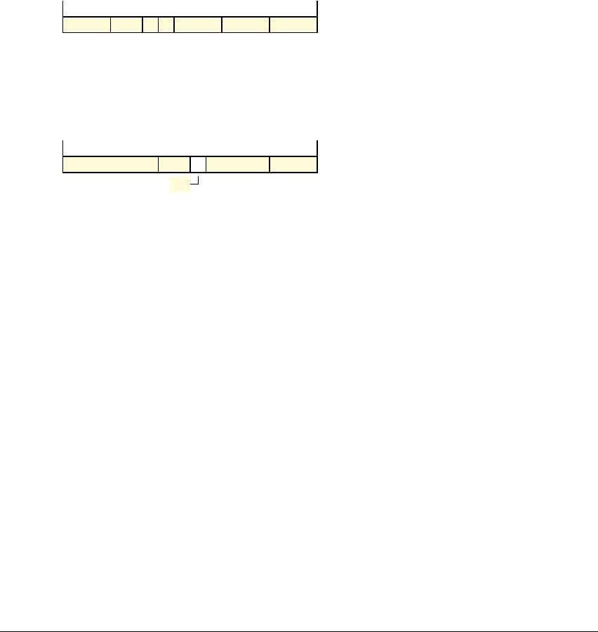
Thumb Instruction Details
ARM DDI 0419C Copyright © 2007-2008, 2010 ARM Limited. All rights reserved. A6-109
ID092410 Non-Confidential
A6.7.3 ADD (register)
This instruction adds a register value and an optionally-shifted register value, and writes the result to the
destination register. Encoding T1 updates the condition flags based on the result.
d = UInt(Rd); n = UInt(Rn); m = UInt(Rm); setflags = !InITBlock();
(shift_t, shift_n) = (SRType_LSL, 0);
if (DN:Rdn) == '1101' || Rm == '1101' then SEE ADD (SP plus register);
d = UInt(DN:Rdn); n = d; m = UInt(Rm); setflags = FALSE; (shift_t, shift_n) = (SRType_LSL, 0);
if n == 15 && m == 15 then UNPREDICTABLE;
if d == 15 && InITBlock() && !LastInITBlock() then UNPREDICTABLE;
Assembler syntax
ADD{S}{<q>} {<Rd>,} <Rn>, <Rm>
where:
S
If present, specifies that the instruction updates the flags. Otherwise, the instruction does not
update the flags.
{<q>}
See Standard assembler syntax fields on page A6-98.
<Rd>
The destination register. If
<Rd>
is omitted, this register is the same as
<Rn>
and encoding T2
is preferred to encoding T1 if both are available. If
<Rd>
is specified, encoding T1 is
preferred to encoding T2. If
R<m>
is not the PC, the PC can be used in encoding T2.
<Rn>
The register that contains the first operand. If the SP is specified for
<Rn>
, see ADD (SP plus
register) on page A6-113. If
R<m>
is not the PC, the PC can be used in encoding T2.
<Rm>
The register that is used as the second operand. The PC can be used in encoding T2.
Encoding T1 All versions of the Thumb instruction set.
ADDS <Rd>,<Rn>,<Rm>
Encoding T2 All versions of the Thumb instruction set.
ADD <Rdn>,<Rm>
0 0 0 1 1 0 0 Rm Rn Rd
15 14 13 12 11 10 9 8 7 6 5 4 3 2 1 0
0 1 0 0 0 1 0 0
DN
Rm Rdn
1514131211109876543210

Thumb Instruction Details
A6-110 Copyright © 2007-2008, 2010 ARM Limited. All rights reserved. ARM DDI 0419C
Non-Confidential ID092410
Operation
if ConditionPassed() then
EncodingSpecificOperations();
shifted = Shift(R[m], shift_t, shift_n, APSR.C);
(result, carry, overflow) = AddWithCarry(R[n], shifted, '0');
if d == 15 then
ALUWritePC(result); // setflags is always FALSE here
else
R[d] = result;
if setflags then
APSR.N = result<31>;
APSR.Z = IsZeroBit(result);
APSR.C = carry;
APSR.V = overflow;
Exceptions
None.
Thumb Instruction Details
ARM DDI 0419C Copyright © 2007-2008, 2010 ARM Limited. All rights reserved. A6-111
ID092410 Non-Confidential
A6.7.4 ADD (SP plus immediate)
This instruction adds an immediate value to the SP value, and writes the result to the destination register.
d = UInt(Rd); setflags = FALSE; imm32 = ZeroExtend(imm8:’00’, 32);
d = 13; setflags = FALSE; imm32 = ZeroExtend(imm7:’00’, 32);
Assembler syntax
where:
{<q>}
See Standard assembler syntax fields on page A6-98.
<Rd>
The destination register. If
<Rd>
is omitted, this register is SP.
<const>
The immediate value to be added to the value obtained from
<Rn>
. Permitted values are
multiples of 4 in the range 0-1020 for encoding T1and multiples of 4 in the range 0-508 for
encoding T2.
Encoding T1 All versions of the Thumb instruction set.
ADD <Rd>,SP,#<imm8>
Encoding T2 All versions of the Thumb instruction set.
ADD SP,SP,#<imm7>
ADD{<q>} {<Rd>,} SP, #<const>
1 0 1 0 1 Rd imm8
15 14 13 12 11 10 9 8 7 6 5 4 3 2 1 0
1 0 1 1 0 0 0 0 0 imm7
15 14 13 12 11 10 9 8 7 6 5 4 3 2 1 0

Thumb Instruction Details
A6-112 Copyright © 2007-2008, 2010 ARM Limited. All rights reserved. ARM DDI 0419C
Non-Confidential ID092410
Operation
if ConditionPassed() then
EncodingSpecificOperations();
(result, carry, overflow) = AddWithCarry(SP, imm32, '0');
R[d] = result;
// no flag setting form of the instruction supported
Exceptions
None.
Thumb Instruction Details
ARM DDI 0419C Copyright © 2007-2008, 2010 ARM Limited. All rights reserved. A6-113
ID092410 Non-Confidential
A6.7.5 ADD (SP plus register)
This instruction adds a register value to the SP value, and writes the result to the destination register.
d = UInt(DM:Rdm); m = UInt(DM:Rdm); setflags = FALSE;
if d == 15 && InITBlock() && !LastInITBlock() then UNPREDICTABLE;
(shift_t, shift_n) = (SRType_LSL, 0);
if Rm == ‘1101’ then SEE encoding T1;
d = 13; m = UInt(Rm); setflags = FALSE;
(shift_t, shift_n) = (SRType_LSL, 0);
Assembler syntax
ADD{<q>} {<Rd>,} SP, <Rm>
where:
{<q>}
See Standard assembler syntax fields on page A6-98.
<Rd>
The destination register. If
<Rd>
is omitted, this register is SP.
<Rm>
The register that is used as the second operand. This register can be the SP, but such
instructions are deprecated and the instruction can only be
ADD SP,SP,SP
.
Encoding T1 All versions of the Thumb instruction set.
ADD <Rdm>, SP, <Rdm>
Encoding T2 All versions of the Thumb instruction set.
ADD SP,<Rm>
0 1 0 0 0 1 0 0
DM
1 1 0 1 Rdm
1514131211109876543210
0 1 0 0 0 1 0 0 1 Rm 1 0 1
15 14 13 12 11 10 9 8 7 6 5 4 3 2 1 0

Thumb Instruction Details
A6-114 Copyright © 2007-2008, 2010 ARM Limited. All rights reserved. ARM DDI 0419C
Non-Confidential ID092410
Operation
if ConditionPassed() then
EncodingSpecificOperations();
shifted = Shift(R[m], shift_t, shift_n, APSR.C);
(result, carry, overflow) = AddWithCarry(SP, shifted, '0');
if d == 15 then
ALUWritePC(result);
else
R[d] = result; // no flag setting form of the instruction supported
Exceptions
None.

Thumb Instruction Details
ARM DDI 0419C Copyright © 2007-2008, 2010 ARM Limited. All rights reserved. A6-115
ID092410 Non-Confidential
A6.7.6 ADR
Address to Register adds an immediate value to the PC value, and writes the result to the destination register.
d = UInt(Rd); imm32 = ZeroExtend(imm8:’00’, 32); add = TRUE;
Assembler syntax
where:
{<q>}
See Standard assembler syntax fields on page A6-98.
<Rd>
The destination register.
<label>
The label of an instruction or literal data item whose address is to be loaded into
<Rd>
. The
assembler calculates the required value of the offset from the
Align(PC,4)
value of the
ADR
instruction to this label.
Only a positive value is permitted with
imm32
equal to the offset. Permitted values of the
offset are multiples of four in the range 0 to 1020 for encoding T1.
In the alternative syntax forms:
<const>
The offset value for the
ADD
form. Permitted values are multiples of four in the range 0 to
1020 for encoding T1.
Note
It is recommended that the alternative syntax form is avoided where possible.
Operation
if ConditionPassed() then
EncodingSpecificOperations();
result = if add then (Align(PC,4) + imm32) else (Align(PC,4) - imm32);
R[d] = result;
Exceptions
None.
Encoding T1 All versions of the Thumb instruction set.
ADR <Rd>,<label>
ADR{<q>} <Rd>, <label>
Normal syntax
ADD{<q>} <Rd>, PC, #<const>
Alternative syntax
1 0 1 0 0 Rd imm8
15 14 13 12 11 10 9 8 7 6 5 4 3 2 1 0

Thumb Instruction Details
A6-116 Copyright © 2007-2008, 2010 ARM Limited. All rights reserved. ARM DDI 0419C
Non-Confidential ID092410
A6.7.7 AND (register)
This instruction performs a bitwise AND of a register value and an optionally-shifted register value, and
writes the result to the destination register. It updates the condition flags based on the result.
d = UInt(Rdn); n = UInt(Rdn); m = UInt(Rm); setflags = !InITBlock();
(shift_t, shift_n) = (SRType_LSL, 0);
Assembler syntax
ANDS{<q>} {<Rd>,} <Rn>, <Rm>
where:
S
The instruction updates the flags.
{<q>}
See Standard assembler syntax fields on page A6-98.
<Rd>
The destination register. If
<Rd>
is omitted, this register is the same as
<Rn>
.
<Rn>
The register that contains the first operand.
<Rm>
The register that is used as the second operand.
Operation
if ConditionPassed() then
EncodingSpecificOperations();
(shifted, carry) = Shift_C(R[m], shift_t, shift_n, APSR.C);
result = R[n] AND shifted;
R[d] = result;
if setflags then
APSR.N = result<31>;
APSR.Z = IsZeroBit(result);
APSR.C = carry;
// APSR.V unchanged
Exceptions
None.
Encoding T1 All versions of the Thumb instruction set.
ANDS <Rdn>,<Rm>
0 1 0 0 0 0 0 0 0 0 Rm Rdn
15 14 13 12 11 10 9 8 7 6 5 4 3 2 1 0

Thumb Instruction Details
ARM DDI 0419C Copyright © 2007-2008, 2010 ARM Limited. All rights reserved. A6-117
ID092410 Non-Confidential
A6.7.8 ASR (immediate)
Arithmetic Shift Right (immediate) shifts a register value right by an immediate number of bits, shifting in
copies of its sign bit, and writes the result to the destination register. It updates the condition flags based on
the result.
d = UInt(Rd); m = UInt(Rm); setflags = !InITBlock();
(-, shift_n) = DecodeImmShift('10', imm5);
Assembler syntax
ASRS{<q>} <Rd>, <Rm>, #<imm5>
where:
S
The instruction updates the flags.
{<q>}
See Standard assembler syntax fields on page A6-98.
<Rd>
The destination register.
<Rm>
The register that contains the first operand.
<imm5>
The shift amount, in the range 1 to 32. See Shifts applied to a register on page A6-101.
Operation
if ConditionPassed() then
EncodingSpecificOperations();
(result, carry) = Shift_C(R[m], SRType_ASR, shift_n, APSR.C);
R[d] = result;
if setflags then
APSR.N = result<31>;
APSR.Z = IsZeroBit(result);
APSR.C = carry;
// APSR.V unchanged
Exceptions
None.
Encoding T1 All versions of the Thumb instruction set.
ASRS <Rd>,<Rm>,#<imm5>
0 0 0 1 0 imm5 Rm Rd
15 14 13 12 11 10 9 8 7 6 5 4 3 2 1 0

Thumb Instruction Details
A6-118 Copyright © 2007-2008, 2010 ARM Limited. All rights reserved. ARM DDI 0419C
Non-Confidential ID092410
A6.7.9 ASR (register)
Arithmetic Shift Right (register) shifts a register value right by a variable number of bits, shifting in copies
of its sign bit, and writes the result to the destination register. The variable number of bits is read from the
bottom byte of a register. It updates the condition flags based on the result.
d = UInt(Rdn); n = UInt(Rdn); m = UInt(Rm); setflags = !InITBlock();
Assembler syntax
ASRS{<q>} <Rd>, <Rn>, <Rm>
where:
S
The instruction updates the flags.
{<q>}
See Standard assembler syntax fields on page A6-98.
<Rd>
The destination register.
<Rn>
The register that contains the first operand.
<Rm>
The register whose bottom byte contains the amount to shift by.
Operation
if ConditionPassed() then
EncodingSpecificOperations();
shift_n = UInt(R[m]<7:0>);
(result, carry) = Shift_C(R[n], SRType_ASR, shift_n, APSR.C);
R[d] = result;
if setflags then
APSR.N = result<31>;
APSR.Z = IsZeroBit(result);
APSR.C = carry;
// APSR.V unchanged
Exceptions
None.
Encoding T1 All versions of the Thumb instruction set.
ASRS <Rdn>,<Rm>
0 1 0 0 0 0 0 1 0 0 Rm Rdn
15 14 13 12 11 10 9 8 7 6 5 4 3 2 1 0
Thumb Instruction Details
ARM DDI 0419C Copyright © 2007-2008, 2010 ARM Limited. All rights reserved. A6-119
ID092410 Non-Confidential
A6.7.10 B
Branch causes a branch to a target address.
if cond == '1110' then UNDEFINED;
if cond == '1111' then SEE SVC;
imm32 = SignExtend(imm8:'0', 32);
if InITBlock() then UNPREDICTABLE;
imm32 = SignExtend(imm11:'0', 32);
if InITBlock() && !LastInITBlock() then UNPREDICTABLE;
Assembler syntax
B{<c>}{<q>} <label>
where:
<c>{<q>}
See Standard assembler syntax fields on page A6-98.
Note
• Encoding T1 is conditional.
• For encoding T1,
<c>
must not be
AL
or omitted.
• For ARMv6-M, for encoding T2, <c> must be
AL
or omitted.
<label>
The label of the instruction that is to be branched to. The assembler calculates the required
value of the offset from the PC value of the
B
instruction to this label, then selects an
encoding that sets
imm32
to that offset.
Permitted offsets are even numbers in the range -256 to 254 for encoding T1 and -2048 to
2046 for encoding T2.
Encoding T1 All versions of the Thumb instruction set.
B<c> <label>
Encoding T2 All versions of the Thumb instruction set.
B<c> <label>
1 1 0 1 cond imm8
15 14 13 12 11 10 9 8 7 6 5 4 3 2 1 0
1 1 1 0 0 imm11
15 14 13 12 11 10 9 8 7 6 5 4 3 2 1 0

Thumb Instruction Details
A6-120 Copyright © 2007-2008, 2010 ARM Limited. All rights reserved. ARM DDI 0419C
Non-Confidential ID092410
Operation
if ConditionPassed() then
EncodingSpecificOperations();
BranchWritePC(PC + imm32);
Exceptions
None.

Thumb Instruction Details
ARM DDI 0419C Copyright © 2007-2008, 2010 ARM Limited. All rights reserved. A6-121
ID092410 Non-Confidential
A6.7.11 BIC (register)
Bit Clear (register) performs a bitwise AND of a register value and the complement of an optionally-shifted
register value, and writes the result to the destination register. It updates the condition flags based on the
result.
d = UInt(Rdn); n = UInt(Rdn); m = UInt(Rm); setflags = !InITBlock();
(shift_t, shift_n) = (SRType_LSL, 0);
Assembler syntax
BICS{<q>} {<Rd>,} <Rn>, <Rm>
where:
S
The instruction updates the flags.
{<q>}
See Standard assembler syntax fields on page A6-98.
<Rd>
The destination register. If
<Rd>
is omitted, this register is the same as
<Rn>
.
<Rn>
The register that contains the first operand.
<Rm>
The register that is used as the second operand.
Operation
if ConditionPassed() then
EncodingSpecificOperations();
(shifted, carry) = Shift_C(R[m], shift_t, shift_n, APSR.C);
result = R[n] AND NOT(shifted);
R[d] = result;
if setflags then
APSR.N = result<31>;
APSR.Z = IsZeroBit(result);
APSR.C = carry;
// APSR.V unchanged
Exceptions
None.
Encoding T1 All versions of the Thumb instruction set.
BICS <Rdn>,<Rm>
0 1 0 0 0 0 1 1 1 0 Rm Rdn
15 14 13 12 11 10 9 8 7 6 5 4 3 2 1 0
Thumb Instruction Details
A6-122 Copyright © 2007-2008, 2010 ARM Limited. All rights reserved. ARM DDI 0419C
Non-Confidential ID092410
A6.7.12 BKPT
Breakpoint causes a HardFault exception or a debug halt to occur depending on the presence and
configuration of the debug support.
imm32 = ZeroExtend(imm8, 32);
// imm32 is for assembly/disassembly only and is ignored by hardware.
Assembler syntax
BKPT{<q>} {#}<imm8>
where:
{<q>}
See Standard assembler syntax fields on page A6-98.
<imm8>
Specifies an 8-bit value that is stored in the instruction. This value is ignored by the ARM
hardware, but can be used by a debugger to store additional information about the
breakpoint.
Operation
EncodingSpecificOperations();
BKPTInstrDebugEvent();
Exceptions
HardFault.
Encoding T1 ARMv5T*, ARMv6-M, ARMv7-M M profile specific behavior
BKPT #<imm8>
1 0 1 1 1 1 1 0 imm8
15 14 13 12 11 10 9 8 7 6 5 4 3 2 1 0
Thumb Instruction Details
ARM DDI 0419C Copyright © 2007-2008, 2010 ARM Limited. All rights reserved. A6-123
ID092410 Non-Confidential
A6.7.13 BL
Branch with Link (immediate) calls a subroutine at a PC-relative address.
I1 = NOT(J1 EOR S); I2 = NOT(J2 EOR S); imm32 = SignExtend(S:I1:I2:imm10:imm11:'0', 32);
if InITBlock() && !LastInITBlock() then UNPREDICTABLE;
Assembler syntax
BL{<q>} <label>
where:
{<q>}
See Standard assembler syntax fields on page A6-98.
<label>
The label of the instruction that is to be branched to.
The assembler calculates the required value of the offset from the PC value of the
BL
instruction to this label, then selects an encoding that sets
imm32
to that offset. Permitted
offsets are even numbers in the range -16777216 to 16777214.
Operation
if ConditionPassed() then
EncodingSpecificOperations();
next_instr_addr = PC;
LR = next_instr_addr<31:1> : '1';
BranchWritePC(PC + imm32);
Exceptions
None.
Note
Before the introduction of Thumb-2 technology, J1 and J2 in encodings T1 and T2 were both 1, resulting in
a smaller branch range. The instructions could be executed as two separate 16-bit instructions, with the first
instruction
instr1
setting LR to
PC + SignExtend(instr1<10:0>:'000000000000', 32)
and the second
instruction completing the operation. It is no longer possible to split the
BL
instruction into two 16-bit
instructions in ARMv6T2, ARMv6-M and ARMv7.
Encoding T1 All versions of the Thumb instruction set.
BL <label>
1 1 1 0 S imm10 1 1 J1 1 J2 imm11
15 14 13 12 11 10 9 8 7 6 5 4 3 2 1 0
1
1514131211109876543210

Thumb Instruction Details
A6-124 Copyright © 2007-2008, 2010 ARM Limited. All rights reserved. ARM DDI 0419C
Non-Confidential ID092410
A6.7.14 BLX (register)
Branch with Link and Exchange calls a subroutine at an address and instruction set specified by a register.
ARMv6-M only supports Thumb execution. An attempt to change the instruction execution state causes an
exception on the instruction at the target address.
m = UInt(Rm);
if m == 15 then UNPREDICTABLE;
if InITBlock() && !LastInITBlock() then UNPREDICTABLE;
Assembler syntax
BLX{<q>} <Rm>
where:
{<q>}
See Standard assembler syntax fields on page A6-98.
<Rm>
The register that contains the branch target address and instruction set selection bit.
Operation
if ConditionPassed() then
EncodingSpecificOperations();
target = R[m];
next_instr_addr = PC - 2;
LR = next_instr_addr<31:1> : '1';
BLXWritePC(target);
Exceptions
HardFault.
Encoding T1 ARMv5T*, ARMv6-M, ARMv7-M
BLX <Rm>
0 1 0 0 0 1 1 1 1 Rm (0) (0) (0)
15 14 13 12 11 10 9 8 7 6 5 4 3 2 1 0

Thumb Instruction Details
ARM DDI 0419C Copyright © 2007-2008, 2010 ARM Limited. All rights reserved. A6-125
ID092410 Non-Confidential
A6.7.15 BX
Branch and Exchange causes a branch to an address and instruction set specified by a register. ARMv6-M
only supports Thumb execution. An attempt to change the instruction execution state causes an exception
on the instruction at the target address.
BX
can also be used for an exception return, see Exception return behavior on page B1-227.
m = UInt(Rm);
if InITBlock() && !LastInITBlock() then UNPREDICTABLE;
if m==15 then UNPREDICTABLE;
Assembler syntax
BX{<q>} <Rm>
where:
{<q>}
See Standard assembler syntax fields on page A6-98.
<Rm>
The register that contains the branch target address and instruction set selection bit.
Operation
if ConditionPassed() then
EncodingSpecificOperations();
BXWritePC(R[m]);
Exceptions
HardFault.
Encoding T1 All versions of the Thumb instruction set.
BX <Rm>
0 1 0 0 0 1 1 1 0 Rm (0) (0) (0)
15 14 13 12 11 10 9 8 7 6 5 4 3 2 1 0

Thumb Instruction Details
A6-126 Copyright © 2007-2008, 2010 ARM Limited. All rights reserved. ARM DDI 0419C
Non-Confidential ID092410
A6.7.16 CMN (register)
Compare Negative (register) adds a register value and an optionally-shifted register value. It updates the
condition flags based on the result, and discards the result.
n = UInt(Rn); m = UInt(Rm);
(shift_t, shift_n) = (SRType_LSL, 0);
Assembler syntax
CMN{<q>} <Rn>, <Rm>
where:
{<q>}
See Standard assembler syntax fields on page A6-98.
<Rn>
The register that contains the first operand.
<Rm>
The register that is used as the second operand.
Operation
if ConditionPassed() then
EncodingSpecificOperations();
shifted = Shift(R[m], shift_t, shift_n, APSR.C);
(result, carry, overflow) = AddWithCarry(R[n], shifted, '0');
APSR.N = result<31>;
APSR.Z = IsZeroBit(result);
APSR.C = carry;
APSR.V = overflow;
Exceptions
None.
Encoding T1 All versions of the Thumb instruction set.
CMN <Rn>,<Rm>
0 1 0 0 0 0 1 0 1 1 Rm Rn
15 14 13 12 11 10 9 8 7 6 5 4 3 2 1 0

Thumb Instruction Details
ARM DDI 0419C Copyright © 2007-2008, 2010 ARM Limited. All rights reserved. A6-127
ID092410 Non-Confidential
A6.7.17 CMP (immediate)
Compare (immediate) subtracts an immediate value from a register value. It updates the condition flags
based on the result, and discards the result.
n = UInt(Rn); imm32 = ZeroExtend(imm8, 32);
Assembler syntax
CMP{<q>} <Rn>, #<const>
where:
{<q>}
See Standard assembler syntax fields on page A6-98.
<Rn>
The register that contains the operand.
<const>
The immediate value to be added to the value obtained from
<Rn>
. The range of permitted
values is 0-255 for encoding T1.
Encoding T1 All versions of the Thumb instruction set.
CMP <Rn>,#<imm8>
0 0 1 0 1 Rn imm8
15 14 13 12 11 10 9 8 7 6 5 4 3 2 1 0

Thumb Instruction Details
A6-128 Copyright © 2007-2008, 2010 ARM Limited. All rights reserved. ARM DDI 0419C
Non-Confidential ID092410
Operation
if ConditionPassed() then
EncodingSpecificOperations();
(result, carry, overflow) = AddWithCarry(R[n], NOT(imm32), '1');
APSR.N = result<31>;
APSR.Z = IsZeroBit(result);
APSR.C = carry;
APSR.V = overflow;
Exceptions
None.
Thumb Instruction Details
ARM DDI 0419C Copyright © 2007-2008, 2010 ARM Limited. All rights reserved. A6-129
ID092410 Non-Confidential
A6.7.18 CMP (register)
Compare (register) subtracts an optionally-shifted register value from a register value. It updates the
condition flags based on the result, and discards the result.
n = UInt(Rn); m = UInt(Rm);
(shift_t, shift_n) = (SRType_LSL, 0);
n = UInt(N:Rn); m = UInt(Rm);
(shift_t, shift_n) = (SRType_LSL, 0);
if n < 8 && m < 8 then UNPREDICTABLE;
if n == 15 || m == 15 then UNPREDICTABLE;
Assembler syntax
CMP{<q>} <Rn>, <Rm>
where:
{<q>}
See Standard assembler syntax fields on page A6-98.
<Rn>
The register that contains the first operand. The SP can be used.
<Rm>
The register that is optionally shifted and used as the second operand. The SP can be used,
but use of the SP is deprecated.
Encoding T1 All versions of the Thumb instruction set.
CMP <Rn>,<Rm> <Rn>
and
<Rm>
both from R0-R7
Encoding T2 All versions of the Thumb instruction set.
CMP <Rn>,<Rm> <Rn>
and
<Rm>
not both from R0-R7
0 1 0 0 0 0 1 0 1 0 Rm Rn
15 14 13 12 11 10 9 8 7 6 5 4 3 2 1 0
0 1 0 0 0 1 0 1 N Rm Rn
15 14 13 12 11 10 9 8 7 6 5 4 3 2 1 0

Thumb Instruction Details
A6-130 Copyright © 2007-2008, 2010 ARM Limited. All rights reserved. ARM DDI 0419C
Non-Confidential ID092410
Operation
if ConditionPassed() then
EncodingSpecificOperations();
shifted = Shift(R[m], shift_t, shift_n, APSR.C);
(result, carry, overflow) = AddWithCarry(R[n], NOT(shifted), '1');
APSR.N = result<31>;
APSR.Z = IsZeroBit(result);
APSR.C = carry;
APSR.V = overflow;
Exceptions
None.


Thumb Instruction Details
A6-132 Copyright © 2007-2008, 2010 ARM Limited. All rights reserved. ARM DDI 0419C
Non-Confidential ID092410
A6.7.20 CPY
Copy is a pre-UAL synonym for
MOV
(register).
Assembler syntax
CPY <Rd>, <Rn>
This is equivalent to:
MOV <Rd>, <Rn>
Exceptions
None.
Thumb Instruction Details
ARM DDI 0419C Copyright © 2007-2008, 2010 ARM Limited. All rights reserved. A6-133
ID092410 Non-Confidential
A6.7.21 DMB
Data Memory Barrier acts as a memory barrier. It ensures that all explicit memory accesses that appear in
program order before the
DMB
instruction are observed before any explicit memory accesses that appear in
program order after the
DMB
instruction. It does not affect the ordering of any other instructions executing on
the processor.
// No additional decoding required
Assembler syntax
DMB{<q>} {<opt>}
where:
{<q>}
See Standard assembler syntax fields on page A6-98.
<opt>
Specifies an optional limitation on the DMB operation:
SY
DMB operation ensures ordering of all accesses, encoded as option == '1111'.
Can be omitted.
All other encodings of the option are reserved. The corresponding instructions execute as
system (SY) DMB operations, but software must not rely on this behavior.
Operation
if ConditionPassed() then
EncodingSpecificOperations();
DataMemoryBarrier(option);
Exceptions
None.
Encoding T1 ARMv6-M, ARMv7-M
DMB #<option>
1 1 1 0 0 1 1 1 0 1 1 (1) (1) (1) (1) 1 0 (0) 0 (1) (1) (1) (1) 0 1 0 1 option
15 14 13 12 11 10 9 8 7 6 5 4 3 2 1 0
1
1514131211109876543210
Thumb Instruction Details
A6-134 Copyright © 2007-2008, 2010 ARM Limited. All rights reserved. ARM DDI 0419C
Non-Confidential ID092410
A6.7.22 DSB
Data Synchronization Barrier acts as a special kind of memory barrier. No instruction in program order after
this instruction can execute until this instruction completes. This instruction completes only when both:
• any explicit memory access made before this instruction is complete
• all cache and branch predictor maintenance operations before this instruction complete.
// No additional decoding required
Assembler syntax
DSB{<q>} {<opt>}
where:
{<q>}
See Standard assembler syntax fields on page A6-98.
<opt>
Specifies an optional limitation on the DSB operation:
SY
DSB operation ensures completion of all accesses, encoded as option == '1111'.
Can be omitted.
All other encodings of option are reserved. The corresponding instructions execute as
system (SY) DSB operations, but software must not rely on this behavior.
Operation
if ConditionPassed() then
EncodingSpecificOperations();
DataSynchronizationBarrier(option);
Exceptions
None.
Encoding T1 ARMv6-M, ARMv7-M
DSB #<option>
1 1 1 0 0 1 1 1 0 1 1 (1) (1) (1) (1) 1 0 (0) 0 (1) (1) (1) (1) 0 1 0 0 option
15 14 13 12 11 10 9 8 7 6 5 4 3 2 1 0
1
1514131211109876543210

Thumb Instruction Details
ARM DDI 0419C Copyright © 2007-2008, 2010 ARM Limited. All rights reserved. A6-135
ID092410 Non-Confidential
A6.7.23 EOR (register)
Exclusive OR (register) performs a bitwise Exclusive OR of a register value and an optionally-shifted
register value, and writes the result to the destination register. It updates the condition flags based on the
result.
d = UInt(Rdn); n = UInt(Rdn); m = UInt(Rm); setflags = !InITBlock();
(shift_t, shift_n) = (SRType_LSL, 0);
Assembler syntax
EORS{<q>} {<Rd>,} <Rn>, <Rm>
where:
S
The instruction updates the flags.
{<q>}
See Standard assembler syntax fields on page A6-98.
<Rd>
The destination register. If
<Rd>
is omitted, this register is the same as
<Rn>
.
<Rn>
The register that contains the first operand.
<Rm>
The register that is used as the second operand.
Operation
if ConditionPassed() then
EncodingSpecificOperations();
(shifted, carry) = Shift_C(R[m], shift_t, shift_n, APSR.C);
result = R[n] EOR shifted;
R[d] = result;
if setflags then
APSR.N = result<31>;
APSR.Z = IsZeroBit(result);
APSR.C = carry;
// APSR.V unchanged
Exceptions
None.
Encoding T1 All versions of the Thumb instruction set.
EORS <Rdn>,<Rm>
0 1 0 0 0 0 0 0 0 1 Rm Rdn
15 14 13 12 11 10 9 8 7 6 5 4 3 2 1 0
Thumb Instruction Details
A6-136 Copyright © 2007-2008, 2010 ARM Limited. All rights reserved. ARM DDI 0419C
Non-Confidential ID092410
A6.7.24 ISB
Instruction Synchronization Barrier flushes the pipeline in the processor, so that all instructions following
the
ISB
are fetched from cache or memory after the instruction has completed. It ensures that the effects of
context altering operations, such as those resulting from read or write accesses to the system control space
(SCS), that completed before the
ISB
instruction are visible to the instructions fetched after the
ISB
. See
Barrier support for system correctness on page B2-255 for more details.
In addition, the
ISB
instruction ensures that any branches that appear in program order after it are always
written into any branch prediction logic with the context that is visible after the
ISB
instruction. This is
required to ensure correct execution of the instruction stream.
// No additional decoding required
Assembler syntax
ISB{<q>} {<opt>}
where:
{<q>}
See Standard assembler syntax fields on page A6-98.
<opt>
Specifies an optional limitation on the ISB operation. Permitted values are:
SY
Full system ISB operation, encoded as option == '1111'. Can be omitted.
All other encodings of option are reserved. The corresponding instructions execute as full
system ISB operations, but must not be relied on by software.
Operation
if ConditionPassed() then
EncodingSpecificOperations();
InstructionSynchronizationBarrier(option);
Exceptions
None.
Encoding T1 ARMv6-M, ARMv7-M
ISB #<option>
1 1 1 0 0 1 1 1 0 1 1 (1) (1) (1) (1) 1 0 (0) 0 (1) (1) (1) (1) 0 1 1 0 option
15 14 13 12 11 10 9 8 7 6 5 4 3 2 1 0
1
1514131211109876543210
Thumb Instruction Details
ARM DDI 0419C Copyright © 2007-2008, 2010 ARM Limited. All rights reserved. A6-137
ID092410 Non-Confidential
A6.7.25 LDM, LDMIA, LDMFD
Load Multiple Increment After loads multiple registers from consecutive memory locations using an
address from a base register. The sequential memory locations start at this address, and the address above
the last of those locations is written back to the base register when the base register is not part of the register
list.
n = UInt(Rn); registers = '00000000':register_list; wback = (registers<n> == '0');
if BitCount(registers) < 1 then UNPREDICTABLE;
Assembler syntax
LDM{<q>} <Rn>{!}, <registers>
where:
{<q>}
See Standard assembler syntax fields on page A6-98.
<Rn>
The base register.
!
Causes the instruction to write a modified value back to
<Rn>
. If
!
is omitted, the
instruction does not change
<Rn>
in this way.
<registers>
Is a list of one or more registers to be loaded, separated by commas and surrounded
by
{
and
}
. The lowest-numbered register is loaded from the lowest memory
address, through to the highest-numbered register from the highest memory address.
LDMIA
and
LDMFD
are pseudo-instructions for
LDM
.
LDMFD
refers to its use for popping data from Full
Descending stacks.
Encoding T1 All versions of the Thumb instruction set.
LDM <Rn>!,<registers> <Rn>
not included in
<registers>
LDM <Rn>,<registers> <Rn>
included in
<registers>
1 1 0 0 1 Rn register_list
15 14 13 12 11 10 9 8 7 6 5 4 3 2 1 0

Thumb Instruction Details
A6-138 Copyright © 2007-2008, 2010 ARM Limited. All rights reserved. ARM DDI 0419C
Non-Confidential ID092410
Operation
if ConditionPassed() then
EncodingSpecificOperations();
address = R[n];
for i = 0 to 7
if registers<i> == '1' then
R[i] = MemA[address,4]; address = address + 4;
if wback && registers<n> == '0' then R[n] = R[n] + 4*BitCount(registers);
Exceptions
HardFault.

Thumb Instruction Details
ARM DDI 0419C Copyright © 2007-2008, 2010 ARM Limited. All rights reserved. A6-139
ID092410 Non-Confidential
A6.7.26 LDR (immediate)
Load Register (immediate) calculates an address from a base register value and an immediate offset, loads
a word from memory, and writes it to a register. Offset addressing is used, see Memory accesses on
page A6-103 for more information.
t = UInt(Rt); n = UInt(Rn); imm32 = ZeroExtend(imm5:'00', 32);
index = TRUE; add = TRUE; wback = FALSE;
t = UInt(Rt); n = 13; imm32 = ZeroExtend(imm8:'00', 32);
index = TRUE; add = TRUE; wback = FALSE;
Assembler syntax
where:
{<q>}
See Standard assembler syntax fields on page A6-98.
<Rt>
The destination register.
<Rn>
The base register.
+/-
Is + or omitted to indicate that the immediate offset is added to the base register value.
add == TRUE
<imm>
The immediate offset added to the value of
<Rn>
to form the address. Permitted values are
multiples of 4 in the range 0-124 for encoding T1 and multiples of 4 in the range 0-1020 for
encoding T2. For the offset addressing syntax,
<imm>
can be omitted, meaning an offset of 0.
Encoding T1 All versions of the Thumb instruction set.
LDR <Rt>, [<Rn>{,#<imm5>}]
Encoding T2 All versions of the Thumb instruction set.
LDR <Rt>,[SP{,#<imm8>}]
LDR{<q>} <Rt>, [<Rn> {, #+/-<imm>}]
0 1 1 0 1 imm5 Rn Rt
15 14 13 12 11 10 9 8 7 6 5 4 3 2 1 0
1 0 0 1 1 Rt imm8
15 14 13 12 11 10 9 8 7 6 5 4 3 2 1 0

Thumb Instruction Details
A6-140 Copyright © 2007-2008, 2010 ARM Limited. All rights reserved. ARM DDI 0419C
Non-Confidential ID092410
Operation
if ConditionPassed() then
EncodingSpecificOperations();
offset_addr = if add then (R[n] + imm32) else (R[n] - imm32);
address = if index then offset_addr else R[n];
R[t] = MemU[address,4];
if wback then R[n] = offset_addr;
Exceptions
HardFault.
Thumb Instruction Details
ARM DDI 0419C Copyright © 2007-2008, 2010 ARM Limited. All rights reserved. A6-141
ID092410 Non-Confidential
A6.7.27 LDR (literal)
Load Register (literal) calculates an address from the PC value and an immediate offset, loads a word from
memory, and writes it to a register. See Memory accesses on page A6-103 for information about memory
accesses.
t = UInt(Rt); imm32 = ZeroExtend(imm8:'00', 32); add = TRUE;
Assembler syntax
where:
{<q>}
See Standard assembler syntax fields on page A6-98.
<Rt>
The destination register.
<label>
The label of the literal data item that is to be loaded into
<Rt>
. The assembler calculates the
required value of the offset from the PC value of this instruction to the label.
Permitted values of the offset are multiples of four in the range 0 to 1020 for encoding T1.
In the alternative syntax form:
<imm>
The immediate offset added to the
Align(PC, 4)
value of the instruction to form the address.
Permitted values are multiples of four in the range 0 to 1020 for encoding T1.
Note
It is recommended that the alternative syntax form is avoided where possible.
Encoding T1 All versions of the Thumb instruction set.
LDR <Rt>,<label>
LDR{<q>} <Rt>, <label>
Normal syntax
LDR{<q>} <Rt>, [PC, #<imm>]
Alternative syntax
0 1 0 0 1 Rt imm8
15 14 13 12 11 10 9 8 7 6 5 4 3 2 1 0

Thumb Instruction Details
A6-142 Copyright © 2007-2008, 2010 ARM Limited. All rights reserved. ARM DDI 0419C
Non-Confidential ID092410
Operation
if ConditionPassed() then
EncodingSpecificOperations();
base = Align(PC,4);
address = if add then (base + imm32) else (base - imm32);
R[t] = MemU[address,4];
Exceptions
HardFault.

Thumb Instruction Details
ARM DDI 0419C Copyright © 2007-2008, 2010 ARM Limited. All rights reserved. A6-143
ID092410 Non-Confidential
A6.7.28 LDR (register)
Load Register (register) calculates an address from a base register value and an offset register value, loads
a word from memory, and writes it to a register. Offset addressing is used, see Memory accesses on
page A6-103 for more information.
The register loaded can be the PC. If it is, the word loaded for the PC is treated as an address or exception
return value and a branch occurs. Bit [0] complies with the ARM architecture interworking rules for
branches to Thumb state execution and must be 1. If bit [0] is 0, a HardFault exception occurs.
t = UInt(Rt); n = UInt(Rn); m = UInt(Rm);
index = TRUE; add = TRUE; wback = FALSE;
(shift_t, shift_n) = (SRType_LSL, 0);
Assembler syntax
LDR{<q>} <Rt>, [<Rn>, <Rm>]
where:
{<q>}
See Standard assembler syntax fields on page A6-98.
<Rt>
The destination register.
<Rn>
The register that contains the base value.
<Rm>
Contains the offset that is added to the value of
<Rn>
to form the address.
Operation
if ConditionPassed() then
EncodingSpecificOperations();
offset = Shift(R[m], shift_t, shift_n, APSR.C);
offset_addr = if add then (R[n] + offset) else (R[n] - offset);
address = if index then offset_addr else R[n];
R[t] = MemU[address,4];
if wback then R[n] = offset_addr;
Exceptions
HardFault.
Encoding T1 All versions of the Thumb instruction set.
LDR <Rt>,[<Rn>,<Rm>]
0 1 0 1 1 0 0 Rm Rn Rt
15 14 13 12 11 10 9 8 7 6 5 4 3 2 1 0

Thumb Instruction Details
A6-144 Copyright © 2007-2008, 2010 ARM Limited. All rights reserved. ARM DDI 0419C
Non-Confidential ID092410
A6.7.29 LDRB (immediate)
Load Register Byte (immediate) calculates an address from a base register value and an immediate offset,
loads a byte from memory, zero-extends it to form a 32-bit word, and writes it to a register. Offset addressing
is used, see Memory accesses on page A6-103 for more information.
t = UInt(Rt); n = UInt(Rn); imm32 = ZeroExtend(imm5, 32);
index = TRUE; add = TRUE; wback = FALSE;
Assembler syntax
where:
{<q>}
See Standard assembler syntax fields on page A6-98.
<Rt>
The destination register.
<Rn>
The base register.
+/-
Is + or omitted to indicate that the immediate offset is added to the base register value.
add == TRUE
<imm>
The immediate offset added to or subtracted from the value of
<Rn>
to form the address. The
range of permitted values is 0-31 for encoding T1.
<imm>
can be omitted, meaning an offset
of 0.
Operation
if ConditionPassed() then
EncodingSpecificOperations();
offset_addr = if add then (R[n] + imm32) else (R[n] - imm32);
address = if index then offset_addr else R[n];
R[t] = ZeroExtend(MemU[address,1], 32);
if wback then R[n] = offset_addr;
Exceptions
HardFault.
Encoding T1 All versions of the Thumb instruction set.
LDRB <Rt>,[<Rn>{,#<imm5>}]
LDRB{<q>} <Rt>, [<Rn> {, #+/-<imm>}]
0 1 1 1 1 imm5 Rn Rt
15 14 13 12 11 10 9 8 7 6 5 4 3 2 1 0

Thumb Instruction Details
ARM DDI 0419C Copyright © 2007-2008, 2010 ARM Limited. All rights reserved. A6-145
ID092410 Non-Confidential
A6.7.30 LDRB (register)
Load Register Byte (register) calculates an address from a base register value and an offset register value,
loads a byte from memory, zero-extends it to form a 32-bit word, and writes it to a register. Offset addressing
is used, see Memory accesses on page A6-103 for more information.
t = UInt(Rt); n = UInt(Rn); m = UInt(Rm);
index = TRUE; add = TRUE; wback = FALSE;
(shift_t, shift_n) = (SRType_LSL, 0);
Assembler syntax
LDRB{<q>} <Rt>, [<Rn>, <Rm>]
where:
{<q>}
See Standard assembler syntax fields on page A6-98.
<Rt>
The destination register.
<Rn>
The register that contains the base value.
<Rm>
Contains the offset that is added to the value of
<Rn>
to form the address.
Operation
if ConditionPassed() then
EncodingSpecificOperations();
offset = Shift(R[m], shift_t, shift_n, APSR.C);
offset_addr = if add then (R[n] + offset) else (R[n] - offset);
address = if index then offset_addr else R[n];
R[t] = ZeroExtend(MemU[address,1],32);
Exceptions
HardFault.
Encoding T1 All versions of the Thumb instruction set.
LDRB <Rt>,[<Rn>,<Rm>]
0 1 0 1 1 1 0 Rm Rn Rt
15 14 13 12 11 10 9 8 7 6 5 4 3 2 1 0

Thumb Instruction Details
A6-146 Copyright © 2007-2008, 2010 ARM Limited. All rights reserved. ARM DDI 0419C
Non-Confidential ID092410
A6.7.31 LDRH (immediate)
Load Register Halfword (immediate) calculates an address from a base register value and an immediate
offset, loads a halfword from memory, zero-extends it to form a 32-bit word, and writes it to a register. Offset
addressing is used, see Memory accesses on page A6-103 for more information.
t = UInt(Rt); n = UInt(Rn); imm32 = ZeroExtend(imm5:'0', 32);
index = TRUE; add = TRUE; wback = FALSE;
Assembler syntax
where:
{<q>}
See Standard assembler syntax fields on page A6-98.
<Rt>
The destination register.
<Rn>
The base register.
+/-
Is + or omitted to indicate that the immediate offset is added to the base register value.
add == TRUE
<imm>
The immediate offset added to the value of
<Rn>
to form the address. Permitted values are
multiples of 2 in the range 0-62 for encoding T1.
<imm>
can be omitted, meaning an offset
of 0.
Operation
if ConditionPassed() then
EncodingSpecificOperations();
offset_addr = if add then (R[n] + imm32) else (R[n] - imm32);
address = if index then offset_addr else R[n];
data = MemU[address,2];
if wback then R[n] = offset_addr;
R[t] = ZeroExtend(data, 32);
Exceptions
HardFault.
Encoding T1 All versions of the Thumb instruction set.
LDRH <Rt>,[<Rn>{,#<imm5>}]
LDRH{<q>} <Rt>, [<Rn> {, #+/-<imm>}]
1 0 0 0 1 imm5 Rn Rt
15 14 13 12 11 10 9 8 7 6 5 4 3 2 1 0

Thumb Instruction Details
ARM DDI 0419C Copyright © 2007-2008, 2010 ARM Limited. All rights reserved. A6-147
ID092410 Non-Confidential
A6.7.32 LDRH (register)
Load Register Halfword (register) calculates an address from a base register value and an offset register
value, loads a halfword from memory, zero-extends it to form a 32-bit word, and writes it to a register. Offset
addressing is used, see Memory accesses on page A6-103 for more information.
t = UInt(Rt); n = UInt(Rn); m = UInt(Rm);
index = TRUE; add = TRUE; wback = FALSE;
(shift_t, shift_n) = (SRType_LSL, 0);
Assembler syntax
LDRH{<q>} <Rt>, [<Rn>, <Rm>]
where:
{<q>}
See Standard assembler syntax fields on page A6-98.
<Rt>
The destination register.
<Rn>
The register that contains the base value.
<Rm>
Contains the offset that is added to the value of
<Rn>
to form the address.
Operation
if ConditionPassed() then
EncodingSpecificOperations();
offset = Shift(R[m], shift_t, shift_n, APSR.C);
offset_addr = if add then (R[n] + offset) else (R[n] - offset);
address = if index then offset_addr else R[n];
data = MemU[address,2];
if wback then R[n] = offset_addr;
R[t] = ZeroExtend(data, 32);
Exceptions
HardFault.
Encoding T1 All versions of the Thumb instruction set.
LDRH <Rt>,[<Rn>,<Rm>]
0 1 0 1 1 0 1 Rm Rn Rt
15 14 13 12 11 10 9 8 7 6 5 4 3 2 1 0

Thumb Instruction Details
A6-148 Copyright © 2007-2008, 2010 ARM Limited. All rights reserved. ARM DDI 0419C
Non-Confidential ID092410
A6.7.33 LDRSB (register)
Load Register Signed Byte (register) calculates an address from a base register value and an offset register
value, loads a byte from memory, sign-extends it to form a 32-bit word, and writes it to a register. Offset
addressing is used, see Memory accesses on page A6-103 for more information.
t = UInt(Rt); n = UInt(Rn); m = UInt(Rm);
index = TRUE; add = TRUE; wback = FALSE;
(shift_t, shift_n) = (SRType_LSL, 0);
Assembler syntax
LDRSB{<q>} <Rt>, [<Rn>, <Rm>]
where:
{<q>}
See Standard assembler syntax fields on page A6-98.
<Rt>
The destination register.
<Rn>
The register that contains the base value.
<Rm>
Contains the offset that is added to the value of
<Rn>
to form the address.
Operation
if ConditionPassed() then
EncodingSpecificOperations();
offset = Shift(R[m], shift_t, shift_n, APSR.C);
offset_addr = if add then (R[n] + offset) else (R[n] - offset);
address = if index then offset_addr else R[n];
R[t] = SignExtend(MemU[address,1], 32);
Exceptions
HardFault.
Encoding T1 All versions of the Thumb instruction set.
LDRSB <Rt>,[<Rn>,<Rm>]
0 1 0 1 0 1 1 Rm Rn Rt
15 14 13 12 11 10 9 8 7 6 5 4 3 2 1 0

Thumb Instruction Details
ARM DDI 0419C Copyright © 2007-2008, 2010 ARM Limited. All rights reserved. A6-149
ID092410 Non-Confidential
A6.7.34 LDRSH (register)
Load Register Signed Halfword (register) calculates an address from a base register value and an offset
register value, loads a halfword from memory, sign-extends it to form a 32-bit word, and writes it to a
register. Offset addressing is used, see Memory accesses on page A6-103 for more information.
t = UInt(Rt); n = UInt(Rn); m = UInt(Rm);
index = TRUE; add = TRUE; wback = FALSE;
(shift_t, shift_n) = (SRType_LSL, 0);
Assembler syntax
LDRSH{<q>} <Rt>, [<Rn>, <Rm>]
where:
{<q>}
See Standard assembler syntax fields on page A6-98.
<Rt>
The destination register.
<Rn>
The register that contains the base value.
<Rm>
Contains the offset that is added to the value of
<Rn>
to form the address.
Operation
if ConditionPassed() then
EncodingSpecificOperations();
offset = Shift(R[m], shift_t, shift_n, APSR.C);
offset_addr = if add then (R[n] + offset) else (R[n] - offset);
address = if index then offset_addr else R[n];
data = MemU[address,2];
if wback then R[n] = offset_addr;
R[t] = SignExtend(data, 32);
Exceptions
HardFault.
Encoding T1 All versions of the Thumb instruction set.
LDRSH <Rt>,[<Rn>,<Rm>]
0 1 0 1 1 1 1 Rm Rn Rt
15 14 13 12 11 10 9 8 7 6 5 4 3 2 1 0

Thumb Instruction Details
A6-150 Copyright © 2007-2008, 2010 ARM Limited. All rights reserved. ARM DDI 0419C
Non-Confidential ID092410
A6.7.35 LSL (immediate)
Logical Shift Left (immediate) shifts a register value left by an immediate number of bits, shifting in zeros,
and writes the result to the destination register. The condition flags are updated based on the result.
if imm5 == '00000' then SEE MOV (register);
d = UInt(Rd); m = UInt(Rm); setflags = !InITBlock();
(-, shift_n) = DecodeImmShift('00', imm5);
Assembler syntax
LSLS{<q>} <Rd>, <Rm>, #<imm5>
where:
S
The instruction updates the flags.
{<q>}
See Standard assembler syntax fields on page A6-98.
<Rd>
The destination register.
<Rm>
The register that contains the first operand.
<imm5>
The shift amount, in the range 0 to 31. See Shifts applied to a register on page A6-101.
Operation
if ConditionPassed() then
EncodingSpecificOperations();
(result, carry) = Shift_C(R[m], SRType_LSL, shift_n, APSR.C);
R[d] = result;
if setflags then
APSR.N = result<31>;
APSR.Z = IsZeroBit(result);
APSR.C = carry;
// APSR.V unchanged
Exceptions
None.
Encoding T1 All versions of the Thumb instruction set.
LSLS <Rd>,<Rm>,#<imm5>
0 0 0 0 0 imm5 Rm Rd
15 14 13 12 11 10 9 8 7 6 5 4 3 2 1 0

Thumb Instruction Details
ARM DDI 0419C Copyright © 2007-2008, 2010 ARM Limited. All rights reserved. A6-151
ID092410 Non-Confidential
A6.7.36 LSL (register)
Logical Shift Left (register) shifts a register value left by a variable number of bits, shifting in zeros, and
writes the result to the destination register. The variable number of bits is read from the bottom byte of a
register. The condition flags are updated based on the result.
d = UInt(Rdn); n = UInt(Rdn); m = UInt(Rm); setflags = !InITBlock();
Assembler syntax
LSLS{<q>} <Rd>, <Rn>, <Rm>
where:
S
The instruction updates the flags.
{<q>}
See Standard assembler syntax fields on page A6-98.
<Rd>
The destination register.
<Rn>
The register that contains the first operand.
<Rm>
The register whose bottom byte contains the amount to shift by.
Operation
if ConditionPassed() then
EncodingSpecificOperations();
shift_n = UInt(R[m]<7:0>);
(result, carry) = Shift_C(R[n], SRType_LSL, shift_n, APSR.C);
R[d] = result;
if setflags then
APSR.N = result<31>;
APSR.Z = IsZeroBit(result);
APSR.C = carry;
// APSR.V unchanged
Exceptions
None.
Encoding T1 All versions of the Thumb instruction set.
LSLS <Rdn>,<Rm>
0 1 0 0 0 0 0 0 1 0 Rm Rdn
15 14 13 12 11 10 9 8 7 6 5 4 3 2 1 0

Thumb Instruction Details
A6-152 Copyright © 2007-2008, 2010 ARM Limited. All rights reserved. ARM DDI 0419C
Non-Confidential ID092410
A6.7.37 LSR (immediate)
Logical Shift Right (immediate) shifts a register value right by an immediate number of bits, shifting in
zeros, and writes the result to the destination register. The condition flags are updated based on the result.
d = UInt(Rd); m = UInt(Rm); setflags = !InITBlock();
(-, shift_n) = DecodeImmShift('01', imm5);
Assembler syntax
LSRS{<q>} <Rd>, <Rm>, #<imm5>
where:
S
The instruction updates the flags..
{<q>}
See Standard assembler syntax fields on page A6-98.
<Rd>
The destination register.
<Rm>
The register that contains the first operand.
<imm5>
The shift amount, in the range 1 to 32. See Shifts applied to a register on page A6-101.
Operation
if ConditionPassed() then
EncodingSpecificOperations();
(result, carry) = Shift_C(R[m], SRType_LSR, shift_n, APSR.C);
R[d] = result;
if setflags then
APSR.N = result<31>;
APSR.Z = IsZeroBit(result);
APSR.C = carry;
// APSR.V unchanged
Exceptions
None.
Encoding T1 All versions of the Thumb instruction set.
LSRS <Rd>,<Rm>,#<imm5>
0 0 0 0 1 imm5 Rm Rd
15 14 13 12 11 10 9 8 7 6 5 4 3 2 1 0

Thumb Instruction Details
ARM DDI 0419C Copyright © 2007-2008, 2010 ARM Limited. All rights reserved. A6-153
ID092410 Non-Confidential
A6.7.38 LSR (register)
Logical Shift Right (register) shifts a register value right by a variable number of bits, shifting in zeros, and
writes the result to the destination register. The variable number of bits is read from the bottom byte of a
register. The condition flags are updated based on the result.
d = UInt(Rdn); n = UInt(Rdn); m = UInt(Rm); setflags = !InITBlock();
Assembler syntax
LSRS{<q>} <Rd>, <Rn>, <Rm>
where:
S
The instruction updates the flags.
{<q>}
See Standard assembler syntax fields on page A6-98.
<Rd>
The destination register.
<Rn>
The register that contains the first operand.
<Rm>
The register whose bottom byte contains the amount to shift by.
Operation
if ConditionPassed() then
EncodingSpecificOperations();
shift_n = UInt(R[m]<7:0>);
(result, carry) = Shift_C(R[n], SRType_LSR, shift_n, APSR.C);
R[d] = result;
if setflags then
APSR.N = result<31>;
APSR.Z = IsZeroBit(result);
APSR.C = carry;
// APSR.V unchanged
Exceptions
None.
Encoding T1 All versions of the Thumb instruction set.
LSRS <Rdn>,<Rm>
0 1 0 0 0 0 0 0 1 1 Rm Rdn
15 14 13 12 11 10 9 8 7 6 5 4 3 2 1 0
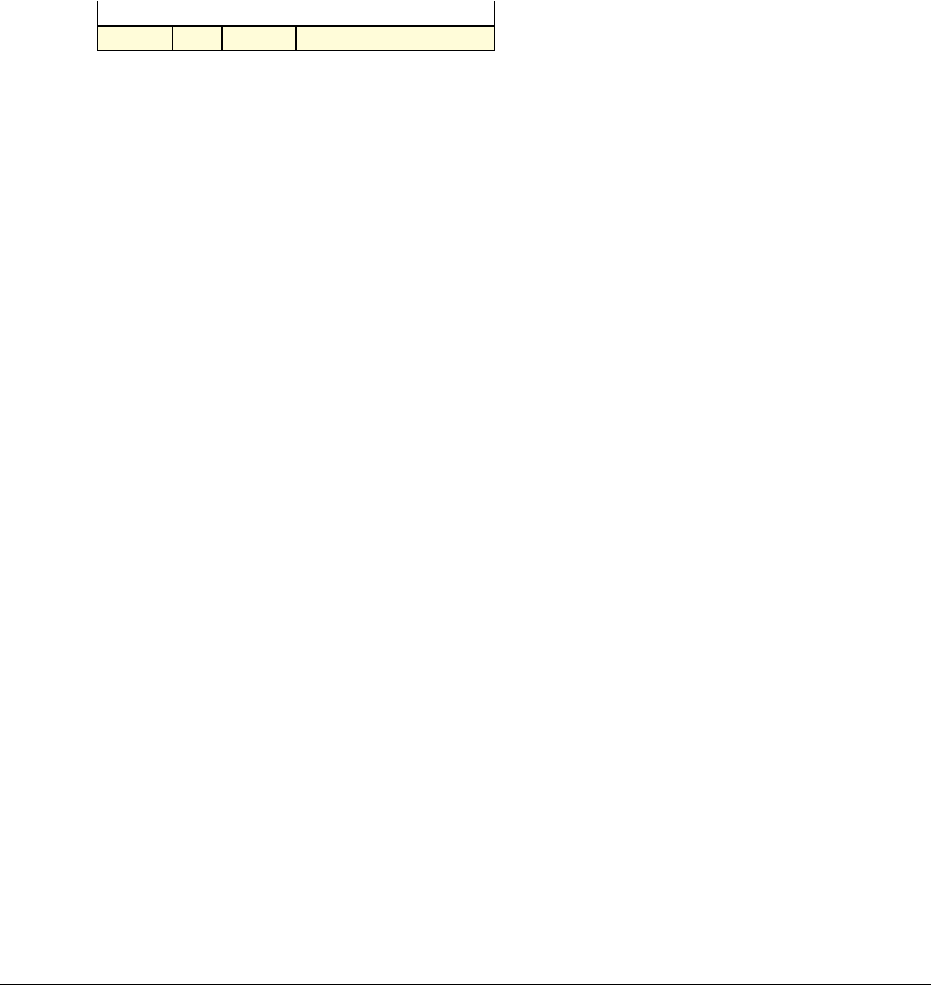
Thumb Instruction Details
A6-154 Copyright © 2007-2008, 2010 ARM Limited. All rights reserved. ARM DDI 0419C
Non-Confidential ID092410
A6.7.39 MOV (immediate)
Move (immediate) writes an immediate value to the destination register. The condition flags are updated
based on the result.
d = UInt(Rd); setflags = !InITBlock(); imm32 = ZeroExtend(imm8, 32); carry = APSR.C;
Assembler syntax
where:
S
The instruction updates the flags.
{<q>}
See Standard assembler syntax fields on page A6-98.
<Rd>
The destination register.
<const>
The immediate value to be placed in
<Rd>
. The range of permitted values is 0-255 for
encoding T1.
Operation
if ConditionPassed() then
EncodingSpecificOperations();
result = imm32;
R[d] = result;
if setflags then
APSR.N = result<31>;
APSR.Z = IsZeroBit(result);
APSR.C = carry;
// APSR.V unchanged
Exceptions
None.
Encoding T1 All versions of the Thumb instruction set.
MOVS <Rd>,#<imm8>
MOVS{<q>} <Rd>, #<const>
0 0 1 0 0 Rd imm8
15 14 13 12 11 10 9 8 7 6 5 4 3 2 1 0
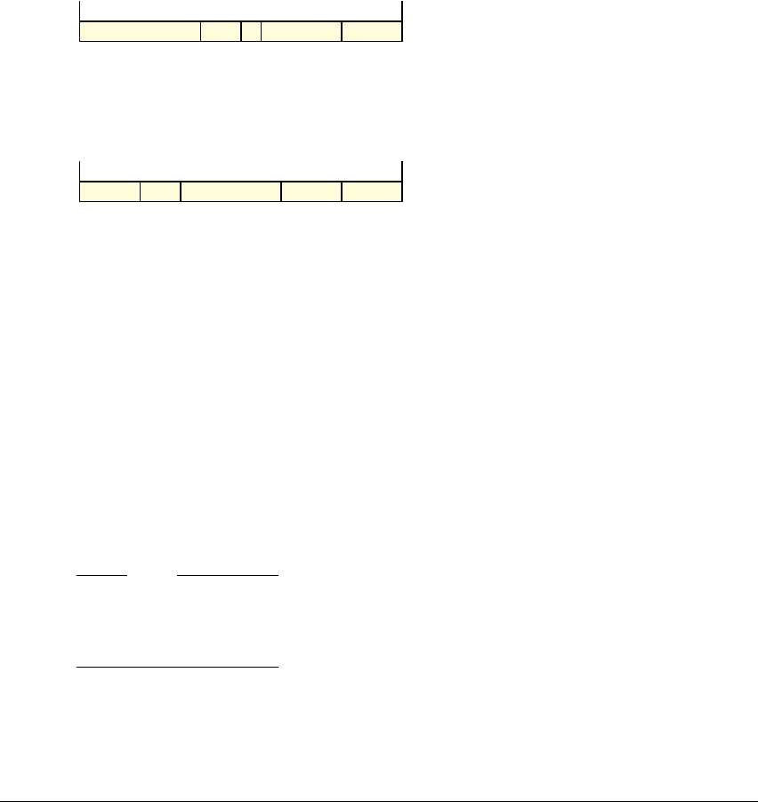
Thumb Instruction Details
ARM DDI 0419C Copyright © 2007-2008, 2010 ARM Limited. All rights reserved. A6-155
ID092410 Non-Confidential
A6.7.40 MOV (register)
Move (register) copies a value from a register to the destination register. Encoding T2 updates the condition
flags based on the value.
d = UInt(D:Rd); m = UInt(Rm); setflags = FALSE;
d = UInt(Rd); m = UInt(Rm); setflags = TRUE;
Assembler syntax
MOV{S}{<q>} <Rd>, <Rm>
where:
{S}
If present, specifies that the instruction updates the flags. Otherwise, the instruction does not
update the flags.
{<q>}
See Standard assembler syntax fields on page A6-98.
<Rd>
The destination register. This register can be the SP or PC, provided S is not specified. If
<Rd>
is the PC, the instruction causes a branch to the address moved to the PC.
<Rm>
The source register. This register can be the SP or PC. The instruction must not specify S if
<Rm>
is the SP or PC.
Note
ARM deprecates the use of the following
MOV
(register) instructions:
• ones in which
<Rd>
is the SP or PC and
<Rm>
is also the SP or PC
• ones in which S is specified and
<Rm>
is the SP, or
<Rm>
is the PC.
Encoding T1 ARMv6-M, ARMv7-M, if
<Rd>
and
<Rm>
both from R0-R7.
MOV <Rd>,<Rm>
Otherwise all versions of the Thumb instruction set.
Encoding T2 All versions of the Thumb instruction set.
MOVS <Rd>,<Rm>
0 1 0 0 0 1 1 0 D Rm Rd
15 14 13 12 11 10 9 8 7 6 5 4 3 2 1 0
0 0 0 0 0 0 0 0 0 0 Rm Rd
15 14 13 12 11 10 9 8 7 6 5 4 3 2 1 0

Thumb Instruction Details
A6-156 Copyright © 2007-2008, 2010 ARM Limited. All rights reserved. ARM DDI 0419C
Non-Confidential ID092410
Operation
if ConditionPassed() then
EncodingSpecificOperations();
result = R[m];
if d == 15 then
ALUWritePC(result); // setflags is always FALSE here
else
R[d] = result;
if setflags then
APSR.N = result<31>;
APSR.Z = IsZeroBit(result);
// APSR.C unchanged
// APSR.V unchanged
Exceptions
None.

Thumb Instruction Details
ARM DDI 0419C Copyright © 2007-2008, 2010 ARM Limited. All rights reserved. A6-157
ID092410 Non-Confidential
A6.7.41 MOV (shifted register)
Move (shifted register) is a pseudo-instruction for
ASR
,
LSL
,
LSR
, and
ROR
.
See the following sections for details:
•ASR (immediate) on page A6-117
•ASR (register) on page A6-118
•LSL (immediate) on page A6-150
•LSL (register) on page A6-151
•LSR (immediate) on page A6-152
•LSR (register) on page A6-153
•ROR (register) on page A6-171.
Assembler syntax
Table A6-2 shows the equivalences between
MOV
(shifted register) and other instructions.
The canonical form of the instruction is produced on disassembly.
Exceptions
None.
Table A6-2 MOV (shift, register shift) equivalences)
MOV instruction Canonical form
MOVS <Rd>,<Rm>,ASR #<n> ASRS <Rd>,<Rm>,#<n>
MOVS <Rd>,<Rm>,LSL #<n> LSLS <Rd>,<Rm>,#<n>
MOVS <Rd>,<Rm>,LSR #<n> LSRS <Rd>,<Rm>,#<n>
MOVS <Rd>,<Rm>,ASR <Rs> ASRS <Rd>,<Rm>,<Rs>
MOVS <Rd>,<Rm>,LSL <Rs> LSLS <Rd>,<Rm>,<Rs>
MOVS <Rd>,<Rm>,LSR <Rs> LSRS <Rd>,<Rm>,<Rs>
MOVS <Rd>,<Rm>,ROR <Rs> RORS <Rd>,<Rm>,<Rs>
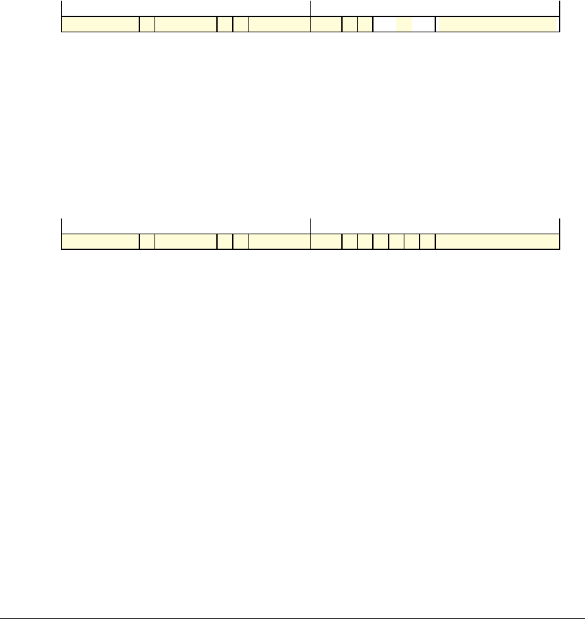
Thumb Instruction Details
A6-158 Copyright © 2007-2008, 2010 ARM Limited. All rights reserved. ARM DDI 0419C
Non-Confidential ID092410
A6.7.42 MRS
Move to Register from Special register moves the value from the selected special-purpose register into a
general-purpose ARM register.
MRS
is a system instruction except when accessing the APSR or CONTROL register. See MRS on
page B4-308 for the complete instruction definition, including the application-level uses.
A6.7.43 MSR (register)
Move to Special Register from ARM Register moves the value of a general-purpose ARM register to the
specified special-purpose register.
MSR
(register) is a system instruction except when accessing the APSR. See MSR (register) on page B4-310
for the complete instruction definition, including the application-level uses.
Encoding T1 ARMv6-M Enhanced functionality in ARMv7-M
MRS <Rd>,<spec_reg>
SYSmRd1 1 1 0 0 1 1 1 1 1 (0) (1) (1) (1) (1) 1 0 (0) 0
15 14 13 12 11 10 9 8 7 6 5 4 3 2 1 0
1
1514131211109876543210
Encoding T1 ARMv6-M Enhanced functionality in ARMv7-M
MSR <spec_reg>,<Rn>
(1) (0)(0)(0) SYSm1 1 1 0 0 1 1 1 0 0 (0) Rn 1 0 (0) 0
15 14 13 12 11 10 9 8 7 6 5 4 3 2 1 0
1
1514131211109876543210

Thumb Instruction Details
ARM DDI 0419C Copyright © 2007-2008, 2010 ARM Limited. All rights reserved. A6-159
ID092410 Non-Confidential
A6.7.44 MUL
Multiply multiplies two register values. The least significant 32 bits of the result are written to the
destination register. These 32 bits do not depend on whether signed or unsigned calculations are performed.
The condition flags are updated based on the result.
d = UInt(Rdm); n = UInt(Rn); m = UInt(Rdm); setflags = !InITBlock();
Assembler syntax
MULS{<q>} {<Rd>,} <Rn>, <Rm>
where:
S
The instruction updates the flags.
{<q>}
See Standard assembler syntax fields on page A6-98.
<Rd>
The destination register.
Note
For ARMv6-M,
<Rd>
can only be omitted when d == n ==m. See Assembler syntax prototype
line conventions on page A6-96 for the rule on optional arguments.
<Rn>
The register that contains the first operand.
<Rm>
The register that contains the second operand.
Encoding T1 All versions of the Thumb instruction set.
MULS <Rdm>,<Rn>,<Rdm>
10 1 0 0 0 0 1 1 0 Rn Rdm
15 14 13 12 11 10 9 8 7 6 5 4 3 2 1 0

Thumb Instruction Details
A6-160 Copyright © 2007-2008, 2010 ARM Limited. All rights reserved. ARM DDI 0419C
Non-Confidential ID092410
Operation
if ConditionPassed() then
EncodingSpecificOperations();
operand1 = SInt(R[n]); // operand1 = UInt(R[n]) produces the same final results
operand2 = SInt(R[m]); // operand2 = UInt(R[m]) produces the same final results
result = operand1 * operand2;
R[d] = result<31:0>;
if setflags then
APSR.N = result<31>;
APSR.Z = IsZeroBit(result);
// APSR.C unchanged
// APSR.V unchanged
Exceptions
None.

Thumb Instruction Details
ARM DDI 0419C Copyright © 2007-2008, 2010 ARM Limited. All rights reserved. A6-161
ID092410 Non-Confidential
A6.7.45 MVN (register)
Bitwise NOT (register) writes the bitwise inverse of a register value to the destination register. The condition
flags are updated based on the result.
d = UInt(Rd); m = UInt(Rm); setflags = !InITBlock();
(shift_t, shift_n) = (SRType_LSL, 0);
Assembler syntax
MVNS{<q>} <Rd>, <Rm>
where:
S
The instruction updates the flags.
{<q>}
See Standard assembler syntax fields on page A6-98.
<Rd>
The destination register.
<Rm>
The register that is used as the source register.
Operation
if ConditionPassed() then
EncodingSpecificOperations();
(shifted, carry) = Shift_C(R[m], shift_t, shift_n, APSR.C);
result = NOT(shifted);
R[d] = result;
if setflags then
APSR.N = result<31>;
APSR.Z = IsZeroBit(result);
APSR.C = carry;
// APSR.V unchanged
Exceptions
None.
Encoding T1 All versions of the Thumb instruction set.
MVNS <Rd>,<Rm>
10 1 0 0 0 0 1 1 1 Rm Rd
15 14 13 12 11 10 9 8 7 6 5 4 3 2 1 0

Thumb Instruction Details
A6-162 Copyright © 2007-2008, 2010 ARM Limited. All rights reserved. ARM DDI 0419C
Non-Confidential ID092410
A6.7.46 NEG
Negate is a pre-UAL synonym for
RSB
(immediate) with an immediate value of 0. See RSB (immediate) on
page A6-172 for details.
Assembler syntax
NEG{<q>} {<Rd>,} <Rm>
This is equivalent to:
RSBS{<q>} {<Rd>,} <Rm>, #0
Exceptions
None.
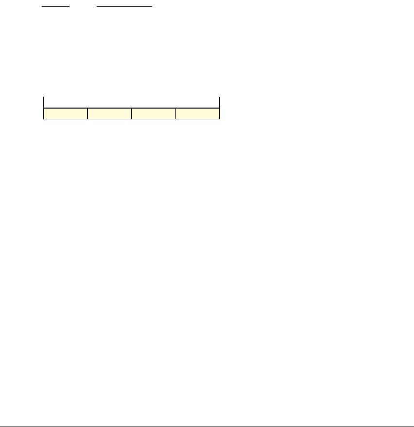
Thumb Instruction Details
ARM DDI 0419C Copyright © 2007-2008, 2010 ARM Limited. All rights reserved. A6-163
ID092410 Non-Confidential
A6.7.47 NOP
No Operation does nothing. This instruction can be used for code alignment purposes.
This is a NOP-compatible hint, the architected NOP. See Hint Instructions on page A6-104 for more
information.
See Pre-UAL pseudo-instruction NOP on page AppxD-384 for details of
NOP
before the introduction of
UAL.
Note
The timing effects of including a
NOP
instruction in code are not guaranteed. It can increase execution time,
leave it unchanged, or even reduce it.
NOP
instructions are therefore not suitable for timing loops.
// No additional decoding required
Assembler syntax
NOP{<q>}
where:
{<q>}
See Standard assembler syntax fields on page A6-98.
Operation
if ConditionPassed() then
EncodingSpecificOperations();
// Do nothing
Exceptions
None.
Encoding T1 ARMv6-M, ARMv7-M
NOP
00000001 0 1 1 1 1 1 1 0
15 14 13 12 11 10 9 8 7 6 5 4 3 2 1 0

Thumb Instruction Details
A6-164 Copyright © 2007-2008, 2010 ARM Limited. All rights reserved. ARM DDI 0419C
Non-Confidential ID092410
A6.7.48 ORR (register)
Logical OR (register) performs a bitwise, inclusive, OR of a register value and an optionally-shifted register
value, and writes the result to the destination register. The condition flags are updated based on the result.
d = UInt(Rdn); n = UInt(Rdn); m = UInt(Rm); setflags = !InITBlock();
(shift_t, shift_n) = (SRType_LSL, 0);
Assembler syntax
ORRS{<q>} {<Rd>,} <Rn>, <Rm>
where:
S
The instruction updates the flags.
{<q>}
See Standard assembler syntax fields on page A6-98.
<Rd>
The destination register. If
<Rd>
is omitted, this register is the same as
<Rn>
.
<Rn>
The register that contains the first operand.
<Rm>
The register that is used as the second operand.
Operation
if ConditionPassed() then
EncodingSpecificOperations();
(shifted, carry) = Shift_C(R[m], shift_t, shift_n, APSR.C);
result = R[n] OR shifted;
R[d] = result;
if setflags then
APSR.N = result<31>;
APSR.Z = IsZeroBit(result);
APSR.C = carry;
// APSR.V unchanged
Exceptions
None.
Encoding T1 All versions of the Thumb instruction set.
ORRS <Rdn>,<Rm>
00 1 0 0 0 0 1 1 0 Rm Rdn
15 14 13 12 11 10 9 8 7 6 5 4 3 2 1 0
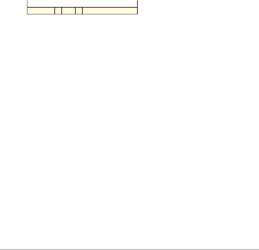
Thumb Instruction Details
ARM DDI 0419C Copyright © 2007-2008, 2010 ARM Limited. All rights reserved. A6-165
ID092410 Non-Confidential
A6.7.49 POP
Pop Multiple Registers loads a subset, or possibly all, of the general-purpose registers R0-R7 and the PC
from the stack.
If the registers loaded include the PC, the word loaded for the PC is treated as a branch address or an
exception return value and a branch occurs. Bit [0] complies with the ARM architecture interworking rules
for branches to Thumb state execution and must be 1. If bit [0] is 0, a HardFault exception occurs.
registers = P:'0000000':register_list; UnalignedAllowed = FALSE;
if BitCount(registers) < 1 then UNPREDICTABLE;
if registers<15> == '1' && InITBlock() && !LastInITBlock() then UNPREDICTABLE;
Assembler syntax
where:
{<q>}
See Standard assembler syntax fields on page A6-98.
<registers>
Is a list of one or more registers, separated by commas and surrounded by
{
and
}
. It
specifies the set of registers to be loaded. The lowest-numbered register is loaded from the
lowest memory address, through to the highest-numbered register from the highest memory
address. If the PC is specified in the register list, the instruction causes a branch to the
address (data) loaded into the PC.
Encoding T1 All versions of the Thumb instruction set.
POP <registers>
POP{<q>} <registers>
1 0 1 1 1 1 0 P register_list
15 14 13 12 11 10 9 8 7 6 5 4 3 2 1 0

Thumb Instruction Details
A6-166 Copyright © 2007-2008, 2010 ARM Limited. All rights reserved. ARM DDI 0419C
Non-Confidential ID092410
Operation
if ConditionPassed() then
EncodingSpecificOperations();
address = SP;
for i = 0 to 7
if registers<i> == '1' then
R[i] = MemA[address,4]; address = address + 4;
if registers<15> == '1' then
LoadWritePC(MemA[address,4]);
SP = SP + 4*BitCount(registers);
Exceptions
HardFault.

Thumb Instruction Details
ARM DDI 0419C Copyright © 2007-2008, 2010 ARM Limited. All rights reserved. A6-167
ID092410 Non-Confidential
A6.7.50 PUSH
Push Multiple Registers stores a subset, or possibly all, of the general-purpose registers R0-R7 and the LR
to the stack.
registers = '0':M:'000000':register_list; UnalignedAllowed = FALSE;
if BitCount(registers) < 1 then UNPREDICTABLE;
Assembler syntax
where:
{<q>}
See Standard assembler syntax fields on page A6-98.
<registers>
Is a list of one or more registers, separated by commas and surrounded by
{
and
}
. It
specifies the set of registers to be stored. The registers are stored in sequence, the
lowest-numbered register to the lowest memory address, through to the highest-numbered
register to the highest memory address.
Operation
if ConditionPassed() then
EncodingSpecificOperations();
address = SP - 4*BitCount(registers);
for i = 0 to 14
if registers<i> == '1' then
MemA[address,4] = R[i];
address = address + 4;
SP = SP - 4*BitCount(registers);
Exceptions
HardFault.
Encoding T1 All versions of the Thumb instruction set.
PUSH <registers>
PUSH{<q>} <registers>
1 0 1 1 0 1 0 M register_list
15 14 13 12 11 10 9 8 7 6 5 4 3 2 1 0

Thumb Instruction Details
A6-168 Copyright © 2007-2008, 2010 ARM Limited. All rights reserved. ARM DDI 0419C
Non-Confidential ID092410
A6.7.51 REV
Byte-Reverse Word reverses the byte order in a 32-bit register.
d = UInt(Rd); m = UInt(Rm);
Assembler syntax
REV{<q>} <Rd>, <Rm>
where:
{<q>}
See Standard assembler syntax fields on page A6-98.
<Rd>
The destination register.
<Rm>
The register that contains the operand.
Operation
if ConditionPassed() then
EncodingSpecificOperations();
bits(32) result;
result<31:24> = R[m]<7:0>;
result<23:16> = R[m]<15:8>;
result<15:8> = R[m]<23:16>;
result<7:0> = R[m]<31:24>;
R[d] = result;
Exceptions
None.
Encoding T1 ARMv6-M, ARMv7-M
REV <Rd>,<Rm>
0 0 Rm1 0 1 1 1 0 1 0 Rd
15 14 13 12 11 10 9 8 7 6 5 4 3 2 1 0

Thumb Instruction Details
ARM DDI 0419C Copyright © 2007-2008, 2010 ARM Limited. All rights reserved. A6-169
ID092410 Non-Confidential
A6.7.52 REV16
Byte-Reverse Packed Halfword reverses the byte order in each 16-bit halfword of a 32-bit register.
d = UInt(Rd); m = UInt(Rm);
Assembler syntax
REV16{<q>} <Rd>, <Rm>
where:
{<q>}
See Standard assembler syntax fields on page A6-98.
<Rd>
The destination register.
<Rm>
The register that contains the operand.
Operation
if ConditionPassed() then
EncodingSpecificOperations();
bits(32) result;
result<31:24> = R[m]<23:16>;
result<23:16> = R[m]<31:24>;
result<15:8> = R[m]<7:0>;
result<7:0> = R[m]<15:8>;
R[d] = result;
Exceptions
None.
Encoding T1 ARMv6-M, ARMv7-M
REV16 <Rd>,<Rm>
0 1 Rm1 0 1 1 1 0 1 0 Rd
15 14 13 12 11 10 9 8 7 6 5 4 3 2 1 0

Thumb Instruction Details
A6-170 Copyright © 2007-2008, 2010 ARM Limited. All rights reserved. ARM DDI 0419C
Non-Confidential ID092410
A6.7.53 REVSH
Byte-Reverse Signed Halfword reverses the byte order in the lower 16-bit halfword of a 32-bit register, and
sign extends the result to 32 bits.
d = UInt(Rd); m = UInt(Rm);
Assembler syntax
REVSH{<q>} <Rd>, <Rm>
where:
{<q>}
See Standard assembler syntax fields on page A6-98.
<Rd>
The destination register.
<Rm>
The register that contains the operand.
Operation
if ConditionPassed() then
EncodingSpecificOperations();
bits(32) result;
result<31:8> = SignExtend(R[m]<7:0>, 24);
result<7:0> = R[m]<15:8>;
R[d] = result;
Exceptions
None.
Encoding T1 ARMv6-M, ARMv7-M
REVSH <Rd>,<Rm>
1 1 Rm1 0 1 1 1 0 1 0 Rd
15 14 13 12 11 10 9 8 7 6 5 4 3 2 1 0

Thumb Instruction Details
ARM DDI 0419C Copyright © 2007-2008, 2010 ARM Limited. All rights reserved. A6-171
ID092410 Non-Confidential
A6.7.54 ROR (register)
Rotate Right (register) provides the value of the contents of a register rotated by a variable number of bits.
The bits that are rotated off the right end are inserted into the vacated bit positions on the left. The variable
number of bits is read from the bottom byte of a register. The condition flags are updated based on the result.
d = UInt(Rdn); n = UInt(Rdn); m = UInt(Rm); setflags = !InITBlock();
Assembler syntax
RORS{<q>} <Rd>, <Rn>, <Rm>
where:
S
The instruction updates the flags.
{<q>}
See Standard assembler syntax fields on page A6-98.
<Rd>
The destination register.
<Rn>
The register that contains the first operand.
<Rm>
The register whose bottom byte contains the amount to rotate by.
Operation
if ConditionPassed() then
EncodingSpecificOperations();
shift_n = UInt(R[m]<7:0>);
(result, carry) = Shift_C(R[n], SRType_ROR, shift_n, APSR.C);
R[d] = result;
if setflags then
APSR.N = result<31>;
APSR.Z = IsZeroBit(result);
APSR.C = carry;
// APSR.V unchanged
Exceptions
None.
Encoding T1 All versions of the Thumb instruction set.
RORS <Rdn>,<Rm>
1 1 Rm0 1 0 0 0 0 0 1 Rdn
15 14 13 12 11 10 9 8 7 6 5 4 3 2 1 0

Thumb Instruction Details
A6-172 Copyright © 2007-2008, 2010 ARM Limited. All rights reserved. ARM DDI 0419C
Non-Confidential ID092410
A6.7.55 RSB (immediate)
Reverse Subtract (immediate) subtracts a register value from an immediate value, and writes the result to
the destination register. The condition flags are updated based on the result.
d = UInt(Rd); n = UInt(Rn); setflags = !InITBlock(); imm32 = Zeros(32); // immediate = #0
Assembler syntax
RSBS{<q>} {<Rd>,} <Rn>, #<const>
where:
S
The instruction updates the flags.
{<q>}
See Standard assembler syntax fields on page A6-98.
<Rd>
The destination register. If
<Rd>
is omitted, this register is the same as
<Rn>
.
<Rn>
The register that contains the first operand.
<const>
The immediate value to be added to the value obtained from
<Rn>
. ARMv6-M only supports
a value of 0.
Operation
if ConditionPassed() then
EncodingSpecificOperations();
(result, carry, overflow) = AddWithCarry(NOT(R[n]), imm32, '1');
R[d] = result;
if setflags then
APSR.N = result<31>;
APSR.Z = IsZeroBit(result);
APSR.C = carry;
APSR.V = overflow;
Exceptions
None.
Encoding T1 All versions of the Thumb instruction set.
RSBS <Rd>,<Rn>,#0
0 1 Rn0 1 0 0 0 0 1 0 Rd
15 14 13 12 11 10 9 8 7 6 5 4 3 2 1 0

Thumb Instruction Details
ARM DDI 0419C Copyright © 2007-2008, 2010 ARM Limited. All rights reserved. A6-173
ID092410 Non-Confidential
A6.7.56 SBC (register)
Subtract with Carry (register) subtracts an optionally-shifted register value and the value of NOT(Carry
flag) from a register value, and writes the result to the destination register. The condition flags are updated
based on the result.
d = UInt(Rdn); n = UInt(Rdn); m = UInt(Rm); setflags = !InITBlock();
(shift_t, shift_n) = (SRType_LSL, 0);
Assembler syntax
SBCS{<q>} {<Rd>,} <Rn>, <Rm>
where:
S
The instruction updates the flags.
{<q>}
See Standard assembler syntax fields on page A6-98.
<Rd>
The destination register. If
<Rd>
is omitted, this register is the same as
<Rn>
.
<Rn>
The register that contains the first operand.
<Rm>
The register that is used as the second operand.
Operation
if ConditionPassed() then
EncodingSpecificOperations();
shifted = Shift(R[m], shift_t, shift_n, APSR.C);
(result, carry, overflow) = AddWithCarry(R[n], NOT(shifted), APSR.C);
R[d] = result;
if setflags then
APSR.N = result<31>;
APSR.Z = IsZeroBit(result);
APSR.C = carry;
APSR.V = overflow;
Exceptions
None.
Encoding T1 All versions of the Thumb instruction set.
SBCS <Rdn>,<Rm>
1 0 Rm0 1 0 0 0 0 0 1 Rdn
15 14 13 12 11 10 9 8 7 6 5 4 3 2 1 0

Thumb Instruction Details
A6-174 Copyright © 2007-2008, 2010 ARM Limited. All rights reserved. ARM DDI 0419C
Non-Confidential ID092410
A6.7.57 SEV
Send Event is a hint instruction. It causes an event to be signaled to all CPUs within a multiprocessor system.
This is a NOP-compatible hint, see Hint Instructions on page A6-104.
// No additional decoding required
Assembler syntax
SEV{<q>}
where:
{<q>}
See Standard assembler syntax fields on page A6-98.
Operation
if ConditionPassed() then
EncodingSpecificOperations();
Hint_SendEvent();
Exceptions
None.
Encoding T1 ARMv6-M, ARMv7-M
SEV
0 00 00 00 11 0 1 1 1 1 1 1
15 14 13 12 11 10 9 8 7 6 5 4 3 2 1 0
Thumb Instruction Details
ARM DDI 0419C Copyright © 2007-2008, 2010 ARM Limited. All rights reserved. A6-175
ID092410 Non-Confidential
A6.7.58 STM, STMIA, STMEA
The Store Multiple Increment After and the Store Multiple Empty Ascending instructions store multiple
registers to consecutive memory locations using an address from a base register. The sequential memory
locations start at this address, and the address above the last of those locations is written back to the base
register.
n = UInt(Rn); registers = '00000000':register_list; wback = TRUE;
if BitCount(registers) < 1 then UNPREDICTABLE;
Assembler syntax
STM{IA|EA}{<q>} <Rn>!, <registers>
where:
{<q>}
See Standard assembler syntax fields on page A6-98.
<Rn>
The base register.
!
Causes the instruction to write a modified value back to
<Rn>
.
<registers>
Is a list of one or more registers to be stored, separated by commas and surrounded by
{
and
}
. The lowest-numbered register is stored to the lowest memory address, through to
the highest-numbered register to the highest memory address.
If the base register is included and not the lowest-numbered register in the list, such an
instruction stores an UNKNOWN value for the base register. Use of <Rn> in the register list
is deprecated.
STMEA
and
STMIA
are pseudo-instructions for
STM
,
STMEA
referring to its use for pushing data onto Empty
Ascending stacks.
Encoding T1 All versions of the Thumb instruction set.
STM <Rn>!,<registers>
register_list1 1 0 0 0 Rn
15 14 13 12 11 10 9 8 7 6 5 4 3 2 1 0

Thumb Instruction Details
A6-176 Copyright © 2007-2008, 2010 ARM Limited. All rights reserved. ARM DDI 0419C
Non-Confidential ID092410
Operation
if ConditionPassed() then
EncodingSpecificOperations();
address = R[n];
for i = 0 to 14
if registers<i> == '1' then
if i == n && wback && i != LowestSetBit(registers) then
MemA[address,4] = bits(32) UNKNOWN; // encoding T1 only
else
MemA[address,4] = R[i];
address = address + 4;
if wback then R[n] = R[n] + 4*BitCount(registers);
Exceptions
HardFault.
Thumb Instruction Details
ARM DDI 0419C Copyright © 2007-2008, 2010 ARM Limited. All rights reserved. A6-177
ID092410 Non-Confidential
A6.7.59 STR (immediate)
Store Register (immediate) calculates an address from a base register value and an immediate offset, and
stores a word from a register to memory. See Memory accesses on page A6-103 for information about
memory accesses.
t = UInt(Rt); n = UInt(Rn); imm32 = ZeroExtend(imm5:'00', 32);
index = TRUE; add = TRUE; wback = FALSE;
t = UInt(Rt); n = 13; imm32 = ZeroExtend(imm8:'00', 32);
index = TRUE; add = TRUE; wback = FALSE;
Assembler syntax
where:
{<q>}
See Standard assembler syntax fields on page A6-98.
<Rt>
The source register.
<Rn>
The base register.
+/-
Is + or omitted to indicate that the immediate offset is added to the base register value.
add == TRUE
<imm>
The immediate offset added to the value of
<Rn>
to form the address. Permitted values are
multiples of 4 in the range 0-124 for encoding T1 and multiples of 4 in the range 0-1020 for
encoding T2.
<imm>
can be omitted, meaning an offset of 0.
Encoding T1 All versions of the Thumb instruction set.
STR <Rt>, [<Rn>{,#<imm5>}]
Encoding T2 All versions of the Thumb instruction set.
STR <Rt>,[SP,#<imm8>]
STR{<q>} <Rt>, [<Rn> {, #+/-<imm>}]
Rn Rt0 1 1 0 0 imm5
15 14 13 12 11 10 9 8 7 6 5 4 3 2 1 0
imm81 0 0 1 0 Rt
15 14 13 12 11 10 9 8 7 6 5 4 3 2 1 0

Thumb Instruction Details
A6-178 Copyright © 2007-2008, 2010 ARM Limited. All rights reserved. ARM DDI 0419C
Non-Confidential ID092410
Operation
if ConditionPassed() then
EncodingSpecificOperations();
offset_addr = if add then (R[n] + imm32) else (R[n] - imm32);
address = if index then offset_addr else R[n];
MemU[address,4] = R[t];
if wback then R[n] = offset_addr;
Exceptions
HardFault.

Thumb Instruction Details
ARM DDI 0419C Copyright © 2007-2008, 2010 ARM Limited. All rights reserved. A6-179
ID092410 Non-Confidential
A6.7.60 STR (register)
Store Register (register) calculates an address from a base register value and an offset register value, stores
a word from a register to memory. See Memory accesses on page A6-103 for information about memory
accesses.
t = UInt(Rt); n = UInt(Rn); m = UInt(Rm);
index = TRUE; add = TRUE; wback = FALSE;
(shift_t, shift_n) = (SRType_LSL, 0);
Assembler syntax
STR{<q>} <Rt>, [<Rn>, <Rm>]
where:
{<q>}
See Standard assembler syntax fields on page A6-98.
<Rt>
The source register.
<Rn>
The register that contains the base value.
<Rm>
Contains the offset that is added to the value of
<Rn>
to form the address.
Operation
if ConditionPassed() then
EncodingSpecificOperations();
offset = Shift(R[m], shift_t, shift_n, APSR.C);
address = R[n] + offset;
MemU[address,4] = R[t];
Exceptions
HardFault.
Encoding T1 All versions of the Thumb instruction set.
STR <Rt>,[<Rn>,<Rm>]
0 0 Rn Rt0 1 0 1 0 Rm
15 14 13 12 11 10 9 8 7 6 5 4 3 2 1 0

Thumb Instruction Details
A6-180 Copyright © 2007-2008, 2010 ARM Limited. All rights reserved. ARM DDI 0419C
Non-Confidential ID092410
A6.7.61 STRB (immediate)
Store Register Byte (immediate) calculates an address from a base register value and an immediate offset,
and stores a byte from a register to memory. See Memory accesses on page A6-103 for information about
memory accesses.
t = UInt(Rt); n = UInt(Rn); imm32 = ZeroExtend(imm5, 32);
index = TRUE; add = TRUE; wback = FALSE;
Assembler syntax
where:
{<q>}
See Standard assembler syntax fields on page A6-98.
<Rt>
The source register.
<Rn>
The base register.
+/-
Is + or omitted to indicate that the immediate offset is added to the base register value.
add == TRUE
<imm>
The immediate offset added to the value of
<Rn>
to form the address. The range of permitted
values is 0-31 for encoding T1.
<imm>
can be omitted, meaning an offset of 0.
Operation
if ConditionPassed() then
EncodingSpecificOperations();
offset_addr = if add then (R[n] + imm32) else (R[n] - imm32);
address = if index then offset_addr else R[n];
MemU[address,1] = R[t]<7:0>;
if wback then R[n] = offset_addr;
Exceptions
HardFault.
Encoding T1 All versions of the Thumb instruction set.
STRB <Rt>,[<Rn>,#<imm5>]
STRB{<q>} <Rt>, [<Rn> {, #+/-<imm>}]
Rn Rt0 1 1 1 0 imm5
15 14 13 12 11 10 9 8 7 6 5 4 3 2 1 0

Thumb Instruction Details
ARM DDI 0419C Copyright © 2007-2008, 2010 ARM Limited. All rights reserved. A6-181
ID092410 Non-Confidential
A6.7.62 STRB (register)
Store Register Byte (register) calculates an address from a base register value and an offset register value,
and stores a byte from a register to memory. See Memory accesses on page A6-103 for information about
memory accesses.
t = UInt(Rt); n = UInt(Rn); m = UInt(Rm);
index = TRUE; add = TRUE; wback = FALSE;
(shift_t, shift_n) = (SRType_LSL, 0);
Assembler syntax
STRB{<q>} <Rt>, [<Rn>, <Rm> {, LSL #<shift>}]
where:
{<q>}
See Standard assembler syntax fields on page A6-98.
<Rt>
The source register.
<Rn>
The base register.
<Rm>
Contains the offset that is added to the value of
<Rn>
to form the address.
Operation
if ConditionPassed() then
EncodingSpecificOperations();
offset = Shift(R[m], shift_t, shift_n, APSR.C);
address = R[n] + offset;
MemU[address,1] = R[t]<7:0>;
Exceptions
HardFault.
Encoding T1 All versions of the Thumb instruction set.
STRB <Rt>,[<Rn>,<Rm>]
1 0 Rn Rt0 1 0 1 0 Rm
15 14 13 12 11 10 9 8 7 6 5 4 3 2 1 0

Thumb Instruction Details
A6-182 Copyright © 2007-2008, 2010 ARM Limited. All rights reserved. ARM DDI 0419C
Non-Confidential ID092410
A6.7.63 STRH (immediate)
Store Register Halfword (immediate) calculates an address from a base register value and an immediate
offset, and stores a halfword from a register to memory. See Memory accesses on page A6-103 for
information about memory accesses.
t = UInt(Rt); n = UInt(Rn); imm32 = ZeroExtend(imm5:'0', 32);
index = TRUE; add = TRUE; wback = FALSE;
Assembler syntax
where:
{<q>}
See Standard assembler syntax fields on page A6-98.
<Rt>
The source register.
<Rn>
The base register.
+/-
Is + or omitted to indicate that the immediate offset is added to the base register value.
add == TRUE
<imm>
The immediate offset added to or subtracted from the value of
<Rn>
to form the address.
Permitted values are multiples of 2 in the range 0-62 for encoding T1.
<imm>
can be omitted,
meaning an offset of 0.
Operation
if ConditionPassed() then
EncodingSpecificOperations();
offset_addr = if add then (R[n] + imm32) else (R[n] - imm32);
address = if index then offset_addr else R[n];
MemU[address,2] = R[t]<15:0>;
if wback then R[n] = offset_addr;
Exceptions
HardFault.
Encoding T1 All versions of the Thumb instruction set.
STRH <Rt>,[<Rn>{,#<imm5>}]
STRH{<q>} <Rt>, [<Rn> {, #+/-<imm>}]
Rn Rt1 0 0 0 0 imm5
15 14 13 12 11 10 9 8 7 6 5 4 3 2 1 0

Thumb Instruction Details
ARM DDI 0419C Copyright © 2007-2008, 2010 ARM Limited. All rights reserved. A6-183
ID092410 Non-Confidential
A6.7.64 STRH (register)
Store Register Halfword (register) calculates an address from a base register value and an offset register
value, and stores a halfword from a register to memory. See Memory accesses on page A6-103 for
information about memory accesses.
t = UInt(Rt); n = UInt(Rn); m = UInt(Rm);
index = TRUE; add = TRUE; wback = FALSE;
(shift_t, shift_n) = (SRType_LSL, 0);
Assembler syntax
STRH{<q>} <Rt>, [<Rn>, <Rm>]
where:
{<q>}
See Standard assembler syntax fields on page A6-98.
<Rt>
The source register.
<Rn>
The base register.
<Rm>
Contains the offset that is added to the value of
<Rn>
to form the address.
Encoding T1 All versions of the Thumb instruction set.
STRH <Rt>,[<Rn>,<Rm>]
0 0 1 Rn Rt0 1 0 1 Rm
15 14 13 12 11 10 9 8 7 6 5 4 3 2 1 0

Thumb Instruction Details
A6-184 Copyright © 2007-2008, 2010 ARM Limited. All rights reserved. ARM DDI 0419C
Non-Confidential ID092410
Operation
if ConditionPassed() then
EncodingSpecificOperations();
offset = Shift(R[m], shift_t, shift_n, APSR.C);
address = R[n] + offset;
MemU[address,2] = R[t]<15:0>;
Exceptions
HardFault.

Thumb Instruction Details
ARM DDI 0419C Copyright © 2007-2008, 2010 ARM Limited. All rights reserved. A6-185
ID092410 Non-Confidential
A6.7.65 SUB (immediate)
This instruction subtracts an immediate value from a register value, and writes the result to the destination
register. The condition flags are updated based on the result.
d = UInt(Rd); n = UInt(Rn); setflags = !InITBlock(); imm32 = ZeroExtend(imm3, 32);
d = UInt(Rdn); n = UInt(Rdn); setflags = !InITBlock(); imm32 = ZeroExtend(imm8, 32);
Assembler syntax
where:
S
The instruction updates the flags.
{<q>}
See Standard assembler syntax fields on page A6-98.
<Rd>
The destination register. If
<Rd>
is omitted, this register is the same as
<Rn>
.
<Rn>
The register that contains the first operand.
<const>
The immediate value to be subtracted from the value obtained from
<Rn>
. The range of
permitted values is 0-7 for encoding T1 and 0-255 for encoding T2.
Encoding T1 is preferred to encoding T2 if
<Rd>
is specified and encoding T2 is preferred to
encoding T1 if
<Rd>
is omitted.
Encoding T1 All versions of the Thumb instruction set.
SUBS <Rd>,<Rn>,#<imm3>
Encoding T2 All versions of the Thumb instruction set.
SUBS <Rdn>,#<imm8>
SUBS{<q>} {<Rd>,} <Rn>, #<const>
1 1 1 Rn Rd0 0 0 1 imm3
15 14 13 12 11 10 9 8 7 6 5 4 3 2 1 0
Rdn1 imm80 0 1 1
15 14 13 12 11 10 9 8 7 6 5 4 3 2 1 0

Thumb Instruction Details
A6-186 Copyright © 2007-2008, 2010 ARM Limited. All rights reserved. ARM DDI 0419C
Non-Confidential ID092410
Operation
if ConditionPassed() then
EncodingSpecificOperations();
(result, carry, overflow) = AddWithCarry(R[n], NOT(imm32), '1');
R[d] = result;
if setflags then
APSR.N = result<31>;
APSR.Z = IsZeroBit(result);
APSR.C = carry;
APSR.V = overflow;
Exceptions
None.

Thumb Instruction Details
ARM DDI 0419C Copyright © 2007-2008, 2010 ARM Limited. All rights reserved. A6-187
ID092410 Non-Confidential
A6.7.66 SUB (register)
This instruction subtracts an optionally-shifted register value from a register value, and writes the result to
the destination register. It updates the condition flags based on the result.
d = UInt(Rd); n = UInt(Rn); m = UInt(Rm); setflags = !InITBlock();
(shift_t, shift_n) = (SRType_LSL, 0);
Assembler syntax
SUBS{<q>} {<Rd>,} <Rn>, <Rm>
where:
S
The instruction updates the flags.
{<q>}
See Standard assembler syntax fields on page A6-98.
<Rd>
The destination register. If
<Rd>
is omitted, this register is the same as
<Rn>
.
<Rn>
The register that contains the first operand.
<Rm>
The register that is used as the second operand.
Operation
if ConditionPassed() then
EncodingSpecificOperations();
shifted = Shift(R[m], shift_t, shift_n, APSR.C);
(result, carry, overflow) = AddWithCarry(R[n], NOT(shifted), '1');
R[d] = result;
if setflags then
APSR.N = result<31>;
APSR.Z = IsZeroBit(result);
APSR.C = carry;
APSR.V = overflow;
Exceptions
None.
Encoding T1 All versions of the Thumb instruction set.
SUBS <Rd>,<Rn>,<Rm>
Rm Rn101 Rd0 0 0 1
15 14 13 12 11 10 9 8 7 6 5 4 3 2 1 0
Thumb Instruction Details
A6-188 Copyright © 2007-2008, 2010 ARM Limited. All rights reserved. ARM DDI 0419C
Non-Confidential ID092410
A6.7.67 SUB (SP minus immediate)
This instruction subtracts an immediate value from the SP value, and writes the result to the destination
register.
d = 13; setflags = FALSE; imm32 = ZeroExtend(imm7:'00', 32);
Assembler syntax
where:
{<q>}
See Standard assembler syntax fields on page A6-98.
<Rd>
The destination register. If
<Rd>
is omitted, this register is SP.
<const>
The immediate value to be added to the value obtained from SP. Permitted values are
multiples of 4 in the range 0-508 for encoding T1.
Operation
if ConditionPassed() then
EncodingSpecificOperations();
(result, carry, overflow) = AddWithCarry(SP, NOT(imm32), '1');
R[d] = result;
// no flag setting form of the instruction supported
Exceptions
None.
Encoding T1 All versions of the Thumb instruction set.
SUB SP,SP,#<imm7>
SUB{<q>} {<Rd>,} SP, #<const>
10000 imm71 0 1 1
15 14 13 12 11 10 9 8 7 6 5 4 3 2 1 0
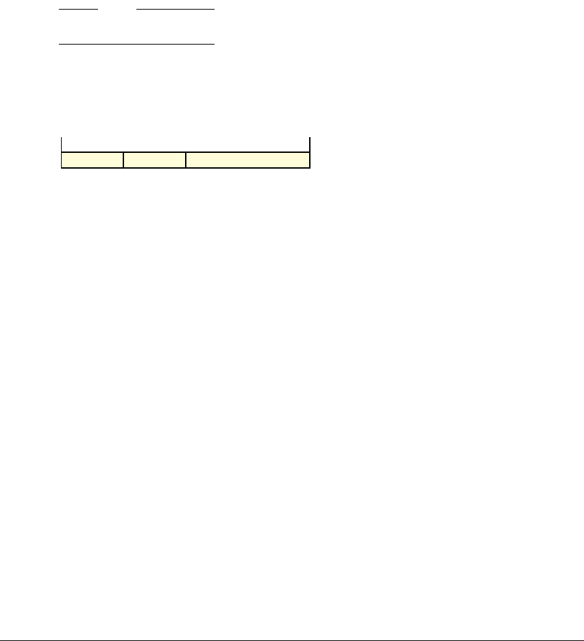
Thumb Instruction Details
ARM DDI 0419C Copyright © 2007-2008, 2010 ARM Limited. All rights reserved. A6-189
ID092410 Non-Confidential
A6.7.68 SVC
The Supervisor Call instruction generates a call to a system supervisor, see Exceptions on page B1-207 for
more information. When the exception is escalated, a HardFault exception is caused.
Use it as a call to an operating system to provide a service.
Note
In older versions of the ARM architecture,
SVC
was called
SWI
, Software Interrupt.
imm32 = ZeroExtend(imm8, 32);
// imm32 is for assembly/disassembly, and is ignored by hardware. SVC handlers in some
// systems interpret imm8 in software, for example to determine the required service.
Assembler syntax
SVC{<q>} {#}<imm>
where:
{<q>}
See Standard assembler syntax fields on page A6-98.
<imm>
Specifies an 8-bit immediate constant.
Operation
if ConditionPassed() then
EncodingSpecificOperations();
CallSupervisor();
Exceptions
SVCall, HardFault.
Encoding T1 All versions of the Thumb instruction set M profile specific behavior
SVC #<imm8>
1111 imm81 1 0 1
15 14 13 12 11 10 9 8 7 6 5 4 3 2 1 0
Thumb Instruction Details
A6-190 Copyright © 2007-2008, 2010 ARM Limited. All rights reserved. ARM DDI 0419C
Non-Confidential ID092410
A6.7.69 SXTB
Signed Extend Byte extracts an 8-bit value from a register, sign extends it to 32 bits, and writes the result to
the destination register.
d = UInt(Rd); m = UInt(Rm); rotation = 0;
Assembler syntax
SXTB{<q>} <Rd>, <Rm>
where:
{<q>}
See Standard assembler syntax fields on page A6-98.
<Rd>
The destination register.
<Rm>
The register that contains the operand.
Operation
if ConditionPassed() then
EncodingSpecificOperations();
rotated = ROR(R[m], rotation);
R[d] = SignExtend(rotated<7:0>, 32);
Exceptions
None.
Encoding T1 ARMv6-M, ARMv7-M
SXTB <Rd>,<Rm>
10 Rm0100 Rd1 0 1 1
15 14 13 12 11 10 9 8 7 6 5 4 3 2 1 0

Thumb Instruction Details
ARM DDI 0419C Copyright © 2007-2008, 2010 ARM Limited. All rights reserved. A6-191
ID092410 Non-Confidential
A6.7.70 SXTH
Signed Extend Halfword extracts a 16-bit value from a register, sign extends it to 32 bits, and writes the
result to the destination register.
d = UInt(Rd); m = UInt(Rm); rotation = 0;
Assembler syntax
SXTH{<q>} <Rd>, <Rm>
where:
{<q>}
See Standard assembler syntax fields on page A6-98.
<Rd>
The destination register.
<Rm>
The register that contains the operand.
Operation
if ConditionPassed() then
EncodingSpecificOperations();
rotated = ROR(R[m], rotation);
R[d] = SignExtend(rotated<15:0>, 32);
Exceptions
None.
Encoding T1 ARMv6-M, ARMv7-M
SXTH <Rd>,<Rm>
00 Rm0100 Rd1 0 1 1
15 14 13 12 11 10 9 8 7 6 5 4 3 2 1 0

Thumb Instruction Details
A6-192 Copyright © 2007-2008, 2010 ARM Limited. All rights reserved. ARM DDI 0419C
Non-Confidential ID092410
A6.7.71 TST (register)
Test (register) performs a logical AND operation on two register values. It updates the condition flags based
on the result, and discards the result.
n = UInt(Rn); m = UInt(Rm);
(shift_t, shift_n) = (SRType_LSL, 0);
Assembler syntax
TST{<q>} <Rn>, <Rm>
where:
{<q>}
See Standard assembler syntax fields on page A6-98.
<Rn>
The register that contains the first operand.
<Rm>
The register that is used as the second operand.
Operation
if ConditionPassed() then
EncodingSpecificOperations();
(shifted, carry) = Shift_C(R[m], shift_t, shift_n, APSR.C);
result = R[n] AND shifted;
APSR.N = result<31>;
APSR.Z = IsZeroBit(result);
APSR.C = carry;
// APSR.V unchanged
Exceptions
None.
Encoding T1 All versions of the Thumb instruction set.
TST <Rn>,<Rm>
00 Rm0100 Rn0 1 0 0
15 14 13 12 11 10 9 8 7 6 5 4 3 2 1 0
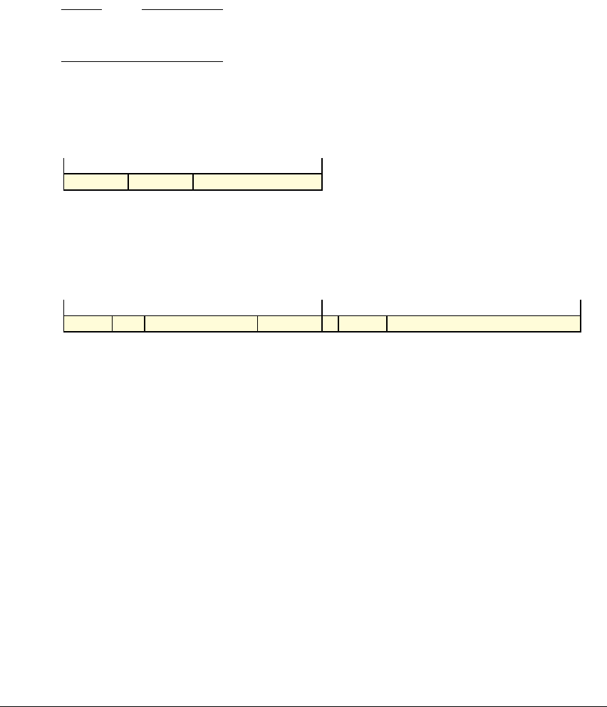
Thumb Instruction Details
ARM DDI 0419C Copyright © 2007-2008, 2010 ARM Limited. All rights reserved. A6-193
ID092410 Non-Confidential
A6.7.72 UDF
Permanently Undefined generates an Undefined Instruction exception.
Note
The encodings for
UDF
are defined as permanently undefined in the versions of the architecture specified in
this section. Issue C of this manual first defines an assembler mnemonic for these encodings.
imm32 = ZeroExtend(imm8, 32);
// imm32 is for assembly and disassembly only, and is ignored by hardware.
imm32 = ZeroExtend(imm4:imm12, 32);
// imm32 is for assembly and disassembly only, and is ignored by hardware.
Assembler syntax
UDF{<q>} {#}<imm>
where:
{<q>}
See Standard assembler syntax fields on page A6-98.
<imm>
Specifies an immediate constant, that is 8-bit in encoding T1, and 16-bit in encoding T2.
The processor ignores the value of this constant.
Encoding T1 All versions of the Thumb instruction set.
UDF #<imm8>
Encoding T2 ARMv6-M, ARMv7-M
UDF.W #<imm16>
1 1 0 1 1 1 1 0 imm8
15 14 13 12 11 10 9 8 7 6 5 4 3 2 1 0
1 1 1 0 1 1 1 1 1 1 1 imm4 1 0 1 0 imm12
15 14 13 12 11 10 9 8 7 6 5 4 3 2 1 0
1
1514131211109876543210

Thumb Instruction Details
A6-194 Copyright © 2007-2008, 2010 ARM Limited. All rights reserved. ARM DDI 0419C
Non-Confidential ID092410
Operation
if ConditionPassed() then
EncodingSpecificOperations();
UNDEFINED;
Exceptions
Undefined Instruction.

Thumb Instruction Details
ARM DDI 0419C Copyright © 2007-2008, 2010 ARM Limited. All rights reserved. A6-195
ID092410 Non-Confidential
A6.7.73 UXTB
Unsigned Extend Byte extracts an 8-bit value from a register, zero extends it to 32 bits, and writes the result
to the destination register.
d = UInt(Rd); m = UInt(Rm); rotation = 0;
Assembler syntax
UXTB{<q>} <Rd>, <Rm>
where:
{<q>}
See Standard assembler syntax fields on page A6-98.
<Rd>
The destination register.
<Rm>
The register that contains the second operand.
Operation
if ConditionPassed() then
EncodingSpecificOperations();
rotated = ROR(R[m], rotation);
R[d] = ZeroExtend(rotated<7:0>, 32);
Exceptions
None.
Encoding T1 ARMv6-M, ARMv7-M
UXTB <Rd>,<Rm>
11 Rm0100 Rd1 0 1 1
15 14 13 12 11 10 9 8 7 6 5 4 3 2 1 0

Thumb Instruction Details
A6-196 Copyright © 2007-2008, 2010 ARM Limited. All rights reserved. ARM DDI 0419C
Non-Confidential ID092410
A6.7.74 UXTH
Unsigned Extend Halfword extracts a 16-bit value from a register, zero extends it to 32 bits, and writes the
result to the destination register.
d = UInt(Rd); m = UInt(Rm); rotation = 0;
Assembler syntax
UXTH{<q>} <Rd>, <Rm>
where:
{<q>}
See Standard assembler syntax fields on page A6-98.
<Rd>
The destination register.
<Rm>
The register that contains the second operand.
Operation
if ConditionPassed() then
EncodingSpecificOperations();
rotated = ROR(R[m], rotation);
R[d] = ZeroExtend(rotated<15:0>, 32);
Exceptions
None.
Encoding T1 ARMv6-M, ARMv7-M
UXTH <Rd>,<Rm>
01 Rm0100 Rd1 0 1 1
15 14 13 12 11 10 9 8 7 6 5 4 3 2 1 0

Thumb Instruction Details
ARM DDI 0419C Copyright © 2007-2008, 2010 ARM Limited. All rights reserved. A6-197
ID092410 Non-Confidential
A6.7.75 WFE
Wait For Event is a hint instruction that permits the processor to enter a low-power state until one of a
number of events occurs, including events signaled by the
SEV
instruction on any processor in a
multiprocessor system. For more information, see Wait For Event and Send Event on page B1-241.
For general hint behavior, see Hint Instructions on page A6-104.
// No additional decoding required
Assembler syntax
WFE{<q>}
where:
{<q>}
See Standard assembler syntax fields on page A6-98.
Operation
if ConditionPassed() then
EncodingSpecificOperations();
if EventRegistered() then
ClearEventRegister();
else
WaitForEvent();
Exceptions
None.
Encoding T1 ARMv6-M, ARMv7-M
WFE
01 00000011111 0 1 1
15 14 13 12 11 10 9 8 7 6 5 4 3 2 1 0

Thumb Instruction Details
A6-198 Copyright © 2007-2008, 2010 ARM Limited. All rights reserved. ARM DDI 0419C
Non-Confidential ID092410
A6.7.76 WFI
Wait For Interrupt is a hint instruction that suspends execution until one of a number of events occurs. For
more information, see Wait For Interrupt on page B1-243.
For general hint behavior, see Hint Instructions on page A6-104.
// No additional decoding required
Assembler syntax
WFI{<q>}
where:
{<q>}
See Standard assembler syntax fields on page A6-98.
Operation
if ConditionPassed() then
EncodingSpecificOperations();
WaitForInterrupt();
Exceptions
None.
Notes
PRIMASK If PRIMASK.PM is set to 1, an asynchronous exception that has a higher group priority than
any active exception results in a
WFI
instruction exit. If the group priority of the exception is
less than or equal to the execution group priority, the exception is ignored.
Encoding T1 ARMv6-M, ARMv7-M
WFI
11 00000011111 0 1 1
15 14 13 12 11 10 9 8 7 6 5 4 3 2 1 0

Thumb Instruction Details
ARM DDI 0419C Copyright © 2007-2008, 2010 ARM Limited. All rights reserved. A6-199
ID092410 Non-Confidential
A6.7.77 YIELD
YIELD
is a hint instruction. It enables software with a multithreading capability to indicate to the hardware
that it is performing a task, for example a spinlock, that could be swapped out to improve overall system
performance. Hardware can use this hint to suspend and resume multiple code threads if it supports the
capability.
For general hint behavior, see Hint Instructions on page A6-104.
// No additional decoding required
Assembler syntax
YIELD{<q>}
where:
{<q>}
See Standard assembler syntax fields on page A6-98.
Operation
if ConditionPassed() then
EncodingSpecificOperations();
Hint_Yield();
Exceptions
None.
Encoding T1 ARMv6-M, ARMv7-M
YIELD
10 00000011111 0 1 1
15 14 13 12 11 10 9 8 7 6 5 4 3 2 1 0

Thumb Instruction Details
A6-200 Copyright © 2007-2008, 2010 ARM Limited. All rights reserved. ARM DDI 0419C
Non-Confidential ID092410
Part B
System Level Architecture

ARM DDI 0419C Copyright © 2007-2008, 2010 ARM Limited. All rights reserved. B1-203
ID092410 Non-Confidential
Chapter B1
System Level Programmers’ Model
This chapter provides a system-level view of the ARMv6-M programmers’ model. It contains the following
sections:
•Introduction to the system level on page B1-204
•About the ARMv6-M memory mapped architecture on page B1-205
•Overview of system level terminology and operation on page B1-206
•Registers on page B1-211
•ARMv6-M exception model on page B1-218.

System Level Programmers’ Model
B1-204 Copyright © 2007-2008, 2010 ARM Limited. All rights reserved. ARM DDI 0419C
Non-Confidential ID092410
B1.1 Introduction to the system level
The ARM architecture defines a hierarchy for software operation:
• The lowest level is the application level, described in part A of this manual. In particular, Chapter A2
Application Level Programmers’ Model describes the programmers’ model for applications.
Application-level software is largely independent of the architecture profile.
• The higher level is the system level, that includes support for the applications. The system level
features and how they are supported, are significantly different between the different architecture
profiles.
Part B of this manual describes the ARMv6-M architecture at the system level.
As stated in Privileged execution on page A2-30, ARMv6-M supports unprivileged and privileged
operation, or privileged operation only, depending on whether the implementation includes the
Unprivileged/Privileged Extension. System level support requires privileged access, giving system software
the access permissions required to configure and control the resources. Typically, an operating system
provides system services to the applications, either transparently, or through application initiated supervisor
calls. The operating system is also responsible for servicing interrupts and other system events, making
exceptions a key component of the system level programmers’ model. In a system that supports only
privileged execution, application code can raise a supervisor call using
SVC
, or handle system access and
control directly. ARMv6-M with the Unprivileged/Privileged Extension also supports a software model of
unprivileged applications running under a privileged OS.
The ARMv6-M Debug Extension supports a Debug state, halting debug, and associated control and
configuration registers, see Chapter C1 ARMv6-M Debug for more information.
The optional ARMv6-M Protected Memory System Architecture (PMSA) Extension and its Memory
Protection Unit (MPU) protects the system memory space, see Protected Memory System Architecture,
PMSAv6 on page B3-289
ARMv6-M also supports an optional system timer, SysTick, see The system timer, SysTick on page B3-275.
Note
• In deeply embedded systems, particularly at low cost or performance points, there might be no clear
distinction between an operating system and the applications, and software might be developed as a
homogeneous codebase.
• Appendix B Deprecated and Obsolete Features describes deprecated features of the ARMv6-M
profile.

System Level Programmers’ Model
ARM DDI 0419C Copyright © 2007-2008, 2010 ARM Limited. All rights reserved. B1-205
ID092410 Non-Confidential
B1.2 About the ARMv6-M memory mapped architecture
ARMv6-M is a memory-mapped architecture, meaning the architecture assigns physical addresses for
processor registers to provide:
• exception entry points, as vectors
• system control and configuration.
An ARMv6-M implementation maintains exception handler entry points in a table of address pointers.
The architecture reserves address space
0xE0000000
to
0xFFFFFFFF
for system level use. ARM reserves the
first 1MB of this system address space,
0xE0000000
to
0xE00FFFFF
, as the Private Peripheral Bus (PPB). The
assignment of the rest of the address space, from
0xE0100000
is IMPLEMENTATION DEFINED with some
memory attribute restrictions. See The system address map on page B3-258 for more information.
In the PPB address space, the architecture assigns a 4kB block
0xE000E000
to
0xE000EFFF
, as the SCS. The
SCS supports:
• processor ID registers
• general control and configuration, including the vector table base address
• system handler support, for system interrupts and exceptions
• an optional system timer, SysTick
•a Nested Vectored Interrupt Controller (NVIC), that supports up to 32 discrete external interrupts
• processor debug, optional in ARMv6-M
• MPU registers, in systems that implement the Unprivileged/Privileged Extension.
See System Control Space (SCS) on page B3-262 for more details.

System Level Programmers’ Model
B1-206 Copyright © 2007-2008, 2010 ARM Limited. All rights reserved. ARM DDI 0419C
Non-Confidential ID092410
B1.3 Overview of system level terminology and operation
The following sections describe the concepts that are central to the system level architecture.
B1.3.1 Modes, privilege and stacks
Mode, privilege and stack pointer are key concepts used in ARMv6-M.
Mode An M-profile processor supports two operating modes:
Thread mode
Is entered on Reset, and can be entered as a result of an exception return.
Handler mode
Is entered as a result of an exception. The processor must be in Handler mode
to issue an exception return.
Privilege If an ARMv6-M system does not implement the Unprivileged/Privileged Extension, all
execution is privileged. Privileged execution has access to all resources.
If an ARMv6-M system implements the Unprivileged/Privileged Extension, software can
execute as privileged or unprivileged. Unprivileged execution has limited or no access to
some resources.
Execution in Handler mode is always privileged. The value of CONTROL.nPRIV
determines whether execution in Thread mode is privileged or unprivileged.
Stack Pointer The processor implements a banked pair of stack pointers, the Main Stack Pointer, and the
Process Stack Pointer. See The SP registers on page B1-211 for more information.
In Handler mode, the processor uses the Main Stack Pointer. In Thread mode it can use
either stack pointer.
Table B1-1 shows the possible combinations of mode, privilege and stack pointer usage.
Table B1-1 Mode, privilege and stack relationship
Mode Privilege Stack pointer Typical usage model
Handler Privileged Main Exception handling.
Thread Privileged Main Execution of a privileged process or thread using a common stack
in a system that only supports privileged access.
Process Execution of a privileged process or thread using a stack reserved
for that process or thread in a system that only supports privileged
access.

System Level Programmers’ Model
ARM DDI 0419C Copyright © 2007-2008, 2010 ARM Limited. All rights reserved. B1-207
ID092410 Non-Confidential
Pseudocode detail of processor operating mode
The
CurrentModeIsPrivileged()
pseudocode function determines whether the current software execution is
privileged:
// CurrentModeIsPrivileged()
// =========================
boolean CurrentModeIsPrivileged()
return (CurrentMode == Mode_Handler || CONTROL.nPRIV == '0');
B1.3.2 Exceptions
An exception is a condition that changes the normal flow of control in a program. Exception behavior splits
into two stages:
Exception generation
When an exception event occurs and is presented to the processor
Exception processing, or activation
When the processor follows a sequence of exception entry, exception handler code
execution, and exception return. The transition from exception generation to exception
processing can be instantaneous.
ARMv6-M defines the following exception categories
Reset Reset is a special form of exception that, when asserted, terminates current execution in a
potentially unrecoverable way. When reset is deasserted, execution restarts from a fixed
point.
Supervisor call (SVCall)
An exception caused explicitly by the
SVC
instruction. Application software uses the
SVC
instruction to make a call to an underlying operating system. This is called a Supervisor call.
The
SVC
instruction enables the application to issue a Supervisor call that requires privileged
Thread UnprivilegedaMain Execution of an unprivileged process or thread using a common
stack in a system that supports privileged and unprivileged access.
Process Execution of an unprivileged process or thread using a stack
reserved for that process or thread in a system that supports
privileged and unprivileged access.
a. Only available with the Unprivileged/Privileged Extension.
Table B1-1 Mode, privilege and stack relationship (continued)
Mode Privilege Stack pointer Typical usage model

System Level Programmers’ Model
B1-208 Copyright © 2007-2008, 2010 ARM Limited. All rights reserved. ARM DDI 0419C
Non-Confidential ID092410
access to the system and executes in program order relative to the application. ARMv6-M
also supports an interrupt-driven Supervisor calling mechanism PendSV. See Interrupts in
Overview of the exceptions supported on page B1-218 for more information.
Fault A fault is an exception that results from an error condition in instruction execution. A fault
can be reported synchronously or asynchronously to the instruction that caused it. In
general, faults are reported synchronously.
A synchronous fault is always reported with the instruction that caused the fault. The
architecture makes no guarantee about how an asynchronous fault is reported relative to the
instruction that caused the fault. Faults are considered fatal in ARMv6-M, in that no fault
status information is provided to assist recovery.
Interrupt An interrupt is an exception, other than a reset, fault or a supervisor call. All interrupts are
asynchronous to the instruction stream. Typically interrupts are used by other components
of the system that must communicate with the processor. This can include software running
on another processor in the system.
Each exception has:
• A priority level
• An exception number
• A vector in memory that defines the entry-point for execution on taking the exception. The value held
in a vector is the address of the entry point of the exception handler, or Interrupt Service Routine
(ISR).
An exception, other than reset, has the following possible states:
Inactive An exception that is not pending or active.
Pending An exception that has been generated, but that the processor has not yet started processing.
An exception is generated when the corresponding exception event occurs.
Active An exception for which the processor has started executing a corresponding exception
handler, but has not returned from that handler. The handler for an active exception is either
running or preempted by a the handler for a higher priority exception.
Active and pending
One instance of the exception is active, and a second instance of the exception is pending.
Only asynchronous exceptions can be active and pending. Any synchronous exception is
either inactive, pending, or active.
Priority levels, execution priority, exception entry, and execution preemption
Exception priorities determine the order in which the processor handles exceptions:
• Every exception has a priority level, the exception priority. Three exceptions have fixed priorities,
while all others have a priority that can be configured by privileged software.

System Level Programmers’ Model
ARM DDI 0419C Copyright © 2007-2008, 2010 ARM Limited. All rights reserved. B1-209
ID092410 Non-Confidential
• The instruction stream executing on the processor has a priority level associated with it, the execution
priority.
• The execution priority immediately after a reset is the base level of execution priority. Only execution
in Thread mode can be at this base level of execution priority.
• An exception whose exception priority is sufficiently higher than the execution priority becomes
active. The concept of sufficiently higher priority relates to priority grouping, see Priority grouping
on page B1-222.
Software can boost the execution priority using the PRIMASK register provided for this purpose, otherwise
the execution priority is the highest priority of all the active exceptions, see Execution priority and priority
boosting on page B1-222 for more information.
When an exception becomes active because its priority is sufficiently higher that the executing priority:
• its exception handler preempts the currently running instruction stream
• its priority becomes the executing priority
When an exception other that reset preempts an instruction stream, the processor automatically saves key
context information onto the stack, and execution branches to the code pointed to by the corresponding
exception vector.
An exception can occur during exception activation, for example as a result of a memory fault when pushing
context information. Also, the architecture permits the optimization of a late-arriving exception. Exceptions
on exception entry on page B1-232 describes the behavior of these cases.
The processor always runs an exception handler in Handler mode. If the exception preempts software
running in Thread mode the processor changes to handler mode as part of the exception entry.
Exception Return
The processor executes the exception handler in Handler mode, and returns from the handler. On exception
return:
• If the exception state is active and pending:
— if the exception has sufficient priority, it becomes active and the processor re-enters the
exception handler
— otherwise, it becomes pending.
• If the exception state is active it becomes inactive.
• The processor restores the information that it stacked on exception entry.
• If the code that was preempted by the exception handler was running in Thread mode, the processor
changes to Thread mode.
• The processor resumes execution of the code that was preempted by the exception handler.
The Exception Return Link, a value stored in the link register on exception entry, determines the target of
the exception return.

System Level Programmers’ Model
B1-210 Copyright © 2007-2008, 2010 ARM Limited. All rights reserved. ARM DDI 0419C
Non-Confidential ID092410
On an exception return, there can be a pending exception with sufficient priority to preempt the execution
being returned to. This results in an exception entry sequence immediately after the exception return
sequence. This condition is referred to as chaining of the exceptions. Hardware can optimize chaining of
exceptions to remove the requirement to restore and re-save the key context state, an optimization referred
to as tail-chaining. See Exceptions on exception return, and tail-chaining exceptions on page B1-233 for
details.
Faults can occur during the exception return, for example as a result of a memory fault when popping
previous state off the stack. The behavior in this and other cases is explained in Derived exceptions on
exception entry on page B1-233.
B1.3.3 Execution state
ARMv6-M only executes Thumb instructions, both 16-bit and a few 32-bit instructions. This means it is
always executing in Thumb state. The ARMv6 architecture profile uses a value of 1 for an execution status
bit, the EPSR.T to indicate execution in Thumb state, see The special-purpose program status registers,
xPSR on page B1-212. ARMv6-M is consistent with the software programming model and interworking
support of additional execution states in other ARM architecture profiles. Setting EPSR.T to zero in an
ARMv6-M processor causes a fault when the next instruction executes, because all instructions in this state
are UNDEFINED.
B1.3.4 Debug state
A processor enters Debug state if it is configured to halt on a debug event, and a debug event occurs. See
Chapter C1 ARMv6-M Debug for more details.
Note
Debug state is part of the Debug Extension for ARMv6-M.

System Level Programmers’ Model
ARM DDI 0419C Copyright © 2007-2008, 2010 ARM Limited. All rights reserved. B1-211
ID092410 Non-Confidential
B1.4 Registers
The ARMv6-M profile has the following registers closely coupled to the processor:
• General purpose registers R0-R12.
• Two Stack Pointer registers, SP_main and SP_process. These are banked versions of SP, also
described as R13.
• The Link Register, LR also described as R14.
• The Program Counter, PC, sometimes described as R15.
• Status registers for flags, execution state bits, and the current exception number.
• A mask register, PRIMASK, used to manage the prioritization scheme for exceptions and interrupts.
• A control register, CONTROL that identifies the current stack.
All other registers described in this specification are memory mapped.
Note
Where this part of the manual gives register access restrictions, these apply to normal execution. Debug
restrictions can differ, see General rules applying to debug register access on page C1-318, Debug Core
Register Selector Register, DCRSR on page C1-335 and Debug Core Register Data Register, DCRDR on
page C1-337.
B1.4.1 The ARM core registers
The registers R0-R12, SP, LR, and PC are named the ARM core registers. These registers can be described
as R0-R15.
The SP registers
An ARMv6-M processor implements two stacks:
• the Main stack, SP_main or MSP
• the Process stack, SP_process or PSP.
The active stack pointer is one of the banked stack pointers, SP_main and SP_process. The current stack
depends on the mode and, in Thread mode, the value of the CONTROL.SPSEL bit, see The special-purpose
CONTROL register on page B1-215. A reset selects and initializes SP_main, see Reset behavior on
page B1-224.
For maximum portability across other profiles, ARM strongly recommends that software treats SP bits [1:0]
as SBZP.
The stack pointer that is used in exception entry and exit is described in the pseudocode sequences of the
exception entry and exit, see Exception entry behavior on page B1-224 and Exception return behavior on
page B1-227 for more details. SP_main is selected and initialized on reset, see Reset behavior on
page B1-224.
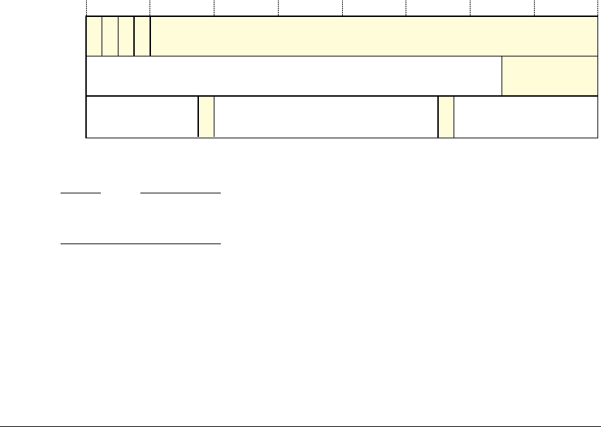
System Level Programmers’ Model
B1-212 Copyright © 2007-2008, 2010 ARM Limited. All rights reserved. ARM DDI 0419C
Non-Confidential ID092410
B1.4.2 The special-purpose program status registers, xPSR
The Program Status Register (PSR) is a 32-bit register that comprises three subregisters:
Application Program Status Register, APSR
Holds flags that can be written by application-level software, that is, by unprivileged
software. APSR handling of application-level writeable flags by the
MSR
and
MRS
instructions
is consistent across ARMv6T2, ARMv6-M, and all ARMv7 profiles.
Interrupt Program Status Register, IPSR
When the processor is executing an exception handler, holds the exception number of the
exception being processed. Otherwise, the IPSR value is zero.
Execution Program Status Register, EPSR
Holds execution state bits.
Software can use the
MRS
and
MSR
instructions.to access the complete PSR, or any combination of one or more
of the subregisters, although there are restrictions on viewing and modifying some fields. xPSR is a generic
term for a program status register. All unused bits in any individual or combined xPSR are Reserved.
Figure B1-1 shows how the APSR, IPSR, and EPSR combine to form the PSR.
Figure B1-1 xPSR register layout
Note
EPSR [9] is reserved, but when the processor stacks the PSR, it uses this bit to indicate the stack alignment,
see Stack alignment on exception entry on page B1-227.
The APSR
Flag setting instructions modify the APSR flags N, Z, C, and V, and the processor uses these flags to
evaluate conditional branch instructions. The Application Program Status Register on page A2-38 describes
the flags. The flags are UNKNOWN on reset.
a
0 or Exception
Number
N
31 30 29 28 24 9 5 0
Z C V
T
EPSR
IPSR
APSR

System Level Programmers’ Model
ARM DDI 0419C Copyright © 2007-2008, 2010 ARM Limited. All rights reserved. B1-213
ID092410 Non-Confidential
The IPSR
The processor updates the IPSR on exception entry and exit. Software can use an
MRS
instruction to read the
IPSR, but the processor ignores writes to the IPSR by an
MSR
instruction. The IPSR Exception Number field
is defined as follows:
• in Thread mode, the value is 0
• in Handler mode, holds the exception number of the currently-executing exception, see Exception
number definition on page B1-220 and The vector table on page B1-220.
On reset, the processor is in Thread mode and the Exception Number field of the IPSR is set to 0. As a result,
the value 1, the Reset Exception Number, is a transitory value, that software cannot see as a valid IPSR
Exception Number.
The EPSR
The EPSR contains the T-bit, that indicates whether the processor is in Thumb state. The T-bit cannot be
read by software. See Debug Core Register Data Register, DCRDR on page C1-337 for information about
debug state access.
All fields Read-As-Zero using an
MRS
instruction, and the processor ignores writes to the EPSR by an
MSR
instruction.
The EPSR T-bit supports the ARM architecture interworking model, however, because ARMv6-M only
supports execution of Thumb instructions, it must always be maintained with the value 1. Updates to the PC
that comply with the Thumb instruction interworking rules must update EPSR.T accordingly. Instruction
execution with EPSR.T set to 0 generates a HardFault.
A reset sets the T bit to the value of bit [0] of the reset vector. This bit must be 1 if the processor is to execute
the code indicated by the reset vector. If this bit is 0, the processor takes a HardFault exception and enters
the HardFault handler, with the stacked
ReturnAddress()
value pointing to the reset handler, and the T bit of
the stacked xPSR value set to 0, see Reset behavior on page B1-224.
All unused bits in the individual or combined registers are reserved.
Composite views of the xPSR registers
The
MSR
and
MRS
instructions recognize
APSR
,
IPSR
, and
EPSR
as mnemonics for the corresponding registers.
It also recognizes mnemonics for different combinations of the registers, as Table B1-2 shows:
Table B1-2 Mnemonics for combinations of xPSR registers
Mnemonic Registers accessed
IAPSR
IPSR and APSR

System Level Programmers’ Model
B1-214 Copyright © 2007-2008, 2010 ARM Limited. All rights reserved. ARM DDI 0419C
Non-Confidential ID092410
See Special register encodings used in ARMv6-M system instructions on page B4-304 for more information.
B1.4.3 The special-purpose mask register, PRIMASK
The processor can use the exception mask register PRIMASK, that is used for priority boosting. PRIMASK
is a special-purpose mask register,
Figure B1-2 shows the format of the PRIMASK register.
Figure B1-2 PRIMASK register bit assignments
PRIMASK.PM is set to 0 on reset. Where the Unprivileged/Privileged Extension is implemented, the
processor ignores unprivileged writes to the mask registers.
Software can access this register using the
MSR
or
MRS
instructions, see MRS on page B4-308 and MSR
(register) on page B4-310 for more information.
In addition:
• Executing the instruction
CPSID i
sets PRIMASK.PM to 1
• Executing the instruction
CPSIE i
sets PRIMASK.PM to 0.
EAPSR
EPSR and APSR
XPSR
All three xPSR registers
IEPSR
IPSR and EPSR
Table B1-2 Mnemonics for combinations of xPSR registers (continued)
Mnemonic Registers accessed
Reserved
31 10
PM

System Level Programmers’ Model
ARM DDI 0419C Copyright © 2007-2008, 2010 ARM Limited. All rights reserved. B1-215
ID092410 Non-Confidential
B1.4.4 The special-purpose CONTROL register
The special-purpose CONTROL register is a 2-bit special-purpose register defined as follows:
nPRIV, bit[0] If the Unprivileged/Privileged Extension is implemented, defines the execution privilege in
Thread mode:
0 Thread mode has privileged access
1 Thread mode has unprivileged access.
Note
• In Handler mode, execution is always privileged.
• If the Unprivileged/Privileged Extension is not implemented, bit[0] is RAZ/WI.
SPSEL, bit[1] Defines the stack to be used:
0 Use SP_main as the current stack
1 In Thread mode, use SP_process as the current stack.
In Handler mode, this value is reserved.
bits[31:2] Reserved on
MRS
and
MSR
accesses.
Software can update the SPSEL bit in privileged Thread mode. In Handler mode, the processor ignores
explicit writes to the SPSEL bit.
A reset clears the CONTROL register to zero. Software can use the
MRS
instruction to read the register, and
the
MSR
instruction to write to the register. Unprivileged write accesses are ignored.
The processor updates the SPSEL bit on exception entry and exception return, see the pseudocode in
Exception entry behavior on page B1-224 and Exception return behavior on page B1-227 for more
information.
Software must use an ISB barrier instruction to ensure a write to the CONTROL register takes effect before
the next instruction is executed.
B1.4.5 Reserved special-purpose register bits
All unused bits in special-purpose registers are reserved. The architecture defines these reserved bits as
RAZ/WI for
MRS
and
MSR
instruction accesses. However, for future compatibility, ARM recommends that
software treats reserved bits as UNK/SBZP.
B1.4.6 Special-purpose register updates and the memory order model
Except for writes to the CONTROL register, any change to a special-purpose register by a
CPS
or
MSR
instruction is guaranteed:
• not to affect that
CPS
or
MSR
instruction or any instruction that precedes it in program order
• to be visible to all instructions that appear in program order after that
CPS
or
MSR
instruction.

System Level Programmers’ Model
B1-216 Copyright © 2007-2008, 2010 ARM Limited. All rights reserved. ARM DDI 0419C
Non-Confidential ID092410
B1.4.7 Register-related definitions for pseudocode
The system programmers’ model pseudocode uses two register types:
• 32-bit core registers, see The ARM core registers on page B1-211
• 32-bit memory mapped registers.
Appendix G Register Index lists the ARMv6-M registers.
This manual describes register bit fields as
<register_name>.<bitfield_name>
or by a specific bit reference,
for example:
•
AIRCR<2>
is equivalent to
AIRCR.SYSRESETREQ
•
ICSR<8:0>
is equivalent to
VECTACTIVE
.
Normally this manual uses the field names.
Pseudocode details for ARM core register access
The following pseudocode supports access to the general-purpose registers for the operations defined in
Alphabetical list of ARMv6-M Thumb instructions on page A6-105:
// The M-profile execution modes.
enumeration Mode {Mode_Thread, Mode_Handler};
// The physical array of core registers R0 to R12.
array bits(32) _R[0..12];
// Physical storage for the two banked stack pointers, link register
// and program counter.
bits(32) SP_process;
bits(32) SP_main;
bits(32) LR;
bits(32) PC;
// R[] - non-assignment form
// =========================
bits(32) R[integer n]
assert n >= 0 && n <= 15;
if n == 15 then
result = PC + 4;
elsif n == 14 then
result = LR;
elsif n == 13 then
result = if CONTROL.SPSEL == '1' then SP_process else SP_main;
else
result = _R[n];
return result;

System Level Programmers’ Model
ARM DDI 0419C Copyright © 2007-2008, 2010 ARM Limited. All rights reserved. B1-217
ID092410 Non-Confidential
// R[] - assignment form
// =====================
R[integer n] = bits(32) value
assert n >= 0 && n <= 14;
if n == 14 then
LR = value;
elsif n == 13 then
if CONTROL.SPSEL == '1' then
SP_process = value<31:2>:'00';
else
SP_main = value<31:2>:'00';
else
_R[n] = value;
return;
// BranchTo()
// ==========
BranchTo(bits(32) address)
PC = address;
return;

System Level Programmers’ Model
B1-218 Copyright © 2007-2008, 2010 ARM Limited. All rights reserved. ARM DDI 0419C
Non-Confidential ID092410
B1.5 ARMv6-M exception model
The exception model is central to the architecture and system correctness in the ARMv6-M profile. The
ARMv6-M profile is the same as ARMv7-M in using hardware saving and restoring of key context state on
exception entry and exit, and using a table of vectors to determine the exception entry points. In addition,
the exception categorization in the ARMv6-M profile is a subset of those provided in ARMv7-M.
The following sections describe the ARMv6-M exception model:
•Overview of the exceptions supported
•Exception number definition on page B1-220
•The vector table on page B1-220
•Exception priorities and preemption on page B1-221
•Reset behavior on page B1-224
•Exception entry behavior on page B1-224
•Stack alignment on exception entry on page B1-227
•Exception return behavior on page B1-227
•Exceptions in single-word load operations on page B1-231
•Exceptions in Load Multiple and Store Multiple operations on page B1-231
•Exceptions on exception entry on page B1-232
•Exceptions on exception return, and tail-chaining exceptions on page B1-233
•Exception status and control on page B1-235
•Fault behavior on page B1-236
•Unrecoverable exception cases on page B1-238
•Reset management on page B1-240
•Power management on page B1-240
•Wait For Event and Send Event on page B1-241
•Wait For Interrupt on page B1-243.
B1.5.1 Overview of the exceptions supported
The ARMv6-M profile supports the following exceptions:
Reset The ARMv6-M profile supports two levels of reset. The reset level determines the register
bit fields that are forced to their reset values on the deassertion of reset.
• Power-on reset resets the processor, SCS and debug logic.
• Local reset resets the processor and SCS except for debug-related resources. For
more details, see Debug and reset on page C1-323.
The Reset exception is permanently enabled with a fixed priority of -3.
NMI NMI (Non Maskable Interrupt) is the highest priority exception other than reset. It is
permanently enabled with a fixed priority of -2.
Hardware can generate an NMI, or software can set the NMI exception to the Pending state,
see Interrupt Control State Register, ICSR on page B3-265, or hardware.

System Level Programmers’ Model
ARM DDI 0419C Copyright © 2007-2008, 2010 ARM Limited. All rights reserved. B1-219
ID092410 Non-Confidential
HardFault HardFault is the generic fault that exists for all classes of fault that cannot be handled by any
of the other exception mechanisms. Typically, HardFault is used for unrecoverable system
failures, although this is not required, and some uses of HardFault might be recoverable.
HardFault is permanently enabled with a fixed priority of -1.
HardFault is used for all fault conditions on ARMv6-M.
SVCall This supervisor call handles the exception caused by the
SVC
instruction. SVCall is
permanently enabled and has a configurable priority.
Interrupts The ARMv6-M profile supports two system level interrupts and up to 32 external interrupts.
Each interrupt has a configurable priority. The system-level interrupts are:
PendSV Used for software-generated supervisor calls. An application uses a supervisor
call, if it requires servicing by the underlying operating system. The supervisor
call associated with PendSV executes when the processor takes the PendSV
interrupt.
Note
For a supervisor call that executes synchronously to program execution,
software must use the
SVC
instruction. This generates an SVCall exception.
PendSV is permanently enabled, and is controlled using the
ICSR.PENDSVSET and ICSR.PENDSVCLR bits, see Interrupt Control State
Register, ICSR on page B3-265
SysTick Generated by the SysTick timer and controlled using the ICSR.PENDSTSET
and ICSR.PENDSTCLR bits. SysTick is an integral component of an
ARMv7-M processor, and is optional in ARMv6-M.
Note
Software can suppress hardware generation of the SysTick event, but
ICSR.PENDSTSET and ICSR.PENDSTCLR are always available to software,
see Interrupt Control State Register, ICSR on page B3-265.
Software can disable all external interrupts, and can set or clear the pending state of any
interrupt. Interrupts other than PendSV can be set to the Pending state by hardware.
See Fault behavior on page B1-236 for a definitive list of all the possible causes of faults. ARMv6-M does
not support run-time fault status register bits to identify the faults.

System Level Programmers’ Model
B1-220 Copyright © 2007-2008, 2010 ARM Limited. All rights reserved. ARM DDI 0419C
Non-Confidential ID092410
B1.5.2 Exception number definition
Each exception has an associated exception number as Table B1-3 shows.
B1.5.3 The vector table
The vector table contains the initialization value for the stack pointer on reset, and the entry point addresses
for all exception handlers. The exception number, defined in Table B1-3, also defines the order of entries in
the vector table, as Table B1-4 shows.
Depending on the implementation, the vector table base is adjustable. The range of values that the VTOR
can accept is IMPLEMENTATION DEFINED. Implementations not providing configurability of the table base
provide a VTOR with RAZ/WI behavior. See Vector Table Offset Register, VTOR on page B3-267 for more
information.
Table B1-3 Exception numbers
Exception number Exception
1Reset
2NMI
3HardFault
4-10 Reserved
11 SVCall
12-13 Reserved
14 PendSV
15 SysTick, optional
16 External Interrupt(0)
……
16 + N External Interrupt(N)
Table B1-4 Vector table format
Word offset in table Description, for all pointer address values
0 SP_main. This is the reset value of the Main stack pointer.
Exception Number Exception using that Exception Number

System Level Programmers’ Model
ARM DDI 0419C Copyright © 2007-2008, 2010 ARM Limited. All rights reserved. B1-221
ID092410 Non-Confidential
Note
For implementations that do not support the VTOR register, the VTOR register space defined in ARMv7-M
is reserved, RAZ/WI.
The table offset address that VTOR defines is 32-word aligned. Where more than 16 external interrupts are
used, the offset word alignment must be increased to accommodate vectors for all the exceptions and
interrupts supported and keep the required table size naturally aligned.
The entry at offset 0 is used to initialize the value for SP_main, see The SP registers on page B1-211. All
other entries must have bit [0] set to 1, because the bit defines the EPSR T-bit on exception entry, see Reset
behavior on page B1-224 and Exception entry behavior on page B1-224 for details. On exception entry, if
bit [0] of the associated vector table entry is 0, execution of the first instruction causes a HardFault.
B1.5.4 Exception priorities and preemption
In the ARMv6-M priority model, lower numbers take precedence. That is, the lower the assigned priority
value, the higher the priority level. The priority order for exceptions with the same priority level is fixed,
and is determined by their exception number.
Reset, NMI, and HardFault execute at fixed priorities of -3, -2, and -1 respectively. Software can set the
priority of all other exceptions using registers in the SCS. A reset clears these software-configured priority
settings. Software-assigned priority values start at 0, so Reset, NMI, and HardFault always have higher
priorities than any other exception.
When multiple pending exceptions have the same priority number, the pending exception with the lowest
exception number takes precedence. When an exception is active, only an exception with a higher priority
can preempt it.
ARMv6-M supports 2-bit priority fields, providing four priority levels.
Note
ARMv7-M supports 8-bit priority fields. The ARMv6-M 2-bit priority fields correspond to the
most-significant two bits of the ARMv7-M priority fields
If software changes the priority of an exception when it is active or enabled, the effect is UNPREDICTABLE
in ARMv6-M.
Note
The not enabled condition does not apply to the permanently enabled SVCall or PendSV exceptions. It
applies to all cases where the configurable priority exception can be disabled in software.

System Level Programmers’ Model
B1-222 Copyright © 2007-2008, 2010 ARM Limited. All rights reserved. ARM DDI 0419C
Non-Confidential ID092410
Priority grouping
Priority grouping is a method of assigning a configurable number of the least significant priority bits so that
they are ignored when determining the highest priority pending exception. The effect is to group the affected
exceptions under a common priority defined by the remaining, most significant, priority bits. ARMv6-M
does not support configurable priority grouping, meaning that all supported priority bits are always used for
the group priority when detecting the highest pending exception.
When two pending exceptions have the same group priority, the lower pending exception number has
priority over the higher pending number as part of the priority precedence rule.
The group priorities of Reset, NMI and HardFault are -3, -2, and -1 respectively.
Execution priority and priority boosting
The execution priority is defined as the highest priority determined from:
• the highest priority of all active exceptions
• the impact of PRIMASK and priority boosting.
Note
Changing the priority of an active exception is UNPREDICTABLE.
Setting the mask bit in the PRIMASK register to 1 raises the execution priority to 0. This prevents any
exceptions with configurable priority from activating, except through the fault escalation mechanism, see
Priority escalation on page B1-223,.This also affects
WFI
, see WFI on page A6-198.
Note
In ARMv6-M, Thread mode has an implicit priority of the lowest priority in the system. Thread mode
executes when there are no pending or active exceptions.
The
ExecutionPriority()
pseudocode function defines the execution priority, where the
ExceptionPriority[]
array defines the priority of each exception.
// ExecutionPriority()
// ===================
// Determine the current execution priority
bit ExceptionActive[*]; // Exception handler active state
// See TakeReset() for more information
integer ExecutionPriority()
highestpri = 4; // Priority of Thread mode with no active exceptions
// The value is PriorityMax + 1 = 4
// (configurable priority bit field is 2 bits)
boostedpri = 4; // Priority influence of PRIMASK

System Level Programmers’ Model
ARM DDI 0419C Copyright © 2007-2008, 2010 ARM Limited. All rights reserved. B1-223
ID092410 Non-Confidential
for (i=2, i<48, i=i+1) ; IPSR values of the exception handlers
if ExceptionActive[i] == '1' then
if ExceptionPriority[i] < highestpri then
highestpri = ExceptionPriority[i];
if PRIMASK.PM == '1' then
boostedpri = 0;
if boostedpri < highestpri then
priority = boostedpri;
else
priority = highestpri;
return (priority);
// ExceptionPriority[], non-assignment form
// ========================================
integer ExceptionPriority[integer n]
assert n >= 2 && n <= 48;
if n == 2 then
result = -2; // NMI
elsif n == 1 then
result = -1; // HardFault
elsif n == 11 then
result = UInt(SHPR2.PRI_11); // SVCall
elsif n == 14 then
result = UInt(SHPR3.PRI_14); // PendSV
elsif n == 15 then
result = UInt(SHPR3.PRI_15); // SysTick
elsif n >= 16 then
r = (n - 16) DIV 4;
v = n MOD 4;
result = UInt(NVIC_IPR:r.PRI_N:v); // External interrupt (n-16)
else
result = 4; // Reserved exceptions
return result;
Priority escalation
When the group priority of a supervisor call, SVCall, is lower than or equal to the currently executing group
priority, inhibiting normal preemption, a HardFault exception is taken. This is known as priority escalation.
Note
Priority escalation applies when the currently executing group priority is less than HardFault. If an
exception occurs at a currently executing group priority of HardFault or higher, the behavior is defined in
Unrecoverable exception cases on page B1-238.

System Level Programmers’ Model
B1-224 Copyright © 2007-2008, 2010 ARM Limited. All rights reserved. ARM DDI 0419C
Non-Confidential ID092410
A fault that is escalated to a HardFault retains the
ReturnAddress()
behavior of the original fault. See the
pseudocode definition of
ReturnAddress()
in Exception entry behavior for more details. For the behavior of
the affected exceptions occurring when the currently executing group priority is that of a HardFault or
higher, see Unrecoverable exception cases on page B1-238.
B1.5.5 Reset behavior
Asserting reset causes the processor to abandon the current execution state without saving it. On the
deassertion of reset, all registers that have a defined reset value contain that value, and the processor
performs the actions described by the
TakeReset()
pseudocode.
For global declarations see Register-related definitions for pseudocode on page B1-216.
// TakeReset()
// ============
bit ExceptionActive[*]; // Conceptual array of 1-bit values for all exceptions
bits(32) vectortable = VTOR;
Mode CurrentMode;
TakeReset()
R[0..12] = bits(32) UNKNOWN;
SP_main = MemA[vectortable,4] & 0xFFFFFFFC;
SP_process = ((bits(30) UNKNOWN):’00’);
LR = bits(32) UNKNOWN; // Value must be initialised by software
CurrentMode = Mode_Thread;
APSR = bits(32) UNKNOWN; // Flags UNPREDICTABLE from reset
IPSR<5:0> = 0x0; // Exception number clearedat reset
PRIMASK.PM = '0'; // Priority mask cleared at reset
CONTROL.SPSEL = '0'; // Current stack is Main
CONTROL.nPRIV = '0'; // Thread is privileged
ResetSCSRegs(); // Catch-all function for System Control Space reset
ExceptionActive[*] = '0'; // All exceptions Inactive
ClearEventRegister(); // See WFE instruction for more information
start = MemA[vectortable+4,4]; // Load address of reset routine
BLXWritePC(start); // Start execution of reset routine
ExceptionActive[*]
is a conceptual array of active flag bits for all exceptions, meaning it has active flags for
the fixed priority system exceptions, configurable priority system exceptions, and external interrupts.
Pseudocode details of the Wait For Event lock mechanism on page B1-243 defines the
ClearEventRegister()
pseudocode function. ResetSCSRegisters() on page AppxE-407 defines the
ResetSCSRegisters()
pseudocode function.
B1.5.6 Exception entry behavior
On preemption of the instruction stream, the hardware saves context state onto a stack pointed to by one of
the SP registers, see The SP registers on page B1-211. The stack used depends on the mode of the processor
at the time of the exception.
The stacked context supports the AAPCS. This means the exception handler can be an AAPCS-compliant
procedure.

System Level Programmers’ Model
ARM DDI 0419C Copyright © 2007-2008, 2010 ARM Limited. All rights reserved. B1-225
ID092410 Non-Confidential
The ARMv6-M architecture uses a full-descending stack, where:
• when pushing context, the hardware decrements the stack pointer to the end of the new stack frame
before it stores data onto the stack
• when popping context, the hardware reads the data from the stack frame and then increments the
stack pointer.
When pushing context to the stack, the hardware saves eight 32-bit words, comprising xPSR,
ReturnAddress, LR (R14), R12, R3, R2, R1, and R0
The
ExceptionEntry()
pseudocode function describes the exception entry behavior:
// ExceptionEntry()
// ================
// NOTE: PushStack() can abandon memory accesses if a fault occurs during the stacking
// sequence.
// Exception entry is modified according to the behavior of a derived exception.
PushStack();
ExceptionTaken(ExceptionType); // ExceptionType is encoded as its exception number
For global declarations see Register-related definitions for pseudocode on page B1-216.
For a definition of
ExceptionActive[*]
see Reset behavior on page B1-224.
For helper functions and procedures see Miscellaneous helper procedures and functions on
page AppxE-406.
The definitions of the
PushStack()
and
ExceptionTaken()
pseudocode functions are:
// PushStack()
// ===========
PushStack()
if CONTROL.SPSEL == '1' && CurrentMode == Mode_Thread then
frameptralign = SP_process<2>;
SP_process = (SP_process - 0x20) AND NOT(ZeroExtend('100',32));
frameptr = SP_process;
else
frameptralign = SP_main<2>;
SP_main = (SP_main - 0x20) AND NOT(ZeroExtend('100',32));
frameptr = SP_main;
/* only the stack locations, not the store order, are architected */
MemA[frameptr,4] = R[0];
MemA[frameptr+0x4,4] = R[1];
MemA[frameptr+0x8,4] = R[2];
MemA[frameptr+0xC,4] = R[3];
MemA[frameptr+0x10,4] = R[12];
MemA[frameptr+0x14,4] = LR;
MemA[frameptr+0x18,4] = ReturnAddress();
MemA[frameptr+0x1C,4] = (xPSR<31:10>:frameptralign:xPSR<8:0>);
if CurrentMode==Mode_Handler then
LR = 0xFFFFFFF1;
else

System Level Programmers’ Model
B1-226 Copyright © 2007-2008, 2010 ARM Limited. All rights reserved. ARM DDI 0419C
Non-Confidential ID092410
if CONTROL.SPSEL == '0' then
LR = 0xFFFFFFF9;
else
LR = 0xFFFFFFFD;
return;
// ExceptionTaken()
// ================
ExceptionTaken(ExceptionNumber)
for n = 0 to 3
R[n] = bits(32) UNKNOWN; // Original values pushed on stack
R[12] = bits(32) UNKNOWN;
APSR = bits(32) UNKNOWN;
CurrentMode = Mode_Handler; // Enter Handler Mode, now Privileged
IPSR<5:0> = ExceptionNumber; // Update IPSR to this exception
CONTROL.SPSEL = '0'; // Current stack is now SP main
// CONTROL.nPRIV unchanged
ExceptionActive[ExceptionNumber] = '1'; // Set exception as being active
SCS_UpdateStatusRegs(); // Update SCS registers
SetEventRegister(); // See WFE instruction for details
InstructionSynchronizationBarrier();
start = MemA[vectortable+4*ExceptionNumber,4]; // Load handler address
BLXWritePC(start); // Start execution of handler
For the definition of
SCS_UpdateStatusRegs()
see SCS_UpdateStatusRegs() on page AppxE-408.
For more information about the registers with UNKNOWN values, see Exceptions on exception entry on
page B1-232
For updates to system status registers, see section System Control Space (SCS) on page B3-262.
ReturnAddress()
is the address to which execution returns after the processor has handled the exception:
// ReturnAddress()
// ===============
ReturnAddress() returns the following values based on the exception cause
// NOTE: ReturnAddress() is always halfword aligned, meaning bit<0> is always zero
// Exception Type Address returned
// ============== ================
// NMI: Address of Next Instruction to be executed
// HardFault (precise): Address of the Instruction causing fault
// HardFault (imprecise): Address of Next Instruction to be executed
// SVC: Address of the Next Instruction after the SVC
// IRQ: Address of Next Instruction to be executed after an interrupt

System Level Programmers’ Model
ARM DDI 0419C Copyright © 2007-2008, 2010 ARM Limited. All rights reserved. B1-227
ID092410 Non-Confidential
Note
• IRQ behavior also applies to the SysTick and PendSV interrupts.
• Where the priority of an SVCall is escalated, this causes a HardFault with the
ReturnAddress()
as
stipulated for the
SVC
related exception.
B1.5.7 Stack alignment on exception entry
The ARMv6-M architecture guarantees that all exceptions are entered with 8-byte stack alignment.
However, because exceptions can occur on any instruction boundary, it is possible that the current stack
pointer is not 8-byte aligned when an exception activates.
The AAPCS requires that the stack-pointer be 8-byte aligned on entry to a conforming function. Because
exception handlers are normally written as AAPCS conforming functions, the system must ensure natural
alignment of the stack for all arguments passed. The 8-byte alignment requirement is guaranteed in
hardware in ARMv6-M.
Note
A function that conforms to the AAPCS must preserve the natural alignment of primitive data of size 1, 2,
4, or 8 bytes. Conforming code can rely on this alignment. Normally, to support unqualified reliance the
stack pointer must be 8-byte aligned on entry to a conforming function. If a function is entered directly from
an underlying execution environment, that environment must accept the stack alignment requirement to
guarantee unconditionally that conforming code executes correctly in all circumstances.
Theory of operation
On an exception entry, the exception entry sequence ensures that the stack pointer in use before the
exception entry has 8-byte alignment, by adjusting its alignment if necessary. When the processor pushes
the PSR value to the stack it uses bit[9] of the stacked PSR value to indicate whether it realigned the stack.
Note
In normal operation, PSR[9] is reserved.
On an exception return, the processor uses the value of bit [9] of the PSR value popped from the stack to
determine whether it must adjust the stack pointer alignment. This reverses any forced stack alignment
performed on the exception entry.
B1.5.8 Exception return behavior
An exception return occurs when the processor is in Handler mode and one of the following instructions
loads a value of
0xFXXXXXXX
into the PC:
•
POP
that includes loading the PC
•
BX
with any register.

System Level Programmers’ Model
B1-228 Copyright © 2007-2008, 2010 ARM Limited. All rights reserved. ARM DDI 0419C
Non-Confidential ID092410
When used in this way, the processor intercepts the value written to the PC. This value is referred to as the
EXC_RETURN value. In this EXC_RETURN value:
Bits [31:28]
0xF
. This value identifies the value in a PC load as an EXC_RETURN value.
Bits [27:4] Reserved, SBOP. The effect of using a value with any bit in this field not set to 1 is
UNPREDICTABLE.
Bits [3:0] Define the required exception return behavior, as Table B1-5 shows:
Note
The effect of using any EXC_RETURN value not shown in Table B1-5 is UNPREDICTABLE.
If an EXC_RETURN value is loaded into the PC when in Thread mode, or from the vector table, or by any
other instruction, the value is treated as an address, not as a special value. This address range is defined to
have XN permissions, and therefore the attempted instruction execution results in a HardFault exception.
Integrity checks on exception returns
Exception return information might be inconsistent with the state of execution held in processor hardware,
or inconsistent with other state stored by the exception mechanisms.
ARMv6-M supports only limited integrity checking on exception return, as described in this section.
The effect of using a reserved or inconsistent EXC_RETURN value is UNPREDICTABLE. However, ARM
recommends that implementations document any cases that are guaranteed to cause a HardFault or a lockup
situation as if those cases are IMPLEMENTATION DEFINED.
Table B1-5 Exception return behavior
EXC_RETURN Behavior
0xFFFFFFF1
Return to Handler Mode.
Exception return gets state from the Main stack.
On return execution uses the Main Stack.
0xFFFFFFF9
Return to Thread Mode.
Exception return gets state from the Main stack.
On return execution uses the Main Stack.
0xFFFFFFFD
Return to Thread Mode.
Exception return gets state from the Process stack.
On return execution uses the Process Stack.
Unused Reserved.

System Level Programmers’ Model
ARM DDI 0419C Copyright © 2007-2008, 2010 ARM Limited. All rights reserved. B1-229
ID092410 Non-Confidential
In the case of a memory fault when recovering the xPSR, if the EXC_RETURN value indicates that the
exception return:
• must use the Main stack, SP_main, a lockup at HardFault priority occurs
• must use the Process stack, SP_process, a Pending HardFault exception is generated.
If the unstacked xPSR is inconsistent with either the EXC_RETURN value used, or with the current set of
active exceptions, the result is UNPREDICTABLE. However, if the EXC_RETURN value indicates a return to
Thread mode, and CONTROL.nPRIV is set to 1, the exception return must:
• perform all stack accesses as unprivileged accesses
• discard the IPSR value from the stacked xPSR, and set IPSR to 0.
Exception return operation
For global declarations see Register-related definitions for pseudocode on page B1-216.
For
ExceptionTaken()
see Exception entry behavior on page B1-224.
See Reset behavior on page B1-224 for a definition of
ExceptionActive[*]
.
ExceptionActiveBitCount()
is a
pseudofunction that returns the number of bits set to '1' in the ExceptionActive[*] array.
For helper functions and procedures see Miscellaneous helper procedures and functions on
page AppxE-406.
The
ExceptionReturn()
pseudocode function describes the exception return operation:
// ExceptionReturn()
// =================
ExceptionReturn(bits(28) EXC_RETURN)
assert CurrentMode == Mode_Handler;
if !IsOnes(EXC_RETURN<27:4>) then UNPREDICTABLE;
integer ReturningExceptionNumber = UInt(IPSR<5:0>);
integer NestedActivation; // Used for Handler => Thread check when value == 1
NestedActivation = ExceptionActiveBitCount(); // Number of active exceptions
if ExceptionActive[ReturningExceptionNumber] == '0' then
UNPREDICTABLE; // Returning from an inactive handler
else
case EXC_RETURN<3:0> of
when '0001' // Return to Handler
if NestedActivation == 1 then
UNPREDICTABLE; // Return to Handler exception mismatch
else
frameptr = SP_main;
CurrentMode = Mode_Handler;
CONTROL.SPSEL = '0';
when '1001' // Return to Thread using Main stack
if NestedActivation != 1 then
UNPREDICTABLE; // Return to Thread exception mismatch
else
frameptr = SP_main;
CurrentMode = Mode_Thread;

System Level Programmers’ Model
B1-230 Copyright © 2007-2008, 2010 ARM Limited. All rights reserved. ARM DDI 0419C
Non-Confidential ID092410
CONTROL.SPSEL = '0';
when '1101' // Return to Thread using Process stack
if NestedActivation != 1 then
UNPREDICTABLE; // Return to Thread exception mismatch
else
frameptr = SP_process;
CurrentMode = Mode_Thread;
CONTROL.SPSEL = '1';
// Assigning CurrentMode to Mode_Thread causes a drop in privilege
// if CONTROL.nPRIV is set to 1
otherwise
UNPREDICTABLE; // Illegal EXC_RETURN
DeActivate(ReturningExceptionNumber);
PopStack(frameptr);
if CurrentMode == Mode_Handler then
if IPSR<5:0> == '000000' then
UNPREDICTABLE; // Return IPSR not consistent with mode
else
if IPSR<5:0> != '000000' then
UNPREDICTABLE; // Return IPSR not consistent with mode
SetEventRegister() // See WFE instruction for more details
InstructionSynchronizationBarrier();
if CurrentMode == Mode_Thread && SCR.SLEEPONEXIT == '1' then
SleepOnExit(); // IMPLEMENTATION DEFINED
For the definition of
ExceptionTaken()
see Exception entry behavior on page B1-224. For ARMv6-M
NestedActivation()
is conceptual.
The definitions of the
DeActivate()
and
PopStack()
pseudo-functions are:
// DeActivate()
// ============
DeActivate(integer ReturningExceptionNumber)
ExceptionActive[ReturningExceptionNumber] = '0';
/* PRIMASK unchanged on exception exit */
return;
// PopStack()
// ==========
PopStack(bits(32) frameptr) // only stack locations, not the load order, are architected
R[0] = MemA[frameptr,4]; // Stack accesses are performed as Unprivileged accesses if
R[1] = MemA[frameptr+0x4,4]; // CONTROL<0>=='1' && EXC_RETURN<3>=='1' Privileged otherwise
R[2] = MemA[frameptr+0x8,4];
R[3] = MemA[frameptr+0xC,4];
R[12] = MemA[frameptr+0x10,4];
LR = MemA[frameptr+0x14,4];
PC = MemA[frameptr+0x18,4]; // UNPREDICTABLE if the new PC not halfword aligned

System Level Programmers’ Model
ARM DDI 0419C Copyright © 2007-2008, 2010 ARM Limited. All rights reserved. B1-231
ID092410 Non-Confidential
psr = MemA[frameptr+0x1C,4];
case EXC_RETURN<3:0> of
when '0001' // Returning to Handler mode
SP_main = (SP_main + 0x20) OR ZeroExtend(psr<9>:'00',32);
when '1001' // Returning to Thread mode using Main stack
SP_main = (SP_main + 0x20) OR ZeroExtend(psr<9>:'00',32);
when '1101' // Returning to Thread mode using Process stack
SP_process = (SP_process + 0x20) OR ZeroExtend(psr<9>:'00',32);
APSR<31:28> = psr<31:28>; // Load valid APSR bits from memory
force_thread = (CurrentMode == Mode_Thread && CONTROL.nPRIV == '1');
IPSR<5:0> = if force_thread then '000000' else psr<5:0>;
// Load valid IPSR bits from memory
EPSR<24> = psr<24>; // Load valid EPSR bits from memory
return;
SleepOnExit()
behavior is controlled by the SLEEPONEXIT bit in the System Control Register, see Power
management on page B1-240.
Note
On an exception return to Thread mode, it is IMPLEMENTATION DEFINED:
• whether the exception return implements any
SleepOnExit()
behavior
• where in the exception return process the implementation performs any supported
SleepOnExit()
behavior.
Compatibility
An operating system might avoid saving and restoring the LR when switching between different processes
in Thread mode if it knows that the EXC_RETURN value is the same for the two processes. This provides
a small improvement in context switch time, but at the cost of future compatibility. ARM does not guarantee
that future revisions of the ARMv6-M architecture will support this software optimization, and recommends
for future compatibility that the R14 value is always saved and restored as part of a context switch.
B1.5.9 Exceptions in single-word load operations
To support instruction replay, single-word load instructions must not update the destination register when a
fault occurs during execution. For example, this means the following instruction can be replayed:
LDR R0, [R2, R0];
B1.5.10 Exceptions in Load Multiple and Store Multiple operations
In ARMv6-M, it is IMPLEMENTATION DEFINED whether interrupts are taken during the execution of the
multi-word instructions
LDM
,
STM
,
PUSH
and
POP
. If an interrupt is taken during a multi-word instruction, the
instruction is abandoned, and if the return from the interrupt re-executes the instruction, the multi-word
instruction is restarted. In the same way, if a precise HardFault occurs during the execution of a multi-word
instruction, the instruction is abandoned, and if the return from the exception re-executes the instruction, the

System Level Programmers’ Model
B1-232 Copyright © 2007-2008, 2010 ARM Limited. All rights reserved. ARM DDI 0419C
Non-Confidential ID092410
multi-word instruction is restarted. In all cases, instructions that are restarted perform all the memory
accesses specified by the instruction, repeating memory accesses performed by the original execution of the
instruction before it was abandoned.
To support instruction replay, the
LDM
,
STM
,
PUSH
and
POP
instructions must restore the base register if the
instruction is abandoned.
Note
Because interrupts might be taken during the execution of multi-word instructions, these instructions must
not be used to access regions of memory if it is unacceptable to repeat a memory access, see Device memory
on page A3-52 and Strongly-ordered memory on page A3-53.
Load multiple and PC in load list
For the ARM architecture in general, the case of
LDM
with PC in the register list is defined as unordered,
meaning the registers can be loaded in a different order to that implied by the register list. The usual use is
to load the PC first, described as loading the PC early.
For ARMv6-M, if the processor loads the PC early, before taking an exception, it must restore the PC, so
that the return address from the exception is to the
LDM
instruction address. The processor then loads the new
PC value again when it restarts executing the
LDM
instruction.
B1.5.11 Exceptions on exception entry
During exception entry other exceptions can occur, either because of a fault on an operation involved in
exception entry, or because of the arrival of an asynchronous exception, an interrupt, that is of higher
priority than the current exception entry sequence.
Late-arriving exceptions
The ARMv6-M architecture does not specify the point during an exception entry at which the processor
recognizes the arrival of an asynchronous exception. However, to support very low interrupt latencies, the
architecture permits a high priority interrupt that arrives during an exception entry to activate during that
exception entry sequence, without causing the entry sequence to repeat.
When the processor takes an asynchronous interrupt during the exception entry sequence, the exception that
caused the exception entry sequence is known as the original exception. The exception caused by the
interrupt is known as the late-arriving exception.
In this case, the exception entry sequence started by the original exception can be used by the late-arriving
exception. The processor takes the original exception after returning from the late-arriving exception. This
is referred to as late-arrival preemption.
For a late arrival preemption, the processor enters the handler for the late-arriving exception, which
becomes active. The original exception remains in the pending state.
A late-arriving exception can be an interrupt, a fault, or a supervisor call.

System Level Programmers’ Model
ARM DDI 0419C Copyright © 2007-2008, 2010 ARM Limited. All rights reserved. B1-233
ID092410 Non-Confidential
It is IMPLEMENTATION DEFINED what conditions, if any, cause late arrival preemption. Late arrival
preemption occurs only when the late-arriving exception is of higher priority than the original exception. If
an implementation supports late arriving exceptions, the
LateArrival()
pseudocode amends the
ExceptionType
argument used in
ExceptionTaken()
, as follows:
// LateArrival()
// =============
LateArrival()
// xEpriority: the lower the value, the higher the priority
integer OEpriority; // original exception group priority
integer LAEpriority; // late-arriving exception group priority
integer OEnumber; // ExceptionNumber for OE
integer LAEnumber; // ExceptionNumber for LAE
if (LAEpriority < OEpriority) then
ExceptionTaken(LAEnumber); // late-arriving exception taken
else
ExceptionTaken(OEnumber); // original exception taken
Derived exceptions on exception entry
Where an exception entry sequence itself causes a fault, the exception that caused the exception entry
sequence is known as the original exception. The fault that is caused by the exception entry sequence is
known as the derived exception. The code stream that was running at the time of the original exception is
known as the preempted code, and the execution priority of that code is the preempted priority.
The following HardFault faults can occur as derived exceptions during exception entry:
• a memory fault on the writes to the stack memory as part of the exception entry
• a memory fault on reading the vector for exception entry.
If the preempted group priority is lower than HardFault, the HardFault exception is set to Pending and the
exception taken in accordance with the prioritization rules for pending exceptions. In this case, it is
permissible for the HardFault exception to be treated as a late-arrival exception. If the preempted group
priority is a HardFault, that is, it has a priority value of -1, a lockup occurs. See Unrecoverable exception
cases on page B1-238.
Derived exceptions that occur during an NMI entry sequence, that is, having a group priority value of -2,
cannot cause preemption.
B1.5.12 Exceptions on exception return, and tail-chaining exceptions
During exception return, other exceptions can affect behavior, either because of a fault on the operations
performed during exception return, or because of an asynchronous exception that is of higher priority than
the priority level that the exception return is returning to. The asynchronous exception might be already
pending or might arrive during the exception return.

System Level Programmers’ Model
B1-234 Copyright © 2007-2008, 2010 ARM Limited. All rights reserved. ARM DDI 0419C
Non-Confidential ID092410
The Exception Return Link describes the target of the exception return. The target priority is the higher of:
• the priority of the highest priority active exception, excluding the exception being returned from
• the boosted priority set by the PRIMASK register.
Where the recognition of interrupts during an exception return is not supported, a HardFault caused by the
exception return is the only exception that can occur at this time.
Derived exceptions on exception return
Where an exception return sequence causes a fault exception, the exception caused by the exception return
sequence is known as the derived exception.
During an exception return, a memory fault on the reads from the stack memory cause a HardFault derived
exception. The restored state including the target priority can not be guaranteed, meaning that either a
HardFault exception is taken or Lockup occurs, see Unrecoverable exception cases on page B1-238.
Tail-chaining
Tail-chaining is the optimization of an exception return and an exception entry sequence by removing the
load and store of the key context state.
An implementation can use tail-chaining in the following cases:
• To handle a derived exception.
• As an optimization to improve interrupt response when there is a pending exception with a higher
priority than the target priority. In this case, the processor takes the Pending exception immediately
on exception return, and tail-chaining optimizes the exception return and entry sequence.
In the tail-chaining optimization, the processor combines the exception return and exception entry
sequences to form the sequence described by the
TailChain()
pseudocode function, in which
ReturningExceptionNumber
is the number of the exception being returned from, and
ExceptionNumber
is the
number of the exception being entered by tail-chaining.
EXC_RETURN
is the EXC_RETURN value that started
the original exception return.
For a definition of
ExceptionTaken()
see Exception entry behavior on page B1-224.
For a definition of
DeActivate()
see Exception return behavior on page B1-227.
// TailChain()
// ===========
TailChain(bits(28) EXC_RETURN)
assert CurrentMode == Mode_Handler;
if !IsOnes(EXC_RETURN<27:4>) then UNPREDICTABLE;
integer ReturningExceptionNumber = UInt(IPSR<5:0>);
LR = 0xF0000000 + EXC_RETURN;
DeActivate(ReturningExceptionNumber);
ExceptionTaken(ExceptionNumber);

System Level Programmers’ Model
ARM DDI 0419C Copyright © 2007-2008, 2010 ARM Limited. All rights reserved. B1-235
ID092410 Non-Confidential
Note
• The
TailChain()
pseudocode defines the minimum required behavior on tail-chaining an exception.
• It is IMPLEMENTATION DEFINED how far into an exception return sequence tail-chaining can be
performed. For example, an implementation might permit tail-chaining after some loads from a
PopStack()
operation have been performed, but is not required to do so.
Use of tail-chaining as an optimization for pending exceptions
If there are pending exceptions with sufficient priority to be taken immediately after an exception, using
tail-chaining to optimize the exception return can prevent many derived exceptions from occurring. If
tail-chaining is not used, the processor takes any derived exception when it returns from the pending
exception.
Late arrival preemption and tail-chaining during exception returns
The ARMv6-M architecture does not specify the point at which the processor recognizes any asynchronous
exception that arrives during an exception. If the processor recognizes a new exception while it is
tail-chaining another exception, and the new exception has higher priority than the exception being
tail-chained, then the processor can, instead, take the new exception, using late-arrival preemption. It is
IMPLEMENTATION DEFINED what conditions, if any, lead to late arrival preemption.
Late-arrival preemption can occur during a tail-chaining optimization of a derived exception on an
exception return. The processor marks the derived exception as pending when it takes a new exception
because of late-arrival preemption of the derived exception by the new exception.
B1.5.13 Exception status and control
The System Control Block is in the SCS, see Interrupt Control State Register, ICSR on page B3-265, and
provides the register support required to manage the exception model. These registers are grouped as
follows:
• general system configuration, status and control, using the following registers:
— ICSR, see Interrupt Control State Register, ICSR on page B3-265
— AIRCR, see Application Interrupt and Reset Control Register, AIRCR on page B3-268
—SHPRs, see System Handler Priority Register 2, SHPR2 on page B3-272, and System Handler
Priority Register 3, SHPR3 on page B3-273
• SysTick support, if implemented, see The system timer, SysTick on page B3-275
• NVIC support, see Nested Vectored Interrupt Controller, NVIC on page B3-281
For ARMv6-M, support of the following is fixed in hardware with no programming interface:
• stack alignment, see Stack alignment on exception entry on page B1-227
• unaligned access trapping, see Alignment support on page A3-43

System Level Programmers’ Model
B1-236 Copyright © 2007-2008, 2010 ARM Limited. All rights reserved. ARM DDI 0419C
Non-Confidential ID092410
• priority grouping, see Priority grouping on page B1-222.
Using the ICSR, see Interrupt Control State Register, ICSR on page B3-265, software can:
• set the NMI, SysTick and PendSV exceptions to the pending state
• clear the pending state of the SysTick and PendSV exceptions
• find status information for any pending or active exceptions.
Using the AIRCR, see Application Interrupt and Reset Control Register, AIRCR on page B3-268, software
can:
• read the endianness used for data accesses, see Controlling endianness in ARMv6-M on page A3-45
• initiate a reset, see Reset management on page B1-240.
Using the SHPRs, see System Handler Priority Register 2, SHPR2 on page B3-272 and System Handler
Priority Register 3, SHPR3 on page B3-273, software can provide the ability to program the priority of
SVCall, SysTick, and PendSV exceptions.
Using the NVIC registers, see NVIC register support in the SCS on page B3-283, software can perform the
following functions for external interrupts:
• enable or disable
• set or clear the pending state
• program the priority.
Note
An interrupt can become pending when it is disabled. Enabling an interrupt means a pending interrupt can
activate.
B1.5.14 Fault behavior
Under the ARMv6-M exception priority scheme, a processor handles a precise fault in one of the following
ways:
• by taking a HardFault exception
• by using the Lockup mechanism in the case of a fault arising while executing a HardFault or NMI,
see Unrecoverable exception cases on page B1-238.
In ARMv6-M, faults are considered fatal. The only fault status information provided on entry to the
HardFault handler is the EXC_RETURN value, that indicates whether the fault originated from Thread or
Handler mode. The fault handler returns according to the rules defined in
ReturnAddress()
, see Exception
entry behavior on page B1-224 for details.

System Level Programmers’ Model
ARM DDI 0419C Copyright © 2007-2008, 2010 ARM Limited. All rights reserved. B1-237
ID092410 Non-Confidential
Table B1-6 lists all faults. The information provided includes the cause and exception taken.
Table B1-6 List of supported faults
Fault Cause Fault
exception Notes
Vector Read error HardFault Bus error returned when reading the vector table entry.
Fault escalation, see Priority escalation
on page B1-223 for more information.
HardFault An SVCall occurred, and the handler group priority is
lower or equal to the execution group priority.
Memory fault on exception entry stack
memory operations
HardFault Bus error resulting from failure when saving context
through hardware.
Memory fault on exception return stack
memory operations
HardFault Bus error resulting from failure when restoring context
through hardware.
Memory fault on instruction access,
precise
HardFault Bus error on an instruction fetch or attempt to execute
from memory marked as XN.
Precise error on data access HardFault Precise bus error because of an explicit memory access.
Imprecise error on data access HardFault Imprecise bus error because of an explicit memory
access.
Undefined Instruction HardFault Unknown instruction.
Attempt to execute an instruction when
EPSR.T==0
HardFault Attempt to execute in an invalid EPSR state, for
example after a BX type instruction has changed state.
This includes state change after entry to or return from
exception, or return from inter-working instructions.
Unaligned load or store HardFault This occurs when any load-store instruction attempts to
access a non-aligned location.
MPU illegal memory access HardFault Permission fault resulting from memory access not
matching all access conditions of a region address
match.
MPU illegal instruction execution HardFault Attempt to execute illegal instruction from memory
marked as XN.
PPB unprivileged access HardFault Unprivileged accesses to the PPB generate a HardFault
error, and PPB access is not permitted.
See Chapter C1 ARMv6-M Debug for information about debug related faults.

System Level Programmers’ Model
B1-238 Copyright © 2007-2008, 2010 ARM Limited. All rights reserved. ARM DDI 0419C
Non-Confidential ID092410
Fault status and address information
The ARMv6-M SCS includes fault status associated with debug only, in the DFSR. See Debug Fault Status
Register, DFSR on page C1-330 for more information.
B1.5.15 Unrecoverable exception cases
The ARMv6-M and ARMv7-M architecture generally assumes that when the processor is running at
priority -1 or higher, any fault or supervisor call that occurs is entirely unexpected and fatal. While
ARMv6-M does not provide fault status information to the HardFault handler, it does permit the handler to
perform an exception return and continue execution, in cases where software has the ability to recover from
the fault situation.
The standard exception entry mechanism does not apply where a fault or supervisor call occurs at a priority
of -1 or higher. ARMv7-M requires the processor to handle most of these cases using a Lockup mechanism,
otherwise the condition becomes pending or is ignored. ARMv6-M uses Lockup in all its supported cases.
Lockup means the processor suspends normal instruction execution and enters Lockup state. When in
Lockup state:
• the processor appears to repeatedly attempt executing instructions from the fixed address
0xFFFFFFFE
• the address
0xFFFFFFFE
is marked as XN, resulting in a further Lockup instruction that keeps the
processor in Lockup state.
Note
Lockup addresses shown as
0xFFFFFFFE
are sometimes described as lockups at address
0xFFFFFFFF
. This is
because any instruction fetch is halfword aligned. and therefore addresses
0xFFFFFFFE
and
0xFFFFFFFF
are
equivalent.
ARM strongly recommends that implementations provide an external signal that indicates that the processor
is in Lockup state, so that an external mechanism can react.
A processor can exit Lockup state in the following ways:
• If locked up at priority -1 and an NMI exception occurs, the NMI is activated as normal. The NMI
return link is the address used for the Lockup state.
• A System reset occurs. This exits Lockup state and resets the system as normal.
• A halt command from a halt mode debug agent is issued. The processor enters Debug state with the
PC set to the same value that is used for the Lockup state. See Table B1-7 on page B1-239 for more
information.
Table B1-7 on page B1-239 outlines the behavior of all Lockup conditions.

System Level Programmers’ Model
ARM DDI 0419C Copyright © 2007-2008, 2010 ARM Limited. All rights reserved. B1-239
ID092410 Non-Confidential
Table B1-7 Lockup conditions
Fault cause Occurrence Behavior
VECTABLE read error at reset Cannot read vector table for SP or
PC at reset
Lockup at priority -1
VECTABLE read error on NMI entry Cannot read NMI vector Lockup at priority -2
VECTABLE read error on HardFault entry Cannot read HardFault vector Lockup at priority -1
Memory Fault, Instruction Priority -1 or -2 Lockup at priority of
occurrence
Memory Fault, Imprecise Data Priority -1 or -2 Lockup at priority of
occurrence
Memory Fault, Precise Data Priority -1 or -2 Lockup at priority of
occurrence
Memory Fault, STKERR on NMI entry Priority before NMI
was -1, HardFault.
Lockup at priority -1 or -2
IMPLEMENTATION DEFINED
Memory Fault, UNSTKERR Unstacking fault Lockup at priority -1 or -2 or
HardFault exceptiona
SVCbPriority -1 or -2 Lockup at priority of
occurrence
Usage Fault Priority -1 or -2 Lockup at priority of
occurrence
Undefined instruction Priority -1 or -2 Lockup at priority of
occurrence
BreakpointcPriority -1 or -2 Lockup at priority of
occurrence
a. The behavior depends on the restored state. See Integrity checks on exception returns on page B1-228 for more
information.
b. At priority -1 or -2, SVC is treated as an UNDEFINED instruction.
c.
BKPT
instruction when DHCSR.C_DEBUGEN is set to 0.

System Level Programmers’ Model
B1-240 Copyright © 2007-2008, 2010 ARM Limited. All rights reserved. ARM DDI 0419C
Non-Confidential ID092410
B1.5.16 Reset management
In ARMv6-M, the AIRCR provides a mechanism for a system reset, see Application Interrupt and Reset
Control Register, AIRCR on page B3-268. Setting the AIRCR.SYSRESETREQ control bit to 1 requests a
reset by an external system resource. The system components that are reset by this request are
IMPLEMENTATION DEFINED. A Local reset is required as part of a system reset request.
Setting the SYSRESETREQ bit to 1 does not guarantee that the reset takes place immediately. A typical
code sequence to synchronize reset following a write to the relevant control bit is:
DSB;
Loop B Loop;
Reset and debug
Debug logic in ARMv6-M is only present when the Debug Extension is implemented and its reset policy is
IMPLEMENTATION DEFINED, as described in Debug and reset on page C1-323.
B1.5.17 Power management
ARMv6-M supports the use of Wait for Interrupt (
WFI
) and Wait for Event (
WFE
) instructions as part of system
power management:
Wait for Interrupt provides a mechanism for hardware support of entry to one or more sleep states. Hardware
can suspend execution until a wakeup event occurs. The levels of power saving and associated wakeup
latency when execution is suspended, are IMPLEMENTATION DEFINED
Wait for Event provides a mechanism for software to suspend program execution until a wakeup condition
occurs with minimal or no impact on wakeup latency. Wait for Event provides some freedom for hardware
to instigate power saving measures. Both
WFI
and
WFE
are hint instructions that might have no effect on
program execution. Normally, they are used in software idle loops that resume program execution only after
an interrupt or event of interest occurs.
Note
Code using
WFE
and
WFI
must handle any spurious wakeup events caused by a debug halt or other
IMPLEMENTATION DEFINED reasons. ARMv6-M permits both
WFI
and
WFE
to be implemented as NOP.
For more information, see:
•Wait For Event and Send Event on page B1-241
•Wait For Interrupt on page B1-243.

System Level Programmers’ Model
ARM DDI 0419C Copyright © 2007-2008, 2010 ARM Limited. All rights reserved. B1-241
ID092410 Non-Confidential
Where a processor implements power management, the System Control Register provides control and
configuration of those features, see System Control Register, SCR on page B3-269. The following SCR bits
control power-management functions:
SEVONPEND
Configures interrupt transitions from inactive to pending state as wakeup events. This
configuration means the system can use a masked interrupt as the wakeup event from WFE
power-saving.
SLEEPONEXIT
Enables sleep-on-exit operation, if implemented. This configuration means that, on an
exception return, if no exception other than the returning exception is active, the processor
suspends execution without returning from the exception. Subsequently, when another
exception becomes active, the processor can tail-chain that exception, see Tail-chaining on
page B1-234.
Whether a processor supports sleep-on-exit functionality, and all aspects of sleep-on-exit
behavior specified in this manual, is IMPLEMENTATION DEFINED.
When a processor enters sleep mode because of the sleep-on-exit functionality, the wakeup
events are identical to those for WFI.
A processor can exit the suspended state spuriously. ARM recommends that any software
that uses the sleep-on-exit feature is written to handle spurious wakeup events and the
exception return to Thread mode that these spurious events cause.
SLEEPDEEP
Selects between different levels of sleep. When this bit is set to 1, it indicates that the
wakeup time from sleep state might be longer than it is when the bit set to 0. Typically, the
system can use this value to determine whether it can suspend a PLL or other clock
generator. The exact behavior is IMPLEMENTATION DEFINED.
B1.5.18 Wait For Event and Send Event
ARMv6-M can support software-based synchronization to system events using the
SEV
and
WFE
hint
instructions. Software can:
•use the
WFE
instruction to indicate that it is able to suspend execution of a process or thread until an
event occurs, permitting hardware to enter a low power state.
• rely on a mechanism that is transparent to software and provides low latency wakeup.
The Wait For Event mechanism relies on hardware and software working together to achieve energy saving.
For example, stalling execution of a processor until a device or another processor has set a flag:
• the hardware provides the mechanism to enter the Wait For Event low-power state
• software enters a polling loop to determine when the flag is set:
— the polling processor issues a Wait For Event instruction as part of a polling loop if the flag is
clear

System Level Programmers’ Model
B1-242 Copyright © 2007-2008, 2010 ARM Limited. All rights reserved. ARM DDI 0419C
Non-Confidential ID092410
— an event is generated (hardware interrupt or Send Event instruction from another processor)
when the flag is set.
The mechanism depends on the interaction of:
• WFE wake-up events, see WFE wake-up events
• the Event Register, see The Event Register
• the Send Event instruction, see The Send Event instruction
• the Wait For Event instruction, see The Wait For Event instruction.
WFE wake-up events
The following events are WFE wake-up events:
• the execution of an
SEV
instruction on any other processor in a multiprocessor system
• any exception entering the pending state if SEVONPEND in the System Control Register is set to 1
• an asynchronous exception at a priority that preempts any currently active exceptions
• a debug event with debug enabled.
The Event Register
The Event Register is a single bit register for each processor in a multiprocessor system. When set, an Event
Register indicates that an event has occurred, since the register was last cleared, that might prevent the
processor having to suspend operation on issuing a
WFE
instruction. The following conditions apply to the
Event Register:
• A reset clears the Event Register.
• Any
WFE
wakeup event, or the execution of an exception return instruction, sets the Event Register.
For the definition of exception return instructions see Exception return behavior on page B1-227.
•A
WFE
instruction clears the Event Register.
• Software cannot read or write the value of the Event Register directly.
The Send Event instruction
The Send Event instruction, see SEV on page A6-174, causes an event to be signaled to all processors in a
multiprocessor system. The mechanism used to signal the event to the processors is IMPLEMENTATION
DEFINED. The Send Event instruction generates a wakeup event.
The Send Event instruction is available to both unprivileged and privileged code.
The Wait For Event instruction
The action of the Wait For Event instruction, see WFE on page A6-197, depends on the state of the Event
Register:
• If the Event Register is set, the instruction clears the register and returns immediately.

System Level Programmers’ Model
ARM DDI 0419C Copyright © 2007-2008, 2010 ARM Limited. All rights reserved. B1-243
ID092410 Non-Confidential
• If the Event Register is clear the processor can suspend execution and enter a low-power state. It can
remain in that state until the processor detects a WFE wakeup event or a reset. When the processor
detects a WFE wakeup event, or earlier if the implementation chooses, the
WFE
instruction completes.
The Wait For Event instruction,
WFE
, is available to both unprivileged and privileged code.
WFE wakeup events can occur before a
WFE
instruction is issued. Software using the Wait For Event
mechanism must tolerate spurious wake-up events, including multiple wakeups.
Pseudocode details of the Wait For Event lock mechanism
The
SetEventRegister()
pseudocode procedure sets the processor Event Register.
The
ClearEventRegister()
pseudocode procedure clears the processor Event Register.
The
EventRegistered()
pseudocode function returns TRUE if the processor Event Register is set and FALSE
if it is clear:
boolean EventRegistered()
The
WaitForEvent()
pseudocode procedure optionally suspends execution until a WFE wake-up event or
reset occurs, or until some earlier time if the implementation chooses. It is IMPLEMENTATION DEFINED
whether restarting execution after the period of suspension causes a
ClearEventRegister()
to occur.
The
SendEvent()
pseudocode procedure sets the Event Register of every processor in a multiprocessor
system.
B1.5.19 Wait For Interrupt
The ARMv6-M architecture supports Wait For Interrupt through the hint instruction,
WFI
. For more
information, see WFI on page A6-198.
When a processor issues a
WFI
instruction it can suspend execution and enter a low-power state. It can remain
in that state until the processor detects one of the following WFI wake-up events:
•A reset.
• An asynchronous exception at a priority that, if PRIMASK.PM was set to 0, would preempt any
currently active exceptions.
Note
If PRIMASK.PM is set to 1, an asynchronous exception that has a higher group priority than any
active exception results in a
WFI
instruction exit. If the group priority of the exception is less than or
equal to the execution group priority, the exception is ignored.
• If debug is enabled, a debug event.
•An
IMPLEMENTATION DEFINED WFI wakeup event.
The
WFI
instruction completes when the hardware detects a WFI wake-up event, or earlier if the
implementation chooses.
The processor recognizes WFI wake-up events only after issuing the
WFI
instruction.

System Level Programmers’ Model
B1-244 Copyright © 2007-2008, 2010 ARM Limited. All rights reserved. ARM DDI 0419C
Non-Confidential ID092410
Note
Because debug entry is one of the WFI wake-up events, ARM recommends that software uses Wait For
Interrupt as part of an idle loop rather than waiting for a single specific interrupt event to occur and then
moving forward. This ensures the intervention of debug while waiting does not significantly change the
operation of the program being debugged.
Using WFI to indicate an idle state on bus interfaces
A common implementation practice is to complete any entry into power-down routines with a
WFI
instruction. Typically, the
WFI
instruction:
1. Forces the suspension of execution, and of all associated bus activity
2. Ceases to execute instructions from the processor.
The control logic required to do this typically tracks the activity of the bus interfaces of the processor. This
means it can signal to an external power controller that there is no ongoing bus activity.
The exact nature of this interface is IMPLEMENTATION DEFINED, but the use of Wait For Interrupt as the only
architecturally-defined mechanism that completely suspends execution makes it very suitable as the
preferred power-down entry mechanism.
Pseudocode details of Wait For Interrupt
The
WaitForInterrupt()
pseudocode procedure optionally suspends execution until a WFI wake-up event
or reset occurs, or until some earlier time if the implementation chooses.

ARM DDI 0419C Copyright © 2007-2008, 2010 ARM Limited. All rights reserved. B2-245
ID092410 Non-Confidential
Chapter B2
System Memory Model
This chapter provides pseudocode that describes the ARMv6-M memory model. It contains the following
sections:
•About the system memory model on page B2-246
•Declarations and support functions on page B2-247
•Memory accesses on page B2-251
•Control of the endianness model in ARMv6-M on page B2-254
•Barrier support for system correctness on page B2-255.

System Memory Model
B2-246 Copyright © 2007-2008, 2010 ARM Limited. All rights reserved. ARM DDI 0419C
Non-Confidential ID092410
B2.1 About the system memory model
The pseudocode described in this chapter is associated with explicit memory accesses. Implicit accesses can
occur because of instruction prefetching in hardware or on exception entry and return.
The pseudocode usage hierarchy is as follows:
• instructions that require a memory access use the helper functions
MemA[]
or
MemU[]
• the access is governed by whether the access is a read or write, its address alignment, data endianness
and memory attributes
• memory attributes are determined from the default system address map as defined in The system
address map on page B3-258.
The pseudocode is broken down into the following subsections:
• declarations and general supporting functions
• memory access support.
The ARMv6-M memory model is compatible with other ARMv6 and ARMv7 architecture variants. Endian
configuration and support is described in Control of the endianness model in ARMv6-M on page B2-254. To
ensure system correctness, barrier instructions are required to provide certain guarantees around accesses to
key resources in the SCS as described in Barrier support for system correctness on page B2-255.

System Memory Model
ARM DDI 0419C Copyright © 2007-2008, 2010 ARM Limited. All rights reserved. B2-247
ID092410 Non-Confidential
B2.2 Declarations and support functions
For global declarations see Register-related definitions for pseudocode on page B1-216.
For a list of helper functions and procedures see Miscellaneous helper procedures and functions on
page AppxE-406.
Declarations are as follows:
// The following are global declarations for memory access attributes:
boolean iswrite; // TRUE for memory stores, FALSE for load accesses
boolean ispriv; // TRUE if the access is privileged, FALSE if unprivileged
boolean isinstrfetch; // TRUE if the memory access is associated with an instruction fetch
General support functions are as follows:
// FindPriv()
// ==========
boolean FindPriv()
return CurrentModeIsPrivileged();
// IsAligned()
// ===========
boolean IsAligned(bits(32) address, integer size)
assert size IN {1,2,4}; // for ARMv6-M size must be one of 1,2,4
mask = (size-1)<31:0>; // integer to bit string conversion
return IsZero(address AND mask);
// BigEndianReverse()
// ==================
bits(8*N) BigEndianReverse (bits(8*N) value, integer N)
assert N == 1 || N == 2 || N == 4;
bits(8*N) result;
case N of
when 1
result<7:0> = value<7:0>;
when 2
result<15:8> = value<7:0>;
result<7:0> = value<15:8>;
when 4
result<31:24> = value<7:0>;
result<23:16> = value<15:8>;
result<15:8> = value<23:16>;
result<7:0> = value<31:24>;
return result;

System Memory Model
B2-248 Copyright © 2007-2008, 2010 ARM Limited. All rights reserved. ARM DDI 0419C
Non-Confidential ID092410
B2.2.1 Definition and mapping of memory attributes and permissions
The following pseudocode defines the selection of memory attributes and permissions for the ARMv6-M
address map.
// Types of memory
enumeration MemType {MemType_Normal, MemType_Device, MemType_StronglyOrdered};
// Memory attributes descriptor
type MemoryAttributes is (
MemType type,
bits(2) innerattrs, // '00' = Non-cacheable; '01' = WBWA; '10' = WT; '11' = WBnWA
bits(2) outerattrs, // '00' = Non-cacheable; '01' = WBWA; '10' = WT; '11' = WBnWA
boolean shareable
)
// Descriptor used to access the underlying memory array
type AddressDescriptor is (
MemoryAttributes memattrs,
bits(32) physicaladdress
)
// Access permissions descriptor
type Permissions is (
bits(3) ap, // Access Permission bits
bit xn // Execute Never bit
)
// DefaultMemoryAttributes()
// =========================
MemoryAttributes DefaultMemoryAttributes(bits(32) address)
MemoryAttributes memattrs;
case address<31:29> of
when '000'
memattrs.type = MemType_Normal;
memattrs.innerattrs = '10';
memattrs.shareable = FALSE;
when '001'
memattrs.type = MemType_Normal;
memattrs.innerattrs = '01';
memattrs.shareable = FALSE;
when '010'
memattrs.type = MemType_Device;
memattrs.innerattrs = '00';
memattrs.shareable = FALSE;
when '011'
memattrs.type = MemType_Normal;

System Memory Model
ARM DDI 0419C Copyright © 2007-2008, 2010 ARM Limited. All rights reserved. B2-249
ID092410 Non-Confidential
memattrs.innerattrs = '01';
memattrs.shareable = FALSE;
when '100'
memattrs.type = MemType_Normal;
memattrs.innerattrs = '10';
memattrs.shareable = FALSE;
when '101'
memattrs.type = MemType_Device;
memattrs.innerattrs = '00';
memattrs.shareable = TRUE;
when '110'
memattrs.type = MemType_Device;
memattrs.innerattrs = '00';
memattrs.shareable = FALSE;
when '111'
if address<28:20> == '00000000' then
memattrs.type = MemType_StronglyOrdered;
memattrs.innerattrs = '00';
memattrs.shareable = TRUE;
else
memattrs.type = MemType_Device;
memattrs.innerattrs = '00';
memattrs.shareable = FALSE;
// Outer attributes are the same as the inner attributes in all cases.
memattrs.outerattrs = memattrs.innerattrs;
return memattrs;
// DefaultPermissions
// ==================
Permissions DefaultPermissions(bits(32) address)
Permissions perms;
perms.ap = '011';
case address<31:29> of
when '000'
perms.xn = FALSE;
when '001'
perms.xn = FALSE;
when '010'
perms.xn = TRUE;
when '011'
perms.xn = FALSE;
when '100'
perms.xn = TRUE;
when '101'
perms.xn = TRUE;
when '110'
perms.xn = TRUE;
when '111'

System Memory Model
B2-250 Copyright © 2007-2008, 2010 ARM Limited. All rights reserved. ARM DDI 0419C
Non-Confidential ID092410
perms.xn = TRUE;
return perms;

System Memory Model
ARM DDI 0419C Copyright © 2007-2008, 2010 ARM Limited. All rights reserved. B2-251
ID092410 Non-Confidential
B2.3 Memory accesses
The pseudocode used to describe the operation of load and store instructions is defined in terms of unaligned
accesses. The underlying structure determines the alignment behavior for cases where an aligned address
must be used. ARMv6-M only supports aligned memory accesses that comply to the
MemA[]
pseudocode
function. This is equivalent to supporting aligned accesses only in other architecture variants, for example
by:
• setting the CCR.UNALIGN_TRP bit in an ARMv7-M implementation
• setting the SCTLR.A bit in an ARMv7-A or ARMv7-R implementation.
The
MemU[]
pseudocode function for unaligned memory accesses is defined as equivalent to the
MemA[]
function.
B2.3.1 The _Mem[] function
The _Mem[] function performs single-copy atomic, aligned, little-endian memory accesses to the
underlying physical memory array of bytes:
bits(8*size) _Mem[AddressDescriptor memaddrdesc, integer size] // non-assignment form
assert size == 1 || size == 2 || size == 4;
_Mem[AddressDescriptor memaddrdesc, integer size] = bits(8*size) value // assignment form
assert size == 1 || size == 2 || size == 4;
The function addresses the array using a 32-bit physical address supplied in memaddrdesc.physicaladdress.
For ARMv6-M, the 232 byte address space complies with the system address map restrictions, as defined in
The system address map on page B3-258.
The attributes within memaddrdesc.memattrs are used by the memory system to determine caching and
ordering behaviors as described in Memory types and attributes and the memory order model on page A3-48
and Access rights on page A3-56.
B2.3.2 The MemA[] and MemU[] functions
For definitions of pseudocode functions used in the
MemA[]
and
MemU[]
function definitions, see:
•Miscellaneous helper procedures and functions on page AppxE-406 for
BigEndianReverse()
and
IsAligned()
•Exception entry behavior on page B1-224 for
ExceptionTaken()
•MPU pseudocode on page B3-290 for
ValidateAddress()
•The _Mem[] function for
Mem[]
.
// MemA[] non-assignment form used for memory reads
// ================================================
bits(8*size) MemA[bits(32) address, integer size]
bits(8*size) value;
// check alignment

System Memory Model
B2-252 Copyright © 2007-2008, 2010 ARM Limited. All rights reserved. ARM DDI 0419C
Non-Confidential ID092410
if !IsAligned(address, size) then
ExceptionTaken(HardFault);
memaddrdesc = ValidateAddress(address, FindPriv(), FALSE, FALSE);
value = _Mem[memaddrdesc, size];
if AIRCR.ENDIANESS == '1' then
value = BigEndianReverse(value, size);
return value;
// MemA[] assignment form used for memory writes
// =============================================
MemA[bits(32) address, integer size] = bits(8*size) value
// check alignment
if !IsAligned(address, size) then
ExceptionTaken(HardFault);
memaddrdesc = ValidateAddress(address, FindPriv(), TRUE, FALSE);
if (memaddrdesc.memattrs.shareable == '1') then
ClearExclusiveByAddress(memaddrdesc.physicaladdress, ProcessorID(), size); // see Note
if AIRCR.ENDIANESS == '1' then
value = BigEndianReverse(value, size);
_Mem[memaddrdesc,size] = value;
// Note: ARMv6-M does not support exclusive access. This function activates to clear a global
// monitor where the fabric and other agents support exclusive accesses, otherwise it is a
// null function.
// MemU[] non-assignment form, used for memory reads
// =================================================
bits(8*size) MemU[bits(32) address, integer size]
return MemA[address, size];
// MemU[] assignment form, used for memory writes
// ==============================================
MemU[bits(32) address, integer size] = bits(8*size) value
MemA[address, size] = value;
B2.3.3 Access permission checking
The
CheckPermission()
pseudocode function describes checking the access permission. Permissions are
checked against access control information associated with a region when memory protection is supported
and enabled, or against access control attributes associated with the default memory map.
// CheckPermission()
// =================
CheckPermission(Permissions perms, bits(32) address, boolean iswrite, boolean ispriv,
boolean isinstrfetch)

System Memory Model
ARM DDI 0419C Copyright © 2007-2008, 2010 ARM Limited. All rights reserved. B2-253
ID092410 Non-Confidential
case perms.ap of
when '000' fault = TRUE;
when '001' fault = !ispriv;
when '010' fault = !ispriv && iswrite;
when '011' fault = FALSE;
when '100' UNPREDICTABLE;
when '101' fault = !ispriv || iswrite;
when '110' fault = iswrite;
when '111' fault = iswrite;
if isinstrfetch then
if fault || (perms.xn == '1') then
ExceptionTaken(HardFault);
elsif fault then
ExceptionTaken(HardFault);
return;
B2.3.4 MPU access control decode
See PMSAv6 MPU operation on page B3-290 for information about the memory attribute decode that is
used when memory protection is enabled.

System Memory Model
B2-254 Copyright © 2007-2008, 2010 ARM Limited. All rights reserved. ARM DDI 0419C
Non-Confidential ID092410
B2.4 Control of the endianness model in ARMv6-M
ARMv6-M supports a selectable endianness model, that is configured to be big endian or little endian. It is
IMPLEMENTATION DEFINED whether the selection is a build time option or determined from a control input
on system reset. The endian mapping has the following restrictions:
• The endian setting only applies to data accesses, instruction fetches are always little endian
• Loads and stores to the PPB are always little endian, see General rules for PPB register accesses on
page B3-260.
The endian configuration can be determined by reading a system control register, see Application Interrupt
and Reset Control Register, AIRCR on page B3-268.

System Memory Model
ARM DDI 0419C Copyright © 2007-2008, 2010 ARM Limited. All rights reserved. B2-255
ID092410 Non-Confidential
B2.5 Barrier support for system correctness
ARMv6-M has limited support for ensuring that system configuration events have completed as part of
system correctness. For special-purpose register support, see The special-purpose CONTROL register on
page B1-215 and Special-purpose register updates and the memory order model on page B1-215.
All other resources are memory mapped and for system correctness it is important that exception
management software can ensure:
• SVCall and PendSV exception priorities can be changed while they are not in the active state.
• SysTick and NVIC generated interrupts can be disabled and it is deterministic when the associated
exception does not enter the active state.
To meet the condition for SVCall or PendSV, priority management must occur in Thread mode, otherwise
software is required to ensure neither exception can transition to the active state while SHPR3 is updated,
see System Handler Priority Register 3, SHPR3 on page B3-273.
For ARMv6-M, the following context guarantees are required between memory-mapped registers and
barrier instructions:
•a
DSB
instruction must ensure that a read or write to the SCS register has completed before the next
instruction executes
•An
ISB
instruction must ensure that the side-effects of any completed reads or writes are visible after
the
ISB
instruction has completed.
The following sequence is required to ensure registers in the SCS are updated:
SCS_RegisterWrite(); // write access to the System Control Space register
DSB; // ensure the write occurs to the register
ISB; // ensure any context guarantees have completed
Table B3-3 on page B3-262 lists the registers in the SCS.
The following are examples of where the barrier support provides the required correctness:
• For SysTick support, a write to clear the STCSR.ENABLE bit including the barrier instruction
sequence ensures that the ICSR.PENDSTSET bit does not change from the Inactive to Pending state.
A subsequent write to set ICSR.PENDSTCLR including the barrier instruction sequence ensures that
activation of the SysTick exception is prevented beyond this point.
• A write of an ICER.CLRENA bit to disable an external interrupt source including the barrier
instruction sequence ensures that the associated ISPR.SETPEND bit does not become active beyond
this point.
• ICSR.VECTPENDING does not change state because of a SysTick or NVIC interrupt after the
associated exception disable sequences described here are executed.

System Memory Model
B2-256 Copyright © 2007-2008, 2010 ARM Limited. All rights reserved. ARM DDI 0419C
Non-Confidential ID092410

ARM DDI 0419C Copyright © 2007-2008, 2010 ARM Limited. All rights reserved. B3-257
ID092410 Non-Confidential
Chapter B3
System Address Map
This chapter describes the ARMv6-M system address map, including the memory-mapped registers. It
contains the following sections:
•The system address map on page B3-258
•System Control Space (SCS) on page B3-262
•The system timer, SysTick on page B3-275
•Nested Vectored Interrupt Controller, NVIC on page B3-281
•Protected Memory System Architecture, PMSAv6 on page B3-289.

System Address Map
B3-258 Copyright © 2007-2008, 2010 ARM Limited. All rights reserved. ARM DDI 0419C
Non-Confidential ID092410
B3.1 The system address map
ARMv6-M supports a predefined 32-bit address space, with subdivision for code, data, and peripherals, and
regions for on-chip and off-chip resources, where on-chip refers to resources that are tightly coupled to the
processor. The address space supports eight primary partitions, of 0.5GB each:
• Code
•SRAM
• Peripheral
• two RAM regions
• two Device regions
• System.
The architecture assigns physical addresses that are used for system control, configuration, and as event
entry points or vectors. The architecture defines the vectors relative to a table base address, that is fixed at
address
0x00000000
in ARMv6-M.
The address space
0xE0000000
to
0xFFFFFFFF
is reserved for system level use.
Table B3-1 on page B3-259 shows the ARMv6-M default address map, and the attributes of the memory
regions in that map. In this table:
• XN indicates an eXecute Never region. Any attempt to execute code from an XN region faults,
generating a HardFault exception.
• The Cache column indicates the cache policy for Normal memory regions, for inner and outer caches,
to support system caches. A declared cache type can be demoted but not promoted, as follows:
WT Write-through. Can be treated as non-cached.
WBWA Write-back, write allocate, can be treated as write-through or non-cached.
• In the Device column:
— Shareable indicates that the region supports shared use by multiple agents in a coherent
memory domain. These agents can be any mix of processors and DMA agents.
— SO indicates Strongly-ordered memory. Strongly-ordered memory is always shareable.
Note
ARMv6-M does not support exclusive access instructions such as
LDREX
or
STREX
, or any form of
atomic swap instruction. Software must take account of this in multiprocessing environments that use
shared memory.
• It is IMPLEMENTATION DEFINED which portions of the overall address space are designated:
— read-write
— read-only, for example Flash memory
— no-access, typically unpopulated parts of the address map.
• A multi-word access that crosses a 0.5GB address boundary is UNPREDICTABLE.

System Address Map
ARM DDI 0419C Copyright © 2007-2008, 2010 ARM Limited. All rights reserved. B3-259
ID092410 Non-Confidential
See Chapter A2 Application Level Programmers’ Model for more information about memory attributes and
the memory model.
The System region of the memory map, starting at
0xE0000000
, subdivides as follows:
• the 1MB region at offset +
0x00000000
is reserved as a Private Peripheral Bus (PPB)
• the region from offset +
0x00100000
is the Vendor system region, Vendor_SYS.
Table B3-2 on page B3-260 shows the subdivision of this region.
In the Vendor_SYS region, ARM recommends that:
• vendor resources start at
0xF0000000
• the region
0xE0100000
-
0xEFFFFFFF
is reserved.
Table B3-1 ARMv6-M address map
Address Name Device type XN? Cache Description
0x00000000
-
0x1FFFFFFF
Code Normal - WT Typically ROM or flash memory. Memory
required from address
0x0
to support the
vector table for system boot code on reset.
0x20000000
-
0x3FFFFFFF
SRAM Normal - WBWA SRAM region typically used for on-chip
RAM.
0x40000000
-
0x5FFFFFFF
Peripheral Device XN - On-chip peripheral address space.
0x60000000
-
0x7FFFFFFF
RAM Normal - WBWA Memory with write-back, write allocate cache
attribute for L2/L3 cache support.
0x80000000
-
0x9FFFFFFF
RAM Normal - WT Memory with write-through cache attribute.
0xA0000000
-
0xBFFFFFFF
Device Device,
shareable
XN - Shared device space.
0xC0000000
-
0xDFFFFFFF
Device Device,
non-shareable
XN - Non-shared device space.
0xE0000000
-
0xFFFFFFFF
System See
Description
XN - System segment for the PPB and vendor
system peripherals, see Table B3-2 on
page B3-260.

System Address Map
B3-260 Copyright © 2007-2008, 2010 ARM Limited. All rights reserved. ARM DDI 0419C
Non-Confidential ID092410
Supporting a software model that recognizes unprivileged and privileged accesses requires a memory
protection scheme to control the access rights. The ARMv6-M Protected Memory System Architecture
(PMSAv6) is an optional extension to the ARMv6-M architecture that provides such a scheme. An
implementation of PMSAv6 provides a Memory Protection Unit (MPU).
If the implementation does not use the ARMv6-M PMSA Extension, the address map in Table B3-1 on
page B3-259 is the only one supported.
If the processor implements the PMSA Extension, the ARMv6-M address map is configurable as follows:
• when the MPU is disabled, the address map in Table B3-1 on page B3-259 is the default address map
• when the MPU is enabled, the address map inTable B3-1 on page B3-259 represents a background
region for privileged accesses, if privileged software enables this use by setting
MPU_CTRL.PRIVDEFENA to 1, see MPU Control Register, MPU_CTRL on page B3-295.
See Protected Memory System Architecture, PMSAv6 on page B3-289 for more information.
B3.1.1 General rules for PPB register accesses
The general rules for the PPB, address range
0xE0000000
to
0xE0100000
, are:
• The region is defined as Strongly-ordered memory, see Strongly-ordered memory on page A3-53 and
Memory access restrictions on page A3-54.
• Registers accesses are always accessed little endian regardless of the endian state of the processor.
• The PPB address space only supports aligned word accesses. Byte and halfword access is
UNPREDICTABLE.
Table B3-2 Subdivision of the System region of the ARMv6-M address map
Address Name Memory type XN? Description
System memory region,
0xE0000000
-
0xFFFFFFFF
0xE0000000
-
0xE00FFFFF
PPBaStrongly-ordered XN 1MB region reserved as a PPB. This supports key
resources, including the System Control Space, and
debug features.
0xE0100000
-
0xFFFFFFFF
Vendor_SYS Device XN Vendor system region, see the ARM
recommendations in this section.
a. Accessible by privileged access only, in all implementations.

System Address Map
ARM DDI 0419C Copyright © 2007-2008, 2010 ARM Limited. All rights reserved. B3-261
ID092410 Non-Confidential
Note
This is different from ARMv7-M where byte and halfword accesses are supported in several cases.
For ARMv6-M, software must perform read-modify-write accesses sequences where it has to modify
byte fields within a word in the PPB memory region.
• The term set means writing the value to 1, and the term clear, or cleared, means writing the value to
0. Where the term applies to multiple bits, all bits assume the written value.
• Features are disabled by writing 0 to the corresponding register bit, and enabled by writing 1 to that
bit.
• Where a bit is defined as being cleared to 0 on a read, the architecture guarantees the following atomic
behavior when a read of the bit coincides with an event that sets the bit to 1:
— if the bit reads as one, the bit is cleared to 0 by the read operation
— if the bit reads as zero, the bit is set to 1, and cleared to 0 by a subsequent read operation.
• A reserved register or bit field must be treated as UNK/SBZP.
• Unprivileged accesses to the PPB generate a HardFault error, without causing a PPB access.
For debug related resources, see General rules applying to debug register access on page C1-318.

System Address Map
B3-262 Copyright © 2007-2008, 2010 ARM Limited. All rights reserved. ARM DDI 0419C
Non-Confidential ID092410
B3.2 System Control Space (SCS)
The SCS is a memory-mapped 4KB address space that provides 32-bit registers for configuration, status
reporting and control. The SCS registers divide into the following groups:
• system control and identification
• the CPUID processor identification space
• system configuration and status
• an optional system timer, SysTick
•a Nested Vectored Interrupt Controller (NVIC)
• system debug, see Chapter C1 ARMv6-M Debug.
Table B3-3 defines the address space breakdown of the SCS register groups.
The following sections summarize the system control and ID registers:
•Interrupt Control State Register, ICSR on page B3-265
•System control and ID registers on page B3-263
•Debug register support in the SCS on page C1-328.
The following sections summarize the other register groups:
•The system timer, SysTick on page B3-275
•Nested Vectored Interrupt Controller, NVIC on page B3-281
•Protected Memory System Architecture, PMSAv6 on page B3-289.
Table B3-3 SCS address space regions
System Control Space, address range
0xE000E000
to
0xE000EFFF
a
Group Address Range Notes
System
control and
ID registers
0xE000E000
-
0xE000E00F
Includes the Auxiliary Control register.
0xE000ED00
-
0xE000ED8F
System Control Block.
0xE000EF90
-
0xE000EFCF
IMPLEMENTATION DEFINED.
SysTick
0xE000E010
-
0xE000E0FF
Optional System Timer.
NVIC
0xE000E100
-
0xE000ECFF
External interrupt controller.
Debug
0xE000EDF0
-
0xE000EEFF
Debug control and configuration. Applies to Debug Extension
only.
MPU
0xE000ED90
-
0xE000EDEF
Optional MPU, see Protected Memory System Architecture,
PMSAv6 on page B3-289.
a. Unassigned addresses are reserved.

System Address Map
ARM DDI 0419C Copyright © 2007-2008, 2010 ARM Limited. All rights reserved. B3-263
ID092410 Non-Confidential
B3.2.1 About the System Control Block
In an ARMv6-M a System Control Block (SCB) in the SCS provides key status information and control
features for the processor. The SCB supports:
• Software reset control at various levels
• Base address management for the exception model, by controlling table pointers
• System exception management, including:
— exception enables
— setting the status of an exception to pending, or removing the pending status from an exception
— showing the status of each exception status as inactive, pending, or active
— setting the priority of the configurable system exceptions
— providing miscellaneous control functions, and status information.
This excludes external interrupt handling. The NVIC handles all external interrupts.
• The exception number of the currently executing code and of the highest priority pending exception
• Miscellaneous control and status features
• Debug status information. This is implemented by control and status in the debug specific register
region, see Chapter C1 ARMv6-M Debug for debug details.
Table B3-4 lists the SCB registers.
B3.2.2 System control and ID registers
Table B3-4 shows the system control and ID registers in address order from the base memory address.
Table B3-4 System control and ID register summary
Address Name Type Reset Description
0xE000E008
ACTLR RW IMPLEMENTATION
DEFINED
The Auxiliary Control Register, ACTLR on
page B3-274
0xE000ED00
CPUID RO IMPLEMENTATION
DEFINED
CPUID Base Register on page B3-264
0xE000ED04
ICSR RW
0x00000000
Interrupt Control State Register, ICSR on page B3-265
0xE000ED08
VTOR RW
0x00000000
aVector Table Offset Register, VTOR on page B3-267
0xE000ED0C
AIRCR RW bits [10:8] =
0b000
Application Interrupt and Reset Control Register,
AIRCR on page B3-268
0xE000ED10
SCR RW bits [4,2,1] =
0b000
Optional System Control Register, SCR on page B3-269
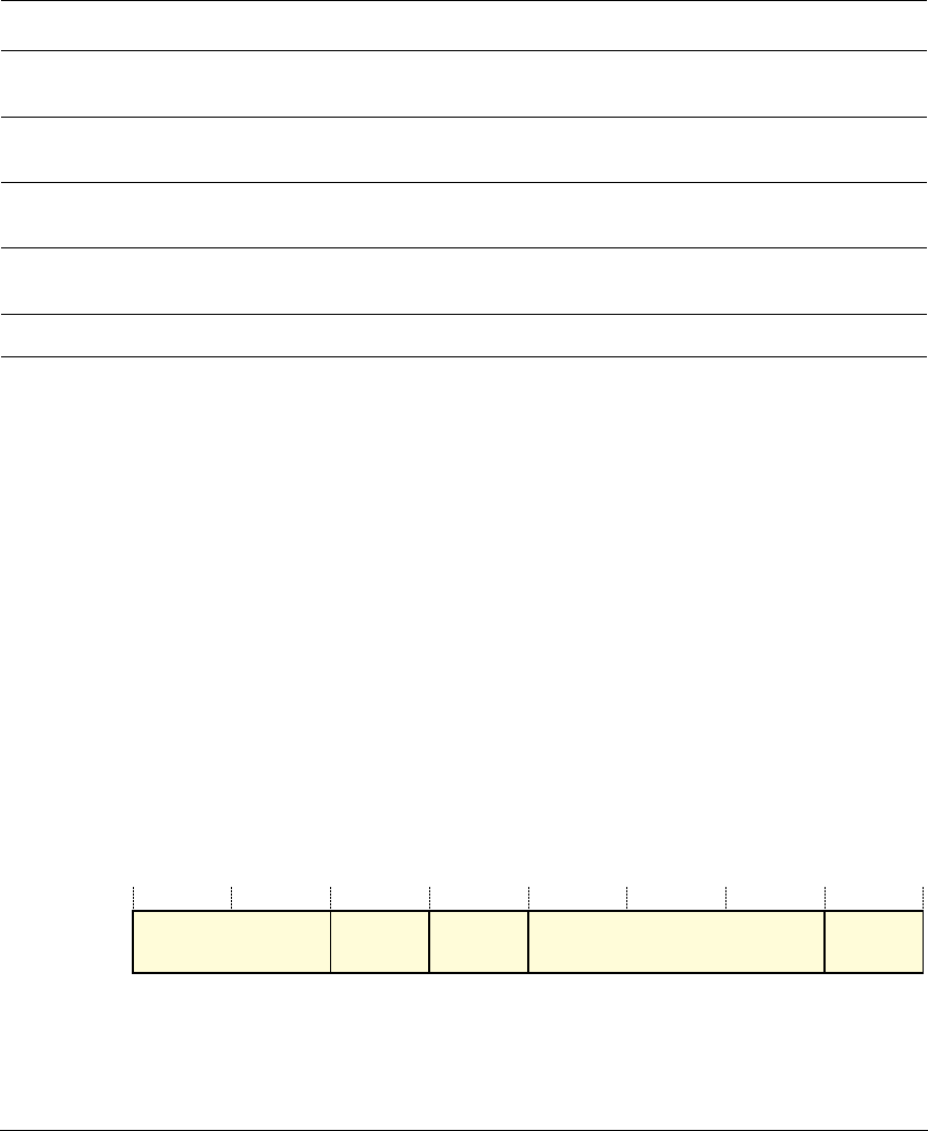
System Address Map
B3-264 Copyright © 2007-2008, 2010 ARM Limited. All rights reserved. ARM DDI 0419C
Non-Confidential ID092410
The remaining subsections of this section describe the SCB registers.
B3.2.3 CPUID Base Register
The CPUID Base Register characteristics are:
Purpose Provides identification information for the processor.
Usage constraints This register is word accessible only.
It is IMPLEMENTATION DEFINED whether the information defines the presence of any
architectural extension.
Configurations Always implemented.
Attributes See Table B3-4 on page B3-263.
Figure B3-1 shows the bit assignments.
Figure B3-1 CPUID Base Register bit assignments
0xE000ED14
CCR RO bits [9:3] =
0b1111111
Configuration and Control Register, CCR on
page B3-271
0xE000ED1C
SHPR2 RW
SBZ
bSystem Handler Priority Register 2, SHPR2 on
page B3-272
0xE000ED20
SHPR3 RW
SBZ
cSystem Handler Priority Register 3, SHPR3 on
page B3-273
0xE000ED24
SHCSR RW
0x00000000
System Handler Control and State Register, SHCSR on
page C1-329d
0xE000ED30
DFSR RW
0x00000000
Debug Fault Status Register, DFSR on page C1-330d
a. See register description for more information.
b. SVCall priority bits [31:30] are zero.
c. SysTick bits [31:30] and PendSV bits [23:22] are zero.
d. Included with the Debug Extension.
Table B3-4 System control and ID register summary (continued)
Address Name Type Reset Description
1 0 01IMPLEMENTER
31 24 23 20 19 16 15 4 3 0
VARIANT PARTNO REVISION
System Address Map
ARM DDI 0419C Copyright © 2007-2008, 2010 ARM Limited. All rights reserved. B3-265
ID092410 Non-Confidential
Table B3-5 shows the CPUID Base Register bit assignments.
B3.2.4 Interrupt Control State Register, ICSR
The ICSR characteristics are:
Purpose Controls and provides status information for the ARMv6-M.
Usage constraints There are no usage constraints.
Configurations Always implemented.
Attributes See Table B3-4 on page B3-263.
Figure B3-2 shows the ICSR bit assignments.
Figure B3-2 ICSR bit assignments
Table B3-5 CPUID Base Register bit assignments
Bits Name Function
[31:24] IMPLEMENTER This field defines the implementer:
0x41
ARM Limited. This is ASCII character A.
[23:20] VARIANT IMPLEMENTATION DEFINED.
[19:16] ARCHITECTURE This field defines the architecture:
0xC
ARMv6-M.
[15:4] PARTNO IMPLEMENTATION DEFINED.
[3:0] REVISION IMPLEMENTATION DEFINED.
31 30 29 28 27 26 25 24 23 22 21 20 12 11 9 8 0
VECTPENDING VECTACTIVE
Reserved
ISRPENDING
ISRPREEMPT
Reserved
PENDSTCLRPENDSTSET
PENDSVCLR
PENDSVSET
Reserved
NMIPENDSET
Reserved

System Address Map
B3-266 Copyright © 2007-2008, 2010 ARM Limited. All rights reserved. ARM DDI 0419C
Non-Confidential ID092410
Table B3-6 shows the ICSR bit assignments.
Table B3-6 ICSR bit assignments
Bits Type Name Function
[31] RW NMIPENDSET Activates an NMI exception or reads back the current state:
0 Do not activate.
1 Activate NMI exception.
Because NMI is the highest priority exception, it activates as soon as it is
registered.
[30:29] - - Reserved.
[28] RW PENDSVSETaSets a pending PendSV interrupt or reads back the current state:
0 Do not set.
1 Set pending PendSV interrupt.
Use this normally to request a context switch.
[27] WO PENDSVCLR Clears a pending PendSV interrupt:
0 Do not clear.
1 Clear pending PendSV.
[26] RW PENDSTSETbSets a pending SysTick or reads back the current state:
0 Do not set.
1 Set pending SysTick.
When SysTick is not implemented, this bit is RAZ/WI.
[25] WO PENDSTCLR Clears a pending SysTick, whether set here or by the timer hardware:
0 Do not clear.
1 Clear pending SysTick.
When SysTick is not implemented, this bit is reserved.
[24] - - Reserved.
[23] RO ISRPREEMPT Indicates whether a pending exception will be serviced on exit from debug
halt state:
0 Will not service.
1 Will service a pending exception.
This bit applies to the Debug Extension only, otherwise it is reserved.
[22] RO ISRPENDING Indicates if an external configurable, NVIC generated, interrupt is pending:
0 Interrupt is not pending.
1 Interrupt is pending.
This bit applies to the Debug Extension only, otherwise it is reserved.
System Address Map
ARM DDI 0419C Copyright © 2007-2008, 2010 ARM Limited. All rights reserved. B3-267
ID092410 Non-Confidential
B3.2.5 Vector Table Offset Register, VTOR
The VTOR characteristics are:
Purpose Holds the vector table offset address.
Usage constraints The number of bits in the VTOR is IMPLEMENTATION DEFINED. Unimplemented bits
are RAZ/WI.
Configurations The VTOR behavior is IMPLEMENTATION DEFINED.
Attributes See Table B3-4 on page B3-263.
An implementation can include configuration input signals that determine the reset
value of the TBLOFF field, otherwise it resets to zero.
Figure B3-3 shows the VTOR bit assignments.
Figure B3-3 VTOR bit assignments
[21] - - Reserved.
[20:12] RO VECTPENDING The exception number for the highest priority pending exception.
0 No pending exceptions.
The pending state includes the effect of memory-mapped enable and mask
registers. It does not include the PRIMASK special-purpose register
qualifier.
[11:9] - - Reserved.
[8:0] RO VECTACTIVE The exception numberc for the current executing exception.
0 Thread mode.
This field applies to the Debug Extension only, otherwise it is reserved.
a. writing PENDSVSET and PENDSVCLR to '1' concurrently is UNPREDICTABLE
b. writing PENDSTSET and PENDSTCLR to '1' concurrently is UNPREDICTABLE
c. this is the same value as IPSR[8:0]
Table B3-6 ICSR bit assignments (continued)
Bits Type Name Function
TBLOFF
31 76 0
Reserved
System Address Map
B3-268 Copyright © 2007-2008, 2010 ARM Limited. All rights reserved. ARM DDI 0419C
Non-Confidential ID092410
Table B3-7 shows the VTOR bit assignments.
Note
All bits of the Vector table address that are not defined by the VTOR are zero.
Software can write all 1s to the TBLOFF field and then read the register to find the maximum supported
offset value.
B3.2.6 Application Interrupt and Reset Control Register, AIRCR
The AIRCR Register characteristics are:
Purpose Sets or returns interrupt control data.
Usage constraints There are no usage constraints.
Configurations Always implemented.
Attributes See Table B3-4 on page B3-263.
Figure B3-4 shows the AIRCR bit assignments.
Figure B3-4 AIRCR bit assignments
Table B3-7 VTOR bit assignments
Bits Name Function
[31:7] TBLOFF Table offset addressa
a. The number of implemented bits within
TBLOFF are IMPLEMENTATION DEFINED.
[6:0] - Reserved
VECTKEY
VECTKEYSTAT
31 16 15 14 3 2 1 0
Reserved
ENDIANESS
VECTCLRACTIVE
SYSRESETREQ
Reserved

System Address Map
ARM DDI 0419C Copyright © 2007-2008, 2010 ARM Limited. All rights reserved. B3-269
ID092410 Non-Confidential
Table B3-8 shows the AIRCR bit assignments.
B3.2.7 System Control Register, SCR
The SCR characteristics are:
Purpose Sets or returns system control data.
Usage constraints There are no usage constraints.
Table B3-8 AIRCR bit assignments
Bits Type Name Function
[31:16] WO VECTKEY Vector Key. The value
0x05FA
must be written to this register, otherwise
the register write is
UNPREDICTABLE
.
[31:16] RO VECTKEYSTAT UNKNOWN
[15] RO ENDIANNESS Indicates the memory system data endianness:
0 little endian
1 big endian.
See Endian support on page A3-44 for more information.
[14:3] - - Reserved
[2] WO SYSRESETREQ System Reset Request:
0 do not request a reset.
1 request reset.
Writing 1 to this bit asserts a signal to request a reset by the external
system. The system components that are reset by this request are
IMPLEMENTATION DEFINED. A Local reset is required as part of a system
reset request.
A Local reset clears this bit to 0.
See Reset management on page B1-240 for more information.
[1] WO VECTCLRACTIVE Clears all active state information for fixed and configurable
exceptions:
0 do not clear state information.
1 clear state information.
The effect of writing a 1 to this bit if the processor is not halted in Debug
state is UNPREDICTABLE.
[0] - - Reserved
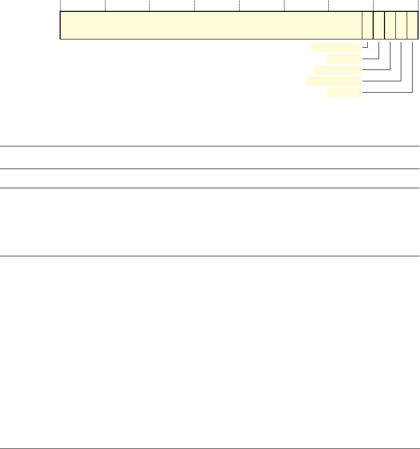
System Address Map
B3-270 Copyright © 2007-2008, 2010 ARM Limited. All rights reserved. ARM DDI 0419C
Non-Confidential ID092410
Configurations The System Control Register is required when power management support is
implemented in the
WFI
and
WFE
hint instructions. See WFE on page A6-197 and WFI
on page A6-198.
Attributes See Table B3-4 on page B3-263.
Figure B3-5 shows the SCR bit assignments.
Figure B3-5 SCR bit assignments
Table B3-9 SCR bit assignments
Bits Name Function
[31:5] - Reserved.
[4] SEVONPEND Determines whether an interrupt transition from inactive state to pending state is a
wakeup event:
0 transitions from inactive to pending are not wakeup events.
1 transitions from inactive to pending are wakeup events.
See WFE on page A6-197 for more information.
[3] - Reserved.
Reserved
31 543210
SEVONPEND
Reserved
SLEEPDEEP
SLEEPONEXIT
Reserved
System Address Map
ARM DDI 0419C Copyright © 2007-2008, 2010 ARM Limited. All rights reserved. B3-271
ID092410 Non-Confidential
A debugger can read S_SLEEP to detect if sleeping. See Debug Halting Control and Status Register,
DHCSR on page C1-331 for more information.
B3.2.8 Configuration and Control Register, CCR
The CCR Register characteristics are:
Purpose Returns configuration and control data.
Usage constraints This register is RO.
Configurations Always implemented.
Attributes See Table B3-4 on page B3-263.
Figure B3-6 shows the CCR bit assignments.
Figure B3-6 CCR bit assignments
[2] SLEEPDEEP Provides a qualifying hint indicating that waking from sleep might take longer. An
implementation can use this bit to select between two alternative sleep states:
0 selected sleep state is not deep sleep.
1 selected sleep state is deep sleep.
Details of the implemented sleep states, if any, and details of the use of this bit, are
IMPLEMENTATION DEFINED.
If the processor does not implement a deep sleep state then this bit can be RAZ/WI
[1] SLEEPONEXIT Determines whether, on an exit from an ISR that returns to the base level of execution
priority, the processor enters a sleep state:
0 do not enter sleep state.
1 enter sleep state.
See Power management on page B1-240 for more information.
[0] - Reserved.
Table B3-9 SCR bit assignments (continued)
Bits Name Function
Reserved
31 10 9 8 4 3 2 0
Reserved
STKALIGN UNALIGN_TRP
Reserved
System Address Map
B3-272 Copyright © 2007-2008, 2010 ARM Limited. All rights reserved. ARM DDI 0419C
Non-Confidential ID092410
Table B3-10 shows the CCR bit assignments.
B3.2.9 System Handler Priority Register 2, SHPR2
The SHPR2 Register characteristics are:
Purpose Sets or returns priority for system handler 11.
Usage constraints There are no usage constraints.
Configurations Always implemented.
Attributes See Table B3-4 on page B3-263.
Figure B3-7 shows the SHPR2 bit assignments.
Figure B3-7 SHPR2 Register bit assignments
Table B3-10 CCR bit assignments
Bits Name Function
[31:10] - Reserved.
[9] STKALIGN Read-As-One
1 On exception entry, the SP used prior to the exception is adjusted to
be 8-byte aligned and the context to restore it is saved. The SP is
restored on the associated exception return.
[8:4] - Reserved.
[3] UNALIGN_TRP Read-As-One
1 unaligned word and halfword accesses generate a HardFault
exception.
[2:0] - Reserved.
31 30 29 0
Reserved
PRI_11
System Address Map
ARM DDI 0419C Copyright © 2007-2008, 2010 ARM Limited. All rights reserved. B3-273
ID092410 Non-Confidential
Table B3-11 shows the SHPR2 bit assignments.
B3.2.10 System Handler Priority Register 3, SHPR3
The SHPR2 Register characteristics are:
Purpose Sets or returns priority for system handlers 14-15.
Usage constraints There are no usage constraints.
Configurations Bits[31:30] are only implemented if the system timer, SysTick is used.
Attributes See Table B3-4 on page B3-263.
Figure B3-8 shows the SHPR2 bit assignments.
Figure B3-8 SHPR3 Register bit assignments
Table B3-12 shows the SHPR3 bit assignments.
B3.2.11 Fault Status Registers
ARMv6-M only supports fault status information as part of the Debug Extension.
Table B3-11 SHPR2 Register bit assignments
Bits Name Function
[31:30] PRI_11 Priority of system handler 11, SVCall
[29:0] - Reserved
ReservedReserved
31 24 2330 0
PRI_14
2229 21
PRI_15
Table B3-12 SHPR3 Register bit assignments
Bits Name Function
[31:30] PRI_15 Priority of system handler 15, SysTick
[29:24] - Reserved
[23:2] PRI_14 Priority of system handler 14, PendSV
[21:0] - Reserved

System Address Map
B3-274 Copyright © 2007-2008, 2010 ARM Limited. All rights reserved. ARM DDI 0419C
Non-Confidential ID092410
The Debug Fault Status Register, DFSR, is part of the Debug Extension. See Chapter C1 ARMv6-M Debug
for a full description of debug support within ARMv6-M and Debug Fault Status Register, DFSR on
page C1-330 for the Debug Fault Status Register.
B3.2.12 The Auxiliary Control Register, ACTLR
The ACTLR Register characteristics are:
Purpose Provides IMPLEMENTATION DEFINED configuration and control options.
Usage constraints The contents of this register might have IMPLEMENTATION DEFINED usage
constraints.
Configurations Always implemented. The contents of this register are IMPLEMENTATION DEFINED.
Attributes See Table B3-4 on page B3-263.

System Address Map
ARM DDI 0419C Copyright © 2007-2008, 2010 ARM Limited. All rights reserved. B3-275
ID092410 Non-Confidential
B3.3 The system timer, SysTick
ARMv6-M supports an optional system timer, SysTick. SysTick provides a simple, 24-bit clear-on-write,
decrementing, wrap-on-zero counter with a flexible control mechanism. A system can use this counter in
several different ways, including:
• As an RTOS tick timer that fires at a programmable rate, such as 100Hz, and invokes a SysTick
routine.
• As a high speed alarm timer using the main processor clock.
• As a variable rate alarm or signal timer. The available duration range depends on the reference clock
used and the dynamic range of the counter.
• As a simple counter. Software can use this to measure time to completion and time used.
• As an internal clock source control based on missing or meeting durations. Software can use the
COUNTFLAG field in the control and status register to determine whether an action completed
within a particular duration, as part of a dynamic clock management control loop.
B3.3.1 SysTick operation
The timer consists of four registers:
• A control and status register. This configures the SysTick clock, enables the counter, enables the
SysTick interrupt, and indicates the counter status.
• A counter reload value register.This provides the wrap value for the counter.
• A counter current value register.
• A calibration value register. This indicates the preload value required for a 10ms system clock.
When enabled, the timer counts down from the value in SYST_CVR, see SysTick Current Value Register,
SYST_CVR on page B3-279. When the counter reaches zero, it reloads the value in SYST_RVR on the next
clock edge, see SysTick Reload Value Register, SYST_RVR on page B3-278. It then decrements on
subsequent clocks. This reloading when the counter reaches zero is called wrapping.
When the counter transitions to zero, it sets the COUNTFLAG status bit to 1. Reading the COUNTFLAG
status bit clears it to 0.
Writing to SYST_CVR clears both the register and the COUNTFLAG status bit to zero. This causes the
SysTick logic to reload SYST_CVR from SYST_RVR on the next timer clock. A write to SYST_CVR does
not trigger the SysTick exception logic.
Reading SYST_CVR returns the value of the counter at the time the register is accessed.
Writing a value of zero to SYST_RVR disables the counter on the next wrap. The SysTick counter logic
maintains this counter value of zero after the wrap.

System Address Map
B3-276 Copyright © 2007-2008, 2010 ARM Limited. All rights reserved. ARM DDI 0419C
Non-Confidential ID092410
Note
• Setting SYST_RVR to zero has the effect of disabling the SysTick counter on the next wrap,
independently of the counter enable bit.
• The SYST_CVR value is UNKNOWN on reset. Before enabling the SysTick counter, software must
write the required counter value to SYST_RVR, and then write to SYST_CVR. This clears
SYST_CVR to zero. When enabled, the counter reloads the value from SYST_RVR, and counts
down from that value, rather than from an arbitrary value.
Software can use the calibration value TENMS to scale the counter to other required clock rates within the
dynamic range of the counter.
When the processor is halted in Debug state, the counter does not decrement.
The timer is clocked by a reference clock. Whether the reference clock is the processor clock or an external
clock source is IMPLEMENTATION DEFINED. If an implementation uses an external clock, it must document
the relationship between the processor clock and the external reference. This is required for system timing
calibration, taking account of metastability, clock skew and jitter.
B3.3.2 System timer register support in the SCS
Table B3-13 summarizes the system timer register support provided within the SCS address map. The
SysTick system timer is an optional feature. If SysTick is not implemented, the SysTick registers are
reserved.
Table B3-13 SysTick register summary
Address Name Type Reset Description
0xE000E010
SYST_CSR RW
0x00000000
or
0x00000004
SysTick Control and Status Register, SYST_CSR
on page B3-277
0xE000E014
SYST_RVR RW UNKNOWN SysTick Reload Value Register, SYST_RVR on
page B3-278
0xE000E018
SYST_CVR RW UNKNOWN SysTick Current Value Register, SYST_CVR on
page B3-279
0xE000E01C
SYST_CALIB RO IMPLEMENTATION
DEFINED
SysTick Current Value Register, SYST_CVR on
page B3-279
…to
0xE000E0FF
- - - Reserved
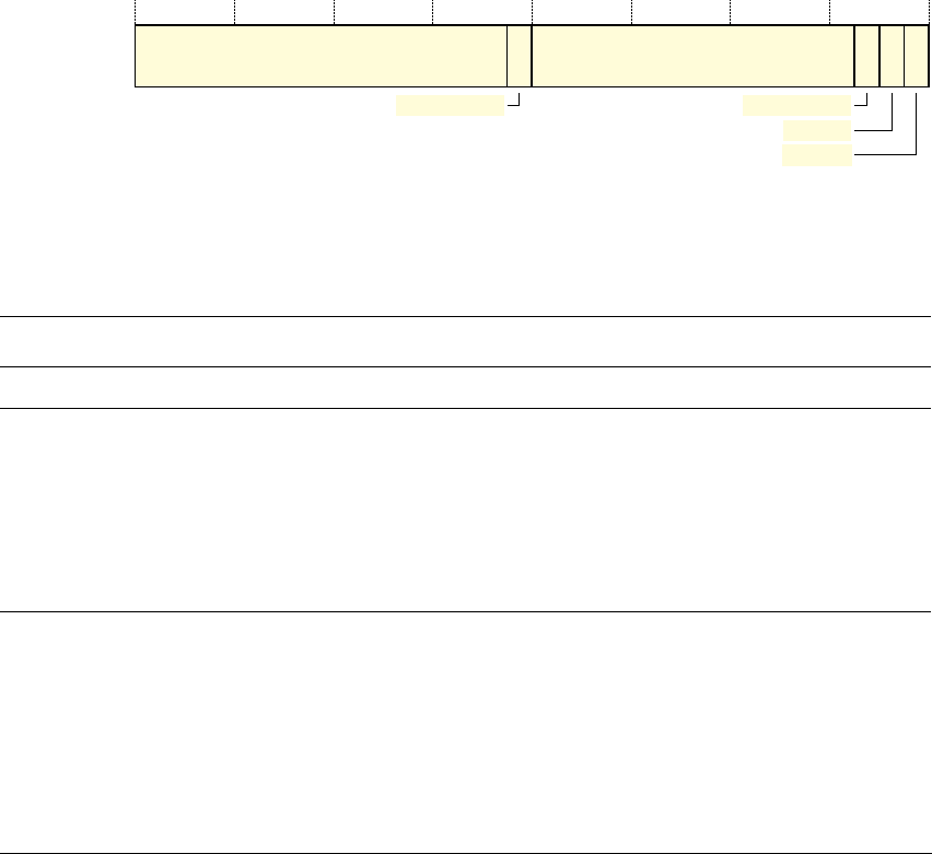
System Address Map
ARM DDI 0419C Copyright © 2007-2008, 2010 ARM Limited. All rights reserved. B3-277
ID092410 Non-Confidential
B3.3.3 SysTick Control and Status Register, SYST_CSR
The SYST_CSR Register characteristics are:
Purpose Controls the system timer and provides status data.
Usage constraints There are no usage constraints.
Configurations The register is only present if the optional system timer is implemented, otherwise
the register is reserved
Attributes See Table B3-13 on page B3-276.
Figure B3-9 shows the SYST_CSR bit assignments.
Figure B3-9 SYST_CSR bit assignments
Table B3-14 shows the SYST_CSR bit assignments.
Reserved
31 17 16 15 3 2 1 0
Reserved
TICKINT
CLKSOURCE
ENABLE
COUNTFLAG
Table B3-14 SYST_CSR bit assignments
Bits TYPE Name Function
[31:17] - - Reserved.
[16] RO COUNTFLAG Indicates whether the counter has counted to 0 since the last read of this
register:
0 timer has not counted to 0.
1 timer has counted to 0.
COUNTFLAG is set to 1 by a count transition from 1 to 0.
COUNTFLAG is cleared to 0 by a read of this register, and by any write to
the Current Value register.
[15:3] - - Reserved.
System Address Map
B3-278 Copyright © 2007-2008, 2010 ARM Limited. All rights reserved. ARM DDI 0419C
Non-Confidential ID092410
B3.3.4 SysTick Reload Value Register, SYST_RVR
The SYST_RVR Register characteristics are:
Purpose Sets or reads the reload value of the SYST_CVR register.
Usage constraints There are no usage constraints.
Configurations The register is only present if the optional system timer is implemented, otherwise
the register is reserved
Attributes See Table B3-15 on page B3-279.
Figure B3-10 shows the SYST_RVR bit assignments.
Figure B3-10 SYST_RVR bit assignments
[2] RW CLKSOURCE Indicates the SysTick clock source:
0 SysTick uses the optional external reference clock.
1 SysTick uses the processor clock.
If no external clock is provided, this bit reads as one and ignores writes.
[1] RW TICKINT Indicates whether counting to 0 causes the status of the SysTick exception to
change to pending:
0 count to 0 does not affect the SysTick exception status.
1 count to 0 changes the SysTick exception status to pending.
Changing the value of the counter to 0 by writing zero to the SysTick Current
Value register to 0 never changes the status of the SysTick exception.
[0] RW ENABLE Indicates the enabled status of the SysTick counter:
0 counter is disabled.
1 counter is operating.
Table B3-14 SYST_CSR bit assignments (continued)
Bits TYPE Name Function
Reserved
31 24 23 0
RELOAD

System Address Map
ARM DDI 0419C Copyright © 2007-2008, 2010 ARM Limited. All rights reserved. B3-279
ID092410 Non-Confidential
Table B3-15 shows the SYST_RVR bit assignments.
B3.3.5 SysTick Current Value Register, SYST_CVR
The SYST_CVR Register characteristics are:
Purpose Reads or clears the current counter value.
Usage constraints Any write to the register clears the register to 0.
The counter does not provide read-modify-write protection.
Unsupported bits are Read-As-Zero. See SysTick Reload Value Register, SYST_RVR
on page B3-278.
Configurations The register is only present if the optional system timer is implemented, otherwise
the register is reserved
Attributes See Table B3-16.
Figure B3-11 shows the SYST_CVR bit assignments.
Figure B3-11 SYST_CVR bit assignments
Table B3-16 shows the SYST_CVR bit assignments.
Table B3-15 SYST_RVR bit assignments
Bits Name Function
[31:24] - Reserved. RAZ/WI.
[23:0] RELOAD The value to load into the SYST_CVR register when the counter reaches 0.
Reserved CURRENT
31 0
2324
Table B3-16 SYST_CVR bit assignments
Bits Name Function
[31:24] - Reserved. RAZ/WI
[23:0] CURRENT Current counter value.
This is the value of the counter at the time it is sampled.
System Address Map
B3-280 Copyright © 2007-2008, 2010 ARM Limited. All rights reserved. ARM DDI 0419C
Non-Confidential ID092410
B3.3.6 SysTick Calibration Value Register, SYST_CALIB
The SYST_CALIB Register characteristics are:
Purpose Reads the calibration value and parameters for SysTick.
Usage constraints There are no usage constraints.
Configurations The register is only present if the optional system timer is implemented, otherwise
the register is reserved
Attributes See Table B3-17.
Figure B3-12 shows the SYST_CALIB bit assignments.
Figure B3-12 SYST_CALIB Register bit assignments
Table B3-17 shows the SYST_CALIB bit assignments.
31 30 29 24 23 0
Reserved TENMS
NOREF
SKEW
Table B3-17 SYST_CALIB Register bit assignments
Bits Name Function
[31] NOREF Indicates whether the IMPLEMENTATION DEFINED reference clock is provided:
0 the reference clock is implemented.
1 the reference clock is not implemented.
When this bit is 1, the CLKSOURCE bit of the SYST_CSR register is forced to 1 and cannot
be cleared to 0.
[30] SKEW Indicates whether the 10ms calibration value is exact:
0 10ms calibration value is exact.
1 10ms calibration value is inexact, because of the clock frequency.
[29:24] - Reserved
[23:0] TENMS Optionally, holds a reload value to be used for 10ms (100Hz) timing, subject to system clock
skew errors. If this field is zero, the calibration value is not known.

System Address Map
ARM DDI 0419C Copyright © 2007-2008, 2010 ARM Limited. All rights reserved. B3-281
ID092410 Non-Confidential
B3.4 Nested Vectored Interrupt Controller, NVIC
ARMv6-M provides an interrupt controller as an integral part of the exception model. The interrupt
controller operation aligns with the ARM General Interrupt Controller (GIC) specification, defined for use
with other architecture variants and ARMv7 profiles.
The ARMv6-M NVIC architecture supports up to 32 discrete interrupts, IRQ[31:0]. The general registers
associated with the NVIC are all accessible from a block of memory in the SCS as described in Table B3-18
on page B3-283.
B3.4.1 NVIC operation
ARMv6-M supports level-sensitive and pulse-sensitive, a variant of an edge sensitive, interrupt behavior.
This means that both level-sensitive and pulse-sensitive interrupts can be handled. Pulse interrupt sources
must be held long enough to be sampled reliably by the processor clock to ensure they are latched and
become pending. A subsequent pulse can add the pending state to an active interrupt, making the status of
the interrupt active and pending. However, multiple pulses that occur during the active period only register
as a single event for interrupt scheduling.
In summary:
• Pulses held for a clock period act like edge-sensitive interrupts. These can become pending again
while the interrupt is active.
Note
A pulse must be cleared before the assertion of AIRCR.VECTCLRACTIVE or the associated
exception return, otherwise the interrupt signal behaves as a level-sensitive input and the pending bit
is asserted again.
• Level-sensitive interrupts become pending and activate the interrupt. The ISR then accesses the
peripheral, causing it to deassert the interrupt. If the interrupt is still asserted on return from the ISR,
it becomes pending again.
All NVIC interrupts have a programmable priority value and an associated exception number as part of the
ARMv6-M exception model and its prioritization policy.
The NVIC supports the following features:
• NVIC interrupts can be enabled and disabled by writing to their corresponding Interrupt Set-Enable
or Interrupt Clear-Enable register bit-field. The registers use a write-1-to-enable and write-1-to-clear
policy, both registers reading back the current enabled state of the corresponding 32 interrupts.
When an interrupt is disabled, interrupt assertion causes the interrupt to become pending, but the
interrupt does not activate. If an interrupt is active when it is disabled, it remains in the active state
until this is cleared by a reset or an exception return. Clearing the enable bit prevents any new
activation of the associated interrupt.
An implementation can hard-wire interrupt enable bits to zero if the associated interrupt line does not
exist, or hard-wire them to one if the associated interrupt line cannot be disabled.

System Address Map
B3-282 Copyright © 2007-2008, 2010 ARM Limited. All rights reserved. ARM DDI 0419C
Non-Confidential ID092410
• Software can set or remove the pending state of NVIC interrupts using a complementary pair of
registers, the Set-Pending Register and Clear-Pending Register. The registers use a
write-one-to-enable and write-one-to-clear policy, and a read of either register returns the current
pending state of the corresponding 32 interrupts. Writing 1 to a bit in the Clear-Pending Register has
no effect on the execution status of an active interrupt.
It is IMPLEMENTATION DEFINED for each interrupt line supported, whether an interrupt supports either
or both setting and clearing of the associated pending state under software control.
• NVIC interrupts are prioritized by updating an 8-bit field within a 32-bit register, with each register
supporting four interrupts. Priorities are maintained according to the ARMv6-M prioritization
scheme. See Exception priorities and preemption on page B1-221.
External interrupt input behavior
The following pseudocode describes the relationship between external interrupt inputs and the NVIC
behavior:
// Definitions
// ===========
NVIC[] is an array of active high external interrupt input signals;
// the type of signal (level or pulse) and its assertion level/sense is IMPLEMENTATION DEFINED
// and might not be the same for all inputs
boolean Edge(integer INTNUM); // Returns true if on a clock edge NVIC[INTNUM]
// has changed from '0' to '1'
boolean NVIC_Pending[INTNUM]; // an array of pending status bits for the external interrupts
integer INTNUM; // the external interrupt number
// The WriteToRegField helper function returns TRUE on a write of '1' event
// to the field FieldNumber of the RegName register.
boolean WriteToRegField(register RegName, integer FieldNumber)
boolean ExceptionIN(integer INTNUM); // returns TRUE if exception entry in progress
// to activate INTNUM
boolean ExceptionOUT(integer INTNUM); // returns TRUE if exception return in progress
// from active INTNUM
// Interrupt interface
// ===================
sampleInterruptHi = WriteToRegField(AIRCR, VECTCLRACTIVE) || ExceptionOUT(INTNUM);
sampleInterruptLo = WriteToRegField(ICPR, INTNUM);
InterruptAssertion = Edge(INTNUM) || (NVIC[INTNUM] && sampleInterruptHi);
InterruptDeassertion = !NVIC[INTNUM] && sampleInterruptLo;
// NVIC behavior
// =============

System Address Map
ARM DDI 0419C Copyright © 2007-2008, 2010 ARM Limited. All rights reserved. B3-283
ID092410 Non-Confidential
clearPend = ExceptionIN(INTNUM) || InterruptDeassertion;
setPend = InterruptAssertion || WriteToRegField(ISPR, INTNUM);
if clearPend && setPend then
IMPLEMENTATION DEFINED whether NVIC_Pending[INTNUM] is TRUE or FALSE;
else
NVIC_Pending[INTNUM] = setPend || (NVIC_Pending[INTNUM] && !clearPend);
B3.4.2 NVIC register support in the SCS
The system control region includes status and configuration registers that apply to the NVIC as part of the
general exception model.
All other external interrupt specific registers reside within the NVIC region of the SCS. Table B3-18
summarizes the NVIC specific registers in the SCS.
Table B3-18 NVIC register summary
Address Name Type Reset Description
0xE000E100
NVIC_ISER RW
0x00000000
Interrupt Set-Enable Register, NVIC_ISER on page B3-284
0xE000E104
-
0xE000E17F
- - - Reserved
0xE000E180
NVIC_ICER RW
0x00000000
Interrupt Clear Enable Register, NVIC_ICER on
page B3-285
0xE000E184
-
0xE000E1FF
- - - Reserved
0xE000E200
NVIC_ISPR RW
0x00000000
Interrupt Set-Pending Register, NVIC_ISPR on
page B3-286
0xE000E204
-
0xE000E27F
- - - Reserved
0xE000E280
NVIC_ICPR RW
0x00000000
Interrupt Clear-Pending Register, NVIC_ICPR on
page B3-287
0xE000E300
-
0xE000E3FC
- - - Reserved
0xE000E400
-
0xE000E41C
NVIC_IPRn RW
0x00000000
Interrupt Priority Registers, NVIC_IPR0 - NVIC_IPR7 on
page B3-288
0xE000E420-
0xE000E43C
- - - Reserved

System Address Map
B3-284 Copyright © 2007-2008, 2010 ARM Limited. All rights reserved. ARM DDI 0419C
Non-Confidential ID092410
B3.4.3 Interrupt Set-Enable Register, NVIC_ISER
The NVIC_ISER characteristics are:
Purpose Enables, or reads the enabled state of one or more interrupts.
Usage constraints Subject to standard PPB usage constraints, see General rules for PPB register
accesses on page B3-260.
Configurations Always implemented.
Attributes See Table B3-18 on page B3-283.
Figure B3-13 shows the NVIC_ISER bit assignments.
Figure B3-13 NVIC_ISER bit assignments
Table B3-19 shows the NVIC_ISER bit assignments.
SETENA
31 0
Table B3-19 NVIC_ISER bit assignments
Bits Name Function
[31:0] SETENA Enables, or reads the enabled state of one or more interrupts. Each bit corresponds to the same
numbered interrupt:
On reads 0 the associated interrupt is disabled.
1 the associated interrupt is enabled.
On writes 0 no effect.
1 enable the associated interrupt.

System Address Map
ARM DDI 0419C Copyright © 2007-2008, 2010 ARM Limited. All rights reserved. B3-285
ID092410 Non-Confidential
B3.4.4 Interrupt Clear Enable Register, NVIC_ICER
The NVIC_ICER characteristics are:
Purpose Disables, or reads the enabled state of one or more interrupts.
Usage constraints Subject to standard PPB usage constraints, see General rules for PPB register
accesses on page B3-260.
Configurations Always implemented.
Attributes See Table B3-18 on page B3-283.
Figure B3-14 shows the NVIC_ICER bit assignments.
Figure B3-14 NVIC_ICER bit assignments
Table B3-20 shows the NVIC_ICER bit assignments.
CLRENA
31 0
Table B3-20 NVIC_ICER bit assignments
Bits Name Function
[31:0] CLRENA Disables, or reads the enabled state of one or more interrupts. Each bit corresponds to the
same numbered interrupt:
On reads 0 the associated interrupt is disabled.
1 the associated interrupt is enabled.
On writes 0 no effect.
1 disable the associated interrupt.

System Address Map
B3-286 Copyright © 2007-2008, 2010 ARM Limited. All rights reserved. ARM DDI 0419C
Non-Confidential ID092410
B3.4.5 Interrupt Set-Pending Register, NVIC_ISPR
The NVIC_ISPR Register characteristics are:
Purpose On writes, sets the status of one or more interrupts to pending. On reads, shows the
pending status of the interrupts.
Usage constraints Subject to standard PPB usage constraints, see General rules for PPB register
accesses on page B3-260.
Configurations Always implemented.
Attributes See Table B3-18 on page B3-283.
Figure B3-15 shows the NVIC_ISPR bit assignments.
Figure B3-15 NVIC_ISPR bit assignments
Table B3-21 shows the NVIC_ISPR bit assignments.
SETPEND
31 0
Table B3-21 NVIC_ISPR bit assignments
Bits Name Function
[31:0] SETPEND Changes the state of one or more interrupts to pending. Each bit corresponds to the same
numbered interrupt:
On reads 0 the associated interrupt is not pending.
1 the associated interrupt is pending.
On writes 0 no effect.
1 change the state of the associated interrupt to pending.
System Address Map
ARM DDI 0419C Copyright © 2007-2008, 2010 ARM Limited. All rights reserved. B3-287
ID092410 Non-Confidential
B3.4.6 Interrupt Clear-Pending Register, NVIC_ICPR
The NVIC_ICPR Register characteristics are:
Purpose On writes, clears the status of one or more interrupts to pending. On reads, shows
the pending status of the interrupts.
Usage constraints Subject to standard PPB usage constraints, see General rules for PPB register
accesses on page B3-260.
Configurations Always implemented.
Attributes See Table B3-18 on page B3-283.
Figure B3-16 shows the NVIC_ICPR bit assignments.
Figure B3-16 NVIC_ICPR bit assignments
Table B3-22 shows the NVIC_ICPR bit assignments.
CLRPEND
31 0
Table B3-22 NVIC_ICPR bit assignments
Bits Name Function
[31:0] CLRPEND Changes the state of one or more interrupts to not pending. Each bit corresponds to the same
numbered interrupt:
On reads 0 the associated interrupt is not pending.
1 the associated interrupt is pending.
On writes 0 no effect.
1 change the state of the associated interrupt to not pending.
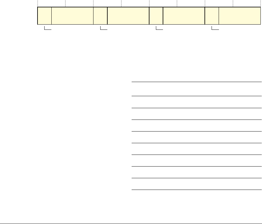
System Address Map
B3-288 Copyright © 2007-2008, 2010 ARM Limited. All rights reserved. ARM DDI 0419C
Non-Confidential ID092410
B3.4.7 Interrupt Priority Registers, NVIC_IPR0 - NVIC_IPR7
The NVIC_IPR characteristics are:
Purpose Sets or reads interrupt priorities
Usage constraints Subject to standard PPB usage constraints, see General rules for PPB register
accesses on page B3-260.
Configurations Eight NVIC_IPRs are implemented, supporting up to 32 interrupts. These registers
are always implemented.
If an interrupt is not implemented, the corresponding PRI_Nx field can be RAZ/WI.
Attributes See Table B3-18 on page B3-283.
Figure B3-17 shows the NVIC_IPR bit assignments.
Figure B3-17 NVIC_IPRn bit assignments
Table B3-23 shows the NVIC_IPR bit assignments. In the table, N = 4n, where n is the NVIC_IPR register
number. For example, for NVIC_IPR2, n is 2 and N is 8.
31 30 29 24 23 22 21 16 15 14 13 8 7 6 5 0
RAZ/WI RAZ/WI RAZ/WI RAZ/WI
PRI_N3 PRI_N2 PRI_N1 PRI_N0
Table B3-23 NVIC_IPRn bit assignments
Bits Name Function
[31:30] PRI_N3 Priority of interrupt number N+3
[29:24] - Reserved, RAZ/WI
[23:22] PRI_N2 Priority of interrupt number N+2
[21:16] - Reserved, RAZ/WI
[15:14] PRI_N1 Priority of interrupt number N+1
[13:8] - Reserved, RAZ/WI
[7:6] PRI_N0 Priority of interrupt number N
[5:0] - Reserved, RAZ/WI

System Address Map
ARM DDI 0419C Copyright © 2007-2008, 2010 ARM Limited. All rights reserved. B3-289
ID092410 Non-Confidential
B3.5 Protected Memory System Architecture, PMSAv6
ARMv6-M supports the Protected Memory System Architecture (PMSAv6) as an optional extension. A
Memory Protection Unit (MPU) implements PMSA to protect the system address space by dividing the
memory into regions and controlling access rights.
The number of supported regions is IMPLEMENTATION DEFINED. PMSAv6 can support subregions as small
as 32 bytes, but the limited register resources in the 4GB address space mean the MPU provides an
inherently coarse-grained protection scheme. The scheme is completely predictive, with all control
information held in registers that are closely-coupled to the processor.
It is IMPLEMENTATION DEFINED whether a processor includes the PMSAv6 Extension, but if it does, it must
also implement the Unprivileged/Privileged Extension. If a processor implements the PMSA Extension, the
MPU coexists with the system memory map described in The system address map on page B3-258 as
described in this section.
The MPU controls access rights to physical addresses. It does not perform address translation.
When the MPU is disabled or not present, the system uses the default system memory map shown in
Table B3-1 on page B3-259. When the MPU is enabled, the enabled regions define the system address map
with the following restrictions:
• Accesses to the PPB always uses the default system memory map.
• Exception vector reads from the Vector Address Table always use the default system memory map.
• The architecture restricts how the MPU can change the default system memory map attributes for
regions in System space, that is, for addresses
0xE0000000
and higher, as follows:
— System space is always XN, Execute Never
— the MPU can map System space regions that default to Device memory as Strongly-Ordered
memory
— the effect of remapping a System space region that defaults to Device memory as Normal
memory is UNPREDICTABLE.
• When the MPU is enabled, the processor can be configured to use the default system memory map
when processing NMI and HardFault exceptions.
• the default system memory map can be configured to provide a background region for privileged
accesses. The background region acts as region number -1 and all memory regions configured in the
MPU have higher priority than the default memory map.
• A memory access to an address that matches in more than one region uses the highest matching
region number for the access attributes.
• A memory access that does not match all access conditions of a region address match, with the MPU
enabled, or a background or default memory map match, generates a fault.

System Address Map
B3-290 Copyright © 2007-2008, 2010 ARM Limited. All rights reserved. ARM DDI 0419C
Non-Confidential ID092410
B3.5.1 PMSAv6 MPU operation
ARMv6-M only supports a unified memory model. All enabled regions provide support for instruction and
data accesses. ARMv6-M does not support memory maps that are defined independently for instruction and
data accesses. However, privileged software can use the XN attribute in the MPU_RASR to specify whether
the processor can execute instructions from each region, see MPU Region Attribute and Size Register,
MPU_RASR on page B3-298.
Privileged software can configure the base address, size and attributes of a region, but all regions must be
naturally aligned.
The size of memory regions, in bytes, is a power of 2. The supported sizes are 2N, where 8 ≤ N ≤ 32. Where
there is an overlap between two regions, the region with the highest region number takes priority.
Sub-region support
The MPU can divide each region into eight sub-regions of size 2(N-3) and disable the sub-regions on an
individual basis. When the processor generates a memory access, the MPU compares the requested memory
address with the programmed memory regions When a sub-region is disabled, an access match is required
from another region, or background matching if enabled. If an access match does not occur a fault is
generated. See MPU Region Attribute and Size Register, MPU_RASR on page B3-298.
MPU pseudocode
The following pseudocode defines the operation of an ARMv6-M MPU. The terms used align with the MPU
register names and bit field names described in Register support for PMSAv6 in the SCS on page B3-293.
Access permission checking on page B2-252 defines the
CheckPermission()
function.
// ValidateAddress()
// =================
AddressDescriptor ValidateAddress(bits(32) address, boolean ispriv, boolean iswrite,
boolean isinstrfetch)
boolean isvectortablelookup; // TRUE if address associated with exception entry
AddressDescriptor result;
Permissions perms;
result.physicaladdress = address;
result.memattrs = DefaultMemoryAttributes(address);
perms = DefaultPermissions(address);
hit = FALSE; // assume no valid MPU region and not using default memory map
isPPBaccess = (address<31:20> == '111000000000');
if isvectortablelookup || isPPBaccess then
hit = TRUE; // use default map for PPB and vector table lookups
elsif MPU_CTRL.ENABLE == '0' then

System Address Map
ARM DDI 0419C Copyright © 2007-2008, 2010 ARM Limited. All rights reserved. B3-291
ID092410 Non-Confidential
if MPU_CTRL.HFNMIENA == '1' then UNPREDICTABLE
else hit = TRUE; // always use default map if MPU disabled
elsif MPU_CTRL.HFNMIENA == '0' && (ExecutionPriority() < 0) then
hit = TRUE; // optionally use default for HardFault and NMI
else // MPU is enabled so check each individual region
if (MPU_CTRL.PRIVDEFENA == '1') && ispriv then
hit = TRUE; // optional default as background for Privileged accesses
for r = 0 to (UInt(MPU_TYPE.DREGION) - 1) // highest matching region wins
bits(16) size_enable = MPU_RASR[r]<15:0>;
bits(32) base_address = MPU_RBAR[r];
bits(16) access_control = MPU_RASR[r]<31:16>;
if size_enable<0> == '1' then // MPU region enabled so perform checks
lsbit = UInt(size_enable<5:1>) + 1;
if lsbit < 8 then UNPREDICTABLE;
if lsbit == 32 || address<31:lsbit> == base_address<31:lsbit> then
subregion = UInt(address<lsbit-1:lsbit-3>);
if size_enable<subregion+8> == '0' then
texcb = access_control<5:3,1:0>;
S = access_control<2>;
perms.ap = access_control<10:8>;
perms.xn = access_control<12>;
result.memattrs = DefaultTEXDecode(texcb,S);
hit = TRUE;
if address<31:29> == '111' then // enforce System space execute never
perms.xn = TRUE;
if hit then // perform check of acquired access permissions
CheckPermission(perms, address, iswrite, ispriv, isinstrfetch);
else // take HardFault if no MPU match or use of default not enabled
ExceptionTaken(Hardfault);
return result;
// DefaultTEXDecode()
// ==================
MemoryAttributes DefaultTEXDecode(bits(5) texcb, bit S)
MemoryAttributes memattrs;
case texcb of
when '00000'
memattrs.type = MemType_StronglyOrdered;
memattrs.innerattrs = '00'; // Non-cacheable
memattrs.shareable = TRUE;
when '00001'
memattrs.type = MemType_Device;

System Address Map
B3-292 Copyright © 2007-2008, 2010 ARM Limited. All rights reserved. ARM DDI 0419C
Non-Confidential ID092410
memattrs.innerattrs = '00'; // Non-cacheable
memattrs.shareable = TRUE;
when '0001x'
memattrs.type = MemType_Normal;
memattrs.innerattrs = texcb<1:0>;
memattrs.shareable = (S == '1');
otherwise
UNPREDICTABLE; // reserved cases
// Outer attributes are the same as the inner attributes in all cases.
memattrs.outerattrs = memattrs.innerattrs;
return memattrs;
MPU fault support
Instruction or data access violations cause a HardFault exception to be generated, see Fault behavior on
page B1-236.

System Address Map
ARM DDI 0419C Copyright © 2007-2008, 2010 ARM Limited. All rights reserved. B3-293
ID092410 Non-Confidential
B3.5.2 Register support for PMSAv6 in the SCS
The MPU registers are located in the SCS. All of these registers are 32-bits wide and are word accessible
only and their addresses are mapped as little endian.
The MPU registers require privileged memory accesses for reads and writes. Any unprivileged access
generates a HardFault.
If an ARMv6-M implementation does not support PMSAv6, only the MPU Type Register is required. The
MPU Control Register is RAZ/WI, and all other registers in this region are reserved, UNK/SBZP.
Table B3-24 shows the MPU registers.
Table B3-24 MPU register summary
Address Name Type Reset Description
0xE000ED90
MPU_TYPE RO IMPLEMENTATION
DEFINED
MPU Type Register, MPU_TYPE on page B3-294
0xE000ED94
MPU_CTRL RW 0x00000000 MPU Control Register, MPU_CTRL on
page B3-295
0xE000ED98
MPU_RNR RW UNKNOWN MPU Region Number Register, MPU_RNR on
page B3-296
0xE000ED9C
MPU_RBAR RW UNKNOWN MPU Region Base Address Register, MPU_RBAR
on page B3-297
0xE000EDA0
MPU_RASR RW UNKNOWN MPU Region Attribute and Size Register,
MPU_RASR on page B3-298
0xE000EDA4
-
0xE000EDEF
- … - Reserved.
System Address Map
B3-294 Copyright © 2007-2008, 2010 ARM Limited. All rights reserved. ARM DDI 0419C
Non-Confidential ID092410
B3.5.3 MPU Type Register, MPU_TYPE
The MPU_TYPE register characteristics are:
Purpose The MPU Type Register indicates how many regions the MPU supports. Software
can use it to determine if the processor implements an MPU.
Usage constraints There are no usage constraints.
Configurations Always implemented, even in implementations without PMSAv6.
Attributes See Table B3-24 on page B3-293.
Figure B3-18 shows the MPU_TYPE register bit assignments.
Figure B3-18 MPU_TYPE Register bit assignments
Table B3-25 shows the MPU_TYPE Register bit assignments.
Reserved
31 24 23 16 15 8 7 1 0
IREGION DREGION Reserved
SEPARATE
Table B3-25 MPU_TYPE Register bit assignments
Bits Name Function
[31:24] - Reserved.
[23:16] IREGION Instruction region. RAZ. ARMv6-M only supports a unified MPU.
[15:8] DREGION Number of regions supported by the MPU. If this field reads-as-zero the processor does
not implement an MPU.
[7:1] - Reserved.
[0] SEPARATE Indicates support for separate instruction and data address maps. RAZ. ARMv6-M only
supports a unified MPU.
System Address Map
ARM DDI 0419C Copyright © 2007-2008, 2010 ARM Limited. All rights reserved. B3-295
ID092410 Non-Confidential
B3.5.4 MPU Control Register, MPU_CTRL
The MPU_CTRL Register characteristics are:
Purpose Enables the MPU, and when the MPU is enabled, controls whether the default
memory map is enabled as a background region for privileged accesses, and
whether the MPU is enabled for HardFaults and NMIs.
Usage constraints If no regions are enabled and the PRIVDEFENA and ENABLE bits are set, only
privileged code can execute from the system address map.
Configurations If the MPU is not implemented, this register is RAZ/WI.
Attributes See Table B3-24 on page B3-293.
Figure B3-19 shows the MPU_CTRL Register bit assignments.
Figure B3-19 MPU_CTRL Register bit assignments
Table B3-26 shows the MPU_CTRL Register bit assignments.
Reserved
31 210
3
HFNMIENA
ENABLE
PRIVDEFENA
Table B3-26 MPU_CTRL Register bit assignments
Bits Name Function
[31:3] - Reserved
[2] PRIVDEFENA When the ENABLE bit is set to 1, the meaning of this bit is:
0 Disables the default memory map. Any instruction or data access that
does not access a defined region faults.
1 Enables the default memory map as a background region for privileged
access. The system address map on page B3-258 describes the default
memory map.
When the ENABLE bit is set to 0, the processor ignores the PRIVDEFENA bit.

System Address Map
B3-296 Copyright © 2007-2008, 2010 ARM Limited. All rights reserved. ARM DDI 0419C
Non-Confidential ID092410
If no regions are enabled and the PRIVDEFENA and ENABLE bits are set to 1, only privileged code can
execute from the system address map.
B3.5.5 MPU Region Number Register, MPU_RNR
The MPU_RNR characteristics are:
Purpose Selects the region currently accessed by MPU_RBAR and MPU_RASR.
Usage constraints Used with MPU_RBAR and MPU_RASR, see MPU Region Base Address Register,
MPU_RBAR on page B3-297, and MPU Region Attribute and Size Register,
MPU_RASR on page B3-298.
If an implementation supports N regions then the regions number from 0 to (N-1),
and the effect of writing a value of N or greater to the REGION field is
UNPREDICTABLE.
Configurations Implemented only if the processor implements an MPU.
Attributes See Table B3-24 on page B3-293.
Figure B3-20 shows the MPU_RNR bit assignments.
Figure B3-20 MPU_RNR bit assignments
[1] HFNMIENA The meaning of this bit is:
0 disables the MPU for HardFaults and NMIs.
1 when the ENABLE bit is set to 1, enables the MPU for HardFaults and
NMIs.
Note
If HFNMIENA is set to 1 when ENABLE is set to 0, behavior is UNPREDICTABLE.
[0] ENABLE Enables the MPU:
0 The MPU is disabled. Privileged and unprivileged accesses use the
default memory map.
1 The MPU is enabled.
Table B3-26 MPU_CTRL Register bit assignments (continued)
Bits Name Function
Reserved
31 24 23 16 15 8 7 0
REGION

System Address Map
ARM DDI 0419C Copyright © 2007-2008, 2010 ARM Limited. All rights reserved. B3-297
ID092410 Non-Confidential
Table B3-27 shows the MPU_RNR bit assignments.
Normally, software must write the required region number to MPU_RNR to select the required memory
region, before accessing MPU_RBAR or MPU_RSAR. However, the MPU_RBAR.VALID bit provides an
alternative way of writing to MPU_RBAR to update a region base address without first writing the region
number to MPU_RNR, see MPU Region Base Address Register, MPU_RBAR.
B3.5.6 MPU Region Base Address Register, MPU_RBAR
The MPU_RBAR characteristics are:
Purpose Holds the base address of the region identified by MPU_RNR. On a write, can also
be used to update the base address of a specified region, in the range 0 to 15,
updating MPU_RNR with the new region number.
Usage constraints Normally, used with MPU_RBAR, see MPU Region Number Register, MPU_RNR
on page B3-296.
The minimum region alignment required by an MPU_RBAR is IMPLEMENTATION
DEFINED. See the register description for more information about permitted region
sizes.
If an implementation supports N regions then the regions number from 0 to (N-1).
If N is less than 16 the effect of writing a value of N or greater to the REGION field
is UNPREDICTABLE.
Configurations Implemented only if the processor implements an MPU.
Attributes See Table B3-24 on page B3-293.
Figure B3-21 shows the MPU_RBAR bit assignments.
Figure B3-21 MPU_RBAR bit assignments
Table B3-27 MPU_RNR bit assignments
Bits Name Function
[31:8] - Reserved
[7:0] REGION Indicates the memory region accessed by MPU_RBAR and MPU_RSAR
ADDR
31 43 0
REGION
5
Reserved
78
VALID

System Address Map
B3-298 Copyright © 2007-2008, 2010 ARM Limited. All rights reserved. ARM DDI 0419C
Non-Confidential ID092410
Table B3-28 shows the MPU_RBAR bit assignments.
Software can find the minimum size of region supported by an MPU region by writing all ones to
MPURBAR[31:5] for that region, and then reading the register to find the value saved to bits [31:5]. The
number of trailing zeros in this bit field indicates the minimum supported alignment and therefore the
supported region size. An implementation must support all region size values from the minimum supported
to 4GB, see the description of the MPU_RASR.SIZE field in MPU Region Attribute and Size Register,
MPU_RASR.
Software must ensure that the value written to the ADDR field aligns with the size of the selected region.
B3.5.7 MPU Region Attribute and Size Register, MPU_RASR
The MPU_RASR characteristics are:
Purpose Defines the size, access behavior, and memory type of the region identified by
MPU_RNR, and enables that region.
Usage constraints Used with MPU_RBAR, see MPU Region Number Register, MPU_RNR on
page B3-296.
Writing a SIZE value greater than the maximum size supported by the
corresponding MPU_RBAR has an UNPREDICTABLE effect.
The smallest supported region size is 256 bytes. This restricts the lowest possible
value of SIZE.
Configurations Implemented only if the processor implements an MPU.
Attributes See Table B3-24 on page B3-293.
Table B3-28 MPU_RBAR bit assignments
Bits Name Function
[31:8] ADDR Base address of the region.
[7:5] - Reserved.
[4] VALID On writes to the register, indicates whether the write must update the base address of the
region identified by the REGION field. updating the MPU_RNR to indicate this new region:
0 Update the base address of the region indicated by MPU_RNR, ignoring the
value of the REGION field.
1 Update the least-significant four bits of the MPU_RNR.REGION field with
MPU_RBAR.REGION field value, writing
0b0000
to bits [7:4] of the
MPU_RBAR.REGION field, and updating the base address of that region.
This bit reads as zero.
[3:0] REGION On writes, can specify the number of the region to update, see VALID field description.
On reads, returns bits [3:0] of MPU_RNR.
System Address Map
ARM DDI 0419C Copyright © 2007-2008, 2010 ARM Limited. All rights reserved. B3-299
ID092410 Non-Confidential
Figure B3-22 shows the MPU_RASR bit assignments.
Figure B3-22 MPU_RASR bit assignments
Table B3-29 shows the MPU_RASR bit assignments.
(0)(0)(0)
31 30 29 28 27 26 24 23 22 21 19 18 17 16 15 8 7 6 5 1 0
AP S C B SRD SIZE
ENABLEReserved
Reserved
XN
Reserved
Reserved
ATTRS
TEX
Table B3-29 MPU_RASR bit assignments
Bits Name Function
[31:16] ATTRS The MPU Region Attribute field, This field has the following subfields, defined in Region
attribute control on page B3-300:
XN MPU_RASR[28]
AP[2:0] MPU_RASR[26:24]
TEX[2:0] MPU_RASR[21:19]
S MPU_RASR[18]
C MPU_RASR[17]
B MPU_RASR[16]
[15:8] SRD Subregion Disable. For regions of 256 bytes or larger, each bit of this field controls whether
one of the eight equal subregions is enabled, see Memory region subregions on
page B3-300:
0 subregion enabled.
1 subregion disabled.
[7:6] - Reserved
[5:1] SIZE Indicates the region size.
The permitted values for SIZE are 7-31, that is
0b00111
-
0b11111
. The associated region size,
in bytes, is 2(SIZE+1). SIZE field values less than 7 are reserved, because the smallest
supported region size is 256 bytes.

System Address Map
B3-300 Copyright © 2007-2008, 2010 ARM Limited. All rights reserved. ARM DDI 0419C
Non-Confidential ID092410
Memory region subregions
The MPU divides the region into eight equally-sized subregions. Setting a bit in the SRD field to 1 disables
the corresponding subregion:
• The least significant bit of the field, MPU_RASR[8], controls the subregion with the lowest address
range.
• The most significant bit of the field, MPU_RASR[15], controls the subregion with the highest
address range.
See Sub-region support on page B3-290 for more information.
Region attribute control
The MPU_RASR.ATTRS field defines the memory type, and where necessary the cacheable, shareable, and
access and privilege properties of the memory region. Figure B3-22 on page B3-299 shows the subfields of
this field, where:
• The TEX[2:0], C, and B bits together indicate the memory type of the region, and:
— for Normal memory, the cacheable properties of the region
— for Device memory, whether the region is shareable.
See Table B3-30 on page B3-301 for the encoding of these bits.
• For Normal memory regions, the S bit indicates whether the region is shareable, see Table B3-30 on
page B3-301. For Strongly-ordered and Device memory, the S bit is ignored.
• The AP[2:0] bits indicate the access and privilege properties of the region, see Table B3-31 on
page B3-301.
• The XN bit is an Execute Never bit, that indicates whether the processor can execute instructions
from the region, see Execute Never encoding on page B3-301.
[0] ENABLE Enables this region:
0 when the MPU is enabled, this region is disabled.
1 When the MPU is enabled, this region is enabled.
Enabling a region has no effect unless the MPU_CTRL.ENABLE bit is set to 1, to enable
the MPU.
Table B3-29 MPU_RASR bit assignments (continued)
Bits Name Function

System Address Map
ARM DDI 0419C Copyright © 2007-2008, 2010 ARM Limited. All rights reserved. B3-301
ID092410 Non-Confidential
The AP bits, AP[2:0], are used for access permissions. These are shown in Table B3-31.
Execute Never encoding
Setting the XN bit to 1 marks the region as Execute Never. For the processor to execute an instruction, the
instruction must be in a memory region with:
• read access, indicated by the AP bits, for the appropriate privilege level
• the XN bit set to 0.
Table B3-30 TEX, C, B, and S encoding
TEXaC B Memory type Description, or Normal region cacheability Shareable?
000 0 0 Strongly-ordered Strongly ordered Shareable
000 0 1 Device Shared device Shareable
000 1 0 Normal Outer and inner write-through, no write allocate S bitb
000 1 1 Normal Outer and inner write-back, no write allocate S bitb
a. All other combinations of TEX, C, and B are reserved.
b. Shareable if the S bit is set to 1, Non-shareable if the S bit is set to 0.
Table B3-31 Access permissions field encoding
AP[2:0] Privileged
access
Unprivileged
access Notes
000 No access No access Any access generates a permission fault
001 Read and write No access Privileged access only
010 Read and write Read only Any unprivileged write generates a permission fault
011 Read and write Read and write Full access
100 UNPREDICTABLE UNPREDICTABLE Reserved
101 Read-only No access Privileged read-only
110 Read-only Read-only Privileged or unprivileged read-only
111 Read-only Read-only Privileged or unprivileged read-only

System Address Map
B3-302 Copyright © 2007-2008, 2010 ARM Limited. All rights reserved. ARM DDI 0419C
Non-Confidential ID092410
Otherwise an attempt to fetch the instruction results in an error and the processor generates a HardFault
before attempting to execute the instruction. Table B3-32 shows the encoding of the XN bit:
Table B3-32 Execute Never encoding
XN Description
0 Fetching and execution of instructions from this region are permitted
1 Neither fetching or execution of instructions from this region are permitted

ARM DDI 0419C Copyright © 2007-2008, 2010 ARM Limited. All rights reserved. B4-303
ID092410 Non-Confidential
Chapter B4
ARMv6-M System Instructions
This chapter describes the ARMv6-M system instructions. It contains the following sections:
•About the ARMv6-M system instructions on page B4-304
•ARMv6-M system instruction descriptions on page B4-305.

ARMv6-M System Instructions
B4-304 Copyright © 2007-2008, 2010 ARM Limited. All rights reserved. ARM DDI 0419C
Non-Confidential ID092410
B4.1 About the ARMv6-M system instructions
As stated in part A of this manual, ARMv6-M only executes instructions in Thumb state. Alphabetical list
of ARMv6-M Thumb instructions on page A6-105 lists all the supported instructions. To support reading and
writing the special-purpose registers under software control, ARMv6-M provides three system instructions,
CPS
,
MRS
, and
MSR
. These system instructions support reading and writing the special-purpose registers under
software control.
Special register encodings used in ARMv6-M system instructions describes the encodings used for the
<spec_reg> argument of the MSR and MRS instructions, and ARMv6-M system instruction descriptions on
page B4-305 describes each of the system instructions.
B4.1.1 Special register encodings used in ARMv6-M system instructions
The syntax for the
MSR
and
MRS
system instructions includes a
<spec_reg>
argument, that compiles to a
numeric value in the SYSm field of the instruction encodings. Table B4-1 lists the possible values of the
<spec_reg>
argument, and shows their encodings in the SYSm field.
Table B4-1 Special register field encoding
Special register Contents SYSm valuea
a. Binary value shown split into the fields used in the instruction operation pseudocode,
SYSm<7:3>
:
SYSm<2:0>
.
APSR
The flags from previous instructions. 0 =
0b00000:000
IAPSR
A composite of IPSR and APSR. 1 =
0b00000:001
EAPSR
A composite of EPSR and APSR. 2 =
0b00000:010
XPSR
A composite of all three PSR registers. 3 =
0b00000:011
IPSR
The Interrupt status register. 5 =
0b00000:101
EPSR
The execution status register.b
b. The EPSR bitfield exhibits RAZ behavior.
6 =
0b00000:110
IEPSR
A composite of IPSR and EPSR. 7 =
0b00000:111
MSP
The Main Stack pointer. 8 =
0b00001:000
PSP
The Process Stack pointer. 9 =
0b00001:001
PRIMASK
Register to mask out configurable exceptions.c
c. Raises the current priority to 0 when set to 1. This is a 1-bit register.
16 =
0b00010:000
CONTROL
The CONTROL register, see The special-purpose
CONTROL register on page B1-215.
20 =
0b00010:100
- Reserved. Other values

ARMv6-M System Instructions
ARM DDI 0419C Copyright © 2007-2008, 2010 ARM Limited. All rights reserved. B4-305
ID092410 Non-Confidential
B4.2 ARMv6-M system instruction descriptions
The ARMv6-M system instructions are defined in this section:
•CPS on page B4-306
•MRS on page B4-308
•MSR (register) on page B4-310.
Note
In other ARM architecture profiles
MSR
(immediate) is a valid instruction. In ARMv6-M, the
MSR
(immediate)
encoding is UNDEFINED.

ARMv6-M System Instructions
B4-306 Copyright © 2007-2008, 2010 ARM Limited. All rights reserved. ARM DDI 0419C
Non-Confidential ID092410
B4.2.1 CPS
Change Processor State changes the PRIMASK special-purpose register value.
// No additional decoding required
Assembler syntax
CPS<effect>{<q>} i
where:
<effect>
Specifies the effect required on PRIMASK. This is one of:
IE
Interrupt Enable. This sets PRIMASK.PM to 0.
ID
Interrupt Disable. This sets PRIMASK.PM to 1.
{<q>}
See Standard assembler syntax fields on page A6-98. A
CPS
instruction must be
unconditional.
i
Indicates that PRIMASK is affected. Raises the current priority to 0 when set to 1.
PRIMASK is a 1-bit register, accessible only from privileged execution.
Operation
EncodingSpecificOperations();
if CurrentModeIsPrivileged() then
PRIMASK.PM = im;
Exceptions
None.
Encoding T1 ARMv6-M, ARMv7-M Enhanced functionality in ARMv7-M.
CPS<effect> i
1 0 1 1 0 1 1 0 0 1 1 im (0) (0) (1) (0)
15 14 13 12 11 10 9 8 7 6 5 4 3 2 1 0

ARMv6-M System Instructions
ARM DDI 0419C Copyright © 2007-2008, 2010 ARM Limited. All rights reserved. B4-307
ID092410 Non-Confidential
Notes
Privilege Any unprivileged code attempt to write the masks is ignored.
Masks and CPS
The
CPSIE
and
CPSID
instructions are equivalent to using an
MSR
instruction:
• the
CPSIE i
instruction is equivalent to writing a 0 into PRIMASK.PM
• the
CPSID i
instruction is equivalent to writing a 1 into PRIMASK.PM.
Visibility of changes in execution priority resulting from executing a
CPS
instruction
If execution of a
CPS
instruction:
• increases the execution priority, the
CPS
execution serializes that change to the
instruction stream
• decreases the execution priority, the architecture guarantees only that the new priority
is visible to instructions executed after either executing an
ISB
instruction, or
performing an exception entry or exception return.
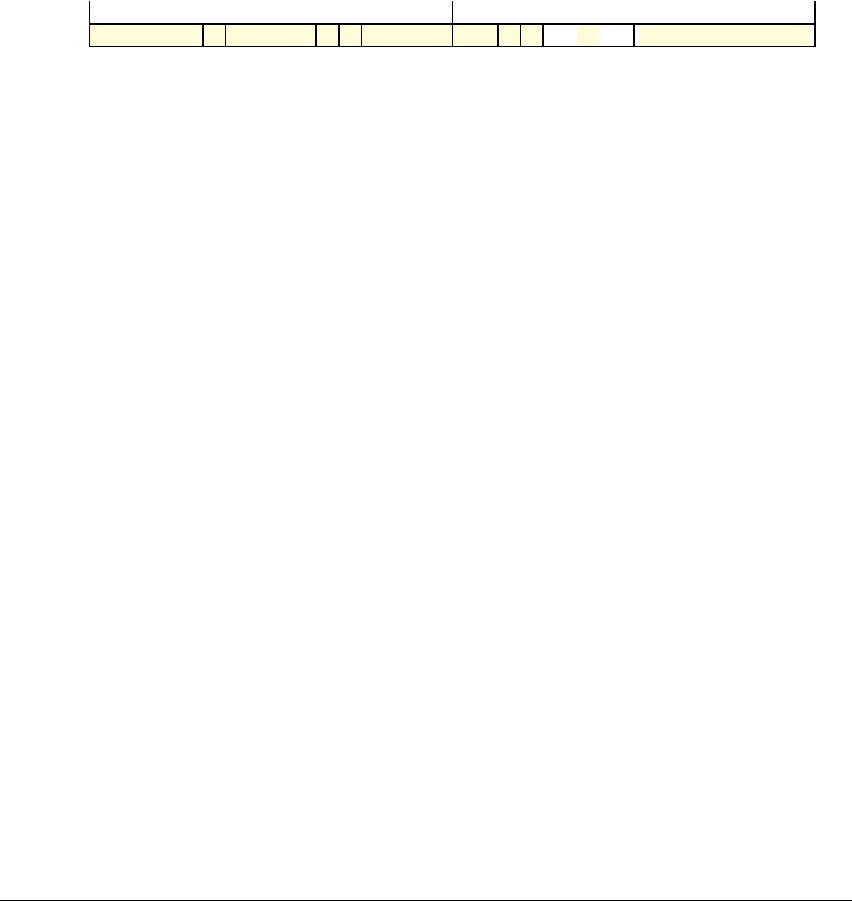
ARMv6-M System Instructions
B4-308 Copyright © 2007-2008, 2010 ARM Limited. All rights reserved. ARM DDI 0419C
Non-Confidential ID092410
B4.2.2 MRS
Move to Register from Special Register moves the value from the selected special-purpose register into a
general-purpose register.
d = UInt(Rd);
if d IN {13,15} || !(UInt(SYSm) IN {0..3,5..9,16,20}) then UNPREDICTABLE;
Assembler syntax
MRS{<q>} <Rd>, <spec_reg>
where:
{<q>}
See Standard assembler syntax fields on page A6-98.
<Rd>
Specifies the destination register.
<spec_reg>
Encoded in SYSm, see Table B4-1 on page B4-304.
Operation
R[d] = 0;
case SYSm<7:3> of
when '00000'
if SYSm<0> == '1' then
R[d]<8:0> = IPSR<8:0>;
if SYSm<1> == '1' then
R[d]<24> = '0'; // T-bit reads as zero
if SYSm<2> == '0' then
R[d]<31:27> = APSR<31:27>;
when '00001'
case SYSm<2:0> of
when '000'
R[d] = SP_main;
when '001'
R[d] = SP_process;
when '00010'
case SYSm<2:0> of
when '000'
R[d]<0> = PRIMASK.PM;
when '100'
R[d]<1:0> = CONTROL<1:0>;
Encoding T1 ARMv6-M, ARMv7-M Enhanced functionality in ARMv7-M.
MRS <Rd>,<spec_reg>
SYSmRd1 1 1 0 0 1 1 1 1 1 (0) (1) (1) (1) (1) 1 0 (0) 0
15 14 13 12 11 10 9 8 7 6 5 4 3 2 1 0
1
1514131211109876543210

ARMv6-M System Instructions
ARM DDI 0419C Copyright © 2007-2008, 2010 ARM Limited. All rights reserved. B4-309
ID092410 Non-Confidential
Exceptions
None.
Notes
Privilege An unprivileged read of any stack pointer or the IPSR returns 0.
EPSR None of the EPSR bits are readable during normal execution. They all Read-As-Zero when
read using MRS. Halting debug can read the EPSR bits using the register transfer
mechanism.
Bit positions The special-purpose program status registers, xPSR on page B1-212 defines the PSR bit
positions.
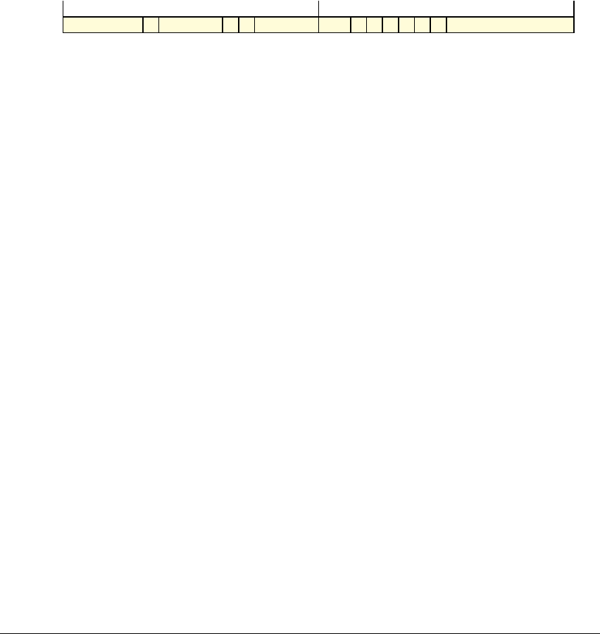
ARMv6-M System Instructions
B4-310 Copyright © 2007-2008, 2010 ARM Limited. All rights reserved. ARM DDI 0419C
Non-Confidential ID092410
B4.2.3 MSR (register)
Move to Special Register from ARM Register moves the value of a general-purpose register to the selected
special-purpose register.
n = UInt(Rn);
if n IN {13,15} || !(UInt(SYSm) IN {0..3,5..9,16,20}) then UNPREDICTABLE;
Assembler syntax
MSR{<q>} <spec_reg>, <Rn>
where:
{<q>}
See Standard assembler syntax fields on page A6-98.
<Rn>
Is the general-purpose register to receive the special register contents.
<spec_reg>
Encoded in SYSm, see Table B4-1 on page B4-304.
Operation
case SYSm<7:3> of
when '00000'
if SYSm<2> == '0' then
APSR = R[n]<31:27>;
when '00001'
if CurrentModeIsPrivileged() then
case SYSm<2:0> of
when '000'
SP_main = R[n]<31:2> : '00';
when '001'
SP_process = R[n]<31:2> : '00';
when '00010'
if CurrentModeIsPrivileged() then
case SYSm<2:0> of
when '000'
PRIMASK.PM = R[n]<0>;
when '100'
If CurrentMode == Mode_Thread then
CONTROL.SPSEL = R[n]<1>;
CONTROL.nPRIV = R[n]<0>;
Encoding T1 ARMv6-M, ARMv7-M Enhanced functionality in ARMv7-M.
MSR <spec_reg>,<Rn>
(1) (0)(0)(0) SYSm1 1 1 0 0 1 1 1 0 0 (0) Rn 1 0 (0) 0
15 14 13 12 11 10 9 8 7 6 5 4 3 2 1 0
1
1514131211109876543210

ARMv6-M System Instructions
ARM DDI 0419C Copyright © 2007-2008, 2010 ARM Limited. All rights reserved. B4-311
ID092410 Non-Confidential
Exceptions
None.
Notes
Privilege If the Unprivileged/Privileged Extension is included, the processor ignores writes from
unprivileged Thread mode to any stack pointer, the EPSR, the IPSR, the masks, or
CONTROL. If privileged software executes an
MSR
instruction that writes to
CONTROL.nPRIV, the processor switches to unprivileged Thread mode execution.
After any Thread mode transition from privileged to unprivileged execution, software must
issue an
ISB
instruction to ensure instruction fetch correctness.
IPSR The IPSR fields are read-only. The processor ignores any attempt by privileged software to
write to them.
EPSR The EPSR fields are read-only. The processor ignores any attempt by privileged software to
write to them.
Bit positions The special-purpose program status registers, xPSR on page B1-212 defines how the fields
of each of the PSRs map onto the composite xPSR.
Visibility of changes in execution priority resulting from executing an
MSR
instruction
If execution of an
MSR
instruction:
• increases the execution priority, the
MSR
execution serializes that change to the
instruction stream
• decreases the execution priority, the architecture guarantees only that the new priority
is visible to instructions executed after either executing an
ISB
, or performing an
exception entry or exception return.

ARMv6-M System Instructions
B4-312 Copyright © 2007-2008, 2010 ARM Limited. All rights reserved. ARM DDI 0419C
Non-Confidential ID092410
Part C
Debug Architecture

ARM DDI 0419C Copyright © 2007-2008, 2010 ARM Limited. All rights reserved. C1-315
ID092410 Non-Confidential
Chapter C1
ARMv6-M Debug
This chapter describes the ARMv6-M debug architecture. It contains the following sections:
•Introduction to ARMv6-M debug on page C1-316
•The Debug Access Port on page C1-318
•Overview of the ARMv6-M debug features on page C1-320
•Debug and reset on page C1-323
•Debug event behavior on page C1-324
•Debug register support in the SCS on page C1-328
•The Data Watchpoint and Trace unit on page C1-341
•Breakpoint Unit on page C1-351.

ARMv6-M Debug
C1-316 Copyright © 2007-2008, 2010 ARM Limited. All rights reserved. ARM DDI 0419C
Non-Confidential ID092410
C1.1 Introduction to ARMv6-M debug
Debug support is a key element of the ARM architecture. ARMv6-M debug is optional and only available
where the Debug Extension is implemented. The features that the Debug Extension provides are a subset of
those available in the ARMv7-M profile. The Debug Extension is limited to invasive debug that can
configure and halt the processor using breakpoints, watchpoints or vector catching, and an optional
non-invasive PC sampling feature that is accessible through the Debug Access Port (DAP), see The Debug
Access Port on page C1-318.
Debug is accessed using the DAP. The DAP permits access to debug resources when the processor is
running, halted, or held in reset. When a processor is halted, it is in Debug state.
Note
In ARMv6-M, processor access to the debug resources is IMPLEMENTATION DEFINED, see Table C1-1.
In addition to the System Control Block (SCB), Debug Control Block (DCB), and other debug controls
within the SCS, other debug related resources are allocated fixed 4KB address regions within the Private
Peripheral Bus (PPB) region of the ARMv6-M system address map. These resources are:
•Debug Watchpoint and Trace (DWT). This provides watchpoint support. Trace is not supported.
•Breakpoint Unit (BPU). This provides breakpoint support. The BPU is a subset of the Flash Patch
and Breakpoint (FPB) block available in ARMv7-M.
• The ROM table. A table of entries providing a mechanism for a debugger to identify the debug
infrastructure supported by the implementation.
These resources, together with the debug registers in the SCS, are accessible through the DAP interface.
Table C1-1 shows the address ranges for the debug resources.
Table C1-1 PPB debug related regions
Debug resource Address Range See
Data Watchpoint and Trace
0xE0001000-0xE0001FFF
The Data Watchpoint and Trace unit on page C1-341
Breakpoint Unit
0xE0002000-0xE0002FFF
Breakpoint Unit on page C1-351
SCS
0xE000ED00-0xE000EEFF
Debug register support in the SCS on page C1-328
System Control Block
0xE000ED00-0xE000ED8F
Debug Control Block
0xE000EDF0-0xE000EEFF
ARMv6-M ROM table
0xE00FF000-0xE00FFFFF
The Debug Access Port on page C1-318

ARMv6-M Debug
ARM DDI 0419C Copyright © 2007-2008, 2010 ARM Limited. All rights reserved. C1-317
ID092410 Non-Confidential
C1.1.1 Debug support in ARMv6-M
On any implementation of the ARMv6-M architecture:
• bit [0] of ROM table entries indicates whether the implementation includes the corresponding block,
see The ARMv6-M ROM table on page C1-319
• if a block is implemented, debug registers might give additional information about the implemented
features of that block.
Table C1-2 shows the bits that provide this information. For descriptions of the registers referred to in the
table see:
•Debug Exception and Monitor Control Register, DEMCR on page C1-338
•Control register, DWT_CTRL on page C1-346
•Breakpoint Control register, BP_CTRL on page C1-352.
Recommended levels of debug
ARM recommends that ARMv6-M debug is implemented at one of the following levels:
• a minimum level with no debug support
• a basic level that requires a DAP and adds halting debug support.
The basic level of debug support includes implementation of:
• the DWT block, with support for:
— external PC sampling using a PC sample register
— at least one watchpoint.
• the BPU with support for at least one breakpoint.
Table C1-2 Determining the debug support in an ARMv6-M implementation
ROM table entry Meaning, and supplementary information
ROMDWT[0] If 0, there is no DWT support and DEMCR.TRCENA is UNK/SBZP. Otherwise,
if DEMCR.DWTENA is 1, then the DWT_CTRL.NUMCOMP field indicates the
number of implemented DWT comparators.
ROMBPU[0] If 0, there is no BPU support. Otherwise the BP_CTRL.NUM_CODE field
indicates the number of implemented BPU comparators.

ARMv6-M Debug
C1-318 Copyright © 2007-2008, 2010 ARM Limited. All rights reserved. ARM DDI 0419C
Non-Confidential ID092410
C1.2 The Debug Access Port
Debug access is through the Debug Access Port (DAP), an implementation of the ARM Debug Interface v5
Architecture Specification (ADIv5). The DAP specification includes details on how a system can be
interrogated to determine what debug resources are available, and how to access any ARMv6-M devices.
The ROM table of information as described in Table C1-4 on page C1-319 is DAP accessible only and
forms part of the Debug Extension. The general format of a ROM table entry is described in Table C1-3 on
page C1-319.
A debugger can use a DAP interface to interrogate a system for memory access ports. The BASE register
in a memory access port provides the address of the ROM table, or a series of ROM tables within a ROM
table hierarchy. The memory access port can then be used to fetch the ROM table entries. See ARM Debug
Interface v5 Architecture Specification for more information.
The typical sequence of events for software to enable ARMv6-M debug using the DAP is:
1. Enable the power-on bits for the debug logic in the DAP Debug Port control register.
2. Configure the appropriate DAP memory access port control register for word accesses.
3. Configure the system for halting debug by setting the DHCSR.C_DEBUGEN bit to 1, see Debug
Halting Control and Status Register, DHCSR on page C1-331.
To halt the target immediately:
a. set the DHCSR..C_HALT bit to 1
b. read back the DHCSR.S_HALT bit, to confirm the target is halted, and therefore in Debug
state
4. To use the watchpoint features, set the DEMCR.DWTENA bit to 1, see Debug Exception and
Monitor Control Register, DEMCR on page C1-338 for more information.
See the ARM Debug Interface v5 Architecture Specification for more information on the DAP.
Warning
Accesses through the DAP can change system control and configuration fields while software is executing.
The architecture cannot give any guarantees about the consequences of using the DAP to update
control and configuration fields that the processor might be using.
C1.2.1 General rules applying to debug register access
The PPB address range
0xE0000000
to
0xE0100000
, supports the following general rules:
• The region is defined as Strongly-ordered memory, see Strongly-ordered memory on page A3-53 and
Memory access restrictions on page A3-54.
• Registers are always accessed little endian regardless of the endian state of the processor.

ARMv6-M Debug
ARM DDI 0419C Copyright © 2007-2008, 2010 ARM Limited. All rights reserved. C1-319
ID092410 Non-Confidential
• Debug registers can only be accessed as a word access. Byte and halfword accesses are
UNPREDICTABLE.
• Undocumented address space in the PPB is reserved.
• Unprivileged accesses to the PPB generate a HardFault error, and the PPB access is not permitted.
C1.2.2 The ARMv6-M ROM table
A valid ARMv6-M system includes a ROM table, that indicates the implemented debug components, and
the position of those components in the memory map. Table C1-3 shows the format of a ROM table entry,
and Table C1-4 shows the format of the ROM table
For ARMv6-M all address offsets are negative. The entry
0x00000000
indicates the end of table marker.
Table C1-3 ROM table entry format
Bits Name Description
[31:12] Address offset Signed base address offset of the component relative to the ROM base address.
[11:2] Reserved UNK/SBZP
[1] Format 0 8-bit format, not used by ARMv6-M.
1 32-bit format.
[0] Entry present 0 when bits [31:1] are not all zero, null entry, ignore this table entry.
1 valid table entry.
Table C1-4 ARMv6-M DAP accessible ROM table
Offset Value Name Description
0x000 0xFFF0F003
SCS Points to the SCS at
0xE000E000
.
0x004 0xFFF02002
or
0xFFF02003
ROMDWT Points to the DWT at
0xE0001000
.
Bit [0] is set to 1 if a DWT is fitted.
0x008 0xFFF03002
or
0xFFF03003
ROMBPU Points to the BPU at
0xE0002000
.
Bit [0] is set to 1 if a BPU is fitted.
0x00C 0x00000000
End End-of-table marker. It is IMPLEMENTATION DEFINED whether the
table is extended with pointers to other system debug resources. The
table entries must terminate with
0x00000000
.
0x010
to
0xFFC
If unused, RAZ For CoreSight compliance requirements, see Appendix A ARMv6-M
CoreSight Infrastructure IDs.

ARMv6-M Debug
C1-320 Copyright © 2007-2008, 2010 ARM Limited. All rights reserved. ARM DDI 0419C
Non-Confidential ID092410
C1.3 Overview of the ARMv6-M debug features
The ARMv6-M debug model has control and configuration integrated into the memory map. The Debug
Access Port defined in the ARM Debug Interface v5 Architecture Specification provides the interface to a
host debugger. Debug resources within ARMv6-M are as listed in Table C1-1 on page C1-316.
ARMv6-M supports the following debug related features:
• Processor halt. Control register support to halt the processor. This can occur asynchronously by
assertion of an external signal, execution of a
BKPT
instruction, or from a debug event. A debugger
can configure a debug event to occur, for example, on reset, or on entry to a HardFault.
• Step, with or without interrupt masking.
• Run, with or without interrupt masking.
• Register access. The Debug Control Block (DCB) supports debug requests, including reading and
writing core registers when halted.
• Access to exception-related information through the System Control Space resources.
• Software breakpoints. The
BKPT
instruction is supported.
• BPU support for hardware breakpoints.
• Watchpoint support through the DWT.
• Access to all memory through the DAP.
Debug and reset on page C1-323 includes the ARMv6-M recommendations for the debug reset scheme.
C1.3.1 Debug authentication
ARM debug supports two generic signals for debug enable and to control invasive versus non-invasive
debug as described in Table C1-5.
For the microcontroller profiles ARMv6-M or ARMv7-M, the provision of DBGEN and NIDEN as actual
signals is IMPLEMENTATION DEFINED. It is acceptable for DBGEN to be considered permanently enabled,
that is DBGEN = HIGH, with control deferred to other enable bits within the profile specific debug
architecture.
Table C1-5 ARM debug authentication signals
DBGEN NIDEN Invasive debug permitted Non-invasive debug permitted
LOW LOW No No
LOW HIGH No Yes
HIGH X Yes Yes
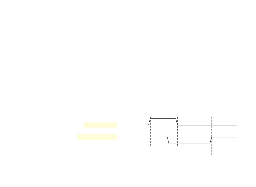
ARMv6-M Debug
ARM DDI 0419C Copyright © 2007-2008, 2010 ARM Limited. All rights reserved. C1-321
ID092410 Non-Confidential
C1.3.2 External debug request
The EDBGRQ input is asserted by an external agent to signal an external debug request. An external debug
request can cause a debug event and entry to Debug state as described in Debug event behavior on
page C1-324. The debug event is reported in the DFSR.EXTERNAL status bit, see Debug Fault Status
Register, DFSR on page C1-330.
When the processor is in Debug state, the HALTED output signal is asserted. HALTED reflects the
DHCSR.S_HALT bit, see Debug Halting Control and Status Register, DHCSR on page C1-331. The signal
can be used as a debug acknowledge for EDBGRQ.
EDBGRQ and HALTED assert HIGH. EDBGRQ is ignored when the processor is in Debug state.
C1.3.3 External restart request
It is IMPLEMENTATION DEFINED whether multiprocessing debug support is provided. An implementation
with multiprocessing debug support is required to provide the ability to perform a linked restart of multiple
processors. Two signals are required to support the multiprocessing restart mechanism:
•a DBGRESTART input
•a DBGRESTARTED output.
Note
In this section, multiprocessing support refers to any system that supports debug of more than one processor,
whether the multiple processors are within a single device, or heterogeneous processors in a more complex
system, for example an integrated system providing debug support for:
• an ARMv6-M processor and an ARMv7-A processor
• an ARMv6-M processor and a DSP.
DBGRESTART and DBGRESTARTED
DBGRESTART and DBGRESTARTED form a four-phase handshake, as shown in Figure C1-1.
Asserting DBGRESTART HIGH causes the processor to exit from Debug state. When DBGRESTART is
asserted, it must be held HIGH until DBGRESTARTED is deasserted. DBGRESTART is ignored unless
HALTED and DBGRESTARTED are asserted.
Figure C1-1 DBGRESTART / DBGRESTARTED handshake
DBGRESTART
DBGRESTARTED
Debug state Non-debug state
123 4

ARMv6-M Debug
C1-322 Copyright © 2007-2008, 2010 ARM Limited. All rights reserved. ARM DDI 0419C
Non-Confidential ID092410
Figure C1-1 on page C1-321 is diagrammatic only, and no timings are implied. The numbers in Figure C1-1
on page C1-321 have the following meanings:
1. If DBGRESTARTED is asserted HIGH the peripheral asserts DBGRESTART HIGH and waits for
DBGRESTARTED to go LOW.
2. The processor drives DBGRESTARTED LOW to deassert the signal and waits for DBGRESTART
to go LOW.
3. The peripheral drives DBGRESTART LOW to deassert the signal. This is the event that indicates to
the processor that it can start the Debug to Non-debug state transition phase.
4. The processor leaves Debug state and asserts DBGRESTARTED HIGH.
In the process of leaving Debug state the processor clears the HALTED signal to LOW. It is
IMPLEMENTATION DEFINED when this change occurs relative to the HIGH to LOW change in
DBGRESTART and the LOW to HIGH change in DBGRESTARTED.

ARMv6-M Debug
ARM DDI 0419C Copyright © 2007-2008, 2010 ARM Limited. All rights reserved. C1-323
ID092410 Non-Confidential
C1.4 Debug and reset
ARMv6-M defines two levels of reset as stated in Overview of the exceptions supported on page B1-218:
• a Power-on reset
•a Local reset.
Typically, in an ARMv6-M implementation:
• a Power-on reset applies to both the processor and the debug components
• a Local reset applies only to the processor, and not to the debug components.
However, the ARMv6-M architecture requires only that a Power-on reset includes a Local reset. The actual
reset scheme is IMPLEMENTATION DEFINED.
Note
• ARM recommends that ARMv6-M implementations include separate reset domains for Power-on
reset and Local reset.
• ARMv6-M does not provide any means to:
— debug a Power-on reset
— differentiate Power-on reset from a Local reset.
Software can initiate a system reset as described in Reset management on page B1-240. It can use the reset
vector catch control bit, DEMCR.VC_CORERESET, to generate a debug event when the processor comes
out of reset. A debug event causes the processor to halt, entering Debug state, when
DHCSR.C_DEBUGEN == 1, meaning halting debug is enabled.
The following bit fields are reset by a Power-on reset but not by a Local reset:
• fault flags in the DFSR, see Debug Fault Status Register, DFSR on page C1-330
• debug control in the DHCSR, see the notes associated with Debug Halting Control and Status
Register, DHCSR on page C1-331
• the vector catch configuration bits, see Debug Exception and Monitor Control Register, DEMCR on
page C1-338.
For reset and the DWT, see DWT register summary on page C1-345. For reset and the BPU, see BPU
register summary on page C1-352.
The relationship with the debug logic reset and power control signals in the DAP is IMPLEMENTATION
DEFINED. See the ARM Debug Interface v5 Architecture Specification for more information.

ARMv6-M Debug
C1-324 Copyright © 2007-2008, 2010 ARM Limited. All rights reserved. ARM DDI 0419C
Non-Confidential ID092410
C1.5 Debug event behavior
A debug event causes one of the following to occur:
• Entry to Debug state. If halting debug is enabled, a debug event halts the processor in Debug state.
Halting debug is enabled when the DHCSR.C_DEBUGEN bit is set to 1, see Debug Halting Control
and Status Register, DHCSR on page C1-331.
• If DHCSR.C_DEBUGEN == 0, meaning halting debug is disabled, a breakpoint in the form of a
BKPT
instruction escalates to a HardFault and the processor ignores the other debug events.Whether the
processor escalates a breakpoint generated by the BPU to a HardFault, or ignores it, is
IMPLEMENTATION DEFINED. See Breakpoint Unit on page C1-351 for more information.
If halting debug is disabled and such a breakpoint occurs in an NMI or HardFault exception handler,
the system locks up with an unrecoverable error. Handling of unrecoverable exceptions in general is
described in Unrecoverable exception cases on page B1-238.
The Debug Fault Status Register contains a status bit for each debug event, see Debug Fault Status Register,
DFSR on page C1-330. The bits are write-one-to-clear. These bits are set to 1 when a debug event causes
the processor to halt or generate an exception. It is IMPLEMENTATION DEFINED whether the bits are updated
when an event is ignored.
Table C1-6 provides a summary of halting debug support.
For a description of the vector catch feature, see Vector catch support on page C1-339.
Table C1-6 Debug related event status
Event cause DFSR bit Notes
Internal halt request HALTED Step command, processor halt request, and similar
Breakpoint BKPT Breakpoint from
BKPT
instruction or match in BPU
Watchpoint DWTTRAP Watchpoint match in DWT
Vector catch VCATCH DEMCR.VC_HARDERR or DEMCR.VC_CORERESET event match
External EXTERNAL EDBGRQ asserted

ARMv6-M Debug
ARM DDI 0419C Copyright © 2007-2008, 2010 ARM Limited. All rights reserved. C1-325
ID092410 Non-Confidential
C1.5.1 Debug stepping
ARMv6-M supports halting debug stepping. A debugger controls stepping in halting debug by writing to
the DHCSR.C_STEP and DHCSR.C_HALT bits, see Debug Halting Control and Status Register, DHCSR
on page C1-331.
When DHCSR.C_STEP is set to 1, and DHCSR.C_HALT is set to 0 in the same or a subsequent register
write, the system:
1. Exits Debug state.
2. Performs one of the following:
• Executes the next instruction. This is called instruction stepping.
• Performs an exception entry sequence that stacks the next instruction context. The processor
enters the exception handler according to the exception priority and late-arrival rules, and halts
on the first instruction of the handler.
• Executes the next instruction, at which point the exception model causes a change from the
expected program flow:
— The processor performs an exception entry sequence, according to the exception
priority and late-arrival rules. The processor halts ready to execute the first instruction
of the exception handler taken.
— If the executed instruction is an exception return instruction, tail-chaining can cause
entry to a new exception handler. The processor halts ready to execute the first
instruction of the exception handler of the tail-chained exception.
Note
The exception entry behavior is not recursive. Only a single
PushStack()
update can occur in a step
sequence.
3. Sets the DFSR.HALTED bit to 1 and returns to Debug state.
Optionally, the debugger can set DHCSR.C_MASKINTS to 1 to prevent PendSV, SysTick, and external
configurable interrupts from occurring. This is described as masking these interrupts. Table C1-7 on
page C1-326 summarizes instruction stepping control.

ARMv6-M Debug
C1-326 Copyright © 2007-2008, 2010 ARM Limited. All rights reserved. ARM DDI 0419C
Non-Confidential ID092410
When DHCSR.C_DEBUGEN is 1 and DHCSR.S_HALT is 0, meaning the system is running with halting
debug enabled, the effect of modifying DHCSR.C_STEP or DHCSR.C_MASKINTS is UNPREDICTABLE.
When DHCSR.C_DEBUGEN is 0, the processor ignores the values of DHCSR.C_HALT,
DHCSR.C_STEP and DHCSR.C_MASKINTS, and these values are UNKNOWN on DHCSR reads.
Note
If software clears DHCSR.C_HALT to 0 when the processor is in Debug state, a subsequent read of the
DHCSR that returns 1 for both C_HALT and S_HALT indicates that the processor has re-entered Debug
state because it has detected a new debug event.
Table C1-7 Debug stepping control using the DHCSR
DHCSR writea
Effect
C_HALT C_STEP C_MASKINTSb
0 0 0 Exit Debug state and start instruction execution.
Exceptions activate according to the exception configuration rules.
0 0 1 Exit Debug state and start instruction execution.
PendSV, SysTick and external configurable interrupts are disabled,
otherwise exceptions activate according to standard configuration
rules.
0 1 0 Exit Debug state, step an instruction and halt.
Exceptions activate according to the exception configuration rules.
0 1 1 Exit Debug state, step an instruction and halt.
PendSV, SysTick and external configurable interrupts are disabled,
otherwise exceptions activate according to standard configuration
rules.
1 x x Remain in Debug state.
a. Assumes the system is halted, with DHCSR.C_DEBUGEN == 1 and DHCSR.S_HALT == 1 when the write occurs.
b. The effect of a write to the DHCSR that changes C_MASKINTS is UNPREDICTABLE if either:
• before the write, the value of C_HALT is 0
• the same write to the DHCSR changes the value of C_HALT from 1 to 0.
To set C_MASKINTS to 1 and C_HALT to 0 a debugger must first write to the DHCSR to set C_MASKINTS to 1, and
then write to the DHCSR again to set C_HALT to 0.

ARMv6-M Debug
ARM DDI 0419C Copyright © 2007-2008, 2010 ARM Limited. All rights reserved. C1-327
ID092410 Non-Confidential
C1.5.2 Debug event prioritization
Debug events can be synchronous or asynchronous:
• The following are synchronous debug events:
— Breakpoint debug events, caused by execution of a
BKPT
instruction or by a match in the BPU
— Vector catch debug events
— Step debug events, caused by DHCSR.C_STEP.
• The following are asynchronous debug events:
— Watchpoint debug events, including PC match watchpoints
— DHCSR.C_HALT halt request debug events
— EDBGRQ external halt request debug events.
A single instruction can generate a number of synchronous debug events. It can also generate a number of
asynchronous exceptions. The following principles apply to the prioritization of those exceptions and debug
events:
• An instruction fetch that generates an MPU fault, or an XN fault resulting from the default memory
map, or a bus error, cannot generate a Breakpoint debug event.
• Step, Breakpoint and Vector catch debug events are associated with the instruction and are taken
instead of executing the instruction. Therefore, when a Step, Breakpoint or Vector catch debug event
occurs the processor does not generate any other synchronous exception or debug event that might
have occurred as a result of executing the instruction.
Note
The Step debug event is taken on the instruction following the instruction being stepped. This means
prioritization of the event applies relative to any other exception or debug event for the following
instruction, not for the instruction being stepped.
• If a single instruction has more than one of the following debug events associated with it, it is
UNPREDICTABLE which is taken:
—Step
—Breakpoint
— Vector catch.
• An undefined instruction that generates a HardFault exception does not cause any memory access,
and therefore cannot cause an MPU fault or external abort exception or a data match Watchpoint
debug event.
• A memory access that generates an MPU fault cannot generate a data match Watchpoint debug event.
• All other synchronous exceptions and synchronous debug events are mutually exclusive, and are
derived from decoding the instruction.
The ARM architecture does not define when asynchronous debug events are taken. Therefore the
prioritization of asynchronous debug events is IMPLEMENTATION DEFINED.

ARMv6-M Debug
C1-328 Copyright © 2007-2008, 2010 ARM Limited. All rights reserved. ARM DDI 0419C
Non-Confidential ID092410
C1.6 Debug register support in the SCS
The debug provision in the System Control Block comprises:
• Two handler-related flag bits, ISRPREEMPT and ISRPENDING, see Interrupt Control State
Register, ICSR on page B3-265.
•The SHCSR, see System Handler Control and State Register, SHCSR on page C1-329.
•The DFSR, see Debug Fault Status Register, DFSR on page C1-330.
Although the SHCSR and DFSR are SCB registers, they are described in this section, with the other debug
registers.
The architecture defines additional debug registers in the DCB. Table C1-8 shows these registers in address
order. All registers are 32-bits wide. See the register descriptions for details of the reset values of the RW
registers.
Note
The DWT, BPU, ROM table, DCB, and the SHCSR and DFSR registers are accessible through the DAP
interface. Access from the processor is IMPLEMENTATION DEFINED.
Table C1-8 DCB register summary
Address Name Type Function
0xE000EDF0
DHCSR RW Debug Halting Control and Status Register, DHCSR on
page C1-331
0xE000EDF4
DCRSR WO Debug Core Register Selector Register, DCRSR on page C1-335
0xE000EDF8
DCRDR RW Debug Core Register Data Register, DCRDR on page C1-337
0xE000EDFC
DEMCR RW Debug Exception and Monitor Control Register, DEMCR on
page C1-338
0xE000EE00
to
0xE000EEFF
- - Reserved for Debug Extension

ARMv6-M Debug
ARM DDI 0419C Copyright © 2007-2008, 2010 ARM Limited. All rights reserved. C1-329
ID092410 Non-Confidential
C1.6.1 System Handler Control and State Register, SHCSR
The SHCSR Register characteristics are:
Purpose Controls and provides the status of system handlers.
Usage constraints Debug register support in the SCS on page C1-328 describes access restrictions to
the SHCSR.
Configurations Implemented only as part of the Debug Extension.
Attributes See Table B3-4 on page B3-263.
Figure C1-2 shows the SHCSR bit assignments.
Figure C1-2 SHCSR bit assignments
Table C1-9 shows the SHCSR bit assignments.
Reserved
31 16 15 14 0
Reserved
SVCALLPENDED
Table C1-9 SHCSR bit assignments
Bits Name Function
[31:16] - Reserved.
[15] SVCALLPENDED 0 SVCall is not pending.
1 SVCall is pendinga.
This bit reflects the pending state on a read, and updates
the pending state, to the value written, on a write.
a. Pending state bits are set to 1 when an exception occurs, and are cleared to 0 when an
exception becomes active.
[14:0] - Reserved.
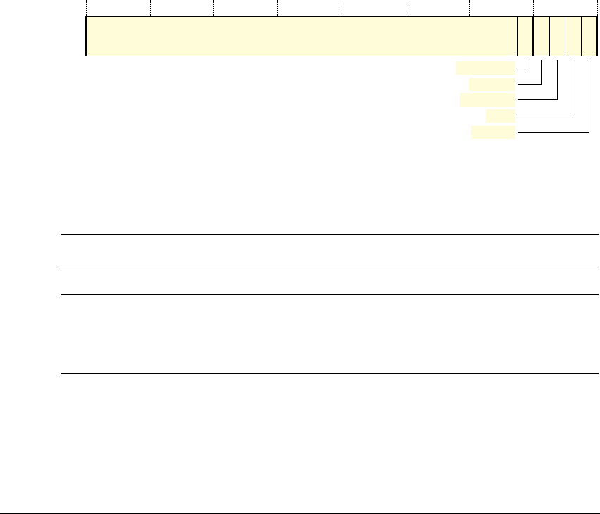
ARMv6-M Debug
C1-330 Copyright © 2007-2008, 2010 ARM Limited. All rights reserved. ARM DDI 0419C
Non-Confidential ID092410
C1.6.2 Debug Fault Status Register, DFSR
The DFSR characteristics are:
Purpose Provides the top level reason why a debug event has occurred
Usage constraints Writing 1 to a register bit clears that bit to 0.
A read of the HALTED bit by an instruction executed by stepping returns an
UNKNOWN value, For more information see Debug stepping on page C1-325.
Configurations Implemented only as part of the Debug Extension.
Attributes See Table B3-4 on page B3-263. A Power-on reset clears the defined register bits
to 0. A Local reset does not affect the value of the register.
Figure C1-3 shows the DFSR bit assignments.
Figure C1-3 DFSR bit assignments
Table C1-10 shows the DFSR bit assignments.
Reserved
31 543210
EXTERNAL
VCATCH
DWTTRAP
BKPT
HALTED
Table C1-10 DFSR bit assignments
Bits Name Function
[31:5] - Reserved
[4] EXTERNAL Indicates an asynchronous debug event generated because of EDBGRQ
being asserted:
0 no EDBGRQ debug event.
1 EDBGRQ debug event.
[3] VCATCH Indicates whether a vector catch debug event was generated:
0 no vector catch debug event generated.
1 vector catch debug event generated.
The corresponding FSR shows the primary cause of the exception.

ARMv6-M Debug
ARM DDI 0419C Copyright © 2007-2008, 2010 ARM Limited. All rights reserved. C1-331
ID092410 Non-Confidential
C1.6.3 Debug Halting Control and Status Register, DHCSR
The DHCSR characteristics are:
Purpose Controls halting debug.
Usage constraints • When C_DEBUGEN is set to 1, C_STEP and C_MASKINTS must not be
modified when the processor is running.
Note
S_HALT is 0 when the processor is running.
• When C_DEBUGEN is set to 0, the processor ignores the values of all other
bits in this register.
• For more information on the use of DHCSR, see Debug stepping on
page C1-325.
Configurations Implemented only as part of the Debug Extension.
Attributes See Table C1-8 on page C1-328.
Figure C1-4 on page C1-332 shows the DHCSR bit assignments.
[2] DWTTRAP Indicates a debug event generated by the DWT:
0 no debug events generated by the DWT.
1 at least one debug event generated by the DWT.
[1] BKPT Indicates a debug event generated by
BKPT
instruction execution or a
breakpoint match in the BPU:
0 no breakpoint debug event.
1 at least one breakpoint debug event.
[0] HALTED Indicates a debug event generated by a C_HALT or C_STEP request,
triggered by a write to the DHCSR:
0 no active halt request debug event.
1 halt request debug event active.
See Debug Halting Control and Status Register, DHCSR for more
information.
Table C1-10 DFSR bit assignments (continued)
Bits Name Function
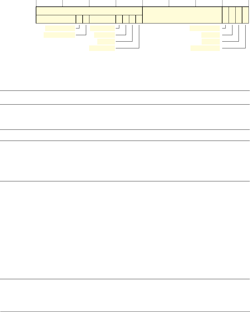
ARMv6-M Debug
C1-332 Copyright © 2007-2008, 2010 ARM Limited. All rights reserved. ARM DDI 0419C
Non-Confidential ID092410
Figure C1-4 DHCSR bit assignments
Table C1-11 shows the DHCSR bit assignments.
DBGKEY
Reserved
31 26 25 24 23 20 19 18 17 16 15 4 3 2 1 0
Reserved Reserved
C_MASKINTS
C_STEP
C_HALT
C_DEBUGEN
S_RESET_ST
S_RETIRE_ST
S_LOCKUP
S_SLEEP
S_HALT
S_REGRDY
Write
Read
Table C1-11 DHCSR bit assignments
Bits Name Access Function
[31:16] DBGKEY WO Debug key:
Software must write
0xA05F
to this field to enable write accesses to bits
[15:0], otherwise the processor ignores the write access.
[31:26] - RO Reserved
[25] S_RESET_ST RO Indicates whether the processor has been reset since the last read of
DHCSR:
0 No reset since last DHCSR read.
1 At least one reset since last DHCSR read.
This is a sticky bit, that clears to 0 on a read of DHCSR.
[24] S_RETIRE_ST RO When not in Debug state, indicates whether the processor has completed
the execution of an instruction since the last read of DHCSR:
0 No instruction has completed since last DHCSR read.
1 At least one instructions has completed since last DHCSR
read.
This is a sticky bit, that clears to 0 on a read of DHCSR.
This bit is UNKNOWN:
• after a Local reset, but is set to 1 as soon as the processor completes
execution of an instruction
• when S_LOCKUP is set to 1
• when S_HALT is set to 1.
When the processor is not in Debug state, a debugger can check this bit to
determine if the processor is stalled on a load, store or fetch access.
[23:20] - - Reserved

ARMv6-M Debug
ARM DDI 0419C Copyright © 2007-2008, 2010 ARM Limited. All rights reserved. C1-333
ID092410 Non-Confidential
[19] S_LOCKUP RO Indicates whether the processor is locked up because of an unrecoverable
exception:
0 Not locked up.
1 Locked up.
See Unrecoverable exception cases on page B1-238 for more
information.
This bit can only read as 1 when accessed by a remote debugger using the
DAP. The value of 1 indicates that the processor is running but locked up.
The bit clears to 0 when the processor enters Debug state.
[18] S_SLEEP RO Indicates whether the processor is sleeping:
0 Not sleeping.
1 Sleeping.
The debugger must set the DHCSR.C_HALT bit to 1 to gain control, or
wait for an interrupt or other wakeup event to wakeup the system.
[17] S_HALT RO Indicates whether the processor is in Debug state:
0 Not in Debug state.
1 In Debug state.
[16] S_REGRDY RO A handshake flag for transfers through the DCRDR:
• Writing to DCRSR clears the bit to 0.
• Completion of the DCRDR transfer then sets the bit to 1.
For more information about DCRDR transfers see Debug Core Register
Data Register, DCRDR on page C1-337.
0 There has been a write to the DCRDR, but the transfer is
not complete.
1 The transfer to or from the DCRDR is complete.
This bit is only valid when the processor is in Debug state, otherwise the
bit is UNKNOWN.
[15:4] - - Reserved
Table C1-11 DHCSR bit assignments (continued)
Bits Name Access Function

ARMv6-M Debug
C1-334 Copyright © 2007-2008, 2010 ARM Limited. All rights reserved. ARM DDI 0419C
Non-Confidential ID092410
[3] C_MASKINTS RW When debug is enabled, the debugger can write to this bit to mask
PendSV, SysTick and external configurable interrupts:
0 Do not mask.
1 Mask PendSV, SysTick and external configurable
interrupts.
The effect of any attempt to change the value of this bit is UNPREDICTABLE
unless both:
• before the write to DHCSR, the value of the C_HALT bit is 1
• the write to the DHCSR that changes the C_MASKINTS bit also
writes 1 to the C_HALT bit
This means that a single write to DHCSR cannot set the C_HALT to 0 and
change the value of the C_MASKINTS bit.
The bit does not affect NMI. When DHCSR.C_DEBUGEN is set to 0, the
value of this bit is UNKNOWN.
For more information about the use of this bit see Table C1-7 on
page C1-326.
This bit is UNKNOWN after a Power-on reset.
[2] C_STEP RW Processor step bit. The effects of writes to this bit are:
0 Single-stepping disabled.
1 Single-stepping enabled.
For more information about the use of this bit see Table C1-7 on
page C1-326.
This bit is UNKNOWN after a Power-on reset.
[1] C_HALT RW Processor halt bit. The effects of writes to this bit are:
0 Request a halted processor to run.
1 Request a running processor to halt.
Table C1-7 on page C1-326 shows the effect of writes to this bit when the
processor is in Debug state.
This bit is UNKNOWN after a Power-on reset.
Table C1-11 DHCSR bit assignments (continued)
Bits Name Access Function
ARMv6-M Debug
ARM DDI 0419C Copyright © 2007-2008, 2010 ARM Limited. All rights reserved. C1-335
ID092410 Non-Confidential
C1.6.4 Debug Core Register Selector Register, DCRSR
The DCRSR characteristics are:
Purpose With the DCRDR, see Debug Core Register Data Register, DCRDR on
page C1-337, the DCRSR provides debug access to the ARM core registers and
special-purpose registers. A write to DCRSR specifies the register to transfer,
whether the transfer is a read or a write, and starts the transfer.
Usage constraints This register is only accessible in Debug state.
For information about using this register see Use of DCRSR and DCRDR on
page C1-338.
Configurations Implemented only as part of the Debug Extension.
Attributes See Table C1-8 on page C1-328.
Figure C1-5 shows the DCRSR bit assignments.
Figure C1-5 DCRSR bit assignments
[0] C_DEBUGEN RW Halting debug enable bit:
0 Halting debug disabled.
1 Halting debug enabled.
If a debugger writes to DHCSR to change the value of this bit from 0 to
1, it must also write 0 to the C_MASKINTS bit, otherwise behavior is
UNPREDICTABLE.
This bit can only be written from the DAP. Access to the DHCSR from
software running on the processor is IMPLEMENTATION DEFINED.
However, writes to this bit from software running on the processor are
ignored.
This bit is 0 after a Power-on reset.
Table C1-11 DHCSR bit assignments (continued)
Bits Name Access Function
Reserved
31 17 16 15 5 4 0
Reserved REGSEL
REGWnR

ARMv6-M Debug
C1-336 Copyright © 2007-2008, 2010 ARM Limited. All rights reserved. ARM DDI 0419C
Non-Confidential ID092410
Table C1-12 shows the DCRSR bit assignments
Note
When the processor is in Debug state, the debugger must preserve the Exception number bits in the IPSR,
otherwise behavior is UNPREDICTABLE.
The DebugReturnAddress value
DebugReturnAddress is the address of the first instruction to be executed on exit from Debug state. This
address indicates the point in the execution stream where the debug event was invoked. For a hardware or
a software breakpoint, this is the address of the breakpointed instruction. For all other debug events,
including PC match watchpoints, DebugReturnAddress is the address of the first instruction that both:
• in a simple sequential execution of the program, executes after the instruction that caused the debug
event
Table C1-12 DCRSR bit assignments
Bits Name Function
[31:17] - Reserved
[16] REGWnR Specifies the type of access for the transfer:
0 read.
1 write.
[15:5] - Reserved
[4:0] REGSEL Specifies the ARM core register or special-purpose register to transfer:
0b00000
-
0b01100
ARM core registers R0-R12. For example,
0b00000
specifies R0, and
0b00101
specifies R5.
0b01101
The current SP. See also values
0b10001
and
0b10010
.
0b01110
LR.
0b01111
DebugReturnAddress, see The DebugReturnAddress value.
0b10000
xPSR.
0b10001
Main stack pointer, MSP.
0b10010
Process stack pointer, PSP.
0b10100
Bits [31:24] CONTROL
Bits [23:8] Reserved
Bits [7:0] PRIMASK.
In each field, the valid bits are packed with leading zeros. For example,
DCRDR[31:26] is
0b000000
.
All other values are reserved.

ARMv6-M Debug
ARM DDI 0419C Copyright © 2007-2008, 2010 ARM Limited. All rights reserved. C1-337
ID092410 Non-Confidential
• has not been executed.
Before entering Debug state, the processor has executed all instructions that are earlier in a simple sequential
execution of the program than the instruction indicated by DebugReturnAddress.
Bit [0] of a DebugReturnAddress value is RAZ/SBZ. When writing a DebugReturnAddress, writing bit [0]
of the address does not affect the EPSR.T bit, see The special-purpose program status registers, xPSR on
page B1-212.
C1.6.5 Debug Core Register Data Register, DCRDR
The DCRDR characteristics are:
Purpose With the DCRSR, see Debug Core Register Selector Register, DCRSR on
page C1-335, the DCRDR provides debug access to the ARM core registers and
special-purpose registers. The DCRDR is the data register for these accesses.
Usage constraints See Use of DCRSR and DCRDR on page C1-338 for constraints that apply to
particular transfers using the DCRSR and DCRDR.
Configurations Implemented only as part of the Debug Extension.
Attributes See Table C1-8 on page C1-328.
Figure C1-6 shows the DCRDR bit assignments
Figure C1-6 DCRDR bit assignments
Table C1-13 shows the DCRDR bit assignments
DBGTMP
31 0
Table C1-13 DCRDR bit assignments
Bits Name Function
[31:0] DBGTMP Data temporary cache, for reading and writing registers.
This register is UNKNOWN:
• on reset
• when DHCSR.S_HALT = 0.
• when DHCSR.S_REGRDY = 0 during execution of a DCRSR based transaction that
updates the register

ARMv6-M Debug
C1-338 Copyright © 2007-2008, 2010 ARM Limited. All rights reserved. ARM DDI 0419C
Non-Confidential ID092410
Use of DCRSR and DCRDR
In Debug state, writing to the DCRSR clears the DHCSR.S_REGRDY bit to 0, and the processor then sets
the bit to 1 when the transfer between the DCRDR and the ARM core register or special-purpose register
completes. For more information about the DHCSR.S_REGRDY bit see Debug Halting Control and Status
Register, DHCSR on page C1-331.
This means that:
• To transfer a data word to an ARM core register or special-purpose register, a debugger:
1. Writes the required word to DCRDR.
2. Writes to the DCRSR, with the REGSEL value indicating the required register, and the
REGWnR bit as 1 to indicate a write access.
This write clears the DHCSR S_REGRDY bit to 0.
3. Polls DHCSR until DHCSR.S_REGRDY reads-as-one. This shows that the processor has
transferred the DCRDR value to the selected register.
• To transfer a data word from an ARM core register or special-purpose register, a debugger:
1. Writes to the DCRSR, with the REGSEL value indicating the required register, and the
REGWnR bit as 0 to indicate a read access.
This write clears the DHCSR.S_REGRDY bit to 0.
2. Polls DHCSR until DHCSR.S_REGRDY reads-as-one. This shows that the processor has
transferred the value of the selected register to DCRDR.
3. Reads the required value from DCRDR.
When using this mechanism to write to the ARM core registers or special-purpose registers:
• All bits of the xPSR registers are fully accessible. The effect of writing an illegal value is
UNPREDICTABLE.
Note
This differs from the behavior of
MSR
and
MRS
instruction accesses to the xPSR, where some bits RAZ,
and some bits are ignored on writes.
• The debugger can write to the DebugReturnAddress, and on exiting Debug state the processor starts
executing from this updated address.
C1.6.6 Debug Exception and Monitor Control Register, DEMCR
The DEMCR characteristics are:
Purpose Manages vector catch behavior and enables the DWT.
Usage constraints There are no usage constraints.
Configurations Implemented only as part of the Debug Extension.
ARMv6-M Debug
ARM DDI 0419C Copyright © 2007-2008, 2010 ARM Limited. All rights reserved. C1-339
ID092410 Non-Confidential
Attributes See Table C1-8 on page C1-328. A Power-on reset sets all register bits to 0. A Local
reset sets DWTENA to 0 but does not affect VC_HARDERR or VC_CORERESET.
Figure C1-7 shows the DEMCR bit assignments:
Figure C1-7 DEMCR bit assignments
Table C1-14 shows the DEMCR bit assignments.
Vector catch support
Vector catch is the mechanism for generating a debug event and entering Debug state when a particular
exception occurs.
Reserved
31 25 24 23 11 10 9 1 0
Reserved Reserved
VC_HARDERRDWTENA VC_CORERESET
Table C1-14 DEMCR bit assignments
Bits Name Function
[31:25] - Reserved
[24] DWTENA Global enable for all features configured and controlled by the DWT unit:
0 DWT disabled.
1 DWT enabled.
When DWTENA is set to 0 DWT registers return UNKNOWN values on reads.
In addition, it is IMPLEMENTATION DEFINED whether the processor ignores writes
to the DWT while DWTENA is 0.
[23:11] - Reserved
[10] VC_HARDERR Enable halting debug trap on a HardFault exception.
0 halting debug trap disabled.
1 halting debug trap enabled.
If DHCSR.C_DEBUGEN is set to 0, the processor ignores the value of this bit.
[9:1] - Reserved.
[0] VC_CORERESET Enable Reset Vector Catch. This causes a Local reset to halt a running system:
0 Reset Vector Catch disabled.
1 Reset Vector Catch enabled.
If DHCSR.C_DEBUGEN is set to 0, the processor ignores the value of this bit.

ARMv6-M Debug
C1-340 Copyright © 2007-2008, 2010 ARM Limited. All rights reserved. ARM DDI 0419C
Non-Confidential ID092410
The conditions for a vector catch are:
• DHCSR.C_DEBUGEN is set to 1
• one or both of DEMCR.VC_HARDERR or DEMCR.VC_CORERESET, the vector catch enable
bits, is set to 1
• the associated exception becomes active.
When these conditions are met, the processor halts execution on the first instruction of the exception handler
and enters Debug state.
Note
• Exception entry sets the Debug Fault Status Register bits to 1. A debugger can use these bits to help
determine the source of the error. See Debug Fault Status Register, DFSR on page C1-330 for more
information.
• The vector catch mechanism guarantees that the processor enters Debug state without executing any
instruction after the instruction that caused the exception. However, saved context might include
information on a lockup situation, or on a higher priority pending exception, for example a pending
NMI exception detected on reset.
Late arrival and derived exceptions can occur, postponing when the processor halts. See Late-arriving
exceptions on page B1-232 and Derived exceptions on exception entry on page B1-233 for more
information.

ARMv6-M Debug
ARM DDI 0419C Copyright © 2007-2008, 2010 ARM Limited. All rights reserved. C1-341
ID092410 Non-Confidential
C1.7 The Data Watchpoint and Trace unit
The Data Watchpoint and Trace (DWT) unit provides the following:
• external PC sampling using a PC sample register.
• comparators, that support:
— watchpoints, for data address matching
— PC watchpoints, for instruction address matching.
Note
The reporting behavior of a PC watchpoint is different from a
BKPT
instruction or breakpoint detection
in a BPU, see Table C1-6 on page C1-324 for details.
The PC sampling feature, DWT_PCSR, and watchpoint support operate independently of each other. See
Program counter sampling support on page C1-344 for more information. The number of watchpoints
supported is defined in the DWT Control Register, DWT_CTRL, see Control register, DWT_CTRL on
page C1-346. Watchpoint support uses a set of compare, mask and function registers:
•DWT_COMPx
•DWT_MASKx
• DWT_FUNCTIONx.
See Comparator registers, DWT_COMPx on page C1-347, Comparator Mask registers, DWT_MASKx on
page C1-348, and Comparator Function registers, DWT_FUNCTIONx on page C1-349 for more
information.
Watchpoint events result in a processor halt and entry to Debug state.
The following sections describe the DWT operation:
•The DWT comparators
•Program counter sampling support on page C1-344
•DWT register summary on page C1-345.
C1.7.1 The DWT comparators
The DWT_COMPx, DWT_MASKx, and DWT_FUNCTIONx register sets provide the programming
interface for the type of match to perform, and the action to take on a match. The number of register sets
supported is IMPLEMENTATION DEFINED and can be determined by reading the NUMCOMP field in the
DWT_CTRL register.
ARMv6-M supports:
• data address matching and creation of a watchpoint event
• instruction address matching and creation of a PC watchpoint event.
This is controlled by the DWT_FUNCTIONx registers as illustrated in Table C1-15 on page C1-342.

ARMv6-M Debug
C1-342 Copyright © 2007-2008, 2010 ARM Limited. All rights reserved. ARM DDI 0419C
Non-Confidential ID092410
DWT_COMPx contains the reference value COMP for the comparator. This value is compared against an
input value to determine a match.
For instruction and data address matching the input value is masked. The number of input value bits masked,
MASK, is defined in DWT_MASKx[4:0]. The maximum address mask range supported, up to 2GB, is
IMPLEMENTATION DEFINED. An address match for a 32-bit instruction must match on the first halfword of
the instruction. An address match on only the second halfword of a 32-bit instruction results in
UNPREDICTABLE behavior.
Note
The recommended mechanism for generating a breakpoint on a single instruction address is to use the BPU,
see Breakpoint Unit on page C1-351, where supported. The DWT based mechanism must be used to
generate a PC matching event on a range of addresses.
A watchpoint event is asynchronous to the instruction that caused it. The DebugReturnAddress value for a
watchpoint event must be that of an instruction to be executed after the instruction responsible for
generating the watchpoint.
Table C1-15 General DWT function support
DWT_FUNCTIONx Comparator Function Description/Action
Bits [3:0] Inputa
a. Daddr: data access address match. Iaddr: instruction address match.
Access Match(Input, COMP) == TRUE
0000 Disabled
0001 - - Reserved
0010 - - Reserved
0011 - - Reserved
0100 Iaddr - PC watchpoint event
0101 Daddr RO Watchpoint event
0110 Daddr WO Watchpoint event
0111 Daddr RW Watchpoint event
1xxx - - Reserved

ARMv6-M Debug
ARM DDI 0419C Copyright © 2007-2008, 2010 ARM Limited. All rights reserved. C1-343
ID092410 Non-Confidential
Instruction address matching
All comparators support instruction address matching. Comparator operation is UNPREDICTABLE unless:
• if masking is not used, the DWT_COMPn value is halfword aligned
• if masking is used, the DWT_COMPn value is the masked address for comparison.
For an instruction address match on the address of a
NOP
instruction, it is UNPREDICTABLE whether a
watchpoint debug event occurs or not.
In the following cases, it is IMPLEMENTATION DEFINED whether a watchpoint debug event occurs on an
instruction address match:
• the addressed instruction generates a Prefetch Abort exception
• the addressed instruction is executed with CPSR.T set to 0
• the addressed instruction generates a breakpoint debug event.
The comparator behavior is defined as follows:
// InstructionAddressMatch()
// =========================
boolean InstructionAddressMatch(integer N, bits(32) Iaddr)
assert N < UInt(DWT_CTRL.NUMCOMP);
valid = DWT_FUNCTION[N].FUNCTION == '0100'; // Condition for selecting Iaddr
if valid then
mask = ZeroExtend(Ones(UInt(DWT_MASK[N].MASK)), 32);
// UNPREDICTABLE if COMP does not meet alignment and masking conditions
if !IsZero(DWT_COMP[N] AND mask) || IsZero(DWT_COMP[N]<0>) then UNPREDICTABLE;
match = ((Iaddr AND NOT(mask)) == DWT_COMP[N]);
else
match = FALSE;
return match;
Data address matching
It is IMPLEMENTATION DEFINED whether a vector table read performed as part of exception processing is
considered as a memory read-access for the purpose of watchpoint matching. ARMv6-M only supports
aligned accesses. Unaligned accesses take a HardFault exception as described in Alignment support on
page A3-43 and Table B1-6 on page B1-237. Data address matching comparator behavior is defined as
follows:
// DataAddressMatch()
// ==================
boolean DataAddressMatch(integer N, bits(32) Daddr, integer size, boolean read)
assert N < UInt(DWT_CTRL.NUMCOMP);
assert size == 1 || size == 2 || size == 4;

ARMv6-M Debug
C1-344 Copyright © 2007-2008, 2010 ARM Limited. All rights reserved. ARM DDI 0419C
Non-Confidential ID092410
case DWT_FUNCTION[N].FUNCTION of
when '0000' valid = FALSE; // Comparator disabled
when '0100' valid = FALSE; // See InstructionAddressMatch()
when '0101' valid = read;
when '0110' valid = !read;
when '0111' valid = TRUE;
otherwise UNPREDICTABLE; // Reserved settings
if valid then
mask = ZeroExtend(Ones(UInt(DWT_MASK[N].MASK)), 32);
if !IsZero(DWT_COMP[N] AND mask) then UNPREDICTABLE;
case size
when 1 comp = DWT_COMP[N];
when 2 comp = DWT_COMP[N]<31:1>:'0';
when 4 comp = DWT_COMP[N]<31:2>:'00';
match = ((Daddr AND NOT(mask)) == comp);
else
match = FALSE;
return match;
C1.7.2 Program counter sampling support
The DWT Program Counter Sampling Register, DWT_PCSR, is an IMPLEMENTATION DEFINED option in
ARMv6-M. The register is defined so that a debugger can access it without changing the behavior of any
code currently executing on the device. This provides a mechanism for coarse-grained non-intrusive
profiling of code executing on the processor.
The DWT_PCSR is a word-accessible read-only register. Writes to the register are ignored. Byte or
halfword reads are UNPREDICTABLE. When the register is read it returns one of the following:
• the address of an instruction recently executed by the processor
•
0xFFFFFFFF
if DWT_PCSR is implemented and any of the following apply:
— the processor is in Debug state
— the processor is in a state and mode where non-invasive debug is not permitted
— the address of a recently-executed instruction is not available.
• RAZ/WI if DWT_PCSR is not implemented.
Note
• There is no architectural definition of recently executed. The delay between an instruction being
executed by the processor and its address appearing in the DWT_PCSR is not defined. There is no
guaranteed relationship between the program counter for a piece of code designed to read the
DWT_PCSR and the value read. The DWT_PCSR is intended only for use by an external agent to
provide statistical information for code profiling. Read accesses made to the DWT_PCSR directly by
the ARM processor can return an UNKNOWN value.

ARMv6-M Debug
ARM DDI 0419C Copyright © 2007-2008, 2010 ARM Limited. All rights reserved. C1-345
ID092410 Non-Confidential
• A debug agent must not rely on a return value of
0xFFFFFFFF
to indicate that the processor is halted.
The DHCSR.S_HALT bit must be used for this purpose.
The value read always references an instruction that would be executed in a simple sequential execution of
the program. It is IMPLEMENTATION DEFINED whether instructions that do not pass their condition codes can
be referenced, but ARM recommends that these instructions can be referenced.
An implementation must not sample any value that references an instructions that is fetched but not
executed.
Note
A value that references an instruction that was abandoned to enable exception-handling is permitted.
A read access from the DWT_PCSR returns an UNKNOWN value when the DEMCR.DWTENA bit is set to 0.
C1.7.3 DWT register summary
The DWT is programmed using the registers described in Table C1-16.
Note
The DWT, BPU, ROM table, DCB, and debug registers in the SCS are accessible through the DAP
interface. Access from the processor is IMPLEMENTATION DEFINED.
Table C1-16 DWT register summary
Address Name Type Function
0xE0001000
DWT_CTRL RO Control register, DWT_CTRL on page C1-346
0xE000101C
DWT_PCSR RO Program Counter Sample Register, DWT_PCSR on
page C1-347
0xE0001020
DWT_COMPx RW Comparator registers, DWT_COMPx on page C1-347
0xE0001024
DWT_MASKx RW Comparator Mask registers, DWT_MASKx on
page C1-348
0xE0001028
DWT_FUNCTIONx RW Comparator Function registers, DWT_FUNCTIONx
on page C1-349

ARMv6-M Debug
C1-346 Copyright © 2007-2008, 2010 ARM Limited. All rights reserved. ARM DDI 0419C
Non-Confidential ID092410
Control register, DWT_CTRL
The DWT_CTRL register characteristics are:
Purpose Defines the number of comparators implemented.
Usage constraints There are no usage constraints.
Configurations Implemented as part of the Debug Extension.
Attributes See Table C1-16 on page C1-345.
Figure C1-8 shows the DWT_CTRL register bit assignments.
Figure C1-8 DWT_CTRL register bit assignments
Table C1-17 shows the DWT_CTRL register bit assignments.
NUMCOMP
31 28 27 0
Reserved
Table C1-17 DWT_CTRL register bit assignments
Bits Name Function
[31:28] NUMCOMP Number of comparators available:
0 no comparator support.
[27:0] - Reserved.

ARMv6-M Debug
ARM DDI 0419C Copyright © 2007-2008, 2010 ARM Limited. All rights reserved. C1-347
ID092410 Non-Confidential
Program Counter Sample Register, DWT_PCSR
The DWT_PCSR characteristics are:
Purpose Samples the current value of the program counter.
Usage constraints The register value is UNKNOWN on reset.
Note
Unless DWT_PCSR reads as
0xFFFFFFFF
, under the conditions described in
Program counter sampling support on page C1-344, bit [0] is RAZ. When RAZ, bit
[0] does not reflect instruction set state as is the case with similar functionality in
other ARM architecture profiles.
Configurations This register is an IMPLEMENTATION DEFINED option in ARMv6-M, see Program
counter sampling support on page C1-344. If not implemented, this register is
RAZ/WI.
Attributes See Table C1-16 on page C1-345.
Figure C1-9 shows the DWT_PCSR bit assignments.
Figure C1-9 DWT_PCSR bit assignments
Table C1-18 shows the DWT_PCSR bit assignments.
Comparator registers, DWT_COMPx
The DWT_COMPx register characteristics are:
Purpose Provides a reference value for use by comparator
x
.
Usage constraints The value is UNKNOWN on reset.
Configurations Implemented when DWT_CTRL.NUMCOMP is non-zero.
DWT_CTRL.NUMCOMP defines the number of implemented DWT_COMPx
registers, from 0 to (NUMCOMP-1). Unimplemented registers are UNK/SBZP
EIASAMPLE
31 0
Table C1-18 DWT_PCSR bit assignments
Bits Name Function
[31:0] EIASAMPLE Executed Instruction Address sample value

ARMv6-M Debug
C1-348 Copyright © 2007-2008, 2010 ARM Limited. All rights reserved. ARM DDI 0419C
Non-Confidential ID092410
Attributes See Table C1-16 on page C1-345.
Figure C1-10 shows the DWT_COMPx register bit assignments.
Figure C1-10 DWT_COMPx register bit assignments
Table C1-19 shows the DWT_COMPx register bit assignments.
Comparator Mask registers, DWT_MASKx
The DWT_MASKx register characteristics are:
Purpose Provides the size of the ignore mask applied to the access address range matching
by comparator
x
.
Usage constraints The value is UNKNOWN on reset.
Configurations Implemented when DWT_CTRL.NUMCOMP is non-zero.
DWT_CTRL.NUMCOMP defines the number of implemented DWT_MASKx
registers, from 0 to (NUMCOMP-1). Unimplemented registers are UNK/SBZP.
Attributes See Table C1-16 on page C1-345.
Figure C1-11 shows the DWT_MASKx register bit assignments.
Figure C1-11 DWT_MASKx register bit assignments
COMP
31 0
Table C1-19 DWT_COMPx register bit assignments
Bits Name Function
[31:0] COMP Reference value for comparison. See The DWT comparators on page C1-341.
Reserved
31 40
MASK
5
ARMv6-M Debug
ARM DDI 0419C Copyright © 2007-2008, 2010 ARM Limited. All rights reserved. C1-349
ID092410 Non-Confidential
Table C1-20 shows the DWT_MASKx register bit assignments.
Comparator Function registers, DWT_FUNCTIONx
The DWT_FUNCTIONx register characteristics are:
Purpose Controls the operation of the comparator DWT_COMPx.
Usage constraints See the footnotes in DWT_FUNCTIONx register bit assignments on page C1-350
for the usage constraints of individual fields.
Configurations Implemented when DWT_CTRL.NUMCOMP is non-zero.
DWT_CTRL.NUMCOMP defines the number of implemented
DWT_FUNCTIONx registers, from 0 to (NUMCOMP-1). Unimplemented
registers are UNK/SBZP.
Attributes See Table C1-16 on page C1-345.
Figure C1-12 shows the DWT_FUNCTIONx register bit assignments.
Figure C1-12 DWT_FUNCTIONx register bit assignments
Table C1-21 on page C1-350 shows the DWT_FUNCTIONx register bit assignments.
Table C1-20 DWT_MASKx register bit assignments
Bits Name Function
[31:5] - Reserved
[4:0] MASK The size of the ignore mask applied to address range matching. See The DWT comparators on
page C1-341 for the usage model.
The mask range is IMPLEMENTATION DEFINED. Writing all ones to this field and reading it back
can be used to determine the maximum mask size supported.
Reserved
31 25 24 23 4 3 0
Reserved FUNCTION
MATCHED

ARMv6-M Debug
C1-350 Copyright © 2007-2008, 2010 ARM Limited. All rights reserved. ARM DDI 0419C
Non-Confidential ID092410
Table C1-21 DWT_FUNCTIONx register bit assignments
Bits Name TYPE Function
[31:25] = - Reserved
[24] MATCHED RO Comparator match. It indicates that the operation defined by FUNCTION
has occurred since the bit was last read:
0 the associated comparator has matched.
1 the associated comparator has not matched.
Reading the register clears this bit to 0.
[23:4] - RW Reserved
[3:0] FUNCTION RW Select action on comparator match. See Table C1-15 on page C1-342 for
information about the values to use for FUNCTION.
This field is set to 0 on a Power-on reset.

ARMv6-M Debug
ARM DDI 0419C Copyright © 2007-2008, 2010 ARM Limited. All rights reserved. C1-351
ID092410 Non-Confidential
C1.8 Breakpoint Unit
The Breakpoint Unit (BPU) provides support for breakpoint functionality on instruction fetches.
C1.8.1 BPU operation
There are two types of register:
• a breakpoint control register, BP_CTRL
• breakpoint comparator registers, BP_COMPx.
The number of instruction address comparators is IMPLEMENTATION DEFINED and can be read from the
BP_CTRL register, see Breakpoint Control register, BP_CTRL on page C1-352.
The BP_CTRL register provides a global enable bit for the BPU, along with ID fields indicating the
numbers of Breakpoint Comparator registers provided.
Each Breakpoint Comparator Register includes its own enable bit that comes into effect when the global
enable bit is set to 1. The comparators match instruction fetches from the Code memory region, meaning
they operate only on instruction read accesses. The comparators do not match data read or data write
accesses.
Address matching can be performed on the upper halfword, lower halfword or both halfwords:
• For 16-bit instructions, halfword matches always generate a breakpoint for the associated instruction.
• For 32-bit instructions, a breakpoint must be configured to match the first halfword or both halfwords
of the instruction. It is UNPREDICTABLE whether breakpoint matches on only the address of the second
halfword of a 32-bit instruction generate a debug event.
Note
It is IMPLEMENTATION DEFINED whether a breakpoint event is generated when debug is disabled, that is,
when DHCSR.C_DEBUGEN == 0. When no breakpoint event is generated, the breakpointed instruction
exhibits its normal architectural behavior. When a breakpoint event is generated, it is escalated to HardFault,
see Debug event behavior on page C1-324.
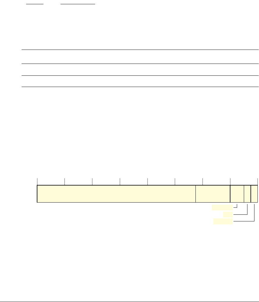
ARMv6-M Debug
C1-352 Copyright © 2007-2008, 2010 ARM Limited. All rights reserved. ARM DDI 0419C
Non-Confidential ID092410
C1.8.2 BPU register summary
Table C1-22 shows the BPU registers.
Note
The DWT, BPU, ROM table, and debug registers in the SCS are accessible through the DAP interface.
Access from the processor is IMPLEMENTATION DEFINED.
Breakpoint Control register, BP_CTRL
The BP_CTRL register characteristics are:
Purpose Provides BPU implementation information, and the global enable for the BPU.
Usage constraints There are no usage constraints.
Configurations Implemented as part of the Debug Extension.
Attributes See Table C1-22.
Figure C1-13 shows the BP_CTRL register bit assignments.
Figure C1-13 BP_CTRL register bit assignments
Table C1-22 BPU register summary
Address Name Type Function
0xE0002000
BP_CTRL RW Breakpoint Control register, BP_CTRL
0xE0002008
BP_COMPx RW Breakpoint Comparator registers, BP_COMPx on page C1-354
NUM_CODE
31 143 0
Reserved
Reserved
87 2
KEY
ENABLE

ARMv6-M Debug
ARM DDI 0419C Copyright © 2007-2008, 2010 ARM Limited. All rights reserved. C1-353
ID092410 Non-Confidential
Table C1-23 shows the BP_CTRL register bit assignments.
Table C1-23 BP_CTRL register bit assignments
Bits Name Function
[31:8] - Reserved
[7:4] NUM_CODE The number of breakpoint comparators.
If NUM_CODE is zero, the implementation does not support any
comparators.
[3:2] - Reserved
[1] KEY RAZ on reads, SBO, for writes. If written as zero, the write to the register
is ignored.
[0] ENABLE Enables the BPU:
0 BPU is disabled.
1 BPU is enabled.
This bit is set to 0 on a Power-on reset.
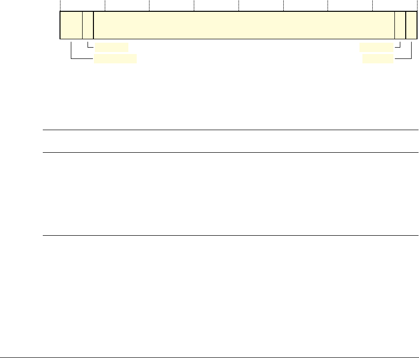
ARMv6-M Debug
C1-354 Copyright © 2007-2008, 2010 ARM Limited. All rights reserved. ARM DDI 0419C
Non-Confidential ID092410
Breakpoint Comparator registers, BP_COMPx
The BP_COMPx register characteristics are:
Purpose Holds a breakpoint address for comparison with instruction addresses in the Code
memory region, see The system address map on page B3-258 for more information.
Usage constraints A comparator can only be enabled when BP_CTRL.ENABLE is set to 1.
Configurations Implemented when BP_CTRL.NUM_CODE is non-zero.
BP_CTRL.NUM_CODE defines the number of implemented BP_COMPx
registers, from 0 to (NUM_CODE-1). Unimplemented registers are UNK/SBZP.
Attributes See Table C1-22 on page C1-352.
Figure C1-14 shows the BP_COMPx register bit assignments.
Figure C1-14 BP_COMPx register bit assignments
Table C1-24 shows the BP_COMPx register bit assignments.
31 10
COMP
Reserved
2
ENABLE
30 29
Reserved
BP_MATCH
28
Table C1-24 BP_COMPx register bit assignments
Bits Name Function
[31:30] BP_MATCH BP_MATCH defines the behavior when the COMP address is matched:
00 no breakpoint matching.
01 breakpoint on lower halfword, upper is unaffected.
10 breakpoint on upper halfword, lower is unaffected.
11 breakpoint on both lower and upper halfwords.
The field is UNKNOWN on reset.
[29] - Reserved

ARMv6-M Debug
ARM DDI 0419C Copyright © 2007-2008, 2010 ARM Limited. All rights reserved. C1-355
ID092410 Non-Confidential
[28:2] COMP Stores bits [28:2] of the comparison address. The comparison address is
compared with the address from the Code memory region. Bits [31:29] and
[1:0] of the comparison address are zero.
The field is UNKNOWN on Power-on reset
[1] - Reserved
[0] ENABLE Enables the comparator:
0 comparator is disabled.
1 comparator is enabled.
This bit is set to 0 on a Power-on reset.
Note
BP_CTRL.ENABLE must also be set to 1 to enable a comparator.
Table C1-24 BP_COMPx register bit assignments (continued)
Bits Name Function

ARMv6-M Debug
C1-356 Copyright © 2007-2008, 2010 ARM Limited. All rights reserved. ARM DDI 0419C
Non-Confidential ID092410
Part D
Appendices

ARM DDI 0419C Copyright © 2007-2008, 2010 ARM Limited. All rights reserved. AppxA-359
ID092410 Non-Confidential
Appendix A
ARMv6-M CoreSight Infrastructure IDs
This appendix describes the ARMv6-M implementation of the ARMv6-M CoreSight Infrastructure IDs. It
contains the following section:
•CoreSight infrastructure IDs for an ARMv6-M implementation on page AppxA-360.

ARMv6-M CoreSight Infrastructure IDs
AppxA-360 Copyright © 2007-2008, 2010 ARM Limited. All rights reserved. ARM DDI 0419C
Non-Confidential ID092410
A.1 CoreSight infrastructure IDs for an ARMv6-M implementation
ARMv6-M implementations support SCS, BPU, and DWT blocks along with a ROM table as illustrated in
Table C1-4 on page C1-319. The ROM table IDs are based on CoreSight, ARM’s system debug
architecture. The CoreSight Architecture Specification defines the CoreSight architecture programmers’
model.This defines a 4KB register space for each CoreSight component. Each 4KB register block
subdivides into the following sections:
• a component ID, held in the Component ID Registers at offsets
0xFF0
to
0xFFF
• a peripheral ID, held in the Peripheral ID Registers at offsets
0xFD0
to
0xFEF
• CoreSight management registers, at offsets
0xF00
to
0xFCF
• device specific registers, at offsets
0x000
to
0xEFF
.
To determine the topology of the ARMv6-M debug infrastructure, ROM table entries indicate whether a
block is present. Presence of an entry guarantees support of the ARMv6-M programming requirements for
the entry. Additional functionality requires additional support. ARM strongly recommends CoreSight as the
recommended framework for this support.
A debugger can use the CPUID support in the SCS to determine details of the architecture variant and
features that the processor supports.
Table A-1 shows the component ID and peripheral ID register formats.
Table A-1 Component and Peripheral ID register formats
Address
offset ValueaSymbol Name Contents
0xFFC 0x000000B1
CID3 Component ID3 Preamble
0xFF8 0x00000005
CID2 Component ID2 Preamble
0xFF4 0x000000X0
CID1 Component ID1 Bits [7:4] Component Class
Bits [3:0] Preamble
0xFF0 0x0000000D
CID0 Component ID0 Preamble
0xFEC 0x000000YY
PID3 Peripheral ID3 Bits [7:4] RevAnd, minor revision field
Bits [3:0], if non-zero, indicate a
customer-modified block
0xFE8 0x000000YX
PID2 Peripheral ID2 Bits [7:4] Revision
Bit [3] == 1: JEDEC assigned ID fields
Bits [2:0] JEP106 ID code [6:4]
0xFE4 0x000000XY
PID1 Peripheral ID1 Bits [7:4] JEP106 ID code [3:0]
Bits [3:0] Part Number [11:8]
0xFE0 0x000000YY
PID0 Peripheral ID0 Part Number [7:0]

ARMv6-M CoreSight Infrastructure IDs
ARM DDI 0419C Copyright © 2007-2008, 2010 ARM Limited. All rights reserved. AppxA-361
ID092410 Non-Confidential
In ARMv6-M, all CoreSight registers are accessed as words. Any 8-bit or 16-bit registers defined in the
CoreSight Architecture Specification are accessed as zero-extended words.
For more information about the registers and their bit fields, see the CoreSight programmers’ model in the
CoreSight Architecture Specification.
Note
The JEDEC defined fields refer to the JEDEC JEP106 code of the block designer. The combination of part
number and designer fields must be unique.
Table A-2 lists the CoreSight management registers.
ARM recommends that all reserved register space is CoreSight compliant or RAZ.
0xFDC 0x00000000
PID7 Peripheral ID7 Reserved
0xFD8 0x00000000
PID6 Peripheral ID6 Reserved
0xFD4 0x00000000
PID5 Peripheral ID5 Reserved
0xFD0 0x000000YX
PID4 Peripheral ID4 Bits [7:4] 4KB count
Bits [3:0] JEP106 continuation code
a. For entries in the Value column, bits identified as X are defined by the CoreSight Architecture Specification, and
bits identified as Y are IMPLEMENTATION DEFINED.
Table A-1 Component and Peripheral ID register formats (continued)
Address
offset ValueaSymbol Name Contents
Table A-2 ARMv6-M CoreSight management registers
Component
classa
Address
offset Type Register name Notes
0x1
, ROM
table
0xFCC
RO MEMTYPE Bits [31:1] RAZ.
Bit [0] is set to 1 to indicate the system memory is
accessible through the DAP.
0x9
, Debug
component
0xFB4
RO Lock Status
(LSR)
Optional in ARMv6-M. For more information, see
Architectural requirements for the Software Lock
mechanism on page AppxA-362.
0x9
, Debug
component
0xFB0
WO Lock Access
(LAR)
a. For information on component classes, see the Component ID register information in CoreSight Architecture
Specification.

ARMv6-M CoreSight Infrastructure IDs
AppxA-362 Copyright © 2007-2008, 2010 ARM Limited. All rights reserved. ARM DDI 0419C
Non-Confidential ID092410
See the CoreSight Architecture Specification for the complete description of the CoreSight management
registers
A.1.1 Architectural requirements for the Software Lock mechanism
The LAR and LSR registers shown in Table A-2 on page AppxA-361 provide the Software Lock
mechanism for a CoreSight component. Access to these registers is defined independently for each interface
to a component. This means that support for the Software Lock mechanism is defined independently for
each interface. For a particular interface:
• if the Software Lock is supported, the LAR and LSR must be accessible using that interface, and:
— LSR is read-only
— LAR is write-only.
• if the Software Lock is not supported, the LAR and LSR locations are RAZ/WI.
ARM recommends that the Software Lock is not supported for accesses from the DAP. For the ARMv6-M
architecture and the ARMv7-M architecture profile, it is IMPLEMENTATION DEFINED whether the Software
Lock is supported for accesses from the DAP.
In addition, for ARMv6-M, the behavior of software accesses to a CoreSight component from the processor
is IMPLEMENTATION DEFINED.

ARM DDI 0419C Copyright © 2007-2008, 2010 ARM Limited. All rights reserved. AppxB-363
ID092410 Non-Confidential
Appendix B
Deprecated and Obsolete Features
This appendix identifies deprecated and obsolete features in the ARMv6-M architecture. It contains the
following sections:
•Deprecated features of the ARMv6-M architecture on page AppxB-364
•Obsolete features of the ARMv6-M architecture on page AppxB-365.

Deprecated and Obsolete Features
AppxB-364 Copyright © 2007-2008, 2010 ARM Limited. All rights reserved. ARM DDI 0419C
Non-Confidential ID092410
B.1 Deprecated features of the ARMv6-M architecture
Deprecated features of the Thumb instruction set that affect instructions supported by ARMv6-M are as
follows:
• use of the PC as
<Rd>
or
<Rm>
in a 16-bit
ADD
(SP plus register) instruction
• use of the SP as
<Rm>
in a 16-bit
CMP
(register) instruction
• use of
<Rn>
as the lowest-numbered register in the register list of a 16-bit STM instruction with base
register writeback
• use of
MOV
(register) instructions in which both
<Rd>
and
<Rm>
are the SP or PC.

Deprecated and Obsolete Features
ARM DDI 0419C Copyright © 2007-2008, 2010 ARM Limited. All rights reserved. AppxB-365
ID092410 Non-Confidential
B.2 Obsolete features of the ARMv6-M architecture
Early versions of the ARMv6-M architecture permitted the implementation of a version of the architecture
with the following characteristics:
• SP_process implemented as RAZ/WI
• CONTROL.SPSEL implemented as RAZ/WI
• the SVC instruction is UNDEFINED
• SCR, SHPR2 and SHPR3 implemented as RAZ/WI
• ICSR[28:25] implemented as RAZ/WI
• no support for the SVCall and PendSV exceptions.
ARM deprecates any implementation of the ARMv6-M architecture with these characteristics, and from the
introduction of the Unprivileged/Privileged and PMSA extensions such an implementation is obsolete.

Deprecated and Obsolete Features
AppxB-366 Copyright © 2007-2008, 2010 ARM Limited. All rights reserved. ARM DDI 0419C
Non-Confidential ID092410

ARM DDI 0419C Copyright © 2007-2008, 2010 ARM Limited. All rights reserved. AppxC-367
ID092410 Non-Confidential
Appendix C
ARMv7-M Differences
This appendix compares the ARMv6-M and ARMv7-R architecture profiles, identifying their similarities
and differences. It contains the following sections:
•ARMv6-M and ARMv7-M compatibility on page AppxC-368
•About the ARMv6-M and ARMv7-M architecture profiles on page AppxC-369
•Instruction support on page AppxC-370
•Programmers’ model support on page AppxC-371
•Memory model support on page AppxC-373
•System Control Space register support on page AppxC-375
•Debug support on page AppxC-377.

ARMv7-M Differences
AppxC-368 Copyright © 2007-2008, 2010 ARM Limited. All rights reserved. ARM DDI 0419C
Non-Confidential ID092410
C.1 ARMv6-M and ARMv7-M compatibility
In general, ARMv6-M is upwardly compatible with ARMv7-M, meaning that application level and system
level software developed for ARMv6-M can execute unmodified on ARMv7-M. Table C-1 provides
information about the upward software compatibility paths between ARMv6-M and ARMv7-M when the
architecture extensions are included.
Table C-1 ARMv6-M and ARMv7-M software compatibility
Software developed for Is compatible with these implementations
ARMv6-M ARMv6-M with Unprivileged/Privileged Extension
ARMv6-M with Unprivileged/Privileged Extension and PMSAv6-M
All ARMv7-M
ARMv6-M with Unprivileged/Privileged
Extension
ARMv6-M with Unprivileged/Privileged Extension and PMSAv6
All ARMv7-M
ARMv6-M with Unprivileged/Privileged
Extension and PMSAv6
ARMv7-M with PMSAv7

ARMv7-M Differences
ARM DDI 0419C Copyright © 2007-2008, 2010 ARM Limited. All rights reserved. AppxC-369
ID092410 Non-Confidential
C.2 About the ARMv6-M and ARMv7-M architecture profiles
At the binary level, ARMv6-M is derived from, and software compatible with, ARMv7-M. This
compatibility applies when moving from ARMv6-M to ARMv7-M only. ARMv7-M is not
downward-compatible with ARMv6-M. The simplifications provided in ARMv6-M affect the application
level, system level and debug capabilities. At the application level, ARMv6-M is backward-compatible with
ARMv4T, ARMv5T and ARMv6 Thumb code.
By understanding the similarities and differences, it is possible to:
• minimize the effort required to support software across the range of Thumb devices
• generate a system architecture that enables straightforward migration from ARMv6-M to
ARMv7-M.
Note
Compatibility assumes that:
• system level support, such as memory provision and the number and assignment of interrupts, is the
same, or a superset, of ARMv6-M.
• the initialization assures compatibility of ARMv6-M reserved registers. For example,
CCR.UNALIGN_TRP = 1, and CCR.STKALIGN = 1.
See the ARMv7-M Architecture Reference Manual for a complete description of the ARMv7-M architecture.

ARMv7-M Differences
AppxC-370 Copyright © 2007-2008, 2010 ARM Limited. All rights reserved. ARM DDI 0419C
Non-Confidential ID092410
C.3 Instruction support
ARMv6-M and ARMv7-M execute instructions in Thumb state only. In addition to the 16-bit Thumb
instruction set as defined for ARMv6, ARMv6-M supports:
• the extended range form of the
BL
instruction
• an M-profile version of the 16-bit
CPS
system control instruction
• the M-profile versions of the 32-bit
MRS
, and
MSR
system control instructions
• the 32-bit
DMB
,
DSB
and
ISB
barrier instructions
• the 16-bit forms of the NOP-compatible hint instructions
NOP
,
SEV
,
WFE
,
WFI
and
YIELD
.
In addition, the ARMv7-M implementation of the Thumb instruction set includes an extensive set of 32-bit
load, store and data processing instructions.
Note
ARMv6-M does not support exclusive access instructions such as
LDREX
, or
STREX
, or any form of atomic
swap instruction. Software must take account of this in multiprocessing environments using shared memory.

ARMv7-M Differences
ARM DDI 0419C Copyright © 2007-2008, 2010 ARM Limited. All rights reserved. AppxC-371
ID092410 Non-Confidential
C.4 Programmers’ model support
ARMv6-M, without the Unprivileged/Privileged Extension, supports privileged execution only, meaning
that the system resources can always be configured and controlled. ARMv7-M supports privileged and
unprivileged execution. While both profiles share a common exception entry and exit model, ARMv6-M
has limitations in its support of exception types, and how they are configured and controlled. A general
assumption is that faults are considered fatal in ARMv6-M with very limited support for fault recovery.
Table C-2 compares the features of the two programmers’ models.
Table C-2 Programmers’ model feature comparison
Unextended ARMv6-M ARMv7-M
Default implementation includes privileged execution
only.
Implementations with Unprivileged/Privileged
Extension support privileged and unprivileged
execution.
Privileged and unprivileged execution supported.
It is IMPLEMENTATION DEFINED whether vector table
base address is configurable.
Configurable vector table base address.
Reset, NMI and HardFault fixed priority exceptions. Reset, NMI and HardFault fixed priority exceptions.
SysTick and its exception support are optional. SysTick is part of the base architecture.
Support for 4 levels of priority (2 bits), no priority
grouping.
3-bit to 8-bit priority support including priority
grouping.
Reduced exception priority management:
PRIMASK special-purpose register.
No support for changing the priority of configurable
exceptions when they are active.
Dynamic exception priority control:
PRIMASK, FAULTMASK, BASEPRI special-purpose
registers.
Dynamic management of configurable exceptions
supported.
All faults reported as HardFaulta.MemManage, UsageFault and BusFault exceptions with
support for escalation to HardFault.
No fault status information other than through debug
support and DFSR. Faults considered fatal.
FAR and FSR support as applicable for all fault
exceptions including debug. Supports recoverable faults.
Stack alignment is mandatory, see Stack alignment on
exception entry on page B1-227.
Stack alignment is a configurable option, controlled by
the CCR.STKALIGN bit.
Late-arrival exception selection on exception entry
permitted.
Late-arrival exception selection on exception entry
permitted.
No validity checks on exception return. Exception return validity checks.
Up to 32 external interrupts in the NVIC. Up to 496 external interrupts in the NVIC.

ARMv7-M Differences
AppxC-372 Copyright © 2007-2008, 2010 ARM Limited. All rights reserved. ARM DDI 0419C
Non-Confidential ID092410
Default memory map with reduced capability MPU
protected memory management option.
Default memory map with MPU protected memory
management option.
A simplified set of memory-mapped system control
registers in the System Control Space. Bit fields and
whole registers in some cases become reserved in line
with the reduced functionality.
Debug support is in general both reduced and only
available through the DAP.
See the ARMv7-M Architecture Reference Manual for a
complete listing of the ARMv7-M base architecture and
debug register support.
Debug Extension supports halting debug only. No debug
monitor support.
Debug support part of the base architecture. Debug
monitor and halting debug support.
a. In ARMv6-M all synchronous faults are handled as a HardFault and can be considered as escalated faults.
Table C-2 Programmers’ model feature comparison (continued)
Unextended ARMv6-M ARMv7-M

ARMv7-M Differences
ARM DDI 0419C Copyright © 2007-2008, 2010 ARM Limited. All rights reserved. AppxC-373
ID092410 Non-Confidential
C.5 Memory model support
ARMv6-M and ARMv7-M share a common default memory map. ARMv6-M and ARMv7-M also support
PMSAv6 and PMSAv7, respectively, as architecture options.
ARMv7-M supports a continuation model for the
LDM
and
STM
instructions using the ICI bits in the EPSR.
ARMv6-M does not support the ICI bits. If the instruction is abandoned because of an interrupt, it restarts
rather than continuing on return from the exception. For this reason, ARMv6-M does not support use of
Device or Strongly-ordered memory with multi-word load or store instructions.
C.5.1 Alignment support
ARMv6-M only supports naturally aligned memory accesses for 16-bit halfword and 32-bit word accesses
using the
LDR
,
LDRH
,
LDRSH
,
STR
and
STRH
instructions. ARMv7-M supports unaligned accesses from these
instructions.
Note
ARMv7-M has additional 32-bit instructions, not supported in ARMv6-M, that provide unaligned accesses.
C.5.2 Endian support
A configurable endian model is supported by both ARMv6-M and ARMv7-M. For more information, see
Endian support on page A3-44.
ARMv6-M and ARMv7-M only support instruction fetches in little endian format. Where a big endian
instruction format is required, the bus fabric must provided byte swapping within a halfword. The byte swap
is required for instruction fetches only and must not occur on data accesses.
For example, for instruction fetches over a 32-bit bus:
PrefetchInstr<31:24> -> PrefetchInstr<23:16>
PrefetchInstr<23:16> -> PrefetchInstr<31:24>
PrefetchInstr<15:8> -> PrefetchInstr<7:0>
PrefetchInstr<7:0> -> PrefetchInstr<15:8>
C.5.3 Exclusive access support
ARMv6-M does not support exclusive access instructions.
ARMv7-M supports the
CLREX
,
LDREX
,
LDREXB
,
LDREXH
,
STREX
,
STREXB
and
STREXH
instructions.
C.5.4 Cache support
ARMv6-M and ARMv7-M only support memory-mapped system caches.

ARMv7-M Differences
AppxC-374 Copyright © 2007-2008, 2010 ARM Limited. All rights reserved. ARM DDI 0419C
Non-Confidential ID092410
C.5.5 PMSA support
ARMv6-M supports PMSAv6 as an architecture option, see Protected Memory System Architecture,
PMSAv6 on page B3-289.
If the PMSAv6 architecture option is not implemented, all associated Memory Protection Unit (MPU)
registers are reserved.

ARMv7-M Differences
ARM DDI 0419C Copyright © 2007-2008, 2010 ARM Limited. All rights reserved. AppxC-375
ID092410 Non-Confidential
C.6 System Control Space register support
Many registers or register fields present in ARMv7-M are reserved in ARMv6-M. Reserved fields relate to
features not supported, or configurable features in ARMv7-M that are fixed in ARMv6-M.
C.6.1 Reserved registers in ARMv6-M
The following registers are defined in ARMv7-M and reserved in ARMv6-M:
• the System Control Register at address
0xE000ED10
• the Configuration and Control Register at address
0xE000ED14
• the System Handler Priority Register 1 at address
0xE000ED18
• the CPU attribute ID region from address
0xE000ED40
to
0xE000ED7F
• the Coprocessor Access Register at address
0xE000ED88
• the Software Trigger Interrupt Register at address
0xE000EF00
• the Configurable Fault Status Registers at address
0xE000ED28
• the HardFault Status Register at address
0xE000ED2C
• the MemManage Address Register at address
0xE000ED34
• the BusFault Address Register at address
0xE000ED38
• the Auxiliary Fault Status Register at address
0xE000ED3C
.
Note
In ARMv6-M, the STKALIGN and UNALIGN_TRP functions are permanently enabled. This corresponds
to the associated control bits in the ARMv7-M Configuration and Control register being implicitly fixed at
1. Similarly, the AIRCR.PRIGROUP field is assumed to RAZ.
For ARMv6-M, the following functionality is fixed in hardware and has no programming interface:
• stack alignment support, see Stack alignment on exception entry on page B1-227
• unaligned access trapping, see Alignment support on page A3-43
• priority grouping, see Priority grouping on page B1-222.
CPU attribute ID registers
ARMv6-M does not support the CPU attribute ID registers.
C.6.2 General Fault Status Registers
ARMv6-M only supports fault status information as part of the Debug Extension, provided by the SHCSR
and DFSR. All other fault status resources in ARMv7-M are reserved in ARMv6-M.
ARMv6-M uses HardFault for all fault conditions. The different fault categories offered by ARMv7-M, that
is, MemManage, BusFault and UsageFault, are always escalated to HardFault in ARMv6-M. See Priority
escalation on page B1-223 for details.

ARMv7-M Differences
AppxC-376 Copyright © 2007-2008, 2010 ARM Limited. All rights reserved. ARM DDI 0419C
Non-Confidential ID092410
C.6.3 System timer support
ARMv7-M includes an architected system timer, SysTick. ARMv6-M supports a compatible timer as an
optional feature.
C.6.4 NVIC support
ARMv6-M supports a compatible NVIC to that supported in ARMv7-M. The only differences are:
• ARMv6-M only supports up to 32 external interrupts. The Interrupt Controller Type register is
reserved in ARMv6-M.
• ARMv6-M does not support an Active Bit Register, the register location is reserved.
• ARMv6-M supports fewer priority levels than ARMv7-M.

ARMv7-M Differences
ARM DDI 0419C Copyright © 2007-2008, 2010 ARM Limited. All rights reserved. AppxC-377
ID092410 Non-Confidential
C.7 Debug support
ARMv7-M supports the Debug Monitor exception, in addition to halting debug and the associated Debug
state. ARMv6-M only supports halting debug, and only when the Debug Extension is present.
Debug resources in ARMv7-M are generally accessible from the processor or using the Debug Access Port
(DAP). ARMv6-M requires only that debug resources are accessible using the DAP.
ARMv6-M offers a simpler set of debug features than ARMv7-M, with fewer options:
• Debug is only provided by the optional Debug Extension.
• Only halting debug is supported. ARMv6-M does not provide a Debug Monitor exception.
• ARMv6-M provides:
— software breakpoint support using the
BKPT
instruction
— hardware breakpoint support using a Breakpoint Unit (BPU)
Note
The BPU corresponds to the Flash Patch and Breakpoint Unit (FPB) in ARMv7-M.The name change
reflects the reduced functionality.
• Watchpoint support provides data access address matching only. ARMv6-M does not support data
value watchpoints.
• ARMv6-M provides an optional PC sampling register, PCSR. It does not provide any other cycle
counter or DWT trace support.
• ARMv6-M does not support:
—an Instrumentation Trace Macrocell (ITM)
—an Embedded Trace Macrocell (ETM), or the associated Trace Port Interface Unit (TPIU).
C.7.1 Debug and reset in ARMv6-M
ARM recommends that implementations that include the Debug Extensions implement separate reset
domains for Power-on reset and Local reset. However, the actual reset scheme is IMPLEMENTATION
DEFINED. For more information see Debug and reset on page C1-323.

ARMv7-M Differences
AppxC-378 Copyright © 2007-2008, 2010 ARM Limited. All rights reserved. ARM DDI 0419C
Non-Confidential ID092410

ARM DDI 0419C Copyright © 2007-2008, 2010 ARM Limited. All rights reserved. AppxD-379
ID092410 Non-Confidential
Appendix D
Legacy Instruction Mnemonics
This appendix describes the legacy mnemonics in the ARMv6-M Thumb instruction set and their UAL
equivalents. It contains the following sections:
•Thumb instruction mnemonics on page AppxD-380
•Pre-UAL pseudo-instruction NOP on page AppxD-384.

Legacy Instruction Mnemonics
AppxD-380 Copyright © 2007-2008, 2010 ARM Limited. All rights reserved. ARM DDI 0419C
Non-Confidential ID092410
D.1 Thumb instruction mnemonics
The following table shows the pre-UAL assembly syntax used for Thumb instructions before the
introduction of Thumb-2 technology and the equivalent UAL syntax for each instruction. It can be used to
translate correctly-assembling pre-UAL Thumb assembler code into UAL assembler code.
This table is not intended to be used for the reverse translation from UAL assembler code to pre-UAL
Thumb assembler code.
In this table, 3-operand forms of the equivalent UAL syntax are used, except in one case where a 2-operand
form has to be used to ensure that the same instruction encoding is selected by a UAL assembler as was
selected by a pre-UAL Thumb assembler.
Table D-1 Pre-UAL assembly syntax
Pre-UAL Thumb syntax Equivalent UAL syntax Notes
ADC
<Rd>
,
<Rm> ADCS
<Rd>
,
<Rd>
,
<Rm>
ADD <Rd>, <Rn>, #<imm> ADDS <Rd>, <Rn>, #<imm>
ADD <Rd>, #<imm> ADDS <Rd>, #<imm>
ADD <Rd>, <Rn>, <Rm> ADDS <Rd>, <Rn>, <Rm>
ADD <Rd>, SP ADD <Rd>, SP, <Rd>
ADD <Rd>, <Rm> ADDS <Rd>, <Rm>
ADD <Rd>, <Rd>, <Rm>
If
<Rd>
and
<Rm>
are both R0-R7.
Otherwise
<Rm>
is not SP.
ADD <Rd>, PC, #<imm>
ADR <Rd>, <label>
ADD <Rd>, PC, #<imm>
ADR <Rd>, <label>
ADR
form preferred where possible.
ADD <Rd>, SP, #<imm> ADD <Rd>, SP, #<imm>
ADD SP, #<imm> ADD SP, SP, #<imm>
AND <Rd>, <Rm> ANDS <Rd>, <Rd>, <Rm>
ASR <Rd>, <Rm>, #<imm> ASRS <Rd>, <Rm>, #<imm>
ASR <Rd>, <Rs> ASRS <Rd>, <Rd>, <Rs>
B<cond> <label> B<cond> <label>
B <label> B <label>
BIC <Rd>, <Rm> BICS <Rd>, <Rd>, <Rm>
BKPT <imm> BKPT <imm>
BL <label> BL <label>

Legacy Instruction Mnemonics
ARM DDI 0419C Copyright © 2007-2008, 2010 ARM Limited. All rights reserved. AppxD-381
ID092410 Non-Confidential
BLX <Rm> BLX <Rm> <Rm>
can be a high register.
BX <Rm> BX <Rm> <Rm>
can be a high register.
CMN <Rn>, <Rm> CMN <Rn>, <Rm>
CMP <Rn>, #<imm> CMP <Rn>, #<imm>
CMP <Rn>, <Rm> CMP <Rn>, <Rm> <Rd>
and
<Rm>
can be high registers.
CPS<effect> <iflags> CPS<effect> <iflags>
CPY <Rd>, <Rm> MOV <Rd>, <Rm>
EOR <Rd>, <Rm> EORS <Rd>, <Rd>, <Rm>
LDMIA <Rn>!, <registers> LDMIA <Rn>, <registers>
LDMIA <Rn>!, <registers>
If
<Rn>
listed in
<registers>
.
Otherwise.
LDR <Rd>, [<Rn>, #<imm>] LDR <Rd>, [<Rn>, #<imm>] <Rn>
can be SP.
LDR <Rd>, [<Rn>, <Rm>] LDR <Rd>, [<Rn>, <Rm>]
LDR <Rd>, [PC, #<imm>]
LDR <Rd>, <label>
LDR <Rd>, [PC, #<imm>]
LDR <Rd>, <label>
<label>
form preferred where possible.
LDRB <Rd>, [<Rn>, #<imm>] LDRB <Rd>, [<Rn>, #<imm>]
LDRB <Rd>, [<Rn>, <Rm>] LDRB <Rd>, [<Rn>, <Rm>]
LDRH <Rd>, [<Rn>, #<imm>] LDRH <Rd>, [<Rn>, #<imm>]
LDRH <Rd>, [<Rn>, <Rm>] LDRH <Rd>, [<Rn>, <Rm>]
LDRSB <Rd>, [<Rn>, <Rm>] LDRSB <Rd>, [<Rn>, <Rm>]
LDRSH <Rd>, [<Rn>, <Rm>] LDRSH <Rd>, [<Rn>, <Rm>]
LSL <Rd>, <Rm>, #<imm> MOVS <Rd>, <Rm>
LSLS <Rd>, <Rm>, #<imm>
If
<imm>
== 0.
Otherwise.
LSL <Rd>, <Rs> LSLS <Rd>, <Rd>, <Rs>
LSR <Rd>, <Rm>, #<imm> LSRS <Rd>, <Rm>, #<imm>
LSR <Rd>, <Rs> LSRS <Rd>, <Rd>, <Rs>
MOV <Rd>, #<imm> MOVS <Rd>, #<imm>
Table D-1 Pre-UAL assembly syntax (continued)
Pre-UAL Thumb syntax Equivalent UAL syntax Notes

Legacy Instruction Mnemonics
AppxD-382 Copyright © 2007-2008, 2010 ARM Limited. All rights reserved. ARM DDI 0419C
Non-Confidential ID092410
MOV <Rd>, <Rm> ADDS <Rd>, <Rm>, #0
MOV <Rd>, <Rm>
If
<Rd>
and
<Rm>
are both R0-R7.
Otherwise.
MUL <Rd>, <Rm> MULS <Rd>, <Rm>, <Rd>
MVN <Rd>, <Rm> MVNS <Rd>, <Rm>
NEG <Rd>, <Rm> RSBS <Rd>, <Rm>, #0
ORR <Rd>, <Rm> ORRS <Rd>, <Rd>, <Rm>
POP <registers> POP <registers> <registers>
can include PC.
PUSH <registers> PUSH <registers> <registers>
can include LR.
REV <Rd>, <Rn> REV <Rd>, <Rn
REV16 <Rd>, <Rn> REV16 <Rd>, <Rn>
REVSH <Rd>, <Rn> REVSH <Rd>, <Rn>
ROR <Rd>, <Rs> RORS <Rd>, <Rd>, <Rs>
SBC <Rd>, <Rm> SBCS <Rd>, <Rd>, <Rm>
STMIA <Rn>!, <registers> STMIA <Rn>!, <registers>
STR <Rd>, [<Rn>, #<imm>] STR <Rd>, [<Rn>, #<imm>
]
<Rn>
can be SP.
STR <Rd>, [<Rn>, <Rm>] STR <Rd>, [<Rn>, <Rm>]
STRB <Rd>, [<Rn>, #<imm>] STRB <Rd>, [<Rn>, #<imm>]
STRB <Rd>, [<Rn>, <Rm>] STRB <Rd>, [<Rn>, <Rm>]
STRH <Rd>, [<Rn>, #<imm>] STRH <Rd>, [<Rn>, #<imm>]
STRH <Rd>, [<Rn>, <Rm>] STRH <Rd>, [<Rn>, <Rm>]
SUB <Rd>, <Rn>, #<imm> SUBS <Rd>, <Rn>, #<imm>
SUB <Rd>, #<imm> SUBS <Rd>, #<imm>
SUB <Rd>, <Rn>, <Rm> SUBS <Rd>, <Rn>, <Rm>
SUB SP, #<imm> SUB SP, SP, #<imm>
SWI <imm> SVC <imm>
Table D-1 Pre-UAL assembly syntax (continued)
Pre-UAL Thumb syntax Equivalent UAL syntax Notes

Legacy Instruction Mnemonics
ARM DDI 0419C Copyright © 2007-2008, 2010 ARM Limited. All rights reserved. AppxD-383
ID092410 Non-Confidential
SXTB <Rd>, <Rm> SXTB <Rd>, <Rm>
SXTH <Rd>, <Rm> SXTH <Rd>, <Rm>
TST <Rn>, <Rm> TST <Rn>, <Rm>
UXTB <Rd>, <Rm> UXTB <Rd>, <Rm>
UXTH <Rd>, <Rm> UXTH <Rd>, <Rm>
Table D-1 Pre-UAL assembly syntax (continued)
Pre-UAL Thumb syntax Equivalent UAL syntax Notes

Legacy Instruction Mnemonics
AppxD-384 Copyright © 2007-2008, 2010 ARM Limited. All rights reserved. ARM DDI 0419C
Non-Confidential ID092410
D.2 Pre-UAL pseudo-instruction NOP
In pre-UAL assembler code,
NOP
is a pseudo-instruction, equivalent to
MOV R8,R8
in Thumb code.
Assembling the
NOP
mnemonic as UAL does not change the functionality of the code, but does change:
• the instruction encoding selected
• the architecture variants on which the resulting binary executes successfully, because the Thumb
version of the
NOP
instruction was introduced in ARMv6T2.
To avoid the change in Thumb code, replace
NOP
in the assembler source code with
MOV R8,R8
, before
assembling as UAL.
Note
The pre-UAL pseudo-instruction is different for ARM code where it is equivalent to
MOV R0,R0
.

ARM DDI 0419C Copyright © 2007-2008, 2010 ARM Limited. All rights reserved. AppxE-385
ID092410 Non-Confidential
Appendix E
Pseudocode Definition
This appendix provides a formal definition of the pseudocode used in this book, and lists those helper
procedures and functions, used by pseudocode for architecture-specific tasks, that are not described
elsewhere in this manual. It contains the following sections:
•Instruction encoding diagrams and pseudocode on page AppxE-386
•Limitations of pseudocode on page AppxE-388
•Data types on page AppxE-389
•Expressions on page AppxE-393
•Operators and built-in functions on page AppxE-395
•Statements and program structure on page AppxE-401
•Miscellaneous helper procedures and functions on page AppxE-406.
See Pseudocode functions and procedures on page AppxF-414 for an index to all of the pseudocode
functions described in this manual.

Pseudocode Definition
AppxE-386 Copyright © 2007-2008, 2010 ARM Limited. All rights reserved. ARM DDI 0419C
Non-Confidential ID092410
E.1 Instruction encoding diagrams and pseudocode
Instruction descriptions in this book contain:
• An Encoding section, containing one or more encoding diagrams, each followed by some
encoding-specific pseudocode that translates the fields of the encoding into inputs for the common
pseudocode of the instruction, and picks out any encoding-specific special cases.
• An Operation section, containing common pseudocode that applies to all of the encodings being
described. The Operation section pseudocode contains a call to the
EncodingSpecificOperations()
function, either at its start or after only a condition check performed by
if ConditionPassed() then
.
An encoding diagram specifies each bit of the instruction as one of the following:
• An obligatory 0 or 1, represented in the diagram as 0 or 1. If this bit does not have this value, the
encoding corresponds to a different instruction.
•A should be 0 or 1, represented in the diagram as (0) or (1). If this bit does not have this value, the
instruction is UNPREDICTABLE.
• A named single bit or a bit within a named multi-bit field.
An encoding diagram matches an instruction if all obligatory bits are identical in the encoding diagram and
the instruction.
The execution model for an instruction is:
1. Find all encoding diagrams that match the instruction. It is possible that no encoding diagrams match.
In that case, abandon this execution model and consult the relevant instruction set chapter instead to
find out how the instruction is to be treated. The bit pattern of such an instruction is usually reserved
and UNDEFINED, though there are some other possibilities. For example, unallocated hint instructions
are documented as being reserved and to be executed as NOPs.
2. If the operation pseudocode for the matching encoding diagrams starts with a condition check,
perform that condition check. If the condition check fails, abandon this execution model and treat the
instruction as a NOP. If there are multiple matching encoding diagrams, either all or none of their
corresponding pieces of common pseudocode start with a condition check.
3. Perform the encoding-specific pseudocode for each of the matching encoding diagrams
independently and in parallel. Each such piece of encoding-specific pseudocode starts with a bitstring
variable for each named bit or multi-bit field within its corresponding encoding diagram, named the
same as the bit or multi-bit field and initialized with the values of the corresponding bit or bits from
the bit pattern of the instruction.
In a few cases, the encoding diagram contains more than one bit or field with the same name. When
this occurs, the values of all of those bits or fields are expected to be identical, and the
encoding-specific pseudocode contains a special case using the
Consistent()
function to specify what
happens if this is not the case. This function returns
TRUE
if all instruction bits or fields with the same
name as its argument have the same value, and
FALSE
otherwise.

Pseudocode Definition
ARM DDI 0419C Copyright © 2007-2008, 2010 ARM Limited. All rights reserved. AppxE-387
ID092410 Non-Confidential
If there are multiple matching encoding diagrams, all but one of the corresponding pieces of
pseudocode must contain a special case that indicates that it does not apply. Discard the results of all
such pieces of pseudocode and their corresponding encoding diagrams.
There is now one remaining piece of pseudocode and its corresponding encoding diagram left to
consider. This pseudocode might also contain a special case, most commonly one indicating that it is
UNPREDICTABLE. If so, abandon this execution model and treat the instruction according to the
special case.
4. Check the should be bits of the encoding diagram against the corresponding bits of the bit pattern of
the instruction. If any of them do not match, abandon this execution model and treat the instruction
as UNPREDICTABLE.
5. Perform the rest of the operation pseudocode for the instruction description that contains the
encoding diagram. That pseudocode starts with all variables set to the values they were left with by
the encoding-specific pseudocode.
The
ConditionPassed()
call in the common pseudocode, if present, performs step 2, and the
EncodingSpecificOperations()
call performs steps 3 and 4.
E.1.1 Pseudocode
The pseudocode provides precise descriptions of what instructions do. Instruction fields are referred to by
the names shown in the encoding diagram for the instruction.
The pseudocode is described in detail in the following sections.

Pseudocode Definition
AppxE-388 Copyright © 2007-2008, 2010 ARM Limited. All rights reserved. ARM DDI 0419C
Non-Confidential ID092410
E.2 Limitations of pseudocode
The pseudocode descriptions of instruction functionality have a number of limitations. These are mainly
because of the fact that, for clarity and brevity, the pseudocode is a sequential and mostly deterministic
language.
These limitations include:
• Pseudocode does not describe the ordering requirements when an instruction generates multiple
memory accesses. For a description of the ordering requirements on memory accesses see Memory
access order on page A3-58.
• The pseudocode statements
UNDEFINED
,
UNPREDICTABLE
and
SEE
indicate behavior that differs from that
indicated by the pseudocode being executed. If one of them is encountered:
— Earlier behavior indicated by the pseudocode is only specified as occurring to the extent
required to determine that the statement is executed.
— No subsequent behavior indicated by the pseudocode occurs. This means that these statements
terminate pseudocode execution.
For more information see Simple statements on page AppxE-401.

Pseudocode Definition
ARM DDI 0419C Copyright © 2007-2008, 2010 ARM Limited. All rights reserved. AppxE-389
ID092410 Non-Confidential
E.3 Data types
This section describes:
•General data type rules
•Bitstrings
•Integers on page AppxE-390
•Reals on page AppxE-390
•Booleans on page AppxE-390
•Enumerations on page AppxE-390
•Lists on page AppxE-391
•Arrays on page AppxE-392.
E.3.1 General data type rules
ARM Architecture pseudocode is a strongly-typed language. Every constant and variable is of one of the
following types:
•bitstring
• integer
• boolean
•real
• enumeration
•list
• array.
The type of a constant is determined by its syntax. The type of a variable is normally determined by
assignment to the variable, with the variable being implicitly declared to be of the same type as whatever is
assigned to it. For example, the assignments
x = 1, y = '1'
, and
z = TRUE
implicitly declare the variables
x
,
y
and
z
to have types integer, length-1 bitstring and boolean respectively.
Variables can also have their types declared explicitly by preceding the variable name with the name of the
type. This is most often done in function definitions for the arguments and the result of the function.
These data types are described in more detail in the following sections.
E.3.2 Bitstrings
A bitstring is a finite-length string of 0s and 1s. Each length of bitstring is a different type. The minimum
permitted length of a bitstring is 1.
The type name for bitstrings of length
N
is
bits(N)
. A synonym of
bits(1)
is
bit
.
Bitstring constants are written as a single quotation mark, followed by the string of 0s and 1s, followed by
another single quotation mark. For example, the two constants of type
bit
are
'0'
and
'1'
. Spaces can be
included in the bitstring for clarity.

Pseudocode Definition
AppxE-390 Copyright © 2007-2008, 2010 ARM Limited. All rights reserved. ARM DDI 0419C
Non-Confidential ID092410
A special form of bitstring constant with
'x'
bits is permitted in bitstring comparisons. See Equality and
non-equality testing on page AppxE-395 for details.
Every bitstring value has a left-to-right order, with the bits being numbered in standard little-endian order.
That is, the leftmost bit of a bitstring of length N is bit N-1 and its rightmost bit is bit 0. This order is used
as the most-significant-to-least-significant bit order in conversions to and from integers. For bitstring
constants and bitstrings derived from encoding diagrams, this order matches the way they are printed.
Bitstrings are the only concrete data type in pseudocode, in the sense that they correspond directly to the
contents of registers, memory locations, and instructions. All of the remaining data types are abstract.
E.3.3 Integers
Pseudocode integers are unbounded in size and can be either positive or negative. That is, they are
mathematical integers rather than what computer languages and architectures commonly call integers.
Computer integers are represented in pseudocode as bitstrings of the appropriate length, associated with
suitable functions to interpret those bitstrings as integers.
The type name for integers is
integer
.
Integer constants are normally written in decimal, such as
0
,
15
,
-1234
. They can also be written in C-style
hexadecimal, such as
0x55
or
0x80000000
. Hexadecimal integer constants are treated as positive unless they
have a preceding minus sign. For example,
0x80000000
is the integer
+2
31
. If
-2
31
has to be written in
hexadecimal, it must be written as
-0x80000000
.
E.3.4 Reals
Pseudocode reals are unbounded in size and precision. That is, they are mathematical real numbers, not
computer floating-point numbers. Computer floating-point numbers are represented in pseudocode as
bitstrings of the appropriate length, associated with suitable functions to interpret those bitstrings as reals.
The type name for reals is
real
.
Real constants are written in decimal with a decimal point. This means
0
is an integer constant, but
0.0
is a
real constant.
E.3.5 Booleans
A boolean is a logical true or false value.
The type name for booleans is
boolean
. This is not the same type as
bit
, a length-1 bitstring.
Boolean constants are
TRUE
and
FALSE
.
E.3.6 Enumerations
An enumeration is a defined set of symbolic constants, such as:
enumeration SRType (SRType_LSL, SRType_LSR, SRType_ASR, SRType_ROR, SRType_RRX);

Pseudocode Definition
ARM DDI 0419C Copyright © 2007-2008, 2010 ARM Limited. All rights reserved. AppxE-391
ID092410 Non-Confidential
An enumeration always contains at least one symbolic constant, and symbolic constants cannot be shared
between enumerations.
Enumerations must be declared explicitly, though a variable of an enumeration type can be declared
implicitly as usual by assigning one of the symbolic constants to it. By convention, each of the symbolic
constants starts with the name of the enumeration followed by an underscore. The name of the enumeration
is its type name, and the symbolic constants are its possible constants.
Note
Booleans are basically a pre-declared enumeration:
enumeration boolean {FALSE, TRUE};
that does not follow the normal naming convention and that has a special role in some pseudocode
constructs, such as
if
statements.
E.3.7 Lists
A list is an ordered set of other data items, separated by commas and enclosed in parentheses, such as:
(bits(32) shifter_result, bit shifter_carry_out)
A list always contains at least one data item.
Lists are often used as the return type for a function that returns multiple results. For example, this particular
list is the return type of the function
Shift_C()
that performs a standard ARM shift or rotation, when its first
operand is of type
bits(32)
.
Some specific pseudocode operators use lists surrounded by other forms of bracketing than parentheses.
These are:
• Bitstring extraction operators. These use lists of bit numbers or ranges of bit numbers surrounded by
angle brackets <...>.
• Array indexing. This uses lists of array indexes surrounded by square brackets [...].
• Array-like function argument passing. This uses lists of function arguments surrounded by square
brackets [...].
Each combination of data types in a list is a separate type, with type name given by listing the data types,
that is,
(bits(32),bit)
in the previous example. The general principle that types can be declared by
assignment extends to the types of the individual list items within a list. For example:
(shift_t, shift_n) = ('00', 0);
implicitly declares
shift_t
,
shift_n
and
(shift_t,shift_n)
to be of types
bits(2)
,
integer
and
(bits(2),integer)
respectively.
A list type can also be explicitly named, with explicitly named elements in the list. For example:
type ShiftSpec is (bits(2) shift, integer amount);

Pseudocode Definition
AppxE-392 Copyright © 2007-2008, 2010 ARM Limited. All rights reserved. ARM DDI 0419C
Non-Confidential ID092410
After this definition and the declaration:
ShiftSpec abc;
the elements of the resulting list can then be referred to as
abc.shift
and
abc.amount
. This sort of qualified
naming of list elements is only permitted for variables that have been explicitly declared, not for those that
have been declared by assignment only.
Explicitly naming a type does not alter what type it is. For example, after the definition of
ShiftSpec
,
ShiftSpec
and
(bits(2),integer)
are two different names for the same type, not the names of two different
types. To avoid ambiguity in references to list elements, it is an error to declare a list variable multiple times
using different names of its type or to qualify it with list element names not associated with the name by
which it was declared.
An item in a list that is being assigned to can be written as
-
to indicate that the corresponding item of the
assigned list value is discarded. For example:
(shifted, -) = LSL_C(operand, amount);
List constants are written as a list of constants of the appropriate types, like
('00', 0)
in this example.
E.3.8 Arrays
Pseudocode arrays are indexed by either enumerations or integer ranges. An integer range is represented by
the lower inclusive end of the range, then
..
, then the upper inclusive end of the range. For example:
enumeration MemType {MemType_Normal, MemType_Device, MemType_StronglyOrdered};
array bits(32) _R[PhysReg];
array bits(8) _Memory[0..0xFFFFFFFF];
Arrays are always explicitly declared, and there is no notation for a constant array. Arrays always contain
at least one element, because enumerations always contain at least one symbolic constant and integer ranges
always contain at least one integer.
Arrays do not usually appear directly in pseudocode. The items that syntactically look like arrays in
pseudocode are usually array-like functions such as
R[i]
,
MemU[address,size]
or
Element[i,type]
. These
functions package up and abstract additional operations normally performed on accesses to the underlying
arrays, such as register banking, memory protection, endian-dependent byte ordering, exclusive-access
housekeeping and vector element processing.

Pseudocode Definition
ARM DDI 0419C Copyright © 2007-2008, 2010 ARM Limited. All rights reserved. AppxE-393
ID092410 Non-Confidential
E.4 Expressions
This section describes:
•General expression syntax
•Operators and functions - polymorphism and prototypes on page AppxE-394
•Precedence rules on page AppxE-394.
E.4.1 General expression syntax
An expression is one of the following:
• a constant
• a variable, optionally preceded by a data type name to declare its type
•the word
UNKNOWN
preceded by a data type name to declare its type
• the result of applying a language-defined operator to other expressions
• the result of applying a function to other expressions.
Variable names normally consist of alphanumeric and underscore characters, starting with an alphabetic or
underscore character.
Each register described in the text is to be regarded as declaring a correspondingly named bitstring variable,
and that variable has the stated behavior of the register. For example, if a bit of a register is stated to
Read-As-Zero and ignore writes, then the corresponding bit of its variable reads as 0 and ignore writes.
An expression like
bits(32) UNKNOWN
indicates that the result of the expression is a value of the given type,
but the architecture does not specify what value it is and software must not rely on such values. The value
produced must not constitute a security hole and must not be promoted as providing any useful information
to software.
Note
This
UNKNOWN
state was described as an UNPREDICTABLE value in some earlier ARM architecture
documentation. It is related to but not the same as
UNPREDICTABLE
, which says architectural behavior cannot
be relied upon.
A subset of expressions are assignable. That is, they can be placed on the left-hand side of an assignment.
This subset consists of:
• Variables
• The results of applying some operators to other expressions. The description of each
language-defined operator that can generate an assignable expression specifies the circumstances
under which it does so. For example, those circumstances might include one or more of the
expressions the operator operates on themselves being assignable expressions.
• The results of applying array-like functions to other expressions. The description of an array-like
function specifies the circumstances under which it can generate an assignable expression.

Pseudocode Definition
AppxE-394 Copyright © 2007-2008, 2010 ARM Limited. All rights reserved. ARM DDI 0419C
Non-Confidential ID092410
Every expression has a data type. This is determined by:
• For a constant, the syntax of the constant.
• For a variable, there are three possible sources for the type
— its optional preceding data type name
— a data type it was given earlier in the pseudocode by recursive application of this rule
— a data type it is being given by assignment, either by direct assignment to it, or by assignment
to a list of which it is a member.
It is a pseudocode error if none of these data type sources exists for a variable, or if more than one of
them exists and they do not agree about the type.
• For a language-defined operator, the definition of the operator.
• For a function, the definition of the function.
E.4.2 Operators and functions - polymorphism and prototypes
Operators and functions in pseudocode can be polymorphic, producing different functionality when applied
to different data types. Each of the resulting forms of an operator or function has a different prototype
definition. For example, the operator
+
has forms that act on various combinations of integers, reals and
bitstrings.
One particularly common form of polymorphism is between bitstrings of different lengths. This is
represented by using, for example,
bits(N)
,
bits(M)
, in the prototype definition.
E.4.3 Precedence rules
The precedence rules for expressions are:
1. Constants, variables and function invocations are evaluated with higher priority than any operators
using their results.
2. Expressions on integers follow the normal exponentiation before multiply/divide before add/subtract
operator precedence rules, with sequences of multiply/divides or add/subtracts evaluated
left-to-right.
3. Other expressions must be parenthesized to indicate operator precedence if ambiguity is possible, but
does not have to be if all permissible precedence orders under the type rules necessarily lead to the
same result. For example, if
i
,
j
and
k
are integer variables,
i > 0 && j > 0 && k > 0
is acceptable,
but
i > 0 && j > 0 || k > 0
is not.

Pseudocode Definition
ARM DDI 0419C Copyright © 2007-2008, 2010 ARM Limited. All rights reserved. AppxE-395
ID092410 Non-Confidential
E.5 Operators and built-in functions
This section describes:
•Operations on generic types
•Operations on booleans
•Bitstring manipulation
•Arithmetic on page AppxE-398.
E.5.1 Operations on generic types
The following operations are defined for all types.
Equality and non-equality testing
Any two values
x
and
y
of the same type can be tested for equality by the expression
x == y
and for
non-equality by the expression
x!= y
. In both cases, the result is of type
boolean
.
A special form of comparison with a bitstring constant that includes
'x'
bits in addition to
'0'
and
'1'
bits
is permitted. The bits corresponding to the
'x'
bits are ignored in determining the result of the comparison.
For example, if opcode is a 4-bit bitstring,
opcode == '1x0x'
is equivalent to
opcode<3> == '1' && opcode<1>
== '0'
. This special form is also permitted in the implied equality comparisons in
when
parts of
case ...
of ...
structures.
Conditional selection
If
x
and
y
are two values of the same type and
t
is a value of type
boolean
, then
if t then x else y
is an
expression of the same type as
x
and
y
that produces
x
if
t
is
TRUE
and
y
if
t
is
FALSE
.
E.5.2 Operations on booleans
If
x
is a
boolean
, then
!x
is its logical inverse.
If
x
and
y
are booleans, then
x && y
is the result of ANDing them together. As in the C language, if
x
is
FALSE
,
the result is determined to be
FALSE
without evaluating
y
.
If
x
and
y
are booleans, then
x || y
is the result of ORing them together. As in the C language, if
x
is
TRUE
,
the result is determined to be
TRUE
without evaluating
y
.
If
x
and
y
are booleans, then
x ^ y
is the result of exclusive-ORing them together.
E.5.3 Bitstring manipulation
The following bitstring manipulation functions are defined:

Pseudocode Definition
AppxE-396 Copyright © 2007-2008, 2010 ARM Limited. All rights reserved. ARM DDI 0419C
Non-Confidential ID092410
Bitstring length and top bit
If
x
is a bitstring, the bitstring length function
Len(x)
returns its length as an integer, and
TopBit(x)
is the
leftmost bit of
x (= x<Len(x)-1>
using bitstring extraction.
Bitstring concatenation and replication
If
x
and
y
are bitstrings of lengths
N
and
M
respectively, then
x:y
is the bitstring of length
N+M
constructed by
concatenating
x
and
y
in left-to-right order.
If
x
is a bitstring and
n
is an integer with
n > 0
,
Replicate(x,n)
is the bitstring of length
n*Len(x)
consisting
of
n
copies of
x
concatenated together and:
•
Zeros(n) = Replicate(’0’,n)
•
Ones(n) = Replicate(’1’,n)
Bitstring extraction
The bitstring extraction operator extracts a bitstring from either another bitstring or an integer. Its syntax is
x<integer_list>
, where
x
is the integer or bitstring being extracted from, and
<integer_list>
is a list of
integers enclosed in angle brackets rather than the usual parentheses. The length of the resulting bitstring is
equal to the number of integers in
<integer_list>
.
In
x<integer_list>
, each of the integers in
<integer_list>
must be:
•
>= 0
•
< Len(x)
if
x
is a bitstring.
The definition of
x<integer_list>
depends on whether
integer_list
contains more than one integer. If it
does,
x<i,j,k,...,n>
is defined to be the concatenation:
x<i> : x<j> : x<k> : ... : x<n>
If
integer_list
consists of one integer
i
,
x<i>
is defined to be:
•if
x
is a bitstring,
'0'
if bit
i
of
x
is a zero and
'1'
if bit
i
of
x
is a one.
•if
x
is an integer, let
y
be the unique integer in the range
0
to
2^(i+1)-1
that is congruent to
x
modulo
2^(i+1)
. Then
x<i>
is
'0'
if
y < 2^i
and
'1'
if
y >= 2^i
.
Loosely, this second definition treats an integer as equivalent to a sufficiently long 2's complement
representation of it as a bitstring.
In
<integer_list>
, the notation
i:j
with
i >= j
is shorthand for the integers in order from
i
down to
j
, both
ends inclusive. For example,
instr<31:28>
is shorthand for
instr<31,30,29,28>
.
The expression
x<integer_list>
is assignable provided
x
is an assignable bitstring and no integer appears
more than once in
<integer_list>
. In particular,
x<i>
is assignable if
x
is an assignable bitstring and
0 <= i
< Len(x)
.

Pseudocode Definition
ARM DDI 0419C Copyright © 2007-2008, 2010 ARM Limited. All rights reserved. AppxE-397
ID092410 Non-Confidential
Encoding diagrams for registers frequently show named bits or multi-bit fields. For example, the encoding
diagram for the APSR shows its bit<31> as N. In such cases, the syntax APSR.N is used as a more readable
synonym for APSR<31>.
Logical operations on bitstrings
If
x
is a bitstring,
NOT(x)
is the bitstring of the same length obtained by logically inverting every bit of
x
.
If
x
and
y
are bitstrings of the same length,
x AND y
,
x OR y
, and
x EOR y
are the bitstrings of that same length
obtained by logically ANDing, ORing, and exclusive-ORing corresponding bits of
x
and
y
together.
Bitstring count
If x is a bitstring,
BitCount(x)
produces an integer result equal to the number of bits of
x
that are ones.
Testing a bitstring for being all zero or all ones
If
x
is a bitstring,
IsZero(x)
produces
TRUE
if all of the bits of
x
are zeros and
FALSE
if any of them are ones,
and
IsZeroBit(x)
produces
'1'
if all of the bits of
x
are zeros and
'0'
if any of them are ones.
IsOnes(x)
and
IsOnesBit(x)
work in the corresponding way. So:
IsZero(x) = (BitCount(x) == 0)
IsOnes(x) = (BitCount(x) == Len(x))
IsZeroBit(x) = if IsZero(x) then '1' else '0'
IsOnesBit(x) = if IsOnes(x) then '1' else '0'
Lowest and highest set bits of a bitstring
If
x
is a bitstring, and
N = Len(x)
:
•
LowestSetBit(x)
is the minimum bit number of any of its bits that are ones. If all of its bits are zeros,
LowestSetBit(x) = N
.
•
HighestSetBit(x)
is the maximum bit number of any of its bits that are ones. If all of its bits are zeros,
HighestSetBit(x) = -1
.
•
CountLeadingZeroBits(x) = N - 1 - HighestSetBit(x)
is the number of zero bits at the left end of x,
in the range 0 to N.
•
CountLeadingSignBits(x) = CountLeadingZeroBits(x<N-1:1> EOR x<N-2:0>)
is the number of copies
of the sign bit of x at the left end of x, excluding the sign bit itself, and is in the range 0 to N-1.
Zero-extension and sign-extension of bitstrings
If
x
is a bitstring and
i
is an integer, then
ZeroExtend(x,i)
is
x
extended to a length of
i
bits, by adding
sufficient zero bits to its left. That is, if
i == Len(x)
, then
ZeroExtend(x,i) = x
, and if
i > Len(x)
, then:

Pseudocode Definition
AppxE-398 Copyright © 2007-2008, 2010 ARM Limited. All rights reserved. ARM DDI 0419C
Non-Confidential ID092410
ZeroExtend(x,i) = Zeros(i-Len(x)) : x
If
x
is a bitstring and
i
is an integer, then
SignExtend(x,i)
is
x
extended to a length of
i
bits, by adding
sufficient copies of its leftmost bit to its left. That is, if
i == Len(x)
, then
SignExtend(x,i) = x
, and if
i >
Len(x)
, then:
SignExtend(x,i) = Replicate(TopBit(x), i-Len(x)) : x
It is a pseudocode error to use either
ZeroExtend(x,i)
or
SignExtend(x,i)
in a context where it is possible
that
i < Len(x)
.
Converting bitstrings to integers
If
x
is a bitstring,
SInt(x)
is the integer whose 2's complement representation is
x
:
// SInt()
// ======
integer SInt(bits(N) x)
result = 0;
for i = 0 to N-1
if x<i> == '1' then result = result + 2^i;
if x<N-1> == '1' then result = result - 2^N;
return result;
UInt(x)
is the integer whose unsigned representation is
x
:
// UInt()
// ======
integer UInt(bits(N) x)
result = 0;
for i = 0 to N-1
if x<i> == '1' then result = result + 2^i;
return result;
Int(x, unsigned)
returns either
SInt(x)
or
UInt(x)
depending on the value of its second argument:
// Int()
// =====
integer Int(bits(N) x, boolean unsigned)
result = if unsigned then UInt(x) else SInt(x);
return result;
E.5.4 Arithmetic
Most pseudocode arithmetic is performed on integer or real values, with operands being obtained by
conversions from bitstrings and results converted back to bitstrings afterwards. As these data types are the
unbounded mathematical types, no issues arise about overflow or similar errors.

Pseudocode Definition
ARM DDI 0419C Copyright © 2007-2008, 2010 ARM Limited. All rights reserved. AppxE-399
ID092410 Non-Confidential
Unary plus, minus and absolute value
If x is an integer or real, then
+x
is
x
unchanged,
-x
is
x
with its sign reversed, and
ABS(x)
is the absolute
value of
x
. All three are of the same type as
x
.
Addition and subtraction
If
x
and
y
are integers or reals,
x+y
and
x-y
are their sum and difference. Both are of type
integer
if
x
and
y
are both of type
integer
, and
real
otherwise.
Addition and subtraction are particularly common arithmetic operations in pseudocode, and so it is also
convenient to have definitions of addition and subtraction acting directly on bitstring operands.
If
x
and
y
are bitstrings of the same length
N = Len(x) = Len(y)
, then
x+y
and
x-y
are the least significant
N
bits of the results of converting them to integers and adding or subtracting them. Signed and unsigned
conversions produce the same result:
x+y = (SInt(x) + SInt(y))<N-1:0>
= (UInt(x) + UInt(y))<N-1:0>
x-y = (SInt(x) - SInt(y))<N-1:0>
= (UInt(x) - UInt(y))<N-1:0>
If
x
is a bitstring of length
N
and
y
is an integer,
x+y
and
x-y
are the bitstrings of length
N
defined by
x+y = x
+ y<N-1:0>
and
x-y = x - y<N-1:0>
. Similarly, if
x
is an integer and
y
is a bitstring of length
M
,
x+y
and
x-y
are the bitstrings of length
M
defined by
x+y = x<M-1:0> + y
and
x-y = x<M-1:0> - y
.
Comparisons
If
x
and
y
are integers or reals, then
x == y
,
x != y
,
x < y
,
x <= y, x > y
, and
x >= y
are equal, not equal,
less than, less than or equal, greater than, and greater than or equal comparisons between them, producing
boolean results. In the case of
==
and
!=
, this extends the generic definition applying to any two values of
the same type to also act between integers and reals.
Multiplication
If
x
and
y
are integers or reals, then
x * y
is the product of
x
and
y
, of type
integer
if both
x
and
y
are of type
integer
and otherwise of type
real
.
Division and modulo
If
x
and
y
are integers or reals, then
x / y
is the result of dividing
x
by
y
, and is always of type
real
.
If
x
and
y
are integers, then
x DIV y
and
x MOD y
are defined by:
x DIV y = RoundDown(x / y)
x MOD y = x - y * (x DIV y)
It is a pseudocode error to use any
x / y
,
x MOD y
, or
x DIV y
in any context where
y
can be zero.

Pseudocode Definition
AppxE-400 Copyright © 2007-2008, 2010 ARM Limited. All rights reserved. ARM DDI 0419C
Non-Confidential ID092410
Square Root
If
x
is an integer or a real,
Sqrt(x)
is its square root, and is always of type real.
Rounding and aligning
If x is a real:
•
RoundDown(x)
produces the largest integer
n
where
n <= x
.
•
RoundUp(x)
produces the smallest integer
n
where
n >= x
.
•
RoundTowardsZero(x)
produces
RoundDown(x)
if
x > 0.0
,
0 if x == 0.0
, and
RoundUp(x) if x < 0.0
.
If
x
and
y
are integers,
Align(x,y) = y * (x DIV y)
is an integer.
If
x
is a bitstring and
y
is an integer,
Align(x,y) = (Align(UInt(x),y))<Len(x)-1:0>
is a bitstring of the same
length as
x
.
It is a pseudocode error to use either form of
Align(x,y)
in any context where
y
can be 0. In practice,
Align(x,y)
is only used with
y
a constant power of two, and the bitstring form used with
y = 2^n
has the
effect of producing its argument with its n low-order bits forced to zero.
Scaling
If
n
is an integer,
2^n
is the result of raising
2
to the power
n
and is of type
real
.
If
x
and
n
are integers, then:
•
x << n = RoundDown(x * 2^n)
•
x >> n = RoundDown(x * 2^(-n))
.
Maximum and minimum
If
x
and
y
are integers or reals, then
Max(x,y)
and
Min(x,y)
are their maximum and minimum respectively.
Both are of type
integer
if both
x
and
y
are of type
integer
and of type
real
otherwise.

Pseudocode Definition
ARM DDI 0419C Copyright © 2007-2008, 2010 ARM Limited. All rights reserved. AppxE-401
ID092410 Non-Confidential
E.6 Statements and program structure
This section describes the control statements used in the pseudocode.
E.6.1 Simple statements
The following simple statements must all be terminated with a semicolon, as shown.
Assignments
An assignment statement takes the form:
<assignable_expression> = <expression>;
Procedure calls
A procedure call takes the form:
<procedure_name>(<arguments>);
Return statements
A procedure return takes the form:
return;
and a function return takes the form:
return <expression>;
where
<expression>
is of the type the function prototype line declared.
UNDEFINED
The statement:
UNDEFINED;
indicates a special case that replaces the behavior defined by the current pseudocode, apart from behavior
required to determine that the special case applies. The replacement behavior is that the Undefined
Instruction exception is taken.
UNPREDICTABLE
The statement:
UNPREDICTABLE;

Pseudocode Definition
AppxE-402 Copyright © 2007-2008, 2010 ARM Limited. All rights reserved. ARM DDI 0419C
Non-Confidential ID092410
indicates a special case that replaces the behavior defined by the current pseudocode, apart from behavior
required to determine that the special case applies. The replacement behavior is not architecturally defined
and must not be relied on by software. It must not constitute a security hole or hang the system, and must
not be promoted as providing any useful information to software.
SEE...
The statement:
SEE <reference>;
indicates a special case that replaces the behavior defined by the current pseudocode, apart from behavior
required to determine that the special case applies. The replacement behavior is that nothing occurs as a
result of the current pseudocode because some other piece of pseudocode defines the required behavior. The
<reference>
indicates where that other pseudocode can be found.
IMPLEMENTATION_DEFINED
The statement:
IMPLEMENTATION_DEFINED <text>;
indicates a special case that specifies that the behavior is IMPLEMENTATION DEFINED. Following text can
give more information.
SUBARCHITECTURE_DEFINED
The statement:
SUBARCHITECTURE_DEFINED <text>;
indicates a special case that specifies that the behavior is SUBARCHITECTURE DEFINED. Following text can
give more information.
E.6.2 Compound statements
Indentation is normally used to indicate structure in compound statements. The statements contained in
structures such as
if ... then ... else ...
or procedure and function definitions are indented more deeply
than the statement itself, and their end is indicated by returning to the original indentation level or less.
Indentation is normally done by four spaces for each level.
if ... then ... else ...
A multi-line
if ... then ... else ...
structure takes the form:
if <boolean_expression> then
<statement 1>
<statement 2>
...

Pseudocode Definition
ARM DDI 0419C Copyright © 2007-2008, 2010 ARM Limited. All rights reserved. AppxE-403
ID092410 Non-Confidential
<statement n>
elsif <boolean_expression> then
<statement a>
<statement b>
...
<statement z>
else
<statement A>
<statement B>
...
<statement Z>
The
else
and its following statements are optional.
if <boolean_expression> then
<statement 1>
<statement 2>
...
<statement n>
elsif <boolean_expression> then
<statement a>
<statement b>
...
<statement z>
else
<statement A>
<statement B>
...
<statement Z>
The block of lines consisting of
elsif
and its indented statements is optional, and multiple such blocks can
be used.
The block of lines consisting of
else
and its indented statements is optional.
Abbreviated one-line forms can be used when there are only simple statements in the
then
part and, if
present, the
else
part, as follows:
if <boolean_expression> then <statement 1>
if <boolean_expression> then <statement 1> else <statement A>
if <boolean_expression> then <statement 1> <statement 2> else <statement A>
Note
In these forms,
<statement 1>
,
<statement 2>
and
<statement A>
must be terminated by semicolons. This and
the fact that the
else
part is optional are differences from the
if ... then ... else ...
expression.
repeat ... until ...
A
repeat ... until ...
structure takes the form:

Pseudocode Definition
AppxE-404 Copyright © 2007-2008, 2010 ARM Limited. All rights reserved. ARM DDI 0419C
Non-Confidential ID092410
repeat
<statement 1>
<statement 2>
...
<statement n>
until <boolean_expression>;
while ... do
A
while ... do
structure takes the form:
while <boolean_expression> do
<statement 1>
<statement 2>
...
<statement n>
for ...
A
for ...
structure takes the form:
for <assignable_expression> = <integer_expr1> to <integer_expr2>
<statement 1>
<statement 2>
...
<statement n>
case ... of ...
A
case ... of ...
structure takes the form:
case <expression> of
when <constant values>
<statement 1>
<statement 2>
...
<statement n>
... more "when" groups ...
otherwise
<statement A>
<statement B>
...
<statement Z>
where
<constant values>
consists of one or more constant values of the same type as
<expression>
,
separated by commas. Abbreviated one line forms of
when
and
otherwise
parts can be used when they
contain only simple statements.
If
<expression>
has a bitstring type,
<constant values>
can also include bitstring constants containing
'x'
bits. See Equality and non-equality testing on page AppxE-395 for details.

Pseudocode Definition
ARM DDI 0419C Copyright © 2007-2008, 2010 ARM Limited. All rights reserved. AppxE-405
ID092410 Non-Confidential
Procedure and function definitions
A procedure definition takes the form:
<procedure name>(<argument prototypes>)
<statement 1>
<statement 2>
...
<statement n>
where the
<argument prototypes>
consists of zero or more argument definitions, separated by commas. Each
argument definition consists of a type name followed by the name of the argument.
Note
This first prototype line is not terminated by a semicolon. This helps to distinguish it from a procedure call.
A function definition is similar, but also declares the return type of the function:
<return type> <function name>(<argument prototypes>)
<statement 1>
<statement 2>
...
<statement n>
An array-like function is similar, but with square brackets:
<return type> <function name>[<argument prototypes>]
<statement 1>
<statement 2>
...
<statement n>
An array-like function also usually has an assignment prototype:
<function name>[<argument prototypes>] = <value prototypes>
<statement 1>
<statement 2>
...
<statement n>
E.6.3 Comments
Two styles of pseudocode comment exist:
•
//
starts a comment that is terminated by the end of the line.
•
/*
starts a comment that is terminated by
*/
.

Pseudocode Definition
AppxE-406 Copyright © 2007-2008, 2010 ARM Limited. All rights reserved. ARM DDI 0419C
Non-Confidential ID092410
E.7 Miscellaneous helper procedures and functions
The functions described in this section are not part of the pseudocode specification. They are helper
procedures and functions used by pseudocode to perform useful architecture-specific jobs. Each has a brief
description and a pseudocode prototype. Some have had a pseudocode definition added.
E.7.1 BigEndianReverse()
This function is used to reverse the bytes in a value where a big endian access is required.
E.7.2 BKPTInstrDebugEvent()
This procedure generates a debug event for a BKPT instruction.
E.7.3 BranchWritePC()
This procedure writes a value to the PC with the correct semantics for such writes by simple branches, that
is, a change to the PC in all circumstances.
BranchWritePC(bits(32) value)
E.7.4 BXWritePC()
This procedure writes a value to the PC with the correct semantics for such writes by interworking
instructions. That is, with
BX
-like interworking behavior in all circumstances.
BXWritePC(bits(32) value)
Note
The M profile only supports the Thumb execution state. An attempt to change the instruction execution state
causes an exception.
E.7.5 CallSupervisor()
In the M profile, this procedure causes an SVCall exception.
E.7.6 ClearExclusiveByAddress()
Return a local monitor to its Open Access state where the address tag matches. It is IMPLEMENTATION
DEFINED whether an associated global monitor is cleared.

Pseudocode Definition
ARM DDI 0419C Copyright © 2007-2008, 2010 ARM Limited. All rights reserved. AppxE-407
ID092410 Non-Confidential
E.7.7 ConditionPassed()
This function performs the condition test for an instruction, based on:
• the two Thumb conditional branch encodings, encodings T1 andT3 of the B instruction
• the current values of the xPSR.IT[7:0] bits for other Thumb instructions.
boolean ConditionPassed()
E.7.8 DataMemoryBarrier()
This procedure produces a DMB.
DataMemoryBarrier(bits(4) option)
E.7.9 DataSynchronizationBarrier()
This procedure produces a DSB.
DataSynchronizationBarrier(bits(4) option)
E.7.10 EncodingSpecificOperations()
This procedure invokes the encoding-specific pseudocode for an instruction encoding and checks the should
be bits of the encoding, as described in Instruction encoding diagrams and pseudocode on page AppxE-386.
E.7.11 Hint_SendEvent()
This procedure performs a send event hint.
E.7.12 Hint_Yield()
This procedure performs a Yield hint.
E.7.13 InstructionSynchronizationBarrier()
This procedure produces an ISB.
InstructionSynchronizationBarrier(bits(4) option)
E.7.14 ProcessorID()
Identifies the executing processor.
E.7.15 ResetSCSRegisters()
Resets the SCS and NVIC registers that have defined reset values to those values, and makes all other SCS
and NVIC registers UNKNOWN.

Pseudocode Definition
AppxE-408 Copyright © 2007-2008, 2010 ARM Limited. All rights reserved. ARM DDI 0419C
Non-Confidential ID092410
E.7.16 SCS_UpdateStatusRegs()
On taking an exception, updates the SCS registers before starting execution of the exception handler.

ARM DDI 0419C Copyright © 2007-2008, 2010 ARM Limited. All rights reserved. AppxF-409
ID092410 Non-Confidential
Appendix F
Pseudocode Index
This appendix provides an index to pseudocode operators and functions that occur elsewhere in the
document. It contains the following sections:
•Pseudocode operators and keywords on page AppxF-410
•Pseudocode functions and procedures on page AppxF-414.

Pseudocode Index
AppxF-410 Copyright © 2007-2008, 2010 ARM Limited. All rights reserved. ARM DDI 0419C
Non-Confidential ID092410
F.1 Pseudocode operators and keywords
Table F-1 lists the pseudocode operators and keywords, and is an index to their descriptions:
Table F-1 Pseudocode operators and keywords
Operator Meaning See
-
Unary minus on integers or reals Unary plus, minus and absolute value on
page AppxE-399
-
Subtraction of integers, reals and
bitstrings
Addition and subtraction on page AppxE-399
+
Unary plus on integers or reals Unary plus, minus and absolute value on
page AppxE-399
+
Addition of integers, reals and
bitstrings
Addition and subtraction on page AppxE-399
(...)
Around arguments of procedure Procedure calls on page AppxE-401,
Procedure and function definitions on
page AppxE-405
(...)
Around arguments of function General expression syntax on
page AppxE-393, Procedure and function
definitions on page AppxE-405
.
Extract named member from a list Lists on page AppxE-391
.
Extract named bit or field from a
register
Bitstring extraction on page AppxE-396
!
Boolean NOT Operations on booleans on page AppxE-395
!=
Compare for non-equality (any type) Equality and non-equality testing on
page AppxE-395
!=
Compare for non-equality (between
integers and reals)
Comparisons on page AppxE-399
&&
Boolean AND Operations on booleans on page AppxE-395
*
Multiplication of integers and reals Multiplication on page AppxE-399
/
Division of integers and reals (real
result)
Division and modulo on page AppxE-399
/*...*/
Comment delimiters Comments on page AppxE-405

Pseudocode Index
ARM DDI 0419C Copyright © 2007-2008, 2010 ARM Limited. All rights reserved. AppxF-411
ID092410 Non-Confidential
//
Introduces comment terminated by
end of line
Comments on page AppxE-405
:
Bitstring concatenation Bitstring concatenation and replication on
page AppxE-396
:
Integer range in bitstring extraction
operator
Bitstring extraction on page AppxE-396
[...]
Around array index Arrays on page AppxE-392
[...]
Around arguments of array-like
function
General expression syntax on
page AppxE-393, Procedure and function
definitions on page AppxE-405
^
Boolean exclusive-OR Operations on booleans on page AppxE-395
||
Boolean OR Operations on booleans on page AppxE-395
<
Less than comparison of integers and
reals
Comparisons on page AppxE-399
<...>
Extraction of specified bits of
bitstring or integer
Bitstring extraction on page AppxE-396
<<
Multiply integer by power of 2 (with
rounding towards -infinity)
Scaling on page AppxE-400
<=
Less than or equal comparison of
integers and reals
Comparisons on page AppxE-399
=
Assignment Assignments on page AppxE-401
==
Compare for equality (any type) Equality and non-equality testing on
page AppxE-395
==
Compare for equality (between
integers and reals)
Comparisons on page AppxE-399
>
Greater than comparison of integers
and reals
Comparisons on page AppxE-399
>=
Greater than or equal comparison of
integers and reals
Comparisons on page AppxE-399
>>
Divide integer by power of 2 (with
rounding towards -infinity)
Scaling on page AppxE-400
Table F-1 Pseudocode operators and keywords (continued)
Operator Meaning See

Pseudocode Index
AppxF-412 Copyright © 2007-2008, 2010 ARM Limited. All rights reserved. ARM DDI 0419C
Non-Confidential ID092410
2^N
Power of two (real result) Scaling on page AppxE-400
AND
Bitwise AND of bitstrings Logical operations on bitstrings on
page AppxE-397
array
Keyword introducing array type
definition
Arrays on page AppxE-392
bit
Bitstring type of length 1 Bitstrings on page AppxE-389
bits(N)
Bitstring type of length N Bitstrings on page AppxE-389
boolean
Boolean type Booleans on page AppxE-390
case ... of ...
Control structure case ... of ... on page AppxE-404
DIV
Quotient from integer division Division and modulo on page AppxE-399
enumeration
Keyword introducing enumeration
type definition
Enumerations on page AppxE-390
EOR
Bitwise EOR of bitstrings Logical operations on bitstrings on
page AppxE-397
FALSE
Boolean constant Booleans on page AppxE-390
for ...
Control structure for ... on page AppxE-404
if ... then ... else ...
Expression selecting between two
values
Conditional selection on page AppxE-395
if ... then ... else ...
Control structure if ... then ... else ... on page AppxE-402
IMPLEMENTATION_DEFINED
Describes IMPLEMENTATION
DEFINED behavior
IMPLEMENTATION_DEFINED on
page AppxE-402
integer
Unbounded integer type Integers on page AppxE-390
MOD
Remainder from integer division Division and modulo on page AppxE-399
OR
Bitwise OR of bitstrings Logical operations on bitstrings on
page AppxE-397
otherwise
Introduces default case in
case ...
of ...
control structure
case ... of ... on page AppxE-404
real
Real number type Reals on page AppxE-390
Table F-1 Pseudocode operators and keywords (continued)
Operator Meaning See

Pseudocode Index
ARM DDI 0419C Copyright © 2007-2008, 2010 ARM Limited. All rights reserved. AppxF-413
ID092410 Non-Confidential
repeat ... until ...
Control structure repeat ... until ... on page AppxE-403
return
Procedure or function return Return statements on page AppxE-401
SEE
Points to other pseudocode to use
instead
SEE... on page AppxE-402
SUBARCHITECTURE_DEFINED
Describes SUBARCHITECTURE
DEFINED behavior
SUBARCHITECTURE_DEFINED on
page AppxE-402
TRUE
Boolean constant Booleans on page AppxE-390
UNDEFINED
Cause Undefined Instruction
exception
UNDEFINED on page AppxE-401
UNKNOWN
Unspecified value General expression syntax on
page AppxE-393
UNPREDICTABLE
Unspecified behavior UNPREDICTABLE on page AppxE-401
when
Introduces specific case in
case ...
of ...
control structure
case ... of ... on page AppxE-404
while ... do ...
Control structure while ... do on page AppxE-404
Table F-1 Pseudocode operators and keywords (continued)
Operator Meaning See

Pseudocode Index
AppxF-414 Copyright © 2007-2008, 2010 ARM Limited. All rights reserved. ARM DDI 0419C
Non-Confidential ID092410
F.2 Pseudocode functions and procedures
Table F-2 lists the pseudocode functions and procedures used in this manual, and is an index to their
descriptions:
Table F-2 Pseudocode functions and procedures
Function Meaning See
_Mem[]
Basic memory accesses. The _Mem[] function on page B2-251
Abs()
Absolute value of an integer or real. Unary plus, minus and absolute value
on page AppxE-399
AddWithCarry()
Addition of bitstrings, with carry input and
carry/overflow outputs.
Pseudocode details of addition and
subtraction on page A2-35
Align()
Align integer or bitstring to multiple of an
integer.
Rounding and aligning on
page AppxE-400
ALUWritePC()
Write value to PC, with interworking for
ARM only from ARMv7.
Pseudocode details of ARM core
register operations on page A2-36
ASR()
Arithmetic shift right of a bitstring. Shift and rotate operations on
page A2-32
ASR_C()
Arithmetic shift right of a bitstring, with
carry output.
Shift and rotate operations on
page A2-32
BigEndianReverse()
Endian-reverse the bytes of a bitstring. Declarations and support functions on
page B2-247
BitCount()
Count number of ones in a bitstring. Bitstring count on page AppxE-397
BKPTInstrDebugEvent()
Breakpoint instruction debug event. Debug event behavior on page C1-324
BLXWritePC()
Interworking branch with Link and
Exchange.
ARM core registers on page A2-36
BranchTo()
Continue execution at specified address. Pseudocode details for ARM core
register access on page B1-216
BranchWritePC()
Write value to PC, without interworking. Pseudocode details of ARM core
register operations on page A2-36
BXWritePC()
Write value to PC, with interworking.
CallSupervisor()
Generate exception for SVC instruction. CallSupervisor() on page AppxE-406
CheckPermission()
Memory system check of access
permission.
Access permission checking on
page B2-252

Pseudocode Index
ARM DDI 0419C Copyright © 2007-2008, 2010 ARM Limited. All rights reserved. AppxF-415
ID092410 Non-Confidential
ClearEventRegister()
Clear the Event Register of the current
processor.
Pseudocode details of the Wait For
Event lock mechanism on page B1-243
ClearExclusiveByAddress()
Clear global exclusive monitor records for
an address range.
ClearExclusiveByAddress() on
page AppxE-406
ConditionPassed()
Returns TRUE if the current instruction
passes its condition check.
Pseudocode details of conditional
execution on page A6-100
Consistent()
Test identically-named instruction bits or
fields are identical.
Instruction encoding diagrams and
pseudocode on page AppxE-386
CountLeadingSignBits()
Number of identical sign bits at left end of
bitstring, excluding the leftmost bit itself.
Lowest and highest set bits of a
bitstring on page AppxE-397
CountLeadingZeroBits()
Number of zeros at left end of bitstring.
CurrentCond()
Returns condition for current instruction. Pseudocode details of conditional
execution on page A6-100
CurrentModeIsPrivileged()
Returns TRUE if current software
execution is privileged.
Pseudocode detail of processor
operating mode on page B1-207
DataAddressMatch()
DWT comparator data address matching. Data address matching on
page C1-343
DataMemoryBarrier()
Perform a DMB operation. DataMemoryBarrier() on
page AppxE-407
DataSynchronizationBarrier()
Perform a DSB operation. DataSynchronizationBarrier() on
page AppxE-407
DecodeImmShift()
Decode shift type and amount for an
immediate shift.
Shift operations on page A6-101
DecodeRegShift()
Decode shift type for a register-controlled
shift.
Shift operations on page A6-101
DefaultMemoryAttributes()
Determine memory attributes for an
address in the default memory map.
Definition and mapping of memory
attributes and permissions on
page B2-248
DefaultPermissions()
Defines the default access permissions for
a memory access.
DefaultTEXDecode()
Determine memory attributes for a set of
TEX[2:0], C, B bits.
MPU pseudocode on page B3-290
Table F-2 Pseudocode functions and procedures (continued)
Function Meaning See

Pseudocode Index
AppxF-416 Copyright © 2007-2008, 2010 ARM Limited. All rights reserved. ARM DDI 0419C
Non-Confidential ID092410
Edge()
Edge detection for external interrupts. External interrupt input behavior on
page B3-282
EncodingSpecificOperations()
Invoke encoding-specific
pseudocode.
Instruction encoding diagrams and
pseudocode on page AppxE-386
EventRegistered()
Determine whether the Event Register of
the current processor is set.
Pseudocode details of the Wait For
Event lock mechanism on page B1-243
ExceptionActiveBitCount()
Return the number of bits set to 1 in the
ExceptionActive[*]
array.
Exception return operation on
page B1-229
ExceptionEntry()
Exception entry behavior. Exception entry behavior on
page B1-224
ExceptionIN()
Determine exception entry status. External interrupt input behavior on
page B3-282
ExceptionOUT()
Determine exception return status. External interrupt input behavior on
page B3-282
ExceptionReturn()
Exception return behavior. Exception return behavior on
page B1-227
ExceptionTaken()
Part of
ExceptionEntry()
behavior. Exception entry behavior on
page B1-224
ExecutionPriority()
Return the execution priority of the current
active handler or thread.
Exception priorities and preemption on
page B1-221
FindPriv()
Determine access privilege. Declarations and support functions on
page B2-247
HighestSetBit()
Position of leftmost 1 in a bitstring. Lowest and highest set bits of a
bitstring on page AppxE-397
Hint_SendEvent()
Perform function of SEV hint instruction. Hint_SendEvent() on page AppxE-407
Hint_Yield()
Perform function of YIELD hint
instruction.
Hint_Yield() on page AppxE-407
InITBlock()
Return TRUE if current instruction is in an
IT block.
Always FALSE in ARMv6-M.
Conditional execution on page A6-99
InterruptAssertion()
Determine status of an external interrupt. External interrupt input behavior on
page B3-282
Table F-2 Pseudocode functions and procedures (continued)
Function Meaning See

Pseudocode Index
ARM DDI 0419C Copyright © 2007-2008, 2010 ARM Limited. All rights reserved. AppxF-417
ID092410 Non-Confidential
InstrAddressMatch()
DWT comparator instruction address
matching.
Instruction address matching on
page C1-343
InstructionSynchronizationBarrier()
Perform an ISB operation. InstructionSynchronizationBarrier()
on page AppxE-407
Int()
Convert bitstring to integer in
argument-specified fashion.
Converting bitstrings to integers on
page AppxE-398
IsAligned()
Address alignment check. Declarations and support functions on
page B2-247
IsOnes()
Test for all-ones bitstring, Boolean result. Testing a bitstring for being all zero or
all ones on page AppxE-397
IsOnesBit()
Test for all-ones bitstring, bit result.
IsZero()
Test for all-zeros bitstring, Boolean result. Testing a bitstring for being all zero or
all ones on page AppxE-397
IsZeroBit()
Test for all-zeros bitstring, bit result.
LastInITBlock()
Return TRUE if current instruction is the
last instruction in an IT block.
Always FALSE in ARMv6-M.
Conditional execution on page A6-99
LateArrival()
Late arrival exception handling. Late-arriving exceptions on
page B1-232
Len()
Bitstring length. Bitstring length and top bit on
page AppxE-396
LoadWritePC()
Write value to PC, with interworking. Pseudocode details of ARM core
register operations on page A2-36
LowestSetBit()
Position of rightmost 1 in a bitstring. Lowest and highest set bits of a
bitstring on page AppxE-397
LSL()
Logical shift left of a bitstring. Shift and rotate operations on
page A2-32
LSL_C()
Logical shift left of a bitstring, with carry
output.
LSR()
Logical shift right of a bitstring.
LSR_C()
Logical shift right of a bitstring, with carry
output.
Table F-2 Pseudocode functions and procedures (continued)
Function Meaning See

Pseudocode Index
AppxF-418 Copyright © 2007-2008, 2010 ARM Limited. All rights reserved. ARM DDI 0419C
Non-Confidential ID092410
Max()
Maximum of integers or reals. Maximum and minimum on
page AppxE-400
MemA[]
Memory access that must be aligned, at
current privilege level.
The MemA[] and MemU[] functions on
page B2-251
MemU[]
Memory access without alignment
requirement, at current privilege level.
Memory accesses on page B2-251
Min()
Minimum of integers or reals. Maximum and minimum on
page AppxE-400
NOT()
Bitwise inversion of a bitstring. Logical operations on bitstrings on
page AppxE-397
Ones()
All-ones bitstring. Bitstring concatenation and
replication on page AppxE-396
ProcessorID()
Return integer identifying the processor. ProcessorID() on page AppxE-407
PopStack()
Stack restore sequence on an exception
return.
Exception return behavior on
page B1-227
PushStack()
Stack save sequence on exception entry. Exception entry behavior on
page B1-224
R[]
Access the main ARM core register bank. Pseudocode details for ARM core
register access on page B1-216
Replicate()
Bitstring replication. Bitstring concatenation and
replication on page AppxE-396
ResetSCSRegisters()
Resets SCS and NVIC registers. ResetSCSRegisters() on
page AppxE-407
ReturnAddress()
Return address stacked on exception entry. Exception entry behavior on
page B1-224
ROR()
Rotate right of a bitstring. Shift and rotate operations on
page A2-32
ROR_C()
Rotate right of a bitstring, with carry
output.
RRX()
Rotate right with extend of a bitstring.
RRX_C()
Rotate right with extend of a bitstring, with
carry output.
Table F-2 Pseudocode functions and procedures (continued)
Function Meaning See

Pseudocode Index
ARM DDI 0419C Copyright © 2007-2008, 2010 ARM Limited. All rights reserved. AppxF-419
ID092410 Non-Confidential
SCS_UpdateStatusRegs()
On taking an exception, updates the SCS
registers.
SCS_UpdateStatusRegs() on
page AppxE-408
SendEvent()
Create a WFE wakeup event. Pseudocode details of the Wait For
Event lock mechanism on page B1-243
SetEventRegister()
Set the Event Register of the current
processor.
Pseudocode details of the Wait For
Event lock mechanism on page B1-243
Shift()
Perform a specified shift by a specified
amount on a bitstring.
Shift operations on page A6-101
Shift_C()
Perform a specified shift by a specified
amount on a bitstring, with carry output.
SignExtend()
Extend bitstring to left with copies of its
leftmost bit.
Zero-extension and sign-extension of
bitstrings on page AppxE-397
SInt()
Convert bitstring to signed integer. Converting bitstrings to integers on
page AppxE-398
SleepOnExit()
Sleep on exit. Power management on page B1-240
TailChain()
Tail chaining exception behavior. Tail-chaining on page B1-234
TakeReset()
Reset behavior. Reset behavior on page B1-224
TopBit()
Leftmost bit of a bitstring. Bitstring length and top bit on
page AppxE-396
UInt()
Convert bitstring to unsigned integer. Converting bitstrings to integers on
page AppxE-398
ValidateAddress()
Validates the address used for a memory
access.
MPU pseudocode on page B3-290
WaitForEvent()
Wait until
WFE
instruction completes. Pseudocode details of the Wait For
Event lock mechanism on page B1-243
WaitForInterrupt()
Wait until
WFI
instruction completes. Pseudocode details of Wait For
Interrupt on page B1-244
Table F-2 Pseudocode functions and procedures (continued)
Function Meaning See

Pseudocode Index
AppxF-420 Copyright © 2007-2008, 2010 ARM Limited. All rights reserved. ARM DDI 0419C
Non-Confidential ID092410
WriteToRegField()
Indicate a write of 1 to a specified field in
a system control register.
External interrupt input behavior on
page B3-282
ZeroExtend()
Extend bitstring to left with zero bits. Zero-extension and sign-extension of
bitstrings on page AppxE-397
Zeros()
All-zeros bitstring. Bitstring concatenation and
replication on page AppxE-396
Table F-2 Pseudocode functions and procedures (continued)
Function Meaning See

ARM DDI 0419C Copyright © 2007-2008, 2010 ARM Limited. All rights reserved. AppxG-421
ID092410 Non-Confidential
Appendix G
Register Index
This appendix provides an index to the descriptions of the ARM registers in the document. It lists both the
ARM core registers and the memory mapped registers, and contains the following sections:
•ARM core registers on page AppxG-422
•Memory mapped system registers on page AppxG-423
•Memory mapped debug registers on page AppxG-424.

Register Index
AppxG-422 Copyright © 2007-2008, 2010 ARM Limited. All rights reserved. ARM DDI 0419C
Non-Confidential ID092410
G.1 ARM core registers
Table G-1 provides an index to the main descriptions of the ARM core registers defined in ARMv6-M.
Table G-1 ARM core register index
Register Description, see
R0, R1, R2, R3, R4, R5, R6, R7, R8, R9,
R10, R11, R12
Registers on page B1-211
SP_main, SP_process (R13, banked) The SP registers on page B1-211
LR (R14) Registers on page B1-211
PC (R15) Registers on page B1-211
APSRaThe special-purpose program status registers, xPSR on page B1-212
IPSRaThe special-purpose program status registers, xPSR on page B1-212
EPSRa, b The special-purpose program status registers, xPSR on page B1-212
PRIMASK The special-purpose mask register, PRIMASK on page B1-214
CONTROL The special-purpose CONTROL register on page B1-215
a. xPSR is the combined APSR, IPSR, and EPSR.
b. EPSR[24] is called the T-bit.

Register Index
ARM DDI 0419C Copyright © 2007-2008, 2010 ARM Limited. All rights reserved. AppxG-423
ID092410 Non-Confidential
G.2 Memory mapped system registers
Table G-2 provides an index to the main descriptions of the memory mapped system control registers
defined in ARMv6-M. The registers are listed in the order they are described in this manual.
Table G-2 Memory-mapped control register index
Register Description, see
CPUID CPUID Base Register on page B3-264
ICSR Interrupt Control State Register, ICSR on page B3-265
AIRCR Application Interrupt and Reset Control Register, AIRCR on page B3-268
CCR Configuration and Control Register, CCR on page B3-271
SHPR2 System Handler Priority Register 2, SHPR2 on page B3-272
SHPR3 System Handler Priority Register 3, SHPR3 on page B3-273
SHCSR System Handler Control and State Register, SHCSR on page C1-329
SYST_CSR SysTick Control and Status Register, SYST_CSR on page B3-277
SYST_RVR SysTick Reload Value Register, SYST_RVR on page B3-278
SYST_CVR SysTick Current Value Register, SYST_CVR on page B3-279
SYST_CALIB SysTick Calibration Value Register, SYST_CALIB on page B3-280
NVIC_ISER Interrupt Set-Enable Register, NVIC_ISER on page B3-284
NVIC_ICER Interrupt Clear Enable Register, NVIC_ICER on page B3-285
NVIC_ISPR Interrupt Set-Pending Register, NVIC_ISPR on page B3-286
NVIC_ICPR Interrupt Clear-Pending Register, NVIC_ICPR on page B3-287
NVIC_IPRn Interrupt Priority Registers, NVIC_IPR0 - NVIC_IPR7 on page B3-288

Register Index
AppxG-424 Copyright © 2007-2008, 2010 ARM Limited. All rights reserved. ARM DDI 0419C
Non-Confidential ID092410
G.3 Memory mapped debug registers
Table G-3 provides an index to the main descriptions of the memory mapped debug registers defined in the
ARMv6-M Debug Extension. The registers are listed in the order they are described in this manual.
Table G-3 Memory-mapped debug register index
Registera
a. In addition to the registers listed, the Debug Extension includes bits in the ICSR, see Interrupt Control
State Register, ICSR on page B3-265.
Description, see
DFSR Debug Fault Status Register, DFSR on page C1-330
DHCSR Debug Halting Control and Status Register, DHCSR on page C1-331
DCRSR Debug Core Register Selector Register, DCRSR on page C1-335
DCRDR Debug Core Register Data Register, DCRDR on page C1-337
DEMCR Debug Exception and Monitor Control Register, DEMCR on page C1-338
DWT_CTRL Control register, DWT_CTRL on page C1-346
DWT_PCSR Program Counter Sample Register, DWT_PCSR on page C1-347
DWT_COMPx Comparator registers, DWT_COMPx on page C1-347
DWT_MASKx Comparator Mask registers, DWT_MASKx on page C1-348
DWT_FUNCTIONx Comparator Function registers, DWT_FUNCTIONx on page C1-349
BP_CTRL Breakpoint Control register, BP_CTRL on page C1-352
BP_COMPx Breakpoint Comparator registers, BP_COMPx on page C1-354

ARM DDI 0419C Copyright © 2007-2008, 2010 ARM Limited. All rights reserved. Glossary-425
ID092410 Non-Confidential
Glossary
AAPCS
Procedure Call Standard for the ARM Architecture.
Addressing mode
Means a method for generating the memory address used by a load/store instruction.
Aligned Refers to data items stored in such a way that their address is divisible by the highest power of 2 that divides
their size. Aligned halfwords, words and doublewords therefore have addresses that are divisible by 2, 4 and
8 respectively.
An aligned access is one where the address of the access is aligned to the size of an element of the access
APSR See Application Program Status Register.
Application Program Status Register
The register containing those bits that deliver status information about the results of instructions, the N, Z,
C, and V bits of the xPSR. See The special-purpose program status registers, xPSR on page B1-212.
Atomicity
Is a term that describes either single-copy atomicity or multi-copy atomicity. The forms of atomicity used
in the ARM architecture are defined in Atomicity in the ARM architecture on page A3-49.
See also Multi-copy Atomicity, Single-copy atomicity.
Banked register
Is a register that has multiple instances, with the instance that is in use depending on the processor mode,
security state, or other processor state.

Glossary
Glossary-426 Copyright © 2007-2008, 2010 ARM Limited. All rights reserved. ARM DDI 0419C
Non-Confidential ID092410
Base register
Is a register specified by a load/store instruction that is used as the base value for the instruction's address
calculation. Depending on the instruction and its addressing mode, an offset can be added to or subtracted
from the base register value to form the virtual address that is sent to memory.
Base register write-back
Describes writing back a modified value to the base register used in an address calculation.
Big-endian memory
Means that:
• a byte or halfword at a word-aligned address is the most significant byte or halfword in the word at
that address
• a byte at a halfword-aligned address is the most significant byte in the halfword at that address.
Blocking
Describes an operation that does not permit following instructions to be executed before the operation is
completed.
A non-blocking operation can permit following instructions to be executed before the operation is
completed, and in the event of encountering an exception do not signal an exception to the processor. This
enables implementations to retire following instructions while the non-blocking operation is executing,
without the requirement to retain precise processor state.
Branch prediction
Is where a processor chooses a future execution path to prefetch along (see Prefetching). For example, after
a branch instruction, the processor can choose to prefetch either the instruction following the branch or the
instruction at the branch target.
Breakpoint
Is a debug event triggered by the execution of a particular instruction, specified in terms of the address of
the instruction and/or the state of the processor when the instruction is executed.
Byte Is an 8-bit data item.
Cache Is a block of high-speed memory locations whose addresses are changed automatically in response to which
memory locations the processor is accessing, and whose purpose is to increase the average speed of a
memory access.
Cache contention
Is when the number of frequently-used memory cache lines that use a particular cache set exceeds the
set-associativity of the cache. In this case, main memory activity goes up and performance drops.
Cache hit
Is a memory access that can be processed at high speed because the data it addresses is already in the cache.
Cache line
Is the basic unit of storage in a cache. Its size is always a power of two (usually 4 or 8 words), and must be
aligned to a suitable memory boundary. A memory cache line is a block of memory locations with the same
size and alignment as a cache line. Memory cache lines are sometimes loosely called cache lines.

Glossary
ARM DDI 0419C Copyright © 2007-2008, 2010 ARM Limited. All rights reserved. Glossary-427
ID092410 Non-Confidential
Cache miss
Is a memory access that cannot be processed at high speed because the data it addresses is not in the cache.
Callee-save registers
Are registers that a called procedure must preserve. To preserve a callee-save register, the called procedure
would normally either not use the register at all, or store the register to the stack during procedure entry and
re-load it from the stack during procedure exit.
Caller-save registers
Are registers that a called procedure does not have to preserve. If the calling procedure requires their values
to be preserved, it must store and reload them itself.
Clear Relates to registers or register fields. Indicates the bit has a value of zero (or bit field all 0s), or is being
written with zero or all 0s.
Conditional execution
Means that if the condition code flags indicate that the corresponding condition is true when the instruction
starts executing, it executes normally. Otherwise, the instruction does nothing.
Configuration
Settings made on reset, or immediately after reset, and normally expected to remain static throughout
program execution.
Context switch
Is the saving and restoring of computational state when switching between different threads or processes.
In this manual, the term context switch is used to describe any situations where the context is switched by
an operating system and might or might not include changes to the address space.
DCB Debug Control Block - a region within the System Control Space (see SCS) specifically assigned to register
support of debug features.
Digital signal processing (DSP)
Refers to a variety of algorithms that are used to process signals that have been sampled and converted to
digital form. Saturated arithmetic is often used in such algorithms.
Direct Memory Access
Is an operation that accesses main memory directly, without the processor performing any accesses to the
data concerned.
Do-not-modify fields (DNM)
Means the value must not be altered by software. DNM fields read as UNKNOWN values, and can only be
written with the same value read from the same field on the same processor.
Doubleword
Is a 64-bit data item. Doublewords are normally at least word-aligned in ARM systems.
Doubleword-aligned
Means that the address is divisible by 8.
DSP See Digital signal processing
DWT Data Watchpoint and Trace - part of the ARM debug architecture.

Glossary
Glossary-428 Copyright © 2007-2008, 2010 ARM Limited. All rights reserved. ARM DDI 0419C
Non-Confidential ID092410
Endianness
Is an aspect of the system’s memory mapping. See big-endian and little-endian.
EPSR See Execution Program Status Register.
ETM Embedded Trace Macrocell - part of the ARM debug architecture
Exception
Handles an event. For example, an exception could handle an external interrupt or an Undefined Instruction.
Exception vector
Is one of a number of fixed addresses in low memory, or in high memory if high vectors are configured.
Execution Program Status Register
The register that contains the execution state bits and is part of the xPSR. See The special-purpose program
status registers, xPSR on page B1-212.
Execution stream
The stream of instructions that would have been executed by sequential execution of the program.
Explicit access
A read from memory, or a write to memory, generated by a load or store instruction executed in the
processor. Reads and writes generated by L1 DMA accesses or hardware translation table accesses are not
explicit accesses.
Fault An exception caused by some form of system error.
General-purpose register
Is one of the 32-bit general-purpose integer registers, R0 to R15. Note that R15 holds the Program Counter,
and there are often limitations on its use that do not apply to R0 to R14.
Halfword
Is a 16-bit data item. Halfwords are normally halfword-aligned in ARM systems.
Halfword-aligned
Means that the address is divisible by 2.
High registers
Are ARM core registers 8 to 15, that can be accessed by some Thumb instructions.
Immediate and offset fields
Are unsigned unless otherwise stated.
Immediate values
Are values that are encoded directly in the instruction and used as numeric data when the instruction is
executed. Many ARM and Thumb instructions permit small numeric values to be encoded as immediate
values in the instruction that operates on them.
IMP Is an abbreviation used in diagrams to indicate that the bit or bits concerned have IMPLEMENTATION DEFINED
behavior.

Glossary
ARM DDI 0419C Copyright © 2007-2008, 2010 ARM Limited. All rights reserved. Glossary-429
ID092410 Non-Confidential
IMPLEMENTATION DEFINED
Means that the behavior is not architecturally defined, but should be defined and documented by individual
implementations.
Index register
Is a register specified in some load/store instructions. The value of this register is used as an offset to be
added to or subtracted from the base register value to form the address that is sent to memory. Some
addressing modes optionally permit the index register value to be shifted before the addition or subtraction.
Inline literals
These are constant addresses and other data items held in the same area as the code itself. They are
automatically generated by compilers, and can also appear in assembler code.
Interrupt Program Status Register
The register that provides status information on whether an application thread or exception handler is
currently executing on the processor. If an exception handler is executing, the register provides information
on the exception type. The register is part of the xPSR. See The special-purpose program status registers,
xPSR on page B1-212.
Interworking
Is a method of working that permits branches between ARM and Thumb code in architecture variants that
support both execution states.
IPSR See Interrupt Program Status Register.
ITM Instrumentation Trace Macrocell - part of the ARM debug architecture
Little-endian memory
Means that:
• a byte or halfword at a word-aligned address is the least significant byte or halfword in the word at
that address
• a byte at a halfword-aligned address is the least significant byte in the halfword at that address.
Load/Store architecture
Is an architecture where data-processing operations only operate on register contents, not directly on
memory contents.
Long branch
Is the use of a load instruction to branch to anywhere in the 4GB address space.
Memory barrier
See Memory barriers on page A3-61.
Memory coherency
Is the problem of ensuring that when a memory location is read (either by a data read or an instruction fetch),
the value actually obtained is always the value that was most recently written to the location. This can be
difficult when there are multiple possible physical locations, such as main memory, a write buffer and/or
cache(s).

Glossary
Glossary-430 Copyright © 2007-2008, 2010 ARM Limited. All rights reserved. ARM DDI 0419C
Non-Confidential ID092410
Memory hint
A memory hint instruction enables you to provide advance information to memory systems about future
memory accesses, without actually loading or storing any data to or from the register file.
Memory-mapped I/O
Uses special memory addresses that supply I/O functions when they are loaded from or stored to.
Memory Protection Unit (MPU)
Is a hardware unit whose registers provide simple control of a limited number of protection regions in
memory.
MPU See Memory Protection Unit.
NRZ Non-Return-to-Zero - physical layer signaling scheme used on asynchronous communication ports.
Multi-copy atomicity
Is the form of atomicity described in Multi-copy atomicity on page A3-50.
See also Atomicity, Single-copy atomicity.
Offset addressing
Means that the memory address is formed by adding or subtracting an offset to or from the base register
value.
Physical address
Identifies a main memory location.
Post-indexed addressing
Means that the memory address is the base register value, but an offset is added to or subtracted from the
base register value and the result is written back to the base register.
Prefetching
Is the process of fetching instructions from memory before the instructions that precede them have finished
executing. Prefetching an instruction does not mean that the instruction has to be executed.
Pre-indexed addressing
Means that the memory address is formed in the same way as for offset addressing, but the memory address
is also written back to the base register.
Privileged access
Memory systems typically check memory accesses from privileged modes against supervisor access
permissions rather than the more restrictive user access permissions. The use of some instructions is also
restricted to privileged modes.
Protection region
Is a memory region whose position, size, and other properties are defined by Memory Protection Unit
registers.
Protection Unit
See Memory Protection Unit.

Glossary
ARM DDI 0419C Copyright © 2007-2008, 2010 ARM Limited. All rights reserved. Glossary-431
ID092410 Non-Confidential
Pseudo-instruction
UAL assembler syntax that assembles to an instruction encoding that is expected to disassemble to a
different assembler syntax, and is described in this manual under that other syntax. For example,
MOV <Rd>,<Rm>, LSL #<n>
is a pseudo-instruction that is expected to disassemble as
LSL <Rd>,<Rm>,#<n>
PSR Program Status Register. See APSR, EPSR, IPSR and xPSR.
RAO See Read-As-One (RAO).
RAZ See Read-As-Zero (RAZ).
RAO/SBOP field
Read-As-One, Should-Be-One-or-Preserved on writes.
In any implementation, the bit must read as 1, or all 1s for a bit field, and writes to the field must be ignored.
Software can rely on the field reading as 1, or all 1s for a bitfield, but must use an SBOP policy to write to
the field.
RAZ/SBZP field
Read-As-Zero, Should-Be-Zero-or-Preserved on writes.
In any implementation, the bit must read as 0, or all 0s for a bit field, and writes to the field must be ignored.
Software can rely on the field reading as zero, but must use an SBZP policy to write to the field.
Read-As-One (RAO)
In any implementation, the bit must read as 1, or all 1s for a bit field.
Read-As-Zero (RAZ)
In any implementation, the bit must read as 0, or all 0s for a bit field.
Read-Modify-Write fields (RMW)
Are read to a general-purpose register, the relevant fields updated in the register, and the register value
written back.
Reserved
Unless otherwise stated:
• instructions that are reserved or that access reserved registers have UNPREDICTABLE behavior
• bit positions described as Reserved are UNK/SBZP.
Return Link
a value relating to the return address
R/W1C register bits marked R/W1C can be read normally and support write-one-to-clear. A read then write of the
result back to the register clears all bits set. R/W1C protects against read-modify-write errors occurring on
bits set between reading the register and writing the value back. Because they are written as zero, they are
not cleared.
RAZ/WI Read-As-Zero, Writes Ignored.
In any implementation, the bit must read as 0, or all 0s for a bit field, and writes to the field must be ignored.

Glossary
Glossary-432 Copyright © 2007-2008, 2010 ARM Limited. All rights reserved. ARM DDI 0419C
Non-Confidential ID092410
Software can rely on the bit reading as 0, or all 0s for a bit field, and on writes being ignored.
RO Read only register or register field. RO bits are ignored on write accesses.
RISC Reduced Instruction Set Computer.
RMW See Read-Modify-Write fields.
Saturated arithmetic
Is integer arithmetic in which a result that would be greater than the largest representable number is set to
the largest representable number, and a result that would be less than the smallest representable number is
set to the smallest representable number. Signed saturated arithmetic is often used in DSP algorithms. It
contrasts with the normal signed integer arithmetic used in ARM processors, in which overflowing results
wrap around from +231–1 to –231, or from –231. to +231–1.
SBO See Should-Be-One fields.
SBOP See Should-Be-One-or-Preserved fields.
SBZ See Should-Be-Zero fields.
SBZP See Should-Be-Zero-or-Preserved fields.
SCB System Control Block - an address region within the System Control Space used for key feature control and
configuration associated with the exception model.
SCS System Control Space - a 4kB region of the memory map reserved for system control and configuration.
Security hole
Is a mechanism that bypasses system protection.
Set Relates to registers or register fields. Indicates the bit has a value of 1 (or bit field all 1s), or is being written
with 1 or all 1s, unless explicitly stated otherwise.
Self-modifying code
Is code that writes one or more instructions to memory and then executes them. This type of code cannot be
relied on without the use of barrier instructions to ensure synchronization.
Should-Be-One fields (SBO)
Should be written as 1 (or all 1s for a bit field) by software. Values other than 1 produce UNPREDICTABLE
results.
Should-Be-One-or-Preserved fields (SBOP)
Should be written as 1 (or all 1s for a bit field) by software if the value is being written without having been
previously read, or if the register has not been initialized. Where the register was previously read, the value
in the field should be preserved by writing the same value that has been previously read from the same field
on the same processor.
Hardware must ignore writes to these fields.
If a value is written to the field that is neither 1 (or all 1s for a bit field), nor a value previously read for the
same field on the same processor, the result is UNPREDICTABLE.

Glossary
ARM DDI 0419C Copyright © 2007-2008, 2010 ARM Limited. All rights reserved. Glossary-433
ID092410 Non-Confidential
Should-Be-Zero fields (SBZ)
Should be written as 0 (or all 0s for a bit field) by software. Values other than 0 produce UNPREDICTABLE
results.
Should-Be-Zero-or-Preserved fields (SBZP)
Should be written as 0 (or all 0s for a bit field) by software if the value is being written without having been
previously read, or if the register has not been initialized. Where the register was previously read, the value
in the field should be preserved by writing the same value that has been previously read from the same field
on the same processor.
Hardware must ignore writes to these fields.
If a value is written to the field that is neither 0 (or all 0s for a bit field), nor a value previously read for the
same field on the same processor, the result is UNPREDICTABLE.
Signed data types
Represent an integer in the range −2N−1 to +2N−1– 1, using two's complement format.
Signed immediate and offset fields
Are encoded in two’s complement notation unless otherwise stated.
Simple sequential execution
The behavior of an implementation that fetches, decodes and completely executes each instruction before
proceeding to the next instruction. Such an implementation performs no speculative accesses to memory,
including to instruction memory. The implementation does not pipeline any phase of execution. In practice,
this is the theoretical execution model that the architecture is based on, and ARM does not expect this model
to correspond to a realistic implementation of the architecture.
Single-copy atomicity
Is the form of atomicity described in Single-copy atomicity on page A3-49.
See also Atomicity, Multi-copy atomicity.
Spatial locality
Is the observed effect that after a program has accessed a memory location, it is likely to also access nearby
memory locations in the near future. Caches with multi-word cache lines exploit this effect to improve
performance.
SUBARCHITECTURE DEFINED
Means that the behavior is expected to be specified by a subarchitecture definition. Typically, this is shared
by multiple implementations, but it must only be relied on by specified types of code. This minimizes the
software changes required when a new subarchitecture has to be developed.
SVC Is a supervisor call.
SWI Is a former term for SVC.
Status registers
See APSR, EPSR, IPSR and xPSR.

Glossary
Glossary-434 Copyright © 2007-2008, 2010 ARM Limited. All rights reserved. ARM DDI 0419C
Non-Confidential ID092410
Temporal locality
Is the observed effect that after a program has accesses a memory location, it is likely to access the same
memory location again in the near future. Caches exploit this effect to improve performance.
Thumb instruction
Is one or two halfwords that specify an operation for a processor in Thumb state to perform. Thumb
instructions must be halfword-aligned.
TPIU Trace Port Interface Unit - part of the ARM debug architecture
UAL See Unified Assembler Language.
Unaligned
An unaligned access is an access where the address of the access is not aligned to the size of an element of
the access.
Unaligned memory accesses
Are memory accesses that are not, or might not be, appropriately halfword-aligned, word-aligned, or
doubleword-aligned.
Unallocated
Except where otherwise stated, an instruction encoding is unallocated if the architecture does not assign a
specific function to the entire bit pattern of the instruction, but instead describes it as UNDEFINED,
UNPREDICTABLE, or an unallocated hint instruction.
A bit in a register is unallocated if the architecture does not assign a function to that bit.
UNDEFINED
Indicates an instruction that generates an Undefined Instruction exception.
Unified Assembler Language
The assembler language introduced with Thumb-2 technology and used in this document. See Unified
Assembler Language on page A4-68 for details.
Unified cache
Is a cache used for both processing instruction fetches and processing data loads and stores.
Unindexed addressing
Means addressing in which the base register value is used directly as the address to send to memory, without
adding or subtracting an offset. In most types of load/store instruction, unindexed addressing is performed
by using offset addressing with an immediate offset of 0.
UNKNOWN
An UNKNOWN value does not contain valid data, and can vary from moment to moment, instruction to
instruction, and implementation to implementation. An UNKNOWN value must not be a security hole.
UNKNOWN values must not be documented or promoted as having a defined value or effect.
UNK/SBOP field
UNKNOWN on reads, Should-Be-One-or-Preserved on writes.
In any implementation, the bit must read as 1 (or all 1s for a bit field), and writes to the field must be ignored.
Software must not rely on the field reading as 1 (or all 1s), and must use an SBOP policy to write to the field.

Glossary
ARM DDI 0419C Copyright © 2007-2008, 2010 ARM Limited. All rights reserved. Glossary-435
ID092410 Non-Confidential
UNK/SBZP field
UNKNOWN on reads, Should-Be-Zero-or-Preserved on writes.
In any implementation, the bit must read as 0 (or all 0s for a bit field), and writes to the field must be ignored.
Software must not rely on the field reading as zero, and must use an SBZP policy to write to the field.
UNK field
Contains an UNKNOWN value.
UNPREDICTABLE
Means the behavior cannot be relied on. UNPREDICTABLE behavior must not represent a security hole.
UNPREDICTABLE behavior must not hang the processor, or any parts of the system. UNPREDICTABLE behavior
must not be documented or promoted as having a defined effect.
Unsigned data types
Represent a non-negative integer in the range 0 to +2N−1, using normal binary format.
Watchpoint
Is a debug event triggered by an access to memory, specified in terms of the address of the location in
memory being accessed.
Word Is a 32-bit data item. Words are normally word-aligned in ARM systems.
WO Write only register or register field. WO bits are UNKNOWN on read accesses.
Word-aligned
Means that the address is divisible by 4.
Write buffer
Is a block of high-speed memory whose purpose is to optimize stores to main memory.
xPSR Is the term used to describe the combination of the APSR, EPSR and IPSR into a single 32-bit Program
Status Register. See The special-purpose program status registers, xPSR on page B1-212.

Glossary
Glossary-436 Copyright © 2007-2008, 2010 ARM Limited. All rights reserved. ARM DDI 0419C
Non-Confidential ID092410
