EE Overview Manual
User Manual: Pdf
Open the PDF directly: View PDF ![]() .
.
Page Count: 64

EE Overview
Copyright © 2002 Sony Computer Entertainment Inc.
All Rights Reserved.
SCE Confidential

SCE CONFIDENTIAL EE Overview Version 6.0
© SCEI
-2-
© 2002 Sony Computer Entertainment Inc.
Publication date: April 2002
Sony Computer Entertainment Inc.
1-1, Akasaka 7-chome, Minato-ku
Tokyo 107-0052 Japan
Sony Computer Entertainment America
919 East Hillsdale Blvd.
Foster City, CA 94404, U.S.A.
Sony Computer Entertainment Europe
30 Golden Square
London W1F 9LD, U.K.
The EE Overview is supplied pursuant to and subject to the terms of the Sony Computer Entertainment
PlayStation® license agreements.
The EE Overview is intended for distribution to and use by only Sony Computer Entertainment licensed
Developers and Publishers in accordance with the PlayStation® license agreements.
Unauthorized reproduction, distribution, lending, rental or disclosure to any third party, in whole or in part, of
this book is expressly prohibited by law and by the terms of the Sony Computer Entertainment PlayStation®
license agreements.
Ownership of the physical property of the book is retained by and reserved by Sony Computer Entertainment.
Alteration to or deletion, in whole or in part, of the book, its presentation, or its contents is prohibited.
The information in the EE Overview is subject to change without notice. The content of this book is
Confidential Information of Sony Computer Entertainment.
® and PlayStation® are registered trademarks, and GRAPHICS SYNTHESIZERTM and
EMOTION ENGINETM are trademarks of Sony Computer Entertainment Inc. All other trademarks are property
of their respective owners and/or their licensors.

SCE CONFIDENTIAL EE Overview Version 6.0
© SCEI
-3-
About This Manual
The "EE Overview" introduces the development concept and main points of the functions and operation of the
Emotion Engine, the CPU of the PlayStation 2.
- Chapter 1 "Architecture Policy" describes the processing and features of the Emotion Engine and Graphics
Synthesizer, which allow the PlayStation 2 to implement high-speed real-time three-dimensional graphics, an
important characteristic of home entertainment software.
- Chapter 2 "Architecture Overview" introduces the functions and operations of the blocks which make up
the Emotion Engine.
- Chapter 3 "Functional Overview" describes the data flow between the blocks of the Emotion Engine and
from the Emotion Engine to the Graphics Synthesizer.
Changes Since Release of 5th Edition
Since release of the 5th Edition of the EE Overview Manual, the following changes have been made.
Note that each of these changes is indicated by a revision bar in the margin of the affected page.
Ch. 2: Architecture Overview
• A correction has been made to the description for Figure 2-11, in section 2.4. IPU Image Data
Processor, on page 45.
Ch. 3: Functional Overview
• A correction has been made to section 3.3.1. Data Transfer Route, on page 60.

SCE CONFIDENTIAL EE Overview Version 6.0
© SCEI
-4-
(This page is left blank intentionally)

SCE CONFIDENTIAL EE Overview Version 6.0
© SCEI
-5-
Glossary
Term Definition
EE Emotion Engine. CPU of the PlayStation 2.
EE Core Generalized computation and control unit of EE. Core of the CPU.
COP0 EE Core system control coprocessor.
COP1 EE Core floating-point operation coprocessor. Also referred to as FPU.
COP2 Vector operation unit coupled as a coprocessor of EE Core. VPU0.
GS Graphics Synthesizer.
Graphics processor connected to EE.
GIF EE Interface unit to GS.
IOP Processor connected to EE for controlling input/output devices.
SBUS Bus connecting EE to IOP.
VPU (VPU0/VPU1) Vector operation unit.
EE contains 2 VPUs: VPU0 and VPU1.
VU (VU0/VU1) VPU core operation unit.
VIF (VIF0/VIF1) VPU data decompression unit.
VIFcode Instruction code for VIF.
SPR Quick-access data memory built into EE Core (Scratchpad memory).
IPU EE Image processor unit.
word Unit of data length: 32 bits
qword Unit of data length: 128 bits
Slice Physical unit of DMA transfer: 8 qwords or less
Packet Data to be handled as a logical unit for transfer processing.
Transfer list A group of packets transferred in serial DMA transfer processing.
Tag Additional data indicating data size and other attributes of packets.
DMAtag Tag positioned first in DMA packet to indicate address/size of data and address
of the following packet.
GS primitive Data to indicate image elements such as point and triangle.
Context A set of drawing information (e.g. texture, distant fog color, and dither matrix)
applied to two or more primitives uniformly. Also referred to as the drawing
environment.
GIFtag Additional data to indicate attributes of GS primitives.
Display list A group of GS primitives to indicate batches of images.

SCE CONFIDENTIAL EE Overview Version 6.0
© SCEI
-6-
(This page is left blank intentionally)

SCE CONFIDENTIAL EE Overview Version 6.0
© SCEI
-7-
Contents
1. Architecture Policy ..................................................................................................................................................................9
1.1. Main Points of Architecture Policy .............................................................................................................................10
1.2. Expansion of Bandwidth ..............................................................................................................................................12
1.3. Geometry Engines in Parallel.......................................................................................................................................14
1.4. Data Decompression/Unpack.....................................................................................................................................16
1.5. Memory Architecture ....................................................................................................................................................17
2. Architecture Overview..........................................................................................................................................................21
2.1. EE Block Configuration ...............................................................................................................................................22
2.2. EE Core: CPU................................................................................................................................................................24
2.2.1. EE Core Features...................................................................................................................................................24
2.2.2. Memory Map...........................................................................................................................................................25
2.2.3. Instruction Set Overview ......................................................................................................................................26
2.3. VPU: Vector Operation Processor..............................................................................................................................35
2.3.1. VPU Architecture...................................................................................................................................................35
2.3.2. VPU0........................................................................................................................................................................38
2.3.3. VPU1........................................................................................................................................................................38
2.3.4. VIF: VPU Interface................................................................................................................................................39
2.3.5. Operation Mode and Programming Model ........................................................................................................39
2.3.6. VPU Instruction Set Overview.............................................................................................................................40
2.4. IPU: Image Data Processor..........................................................................................................................................45
2.5. GIF: GS Interface..........................................................................................................................................................46
2.6. SIF: Sub-CPU Interface ................................................................................................................................................47
3. Functional Overview.............................................................................................................................................................49
3.1. Data Transfer via DMA................................................................................................................................................50
3.1.1. Sliced Transfer ........................................................................................................................................................50
3.1.2. Chain Mode Transfer.............................................................................................................................................50
3.1.3. Interleave Transfer .................................................................................................................................................54
3.1.4. Stall Control ............................................................................................................................................................54
3.1.5. MFIFO ....................................................................................................................................................................55
3.2. Data Transfer to VPU...................................................................................................................................................56
3.2.1. VIF Overview.........................................................................................................................................................56
3.2.2. VIF Packet...............................................................................................................................................................56
3.2.3. VIFcode Structure..................................................................................................................................................57
3.2.4. Data Transfer by UNPACK.................................................................................................................................. 58
3.2.5. Double Buffering ................................................................................................................................................... 59
3.3. Data Transfer to GS......................................................................................................................................................60
3.3.1. Data Transfer Route .............................................................................................................................................. 60
3.3.2. Data Format............................................................................................................................................................60
3.3.3. PACKED Mode.....................................................................................................................................................62
3.3.4. REGLIST Mode.....................................................................................................................................................62

SCE CONFIDENTIAL EE Overview Version 6.0
© SCEI
-8-
3.3.5. IMAGE Mode.........................................................................................................................................................62
3.4. Image Decompression by IPU .....................................................................................................................................63

SCE CONFIDENTIAL EE Overview Version 6.0
© SCEI
-9-
1. Architecture Policy

SCE CONFIDENTIAL EE Overview Version 6.0
© SCEI
-10-
1.1. Main Points of Architecture Policy
Cutting-edge Process for Consumers
A characteristic of a home entertainment computer (a consumer video game console) is that its functions and
performance cannot be changed during its life. Changing functions and performance brings profit to neither
the developer nor the user. With this in mind, the PlayStation 2 is designed to have the highest performance
by adopting the latest technology and the most advanced manufacturing technology from the early stages, to
secure a long product life with performance at the point of sale kept unchanged.
Silicon for Emotion
High-quality computer graphics require a huge amount of calculation. In addition, high-quality
entertainment software requires a large amount of calculation, not only for beautiful graphics but also for
logical inference and simulation of physical phenomena. The PlayStation 2 has sufficient resources to
produce this level of computer graphics, along with these additional elements.
Fast Rendering
One of the most advanced manufacturing technologies for improving performance in computer graphics is
embedded DRAM, equipped with both an operation circuit and memory. By using embedded DRAM for
the rendering engine, the bandwidth between memory and processor expands dramatically. This eliminates a
bottleneck in pixel fill rate, which has been a problem with rendering engines up to now, and improves
drawing performance dynamically.
Multi Path Geometry
Geometry performance is decreased relative to the improved drawing performance. To increase
performance and distribute the load, the architecture allows parallel geometry engines, and allows two or
more processors to share the same rendering engine by timesharing. This is unlike the previous architecture,
in which the rendering engines are in parallel.
On-demand Data Decompression
The performance of memory is decreased relative to the improved processor performance. To make
effective use of low-capacity, low-speed memory, data is placed in memory in a compressed state, and is
decompressed and generated as necessary. High-resolution textures and modeling data, which use a lot of
memory, are normally kept in main memory in a compressed state and decompressed and generated by
means of a special circuit as necessary.
Stall Control and Memory FIFO
A huge amount of intermediate data (display lists) is continually transferred from the geometry engine to the
rendering engine. To control this data flow without imposing a load on the processor, an MFIFO (Memory
FIFO) mechanism is provided. This allows synchronized data transfers from the geometry engine to
memory and from memory to the rendering engine by using memory as a buffer.
Application-Specific Processors
Video game applications inevitably use regular processes such as coordinate conversion and image
processing. Besides the processing load itself, context-switching overhead places a heavy load on the CPU.
For these reasons, many small-scale sub-processors are applied to these regular processes to share CPU
processing.

SCE CONFIDENTIAL EE Overview Version 6.0
© SCEI
-11-
Intelligent Data Transport
Distributed processing by increasing sub-processors requires synchronization and arbitration controls. To
ensure that these controls are not a load on the CPU, all the instructions (programs) to the sub-processors
are sent along with data by DMA transfer through main memory.
Data Path Buffering
In a UMA (Unified Memory Architecture) system with many sub-processors, competition for bus access
creates a bottleneck. Therefore, a small-capacity buffer memory is embedded in each sub-processor. The
results of processing are temporarily collected there and then collectively DMA-transferred to main memory.
As a result, burst transfer becomes central to bus access. Transmission efficiency should improve as well.
SCE CONFIDENTIAL EE Overview Version 6.0
© SCEI
-12-
1.2. Expansion of Bandwidth
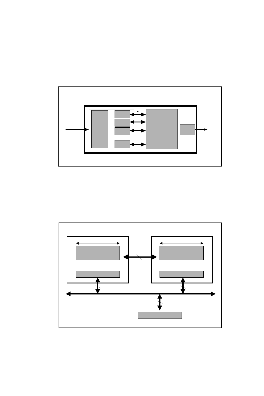
Embedded DRAM
Since performance of the rendering engine is determined by access to the frame buffer (pixel fill rate),
performance is maximized by using embedded DRAM in the GS (the frame buffer is embedded in the same
chip as the rendering circuit) and by providing multiple pixel engines to draw several pixels in parallel.
Ctrl Frame
Buffer
PXE
PXE
PXE
….
PXE
Host
Interface
CRTC
Video
Total
2048bit
width
Figure 1-1 Speedup in Rendering Engine by Embedded DRAM
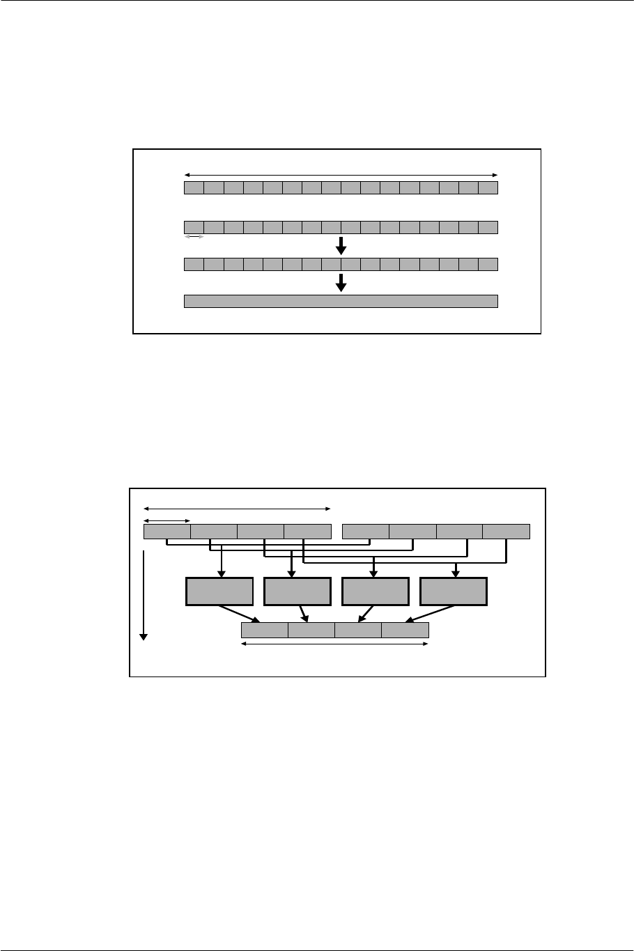
Complete 128-bit Data Bus
The processor has a 128-bit width data bus and registers. The CPU's general-purpose registers (GPR) and
floating-point coprocessor registers are 128 bits wide. All the processors are connected via a 128-bit bus.
VF00
VF01
VF31
….
128 bit
128 bit
GPR0
GPR1
GPR31
….
128 bit
128 bit
Main Bus
Co-ProcessorCPU
128 bit
128 bit
Memory System
Figure 1-2 128-bit Bus
SCE CONFIDENTIAL EE Overview Version 6.0
© SCEI
-13-
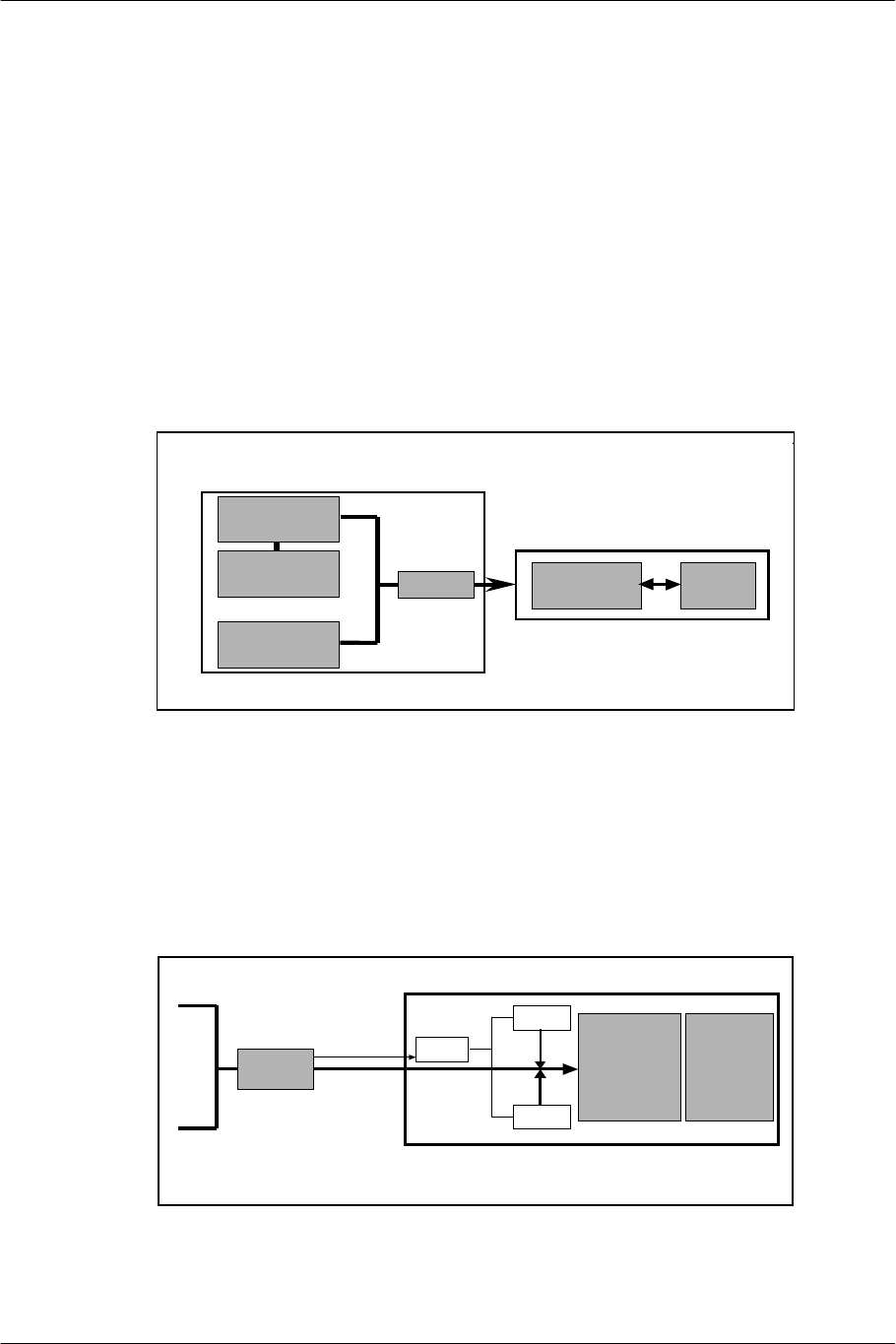
Parallel 128-bit Integer Operation
A multimedia instruction set is implemented. It uses the 128-bit wide GPRs (integer registers) in parallel by
dividing them into fields of 8 bits x 16, 16 bits x 8, 32 bits x 4, and 64 bits x 2. The following example shows
execution of 16-parallel 8-bit addition.
a0
8bit
a1 a2 a3 a4 a5 a6 a7 a8 a9 a10 a11 a12 a13 a14 a15
rs
b0 b1 b2 b3 b4 b5 b6 b7 b8 b9 b10 b11 b12 b13 b14 b15
rt
c0 c1 c2 c3 c4 c5 c6 c7 c8 c9 c10 c11 c12 c13 c14 c15
rd
++++++++++++++++
Main Memory
PADDB (Parallel Add Byte)
SQ (Store Quad Word)
128bit
Figure 1-3 128-bit Parallel Processing by Multimedia Instruction
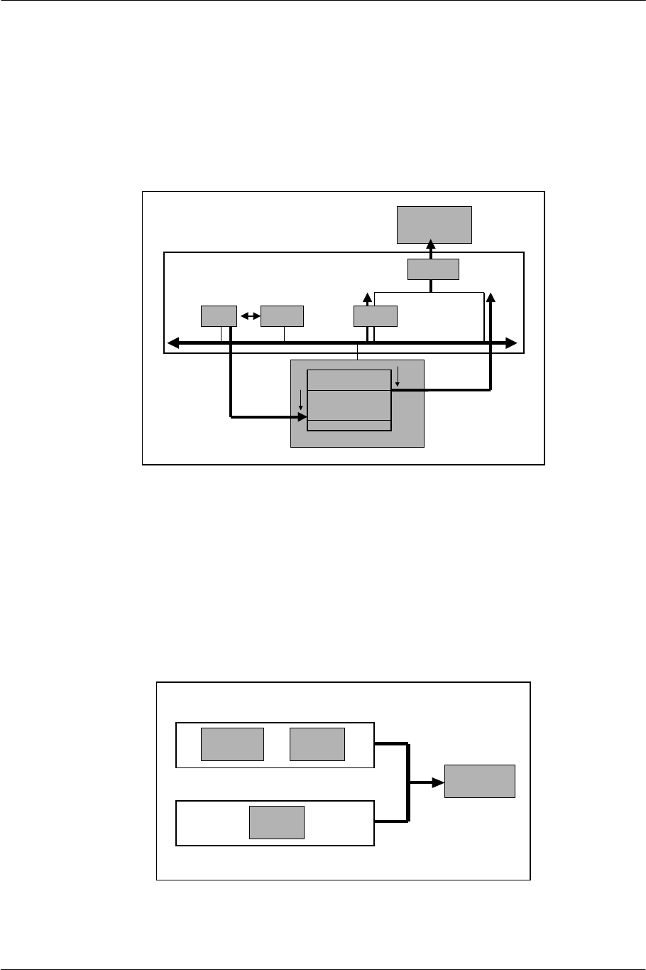
Parallel 128-bit Floating Operation
The 128-bit floating-point registers are divided into four 32-bit floating-point fields. Four FMACs (floating-
point multiply-add ALUs) are provided for four fields to perform operations in parallel. The following
example shows the execution of four parallel 32-bit multiplications.
VFa .x VFa .y VFa .z VFa .w VFb .x VFb .y VFb .z VFb .w
FMAC FMAC FMAC FMAC
32 bit
128 bit
VFc .x VFc .y VFc .z VFc.w
1 cycle
(Throughput) 128 bit
MUL MUL MUL MUL
Figure 1-4 4-Parallel Floating-Point Operation
SCE CONFIDENTIAL EE Overview Version 6.0
© SCEI
-14-
1.3. Geometry Engines in Parallel
Principle
To improve geometry performance relative to drawing performance, an architecture is implemented with
two geometry engines connected in parallel to one rendering engine. One of the geometry engines consists
of the CPU, with a high degree of flexibility, and a vector operation unit (VPU0) as a coprocessor to perform
complex irregular geometry processing, including physical simulation. The other engine is structured with a
programmable vector operation unit (VPU1) to perform simple, repetitive geometry processing such as
background and distant views.
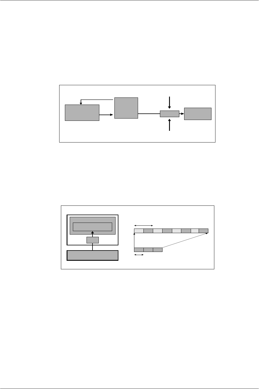
The transfer right between the display lists from each geometry engine is arbitrated, and the display lists are
supplied to the rendering engine asynchronously.
CPU
Vector
Engine
Rendering
Logic
Frame
Buffer
Arbiter
GS
Rendering Engine2 Geometry Engines
Vector
Engine
GIF
Figure 1-5 Parallel Geometry Engines
Dual Context
The display lists supplied from the geometry engines have a context that includes status data such as texture
page and drawing mode. To eliminate the need for setting context information again, two contexts are
maintained in the GS, corresponding to the two geometry engines, VPU0 and VPU1. This is the dual
context mechanism.
GC0
GC1
Rendering
Logic
SEL
Context
Information
Display
List
Arbiter
GS
Frame
Buffer
GC: Graphic Context
GIF
Figure 1-6 Rendering Engine with Dual Context
SCE CONFIDENTIAL EE Overview Version 6.0
© SCEI
-15-
Data Path
Of the two geometry engines, the higher-priority VPU1 is directly connected to the GS, and the lower-
priority CPU+VPU0 is connected to the GS through the main bus. Because data transfer from the lower-
priority geometry engine might be suspended, generated display lists are buffered temporarily in main
memory. The corresponding DMA channels can monitor each other's transfer address so that the buffer
does not overflow.
GS
VPU1CPU VPU0
Main Memory
Main Bus
128bit
MFIFO
1st Priority 2nd Priority
Arbiter
Figure 1-7 Typical Data Paths
Application-Specific Path
The two geometry paths seem to the programmer to be two independent paths. That is, it is possible to
divide graphic processing of the application into two and allocate a portion to each geometry engine.
In general, a high-speed geometry engine (VPU1) takes charge of regular processing such as background and
distant view, and a geometry engine with a high degree of flexibility (CPU+VPU0) takes charge of complex
irregular processing including physical simulation. Simple lighting calculations and transparency perspective
conversions can be executed in VPU1, and the CPU does not have to participate in them directly.
Rendering
Engine
Non-fixed, emotional, and creative operation
Fixed, routine operation
VPU1
EE Core VPU0
Figure 1-8 Processing Allocation of Geometry Engines
SCE CONFIDENTIAL EE Overview Version 6.0
© SCEI
-16-
1.4. Data Decompression/Unpack
Image Decompression
High-resolution texture data requiring a large amount of memory is stored in main memory in a compressed
state, and is decompressed with a special decompression processor (IPU) when used. The decompressed
texture data is returned to main memory temporarily and transferred to the GS.
GS
Decompresser
Main
Memory Arbiter
Display List
Display List
Texture
Compressed Image
IPU
Figure 1-9 Image Data Decompression
Geometry Data Unpack
Modeling data is packed into an optimal bit width in data units, maintained in main memory, and
automatically unpacked by the VIF when sent to the geometry engine (VPU). As a result, the data size in
main memory is reduced, and the load on the VPU can be reduced.
X
Main
Memory
Y Z
X Y Z 1.0
VIF
8/16bit
32bit
VUMEM
VU
unpack
VPU
Figure 1-10 Geometry Data Unpack
SCE CONFIDENTIAL EE Overview Version 6.0
© SCEI
-17-
1.5. Memory Architecture
Hybrid UMA
To correct the problems with UMA (Unified Memory Architecture), each processor has a high-speed, small
capacity cache or working memory for exclusive use, and is connected to the large capacity shared memory
through the high-speed memory.
By storing the data read from or written to memory in 4-qword units, the cache speeds up the second and
succeeding accesses to the nearby addresses and decreases the frequency of accesses to the main memory.
Access to the main memory is made only when
- the data attempted to be read is not in the cache (cache miss)
- the data written to the cache is not reflected in memory (dirty) and the cache space is required to be
freed to access other addresses (cache out).
Data is transferred between the cache and main memory as burst access every 4-qword block (cache line) to
improve the bus efficiency.
CPU
Main Bus
Main Memory
Local Cache
Geometry
Engine
Local Cache
Rendering
Engine
Local Cache
Burst Access
Figure 1-11 Shared Main Memory and Local Cache
CPU Cache
The CPU has an instruction cache (I-Cache) and a data cache (D-Cache). The data cache has the ability to
load a necessary word from a cache line first (sub-block ordering) and to permit a hazard-free cache-line hit
while a previous load is still in process (hit-under-miss). Since this hit-under-miss effect is similar to the
prefetch (PREF) instruction, it is effective when the address to be accessed is known in advance.
Cache Size Way Line Size Sub-block
Ordering
Hit-under-miss
Instruction 16 KB 2-way 4 qwords No No
Data 8 KB 2-way 4 qwords Yes Yes
The output from the cache is also buffered in the Write Back Buffer (WBB). The WBB is a FIFO of 8
qwords. Write requests are stored here, and then written to memory according to the state of the main bus.
SCE CONFIDENTIAL EE Overview Version 6.0
© SCEI
-18-
Uncached Access
In applications primarily designed for computer graphics, writing display lists to memory is the major
process. The display lists are calculated from the three-dimensional data just read from memory. When
processing a one-way data flow like this, the use of cache may be a disadvantage. Furthermore, in some
cases (e.g. when writing hardware registers and writing data which should be DMA-transferred), it is
preferable that written data be reflected in the main memory immediately.
Therefore, a mode that does not use cache ( uncached mode) is provided. To speed up reading while writing
synchronously, an uncached accelerated mode that uses a special-purpose buffer (UCAB: uncached
accelerated buffer) is also available. The UCAB (in size 8 qwords) speeds up continuous data reading from
the adjoining addresses.
GPR
D Cache
Memory
WBB
Cached
GPR
Memory
WBB
UnCached
GPR
Memory
WBB
UnCached Accelarated
UCAB
Figure 1-12 Three Memory Access Modes
SCE CONFIDENTIAL EE Overview Version 6.0
© SCEI
-19-
Scratchpad RAM
A general-purpose high-speed internal memory (Scratchpad RAM: SPR) useable as a working memory for
the CPU is embedded, in addition to the data cache. DMA transfer between main memory and the SPR can
be performed in parallel with SPR access from the CPU. Main memory access overhead can be hidden from
the program by using the SPR as a double buffer.
CPU
#1
DMA
External
Memory
read read write
read Calc
Memory
#1
#2
pseudo-
dual-port
a) Architecture b) Scheduling
SPR #2
write read
writeread read
CPU
Calc Calc Calc
read Calc write Calc
read
Figure 1-13 Double Buffering with SPR
List processor DMA
Display lists are not always located in consecutive areas in memory. In most cases they can be arranged
discontinuously by adopting a linked list structure. To negate the need for data sorting when transferring
non-continuous data between processors, the DMAC can trace data lists according to the tag information
(DMAtag) in the data. This releases the CPU from simple memory copying and increases efficiency in using
the cache.
CONT
Matrix
REF
REF
NEXT
Texture
Vertex Next Object
DMA Start Address
Matrix
Texture
Vertex
Reference
Reference
Figure 1-14 List Processing with DMAC

SCE CONFIDENTIAL EE Overview Version 6.0
© SCEI
-20-
(This page is left blank intentionally)

SCE CONFIDENTIAL EE Overview Version 6.0
© SCEI
-21-
2. Architecture Overview
SCE CONFIDENTIAL EE Overview Version 6.0
© SCEI
-22-
2.1. EE Block Configuration
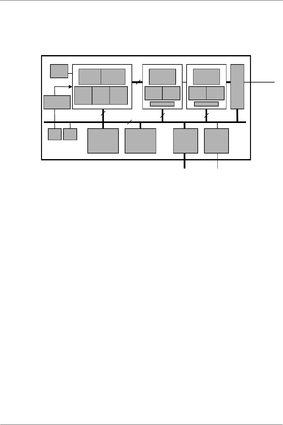
The block diagram and main specifications of the EE are shown below.
FPU
I$
16KB
IU 0
64bit
Interrupt
Controller
CPU
Timer SIO
IPU Memory
Interface
VPU1VPU0
cop1 cop2
GS
128
128
External Memory Peripherals
10ch DMA
Controller
I/O
Interface
VU0
D$
8KB
SPRAM
16KB
IU 1
64bit
GIF
micro
MEM
VU
MEM
VU1
micro
MEM
VU
MEM
128 128 128
EE Core
VIF VIF
Figure 2-1 EE Block Diagram

SCE CONFIDENTIAL EE Overview Version 6.0
© SCEI
-23-
Main Specifications
Block Name Contents
Core 2-way superscalar
Data bus 128 bits (64 bits x 2)
Internal bus 128 bits
Internal register 128 bits x 32
CACHE I-Cache 16 KB 2-way set associative
D-Cache 8 KB 2-way set associative with
line lock
Scratchpad RAM (SPR) 16 KB
MMU 48-double-entry TLB
32-bit physical/logical address space conversion
CPU
Instruction set 64 bits, conforms to MIPS III (partly to MIPS IV)
128-bit parallel multimedia instruction set
3-operand multiply/multiply-add calculation instruction
Interrupt enable/disable instruction
FPU 32-bit single-precision floating-point multiply-add arithmetic
logical unit
32-bit single-precision floating-point divide calculator
Coprocessors
VPU0 32-bit single-precision floating-point multiply-add arithmetic
logical unit x 4
32-bit single-precision floating-point divide calculator x 1
Data unpacking function (VIF)
Programmable LIW DSP
Internal bus (data) 128 bits
Coordinate
engine
VPU1 32-bit single-precision floating-point multiply-add arithmetic
logical unit x 5
32-bit single-precision floating-point divide calculator x 2
Data unpacking function (VIF)
Programmable LIW DSP
Internal bus (data) 128 bits
Image engine IPU MPEG2 video layer decoding/bit stream decoding/IDCT/CSC
(Color Space Conversion)/Dither/ VQ (Vector Quantization)
DMAC 10ch (transfer between memory and I/O, memory and SPR)
DRAMC RDRAM controller
INTC 2 types: INT0 (for interrupt from each device)/INT1 (for
interrupt from DMAC)
TIMER 16 bits x 4
GIF 256-byte FIFO embedded
Data formatting function
Arbitration (PATH1, 2 and 3)
Built-in devices
SIF 32-bit (address/data multiplex), 128-byte FIFO embedded
Main bus 128 bits

SCE CONFIDENTIAL EE Overview Version 6.0
© SCEI
-24-
2.2. EE Core: CPU
2.2.1. EE Core Features
The EE Core is a processor that implements the superscalar 64-bit MIPS IV instruction set architecture. In
particular, 128-bit parallel processing for multimedia applications has been greatly expanded.
The EE Core is composed of the CPU, a floating-point execution unit (Coprocessor 1), an instruction cache, a
data cache, scratchpad RAM, and a tightly coupled vector operation unit (Coprocessor 2).
The CPU has two pipelines and can decode two instructions in each cycle. Instructions are executed and
completed in order. However, since data cache misses are not blocked and a single cache miss does not stall the
pipelines, a load miss or non-cached load completion may occur out of order. Completion of Multiply, Multiply-
Add, Divide, Prefetch, and Coprocessor instructions may also occur out of order. The above features are
summarized as follows:
• 2-way superscalar pipelines
• 128-bit (64 bits x 2) data path and 128-bit system bus
• Instruction set
- 64-bit instruction set conforming to MIPS III and partly conforming to MIPS IV (Prefetch instruction
and conditional move instructions)
- Non-blocking load instructions
- Three-operand Multiply and Multiply-Add instructions
- 128-bit multimedia instructions (Parallel processing of 64 bits x 2, 32 bits x 4, 16 bits x 8, or 8 bits x 16)
• On-chip caches and scratchpad RAM
- Instruction cache: 16 KB, 2-way set associative
- Data cache: 8 KB, 2-way set associative (with a write back protocol)
- Data scratchpad RAM: 16 KB
- Data cache line lock function
- Prefetch function
• MMU
- 48-double-entry full-set-associative address translation look-aside buffer (TLB)
SCE CONFIDENTIAL EE Overview Version 6.0
© SCEI
-25-
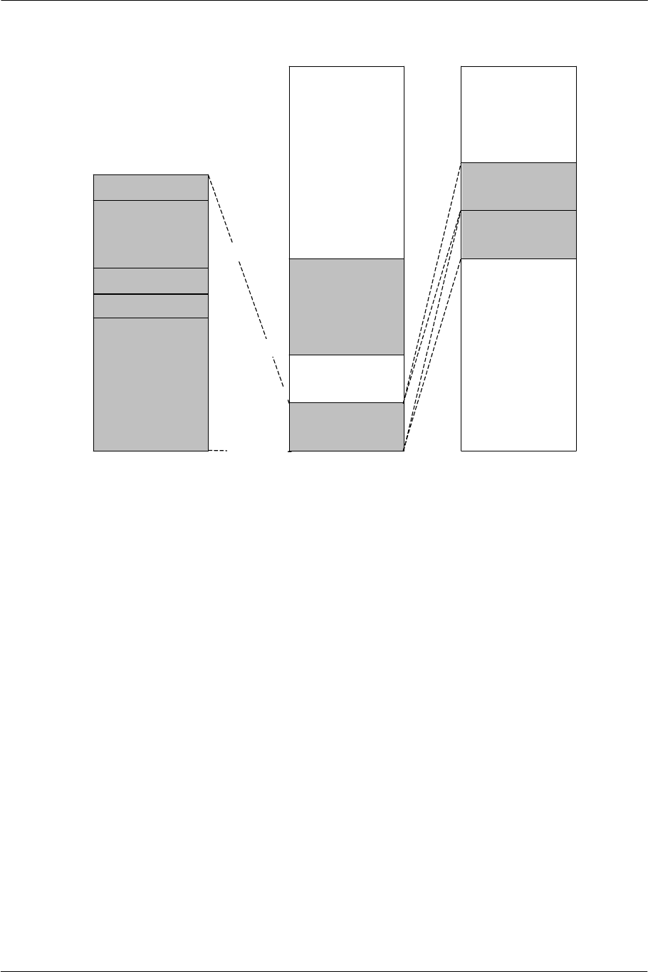
2.2.2. Memory Map
Boot ROM (Max. 4MB)
GS Registers
EE Registers
Main Memory
(Max. 256MB)
Reserved
NO Mount
NO Mount
System
Extend
Main Memory
(Max. 1GB)
1fc0_0000
1400_0000
1200_0000
1000_0000
0000_0000
ffff_ffff
0000_0000
2000_0000
4000_0000
KSEG0
System
KSEG1
System
8000_0000
ffff_ffff
a000_0000
c000_0000
Physical Memory Kernel Mode
8000_0000
Figure 2-2 EE Core Memory Map

SCE CONFIDENTIAL EE Overview Version 6.0
© SCEI
-26-
2.2.3. Instruction Set Overview
The EE Core has an instruction set consisting of the MIPS III instruction set, part of the MIPS IV instruction
set, 128-bit multimedia instructions, three-operand multiply instructions, I1 pipe operation instructions, and
others. The EE Core instructions are listed below.
Integer Add/Subtract
Instruction Fuction Level
ADD Add Word MIPS I
ADDI Add Immediate Word MIPS I
ADDIU Add Immediate Unsigned Word MIPS I
ADDU Add Unsigned Word MIPS I
DADD Doubleword Add MIPS III
DADDI Doubleword Add Immediate MIPS III
DADDIU Doubleword Add Immediate Unsigned MIPS III
DADDU Doubleword Add Unsigned MIPS III
DSUB Doubleword Subtract MIPS III
DSUBU Doubleword Subtract Unsigned MIPS III
SUB Subtract Word MIPS I
SUBU Subtract Unsigned Word MIPS I
PADDB Parallel Add Byte 128-bit MMI
PADDH Parallel Add Halfword 128-bit MMI
PADDSB Parallel Add with Signed Saturation Byte 128-bit MMI
PADDSH Parallel Add with Signed Saturation Halfword 128-bit MMI
PADDSW Parallel Add with Signed Saturation Word 128-bit MMI
PADDUB Parallel Add with Unsigned Saturation Byte 128-bit MMI
PADDUH Parallel Add with Unsigned Saturation Halfword 128-bit MMI
PADDUW Parallel Add with Unsigned Saturation Word 128-bit MMI
PADDW Parallel Add Word 128-bit MMI
PADSBH Parallel Add/Subtract Halfword 128-bit MMI
PSUBB Parallel Subtract Byte 128-bit MMI
PSUBH Parallel Subtract Halfword 128-bit MMI
PSUBSB Parallel Subtract with Signed Saturation Byte 128-bit MMI
PSUBSH Parallel Subtract with Signed Saturation Halfword 128-bit MMI
PSUBSW Parallel Subtract with Signed Saturation Word 128-bit MMI
PSUBUB Parallel Subtract with Unsigned Saturation Byte 128-bit MMI
PSUBUH Parallel Subtract with Unsigned Saturation Halfword 128-bit MMI
PSUBUW Parallel Subtract with Unsigned Saturation Word 128-bit MMI
PSUBW Parallel Subtract Word 128-bit MMI

SCE CONFIDENTIAL EE Overview Version 6.0
© SCEI
-27-
Integer Multiply/Divide
Instruction Function Level
DIV Divide Word MIPS I
DIV1 Divide Word Pipeline 1 EE Core
DIVU Divide Unsigned Word MIPS I
DIVU1 Divide Unsigned Word Pipeline 1 EE Core
MULT Multiply Word MIPS I
MULTU Multiply Unsigned Word MIPS I
MULT1 Multiply Word Pipeline 1 EE Core
MULTU1 Multiply Unsigned Word Pipeline 1 EE Core
PDIVBW Parallel Divide Broadcast Word 128-bit MMI
PDIVUW Parallel Divide Unsigned Word 128-bit MMI
PDIVW Parallel Divide Word 128-bit MMI
PMULTH Parallel Multiply Halfword 128-bit MMI
PMULTUW Parallel Multiply Unsigned Word 128-bit MMI
PMULTW Parallel Multiply Word 128-bit MMI
Integer Multiply-Add
Instruction Function Level
MADD Multiply-Add word EE Core
MADD1 Multiply-Add word Pipeline 1 EE Core
MADDU Multiply-Add Unsigned word EE Core
MADDU1 Multiply-Add Unsigned word Pipeline 1 EE Core
PHMADH Parallel Horizontal Multiply-Add Halfword 128-bit MMI
PHMSBH Parallel Horizontal Multiply-Subtract Halfword 128-bit MMI
PMADDH Parallel Multiply-Add Halfword 128-bit MMI
PMADDUW Parallel Multiply-Add Unsigned Word 128-bit MMI
PMADDW Parallel Multiply-Add Word 128-bit MMI
PMSUBH Parallel Multiply-Subtract Halfword 128-bit MMI
PMSUBW Parallel Multiply-Subtract Word 128-bit MMI
Floating-Point
Instruction Function Level
ADD.S Floating Point Add MIPS I
ADDA.S Floating Point Add to Accumulator EE Core
MADD.S Floating Point Multiply-Add MIPS I
MADDA.S Floating Point Multiply and Add to Accumulator EE Core
MUL.S Floating Point Multiply MIPS I
MULA.S Floating Point Multiply to Accumulator EE Core
MSUB.S Floating Point Multiply and Subtract MIPS I
MSUBA.S Floating Point Multiply and Subtract from Accumulator EE Core
SUB.S Floating Point Subtract MIPS I
SUBA.S Floating Point Subtract to Accumulator EE Core

SCE CONFIDENTIAL EE Overview Version 6.0
© SCEI
-28-
Shift
Instruction Function Level
DSRA Doubleword Shift Right Arithmetic MIPS III
DSLL Doubleword Shift Left Logical MIPS III
DSLL32 Doubleword Shift Left Logical Plus 32 MIPS III
DSLLV Doubleword Shift Left Logical Variable MIPS III
DSRA32 Doubleword Shift Right Arithmetic Plus 32 MIPS III
DSRAV Doubleword Shift Right Arithmetic Variable MIPS III
DSRL Doubleword Shift Right Logical MIPS III
DSRL32 Doubleword Shift Right Logical Plus 32 MIPS III
DSRLV Doubleword Shift Right Logical Variable MIPS III
SLL Shift Word Left Logical MIPS I
SLLV Shift Word Left Logical Variable MIPS I
SRA Shift Word Right Arithmetic MIPS I
SRAV Shift Word Right Arithmetic Variable MIPS I
SRL Shift Word Right Logical MIPS I
SRLV Shift Word Right Logical Variable MIPS I
PSLLH Parallel Shift Left Logical Halfword 128-bit MMI
PSLLVW Parallel Shift Left Logical Variable Word 128-bit MMI
PSLLW Parallel Shift Left Logical Word 128-bit MMI
PSRAH Parallel Shift Right Arithmetic Halfword 128-bit MMI
PSRAVW Parallel Shift Right Arithmetic Variable Word 128-bit MMI
PSRAW Parallel Shift Right Arithmetic Word 128-bit MMI
PSRLH Parallel Shift Right Logical Halfword 128-bit MMI
PSRLVW Parallel Shift Right Logical Variable Word 128-bit MMI
PSRLW Parallel Shift Right Logical Word 128-bit MMI
QFSRV Quadword Funnel Shift Right Variable 128-bit MMI
Logical
Instruction Function Level
AND And MIPS I
ANDI And Immediate MIPS I
NOR Not Or MIPS I
OR Or MIPS I
ORI Or Immediate MIPS I
XOR Exclusive OR MIPS I
XORI Exclusive OR Immediate MIPS I
PAND Parallel And 128-bit MMI
PNOR Parallel Not Or 128-bit MMI
POR Parallel Or 128-bit MMI
PXOR Parallel Exclusive OR 128-bit MMI

SCE CONFIDENTIAL EE Overview Version 6.0
© SCEI
-29-
Compare
Instruction Function Level
SLTI Set on Less Than Immediate MIPS I
SLTIU Set on Less Than Immediate Unsigned MIPS I
SLTU Set on Less Than Unsigned MIPS I
PCEQB Parallel Compare for Equal Byte 128-bit MMI
PCEQH Parallel Compare for Equal Halfword 128-bit MMI
PCEQW Parallel Compare for Equal Word 128-bit MMI
PCGTB Parallel Compare for Greater Than Byte 128-bit MMI
PCGTH Parallel Compare for Greater Than Halfword 128-bit MMI
PCGTW Parallel Compare for Greater Than Word 128-bit MMI
C.EQ.S Floating Point Compare (Equal) MIPS I
C.F.S Floating Point Compare (False) MIPS I
C.LE.S Floating Point Compare (Less than or Equal) MIPS I
C.LT.S Floating Point Compare (Less than) MIPS I
Min/Max
Instruction Function Level
PMAXH Parallel Maximize Halfword 128-bit MMI
PMAXW Parallel Maximize Word 128-bit MMI
PMINH Parallel Minimize Halfword 128-bit MMI
PMINW Parallel Minimize Word 128-bit MMI
MAX.S Floating Point Maximum EE Core
MIN.S Floating Point Minimum EE Core
Data Format Conversion
Instruction Function Level
PEXT5 Parallel Extend Upper from 5 bits 128-bit MMI
PPAC5 Parallel Pack to 5 bits 128-bit MMI
CVT.S.W Fixed point Convert to Single Floating Point MIPS I
CVT.W.S Floating point Convert to Word Fixed-Point MIPS I

SCE CONFIDENTIAL EE Overview Version 6.0
© SCEI
-30-
Reordering
Instruction Function Level
PCPYH Parallel Copy Halfword 128-bit MMI
PCPYLD Parallel Copy Lower Doubleword 128-bit MMI
PCPYUD Parallel Copy Upper Doubleword 128-bit MMI
PEXCH Parallel Exchange Center Halfword 128-bit MMI
PEXCW Parallel Exchange Center Word 128-bit MMI
PEXEH Parallel Exchange Even Halfword 128-bit MMI
PEXEW Parallel Exchange Even Word 128-bit MMI
PEXTLB Parallel Extend Lower from Byte 128-bit MMI
PEXTLH Parallel Extend Lower from Halfword 128-bit MMI
PEXTLW Parallel Extend Lower form Word 128-bit MMI
PEXTUB Parallel Extend Upper from Byte 128-bit MMI
PEXTUH Parallel Extend Upper from Halfword 128-bit MMI
PEXTUW Parallel Extend Upper from Word 128-bit MMI
PINTEH Parallel Interleave Even Halfword 128-bit MMI
PINTH Parallel Interleave Halfword 128-bit MMI
PPACB Parallel Pack to Byte 128-bit MMI
PPACH Parallel Pack to Halfword 128-bit MMI
PPACW Parallel Pack to Word 128-bit MMI
PREVH Parallel Reverse Halfword 128-bit MMI
PROT3W Parallel Rotate 3 Words 128-bit MMI
Others
Instruction Function Level
PABSH Parallel Absolute Halfword 128-bit MMI
PABSW Parallel Absolute Word 128-bit MMI
PLZCW Parallel Leading Zero or One Count Word 128-bit MMI
ABS.S Floating Point Absolute Value MIPS I
NEG.S Floating Point Negate MIPS I
RSQRT.S Floating Point Reciprocal Root MIPS IV
SQRT.S Floating Point Square Root MIPS II

SCE CONFIDENTIAL EE Overview Version 6.0
© SCEI
-31-
Register-Register Transfer
Instruction Function Level
MFHI Move from HI Register MIPS I
MFLO Move from LO Register MIPS I
MOVN Move Conditional on Not Zero MIPS IV
MOVZ Move Conditional on Zero MIPS IV
MTHI Move to HI Register MIPS I
MTLO Move to LO Register MIPS I
MFHI1 Move From HI1 Register EE Core
MFLO1 Move From LO1 Register EE Core
MTHI1 Move To HI1 Register EE Core
MTLO1 Move to LO1 Register EE Core
PMFHI Parallel Move From HI Register 128-bit MMI
PMFHL Parallel Move from HI/LO Register 128-bit MMI
PMFLO Parallel Move from LO Register 128-bit MMI
PMTHI Parallel Move To HI Register 128-bit MMI
PMTHL Parallel Move To HI/LO Register 128-bit MMI
PMTLO Parallel Move To LO Register 128-bit MMI
MFC1 Move Word from Floating Point MIPS I
MOV.S Floating Point Move MIPS I
MTC1 Move Word to Floating Point MIPS I
Load from Memory
Instruction Function Level
LB Load Byte MIPS I
LBU Load Byte Unsigned MIPS I
LD Load Doubleword MIPS III
LDL Load Doubleword Left MIPS III
LDR Load Doubleword Right MIPS III
LH Load Halfword MIPS I
LHU Load Halfword Unsigned MIPS I
LUI Load Upper Immediate MIPS I
LW Load Word MIPS I
LWL Load Word Left MIPS I
LWR Load Word Right MIPS I
LWU Load Word Unsigned MIPS I
LQ Load Quadword 128-bit MMI
LWC1 Load Word to Floating Point MIPS I

SCE CONFIDENTIAL EE Overview Version 6.0
© SCEI
-32-
Store in Memory
Instruction Function Level
SB Store Byte MIPS I
SD Store Doubleword MIPS III
SDL Store Doubleword Left MIPS III
SDR Store Doubleword Right MIPS III
SH Store Halfword MIPS I
SW Store Word MIPS I
SWL Store Word Left MIPS I
SWR Store Word Right MIPS I
SQ Store Quadword 128-bit MMI
SWC1 Store Word from Floating Point MIPS I
Special Data Transfer
Instruction Function Level
MFSA Move from Shift Amount Register EE Core
MTSA Move to Shift Amount Register EE Core
MTSAB Move Byte Count to Shift Amount Register EE Core
MTSAH Move Halfword Count to Shift Amount Register EE Core
MFBPC Move from Breakpoint Control Register MIPS I
MFCO Move from System Control Coprocessor MIPS I
MFDAB Move from Data Address Breakpoint register MIPS I
MFDABM Move from Data Address Breakpoint Mask Register MIPS I
MFDVB Move from Data value Breakpoint Register MIPS I
MFDVBM Move from Data Value Breakpoint Mask Register MIPS I
MFIAB Move from Instruction Address Breakpoint Register MIPS I
MFIABM Move from Instruction Address Breakpoint Mask Register MIPS I
MFPC Move from Performance Counter MIPS I
MFPS Move from Performance Event Specifier MIPS I
MTBPC Move to Breakpoint Control Register MIPS I
MTCO Move to System Control Coprocessor MIPS I
MTDAB Move to Data Address Breakpoint Register MIPS I
MTDABM Move to Data Address Breakpoint Mask Register MIPS I
MTDVB Move to Data Value Breakpoint Register MIPS I
MTDVBM Move to Data Value Breakpoint Mask Register MIPS I
MTIAB Move to Instruction Address Breakpoint Register MIPS I
MTIABM Move to Instruction Address Mask Breakpoint Register MIPS I
MTPC Move to Performance Counter MIPS I
MTPS Move to Performance Event Specifier MIPS I
CFC1 Move Control Word from Floating Point MIPS I
CTC1 Move Control Word to Floating Point MIPS I

SCE CONFIDENTIAL EE Overview Version 6.0
© SCEI
-33-
Conditional Branch and Jump
Instruction Function Level
BEQ Branch on Equal MIPS I
BEQL Branch on Equal Likely MIPS II
BGEZ Branch on Greater Than or Equal to Zero MIPS I
BGEZL Branch on Greater Than or Equal to Zero Likely MIPS II
BGTZ Branch on Greater Than Zero MIPS I
BGTZL Branch on Greater Than Zero Likely MIPS II
BLEZ Branch on Less Than or Equal to Zero MIPS I
BLEZL Branch on Less Than or Equal to Zero Likely MIPS II
BLTZ Branch on Less Than Zero MIPS I
BLTZL Branch on Less Than Zero Likely MIPS II
BNE Branch on Not Equal MIPS I
BNEL Branch on Not Equal Likely MIPS II
BC0F Branch on Coprocessor 0 False MIPS I
BC0FL Branch on Coprocessor 0 False Likely MIPS I
BC0T Branch on Coprocessor 0 True MIPS I
BC0TL Branch on Coprocessor 0 True Likely MIPS I
BC1F Branch on FP False MIPS I
BC1FL Branch on FP False Likely MIPS II
BC1T Branch on FP True MIPS I
BC1TL Branch on FP True Likely MIPS II
BC2F Branch on Coprocessor 2 False MIPS I
BC2FL Branch on Coprocessor 2 False Likely MIPS I
BC2T Branch on Coprocessor 2 True MIPS I
BC2TL Branch on Coprocessor 2 True Likely MIPS I
J Jump MIPS I
JR Jump Register MIPS I
Subroutine Call
Instruction Function Level
BGEZAL Branch on Greater Than or Equal to Zero and Link MIPS I
BGEZALL Branch on Greater Than or Equal to Zero and Link Likely MIPS II
BLTZAL Branch on Less Than Zero and Link MIPS I
BLTZALL Branch on Less Than Zero and Link Likely MIPS II
JAL Jump and Link MIPS I
JALR Jump and Link Register MIPS I

SCE CONFIDENTIAL EE Overview Version 6.0
© SCEI
-34-
Break and Trap
Instruction Function Level
BREAK Breakpoint MIPS I
SYSCALL System Call MIPS I
TEQ Trap if Equal MIPS II
TEQI Trap if Equal Immediate MIPS II
TGE Trap if Greater or Equal MIPS II
TGEI Trap if Greater or Equal Immediate MIPS II
TGEIU Trap if Greater or Equal Immediate Unsigned MIPS II
TGEU Trap if Greater or Equal Unsigned MIPS II
TLT Trap if Less Than MIPS II
TLTI Trap if Less Than Immediate MIPS II
TLTIU Trap if Less Than Immediate Unsigned MIPS II
TLTU Trap if Less Than Unsigned MIPS II
TNE Trap if Not Equal MIPS II
TNEI Trap if Not Equal Immediate MIPS II
ERET Exception Return MIPS III
Others
Instruction Function Level
SYNC.stype Synchronize Shared Memory MIPS II
PREF Prefetch MIPS IV
DI Disabled Interrupt MIPS I
EI Enabled Interrupt MIPS I
SCE CONFIDENTIAL EE Overview Version 6.0
© SCEI
-35-
2.3. VPU: Vector Operation Processor
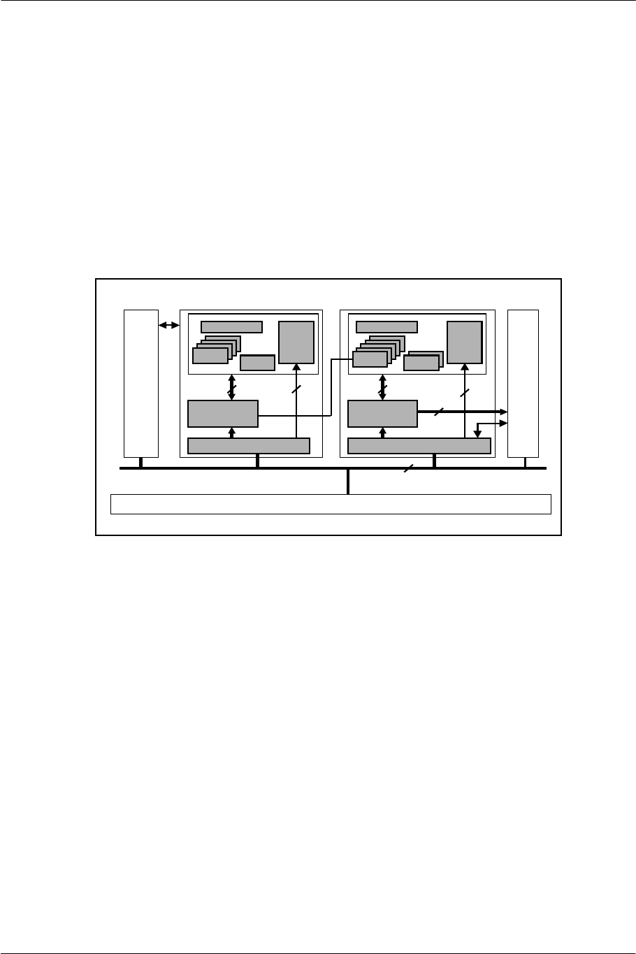
The EE has two on-chip vector operation processors with the same architecture, VPU0 and VPU1, for floating-
point vector operation indispensable to geometry processing.
VPU0 is connected to the EE Core via a 128-bit coprocessor bus. The operation resources and registers for
VPU0 can be used directly from the EE Core by using coprocessor instructions and not by using the main bus.
VPU1 is directly connected to the rendering engine, the GS, via the GIF (Graphics Synthesizer Interface Unit).
Display lists generated in VPU1 are not transferred to the GS via the main bus.
VPU0 and VPU1 each have a packet expansion engine called VIF (VPU Interface Unit) at the front end. They
are named VIF0 and VIF1 respectively.
EE
Core
Main Memory
ALU
FMAC FDIV
micro
Mem0
VU Mem0
VIF0
VU Mem1
VIF1
VPU0
128
128
128
128
6464 GIF
micro
Mem1
FDIV
FMAC
ALU
VPU1
Figure 2-3 VPU-Related Block Diagram
2.3.1. VPU Architecture
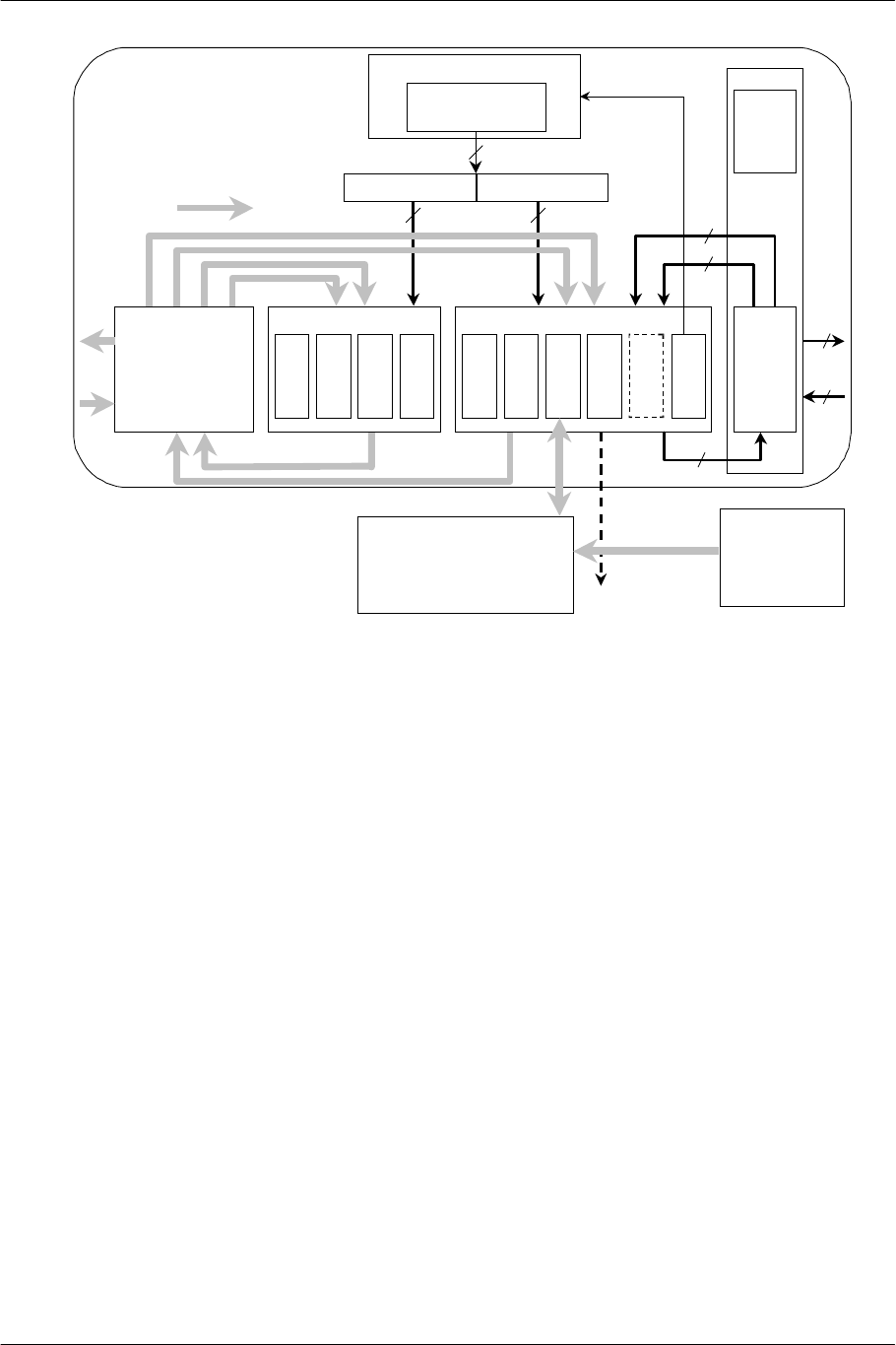
The 2 VPUs basically have the same architecture, consisting of the VU, VU Mem (data memory for VU), and
VIF (compressed-data decompression engine). The VU is a processor unit consisting of several FMACs
(Floating-point Multiply-Add ALUs), FDIV (Floating-point Divide Calculator), 32 four-parallel floating-point
registers, 16 integer registers, and a Micro Mem (program memory). It loads data from the VU Mem in 128-bit
units (single-precision floating-point x 4), performs operations according to microprograms placed in the Micro
Mem, and stores the results in the VU Mem.
Microprograms use a 64-bit-long LIW (Long Instruction Word) instruction set, and can concurrently execute
floating-point multiply-add operations in the Upper 32-bit field (Upper instruction field) and floating-point
divide or integer operations in the Lower 32-bit field (Lower instruction field).
SCE CONFIDENTIAL EE Overview Version 6.0
© SCEI
-36-
Micro Mem
4 KBytes or 16 KBytes
Upper Instruction Lower Instruction
63 0
64
32 32
bold line : 128 bits
Micro instruction fetch unit
FMACw
FMACz
FMACy
FMACx
Upper Execution Unit
RANDU/etc
LSU
IALU
EFU
Lower Execution Unit
floating
registers
VF00~VF31
(COP2 data registers)
127 0
BRU
VU Mem
4 KBytes or 16 KBytes
integer
registers
VI00~VI15
16
16
16
QMTC2
/ LQC2
QMFC2
/ SQC2
CTC2
32
CFC2
32
special
registers
VI16~VI31
COP2
control
registers
External Units
Vector Unit : VU
Vector Processing Unit :
VPU
FDIV
VIF
Figure 2-4 VU Block Diagram
Following are brief descriptions of the VPU units.
FMAC
This unit handles add/subtract, multiply, and multiply-add of the floating-point numbers. FMACx, FMACy,
FMACz, and FMACw are mounted to execute four-element vector operations efficiently. The latency of
instructions which use the FMAC has been unified at four cycles to increase the efficiency of pipeline
processing.
FDIV
This unit performs self-synchronous type floating-point divide/square root operations. FDIV operations
differ from others in latency, so the results are stored in the Q register.
LSU
This unit controls loading and storing to and from VU Mem.
Load/Store must be performed in units of 128 bits, but can be masked in units of x, y, z and w fields.
IALU
This unit performs 16-bit integer operations.
Loop counter operations and load/store address calculations are performed in conjunction with the integer
register.
BRU
This unit controls jump and conditional branch.
RANDU
This unit generates random numbers. Random numbers are generated by the M sequence and stored in the
R register.
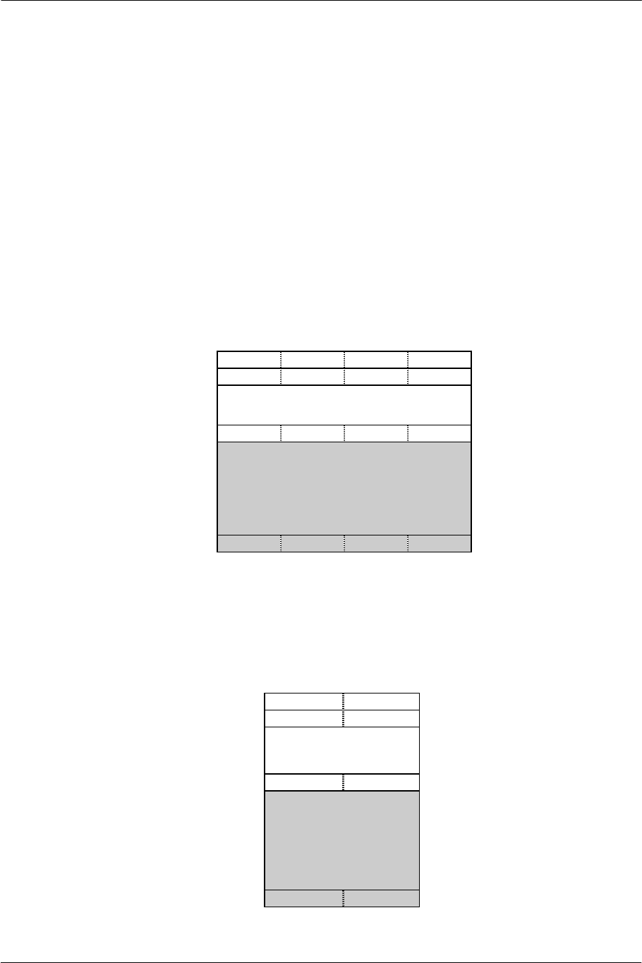
SCE CONFIDENTIAL EE Overview Version 6.0
© SCEI
-37-
EFU
This is an elementary function unit, which executes operations such as exponential and trigonometric
functions. This unit is mounted only on VU1. Operation results are stored in the P register.
Floating-Point Registers
32 128-bit floating-point registers (VF00 - VF31) are mounted. Each register can be divided into 4 fields of
x, y, z, and w, and is equivalent to a vector of four single-precision floating-point numbers. VF00 is a
constant register.
Integer Registers
Sixteen 16-bit integer registers (VI00 - VI15) are mounted. These registers are used as loop counters, and
used for load/store address calculations. VI00 is a constant register.
VU Mem
This is data memory for the VU's exclusive use. Memory capacity is 4 Kbytes for VU0 and 16 Kbytes for
VU1. This memory is connected to the LSU at a width of 128 bits, and addresses are aligned on qword
boundaries.
Address
0x0000 w z y x
0x0010 w z y x
:
:
0x0ff0 w z y x
:
Implemented on VU1 only
:
0x3ff0 w z y x
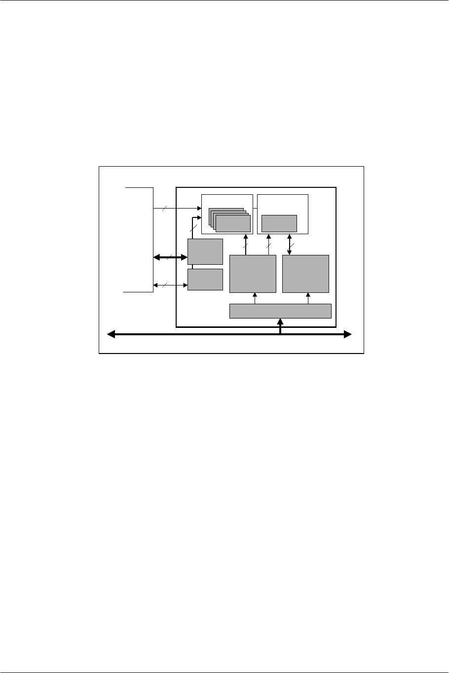
Figure 2-5 VU Mem Memory Map
Furthermore, VU1 registers are mapped to addresses 0x4000 to 0x43ff in VU0.
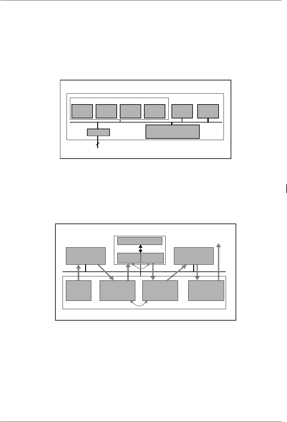
Micro Mem
This is on-chip memory, which stores microinstruction programs. Memory capacity is 4 Kbytes in VU0 and
16 Kbytes in VU1.
Address
0x0000 Upper Lower
0x0008 Upper Lower
:
:
0x0ff8 Upper Lower
:
Implemented on VU1 only
:
0x3ff8 Upper Lower
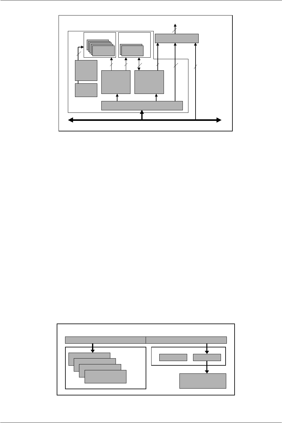
Figure 2-6 Micro Mem Memory Map
SCE CONFIDENTIAL EE Overview Version 6.0
© SCEI
-38-
2.3.2. VPU0
VPU0 has a macro mode, which operates according to coprocessor instructions from the EE Core, and a micro
mode, which operates independently according to microprograms stored in the Micro Mem. Almost all the
instructions used in micro mode are also defined as coprocessor instructions, and are executable directly from
the EE Core. Similarly, VPU0 registers can be referred to directly from the EE Core with coprocessor transfer
instructions.
VPU0 is tightly coupled with the EE Core as mentioned above, and takes charge of relatively small-sized
processing.
FMAC FDIV
VIF
Main Bus
VPU0
VU Mem
4KB
Micro Mem
4KB
12832
128bit
Floating
Regs
Integer
Regs
32
Upper Exec. Unit Lower Exec.Unit
128
EE Core
Cop2
Interface
32
128
32
Figure 2-7 VPU0 Block Diagram
2.3.3. VPU1
VPU1 operates only in micro mode. VPU1 has a larger Micro Mem and VU Mem than VPU0, and is equipped
with an EFU. It is also directly connected to the GIF, and has additional synchronization control instructions
such as transfer to the GIF. Furthermore, it structures double buffers in VU Mem and has additional functions
to perform data transfer and operations in parallel.
As mentioned above, VPU1 operates autonomously as a geometry engine independently of the EE Core. High-
speed processing is possible with VPU1, but because of the limits of complexity of what it can process, it divides
processing of standard three-dimensional graphics.
VPU1 operation results are transferred from VU Mem1 to the GS via the GIF, with the highest priority.
SCE CONFIDENTIAL EE Overview Version 6.0
© SCEI
-39-
FMAC FDIV Path3Path2Path1
VIF
GIF
Main Bus
VPU1
Rendering Engine
VU Mem
16KB
Micro Mem
16KB
12832
64
128 128
128
128 bit
Floating
Regs
Integer
Regs
32
Upper Exec.Unit
128
Lower Exec.Unit
Figure 2-8 VPU1 Block Diagram
2.3.4. VIF: VPU Interface
The VIF functions as a preprocessor for the VPU. The VIF unpacks the packed vertex data, based on the
specification of the tag (VIFtag) at the start of the data, and transfers it to the data memory (VU Mem) of the
VPU. As a result, in addition to reducing the data size in main memory, the VIF removes the load in data
formatting from the VPU, which has low degree of programming freedom.
The VIF also stores microprograms in Micro Mem and transfers DIRECT data to the GIF according to the
VIFtag specification.
2.3.5. Operation Mode and Programming Model
The VU has two execution modes, micro mode and macro mode. In micro mode, the VU functions as a stand-
alone processor and executes microprograms stored in Micro Mem. VU1 operates in this mode. In macro
mode, the VU executes macroinstructions as COP2 (Coprocessor 2) of the EE Core. VU0 operates primarily in
this mode.
Microinstructions are LIW (Long Instruction Word) instructions of 32 bits x 2, and can concurrently execute an
Upper instruction, which uses the upper 32 bits of the instruction word, and a Lower instruction, which uses the
lower 32 bits of the instruction word. The Upper instruction controls the FMAC, and the Lower instruction
controls operations which use the FDIV/EFU/LSU/BRU and integer registers. In the Upper instruction, 4
FMACs are operable concurrently with 1 instruction, and a four-dimensional vector calculation can be made in 1
cycle (throughput).
VU Mem
MUL VF01,VF02,VF03
FDIV
Upper Instruction Lower Instruction
FMAC
FMAC
FMAC
FMAC
LSU
SQ VF04, VI01
Upper Exec. Unit Lower Exec. Unit
Figure 2-9 Upper Instruction and Lower Instruction

SCE CONFIDENTIAL EE Overview Version 6.0
© SCEI
-40-
Operation Latency Throughput
4-parallel floating-point multiply + 4-parallel floating-point add 4 1
Floating point divide 7 7
4 x 4 matrix * 4-row vector 8 4
4 x 4 matrix * 4 x 4 matrix 20 16
1 vertex processing (matrix * vector + divide) 19 8
Some microinstructions do not have macroinstruction equivalents. Macro mode cannot execute the Upper
instruction and Lower instruction at the same time, either. However, macroinstructions can execute the
CALLMS instruction, which executes a microinstruction program in Micro Mem like a subroutine, and the
COP2 data transfer instruction, which transfers data to the VU registers.
Micro Mode (VU1) Macro Mode (VU0)
Operation Operates as a stand-alone processor Operates as a coprocessor of the EE Core
Operation
code
64-bit-long LIW instruction 32-bit MIPS COP2 instruction
Instruction set Upper instruction + Lower instruction
(Can be specified concurrently)
EFU instruction
External unit control instruction
Upper instruction
Lower instruction (partial)
VCALLMS, VCALLMSR instruction
COP2 transfer instruction
Total number
of instructions
127 instructions 90 instructions
EFU Usable as an option Not supported
Register Floating-point register: 32 x 128 bits
Integer register: 16
Special register: ACC, I, Q, R (, P)
Floating-point register: 32 x 128 bits
Integer register: 16
Special register: ACC, I, Q, R
Control register: 16
2.3.6. VPU Instruction Set Overview
VPU microinstructions/macroinstructions are listed below.
Floating-Point Operation
Microinstruction
Upper Lower
Macro-instruction Function
ABS - VABS absolute
ADD - VADD addition
ADDA - VADDA ADD output to ACC
ADDAbc - VADDAbc ADD output to ACC broadcast bc field
ADDAi - VADDAi ADD output to ACC broadcast I register
ADDAq - VADDAq ADD output to ACC broadcast Q register
ADDbc - VADDbc ADD broadcast bc field
ADDi - VADDi ADD broadcast I register
ADDq - VADDq ADD broadcast Q register
- DIV VDIV floating divide
MADD - VMADD MUL and ADD
MADDA - VMADDA MUL and ADD output to ACC
MADDAbc - VMADDAbc MUL and ADD output to ACC broadcast bc field
MADDAi - VMADDAi MUL and ADD output to ACC broadcast I register
MADDAq - VMADDAq MUL and ADD output to ACC broadcast Q register
MADDbc - VMADDbc MUL and ADD broadcast bc field

SCE CONFIDENTIAL EE Overview Version 6.0
© SCEI
-41-
Microinstruction
Upper Lower
Macro-instruction Function
MADDi - VMADDi MUL and ADD broadcast I register
MADDq - VMADDq MUL and ADD broadcast Q register
MAX - VMAX maximum
MAXbc - VMAXbc MAX broadcast bc field
MAXi - VMAXi MAX broadcast I register
MINI - VMINI minimum
MINIbc - VMINIbc MINI broadcast bc field
MINIi - VMINIi MINI broadcast I register
MSUB - VMSUB MUL and SUB
MSUBA - VMSUBA MUL and SUB output to ACC
MSUBAbc - VMSUBAbc MUL and SUB output to ACC broadcast bc field
MSUBAi - VMSUBAi MUL and SUB output to ACC broadcast I register
MSUBAq - VMSUBAq MUL and SUB output to ACC broadcast Q register
MSUBbc - VMSUBbc MUL and SUB broadcast bc field
MSUBi - VMSUBi MUL and SUB broadcast I register
MSUBq - VMSUBq MUL and SUB broadcast Q register
MUL - VMUL multiply
MULA - VMULA MUL output to ACC
MULAbc - VMULAbc MUL output to ACC broadcast bc field
MULAi - VMULAi MUL output to ACC broadcast I register
MULAq - VMULAq MUL output to ACC broadcast Q register
MULbc - VMULbc MUL broadcast bc field
MULi - VMULi MUL broadcast I register
MULq - VMULq MUL broadcast Q register
OPMSUB - VOPMSUB outer product MSUB
OPMULA - VOPMULA outer product MULA
- RSQRT VRSQRT floating reciprocal square-root
- SQRT VSQRT floating square-root
SUB - VSUB subtraction
SUBA - VSUBA SUB output to ACC
SUBAbc - VSUBAbc SUB output to ACC broadcast bc field
SUBAi - VSUBAi SUB output to ACC broadcast I register
SUBAq - VSUBAq SUB output to ACC broadcast Q register
SUBbc - VSUBbc SUB broadcast bc field
SUBi - VSUBi SUB broadcast I register
SUBq - VSUBq SUB broadcast Q register

SCE CONFIDENTIAL EE Overview Version 6.0
© SCEI
-42-
Format Conversion
Microinstruction
Upper Lower
Macro-instruction Function
FTOI0 - VFTOI0 float to integer, fixed point 0 bit
FTOI12 - VFTOI12 float to integer, fixed point 12 bits
FTOI15 - VFTOI15 float to integer, fixed point 15 bits
FTOI4 - VFTOI4 float to integer, fixed point 4 bits
ITOF0 - VITOF0 integer to float, fixed point 0 bit
ITOF12 - VITOF12 integer to float, fixed point 12 bits
ITOF15 - VITOF15 integer to float, fixed point 15 bits
ITOF4 - VITOF4 integer to float, fixed point 4 bits
Integer Operation
Microinstruction
Upper Lower
Macro-instruction Function
- IADD VIADD integer ADD
- IADDI VIADDI integer ADD immediate
- IADDIU - integer ADD immediate unsigned
- IAND VIAND integer AND
- IOR VIOR integer OR
- ISUB VISUB integer SUB
- ISUBIU - integer SUB immediate unsigned
Elementary Function Operation
Microinstruction
Upper Lower
Macro-instruction Function
- EATAN - Elementary-function ArcTAN
- EATANxy - Elementary-function ArcTAN y/x
- EATANxz - Elementary-function ArcTAN z/x
- EEXP - Elementary-function Exponential
- ELENG - Elementary-function Length
- ERCPR - Elementary-function Reciprocal
- ERLENG - Elementary-function Reciprocal Length
- ERSADD - Elementary-function Reciprocal Square and ADD
- ERSQRT - Elementary-function Reciprocal Square-root
- ESADD - Elementary-function Square and ADD
- ESIN - Elementary-function SIN
- ESQRT - Elementary-function Square-root
- ESUM - Elementary-function Sum
Register-Register Transfer
Microinstruction
Upper Lower
Macro-instruction Function
- MFIR VMFIR move from integer register
- MFP - move from P register
- MOVE VMOVE move floating register
- MR32 VMR32 move rotate 32 bits
- MTIR VMTIR move to integer register

SCE CONFIDENTIAL EE Overview Version 6.0
© SCEI
-43-
Load/Store
Microinstruction
Upper Lower
Macro-instruction Function
- ILW - integer load word
- ILWR VILWR integer load word register
- ISW - integer store word
- ISWR VISWR integer store word register
- LQ - Load Quadword
- LQD VLQD Load Quadword with pre-decrement
- LQI VLQI Load Quadword with post-increment
- SQ - Store Quadword
- SQD VSQD Store Quadword with pre-decrement
- SQI VSQI Store Quadword with post-increment
Flag Operation
Microinstruction
Upper Lower
Macro-instruction Function
- FCAND - flag-operation clipping flag AND
- FCEQ - flag-operation clipping flag EQ
- FCGET - flag-operation clipping flag get
- FCOR - flag-operation clipping flag OR
- FCSET - flag-operation clipping flag set
- FMAND - flag-operation MAC flag AND
- FMEQ - flag-operation MAC flag EQ
- FMOR - flag-operation MAC flag OR
- FSAND - flag-operation status flag AND
- FSEQ - flag-operation status flag EQ
- FSOR - flag-operation status flag OR
- FSSET - flag-operation set status flag
Branching
Microinstruction
Upper Lower
Macro-instruction Function
- B - branch (PC relative address)
- BAL - branch and link (PC relative address)
- IBEQ - integer branch on equal
- IBGEZ - integer branch on greater than or equal to zero
- IBGTZ - integer branch on greater than 0
- IBLEZ - integer branch on less than or equal to zero
- IBLTZ - integer branch on less than zero
- IBNE - integer branch on not equal
- JALR - jump and link register (absolute address)
- JR - jump register (absolute address)

SCE CONFIDENTIAL EE Overview Version 6.0
© SCEI
-44-
Random Numbers
Microinstruction
Upper Lower
Macro-instruction Function
- RGET VRGET random-unit get R register
- RINIT VRINIT random-unit init R register
- RNEXT VRNEXT random-unit next M sequence
- RXOR VRXOR random-unit XOR register
Others
Microinstruction
Upper Lower
Macro-instruction Function
CLIP - VCLIP clipping
NOP - VNOP no operation
- WAITP - wait P register
- WAITQ VWAITQ wait Q register
- XGKICK - eXternal-unit GPU2 Interface Kick
- XITOP - eXternal-unit read ITOP register
- XTOP - eXternal-unit read TOP register
SCE CONFIDENTIAL EE Overview Version 6.0
© SCEI
-45-
2.4. IPU: Image Data Processor
The IPU implements decompression of two-dimensional images, such as texture data and video data. The IPU
decompresses the data, using MPEG2 or a subset of MPEG2, or converts the data, using VQ (Vector
Quantization). Which layer to use depends on the purpose and the property of the image.
FIFO Local Buffer
Memory
CSC VQ
Macro-Block Decoder
128
IPU
VLD Zig-zag
Scan IDCT IQ
Figure 2-10 IPU Block Diagram
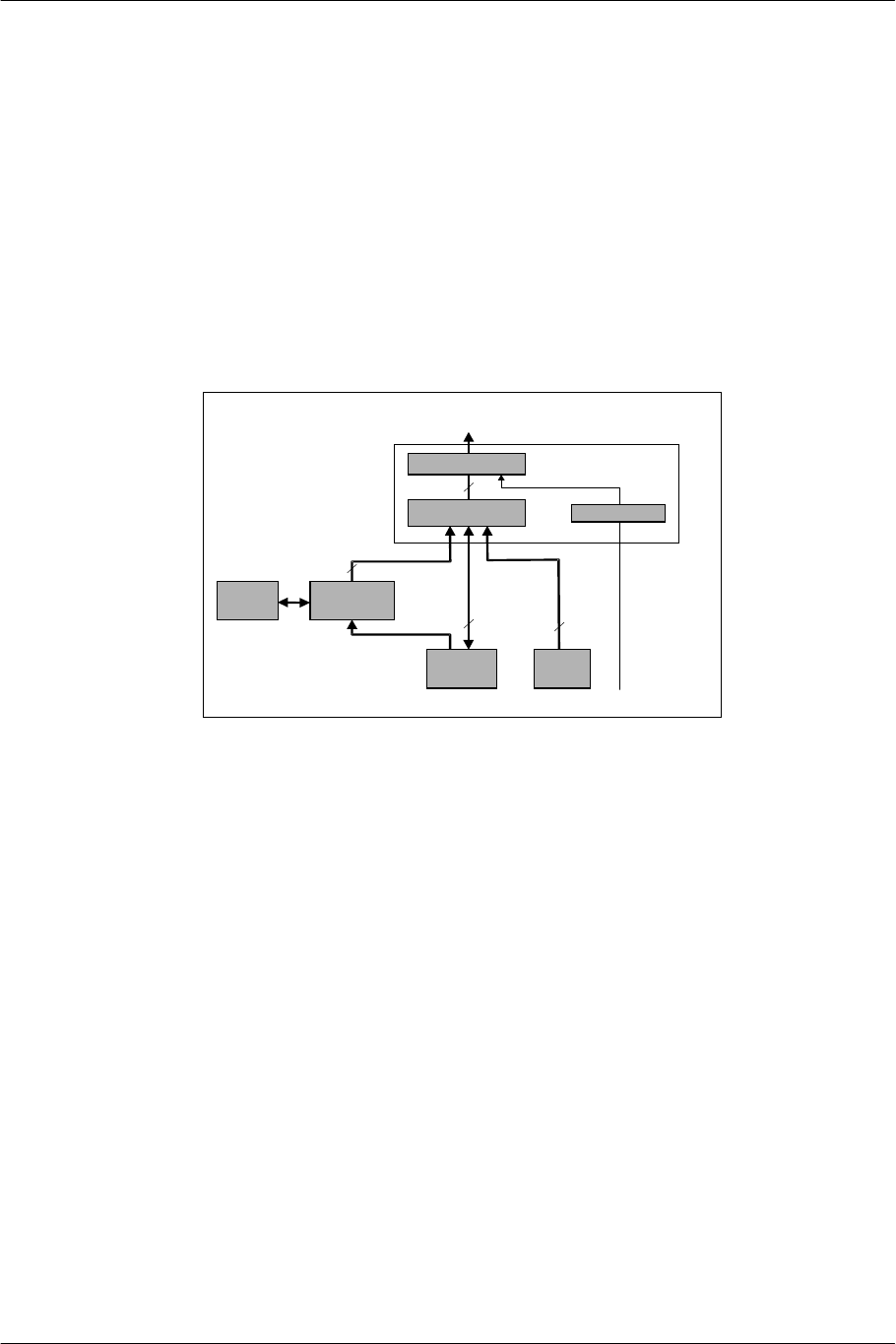
In decoding MPEG2 bit streams, the IPU decodes macro blocks and the EE Core performs motion
compensation via software by using multimedia instructions. For CSC (Color Space Conversion), the IPU is in
charge.
IPU
(IDCT)
Bit
Stream
Reference
Image
Decoded
Image
RGB
Decoded
Image
128 bit ALU
SPR
Buffer#0
SPR
Buffer#1
IPU
(CSC)
Rendering
Engine
Main Memory
EE Core
Figure 2-11 Decoding Process Flow for Motion Compensation
SCE CONFIDENTIAL EE Overview Version 6.0
© SCEI
-46-
2.5. GIF: GS Interface
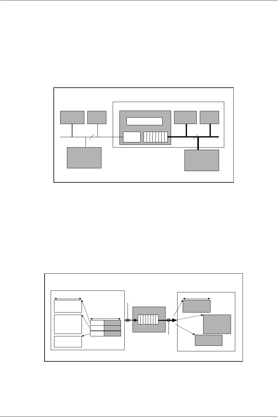
As a front end to the GS, the GIF formats data based on the specifications of a tag (GIFtag) at the start of the
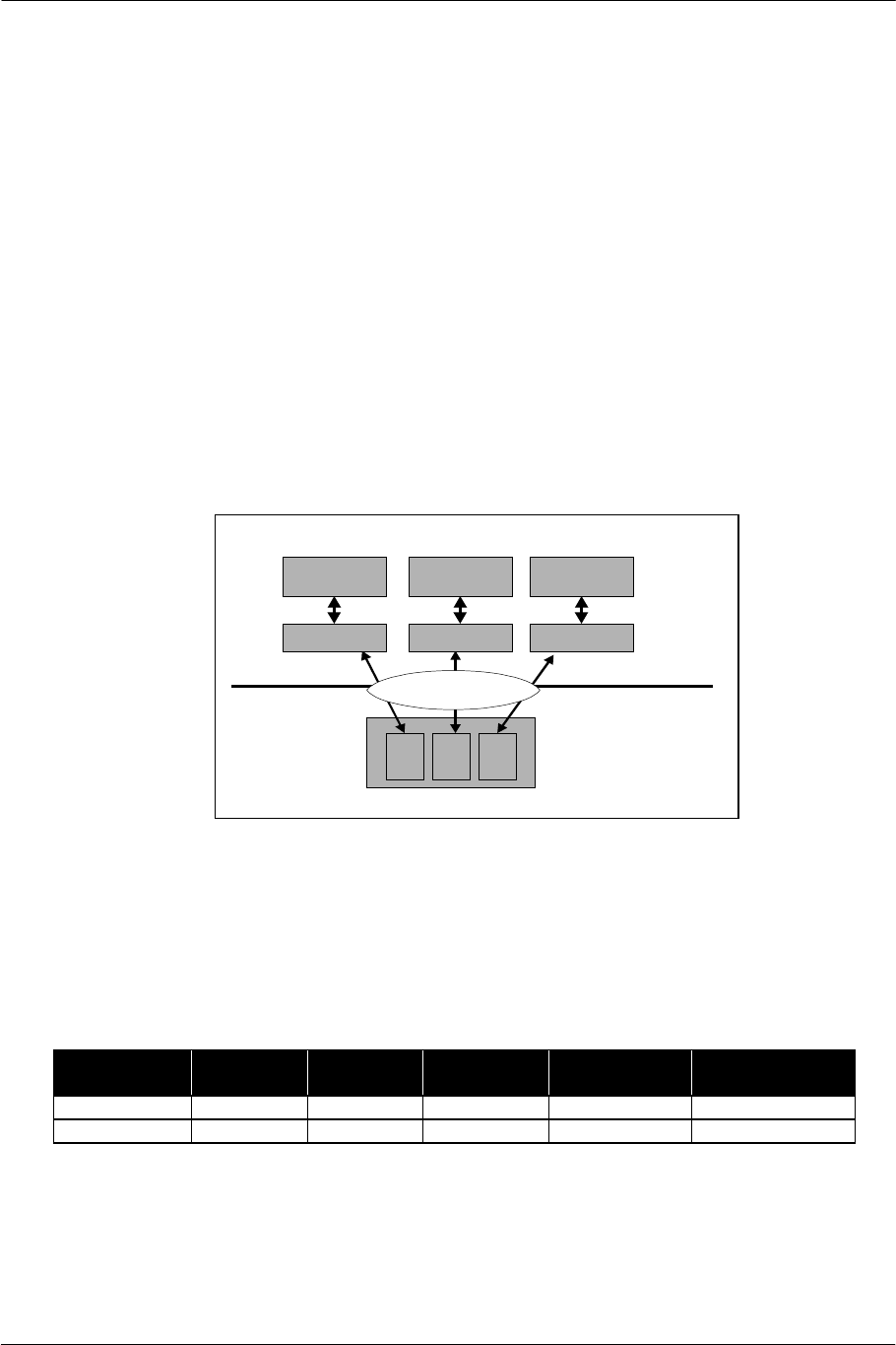
display list packet, and then transfers the formatted data to the GS as a drawing command. Data is input to the
GIF from VU Mem1 via PATH1, from VIF1 via PATH2, and from main memory via PATH3. The GIF also
plays a role in data path arbitration.
PATH1 is assigned to the transfer of display lists processed in VPU1. PATH2 is assigned to the data directly
transferable to the rendering engine, e.g. online textures. PATH3 is assigned to the transfer of display lists
which have been generated by the EE Core and VPU0 and stored temporarily in main memory. The order of
priority is PATH1, PATH2, and PATH3.
Buffer
Packing Logic
VIF1 GIF
FIFO
PATH1 PATH3
PATH2
VU1
GS Control Regs
128 128
128
64
GIF
G S
VU Mem1
Figure 2-12 Data Paths to GS
SCE CONFIDENTIAL EE Overview Version 6.0
© SCEI
-47-
2.6. SIF: Sub-CPU Interface
The Sub-CPU (IOP) controls sound output and I/O to and from storage devices. It adopts an LMA
configuration with memory independent of the EE. The SIF is the interface to exchange data between these
processors. The DMA controllers (DMACs) for the IOP and EE operate in cooperation through the
bidirectional FIFO (SFIFO) in the SIF.
IOP
Core
IOP-Memory Main Memory
(MEM)
pack/
unpack
Control Regs .
IOP
DMAC
EE
Core
EE
DMAC
SIF
SFIFO
32 128
Figure 2-13 EE-IOP Interface
Data is transmitted in units called packets. A tag (DMATag) is attached to each packet, containing a memory
address in the IOP memory space, a memory address in the EE memory space, and the data size. The IOP-
DMAC reads the IOP memory address and data size from the tag, and transmits the packet with its tag to the
SIF. The EE-DMAC reads the packet from the SIF, interprets the first word as a tag, reads the EE memory
address and data size from the tag, and decompresses the data to the specified memory address. These transfer
operations are performed by the DMACs to avoid generating unnecessary interrupts of the CPU.
Packet C
Packet B
Packet A
Tag Tag
Tag Tag
Tag Tag
IOP Memory EE Memory
Source
Chain
DMA
Destination
Chain
DMA
128 bit
Packet C
Packet B
Packet A
128 bit
128 bit
SIF
Figure 2-14 SIF Data Flow

SCE CONFIDENTIAL EE Overview Version 6.0
© SCEI
-48-
(This page is left blank intentionally)

SCE CONFIDENTIAL EE Overview Version 6.0
© SCEI
-49-
3. Functional Overview
SCE CONFIDENTIAL EE Overview Version 6.0
© SCEI
-50-
3.1. Data Transfer via DMA
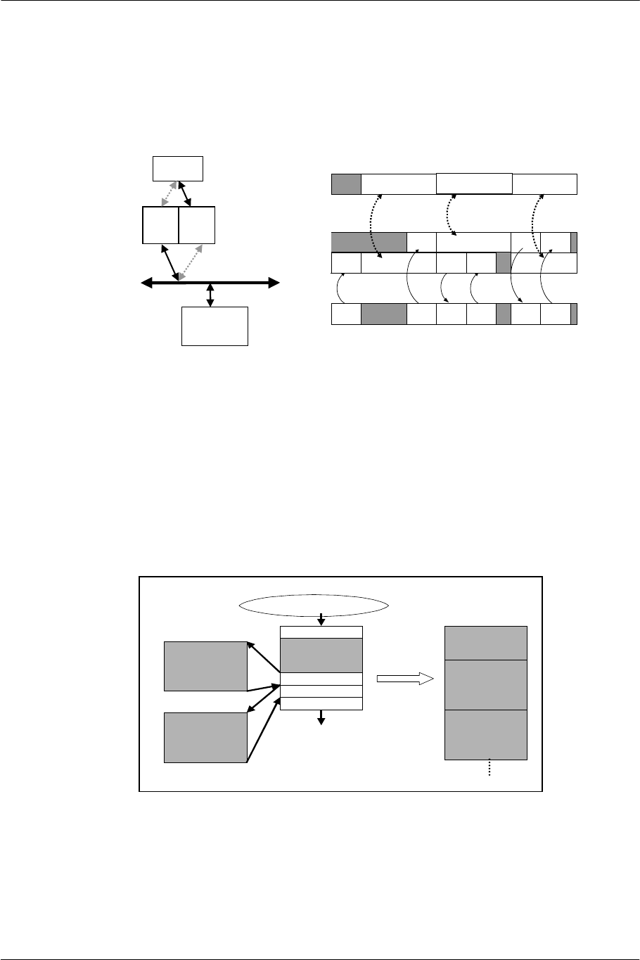
Data is transferred between main memory, peripheral processors, and scratchpad memory (SPR) via DMA.
The unit of data transfer is a quadword (128 bits = qword). In data transfer to and from peripheral processors,
data is divided into blocks (slices) of 8 qwords.
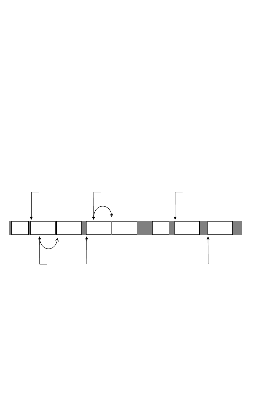
On some of the channels, Chain mode is available. This mode performs processing such as switching transfer
addresses according to the tag (DMAtag) in the transfer data. This not only reduces processing such as data
sorting before transfer, but also enables data exchange between peripheral processors through the mediation of
main memory without the EE Core. At such times, the stall control function, which mutually synchronizes
transfer, is available. For the GIF channel, memory FIFO function to use the ring buffer in main memory is
also provided.
3.1.1. Sliced Transfer
Except for the data transfer between the SPR and main memory, DMA transfer is performed by slicing the data
every 8 qwords and arbitrating the transfer requests from each channel. A channel releases the bus right
temporarily whenever transfer of one slice is completed, and it continues transferring if there are no requests
from others. This sliced-transfer mechanism not only enables two or more transfer processes to be executed in
parallel but also allows the EE Core to access main memory during the transfer process. The following figure
illustrates DMA transfers performed concurrently on Channel A and B.
ch-A ch-BCPU CPU
ch-B ch-B
ch-A ch-A
8 qword 8 qword 8 qword
8 qword 8 qword 8 qword
Stall
Stall
ch-A DREQ ch-A DREQ ch-A DREQ
ch-B DREQ ch-B DREQ ch-B DREQ
Figure 3-1 Example of Sliced Transfer
3.1.2. Chain Mode Transfer
Source Chain Mode
Source Chain Mode is used for DMA transfer from memory to peripherals. In this mode, transfer address
and transfer data size are specified according to the tag data (DMAtag) in the packet. The DMAC repeats
transfer processing while tracing the tags in memory, and ends a series of transfers at the point where
transfer of the tag with the end instruction finishes.
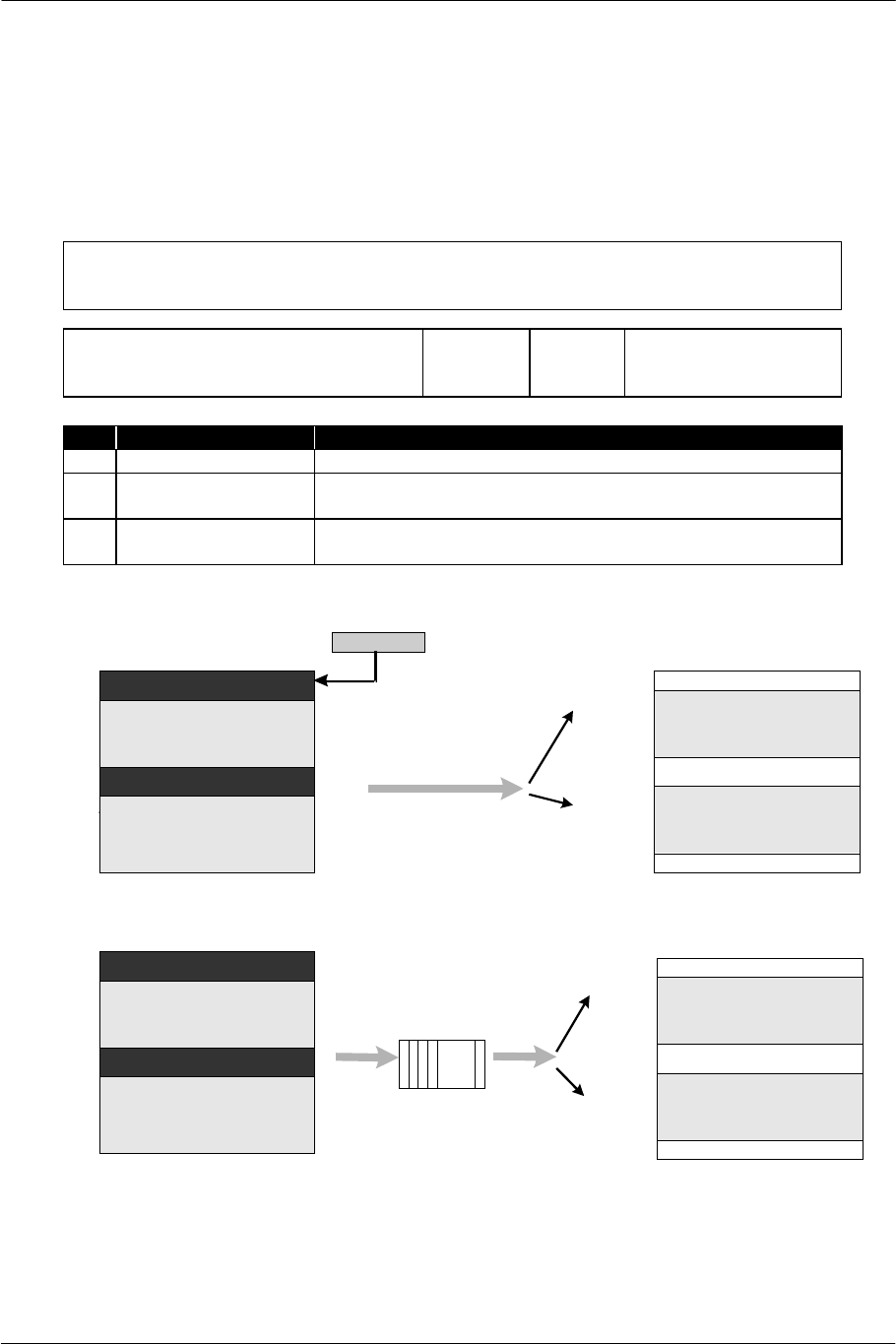
The DMAtag is 128-bit data with the following structure. ID is a field in which details of the transfer
operation are specified. Eight types in the table below can be specified.

SCE CONFIDENTIAL EE Overview Version 6.0
© SCEI
-51-
127 64
(Arbitrary)
63 32 31 24 15 0
Address Specification ADDR
ID/FLG
Data Size QWC
ID Transfer Data Position Next Tag Position Operation
cnt Next to tag Next to transfer data Transfers the data following the tag and
proceeds to the succeeding data.
next Next to tag Specified in tag Transfers the data following the tag and
jumps to the specified position.
ref Specified in tag Next to tag Transfers the data at the specified
position.
refs Specified in tag Next to tag Transfers the data at the specified
position while applying stall control.
refe Specified in tag (None) Transfers the data at the specified
position and ends transfer.
call Next to tag Specified in tag Transfers the data following the tag,
stores the next address, and jumps to the
specified position.
ret Next to tag Position stored
when call was
specified
Transfers the data following the tag and
jumps to the position stored when call
was specified.
end Next to tag (None) Transfers the data following the tag and
ends transfer.
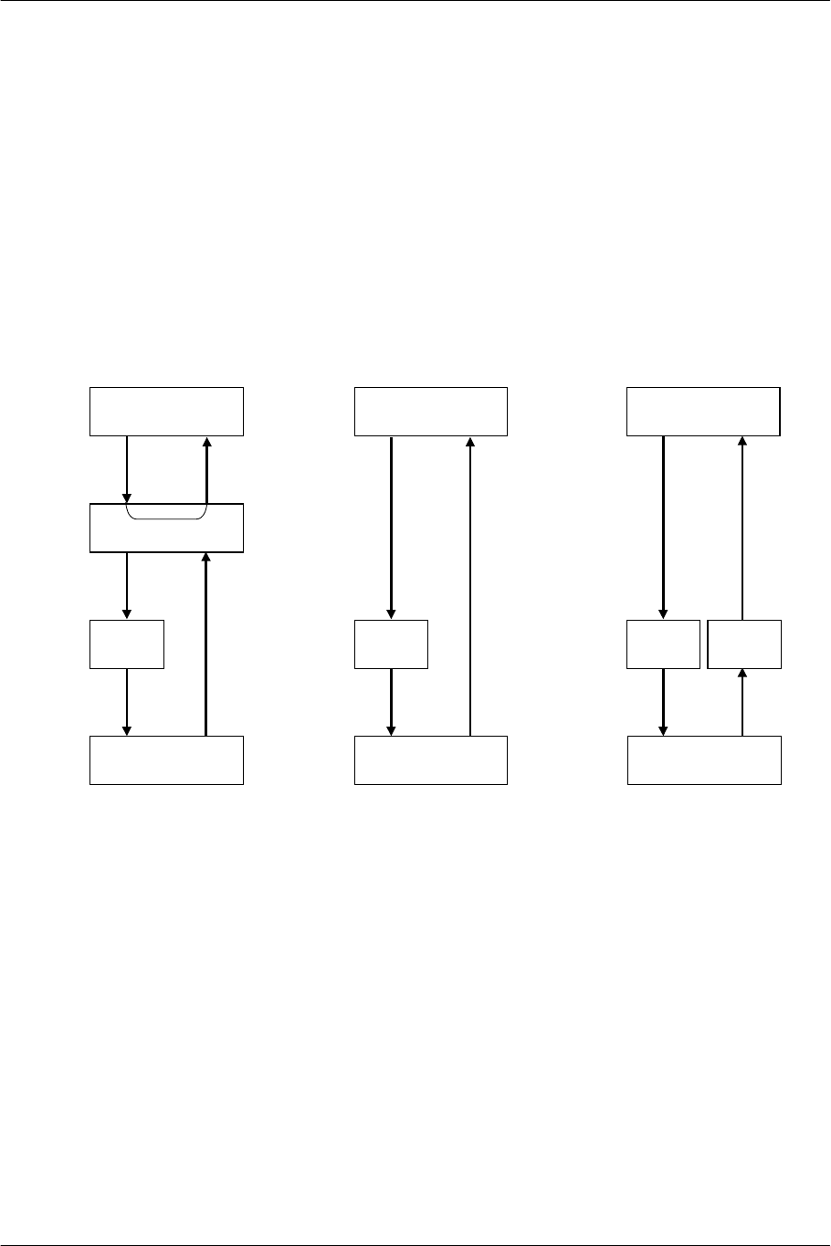
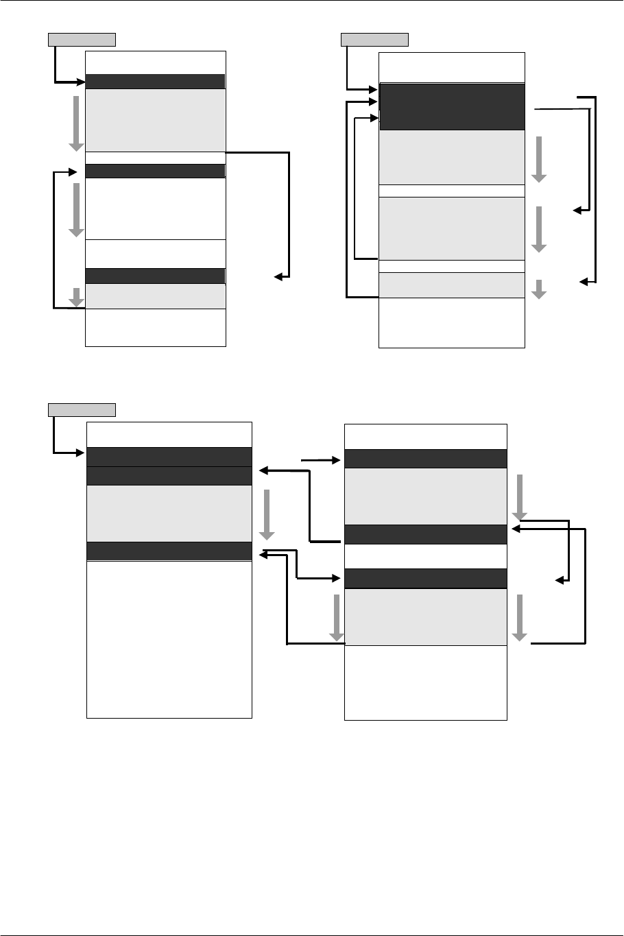
Data transfers can be performed most efficiently by using these IDs appropriately according to the data
structures in memory. The following is an example.
SCE CONFIDENTIAL EE Overview Version 6.0
© SCEI
-52-
next tag
TADR
ref tag
(1)NEXT ADDR=ADDR2
(5) END ADDR=-
(3)NEXT ADDR=ADDR1
DATA 0
(2)
(4)
DATA 1
DATA 2
(6)
ADDR0
ADDR1
ADDR2
(3)REF ADDR=ADDR1
(1)REF ADDR=ADDR2
(5)END ADDR=-
DATA 0
DATA 1
DATA 2
(6)
(4)
(2)
ADDR0
ADDR1
ADDR2
TADR
DATA 0
(7)CALL ADDR=ADDR2
(1)CALL ADDR=ADDR1
(11)END ADDR=-
ADDR0 (2)CALL ADDR=ADDR2
(6) RET ADDR=-
RET ADDR=-(4)(9)
DATA 1
DATA 2
(5)(10)
ADDR1
ADDR2
2
1
3
4
2
1
3
2
3
1
call tag/ret tag
(8)
(3)
TADR
Figure 3-2 Source Chain DMA Tags Showing Data Structures
SCE CONFIDENTIAL EE Overview Version 6.0
© SCEI
-53-
Destination Chain Mode
Destination Chain Mode is used to transfer data from peripherals to memory. The tag (DMAtag) bearing the
destination address and packet length is placed at the start of the transfer packet. This enables the peripheral
side to control the address where data is stored.
The Destination Chain tag is 128-bit data with the following structure, and is classified into three types as
shown in the table below.
127 64
(Arbitrary)
63 32 31 24 15 0
Address Specification ADDR
ID/FLG
Data Size QWC
ID Destination Address Operation
cnt Specified in tag Stores the data following the tag at the specified address.
cnts Specified in tag Stores the data following the tag at the specified address while
applying stall control.
end Specified in tag Stores the data following the tag at the specified address and ends
transfer.
The following is an example.
Start Address Register
D.Chain
DMA
CNT ADDR=ADDR1,QWC=8
CNT ADDR=ADDR0,QWC=8
DATA 0
DATA 1
CNT ADDR=ADDR1,QWC=8
CNT ADDR=ADDR0,QWC=8
DATA 0
DATA 1
IOP Memory
SPR
D.Chain
DMA
SDMA
ADDR0
ADDR1
DATA 1
DATA 0
Main Memory
ADDR0
ADDR1
DATA 1
DATA 0
Main Memory
Destination Chain DMA from SIF
Destination Chain DMA from SPR
SADDR
SFIFO
Figure 3-3 Destination Chain DMA to Transfer Data to Specified Address
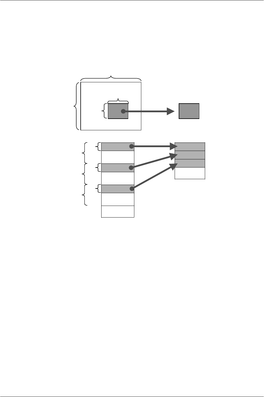
SCE CONFIDENTIAL EE Overview Version 6.0
© SCEI
-54-
3.1.3. Interleave Transfer
Interleave mode is available for DMA transfer between main memory and SPR. This mode processes data in
such a way that a small rectangular area is cut out from or fitted into the two-dimensional data (image data)
allocated in memory.
Figure 3-4 illustrates an example of cutting out a small rectangular area (TW, TH) from a rectangular area (FW,
FH).
Tw T0
Fw skip
Tw T1
Fw skip
Tw T2
Fw skip
:
:
Main
memor
y
T0
T1
T2
:
:
SPR
Source
Image
Fw
Tw
Fh
Th
Destination
Figure 3-4 Cutting Out a Small Rectangular Area in Interleave Mode
3.1.4. Stall Control
When a transfer from a peripheral to memory and a transfer from memory to another peripheral are performed
concurrently, they can be synchronized through the stall address register (D_STADR). The channel that handles
the DMA transfer to memory is called the source channel. The channel that handles the DMA transfer from
memory is called the drain channel. The value of D_STADR is updated as transfer processing on the source
channel side advances, but transfer processing on the drain channel side stalls at the address immediately
preceding the D_STADR address. This mechanism is called stall control.
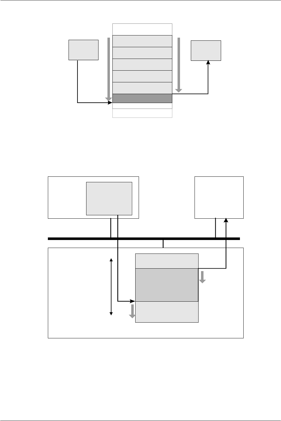
SCE CONFIDENTIAL EE Overview Version 6.0
© SCEI
-55-
8 qwords
8 qwords
8 qwords
8 qwords
8 qwords
Source
DMA
Drain
DMA
Peripheral0 Peripheral1
D_STADR
Main Memory/SPR
Figure 3-5 Synchronization between DMA Transfers by Stall Control
3.1.5. MFIFO
A FIFO function can be implemented by using a ring buffer and the DMA tag set in main memory when
transferring data from the scratchpad memory to the VIF1/GIF. This is called MFIFO (MemoryFIFO).
EE Core
SPR VIF1/GIF
Main BUS
Main Memory
D_RBOR
D_RBSR
Dd_TADR
D8_MADR
Ring Buffer (MFIF0)
Figure 3-6 Memory FIFO (MFIFO)

SCE CONFIDENTIAL EE Overview Version 6.0
© SCEI
-56-
3.2. Data Transfer to VPU
The EE has two built-in VPUs. These floating-point vector processors execute matrix operations, coordinate
conversion, transparency perspective conversion, and so forth, at high speed. Data is DMA-transferred to the
VPU through the VIF. The header information (VIFcode) embedded in the transfer data specifies how to
process the data in the VPU. This is the mechanism of DMA transfer to the VPU.
3.2.1. VIF Overview
The VIF is an interface unit, which decompresses the DMA-transferred data in packets and transfers it to the
VPU memory. The VIF is designed to set the decompression method and destination memory address of the
data according to the VIFcode included in the VIF packet. It enables the VPU to perform operations
independently of the EE Core by transferring VIF packets of vector data, VIF packets of microinstruction
program, and VIF packets to give an instruction to activate a microinstruction program.
The data types the VIF can decompress and transfer to the VU Mem are one- to four-dimensional vectors
consisting of 8-bit/16-bit/32-bit elements, and a four-dimensional vector of 16-bit color type with RGBa:
5.5.5.1. In addition, the VIF can transfer microinstruction code to be transferred to the Micro Mem. VIF1 can
also transfer data to the GS via the GIF.
3.2.2. VIF Packet
According to the 32-bit VIFcode in the transferred data, the VIF decompresses the following data and writes
memory and registers in the VU. The VIFcode and the following data string are called the VIF packet. Several
VIF packets can exist in 1 DMA packet as shown in the figure below.
DMA packet example (When DMAtag is transferred)
←MSB 128 bits LSB→
data VIFcode0 DMAtag
data data VIFcode2 VIFcode1
data data data data
data data data data
data data data data
data data data VIFcode3
data data VIFcode4 data
data data data data
VIFcode5 data data data
DMA packet example (When DMAtag is not transferred)
←MSB 128 bits LSB→
-- -- DMAtag
VIFcode2 VIFcode1 data VIFcode0
data data data data
data data data data
data data data data
data VIFcode3 data data
VIFcode4 data data data
data data data data
data data data data
-- -- VIFcode5 data

SCE CONFIDENTIAL EE Overview Version 6.0
© SCEI
-57-
VIF packets included in the above DMA packets
data VIFcode0
VIFcode1
data data ……data x 12 VIFcode2
data data ……data x 2 VIFcode3
data data ……data x 3 VIFcode4
VIFcode5
3.2.3. VIFcode Structure
The VIFcode is 32 bits in length, consisting of the CMD field (8 bits), the NUM field (8 bits), and the
IMMEDIATE field (16 bits) as shown in the figure below.
31 24 23 16 15 0
CMD
NUM
IMMEDIATE
The CMD field gives the VIF instructions on the operation and the decompression method of the following
data. The meanings of the NUM and IMMEDIATE fields change according to the value of the CMD field.
Category CMD Name Function Following data
UNPACK Decompresses data and writes to VU Mem. Packed vector data
STCYCL Sets CYCLE register value. None
OFFSET Sets OFFSET register value (VIF1 only). None
STMOD Sets MODE register value. None
STMASK Sets MASK register value. Mask pattern
STROW Sets Row register value. Row-completion
data
Data transfer
STCOL Sets Col register value. Column-completion
data
MPG Loads a microprogram. Microinstruction
program
FLUSHE Waits for end of a microprogram. None
FLUSH Waits for end of a microprogram and end of
GIF (PATH1 /PATH2) transfer. (VIF1 only)
None
FLUSHA Waits for end of a microprogram and end of
GIF transfer. (VIF1 only)
None
MSCAL Activates a microprogram. None
MSCNT Executes a microprogram continuously. None
Micro-program
execution
MSCALF FLUSH and activates a microprogram.
(VIF1 only) None
BASE Sets BASE register value. (VIF1 only) None Double
buffering ITOP Sets ITOPS register value. None
DIRECT Transfers data to GIF (via PATH2). GS data
DIRECTHL Transfers data to GIF (via PATH2). GS data
GS data
transfer
(VIF1 only) MSKPATH3 Masks transfer via PATH3 to GIF. None
NOP No operation None Others
MARK Sets MARK register value. None

SCE CONFIDENTIAL EE Overview Version 6.0
© SCEI
-58-
3.2.4. Data Transfer by UNPACK
The most general data transfer via the VIF is data transfer to VU Mem by using the VIFcode UNPACK. The
transfer data following the VIFcode is packed data; 8 bits x 4 elements and 32 bits x 3 elements, for example.
The VIF decompresses the packed data to vector data of 32 bits x 4 elements and writes it to the VU Mem. At
this time, VU Mem area left blank can be filled with a VPU register value (supplementation), and a constant
offset value can be added to the transfer data (addition).
The list of packing formats is shown as follows.
Format Data length No. of elements
(dimensions)
S-32 32 bits 1
S-16 16 bits 1
S-8 8 bits 1
V2-32 32 bits 2
V2-16 16 bits 2
V2-8 8 bits 2
V3-32 32 bits 3
V3-16 16 bits 3
V3-8 8 bits 3
V4-32 32 bits 4
V4-16 16 bits 4
V4-8 8 bits 4
V4-5 5+5+5+1 bits 4
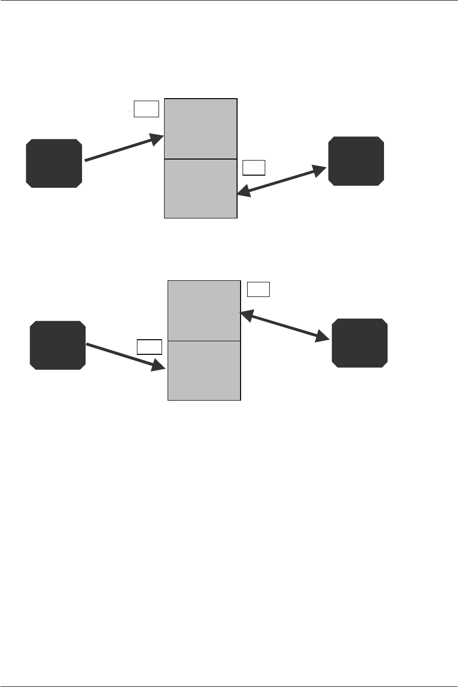
SCE CONFIDENTIAL EE Overview Version 6.0
© SCEI
-59-
3.2.5. Double Buffering
VPU1 supports double buffering, which sets two buffer areas in the VU Mem and enhances throughputs by
simultaneously transferring data to VU Mem and performing microprogram operations.
Buffer A
Following data transfer
Transferred data processing
Buffer B
VU
VIF
Buffer A
Following data transfer
Transferred data processing
Buffer B
VU
VIF
TOPS
TOPS
TOP
TOP
Figure 3-7 Double Buffering in VU Mem
Double buffer addresses can be set with the VIF1_BASE and VIF1_OFST registers. These can be reflected in
the VIF1_TOPS register and the TOP register of VU1 by taking appropriate steps.
By setting the FLG bit in the VIFcode UNPACK, data can be transferred to the double buffers according to the
relative specification based on the address shown by the TOPS register. When a microprogram reads data from
double buffers, it reads the TOP register value using the XTOP instruction and accesses the data in the buffer
accordingly.
The values of TOPS and TOP are replaced whenever a microprogram is activated. So it is possible to process
transferred data with a microprogram while transferring data to two buffers alternately, by repeating data transfer
and microprogram activation.

SCE CONFIDENTIAL EE Overview Version 6.0
© SCEI
-60-
3.3. Data Transfer to GS
Regular display lists generated by VU1 and exceptional display lists generated by the EE Core and VU0 are
transferred concurrently while having the transfer right arbitrated through the GIF. This is the typical data flow
from the EE to the GS.
The following are brief descriptions of this data flow.
3.3.1. Data Transfer Route
The GIF has three general data transfer paths called PATH1, PATH2, and PATH3. They work as follows.
• PATH1 PATH1 is a data transfer path from VPU1 data memory (VU Mem1) to the GS. When VU1
executes the XGKICK instruction, transfer processing via this path is performed.
• PATH2 PATH2 is a data transfer path between the FIFO inside the VPU1 VIF and the GIF. This path
is used when executing the DIRECT/DIRECT_HL instruction in the VIF and when
transferring data from the GS to main memory by using the image data transfer function of the
GS.
• PATH3 PATH3 is a direct data transfer path from the EE main bus to the GIF. This path is used when
transferring data from main memory or the SPR to the GS.
Priority and Timing
The three general data transfer paths are prioritized as PATH1>PATH2>PATH3. Whenever transfer of the
GS packet (described later in this document) ends in each path, transfer requests from other paths are
checked. If there is a request, transfer processing is performed according to priority.
Access to GS Privileged Register
The privileged registers of the GS are directly mapped to the I/O space of the EE core, and are accessible
without using the GIF, regardless of the state of the general data transfer paths. The GIF monitors access to
the privileged registers. When the transfer direction switching register (BUSDIR) is accessed, the GIF
switches data transfer direction accordingly.
3.3.2. Data Format
GS Packet
The basic unit of data transferred by the GIF is a GS primitive consisting of header information (GIFtag)
and following data. However, transfer processing is performed in units of GS packets in which several GS
primitives are gathered. The last GS primitive in the GS packet is shown by the termination information
(EOP=1) in the GIFtag.
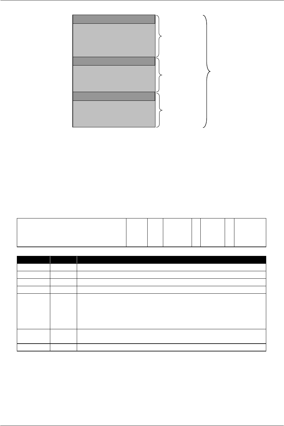
SCE CONFIDENTIAL EE Overview Version 6.0
© SCEI
-61-
GS Primitive
GS Packet
DATA
DATA
GIFtag(EOP=1)
GIFtag(EOP=0)
GIFtag(EOP=0)
DATA
GS Primitive
GS Primitive
Figure 3-8 GS Packet Structure
The above data structure is common to any data transfer path. For PATH2 and PATH3, however, the
VIFcode and DMATag are put in front of the GS packet.
It is necessary to align the GIFtag and data on a 128-bit boundary in memory.
GIFtag
The GIFtag has a 128-bit fixed length, and specifies the size and structure of the following data and the data
format (mode). The structure of the GIFtag is as follows:
1
2
7
6
4
6
3
6
0
5
9
5
8
5
7
4
7
4
6
1
5
1
4
0
0
REGS (max 16)
N
R
E
G
F
L
G
P
R
I
M
P
R
E
E
O
P
NLOOP
Name Pos. Contents
NLOOP 14:0 Repeat count (GS primitive data size)
EOP 15 Termination information (End of Packet)
PRE 46 PRIM field enabled
PRIM 57:47 Data to be set to the PRIM register of GS
FLG 59:58 Data format
00 PACKED mode
01 REGLIST mode
10 IMAGE mode
11 Disabled (Same operation as the IMAGE mode)
NREG 63:60 Number of register descriptors (Number of register descriptors in REGS
field)
REGS 127:64 Register descriptor (4 bits x 16 max.)
The value of the NLOOP field shows the data size of GS primitive, but the unit varies depending on the
data format.

SCE CONFIDENTIAL EE Overview Version 6.0
© SCEI
-62-
3.3.3. PACKED Mode
PACKED mode formats (packs) vertex coordinate values, texture coordinate values, and color values generated
as vector data of 32 bits x 4 elements adjusting to the corresponding bit fields of the GS registers, and writes
them to the GS registers. The register descriptors put in the REGS field of the GIFtag correspond to every
qword in the following data, and show the data format and the register where the data is written. The following
9 types of register descriptors are available:
Name Input Data Destination Register
PRIM Type and attribute of primitive PRIM
RGBAQ Vertex color RGBAQ
ST Vertex texture coordinates ST
UV Vertex texture coordinates (Texel coordinate values) UV
XYZF2 Vertex coordinate values + Fog coefficient XYZF2/XYZF3
XYZ2 Vertex coordinate values XYZ2/XYZ3
FOG Fog coefficient FOG
A+D Arbitrary register set value Specified arbitrarily.
NOP Arbitrary None (Not output)
3.3.4. REGLIST Mode
REGLIST mode transfers data strings formatted in such a way that they can be written to the GS register as they
are. The data following the GIFtag is considered to be data strings of 64 bits x 2 as they are, and the register
descriptors put in the REGS field of the GIFtag show to which register the data is written.
3.3.5. IMAGE Mode
IMAGE mode transfers image data by means of the host-local transfer function of the GS. The data following
the GIFtag is considered to be data strings of 64 bits x 2 and is written to the HWREG register of the GS
consecutively.

SCE CONFIDENTIAL EE Overview Version 6.0
© SCEI
-63-
3.4. Image Decompression by IPU
The IPU (Image Processing Unit) is an image data processor whose main functions are bit stream
decompression and macro block decoding of MPEG2. Compressed data in main memory is decoded,
decompressed, and written back again to main memory. The decoded images are transferred to the GS and used
as moving picture image data and texture data.
Figure 3-9 illustrates the basic processing flow of the IPU.
Input data BS128 RAW8 RGB32
↓ ↓ ↓
Processing VLC → IDCT → CSC → Dither → VQ
↓ ↓ ↓ ↓ ↓
Output data CODE16 RAW16 RGB32 RGB16 INDX4
Figure 3-9 IPU Processing Flow
The IPU has the following basic functions:
• MPEG2 macro block layer decoding
• MPEG2 bit stream decoding
• Bit stream decompression
The IPU has the following additional post-processing functions.
• YCbCr → RGB color conversion (CSC)
• 4 x 4 ordered dither
• Vector quantization (VQ)
The IPU handles the following data formats:
Name Contents Width
BS128 MPEG2 bit stream subset 128 bits
RGB32 RGBA pixels (A8+R8+G8+B8) 32 bits
RGB16 RGBA pixels (A1+R5+G5+B5) 16 bits
RAW8 Unsigned 8-bit YCbCr pixels 8 bits
RAW16 Singed 16-bit YCbCr pixels (Only lower 9 bits are effective.) 16 bits
INDX4 Unsigned 4-bit index pixels 4 bits

SCE CONFIDENTIAL EE Overview Version 6.0
© SCEI
-64-
The following commands are available:
Name Contents Input Output
BCLR Input FIFO initialization command - -
IDEC Intra decoding command BS128 RGB32/RGB16
BDEC Block decoding command BS128 RAW16
VDEC Variable-length data decoding command BS128 Variable-length code +
decoding code
FDEC Fixed-length data decoding command BS128 Fixed-length data
SETIQ IQ table setting command RAW8 -
SETVQ VQ table setting command RGB16 -
CSC Color space conversion command RAW8 RGB32/RGB16
PACK Format conversion command RGB32 RGB16/INDX4
SETTH Threshold setting command - -
Other functional features are as follows.
• Motion Compensation (MC) In decoding an MPEG2 bit stream, motion compensation (MC) is not
performed in the IPU, but in the EE core, by using multimedia
instructions.
• Automatic Generation of Alpha The alpha plane (transparency plane) is generated from the decoded
luminance value according to a fixed rule. This is useful in effectively
cutting out the texture pattern when decoding the bit stream without
the stencil pattern (transparent pixel mask pattern).