AMD64 Architecture Programmer’s Manual, Volume 3: General Purpose And System Instructions EN Programmer's Manual 3
AMD64 Architecture Programmer's Manual Volume 3 General-Purpose and System Instructions manual pdf -FilePursuit
AMD64 Architecture Programmer's Manual Volume 3 General-Purpose and System Instructions manual pdf -FilePursuit
EN%20-%20AMD64%20Architecture%20Programmer's%20Manual%20Volume%203%20General-Purpose%20and%20System%20Instructions
EN%20-%20AMD64%20Architecture%20Programmer's%20Manual%20Volume%203%20General-Purpose%20and%20System%20Instructions
User Manual: Pdf
Open the PDF directly: View PDF ![]() .
.
Page Count: 474 [warning: Documents this large are best viewed by clicking the View PDF Link!]
- Contents
- Figures
- Tables
- Revision History
- Preface
- 1 Instruction Formats
- 2 Instruction Overview
- 3 General-Purpose Instruction Reference
- AAA
- AAD
- AAM
- AAS
- ADC
- ADD
- AND
- BOUND
- BSF
- BSR
- BSWAP
- BT
- BTC
- BTR
- BTS
- CALL (Near)
- CALL (Far)
- CBW CWDE CDQE
- CWD CDQ CQO
- CLC
- CLD
- CLFLUSH
- CMC
- CMOVcc
- CMP
- CMPS CMPSB CMPSW CMPSD CMPSQ
- CMPXCHG
- CMPXCHG8B CMPXCHG16B
- CPUID
- DAA
- DAS
- DEC
- DIV
- ENTER
- IDIV
- IMUL
- IN
- INC
- INS INSB INSW INSD
- INT
- INTO
- Jcc
- JCXZ JECXZ JRCXZ
- JMP (Near)
- JMP (Far)
- LAHF
- LDS LES LFS LGS LSS
- LEA
- LEAVE
- LFENCE
- LODS LODSB LODSW LODSD LODSQ
- LOOP LOOPE LOOPNE LOOPNZ LOOPZ
- LZCNT
- MFENCE
- MOV
- MOVD
- MOVMSKPD
- MOVMSKPS
- MOVNTI
- MOVS MOVSB MOVSW MOVSD MOVSQ
- MOVSX
- MOVSXD
- MOVZX
- MUL
- NEG
- NOP
- NOT
- OR
- OUT
- OUTS OUTSB OUTSW OUTSD
- PAUSE
- POP
- POPA POPAD
- POPCNT
- POPF POPFD POPFQ
- PREFETCH PREFETCHW
- PREFETCHlevel
- PUSH
- PUSHA PUSHAD
- PUSHF PUSHFD PUSHFQ
- RCL
- RCR
- RET (Near)
- RET (Far)
- ROL
- ROR
- SAHF
- SAL SHL
- SAR
- SBB
- SCAS SCASB SCASW SCASD SCASQ
- SETcc
- SFENCE
- SHL
- SHLD
- SHR
- SHRD
- STC
- STD
- STOS STOSB STOSW STOSD STOSQ
- SUB
- TEST
- XADD
- XCHG
- XLAT
- XLATB
- XOR
- 4 System Instruction Reference
- Appendix A Opcode and Operand Encodings
- Appendix B General-Purpose Instructions in 64-Bit Mode
- B.1 General Rules for 64-Bit Mode
- B.2 Operation and Operand Size in 64-Bit Mode
- B.3 Invalid and Reassigned Instructions in 64-Bit Mode
- B.4 Instructions with 64-Bit Default Operand Size
- B.5 Single-Byte INC and DEC Instructions in 64-Bit Mode
- B.6 NOP in 64-Bit Mode
- B.7 Segment Override Prefixes in 64-Bit Mode
- Appendix C Differences Between Long Mode and Legacy Mode
- Appendix D Instruction Subsets and CPUID Feature Sets
- Appendix E Instruction Effects on RFLAGS
- Index

Advanced Micro Devices
AMD64 Technology
AMD64 Architecture
Programmer’s Manual
Volume 3:
General-Purpose and
System Instructions
Publication No. Revision Date
24594 3.14 September 2007

AMD64 Technology 24594—Rev. 3.14—September 2007
Trademarks
AMD, the AMD arrow logo, AMD Athlon, and AMD Opteron, and combinations thereof, and 3DNow! are trademarks,
and AMD-K6 is a registered trademark of Advanced Micro Devices, Inc.
MMX is a trademark and Pentium is a registered trademark of Intel Corporation.
Windows NT is a registered trademark of Microsoft Corporation.
Other product names used in this publication are for identification purposes only and may be trademarks of their
respective companies.
© 2002 – 2007 Advanced Micro Devices, Inc. All rights reserved.
The contents of this document are provided in connection with Advanced Micro
Devices, Inc. (“AMD”) products. AMD makes no representations or warranties with
respect to the accuracy or completeness of the contents of this publication and
reserves the right to make changes to specifications and product descriptions at
any time without notice. The information contained herein may be of a preliminary
or advance nature and is subject to change without notice. No license, whether
express, implied, arising by estoppel or otherwise, to any intellectual property rights
is granted by this publication. Except as set forth in AMD’s Standard Terms and
Conditions of Sale, AMD assumes no liability whatsoever, and disclaims any
express or implied warranty, relating to its products including, but not limited to, the
implied warranty of merchantability, fitness for a particular purpose, or infringement
of any intellectual property right.
AMD’s products are not designed, intended, authorized or warranted for use as
components in systems intended for surgical implant into the body, or in other appli-
cations intended to support or sustain life, or in any other application in which the
failure of AMD’s product could create a situation where personal injury, death, or
severe property or environmental damage may occur. AMD reserves the right to
discontinue or make changes to its products at any time without notice.

Contents i
24594—Rev. 3.14—September 2007 AMD64 Technology
Contents
Revision History. . . . . . . . . . . . . . . . . . . . . . . . . . . . . . . . . . . . . . . . . . . . . . . . . . . . . . . . . . . . . . . xiii
Preface. . . . . . . . . . . . . . . . . . . . . . . . . . . . . . . . . . . . . . . . . . . . . . . . . . . . . . . . . . . . . . . . . . . . . . . . xv
About This Book. . . . . . . . . . . . . . . . . . . . . . . . . . . . . . . . . . . . . . . . . . . . . . . . . . . . . . . . . . . . . . . . . . xv
Audience . . . . . . . . . . . . . . . . . . . . . . . . . . . . . . . . . . . . . . . . . . . . . . . . . . . . . . . . . . . . . . . . . . . . . . . . xv
Organization . . . . . . . . . . . . . . . . . . . . . . . . . . . . . . . . . . . . . . . . . . . . . . . . . . . . . . . . . . . . . . . . . . . . . xv
Definitions . . . . . . . . . . . . . . . . . . . . . . . . . . . . . . . . . . . . . . . . . . . . . . . . . . . . . . . . . . . . . . . . . . . . . xvi
Related Documents . . . . . . . . . . . . . . . . . . . . . . . . . . . . . . . . . . . . . . . . . . . . . . . . . . . . . . . . . . . . . . xxvi
1 Instruction Formats. . . . . . . . . . . . . . . . . . . . . . . . . . . . . . . . . . . . . . . . . . . . . . . . . . . . . . . . .1
1.1 Instruction Byte Order . . . . . . . . . . . . . . . . . . . . . . . . . . . . . . . . . . . . . . . . . . . . . . . . . . . . . . . . 1
1.2 Instruction Prefixes . . . . . . . . . . . . . . . . . . . . . . . . . . . . . . . . . . . . . . . . . . . . . . . . . . . . . . . . . . 3
Summary of Legacy Prefixes. . . . . . . . . . . . . . . . . . . . . . . . . . . . . . . . . . . . . . . . . . . . . . . . . . . 3
Operand-Size Override Prefix . . . . . . . . . . . . . . . . . . . . . . . . . . . . . . . . . . . . . . . . . . . . . . . . . .4
Address-Size Override Prefix . . . . . . . . . . . . . . . . . . . . . . . . . . . . . . . . . . . . . . . . . . . . . . . . . .6
Segment-Override Prefixes . . . . . . . . . . . . . . . . . . . . . . . . . . . . . . . . . . . . . . . . . . . . . . . . . . . .8
Lock Prefix . . . . . . . . . . . . . . . . . . . . . . . . . . . . . . . . . . . . . . . . . . . . . . . . . . . . . . . . . . . . . . . . 8
Repeat Prefixes . . . . . . . . . . . . . . . . . . . . . . . . . . . . . . . . . . . . . . . . . . . . . . . . . . . . . . . . . . . . . 9
REX Prefixes . . . . . . . . . . . . . . . . . . . . . . . . . . . . . . . . . . . . . . . . . . . . . . . . . . . . . . . . . . . . . . 11
1.3 Opcode. . . . . . . . . . . . . . . . . . . . . . . . . . . . . . . . . . . . . . . . . . . . . . . . . . . . . . . . . . . . . . . . . . . 17
1.4 ModRM and SIB Bytes . . . . . . . . . . . . . . . . . . . . . . . . . . . . . . . . . . . . . . . . . . . . . . . . . . . . . .17
1.5 Displacement Bytes . . . . . . . . . . . . . . . . . . . . . . . . . . . . . . . . . . . . . . . . . . . . . . . . . . . . . . . . . 19
1.6 Immediate Bytes . . . . . . . . . . . . . . . . . . . . . . . . . . . . . . . . . . . . . . . . . . . . . . . . . . . . . . . . . . . 19
1.7 RIP-Relative Addressing . . . . . . . . . . . . . . . . . . . . . . . . . . . . . . . . . . . . . . . . . . . . . . . . . . . . . 19
Encoding . . . . . . . . . . . . . . . . . . . . . . . . . . . . . . . . . . . . . . . . . . . . . . . . . . . . . . . . . . . . . . . . . 20
REX Prefix and RIP-Relative Addressing. . . . . . . . . . . . . . . . . . . . . . . . . . . . . . . . . . . . . . . . 20
Address-Size Prefix and RIP-Relative Addressing . . . . . . . . . . . . . . . . . . . . . . . . . . . . . . . . . 20
2 Instruction Overview. . . . . . . . . . . . . . . . . . . . . . . . . . . . . . . . . . . . . . . . . . . . . . . . . . . . . . .21
2.1 Instruction Subsets. . . . . . . . . . . . . . . . . . . . . . . . . . . . . . . . . . . . . . . . . . . . . . . . . . . . . . . . . . 21
2.2 Reference-Page Format . . . . . . . . . . . . . . . . . . . . . . . . . . . . . . . . . . . . . . . . . . . . . . . . . . . . . . 22
2.3 Summary of Registers and Data Types . . . . . . . . . . . . . . . . . . . . . . . . . . . . . . . . . . . . . . . . . . 24
General-Purpose Instructions. . . . . . . . . . . . . . . . . . . . . . . . . . . . . . . . . . . . . . . . . . . . . . . . . . 24
System Instructions . . . . . . . . . . . . . . . . . . . . . . . . . . . . . . . . . . . . . . . . . . . . . . . . . . . . . . . . . 27
128-Bit Media Instructions . . . . . . . . . . . . . . . . . . . . . . . . . . . . . . . . . . . . . . . . . . . . . . . . . . .29
64-Bit Media Instructions . . . . . . . . . . . . . . . . . . . . . . . . . . . . . . . . . . . . . . . . . . . . . . . . . . . .32
x87 Floating-Point Instructions . . . . . . . . . . . . . . . . . . . . . . . . . . . . . . . . . . . . . . . . . . . . . . . . 34
2.4 Summary of Exceptions. . . . . . . . . . . . . . . . . . . . . . . . . . . . . . . . . . . . . . . . . . . . . . . . . . . . . . 35
2.5 Notation . . . . . . . . . . . . . . . . . . . . . . . . . . . . . . . . . . . . . . . . . . . . . . . . . . . . . . . . . . . . . . . . . . 37
Mnemonic Syntax . . . . . . . . . . . . . . . . . . . . . . . . . . . . . . . . . . . . . . . . . . . . . . . . . . . . . . . . . . 37
Opcode Syntax. . . . . . . . . . . . . . . . . . . . . . . . . . . . . . . . . . . . . . . . . . . . . . . . . . . . . . . . . . . . . 39
Pseudocode Definitions . . . . . . . . . . . . . . . . . . . . . . . . . . . . . . . . . . . . . . . . . . . . . . . . . . . . . .41

ii Contents
AMD64 Technology 24594—Rev. 3.14—September 2007
3 General-Purpose Instruction Reference . . . . . . . . . . . . . . . . . . . . . . . . . . . . . . . . . . . . . . .51
AAA. . . . . . . . . . . . . . . . . . . . . . . . . . . . . . . . . . . . . . . . . . . . . . . . . . . . . . . . . . . . . . . . . . . . . 53
AAD. . . . . . . . . . . . . . . . . . . . . . . . . . . . . . . . . . . . . . . . . . . . . . . . . . . . . . . . . . . . . . . . . . . . . 54
AAM . . . . . . . . . . . . . . . . . . . . . . . . . . . . . . . . . . . . . . . . . . . . . . . . . . . . . . . . . . . . . . . . . . . . 55
AAS . . . . . . . . . . . . . . . . . . . . . . . . . . . . . . . . . . . . . . . . . . . . . . . . . . . . . . . . . . . . . . . . . . . . . 56
ADC. . . . . . . . . . . . . . . . . . . . . . . . . . . . . . . . . . . . . . . . . . . . . . . . . . . . . . . . . . . . . . . . . . . . . 57
ADD. . . . . . . . . . . . . . . . . . . . . . . . . . . . . . . . . . . . . . . . . . . . . . . . . . . . . . . . . . . . . . . . . . . . . 59
AND. . . . . . . . . . . . . . . . . . . . . . . . . . . . . . . . . . . . . . . . . . . . . . . . . . . . . . . . . . . . . . . . . . . . . 61
BOUND . . . . . . . . . . . . . . . . . . . . . . . . . . . . . . . . . . . . . . . . . . . . . . . . . . . . . . . . . . . . . . . . . . 63
BSF . . . . . . . . . . . . . . . . . . . . . . . . . . . . . . . . . . . . . . . . . . . . . . . . . . . . . . . . . . . . . . . . . . . . . 65
BSR . . . . . . . . . . . . . . . . . . . . . . . . . . . . . . . . . . . . . . . . . . . . . . . . . . . . . . . . . . . . . . . . . . . . . 66
BSWAP . . . . . . . . . . . . . . . . . . . . . . . . . . . . . . . . . . . . . . . . . . . . . . . . . . . . . . . . . . . . . . . . . . 67
BT . . . . . . . . . . . . . . . . . . . . . . . . . . . . . . . . . . . . . . . . . . . . . . . . . . . . . . . . . . . . . . . . . . . . . . 68
BTC . . . . . . . . . . . . . . . . . . . . . . . . . . . . . . . . . . . . . . . . . . . . . . . . . . . . . . . . . . . . . . . . . . . . . 70
BTR . . . . . . . . . . . . . . . . . . . . . . . . . . . . . . . . . . . . . . . . . . . . . . . . . . . . . . . . . . . . . . . . . . . . . 72
BTS . . . . . . . . . . . . . . . . . . . . . . . . . . . . . . . . . . . . . . . . . . . . . . . . . . . . . . . . . . . . . . . . . . . . . 74
CALL (Near) . . . . . . . . . . . . . . . . . . . . . . . . . . . . . . . . . . . . . . . . . . . . . . . . . . . . . . . . . . . . . . 76
CALL (Far) . . . . . . . . . . . . . . . . . . . . . . . . . . . . . . . . . . . . . . . . . . . . . . . . . . . . . . . . . . . . . . . 78
CBW
CWDE
CDQE . . . . . . . . . . . . . . . . . . . . . . . . . . . . . . . . . . . . . . . . . . . . . . . . . . . . . . . . . . . . . . . . . . . 84
CWD
CDQ
CQO. . . . . . . . . . . . . . . . . . . . . . . . . . . . . . . . . . . . . . . . . . . . . . . . . . . . . . . . . . . . . . . . . . . . . 85
CLC . . . . . . . . . . . . . . . . . . . . . . . . . . . . . . . . . . . . . . . . . . . . . . . . . . . . . . . . . . . . . . . . . . . . . 86
CLD . . . . . . . . . . . . . . . . . . . . . . . . . . . . . . . . . . . . . . . . . . . . . . . . . . . . . . . . . . . . . . . . . . . . . 87
CLFLUSH . . . . . . . . . . . . . . . . . . . . . . . . . . . . . . . . . . . . . . . . . . . . . . . . . . . . . . . . . . . . . . . . 88
CMC . . . . . . . . . . . . . . . . . . . . . . . . . . . . . . . . . . . . . . . . . . . . . . . . . . . . . . . . . . . . . . . . . . . . 90
CMOVcc . . . . . . . . . . . . . . . . . . . . . . . . . . . . . . . . . . . . . . . . . . . . . . . . . . . . . . . . . . . . . . . . . 91
CMP. . . . . . . . . . . . . . . . . . . . . . . . . . . . . . . . . . . . . . . . . . . . . . . . . . . . . . . . . . . . . . . . . . . . . 94
CMPS
CMPSB
CMPSW
CMPSD
CMPSQ . . . . . . . . . . . . . . . . . . . . . . . . . . . . . . . . . . . . . . . . . . . . . . . . . . . . . . . . . . . . . . . . . . 97
CMPXCHG . . . . . . . . . . . . . . . . . . . . . . . . . . . . . . . . . . . . . . . . . . . . . . . . . . . . . . . . . . . . . . . 99
CMPXCHG8B
CMPXCHG16B. . . . . . . . . . . . . . . . . . . . . . . . . . . . . . . . . . . . . . . . . . . . . . . . . . . . . . . . . . . 101
CPUID . . . . . . . . . . . . . . . . . . . . . . . . . . . . . . . . . . . . . . . . . . . . . . . . . . . . . . . . . . . . . . . . . . 103
DAA. . . . . . . . . . . . . . . . . . . . . . . . . . . . . . . . . . . . . . . . . . . . . . . . . . . . . . . . . . . . . . . . . . . . 105
DAS . . . . . . . . . . . . . . . . . . . . . . . . . . . . . . . . . . . . . . . . . . . . . . . . . . . . . . . . . . . . . . . . . . . . 106
DEC . . . . . . . . . . . . . . . . . . . . . . . . . . . . . . . . . . . . . . . . . . . . . . . . . . . . . . . . . . . . . . . . . . . . 107
DIV . . . . . . . . . . . . . . . . . . . . . . . . . . . . . . . . . . . . . . . . . . . . . . . . . . . . . . . . . . . . . . . . . . . . 109
ENTER . . . . . . . . . . . . . . . . . . . . . . . . . . . . . . . . . . . . . . . . . . . . . . . . . . . . . . . . . . . . . . . . . 111
IDIV. . . . . . . . . . . . . . . . . . . . . . . . . . . . . . . . . . . . . . . . . . . . . . . . . . . . . . . . . . . . . . . . . . . . 113
IMUL . . . . . . . . . . . . . . . . . . . . . . . . . . . . . . . . . . . . . . . . . . . . . . . . . . . . . . . . . . . . . . . . . . . 115
IN . . . . . . . . . . . . . . . . . . . . . . . . . . . . . . . . . . . . . . . . . . . . . . . . . . . . . . . . . . . . . . . . . . . . . . 117

Contents iii
24594—Rev. 3.14—September 2007 AMD64 Technology
INC . . . . . . . . . . . . . . . . . . . . . . . . . . . . . . . . . . . . . . . . . . . . . . . . . . . . . . . . . . . . . . . . . . . . 118
INS
INSB
INSW
INSD . . . . . . . . . . . . . . . . . . . . . . . . . . . . . . . . . . . . . . . . . . . . . . . . . . . . . . . . . . . . . . . . . . . 120
INT. . . . . . . . . . . . . . . . . . . . . . . . . . . . . . . . . . . . . . . . . . . . . . . . . . . . . . . . . . . . . . . . . . . . . 122
INTO . . . . . . . . . . . . . . . . . . . . . . . . . . . . . . . . . . . . . . . . . . . . . . . . . . . . . . . . . . . . . . . . . . . 129
Jcc . . . . . . . . . . . . . . . . . . . . . . . . . . . . . . . . . . . . . . . . . . . . . . . . . . . . . . . . . . . . . . . . . . . . . 130
JCXZ
JECXZ
JRCXZ . . . . . . . . . . . . . . . . . . . . . . . . . . . . . . . . . . . . . . . . . . . . . . . . . . . . . . . . . . . . . . . . . . 134
JMP (Near). . . . . . . . . . . . . . . . . . . . . . . . . . . . . . . . . . . . . . . . . . . . . . . . . . . . . . . . . . . . . . . 135
JMP (Far) . . . . . . . . . . . . . . . . . . . . . . . . . . . . . . . . . . . . . . . . . . . . . . . . . . . . . . . . . . . . . . . . 137
LAHF. . . . . . . . . . . . . . . . . . . . . . . . . . . . . . . . . . . . . . . . . . . . . . . . . . . . . . . . . . . . . . . . . . . 142
LDS
LES
LFS
LGS
LSS . . . . . . . . . . . . . . . . . . . . . . . . . . . . . . . . . . . . . . . . . . . . . . . . . . . . . . . . . . . . . . . . . . . . 143
LEA . . . . . . . . . . . . . . . . . . . . . . . . . . . . . . . . . . . . . . . . . . . . . . . . . . . . . . . . . . . . . . . . . . . . 145
LEAVE. . . . . . . . . . . . . . . . . . . . . . . . . . . . . . . . . . . . . . . . . . . . . . . . . . . . . . . . . . . . . . . . . . 147
LFENCE . . . . . . . . . . . . . . . . . . . . . . . . . . . . . . . . . . . . . . . . . . . . . . . . . . . . . . . . . . . . . . . . 148
LODS
LODSB
LODSW
LODSD
LODSQ . . . . . . . . . . . . . . . . . . . . . . . . . . . . . . . . . . . . . . . . . . . . . . . . . . . . . . . . . . . . . . . . . 149
LOOP
LOOPE
LOOPNE
LOOPNZ
LOOPZ . . . . . . . . . . . . . . . . . . . . . . . . . . . . . . . . . . . . . . . . . . . . . . . . . . . . . . . . . . . . . . . . . 151
LZCNT . . . . . . . . . . . . . . . . . . . . . . . . . . . . . . . . . . . . . . . . . . . . . . . . . . . . . . . . . . . . . . . . . 153
MFENCE . . . . . . . . . . . . . . . . . . . . . . . . . . . . . . . . . . . . . . . . . . . . . . . . . . . . . . . . . . . . . . . . 155
MOV . . . . . . . . . . . . . . . . . . . . . . . . . . . . . . . . . . . . . . . . . . . . . . . . . . . . . . . . . . . . . . . . . . . 156
MOVD . . . . . . . . . . . . . . . . . . . . . . . . . . . . . . . . . . . . . . . . . . . . . . . . . . . . . . . . . . . . . . . . . . 159
MOVMSKPD . . . . . . . . . . . . . . . . . . . . . . . . . . . . . . . . . . . . . . . . . . . . . . . . . . . . . . . . . . . . 162
MOVMSKPS . . . . . . . . . . . . . . . . . . . . . . . . . . . . . . . . . . . . . . . . . . . . . . . . . . . . . . . . . . . . . 164
MOVNTI . . . . . . . . . . . . . . . . . . . . . . . . . . . . . . . . . . . . . . . . . . . . . . . . . . . . . . . . . . . . . . . . 166
MOVS
MOVSB
MOVSW
MOVSD
MOVSQ . . . . . . . . . . . . . . . . . . . . . . . . . . . . . . . . . . . . . . . . . . . . . . . . . . . . . . . . . . . . . . . . . 168
MOVSX . . . . . . . . . . . . . . . . . . . . . . . . . . . . . . . . . . . . . . . . . . . . . . . . . . . . . . . . . . . . . . . . . 170
MOVSXD . . . . . . . . . . . . . . . . . . . . . . . . . . . . . . . . . . . . . . . . . . . . . . . . . . . . . . . . . . . . . . . 171
MOVZX. . . . . . . . . . . . . . . . . . . . . . . . . . . . . . . . . . . . . . . . . . . . . . . . . . . . . . . . . . . . . . . . . 172

iv Contents
AMD64 Technology 24594—Rev. 3.14—September 2007
MUL . . . . . . . . . . . . . . . . . . . . . . . . . . . . . . . . . . . . . . . . . . . . . . . . . . . . . . . . . . . . . . . . . . . 173
NEG . . . . . . . . . . . . . . . . . . . . . . . . . . . . . . . . . . . . . . . . . . . . . . . . . . . . . . . . . . . . . . . . . . . . 175
NOP . . . . . . . . . . . . . . . . . . . . . . . . . . . . . . . . . . . . . . . . . . . . . . . . . . . . . . . . . . . . . . . . . . . . 177
NOT . . . . . . . . . . . . . . . . . . . . . . . . . . . . . . . . . . . . . . . . . . . . . . . . . . . . . . . . . . . . . . . . . . . . 178
OR . . . . . . . . . . . . . . . . . . . . . . . . . . . . . . . . . . . . . . . . . . . . . . . . . . . . . . . . . . . . . . . . . . . . . 179
OUT . . . . . . . . . . . . . . . . . . . . . . . . . . . . . . . . . . . . . . . . . . . . . . . . . . . . . . . . . . . . . . . . . . . . 181
OUTS
OUTSB
OUTSW
OUTSD . . . . . . . . . . . . . . . . . . . . . . . . . . . . . . . . . . . . . . . . . . . . . . . . . . . . . . . . . . . . . . . . . 182
PAUSE . . . . . . . . . . . . . . . . . . . . . . . . . . . . . . . . . . . . . . . . . . . . . . . . . . . . . . . . . . . . . . . . . . 184
POP . . . . . . . . . . . . . . . . . . . . . . . . . . . . . . . . . . . . . . . . . . . . . . . . . . . . . . . . . . . . . . . . . . . . 185
POPA
POPAD. . . . . . . . . . . . . . . . . . . . . . . . . . . . . . . . . . . . . . . . . . . . . . . . . . . . . . . . . . . . . . . . . . 187
POPCNT . . . . . . . . . . . . . . . . . . . . . . . . . . . . . . . . . . . . . . . . . . . . . . . . . . . . . . . . . . . . . . . . 188
POPF
POPFD
POPFQ. . . . . . . . . . . . . . . . . . . . . . . . . . . . . . . . . . . . . . . . . . . . . . . . . . . . . . . . . . . . . . . . . . 190
PREFETCH
PREFETCHW . . . . . . . . . . . . . . . . . . . . . . . . . . . . . . . . . . . . . . . . . . . . . . . . . . . . . . . . . . . . 193
PREFETCHlevel . . . . . . . . . . . . . . . . . . . . . . . . . . . . . . . . . . . . . . . . . . . . . . . . . . . . . . . . . . 195
PUSH . . . . . . . . . . . . . . . . . . . . . . . . . . . . . . . . . . . . . . . . . . . . . . . . . . . . . . . . . . . . . . . . . . . 197
PUSHA
PUSHAD . . . . . . . . . . . . . . . . . . . . . . . . . . . . . . . . . . . . . . . . . . . . . . . . . . . . . . . . . . . . . . . . 199
PUSHF
PUSHFD
PUSHFQ . . . . . . . . . . . . . . . . . . . . . . . . . . . . . . . . . . . . . . . . . . . . . . . . . . . . . . . . . . . . . . . . 200
RCL . . . . . . . . . . . . . . . . . . . . . . . . . . . . . . . . . . . . . . . . . . . . . . . . . . . . . . . . . . . . . . . . . . . . 202
RCR . . . . . . . . . . . . . . . . . . . . . . . . . . . . . . . . . . . . . . . . . . . . . . . . . . . . . . . . . . . . . . . . . . . . 204
RET (Near) . . . . . . . . . . . . . . . . . . . . . . . . . . . . . . . . . . . . . . . . . . . . . . . . . . . . . . . . . . . . . . 206
RET (Far). . . . . . . . . . . . . . . . . . . . . . . . . . . . . . . . . . . . . . . . . . . . . . . . . . . . . . . . . . . . . . . . 207
ROL . . . . . . . . . . . . . . . . . . . . . . . . . . . . . . . . . . . . . . . . . . . . . . . . . . . . . . . . . . . . . . . . . . . . 211
ROR . . . . . . . . . . . . . . . . . . . . . . . . . . . . . . . . . . . . . . . . . . . . . . . . . . . . . . . . . . . . . . . . . . . . 213
SAHF . . . . . . . . . . . . . . . . . . . . . . . . . . . . . . . . . . . . . . . . . . . . . . . . . . . . . . . . . . . . . . . . . . . 215
SAL
SHL . . . . . . . . . . . . . . . . . . . . . . . . . . . . . . . . . . . . . . . . . . . . . . . . . . . . . . . . . . . . . . . . . . . . 216
SAR . . . . . . . . . . . . . . . . . . . . . . . . . . . . . . . . . . . . . . . . . . . . . . . . . . . . . . . . . . . . . . . . . . . . 219
SBB . . . . . . . . . . . . . . . . . . . . . . . . . . . . . . . . . . . . . . . . . . . . . . . . . . . . . . . . . . . . . . . . . . . . 221
SCAS
SCASB
SCASW
SCASD
SCASQ . . . . . . . . . . . . . . . . . . . . . . . . . . . . . . . . . . . . . . . . . . . . . . . . . . . . . . . . . . . . . . . . . 223
SETcc. . . . . . . . . . . . . . . . . . . . . . . . . . . . . . . . . . . . . . . . . . . . . . . . . . . . . . . . . . . . . . . . . . . 225
SFENCE . . . . . . . . . . . . . . . . . . . . . . . . . . . . . . . . . . . . . . . . . . . . . . . . . . . . . . . . . . . . . . . . 227
SHL . . . . . . . . . . . . . . . . . . . . . . . . . . . . . . . . . . . . . . . . . . . . . . . . . . . . . . . . . . . . . . . . . . . . 228
SHLD. . . . . . . . . . . . . . . . . . . . . . . . . . . . . . . . . . . . . . . . . . . . . . . . . . . . . . . . . . . . . . . . . . . 229

Contents v
24594—Rev. 3.14—September 2007 AMD64 Technology
SHR . . . . . . . . . . . . . . . . . . . . . . . . . . . . . . . . . . . . . . . . . . . . . . . . . . . . . . . . . . . . . . . . . . . . 231
SHRD. . . . . . . . . . . . . . . . . . . . . . . . . . . . . . . . . . . . . . . . . . . . . . . . . . . . . . . . . . . . . . . . . . . 233
STC . . . . . . . . . . . . . . . . . . . . . . . . . . . . . . . . . . . . . . . . . . . . . . . . . . . . . . . . . . . . . . . . . . . . 235
STD . . . . . . . . . . . . . . . . . . . . . . . . . . . . . . . . . . . . . . . . . . . . . . . . . . . . . . . . . . . . . . . . . . . . 236
STOS
STOSB
STOSW
STOSD
STOSQ. . . . . . . . . . . . . . . . . . . . . . . . . . . . . . . . . . . . . . . . . . . . . . . . . . . . . . . . . . . . . . . . . . 237
SUB . . . . . . . . . . . . . . . . . . . . . . . . . . . . . . . . . . . . . . . . . . . . . . . . . . . . . . . . . . . . . . . . . . . . 239
TEST . . . . . . . . . . . . . . . . . . . . . . . . . . . . . . . . . . . . . . . . . . . . . . . . . . . . . . . . . . . . . . . . . . . 241
XADD . . . . . . . . . . . . . . . . . . . . . . . . . . . . . . . . . . . . . . . . . . . . . . . . . . . . . . . . . . . . . . . . . . 243
XCHG . . . . . . . . . . . . . . . . . . . . . . . . . . . . . . . . . . . . . . . . . . . . . . . . . . . . . . . . . . . . . . . . . . 245
XLAT . . . . . . . . . . . . . . . . . . . . . . . . . . . . . . . . . . . . . . . . . . . . . . . . . . . . . . . . . . . . . . . . . . . 247
XLATB . . . . . . . . . . . . . . . . . . . . . . . . . . . . . . . . . . . . . . . . . . . . . . . . . . . . . . . . . . . . . . . . . 247
XOR. . . . . . . . . . . . . . . . . . . . . . . . . . . . . . . . . . . . . . . . . . . . . . . . . . . . . . . . . . . . . . . . . . . . 248
4 System Instruction Reference. . . . . . . . . . . . . . . . . . . . . . . . . . . . . . . . . . . . . . . . . . . . . . .251
ARPL . . . . . . . . . . . . . . . . . . . . . . . . . . . . . . . . . . . . . . . . . . . . . . . . . . . . . . . . . . . . . . . . . . . 252
CLGI . . . . . . . . . . . . . . . . . . . . . . . . . . . . . . . . . . . . . . . . . . . . . . . . . . . . . . . . . . . . . . . . . . . 254
CLI. . . . . . . . . . . . . . . . . . . . . . . . . . . . . . . . . . . . . . . . . . . . . . . . . . . . . . . . . . . . . . . . . . . . . 255
CLTS . . . . . . . . . . . . . . . . . . . . . . . . . . . . . . . . . . . . . . . . . . . . . . . . . . . . . . . . . . . . . . . . . . . 257
HLT . . . . . . . . . . . . . . . . . . . . . . . . . . . . . . . . . . . . . . . . . . . . . . . . . . . . . . . . . . . . . . . . . . . . 258
INT 3 . . . . . . . . . . . . . . . . . . . . . . . . . . . . . . . . . . . . . . . . . . . . . . . . . . . . . . . . . . . . . . . . . . . 259
INVD . . . . . . . . . . . . . . . . . . . . . . . . . . . . . . . . . . . . . . . . . . . . . . . . . . . . . . . . . . . . . . . . . . . 262
INVLPG. . . . . . . . . . . . . . . . . . . . . . . . . . . . . . . . . . . . . . . . . . . . . . . . . . . . . . . . . . . . . . . . . 263
INVLPGA . . . . . . . . . . . . . . . . . . . . . . . . . . . . . . . . . . . . . . . . . . . . . . . . . . . . . . . . . . . . . . . 264
IRET
IRETD
IRETQ . . . . . . . . . . . . . . . . . . . . . . . . . . . . . . . . . . . . . . . . . . . . . . . . . . . . . . . . . . . . . . . . . . 265
LAR . . . . . . . . . . . . . . . . . . . . . . . . . . . . . . . . . . . . . . . . . . . . . . . . . . . . . . . . . . . . . . . . . . . . 271
LGDT. . . . . . . . . . . . . . . . . . . . . . . . . . . . . . . . . . . . . . . . . . . . . . . . . . . . . . . . . . . . . . . . . . . 273
LIDT . . . . . . . . . . . . . . . . . . . . . . . . . . . . . . . . . . . . . . . . . . . . . . . . . . . . . . . . . . . . . . . . . . . 275
LLDT . . . . . . . . . . . . . . . . . . . . . . . . . . . . . . . . . . . . . . . . . . . . . . . . . . . . . . . . . . . . . . . . . . . 277
LMSW . . . . . . . . . . . . . . . . . . . . . . . . . . . . . . . . . . . . . . . . . . . . . . . . . . . . . . . . . . . . . . . . . . 279
LSL . . . . . . . . . . . . . . . . . . . . . . . . . . . . . . . . . . . . . . . . . . . . . . . . . . . . . . . . . . . . . . . . . . . . 280
LTR . . . . . . . . . . . . . . . . . . . . . . . . . . . . . . . . . . . . . . . . . . . . . . . . . . . . . . . . . . . . . . . . . . . . 282
MONITOR. . . . . . . . . . . . . . . . . . . . . . . . . . . . . . . . . . . . . . . . . . . . . . . . . . . . . . . . . . . . . . . 284
MOV (CRn) . . . . . . . . . . . . . . . . . . . . . . . . . . . . . . . . . . . . . . . . . . . . . . . . . . . . . . . . . . . . . . 286
MOV(DRn) . . . . . . . . . . . . . . . . . . . . . . . . . . . . . . . . . . . . . . . . . . . . . . . . . . . . . . . . . . . . . . 288
MWAIT . . . . . . . . . . . . . . . . . . . . . . . . . . . . . . . . . . . . . . . . . . . . . . . . . . . . . . . . . . . . . . . . . 290
RDMSR . . . . . . . . . . . . . . . . . . . . . . . . . . . . . . . . . . . . . . . . . . . . . . . . . . . . . . . . . . . . . . . . . 292
RDPMC . . . . . . . . . . . . . . . . . . . . . . . . . . . . . . . . . . . . . . . . . . . . . . . . . . . . . . . . . . . . . . . . . 293
RDTSC . . . . . . . . . . . . . . . . . . . . . . . . . . . . . . . . . . . . . . . . . . . . . . . . . . . . . . . . . . . . . . . . . 294
RDTSCP . . . . . . . . . . . . . . . . . . . . . . . . . . . . . . . . . . . . . . . . . . . . . . . . . . . . . . . . . . . . . . . . 295
RSM. . . . . . . . . . . . . . . . . . . . . . . . . . . . . . . . . . . . . . . . . . . . . . . . . . . . . . . . . . . . . . . . . . . . 297
SGDT. . . . . . . . . . . . . . . . . . . . . . . . . . . . . . . . . . . . . . . . . . . . . . . . . . . . . . . . . . . . . . . . . . . 299
SIDT . . . . . . . . . . . . . . . . . . . . . . . . . . . . . . . . . . . . . . . . . . . . . . . . . . . . . . . . . . . . . . . . . . . 300

vi Contents
AMD64 Technology 24594—Rev. 3.14—September 2007
SKINIT . . . . . . . . . . . . . . . . . . . . . . . . . . . . . . . . . . . . . . . . . . . . . . . . . . . . . . . . . . . . . . . . . 301
SLDT . . . . . . . . . . . . . . . . . . . . . . . . . . . . . . . . . . . . . . . . . . . . . . . . . . . . . . . . . . . . . . . . . . . 303
SMSW . . . . . . . . . . . . . . . . . . . . . . . . . . . . . . . . . . . . . . . . . . . . . . . . . . . . . . . . . . . . . . . . . . 304
STI . . . . . . . . . . . . . . . . . . . . . . . . . . . . . . . . . . . . . . . . . . . . . . . . . . . . . . . . . . . . . . . . . . . . . 305
STGI . . . . . . . . . . . . . . . . . . . . . . . . . . . . . . . . . . . . . . . . . . . . . . . . . . . . . . . . . . . . . . . . . . . 307
STR . . . . . . . . . . . . . . . . . . . . . . . . . . . . . . . . . . . . . . . . . . . . . . . . . . . . . . . . . . . . . . . . . . . . 308
SWAPGS . . . . . . . . . . . . . . . . . . . . . . . . . . . . . . . . . . . . . . . . . . . . . . . . . . . . . . . . . . . . . . . . 309
SYSCALL . . . . . . . . . . . . . . . . . . . . . . . . . . . . . . . . . . . . . . . . . . . . . . . . . . . . . . . . . . . . . . . 311
SYSENTER . . . . . . . . . . . . . . . . . . . . . . . . . . . . . . . . . . . . . . . . . . . . . . . . . . . . . . . . . . . . . . 315
SYSEXIT. . . . . . . . . . . . . . . . . . . . . . . . . . . . . . . . . . . . . . . . . . . . . . . . . . . . . . . . . . . . . . . . 317
SYSRET . . . . . . . . . . . . . . . . . . . . . . . . . . . . . . . . . . . . . . . . . . . . . . . . . . . . . . . . . . . . . . . . 319
UD2 . . . . . . . . . . . . . . . . . . . . . . . . . . . . . . . . . . . . . . . . . . . . . . . . . . . . . . . . . . . . . . . . . . . . 323
VERR. . . . . . . . . . . . . . . . . . . . . . . . . . . . . . . . . . . . . . . . . . . . . . . . . . . . . . . . . . . . . . . . . . . 324
VERW . . . . . . . . . . . . . . . . . . . . . . . . . . . . . . . . . . . . . . . . . . . . . . . . . . . . . . . . . . . . . . . . . . 326
VMLOAD . . . . . . . . . . . . . . . . . . . . . . . . . . . . . . . . . . . . . . . . . . . . . . . . . . . . . . . . . . . . . . . 327
VMMCALL. . . . . . . . . . . . . . . . . . . . . . . . . . . . . . . . . . . . . . . . . . . . . . . . . . . . . . . . . . . . . . 329
VMRUN. . . . . . . . . . . . . . . . . . . . . . . . . . . . . . . . . . . . . . . . . . . . . . . . . . . . . . . . . . . . . . . . . 330
VMSAVE. . . . . . . . . . . . . . . . . . . . . . . . . . . . . . . . . . . . . . . . . . . . . . . . . . . . . . . . . . . . . . . . 335
WBINVD. . . . . . . . . . . . . . . . . . . . . . . . . . . . . . . . . . . . . . . . . . . . . . . . . . . . . . . . . . . . . . . . 337
WRMSR . . . . . . . . . . . . . . . . . . . . . . . . . . . . . . . . . . . . . . . . . . . . . . . . . . . . . . . . . . . . . . . . 338
Appendix A Opcode and Operand Encodings . . . . . . . . . . . . . . . . . . . . . . . . . . . . . . . . . . .339
A.1 Opcode-Syntax Notation . . . . . . . . . . . . . . . . . . . . . . . . . . . . . . . . . . . . . . . . . . . . . . . . . . . . 339
A.2 Opcode Encodings . . . . . . . . . . . . . . . . . . . . . . . . . . . . . . . . . . . . . . . . . . . . . . . . . . . . . . . . . 340
One-Byte Opcodes. . . . . . . . . . . . . . . . . . . . . . . . . . . . . . . . . . . . . . . . . . . . . . . . . . . . . . . . . 340
Two-Byte Opcodes . . . . . . . . . . . . . . . . . . . . . . . . . . . . . . . . . . . . . . . . . . . . . . . . . . . . . . . . 343
rFLAGS Condition Codes for Two-Byte Opcodes . . . . . . . . . . . . . . . . . . . . . . . . . . . . . . . . 348
ModRM Extensions to One-Byte and Two-Byte Opcodes . . . . . . . . . . . . . . . . . . . . . . . . . . 348
ModRM Extensions to Opcodes 0F 01 and 0F AE . . . . . . . . . . . . . . . . . . . . . . . . . . . . . . . . 351
3DNow!™ Opcodes. . . . . . . . . . . . . . . . . . . . . . . . . . . . . . . . . . . . . . . . . . . . . . . . . . . . . . . . 351
x87 Encodings . . . . . . . . . . . . . . . . . . . . . . . . . . . . . . . . . . . . . . . . . . . . . . . . . . . . . . . . . . . . 354
rFLAGS Condition Codes for x87 Opcodes . . . . . . . . . . . . . . . . . . . . . . . . . . . . . . . . . . . . . 363
A.3 Operand Encodings . . . . . . . . . . . . . . . . . . . . . . . . . . . . . . . . . . . . . . . . . . . . . . . . . . . . . . . . 363
ModRM Operand References . . . . . . . . . . . . . . . . . . . . . . . . . . . . . . . . . . . . . . . . . . . . . . . . 363
SIB Operand References . . . . . . . . . . . . . . . . . . . . . . . . . . . . . . . . . . . . . . . . . . . . . . . . . . . . 369
Appendix B General-Purpose Instructions in 64-Bit Mode . . . . . . . . . . . . . . . . . . . . . . . .373
B.1 General Rules for 64-Bit Mode . . . . . . . . . . . . . . . . . . . . . . . . . . . . . . . . . . . . . . . . . . . . . . . 373
B.2 Operation and Operand Size in 64-Bit Mode . . . . . . . . . . . . . . . . . . . . . . . . . . . . . . . . . . . . 374
B.3 Invalid and Reassigned Instructions in 64-Bit Mode . . . . . . . . . . . . . . . . . . . . . . . . . . . . . . 399
B.4 Instructions with 64-Bit Default Operand Size . . . . . . . . . . . . . . . . . . . . . . . . . . . . . . . . . . . 400
B.5 Single-Byte INC and DEC Instructions in 64-Bit Mode . . . . . . . . . . . . . . . . . . . . . . . . . . . . 401
B.6 NOP in 64-Bit Mode . . . . . . . . . . . . . . . . . . . . . . . . . . . . . . . . . . . . . . . . . . . . . . . . . . . . . . . 401
B.7 Segment Override Prefixes in 64-Bit Mode . . . . . . . . . . . . . . . . . . . . . . . . . . . . . . . . . . . . . 402
Appendix C Differences Between Long Mode and Legacy Mode. . . . . . . . . . . . . . . . . . . .403

Contents vii
24594—Rev. 3.14—September 2007 AMD64 Technology
Appendix D Instruction Subsets and CPUID Feature Sets. . . . . . . . . . . . . . . . . . . . . . . . .405
D.1 Instruction Subsets. . . . . . . . . . . . . . . . . . . . . . . . . . . . . . . . . . . . . . . . . . . . . . . . . . . . . . . . . 405
D.2 CPUID Feature Sets. . . . . . . . . . . . . . . . . . . . . . . . . . . . . . . . . . . . . . . . . . . . . . . . . . . . . . . . 407
D.3 Instruction List. . . . . . . . . . . . . . . . . . . . . . . . . . . . . . . . . . . . . . . . . . . . . . . . . . . . . . . . . . . . 409
Appendix E Instruction Effects on RFLAGS. . . . . . . . . . . . . . . . . . . . . . . . . . . . . . . . . . . .435
Index . . . . . . . . . . . . . . . . . . . . . . . . . . . . . . . . . . . . . . . . . . . . . . . . . . . . . . . . . . . . . . . . . . . . . . . . 439

viii Contents
AMD64 Technology 24594—Rev. 3.14—September 2007

Figures ix
24594—Rev. 3.14—September 2007 AMD64 Technology
Figures
Figure 1-1. Instruction Byte-Order . . . . . . . . . . . . . . . . . . . . . . . . . . . . . . . . . . . . . . . . . . . . . . . . . . . . . . . . . 1
Figure 1-2. Little-Endian Byte-Order of Instruction Stored in Memory . . . . . . . . . . . . . . . . . . . . . . . . . . . . . 2
Figure 1-3. Encoding Examples of REX-Prefix R, X, and B Bits. . . . . . . . . . . . . . . . . . . . . . . . . . . . . . . . . 15
Figure 1-4. ModRM-Byte Format . . . . . . . . . . . . . . . . . . . . . . . . . . . . . . . . . . . . . . . . . . . . . . . . . . . . . . . . . 18
Figure 1-5. SIB-Byte Format. . . . . . . . . . . . . . . . . . . . . . . . . . . . . . . . . . . . . . . . . . . . . . . . . . . . . . . . . . . . . 18
Figure 2-1. Format of Instruction-Detail Pages. . . . . . . . . . . . . . . . . . . . . . . . . . . . . . . . . . . . . . . . . . . . . . . 23
Figure 2-2. General Registers in Legacy and Compatibility Modes . . . . . . . . . . . . . . . . . . . . . . . . . . . . . . . 24
Figure 2-3. General Registers in 64-Bit Mode . . . . . . . . . . . . . . . . . . . . . . . . . . . . . . . . . . . . . . . . . . . . . . . 25
Figure 2-4. Segment Registers. . . . . . . . . . . . . . . . . . . . . . . . . . . . . . . . . . . . . . . . . . . . . . . . . . . . . . . . . . . . 26
Figure 2-5. General-Purpose Data Types . . . . . . . . . . . . . . . . . . . . . . . . . . . . . . . . . . . . . . . . . . . . . . . . . . . 27
Figure 2-6. System Registers. . . . . . . . . . . . . . . . . . . . . . . . . . . . . . . . . . . . . . . . . . . . . . . . . . . . . . . . . . . . . 28
Figure 2-7. System Data Structures . . . . . . . . . . . . . . . . . . . . . . . . . . . . . . . . . . . . . . . . . . . . . . . . . . . . . . . . 29
Figure 2-8. 128-Bit Media Registers . . . . . . . . . . . . . . . . . . . . . . . . . . . . . . . . . . . . . . . . . . . . . . . . . . . . . . . 30
Figure 2-9. 128-Bit Media Data Types . . . . . . . . . . . . . . . . . . . . . . . . . . . . . . . . . . . . . . . . . . . . . . . . . . . . . 31
Figure 2-10. 64-Bit Media Registers . . . . . . . . . . . . . . . . . . . . . . . . . . . . . . . . . . . . . . . . . . . . . . . . . . . . . . . . 32
Figure 2-11. 64-Bit Media Data Types . . . . . . . . . . . . . . . . . . . . . . . . . . . . . . . . . . . . . . . . . . . . . . . . . . . . . . 33
Figure 2-12. x87 Registers. . . . . . . . . . . . . . . . . . . . . . . . . . . . . . . . . . . . . . . . . . . . . . . . . . . . . . . . . . . . . . . . 34
Figure 2-13. x87 Data Types . . . . . . . . . . . . . . . . . . . . . . . . . . . . . . . . . . . . . . . . . . . . . . . . . . . . . . . . . . . . . . 35
Figure 2-14. Syntax for Typical Two-Operand Instruction. . . . . . . . . . . . . . . . . . . . . . . . . . . . . . . . . . . . . . . 37
Figure 3-1. MOVD Instruction Operation . . . . . . . . . . . . . . . . . . . . . . . . . . . . . . . . . . . . . . . . . . . . . . . . . . 160
Figure A-1. ModRM-Byte Fields . . . . . . . . . . . . . . . . . . . . . . . . . . . . . . . . . . . . . . . . . . . . . . . . . . . . . . . . . 348
Figure A-2. ModRM-Byte Format . . . . . . . . . . . . . . . . . . . . . . . . . . . . . . . . . . . . . . . . . . . . . . . . . . . . . . . . 364
Figure A-3. SIB Byte Format . . . . . . . . . . . . . . . . . . . . . . . . . . . . . . . . . . . . . . . . . . . . . . . . . . . . . . . . . . . . 370
Figure D-1. Instruction Subsets vs. CPUID Feature Sets. . . . . . . . . . . . . . . . . . . . . . . . . . . . . . . . . . . . . . . 406

xFigures
AMD64 Technology 24594—Rev. 3.14—September 2007

Tables xi
24594—Rev. 3.14—September 2007 AMD64 Technology
Tables
Table 1-1. Legacy Instruction Prefixes . . . . . . . . . . . . . . . . . . . . . . . . . . . . . . . . . . . . . . . . . . . . . . . . . . . . . 4
Table 1-2. Operand-Size Overrides . . . . . . . . . . . . . . . . . . . . . . . . . . . . . . . . . . . . . . . . . . . . . . . . . . . . . . . . 5
Table 1-3. Address-Size Overrides. . . . . . . . . . . . . . . . . . . . . . . . . . . . . . . . . . . . . . . . . . . . . . . . . . . . . . . . . 6
Table 1-4. Pointer and Count Registers and the Address-Size Prefix . . . . . . . . . . . . . . . . . . . . . . . . . . . . . . 7
Table 1-5. Segment-Override Prefixes . . . . . . . . . . . . . . . . . . . . . . . . . . . . . . . . . . . . . . . . . . . . . . . . . . . . . . 8
Table 1-6. REP Prefix Opcodes . . . . . . . . . . . . . . . . . . . . . . . . . . . . . . . . . . . . . . . . . . . . . . . . . . . . . . . . . . . 9
Table 1-7. REPE and REPZ Prefix Opcodes . . . . . . . . . . . . . . . . . . . . . . . . . . . . . . . . . . . . . . . . . . . . . . . . 10
Table 1-8. REPNE and REPNZ Prefix Opcodes . . . . . . . . . . . . . . . . . . . . . . . . . . . . . . . . . . . . . . . . . . . . .11
Table 1-9. REX Instruction Prefixes . . . . . . . . . . . . . . . . . . . . . . . . . . . . . . . . . . . . . . . . . . . . . . . . . . . . . . 12
Table 1-10. Instructions Not Requiring REX Size Prefix in 64-Bit Mode . . . . . . . . . . . . . . . . . . . . . . . . . . 12
Table 1-11. REX Prefix-Byte Fields . . . . . . . . . . . . . . . . . . . . . . . . . . . . . . . . . . . . . . . . . . . . . . . . . . . . . . . 13
Table 1-12. Special REX Encodings for Registers . . . . . . . . . . . . . . . . . . . . . . . . . . . . . . . . . . . . . . . . . . . . 16
Table 1-13. Encoding for RIP-Relative Addressing. . . . . . . . . . . . . . . . . . . . . . . . . . . . . . . . . . . . . . . . . . . . 20
Table 2-1. Interrupt-Vector Source and Cause. . . . . . . . . . . . . . . . . . . . . . . . . . . . . . . . . . . . . . . . . . . . . . . 36
Table 2-2. +rb, +rw, +rd, and +rq Register Value . . . . . . . . . . . . . . . . . . . . . . . . . . . . . . . . . . . . . . . . . . . . 40
Table 3-1. Instruction Support Indicated by CPUID Feature Bits . . . . . . . . . . . . . . . . . . . . . . . . . . . . . . . . 51
Table 3-2. Processor Vendor Return Values . . . . . . . . . . . . . . . . . . . . . . . . . . . . . . . . . . . . . . . . . . . . . . . 104
Table 3-3. Locality References for the Prefetch Instructions. . . . . . . . . . . . . . . . . . . . . . . . . . . . . . . . . . . 195
Table A-1. One-Byte Opcodes, Low Nibble 0–7h . . . . . . . . . . . . . . . . . . . . . . . . . . . . . . . . . . . . . . . . . . . 341
Table A-2. One-Byte Opcodes, Low Nibble 8–Fh . . . . . . . . . . . . . . . . . . . . . . . . . . . . . . . . . . . . . . . . . . . 342
Table A-3. Second Byte of Two-Byte Opcodes, Low Nibble 0–7h . . . . . . . . . . . . . . . . . . . . . . . . . . . . . . 343
Table A-4. Second Byte of Two-Byte Opcodes, Low Nibble 8–Fh . . . . . . . . . . . . . . . . . . . . . . . . . . . . . . 345
Table A-5. rFLAGS Condition Codes for CMOVcc, Jcc, and SETcc . . . . . . . . . . . . . . . . . . . . . . . . . . . . 348
Table A-6. One-Byte and Two-Byte Opcode ModRM Extensions . . . . . . . . . . . . . . . . . . . . . . . . . . . . . . 349
Table A-7. Opcode 0F 01 and 0F AE ModRM Extensions . . . . . . . . . . . . . . . . . . . . . . . . . . . . . . . . . . . . 351
Table A-8. Immediate Byte for 3DNow!™ Opcodes, Low Nibble 0–7h . . . . . . . . . . . . . . . . . . . . . . . . . . 352
Table A-9. Immediate Byte for 3DNow!™ Opcodes, Low Nibble 8–Fh. . . . . . . . . . . . . . . . . . . . . . . . . . 353
Table A-10. x87 Opcodes and ModRM Extensions . . . . . . . . . . . . . . . . . . . . . . . . . . . . . . . . . . . . . . . . . . . 355
Table A-11. rFLAGS Condition Codes for FCMOVcc . . . . . . . . . . . . . . . . . . . . . . . . . . . . . . . . . . . . . . . . 363
Table A-12. ModRM Register References, 16-Bit Addressing . . . . . . . . . . . . . . . . . . . . . . . . . . . . . . . . . . 364
Table A-13. ModRM Memory References, 16-Bit Addressing . . . . . . . . . . . . . . . . . . . . . . . . . . . . . . . . . . 365
Table A-14. ModRM Register References, 32-Bit and 64-Bit Addressing . . . . . . . . . . . . . . . . . . . . . . . . . 367
Table A-15. ModRM Memory References, 32-Bit and 64-Bit Addressing . . . . . . . . . . . . . . . . . . . . . . . . . 368
Table A-16. SIB base Field References . . . . . . . . . . . . . . . . . . . . . . . . . . . . . . . . . . . . . . . . . . . . . . . . . . . . 370

xii Tables
AMD64 Technology 24594—Rev. 3.14—September 2007
Table A-17. SIB Memory References. . . . . . . . . . . . . . . . . . . . . . . . . . . . . . . . . . . . . . . . . . . . . . . . . . . . . . 371
Table B-1. Operations and Operands in 64-Bit Mode . . . . . . . . . . . . . . . . . . . . . . . . . . . . . . . . . . . . . . . . 374
Table B-2. Invalid Instructions in 64-Bit Mode . . . . . . . . . . . . . . . . . . . . . . . . . . . . . . . . . . . . . . . . . . . . . 399
Table B-3. Reassigned Instructions in 64-Bit Mode. . . . . . . . . . . . . . . . . . . . . . . . . . . . . . . . . . . . . . . . . . 400
Table B-4. Invalid Instructions in Long Mode . . . . . . . . . . . . . . . . . . . . . . . . . . . . . . . . . . . . . . . . . . . . . . 400
Table B-5. Instructions Defaulting to 64-Bit Operand Size . . . . . . . . . . . . . . . . . . . . . . . . . . . . . . . . . . . . 400
Table C-1. Differences Between Long Mode and Legacy Mode . . . . . . . . . . . . . . . . . . . . . . . . . . . . . . . . 403
Table D-1. Instruction Subsets and CPUID Feature Sets . . . . . . . . . . . . . . . . . . . . . . . . . . . . . . . . . . . . . . 409
Table E-1. Instruction Effects on RFLAGS . . . . . . . . . . . . . . . . . . . . . . . . . . . . . . . . . . . . . . . . . . . . . . . . 435

Revision History xiii
24594—Rev. 3.14—September 2007 AMD64 Technology
Revision History
Date Revision Description
September
2007 3.14 Added minor clarifications and corrected typographical and
formatting errors.
July 2007 3.13
Added the following instructions: “LZCNT” on page 153, “POPCNT”
on page 188, “MONITOR” on page 284, and “MWAIT” on page 290.
Reformatted information on instruction support indicated by CPUID
feature bits into Table 3-1.
Added minor clarifications and corrected typographical and
formatting errors.
September
2006 3.12 Added minor clarifications and corrected typographical and
formatting errors.
December
2005 3.11 Added SVM instructions; added PAUSE instructions; made factual
changes.
January
2005 3.10
Clarified CPUID information in exception tables on instruction pages.
Added information under “CPUID” on page 103. Made numerous
small corrections.
September
2003 3.09
Corrected table of valid descriptor types for LAR and LSL instructions
and made several minor formatting, stylistic and factual corrections.
Clarified several technical definitions.
April 2003 3.08
Corrected description of the operation of flags for RCL, RCR, ROL,
and ROR instructions. Clarified description of the MOVSXD and
IMUL instructions. Corrected operand specification for the STOS
instruction. Corrected opcode of SETcc, Jcc, instructions. Added
thermal control and thermal monitoring bits to CPUID instruction.
Corrected exception tables for POPF, SFENCE, SUB, XLAT, IRET,
LSL, MOV(CRn), SGDT/SIDT, SMSW, and STI instructions.
Corrected many small typos and incorporated branding terminology.

xiv Revision History
AMD64 Technology 24594—Rev. 3.14—September 2007

Preface xv
24594—Rev. 3.14—September 2007 AMD64 Technology
Preface
About This Book
This book is part of a multivolume work entitled the AMD64 Architecture Programmer’s Manual. This
table lists each volume and its order number.
Audience
This volume (Volume 3) is intended for all programmers writing application or system software for a
processor that implements the AMD64 architecture. Descriptions of general-purpose instructions
assume an understanding of the application-level programming topics described in Volume 1.
Descriptions of system instructions assume an understanding of the system-level programming topics
described in Volume 2.
Organization
Volumes 3, 4, and 5 describe the AMD64 architecture’s instruction set in detail. Together, they cover
each instruction’s mnemonic syntax, opcodes, functions, affected flags, and possible exceptions.
The AMD64 instruction set is divided into five subsets:
•General-purpose instructions
•System instructions
•128-bit media instructions
•64-bit media instructions
•x87 floating-point instructions
Several instructions belong to—and are described identically in—multiple instruction subsets.
This volume describes the general-purpose and system instructions. The index at the end cross-
references topics within this volume. For other topics relating to the AMD64 architecture, and for
Title Order No.
Volume 1: Application Programming 24592
Volume 2: System Programming 24593
Volume 3: General-Purpose and System Instructions 24594
Volume 4: 128-Bit Media Instructions 26568
Volume 5: 64-Bit Media and x87 Floating-Point Instructions 26569

xvi Preface
AMD64 Technology 24594—Rev. 3.14—September 2007
information on instructions in other subsets, see the tables of contents and indexes of the other
volumes.
Definitions
Many of the following definitions assume an in-depth knowledge of the legacy x86 architecture. See
“Related Documents” on page xxvi for descriptions of the legacy x86 architecture.
Terms and Notation
In addition to the notation described below, “Opcode-Syntax Notation” on page 339 describes notation
relating specifically to opcodes.
1011b
A binary value—in this example, a 4-bit value.
F0EAh
A hexadecimal value—in this example a 2-byte value.
[1,2)
A range that includes the left-most value (in this case, 1) but excludes the right-most value (in this
case, 2).
7–4
A bit range, from bit 7 to 4, inclusive. The high-order bit is shown first.
128-bit media instructions
Instructions that use the 128-bit XMM registers. These are a combination of the SSE and SSE2
instruction sets.
64-bit media instructions
Instructions that use the 64-bit MMX registers. These are primarily a combination of MMX™ and
3DNow!™ instruction sets, with some additional instructions from the SSE and SSE2 instruction
sets.
16-bit mode
Legacy mode or compatibility mode in which a 16-bit address size is active. See legacy mode and
compatibility mode.
32-bit mode
Legacy mode or compatibility mode in which a 32-bit address size is active. See legacy mode and
compatibility mode.

Preface xvii
24594—Rev. 3.14—September 2007 AMD64 Technology
64-bit mode
A submode of long mode. In 64-bit mode, the default address size is 64 bits and new features, such
as register extensions, are supported for system and application software.
#GP(0)
Notation indicating a general-protection exception (#GP) with error code of 0.
absolute
Said of a displacement that references the base of a code segment rather than an instruction pointer.
Contrast with relative.
biased exponent
The sum of a floating-point value’s exponent and a constant bias for a particular floating-point data
type. The bias makes the range of the biased exponent always positive, which allows reciprocation
without overflow.
byte
Eight bits.
clear
To write a bit value of 0. Compare set.
compatibility mode
A submode of long mode. In compatibility mode, the default address size is 32 bits, and legacy 16-
bit and 32-bit applications run without modification.
commit
To irreversibly write, in program order, an instruction’s result to software-visible storage, such as a
register (including flags), the data cache, an internal write buffer, or memory.
CPL
Current privilege level.
CR0–CR4
A register range, from register CR0 through CR4, inclusive, with the low-order register first.
CR0.PE = 1
Notation indicating that the PE bit of the CR0 register has a value of 1.
direct
Referencing a memory location whose address is included in the instruction’s syntax as an
immediate operand. The address may be an absolute or relative address. Compare indirect.
dirty data
Data held in the processor’s caches or internal buffers that is more recent than the copy held in
main memory.

xviii Preface
AMD64 Technology 24594—Rev. 3.14—September 2007
displacement
A signed value that is added to the base of a segment (absolute addressing) or an instruction pointer
(relative addressing). Same as offset.
doubleword
Two words, or four bytes, or 32 bits.
double quadword
Eight words, or 16 bytes, or 128 bits. Also called octword.
DS:rSI
The contents of a memory location whose segment address is in the DS register and whose offset
relative to that segment is in the rSI register.
EFER.LME = 0
Notation indicating that the LME bit of the EFER register has a value of 0.
effective address size
The address size for the current instruction after accounting for the default address size and any
address-size override prefix.
effective operand size
The operand size for the current instruction after accounting for the default operand size and any
operand-size override prefix.
element
See vector.
exception
An abnormal condition that occurs as the result of executing an instruction. The processor’s
response to an exception depends on the type of the exception. For all exceptions except 128-bit
media SIMD floating-point exceptions and x87 floating-point exceptions, control is transferred to
the handler (or service routine) for that exception, as defined by the exception’s vector. For
floating-point exceptions defined by the IEEE 754 standard, there are both masked and unmasked
responses. When unmasked, the exception handler is called, and when masked, a default response
is provided instead of calling the handler.
FF /0
Notation indicating that FF is the first byte of an opcode, and a subopcode in the ModR/M byte has
a value of 0.
flush
An often ambiguous term meaning (1) writeback, if modified, and invalidate, as in “flush the cache
line,” or (2) invalidate, as in “flush the pipeline,” or (3) change a value, as in “flush to zero.”

Preface xix
24594—Rev. 3.14—September 2007 AMD64 Technology
GDT
Global descriptor table.
IDT
Interrupt descriptor table.
IGN
Ignore. Field is ignored.
indirect
Referencing a memory location whose address is in a register or other memory location. The
address may be an absolute or relative address. Compare direct.
IRB
The virtual-8086 mode interrupt-redirection bitmap.
IST
The long-mode interrupt-stack table.
IVT
The real-address mode interrupt-vector table.
LDT
Local descriptor table.
legacy x86
The legacy x86 architecture. See “Related Documents” on page xxvi for descriptions of the legacy
x86 architecture.
legacy mode
An operating mode of the AMD64 architecture in which existing 16-bit and 32-bit applications and
operating systems run without modification. A processor implementation of the AMD64
architecture can run in either long mode or legacy mode. Legacy mode has three submodes, real
mode, protected mode, and virtual-8086 mode.
long mode
An operating mode unique to the AMD64 architecture. A processor implementation of the
AMD64 architecture can run in either long mode or legacy mode. Long mode has two submodes,
64-bit mode and compatibility mode.
lsb
Least-significant bit.
LSB
Least-significant byte.

xx Preface
AMD64 Technology 24594—Rev. 3.14—September 2007
main memory
Physical memory, such as RAM and ROM (but not cache memory) that is installed in a particular
computer system.
mask
(1) A control bit that prevents the occurrence of a floating-point exception from invoking an
exception-handling routine. (2) A field of bits used for a control purpose.
MBZ
Must be zero. If software attempts to set an MBZ bit to 1, a general-protection exception (#GP)
occurs.
memory
Unless otherwise specified, main memory.
ModRM
A byte following an instruction opcode that specifies address calculation based on mode (Mod),
register (R), and memory (M) variables.
moffset
A 16, 32, or 64-bit offset that specifies a memory operand directly, without using a ModRM or SIB
byte.
msb
Most-significant bit.
MSB
Most-significant byte.
multimedia instructions
A combination of 128-bit media instructions and 64-bit media instructions.
octword
Same as double quadword.
offset
Same as displacement.
overflow
The condition in which a floating-point number is larger in magnitude than the largest, finite,
positive or negative number that can be represented in the data-type format being used.
packed
See vector.

Preface xxi
24594—Rev. 3.14—September 2007 AMD64 Technology
PAE
Physical-address extensions.
physical memory
Actual memory, consisting of main memory and cache.
probe
A check for an address in a processor’s caches or internal buffers. External probes originate
outside the processor, and internal probes originate within the processor.
protected mode
A submode of legacy mode.
quadword
Four words, or eight bytes, or 64 bits.
RAZ
Read as zero (0), regardless of what is written.
real-address mode
See real mode.
real mode
A short name for real-address mode, a submode of legacy mode.
relative
Referencing with a displacement (also called offset) from an instruction pointer rather than the
base of a code segment. Contrast with absolute.
reserved
Fields marked as reserved may be used at some future time.
To preserve compatibility with future processors, reserved fields require special handling when
read or written by software.
Reserved fields may be further qualified as MBZ, RAZ, SBZ or IGN (see definitions).
Software must not depend on the state of a reserved field, nor upon the ability of such fields to
return to a previously written state.
If a reserved field is not marked with one of the above qualifiers, software must not change the state
of that field; it must reload that field with the same values returned from a prior read.
REX
An instruction prefix that specifies a 64-bit operand size and provides access to additional
registers.
RIP-relative addressing
Addressing relative to the 64-bit RIP instruction pointer.

xxii Preface
AMD64 Technology 24594—Rev. 3.14—September 2007
set
To write a bit value of 1. Compare clear.
SIB
A byte following an instruction opcode that specifies address calculation based on scale (S), index
(I), and base (B).
SIMD
Single instruction, multiple data. See vector.
SSE
Streaming SIMD extensions instruction set. See 128-bit media instructions and 64-bit media
instructions.
SSE2
Extensions to the SSE instruction set. See 128-bit media instructions and 64-bit media
instructions.
SSE3
Further extensions to the SSE instruction set. See 128-bit media instructions.
sticky bit
A bit that is set or cleared by hardware and that remains in that state until explicitly changed by
software.
TOP
The x87 top-of-stack pointer.
TPR
Task-priority register (CR8).
TSS
Task-state segment.
underflow
The condition in which a floating-point number is smaller in magnitude than the smallest nonzero,
positive or negative number that can be represented in the data-type format being used.
vector
(1) A set of integer or floating-point values, called elements, that are packed into a single operand.
Most of the 128-bit and 64-bit media instructions use vectors as operands. Vectors are also called
packed or SIMD (single-instruction multiple-data) operands.
(2) An index into an interrupt descriptor table (IDT), used to access exception handlers. Compare
exception.

Preface xxiii
24594—Rev. 3.14—September 2007 AMD64 Technology
virtual-8086 mode
A submode of legacy mode.
word
Two bytes, or 16 bits.
x86
See legacy x86.
Registers
In the following list of registers, the names are used to refer either to a given register or to the contents
of that register:
AH–DH
The high 8-bit AH, BH, CH, and DH registers. Compare AL–DL.
AL–DL
The low 8-bit AL, BL, CL, and DL registers. Compare AH–DH.
AL–r15B
The low 8-bit AL, BL, CL, DL, SIL, DIL, BPL, SPL, and R8B–R15B registers, available in 64-bit
mode.
BP
Base pointer register.
CRn
Control register number n.
CS
Code segment register.
eAX–eSP
The 16-bit AX, BX, CX, DX, DI, SI, BP, and SP registers or the 32-bit EAX, EBX, ECX, EDX,
EDI, ESI, EBP, and ESP registers. Compare rAX–rSP.
EFER
Extended features enable register.
eFLAGS
16-bit or 32-bit flags register. Compare rFLAGS.
EFLAGS
32-bit (extended) flags register.

xxiv Preface
AMD64 Technology 24594—Rev. 3.14—September 2007
eIP
16-bit or 32-bit instruction-pointer register. Compare rIP.
EIP
32-bit (extended) instruction-pointer register.
FLAGS
16-bit flags register.
GDTR
Global descriptor table register.
GPRs
General-purpose registers. For the 16-bit data size, these are AX, BX, CX, DX, DI, SI, BP, and SP.
For the 32-bit data size, these are EAX, EBX, ECX, EDX, EDI, ESI, EBP, and ESP. For the 64-bit
data size, these include RAX, RBX, RCX, RDX, RDI, RSI, RBP, RSP, and R8–R15.
IDTR
Interrupt descriptor table register.
IP
16-bit instruction-pointer register.
LDTR
Local descriptor table register.
MSR
Model-specific register.
r8–r15
The 8-bit R8B–R15B registers, or the 16-bit R8W–R15W registers, or the 32-bit R8D–R15D
registers, or the 64-bit R8–R15 registers.
rAX–rSP
The 16-bit AX, BX, CX, DX, DI, SI, BP, and SP registers, or the 32-bit EAX, EBX, ECX, EDX,
EDI, ESI, EBP, and ESP registers, or the 64-bit RAX, RBX, RCX, RDX, RDI, RSI, RBP, and RSP
registers. Replace the placeholder r with nothing for 16-bit size, “E” for 32-bit size, or “R” for 64-
bit size.
RAX
64-bit version of the EAX register.
RBP
64-bit version of the EBP register.

Preface xxv
24594—Rev. 3.14—September 2007 AMD64 Technology
RBX
64-bit version of the EBX register.
RCX
64-bit version of the ECX register.
RDI
64-bit version of the EDI register.
RDX
64-bit version of the EDX register.
rFLAGS
16-bit, 32-bit, or 64-bit flags register. Compare RFLAGS.
RFLAGS
64-bit flags register. Compare rFLAGS.
rIP
16-bit, 32-bit, or 64-bit instruction-pointer register. Compare RIP.
RIP
64-bit instruction-pointer register.
RSI
64-bit version of the ESI register.
RSP
64-bit version of the ESP register.
SP
Stack pointer register.
SS
Stack segment register.
TPR
Task priority register, a new register introduced in the AMD64 architecture to speed interrupt
management.
TR
Task register.

xxvi Preface
AMD64 Technology 24594—Rev. 3.14—September 2007
Endian Order
The x86 and AMD64 architectures address memory using little-endian byte-ordering. Multibyte
values are stored with their least-significant byte at the lowest byte address, and they are illustrated
with their least significant byte at the right side. Strings are illustrated in reverse order, because the
addresses of their bytes increase from right to left.
Related Documents
•Peter Abel, IBM PC Assembly Language and Programming, Prentice-Hall, Englewood Cliffs, NJ,
1995.
•Rakesh Agarwal, 80x86 Architecture & Programming: Volume II, Prentice-Hall, Englewood
Cliffs, NJ, 1991.
•AMD, AMD-K6™ MMX™ Enhanced Processor Multimedia Technology, Sunnyvale, CA, 2000.
•AMD, 3DNow!™ Technology Manual, Sunnyvale, CA, 2000.
•AMD, AMD Extensions to the 3DNow!™ and MMX™ Instruction Sets, Sunnyvale, CA, 2000.
•Don Anderson and Tom Shanley, Pentium Processor System Architecture, Addison-Wesley, New
York, 1995.
•Nabajyoti Barkakati and Randall Hyde, Microsoft Macro Assembler Bible, Sams, Carmel, Indiana,
1992.
•Barry B. Brey, 8086/8088, 80286, 80386, and 80486 Assembly Language Programming,
Macmillan Publishing Co., New York, 1994.
•Barry B. Brey, Programming the 80286, 80386, 80486, and Pentium Based Personal Computer,
Prentice-Hall, Englewood Cliffs, NJ, 1995.
•Ralf Brown and Jim Kyle, PC Interrupts, Addison-Wesley, New York, 1994.
•Penn Brumm and Don Brumm, 80386/80486 Assembly Language Programming, Windcrest
McGraw-Hill, 1993.
•Geoff Chappell, DOS Internals, Addison-Wesley, New York, 1994.
•Chips and Technologies, Inc. Super386 DX Programmer’s Reference Manual, Chips and
Technologies, Inc., San Jose, 1992.
•John Crawford and Patrick Gelsinger, Programming the 80386, Sybex, San Francisco, 1987.
•Cyrix Corporation, 5x86 Processor BIOS Writer's Guide, Cyrix Corporation, Richardson, TX,
1995.
•Cyrix Corporation, M1 Processor Data Book, Cyrix Corporation, Richardson, TX, 1996.
•Cyrix Corporation, MX Processor MMX Extension Opcode Table, Cyrix Corporation, Richardson,
TX, 1996.
•Cyrix Corporation, MX Processor Data Book, Cyrix Corporation, Richardson, TX, 1997.
•Ray Duncan, Extending DOS: A Programmer's Guide to Protected-Mode DOS, Addison Wesley,
NY, 1991.

Preface xxvii
24594—Rev. 3.14—September 2007 AMD64 Technology
•William B. Giles, Assembly Language Programming for the Intel 80xxx Family, Macmillan, New
York, 1991.
•Frank van Gilluwe, The Undocumented PC, Addison-Wesley, New York, 1994.
•John L. Hennessy and David A. Patterson, Computer Architecture, Morgan Kaufmann Publishers,
San Mateo, CA, 1996.
•Thom Hogan, The Programmer’s PC Sourcebook, Microsoft Press, Redmond, WA, 1991.
•Hal Katircioglu, Inside the 486, Pentium, and Pentium Pro, Peer-to-Peer Communications, Menlo
Park, CA, 1997.
•IBM Corporation, 486SLC Microprocessor Data Sheet, IBM Corporation, Essex Junction, VT,
1993.
•IBM Corporation, 486SLC2 Microprocessor Data Sheet, IBM Corporation, Essex Junction, VT,
1993.
•IBM Corporation, 80486DX2 Processor Floating Point Instructions, IBM Corporation, Essex
Junction, VT, 1995.
•IBM Corporation, 80486DX2 Processor BIOS Writer's Guide, IBM Corporation, Essex Junction,
VT, 1995.
•IBM Corporation, Blue Lightning 486DX2 Data Book, IBM Corporation, Essex Junction, VT,
1994.
•Institute of Electrical and Electronics Engineers, IEEE Standard for Binary Floating-Point
Arithmetic, ANSI/IEEE Std 754-1985.
•Institute of Electrical and Electronics Engineers, IEEE Standard for Radix-Independent Floating-
Point Arithmetic, ANSI/IEEE Std 854-1987.
•Muhammad Ali Mazidi and Janice Gillispie Mazidi, 80X86 IBM PC and Compatible Computers,
Prentice-Hall, Englewood Cliffs, NJ, 1997.
•Hans-Peter Messmer, The Indispensable Pentium Book, Addison-Wesley, New York, 1995.
•Karen Miller, An Assembly Language Introduction to Computer Architecture: Using the Intel
Pentium, Oxford University Press, New York, 1999.
•Stephen Morse, Eric Isaacson, and Douglas Albert, The 80386/387 Architecture, John Wiley &
Sons, New York, 1987.
•NexGen Inc., Nx586 Processor Data Book, NexGen Inc., Milpitas, CA, 1993.
•NexGen Inc., Nx686 Processor Data Book, NexGen Inc., Milpitas, CA, 1994.
•Bipin Patwardhan, Introduction to the Streaming SIMD Extensions in the Pentium III,
www.x86.org/articles/sse_pt1/ simd1.htm, June, 2000.
•Peter Norton, Peter Aitken, and Richard Wilton, PC Programmer’s Bible, Microsoft Press,
Redmond, WA, 1993.
•PharLap 386|ASM Reference Manual, Pharlap, Cambridge MA, 1993.
•PharLap TNT DOS-Extender Reference Manual, Pharlap, Cambridge MA, 1995.

xxviii Preface
AMD64 Technology 24594—Rev. 3.14—September 2007
•Sen-Cuo Ro and Sheau-Chuen Her, i386/i486 Advanced Programming, Van Nostrand Reinhold,
New York, 1993.
•Jeffrey P. Royer, Introduction to Protected Mode Programming, course materials for an onsite
class, 1992.
•Tom Shanley, Protected Mode System Architecture, Addison Wesley, NY, 1996.
•SGS-Thomson Corporation, 80486DX Processor SMM Programming Manual, SGS-Thomson
Corporation, 1995.
•Walter A. Triebel, The 80386DX Microprocessor, Prentice-Hall, Englewood Cliffs, NJ, 1992.
•John Wharton, The Complete x86, MicroDesign Resources, Sebastopol, California, 1994.
•Web sites and newsgroups:
- www.amd.com
- news.comp.arch
- news.comp.lang.asm.x86
- news.intel.microprocessors
- news.microsoft
Instruction Formats 1
24594—Rev. 3.14—September 2007 AMD64 Technology
1 Instruction Formats
The format of an instruction encodes its operation, as well as the locations of the instruction’s initial
operands and the result of the operation. This section describes the general format and parameters used
by all instructions. For information on the specific format(s) for each instruction, see:
•Chapter 3, “General-Purpose Instruction Reference.”
•Chapter 4, “System Instruction Reference.”
•“128-Bit Media Instruction Reference” in Volume 4.
•“64-Bit Media Instruction Reference” in Volume 5.
•“x87 Floating-Point Instruction Reference” in Volume 5.
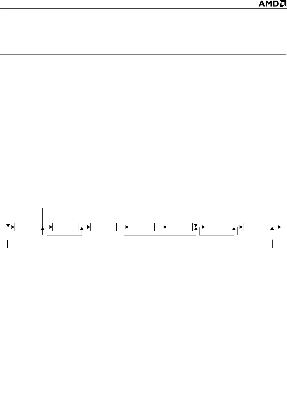
1.1 Instruction Byte Order
An instruction can be between one and 15 bytes in length. Figure 1-1 shows the byte order of the
instruction format.
Figure 1-1. Instruction Byte-Order
Instructions are stored in memory in little-endian order. The least-significant byte of an instruction is
stored at its lowest memory address, as shown in Figure 1-2 on page 2.
Legacy
Prefix
REX
Prefix
Opcode
(1 or 2 bytes) ModRM SIB
Displacement
(1, 2, 4, or 8 bytes)
Immediate
(1, 2, 4, or 8 bytes)
Instruction Length ≤ 15 Bytes
2Instruction Formats
AMD64 Technology 24594—Rev. 3.14—September 2007
Figure 1-2. Little-Endian Byte-Order of Instruction Stored in Memory
The basic operation of an instruction is specified by an opcode. The opcode is one or two bytes long, as
described in “Opcode” on page 17. An opcode can be preceded by any number of legacy prefixes.
These prefixes can be classified as belonging to any of the five groups of prefixes described in
“Instruction Prefixes” on page 3. The legacy prefixes modify an instruction’s default address size,
operand size, or segment, or they invoke a special function such as modification of the opcode, atomic
bus-locking, or repetition. The REX prefix can be used in 64-bit mode to access the register extensions
illustrated in “Application-Programming Register Set” in Volume 1. If a REX prefix is used, it must
immediately precede the first opcode byte.
An instruction’s opcode consists of one or two bytes. In several 128-bit and 64-bit media instructions,
a legacy operand-size or repeat prefix byte is used in a special-purpose way to modify the opcode. The
opcode can be followed by a mode-register-memory (ModRM) byte, which further describes the
operation and/or operands. The opcode, or the opcode and ModRM byte, can also be followed by a
scale-index-base (SIB) byte, which describes the scale, index, and base forms of memory addressing.
The ModRM and SIB bytes are described in “ModRM and SIB Bytes” on page 17, but their legacy
functions can be modified by the REX prefix (“Instruction Prefixes” on page 3).
The 15-byte instruction-length limit can only be exceeded by using redundant prefixes. If the limit is
exceeded, a general-protection exception occurs.
513-304.eps
Legacy Prefix
Legacy Prefix
Legacy Prefix
Legacy Prefix
REX Prefix
SIB
Displacement
* optional, depending on the instruction
+ optional, with most instructions
Immediate
Opcode
ModRM
Least-significant
(lowest) address
+ (available only in 64-bit mode)
+
+
+
+
Most-significant
(highest) address
*
Immediate *
Immediate *
Immediate *
*
Displacement *
Displacement *
Displacement *
*
*
*
Opcode
≤ 15 Bytes
70
(all two-byte opcodes have 0Fh as their first byte)

Instruction Formats 3
24594—Rev. 3.14—September 2007 AMD64 Technology
1.2 Instruction Prefixes
The instruction prefixes shown in Figure 1-1 on page 1 are of two types: legacy prefixes and REX
prefixes. Each of the legacy prefixes has a unique byte value. By contrast, the REX prefixes, which
enable use of the AMD64 register extensions in 64-bit mode, are organized as a group of byte values in
which the value of the prefix indicates the combination of register-extension features to be enabled.
1.2.1 Summary of Legacy Prefixes
Table 1-1 on page 4 shows the legacy prefixes—that is, all prefixes except the REX prefixes, which are
described on page 11. The legacy prefixes are organized into five groups, as shown in the left-most
column of Table 1-1. A single instruction should include a maximum of one prefix from each of the
five groups. The legacy prefixes can appear in any order within the position shown in Figure 1-1 for
legacy prefixes. The result of using multiple prefixes from a single group is unpredictable.
Some of the restrictions on legacy prefixes are:
•Operand-Size Override—This prefix affects only general-purpose instructions and a few x87
instructions. When used with 128-bit and 64-bit media instructions, this prefix acts in a special
way to modify the opcode.
•Address-Size Override—This prefix affects only memory operands.
•Segment Override—In 64-bit mode, the CS, DS, ES, and SS segment override prefixes are ignored.
•LOCK Prefix—This prefix is allowed only with certain instructions that modify memory.
•Repeat Prefixes—These prefixes affect only certain string instructions. When used with 128-bit
and 64-bit media instructions, these prefixes act in a special way to modify the opcode.

4Instruction Formats
AMD64 Technology 24594—Rev. 3.14—September 2007
1.2.2 Operand-Size Override Prefix
The default operand size for an instruction is determined by a combination of its opcode, the D
(default) bit in the current code-segment descriptor, and the current operating mode, as shown in
Table 1-2. The operand-size override prefix (66h) selects the non-default operand size. The prefix can
Table 1-1. Legacy Instruction Prefixes
Prefix Group1Mnemonic Prefix
Byte (Hex) Description
Operand-Size Override none 662Changes the default operand size of a memory or
register operand, as shown in Table 1-2 on page 5.
Address-Size Override none 673Changes the default address size of a memory operand,
as shown in Table 1-3 on page 6.
Segment Override
CS 2E4Forces use of the current CS segment for memory
operands.
DS 3E4Forces use of the current DS segment for memory
operands.
ES 264Forces use of the current ES segment for memory
operands.
FS 64 Forces use of the current FS segment for memory
operands.
GS 65 Forces use of the current GS segment for memory
operands.
SS 364Forces use of the current SS segment for memory
operands.
Lock LOCK F05Causes certain kinds of memory read-modify-write
instructions to occur atomically.
Repeat
REP
F36
Repeats a string operation (INS, MOVS, OUTS, LODS,
and STOS) until the rCX register equals 0.
REPE or
REPZ
Repeats a compare-string or scan-string operation
(CMPSx and SCASx) until the rCX register equals 0 or
the zero flag (ZF) is cleared to 0.
REPNE or
REPNZ F26
Repeats a compare-string or scan-string operation
(CMPSx and SCASx) until the rCX register equals 0 or
the zero flag (ZF) is set to 1.
Note:
1. A single instruction should include a maximum of one prefix from each of the five groups.
2. When used with 128-bit and 64-bit media instructions, this prefix acts in a special way to modify the opcode. The
prefix is ignored by 64-bit media floating-point (3DNow!™) instructions. See “Instructions that Cannot Use the Oper-
and-Size Prefix” on page 5.
3. This prefix also changes the size of the RCX register when used as an implied count register.
4. In 64-bit mode, the CS, DS, ES, and SS segment overrides are ignored.
5. The LOCK prefix should not be used for instructions other than those listed in “Lock Prefix” on page 8.
6. This prefix should be used only with compare-string and scan-string instructions. When used with 128-bit and 64-
bit media instructions, the prefix acts in a special way to modify the opcode.
Instruction Formats 5
24594—Rev. 3.14—September 2007 AMD64 Technology
be used with any general-purpose instruction that accesses non-fixed-size operands in memory or
general-purpose registers (GPRs), and it can also be used with the x87 FLDENV, FNSTENV,
FNSAVE, and FRSTOR instructions.
In 64-bit mode, the prefix allows mixing of 16-bit, 32-bit, and 64-bit data on an instruction-by-
instruction basis. In compatibility and legacy modes, the prefix allows mixing of 16-bit and 32-bit
operands on an instruction-by-instruction basis.
In 64-bit mode, most instructions default to a 32-bit operand size. For these instructions, a REX prefix
(page 13) can specify a 64-bit operand size, and a 66h prefix specifies a 16-bit operand size. The REX
prefix takes precedence over the 66h prefix. However, if an instruction defaults to a 64-bit operand
size, it does not need a REX prefix and it can only be overridden to a 16-bit operand size. It cannot be
overridden to a 32-bit operand size, because there is no 32-bit operand-size override prefix in 64-bit
mode. Two groups of instructions have a default 64-bit operand size in 64-bit mode:
•Near branches. For details, see “Near Branches in 64-Bit Mode” in Volume 1.
•All instructions, except far branches, that implicitly reference the RSP. For details, see “Stack
Operation” in Volume 1.
Instructions that Cannot Use the Operand-Size Prefix. The operand-size prefix should be used
only with general-purpose instructions and the x87 FLDENV, FNSTENV, FNSAVE, and FRSTOR
Table 1-2. Operand-Size Overrides
Operating Mode
Default
Operand
Size (Bits)
Effective
Operand
Size
(Bits)
Instruction Prefix1
66h REX.W3
Long
Mode
64-Bit
Mode 322
64 don’t care yes
32 no no
16 yes no
Compatibility
Mode
32 32 no
Not Appli-
cable
16 yes
16 32 yes
16 no
Legacy Mode
(Protected, Virtual-8086,
or Real Mode)
32 32 no
16 yes
16 32 yes
16 no
Note:
1. A “no’ indicates that the default operand size is used.
2. This is the typical default, although some instructions default to other operand
sizes. See Appendix B, “General-Purpose Instructions in 64-Bit Mode,” for details.
3. See “REX Prefixes” on page 11.
6Instruction Formats
AMD64 Technology 24594—Rev. 3.14—September 2007
instructions, in which the prefix selects between 16-bit and 32-bit operand size. The prefix is ignored
by all other x87 instructions and by 64-bit media floating-point (3DNow!™) instructions.
When used with 64-bit media integer instructions, the 66h prefix acts in a special way to modify the
opcode. This modification typically causes an access to an XMM register or 128-bit memory operand
and thereby converts the 64-bit media instruction into its comparable 128-bit media instruction. The
result of using an F2h or F3h repeat prefix along with a 66h prefix in 128-bit or 64-bit media
instructions is unpredictable.
Operand-Size and REX Prefixes. The REX operand-size prefix takes precedence over the 66h
prefix. See “REX.W: Operand Width” on page 13 for details.
1.2.3 Address-Size Override Prefix
The default address size for instructions that access non-stack memory is determined by the current
operating mode, as shown in Table 1-3. The address-size override prefix (67h) selects the non-default
address size. Depending on the operating mode, this prefix allows mixing of 16-bit and 32-bit, or of
32-bit and 64-bit addresses, on an instruction-by-instruction basis. The prefix changes the address size
for memory operands. It also changes the size of the RCX register for instructions that use RCX
implicitly.
For instructions that implicitly access the stack segment (SS), the address size for stack accesses is
determined by the D (default) bit in the stack-segment descriptor. In 64-bit mode, the D bit is ignored,
and all stack references have a 64-bit address size. However, if an instruction accesses both stack and
non-stack memory, the address size of the non-stack access is determined as shown in Table 1-3.
Table 1-3. Address-Size Overrides
Operating Mode
Default
Address
Size (Bits)
Effective
Address Size
(Bits)
Address-
Size Prefix
(67h)1
Required?
Long Mode
64-Bit
Mode 64 64 no
32 yes
Compatibility
Mode
32 32 no
16 yes
16 32 yes
16 no
Legacy Mode
(Protected, Virtual-8086, or Real
Mode)
32 32 no
16 yes
16 32 yes
16 no
Note:
1. A “no” indicates that the default address size is used.

Instruction Formats 7
24594—Rev. 3.14—September 2007 AMD64 Technology
As Table 1-3 shows, the default address size is 64 bits in 64-bit mode. The size can be overridden to 32
bits, but 16-bit addresses are not supported in 64-bit mode. In compatibility and legacy modes, the
default address size is 16 bits or 32 bits, depending on the operating mode (see “Processor
Initialization and Long Mode Activation” in Volume 2 for details). In these modes, the address-size
prefix selects the non-default size, but the 64-bit address size is not available.
Certain instructions reference pointer registers or count registers implicitly, rather than explicitly. In
such instructions, the address-size prefix affects the size of such addressing and count registers, just as
it does when such registers are explicitly referenced. Table 1-4 lists all such instructions and the
registers referenced using the three possible address sizes.
Table 1-4. Pointer and Count Registers and the Address-Size Prefix
Instruction
Pointer or Count Register
16-Bit
Address Size
32-Bit
Address Size
64-Bit
Address Size
CMPS, CMPSB, CMPSW,
CMPSD, CMPSQ—Compare
Strings
SI, DI, CX ESI, EDI, ECX RSI, RDI, RCX
INS, INSB, INSW, INSD—
Input String DI, CX EDI, ECX RDI, RCX
JCXZ, JECXZ, JRCXZ—Jump
on CX/ECX/RCX Zero CX ECX RCX
LODS, LODSB, LODSW,
LODSD, LODSQ—Load
String
SI, CX ESI, ECX RSI, RCX
LOOP, LOOPE, LOOPNZ,
LOOPNE, LOOPZ—Loop CX ECX RCX
MOVS, MOVSB, MOVSW,
MOVSD, MOVSQ—Move
String
SI, DI, CX ESI, EDI, ECX RSI, RDI, RCX
OUTS, OUTSB, OUTSW,
OUTSD—Output String SI, CX ESI, ECX RSI, RCX
REP, REPE, REPNE, REPNZ,
REPZ—Repeat Prefixes CX ECX RCX
SCAS, SCASB, SCASW,
SCASD, SCASQ—Scan
String
DI, CX EDI, ECX RDI, RCX
STOS, STOSB, STOSW,
STOSD, STOSQ—Store
String
DI, CX EDI, ECX RDI, RCX
XLAT, XLATB—Table Look-up
Translation BX EBX RBX
8Instruction Formats
AMD64 Technology 24594—Rev. 3.14—September 2007
1.2.4 Segment-Override Prefixes
Segment overrides can be used only with instructions that reference non-stack memory. Most
instructions that reference memory are encoded with a ModRM byte (page 17). The default segment
for such memory-referencing instructions is implied by the base register indicated in its ModRM byte,
as follows:
•Instructions that Reference a Non-Stack Segment—If an instruction encoding references any base
register other than rBP or rSP, or if an instruction contains an immediate offset, the default segment
is the data segment (DS). These instructions can use the segment-override prefix to select one of
the non-default segments, as shown in Table 1-5.
•String Instructions—String instructions reference two memory operands. By default, they
reference both the DS and ES segments (DS:rSI and ES:rDI). These instructions can override their
DS-segment reference, as shown in Table 1-5, but they cannot override their ES-segment
reference.
•Instructions that Reference the Stack Segment—If an instruction’s encoding references the rBP or
rSP base register, the default segment is the stack segment (SS). All instructions that reference the
stack (push, pop, call, interrupt, return from interrupt) use SS by default. These instructions cannot
use the segment-override prefix.
Segment Overrides in 64-Bit Mode. In 64-bit mode, the CS, DS, ES, and SS segment-override
prefixes have no effect. These four prefixes are not treated as segment-override prefixes for the
purposes of multiple-prefix rules. Instead, they are treated as null prefixes.
The FS and GS segment-override prefixes are treated as true segment-override prefixes in 64-bit mode.
Use of the FS or GS prefix causes their respective segment bases to be added to the effective address
calculation. See “FS and GS Registers in 64-Bit Mode” in Volume 2 for details.
1.2.5 Lock Prefix
The LOCK prefix causes certain kinds of memory read-modify-write instructions to occur atomically.
The mechanism for doing so is implementation-dependent (for example, the mechanism may involve
Table 1-5. Segment-Override Prefixes
Mnemonic Prefix Byte
(Hex) Description
CS12E Forces use of current CS segment for memory operands.
DS13E Forces use of current DS segment for memory operands.
ES126 Forces use of current ES segment for memory operands.
FS 64 Forces use of current FS segment for memory operands.
GS 65 Forces use of current GS segment for memory operands.
SS136 Forces use of current SS segment for memory operands.
Note:
1. In 64-bit mode, the CS, DS, ES, and SS segment overrides are ignored.

Instruction Formats 9
24594—Rev. 3.14—September 2007 AMD64 Technology
bus signaling or packet messaging between the processor and a memory controller). The prefix is
intended to give the processor exclusive use of shared memory in a multiprocessor system.
The LOCK prefix can only be used with forms of the following instructions that write a memory
operand: ADC, ADD, AND, BTC, BTR, BTS, CMPXCHG, CMPXCHG8B, CMPXCHG16B, DEC,
INC, NEG, NOT, OR, SBB, SUB, XADD, XCHG, and XOR. An invalid-opcode exception occurs if
the LOCK prefix is used with any other instruction.
1.2.6 Repeat Prefixes
The repeat prefixes cause repetition of certain instructions that load, store, move, input, or output
strings. The prefixes should only be used with such string instructions. Two pairs of repeat prefixes,
REPE/REPZ and REPNE/REPNZ, perform the same repeat functions for certain compare-string and
scan-string instructions. The repeat function uses rCX as a count register. The size of rCX is based on
address size, as shown in Table 1-4 on page 7.
REP. The REP prefix repeats its associated string instruction the number of times specified in the
counter register (rCX). It terminates the repetition when the value in rCX reaches 0. The prefix can be
used with the INS, LODS, MOVS, OUTS, and STOS instructions. Table 1-6 shows the valid REP
prefix opcodes.
Table 1-6. REP Prefix Opcodes
Mnemonic Opcode
REP INS reg/mem8, DX
REP INSB F3 6C
REP INS reg/mem16/32, DX
REP INSW
REP INSD
F3 6D
REP LODS mem8
REP LODSB F3 AC
REP LODS mem16/32/64
REP LODSW
REP LODSD
REP LODSQ
F3 AD
REP MOVS mem8, mem8
REP MOVSB F3 A4
REP MOVS mem16/32/64, mem16/32/64
REP MOVSW
REP MOVSD
REP MOVSQ
F3 A5
REP OUTS DX, reg/mem8
REP OUTSB F3 6E

10 Instruction Formats
AMD64 Technology 24594—Rev. 3.14—September 2007
REPE and REPZ. REPE and REPZ are synonyms and have identical opcodes. These prefixes repeat
their associated string instruction the number of times specified in the counter register (rCX). The
repetition terminates when the value in rCX reaches 0 or when the zero flag (ZF) is cleared to 0. The
REPE and REPZ prefixes can be used with the CMPS, CMPSB, CMPSD, CMPSW, SCAS, SCASB,
SCASD, and SCASW instructions. Table 1-7 shows the valid REPE and REPZ prefix opcodes.
REPNE and REPNZ. REPNE and REPNZ are synonyms and have identical opcodes. These prefixes
repeat their associated string instruction the number of times specified in the counter register (rCX).
The repetition terminates when the value in rCX reaches 0 or when the zero flag (ZF) is set to 1. The
REPNE and REPNZ prefixes can be used with the CMPS, CMPSB, CMPSD, CMPSW, SCAS,
SCASB, SCASD, and SCASW instructions. Table 1-8 on page 11 shows the valid REPNE and
REPNZ prefix opcodes.
REP OUTS DX, reg/mem16/32
REP OUTSW
REP OUTSD
F3 6F
REP STOS mem8
REP STOSB F3 AA
REP STOS mem16/32/64
REP STOSW
REP STOSD
REP STOSQ
F3 AB
Table 1-7. REPE and REPZ Prefix Opcodes
Mnemonic Opcode
REPx CMPS mem8, mem8
REPx CMPSB F3 A6
REPx CMPS mem16/32/64, mem16/32/64
REPx CMPSW
REPx CMPSD
REPx CMPSQ
F3 A7
REPx SCAS mem8
REPx SCASB F3 AE
REPx SCAS mem16/32/64
REPx SCASW
REPx SCASD
REPx SCASQ
F3 AF
Table 1-6. REP Prefix Opcodes (continued)
Mnemonic Opcode

Instruction Formats 11
24594—Rev. 3.14—September 2007 AMD64 Technology
Instructions that Cannot Use Repeat Prefixes. In general, the repeat prefixes should only be used
in the string instructions listed in tables 1-6, 1-7, and 1-8, and in 128-bit or 64-bit media instructions.
When used in media instructions, the F2h and F3h prefixes act in a special way to modify the opcode
rather than cause a repeat operation. The result of using a 66h operand-size prefix along with an F2h or
F3h prefix in 128-bit or 64-bit media instructions is unpredictable.
Optimization of Repeats. Depending on the hardware implementation, the repeat prefixes can have a
setup overhead. If the repeated count is variable, the overhead can sometimes be avoided by substituting
a simple loop to move or store the data. Repeated string instructions can be expanded into equivalent
sequences of inline loads and stores or a sequence of stores can be used to emulate a REP STOS.
For repeated string moves, performance can be maximized by moving the largest possible operand
size. For example, use REP MOVSD rather than REP MOVSW and REP MOVSW rather than REP
MOVSB. Use REP STOSD rather than REP STOSW and REP STOSW rather than REP MOVSB.
Depending on the hardware implementation, string moves with the direction flag (DF) cleared to 0
(up) may be faster than string moves with DF set to 1 (down). DF = 1 is only needed for certain cases
of overlapping REP MOVS, such as when the source and the destination overlap.
1.2.7 REX Prefixes
REX prefixes are a group of instruction-prefix bytes that can be used only in 64-bit mode. They enable
access to the AMD64 register extensions. Figure 1-1 on page 1 and Figure 1-2 on page 2 show how a
REX prefix fits within the byte order of instructions. REX prefixes enable the following features in 64-
bit mode:
•Use of the extended GPR (Figure 2-3 on page 25) or XMM registers (Figure 2-8 on page 30).
•Use of the 64-bit operand size when accessing GPRs.
Table 1-8. REPNE and REPNZ Prefix Opcodes
Mnemonic Opcode
REPNx CMPS mem8, mem8
REPNx CMPSB F2 A6
REPNx CMPS mem16/32/64, mem16/32/64
REPNx CMPSW
REPNx CMPSD
REPNx CMPSQ
F2 A7
REPNx SCAS mem8
REPNx SCASB F2 AE
REPNx SCAS mem16/32/64
REPNx SCASW
REPNx SCASD
REPNx SCASQ
F2 AF
12 Instruction Formats
AMD64 Technology 24594—Rev. 3.14—September 2007
•Use of the extended control and debug registers, as described in “64-Bit-Mode Extended Control
Registers” in Volume 2 and “64-Bit-Mode Extended Debug Registers” in Volume 2.
•Use of the uniform byte registers (AL–R15).
Table 1-9 shows the REX prefixes. The value of a REX prefix is in the range 40h through 4Fh,
depending on the particular combination of AMD64 register extensions desired.
A REX prefix is normally required with an instruction that accesses a 64-bit GPR or one of the
extended GPR or XMM registers. Only a few instructions have an operand size that defaults to (or is
fixed at) 64 bits in 64-bit mode, and thus do not need a REX prefix. These exceptions to the normal
rule are listed in Table 1-10.
An instruction can have only one REX prefix, although the prefix can express several extension
features. If a REX prefix is used, it must immediately precede the first opcode byte in the instruction
format. Any other placement of a REX prefix, or any use of a REX prefix in an instruction that does
Table 1-9. REX Instruction Prefixes
Prefix Type Mnemonic Prefix Code
(Hex) Description
Register Extensions
REX.W
401
through
4F1
Access an AMD64 register
extension.
REX.R
REX.X
REX.B
Note:
1. See Table 1-11 for encoding of REX prefixes.
Table 1-10. Instructions Not Requiring REX Size Prefix in 64-Bit Mode
CALL (Near) POP reg/mem
ENTER POP reg
Jcc POP FS
JrCXZ POP GS
JMP (Near) POPFQ
LEAVE PUSH imm8
LGDT PUSH imm32
LIDT PUSH reg/mem
LLDT PUSH reg
LOOP PUSH FS
LOOPcc PUSH GS
LTR PUSHFQ
MOV CR(n)RET (Near)
MOV DR(n)

Instruction Formats 13
24594—Rev. 3.14—September 2007 AMD64 Technology
not access an extended register, is ignored. The legacy instruction-size limit of 15 bytes still applies to
instructions that contain a REX prefix.
REX prefixes are a set of sixteen values that span one row of the main opcode map and occupy entries
40h through 4Fh. Table 1-11 and Figure 1-3 on page 15 show the prefix fields and their uses.
REX.W: Operand Width. Setting the REX.W bit to 1 specifies a 64-bit operand size. Like the
existing 66h operand-size prefix, the REX 64-bit operand-size override has no effect on byte
operations. For non-byte operations, the REX operand-size override takes precedence over the 66h
prefix. If a 66h prefix is used together with a REX prefix that has the REX.W bit set to 1, the 66h
prefix is ignored. However, if a 66h prefix is used together with a REX prefix that has the REX.W bit
cleared to 0, the 66h prefix is not ignored and the operand size becomes 16 bits.
REX.R: Register. The REX.R bit adds a 1-bit (high) extension to the ModRM reg field (page 17)
when that field encodes a GPR, XMM, control, or debug register. REX.R does not modify ModRM reg
when that field specifies other registers or opcodes. REX.R is ignored in such cases.
REX.X: Index. The REX.X bit adds a 1-bit (high) extension to the SIB index field (page 17).
REX.B: Base. The REX.B bit adds a 1-bit (high) extension to either the ModRM r/m field to specify
a GPR or XMM register, or to the SIB base field to specify a GPR. (See Table 2-2 on page 40 for more
about the REX.B bit.)
Encoding Examples. Figure 1-3 on page 15 shows four examples of how the R, X, and B bits of
REX prefixes are concatenated with fields from the ModRM byte, SIB byte, and opcode to specify
register and memory addressing. The R, X, and B bits are described in Table 1-11 on page 13.
Table 1-11. REX Prefix-Byte Fields
Mnemonic Bit Position Definition
— 7–4 0100
REX.W 3 0 = Default operand size
1 = 64-bit operand size
REX.R 2
1-bit (high) extension of the ModRM reg
field1, thus permitting access to 16
registers.
REX.X 1 1-bit (high) extension of the SIB index field1,
thus permitting access to 16 registers.
REX.B 0
1-bit (high) extension of the ModRM r/m
field1, SIB base field1, or opcode reg field,
thus permitting access to 16 registers.
Note:
1. For a description of the ModRM and SIB bytes, see “ModRM and SIB Bytes” on
page 17.

14 Instruction Formats
AMD64 Technology 24594—Rev. 3.14—September 2007
Byte-Register Addressing. In the legacy architecture, the byte registers (AH, AL, BH, BL, CH, CL,
DH, and DL, shown in Figure 2-2 on page 24) are encoded in the ModRM reg or r/m field or in the
opcode reg field as registers 0 through 7. The REX prefix provides an additional byte-register
addressing capability that makes the least-significant byte of any GPR available for byte operations
(Figure 2-3 on page 25). This provides a uniform set of byte, word, doubleword, and quadword
registers better suited for register allocation by compilers.
Special Encodings for Registers. Readers who need to know the details of instruction encodings
should be aware that certain combinations of the ModRM and SIB fields have special meaning for
register encodings. For some of these combinations, the instruction fields expanded by the REX prefix
are not decoded (treated as don’t cares), thereby creating aliases of these encodings in the extended
registers. Table 1-12 on page 16 describes how each of these cases behaves.
Implications for INC and DEC Instructions. The REX prefix values are taken from the 16 single-
byte INC and DEC instructions, one for each of the eight GPRs. Therefore, these single-byte opcodes
for INC and DEC are not available in 64-bit mode, although they are available in legacy and
compatibility modes. The functionality of these INC and DEC instructions is still available in 64-bit
mode, however, using the ModRM forms of those instructions (opcodes FF /0 and FF /1).

Instruction Formats 15
24594—Rev. 3.14—September 2007 AMD64 Technology
Figure 1-3. Encoding Examples of REX-Prefix R, X, and B Bits
513-302.eps
REX Prefix
Case 1: Register-Register Addressing (No Memory Operand)
REX.X is not used
REX.X is not used
4WRXB
Opcode
ModRM Byte
mod regr/m
mod regr/m
mod regr/m
rrr
11 bbb
REX Prefix
Case 2: Memory Addressing Without an SIB Byte
Rrrr
Rrrr Bbbb
4WRXB
Opcode
ModRM Byte
rrr
!11 bbb
Bbbb
4
4
4
4
REX Prefix
Case 3: Memory Addressing With an SIB Byte
Rrrr
4WRXB
Opcode
ModRM Byte
rrr
!11 100
SIB Byte
scale index base
xxx
bb bbb
BbbbXxxx
44
4
REX.R is not used
REX.X is not used
REX Prefix
Case 4: Register Operand Coded in Opcode Byte
Bbbb
4WRXB
Opcode Byte
op reg
bbb
4
ModRM reg field != 100

16 Instruction Formats
AMD64 Technology 24594—Rev. 3.14—September 2007
Table 1-12. Special REX Encodings for Registers
ModRM and SIB
Encodings2
Meaning in Legacy and
Compatibility Modes
Implications in Legacy
and Compatibility
Modes
Additional REX
Implications
ModRM Byte:
•mod≠11
•r/m
1= 100 (ESP)
SIB byte is present. SIB byte is required for
ESP-based addressing.
REX prefix adds a fourth
bit (b), which is decoded
and modifies the base
register in the SIB byte.
Therefore, the SIB byte is
also required for R12-
based addressing.
ModRM Byte:
•mod=00
•r/m
1= x101 (EBP)
Base register is not used.
Using EBP without a
displacement must be
done by setting mod = 01
with a displacement of 0
(with or without an index
register).
REX prefix adds a fourth
bit (x), which is not
decoded (don’t care).
Therefore, using RBP or
R13 without a
displacement must be
done via mod = 01 with a
displacement of 0.
SIB Byte:
• index1= x100 (ESP) Index register is not used. ESP cannot be used as
an index register.
REX prefix adds a fourth
bit (x), which is decoded.
Therefore, there are no
additional implications.
The expanded index field
is used to distinguish RSP
from R12, allowing R12 to
be used as an index.
SIB Byte:
• base = b101 (EBP)
• ModRM.mod = 00
Base register is not used
if ModRM.mod = 00.
Base register depends on
mod encoding. Using
EBP with a scaled index
and without a
displacement must be
done by setting mod = 01
with a displacement of 0.
REX prefix adds a fourth
bit (b), which is not
decoded (don’t care).
Therefore, using RBP or
R13 without a
displacement must be
done via mod = 01 with a
displacement of 0 (with or
without an index register).
Note:
1. The REX-prefix bit is shown in the fourth (most-significant) bit position of the encodings for the ModRM r/m, SIB
index, and SIB base fields. The lower-case “x” for ModRM r/m (rather than the upper-case “B” shown in Figure 1-3
on page 15) indicates that the REX-prefix bit is not decoded (don’t care).
2. For a description of the ModRM and SIB bytes, see “ModRM and SIB Bytes” on page 17.

Instruction Formats 17
24594—Rev. 3.14—September 2007 AMD64 Technology
1.3 Opcode
Each instruction has a unique opcode, although assemblers can support multiple mnemonics for a
single instruction opcode. The opcode specifies the operation that the instruction performs and, in
certain cases, the kinds of operands it uses. An opcode consists of one or two bytes, but certain 128-bit
media instructions also use a prefix byte in a special way to modify the opcode. The 3-bit reg field of
the ModRM byte (“ModRM and SIB Bytes” on page 17) is also used in certain instructions either for
three additional opcode bits or for a register specification.
128-Bit and 64-Bit Media Instruction Opcodes. Many 128-bit and 64-bit media instructions
include a 66h, F2h, or F3h prefix byte in a special way to modify the opcode. These same byte values
can be used in certain general-purpose and x87 instructions to modify operand size (66h) or repeat the
operation (F2h, F3h). In 128-bit and 64-bit media instructions, however, such prefix bytes modify the
opcode. If a 128-bit or 64-bit media instruction uses one of these three prefixes, and also includes any
other prefix in the 66h, F2h, and F3h group, the result is unpredictable.
All opcodes for 64-bit media instructions begin with a 0Fh byte. In the case of 64-bit floating-point
(3DNow!) instructions, the 0Fh byte is followed by a second 0Fh opcode byte. A third opcode byte
occupies the same position at the end of a 3DNow! instruction as would an immediate byte. The value
of the immediate byte is shown as the third opcode byte-value in the syntax for each instruction in
“64-Bit Media Instruction Reference” in Volume 5. The format is:
0Fh 0Fh ModRM [SIB] [displacement]
3DNow!_third_opcode_byte
For details on opcode encoding, see Appendix A, “Opcode and Operand Encodings.”
1.4 ModRM and SIB Bytes
The ModRM byte is used in certain instruction encodings to:
•Define a register reference.
•Define a memory reference.
•Provide additional opcode bits with which to define the instruction’s function.
ModRM bytes have three fields—mod, reg, and r/m. The reg field provides additional opcode bits with
which to define the function of the instruction or one of its operands. The mod and r/m fields are used
together with each other and, in 64-bit mode, with the REX.R and REX.B bits of the REX prefix
(page 11), to specify the location of an instruction’s operands and certain of the possible addressing
modes (specifically, the non-complex modes).
Figure 1-4 on page 18 shows the format of a ModRM byte.
18 Instruction Formats
AMD64 Technology 24594—Rev. 3.14—September 2007
Figure 1-4. ModRM-Byte Format
In some instructions, the ModRM byte is followed by an SIB byte, which defines memory addressing
for the complex-addressing modes described in “Effective Addresses” in Volume 1. The SIB byte has
three fields—scale, index, and base—that define the scale factor, index-register number, and base-
register number for 32-bit and 64-bit complex addressing modes. In 64-bit mode, the REX.B and
REX.X bits extend the encoding of the SIB byte’s base and index fields.
Figure 1-5 shows the format of an SIB byte.
Figure 1-5. SIB-Byte Format
The encodings of ModRM and SIB bytes not only define memory-addressing modes, but they also
specify operand registers. The encodings do this by using 3-bit fields in the ModRM and SIB bytes,
depending on the format:
•ModRM: the reg and r/m fields of the ModRM byte. (Case 1 in Figure 1-3 on page 15 shows an
example of this).
•ModRM with SIB: the reg field of the ModRM byte and the base and index fields of the SIB byte.
(Case 3 in Figure 1-3 on page 15 shows an example of this).
513-305.eps
mod
REX.R bit of REX prefix can
extend this field to 4 bits
REX.B bit of REX prefix can
extend this field to 4 bits
regr/mModRM
01234567Bits:
513-306.eps
Bits:
scale index base SIB
01234567
REX.X bit of REX prefix can
extend this field to 4 bits
REX.B bit of REX prefix can
extend this field to 4 bits

Instruction Formats 19
24594—Rev. 3.14—September 2007 AMD64 Technology
•Instructions without ModRM: the reg field of the opcode. (Case 4 in Figure 1-3 on page 15 shows
an example of this).
In 64-bit mode, the bits needed to extend each field for accessing the additional registers are provided
by the REX prefixes, as shown in Figure 1-4 and Figure 1-5 on page 18.
For details on opcode encoding, see Appendix A, “Opcode and Operand Encodings.”
1.5 Displacement Bytes
A displacement (also called an offset) is a signed value that is added to the base of a code segment
(absolute addressing) or to an instruction pointer (relative addressing), depending on the addressing
mode. The size of a displacement is 1, 2, or 4 bytes. If an addressing mode requires a displacement, the
bytes (1, 2, or 4) for the displacement follow the opcode, ModRM, or SIB byte (whichever comes last)
in the instruction encoding.
In 64-bit mode, the same ModRM and SIB encodings are used to specify displacement sizes as those
used in legacy and compatibility modes. However, the displacement is sign-extended to 64 bits during
effective-address calculations. Also, in 64-bit mode, support is provided for some 64-bit displacement
and immediate forms of the MOV instruction. See “Immediate Operand Size” in Volume 1 for more
information on this.
1.6 Immediate Bytes
An immediate is a value—typically an operand value—encoded directly into the instruction.
Depending on the opcode and the operating mode, the size of an immediate operand can be 1, 2, 4, or 8
bytes. 64-bit immediates are allowed in 64-bit mode on MOV instructions that load GPRs, otherwise
they are limited to 4 bytes. See “Immediate Operand Size” in Volume 1 for more information.
If an instruction takes an immediate operand, the bytes (1, 2, 4, or 8) for the immediate follow the
opcode, ModRM, SIB, or displacement bytes (whichever come last) in the instruction encoding. Some
128-bit media instructions use the immediate byte as a condition code.
1.7 RIP-Relative Addressing
In 64-bit mode, addressing relative to the contents of the 64-bit instruction pointer (program
counter)—called RIP-relative addressing or PC-relative addressing—is implemented for certain
instructions. In such cases, the effective address is formed by adding the displacement to the 64-bit RIP
of the next instruction.
In the legacy x86 architecture, addressing relative to the instruction pointer is available only in control-
transfer instructions. In the 64-bit mode, any instruction that uses ModRM addressing can use RIP-
relative addressing. This feature is particularly useful for addressing data in position-independent code
and for code that addresses global data.

20 Instruction Formats
AMD64 Technology 24594—Rev. 3.14—September 2007
Without RIP-relative addressing, ModRM instructions address memory relative to zero. With RIP-
relative addressing, ModRM instructions can address memory relative to the 64-bit RIP using a signed
32-bit displacement. This provides an offset range of ±2 Gbytes from the RIP.
Programs usually have many references to data, especially global data, that are not register-based. To
load such a program, the loader typically selects a location for the program in memory and then adjusts
program references to global data based on the load location. RIP-relative addressing of data makes
this adjustment unnecessary.
1.7.1 Encoding
Table 1-13 shows the ModRM and SIB encodings for RIP-relative addressing. Redundant forms of 32-
bit displacement-only addressing exist in the current ModRM and SIB encodings. There is one
ModRM encoding with several SIB encodings. RIP-relative addressing is encoded using one of the
redundant forms. In 64-bit mode, the ModRM Disp32 (32-bit displacement) encoding is redefined to
be RIP + Disp32 rather than displacement-only.
1.7.2 REX Prefix and RIP-Relative Addressing
ModRM encoding for RIP-relative addressing does not depend on a REX prefix. In particular, the r/m
encoding of 101, used to select RIP-relative addressing, is not affected by the REX prefix. For
example, selecting R13 (REX.B = 1, r/m = 101) with mod = 00 still results in RIP-relative addressing.
The four-bit r/m field of ModRM is not fully decoded. Therefore, in order to address R13 with no
displacement, software must encode it as R13 + 0 using a one-byte displacement of zero.
1.7.3 Address-Size Prefix and RIP-Relative Addressing
RIP-relative addressing is enabled by 64-bit mode, not by a 64-bit address-size. Conversely, use of the
address-size prefix (“Address-Size Override Prefix” on page 6) does not disable RIP-relative
addressing. The effect of the address-size prefix is to truncate and zero-extend the computed effective
address to 32 bits, like any other addressing mode.
Table 1-13. Encoding for RIP-Relative Addressing
ModRM and SIB
Encodings
Meaning in Legacy and
Compatibility Modes Meaning in 64-bit Mode Additional 64-bit
Implications
ModRM Byte:
•mod=00
• r/m = 101 (none)
Disp32 RIP + Disp32
Zero-based (normal)
displacement addressing
must use SIB form (see
next row).
SIB Byte:
• base = 101 (none)
• index = 100 (none)
• scale = 1, 2, 4,8
If mod = 00, Disp32 Same as Legacy None

Instruction Overview 21
24594—Rev. 3.14—September 2007 AMD64 Technology
2 Instruction Overview
2.1 Instruction Subsets
For easier reference, the instruction descriptions are divided into five instruction subsets. The
following sections describe the function, mnemonic syntax, opcodes, affected flags, and possible
exceptions generated by all instructions in the AMD64 architecture:
•Chapter 3, “General-Purpose Instruction Reference”—The general-purpose instructions are used
in basic software execution. Most of these load, store, or operate on data in the general-purpose
registers (GPRs), in memory, or in both. Other instructions are used to alter sequential program
flow by branching to other locations within the program or to entirely different programs.
•Chapter 4, “System Instruction Reference”—The system instructions establish the processor
operating mode, access processor resources, handle program and system errors, and manage
memory.
•“128-Bit Media Instruction Reference” in Volume 4—The 128-bit media instructions load, store,
or operate on data located in the 128-bit XMM registers. These instructions define both vector and
scalar operations on floating-point and integer data types. They include the SSE and SSE2
instructions that operate on the XMM registers. Some of these instructions convert source
operands in XMM registers to destination operands in GPR, MMX, or x87 registers or otherwise
affect XMM state.
•“64-Bit Media Instruction Reference” in Volume 5—The 64-bit media instructions load, store, or
operate on data located in the 64-bit MMX registers. These instructions define both vector and
scalar operations on integer and floating-point data types. They include the legacy MMX™
instructions, the 3DNow!™ instructions, and the AMD extensions to the MMX and 3DNow!
instruction sets. Some of these instructions convert source operands in MMX registers to
destination operands in GPR, XMM, or x87 registers or otherwise affect MMX state.
•“x87 Floating-Point Instruction Reference” in Volume 5—The x87 instructions are used in legacy
floating-point applications. Most of these instructions load, store, or operate on data located in the
x87 ST(0)–ST(7) stack registers (the FPR0–FPR7 physical registers). The remaining instructions
within this category are used to manage the x87 floating-point environment.
The description of each instruction covers its behavior in all operating modes, including legacy mode
(real, virtual-8086, and protected modes) and long mode (compatibility and 64-bit modes). Details of
certain kinds of complex behavior—such as control-flow changes in CALL, INT, or FXSAVE
instructions—have cross-references in the instruction-detail pages to detailed descriptions in volumes
1 and 2.
Two instructions—CMPSD and MOVSD—use the same mnemonic for different instructions.
Assemblers can distinguish them on the basis of the number and type of operands with which they are
used.

22 Instruction Overview
AMD64 Technology 24594—Rev. 3.14—September 2007
2.2 Reference-Page Format
Figure 2-1 on page 23 shows the format of an instruction-detail page. The instruction mnemonic is
shown in bold at the top-left, along with its name. In this example, POPFD is the mnemonic and POP
to EFLAGS Doubleword is the name. Next, there is a general description of the instruction’s operation.
Many descriptions have cross-references to more detail in other parts of the manual.
Beneath the general description, the mnemonic is shown again, together with the related opcode(s) and
a description summary. Related instructions are listed below this, followed by a table showing the flags
that the instruction can affect. Finally, each instruction has a summary of the possible exceptions that
can occur when executing the instruction. The columns labeled “Real” and “Virtual-8086” apply only
to execution in legacy mode. The column labeled “Protected” applies both to legacy mode and long
mode, because long mode is a superset of legacy protected mode.
The 128-bit and 64-bit media instructions also have diagrams illustrating the operation. A few
instructions have examples or pseudocode describing the action.
Instruction Overview 23
24594—Rev. 3.14—September 2007 AMD64 Technology
Figure 2-1. Format of Instruction-Detail Pages
24594 Rev. 3.07 September 2003 AMD64 Technology
AAM 63
Converts the value in the AL register from binary to two unpacked BCD digits in the
AH (most significant) and AL (least significant) registers using the following formula:
AH = (AL/10d)
AL = (AL mod 10d).
In most modern assemblers, the AAM instruction adjusts to base-10 values. However,
by coding the instruction directly in binary, it can adjust to any base specified by the
immediate byte value (ib) suffixed onto the D4h opcode. For example, code D408h for
octal, D40Ah for decimal, and D40Ch for duodecimal (base 12).
Using this instruction in 64-bit mode generates an invalid-opcode exception.
Related Instructions
AAA, AAD, AAS
rFLAGS Affected
Exceptions
AAM ASCII Adjust After Multiply
Mnemonic Opcode Description
AAM D4 0A Create a pair of unpacked BCD values in AH and AL.
(Invalid in 64-bit mode.)
(None) D4 ib Create a pair of unpacked values to the immediate byte base.
(Invalid in 64-bit mode.)
ID VIP VIF AC VM RF NT IOPL OF DF IF TF SF ZF AF PF CF
U MMUMU
21201918171614 13–12 11109876420
Note: Bits 31–22, 15, 5, 3, and 1 are reserved. A flag set to 1 or cleared to 0 is M. Unaffected flags are blank. Undefined flags are U.
Exception Real
Virtual
8086 Protected Cause of Exception
Divide by zero, #DE X X X 8-bit immediate value was 0.
Invalid opcode, #UD X This instruction was executed in 64-bit mode.
Mnemonic and any operands Opcode Description of operation
“M” means the flag is either set or
cleared, depending on the result.
Possible exceptions
and causes, by mode of
operation
“Protected” column
covers both legacy
and long mode
Alphabetic mnemonic locator
24 Instruction Overview
AMD64 Technology 24594—Rev. 3.14—September 2007
2.3 Summary of Registers and Data Types
This section summarizes the registers available to software using the five instruction subsets described
in “Instruction Subsets” on page 21. For details on the organization and use of these registers, see their
respective chapters in volumes 1 and 2.
2.3.1 General-Purpose Instructions
Registers. The size and number of general-purpose registers (GPRs) depends on the operating mode,
as do the size of the flags and instruction-pointer registers. Figure 2-2 shows the registers available in
legacy and compatibility modes.
Figure 2-2. General Registers in Legacy and Compatibility Modes
Figure 2-3 on page 25 shows the registers accessible in 64-bit mode. Compared with legacy mode,
registers become 64 bits wide, eight new data registers (R8–R15) are added and the low byte of all 16
GPRs is available for byte operations, and the four high-byte registers of legacy mode (AH, BH, CH,
and DH) are not available if the REX prefix is used. The high 32 bits of doubleword operands are zero-
extended to 64 bits, but the high bits of word and byte operands are not modified by operations in 64-
513-311.eps
31 15 016
EAX
EBX
ECX
EDX
ESI
EDI
EBP
ESP
AX
16-bit
low
8-bit
high
8-bit32-bit
BX
CX
DX
SI
DI
BP
SP
AH (4)
BH (7)
CH (5)
DH (6)
AL
BL
CL
DL
SI
DI
BP
SP
FLAGS
IP
31 0
FLAGS
IP
EFLAGS
EIP
0
3
1
2
6
7
5
4
register
encoding
Instruction Overview 25
24594—Rev. 3.14—September 2007 AMD64 Technology
bit mode. The RFLAGS register is 64 bits wide, but the high 32 bits are reserved. They can be written
with anything but they read as zeros (RAZ).
Figure 2-3. General Registers in 64-Bit Mode
For most instructions running in 64-bit mode, access to the extended GPRs requires a REX instruction
prefix (page 11).
513-309.eps
6331157081632
R8
R9
R10
R11
R12
R13
R14
R15
R8W
R9W
R10W
R11W
R12W
R13W
R14W
R15W
R8D
R9D
R10D
R11D
R12D
R13D
R14D
R15D
EAX
EBX
ECX
EDX
ESI
EDI
EBP
ESP
RAX
RBX
RCX
RDX
RSI
RDI
RBP
RSP
AX
AH*
BH*
CH*
DH*
16-bit32-bit64-bit
8
9
10
11
12
13
14
15
0
3
1
2
6
7
5
4
register
encoding
zero-extended
for 32-bit operands
not modified for 8-bit operands
not modified for 16-bit operands
BX
CX
DX
SI
DI
BP
SP
6331032
RFLAGS
RIP
0
low
8-bit
R8B
R9B
R10B
R11B
R12B
R13B
R14B
R15B
AL
BL
CL
DL
SIL**
DIL**
BPL**
SPL**
*Not addressable when
a REX prefix is used.
** Only addressable when
a REX
p
refix is used.
26 Instruction Overview
AMD64 Technology 24594—Rev. 3.14—September 2007
Figure 2-4 shows the segment registers which, like the instruction pointer, are used by all instructions.
In legacy and compatibility modes, all segments are accessible. In 64-bit mode, which uses the flat
(non-segmented) memory model, only the CS, FS, and GS segments are recognized, whereas the
contents of the DS, ES, and SS segment registers are ignored (the base for each of these segments is
assumed to be zero, and neither their segment limit nor attributes are checked). For details, see
“Segmented Virtual Memory” in Volume 2.
Figure 2-4. Segment Registers
Data Types. Figure 2-5 on page 27 shows the general-purpose data types. They are all scalar, integer
data types. The 64-bit (quadword) data types are only available in 64-bit mode, and for most
instructions they require a REX instruction prefix.
513-312.eps
15 0
ES
FS
GS
SS
CS
DS
15 0
FS
(Base only)
GS
(Base only)
CS
(Attributes only)
Legacy Mode and
Compatibility Mode
64-Bit
Mode
ignored
ignored
ignored
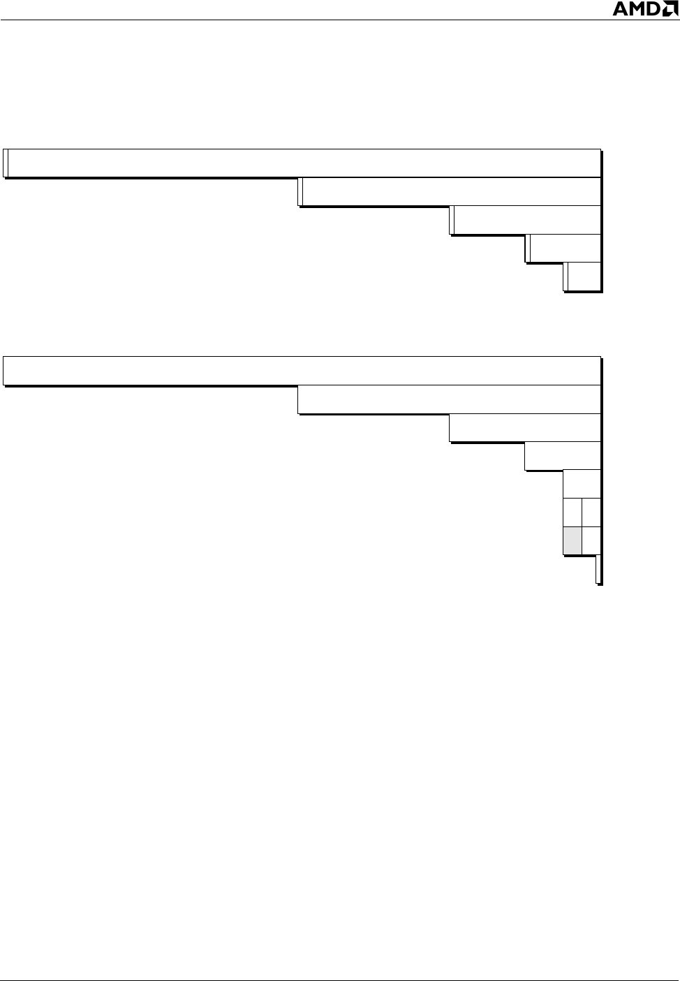
Instruction Overview 27
24594—Rev. 3.14—September 2007 AMD64 Technology
Figure 2-5. General-Purpose Data Types
2.3.2 System Instructions
Registers. The system instructions use several specialized registers shown in Figure 2-6 on page 28.
System software uses these registers to, among other things, manage the processor’s operating
environment, define system resource characteristics, and monitor software execution. With the
exception of the RFLAGS register, system registers can be read and written only from privileged
software.
All system registers are 64 bits wide, except for the descriptor-table registers and the task register,
which include 64-bit base-address fields and other fields.
513-326.eps
127
63
63
31
15
70
Quadword
Double
Quadword
Doubleword
Word
Byte
0
s
s
s
s
Quadword
Unsigned Integer
Signed Integer
Doubleword
Word
Byte
Bit
8 bytes (64-bit mode only)
s16 bytes (64-bit mode only)
127
Double
Quadword
0
16 bytes (64-bit mode only)
4 bytes
2 bytes
31
15
73
Packed BCD
BCD Digit
0
8 bytes (64-bit mode only)
4 bytes
2 bytes
28 Instruction Overview
AMD64 Technology 24594—Rev. 3.14—September 2007
Figure 2-6. System Registers
Data Structures. Figure 2-7 on page 29 shows the system data structures. These are created and
maintained by system software for use in protected mode. A processor running in protected mode uses
these data structures to manage memory and protection, and to store program-state information when
an interrupt or task switch occurs.
Control Registers
CR0
CR2
CR3
CR4
CR8
System-Flags Register
RFLAGS
Debug Registers
DR0
DR1
DR2
DR3
DR6
DR7
513-260.eps
Memory-Typing Registers
MTRRcap
MTRRdefType
MTRRphysBasen
MTRRphysMaskn
MTRRfixn
PAT
TOP_MEM
TOP_MEM2
Machine-Check Registers
MCG_CAP
MCG_STAT
MCG_CTL
MCi_CTL
MCi_STATUS
MCi_ADDR
MCi_MISC
Performance-Monitoring Registers
TSC
PerfEvtSeln
PerfCtrn
Model-Specific Registers
Descriptor-Table Registers
GDTR
IDTR
LDTR
Task Register
TR
Extended-Feature-Enable Register
EFER
Debug-Extension Registers
DebugCtlMSR
LastBranchFromIP
LastBranchToIP
LastIntFromIP
LastIntToIP
System-Configuration Register
SYSCFG
System-Linkage Registers
STAR
LSTAR
CSTAR
FS.base
GS.base
KernelGSbase
SYSENTER_CS
SYSENTER_ESP
SYSENTER_EIP
SFMASK
Instruction Overview 29
24594—Rev. 3.14—September 2007 AMD64 Technology
Figure 2-7. System Data Structures
2.3.3 128-Bit Media Instructions
Registers. The 128-bit media instructions use the 128-bit XMM registers. The number of available
XMM data registers depends on the operating mode, as shown in Figure 2-8 on page 30. In legacy and
compatibility modes, the eight legacy XMM data registers (XMM0–XMM7) are available. In 64-bit
mode, eight additional XMM data registers (XMM8–XMM15) are available when a REX instruction
prefix is used.
The MXCSR register contains floating-point and other control and status flags used by the 128-bit
media instructions. Some 128-bit media instructions also use the GPR (Figure 2-2 and Figure 2-3) and
513-261.eps
Segment Descriptors (Contained in Descriptor Tables)
Code
Stack
Data
Gate
Task-State Segment
Local-Descriptor Table
Task-State Segment
Page-Translation Tables
Page-Map Level-4 Page TablePage DirectoryPage-Directory Pointer
Global-Descriptor Table
Descriptor
Descriptor
. . .
Descriptor
Interrupt-Descriptor Table
Gate Descriptor
Gate Descriptor
. . .
Gate Descriptor
Local-Descriptor Table
Descriptor
Descriptor
. . .
Descriptor
Descriptor Tables

30 Instruction Overview
AMD64 Technology 24594—Rev. 3.14—September 2007
the MMX registers (Figure 2-10 on page 32) or set or clear flags in the rFLAGS register (see
Figure 2-2 and Figure 2-3).
Figure 2-8. 128-Bit Media Registers
Data Types. Figure 2-9 on page 31 shows the 128-bit media data types. They include floating-point
and integer vectors and floating-point scalars. The floating-point data types include IEEE-754 single
precision and double precision types.
513-314.eps
XMM Data Registers
127 0
xmm0
xmm1
xmm2
xmm3
xmm4
xmm5
xmm6
xmm7
xmm8
xmm9
xmm10
xmm11
xmm12
xmm13
xmm14
xmm15
Available in all modes
Available only in 64-bit mode
31 0
MXCSR
128-Bit Media Control and Status Register
Instruction Overview 31
24594—Rev. 3.14—September 2007 AMD64 Technology
Figure 2-9. 128-Bit Media Data Types
ssss
ss
ssss
ss
ssssssss
ssss
ss
ssssssssssssssss
ssssssss
ssss
ss
ssssssssssssssss
513-316.eps
71523313947556371798795103111119127 0
bytebytebytebytebytebytebytebytebytebytebytebytebytebytebytebyte
31 22635495 86127 118 0
Vector (Packed) Floating-Point Double Precision and Single Precision
Vector (Packed) Unsigned Integer Quadword, Doubleword, Word, Byte
71523313947556371798795103111119127 0
quadwordquadword
doubleworddoubleworddoubleworddoubleword
wordwordwordwordwordwordwordword
quadwordquadword
doubleworddoubleworddoubleworddoubleword
wordwordwordwordwordwordwordword
127 0
Scalar Unsigned Integers
127
double quadword
bytebytebytebytebytebytebytebytebytebytebytebytebytebytebytebyte
Vector (Packed) Signed Integer Quadword, Doubleword, Word, Byte
significand
expsignificand
06351127 115
expsignificand
expsignificandexpsignificandexpsignificandexp
s
s
s
s
31 22 0
Scalar Floating-Point Double Precision and Single Precision
significand
expsignificand
6351 exp
15
31
63
quadword
doubleword
word
7
0
byte
bit

32 Instruction Overview
AMD64 Technology 24594—Rev. 3.14—September 2007
2.3.4 64-Bit Media Instructions
Registers. The 64-bit media instructions use the eight 64-bit MMX registers, as shown in
Figure 2-10. These registers are mapped onto the x87 floating-point registers, and 64-bit media
instructions write the x87 tag word in a way that prevents an x87 instruction from using MMX data.
Some 64-bit media instructions also use the GPR (Figure 2-2 and Figure 2-3) and the XMM registers
(Figure 2-8).
Figure 2-10. 64-Bit Media Registers
Data Types. Figure 2-11 on page 33 shows the 64-bit media data types. They include floating-point
and integer vectors and integer scalars. The floating-point data type, used by 3DNow! instructions,
consists of a packed vector or two IEEE-754 32-bit single-precision data types. Unlike other kinds of
floating-point instructions, however, the 3DNow!™ instructions do not generate floating-point
exceptions. For this reason, there is no register for reporting or controlling the status of exceptions in
the 64-bit-media instruction subset.
513-327.eps
MMX Data Registers
630
mmx0
mmx1
mmx2
mmx3
mmx4
mmx5
mmx6
mmx7
Instruction Overview 33
24594—Rev. 3.14—September 2007 AMD64 Technology
Figure 2-11. 64-Bit Media Data Types
ss ss
ssss
ss
ssssssss
ssss
ss
ssssssss
513-319.eps
7152331394755630
bytebytebytebytebytebytebytebyte
31 226354 0
Vector (Packed) Single-Precision Floating-Point
Vector (Packed) Unsigned Integers
7152331394755630
doubleworddoubleword
wordwordwordword
doubleworddoubleword
wordwordwordword
bytebytebytebytebytebytebytebyte
Vector (Packed) Signed Integers
significandexpsignificandexp
63
31
15
70
s
s
s
s
Unsigned Integers
Signed Integers
quadword
doubleword
word
byte
63
31
15
7
0
quadword
doubleword
word
byte
34 Instruction Overview
AMD64 Technology 24594—Rev. 3.14—September 2007
2.3.5 x87 Floating-Point Instructions
Registers. The x87 floating-point instructions use the x87 registers shown in Figure 2-12. There are
eight 80-bit data registers, three 16-bit registers that hold the x87 control word, status word, and tag
word, and three registers (last instruction pointer, last opcode, last data pointer) that hold information
about the last x87 operation.
The physical data registers are named FPR0–FPR7, although x87 software references these registers as
a stack of registers, named ST(0)–ST(7). The x87 instructions store operands only in their own 80-bit
floating-point registers or in memory. They do not access the GPR or XMM registers.
Figure 2-12. x87 Registers
Data Types. Figure 2-13 on page 35 shows all x87 data types. They include three floating-point
formats (80-bit double-extended precision, 64-bit double precision, and 32-bit single precision), three
signed-integer formats (quadword, doubleword, and word), and an 80-bit packed binary-coded
decimal (BCD) format.
Tag Word
Status Word
Control Word
513-321.eps
x87 Data Registers
79 0
fpr0
fpr1
fpr2
fpr3
fpr4
fpr5
fpr6
fpr7
015
63
010
Instruction Pointer (rIP)
Data Pointer (rDP)
Tag Word
Status Word
Control Word
Opcode
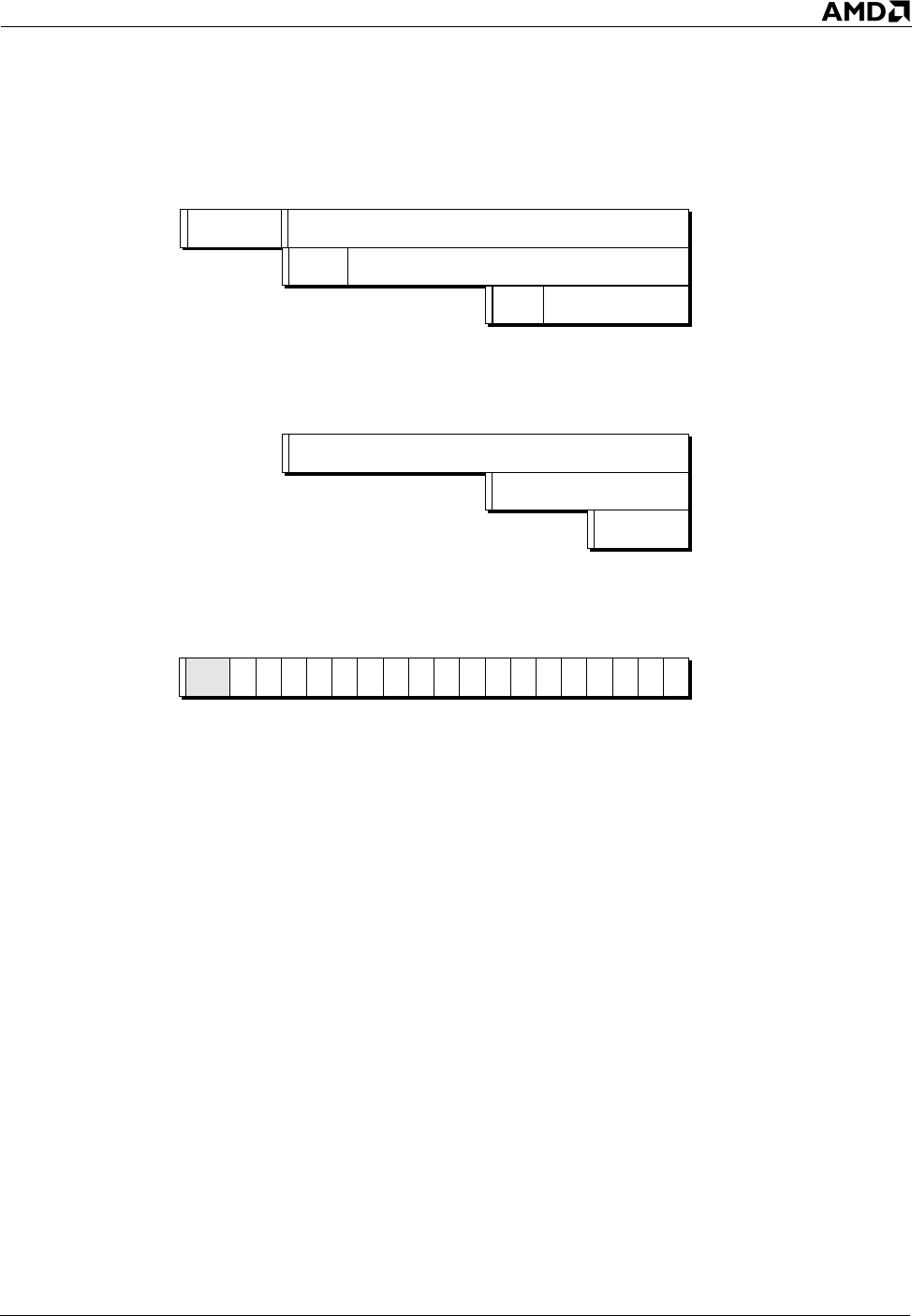
Instruction Overview 35
24594—Rev. 3.14—September 2007 AMD64 Technology
Figure 2-13. x87 Data Types
2.4 Summary of Exceptions
Table 2-1 on page 36 lists all possible exceptions. The table shows the interrupt-vector numbers,
names, mnemonics, source, and possible causes. Exceptions that apply to specific instructions are
documented with each instruction in the instruction-detail pages that follow.
s
513-317.eps
63
31
31
22
15 0
0
0
Quadword
Doubleword
Word
s
s
s
Signed Integer
Binary-Coded Decimal (BCD)
Floating-Point
8 bytes
4 bytes
63
63
51
Double Precision
Single Precision
s
s
2 bytes
79
79
079 71
Double-Extended
Precision
Packed Decimal
s i
significand
expsignificand
expsignificand
exp
s

36 Instruction Overview
AMD64 Technology 24594—Rev. 3.14—September 2007
Table 2-1. Interrupt-Vector Source and Cause
Vector Interrupt (Exception) Mnemonic Source Cause
0 Divide-By-Zero-Error #DE Software DIV, IDIV, AAM instructions
1 Debug #DB Internal Instruction accesses and data accesses
2 Non-Maskable-Interrupt #NMI External External NMI signal
3 Breakpoint #BP Software INT3 instruction
4 Overflow #OF Software INTO instruction
5 Bound-Range #BR Software BOUND instruction
6 Invalid-Opcode #UD Internal Invalid instructions
7 Device-Not-Available #NM Internal x87 instructions
8 Double-Fault #DF Internal Interrupt during an interrupt
9Coprocessor-Segment-Overrun —External Unsupported (reserved)
10 Invalid-TSS #TS Internal Task-state segment access and task
switch
11 Segment-Not-Present #NP Internal Segment access through a descriptor
12 Stack #SS Internal SS register loads and stack references
13 General-Protection #GP Internal Memory accesses and protection
checks
14 Page-Fault #PF Internal Memory accesses when paging
enabled
15 Reserved —
16 Floating-Point Exception-
Pending #MF Software x87 floating-point and 64-bit media
floating-point instructions
17 Alignment-Check #AC Internal Memory accesses
18 Machine-Check #MC Internal
External Model specific
19 SIMD Floating-Point #XF Internal 128-bit media floating-point instructions
20—29 Reserved (Internal and External) —
30 SVM Security Exception #SX External Security-Sensitive Events
31 Reserved (Internal and External) —
0—255 External Interrupts (Maskable) #INTR External External interrupt signal
0—255 Software Interrupts — Software INTn instruction

Instruction Overview 37
24594—Rev. 3.14—September 2007 AMD64 Technology
2.5 Notation
2.5.1 Mnemonic Syntax
Each instruction has a syntax that includes the mnemonic and any operands that the instruction can
take. Figure 2-14 shows an example of a syntax in which the instruction takes two operands. In most
instructions that take two operands, the first (left-most) operand is both a source operand (the first
source operand) and the destination operand. The second (right-most) operand serves only as a source,
not a destination.
Figure 2-14. Syntax for Typical Two-Operand Instruction
The following notation is used to denote the size and type of source and destination operands:
•cReg—Control register.
•dReg—Debug register.
•imm8—Byte (8-bit) immediate.
•imm16—Word (16-bit) immediate.
•imm16/32—Word (16-bit) or doubleword (32-bit) immediate.
•imm32—Doubleword (32-bit) immediate.
•imm32/64—Doubleword (32-bit) or quadword (64-bit) immediate.
•imm64—Quadword (64-bit) immediate.
•mem—An operand of unspecified size in memory.
•mem8—Byte (8-bit) operand in memory.
•mem16—Word (16-bit) operand in memory.
•mem16/32—Word (16-bit) or doubleword (32-bit) operand in memory.
•mem32—Doubleword (32-bit) operand in memory.
•mem32/48—Doubleword (32-bit) or 48-bit operand in memory.
•mem48—48-bit operand in memory.
513-322.eps
Mnemonic
First Source Operand
and Destination Operand
Second Source Operand
ADDPD xmm1, xmm2/mem128

38 Instruction Overview
AMD64 Technology 24594—Rev. 3.14—September 2007
•mem64—Quadword (64-bit) operand in memory.
•mem128—Double quadword (128-bit) operand in memory.
•mem16:16—Two sequential word (16-bit) operands in memory.
•mem16:32—A doubleword (32-bit) operand followed by a word (16-bit) operand in memory.
•mem32real—Single-precision (32-bit) floating-point operand in memory.
•mem32int—Doubleword (32-bit) integer operand in memory.
•mem64real—Double-precision (64-bit) floating-point operand in memory.
•mem64int—Quadword (64-bit) integer operand in memory.
•mem80real—Double-extended-precision (80-bit) floating-point operand in memory.
•mem80dec—80-bit packed BCD operand in memory, containing 18 4-bit BCD digits.
•mem2env—16-bit x87 control word or x87 status word.
•mem14/28env—14-byte or 28-byte x87 environment. The x87 environment consists of the x87
control word, x87 status word, x87 tag word, last non-control instruction pointer, last data pointer,
and opcode of the last non-control instruction completed.
•mem94/108env—94-byte or 108-byte x87 environment and register stack.
•mem512env—512-byte environment for 128-bit media, 64-bit media, and x87 instructions.
•mmx—Quadword (64-bit) operand in an MMX register.
•mmx1—Quadword (64-bit) operand in an MMX register, specified as the left-most (first) operand
in the instruction syntax.
•mmx2—Quadword (64-bit) operand in an MMX register, specified as the right-most (second)
operand in the instruction syntax.
•mmx/mem32—Doubleword (32-bit) operand in an MMX register or memory.
•mmx/mem64—Quadword (64-bit) operand in an MMX register or memory.
•mmx1/mem64—Quadword (64-bit) operand in an MMX register or memory, specified as the left-
most (first) operand in the instruction syntax.
•mmx2/mem64—Quadword (64-bit) operand in an MMX register or memory, specified as the right-
most (second) operand in the instruction syntax.
•moffset—Direct memory offset that specifies an operand in memory.
•moffset8—Direct memory offset that specifies a byte (8-bit) operand in memory.
•moffset16—Direct memory offset that specifies a word (16-bit) operand in memory.
•moffset32—Direct memory offset that specifies a doubleword (32-bit) operand in memory.
•moffset64—Direct memory offset that specifies a quadword (64-bit) operand in memory.
•pntr16:16—Far pointer with 16-bit selector and 16-bit offset.
•pntr16:32—Far pointer with 16-bit selector and 32-bit offset.
•reg—Operand of unspecified size in a GPR register.
•reg8—Byte (8-bit) operand in a GPR register.

Instruction Overview 39
24594—Rev. 3.14—September 2007 AMD64 Technology
•reg16—Word (16-bit) operand in a GPR register.
•reg16/32—Word (16-bit) or doubleword (32-bit) operand in a GPR register.
•reg32—Doubleword (32-bit) operand in a GPR register.
•reg64—Quadword (64-bit) operand in a GPR register.
•reg/mem8—Byte (8-bit) operand in a GPR register or memory.
•reg/mem16—Word (16-bit) operand in a GPR register or memory.
•reg/mem32—Doubleword (32-bit) operand in a GPR register or memory.
•reg/mem64—Quadword (64-bit) operand in a GPR register or memory.
•rel8off—Signed 8-bit offset relative to the instruction pointer.
•rel16off—Signed 16-bit offset relative to the instruction pointer.
•rel32off—Signed 32-bit offset relative to the instruction pointer.
•segReg or sReg—Word (16-bit) operand in a segment register.
•ST(0)—x87 stack register 0.
•ST(i)—x87 stack register i, where i is between 0 and 7.
•xmm—Double quadword (128-bit) operand in an XMM register.
•xmm1—Double quadword (128-bit) operand in an XMM register, specified as the left-most (first)
operand in the instruction syntax.
•xmm2—Double quadword (128-bit) operand in an XMM register, specified as the right-most
(second) operand in the instruction syntax.
•xmm/mem64—Quadword (64-bit) operand in a 128-bit XMM register or memory.
•xmm/mem128—Double quadword (128-bit) operand in an XMM register or memory.
•xmm1/mem128—Double quadword (128-bit) operand in an XMM register or memory, specified as
the left-most (first) operand in the instruction syntax.
•xmm2/mem128—Double quadword (128-bit) operand in an XMM register or memory, specified as
the right-most (second) operand in the instruction syntax.
2.5.2 Opcode Syntax
In addition to the notation shown above in “Mnemonic Syntax” on page 37, the following notation
indicates the size and type of operands in the syntax of an instruction opcode:
•/digit—Indicates that the ModRM byte specifies only one register or memory (r/m) operand. The
digit is specified by the ModRM reg field and is used as an instruction-opcode extension. Valid
digit values range from 0 to 7.
•/r—Indicates that the ModRM byte specifies both a register operand and a reg/mem (register or
memory) operand.
•cb, cw, cd, cp—Specifies a code-offset value and possibly a new code-segment register value. The
value following the opcode is either one byte (cb), two bytes (cw), four bytes (cd), or six bytes (cp).
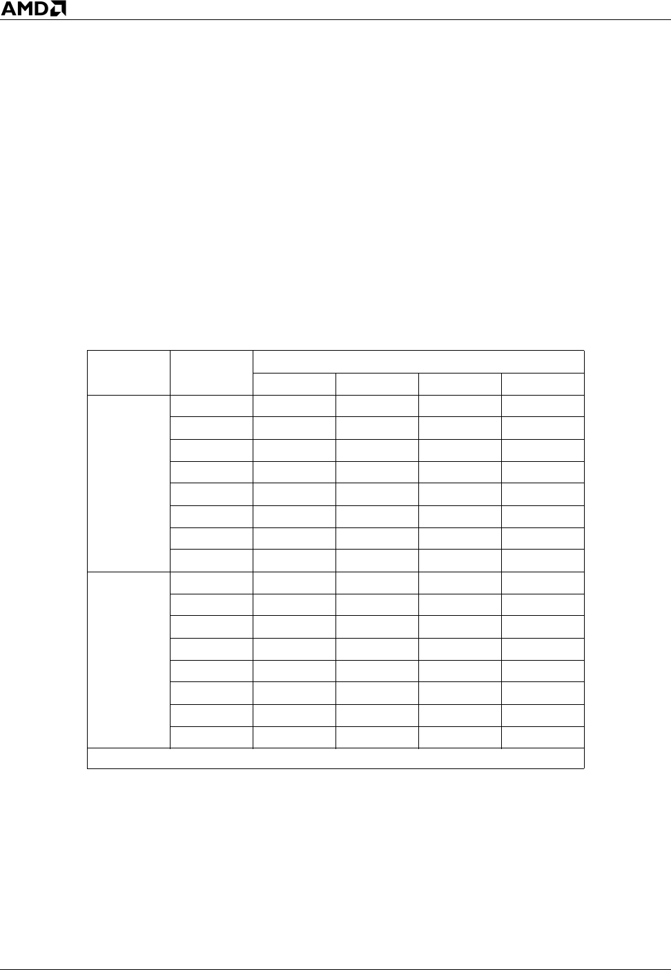
40 Instruction Overview
AMD64 Technology 24594—Rev. 3.14—September 2007
•ib, iw, id, iq—Specifies an immediate-operand value. The opcode determines whether the value is
signed or unsigned. The value following the opcode, ModRM, or SIB byte is either one byte (ib),
two bytes (iw), or four bytes (id). Word and doubleword values start with the low-order byte.
•+rb, +rw, +rd, +rq—Specifies a register value that is added to the hexadecimal byte on the left,
forming a one-byte opcode. The result is an instruction that operates on the register specified by the
register code. Valid register-code values are shown in Table 2-2.
•m64—Specifies a quadword (64-bit) operand in memory.
•+i—Specifies an x87 floating-point stack operand, ST(i). The value is used only with x87 floating-
point instructions. It is added to the hexadecimal byte on the left, forming a one-byte opcode. Valid
values range from 0 to 7.
Table 2-2. +rb, +rw, +rd, and +rq Register Value
REX.B
Bit1Value Specified Register
+rb +rw +rd +rq
0
or no REX
Prefix
0ALAXEAXRAX
1 CL CX ECX RCX
2 DL DX EDX RDX
3BLBXEBXRBX
4AH, SPL
1SP ESP RSP
5 CH, BPL1BP EBP RBP
6DH, SIL
1SI ESI RSI
7 BH, DIL1DI EDI RDI
1
0 R8B R8W R8D R8
1 R9B R9W R9D R9
2 R10B R10W R10D R10
3 R11B R11W R11D R11
4 R12B R12W R12D R12
5 R13B R13W R13D R13
6 R14B R14W R14D R14
7 R15B R15W R15D R15
1. See “REX Prefixes” on page 11.

Instruction Overview 41
24594—Rev. 3.14—September 2007 AMD64 Technology
2.5.3 Pseudocode Definitions
Pseudocode examples are given for the actions of several complex instructions (for example, see
“CALL (Near)” on page 76). The following definitions apply to all such pseudocode examples:
/////////////////////////////////////////////////////////////////////////////////
// Basic Definitions
/////////////////////////////////////////////////////////////////////////////////
// All comments start with these double slashes.
REAL_MODE = (cr0.pe=0)
PROTECTED_MODE = ((cr0.pe=1) && (rflags.vm=0))
VIRTUAL_MODE = ((cr0.pe=1) && (rflags.vm=1))
LEGACY_MODE = (efer.lma=0)
LONG_MODE = (efer.lma=1)
64BIT_MODE = ((efer.lma=1) && (cs.L=1) && (cs.d=0))
COMPATIBILITY_MODE = (efer.lma=1) && (cs.L=0)
PAGING_ENABLED = (cr0.pg=1)
ALIGNMENT_CHECK_ENABLED = ((cr0.am=1) && (eflags.ac=1) && (cpl=3))
CPL = the current privilege level (0-3)
OPERAND_SIZE = 16, 32, or 64 (depending on current code and 66h/rex prefixes)
ADDRESS_SIZE = 16, 32, or 64 (depending on current code and 67h prefixes)
STACK_SIZE = 16, 32, or 64 (depending on current code and SS.attr.B)
old_RIP = RIP at the start of current instruction
old_RSP = RSP at the start of current instruction
old_RFLAGS = RFLAGS at the start of the instruction
old_CS = CS selector at the start of current instruction
old_DS = DS selector at the start of current instruction
old_ES = ES selector at the start of current instruction
old_FS = FS selector at the start of current instruction
old_GS = GS selector at the start of current instruction
old_SS = SS selector at the start of current instruction
RIP = the current RIP register
RSP = the current RSP register
RBP = the current RBP register
RFLAGS = the current RFLAGS register
next_RIP = RIP at start of next instruction
CS = the current CS descriptor, including the subfields:
sel base limit attr
SS = the current SS descriptor, including the subfields:
sel base limit attr
SRC = the instruction’s Source operand
DEST = the instruction’s Destination operand
temp_* // 64-bit temporary register

42 Instruction Overview
AMD64 Technology 24594—Rev. 3.14—September 2007
temp_*_desc // temporary descriptor, with subfields:
// if it points to a block of memory: sel base limit attr
// if it’s a gate descriptor: sel offset segment attr
NULL = 0x0000 // null selector is all zeros
// V,Z,A,S are integer variables, assigned a value when an instruction begins
// executing (they can be assigned a different value in the middle of an
// instruction, if needed)
V = 2 if OPERAND_SIZE=16
4 if OPERAND_SIZE=32
8 if OPERAND_SIZE=64
Z = 2 if OPERAND_SIZE=16
4 if OPERAND_SIZE=32
4 if OPERAND_SIZE=64
A = 2 if ADDRESS_SIZE=16
4 if ADDRESS_SIZE=32
8 if ADDRESS_SIZE=64
S = 2 if STACK_SIZE=16
4 if STACK_SIZE=32
8 if STACK_SIZE=64
/////////////////////////////////////////////////////////////////////////////////
// Bit Range Inside a Register
/////////////////////////////////////////////////////////////////////////////////
temp_data.[X:Y] // Bit X through Y in temp_data, with the other bits
// in the register masked off.
/////////////////////////////////////////////////////////////////////////////////
// Moving Data From One Register To Another
/////////////////////////////////////////////////////////////////////////////////
temp_dest.b = temp_src // 1-byte move (copies lower 8 bits of temp_src to
// temp_dest, preserving the upper 56 bits of temp_dest)
temp_dest.w = temp_src // 2-byte move (copies lower 16 bits of temp_src to
// temp_dest, preserving the upper 48 bits of temp_dest)
temp_dest.d = temp_src // 4-byte move (copies lower 32 bits of temp_src to
// temp_dest, and zeros out the upper 32 bits of temp_dest)
temp_dest.q = temp_src // 8-byte move (copies all 64 bits of temp_src to
// temp_dest)
temp_dest.v = temp_src // 2-byte move if V=2,
// 4-byte move if V=4,
// 8-byte move if V=8

Instruction Overview 43
24594—Rev. 3.14—September 2007 AMD64 Technology
temp_dest.z = temp_src // 2-byte move if Z=2,
// 4-byte move if Z=4
temp_dest.a = temp_src // 2-byte move if A=2,
// 4-byte move if A=4,
// 8-byte move if A=8
temp_dest.s = temp_src // 2-byte move if S=2,
// 4-byte move if S=4,
// 8-byte move if S=8
/////////////////////////////////////////////////////////////////////////////////
// Bitwise Operations
/////////////////////////////////////////////////////////////////////////////////
temp = a AND b
temp = a OR b
temp = a XOR b
temp = NOT a
temp = a SHL b
temp = a SHR b
/////////////////////////////////////////////////////////////////////////////////
// Logical Operations
/////////////////////////////////////////////////////////////////////////////////
IF (FOO && BAR)
IF (FOO || BAR)
IF (FOO = BAR)
IF (FOO != BAR)
IF (FOO > BAR)
IF (FOO < BAR)
IF (FOO >= BAR)
IF (FOO <= BAR)
/////////////////////////////////////////////////////////////////////////////////
// IF-THEN-ELSE
/////////////////////////////////////////////////////////////////////////////////
IF (FOO)
...
IF (FOO)
...
ELSIF (BAR)
...
ELSE

44 Instruction Overview
AMD64 Technology 24594—Rev. 3.14—September 2007
...
IF ((FOO && BAR) || (CONE && HEAD))
...
/////////////////////////////////////////////////////////////////////////////////
// Exceptions
/////////////////////////////////////////////////////////////////////////////////
EXCEPTION [#GP(0)] // error code in parenthesis
EXCEPTION [#UD] // if no error code
possible exception types:
#DE // Divide-By-Zero-Error Exception (Vector 0)
#DB // Debug Exception (Vector 1)
#BP // INT3 Breakpoint Exception (Vector 3)
#OF // INTO Overflow Exception (Vector 4)
#BR // Bound-Range Exception (Vector 5)
#UD // Invalid-Opcode Exception (Vector 6)
#NM // Device-Not-Available Exception (Vector 7)
#DF // Double-Fault Exception (Vector 8)
#TS // Invalid-TSS Exception (Vector 10)
#NP // Segment-Not-Present Exception (Vector 11)
#SS // Stack Exception (Vector 12)
#GP // General-Protection Exception (Vector 13)
#PF // Page-Fault Exception (Vector 14)
#MF // x87 Floating-Point Exception-Pending (Vector 16)
#AC // Alignment-Check Exception (Vector 17)
#MC // Machine-Check Exception (Vector 18)
#XF // SIMD Floating-Point Exception (Vector 19)
/////////////////////////////////////////////////////////////////////////////////
// READ_MEM
// General memory read. This zero-extends the data to 64 bits and returns it.
/////////////////////////////////////////////////////////////////////////////////
usage:
temp = READ_MEM.x [seg:offset] // where x is one of {v, z, b, w, d, q}
// and denotes the size of the memory read
definition:
IF ((seg AND 0xFFFC) = NULL) // GP fault for using a null segment to
// reference memory
EXCEPTION [#GP(0)]
IF ((seg=CS) || (seg=DS) || (seg=ES) || (seg=FS) || (seg=GS))
// CS,DS,ES,FS,GS check for segment limit or canonical

Instruction Overview 45
24594—Rev. 3.14—September 2007 AMD64 Technology
IF ((!64BIT_MODE) && (offset is outside seg’s limit))
EXCEPTION [#GP(0)]
// #GP fault for segment limit violation in non-64-bit mode
IF ((64BIT_MODE) && (offset is non-canonical))
EXCEPTION [#GP(0)]
// #GP fault for non-canonical address in 64-bit mode
ELSIF (seg=SS) // SS checks for segment limit or canonical
IF ((!64BIT_MODE) && (offset is outside seg’s limit))
EXCEPTION [#SS(0)]
// stack fault for segment limit violation in non-64-bit mode
IF ((64BIT_MODE) && (offset is non-canonical))
EXCEPTION [#SS(0)]
// stack fault for non-canonical address in 64-bit mode
ELSE // ((seg=GDT) || (seg=LDT) || (seg=IDT) || (seg=TSS))
// GDT,LDT,IDT,TSS check for segment limit and canonical
IF (offset > seg.limit)
EXCEPTION [#GP(0)] // #GP fault for segment limit violation
// in all modes
IF ((LONG_MODE) && (offset is non-canonical))
EXCEPTION [#GP(0)] // #GP fault for non-canonical address in long mode
IF ((ALIGNMENT_CHECK_ENABLED) && (offset misaligned, considering its
size and alignment))
EXCEPTION [#AC(0)]
IF ((64_bit_mode) && ((seg=CS) || (seg=DS) || (seg=ES) || (seg=SS))
temp_linear = offset
ELSE
temp_linear = seg.base + offset
IF ((PAGING_ENABLED) && (virtual-to-physical translation for temp_linear
results in a page-protection violation))
EXCEPTION [#PF(error_code)] // page fault for page-protection violation
// (U/S violation, Reserved bit violation)
IF ((PAGING_ENABLED) && (temp_linear is on a not-present page))
EXCEPTION [#PF(error_code)] // page fault for not-present page
temp_data = memory [temp_linear].x // zero-extends the data to 64
// bits, and saves it in temp_data
RETURN (temp_data) // return the zero-extended data
/////////////////////////////////////////////////////////////////////////////////
// WRITE_MEM // General memory write
/////////////////////////////////////////////////////////////////////////////////
usage:
WRITE_MEM.x [seg:offset] = temp.x // where <X> is one of these:
// {V, Z, B, W, D, Q} and denotes the

46 Instruction Overview
AMD64 Technology 24594—Rev. 3.14—September 2007
// size of the memory write
definition:
IF ((seg & 0xFFFC)= NULL) // GP fault for using a null segment
// to reference memory
EXCEPTION [#GP(0)]
IF (seg isn’t writable) // GP fault for writing to a read-only segment
EXCEPTION [#GP(0)]
IF ((seg=CS) || (seg=DS) || (seg=ES) || (seg=FS) || (seg=GS))
// CS,DS,ES,FS,GS check for segment limit or canonical
IF ((!64BIT_MODE) && (offset is outside seg’s limit))
EXCEPTION [#GP(0)]
// #GP fault for segment limit violation in non-64-bit mode
IF ((64BIT_MODE) && (offset is non-canonical))
EXCEPTION [#GP(0)]
// #GP fault for non-canonical address in 64-bit mode
ELSIF (seg=SS) // SS checks for segment limit or canonical
IF ((!64BIT_MODE) && (offset is outside seg’s limit))
EXCEPTION [#SS(0)]
// stack fault for segment limit violation in non-64-bit mode
IF ((64BIT_MODE) && (offset is non-canonical))
EXCEPTION [#SS(0)]
// stack fault for non-canonical address in 64-bit mode
ELSE // ((seg=GDT) || (seg=LDT) || (seg=IDT) || (seg=TSS))
// GDT,LDT,IDT,TSS check for segment limit and canonical
IF (offset > seg.limit)
EXCEPTION [#GP(0)]
// #GP fault for segment limit violation in all modes
IF ((LONG_MODE) && (offset is non-canonical))
EXCEPTION [#GP(0)]
// #GP fault for non-canonical address in long mode
IF ((ALIGNMENT_CHECK_ENABLED) && (offset is misaligned, considering
its size and alignment))
EXCEPTION [#AC(0)]
IF ((64_bit_mode) && ((seg=CS) || (seg=DS) || (seg=ES) || (seg=SS))
temp_linear = offset
ELSE
temp_linear = seg.base + offset
IF ((PAGING_ENABLED) && (the virtual-to-physical translation for
temp_linear results in a page-protection violation))
{
EXCEPTION [#PF(error_code)]
// page fault for page-protection violation
// (U/S violation, Reserved bit violation)
}

Instruction Overview 47
24594—Rev. 3.14—September 2007 AMD64 Technology
IF ((PAGING_ENABLED) && (temp_linear is on a not-present page))
EXCEPTION [#PF(error_code)] // page fault for not-present page
memory [temp_linear].x = temp.x // write the bytes to memory
/////////////////////////////////////////////////////////////////////////////////
// PUSH // Write data to the stack
/////////////////////////////////////////////////////////////////////////////////
usage:
PUSH.x temp // where x is one of these: {v, z, b, w, d, q} and
// denotes the size of the push
definition:
WRITE_MEM.x [SS:RSP.s - X] = temp.x // write to the stack
RSP.s = RSP - X // point rsp to the data just written
/////////////////////////////////////////////////////////////////////////////////
// POP // Read data from the stack, zero-extend it to 64 bits
/////////////////////////////////////////////////////////////////////////////////
usage:
POP.x temp // where x is one of these: {v, z, b, w, d, q} and
// denotes the size of the pop
definition:
temp = READ_MEM.x [SS:RSP.s] // read from the stack
RSP.s = RSP + X // point rsp above the data just written
/////////////////////////////////////////////////////////////////////////////////
// READ_DESCRIPTOR // Read 8-byte descriptor from GDT/LDT, return the descriptor
/////////////////////////////////////////////////////////////////////////////////
usage:
temp_descriptor = READ_DESCRIPTOR (selector, chktype)
// chktype field is one of the following:
// cs_chk used for far call and far jump
// clg_chk used when reading CS for far call or far jump through call gate
// ss_chk used when reading SS
// iret_chk used when reading CS for IRET or RETF
// intcs_chk used when readin the CS for interrupts and exceptions
definition:
temp_offset = selector AND 0xfff8 // upper 13 bits give an offset

48 Instruction Overview
AMD64 Technology 24594—Rev. 3.14—September 2007
// in the descriptor table
IF (selector.TI = 0) // read 8 bytes from the gdt, split it into
// (base,limit,attr) if the type bits
temp_desc = READ_MEM.q [gdt:temp_offset]
// indicate a block of memory, or split
// it into (segment,offset,attr)
// if the type bits indicate
// a gate, and save the result in temp_desc
ELSE
temp_desc = READ_MEM.q [ldt:temp_offset]
// read 8 bytes from the ldt, split it into
// (base,limit,attr) if the type bits
// indicate a block of memory, or split
// it into (segment,offset,attr) if the type
// bits indicate a gate, and save the result
// in temp_desc
IF (selector.rpl or temp_desc.attr.dpl is illegal for the current mode/cpl)
EXCEPTION [#GP(selector)]
IF (temp_desc.attr.type is illegal for the current mode/chktype)
EXCEPTION [#GP(selector)]
IF (temp_desc.attr.p=0)
EXCEPTION [#NP(selector)]
RETURN (temp_desc)
/////////////////////////////////////////////////////////////////////////////////
// READ_IDT // Read an 8-byte descriptor from the IDT, return the descriptor
/////////////////////////////////////////////////////////////////////////////////
usage:
temp_idt_desc = READ_IDT (vector)
// "vector" is the interrupt vector number
definition:
IF (LONG_MODE) // long-mode idt descriptors are 16 bytes long
temp_offset = vector*16
ELSE // (LEGACY_MODE) legacy-protected-mode idt descriptors are 8 bytes long
temp_offset = vector*8
temp_desc = READ_MEM.q [idt:temp_offset]
// read 8 bytes from the idt, split it into
// (segment,offset,attr), and save it in temp_desc
IF (temp_desc.attr.dpl is illegal for the current mode/cpl)
// exception, with error code that indicates this idt gate

Instruction Overview 49
24594—Rev. 3.14—September 2007 AMD64 Technology
EXCEPTION [#GP(vector*8+2)]
IF (temp_desc.attr.type is illegal for the current mode)
// exception, with error code that indicates this idt gate
EXCEPTION [#GP(vector*8+2)]
IF (temp_desc.attr.p=0)
EXCEPTION [#NP(vector*8+2)]
// segment-not-present exception, with an error code that
// indicates this idt gate
RETURN (temp_desc)
/////////////////////////////////////////////////////////////////////////////////
// READ_INNER_LEVEL_STACK_POINTER
// Read a new stack pointer (rsp or ss:esp) from the tss
/////////////////////////////////////////////////////////////////////////////////
usage:
temp_SS_desc:temp_RSP = READ_INNER_LEVEL_STACK_POINTER (new_cpl, ist_index)
definition:
IF (LONG_MODE)
{
IF (ist_index>0)
// if IST is selected, read an ISTn stack pointer from the tss
temp_RSP = READ_MEM.q [tss:ist_index*8+28]
ELSE // (ist_index=0)
// otherwise read an RSPn stack pointer from the tss
temp_RSP = READ_MEM.q [tss:new_cpl*8+4]
temp_SS_desc.sel = NULL + new_cpl
// in long mode, changing to lower cpl sets SS.sel to
// NULL+new_cpl
}
ELSE // (LEGACY_MODE)
{
temp_RSP = READ_MEM.d [tss:new_cpl*8+4] // read ESPn from the tss
temp_sel = READ_MEM.d [tss:new_cpl*8+8] // read SSn from the tss
temp_SS_desc = READ_DESCRIPTOR (temp_sel, ss_chk)
}
return (temp_RSP:temp_SS_desc)

50 Instruction Overview
AMD64 Technology 24594—Rev. 3.14—September 2007
/////////////////////////////////////////////////////////////////////////////////
// READ_BIT_ARRAY // Read 1 bit from a bit array in memory
/////////////////////////////////////////////////////////////////////////////////
usage:
temp_value = READ_BIT_ARRAY ([mem], bit_number)
definition:
temp_BYTE = READ_MEM.b [mem + (bit_number SHR 3)]
// read the byte containing the bit
temp_BIT = temp_BYTE SHR (bit_number & 7)
// shift the requested bit position into bit 0
return (temp_BIT & 0x01) // return ’0’ or ’1’

Instruction Reference 51
24594—Rev. 3.14—September 2007 AMD64 Technology
3 General-Purpose Instruction Reference
This chapter describes the function, mnemonic syntax, opcodes, affected flags, and possible
exceptions generated by the general-purpose instructions. General-purpose instructions are used in
basic software execution. Most of these instructions load, store, or operate on data located in the
general-purpose registers (GPRs), in memory, or in both. The remaining instructions are used to alter
the sequential flow of the program by branching to other locations within the program, or to entirely
different programs. With the exception of the MOVD, MOVMSKPD and MOVMSKPS instructions,
which operate on MMX/XMM registers, the instructions within the category of general-purpose
instructions do not operate on any other register set.
Most general-purpose instructions are supported in all hardware implementations of the AMD64
architecture, however it may be necessary to use the CPUID instruction to test for support for a small
set of general-purpose instructions. These instructions are listed in Table 3-1, along with the CPUID
function, the register and bit used to test for the presence of the instruction.
The general-purpose instructions can be used in legacy mode or 64-bit long mode. Compilation of
general-purpose programs for execution in 64-bit long mode offers three primary advantages: access to
the eight extended, 64-bit general-purpose registers (for a register set consisting of GPR0–GPR15),
access to the 64-bit virtual address space, and access to the RIP-relative addressing mode.
For further information about the general-purpose instructions and register resources, see:
Table 3-1. Instruction Support Indicated by CPUID Feature Bits
Instruction Register[Bit] Feature Mnemonic CPUID Function(s)
CMPXCHG8B EDX[8] CMPXCHG8B 0000_0001h, 8000_0001h
CMPXCHG16B ECX[13] CMPXCHG16B 0000_0001h
CMOVcc (Conditional Moves) EDX[15] CMOV 0000_0001h, 8000_0001h
CLFLUSH EDX[19] CLFSH 0000_0001h
LZCNT ECX[5] Advanced Bit
Manipulation (ABM) 8000_0001h
Long Mode instructions EDX[29] Long Mode (LM) 8000_0001h
MFENCE, LFENCE EDX[26] SSE2 0000_0001h
MOVD EDX[25] SSE 0000_0001h
EDX[26] SSE2
MOVNTI EDX[26] SSE2 0000_0001h
POPCNT ECX[23] POPCNT 0000_0001h
PREFETCH/W
ECX[8] 3DNow!™ Prefetch
8000_0001hEDX[29] LM
EDX[31] 3DNow!™
SFENCE EDX[25] FXSR 0000_0001h

52 Instruction Reference
AMD64 Technology 24594—Rev. 3.14—September 2007
•“General-Purpose Programming” in Volume 1.
•“Summary of Registers and Data Types” on page 24.
•“Notation” on page 37.
•“Instruction Prefixes” on page 3.
•Appendix B, “General-Purpose Instructions in 64-Bit Mode.” In particular, see “General Rules for
64-Bit Mode” on page 373.
Instruction Reference AAA 53
24594—Rev. 3.14—September 2007 AMD64 Technology
Adjusts the value in the AL register to an unpacked BCD value. Use the AAA instruction after using
the ADD instruction to add two unpacked BCD numbers.
If the value in the lower nibble of AL is greater than 9 or the AF flag is set to 1, the instruction
increments the AH register, adds 6 to the AL register, and sets the CF and AF flags to 1. Otherwise, it
does not change the AH register and clears the CF and AF flags to 0. In either case, AAA clears bits
7–4 of the AL register, leaving the correct decimal digit in bits 3–0.
This instruction also makes it possible to add ASCII numbers without having to mask off the upper
nibble ‘3’.
MXCSR Flags Affected
Using this instruction in 64-bit mode generates an invalid-opcode exception.
Related Instructions
AAD, AAM, AAS
rFLAGS Affected
Exceptions
AAA ASCII Adjust After Addition
Mnemonic Opcode Description
AAA 37 Create an unpacked BCD number.
(Invalid in 64-bit mode.)
ID VIP VIF AC VM RF NT IOPL OF DF IF TF SF ZF AF PF CF
U UUMUM
2120191817161413–1211109876420
Note: Bits 31–22, 15, 5, 3, and 1 are reserved. A flag set to 1 or cleared to 0 is M (modified). Unaffected flags are
blank. Undefined flags are U.
Exception Real
Virtual
8086 Protected Cause of Exception
Invalid opcode, #UD X This instruction was executed in 64-bit mode.

54 AAD Instruction Reference
AMD64 Technology 24594—Rev. 3.14—September 2007
Converts two unpacked BCD digits in the AL (least significant) and AH (most significant) registers to
a single binary value in the AL register using the following formula:
AL = ((10d * AH) + (AL))
After the conversion, AH is cleared to 00h.
In most modern assemblers, the AAD instruction adjusts from base-10 values. However, by coding the
instruction directly in binary, it can adjust from any base specified by the immediate byte value (ib)
suffixed onto the D5h opcode. For example, code D508h for octal, D50Ah for decimal, and D50Ch for
duodecimal (base 12).
Using this instruction in 64-bit mode generates an invalid-opcode exception.
Related Instructions
AAA, AAM, AAS
rFLAGS Affected
Exceptions
AAD ASCII Adjust Before Division
Mnemonic Opcode Description
AAD D5 0A Adjust two BCD digits in AL and AH.
(Invalid in 64-bit mode.)
(None) D5 ib Adjust two BCD digits to the immediate byte base.
(Invalid in 64-bit mode.)
ID VIP VIF AC VM RF NT IOPL OF DF IF TF SF ZF AF PF CF
U MMUMU
2120191817161413–1211109876420
Note: Bits 31–22, 15, 5, 3, and 1 are reserved. A flag set to 1 or cleared to 0 is M (modified). Unaffected flags are blank.
Undefined flags are U.
Exception Real
Virtual
8086 Protected Cause of Exception
Invalid opcode, #UD X This instruction was executed in 64-bit mode.

Instruction Reference AAM 55
24594—Rev. 3.14—September 2007 AMD64 Technology
Converts the value in the AL register from binary to two unpacked BCD digits in the AH (most
significant) and AL (least significant) registers using the following formula:
AH = (AL/10d)
AL = (AL mod 10d)
In most modern assemblers, the AAM instruction adjusts to base-10 values. However, by coding the
instruction directly in binary, it can adjust to any base specified by the immediate byte value (ib)
suffixed onto the D4h opcode. For example, code D408h for octal, D40Ah for decimal, and D40Ch for
duodecimal (base 12).
Using this instruction in 64-bit mode generates an invalid-opcode exception.
Related Instructions
AAA, AAD, AAS
rFLAGS Affected
Exceptions
AAM ASCII Adjust After Multiply
Mnemonic Opcode Description
AAM D4 0A Create a pair of unpacked BCD values in AH and AL.
(Invalid in 64-bit mode.)
(None) D4 ib
Create a pair of unpacked values to the immediate byte
base.
(Invalid in 64-bit mode.)
ID VIP VIF AC VM RF NT IOPL OF DF IF TF SF ZF AF PF CF
U MMUMU
2120191817161413–1211109876420
Note: Bits 31–22, 15, 5, 3, and 1 are reserved. A flag set to 1 or cleared to 0 is M. Unaffected flags are blank. Undefined
flags are U.
Exception Real
Virtual
8086 Protected Cause of Exception
Divide by zero, #DE X X X 8-bit immediate value was 0.
Invalid opcode, #UD X This instruction was executed in 64-bit mode.
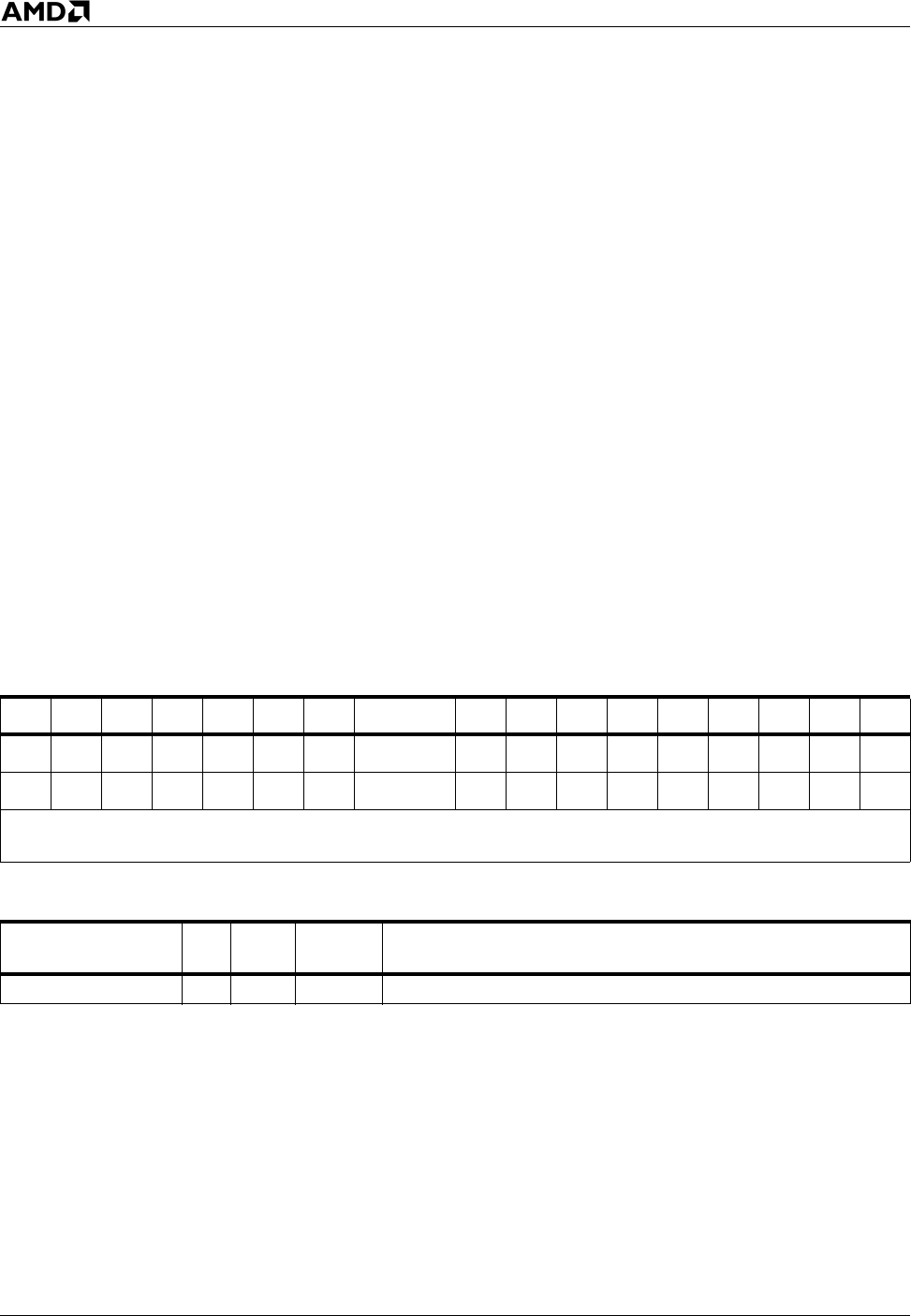
56 AAS Instruction Reference
AMD64 Technology 24594—Rev. 3.14—September 2007
Adjusts the value in the AL register to an unpacked BCD value. Use the AAS instruction after using
the SUB instruction to subtract two unpacked BCD numbers.
If the value in AL is greater than 9 or the AF flag is set to 1, the instruction decrements the value in AH,
subtracts 6 from the AL register, and sets the CF and AF flags to 1. Otherwise, it clears the CF and AF
flags and the AH register is unchanged. In either case, the instruction clears bits 7–4 of the AL register,
leaving the correct decimal digit in bits 3–0.
Using this instruction in 64-bit mode generates an invalid-opcode exception.
Related Instructions
AAA, AAD, AAM
rFLAGS Affected
Exceptions
AAS ASCII Adjust After Subtraction
Mnemonic Opcode Description
AAS 3F
Create an unpacked BCD number from the contents of
the AL register.
(Invalid in 64-bit mode.)
ID VIP VIF AC VM RF NT IOPL OF DF IF TF SF ZF AF PF CF
U UUMUM
2120191817161413–1211109876420
Note: Bits 31–22, 15, 5, 3, and 1 are reserved. A flag set to 1 or cleared to 0 is M (modified). Unaffected flags are
blank. Undefined flags are U.
Exception Real
Virtual
8086 Protected Cause of Exception
Invalid opcode, #UD X This instruction was executed in 64-bit mode.

Instruction Reference ADC 57
24594—Rev. 3.14—September 2007 AMD64 Technology
Adds the carry flag (CF), the value in a register or memory location (first operand), and an immediate
value or the value in a register or memory location (second operand), and stores the result in the first
operand location. The instruction cannot add two memory operands. The CF flag indicates a pending
carry from a previous addition operation. The instruction sign-extends an immediate value to the
length of the destination register or memory location.
This instruction evaluates the result for both signed and unsigned data types and sets the OF and CF
flags to indicate a carry in a signed or unsigned result, respectively. It sets the SF flag to indicate the
sign of a signed result.
Use the ADC instruction after an ADD instruction as part of a multibyte or multiword addition.
The forms of the ADC instruction that write to memory support the LOCK prefix. For details about the
LOCK prefix, see “Lock Prefix” on page 8.
ADC Add with Carry
Mnemonic Opcode Description
ADC AL, imm8 14 ib Add imm8 to AL + CF.
ADC AX, imm16 15 iw Add imm16 to AX + CF.
ADC EAX, imm32 15 id Add imm32 to EAX + CF.
ADC RAX, imm32 15 id Add sign-extended imm32 to RAX + CF.
ADC reg/mem8, imm8 80 /2 ib Add imm8 to reg/mem8 + CF.
ADC reg/mem16, imm16 81 /2 iw Add imm16 to reg/mem16 + CF.
ADC reg/mem32, imm32 81 /2 id Add imm32 to reg/mem32 + CF.
ADC reg/mem64, imm32 81 /2 id Add sign-extended imm32 to reg/mem64 + CF.
ADC reg/mem16, imm8 83 /2 ib Add sign-extended imm8 to reg/mem16 + CF.
ADC reg/mem32, imm8 83 /2 ib Add sign-extended imm8 to reg/mem32 + CF.
ADC reg/mem64, imm8 83 /2 ib Add sign-extended imm8 to reg/mem64 + CF.
ADC reg/mem8, reg8 10 /r Add reg8 to reg/mem8 + CF
ADC reg/mem16, reg16 11 /r Add reg16 to reg/mem16 + CF.
ADC reg/mem32, reg32 11 /r Add reg32 to reg/mem32 + CF.
ADC reg/mem64, reg64 11 /r Add reg64 to reg/mem64 + CF.
ADC reg8, reg/mem8 12 /r Add reg/mem8 to reg8 + CF.
ADC reg16, reg/mem16 13 /r Add reg/mem16 to reg16 + CF.
ADC reg32, reg/mem32 13 /r Add reg/mem32 to reg32 + CF.
ADC reg64, reg/mem64 13 /r Add reg/mem64 to reg64 + CF.

58 ADC Instruction Reference
AMD64 Technology 24594—Rev. 3.14—September 2007
Related Instructions
ADD, SBB, SUB
rFLAGS Affected
Exceptions
ID VIP VIF AC VM RF NT IOPL OF DF IF TF SF ZF AF PF CF
M MMMMM
2120191817161413–1211109876420
Note: Bits 31–22, 15, 5, 3, and 1 are reserved. A flag set to 1 or cleared to 0 is M (modified). Unaffected flags are blank.
Undefined flags are U.
Exception Real
Virtual
8086 Protected Cause of Exception
Stack, #SS X X X A memory address exceeded the stack segment limit or was
non-canonical.
General protection,
#GP
XX XA memory address exceeded a data segment limit or was non-
canonical.
X The destination operand was in a non-writable segment.
X A null data segment was used to reference memory.
Page fault, #PF X X A page fault resulted from the execution of the instruction.
Alignment check,
#AC XX
An unaligned memory reference was performed while
alignment checking was enabled.

Instruction Reference ADD 59
24594—Rev. 3.14—September 2007 AMD64 Technology
Adds the value in a register or memory location (first operand) and an immediate value or the value in
a register or memory location (second operand), and stores the result in the first operand location. The
instruction cannot add two memory operands. The instruction sign-extends an immediate value to the
length of the destination register or memory operand.
This instruction evaluates the result for both signed and unsigned data types and sets the OF and CF
flags to indicate a carry in a signed or unsigned result, respectively. It sets the SF flag to indicate the
sign of a signed result.
The forms of the ADD instruction that write to memory support the LOCK prefix. For details about the
LOCK prefix, see “Lock Prefix” on page 8.
Related Instructions
ADC, SBB, SUB
ADD Signed or Unsigned Add
Mnemonic Opcode Description
ADD AL, imm8 04 ib Add imm8 to AL.
ADD AX, imm16 05 iw Add imm16 to AX.
ADD EAX, imm32 05 id Add imm32 to EAX.
ADD RAX, imm32 05 id Add sign-extended imm32 to RAX.
ADD reg/mem8, imm8 80 /0 ib Add imm8 to reg/mem8.
ADD reg/mem16, imm16 81 /0 iw Add imm16 to reg/mem16
ADD reg/mem32, imm32 81 /0 id Add imm32 to reg/mem32.
ADD reg/mem64, imm32 81 /0 id Add sign-extended imm32 to reg/mem64.
ADD reg/mem16, imm8 83 /0 ib Add sign-extended imm8 to reg/mem16
ADD reg/mem32, imm8 83 /0 ib Add sign-extended imm8 to reg/mem32.
ADD reg/mem64, imm8 83 /0 ib Add sign-extended imm8 to reg/mem64.
ADD reg/mem8, reg8 00 /r Add reg8 to reg/mem8.
ADD reg/mem16, reg16 01 /r Add reg16 to reg/mem16.
ADD reg/mem32, reg32 01 /r Add reg32 to reg/mem32.
ADD reg/mem64, reg64 01 /r Add reg64 to reg/mem64.
ADD reg8, reg/mem8 02 /r Add reg/mem8 to reg8.
ADD reg16, reg/mem16 03 /r Add reg/mem16 to reg16.
ADD reg32, reg/mem32 03 /r Add reg/mem32 to reg32.
ADD reg64, reg/mem64 03 /r Add reg/mem64 to reg64.

60 ADD Instruction Reference
AMD64 Technology 24594—Rev. 3.14—September 2007
rFLAGS Affected
Exceptions
ID VIP VIF AC VM RF NT IOPL OF DF IF TF SF ZF AF PF CF
M MMMMM
2120191817161413–1211109876420
Note: Bits 31–22, 15, 5, 3, and 1 are reserved. A flag set to 1 or cleared to 0 is M (modified). Unaffected flags are
blank. Undefined flags are U.
Exception Real
Virtual
8086 Protected Cause of Exception
Stack, #SS X X X A memory address exceeded the stack segment limit or was
non-canonical.
General protection,
#GP
XX XA memory address exceeded a data segment limit or was non-
canonical.
X The destination operand was in a non-writable segment.
X A null data segment was used to reference memory.
Page fault, #PF X X A page fault resulted from the execution of the instruction.
Alignment check,
#AC XX
An unaligned memory reference was performed while
alignment checking was enabled.

Instruction Reference AND 61
24594—Rev. 3.14—September 2007 AMD64 Technology
Performs a bitwise AND operation on the value in a register or memory location (first operand) and an
immediate value or the value in a register or memory location (second operand), and stores the result in
the first operand location. The instruction cannot AND two memory operands.
The instruction sets each bit of the result to 1 if the corresponding bit of both operands is set;
otherwise, it clears the bit to 0. The following table shows the truth table for the AND operation:
The forms of the AND instruction that write to memory support the LOCK prefix. For details about the
LOCK prefix, see “Lock Prefix” on page 8.
AND Logical AND
X Y X AND Y
000
010
100
111
Mnemonic Opcode Description
AND AL, imm8 24 ib AND the contents of AL with an immediate 8-bit value
and store the result in AL.
AND AX, imm16 25 iw AND the contents of AX with an immediate 16-bit value
and store the result in AX.
AND EAX, imm32 25 id AND the contents of EAX with an immediate 32-bit
value and store the result in EAX.
AND RAX, imm32 25 id AND the contents of RAX with a sign-extended
immediate 32-bit value and store the result in RAX.
AND reg/mem8, imm8 80 /4 ib AND the contents of reg/mem8 with imm8.
AND reg/mem16, imm16 81 /4 iw AND the contents of reg/mem16 with imm16.
AND reg/mem32, imm32 81 /4 id AND the contents of reg/mem32 with imm32.
AND reg/mem64, imm32 81 /4 id AND the contents of reg/mem64 with sign-extended
imm32.
AND reg/mem16, imm8 83 /4 ib AND the contents of reg/mem16 with a sign-extended
8-bit value.
AND reg/mem32, imm8 83 /4 ib AND the contents of reg/mem32 with a sign-extended
8-bit value.
AND reg/mem64, imm8 83 /4 ib AND the contents of reg/mem64 with a sign-extended
8-bit value.
AND reg/mem8, reg8 20 /r AND the contents of an 8-bit register or memory
location with the contents of an 8-bit register.
62 AND Instruction Reference
AMD64 Technology 24594—Rev. 3.14—September 2007
Related Instructions
TEST, OR, NOT, NEG, XOR
rFLAGS Affected
Exceptions
AND reg/mem16, reg16 21 /r AND the contents of a 16-bit register or memory
location with the contents of a 16-bit register.
AND reg/mem32, reg32 21 /r AND the contents of a 32-bit register or memory
location with the contents of a 32-bit register.
AND reg/mem64, reg64 21 /r AND the contents of a 64-bit register or memory
location with the contents of a 64-bit register.
AND reg8, reg/mem8 22 /r AND the contents of an 8-bit register with the contents
of an 8-bit memory location or register.
AND reg16, reg/mem16 23 /r AND the contents of a 16-bit register with the contents
of a 16-bit memory location or register.
AND reg32, reg/mem32 23 /r AND the contents of a 32-bit register with the contents
of a 32-bit memory location or register.
AND reg64, reg/mem64 23 /r AND the contents of a 64-bit register with the contents
of a 64-bit memory location or register.
ID VIP VIF AC VM RF NT IOPL OF DF IF TF SF ZF AF PF CF
0MMUM0
2120191817161413–1211109876420
Note: Bits 31–22, 15, 5, 3, and 1 are reserved. A flag set to 1 or cleared to 0 is M (modified). Unaffected flags are
blank. Undefined flags are U.
Exception Real
Virtual
8086 Protected Cause of Exception
Stack, #SS X X X A memory address exceeded the stack segment limit or was
non-canonical.
General protection,
#GP
XX XA memory address exceeded a data segment limit or was non-
canonical.
X The destination operand was in a non-writable segment.
X A null data segment was used to reference memory.
Page fault, #PF X X A page fault resulted from the execution of the instruction.
Alignment check,
#AC XX
An unaligned memory reference was performed while
alignment checking was enabled.
Mnemonic Opcode Description

Instruction Reference BOUND 63
24594—Rev. 3.14—September 2007 AMD64 Technology
Checks whether an array index (first operand) is within the bounds of an array (second operand). The
array index is a signed integer in the specified register. If the operand-size attribute is 16, the array
operand is a memory location containing a pair of signed word-integers; if the operand-size attribute is
32, the array operand is a pair of signed doubleword-integers. The first word or doubleword specifies
the lower bound of the array and the second word or doubleword specifies the upper bound.
The array index must be greater than or equal to the lower bound and less than or equal to the upper
bound. If the index is not within the specified bounds, the processor generates a BOUND range-
exceeded exception (#BR).
The bounds of an array, consisting of two words or doublewords containing the lower and upper limits
of the array, usually reside in a data structure just before the array itself, making the limits addressable
through a constant offset from the beginning of the array. With the address of the array in a register,
this practice reduces the number of bus cycles required to determine the effective address of the array
bounds.
Using this instruction in 64-bit mode generates an invalid-opcode exception.
Related Instructions
INT, INT3, INTO
rFLAGS Affected
None
Exceptions
BOUND Check Array Bound
Mnemonic Opcode Description
BOUND reg16, mem16&mem16 62 /r
Test whether a 16-bit array index is within the bounds
specified by the two 16-bit values in mem16&mem16.
(Invalid in 64-bit mode.)
BOUND reg32, mem32&mem32 62 /r
Test whether a 32-bit array index is within the bounds
specified by the two 32-bit values in mem32&mem32.
(Invalid in 64-bit mode.)
Exception Real
Virtual
8086 Protected Cause of Exception
Bound range, #BR X X X The bound range was exceeded.
Invalid opcode, #UD X X X The source operand was a register.
X Instruction was executed in 64-bit mode.
Stack, #SS X X X A memory address exceeded the stack segment limit
General protection,
#GP
X X X A memory address exceeded a data segment limit.
X A null data segment was used to reference memory.

64 BOUND Instruction Reference
AMD64 Technology 24594—Rev. 3.14—September 2007
Page fault, #PF X X A page fault resulted from the execution of the instruction.
Alignment check,
#AC XX
An unaligned memory reference was performed while
alignment checking was enabled.
Exception Real
Virtual
8086 Protected Cause of Exception
Instruction Reference BSF 65
24594—Rev. 3.14—September 2007 AMD64 Technology
Searches the value in a register or a memory location (second operand) for the least-significant set bit.
If a set bit is found, the instruction clears the zero flag (ZF) and stores the index of the least-significant
set bit in a destination register (first operand). If the second operand contains 0, the instruction sets ZF
to 1 and does not change the contents of the destination register. The bit index is an unsigned offset
from bit 0 of the searched value.
Related Instructions
BSR
rFLAGS Affected
Exceptions
BSF Bit Scan Forward
Mnemonic Opcode Description
BSF reg16, reg/mem16 0F BC /r Bit scan forward on the contents of reg/mem16.
BSF reg32, reg/mem32 0F BC /r Bit scan forward on the contents of reg/mem32.
BSF reg64, reg/mem64 0F BC /r Bit scan forward on the contents of reg/mem64
ID VIP VIF AC VM RF NT IOPL OF DF IF TF SF ZF AF PF CF
U UMUUU
2120191817161413–1211109876420
Note: Bits 31–22, 15, 5, 3, and 1 are reserved. A flag set to 1 or cleared to 0 is M (modified). Unaffected flags are
blank. Undefined flags are U.
Exception Real
Virtual
8086 Protected Cause of Exception
Stack, #SS X X X A memory address exceeded the stack segment limit or was
non-canonical.
General protection,
#GP
XX XA memory address exceeded a data segment limit or was non-
canonical.
X A null data segment was used to reference memory.
Page fault, #PF X X A page fault resulted from the execution of the instruction.
Alignment check,
#AC XX
An unaligned memory reference was performed while
alignment checking was enabled.
66 BSR Instruction Reference
AMD64 Technology 24594—Rev. 3.14—September 2007
Searches the value in a register or a memory location (second operand) for the most-significant set bit.
If a set bit is found, the instruction clears the zero flag (ZF) and stores the index of the most-significant
set bit in a destination register (first operand). If the second operand contains 0, the instruction sets ZF
to 1 and does not change the contents of the destination register. The bit index is an unsigned offset
from bit 0 of the searched value.
Related Instructions
BSF
rFLAGS Affected
Exceptions
BSR Bit Scan Reverse
Mnemonic Opcode Description
BSR reg16, reg/mem16 0F BD /r Bit scan reverse on the contents of reg/mem16.
BSR reg32, reg/mem32 0F BD /r Bit scan reverse on the contents of reg/mem32.
BSR reg64, reg/mem64 0F BD /r Bit scan reverse on the contents of reg/mem64.
ID VIP VIF AC VM RF NT IOPL OF DF IF TF SF ZF AF PF CF
U UMUUU
2120191817161413–1211109876420
Note: Bits 31–22, 15, 5, 3, and 1 are reserved. A flag set to 1 or cleared to 0 is M (modified). Unaffected flags are
blank. Undefined flags are U.
Exception Real
Virtual
8086 Protected Cause of Exception
Stack, #SS X X X A memory address exceeded the stack segment limit or was
non-canonical.
General protection,
#GP
XX XA memory address exceeded the data segment limit or was
non-canonical.
X A null data segment was used to reference memory.
Page fault, #PF X X A page fault resulted from the execution of the instruction.
Alignment check,
#AC XX
An unaligned memory reference was performed while
alignment checking was enabled.

Instruction Reference BSWAP 67
24594—Rev. 3.14—September 2007 AMD64 Technology
Reverses the byte order of the specified register. This action converts the contents of the register from
little endian to big endian or vice versa. In a doubleword, bits 7–0 are exchanged with bits 31–24, and
bits 15–8 are exchanged with bits 23–16. In a quadword, bits 7–0 are exchanged with bits 63–56, bits
15–8 with bits 55–48, bits 23–16 with bits 47–40, and bits 31–24 with bits 39–32. A subsequent use of
the BSWAP instruction with the same operand restores the original value of the operand.
The result of applying the BSWAP instruction to a 16-bit register is undefined. To swap the bytes of a
16-bit register, use the XCHG instruction and specify the respective byte halves of the 16-bit register
as the two operands. For example, to swap the bytes of AX, use XCHG AL, AH.
Related Instructions
XCHG
rFLAGS Affected
None
Exceptions
None
BSWAP Byte Swap
Mnemonic Opcode Description
BSWAP reg32 0F C8 +rd Reverse the byte order of reg32.
BSWAP reg64 0F C8 +rq Reverse the byte order of reg64.

68 BT Instruction Reference
AMD64 Technology 24594—Rev. 3.14—September 2007
Copies a bit, specified by a bit index in a register or 8-bit immediate value (second operand), from a bit
string (first operand), also called the bit base, to the carry flag (CF) of the rFLAGS register.
If the bit base operand is a register, the instruction uses the modulo 16, 32, or 64 (depending on the
operand size) of the bit index to select a bit in the register.
If the bit base operand is a memory location, bit 0 of the byte at the specified address is the bit base of
the bit string. If the bit index is in a register, the instruction selects a bit position relative to the bit base
in the range –263 to +263 – 1 if the operand size is 64, –231 to +231 – 1, if the operand size is 32, and
–215 to +215 – 1 if the operand size is 16. If the bit index is in an immediate value, the bit selected is
that value modulo 16, 32, or 64, depending on operand size.
When the instruction attempts to copy a bit from memory, it accesses 2, 4, or 8 bytes starting from the
specified memory address for 16-bit, 32-bit, or 64-bit operand sizes, respectively, using the following
formula:
Effective Address + (NumBytesi * (BitOffset DIV NumBitsi*8))
When using this bit addressing mechanism, avoid referencing areas of memory close to address space
holes, such as references to memory-mapped I/O registers. Instead, use a MOV instruction to load a
register from such an address and use a register form of the BT instruction to manipulate the data.
Related Instructions
BTC, BTR, BTS
BT Bit Test
Mnemonic Opcode Description
BT reg/mem16, reg16 0F A3 /r Copy the value of the selected bit to the carry flag.
BT reg/mem32, reg32 0F A3 /r Copy the value of the selected bit to the carry flag.
BT reg/mem64, reg64 0F A3 /r Copy the value of the selected bit to the carry flag.
BT reg/mem16, imm8 0F BA /4 ib Copy the value of the selected bit to the carry flag.
BT reg/mem32, imm8 0F BA /4 ib Copy the value of the selected bit to the carry flag.
BT reg/mem64, imm8 0F BA /4 ib Copy the value of the selected bit to the carry flag.

Instruction Reference BT 69
24594—Rev. 3.14—September 2007 AMD64 Technology
rFLAGS Affected
Exceptions
ID VIP VIF AC VM RF NT IOPL OF DF IF TF SF ZF AF PF CF
U UUUUM
2120191817161413–1211109876420
Note: Bits 31–22, 15, 5, 3, and 1 are reserved. A flag set to 1 or cleared to 0 is M (modified). Unaffected flags are
blank. Undefined flags are U.
Exception Real
Virtual
8086 Protected Cause of Exception
Stack, #SS X X X A memory address exceeded the stack segment limit or was
non-canonical.
General protection,
#GP
XX XA memory address exceeded a data segment limit or was non-
canonical.
X A null data segment was used to reference memory.
Page fault, #PF X X A page fault resulted from the execution of the instruction.
Alignment check,
#AC XX
An unaligned memory reference was performed while
alignment checking was enabled.

70 BTC Instruction Reference
AMD64 Technology 24594—Rev. 3.14—September 2007
Copies a bit, specified by a bit index in a register or 8-bit immediate value (second operand), from a bit
string (first operand), also called the bit base, to the carry flag (CF) of the rFLAGS register, and then
complements (toggles) the bit in the bit string.
If the bit base operand is a register, the instruction uses the modulo 16, 32, or 64 (depending on the
operand size) of the bit index to select a bit in the register.
If the bit base operand is a memory location, bit 0 of the byte at the specified address is the bit base of
the bit string. If the bit index is in a register, the instruction selects a bit position relative to the bit base
in the range –263 to +263 – 1 if the operand size is 64, –231 to +231 – 1, if the operand size is 32, and
–215 to +215 – 1 if the operand size is 16. If the bit index is in an immediate value, the bit selected is
that value modulo 16, 32, or 64, depending the operand size.
This instruction is useful for implementing semaphores in concurrent operating systems. Such an
application should precede this instruction with the LOCK prefix. For details about the LOCK prefix,
see “Lock Prefix” on page 8.
Related Instructions
BT, BTR, BTS
BTC Bit Test and Complement
Mnemonic Opcode Description
BTC reg/mem16, reg16 0F BB /r Copy the value of the selected bit to the carry flag, then
complement the selected bit.
BTC reg/mem32, reg32 0F BB /r Copy the value of the selected bit to the carry flag, then
complement the selected bit.
BTC reg/mem64, reg64 0F BB /r Copy the value of the selected bit to the carry flag, then
complement the selected bit.
BTC reg/mem16, imm8 0F BA /7 ib Copy the value of the selected bit to the carry flag, then
complement the selected bit.
BTC reg/mem32, imm8 0F BA /7 ib Copy the value of the selected bit to the carry flag, then
complement the selected bit.
BTC reg/mem64, imm8 0F BA /7 ib Copy the value of the selected bit to the carry flag, then
complement the selected bit.
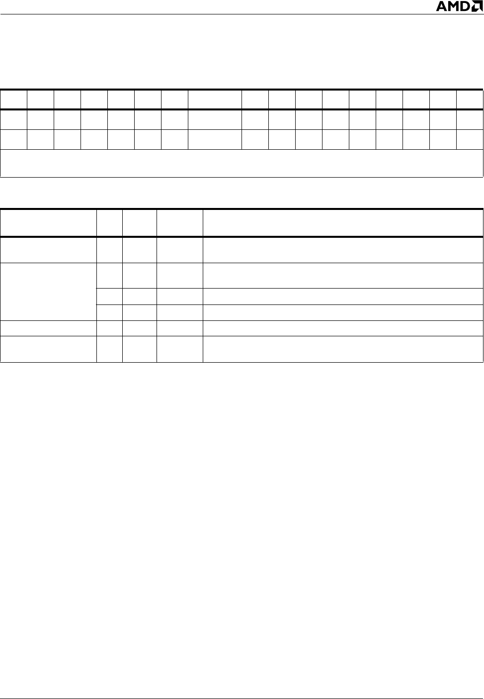
Instruction Reference BTC 71
24594—Rev. 3.14—September 2007 AMD64 Technology
rFLAGS Affected
Exceptions
ID VIP VIF AC VM RF NT IOPL OF DF IF TF SF ZF AF PF CF
U UUUUM
2120191817161413–1211109876420
Note: Bits 31–22, 15, 5, 3, and 1 are reserved. A flag set to 1 or cleared to 0 is M (modified). Unaffected flags are
blank. Undefined flags are U.
Exception Real
Virtual
8086 Protected Cause of Exception
Stack, #SS X X X A memory address exceeded the stack segment limit or was
non-canonical.
General protection,
#GP
XX XA memory address exceeded a data segment limit or was non-
canonical.
X The destination operand was in a non-writable segment.
X A null data segment was used to reference memory.
Page fault, #PF X X A page fault resulted from the execution of the instruction.
Alignment check,
#AC XX
An unaligned memory reference was performed while
alignment checking was enabled.

72 BTR Instruction Reference
AMD64 Technology 24594—Rev. 3.14—September 2007
Copies a bit, specified by a bit index in a register or 8-bit immediate value (second operand), from a bit
string (first operand), also called the bit base, to the carry flag (CF) of the rFLAGS register, and then
clears the bit in the bit string to 0.
If the bit base operand is a register, the instruction uses the modulo 16, 32, or 64 (depending on the
operand size) of the bit index to select a bit in the register.
If the bit base operand is a memory location, bit 0 of the byte at the specified address is the bit base of
the bit string. If the bit index is in a register, the instruction selects a bit position relative to the bit base
in the range –263 to +263 – 1 if the operand size is 64, –231 to +231 – 1, if the operand size is 32, and
–215 to +215 – 1 if the operand size is 16. If the bit index is in an immediate value, the bit selected is
that value modulo 16, 32, or 64, depending on the operand size.
This instruction is useful for implementing semaphores in concurrent operating systems. Such
applications should precede this instruction with the LOCK prefix. For details about the LOCK prefix,
see “Lock Prefix” on page 8.
Related Instructions
BT, BTC, BTS
BTR Bit Test and Reset
Mnemonic Opcode Description
BTR reg/mem16, reg16 0F B3 /r Copy the value of the selected bit to the carry flag, then
clear the selected bit.
BTR reg/mem32, reg32 0F B3 /r Copy the value of the selected bit to the carry flag, then
clear the selected bit.
BTR reg/mem64, reg64 0F B3 /r Copy the value of the selected bit to the carry flag, then
clear the selected bit.
BTR reg/mem16, imm8 0F BA /6 ib Copy the value of the selected bit to the carry flag, then
clear the selected bit.
BTR reg/mem32, imm8 0F BA /6 ib Copy the value of the selected bit to the carry flag, then
clear the selected bit.
BTR reg/mem64, imm8 0F BA /6 ib Copy the value of the selected bit to the carry flag, then
clear the selected bit.

Instruction Reference BTR 73
24594—Rev. 3.14—September 2007 AMD64 Technology
rFLAGS Affected
Exceptions
ID VIP VIF AC VM RF NT IOPL OF DF IF TF SF ZF AF PF CF
U UUUUM
2120191817161413–1211109876420
Note: Bits 31–22, 15, 5, 3, and 1 are reserved. A flag set to 1 or cleared to 0 is M (modified). Unaffected flags are
blank. Undefined flags are U.
Exception Real
Virtual
8086 Protected Cause of Exception
Stack, #SS X X X A memory address exceeded the stack segment limit or was
non-canonical.
General protection,
#GP
XX XA memory address exceeded a data segment limit or was non-
canonical.
X The destination operand was in a non-writable segment.
X A null data segment was used to reference memory.
Page fault, #PF X X A page fault resulted from the execution of the instruction.
Alignment check,
#AC XX
An unaligned memory reference was performed while
alignment checking was enabled.

74 BTS Instruction Reference
AMD64 Technology 24594—Rev. 3.14—September 2007
Copies a bit, specified by bit index in a register or 8-bit immediate value (second operand), from a bit
string (first operand), also called the bit base, to the carry flag (CF) of the rFLAGS register, and then
sets the bit in the bit string to 1.
If the bit base operand is a register, the instruction uses the modulo 16, 32, or 64 (depending on the
operand size) of the bit index to select a bit in the register.
If the bit base operand is a memory location, bit 0 of the byte at the specified address is the bit base of
the bit string. If the bit index is in a register, the instruction selects a bit position relative to the bit base
in the range –263 to +263 – 1 if the operand size is 64, –231 to +231 – 1, if the operand size is 32, and
–215 to +215 – 1 if the operand size is 16. If the bit index is in an immediate value, the bit selected is
that value modulo 16, 32, or 64, depending on the operand size.
This instruction is useful for implementing semaphores in concurrent operating systems. Such
applications should precede this instruction with the LOCK prefix. For details about the LOCK prefix,
see “Lock Prefix” on page 8.
Related Instructions
BT, BTC, BTR
BTS Bit Test and Set
Mnemonic Opcode Description
BTS reg/mem16, reg16 0F AB /r Copy the value of the selected bit to the carry flag, then
set the selected bit.
BTS reg/mem32, reg32 0F AB /r Copy the value of the selected bit to the carry flag, then
set the selected bit.
BTS reg/mem64, reg64 0F AB /r Copy the value of the selected bit to the carry flag, then
set the selected bit.
BTS reg/mem16, imm8 0F BA /5 ib Copy the value of the selected bit to the carry flag, then
set the selected bit.
BTS reg/mem32, imm8 0F BA /5 ib Copy the value of the selected bit to the carry flag, then
set the selected bit.
BTS reg/mem64, imm8 0F BA /5 ib Copy the value of the selected bit to the carry flag, then
set the selected bit.

Instruction Reference BTS 75
24594—Rev. 3.14—September 2007 AMD64 Technology
rFLAGS Affected
Exceptions
ID VIP VIF AC VM RF NT IOPL OF DF IF TF SF ZF AF PF CF
U UUUUM
2120191817161413–1211109876420
Note: Bits 31–22, 15, 5, 3, and 1 are reserved. A flag set to 1 or cleared to 0 is M (modified). Unaffected flags are
blank. Undefined flags are U.
Exception Real
Virtual
8086 Protected Cause of Exception
Stack, #SS X X X A memory address exceeded the stack segment limit or was
non-canonical.
General protection,
#GP
XX XA memory address exceeded a data segment limit or was non-
canonical.
X The destination operand was in a non-writable segment.
X A null data segment was used to reference memory.
Page fault, #PF X X A page fault resulted from the execution of the instruction.
Alignment check,
#AC XX
An unaligned memory reference was performed while
alignment checking was enabled.

76 CALL (Near) Instruction Reference
AMD64 Technology 24594—Rev. 3.14—September 2007
Pushes the offset of the next instruction onto the stack and branches to the target address, which
contains the first instruction of the called procedure. The target operand can specify a register, a
memory location, or a label. A procedure accessed by a near CALL is located in the same code
segment as the CALL instruction.
If the CALL target is specified by a register or memory location, then a 16-, 32-, or 64-bit rIP is read
from the operand, depending on the operand size. A 16- or 32-bit rIP is zero-extended to 64 bits.
If the CALL target is specified by a displacement, the signed displacement is added to the rIP (of the
following instruction), and the result is truncated to 16, 32, or 64 bits, depending on the operand size.
The signed displacement is 16 or 32 bits, depending on the operand size.
In all cases, the rIP of the instruction after the CALL is pushed on the stack, and the size of the stack
push (16, 32, or 64 bits) depends on the operand size of the CALL instruction.
For near calls in 64-bit mode, the operand size defaults to 64 bits. The E8 opcode results in
RIP = RIP + 32-bit signed displacement and the FF /2 opcode results in RIP = 64-bit offset from
register or memory. No prefix is available to encode a 32-bit operand size in 64-bit mode.
At the end of the called procedure, RET is used to return control to the instruction following the
original CALL. When RET is executed, the rIP is popped off the stack, which returns control to the
instruction after the CALL.
See CALL (Far) for information on far calls—calls to procedures located outside of the current code
segment. For details about control-flow instructions, see “Control Transfers” in Volume 1, and
“Control-Transfer Privilege Checks” in Volume 2.
For details about control-flow instructions, see “Control Transfers” in Volume 1, and “Control-
Transfer Privilege Checks” in Volume 2.
Related Instructions
CALL(Far), RET(Near), RET(Far)
CALL (Near) Near Procedure Call
Mnemonic Opcode Description
CALL rel16off E8 iw Near call with the target specified by a 16-bit relative
displacement.
CALL rel32off E8 id Near call with the target specified by a 32-bit relative
displacement.
CALL reg/mem16 FF /2 Near call with the target specified by reg/mem16.
CALL reg/mem32 FF /2 Near call with the target specified by reg/mem32. (There
is no prefix for encoding this in 64-bit mode.)
CALL reg/mem64 FF /2 Near call with the target specified by reg/mem64.
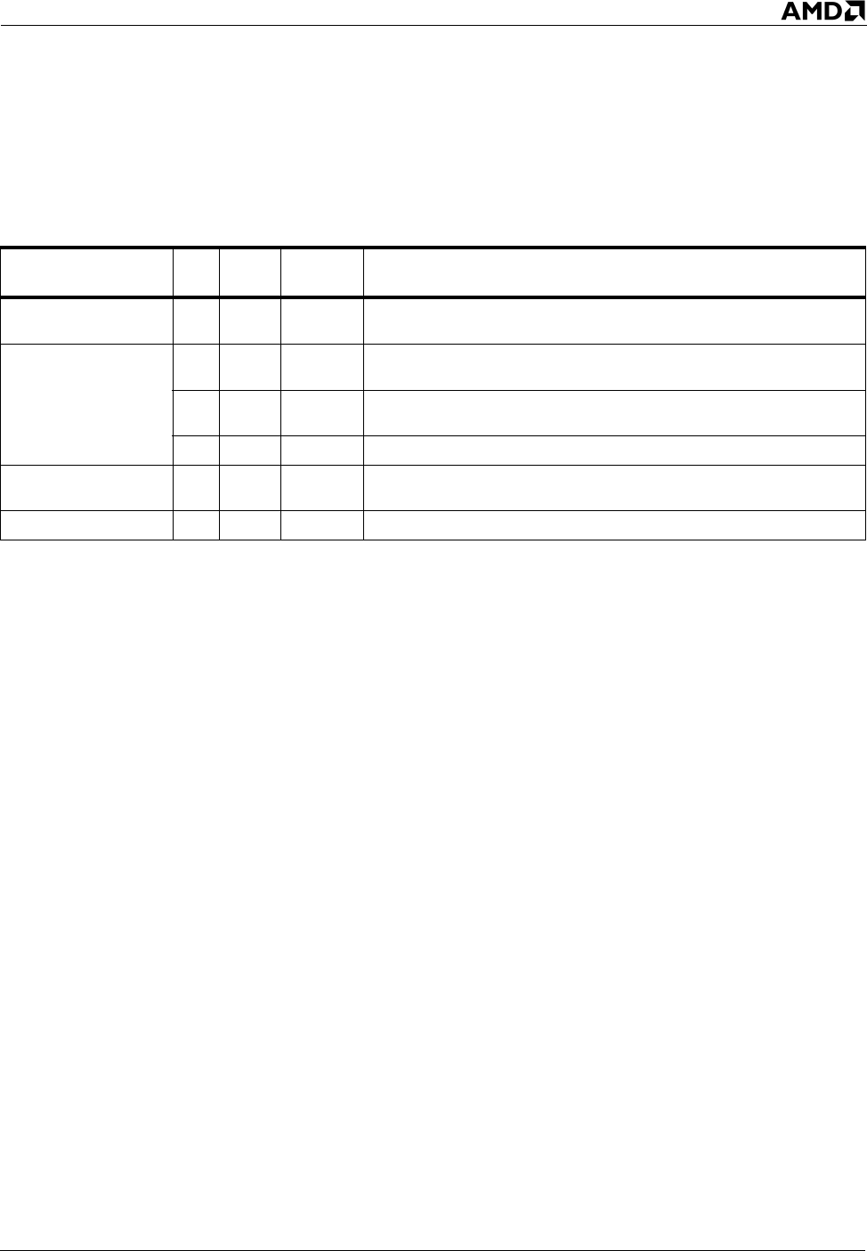
Instruction Reference CALL (Near) 77
24594—Rev. 3.14—September 2007 AMD64 Technology
rFLAGS Affected
None.
Exceptions
Exception Real
Virtual
8086 Protected Cause of Exception
Stack, #SS X X X A memory address exceeded the stack segment limit or was
non-canonical.
General protection,
#GP
XX XA memory address exceeded a data segment limit or was non-
canonical.
XX XThe target offset exceeded the code segment limit or was non-
canonical.
X A null data segment was used to reference memory.
Alignment Check,
#AC XX
An unaligned memory reference was performed while
alignment checking was enabled.
Page Fault, #PF X X A page fault resulted from the execution of the instruction.

78 CALL (Far) Instruction Reference
AMD64 Technology 24594—Rev. 3.14—September 2007
Pushes procedure linking information onto the stack and branches to the target address, which contains
the first instruction of the called procedure. The operand specifies a target selector and offset.
The instruction can specify the target directly, by including the far pointer in the CALL (Far) opcode
itself, or indirectly, by referencing a far pointer in memory. In 64-bit mode, only indirect far calls are
allowed, executing a direct far call (opcode 9A) generates an undefined opcode exception. For both
direct and indirect far calls, if the CALL (Far) operand-size is 16 bits, the instruction's operand is a 16-
bit selector followed by a 16-bit offset. If the operand-size is 32 or 64 bits, the operand is a 16-bit
selector followed by a 32-bit offset.
The target selector used by the instruction can be a code selector in all modes. Additionally, the target
selector can reference a call gate in protected mode, or a task gate or TSS selector in legacy protected
mode.
•Target is a code selector—The CS:rIP of the next instruction is pushed to the stack, using operand-
size stack pushes. Then code is executed from the target CS:rIP. In this case, the target offset can
only be a 16- or 32-bit value, depending on operand-size, and is zero-extended to 64 bits. No CPL
change is allowed.
•Target is a call gate—The call gate specifies the actual target code segment and offset. Call gates
allow calls to the same or more privileged code. If the target segment is at the same CPL as the
current code segment, the CS:rIP of the next instruction is pushed to the stack.
If the CALL (Far) changes privilege level, then a stack-switch occurs, using an inner-level stack
pointer from the TSS. The CS:rIP of the next instruction is pushed to the new stack. If the mode is
legacy mode and the param-count field in the call gate is non-zero, then up to 31 operands are
copied from the caller's stack to the new stack. Finally, the caller's SS:rSP is pushed to the new
stack.
When calling through a call gate, the stack pushes are 16-, 32-, or 64-bits, depending on the size of
the call gate. The size of the target rIP is also 16, 32, or 64 bits, depending on the size of the call
gate. If the target rIP is less than 64 bits, it is zero-extended to 64 bits. Long mode only allows 64-
bit call gates that must point to 64-bit code segments.
•Target is a task gate or a TSS—If the mode is legacy protected mode, then a task switch occurs. See
“Hardware Task-Management in Legacy Mode” in volume 2 for details about task switches.
Hardware task switches are not supported in long mode.
See CALL (Near) for information on near calls—calls to procedures located inside the current code
segment. For details about control-flow instructions, see “Control Transfers” in Volume 1, and
“Control-Transfer Privilege Checks” in Volume 2.
CALL (Far) Far Procedure Call

Instruction Reference CALL (Far) 79
24594—Rev. 3.14—September 2007 AMD64 Technology
Action
// See “Pseudocode Definitions” on page 41.
CALLF_START:
IF (REAL_MODE)
CALLF_REAL_OR_VIRTUAL
ELSIF (PROTECTED_MODE)
CALLF_PROTECTED
ELSE // (VIRTUAL_MODE)
CALLF_REAL_OR_VIRTUAL
CALLF_REAL_OR_VIRTUAL:
IF (OPCODE = callf [mem]) // CALLF Indirect
{
temp_RIP = READ_MEM.z [mem]
temp_CS = READ_MEM.w [mem+Z]
}
ELSE // (OPCODE = callf direct)
{
temp_RIP = z-sized offset specified in the instruction
zero-extended to 64 bits
temp_CS = selector specified in the instruction
}
PUSH.v old_CS
PUSH.v next_RIP
IF (temp_RIP>CS.limit)
EXCEPTION [#GP(0)]
CS.sel = temp_CS
CS.base = temp_CS SHL 4
RIP = temp_RIP
EXIT
Mnemonic Opcode Description
CALL FAR pntr16:16 9A cd Far call direct, with the target specified by a far pointer
contained in the instruction. (Invalid in 64-bit mode.)
CALL FAR pntr16:32 9A cp Far call direct, with the target specified by a far pointer
contained in the instruction. (Invalid in 64-bit mode.)
CALL FAR mem16:16 FF /3 Far call indirect, with the target specified by a far pointer
in memory.
CALL FAR mem16:32 FF /3 Far call indirect, with the target specified by a far pointer
in memory.

80 CALL (Far) Instruction Reference
AMD64 Technology 24594—Rev. 3.14—September 2007
CALLF_PROTECTED:
IF (OPCODE = callf [mem]) //CALLF Indirect
{
temp_offset = READ_MEM.z [mem]
temp_sel = READ_MEM.w [mem+Z]
}
ELSE // (OPCODE = callf direct)
{
IF (64BIT_MODE)
EXCEPTION [#UD] // ’CALLF direct’ is illegal in 64-bit mode.
temp_offset = z-sized offset specified in the instruction
zero-extended to 64 bits
temp_sel = selector specified in the instruction
}
temp_desc = READ_DESCRIPTOR (temp_sel, cs_chk)
IF (temp_desc.attr.type = ’available_tss’)
TASK_SWITCH // Using temp_sel as the target TSS selector.
ELSIF (temp_desc.attr.type = ’taskgate’)
TASK_SWITCH // Using the TSS selector in the task gate
// as the target TSS.
ELSIF (temp_desc.attr.type = ’code’)
// If the selector refers to a code descriptor, then
// the offset we read is the target RIP.
{
temp_RIP = temp_offset
CS = temp_desc
PUSH.v old_CS
PUSH.v next_RIP
IF ((!64BIT_MODE) && (temp_RIP > CS.limit))
// temp_RIP can’t be non-canonical because
EXCEPTION [#GP(0)] // it’s a 16- or 32-bit offset, zero-extended
// to 64 bits.
RIP = temp_RIP
EXIT
}
ELSE // (temp_desc.attr.type = ’callgate’)
// If the selector refers to a call gate, then
// the target CS and RIP both come from the call gate.
{
IF (LONG_MODE)
// The size of the gate controls the size of the stack pushes.
V=8-byte
// Long mode only uses 64-bit call gates, force 8-byte opsize.
ELSIF (temp_desc.attr.type = ’callgate32’)
V=4-byte
// Legacy mode, using a 32-bit call-gate, force 4-byte opsize.
ELSE // (temp_desc.attr.type = ’callgate16’)
V=2-byte

Instruction Reference CALL (Far) 81
24594—Rev. 3.14—September 2007 AMD64 Technology
// Legacy mode, using a 16-bit call-gate, force 2-byte opsize.
temp_RIP = temp_desc.offset
IF (LONG_MODE) // In long mode, we need to read the 2nd half of a
// 16-byte call-gate from the GDT/LDT, to get the upper
// 32 bits of the target RIP.
{
temp_upper = READ_MEM.q [temp_sel+8]
IF (temp_upper’s extended attribute bits != 0)
EXCEPTION [#GP(temp_sel)]
temp_RIP = tempRIP + (temp_upper SHL 32)
// Concatenate both halves of RIP
}
CS = READ_DESCRIPTOR (temp_desc.segment, clg_chk)
IF (CS.attr.conforming=1)
temp_CPL = CPL
ELSE
temp_CPL = CS.attr.dpl
IF (CPL=temp_CPL)
{
PUSH.v old_CS
PUSH.v next_RIP
IF ((64BIT_MODE) && (temp_RIP is non-canonical)
|| (!64BIT_MODE) && (temp_RIP > CS.limit))
{
EXCEPTION[#GP(0)]
}
RIP = temp_RIP
EXIT
}
ELSE // (CPL != temp_CPL), Changing privilege level.
{
CPL = temp_CPL
temp_ist = 0 // Call-far doesn’t use ist pointers.
temp_SS_desc:temp_RSP = READ_INNER_LEVEL_STACK_POINTER (CPL, temp_ist)
RSP.q = temp_RSP
SS = temp_SS_desc
PUSH.v old_SS // #SS on this and following pushes use
// SS.sel as error code.
PUSH.v old_RSP
IF (LEGACY_MODE) // Legacy-mode call gates have
{ // a param_count field.
temp_PARAM_COUNT = temp_desc.attr.param_count

82 CALL (Far) Instruction Reference
AMD64 Technology 24594—Rev. 3.14—September 2007
FOR (I=temp_PARAM_COUNT; I>0; I--)
{
temp_DATA = READ_MEM.v [old_SS:(old_RSP+I*V)]
PUSH.v temp_DATA
}
}
PUSH.v old_CS
PUSH.v next_RIP
IF ((64BIT_MODE) && (temp_RIP is non-canonical)
|| (!64BIT_MODE) && (temp_RIP > CS.limit))
{
EXCEPTION [#GP(0)]
}
RIP = temp_RIP
EXIT
}
}
Related Instructions
CALL (Near), RET (Near), RET (Far)
rFLAGS Affected
None, unless a task switch occurs, in which case all flags are modified.
Exceptions
Exception Real
Virtual
8086 Protected Cause of Exception
Invalid opcode, #UD X X X The far CALL indirect opcode (FF /3) had a register operand.
X The far CALL direct opcode (9A) was executed in 64-bit mode.
Invalid TSS, #TS
(selector)
XAs part of a stack switch, the target stack segment selector or
rSP in the TSS was beyond the TSS limit.
XAs part of a stack switch, the target stack segment selector in
the TSS was a null selector.
XAs part of a stack switch, the target stack selector’s TI bit was
set, but LDT selector was a null selector.
X
As part of a stack switch, the target stack segment selector in
the TSS was beyond the limit of the GDT or LDT descriptor
table.
XAs part of a stack switch, the target stack segment selector in
the TSS contained a RPL that was not equal to its DPL.
X
As part of a stack switch, the target stack segment selector in
the TSS contained a DPL that was not equal to the CPL of the
code segment selector.
XAs part of a stack switch, the target stack segment selector in
the TSS was not a writable segment.

Instruction Reference CALL (Far) 83
24594—Rev. 3.14—September 2007 AMD64 Technology
Segment not
present, #NP
(selector)
XThe accessed code segment, call gate, task gate, or TSS was
not present.
Stack, #SS X X X A memory address exceeded the stack segment limit or was
non-canonical, and no stack switch occurred.
Stack, #SS
(selector)
XAfter a stack switch, a memory access exceeded the stack
segment limit or was non-canonical.
X
As part of a stack switch, the SS register was loaded with a
non-null segment selector and the segment was marked not
present.
General protection,
#GP
XX XA memory address exceeded a data segment limit or was non-
canonical.
XX XThe target offset exceeded the code segment limit or was non-
canonical.
X A null data segment was used to reference memory.
General protection,
#GP
(selector)
X The target code segment selector was a null selector.
XA code, call gate, task gate, or TSS descriptor exceeded the
descriptor table limit.
XA segment selector’s TI bit was set but the LDT selector was a
null selector.
X
The segment descriptor specified by the instruction was not a
code segment, task gate, call gate or available TSS in legacy
mode, or not a 64-bit code segment or a 64-bit call gate in long
mode.
X
The RPL of the non-conforming code segment selector
specified by the instruction was greater than the CPL, or its
DPL was not equal to the CPL.
XThe DPL of the conforming code segment descriptor specified
by the instruction was greater than the CPL.
X
The DPL of the callgate, taskgate, or TSS descriptor specified
by the instruction was less than the CPL, or less than its own
RPL.
XThe segment selector specified by the call gate or task gate
was a null selector.
X
The segment descriptor specified by the call gate was not a
code segment in legacy mode, or not a 64-bit code segment in
long mode.
XThe DPL of the segment descriptor specified by the call gate
was greater than the CPL.
X The 64-bit call gate’s extended attribute bits were not zero.
X The TSS descriptor was found in the LDT.
Page fault, #PF X X A page fault resulted from the execution of the instruction.
Alignment check,
#AC XX
An unaligned memory reference was performed while
alignment checking was enabled.
Exception Real
Virtual
8086 Protected Cause of Exception

84 CBW, CWDE, CDQE Instruction Reference
AMD64 Technology 24594—Rev. 3.14—September 2007
Copies the sign bit in the AL or eAX register to the upper bits of the rAX register. The effect of this
instruction is to convert a signed byte, word, or doubleword in the AL or eAX register into a signed
word, doubleword, or double quadword in the rAX register. This action helps avoid overflow problems
in signed number arithmetic.
The CDQE mnemonic is meaningful only in 64-bit mode.
Related Instructions
CWD, CDQ, CQO
rFLAGS Affected
None
Exceptions
None
CBW
CWDE
CDQE
Convert to Sign-Extended
Mnemonic Opcode Description
CBW 98 Sign-extend AL into AX.
CWDE 98 Sign-extend AX into EAX.
CDQE 98 Sign-extend EAX into RAX.

Instruction Reference CWD, CDQ, CQO 85
24594—Rev. 3.14—September 2007 AMD64 Technology
Copies the sign bit in the rAX register to all bits of the rDX register. The effect of this instruction is to
convert a signed word, doubleword, or quadword in the rAX register into a signed doubleword,
quadword, or double-quadword in the rDX:rAX registers. This action helps avoid overflow problems
in signed number arithmetic.
The CQO mnemonic is meaningful only in 64-bit mode.
Related Instructions
CBW, CWDE, CDQE
rFLAGS Affected
None
Exceptions
None
CWD
CDQ
CQO
Convert to Sign-Extended
Mnemonic Opcode Description
CWD 99 Sign-extend AX into DX:AX.
CDQ 99 Sign-extend EAX into EDX:EAX.
CQO 99 Sign-extend RAX into RDX:RAX.

86 CLC Instruction Reference
AMD64 Technology 24594—Rev. 3.14—September 2007
Clears the carry flag (CF) in the rFLAGS register to zero.
Related Instructions
STC, CMC
rFLAGS Affected
Exceptions
None
CLC Clear Carry Flag
Mnemonic Opcode Description
CLC F8 Clear the carry flag (CF) to zero.
ID VIP VIF AC VM RF NT IOPL OF DF IF TF SF ZF AF PF CF
0
2120191817161413–1211109876420
Note: Bits 31–22, 15, 5, 3, and 1 are reserved. A flag set to 1 or cleared to 0 is M (modified). Unaffected flags are blank.
Undefined flags are U.
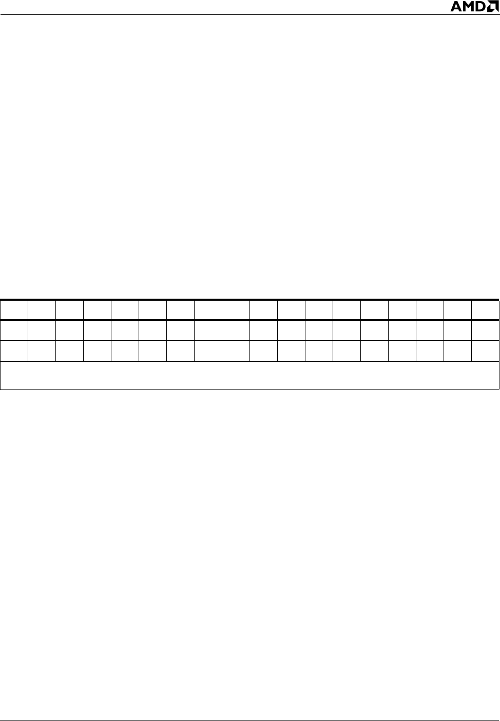
Instruction Reference CLD 87
24594—Rev. 3.14—September 2007 AMD64 Technology
Clears the direction flag (DF) in the rFLAGS register to zero. If the DF flag is 0, each iteration of a
string instruction increments the data pointer (index registers rSI or rDI). If the DF flag is 1, the string
instruction decrements the pointer. Use the CLD instruction before a string instruction to make the data
pointer increment.
Related Instructions
CMPSx, INSx, LODSx, MOVSx, OUTSx, SCASx, STD, STOSx
rFLAGS Affected
Exceptions
None
CLD Clear Direction Flag
Mnemonic Opcode Description
CLD FC Clear the direction flag (DF) to zero.
ID VIP VIF AC VM RF NT IOPL OF DF IF TF SF ZF AF PF CF
0
2120191817161413–1211109876420
Note: Bits 31–22, 15, 5, 3, and 1 are reserved. A flag set to 1 or cleared to 0 is M (modified). Unaffected flags are
blank. Undefined flags are U.

88 CLFLUSH Instruction Reference
AMD64 Technology 24594—Rev. 3.14—September 2007
Flushes the cache line specified by the mem8 linear-address. The instruction checks all levels of the
cache hierarchy—internal caches and external caches—and invalidates the cache line in every cache in
which it is found. If a cache contains a dirty copy of the cache line (that is, the cache line is in the
modified or owned MOESI state), the line is written back to memory before it is invalidated. The
instruction sets the cache-line MOESI state to invalid.
The instruction also checks the physical address corresponding to the linear-address operand against
the processor’s write-combining buffers. If the write-combining buffer holds data intended for that
physical address, the instruction writes the entire contents of the buffer to memory. This occurs even
though the data is not cached in the cache hierarchy. In a multiprocessor system, the instruction checks
the write-combining buffers only on the processor that executed the CLFLUSH instruction.
The CLFLUSH instruction is weakly-ordered with respect to other instructions that operate on
memory. Speculative loads initiated by the processor, or specified explicitly using cache-prefetch
instructions, can be reordered around a CLFLUSH instruction. Such reordering can invalidate a
speculatively prefetched cache line, unintentionally defeating the prefetch operation. The only way to
avoid this situation is to use the MFENCE instruction after the CLFLUSH instruction to force strong-
ordering of the CLFLUSH instruction with respect to subsequent memory operations. The CLFLUSH
instruction may also take effect on a cache line while stores from previous store instructions are still
pending in the store buffer. To ensure that such stores are included in the cache line that is flushed, use
an MFENCE instruction ahead of the CLFLUSH instruction. Such stores would otherwise cause the
line to be re-cached and modified after the CLFLUSH completed. The LFENCE, SFENCE, and
serializing instructions are not ordered with respect to CLFLUSH.
The CLFLUSH instruction behaves like a load instruction with respect to setting the page-table
accessed and dirty bits. That is, it sets the page-table accessed bit to 1, but does not set the page-table
dirty bit.
The CLFLUSH instruction is supported if CPUID function 0000_0001h sets EDX bit 19. CPUID
function 0000_0001h returns the CLFLUSH size in EBX bits 23:16. This value reports the size of a
line flushed by CLFLUSH in quadwords. See CPUID for details.
The CLFLUSH instruction executes at any privilege level. CLFLUSH performs all the segmentation
and paging checks that a 1-byte read would perform, except that it also allows references to execute-
only segments.
Related Instructions
INVD, WBINVD
CLFLUSH Cache Line Flush
Mnemonic Opcode Description
CFLUSH mem8 0F AE /7 flush cache line containing mem8.
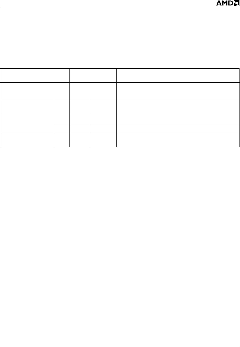
Instruction Reference CLFLUSH 89
24594—Rev. 3.14—September 2007 AMD64 Technology
rFLAGS Affected
None
Exceptions
Exception (vector) Real
Virtual
8086 Protected Cause of Exception
Invalid opcode, #UD X X X
The CLFLUSH instruction is not supported, as
indicated by EDX bit 19 of CPUID function
0000_0001h.
Stack, #SS X X X A memory address exceeded the stack segment limit
or was non-canonical.
General protection,
#GP
XX X
A memory address exceeded a data segment limit or
was non-canonical.
X A null data segment was used to reference memory.
Page fault, #PF X X A page fault resulted from the execution of the
instruction.

90 CMC Instruction Reference
AMD64 Technology 24594—Rev. 3.14—September 2007
Complements (toggles) the carry flag (CF) bit of the rFLAGS register.
Related Instructions
CLC, STC
rFLAGS Affected
Exceptions
None
CMC Complement Carry Flag
Mnemonic Opcode Description
CMC F5 Complement the carry flag (CF).
ID VIP VIF AC VM RF NT IOPL OF DF IF TF SF ZF AF PF CF
M
2120191817161413–1211109876420
Note: Bits 31–22, 15, 5, 3, and 1 are reserved. A flag set to 1 or cleared to 0 is M (modified). Unaffected flags are blank.
Undefined flags are U.

Instruction Reference CMOVcc 91
24594—Rev. 3.14—September 2007 AMD64 Technology
Conditionally moves a 16-bit, 32-bit, or 64-bit value in memory or a general-purpose register (second
operand) into a register (first operand), depending upon the settings of condition flags in the rFLAGS
register. If the condition is not satisfied, the instruction has no effect.
The mnemonics of CMOVcc instructions denote the condition that must be satisfied. Most assemblers
provide instruction mnemonics with A (above) and B (below) tags to supply the semantics for
manipulating unsigned integers. Those with G (greater than) and L (less than) tags deal with signed
integers. Many opcodes may be represented by synonymous mnemonics. For example, the CMOVL
instruction is synonymous with the CMOVNGE instruction and denote the instruction with the opcode
0F 4C.
Support for CMOVcc instructions depends on the processor implementation. To determine whether a
processor can perform CMOVcc instructions, use the CPUID instruction to determine whether EDX
bit 15 of CPUID function 0000_0001h or function 8000_0001h is set to 1.
CMOVcc Conditional Move
Mnemonic Opcode Description
CMOVO reg16, reg/mem16
CMOVO reg32, reg/mem32
CMOVO reg64, reg/mem64
0F 40 /r Move if overflow (OF = 1).
CMOVNO reg16, reg/mem16
CMOVNO reg32, reg/mem32
CMOVNO reg64, reg/mem64
0F 41 /r Move if not overflow (OF = 0).
CMOVB reg16, reg/mem16
CMOVB reg32, reg/mem32
CMOVB reg64, reg/mem64
0F 42 /r Move if below (CF = 1).
CMOVC reg16, reg/mem16
CMOVC reg32, reg/mem32
CMOVC reg64, reg/mem64
0F 42 /r Move if carry (CF = 1).
CMOVNAE reg16, reg/mem16
CMOVNAE reg32, reg/mem32
CMOVNAE reg64, reg/mem64
0F 42 /r Move if not above or equal (CF = 1).
CMOVNB reg16,reg/mem16
CMOVNB reg32,reg/mem32
CMOVNB reg64,reg/mem64
0F 43 /r Move if not below (CF = 0).
CMOVNC reg16,reg/mem16
CMOVNC reg32,reg/mem32
CMOVNC reg64,reg/mem64
0F 43 /r Move if not carry (CF = 0).
CMOVAE reg16, reg/mem16
CMOVAE reg32, reg/mem32
CMOVAE reg64, reg/mem64
0F 43 /r Move if above or equal (CF = 0).
CMOVZ reg16, reg/mem16
CMOVZ reg32, reg/mem32
CMOVZ reg64, reg/mem64
0F 44 /r Move if zero (ZF = 1).

92 CMOVcc Instruction Reference
AMD64 Technology 24594—Rev. 3.14—September 2007
CMOVE reg16, reg/mem16
CMOVE reg32, reg/mem32
CMOVE reg64, reg/mem64
0F 44 /r Move if equal (ZF =1).
CMOVNZ reg16, reg/mem16
CMOVNZ reg32, reg/mem32
CMOVNZ reg64, reg/mem64
0F 45 /r Move if not zero (ZF = 0).
CMOVNE reg16, reg/mem16
CMOVNE reg32, reg/mem32
CMOVNE reg64, reg/mem64
0F 45 /r Move if not equal (ZF = 0).
CMOVBE reg16, reg/mem16
CMOVBE reg32, reg/mem32
CMOVBE reg64, reg/mem64
0F 46 /r Move if below or equal (CF = 1 or ZF = 1).
CMOVNA reg16, reg/mem16
CMOVNA reg32, reg/mem32
CMOVNA reg64, reg/mem64
0F 46 /r Move if not above (CF = 1 or ZF = 1).
CMOVNBE reg16, reg/mem16
CMOVNBE reg32,reg/mem32
CMOVNBE reg64,reg/mem64
0F 47 /r Move if not below or equal (CF = 0 and ZF = 0).
CMOVA reg16, reg/mem16
CMOVA reg32, reg/mem32
CMOVA reg64, reg/mem64
0F 47 /r Move if above (CF = 0 and ZF = 0).
CMOVS reg16, reg/mem16
CMOVS reg32, reg/mem32
CMOVS reg64, reg/mem64
0F 48 /r Move if sign (SF =1).
CMOVNS reg16, reg/mem16
CMOVNS reg32, reg/mem32
CMOVNS reg64, reg/mem64
0F 49 /r Move if not sign (SF = 0).
CMOVP reg16, reg/mem16
CMOVP reg32, reg/mem32
CMOVP reg64, reg/mem64
0F 4A /r Move if parity (PF = 1).
CMOVPE reg16, reg/mem16
CMOVPE reg32, reg/mem32
CMOVPE reg64, reg/mem64
0F 4A /r Move if parity even (PF = 1).
CMOVNP reg16, reg/mem16
CMOVNP reg32, reg/mem32
CMOVNP reg64, reg/mem64
0F 4B /r Move if not parity (PF = 0).
CMOVPO reg16, reg/mem16
CMOVPO reg32, reg/mem32
CMOVPO reg64, reg/mem64
0F 4B /r Move if parity odd (PF = 0).
CMOVL reg16, reg/mem16
CMOVL reg32, reg/mem32
CMOVL reg64, reg/mem64
0F 4C /r Move if less (SF <> OF).
CMOVNGE reg16, reg/mem16
CMOVNGE reg32, reg/mem32
CMOVNGE reg64, reg/mem64
0F 4C /r Move if not greater or equal (SF <> OF).
Mnemonic Opcode Description
Instruction Reference CMOVcc 93
24594—Rev. 3.14—September 2007 AMD64 Technology
Related Instructions
MOV
rFLAGS Affected
None
Exceptions
CMOVNL reg16, reg/mem16
CMOVNL reg32, reg/mem32
CMOVNL reg64, reg/mem64
0F 4D /r Move if not less (SF = OF).
CMOVGE reg16, reg/mem16
CMOVGE reg32, reg/mem32
CMOVGE reg64, reg/mem64
0F 4D /r Move if greater or equal (SF = OF).
CMOVLE reg16, reg/mem16
CMOVLE reg32, reg/mem32
CMOVLE reg64, reg/mem64
0F 4E /r Move if less or equal (ZF = 1 or SF <> OF).
CMOVNG reg16, reg/mem16
CMOVNG reg32, reg/mem32
CMOVNG reg64, reg/mem64
0F 4E /r Move if not greater (ZF = 1 or SF <> OF).
CMOVNLE reg16, reg/mem16
CMOVNLE reg32, reg/mem32
CMOVNLE reg64, reg/mem64
0F 4F /r Move if not less or equal (ZF = 0 and SF = OF).
CMOVG reg16, reg/mem16
CMOVG reg32, reg/mem32
CMOVG reg64, reg/mem64
0F 4F /r Move if greater (ZF = 0 and SF = OF).
Exception Real
Virtual
8086 Protected Cause of Exception
Invalid opcode, #UD X X X
The CMOVcc instruction is not supported, as indicated by
EDX bit 15 of CPUID function 0000_0001h or function
8000_0001h.
Stack, #SS X X X A memory address exceeded the stack segment limit or was
non-canonical.
General protection,
#GP
XX XA memory address exceeded a data segment limit or was non-
canonical.
X A null data segment was used to reference memory.
Page fault, #PF X X A page fault resulted from the execution of the instruction.
Alignment check,
#AC XX
An unaligned memory reference was performed while
alignment checking was enabled.
Mnemonic Opcode Description

94 CMP Instruction Reference
AMD64 Technology 24594—Rev. 3.14—September 2007
Compares the contents of a register or memory location (first operand) with an immediate value or the
contents of a register or memory location (second operand), and sets or clears the status flags in the
rFLAGS register to reflect the results. To perform the comparison, the instruction subtracts the second
operand from the first operand and sets the status flags in the same manner as the SUB instruction, but
does not alter the first operand. If the second operand is an immediate value, the instruction sign-
extends the value to the length of the first operand.
Use the CMP instruction to set the condition codes for a subsequent conditional jump (Jcc),
conditional move (CMOVcc), or conditional SETcc instruction. Appendix E, “Instruction Effects on
RFLAGS,” shows how instructions affect the rFLAGS status flags.
.
CMP Compare
Mnemonic Opcode Description
CMP AL, imm8 3C ib Compare an 8-bit immediate value with the contents of
the AL register.
CMP AX, imm16 3D iw Compare a 16-bit immediate value with the contents of
the AX register.
CMP EAX, imm32 3D id Compare a 32-bit immediate value with the contents of
the EAX register.
CMP RAX, imm32 3D id Compare a 32-bit immediate value with the contents of
the RAX register.
CMP reg/mem8, imm8 80 /7 ib Compare an 8-bit immediate value with the contents of
an 8-bit register or memory operand.
CMP reg/mem16, imm16 81 /7 iw Compare a 16-bit immediate value with the contents of
a 16-bit register or memory operand.
CMP reg/mem32, imm32 81 /7 id Compare a 32-bit immediate value with the contents of
a 32-bit register or memory operand.
CMP reg/mem64, imm32 81 /7 id Compare a 32-bit signed immediate value with the
contents of a 64-bit register or memory operand.
CMP reg/mem16, imm8 83 /7 ib Compare an 8-bit signed immediate value with the
contents of a 16-bit register or memory operand.
CMP reg/mem32, imm8 83 /7 ib Compare an 8-bit signed immediate value with the
contents of a 32-bit register or memory operand.
CMP reg/mem64, imm8 83 /7 ib Compare an 8-bit signed immediate value with the
contents of a 64-bit register or memory operand.
CMP reg/mem8, reg8 38 /r Compare the contents of an 8-bit register or memory
operand with the contents of an 8-bit register.
CMP reg/mem16, reg16 39 /r Compare the contents of a 16-bit register or memory
operand with the contents of a 16-bit register.
CMP reg/mem32, reg32 39 /r Compare the contents of a 32-bit register or memory
operand with the contents of a 32-bit register.
CMP reg/mem64, reg64 39 /r Compare the contents of a 64-bit register or memory
operand with the contents of a 64-bit register.
Instruction Reference CMP 95
24594—Rev. 3.14—September 2007 AMD64 Technology
When interpreting operands as unsigned, flag settings are as follows:
When interpreting operands as signed, flag settings are as follows:
Related Instructions
SUB, CMPSx, SCASx
CMP reg8, reg/mem8 3A /r Compare the contents of an 8-bit register with the
contents of an 8-bit register or memory operand.
CMP reg16, reg/mem16 3B /r Compare the contents of a 16-bit register with the
contents of a 16-bit register or memory operand.
CMP reg32, reg/mem32 3B /r Compare the contents of a 32-bit register with the
contents of a 32-bit register or memory operand.
CMP reg64, reg/mem64 3B /r Compare the contents of a 64-bit register with the
contents of a 64-bit register or memory operand.
Operands CF ZF
dest > source 0 0
dest = source 0 1
dest < source 1 0
Operands OF ZF
dest > source SF 0
dest = source 0 1
dest < source NOT SF 0
Mnemonic Opcode Description

96 CMP Instruction Reference
AMD64 Technology 24594—Rev. 3.14—September 2007
rFLAGS Affected
Exceptions
ID VIP VIF AC VM RF NT IOPL OF DF IF TF SF ZF AF PF CF
M MMMMM
2120191817161413–1211109876420
Note: Bits 31–22, 15, 5, 3, and 1 are reserved. A flag set to 1 or cleared to 0 is M (modified). Unaffected flags are
blank. Undefined flags are U.
Exception Real
Virtual
8086 Protected Cause of Exception
Stack, #SS X X X A memory address exceeded the stack segment limit or was
non-canonical.
General protection,
#GP
XX XA memory address exceeded a data segment limit or was non-
canonical.
X A null data segment was used to reference memory.
Page fault, #PF X X A page fault resulted from the execution of the instruction.
Alignment check,
#AC XX
An unaligned memory reference was performed while
alignment checking was enabled.

Instruction Reference CMPSx 97
24594—Rev. 3.14—September 2007 AMD64 Technology
Compares the bytes, words, doublewords, or quadwords pointed to by the rSI and rDI registers, sets or
clears the status flags of the rFLAGS register to reflect the results, and then increments or decrements
the rSI and rDI registers according to the state of the DF flag in the rFLAGS register. To perform the
comparison, the instruction subtracts the second operand from the first operand and sets the status
flags in the same manner as the SUB instruction, but does not alter the first operand. The two operands
must be the same size.
If the DF flag is 0, the instruction increments rSI and rDI; otherwise, it decrements the pointers. It
increments or decrements the pointers by 1, 2, 4, or 8, depending on the size of the operands.
The forms of the CMPSx instruction with explicit operands address the first operand at seg:[rSI]. The
value of seg defaults to the DS segment, but may be overridden by a segment prefix. These instructions
always address the second operand at ES:[rDI]. ES may not be overridden. The explicit operands serve
only to specify the type (size) of the values being compared and the segment used by the first operand.
The no-operands forms of the instruction use the DS:[rSI] and ES:[rDI] registers to point to the values
to be compared. The mnemonic determines the size of the operands.
Do not confuse this CMPSD instruction with the same-mnemonic CMPSD (compare scalar double-
precision floating-point) instruction in the 128-bit media instruction set. Assemblers can distinguish
the instructions by the number and type of operands.
For block comparisons, the CMPS instruction supports the REPE or REPZ prefixes (they are
synonyms) and the REPNE or REPNZ prefixes (they are synonyms). For details about the REP
prefixes, see “Repeat Prefixes” on page 9. If a conditional jump instruction like JL follows a CMPSx
instruction, the jump occurs if the value of the seg:[rSI] operand is less than the ES:[rDI] operand. This
action allows lexicographical comparisons of string or array elements. A CMPSx instruction can also
operate inside a loop controlled by the LOOPcc instruction.
CMPS
CMPSB
CMPSW
CMPSD
CMPSQ
Compare Strings
Mnemonic Opcode Description
CMPS mem8, mem8 A6 Compare the byte at DS:rSI with the byte at ES:rDI and
then increment or decrement rSI and rDI.
CMPS mem16, mem16 A7 Compare the word at DS:rSI with the word at ES:rDI and
then increment or decrement rSI and rDI.
CMPS mem32, mem32 A7 Compare the doubleword at DS:rSI with the doubleword
at ES:rDI and then increment or decrement rSI and rDI.
CMPS mem64, mem64 A7 Compare the quadword at DS:rSI with the quadword at
ES:rDI and then increment or decrement rSI and rDI.
98 CMPSx Instruction Reference
AMD64 Technology 24594—Rev. 3.14—September 2007
Related Instructions
CMP, SCASx
rFLAGS Affected
Exceptions
CMPSB A6 Compare the byte at DS:rSI with the byte at ES:rDI and
then increment or decrement rSI and rDI.
CMPSW A7 Compare the word at DS:rSI with the word at ES:rDI and
then increment or decrement rSI and rDI.
CMPSD A7 Compare the doubleword at DS:rSI with the doubleword
at ES:rDI and then increment or decrement rSI and rDI.
CMPSQ A7 Compare the quadword at DS:rSI with the quadword at
ES:rDI and then increment or decrement rSI and rDI.
ID VIP VIF AC VM RF NT IOPL OF DF IF TF SF ZF AF PF CF
M MMMMM
2120191817161413–1211109876420
Note: Bits 31–22, 15, 5, 3, and 1 are reserved. A flag set to 1 or cleared to 0 is M (modified). Unaffected flags are blank.
Undefined flags are U.
Exception Real
Virtual
8086 Protected Cause of Exception
Stack, #SS X X X A memory address exceeded the stack segment limit or was
non-canonical.
General protection,
#GP
XX XA memory address exceeded a data segment limit or was non-
canonical.
X A null data segment was used to reference memory.
Page fault, #PF X X A page fault resulted from the execution of the instruction.
Alignment check,
#AC XX
An unaligned memory reference was performed while
alignment checking was enabled.
Mnemonic Opcode Description

Instruction Reference CMPXCHG 99
24594—Rev. 3.14—September 2007 AMD64 Technology
Compares the value in the AL, AX, EAX, or RAX register with the value in a register or a memory
location (first operand). If the two values are equal, the instruction copies the value in the second
operand to the first operand and sets the ZF flag in the rFLAGS register to 1. Otherwise, it copies the
value in the first operand to the AL, AX, EAX, or RAX register and clears the ZF flag to 0.
The OF, SF, AF, PF, and CF flags are set to reflect the results of the compare.
When the first operand is a memory operand, CMPXCHG always does a read-modify-write on the
memory operand. If the compared operands were unequal, CMPXCHG writes the same value to the
memory operand that was read.
The forms of the CMPXCHG instruction that write to memory support the LOCK prefix. For details
about the LOCK prefix, see “Lock Prefix” on page 8.
Related Instructions
CMPXCHG8B, CMPXCHG16B
CMPXCHG Compare and Exchange
Mnemonic Opcode Description
CMPXCHG reg/mem8, reg8 0F B0 /r
Compare AL register with an 8-bit register or memory
location. If equal, copy the second operand to the first
operand. Otherwise, copy the first operand to AL.
CMPXCHG reg/mem16, reg16 0F B1 /r
Compare AX register with a 16-bit register or memory
location. If equal, copy the second operand to the first
operand. Otherwise, copy the first operand to AX.
CMPXCHG reg/mem32, reg32 0F B1 /r
Compare EAX register with a 32-bit register or memory
location. If equal, copy the second operand to the first
operand. Otherwise, copy the first operand to EAX.
CMPXCHG reg/mem64, reg64 0F B1 /r
Compare RAX register with a 64-bit register or memory
location. If equal, copy the second operand to the first
operand. Otherwise, copy the first operand to RAX.

100 CMPXCHG Instruction Reference
AMD64 Technology 24594—Rev. 3.14—September 2007
rFLAGS Affected
Exceptions
ID VIP VIF AC VM RF NT IOPL OF DF IF TF SF ZF AF PF CF
M MMMMM
2120191817161413–1211109876420
Note: Bits 31–22, 15, 5, 3, and 1 are reserved. A flag set to 1 or cleared to 0 is M (modified). Unaffected flags are
blank. Undefined flags are U.
Exception Real
Virtual
8086 Protected Cause of Exception
Stack, #SS X X X A memory address exceeded the stack segment limit or was
non-canonical.
General protection,
#GP
XX XA memory address exceeded a data segment limit or was non-
canonical.
X The destination operand was in a non-writable segment.
X A null data segment was used to reference memory.
Page fault, #PF X X A page fault resulted from the execution of the instruction.
Alignment check,
#AC XX
An unaligned memory reference was performed while
alignment checking was enabled.

Instruction Reference CMPXCHG8/16B 101
24594—Rev. 3.14—September 2007 AMD64 Technology
Compares the value in the rDX:rAX registers with a 64-bit or 128-bit value in the specified memory
location. If the values are equal, the instruction copies the value in the rCX:rBX registers to the
memory location and sets the zero flag (ZF) of the rFLAGS register to 1. Otherwise, it copies the value
in memory to the rDX:rAX registers and clears ZF to 0.
If the effective operand size is 16-bit or 32-bit, the CMPXCHG8B instruction is used. This instruction
uses the EDX:EAX and ECX:EBX register operands and a 64-bit memory operand. If the effective
operand size is 64-bit, the CMPXCHG16B instruction is used; this instruction uses RDX:RAX and
RCX:RBX register operands and a 128-bit memory operand.
The CMPXCHG8B and CMPXCHG16B instructions always do a read-modify-write on the memory
operand. If the compared operands were unequal, the instructions write the same value to the memory
operand that was read.
The CMPXCHG8B and CMPXCHG16B instructions support the LOCK prefix. For details about the
LOCK prefix, see “Lock Prefix” on page 8.
Support for the CMPXCHG8B and CMPXCHG16B instructions depends on the processor
implementation. To find out if a processor can execute the CMPXCHG8B instruction, use the CPUID
instruction to determine whether EDX bit 8 of CPUID function 0000_0001h or function 8000_0001h
is set to 1. To find out if a processor can execute the CMPXCHG16B instruction, use the CPUID
instruction to determine whether ECX bit 13 of CPUID function 0000_0001h is set to 1.
The memory operand used by CMPXCHG16B must be 16-byte aligned or else a general-protection
exception is generated.
Related Instructions
CMPXCHG
CMPXCHG8B
CMPXCHG16B
Compare and Exchange Eight Bytes
Compare and Exchange Sixteen Bytes
Mnemonic Opcode Description
CMPXCHG8B mem64 0F C7 /1 m64
Compare EDX:EAX register to 64-bit memory location.
If equal, set the zero flag (ZF) to 1 and copy the
ECX:EBX register to the memory location. Otherwise,
copy the memory location to EDX:EAX and clear the
zero flag.
CMPXCHG16B mem128 0F C7 /1
m128
Compare RDX:RAX register to 128-bit memory location.
If equal, set the zero flag (ZF) to 1 and copy the
RCX:RBX register to the memory location. Otherwise,
copy the memory location to RDX:RAX and clear the
zero flag.

102 CMPXCHG8/16B Instruction Reference
AMD64 Technology 24594—Rev. 3.14—September 2007
rFLAGS Affected
Exceptions
ID VIP VIF AC VM RF NT IOPL OF DF IF TF SF ZF AF PF CF
M
2120191817161413–1211109876420
Note: Bits 31–22, 15, 5, 3, and 1 are reserved. A flag set to 1 or cleared to 0 is M (modified). Unaffected flags are
blank. Undefined flags are U.
Exception Real
Virtual
8086 Protected Cause of Exception
Invalid opcode, #UD
XX X
The CMPXCHG8B instruction is not supported, as indicated
by EDX bit 8 of CPUID function 0000_0001h or function
8000_0001h.
XThe CMPXCHG16B instruction is not supported, as indicated
by ECX bit 13 of CPUID function 0000_0001h.
X X X The operand was a register.
Stack, #SS X X X A memory address exceeded the stack segment limit or was
non-canonical.
General protection,
#GP
XX XA memory address exceeded a data segment limit or was non-
canonical.
X The destination operand was in a non-writable segment.
X A null data segment was used to reference memory.
XThe memory operand for CMPXCHG16B was not aligned on a
16-byte boundary.
Page fault, #PF X X A page fault resulted from the execution of the instruction.
Alignment check,
#AC XX
An unaligned memory reference was performed while
alignment checking was enabled.

Instruction Reference CPUID 103
24594—Rev. 3.14—September 2007 AMD64 Technology
Provides information about the processor and its capabilities through a number of different functions.
Software should load the number of the CPUID function to execute into the EAX register before
executing the CPUID instruction. The processor returns information in the EAX, EBX, ECX, and
EDX registers; the contents and format of these registers depend on the function.
The architecture supports CPUID information about standard functions and extended functions. The
standard functions have numbers in the 0000_xxxxh series (for example, standard function 1). To
determine the largest standard function number that a processor supports, execute CPUID function 0.
The extended functions have numbers in the 8000_xxxxh series (for example, extended
function 8000_0001h). To determine the largest extended function number that a processor supports,
execute CPUID extended function 8000_0000h. If the value returned in EAX is greater than
8000_0000h, the processor supports extended functions.
Software operating at any privilege level can execute the CPUID instruction to collect this information.
In 64-bit mode, this instruction works the same as in legacy mode except that it zero-extends 32-bit
register results to 64 bits.
CPUID is a serializing instruction.
Testing for the CPUID Instruction
To avoid an invalid-opcode exception (#UD) on those processor implementations that do not support
the CPUID instruction, software must first test to determine if the CPUID instruction is supported.
Support for the CPUID instruction is indicated by the ability to write the ID bit in the rFLAGS register.
Normally, 32-bit software uses the PUSHFD and POPFD instructions in an attempt to write
rFLAGS.ID. After reading the updated rFLAGS.ID bit, a comparison determines if the operation
changed its value. If the value changed, the processor executing the code supports the CPUID
instruction. If the value did not change, rFLAGS.ID is not writable, and the processor does not support
the CPUID instruction.
The following code sample shows how to test for the presence of the CPUID instruction using 32-bit
code.
pushfd ; save EFLAGS
pop eax ; store EFLAGS in EAX
mov ebx, eax ; save in EBX for later testing
xor eax, 00200000h ; toggle bit 21
push eax ; push to stack
popfd ; save changed EAX to EFLAGS
CPUID Processor Identification
Mnemonic Opcode Description
CPUID 0F A2
Returns information about the processor and its
capabilities. EAX specifies the function number, and the
data is returned in EAX, EBX, ECX, EDX.
104 CPUID Instruction Reference
AMD64 Technology 24594—Rev. 3.14—September 2007
pushfd ; push EFLAGS to TOS
pop eax ; store EFLAGS in EAX
cmp eax, ebx ; see if bit 21 has changed
jz NO_CPUID ; if no change, no CPUID
Standard Function 0 and Extended Function 8000_0000h
CPUID standard function 0 loads the EAX register with the largest CPUID standard function number
supported by the processor implementation; similarly, CPUID extended function 8000_0000h loads
the EAX register with the largest extended function number supported.
Standard function 0 and extended function 8000_0000h both load a 12-character string into the EBX,
EDX, and ECX registers identifying the processor vendor. For AMD processors, the string is
AuthenticAMD. This string informs software that it should follow the AMD CPUID definition for
subsequent CPUID function calls. If the function returns another vendor’s string, software must use
that vendor’s CPUID definition when interpreting the results of subsequent CPUID function calls.
Table 3-2 shows the contents of the EBX, EDX, and ECX registers after executing function 0 on an
AMD processor.
For more detailed on CPUID standard and extended functions, see the AMD CPUID Specification,
order# 25481.
Related Instructions
None
rFLAGS Affected
None
Exceptions
None
Table 3-2. Processor Vendor Return Values
Register Return Value ASCII Characters
EBX 6874_7541h “h t u A”
EDX 6974_6E65h “i t n e”
ECX 444D_4163h “D M A c”
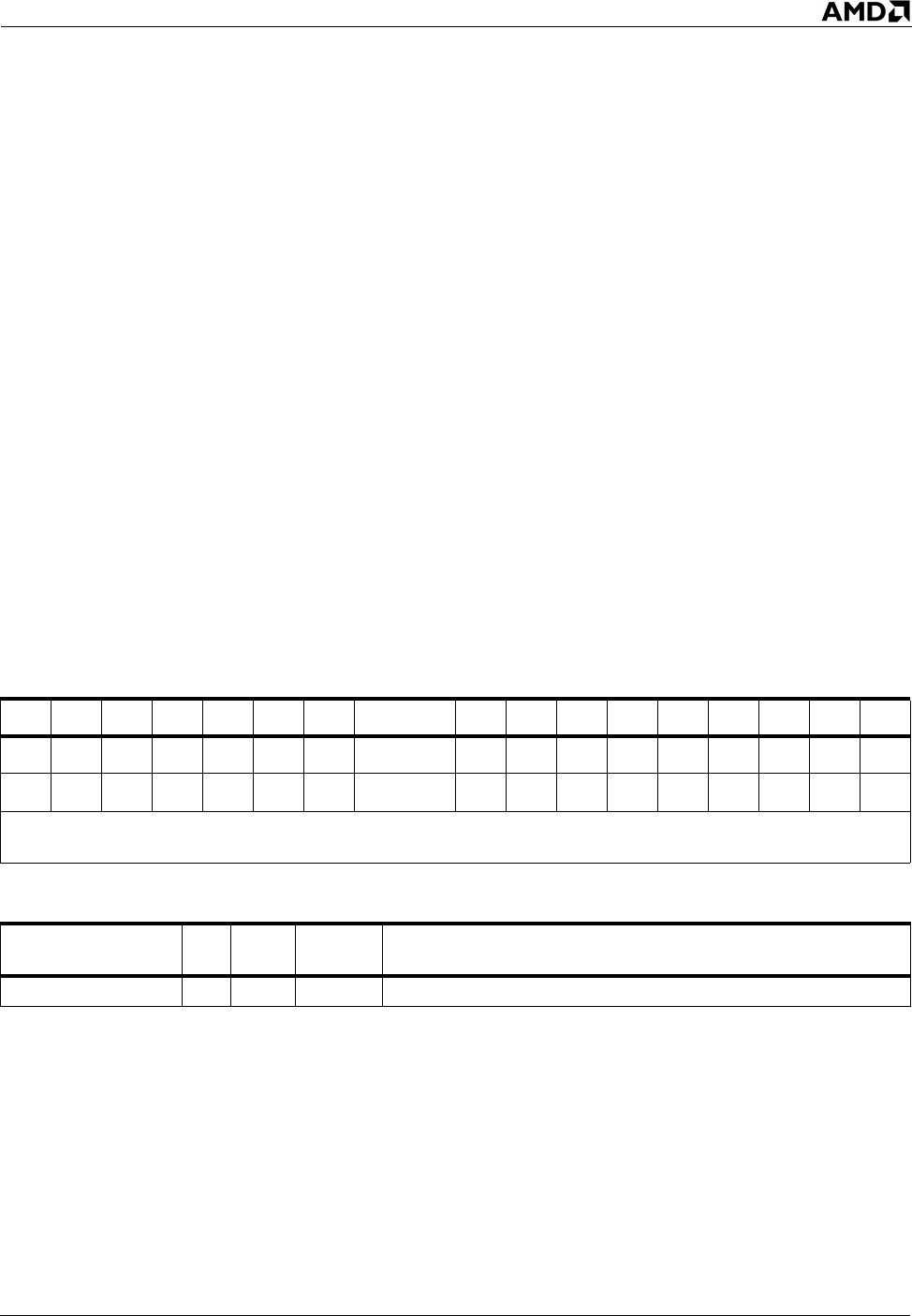
Instruction Reference DAA 105
24594—Rev. 3.14—September 2007 AMD64 Technology
Adjusts the value in the AL register into a packed BCD result and sets the CF and AF flags in the
rFLAGS register to indicate a decimal carry out of either nibble of AL.
Use this instruction to adjust the result of a byte ADD instruction that performed the binary addition of
one 2-digit packed BCD values to another.
The instruction performs the adjustment by adding 06h to AL if the lower nibble is greater than 9 or if
AF = 1. Then 60h is added to AL if the original AL was greater than 99h or if CF = 1.
If the lower nibble of AL was adjusted, the AF flag is set to 1. Otherwise AF is not modified. If the
upper nibble of AL was adjusted, the CF flag is set to 1. Otherwise, CF is not modified. SF, ZF, and PF
are set according to the final value of AL.
Using this instruction in 64-bit mode generates an invalid-opcode (#UD) exception.
rFLAGS Affected
Exceptions
DAA Decimal Adjust after Addition
Mnemonic Opcode Description
DAA 27 Decimal adjust AL.
(Invalid in 64-bit mode.)
ID VIP VIF AC VM RF NT IOPL OF DF IF TF SF ZF AF PF CF
U MMMMM
2120191817161413–1211109876420
Note: Bits 31–22, 15, 5, 3, and 1 are reserved. A flag set to 1 or cleared to 0 is M (modified). Unaffected flags are
blank. Undefined flags are U.
Exception Real
Virtual
8086 Protected Cause of Exception
Invalid opcode, #UD X This instruction was executed in 64-bit mode.

106 DAS Instruction Reference
AMD64 Technology 24594—Rev. 3.14—September 2007
Adjusts the value in the AL register into a packed BCD result and sets the CF and AF flags in the
rFLAGS register to indicate a decimal borrow.
Use this instruction to adjust the result of a byte SUB instruction that performed a binary subtraction of
one 2-digit, packed BCD value from another.
This instruction performs the adjustment by subtracting 06h from AL if the lower nibble is greater than
9 or if AF = 1. Then 60h is subtracted from AL if the original AL was greater than 99h or if CF = 1.
If the adjustment changes the lower nibble of AL, the AF flag is set to 1; otherwise AF is not modified.
If the adjustment results in a borrow for either nibble of AL, the CF flag is set to 1; otherwise CF is not
modified. The SF, ZF, and PF flags are set according to the final value of AL.
Using this instruction in 64-bit mode generates an invalid-opcode (#UD) exception.
Related Instructions
DAA
rFLAGS Affected
Exceptions
DAS Decimal Adjust after Subtraction
Mnemonic Opcode Description
DAS 2F Decimal adjusts AL after subtraction.
(Invalid in 64-bit mode.)
ID VIP VIF AC VM RF NT IOPL OF DF IF TF SF ZF AF PF CF
U MMMMM
2120191817161413–1211109876420
Note: Bits 31–22, 15, 5, 3, and 1 are reserved. A flag set to 1 or cleared to 0 is M (modified). Unaffected flags are blank.
Undefined flags are U.
Exception Real
Virtual
8086 Protected Cause of Exception
Invalid opcode, #UD X This instruction was executed in 64-bit mode.

Instruction Reference DEC 107
24594—Rev. 3.14—September 2007 AMD64 Technology
Subtracts 1 from the specified register or memory location. The CF flag is not affected.
The one-byte forms of this instruction (opcodes 48 through 4F) are used as REX prefixes in 64-bit
mode. See “REX Prefixes” on page 11.
The forms of the DEC instruction that write to memory support the LOCK prefix. For details about the
LOCK prefix, see “Lock Prefix” on page 8.
To perform a decrement operation that updates the CF flag, use a SUB instruction with an immediate
operand of 1.
Related Instructions
INC, SUB
rFLAGS Affected
DEC Decrement by 1
Mnemonic Opcode Description
DEC reg/mem8 FE /1 Decrement the contents of an 8-bit register or memory
location by 1.
DEC reg/mem16 FF /1 Decrement the contents of a 16-bit register or memory
location by 1.
DEC reg/mem32 FF /1 Decrement the contents of a 32-bit register or memory
location by 1.
DEC reg/mem64 FF /1 Decrement the contents of a 64-bit register or memory
location by 1.
DEC reg16 48 +rw Decrement the contents of a 16-bit register by 1.
(See “REX Prefixes” on page 11.)
DEC reg32 48 +rd Decrement the contents of a 32-bit register by 1.
(See “REX Prefixes” on page 11.)
ID VIP VIF AC VM RF NT IOPL OF DF IF TF SF ZF AF PF CF
M MMMM
2120191817161413–1211109876420
Note: Bits 31–22, 15, 5, 3, and 1 are reserved. A flag set to 1 or cleared to 0 is M (modified). Unaffected flags are
blank. Undefined flags are U.

108 DEC Instruction Reference
AMD64 Technology 24594—Rev. 3.14—September 2007
Exceptions
Exception Real
Virtual
8086 Protected Cause of Exception
Stack, #SS X X X A memory address exceeded the stack segment limit or was
non-canonical.
General protection,
#GP
XX XA memory address exceeded the data segment limit or was
non-canonical.
X The destination operand was in a non-writable segment.
X A null data segment was used to reference memory.
Page fault, #PF X X A page fault resulted from the execution of the instruction.
Alignment check,
#AC XX
An unaligned memory reference was performed while
alignment checking was enabled.
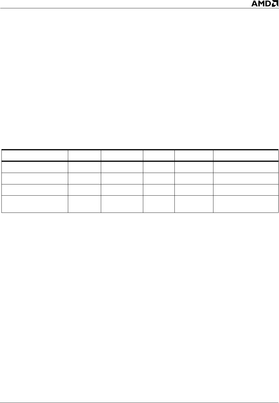
Instruction Reference DIV 109
24594—Rev. 3.14—September 2007 AMD64 Technology
Divides the unsigned value in a register by the unsigned value in the specified register or memory
location. The register to be divided depends on the size of the divisor.
When dividing a word, the dividend is in the AX register. The instruction stores the quotient in the AL
register and the remainder in the AH register.
When dividing a doubleword, quadword, or double quadword, the most-significant word of the
dividend is in the rDX register and the least-significant word is in the rAX register. After the division,
the instruction stores the quotient in the rAX register and the remainder in the rDX register.
The following table summarizes the action of this instruction:
The instruction truncates non-integral results towards 0 and the remainder is always less than the
divisor. An overflow generates a #DE (divide error) exception, rather than setting the CF flag.
Division by zero generates a divide-by-zero exception.
Related Instructions
MUL
DIV Unsigned Divide
Division Size Dividend Divisor Quotient Remainder Maximum Quotient
Word/byte AX reg/mem8 AL AH 255
Doubleword/word DX:AX reg/mem16 AX DX 65,535
Quadword/doubleword EDX:EAX reg/mem32 EAX EDX 2 32 –1
Double quadword/
quadword RDX:RAX reg/mem64 RAX RDX 264 –1
Mnemonic Opcode Description
DIV reg/mem8 F6 /6
Perform unsigned division of AX by the contents of an 8-
bit register or memory location and store the quotient in
AL and the remainder in AH.
DIV reg/mem16 F7 /6
Perform unsigned division of DX:AX by the contents of a
16-bit register or memory operand store the quotient in
AX and the remainder in DX.
DIV reg/mem32 F7 /6
Perform unsigned division of EDX:EAX by the contents
of a 32-bit register or memory location and store the
quotient in EAX and the remainder in EDX.
DIV reg/mem64 F7 /6
Perform unsigned division of RDX:RAX by the contents
of a 64-bit register or memory location and store the
quotient in RAX and the remainder in RDX.

110 DIV Instruction Reference
AMD64 Technology 24594—Rev. 3.14—September 2007
rFLAGS Affected
Exceptions
ID VIP VIF AC VM RF NT IOPL OF DF IF TF SF ZF AF PF CF
U UUUUU
2120191817161413–1211109876420
Note: Bits 31–22, 15, 5, 3, and 1 are reserved. A flag set to 1 or cleared to 0 is M (modified). Unaffected flags are
blank. Undefined flags are U.
Exception Real
Virtual
8086 Protected Cause of Exception
Divide by zero, #DE X X X The divisor operand was 0.
X X X The quotient was too large for the designated register.
Stack, #SS X X X A memory address exceeded the stack segment limit or was
non-canonical.
General protection,
#GP
XX XA memory address exceeded a data segment limit or was non-
canonical.
X A null data segment was used to reference memory.
Page fault, #PF X X A page fault resulted from the execution of the instruction.
Alignment check,
#AC XX
An unaligned memory reference was performed while
alignment checking was enabled.

Instruction Reference ENTER 111
24594—Rev. 3.14—September 2007 AMD64 Technology
Creates a stack frame for a procedure.
The first operand specifies the size of the stack frame allocated by the instruction.
The second operand specifies the nesting level (0 to 31—the value is automatically masked to 5 bits).
For nesting levels of 1 or greater, the processor copies earlier stack frame pointers before adjusting the
stack pointer. This action provides a called procedure with access points to other nested stack frames.
The 32-bit enter N, 0 (a nesting level of 0) instruction is equivalent to the following 32-bit
instruction sequence:
push ebp ; save current EBP
mov ebp, esp ; set stack frame pointer value
sub esp, N ; allocate space for local variables
The ENTER and LEAVE instructions provide support for block structured languages. The LEAVE
instruction releases the stack frame on returning from a procedure.
In 64-bit mode, the operand size of ENTER defaults to 64 bits, and there is no prefix available for
encoding a 32-bit operand size.
Action
// See “Pseudocode Definitions” on page 41.
ENTER_START:
temp_ALLOC_SPACE = word-sized immediate specified in the instruction
(first operand), zero-extended to 64 bits
temp_LEVEL = byte-sized immediate specified in the instruction
(second operand), zero-extended to 64 bits
temp_LEVEL = temp_LEVEL AND 0x1f
// only keep 5 bits of level count
PUSH.v old_RBP
temp_RBP = RSP // This value of RSP will eventually be loaded
// into RBP.
IF (temp_LEVEL>0) // Push "temp_LEVEL" parameters to the stack.
{
FOR (I=1; I<temp_LEVEL; I++)
ENTER Create Procedure Stack Frame
Mnemonic Opcode Description
ENTER imm16, 0 C8 iw 00 Create a procedure stack frame.
ENTER imm16, 1 C8 iw 01 Create a nested stack frame for a procedure.
ENTER imm16, imm8 C8 iw ib Create a nested stack frame for a procedure.
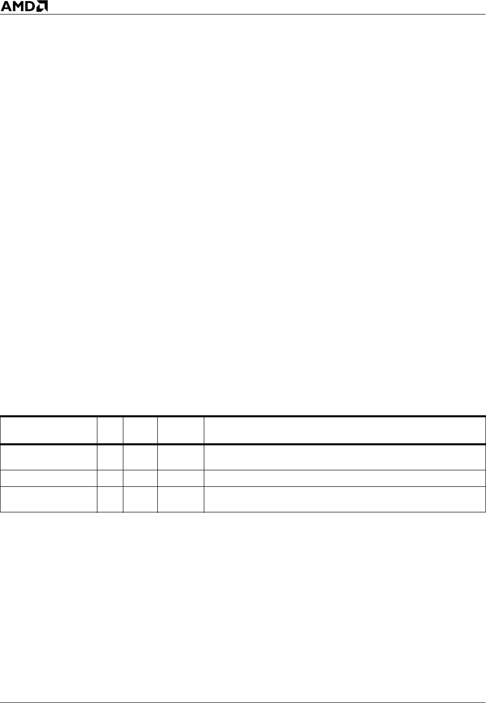
112 ENTER Instruction Reference
AMD64 Technology 24594—Rev. 3.14—September 2007
// All but one of the parameters are copied
// from higher up on the stack.
{
temp_DATA = READ_MEM.v [SS:old_RBP-I*V]
PUSH.v temp_DATA
}
PUSH.v temp_RBP // The last parameter is the offset of the old
// value of RSP on the stack.
}
RSP.s = RSP - temp_ALLOC_SPACE // Leave "temp_ALLOC_SPACE" free bytes on
// the stack
WRITE_MEM.v [SS:RSP.s] = temp_unused // ENTER finishes with a memory write
// check on the final stack pointer,
// but no write actually occurs.
RBP.v = temp_RBP
EXIT
Related Instructions
LEAVE
rFLAGS Affected
None
Exceptions
Exception Real
Virtual
8086 Protected Cause of Exception
Stack, #SS X X X A memory address exceeded the stack-segment limit or was
non-canonical.
Page fault, #PF X X A page fault resulted from the execution of the instruction.
Alignment check,
#AC XX
An unaligned memory reference was performed while
alignment checking was enabled.

Instruction Reference IDIV 113
24594—Rev. 3.14—September 2007 AMD64 Technology
Divides the signed value in a register by the signed value in the specified register or memory location.
The register to be divided depends on the size of the divisor.
When dividing a word, the dividend is in the AX register. The instruction stores the quotient in the AL
register and the remainder in the AH register.
When dividing a doubleword, quadword, or double quadword, the most-significant word of the
dividend is in the rDX register and the least-significant word is in the rAX register. After the division,
the instruction stores the quotient in the rAX register and the remainder in the rDX register.
The following table summarizes the action of this instruction:
The instruction truncates non-integral results towards 0. The sign of the remainder is always the same
as the sign of the dividend, and the absolute value of the remainder is less than the absolute value of the
divisor. An overflow generates a #DE (divide error) exception, rather than setting the OF flag.
To avoid overflow problems, precede this instruction with a CBW, CWD, CDQ, or CQO instruction to
sign-extend the dividend.
IDIV Signed Divide
Division Size Dividend Divisor Quotient Remainder Quotient Range
Word/byte AX reg/mem8 AL AH –128 to +127
Doubleword/word DX:AX reg/mem16 AX DX –32,768 to +32,767
Quadword/doubleword EDX:EAX reg/mem32 EAX EDX –2 31 to 2 31–1
Double quadword/
quadword RDX:RAX reg/mem64 RAX RDX –2 63 to 263–1
Mnemonic Opcode Description
IDIV reg/mem8 F6 /7
Perform signed division of AX by the contents of an 8-bit
register or memory location and store the quotient in AL
and the remainder in AH.
IDIV reg/mem16 F7 /7
Perform signed division of DX:AX by the contents of a
16-bit register or memory location and store the quotient
in AX and the remainder in DX.
IDIV reg/mem32 F7 /7
Perform signed division of EDX:EAX by the contents of
a 32-bit register or memory location and store the
quotient in EAX and the remainder in EDX.
IDIV reg/mem64 F7 /7
Perform signed division of RDX:RAX by the contents of
a 64-bit register or memory location and store the
quotient in RAX and the remainder in RDX.
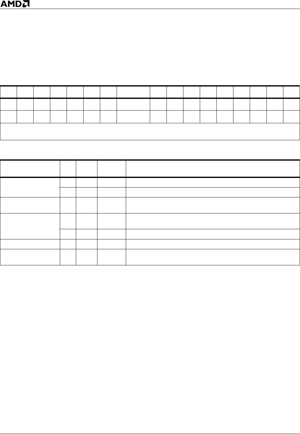
114 IDIV Instruction Reference
AMD64 Technology 24594—Rev. 3.14—September 2007
Related Instructions
IMUL
rFLAGS Affected
Exceptions
ID VIP VIF AC VM RF NT IOPL OF DF IF TF SF ZF AF PF CF
U UUUUU
2120191817161413–1211109876420
Note: Bits 31–22, 15, 5, 3, and 1 are reserved. A flag set to 1 or cleared to 0 is M (modified). Unaffected flags are
blank. Undefined flags are U.
Exception Real
Virtual
8086 Protected Cause of Exception
Divide by zero, #DE X X X The divisor operand was 0.
X X X The quotient was too large for the designated register.
Stack, #SS X X X A memory address exceeded the stack segment limit or was
non-canonical.
General protection,
#GP
XX XA memory address exceeded a data segment limit or was non-
canonical.
X A null data segment was used to reference memory.
Page fault, #PF X X A page fault resulted from the execution of the instruction.
Alignment check,
#AC XX
An unaligned memory reference was performed while
alignment checking was enabled.

Instruction Reference IMUL 115
24594—Rev. 3.14—September 2007 AMD64 Technology
Multiplies two signed operands. The number of operands determines the form of the instruction.
If a single operand is specified, the instruction multiplies the value in the specified general-purpose
register or memory location by the value in the AL, AX, EAX, or RAX register (depending on the
operand size) and stores the product in AX, DX:AX, EDX:EAX, or RDX:RAX, respectively.
If two operands are specified, the instruction multiplies the value in a general-purpose register (first
operand) by an immediate value or the value in a general-purpose register or memory location (second
operand) and stores the product in the first operand location.
If three operands are specified, the instruction multiplies the value in a general-purpose register or
memory location (second operand), by an immediate value (third operand) and stores the product in a
register (first operand).
The IMUL instruction sign-extends an immediate operand to the length of the other register/memory
operand.
The CF and OF flags are set if, due to integer overflow, the double-width multiplication result cannot
be represented in the half-width destination register. Otherwise the CF and OF flags are cleared.
IMUL Signed Multiply
Mnemonic Opcode Description
IMUL reg/mem8 F6 /5
Multiply the contents of AL by the contents of an 8-bit
memory or register operand and put the signed result in
AX.
IMUL reg/mem16 F7 /5
Multiply the contents of AX by the contents of a 16-bit
memory or register operand and put the signed result in
DX:AX.
IMUL reg/mem32 F7 /5
Multiply the contents of EAX by the contents of a 32-bit
memory or register operand and put the signed result in
EDX:EAX.
IMUL reg/mem64 F7 /5
Multiply the contents of RAX by the contents of a 64-bit
memory or register operand and put the signed result in
RDX:RAX.
IMUL reg16, reg/mem16 0F AF /r
Multiply the contents of a 16-bit destination register by
the contents of a 16-bit register or memory operand and
put the signed result in the 16-bit destination register.
IMUL reg32, reg/mem32 0F AF /r
Multiply the contents of a 32-bit destination register by
the contents of a 32-bit register or memory operand and
put the signed result in the 32-bit destination register.
IMUL reg64, reg/mem64 0F AF /r
Multiply the contents of a 64-bit destination register by
the contents of a 64-bit register or memory operand and
put the signed result in the 64-bit destination register.
IMUL reg16, reg/mem16, imm8 6B /r ib
Multiply the contents of a 16-bit register or memory
operand by a sign-extended immediate byte and put the
signed result in the 16-bit destination register.
116 IMUL Instruction Reference
AMD64 Technology 24594—Rev. 3.14—September 2007
Related Instructions
IDIV
rFLAGS Affected
Exceptions
IMUL reg32, reg/mem32, imm8 6B /r ib
Multiply the contents of a 32-bit register or memory
operand by a sign-extended immediate byte and put the
signed result in the 32-bit destination register.
IMUL reg64, reg/mem64, imm8 6B /r ib
Multiply the contents of a 64-bit register or memory
operand by a sign-extended immediate byte and put the
signed result in the 64-bit destination register.
IMUL reg16, reg/mem16,
imm16 69 /r iw
Multiply the contents of a 16-bit register or memory
operand by a sign-extended immediate word and put the
signed result in the 16-bit destination register.
IMUL reg32, reg/mem32,
imm32 69 /r id
Multiply the contents of a 32-bit register or memory
operand by a sign-extended immediate double and put
the signed result in the 32-bit destination register.
IMUL reg64, reg/mem64,
imm32 69 /r id
Multiply the contents of a 64-bit register or memory
operand by a sign-extended immediate double and put
the signed result in the 64-bit destination register.
ID VIP VIF AC VM RF NT IOPL OF DF IF TF SF ZF AF PF CF
M UUUUM
2120191817161413–1211109876420
Note: Bits 31–22, 15, 5, 3, and 1 are reserved. A flag set to 1 or cleared to 0 is M (modified). Unaffected flags are
blank. Undefined flags are U.
Exception Real
Virtual
8086 Protected Cause of Exception
Stack, #SS X X X A memory address exceeded the stack segment limit or was
non-canonical.
General protection,
#GP
XX XA memory address exceeded a data segment limit or was non-
canonical.
X A null data segment was used to reference memory.
Page fault, #PF X X A page fault resulted from the execution of the instruction.
Alignment check,
#AC XX
An unaligned memory reference was performed while
alignment checking was enabled.
Mnemonic Opcode Description

Instruction Reference IN 117
24594—Rev. 3.14—September 2007 AMD64 Technology
Transfers a byte, word, or doubleword from an I/O port (second operand) to the AL, AX or EAX
register (first operand). The port address can be an 8-bit immediate value (00h to FFh) or contained in
the DX register (0000h to FFFFh).
The port is in the processor’s I/O address space. For 8-bit I/O port accesses, the opcode determines the
port size. For 16-bit and 32-bit accesses, the operand-size attribute determines the port size. If the
operand size is 64-bits, IN reads only 32 bits from the I/O port.
If the CPL is higher than IOPL, or the mode is virtual mode, IN checks the I/O permission bitmap in
the TSS before allowing access to the I/O port. (See Volume 2 for details on the TSS I/O permission
bitmap.)
Related Instructions
INSx, OUT, OUTSx
rFLAGS Affected
None
Exceptions
IN Input from Port
Mnemonic Opcode Description
IN AL, imm8 E4 ib Input a byte from the port at the address specified by
imm8 and put it into the AL register.
IN AX, imm8 E5 ib Input a word from the port at the address specified by
imm8 and put it into the AX register.
IN EAX, imm8 E5 ib Input a doubleword from the port at the address
specified by imm8 and put it into the EAX register.
IN AL, DX EC Input a byte from the port at the address specified by the
DX register and put it into the AL register.
IN AX, DX ED Input a word from the port at the address specified by
the DX register and put it into the AX register.
IN EAX, DX ED
Input a doubleword from the port at the address
specified by the DX register and put it into the EAX
register.
Exception Real
Virtual
8086 Protected Cause of Exception
General protection,
#GP
XOne or more I/O permission bits were set in the TSS for the
accessed port.
XThe CPL was greater than the IOPL and one or more I/O
permission bits were set in the TSS for the accessed port.
Page fault, #PF X X A page fault resulted from the execution of the instruction.

118 INC Instruction Reference
AMD64 Technology 24594—Rev. 3.14—September 2007
Adds 1 to the specified register or memory location. The CF flag is not affected, even if the operand is
incremented to 0000.
The one-byte forms of this instruction (opcodes 40 through 47) are used as REX prefixes in 64-bit
mode. See “REX Prefixes” on page 11.
The forms of the INC instruction that write to memory support the LOCK prefix. For details about the
LOCK prefix, see “Lock Prefix” on page 8.
To perform an increment operation that updates the CF flag, use an ADD instruction with an
immediate operand of 1.
Related Instructions
ADD, DEC
INC Increment by 1
Mnemonic Opcode Description
INC reg/mem8 FE /0 Increment the contents of an 8-bit register or memory
location by 1.
INC reg/mem16 FF /0 Increment the contents of a 16-bit register or memory
location by 1.
INC reg/mem32 FF /0 Increment the contents of a 32-bit register or memory
location by 1.
INC reg/mem64 FF /0 Increment the contents of a 64-bit register or memory
location by 1.
INC reg16 40 +rw
Increment the contents of a 16-bit register by 1.
(These opcodes are used as REX prefixes in 64-bit
mode. See “REX Prefixes” on page 11.)
INC reg32 40 +rd
Increment the contents of a 32-bit register by 1.
(These opcodes are used as REX prefixes in 64-bit
mode. See “REX Prefixes” on page 11.)

Instruction Reference INC 119
24594—Rev. 3.14—September 2007 AMD64 Technology
rFLAGS Affected
Exceptions
ID VIP VIF AC VM RF NT IOPL OF DF IF TF SF ZF AF PF CF
M MMMM
2120191817161413–1211109876420
Note: Bits 31–22, 15, 5, 3, and 1 are reserved. A flag set to 1 or cleared to 0 is M (modified). Unaffected flags are
blank. Undefined flags are U.
Exception Real
Virtual
8086 Protected Cause of Exception
Stack, #SS X X X A memory address exceeded the stack segment limit or was
non-canonical.
General protection,
#GP
XX XA memory address exceeded a data segment limit or was non-
canonical.
X The destination operand was in a non-writable segment.
X A null data segment was used to reference memory.
Page fault, #PF X X A page fault resulted from the execution of the instruction.
Alignment check,
#AC XX
An unaligned memory reference was performed while
alignment checking was enabled.

120 INSx Instruction Reference
AMD64 Technology 24594—Rev. 3.14—September 2007
Transfers data from the I/O port specified in the DX register to an input buffer specified in the rDI
register and increments or decrements the rDI register according to the setting of the DF flag in the
rFLAGS register.
If the DF flag is 0, the instruction increments rDI by 1, 2, or 4, depending on the number of bytes read.
If the DF flag is 1, it decrements the pointer by 1, 2, or 4.
In 16-bit and 32-bit mode, the INS instruction always uses ES as the data segment. The ES segment
cannot be overridden with a segment override prefix. In 64-bit mode, INS always uses the
unsegmented memory space.
The INS instructions use the explicit memory operand (first operand) to determine the size of the I/O
port, but always use ES:[rDI] for the location of the input buffer. The explicit register operand (second
operand) specifies the I/O port address and must always be DX.
The INSB, INSW, and INSD instructions copy byte, word, and doubleword data, respectively, from the
I/O port (0000h to FFFFh) specified in the DX register to the input buffer specified in the ES:rDI
registers.
If the operand size is 64-bits, the instruction behaves as if the operand size were 32-bits.
If the CPL is higher than the IOPL or the mode is virtual mode, INSx checks the I/O permission bitmap
in the TSS before allowing access to the I/O port. (See volume 2 for details on the TSS I/O permission
bitmap.)
The INSx instructions support the REP prefix for block input of rCX bytes, words, or doublewords.
For details about the REP prefix, see “Repeat Prefixes” on page 9.
INS
INSB
INSW
INSD
Input String
Mnemonic Opcode Description
INS mem8, DX 6C
Input a byte from the port specified by DX, put it into the
memory location specified in ES:rDI, and then
increment or decrement rDI.
INS mem16, DX 6D
Input a word from the port specified by DX register, put it
into the memory location specified in ES:rDI, and then
increment or decrement rDI.
INS mem32, DX 6D
Input a doubleword from the port specified by DX, put it
into the memory location specified in ES:rDI, and then
increment or decrement rDI.
INSB 6C
Input a byte from the port specified by DX, put it into the
memory location specified in ES:rDI, and then
increment or decrement rDI.
Instruction Reference INSx 121
24594—Rev. 3.14—September 2007 AMD64 Technology
Related Instructions
IN, OUT, OUTSx
rFLAGS Affected
None
Exceptions
INSW 6D
Input a word from the port specified by DX, put it into the
memory location specified in ES:rDI, and then
increment or decrement rDI.
INSD 6D
Input a doubleword from the port specified by DX, put it
into the memory location specified in ES:rDI, and then
increment or decrement rDI.
Exception Real
Virtual
8086 Protected Cause of Exception
General protection,
#GP
XX XA memory address exceeded a data segment limit or was non-
canonical.
XOne or more I/O permission bits were set in the TSS for the
accessed port.
XThe CPL was greater than the IOPL and one or more I/O
permission bits were set in the TSS for the accessed port.
X A null data segment was used to reference memory.
X The destination operand was in a non-writable segment.
Page fault, #PF X X A page fault resulted from the execution of the instruction.
Alignment check,
#AC XX
An unaligned memory reference was performed while
alignment checking was enabled.
Mnemonic Opcode Description

122 INT Instruction Reference
AMD64 Technology 24594—Rev. 3.14—September 2007
Transfers execution to the interrupt handler specified by an 8-bit unsigned immediate value. This value
is an interrupt vector number (00h to FFh), which the processor uses as an index into the interrupt-
descriptor table (IDT).
For detailed descriptions of the steps performed by INTn instructions, see the following:
•Legacy-Mode Interrupts: “Legacy Protected-Mode Interrupt Control Transfers” in Volume 2.
•Long-Mode Interrupts: “Long-Mode Interrupt Control Transfers” in Volume 2.
See also the descriptions of the INT3 instruction on page 259 and the INTO instruction on page 129.
Action
// See “Pseudocode Definitions” on page 41.
INT_N_START:
IF (REAL_MODE)
INT_N_REAL
ELSIF (PROTECTED_MODE)
INT_N_PROTECTED
ELSE // (VIRTUAL_MODE)
INT_N_VIRTUAL
INT_N_REAL:
temp_int_n_vector = byte-sized interrupt vector specified in the instruction,
zero-extended to 64 bits
temp_RIP = READ_MEM.w [idt:temp_int_n_vector*4]
// read target CS:RIP from the real-mode idt
temp_CS = READ_MEM.w [idt:temp_int_n_vector*4+2]
PUSH.w old_RFLAGS
PUSH.w old_CS
PUSH.w next_RIP
IF (temp_RIP>CS.limit)
EXCEPTION [#GP]
CS.sel = temp_CS
CS.base = temp_CS SHL 4
RFLAGS.AC,TF,IF,RF cleared
INT Interrupt to Vector
Mnemonic Opcode Description
INT imm8 CD ib Call interrupt service routine specified by interrupt
vector imm8.

Instruction Reference INT 123
24594—Rev. 3.14—September 2007 AMD64 Technology
RIP = temp_RIP
EXIT
INT_N_PROTECTED:
temp_int_n_vector = byte-sized interrupt vector specified in the instruction,
zero-extended to 64 bits
temp_idt_desc = READ_IDT (temp_int_n_vector)
IF (temp_idt_desc.attr.type = ’taskgate’)
TASK_SWITCH // using tss selector in the task gate as the target tss
IF (LONG_MODE) // The size of the gate controls the size of the
// stack pushes.
V=8-byte // Long mode only uses 64-bit gates.
ELSIF ((temp_idt_desc.attr.type = ’intgate32’)
|| (temp_idt_desc.attr.type = ’trapgate32’))
V=4-byte // Legacy mode, using a 32-bit gate
ELSE // gate is intgate16 or trapgate16
V=2-byte // Legacy mode, using a 16-bit gate
temp_RIP = temp_idt_desc.offset
IF (LONG_MODE)
// In long mode, we need to read the 2nd half of a
// 16-byte interrupt-gate from the IDT, to get the
// upper 32 bits of the target RIP
{
temp_upper = READ_MEM.q [idt:temp_int_n_vector*16+8]
temp_RIP = tempRIP + (temp_upper SHL 32) // concatenate both halves of RIP
}
CS = READ_DESCRIPTOR (temp_idt_desc.segment, intcs_chk)
IF (CS.attr.conforming=1)
temp_CPL = CPL
ELSE
temp_CPL = CS.attr.dpl
IF (CPL=temp_CPL) // no privilege-level change
{
IF (LONG_MODE)
{
IF (temp_idt_desc.ist!=0)
// In long mode, if the IDT gate specifies an IST pointer,
// a stack-switch is always done
RSP = READ_MEM.q [tss:ist_index*8+28]
RSP = RSP AND 0xFFFFFFFFFFFFFFF0

124 INT Instruction Reference
AMD64 Technology 24594—Rev. 3.14—September 2007
// In long mode, interrupts/exceptions align RSP to a
// 16-byte boundary
PUSH.q old_SS // In long mode, SS:RSP is always pushed to the stack
PUSH.q old_RSP
}
PUSH.v old_RFLAGS
PUSH.v old_CS
PUSH.v next_RIP
IF ((64BIT_MODE) && (temp_RIP is non-canonical)
|| (!64BIT_MODE) && (temp_RIP > CS.limit))
EXCEPTION [#GP(0)]
RFLAGS.VM,NT,TF,RF cleared
RFLAGS.IF cleared if interrupt gate
RIP = temp_RIP
EXIT
}
ELSE // (CPL > temp_CPL), changing privilege level
{
CPL = temp_CPL
temp_SS_desc:temp_RSP = READ_INNER_LEVEL_STACK_POINTER
(CPL, temp_idt_desc.ist)
IF (LONG_MODE)
temp_RSP = temp_RSP AND 0xFFFFFFFFFFFFFFF0
// in long mode, interrupts/exceptions align rsp
// to a 16-byte boundary
RSP.q = temp_RSP
SS = temp_SS_desc
PUSH.v old_SS // #SS on the following pushes uses SS.sel as error code
PUSH.v old_RSP
PUSH.v old_RFLAGS
PUSH.v old_CS
PUSH.v next_RIP
IF ((64BIT_MODE) && (temp_RIP is non-canonical)
|| (!64BIT_MODE) && (temp_RIP > CS.limit))
EXCEPTION [#GP(0)]
RFLAGS.VM,NT,TF,RF cleared
RFLAGS.IF cleared if interrupt gate
RIP = temp_RIP
EXIT
}

Instruction Reference INT 125
24594—Rev. 3.14—September 2007 AMD64 Technology
INT_N_VIRTUAL:
temp_int_n_vector = byte-sized interrupt vector specified in the instruction,
zero-extended to 64 bits
IF (CR4.VME=0) // vme isn’t enabled
{
IF (RFLAGS.IOPL=3)
INT_N_VIRTUAL_TO_PROTECTED
ELSE
EXCEPTION [#GP(0)]
}
temp_IRB_BASE = READ_MEM.w [tss:102] - 32
// check the vme Int-n Redirection Bitmap (IRB), to see
// if we should redirect this interrupt to a virtual-mode
// handler
temp_VME_REDIRECTION_BIT = READ_BIT_ARRAY ([tss:temp_IRB_BASE],
temp_int_n_vector)
IF (temp_VME_REDIRECTION_BIT=1)
{ // the virtual-mode int-n bitmap bit is set, so don’t
// redirect this interrupt
IF (RFLAGS.IOPL=3)
INT_N_VIRTUAL_TO_PROTECTED
ELSE
EXCEPTION [#GP(0)]
}
ELSE // redirect interrupt through virtual-mode idt
{
temp_RIP = READ_MEM.w [0:temp_int_n_vector*4]
// read target CS:RIP from the virtual-mode idt at
// linear address 0
temp_CS = READ_MEM.w [0:temp_int_n_vector*4+2]
IF (RFLAGS.IOPL < 3)
old_RFLAGS = old_RFLAGS with VIF bit shifted into IF bit, and IOPL = 3
PUSH.w old_RFLAGS
PUSH.w old_CS
PUSH.w next_RIP
CS.sel = temp_CS
CS.base = temp_CS SHL 4
RFLAGS.TF,RF cleared
RIP = temp_RIP // RFLAGS.IF cleared if IOPL = 3
// RFLAGS.VIF cleared if IOPL < 3
EXIT
}

126 INT Instruction Reference
AMD64 Technology 24594—Rev. 3.14—September 2007
INT_N_VIRTUAL_TO_PROTECTED:
temp_idt_desc = READ_IDT (temp_int_n_vector)
IF (temp_idt_desc.attr.type = ’taskgate’)
TASK_SWITCH // using tss selector in the task gate as the target tss
IF ((temp_idt_desc.attr.type = ’intgate32’)
|| (temp_idt_desc.attr.type = ’trapgate32’))
// the size of the gate controls the size of the stack pushes
V=4-byte // legacy mode, using a 32-bit gate
ELSE // gate is intgate16 or trapgate16
V=2-byte // legacy mode, using a 16-bit gate
temp_RIP = temp_idt_desc.offset
CS = READ_DESCRIPTOR (temp_idt_desc.segment, intcs_chk)
IF (CS.attr.dpl!=0) // Handler must run at CPL 0.
EXCEPTION [#GP(CS.sel)]
CPL = 0
temp_ist = 0 // Legacy mode doesn’t use ist pointers
temp_SS_desc:temp_RSP = READ_INNER_LEVEL_STACK_POINTER (CPL, temp_ist)
RSP.q = temp_RSP
SS = temp_SS_desc
PUSH.v old_GS // #SS on the following pushes use SS.sel as error code.
PUSH.v old_FS
PUSH.v old_DS
PUSH.v old_ES
PUSH.v old_SS
PUSH.v old_RSP
PUSH.v old_RFLAGS // Pushed with RF clear.
PUSH.v old_CS
PUSH.v next_RIP
IF (temp_RIP > CS.limit)
EXCEPTION [#GP(0)]
DS = NULL // can’t use virtual-mode selectors in protected mode
ES = NULL // can’t use virtual-mode selectors in protected mode
FS = NULL // can’t use virtual-mode selectors in protected mode
GS = NULL // can’t use virtual-mode selectors in protected mode
RFLAGS.VM,NT,TF,RF cleared
RFLAGS.IF cleared if interrupt gate
RIP = temp_RIP
EXIT

Instruction Reference INT 127
24594—Rev. 3.14—September 2007 AMD64 Technology
Related Instructions
INT 3, INTO, BOUND
rFLAGS Affected
If a task switch occurs, all flags are modified. Otherwise settings are as follows:
Exceptions
ID VIP VIF AC VM RF NT IOPL OF DF IF TF SF ZF AF PF CF
MMM 0 M M 0
2120191817161413–1211109876420
Note: Bits 31–22, 15, 5, 3, and 1 are reserved. A flag set to 1 or cleared to 0 is M (modified). Unaffected flags are
blank. Undefined flags are U.
Exception Real
Virtual
8086 Protected Cause of Exception
Invalid TSS, #TS
(selector)
XX
As part of a stack switch, the target stack segment selector or
rSP in the TSS was beyond the TSS limit.
XX
As part of a stack switch, the target stack segment selector in
the TSS was a null selector.
XX
As part of a stack switch, the target stack segment selector’s
TI bit was set, but the LDT selector was a null selector.
XX
As part of a stack switch, the target stack segment selector in
the TSS was beyond the limit of the GDT or LDT descriptor
table.
XX
As part of a stack switch, the target stack segment selector in
the TSS contained a RPL that was not equal to its DPL.
XX
As part of a stack switch, the target stack segment selector in
the TSS contained a DPL that was not equal to the CPL of the
code segment selector.
XX
As part of a stack switch, the target stack segment selector in
the TSS was not a writable segment.
Segment not
present, #NP
(selector)
XX
The accessed code segment, interrupt gate, trap gate, task
gate, or TSS was not present.
Stack, #SS X X X A memory address exceeded the stack segment limit or was
non-canonical, and no stack switch occurred.
Stack, #SS
(selector)
XX
After a stack switch, a memory address exceeded the stack
segment limit or was non-canonical.
XX
As part of a stack switch, the SS register was loaded with a
non-null segment selector and the segment was marked not
present.

128 INT Instruction Reference
AMD64 Technology 24594—Rev. 3.14—September 2007
General protection,
#GP
XX XA memory address exceeded a data segment limit or was non-
canonical.
XX XThe target offset exceeded the code segment limit or was non-
canonical.
X The IOPL was less than 3 and CR4.VME was 0.
X
IOPL was less than 3, CR4.VME was 1, and the
corresponding bit in the VME interrupt redirection bitmap was
1.
General protection,
#GP
(selector)
X X X The interrupt vector was beyond the limit of IDT.
XX
The descriptor in the IDT was not an interrupt, trap, or task
gate in legacy mode or not a 64-bit interrupt or trap gate in
long mode.
XX
The DPL of the interrupt, trap, or task gate descriptor was less
than the CPL.
XX
The segment selector specified by the interrupt or trap gate
had its TI bit set, but the LDT selector was a null selector.
XX
The segment descriptor specified by the interrupt or trap gate
exceeded the descriptor table limit or was a null selector.
XX
The segment descriptor specified by the interrupt or trap gate
was not a code segment in legacy mode, or not a 64-bit code
segment in long mode.
XThe DPL of the segment specified by the interrupt or trap gate
was greater than the CPL.
XThe DPL of the segment specified by the interrupt or trap gate
pointed was not 0 or it was a conforming segment.
Page fault, #PF X X A page fault resulted from the execution of the instruction.
Alignment check,
#AC XX
An unaligned memory reference was performed while
alignment checking was enabled.
Exception Real
Virtual
8086 Protected Cause of Exception

Instruction Reference INTO 129
24594—Rev. 3.14—September 2007 AMD64 Technology
Checks the overflow flag (OF) in the rFLAGS register and calls the overflow exception (#OF) handler
if the OF flag is set to 1. This instruction has no effect if the OF flag is cleared to 0. The INTO
instruction detects overflow in signed number addition. See AMD64 Architecture Programmer’s
Manual Volume 1: Application Programming for more information on the OF flag.
Using this instruction in 64-bit mode generates an invalid-opcode exception.
For detailed descriptions of the steps performed by INT instructions, see the following:
•Legacy-Mode Interrupts: “Legacy Protected-Mode Interrupt Control Transfers” in Volume 2.
•Long-Mode Interrupts: “Long-Mode Interrupt Control Transfers” in Volume 2.
Action
IF (64BIT_MODE)
EXCEPTION[#UD]
IF (RFLAGS.OF = 1) // #OF is a trap, and pushes the rIP of the instruction
EXCEPTION [#OF] // following INTO.
EXIT
Related Instructions
INT, INT 3, BOUND
rFLAGS Affected
None.
Exceptions
INTO Interrupt to Overflow Vector
Mnemonic Opcode Description
INTO CE Call overflow exception if the overflow flag is set.
(Invalid in 64-bit mode.)
Exception Real
Virtual
8086 Protected Cause of Exception
Overflow, #OF X X X The INTO instruction was executed with 0F set to 1.
Invalid opcode, #UD X Instruction was executed in 64-bit mode.

130 Jcc Instruction Reference
AMD64 Technology 24594—Rev. 3.14—September 2007
Checks the status flags in the rFLAGS register and, if the flags meet the condition specified by the
condition code in the mnemonic (cc), jumps to the target instruction located at the specified relative
offset. Otherwise, execution continues with the instruction following the Jcc instruction.
Unlike the unconditional jump (JMP), conditional jump instructions have only two forms—short and
near conditional jumps. Different opcodes correspond to different forms of one instruction. For
example, the JO instruction (jump if overflow) has opcode 0Fh 80h for its near form and 70h for its
short form, but the mnemonic is the same for both forms. The only difference is that the near form has
a 16- or 32-bit relative displacement, while the short form always has an 8-bit relative displacement.
Mnemonics are provided to deal with the programming semantics of both signed and unsigned
numbers. Instructions tagged A (above) and B (below) are intended for use in unsigned integer code;
those tagged G (greater) and L (less) are intended for use in signed integer code.
If the jump is taken, the signed displacement is added to the rIP (of the following instruction) and the
result is truncated to 16, 32, or 64 bits, depending on operand size.
In 64-bit mode, the operand size defaults to 64 bits. The processor sign-extends the 8-bit or 32-bit
displacement value to 64 bits before adding it to the RIP.
These instructions cannot perform far jumps (to other code segments). To create a far-conditional-
jump code sequence corresponding to a high-level language statement like:
IF A = B THEN GOTO FarLabel
where FarLabel is located in another code segment, use the opposite condition in a conditional short
jump before an unconditional far jump. Such a code sequence might look like:
cmp A,B ; compare operands
jne NextInstr ; continue program if not equal
jmp far FarLabel ; far jump if operands are equal
NextInstr: ; continue program
For details about control-flow instructions, see “Control Transfers” in Volume 1, and “Control-
Transfer Privilege Checks” in Volume 2.
Jcc Jump on Condition
Mnemonic Opcode Description
JO rel8off
JO rel16off
JO rel32off
70 cb
0F 80 cw
0F 80 cd
Jump if overflow (OF = 1).
JNO rel8off
JNO rel16off
JNO rel32off
71 cb
0F 81 cw
0F 81 cd
Jump if not overflow (OF = 0).
JB rel8off
JB rel16off
JB rel32off
72 cb
0F 82 cw
0F 82 cd
Jump if below (CF = 1).

Instruction Reference Jcc 131
24594—Rev. 3.14—September 2007 AMD64 Technology
JC rel8off
JC rel16off
JC rel32off
72 cb
0F 82 cw
0F 82 cd
Jump if carry (CF = 1).
JNAE rel8off
JNAE rel16off
JNAE rel32off
72 cb
0F 82 cw
0F 82 cd
Jump if not above or equal (CF = 1).
JNB rel8off
JNB rel16off
JNB rel32off
73 cb
0F 83 cw
0F 83 cd
Jump if not below (CF = 0).
JNC rel8off
JNC rel16off
JNC rel32off
73 cb
0F 83 cw
0F 83 cd
Jump if not carry (CF = 0).
JAE rel8off
JAE rel16off
JAE rel32off
73 cb
0F 83 cw
0F 83 cd
Jump if above or equal (CF = 0).
JZ rel8off
JZ rel16off
JZ rel32off
74 cb
0F 84 cw
0F 84 cd
Jump if zero (ZF = 1).
JE rel8off
JE rel16off
JE rel32off
74 cb
0F 84 cw
0F 84 cd
Jump if equal (ZF = 1).
JNZ rel8off
JNZ rel16off
JNZ rel32off
75 cb
0F 85 cw
0F 85 cd
Jump if not zero (ZF = 0).
JNE rel8off
JNE rel16off
JNE rel32off
75 cb
0F 85 cw
0F 85 cd
Jump if not equal (ZF = 0).
JBE rel8off
JBE rel16off
JBE rel32off
76 cb
0F 86 cw
0F 86 cd
Jump if below or equal (CF = 1 or ZF = 1).
JNA rel8off
JNA rel16off
JNA rel32off
76 cb
0F 86 cw
0F 86 cd
Jump if not above (CF = 1 or ZF = 1).
JNBE rel8off
JNBE rel16off
JNBE rel32off
77 cb
0F 87 cw
0F 87 cd
Jump if not below or equal (CF = 0 and ZF = 0).
JA rel8off
JA rel16off
JA rel32off
77 cb
0F 87 cw
0F 87 cd
Jump if above (CF = 0 and ZF = 0).
JS rel8off
JS rel16off
JS rel32off
78 cb
0F 88 cw
0F 88 cd
Jump if sign (SF = 1).
JNS rel8off
JNS rel16off
JNS rel32off
79 cb
0F 89 cw
0F 89 cd
Jump if not sign (SF = 0).
Mnemonic Opcode Description

132 Jcc Instruction Reference
AMD64 Technology 24594—Rev. 3.14—September 2007
Related Instructions
JMP (Near), JMP (Far), JrCXZ
rFLAGS Affected
None
JP rel8off
JP rel16off
JP rel32off
7A cb
0F 8A cw
0F 8A cd
Jump if parity (PF = 1).
JPE rel8off
JPE rel16off
JPE rel32off
7A cb
0F 8A cw
0F 8A cd
Jump if parity even (PF = 1).
JNP rel8off
JNP rel16off
JNP rel32off
7B cb
0F 8B cw
0F 8B cd
Jump if not parity (PF = 0).
JPO rel8off
JPO rel16off
JPO rel32off
7B cb
0F 8B cw
0F 8B cd
Jump if parity odd (PF = 0).
JL rel8off
JL rel16off
JL rel32off
7C cb
0F 8C cw
0F 8C cd
Jump if less (SF <> OF).
JNGE rel8off
JNGE rel16off
JNGE rel32off
7C cb
0F 8C cw
0F 8C cd
Jump if not greater or equal (SF <> OF).
JNL rel8off
JNL rel16off
JNL rel32off
7D cb
0F 8D cw
0F 8D cd
Jump if not less (SF = OF).
JGE rel8off
JGE rel16off
JGE rel32off
7D cb
0F 8D cw
0F 8D cd
Jump if greater or equal (SF = OF).
JLE rel8off
JLE rel16off
JLE rel32off
7E cb
0F 8E cw
0F 8E cd
Jump if less or equal (ZF = 1 or SF <> OF).
JNG rel8off
JNG rel16off
JNG rel32off
7E cb
0F 8E cw
0F 8E cd
Jump if not greater (ZF = 1 or SF <> OF).
JNLE rel8off
JNLE rel16off
JNLE rel32off
7F cb
0F 8F cw
0F 8F cd
Jump if not less or equal (ZF = 0 and SF = OF).
JG rel8off
JG rel16off
JG rel32off
7F cb
0F 8F cw
0F 8F cd
Jump if greater (ZF = 0 and SF = OF).
Mnemonic Opcode Description

Instruction Reference Jcc 133
24594—Rev. 3.14—September 2007 AMD64 Technology
Exceptions
Exception Real
Virtual
8086 Protected Cause of Exception
General protection,
#GP XX XThe target offset exceeded the code segment limit or was non-
canonical.

134 JrCXZ Instruction Reference
AMD64 Technology 24594—Rev. 3.14—September 2007
Checks the contents of the count register (rCX) and, if 0, jumps to the target instruction located at the
specified 8-bit relative offset. Otherwise, execution continues with the instruction following the
JrCXZ instruction.
The size of the count register (CX, ECX, or RCX) depends on the address-size attribute of the JrCXZ
instruction. Therefore, JRCXZ can only be executed in 64-bit mode and JCXZ cannot be executed in
64-bit mode.
If the jump is taken, the signed displacement is added to the rIP (of the following instruction) and the
result is truncated to 16, 32, or 64 bits, depending on operand size.
In 64-bit mode, the operand size defaults to 64 bits. The processor sign-extends the 8-bit displacement
value to 64 bits before adding it to the RIP.
For details about control-flow instructions, see “Control Transfers” in Volume 1, and “Control-
Transfer Privilege Checks” in Volume 2.
Related Instructions
Jcc, JMP (Near), JMP (Far)
rFLAGS Affected
None
Exceptions
JCXZ
JECXZ
JRCXZ
Jump if rCX Zero
Mnemonic Opcode Description
JCXZ rel8off E3 cb Jump short if the 16-bit count register (CX) is zero.
JECXZ rel8off E3 cb Jump short if the 32-bit count register (ECX) is zero.
JRCXZ rel8off E3 cb Jump short if the 64-bit count register (RCX) is zero.
Exception Real
Virtual
8086 Protected Cause of Exception
General protection,
#GP XX XThe target offset exceeded the code segment limit or was non-
canonical

Instruction Reference JMP (Near) 135
24594—Rev. 3.14—September 2007 AMD64 Technology
Unconditionally transfers control to a new address without saving the current rIP value. This form of
the instruction jumps to an address in the current code segment and is called a near jump. The target
operand can specify a register, a memory location, or a label.
If the JMP target is specified in a register or memory location, then a 16-, 32-, or 64-bit rIP is read from
the operand, depending on operand size. This rIP is zero-extended to 64 bits.
If the JMP target is specified by a displacement in the instruction, the signed displacement is added to
the rIP (of the following instruction), and the result is truncated to 16, 32, or 64 bits depending on
operand size. The signed displacement can be 8 bits, 16 bits, or 32 bits, depending on the opcode and
the operand size.
For near jumps in 64-bit mode, the operand size defaults to 64 bits. The E9 opcode results in RIP = RIP
+ 32-bit signed displacement, and the FF /4 opcode results in RIP = 64-bit offset from register or
memory. No prefix is available to encode a 32-bit operand size in 64-bit mode.
See JMP (Far) for information on far jumps—jumps to procedures located outside of the current code
segment. For details about control-flow instructions, see “Control Transfers” in Volume 1, and
“Control-Transfer Privilege Checks” in Volume 2.
Related Instructions
JMP (Far), Jcc, JrCX
rFLAGS Affected
None.
JMP (Near) Near Jump
Mnemonic Opcode Description
JMP rel8off EB cb Short jump with the target specified by an 8-bit signed
displacement.
JMP rel16off E9 cw Near jump with the target specified by a 16-bit signed
displacement.
JMP rel32off E9 cd Near jump with the target specified by a 32-bit signed
displacement.
JMP reg/mem16 FF /4 Near jump with the target specified reg/mem16.
JMP reg/mem32 FF /4 Near jump with the target specified reg/mem32.
(No prefix for encoding in 64-bit mode.)
JMP reg/mem64 FF /4 Near jump with the target specified reg/mem64.

136 JMP (Near) Instruction Reference
AMD64 Technology 24594—Rev. 3.14—September 2007
Exceptions
Exception Real
Virtual
8086 Protected Cause of Exception
Stack, #SS X X X A memory address exceeded the stack segment limit or was
non-canonical.
General protection,
#GP
XX XA memory address exceeded a data segment limit or was non-
canonical.
XX XThe target offset exceeded the code segment limit or was non-
canonical.
X A null data segment was used to reference memory.
Page fault, #PF X X A page fault resulted from the execution of the instruction.
Alignment check,
#AC XX
An unaligned memory reference was performed while
alignment checking was enabled.

Instruction Reference JMP (Far) 137
24594—Rev. 3.14—September 2007 AMD64 Technology
Unconditionally transfers control to a new address without saving the current CS:rIP values. This form
of the instruction jumps to an address outside the current code segment and is called a far jump. The
operand specifies a target selector and offset.
The target operand can be specified by the instruction directly, by containing the far pointer in the jmp
far opcode itself, or indirectly, by referencing a far pointer in memory. In 64-bit mode, only indirect far
jumps are allowed, executing a direct far jmp (opcode EA) will generate an undefined opcode
exception. For both direct and indirect far calls, if the JMP (Far) operand-size is 16 bits, the
instruction's operand is a 16-bit selector followed by a 16-bit offset. If the operand-size is 32 or 64 bits,
the operand is a 16-bit selector followed by a 32-bit offset.
In all modes, the target selector used by the instruction can be a code selector. Additionally, the target
selector can also be a call gate in protected mode, or a task gate or TSS selector in legacy protected
mode.
•Target is a code segment—Control is transferred to the target CS:rIP. In this case, the target offset
can only be a 16 or 32 bit value, depending on operand-size, and is zero-extended to 64 bits. No
CPL change is allowed.
•Target is a call gate—The call gate specifies the actual target code segment and offset, and control
is transferred to the target CS:rIP. When jumping through a call gate, the size of the target rIP is 16,
32, or 64 bits, depending on the size of the call gate. If the target rIP is less than 64 bits, it's zero-
extended to 64 bits. In long mode, only 64-bit call gates are allowed, and they must point to 64-bit
code segments. No CPL change is allowed.
•Target is a task gate or a TSS—If the mode is legacy protected mode, then a task switch occurs. See
“Hardware Task-Management in Legacy Mode” in volume 2 for details about task switches.
Hardware task switches are not supported in long mode.
See JMP (Near) for information on near jumps—jumps to procedures located inside the current code
segment. For details about control-flow instructions, see “Control Transfers” in Volume 1, and
“Control-Transfer Privilege Checks” in Volume 2.
JMP (Far) Far Jump
Mnemonic Opcode Description
JMP FAR pntr16:16 EA cd Far jump direct, with the target specified by a far pointer
contained in the instruction. (Invalid in 64-bit mode.)
JMP FAR pntr16:32 EA cp Far jump direct, with the target specified by a far pointer
contained in the instruction. (Invalid in 64-bit mode.)
JMP FAR mem16:16 FF /5 Far jump indirect, with the target specified by a far
pointer in memory.
JMP FAR mem16:32 FF /5 Far jump indirect, with the target specified by a far
pointer in memory.

138 JMP (Far) Instruction Reference
AMD64 Technology 24594—Rev. 3.14—September 2007
Action
// Far jumps (JMPF)
// See “Pseudocode Definitions” on page 41.
JMPF_START:
IF (REAL_MODE)
JMPF_REAL_OR_VIRTUAL
ELSIF (PROTECTED_MODE)
JMPF_PROTECTED
ELSE // (VIRTUAL_MODE)
JMPF_REAL_OR_VIRTUAL
JMPF_REAL_OR_VIRTUAL:
IF (OPCODE = jmpf [mem]) //JMPF Indirect
{
temp_RIP = READ_MEM.z [mem]
temp_CS = READ_MEM.w [mem+Z]
}
ELSE // (OPCODE = jmpf direct)
{
temp_RIP = z-sized offset specified in the instruction,
zero-extended to 64 bits
temp_CS = selector specified in the instruction
}
IF (temp_RIP>CS.limit)
EXCEPTION [#GP(0)]
CS.sel = temp_CS
CS.base = temp_CS SHL 4
RIP = temp_RIP
EXIT
JMPF_PROTECTED:
IF (OPCODE = jmpf [mem]) // JMPF Indirect
{
temp_offset = READ_MEM.z [mem]
temp_sel = READ_MEM.w [mem+Z]
}
ELSE // (OPCODE = jmpf direct)
{
IF (64BIT_MODE)
EXCEPTION [#UD] // ’jmpf direct’ is illegal in 64-bit mode
temp_offset = z-sized offset specified in the instruction,
zero-extended to 64 bits
temp_sel = selector specified in the instruction
}

Instruction Reference JMP (Far) 139
24594—Rev. 3.14—September 2007 AMD64 Technology
temp_desc = READ_DESCRIPTOR (temp_sel, cs_chk)
// read descriptor, perform protection and type checks
IF (temp_desc.attr.type = ’available_tss’)
TASK_SWITCH // using temp_sel as the target tss selector
ELSIF (temp_desc.attr.type = ’taskgate’)
TASK_SWITCH // using the tss selector in the task gate as the
// target tss
ELSIF (temp_desc.attr.type = ’code’)
// if the selector refers to a code descriptor, then
// the offset we read is the target RIP
{
temp_RIP = temp_offset
CS = temp_desc
IF ((!64BIT_MODE) && (temp_RIP > CS.limit))
// temp_RIP can’t be non-canonical because
// it’s a 16- or 32-bit offset, zero-extended to 64 bits
{
EXCEPTION [#GP(0)]
}
RIP = temp_RIP
EXIT
}
ELSE
{
// (temp_desc.attr.type = ’callgate’)
// if the selector refers to a call gate, then
// the target CS and RIP both come from the call gate
temp_RIP = temp_desc.offset
IF (LONG_MODE)
{
// in long mode, we need to read the 2nd half of a 16-byte call-gate
// from the gdt/ldt to get the upper 32 bits of the target RIP
temp_upper = READ_MEM.q [temp_sel+8]
IF (temp_upper’s extended attribute bits != 0)
EXCEPTION [#GP(temp_sel)] // Make sure the extended
// attribute bits are all zero.
temp_RIP = tempRIP + (temp_upper SHL 32)
// concatenate both halves of RIP
}
CS = READ_DESCRIPTOR (temp_desc.segment, clg_chk)
// set up new CS base, attr, limits
IF ((64BIT_MODE) && (temp_RIP is non-canonical)
|| (!64BIT_MODE) && (temp_RIP > CS.limit))
EXCEPTION [#GP(0)]
RIP = temp_RIP
EXIT
}
140 JMP (Far) Instruction Reference
AMD64 Technology 24594—Rev. 3.14—September 2007
Related Instructions
JMP (Near), Jcc, JrCX
rFLAGS Affected
None, unless a task switch occurs, in which case all flags are modified.
Exceptions
Exception Real
Virtual
8086 Protected Cause of Exception
Invalid opcode, #UD
X X X The far JUMP indirect opcode (FF /5) had a register operand.
XThe far JUMP direct opcode (EA) was executed in 64-bit
mode.
Segment not
present, #NP
(selector)
XThe accessed code segment, call gate, task gate, or TSS was
not present.
Stack, #SS X X X A memory address exceeded the stack segment limit or was
non-canonical.
General protection,
#GP
XX XA memory address exceeded a data segment limit or was non-
canonical.
XX XThe target offset exceeded the code segment limit or was non-
canonical.
X A null data segment was used to reference memory.

Instruction Reference JMP (Far) 141
24594—Rev. 3.14—September 2007 AMD64 Technology
General protection,
#GP
(selector)
X The target code segment selector was a null selector.
XA code, call gate, task gate, or TSS descriptor exceeded the
descriptor table limit.
XA segment selector’s TI bit was set, but the LDT selector was
a null selector.
X
The segment descriptor specified by the instruction was not a
code segment, task gate, call gate or available TSS in legacy
mode, or not a 64-bit code segment or a 64-bit call gate in long
mode.
X
The RPL of the non-conforming code segment selector
specified by the instruction was greater than the CPL, or its
DPL was not equal to the CPL.
XThe DPL of the conforming code segment descriptor specified
by the instruction was greater than the CPL.
X
The DPL of the callgate, taskgate, or TSS descriptor specified
by the instruction was less than the CPL or less than its own
RPL.
XThe segment selector specified by the call gate or task gate
was a null selector.
X
The segment descriptor specified by the call gate was not a
code segment in legacy mode or not a 64-bit code segment in
long mode.
XThe DPL of the segment descriptor specified the call gate was
greater than the CPL and it is a conforming segment.
XThe DPL of the segment descriptor specified by the callgate
was not equal to the CPL and it is a non-conforming segment.
X The 64-bit call gate’s extended attribute bits were not zero.
X The TSS descriptor was found in the LDT.
Page fault, #PF X X A page fault resulted from the execution of the instruction.
Alignment check,
#AC XX
An unaligned memory reference was performed while
alignment checking was enabled.
Exception Real
Virtual
8086 Protected Cause of Exception
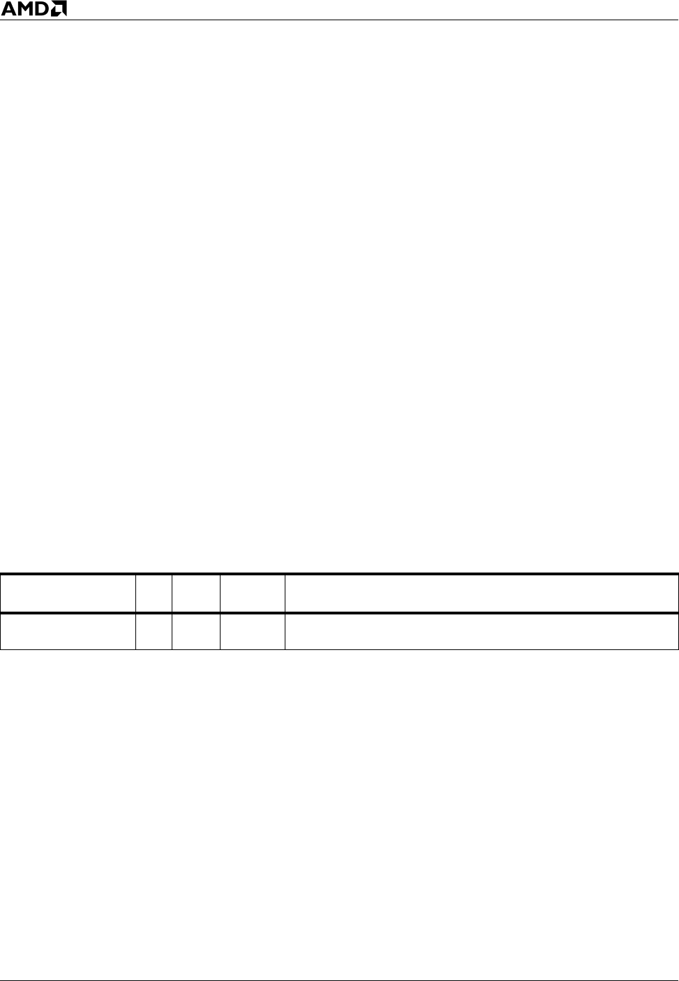
142 LAHF Instruction Reference
AMD64 Technology 24594—Rev. 3.14—September 2007
Loads the lower 8 bits of the rFLAGS register, including sign flag (SF), zero flag (ZF), auxiliary carry
flag (AF), parity flag (PF), and carry flag (CF), into the AH register.
The instruction sets the reserved bits 1, 3, and 5 of the rFLAGS register to 1, 0, and 0, respectively, in
the AH register.
The LAHF instruction can only be executed in 64-bit mode if supported by the processor
implementation. Check the status of ECX bit 0 returned by CPUID function 8000_0001h to verify that
the processor supports LAHF in 64-bit mode.
Related Instructions
SAHF
rFLAGS Affected
None.
Exceptions
LAHF Load Status Flags into AH Register
Mnemonic Opcode Description
LAHF 9F Load the SF, ZF, AF, PF, and CF flags into the AH
register.
Exception Real
Virtual
8086 Protected Cause of Exception
Invalid opcode, #UD X This instruction is not supported in 64-bit mode, as indicated
by ECX bit 0 returned by CPUID function 8000_0001h.

Instruction Reference LxS 143
24594—Rev. 3.14—September 2007 AMD64 Technology
Loads a far pointer from a memory location (second operand) into a segment register (mnemonic) and
general-purpose register (first operand). The instruction stores the 16-bit segment selector of the
pointer into the segment register and the 16-bit or 32-bit offset portion into the general-purpose
register. The operand-size attribute determines whether the pointer is 32-bit or 48-bit.
These instructions load associated segment-descriptor information into the hidden portion of the
specified segment register.
Using LDS or LES in 64-bit mode generates an invalid-opcode exception.
Executing LFS, LGS, or LSS with a 64-bit operand size only loads a 32-bit general purpose register
and the specified segment register.
Related Instructions
None
rFLAGS Affected
None
LDS
LES
LFS
LGS
LSS
Load Far Pointer
Mnemonic Opcode Description
LDS reg16, mem16:16 C5 /r Load DS:reg16 with a far pointer from memory.
(Invalid in 64-bit mode.)
LDS reg32, mem16:32 C5 /r Load DS:reg32 with a far pointer from memory.
(Invalid in 64-bit mode.)
LES reg16, mem16:16 C4 /r Load ES:reg16 with a far pointer from memory.
(Invalid in 64-bit mode.)
LES reg32, mem16:32 C4 /r Load ES:reg32 with a far pointer from memory.
(Invalid in 64-bit mode.)
LFS reg16, mem16:16 0F B4 /r Load FS:reg16 with a far pointer from memory.
LFS reg32, mem16:32 0F B4 /r Load FS:reg32 with a far pointer from memory.
LGS reg16, mem16:16 0F B5 /r Load GS:reg16 with a far pointer from memory.
LGS reg32, mem16:32 0F B5 /r Load GS:reg32 with a far pointer from memory.
LSS reg16, mem16:16 0F B2 /r Load SS:reg16 with a far pointer from memory.
LSS reg32, mem16:32 0F B2 /r Load SS:reg32 with a far pointer from memory.

144 LxS Instruction Reference
AMD64 Technology 24594—Rev. 3.14—September 2007
Exceptions
Exception Real
Virtual
8086 Protected Cause of Exception
Invalid opcode, #UD X X X The source operand was a register.
X LDS or LES was executed in 64-bit mode.
Segment not
present, #NP
(selector)
XThe DS, ES, FS, or GS register was loaded with a non-null
segment selector and the segment was marked not present.
Stack, #SS X X X A memory address exceeded the stack segment limit or was
non-canonical.
Stack, #SS
(selector) XThe SS register was loaded with a non-null segment selector
and the segment was marked not present.
General protection,
#GP
XX XA memory address exceeded a data segment limit or was non-
canonical.
X A null data segment was used to reference memory.
General protection,
#GP
(selector)
XA segment register was loaded, but the segment descriptor
exceeded the descriptor table limit.
XA segment register was loaded and the segment selector’s TI
bit was set, but the LDT selector was a null selector.
XThe SS register was loaded with a null segment selector in
non-64-bit mode or while CPL = 3.
XThe SS register was loaded and the segment selector RPL
and the segment descriptor DPL were not equal to the CPL.
XThe SS register was loaded and the segment pointed to was
not a writable data segment.
X
The DS, ES, FS, or GS register was loaded and the segment
pointed to was a data or non-conforming code segment, but
the RPL or CPL was greater than the DPL.
XThe DS, ES, FS, or GS register was loaded and the segment
pointed to was not a data segment or readable code segment.
Page fault, #PF X X A page fault resulted from the execution of the instruction.
Alignment check,
#AC XX
An unaligned memory reference was performed while
alignment checking was enabled.

Instruction Reference LEA 145
24594—Rev. 3.14—September 2007 AMD64 Technology
Computes the effective address of a memory location (second operand) and stores it in a general-
purpose register (first operand).
The address size of the memory location and the size of the register determine the specific action taken
by the instruction, as follows:
•If the address size and the register size are the same, the instruction stores the effective address as
computed.
•If the address size is longer than the register size, the instruction truncates the effective address to
the size of the register.
•If the address size is shorter than the register size, the instruction zero-extends the effective address
to the size of the register.
If the second operand is a register, an undefined-opcode exception occurs.
The LEA instruction is related to the MOV instruction, which copies data from a memory location to a
register, but LEA takes the address of the source operand, whereas MOV takes the contents of the
memory location specified by the source operand. In the simplest cases, LEA can be replaced with
MOV. For example:
lea eax, [ebx]
has the same effect as:
mov eax, ebx
However, LEA allows software to use any valid ModRM and SIB addressing mode for the source
operand. For example:
lea eax, [ebx+edi]
loads the sum of the EBX and EDI registers into the EAX register. This could not be accomplished by
a single MOV instruction.
The LEA instruction has a limited capability to perform multiplication of operands in general-purpose
registers using scaled-index addressing. For example:
lea eax, [ebx+ebx*8]
loads the value of the EBX register, multiplied by 9, into the EAX register. Possible values of
multipliers are 2, 4, 8, 3, 5, and 9.
The LEA instruction is widely used in string-processing and array-processing to initialize an index
register (rSI or rDI) before performing string instructions such as MOVSx. It is also used to initialize
the rBX register before performing the XLAT instruction in programs that perform character
translations. In data structures, the LEA instruction can calculate addresses of operands stored in
memory, and in particular, addresses of array or string elements.
LEA Load Effective Address
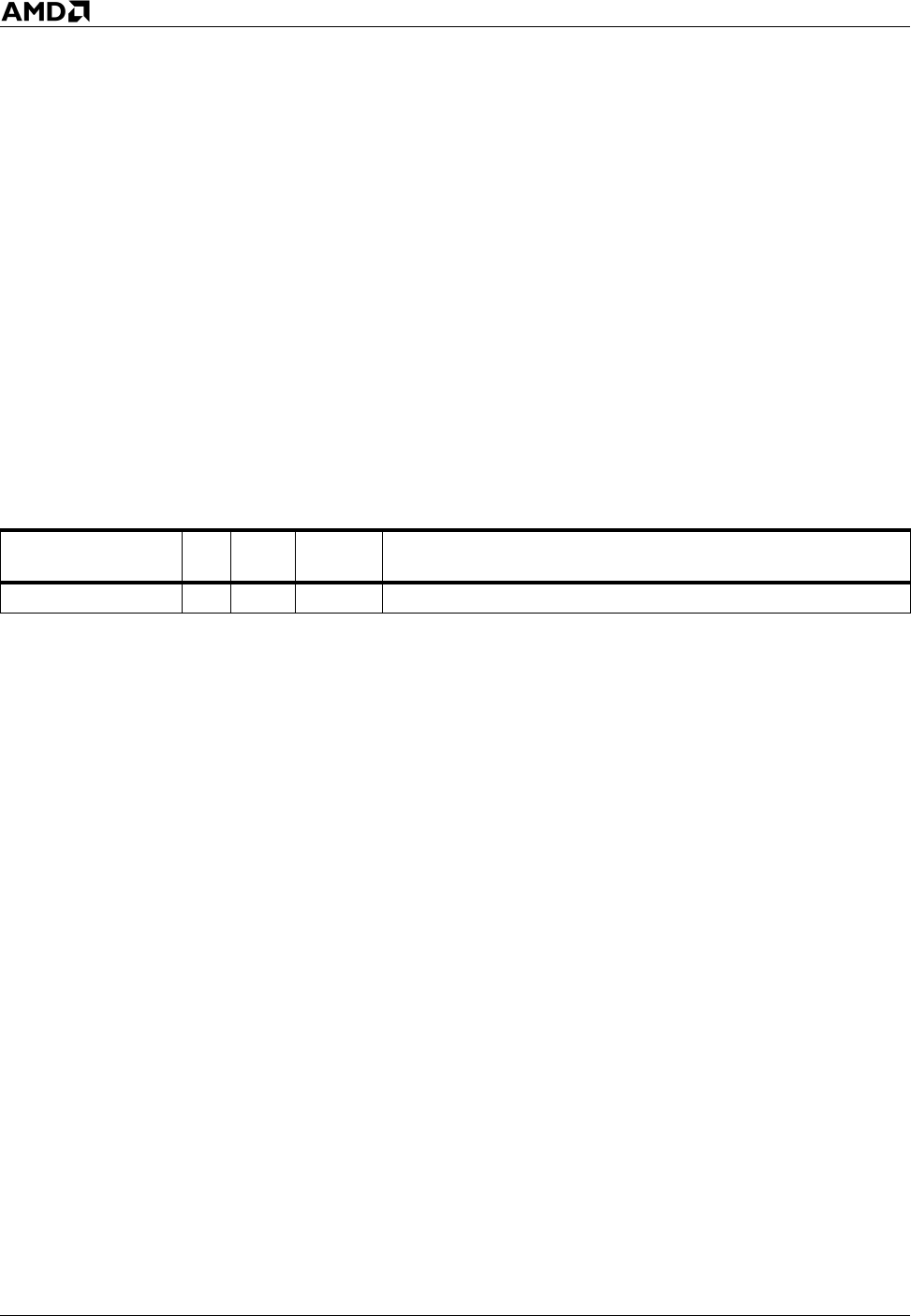
146 LEA Instruction Reference
AMD64 Technology 24594—Rev. 3.14—September 2007
Related Instructions
MOV
rFLAGS Affected
None
Exceptions
Mnemonic Opcode Description
LEA reg16, mem 8D /r Store effective address in a 16-bit register.
LEA reg32, mem 8D /r Store effective address in a 32-bit register.
LEA reg64, mem 8D /r Store effective address in a 64-bit register.
Exception Real
Virtual
8086 Protected Cause of Exception
Invalid opcode, #UD X X X The source operand was a register.

Instruction Reference LEAVE 147
24594—Rev. 3.14—September 2007 AMD64 Technology
Releases a stack frame created by a previous ENTER instruction. To release the frame, it copies the
frame pointer (in the rBP register) to the stack pointer register (rSP), and then pops the old frame
pointer from the stack into the rBP register, thus restoring the stack frame of the calling procedure.
The 32-bit LEAVE instruction is equivalent to the following 32-bit operation:
MOV ESP,EBP
POP EBP
To return program control to the calling procedure, execute a RET instruction after the LEAVE
instruction.
In 64-bit mode, the LEAVE operand size defaults to 64 bits, and there is no prefix available for
encoding a 32-bit operand size.
Related Instructions
ENTER
rFLAGS Affected
None
Exceptions
LEAVE Delete Procedure Stack Frame
Mnemonic Opcode Description
LEAVE C9 Set the stack pointer register SP to the value in the BP
register and pop BP.
LEAVE C9
Set the stack pointer register ESP to the value in the
EBP register and pop EBP.
(No prefix for encoding this in 64-bit mode.)
LEAVE C9 Set the stack pointer register RSP to the value in the
RBP register and pop RBP.
Exception Real
Virtual
8086 Protected Cause of Exception
Stack, #SS X X X A memory address exceeded the stack segment limit or was
non-canonical.
Page fault, #PF X X A page fault resulted from the execution of the instruction.
Alignment check,
#AC XX
An unaligned memory reference was performed while
alignment checking was enabled.

148 LFENCE Instruction Reference
AMD64 Technology 24594—Rev. 3.14—September 2007
Acts as a barrier to force strong memory ordering (serialization) between load instructions preceding
the LFENCE and load instructions that follow the LFENCE. Loads from differing memory types may
be performed out of order, in particular between WC/WC+ and other memory types. The LFENCE
instruction assures that the system completes all previous loads before executing subsequent loads.
The LFENCE instruction is weakly-ordered with respect to store instructions, data and instruction
prefetches, and the SFENCE instruction. Speculative loads initiated by the processor, or specified
explicitly using cache-prefetch instructions, can be reordered around an LFENCE.
In addition to load instructions, the LFENCE instruction is strongly ordered with respect to other
LFENCE instructions, MFENCE instructions, and serializing instructions. Further details on the use
of MFENCE to order accesses among differing memory types may be found in AMD64 Architecture
Programmer’s Manual Volume 2: System Programming, section 7.4 “Memory Types” on page 170.
Support for the LFENCE instruction is indicated when the SSE2 bit (bit 26) is set to 1 in EDX after
executing CPUID function 0000_0001h.
Related Instructions
MFENCE, SFENCE
rFLAGS Affected
None
Exceptions
LFENCE Load Fence
Mnemonic Opcode Description
LFENCE 0F AE E8 Force strong ordering of (serialize) load operations.
Exception Real
Virtual
8086 Protected Cause of Exception
Invalid opcode, #UD X X X The LFENCE instruction is not supported as indicated by EDX
bit 26 of CPUID function 0000_0001h.

Instruction Reference LODSx 149
24594—Rev. 3.14—September 2007 AMD64 Technology
Copies the byte, word, doubleword, or quadword in the memory location pointed to by the DS:rSI
registers to the AL, AX, EAX, or RAX register, depending on the size of the operand, and then
increments or decrements the rSI register according to the state of the DF flag in the rFLAGS register.
If the DF flag is 0, the instruction increments rSI; otherwise, it decrements rSI. It increments or
decrements rSI by 1, 2, 4, or 8, depending on the number of bytes being loaded.
The forms of the LODS instruction with an explicit operand address the operand at seg:[rSI]. The
value of seg defaults to the DS segment, but may be overridden by a segment prefix. The explicit
operand serves only to specify the type (size) of the value being copied and the specific registers used.
The no-operands forms of the instruction always use the DS:[rSI] registers to point to the value to be
copied (they do not allow a segment prefix). The mnemonic determines the size of the operand and the
specific registers used.
The LODSx instructions support the REP prefixes. For details about the REP prefixes, see “Repeat
Prefixes” on page 9. More often, software uses the LODSx instruction inside a loop controlled by a
LOOPcc instruction as a more efficient replacement for instructions like:
mov eax, dword ptr ds:[esi]
add esi, 4
The LODSQ instruction can only be used in 64-bit mode.
LODS
LODSB
LODSW
LODSD
LODSQ
Load String
Mnemonic Opcode Description
LODS mem8 AC Load byte at DS:rSI into AL and then increment or
decrement rSI.
LODS mem16 AD Load word at DS:rSI into AX and then increment or
decrement rSI.
LODS mem32 AD Load doubleword at DS:rSI into EAX and then
increment or decrement rSI.
LODS mem64 AD Load quadword at DS:rSI into RAX and then increment
or decrement rSI.
LODSB AC Load byte at DS:rSI into AL and then increment or
decrement rSI.
LODSW AD Load the word at DS:rSI into AX and then increment or
decrement rSI.
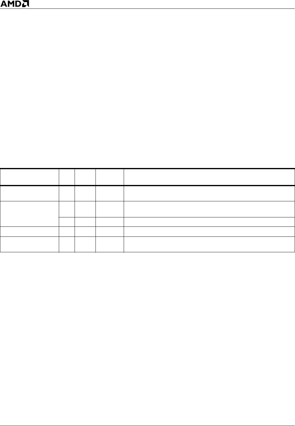
150 LODSx Instruction Reference
AMD64 Technology 24594—Rev. 3.14—September 2007
Related Instructions
MOVSx, STOSx
rFLAGS Affected
None
Exceptions
LODSD AD Load doubleword at DS:rSI into EAX and then
increment or decrement rSI.
LODSQ AD Load quadword at DS:rSI into RAX and then increment
or decrement rSI.
Exception Real
Virtual
8086 Protected Cause of Exception
Stack, #SS X X X A memory address exceeded the stack segment limit or was
non-canonical.
General protection,
#GP
XX XA memory address exceeded a data segment limit or was non-
canonical.
X A null data segment was used to reference memory.
Page fault, #PF X X A page fault resulted from the execution of the instruction.
Alignment check,
#AC XX
An unaligned memory reference was performed while
alignment checking was enabled.
Mnemonic Opcode Description

Instruction Reference LOOPcc 151
24594—Rev. 3.14—September 2007 AMD64 Technology
Decrements the count register (rCX) by 1, then, if rCX is not 0 and the ZF flag meets the condition
specified by the mnemonic, it jumps to the target instruction specified by the signed 8-bit relative
offset. Otherwise, it continues with the next instruction after the LOOPcc instruction.
The size of the count register used (CX, ECX, or RCX) depends on the address-size attribute of the
LOOPcc instruction.
The LOOP instruction ignores the state of the ZF flag.
The LOOPE and LOOPZ instructions jump if rCX is not 0 and the ZF flag is set to 1. In other words,
the instruction exits the loop (falls through to the next instruction) if rCX becomes 0 or ZF = 0.
The LOOPNE and LOOPNZ instructions jump if rCX is not 0 and ZF flag is cleared to 0. In other
words, the instruction exits the loop if rCX becomes 0 or ZF = 1.
The LOOPcc instruction does not change the state of the ZF flag. Typically, the loop contains a
compare instruction to set or clear the ZF flag.
If the jump is taken, the signed displacement is added to the rIP (of the following instruction) and the
result is truncated to 16, 32, or 64 bits, depending on operand size.
In 64-bit mode, the operand size defaults to 64 bits without the need for a REX prefix, and the
processor sign-extends the 8-bit offset before adding it to the RIP.
Related Instructions
None
LOOP
LOOPE
LOOPNE
LOOPNZ
LOOPZ
Loop
Mnemonic Opcode Description
LOOP rel8off E2 cb Decrement rCX, then jump short if rCX is not 0.
LOOPE rel8off E1 cb Decrement rCX, then jump short if rCX is not 0 and ZF
is 1.
LOOPNE rel8off E0 cb Decrement rCX, then Jump short if rCX is not 0 and ZF
is 0.
LOOPNZ rel8off E0 cb Decrement rCX, then Jump short if rCX is not 0 and ZF
is 0.
LOOPZ rel8off E1 cb Decrement rCX, then Jump short if rCX is not 0 and ZF
is 1.

152 LOOPcc Instruction Reference
AMD64 Technology 24594—Rev. 3.14—September 2007
rFLAGS Affected
None
Exceptions
Exception Real
Virtual
8086 Protected Cause of Exception
General protection,
#GP XX XThe target offset exceeded the code segment limit or was non-
canonical.

Instruction Reference LZCNT 153
24594—Rev. 3.14—September 2007 AMD64 Technology
Counts the number of leading zero bits in the 16-, 32-, or 64-bit general purpose register or memory
source operand. Counting starts downward from the most significant bit and stops when the highest bit
having a value of 1 is encountered or when the least significant bit is encountered. The count is written
to the destination register.
If the input operand is zero, CF is set to 1 and the size (in bits) of the input operand is written to the
destination register. Otherwise, CF is cleared.
If the most significant bit is a one, the ZF flag is set to 1, zero is written to the destination register.
Otherwise, ZF is cleared.
Support for the LZCNT instruction is indicated by ECX bit 5 (LZCNT) as returned by CPUID
function 8000_0001h. If the LZCNT instruction is not available, the encoding is treated as the BSR
instruction. Software MUST check the CPUID bit once per program or library initialization before
using the LZCNT instruction, or inconsistent behavior may result.
Related Instructions
BSF, BSR, POPCNT
LZCNT Count Leading Zeros
Mnemonic Opcode Description
LZCNT reg16, reg/mem16 F3 0F BD /r Count the number of leading zeros in reg/mem16.
LZCNT reg32, reg/mem32 F3 0F BD /r Count the number of leading zeros in reg/mem32.
LZCNT reg64, reg/mem64 F3 0F BD /r Count the number of leading zeros in reg/mem64.

154 LZCNT Instruction Reference
AMD64 Technology 24594—Rev. 3.14—September 2007
rFLAGS Affected
Exceptions
ID VIP VIF AC VM RF NT IOPL OF DF IF TF SF ZF AF PF CF
UUMUUM
2120191817161413–1211109876420
Note: Bits 31–22, 15, 5, 3, and 1 are reserved. A flag set to 1 or cleared to 0 is M (modified). Unaffected flags are
blank. Undefined flags are U.
Exception Real
Virtual
8086 Protected Cause of Exception
Stack, #SS X X X A memory address exceeded the stack segment limit or
was non-canonical.
General protection, #GP XX XA memory address exceeded a data segment limit or was
non-canonical.
X A null data segment was used to reference memory.
Page fault, #PF X X A page fault resulted from the execution of the instruction.
Alignment check, #AC X X An unaligned memory reference was performed while
alignment checking was enabled.

Instruction Reference MFENCE 155
24594—Rev. 3.14—September 2007 AMD64 Technology
Acts as a barrier to force strong memory ordering (serialization) between load and store instructions
preceding the MFENCE, and load and store instructions that follow the MFENCE. The processor may
perform loads out of program order with respect to non-conflicting stores for certain memory types.
The MFENCE instruction guarantees that the system completes all previous memory accesses before
executing subsequent accesses.
The MFENCE instruction is weakly-ordered with respect to data and instruction prefetches.
Speculative loads initiated by the processor, or specified explicitly using cache-prefetch instructions,
can be reordered around an MFENCE.
In addition to load and store instructions, the MFENCE instruction is strongly ordered with respect to
other MFENCE instructions, LFENCE instructions, SFENCE instructions, serializing instructions,
and CLFLUSH instructions. Further details on the use of MFENCE to order accesses among differing
memory types may be found in AMD64 Architecture Programmer’s Manual Volume 2: System
Programming, section 7.4 “Memory Types” on page 170.
Support for the MFENCE instruction is indicated when the SSE2 bit (bit 26) is set to 1 in EDX after
executing CPUID with function 0000_0001h.
Related Instructions
LFENCE, SFENCE
rFLAGS Affected
None
Exceptions
MFENCE Memory Fence
Mnemonic Opcode Description
MFENCE 0F AE F0 Force strong ordering of (serialized) load and store
operations.
Exception Real
Virtual
8086 Protected Cause of Exception
Invalid opcode, #UD X X X The MFENCE instruction is not supported as indicated by bit
26 of CPUID function 0000_0001h.

156 MOV Instruction Reference
AMD64 Technology 24594—Rev. 3.14—September 2007
Copies an immediate value or the value in a general-purpose register, segment register, or memory
location (second operand) to a general-purpose register, segment register, or memory location. The
source and destination must be the same size (byte, word, doubleword, or quadword) and cannot both
be memory locations.
In opcodes A0 through A3, the memory offsets (called moffsets) are address sized. In 64-bit mode,
memory offsets default to 64 bits. Opcodes A0–A3, in 64-bit mode, are the only cases that support a
64-bit offset value. (In all other cases, offsets and displacements are a maximum of 32 bits.) The B8
through BF (B8 +rq) opcodes, in 64-bit mode, are the only cases that support a 64-bit immediate value
(in all other cases, immediate values are a maximum of 32 bits).
When reading segment-registers with a 32-bit operand size, the processor zero-extends the 16-bit
selector results to 32 bits. When reading segment-registers with a 64-bit operand size, the processor
zero-extends the 16-bit selector to 64 bits. If the destination operand specifies a segment register (DS,
ES, FS, GS, or SS), the source operand must be a valid segment selector.
It is possible to move a null segment selector value (0000–0003h) into the DS, ES, FS, or GS register.
This action does not cause a general protection fault, but a subsequent reference to such a segment
does cause a #GP exception. For more information about segment selectors, see “Segment Selectors
and Registers” on page 67.
When the MOV instruction is used to load the SS register, the processor blocks external interrupts until
after the execution of the following instruction. This action allows the following instruction to be a
MOV instruction to load a stack pointer into the ESP register (MOV ESP,val) before an interrupt
occurs. However, the LSS instruction provides a more efficient method of loading SS and ESP.
Attempting to use the MOV instruction to load the CS register generates an invalid opcode exception
(#UD). Use the far JMP, CALL, or RET instructions to load the CS register.
To initialize a register to 0, rather than using a MOV instruction, it may be more efficient to use the
XOR instruction with identical destination and source operands.
MOV Move
Mnemonic Opcode Description
MOV reg/mem8, reg8 88 /r Move the contents of an 8-bit register to an 8-bit
destination register or memory operand.
MOV reg/mem16, reg16 89 /r Move the contents of a 16-bit register to a 16-bit
destination register or memory operand.
MOV reg/mem32, reg32 89 /r Move the contents of a 32-bit register to a 32-bit
destination register or memory operand.
MOV reg/mem64, reg64 89 /r Move the contents of a 64-bit register to a 64-bit
destination register or memory operand.
MOV reg8, reg/mem8 8A /r Move the contents of an 8-bit register or memory
operand to an 8-bit destination register.

Instruction Reference MOV 157
24594—Rev. 3.14—September 2007 AMD64 Technology
MOV reg16, reg/mem16 8B /r Move the contents of a 16-bit register or memory
operand to a 16-bit destination register.
MOV reg32, reg/mem32 8B /r Move the contents of a 32-bit register or memory
operand to a 32-bit destination register.
MOV reg64, reg/mem64 8B /r Move the contents of a 64-bit register or memory
operand to a 64-bit destination register.
MOV reg16/32/64/mem16,
segReg 8C /r
Move the contents of a segment register to a 16-bit, 32-
bit, or 64-bit destination register or to a 16-bit memory
operand.
MOV segReg, reg/mem16 8E /r Move the contents of a 16-bit register or memory
operand to a segment register.
MOV AL, moffset8 A0 Move 8-bit data at a specified memory offset to the AL
register.
MOV AX, moffset16 A1 Move 16-bit data at a specified memory offset to the AX
register.
MOV EAX, moffset32 A1 Move 32-bit data at a specified memory offset to the
EAX register.
MOV RAX, moffset64 A1 Move 64-bit data at a specified memory offset to the
RAX register.
MOV moffset8, AL A2 Move the contents of the AL register to an 8-bit memory
offset.
MOV moffset16, AX A3 Move the contents of the AX register to a 16-bit memory
offset.
MOV moffset32, EAX A3 Move the contents of the EAX register to a 32-bit
memory offset.
MOV moffset64, RAX A3 Move the contents of the RAX register to a 64-bit
memory offset.
MOV reg8, imm8 B0 +rb ib Move an 8-bit immediate value into an 8-bit register.
MOV reg16, imm16 B8 +rw iw Move a 16-bit immediate value into a 16-bit register.
MOV reg32, imm32 B8 +rd id Move an 32-bit immediate value into a 32-bit register.
MOV reg64, imm64 B8 +rq iq Move an 64-bit immediate value into a 64-bit register.
MOV reg/mem8, imm8 C6 /0 ib Move an 8-bit immediate value to an 8-bit register or
memory operand.
MOV reg/mem16, imm16 C7 /0 iw Move a 16-bit immediate value to a 16-bit register or
memory operand.
MOV reg/mem32, imm32 C7 /0 id Move a 32-bit immediate value to a 32-bit register or
memory operand.
MOV reg/mem64, imm32 C7 /0 id Move a 32-bit signed immediate value to a 64-bit
register or memory operand.
Mnemonic Opcode Description
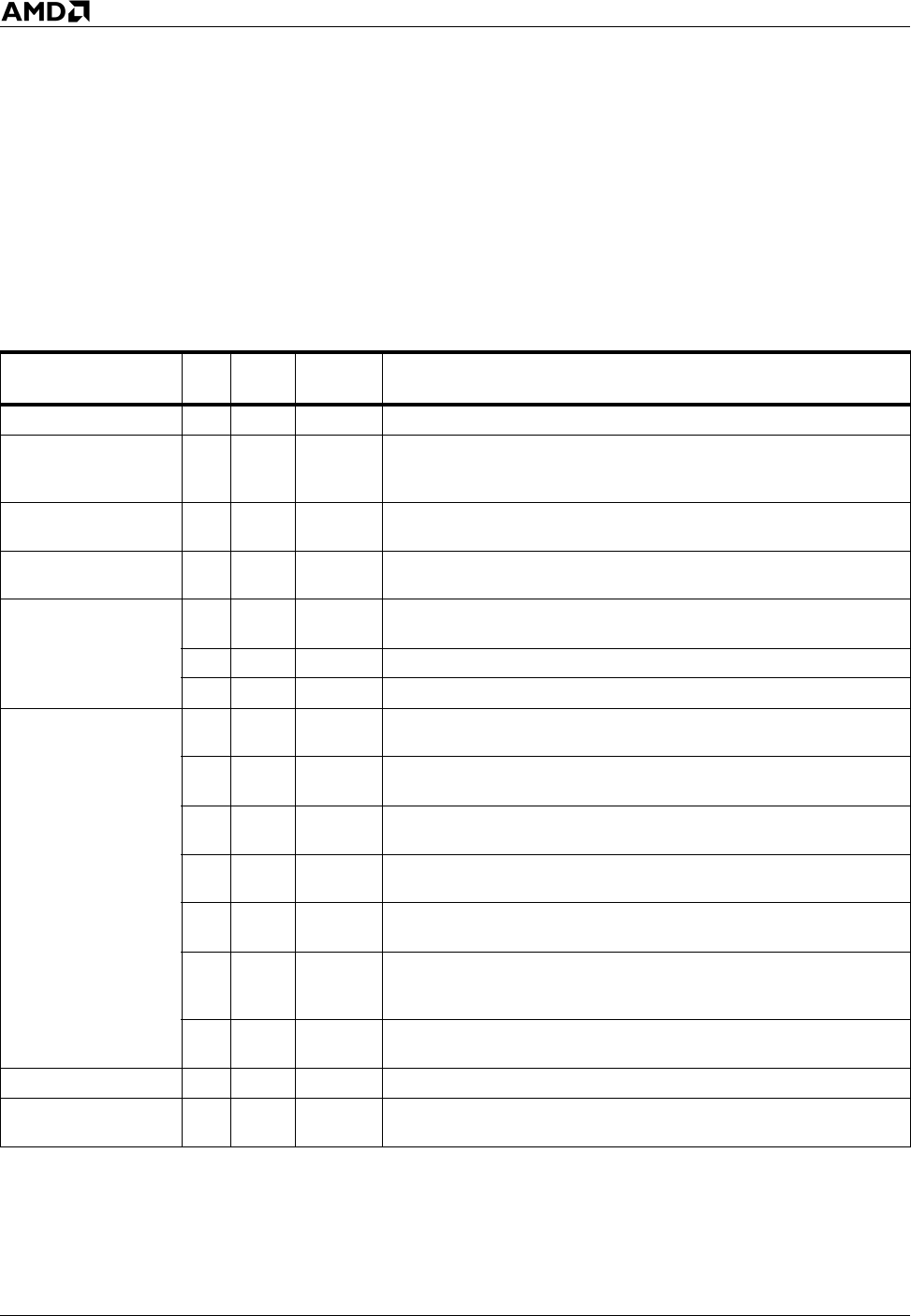
158 MOV Instruction Reference
AMD64 Technology 24594—Rev. 3.14—September 2007
Related Instructions
MOV(CRn), MOV(DRn), MOVD, MOVSX, MOVZX, MOVSXD, MOVSx
rFLAGS Affected
None
Exceptions
Exception Real
Virtual
8086 Protected Cause of Exception
Invalid opcode, #UD X X X An attempt was made to load the CS register.
Segment not
present, #NP
(selector)
XThe DS, ES, FS, or GS register was loaded with a non-null
segment selector and the segment was marked not present.
Stack, #SS X X X A memory address exceeded the stack segment limit or was
non-canonical.
Stack, #SS
(selector) XThe SS register was loaded with a non-null segment selector,
and the segment was marked not present.
General protection,
#GP
XX XA memory address exceeded a data segment limit or was non-
canonical.
X The destination operand was in a non-writable segment.
X A null data segment was used to reference memory.
General protection,
#GP
(selector)
XA segment register was loaded, but the segment descriptor
exceeded the descriptor table limit.
XA segment register was loaded and the segment selector’s TI
bit was set, but the LDT selector was a null selector.
XThe SS register was loaded with a null segment selector in
non-64-bit mode or while CPL = 3.
XThe SS register was loaded and the segment selector RPL
and the segment descriptor DPL were not equal to the CPL.
XThe SS register was loaded and the segment pointed to was
not a writable data segment.
X
The DS, ES, FS, or GS register was loaded and the segment
pointed to was a data or non-conforming code segment, but
the RPL or CPL was greater than the DPL.
XThe DS, ES, FS, or GS register was loaded and the segment
pointed to was not a data segment or readable code segment.
Page fault, #PF X X A page fault resulted from the execution of the instruction.
Alignment check,
#AC XX
An unaligned memory reference was performed while
alignment checking was enabled.

Instruction Reference MOVD 159
24594—Rev. 3.14—September 2007 AMD64 Technology
Moves a 32-bit or 64-bit value in one of the following ways:
•from a 32-bit or 64-bit general-purpose register or memory location to the low-order 32 or 64 bits
of an XMM register, with zero-extension to 128 bits
•from the low-order 32 or 64 bits of an XMM to a 32-bit or 64-bit general-purpose register or
memory location
•from a 32-bit or 64-bit general-purpose register or memory location to the low-order 32 bits (with
zero-extension to 64 bits) or the full 64 bits of an MMX register
•from the low-order 32 or the full 64 bits of an MMX register to a 32-bit or 64-bit general-purpose
register or memory location
The diagrams in Figure 3-1 on page 160 illustrate the operation of the MOVD instruction.
MOVD Move Doubleword or Quadword
Mnemonic Opcode Description
MOVD xmm, reg/mem32 66 0F 6E /r Move 32-bit value from a general-purpose register or
32-bit memory location to an XMM register.
MOVD xmm, reg/mem64 66 0F 6E /r Move 64-bit value from a general-purpose register or
64-bit memory location to an XMM register.
MOVD reg/mem32, xmm 66 0F 7E /r Move 32-bit value from an XMM register to a 32-bit
general-purpose register or memory location.
MOVD reg/mem64, xmm 66 0F 7E /r Move 64-bit value from an XMM register to a 64-bit
general-purpose register or memory location.
MOVD mmx, reg/mem32 0F 6E /r Move 32-bit value from a general-purpose register or
32-bit memory location to an MMX register.
MOVD mmx, reg/mem64 0F 6E /r Move 64-bit value from a general-purpose register or
64-bit memory location to an MMX register.
MOVD reg/mem32, mmx 0F 7E /r Move 32-bit value from an MMX register to a 32-bit
general-purpose register or memory location.
MOVD reg/mem64, mmx 0F 7E /r Move 64-bit value from an MMX register to a 64-bit
general-purpose register or memory location.
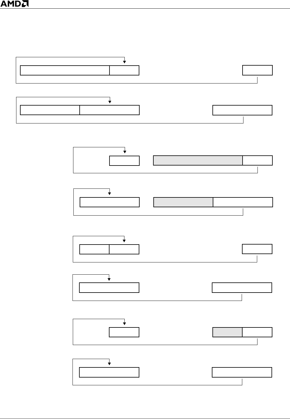
160 MOVD Instruction Reference
AMD64 Technology 24594—Rev. 3.14—September 2007
Figure 3-1. MOVD Instruction Operation
movd.eps
with REX prefix
All operations
are "copy"
with REX prefix
reg/mem64xmm
630
630
127 63064
127 63064
reg/mem64 xmm
0
031
reg/mem32xmm
reg/mem32 xmm
127 03132
31 0
127 31 032
0
0
reg/mem64mmx
reg/mem64 mmx
0
with REX prefix
with REX prefix
630630
630630
031
0
reg/mem32mmx
reg/mem32 mmx
31 0
3132630
3132630
0

Instruction Reference MOVD 161
24594—Rev. 3.14—September 2007 AMD64 Technology
Related Instructions
MOVDQA, MOVDQU, MOVDQ2Q, MOVQ, MOVQ2DQ
rFLAGS Affected
None
MXCSR Flags Affected
None
Exceptions
Exception Real
Virtual
8086 Protected Description
Invalid opcode, #UD
XX X
The MMX instructions are not supported, as indicated
by EDX bit 23 of CPUID function 0000_0001h.
XX X
The SSE2 instructions are not supported, as indicated
by EDX bit 26 of CPUID function 0000_0001.
X X X The emulate bit (EM) of CR0 was set to 1.
XX X
The instruction used XMM registers while
CR4.OSFXSR=0.
Device not available,
#NM X X X The task-switch bit (TS) of CR0 was set to 1.
Stack, #SS X X X A memory address exceeded the stack segment limit
or was non-canonical.
General protection,
#GP XX X
A memory address exceeded a data segment limit or
was non-canonical.
Page fault, #PF X X A page fault resulted from the execution of the
instruction.
x87 floating-point
exception pending,
#MF
XX X
An x87 floating-point exception was pending and the
instruction referenced an MMX register.
Alignment check, #AC X X An unaligned memory reference was performed while
alignment checking was enabled.
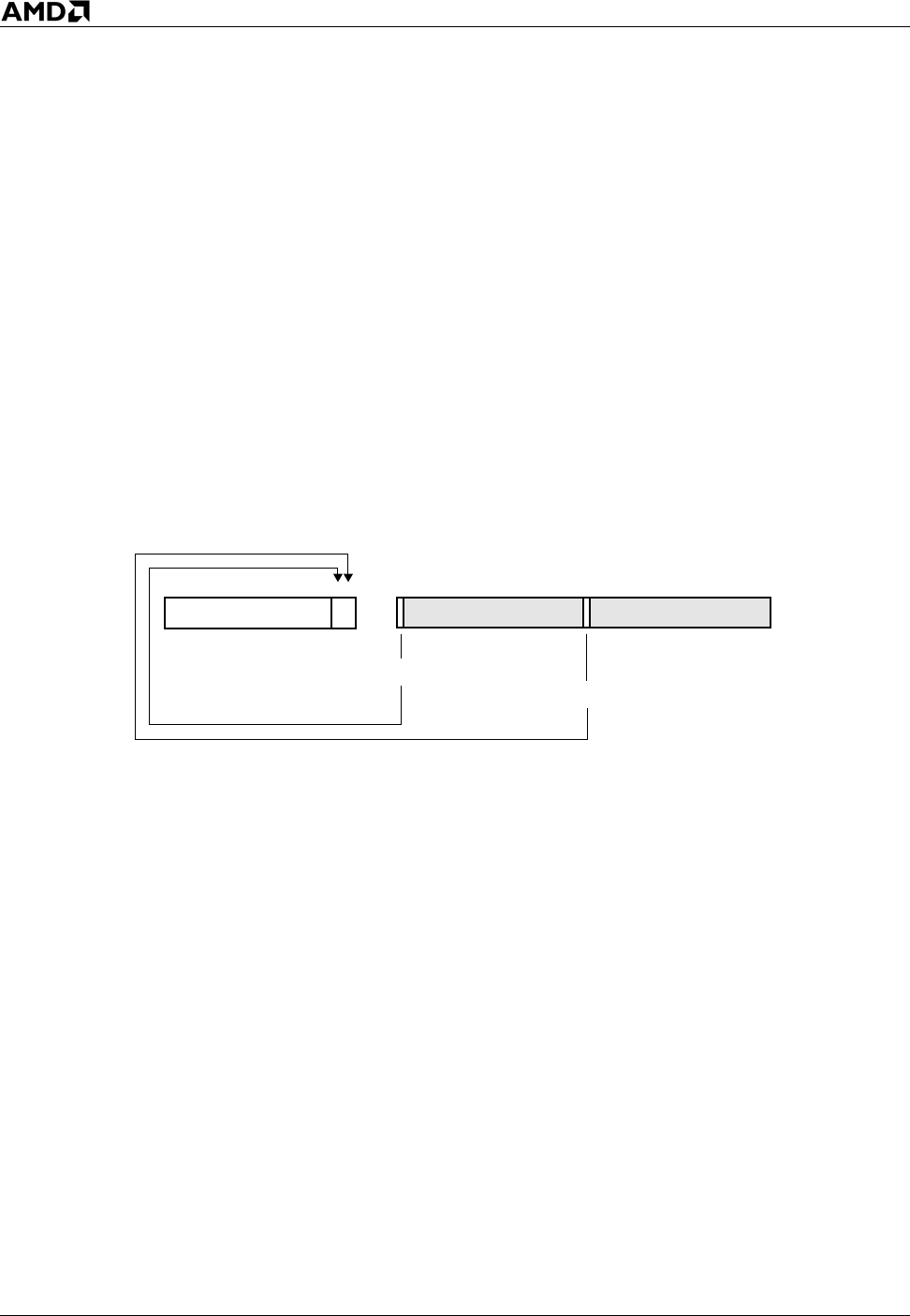
162 MOVMSKPD Instruction Reference
AMD64 Technology 24594—Rev. 3.14—September 2007
Moves the sign bits of two packed double-precision floating-point values in an XMM register (second
operand) to the two low-order bits of a general-purpose register (first operand) with zero-extension.
The MOVMSKPD instruction is an SSE2 instruction; Check the status of EDX bit 26 of CPUID
function 0000_0001h to verify that the processor supports this function.
Related Instructions
MOVMSKPS, PMOVMSKB
rFLAGS Affected
None
MXCSR Flags Affected
None
MOVMSKPD Extract Packed Double-Precision
Floating-Point Sign Mask
Mnemonic Opcode Description
MOVMSKPD reg32, xmm 66 0F 50 /r Move sign bits 127 and 63 in an XMM register to a 32-bit
general-purpose register.
movmskpd.eps
reg32 xmm
copy sign
copy sign
127 630
0
0
1
31

Instruction Reference MOVMSKPD 163
24594—Rev. 3.14—September 2007 AMD64 Technology
Exceptions
Exception (vector) Real
Virtual
8086 Protected Cause of Exception
Invalid opcode, #UD
XX X
The SSE2 instructions are not supported, as indicated
by EDX bit 26 of CPUID function 0000_0001h.
XX X
The operating-system FXSAVE/FXRSTOR support bit
(OSFXSR) of CR4 was cleared to 0.
X X X The emulate bit (EM) of CR0 was set to 1.
Device not available,
#NM X X X The task-switch bit (TS) of CR0 was set to 1.
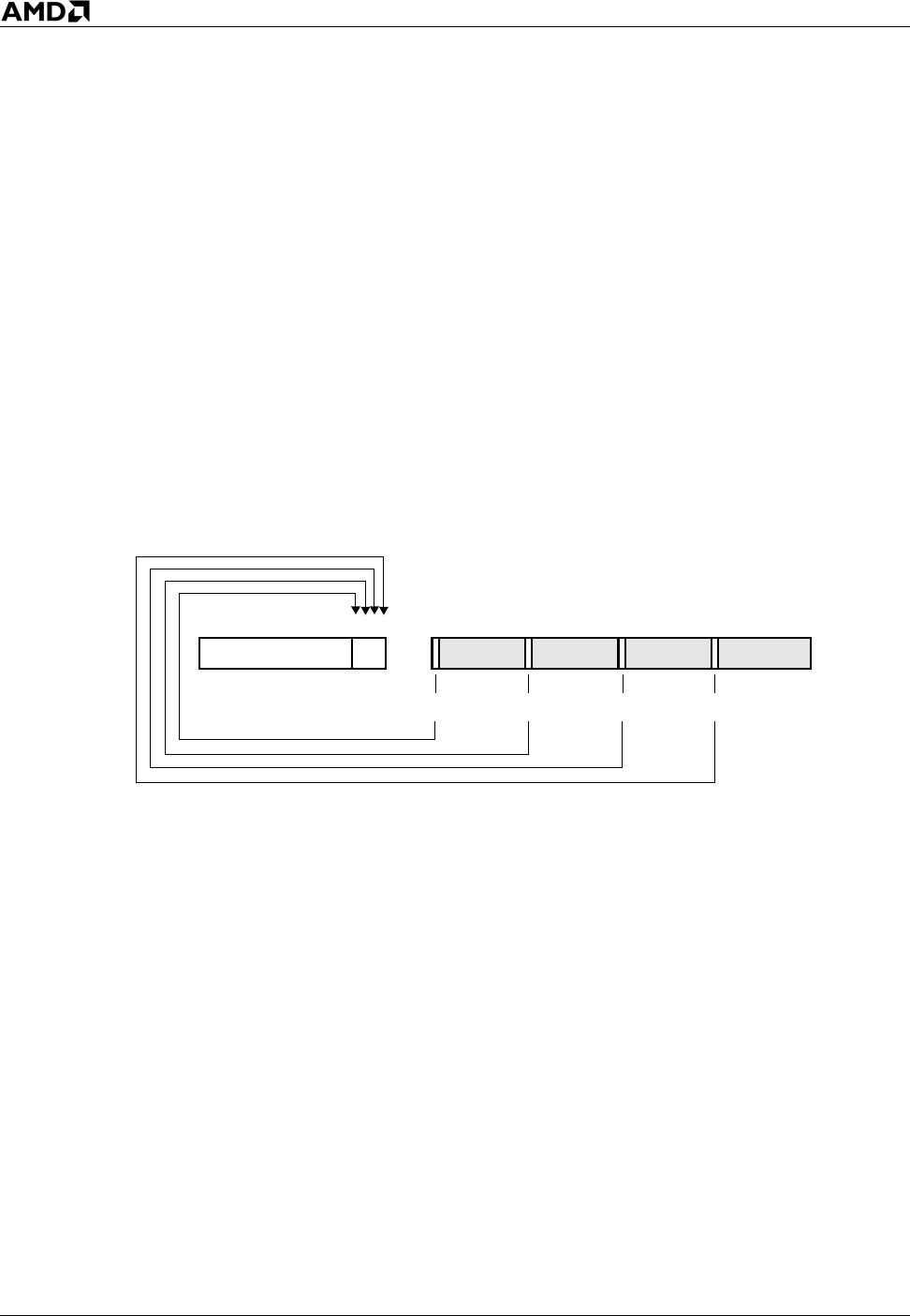
164 MOVMSKPS Instruction Reference
AMD64 Technology 24594—Rev. 3.14—September 2007
Moves the sign bits of four packed single-precision floating-point values in an XMM register (second
operand) to the four low-order bits of a general-purpose register (first operand) with zero-extension.
The MOVMSKPD instruction is an SSE2 instruction; Check the status of EDX bit 26 of CPUID
function 0000_0001h to verify that the processor supports this function.
Related Instructions
MOVMSKPD, PMOVMSKB
rFLAGS Affected
None
MXCSR Flags Affected
None
MOVMSKPS Extract Packed Single-Precision
Floating-Point Sign Mask
Mnemonic Opcode Description
MOVMSKPS reg32, xmm 0F 50 /r Move sign bits 127, 95, 63, 31 in an XMM register to a
32-bit general-purpose register.
movmskps.eps
03 127 63095 31
reg32 xmm
copy signcopy signcopy signcopy sign
0
31

Instruction Reference MOVMSKPS 165
24594—Rev. 3.14—September 2007 AMD64 Technology
Exceptions
Exception Real
Virtual
8086 Protected Cause of Exception
Invalid opcode, #UD
XX X
The SSE2 instructions are not supported, as indicated
by EDX bit 26 of CPUID function 1.
XX X
The operating-system FXSAVE/FXRSTOR support bit
(OSFXSR) of CR4 was cleared to 0.
X X X The emulate bit (EM) of CR0 was set to 1.
Device not available,
#NM X X X The task-switch bit (TS) of CR0 was set to 1.

166 MOVNTI Instruction Reference
AMD64 Technology 24594—Rev. 3.14—September 2007
Stores a value in a 32-bit or 64-bit general-purpose register (second operand) in a memory location
(first operand). This instruction indicates to the processor that the data is non-temporal and is unlikely
to be used again soon. The processor treats the store as a write-combining (WC) memory write, which
minimizes cache pollution. The exact method by which cache pollution is minimized depends on the
hardware implementation of the instruction. For further information, see “Memory Optimization” in
Volume 1.
The MOVNTI instruction is weakly-ordered with respect to other instructions that operate on memory.
Software should use an SFENCE instruction to force strong memory ordering of MOVNTI with
respect to other stores.
Support for the MOVNTI instruction is indicated when the SSE2 bit (bit 26) is set to 1 in EDX after
executing CPUID function 0000_0001h.
Related Instructions
MOVNTDQ, MOVNTPD, MOVNTPS, MOVNTQ
rFLAGS Affected
None
Exceptions
MOVNTI Move Non-Temporal Doubleword or
Quadword
Mnemonic Opcode Description
MOVNTI mem32, reg32 0F C3 /r Stores a 32-bit general-purpose register value into a 32-
bit memory location, minimizing cache pollution.
MOVNTI mem64, reg64 0F C3 /r Stores a 64-bit general-purpose register value into a 64-
bit memory location, minimizing cache pollution.
Exception (vector) Real
Virtual
8086 Protected Cause of Exception
Invalid opcode, #UD X X X The SSE2 instructions are not supported, as indicated
by EDX bit 26 of CPUID function 0000_0001h.
Stack, #SS X X X A memory address exceeded the stack segment limit
or was non-canonical.
General protection,
#GP
XX X
A memory address exceeded a data segment limit or
was non-canonical.
X A null data segment was used to reference memory.
XThe destination operand was in a non-writable
segment.

Instruction Reference MOVNTI 167
24594—Rev. 3.14—September 2007 AMD64 Technology
Page fault, #PF X X A page fault resulted from the execution of the
instruction.
Alignment check, #AC X X An unaligned memory reference was performed while
alignment checking was enabled.
Exception (vector) Real
Virtual
8086 Protected Cause of Exception

168 MOVSx Instruction Reference
AMD64 Technology 24594—Rev. 3.14—September 2007
Moves a byte, word, doubleword, or quadword from the memory location pointed to by DS:rSI to the
memory location pointed to by ES:rDI, and then increments or decrements the rSI and rDI registers
according to the state of the DF flag in the rFLAGS register.
If the DF flag is 0, the instruction increments both pointers; otherwise, it decrements them. It
increments or decrements the pointers by 1, 2, 4, or 8, depending on the size of the operands.
The forms of the MOVSx instruction with explicit operands address the first operand at seg:[rSI]. The
value of seg defaults to the DS segment, but can be overridden by a segment prefix. These instructions
always address the second operand at ES:[rDI] (ES may not be overridden). The explicit operands
serve only to specify the type (size) of the value being moved.
The no-operands forms of the instruction use the DS:[rSI] and ES:[rDI] registers to point to the value
to be moved (they do not allow a segment prefix). The mnemonic determines the size of the operands.
Do not confuse this MOVSD instruction with the same-mnemonic MOVSD (move scalar double-
precision floating-point) instruction in the 128-bit media instruction set. Assemblers can distinguish
the instructions by the number and type of operands.
The MOVSx instructions support the REP prefixes. For details about the REP prefixes, see “Repeat
Prefixes” on page 9.
MOVS
MOVSB
MOVSW
MOVSD
MOVSQ
Move String
Mnemonic Opcode Description
MOVS mem8, mem8 A4 Move byte at DS:rSI to ES:rDI, and then increment or
decrement rSI and rDI.
MOVS mem16, mem16 A5 Move word at DS:rSI to ES:rDI, and then increment or
decrement rSI and rDI.
MOVS mem32, mem32 A5 Move doubleword at DS:rSI to ES:rDI, and then
increment or decrement rSI and rDI.
MOVS mem64, mem64 A5 Move quadword at DS:rSI to ES:rDI, and then increment
or decrement rSI and rDI.
MOVSB A4 Move byte at DS:rSI to ES:rDI, and then increment or
decrement rSI and rDI.
MOVSW A5 Move word at DS:rSI to ES:rDI, and then increment or
decrement rSI and rDI.
Instruction Reference MOVSx 169
24594—Rev. 3.14—September 2007 AMD64 Technology
Related Instructions
MOV, LODSx, STOSx
rFLAGS Affected
None
Exceptions
MOVSD A5 Move doubleword at DS:rSI to ES:rDI, and then
increment or decrement rSI and rDI.
MOVSQ A5 Move quadword at DS:rSI to ES:rDI, and then increment
or decrement rSI and rDI.
Exception Real
Virtual
8086 Protected Cause of Exception
Stack, #SS X X X A memory address exceeded the stack segment limit or was
non-canonical.
General protection,
#GP
XX XA memory address exceeded a data segment limit or was non-
canonical.
X The destination operand was in a non-writable segment.
X A null data segment was used to reference memory.
Page fault, #PF X X A page fault resulted from the execution of the instruction.
Alignment check,
#AC XX
An unaligned memory reference was performed while
alignment checking was enabled.
Mnemonic Opcode Description

170 MOVSX Instruction Reference
AMD64 Technology 24594—Rev. 3.14—September 2007
Copies the value in a register or memory location (second operand) into a register (first operand),
extending the most significant bit of an 8-bit or 16-bit value into all higher bits in a 16-bit, 32-bit, or
64-bit register.
Related Instructions
MOVSXD, MOVZX
rFLAGS Affected
None
Exceptions
MOVSX Move with Sign-Extension
Mnemonic Opcode Description
MOVSX reg16, reg/mem8 0F BE /r Move the contents of an 8-bit register or memory
location to a 16-bit register with sign extension.
MOVSX reg32, reg/mem8 0F BE /r Move the contents of an 8-bit register or memory
location to a 32-bit register with sign extension.
MOVSX reg64, reg/mem8 0F BE /r Move the contents of an 8-bit register or memory
location to a 64-bit register with sign extension.
MOVSX reg32, reg/mem16 0F BF /r Move the contents of an 16-bit register or memory
location to a 32-bit register with sign extension.
MOVSX reg64, reg/mem16 0F BF /r Move the contents of an 16-bit register or memory
location to a 64-bit register with sign extension.
Exception Real
Virtual
8086 Protected Cause of Exception
Stack, #SS X X X A memory address exceeded the stack segment limit or was
non-canonical.
General protection,
#GP
XX XA memory address exceeded a data segment limit or was non-
canonical.
X A null data segment was used to reference memory.
Page fault, #PF X X A page fault resulted from the execution of the instruction.
Alignment check,
#AC XX
An unaligned memory reference was performed while
alignment checking was enabled.
Instruction Reference MOVSXD 171
24594—Rev. 3.14—September 2007 AMD64 Technology
Copies the 32-bit value in a register or memory location (second operand) into a 64-bit register (first
operand), extending the most significant bit of the 32-bit value into all higher bits of the 64-bit register.
This instruction requires the REX prefix 64-bit operand size bit (REX.W) to be set to 1 to sign-extend
a 32-bit source operand to a 64-bit result. Without the REX operand-size prefix, the operand size will
be 32 bits, the default for 64-bit mode, and the source is zero-extended into a 64-bit register. With a 16-
bit operand size, only 16 bits are copied, without modifying the upper 48 bits in the destination.
This instruction is available only in 64-bit mode. In legacy or compatibility mode this opcode is
interpreted as ARPL.
Related Instructions
MOVSX, MOVZX
rFLAGS Affected
None
Exceptions
MOVSXD Move with Sign-Extend Doubleword
Mnemonic Opcode Description
MOVSXD reg64, reg/mem32 63 /r Move the contents of a 32-bit register or memory
operand to a 64-bit register with sign extension.
Exception Real
Virtual
8086 Protected Cause of Exception
Stack, #SS X A memory address was non-canonical.
General protection,
#GP X A memory address was non-canonical.
Page fault, #PF X A page fault resulted from the execution of the instruction.
Alignment check,
#AC XAn unaligned memory reference was performed while
alignment checking was enabled.
172 MOVZX Instruction Reference
AMD64 Technology 24594—Rev. 3.14—September 2007
Copies the value in a register or memory location (second operand) into a register (first operand), zero-
extending the value to fit in the destination register. The operand-size attribute determines the size of
the zero-extended value.
Related Instructions
MOVSXD, MOVSX
rFLAGS Affected
None
Exceptions
MOVZX Move with Zero-Extension
Mnemonic Opcode Description
MOVZX reg16, reg/mem8 0F B6 /r Move the contents of an 8-bit register or memory
operand to a 16-bit register with zero-extension.
MOVZX reg32, reg/mem8 0F B6 /r Move the contents of an 8-bit register or memory
operand to a 32-bit register with zero-extension.
MOVZX reg64, reg/mem8 0F B6 /r Move the contents of an 8-bit register or memory
operand to a 64-bit register with zero-extension.
MOVZX reg32, reg/mem16 0F B7 /r Move the contents of a 16-bit register or memory
operand to a 32-bit register with zero-extension.
MOVZX reg64, reg/mem16 0F B7 /r Move the contents of a 16-bit register or memory
operand to a 64-bit register with zero-extension.
Exception Real
Virtual
8086 Protected Cause of Exception
Stack, #SS X X X A memory address exceeded the stack segment limit or was
non-canonical.
General protection,
#GP
XX XA memory address exceeded a data segment limit or was non-
canonical.
X A null data segment was used to reference memory.
Page fault, #PF X X A page fault resulted from the execution of the instruction.
Alignment check,
#AC XX
An unaligned memory reference was performed while
alignment checking was enabled.
Instruction Reference MUL 173
24594—Rev. 3.14—September 2007 AMD64 Technology
Multiplies the unsigned byte, word, doubleword, or quadword value in the specified register or
memory location by the value in AL, AX, EAX, or RAX and stores the result in AX, DX:AX,
EDX:EAX, or RDX:RAX (depending on the operand size). It puts the high-order bits of the product in
AH, DX, EDX, or RDX.
If the upper half of the product is non-zero, the instruction sets the carry flag (CF) and overflow flag
(OF) both to 1. Otherwise, it clears CF and OF to 0. The other arithmetic flags (SF, ZF, AF, PF) are
undefined.
Related Instructions
DIV
rFLAGS Affected
MUL Unsigned Multiply
Mnemonic Opcode Description
MUL reg/mem8 F6 /4
Multiplies an 8-bit register or memory operand by the
contents of the AL register and stores the result in the
AX register.
MUL reg/mem16 F7 /4
Multiplies a 16-bit register or memory operand by the
contents of the AX register and stores the result in the
DX:AX register.
MUL reg/mem32 F7 /4
Multiplies a 32-bit register or memory operand by the
contents of the EAX register and stores the result in the
EDX:EAX register.
MUL reg/mem64 F7 /4
Multiplies a 64-bit register or memory operand by the
contents of the RAX register and stores the result in the
RDX:RAX register.
ID VIP VIF AC VM RF NT IOPL OF DF IF TF SF ZF AF PF CF
M UUUUM
2120191817161413–1211109876420
Note: Bits 31–22, 15, 5, 3, and 1 are reserved. A flag set to 1 or cleared to 0 is M (modified). Unaffected flags are blank.
Undefined flags are U.

174 MUL Instruction Reference
AMD64 Technology 24594—Rev. 3.14—September 2007
Exceptions
Exception Real
Virtual
8086 Protected Cause of Exception
Stack, #SS X X X A memory address exceeded the stack segment limit or was
non-canonical.
General protection,
#GP
XX XA memory address exceeded a data segment limit or was non-
canonical.
X A null data segment was used to reference memory.
Page fault, #PF X X A page fault resulted from the execution of the instruction.
Alignment check,
#AC XX
An unaligned memory reference is performed while alignment
checking was enabled.

Instruction Reference NEG 175
24594—Rev. 3.14—September 2007 AMD64 Technology
Performs the two’s complement negation of the value in the specified register or memory location by
subtracting the value from 0. Use this instruction only on signed integer numbers.
If the value is 0, the instruction clears the CF flag to 0; otherwise, it sets CF to 1. The OF, SF, ZF, AF,
and PF flag settings depend on the result of the operation.
The forms of the NEG instruction that write to memory support the LOCK prefix. For details about the
LOCK prefix, see “Lock Prefix” on page 8.
Related Instructions
AND, NOT, OR, XOR
rFLAGS Affected
NEG Two’s Complement Negation
Mnemonic Opcode Description
NEG reg/mem8 F6 /3 Performs a two’s complement negation on an 8-bit
register or memory operand.
NEG reg/mem16 F7 /3 Performs a two’s complement negation on a 16-bit
register or memory operand.
NEG reg/mem32 F7 /3 Performs a two’s complement negation on a 32-bit
register or memory operand.
NEG reg/mem64 F7 /3 Performs a two’s complement negation on a 64-bit
register or memory operand.
ID VIP VIF AC VM RF NT IOPL OF DF IF TF SF ZF AF PF CF
M MMMMM
2120191817161413–1211109876420
Note: Bits 31–22, 15, 5, 3, and 1 are reserved. A flag set to 1 or cleared to 0 is M (modified). Unaffected flags are blank.
Undefined flags are U.
176 NEG Instruction Reference
AMD64 Technology 24594—Rev. 3.14—September 2007
Exceptions
Exception Real
Virtual
8086 Protected Cause of Exception
Stack, #SS X X X A memory address exceeded the stack segment limit or was
non-canonical.
General protection,
#GP
XX XA memory address exceeded a data segment limit or was non-
canonical.
X The destination operand is in a non-writable segment.
X A null data segment was used to reference memory.
Page fault, #PF X X A page fault resulted from the execution of the instruction.
Alignment check,
#AC XX
An unaligned memory reference was performed while
alignment checking was enabled.

Instruction Reference NOP 177
24594—Rev. 3.14—September 2007 AMD64 Technology
Does nothing. This one-byte instruction increments the rIP to point to next instruction in the
instruction stream, but does not affect the machine state in any other way.
The NOP instruction is an alias for XCHG rAX,rAX.
Related Instructions
None
rFLAGS Affected
None
Exceptions
None
NOP No Operation
Mnemonic Opcode Description
NOP 90 Performs no operation.
178 NOT Instruction Reference
AMD64 Technology 24594—Rev. 3.14—September 2007
Performs the one’s complement negation of the value in the specified register or memory location by
inverting each bit of the value.
The memory-operand forms of the NOT instruction support the LOCK prefix. For details about the
LOCK prefix, see “Lock Prefix” on page 8.
Related Instructions
AND, NEG, OR, XOR
rFLAGS Affected
None
Exceptions
NOT One’s Complement Negation
Mnemonic Opcode Description
NOT reg/mem8 F6 /2 Complements the bits in an 8-bit register or memory
operand.
NOT reg/mem16 F7 /2 Complements the bits in a 16-bit register or memory
operand.
NOT reg/mem32 F7 /2 Complements the bits in a 32-bit register or memory
operand.
NOT reg/mem64 F7 /2 Compliments the bits in a 64-bit register or memory
operand.
Exception Real
Virtual
8086 Protected Cause of Exception
Stack, #SS X X X A memory address exceeded the stack segment limit or was
non-canonical.
General protection,
#GP
XX XA memory address exceeded a data segment limit or was non-
canonical.
X The destination operand was in a non-writable segment.
X A null data segment was used to reference memory.
Page fault, #PF X X A page fault resulted from the execution of the instruction.
Alignment check,
#AC XX
An unaligned memory reference is performed while alignment
checking was enabled.

Instruction Reference OR 179
24594—Rev. 3.14—September 2007 AMD64 Technology
Performs a logical OR on the bits in a register, memory location, or immediate value (second operand)
and a register or memory location (first operand) and stores the result in the first operand location. The
two operands cannot both be memory locations.
If both corresponding bits are 0, the corresponding bit of the result is 0; otherwise, the corresponding
result bit is 1.
The forms of the OR instruction that write to memory support the LOCK prefix. For details about the
LOCK prefix, see “Lock Prefix” on page 8.
OR Logical OR
Mnemonic Opcode Description
OR AL, imm8 0C ib OR the contents of AL with an immediate 8-bit value.
OR AX, imm16 0D iw OR the contents of AX with an immediate 16-bit value.
OR EAX, imm32 0D id OR the contents of EAX with an immediate 32-bit value.
OR RAX, imm32 0D id OR the contents of RAX with a sign-extended
immediate 32-bit value.
OR reg/mem8, imm8 80 /1 ib OR the contents of an 8-bit register or memory operand
and an immediate 8-bit value.
OR reg/mem16, imm16 81 /1 iw OR the contents of a 16-bit register or memory operand
and an immediate 16-bit value.
OR reg/mem32, imm32 81 /1 id OR the contents of a 32-bit register or memory operand
and an immediate 32-bit value.
OR reg/mem64, imm32 81 /1 id OR the contents of a 64-bit register or memory operand
and sign-extended immediate 32-bit value.
OR reg/mem16, imm8 83 /1 ib OR the contents of a 16-bit register or memory operand
and a sign-extended immediate 8-bit value.
OR reg/mem32, imm8 83 /1 ib OR the contents of a 32-bit register or memory operand
and a sign-extended immediate 8-bit value.
OR reg/mem64, imm8 83 /1 ib OR the contents of a 64-bit register or memory operand
and a sign-extended immediate 8-bit value.
OR reg/mem8, reg8 08 /r OR the contents of an 8-bit register or memory operand
with the contents of an 8-bit register.
OR reg/mem16, reg16 09 /r OR the contents of a 16-bit register or memory operand
with the contents of a 16-bit register.
OR reg/mem32, reg32 09 /r OR the contents of a 32-bit register or memory operand
with the contents of a 32-bit register.
OR reg/mem64, reg64 09 /r OR the contents of a 64-bit register or memory operand
with the contents of a 64-bit register.
OR reg8, reg/mem8 0A /r OR the contents of an 8-bit register with the contents of
an 8-bit register or memory operand.
180 OR Instruction Reference
AMD64 Technology 24594—Rev. 3.14—September 2007
The following chart summarizes the effect of this instruction:
Related Instructions
AND, NEG, NOT, XOR
rFLAGS Affected
Exceptions
OR reg16, reg/mem16 0B /r OR the contents of a 16-bit register with the contents of
a 16-bit register or memory operand.
OR reg32, reg/mem32 0B /r OR the contents of a 32-bit register with the contents of
a 32-bit register or memory operand.
OR reg64, reg/mem64 0B /r OR the contents of a 64-bit register with the contents of
a 64-bit register or memory operand.
XYX OR Y
000
011
101
111
ID VIP VIF AC VM RF NT IOPL OF DF IF TF SF ZF AF PF CF
0MMUM0
2120191817161413–1211109876420
Note: Bits 31–22, 15, 5, 3, and 1 are reserved. A flag set to 1 or cleared to 0 is M (modified). Unaffected flags are
blank. Undefined flags are U.
Exception Real
Virtual
8086 Protected Cause of Exception
Stack, #SS X X X A memory address exceeded the stack segment limit or was
non-canonical.
General protection,
#GP
XX XA memory address exceeded a data segment limit or was non-
canonical.
X The destination operand was in a non-writable segment.
X A null data segment was used to reference memory.
Page fault, #PF X X A page fault resulted from the execution of the instruction.
Alignment check,
#AC XX
An unaligned memory reference was performed while
alignment checking was enabled.
Mnemonic Opcode Description

Instruction Reference OUT 181
24594—Rev. 3.14—September 2007 AMD64 Technology
Copies the value from the AL, AX, or EAX register (second operand) to an I/O port (first operand).
The port address can be a byte-immediate value (00h to FFh) or the value in the DX register (0000h to
FFFFh). The source register used determines the size of the port (8, 16, or 32 bits).
If the operand size is 64 bits, OUT only writes to a 32-bit I/O port.
If the CPL is higher than the IOPL or the mode is virtual mode, OUT checks the I/O permission bitmap
in the TSS before allowing access to the I/O port. See Volume 2 for details on the TSS I/O permission
bitmap.
Related Instructions
IN, INSx, OUTSx
rFLAGS Affected
None
Exceptions
OUT Output to Port
Mnemonic Opcode Description
OUT imm8, AL E6 ib Output the byte in the AL register to the port specified by
an 8-bit immediate value.
OUT imm8, AX E7 ib Output the word in the AX register to the port specified
by an 8-bit immediate value.
OUT imm8, EAX E7 ib Output the doubleword in the EAX register to the port
specified by an 8-bit immediate value.
OUT DX, AL EE Output byte in AL to the output port specified in DX.
OUT DX, AX EF Output word in AX to the output port specified in DX.
OUT DX, EAX EF Output doubleword in EAX to the output port specified in
DX.
Exception Real
Virtual
8086 Protected Cause of Exception
General protection,
#GP
XOne or more I/O permission bits were set in the TSS for the
accessed port.
XThe CPL was greater than the IOPL and one or more I/O
permission bits were set in the TSS for the accessed port.
Page fault (#PF) X X A page fault resulted from the execution of the instruction.

182 OUTSx Instruction Reference
AMD64 Technology 24594—Rev. 3.14—September 2007
Copies data from the memory location pointed to by DS:rSI to the I/O port address (0000h to FFFFh)
specified in the DX register, and then increments or decrements the rSI register according to the setting
of the DF flag in the rFLAGS register.
If the DF flag is 0, the instruction increments rSI; otherwise, it decrements rSI. It increments or
decrements the pointer by 1, 2, or 4, depending on the size of the value being copied.
The OUTSx instruction uses an explicit memory operand (second operand) to determine the type (size)
of the value being copied, but always uses DS:rSI for the location of the value to copy. The explicit
register operand specifies the I/O port address and must always be DX.
The no-operands forms of the instruction use the DS:[rSI] register pair to point to the data to be copied
and the DX register as the destination. The mnemonic specifies the size of the I/O port and the type
(size) of the value being copied.
The OUTSx instruction supports the REP prefix. For details about the REP prefix, see “Repeat
Prefixes” on page 9.
If the operand size is 64-bits, OUTS only writes to a 32-bit I/O port.
If the CPL is higher than the IOPL or the mode is virtual mode, OUTSx checks the I/O permission
bitmap in the TSS before allowing access to the I/O port. See Volume 2 for details on the TSS I/O
permission bitmap.
OUTS
OUTSB
OUTSW
OUTSD
Output String
Mnemonic Opcode Description
OUTS DX, mem8 6E Output the byte in DS:rSI to the port specified in DX,
then increment or decrement rSI.
OUTS DX, mem16 6F Output the word in DS:rSI to the port specified in DX,
then increment or decrement rSI.
OUTS DX, mem32 6F Output the doubleword in DS:rSI to the port specified in
DX, then increment or decrement rSI.
OUTSB 6E Output the byte in DS:rSI to the port specified in DX,
then increment or decrement rSI.
OUTSW 6F Output the word in DS:rSI to the port specified in DX,
then increment or decrement rSI.
OUTSD 6F Output the doubleword in DS:rSI to the port specified in
DX, then increment or decrement rSI.

Instruction Reference OUTSx 183
24594—Rev. 3.14—September 2007 AMD64 Technology
Related Instructions
IN, INSx, OUT
rFLAGS Affected
None
Exceptions
Exception Real
Virtual
8086 Protected Cause of Exception
Stack, #SS X X X A memory address exceeded the stack segment limit or was
non-canonical.
General protection,
#GP
XX XA memory address exceeded a data segment limit or was non-
canonical.
X A null data segment was used to reference memory.
XOne or more I/O permission bits were set in the TSS for the
accessed port.
XThe CPL was greater than the IOPL and one or more I/O
permission bits were set in the TSS for the accessed port.
Page fault, #PF X X A page fault resulted from the execution of the instruction.
Alignment check,
#AC XX
An unaligned memory reference is performed while alignment
checking was enabled.

184 PAUSE Instruction Reference
AMD64 Technology 24594—Rev. 3.14—September 2007
Improves the performance of spin loops, by providing a hint to the processor that the current code is in
a spin loop. The processor may use this to optimize power consumption while in the spin loop.
Architecturally, this instruction behaves like a NOP instruction.
Processors that do not support PAUSE treat this opcode as a NOP instruction.
Related Instructions
None
rFLAGS Affected
None
Exceptions
None
PAUSE Pause
Mnemonic Opcode Description
PAUSE F3 90 Provides a hint to processor that a spin loop is being
executed.

Instruction Reference POP 185
24594—Rev. 3.14—September 2007 AMD64 Technology
Copies the value pointed to by the stack pointer (SS:rSP) to the specified register or memory location
and then increments the rSP by 2 for a 16-bit pop, 4 for a 32-bit pop, or 8 for a 64-bit pop.
The operand-size attribute determines the amount by which the stack pointer is incremented (2, 4 or 8
bytes). The stack-size attribute determines whether SP, ESP, or RSP is incremented.
For forms of the instruction that load a segment register (POP DS, POP ES, POP FS, POP GS, POP
SS), the source operand must be a valid segment selector. When a segment selector is popped into a
segment register, the processor also loads all associated descriptor information into the hidden part of
the register and validates it.
It is possible to pop a null segment selector value (0000–0003h) into the DS, ES, FS, or GS register.
This action does not cause a general protection fault, but a subsequent reference to such a segment
does cause a #GP exception. For more information about segment selectors, see “Segment Selectors
and Registers” on page 67.
In 64-bit mode, the POP operand size defaults to 64 bits and there is no prefix available to encode a 32-
bit operand size. Using POP DS, POP ES, or POP SS instruction in 64-bit mode generates an invalid-
opcode exception.
This instruction cannot pop a value into the CS register. The RET (Far) instruction performs this
function.
POP Pop Stack
Mnemonic Opcode Description
POP reg/mem16 8F /0 Pop the top of the stack into a 16-bit register or memory
location.
POP reg/mem32 8F /0
Pop the top of the stack into a 32-bit register or memory
location.
(No prefix for encoding this in 64-bit mode.)
POP reg/mem64 8F /0 Pop the top of the stack into a 64-bit register or memory
location.
POP reg16 58 +rw Pop the top of the stack into a 16-bit register.
POP reg32 58 +rd Pop the top of the stack into a 32-bit register.
(No prefix for encoding this in 64-bit mode.)
POP reg64 58 +rq Pop the top of the stack into a 64-bit register.
POP DS 1F Pop the top of the stack into the DS register.
(Invalid in 64-bit mode.)
POP ES 07 Pop the top of the stack into the ES register.
(Invalid in 64-bit mode.)
POP SS 17 Pop the top of the stack into the SS register.
(Invalid in 64-bit mode.)

186 POP Instruction Reference
AMD64 Technology 24594—Rev. 3.14—September 2007
Related Instructions
PUSH
rFLAGS Affected
None
Exceptions
POP FS 0F A1 Pop the top of the stack into the FS register.
POP GS 0F A9 Pop the top of the stack into the GS register.
Exception Real
Virtual
8086 Protected Cause of Exception
Invalid opcode, #UD X POP DS, POP ES, or POP SS was executed in 64-bit mode.
Segment not
present, #NP
(selector)
XThe DS, ES, FS, or GS register was loaded with a non-null
segment selector and the segment was marked not present.
Stack, #SS X X X A memory address exceeded the stack segment limit or was
non-canonical.
Stack, #SS
(selector) XThe SS register was loaded with a non-null segment selector
and the segment was marked not present.
General protection,
#GP
XX XA memory address exceeded a data segment limit or was non-
canonical.
X The destination operand was in a non-writable segment.
X A null data segment was used to reference memory.
General protection,
#GP
(selector)
XA segment register was loaded and the segment descriptor
exceeded the descriptor table limit.
XA segment register was loaded and the segment selector’s TI
bit was set, but the LDT selector was a null selector.
XThe SS register was loaded with a null segment selector in
non-64-bit mode or while CPL = 3.
XThe SS register was loaded and the segment selector RPL
and the segment descriptor DPL were not equal to the CPL.
XThe SS register was loaded and the segment pointed to was
not a writable data segment.
X
The DS, ES, FS, or GS register was loaded and the segment
pointed to was a data or non-conforming code segment, but
the RPL or the CPL was greater than the DPL.
XThe DS, ES, FS, or GS register was loaded and the segment
pointed to was not a data segment or readable code segment.
Page fault, #PF X X A page fault resulted from the execution of the instruction.
Alignment check,
#AC XX
An unaligned memory reference was performed while
alignment checking was enabled.
Mnemonic Opcode Description
Instruction Reference POPAx 187
24594—Rev. 3.14—September 2007 AMD64 Technology
Pops words or doublewords from the stack into the general-purpose registers in the following order:
eDI, eSI, eBP, eSP (image is popped and discarded), eBX, eDX, eCX, and eAX. The instruction
increments the stack pointer by 16 or 32, depending on the operand size.
Using the POPA or POPAD instructions in 64-bit mode generates an invalid-opcode exception.
Related Instructions
PUSHA, PUSHAD
rFLAGS Affected
None
Exceptions
POPA
POPAD
POP All GPRs
Mnemonic Opcode Description
POPA 61 Pop the DI, SI, BP, SP, BX, DX, CX, and AX registers.
(Invalid in 64-bit mode.)
POPAD 61
Pop the EDI, ESI, EBP, ESP, EBX, EDX, ECX, and EAX
registers.
(Invalid in 64-bit mode.)
Exception Real
Virtual
8086 Protected Cause of Exception
Invalid opcode
(#UD) X This instruction was executed in 64-bit mode.
Stack, #SS X X X A memory address exceeded the stack segment limit.
Page fault, #PF X X A page fault resulted from the execution of the instruction.
Alignment check,
#AC XX
An unaligned memory reference was performed while
alignment checking was enabled.

188 POPCNT Instruction Reference
AMD64 Technology 24594—Rev. 3.14—September 2007
Counts the number of bits having a value of 1 in the source operand and places the result in the
destination register. The source operand is a 16-, 32-, or 64-bit general purpose register or memory
operand; the destination operand is a general purpose register of the same size as the source operand
register.
If the input operand is zero, the ZF flag is set to 1 and zero is written to the destination register.
Otherwise, the ZF flag is cleared. The other flags are cleared.
Support for the POPCNT instruction is indicated by ECX bit 23 (POPCNT) as returned by CPUID
function 0000_0001h. Software MUST check the CPUID bit once per program or library initialization
before using the POPCNT instruction, or inconsistent behavior may result.
Related Instructions
BSF, BSR, LZCNT
rFLAGS Affected
POPCNT Bit Population Count
Mnemonic Opcode Description
POPCNT reg16, reg/mem16 F3 0F B8 /r Count the 1s in reg/mem16.
POPCNT reg32, reg/mem32 F3 0F B8 /r Count the 1s in reg/mem32.
POPCNT reg64, reg/mem64 F3 0F B8 /r Count the 1s in reg/mem64.
ID VIP VIF AC VM RF NT IOPL OF DF IF TF SF ZF AF PF CF
0 0M000
2120191817161413–1211109876420
Note: Bits 31–22, 15, 5, 3, and 1 are reserved. A flag set to 1 or cleared to 0 is M (modified). Unaffected flags are
blank. Undefined flags are U.

Instruction Reference POPCNT 189
24594—Rev. 3.14—September 2007 AMD64 Technology
Exceptions
Exception Real
Virtual
8086 Protected Cause of Exception
Invalid opcode, #UD X X X The POPCNT instruction is not supported, as indicated by
ECX bit 23 as returned by CPUID function 0000_0001h.
Stack, #SS X X X A memory address exceeded the stack segment limit or was
non-canonical.
General protection,
#GP
XX XA memory address exceeded a data segment limit or was non-
canonical.
X A null data segment was used to reference memory.
Page fault, #PF X X A page fault resulted from the execution of the instruction.
Alignment check,
#AC XX
An unaligned memory reference was performed while
alignment checking was enabled.

190 POPFx Instruction Reference
AMD64 Technology 24594—Rev. 3.14—September 2007
Pops a word, doubleword, or quadword from the stack into the rFLAGS register and then increments
the stack pointer by 2, 4, or 8, depending on the operand size.
In protected or real mode, all the non-reserved flags in the rFLAGS register can be modified, except
the VIP, VIF, and VM flags, which are unchanged. In protected mode, at a privilege level greater than
0 the IOPL is also unchanged. The instruction alters the interrupt flag (IF) only when the CPL is less
than or equal to the IOPL.
In virtual-8086 mode, if IOPL field is less than 3, attempting to execute a POPFx or PUSHFx
instruction while VME is not enabled, or the operand size is not 16-bit, generates a #GP exception.
In 64-bit mode, this instruction defaults to a 64-bit operand size; there is no prefix available to encode
a 32-bit operand size.
Action
// See “Pseudocode Definitions” on page 41.
POPF_START:
IF (REAL_MODE)
POPF_REAL
ELSIF (PROTECTED_MODE)
POPF_PROTECTED
ELSE // (VIRTUAL_MODE)
POPF_VIRTUAL
POPF_REAL:
POP.v temp_RFLAGS
RFLAGS.v = temp_RFLAGS // VIF,VIP,VM unchanged
// RF cleared
EXIT
POPF
POPFD
POPFQ
POP to rFLAGS
Mnemonic Opcode Description
POPF 9D Pop a word from the stack into the FLAGS register.
POPFD 9D Pop a double word from the stack into the EFLAGS
register. (No prefix for encoding this in 64-bit mode.)
POPFQ 9D Pop a quadword from the stack to the RFLAGS register.

Instruction Reference POPFx 191
24594—Rev. 3.14—September 2007 AMD64 Technology
POPF_PROTECTED:
POP.v temp_RFLAGS
RFLAGS.v = temp_RFLAGS // VIF,VIP,VM unchanged
// IOPL changed only if (CPL=0)
// IF changed only if (CPL<=old_RFLAGS.IOPL)
// RF cleared
EXIT
POPF_VIRTUAL:
IF (RFLAGS.IOPL=3)
{
POP.v temp_RFLAGS
RFLAGS.v = temp_RFLAGS // VIF,VIP,VM,IOPL unchanged
// RF cleared
EXIT
}
ELSIF ((CR4.VME=1) && (OPERAND_SIZE=16))
{
POP.w temp_RFLAGS
IF (((temp_RFLAGS.IF=1) && (RFLAGS.VIP=1)) || (temp_RFLAGS.TF=1))
EXCEPTION [#GP(0)]
// notify the virtual-mode-manager to deliver
// the task’s pending interrupts
RFLAGS.w = temp_RFLAGS // IF,IOPL unchanged
// RFLAGS.VIF=temp_RFLAGS.IF
// RF cleared
EXIT
}
ELSE // ((RFLAGS.IOPL<3) && ((CR4.VME=0) || (OPERAND_SIZE!=16)))
EXCEPTION [#GP(0)]
Related Instructions
PUSHF, PUSHFD, PUSHFQ
rFLAGS Affected
ID VIP VIF AC VM RF NT IOPL OF DF IF TF SF ZF AF PF CF
M MM 0 M M MMMMMMMMM
2120191817161413–1211109876420
Note: Bits 31–22, 15, 5, 3, and 1 are reserved. A flag set to 1 or cleared to 0 is M (modified). Unaffected flags are blank.
Undefined flags are U.

192 POPFx Instruction Reference
AMD64 Technology 24594—Rev. 3.14—September 2007
Exceptions
Exception Real
Virtual
8086 Protected Cause of Exception
Stack, #SS X X X A memory address exceeded the stack segment limit or was
non-canonical.
General protection,
#GP X
The I/O privilege level was less than 3 and one of the following
conditions was true:
•CR4.VME was 0.
• The effective operand size was 32-bit.
• Both the original EFLAGS.VIP and the new EFLAGS.IF bits
were set.
• The new EFLAGS.TF bit was set.
Page fault, #PF X X A page fault resulted from the execution of the instruction.
Alignment check,
#AC XX
An unaligned memory reference was performed while
alignment checking was enabled.

Instruction Reference PREFETCHx 193
24594—Rev. 3.14—September 2007 AMD64 Technology
Loads the entire 64-byte aligned memory sequence containing the specified memory address into the
L1 data cache. The position of the specified memory address within the 64-byte cache line is
irrelevant. If a cache hit occurs, or if a memory fault is detected, no bus cycle is initiated and the
instruction is treated as a NOP.
The PREFETCHW instruction loads the prefetched line and sets the cache-line state to Modified, in
anticipation of subsequent data writes to the line. The PREFETCH instruction, by contrast, typically
sets the cache-line state to Exclusive (depending on the hardware implementation).
The opcodes for the PREFETCH/PREFETCHW instructions include the ModRM byte; however, only
the memory form of ModRM is valid. The register form of ModRM causes an invalid-opcode
exception. Because there is no destination register, the three destination register field bits of the
ModRM byte define the type of prefetch to be performed. The bit patterns 000b and 001b define the
PREFETCH and PREFETCHW instructions, respectively. All other bit patterns are reserved for future
use.
The reserved PREFETCH types do not result in an invalid-opcode exception if executed. Instead, for
forward compatibility with future processors that may implement additional forms of the PREFETCH
instruction, all reserved PREFETCH types are implemented as synonyms of the basic PREFETCH
type (the PREFETCH instruction with type 000b).
The operation of these instructions is implementation-dependent. The processor implementation can
ignore or change these instructions. The size of the cache line also depends on the implementation,
with a minimum size of 32 bytes. For details on the use of this instruction, see the processor data sheets
or other software-optimization documentation relating to particular hardware implementations.
Support for these instructions may be indicated by any of the following:
•EDX bit 31 as returned by CPUID function 8000_0001h
•EDX bit 29 as returned by CPUID function 8000_0001h
•ECX bit 8 as returned by CPUID function 8000_0001h
Related Instructions
PREFETCHlevel
PREFETCH
PREFETCHW
Prefetch L1 Data-Cache Line
Mnemonic Opcode Description
PREFETCH mem8 0F 0D /0 Prefetch processor cache line into L1 data cache.
PREFETCHW mem8 0F 0D /1 Prefetch processor cache line into L1 data cache and
mark it modified.
194 PREFETCHx Instruction Reference
AMD64 Technology 24594—Rev. 3.14—September 2007
rFLAGS Affected
None
Exceptions
Exception (vector) Real
Virtual
8086 Protected Cause of Exception
Invalid opcode, #UD XX X
The PREFETCH/W instructions are not supported, as
indicated when the following bits are all clear:
• PREFETCH/PREFETCHW are not supported, as
indicated by ECX bit 8 of CPUID function
8000_0001h
• Long Mode is not supported, as indicated by EDX
bit 29 of CPUID function 8000_0001h
• The 3DNow!™ instructions are not supported, as
indicated by EDX bit 31 of CPUID function
8000_0001h.
X X X The operand was a register.

Instruction Reference PREFETCHlevel 195
24594—Rev. 3.14—September 2007 AMD64 Technology
Loads a cache line from the specified memory address into the data-cache level specified by the
locality reference bits 5–3 of the ModRM byte. Table 3-3 on page 195 lists the locality reference
options for the instruction.
This instruction loads a cache line even if the mem8 address is not aligned with the start of the line. If
the cache line is already contained in a cache level that is lower than the specified locality reference, or
if a memory fault is detected, a bus cycle is not initiated and the instruction is treated as a NOP.
The operation of this instruction is implementation-dependent. The processor implementation can
ignore or change this instruction. The size of the cache line also depends on the implementation, with a
minimum size of 32 bytes. AMD processors alias PREFETCH1 and PREFETCH2 to PREFETCH0.
For details on the use of this instruction, see the software-optimization documentation relating to
particular hardware implementations.
Related Instructions
PREFETCH, PREFETCHW
PREFETCHlevel Prefetch Data to Cache Level level
Mnemonic Opcode Description
PREFETCHNTA mem8 0F 18 /0 Move data closer to the processor using the NTA
reference.
PREFETCHT0 mem8 0F 18 /1 Move data closer to the processor using the T0
reference.
PREFETCHT1 mem8 0F 18 /2 Move data closer to the processor using the T1
reference.
PREFETCHT2 mem8 0F 18 /3 Move data closer to the processor using the T2
reference.
Table 3-3. Locality References for the Prefetch Instructions
Locality
Reference Description
NTA
Non-Temporal Access—Move the specified data into the processor with
minimum cache pollution. This is intended for data that will be used only
once, rather than repeatedly. The specific technique for minimizing cache
pollution is implementation-dependent and may include such techniques
as allocating space in a software-invisible buffer, allocating a cache line in
only a single way, etc. For details, see the software-optimization
documentation for a particular hardware implementation.
T0 All Cache Levels—Move the specified data into all cache levels.
T1 Level 2 and Higher—Move the specified data into all cache levels except
0th level (L1) cache.
T2 Level 3 and Higher—Move the specified data into all cache levels except
0th level (L1) and 1st level (L2) caches.

196 PREFETCHlevel Instruction Reference
AMD64 Technology 24594—Rev. 3.14—September 2007
rFLAGS Affected
None
Exceptions
None

Instruction Reference PUSH 197
24594—Rev. 3.14—September 2007 AMD64 Technology
Decrements the stack pointer and then copies the specified immediate value or the value in the
specified register or memory location to the top of the stack (the memory location pointed to by
SS:rSP).
The operand-size attribute determines the number of bytes pushed to the stack. The stack-size attribute
determines whether SP, ESP, or RSP is the stack pointer. The address-size attribute is used only to
locate the memory operand when pushing a memory operand to the stack.
If the instruction pushes the stack pointer (rSP), the resulting value on the stack is that of rSP before
execution of the instruction.
There is a PUSH CS instruction but no corresponding POP CS. The RET (Far) instruction pops a value
from the top of stack into the CS register as part of its operation.
In 64-bit mode, the operand size of all PUSH instructions defaults to 64 bits, and there is no prefix
available to encode a 32-bit operand size. Using the PUSH CS, PUSH DS, PUSH ES, or PUSH SS
instructions in 64-bit mode generates an invalid-opcode exception.
Pushing an odd number of 16-bit operands when the stack address-size attribute is 32 results in a
misaligned stack pointer.
PUSH Push onto Stack
Mnemonic Opcode Description
PUSH reg/mem16 FF /6 Push the contents of a 16-bit register or memory
operand onto the stack.
PUSH reg/mem32 FF /6
Push the contents of a 32-bit register or memory
operand onto the stack. (No prefix for encoding this in
64-bit mode.)
PUSH reg/mem64 FF /6 Push the contents of a 64-bit register or memory
operand onto the stack.
PUSH reg16 50 +rw Push the contents of a 16-bit register onto the stack.
PUSH reg32 50 +rd Push the contents of a 32-bit register onto the stack. (No
prefix for encoding this in 64-bit mode.)
PUSH reg64 50 +rq Push the contents of a 64-bit register onto the stack.
PUSH imm8 6A ib Push an 8-bit immediate value (sign-extended to 16, 32,
or 64 bits) onto the stack.
PUSH imm16 68 iw Push a 16-bit immediate value onto the stack.
PUSH imm32 68 id Push a 32-bit immediate value onto the stack. (No prefix
for encoding this in 64-bit mode.)
PUSH imm64 68 id Push a sign-extended 32-bit immediate value onto the
stack.
PUSH CS 0E Push the CS selector onto the stack. (Invalid in 64-bit
mode.)

198 PUSH Instruction Reference
AMD64 Technology 24594—Rev. 3.14—September 2007
Related Instructions
POP
rFLAGS Affected
None
Exceptions
PUSH SS 16 Push the SS selector onto the stack. (Invalid in 64-bit
mode.)
PUSH DS 1E Push the DS selector onto the stack. (Invalid in 64-bit
mode.)
PUSH ES 06 Push the ES selector onto the stack. (Invalid in 64-bit
mode.)
PUSH FS 0F A0 Push the FS selector onto the stack.
PUSH GS 0F A8 Push the GS selector onto the stack.
Exception Real
Virtual
8086 Protected Cause of Exception
Invalid opcode, #UD X PUSH CS, PUSH DS, PUSH ES, or PUSH SS was executed
in 64-bit mode.
Stack, #SS X X X A memory address exceeded the stack segment limit or was
non-canonical.
General protection,
#GP
XX XA memory address exceeded a data segment limit or was non-
canonical.
X A null data segment was used to reference memory.
Page fault, #PF X X A page fault resulted from the execution of the instruction.
Alignment check,
#AC XX
An unaligned memory reference was performed while
alignment checking was enabled.
Mnemonic Opcode Description
Instruction Reference PUSHAx 199
24594—Rev. 3.14—September 2007 AMD64 Technology
Pushes the contents of the eAX, eCX, eDX, eBX, eSP (original value), eBP, eSI, and eDI general-
purpose registers onto the stack in that order. This instruction decrements the stack pointer by 16 or 32
depending on operand size.
Using the PUSHA or PUSHAD instruction in 64-bit mode generates an invalid-opcode exception.
Related Instructions
POPA, POPAD
rFLAGS Affected
None
Exceptions
PUSHA
PUSHAD
Push All GPRs onto Stack
Mnemonic Opcode Description
PUSHA 60
Push the contents of the AX, CX, DX, BX, original SP,
BP, SI, and DI registers onto the stack.
(Invalid in 64-bit mode.)
PUSHAD 60
Push the contents of the EAX, ECX, EDX, EBX, original
ESP, EBP, ESI, and EDI registers onto the stack.
(Invalid in 64-bit mode.)
Exception Real
Virtual
8086 Protected Cause of Exception
Invalid opcode, #UD X This instruction was executed in 64-bit mode.
Stack, #SS X X X A memory address exceeded the stack segment limit.
Page fault, #PF X X A page fault resulted from the execution of the instruction.
Alignment check,
#AC XX
An unaligned memory reference was performed while
alignment checking was enabled.

200 PUSHFx Instruction Reference
AMD64 Technology 24594—Rev. 3.14—September 2007
Decrements the rSP register and copies the rFLAGS register (except for the VM and RF flags) onto the
stack. The instruction clears the VM and RF flags in the rFLAGS image before putting it on the stack.
The instruction pushes 2, 4, or 8 bytes, depending on the operand size.
In 64-bit mode, this instruction defaults to a 64-bit operand size and there is no prefix available to
encode a 32-bit operand size.
In virtual-8086 mode, if system software has set the IOPL field to a value less than 3, a general-
protection exception occurs if application software attempts to execute PUSHFx or POPFx while VME
is not enabled or the operand size is not 16-bit.
Action
// See “Pseudocode Definitions” on page 41.
PUSHF_START:
IF (REAL_MODE)
PUSHF_REAL
ELSIF (PROTECTED_MODE)
PUSHF_PROTECTED
ELSE // (VIRTUAL_MODE)
PUSHF_VIRTUAL
PUSHF_REAL:
PUSH.v old_RFLAGS // Pushed with RF and VM cleared.
EXIT
PUSHF_PROTECTED:
PUSH.v old_RFLAGS // Pushed with RF cleared.
EXIT
PUSHF_VIRTUAL:
IF (RFLAGS.IOPL=3)
{
PUSH.v old_RFLAGS // Pushed with RF,VM cleared.
EXIT
}
PUSHF
PUSHFD
PUSHFQ
Push rFLAGS onto Stack
Mnemonic Opcode Description
PUSHF 9C Push the FLAGS word onto the stack.
PUSHFD 9C Push the EFLAGS doubleword onto stack. (No prefix
encoding this in 64-bit mode.)
PUSHFQ 9C Push the RFLAGS quadword onto stack.
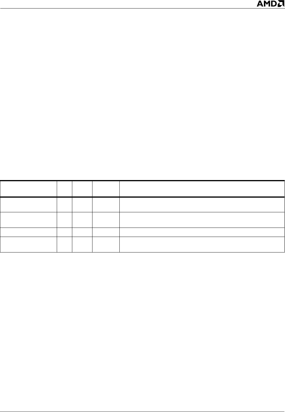
Instruction Reference PUSHFx 201
24594—Rev. 3.14—September 2007 AMD64 Technology
ELSIF ((CR4.VME=1) && (OPERAND_SIZE=16))
{
PUSH.v old_RFLAGS // Pushed with VIF in the IF position.
// Pushed with IOPL=3.
EXIT
}
ELSE // ((RFLAGS.IOPL<3) && ((CR4.VME=0) || (OPERAND_SIZE!=16)))
EXCEPTION [#GP(0)]
Related Instructions
POPF, POPFD, POPFQ
rFLAGS Affected
None
Exceptions
Exception Real
Virtual
8086 Protected Cause of Exception
Stack, #SS X X X A memory address exceeded the stack segment limit or was
non-canonical.
General protection,
#GP XThe I/O privilege level was less than 3 and either VME was not
enabled or the operand size was not 16-bit.
Page fault, #PF X X A page fault resulted from the execution of the instruction.
Alignment check,
#AC XX
An unaligned memory reference was performed while
alignment checking was enabled.

202 RCL Instruction Reference
AMD64 Technology 24594—Rev. 3.14—September 2007
Rotates the bits of a register or memory location (first operand) to the left (more significant bit
positions) and through the carry flag by the number of bit positions in an unsigned immediate value or
the CL register (second operand). The bits rotated through the carry flag are rotated back in at the right
end (lsb) of the first operand location.
The processor masks the upper three bits of the count operand, thus restricting the count to a number
between 0 and 31. When the destination is 64 bits wide, the processor masks the upper two bits of the
count, providing a count in the range of 0 to 63.
For 1-bit rotates, the instruction sets the OF flag to the exclusive OR of the CF bit (after the rotate) and
the most significant bit of the result. When the rotate count is greater than 1, the OF flag is undefined.
When the rotate count is 0, no flags are affected.
RCL Rotate Through Carry Left
Mnemonic Opcode Description
RCL reg/mem8,1 D0 /2 Rotate the 9 bits consisting of the carry flag and an 8-bit
register or memory location left 1 bit.
RCL reg/mem8, CL D2 /2
Rotate the 9 bits consisting of the carry flag and an 8-bit
register or memory location left the number of bits
specified in the CL register.
RCL reg/mem8, imm8 C0 /2 ib
Rotate the 9 bits consisting of the carry flag and an 8-bit
register or memory location left the number of bits
specified by an 8-bit immediate value.
RCL reg/mem16, 1 D1 /2 Rotate the 17 bits consisting of the carry flag and a 16-
bit register or memory location left 1 bit.
RCL reg/mem16, CL D3 /2
Rotate the 17 bits consisting of the carry flag and a 16-
bit register or memory location left the number of bits
specified in the CL register.
RCL reg/mem16, imm8 C1 /2 ib
Rotate the 17 bits consisting of the carry flag and a 16-
bit register or memory location left the number of bits
specified by an 8-bit immediate value.
RCL reg/mem32, 1 D1 /2 Rotate the 33 bits consisting of the carry flag and a 32-
bit register or memory location left 1 bit.
RCL reg/mem32, CL D3 /2
Rotate 33 bits consisting of the carry flag and a 32-bit
register or memory location left the number of bits
specified in the CL register.
RCL reg/mem32, imm8 C1 /2 ib
Rotate the 33 bits consisting of the carry flag and a 32-
bit register or memory location left the number of bits
specified by an 8-bit immediate value.
RCL reg/mem64, 1 D1 /2 Rotate the 65 bits consisting of the carry flag and a 64-
bit register or memory location left 1 bit.

Instruction Reference RCL 203
24594—Rev. 3.14—September 2007 AMD64 Technology
Related Instructions
RCR, ROL, ROR
rFLAGS Affected
Exceptions
RCL reg/mem64, CL D3 /2
Rotate the 65 bits consisting of the carry flag and a 64-
bit register or memory location left the number of bits
specified in the CL register.
RCL reg/mem64, imm8 C1 /2 ib
Rotates the 65 bits consisting of the carry flag and a 64-
bit register or memory location left the number of bits
specified by an 8-bit immediate value.
ID VIP VIF AC VM RF NT IOPL OF DF IF TF SF ZF AF PF CF
MM
2120191817161413–1211109876420
Note: Bits 31–22, 15, 5, 3, and 1 are reserved. A flag set to 1 or cleared to 0 is M (modified). Unaffected flags are
blank. Undefined flags are U.
Exception Real
Virtual
8086 Protected Cause of Exception
Stack, #SS X X X A memory address exceeded the stack segment limit or was
non-canonical.
General protection,
#GP
XX XA memory address exceeded a data segment limit or was non-
canonical.
X The destination operand was in a non-writable segment.
X A null data segment was used to reference memory.
Page fault, #PF X X A page fault resulted from the execution of the instruction.
Alignment check,
#AC XX
An unaligned memory reference was performed while
alignment checking was enabled.
Mnemonic Opcode Description

204 RCR Instruction Reference
AMD64 Technology 24594—Rev. 3.14—September 2007
Rotates the bits of a register or memory location (first operand) to the right (toward the less significant
bit positions) and through the carry flag by the number of bit positions in an unsigned immediate value
or the CL register (second operand). The bits rotated through the carry flag are rotated back in at the
left end (msb) of the first operand location.
The processor masks the upper three bits in the count operand, thus restricting the count to a number
between 0 and 31. When the destination is 64 bits wide, the processor masks the upper two bits of the
count, providing a count in the range of 0 to 63.
For 1-bit rotates, the instruction sets the OF flag to the exclusive OR of the CF flag (before the rotate)
and the most significant bit of the original value. When the rotate count is greater than 1, the OF flag is
undefined. When the rotate count is 0, no flags are affected.
RCR Rotate Through Carry Right
Mnemonic Opcode Description
RCR reg/mem8, 1 D0 /3 Rotate the 9 bits consisting of the carry flag and an 8-bit
register or memory location right 1 bit.
RCR reg/mem8,CL D2 /3
Rotate the 9 bits consisting of the carry flag and an 8-bit
register or memory location right the number of bits
specified in the CL register.
RCR reg/mem8,imm8 C0 /3 ib
Rotate the 9 bits consisting of the carry flag and an 8-bit
register or memory location right the number of bits
specified by an 8-bit immediate value.
RCR reg/mem16,1 D1 /3 Rotate the 17 bits consisting of the carry flag and a 16-
bit register or memory location right 1 bit.
RCR reg/mem16,CL D3 /3
Rotate the17 bits consisting of the carry flag and a 16-
bit register or memory location right the number of bits
specified in the CL register.
RCR reg/mem16, imm8 C1 /3 ib
Rotate the 17 bits consisting of the carry flag and a 16-
bit register or memory location right the number of bits
specified by an 8-bit immediate value.
RCR reg/mem32,1 D1 /3 Rotate the 33 bits consisting of the carry flag and a 32-
bit register or memory location right 1 bit.
RCR reg/mem32,CL D3 /3
Rotate 33 bits consisting of the carry flag and a 32-bit
register or memory location right the number of bits
specified in the CL register.
RCR reg/mem32, imm8 C1 /3 ib
Rotate the 33 bits consisting of the carry flag and a 32-
bit register or memory location right the number of bits
specified by an 8-bit immediate value.
RCR reg/mem64,1 D1 /3 Rotate the 65 bits consisting of the carry flag and a 64-
bit register or memory location right 1 bit.
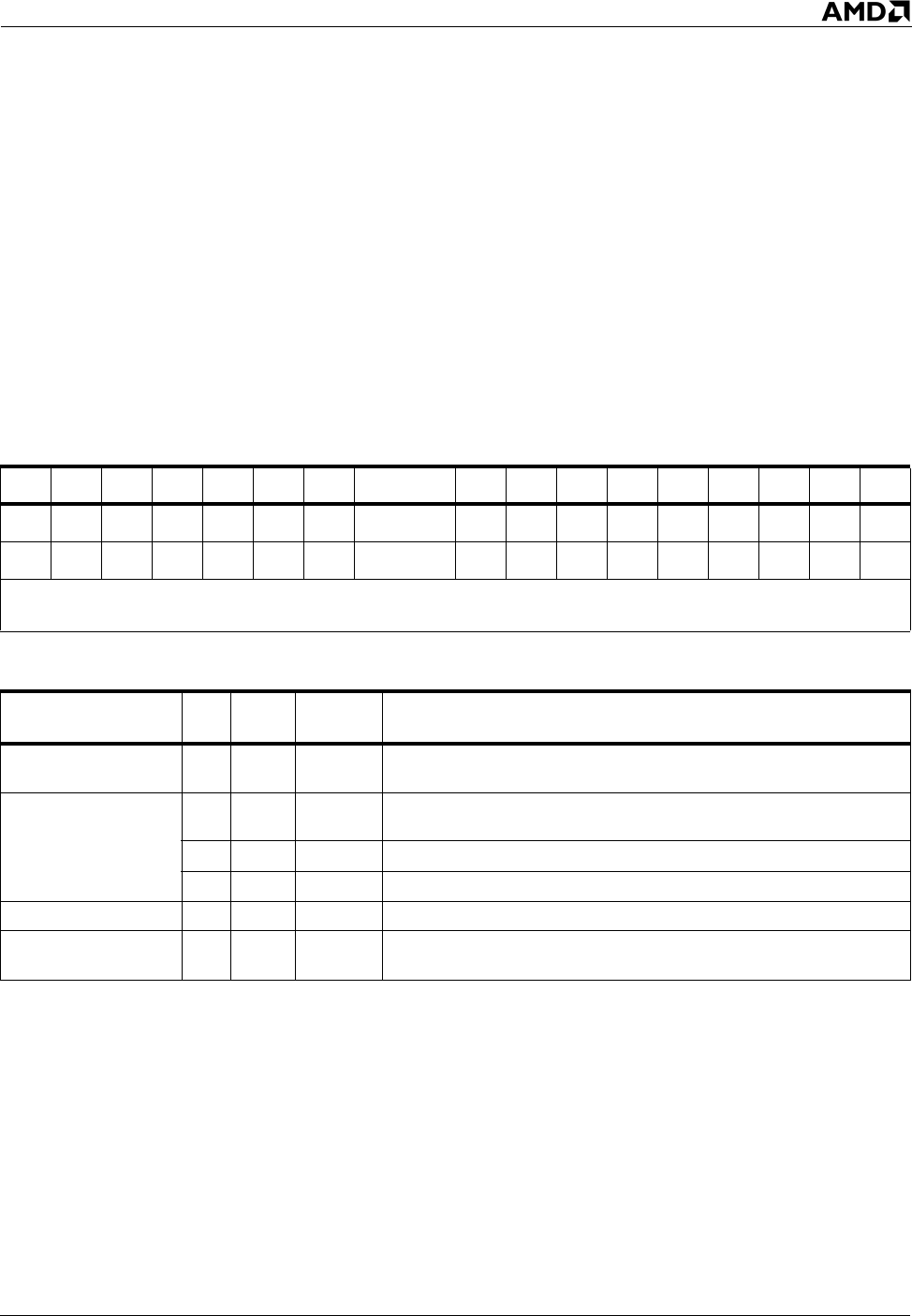
Instruction Reference RCR 205
24594—Rev. 3.14—September 2007 AMD64 Technology
Related Instructions
RCL, ROR, ROL
rFLAGS Affected
Exceptions
RCR reg/mem64,CL D3 /3
Rotate 65 bits consisting of the carry flag and a 64-bit
register or memory location right the number of bits
specified in the CL register.
RCR reg/mem64, imm8 C1 /3 ib
Rotate the 65 bits consisting of the carry flag and a 64-
bit register or memory location right the number of bits
specified by an 8-bit immediate value.
ID VIP VIF AC VM RF NT IOPL OF DF IF TF SF ZF AF PF CF
MM
2120191817161413–1211109876420
Note: Bits 31–22, 15, 5, 3, and 1 are reserved. A flag set to 1 or cleared to 0 is M (modified). Unaffected flags are
blank. Undefined flags are U.
Exception Real
Virtual
8086 Protected Cause of Exception
Stack, #SS X X X A memory address exceeded the stack segment limit or was
non-canonical.
General protection,
#GP
XX XA memory address exceeded a data segment limit or was non-
canonical.
X The destination operand was in a non-writable segment.
X A null data segment was used to reference memory.
Page fault, #PF X X A page fault resulted from the execution of the instruction.
Alignment check,
#AC XX
An unaligned memory reference was performed while
alignment checking was enabled.
Mnemonic Opcode Description

206 RET (Near) Instruction Reference
AMD64 Technology 24594—Rev. 3.14—September 2007
Returns from a procedure previously entered by a CALL near instruction. This form of the RET
instruction returns to a calling procedure within the current code segment.
This instruction pops the rIP from the stack, with the size of the pop determined by the operand size.
The new rIP is then zero-extended to 64 bits. The RET instruction can accept an immediate value
operand that it adds to the rSP after it pops the target rIP. This action skips over any parameters
previously passed back to the subroutine that are no longer needed.
In 64-bit mode, the operand size defaults to 64 bits (eight bytes) without the need for a REX prefix. No
prefix is available to encode a 32-bit operand size in 64-bit mode.
See RET (Far) for information on far returns—returns to procedures located outside of the current
code segment. For details about control-flow instructions, see “Control Transfers” in Volume 1, and
“Control-Transfer Privilege Checks” in Volume 2.
Related Instructions
CALL (Near), CALL (Far), RET (Far)
rFLAGS Affected
None
Exceptions
RET (Near) Near Return from Called Procedure
Mnemonic Opcode Description
RET C3 Near return to the calling procedure.
RET imm16 C2 iw Near return to the calling procedure then pop the
specified number of bytes from the stack.
Exception Real
Virtual
8086 Protected Cause of Exception
Stack, #SS X X X A memory address exceeded the stack segment limit or was
non-canonical.
General protection,
#GP XX XThe target offset exceeded the code segment limit or was non-
canonical.
Page fault, #PF X X A page fault resulted from the execution of the instruction.
Alignment check,
#AC XX
An unaligned memory reference was performed while
alignment checking was enabled.

Instruction Reference RET (Far) 207
24594—Rev. 3.14—September 2007 AMD64 Technology
Returns from a procedure previously entered by a CALL Far instruction. This form of the RET
instruction returns to a calling procedure in a different segment than the current code segment. It can
return to the same CPL or to a less privileged CPL.
RET Far pops a target CS and rIP from the stack. If the new code segment is less privileged than the
current code segment, the stack pointer is incremented by the number of bytes indicated by the
immediate operand, if present; then a new SS and rSP are also popped from the stack.
The final value of rSP is incremented by the number of bytes indicated by the immediate operand, if
present. This action skips over the parameters (previously passed to the subroutine) that are no longer
needed.
All stack pops are determined by the operand size. If necessary, the target rIP is zero-extended to 64
bits before assuming program control.
If the CPL changes, the data segment selectors are set to NULL for any of the data segments (DS, ES,
FS, GS) not accessible at the new CPL.
See RET (Near) for information on near returns—returns to procedures located inside the current code
segment. For details about control-flow instructions, see “Control Transfers” in Volume 1, and
“Control-Transfer Privilege Checks” in Volume 2.
Action
// Far returns (RETF)
// See “Pseudocode Definitions” on page 41.
RETF_START:
IF (REAL_MODE)
RETF_REAL_OR_VIRTUAL
ELSIF (PROTECTED_MODE)
RETF_PROTECTED
ELSE // (VIRTUAL_MODE)
RETF_REAL_OR_VIRTUAL
RETF_REAL_OR_VIRTUAL:
IF (OPCODE = retf imm16)
temp_IMM = word-sized immediate specified in the instruction,
zero-extended to 64 bits
RET (Far) Far Return from Called Procedure
Mnemonic Opcode Description
RETF CB Far return to the calling procedure.
RETF imm16 CA iw Far return to the calling procedure, then pop the
specified number of bytes from the stack.

208 RET (Far) Instruction Reference
AMD64 Technology 24594—Rev. 3.14—September 2007
ELSE // (OPCODE = retf)
temp_IMM = 0
POP.v temp_RIP
POP.v temp_CS
IF (temp_RIP > CS.limit)
EXCEPTION [#GP(0)]
CS.sel = temp_CS
CS.base = temp_CS SHL 4
RSP.s = RSP + temp_IMM
RIP = temp_RIP
EXIT
RETF_PROTECTED:
IF (OPCODE = retf imm16)
temp_IMM = word-sized immediate specified in the instruction,
zero-extended to 64 bits
ELSE // (OPCODE = retf)
temp_IMM = 0
POP.v temp_RIP
POP.v temp_CS
temp_CPL = temp_CS.rpl
IF (CPL=temp_CPL)
{
CS = READ_DESCRIPTOR (temp_CS, iret_chk)
RSP.s = RSP + temp_IMM
IF ((64BIT_MODE) && (temp_RIP is non-canonical)
|| (!64BIT_MODE) && (temp_RIP > CS.limit))
EXCEPTION [#GP(0)]
RIP = temp_RIP
EXIT
}
ELSE // (CPL!=temp_CPL)
{
RSP.s = RSP + temp_IMM
POP.v temp_RSP
POP.v temp_SS
CS = READ_DESCRIPTOR (temp_CS, iret_chk)

Instruction Reference RET (Far) 209
24594—Rev. 3.14—September 2007 AMD64 Technology
CPL = temp_CPL
IF ((64BIT_MODE) && (temp_RIP is non-canonical)
|| (!64BIT_MODE) && (temp_RIP > CS.limit))
EXCEPTION [#GP(0)]
SS = READ_DESCRIPTOR (temp_SS, ss_chk)
RSP.s = temp_RSP + temp_IMM
IF (changing CPL)
{
FOR (seg = ES, DS, FS, GS)
IF ((seg.attr.dpl < CPL) && ((seg.attr.type = ’data’)
|| (seg.attr.type = ’non-conforming-code’)))
{
seg = NULL // can’t use lower dpl data segment at higher cpl
}
}
RIP = temp_RIP
EXIT
}
Related Instructions
CALL (Near), CALL (Far), RET (Near)
rFLAGS Affected
None
Exceptions
Exception Real
Virtual
8086 Protected Cause of Exception
Segment not
present, #NP
(selector)
X The return code segment was marked not present.
Stack, #SS X X X A memory address exceeded the stack segment limit or was
non-canonical.
Stack, #SS
(selector) X The return stack segment was marked not present.
General protection,
#GP XX XThe target offset exceeded the code segment limit or was non-
canonical.

210 RET (Far) Instruction Reference
AMD64 Technology 24594—Rev. 3.14—September 2007
General protection,
#GP
(selector)
X The return code selector was a null selector.
XThe return stack selector was a null selector and the return
mode was non-64-bit mode or CPL was 3.
XThe return code or stack descriptor exceeded the descriptor
table limit.
XThe return code or stack selector’s TI bit was set but the LDT
selector was a null selector.
XThe segment descriptor for the return code was not a code
segment.
XThe RPL of the return code segment selector was less than
the CPL.
X
The return code segment was non-conforming and the
segment selector’s DPL was not equal to the RPL of the code
segment’s segment selector.
X
The return code segment was conforming and the segment
selector’s DPL was greater than the RPL of the code
segment’s segment selector.
XThe segment descriptor for the return stack was not a writable
data segment.
XThe stack segment descriptor DPL was not equal to the RPL
of the return code segment selector.
XThe stack segment selector RPL was not equal to the RPL of
the return code segment selector.
Page fault, #PF X X A page fault resulted from the execution of the instruction.
Alignment check,
#AC XX
An unaligned-memory reference was performed while
alignment checking was enabled.
Exception Real
Virtual
8086 Protected Cause of Exception

Instruction Reference ROL 211
24594—Rev. 3.14—September 2007 AMD64 Technology
Rotates the bits of a register or memory location (first operand) to the left (toward the more significant
bit positions) by the number of bit positions in an unsigned immediate value or the CL register (second
operand). The bits rotated out left are rotated back in at the right end (lsb) of the first operand location.
The processor masks the upper three bits of the count operand, thus restricting the count to a number
between 0 and 31. When the destination is 64 bits wide, it masks the upper two bits of the count,
providing a count in the range of 0 to 63.
After completing the rotation, the instruction sets the CF flag to the last bit rotated out (the lsb of the
result). For 1-bit rotates, the instruction sets the OF flag to the exclusive OR of the CF bit (after the
rotate) and the most significant bit of the result. When the rotate count is greater than 1, the OF flag is
undefined. When the rotate count is 0, no flags are affected.
Related Instructions
RCL, RCR, ROR
ROL Rotate Left
Mnemonic Opcode Description
ROL reg/mem8, 1 D0 /0 Rotate an 8-bit register or memory operand left 1 bit.
ROL reg/mem8, CL D2 /0 Rotate an 8-bit register or memory operand left the
number of bits specified in the CL register.
ROL reg/mem8, imm8 C0 /0 ib Rotate an 8-bit register or memory operand left the
number of bits specified by an 8-bit immediate value.
ROL reg/mem16, 1 D1 /0 Rotate a 16-bit register or memory operand left 1 bit.
ROL reg/mem16, CL D3 /0 Rotate a 16-bit register or memory operand left the
number of bits specified in the CL register.
ROL reg/mem16, imm8 C1 /0 ib Rotate a 16-bit register or memory operand left the
number of bits specified by an 8-bit immediate value.
ROL reg/mem32, 1 D1 /0 Rotate a 32-bit register or memory operand left 1 bit.
ROL reg/mem32, CL D3 /0 Rotate a 32-bit register or memory operand left the
number of bits specified in the CL register.
ROL reg/mem32, imm8 C1 /0 ib Rotate a 32-bit register or memory operand left the
number of bits specified by an 8-bit immediate value.
ROL reg/mem64, 1 D1 /0 Rotate a 64-bit register or memory operand left 1 bit.
ROL reg/mem64, CL D3 /0 Rotate a 64-bit register or memory operand left the
number of bits specified in the CL register.
ROL reg/mem64, imm8 C1 /0 ib Rotate a 64-bit register or memory operand left the
number of bits specified by an 8-bit immediate value.

212 ROL Instruction Reference
AMD64 Technology 24594—Rev. 3.14—September 2007
rFLAGS Affected
Exceptions
ID VIP VIF AC VM RF NT IOPL OF DF IF TF SF ZF AF PF CF
MM
2120191817161413–1211109876420
Note: Bits 31–22, 15, 5, 3, and 1 are reserved. A flag set to 1 or cleared to 0 is M (modified). Unaffected flags are
blank. Undefined flags are U.
Exception Real
Virtual
8086 Protected Cause of Exception
Stack, #SS X X X A memory address exceeded the stack segment limit or was
non-canonical.
General protection,
#GP
XX XA memory address exceeded a data segment limit or was non-
canonical.
X The destination operand was in a non-writable segment.
X A null data segment was used to reference memory.
Page fault, #PF X X A page fault resulted from the execution of the instruction.
Alignment check,
#AC XX
An unaligned memory reference was performed while
alignment checking was enabled.

Instruction Reference ROR 213
24594—Rev. 3.14—September 2007 AMD64 Technology
Rotates the bits of a register or memory location (first operand) to the right (toward the less significant
bit positions) by the number of bit positions in an unsigned immediate value or the CL register (second
operand). The bits rotated out right are rotated back in at the left end (the most significant bit) of the
first operand location.
The processor masks the upper three bits of the count operand, thus restricting the count to a number
between 0 and 31. When the destination is 64 bits wide, the processor masks the upper two bits of the
count, providing a count in the range of 0 to 63.
After completing the rotation, the instruction sets the CF flag to the last bit rotated out (the most
significant bit of the result). For 1-bit rotates, the instruction sets the OF flag to the exclusive OR of the
two most significant bits of the result. When the rotate count is greater than 1, the OF flag is undefined.
When the rotate count is 0, no flags are affected.
Related Instructions
RCL, RCR, ROL
ROR Rotate Right
Mnemonic Opcode Description
ROR reg/mem8, 1 D0 /1 Rotate an 8-bit register or memory location right 1 bit.
ROR reg/mem8, CL D2 /1 Rotate an 8-bit register or memory location right the
number of bits specified in the CL register.
ROR reg/mem8, imm8 C0 /1 ib Rotate an 8-bit register or memory location right the
number of bits specified by an 8-bit immediate value.
ROR reg/mem16, 1 D1 /1 Rotate a 16-bit register or memory location right 1 bit.
ROR reg/mem16, CL D3 /1 Rotate a 16-bit register or memory location right the
number of bits specified in the CL register.
ROR reg/mem16, imm8 C1 /1 ib Rotate a 16-bit register or memory location right the
number of bits specified by an 8-bit immediate value.
ROR reg/mem32, 1 D1 /1 Rotate a 32-bit register or memory location right 1 bit.
ROR reg/mem32, CL D3 /1 Rotate a 32-bit register or memory location right the
number of bits specified in the CL register.
ROR reg/mem32, imm8 C1 /1 ib Rotate a 32-bit register or memory location right the
number of bits specified by an 8-bit immediate value.
ROR reg/mem64, 1 D1 /1 Rotate a 64-bit register or memory location right 1 bit.
ROR reg/mem64, CL D3 /1 Rotate a 64-bit register or memory operand right the
number of bits specified in the CL register.
ROR reg/mem64, imm8 C1 /1 ib Rotate a 64-bit register or memory operand right the
number of bits specified by an 8-bit immediate value.

214 ROR Instruction Reference
AMD64 Technology 24594—Rev. 3.14—September 2007
rFLAGS Affected
Exceptions
ID VIP VIF AC VM RF NT IOPL OF DF IF TF SF ZF AF PF CF
MM
2120191817161413–1211109876420
Note: Bits 31–22, 15, 5, 3, and 1 are reserved. A flag set to 1 or cleared to 0 is M (modified). Unaffected flags are
blank. Undefined flags are U.
Exception Real
Virtual
8086 Protected Cause of Exception
Stack, #SS X X X A memory address exceeded the stack segment limit or was
non-canonical.
General protection,
#GP
XX XA memory address exceeded a data segment limit or was non-
canonical.
X The destination operand was in a non-writable segment.
X A null data segment was used to reference memory.
Page fault, #PF X X A page fault resulted from the execution of the instruction.
Alignment check,
#AC XX
An unaligned memory reference was performed while
alignment checking was enabled.
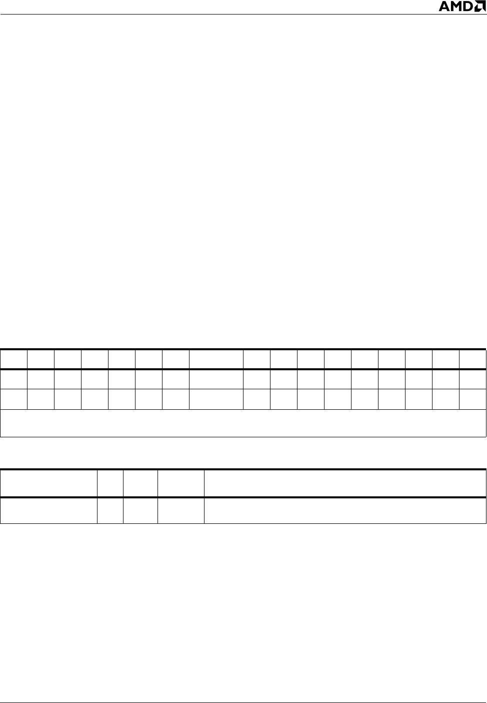
Instruction Reference SAHF 215
24594—Rev. 3.14—September 2007 AMD64 Technology
Loads the SF, ZF, AF, PF, and CF flags of the EFLAGS register with values from the corresponding
bits in the AH register (bits 7, 6, 4, 2, and 0, respectively). The instruction ignores bits 1, 3, and 5 of
register AH; it sets those bits in the EFLAGS register to 1, 0, and 0, respectively.
The SAHF instruction can only be executed in 64-bit mode if supported by the processor
implementation. Check the status of ECX bit 0 returned by CPUID function 8000_0001h to verify that
the processor supports SAHF in 64-bit mode.
Related Instructions
LAHF
rFLAGS Affected
Exceptions
SAHF Store AH into Flags
Mnemonic Opcode Description
SAHF 9E
Loads the sign flag, the zero flag, the auxiliary flag, the
parity flag, and the carry flag from the AH register into
the lower 8 bits of the EFLAGS register.
ID VIP VIF AC VM RF NT IOPL OF DF IF TF SF ZF AF PF CF
MMMMM
2120191817161413–1211109876420
Note: Bits 31–22, 15, 5, 3, and 1 are reserved. A flag set to 1 or cleared to 0 is M (modified). Unaffected flags are
blank. Undefined flags are U.
Exception Real
Virtual
8086 Protected Cause of Exception
Invalid opcode, #UD X This instruction is not supported in 64-bit mode, as indicated
by ECX bit 0 returned by CPUID function 8000_0001h.

216 SAL, SHL Instruction Reference
AMD64 Technology 24594—Rev. 3.14—September 2007
Shifts the bits of a register or memory location (first operand) to the left through the CF bit by the
number of bit positions in an unsigned immediate value or the CL register (second operand). The
instruction discards bits shifted out of the CF flag. For each bit shift, the SAL instruction clears the
least-significant bit to 0. At the end of the shift operation, the CF flag contains the last bit shifted out of
the first operand.
The processor masks the upper three bits of the count operand, thus restricting the count to a number
between 0 and 31. When the destination is 64 bits wide, the processor masks the upper two bits of the
count, providing a count in the range of 0 to 63.
The effect of this instruction is multiplication by powers of two.
For 1-bit shifts, the instruction sets the OF flag to the exclusive OR of the CF bit (after the shift) and
the most significant bit of the result. When the shift count is greater than 1, the OF flag is undefined.
If the shift count is 0, no flags are modified.
SHL is an alias to the SAL instruction.
SAL
SHL
Shift Left
Mnemonic Opcode Description
SAL reg/mem8, 1 D0 /4 Shift an 8-bit register or memory location left 1 bit.
SAL reg/mem8, CL D2 /4 Shift an 8-bit register or memory location left the number
of bits specified in the CL register.
SAL reg/mem8, imm8 C0 /4 ib Shift an 8-bit register or memory location left the number
of bits specified by an 8-bit immediate value.
SAL reg/mem16, 1 D1 /4 Shift a 16-bit register or memory location left 1 bit.
SAL reg/mem16, CL D3 /4 Shift a 16-bit register or memory location left the number
of bits specified in the CL register.
SAL reg/mem16, imm8 C1 /4 ib Shift a 16-bit register or memory location left the number
of bits specified by an 8-bit immediate value.
SAL reg/mem32, 1 D1 /4 Shift a 32-bit register or memory location left 1 bit.
SAL reg/mem32, CL D3 /4 Shift a 32-bit register or memory location left the number
of bits specified in the CL register.
SAL reg/mem32, imm8 C1 /4 ib Shift a 32-bit register or memory location left the number
of bits specified by an 8-bit immediate value.
SAL reg/mem64, 1 D1 /4 Shift a 64-bit register or memory location left 1 bit.
SAL reg/mem64, CL D3 /4 Shift a 64-bit register or memory location left the number
of bits specified in the CL register.
SAL reg/mem64, imm8 C1 /4 ib Shift a 64-bit register or memory location left the number
of bits specified by an 8-bit immediate value.

Instruction Reference SAL, SHL 217
24594—Rev. 3.14—September 2007 AMD64 Technology
Related Instructions
SAR, SHR, SHLD, SHRD
rFLAGS Affected
SHL reg/mem8, 1 D0 /4 Shift an 8-bit register or memory location by 1 bit.
SHL reg/mem8, CL D2 /4 Shift an 8-bit register or memory location left the number
of bits specified in the CL register.
SHL reg/mem8, imm8 C0 /4 ib Shift an 8-bit register or memory location left the number
of bits specified by an 8-bit immediate value.
SHL reg/mem16, 1 D1 /4 Shift a 16-bit register or memory location left 1 bit.
SHL reg/mem16, CL D3 /4 Shift a 16-bit register or memory location left the number
of bits specified in the CL register.
SHL reg/mem16, imm8 C1 /4 ib Shift a 16-bit register or memory location left the number
of bits specified by an 8-bit immediate value.
SHL reg/mem32, 1 D1 /4 Shift a 32-bit register or memory location left 1 bit.
SHL reg/mem32, CL D3 /4 Shift a 32-bit register or memory location left the number
of bits specified in the CL register.
SHL reg/mem32, imm8 C1 /4 ib Shift a 32-bit register or memory location left the number
of bits specified by an 8-bit immediate value.
SHL reg/mem64, 1 D1 /4 Shift a 64-bit register or memory location left 1 bit.
SHL reg/mem64, CL D3 /4 Shift a 64-bit register or memory location left the number
of bits specified in the CL register.
SHL reg/mem64, imm8 C1 /4 ib Shift a 64-bit register or memory location left the number
of bits specified by an 8-bit immediate value.
ID VIP VIF AC VM RF NT IOPL OF DF IF TF SF ZF AF PF CF
MMMUMM
2120191817161413–1211109876420
Note: Bits 31–22, 15, 5, 3, and 1 are reserved. A flag set to 1 or cleared to 0 is M (modified). Unaffected flags are
blank. Undefined flags are U.
Mnemonic Opcode Description

218 SAL, SHL Instruction Reference
AMD64 Technology 24594—Rev. 3.14—September 2007
Exceptions
Exception Real
Virtual
8086 Protected Cause of Exception
Stack, #SS X X A memory address exceeded the stack segment limit or was
non-canonical.
General protection,
#GP
XX XA memory address exceeded a data segment limit or was non-
canonical.
X The destination operand was in a non-writable segment.
X A null data segment was used to reference memory.
Page fault, #PF X X A page fault resulted from the execution of the instruction.
Alignment check,
#AC XX
An unaligned memory reference was performed while
alignment checking was enabled.

Instruction Reference SAR 219
24594—Rev. 3.14—September 2007 AMD64 Technology
Shifts the bits of a register or memory location (first operand) to the right through the CF bit by the
number of bit positions in an unsigned immediate value or the CL register (second operand). The
instruction discards bits shifted out of the CF flag. At the end of the shift operation, the CF flag
contains the last bit shifted out of the first operand.
The SAR instruction does not change the sign bit of the target operand. For each bit shift, it copies the
sign bit to the next bit, preserving the sign of the result.
The processor masks the upper three bits of the count operand, thus restricting the count to a number
between 0 and 31. When the destination is 64 bits wide, the processor masks the upper two bits of the
count, providing a count in the range of 0 to 63.
For 1-bit shifts, the instruction clears the OF flag to 0. When the shift count is greater than 1, the OF
flag is undefined.
If the shift count is 0, no flags are modified.
Although the SAR instruction effectively divides the operand by a power of 2, the behavior is different
from the IDIV instruction. For example, shifting –11 (FFFFFFF5h) by two bits to the right (that is,
divide –11 by 4), gives a result of FFFFFFFDh, or –3, whereas the IDIV instruction for dividing –11 by
4 gives a result of –2. This is because the IDIV instruction rounds off the quotient to zero, whereas the
SAR instruction rounds off the remainder to zero for positive dividends and to negative infinity for
negative dividends. So, for positive operands, SAR behaves like the corresponding IDIV instruction.
For negative operands, it gives the same result if and only if all the shifted-out bits are zeroes;
otherwise, the result is smaller by 1.
SAR Shift Arithmetic Right
Mnemonic Opcode Description
SAR reg/mem8, 1 D0 /7 Shift a signed 8-bit register or memory operand right 1
bit.
SAR reg/mem8, CL D2 /7 Shift a signed 8-bit register or memory operand right the
number of bits specified in the CL register.
SAR reg/mem8, imm8 C0 /7 ib Shift a signed 8-bit register or memory operand right the
number of bits specified by an 8-bit immediate value.
SAR reg/mem16, 1 D1 /7 Shift a signed 16-bit register or memory operand right 1
bit.
SAR reg/mem16, CL D3 /7 Shift a signed 16-bit register or memory operand right
the number of bits specified in the CL register.
SAR reg/mem16, imm8 C1 /7 ib Shift a signed 16-bit register or memory operand right
the number of bits specified by an 8-bit immediate value.
SAR reg/mem32, 1 D1 /7 Shift a signed 32-bit register or memory location 1 bit.
SAR reg/mem32, CL D3 /7 Shift a signed 32-bit register or memory location right
the number of bits specified in the CL register.
220 SAR Instruction Reference
AMD64 Technology 24594—Rev. 3.14—September 2007
Related Instructions
SAL, SHL, SHR, SHLD, SHRD
rFLAGS Affected
Exceptions
SAR reg/mem32, imm8 C1 /7 ib Shift a signed 32-bit register or memory location right
the number of bits specified by an 8-bit immediate value.
SAR reg/mem64, 1 D1 /7 Shift a signed 64-bit register or memory location right 1
bit.
SAR reg/mem64, CL D3 /7 Shift a signed 64-bit register or memory location right
the number of bits specified in the CL register.
SAR reg/mem64, imm8 C1 /7 ib Shift a signed 64-bit register or memory location right
the number of bits specified by an 8-bit immediate value.
ID VIP VIF AC VM RF NT IOPL OF DF IF TF SF ZF AF PF CF
MMMUMM
2120191817161413–1211109876420
Note: Bits 31–22, 15, 5, 3, and 1 are reserved. A flag set to 1 or cleared to 0 is M (modified). Unaffected flags are
blank. Undefined flags are U.
Exception Real
Virtual
8086 Protected Cause of Exception
Stack, #SS X X X A memory address exceeded the stack segment limit or was
non-canonical.
General protection,
#GP
XX XA memory address exceeded a data segment limit or was non-
canonical.
X The destination operand was in a non-writable segment.
X A null data segment was used to reference memory.
Page fault, #PF X X A page fault resulted from the execution of the instruction.
Alignment check,
#AC XX
An unaligned memory reference was performed while
alignment checking was enabled.
Mnemonic Opcode Description

Instruction Reference SBB 221
24594—Rev. 3.14—September 2007 AMD64 Technology
Subtracts an immediate value or the value in a register or a memory location (second operand) from a
register or a memory location (first operand), and stores the result in the first operand location. If the
carry flag (CF) is 1, the instruction subtracts 1 from the result. Otherwise, it operates like SUB.
The SBB instruction sign-extends immediate value operands to the length of the first operand size.
This instruction evaluates the result for both signed and unsigned data types and sets the OF and CF
flags to indicate a borrow in a signed or unsigned result, respectively. It sets the SF flag to indicate the
sign of a signed result.
This instruction is useful for multibyte (multiword) numbers because it takes into account the borrow
from a previous SUB instruction.
The forms of the SBB instruction that write to memory support the LOCK prefix. For details about the
LOCK prefix, see “Lock Prefix” on page 8.
SBB Subtract with Borrow
Mnemonic Opcode Description
SBB AL, imm8 1C ib Subtract an immediate 8-bit value from the AL register
with borrow.
SBB AX, imm16 1D iw Subtract an immediate 16-bit value from the AX register
with borrow.
SBB EAX, imm32 1D id Subtract an immediate 32-bit value from the EAX
register with borrow.
SBB RAX, imm32 1D id Subtract a sign-extended immediate 32-bit value from
the RAX register with borrow.
SBB reg/mem8, imm8 80 /3 ib Subtract an immediate 8-bit value from an 8-bit register
or memory location with borrow.
SBB reg/mem16, imm16 81 /3 iw Subtract an immediate 16-bit value from a 16-bit register
or memory location with borrow.
SBB reg/mem32, imm32 81 /3 id Subtract an immediate 32-bit value from a 32-bit register
or memory location with borrow.
SBB reg/mem64, imm32 81 /3 id Subtract a sign-extended immediate 32-bit value from a
64-bit register or memory location with borrow.
SBB reg/mem16, imm8 83 /3 ib Subtract a sign-extended 8-bit immediate value from a
16-bit register or memory location with borrow.
SBB reg/mem32, imm8 83 /3 ib Subtract a sign-extended 8-bit immediate value from a
32-bit register or memory location with borrow.
SBB reg/mem64, imm8 83 /3 ib Subtract a sign-extended 8-bit immediate value from a
64-bit register or memory location with borrow.
SBB reg/mem8, reg8 18 /r Subtract the contents of an 8-bit register from an 8-bit
register or memory location with borrow.
SBB reg/mem16, reg16 19 /r Subtract the contents of a 16-bit register from a 16-bit
register or memory location with borrow.
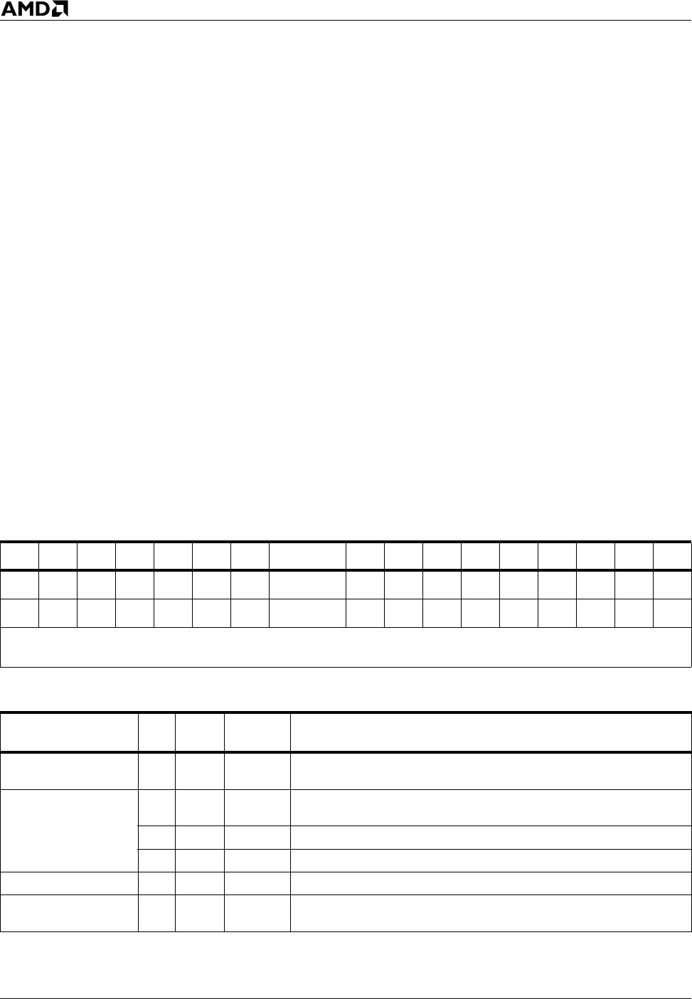
222 SBB Instruction Reference
AMD64 Technology 24594—Rev. 3.14—September 2007
Related Instructions
SUB, ADD, ADC
rFLAGS Affected
Exceptions
SBB reg/mem32, reg32 19 /r Subtract the contents of a 32-bit register from a 32-bit
register or memory location with borrow.
SBB reg/mem64, reg64 19 /r Subtract the contents of a 64-bit register from a 64-bit
register or memory location with borrow.
SBB reg8, reg/mem8 1A /r
Subtract the contents of an 8-bit register or memory
location from the contents of an 8-bit register with
borrow.
SBB reg16, reg/mem16 1B /r
Subtract the contents of a 16-bit register or memory
location from the contents of a 16-bit register with
borrow.
SBB reg32, reg/mem32 1B /r
Subtract the contents of a 32-bit register or memory
location from the contents of a 32-bit register with
borrow.
SBB reg64, reg/mem64 1B /r
Subtract the contents of a 64-bit register or memory
location from the contents of a 64-bit register with
borrow.
ID VIP VIF AC VM RF NT IOPL OF DF IF TF SF ZF AF PF CF
M MMMMM
2120191817161413–1211109876420
Note: Bits 31–22, 15, 5, 3, and 1 are reserved. A flag set to 1 or cleared to 0 is M (modified). Unaffected flags are
blank. Undefined flags are U.
Exception Real
Virtual
8086 Protected Cause of Exception
Stack, #SS X X X A memory address exceeded the stack segment limit or was
non-canonical.
General protection,
#GP
XX XA memory address exceeded a data segment limit or was non-
canonical.
X The destination operand was in a non-writable segment.
X A null data segment was used to reference memory.
Page fault, #PF X X A page fault resulted from the execution of the instruction.
Alignment check,
#AC XX
An unaligned memory reference was performed while
alignment checking was enabled.
Mnemonic Opcode Description

Instruction Reference SCASx 223
24594—Rev. 3.14—September 2007 AMD64 Technology
Compares the AL, AX, EAX, or RAX register with the byte, word, doubleword, or quadword pointed
to by ES:rDI, sets the status flags in the rFLAGS register according to the results, and then increments
or decrements the rDI register according to the state of the DF flag in the rFLAGS register.
If the DF flag is 0, the instruction increments the rDI register; otherwise, it decrements it. The
instruction increments or decrements the rDI register by 1, 2, 4, or 8, depending on the size of the
operands.
The forms of the SCASx instruction with an explicit operand address the operand at ES:rDI. The
explicit operand serves only to specify the size of the values being compared.
The no-operands forms of the instruction use the ES:rDI registers to point to the value to be compared.
The mnemonic determines the size of the operands and the specific register containing the other
comparison value.
For block comparisons, the SCASx instructions support the REPE or REPZ prefixes (they are
synonyms) and the REPNE or REPNZ prefixes (they are synonyms). For details about the REP
prefixes, see “Repeat Prefixes” on page 9. A SCASx instruction can also operate inside a loop
controlled by the LOOPcc instruction.
SCAS
SCASB
SCASW
SCASD
SCASQ
Scan String
Mnemonic Opcode Description
SCAS mem8 AE Compare the contents of the AL register with the byte at
ES:rDI, and then increment or decrement rDI.
SCAS mem16 AF Compare the contents of the AX register with the word
at ES:rDI, and then increment or decrement rDI.
SCAS mem32 AF
Compare the contents of the EAX register with the
doubleword at ES:rDI, and then increment or decrement
rDI.
SCAS mem64 AF
Compare the contents of the RAX register with the
quadword at ES:rDI, and then increment or decrement
rDI.
SCASB AE Compare the contents of the AL register with the byte at
ES:rDI, and then increment or decrement rDI.
SCASW AF Compare the contents of the AX register with the word
at ES:rDI, and then increment or decrement rDI.
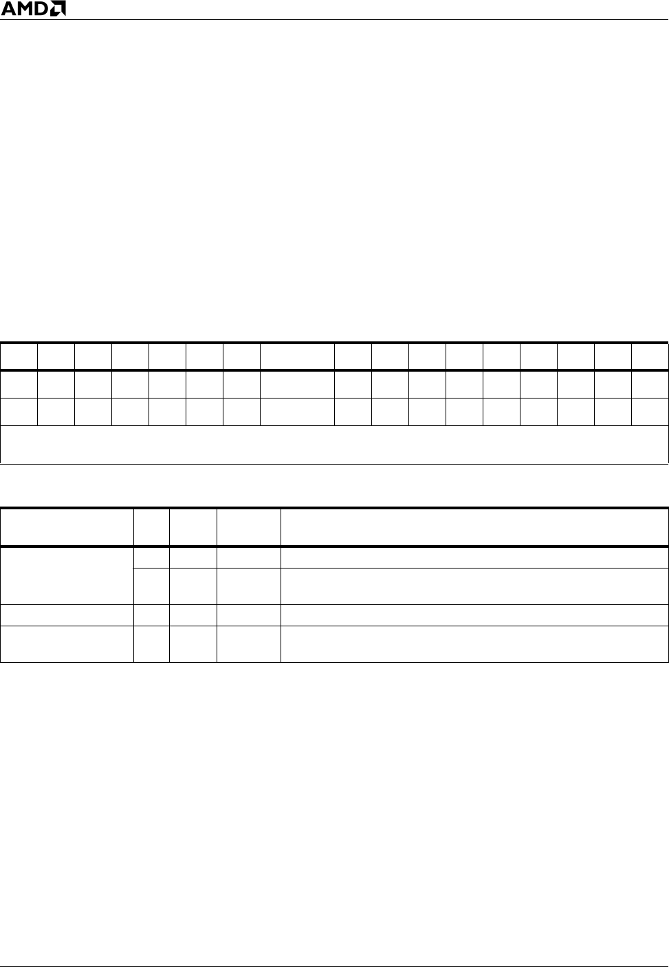
224 SCASx Instruction Reference
AMD64 Technology 24594—Rev. 3.14—September 2007
Related Instructions
CMP, CMPSx
rFLAGS Affected
Exceptions
SCASD AF
Compare the contents of the EAX register with the
doubleword at ES:rDI, and then increment or decrement
rDI.
SCASQ AF
Compare the contents of the RAX register with the
quadword at ES:rDI, and then increment or decrement
rDI.
ID VIP VIF AC VM RF NT IOPL OF DF IF TF SF ZF AF PF CF
M MMMMM
2120191817161413–1211109876420
Note: Bits 31–22, 15, 5, 3, and 1 are reserved. A flag set to 1 or cleared to 0 is M (modified). Unaffected flags are
blank. Undefined flags are U.
Exception Real
Virtual
8086 Protected Cause of Exception
General protection,
#GP
X A null ES segment was used to reference memory.
XX XA memory address exceeded the ES segment limit or was
non-canonical.
Page fault, #PF X X A page fault resulted from the execution of the instruction.
Alignment check,
#AC XX
An unaligned memory reference was performed while
alignment checking was enabled.
Mnemonic Opcode Description

Instruction Reference SETcc 225
24594—Rev. 3.14—September 2007 AMD64 Technology
Checks the status flags in the rFLAGS register and, if the flags meet the condition specified in the
mnemonic (cc), sets the value in the specified 8-bit memory location or register to 1. If the flags do not
meet the specified condition, SETcc clears the memory location or register to 0.
Mnemonics with the A (above) and B (below) tags are intended for use when performing unsigned
integer comparisons; those with G (greater) and L (less) tags are intended for use with signed integer
comparisons.
Software typically uses the SETcc instructions to set logical indicators. Like the CMOVcc instructions
(page 91), the SETcc instructions can replace two instructions—a conditional jump and a move.
Replacing conditional jumps with conditional sets can help avoid branch-prediction penalties that may
result from conditional jumps.
If the logical value “true” (logical one) is represented in a high-level language as an integer with all bits
set to 1, software can accomplish such representation by first executing the opposite SETcc
instruction—for example, the opposite of SETZ is SETNZ—and then decrementing the result.
A ModR/M byte is used to identify the operand. The reg field in the ModR/M byte is unused.
SETcc Set Byte on Condition
Mnemonic Opcode Description
SETO reg/mem8 0F 90 /0 Set byte if overflow (OF = 1).
SETNO reg/mem8 0F 91 /0 Set byte if not overflow (OF = 0).
SETB reg/mem8
SETC reg/mem8
SETNAE reg/mem8
0F 92 /0
Set byte if below (CF = 1).
Set byte if carry (CF = 1).
Set byte if not above or equal (CF = 1).
SETNB reg/mem8
SETNC reg/mem8
SETAE reg/mem8
0F 93 /0
Set byte if not below (CF = 0).
Set byte if not carry (CF = 0).
Set byte if above or equal (CF = 0).
SETZ reg/mem8
SETE reg/mem8 0F 94 /0 Set byte if zero (ZF = 1).
Set byte if equal (ZF = 1).
SETNZ reg/mem8
SETNE reg/mem8 0F 95 /0 Set byte if not zero (ZF = 0).
Set byte if not equal (ZF = 0).
SETBE reg/mem8
SETNA reg/mem8 0F 96 /0 Set byte if below or equal (CF = 1 or ZF = 1).
Set byte if not above (CF = 1 or ZF = 1).
SETNBE reg/mem8
SETA reg/mem8 0F 97 /0 Set byte if not below or equal (CF = 0 and ZF = 0).
Set byte if above (CF = 0 and ZF = 0).
SETS reg/mem8 0F 98 /0 Set byte if sign (SF = 1).
SETNS reg/mem8 0F 99 /0 Set byte if not sign (SF = 0).
SETP reg/mem8
SETPE reg/mem8 0F 9A /0 Set byte if parity (PF = 1).
Set byte if parity even (PF = 1).
SETNP reg/mem8
SETPO reg/mem8 0F 9B /0 Set byte if not parity (PF = 0).
Set byte if parity odd (PF = 0).
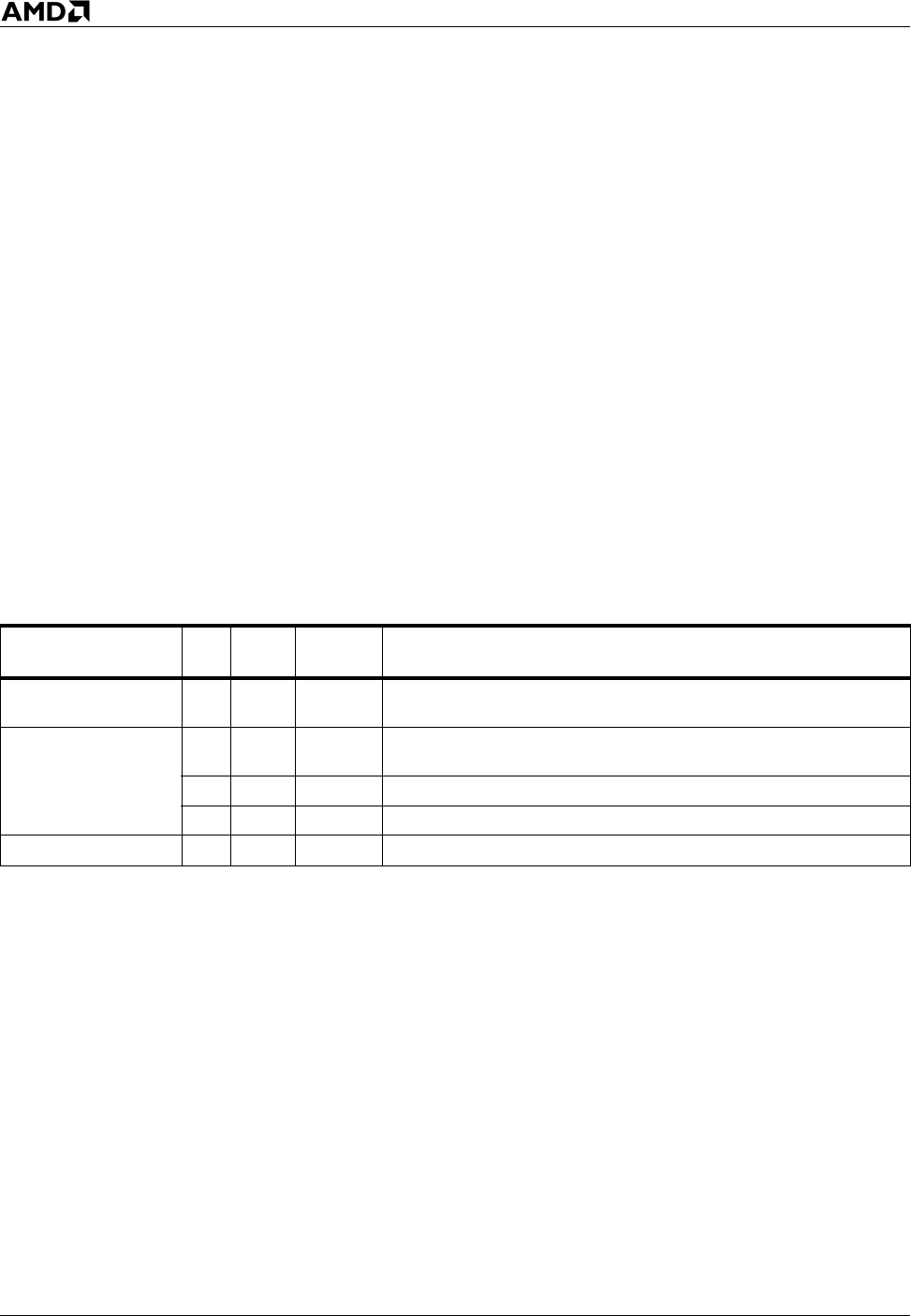
226 SETcc Instruction Reference
AMD64 Technology 24594—Rev. 3.14—September 2007
Related Instructions
None
rFLAGS Affected
None
Exceptions
SETL reg/mem8
SETNGE reg/mem8 0F 9C /0 Set byte if less (SF <> OF).
Set byte if not greater or equal (SF <> OF).
SETNL reg/mem8
SETGE reg/mem8 0F 9D /0 Set byte if not less (SF = OF).
Set byte if greater or equal (SF = OF).
SETLE reg/mem8
SETNG reg/mem8 0F 9E /0 Set byte if less or equal (ZF = 1 or SF <> OF).
Set byte if not greater (ZF = 1 or SF <> OF).
SETNLE reg/mem8
SETG reg/mem8 0F 9F /0 Set byte if not less or equal (ZF = 0 and SF = OF).
Set byte if greater (ZF = 0 and SF = OF).
Exception Real
Virtual
8086 Protected Cause of Exception
Stack, #SS X X X A memory address exceeded the stack segment limit or was
non-canonical.
General protection,
#GP
XX XA memory address exceeded a data segment limit or was non-
canonical.
X The destination operand was in a non-writable segment.
X A null data segment was used to reference memory.
Page fault, #PF X X A page fault resulted from the execution of the instruction.
Mnemonic Opcode Description

Instruction Reference SFENCE 227
24594—Rev. 3.14—September 2007 AMD64 Technology
Acts as a barrier to force strong memory ordering (serialization) between store instructions preceding
the SFENCE and store instructions that follow the SFENCE. Stores to differing memory types, or
within the WC memory type, may become visible out of program order; the SFENCE instruction
ensures that the system completes all previous stores in such a way that they are globally visible
before executing subsequent stores. This includes emptying the store buffer and all write-combining
buffers.
The SFENCE instruction is weakly-ordered with respect to load instructions, data and instruction
prefetches, and the LFENCE instruction. Speculative loads initiated by the processor, or specified
explicitly using cache-prefetch instructions, can be reordered around an SFENCE.
In addition to store instructions, SFENCE is strongly ordered with respect to other SFENCE
instructions, MFENCE instructions, and serializing instructions. Further details on the use of
MFENCE to order accesses among differing memory types may be found in AMD64 Architecture
Programmer’s Manual Volume 2: System Programming, section 7.4 “Memory Types” on page 170.
Support for the SFENCE instruction is indicated when the SSE bit (bit 25) is set to 1 in EDX after
executing CPUID function 0000_0001h.
Related Instructions
LFENCE, MFENCE
rFLAGS Affected
None
Exceptions
SFENCE Store Fence
Mnemonic Opcode Description
SFENCE 0F AE F8 Force strong ordering of (serialized) store operations.
Exception Real
Virtual
8086 Protected Cause of Exception
Invalid Opcode,
#UD XX X
The SSE instructions are not supported, as indicated by EDX
bit 25 of CPUID function 0000_0001h; and the AMD
extensions to MMX are not supported, as indicated by EDX bit
22 of CPUID function 8000_0001h.


Instruction Reference SHLD 229
24594—Rev. 3.14—September 2007 AMD64 Technology
Shifts the bits of a register or memory location (first operand) to the left by the number of bit positions
in an unsigned immediate value or the CL register (third operand), and shifts in a bit pattern (second
operand) from the right. At the end of the shift operation, the CF flag contains the last bit shifted out of
the first operand.
The processor masks the upper three bits of the count operand, thus restricting the count to a number
between 0 and 31. When the destination is 64 bits wide, the processor masks the upper two bits of the
count, providing a count in the range of 0 to 63. If the masked count is greater than the operand size,
the result in the destination register is undefined.
If the shift count is 0, no flags are modified.
If the count is 1 and the sign of the operand being shifted changes, the instruction sets the OF flag to 1.
If the count is greater than 1, OF is undefined.
Related Instructions
SHRD, SAL, SAR, SHR, SHL
SHLD Shift Left Double
Mnemonic Opcode Description
SHLD reg/mem16, reg16, imm8 0F A4 /r ib
Shift bits of a 16-bit destination register or memory
operand to the left the number of bits specified in an 8-
bit immediate value, while shifting in bits from the
second operand.
SHLD reg/mem16, reg16, CL 0F A5 /r
Shift bits of a 16-bit destination register or memory
operand to the left the number of bits specified in the CL
register, while shifting in bits from the second operand.
SHLD reg/mem32, reg32, imm8 0F A4 /r ib
Shift bits of a 32-bit destination register or memory
operand to the left the number of bits specified in an 8-
bit immediate value, while shifting in bits from the
second operand.
SHLD reg/mem32, reg32, CL 0F A5 /r
Shift bits of a 32-bit destination register or memory
operand to the left the number of bits specified in the CL
register, while shifting in bits from the second operand.
SHLD reg/mem64, reg64, imm8 0F A4 /r ib
Shift bits of a 64-bit destination register or memory
operand to the left the number of bits specified in an 8-
bit immediate value, while shifting in bits from the
second operand.
SHLD reg/mem64, reg64, CL 0F A5 /r
Shift bits of a 64-bit destination register or memory
operand to the left the number of bits specified in the CL
register, while shifting in bits from the second operand.

230 SHLD Instruction Reference
AMD64 Technology 24594—Rev. 3.14—September 2007
rFLAGS Affected
Exceptions
ID VIP VIF AC VM RF NT IOPL OF DF IF TF SF ZF AF PF CF
MMMUMM
2120191817161413–1211109876420
Note: Bits 31–22, 15, 5, 3, and 1 are reserved. A flag set to 1 or cleared to 0 is M (modified). Unaffected flags are blank.
Undefined flags are U.
Exception Real
Virtual
8086 Protected Cause of Exception
Stack, #SS X X X A memory address exceeded the stack segment limit or was
non-canonical.
General protection,
#GP
XX XA memory address exceeded a data segment limit or was non-
canonical.
X The destination operand was in a non-writable segment.
X A null data segment was used to reference memory.
Page fault, #PF X X A page fault resulted from the execution of the instruction.
Alignment check,
#AC XX
An unaligned memory reference was performed while
alignment checking was enabled.

Instruction Reference SHR 231
24594—Rev. 3.14—September 2007 AMD64 Technology
Shifts the bits of a register or memory location (first operand) to the right through the CF bit by the
number of bit positions in an unsigned immediate value or the CL register (second operand). The
instruction discards bits shifted out of the CF flag. At the end of the shift operation, the CF flag
contains the last bit shifted out of the first operand.
For each bit shift, the instruction clears the most-significant bit to 0.
The effect of this instruction is unsigned division by powers of two.
The processor masks the upper three bits of the count operand, thus restricting the count to a number
between 0 and 31. When the destination is 64 bits wide, the processor masks the upper two bits of the
count, providing a count in the range of 0 to 63.
For 1-bit shifts, the instruction sets the OF flag to the most-significant bit of the original value. If the
count is greater than 1, the OF flag is undefined.
If the shift count is 0, no flags are modified.
SHR Shift Right
Mnemonic Opcode Description
SHR reg/mem8, 1 D0 /5 Shift an 8-bit register or memory operand right 1 bit.
SHR reg/mem8, CL D2 /5 Shift an 8-bit register or memory operand right the
number of bits specified in the CL register.
SHR reg/mem8, imm8 C0 /5 ib Shift an 8-bit register or memory operand right the
number of bits specified by an 8-bit immediate value.
SHR reg/mem16, 1 D1 /5 Shift a 16-bit register or memory operand right 1 bit.
SHR reg/mem16, CL D3 /5 Shift a 16-bit register or memory operand right the
number of bits specified in the CL register.
SHR reg/mem16, imm8 C1 /5 ib Shift a 16-bit register or memory operand right the
number of bits specified by an 8-bit immediate value.
SHR reg/mem32, 1 D1 /5 Shift a 32-bit register or memory operand right 1 bit.
SHR reg/mem32, CL D3 /5 Shift a 32-bit register or memory operand right the
number of bits specified in the CL register.
SHR reg/mem32, imm8 C1 /5 ib Shift a 32-bit register or memory operand right the
number of bits specified by an 8-bit immediate value.
SHR reg/mem64, 1 D1 /5 Shift a 64-bit register or memory operand right 1 bit.
SHR reg/mem64, CL D3 /5 Shift a 64-bit register or memory operand right the
number of bits specified in the CL register.
SHR reg/mem64, imm8 C1 /5 ib Shift a 64-bit register or memory operand right the
number of bits specified by an 8-bit immediate value.

232 SHR Instruction Reference
AMD64 Technology 24594—Rev. 3.14—September 2007
Related Instructions
SHL, SAL, SAR, SHLD, SHRD
rFLAGS Affected
Exceptions
ID VIP VIF AC VM RF NT IOPL OF DF IF TF SF ZF AF PF CF
MMMUMM
2120191817161413–1211109876420
Note: Bits 31–22, 15, 5, 3, and 1 are reserved. A flag set to 1 or cleared to 0 is M (modified). Unaffected flags are
blank. Undefined flags are U.
Exception Real
Virtual
8086 Protected Cause of Exception
Stack, #SS X X X A memory address exceeded the stack segment limit or was
non-canonical.
General protection,
#GP
XX XA memory address exceeded a data segment limit or was non-
canonical.
X The destination operand was in a non-writable segment.
X A null data segment was used to reference memory.
Page fault, #PF X X A page fault resulted from the execution of the instruction.
Alignment check,
#AC XX
An unaligned memory reference was performed while
alignment checking was enabled.

Instruction Reference SHRD 233
24594—Rev. 3.14—September 2007 AMD64 Technology
Shifts the bits of a register or memory location (first operand) to the right by the number of bit
positions in an unsigned immediate value or the CL register (third operand), and shifts in a bit pattern
(second operand) from the left. At the end of the shift operation, the CF flag contains the last bit shifted
out of the first operand.
The processor masks the upper three bits of the count operand, thus restricting the count to a number
between 0 and 31. When the destination is 64 bits wide, the processor masks the upper two bits of the
count, providing a count in the range of 0 to 63. If the masked count is greater than the operand size,
the result in the destination register is undefined.
If the shift count is 0, no flags are modified.
If the count is 1 and the sign of the value being shifted changes, the instruction sets the OF flag to 1. If
the count is greater than 1, the OF flag is undefined.
Related Instructions
SHLD, SHR, SHL, SAR, SAL
SHRD Shift Right Double
Mnemonic Opcode Description
SHRD reg/mem16, reg16, imm8 0F AC /r ib
Shift bits of a 16-bit destination register or memory
operand to the right the number of bits specified in an 8-
bit immediate value, while shifting in bits from the
second operand.
SHRD reg/mem16, reg16, CL 0F AD /r
Shift bits of a 16-bit destination register or memory
operand to the right the number of bits specified in the
CL register, while shifting in bits from the second
operand.
SHRD reg/mem32, reg32, imm8 0F AC /r ib
Shift bits of a 32-bit destination register or memory
operand to the right the number of bits specified in an 8-
bit immediate value, while shifting in bits from the
second operand.
SHRD reg/mem32, reg32, CL 0F AD /r
Shift bits of a 32-bit destination register or memory
operand to the right the number of bits specified in the
CL register, while shifting in bits from the second
operand.
SHRD reg/mem64, reg64, imm8 0F AC /r ib
Shift bits of a 64-bit destination register or memory
operand to the right the number of bits specified in an 8-
bit immediate value, while shifting in bits from the
second operand.
SHRD reg/mem64, reg64, CL 0F AD /r
Shift bits of a 64-bit destination register or memory
operand to the right the number of bits specified in the
CL register, while shifting in bits from the second
operand.

234 SHRD Instruction Reference
AMD64 Technology 24594—Rev. 3.14—September 2007
rFLAGS Affected
Exceptions
ID VIP VIF AC VM RF NT IOPL OF DF IF TF SF ZF AF PF CF
MMMUMM
2120191817161413–1211109876420
Note: Bits 31–22, 15, 5, 3, and 1 are reserved. A flag set to 1 or cleared to 0 is M (modified). Unaffected flags are blank.
Undefined flags are U.
Exception Real
Virtual
8086 Protected Cause of Exception
Stack, #SS X X X A memory address exceeded the stack segment limit or was
non-canonical.
General protection,
#GP
XX XA memory address exceeded a data segment limit or was non-
canonical.
X The destination operand was in a non-writable segment.
X A null data segment was used to reference memory.
Page fault, #PF X X A page fault resulted from the execution of the instruction.
Alignment check,
#AC XX
An unaligned memory reference was performed while
alignment checking was enabled.
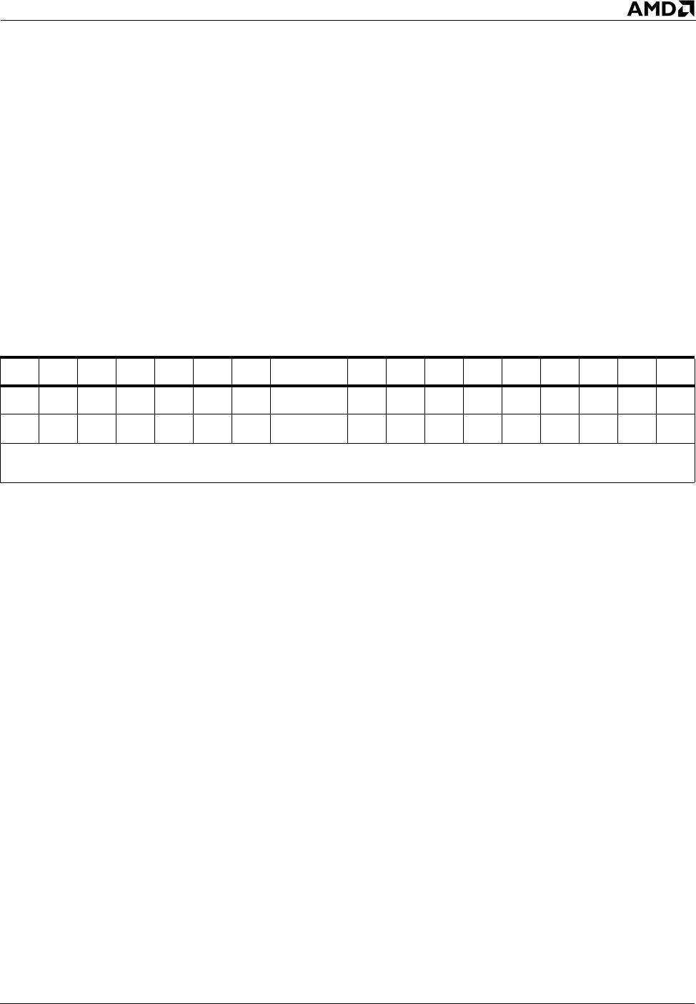
Instruction Reference STC 235
24594—Rev. 3.14—September 2007 AMD64 Technology
Sets the carry flag (CF) in the rFLAGS register to one.
Related Instructions
CLC, CMC
rFLAGS Affected
Exceptions
None
STC Set Carry Flag
Mnemonic Opcode Description
STC F9 Set the carry flag (CF) to one.
ID VIP VIF AC VM RF NT IOPL OF DF IF TF SF ZF AF PF CF
1
2120191817161413–1211109876420
Note: Bits 31–22, 15, 5, 3, and 1 are reserved. A flag set to 1 or cleared to 0 is M (modified). Unaffected flags are blank.
Undefined flags are U.
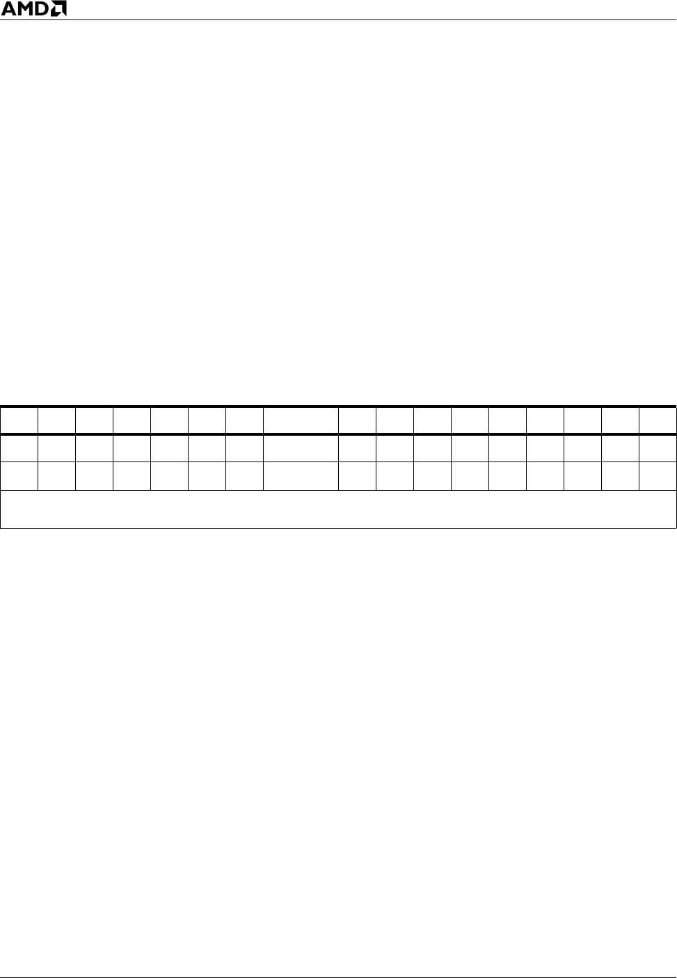
236 STD Instruction Reference
AMD64 Technology 24594—Rev. 3.14—September 2007
Set the direction flag (DF) in the rFLAGS register to 1. If the DF flag is 0, each iteration of a string
instruction increments the data pointer (index registers rSI or rDI). If the DF flag is 1, the string
instruction decrements the pointer. Use the CLD instruction before a string instruction to make the data
pointer increment.
Related Instructions
CLD, INSx, LODSx, MOVSx, OUTSx, SCASx, STOSx, CMPSx
rFLAGS Affected
Exceptions
None
STD Set Direction Flag
Mnemonic Opcode Description
STD FD Set the direction flag (DF) to one.
ID VIP VIF AC VM RF NT IOPL OF DF IF TF SF ZF AF PF CF
1
2120191817161413–1211109876420
Note: Bits 31–22, 15, 5, 3, and 1 are reserved. A flag set to 1 or cleared to 0 is M (modified). Unaffected flags are
blank. Undefined flags are U.

Instruction Reference STOSx 237
24594—Rev. 3.14—September 2007 AMD64 Technology
Copies a byte, word, doubleword, or quadword from the AL, AX, EAX, or RAX registers to the
memory location pointed to by ES:rDI and increments or decrements the rDI register according to the
state of the DF flag in the rFLAGS register.
If the DF flag is 0, the instruction increments the pointer; otherwise, it decrements the pointer. It
increments or decrements the pointer by 1, 2, 4, or 8, depending on the size of the value being copied.
The forms of the STOSx instruction with an explicit operand use the operand only to specify the type
(size) of the value being copied.
The no-operands forms specify the type (size) of the value being copied with the mnemonic.
The STOSx instructions support the REP prefixes. For details about the REP prefixes, see “Repeat
Prefixes” on page 9. The STOSx instructions can also operate inside a LOOPcc instruction.
Related Instructions
LODSx, MOVSx
STOS
STOSB
STOSW
STOSD
STOSQ
Store String
Mnemonic Opcode Description
STOS mem8 AA Store the contents of the AL register to ES:rDI, and then
increment or decrement rDI.
STOS mem16 AB Store the contents of the AX register to ES:rDI, and then
increment or decrement rDI.
STOS mem32 AB Store the contents of the EAX register to ES:rDI, and
then increment or decrement rDI.
STOS mem64 AB Store the contents of the RAX register to ES:rDI, and
then increment or decrement rDI.
STOSB AA Store the contents of the AL register to ES:rDI, and then
increment or decrement rDI.
STOSW AB Store the contents of the AX register to ES:rDI, and then
increment or decrement rDI.
STOSD AB Store the contents of the EAX register to ES:rDI, and
then increment or decrement rDI.
STOSQ AB Store the contents of the RAX register to ES:rDI, and
then increment or decrement rDI.
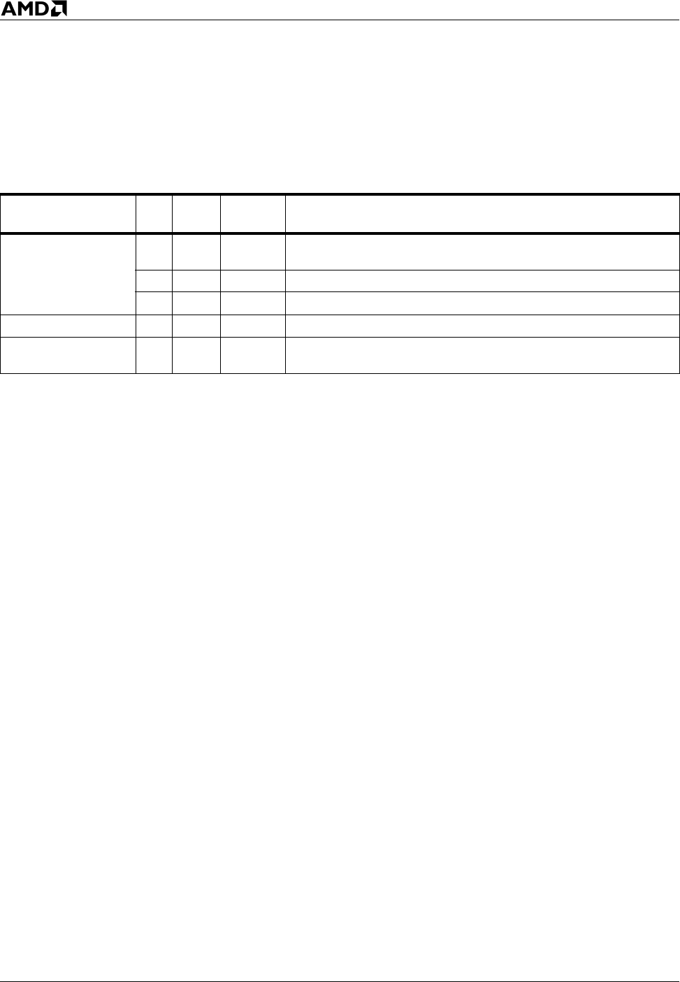
238 STOSx Instruction Reference
AMD64 Technology 24594—Rev. 3.14—September 2007
rFLAGS Affected
None
Exceptions
Exception Real
Virtual
8086 Protected Cause of Exception
General protection,
#GP
XX XA memory address exceeded the ES segment limit or was
non-canonical.
X The ES segment was a non-writable segment.
X A null ES segment was used to reference memory.
Page fault, #PF X X A page fault resulted from the execution of the instruction.
Alignment check,
#AC XX
An unaligned memory reference was performed while
alignment checking was enabled.

Instruction Reference SUB 239
24594—Rev. 3.14—September 2007 AMD64 Technology
Subtracts an immediate value or the value in a register or memory location (second operand) from a
register or a memory location (first operand) and stores the result in the first operand location. An
immediate value is sign-extended to the length of the first operand.
This instruction evaluates the result for both signed and unsigned data types and sets the OF and CF
flags to indicate a borrow in a signed or unsigned result, respectively. It sets the SF flag to indicate the
sign of a signed result.
The forms of the SUB instruction that write to memory support the LOCK prefix. For details about the
LOCK prefix, see “Lock Prefix” on page 8.
SUB Subtract
Mnemonic Opcode Description
SUB AL, imm8 2C ib Subtract an immediate 8-bit value from the AL register
and store the result in AL.
SUB AX, imm16 2D iw Subtract an immediate 16-bit value from the AX register
and store the result in AX.
SUB EAX, imm32 2D id Subtract an immediate 32-bit value from the EAX
register and store the result in EAX.
SUB RAX, imm32 2D id Subtract a sign-extended immediate 32-bit value from
the RAX register and store the result in RAX.
SUB reg/mem8, imm8 80 /5 ib Subtract an immediate 8-bit value from an 8-bit
destination register or memory location.
SUB reg/mem16, imm16 81 /5 iw Subtract an immediate 16-bit value from a 16-bit
destination register or memory location.
SUB reg/mem32, imm32 81 /5 id Subtract an immediate 32-bit value from a 32-bit
destination register or memory location.
SUB reg/mem64, imm32 81 /5 id Subtract a sign-extended immediate 32-bit value from a
64-bit destination register or memory location.
SUB reg/mem16, imm8 83 /5 ib Subtract a sign-extended immediate 8-bit value from a
16-bit register or memory location.
SUB reg/mem32, imm8 83 /5 ib Subtract a sign-extended immediate 8-bit value from a
32-bit register or memory location.
SUB reg/mem64, imm8 83 /5 ib Subtract a sign-extended immediate 8-bit value from a
64-bit register or memory location.
SUB reg/mem8, reg8 28 /r Subtract the contents of an 8-bit register from an 8-bit
destination register or memory location.
SUB reg/mem16, reg16 29 /r Subtract the contents of a 16-bit register from a 16-bit
destination register or memory location.
SUB reg/mem32, reg32 29 /r Subtract the contents of a 32-bit register from a 32-bit
destination register or memory location.
SUB reg/mem64, reg64 29 /r Subtract the contents of a 64-bit register from a 64-bit
destination register or memory location.

240 SUB Instruction Reference
AMD64 Technology 24594—Rev. 3.14—September 2007
Related Instructions
ADC, ADD, SBB
rFLAGS Affected
Exceptions
SUB reg8, reg/mem8 2A /r Subtract the contents of an 8-bit register or memory
operand from an 8-bit destination register.
SUB reg16, reg/mem16 2B /r Subtract the contents of a 16-bit register or memory
operand from a 16-bit destination register.
SUB reg32, reg/mem32 2B /r Subtract the contents of a 32-bit register or memory
operand from a 32-bit destination register.
SUB reg64, reg/mem64 2B /r Subtract the contents of a 64-bit register or memory
operand from a 64-bit destination register.
ID VIP VIF AC VM RF NT IOPL OF DF IF TF SF ZF AF PF CF
M MMMMM
2120191817161413–1211109876420
Note: Bits 31–22, 15, 5, 3, and 1 are reserved. A flag set to 1 or cleared to 0 is M (modified). Unaffected flags are blank.
Undefined flags are U.
Exception Real
Virtual
8086 Protected Cause of Exception
Stack, #SS X X X A memory address exceeded the stack segment limit or was
non-canonical.
General protection,
#GP
XX XA memory address exceeded a data segment limit or was non-
canonical.
X The destination operand was in a non-writable segment.
X A null data segment was used to reference memory.
Page fault, #PF X X A page fault resulted from the execution of the instruction.
Alignment check,
#AC XX
An unaligned memory reference was performed while
alignment checking was enabled.
Mnemonic Opcode Description

Instruction Reference TEST 241
24594—Rev. 3.14—September 2007 AMD64 Technology
Performs a bit-wise logical AND on the value in a register or memory location (first operand) with an
immediate value or the value in a register (second operand) and sets the flags in the rFLAGS register
based on the result. While the AND instruction changes the contents of the destination and the flag
bits, the TEST instruction changes only the flag bits.
Related Instructions
AND, CMP
TEST Test Bits
Mnemonic Opcode Description
TEST AL, imm8 A8 ib AND an immediate 8-bit value with the contents of the
AL register and set rFLAGS to reflect the result.
TEST AX, imm16 A9 iw AND an immediate 16-bit value with the contents of the
AX register and set rFLAGS to reflect the result.
TEST EAX, imm32 A9 id AND an immediate 32-bit value with the contents of the
EAX register and set rFLAGS to reflect the result.
TEST RAX, imm32 A9 id
AND a sign-extended immediate 32-bit value with the
contents of the RAX register and set rFLAGS to reflect
the result.
TEST reg/mem8, imm8 F6 /0 ib
AND an immediate 8-bit value with the contents of an 8-
bit register or memory operand and set rFLAGS to
reflect the result.
TEST reg/mem16, imm16 F7 /0 iw
AND an immediate 16-bit value with the contents of a
16-bit register or memory operand and set rFLAGS to
reflect the result.
TEST reg/mem32, imm32 F7 /0 id
AND an immediate 32-bit value with the contents of a
32-bit register or memory operand and set rFLAGS to
reflect the result.
TEST reg/mem64, imm32 F7 /0 id
AND a sign-extended immediate32-bit value with the
contents of a 64-bit register or memory operand and set
rFLAGS to reflect the result.
TEST reg/mem8, reg8 84 /r
AND the contents of an 8-bit register with the contents
of an 8-bit register or memory operand and set rFLAGS
to reflect the result.
TEST reg/mem16, reg16 85 /r
AND the contents of a 16-bit register with the contents
of a 16-bit register or memory operand and set rFLAGS
to reflect the result.
TEST reg/mem32, reg32 85 /r
AND the contents of a 32-bit register with the contents
of a 32-bit register or memory operand and set rFLAGS
to reflect the result.
TEST reg/mem64, reg64 85 /r
AND the contents of a 64-bit register with the contents
of a 64-bit register or memory operand and set rFLAGS
to reflect the result.
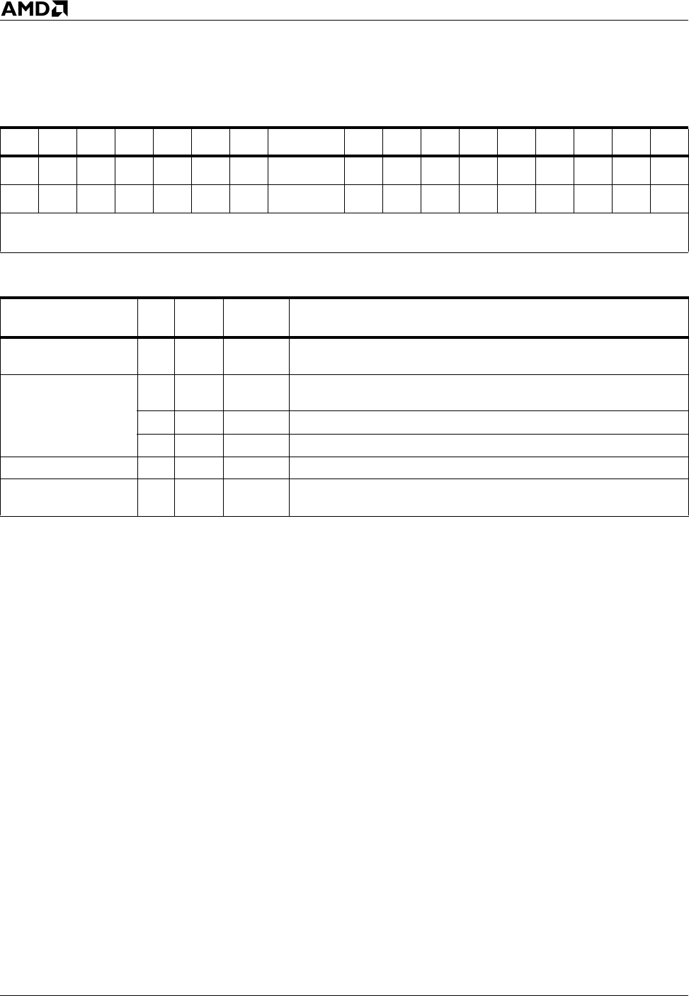
242 TEST Instruction Reference
AMD64 Technology 24594—Rev. 3.14—September 2007
rFLAGS Affected
Exceptions
ID VIP VIF AC VM RF NT IOPL OF DF IF TF SF ZF AF PF CF
0MMUM0
2120191817161413–1211109876420
Note: Bits 31–22, 15, 5, 3, and 1 are reserved. A flag set to 1 or cleared to 0 is M (modified). Unaffected flags are blank.
Undefined flags are U.
Exception Real
Virtual
8086 Protected Cause of Exception
Stack, #SS X X X A memory address exceeded the stack segment limit or was
non-canonical.
General protection,
#GP
XX XA memory address exceeded a data segment limit or was non-
canonical.
X The destination operand was in a non-writable segment.
X A null data segment was used to reference memory.
Page fault, #PF X X A page fault resulted from the execution of the instruction.
Alignment check,
#AC XX
An unaligned memory reference was performed while
alignment checking was enabled.

Instruction Reference XADD 243
24594—Rev. 3.14—September 2007 AMD64 Technology
Exchanges the contents of a register (second operand) with the contents of a register or memory
location (first operand), computes the sum of the two values, and stores the result in the first operand
location.
The forms of the XADD instruction that write to memory support the LOCK prefix. For details about
the LOCK prefix, see “Lock Prefix” on page 8.
Related Instructions
None
rFLAGS Affected
XADD Exchange and Add
Mnemonic Opcode Description
XADD reg/mem8, reg8 0F C0 /r
Exchange the contents of an 8-bit register with the
contents of an 8-bit destination register or memory
operand and load their sum into the destination.
XADD reg/mem16, reg16 0F C1 /r
Exchange the contents of a 16-bit register with the
contents of a 16-bit destination register or memory
operand and load their sum into the destination.
XADD reg/mem32, reg32 0F C1 /r
Exchange the contents of a 32-bit register with the
contents of a 32-bit destination register or memory
operand and load their sum into the destination.
XADD reg/mem64, reg64 0F C1 /r
Exchange the contents of a 64-bit register with the
contents of a 64-bit destination register or memory
operand and load their sum into the destination.
ID VIP VIF AC VM RF NT IOPL OF DF IF TF SF ZF AF PF CF
M MMMMM
2120191817161413–1211109876420
Note: Bits 31–22, 15, 5, 3, and 1 are reserved. A flag set to 1 or cleared to 0 is M (modified). Unaffected flags are blank.
Undefined flags are U.

244 XADD Instruction Reference
AMD64 Technology 24594—Rev. 3.14—September 2007
Exceptions
Exception Real
Virtual
8086 Protected Cause of Exception
Stack, #SS X X X A memory address exceeded the stack segment limit or was
non-canonical.
General protection,
#GP
XX XA memory address exceeded a data segment limit or was non-
canonical.
X The destination operand was in a non-writable segment.
X A null data segment was used to reference memory.
Page fault, #PF X X A page fault resulted from the execution of the instruction.
Alignment check,
#AC XX
An unaligned memory reference was performed while
alignment checking was enabled.

Instruction Reference XCHG 245
24594—Rev. 3.14—September 2007 AMD64 Technology
Exchanges the contents of the two operands. The operands can be two general-purpose registers or a
register and a memory location. If either operand references memory, the processor locks
automatically, whether or not the LOCK prefix is used and independently of the value of IOPL. For
details about the LOCK prefix, see “Lock Prefix” on page 8.
The x86 architecture commonly uses the XCHG EAX, EAX instruction (opcode 90h) as a one-byte
NOP. In 64-bit mode, the processor treats opcode 90h as a true NOP only if it would exchange rAX
with itself. Without this special handling, the instruction would zero-extend the upper 32 bits of RAX,
and thus it would not be a true no-operation. Opcode 90h can still be used to exchange rAX and r8 if
the appropriate REX prefix is used.
This special handling does not apply to the two-byte ModRM form of the XCHG instruction.
XCHG Exchange
Mnemonic Opcode Description
XCHG AX, reg16 90 +rw Exchange the contents of the AX register with the
contents of a 16-bit register.
XCHG reg16, AX 90 +rw Exchange the contents of a 16-bit register with the
contents of the AX register.
XCHG EAX, reg32 90 +rd Exchange the contents of the EAX register with the
contents of a 32-bit register.
XCHG reg32, EAX 90 +rd Exchange the contents of a 32-bit register with the
contents of the EAX register.
XCHG RAX, reg64 90 +rq Exchange the contents of the RAX register with the
contents of a 64-bit register.
XCHG reg64, RAX 90 +rq Exchange the contents of a 64-bit register with the
contents of the RAX register.
XCHG reg/mem8, reg8 86 /r Exchange the contents of an 8-bit register with the
contents of an 8-bit register or memory operand.
XCHG reg8, reg/mem8 86 /r Exchange the contents of an 8-bit register or memory
operand with the contents of an 8-bit register.
XCHG reg/mem16, reg16 87 /r Exchange the contents of a 16-bit register with the
contents of a 16-bit register or memory operand.
XCHG reg16, reg/mem16 87 /r Exchange the contents of a 16-bit register or memory
operand with the contents of a 16-bit register.
XCHG reg/mem32, reg32 87 /r Exchange the contents of a 32-bit register with the
contents of a 32-bit register or memory operand.
XCHG reg32, reg/mem32 87 /r Exchange the contents of a 32-bit register or memory
operand with the contents of a 32-bit register.
XCHG reg/mem64, reg64 87 /r Exchange the contents of a 64-bit register with the
contents of a 64-bit register or memory operand.
XCHG reg64, reg/mem64 87 /r Exchange the contents of a 64-bit register or memory
operand with the contents of a 64-bit register.
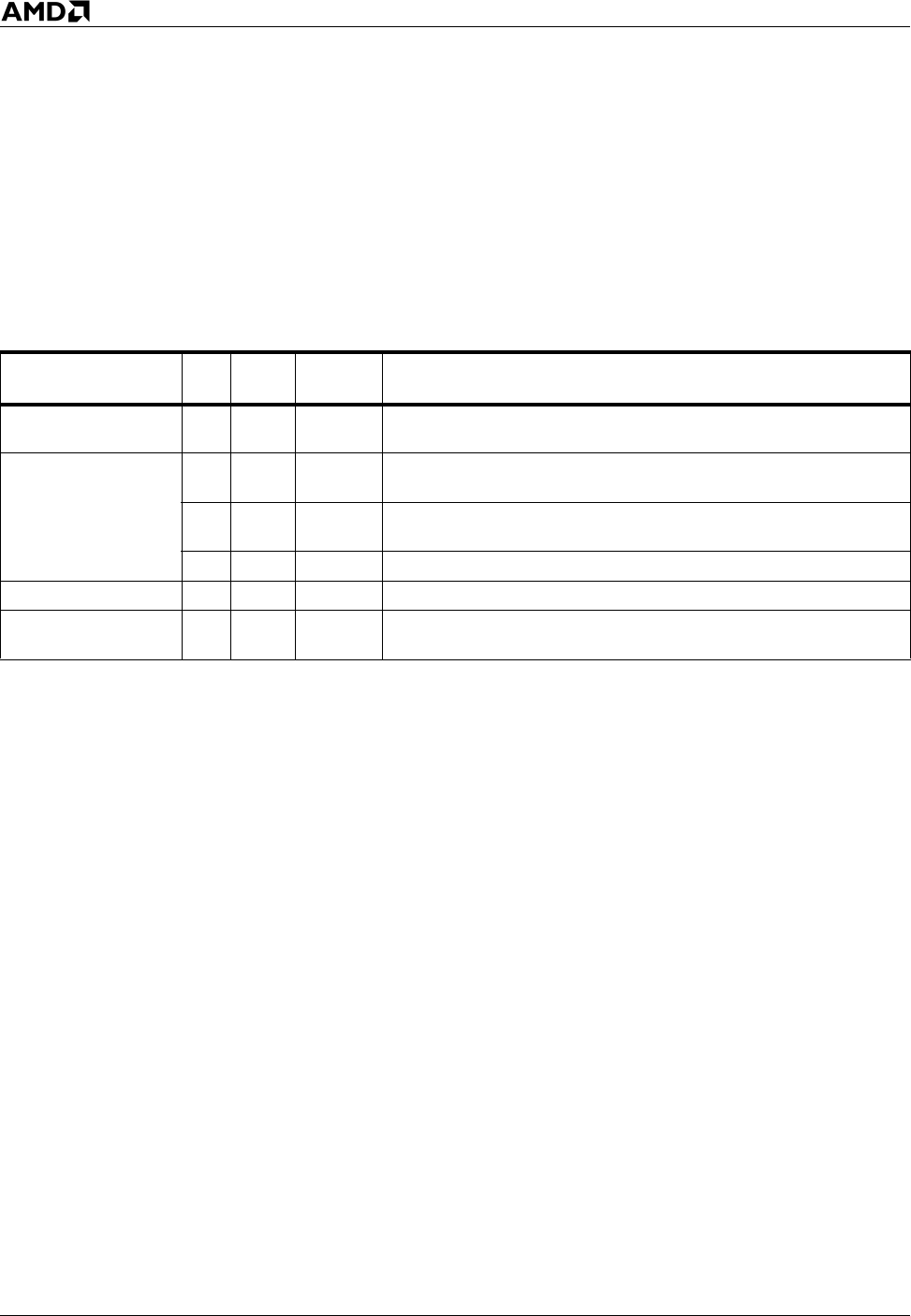
246 XCHG Instruction Reference
AMD64 Technology 24594—Rev. 3.14—September 2007
Related Instructions
BSWAP, XADD
rFLAGS Affected
None
Exceptions
Exception Real
Virtual
8086 Protected Cause of Exception
Stack, #SS X X X A memory address exceeded the stack segment limit or was
non-canonical.
General protection,
#GP
XX XA memory address exceeded a data segment limit or was non-
canonical.
XThe source or destination operand was in a non-writable
segment.
X A null data segment was used to reference memory.
Page fault, #PF X X A page fault resulted from the execution of the instruction.
Alignment check,
#AC XX
An unaligned memory reference was performed while
alignment checking was enabled.

General-Purpose Instruction Reference 247
24594—Rev. 3.14—September 2007 AMD64 Technology
Uses the unsigned integer in the AL register as an offset into a table and copies the contents of the table
entry at that location to the AL register.
The instruction uses seg:[rBX] as the base address of the table. The value of seg defaults to the DS
segment, but may be overridden by a segment prefix.
This instruction writes AL without changing RAX[63:8]. This instruction ignores operand size.
The single-operand form of the XLAT instruction uses the operand to document the segment and
address size attribute, but it uses the base address specified by the rBX register.
This instruction is often used to translate data from one format (such as ASCII) to another (such as
EBCDIC).
Related Instructions
None
rFLAGS Affected
None
Exceptions
XLAT
XLATB
Translate Table Index
Mnemonic Opcode Description
XLAT mem8 D7 Set AL to the contents of DS:[rBX + unsigned AL].
XLATB D7 Set AL to the contents of DS:[rBX + unsigned AL].
Exception Real
Virtual
8086 Protected Cause of Exception
Stack, #SS X X X A memory address exceeded the stack segment limit or was
non-canonical.
General protection,
#GP
XX XA memory address exceeded a data segment limit or was non-
canonical.
X A null data segment was used to reference memory.
Page fault, #PF X X A page fault resulted from the execution of the instruction.

248 General-Purpose Instruction Reference
AMD64 Technology 24594—Rev. 3.14—September 2007
Performs a bitwise exclusive OR operation on both operands and stores the result in the first operand
location. The first operand can be a register or memory location. The second operand can be an
immediate value, a register, or a memory location. XOR-ing a register with itself clears the register.
The forms of the XOR instruction that write to memory support the LOCK prefix. For details about the
LOCK prefix, see “Lock Prefix” on page 8.
The instruction performs the following operation for each bit:
XOR Logical Exclusive OR
X Y X XOR Y
000
011
101
110
Mnemonic Opcode Description
XOR AL, imm8 34 ib XOR the contents of AL with an immediate 8-bit
operand and store the result in AL.
XOR AX, imm16 35 iw XOR the contents of AX with an immediate 16-bit
operand and store the result in AX.
XOR EAX, imm32 35 id XOR the contents of EAX with an immediate 32-bit
operand and store the result in EAX.
XOR RAX, imm32 35 id XOR the contents of RAX with a sign-extended
immediate 32-bit operand and store the result in RAX.
XOR reg/mem8, imm8 80 /6 ib
XOR the contents of an 8-bit destination register or
memory operand with an 8-bit immediate value and
store the result in the destination.
XOR reg/mem16, imm16 81 /6 iw
XOR the contents of a 16-bit destination register or
memory operand with a 16-bit immediate value and
store the result in the destination.
XOR reg/mem32, imm32 81 /6 id
XOR the contents of a 32-bit destination register or
memory operand with a 32-bit immediate value and
store the result in the destination.
XOR reg/mem64, imm32 81 /6 id
XOR the contents of a 64-bit destination register or
memory operand with a sign-extended 32-bit immediate
value and store the result in the destination.
XOR reg/mem16, imm8 83 /6 ib
XOR the contents of a 16-bit destination register or
memory operand with a sign-extended 8-bit immediate
value and store the result in the destination.

General-Purpose Instruction Reference 249
24594—Rev. 3.14—September 2007 AMD64 Technology
Related Instructions
OR, AND, NOT, NEG
rFLAGS Affected
XOR reg/mem32, imm8 83 /6 ib
XOR the contents of a 32-bit destination register or
memory operand with a sign-extended 8-bit immediate
value and store the result in the destination.
XOR reg/mem64, imm8 83 /6 ib
XOR the contents of a 64-bit destination register or
memory operand with a sign-extended 8-bit immediate
value and store the result in the destination.
XOR reg/mem8, reg8 30 /r
XOR the contents of an 8-bit destination register or
memory operand with the contents of an 8-bit register
and store the result in the destination.
XOR reg/mem16, reg16 31 /r
XOR the contents of a 16-bit destination register or
memory operand with the contents of a 16-bit register
and store the result in the destination.
XOR reg/mem32, reg32 31 /r
XOR the contents of a 32-bit destination register or
memory operand with the contents of a 32-bit register
and store the result in the destination.
XOR reg/mem64, reg64 31 /r
XOR the contents of a 64-bit destination register or
memory operand with the contents of a 64-bit register
and store the result in the destination.
XOR reg8, reg/mem8 32 /r
XOR the contents of an 8-bit destination register with
the contents of an 8-bit register or memory operand and
store the results in the destination.
XOR reg16, reg/mem16 33 /r
XOR the contents of a 16-bit destination register with
the contents of a 16-bit register or memory operand and
store the results in the destination.
XOR reg32, reg/mem32 33 /r
XOR the contents of a 32-bit destination register with
the contents of a 32-bit register or memory operand and
store the results in the destination.
XOR reg64, reg/mem64 33 /r
XOR the contents of a 64-bit destination register with
the contents of a 64-bit register or memory operand and
store the results in the destination.
ID VIP VIF AC VM RF NT IOPL OF DF IF TF SF ZF AF PF CF
0MMUM0
2120191817161413–1211109876420
Note: Bits 31–22, 15, 5, 3, and 1 are reserved. A flag set to 1 or cleared to 0 is M (modified). Unaffected flags are
blank. Undefined flags are U.
Mnemonic Opcode Description

250 General-Purpose Instruction Reference
AMD64 Technology 24594—Rev. 3.14—September 2007
Exceptions
Exception Real
Virtual
8086 Protected Cause of Exception
Stack, #SS X X X A memory address exceeded the stack segment limit or was
non-canonical.
General protection,
#GP
XX XA memory address exceeded a data segment limit or was non-
canonical.
X The destination operand was in a non-writable segment.
X A null data segment was used to reference memory.
Page fault, #PF X X A page fault resulted from the execution of the instruction.
Alignment check,
#AC XX
An unaligned memory reference was performed while
alignment checking was enabled.

Instruction Reference 251
24594—Rev. 3.14—September 2007 AMD64 Technology
4 System Instruction Reference
This chapter describes the function, mnemonic syntax, opcodes, affected flags, and possible
exceptions generated by the system instructions. The system instructions are used to establish the
operating mode, access processor resources, handle program and system errors, and manage memory.
Many of these instructions can only be executed by privileged software, such as the operating system
kernel and interrupt handlers, that run at the highest privilege level. Only system instructions can
access certain processor resources, such as the control registers, model-specific registers, and debug
registers.
System instructions are supported in all hardware implementations of the AMD64 architecture, except
that the following system instructions are implemented only if their associated CPUID function bits
are set:
• RDMSR and WRMSR, indicated by bit 5 of CPUID function 0000_0001h or function
8000_0001h.
• SYSENTER and SYSEXIT, indicated by bit 11 of CPUID function 0000_0001h.
• SYSCALL and SYSRET, indicated by bit 11 of CPUID function 8000_0001h.
• Long Mode instructions, indicated by bit 29 of CPUID function 8000_0001h.
• There are also several other CPUID function bits that control the use of system resources and
functions, such as paging functions, virtual-mode extensions, machine-check exceptions,
advanced programmable interrupt control (APIC), memory-type range registers (MTRRs), etc.
For details, see “Processor Feature Identification” in Volume 2.
For further information about the system instructions and register resources, see:
• “System-Management Instructions” in Volume 2.
• “Summary of Registers and Data Types” on page 24.
• “Notation” on page 37.
• “Instruction Prefixes” on page 3.

252 ARPL Instruction Reference
AMD64 Technology 24594—Rev. 3.14—September 2007
Compares the requestor privilege level (RPL) fields of two segment selectors in the source and
destination operands of the instruction. If the RPL field of the destination operand is less than the RPL
field of the segment selector in the source register, then the zero flag is set and the RPL field of the
destination operand is increased to match that of the source operand. Otherwise, the destination
operand remains unchanged and the zero flag is cleared.
The destination operand can be either a 16-bit register or memory location; the source operand must be
a 16-bit register.
The ARPL instruction is intended for use by operating-system procedures to adjust the RPL of a
segment selector that has been passed to the operating system by an application program to match the
privilege level of the application program. The segment selector passed to the operating system is
placed in the destination operand and the segment selector for the code segment of the application
program is placed in the source operand. The RPL field in the source operand represents the privilege
level of the application program. The ARPL instruction then insures that the RPL of the segment
selector received by the operating system is no lower than the privilege level of the application
program.
See “Adjusting Access Rights” in Volume 2, for more information on access rights.
In 64-bit mode, this opcode (63H) is used for the MOVSXD instruction.
Related Instructions
LAR, LSL, VERR, VERW
rFLAGS Affected
ARPL Adjust Requestor Privilege Level
Mnemonic Opcode Description
ARPL reg/mem16, reg16 63 /r
Adjust the RPL of a destination segment selector to
a level not less than the RPL of the segment
selector specified in the 16-bit source register.
(Invalid in 64-bit mode.)
ID VIP VIF AC VM RF NT IOPL OF DF IF TF SF ZF AF PF CF
M
2120191817161413–1211109876420
Note: Bits 31–22, 15, 5, 3, and 1 are reserved. A flag set to one or cleared to zero is M (modified). Unaffected flags
are blank. Undefined flags are U.
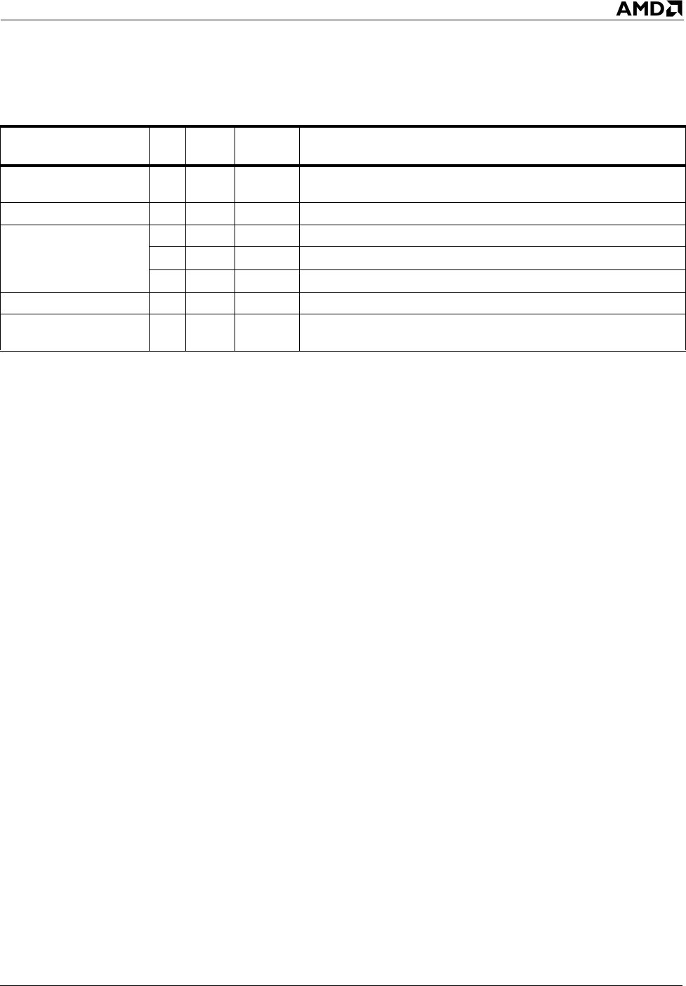
Instruction Reference ARPL 253
24594—Rev. 3.14—September 2007 AMD64 Technology
Exceptions
Exception Real
Virtual
8086 Protected Cause of Exception
Invalid opcode, #UD X X This instruction is only recognized in protected legacy and
compatibility mode.
Stack, #SS X A memory address exceeded the stack segment limit.
General protection,
#GP
X A memory address exceeded a data segment limit.
X The destination operand was in a non-writable segment.
X A null segment selector was used to reference memory.
Page fault, #PF X A page fault resulted from the execution of the instruction.
Alignment check, #AC X An unaligned memory reference was performed while
alignment checking was enabled.
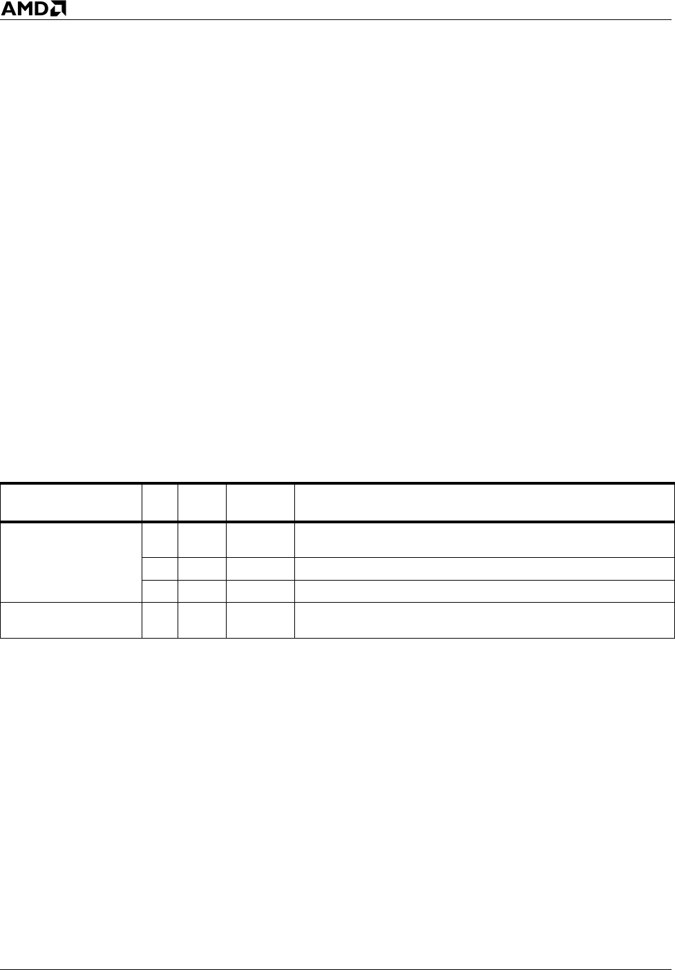
254 CLGI Instruction Reference
AMD64 Technology 24594—Rev. 3.14—September 2007
Clears the global interrupt flag (GIF). While GIF is zero, all external interrupts are disabled.
This is a Secure Virtual Machine instruction. This instruction generates a #UD exception if SVM is
not enabled. See “Enabling SVM” on page 369 in AMD64 Architecture Programmer’s Manual
Volume-2: System Instructions, order# 24593.
Related Instructions
STGI
rFLAGS Affected
None.
Exceptions
CLGI Clear Global Interrupt Flag
Mnemonic Opcode Description
CLGI 0F 01 DD Clears the global interrupt flag (GIF).
Exception Real
Virtual
8086 Protected Cause of Exception
Invalid opcode, #UD
XX X The SVM instructions are not supported as indicated by ECX
bit 2 as returned by CPUID function 8000_0001h.
X Secure Virtual Machine was not enabled (EFER.SVME=0).
X X Instruction is only recognized in protected mode.
General protection,
#GP X CPL was not zero.

Instruction Reference CLI 255
24594—Rev. 3.14—September 2007 AMD64 Technology
Clears the interrupt flag (IF) in the rFLAGS register to zero, thereby masking external interrupts
received on the INTR input. Interrupts received on the non-maskable interrupt (NMI) input are not
affected by this instruction.
In real mode, this instruction clears IF to 0.
In protected mode and virtual-8086-mode, this instruction is IOPL-sensitive. If the CPL is less than or
equal to the rFLAGS.IOPL field, the instruction clears IF to 0.
In protected mode, if IOPL < 3, CPL = 3, and protected mode virtual interrupts are enabled (CR4.PVI
= 1), then the instruction instead clears rFLAGS.VIF to 0. If none of these conditions apply, the
processor raises a general-purpose exception (#GP). For more information, see “Protected Mode
Virtual Interrupts” in Volume 2.
In virtual-8086 mode, if IOPL < 3 and the virtual-8086-mode extensions are enabled (CR4.VME = 1),
the CLI instruction clears the virtual interrupt flag (rFLAGS.VIF) to 0 instead.
See “Virtual-8086 Mode Extensions” in Volume 2 for more information about IOPL-sensitive
instructions.
Action
IF (CPL <= IOPL)
RFLAGS.IF = 0
ELSEIF (((VIRTUAL_MODE) && (CR4.VME = 1))
|| ((PROTECTED_MODE) && (CR4.PVI = 1) && (CPL == 3)))
RFLAGS.VIF = 0;
ELSE
EXCEPTION[#GP(0)]
Related Instructions
STI
CLI Clear Interrupt Flag
Mnemonic Opcode Description
CLI FA Clear the interrupt flag (IF) to zero.

256 CLI Instruction Reference
AMD64 Technology 24594—Rev. 3.14—September 2007
rFLAGS Affected
Exceptions
ID VIP VIF AC VM RF NT IOPL OF DF IF TF SF ZF AF PF CF
MM
2120191817161413–1211109876420
Note: Bits 31–22, 15, 5, 3, and 1 are reserved. A flag set to one or cleared to zero is M (modified). Unaffected flags
are blank. Undefined flags are U.
Exception Real
Virtual
8086 Protected Cause of Exception
General protection,
#GP
XThe CPL was greater than the IOPL and virtual mode
extensions are not enabled (CR4.VME = 0).
X
The CPL was greater than the IOPL and either the CPL was
not 3 or protected mode virtual interrupts were not enabled
(CR4.PVI = 0).
Instruction Reference CLTS 257
24594—Rev. 3.14—September 2007 AMD64 Technology
Clears the task-switched (TS) flag in the CR0 register to 0. The processor sets the TS flag on each task
switch. The CLTS instruction is intended to facilitate the synchronization of FPU context saves during
multitasking operations.
This instruction can only be used if the current privilege level is 0.
See “System-Control Registers” in Volume 2 for more information on FPU synchronization and the
TS flag.
Related Instructions
LMSW, MOV (CRn)
rFLAGS Affected
None
Exceptions
CLTS Clear Task-Switched Flag in CR0
Mnemonic Opcode Description
CLTS 0F 06 Clear the task-switched (TS) flag in CR0 to 0.
Exception Real
Virtual
8086 Protected Cause of Exception
General protection,
#GP X X CPL was not 0.

258 HLT Instruction Reference
AMD64 Technology 24594—Rev. 3.14—September 2007
Causes the microprocessor to halt instruction execution and enter the HALT state. Entering the HALT
state puts the processor in low-power mode. Execution resumes when an unmasked hardware interrupt
(INTR), non-maskable interrupt (NMI), system management interrupt (SMI), RESET, or INIT occurs.
If an INTR, NMI, or SMI is used to resume execution after a HLT instruction, the saved instruction
pointer points to the instruction following the HLT instruction.
Before executing a HLT instruction, hardware interrupts should be enabled. If rFLAGS.IF = 0, the
system will remain in a HALT state until an NMI, SMI, RESET, or INIT occurs.
If an SMI brings the processor out of the HALT state, the SMI handler can decide whether to return to
the HALT state or not. See Volume 2: System Programming, for information on SMIs.
Current privilege level must be 0 to execute this instruction.
Related Instructions
STI, CLI
rFLAGS Affected
None
Exceptions
HLT Halt
Mnemonic Opcode Description
HLT F4 Halt instruction execution.
Exception Real
Virtual
8086 Protected Cause of Exception
General protection,
#GP X X CPL was not 0.

Instruction Reference INT 3 259
24594—Rev. 3.14—September 2007 AMD64 Technology
Calls the debug exception handler. This instruction maps to a 1-byte opcode (CC) that raises a #BP
exception. The INT 3 instruction is normally used by debug software to set instruction breakpoints by
replacing the first byte of the instruction opcode bytes with the INT 3 opcode.
This one-byte INT 3 instruction behaves differently from the two-byte INT 3 instruction (opcode CD
03) (see “INT” in Chapter 3 “General Purpose Instructions” for further information) in two ways:
The #BP exception is handled without any IOPL checking in virtual x86 mode. (IOPL mismatches will
not trigger an exception.)
• In VME mode, the #BP exception is not redirected via the interrupt redirection table. (Instead, it is
handled by a protected mode handler.)
For complete descriptions of the steps performed by INT instructions, see the following:
•Legacy-Mode Interrupts: “Legacy Protected-Mode Interrupt Control Transfers” in Volume 2.
•Long-Mode Interrupts: “Long-Mode Interrupt Control Transfers” in Volume 2.
Action
// Refer to INT instruction’s Action section for the details on INT_N_REAL,
// INT_N_PROTECTED, and INT_N_VIRTUAL_TO_PROTECTED.
INT3_START:
If (REAL_MODE)
INT_N_REAL //N = 3
ELSEIF (PROTECTED_MODE)
INT_N_PROTECTED //N = 3
ELSE // VIRTUAL_MODE
INT_N_VIRTUAL_TO_PROTECTED //N = 3
Related Instructions
INT, INTO, IRET
INT 3 Interrupt to Debug Vector
Mnemonic Opcode Description
INT 3 CC Trap to debugger at Interrupt 3.

260 INT 3 Instruction Reference
AMD64 Technology 24594—Rev. 3.14—September 2007
rFLAGS Affected
If a task switch occurs, all flags are modified; otherwise, setting are as follows:
Exceptions
ID VIP VIF AC VM RF NT IOPL OF DF IF TF SF ZF AF PF CF
M0 0M M0
2120191817161413–1211109876420
Note: Bits 31–22, 15, 5, 3, and 1 are reserved. A flag set to one or cleared to zero is M (modified). Unaffected flags
are blank. Undefined flags are U.
Exception Real
Virtual
8086 Protected Cause of Exception
Breakpoint, #BP X X X INT 3 instruction was executed.
Invalid TSS, #TS
(selector)
XX
As part of a stack switch, the target stack segment selector or
rSP in the TSS that was beyond the TSS limit.
XX
As part of a stack switch, the target stack segment selector in
the TSS was beyond the limit of the GDT or LDT descriptor
table.
XX
As part of a stack switch, the target stack segment selector in
the TSS was a null selector.
XX
As part of a stack switch, the target stack segment selector’s
TI bit was set, but the LDT selector was a null selector.
XX
As part of a stack switch, the target stack segment selector in
the TSS contained a RPL that was not equal to its DPL.
XX
As part of a stack switch, the target stack segment selector in
the TSS contained a DPL that was not equal to the CPL of the
code segment selector.
XX
As part of a stack switch, the target stack segment selector in
the TSS was not a writable segment.
Segment not
present, #NP
(selector)
XX
The accessed code segment, interrupt gate, trap gate, task
gate, or TSS was not present.
Stack, #SS X X X A memory address exceeded the stack segment limit or was
non-canonical.
Stack, #SS
(selector)
XX
After a stack switch, a memory address exceeded the stack
segment limit or was non-canonical and a stack switch
occurred.
XX
As part of a stack switch, the SS register was loaded with a
non-null segment selector and the segment was marked not
present.
General protection,
#GP
XX XA memory address exceeded the data segment limit or was
non-canonical.
XX XThe target offset exceeded the code segment limit or was non-
canonical.

Instruction Reference INT 3 261
24594—Rev. 3.14—September 2007 AMD64 Technology
General protection,
#GP
(selector)
X X X The interrupt vector was beyond the limit of IDT.
XX
The descriptor in the IDT was not an interrupt, trap, or task
gate in legacy mode or not a 64-bit interrupt or trap gate in
long mode.
XX
The DPL of the interrupt, trap, or task gate descriptor was less
than the CPL.
XX
The segment selector specified by the interrupt or trap gate
had its TI bit set, but the LDT selector was a null selector.
XX
The segment descriptor specified by the interrupt or trap gate
exceeded the descriptor table limit or was a null selector.
XX
The segment descriptor specified by the interrupt or trap gate
was not a code segment in legacy mode, or not a 64-bit code
segment in long mode.
XThe DPL of the segment specified by the interrupt or trap gate
was greater than the CPL.
XThe DPL of the segment specified by the interrupt or trap gate
pointed was not 0 or it was a conforming segment.
Page fault, #PF X X A page fault resulted from the execution of the instruction.
Alignment check,
#AC XX
An unaligned memory reference was performed while
alignment checking was enabled.
Exception Real
Virtual
8086 Protected Cause of Exception

262 INVD Instruction Reference
AMD64 Technology 24594—Rev. 3.14—September 2007
Invalidates internal caches (data cache, instruction cache, and on-chip L2 cache) and triggers a bus
cycle that causes external caches to invalidate themselves as well.
No data is written back to main memory from invalidating internal caches. After invalidating internal
caches, the processor proceeds immediately with the execution of the next instruction without waiting
for external hardware to invalidate its caches.
This is a privileged instruction. The current privilege level (CPL) of a procedure invalidating the
processor’s internal caches must be 0.
To insure that data is written back to memory prior to invalidating caches, use the WBINVD
instruction.
This instruction does not invalidate TLB caches.
INVD is a serializing instruction.
Related Instructions
WBINVD, CLFLUSH
rFLAGS Affected
None
Exceptions
INVD Invalidate Caches
Mnemonic Opcode Description
INVD 0F 08 Invalidate internal caches and trigger external cache
invalidations.
Exception Real
Virtual
8086 Protected Cause of Exception
General protection,
#GP X X CPL was not 0.

Instruction Reference INVLPG 263
24594—Rev. 3.14—September 2007 AMD64 Technology
Invalidates the TLB entry that would be used for the 1-byte memory operand.
This instruction invalidates the TLB entry, regardless of the G (Global) bit setting in the associated
PDE or PTE entry and regardless of the page size (4 Kbytes, 2 Mbytes, or 4 Mbytes). It may invalidate
any number of additional TLB entries, in addition to the targeted entry.
INVLPG is a serializing instruction and a privileged instruction. The current privilege level must be 0
to execute this instruction.
See “Page Translation and Protection” in Volume 2 for more information on page translation.
Related Instructions
INVLPGA, MOV CRn (CR3 and CR4)
rFLAGS Affected
None
Exceptions
INVLPG Invalidate TLB Entry
Mnemonic Opcode Description
INVLPG mem8 0F 01 /7 Invalidate the TLB entry for the page containing a specified
memory location.
Exception Real
Virtual
8086 Protected Cause of Exception
General protection,
#GP X X CPL was not 0.

264 INVLPGA Instruction Reference
AMD64 Technology 24594—Rev. 3.14—September 2007
Invalidates the TLB mapping for a given virtual page and a given ASID. The virtual address is
specified in the implicit register operand rAX. The portion of RAX used to form the address is
determined by the effective address size. The ASID is taken from ECX.
The INVLPGA instruction may invalidate any number of additional TLB entries, in addition to the
targeted entry.
The INVLPGA instruction is a serializing instruction and a privileged instruction. The current
privilege level must be 0 to execute this instruction.
This is a Secure Virtual Machine instruction. This instruction generates a #UD exception if SVM is
not enabled. See “Enabling SVM” on page 369 in AMD64 Architecture Programmer’s Manual
Volume-2: System Instructions, order# 24593.
Related Instructions
INVLPG.
rFLAGS Affected
None.
Exceptions
INVLPGA Invalidate TLB Entry in a Specified ASID
Mnemonic Opcode Description
INVLPGA rAX, ECX 0F 01 DF Invalidates the TLB mapping for the virtual page
specified in rAX and the ASID specified in ECX.
Exception Real
Virtual
8086 Protected Cause of Exception
Invalid opcode, #UD
XX XThe SVM instructions are not supported as indicated by ECX
bit 2 as returned by CPUID function 8000_0001h.
X Secure Virtual Machine was not enabled (EFER.SVME=0).
X X Instruction is only recognized in protected mode.
General protection,
#GP X CPL was not zero.

Instruction Reference IRETx 265
24594—Rev. 3.14—September 2007 AMD64 Technology
Returns program control from an exception or interrupt handler to a program or procedure previously
interrupted by an exception, an external interrupt, or a software-generated interrupt. These instructions
also perform a return from a nested task. All flags, CS, and rIP are restored to the values they had
before the interrupt so that execution may continue at the next instruction following the interrupt or
exception. In 64-bit mode or if the CPL changes, SS and RSP are also restored.
IRET, IRETD, and IRETQ are synonyms mapping to the same opcode. They are intended to provide
semantically distinct forms for various opcode sizes. The IRET instruction is used for 16-bit operand
size; IRETD is used for 32-bit operand sizes; IRETQ is used for 64-bit operands. The latter form is
only meaningful in 64-bit mode.
IRET, IRETD, or IRETQ must be used to terminate the exception or interrupt handler associated with
the exception, external interrupt, or software-generated interrupt.
IRETx is a serializing instruction.
For detailed descriptions of the steps performed by IRETx instructions, see the following:
•Legacy-Mode Interrupts: “Legacy Protected-Mode Interrupt Control Transfers” in Volume 2.
•Long-Mode Interrupts: “Long-Mode Interrupt Control Transfers” in Volume 2.
Action
IRET_START:
IF (REAL_MODE)
IRET_REAL
ELSIF (PROTECTED_MODE)
IRET_PROTECTED
ELSE // (VIRTUAL_MODE)
IRET_VIRTUAL
IRET_REAL:
POP.v temp_RIP
POP.v temp_CS
POP.v temp_RFLAGS
IRET
IRETD
IRETQ
Return from Interrupt
Mnemonic Opcode Description
IRET CF Return from interrupt (16-bit operand size).
IRETD CF Return from interrupt (32-bit operand size).
IRETQ CF Return from interrupt (64-bit operand size).

266 IRETx Instruction Reference
AMD64 Technology 24594—Rev. 3.14—September 2007
IF (temp_RIP > CS.limit)
EXCEPTION [#GP(0)]
CS.sel = temp_CS
CS.base = temp_CS SHL 4
RFLAGS.v = temp_RFLAGS // VIF,VIP,VM unchanged
RIP = temp_RIP
EXIT
IRET_PROTECTED:
IF (RFLAGS.NT=1) // iret does a task-switch to a previous task
IF (LEGACY_MODE)
TASK_SWITCH // using the ’back link’ field in the tss
ELSE // (LONG_MODE)
EXCEPTION [#GP(0)] // task switches aren’t supported in long mode
POP.v temp_RIP
POP.v temp_CS
POP.v temp_RFLAGS
IF ((temp_RFLAGS.VM=1) && (CPL=0) && (LEGACY_MODE))
IRET_FROM_PROTECTED_TO_VIRTUAL
temp_CPL = temp_CS.rpl
IF ((64BIT_MODE) || (temp_CPL!=CPL))
{
POP.v temp_RSP // in 64-bit mode, iret always pops ss:rsp
POP.v temp_SS
}
CS = READ_DESCRIPTOR (temp_CS, iret_chk)
IF ((64BIT_MODE) && (temp_RIP is non-canonical)
|| (!64BIT_MODE) && (temp_RIP > CS.limit))
{
EXCEPTION [#GP(0)]
}
CPL = temp_CPL
IF ((started in 64-bit mode) || (changing CPL))
// ss:rsp were popped, so load them into the registers
{
SS = READ_DESCRIPTOR (temp_SS, ss_chk)
RSP.s = temp_RSP
}

Instruction Reference IRETx 267
24594—Rev. 3.14—September 2007 AMD64 Technology
IF (changing CPL)
{
FOR (seg = ES, DS, FS, GS)
IF ((seg.attr.dpl < CPL) && ((seg.attr.type = ’data’)
|| (seg.attr.type = ’non-conforming-code’)))
{
seg = NULL // can’t use lower dpl data segment at higher cpl
}
}
RFLAGS.v = temp_RFLAGS // VIF,VIP,IOPL only changed if (old_CPL=0)
// IF only changed if (old_CPL<=old_RFLAGS.IOPL)
// VM unchanged
// RF cleared
RIP = temp_RIP
EXIT
IRET_VIRTUAL:
IF ((RFLAGS.IOPL<3) && (CR4.VME=0))
EXCEPTION [#GP(0)]
POP.v temp_RIP
POP.v temp_CS
POP.v temp_RFLAGS
IF (temp_RIP > CS.limit)
EXCEPTION [#GP(0)]
IF (RFLAGS.IOPL=3)
{
RFLAGS.v = temp_RFLAGS // VIF,VIP,VM,IOPL unchanged
// RF cleared
CS.sel = temp_CS
CS.base = temp_CS SHL 4
RIP = temp_RIP
EXIT
}
// now ((IOPL<3) && (CR4.VME=1)
ELSIF ((OPERAND_SIZE=16)
&& !((temp_RFLAGS.IF=1) && (RFLAGS.VIP=1))
&& (temp_RFLAGS.TF=0))
{
RFLAGS.w = temp_RFLAGS // RFLAGS.VIF=temp_RFLAGS.IF
// IF,IOPL unchanged
// RF cleared
CS.sel = temp_CS
CS.base = temp_CS SHL 4

268 IRETx Instruction Reference
AMD64 Technology 24594—Rev. 3.14—September 2007
RIP = temp_RIP
EXIT
}
ELSE // ((RFLAGS.IOPL<3) && (CR4.VME=1) && ((OPERAND_SIZE=32) ||
// ((temp_RFLAGS.IF=1) && (RFLAGS.VIP=1)) || (temp_RFLAGS.TF=1)))
EXCEPTION [#GP(0)]
IRET_FROM_PROTECTED_TO_VIRTUAL:
// temp_RIP already popped
// temp_CS already popped
// temp_RFLAGS already popped, temp_RFLAGS.VM=1
POP.d temp_RSP
POP.d temp_SS
POP.d temp_ES
POP.d temp_DS
POP.d temp_FS
POP.d temp_GS
CS.sel = temp_CS // force the segments to have virtual-mode values
CS.base = temp_CS SHL 4
CS.limit= 0x0000FFFF
CS.attr = 16-bit dpl3 code
SS.sel = temp_SS
SS.base = temp_SS SHL 4
SS.limit= 0x0000FFFF
SS.attr = 16-bit dpl3 stack
DS.sel = temp_DS
DS.base = temp_DS SHL 4
DS.limit= 0x0000FFFF
DS.attr = 16-bit dpl3 data
ES.sel = temp_ES
ES.base = temp_ES SHL 4
ES.limit= 0x0000FFFF
ES.attr = 16-bit dpl3 data
FS.sel = temp_FS
FS.base = temp_FS SHL 4
FS.limit= 0x0000FFFF
FS.attr = 16-bit dpl3 data
GS.sel = temp_GS
GS.base = temp_GS SHL 4
GS.limit= 0x0000FFFF
GS.attr = 16-bit dpl3 data
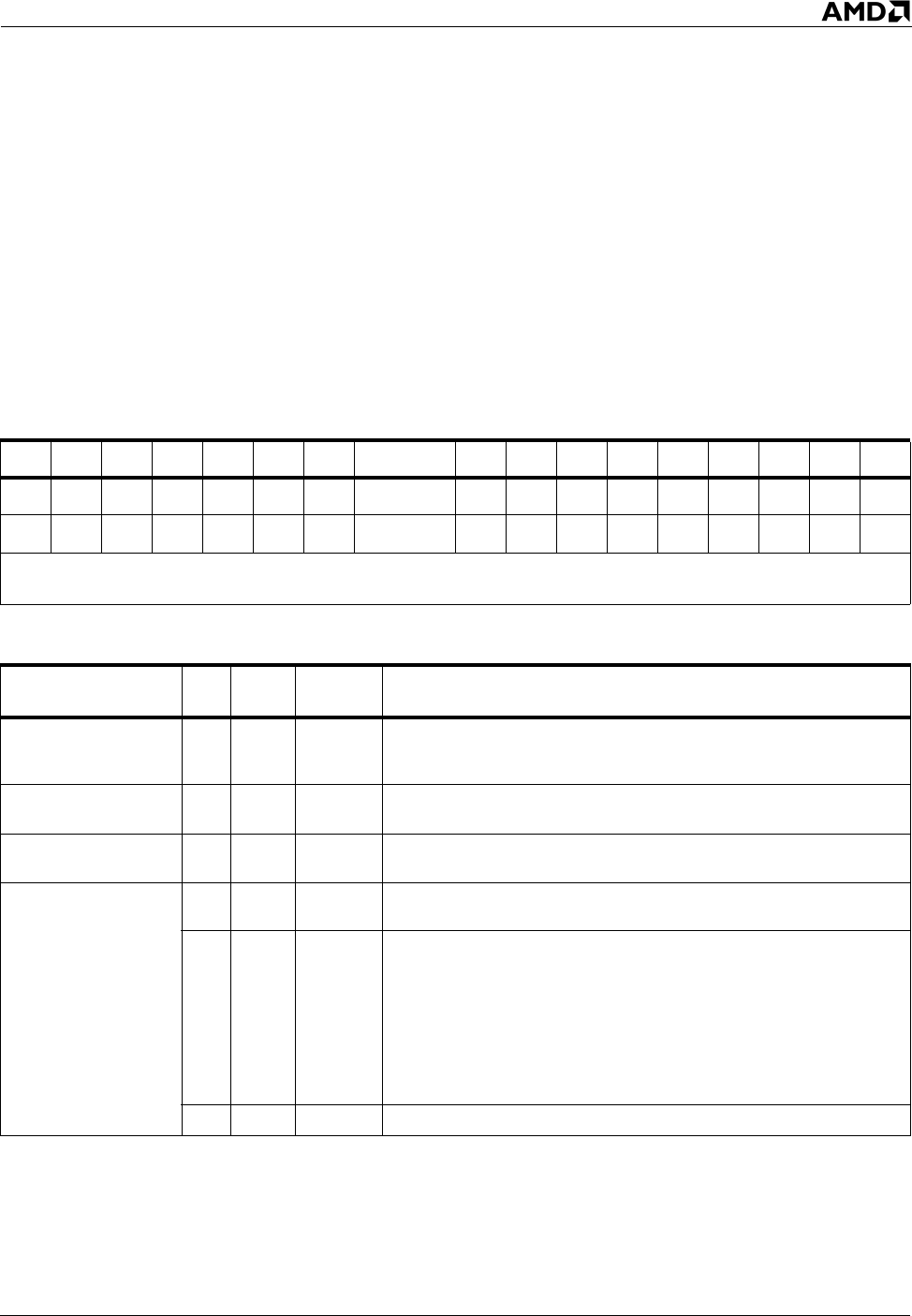
Instruction Reference IRETx 269
24594—Rev. 3.14—September 2007 AMD64 Technology
RSP.d = temp_RSP
RFLAGS.d = temp_RFLAGS
CPL = 3
RIP = temp_RIP AND 0x0000FFFF
EXIT
Related Instructions
INT, INTO, INT3
rFLAGS Affected
Exceptions
ID VIP VIF AC VM RF NT IOPL OF DF IF TF SF ZF AF PF CF
MMMMMMM M MMMMMMMMM
2120191817161413–1211109876420
Note: Bits 31–22, 15, 5, 3, and 1 are reserved. A flag set to one or cleared to zero is M (modified). Unaffected flags
are blank. Undefined flags are U.
Exception Real
Virtual
8086 Protected Cause of Exception
Segment not
present, #NP
(selector)
X The return code segment was marked not present.
Stack, #SS X X X A memory address exceeded the stack segment limit or was
non-canonical.
Stack, #SS
(selector) XThe SS register was loaded with a non-null segment selector
and the segment was marked not present.
General protection,
#GP
XX XThe target offset exceeded the code segment limit or was non-
canonical.
X
IOPL was less than 3 and one of the following conditions was
true:
•CR4.VME was 0.
• The effective operand size was 32-bit.
• Both the original EFLAGS.VIP and the new EFLAGS.IF
were set.
• The new EFLAGS.TF was set.
XIRETx was executed in long mode while EFLAGS.NT=1.

270 IRETx Instruction Reference
AMD64 Technology 24594—Rev. 3.14—September 2007
General protection,
#GP
(selector)
X The return code selector was a null selector.
XThe return stack selector was a null selector and the return
mode was non-64-bit mode or CPL was 3.
XThe return code or stack descriptor exceeded the descriptor
table limit.
XThe return code or stack selector’s TI bit was set but the LDT
selector was a null selector.
XThe segment descriptor for the return code was not a code
segment.
XThe RPL of the return code segment selector was less than
the CPL.
X
The return code segment was non-conforming and the
segment selector’s DPL was not equal to the RPL of the code
segment’s segment selector.
X
The return code segment was conforming and the segment
selector’s DPL was greater than the RPL of the code
segment’s segment selector.
XThe segment descriptor for the return stack was not a writable
data segment.
XThe stack segment descriptor DPL was not equal to the RPL
of the return code segment selector.
XThe stack segment selector RPL was not equal to the RPL of
the return code segment selector.
Page fault, #PF X X A page fault resulted from the execution of the instruction.
Alignment check,
#AC XX
An unaligned memory reference was performed while
alignment checking was enabled.
Exception Real
Virtual
8086 Protected Cause of Exception

Instruction Reference LAR 271
24594—Rev. 3.14—September 2007 AMD64 Technology
Loads the access rights from the segment descriptor specified by a 16-bit source register or memory
operand into a specified 16-bit, 32-bit, or 64-bit general-purpose register and sets the zero (ZF) flag in
the rFLAGS register if successful. LAR clears the zero flag if the descriptor is invalid for any reason.
The LAR instruction checks that:
• the segment selector is not a null selector.
• the descriptor is within the GDT or LDT limit.
• the descriptor DPL is greater than or equal to both the CPL and RPL, or the segment is a conform-
ing code segment.
• the descriptor type is valid for the LAR instruction. Valid descriptor types are shown in the fol-
lowing table. LDT and TSS descriptors in 64-bit mode, and call-gate descriptors in long mode, are
only valid if bits 12–8 of doubleword +12 are zero, as shown on page 111 of vol. 2 in Figure 4-22.
If the segment descriptor passes these checks, the attributes are loaded into the destination general-
purpose register. If it does not, then the zero flag is cleared and the destination register is not modified.
When the operand size is 16 bits, access rights include the DPL and Type fields located in bytes 4 and
5 of the descriptor table entry. Before loading the access rights into the destination operand, the low
order word is masked with FF00H.
When the operand size is 32 or 64 bits, access rights include the DPL and type as well as the descriptor
type (S field), segment present (P flag), available to system (AVL flag), default operation size (D/B
flag), and granularity flags located in bytes 4–7 of the descriptor. Before being loaded into the
destination operand, the doubleword is masked with 00FF_FF00H.
LAR Load Access Rights Byte
Valid Descriptor Type Description
Legacy Mode Long Mode
All All All code and data descriptors
1 — Available 16-bit TSS
22LDT
3 — Busy 16-bit TSS
4 — 16-bit call gate
5 — Task gate
9 9 Available 32-bit or 64-bit TSS
B B Busy 32-bit or 64-bit TSS
C C 32-bit or 64-bit call gate
272 LAR Instruction Reference
AMD64 Technology 24594—Rev. 3.14—September 2007
In 64-bit mode, for both 32-bit and 64-bit operand sizes, 32-bit register results are zero-extended to 64
bits.
This instruction can only be executed in protected mode.
Related Instructions
ARPL, LSL, VERR, VERW
rFLAGS Affected
Exceptions
Mnemonic Opcode Description
LAR reg16, reg/mem16 0F 02 /r
Reads the GDT/LDT descriptor referenced by the 16-bit
source operand, masks the attributes with FF00h and saves
the result in the 16-bit destination register.
LAR reg32, reg/mem16 0F 02 /r
Reads the GDT/LDT descriptor referenced by the 16-bit
source operand, masks the attributes with 00FFFF00h and
saves the result in the 32-bit destination register.
LAR reg64, reg/mem16 0F 02 /r
Reads the GDT/LDT descriptor referenced by the 16-bit
source operand, masks the attributes with 00FFFF00h and
saves the result in the 64-bit destination register.
ID VIP VIF AC VM RF NT IOPL OF DF IF TF SF ZF AF PF CF
M
2120191817161413–1211109876420
Note: Bits 31–22, 15, 5, 3, and 1 are reserved. A flag set to one or zero is M (modified). Unaffected flags are blank.
Undefined flags are U.
Exception Real
Virtual
8086 Protected Cause of Exception
Invalid opcode, #UD X X This instruction is only recognized in protected mode.
Stack, #SS X A memory address exceeded the stack segment limit or was
non-canonical.
General protection,
#GP
XA memory address exceeded the data segment limit or was
non-canonical.
X A null data segment was used to reference memory.
XThe extended attribute bits of a system descriptor was not
zero in 64-bit mode.
Page fault, #PF X A page fault resulted from the execution of the instruction.
Alignment check, #AC X An unaligned memory reference was performed while
alignment checking was enabled.

Instruction Reference LGDT 273
24594—Rev. 3.14—September 2007 AMD64 Technology
Loads the pseudo-descriptor specified by the source operand into the global descriptor table register
(GDTR). The pseudo-descriptor is a memory location containing the GDTR base and limit. In legacy
and compatibility mode, the pseudo-descriptor is 6 bytes; in 64-bit mode, it is 10 bytes.
If the operand size is 16 bits, the high-order byte of the 6-byte pseudo-descriptor is not used. The lower
two bytes specify the 16-bit limit and the third, fourth, and fifth bytes specify the 24-bit base address.
The high-order byte of the GDTR is filled with zeros.
If the operand size is 32 bits, the lower two bytes specify the 16-bit limit and the upper four bytes
specify a 32-bit base address.
In 64-bit mode, the lower two bytes specify the 16-bit limit and the upper eight bytes specify a 64-bit
base address. In 64-bit mode, operand-size prefixes are ignored and the operand size is forced to 64-
bits; therefore, the pseudo-descriptor is always 10 bytes.
This instruction is only used in operating system software and must be executed at CPL 0. It is
typically executed once in real mode to initialize the processor before switching to protected mode.
LGDT is a serializing instruction.
Related Instructions
LIDT, LLDT, LTR, SGDT, SIDT, SLDT, STR
rFLAGS Affected
None
Exceptions
LGDT Load Global Descriptor Table Register
Mnemonic Opcode Description
LGDT mem16:32 0F 01 /2 Loads mem16:32 into the global descriptor table register.
LGDT mem16:64 0F 01 /2 Loads mem16:64 into the global descriptor table register.
Exception Real
Virtual
8086 Protected Cause of Exception
Invalid opcode, #UD X X X The operand was a register.
Stack, #SS X X A memory address exceeded the stack segment limit or was
non-canonical.

274 LGDT Instruction Reference
AMD64 Technology 24594—Rev. 3.14—September 2007
General protection,
#GP
XX
A memory address exceeded the data segment limit or was
non-canonical.
X X CPL was not 0.
X The new GDT base address was non-canonical.
X A null data segment was used to reference memory.
Page fault, #PF X A page fault resulted from the execution of the instruction.
Exception Real
Virtual
8086 Protected Cause of Exception

Instruction Reference LIDT 275
24594—Rev. 3.14—September 2007 AMD64 Technology
Loads the pseudo-descriptor specified by the source operand into the interrupt descriptor table register
(IDTR). The pseudo-descriptor is a memory location containing the IDTR base and limit. In legacy
and compatibility mode, the pseudo-descriptor is six bytes; in 64-bit mode, it is 10 bytes.
If the operand size is 16 bits, the high-order byte of the 6-byte pseudo-descriptor is not used. The lower
two bytes specify the 16-bit limit and the third, fourth, and fifth bytes specify the 24-bit base address.
The high-order byte of the IDTR is filled with zeros.
If the operand size is 32 bits, the lower two bytes specify the 16-bit limit and the upper four bytes
specify a 32-bit base address.
In 64-bit mode, the lower two bytes specify the 16-bit limit, and the upper eight bytes specify a 64-bit
base address. In 64-bit mode, operand-size prefixes are ignored and the operand size is forced to 64-
bits; therefore, the pseudo-descriptor is always 10 bytes.
This instruction is only used in operating system software and must be executed at CPL 0. It is
normally executed once in real mode to initialize the processor before switching to protected mode.
LIDT is a serializing instruction.
Related Instructions
LGDT, LLDT, LTR, SGDT, SIDT, SLDT, STR
rFLAGS Affected
None
Exceptions
LIDT Load Interrupt Descriptor Table Register
Mnemonic Opcode Description
LIDT mem16:32 0F 01 /3 Loads mem16:32 into the interrupt descriptor table register.
LIDT mem16:64 0F 01 /3 Loads mem16:64 into the interrupt descriptor table register.
Exception Real
Virtual
8086 Protected Cause of Exception
Invalid opcode, #UD X X X The operand was a register.
Stack, #SS X X A memory address exceeded the stack segment limit or was
non-canonical.

276 LIDT Instruction Reference
AMD64 Technology 24594—Rev. 3.14—September 2007
General protection,
#GP
XX
A memory address exceeded the data segment limit or was
non-canonical.
X X CPL was not 0.
X The new IDT base address was non-canonical.
X A null data segment was used to reference memory.
Page fault, #PF X A page fault resulted from the execution of the instruction.
Exception Real
Virtual
8086 Protected Cause of Exception

Instruction Reference LLDT 277
24594—Rev. 3.14—September 2007 AMD64 Technology
Loads the specified segment selector into the visible portion of the local descriptor table (LDT). The
processor uses the selector to locate the descriptor for the LDT in the global descriptor table. It then
loads this descriptor into the hidden portion of the LDTR.
If the source operand is a null selector, the LDTR is marked invalid and all references to descriptors in
the LDT will generate a general protection exception (#GP), except for the LAR, VERR, VERW or
LSL instructions.
In legacy and compatibility modes, the LDT descriptor is 8 bytes long and contains a 32-bit base
address.
In 64-bit mode, the LDT descriptor is 16-bytes long and contains a 64-bit base address. The LDT
descriptor type (02h) is redefined in 64-bit mode for use as the 16-byte LDT descriptor.
This instruction must be executed in protected mode. It is only provided for use by operating system
software at CPL 0.
LLDT is a serializing instruction.
Related Instructions
LGDT, LIDT, LTR, SGDT, SIDT, SLDT, STR
rFLAGS Affected
None
Exceptions
LLDT Load Local Descriptor Table Register
Mnemonic Opcode Description
LLDT
reg/mem16 0F 00 /2 Load the 16-bit segment selector into the local descriptor
table register and load the LDT descriptor from the GDT.
Exception Real
Virtual
8086 Protected Cause of Exception
Invalid opcode, #UD X X This instruction is only recognized in protected mode.
Segment not present,
#NP (selector) X The LDT descriptor was marked not present.
Stack, #SS X A memory address exceeded the stack segment limit or was
non-canonical.
General protection,
#GP
XA memory address exceeded a data segment limit or was
non-canonical.
X CPL was not 0.
X A null data segment was used to reference memory.

278 LLDT Instruction Reference
AMD64 Technology 24594—Rev. 3.14—September 2007
General protection,
#GP
(selector)
X The source selector did not point into the GDT.
X The descriptor was beyond the GDT limit.
X The descriptor was not an LDT descriptor.
XThe descriptor's extended attribute bits were not zero in 64-
bit mode.
X The new LDT base address was non-canonical.
Page fault, #PF X A page fault resulted from the execution of the instruction.
Exception Real
Virtual
8086 Protected Cause of Exception
Instruction Reference LMSW 279
24594—Rev. 3.14—September 2007 AMD64 Technology
Loads the lower four bits of the 16-bit register or memory operand into bits 3–0 of the machine status
word in register CR0. Only the protection enabled (PE), monitor coprocessor (MP), emulation (EM),
and task switched (TS) bits of CR0 are modified. Additionally, LMSW can set CR0.PE, but cannot
clear it.
The LMSW instruction can be used only when the current privilege level is 0. It is only provided for
compatibility with early processors.
Use the MOV CR0 instruction to load all 32 or 64 bits of CR0.
Related Instructions
MOV (CRn), SMSW
rFLAGS Affected
None
Exceptions
LMSW Load Machine Status Word
Mnemonic Opcode Description
LMSW reg/mem16 0F 01 /6 Load the lower 4 bits of the source into the lower 4 bits of
CR0.
Exception Real
Virtual
8086 Protected Cause of Exception
Stack, #SS X X A memory address exceeded the stack segment limit or was
non-canonical.
General protection,
#GP
XX
A memory address exceeded a data segment limit or was non-
canonical.
X X CPL was not 0.
X A null data segment was used to reference memory.
Page fault, #PF X A page fault resulted from the execution of the instruction.

280 LSL Instruction Reference
AMD64 Technology 24594—Rev. 3.14—September 2007
Loads the segment limit from the segment descriptor specified by a 16-bit source register or memory
operand into a specified 16-bit, 32-bit, or 64-bit general-purpose register and sets the zero (ZF) flag in
the rFLAGS register if successful. LSL clears the zero flag if the descriptor is invalid for any reason.
In 64-bit mode, for both 32-bit and 64-bit operand sizes, 32-bit register results are zero-extended to 64
bits.
The LSL instruction checks that:
• the segment selector is not a null selector.
• the descriptor is within the GDT or LDT limit.
• the descriptor DPL is greater than or equal to both the CPL and RPL, or the segment is a conform-
ing code segment.
• the descriptor type is valid for the LAR instruction. Valid descriptor types are shown in the fol-
lowing table. LDT and TSS descriptors in 64-bit mode are only valid if bits 12–8 of doubleword
+12 are zero, as shown on Figure 4-22 on page 89 of Volume 2: System Programming.
If the segment selector passes these checks and the segment limit is loaded into the destination general-
purpose register, the instruction sets the zero flag of the rFLAGS register to 1. If the selector does not
pass the checks, then LSL clears the zero flag to 0 and does not modify the destination.
The instruction calculates the segment limit to 32 bits, taking the 20-bit limit and the granularity bit
into account. When the operand size is 16 bits, it truncates the upper 16 bits of the 32-bit adjusted
segment limit and loads the lower 16-bits into the target register.
LSL Load Segment Limit
Valid Descriptor Type Description
Legacy Mode Long Mode
— — All code and data descriptors
1 — Available 16-bit TSS
22LDT
3 — Busy 16-bit TSS
9 9 Available 32-bit or 64-bit TSS
B B Busy 32-bit or 64-bit TSS
Mnemonic Opcode Description
LSL reg16, reg/mem16 0F 03 /r
Loads a 16-bit general-purpose register with the segment
limit for a selector specified in a 16-bit memory or register
operand.
Instruction Reference LSL 281
24594—Rev. 3.14—September 2007 AMD64 Technology
Related Instructions
ARPL, LAR, VERR, VERW
rFLAGS Affected
Exceptions
LSL reg32, reg/mem16 0F 03 /r
Loads a 32-bit general-purpose register with the segment
limit for a selector specified in a 16-bit memory or register
operand.
LSL reg64, reg/mem16 0F 03 /r
Loads a 64-bit general-purpose register with the segment
limit for a selector specified in a 16-bit memory or register
operand.
ID VIP VIF AC VM RF NT IOPL OF DF IF TF SF ZF AF PF CF
M
2120191817161413–1211109876420
Note: Bits 31–22, 15, 5, 3, and 1 are reserved. A flag set to 1 or cleared to 0 is M (modified). Unaffected flags are
blank. Undefined flags are U.
Exception Real
Virtual
8086 Protected Cause of Exception
Invalid opcode, #UD X X This instruction is only recognized in protected mode.
Stack, #SS X A memory address exceeded the stack segment limit or was
non-canonical.
General protection,
#GP
XA memory address exceeded a data segment limit or was non-
canonical.
X A null data segment was used to reference memory.
XThe extended attribute bits of a system descriptor was not
zero in 64-bit mode.
Page fault, #PF X A page fault resulted from the execution of the instruction.
Alignment check,
#AC XAn unaligned memory reference was performed while
alignment checking was enabled.

282 LTR Instruction Reference
AMD64 Technology 24594—Rev. 3.14—September 2007
Loads the specified segment selector into the visible portion of the task register (TR). The processor
uses the selector to locate the descriptor for the TSS in the global descriptor table. It then loads this
descriptor into the hidden portion of TR. The TSS descriptor in the GDT is marked busy, but no task
switch is made.
If the source operand is null, a general protection exception (#GP) is generated.
In legacy and compatibility modes, the TSS descriptor is 8 bytes long and contains a 32-bit base
address.
In 64-bit mode, the instruction references a 64-bit descriptor to load a 64-bit base address. The TSS
type (09H) is redefined in 64-bit mode for use as the 16-byte TSS descriptor.
This instruction must be executed in protected mode when the current privilege level is 0. It is only
provided for use by operating system software.
The operand size attribute has no effect on this instruction.
LTR is a serializing instruction.
Related Instructions
LGDT, LIDT, LLDT, STR, SGDT, SIDT, SLDT
rFLAGS Affected
None
Exceptions
LTR Load Task Register
Mnemonic Opcode Description
LTR reg/mem16 0F 00 /3 Load the 16-bit segment selector into the task register and
load the TSS descriptor from the GDT.
Exception Real
Virtual
8086 Protected Cause of Exception
Invalid opcode, #UD X X This instruction is only recognized in protected mode.
Segment not present,
#NP (selector) X The TSS descriptor was marked not present.
Stack, #SS X A memory address exceeded the stack segment limit or was
non-canonical.

Instruction Reference LTR 283
24594—Rev. 3.14—September 2007 AMD64 Technology
General protection,
#GP
XA memory address exceeded a data segment limit or was
non-canonical.
X CPL was not 0.
X A null data segment was used to reference memory.
X The new TSS selector was a null selector.
General protection,
#GP
(selector)
X The source selector did not point into the GDT.
X The descriptor was beyond the GDT limit.
X The descriptor was not an available TSS descriptor.
XThe descriptor's extended attribute bits were not zero in 64-
bit mode.
X The new TSS base address was non-canonical.
Page fault, #PF X A page fault resulted from the execution of the instruction.
Exception Real
Virtual
8086 Protected Cause of Exception

284 MONITOR Instruction Reference
AMD64 Technology 24594—Rev. 3.14—September 2007
Establishes a linear address range of memory for hardware to monitor and puts the processor in the
monitor event pending state. When in the monitor event pending state, the monitoring hardware
detects stores to the specified linear address range and causes the processor to exit the monitor event
pending state. The MWAIT instruction uses the state of the monitor hardware.
The address range should be a write-back memory type. Executing MONITOR on an address range for
a non-write-back memory type is not guaranteed to cause the processor to enter the monitor event
pending state. The size of the linear address range that is established by the MONITOR instruction can
be determined by CPUID function 0000_0005h.
The [rAX] register provides the effective address. The DS segment is the default segment used to
create the linear address. Segment overrides may be used with the MONITOR instruction.
The ECX register specifies optional extensions for the MONITOR instruction. There are currently no
extensions defined and setting any bits in ECX will result in a #GP exception. The ECX register
operand is implicitly 32-bits.
The EDX register specifies optional hints for the MONITOR instruction. There are currently no hints
defined and EDX is ignored by the processor. The EDX register operand is implicitly 32-bits.
The MONITOR instruction can be executed at CPL 0 and is allowed at CPL > 0
only if MSR C001_0015h[MonMwaitUserEn] = 1. When MSR C001_0015h[MonMwaitUserEn] = 0,
MONITOR generates #UD at CPL > 0. (See the appropriate version of the BIOS and Kernel
Developer's Guide for specific details on MSR C001_0015h.)
MONITOR performs the same segmentation and paging checks as a 1-byte read.
Support for the MONITOR instruction is indicated by ECX bit 3 (Monitor) as returned by CPUID
function 0000_0001h. Software must check the CPUID bit once per program or library initialization
before using the MONITOR instruction, or inconsistent behavior may result. Software designed to run
at CPL greater than 0 must also check for availability by testing whether executing MONITOR causes
a #UD exception.
The following pseudo-code shows typical usage of a MONITOR/MWAIT pair:
EAX = Linear_Address_to_Monitor;
ECX = 0; // Extensions
EDX = 0; // Hints
while (!matching_store_done){
MONITOR EAX, ECX, EDX
IF (!matching_store_done) {
MWAIT EAX, ECX
}
}
MONITOR Setup Monitor Address
Instruction Reference MONITOR 285
24594—Rev. 3.14—September 2007 AMD64 Technology
Related Instructions
MWAIT
rFLAGS Affected
None
Exceptions
Mnemonic Opcode Description
MONITOR 0F 01 C8 Establishes a linear address range to be monitored
by hardware and activates the monitor hardware.
Exception Real
Virtual
8086 Protected Cause of Exception
Invalid opcode, #UD
XX X
The MONITOR/MWAIT instructions are not
supported, as indicated by ECX bit 3 (Monitor) as
returned by CPUID function 0000_0001h.
XX
CPL was not zero and
MSR C001_0015[MonMwaitUserEn] = 0.
Stack, #SS X X X A memory address exceeded the stack segment limit
or was non-canonical.
General protection, #GP
XX X
A memory address exceeded a data segment limit or
was non-canonical.
X X X ECX was non-zero.
X A null data segment was used to reference memory.
Page Fault, #PF X X A page fault resulted from the execution of the
instruction.

286 MOV (CRn) Instruction Reference
AMD64 Technology 24594—Rev. 3.14—September 2007
Moves the contents of a 32-bit or 64-bit general-purpose register to a control register or vice versa.
In 64-bit mode, the operand size is fixed at 64 bits without the need for a REX prefix. In non-64-bit
mode, the operand size is fixed at 32 bits and the upper 32 bits of the destination are forced to 0.
CR0 maintains the state of various control bits. CR2 and CR3 are used for page translation. CR4 holds
various feature enable bits. CR8 is used to prioritize external interrupts. CR1, CR5, CR6, CR7, and
CR9 through CR15 are all reserved and raise an undefined opcode exception (#UD) if referenced.
CR8 can be read and written in 64-bit mode, using a REX prefix. CR8 can be read and written in all
modes using a LOCK prefix instead of a REX prefix to specify the additional opcode bit. To verify
whether the LOCK prefix can be used in this way, check the status of ECX bit 4 returned by CPUID
function 8000_0001h.
CR8 can also be read and modified using the task priority register described in “System-Control
Registers” in Volume 2.
This instruction is always treated as a register-to-register (MOD = 11) instruction, regardless of the
encoding of the MOD field in the MODR/M byte.
MOV(CRn) is a privileged instruction and must always be executed at CPL = 0.
MOV (CRn) is a serializing instruction.
Related Instructions
CLTS, LMSW, SMSW
rFLAGS Affected
None
MOV (CRn) Move to/from Control Registers
Mnemonic Opcode Description
MOV CRn, reg32 0F 22 /r Move the contents of a 32-bit register to CRn
MOV CRn, reg64 0F 22 /r Move the contents of a 64-bit register to CRn
MOV reg32, CRn0F 20 /r Move the contents of CRn to a 32-bit register.
MOV reg64, CRn0F 20 /r Move the contents of CRn to a 64-bit register.
MOV CR8, reg32 F0 0F 22/r Move the contents of a 32-bit register to CR8.
MOV CR8, reg64 F0 0F 22/r Move the contents of a 64-bit register to CR8.
MOV reg32, CR8 F0 0F 20/r Move the contents of CR8 into a 32-bit register.
MOV reg64, CR8 F0 0F 20/r Move the contents of CR8 into a 64-bit register.

Instruction Reference MOV (CRn) 287
24594—Rev. 3.14—September 2007 AMD64 Technology
Exceptions
Exception Real
Virtual
8086 Protected Cause of Exception
Invalid Instruction,
#UD
XX XAn illegal control register was referenced (CR1, CR5–CR7,
CR9–CR15).
XX X
The use of the LOCK prefix to read CR8 is not supported, as
indicated by ECX bit 4 as returned by CPUID function
8000_0001h.
General protection,
#GP
X X CPL was not 0.
X X An attempt was made to set CR0.PG = 1 and CR0.PE = 0.
X X An attempt was made to set CR0.CD = 0 and CR0.NW = 1.
XX
Reserved bits were set in the page-directory pointers table
(used in the legacy extended physical addressing mode) and
the instruction modified CR0, CR3, or CR4.
XX
An attempt was made to write 1 to any reserved bit in CR0,
CR3, CR4 or CR8.
XX
An attempt was made to set CR0.PG while long mode was
enabled (EFER.LME = 1), but paging address extensions
were disabled (CR4.PAE = 0).
XAn attempt was made to clear CR4.PAE while long mode was
active (EFER.LMA = 1).

288 MOV(DRn) Instruction Reference
AMD64 Technology 24594—Rev. 3.14—September 2007
Moves the contents of a debug register into a 32-bit or 64-bit general-purpose register or vice versa.
In 64-bit mode, the operand size is fixed at 64 bits without the need for a REX prefix. In non-64-bit
mode, the operand size is fixed at 32-bits and the upper 32 bits of the destination are forced to 0.
DR0 through DR3 are linear breakpoint address registers. DR6 is the debug status register and DR7 is
the debug control register. DR4 and DR5 are aliased to DR6 and DR7 if CR4.DE = 0, and are reserved
if CR4.DE = 1.
DR8 through DR15 are reserved and generate an undefined opcode exception if referenced.
These instructions are privileged and must be executed at CPL 0.
The MOV DRn,reg32 and MOV DRn,reg64 instructions are serializing instructions.
The MOV(DR) instruction is always treated as a register-to-register (MOD = 11) instruction,
regardless of the encoding of the MOD field in the MODR/M byte.
See “Debug and Performance Resources” in Volume 2 for details.
Related Instructions
None
rFLAGS Affected
None
MOV(DRn) Move to/from Debug Registers
Mnemonic Opcode Description
MOV reg32, DRn0F 21 /r Move the contents of DRn to a 32-bit register.
MOV reg64, DRn0F 21 /r Move the contents of DRn to a 64-bit register.
MOV DRn, reg32 0F 23 /r Move the contents of a 32-bit register to DRn.
MOV DRn, reg64 0F 23 /r Move the contents of a 64-bit register to DRn.

Instruction Reference MOV(DRn) 289
24594—Rev. 3.14—September 2007 AMD64 Technology
Exceptions
Exception Real
Virtual
8086 Protected Cause of Exception
Debug, #DB X X A debug register was referenced while the general detect
(GD) bit in DR7 was set.
Invalid opcode, #UD XX
DR4 or DR5 was referenced while the debug extensions
(DE) bit in CR4 was set.
X An illegal debug register (DR8–DR15) was referenced.
General protection,
#GP
X X CPL was not 0.
XA 1 was written to any of the upper 32 bits of DR6 or DR7 in
64-bit mode.

290 MWAIT Instruction Reference
AMD64 Technology 24594—Rev. 3.14—September 2007
Used in conjunction with the MONITOR instruction to cause a processor to wait until a store occurs to
a specific linear address range from another processor. The previously executed MONITOR
instruction causes the processor to enter the monitor event pending state. The MWAIT instruction may
enter an implementation dependent power state until the monitor event pending state is exited. The
MWAIT instruction has the same effect on architectural state as the NOP instruction.
Events that cause an exit from the monitor event pending state include:
• A store from another processor matches the address range established by the MONITOR instruc-
tion.
• Any unmasked interrupt, including INTR, NMI, SMI, INIT.
• RESET.
• Any far control transfer that occurs between the MONITOR and the MWAIT.
EAX specifies optional hints for the MWAIT instruction. There are currently no hints defined and all
bits should be 0. Setting a reserved bit in EAX is ignored by the processor.
ECX specifies optional extensions for the MWAIT instruction. The only extension currently defined is
ECX bit 0, which allows interrupts to wake MWAIT, even when eFLAGS.IF=0. Support for this
extension is indicated by CPUID. Setting any unsupported bit in ECX results in a #GP exception.
CPUID function 5 indicates support for extended features of MONITOR/MWAIT in ECX:
• ECX[0] indicates support for enumeration of MONITOR/MWAIT extensions.
• ECX[1] indicates that MWAIT can use ECX bit 0 to allow interrupts to cause an exit from the
monitor event pending state even when eFLAGS.IF=0.
The MWAIT instruction can be executed at CPL 0 and is allowed at CPL > 0 only if MSR
C001_0015h[MonMwaitUserEn] =1. When MSR C001_0015h[MonMwaitUserEn] is 0, MWAIT
generates #UD at CPL > 0. (See the appropriate version of the BIOS and Kernel Developer's Guide for
specific details on MSR C001_0015h.)
Support for the MWAIT instruction is indicated by ECX bit 3 (Monitor) as returned by CPUID
function 0000_0001h. Software MUST check the CPUID bit once per program or library initialization
before using the MWAIT instruction, or inconsistent behavior may result. Software designed to run at
CPL greater than 0 must also check for availability by testing whether executing MWAIT causes a
#UD exception.
The use of the MWAIT instruction is contingent upon the satisfaction of the following coding
requirements:
• MONITOR must precede the MWAIT and occur in the same loop.
• MWAIT must be conditionally executed only if the awaited store has not already occurred. (This
prevents a race condition between the MONITOR instruction arming the monitoring hardware
and the store intended to trigger the monitoring hardware.)
MWAIT Monitor Wait

Instruction Reference MWAIT 291
24594—Rev. 3.14—September 2007 AMD64 Technology
The following pseudo-code shows typical usage of a MONITOR/MWAIT pair:
EAX = Linear_Address_to_Monitor;
ECX = 0; // Extensions
EDX = 0; // Hints
while (!matching_store_done ){
MONITOR EAX, ECX, EDX
IF ( !matching_store_done ) {
MWAIT EAX, ECX
}
}
Related Instructions
MONITOR
rFLAGS Affected
None
Exceptions
Mnemonic Opcode Description
MWAIT 0F 01 C9
Causes the processor to stop instruction execution
and enter an implementation-dependent optimized
state until occurrence of a class of events.
Exception Real
Virtual
8086 Protected Cause of Exception
Invalid opcode, #UD
XX X
The MONITOR/MWAIT instructions are not supported,
as indicated by ECX bit 3 (Monitor) as returned by
CPUID function 0000_0001h.
XX
CPL was not zero and
MSRC001_0015[MonMwaitUserEn] = 0.
General protection,
#GP X X X Unsupported extension bits were set in ECX

292 RDMSR Instruction Reference
AMD64 Technology 24594—Rev. 3.14—September 2007
Loads the contents of a 64-bit model-specific register (MSR) specified in the ECX register into
registers EDX:EAX. The EDX register receives the high-order 32 bits and the EAX register receives
the low order bits. The RDMSR instruction ignores operand size; ECX always holds the MSR number,
and EDX:EAX holds the data. If a model-specific register has fewer than 64 bits, the unimplemented
bit positions loaded into the destination registers are undefined.
This instruction must be executed at a privilege level of 0 or a general protection exception (#GP) will
be raised. This exception is also generated if a reserved or unimplemented model-specific register is
specified in ECX.
Use the CPUID instruction to determine if this instruction is supported.
For more information about model-specific registers, see the documentation for various hardware
implementations and Volume 2: System Programming.
Related Instructions
WRMSR, RDTSC, RDPMC
rFLAGS Affected
None
Exceptions
RDMSR Read Model-Specific Register
Mnemonic Opcode Description
RDMSR 0F 32 Copy MSR specified by ECX into EDX:EAX.
Exception Real
Virtual
8086 Protected Cause of Exception
Invalid opcode, #UD X X X
The RDMSR instruction is not supported, as indicated by
EDX bit 5 returned by CPUID function 0000_0001h or function
8000_0001h.
General protection,
#GP
X X CPL was not 0.
XX
The value in ECX specifies a reserved or unimplemented
MSR address.

Instruction Reference RDPMC 293
24594—Rev. 3.14—September 2007 AMD64 Technology
Loads the contents of a 64-bit performance counter register (PerfCtrn) specified in the ECX register
into registers EDX:EAX. The EDX register receives the high-order 32 bits and the EAX register
receives the low order 32 bits. The RDPMC instruction ignores operand size; ECX always holds the
number of the PerfCtr, and EDX:EAX holds the data.
The AMD64 architecture currently supports four performance counters: PerfCtr0 through PerfCtr3. To
specify the performance counter number in ECX, specify the counter number
(0000_0000h–0000_0003h), rather than the performance counter MSR address
(C001_0004h–C001_0007h).
Programs running at any privilege level can read performance monitor counters if the PCE flag in CR4
is set to 1; otherwise this instruction must be executed at a privilege level of 0.
This instruction is not serializing. Therefore, there is no guarantee that all instructions have completed
at the time the performance counter is read.
For more information about performance-counter registers, see the documentation for various
hardware implementations and “Performance Counters” in Volume 2.
Related Instructions
RDMSR, WRMSR
rFLAGS Affected
None
Exceptions
RDPMC Read Performance-Monitoring Counter
Mnemonic Opcode Description
RDPMC 0F 33 Copy the performance monitor counter specified
by ECX into EDX:EAX.
Exception Real
Virtual
8086 Protected Cause of Exception
General Protection,
#GP
XX XThe value in ECX specified an unimplemented performance
counter number.
X X CPL was not 0 and CR4.PCE = 0.

294 RDTSC Instruction Reference
AMD64 Technology 24594—Rev. 3.14—September 2007
Loads the value of the processor’s 64-bit time-stamp counter into registers EDX:EAX.
The time-stamp counter (TSC) is contained in a 64-bit model-specific register (MSR). The processor
sets the counter to 0 upon reset and increments the counter every clock cycle. INIT does not modify the
TSC.
The high-order 32 bits are loaded into EDX, and the low-order 32 bits are loaded into the EAX register.
This instruction ignores operand size.
When the time-stamp disable flag (TSD) in CR4 is set to 1, the RDTSC instruction can only be used at
privilege level 0. If the TSD flag is 0, this instruction can be used at any privilege level.
This instruction is not serializing. Therefore, there is no guarantee that all instructions have completed
at the time the time-stamp counter is read.
The behavior of the RDTSC instruction is implementation dependent. The TSC counts at a constant
rate, but may be affected by power management events (such as frequency changes), depending on the
processor implementation. If CPUID 8000_0007.edx[8] = 1, then the TSC rate is ensured to be
invariant across all P-States, C-States, and stop-grant transitions (such as STPCLK Throttling);
therefore, the TSC is suitable for use as a source of time. Consult the BIOS and kernel developer’s
guide for your AMD processor implementation for information concerning the effect of power
management on the TSC.
Related Instructions
RDTSCP, RDMSR, WRMSR
rFLAGS Affected
None
Exceptions
RDTSC Read Time-Stamp Counter
Mnemonic Opcode Description
RDTSC 0F 31 Copy the time-stamp counter into EDX:EAX.
Exception Real
Virtual
8086 Protected Cause of Exception
Invalid opcode, #UD X X X
The RDTSC instruction is not supported, as indicated by
EDX bit 4 returned by CPUID function 0000_0001h or
function 8000_0001h.
General protection,
#GP X X CPL was not 0 and CR4.TSD = 1.

Instruction Reference RDTSCP 295
24594—Rev. 3.14—September 2007 AMD64 Technology
Loads the value of the processor’s 64-bit time-stamp counter into registers EDX:EAX, and loads the
value of TSC_AUX into ECX. This instruction ignores operand size.
The time-stamp counter is contained in a 64-bit model-specific register (MSR). The processor sets the
counter to 0 upon reset and increments the counter every clock cycle. INIT does not modify the TSC.
The high-order 32 bits are loaded into EDX, and the low-order 32 bits are loaded into the EAX register.
The TSC_AUX value is contained in the low-order 32 bits of the TSC_AUX register (MSR address
C000_0103h). This MSR is initialized by privileged software to any meaningful value, such as a
processor ID, that software wants to associate with the returned TSC value.
When the time-stamp disable flag (TSD) in CR4 is set to 1, the RDTSCP instruction can only be used
at privilege level 0. If the TSD flag is 0, this instruction can be used at any privilege level.
Unlike the RDTSC instruction, RDTSCP forces all older instructions to retire before reading the time-
stamp counter.
The behavior of the RDTSCP instruction is implementation dependent. The TSC counts at a constant
rate, but may be affected by power management events (such as frequency changes), depending on the
processor implementation. If CPUID 8000_0007.edx[8] = 1, then the TSC rate is ensured to be
invariant across all P-States, C-States, and stop-grant transitions (such as STPCLK Throttling);
therefore, the TSC is suitable for use as a source of time. Consult the BIOS and kernel developer’s
guide for your AMD processor implementation for information concerning the effect of power
management on the TSC.
Use the CPUID instruction to verify support for this instruction.
Related Instructions
RDTSC
rFLAGS Affected
None
RDTSCP Read Time-Stamp Counter
and Processor ID
Mnemonic Opcode Description
RDTSCP 0F 01 F9 Copy the time-stamp counter into EDX:EAX and
the TSC_AUX register into ECX.

296 RDTSCP Instruction Reference
AMD64 Technology 24594—Rev. 3.14—September 2007
Exceptions
Exception Real
Virtual
8086 Protected Cause of Exception
Invalid opcode, #UD X X X The RDTSCP instruction is not supported, as indicated by
EDX bit 27 returned by CPUID function 8000_0001h.
General protection,
#GP X X CPL was not 0 and CR4.TSD = 1.

Instruction Reference RSM 297
24594—Rev. 3.14—September 2007 AMD64 Technology
Resumes an operating system or application procedure previously interrupted by a system
management interrupt (SMI). The processor state is restored from the information saved when the SMI
was taken. If the processor detects invalid state information in the system management mode (SMM)
save area during RSM, it goes into a shutdown state.
RSM will shutdown if any of the following conditions are found in the save map (SSM):
• An illegal combination of flags in CR0 (CR0.PG = 1 and CR0.PE = 0, or CR0.NW = 1 and
CR0.CD = 0).
• A reserved bit in CR0, CR3, CR4, DR6, DR7, or the extended feature enable register (EFER) is
set to 1.
• The following bit combination occurs: EFER.LME = 1, CR0.PG = 1, CR4.PAE = 0.
• The following bit combination occurs: EFER.LME = 1, CR0.PG = 1, CR4.PAE = 1, CS.D = 1,
CS.L = 1.
• SMM revision field has been modified.
RSM cannot modify EFER.SVME. Attempts to do so are ignored.
When EFER.SVME is 1, RSM reloads the four PDPEs (through the incoming CR3) when returning to
a mode that has legacy PAE mode paging enabled.
When EFER.SVME is 1, the RSM instruction is permitted to return to paged real mode (i.e.,
CR0.PE=0 and CR0.PG=1).
The AMD64 architecture uses a new 64-bit SMM state-save memory image. This 64-bit save-state
map is used in all modes, regardless of mode. See “System-Management Mode” in Volume 2 for
details.
Related Instructions
None
RSM Resume from System Management Mode
Mnemonic Opcode Description
RSM 0F AA Resume operation of an interrupted program.
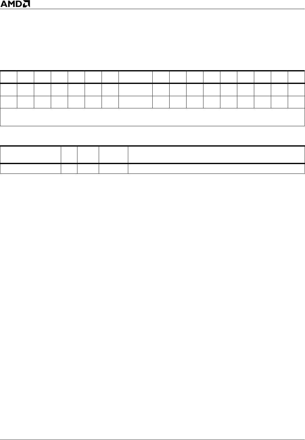
298 RSM Instruction Reference
AMD64 Technology 24594—Rev. 3.14—September 2007
rFLAGS Affected
All flags are restored from the state-save map (SSM).
Exceptions
ID VIP VIF AC VM RF NT IOPL OF DF IF TF SF ZF AF PF CF
MMMMMMM M MMMMMMMMM
2120191817161413–1211109876420
Note: Bits 31–22, 15, 5, 3, and 1 are reserved. A flag set to 1 or cleared to 0 is M (modified). Unaffected flags are
blank. Undefined flags are U.
Exception Real
Virtual
8086 Protected Cause of Exception
Invalid opcode, #UD X X X The processor was not in System Management Mode (SMM).
Instruction Reference SGDT 299
24594—Rev. 3.14—September 2007 AMD64 Technology
Stores the global descriptor table register (GDTR) into the destination operand. In legacy and
compatibility mode, the destination operand is 6 bytes; in 64-bit mode, it is 10 bytes. In all modes,
operand-size prefixes are ignored.
In non-64-bit mode, the lower two bytes of the operand specify the 16-bit limit and the upper 4 bytes
specify the 32-bit base address.
In 64-bit mode, the lower two bytes of the operand specify the 16-bit limit and the upper 8 bytes
specify the 64-bit base address.
This instruction is intended for use in operating system software, but it can be used at any privilege
level.
Related Instructions
SIDT, SLDT, STR, LGDT, LIDT, LLDT, LTR
rFLAGS Affected
None
Exceptions
SGDT Store Global Descriptor Table Register
Mnemonic Opcode Description
SGDT mem16:32 0F 01 /0 Store global descriptor table register to memory.
SGDT mem16:64 0F 01 /0 Store global descriptor table register to memory.
Exception Real
Virtual
8086 Protected Cause of Exception
Invalid opcode, #UD X X X The operand was a register.
Stack, #SS X X X A memory address exceeded the stack segment limit or was
non-canonical.
General protection,
#GP
XX XA memory address exceeded a data segment limit or was non-
canonical.
X The destination operand was in a non-writable segment.
X A null data segment was used to reference memory.
Page fault, #PF X X A page fault resulted from the execution of the instruction.
Alignment check,
#AC XX
An unaligned memory reference was performed while
alignment checking was enabled.
300 SIDT Instruction Reference
AMD64 Technology 24594—Rev. 3.14—September 2007
Stores the interrupt descriptor table register (IDTR) in the destination operand. In legacy and
compatibility mode, the destination operand is 6 bytes; in 64-bit mode it is 10 bytes. In all modes,
operand-size prefixes are ignored.
In non-64-bit mode, the lower two bytes of the operand specify the 16-bit limit and the upper 4 bytes
specify the 32-bit base address.
In 64-bit mode, the lower two bytes of the operand specify the 16-bit limit and the upper 8 bytes
specify the 64-bit base address.
This instruction is intended for use in operating system software, but it can be used at any privilege
level.
Related Instructions
SGDT, SLDT, STR, LGDT, LIDT, LLDT, LTR
rFLAGS Affected
None
Exceptions
SIDT Store Interrupt Descriptor Table Register
Mnemonic Opcode Description
SIDT mem16:32 0F 01 /1 Store interrupt descriptor table register to memory.
SIDT mem16:64 0F 01 /1 Store interrupt descriptor table register to memory.
Exception Real
Virtual
8086 Protected Cause of Exception
Invalid opcode, #UD X X X The operand was a register.
Stack, #SS X X X A memory address exceeded the stack segment limit or was
non-canonical.
General protection,
#GP
XX XA memory address exceeded a data segment limit or was non-
canonical.
X The destination operand was in a non-writable segment.
X A null data segment was used to reference memory.
Page fault, #PF X X A page fault resulted from the execution of the instruction.
Alignment check,
#AC XX
An unaligned memory reference was performed while
alignment checking was enabled.

Instruction Reference SKINIT 301
24594—Rev. 3.14—September 2007 AMD64 Technology
Securely reinitializes the cpu, allowing for the startup of trusted software (such as a VMM). The code
to be executed after reinitialization can be verified based on a secure hash comparison. SKINIT takes
the physical base address of the SLB as its only input operand, in EAX. The SLB must be structured as
described in “Secure Loader Block” on page 415 of the AMD64 Architecture Programmer’s Manual
Volume 2: System Programming, order# 24593, and is assumed to contain the code for a Secure Loader
(SL).
This is a Secure Virtual Machine instruction. This instruction generates a #UD exception if SVM is
not enabled. See “Enabling SVM” on page 369 in AMD64 Architecture Programmer’s Manual
Volume 2: System Instructions, order# 24593.
Action
IF ((EFER.SVMEN == 0) && !(CPUID 8000_0001.ECX[SKINIT]) || (!PROTECTED_MODE))
EXCEPTION [#UD] // This instruction can only be executed
// in protected mode with SVM enabled.
IF (CPL != 0) // This instruction is only allowed at CPL 0.
EXCEPTION [#GP]
Initialize processor state as for an INIT signal
CR0.PE = 1
CS.sel = 0x0008
CS.attr = 32-bit code, read/execute
CS.base = 0
CS.limit = 0xFFFFFFFF
SS.sel = 0x0010
SS.attr = 32-bit stack, read/write, expand up
SS.base = 0
SS.limit = 0xFFFFFFFF
EAX = EAX & 0xFFFF0000 // Form SLB base address.
EDX = family/model/stepping
ESP = EAX + 0x00010000 // Initial SL stack.
Clear GPRs other than EAX, EDX, ESP
EFER = 0
VM_CR.DPD = 1
VM_CR.R_INIT = 1
VM_CR.DIS_A20M = 1
SKINIT Secure Init and Jump with Attestation
Mnemonic Opcode Description
SKINIT EAX 0F 01 DE Secure initialization and jump, with attestation.
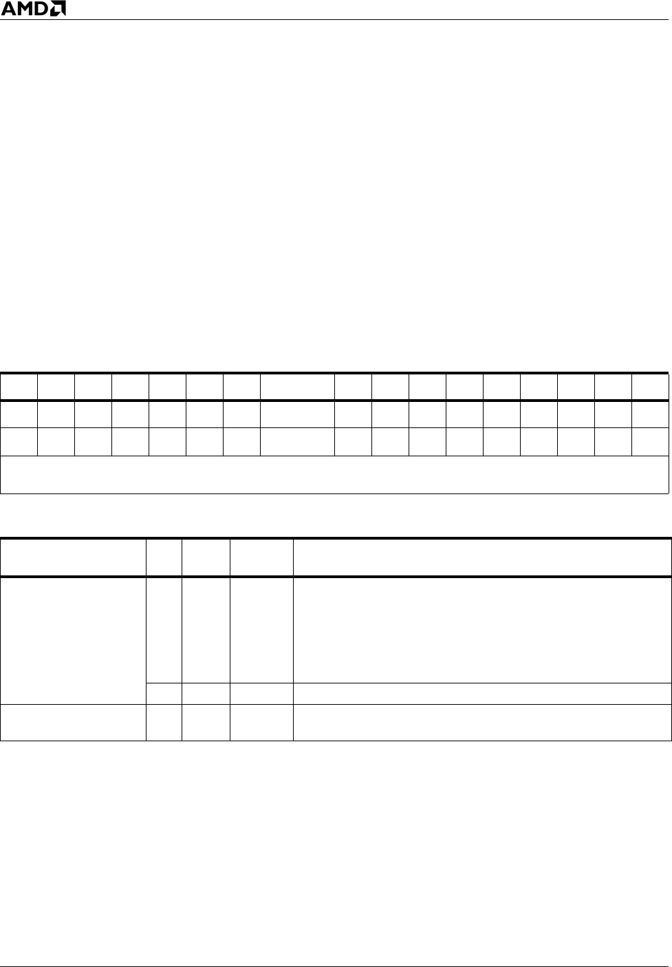
302 SKINIT Instruction Reference
AMD64 Technology 24594—Rev. 3.14—September 2007
Enable SL_DEV, to protect 64Kbyte of physical memory starting at
the physical address in EAX
GIF = 0
Read the SL length from offset 0x0002 in the SLB
Copy the SL image to the TPM for attestation
Read the SL entrypoint offset from offset 0x0000 in the SLB
Jump to the SL entrypoint, at EIP = EAX+entrypoint offset
Related Instructions
None.
rFLAGS Affected
Exceptions
ID VIP VIF AC VM RF NT IOPL OF DF IF TF SF ZF AF PF CF
0000000 0 000000000
2120191817161413–1211109876420
Note: Bits 31–22, 15, 5, 3, and 1 are reserved. A flag set to 1 or cleared to 0 is M (modified). Unaffected flags are blank.
Undefined flags are U.
Exception Real
Virtual
8086 Protected Cause of Exception
Invalid opcode, #UD X
Secure Virtual Machine was not enabled (EFER.SVME=0)
and both of the following conditions were true:
• SVM-Lock is not available, as indicated by EDX bit 2
returned by CPUID function 8000_000Ah.
• DEV is not available, as indicated by ECX bit 12 returned
by CPUID function 8000_0001h.
X X Instruction is only recognized in protected mode.
General protection,
#GP X CPL was not zero.

Instruction Reference SLDT 303
24594—Rev. 3.14—September 2007 AMD64 Technology
Stores the local descriptor table (LDT) selector to a register or memory destination operand.
If the destination is a register, the selector is zero-extended into a 16-, 32-, or 64-bit general purpose
register, depending on operand size.
If the destination operand is a memory location, the segment selector is written to memory as a 16-bit
value, regardless of operand size.
This SLDT instruction can only be used in protected mode, but it can be executed at any privilege
level.
Related Instructions
SIDT, SGDT, STR, LIDT, LGDT, LLDT, LTR
rFLAGS Affected
None
Exceptions
SLDT Store Local Descriptor Table Register
Mnemonic Opcode Description
SLDT reg16 0F 00 /0 Store the segment selector from the local
descriptor table register to a 16-bit register.
SLDT reg32 0F 00 /0 Store the segment selector from the local
descriptor table register to a 32-bit register.
SLDT reg64 0F 00 /0 Store the segment selector from the local
descriptor table register to a 64-bit register.
SLDT mem16 0F 00 /0
Store the segment selector from the local
descriptor table register to a 16-bit memory
location.
Exception Real
Virtual
8086 Protected Cause of Exception
Invalid opcode, #UD X X This instruction is only recognized in protected mode.
Stack, #SS X A memory address exceeded the stack segment limit or was
non-canonical.
General protection,
#GP
XA memory address exceeded a data segment limit or was non-
canonical.
X The destination operand was in a non-writable segment.
X A null data segment was used to reference memory.
Page fault, #PF X A page fault resulted from the execution of the instruction.
Alignment check,
#AC XAn unaligned memory reference was performed while
alignment checking was enabled.
304 SMSW Instruction Reference
AMD64 Technology 24594—Rev. 3.14—September 2007
Stores the lower bits of the machine status word (CR0). The target can be a 16-, 32-, or 64-bit register
or a 16-bit memory operand.
This instruction is provided for compatibility with early processors.
This instruction can be used at any privilege level (CPL).
Related Instructions
LMSW, MOV(CRn)
rFLAGS Affected
None
Exceptions
SMSW Store Machine Status Word
Mnemonic Opcode Description
SMSW reg16 0F 01 /4 Store the low 16 bits of CR0 to a 16-bit register.
SMSW reg32 0F 01 /4 Store the low 32 bits of CR0 to a 32-bit register.
SMSW reg64 0F 01 /4 Store the entire 64-bit CR0 to a 64-bit register.
SMSW mem16 0F 01 /4 Store the low 16 bits of CR0 to memory.
Exception Real
Virtual
8086 Protected Cause of Exception
Stack, #SS X X X A memory address exceeded the stack segment limit or was
non-canonical.
General protection,
#GP
XX XA memory address exceeded a data segment limit or was non-
canonical.
X The destination operand was in a non-writable segment.
X A null data segment was used to reference memory.
Page fault, #PF X X A page fault resulted from the execution of the instruction.
Alignment check,
#AC XX
An unaligned memory reference was performed while
alignment checking was enabled.

Instruction Reference STI 305
24594—Rev. 3.14—September 2007 AMD64 Technology
Sets the interrupt flag (IF) in the rFLAGS register to 1, thereby allowing external interrupts received on
the INTR input. Interrupts received on the non-maskable interrupt (NMI) input are not affected by this
instruction.
In real mode, this instruction sets IF to 1.
In protected mode and virtual-8086-mode, this instruction is IOPL-sensitive. If the CPL is less than or
equal to the rFLAGS.IOPL field, the instruction sets IF to 1.
In protected mode, if IOPL < 3, CPL = 3, and protected mode virtual interrupts are enabled
(CR4.PVI = 1), then the instruction instead sets rFLAGS.VIF to 1. If none of these conditions apply,
the processor raises a general protection exception (#GP). For more information, see “Protected Mode
Virtual Interrupts” in Volume 2.
In virtual-8086 mode, if IOPL < 3 and the virtual-8086-mode extensions are enabled (CR4.VME = 1),
the STI instruction instead sets the virtual interrupt flag (rFLAGS.VIF) to 1.
If STI sets the IF flag and IF was initially clear, then interrupts are not enabled until after the
instruction following STI. Thus, if IF is 0, this code will not allow an INTR to happen:
STI
CLI
In the following sequence, INTR will be allowed to happen only after the NOP.
STI
NOP
CLI
If STI sets the VIF flag and VIP is already set, a #GP fault will be generated.
See “Virtual-8086 Mode Extensions” in Volume 2 for more information about IOPL-sensitive
instructions.
STI Set Interrupt Flag
Mnemonic Opcode Description
STI FB Set interrupt flag (IF) to 1.
306 STI Instruction Reference
AMD64 Technology 24594—Rev. 3.14—September 2007
Action
IF (CPL <= IOPL)
RFLAGS.IF = 1
ELSIF (((VIRTUAL_MODE) && (CR4.VME = 1))
|| ((PROTECTED_MODE) && (CR4.PVI = 1) && (CPL = 3)))
{
IF (RFLAGS.VIP = 1)
EXCEPTION[#GP(0)]
RFLAGS.VIF = 1
}
ELSE
EXCEPTION[#GP(0)]
Related Instructions
CLI
rFLAGS Affected
Exceptions
ID VIP VIF AC VM RF NT IOPL OF DF IF TF SF ZF AF PF CF
MM
2120191817161413–1211109876420
Note: Bits 31–22, 15, 5, 3, and 1 are reserved. M (modified) is either set to one or cleared to zero. Unaffected flags
are blank. Undefined flags are U.
Exception Real
Virtual
8086 Protected Cause of Exception
General protection,
#GP
XThe CPL was greater than the IOPL and virtual-mode
extensions were not enabled (CR4.VME = 0).
X
The CPL was greater than the IOPL and either the CPL was
not 3 or protected-mode virtual interrupts were not enabled
(CR4.PVI = 0).
XX
This instruction would set RFLAGS.VIF to 1 and
RFLAGS.VIP was already 1.
Instruction Reference STGI 307
24594—Rev. 3.14—September 2007 AMD64 Technology
Sets the global interrupt flag (GIF) to 1. While GIF is zero, all external interrupts are disabled.
This is a Secure Virtual Machine instruction. This instruction generates a #UD exception if SVM is
not enabled and ECX.SKINIT as returned by CPUID function 8000_0001 is cleared to 0. See
“Enabling SVM” on page 369 in AMD64 Architecture Programmer’s Manual Volume-2: System
Instructions, order# 24593.
Related Instructions
CLGI
rFLAGS Affected
None.
Exceptions
STGI Set Global Interrupt Flag
Mnemonic Opcode Description
STGI 0F 01 DC Sets the global interrupt flag (GIF).
Exception Real
Virtual
8086 Protected Cause of Exception
Invalid opcode, #UD X
Secure Virtual Machine was not enabled (EFER.SVME=0)
and both of the following conditions were true:
• SVM-Lock is not available, as indicated by EDX bit 2
returned by CPUID function 8000_000Ah.
• DEV is not available, as indicated by ECX bit 12 returned
by CPUID function 8000_0001h.
X X Instruction is only recognized in protected mode.
General protection,
#GP X CPL was not zero.

308 STR Instruction Reference
AMD64 Technology 24594—Rev. 3.14—September 2007
Stores the task register (TR) selector to a register or memory destination operand.
If the destination is a register, the selector is zero-extended into a 16-, 32-, or 64-bit general purpose
register, depending on the operand size.
If the destination is a memory location, the segment selector is written to memory as a 16-bit value,
regardless of operand size.
The STR instruction can only be used in protected mode, but it can be used at any privilege level.
Related Instructions
LGDT, LIDT, LLDT, LTR, SIDT, SGDT, SLDT
rFLAGS Affected
None
Exceptions
STR Store Task Register
Mnemonic Opcode Description
STR reg16 0F 00 /1 Store the segment selector from the task register to a 16-bit
general-purpose register.
STR reg32 0F 00 /1 Store the segment selector from the task register to a 32-bit
general-purpose register.
STR reg64 0F 00 /1 Store the segment selector from the task register to a 64-bit
general-purpose register.
STR mem16 0F 00 /1 Store the segment selector from the task register to a 16-bit
memory location.
Exception Real
Virtual
8086 Protected Cause of Exception
Invalid opcode, #UD X X This instruction is only recognized in protected mode.
Stack, #SS X A memory address exceeded the stack segment limit or was
non-canonical.
General protection,
#GP
XA memory address exceeded a data segment limit or was
non-canonical.
X The destination operand was in a non-writable segment.
X A null data segment was used to reference memory.
Page fault, #PF X A page fault resulted from the execution of the instruction.
Alignment check, #AC X An unaligned memory reference was performed while
alignment checking was enabled.

Instruction Reference SWAPGS 309
24594—Rev. 3.14—September 2007 AMD64 Technology
Provides a fast method for system software to load a pointer to system data structures. SWAPGS can
be used upon entering system-software routines as a result of a SYSCALL instruction, an interrupt or
an exception. Prior to returning to application software, SWAPGS can be used to restore the
application data pointer that was replaced by the system data-structure pointer.
This instruction can only be executed in 64-bit mode. Executing SWAPGS in any other mode
generates an undefined opcode exception.
The SWAPGS instruction only exchanges the base-address value located in the KernelGSbase model-
specific register (MSR address C000_0102h) with the base-address value located in the hidden-portion
of the GS selector register (GS.base). This allows the system-kernel software to access kernel data
structures by using the GS segment-override prefix during memory references.
The address stored in the KernelGSbase MSR must be in canonical form. The WRMSR instruction
used to load the KernelGSbase MSR causes a general-protection exception if the address loaded is not
in canonical form. The SWAPGS instruction itself does not perform a canonical check.
This instruction is only valid in 64-bit mode at CPL 0. A general protection exception (#GP) is
generated if this instruction is executed at any other privilege level.
For additional information about this instruction, refer to “System-Management Instructions” in
Vo l u m e 2 .
Examples
At a kernel entry point, the OS uses SwapGS to obtain a pointer to kernel data structures and
simultaneously save the user's GS base. Upon exit, it uses SwapGS to restore the user's GS base:
SystemCallEntryPoint:
SwapGS ; get kernel pointer, save user GSbase
mov gs:[SavedUserRSP], rsp ; save user's stack pointer
mov rsp, gs:[KernelStackPtr] ; set up kernel stack
push rax ; now save user GPRs on kernel stack
. ; perform system service
.
SwapGS ; restore user GS, save kernel pointer
Related Instructions
None
SWAPGS Swap GS Register with KernelGSbase MSR
Mnemonic Opcode Description
SWAPGS 0F 01 F8 Exchange GS base with KernelGSBase MSR.
(Invalid in legacy and compatibility modes.)

310 SWAPGS Instruction Reference
AMD64 Technology 24594—Rev. 3.14—September 2007
rFLAGS Affected
None
Exceptions
Exception Real
Virtual
8086 Protected Cause of Exception
Invalid opcode, #UD X X X This instruction was executed in legacy or
compatibility mode.
General protection, #GP X CPL was not 0.

Instruction Reference SYSCALL 311
24594—Rev. 3.14—September 2007 AMD64 Technology
Transfers control to a fixed entry point in an operating system. It is designed for use by system and
application software implementing a flat-segment memory model.
The SYSCALL and SYSRET instructions are low-latency system call and return control-transfer
instructions, which assume that the operating system implements a flat-segment memory model. By
eliminating unneeded checks, and by loading pre-determined values into the CS and SS segment
registers (both visible and hidden portions), calls to and returns from the operating system are greatly
simplified. These instructions can be used in protected mode and are particularly well-suited for use in
64-bit mode, which requires implementation of a paged, flat-segment memory model.
This instruction has been optimized by reducing the number of checks and memory references that are
normally made so that a call or return takes considerably fewer clock cycles than the CALL FAR /RET
FAR instruction method.
It is assumed that the base, limit, and attributes of the Code Segment will remain flat for all processes
and for the operating system, and that only the current privilege level for the selector of the calling
process should be changed from a current privilege level of 3 to a new privilege level of 0. It is also
assumed (but not checked) that the RPL of the SYSCALL and SYSRET target selectors are set to 0
and 3, respectively.
SYSCALL sets the CPL to 0, regardless of the values of bits 33–32 of the STAR register. There are no
permission checks based on the CPL, real mode, or virtual-8086 mode. SYSCALL and SYSRET must
be enabled by setting EFER.SCE to 1.
It is the responsibility of the operating system to keep the descriptors in memory that correspond to the
CS and SS selectors loaded by the SYSCALL and SYSRET instructions consistent with the segment
base, limit, and attribute values forced by these instructions.
Legacy x86 Mode. In legacy x86 mode, when SYSCALL is executed, the EIP of the instruction
following the SYSCALL is copied into the ECX register. Bits 31–0 of the SYSCALL/SYSRET target
address register (STAR) are copied into the EIP register. (The STAR register is model-specific register
C000_0081h.)
New selectors are loaded, without permission checking (see above), as follows:
• Bits 47–32 of the STAR register specify the selector that is copied into the CS register.
• Bits 47–32 of the STAR register + 8 specify the selector that is copied into the SS register.
• The CS_base and the SS_base are both forced to zero.
• The CS_limit and the SS_limit are both forced to 4 Gbyte.
• The CS segment attributes are set to execute/read 32-bit code with a CPL of zero.
• The SS segment attributes are set to read/write and expand-up with a 32-bit stack referenced by
ESP.
SYSCALL Fast System Call

312 SYSCALL Instruction Reference
AMD64 Technology 24594—Rev. 3.14—September 2007
Long Mode. When long mode is activated, the behavior of the SYSCALL instruction depends on
whether the calling software is in 64-bit mode or compatibility mode. In 64-bit mode, SYSCALL
saves the RIP of the instruction following the SYSCALL into RCX and loads the new RIP from
LSTAR bits 63–0. (The LSTAR register is model-specific register C000_0082h.) In compatibility
mode, SYSCALL saves the RIP of the instruction following the SYSCALL into RCX and loads the
new RIP from CSTAR bits 63–0. (The CSTAR register is model-specific register C000_0083h.)
New selectors are loaded, without permission checking (see above), as follows:
• Bits 47–32 of the STAR register specify the selector that is copied into the CS register.
• Bits 47–32 of the STAR register + 8 specify the selector that is copied into the SS register.
• The CS_base and the SS_base are both forced to zero.
• The CS_limit and the SS_limit are both forced to 4 Gbyte.
• The CS segment attributes are set to execute/read 64-bit code with a CPL of zero.
• The SS segment attributes are set to read/write and expand-up with a 64-bit stack referenced by
RSP.
The WRMSR instruction loads the target RIP into the LSTAR and CSTAR registers. If an RIP written
by WRMSR is not in canonical form, a general-protection exception (#GP) occurs.
How SYSCALL and SYSRET handle rFLAGS, depends on the processor’s operating mode.
In legacy mode, SYSCALL treats EFLAGS as follows:
• EFLAGS.IF is cleared to 0.
• EFLAGS.RF is cleared to 0.
• EFLAGS.VM is cleared to 0.
In long mode, SYSCALL treats RFLAGS as follows:
• The current value of RFLAGS is saved in R11.
• RFLAGS is masked using the value stored in SYSCALL_FLAG_MASK.
• RFLAGS.RF is cleared to 0.
For further details on the SYSCALL and SYSRET instructions and their associated MSR registers
(STAR, LSTAR, CSTAR, and SYSCALL_FLAG_MASK), see “Fast System Call and Return” in
Vo l u m e 2 .
Mnemonic Opcode Description
SYSCALL 0F 05 Call operating system.

Instruction Reference SYSCALL 313
24594—Rev. 3.14—September 2007 AMD64 Technology
Action
// See “Pseudocode Definitions” on page 41.
SYSCALL_START:
IF (MSR_EFER.SCE = 0) // Check if syscall/sysret are enabled.
EXCEPTION [#UD]
IF (LONG_MODE)
SYSCALL_LONG_MODE
ELSE // (LEGACY_MODE)
SYSCALL_LEGACY_MODE
SYSCALL_LONG_MODE:
RCX.q = next_RIP
R11.q = RFLAGS // with rf cleared
IF (64BIT_MODE)
temp_RIP.q = MSR_LSTAR
ELSE // (COMPATIBILITY_MODE)
temp_RIP.q = MSR_CSTAR
CS.sel = MSR_STAR.SYSCALL_CS AND 0xFFFC
CS.attr = 64-bit code,dpl0 // Always switch to 64-bit mode in long mode.
CS.base = 0x00000000
CS.limit = 0xFFFFFFFF
SS.sel = MSR_STAR.SYSCALL_CS + 8
SS.attr = 64-bit stack,dpl0
SS.base = 0x00000000
SS.limit = 0xFFFFFFFF
RFLAGS = RFLAGS AND ~MSR_SFMASK
RFLAGS.RF = 0
CPL = 0
RIP = temp_RIP
EXIT
SYSCALL_LEGACY_MODE:
RCX.d = next_RIP
temp_RIP.d = MSR_STAR.EIP
CS.sel = MSR_STAR.SYSCALL_CS AND 0xFFFC
CS.attr = 32-bit code,dpl0 // Always switch to 32-bit mode in legacy mode.
314 SYSCALL Instruction Reference
AMD64 Technology 24594—Rev. 3.14—September 2007
CS.base = 0x00000000
CS.limit = 0xFFFFFFFF
SS.sel = MSR_STAR.SYSCALL_CS + 8
SS.attr = 32-bit stack,dpl0
SS.base = 0x00000000
SS.limit = 0xFFFFFFFF
RFLAGS.VM,IF,RF=0
CPL = 0
RIP = temp_RIP
EXIT
Related Instructions
SYSRET, SYSENTER, SYSEXIT
rFLAGS Affected
Exceptions
ID VIP VIF AC VM RF NT IOPL OF DF IF TF SF ZF AF PF CF
MMMM 0 0 M M MMMMMMMMM
2120191817161413–1211109876420
Note: Bits 31–22, 15, 5, 3, and 1 are reserved. A flag set to one or cleared to zero is M (modified). Unaffected flags
are blank. Undefined flags are U.
Exception Real
Virtual
8086 Protected Cause of Exception
Invalid opcode, #UD
XX X
The SYSCALL and SYSRET instructions are not
supported, as indicated by EDX bit 11 returned by
CPUID function 8000_0001h.
XX X
The system call extension bit (SCE) of the extended
feature enable register (EFER) is set to 0. (The
EFER register is MSR C000_0080h.)

Instruction Reference SYSENTER 315
24594—Rev. 3.14—September 2007 AMD64 Technology
Transfers control to a fixed entry point in an operating system. It is designed for use by system and
application software implementing a flat-segment memory model. This instruction is valid only in
legacy mode.
Three model-specific registers (MSRs) are used to specify the target address and stack pointers for the
SYSENTER instruction, as well as the CS and SS selectors of the called and returned procedures:
• MSR_SYSENTER_CS: Contains the CS selector of the called procedure. The SS selector is set to
MSR_SYSENTER_CS + 8.
• MSR_SYSENTER_ESP: Contains the called procedure’s stack pointer.
• MSR_SYSENTER_EIP: Contains the offset into the CS of the called procedure.
The hidden portions of the CS and SS segment registers are not loaded from the descriptor table as they
would be using a legacy x86 CALL instruction. Instead, the hidden portions are forced by the
processor to the following values:
• The CS and SS base values are forced to 0.
• The CS and SS limit values are forced to 4 Gbytes.
• The CS segment attributes are set to execute/read 32-bit code with a CPL of zero.
• The SS segment attributes are set to read/write and expand-up with a 32-bit stack referenced by
ESP.
System software must create corresponding descriptor-table entries referenced by the new CS and SS
selectors that match the values described above.
The return EIP and application stack are not saved by this instruction. System software must explicitly
save that information.
An invalid-opcode exception occurs if this instruction is used in long mode. Software should use the
SYSCALL (and SYSRET) instructions in long mode. If SYSENTER is used in real mode, a #GP is
raised.
For additional information on this instruction, see “SYSENTER and SYSEXIT (Legacy Mode Only)”
in Volume 2.
Related Instructions
SYSCALL, SYSEXIT, SYSRET
SYSENTER System Call
Mnemonic Opcode Description
SYSENTER 0F 34 Call operating system.
316 SYSENTER Instruction Reference
AMD64 Technology 24594—Rev. 3.14—September 2007
rFLAGS Affected
Exceptions
ID VIP VIF AC VM RF NT IOPL OF DF IF TF SF ZF AF PF CF
00
2120191817161413–1211109876420
Note: Bits 31–22, 15, 5, 3, and 1 are reserved. A flag set to one or zero is M (modified). Unaffected flags are blank.
Undefined flags are U.
Exception Real
Virtual
8086 Protected Cause of Exception
Invalid opcode, #UD XX X
The SYSENTER and SYSEXIT instructions are not
supported, as indicated by EDX bit 11 returned by
CPUID function 0000_0001h.
X This instruction is not recognized in long mode.
General protection, #GP X This instruction is not recognized in real mode.
X X MSR_SYSENTER_CS was a null selector.

Instruction Reference SYSEXIT 317
24594—Rev. 3.14—September 2007 AMD64 Technology
Returns from the operating system to an application. It is a low-latency system return instruction
designed for use by system and application software implementing a flat-segment memory model.
This is a privileged instruction. The current privilege level must be zero to execute this instruction. An
invalid-opcode exception occurs if this instruction is used in long mode. Software should use the
SYSRET (and SYSCALL) instructions when running in long mode.
When a system procedure performs a SYSEXIT back to application software, the CS selector is
updated to point to the second descriptor entry after the SYSENTER CS value (MSR
SYSENTER_CS+16). The SS selector is updated to point to the third descriptor entry after the
SYSENTER CS value (MSR SYSENTER_CS+24). The CPL is forced to 3, as are the descriptor
privilege levels.
The hidden portions of the CS and SS segment registers are not loaded from the descriptor table as they
would be using a legacy x86 RET instruction. Instead, the hidden portions are forced by the processor
to the following values:
• The CS and SS base values are forced to 0.
• The CS and SS limit values are forced to 4 Gbytes.
• The CS segment attributes are set to 32-bit read/execute at CPL 3.
• The SS segment attributes are set to read/write and expand-up with a 32-bit stack referenced by
ESP.
System software must create corresponding descriptor-table entries referenced by the new CS and SS
selectors that match the values described above.
The following additional actions result from executing SYSEXIT:
• EIP is loaded from EDX.
• ESP is loaded from ECX.
System software must explicitly load the return address and application software-stack pointer into the
EDX and ECX registers prior to executing SYSEXIT.
For additional information on this instruction, see “SYSENTER and SYSEXIT (Legacy Mode Only)”
in Volume 2.
Related Instructions
SYSCALL, SYSENTER, SYSRET
SYSEXIT System Return
Mnemonic Opcode Description
SYSEXIT 0F 35 Return from operating system to application.

318 SYSEXIT Instruction Reference
AMD64 Technology 24594—Rev. 3.14—September 2007
rFLAGS Affected
Exceptions
ID VIP VIF AC VM RF NT IOPL OF DF IF TF SF ZF AF PF CF
0
2120191817161413–1211109876420
Note: Bits 31–22, 15, 5, 3, and 1 are reserved. A flag set to one or cleared to zero is M (modified). Unaffected flags
are blank.
Exception Real
Virtual
8086 Protected Cause of Exception
Invalid opcode, #UD XX X
The SYSENTER and SYSEXIT instructions are not
supported, as indicated by EDX bit 11 returned by
CPUID function 0000_0001h.
X This instruction is not recognized in long mode.
General protection, #GP
XX This instruction is only recognized in protected
mode.
X CPL was not 0.
X MSR_SYSENTER_CS was a null selector.

Instruction Reference SYSRET 319
24594—Rev. 3.14—September 2007 AMD64 Technology
Returns from the operating system to an application. It is a low-latency system return instruction
designed for use by system and application software implementing a flat segmentation memory model.
The SYSCALL and SYSRET instructions are low-latency system call and return control-transfer
instructions that assume that the operating system implements a flat-segment memory model. By
eliminating unneeded checks, and by loading pre-determined values into the CS and SS segment
registers (both visible and hidden portions), calls to and returns from the operating system are greatly
simplified. These instructions can be used in protected mode and are particularly well-suited for use in
64-bit mode, which requires implementation of a paged, flat-segment memory model.
This instruction has been optimized by reducing the number of checks and memory references that are
normally made so that a call or return takes substantially fewer internal clock cycles when compared to
the CALL/RET instruction method.
It is assumed that the base, limit, and attributes of the Code Segment will remain flat for all processes
and for the operating system, and that only the current privilege level for the selector of the calling
process should be changed from a current privilege level of 0 to a new privilege level of 3. It is also
assumed (but not checked) that the RPL of the SYSCALL and SYSRET target selectors are set to 0
and 3, respectively.
SYSRET sets the CPL to 3, regardless of the values of bits 49–48 of the star register. SYSRET can
only be executed in protected mode at CPL 0. SYSCALL and SYSRET must be enabled by setting
EFER.SCE to 1.
It is the responsibility of the operating system to keep the descriptors in memory that correspond to the
CS and SS selectors loaded by the SYSCALL and SYSRET instructions consistent with the segment
base, limit, and attribute values forced by these instructions.
When a system procedure performs a SYSRET back to application software, the CS selector is
updated from bits 63–50 of the STAR register (STAR.SYSRET_CS) as follows:
• If the return is to 32-bit mode (legacy or compatibility), CS is updated with the value of
STAR.SYSRET_CS.
• If the return is to 64-bit mode, CS is updated with the value of STAR.SYSRET_CS + 16.
In both cases, the CPL is forced to 3, effectively ignoring STAR bits 49–48. The SS selector is updated
to point to the next descriptor-table entry after the CS descriptor (STAR.SYSRET_CS + 8), and its
RPL is not forced to 3.
The hidden portions of the CS and SS segment registers are not loaded from the descriptor table as they
would be using a legacy x86 RET instruction. Instead, the hidden portions are forced by the processor
to the following values:
• The CS base value is forced to 0.
• The CS limit value is forced to 4 Gbytes.
SYSRET Fast System Return

320 SYSRET Instruction Reference
AMD64 Technology 24594—Rev. 3.14—September 2007
• The CS segment attributes are set to execute-read 32 bits or 64 bits (see below).
• The SS segment base, limit, and attributes are not modified.
When SYSCALLed system software is running in 64-bit mode, it has been entered from either 64-bit
mode or compatibility mode. The corresponding SYSRET needs to know the mode to which it must
return. Executing SYSRET in non-64-bit mode or with a 16- or 32-bit operand size returns to 32-bit
mode with a 32-bit stack pointer. Executing SYSRET in 64-bit mode with a 64-bit operand size returns
to 64-bit mode with a 64-bit stack pointer.
The instruction pointer is updated with the return address based on the operating mode in which
SYSRET is executed:
• If returning to 64-bit mode, SYSRET loads RIP with the value of RCX.
• If returning to 32-bit mode, SYSRET loads EIP with the value of ECX.
How SYSRET handles RFLAGS depends on the processor’s operating mode:
• If executed in 64-bit mode, SYSRET loads the lower-32 RFLAGS bits from R11[31:0] and clears
the upper 32 RFLAGS bits.
• If executed in legacy mode or compatibility mode, SYSRET sets EFLAGS.IF.
For further details on the SYSCALL and SYSRET instructions and their associated MSR registers
(STAR, LSTAR, and CSTAR), see “Fast System Call and Return” in Volume 2.
Action
// See “Pseudocode Definitions” on page 41.
SYSRET_START:
IF (MSR_EFER.SCE = 0) // Check if syscall/sysret are enabled.
EXCEPTION [#UD]
IF ((!PROTECTED_MODE) || (CPL != 0))
EXCEPTION [#GP(0)] // SYSRET requires protected mode, cpl0
IF (64BIT_MODE)
SYSRET_64BIT_MODE
ELSE // (!64BIT_MODE)
SYSRET_NON_64BIT_MODE
SYSRET_64BIT_MODE:
IF (OPERAND_SIZE = 64) // Return to 64-bit mode.
{
Mnemonic Opcode Description
SYSRET 0F 07 Return from operating system.

Instruction Reference SYSRET 321
24594—Rev. 3.14—September 2007 AMD64 Technology
CS.sel = (MSR_STAR.SYSRET_CS + 16) OR 3
CS.base = 0x00000000
CS.limit = 0xFFFFFFFF
CS.attr = 64-bit code,dpl3
temp_RIP.q = RCX
}
ELSE // Return to 32-bit compatibility mode.
{
CS.sel = MSR_STAR.SYSRET_CS OR 3
CS.base = 0x00000000
CS.limit = 0xFFFFFFFF
CS.attr = 32-bit code,dpl3
temp_RIP.d = RCX
}
SS.sel = MSR_STAR.SYSRET_CS + 8 // SS selector is changed,
// SS base, limit, attributes unchanged.
RFLAGS.q = R11 // RF=0,VM=0
CPL = 3
RIP = temp_RIP
EXIT
SYSRET_NON_64BIT_MODE:
CS.sel = MSR_STAR.SYSRET_CS OR 3 // Return to 32-bit legacy protected mode.
CS.base = 0x00000000
CS.limit = 0xFFFFFFFF
CS.attr = 32-bit code,dpl3
temp_RIP.d = RCX
SS.sel = MSR_STAR.SYSRET_CS + 8 // SS selector is changed.
// SS base, limit, attributes unchanged.
RFLAGS.IF = 1
CPL = 3
RIP = temp_RIP
EXIT
Related Instructions
SYSCALL, SYSENTER, SYSEXIT

322 SYSRET Instruction Reference
AMD64 Technology 24594—Rev. 3.14—September 2007
rFLAGS Affected
Exceptions
ID VIP VIF AC VM RF NT IOPL OF DF IF TF SF ZF AF PF CF
MMMM 0 M M MMMMMMMMM
2120191817161413–1211109876420
Note: Bits 31–22, 15, 5, 3, and 1 are reserved. A flag set to one or cleared to zero is M (modified). Unaffected flags
are blank. Undefined flags are U.
Exception Real
Virtual
8086 Protected Cause of Exception
Invalid opcode, #UD
XX X
The SYSCALL and SYSRET instructions are not
supported, as indicated by EDX bit 11 returned by
CPUID function 8000_0001h.
XX X
The system call extension bit (SCE) of the extended
feature enable register (EFER) is set to 0. (The
EFER register is MSR C000_0080h.)
General protection, #GP XX This instruction is only recognized in protected
mode.
X CPL was not 0.
Instruction Reference UD2 323
24594—Rev. 3.14—September 2007 AMD64 Technology
Generates an invalid opcode exception. Unlike other undefined opcodes that may be defined as legal
instructions in the future, UD2 is guaranteed to stay undefined.
Related Instructions
None
rFLAGS Affected
None
Exceptions
UD2 Undefined Operation
Mnemonic Opcode Description
UD2 0F 0B Raise an invalid opcode exception.
Exception Real
Virtual
8086 Protected Cause of Exception
Invalid opcode, #UD X X X This instruction is not recognized.
324 VERR Instruction Reference
AMD64 Technology 24594—Rev. 3.14—September 2007
Verifies whether a code or data segment specified by the segment selector in the 16-bit register or
memory operand is readable from the current privilege level. The zero flag (ZF) is set to 1 if the
specified segment is readable. Otherwise, ZF is cleared.
A segment is readable if all of the following apply:
• the selector is not a null selector.
• the descriptor is within the GDT or LDT limit.
• the segment is a data segment or readable code segment.
• the descriptor DPL is greater than or equal to both the CPL and RPL, or the segment is a conform-
ing code segment.
The processor does not recognize the VERR instruction in real or virtual-8086 mode.
Related Instructions
ARPL, LAR, LSL, VERW
rFLAGS Affected
Exceptions
VERR Verify Segment for Reads
Mnemonic Opcode Description
VERR reg/mem16 0F 00 /4 Set the zero flag (ZF) to 1 if the segment
selected can be read.
ID VIP VIF AC VM RF NT IOPL OF DF IF TF SF ZF AF PF CF
M
2120191817161413–1211109876420
Note: Bits 31–22, 15, 5, 3, and 1 are reserved. A flag set to one or cleared to zero is M (modified). Unaffected flags
are blank. Undefined flags are U.
Exception Real
Virtual
8086 Protected Cause of Exception
Invalid opcode, #UD X X This instruction is only recognized in protected mode.
Stack, #SS X A memory address exceeded the stack segment limit or is
non-canonical.
General protection,
#GP
XA memory address exceeded a data segment limit or was non-
canonical.
X A null data segment was used to reference memory.

Instruction Reference VERR 325
24594—Rev. 3.14—September 2007 AMD64 Technology
Page fault, #PF X A page fault resulted from the execution of the instruction.
Alignment check,
#AC XAn unaligned memory reference was performed while
alignment checking was enabled.
Exception Real
Virtual
8086 Protected Cause of Exception

326 VERW Instruction Reference
AMD64 Technology 24594—Rev. 3.14—September 2007
Verifies whether a data segment specified by the segment selector in the 16-bit register or memory
operand is writable from the current privilege level. The zero flag (ZF) is set to 1 if the specified
segment is writable. Otherwise, ZF is cleared.
A segment is writable if all of the following apply:
• the selector is not a null selector.
• the descriptor is within the GDT or LDT limit.
• the segment is a writable data segment.
• the descriptor DPL is greater than or equal to both the CPL and RPL.
The processor does not recognize the VERW instruction in real or virtual-8086 mode.
Related Instructions
ARPL, LAR, LSL, VERR
rFLAGS Affected
Exceptions
VERW Verify Segment for Write
Mnemonic Opcode Description
VERW reg/mem16 0F 00 /5 Set the zero flag (ZF) to 1 if the segment
selected can be written.
ID VIP VIF AC VM RF NT IOPL OF DF IF TF SF ZF AF PF CF
M
2120191817161413–1211109876420
Note: Bits 31–22, 15, 5, 3, and 1 are reserved. A flag set to one or cleared to zero is M (modified). Unaffected flags
are blank. Undefined flags are U.
Exception Real
Virtual
8086 Protected Cause of Exception
Invalid opcode, #UD X X This instruction is only recognized in protected mode.
Stack, #SS X A memory address exceeded the stack segment limit or was
non-canonical.
General protection,
#GP
XA memory address exceeded a data segment limit or was non-
canonical.
X A null data segment was used to access memory.
Page fault, #PF X A page fault resulted from the execution of the instruction.
Alignment check,
#AC XAn unaligned memory reference was performed while
alignment checking was enabled.

Instruction Reference VMLOAD 327
24594—Rev. 3.14—September 2007 AMD64 Technology
Loads a subset of processor state from the VMCB specified by the physical address in the rAX register.
The portion of RAX used to form the address is determined by the effective address size.
The VMSAVE and VMLOAD instructions complement the state save/restore abilities of VMRUN and
#VMEXIT, providing access to hidden state that software is otherwise unable to access, plus some
additional commonly-used state.
This is a Secure Virtual Machine instruction. This instruction generates a #UD exception if SVM is
not enabled. See “Enabling SVM” on page 369 in AMD64 Architecture Programmer’s Manual
Volume 2: System Instructions, order# 24593.
Action
IF ((MSR_EFER.SVME = 0) || (!PROTECTED_MODE))
EXCEPTION [#UD] // This instruction can only be executed in protected
// mode with SVM enabled
IF (CPL != 0) // This instruction is only allowed at CPL 0
EXCEPTION [#GP]
IF (rAX contains an unsupported physical address)
EXCEPTION [#GP]
Load from a VMCB at physical address rAX:
FS, GS, TR, LDTR (including all hidden state)
KernelGsBase
STAR, LSTAR, CSTAR, SFMASK
SYSENTER_CS, SYSENTER_ESP, SYSENTER_EIP
Related Instructions
VMSAVE
rFLAGS Affected
None.
VMLOAD Load State from VMCB
Mnemonic Opcode Description
VMLOAD rAX 0F 01 DA Load additional state from VMCB.
328 VMLOAD Instruction Reference
AMD64 Technology 24594—Rev. 3.14—September 2007
Exceptions
Exception Real
Virtual
8086 Protected Cause of Exception
Invalid opcode, #UD
XX XThe SVM instructions are not supported as indicated by ECX
bit 2 as returned by CPUID function 8000_0001h.
X Secure Virtual Machine was not enabled (EFER.SVME=0).
X X The instruction is only recognized in protected mode.
General protection,
#GP
X CPL was not zero.
XrAX referenced a physical address above the maximum
supported physical address.
X The address in rAX was not aligned on a 4Kbyte boundary.

Instruction Reference VMMCALL 329
24594—Rev. 3.14—September 2007 AMD64 Technology
Provides a mechanism for a guest to explicitly communicate with the VMM by generating a
#VMEXIT.
A non-intercepted VMMCALL unconditionally raises a #UD exception.
VMMCALL is not restricted to either protected mode or CPL zero.
This is a Secure Virtual Machine instruction. This instruction generates a #UD exception if SVM is
not enabled. See “Enabling SVM” on page 369 in AMD64 Architecture Programmer’s Manual
Volume 2: System Instructions, order# 24593.
Related Instructions
None.
rFLAGS Affected
None.
Exceptions
VMMCALL Call VMM
Mnemonic Opcode Description
VMMCALL 0F 01 D9 Explicit communication with the VMM.
Exception Real
Virtual
8086 Protected Cause of Exception
Invalid opcode, #UD
XX XThe SVM instructions are not supported as indicated by ECX
bit 2 as returned by CPUID function 8000_0001h.
X X X Secure Virtual Machine was not enabled (EFER.SVME=0).
X X X VMMCALL was not intercepted.

330 VMRUN Instruction Reference
AMD64 Technology 24594—Rev. 3.14—September 2007
Starts execution of a guest instruction stream. The physical address of the virtual machine control
block (VMCB) describing the guest is taken from the rAX register (the portion of RAX used to form
the address is determined by the effective address size).
VMRUN saves a subset of host processor state to the host state-save area specified by the physical
address in the VM_HSAVE_PA MSR. VMRUN then loads guest processor state (and control
information) from the VMCB at the physical address specified in rAX. The processor then executes
guest instructions until one of several intercept events (specified in the VMCB) is triggered. When an
intercept event occurs, the processor stores a snapshot of the guest state back into the VMCB, reloads
the host state, and continues execution of host code at the instruction following the VMRUN
instruction.
This is a Secure Virtual Machine instruction. This instruction generates a #UD exception if SVM is
not enabled. See “Enabling SVM” on page 369 in AMD64 Architecture Programmer’s Manual
Volume 2: System Instructions, order# 24593.
Action
IF ((MSR_EFER.SVME = 0) || (!PROTECTED_MODE))
EXCEPTION [#UD] // This instruction can only be executed in protected
// mode with SVM enabled
IF (CPL != 0) // This instruction is only allowed at CPL 0
EXCEPTION [#GP]
IF (rAX contains an unsupported physical address)
EXCEPTION [#GP]
if (intercepted(VMRUN))
#VMEXIT (VMRUN)
remember VMCB address (delivered in rAX) for next #VMEXIT
save host state to physical memory indicated in the VM_HSAVE_PA MSR:
ES.sel
CS.sel
SS.sel
DS.sel
GDTR.{base,limit}
IDTR.{base,limit}
EFER
CR0
CR4
CR3
// host CR2 is not saved
RFLAGS
VMRUN Run Virtual Machine
Mnemonic Opcode Description
VMRUN rAX 0F 01 D8 Performs a world-switch to guest.

Instruction Reference VMRUN 331
24594—Rev. 3.14—September 2007 AMD64 Technology
RIP
RSP
RAX
from the VMCB at physical address rAX, load control information:
intercept vector
TSC_OFFSET
interrupt control (v_irq, v_intr_*, v_tpr)
EVENTINJ field
ASID
if (nested paging supported)
NP_ENABLE
if (NP_ENABLE = 1)
nCR3
from the VMCB at physical address rAX, load guest state:
ES.{base,limit,attr,sel}
CS.{base,limit,attr,sel}
SS.{base,limit,attr,sel}
DS.{base,limit,attr,sel}
GDTR.{base,limit}
IDTR.{base,limit}
EFER
CR0
CR4
CR3
CR2
if (NP_ENABLE = 1)
gPAT // Leaves host hPAT register unchanged.
RFLAGS
RIP
RSP
RAX
DR7
DR6
CPL // 0 for real mode, 3 for v86 mode, else as loaded.
INTERRUPT_SHADOW
if (LBR virtualization supported)
LBR_VIRTUALIZATION_ENABLE
if (LBR_VIRTUALIZATION_ENABLE=1)
save LBR state to the host save area
DBGCTL
BR_FROM
BR_TO
LASTEXCP_FROM
LASTEXCP_TO
load LBR state from the VMCB
DBGCTL
BR_FROM

332 VMRUN Instruction Reference
AMD64 Technology 24594—Rev. 3.14—September 2007
BR_TO
LASTEXCP_FROM
LASTEXCP_TO
if (guest state consistency checks fail)
#VMEXIT(INVALID)
Execute command stored in TLB_CONTROL.
GIF = 1 // allow interrupts in the guest
if (EVENTINJ.V)
cause exception/interrupt in guest
else
jump to first guest instruction
Upon #VMEXIT, the processor performs the following actions in order to return to the host execution
context:
GIF = 0
save guest state to VMCB:
ES.{base,limit,attr,sel}
CS.{base,limit,attr,sel}
SS.{base,limit,attr,sel}
DS.{base,limit,attr,sel}
GDTR.{base,limit}
IDTR.{base,limit}
EFER
CR4
CR3
CR2
CR0
if (nested paging enabled)
gPAT
RFLAGS
RIP
RSP
RAX
DR7
DR6
CPL
INTERRUPT_SHADOW
save additional state and intercept information:
V_IRQ, V_TPR
EXITCODE
EXITINFO1
EXITINFO2
EXITINTINFO
clear EVENTINJ field in VMCB
prepare for host mode by clearing internal processor state bits:
clear intercepts
clear v_irq

Instruction Reference VMRUN 333
24594—Rev. 3.14—September 2007 AMD64 Technology
clear v_intr_masking
clear tsc_offset
disable nested paging
clear ASID to zero
reload host state
GDTR.{base,limit}
IDTR.{base,limit}
EFER
CR0
CR0.PE = 1 // saved copy of CR0.PE is ignored
CR4
CR3
if (host is in PAE paging mode)
reloaded host PDPEs
// Do not reload host CR2 or PAT
RFLAGS
RIP
RSP
RAX
DR7 = “all disabled”
CPL = 0
ES.sel; reload segment descriptor from GDT
CS.sel; reload segment descriptor from GDT
SS.sel; reload segment descriptor from GDT
DS.sel; reload segment descriptor from GDT
if (LBR virtualization supported)
LBR_VIRTUALIZATION_ENABLE
if (LBR_VIRTUALIZATION_ENABLE=1)
save LBR state to the VMCB:
DBGCTL
BR_FROM
BR_TO
LASTEXCP_FROM
LASTEXCP_TO
load LBR state from the host save area:
DBGCTL
BR_FROM
BR_TO
LASTEXCP_FROM
LASTEXCP_TO
if (illegal host state loaded, or exception while loading host state)
shutdown
else
execute first host instruction following the VMRUN
Related Instructions
VMLOAD, VMSAVE.
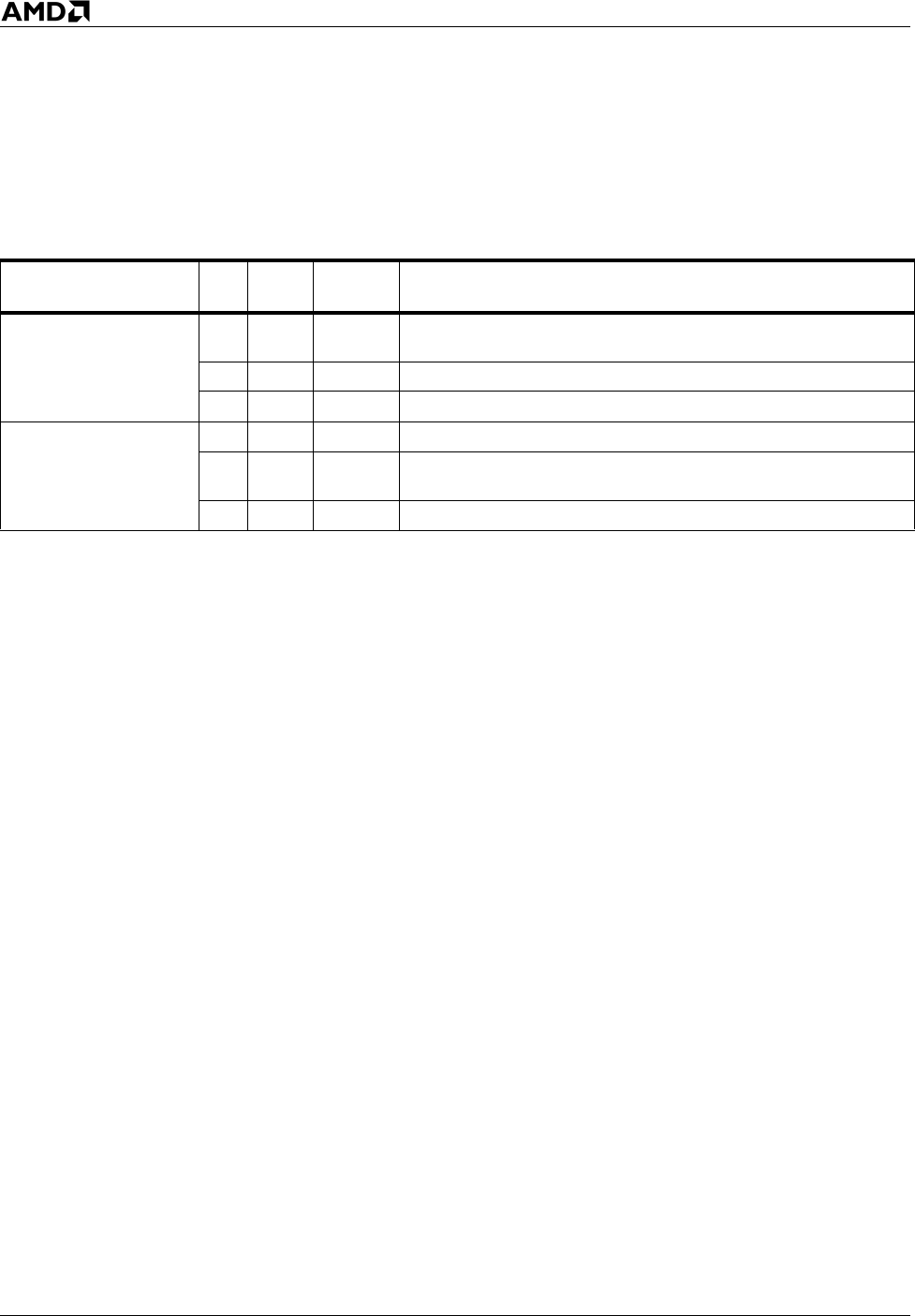
334 VMRUN Instruction Reference
AMD64 Technology 24594—Rev. 3.14—September 2007
rFLAGS Affected
None.
Exceptions
Exception Real
Virtual
8086 Protected Cause of Exception
Invalid opcode, #UD
XX XThe SVM instructions are not supported as indicated by ECX
bit 2 as returned by CPUID function 8000_0001h.
X Secure Virtual Machine was not enabled (EFER.SVME=0).
X X The instruction is only recognized in protected mode.
General protection,
#GP
X CPL was not zero.
XrAX referenced a physical address above the maximum
supported physical address.
X The address in rAX was not aligned on a 4Kbyte boundary.

System Instruction Reference 335
24594—Rev. 3.14—September 2007 AMD64 Technology
Stores a subset of the processor state into the VMCB specified by the physical address in the rAX
register (the portion of RAX used to form the address is determined by the effective address size).
The VMSAVE and VMLOAD instructions complement the state save/restore abilities of VMRUN and
#VMEXIT, providing access to hidden state that software is otherwise unable to access, plus some
additional commonly-used state.
This is a Secure Virtual Machine instruction. This instruction generates a #UD exception if SVM is
not enabled. See “Enabling SVM” on page 369 in AMD64 Architecture Programmer’s Manual
Volume 2: System Instructions, order# 24593.
Action
IF ((MSR_EFER.SVME = 0) || (!PROTECTED_MODE))
EXCEPTION [#UD] // This instruction can only be executed in protected
// mode with SVM enabled
IF (CPL != 0) // This instruction is only allowed at CPL 0
EXCEPTION [#GP]
IF (rAX contains an unsupported physical address)
EXCEPTION [#GP]
Store to a VMCB at physical address rAX:
FS, GS, TR, LDTR (including all hidden state)
KernelGsBase
STAR, LSTAR, CSTAR, SFMASK
SYSENTER_CS, SYSENTER_ESP, SYSENTER_EIP
Related Instructions
VMLOAD
rFLAGS Affected
None.
VMSAVE Save State to VMCB
Mnemonic Opcode Description
VMSAVE rAX 0F 01 DB Save additional guest state to VMCB.

336 System Instruction Reference
AMD64 Technology 24594—Rev. 3.14—September 2007
Exceptions
Exception Real
Virtual
8086 Protected Cause of Exception
Invalid opcode, #UD
XX XThe SVM instructions are not supported as indicated by ECX
bit 2 as returned by CPUID function 8000_0001h.
X Secure Virtual Machine was not enabled (EFER.SVME=0).
X X The instruction is only recognized in protected mode.
General protection,
#GP
X CPL was not zero.
XrAX referenced a physical address above the maximum
supported physical address.
X The address in rAX was not aligned on a 4Kbyte boundary.
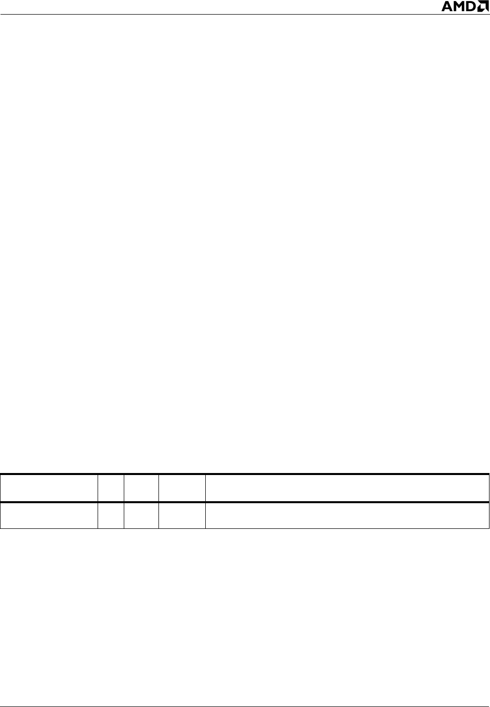
System Instruction Reference 337
24594—Rev. 3.14—September 2007 AMD64 Technology
Writes all modified cache lines in the internal caches back to main memory and invalidates (flushes)
internal caches. It then causes external caches to write back modified data to main memory; the
external caches are subsequently invalidated. After invalidating internal caches, the processor
proceeds immediately with the execution of the next instruction without waiting for external hardware
to invalidate its caches.
The INVD instruction can be used when cache coherence with memory is not important.
This instruction does not invalidate TLB caches.
This is a privileged instruction. The current privilege level of a procedure invalidating the processor’s
internal caches must be zero.
WBINVD is a serializing instruction.
Related Instructions
CLFLUSH, INVD
rFLAGS Affected
None
Exceptions
WBINVD Writeback and Invalidate Caches
Mnemonic Opcode Description
WBINVD 0F 09 Write modified cache lines to main memory, invalidate
internal caches, and trigger external cache flushes.
Exception Real
Virtual
8086 Protected Cause of Exception
General protection,
#GP X X CPL was not 0.

338 System Instruction Reference
AMD64 Technology 24594—Rev. 3.14—September 2007
Writes data to 64-bit model-specific registers (MSRs). These registers are widely used in performance-
monitoring and debugging applications, as well as testability and program execution tracing.
This instruction writes the contents of the EDX:EAX register pair into a 64-bit model-specific register
specified in the ECX register. The 32 bits in the EDX register are mapped into the high-order bits of the
model-specific register and the 32 bits in EAX form the low-order 32 bits.
This instruction must be executed at a privilege level of 0 or a general protection fault #GP(0) will be
raised. This exception is also generated if an attempt is made to specify a reserved or unimplemented
model-specific register in ECX.
WRMSR is a serializing instruction.
The CPUID instruction can provide model information useful in determining the existence of a
particular MSR.
See Volume 2: System Programming, for more information about model-specific registers, machine
check architecture, performance monitoring and debug registers.
Related Instructions
RDMSR
rFLAGS Affected
None
Exceptions
WRMSR Write to Model-Specific Register
Mnemonic Opcode Description
WRMSR 0F 30 Write EDX:EAX to the MSR specified by ECX.
Exception Real
Virtual
8086 Protected Cause of Exception
Invalid opcode, #UD X X X The WRMSR instruction is not supported, as indicated by
EDX bit 5 returned by CPUID function 1 or 8000_0001h.
General protection,
#GP
X X CPL was not 0.
XX
The value in ECX specifies a reserved or unimplemented
MSR address.
X X Writing 1 to any bit that must be zero (MBZ) in the MSR.
XX
Writing a non-canonical value to a MSR that can only be
written with canonical values.

Opcode and Operand Encodings 339
24594—Rev. 3.14—September 2007 AMD64 Technology
Appendix A Opcode and Operand Encodings
This section specifies the hexadecimal and/or binary encodings for the opcodes and the implicit
operand references used in the AMD64 instruction set. For an overview of the instruction formats to
which these encodings apply, see Chapter 1, “Instruction Formats.”
A.1 Opcode-Syntax Notation
The following notation is used in this section to specify opcodes and their operands:
A Far pointer is encoded in the instruction.
CControl register specified by the ModRM reg field.
DDebug register specified by the ModRM reg field.
EGeneral purpose register or memory operand specified by the ModRM byte. Memory addresses
can be computed from a segment register, SIB byte, and/or displacement.
FrFLAGS register.
GGeneral purpose register specified by the ModRM reg field.
IImmediate value.
JThe instruction includes a relative offset that is added to the rIP.
MA memory operand specified by the ModRM byte.
OThe offset of an operand is encoded in the instruction. There is no ModRM byte in the
instruction. Complex addressing using the SIB byte cannot be done.
P64-bit MMX register specified by the ModRM reg field.
PR 64-bit MMX register specified by the ModRM r/m field. The ModRM mod field must be 11b.
Q64-bit MMX-register or memory operand specified by the ModRM byte. Memory addresses can
be computed from a segment register, SIB byte, and/or displacement.
RGeneral purpose register specified by the ModRM r/m field. The ModRM mod field must be 11b.
SSegment register specified by the ModRM reg field.
V128-bit XMM register specified by the ModRM reg field.
VR 128-bit XMM register specified by the ModRM r/m field. The ModRM mod field must be 11b.
WA 128-bit XMM register or memory operand specified by the ModRM byte. Memory addresses
can be computed from a segment register, SIB byte, and/or displacement.
XA memory operand addressed by the DS.rSI registers. Used in string instructions.
YA memory operand addressed by the ES.rDI registers. Used in string instructions.

340 Opcode and Operand Encodings
AMD64 Technology 24594—Rev. 3.14—September 2007
aTwo 16-bit or 32-bit memory operands, depending on the effective operand size. Used in the
BOUND instruction.
bA byte, irrespective of the effective operand size.
dA doubleword (32 bits), irrespective of the effective operand size.
dq A double-quadword (128 bits), irrespective of the effective operand size.
pA 32-bit or 48-bit far pointer, depending on the effective operand size.
pd A 128-bit double-precision floating-point vector operand (packed double).
pi A 64-bit MMX operand (packed integer).
ps A 128-bit single-precision floating-point vector operand (packed single).
qA quadword, irrespective of the effective operand size.
sA 6-byte or 10-byte pseudo-descriptor.
sd A scalar double-precision floating-point operand (scalar double).
si A scalar doubleword (32-bit) integer operand (scalar integer).
ss A scalar single-precision floating-point operand (scalar single).
vA word, doubleword, or quadword, depending on the effective operand size.
wA word, irrespective of the effective operand size.
zA word if the effective operand size is 16 bits, or a doubleword if the effective operand size is 32
or 64 bits.
/n A ModRM-byte reg field or SIB-byte base field that contains a value (n) between zero (binary
000) and 7 (binary 111).
For definitions of the mnemonics used to name registers, see “Summary of Registers and Data Types”
on page 24.
A.2 Opcode Encodings
A.2.1 One-Byte Opcodes
Table A-1 on page 341 shows the one-byte opcodes in which the low nibble is in the range 0–7h.
Table A-2 on page 342 shows those opcodes in which the low nibble is in the range 8–Fh. In both
tables, the rows show the full range (0–Fh) of the high nibble, and the columns show the specified
range of the low nibble.
Opcode and Operand Encodings 341
24594—Rev. 3.14—September 2007 AMD64 Technology
Table A-1. One-Byte Opcodes, Low Nibble 0–7h
Nibble101234567
0ADD PUSH POP
Eb, Gb Ev, Gv Gb, Eb Gv, Ev AL, Ib rAX, Iz ES3ES3
1ADC PUSH POP
Eb, Gb Ev, Gv Gb, Eb Gv, Ev AL, Ib rAX, Iz SS3SS3
2AND seg ES6DAA3
Eb, Gb Ev, Gv Gb, Eb Gv, Ev AL, Ib rAX, Iz
3XOR seg SS6AAA3
Eb, Gb Ev, Gv Gb, Eb Gv, Ev AL, Ib rAX, Iz
4INC5
eAX eCX eDX eBX eSP eBP eSI eDI
5PUSH
rAX/r8 rCX/r9 rDX/r10 rBX/r11 rSP/r12 rBP/r13 rSI/r14 rDI/r15
6
PUSHA/D3POPA/D3BOUND 3
Gv, Ma
ARPL3
Ew, Gw seg FS seg GS operand size address
size
MOVSXD4
Gv, Ed
7JO JNO JB JNB JZ JNZ JBE JNBE
Jb Jb Jb Jb Jb Jb Jb Jb
8Group 12TEST XCHG
Eb, Ib Ev, Iz Eb, Ib3Ev, Ib Eb, Gb Ev, Gv Eb, Gb Ev, Gv
9
XCHG
r8, rAX
NOP,PAUSE rCX/r9, rAX rDX/r10, rAX rBX/r11, rAX rSP/r12, rAX rBP/r13, rAX rSI/r14, rAX rDI/r15, rAX
AMOV MOVSB MOVSW/D/Q CMPSB CMPSW/D/Q
AL, Ob rAX, Ov Ob, AL Ov, rAX Yb, Xb Yv, Xv Xb, Yb Xv, Yv
B
MOV
AL, Ib
r8b, Ib
CL, Ib
r9b, Ib
DL, Ib
r10b, Ib
BL, Ib
r11b, Ib
AH, Ib
r12b, Ib
CH, Ib
r13b, Ib
DH, Ib
r14b, Ib
BH, Ib
r15b, Ib
CGroup 22RET near LES3LDS3Group 112
Eb, Ib Ev, Ib Iw Gz, Mp Gz, Mp Eb, Ib Ev, Iz
DGroup 22AAM3AAD3SALC3XLAT
Eb, 1 Ev, 1 Eb, CL Ev, CL
ELOOPNE/NZ LOOPE/Z LOOP JrCXZ IN OUT
Jb Jb Jb Jb AL, Ib eAX, Ib Ib, AL Ib, eAX
FLOCK: INT1 REPNE: REP: HLT CMC Group 32
ICE Bkpt REPE:
Notes:
1. Rows in this table show the high opcode nibble, columns show the low opcode nibble.
2. An opcode extension is specified in bits 5–3 of the ModRM byte. See “ModRM Extensions to One-Byte and Two-
Byte Opcodes” on page 348 for details.
3. Invalid in 64-bit mode.
4. Valid only in 64-bit mode.
5. Used as REX prefixes in 64-bit mode.
6. This is a null prefix in 64-bit mode.
342 Opcode and Operand Encodings
AMD64 Technology 24594—Rev. 3.14—September 2007
Table A-2. One-Byte Opcodes, Low Nibble 8–Fh
Nibble18 9ABCDEF
0OR PUSH 2-byte
Eb, Gb Ev, Gv Gb, Eb Gv, Ev AL, Ib rAX, Iz CS3opcodes
1SBB PUSH POP
Eb, Gb Ev, Gv Gb, Eb Gv, Ev AL, Ib rAX, Iz DS3DS3
2SUB seg CS6DAS3
Eb, Gb Ev, Gv Gb, Eb Gv, Ev AL, Ib rAX, Iz
3CMP seg DS6AAS3
Eb, Gb Ev, Gv Gb, Eb Gv, Ev AL, Ib rAX, Iz
4DEC5
eAX eCX eDX eBX eSP eBP eSI eDI
5POP
rAX/r8 rCX/r9 rDX/r10 rBX/r11 rSP/r12 rBP/r13 rSI/r14 rDI/r15
6PUSH IMUL PUSH IMUL INSB INSW/D OUTSB OUTSW/D
Iz Gv, Ev, Iz Ib Gv, Ev, Ib Yb, DX Yz, DX DX, Xb DX, Xz
7JS JNS JP JNP JL JNL JLE JNLE
Jb Jb Jb Jb Jb Jb Jb Jb
8MOV LEA MOV Group 1a2
Eb, Gb Ev, Gv Gb, Eb Gv, Ev Mw/Rv, Sw Gv, M Sw, Ew Ev
9CBW, CWDE CWD, CDQ, CALL3WAIT PUSHF/D/Q POPF/D/Q SAHF LAHF
CDQE CQO Ap FWAIT Fv Fv
ATEST STOSB STOSW/D/Q LODSB LODSW/D/Q SCASB SCASW/D/Q
AL, Ib rAX, Iz Yb, AL Yv, rAX AL, Xb rAX, Xv AL, Yb rAX, Yv
B
MOV
rAX, Iv
r8, Iv
rCX, Iv
r9, Iv
rDX, Iv
r10, Iv
rBX, Iv
r11, Iv
rSP, Iv
r12, Iv
rBP, Iv
r13, Iv
rSI, Iv
r14, Iv
rDI, Iv
r15, Iv
CENTER LEAVE RET far INT3 INT INTO3IRET, IRETD
Iw, Ib Iw Ib IRETQ
Dx87
see Table A-10 on page 355
ECALL JMP IN OUT
Jz Jz Ap3Jb AL, DX eAX, DX DX, AL DX, eAX
FCLC STC CLI STI CLD STD Group 42Group 52
Eb
Note:
1. Rows in this table show the high opcode nibble, columns show the low opcode nibble.
2. An opcode extension is specified in bits 5–3 of the ModRM byte. See “ModRM Extensions to One-Byte and Two-
Byte Opcodes” on page 348 for details.
3. Invalid in 64-bit mode.
4. Valid only in 64-bit mode.
5. Used as REX prefixes in 64-bit mode.
6. This is a null prefix in 64-bit mode.

Opcode and Operand Encodings 343
24594—Rev. 3.14—September 2007 AMD64 Technology
A.2.2 Two-Byte Opcodes
All two-byte opcodes have 0Fh as their first byte. Table A-3 below shows the second byte of the two-
byte opcodes in which the second byte’s low nibble is in the range 0–7h. Table A-4 on page 345 shows
those opcodes in which the second byte’s low nibble is in the range 8–Fh. In both tables, the rows show
the full range (0–Fh) of the high nibble, and the columns show the low nibble of the opcode. The left-
most column shows special-purpose prefix bytes used in many 128-bit and 64-bit instructions to
modify the opcode.
Table A-3. Second Byte of Two-Byte Opcodes, Low Nibble 0–7h
Prefix Nibble101234567
n/a 0Group 62Group 72LAR LSL invalid SYSCALL CLTS SYSRET
Gv, Ew Gv, Ew
none
1
MOVUPS MOVLPS
Vps, Mq
MOVHLPS
MOVLPS UNPCKLPS UNPCKHPS
MOVHPS
Vps, Mq
MOVLHPS
MOVHPS
Vps, Wps Wps, Vps Vps, VRq Mq, Vps Vps, Wq Vps, Wq Vps, VRq Mq, Vps
F3 MOVSS MOVSLDUP invalid invalid invalid MOVSHDUP invalid
Vdq/ss, Wss Wss, Vss Vps, Wps Vps, Wps
66 MOVUPD MOVLPD UNPCKLPD UNPCKHPD MOVHPD
Vpd, Wpd Wpd, Vpd Vsd, Mq Mq, Vsd Vpd, Wq Vpd, Wq Vsd, Mq Mq, Vsd
F2 MOVSD MOVDDUP invalid invalid invalid invalid invalid
Vdq/sd, Wsd Wsd, Vsd Vpd,Wsd
n/a 2MOV invalid invalid invalid invalid
Rd/q, Cd/q Rd/q, Dd/q Cd/q, Rd/q Dd/q, Rd/q
n/a 3WRMSR RDTSC RDMSR RDPMC SYSENTER3SYSEXIT3invalid invalid
n/a 4CMOVO CMOVNO CMOVB CMOVNB CMOVZ CMOVNZ CMOVBE CMOVNBE
Gv, Ev Gv, Ev Gv, Ev Gv, Ev Gv, Ev Gv, Ev Gv, Ev Gv, Ev
none
5
MOVMSKPS SQRTPS RSQRTPS RCPPS ANDPS ANDNPS ORPS XORPS
Gd, VRps Vps, Wps Vps, Wps Vps, Wps Vps, Wps Vps, Wps Vps, Wps Vps, Wps
F3 invalid SQRTSS RSQRTSS RCPSS invalid invalid invalid invalid
Vss, Wss Vss, Wss Vss, Wss
66 MOVMSKPD SQRTPD invalid invalid ANDPD ANDNPD ORPD XORPD
Gd, VRpd Vpd, Wpd Vpd, Wpd Vpd, Wpd Vpd, Wpd Vpd, Wpd
F2 invalid SQRTSD invalid invalid invalid invalid invalid invalid
Vsd, Wsd
Note:
1. All two-byte opcodes begin with an 0Fh byte. Rows in the table show the high nibble of the second opcode bytes,
columns show the low nibble of this byte.
2. An opcode extension is specified in bits 5–3 of the ModRM byte. See “ModRM Extensions to One-Byte and Two-
Byte Opcodes” on page 348 for details.
3. Invalid in long mode.
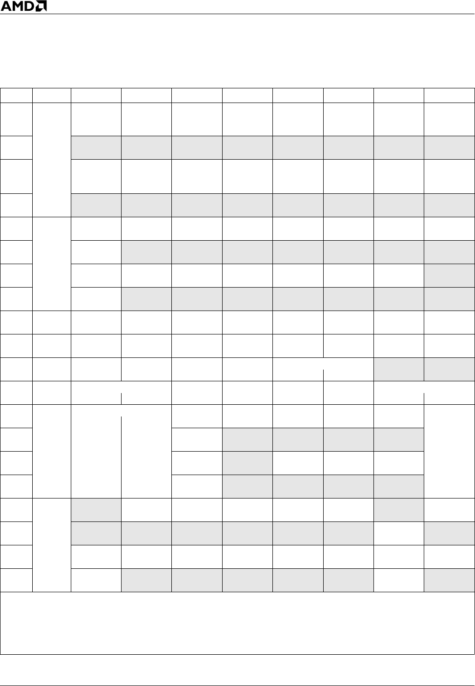
344 Opcode and Operand Encodings
AMD64 Technology 24594—Rev. 3.14—September 2007
none
6
PUNPCK-
LBW
PUNPCK-
LWD
PUN-
PCKLDQ PACKSSWB PCMPGTB PCMPGTW PCMPGTD PACKUSWB
Pq, Qd Pq, Qd Pq, Qd Pq, Qq Pq, Qq Pq, Qq Pq, Qq Pq, Qq
F3 invalid invalid invalid invalid invalid invalid invalid invalid
PUNPCK-
LBW
PUNPCK-
LWD
PUN-
PCKLDQ PACKSSWB PCMPGTB PCMPGTW PCMPGTD PACKUSWB
66 Vdq, Wq Vdq, Wq Vdq, Wq Vdq, Wdq Vdq, Wdq Vdq, Wdq Vdq, Wdq Vdq, Wdq
F2 invalid invalid invalid invalid invalid invalid invalid invalid
none
7
PSHUFW Group 122Group 132Group 142PCMPEQB PCMPEQW PCMPEQD EMMS
Pq, Qq, Ib Pq, Qq Pq, Qq Pq, Qq
F3 PSHUFHW invalid invalid invalid invalid invalid invalid invalid
Vq, Wq, Ib
66 PSHUFD Group 122Group 132Group 142PCMPEQB PCMPEQW PCMPEQD invalid
Vdq, Wdq, Ib Vdq, Wdq Vdq, Wdq Vdq, Wdq
F2 PSHUFLW invalid invalid invalid invalid invalid invalid invalid
Vq, Wq, Ib
n/a 8 JO JNO JB JNB JZ JNZ JBE JNBE
Jz Jz Jz Jz Jz Jz Jz Jz
n/a 9 SETO SETNO SETB SETNB SETZ SETNZ SETBE SETNBE
Eb Eb Eb Eb Eb Eb Eb Eb
n/a A PUSH POP CPUID BT SHLD invalid invalid
FS FS Ev, Gv Ev, Gv, Ib Ev, Gv, CL
n/a B CMPXCHG LSS BTR LFS LGS MOVZX
Eb, Gb Ev, Gv Gz, Mp Ev, Gv Gz, Mp Gz, Mp Gv, Eb Gv, Ew
none
C
XADD CMPPS MOVNTI PINSRW PEXTRW SHUFPS Group 92
Eb, Gb Ev, Gv
Vps, Wps, Ib Md/q, Gd/q Pq, Ew, Ib Gd, PRq, Ib Vps, Wps, Ib
Mq
F3 CMPSS invalid invalid invalid invalid
Vss, Wss, Ib
66 CMPPD invalid PINSRW PEXTRW SHUFPD
Vpd, Wpd, Ib Vdq, Ew, Ib Gd, VRdq, Ib Vpd, Wpd, Ib
F2 CMPSD invalid invalid invalid invalid
Vsd, Wsd, Ib
none
D
invalid PSRLW PSRLD PSRLQ PADDQ PMULLW invalid PMOVMSKB
Pq, Qq Pq, Qq Pq, Qq Pq, Qq Pq, Qq Gd, PRq
F3 invalid invalid invalid invalid invalid invalid MOVQ2DQ invalid
Vdq, PRq
66 ADDSUBPD PSRLW PSRLD PSRLQ PADDQ PMULLW MOVQ PMOVMSKB
Vpd, Wpd Vdq, Wdq Vdq, Wdq Vdq, Wdq Vdq, Wdq Vdq, Wdq Wq, Vq Gd, VRdq
F2 ADDSUBPS invalid invalid invalid invalid invalid MOVDQ2Q invalid
Vps, Wps Pq, VRq
Table A-3. Second Byte of Two-Byte Opcodes, Low Nibble 0–7h (continued)
Prefix Nibble101234567
Note:
1. All two-byte opcodes begin with an 0Fh byte. Rows in the table show the high nibble of the second opcode bytes,
columns show the low nibble of this byte.
2. An opcode extension is specified in bits 5–3 of the ModRM byte. See “ModRM Extensions to One-Byte and Two-
Byte Opcodes” on page 348 for details.
3. Invalid in long mode.
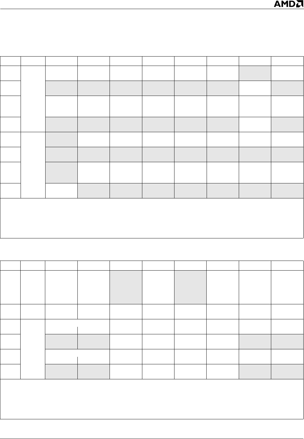
Opcode and Operand Encodings 345
24594—Rev. 3.14—September 2007 AMD64 Technology
none
E
PAVGB PSRAW PSRAD PAVGW PMULHUW PMULHW invalid MOVNTQ
Pq, Qq Pq, Qq Pq, Qq Pq, Qq Pq, Qq Pq, Qq Mq, Pq
F3 invalid invalid invalid invalid invalid invalid CVTDQ2PD invalid
Vpd, Wq
66 PAVGB PSRAW PSRAD PAVGW PMULHUW PMULHW CVTTPD2D
QMOVNTDQ
Vdq, Wdq Vdq, Wdq Vdq, Wdq Vdq, Wdq Vdq, Wdq Vdq, Wdq Vq, Wpd Mdq, Vdq
F2 invalid invalid invalid invalid invalid invalid CVTPD2DQ invalid
Vq, Wpd
none
F
invalid PSLLW PSLLD PSLLQ PMULUDQ PMADDWD PSADBW MASKMOVQ
Pq, Qq Pq, Qq Pq, Qq Pq, Qq Pq, Qq Pq, Qq Pq, PRq
F3 invalid invalid invalid invalid invalid invalid invalid invalid
66 invalid PSLLW PSLLD PSLLQ PMULUDQ PMADDWD PSADBW MASK-
MOVDQU
Vdq, Wdq Vdq, Wdq Vdq, Wdq Vdq, Wdq Vdq, Wdq Vdq, Wdq Vdq, VRdq
F2 LDDQU invalid invalid invalid invalid invalid invalid invalid
Vpd,Mdq
Table A-4. Second Byte of Two-Byte Opcodes, Low Nibble 8–Fh
Prefix Nibble18 9ABCDEF
n/a 0
INVD WBINVD invalid UD2 invalid Group P2FEMMS 3DNow!
PREFETCH
See
“3DNow!™
Opcodes” on
page 351
n/a 1Group 162NOP3NOP3NOP3NOP3NOP3NOP3NOP3
none
2
MOVAPS CVTPI2PS MOVNTPS CVTTPS2PI CVTPS2PI UCOMISS COMISS
Vps, Wps Wps, Vps Vps, Qq Mdq, Vps Pq, Wps Pq, Wps Vss, Wss Vps, Wps
F3 invalid invalid CVTSI2SS MOVNTSS CVTTSS2SI CVTSS2SI invalid invalid
Vss, Ed/q Md, Vss Gd/q, Wss Gd/q, Wss
66 MOVAPD CVTPI2PD MOVNTPD CVTTPD2PI CVTPD2PI UCOMISD COMISD
Vpd, Wpd Wpd, Vpd Vpd, Qq Mdq, Vpd Pq, Wpd Pq, Wpd Vsd, Wsd Vpd, Wsd
F2 invalid invalid CVTSI2SD MOVNTSD CVTTSD2SI CVTSD2SI invalid invalid
Vsd, Ed/q Mq, Vsd Gd/q, Wsd Gd/q, Wsd
Note:
1. All two-byte opcodes begin with an 0Fh byte. Rows show high opcode nibble (hex), columns show low opcode nibble
in hex.
2. An opcode extension is specified in the ModRM reg field (bits 5–3). See “ModRM Extensions to One-Byte and Two-
Byte Opcodes” on page 348 for details.
3. This instruction takes a ModRM byte.
Table A-3. Second Byte of Two-Byte Opcodes, Low Nibble 0–7h (continued)
Prefix Nibble101234567
Note:
1. All two-byte opcodes begin with an 0Fh byte. Rows in the table show the high nibble of the second opcode bytes,
columns show the low nibble of this byte.
2. An opcode extension is specified in bits 5–3 of the ModRM byte. See “ModRM Extensions to One-Byte and Two-
Byte Opcodes” on page 348 for details.
3. Invalid in long mode.

346 Opcode and Operand Encodings
AMD64 Technology 24594—Rev. 3.14—September 2007
n/a 3invalid invalid invalid invalid invalid invalid invalid invalid
n/a 4CMOVS CMOVNS CMOVP CMOVNP CMOVL CMOVNL CMOVLE CMOVNLE
Gv, Ev Gv, Ev Gv, Ev Gv, Ev Gv, Ev Gv, Ev Gv, Ev Gv, Ev
none
5
ADDPS MULPS CVTPS2PD CVTDQ2PS SUBPS MINPS DIVPS MAXPS
Vps, Wps Vps, Wps Vpd, Wps Vps, Wdq Vps, Wps Vps, Wps Vps, Wps Vps, Wps
F3 ADDSS MULSS CVTSS2SD CVTTPS2D
QSUBSS MINSS DIVSS MAXSS
Vss, Wss Vss, Wss Vsd, Wss Vdq, Wps Vss, Wss Vss, Wss Vss, Wss Vss, Wss
66 ADDPD MULPD CVTPD2PS CVTPS2DQ SUBPD MINPD DIVPD MAXPD
Vpd, Wpd Vpd, Wpd Vps, Wpd Vdq, Wps Vpd, Wpd Vpd, Wpd Vpd, Wpd Vpd, Wpd
F2 ADDSD MULSD CVTSD2SS invalid SUBSD MINSD DIVSD MAXSD
Vsd, Wsd Vsd, Wsd Vss, Wsd Vsd, Wsd Vsd, Wsd Vsd, Wsd Vsd, Wsd
none
6
PUNPCK-
HBW
PUNPCK-
HWD
PUNPCK-
HDQ PAC K S S D W invalid invalid MOVD MOVQ
Pq, Qd Pq, Qd Pq, Qd Pq, Qq Pq, Ed/q Pq, Qq
F3 invalid invalid invalid invalid invalid invalid invalid MOVDQU
Vdq, Wdq
66
PUNPCK-
HBW
PUNPCK-
HWD
PUNPCK-
HDQ PAC K S S D W PUNPCK-
LQDQ
PUNPCK-
HQDQ MOVD MOVDQA
Vdq, Wq Vdq, Wq Vdq, Wq Vdq, Wdq Vdq, Wq Vdq, Wq Vdq, Ed/q Vdq, Wdq
F2 invalid invalid invalid invalid invalid invalid invalid invalid
none
7
invalid invalid invalid invalid invalid invalid MOVD MOVQ
Ed/q, Pd/q Qq, Pq
F3 invalid invalid invalid invalid invalid invalid MOVQ MOVDQU
Vq, Wq Wdq, Vdq
66 Group 172EXTRQ invalid invalid HADDPD HSUBPD MOVD MOVDQA
Vdq, VRq Vpd,Wpd Vpd,Wpd Ed/q, Vd/q Wdq, Vdq
F2 INSERTQ INSERTQ invalid invalid HADDPS HSUBPS invalid invalid
Vdq,VRq,Ib,Ib Vdq, VRdq Vps,Wps Vps,Wps
n/a 8 JS JNS JP JNP JL JNL JLE JNLE
Jz Jz Jz Jz Jz Jz Jz Jz
n/a 9 SETS SETNS SETP SETNP SETL SETNL SETLE SETNLE
Eb Eb Eb Eb Eb Eb Eb Eb
n/a A PUSH POP RSM BTS SHRD Group 152IMUL
GS GS Ev, Gv Ev, Gv, Ib Ev, Gv, CL Gv, Ev
none
B
reserved Group 102Group 82BTC BSF BSR MOVSX
Ev, Ib Ev, Gv Gv, Ev Gv, Ev Gv, Eb Gv, Ew
F3 POPCNT reserved reserved reserved reserved LZCNT reserved reserved
Gv, Ev Gv, Ev
F2 reserved reserved reserved reserved reserved reserved reserved reserved
Table A-4. Second Byte of Two-Byte Opcodes, Low Nibble 8–Fh (continued)
Prefix Nibble18 9ABCDEF
Note:
1. All two-byte opcodes begin with an 0Fh byte. Rows show high opcode nibble (hex), columns show low opcode nibble
in hex.
2. An opcode extension is specified in the ModRM reg field (bits 5–3). See “ModRM Extensions to One-Byte and Two-
Byte Opcodes” on page 348 for details.
3. This instruction takes a ModRM byte.

Opcode and Operand Encodings 347
24594—Rev. 3.14—September 2007 AMD64 Technology
n/a C BSWAP
rAX/r8 rCX/r9 rDX/r10 rBX/r11 rSP/r12 rBP/r13 rSI/r14 rDI/r15
none
D
PSUBUSB PSUBUSW PMINUB PAND PADDUSB PADDUSW PMAXUB PANDN
Pq, Qq Pq, Qq Pq, Qq Pq, Qq Pq, Qq Pq, Qq Pq, Qq Pq, Qq
F3 invalid invalid invalid invalid invalid invalid invalid invalid
66 PSUBUSB PSUBUSW PMINUB PAND PADDUSB PADDUSW PMAXUB PANDN
Vdq, Wdq Vdq, Wdq Vdq, Wdq Vdq, Wdq Vdq, Wdq Vdq, Wdq Vdq, Wdq Vdq, Wdq
F2 invalid invalid invalid invalid invalid invalid invalid invalid
none
E
PSUBSB PSUBSW PMINSW POR PADDSB PADDSW PMAXSW PXOR
Pq, Qq Pq, Qq Pq, Qq Pq, Qq Pq, Qq Pq, Qq Pq, Qq Pq, Qq
F3 invalid invalid invalid invalid invalid invalid invalid invalid
66 PSUBSB PSUBSW PMINSW POR PADDSB PADDSW PMAXSW PXOR
Vdq, Wdq Vdq, Wdq Vdq, Wdq Vdq, Wdq Vdq, Wdq Vdq, Wdq Vdq, Wdq Vdq, Wdq
F2 invalid invalid invalid invalid invalid invalid invalid invalid
none
F
PSUBB PSUBW PSUBD PSUBQ PADDB PADDW PADDD invalid
Pq, Qq Pq, Qq Pq, Qq Pq, Qq Pq, Qq Pq, Qq Pq, Qq
F3 invalid invalid invalid invalid invalid invalid invalid invalid
66 PSUBB PSUBW PSUBD PSUBQ PADDB PADDW PADDD invalid
Vdq, Wdq Vdq, Wdq Vdq, Wdq Vdq, Wdq Vdq, Wdq Vdq, Wdq Vdq, Wdq
F2 invalid invalid invalid invalid invalid invalid invalid invalid
Table A-4. Second Byte of Two-Byte Opcodes, Low Nibble 8–Fh (continued)
Prefix Nibble18 9ABCDEF
Note:
1. All two-byte opcodes begin with an 0Fh byte. Rows show high opcode nibble (hex), columns show low opcode nibble
in hex.
2. An opcode extension is specified in the ModRM reg field (bits 5–3). See “ModRM Extensions to One-Byte and Two-
Byte Opcodes” on page 348 for details.
3. This instruction takes a ModRM byte.
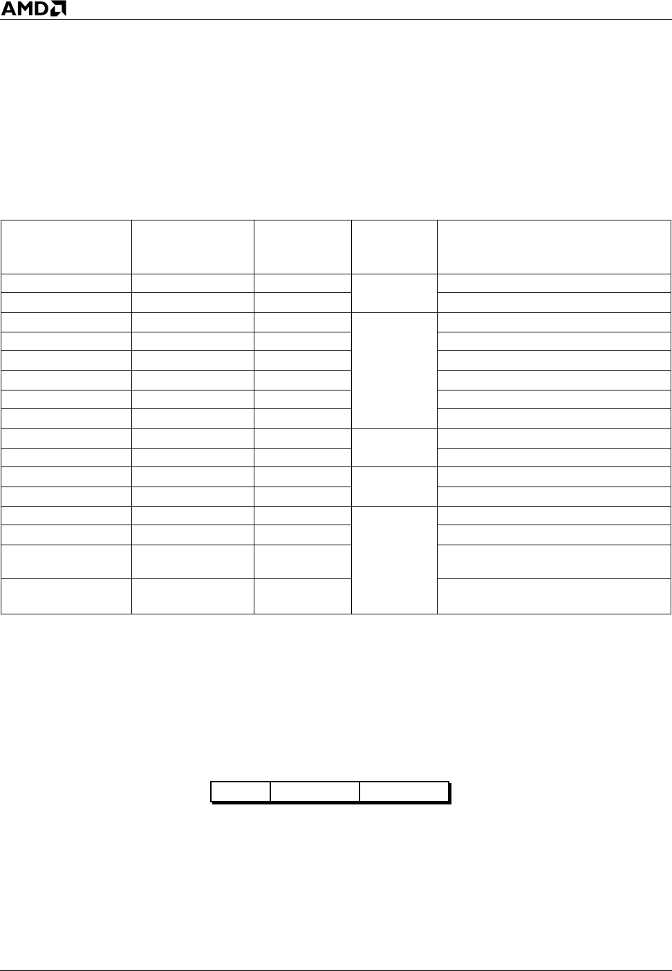
348 Opcode and Operand Encodings
AMD64 Technology 24594—Rev. 3.14—September 2007
A.2.3 rFLAGS Condition Codes for Two-Byte Opcodes
Table A-5 shows the rFLAGS condition codes specified by the low nibble in the second opcode byte of
the CMOVcc, Jcc, and SETcc instructions.
A.2.4 ModRM Extensions to One-Byte and Two-Byte Opcodes
The ModRM byte, which immediately follows the last opcode byte, is used in certain instruction
encodings to provide additional opcode bits with which to define the function of the instruction.
ModRM bytes have three fields—mod, reg, and r/m, as shown in Figure A-1.
Figure A-1. ModRM-Byte Fields
In most cases, the reg field (bits 5–3) provides the additional bits with which to extend the encodings
of the first one or two opcode bytes. In the case of the x87 floating-point instructions, the entire
ModRM byte is used to extend the opcode encodings.
Table A-5. rFLAGS Condition Codes for CMOVcc, Jcc, and SETcc
Low Nibble of
Second Opcode
Byte (hex)
rFLAGS Value cc Mnemonic Arithmetic
Type Condition(s)
0OF=1O
Signed Overflow
1 OF = 0 NO No Overflow
2CF=1B, C, NAE
Unsigned
Below, Carry, Not Above or Equal
3 CF = 0 NB, NC, AE Not Below, No Carry, Above or Equal
4 ZF = 1 Z, E Zero, Equal
5 ZF = 0 NZ, NE Not Zero, Not Equal
6 CF = 1 or ZF = 1 BE, NA Below or Equal, Not Above
7 CF = 0 and ZF = 0 NBE, A Not Below or Equal, Above
8SF=1S
Signed Sign
9SF=0NS Not Sign
APF=1P, PE
n/a Parity, Parity Even
B PF = 0 NP, PO Not Parity, Parity Odd
C (SF xor OF) = 1 L, NGE
Signed
Less than, Not Greater than or Equal to
D (SF xor OF) = 0 NL, GE Not Less than, Greater than or Equal to
E(SF xor OF) = 1
or ZF = 1 LE, NG Less than or Equal to, Not Greater than
F(SF xor OF) = 0
and ZF = 0 NLE, G Not Less than or Equal to, Greater than
513-325.eps
mod regr/mModRM
01234567Bits:
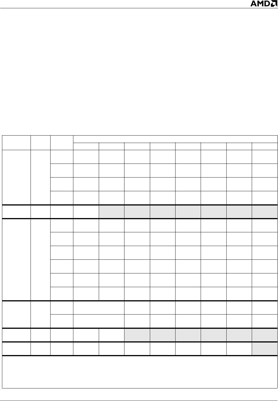
Opcode and Operand Encodings 349
24594—Rev. 3.14—September 2007 AMD64 Technology
Table A-6 on page 349 shows how the ModRM reg field is used to extend the range of one-byte and
two-byte opcodes. The opcode ranges are organized into groups of opcode extensions. The group
number is shown in the left-most column of Table A-6. These groups are referenced in the opcodes
shown in Table A-1 on page 341 through Table A-4 on page 345. An entry of “n.a.” in the Prefix
column means that prefixes are not applicable to the opcodes in that row. Prefixes only apply to certain
128-bit media, 64-bit media, and a few other instructions introduced with the SSE or SSE2
technologies.
The /0 through /7 notation for the ModRM reg field (bits 5–3) means that the three-bit field contains a
value from zero (binary 000) to 7 (binary 111).
Table A-6. One-Byte and Two-Byte Opcode ModRM Extensions
Group
Number Prefix Opcode ModRM reg Field
/0 /1 /2 /3 /4 /5 /6 /7
Group 1 n/a
80 ADD OR ADC SBB AND SUB XOR CMP
Eb, Ib Eb, Ib Eb, Ib Eb, Ib Eb, Ib Eb, Ib Eb, Ib Eb, Ib
81 ADD OR ADC SBB AND SUB XOR CMP
Ev, Iz Ev, Iz Ev, Iz Ev, Iz Ev, Iz Ev, Iz Ev, Iz Ev, Iz
82 ADD OR ADC SBB AND SUB XOR CMP
Eb, Ib2Eb, Ib2Eb, Ib2Eb, Ib2Eb, Ib2Eb, Ib2Eb, Ib2Eb, Ib2
83 ADD OR ADC SBB AND SUB XOR CMP
Ev, Ib Ev, Ib Ev, Ib Ev, Ib Ev, Ib Ev, Ib Ev, Ib Ev, Ib
Group 1a n/a 8F POP invalid invalid invalid invalid invalid invalid invalid
Ev
Group 2 n/a
C0 ROL ROR RCL RCR SHL/SAL SHR SHL/SAL SAR
Eb, Ib Eb, Ib Eb, Ib Eb, Ib Eb, Ib Eb, Ib Eb, Ib Eb, Ib
C1 ROL ROR RCL RCR SHL/SAL SHR SHL/SAL SAR
Ev, Ib Ev, Ib Ev, Ib Ev, Ib Ev, Ib Ev, Ib Ev, Ib Ev, Ib
D0 ROL ROR RCL RCR SHL/SAL SHR SHL/SAL SAR
Eb, 1 Eb, 1 Eb, 1 Eb, 1 Eb, 1 Eb, 1 Eb, 1 Eb, 1
D1 ROL ROR RCL RCR SHL/SAL SHR SHL/SAL SAR
Ev, 1Ev, 1Ev, 1Ev, 1Ev, 1Ev, 1Ev, 1Ev, 1
D2 ROL ROR RCL RCR SHL/SAL SHR SHL/SAL SAR
Eb, CL Eb, CL Eb, CL Eb, CL Eb, CL Eb, CL Eb, CL Eb, CL
D3 ROL ROR RCL RCR SHL/SAL SHR SHL/SAL SAR
Ev, CL Ev, CL Ev, CL Ev, CL Ev, CL Ev, CL Ev, CL Ev, CL
Group 3 n/a
F6 TEST
Eb,Ib
NOT NEG MUL IMUL DIV IDIV
Eb Eb Eb Eb Eb Eb
F7 TEST
Ev,Iz
NOT NEG MUL IMUL DIV IDIV
Ev Ev Ev Ev Ev Ev
Group 4 n/a FE INC DEC invalid invalid invalid invalid invalid invalid
Eb Eb
Group 5 n/a FF INC DEC CALL CALL JMP JMP PUSH invalid
Ev Ev Ev Mp Ev Mp Ev
Note:
1. See Table A-7 on page 351 for ModRM extensions of this two-byte opcode.
2. Invalid in 64-bit mode.
3. This instruction takes a ModRM byte.
4. Reserved prefetch encodings are aliased to the /0 encoding (PREFETCH Exclusive) for future compatibility.
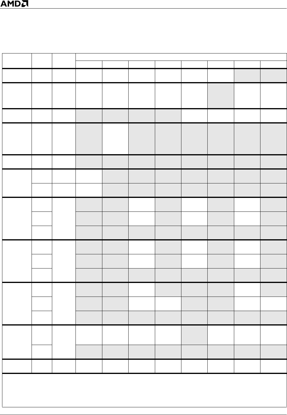
350 Opcode and Operand Encodings
AMD64 Technology 24594—Rev. 3.14—September 2007
Group 6 n/a 0F 00 SLDT STR LLDT LTR VERR VERW invalid invalid
Mw/Rv Mw/Rv Ew Ew Ew Ew
Group 7 n/a 0F 01
SGDT
Ms
SIDT
Ms LGDT LIDT SMSW invalid LMSW INVLPG
Mb
MONITOR1
MWAIT Ms Ms
SVM1Mw/Rv Ew SWAPGS1
RDTSCP
Group 8 n/a 0F BA invalid invalid invalid invalid BT BTS BTR BTC
Ev, Ib Ev, Ib Ev, Ib Ev, Ib
Group 9 n/a 0F C7
invalid CMPXCH
G8B invalid invalid invalid invalid invalid invalid
Mq
CMPXCH
G16Mdq
Group 10 n/a 0F B9 invalid invalid invalid invalid invalid invalid invalid invalid
Group 11
n/a C6 MOV invalid invalid invalid invalid invalid invalid invalid
Eb,Ib
n/a C7 MOV invalid invalid invalid invalid invalid invalid invalid
Ev,Iz
Group 12
none
0F 71
invalid invalid PSRLW invalid PSRAW invalid PSLLW invalid
PRq, Ib PRq, Ib PRq, Ib
66 invalid invalid PSRLW invalid PSRAW invalid PSLLW invalid
VRdq, Ib VRdq, Ib VRdq, Ib
F2, F3 invalid invalid invalid invalid invalid invalid invalid invalid
Group 13
none
0F 72
invalid invalid PSRLD invalid PSRAD invalid PSLLD invalid
PRq, Ib PRq, Ib PRq, Ib
66 invalid invalid PSRLD invalid PSRAD invalid PSLLD invalid
VRdq, Ib VRdq, Ib VRdq, Ib
F2, F3 invalid invalid invalid invalid invalid invalid invalid invalid
Group 14
none
0F 73
invalid invalid PSRLQ invalid invalid invalid PSLLQ invalid
PRq, Ib PRq, Ib
66 invalid invalid PSRLQ PSRLDQ invalid invalid PSLLQ PSLLDQ
VRdq, Ib VRdq, Ib VRdq, Ib VRdq, Ib
F2, F3 invalid invalid invalid invalid invalid invalid invalid invalid
Group 15
none
0F AE
FXSAVE FXRSTOR LDMXCSR STMXCSR invalid LFENCE1MFENCE1SFENCE1
M M Md Md CLFLUSH
Mb
66,
F2, F3
invalid invalid invalid invalid invalid invalid invalid invalid
Group 16 n/a. 0F 18
PREFETCH PREFETCH PREFETCH PREFETCH
NOP4NOP4NOP4NOP4
NTAT0T1T2
Table A-6. One-Byte and Two-Byte Opcode ModRM Extensions (continued)
Group
Number Prefix Opcode ModRM reg Field
/0 /1 /2 /3 /4 /5 /6 /7
Note:
1. See Table A-7 on page 351 for ModRM extensions of this two-byte opcode.
2. Invalid in 64-bit mode.
3. This instruction takes a ModRM byte.
4. Reserved prefetch encodings are aliased to the /0 encoding (PREFETCH Exclusive) for future compatibility.
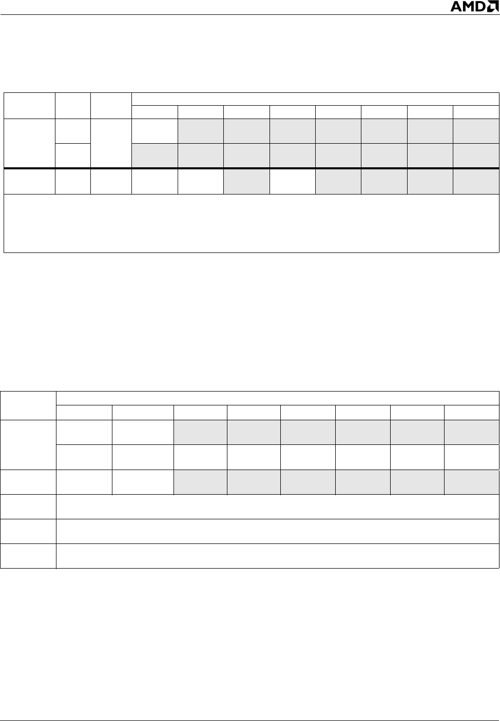
Opcode and Operand Encodings 351
24594—Rev. 3.14—September 2007 AMD64 Technology
A.2.5 ModRM Extensions to Opcodes 0F 01 and 0F AE
Table A-7 shows the ModRM r/m field encodings for the 0F 01 and 0F AE opcodes, shown in
Table A-6 on page 349. The 0F 01 opcode is shared by several system instructions, and the 0F AE
opcode is shared by several media and fence instructions. The opcodes are differentiated by the fact
that the binary value of the ModRM mod field is always 11 for these instructions. The ModRM mod
field can be any value except 11 for the instructions having an explicit memory operand.
A.2.6 3DNow!™ Opcodes
The 64-bit media instructions include the MMX™ instructions and the AMD 3DNow!™ instructions.
The MMX instructions are encoded using two opcode bytes, as described in “Two-Byte Opcodes” on
page 343.
The 3DNow! instructions are encoded using two 0Fh opcode bytes and an immediate byte that is
located at the last byte position of the instruction encoding. Thus, the format for 3DNow! instructions
is:
Group 17
66
0F 78
EXTRQ invalid invalid invalid invalid invalid invalid invalid
Vdq, Ib, Ib
none,
F2, F3
invalid invalid invalid invalid invalid invalid invalid invalid
Group P n/a. 0F 0D
PREFETCH PREFETCH
Prefetch
PREFETCH
Prefetch Prefetch Prefetch Prefetch
Exclusive Modified Reserved4Modified Reserved4Reserved4Reserved4Reserved4
Table A-7. Opcode 0F 01 and 0F AE ModRM Extensions
Opcode ModRM r/m Field
01234567
0F 01 /7
mod=11
0F 01 F8
SWAPGS
0F 01 F9
RDTSCP invalid invalid invalid invalid invalid invalid
0F 01 /3
mod=11
0F 01 D8
VMRUN
0F 01 D9
VMMCALL
0F 01 DA
VMLOAD
0F 01 DB
VMSAVE
0F 01 DC
STGI
0F 01 DD
CLGI
0F 01 DE
SKINIT
0F 01 DF
INVLPGA
0F 01 /1
mod=11
0F 01 C8
MONITOR
0F 01 C9
MWAIT invalid invalid invalid invalid invalid invalid
0F AE /5
mod=11 LFENCE
0F AE /6
mod=11 MFENCE
0F AE /7
mod=11 SFENCE
Table A-6. One-Byte and Two-Byte Opcode ModRM Extensions (continued)
Group
Number Prefix Opcode ModRM reg Field
/0 /1 /2 /3 /4 /5 /6 /7
Note:
1. See Table A-7 on page 351 for ModRM extensions of this two-byte opcode.
2. Invalid in 64-bit mode.
3. This instruction takes a ModRM byte.
4. Reserved prefetch encodings are aliased to the /0 encoding (PREFETCH Exclusive) for future compatibility.

352 Opcode and Operand Encodings
AMD64 Technology 24594—Rev. 3.14—September 2007
0Fh 0Fh [ModRM] [SIB] [displacement]
imm8_opcode
Table A-8 and Table A-9 on page 353 show the immediate byte following the opcode bytes for
3DNow! instructions. In these tables, rows show the high nibble of the immediate byte, and columns
show the low nibble of the immediate byte. Table A-8 shows the immediate bytes whose low nibble is
in the range 0–7h. Table A-9 shows the same for immediate bytes whose low nibble is in the range
8–Fh.
Byte values shown as reserved in these tables have implementation-specific functions, which can
include an invalid-opcode exception.
Table A-8. Immediate Byte for 3DNow!™ Opcodes, Low Nibble 0–7h
Nibble101234567
0reserved reserved reserved reserved reserved reserved reserved reserved
1reserved reserved reserved reserved reserved reserved reserved reserved
2reserved reserved reserved reserved reserved reserved reserved reserved
3reserved reserved reserved reserved reserved reserved reserved reserved
4reserved reserved reserved reserved reserved reserved reserved reserved
5reserved reserved reserved reserved reserved reserved reserved reserved
6reserved reserved reserved reserved reserved reserved reserved reserved
7reserved reserved reserved reserved reserved reserved reserved reserved
8reserved reserved reserved reserved reserved reserved reserved reserved
9PFCMPGE reserved reserved reserved PFMIN reserved PFRCP PFRSQRT
Pq, Qq Pq, Qq Pq, Qq Pq, Qq
APFCMPGT reserved reserved reserved PFMAX reserved PFRCPIT1 PFRSQIT1
Pq, Qq Pq, Qq Pq, Qq Pq, Qq
BPFCMPEQ reserved reserved reserved PFMUL reserved PFRCPIT2 PMULHRW
Pq, Qq Pq, Qq Pq, Qq Pq, Qq
Creserved reserved reserved reserved reserved reserved reserved reserved
Dreserved reserved reserved reserved reserved reserved reserved reserved
Ereserved reserved reserved reserved reserved reserved reserved reserved
Freserved reserved reserved reserved reserved reserved reserved reserved
Note:
1. All 3DNow!™ opcodes consist of two 0Fh bytes. This table shows the immediate byte for 3DNow! opcodes. Rows
show the high nibble of the immediate byte. Columns show the low nibble of the immediate byte.

Opcode and Operand Encodings 353
24594—Rev. 3.14—September 2007 AMD64 Technology
Table A-9. Immediate Byte for 3DNow!™ Opcodes, Low Nibble 8–Fh
Nibble18 9ABCDEF
0reserved reserved reserved reserved PI2FW PI2FD reserved reserved
Pq, Qq Pq, Qq
1reserved reserved reserved reserved PF2IW PF2ID reserved reserved
Pq, Qq Pq, Qq
2reserved reserved reserved reserved reserved reserved reserved reserved
3reserved reserved reserved reserved reserved reserved reserved reserved
4reserved reserved reserved reserved reserved reserved reserved reserved
5reserved reserved reserved reserved reserved reserved reserved reserved
6reserved reserved reserved reserved reserved reserved reserved reserved
7reserved reserved reserved reserved reserved reserved reserved reserved
8reserved reserved PFNACC reserved reserved reserved PFPNACC reserved
Pq, Qq Pq, Qq
9reserved reserved PFSUB reserved reserved reserved PFADD reserved
Pq, Qq Pq, Qq
Areserved reserved PFSUBR reserved reserved reserved PFACC reserved
Pq, Qq Pq, Qq
Breserved reserved reserved PSWAPD reserved reserved reserved PAVGUSB
Pq, Qq Pq, Qq
Creserved reserved reserved reserved reserved reserved reserved reserved
Dreserved reserved reserved reserved reserved reserved reserved reserved
Ereserved reserved reserved reserved reserved reserved reserved reserved
Freserved reserved reserved reserved reserved reserved reserved reserved
Note:
1. All 3DNow!™ opcodes consist of two 0Fh bytes. This table shows the immediate byte for 3DNow! opcodes. Rows
show the high nibble of the immediate byte. Columns show the low nibble of the immediate byte.

354 Opcode and Operand Encodings
AMD64 Technology 24594—Rev. 3.14—September 2007
A.2.7 x87 Encodings
All x87 instructions begin with an opcode byte in the range D8h to DFh, as shown in Table A-2 on
page 342. These opcodes are followed by a ModRM byte that further defines the opcode. Table A-10
shows both the opcode byte and the ModRM byte for each x87 instruction.
There are two significant ranges for the ModRM byte for x87 opcodes: 00–BFh and C0–FFh. When
the value of the ModRM byte falls within the first range, 00–BFh, the opcode uses only the reg field to
further define the opcode. When the value of the ModRM byte falls within the second range, C0–FFh,
the opcode uses the entire ModRM byte to further define the opcode.
Byte values shown as reserved or invalid in Table A-10 have implementation-specific functions, which
can include an invalid-opcode exception.
The basic instructions FNSTENV, FNSTCW, FNCLEX, FNINIT, FNSAVE, FNSTSW, and FNSTSW
do not check for possible floating point exceptions before operating. Utility versions of these
mnemonics are provided that insert an FWAIT (opcode 9B) before the corresponding non-waiting
instruction. These are FSTENV, FSTCW, FCLEX, FINIT, FSAVE, and FSTSW. For further
information on wait and non-waiting versions of these instructions, see their corresponding pages in
Vo l u m e 5 .

Opcode and Operand Encodings 355
24594—Rev. 3.14—September 2007 AMD64 Technology
Table A-10. x87 Opcodes and ModRM Extensions
Opcode
ModRM
mod
Field
ModRM reg Field
/0 /1 /2 /3 /4 /5 /6 /7
D8
!11
00–BF
FADD FMUL FCOM FCOMP FSUB FSUBR FDIV FDIVR
mem32real mem32real mem32real mem32real mem32real mem32real mem32real mem32real
11
C0 C8 D0 D8 E0 E8 F0 F8
FADD FMUL FCOM FCOMP FSUB FSUBR FDIV FDIVR
ST(0),
ST(0) ST(0), ST(0) ST(0), ST(0) ST(0), ST(0) ST(0), ST(0) ST(0),
ST(0) ST(0), ST(0) ST(0), ST(0)
C1 C9 D1 D9 E1 E9 F1 F9
FADD FMUL FCOM FCOMP FSUB FSUBR FDIV FDIVR
ST(0),
ST(1) ST(0), ST(1) ST(0), ST(1) ST(0), ST(1) ST(0), ST(1) ST(0),
ST(1) ST(0), ST(1) ST(0), ST(1)
C2 CA D2 DA E2 EA F2 FA
FADD FMUL FCOM FCOMP FSUB FSUBR FDIV FDIVR
ST(0),
ST(2) ST(0), ST(2) ST(0), ST(2) ST(0), ST(2) ST(0), ST(2) ST(0),
ST(2) ST(0), ST(2) ST(0), ST(2)
C3 CB D3 DB E3 EB F3 FB
FADD FMUL FCOM FCOMP FSUB FSUBR FDIV FDIVR
ST(0),
ST(3) ST(0), ST(3) ST(0), ST(3) ST(0), ST(3) ST(0), ST(3) ST(0),
ST(3) ST(0), ST(3) ST(0), ST(3)
C4 CC D4 DC E4 EC F4 FC
FADD FMUL FCOM FCOMP FSUB FSUBR FDIV FDIVR
ST(0),
ST(4) ST(0), ST(4) ST(0), ST(4) ST(0), ST(4) ST(0), ST(4) ST(0),
ST(4) ST(0), ST(4) ST(0), ST(4)
C5 CD D5 DD E5 ED F5 FD
FADD FMUL FCOM FCOMP FSUB FSUBR FDIV FDIVR
ST(0),
ST(5) ST(0), ST(5) ST(0), ST(5) ST(0), ST(5) ST(0), ST(5) ST(0),
ST(5) ST(0), ST(5) ST(0), ST(5)
C6 CE D6 DE E6 EE F6 FE
FADD FMUL FCOM FCOMP FSUB FSUBR FDIV FDIVR
ST(0),
ST(6) ST(0), ST(6) ST(0), ST(6) ST(0), ST(6) ST(0), ST(6) ST(0),
ST(6) ST(0), ST(6) ST(0), ST(6)
C7 CF D7 DF E7 EF F7 FF
FADD FMUL FCOM FCOMP FSUB FSUBR FDIV FDIVR
ST(0),
ST(7) ST(0), ST(7) ST(0), ST(7) ST(0), ST(7) ST(0), ST(7) ST(0),
ST(7) ST(0), ST(7) ST(0), ST(7)

356 Opcode and Operand Encodings
AMD64 Technology 24594—Rev. 3.14—September 2007
D9
!11
00–BF
FLD invalid FST FSTP FLDENV FLDCW FNSTENV FNSTCW
mem32real mem32real mem32real mem14/28env mem16 mem14/28env mem16
11
C0 C8 D0 D8 E0 E8 F0 F8
FLD FXCH FNOP reserved FCHS FLD1 F2XM1 FPREM
ST(0),
ST(0) ST(0), ST(0)
C1 C9 D1 D9 E1 E9 F1 F9
FLD FXCH invalid reserved FABS FLDL2T FYL2X FYL2XP1
ST(0),
ST(1) ST(0), ST(1)
C2 CA D2 DA E2 EA F2 FA
FLD FXCH invalid reserved invalid FLDL2E FPTAN FSQRT
ST(0),
ST(2) ST(0), ST(2)
C3 CB D3 DB E3 EB F3 FB
FLD FXCH invalid reserved invalid FLDPI FPATAN FSINCOS
ST(0),
ST(3) ST(0), ST(3)
C4 CC D4 DC E4 EC F4 FC
FLD FXCH invalid reserved FTST FLDLG2 FXTRACT FRNDINT
ST(0),
ST(4) ST(0), ST(4)
C5 CD D5 DD E5 ED F5 FD
FLD FXCH invalid reserved FXAM FLDLN2 FPREM1 FSCALE
ST(0),
ST(5) ST(0), ST(5)
C6 CE D6 DE E6 EE F6 FE
FLD FXCH invalid reserved invalid FLDZ FDECSTP FSIN
ST(0),
ST(6) ST(0), ST(6)
C7 CF D7 DF E7 EF F7 FF
FLD FXCH invalid reserved invalid invalid FINCSTP FCOS
ST(0),
ST(7) ST(0), ST(7)
Table A-10. x87 Opcodes and ModRM Extensions (continued)
Opcode
ModRM
mod
Field
ModRM reg Field
/0 /1 /2 /3 /4 /5 /6 /7

Opcode and Operand Encodings 357
24594—Rev. 3.14—September 2007 AMD64 Technology
DA
!11
00–BF
FIADD FIMUL FICOM FICOMP FISUB FISUBR FIDIV FIDIVR
mem32int mem32int mem32int mem32int mem32int mem32int mem32int mem32int
11
C0 C8 D0 D8 E0 E8 F0 F8
FCMOVB FCMOVE FCMOVBE FCMOVU invalid invalid invalid invalid
ST(0),
ST(0) ST(0), ST(0) ST(0), ST(0) ST(0), ST(0)
C1 C9 D1 D9 E1 E9 F1 F9
FCMOVB FCMOVE FCMOVBE FCMOVU invalid FUCOMPP invalid invalid
ST(0),
ST(1) ST(0), ST(1) ST(0), ST(1) ST(0), ST(1)
C2 CA D2 DA E2 EA F2 FA
FCMOVB FCMOVE FCMOVBE FCMOVU invalid invalid invalid invalid
ST(0),
ST(2) ST(0), ST(2) ST(0), ST(2) ST(0), ST(2)
C3 CB D3 DB E3 EB F3 FB
FCMOVB FCMOVE FCMOVBE FCMOVU invalid invalid invalid invalid
ST(0),
ST(3) ST(0), ST(3) ST(0), ST(3) ST(0), ST(3)
C4 CC D4 DC E4 EC F4 FC
FCMOVB FCMOVE FCMOVBE FCMOVU invalid invalid invalid invalid
ST(0),
ST(4) ST(0), ST(4) ST(0), ST(4) ST(0), ST(4)
C5 CD D5 DD E5 ED F5 FD
FCMOVB FCMOVE FCMOVBE FCMOVU invalid invalid invalid invalid
ST(0),
ST(5) ST(0), ST(5) ST(0), ST(5) ST(0), ST(5)
C6 CE D6 DE E6 EE F6 FE
FCMOVB FCMOVE FCMOVBE FCMOVU invalid invalid invalid invalid
ST(0),
ST(6) ST(0), ST(6) ST(0), ST(6) ST(0), ST(6)
C7 CF D7 DF E7 EF F7 FF
FCMOVB FCMOVE FCMOVBE FCMOVU invalid invalid invalid invalid
ST(0),
ST(7) ST(0), ST(7) ST(0), ST(7) ST(0), ST(7)
Table A-10. x87 Opcodes and ModRM Extensions (continued)
Opcode
ModRM
mod
Field
ModRM reg Field
/0 /1 /2 /3 /4 /5 /6 /7

358 Opcode and Operand Encodings
AMD64 Technology 24594—Rev. 3.14—September 2007
DB
!11
00–BF
FILD FISTTP FIST FISTP invalid FLD invalid FSTP
mem32int mem32int mem32int mem32int mem80real mem80real
11
C0 C8 D0 D8 E0 E8 F0 F8
FCMOVNB FCMOVNE FCMOVNBE FCMOVNU reserved FUCOMI FCOMI invalid
ST(0),
ST(0) ST(0), ST(0) ST(0), ST(0) ST(0), ST(0) ST(0),
ST(0) ST(0), ST(0)
C1 C9 D1 D9 E1 E9 F1 F9
FCMOVNB FCMOVNE FCMOVNBE FCMOVNU reserved FUCOMI FCOMI invalid
ST(0),
ST(1) ST(0), ST(1) ST(0), ST(1) ST(0), ST(1) ST(0),
ST(1) ST(0), ST(1)
C2 CA D2 DA E2 EA F2 FA
FCMOVNB FCMOVNE FCMOVNBE FCMOVNU FNCLEX FUCOMI FCOMI invalid
ST(0),
ST(2) ST(0), ST(2) ST(0), ST(2) ST(0), ST(2) ST(0),
ST(2) ST(0), ST(2)
C3 CB D3 DB E3 EB F3 FB
FCMOVNB FCMOVNE FCMOVNBE FCMOVNU FNINIT FUCOMI FCOMI invalid
ST(0),
ST(3) ST(0), ST(3) ST(0), ST(3) ST(0), ST(3) ST(0),
ST(3) ST(0), ST(3)
C4 CC D4 DC E4 EC F4 FC
FCMOVNB FCMOVNE FCMOVNBE FCMOVNU reserved FUCOMI FCOMI invalid
ST(0),
ST(4) ST(0), ST(4) ST(0), ST(4) ST(0), ST(4) ST(0),
ST(4) ST(0), ST(4)
C5 CD D5 DD E5 ED F5 FD
FCMOVNB FCMOVNE FCMOVNBE FCMOVNU invalid FUCOMI FCOMI invalid
ST(0),
ST(5) ST(0), ST(5) ST(0), ST(5) ST(0), ST(5) ST(0),
ST(5) ST(0), ST(5)
C6 CE D6 DE E6 EE F6 FE
FCMOVNB FCMOVNE FCMOVNBE FCMOVNU invalid FUCOMI FCOMI invalid
ST(0),
ST(6) ST(0), ST(6) ST(0), ST(6) ST(0), ST(6) ST(0),
ST(6) ST(0), ST(6)
C7 CF D7 DF E7 EF F7 FF
FCMOVNB FCMOVNE FCMOVNBE FCMOVNU invalid FUCOMI FCOMI invalid
ST(0),
ST(7) ST(0), ST(7) ST(0), ST(7) ST(0), ST(7) ST(0),
ST(7) ST(0), ST(7)
Table A-10. x87 Opcodes and ModRM Extensions (continued)
Opcode
ModRM
mod
Field
ModRM reg Field
/0 /1 /2 /3 /4 /5 /6 /7

Opcode and Operand Encodings 359
24594—Rev. 3.14—September 2007 AMD64 Technology
DC
!11
00–BF
FADD FMUL FCOM FCOMP FSUB FSUBR FDIV FDIVR
mem64real mem64real mem64real mem64real mem64real mem64real mem64real mem64real
11
C0 C8 D0 D8 E0 E8 F0 F8
FADD FMUL reserved reserved FSUBR FSUB FDIVR FDIV
ST(0),
ST(0) ST(0), ST(0) ST(0), ST(0) ST(0),
ST(0) ST(0), ST(0) ST(0), ST(0)
C1 C9 D1 D9 E1 E9 F1 F9
FADD FMUL reserved reserved FSUBR FSUB FDIVR FDIV
ST(1),
ST(0) ST(1), ST(0) ST(1), ST(0) ST(1),
ST(0) ST(1), ST(0) ST(1), ST(0)
C2 CA D2 DA E2 EA F2 FA
FADD FMUL reserved reserved FSUBR FSUB FDIVR FDIV
ST(2),
ST(0) ST(2), ST(0) ST(2), ST(0) ST(2),
ST(0) ST(2), ST(0) ST(2), ST(0)
C3 CB D3 DB E3 EB F3 FB
FADD FMUL reserved reserved FSUBR FSUB FDIVR FDIV
ST(3),
ST(0) ST(3), ST(0) ST(3), ST(0) ST(3),
ST(0) ST(3), ST(0) ST(3), ST(0)
C4 CC D4 DC E4 EC F4 FC
FADD FMUL reserved reserved FSUBR FSUB FDIVR FDIV
ST(4),
ST(0) ST(4), ST(0) ST(4), ST(0) ST(4),
ST(0) ST(4), ST(0) ST(4), ST(0)
C5 CD D5 DD E5 ED F5 FD
FADD FMUL reserved reserved FSUBR FSUB FDIVR FDIV
ST(5),
ST(0) ST(5), ST(0) ST(5), ST(0) ST(5),
ST(0) ST(5), ST(0) ST(5), ST(0)
C6 CE D6 DE E6 EE F6 FE
FADD FMUL reserved reserved FSUBR FSUB FDIVR FDIV
ST(6),
ST(0) ST(6), ST(0) ST(6), ST(0) ST(6),
ST(0) ST(6), ST(0) ST(6), ST(0)
C7 CF D7 DF E7 EF F7 FF
FADD FMUL reserved reserved FSUBR FSUB FDIVR FDIV
ST(7),
ST(0) ST(7), ST(0) ST(7), ST(0) ST(7),
ST(0) ST(7), ST(0) ST(7), ST(0)
Table A-10. x87 Opcodes and ModRM Extensions (continued)
Opcode
ModRM
mod
Field
ModRM reg Field
/0 /1 /2 /3 /4 /5 /6 /7

360 Opcode and Operand Encodings
AMD64 Technology 24594—Rev. 3.14—September 2007
DD
!11
00–BF
FLD FISTTP FST FSTP FRSTOR invalid FNSAVE FNSTSW
mem64real mem64int mem64real mem64real mem98/108e
nv
mem98/108e
nv mem16
11
C0 C8 D0 D8 E0 E8 F0 F8
FFREE reserved FST FSTP FUCOM FUCOMP invalid invalid
ST(0) ST(0) ST(0) ST(0), ST(0) ST(0)
C1 C9 D1 D9 E1 E9 F1 F9
FFREE reserved FST FSTP FUCOM FUCOMP invalid invalid
ST(1) ST(1) ST(1) ST(1), ST(0) ST(1)
C2 CA D2 DA E2 EA F2 FA
FFREE reserved FST FSTP FUCOM FUCOMP invalid invalid
ST(2) ST(2) ST(2) ST(2), ST(0) ST(2)
C3 CB D3 DB E3 EB F3 FB
FFREE reserved FST FSTP FUCOM FUCOMP invalid invalid
ST(3) ST(3) ST(3) ST(3), ST(0) ST(3)
C4 CC D4 DC E4 EC F4 FC
FFREE reserved FST FSTP FUCOM FUCOMP invalid invalid
ST(4) ST(4) ST(4) ST(4), ST(0) ST(4)
C5 CD D5 DD E5 ED F5 FD
FFREE reserved FST FSTP FUCOM FUCOMP invalid invalid
ST(5) ST(5) ST(5) ST(5), ST(0) ST(5)
C6 CE D6 DE E6 EE F6 FE
FFREE reserved FST FSTP FUCOM FUCOMP invalid invalid
ST(6) ST(6) ST(6) ST(6), ST(0) ST(6)
C7 CF D7 DF E7 EF F7 FF
FFREE reserved FST FSTP FUCOM FUCOMP invalid invalid
ST(7) ST(7) ST(7) ST(7), ST(0) ST(7)
Table A-10. x87 Opcodes and ModRM Extensions (continued)
Opcode
ModRM
mod
Field
ModRM reg Field
/0 /1 /2 /3 /4 /5 /6 /7

Opcode and Operand Encodings 361
24594—Rev. 3.14—September 2007 AMD64 Technology
DE
!11
00–BF
FIADD FIMUL FICOM FICOMP FISUB FISUBR FIDIV FIDIVR
mem16int mem16int mem16int mem16int mem16int mem16int mem16int mem16int
11
C0 C8 D0 D8 E0 E8 F0 F8
FADDP FMULP reserved invalid FSUBRP FSUBP FDIVRP FDIVP
ST(0),
ST(0) ST(0), ST(0) ST(0), ST(0) ST(0),
ST(0) ST(0), ST(0) ST(0), ST(0)
C1 C9 D1 D9 E1 E9 F1 F9
FADDP FMULP reserved FCOMPP FSUBRP FSUBP FDIVRP FDIVP
ST(1),
ST(0) ST(1), ST(0) ST(1), ST(0) ST(1),
ST(0) ST(1), ST(0) ST(1), ST(0)
C2 CA D2 DA E2 EA F2 FA
FADDP FMULP reserved invalid FSUBRP FSUBP FDIVRP FDIVP
ST(2),
ST(0) ST(2), ST(0) ST(2), ST(0) ST(2),
ST(0) ST(2), ST(0) ST(2), ST(0)
C3 CB D3 DB E3 EB F3 FB
FADDP FMULP reserved invalid FSUBRP FSUBP FDIVRP FDIVP
ST(3),
ST(0) ST(3), ST(0) ST(3), ST(0) ST(3),
ST(0) ST(3), ST(0) ST(3), ST(0)
C4 CC D4 DC E4 EC F4 FC
FADDP FMULP reserved invalid FSUBRP FSUBP FDIVRP FDIVP
ST(4),
ST(0) ST(4), ST(0) ST(4), ST(0) ST(4),
ST(0) ST(4), ST(0) ST(4), ST(0)
C5 CD D5 DD E5 ED F5 FD
FADDP FMULP reserved invalid FSUBRP FSUBP FDIVRP FDIVP
ST(5),
ST(0) ST(5), ST(0) ST(5), ST(0) ST(5),
ST(0) ST(5), ST(0) ST(5), ST(0)
C6 CE D6 DE E6 EE F6 FE
FADDP FMULP reserved invalid FSUBRP FSUBP FDIVRP FDIVP
ST(6),
ST(0) ST(6), ST(0) ST(6), ST(0) ST(6),
ST(0) ST(6), ST(0) ST(6), ST(0)
C7 CF D7 DF E7 EF F7 FF
FADDP FMULP reserved invalid FSUBRP FSUBP FDIVRP FDIVP
ST(7),
ST(0) ST(7), ST(0) ST(7), ST(0) ST(7),
ST(0) ST(7), ST(0) ST(7), ST(0)
Table A-10. x87 Opcodes and ModRM Extensions (continued)
Opcode
ModRM
mod
Field
ModRM reg Field
/0 /1 /2 /3 /4 /5 /6 /7

362 Opcode and Operand Encodings
AMD64 Technology 24594—Rev. 3.14—September 2007
DF
!11
00–BF
FILD FISTTP FIST FISTP FBLD FILD FBSTP FISTP
mem16int mem16int mem16int mem16int mem80dec mem64int mem80dec mem64int
11
C0 C8 D0 D8 E0 E8 F0 F8
reserved reserved reserved reserved FNSTSW FUCOMIP FCOMIP invalid
AX ST(0),
ST(0) ST(0), ST(0)
C1 C9 D1 D9 E1 E9 F1 F9
reserved reserved reserved reserved invalid FUCOMIP FCOMIP invalid
ST(0),
ST(1) ST(0), ST(1)
C2 CA D2 DA E2 EA F2 FA
reserved reserved reserved reserved invalid FUCOMIP FCOMIP invalid
ST(0),
ST(2) ST(0), ST(2)
C3 CB D3 DB E3 EB F3 FB
reserved reserved reserved reserved invalid FUCOMIP FCOMIP invalid
ST(0),
ST(3) ST(0), ST(3)
C4 CC D4 DC E4 EC F4 FC
reserved reserved reserved reserved invalid FUCOMIP FCOMIP invalid
ST(0),
ST(4) ST(0), ST(4)
C5 CD D5 DD E5 ED F5 FD
reserved reserved reserved reserved invalid FUCOMIP FCOMIP invalid
ST(0),
ST(5) ST(0), ST(5)
C6 CE D6 DE E6 EE F6 FE
reserved reserved reserved reserved invalid FUCOMIP FCOMIP invalid
ST(0),
ST(6) ST(0), ST(6)
C7 CF D7 DF E7 EF F7 FF
reserved reserved reserved reserved invalid FUCOMIP FCOMIP invalid
ST(0),
ST(7) ST(0), ST(7)
Table A-10. x87 Opcodes and ModRM Extensions (continued)
Opcode
ModRM
mod
Field
ModRM reg Field
/0 /1 /2 /3 /4 /5 /6 /7
Opcode and Operand Encodings 363
24594—Rev. 3.14—September 2007 AMD64 Technology
A.2.8 rFLAGS Condition Codes for x87 Opcodes
Table A-11 shows the rFLAGS condition codes specified by the opcode and ModRM bytes of the
FCMOVcc instructions.
A.3 Operand Encodings
Register and memory operands are encoded using the mode-register-memory (ModRM) and the scale-
index-base (SIB) bytes that follow the opcodes. In some instructions, the ModRM byte is followed by
an SIB byte, which defines the instruction’s memory-addressing mode for the complex-addressing
modes.
A.3.1 ModRM Operand References
Figure A-2 on page 364 shows the format of a ModRM byte. There are three fields—mod, reg, and
r/m. The reg field not only provides additional opcode bits—as described above beginning with
“ModRM Extensions to One-Byte and Two-Byte Opcodes” on page 348 and ending with “x87
Encodings” on page 354—but is also used with the other two fields to specify operands. The mod and
r/m fields are used together with each other and, in 64-bit mode, with the REX.R and REX.B bits of the
REX prefix, to specify the location of the instruction’s operands and certain of the possible addressing
modes (specifically, the non-complex modes).
Table A-11. rFLAGS Condition Codes for FCMOVcc
Opcode
(hex)
ModRM
mod
Field
ModRM
reg
Field
rFLAGS Value cc Mnemonic Condition
DA
11
000 CF = 1 B Below
001 ZF = 1 E Equal
010 CF = 1 or ZF = 1 BE Below or Equal
011 PF = 1 U Unordered
DB
000 CF = 0 NB Not Below
001 ZF = 0 NE Not Equal
010 CF = 0 and ZF = 0 NBE Not Below or Equal
011 PF = 0 NU Not Unordered
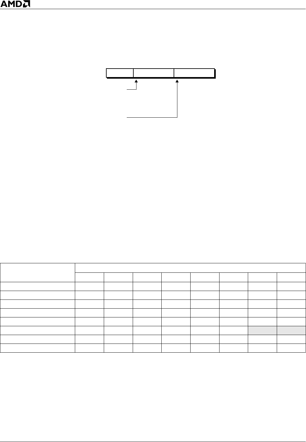
364 Opcode and Operand Encodings
AMD64 Technology 24594—Rev. 3.14—September 2007
Figure A-2. ModRM-Byte Format
The two sections below describe the ModRM operand encodings, first for 16-bit references and then
for 32-bit and 64-bit references.
16-Bit Register and Memory References. Table A-12 shows the notation and encoding
conventions for register references using the ModRM reg field. This table is comparable to Table A-14
on page 367 but applies only when the address-size is 16-bit. Table A-13 on page 365 shows the
notation and encoding conventions for 16-bit memory references using the ModRM byte. This table is
comparable to Table A-15 on page 368.
Table A-12. ModRM Register References, 16-Bit Addressing
Mnemonic
Notation
ModRM reg Field
/0 /1 /2 /3 /4 /5 /6 /7
reg8 AL CL DL BL AH CH DH BH
reg16 AXCXDXBXSPBP SI DI
reg32 EAX ECX EDX EBX ESP EBP ESI EDI
mmx MMX0 MMX1 MMX2 MMX3 MMX4 MMX5 MMX6 MMX7
xmm XMM0 XMM1 XMM2 XMM3 XMM4 XMM5 XMM6 XMM7
sReg ES CS SS DS FS GS invalid invalid
cReg CR0 CR1 CR2 CR3 CR4 CR5 CR6 CR7
dReg DR0 DR1 DR2 DR3 DR4 DR5 DR6 DR7
513-305.eps
mod
REX.R bit of REX prefix can
extend this field to 4 bits
REX.B bit of REX prefix can
extend this field to 4 bits
regr/mModRM
01234567Bits:
Opcode and Operand Encodings 365
24594—Rev. 3.14—September 2007 AMD64 Technology
Table A-13. ModRM Memory References, 16-Bit Addressing
Effective Address1
ModRM
mod
Field
(binary)
ModRM reg Field2ModRM
r/m
Field
(binary)
/0 /1 /2 /3 /4 /5 /6 /7
Complete ModRM Byte (hex)
[BX+SI]
00
00 08 10 18 20 28 30 38 000
[BX+DI] 01 09 11 19 21 29 31 39 001
[BP+SI] 02 0A 12 1A 22 2A 32 3A 010
[BP+DI] 03 0B 13 1B 23 2B 33 3B 011
[SI] 04 0C 14 1C 24 2C 34 3C 100
[DI] 05 0D 15 1D 25 2D 35 3D 101
[disp16]06 0E 16 1E 26 2E 36 3E 110
[BX] 07 0F 17 1F 27 2F 37 3F 111
[BX+SI+disp8]
01
40 48 50 58 60 68 70 78 000
[BX+DI+disp8]41 49 51 59 61 69 71 79 001
[BP+SI+disp8]42 4A 52 5A 62 6A 72 7A 010
[BP+DI+disp8]43 4B 53 5B 63 6B 73 7B 011
[SI+disp8]44 4C 54 5C 64 6C 74 7C 100
[DI+disp8]45 4D 55 5D 65 6D 75 7D 101
[BP+disp8]46 4E 56 5E 66 6E 76 7E 110
[BX+disp8]47 4F 57 5F 67 6F 77 7F 111
[BX+SI+disp16]
10
80 88 90 98 A0 A8 B0 B8 000
[BX+DI+disp16]81 89 91 99 A1 A9 B1 B9 001
[BP+SI+disp16]82 8A 92 9A A2 AA B2 BA 010
[BP+DI+disp16]83 8B 93 9B A3 AB B3 BB 011
[SI+disp16]84 8C 94 9C A4 AC B4 BC 100
[DI+disp16]85 8D 95 9D A5 AD B5 BD 101
[BP+disp16]86 8E 96 9E A6 AE B6 BE 110
[BX+disp16]87 8F 97 9F A7 AF B7 BF 111
Note:
1. In these combinations, “disp8” and “disp16” indicate an 8-bit or 16-bit signed displacement.
2. See Table A-12 for complete specification of ModRM “reg” field.
366 Opcode and Operand Encodings
AMD64 Technology 24594—Rev. 3.14—September 2007
Register and Memory References for 32-Bit and 64-Bit Addressing. Table A-14 on
page 367 shows the encoding for 32-bit and 64-bit register references using the ModRM reg field. The
first nine rows of Table A-14 show references when the REX.R bit is cleared to 0, and the last nine
rows show references when the REX.R bit is set to 1. In this table, Mnemonic Notation means the
syntax notation shown in “Mnemonic Syntax” on page 37 for a register, and ModRM Notation (/r)
means the opcode-syntax notation shown in “Opcode Syntax” on page 39 for the register.
Table A-15 on page 368 shows the encoding for 32-bit and 64-bit memory references using the
ModRM byte. This table describes 32-bit and 64-bit addressing, with the REX.B bit set or cleared. The
Effective Address is shown in the two left-most columns, followed by the binary encoding of the
ModRM-byte mod field, followed by the eight possible hex values of the complete ModRM byte (one
value for each binary encoding of the ModRM-byte reg field), followed by the binary encoding of the
ModRM r/m field.
The /0 through /7 notation for the ModRM reg field (bits 5–3) means that the three-bit field contains a
value from zero (binary 000) to 7 (binary 111).
AL/AX/EAX/MMX0/XMM0
11
C0 C8 D0 D8 E0 E8 F0 F8 000
CL/CX/ECX/MMX1/XMM1 C1 C9 D1 D9 E1 E9 F1 F9 001
DL/DX/EDX/MMX2/XMM2 C2 CA D2 DA E2 EA F2 FA 010
BL/BX/EBX/MMX3/XMM3 C3 CB D3 DB E3 EB F3 FB 011
AH/SP/ESP/MMX4/XMM4 C4 CC D4 DC E4 EC F4 FC 100
CH/BP/EBP/MMX5/XMM5 C5 CD D5 DD E5 ED F5 FD 101
DH/SI/ESI/MMX6/XMM6 C6 CE D6 DE E6 EE F6 FE 110
BH/DI/EDI/MMX7/XMM7 C7 CF D7 DF E7 EF F7 FF 111
Table A-13. ModRM Memory References, 16-Bit Addressing (continued)
Effective Address1
ModRM
mod
Field
(binary)
ModRM reg Field2ModRM
r/m
Field
(binary)
/0 /1 /2 /3 /4 /5 /6 /7
Complete ModRM Byte (hex)
Note:
1. In these combinations, “disp8” and “disp16” indicate an 8-bit or 16-bit signed displacement.
2. See Table A-12 for complete specification of ModRM “reg” field.
Opcode and Operand Encodings 367
24594—Rev. 3.14—September 2007 AMD64 Technology
Table A-14. ModRM Register References, 32-Bit and 64-Bit Addressing
Mnemonic
Notation REX.R Bit ModRM reg Field
/0 /1 /2 /3 /4 /5 /6 /7
reg8
0
AL CL DL BL AH/SPL CH/BPL DH/SIL BH/DIL
reg16 AX CX DX BX SP BP SI DI
reg32 EAX ECX EDX EBX ESP EBP ESI EDI
reg64 RAX RCX RDX RBX RSP RBP RSI RDI
mmx MMX0 MMX1 MMX2 MMX3 MMX4 MMX5 MMX6 MMX7
xmm XMM0 XMM1 XMM2 XMM3 XMM4 XMM5 XMM6 XMM7
sReg ES CS SS DS FS GS invalid invalid
cReg CR0 CR1 CR2 CR3 CR4 CR5 CR6 CR7
dReg DR0 DR1 DR2 DR3 DR4 DR5 DR6 DR7
reg8
1
R8B R9B R10B R11B R12B R13B R14B R15B
reg16 R8W R9W R10W R11W R12W R13W R14W R15W
reg32 R8D R9D R10D R11D R12D R13D R14D R15D
reg64 R8 R9 R10 R11 R12 R13 R14 R15
mmx MMX0 MMX1 MMX2 MMX3 MMX4 MMX5 MMX6 MMX7
xmm XMM8 XMM9 XMM10 XMM11 XMM12 XMM13 XMM14 XMM15
sReg ES CS SS DS FS GS invalid invalid
cReg CR8 CR9 CR10 CR11 CR12 CR13 CR14 CR15
dReg DR8 DR9 DR10 DR11 DR12 DR13 DR14 DR15
368 Opcode and Operand Encodings
AMD64 Technology 24594—Rev. 3.14—September 2007
Table A-15. ModRM Memory References, 32-Bit and 64-Bit Addressing
Effective Address1
ModRM
mod
Field
(binary)
ModRM reg Field3ModRM
r/m
Field
(binary)
/0 /1 /2 /3 /4 /5 /6 /7
REX.B = 0 REX.B = 1 Complete ModRM Byte (hex)
[rAX] [r8]
00
00 08 10 18 20 28 30 38 000
[rCX] [r9] 01 09 11 19 21 29 31 39 001
[rDX] [r10] 02 0A 12 1A 22 2A 32 3A 010
[rBX] [r11] 03 0B 13 1B 23 2B 33 3B 011
[SIB]4[SIB]404 0C 14 1C 24 2C 34 3C 100
[rIP+disp32] or [disp32]2[rIP+disp32] or
[disp32]205 0D 15 1D 25 2D 35 3D 101
[rSI] [r14] 06 0E 16 1E 26 2E 36 3E 110
[rDI] [r15] 07 0F 17 1F 27 2F 37 3F 111
[rAX+disp8][r8+disp8]
01
40 48 50 58 60 68 70 78 000
[rCX+disp8][r9+disp8]41 49 51 59 61 69 71 79 001
[rDX+disp8][r10+disp8]42 4A 52 5A 62 6A 72 7A 010
[rBX+disp8][r11+disp8]43 4B 53 5B 63 6B 73 7B 011
[SIB+disp8]4[SIB+disp8]444 4C 54 5C 64 6C 74 7C 100
[rBP+disp8][r13+disp8]45 4D 55 5D 65 6D 75 7D 101
[rSI+disp8][r14+disp8]46 4E 56 5E 66 6E 76 7E 110
[rDI+disp8][r15+disp8]47 4F 57 5F 67 6F 77 7F 111
[rAX+disp32][r8+disp32]
10
80 88 90 98 A0 A8 B0 B8 000
[rCX+disp32][r9+disp32]81 89 91 99 A1 A9 B1 B9 001
[rDX+disp32][r10+disp32]82 8A 92 9A A2 AA B2 BA 010
[rBX+disp32][r11+disp32]83 8B 93 9B A3 AB B3 BB 011
[SIB+disp32]4[SIB+disp32]484 8C 94 9C A4 AC B4 BC 100
[rBP+disp32][r13+disp32]85 8D 95 9D A5 AD B5 BD 101
[rSI+disp32][r14+disp32]86 8E 96 9E A6 AE B6 BE 110
[rDI+disp32][r15+disp32]87 8F 97 9F A7 AF B7 BF 111
Note:
1. In these combinations, “disp8” and “disp32” indicate an 8-bit or 32-bit signed displacement.
2. In 64-bit mode, the effective address is [rIP+disp32]. In all other modes, the effective address is [disp32]. If the
address-size prefix is used in 64-bit mode to override 64-bit addressing, the [RIP+disp32] effective address is trun-
cated after computation to 64 bits.
3. See Table A-14 for complete specification of ModRM “reg” field.
4. An SIB byte follows the ModRM byte to identify the memory operand.
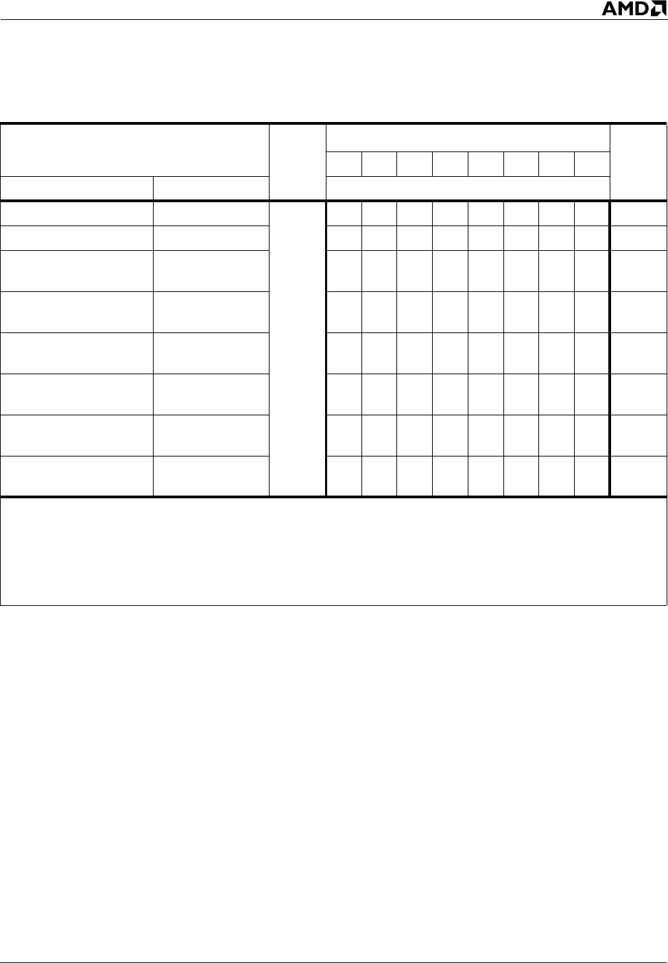
Opcode and Operand Encodings 369
24594—Rev. 3.14—September 2007 AMD64 Technology
A.3.2 SIB Operand References
Figure A-3 on page 370 shows the format of a scale-index-base (SIB) byte. Some instructions have an
SIB byte following their ModRM byte to define memory addressing for the complex-addressing
modes described in “Effective Addresses” in Volume 1. The SIB byte has three fields—scale, index,
and base—that define the scale factor, index-register number, and base-register number for 32-bit and
64-bit complex addressing modes. In 64-bit mode, the REX.B and REX.X bits extend the encoding of
the SIB byte’s base and index fields.
AL/rAX/MMX0/XMM0 r8/MMX0/XMM8
11
C0 C8 D0 D8 E0 E8 F0 F8 000
CL/rCX/MMX1/XMM1 r9/MMX1/XMM9 C1 C9 D1 D9 E1 E9 F1 F9 001
DL/rDX/MMX2/XMM2 r10/MMX2/XMM1
0C2 CA D2 DA E2 EA F2 FA 010
BL/rBX/MMX3/XMM3 r11/MMX3/XMM1
1C3 CB D3 DB E3 EB F3 FB 011
AH/SPL/rSP/MMX4/XM
M4
r12/MMX4/XMM1
2C4 CC D4 DC E4 EC F4 FC 100
CH/BPL/rBP/MMX5/XM
M5
r13/MMX5/XMM1
3C5 CD D5 DD E5 ED F5 FD 101
DH/SIL/rSI/MMX6/XMM
6
r14/MMX6/XMM1
4C6 CE D6 DE E6 EE F6 FE 110
BH/DIL/rDI/MMX7/XMM
7
r15/MMX7/XMM1
5C7 CF D7 DF E7 EF F7 FF 111
Table A-15. ModRM Memory References, 32-Bit and 64-Bit Addressing (continued)
Effective Address1
ModRM
mod
Field
(binary)
ModRM reg Field3ModRM
r/m
Field
(binary)
/0 /1 /2 /3 /4 /5 /6 /7
REX.B = 0 REX.B = 1 Complete ModRM Byte (hex)
Note:
1. In these combinations, “disp8” and “disp32” indicate an 8-bit or 32-bit signed displacement.
2. In 64-bit mode, the effective address is [rIP+disp32]. In all other modes, the effective address is [disp32]. If the
address-size prefix is used in 64-bit mode to override 64-bit addressing, the [RIP+disp32] effective address is trun-
cated after computation to 64 bits.
3. See Table A-14 for complete specification of ModRM “reg” field.
4. An SIB byte follows the ModRM byte to identify the memory operand.
370 Opcode and Operand Encodings
AMD64 Technology 24594—Rev. 3.14—September 2007
Figure A-3. SIB Byte Format
Table A-16 shows the encodings for the SIB byte’s base field, which specifies the base register for
addressing. Table A-17 on page 371 shows the encodings for the effective address referenced by a
complete SIB byte, including its scale and index fields. The /0 through /7 notation for the SIB base
field means that the three-bit field contains a value between zero (binary 000) and 7 (binary 111).
Table A-16. SIB base Field References
REX.B Bit ModRM mod Field SIB base Field
/0 /1 /2 /3 /4 /5 /6 /7
0
00
rAX rCX rDX rBX rSP
disp32
rSI rDI01 rBP+disp8
10 rBP+disp32
1
00
r8 r9 r10 r11 r12
disp32
r14 r1501 r13+disp8
10 r13+disp32
513-306.eps
Bits:
scale index base SIB
01234567
REX.X bit of REX prefix can
extend this field to 4 bits
REX.B bit of REX prefix can
extend this field to 4 bits
Opcode and Operand Encodings 371
24594—Rev. 3.14—September 2007 AMD64 Technology
Table A-17. SIB Memory References
Effective Address SIB
scale
Field
SIB
index
Field
SIB base Field1
REX.B = 0: rAX rCX rDX rBX rSP note
1 rSI rDI
REX.B = 1: r8 r9 r10 r11 r12 note
1 r14 r15
/0 /1 /2 /3 /4 /5 /6 /7
REX.X = 0 REX.X = 1 Complete SIB Byte (hex)
[rAX+base] [r8+base]
00
000 0001020304050607
[rCX+base] [r9+base] 001 08 09 0A 0B 0C 0D 0E 0F
[rDX+base] [r10+base] 010 1011121314151617
[rBX+base] [r11+base] 011 18 19 1A 1B 1C 1D 1E 1F
[base] [r12+base] 100 2021222324252627
[rBP+base] [r13+base] 101 28 29 2A 2B 2C 2D 2E 2F
[rSI+base] [r14+base] 110 3031323334353637
[rDI+base] [r15+base] 111 38 39 3A 3B 3C 3D 3E 3F
[rAX*2+base] [r8*2+base]
01
000 4041424344454647
[rCX*2+base] [r9*2+base] 001 48 49 4A 4B 4C 4D 4E 4F
[rDX*2+base] [r10*2+base] 010 5051525354555657
[rBX*2+base] [r11*2+base] 011 58 59 5A 5B 5C 5D 5E 5F
[base] [r12*2+base] 100 6061626364656667
[rBP*2+base] [r13*2+base] 101 68 69 6A 6B 6C 6D 6E 6F
[rSI*2+base] [r14*2+base] 110 7071727374757677
[rDI*2+base] [r15*2+base] 111 78 79 7A 7B 7C 7D 7E 7F
[rAX*4+base] [r8*4+base]
10
000 8081828384858687
[rCX*4+base] [r9*4+base] 001 88 89 8A 8B 8C 8D 8E 8F
[rDX*4+base] [r10*4+base] 010 9091929394959697
[rBX*4+base] [r11*4+base] 011 98 99 9A 9B 9C 9D 9E 9F
[base] [r12*4+base] 100 A0A1A2A3A4A5A6A7
[rBP*4+base] [r13*4+base] 101 A8 A9 AA AB AC AD AE AF
[rSI*4+base] [r14*4+base] 110 B0B1B2B3B4B5B6B7
[rDI*4+base] [r15*4+base] 111 B8 B9 BA BB BC BD BE BF
Note:
1. See Table A-16 on page 370 for complete specification of SIB “base” field.
372 Opcode and Operand Encodings
AMD64 Technology 24594—Rev. 3.14—September 2007
[rAX*8+base] [r8*8+base]
11
000 C0C1C2C3C4C5C6C7
[rCX*8+base] [r9*8+base] 001 C8 C9 CA CB CC CD CE CF
[rDX*8+base] [r10*8+base] 010 D0D1D2D3D4D5D6D7
[rBX*8+base] [r11*8+base] 011 D8 D9 DA DB DC DD DE DF
[base] [r12*8+base] 100 E0E1E2E3E4E5E6E7
[rBP*8+base] [r13*8+base] 101 E8 E9 EA EB EC ED EE EF
[rSI*8+base] [r14*8+base] 110 F0F1F2F3F4F5F6F7
[rDI*8+base] [r15*8+base] 111 F8 F9 FA FB FC FD FE FF
Table A-17. SIB Memory References (continued)
Effective Address SIB
scale
Field
SIB
index
Field
SIB base Field1
REX.B = 0: rAX rCX rDX rBX rSP note
1 rSI rDI
REX.B = 1: r8 r9 r10 r11 r12 note
1 r14 r15
/0 /1 /2 /3 /4 /5 /6 /7
REX.X = 0 REX.X = 1 Complete SIB Byte (hex)
Note:
1. See Table A-16 on page 370 for complete specification of SIB “base” field.

General-Purpose Instructions in 64-Bit Mode 373
24594—Rev. 3.14—September 2007 AMD64 Technology
Appendix B General-Purpose Instructions in
64-Bit Mode
This appendix provides details of the general-purpose instructions in 64-bit mode and its differences
from legacy and compatibility modes. The appendix covers only the general-purpose instructions
(those described in Chapter 3, “General-Purpose Instruction Reference”). It does not cover the 128-
bit media, 64-bit media, or x87 floating-point instructions because those instructions are not affected
by 64-bit mode, other than in the access by such instructions to extended GPR and XMM registers
when using a REX prefix.
B.1 General Rules for 64-Bit Mode
In 64-bit mode, the following general rules apply to instructions and their operands:
• “Promoted to 64 Bit”: If an instruction’s operand size (16-bit or 32-bit) in legacy and
compatibility modes depends on the CS.D bit and the operand-size override prefix, then the
operand-size choices in 64-bit mode are extended from 16-bit and 32-bit to include 64 bits (with a
REX prefix), or the operand size is fixed at 64 bits. Such instructions are said to be “Promoted to
64 bits” in Table B-1. However, byte-operand opcodes of such instructions are not promoted.
• Byte-Operand Opcodes Not Promoted: As stated above in “Promoted to 64 Bit”, byte-operand
opcodes of promoted instructions are not promoted. Those opcodes continue to operate only on
bytes.
• Fixed Operand Size: If an instruction’s operand size is fixed in legacy mode (thus, independent of
CS.D and prefix overrides), that operand size is usually fixed at the same size in 64-bit mode. For
example, CPUID operates on 32-bit operands, irrespective of attempts to override the operand size.
• Default Operand Size: The default operand size for most instructions is 32 bits, and a REX prefix
must be used to change the operand size to 64 bits. However, two groups of instructions default to
64-bit operand size and do not need a REX prefix: (1) near branches and (2) all instructions, except
far branches, that implicitly reference the RSP. See Table B-5 on page 400 for a list of all
instructions that default to 64-bit operand size.
• Zero-Extension of 32-Bit Results: Operations on 32-bit operands in 64-bit mode zero-extend the
high 32 bits of 64-bit GPR destination registers.
• No Extension of 8-Bit and 16-Bit Results: Operations on 8-bit and 16-bit operands in 64-bit
mode leave the high 56 or 48 bits, respectively, of 64-bit GPR destination registers unchanged.
• Shift and Rotate Counts: When the operand size is 64 bits, shifts and rotates use one additional
bit (6 bits total) to specify shift-count or rotate-count, allowing 64-bit shifts and rotates.
•Immediates: The maximum size of immediate operands is 32 bits, except that 64-bit immediates
can be MOVed into 64-bit GPRs. Immediates that are less than 64 bits are a maximum of 32 bits,
and are sign-extended to 64 bits during use.

374 General-Purpose Instructions in 64-Bit Mode
AMD64 Technology 24594—Rev. 3.14—September 2007
• Displacements and Offsets: The maximum size of an address displacement or offset is 32 bits,
except that 64-bit offsets can be used by specific MOV opcodes that read or write AL or rAX.
Displacements and offsets that are less than 64 bits are a maximum of 32 bits, and are sign-
extended to 64 bits during use.
• Undefined High 32 Bits After Mode Change: The processor does not preserve the upper 32 bits
of the 64-bit GPRs across switches from 64-bit mode to compatibility or legacy modes. In
compatibility or legacy mode, the upper 32 bits of the GPRs are undefined and not accessible to
software.
B.2 Operation and Operand Size in 64-Bit Mode
Table B-1 on page 374 lists the integer instructions, showing operand size in 64-bit mode and the state
of the high 32 bits of destination registers when 32-bit operands are used. Opcodes, such as byte-
operand versions of several instructions, that do not appear in Table B-1 are covered by the general
rules described in “General Rules for 64-Bit Mode” on page 373.
Table B-1. Operations and Operands in 64-Bit Mode
Instruction and
Opcode (hex)1
Type of
Operation2
Default
Operand
Size3
For 32-Bit
Operand Size4
For 64-Bit
Operand Size4
AAA - ASCII Adjust after Addition INVALID IN 64-BIT MODE (invalid-opcode exception)
37
AAD - ASCII Adjust AX before Division INVALID IN 64-BIT MODE (invalid-opcode exception)
D5
AAM - ASCII Adjust AX after Multiply INVALID IN 64-BIT MODE (invalid-opcode exception)
D4
AAS - ASCII Adjust AL after Subtraction INVALID IN 64-BIT MODE (invalid-opcode exception)
3F
Note:
1. See “General Rules for 64-Bit Mode” on page 373, for opcodes that do not appear in this table.
2. The type of operation, excluding considerations of operand size or extension of results. See “General Rules for 64-
Bit Mode” on page 373 for definitions of “Promoted to 64 bits” and related topics.
3. If “Type of Operation” is 64 bits, a REX prefix is needed for 64-bit operand size, unless the instruction size defaults
to 64 bits. If the operand size is fixed, operand-size overrides are silently ignored.
4. Special actions in 64-bit mode, in addition to legacy-mode actions. Zero or sign extensions apply only to result oper-
ands, not source operands. Unless otherwise stated, 8-bit and 16-bit results leave the high 56 or 48 bits, respec-
tively, of 64-bit destination registers unchanged. Immediates and branch displacements are sign-extended to 64
bits.
5. Any pointer registers (rDI, rSI) or count registers (rCX) are address-sized and default to 64 bits. For 32-bit address
size, any pointer and count registers are zero-extended to 64 bits.
6. The default operand size can be overridden to 16 bits with 66h prefix, but there is no 32-bit operand-size override
in 64-bit mode.

General-Purpose Instructions in 64-Bit Mode 375
24594—Rev. 3.14—September 2007 AMD64 Technology
ADC—Add with Carry
Promoted to
64 bits. 32 bits
Zero-extends 32-
bit register
results to 64 bits.
11
13
15
81 /2
83 /2
ADD—Signed or Unsigned Add
Promoted to
64 bits. 32 bits
Zero-extends 32-
bit register
results to 64 bits.
01
03
05
81 /0
83 /0
AND—Logical AND
Promoted to
64 bits. 32 bits
Zero-extends 32-
bit register
results to 64 bits.
21
23
25
81 /4
83 /4
ARPL - Adjust Requestor Privilege Level OPCODE USED as MOVSXD in 64-BIT MODE
63
BOUND - Check Array Against Bounds INVALID IN 64-BIT MODE (invalid-opcode exception)
62
BSF—Bit Scan Forward Promoted to
64 bits. 32 bits
Zero-extends 32-
bit register
results to 64 bits.
0F BC
Table B-1. Operations and Operands in 64-Bit Mode (continued)
Instruction and
Opcode (hex)1
Type of
Operation2
Default
Operand
Size3
For 32-Bit
Operand Size4
For 64-Bit
Operand Size4
Note:
1. See “General Rules for 64-Bit Mode” on page 373, for opcodes that do not appear in this table.
2. The type of operation, excluding considerations of operand size or extension of results. See “General Rules for 64-
Bit Mode” on page 373 for definitions of “Promoted to 64 bits” and related topics.
3. If “Type of Operation” is 64 bits, a REX prefix is needed for 64-bit operand size, unless the instruction size defaults
to 64 bits. If the operand size is fixed, operand-size overrides are silently ignored.
4. Special actions in 64-bit mode, in addition to legacy-mode actions. Zero or sign extensions apply only to result oper-
ands, not source operands. Unless otherwise stated, 8-bit and 16-bit results leave the high 56 or 48 bits, respec-
tively, of 64-bit destination registers unchanged. Immediates and branch displacements are sign-extended to 64
bits.
5. Any pointer registers (rDI, rSI) or count registers (rCX) are address-sized and default to 64 bits. For 32-bit address
size, any pointer and count registers are zero-extended to 64 bits.
6. The default operand size can be overridden to 16 bits with 66h prefix, but there is no 32-bit operand-size override
in 64-bit mode.

376 General-Purpose Instructions in 64-Bit Mode
AMD64 Technology 24594—Rev. 3.14—September 2007
BSR—Bit Scan Reverse Promoted to
64 bits. 32 bits
Zero-extends 32-
bit register
results to 64 bits.
0F BD
BSWAP—Byte Swap Promoted to
64 bits. 32 bits
Zero-extends 32-
bit register
results to 64 bits.
Swap all 8 bytes
of a 64-bit GPR.
0F C8 through 0F CF
BT—Bit Test
Promoted to
64 bits. 32 bits No GPR register results.0F A3
0F BA /4
BTC—Bit Test and Complement
Promoted to
64 bits. 32 bits
Zero-extends 32-
bit register
results to 64 bits.
0F BB
0F BA /7
BTR—Bit Test and Reset
Promoted to
64 bits. 32 bits
Zero-extends 32-
bit register
results to 64 bits.
0F B3
0F BA /6
BTS—Bit Test and Set
Promoted to
64 bits. 32 bits
Zero-extends 32-
bit register
results to 64 bits.
0F AB
0F BA /5
CALL—Procedure Call Near See “Near Branches in 64-Bit Mode” in Volume 1.
E8 Promoted to
64 bits. 64 bits Can’t encode.6
RIP = RIP + 32-
bit displacement
sign-extended to
64 bits.
FF /2 Promoted to
64 bits. 64 bits Can’t encode.6
RIP = 64-bit
offset from
register or
memory.
Table B-1. Operations and Operands in 64-Bit Mode (continued)
Instruction and
Opcode (hex)1
Type of
Operation2
Default
Operand
Size3
For 32-Bit
Operand Size4
For 64-Bit
Operand Size4
Note:
1. See “General Rules for 64-Bit Mode” on page 373, for opcodes that do not appear in this table.
2. The type of operation, excluding considerations of operand size or extension of results. See “General Rules for 64-
Bit Mode” on page 373 for definitions of “Promoted to 64 bits” and related topics.
3. If “Type of Operation” is 64 bits, a REX prefix is needed for 64-bit operand size, unless the instruction size defaults
to 64 bits. If the operand size is fixed, operand-size overrides are silently ignored.
4. Special actions in 64-bit mode, in addition to legacy-mode actions. Zero or sign extensions apply only to result oper-
ands, not source operands. Unless otherwise stated, 8-bit and 16-bit results leave the high 56 or 48 bits, respec-
tively, of 64-bit destination registers unchanged. Immediates and branch displacements are sign-extended to 64
bits.
5. Any pointer registers (rDI, rSI) or count registers (rCX) are address-sized and default to 64 bits. For 32-bit address
size, any pointer and count registers are zero-extended to 64 bits.
6. The default operand size can be overridden to 16 bits with 66h prefix, but there is no 32-bit operand-size override
in 64-bit mode.

General-Purpose Instructions in 64-Bit Mode 377
24594—Rev. 3.14—September 2007 AMD64 Technology
CALL—Procedure Call Far See “Branches to 64-Bit Offsets” in Volume 1.
9A INVALID IN 64-BIT MODE (invalid-opcode exception)
FF /3 Promoted to
64 bits. 32 bits
If selector points to a gate, then
RIP = 64-bit offset from gate, else
RIP = zero-extended 32-bit offset
from far pointer referenced in
instruction.
CBW, CWDE, CDQE—Convert Byte to
Word, Convert Word to Doubleword,
Convert Doubleword to Quadword Promoted to
64 bits.
32 bits
(size of desti-
nation regis-
ter)
CWDE: Converts
word to
doubleword.
Zero-extends
EAX to RAX.
CDQE (new
mnemonic):
Converts
doubleword to
quadword.
RAX = sign-
extended EAX.
98
CDQ see CWD, CDQ, CQO
CDQE (new mnemonic) see CBW, CWDE, CDQE
CDWE see CBW, CWDE, CDQE
CLC—Clear Carry Flag Same as
legacy mode. Not relevant. No GPR register results.
F8
CLD—Clear Direction Flag Same as
legacy mode. Not relevant. No GPR register results.
FC
CLFLUSH—Cache Line Invalidate Same as
legacy mode. Not relevant. No GPR register results.
0F AE /7
CLGI—Clear Global Interrupt Same as
legacy mode Not relevant No GPR register results.
0F 01 DD
CLI—Clear Interrupt Flag Same as
legacy mode. Not relevant. No GPR register results.
FA
Table B-1. Operations and Operands in 64-Bit Mode (continued)
Instruction and
Opcode (hex)1
Type of
Operation2
Default
Operand
Size3
For 32-Bit
Operand Size4
For 64-Bit
Operand Size4
Note:
1. See “General Rules for 64-Bit Mode” on page 373, for opcodes that do not appear in this table.
2. The type of operation, excluding considerations of operand size or extension of results. See “General Rules for 64-
Bit Mode” on page 373 for definitions of “Promoted to 64 bits” and related topics.
3. If “Type of Operation” is 64 bits, a REX prefix is needed for 64-bit operand size, unless the instruction size defaults
to 64 bits. If the operand size is fixed, operand-size overrides are silently ignored.
4. Special actions in 64-bit mode, in addition to legacy-mode actions. Zero or sign extensions apply only to result oper-
ands, not source operands. Unless otherwise stated, 8-bit and 16-bit results leave the high 56 or 48 bits, respec-
tively, of 64-bit destination registers unchanged. Immediates and branch displacements are sign-extended to 64
bits.
5. Any pointer registers (rDI, rSI) or count registers (rCX) are address-sized and default to 64 bits. For 32-bit address
size, any pointer and count registers are zero-extended to 64 bits.
6. The default operand size can be overridden to 16 bits with 66h prefix, but there is no 32-bit operand-size override
in 64-bit mode.

378 General-Purpose Instructions in 64-Bit Mode
AMD64 Technology 24594—Rev. 3.14—September 2007
CLTS—Clear Task-Switched Flag in
CR0 Same as
legacy mode. Not relevant. No GPR register results.
0F 06
CMC—Complement Carry Flag Same as
legacy mode. Not relevant. No GPR register results.
F5
CMOVcc—Conditional Move
Promoted to
64 bits. 32 bits
Zero-extends 32-
bit register
results to 64 bits.
This occurs even
if the condition is
false.
0F 40 through 0F 4F
CMP—Compare
Promoted to
64 bits. 32 bits
Zero-extends 32-
bit register
results to 64 bits.
39
3B
3D
81 /7
83 /7
CMPS, CMPSW, CMPSD, CMPSQ—
Compare Strings Promoted to
64 bits. 32 bits
CMPSD:
Compare String
Doublewords.
See footnote5
CMPSQ (new
mnemonic):
Compare String
Quadwords
See footnote5
A7
CMPXCHG—Compare and Exchange Promoted to
64 bits. 32 bits
Zero-extends 32-
bit register
results to 64 bits.
0F B1
Table B-1. Operations and Operands in 64-Bit Mode (continued)
Instruction and
Opcode (hex)1
Type of
Operation2
Default
Operand
Size3
For 32-Bit
Operand Size4
For 64-Bit
Operand Size4
Note:
1. See “General Rules for 64-Bit Mode” on page 373, for opcodes that do not appear in this table.
2. The type of operation, excluding considerations of operand size or extension of results. See “General Rules for 64-
Bit Mode” on page 373 for definitions of “Promoted to 64 bits” and related topics.
3. If “Type of Operation” is 64 bits, a REX prefix is needed for 64-bit operand size, unless the instruction size defaults
to 64 bits. If the operand size is fixed, operand-size overrides are silently ignored.
4. Special actions in 64-bit mode, in addition to legacy-mode actions. Zero or sign extensions apply only to result oper-
ands, not source operands. Unless otherwise stated, 8-bit and 16-bit results leave the high 56 or 48 bits, respec-
tively, of 64-bit destination registers unchanged. Immediates and branch displacements are sign-extended to 64
bits.
5. Any pointer registers (rDI, rSI) or count registers (rCX) are address-sized and default to 64 bits. For 32-bit address
size, any pointer and count registers are zero-extended to 64 bits.
6. The default operand size can be overridden to 16 bits with 66h prefix, but there is no 32-bit operand-size override
in 64-bit mode.

General-Purpose Instructions in 64-Bit Mode 379
24594—Rev. 3.14—September 2007 AMD64 Technology
CMPXCHG8B—Compare and
Exchange Eight Bytes
Same as
legacy mode. 32 bits.
Zero-extends
EDX and EAX to
64 bits.
CMPXCHG16B
(new mne-
monic): Com-
pare and
Exchange 16
Bytes.
0F C7 /1
CPUID—Processor Identification Same as
legacy mode.
Operand size
fixed at 32
bits.
Zero-extends 32-bit register results
to 64 bits.
0F A2
CQO (new mnemonic) see CWD, CDQ, CQO
CWD, CDQ, CQO—Convert Word to
Doubleword, Convert Doubleword to
Quadword, Convert Quadword to Double
Quadword
Promoted to
64 bits.
32 bits
(size of desti-
nation regis-
ter)
CDQ: Converts
doubleword to
quadword.
Sign-extends
EAX to EDX.
Zero-extends
EDX to RDX.
RAX is
unchanged.
CQO (new
mnemonic):
Converts
quadword to
double
quadword.
Sign-extends
RAX to RDX.
RAX is
unchanged.
99
DAA - Decimal Adjust AL after Addition INVALID IN 64-BIT MODE (invalid-opcode exception)
27
DAS - Decimal Adjust AL after
Subtraction INVALID IN 64-BIT MODE (invalid-opcode exception)
2F
Table B-1. Operations and Operands in 64-Bit Mode (continued)
Instruction and
Opcode (hex)1
Type of
Operation2
Default
Operand
Size3
For 32-Bit
Operand Size4
For 64-Bit
Operand Size4
Note:
1. See “General Rules for 64-Bit Mode” on page 373, for opcodes that do not appear in this table.
2. The type of operation, excluding considerations of operand size or extension of results. See “General Rules for 64-
Bit Mode” on page 373 for definitions of “Promoted to 64 bits” and related topics.
3. If “Type of Operation” is 64 bits, a REX prefix is needed for 64-bit operand size, unless the instruction size defaults
to 64 bits. If the operand size is fixed, operand-size overrides are silently ignored.
4. Special actions in 64-bit mode, in addition to legacy-mode actions. Zero or sign extensions apply only to result oper-
ands, not source operands. Unless otherwise stated, 8-bit and 16-bit results leave the high 56 or 48 bits, respec-
tively, of 64-bit destination registers unchanged. Immediates and branch displacements are sign-extended to 64
bits.
5. Any pointer registers (rDI, rSI) or count registers (rCX) are address-sized and default to 64 bits. For 32-bit address
size, any pointer and count registers are zero-extended to 64 bits.
6. The default operand size can be overridden to 16 bits with 66h prefix, but there is no 32-bit operand-size override
in 64-bit mode.

380 General-Purpose Instructions in 64-Bit Mode
AMD64 Technology 24594—Rev. 3.14—September 2007
DEC—Decrement by 1
FF /1
Promoted to
64 bits. 32 bits
Zero-extends 32-
bit register
results to 64 bits.
48 through 4F OPCODE USED as REX PREFIX in 64-BIT MODE
DIV—Unsigned Divide
Promoted to
64 bits. 32 bits
Zero-extends 32-
bit register
results to 64 bits.
RDX:RAX
contain a 64-bit
quotient (RAX)
and 64-bit
remainder
(RDX).
F7 /6
ENTER—Create Procedure Stack
Frame Promoted to
64 bits. 64 bits Can’t encode6
C8
HLT—Halt Same as
legacy mode. Not relevant. No GPR register results.
F4
IDIV—Signed Divide
Promoted to
64 bits. 32 bits
Zero-extends 32-
bit register
results to 64 bits.
RDX:RAX
contain a 64-bit
quotient (RAX)
and 64-bit
remainder
(RDX).
F7 /7
Table B-1. Operations and Operands in 64-Bit Mode (continued)
Instruction and
Opcode (hex)1
Type of
Operation2
Default
Operand
Size3
For 32-Bit
Operand Size4
For 64-Bit
Operand Size4
Note:
1. See “General Rules for 64-Bit Mode” on page 373, for opcodes that do not appear in this table.
2. The type of operation, excluding considerations of operand size or extension of results. See “General Rules for 64-
Bit Mode” on page 373 for definitions of “Promoted to 64 bits” and related topics.
3. If “Type of Operation” is 64 bits, a REX prefix is needed for 64-bit operand size, unless the instruction size defaults
to 64 bits. If the operand size is fixed, operand-size overrides are silently ignored.
4. Special actions in 64-bit mode, in addition to legacy-mode actions. Zero or sign extensions apply only to result oper-
ands, not source operands. Unless otherwise stated, 8-bit and 16-bit results leave the high 56 or 48 bits, respec-
tively, of 64-bit destination registers unchanged. Immediates and branch displacements are sign-extended to 64
bits.
5. Any pointer registers (rDI, rSI) or count registers (rCX) are address-sized and default to 64 bits. For 32-bit address
size, any pointer and count registers are zero-extended to 64 bits.
6. The default operand size can be overridden to 16 bits with 66h prefix, but there is no 32-bit operand-size override
in 64-bit mode.

General-Purpose Instructions in 64-Bit Mode 381
24594—Rev. 3.14—September 2007 AMD64 Technology
IMUL - Signed Multiply
Promoted to
64 bits. 32 bits
Zero-extends 32-
bit register
results to 64 bits.
RDX:RAX = RAX
* reg/mem64
(i.e., 128-bit
result)
F7 /5
0F AF reg64 = reg64 *
reg/mem64
69
reg64 =
reg/mem64 *
imm32
6B
reg64 =
reg/mem64 *
imm8
IN—Input From Port
Same as
legacy mode. 32 bits Zero-extends 32-bit register results
to 64 bits.
E5
ED
INC—Increment by 1 Promoted to
64 bits. 32 bits
Zero-extends 32-
bit register
results to 64 bits.
FF /0
40 through 47 OPCODE USED as REX PREFIX in 64-BIT MODE
INS, INSW, INSD—Input String Same as
legacy mode. 32 bits
INSD: Input String Doublewords.
No GPR register results.
See footnote5
6D
INT n—Interrupt to Vector
Promoted to
64 bits. Not relevant. See “Long-Mode Interrupt Control
Transfers” in Volume 2.
CD
INT3—Interrupt to Debug Vector
CC
INTO - Interrupt to Overflow Vector INVALID IN 64-BIT MODE (invalid-opcode exception)
CE
Table B-1. Operations and Operands in 64-Bit Mode (continued)
Instruction and
Opcode (hex)1
Type of
Operation2
Default
Operand
Size3
For 32-Bit
Operand Size4
For 64-Bit
Operand Size4
Note:
1. See “General Rules for 64-Bit Mode” on page 373, for opcodes that do not appear in this table.
2. The type of operation, excluding considerations of operand size or extension of results. See “General Rules for 64-
Bit Mode” on page 373 for definitions of “Promoted to 64 bits” and related topics.
3. If “Type of Operation” is 64 bits, a REX prefix is needed for 64-bit operand size, unless the instruction size defaults
to 64 bits. If the operand size is fixed, operand-size overrides are silently ignored.
4. Special actions in 64-bit mode, in addition to legacy-mode actions. Zero or sign extensions apply only to result oper-
ands, not source operands. Unless otherwise stated, 8-bit and 16-bit results leave the high 56 or 48 bits, respec-
tively, of 64-bit destination registers unchanged. Immediates and branch displacements are sign-extended to 64
bits.
5. Any pointer registers (rDI, rSI) or count registers (rCX) are address-sized and default to 64 bits. For 32-bit address
size, any pointer and count registers are zero-extended to 64 bits.
6. The default operand size can be overridden to 16 bits with 66h prefix, but there is no 32-bit operand-size override
in 64-bit mode.

382 General-Purpose Instructions in 64-Bit Mode
AMD64 Technology 24594—Rev. 3.14—September 2007
INVD—Invalidate Internal Caches Same as
legacy mode. Not relevant. No GPR register results.
0F 08
INVLPG—Invalidate TLB Entry Promoted to
64 bits. Not relevant. No GPR register results.
0F 01 /7
INVLPGA—Invalidate TLB Entry in a
Specified ASID
Same as
legacy mode. Not relevant. No GPR register results.
IRET, IRETD, IRETQ—Interrupt Return
Promoted to
64 bits. 32 bits
IRETD: Interrupt
Return
Doubleword.
See “Long-Mode
Interrupt Control
Transfers” in
Volume 2.
IRETQ (new
mnemonic):
Interrupt Return
Quadword.
See “Long-Mode
Interrupt Control
Transfers” in
Volume 2.
CF
Jcc—Jump Conditional See “Near Branches in 64-Bit Mode” in Volume 1.
70 through 7F
Promoted to
64 bits. 64 bits Can’t encode.6
RIP = RIP + 8-bit
displacement
sign-extended to
64 bits.
0F 80 through 0F 8F
RIP = RIP + 32-
bit displacement
sign-extended to
64 bits.
JCXZ, JECXZ, JRCXZ—Jump on
CX/ECX/RCX Zero Promoted to
64 bits. 64 bits Can’t encode.6
RIP = RIP + 8-bit
displacement
sign-extended to
64 bits.
See footnote5
E3
Table B-1. Operations and Operands in 64-Bit Mode (continued)
Instruction and
Opcode (hex)1
Type of
Operation2
Default
Operand
Size3
For 32-Bit
Operand Size4
For 64-Bit
Operand Size4
Note:
1. See “General Rules for 64-Bit Mode” on page 373, for opcodes that do not appear in this table.
2. The type of operation, excluding considerations of operand size or extension of results. See “General Rules for 64-
Bit Mode” on page 373 for definitions of “Promoted to 64 bits” and related topics.
3. If “Type of Operation” is 64 bits, a REX prefix is needed for 64-bit operand size, unless the instruction size defaults
to 64 bits. If the operand size is fixed, operand-size overrides are silently ignored.
4. Special actions in 64-bit mode, in addition to legacy-mode actions. Zero or sign extensions apply only to result oper-
ands, not source operands. Unless otherwise stated, 8-bit and 16-bit results leave the high 56 or 48 bits, respec-
tively, of 64-bit destination registers unchanged. Immediates and branch displacements are sign-extended to 64
bits.
5. Any pointer registers (rDI, rSI) or count registers (rCX) are address-sized and default to 64 bits. For 32-bit address
size, any pointer and count registers are zero-extended to 64 bits.
6. The default operand size can be overridden to 16 bits with 66h prefix, but there is no 32-bit operand-size override
in 64-bit mode.
General-Purpose Instructions in 64-Bit Mode 383
24594—Rev. 3.14—September 2007 AMD64 Technology
JMP—Jump Near See “Near Branches in 64-Bit Mode” in Volume 1.
EB
Promoted to
64 bits. 64 bits Can’t encode.6
RIP = RIP + 8-bit
displacement
sign-extended to
64 bits.
E9
RIP = RIP + 32-
bit displacement
sign-extended to
64 bits.
FF /4
RIP = 64-bit
offset from
register or
memory.
JMP—Jump Far See “Branches to 64-Bit Offsets” in Volume 1.
EA INVALID IN 64-BIT MODE (invalid-opcode exception)
FF /5 Promoted to
64 bits. 32 bits
If selector points to a gate, then
RIP = 64-bit offset from gate, else
RIP = zero-extended 32-bit offset
from far pointer referenced in
instruction.
LAHF - Load Status Flags into AH
Register Same as leg-
acy mode. Not relevant.
9F
LAR—Load Access Rights Byte Same as
legacy mode. 32 bits
Zero-extends 32-
bit register
results to 64 bits.
0F 02
LDS - Load DS Far Pointer INVALID IN 64-BIT MODE (invalid-opcode exception)
C5
Table B-1. Operations and Operands in 64-Bit Mode (continued)
Instruction and
Opcode (hex)1
Type of
Operation2
Default
Operand
Size3
For 32-Bit
Operand Size4
For 64-Bit
Operand Size4
Note:
1. See “General Rules for 64-Bit Mode” on page 373, for opcodes that do not appear in this table.
2. The type of operation, excluding considerations of operand size or extension of results. See “General Rules for 64-
Bit Mode” on page 373 for definitions of “Promoted to 64 bits” and related topics.
3. If “Type of Operation” is 64 bits, a REX prefix is needed for 64-bit operand size, unless the instruction size defaults
to 64 bits. If the operand size is fixed, operand-size overrides are silently ignored.
4. Special actions in 64-bit mode, in addition to legacy-mode actions. Zero or sign extensions apply only to result oper-
ands, not source operands. Unless otherwise stated, 8-bit and 16-bit results leave the high 56 or 48 bits, respec-
tively, of 64-bit destination registers unchanged. Immediates and branch displacements are sign-extended to 64
bits.
5. Any pointer registers (rDI, rSI) or count registers (rCX) are address-sized and default to 64 bits. For 32-bit address
size, any pointer and count registers are zero-extended to 64 bits.
6. The default operand size can be overridden to 16 bits with 66h prefix, but there is no 32-bit operand-size override
in 64-bit mode.

384 General-Purpose Instructions in 64-Bit Mode
AMD64 Technology 24594—Rev. 3.14—September 2007
LEA—Load Effective Address Promoted to
64 bits. 32 bits
Zero-extends 32-
bit register
results to 64 bits.
8D
LEAVE—Delete Procedure Stack Frame Promoted to
64 bits. 64 bits Can’t encode6
C9
LES - Load ES Far Pointer INVALID IN 64-BIT MODE (invalid-opcode exception)
C4
LFENCE—Load Fence Same as
legacy mode. Not relevant. No GPR register results.
0F AE /5
LFS—Load FS Far Pointer Same as
legacy mode. 32 bits Zero-extends 32-bit register results
to 64 bits.
0F B4
LGDT—Load Global Descriptor Table
Register Promoted to
64 bits.
Operand size
fixed at 64
bits.
No GPR register results.
Loads 8-byte base and 2-byte limit.
0F 01 /2
LGS—Load GS Far Pointer Same as
legacy mode. 32 bits Zero-extends 32-bit register results
to 64 bits.
0F B5
LIDT—Load Interrupt Descriptor Table
Register Promoted to
64 bits.
Operand size
fixed at 64
bits.
No GPR register results.
Loads 8-byte base and 2-byte limit.
0F 01 /3
LLDT—Load Local Descriptor Table
Register Promoted to
64 bits.
Operand size
fixed at 16
bits.
No GPR register results.
References 16-byte descriptor to
load 64-bit base.
0F 00 /2
LMSW—Load Machine Status Word Same as
legacy mode.
Operand size
fixed at 16
bits.
No GPR register results.
0F 01 /6
Table B-1. Operations and Operands in 64-Bit Mode (continued)
Instruction and
Opcode (hex)1
Type of
Operation2
Default
Operand
Size3
For 32-Bit
Operand Size4
For 64-Bit
Operand Size4
Note:
1. See “General Rules for 64-Bit Mode” on page 373, for opcodes that do not appear in this table.
2. The type of operation, excluding considerations of operand size or extension of results. See “General Rules for 64-
Bit Mode” on page 373 for definitions of “Promoted to 64 bits” and related topics.
3. If “Type of Operation” is 64 bits, a REX prefix is needed for 64-bit operand size, unless the instruction size defaults
to 64 bits. If the operand size is fixed, operand-size overrides are silently ignored.
4. Special actions in 64-bit mode, in addition to legacy-mode actions. Zero or sign extensions apply only to result oper-
ands, not source operands. Unless otherwise stated, 8-bit and 16-bit results leave the high 56 or 48 bits, respec-
tively, of 64-bit destination registers unchanged. Immediates and branch displacements are sign-extended to 64
bits.
5. Any pointer registers (rDI, rSI) or count registers (rCX) are address-sized and default to 64 bits. For 32-bit address
size, any pointer and count registers are zero-extended to 64 bits.
6. The default operand size can be overridden to 16 bits with 66h prefix, but there is no 32-bit operand-size override
in 64-bit mode.

General-Purpose Instructions in 64-Bit Mode 385
24594—Rev. 3.14—September 2007 AMD64 Technology
LODS, LODSW, LODSD, LODSQ—
Load String
Promoted to
64 bits. 32 bits
LODSD: Load
String
Doublewords.
Zero-extends 32-
bit register
results to 64 bits.
See footnote5
LODSQ (new
mnemonic): Load
String
Quadwords.
See footnote5
AD
LOOP—Loop
Promoted to
64 bits. 64 bits Can’t encode.6
RIP = RIP + 8-bit
displacement
sign-extended to
64 bits.
See footnote5
E2
LOOPZ, LOOPE—Loop if Zero/Equal
E1
LOOPNZ, LOOPNE—Loop if Not
Zero/Equal
E0
LSL—Load Segment Limit Same as
legacy mode. 32 bits Zero-extends 32-bit register results
to 64 bits.
0F 03
LSS —Load SS Segment Register Same as
legacy mode. 32 bits Zero-extends 32-bit register results
to 64 bits.
0F B2
LTR—Load Task Register Promoted to
64 bits.
Operand size
fixed at 16
bits.
No GPR register results.
References 16-byte descriptor to
load 64-bit base.
0F 00 /3
LZCNT—Count Leading Zeros
F3 0F BD
Promoted to
64 bits. 32 bits Zero-extends 32-bit register results
to 64 bits.
MFENCE—Memory Fence Same as
legacy mode. Not relevant. No GPR register results.
0F AE /6
MONITOR—Setup Monitor Address
0F 01 C8
Same as
legacy mode.
Operand size
fixed at 32
bits.
No GPR register results.
Table B-1. Operations and Operands in 64-Bit Mode (continued)
Instruction and
Opcode (hex)1
Type of
Operation2
Default
Operand
Size3
For 32-Bit
Operand Size4
For 64-Bit
Operand Size4
Note:
1. See “General Rules for 64-Bit Mode” on page 373, for opcodes that do not appear in this table.
2. The type of operation, excluding considerations of operand size or extension of results. See “General Rules for 64-
Bit Mode” on page 373 for definitions of “Promoted to 64 bits” and related topics.
3. If “Type of Operation” is 64 bits, a REX prefix is needed for 64-bit operand size, unless the instruction size defaults
to 64 bits. If the operand size is fixed, operand-size overrides are silently ignored.
4. Special actions in 64-bit mode, in addition to legacy-mode actions. Zero or sign extensions apply only to result oper-
ands, not source operands. Unless otherwise stated, 8-bit and 16-bit results leave the high 56 or 48 bits, respec-
tively, of 64-bit destination registers unchanged. Immediates and branch displacements are sign-extended to 64
bits.
5. Any pointer registers (rDI, rSI) or count registers (rCX) are address-sized and default to 64 bits. For 32-bit address
size, any pointer and count registers are zero-extended to 64 bits.
6. The default operand size can be overridden to 16 bits with 66h prefix, but there is no 32-bit operand-size override
in 64-bit mode.

386 General-Purpose Instructions in 64-Bit Mode
AMD64 Technology 24594—Rev. 3.14—September 2007
MOV—Move
Promoted to
64 bits. 32 bits
Zero-extends 32-
bit register
results to 64 bits.
89
8B
C7
32-bit immediate
is sign-extended
to 64 bits.
B8 through BF 64-bit immediate.
A1 (moffset) Zero-extends 32-
bit register
results to 64 bits.
Memory offsets
are address-
sized and default
to 64 bits.
Memory offsets
are address-
sized and default
to 64 bits.
A3 (moffset)
MOV—Move to/from Segment Registers
Same as
legacy mode.
32 bits Zero-extends 32-bit register results
to 64 bits.
8C
8E
Operand size
fixed at 16
bits.
No GPR register results.
MOV(CRn)—Move to/from Control
Registers Promoted to
64 bits.
Operand size
fixed at 64
bits.
The high 32 bits of control registers
differ in their writability and reserved
status. See “System Resources” in
Volume 2 for details.
0F 22
0F 20
MOV(DRn)—Move to/from Debug
Registers Promoted to
64 bits.
Operand size
fixed at 64
bits.
The high 32 bits of debug registers
differ in their writability and reserved
status. See “Debug and
Performance Resources” in
Volume 2 for details.
0F 21
0F 23
Table B-1. Operations and Operands in 64-Bit Mode (continued)
Instruction and
Opcode (hex)1
Type of
Operation2
Default
Operand
Size3
For 32-Bit
Operand Size4
For 64-Bit
Operand Size4
Note:
1. See “General Rules for 64-Bit Mode” on page 373, for opcodes that do not appear in this table.
2. The type of operation, excluding considerations of operand size or extension of results. See “General Rules for 64-
Bit Mode” on page 373 for definitions of “Promoted to 64 bits” and related topics.
3. If “Type of Operation” is 64 bits, a REX prefix is needed for 64-bit operand size, unless the instruction size defaults
to 64 bits. If the operand size is fixed, operand-size overrides are silently ignored.
4. Special actions in 64-bit mode, in addition to legacy-mode actions. Zero or sign extensions apply only to result oper-
ands, not source operands. Unless otherwise stated, 8-bit and 16-bit results leave the high 56 or 48 bits, respec-
tively, of 64-bit destination registers unchanged. Immediates and branch displacements are sign-extended to 64
bits.
5. Any pointer registers (rDI, rSI) or count registers (rCX) are address-sized and default to 64 bits. For 32-bit address
size, any pointer and count registers are zero-extended to 64 bits.
6. The default operand size can be overridden to 16 bits with 66h prefix, but there is no 32-bit operand-size override
in 64-bit mode.

General-Purpose Instructions in 64-Bit Mode 387
24594—Rev. 3.14—September 2007 AMD64 Technology
MOVD—Move Doubleword or Quadword
Promoted to
64 bits. 32 bits
Zero-extends 32-
bit register
results to 64 bits.
0F 6E
0F 7E
66 0F 6E Zero-extends 32-
bit register
results to 128
bits.
Zero-extends 64-
bit register
results to 128
bits.
66 0F 7E
MOVNTI—Move Non-Temporal
Doubleword Promoted to
64 bits. 32 bits No GPR register results.
0F C3
MOVS, MOVSW, MOVSD, MOVSQ—
Move String Promoted to
64 bits. 32 bits
MOVSD: Move
String
Doublewords.
See footnote5
MOVSQ (new
mnemonic):
Move String
Quadwords.
See footnote5
A5
MOVSX—Move with Sign-Extend
Promoted to
64 bits. 32 bits
Zero-extends 32-
bit register
results to 64 bits.
0F BE
Sign-extends
byte to
quadword.
0F BF
Sign-extends
word to
quadword.
Table B-1. Operations and Operands in 64-Bit Mode (continued)
Instruction and
Opcode (hex)1
Type of
Operation2
Default
Operand
Size3
For 32-Bit
Operand Size4
For 64-Bit
Operand Size4
Note:
1. See “General Rules for 64-Bit Mode” on page 373, for opcodes that do not appear in this table.
2. The type of operation, excluding considerations of operand size or extension of results. See “General Rules for 64-
Bit Mode” on page 373 for definitions of “Promoted to 64 bits” and related topics.
3. If “Type of Operation” is 64 bits, a REX prefix is needed for 64-bit operand size, unless the instruction size defaults
to 64 bits. If the operand size is fixed, operand-size overrides are silently ignored.
4. Special actions in 64-bit mode, in addition to legacy-mode actions. Zero or sign extensions apply only to result oper-
ands, not source operands. Unless otherwise stated, 8-bit and 16-bit results leave the high 56 or 48 bits, respec-
tively, of 64-bit destination registers unchanged. Immediates and branch displacements are sign-extended to 64
bits.
5. Any pointer registers (rDI, rSI) or count registers (rCX) are address-sized and default to 64 bits. For 32-bit address
size, any pointer and count registers are zero-extended to 64 bits.
6. The default operand size can be overridden to 16 bits with 66h prefix, but there is no 32-bit operand-size override
in 64-bit mode.

388 General-Purpose Instructions in 64-Bit Mode
AMD64 Technology 24594—Rev. 3.14—September 2007
MOVSXD—Move with Sign-Extend
Doubleword
New
instruction,
available only
in 64-bit
mode. (In
other modes,
this opcode
is ARPL
instruction.)
32 bits
Zero-extends 32-
bit register
results to 64 bits.
Sign-extends
doubleword to
quadword.
63
MOVZX—Move with Zero-Extend
Zero-extends 32-
bit register
results to 64 bits.
0F B6
Promoted to
64 bits. 32 bits
Zero-extends
byte to
quadword.
0F B7
Zero-extends
word to
quadword.
MUL—Multiply Unsigned
Promoted to
64 bits. 32 bits
Zero-extends 32-
bit register
results to 64 bits.
RDX:RAX=RAX *
quadword in
register or
memory.
F7 /4
MWAIT—Monitor Wait
0F 01 C9
Same as
legacy mode.
Operand size
fixed at 32
bits.
No GPR register results.
NEG—Negate Two’s Complement Promoted to
64 bits. 32 bits
Zero-extends 32-
bit register
results to 64 bits.
F7 /3
NOP—No Operation Same as
legacy mode. Not relevant. No GPR register results.
90
NOT—Negate One’s Complement Promoted to
64 bits. 32 bits
Zero-extends 32-
bit register
results to 64 bits.
F7 /2
Table B-1. Operations and Operands in 64-Bit Mode (continued)
Instruction and
Opcode (hex)1
Type of
Operation2
Default
Operand
Size3
For 32-Bit
Operand Size4
For 64-Bit
Operand Size4
Note:
1. See “General Rules for 64-Bit Mode” on page 373, for opcodes that do not appear in this table.
2. The type of operation, excluding considerations of operand size or extension of results. See “General Rules for 64-
Bit Mode” on page 373 for definitions of “Promoted to 64 bits” and related topics.
3. If “Type of Operation” is 64 bits, a REX prefix is needed for 64-bit operand size, unless the instruction size defaults
to 64 bits. If the operand size is fixed, operand-size overrides are silently ignored.
4. Special actions in 64-bit mode, in addition to legacy-mode actions. Zero or sign extensions apply only to result oper-
ands, not source operands. Unless otherwise stated, 8-bit and 16-bit results leave the high 56 or 48 bits, respec-
tively, of 64-bit destination registers unchanged. Immediates and branch displacements are sign-extended to 64
bits.
5. Any pointer registers (rDI, rSI) or count registers (rCX) are address-sized and default to 64 bits. For 32-bit address
size, any pointer and count registers are zero-extended to 64 bits.
6. The default operand size can be overridden to 16 bits with 66h prefix, but there is no 32-bit operand-size override
in 64-bit mode.

General-Purpose Instructions in 64-Bit Mode 389
24594—Rev. 3.14—September 2007 AMD64 Technology
OR—Logical OR
Promoted to
64 bits. 32 bits
Zero-extends 32-
bit register
results to 64 bits.
09
0B
0D
81 /1
83 /1
OUT—Output to Port
Same as
legacy mode. 32 bits No GPR register results.E7
EF
OUTS, OUTSW, OUTSD—Output String Same as
legacy mode. 32 bits
Writes doubleword to I/O port.
No GPR register results.
See footnote5
6F
PAUS E—Pause Same as
legacy mode. Not relevant. No GPR register results.
F3 90
POP—Pop Stack
Promoted to
64 bits. 64 bits Cannot encode6No GPR register
results.
8F /0
58 through 5F
POP—Pop (segment register from)
Stack Same as
legacy mode. 64 bits Cannot encode6No GPR register
results.0F A1 (POP FS)
0F A9 (POP GS)
1F (POP DS)
INVALID IN 64-BIT MODE (invalid-opcode exception)07 (POP ES)
17 (POP SS)
Table B-1. Operations and Operands in 64-Bit Mode (continued)
Instruction and
Opcode (hex)1
Type of
Operation2
Default
Operand
Size3
For 32-Bit
Operand Size4
For 64-Bit
Operand Size4
Note:
1. See “General Rules for 64-Bit Mode” on page 373, for opcodes that do not appear in this table.
2. The type of operation, excluding considerations of operand size or extension of results. See “General Rules for 64-
Bit Mode” on page 373 for definitions of “Promoted to 64 bits” and related topics.
3. If “Type of Operation” is 64 bits, a REX prefix is needed for 64-bit operand size, unless the instruction size defaults
to 64 bits. If the operand size is fixed, operand-size overrides are silently ignored.
4. Special actions in 64-bit mode, in addition to legacy-mode actions. Zero or sign extensions apply only to result oper-
ands, not source operands. Unless otherwise stated, 8-bit and 16-bit results leave the high 56 or 48 bits, respec-
tively, of 64-bit destination registers unchanged. Immediates and branch displacements are sign-extended to 64
bits.
5. Any pointer registers (rDI, rSI) or count registers (rCX) are address-sized and default to 64 bits. For 32-bit address
size, any pointer and count registers are zero-extended to 64 bits.
6. The default operand size can be overridden to 16 bits with 66h prefix, but there is no 32-bit operand-size override
in 64-bit mode.

390 General-Purpose Instructions in 64-Bit Mode
AMD64 Technology 24594—Rev. 3.14—September 2007
POPA, POPAD—Pop All to GPR Words
or Doublewords INVALID IN 64-BIT MODE (invalid-opcode exception)
61
POPCNT—Bit Population Count
F3 0F B8
Promoted to
64 bits. 32 bits Zero-extends 32-bit register results
to 64 bits.
POPF, POPFD, POPFQ—Pop to
rFLAGS Word, Doublword, or Quadword
Promoted to
64 bits. 64 bits Cannot encode6
POPFQ (new
mnemonic): Pops
64 bits off stack,
writes low 32 bits
into EFLAGS and
zero-extends the
high 32 bits of
RFLAGS.
9D
PREFETCH—Prefetch L1 Data-Cache
Line Same as
legacy mode. Not relevant. No GPR register results.
0F 0D /0
PREFETCHlevel—Prefetch Data to
Cache Level level Same as
legacy mode. Not relevant. No GPR register results.
0F 18 /0-3
PREFETCHW—Prefetch L1 Data-Cache
Line for Write Same as
legacy mode. Not relevant. No GPR register results.
0F 0D /1
PUSH—Push onto Stack
Promoted to
64 bits. 64 bits Cannot encode6
FF /6
50 through 57
6A
68
Table B-1. Operations and Operands in 64-Bit Mode (continued)
Instruction and
Opcode (hex)1
Type of
Operation2
Default
Operand
Size3
For 32-Bit
Operand Size4
For 64-Bit
Operand Size4
Note:
1. See “General Rules for 64-Bit Mode” on page 373, for opcodes that do not appear in this table.
2. The type of operation, excluding considerations of operand size or extension of results. See “General Rules for 64-
Bit Mode” on page 373 for definitions of “Promoted to 64 bits” and related topics.
3. If “Type of Operation” is 64 bits, a REX prefix is needed for 64-bit operand size, unless the instruction size defaults
to 64 bits. If the operand size is fixed, operand-size overrides are silently ignored.
4. Special actions in 64-bit mode, in addition to legacy-mode actions. Zero or sign extensions apply only to result oper-
ands, not source operands. Unless otherwise stated, 8-bit and 16-bit results leave the high 56 or 48 bits, respec-
tively, of 64-bit destination registers unchanged. Immediates and branch displacements are sign-extended to 64
bits.
5. Any pointer registers (rDI, rSI) or count registers (rCX) are address-sized and default to 64 bits. For 32-bit address
size, any pointer and count registers are zero-extended to 64 bits.
6. The default operand size can be overridden to 16 bits with 66h prefix, but there is no 32-bit operand-size override
in 64-bit mode.

General-Purpose Instructions in 64-Bit Mode 391
24594—Rev. 3.14—September 2007 AMD64 Technology
PUSH—Push (segment register) onto
Stack Promoted to
64 bits. 64 bits Cannot encode6
0F A0 (PUSH FS)
0F A8 (PUSH GS)
0E (PUSH CS)
INVALID IN 64-BIT MODE (invalid-opcode exception)
1E (PUSH DS)
06 (PUSH ES)
16 (PUSH SS)
PUSHA, PUSHAD - Push All to GPR
Words or Doublewords INVALID IN 64-BIT MODE (invalid-opcode exception)
60
PUSHF, PUSHFD, PUSHFQ—Push
rFLAGS Word, Doubleword, or
Quadword onto Stack Promoted to
64 bits. 64 bits Cannot encode6
PUSHFQ (new
mnemonic):
Pushes the 64-bit
RFLAGS
register.
9C
RCL—Rotate Through Carry Left
Promoted to
64 bits. 32 bits
Zero-extends 32-
bit register
results to 64 bits.
Uses 6-bit count.
D1 /2
D3 /2
C1 /2
RCR—Rotate Through Carry Right
Promoted to
64 bits. 32 bits
Zero-extends 32-
bit register
results to 64 bits.
Uses 6-bit count.
D1 /3
D3 /3
C1 /3
RDMSR—Read Model-Specific Register
Same as
legacy mode. Not relevant.
RDX[31:0] contains MSR[63:32],
RAX[31:0] contains MSR[31:0].
Zero-extends 32-bit register results
to 64 bits.
0F 32
Table B-1. Operations and Operands in 64-Bit Mode (continued)
Instruction and
Opcode (hex)1
Type of
Operation2
Default
Operand
Size3
For 32-Bit
Operand Size4
For 64-Bit
Operand Size4
Note:
1. See “General Rules for 64-Bit Mode” on page 373, for opcodes that do not appear in this table.
2. The type of operation, excluding considerations of operand size or extension of results. See “General Rules for 64-
Bit Mode” on page 373 for definitions of “Promoted to 64 bits” and related topics.
3. If “Type of Operation” is 64 bits, a REX prefix is needed for 64-bit operand size, unless the instruction size defaults
to 64 bits. If the operand size is fixed, operand-size overrides are silently ignored.
4. Special actions in 64-bit mode, in addition to legacy-mode actions. Zero or sign extensions apply only to result oper-
ands, not source operands. Unless otherwise stated, 8-bit and 16-bit results leave the high 56 or 48 bits, respec-
tively, of 64-bit destination registers unchanged. Immediates and branch displacements are sign-extended to 64
bits.
5. Any pointer registers (rDI, rSI) or count registers (rCX) are address-sized and default to 64 bits. For 32-bit address
size, any pointer and count registers are zero-extended to 64 bits.
6. The default operand size can be overridden to 16 bits with 66h prefix, but there is no 32-bit operand-size override
in 64-bit mode.

392 General-Purpose Instructions in 64-Bit Mode
AMD64 Technology 24594—Rev. 3.14—September 2007
RDPMC—Read Performance-Monitoring
Counters Same as
legacy mode. Not relevant.
RDX[31:0] contains PMC[63:32],
RAX[31:0] contains PMC[31:0].
Zero-extends 32-bit register results
to 64 bits.
0F 33
RDTSC—Read Time-Stamp Counter
Same as
legacy mode. Not relevant.
RDX[31:0] contains TSC[63:32],
RAX[31:0] contains TSC[31:0].
Zero-extends 32-bit register results
to 64 bits.
0F 31
RDTSCP—Read Time-Stamp Counter
and Processor ID
Same as
legacy mode. Not relevant.
RDX[31:0] contains TSC[63:32],
RAX[31:0] contains TSC[31:0].
RCX[31:0] contains the TSC_AUX
MSR C000_0103h[31:0]. Zero-
extends 32-bit register results to 64
bits.
0F 01 F9
REP INS—Repeat Input String Same as
legacy mode. 32 bits Reads doubleword I/O port.
See footnote5
F3 6D
REP LODS—Repeat Load String Promoted to
64 bits. 32 bits
Zero-extends
EAX to 64 bits.
See footnote5
See footnote5
F3 AD
REP MOVS—Repeat Move String Promoted to
64 bits. 32 bits No GPR register results.
See footnote5
F3 A5
REP OUTS—Repeat Output String to
Port Same as
legacy mode. 32 bits
Writes doubleword to I/O port.
No GPR register results.
See footnote5
F3 6F
REP STOS—Repeat Store String Promoted to
64 bits. 32 bits No GPR register results.
See footnote5
F3 AB
REPx CMPS —Repeat Compare String Promoted to
64 bits. 32 bits No GPR register results.
See footnote5
F3 A7
Table B-1. Operations and Operands in 64-Bit Mode (continued)
Instruction and
Opcode (hex)1
Type of
Operation2
Default
Operand
Size3
For 32-Bit
Operand Size4
For 64-Bit
Operand Size4
Note:
1. See “General Rules for 64-Bit Mode” on page 373, for opcodes that do not appear in this table.
2. The type of operation, excluding considerations of operand size or extension of results. See “General Rules for 64-
Bit Mode” on page 373 for definitions of “Promoted to 64 bits” and related topics.
3. If “Type of Operation” is 64 bits, a REX prefix is needed for 64-bit operand size, unless the instruction size defaults
to 64 bits. If the operand size is fixed, operand-size overrides are silently ignored.
4. Special actions in 64-bit mode, in addition to legacy-mode actions. Zero or sign extensions apply only to result oper-
ands, not source operands. Unless otherwise stated, 8-bit and 16-bit results leave the high 56 or 48 bits, respec-
tively, of 64-bit destination registers unchanged. Immediates and branch displacements are sign-extended to 64
bits.
5. Any pointer registers (rDI, rSI) or count registers (rCX) are address-sized and default to 64 bits. For 32-bit address
size, any pointer and count registers are zero-extended to 64 bits.
6. The default operand size can be overridden to 16 bits with 66h prefix, but there is no 32-bit operand-size override
in 64-bit mode.

General-Purpose Instructions in 64-Bit Mode 393
24594—Rev. 3.14—September 2007 AMD64 Technology
REPx SCAS —Repeat Scan String Promoted to
64 bits. 32 bits No GPR register results.
See footnote5
F3 AF
RET—Return from Call Near See “Near Branches in 64-Bit Mode” in Volume 1.
C2 Promoted to
64 bits. 64 bits Cannot encode.6No GPR register
results.
C3
RET—Return from Call Far
Promoted to
64 bits. 32 bits
See “Control Transfers” in Volume 1
and “Control-Transfer Privilege
Checks” in Volume 2.
CB
CA
ROL—Rotate Left
Promoted to
64 bits. 32 bits
Zero-extends 32-
bit register
results to 64 bits.
Uses 6-bit count.
D1 /0
D3 /0
C1 /0
ROR—Rotate Right
Promoted to
64 bits. 32 bits
Zero-extends 32-
bit register
results to 64 bits.
Uses 6-bit count.
D1 /1
D3 /1
C1 /1
RSM—Resume from System
Management Mode
New SMM
state-save
area.
Not relevant. See “System-Management Mode” in
Volume 2.
0F AA
SAHF - Store AH into Flags Same as leg-
acy mode. Not relevant. No GPR register results.
9E
SAL—Shift Arithmetic Left
Promoted to
64 bits. 32 bits
Zero-extends 32-
bit register
results to 64 bits.
Uses 6-bit count.
D1 /4
D3 /4
C1 /4
Table B-1. Operations and Operands in 64-Bit Mode (continued)
Instruction and
Opcode (hex)1
Type of
Operation2
Default
Operand
Size3
For 32-Bit
Operand Size4
For 64-Bit
Operand Size4
Note:
1. See “General Rules for 64-Bit Mode” on page 373, for opcodes that do not appear in this table.
2. The type of operation, excluding considerations of operand size or extension of results. See “General Rules for 64-
Bit Mode” on page 373 for definitions of “Promoted to 64 bits” and related topics.
3. If “Type of Operation” is 64 bits, a REX prefix is needed for 64-bit operand size, unless the instruction size defaults
to 64 bits. If the operand size is fixed, operand-size overrides are silently ignored.
4. Special actions in 64-bit mode, in addition to legacy-mode actions. Zero or sign extensions apply only to result oper-
ands, not source operands. Unless otherwise stated, 8-bit and 16-bit results leave the high 56 or 48 bits, respec-
tively, of 64-bit destination registers unchanged. Immediates and branch displacements are sign-extended to 64
bits.
5. Any pointer registers (rDI, rSI) or count registers (rCX) are address-sized and default to 64 bits. For 32-bit address
size, any pointer and count registers are zero-extended to 64 bits.
6. The default operand size can be overridden to 16 bits with 66h prefix, but there is no 32-bit operand-size override
in 64-bit mode.

394 General-Purpose Instructions in 64-Bit Mode
AMD64 Technology 24594—Rev. 3.14—September 2007
SAR—Shift Arithmetic Right
Promoted to
64 bits. 32 bits
Zero-extends 32-
bit register
results to 64 bits.
Uses 6-bit count.
D1 /7
D3 /7
C1 /7
SBB—Subtract with Borrow
Promoted to
64 bits. 32 bits
Zero-extends 32-
bit register
results to 64 bits.
19
1B
1D
81 /3
83 /3
SCAS, SCASW, SCASD, SCASQ—
Scan String
Promoted to
64 bits. 32 bits
SCASD: Scan
String
Doublewords.
Zero-extends 32-
bit register
results to 64 bits.
See footnote5
SCASQ (new
mnemonic): Scan
String
Quadwords.
See footnote5
AF
SFENCE—Store Fence Same as
legacy mode. Not relevant. No GPR register results.
0F AE /7
SGDT—Store Global Descriptor Table
Register Promoted to
64 bits.
Operand size
fixed at 64
bits.
No GPR register results.
Stores 8-byte base and 2-byte limit.
0F 01 /0
SHL—Shift Left
Promoted to
64 bits. 32 bits
Zero-extends 32-
bit register
results to 64 bits.
Uses 6-bit count.
D1 /4
D3 /4
C1 /4
Table B-1. Operations and Operands in 64-Bit Mode (continued)
Instruction and
Opcode (hex)1
Type of
Operation2
Default
Operand
Size3
For 32-Bit
Operand Size4
For 64-Bit
Operand Size4
Note:
1. See “General Rules for 64-Bit Mode” on page 373, for opcodes that do not appear in this table.
2. The type of operation, excluding considerations of operand size or extension of results. See “General Rules for 64-
Bit Mode” on page 373 for definitions of “Promoted to 64 bits” and related topics.
3. If “Type of Operation” is 64 bits, a REX prefix is needed for 64-bit operand size, unless the instruction size defaults
to 64 bits. If the operand size is fixed, operand-size overrides are silently ignored.
4. Special actions in 64-bit mode, in addition to legacy-mode actions. Zero or sign extensions apply only to result oper-
ands, not source operands. Unless otherwise stated, 8-bit and 16-bit results leave the high 56 or 48 bits, respec-
tively, of 64-bit destination registers unchanged. Immediates and branch displacements are sign-extended to 64
bits.
5. Any pointer registers (rDI, rSI) or count registers (rCX) are address-sized and default to 64 bits. For 32-bit address
size, any pointer and count registers are zero-extended to 64 bits.
6. The default operand size can be overridden to 16 bits with 66h prefix, but there is no 32-bit operand-size override
in 64-bit mode.

General-Purpose Instructions in 64-Bit Mode 395
24594—Rev. 3.14—September 2007 AMD64 Technology
SHLD—Shift Left Double
Promoted to
64 bits. 32 bits
Zero-extends 32-
bit register
results to 64 bits.
Uses 6-bit count. 0F A4
0F A5
SHR—Shift Right
Promoted to
64 bits. 32 bits
Zero-extends 32-
bit register
results to 64 bits.
Uses 6-bit count.
D1 /5
D3 /5
C1 /5
SHRD—Shift Right Double
Promoted to
64 bits. 32 bits
Zero-extends 32-
bit register
results to 64 bits.
Uses 6-bit count. 0F AC
0F AD
SIDT—Store Interrupt Descriptor Table
Register Promoted to
64 bits.
Operand size
fixed at 64
bits.
No GPR register results.
Stores 8-byte base and 2-byte limit.
0F 01 /1
SKINIT—Secure Init and Jump with
Attestation
0F 01 DE
Same as
legacy mode. Not relevant
Zero-extends 32-
bit register
results to 64 bits.
SLDT—Store Local Descriptor Table
Register Same as
legacy mode. 32 Zero-extends 2-byte LDT selector to
64 bits.
0F 00 /0
SMSW—Store Machine Status Word Same as
legacy mode. 32
Zero-extends 32-
bit register
results to 64 bits.
Stores 64-bit
machine status
word (CR0).
0F 01 /4
STC—Set Carry Flag Same as
legacy mode. Not relevant. No GPR register results.
F9
STD—Set Direction Flag Same as
legacy mode. Not relevant. No GPR register results.
FD
Table B-1. Operations and Operands in 64-Bit Mode (continued)
Instruction and
Opcode (hex)1
Type of
Operation2
Default
Operand
Size3
For 32-Bit
Operand Size4
For 64-Bit
Operand Size4
Note:
1. See “General Rules for 64-Bit Mode” on page 373, for opcodes that do not appear in this table.
2. The type of operation, excluding considerations of operand size or extension of results. See “General Rules for 64-
Bit Mode” on page 373 for definitions of “Promoted to 64 bits” and related topics.
3. If “Type of Operation” is 64 bits, a REX prefix is needed for 64-bit operand size, unless the instruction size defaults
to 64 bits. If the operand size is fixed, operand-size overrides are silently ignored.
4. Special actions in 64-bit mode, in addition to legacy-mode actions. Zero or sign extensions apply only to result oper-
ands, not source operands. Unless otherwise stated, 8-bit and 16-bit results leave the high 56 or 48 bits, respec-
tively, of 64-bit destination registers unchanged. Immediates and branch displacements are sign-extended to 64
bits.
5. Any pointer registers (rDI, rSI) or count registers (rCX) are address-sized and default to 64 bits. For 32-bit address
size, any pointer and count registers are zero-extended to 64 bits.
6. The default operand size can be overridden to 16 bits with 66h prefix, but there is no 32-bit operand-size override
in 64-bit mode.

396 General-Purpose Instructions in 64-Bit Mode
AMD64 Technology 24594—Rev. 3.14—September 2007
STGI—Set Global Interrupt Flag Same as
legacy mode.
Not relevant. No GPR register results.
0F 01 DC
STI - Set Interrupt Flag Same as
legacy mode. Not relevant. No GPR register results.
FB
STOS, STOSW, STOSD, STOSQ- Store
String Promoted to
64 bits. 32 bits
STOSD: Store
String
Doublewords.
See footnote5
STOSQ (new
mnemonic):
Store String
Quadwords.
See footnote5
AB
STR—Store Task Register Same as
legacy mode. 32 Zero-extends 2-byte TR selector to
64 bits.
0F 00 /1
SUB—Subtract
Promoted to
64 bits. 32 bits
Zero-extends 32-
bit register
results to 64 bits.
29
2B
2D
81 /5
83 /5
SWAPGS—Swap GS Register with
KernelGSbase MSR
New
instruction,
available only
in 64-bit
mode. (In
other modes,
this opcode
is invalid.)
Not relevant. See “SWAPGS Instruction” in
Volume 2.
0F 01 /7
SYSCALL—Fast System Call Promoted to
64 bits. Not relevant. See “SYSCALL and SYSRET
Instructions” in Volume 2 for details.
0F 05
Table B-1. Operations and Operands in 64-Bit Mode (continued)
Instruction and
Opcode (hex)1
Type of
Operation2
Default
Operand
Size3
For 32-Bit
Operand Size4
For 64-Bit
Operand Size4
Note:
1. See “General Rules for 64-Bit Mode” on page 373, for opcodes that do not appear in this table.
2. The type of operation, excluding considerations of operand size or extension of results. See “General Rules for 64-
Bit Mode” on page 373 for definitions of “Promoted to 64 bits” and related topics.
3. If “Type of Operation” is 64 bits, a REX prefix is needed for 64-bit operand size, unless the instruction size defaults
to 64 bits. If the operand size is fixed, operand-size overrides are silently ignored.
4. Special actions in 64-bit mode, in addition to legacy-mode actions. Zero or sign extensions apply only to result oper-
ands, not source operands. Unless otherwise stated, 8-bit and 16-bit results leave the high 56 or 48 bits, respec-
tively, of 64-bit destination registers unchanged. Immediates and branch displacements are sign-extended to 64
bits.
5. Any pointer registers (rDI, rSI) or count registers (rCX) are address-sized and default to 64 bits. For 32-bit address
size, any pointer and count registers are zero-extended to 64 bits.
6. The default operand size can be overridden to 16 bits with 66h prefix, but there is no 32-bit operand-size override
in 64-bit mode.

General-Purpose Instructions in 64-Bit Mode 397
24594—Rev. 3.14—September 2007 AMD64 Technology
SYSENTER—System Call INVALID IN LONG MODE (invalid-opcode exception)
0F 34
SYSEXIT—System Return INVALID IN LONG MODE (invalid-opcode exception)
0F 35
SYSRET—Fast System Return Promoted to
64 bits. 32 bits See “SYSCALL and SYSRET
Instructions” in Volume 2 for details.
0F 07
TEST—Test Bits
Promoted to
64 bits. 32 bits No GPR register results.
85
A9
F7 /0
UD2—Undefined Operation Same as
legacy mode. Not relevant. No GPR register results.
0F 0B
VERR—Verify Segment for Reads Same as
legacy mode.
Operand size
fixed at 16
bits
No GPR register results.
0F 00 /4
VERW—Verify Segment for Writes Same as
legacy mode.
Operand size
fixed at 16
bits
No GPR register results.
0F 00 /5
VMLOAD—Load State from VMCB Same as
legacy mode. Not relevant. No GPR register results.
0F 01 DA
VMMCALL—Call VMM Same as
legacy mode. Not relevant. No GPR register results.
0F 01 D9
VMRUN—Run Virtual Machine Same as
legacy mode. Not relevant. No GPR register results.
0F 01 D8
VMSAVE—Save State to VMCB Same as
legacy mode. Not relevant. No GPR register results.
0F 01 DB
Table B-1. Operations and Operands in 64-Bit Mode (continued)
Instruction and
Opcode (hex)1
Type of
Operation2
Default
Operand
Size3
For 32-Bit
Operand Size4
For 64-Bit
Operand Size4
Note:
1. See “General Rules for 64-Bit Mode” on page 373, for opcodes that do not appear in this table.
2. The type of operation, excluding considerations of operand size or extension of results. See “General Rules for 64-
Bit Mode” on page 373 for definitions of “Promoted to 64 bits” and related topics.
3. If “Type of Operation” is 64 bits, a REX prefix is needed for 64-bit operand size, unless the instruction size defaults
to 64 bits. If the operand size is fixed, operand-size overrides are silently ignored.
4. Special actions in 64-bit mode, in addition to legacy-mode actions. Zero or sign extensions apply only to result oper-
ands, not source operands. Unless otherwise stated, 8-bit and 16-bit results leave the high 56 or 48 bits, respec-
tively, of 64-bit destination registers unchanged. Immediates and branch displacements are sign-extended to 64
bits.
5. Any pointer registers (rDI, rSI) or count registers (rCX) are address-sized and default to 64 bits. For 32-bit address
size, any pointer and count registers are zero-extended to 64 bits.
6. The default operand size can be overridden to 16 bits with 66h prefix, but there is no 32-bit operand-size override
in 64-bit mode.

398 General-Purpose Instructions in 64-Bit Mode
AMD64 Technology 24594—Rev. 3.14—September 2007
WAIT—Wait for Interrupt Same as
legacy mode. Not relevant. No GPR register results.
9B
WBINVD—Writeback and Invalidate All
Caches Same as
legacy mode. Not relevant. No GPR register results.
0F 09
WRMSR—Write to Model-Specific
Register Same as
legacy mode. Not relevant.
No GPR register results.
MSR[63:32] = RDX[31:0]
MSR[31:0] = RAX[31:0]
0F 30
XADD—Exchange and Add Promoted to
64 bits. 32 bits
Zero-extends 32-
bit register
results to 64 bits.
0F C1
XCHG—Exchange Register/Memory
with Register Promoted to
64 bits. 32 bits
Zero-extends 32-
bit register
results to 64 bits.
87
90
XOR—Logical Exclusive OR
Promoted to
64 bits. 32 bits
Zero-extends 32-
bit register
results to 64 bits.
31
33
35
81 /6
83 /6
Table B-1. Operations and Operands in 64-Bit Mode (continued)
Instruction and
Opcode (hex)1
Type of
Operation2
Default
Operand
Size3
For 32-Bit
Operand Size4
For 64-Bit
Operand Size4
Note:
1. See “General Rules for 64-Bit Mode” on page 373, for opcodes that do not appear in this table.
2. The type of operation, excluding considerations of operand size or extension of results. See “General Rules for 64-
Bit Mode” on page 373 for definitions of “Promoted to 64 bits” and related topics.
3. If “Type of Operation” is 64 bits, a REX prefix is needed for 64-bit operand size, unless the instruction size defaults
to 64 bits. If the operand size is fixed, operand-size overrides are silently ignored.
4. Special actions in 64-bit mode, in addition to legacy-mode actions. Zero or sign extensions apply only to result oper-
ands, not source operands. Unless otherwise stated, 8-bit and 16-bit results leave the high 56 or 48 bits, respec-
tively, of 64-bit destination registers unchanged. Immediates and branch displacements are sign-extended to 64
bits.
5. Any pointer registers (rDI, rSI) or count registers (rCX) are address-sized and default to 64 bits. For 32-bit address
size, any pointer and count registers are zero-extended to 64 bits.
6. The default operand size can be overridden to 16 bits with 66h prefix, but there is no 32-bit operand-size override
in 64-bit mode.

General-Purpose Instructions in 64-Bit Mode 399
24594—Rev. 3.14—September 2007 AMD64 Technology
B.3 Invalid and Reassigned Instructions in 64-Bit Mode
Table B-2 lists instructions that are illegal in 64-bit mode. Attempted use of these instructions
generates an invalid-opcode exception (#UD).
Table B-2. Invalid Instructions in 64-Bit Mode
Mnemonic Opcode
(hex) Description
AAA 37 ASCII Adjust After Addition
AAD D5 ASCII Adjust Before Division
AAM D4 ASCII Adjust After Multiply
AAS 3F ASCII Adjust After Subtraction
BOUND 62 Check Array Bounds
CALL (far) 9A Procedure Call Far (far absolute)
DAA 27 Decimal Adjust after Addition
DAS 2F Decimal Adjust after Subtraction
INTO CE Interrupt to Overflow Vector
JMP (far) EA Jump Far (absolute)
LDS C5 Load DS Far Pointer
LES C4 Load ES Far Pointer
POP DS 1F Pop Stack into DS Segment
POP ES 07 Pop Stack into ES Segment
POP SS 17 Pop Stack into SS Segment
POPA, POPAD 61 Pop All to GPR Words or Doublewords
PUSH CS 0E Push CS Segment Selector onto Stack
PUSH DS 1E Push DS Segment Selector onto Stack
PUSH ES 06 Push ES Segment Selector onto Stack
PUSH SS 16 Push SS Segment Selector onto Stack
PUSHA,
PUSHAD 60 Push All to GPR Words or Doublewords
Redundant Grp1 82 /2 Redundant encoding of group1 Eb,Ib
opcodes
SALC D6 Set AL According to CF
400 General-Purpose Instructions in 64-Bit Mode
AMD64 Technology 24594—Rev. 3.14—September 2007
Table B-3 lists instructions that are reassigned to different functions in 64-bit mode. Attempted use of
these instructions generates the reassigned function.
Table B-4 lists instructions that are illegal in long mode. Attempted use of these instructions generates
an invalid-opcode exception (#UD).
B.4 Instructions with 64-Bit Default Operand Size
In 64-bit mode, two groups of instructions default to 64-bit operand size without the need for a REX
prefix:
•Near branches —CALL, Jcc, JrCX, JMP, LOOP, and RET.
•All instructions, except far branches, that implicitly reference the RSP—CALL, ENTER, LEAVE,
POP, PUSH, and RET (CALL and RET are in both groups of instructions).
Table B-5 lists these instructions.
Table B-3. Reassigned Instructions in 64-Bit Mode
Mnemonic Opcode
(hex) Description
ARPL 63
Opcode for MOVSXD instruction in 64-bit
mode. In all other modes, this is the Adjust
Requestor Privilege Level instruction opcode.
DEC and INC 40-4F REX prefixes in 64-bit mode. In all other
modes, decrement by 1 and increment by 1.
Table B-4. Invalid Instructions in Long Mode
Mnemonic Opcode
(hex) Description
SYSENTER 0F 34 System Call
SYSEXIT 0F 35 System Return
Table B-5. Instructions Defaulting to 64-Bit Operand Size
Mnemonic Opcode
(hex)
Implicitly
Reference
RSP
Description
CALL E8, FF /2 yes Call Procedure Near
ENTER C8 yes Create Procedure Stack Frame
Jcc many no Jump Conditional Near
JMP E9, EB, FF /4 no Jump Near
LEAVE C9 yes Delete Procedure Stack Frame
LOOP E2 no Loop

General-Purpose Instructions in 64-Bit Mode 401
24594—Rev. 3.14—September 2007 AMD64 Technology
The 64-bit default operand size can be overridden to 16 bits using the 66h operand-size override.
However, it is not possible to override the operand size to 32 bits because there is no 32-bit operand-
size override prefix for 64-bit mode. See “Operand-Size Override Prefix” on page 4 for details.
B.5 Single-Byte INC and DEC Instructions in 64-Bit Mode
In 64-bit mode, the legacy encodings for the 16 single-byte INC and DEC instructions (one for each of
the eight GPRs) are used to encode the REX prefix values, as described in “REX Prefixes” on page 11.
Therefore, these single-byte opcodes for INC and DEC are not available in 64-bit mode, although they
are available in legacy and compatibility modes. The functionality of these INC and DEC instructions
is still available in 64-bit mode, however, using the ModRM forms of those instructions (opcodes FF/0
and FF/1).
B.6 NOP in 64-Bit Mode
Programs written for the legacy x86 architecture commonly use opcode 90h (the XCHG EAX, EAX
instruction) as a one-byte NOP. In 64-bit mode, the processor treats opcode 90h specially in order to
preserve this legacy NOP use. Without special handling in 64-bit mode, the instruction would not be a
true no-operation. Therefore, in 64-bit mode the processor treats XCHG EAX, EAX as a true NOP,
regardless of operand size.
LOOPcc E0, E1 no Loop Conditional
POP reg/mem 8F /0 yes Pop Stack (register or memory)
POP reg 58-5F yes Pop Stack (register)
POP FS 0F A1 yes Pop Stack into FS Segment Register
POP GS 0F A9 yes Pop Stack into GS Segment Register
POPF, POPFD, POPFQ 9D yes Pop to rFLAGS Word, Doubleword, or Quadword
PUSH imm8 6A yes Push onto Stack (sign-extended byte)
PUSH imm32 68 yes Push onto Stack (sign-extended doubleword)
PUSH reg/mem FF /6 yes Push onto Stack (register or memory)
PUSH reg 50-57 yes Push onto Stack (register)
PUSH FS 0F A0 yes Push FS Segment Register onto Stack
PUSH GS 0F A8 yes Push GS Segment Register onto Stack
PUSHF, PUSHFD, PUSHFQ 9C yes Push rFLAGS Word, Doubleword, or Quadword onto
Stack
RET C2, C3 yes Return From Call (near)
Table B-5. Instructions Defaulting to 64-Bit Operand Size (continued)
Mnemonic Opcode
(hex)
Implicitly
Reference
RSP
Description

402 General-Purpose Instructions in 64-Bit Mode
AMD64 Technology 24594—Rev. 3.14—September 2007
This special handling does not apply to the two-byte ModRM form of the XCHG instruction. Unless a
64-bit operand size is specified using a REX prefix byte, using the two byte form of XCHG to
exchange a register with itself will not result in a no-operation because the default operation size is 32
bits in 64-bit mode.
B.7 Segment Override Prefixes in 64-Bit Mode
In 64-bit mode, the CS, DS, ES, SS segment-override prefixes have no effect. These four prefixes are
no longer treated as segment-override prefixes in the context of multiple-prefix rules. Instead, they are
treated as null prefixes.
The FS and GS segment-override prefixes are treated as true segment-override prefixes in 64-bit mode.
Use of the FS and GS prefixes cause their respective segment bases to be added to the effective address
calculation. See “FS and GS Registers in 64-Bit Mode” in Volume 2 for details.

Differences Between Long Mode and Legacy Mode 403
24594—Rev. 3.14—September 2007 AMD64 Technology
Appendix C Differences Between Long Mode and
Legacy Mode
Table C-1 summarizes the major differences between 64-bit mode and legacy protected mode. The
third column indicates differences between 64-bit mode and legacy mode. The fourth column indicates
whether that difference also applies to compatibility mode.
Table C-1. Differences Between Long Mode and Legacy Mode
Type Subject 64-Bit Mode Difference
Applies To
Compatibility
Mode?
Application
Programming
Addressing RIP-relative addressing available
no
Data and Address
Sizes
Default data size is 32 bits
REX Prefix toggles data size to 64 bits
Default address size is 64 bits
Address size prefix toggles address size to 32 bits
Instruction
Differences
Various opcodes are invalid or changed in 64-bit
mode (see Table B-2 on page 399 and Table B-3 on
page 400)
Various opcodes are invalid in long mode (see
Table B-4 on page 400) yes
MOV reg,imm32 becomes MOV reg,imm64 (with
REX operand size prefix)
no
REX is always enabled
Direct-offset forms of MOV to or from accumulator
become 64-bit offsets
MOVD extended to MOV 64 bits between MMX
registers and long GPRs (with REX operand-size
prefix)
404 Differences Between Long Mode and Legacy Mode
AMD64 Technology 24594—Rev. 3.14—September 2007
System
Programming
x86 Modes Real and virtual-8086 modes not supported yes
Task Switching Task switching not supported yes
Addressing
64-bit virtual addresses
yes4-level paging structures
PAE must always be enabled
Segmentation
CS, DS, ES, SS segment bases are ignored
noCS, DS, ES, FS, GS, SS segment limits are ignored
CS, DS, ES, SS Segment prefixes are ignored
Exception and
Interrupt Handling
All pushes are 8 bytes
yes
16-bit interrupt and trap gates are illegal
32-bit interrupt and trap gates are redefined as 64-bit
gates and are expanded to 16 bytes
SS is set to null on stack switch
SS:RSP is pushed unconditionally
Call Gates
All pushes are 8 bytes
yes
16-bit call gates are illegal
32-bit call gate type is redefined as 64-bit call gate
and is expanded to 16 bytes.
SS is set to null on stack switch
System-Descriptor
Registers
GDT, IDT, LDT, TR base registers expanded to 64
bits yes
System-Descriptor
Table Entries and
Pseudo-descriptors
LGDT and LIDT use expanded 10-byte pseudo-
descriptors. no
LLDT and LTR use expanded 16-byte table entries.
Table C-1. Differences Between Long Mode and Legacy Mode (continued)
Type Subject 64-Bit Mode Difference
Applies To
Compatibility
Mode?

Instruction Subsets and CPUID Feature Sets 405
24594—Rev. 3.14—September 2007 AMD64 Technology
Appendix D Instruction Subsets and CPUID
Feature Sets
Table D-1 is an alphabetical list of the AMD64 instruction set, including the instructions from all five
of the instruction subsets that make up the entire AMD64 instruction-set architecture:
•Chapter 3, “General-Purpose Instruction Reference.”
•Chapter 4, “System Instruction Reference.”
•“128-Bit Media Instruction Reference” in Volume 4.
•“64-Bit Media Instruction Reference” in Volume 5.
•“x87 Floating-Point Instruction Reference” in Volume 5.
Several instructions belong to—and are described in—multiple instruction subsets. Table D-1 shows
the minimum current privilege level (CPL) required to execute each instruction and the instruction
subset(s) to which the instruction belongs. For each instruction subset, the CPUID feature set(s) that
enables the instruction is shown.
D.1 Instruction Subsets
Figure D-1 on page 406 shows the relationship between the five instruction subsets and the CPUID
feature sets. Dashed-line polygons represent the instruction subsets. Circles represent the major
CPUID feature sets that enable various classes of instructions. (There are a few additional CPUID
feature sets, not shown, each of which apply to only a few instructions.)
The overlapping of the 128-bit and 64-bit media instruction subsets indicates that these subsets share
some common mnemonics. However, these common mnemonics either have distinct opcodes for each
subset or they take operands in both the MMX and XMM register sets.
The horizontal axis of Figure D-1 shows how the subsets and CPUID feature sets have evolved over
time.
406 Instruction Subsets and CPUID Feature Sets
AMD64 Technology 24594—Rev. 3.14—September 2007
Figure D-1. Instruction Subsets vs. CPUID Feature Sets
AMD 3DNow!™
Instructions
MMX™
x87 Instructions
Instructions
General-Purpose Instructions
x87 Instructions
System Instructions
AMD Extension
to
3DNow!™
Instructions
SSE
Instructions
SSE3
Instructions
128-Bit Media
Instructions
64-Bit Media
Instructions
Time of Introduction
Dashed-line boxes show instruction subsets.
Circles show major CPUID feature sets.
(Minor features sets are not shown.)
Basic
Instructions Long-Mode
Instructions
SSE4A
Instructions
AMD Extensions
to MMX™
Instructions
SVM
Instructions
SSE2
Instructions

Instruction Subsets and CPUID Feature Sets 407
24594—Rev. 3.14—September 2007 AMD64 Technology
D.2 CPUID Feature Sets
The CPUID feature sets shown in Figure D-1 and listed in Table D-1 on page 409 include:
•Basic Instructions—Instructions that are supported in all hardware implementations of the
AMD64 architecture, except that the following instructions are implemented only if their
associated CPUID function bit is set:
- CLFLUSH, indicated by EDX bit 19 of CPUID function 0000_0001h.
- CMPXCHG8B, indicated by EDX bit 8 of CPUID function 0000_0001h and function
8000_0001h.
- CMPXCHG16B, indicated by ECX bit 13 of CPUID function 0000_0001h.
-CMOVcc (conditional moves), indicated by EDX bit 15 of CPUID function 0000_0001h and
function 8000_0001h.
- RDMSR and WRMSR, indicated by EDX bit 5 of CPUID function 0000_0001h and function
8000_0001h.
- RDTSC, indicated by EDX bit 4 of CPUID function 0000_0001h and function 8000_0001h.
- RDTSCP, indicated by EDX bit 27 of CPUID function 8000_0001h.
- SYSCALL and SYSRET, indicated by EDX bit 11 of CPUID function 8000_0001h.
- SYSENTER and SYSEXIT, indicated by EDX bit 11 of CPUID function 0000_0001h.
•x87 Instructions—Legacy floating-point instructions that use the ST(0)–ST(7) stack registers
(FPR0–FPR7 physical registers) and are supported if the following bits are set:
- On-chip floating-point unit, indicated by EDX bit 0 of CPUID function 0000_0001h and
function 8000_0001h.
-FCMOVcc (conditional moves), indicated by EDX bit 15 of CPUID function 0000_0001h and
function 8000_0001h. This bit indicates support for x87 floating-point conditional moves
(FCMOVcc) whenever the On-Chip Floating-Point Unit bit (bit 0) is also set.
•MMX™ Instructions—Vector integer instructions that are implemented in the MMX instruction
set, use the MMX logical registers (FPR0–FPR7 physical registers), and are supported if the
following bit is set:
- MMX instructions, indicated by EDX bit 23 of CPUID function 0000_0001h and function
8000_0001h.
•AMD 3DNow!™ Instructions—Vector floating-point instructions that comprise the AMD
3DNow! technology, use the MMX logical registers (FPR0–FPR7 physical registers), and are
supported if the following bit is set:
- AMD 3DNow! instructions, indicated by EDX bit 31 of CPUID function 8000_0001h.
•AMD Extensions to MMX™ Instructions—Vector integer instructions that use the MMX registers
and are supported if the following bit is set:
- AMD extensions to MMX instructions, indicated by EDX bit 22 of CPUID function
8000_0001h.

408 Instruction Subsets and CPUID Feature Sets
AMD64 Technology 24594—Rev. 3.14—September 2007
•AMD Extensions to 3DNow!™ Instructions—Vector floating-point instructions that use the MMX
registers and are supported if the following bit is set:
- AMD extensions to 3DNow! instructions, indicated by EDX bit 30 of CPUID function
8000_0001h.
•SSE Instructions—Vector integer instructions that use the MMX registers, single-precision vector
and scalar floating-point instructions that use the XMM registers, plus other instructions for data-
type conversion, prefetching, cache control, and memory-access ordering. These instructions are
supported if the following bits are set:
- SSE, indicated by EDX bit 25 of CPUID function 0000_0001h.
- FXSAVE and FXRSTOR, indicated by EDX bit 24 of CPUID function 0000_0001h and
function 8000_0001h.
Several SSE opcodes are also implemented by the AMD Extensions to MMX™ Instructions.
•SSE2 Instructions—Vector and scalar integer and double-precision floating-point instructions that
use the XMM registers, plus other instructions for data-type conversion, cache control, and
memory-access ordering. These instructions are supported if the following bit is set:
- SSE2, indicated by EDX bit 26 of CPUID function 0000_0001h.
Several instructions originally implemented as MMX™ instructions are extended in the SSE2
instruction set to include opcodes that use XMM registers.
•SSE3 Instructions—Horizontal addition and subtraction of packed single-precision and double-
precision floating point values, simultaneous addition and subtraction of packed single-precision
and double-precision values, move with duplication, and floating-point-to-integer conversion.
These instructions are supported if the following bit is set:
- SSE3, indicated by ECX bit 0 of CPUID function 0000_0001h.
•SSE4A Instructions—The SSE4A instructions are EXTRQ, INSERTQ, MOVNTSD, and
MOVNTSS.
- SSE4A, indicated by ECX bit 6 of CPUID function 8000_0001h.
•Long-Mode Instructions—Instructions introduced by AMD with the AMD64 architecture. These
instructions are supported if the following bit is set:
- Long mode, indicated by EDX bit 29 of CPUID function 8000_0001h.
•SVM Instructions—Instructions introduced by AMD with the Secure Virtual Machine feature.
These instructions are supported if the following bit is set:
- SVM, indicated by ECX bit 2 of CPUID function 8000_0001h.
For complete details on the CPUID feature sets listed in Table D-1, see the AMD CPUID
Specification, order# 25481.

Instruction Subsets and CPUID Feature Sets 409
24594—Rev. 3.14—September 2007 AMD64 Technology
D.3 Instruction List
Table D-1. Instruction Subsets and CPUID Feature Sets
Instruction Instruction Subset
and CPUID Feature Set(s)1
Mnemonic Description CPL General-
Purpose
128-Bit
Media
64-Bit
Media x87 System
AAA ASCII Adjust After Addition 3 Basic
AAD ASCII Adjust Before
Division 3Basic
AAM ASCII Adjust After Multiply 3 Basic
AAS ASCII Adjust After
Subtraction 3Basic
ADC Add with Carry 3 Basic
ADD Signed or Unsigned Add 3 Basic
ADDPD Add Packed Double-
Precision Floating-Point 3 SSE2
ADDPS Add Packed Single-
Precision Floating-Point 3 SSE
ADDSD Add Scalar Double-
Precision Floating-Point 3 SSE2
ADDSS Add Scalar Single-
Precision Floating-Point 3 SSE
ADDSUBPD Add and Subtract Double-
Precision 3 SSE3
ADDSUBPS Add and Subtract Single-
Precision 3 SSE3
AND Logical AND 3 Basic
ANDNPD
Logical Bitwise AND NOT
Packed Double-Precision
Floating-Point
3 SSE2
ANDNPS
Logical Bitwise AND NOT
Packed Single-Precision
Floating-Point
3 SSE
ANDPD
Logical Bitwise AND
Packed Double-Precision
Floating-Point
3 SSE2
ANDPS
Logical Bitwise AND
Packed Single-Precision
Floating-Point
3 SSE
ARPL Adjust Requestor Privilege
Level 3Basic
BOUND Check Array Bounds 3 Basic
Note:
1. Columns indicate the instruction subsets. Entries indicate the CPUID feature set(s) to which the instruction belongs.
2. Mnemonic is used for two different instructions. Assemblers can distinguish them by the number and type of oper-
ands.

410 Instruction Subsets and CPUID Feature Sets
AMD64 Technology 24594—Rev. 3.14—September 2007
BSF Bit Scan Forward 3 Basic
BSR Bit Scan Reverse 3 Basic
BSWAP Byte Swap 3 Basic
BT Bit Test 3 Basic
BTC Bit Test and Complement 3 Basic
BTR Bit Test and Reset 3 Basic
BTS Bit Test and Set 3 Basic
CALL Procedure Call 3 Basic
CBW Convert Byte to Word 3 Basic
CDQ Convert Doubleword to
Quadword 3Basic
CDQE Convert Doubleword to
Quadword 3 Long Mode
CLC Clear Carry Flag 3 Basic
CLD Clear Direction Flag 3 Basic
CLFLUSH Cache Line Flush 3 CLFLUSH
CLGI Clear Global Interrupt Flag 0 SVM
CLI Clear Interrupt Flag 3 Basic
CLTS Clear Task-Switched Flag
in CR0 0Basic
CMC Complement Carry Flag 3 Basic
CMOVcc Conditional Move 3 CMOVcc
CMP Compare 3 Basic
CMPPD Compare Packed Double-
Precision Floating-Point 3 SSE2
CMPPS Compare Packed Single-
Precision Floating-Point 3 SSE
CMPS Compare Strings 3 Basic
CMPSB Compare Strings by Byte 3 Basic
CMPSD Compare Strings by
Doubleword 3Basic
2
CMPSD Compare Scalar Double-
Precision Floating-Point 3 SSE22
CMPSQ Compare Strings by
Quadword 3 Long Mode
CMPSS Compare Scalar Single-
Precision Floating-Point 3 SSE
Table D-1. Instruction Subsets and CPUID Feature Sets (continued)
Instruction Instruction Subset
and CPUID Feature Set(s)1
Mnemonic Description CPL General-
Purpose
128-Bit
Media
64-Bit
Media x87 System
Note:
1. Columns indicate the instruction subsets. Entries indicate the CPUID feature set(s) to which the instruction belongs.
2. Mnemonic is used for two different instructions. Assemblers can distinguish them by the number and type of oper-
ands.

Instruction Subsets and CPUID Feature Sets 411
24594—Rev. 3.14—September 2007 AMD64 Technology
CMPSW Compare Strings by Word 3 Basic
CMPXCHG Compare and Exchange 3 Basic
CMPXCHG8B Compare and Exchange
Eight Bytes 3
CMPXCHG8B
CMPXCHG16B Compare and Exchange
Sixteen Bytes 3
CMPXCHG16B
COMISD
Compare Ordered Scalar
Double-Precision Floating-
Point
3 SSE2
COMISS
Compare Ordered Scalar
Single-Precision Floating-
Point
3 SSE
CPUID Processor Identification 3 Basic
CQO Convert Quadword to
Double Quadword 3 Long Mode
CVTDQ2PD
Convert Packed
Doubleword Integers to
Packed Double-Precision
Floating-Point
3 SSE2
CVTDQ2PS
Convert Packed
Doubleword Integers to
Packed Single-Precision
Floating-Point
3 SSE2
CVTPD2DQ
Convert Packed Double-
Precision Floating-Point to
Packed Doubleword
Integers
3 SSE2
CVTPD2PI
Convert Packed Double-
Precision Floating-Point to
Packed Doubleword
Integers
3 SSE2 SSE2
CVTPD2PS
Convert Packed Double-
Precision Floating-Point to
Packed Single-Precision
Floating-Point
3 SSE2
CVTPI2PD
Convert Packed
Doubleword Integers to
Packed Double-Precision
Floating-Point
3 SSE2 SSE2
Table D-1. Instruction Subsets and CPUID Feature Sets (continued)
Instruction Instruction Subset
and CPUID Feature Set(s)1
Mnemonic Description CPL General-
Purpose
128-Bit
Media
64-Bit
Media x87 System
Note:
1. Columns indicate the instruction subsets. Entries indicate the CPUID feature set(s) to which the instruction belongs.
2. Mnemonic is used for two different instructions. Assemblers can distinguish them by the number and type of oper-
ands.

412 Instruction Subsets and CPUID Feature Sets
AMD64 Technology 24594—Rev. 3.14—September 2007
CVTPI2PS
Convert Packed
Doubleword Integers to
Packed Single-Precision
Floating-Point
3 SSE SSE
CVTPS2DQ
Convert Packed Single-
Precision Floating-Point to
Packed Doubleword
Integers
3 SSE2
CVTPS2PD
Convert Packed Single-
Precision Floating-Point to
Packed Double-Precision
Floating-Point
3 SSE2
CVTPS2PI
Convert Packed Single-
Precision Floating-Point to
Packed Doubleword
Integers
3 SSE SSE
CVTSD2SI
Convert Scalar Double-
Precision Floating-Point to
Signed Doubleword or
Quadword Integer
3 SSE2
CVTSD2SS
Convert Scalar Double-
Precision Floating-Point to
Scalar Single-Precision
Floating-Point
3 SSE2
CVTSI2SD
Convert Signed
Doubleword or Quadword
Integer to Scalar Double-
Precision Floating-Point
3 SSE2
CVTSI2SS
Convert Signed
Doubleword or Quadword
Integer to Scalar Single-
Precision Floating-Point
3 SSE
CVTSS2SD
Convert Scalar Single-
Precision Floating-Point to
Scalar Double-Precision
Floating-Point
3 SSE2
CVTSS2SI
Convert Scalar Single-
Precision Floating-Point to
Signed Doubleword or
Quadword Integer
3 SSE
Table D-1. Instruction Subsets and CPUID Feature Sets (continued)
Instruction Instruction Subset
and CPUID Feature Set(s)1
Mnemonic Description CPL General-
Purpose
128-Bit
Media
64-Bit
Media x87 System
Note:
1. Columns indicate the instruction subsets. Entries indicate the CPUID feature set(s) to which the instruction belongs.
2. Mnemonic is used for two different instructions. Assemblers can distinguish them by the number and type of oper-
ands.

Instruction Subsets and CPUID Feature Sets 413
24594—Rev. 3.14—September 2007 AMD64 Technology
CVTTPD2DQ
Convert Packed Double-
Precision Floating-Point to
Packed Doubleword
Integers, Truncated
3 SSE2
CVTTPD2PI
Convert Packed Double-
Precision Floating-Point to
Packed Doubleword
Integers, Truncated
3 SSE2 SSE2
CVTTPS2DQ
Convert Packed Single-
Precision Floating-Point to
Packed Doubleword
Integers, Truncated
3 SSE2
CVTTPS2PI
Convert Packed Single-
Precision Floating-Point to
Packed Doubleword
Integers, Truncated
3 SSE SSE
CVTTSD2SI
Convert Scalar Double-
Precision Floating-Point to
Signed Doubleword or
Quadword Integer,
Truncated
3 SSE2
CVTTSS2SI
Convert Scalar Single-
Precision Floating-Point to
Signed Doubleword or
Quadword Integer,
Truncated
3 SSE
CWD Convert Word to
Doubleword 3Basic
CWDE Convert Word to
Doubleword 3Basic
DAA Decimal Adjust after
Addition 3Basic
DAS Decimal Adjust after
Subtraction 3Basic
DEC Decrement by 1 3 Basic
DIV Unsigned Divide 3 Basic
DIVPD Divide Packed Double-
Precision Floating-Point 3 SSE2
Table D-1. Instruction Subsets and CPUID Feature Sets (continued)
Instruction Instruction Subset
and CPUID Feature Set(s)1
Mnemonic Description CPL General-
Purpose
128-Bit
Media
64-Bit
Media x87 System
Note:
1. Columns indicate the instruction subsets. Entries indicate the CPUID feature set(s) to which the instruction belongs.
2. Mnemonic is used for two different instructions. Assemblers can distinguish them by the number and type of oper-
ands.

414 Instruction Subsets and CPUID Feature Sets
AMD64 Technology 24594—Rev. 3.14—September 2007
DIVPS Divide Packed Single-
Precision Floating-Point 3 SSE
DIVSD Divide Scalar Double-
Precision Floating-Point 3 SSE2
DIVSS Divide Scalar Single-
Precision Floating-Point 3 SSE
EMMS Enter/Exit Multimedia State 3 MMX™ MMX
ENTER Create Procedure Stack
Frame 3Basic
EXTRQ Extract Field From Register 3 SSE4A
F2XM1 Floating-Point Compute
2x–1 3X87
FABS Floating-Point Absolute
Value 3X87
FADD Floating-Point Add 3 X87
FADDP Floating-Point Add and Pop 3 X87
FBLD Floating-Point Load Binary-
Coded Decimal 3X87
FBSTP
Floating-Point Store
Binary-Coded Decimal
Integer and Pop
3X87
FCHS Floating-Point Change
Sign 3X87
FCLEX Floating-Point Clear Flags 3 X87
FCMOVB Floating-Point Conditional
Move If Below 3X87,
CMOVcc
FCMOVBE Floating-Point Conditional
Move If Below or Equal 3X87,
CMOVcc
FCMOVE Floating-Point Conditional
Move If Equal 3X87,
CMOVcc
FCMOVNB Floating-Point Conditional
Move If Not Below 3X87,
CMOVcc
FCMOVNBE Floating-Point Conditional
Move If Not Below or Equal 3X87,
CMOVcc
FCMOVNE Floating-Point Conditional
Move If Not Equal 3X87,
CMOVcc
FCMOVNU Floating-Point Conditional
Move If Not Unordered 3X87,
CMOVcc
Table D-1. Instruction Subsets and CPUID Feature Sets (continued)
Instruction Instruction Subset
and CPUID Feature Set(s)1
Mnemonic Description CPL General-
Purpose
128-Bit
Media
64-Bit
Media x87 System
Note:
1. Columns indicate the instruction subsets. Entries indicate the CPUID feature set(s) to which the instruction belongs.
2. Mnemonic is used for two different instructions. Assemblers can distinguish them by the number and type of oper-
ands.

Instruction Subsets and CPUID Feature Sets 415
24594—Rev. 3.14—September 2007 AMD64 Technology
FCMOVU Floating-Point Conditional
Move If Unordered 3X87,
CMOVcc
FCOM Floating-Point Compare 3 X87
FCOMI Floating-Point Compare
and Set Flags 3X87
FCOMIP Floating-Point Compare
and Set Flags and Pop 3X87
FCOMP Floating-Point Compare
and Pop 3X87
FCOMPP Floating-Point Compare
and Pop Twice 3X87
FCOS Floating-Point Cosine 3 X87
FDECSTP Floating-Point Decrement
Stack-Top Pointer 3X87
FDIV Floating-Point Divide 3 X87
FDIVP Floating-Point Divide and
Pop 3X87
FDIVR Floating-Point Divide
Reverse 3X87
FDIVRP Floating-Point Divide
Reverse and Pop 3X87
FEMMS Fast Enter/Exit Multimedia
State 3 3DNow!™ 3DNow!
FFREE Free Floating-Point
Register 3X87
FIADD Floating-Point Add Integer
to Stack Top 3X87
FICOM Floating-Point Integer
Compare 3X87
FICOMP Floating-Point Integer
Compare and Pop 3X87
FIDIV Floating-Point Integer
Divide 3X87
FIDIVR Floating-Point Integer
Divide Reverse 3X87
FILD Floating-Point Load Integer 3 X87
FIMUL Floating-Point Integer
Multiply 3X87
Table D-1. Instruction Subsets and CPUID Feature Sets (continued)
Instruction Instruction Subset
and CPUID Feature Set(s)1
Mnemonic Description CPL General-
Purpose
128-Bit
Media
64-Bit
Media x87 System
Note:
1. Columns indicate the instruction subsets. Entries indicate the CPUID feature set(s) to which the instruction belongs.
2. Mnemonic is used for two different instructions. Assemblers can distinguish them by the number and type of oper-
ands.

416 Instruction Subsets and CPUID Feature Sets
AMD64 Technology 24594—Rev. 3.14—September 2007
FINCSTP Floating-Point Increment
Stack-Top Pointer 3X87
FINIT Floating-Point Initialize 3 X87
FIST Floating-Point Integer
Store 3X87
FISTP Floating-Point Integer
Store and Pop 3X87
FISTTP Floating-Point Integer
Truncate and Store 3 SSE3
FISUB Floating-Point Integer
Subtract 3X87
FISUBR Floating-Point Integer
Subtract Reverse 3X87
FLD Floating-Point Load 3 X87
FLD1 Floating-Point Load +1.0 3 X87
FLDCW Floating-Point Load x87
Control Word 3X87
FLDENV Floating-Point Load x87
Environment 3X87
FLDL2E Floating-Point Load
Log2 e 3X87
FLDL2T Floating-Point Load
Log2 10 3X87
FLDLG2 Floating-Point Load Log10
23X87
FLDLN2 Floating-Point Load Ln 2 3 X87
FLDPI Floating-Point Load Pi 3 X87
FLDZ Floating-Point Load +0.0 3 X87
FMUL Floating-Point Multiply 3 X87
FMULP Floating-Point Multiply and
Pop 3X87
FNCLEX Floating-Point No-Wait
Clear Flags 3X87
FNINIT Floating-Point No-Wait
Initialize 3X87
FNOP Floating-Point No
Operation 3X87
Table D-1. Instruction Subsets and CPUID Feature Sets (continued)
Instruction Instruction Subset
and CPUID Feature Set(s)1
Mnemonic Description CPL General-
Purpose
128-Bit
Media
64-Bit
Media x87 System
Note:
1. Columns indicate the instruction subsets. Entries indicate the CPUID feature set(s) to which the instruction belongs.
2. Mnemonic is used for two different instructions. Assemblers can distinguish them by the number and type of oper-
ands.

Instruction Subsets and CPUID Feature Sets 417
24594—Rev. 3.14—September 2007 AMD64 Technology
FNSAVE Save No-Wait x87 and
MMX State 3X87X87
FNSTCW Floating-Point No-Wait
Store x87 Control Word 3X87
FNSTENV Floating-Point No-Wait
Store x87 Environment 3X87
FNSTSW Floating-Point No-Wait
Store x87 Status Word 3X87
FPATA N Floating-Point Partial
Arctangent 3X87
FPREM Floating-Point Partial
Remainder 3X87
FPREM1 Floating-Point Partial
Remainder 3X87
FPTAN Floating-Point Partial
Tangent 3X87
FRNDINT Floating-Point Round to
Integer 3X87
FRSTOR Restore x87 and MMX
State 3X87X87
FSAVE Save x87 and MMX State 3 X87 X87
FSCALE Floating-Point Scale 3 X87
FSIN Floating-Point Sine 3 X87
FSINCOS Floating-Point Sine and
Cosine 3X87
FSQRT Floating-Point Square Root 3 X87
FST Floating-Point Store Stack
Top 3X87
FSTCW Floating-Point Store x87
Control Word 3X87
FSTENV Floating-Point Store x87
Environment 3X87
FSTP Floating-Point Store Stack
Top and Pop 3X87
FSTSW Floating-Point Store x87
Status Word 3X87
FSUB Floating-Point Subtract 3 X87
Table D-1. Instruction Subsets and CPUID Feature Sets (continued)
Instruction Instruction Subset
and CPUID Feature Set(s)1
Mnemonic Description CPL General-
Purpose
128-Bit
Media
64-Bit
Media x87 System
Note:
1. Columns indicate the instruction subsets. Entries indicate the CPUID feature set(s) to which the instruction belongs.
2. Mnemonic is used for two different instructions. Assemblers can distinguish them by the number and type of oper-
ands.

418 Instruction Subsets and CPUID Feature Sets
AMD64 Technology 24594—Rev. 3.14—September 2007
FSUBP Floating-Point Subtract and
Pop 3X87
FSUBR Floating-Point Subtract
Reverse 3X87
FSUBRP Floating-Point Subtract
Reverse and Pop 3X87
FTST Floating-Point Test with
Zero 3X87
FUCOM Floating-Point Unordered
Compare 3X87
FUCOMI Floating-Point Unordered
Compare and Set Flags 3X87
FUCOMIP
Floating-Point Unordered
Compare and Set Flags
and Pop
3X87
FUCOMP Floating-Point Unordered
Compare and Pop 3X87
FUCOMPP Floating-Point Unordered
Compare and Pop Twice 3X87
FWAIT Wait for x87 Floating-Point
Exceptions 3X87
FXAM Floating-Point Examine 3 X87
FXCH Floating-Point Exchange 3 X87
FXRSTOR Restore XMM, MMX, and
x87 State 3FXSAVE,
FXRSTOR
FXSAVE,
FXRSTOR
FXSAVE,
FXRSTOR
FXSAVE Save XMM, MMX, and x87
State 3FXSAVE,
FXRSTOR
FXSAVE,
FXRSTOR
FXSAVE,
FXRSTOR
FXTRACT Floating-Point Extract
Exponent and Significand 3X87
FYL2X Floating-Point y * log2x 3 X87
FYL2XP1 Floating-Point
y * log2(x +1) 3X87
HADDPD Horizontal Add Packed
Double 3 SSE3
HADDPS Horizontal Add Packed
Single 3 SSE3
HLT Halt 0 Basic
Table D-1. Instruction Subsets and CPUID Feature Sets (continued)
Instruction Instruction Subset
and CPUID Feature Set(s)1
Mnemonic Description CPL General-
Purpose
128-Bit
Media
64-Bit
Media x87 System
Note:
1. Columns indicate the instruction subsets. Entries indicate the CPUID feature set(s) to which the instruction belongs.
2. Mnemonic is used for two different instructions. Assemblers can distinguish them by the number and type of oper-
ands.

Instruction Subsets and CPUID Feature Sets 419
24594—Rev. 3.14—September 2007 AMD64 Technology
HSUBPD Horizontal Subtract Packed
Double 3 SSE3
HSUBPS Horizontal Subtract Packed
Single 3 SSE3
IDIV Signed Divide 3 Basic
IMUL Signed Multiply 3 Basic
IN Input from Port 3 Basic
INC Increment by 1 3 Basic
INS Input String 3 Basic
INSB Input String Byte 3 Basic
INSD Input String Doubleword 3 Basic
INSERTQ Insert Field 3 SSE4A
INSW Input String Word 3 Basic
INT Interrupt to Vector 3 Basic
INT 3 Interrupt to Debug Vector 3 Basic
INTO Interrupt to Overflow Vector 3 Basic
INVD Invalidate Caches 0 Basic
INVLPG Invalidate TLB Entry 0 Basic
INVLPGA Invalidate TLB Entry in a
Specified ASID 0 SVM
IRET Interrupt Return Word 3 Basic
IRETD Interrupt Return
Doubleword 3Basic
IRETQ Interrupt Return Quadword 3 Long Mode
Jcc Jump Condition 3 Basic
JCXZ Jump if CX Zero 3 Basic
JECXZ Jump if ECX Zero 3 Basic
JMP Jump 3 Basic
JRCXZ Jump if RCX Zero 3 Basic
LAHF Load Status Flags into AH
Register 3Basic
LAR Load Access Rights Byte 3 Basic
LDDQU Load Unaligned Double
Quadword 3 SSE3
LDMXCSR Load MXCSR
Control/Status Register 3 SSE
Table D-1. Instruction Subsets and CPUID Feature Sets (continued)
Instruction Instruction Subset
and CPUID Feature Set(s)1
Mnemonic Description CPL General-
Purpose
128-Bit
Media
64-Bit
Media x87 System
Note:
1. Columns indicate the instruction subsets. Entries indicate the CPUID feature set(s) to which the instruction belongs.
2. Mnemonic is used for two different instructions. Assemblers can distinguish them by the number and type of oper-
ands.

420 Instruction Subsets and CPUID Feature Sets
AMD64 Technology 24594—Rev. 3.14—September 2007
LDS Load DS Far Pointer 3 Basic
LEA Load Effective Address 3 Basic
LEAVE Delete Procedure Stack
Frame 3Basic
LES Load ES Far Pointer 3 Basic
LFENCE Load Fence 3 SSE2
LFS Load FS Far Pointer 3 Basic
LGDT Load Global Descriptor
Table Register 0Basic
LGS Load GS Far Pointer 3 Basic
LIDT Load Interrupt Descriptor
Table Register 0Basic
LLDT Load Local Descriptor
Table Register 0Basic
LMSW Load Machine Status Word 0 Basic
LODS Load String 3 Basic
LODSB Load String Byte 3 Basic
LODSD Load String Doubleword 3 Basic
LODSQ Load String Quadword 3 Long Mode
LODSW Load String Word 3 Basic
LOOP Loop 3 Basic
LOOPE Loop if Equal 3 Basic
LOOPNE Loop if Not Equal 3 Basic
LOOPNZ Loop if Not Zero 3 Basic
LOOPZ Loop if Zero 3 Basic
LSL Load Segment Limit 3 Basic
LSS Load SS Segment Register 3 Basic
LTR Load Task Register 0 Basic
LZCNT Count Leading Zeros 3 Basic
MASKMOVDQU Masked Move Double
Quadword Unaligned 3 SSE2
MASKMOVQ Masked Move Quadword 3 SSE, MMX
Extensions
MAXPD Maximum Packed Double-
Precision Floating-Point 3 SSE2
Table D-1. Instruction Subsets and CPUID Feature Sets (continued)
Instruction Instruction Subset
and CPUID Feature Set(s)1
Mnemonic Description CPL General-
Purpose
128-Bit
Media
64-Bit
Media x87 System
Note:
1. Columns indicate the instruction subsets. Entries indicate the CPUID feature set(s) to which the instruction belongs.
2. Mnemonic is used for two different instructions. Assemblers can distinguish them by the number and type of oper-
ands.

Instruction Subsets and CPUID Feature Sets 421
24594—Rev. 3.14—September 2007 AMD64 Technology
MAXPS Maximum Packed Single-
Precision Floating-Point 3 SSE
MAXSD Maximum Scalar Double-
Precision Floating-Point 3 SSE2
MAXSS Maximum Scalar Single-
Precision Floating-Point 3 SSE
MFENCE Memory Fence 3 SSE2
MINPD Minimum Packed Double-
Precision Floating-Point 3 SSE2
MINPS Minimum Packed Single-
Precision Floating-Point 3 SSE
MINSD Minimum Scalar Double-
Precision Floating-Point 3 SSE2
MINSS Minimum Scalar Single-
Precision Floating-Point 3 SSE
MONITOR Setup Monitor Address 0 Basic
MOV Move 3 Basic
MOV CRn Move to/from Control
Registers 0Basic
MOV DRn Move to/from Debug
Registers 0Basic
MOVAPD
Move Aligned Packed
Double-Precision Floating-
Point
3 SSE2
MOVAPS
Move Aligned Packed
Single-Precision Floating-
Point
3 SSE
MOVD Move Doubleword or
Quadword 3 MMX, SSE2 SSE2 MMX
MOVDDUP Move Double-Precision
and Duplicate 3 SSE3
MOVDQ2Q Move Quadword to
Quadword 3 SSE2 SSE2
MOVDQA Move Aligned Double
Quadword 3 SSE2
MOVDQU Move Unaligned Double
Quadword 3 SSE2
Table D-1. Instruction Subsets and CPUID Feature Sets (continued)
Instruction Instruction Subset
and CPUID Feature Set(s)1
Mnemonic Description CPL General-
Purpose
128-Bit
Media
64-Bit
Media x87 System
Note:
1. Columns indicate the instruction subsets. Entries indicate the CPUID feature set(s) to which the instruction belongs.
2. Mnemonic is used for two different instructions. Assemblers can distinguish them by the number and type of oper-
ands.

422 Instruction Subsets and CPUID Feature Sets
AMD64 Technology 24594—Rev. 3.14—September 2007
MOVHLPS
Move Packed Single-
Precision Floating-Point
High to Low
3 SSE
MOVHPD Move High Packed Double-
Precision Floating-Point 3 SSE2
MOVHPS Move High Packed Single-
Precision Floating-Point 3 SSE
MOVLHPS
Move Packed Single-
Precision Floating-Point
Low to High
3 SSE
MOVLPD Move Low Packed Double-
Precision Floating-Point 3 SSE2
MOVLPS Move Low Packed Single-
Precision Floating-Point 3 SSE
MOVMSKPD
Extract Packed Double-
Precision Floating-Point
Sign Mask
3 SSE2 SSE2
MOVMSKPS
Extract Packed Single-
Precision Floating-Point
Sign Mask
3 SSE SSE
MOVNTDQ Move Non-Temporal
Double Quadword 3 SSE2
MOVNTI Move Non-Temporal
Doubleword or Quadword 3 SSE2
MOVNTPD
Move Non-Temporal
Packed Double-Precision
Floating-Point
3 SSE2
MOVNTPS
Move Non-Temporal
Packed Single-Precision
Floating-Point
3 SSE
MOVNTSD
Move Non-Temporal Scalar
Double-Precision Floating-
Point
3 SSE4A
MOVNTSS
Move Non-Temporal Scalar
Single-Precision Floating-
Point
3 SSE4A
MOVNTQ Move Non-Temporal
Quadword 3SSE, MMX
Extensions
MOVQ Move Quadword 3 SSE2 MMX
Table D-1. Instruction Subsets and CPUID Feature Sets (continued)
Instruction Instruction Subset
and CPUID Feature Set(s)1
Mnemonic Description CPL General-
Purpose
128-Bit
Media
64-Bit
Media x87 System
Note:
1. Columns indicate the instruction subsets. Entries indicate the CPUID feature set(s) to which the instruction belongs.
2. Mnemonic is used for two different instructions. Assemblers can distinguish them by the number and type of oper-
ands.

Instruction Subsets and CPUID Feature Sets 423
24594—Rev. 3.14—September 2007 AMD64 Technology
MOVQ2DQ Move Quadword to
Quadword 3 SSE2 SSE2
MOVS Move String 3 Basic
MOVSB Move String Byte 3 Basic
MOVSD Move String Doubleword 3 Basic2
MOVSD Move Scalar Double-
Precision Floating-Point 3 SSE22
MOVSHDUP Move Single-Precision
High and Duplicate 3 SSE3
MOVSLDUP Move Single-Precision Low
and Duplicate 3 SSE3
MOVSQ Move String Quadword 3 Long Mode
MOVSS Move Scalar Single-
Precision Floating-Point 3 SSE
MOVSW Move String Word 3 Basic
MOVSX Move with Sign-Extend 3 Basic
MOVSXD Move with Sign-Extend
Doubleword 3 Long Mode
MOVUPD
Move Unaligned Packed
Double-Precision Floating-
Point
3 SSE2
MOVUPS
Move Unaligned Packed
Single-Precision Floating-
Point
3 SSE
MOVZX Move with Zero-Extend 3 Basic
MUL Multiply Unsigned 3 Basic
MULPD Multiply Packed Double-
Precision Floating-Point 3 SSE2
MULPS Multiply Packed Single-
Precision Floating-Point 3 SSE
MULSD Multiply Scalar Double-
Precision Floating-Point 3 SSE2
MULSS Multiply Scalar Single-
Precision Floating-Point 3 SSE
MWAIT Monitor Wait 0 Basic
NEG Two's Complement
Negation 3Basic
Table D-1. Instruction Subsets and CPUID Feature Sets (continued)
Instruction Instruction Subset
and CPUID Feature Set(s)1
Mnemonic Description CPL General-
Purpose
128-Bit
Media
64-Bit
Media x87 System
Note:
1. Columns indicate the instruction subsets. Entries indicate the CPUID feature set(s) to which the instruction belongs.
2. Mnemonic is used for two different instructions. Assemblers can distinguish them by the number and type of oper-
ands.

424 Instruction Subsets and CPUID Feature Sets
AMD64 Technology 24594—Rev. 3.14—September 2007
NOP No Operation 3 Basic
NOT One's Complement
Negation 3Basic
OR Logical OR 3 Basic
ORPD
Logical Bitwise OR Packed
Double-Precision Floating-
Point
3 SSE2
ORPS
Logical Bitwise OR Packed
Single-Precision Floating-
Point
3 SSE
OUT Output to Port 3 Basic
OUTS Output String 3 Basic
OUTSB Output String Byte 3 Basic
OUTSD Output String Doubleword 3 Basic
OUTSW Output String Word 3 Basic
PACKSSDW
Pack with Saturation
Signed Doubleword to
Word
3 SSE2 MMX
PACKSSWB Pack with Saturation
Signed Word to Byte 3 SSE2 MMX
PACKUSWB
Pack with Saturation
Signed Word to Unsigned
Byte
3 SSE2 MMX
PADDB Packed Add Bytes 3 SSE2 MMX
PADDD Packed Add Doublewords 3 SSE2 MMX
PADDQ Packed Add Quadwords 3 SSE2 SSE2
PADDSB Packed Add Signed with
Saturation Bytes 3 SSE2 MMX
PADDSW Packed Add Signed with
Saturation Words 3 SSE2 MMX
PADDUSB Packed Add Unsigned with
Saturation Bytes 3 SSE2 MMX
PADDUSW Packed Add Unsigned with
Saturation Words 3 SSE2 MMX
PADDW Packed Add Words 3 SSE2 MMX
PA N D Packed Logical Bitwise
AND 3 SSE2 MMX
Table D-1. Instruction Subsets and CPUID Feature Sets (continued)
Instruction Instruction Subset
and CPUID Feature Set(s)1
Mnemonic Description CPL General-
Purpose
128-Bit
Media
64-Bit
Media x87 System
Note:
1. Columns indicate the instruction subsets. Entries indicate the CPUID feature set(s) to which the instruction belongs.
2. Mnemonic is used for two different instructions. Assemblers can distinguish them by the number and type of oper-
ands.

Instruction Subsets and CPUID Feature Sets 425
24594—Rev. 3.14—September 2007 AMD64 Technology
PANDN Packed Logical Bitwise
AND NOT 3 SSE2 MMX
PAV G B Packed Average Unsigned
Bytes 3 SSE2 SSE, MMX
Extensions
PAV G U S B Packed Average Unsigned
Bytes 33DNow!
PAV G W Packed Average Unsigned
Words 3 SSE2 SSE, MMX
Extensions
PCMPEQB Packed Compare Equal
Bytes 3 SSE2 MMX
PCMPEQD Packed Compare Equal
Doublewords 3 SSE2 MMX
PCMPEQW Packed Compare Equal
Words 3 SSE2 MMX
PCMPGTB Packed Compare Greater
Than Signed Bytes 3 SSE2 MMX
PCMPGTD Packed Compare Greater
Than Signed Doublewords 3 SSE2 MMX
PCMPGTW Packed Compare Greater
Than Signed Words 3 SSE2 MMX
PEXTRW Packed Extract Word 3 SSE2 SSE, MMX
Extensions
PF2ID
Packed Floating-Point to
Integer Doubleword
Conversion
33DNow!
PF2IW Packed Floating-Point to
Integer Word Conversion 33DNow!
Extensions
PFACC Packed Floating-Point
Accumulate 33DNow!
PFADD Packed Floating-Point Add 3 3DNow!
PFCMPEQ Packed Floating-Point
Compare Equal 33DNow!
PFCMPGE Packed Floating-Point
Compare Greater or Equal 33DNow!
PFCMPGT Packed Floating-Point
Compare Greater Than 33DNow!
PFMAX Packed Floating-Point
Maximum 33DNow!
Table D-1. Instruction Subsets and CPUID Feature Sets (continued)
Instruction Instruction Subset
and CPUID Feature Set(s)1
Mnemonic Description CPL General-
Purpose
128-Bit
Media
64-Bit
Media x87 System
Note:
1. Columns indicate the instruction subsets. Entries indicate the CPUID feature set(s) to which the instruction belongs.
2. Mnemonic is used for two different instructions. Assemblers can distinguish them by the number and type of oper-
ands.

426 Instruction Subsets and CPUID Feature Sets
AMD64 Technology 24594—Rev. 3.14—September 2007
PFMIN Packed Floating-Point
Minimum 33DNow!
PFMUL Packed Floating-Point
Multiply 33DNow!
PFNACC Packed Floating-Point
Negative Accumulate 33DNow!
Extensions
PFPNACC
Packed Floating-Point
Positive-Negative
Accumulate
33DNow!
Extensions
PFRCP Packed Floating-Point
Reciprocal Approximation 33DNow!
PFRCPIT1 Packed Floating-Point
Reciprocal, Iteration 1 33DNow!
PFRCPIT2
Packed Floating-Point
Reciprocal or Reciprocal
Square Root, Iteration 2
33DNow!
PFRSQIT1
Packed Floating-Point
Reciprocal Square Root,
Iteration 1
33DNow!
PFRSQRT
Packed Floating-Point
Reciprocal Square Root
Approximation
33DNow!
PFSUB Packed Floating-Point
Subtract 33DNow!
PFSUBR Packed Floating-Point
Subtract Reverse 33DNow!
PI2FD
Packed Integer to Floating-
Point Doubleword
Conversion
33DNow!
PI2FW Packed Integer To Floating-
Point Word Conversion 33DNow!
Extensions
PINSRW Packed Insert Word 3 SSE2 SSE, MMX
Extensions
PMADDWD Packed Multiply Words and
Add Doublewords 3 SSE2 MMX
PMAXSW Packed Maximum Signed
Words 3 SSE2 SSE, MMX
Extensions
Table D-1. Instruction Subsets and CPUID Feature Sets (continued)
Instruction Instruction Subset
and CPUID Feature Set(s)1
Mnemonic Description CPL General-
Purpose
128-Bit
Media
64-Bit
Media x87 System
Note:
1. Columns indicate the instruction subsets. Entries indicate the CPUID feature set(s) to which the instruction belongs.
2. Mnemonic is used for two different instructions. Assemblers can distinguish them by the number and type of oper-
ands.

Instruction Subsets and CPUID Feature Sets 427
24594—Rev. 3.14—September 2007 AMD64 Technology
PMAXUB Packed Maximum
Unsigned Bytes 3 SSE2 SSE, MMX
Extensions
PMINSW Packed Minimum Signed
Words 3 SSE2 SSE, MMX
Extensions
PMINUB Packed Minimum Unsigned
Bytes 3 SSE2 SSE, MMX
Extensions
PMOVMSKB Packed Move Mask Byte 3 SSE2 SSE, MMX
Extensions
PMULHRW Packed Multiply High
Rounded Word 33DNow!
PMULHUW Packed Multiply High
Unsigned Word 3 SSE2 SSE, MMX
Extensions
PMULHW Packed Multiply High
Signed Word 3 SSE2 MMX
PMULLW Packed Multiply Low
Signed Word 3 SSE2 MMX
PMULUDQ
Packed Multiply Unsigned
Doubleword and Store
Quadword
3 SSE2 SSE2
POP Pop Stack 3 Basic
POPA Pop All to GPR Words 3 Basic
POPAD Pop All to GPR
Doublewords 3Basic
POPCNT Bit Population Count 3 Basic
POPF Pop to FLAGS Word 3 Basic
POPFD Pop to EFLAGS
Doubleword 3Basic
POPFQ Pop to RFLAGS Quadword 3 Long Mode
POR Packed Logical Bitwise OR 3 SSE2 MMX
PREFETCH Prefetch L1 Data-Cache
Line 33DNow!™,
Long Mode
PREFETCHlevel Prefetch Data to Cache
Level level 3SSE, MMX
Extensions
PREFETCHW Prefetch L1 Data-Cache
Line for Write 33DNow!,
Long Mode
PSADBW
Packed Sum of Absolute
Differences of Bytes into a
Word
3 SSE2 SSE, MMX
Extensions
Table D-1. Instruction Subsets and CPUID Feature Sets (continued)
Instruction Instruction Subset
and CPUID Feature Set(s)1
Mnemonic Description CPL General-
Purpose
128-Bit
Media
64-Bit
Media x87 System
Note:
1. Columns indicate the instruction subsets. Entries indicate the CPUID feature set(s) to which the instruction belongs.
2. Mnemonic is used for two different instructions. Assemblers can distinguish them by the number and type of oper-
ands.

428 Instruction Subsets and CPUID Feature Sets
AMD64 Technology 24594—Rev. 3.14—September 2007
PSHUFD Packed Shuffle
Doublewords 3 SSE2
PSHUFHW Packed Shuffle High Words 3 SSE2
PSHUFLW Packed Shuffle Low Words 3 SSE2
PSHUFW Packed Shuffle Words 3 SSE, MMX
Extensions
PSLLD Packed Shift Left Logical
Doublewords 3 SSE2 MMX
PSLLDQ Packed Shift Left Logical
Double Quadword 3 SSE2
PSLLQ Packed Shift Left Logical
Quadwords 3 SSE2 MMX
PSLLW Packed Shift Left Logical
Words 3 SSE2 MMX
PSRAD Packed Shift Right
Arithmetic Doublewords 3 SSE2 MMX
PSRAW Packed Shift Right
Arithmetic Words 3 SSE2 MMX
PSRLD Packed Shift Right Logical
Doublewords 3 SSE2 MMX
PSRLDQ Packed Shift Right Logical
Double Quadword 3 SSE2
PSRLQ Packed Shift Right Logical
Quadwords 3 SSE2 MMX
PSRLW Packed Shift Right Logical
Words 3 SSE2 MMX
PSUBB Packed Subtract Bytes 3 SSE2 MMX
PSUBD Packed Subtract
Doublewords 3 SSE2 MMX
PSUBQ Packed Subtract Quadword 3 SSE2 SSE2
PSUBSB Packed Subtract Signed
With Saturation Bytes 3 SSE2 MMX
PSUBSW Packed Subtract Signed
with Saturation Words 3 SSE2 MMX
PSUBUSB Packed Subtract Unsigned
and Saturate Bytes 3 SSE2 MMX
PSUBUSW Packed Subtract Unsigned
and Saturate Words 3 SSE2 MMX
Table D-1. Instruction Subsets and CPUID Feature Sets (continued)
Instruction Instruction Subset
and CPUID Feature Set(s)1
Mnemonic Description CPL General-
Purpose
128-Bit
Media
64-Bit
Media x87 System
Note:
1. Columns indicate the instruction subsets. Entries indicate the CPUID feature set(s) to which the instruction belongs.
2. Mnemonic is used for two different instructions. Assemblers can distinguish them by the number and type of oper-
ands.

Instruction Subsets and CPUID Feature Sets 429
24594—Rev. 3.14—September 2007 AMD64 Technology
PSUBW Packed Subtract Words 3 SSE2 MMX
PSWAPD Packed Swap Doubleword 3 3DNow!
Extensions
PUNPCKHBW Unpack and Interleave
High Bytes 3 SSE2 MMX
PUNPCKHDQ Unpack and Interleave
High Doublewords 3 SSE2 MMX
PUNPCKHQDQ Unpack and Interleave
High Quadwords 3 SSE2
PUNPCKHWD Unpack and Interleave
High Words 3 SSE2 MMX
PUNPCKLBW Unpack and Interleave Low
Bytes 3 SSE2 MMX
PUNPCKLDQ Unpack and Interleave Low
Doublewords 3 SSE2 MMX
PUNPCKLQDQ Unpack and Interleave Low
Quadwords 3 SSE2
PUNPCKLWD Unpack and Interleave Low
Words 3 SSE2 3DNow!
PUSH Push onto Stack 3 Basic
PUSHA Push All GPR Words onto
Stack 3Basic
PUSHAD Push All GPR
Doublewords onto Stack 3Basic
PUSHF Push EFLAGS Word onto
Stack 3Basic
PUSHFD Push EFLAGS Doubleword
onto Stack 3Basic
PUSHFQ Push RFLAGS Quadword
onto Stack 3 Long Mode
PXOR Packed Logical Bitwise
Exclusive OR 3 SSE2 MMX
RCL Rotate Through Carry Left 3 Basic
RCPPS Reciprocal Packed Single-
Precision Floating-Point 3 SSE
RCPSS Reciprocal Scalar Single-
Precision Floating-Point 3 SSE
Table D-1. Instruction Subsets and CPUID Feature Sets (continued)
Instruction Instruction Subset
and CPUID Feature Set(s)1
Mnemonic Description CPL General-
Purpose
128-Bit
Media
64-Bit
Media x87 System
Note:
1. Columns indicate the instruction subsets. Entries indicate the CPUID feature set(s) to which the instruction belongs.
2. Mnemonic is used for two different instructions. Assemblers can distinguish them by the number and type of oper-
ands.

430 Instruction Subsets and CPUID Feature Sets
AMD64 Technology 24594—Rev. 3.14—September 2007
RCR Rotate Through Carry
Right 3Basic
RDMSR Read Model-Specific
Register 0RDMSR,
WRMSR
RDPMC Read Performance-
Monitoring Counter 3Basic
RDTSC Read Time-Stamp Counter 3 TSC
RDTSCP Read Time-Stamp Counter
and Processor ID 3RDTSCP
RET Return from Call 3 Basic
ROL Rotate Left 3 Basic
ROR Rotate Right 3 Basic
RSM Resume from System
Management Mode 3Basic
RSQRTPS
Reciprocal Square Root
Packed Single-Precision
Floating-Point
3 SSE
RSQRTSS
Reciprocal Square Root
Scalar Single-Precision
Floating-Point
3 SSE
SAHF Store AH into Flags 3 Basic
SAL Shift Arithmetic Left 3 Basic
SAR Shift Arithmetic Right 3 Basic
SBB Subtract with Borrow 3 Basic
SCAS Scan String 3 Basic
SCASB Scan String as Bytes 3 Basic
SCASD Scan String as Doubleword 3 Basic
SCASQ Scan String as Quadword 3 Long Mode
SCASW Scan String as Words 3 Basic
SETcc Set Byte if Condition 3 Basic
SFENCE Store Fence 3
SSE,
MMX™
Extensions
SGDT Store Global Descriptor
Table Register 3Basic
SHL Shift Left 3 Basic
SHLD Shift Left Double 3 Basic
Table D-1. Instruction Subsets and CPUID Feature Sets (continued)
Instruction Instruction Subset
and CPUID Feature Set(s)1
Mnemonic Description CPL General-
Purpose
128-Bit
Media
64-Bit
Media x87 System
Note:
1. Columns indicate the instruction subsets. Entries indicate the CPUID feature set(s) to which the instruction belongs.
2. Mnemonic is used for two different instructions. Assemblers can distinguish them by the number and type of oper-
ands.

Instruction Subsets and CPUID Feature Sets 431
24594—Rev. 3.14—September 2007 AMD64 Technology
SHR Shift Right 3 Basic
SHRD Shift Right Double 3 Basic
SHUFPD Shuffle Packed Double-
Precision Floating-Point 3 SSE2
SHUFPS Shuffle Packed Single-
Precision Floating-Point 3 SSE
SIDT Store Interrupt Descriptor
Table Register 3Basic
SKINIT Secure Init and Jump with
Attestation 0 SVM
SLDT Store Local Descriptor
Table Register 3Basic
SMSW Store Machine Status
Word 3Basic
SQRTPD
Square Root Packed
Double-Precision Floating-
Point
3 SSE2
SQRTPS
Square Root Packed
Single-Precision Floating-
Point
3 SSE
SQRTSD
Square Root Scalar
Double-Precision Floating-
Point
3 SSE2
SQRTSS Square Root Scalar Single-
Precision Floating-Point 3 SSE
STC Set Carry Flag 3 Basic
STD Set Direction Flag 3 Basic
STGI Set Global Interrupt Flag 0 SVM
STI Set Interrupt Flag 3 Basic
STMXCSR Store MXCSR
Control/Status Register 3 SSE
STOS Store String 3 Basic
STOSB Store String Bytes 3 Basic
STOSD Store String Doublewords 3 Basic
STOSQ Store String Quadwords 3 Long Mode
STOSW Store String Words 3 Basic
STR Store Task Register 3 Basic
Table D-1. Instruction Subsets and CPUID Feature Sets (continued)
Instruction Instruction Subset
and CPUID Feature Set(s)1
Mnemonic Description CPL General-
Purpose
128-Bit
Media
64-Bit
Media x87 System
Note:
1. Columns indicate the instruction subsets. Entries indicate the CPUID feature set(s) to which the instruction belongs.
2. Mnemonic is used for two different instructions. Assemblers can distinguish them by the number and type of oper-
ands.

432 Instruction Subsets and CPUID Feature Sets
AMD64 Technology 24594—Rev. 3.14—September 2007
SUB Subtract 3 Basic
SUBPD Subtract Packed Double-
Precision Floating-Point 3 SSE2
SUBPS Subtract Packed Single-
Precision Floating-Point 3 SSE
SUBSD Subtract Scalar Double-
Precision Floating-Point 3 SSE2
SUBSS Subtract Scalar Single-
Precision Floating-Point 3 SSE
SWAPGS Swap GS Register with
KernelGSbase MSR 0 Long Mode
SYSCALL Fast System Call 3 SYSCALL,
SYSRET
SYSENTER System Call 3 SYSENTER
, SYSEXIT
SYSEXIT System Return 0 SYSENTER
, SYSEXIT
SYSRET Fast System Return 0 SYSCALL,
SYSRET
TEST Test Bits 3 Basic
UCOMISD
Unordered Compare
Scalar Double-Precision
Floating-Point
3 SSE2
UCOMISS
Unordered Compare
Scalar Single-Precision
Floating-Point
3 SSE
UD2 Undefined Operation 3 Basic
UNPCKHPD Unpack High Double-
Precision Floating-Point 3 SSE2
UNPCKHPS Unpack High Single-
Precision Floating-Point 3 SSE
UNPCKLPD Unpack Low Double-
Precision Floating-Point 3 SSE2
UNPCKLPS Unpack Low Single-
Precision Floating-Point 3 SSE
VERR Verify Segment for Reads 3 Basic
VERW Verify Segment for Writes 3 Basic
VMLOAD Load State from VMCB 0 SVM
Table D-1. Instruction Subsets and CPUID Feature Sets (continued)
Instruction Instruction Subset
and CPUID Feature Set(s)1
Mnemonic Description CPL General-
Purpose
128-Bit
Media
64-Bit
Media x87 System
Note:
1. Columns indicate the instruction subsets. Entries indicate the CPUID feature set(s) to which the instruction belongs.
2. Mnemonic is used for two different instructions. Assemblers can distinguish them by the number and type of oper-
ands.

Instruction Subsets and CPUID Feature Sets 433
24594—Rev. 3.14—September 2007 AMD64 Technology
VMMCALL Call VMM 0 SVM
VMRUN Run Virtual Machine 0 SVM
VMSAVE Save State to VMCB 0 SVM
WAIT Wait for x87 Floating-Point
Exceptions 3X87
WBINVD Writeback and Invalidate
Caches 0Basic
WRMSR Write to Model-Specific
Register 0RDMSR,
WRMSR
XADD Exchange and Add 3 Basic
XCHG Exchange 3 Basic
XLAT Translate Table Index 3 Basic
XLATB Translate Table Index (No
Operands) 3Basic
XOR Exclusive OR 3 Basic
XORPD
Logical Bitwise Exclusive
OR Packed Double-
Precision Floating-Point
3 SSE2
XORPS
Logical Bitwise Exclusive
OR Packed Single-
Precision Floating-Point
3 SSE
Table D-1. Instruction Subsets and CPUID Feature Sets (continued)
Instruction Instruction Subset
and CPUID Feature Set(s)1
Mnemonic Description CPL General-
Purpose
128-Bit
Media
64-Bit
Media x87 System
Note:
1. Columns indicate the instruction subsets. Entries indicate the CPUID feature set(s) to which the instruction belongs.
2. Mnemonic is used for two different instructions. Assemblers can distinguish them by the number and type of oper-
ands.

434 Instruction Subsets and CPUID Feature Sets
AMD64 Technology 24594—Rev. 3.14—September 2007

Instruction Effects on RFLAGS 435
24594—Rev. 3.14—September 2007 AMD64 Technology
Appendix E Instruction Effects on RFLAGS
The flags in the RFLAGS register are described in “Flags Register” in Volume 1 and “RFLAGS
Register” in Volume 2. Table E-1 summarizes the effect that instructions have on these flags. The table
includes all instructions that affect the flags. Instructions not shown have no effect on RFLAGS.
The following codes are used within the table:
•0—The flag is always cleared to 0.
•1—The flag is always set to 1.
•AH—The flag is loaded with value from AH register.
•Mod—The flag is modified, depending on the results of the instruction.
•Pop—The flag is loaded with value popped off of the stack.
•Tst—The flag is tested.
•U—The effect on the flag is undefined.
•Gray shaded cells indicate that the flag is not affected by the instruction.
Table E-1. Instruction Effects on RFLAGS
Instruction
Mnemonic
RFLAGS Mnemonic and Bit Number
ID
21
VIP
20
VIF
19
AC
18
VM
17
RF
16
NT
14
IOPL
13-12
OF
11
DF
10
IF
9
TF
8
SF
7
ZF
6
AF
4
PF
2
CF
0
AAA
AAS UUU
Tst
Mod UMod
AAD
AAM Mod Mod U Mod UU
ADC Mod Mod Mod Mod Mod Tst
Mod
ADD Mod Mod Mod Mod Mod Mod
AND 0Mod Mod U Mod 0
ARPL Mod
BSF
BSR UUModUUU
BT
BTC
BTR
BTS
UUUUUMod
CLC 0
CLD 0
CLI Mod TST Mod
CMC Mod
CMOVcc Tst Tst Tst Tst Tst
CMP Mod Mod Mod Mod Mod Mod
CMPSxMod Tst Mod Mod Mod Mod Mod
436 Instruction Effects on RFLAGS
AMD64 Technology 24594—Rev. 3.14—September 2007
CMPXCHG Mod Mod Mod Mod Mod Mod
CMPXCHG8B Mod
CMPXCHG16B Mod
COMISD
COMISS 00Mod0ModMod
DAA
DAS UMod Mod Tst
Mod Mod Tst
Mod
DEC Mod Mod Mod Mod Mod
DIV U UUUUU
FCMOVcc Tst Tst Tst
FCOMI
FCOMIP
FUCOMI
FUCOMIP
Mod Mod Mod
IDIV UUUUUU
IMUL Mod UUUUMod
INC Mod Mod Mod Mod Mod
IN Tst
INSxTst Tst
INT
INT 3 Mod Mod Tst
Mod 0ModTst Mod 0
INTO Mod Tst
Mod 0ModTst Tst Mod Mod
IRETxPop Pop Pop Pop Tst
Pop Pop Tst
Pop
Tst
Pop Pop Pop Pop Pop Pop Pop Pop Pop Pop
Jcc Tst Tst Tst Tst Tst
LAR Mod
LODSxTst
LOOPE
LOOPNE Tst
LSL Mod
LZCNT UUModU UMod
MOVSxTst
MUL Mod UUUUMod
NEG Mod Mod Mod Mod Mod Mod
OR 0Mod Mod U Mod 0
OUT Tst
OUTSxTst Tst
POPCNT 00Mod000
POPFxPop Tst Mod Pop Tst 0 Pop Tst
Pop Pop Pop Pop Pop Pop Pop Pop Pop Pop
Table E-1. Instruction Effects on RFLAGS (continued)
Instruction
Mnemonic
RFLAGS Mnemonic and Bit Number
ID
21
VIP
20
VIF
19
AC
18
VM
17
RF
16
NT
14
IOPL
13-12
OF
11
DF
10
IF
9
TF
8
SF
7
ZF
6
AF
4
PF
2
CF
0

Instruction Effects on RFLAGS 437
24594—Rev. 3.14—September 2007 AMD64 Technology
RCL 1 Mod Tst
Mod
RCL count UTst
Mod
RCR 1 Mod Tst
Mod
RCR count UTst
Mod
ROL 1 Mod Mod
ROL count UMod
ROR 1 Mod Mod
ROR count UMod
RSM Mod Mod Mod Mod Mod Mod Mod Mod Mod Mod Mod Mod Mod Mod Mod Mod Mod
SAHF AH AH AH AH AH
SAL 1 Mod Mod Mod U Mod Mod
SAL count UMod Mod U Mod Mod
SAR 1 Mod Mod Mod U Mod Mod
SAR count UMod Mod U Mod Mod
SBB Mod Mod Mod Mod Mod Tst
Mod
SCASxMod Tst Mod Mod Mod Mod Mod
SETcc Tst Tst Tst Tst Tst
SHLD 1
SHRD 1 Mod Mod Mod U Mod Mod
SHLD count
SHRD count UMod Mod U Mod Mod
SHR 1 Mod Mod Mod U Mod Mod
SHR count UMod Mod U Mod Mod
STC 1
STD 1
STI Mod Tst Mod
STOSxTst
SUB Mod Mod Mod Mod Mod Mod
SYSCALL Mod Mod Mod Mod 0 0 Mod Mod Mod Mod Mod Mod Mod Mod Mod Mod Mod
SYSENTER 00 0
SYSRET Mod Mod Mod Mod 0 Mod Mod Mod Mod Mod Mod Mod Mod Mod Mod Mod
TEST 0Mod Mod U Mod 0
UCOMISD
UCOMISS 00Mod0ModMod
Table E-1. Instruction Effects on RFLAGS (continued)
Instruction
Mnemonic
RFLAGS Mnemonic and Bit Number
ID
21
VIP
20
VIF
19
AC
18
VM
17
RF
16
NT
14
IOPL
13-12
OF
11
DF
10
IF
9
TF
8
SF
7
ZF
6
AF
4
PF
2
CF
0

438 Instruction Effects on RFLAGS
AMD64 Technology 24594—Rev. 3.14—September 2007
VERR
VERW Mod
XADD Mod Mod Mod Mod Mod Mod
XOR 0Mod Mod U Mod 0
Table E-1. Instruction Effects on RFLAGS (continued)
Instruction
Mnemonic
RFLAGS Mnemonic and Bit Number
ID
21
VIP
20
VIF
19
AC
18
VM
17
RF
16
NT
14
IOPL
13-12
OF
11
DF
10
IF
9
TF
8
SF
7
ZF
6
AF
4
PF
2
CF
0

Index 439
24594—Rev. 3.14—September 2007 AMD64 Technology
Symbols
#VMEXIT............................................................. 332
Numerics
16-bit mode ............................................................ xvi
32-bit mode ............................................................ xvi
64-bit mode ........................................................... xvii
A
AAA....................................................................... 53
AAD....................................................................... 54
AAM ...................................................................... 55
AAS ....................................................................... 56
ADC....................................................................... 57
ADD....................................................................... 59
address size prefix................................................ 6, 20
addressing
byte registers........................................................ 14
effective address ........................... 365, 368, 369, 371
PC-relative........................................................... 19
RIP-relative................................................... xxi, 19
AND....................................................................... 61
ARPL ................................................................... 252
B
base field........................................................ 370, 371
biased exponent ..................................................... xvii
BOUND.................................................................. 63
BSF ........................................................................ 65
BSR........................................................................ 66
BSWAP .................................................................. 67
BT .......................................................................... 68
BTC ....................................................................... 70
BTR ....................................................................... 72
BTS........................................................................ 74
byte order of instructions............................................ 1
byte register addressing ............................................ 14
C
CALL ..................................................................... 12
far call ................................................................. 78
near call............................................................... 76
CBW ...................................................................... 84
CDQ....................................................................... 85
CDQE..................................................................... 84
CLC ....................................................................... 86
CLD ....................................................................... 87
CLFLUSH .............................................................. 88
CLGI .................................................................... 254
CLI ....................................................................... 255
CLTS .................................................................... 257
CMC....................................................................... 90
CMOVcc ......................................................... 91, 348
CMP ....................................................................... 94
CMPSx ................................................................... 97
CMPXCHG............................................................. 99
CMPXCHG16B..................................................... 101
CMPXCHG8B....................................................... 101
commit.................................................................. xvii
compatibility mode ................................................ xvii
condition codes
rFLAGS ..................................................... 348, 363
count..................................................................... 373
CPUID .................................................................. 103
extended functions .............................................. 103
feature sets ......................................................... 407
standard functions............................................... 103
CPUID instruction
testing for........................................................... 103
CQO ....................................................................... 85
CWD ...................................................................... 85
CWDE .................................................................... 84
D
DAA ..................................................................... 105
DAS...................................................................... 106
data types
128-bit media ....................................................... 30
64-bit media ......................................................... 32
general-purpose .................................................... 26
x87 ...................................................................... 34
DEC......................................................... 14, 107, 401
direct referencing ................................................... xvii
displacements ................................................. xviii, 19
DIV ...................................................................... 109
double quadword .................................................. xviii
doubleword........................................................... xviii
E
eAX–eSP register.................................................. xxiii
effective address .............................. 365, 368, 369, 371
effective address size ............................................. xviii
effective operand size ............................................ xviii
eFLAGS register ................................................... xxiii
eIP register ........................................................... xxiv
element ................................................................ xviii
endian order...................................................... xxvi, 1
Index

440 Index
AMD64 Technology 24594—Rev. 3.14—September 2007
ENTER............................................................ 12, 111
exceptions ...................................................... xviii, 35
exponent ............................................................... xvii
F
FCMOVcc............................................................. 363
flush .................................................................... xviii
G
general-purpose registers.......................................... 24
H
HLT...................................................................... 258
I
IDIV ..................................................................... 113
IGN ....................................................................... xix
immediate operands .......................................... 19, 373
IMUL ................................................................... 115
IN......................................................................... 117
INC ......................................................... 14, 118, 401
index field ............................................................. 371
indirect .................................................................. xix
INSB .................................................................... 120
INSD .................................................................... 120
Instructions
SSE3 ................................................................. 408
SSE4A............................................................... 408
instructions
128-bit media ..................................................... 409
3DNow!™ ......................................................... 407
64-bit media....................................................... 409
byte order .............................................................. 1
effects on rFLAGS.............................................. 435
formats .................................................................. 1
general-purpose............................................. 51, 409
invalid in 64-bit mode ......................................... 399
invalid in long mode ........................................... 400
MMX™............................................................. 407
opcodes ........................................................ 17, 339
origins ............................................................... 405
reassigned in 64-bit mode.................................... 400
SSE ................................................................... 408
SSE-2 ................................................................ 408
subsets.......................................................... 21, 405
system ........................................................ 251, 409
x87............................................................. 407, 409
INSW ................................................................... 120
INSx ..................................................................... 120
INT....................................................................... 122
INT 3.................................................................... 259
interrupt vectors....................................................... 35
INTO .................................................................... 129
INVD.................................................................... 262
INVLPG ............................................................... 263
INVLPGA ............................................................. 264
IRET..................................................................... 265
IRETD .................................................................. 265
IRETQ .................................................................. 265
J
Jcc ........................................................... 12, 130, 348
JCXZ .................................................................... 134
JECXZ.................................................................. 134
JMP ........................................................................ 12
far jump ............................................................. 137
near jump........................................................... 135
JRCXZ.................................................................. 134
JrCXZ..................................................................... 12
L
LAHF ................................................................... 142
LAR...................................................................... 271
LDS ...................................................................... 143
LEA...................................................................... 145
LEAVE ........................................................... 12, 147
legacy mode ........................................................... xix
legacy x86 .............................................................. xix
LES ...................................................................... 143
LFENCE ............................................................... 148
LFS....................................................................... 143
LGDT ............................................................. 12, 273
LGS ...................................................................... 143
LIDT........................................................ 12, 275, 277
LLDT.............................................................. 12, 277
LMSW.................................................................. 279
LOCK prefix ............................................................. 8
LODSB................................................................. 149
LODSD................................................................. 149
LODSQ................................................................. 149
LODSW................................................................ 149
LODSx ................................................................. 149
long mode .............................................................. xix
LOOP ..................................................................... 12
LOOPcc .................................................................. 12
LOOPx ................................................................. 151
LSB ....................................................................... xix
lsb.......................................................................... xix
LSL ...................................................................... 280
LSS....................................................................... 143
LTR ................................................................ 12, 282
LZCNT ................................................................. 153

Index 441
24594—Rev. 3.14—September 2007 AMD64 Technology
M
mask....................................................................... xx
MBZ....................................................................... xx
MFENCE.............................................................. 155
mod field............................................................... 368
mode-register-memory (ModRM) ........................... 363
modes ................................................................... 403
16-bit.................................................................. xvi
32-bit.................................................................. xvi
64-bit.......................................................... xvii, 403
compatibility ............................................... xvii, 403
legacy ................................................................. xix
long............................................................. xix, 403
protected............................................................. xxi
real..................................................................... xxi
virtual-8086 ...................................................... xxiii
ModRM ................................................................ 363
ModRM byte......................... 16, 17, 20, 348, 354, 363
moffset.................................................................... xx
MONITOR............................................................ 284
MOV .................................................................... 156
MOV (CRn) .......................................................... 286
MOV CR(n) ............................................................ 12
MOV DR(n) ............................................................ 12
MOV(DRn) ........................................................... 288
MOVD.................................................................. 159
MOVMSKPD........................................................ 162
MOVMSKPS ........................................................ 164
MOVNTI .............................................................. 166
MOVSX................................................................ 170
MOVSx ................................................................ 168
MOVSXD ............................................................. 171
MOVZX ............................................................... 172
MSB....................................................................... xx
msb ........................................................................ xx
MSR.................................................................... xxiv
MUL .................................................................... 173
MWAIT ................................................................ 290
N
NEG ..................................................................... 175
NOP .............................................................. 177, 401
NOT ..................................................................... 178
notation............................................................ 37, 339
O
octword................................................................... xx
offset ................................................................ xx, 19
opcodes................................................................... 17
3DNow!™ ......................................................... 351
group 1 .............................................................. 349
group 10 ............................................................ 350
group 11 ............................................................ 350
group 12 ............................................................ 350
group 13 ............................................................ 350
group 14 ............................................................ 350
group 15 ............................................................ 350
group 16 ............................................................ 350
group 17 ............................................................ 351
group 1a............................................................. 349
group 2 .............................................................. 349
group 3 .............................................................. 349
group 4 .............................................................. 349
group 5 .............................................................. 349
group 6 .............................................................. 350
group 7 .............................................................. 350
group 8 .............................................................. 350
group 9 .............................................................. 350
group P .............................................................. 351
groups................................................................ 349
ModRM byte...................................................... 348
one-byte opcode map .......................................... 340
two-byte opcode map .......................................... 343
x87 opcode map ................................................. 354
operands
encodings........................................................... 363
immediate .................................................... 19, 373
size................................................. 4, 373, 374, 400
OR........................................................................ 179
OUT ..................................................................... 181
OUTS ................................................................... 182
OUTSB ................................................................. 182
OUTSD................................................................. 182
OUTSW................................................................ 182
overflow .................................................................. xx
P
packed..................................................................... xx
PAUSE .................................................................. 184
PC-relative addressing.............................................. 19
POP ...................................................................... 185
POP FS ................................................................... 12
POP GS................................................................... 12
POP reg................................................................... 12
POP reg/mem .......................................................... 12
POPAD ................................................................. 187
POPAx .................................................................. 187
POPCNT............................................................... 188
POPF .................................................................... 190
POPFD ................................................................. 190
POPFQ ........................................................... 12, 190
PREFETCH........................................................... 193
PREFETCHlevel.................................................... 195
PREFETCHW ....................................................... 193

442 Index
AMD64 Technology 24594—Rev. 3.14—September 2007
prefixes
address size...................................................... 6, 20
LOCK ................................................................... 8
operand size ........................................................... 4
repeat .................................................................... 9
REX .............................................................. 11, 20
segment ................................................................. 8
processor feature identification (rFLAGS.ID)........... 103
processor vendor.................................................... 104
protected mode ....................................................... xxi
PUSH ................................................................... 197
PUSH FS ................................................................ 12
PUSH GS................................................................ 12
PUSH imm32 .......................................................... 12
PUSH imm8............................................................ 12
PUSH reg................................................................ 12
PUSH reg/mem ....................................................... 12
PUSHA................................................................. 199
PUSHAD .............................................................. 199
PUSHF ................................................................. 200
PUSHFD............................................................... 200
PUSHFQ.......................................................... 12, 200
Q
quadword ............................................................... xxi
R
r/m field ................................................................ 348
r8–r15.................................................................. xxiv
rAX–rSP .............................................................. xxiv
RAZ ...................................................................... xxi
RCL ..................................................................... 202
RCR ..................................................................... 204
RDMSR................................................................ 292
RDPMC................................................................ 293
RDTSC................................................................. 294
RDTSCP............................................................... 295
real address mode. See real mode
real mode ............................................................... xxi
reg field .......................................... 349, 364, 367, 368
registers
eAX–eSP .......................................................... xxiii
eFLAGS ........................................................... xxiii
eIP ................................................................... xxiv
encodings............................................................. 14
general-purpose.................................................... 24
MMX .................................................................. 32
r8–r15............................................................... xxiv
rAX–rSP........................................................... xxiv
rFLAGS....................................... xxv, 348, 363, 435
rIP..................................................................... xxv
segment ............................................................... 26
system ................................................................. 27
x87 ...................................................................... 34
XMM .................................................................. 29
relative ................................................................... xxi
REPx prefixes............................................................ 9
reserved.................................................................. xxi
RET
far return ............................................................ 207
near return.......................................................... 206
RET (Near).............................................................. 12
revision history ....................................................... xiii
REX prefixes .............................................. 11, 20, 363
REX.B bit .......................................... 13, 40, 368, 370
REX.R bit ....................................................... 13, 367
REX.W bit .............................................................. 13
REX.X bit ............................................................... 13
rFLAGS conditions codes ............................... 348, 363
rFLAGS register ............................................ xxv, 435
rIP register............................................................. xxv
RIP-relative addressing...................................... xxi, 19
ROL ...................................................................... 211
ROR ..................................................................... 213
rotate count............................................................ 373
RSM ..................................................................... 297
RSM instruction..................................................... 297
S
SAHF.................................................................... 215
SAL ...................................................................... 216
SAR...................................................................... 219
SBB ...................................................................... 221
scale field .............................................................. 371
scale-index-base (SIB)............................................ 363
SCAS.................................................................... 223
SCASB ................................................................. 223
SCASD ................................................................. 223
SCASQ ................................................................. 223
SCASW ................................................................ 223
segment prefixes ................................................ 8, 402
segment registers...................................................... 26
set......................................................................... xxii
SETcc ........................................................... 225, 348
SFENCE ............................................................... 227
SGDT ................................................................... 299
shift count ............................................................. 373
SHL .............................................................. 216, 228
SHLD ................................................................... 229
SHR...................................................................... 231
SHRD ................................................................... 233
SIB ....................................................................... 363
SIB byte ............................................... 16, 18, 20, 369
SIDT..................................................................... 300
SKINIT ................................................................. 301

Index 443
24594—Rev. 3.14—September 2007 AMD64 Technology
SLDT ................................................................... 303
SMSW.................................................................. 304
SSE ...................................................................... xxii
SSE2 .................................................................... xxii
SSE3 .................................................................... xxii
STC ...................................................................... 235
STD...................................................................... 236
STGI .................................................................... 307
STI ....................................................................... 305
sticky bits.............................................................. xxii
STOS.................................................................... 237
STOSB ................................................................. 237
STOSD ................................................................. 237
STOSQ ................................................................. 237
STOSW ................................................................ 237
STR ...................................................................... 308
SUB ..................................................................... 239
SWAPGS .............................................................. 309
syntax ..................................................................... 37
SYSCALL ............................................................ 311
SYSENTER .......................................................... 315
SYSEXIT.............................................................. 317
SYSRET ............................................................... 319
system data structures .............................................. 28
T
TEST.................................................................... 241
TSS ...................................................................... xxii
U
UD2 ..................................................................... 323
underflow.............................................................. xxii
V
vector.................................................................... xxii
VERR................................................................... 324
VERW .................................................................. 326
virtual-8086 mode................................................. xxiii
VMLOAD............................................................. 327
VMMCALL .......................................................... 329
VMRUN ............................................................... 330
VMSAVE.............................................................. 335
W
WBINVD.............................................................. 337
WRMSR ............................................................... 338
X
XADD .................................................................. 243
XCHG .................................................................. 245
XLATx ................................................................. 247
XOR ..................................................................... 248
Z
zero-extension ....................................................... 373

444 Index
AMD64 Technology 24594—Rev. 3.14—September 2007
