Evaluation Board With STM32L476ZGT6 MCU Eval User Manual
User Manual: Pdf
Open the PDF directly: View PDF ![]() .
.
Page Count: 101 [warning: Documents this large are best viewed by clicking the View PDF Link!]
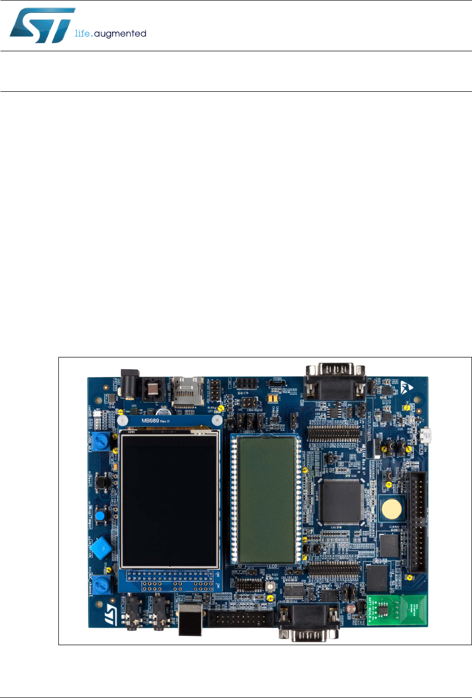
- Figure 1. STM32L476G-EVAL evaluation board
- 1 Overview
- 2 Hardware layout and configuration
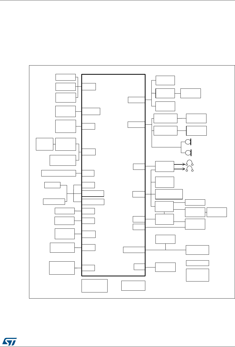
- Figure 2. STM32L476G-EVAL hardware block diagram
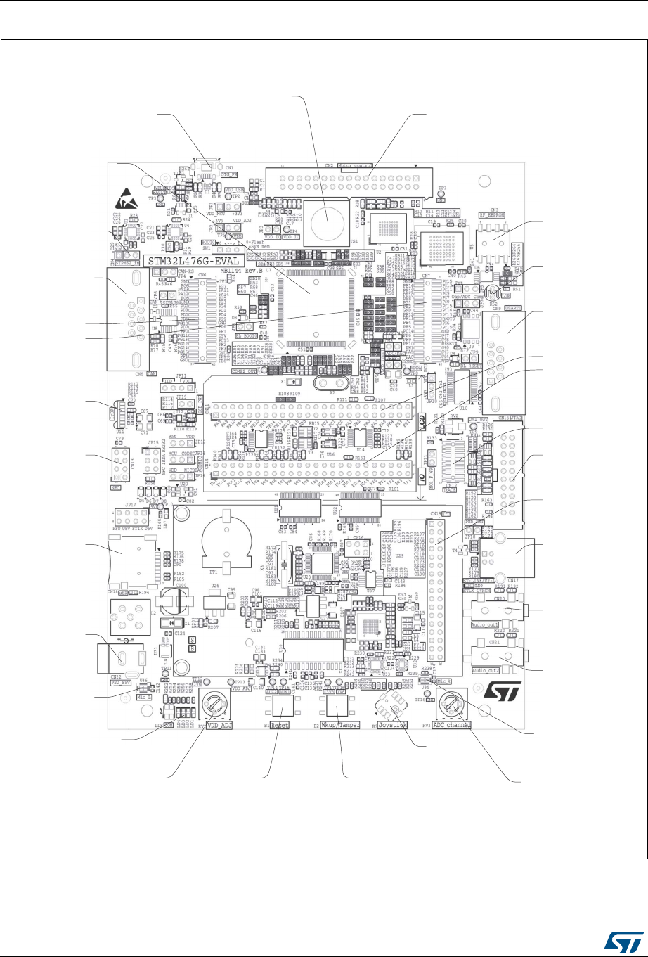
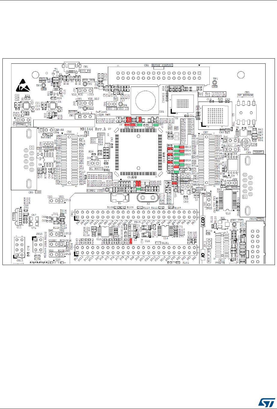
- Figure 3. STM32L476G-EVAL main component layout
- 2.1 ST-LINK/V2-1
- 2.2 ETM trace
- 2.3 Power supply
- 2.4 Clock references
- 2.5 Reset sources
- 2.6 Boot
- 2.7 Audio
- 2.8 USB OTG FS port
- 2.9 RS-232 and IrDA ports
- 2.10 LPUART port
- 2.11 microSD card
- 2.12 Motor control
- 2.13 CAN
- 2.14 Extension connectors CN6 and CN7
- 2.15 LCD glass module daughterboard
- Figure 9. LCD glass module daughterboard in display position
- Figure 10. LCD glass module daughterboard in I/O-bridge position
- Table 14. LCD-daughterboard-related configuration elements (continued)
- Table 15. LCD glass element mapping - segments 0 to 9
- Table 16. LCD glass element mapping - segments 10 to 19
- Table 17. LCD glass element mapping - segments 20 to 29
- Table 18. LCD glass element mapping - segments 30 to 39
- 2.15.1 Limitations
- 2.16 TFT LCD panel
- 2.17 User LEDs
- 2.18 Physical input devices
- 2.19 Operational amplifier and comparator
- 2.20 Analog input, output, VREF
- 2.21 SRAM device
- 2.22 NOR Flash memory device
- 2.23 EEPROM
- 2.24 RF-EEPROM
- 2.25 Quad-SPI Flash memory device
- 2.26 Touch-sensing button
- 2.27 Smartcard, SWP
- 2.28 Near-field communication (NFC)
- 2.29 Dual-channel sigma-delta modulators STPMS2L
- 2.30 STM32L476ZGT6 current consumption measurement
- 3 Connectors
- 3.1 RS-232 D-sub male connector CN9
- 3.2 Power connector CN22
- 3.3 LCD daughterboard connectors CN11 and CN14
- 3.4 Extension connectors CN6 and CN7
- 3.5 ST-LINK/V2-1 programming connector CN16
- 3.6 ST-LINK/V2-1 Standard-B USB connector CN17
- 3.7 JTAG connector CN15
- 3.8 ETM trace debugging connector CN12
- 3.9 microSD card connector CN18
- 3.10 ADC/DAC connector CN8
- 3.11 RF-EEPROM daughterboard connector CN3
- 3.12 Motor control connector CN2
- 3.13 USB OTG FS Micro-AB connector CN1
- 3.14 CAN D-sub male connector CN5
- 3.15 NFC connector CN13
- Appendix A Schematic diagrams
- Figure 32. STM32L476G-EVAL top
- Figure 33. MCU, LCD daughterboard and I/O expander interfaces
- Figure 34. STM32L476G-EVAL MCU part 1
- Figure 35. STM32L476G-EVAL MCU part 2
- Figure 36. LCD glass module daughterboard connectors
- Figure 37. I/O expander
- Figure 38. Power supply
- Figure 39. Smartcard, SWP and NFC
- Figure 40. USART and IrDA
- Figure 41. SRAM and NOR Flash memory devices
- Figure 42. TFT LCD
- Figure 43. Extension connector
- Figure 44. Quad-SPI Flash memory device
- Figure 45. microSD card
- Figure 46. Physical control peripherals
- Figure 47. CAN transceiver
- Figure 48. Touch-sensing device
- Figure 49. USB_OTG_FS port
- Figure 50. IDD measurement
- Figure 51. Audio codec device
- Figure 52. STPMS2L and PT100
- Figure 53. RF-EEPROM and EEPROM
- Figure 54. Motor control connector
- Figure 55. JTAG and trace debug connectors
- Figure 56. ST-LINK/V2-1
- Appendix B Federal Communications Commission (FCC) and Industry Canada (IC) Compliance Statements
- 4 Revision history
November 2016 DocID027351 Rev 5 1/101
1
UM1855
User manual
Evaluation board with STM32L476ZGT6 MCU
Introduction
The STM32L476G-EVAL evaluation board is designed as complete demonstration and
development platform for STMicroelectronics ARM® Cortex®-M4-core-based
STM32L476ZGT6 microcontroller with three I²C buses, three SPI and six USART ports,
CAN port, SWPMI, two SAI ports, 12-bit ADC, 12-bit DAC, LCD driver, internal 128-Kbyte
SRAM and 1-Mbyte Flash memory, Quad-SPI port, touch sensing capability, USB OTG FS
port, LCD controller, flexible memory controller (FMC), JTAG debug port.
STM32L476G-EVAL, shown in Figure 1, is used as reference design for user application
development, although it is not considered as final application.
A full range of hardware features on the board helps users to evaluate all on-board
peripherals such as USB, USART, digital microphones, ADC and DAC, dot-matrix TFT LCD,
LCD glass module, IrDA (supported up to version MB1144 C-01 of the board), LDR, SRAM,
NOR Flash memory device, Quad-SPI Flash memory device, microSD card, sigma-delta
modulators, smartcard with SWP, CAN transceiver, EEPROM, RF-EEPROM. Extension
headers allow connecting daughterboards or wrapping boards.
ST-LINK/V2-1 in-circuit debugger and flashing facility is integrated on the mainboard.
Figure 1. STM32L476G-EVAL evaluation board
1. Picture not contractual.
www.st.com

Contents UM1855
2/101 DocID027351 Rev 5
Contents
1 Overview . . . . . . . . . . . . . . . . . . . . . . . . . . . . . . . . . . . . . . . . . . . . . . . . . . 9
1.1 Features . . . . . . . . . . . . . . . . . . . . . . . . . . . . . . . . . . . . . . . . . . . . . . . . . . . 9
1.2 Demonstration software . . . . . . . . . . . . . . . . . . . . . . . . . . . . . . . . . . . . . . 10
1.3 Order code . . . . . . . . . . . . . . . . . . . . . . . . . . . . . . . . . . . . . . . . . . . . . . . . 10
1.4 Unpacking recommendations . . . . . . . . . . . . . . . . . . . . . . . . . . . . . . . . . . 10
2 Hardware layout and configuration . . . . . . . . . . . . . . . . . . . . . . . . . . . . 11
2.1 ST-LINK/V2-1 . . . . . . . . . . . . . . . . . . . . . . . . . . . . . . . . . . . . . . . . . . . . . . 13
2.1.1 Drivers . . . . . . . . . . . . . . . . . . . . . . . . . . . . . . . . . . . . . . . . . . . . . . . . . . 13
2.1.2 ST-LINK/V2-1 firmware upgrade . . . . . . . . . . . . . . . . . . . . . . . . . . . . . . 14
2.2 ETM trace . . . . . . . . . . . . . . . . . . . . . . . . . . . . . . . . . . . . . . . . . . . . . . . . . 14
2.3 Power supply . . . . . . . . . . . . . . . . . . . . . . . . . . . . . . . . . . . . . . . . . . . . . . 15
2.3.1 Supplying the board through ST-LINK/V2-1 USB port . . . . . . . . . . . . . . 15
2.3.2 Using ST-LINK/2-1 along with powering through CN22 power jack . . . 16
2.4 Clock references . . . . . . . . . . . . . . . . . . . . . . . . . . . . . . . . . . . . . . . . . . . 19
2.5 Reset sources . . . . . . . . . . . . . . . . . . . . . . . . . . . . . . . . . . . . . . . . . . . . . 19
2.6 Boot . . . . . . . . . . . . . . . . . . . . . . . . . . . . . . . . . . . . . . . . . . . . . . . . . . . . . 20
2.6.1 Boot options . . . . . . . . . . . . . . . . . . . . . . . . . . . . . . . . . . . . . . . . . . . . . . 20
2.6.2 Bootloader limitations . . . . . . . . . . . . . . . . . . . . . . . . . . . . . . . . . . . . . . 21
2.7 Audio . . . . . . . . . . . . . . . . . . . . . . . . . . . . . . . . . . . . . . . . . . . . . . . . . . . . 21
2.7.1 Digital microphones . . . . . . . . . . . . . . . . . . . . . . . . . . . . . . . . . . . . . . . . 22
2.7.2 Headphones outputs . . . . . . . . . . . . . . . . . . . . . . . . . . . . . . . . . . . . . . . 22
2.7.3 Limitations in using audio features . . . . . . . . . . . . . . . . . . . . . . . . . . . . 23
2.8 USB OTG FS port . . . . . . . . . . . . . . . . . . . . . . . . . . . . . . . . . . . . . . . . . . 23
2.8.1 STM32L476G-EVAL used as USB device . . . . . . . . . . . . . . . . . . . . . . . 23
2.8.2 STM32L476G-EVAL used as USB host . . . . . . . . . . . . . . . . . . . . . . . . 24
2.8.3 Configuration elements related with USB OTG FS port . . . . . . . . . . . . 24
2.8.4 Limitations in using USB OTG FS port . . . . . . . . . . . . . . . . . . . . . . . . . 25
2.8.5 Operating voltage . . . . . . . . . . . . . . . . . . . . . . . . . . . . . . . . . . . . . . . . . 25
2.9 RS-232 and IrDA ports . . . . . . . . . . . . . . . . . . . . . . . . . . . . . . . . . . . . . . . 25
2.9.1 RS-232 port . . . . . . . . . . . . . . . . . . . . . . . . . . . . . . . . . . . . . . . . . . . . . . 26
2.9.2 IrDA port . . . . . . . . . . . . . . . . . . . . . . . . . . . . . . . . . . . . . . . . . . . . . . . . 26
2.9.3 Limitations . . . . . . . . . . . . . . . . . . . . . . . . . . . . . . . . . . . . . . . . . . . . . . . 26

DocID027351 Rev 5 3/101
UM1855 Contents
5
2.9.4 Operating voltage . . . . . . . . . . . . . . . . . . . . . . . . . . . . . . . . . . . . . . . . . 26
2.10 LPUART port . . . . . . . . . . . . . . . . . . . . . . . . . . . . . . . . . . . . . . . . . . . . . . 27
2.11 microSD card . . . . . . . . . . . . . . . . . . . . . . . . . . . . . . . . . . . . . . . . . . . . . . 27
2.11.1 Limitations . . . . . . . . . . . . . . . . . . . . . . . . . . . . . . . . . . . . . . . . . . . . . . . 27
2.11.2 Operating voltage . . . . . . . . . . . . . . . . . . . . . . . . . . . . . . . . . . . . . . . . . 28
2.12 Motor control . . . . . . . . . . . . . . . . . . . . . . . . . . . . . . . . . . . . . . . . . . . . . . 28
2.12.1 Board modifications to enable motor control . . . . . . . . . . . . . . . . . . . . . 30
2.12.2 Limitations . . . . . . . . . . . . . . . . . . . . . . . . . . . . . . . . . . . . . . . . . . . . . . . 31
2.13 CAN . . . . . . . . . . . . . . . . . . . . . . . . . . . . . . . . . . . . . . . . . . . . . . . . . . . . . 31
2.13.1 Limitations . . . . . . . . . . . . . . . . . . . . . . . . . . . . . . . . . . . . . . . . . . . . . . . 32
2.13.2 Operating voltage . . . . . . . . . . . . . . . . . . . . . . . . . . . . . . . . . . . . . . . . . 32
2.14 Extension connectors CN6 and CN7 . . . . . . . . . . . . . . . . . . . . . . . . . . . . 32
2.15 LCD glass module daughterboard . . . . . . . . . . . . . . . . . . . . . . . . . . . . . . 32
2.15.1 Limitations . . . . . . . . . . . . . . . . . . . . . . . . . . . . . . . . . . . . . . . . . . . . . . . 37
2.16 TFT LCD panel . . . . . . . . . . . . . . . . . . . . . . . . . . . . . . . . . . . . . . . . . . . . . 39
2.17 User LEDs . . . . . . . . . . . . . . . . . . . . . . . . . . . . . . . . . . . . . . . . . . . . . . . . 40
2.18 Physical input devices . . . . . . . . . . . . . . . . . . . . . . . . . . . . . . . . . . . . . . . 40
2.18.1 Limitations . . . . . . . . . . . . . . . . . . . . . . . . . . . . . . . . . . . . . . . . . . . . . . . 41
2.19 Operational amplifier and comparator . . . . . . . . . . . . . . . . . . . . . . . . . . . 41
2.19.1 Operational amplifier . . . . . . . . . . . . . . . . . . . . . . . . . . . . . . . . . . . . . . . 41
2.19.2 Comparator . . . . . . . . . . . . . . . . . . . . . . . . . . . . . . . . . . . . . . . . . . . . . . 42
2.20 Analog input, output, VREF . . . . . . . . . . . . . . . . . . . . . . . . . . . . . . . . . . . 42
2.21 SRAM device . . . . . . . . . . . . . . . . . . . . . . . . . . . . . . . . . . . . . . . . . . . . . . 42
2.21.1 Limitations . . . . . . . . . . . . . . . . . . . . . . . . . . . . . . . . . . . . . . . . . . . . . . . 43
2.21.2 Operating voltage . . . . . . . . . . . . . . . . . . . . . . . . . . . . . . . . . . . . . . . . . 43
2.22 NOR Flash memory device . . . . . . . . . . . . . . . . . . . . . . . . . . . . . . . . . . . 43
2.22.1 Limitations . . . . . . . . . . . . . . . . . . . . . . . . . . . . . . . . . . . . . . . . . . . . . . . 44
2.22.2 Operating voltage . . . . . . . . . . . . . . . . . . . . . . . . . . . . . . . . . . . . . . . . . 44
2.23 EEPROM . . . . . . . . . . . . . . . . . . . . . . . . . . . . . . . . . . . . . . . . . . . . . . . . . 44
2.23.1 Operating voltage . . . . . . . . . . . . . . . . . . . . . . . . . . . . . . . . . . . . . . . . . 44
2.24 RF-EEPROM . . . . . . . . . . . . . . . . . . . . . . . . . . . . . . . . . . . . . . . . . . . . . . 44
2.25 Quad-SPI Flash memory device . . . . . . . . . . . . . . . . . . . . . . . . . . . . . . . 45
2.25.1 Limitations . . . . . . . . . . . . . . . . . . . . . . . . . . . . . . . . . . . . . . . . . . . . . . . 46
2.25.2 Operating voltage . . . . . . . . . . . . . . . . . . . . . . . . . . . . . . . . . . . . . . . . . 46
2.26 Touch-sensing button . . . . . . . . . . . . . . . . . . . . . . . . . . . . . . . . . . . . . . . . 46

Contents UM1855
4/101 DocID027351 Rev 5
2.26.1 Limitations . . . . . . . . . . . . . . . . . . . . . . . . . . . . . . . . . . . . . . . . . . . . . . . 48
2.27 Smartcard, SWP . . . . . . . . . . . . . . . . . . . . . . . . . . . . . . . . . . . . . . . . . . . . 48
2.27.1 Limitations . . . . . . . . . . . . . . . . . . . . . . . . . . . . . . . . . . . . . . . . . . . . . . . 50
2.27.2 Operating voltage . . . . . . . . . . . . . . . . . . . . . . . . . . . . . . . . . . . . . . . . . 50
2.28 Near-field communication (NFC) . . . . . . . . . . . . . . . . . . . . . . . . . . . . . . . 50
2.29 Dual-channel sigma-delta modulators STPMS2L . . . . . . . . . . . . . . . . . . 51
2.29.1 STPMS2L presentation . . . . . . . . . . . . . . . . . . . . . . . . . . . . . . . . . . . . . 51
2.29.2 STPMS2L settings . . . . . . . . . . . . . . . . . . . . . . . . . . . . . . . . . . . . . . . . 52
2.29.3 STPMS2L power metering . . . . . . . . . . . . . . . . . . . . . . . . . . . . . . . . . . . 52
2.29.4 STPMS2L for PT100 measurement . . . . . . . . . . . . . . . . . . . . . . . . . . . . 54
2.29.5 Limitations . . . . . . . . . . . . . . . . . . . . . . . . . . . . . . . . . . . . . . . . . . . . . . . 54
2.30 STM32L476ZGT6 current consumption measurement . . . . . . . . . . . . . . 54
2.30.1 IDD measurement principle - analog part . . . . . . . . . . . . . . . . . . . . . . . 55
2.30.2 Low-power-mode IDD measurement principle - logic part . . . . . . . . . . . 56
2.30.3 IDD measurement in dynamic run mode . . . . . . . . . . . . . . . . . . . . . . . . 58
2.30.4 Calibration procedure . . . . . . . . . . . . . . . . . . . . . . . . . . . . . . . . . . . . . . 58
3 Connectors . . . . . . . . . . . . . . . . . . . . . . . . . . . . . . . . . . . . . . . . . . . . . . . 60
3.1 RS-232 D-sub male connector CN9 . . . . . . . . . . . . . . . . . . . . . . . . . . . . . 60
3.2 Power connector CN22 . . . . . . . . . . . . . . . . . . . . . . . . . . . . . . . . . . . . . . 60
3.3 LCD daughterboard connectors CN11 and CN14 . . . . . . . . . . . . . . . . . . 61
3.4 Extension connectors CN6 and CN7 . . . . . . . . . . . . . . . . . . . . . . . . . . . . 62
3.5 ST-LINK/V2-1 programming connector CN16 . . . . . . . . . . . . . . . . . . . . . 65
3.6 ST-LINK/V2-1 Standard-B USB connector CN17 . . . . . . . . . . . . . . . . . . . 65
3.7 JTAG connector CN15 . . . . . . . . . . . . . . . . . . . . . . . . . . . . . . . . . . . . . . 66
3.8 ETM trace debugging connector CN12 . . . . . . . . . . . . . . . . . . . . . . . . . . 67
3.9 microSD card connector CN18 . . . . . . . . . . . . . . . . . . . . . . . . . . . . . . . . . 68
3.10 ADC/DAC connector CN8 . . . . . . . . . . . . . . . . . . . . . . . . . . . . . . . . . . . . 68
3.11 RF-EEPROM daughterboard connector CN3 . . . . . . . . . . . . . . . . . . . . . 69
3.12 Motor control connector CN2 . . . . . . . . . . . . . . . . . . . . . . . . . . . . . . . . . . 69
3.13 USB OTG FS Micro-AB connector CN1 . . . . . . . . . . . . . . . . . . . . . . . . . . 70
3.14 CAN D-sub male connector CN5 . . . . . . . . . . . . . . . . . . . . . . . . . . . . . . . 71
3.15 NFC connector CN13 . . . . . . . . . . . . . . . . . . . . . . . . . . . . . . . . . . . . . . . . 71
Appendix A Schematic diagrams . . . . . . . . . . . . . . . . . . . . . . . . . . . . . . . . . . . . . 73

DocID027351 Rev 5 5/101
UM1855 Contents
5
Appendix B Federal Communications Commission (FCC)
and Industry Canada (IC) Compliance Statements. . . . . . . . . . . . . 99
B.1 FCC Compliance Statement . . . . . . . . . . . . . . . . . . . . . . . . . . . . . . . . . . . 99
B.1.1 Part 15.19 . . . . . . . . . . . . . . . . . . . . . . . . . . . . . . . . . . . . . . . . . . . . . . . . 99
B.1.2 Part 15.105 . . . . . . . . . . . . . . . . . . . . . . . . . . . . . . . . . . . . . . . . . . . . . . . 99
B.1.3 Part 15.21 . . . . . . . . . . . . . . . . . . . . . . . . . . . . . . . . . . . . . . . . . . . . . . . . 99
B.2 IC Compliance Statement . . . . . . . . . . . . . . . . . . . . . . . . . . . . . . . . . . . . . 99
B.2.1 Compliance Statement . . . . . . . . . . . . . . . . . . . . . . . . . . . . . . . . . . . . . . 99
B.2.2 Déclaration de conformité. . . . . . . . . . . . . . . . . . . . . . . . . . . . . . . . . . . . 99
4 Revision history . . . . . . . . . . . . . . . . . . . . . . . . . . . . . . . . . . . . . . . . . . 100

List of tables UM1855
6/101 DocID027351 Rev 5
List of tables
Table 1. Setting of configuration elements for trace connector CN12 . . . . . . . . . . . . . . . . . . . . . . . 14
Table 2. Power-supply-related jumper settings . . . . . . . . . . . . . . . . . . . . . . . . . . . . . . . . . . . . . . . . 17
Table 3. X1-crystal-related solder bridge settings . . . . . . . . . . . . . . . . . . . . . . . . . . . . . . . . . . . . . . 19
Table 4. X2-crystal-related solder bridge settings . . . . . . . . . . . . . . . . . . . . . . . . . . . . . . . . . . . . . . 19
Table 5. Boot selection switch . . . . . . . . . . . . . . . . . . . . . . . . . . . . . . . . . . . . . . . . . . . . . . . . . . . . . 20
Table 6. Bootloader-related jumper setting. . . . . . . . . . . . . . . . . . . . . . . . . . . . . . . . . . . . . . . . . . . . 20
Table 7. Digital microphone-related jumper settings . . . . . . . . . . . . . . . . . . . . . . . . . . . . . . . . . . . . 22
Table 8. Configuration elements related with USB OTG FS port . . . . . . . . . . . . . . . . . . . . . . . . . . . 24
Table 9. Settings of configuration elements for RS-232 and IrDA ports . . . . . . . . . . . . . . . . . . . . . . 26
Table 10. Hardware settings for LPUART . . . . . . . . . . . . . . . . . . . . . . . . . . . . . . . . . . . . . . . . . . . . . 27
Table 11. Terminals of CN18 microSD slot . . . . . . . . . . . . . . . . . . . . . . . . . . . . . . . . . . . . . . . . . . . . 27
Table 12. Motor control terminal and function assignment . . . . . . . . . . . . . . . . . . . . . . . . . . . . . . . . . 28
Table 13. CAN related jumpers . . . . . . . . . . . . . . . . . . . . . . . . . . . . . . . . . . . . . . . . . . . . . . . . . . . . . 32
Table 14. LCD-daughterboard-related configuration elements. . . . . . . . . . . . . . . . . . . . . . . . . . . . . . 34
Table 15. LCD glass element mapping - segments 0 to 9 . . . . . . . . . . . . . . . . . . . . . . . . . . . . . . . . . 36
Table 16. LCD glass element mapping - segments 10 to 19 . . . . . . . . . . . . . . . . . . . . . . . . . . . . . . . 36
Table 17. LCD glass element mapping - segments 20 to 29 . . . . . . . . . . . . . . . . . . . . . . . . . . . . . . . 36
Table 18. LCD glass element mapping - segments 30 to 39 . . . . . . . . . . . . . . . . . . . . . . . . . . . . . . . 37
Table 19. Access to TFT LCD resources with FMC address lines A0 and A1 . . . . . . . . . . . . . . . . . . 39
Table 20. Assignment of CN19 connector terminals of TFT LCD panel. . . . . . . . . . . . . . . . . . . . . . . 39
Table 21. Port assignment for control of LED indicators . . . . . . . . . . . . . . . . . . . . . . . . . . . . . . . . . . 40
Table 22. Port assignment for control of physical input devices. . . . . . . . . . . . . . . . . . . . . . . . . . . . . 40
Table 23. Setting of jumpers related with potentiometer and LDR . . . . . . . . . . . . . . . . . . . . . . . . . . . 41
Table 24. SRAM chip select configuration . . . . . . . . . . . . . . . . . . . . . . . . . . . . . . . . . . . . . . . . . . . . . 43
Table 25. NOR Flash memory-related configuration elements. . . . . . . . . . . . . . . . . . . . . . . . . . . . . . 44
Table 26. Configuration elements related with Quad-SPI device . . . . . . . . . . . . . . . . . . . . . . . . . . . . 45
Table 27. Touch-sensing-related configuration elements. . . . . . . . . . . . . . . . . . . . . . . . . . . . . . . . . . 47
Table 28. Assignment of ports for ST8024CDR control . . . . . . . . . . . . . . . . . . . . . . . . . . . . . . . . . . . 48
Table 29. Configuration elements related with smartcard and SWP . . . . . . . . . . . . . . . . . . . . . . . . . 49
Table 30. CN13 NFC connector terminal assignment . . . . . . . . . . . . . . . . . . . . . . . . . . . . . . . . . . . . 51
Table 31. JP11 jumper settings during IDD measurement with calibration . . . . . . . . . . . . . . . . . . . . 59
Table 32. RS-232 D-sub (DE-9M) connector CN9 with HW flow control and ISP support . . . . . . . . . 60
Table 33. CN11 and CN14 daughterboard connectors . . . . . . . . . . . . . . . . . . . . . . . . . . . . . . . . . . . 61
Table 34. Daughterboard extension connector CN6 . . . . . . . . . . . . . . . . . . . . . . . . . . . . . . . . . . . . . 62
Table 35. Daughterboard extension connector CN7 . . . . . . . . . . . . . . . . . . . . . . . . . . . . . . . . . . . . . 63
Table 36. USB Standard-B connector CN17 . . . . . . . . . . . . . . . . . . . . . . . . . . . . . . . . . . . . . . . . . . . 66
Table 37. JATG debugging connector CN15 . . . . . . . . . . . . . . . . . . . . . . . . . . . . . . . . . . . . . . . . . . . 66
Table 38. Trace debugging connector CN12 . . . . . . . . . . . . . . . . . . . . . . . . . . . . . . . . . . . . . . . . . . . 67
Table 39. microSD card connector CN18 . . . . . . . . . . . . . . . . . . . . . . . . . . . . . . . . . . . . . . . . . . . . . . 68
Table 40. Analog input-output connector CN8 . . . . . . . . . . . . . . . . . . . . . . . . . . . . . . . . . . . . . . . . . . 69
Table 41. RF-EEPROM daughterboard connector CN3. . . . . . . . . . . . . . . . . . . . . . . . . . . . . . . . . . . 69
Table 42. Motor control connector CN2 . . . . . . . . . . . . . . . . . . . . . . . . . . . . . . . . . . . . . . . . . . . . . . . 70
Table 43. USB OTG FS Micro-AB connector CN1 . . . . . . . . . . . . . . . . . . . . . . . . . . . . . . . . . . . . . . . 70
Table 44. CAN D-sub (DE-9M) 9-pins male connector CN5. . . . . . . . . . . . . . . . . . . . . . . . . . . . . . . . 71
Table 45. NFC CN13 terminal assignment . . . . . . . . . . . . . . . . . . . . . . . . . . . . . . . . . . . . . . . . . . . . . 71
Table 46. Document revision history . . . . . . . . . . . . . . . . . . . . . . . . . . . . . . . . . . . . . . . . . . . . . . . . 100

DocID027351 Rev 5 7/101
UM1855 List of figures
8
List of figures
Figure 1. STM32L476G-EVAL evaluation board . . . . . . . . . . . . . . . . . . . . . . . . . . . . . . . . . . . . . . . . . 1
Figure 2. STM32L476G-EVAL hardware block diagram . . . . . . . . . . . . . . . . . . . . . . . . . . . . . . . . . . 11
Figure 3. STM32L476G-EVAL main component layout. . . . . . . . . . . . . . . . . . . . . . . . . . . . . . . . . . . 12
Figure 4. USB composite device . . . . . . . . . . . . . . . . . . . . . . . . . . . . . . . . . . . . . . . . . . . . . . . . . . . . 13
Figure 5. CN22 power jack polarity . . . . . . . . . . . . . . . . . . . . . . . . . . . . . . . . . . . . . . . . . . . . . . . . . . 16
Figure 6. CN20, CN21 top view . . . . . . . . . . . . . . . . . . . . . . . . . . . . . . . . . . . . . . . . . . . . . . . . . . . . . 23
Figure 7. PCB top-side rework for motor control . . . . . . . . . . . . . . . . . . . . . . . . . . . . . . . . . . . . . . . . 30
Figure 8. PCB underside rework for motor control. . . . . . . . . . . . . . . . . . . . . . . . . . . . . . . . . . . . . . . 31
Figure 9. LCD glass module daughterboard in display position. . . . . . . . . . . . . . . . . . . . . . . . . . . . . 33
Figure 10. LCD glass module daughterboard in I/O-bridge position . . . . . . . . . . . . . . . . . . . . . . . . . . 34
Figure 11. LCD glass display element mapping . . . . . . . . . . . . . . . . . . . . . . . . . . . . . . . . . . . . . . . . . 38
Figure 12. NFC board plugged into STM32L476G-EVAL board . . . . . . . . . . . . . . . . . . . . . . . . . . . . . 50
Figure 13. Routing of STPMS2L dual-channel sigma-delta modulators . . . . . . . . . . . . . . . . . . . . . . . 52
Figure 14. Power measurement principle schematic diagram . . . . . . . . . . . . . . . . . . . . . . . . . . . . . . . 53
Figure 15. STPMS2L power metering schematic diagram. . . . . . . . . . . . . . . . . . . . . . . . . . . . . . . . . . 53
Figure 16. Temperature measurement principle schematic diagram. . . . . . . . . . . . . . . . . . . . . . . . . . 54
Figure 17. Schematic diagram of the analog part of IDD measurement . . . . . . . . . . . . . . . . . . . . . . . 56
Figure 18. Schematic diagram of logic part of low-power-mode IDD measurement . . . . . . . . . . . . . . 57
Figure 19. Low-power-mode IDD measurement timing . . . . . . . . . . . . . . . . . . . . . . . . . . . . . . . . . . . . 58
Figure 20. RS-232 D-sub (DE-9M) 9-pole connector (front view) . . . . . . . . . . . . . . . . . . . . . . . . . . . . 60
Figure 21. Power supply connector CN22 (front view) . . . . . . . . . . . . . . . . . . . . . . . . . . . . . . . . . . . . 60
Figure 22. USB type B connector CN17 (front view) . . . . . . . . . . . . . . . . . . . . . . . . . . . . . . . . . . . . . . 65
Figure 23. JTAG debugging connector CN15 (top view) . . . . . . . . . . . . . . . . . . . . . . . . . . . . . . . . . . . 66
Figure 24. Trace debugging connector CN12 (top view) . . . . . . . . . . . . . . . . . . . . . . . . . . . . . . . . . . . 67
Figure 25. microSD card connector CN18 . . . . . . . . . . . . . . . . . . . . . . . . . . . . . . . . . . . . . . . . . . . . . . 68
Figure 26. Analog input-output connector CN8 (top view) . . . . . . . . . . . . . . . . . . . . . . . . . . . . . . . . . . 68
Figure 27. RF-EEPROM daughterboard connector CN3 (front view) . . . . . . . . . . . . . . . . . . . . . . . . . 69
Figure 28. Motor control connector CN2 (top view) . . . . . . . . . . . . . . . . . . . . . . . . . . . . . . . . . . . . . . . 69
Figure 29. USB OTG FS Micro-AB connector CN1 (front view). . . . . . . . . . . . . . . . . . . . . . . . . . . . . . 70
Figure 30. CAN D-sub (DE-9M) 9-pole male connector CN5 (front view) . . . . . . . . . . . . . . . . . . . . . . 71
Figure 31. NFC female connector CN13 (top view) . . . . . . . . . . . . . . . . . . . . . . . . . . . . . . . . . . . . . . . 71
Figure 32. STM32L476G-EVAL top . . . . . . . . . . . . . . . . . . . . . . . . . . . . . . . . . . . . . . . . . . . . . . . . . . . 74
Figure 33. MCU, LCD daughterboard and I/O expander interfaces. . . . . . . . . . . . . . . . . . . . . . . . . . . 75
Figure 34. STM32L476G-EVAL MCU part 1 . . . . . . . . . . . . . . . . . . . . . . . . . . . . . . . . . . . . . . . . . . . . 76
Figure 35. STM32L476G-EVAL MCU part 2 . . . . . . . . . . . . . . . . . . . . . . . . . . . . . . . . . . . . . . . . . . . . 77
Figure 36. LCD glass module daughterboard connectors . . . . . . . . . . . . . . . . . . . . . . . . . . . . . . . . . 78
Figure 37. I/O expander . . . . . . . . . . . . . . . . . . . . . . . . . . . . . . . . . . . . . . . . . . . . . . . . . . . . . . . . . . . . 79
Figure 38. Power supply . . . . . . . . . . . . . . . . . . . . . . . . . . . . . . . . . . . . . . . . . . . . . . . . . . . . . . . . . . . 80
Figure 39. Smartcard, SWP and NFC . . . . . . . . . . . . . . . . . . . . . . . . . . . . . . . . . . . . . . . . . . . . . . . . . 81
Figure 40. USART and IrDA . . . . . . . . . . . . . . . . . . . . . . . . . . . . . . . . . . . . . . . . . . . . . . . . . . . . . . . . 82
Figure 41. SRAM and NOR Flash memory devices. . . . . . . . . . . . . . . . . . . . . . . . . . . . . . . . . . . . . . . 83
Figure 42. TFT LCD . . . . . . . . . . . . . . . . . . . . . . . . . . . . . . . . . . . . . . . . . . . . . . . . . . . . . . . . . . . . . . . 84
Figure 43. Extension connector . . . . . . . . . . . . . . . . . . . . . . . . . . . . . . . . . . . . . . . . . . . . . . . . . . . . . . 85
Figure 44. Quad-SPI Flash memory device. . . . . . . . . . . . . . . . . . . . . . . . . . . . . . . . . . . . . . . . . . . . . 86
Figure 45. microSD card . . . . . . . . . . . . . . . . . . . . . . . . . . . . . . . . . . . . . . . . . . . . . . . . . . . . . . . . . . . 87
Figure 46. Physical control peripherals . . . . . . . . . . . . . . . . . . . . . . . . . . . . . . . . . . . . . . . . . . . . . . . . 88
Figure 47. CAN transceiver . . . . . . . . . . . . . . . . . . . . . . . . . . . . . . . . . . . . . . . . . . . . . . . . . . . . . . . . . 89
Figure 48. Touch-sensing device. . . . . . . . . . . . . . . . . . . . . . . . . . . . . . . . . . . . . . . . . . . . . . . . . . . . . 90

List of figures UM1855
8/101 DocID027351 Rev 5
Figure 49. USB_OTG_FS port. . . . . . . . . . . . . . . . . . . . . . . . . . . . . . . . . . . . . . . . . . . . . . . . . . . . . . . 91
Figure 50. IDD measurement. . . . . . . . . . . . . . . . . . . . . . . . . . . . . . . . . . . . . . . . . . . . . . . . . . . . . . . . 92
Figure 51. Audio codec device. . . . . . . . . . . . . . . . . . . . . . . . . . . . . . . . . . . . . . . . . . . . . . . . . . . . . . . 93
Figure 52. STPMS2L and PT100. . . . . . . . . . . . . . . . . . . . . . . . . . . . . . . . . . . . . . . . . . . . . . . . . . . . . 94
Figure 53. RF-EEPROM and EEPROM. . . . . . . . . . . . . . . . . . . . . . . . . . . . . . . . . . . . . . . . . . . . . . . . 95
Figure 54. Motor control connector . . . . . . . . . . . . . . . . . . . . . . . . . . . . . . . . . . . . . . . . . . . . . . . . . . . 96
Figure 55. JTAG and trace debug connectors . . . . . . . . . . . . . . . . . . . . . . . . . . . . . . . . . . . . . . . . . . . 97
Figure 56. ST-LINK/V2-1 . . . . . . . . . . . . . . . . . . . . . . . . . . . . . . . . . . . . . . . . . . . . . . . . . . . . . . . . . . . 98

DocID027351 Rev 5 9/101
UM1855 Overview
100
1 Overview
1.1 Features
•STM32L476ZGT6 microcontroller with 1-Mbyte Flash memory and 128-Kbyte RAM
•Four power supply options: power jack, ST-LINK/V2-1 USB connector, USB OTG FS
connector, daughterboard
•Microcontroller supply voltage: 3.3 V or range from 1.71 V to 3.6 V
•Two MEMS digital microphones
•Two jack outputs for stereo audio headphone with independent content
•Slot for microSD card supporting SD, SDHC, SDXC
•4-Gbyte microSD card bundled
•16-Mbit (1M x 16 bit) SRAM device
•128-Mbit (8M x 16 bit) NOR Flash memory device
•256-Mbit Quad-SPI Flash memory device with double transfer rate (DTR) support
•RF-EEPROM with I²C bus
•EEPROM supporting 1 MHz I²C-bus communication speed
•RS-232 port configurable for communication or MCU flashing
•IrDA transceiver (only supported up to MB1144 C-01 version of the board, no more
supported from MB1144 C-02 version)
•USB OTG FS Micro-AB port
•CAN 2.0A/B-compliant port
•Joystick with four-way controller and selector
•Reset and wake-up / tamper buttons
•Touch-sensing button
•Light-dependent resistor (LDR)
•Potentiometer
•Coin battery cell for power backup
•LCD glass module daughterboard (MB979) with 40x8-segment LCD driven directly by
STM32L476ZGT6
•2.8-inch 320x240 dot-matrix color TFT LCD panel with resistive touchscreen
•Smartcard connector and SWP support
•NFC transceiver connector
•Connector for ADC input and DAC output
•Power-metering demonstration with dual-channel, sigma-delta modulator
•PT100 thermal sensor with dual-channel, sigma-delta modulator
•MCU current consumption measurement circuit
•Access to comparator and operational amplifier of STM32L476ZGT6
•Extension connector for motor control module
•JTAG/SWD, ETM trace debug support, user interface through USB virtual COM port,
embedded ST-LINK/V2-1 debug and flashing facility
•Extension connector for daughterboard

Overview UM1855
10/101 DocID027351 Rev 5
1.2 Demonstration software
Demonstration software is preloaded in the STM32L476ZGT6 Flash memory, for easy
demonstration of the device peripherals in stand-alone mode. For more information and to
download the latest available version, refer to the STM32L476G-EVAL demonstration
software available on the www.st.com website.
1.3 Order code
To order the evaluation board based on the STM32L476ZGT6 MCU, use the order code
STM32L476G-EVAL.
1.4 Unpacking recommendations
Before the first use, make sure that, no damage occurred to the board during shipment and
no socketed components are loosen in their sockets or fallen into the plastic bag.
In particular, pay attention to the following components:
1. Quartz crystal (X2 position)
2. microSD card in its CN18 receptacle
3. RF-EEPROM board (ANT7-M24LR-A) in its CN3 connector
For product information related with STM32L476ZGT6 microcontroller, visit www.st.com
website.
DocID027351 Rev 5 11/101
UM1855 Hardware layout and configuration
100
2 Hardware layout and configuration
The STM32L476G-EVAL evaluation board is designed around STM32L476ZGT6 target
microcontroller in LQFP 144-pin package. Figure 2 illustrates STM32L476ZGT6
connections with peripheral components. Figure 3 shows the location of main components
on the evaluation board.
Figure 2. STM32L476G-EVAL hardware block diagram
Note: If the STM32L476G-EVAL board version is greater than or equal to MB1144 C-02, the IrDA
feature is not populated. Any mention of the IrDA feature in this User manual refers to the
previous versions of the board (up to MB1144 C-01). The version of the board is written on
the sticker placed on bottom side of the board.
06Y9
*3,2
,&
86$57
-7$*
3RWHQWLRPHWHU -R\VWLFN
/('
.H\
EXWWRQ
5)((3520
FRQQHFWRU
56
WUDQVFHLYHU
,U'$
WUDQVFHLYHU
56
FRQQHFWRU
6$, $XGLR
FRGHF
67/,1.9
6WDQGDUG%
86%
FRQQHFWRU
-7$*WUDFHDQG
6:'FRQQHFWRUV
([WHQVLRQ
FRQQHFWRUVIRU
*3,2V
WZRVWHUHR
KHDGSKRQH
RXWSXWV
670/=*7
&$1WUDQVFHLYHU
DQGFRQQHFWRU &$1
0RWRUFRQWURO
FRQQHFWRU
&RPSDUDWRU
6',2
PLFUR6'
FDUG
)0&
57& %DWWHU\
*3,2
,2
([SDQGHU
65$0
125)ODVK
PHPRU\
86%27*)6 86%0LFUR$%
FRQQHFWRU
86%SRZHU
VZLWFK
¶¶FRORU
7)7/&'
/&'
0LIDUH
FRQQHFWRU
6PDUWFDUG
ZLWK6:3
6:3
*3,2 6PDUWFDUG
LQWHUIDFH
/'5
2S$PS
$'&
((3520
/&'J/DVV
PRGXOH
[
7)7/&'
FRQWUROOHU
')6'0
WZRGLJLWDO0(06
PLFURSKRQHV
4XDG63,
)ODVKP(PRU\
GHYLFH
48$'63,
76&
7RXFKVHQVLQJEXWWRQ
6LJPDGHOWD
PRGXODWRU
37
VHQVRU
3RZHUPHWHU
0&8
VXSSO\FXUUHQW
PHDVXUHPHQW
9UHJXODWRU
WR9
DGMXVWDEOH
UHJXODWRU
6LJPDGHOWD
PRGXODWRU
7)7/&'
WRXFKVFUHHQ
*3,2
Hardware layout and configuration UM1855
12/101 DocID027351 Rev 5
Figure 3. STM32L476G-EVAL main component layout
06Y9
59
3RWHQWLRPHWHU
8ULJKW
PLFURSKRQH
&1
+HDGSKRQHV
MDFN
&1
+HDGSKRQHV
MDFN
6WDQGDUG%
86%SRUWRI
67/,1.9
&1
-7$*
&17UDFH
&1
&1
/&'JODVVPRGXOH
GDXJKWHUERDUG
'%
&1
86$57
5
/'5
&1
5)((3520
&1
0RWRUFRQWURO
76
7RXFKVHQVLQJ
EXWWRQ
&1
86%27*SRUW
8
670/=*7
&1
6LJPDGHOWDLQ
&1
&$1
&1
&1
([WHQVLRQ
FRQQHFWRUV
8
,U'$
&1
1)&
&1
7)7/&'
&1
PLFUR6'FDUG
&1
3RZHUMDFN
8OHIW
PLFURSKRQH
)RXU/('V
59
9''VHWWLQJ
%
5HVHWEXWWRQ
%
:DNHXSWDPSHU
EXWWRQ
%
-R\VWLFN
DocID027351 Rev 5 13/101
UM1855 Hardware layout and configuration
100
2.1 ST-LINK/V2-1
ST-LINK/V2-1 facility for debug and flashing of STM32L476ZGT6, is integrated on the
STM32L476G-EVAL evaluation board.
Compared to ST-LINK/V2 stand-alone tool available from STMicroelectronics,
ST-LINK/V2-1 offers new features and drops some others.
New features:
•USB software re-enumeration
•Virtual COM port interface on USB
•Mass storage interface on USB
•USB power management request for more than 100mA power on USB
Features dropped:
•SWIM interface
The USB connector CN17 can be used to power STM32L476G-EVAL regardless of
the ST-LINK/V2-1 facility use for debugging or for flashing STM32L476ZGT6. This holds
also when ST-LINK/V2 stand-alone tool is connected to CN12 or CN15 connector and used
for debugging or flashing STM32L476ZGT6. Section 2.3 provides more detail on powering
STM32L476G-EVAL.
For full detail on both versions of the debug and flashing tool, the stand-alone ST-LINK/V2
and the embedded ST-LINK/V2-1, refer to www.st.com.
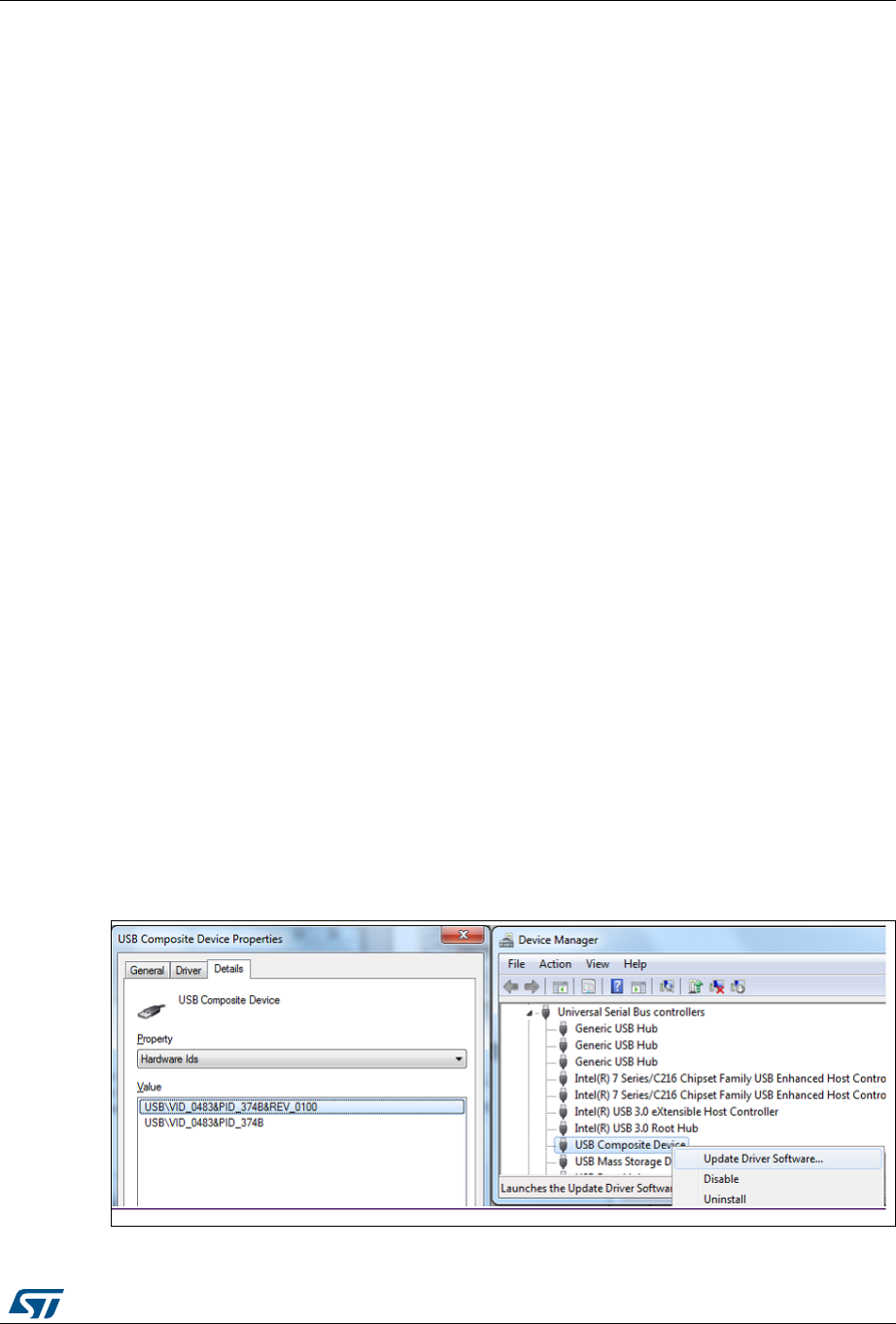
2.1.1 Drivers
Before connecting STM32L476G-EVAL to a Windows 7, Windows 8 or Windows XP PC via
USB, a driver for ST-LINK/V2-1 must be installed. It can be downloaded from www.st.com.
In case the STM32L476G-EVAL evaluation board is connected to the PC before installing
the driver, the Windows device manager may report some USB devices found on
STM32L476G-EVAL as “Unknown”. To recover from this situation, after installing the
dedicated driver downloaded from www.st.com, the association of “Unknown” USB devices
found on STM32L476G-EVAL to this dedicated driver must be updated in the device
manager manually. It is recommended to proceed using USB Composite Device line, as
shown in Figure 4.
Figure 4. USB composite device
Hardware layout and configuration UM1855
14/101 DocID027351 Rev 5
2.1.2 ST-LINK/V2-1 firmware upgrade
For its own operation, ST-LINK/V2-1 employs a dedicated MCU with Flash memory. Its
firmware determines ST-LINK/V2-1 functionality and performance. The firmware may evolve
during the life span of STM32L476G-EVAL to include new functionality, fix bugs or support
new target microcontroller families. It is therefore recommended to keep ST-LINK/V2-1
firmware up to date. The latest version is available from www.st.com.
2.2 ETM trace
The connector CN12 can output trace signals used for debug. By default, the evaluation
board is configured such that, STM32L476ZGT6 signals PE2 through PE5 are not
connected to trace outputs Trace_D0, Trace_D1, Trace_D2, Trace_D3 and Trace_CK of
CN12. They are used for other functions.
Table 1 shows the setting of configuration elements to shunt PE2, PE3, PE4 and PE5 MCU
ports to CN12 connector, to use them as debug trace signals.
Warning: Enabling the CN12 trace outputs through hardware modifications described in
Table 1 results in reducing the memory address bus width to 19 address lines and so the
addressable space to 512 Kwords of 16 bits. As a consequence, the on-board SRAM and
NOR Flash memory usable capacity is reduced to 8 Mbits.
Table 1. Setting of configuration elements for trace connector CN12
Element Setting Use of PE2, PE3, PE4, PE5 terminals of STM32L476ZGT6
R103
SB26
R103 in
SB26 open
Default setting.
PE2 connected to LCDSEG38 and memory address line A23.
R103 out
SB26 closed PE2 connected to TRACE_CK on CN12. A23 pulled down.
R104
R104 in Default setting.
PE3 connected to LCDSEG39 and memory address line A19.
R104 out PE3 connected to TRACE_D0 on CN12. A19 pulled down.
R84
SB40
R84 in
SB40 open
Default setting.
PE4 connected to memory address line A20.
R84 out
SB40 closed PE4 connected to TRACE_D1 on CN12. A20 pulled down.
R85
SB38
R85 in
SB38 open
Default setting.
PE5 connected to memory address line A21.
R85 out
SB38 closed PE5 connected to TRACE_D2 on CN12. A21 pulled down.
R86
SB39
R86 in
SB39 open
Default setting.
PE6 is used for address bit A22.
R86 out
SB39 closed PE6 connected to TRACE_D3 on CN12. A22 pulled down.

DocID027351 Rev 5 15/101
UM1855 Hardware layout and configuration
100
2.3 Power supply
STM32L476G-EVAL evaluation board is designed to be powered from 5 V DC power
source. It incorporates a precise polymer Zener diode (Poly-Zen) protecting the board from
damage due to wrong power supply. One of the following four 5V DC power inputs can be
used, upon an appropriate board configuration:
•Power jack CN22, marked PSU_E5V on the board. A jumper must be placed in PSU
location of JP17. The positive pole is on the center pin as illustrated in Figure 5.
•Standard-B USB receptacle CN17 of ST-LINK/V2-1, offering enumeration feature
described in Section 2.3.1.
•Micro-AB USB receptacle CN1 of USB OTG interface, marked OTG_FS on the board.
Up to 500mA can be supplied to the board in this way.
•Pin 28 of CN6 extension connector for custom daughterboards, marked D5V on the
board.
No external power supply is provided with the board.
LD7 red LED turns on when the voltage on the power line marked as +5V is present. All
supply lines required for the operation of the components on STM32L476G-EVAL are
derived from that +5V line.
Table 2 describes the settings of all jumpers related with powering STM32L476G-EVAL and
extension board. VDD_MCU is STM32L476ZGT6 digital supply voltage line. It can be
connected to either fixed 3.3 V or to an adjustable voltage regulator controlled with RV1
potentiometer and producing a range of voltages between 1.71 V and 3.6 V.
2.3.1 Supplying the board through ST-LINK/V2-1 USB port
To power STM32L476G-EVAL in this way, the USB host (a PC) gets connected with the
STM32L476G-EVAL board’s Standard-B USB receptacle, via a USB cable. This event starts
the USB enumeration procedure. In its initial phase, the host’s USB port current supply
capability is limited to 100 mA. It is enough because only ST-LINK/V2-1 part of
STM32L476G-EVAL draws power at that time. If the jumper header JP18 is open, the U37
ST890 power switch is set to OFF position, which isolates the remainder of
STM32L476G-EVAL from the power source. In the next phase of the enumeration
procedure, the host PC informs the ST-LINK/V2-1 facility of its capability to supply up to
300 mA of current. If the answer is positive, the ST-LINK/V2-1 sets the U37 ST890 switch to
ON position to supply power to the remainder of the STM32L476G-EVAL board. If the PC
USB port is not capable of supplying up to 300 mA of current, the CN22 power jack can be
used to supply the board.
Should a short-circuit occur on the board, the ST890 power switch protects the USB port of
the host PC against a current demand exceeding 600 mA, In such an event, the LD9 LED
lights on.
The STM32L476G-EVAL board can also be supplied from a USB power source not
supporting enumeration, such as a USB charger. In this particular case, the JP18 header
must be fitted with a jumper as shown in Table 2. ST-LINK/V2-1 turns the ST890 power
switch ON regardless of enumeration procedure result and passes the power
unconditionally to the board.
The LD7 red LED turns on whenever the whole board is powered.
Hardware layout and configuration UM1855
16/101 DocID027351 Rev 5
2.3.2 Using ST-LINK/2-1 along with powering through CN22 power jack
It can happen that the board requires more than 300 mA of supply current. It cannot be
supplied from host PC connected to ST-LINK/2-1 USB port for debugging or flashing
STM32L476ZGT6. In such a case, the board can be supplied through CN22 (marked PSU
_E5V on the board).
To do this, it is important to power the board before connecting it with the host PC, which
requires the following sequence to be respected:
1. Set the jumper in JP15 header in PSU position
2. Connect the external 5 V power source to CN22
3. Check the red LED LD7 is turned on
4. Connect host PC to USB connector CN17
In case the board demands more than 300 mA and the host PC is connected via USB
before the board is powered from CN22, there is a risk of the following events to occur, in
the order of severity:
1. The host PC is capable of supplying 300 mA (the enumeration succeeds) but it does
not incorporate any over-current protection on its USB port. It is damaged due to over-
current.
2. The host PC is capable of supplying 300 mA (the enumeration succeeds) and it has a
built-in over-current protection on its USB port, limiting or shutting down the power out
of its USB port when the excessive current demand from STM32L476G-EVAL is
detected. This causes an operating failure to STM32L476G-EVAL.
3. The host PC is not capable of supplying 300 mA (the enumeration fails) so
ST-LINK/V2-1 does not supply the remainder of STM32L476G-EVAL from its USB port
VBUS line.
Figure 5. CN22 power jack polarity
DocID027351 Rev 5 17/101
UM1855 Hardware layout and configuration
100
Table 2. Power-supply-related jumper settings
Jumper array Jumper setting Configuration
JP17
Power source
selector
JP17 STM32L476G-EVAL is supplied through CN22 power
jack (marked PSU_E5V). CN6 extension connector
does not pass the 5 V of STM32L476G-EVAL to
daughterboard.
JP17
STM32L476G-EVAL is supplied through CN1 Micro-AB
USB connector. CN6 extension connector does not
pass the 5 V of STM32L476G-EVAL to daughterboard.
JP17 Default setting.
STM32L476G-EVAL is supplied through CN17
Standard-B USB connector. CN6 extension connector
does not pass the 5 V of STM32L476G-EVAL to
daughterboard.
Check JP18 setting in Table 2.
JP17
STM32L476G-EVAL is supplied through pin 28 of CN6
extension connector.
JP17 STM32L476G-EVAL is supplied through CN22 power
jack (marked PSU_E5V). CN6 extension connector
passes the 5 V of STM32L476G-EVAL to
daughterboard. Make sure to disconnect from the
daughterboard any power supply that could generate
conflict with the power supply on CN22 power jack.
JP12
Vbat connection
JP12
Vbat is connected to battery.
JP12
Default setting.
Vbat is connected to VDD.
3688967/.'9
3688967/.'9
3688967/.'9
3688967/.'9
3688967/.'9
Hardware layout and configuration UM1855
18/101 DocID027351 Rev 5
JP2
VDD_MCU
connection
JP2 Default setting.
VDD_MCU (VDD terminals of STM32L476ZGT6) is
connected to fixed +3.3 V.
JP2 VDD_MCU is connected to voltage in the range from
+1.71 V to +3.6 V, adjustable with potentiometer RV1.
JP10
VDDA
connection
JP10 Default setting.
VDDA terminal of STM32L476ZGT6 is connected with
VDD_MCU.
JP10 VDDA terminal of STM32L476ZGT6 is connected to
+3.3 V.
JP1
VDD_USB
connection
JP1 Default setting.
VDD_USB (VDDUSB terminal of STM32L476ZGT6) is
connected with VDD_MCU.
JP1
VDD_USB is connected to +3.3V.
JP3
VDD_IO
connection
JP3 Default setting.
VDD_IO (VDDIO2 terminals of STM32L476ZGT6) is
connected with VDD_MCU
JP3
VDD_IO is open.
JP18
Powering
through USB of
ST-LINK/V2-1
JP18 Default setting.
Standard-B USB connector CN17 of ST-LINK/V2-1 can
supply power to the STM32L476G-EVAL board
remainder, depending on host PC USB port’s powering
capability declared in the enumeration.
JP18 Standard-B USB connector CN17 of ST-LINK/V2-1
supplies power to the STM32L476G-EVAL board
remainder. Setting for powering the board through
CN17 using USB charger.
Table 2. Power-supply-related jumper settings (continued)
Jumper array Jumper setting Configuration
DocID027351 Rev 5 19/101
UM1855 Hardware layout and configuration
100
2.4 Clock references
Two clock references are available on STM32L476G-EVAL for the STM32L476ZGT6 target
microcontroller:
•32.768 kHz crystal X1, for embedded RTC
•8 MHz crystal X2, for main clock generator
The main clock can also be generated using an internal RC oscillator. The X2 crystal is in a
socket. It can be removed when the internal RC oscillator is used.
2.5 Reset sources
Reset signal of the STM32L476G-EVAL board is active low.
Table 3. X1-crystal-related solder bridge settings
Solder
bridge Setting Description
SB41
Open
Default setting.
PC14-OSC32_IN terminal is not routed to extension connector CN7. X1 is
used as clock reference.
Closed
PC14-OSC32_IN is routed to extension connector CN7.
R87 must be removed, for X1 quartz circuit not to disturb clock reference
or source on daughterboard.
SB33
Open
Default setting.
PC15-OSC32_OUT terminal is not routed to extension connector CN7.
X1 is used as clock reference.
Closed
PC15-OSC32_OUT is routed to extension connector CN7.
R88 must be removed, for X1 quartz circuit not to disturb clock reference
on daughterboard.
Table 4. X2-crystal-related solder bridge settings
Solder
bridge Setting Configuration
SB24
Open
Default setting.
PH0-OSC_IN terminal is not routed to extension connector CN7. X2 is
used as clock reference.
Closed
PH0-OSC_IN is routed to extension connector CN7.
X2 and C54 must be removed, in order not to disturb clock reference or
source on daughterboard.
SB23
Open
Default setting.
PH1-OSC_OUT terminal is not routed to extension connector CN7. X2 is
used as clock reference.
Closed
PH1-OSC_OUT is routed to extension connector CN7.
R95 must be removed, in order not to disturb clock reference or source on
daughterboard.
Hardware layout and configuration UM1855
20/101 DocID027351 Rev 5
Sources of reset are:
•reset button B1
•JTAG/SWD connector CN15 and ETM trace connector CN12 (reset from debug tools)
•through extension connector CN7, pin 32 (reset from daughterboard)
•ST-LINK/V2-1
•RS-232 connector CN9, terminal 8 (CTS signal), if JP9 is closed (open by default)
2.6 Boot
2.6.1 Boot options
After reset, the STM32L476ZGT6 MCU can boot from the following embedded memory
locations:
•main (user, non-protected) Flash memory
•system (protected) Flash memory
•RAM, for debugging
The microcontroller is configured to one of the listed boot options by setting the
STM32L476ZGT6 port BOOT0 level by the switch SW1 and by setting nBOOT1 bit of
FLASH_OPTR option bytes register, as shown in Table 5. Depending on JP8, BOOT0 level
can be forced high and, SW1 action overruled, by DSR line of RS-232 connector CN9, as
shown in Table 6. This can be used to force the execution of bootloader and start user Flash
memory flashing process (ISP) from RS-232 interface.
The option bytes of STM32L476ZGT6 and their modification procedure are described in the
reference manual RM0351. The application note AN2606 details the bootloader mechanism
and configurations.
Table 5. Boot selection switch
Switch Setting Description
SW1
Default setting.
BOOT0 line is tied low. STM32L476ZGT6 boots from user Flash
memory.
BOOT0 line is tied high. STM32L476ZGT6 boots from system Flash
memory (nBOOT1 bit of FLASH_OPTR register is set high) or from
RAM (nBOOT1 is set low).
Table 6. Bootloader-related jumper setting
Jumper Setting Description
JP8
JP8
Default setting.
BOOT0 level only depends on SW1 switch position
JP8 BOOT0 can be forced high with terminal 6 of CN9 connector (RS-232
DSR line). This configuration is used to allow the device connected via
RS-232 to initiate STM32L476ZGT6 flashing process.

DocID027351 Rev 5 21/101
UM1855 Hardware layout and configuration
100
2.6.2 Bootloader limitations
Boot from system Flash memory results in executing bootloader code stored in the system
Flash memory protected against write and erase. This allows in-system programming (ISP),
that is, flashing the MCU user Flash memory. It also allows writing data into RAM. The data
come in via one of the communication interfaces such as USART, SPI, I²C bus, USB or
CAN.
Bootloader version can be identified by reading Bootloader ID at the address 0x1FFF6FFE.
The STM32L476ZGT6 part soldered on the STM32L476G-EVAL main board is marked with
a date code corresponding to its date of manufacture. STM32L476ZGT6 parts with the date
code prior or equal to week 22 of 2015 are fitted with bootloader V 9.0 affected by the
limitations to be worked around, as described hereunder. Parts with the date code starting
week 23 of 2015 contain bootloader V9.2 in which the limitations no longer exist.
To locate the visual date code information on the STM32L476ZGT6 package, refer to its
datasheet (DS10198) available on www.st.com, section Package Information. Date code
related portion of the package marking takes Y WW format, where Y is the last digit of the
year and WW is the week. For example, a part manufactured in week 23 of 2015 bares the
date code 5 23.
Bootloader ID of the bootloader V 9.0 is 0x90.
The following limitations exist in the bootloader V 9.0:
1. RAM data get corrupted when written via USART/SPI/I2C/USB interface
Description:
Data write operation into RAM space via USART, SPI, I²C bus or USB results in wrong
or no data written.
Workaround:
To correct the issue of wrong write into RAM, download STSW-STM32158 bootloader
V 9.0 patch package from www.st.com and load "Bootloader V9.0 SRAM patch" to the
MCU, following the information in readme.txt file available in the package.
2. User Flash memory data get corrupted when written via CAN interface
Description:
Data write operation into user Flash memory space via CAN interface results in wrong
or no data written.
Workaround:
To correct the issue of wrong write into Flash memory, download STSW-STM32158
bootloader V 0.9 patch package from www.st.com and load "Bootloader V9.0 CAN
patch" to the MCU, following the information in readme.txt file available in the package.
2.7 Audio
A codec connected to SAI interface of STM32L476ZGT6 supports TDM feature of the SAI
port. TDM feature offers to STM32L476ZGT6 the capability to stream two independent
stereo audio channels to two separate stereo analog audio outputs, simultaneously.
There are two digital microphones on board of STM32L476G-EVAL.
Hardware layout and configuration UM1855
22/101 DocID027351 Rev 5
2.7.1 Digital microphones
U35 and U36 on board of STM32L476G-EVAL are MP34DT01TR MEMS digital omni-
directional microphones providing PDM (pulse density modulation) outputs. To share the
same data line, their outputs are interlaced. The combined data output of the microphones
is directly routed to STM32L476ZGT6 terminals, thanks to the integrated input digital filters.
The microphones are supplied with programmable clock generated directly by
STM32L476ZGT6.
As an option, the microphones can be connected to U29, Wolfson audio codec device,
WM8994. In that configuration, U29 also supplies the PDM clock to the microphones.
Regardless of where the microphones are routed to, STM32L476ZGT6 or WM8994, they
can be power-supplied from either VDD or MICBIAS1 output of the WM8994 codec device.
Table 7 shows settings of all jumpers associated with the digital microphones on the board.
2.7.2 Headphones outputs
The STM32L476G-EVAL evaluation board can drive two sets of stereo headphones.
Identical or different stereo audio content can be played back in each set of headphones.
The STM32L476ZGT6 sends up to two independent stereo audio channels, via its SAI1
TDM port, to the WM8994 codec device. The codec device converts the digital audio stream
to stereo analog signals. It then boosts them for direct drive of headphones connecting to
3.5 mm stereo jack receptacles on the board, CN20 for Audio-output1 and CN21 for
Audio_output2. Figure 6 shows a top view of the CN20 and CN21 headphones jack
receptacles.
The CN21 jack takes its signal from the output of the WM8994 codec device intended for
driving an amplifier for loudspeakers. A hardware adaptation is incorporated on the board to
make it compatible with a direct headphone drive. The adaptation consists of coupling
capacitors blocking the DC component of the signal, attenuator and anti-pop resistors. The
loudspeaker output of the WM8994 codec device must be configured by software in linear
mode called “class AB” and not in switching mode called “class D”.
The I²C-bus address of WM8994 is 0b0011010.
Table 7. Digital microphone-related jumper settings
Jumper Setting Configuration
JP14
JP14
Default setting.
PDM clock for digital microphones comes from STM32L476ZGT6
JP14
PDM clock for digital microphones comes from WM8994 codec.
JP16
JP16
Default setting.
Power supply of digital microphones is VDD.
JP16
Power supply of digital microphones is generated by WM8994 codec.
DocID027351 Rev 5 23/101
UM1855 Hardware layout and configuration
100
Figure 6. CN20, CN21 top view
2.7.3 Limitations in using audio features
Due to the share of some terminals of STM32L476ZGT6 by multiple peripherals, the
following limitations apply in using the audio features:
•If the SAI1_SDA is used as part of SAI1 port, it cannot be used as FMC_NWAIT signal
for NOR Flash memory device. However, FMC_NWAIT is not necessary for operating
the NOR Flash memory device. More details on FMC_NWAIT are available in
Section 2.22: NOR Flash memory device.
•If the SAI1 port of STM32L476ZGT6 is used for streaming audio to the WM8994 codec
IC, STM32L476ZGT6 cannot control the motor.
•If the digital microphones are attached to STM32L476ZGT6, the LCD glass module
cannot be driven.
2.8 USB OTG FS port
The STM32L476G-EVAL board supports USB OTG full-speed (FS) communication. The
USB OTG connector CN1 is of Micro-AB type.
2.8.1 STM32L476G-EVAL used as USB device
When a “USB host” connection to the CN1 Micro-AB USB connector of STM32L476G-EVAL
is detected, the STM32L476G-EVAL board starts behaving as “USB device”. Depending on
the powering capability of the USB host, the board can take power from VBUS terminal of
CN1. In the board schematic diagrams, the corresponding power voltage line is called U5V.
Section 2.3 provides information on how to set associated jumpers for this powering option.
The JP19 jumper must be left open to prevent STM32L476G-EVAL from sourcing 5 V to
VBUS terminal, which would cause conflict with the 5 V sourced by the USB host. This may
06Y9
(YDOXDWLRQERDUG
5LJKW
FKDQQHO
/HIW
FKDQQHO *1'
+HDGSKRQHVMDFN
+HDGSKRQHVMDFN

Hardware layout and configuration UM1855
24/101 DocID027351 Rev 5
happen if the PC6 GPIO is controlled by the software of the STM32L476ZGT6 such that, it
enables the output of U1 power switch.
2.8.2 STM32L476G-EVAL used as USB host
When a “USB device” connection to the CN1 Micro-AB USB connector is detected, the
STM32L476G-EVAL board starts behaving as “USB host”. It sources 5 V on the VBUS
terminal of CN1 Micro-AB USB connector to power the USB device. For this to happen, the
STM32L476ZGT6 MCU sets the U1 power switch STMPS2151STR to ON state. The LD5
green LED marked VBUS indicates that the peripheral is supplied from the board. The LD6
red LED marked FAULT lights up if over-current is detected. The JP19 jumper must be
closed to allow the PC6 GPIO to control the U1 power switch.
In any other STM32L476G-EVAL powering option, the JP19 jumper should be open, to
avoid accidental damage caused to an external USB host.
2.8.3 Configuration elements related with USB OTG FS port
The following STM32L476ZGT6 terminals related with USB OTG FS port control are shared
by other resources of the STM32L476G-EVAL board:
•PB12, used as USB over-current input (USBOTG_OVRCR signal); it is shared with
SWP, touch sensing, LCD glass module and motor control resources
•PB13, used as USB power ready input (USBOTG_PRDY signal); it is shared with NFC,
touch sensing and LCD glass module resources
•PC6, used as USB power switch control (USBOTG_PPWR signal); it is shared with
touch sensing, LCD glass module and motor control
Configuration elements related with the USB OTG FS port, such as jumpers, solder bridges
and zero-ohm resistors, shunt the shared ports toward different resources or determine the
operating mode of the USB OTG FS port. By default, they are set such as to enable the
USB OTG FS port operation where STM32L476G-EVAL plays USB device role and can be
connected to a USB host. Table 8 gives an overview of all configuration elements related
with the USB OTG FS port. The LCD glass module daughterboard should be connected in
I/O position.
USBOTG_OVRCR and USBOTG_PRDY signals, requiring the PB12 and PB13 ports of
STM32L476ZGT6, are only exploited when STM32L476G-EVAL acts as USB host. That is
why, the USB host function of STM32L476G-EVAL is exclusive with alternate functions also
requiring PB12 and PB13 ports of STM32L476ZGT6 - NFC, touch sensing, motor control,
SWP.
The PB12 and PB13 ports of STM32L476ZGT6 are not required for the USB OTG FS port
operating as USB device.
Table 8. Configuration elements related with USB OTG FS port
Element Setting Description
JP19
Open
USB OTG FS port can be connected with a USB host and get power
from it. If connected with USB device, STM32L476G-EVAL cannot
supply power to it.
Closed
Default setting.
USB OTG FS port can be connected with a USB device and supply
power to it. It must not be connected with USB host.
DocID027351 Rev 5 25/101
UM1855 Hardware layout and configuration
100
2.8.4 Limitations in using USB OTG FS port
•The USB OTG FS port operation as USB host is exclusive with NFC, SWP, LCD glass
module, touch sensing, motor control
•The USB OTG FS port operation as USB device is exclusive with LCD glass module,
touch sensing, motor control
2.8.5 Operating voltage
The USB-related operating supply voltage of STM32L476ZGT6 (VDD_USB line) must be
within the range from 3.0 V to 3.6 V.
2.9 RS-232 and IrDA ports
The STM32L476G-EVAL board offers one RS-232 communication port and one IrDA port.
If the STM32L476G-EVAL board version is greater than or equal to
MB1144 C-02, the IrDA transceiver (TFDU6300) is not populated, but it is possible to solder
manually the TDFU6300 on U11 footprint to support IRDA feature.
R36
In
Default setting
PC6 is shunted to control the U1 power switch, transiting through the
LCD glass module daughterboard connector.
LCD glass module daughterboard should be in I/O position, with SB2
and SB27 open.
Out
PC6 is disconnected from the LCD glass module daughterboard
connector. It can be shunted to one of alternate resources, either
touch sensing (SB2 closed) or motor control (SB27 closed).
R39
In
Default setting.
PB12 receives USBOTG_OVRCR signal from U1 power switch,
transiting through the LCD glass module daughterboard connector.
SB3 should be open, R109 in, no smartcard in CN23 slot.
Out
PB12 is disconnected from the LCD glass module daughterboard
connector. It can be shunted to one of alternate resources, either
touch sensing or motor control (SB3 closed).
R38
In
Default setting.
PB13 receives USBOTG_PRDY signal from CN1 connector, transiting
through the LCD glass module daughterboard connector.
SB6 should be open and no daughterboard inserted in CN13 NFC
connector.
Out PB13 s disconnected from the LCD glass module daughterboard
connector. It can be shunted to touch sensing (SB6 closed).
Table 8. Configuration elements related with USB OTG FS port (continued)
Element Setting Description
Hardware layout and configuration UM1855
26/101 DocID027351 Rev 5
2.9.1 RS-232 port
The RS-232 communication port uses the DE-9M 9-pole connector CN9. RX, TX, RTS and
CTS signals of USART1 port of STM32L476ZGT6 are routed to CN9.
Bootloader_RESET_3V3 and Bootloader_BOOT0_3V3 signals can also be routed to CN9,
for ISP (in-system programming) support. To route Bootloader_RESET_3V3 to CN9, the
R93 resistor must be removed and the JP9 jumper closed (open by default). To route
Bootloader_BOOT0_3V3 to CN9, the JP8 jumper must be closed.
For configuration elements related with the RS-232 port operation, refer to Table 6 and
Table 9.
Section 2.10 brings information on using the LPUART port of STM32L476ZGT6 for RS-232,
instead of its USART1 port.
2.9.2 IrDA port
The IrDA communication port uses an IrDA transceiver (U11). Table 9 shows the
configuration elements related with the IrDA port operation
.
2.9.3 Limitations
The operation of RS-232 and IrDA ports is mutually exclusive. The operation of either port is
also mutually exclusive with the NFC peripheral operation.
2.9.4 Operating voltage
The RS-232- and IrDA-related operating supply voltage of STM32L476ZGT6 (VDD line)
must be within the range from 1.71 V to 3.6 V.
Table 9. Settings of configuration elements for RS-232 and IrDA ports
Element Setting Description
JP15
JP15
Default setting.
RS-232 selected: PB7 port of STM32L476ZGT6 receives signal
originating from RXD terminal of CN9.
JP15
IrDA selected: PB7 port of STM32L476ZGT6 is connected with RxD
terminal of the IrDA transceiver U11.
JP15
NFC selected: PB7 port of STM32L476ZGT6 receives NFC_IRQOUT
signal from NFC peripheral. Section 2.28 provides more detail on the
NFC peripheral.
R93, R118,
R116 In Required for IrDA operation
R158, R119 Out Required for IrDA operation
3
1
5
4
6
2
3
1
5
4
6
2
3
1
5
4
6
2
DocID027351 Rev 5 27/101
UM1855 Hardware layout and configuration
100
2.10 LPUART port
On top of USART1 port for serial communication, the STM32L476ZGT6 offers LPUART, a
low-power UART port.
In the default configuration of STM32L476G-EVAL, the RX and TX terminals of the LPUART
port are routed to the USB virtual COM port of ST-LINK/V2-1 and, the RX and TX terminals
of USART1 port to the RS-232 connector CN9.
For specific purposes, the TX and RX of the LPUART port of STM32L476ZGT6 can be
routed to the RS-232 connector CN9 instead. As RTS and CTS terminals of CN9 keep
routed to USART1 port, they may block the LPUART communication flow. To avoid this, set
the USART1 hardware flow control off.
The default settings of LPUART are: 115200b/s, 8bits, no parity, 1 stop bit, no flow control.
2.11 microSD card
The CN18 slot for microSD card is routed to STM32L476ZGT6’s SDIO port, accepting SD
(up to 2 Gbytes), SDHC (up to 32 Gbytes) and SDXC (up to 2 Tbytes) cards. One 4-Gbyte
microSD card is delivered as part of STM32L476G-EVAL. The card insertion switch is
routed to the PA8 GPIO port.
For microSD card operation, the LCD glass module daughterboard must be plugged into
CN11 and CN14 in I/O-bridge position, as explained in Section 2.15.
2.11.1 Limitations
Due to the share of SDIO port and PA8 terminals, the following limitations apply:
•The microSD card cannot be operated simultaneously with LCD glass module or with
motor control.
•The microSD card insertion cannot be detected when the PA8 is used as
microcontroller clock output (MCO), one of alternate functions of PA8.
Table 10. Hardware settings for LPUART
LPUART port use R188 R189 R158 R119 R118 JP15 1-2
Default setting
USB virtual COM port of ST-LINK/V2-1 In In Out Out Do not
care
Do not
care
RS-232 (RX and TX) Out Out In In Out Closed
Table 11. Terminals of CN18 microSD slot
Terminal Terminal name (MCU port) Terminal Terminal name (MCU port)
1SDIO_D2 (PC10) 6Vss/GND
2SDIO_D3 (PC11) 7SDIO_D0 (PC8)
3SDIO_CMD (PD2) 8SDIO_D1 (PC9)
4VDD 9GND
5SDIO_CLK (PC12) 10 MicroSDcard_detect (PA8)
Hardware layout and configuration UM1855
28/101 DocID027351 Rev 5
2.11.2 Operating voltage
The supply voltage for STM32L476G-EVAL microSD card operation must be within the
range from 2.7 V to 3.6 V.
2.12 Motor control
The CN2 connector is designed to receive a motor control (MC) module. Table 12 shows the
assignment of CN2 and STM32L476ZGT6 terminals.
Table 12 also lists the modifications to be made on the board versus its by-default
configuration. See Section 2.12.1 for further details.
Table 12. Motor control terminal and function assignment
Motor control
connector CN2 STM32L476ZGT6 microcontroller
Terminal Terminal
name Port name Function Alternate
function
Board modifications for
enabling motor control
1Emergency
Stop PC9 TIM8_BKIN2 -Close SB29
Remove MB979 daughterboard
2GND - GND - -
3PWM_1H PC6 TIM8_CH1 -
Close SB27
Open SB2
Remove MB979 daughterboard
4GND - GND - -
5PWM_1L PA7 TIM8_CH1N -
Close SB19
Open SB18
Remove R66
6GND - GND - -
7PWM_2H PC7 TIM8_CH2 -
Close SB30
Open SB4
Remove R33
8GND - GND - -
9PWM_2L PB0 TIM8_CH2N -
Close SB15
Open SB14
Remove R62
10 GND - GND - -
11 PWM_3H PC8 TIM8_CH3 -Close SB28
Remove MB979 daughterboard
12 GND - GND - -
13 PWM_3L PB1 TIM8_CH3N -Close SB13
Open SB12
14 Bus Voltage PC5 ADC12_IN -Close SB16
Remove MB979 daughterboard
DocID027351 Rev 5 29/101
UM1855 Hardware layout and configuration
100
15 PhaseA
current+ PC0 ADC123_IN -Close SB34
Remove MB979 daughterboard
16 PhaseA
current- - GND - -
17 PhaseB
current+ PC1 ADC123_IN -Close SB36
18 PhaseB
current- - GND - -
19 PhaseC
current+ PC2 ADC123_IN -Close SB42
Remove MB979 daughterboard
20 PhaseC
current- - GND - -
21 ICL Shutout PG6 GPIO -Close SB5
Remove R35
22 GND - GND - -
23 Dissipative
Brake PB2 GPIO -Close SB11
Remove R54
24 PFC ind.
curr. PC4 ADC12_IN -Close SB17
Remove MB979 daughterboard
25 +5V -+5V - -
26 Heatsink
Temp. PA3 ADC12_IN -Close SB22
Remove MB979 daughterboard
27 PFC Sync PF9 TIM15_CH1 -Close SB25
Remove R90
28 +3.3V -+3.3V - -
29 PFC PWM PF10 TIM15_CH2 -Close SB37
Remove R91
30 PFC
Shutdown PB12 TIM15_BKIN -Close SB3
Remove MB979 daughterboard
31 Encoder A PA0 TIM2_CH1 ADC12_IN Close SB35
Remove R83
32 PFC Vac PA6 ADC12_IN -
Close SB20
Open SB21
Remove MB979 daughterboard
33 Encoder B PA1 TIM2_CH2 ADC12_IN Close SB32
Remove MB979 daughterboard
34 Encoder
Index PA2 TIM2_CH3 ADC12_IN Close SB31
Remove MB979 daughterboard
Table 12. Motor control terminal and function assignment (continued)
Motor control
connector CN2 STM32L476ZGT6 microcontroller
Terminal Terminal
name Port name Function Alternate
function
Board modifications for
enabling motor control
Hardware layout and configuration UM1855
30/101 DocID027351 Rev 5
2.12.1 Board modifications to enable motor control
Figure 7 (top side) and Figure 8 (bottom side) illustrate the board modifications listed in
Table 12, required for the operation of motor control. Red color denotes a component to be
remove. Green color denotes a component to be fitted.
Figure 7. PCB top-side rework for motor control
DocID027351 Rev 5 31/101
UM1855 Hardware layout and configuration
100
Figure 8. PCB underside rework for motor control
2.12.2 Limitations
Motor control operation is exclusive with LCD glass module, Quad-SPI Flash memory
device, audio codec, potentiometer, LDR, smartcard, LED1 drive and the use of sigma-delta
modulators.
2.13 CAN
The STM32L476G-EVAL board supports one CAN2.0A/B channel compliant with CAN
specification. The CN5 9-pole male connector of DE-9M type is available as CAN interface.
A 3.3 V CAN transceiver is fitted between the CN5 connector and the CAN controller port of
STM32L476ZGT6.
The JP4 jumper allows selecting one of high-speed, standby and slope control modes of the
CAN transceiver. The JP6 jumper can fit a CAN termination resistor in.
Hardware layout and configuration UM1855
32/101 DocID027351 Rev 5
2.13.1 Limitations
CAN operation is exclusive with LCD glass module operation.
2.13.2 Operating voltage
The supply voltage for STM32L476G-EVAL CAN operation must be within the range from
3.0 V to 3.6 V.
2.14 Extension connectors CN6 and CN7
The CN6 and CN7 headers complement the LCD glass module daughterboard connector, to
give access to all GPIOs of the STM32L476ZGT6 microcontroller. In addition to GPIOs, the
following signals and power supply lines are also routed on CN6 or CN7:
•GND
•+3V3
•DSV
•RESET#
•VDD
•Clock terminals PC14-OSC32_IN, PC15-OSC32_OUT, PH0-OSC_IN, PH1-OSC_OUT
Each header has two rows of 20 pins, with 1.27 mm pitch and 2.54 mm row spacing. For
extension modules, SAMTEC RSM-120-02-L-D-xxx and SMS-120-x-x-D can be
recommended as SMD and through-hole receptacles, respectively (x is a wild card).
2.15 LCD glass module daughterboard
The MB979 daughterboard delivered in the STM32L476G-EVAL package bears a
segmented LCD glass module. The daughterboard inserts into CN11 and CN14 extension
headers of the main board, each having two rows of pins. The corresponding female
Table 13. CAN related jumpers
Jumper Setting Configuration
JP4
JP4
Default setting
CAN transceiver operates in high-speed mode
JP4
CAN transceiver is in standby mode
JP6
JP6
No termination resistor on CAN physical link
JP6
Default setting
Termination resistor fitted on CAN physical link
DocID027351 Rev 5 33/101
UM1855 Hardware layout and configuration
100
connectors on the daughterboard have three rows of holes each. One raw is routed to
segments of the LCD. The other two rows are interconnected and form a series of jumpers.
The way of inserting the LCD glass module daughterboard into CN11 and CN14 headers
determines two functions of LCD glass module daughterboard. In its display function,
STM32L476ZGT6 terminals are routed to LCD segments. In its I/O-bridge function, they are
not. Instead, they transit from one row of CN11 pins to the other and from one row of CN14
pins to the other, thanks to interconnections fitted by the LCD glass module daughterboard.
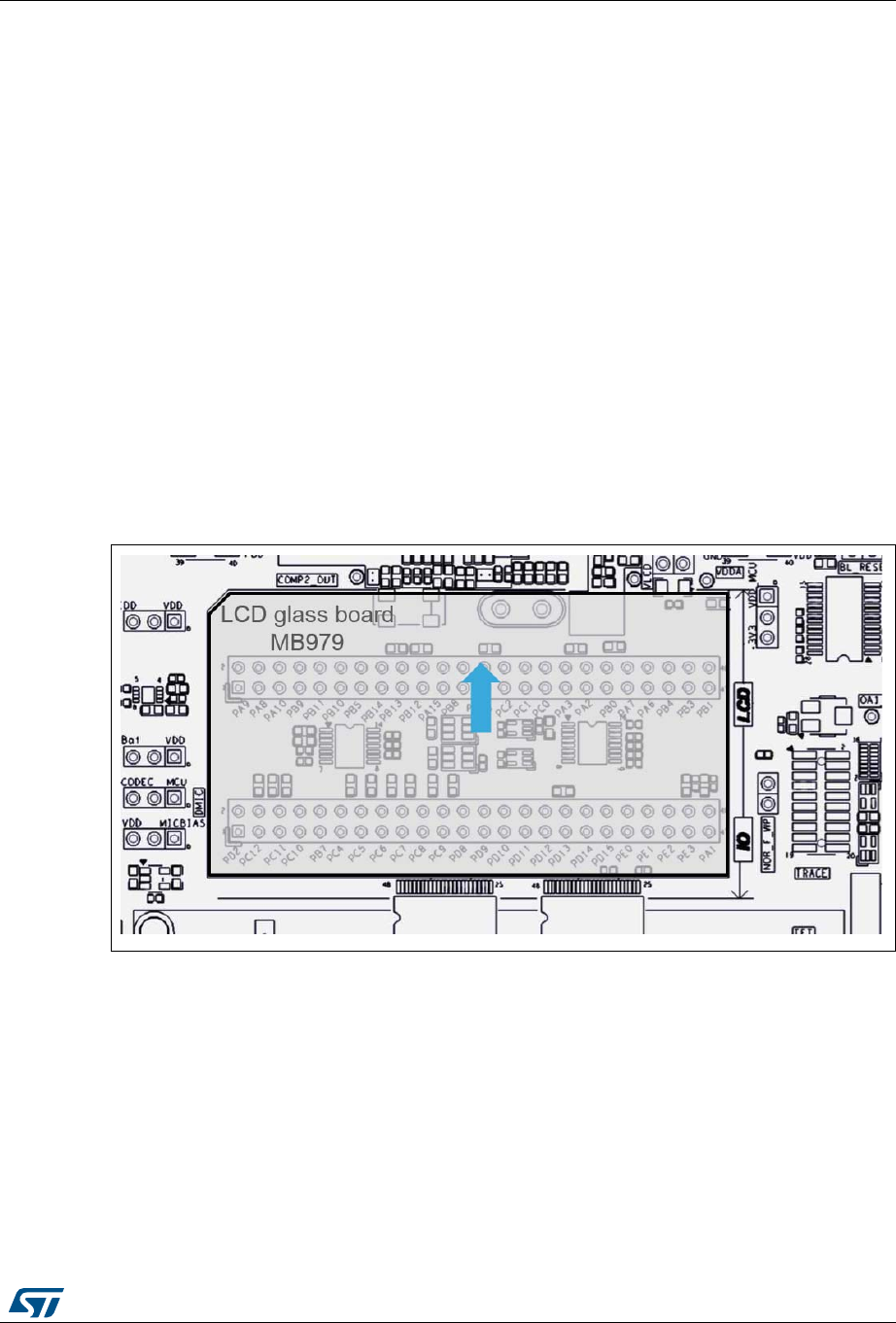
Figure 9 shows how the LCD glass module daughterboard must be positioned for display
function. This position is designated in the document as display position.
Figure 10 shows how the LCD glass module daughterboard must be positioned for I/O-
bridge function. This position is designated in the document as I/O-bridge position.
The arrow indicates the side of the CN11 and CN14 headers where the extra row of holes of
each female counterpart on the LCD glass module daughterboard has to protrude.
When the LCD glass module daughterboard is not plugged in, CN11 and CN14 give access
to ports of the target microcontroller. Figure 36 shows the related schematic diagram.
Table 14 shows the default settings of board configuration elements linked with CN11 and
CN14 extension connectors and LCD glass module daughterboard.
Figure 9. LCD glass module daughterboard in display position
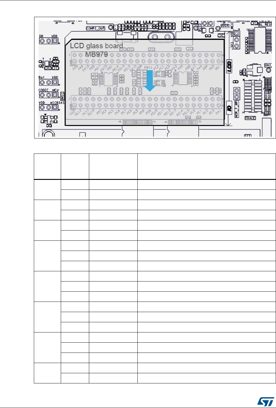
Hardware layout and configuration UM1855
34/101 DocID027351 Rev 5
Figure 10. LCD glass module daughterboard in I/O-bridge position
Table 14. LCD-daughterboard-related configuration elements
LCD
segment Element
Setting to enable
LCD glass
module
Description
SEG0 R82 In PA1 routed to LCDSEG0
SB32 Open PA1 not routed to motor control
SEG1 R81 In PA2 routed to LCDSEG1
SB31 Open PA2 not routed to motor control
SEG2 R78 In PA3 routed to LCDSEG2
SB22 Open PA3 not routed to motor control
SEG3
R68 In PA6 routed to LCDSEG3
SB21 Open PA6 not routed to Quad-SPI Flash memory device
SB20 Open PA6 not routed to motor control
SEG4
R66 In PA7 routed to LCDSEG4
SB18 Open PA7 not routed to Quad-SPI Flash memory device
SB19 Open PA7 not routed to motor control
SEG5
R62 In PB0 routed to LCDSEG5
SB14 Open PB0 not routed to Quad-SPI Flash memory device
SB15 Open PB0 not routed to motor control
SEG6
R56 In PB1 routed to LCDSEG6
SB12 Open PB1 not routed to Quad-SPI Flash memory device
SB13 Open PB1 not routed to motor control
SEG10 R50 In PB10 routed to LCDSEG10
SB9 Open PB10 not routed to Quad-SPI Flash memory device
DocID027351 Rev 5 35/101
UM1855 Hardware layout and configuration
100
The custom LCD glass module used on MB979 daughterboard is XHO5002B. To optimize
the number of driving signals, the display elements are connected to eight common planes
called COMx (LCDCOMx in the schematic diagrams), where “x” can be substituted with
figures from “0” to “7”. The other pole of each display element is called segment, SEGy
(LCDSEGy in the schematic diagrams), where “y” can be substituted with figures from “0” to
“39”. Each combination of COMx and SEGy addresses one display element. Table 15,
Table 16, Table 17 and Ta ble 22 show the LCD element mapping. COMx are ordered in
rows, SEGy in columns. The table cells then display the display element names
SEG11 R48 In PB11 routed to LCDSEG11
SB8 Open PB11 not routed to Quad-SPI Flash memory device
SEG12 R39 In PB12 routed to LCDSEG12
SB3 Open PB12 not routed to Quad-SPI Flash memory device
SEG13 R38 In PB13 routed to LCDSEG13
SB6 Open PB13 not routed to Touch sensing
SEG18 R97 In PC0 routed to LCDSEG18
SB34 Open PC0 not routed to motor control
SEG19 R98 In PC1 routed to LCDSEG19
SB36 Open PC1 not routed to motor control
SEG20 R99 In PC2 routed to LCDSEG20
SB42 Open PC2 not routed to motor control
SEG22 R65 In PC4 routed to LCDSEG22
SB17 Open PC4 not routed to motor control
SEG23 R64 In PC5 routed to LCDSEG23
SB16 Open PC5 not routed to motor control
SEG24
R36 In PC6 routed to LCDSEG24
SB2 Open PC6 not routed to Touch sensing
SB27 Open PC6 not routed to for motor control
SEG25
R33 In PC7 routed to LCDSEG25
SB4 Open PC7 not routed to Touch sensing
SB30 Open PC7 not routed to for motor control
SEG26 SB28 Open PC8 not routed to motor control
SEG27 SB29 Open PC9 not routed to motor control
SEG38 R103 In PE2 routed to LCDSEG38
SB26 Open PE2 not routed to Trace
SEG39 R104 In PE3 routed to LCDSEG39
Table 14. LCD-daughterboard-related configuration elements (continued)
LCD
segment Element
Setting to enable
LCD glass
module
Description
Hardware layout and configuration UM1855
36/101 DocID027351 Rev 5
corresponding to each COMx and SEGy combination. Names in quoting marks denote
elements forming textual symbols, for example “µA” or “+”. Figure 11 shows the physical
location and shape of each segment on the LCD glass module.
Table 15. LCD glass element mapping - segments 0 to 9
SEG0 SEG1 SEG2 SEG3 SEG4 SEG5 SEG6 SEG7 SEG8 SEG9
COM0 O1 5D Q4 O4 6D Q5 ST 7D Q6 S5
COM1 O2 5K 5L O3 6K 6L “nA” 7K 7L S6
COM2 13b 12b 11b 16b 15b 14b 19b 18b 17b 1b
COM3 13a 12a 11a 16a 15a 14a 19a 18a 17a 1a
COM4 5I 5A 5G 6I 6A 6G 7I 7A 7G 1I
COM5 5B 5H 5F 6B 6H 6F 7B 7H 7F 1B
COM6 5C 5M P4 6C 6M P5 7C 7M P6 1C
COM7 5J 5N 5E 6J 6N 6E 7J 7N 7E 1J
Table 16. LCD glass element mapping - segments 10 to 19
SEG10 SEG11 SEG12 SEG13 SEG14 SEG15 SEG16 SEG17 SEG18 SEG19
COM0 1D “-” C1 2D Q1 C4 3D Q2 “µA” 4D
COM1 1K 1L C2 2K 2L C3 3K 3L “mA” 4K
COM2 S4 S2 4b 3b 2b 7b 6b 5b 10b 9b
COM3 S3 S1 4a 3a 2a 7a 6a 5a 10a 9a
COM4 1A 1G 2I 2A 2G 3I 3A 3G 4I 4A
COM5 1H 1F 2B 2H 2F 3B 3H 3F 4B 4H
COM6 1M “+” 2C 2M P1 3C 3M P2 4C 4M
COM7 1N 1E 2J 2N 2E 3J 3N 3E 4J 4N
Table 17. LCD glass element mapping - segments 20 to 29
SEG20 SEG21 SEG22 SEG23 SEG24 SEG25 SEG26 SEG27 SEG28 SEG29
COM0 Q3 1e 2e 3e 4e 5e 6e 7e 8e 9e
COM1 4L 1f 2f 3f 4f 5f 6f 7f 8f 9f
COM2 8b 1c 2c 3c 4c 5c 6c 7c 8c 9c
COM3 8a 1d 2d 3d 4d 5d 6d 7d 8d 9d
COM4 4G 1j 2j 3j 4j 5j 6j 7j 8j 9j
COM5 4F 1i 2i 3i 4i 5i 6i 7i 8i 9i
COM6 P3 1h 2h 3h 4h 5h 6h 7h 8h 9h
COM7 4E 1g 2g 3g 4g 5g 6g 7g 8g 9g

DocID027351 Rev 5 37/101
UM1855 Hardware layout and configuration
100
2.15.1 Limitations
LCD glass module operation is exclusive with all other features of the board.
Table 18. LCD glass element mapping - segments 30 to 39
SEG30 SEG31 SEG32 SEG33 SEG34 SEG35 SEG36 SEG37 SEG38 SEG39
COM0 10e 11e 12e 13e 14e 15e 16e 17e 18e 19e
COM1 10f 11f 12f 13f 14f 15f 16f 17f 18f 19f
COM2 10c 11c 12c 13c 14c 15c 16c 17c 18c 19c
COM3 10d 11d 12d 13d 14d 15d 16d 17d 18d 19d
COM4 10j 11j 12j 13j 14j 15j 16j 17j 18j 19j
COM5 10i 11i 12i 13i 14i 15i 16i 17i 18i 19i
COM6 10h 11h 12h 13h 14h 15h 16h 17h 18h 19h
COM7 10g 11g 12g 13g 14g 15g 16g 17g 18g 19g
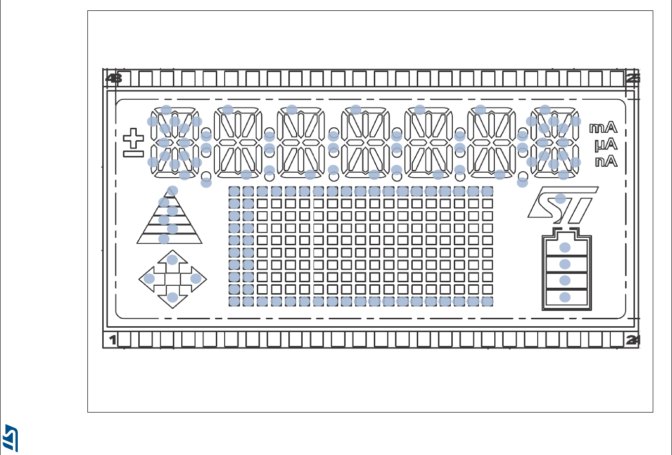
Hardware layout and configuration UM1855
38/101 DocID027351 Rev 5
Figure 11. LCD glass display element mapping
$
%
&
'
(
)
*
+
,
-
.
/
0 1 3
3
4
$
%
&
'
(
)
*
+
,
-
.
/
0 1
3
3
4
$ $ $ $ $
&
&
&
&
6
6
6
6
6
6
2
2
2
2
3
3
4
3
3
4
3
3
4
3
3
4
' ' ' ' '
67
D
E
F
G
H
I
J
K
L
M
D
E
F
G
H
I
J
K
L
M
D D D D D D D DD D D D D D D D D
M M M M M M M MM M M M M M M M M
06Y9
DocID027351 Rev 5 39/101
UM1855 Hardware layout and configuration
100
2.16 TFT LCD panel
STM32L476G-EVAL is delivered with MB989P, a daughterboard plugged into the CN19
extension connector. It bears a TFT 2.8-inch color LCD panel with resistive touchscreen and
an on-board controller. Section 2.18 provides further information.
Thanks to level shifters on all signal lines, the TFT LCD panel can operate with the entire
operating voltage range of STM32L476G-EVAL.
The TFT LCD panel is attached to the 16-bit data bus and accessed with FMC. The base
address is 0x6800 0000, corresponding to NOR/SRAM3 bank1. The panel is selected with
LCD_NE3 chip select signal generated by PG10 port of the STM32L476ZGT6. Address
lines A0 and A1 determine the panel resources addressed, as depicted in Table 19.
Table 20 gives the CN19 extension connector terminal assignment.
Table 19. Access to TFT LCD resources with FMC address lines A0 and A1
Address A1 A0 Usage
0x6800_0000 0 0 Read register
0x6800_0002 0 1 Read Graphic RAM (GRAM)
0x6800_0004 1 0 Write register
0x6800_0006 1 1 Write graphic RAM (GRAM)
Table 20. Assignment of CN19 connector terminals of TFT LCD panel
CN19
terminal
Terminal
name
MCU
port
CN19
terminal
Terminal
name
MCU
port
1CSN PG10 2RS PF0
3WRN PD5 4RDN PD4
5RSTN RESET# 6D0 PD14
7D1 PD15 8D2 PD0
9D3 PD1 10 D4 PE7
11 D5 PE8 12 D6 PE9
13 D7 PE10 14 D8 PE11
15 D9 PE12 16 D10 PE13
17 D11 PE14 18 D12 PE15
19 D13 PD8 20 D14 PD9
21 D15 PD10 22 BL_GND -
23 BL_CONTROL -24 +3V3 -
25 +3V3 -26 26 -
27 GND -28 BL_VDD -
29 SDO -30 SDI -
31 XL I/O expander_X- 32 XR I/O expander_X+
33 YD I/O expander_Y- 34 YU I/O expander_Y+
Hardware layout and configuration UM1855
40/101 DocID027351 Rev 5
2.17 User LEDs
Four general-purpose color LEDs (LD1, LD2, LD3, LD4) are available as light indicators.
Each LED is in light-emitting state with low level of the corresponding control port. They are
controlled either by the STM32L476ZGT6 or by the I/O expander IC U32, named
IOExpander1 in the schematic diagram. Table 21 gives the assignment of control ports to
the LED indicators.
2.18 Physical input devices
The STM32L476G-EVAL board provides a number of input devices for physical human
control. These are:
•four-way joystick controller with select key (B3)
•wake-up/ tamper button (B2)
•reset button (B1)
•resistive touchscreen of the TFT LCD panel
•10 kΩ potentiometer (RV3)
•light-dependent resistor, LDR (R52)
Table 22 shows the assignment of ports routed to the physical input devices. They are either
ports of the STM32L476ZGT6 or of one of the two I/O expander ICs on the board, named, in
the schematic diagrams, IOExpander1 and IOExpander2.
Table 21. Port assignment for control of LED indicators
User LED Control port Control device
LED1 (Green) PB2 STM32L476ZGT6
LED2 (Orange) GPIO0 IOExpander1
LED3 (Red) PC1 STM32L476ZGT6
LED4 (Blue) GPIO2 IOExpander1
Table 22. Port assignment for control of physical input devices
Input device Control port Control device
Joystick SEL GPIO0 IOExpander2
Joystick DOWN GPIO1 IOExpander2
Joystick LEFT GPIO2 IOExpander2
Joystick RIGHT GPIO3 IOExpander2
Joystick UP GPIO4 IOExpander2
Wake-up/ tamper B2 PC13 STM32L476ZGT6
Reset B1 NRST STM32L476ZGT6
Resistive touch screen X+ X+ IOExpander1
Resistive touch screen X- X- IOExpander1
Resistive touch screen Y+ Y+ IOExpander1
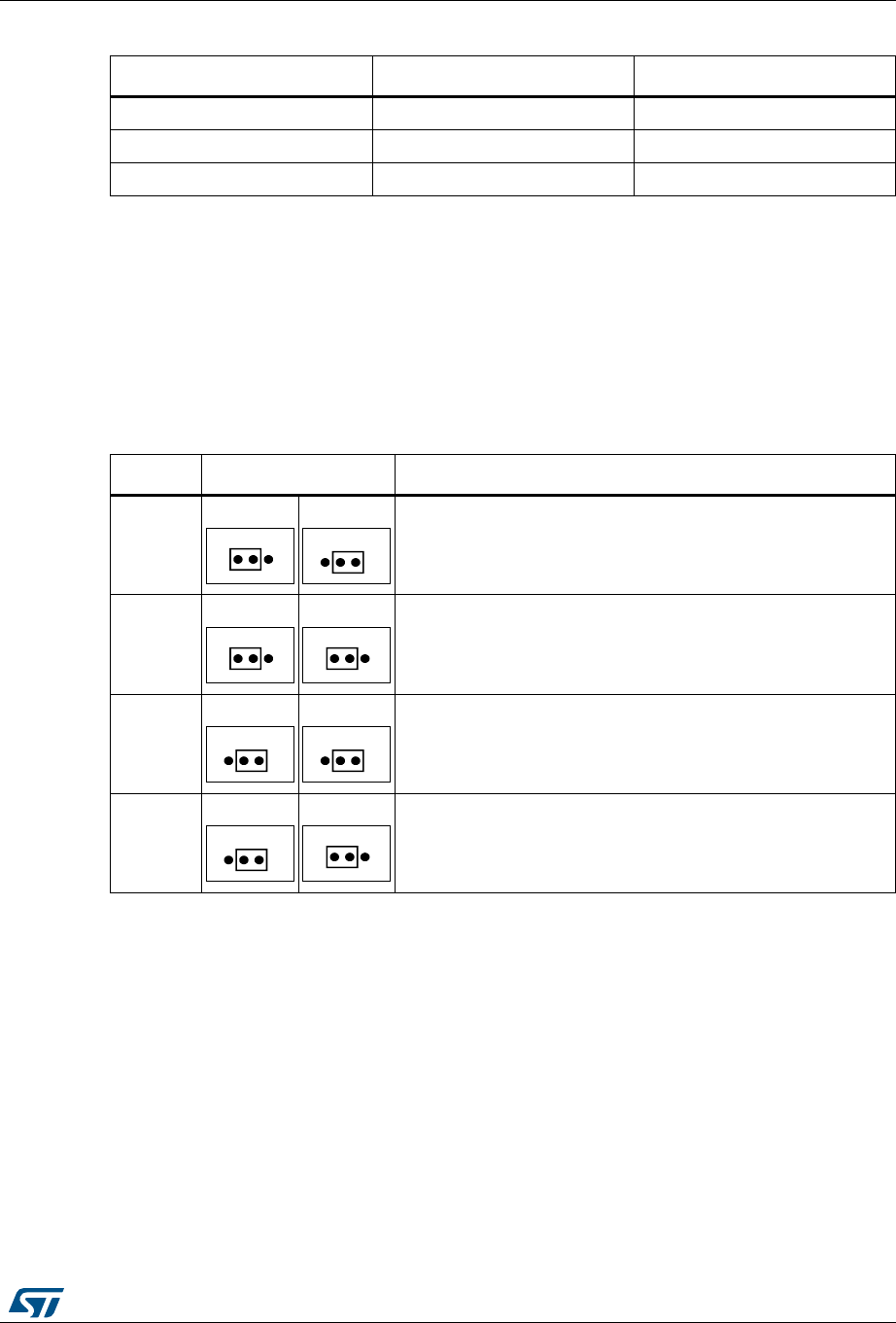
DocID027351 Rev 5 41/101
UM1855 Hardware layout and configuration
100
The potentiometer and the light-dependent resistor can be routed, mutually exclusively, to
either PB4 or to PA0 port of STM32L476ZGT6. Table 23 depicts the setting of associated
configuration jumpers.
As illustrated in the schematic diagram in Figure 46, the PB4 port is routed, in the
STM32L476ZGT6, to the non-inverting input of comparator Comp2. The PA0 is routed to
non-inverting input of operational amplifier OpAmp1. However, depending on register
settings, it can also be routed to ADC1 or to ADC2.
2.18.1 Limitations
The potentiometer and the light-dependent resistor are mutually exclusive.
2.19 Operational amplifier and comparator
2.19.1 Operational amplifier
STM32L476ZGT6 provides two on-board operational amplifiers, one of which, OpAmp1, is
made accessible on STM32L476G-EVAL. OpAmp1 has its inputs and its output routed to
I/O ports PA0, PA1 and PA3, respectively. The non-inverting input PA0 is accessible on the
terminal 1 of the JP7 jumper header. On top of the possibility of routing either of the
Resistive touch screen Y- Y- IOExpander1
Potentiometer PB4 or PA0 STM32L476ZGT6
LDR PA0 or PB4 STM32L476ZGT6
Table 23. Setting of jumpers related with potentiometer and LDR
Jumper Setting Routing
JP5
JP7
JP5 JP7
Potentiometer is routed to pin PB4 of STM32L476ZGT6.
JP5
JP7
JP5 JP7
Default setting.
Potentiometer is routed to pin PA0 of STM32L476ZGT6.
JP5
JP7
JP5 JP7
LDR is routed to pin PB4 of STM32L476ZGT6.
JP5
JP7
JP5 JP7
LDR is routed to pin PA0 of STM32L476ZGT6.
Table 22. Port assignment for control of physical input devices (continued)
Input device Control port Control device

Hardware layout and configuration UM1855
42/101 DocID027351 Rev 5
potentiometer or LDR to PA0, en external source can also be connected to it, using the
terminal 1 of JP7.
The PA3 output of the operational amplifier can be accessed on test point TP9. Refer to the
schematic diagram in Figure 46.
The gain of OpAmp1 is determined by the ratio of the variable resistor RV2 and the resistor
R121, as shown in the following equation:
With the RV2 ranging from 0 to 10 kΩ and R121 being 1 kΩ, the gain can vary from 1 to 11.
The R63 resistor in series with PA0 is beneficial for reducing the output offset.
2.19.2 Comparator
STM32L476ZGT6 provides two on-board comparators, one of which, Comp2, is made
accessible on STM32L476G-EVAL. Comp2 has its non-inverting input and its output routed
to I/O ports PB4 and PB5, respectively. The input is accessible on the terminal 3 of the JP7
jumper header. On top of the possibility of routing either the potentiometer or LDR to PB4,
an external source can also be connected to it, using the terminal 3 of JP7.
The PB5 output of the comparator can be accessed on test point TP6. Refer to the
schematic diagram in Figure 46.
2.20 Analog input, output, VREF
STM32L476ZGT6 provides on-board analog-to-digital converter, ADC and, digital-to-analog
converter, DAC. The port PA4 can be configured to operate either as ADC input or as DAC
output. PA4 is routed to the two-way header CN8 allowing to fetch signals to or from PA4 or
to ground it by fitting a jumper into CN8.
Parameters of the ADC input low-pass filter formed with R72 and C47 can be modified by
replacing these components according to application requirements. Similarly, parameters of
the DAC output low-pass filter formed with R73 and C47 can be modified by replacing these
components according to application requirements.
The VREF+ terminal of STM32L476ZGT6 is used as reference voltage for both ADC and
DAC. By default, it is routed to VDDA through a jumper fitted into the two-way header CN10.
The jumper can be removed and an external voltage applied to the terminal 1 of CN10, for
specific purposes.
2.21 SRAM device
IS61WV102416BLL, a 16-Mbit static RAM (SRAM), 1 M x16 bit, is fitted on the
STM32L476G-EVAL main board, in U2 position. The STM32L476G-EVAL main board as
well as the addressing capabilities of FMC allow hosting SRAM devices up to 64 Mbytes.
This is the reason why the schematic diagram in Figure 41 mentions several SRAM
devices.
The SRAM device is attached to the 16-bit data bus and accessed with FMC. The base
address is 0x6000 0000, corresponding to NOR/SRAM1 bank1. The SRAM device is
Gain 1 RV2()R121()÷+=

DocID027351 Rev 5 43/101
UM1855 Hardware layout and configuration
100
selected with FMC_NE1 chip select. FMC_NBL0 and FMC_NBL1 signals allow selecting 8-
bit and 16-bit data word operating modes.
By removal of R18, a zero-ohm resistor, the SRAM is deselected and the STM32L476ZGT6
ports PD7, PE0 and PE1 corresponding to FMC_NE1, FMC_NBL0 and FMC_NBL1 signals,
respectively, can be used for other application purposes.
2.21.1 Limitations
The SRAM addressable space is limited if some or all of A19, A20, A21, A22 and A23 FMC
address lines are shunted to the CN12 connector for debug trace purposes. In such a case,
the disconnected addressing inputs of the SRAM device are pulled down by resistors.
Section 2.2 provides information on the associated configuration elements.
2.21.2 Operating voltage
The SRAM device operating voltage is in the range from 2.4 V to 3.6 V.
2.22 NOR Flash memory device
M29W128GL70ZA6E, a 128-Mbit NOR Flash memory, 8 M x16 bit, is fitted on the
STM32L476G-EVAL main board, in U5 position. The STM32L476G-EVAL main board as
well as the addressing capabilities of FMC allow hosting M29W256GL70ZA6E, a 256-Mbit
NOR Flash memory device. This is the reason why the schematic diagram in Figure 41
mentions both devices.
The NOR Flash memory device is attached to the 16-bit data bus and accessed with FMC.
The base address is 0x6400 0000, corresponding to NOR/SRAM2 bank1. The NOR Flash
memory device is selected with FMC_NE2 chip select signal. 16-bit data word operation
mode is selected by a pull-up resistor connected to BYTE terminal of NOR Flash memory.
The jumper JP13 is dedicated for write protect configuration.
By default, the FMC_NWAIT signal is not routed to RB port of the NOR Flash memory
device, and, to know its ready status, its status register is polled by the demo software fitted
in STM32L476G-EVAL. This can be modified with configuration elements, as shown in
Table 25.
Table 24. SRAM chip select configuration
Resistor Fitting Configuration
R18
In Default setting.
SRAM chip select is controlled with FMC_NE1
Out SRAM is deselected. FMC_NE1 is freed for other application purposes.
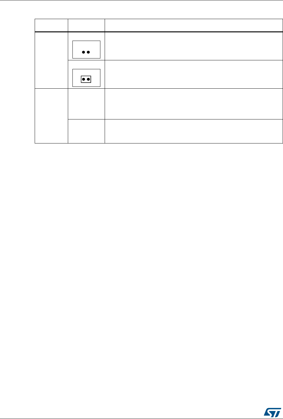
Hardware layout and configuration UM1855
44/101 DocID027351 Rev 5
2.22.1 Limitations
•FMC_NWAIT and SAI1_SDA signals are mutually exclusive.
•The NOR Flash memory device’s addressable space is limited if some or all of A19,
A20, A21, A22 and A23 FMC address lines are shunted to the CN12 connector for
debug trace purposes. In such a case, the disconnected addressing inputs of the NOR
Flash memory device are pulled down by resistors. Section 2.2 provides information on
the associated configuration elements.
2.22.2 Operating voltage
NOR Flash memory operating voltage must be in the range from 1.65 V to 3.6 V.
2.23 EEPROM
M24128-DFDW6TP, a 128-Kbit I²C-bus EEPROM device, is fitted on the main board of
STM32L476G-EVAL, in U6 position. It is accessed with I²C-bus lines I2C2_SCL and
I2C2_SDA of STM32L476ZGT6. It supports all I²C-bus modes with speeds up to 1 MHz.
The base I²C-bus address is 0xA0. Write-protecting the EEPROM is possible through
opening the SB7 solder bridge. By default, SB7 is closed and writing into the EEPROM
enabled.
2.23.1 Operating voltage
The M24128-DFDW6TP EEPROM device’s operating voltage must be in the range from
1.7 V to 3.6 V
2.24 RF-EEPROM
RF-EEPROM daughterboard, ANT7-M24LR-A, can be connected to CN3 connector of the
STM32L476G-EVAL board. STM32L476ZGT6 can access the RF-EEPROM in two ways,
Table 25. NOR Flash memory-related configuration elements
Element Setting Configuration
JP13
JP13
Default setting.
NOR Flash memory write is enabled.
JP13
NOR Flash memory write is inhibited. Write protect is activated.
R53
SB10
R53 In
SB10 open
Default setting.
PD6 port of STM32L476ZGT6 is used for SAI1_SDA signal and routed
to audio codec.
NOR Flash memory device’s status register can be accessed.
R53 Out
SB10 closed
PD6 port of STM32L476ZGT6 is used for FMC_NWAIT signal and
routed to NOR Flash memory device’s RB port.
NOR Flash memory device’s status register cannot be accessed.
DocID027351 Rev 5 45/101
UM1855 Hardware layout and configuration
100
wired through I²C bus or wireless using 13.56 MHz RF band reserved for RFID and NFC
equipment. For wireless access, CR95HF reader daughterboard plugged in the CN13
connector can be used, for example.
I²C address of RF-EEPROM device is 0xA6.
2.25 Quad-SPI Flash memory device
N25Q256A13EF840E, a 256-Mbit Quad-SPI Flash memory device, is fitted on the
STM32L476G-EVAL main board, in U9 position. It allows evaluating STM32L476ZGT6
Quad-SPI Flash memory device interface.
N25Q256A13EF840E can operate in single transfer rate (STR) and double transfer rate
(DTR) modes.
By default, the Quad-SPI Flash memory device is not accessible. Table 26 shows the
configuration elements and their settings allowing to access the Quad-SPI Flash memory
device. The LCD glass module daughterboard MB979 takes active part in the configuration.
It must be removed from the main board (denoted as “MB979 out”), to operate the Quad-
SPI Flash memory device. Section 2.12: Motor control provides additional information.
Table 26. Configuration elements related with Quad-SPI device
Element Setting Configuration
SB12
SB13
MB979
SB12 open
SB13 open
Default setting.
QSPI_D0 data line is not available at Quad-SPI Flash memory device:
PB1 port of STM32L476ZGT6 is only routed to CN11 connector for the
MB979 daughterboard.
SB12 closed
SB13 open
MB979 out
QSPI_D0 data line is available at Quad-SPI Flash memory device:
PB1 port of STM32L476ZGT6 is routed to DQ0 port of Quad-SPI Flash
memory device.
SB14
SB15
MB979
SB14 open
SB15 open
Default setting.
QSPI_D1 data line is not available at Quad-SPI Flash memory device:
PB0 port of STM32L476ZGT6 is only routed to CN11 connector for the
MB979 daughterboard.
SB14 closed
SB15 open
MB979 out
QSPI_D1 data line is available at Quad-SPI Flash memory device:
PB0 port of STM32L476ZGT6 is routed to DQ1 port of Quad-SPI Flash
memory device.
SB18
SB19
MB979
SB18 open
SB19 open
Default setting.
QSPI_D2 data line is not available at Quad-SPI Flash memory device:
PA7 port of STM32L476ZGT6 is only routed to CN11 connector for the
MB979 daughterboard.
SB18 closed
SB19 open
MB979 out
QSPI_D2 data line is available at Quad-SPI Flash memory device:
PA7 port of STM32L476ZGT6 is routed to DQ2 port of Quad-SPI Flash
memory device.
Hardware layout and configuration UM1855
46/101 DocID027351 Rev 5
2.25.1 Limitations
Quad-SPI operation is exclusive with LCD glass module and with motor control.
2.25.2 Operating voltage
Voltage of Quad-SPI Flash memory device N25Q256A13EF840E is in the range of 2.7 V to
3.6 V.
2.26 Touch-sensing button
The STM32L476G-EVAL evaluation board supports a touch sensing button based on either
RC charging or on charge-transfer technique. The latter is enabled, by default.
The touch sensing button is connected to PB12 port of STM32L476ZGT6 and the related
charge capacitor is connected to PB13.
An active shield is designed in the layer two of the main PCB, under the button footprint. It
allows reducing disturbances from other circuits to prevent from false touch detections.
The active shield is connected to PC6 port of STM32L476ZGT6 through the resistor
R37.The related charge capacitor is connected to PC7.
Table 27 shows the configuration elements related with the touch sensing function. Some of
them serve to enable or disable its operation. However, most of them serve to optimize the
touch sensing performance, by isolating copper tracks to avoid disturbances due to their
antenna effect.
SB21
SB20
MB979
SB21 open
SB20 open
Default setting.
QSPI_D3 data line is not available at Quad-SPI Flash memory device:
PA6 port of STM32L476ZGT6 is only routed to CN11 connector for the
MB979 daughterboard.
SB21 closed
SB20 open
MB979 out
QSPI_D3 data line is available at Quad-SPI Flash memory device:
PA6 port of STM32L476ZGT6 is routed to DQ3 port of Quad-SPI Flash
memory device.
SB9
MB979
SB9 open
Default setting.
QSPI_CLK clock line is not available at Quad-SPI Flash memory device:
PB10 port of STM32L476ZGT6 is only routed to CN11 connector for the
MB979 daughterboard.
SB9 closed
MB979 out
QSPI_CLK clock line is available at Quad-SPI Flash memory device:
PB10 port of STM32L476ZGT6 is routed to C port of Quad-SPI Flash
memory device.
SB8
MB979
SB8 open
Default setting.
QSPI_CS line is not available at Quad-SPI Flash memory device:
PB11 port of STM32L476ZGT6 is only routed to CN11 connector for the
MB979 daughterboard.
SB8 closed
MB979 out
QSPI_CS line is available at Quad-SPI Flash memory device:
PB11 port of STM32L476ZGT6 is routed to S# port of Quad-SPI Flash
memory device.
Table 26. Configuration elements related with Quad-SPI device (continued)
Element Setting Configuration
DocID027351 Rev 5 47/101
UM1855 Hardware layout and configuration
100
Table 27. Touch-sensing-related configuration elements
Element Setting Configuration
R39
In
Default setting. PB12 port is routed to CN11 connector for LCD glass
module daughterboard.
This setting is not good for robustness of touch sensing.
Out PB12 port is cut from CN11.
This setting is good for robustness of touch sensing.
SB3
Open Default setting. PB12 is not routed to motor control.
This setting is good for robustness of touch sensing.
Closed PB12 is routed to motor control.
This setting is not good for robustness of touch sensing.
R38
In
Default setting. PB13 port is routed to CN11 connector for LCD glass
module daughterboard.
This setting is not good for robustness of touch sensing.
Out PB13 port is cut from CN11.
This setting is good for robustness of touch sensing.
SB6 Open Default setting. PB13 is not routed to sampling capacitor. Touch
sensing cannot operate.
Closed PB13 is routed to sampling capacitor. Touch sensing can operate.
R36
In
Default setting. PC6 port is routed to CN14 connector for LCD glass
module daughterboard.
This setting is not good for robustness of touch sensing.
Out PC6 port is cut from CN14.
This setting is good for robustness of touch sensing.
SB2
Open
Default setting. PC6 is not routed to active shield under the touch-
sensing button.
This setting is not good for robustness of touch sensing.
Closed PC6 is routed to active shield under the touch-sensing button.
This setting is good for robustness of touch sensing.
SB27
Open Default setting. PC6 port of STM32L476ZGT6 is not routed to motor
control. This setting is good for robustness of touch sensing.
Closed PC6 is routed to motor control.
This setting is not good for robustness of touch sensing.
R33
In
Default setting. PC7 port is routed to CN14 connector for LCD glass
module daughterboard.
This setting is not good for robustness of touch sensing.
Out PC7 port is cut from CN14.
This setting is good for robustness of touch sensing.
SB4
Open
Default setting. PC7 port of STM32L476ZGT6 is not routed to
sampling capacitor of the active shield under the touch-sensing button.
This setting is not good for robustness of touch sensing.
Closed
PC7 is routed to sampling capacitor of the active shield under the
touch-sensing button.
This setting is good for robustness of touch sensing.
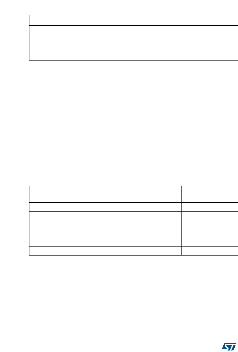
Hardware layout and configuration UM1855
48/101 DocID027351 Rev 5
2.26.1 Limitations
Touch sensing button is exclusive with LCD glass module, thermal sensor PT100 via sigma-
delta conversion, USB OTG FS port operating as USB host, SWP and NFC.
2.27 Smartcard, SWP
ST8024CDR, an interface device for 3 V and 5 V asynchronous smartcards, is fitted on the
STM32L476G-EVAL main board, in U30 position. ST8024CDR performs all supply
protection and control functions of the smartcard.
ST8024CDR is controlled, on its turn, by STM32L476ZGT6, directly through its ports or
indirectly through ports of the U33 I/O expander device (IOExpander2), as shown in
Table 28.
The SWIO port of the smartcard for single-wire protocol (SWP) communication is managed
directly by PB12 port of STM32L476ZGT6.
Table 29 provides information on configuration elements related with smartcard operation.
Refer to Table 8, Table 12, Table 26 and Table 27 for complementary information. Bridging
of CN11 and CN14 rows of I/Os can be done by means of the MB979 daughterboard
plugged into CN11 and CN14 in I/O-bridge position, as explained in Section 2.15.
SB30
Open
Default setting. PC7 port of STM32L476ZGT6 is not routed to motor
control.
This setting is good for robustness of touch sensing.
Closed PC7 is routed to motor control. This setting is not good for robustness
of touch sensing.
Table 27. Touch-sensing-related configuration elements (continued)
Element Setting Configuration
Table 28. Assignment of ports for ST8024CDR control
ST8024CDR
port Function Control port
5V/3V Smartcard power supply selection pin. IOexpander2 GPIO7
I/OUC Data I/O line STM32L476ZGT6 PC4
XTAL1 Quartz crystal or external clock input STM32L476ZGT6 PB0
OFF Card presence detect IOexpander2 GPIO8
RSTIN Card reset command input IOexpander2 GPIO5
CMDVCC Activation sequence start command input (active low) IOexpander2 GPIO6
DocID027351 Rev 5 49/101
UM1855 Hardware layout and configuration
100
Table 29. Configuration elements related with smartcard and SWP
Element Setting Configuration
R39
SB3
R109
CN11
R109 in
R39 in
SB3 open
CN11 I/O-bridged
Default setting.
Smartcard SWP cannot be handled:
PB12 is routed to USB OTG FS port as USBOTG_OVRCR line, on
top of being routed to SWIO port of smartcard
Configuration dedicated for USB OTG FS operation.
R109 out
R39 in
SB3 open
CN11 I/O-bridged
Smartcard SWP can be handled:
PB12 is routed to SWIO port of smartcard. It is disconnected from
any other resource that could affect the SWP operation
Configuration dedicated for smartcard SWP operation
R39 out
SB3 closed
Smartcard SWP cannot be handled:
PB12 is routed to motor control as MC_PFC_Shutdown
Configuration dedicated for motor control operation
R39 out
SB3 open
Smartcard SWP cannot be handled:
PB12 is only routed to touch-sensing button and it is disconnected
from any other resource.
Configuration dedicated for touch-sensing button operation.
R62
SB14
SB15
R62 in
SB14 open
SB15 open
CN11 I/O-bridged
Default setting.
Smartcard controller U30 is supplied with clock:
PB0 port is routed to XTAL1 of U30, as SmartCard_CLK line and it
is not routed to other resources.
Configuration dedicated for smartcard operation.
R62 out
SB14 closed
SB15 open
Smartcard controller U30 is not supplied with clock:
PB0 is routed to Quad-SPI Flash memory device as QSPI_D1 and it
is not routed to other resources.
Configuration dedicated for Quad-SPI Flash memory device
operation.
R62 out
SB14 open
SB15 closed
Smartcard controller U30 is not supplied with clock:
PB0 is routed to motor control as MC_PWM_2L line and it is not
routed to other resources.
Configuration dedicated for motor control operation.
R65
SB17
CN14
R65 in
SB17 open
CN14 I/O-bridged
Default setting.
Smartcard controller gets SmartCard_IO line:
PC4 port of MCU is routed to IOUC port of U30, as SmartCard_IO
line and it is not routed to other resources.
Configuration dedicated for smartcard operation.
R65 out
SB17 closed
Smartcard controller does not get SmartCard_IO line:
PC4 port of MCU is routed to motor control as MC0PFC0IndCur line
and it is not routed to other resources.
Configuration dedicated for motor control operation.
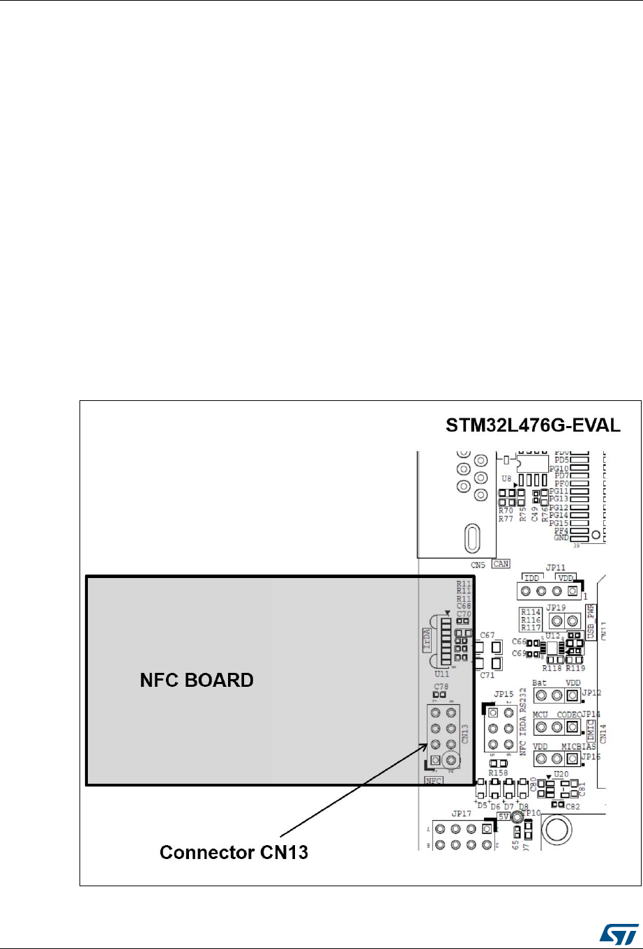
Hardware layout and configuration UM1855
50/101 DocID027351 Rev 5
2.27.1 Limitations
The following limitations apply for the smartcard operation:
•Smartcard operation is mutually exclusive with LCD glass module, Quad-SPI Flash
memory device and motor control operation.
•SWP operation is mutually exclusive with LCD glass module, touch-sensing button,
motor control and USB OTG FS port operation, if the last operates as USB host. SWP
can operate concurrently with USB OTG FS port acting as USB device.
2.27.2 Operating voltage
Smartcard operating ranging from VDD = 2.7 V to VDD = 3.6 V. However, the SWP only
operates with the supply voltage of 3.3 V.
2.28 Near-field communication (NFC)
The STM32L476G-EVAL board can host an NFC transceiver board plugged in CN13
extension connector.
Figure 12 illustrates the way of attaching an NFC board.
Figure 12. NFC board plugged into STM32L476G-EVAL board
DocID027351 Rev 5 51/101
UM1855 Hardware layout and configuration
100
Table 30 shows the assignment of signals to CN13 connector.
The serial communication with the module plugged in CN13 can either use SPI
communication protocol (default) or UART communication protocol.
2.29 Dual-channel sigma-delta modulators STPMS2L
2.29.1 STPMS2L presentation
With its DFSDM interface, the STM32L476ZGT6 microcontroller can directly interact with
sigma-delta modulator devices, such as STPMS2L.
STPMS2L comprises two analog measuring channels based on second-order sigma-delta
modulators. Typically, it can be used in power metering where both voltage and current
need to be known. One channel measures the voltage, the other channel measures the
current.
DAT port outputs converted measurement data on the DFSDM_DATIN1 line, received by
the STM32L476ZGT6 DFSDM controller. The data from STPMS2L are synchronized with
DFSDM_CKOUT clock generated by the STM32L476ZGT6 DFSDM controller and received
on CLK terminal of STPMS2L.
There are two STPMS2L devices on STM32L476G-EVAL, sharing the DFSDM clock. One is
wired such as to support a power-metering demonstrator. The other allows measuring
temperature using the PT100 sensor.
Table 30. CN13 NFC connector terminal assignment
CN13
terminal NFC line name MCU port Function
1NFC_IRQOUTN or
UART_TX PB7 Interrupt output for NFC device
Connected to STM32L476ZGT6 UART RX
2NFC_IRQINN or
UART_RX PB6 Interrupt input for NFC device
Connected to STM32L476ZGT6 UART TX
3NFC_NSS PF11 SPI slave select
4NFC_MISO PB14 SPI data, slave output
5NFC_MOSI PB15 SPI data, slave input
6NFC_SCK PB13 SPI serial clock
7+3V3 -Main power supply/power supply for RF drivers
8GND -Ground
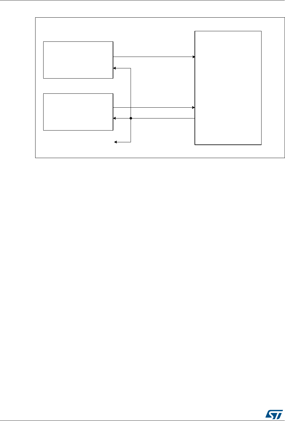
Hardware layout and configuration UM1855
52/101 DocID027351 Rev 5
Figure 13. Routing of STPMS2L dual-channel sigma-delta modulators
2.29.2 STPMS2L settings
STPMS2L operating parameters are set through its configuration terminals MS0, MS1, MS2
and MS3. On STM32L476G-EVAL, both devices are configured as follows:
•Voltage channel range: differential voltage +/- 300mV
•Current channel range: differential voltage +/- 300mV
•Internal voltage reference is used
•Input bandwidth: 0 to 1 kHz
•Temperature compensation: flattest +30ppm/°C
•DAT output: voltage and current samples multiplexed
•DATn output: not used
•HW mode selected for settings
2.29.3 STPMS2L power metering
STPMS2L in U3 position simulates low-voltage AC power metering, with capacitive load
impedance, to give different phase to voltage and current.
06Y9
&/.287
WR0(06PLFURSKRQHV
67306/
3RZHUPHWHULQJ
'$7
&/.
'$7
&/.
')6'0B'$7,1
37B'$7,1
3&
')6'0B&.287
67306/
7HPSHUDWXUHPHWHULQJ
37
670/=*7
3&
3'
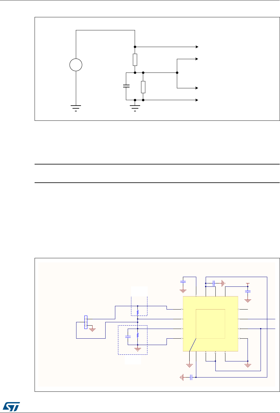
DocID027351 Rev 5 53/101
UM1855 Hardware layout and configuration
100
Figure 14. Power measurement principle schematic diagram
A low-voltage AC generator is to be applied by the user as shown in Figure 14. The shunt
resistor is connected in series with the load to provide current measurement points to one of
STPMS2L input channels. The voltage measurement points for the other input channel are
taken across the load. Figure 15 shows an extract of the corresponding schematic diagram.
Warning: do not connect AC mains!
Test example:
The output of a low-voltage AC generator is connected to CN4, terminals 1 and 3. The
amplitude is set between 200 mV and 300 mV and the frequency adjustable between 10 Hz
and 100 Hz.
With 34 Hz frequency and the load formed of R27 of 1 kΩ in parallel with C29 of 4.7 µF, the
voltage and current phases are theoretically 45 degrees apart.
Figure 15. STPMS2L power metering schematic diagram
06Y9
$&VRXUFH 6KXQWUHVLVWRU
IRUFXUUHQW
PHDVXUHPHQW
&RPSOH[
LPSHGDQFH
FXUUHQW
YROWDJH
WR67306/
GLIIHUHQWLDOLQSXW
WR67306/
GLIIHUHQWLDOLQSXW
a
STPMS2 power metering
R26
1K
GND
GND
GND
GND
C26
100nF
GND
GND
R27
1K
GND
R+jX Load
current
shunt
external generator input: pins 1 and 3
voltage of complex load: pins 2 and 3
shunt voltage : pins 1 and 2
VDD
VCC 1
VDDAC 2
VDDA 3
VBG 4
DATn 16
DAT 15
CLK 14
MS3 13
MS2
12
MS1
11
MS0
10
VDDAV
9
VIP
8
VIN
7
CIP
6
CIN
5
GND
17
A
V
Exposed
p
ad GND
U3
STPMS2L-PUR
3
2
1
CN4
GND
C294.7uF
C27
1uF
C221uF
C24
1uF
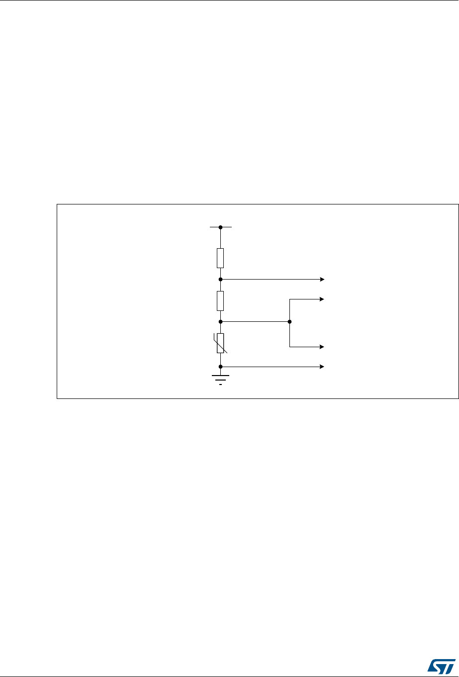
Hardware layout and configuration UM1855
54/101 DocID027351 Rev 5
2.29.4 STPMS2L for PT100 measurement
PT100 is a resistor with temperature-dependent resistance.
Usually, one of two methods is used for measuring temperature with a temperature-
dependent resistor. In the first method, a known current is driven through the measuring
resistor. The temperature is represented by the voltage measured across the resistor. In the
second method, a known voltage is applied on the resistor and the current flowing through is
measured, representing the temperature. In these methods, either an accurate current
source or an accurate voltage source is required.
With the dual-input measurement with STPMS2L in U4 position, no such accurate current or
voltage sources are required. Instead, a precision shunt resistor is required. One channel of
the STPMS2L measures the voltage across the precise shunt resistor, representing the
current flowing through PT100. The other channel measures the voltage across PT100.
Figure 16. Temperature measurement principle schematic diagram
With voltage across and current through the PT100 resistor, the STM32L476ZGT6
microcontroller computes resistance PT100.
For temperatures lower than +100°C, the temperature is given by the following equation,
where PT100 is resistance of the PT100 resistor and T is temperature in degrees
centigrade:
2.29.5 Limitations
Operating voltage must be in the range from 3.2 V to 3.6 V.
2.30 STM32L476ZGT6 current consumption measurement
STM32L476ZGT6 has a built-in circuit allowing to measure its own current consumption
(IDD) in Run and Low-power modes, except for Shutdown mode.
06Y9
9''
6KXQWUHVLVWRUIRUFXUUHQW
PHDVXUHPHQW
7HPSHUDWXUHGHSHQGHQW
UHVLVWRU
%LDVLQJUHVLVWRU N
37
FXUUHQW
YROWDJH
WR67306/
GLIIHUHQWLDOLQSXW
WR67306/
GLIIHUHQWLDOLQSXW
T PT100 100–()0.385()⁄=

DocID027351 Rev 5 55/101
UM1855 Hardware layout and configuration
100
It is strongly recommended that, the MCU supply voltage (VDD_MCU line) does not exceed
3.3 V. This is because there are components on STM32L476G-EVAL supplied from 3.3 V
that communicate with the MCU through I/O ports. Voltage exceeding 3.3 V on the MCU
output port may inject current into 3.3 V-supplied peripheral I/Os and false the MCU current
consumption measurement.
2.30.1 IDD measurement principle - analog part
The analog part is based on measuring voltage drop across a shunt resistor, amplified with a
differential amplifier. The STM32L476ZGT6 microcontroller supply current is shunted, by
jumper settings, to flow through the measurement 1 Ω resistor R135: JP11 terminals 1 and 2
are to be open, terminals 3 and 4 closed. When the transistor T2 is in conductive state, the
MCU supply current is proportional to the voltage across R135. When T2 is in high-
impedance state, the MCU supply current is proportional to the voltage across the series of
R135 and R123. The former state is used for measuring the current consumption in dynamic
run mode, the latter in low-power mode.
The differential amplifier uses three stages U15B, U15C, U15D of quadruple operational
amplifier device U15, TSZ124. The gain is set to 50, so every 1 mA of supply current is
represented by additional 50 mV at the U15C output, terminal 8 of U15.
The resistance formed with the series of R135 and R123, when T2 is in high-impedance
state, is of 1001 Ω. It makes the voltage on terminal 8 of U15 increase by approximately
50 mV for every µA of MCU power consumption. The full-scale range, with VDD at 1.8 V is
about 30 µA.
Even with precision resistors R136, R125, R129, R132 to set the gain of the differential
amplifier, the output voltage may theoretically become negative. To avoid the need of
negative power supply, a positive offset of about 220 mV is created at the output, at zero
current consumption of the MCU. This offset does not need to be precise. Any dispersion is
compensated through a calibration procedure detailed in Section 2.30.4.
For allowing the IDD measurement, the jumper in the JP11 header must be placed such as
to short its terminals 3 and 4.
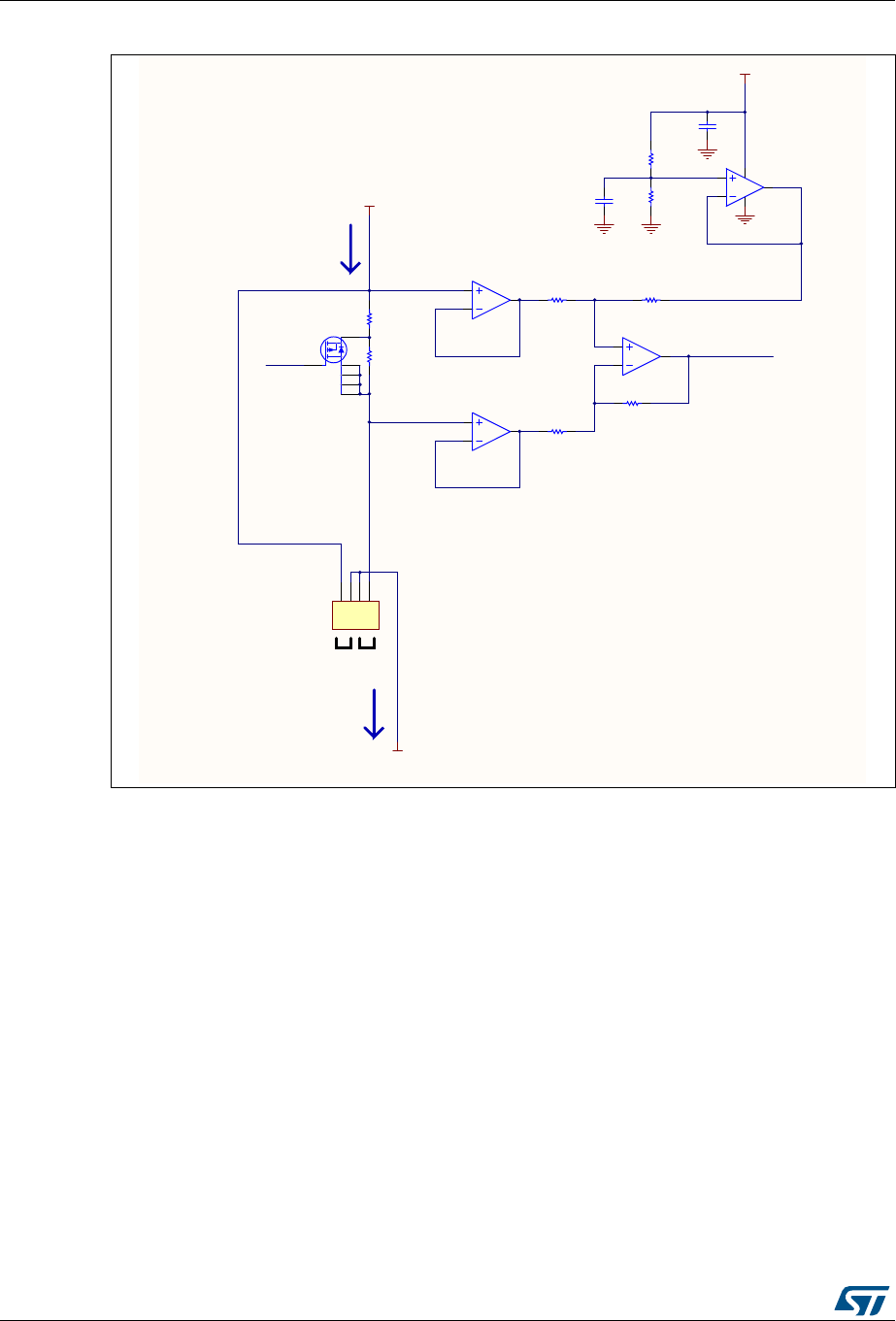
Hardware layout and configuration UM1855
56/101 DocID027351 Rev 5
Figure 17. Schematic diagram of the analog part of IDD measurement
2.30.2 Low-power-mode IDD measurement principle - logic part
The target microcontroller can only carry out actions for measuring a voltage when in
dynamic run mode. This is the reason why, voltage representing the current consumed by
the microcontroller when in low-power mode needs to be held by a sample-and-hold circuit,
for being exploited by the microcontroller at a later time, when back in dynamic run mode.
The sample-and-hold (S&H) circuit is built with U13 switch, R122 resistor and C73 sampling
capacitor.
The measurement of low-power-mode current consumption is started and end by the
microcontroller in its dynamic run mode. As, between the start and end event, the
microcontroller must transit through one of its low-power modes, an extra logic is required to
time and control events during this state. It consists of U14 counter, U16 inverter and the
transistor T3. Figure 18 shows the corresponding schematic diagram.
VDD
R135
1[1%]
R123
1K[1%]
3
4
5
G
S
D
1
2
6
T2
FDC606P
VDD_MCU
R136
3K6 0.1%
R125
3K6 0.1%
R129
180K 0.1%
R132
180K 0.1%
GND
+5V
C75
100nF
GND
GND
decoupling capacitor
close from TSZ124 part
1
4
3
2
11
V+
V-
U15A
TSZ124IPT
7
5
6
U15B
TSZ124IPT
14
12
13
U15D
TSZ124IPT
8
10
9
U15C
TSZ124IPT
R128
22K
R124
1K
Shunt_x1000
Current
direction
to MCU
bypass path current
measurement
path
differential
amplifier
shunts
C144
100nF
GND
1
2
3
4
JP11
Current
direction
VDD from
power
supply
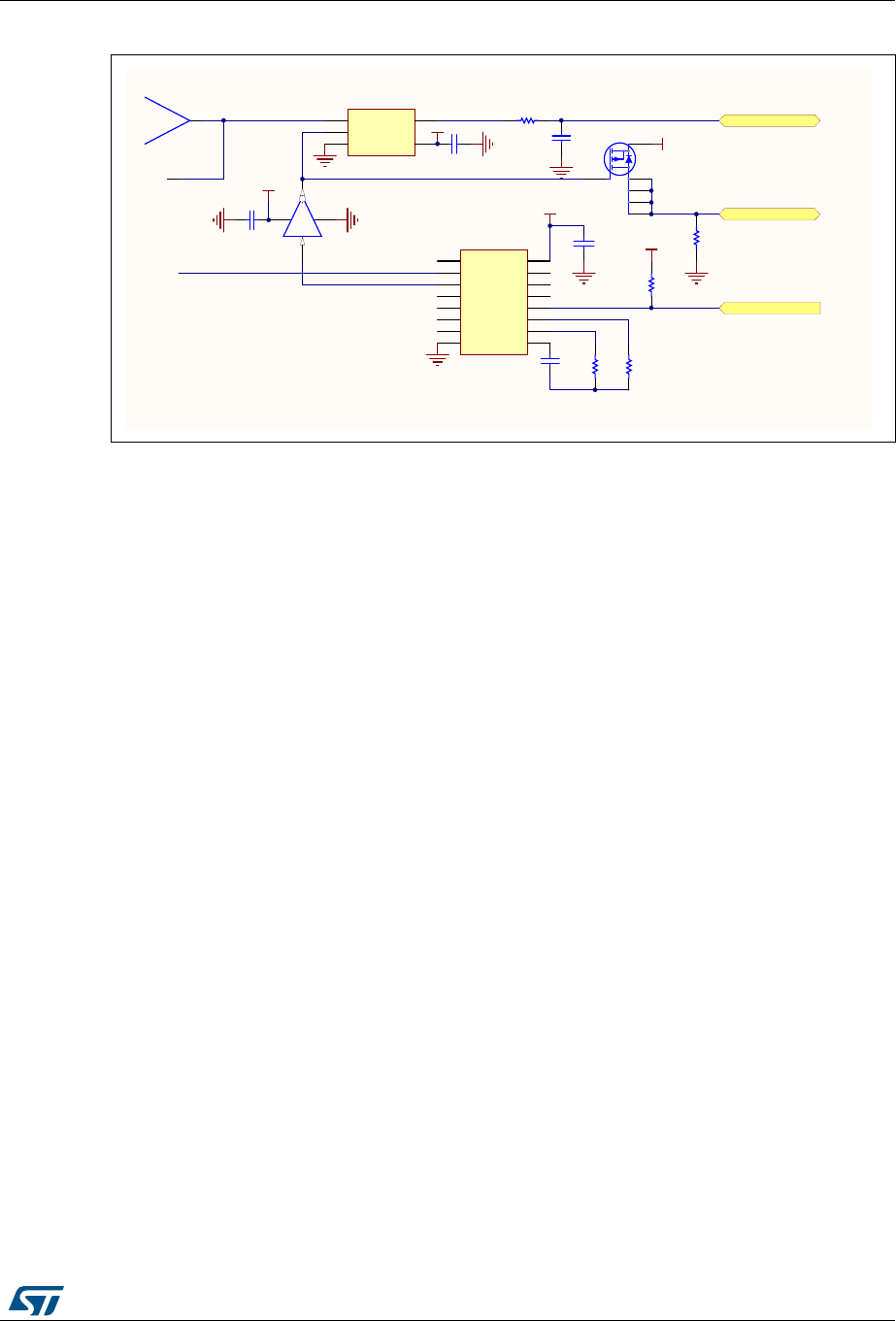
DocID027351 Rev 5 57/101
UM1855 Hardware layout and configuration
100
Figure 18. Schematic diagram of logic part of low-power-mode IDD measurement
The measurement process consists of 3 phases:
Phase 1 - start and transiting to low-power mode
While in dynamic run mode, the MCU sets IDD_CNT_EN signal on its PF10 port low,
starting the measurement process. This makes the counters in U14 start counting the clock
pulses generated with an own RC oscillator. At about 150 ms from the start, the Q12 output
of U14 goes high, terminating the phase 1. After starting the measurement process, the
MCU transits to low-power mode. The duration of the phase 1 of about 150ms allows the
MCU enough time for transiting into low-power mode.
Phase 2 - sampling
The MCU is now in low-power mode. The phase 2 starts with the Q12 port of U14 going
high, 150 ms after the MCU, at that time in dynamic run mode, started the low-power-mode
consumption current measurement process. The transistor T2 goes in high-impedance
mode, which results in setting the analog part in high sensitivity state, needed for measuring
very low currents. The Q13 port of U14 keeps the path between ports I/O and O/I of U13
conductive. The sampling capacitor C73 is charged through the resistor R122 to the voltage
at the output of the differential analog amplifier, representing the current consumed by the
MCU in low-power mode. The duration of the phase 2 is about 150 ms. This time is needed
to allow the voltage on the sampling capacitor C73 to stabilize.
Phase 3 - exiting low-power mode, measurement and end
The MCU is in low-power mode. The voltage across C73 capacitor is now stabilized so it
represents the current consumed by the MCU in low-power mode. The phase 3 starts with
setting the U13 path between ports O/I and I/O to non-conductive state, for the voltage
across C73 to hold. The same event causes the IDD_WAKEUP signal for the MCU to
change state, to signal to the MCU that the voltage on C73 is now ready for being
measured. The MCU transits from low-power mode to dynamic run mode. The voltage on
C73 representing the current the MCU consumed when it was in low-power mode, is now
measured by the MCU, using the ADC port PA5, and stored. The Q12 port transits to low
state at the same time as the Q13 goes high. As a consequence, the analog part of the IDD
measurement circuit is back to low-sensitivity mode adapted for measuring the
microcontroller supply current in its dynamic run mode. The phase 3 and the whole
measurement process ends with the microcontroller setting the IDD_CNT_EN signal back
high. Figure 19 illustrates the timing of the low-power-mode current consumption
measurement process.
IDD_Measurement
IDD_CNT_EN
IDD_WAKEUP
2
3
4
5
U16
SN74LVC1G04DCKT
I/O
1O/I 2
GND
3C
4
VCC 5
U13
SN74LVC1G66DCKT
3
4
5
G
S
D
1
2
6
T3
FDC606P
VDD
Q11
1
Q12
2
Q13
3
Q5
4
Q4
5
Q6
6
Q3
7
GND
8Ctc 9
Rtc 10
RS 11
MR 12
Q8 13
Q7 14
Q9 15
VCC 16
U14
74LV4060PW
VDD
VDD
R127
220K
R122
10K
VDD
C77
1nF
R134
15K
R130
30K
Oscillator frequency 30KHz
VDD
C72
100nF
PC5
PF10
PA5
8
U15C
TSZ124IPT
Shunt_x1000
C73
1uF
R137
220K
C74
100nF
C76
100nF
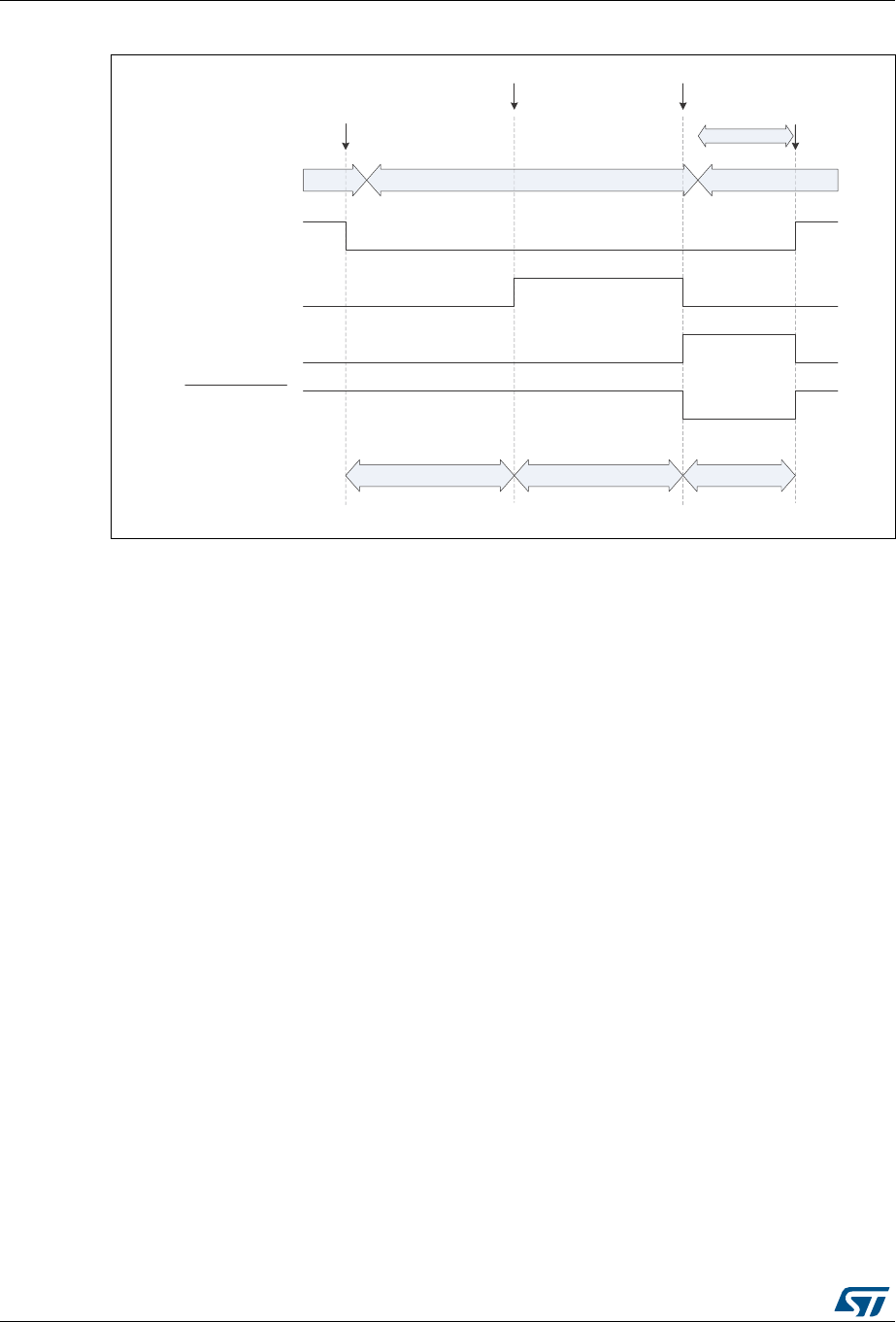
Hardware layout and configuration UM1855
58/101 DocID027351 Rev 5
Figure 19. Low-power-mode IDD measurement timing
2.30.3 IDD measurement in dynamic run mode
In dynamic run mode, the IDD_CNT_EN remains high. The T2 is in conductive state, setting
the shunt resistor to 1 Ω. The U13 path from port 1 to 2 is permanently conductive and the
voltage on the capacitor C73 follows the MCU current consumption. R122 allows filtering
fast changes.
2.30.4 Calibration procedure
For the measurement to be precise, it is mandatory to perform a calibration before the
measurement. The calibration allows subtracting, from the voltage measured across C73,
the offset at the differential amplifier output, described in Section 2.30.1.
The calibration procedure consists in measuring the offset voltage when the current through
the shunt resistor is zero. The current consumption values measured by the microcontroller
are then compensated for offset, by subtracting the now-known offset number from the
measured number. Setting the current through the shunt resistor to zero is reached through
appropriate setting jumpers in the JP11 jumper header.
06Y9
,''B&17B(1
80&8SRUW3%
/2:B32:(5B(1
8FRXQWHUSRUW4
,''B:$.(83
8FRXQWHUSRUW4
,''B:$.(83
8LQYHUWHUWHUPLQDO
WŚĂƐĞϭ WŚĂƐĞϮ WŚĂƐĞϯ
6+VZLWFK8FORVHG 8RSHQ
KLJK,''UDQJH ORZ,''UDQJH KLJK,''UDQJH
,''PHDVXUHPHQWSURFHVVLQSURJUHVV
>ŽǁͲƉŽǁĞƌ
ZƵŶ ZƵŶ
0&8RSHUDWLQJPRGH
6WDUW
SURFHVV
6WDUWORZSRZHU,''
VDPSOLQJ
+ROGORZSRZHU,''VDPSOH
:DNH0&8XS
(QG
SURFHVV
$FWLRQE\0&8
$FWLRQE\ORJLF
ŵĞĂƐƵƌĞŵĞŶƚ
aPV aPV
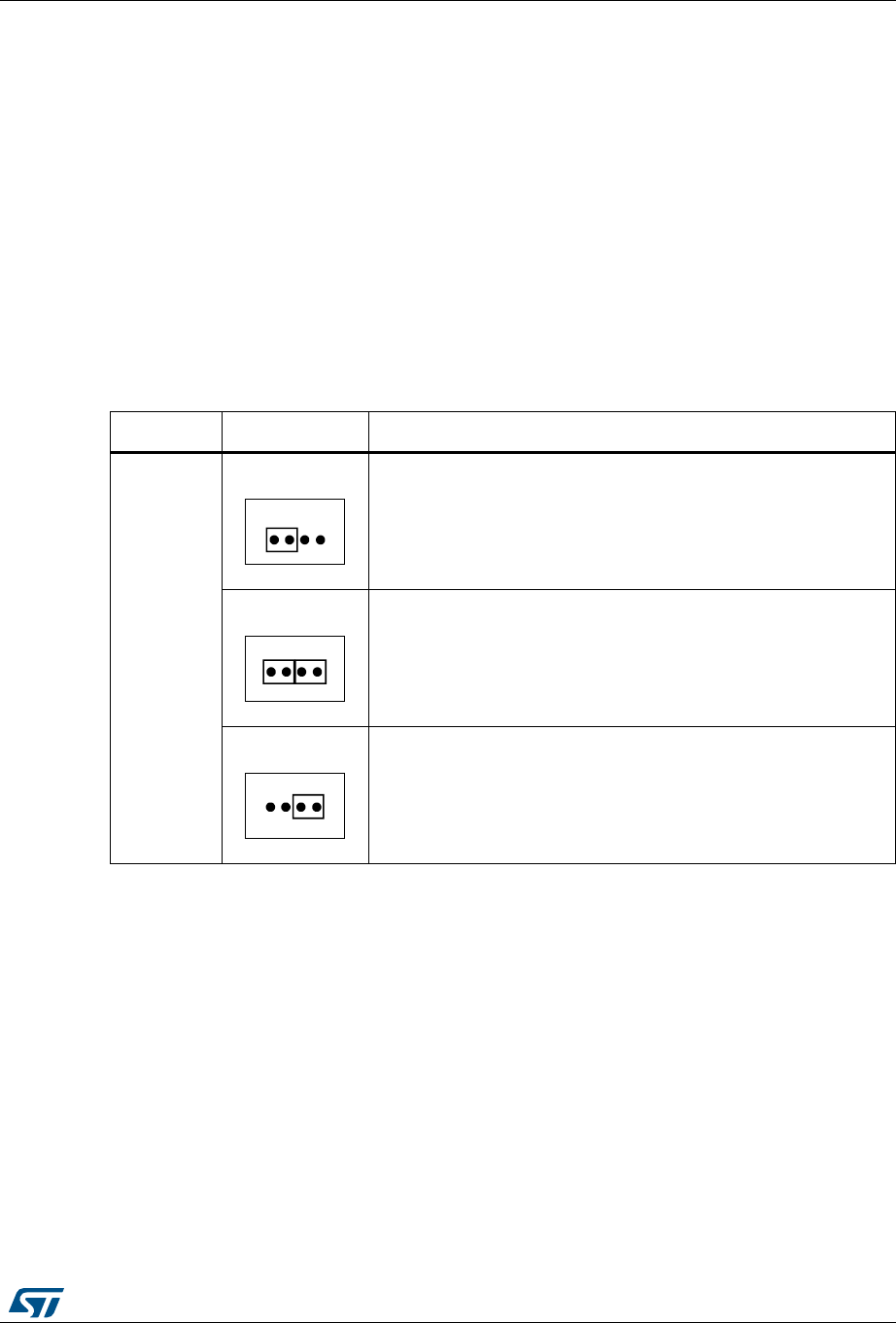
DocID027351 Rev 5 59/101
UM1855 Hardware layout and configuration
100
Calibration procedure and current measurement compensation steps:
•On JP11, short terminals 1 and 2 and open terminals 3 and 4. The current through the
shunt resistor is now zero.
•Run low-power-mode IDD measurement as described in Section 2.30.2. The value
Voffset measured corresponds to offset of the differential amplifier.
•On JP11, add a second jumper, to short terminals 3 and 4, then remove the jumper
from terminals 1 and 2 of JP11. The MCU supply has not been interrupted and the
supply current now passes through the shunt resistor.
•Run low-power-mode IDD measurement as described in Section 2.30.2. The value
Vmeasured obtained corresponds to the sum of MCU supply current and the differential
amplifier’s offset Voffset.
•The software computes a Vout number representing the MCU supply current as
Vout = Vmeasured - Voffset
Table 31. JP11 jumper settings during IDD measurement with calibration
Jumper Setting Description
JP11
JP11 Configuration used to measure Voffset.
JP11 in VDD position
STM32L476ZGT6 supply current does not flow through shunt
resistor.
JP11
Configuration to transit from direct to shunted supply to
STM32L476ZGT6, without ever interrupting the MCU supply.
JP11 Default setting.
Configuration used to measure the MCU supply current.
JP11 in IDD position
STM32L476ZGT6 supply current flows through shunt resistor.
İ
1 2 3 4
İ
1 2 3 4
İ
1 2 3 4
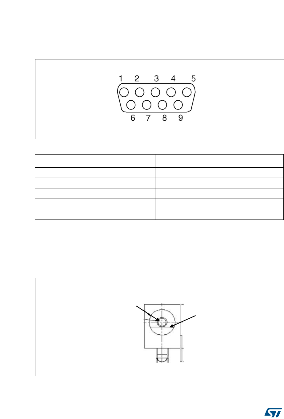
Connectors UM1855
60/101 DocID027351 Rev 5
3 Connectors
3.1 RS-232 D-sub male connector CN9
Figure 20. RS-232 D-sub (DE-9M) 9-pole connector (front view)
3.2 Power connector CN22
The STM32L476G-EVAL board can be powered from a DC-5V external power supply via
the CN22 jack illustrated in Figure 21. The central pin of CN22 must be positive.
Figure 21. Power supply connector CN22 (front view)
Table 32. RS-232 D-sub (DE-9M) connector CN9 with HW flow control and ISP support
Terminal Terminal name Terminal Description
1NC 6Bootloader_BOOT0
2RS232_RX (PB7) 7NC
3RS232_TX (PG12) 8Bootloader_RESET
4NC 9NC
5 GND - -
-36
-36
'&9
*1'
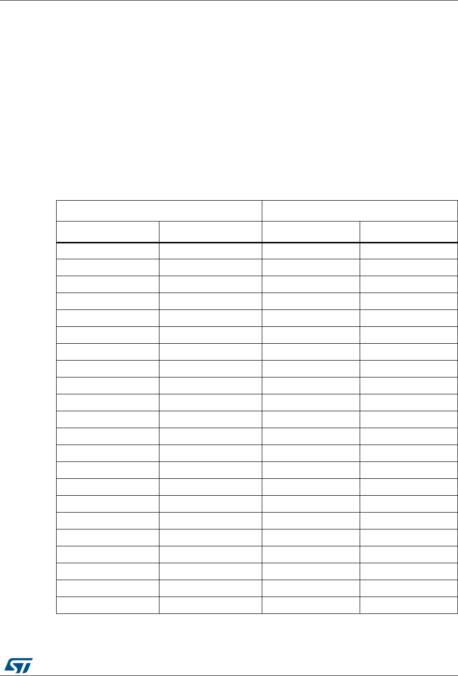
DocID027351 Rev 5 61/101
UM1855 Connectors
100
3.3 LCD daughterboard connectors CN11 and CN14
Two 48-pin male headers CN11 and CN14 are used to connect to LCD glass module
daughterboard MB979. The type of connectors, their mutual orientation, distance and
terminal assignment are kept for a number of ST MCU evaluation boards. This
standardization allows developing daughterboards that can be used in multiple evaluation
kits. The width between CN11 pin1 and CN14 pin1 is 700 mils (17.78 mm).
STM32L476ZGT6 ports routed to these two connectors can be accessed on odd CN11 and
CN14 pins (the row of pin 1), when no daughterboard is plugged in.
Daughterboards plugging into CN11 and CN14 must keep the even terminals of CN11 and
CN14 open.
Table 33 shows the signal assignment to terminals.
Table 33. CN11 and CN14 daughterboard connectors
CN11 CN14
Odd pin MCU port Odd pin MCU port
1PA9 1PD2
3PA8 3PC12
5PA10 5PC11
7PB9 7PC10
9PB11 9PB7
11 PB10 11 PC4
13 PB5 13 PC5
15 PB14 15 PC6
17 PB13 17 PC7
19 PB12 19 PC8
21 PA15 21 PC9
23 PB8 23 PD8
25 PB15 25 PD9
27 PC2 27 PD10
29 PC1 29 PD11
31 PC0 31 PD12
33 PA3 33 PD13
35 PA2 35 PD14
37 PB0 37 PD15
39 PA7 39 PE0
41 PA6 41 PE1
43 PB4 43 PE2
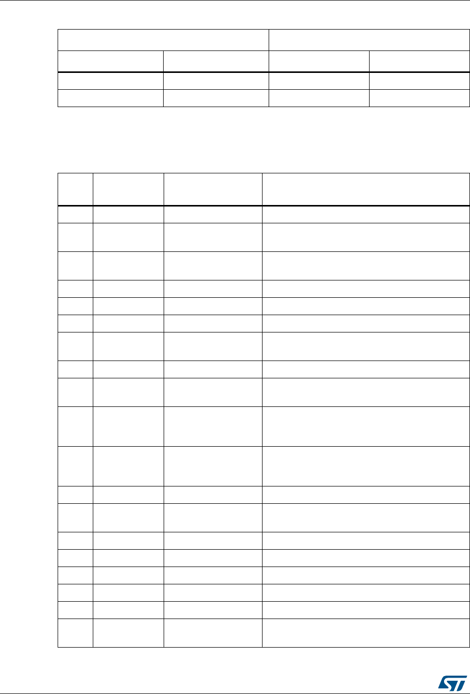
Connectors UM1855
62/101 DocID027351 Rev 5
3.4 Extension connectors CN6 and CN7
45 PB3 45 PE3
47 PB1 47 PA1
Table 33. CN11 and CN14 daughterboard connectors (continued)
CN11 CN14
Odd pin MCU port Odd pin MCU port
Table 34. Daughterboard extension connector CN6
Pin Description Alternative
Functions
How to disconnect Alternative functions to
use on the extension connector
1GND - -
3PG6 CODEC_INT,
MC_ICL_Shutout Remove R35, Open SB5
5PA13 TMS/SWDIO Do not use Trace connector CN12 and JTAG
connector CN15
7PA12 USBOTG_DP Remove R4
9PG8 LPUART_RX_3V3 Remove R158, R188
11 GND - -
13 PG2 A12 Remove R18 to deselect SRAM U2
Remove R43 to deselect Flash memory U5
15 PD3 DFSDM_DATIN1 Remove R23
17 PD0 D2 Remove R18 to deselect SRAM U2
Remove R43 to deselect Flash memory U5
19 PD5 FMC_NWE
Cannot be disconnected from SRAM and Flash
memory, but is an input for SRAM and Flash
memory
21 PG10 LCD_NE3
Cannot be disconnected from TFT LCD level
shifters U21 and U22, but is an input for TFT
LCD.
23 PD7 FMC_NE1 Remove R18
25 PF0 A0 Remove R18 to deselect SRAM U2
Remove R43 to deselect Flash memory U5
27 PG11 USART1_CTS_3V3 Remove R93
29 PG13 I2C_SDA Remove R58
31 PG12 USART1_RTS Remove R116
33 PG14 I2C_SCL Remove R61
35 PG15 IOExpander_INT Remove R228
37 PF4 A4 Remove R18 to deselect SRAM U2
Remove R43 to deselect Flash memory U5
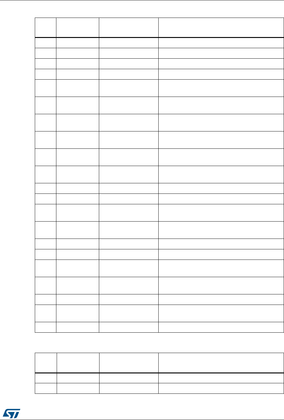
DocID027351 Rev 5 63/101
UM1855 Connectors
100
39 GND - -
2+3V3 - -
4PG7 LPUART_TX Remove R119, R189
6PA11 USBOTG_DM Remove R3
8PA14 TCK/SWCLK Do not use Trace connector CN12 and JTAG
connector CN15
10 PG5 A15 Remove R18 to deselect SRAM U2
Remove R43 to deselect Flash memory U5
12 PG3 A13 Remove R18 to deselect SRAM U2
Remove R43 to deselect Flash memory U5
14 PG4 A14 Remove R18 to deselect SRAM U2
Remove R43 to deselect Flash memory U5
16 PD1 D3 Remove R18 to deselect SRAM U2
Remove R43 to deselect Flash memory U5
18 PD4 FMC_NOE Remove R18 to deselect SRAM U2
Remove R43 to deselect Flash memory U5
20 PG9 FMC_NE2 Remove R43
22 GND - -
24 PD6 SAI1_SDA,
FMC_NWAIT Remove R53, open SB10
26 PF1 A1 Remove R18 to deselect SRAM U2
Remove R43 to deselect Flash memory U5
28 D5V - -
30 PC13 Wake-up Remove R244
32 PF2 A2 Remove R18 to deselect SRAM U2
Remove R43 to deselect Flash memory U5
34 PF3 A3 Remove R18 to deselect SRAM U2
Remove R43 to deselect Flash memory U5
36 GND - -
38 PF5 A5 Remove R18 to deselect SRAM U2
Remove R43 to deselect Flash memory U5
40 PB6 USART1_TX Remove R118
Table 35. Daughterboard extension connector CN7
Pin Description Alternative
Functions
How to disconnect Alternative functions to
use on the extension connector
1GND - -
3PE14 D11 -
Table 34. Daughterboard extension connector CN6 (continued)
Pin Description Alternative
Functions
How to disconnect Alternative functions to
use on the extension connector
Connectors UM1855
64/101 DocID027351 Rev 5
5PE12 D9 -
7PE10 D7 -
9PE8 D5 -
11 PG1 A11 -
13 PB2 LED1,
MC_DissipativeBrake Remove R54, SB11
15 GND - -
17 PF12 A6 -
19 PF11 NFC_NSS Do not connect the NFC daughterboard to
connector CN13
21 PE4 A20, TRACE_D1 Remove R84, SB40
23 PE5 A21, TRACE_D2 Remove R85, SB38
25 PC14 OSC32_IN Remove R87, Close SB41
27 PF6 SAI1_SDB Remove R105
29 PF9 SAI1_FSB,
MC_PFC_sync Remove R90, SB25
31 PF10 IDD_CNT_EN,
MC_PFC_PWM Remove R91, SB37
33 PH1 OSC_OUT Remove R95, close SB23
35 PA5 IDD_Measurement Remove R69
37 PA0 OpAmp1_INP,
MC_EncA Remove R83, SB35
39 GND - -
2PE15 D12 -
4PE13 D10 -
6PE11 D8 -
8PE9 D6 -
10 PE7 D4 -
12 PG0 A10 -
14 PF15 A9 -
16 PF14 A8 -
18 PF13 A7 -
20 BOOT0 BootLoader from
UART Remove JP8
22 PE6 A21, TRACE_D3 Remove R86, SB39
24 PC15 OSC32_OUT Remove R88, close SB33
Table 35. Daughterboard extension connector CN7 (continued)
Pin Description Alternative
Functions
How to disconnect Alternative functions to
use on the extension connector
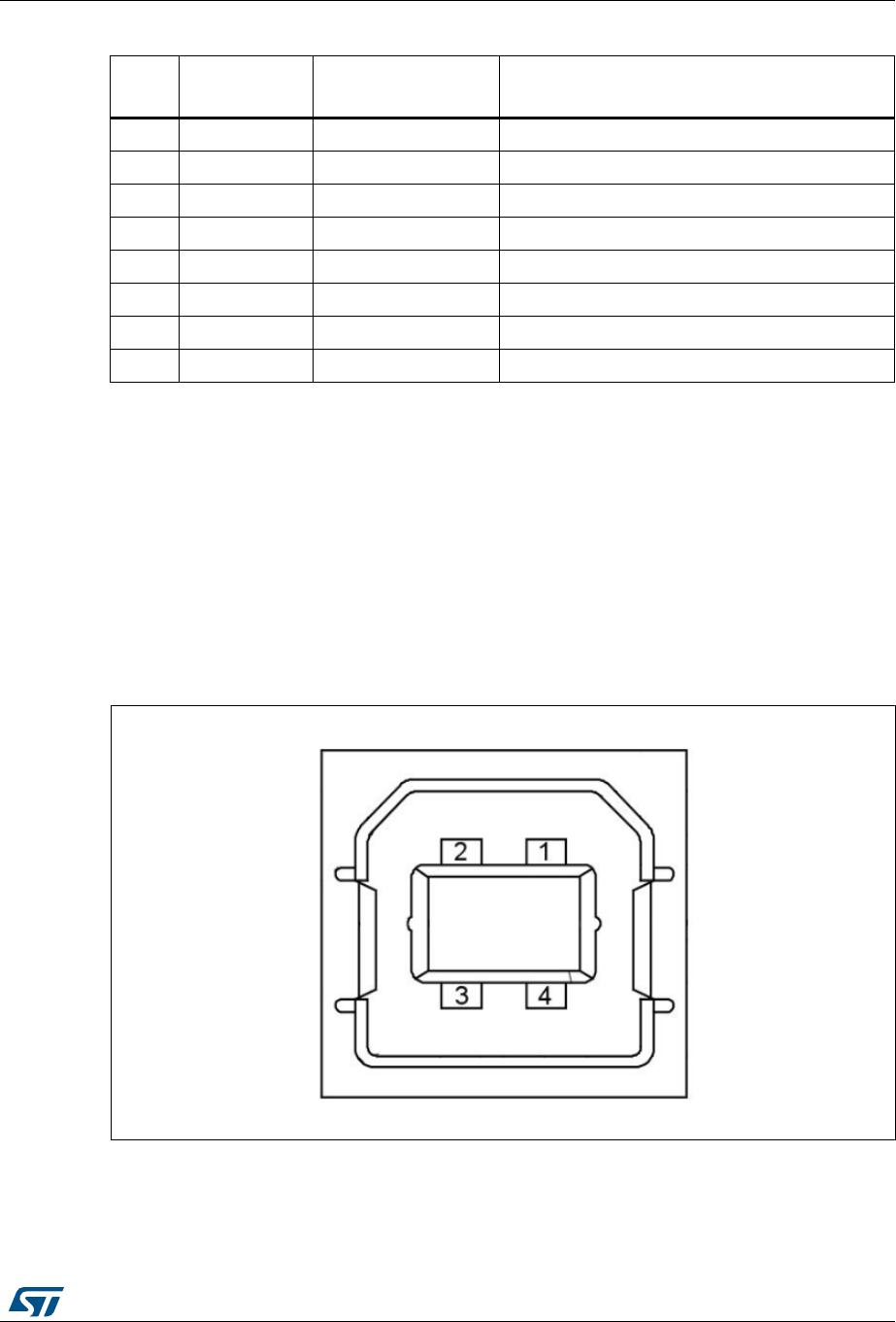
DocID027351 Rev 5 65/101
UM1855 Connectors
100
3.5 ST-LINK/V2-1 programming connector CN16
The connector CN16 is used only for embedded ST-LINK/V2-1 programming, during board
manufacture. It is not populated by default and not for use by the end user.
3.6 ST-LINK/V2-1 Standard-B USB connector CN17
The USB connector CN17 is used to connect the on-board ST-LINK/V2-1 facility to PC for
flashing and debugging software.
Figure 22. USB type B connector CN17 (front view)
26 GND - -
28 PF7 SAI1_MCKB Remove R106
30 PF8 SAI1_SCKB Remove R89
32 RESET# - -
34 PH0 OSCIN Remove crystal X2, C54, close SB24
36 PC3 VLCD Remove R94
38 PA4 ADC_DAC Remove R73
40 VDD - -
Table 35. Daughterboard extension connector CN7 (continued)
Pin Description Alternative
Functions
How to disconnect Alternative functions to
use on the extension connector
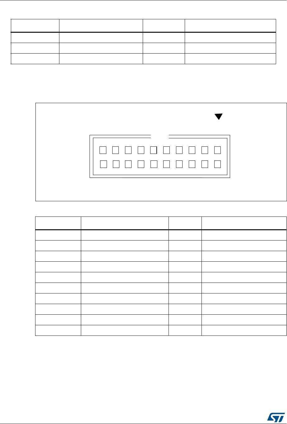
Connectors UM1855
66/101 DocID027351 Rev 5
3.7 JTAG connector CN15
Figure 23. JTAG debugging connector CN15 (top view)
Table 36. USB Standard-B connector CN17
Terminal Description Terminal Description
1VBUS(power) 4 GND
2DM 5,6 Shield
3DP - -
Table 37. JATG debugging connector CN15
Terminal Function / MCU port Terminal Function / MCU port
1VDD power 2VDD power
3PB4 4 GND
5PA15 6 GND
7PA13 8 GND
9PA14 10 GND
11 RTCK 12 GND
13 PB3 14 GND
15 RESET# 16 GND
17 DBGRQ 18 GND
19 DBGACK 20 GND
D^ϯϬϳϮϮsϮ
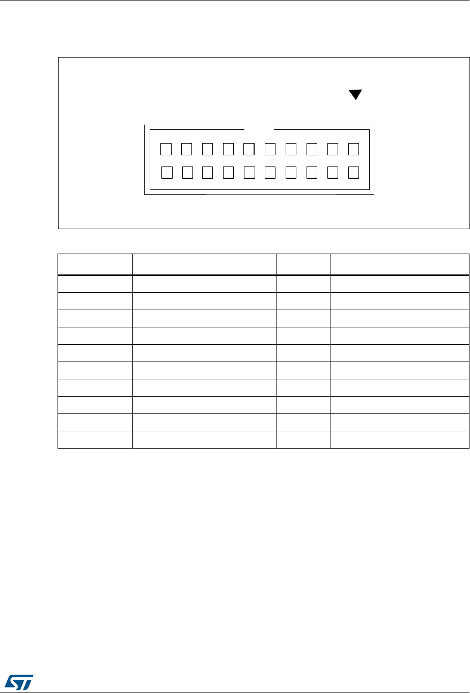
DocID027351 Rev 5 67/101
UM1855 Connectors
100
3.8 ETM trace debugging connector CN12
Figure 24. Trace debugging connector CN12 (top view)
Table 38. Trace debugging connector CN12
Terminal Function / MCU port Terminal Function / MCU port
1VDD power 2TMS/PA13
3 GND 4 TCK/PA14
5 GND 6 TDO/PB3
7KEY 8TDI/PA15
9 GND 10 RESET#
11 GND 12 TraceCLK/PE2
13 GND 14 TraceD0/PE3 or SWO/PB3
15 GND 16 TraceD1/PE4 or nTRST/PB4
17 GND 18 TraceD2/PE5
19 GND 20 TraceD3/PE6
D^ϯϬϳϮϮsϮ
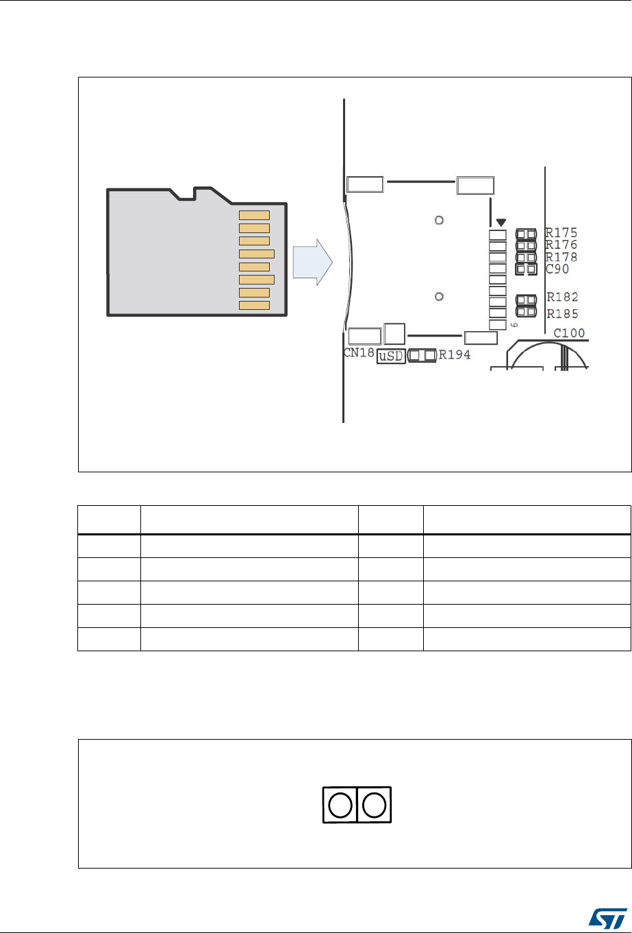
Connectors UM1855
68/101 DocID027351 Rev 5
3.9 microSD card connector CN18
Figure 25. microSD card connector CN18
3.10 ADC/DAC connector CN8
Figure 26. Analog input-output connector CN8 (top view)
Table 39. microSD card connector CN18
Terminal Terminal name (MCU port) Terminal Terminal name (MCU port)
1SDIO_D2 (PC10) 6Vss/GND
2SDIO_D3 (PC11) 7SDIO_D0 (PC8)
3SDIO_CMD (PD2) 8SDIO_D1 (PC9)
4VDD 9GND
5SDIO_CLK (PC12) 10 MicroSDcard_detect (PA8)
06Y9
PLFUR6'
FDUG &1
(YDOXDWLRQERDUG
06Y9
Ϯ
ϭ
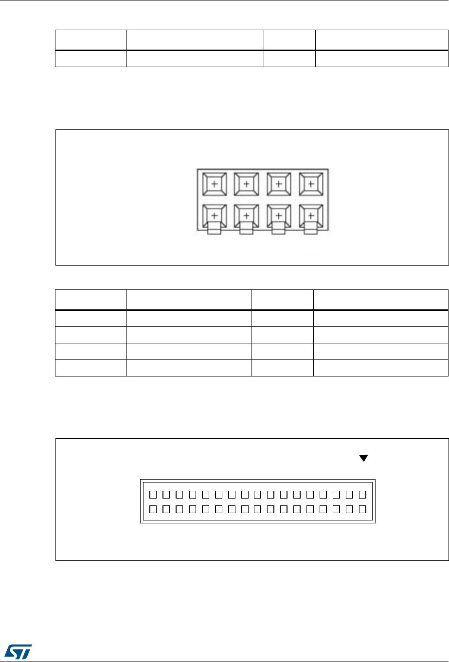
DocID027351 Rev 5 69/101
UM1855 Connectors
100
3.11 RF-EEPROM daughterboard connector CN3
Figure 27. RF-EEPROM daughterboard connector CN3 (front view)
3.12 Motor control connector CN2
Figure 28. Motor control connector CN2 (top view)
Table 40. Analog input-output connector CN8
Terminal Function / MCU port Terminal Function / MCU port
1 GND 2 analog input-output PA4
Table 41. RF-EEPROM daughterboard connector CN3
Terminal Terminal name (MCU port) Terminal Terminal name (MCU port)
1I2C_SDA (PG13) 5+3V3
2NC 6NC
3I2C_SCL (PG14) 7GND
4EXT_RESET(PC6) 8+5 V
069
-36
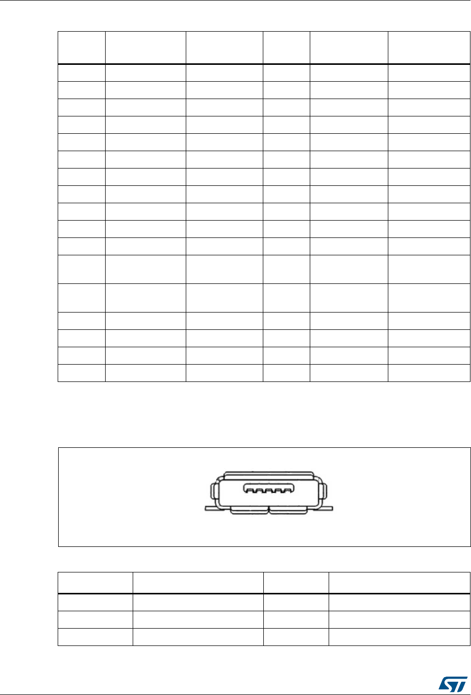
Connectors UM1855
70/101 DocID027351 Rev 5
3.13 USB OTG FS Micro-AB connector CN1
Figure 29. USB OTG FS Micro-AB connector CN1 (front view)
Table 42. Motor control connector CN2
CN2
terminal Description MCU port CN2
terminal MCU port Description
1Emergency STOP PC9 2 - GND
3PWM_1H PC6 4 - GND
5PWM_1L PA7 6 - GND
7PWM_2H PC7 8 - GND
9PWM_2L PB0 10 -GND
11 PWM_3H PC8 12 -GND
13 PWM_3L PB1 14 PC5 BUS VOLTAGE
15 CURRENT A PC0 16 -GND
17 CURRENT B PC1 18 -GND
19 CURRENT C PC2 20 -GND
21 ICL Shutout PG6 22 -GND
23 DISSIPATIVE
BRAKE PB2 24 PC4 PCD Ind Current
25 +5V power -26 PA3 Heat sink
temperature
27 PFC SYNC PF9 28 -3.3 V power
29 PFC PWM PF10 30 PB12 PFC Shut Down
31 Encoder A PA0 32 PA6 PFC Vac
33 Encoder B PA1 34 PA2 Encoder Index
Table 43. USB OTG FS Micro-AB connector CN1
Terminal Terminal name (MCU port) Terminal Terminal name (MCU port)
1VBUS (PA9 & PB13) 4ID (PA10)
2D- (PA11) 5GND
3D+ (PA12) - -
069
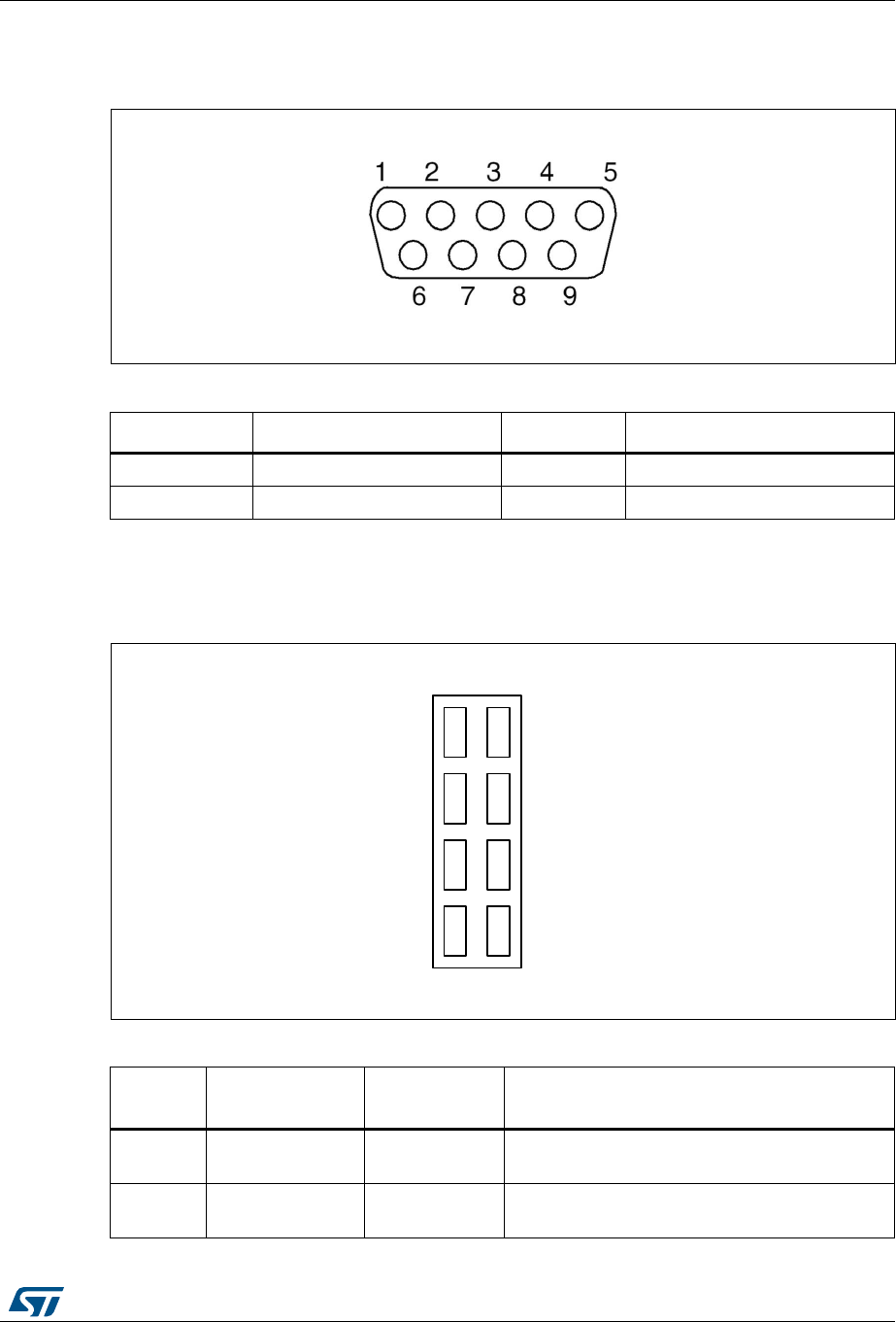
DocID027351 Rev 5 71/101
UM1855 Connectors
100
3.14 CAN D-sub male connector CN5
Figure 30. CAN D-sub (DE-9M) 9-pole male connector CN5 (front view)
3.15 NFC connector CN13
Figure 31. NFC female connector CN13 (top view)
Table 44. CAN D-sub (DE-9M) 9-pins male connector CN5
Terminal Terminal name Terminal Terminal name
1,4,8,9 NC 7CANH
2CANL 3,5,6 GND
-36
Table 45. NFC CN13 terminal assignment
CN13
terminal NFC signal MCU port Description
1NFC_IRQOUTN or
UART_TX PB7 Interrupt output for NFC
Connected to STM32L476ZGT6 UART RX
2NFC_IRQINN or
UART_RX PB6 Interrupt input for CR95HF
Connected to STM32L476ZGT6 UART TX
06Y9
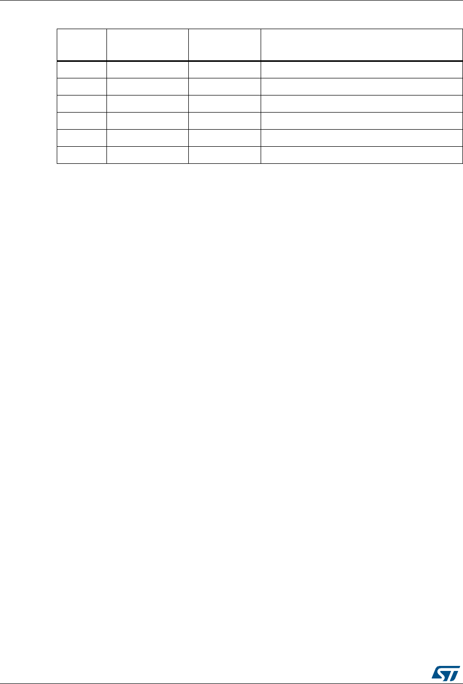
Connectors UM1855
72/101 DocID027351 Rev 5
3NFC_NSS PF11 SPI slave select
4NFC_MISO PB14 SPI data, slave output
5NFC_MOSI PB15 SPI data, slave input
6NFC_SCK PB13 SPI serial clock
7+3V3 PB6 Main power supply/power supply for RF drivers
8GND PB7 Ground
Table 45. NFC CN13 terminal assignment (continued)
CN13
terminal NFC signal MCU port Description

DocID027351 Rev 5 73/101
UM1855 Schematic diagrams
100
Appendix A Schematic diagrams
This section provides design schematics for the STM32L476G-EVAL key features to help
users to implement these features in application designs.
This section includes:
•Overall schematics for the board, see Figure 32
•MCU, LCD daughterboard and I/O expander interfaces, see Figure 33
•STM32L476G-EVALMCU part 1, see Figure 34
•STM32L476G-EVAL MCU part 2, see Figure 35
•LCD glass module daughterboard connectors, see Figure 36
•I/O expander, see Figure 37
•Power supply, see Figure 38
•Smartcard, SWP and NFC, see Figure 39
•USART and IrDA, see Figure 40
•SRAM and NOR Flash memory devices, see Figure 41
•TFT LCD, see Figure 42
•Extension connector, see Figure 43
•Quad-SPI Flash memory device, Figure 44
•microSD card, see Figure 45
•Physical control peripherals, see Figure 46
•CAN transceiver, see Figure 47
•Touch-sensing device, see Figure 48
•USB_OTG_FS port, see Figure 49
•IDD measurement, see Figure 50
•Audio codec device, see Figure 51
•STPMS2L and PT100, see Figure 52
•RF-EEPROM and EEPROM, see Figure 53
•Motor control connector, see Figure 54
•JTAG and trace debug connectors, Figure 55
•ST-LINK/V2-1, see Figure 56
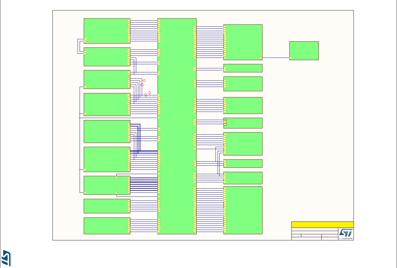
Schematic diagrams UM1855
74/101 DocID027351 Rev 5
Figure 32. STM32L476G-EVAL top
125
Top schematic
MB1144 C-02
10/7/2016
Title:
Size: Reference:
Date: Sheet: of
A3 Revision:
STM32L476G-EVAL
Project:
FMC_NWAIT
FMC_NOE
FMC_NWE
FMC_NE1
FMC_NE2
LCD_NE3
LED1
LED2
LPUART_TX
USART1_TX
USART1_RTS
TMS/SWDIO
TCK/SWCLK
TDI
TRST
Key
DFSDM_DATIN1
IDD_Measurement
CODEC_INT
USBOTG_PRDY
USBOTG_OVRCR
DMIC_DATIN
PT100_DATIN
USBOTG_VBUS
USBOTG_ID
IDD_WAKEUP
OpAmp1_INM
Comp2_INP
TDO/SWO
TRACE_D1
TRACE_D2
TRACE_D3
IDD_CNT_EN
USBOTG_PPWR
TRACE_CK
TRACE_D0
SmartCard_CLK
OpAmp1_OUT
ADC_DAC
USBOTG_DP
USBOTG_DM
SmartCard_IO
QSPI_D0
QSPI_D1
QSPI_D2
QSPI_D3
uSD_D0
uSD_D1
uSD_D2
uSD_D3
MC_DissipativeBrake
MC_PFC_sync
MC_PWM_1H
MC_PWM_1L
MC_PWM_2H
MC_PWM_2L
MC_PWM_3H
MC_PWM_3L
MC_ICL_Shutout
MC_PFC_PWM
MC_PFC_Vac
QSPI_CLK
QSPI_CS
FMC_NBL0
FMC_NBL1
CAN_TX
MC_EncA
MC_EncB
MC_EncIndex
MC_CurrentB
MC_CurrentC
MC_Temperature
MC_PFC_Shutdown
CAN_RX
uSD_DETECT
uSD_CMD
uSD_CLK
SWP_IO
IOExpander_X+
IOExpander_X-
IOExpander_Y+
IOExpander_Y-
JOY_SEL
JOY_DOWN
JOY_LEFT
JOY_RIGHT
JOY_UP
SmartCard_OFF
LED4
LED3
SmartCard_RST
SmartCard_CMDVCC
SmartCard_3/5V
D[0..15]
A[0..23]
PA[0..15]
PB[0..15]
PC[0..15]
PD[0..15]
PE[0..15]
PF[0..15]
PG[0..15]
MC_CurrentA
MC_EmergencySTOP
MC_BusVoltage
MC_PFC_IndCurr
RESET#
DFSDM_CKOUT
I2C_SCL
I2C_SDA
PH1
PH0
SHIELD
SAI1_MCKB
SAI1_SCKB
SAI1_FSB
SAI1_SDB
SAI1_SDA
OpAmp1_INP
Comp2_OUT
TKEY
TKEY_CS
SHIELD_CS
Bootloader_RESET_3V3
Bootloader_BOOT0_3V3
LPUART_RX_3V3
USART1_CTS_3V3
USART1/IrDA_RX_3V3
BL_Control
EXT_RESET
BOOT0
NFC_NSS
NFC_MOSI
NFC_SCK
NFC_MISO
I2C2_SDA
I2C2_SCL
U_MCU_LCDGlass_Symbol
MCU_LCDGlass_Symbol.SchDoc
FMC_NWE
FMC_NOE
FMC_NWAIT
FMC_NBL0
FMC_NBL1
D[0..15]
A[0..23]
FMC_NE1
FMC_NE2
U_SRAM&Flash
SRAM&Flash.SchDoc
MC_EmergencySTOP
MC_CurrentA
MC_CurrentB
MC_CurrentC
MC_PFC_sync
MC_PWM_3L
MC_PWM_2H
MC_PWM_2L
MC_PWM_1H
MC_PWM_1L
MC_PWM_3H
MC_ICL_Shutout
MC_DissipativeBrake
MC_PFC_PWM
MC_EncA
MC_EncB
MC_BusVoltage
MC_EncIndex
MC_PFC_IndCurr
MC_Temperature
MC_PFC_Shutdown
MC_PFC_Vac
U_MotorControl
MotorControl.SchDoc
uSD_CLK
uSD_CMD
uSD_D0
uSD_D1
uSD_D2
uSD_D3
uSD_DETECT
U_MicroSD
MicroSD.SchDoc
QSPI_D0
QSPI_D3
QSPI_D2
QSPI_D1
QSPI_CLK
QSPI_CS
U_QSPI
QSPI.SchDoc
PA[0..15]
PB[0..15]
PC[0..15]
PD[0..15]
PE[0..15]
RESET#
PF[0..15]
PG[0..15]
PH1
PH0
BOOT0
U_Extension connector
Extension connector.SCHDOC
TDI
RESET#
TRACE_D3
TRACE_D2
TRACE_D1
TRACE_D0
TRACE_CK
TRST
TMS/SWDIO
TCK/SWCLK
TDO/SWO
U_JTAG&Trace
JTAG&Trace.SchDoc
TDO/SWO
RESET#
TDI
TRST
TMS/SWDIO
TCK/SWCLK
LPUART_RX_3V3
LPUART_TX
U_ST_LINK
ST_LINK.SCHDOC
USART1/IrDA_RX_3V3
Bootloader_BOOT0_3V3
Bootloader_RESET_3V3
USART1_CTS_3V3
USART1_TX
USART1_RTS
LPUART_RX_3V3
LPUART_TX
NFC_IRQINN
NFC_IRQOUTN
U_USART_IrDA
USART_IrDA.SchDoc
SWP_IO
SmartCard_3/5V
SmartCard_IO
SmartCard_RST
SmartCard_CLK
SmartCard_OFF
SmartCard_CMDVCC
NFC_IRQINN
NFC_IRQOUTN
NFC_NSS
NFC_MOSI
NFC_MISO
NFC_SCK
U_SWP_SmartCard_NFC
SWP_SmartCard_NFC.SchDoc
DFSDM_CKOUT
DFSDM_DATIN1
PT100_DATIN
U_STPMS2&PT100
STPMS2&PT100.SchDoc
IDD_Measurement
IDD_CNT_EN
IDD_WAKEUP
U_IDD_measurement
IDD_measurement.SchDoc
USBOTG_VBUS
USBOTG_PRDY
USBOTG_DM
USBOTG_DP
USBOTG_OVRCR
USBOTG_PPWR
USBOTG_ID
U_USB_OTG_FS
USB_OTG_FS.SchDoc
SHIELD
SHIELD_CS
TKEY_CS
TKEY
U_Touch Sensing
Touch Sensing.SchDoc
CAN_TX
CAN_RX
U_CAN
CAN.SchDoc
ADC_DAC
LED4
LED3
LED1
LED2
JOY_SEL
JOY_DOWN
JOY_LEFT
JOY_RIGHT
JOY_UP
KEY
VREF+
Comp2_INP
OpAmp1_OUT
OpAmp1_INM
OpAmp1_INP
Comp2_OUT
U_peripherals
peripherals.SchDoc
VREF+
U_Power
Power.SchDoc
SAI1_SCKB
SAI1_FSB
SAI1_SDB
CODEC_INT
I2C_SCL
SAI1_MCKB
I2C_SDA
DMIC_DATIN
DFSDM_CKOUT
SAI1_SDA
U_Audio
Audio.SchDoc
RESET#
FMC_NWE
LCD_NE3
FMC_NOE
D[0..15]
A[0..23]
IOExpander_Y+
IOExpander_Y-
IOExpander_X+
IOExpander_X-
BL_Control
U_LCD_TFT
LCD_TFT.SchDoc
I2C_SCL
I2C_SDA
EXT_RESET
I2C2_SDA
I2C2_SCL
U_RF_I2C_EEPROM
RF_I2C_EEPROM.SchDoc
N
ote: In all sheets, Italic format is used to differentiate text from schematic Net labels.
i
Matched Net Lengths [Tolerance = 100mil]
i
iPCB Rule
Clearance Constraint [Clearance = 10mil]
iPCB Rule
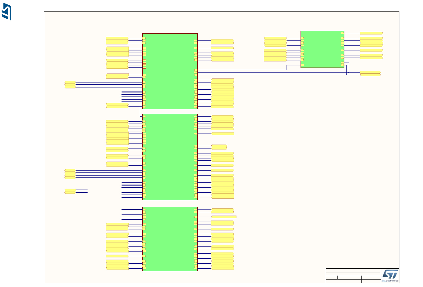
UM1855 Schematic diagrams
DocID027351 Rev 5 75/101
Figure 33. MCU, LCD daughterboard and I/O expander interfaces
225
MCU_LCDGlassl
MB1144 C-02
10/7/2016
Title:
Size: Reference:
Date: Sheet: of
A3 Revision:
STM32L476G-EVAL
Project:
PA[0..15]
PB[0..15]
PD[0..15]
PE[0..15]
USBOTG_DM
USBOTG_DP
TMS/SWDIO
TCK/SWCLK
DFSDM_DATIN1
FMC_NOE
FMC_NWE
FMC_NWAIT
FMC_NE1
TRACE_D3
TRACE_D1
TRST
D[0..15]
IDD_Measurement
USART1_TX
LED1
MC_DissipativeBrake
TRACE_D2
MC_EncA
TDI
TDO/SWO
ADC_DAC
RESET#
QSPI_D3
QSPI_D2
QSPI_D1
QSPI_D0
QSPI_CLK
QSPI_CS
TRACE_D0
TRACE_CK
SAI1_SDA
OpAmp1_INP
MC_PFC_Vac
MC_Temperature
MC_EncB
MC_EncIndex
TKEY
TKEY_CS
MC_PWM_1L
MC_PWM_2L
MC_PWM_3L
MC_PFC_Shutdown
A[20..22]
LCDCOM[0..3]
LCDCOM7
LCDSEG[0..17]
LCDSEG[28..39]
LCDSEG21
U_MCU
MCU.SchDoc
uSD_CMD
uSD_CLK
uSD_D3
uSD_D2
IDD_WAKEUP
PT100_DATIN
uSD_D0
uSD_D1OpAmp1_INM
FMC_NBL0
FMC_NBL1
LCDSEG[0..39]
LCDCOM[0..7]
USBOTG_VBUS
USBOTG_ID
CAN_TX
SWP_IO
CAN_RX
DMIC_DATIN
OpAmp1_OUT
Comp2_INP
SmartCard_CLK
SmartCard_IO
uSD_DETECT
DFSDM_CKOUT
D[0..15]
USBOTG_PRDY
USBOTG_OVRCR
USBOTG_PPWR
Comp2_OUT
USART1/IrDA_RX_3V3A[16..19]
A23
NFC_MISO
NFC_SCK
NFC_MOSI
I2C2_SDA
I2C2_SCL
LED3
U_LCD_Glass
LCD_Glass.SchDoc
IOExpander_Y+
IOExpander_Y-
IOExpander_X+
IOExpander_X-
IOExpander_INT I2C_SDA
JOY_SEL
JOY_DOWN
JOY_LEFT
JOY_RIGHT
JOY_UP
LED4
SmartCard_RST
SmartCard_CMDVCC
SmartCard_3/5V
SmartCard_OFF
I2C_SCL
LED2
BL_Control
EXT_RESET
U_IO_Expandor
IO_Expandor.SchDoc
Bootloader_RESET_3V3
Bootloader_BOOT0_3V3
FMC_NWAIT
LPUART_RX_3V3
USART1_CTS_3V3
FMC_NOE
FMC_NWE
FMC_NE1
FMC_NE2
LCD_NE3
LED1
NFC_NSS
LPUART_TX
USART1_TX
USART1_RTS
TMS/SWDIO
TCK/SWCLK
TDI
TRST
Key
DFSDM_DATIN1
IDD_Measurement
CODEC_INT
OpAmp1_INP
DMIC_DATIN
PT100_DATIN
USBOTG_VBUS
USBOTG_ID
IDD_WAKEUP
OpAmp1_INM
Comp2_INP
TDO/SWO
TRACE_D1
TRACE_D2
TRACE_D3
IDD_CNT_EN
TRACE_CK
TRACE_D0
SmartCard_CLK
OpAmp1_OUT
Comp2_OUT
ADC_DAC
USBOTG_DP
USBOTG_DM
SmartCard_IO
QSPI_D0
QSPI_D1
QSPI_D2
QSPI_D3
uSD_D0
uSD_D1
uSD_D2
uSD_D3
MC_BusVoltage
MC_DissipativeBrake
MC_PFC_sync
MC_PWM_1H
MC_PWM_1L
MC_PWM_2H
MC_PWM_2L
MC_PWM_3H
MC_PWM_3L
MC_ICL_Shutout
MC_PFC_IndCurr
MC_PFC_PWM
MC_PFC_Vac
MC_EmergencySTOP
QSPI_CLK
QSPI_CS
FMC_NBL0
FMC_NBL1
NFC_MOSI
NFC_SCK
CAN_TX
MC_EncA
MC_EncB
MC_EncIndex
MC_CurrentB
MC_CurrentC
MC_Temperature
MC_PFC_Shutdown
USART1/IrDA_RX_3V3
CAN_RX
uSD_DETECT
NFC_MISO
uSD_CMD
uSD_CLK
SWP_IO
IOExpander_X+
IOExpander_X-
IOExpander_Y+
IOExpander_Y-
JOY_SEL
JOY_DOWN
JOY_LEFT
JOY_RIGHT
JOY_UP
SmartCard_OFF
LED4
LED3
SmartCard_RST
SmartCard_CMDVCC
SmartCard_3/5V
D[0..15]
A[0..23]
PA[0..15]
PB[0..15]
PC[0..15]
PD[0..15]
PE[0..15]
PF[0..15]
PG[0..15]
MC_CurrentA
RESET#
I2C_SCL
I2C_SDA
DFSDM_CKOUT
PH1
PH0
TKEY
TKEY_CS
SHIELD
SHIELD_CS
LED2
SAI1_SDB
SAI1_SDA
SAI1_MCKB
SAI1_SCKB
SAI1_FSB
USBOTG_PRDY
USBOTG_OVRCR
USBOTG_PPWR
BL_Control
PC[0..15]
Bootloader_BOOT0_3V3
Bootloader_RESET_3V3
Key
CODEC_INT
USART1_CTS_3V3
FMC_NE2
USART1_RTS
PF[0..15]
PG[0..15]
D[0..15]
MC_PFC_sync
IDD_CNT_EN
LPUART_TX
LPUART_RX_3V3
LCD_NE3
IOExpander_INT
I2C_SCL
I2C_SDA
RESET#
PH1
PH0
SHIELD
SAI1_SDB
SAI1_MCKB
SAI1_SCKB
SAI1_FSB
MC_ICL_Shutout
MC_PFC_PWM
MC_CurrentB
MC_CurrentC
MC_CurrentA
MC_PFC_IndCurr
MC_BusVoltage
MC_PWM_1H
SHIELD_CS
MC_PWM_2H
MC_PWM_3H
MC_EmergencySTOP
A[0..15]
LCDSEG[18..20]
LCDCOM[4..6]
LCDSEG[22..27]
BOOT0
NFC_NSS
U_MCU2
MCU2.SchDoc
A[0..15]
A[16..19]
A[20..22]
A[0..23]
A23
D[0..15]
D[0..15]
D[0..15]
D[0..15]
LCDSEG[0..39]
LCDSEG[28..39]
LCDSEG[18..20]
LCDCOM[4..6]
LCDCOM[0..3]
LCDCOM[0..7]
LCDSEG[22..27]
LCDSEG21
LCDCOM7
LCDSEG[0..17]
BOOT0
EXT_RESET
I2C2_SDA
I2C2_SCL
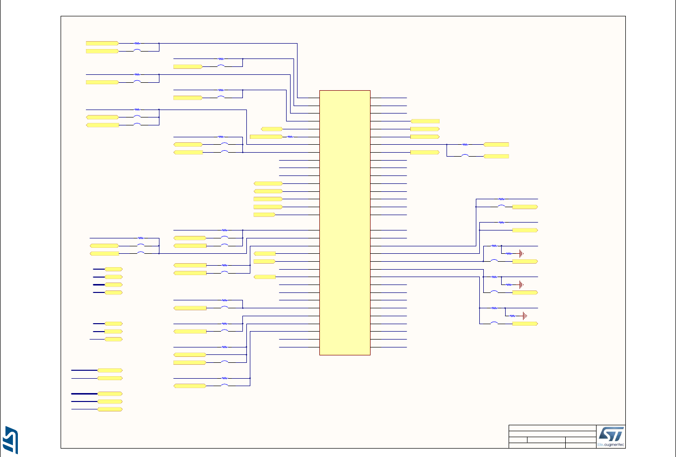
Schematic diagrams UM1855
76/101 DocID027351 Rev 5
Figure 34. STM32L476G-EVAL MCU part 1
325
MCU
MB1144 C-02
10/7/2016
Title:
Size: Reference:
Date: Sheet: of
A3 Revision:
STM32L476G-EVAL
Project:
PE0
PE1
PE2
PE4
PE5
PE6
PE7
PE8
PE9
PE10
PE11
PE12
PE13
PE14
PE15
PA[0..15] PA[0..15]
PB[0..15] PB[0..15]
PD[0..15] PD[0..15]
PE[0..15] PE[0..15]
PA0
PA1
PA2
PA3
PA4
PA5
PA6
PA7
PA8
PA9
PA10
PA11
PA12
PA13
PA14
PA15
PB0
PB1
PB2
PB3
PB4
PB5
PB6
PB7
PB8
PB9
PB12
PB13
PB14
PB15
PD0
PD1
PD2
PD3
PD4
PD5
PD6
PD7
PD8
PD9
PD10
PD11
PD12
PD13
PD14
PD15
USBOTG_DM
USBOTG_DP
TMS/SWDIO
TCK/SWCLK
D2
D3
DFSDM_DATIN1
FMC_NOE
FMC_NWE
FMC_NWAIT
FMC_NE1
TRACE_D3
TRACE_D1TRST
D4
D5
D6
D7
D8
D9
D10
D11
D12
D[0..15]
A[20..22]
D[0..15]
A[20..22]
R83 0
IDD_Measurement
USART1_TX
LED1
MC_DissipativeBrake
R54 0
A20
A22
TRACE_D2
A21
MC_EncA
R84 0
R86 0
R85 0
TDI
TDO/SWO
R102
100K GND
R100
100K GND
R101
100K GND
ADC_DAC
RESET# RESET#
LCDCOM7
LCDSEG28
LCDSEG29
LCDSEG30
LCDSEG31
LCDSEG32
LCDSEG33
LCDSEG34
LCDSEG35
LCDSEG36
LCDSEG37
LCDSEG38
LCDSEG0
LCDSEG1
LCDSEG2
LCDSEG3
LCDSEG4
LCDCOM0
LCDCOM1
LCDCOM2
LCDSEG17
LCDSEG5
LCDSEG6
LCDSEG7
LCDSEG8
LCDSEG9
LCDSEG21
LCDSEG16
LCDCOM3
LCDSEG12
LCDSEG13
LCDSEG14
LCDSEG15
LCDCOM[0..3]
LCDCOM[0..3]
TKEY
TKEY_CS
QSPI_D3
QSPI_D2
QSPI_D1
QSPI_D0
R68
0
R66 0
R62 0
R56
0
R82 0
R103
0
TRACE_CK
R53 0 SAI1_SDA
R69 0
OpAmp1_INP
R39 0
R38 0
MC_PFC_Vac
MC_Temperature
R78 0
MC_EncB
R81 0
MC_EncIndex
MC_PWM_1L
MC_PWM_2L
MC_PWM_3L
PB10
PB11
LCDSEG10
LCDSEG11
QSPI_CLK
QSPI_CS
R50 0
R48 0
MC_PFC_Shutdown
TRACE_D0
PE3 LCDSEG39
R104
0
LCDCOM7
LCDCOM7
LCDSEG[0..17]
LCDSEG[0..17]
LCDSEG[28..39]
LCDSEG[28..39]
LCDSEG21
LCDSEG21
PE2 1
PE3 2
PE4 3
PE5 4
PE6 5
PA0-WKUP1
34
PA1
35
PA2
36
PA3
37
PA4
40
PA5
41
PA6
42
PA7
43
PB0
46
PB1
47
PB2
48
PE7 58
PE8 59
PE9 60
PE10 63
PE11 64
PE12 65
PE13 66
PE14 67
PE15 68
PB10
69
PB11
70
PB12
73
PB13
74
PB14
75
PB15
76
PD8 77
PD9 78
PD10 79
PD11 80
PD12 81
PD13 82
PD14 85
PD15 86
PA8
100
PA9
101
PA10
102
PA11
103
PA12
104
PA13
105
PA14
109
PA15
110
PD0 114
PD1 115
PD2 116
PD3 117
PD4 118
PD5 119
PD6 122
PD7 123
PB3
133
PB4
134
PB5
135
PB6
136
PB7
137
PB8
139
PB9
140
PE0 141
PE1 142
U7A
STM32L476ZGT6U
SB35
Open by default
SB32
Open by default
SB22
Open by default
SB31
Open by default
SB21
Open by default
SB20
Open by default
SB18
Open by default
SB19
Open by default
SB14
Open by default
SB15
Open by default
SB12
Open by default
SB13
Open by default
SB11
Open by default
SB9
Open by default
SB8
Open by default
SB3
Open by default
SB6
Open by default
SB10
Open by default
SB26
Open by default
SB40
Open by default
SB38
Open by default
SB39
Open by default
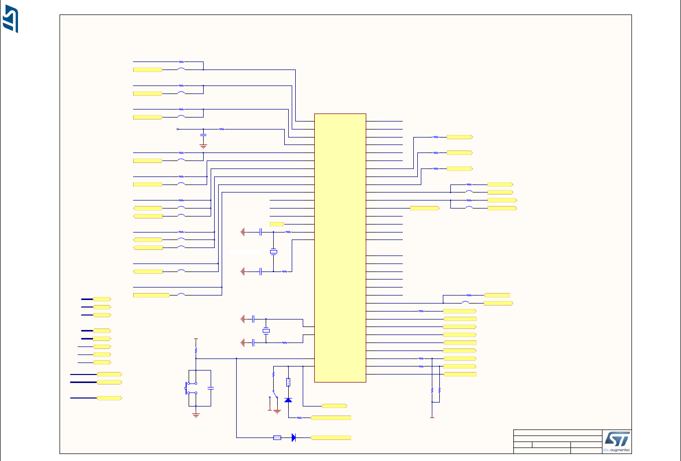
UM1855 Schematic diagrams
DocID027351 Rev 5 77/101
Figure 35. STM32L476G-EVAL MCU part 2
425
MCU2
MB1144 C-02
10/7/2016
Title:
Size: Reference:
Date: Sheet: of
A3 Revision:
STM32L476G-EVAL
Project:
PC[0..15] PC[0..15]
C141
100nF
R96
[N/A]
C55
20pF
C54
20pF
X2
8MHz (with socket)
R95
390
R67
10K
2
3
1
SW1
09.03290.01
D3
BAT60JFILM
D4
BAT60JFILM
PH0
PH1
JP8
Header 2X1
R59
150
1
4 3
2
B1
RESET
VDD
VDD
Bootloader_BOOT0_3V3
Bootloader_RESET_3V3
C57
2.7pF
C56
2.7pF
R88
0
R87
0
PC1
PC2
PC6
PC8
PC9
PC10
PC11
PC12
PC13
PC14
PC15
Key
PF0
PF1
PF2
PF3
PF4
PF5
PF6
PF7
PF8
PF9
PF10
PF11
PF12
PF13
PF14
PF15
PG0
PG1
PG2
PG3
PG4
PG5
PG6
PG7
PG9
PG10
PG11
PG12
PG13
PG14
PG15
CODEC_INT
USART1_CTS_3V3
FMC_NE2
USART1_RTS
PF[0..15] PF[0..15]
PG[0..15] PG[0..15]
A0
A1
A2
A3
A4
A5
A6
A7
A8
A9
A10
A11
A12
A13
A14
A15
D[0..15]
A[0..15]
D[0..15]
A[0..15]
MC_PFC_sync
C58
1uF
IDD_CNT_EN
NFC_NSS
LPUART_TX
LPUART_RX_3V3
LCD_NE3
VLCD input
TP7 VLCD
IOExpander_INT
I2C_SCL
I2C_SDA
R94 0
R105 0
R106 0
R89 0
JP9
Header 2X1
R58 0
R34 0
R90 0
RESET#
RESET# RESET#
LCDSEG19
LCDSEG20
LCDSEG24
LCDSEG26
LCDSEG27
LCDCOM4
LCDCOM5
LCDCOM6
LCDSEG[18..20]
LCDSEG[18..20]
LCDCOM[4..6]
LCDCOM[4..6]
PH1
PH0
PH0
PH1
SHIELD
R57
1K2
R60
1K2
R61 0
VDD
SAI1_SDB
SAI1_MCKB
SAI1_SCKB
SAI1_FSB
MC_ICL_Shutout
R35 0
R91 0
MC_PFC_PWM
R36 0
MC_CurrentB
MC_CurrentC
R99 0
PC3
R98 0
32.768 kHz crystal
PC0LCDSEG18
MC_CurrentA
R97 0
MC_PFC_IndCurr
PC4LCDSEG22 R65 0
PC5LCDSEG23 R64 0
MC_BusVoltage
MC_PWM_1H
PC7LCDSEG25
SHIELD_CS
R33 0
MC_PWM_2H
MC_PWM_3H
MC_EmergencySTOP
PG8
LCDSEG[22..27]
LCDSEG[22..27]
BOOT0
BOOT0
PH0-OSC_IN
23
PH1-OSC_OUT
24
NRST
25
BOOT0
138
PC13-WKUP2
7
PC14-OSC32_IN
8
PC15-OSC32_OUT
9
PC0
26
PC1
27
PC2
28
PC3
29
PC4
44
PC5
45
PC6
96
PC7
97
PC8
98
PC9
99
PC10
111
PC11
112
PC12
113
PF2 12
PF3 13
PF4 14
PF5 15
PF6 18
PF7 19
PF8 20
PF9 21
PF10 22
PF11 49
PF12 50
PF13 53
PF14 54
PF15 55
PF0 10
PF1 11
PG2 87
PG3 88
PG4 89
PG5 90
PG6 91
PG7 92
PG8 93
PG9 124
PG10 125
PG11 126
PG12 127
PG13 128
PG14 129
PG15 132
PG0 56
PG1 57
U7C
STM32L476ZGT6U
SB34
Open by default
SB36
Open by default
SB42
Open by default
SB17
Open by default
SB16
Open by default
SB2
Open by default
SB27
Open by default
SB4
Open by default
SB30
Open by default
SB28
Open by default
SB29
Open by default
SB25
Open by default
SB37
Open by default
SB5
Open by default
X1
NDK NX3215SA-32.768KHZ-EXS00A-MU00525
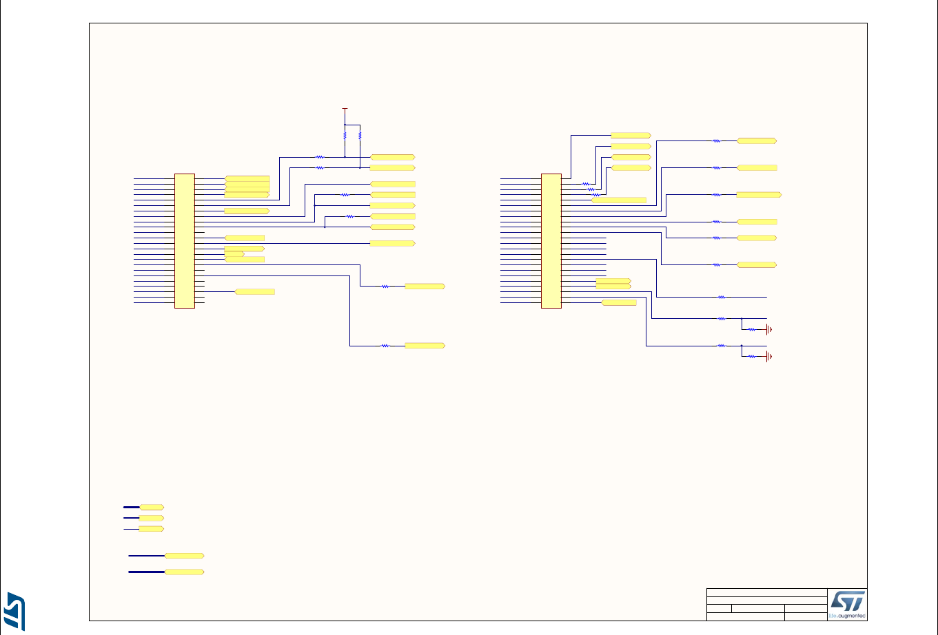
Schematic diagrams UM1855
78/101 DocID027351 Rev 5
Figure 36. LCD glass module daughterboard connectors
525
LCD_Glass
MB1144 C-02
10/7/2016
Title:
Size: Reference:
Date: Sheet: of
A3 Revision:
STM32L476G-EVAL
Project:
A[16..19]
1 2
3 4
5 6
7 8
9 10
11 12
13 14
15 16
17 18
19 20
21 22
23 24
25 26
27 28
29 30
31 32
33 34
35 36
37 38
39 40
41 42
43 44
45 46
47 48
CN14
Header 24X2
LCD Glass Connector
uSD_CMD
uSD_CLK
uSD_D3
uSD_D2
USART1/IrDA_RX_3V3
R144 0 IDD_WAKEUP
R145 0
R146 0
R147 0
PT100_DATIN
uSD_D0
uSD_D1
D13
D14
D15
A16
R151 0 A17
A18
D0
D1
R150 0 A19
R149 0 A23
R138
100K GND
R139
100K GND
OpAmp1_INM
PD11
PD12
PD13
PD14
PD15
PD10
PD9
PD8
PD2
PC12
PC11
PC10
PC4
PC5
PC6
PC7
PCPC8
PC9
PB7
PE0
PE1
PE2
PE3
PA1
LCDSEG21
LCDSEG22
LCDSEG23
LCDSEG24
LCDSEG25
LCDSEG26
LCDSEG27
LCDSEG28
LCDSEG29
LCDSEG30
LCDSEG31
LCDSEG32
LCDSEG33
LCDSEG34
LCDSEG35
LCDSEG36
LCDSEG37
LCDSEG38
LCDSEG39
LCDSEG0
LCDCOM7
LCDCOM6
LCDCOM5
LCDCOM4
FMC_NBL0
FMC_NBL1
LCDSEG[0..39]
LCDSEG[0..39]
LCDCOM[0..7]
LCDCOM[0..7]
1 2
3 4
5 6
7 8
9 10
11 12
13 14
15 16
17 18
19 20
21 22
23 24
25 26
27 28
29 30
31 32
33 34
35 36
37 38
39 40
41 42
43 44
45 46
47 48
CN11
Header 24X2
LCD Glass Connector
USBOTG_VBUS
uSD_DETECT
USBOTG_ID
CAN_TX
NFC_MISO
NFC_SCK
SWP_IO
CAN_RX
NFC_MOSI
DFSDM_CKOUT
DMIC_DATIN
OpAmp1_OUT
R107 0
Comp2_INP
R111 0
LCDCOM1 PA9
PA8
PA10
PA15
PA3
PA2
PA7
PA6
PB9
PB11
PB10
PB5
PB14
PB13
PB12
PB8
PB0
PB4
PB3
PB1
PB15
PC2
PC1
PC0
LCDCOM0
LCDCOM2
LCDCOM3
LCDSEG11
LCDSEG10
LCDSEG9
LCDSEG14
LCDSEG13
LCDSEG12
LCDSEG17
LCDSEG16
LCDSEG15
LCDSEG20
LCDSEG19
LCDSEG18
LCDSEG2
LCDSEG1
LCDSEG5
LCDSEG4
LCDSEG3
LCDSEG8
LCDSEG7
LCDSEG6
SmartCard_CLK
SmartCard_IO
R143 0
D[0..15]
D[0..15]
USBOTG_PRDY
R108
0
R109
0USBOTG_OVRCR
USBOTG_PPWR
R148 0
Comp2_OUT
R140 0
R142 0
R141 0
A[16..19]
A23
A23
R265 0
R266 0
R264
1K2
VDD
R263
1K2
I2C2_SDA
I2C2_SCL
LED3
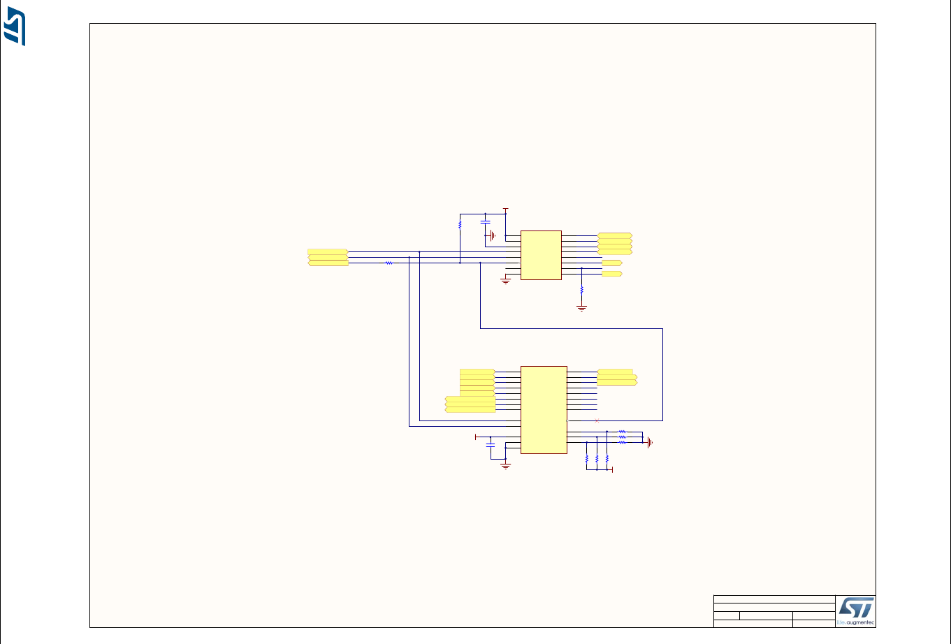
UM1855 Schematic diagrams
DocID027351 Rev 5 79/101
Figure 37. I/O expander
625
IO_Expandor
MB1144 C-02
10/7/2016
Title:
Size: Reference:
Date: Sheet: of
A3 Revision:
STM32L476G-EVAL
Project:
Y- 1
INT
2
A0/Data Out
3
SCLK
4
SDAT
5
VCC
6
Data in
7
IN0 8
IN1 9
GND
10
IN2 11
IN3 12
X+ 13
Vio
14
Y+ 15
X- 16
U32
STMPE811QTR
I2C device address:0x82
VDD
R239
100K
R228 0
C134
100nF
PG13
PG14
PG15
IOExpander_Y+
IOExpander_Y-
IOExpander_X+
IOExpander_X-
IOExpander_INT
I2C_SCL
I2C_SDA
JOY_SEL
JOY_DOWN
JOY_LEFT
JOY_RIGHT
JOY_UP
LED4
GPIO0
1
INT 22
A0 18
SCL
19
SDA
20
VCC
21 A2 24
GPIO7
8GPIO6
7
GND
9
GPIO5
6GPIO4
5GPIO3
4
A1 23
GPIO2
3GPIO1
2GPIO8 10
GPIO15 17
GPIO14 16
GPIO13 15
GPIO12 14
GPIO11 13
GPIO10 12
GPIO9 11
TAB
25
U33
STMPE1600QTR
VDD
C132
100nF
Default I2C Address:1000010X
R243 10K
R232 10K
R230 10K
R237
[N/A]
R233
[N/A]
R231
[N/A]
VDD
SmartCard_RST
SmartCard_CMDVCC
SmartCard_3/5V
SmartCard_OFF
R229
100K
IOExpander1
IOExpander2
LED2
BL_Control
EXT_RESET
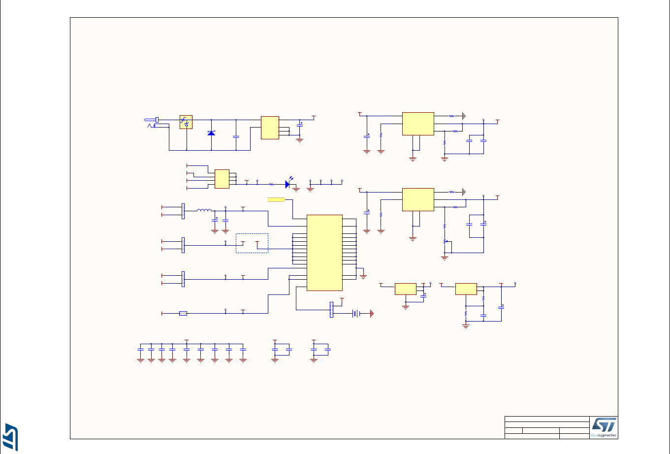
Schematic diagrams UM1855
80/101 DocID027351 Rev 5
Figure 38. Power supply
725
Power
MB1144 C-02
10/7/2016
Title:
Size: Reference:
Date: Sheet: of
A3 Revision:
STM32L476G-EVAL
Project:
SV
1
SG
2
CV 3
CG1 4
CG2 5
CG3 6
L2
BNX002-01
C100
220uF
E5V
C131
10uF[ESR<0.2ohm]
VDD_ADJ
+5V
VDD_ADJ
TP13
1
3
2
CN22
DC-10B Z1
SMAJ5.0A-TR C124
100nF
1
2
3
U31
ZEN056V130A24LS
13
2RV1
3386P-503H[5%]
R235
10.2K[1%]
Power Supply VDD_ADJ [1.7V to 3.61V]
R236
20K[1%]
C140
4.7uF
Vout=1.22*(1+R1/R2)
C133
100nF
VDD_MCUVDD
BT1
CR1220 holder
L1
BEAD
3
2
1
JP2 VDD
TP5
+3V3
VDD_ADJ
C45
100nF
C42
100nF
VDD_MCU
C35
100nF
5V
TP10
+5V R165
1K
1 2
LD7
Red
TP1
D5V
U5V_STLINK
U5V 78
56
34
12
JP17
Header 4X2
E5V
EN
1
GND
2
VO 4
ADJ 5
GND
7
VI
6PG 3
U34
ST1L05BPUR
VDD_IO
+5V
+3V3
TP17
C116
4.7uF
R204
20.5K[1%]
R203 11.8K[1%]
C98
10uF[ESR<0.2ohm]
EN
1
GND
2
VO 4
ADJ 5
GND
7
VI
6PG 3
U28
ST1L05BPUR
Power Supply 3.3V
Vout=1.22*(1+R1/R2)
C101
100nF
+3V3
TP11
C38
100nF
VDD_IO
VDD_IO
TP4
VDDA
3
2
1
JP10
VDDA
TP8
+3V3
VDD_USB
3
2
1
JP1
VDD_USB
TP2
+3V3
VDD
C59
1uF
C60
100nF
GND GND
TP18 TP3
VREF+
Vin
3Vout 2
1
Tab 4
U27
LD1117S18TR
C107
10uF
+1V8
1V8
TP16
+3V3
connected by shunt of
IDD_measurement circuitry
to use a supercapacitor:
remove the jumper, and connect positive terminal
of the supercapacitor to pin 2 of the jumper.
VDD_MCU
VDD_MCU
VDD_MCU
C36
100nF
VDD_USB
R202
[N/A]
3
2
1
JP12
JP3
Header 2X1
R206
[N/A]
R234
[N/A]
R240
[N/A]
C46
1uF
C33
1uF
C32
1uF
C50
100nF
C41
100nF
C48
100nF
C51
100nF
Recommendation:
100nF decoupling capacitor for each VDD pin
R207
124[1%]
R209
232[1%]
+5V
C99
10uF
+3V6
3V6
TP12
Vout=1.25*(1+232/124)=3.589V
C114
100nF
+-
Vin
3Vout 2
1
Tab 4
U26
LD1117STR
VBAT
6
VSS 16
VDD
17
VSSA 30
VREF- 31
VREF+
32
VDDA
33
VSS 38
VDD
39
VSS 71
VDD
72
VSS 107
VDD
108
VSS 143
VDD
144
VDDIO2
95
VDD
52
VDD
62
VDD
84
VDDIO2
131
VSS 120
VSS 94
VSS 51
VSS 61
VSS 83
VSS 130
VDDUSB
106 VDD
121
U7B
STM32L476ZGT6U
C43
100nF
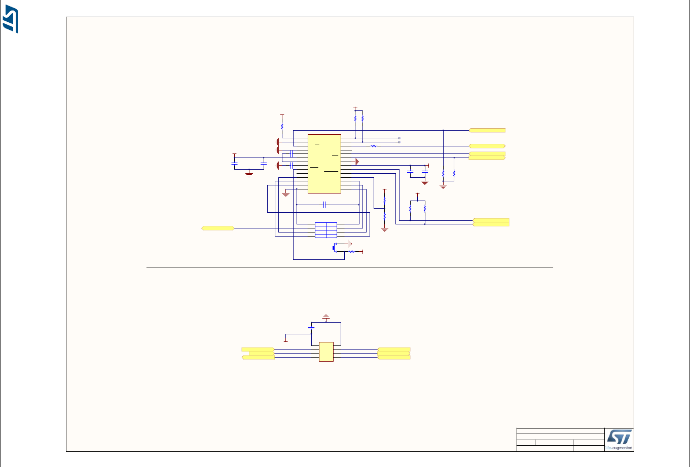
UM1855 Schematic diagrams
DocID027351 Rev 5 81/101
Figure 39. Smartcard, SWP and NFC
825
SWP_SmartCard_NFC
MB1144 C-02
10/7/2016
Title:
Size: Reference:
Date: Sheet: of
A3 Revision:
STM32L476G-EVAL
Project:
SWP_IO
NFC_IRQINNNFC_IRQOUTN
NFC_NSS
NFC_MOSI
PB15
PF11 PB14
NFC_MISO
NFC_SCK
PB13
+3V3
GND
C78
100nF
SmartCard and SWP
NFC
PB7 PB6
CLKDIV1
1
CLKDIV2
2
5V/3V
3
PGND
4
C1+
5
Vddp
6
C1-
7
Vup
8
PRES
9
PRES
10
I/O
11
AUX2
12
AUX1
13
CGND
14 CLK 15
RST 16
Vcc 17
PORADJ 18
CMDVCC 19
RSTIN 20
Vdd 21
GND 22
OFF 23
XTAL1 24
XTAL2 25
I/OUC 26
AUX1UC 27
AUX2UC 28
U30
ST8024CDR
C136 100nF
C135
100nF
+5V
C137 100nF
C117
100nF
R242
100K +3V3
R216
4K7
+3V3
R218
10K
R217
10K
+3V3
C119
100nF
VDD
R211
10K
+3V3
R210 0
R212
10K
AUX2TP14
AUX1TP15
SmartCard_3/5V
SmartCard_IO
SmartCard_RST
SmartCard_CLK
SmartCard_OFF
SmartCard_CMDVCC
PB0
PC4
IOExpander1
IOExpander1
IOExpander1
IOExpander1
PB12
NFC kit reference: CR95HF-B
C112
4.7uF
C138
4.7uF
VCC 1
RST 2
CLK 3
NC 4
GND
5
SWIO
6
I/O
7
NC
8
18
17
CN23
C816
SmartCard Connector
Operating range: 2.7<VDD<3.6V
Operating Voltage: +3.3V
R215
100K
R241
100K
R213
100K
R214
100K
+3V3
7 8
5 6
3 4
1 2
CN13
female conn 4X2
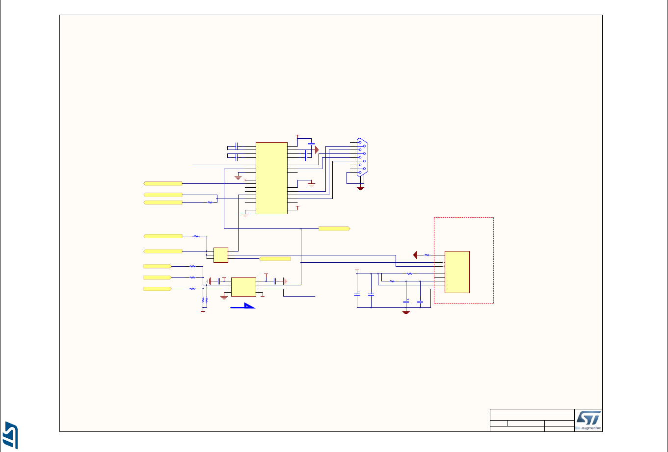
Schematic diagrams UM1855
82/101 DocID027351 Rev 5
Figure 40. USART and IrDA
925
USART_IrDA
MB1144 C-02
10/7/2016
Title:
Size: Reference:
Date: Sheet: of
A3 Revision:
STM32L476G-EVAL
Project:
SD
5
TxD
3
GND
8
Anode (VCC2)
1
Cathode
2
RxD
4
VCC1
6
Vlogic
7
U11
TFDU6300
+3V3
C67
4.7uF
C71
4.7uF
1
6
2
7
3
8
4
9
5
CN9
DB9-male
USART1/IrDA_RX_3V3
USART
Bootloader_BOOT0_3V3
Bootloader_RESET_3V3
C2+
1
C2-
2V- 3
R1IN 4
R2IN 5
R3IN 6
R4IN 7
R5IN 8
T1OUT 9
T2OUT 10
T3OUT 11
T3IN
12 T2IN
13 T1IN
14
R5OUT
15 R4OUT
16 R3OUT
17 R2OUT
18 R1OUT
19 R2OUTB
20 R1OUTB
21
nSHDN 22
nEN
23
C1-
24 GND 25
VCC 26
V+ 27
C1+
28
U10
ST3241EBPR
C62
100nF
C64
100nF
C61
100nF
C65
100nF
C63
100nF
+3V3
+3V3
RXD
RTS
TXD
CTS
DSR
R113
0
USART1_CTS_3V3
PG11
R112 5.1
R115 47
PB7
USART1_RTS_3V3
PG12
VCCA
1
A1
2
A2
3
GND
4DIR 5
B2 6
B1 7
VCCB 8
U12
SN74LVC2T45DCUT
+3V3
VDD
VDD
C66
100nF
C69
100nF
R114
100K
R117
100K
VDD
USART1_RTS_3V3
R93 0
R118 0
R116 0
C70
100nF
C68
100nF
USART1_TX
IRDA
USART1_RTS
PB6
NFC_IRQINN
NFC_IRQOUTN
LPUART_RX_3V3
PG8
R119 [N/A]
LPUART_TX
PG7
IRDA_RX
R158 [N/A]
GND
GND
65
43
21
JP15
Header 3X2
N
ote:
TFDU6300 (U11) is not populated
on boards manufactured starting from
middle 2016 (schematic and board
revision C02)
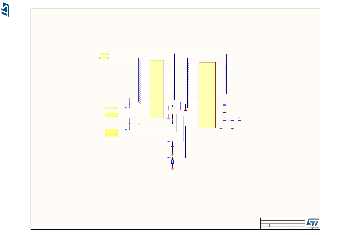
UM1855 Schematic diagrams
DocID027351 Rev 5 83/101
Figure 41. SRAM and NOR Flash memory devices
10 25
SRAM&Flash
MB1144 C-02
10/7/2016
Title:
Size: Reference:
Date: Sheet: of
A3 Revision:
STM32L476G-EVAL
Project:
VDD
A1
A2
A3
A4
A5
A6
A7
A8
A9
A10
A11
A12
A13
A14
A15
A16
A1
A2
A3
A4
A5
A6
A7
A8
A9
A10
A11
A12
A13
A14
A15
A16
A17
A18
A19
A20
A21
A22
VDD
FMC_NWE
FMC_NOE
FMC_NWAIT
VDDVDD
VDD
JP13
Header 2X1
A0
A0
A17
A18
VDD
D0
D1
D2
D3
D4
D5
D6
D7
D8
D9
D10
D11
D12
D13
D14
D15
D0
D1
D2
D3
D4
D5
D6
D7
D8
D9
D10
D11
D12
D13
D14
D15
VDD
Default setting: Open
PE1
PE0
PD5
PG9
PD6
PD4
PD7
FMC_NBL0
FMC_NBL1
A19
A20 A23
VDD
2Mx16: CY7C1071DV33-12BAXI
A22
B8
A15
D7
A14
C7
A13
A7
A12
B7
A11
D6
A10
C6
A9
A6
A8
B6
A19
D5 A20
D4
W
A5
RP
B5
A21
C5
Vpp/WP
B4
RB
A4
A18
C4
A17
B3
A7
A3
A6
C3
A5
D3
A4
B2
A3
A2
A2
C2
A1
D2
VCCQ D8
A0
E2
E
F2
VSS E8
G
G2
DQ0 E3
DQ8 F3
DQ1 H3
DQ9 G3
DQ2 E4
DQ10 F4
DQ3 H4
DQ11 G4
VCCQ F1
DQ4 H5
DQ12 F5
DQ5 E5
DQ13 G6
DQ6 H6
DQ14 F6
DQ7 E6
DQ15A-1 G7
VSS H7
BYTE
F7
A16
E7
VCC G5
VSS H2
A23
C8
U5
M29W128GL70ZA6E
M29W256GL70ZA6E
D[0..15]
A[0..23]
D[0..15]
A[0..23]
R18
0
R43
0
C30
100nF
C20
100nF
C18
100nF
C40
100nF
C19
100nF
C31 100nF
C12 100nF
R28
10K
R22
10K
R25
10K
R41
10K
R32
10K
R133
10K
SRAM Nor Flash
A21
FMC_NE1
512kx16: IS61WV51216BLL-10MLI
4Mx16: CY62187EV30LL
FMC_NE2
+3V6
Operating range: 1.65<VDD<3.6V
512x16: IS61WV51216BLL-10MLI VDD: 2.4V to 3.6V
2Mx16: CY7C1071DV33-12BAXI VDD: 3.0V to 3.6V
4Mx16: CY62187EV30LL VDD: 2.2V to 3.7V
Operating Voltages :
1Mx16: IS61WV102416BLL-10MLI VDD: 2.4V to 3.6V
1Mx16: IS61WV102416BLL
A4
B4
A3
B3
A2
A5
A1
A4
A0
A3
CE
B5
I/O0 B6
I/O1 C5
I/O2 C6
I/O3 D5
VCC D6
VSS D1
I/O4 E5
I/O5 F5
I/O6 F6
I/O7 G6
WE
G5
A16
E4
A15
F4
A14
F3
A13
G4
A12
G3
A11
H5
A10
H4
A9
H3
A8
H2 I/O8 B1
I/O9 C1
I/O10 C2
I/O11 D2
VCC E1
I/O12 E2
I/O13 F2
I/O14 F1
I/O15 G1
BLE
A1
BHE
B2
OE
A2
A7
D4
A6
C4
A5
C3
A17
D3 A18
H1
VSS E6
A20
H6
A19
G2
CE2 A6
A21
E3
U2
IS61WV102416BLL-10MLI
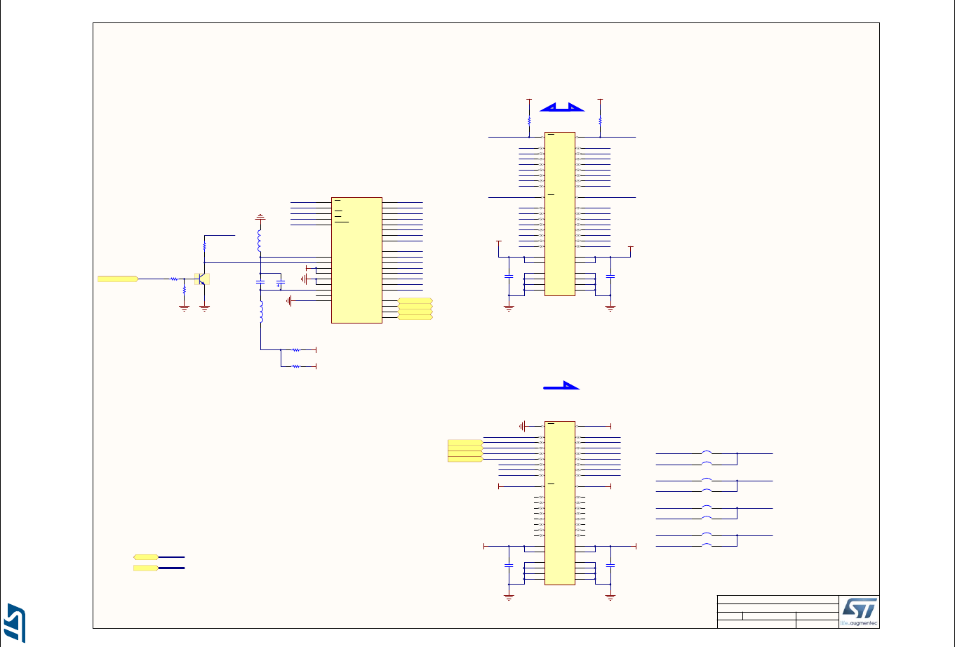
Schematic diagrams UM1855
84/101 DocID027351 Rev 5
Figure 42. TFT LCD
11 25
LCD_TFT
MB1144 C-02
10/7/2016
Title:
Size: Reference:
Date: Sheet: of
A3 Revision:
STM32L476G-EVAL
Project:
PG10
PD5
PD4
D0
D1
D2
D3
D4
D5
D6
D7
D8
D9
D10
D11
D12
D13
D14
D15
LCD_D0
LCD_D1
LCD_D2
LCD_D3
LCD_D4
LCD_D5
LCD_D6
LCD_D7
LCD_D8
LCD_D9
LCD_D10
LCD_D11
LCD_D12
LCD_D13
LCD_D14
LCD_D15
C79
100nF
VDD
C85
100nF
+3V3
LCD_RS
LCD_CSN
LCD_WRN
LCD_RDN
LCD_RSTN
OE
48
A1
47 B1 2
A2
46 B2 3
A3
44 B3 5
A4
43 B4 6
A5
41 B5 8
A6
40 B6 9
A7
38 B7 11
A8
37 B8 12
OE
25
A1
36 B1 13
A2
35 B2 14
A3
33 B3 16
A4
32 B4 17
A5
30 B5 19
A6
29 B6 20
A7
27 B7 22
A8
26 B8 23
DIR 24
VCCB 18
VCCB 7
GND
4
GND
10
GND
15
GND
21
DIR 1
VCCA
42 VCCA
31
GND 45
GND 39
GND 34
GND 28
U21
SN74LVC16T245DGGR
C83
100nF
VDD
C84
100nF
+3V3
VDD
RESET#
FMC_NWE
LCD_NE3
FMC_NOE
OE
48
A1
47 B1 2
A2
46 B2 3
A3
44 B3 5
A4
43 B4 6
A5
41 B5 8
A6
40 B6 9
A7
38 B7 11
A8
37 B8 12
OE
25
A1
36 B1 13
A2
35 B2 14
A3
33 B3 16
A4
32 B4 17
A5
30 B5 19
A6
29 B6 20
A7
27 B7 22
A8
26 B8 23
DIR 24
VCCB 18
VCCB 7
GND
4
GND
10
GND
15
GND
21
DIR 1
VCCA
42 VCCA
31
GND 45
GND 39
GND 34
GND 28
U22
SN74LVC16T245DGGR
A1_BUF
A1_BUF
PF0
D[0..15]
A[0..23]
D[0..15]
A0
LCD_NE3
VDD VDD
R161
10K
R166
10K
+3V3
TFT LCD
LCD_D0
LCD_D1
LCD_D2
LCD_D3
LCD_D4
LCD_D5
LCD_D6
LCD_D7
LCD_D8
LCD_D9
LCD_D10
LCD_D11
LCD_D12
LCD_D13
LCD_D14
LCD_D15
LCD_RS
LCD_CSN
LCD_WRN
LCD_RDN
LCD_RSTN
+5V
C115
10uF
L4
BEAD
C113
100nF
L3
BEAD
R223
0
+3V3
R219
[N/A]
CS
1
RS
2
WR/SCL
3
RD
4
RESET
5
VDD
24
VCI
25
GND
26
GND
27
BL_VDD
28
BL_Control
23 BL_GND
22
PD1 6
PD2 7
PD3 8
PD4 9
PD5 10
PD6 11
PD7 12
PD8 13
PD10 14
PD11 15
PD12 16
PD13 17
PD14 18
PD15 19
PD16 20
PD17 21
SDO
29
SDI
30 XL 31
XR 32
YD 33
YU 34
CN19
16-bit connector
IOExpander_Y+
IOExpander_Y-
IOExpander_X+
IOExpander_X-
BL_Control
2.8'' LCD TFT board MB989P
A[0..23]
3
1
2
T6
9013-SOT23
R260
1K
R259
47K
BL_VDD
BL_VDD
VDD
SB44
Open by default
SB45
Closed by default
A0_1DELAY
A0_1DELAY A0_2DELAY
A0_1DELAY
A0_2DELAY
SB46
Open by default
SB47
Closed by default
SB49
Open by default
SB48
Closed by default
SB51
Open by default
SB50
Closed by default
NE3_1DELAY NE3_2DELAY
NE3_1DELAY
NE3_2DELAY
NE3_1DELAY
LCD_NE3
NE3_1DELAY LCD_NE3_BUF
LCD_NE3_BUF
LCD_NE3_BUF
A1
A1_1DELAY A1_BUF
A1 A1_1DELAY
VDD
R267
22K
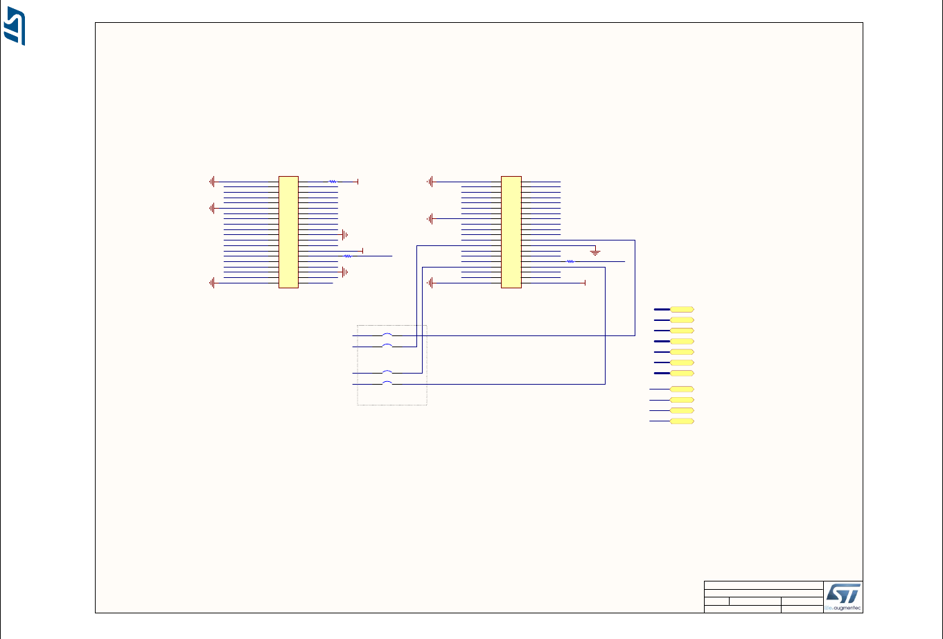
UM1855 Schematic diagrams
DocID027351 Rev 5 85/101
Figure 43. Extension connector
12 25
Extension connector
MB1144 C-02
10/7/2016
Title:
Size: Reference:
Date: Sheet: of
A3 Revision:
STM32L476G-EVAL
Project:
R79 820
R80
820
+3V3
PA[0..15] PA[0..15]
PB[0..15] PB[0..15]
PC[0..15] PC[0..15]
PD[0..15] PD[0..15]
PE[0..15] PE[0..15]
RESET# RESET#
Left Right
PG9
PG10
PG11
PA4
PA5
PF11
PG12
PD5
PD6
PD1
PE6
PF1PF0
PF3
PF2
PF4
PC13
PF14
PG1 PG0
PE7PE8
PE9
RESET#
PB2
PH1
PH0
close to MCU
D5V
PA13
PA12
PA11
PG8
PG7PG6
PD7
PG15
PB6
BOOT0
PE4
PE5
PE10
PE11PE12
PG2
PG3
PG4
PG5
PF[0..15] PF[0..15]
PG[0..15] PG[0..15]
R44 0
VDD
PD3
PD4
PG13
PG14
PE15
PE13PE14
PF15
PF13PF12
PA0
PC3
PF10
PF9
PF7
PF8
1 2
3 4
5 6
7 8
9 10
11 12
13 14
15 16
17 18
19 20
21 22
23 24
25 26
27 28
29 30
31 32
33 34
35 36
37 38
39 40
CN7
P1039-2*20MGF-089-1A
1 2
3 4
5 6
7 8
9 10
11 12
13 14
15 16
17 18
19 20
21 22
23 24
25 26
27 28
29 30
31 32
33 34
35 36
37 38
39 40
CN6
P1039-2*20MGF-089-1A
townes townes
PC14
PC15
PH1
PH0
PH0
PH1
PF5
PF6
PD0
PA14
BOOT0
BOOT0
SB33
Open by default
SB41
Open by default
SB23
Open by default
SB24
Open by default
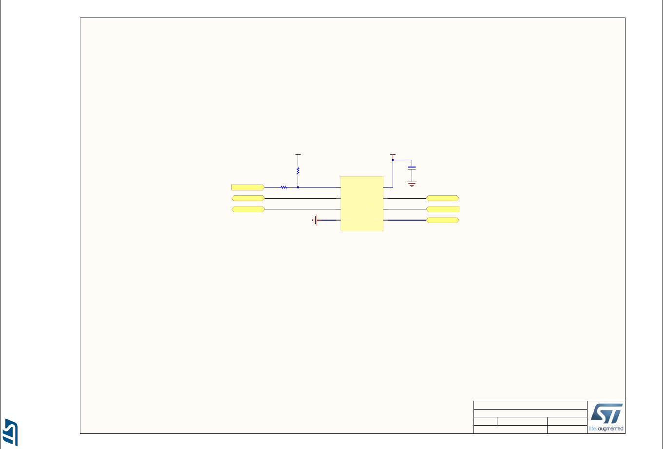
Schematic diagrams UM1855
86/101 DocID027351 Rev 5
Figure 44. Quad-SPI Flash memory device
13 25
QSPI
MB1144 C-02
10/7/2016
Title:
Size: Reference:
Date: Sheet: of
A4 Revision:
STM32L476G-EVAL
Project:
VDD
Quad SPI Memory
QSPI_D0
QSPI_D3
QSPI_D2
QSPI_D1
GND
PB1
PB0
PA7
PA6
QSPI_CLK
PB10
QSPI_CS
R71
0
VDD
R74
10K
PB11
C44
100nF
GND
MICRON
Operating range: 2.7<VDD<3.6V
HOLD#/DQ3 7
VCC 8
S#
1
DQ1
2
C6
DQ0 5
Vss
4
W#/Vpp/DQ2
3
HOLD#
/
DQ
3
VCC
S#
D
Q1
C
DQ
0
V
s
s
W
#
/
V
pp/
DQ2
U9
N25Q256A13EF840E
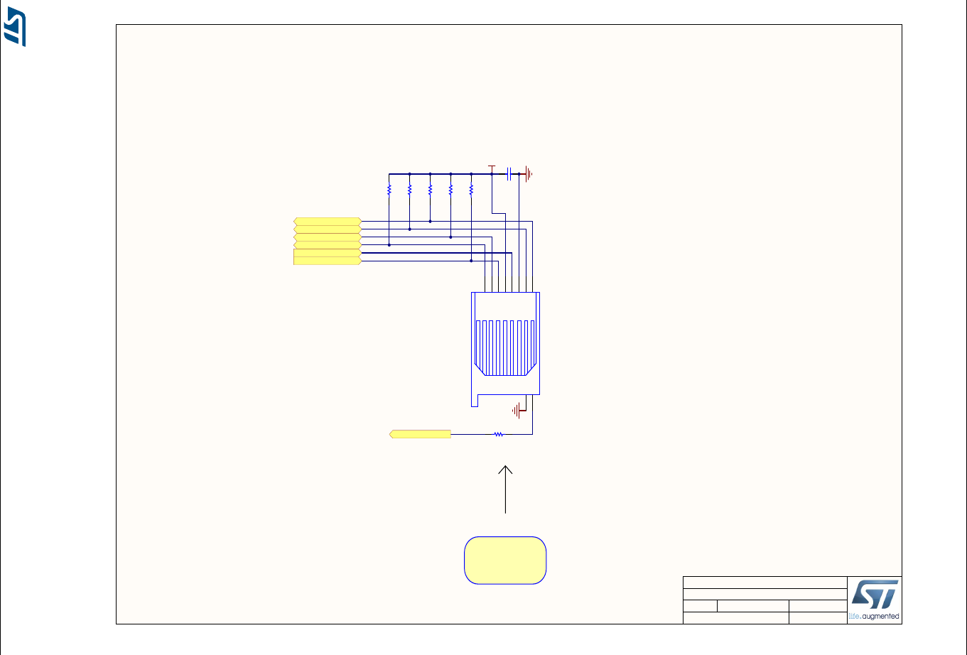
UM1855 Schematic diagrams
DocID027351 Rev 5 87/101
Figure 45. microSD card
14 25
MicroSD
MB1144 C-02
10/7/2016
Title:
Size: Reference:
Date: Sheet: of
A4 Revision:
STM32L476G-EVAL
Project:
MicroSD card
uSD_CLK
uSD_CMD
uSD_D0
uSD_D1
uSD_D2
uSD_D3
R182
47K
R185
47K
R194
0
R176
47K
R178
47K
R175
47K
VDD
PC9
PC8
PC10
PC11
PC12
PD2
PA8
Operating Voltage: VDD no Lower than 2.7V
uSD_DETECT
C90
100nF
RVS 1
CS 2
DI 3
Vdd 4
SCLK 5
Vss 6
DO 7
RVS 8
SW2
9
SW1
10
CN18
PJS008-2000 (SMS064FF or SMS128FF)
ZZ1
micro SD card
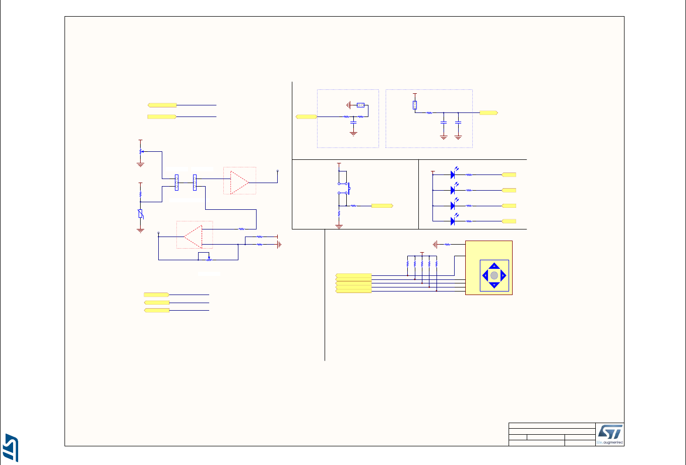
Schematic diagrams UM1855
88/101 DocID027351 Rev 5
Figure 46. Physical control peripherals
15 25
peripherals
MB1144 C-02
10/7/2016
Title:
Size: Reference:
Date: Sheet: of
A3 Revision:
STM32L476G-EVAL
Project:
13
2
RV3
3386P-103(10K)
VDD
ADC_DAC
ADC&DAC connector and Reference Voltage
Potentiometer/LDR
1 2
LD3
Red
1 2
LD2
Orange
1 2
LD4
Blue
1 2
LD1
Green
+3V3 R258
510
R257
680
R256
680
R255
680 LED4
LED3
LED1
LED2
R247
10K
R248
10K
R249
10K
R250
10K
R246
10K
VDD
R251
100 COMMON
5
Selection
2
DWON
3
LEFT
1
RIGHT
4
UP
6
B3
MT008-A
JOY_SEL
JOY_DOWN
JOY_LEFT
JOY_RIGHT
JOY_UP
Joystick
WKUP/TAMPER Button LEDs
R51
8.2K
PB2
C47
[N/A]
R72 0
R73
0
R245
220K
1
43
2
B2
WKUP
VDD
R244
330 KEY
Close to MCU on PCB
PA4
VDD
CN8
Header 2X1
PC13
R92
0
C52
100nF
VREF+
Comp2_INP
Close to MCU on PCB
3
2
1
JP5
3
2
1
JP7
R63
1K
R121
1K
OpAmp1_INP
OpAmp1_INM
R120 [N/A]OpAmp1_OUT
OA1_OUT
TP9
+
-
OpAmp1
13
2
RV2
3314J-1-103
STM32L
PA0
PA1
PA3 VDD
VDDA
Potentiometer
LDR
Comparator
OpAmp/ADC
COMP2_OUT
TP6
OpAmp1_OUT
OpAmp1_INM
OpAmp1_OUT
OpAmp1_INM
OpAmp1_INP OpAmp1_INP
I/Oexpander
PC1
I/Oexpander
PA3
PA0
PA1
STM32L
Comp2
Comp2_INP
Comp2_INP
PB4 Comp2_OUT
Comp2_OUT Comp2_OUT
PB5
PB4
PB5
C531uF
Variable gain
CN10
Header 2X1
R52
VT9ON1
1
2
12

UM1855 Schematic diagrams
DocID027351 Rev 5 89/101
Figure 47. CAN transceiver
16 25
CAN
MB1144 C-02
10/7/2016
Title:
Size: Reference:
Date: Sheet: of
A4 Revision:
STM32L476G-EVAL
Project:
D
1
GND
2
VCC
3
R
4Vref 5
CANL 6
CANH 7
RS 8
U8
SN65HVD230
+3V3
VDD
R55
120
JP6
Header 2X1
3
2
1
JP4
R45
10K
VDD
C49
100nF
R46
0
R77
0
R70
[N/A]
Default setting: 1<->2
Default setting: Open
1
6
2
7
3
8
4
9
5
CN5
DB9-male
PB9
PB8
CAN_TX
R76 0
CAN_RX
R75 0
3
1
2
D2
ESDCAN24-2BLY
Optional
Operating voltage range: 3.0<VDD<3.6V

Schematic diagrams UM1855
90/101 DocID027351 Rev 5
Figure 48. Touch-sensing device
17 25
Touch Sensing
MB1144 C-02
10/7/2016
Title:
Size: Reference:
Date: Sheet: of
A4 Revision:
STM32L476G-EVAL
Project:
<----Touch Sensing diameter 10mm min on active shield diameter 12mm min
R40
10K
SHIELD
SHIELD_CS
TS1
TS_PAD
ESD resistor close to MCU pad
TKEY_CS
C37
22nF(COG)GRM3195C1H223JA01L
R37
1K
C34
220nF
TKEY
PB12
PB13
PC6
PC7

UM1855 Schematic diagrams
DocID027351 Rev 5 91/101
Figure 49. USB_OTG_FS port
18 25
USB_OTG_FS
MB1144 C-02
10/7/2016
Title:
Size: Reference:
Date: Sheet: of
A4 Revision:
STM32L476G-EVAL
Project:
+5V
+3V3
R5 0
GND
2
IN
5
EN
4OUT 1
FAULT 3
U1
STMPS2151STR
VBUS
1
DM
2
DP
3
ID
4
GND
5
Shield
6
USB_Micro-AB receptacle
Shield
7
Shield
8
Shield
9
EXP
10
CN1
475900001
PA9
PA10
PA11
PA12
R3 0
R4 0
Dz
A2
ID A3
Pd1 B1
Pup
B2
Vbus
B3
D+in C1
Pd2 C2
D+out
C3
D-in D1
GND D2
D-out
D3
D1
EMIF02-USB03F2
12
LD5
Green
PC6
R21
10K
R8
47K
USBOTG_VBUS
VBUS OK
USBOTG_PRDY
PB13
U5V
USBOTG_DM
USBOTG_DP
USBOTG_ID
USBOTG_OVRCR
PB12
USBOTG_PPWR
MICROAB_N
MICROAB_P
R2
0
12
LD6
Red
R9
620
C15
4.7uF
3
1
2
T1
9013-SOT23
R1
47K
R6
330
+3V3
transistor pins numbers follow
SOT23 JEDEC standard,
USB Full Speed operating range voltage: 3.0V<VDDUSB<3.6V
R261
22K
JP19
Header 2X1

Schematic diagrams UM1855
92/101 DocID027351 Rev 5
Figure 50. IDD measurement
19 25
IDD_measurement
MB1144 C-02
10/7/2016
Title:
Size: Reference:
Date: Sheet: of
A3 Revision:
STM32L476G-EVAL
Project:
IDD_Measurement
IDD_CNT_EN
IDD_WAKEUP
2
3
4
5
U16
SN74LVC1G04DCKT
I/O
1O/I 2
GND
3C
4
VCC 5
U13
SN74LVC1G66DCKT
VDD
R135
1[1%]
R123
1K[1%]
3
4
5
G
S
D
1
2
6
T2
FDC606P 3
4
5
G
S
D
1
2
6
T3
FDC606P
VDD
Q11
1
Q12
2
Q13
3
Q5
4
Q4
5
Q6
6
Q3
7
GND
8Ctc 9
Rtc 10
RS 11
MR 12
Q8 13
Q7 14
Q9 15
VCC 16
U14
74LV4060PW
VDD
VDD
R127
220K
R122
10K
VDD
VDD_MCU
C77
1nF
R134
15K
R130
30K
Oscillator frequency 30KHz
VDD
C72
100nF
PC5
PF10
PA5
R136
3K6 0.1%
R125
3K6 0.1%
R129
180K 0.1%
R132
180K 0.1%
GND
+5V
C75
100nF
GND
GND
decoupling capacitor
close from TSZ124 part
1
4
3
2
11
V+
V-
U15A
TSZ124IPT
7
5
6
U15B
TSZ124IPT
14
12
13
U15D
TSZ124IPT
8
10
9
U15C
TSZ124IPT
R128
22K
R124
1K
Shunt_x1000
Shunt_x1000
Current
direction
to MCU
bypass path current
measurement
path
differential
amplifier
shunts
C73
1uF
R137
220K
C74
100nF
C76
100nF
C144
100nF
GND
1
2
3
4
JP11
Current
direction
VDD from
power
supply

UM1855 Schematic diagrams
DocID027351 Rev 5 93/101
Figure 51. Audio codec device
20 25
Audio
MB1144 C-02
10/7/2016
Title:
Size: Reference:
Date: Sheet: of
A3 Revision:
STM32L476G-EVAL
Project:
SAI1_SCKB
Default I2C Address:0011010
PD6 ADCDAT1
F2
ADCLRCLK1/GPIO1
G3
AGND D6
CPVDD
G9
CPVOUTN H7
CPVOUTP G7
CS/ADDR G2
DACDAT1
E4
CPGND H9
DCVDD
F1
DBVDD
D2 DGND E2
CPCB H8
AVDD1
D9
BCLK1
G1
CIFMODE A4
CPCA G8
DMICCLK
C6
AGND E7
AGND E8
AVDD2
D8
GPIO2/MCLK2 E1
GPIO3/BCLK2
H2
GPIO4/LRCLK2
F4
GPIO5/DACDAT2
H3
GPIO6/ADCLRCLK2
G4 GPIO7/ADCDAT2
E5
GPIO8/DACDAT3
H4
GPIO9/ADCDAT3
F5
GPIO10/LRCLK3
H5 GPIO11/BCLK3
F6
HP2GND F7
HPOUT1FB G5
HPOUT1L H6
HPOUT1R G6
HPOUT2N F9
HPOUT2P F8
IN1LN
D7 IN1LP
C8
IN1RN
B7 IN1RP
C7
IN2LN/DMICDAT1
B9 IN2LP/VRXN
B8
IN2RN/DMICDAT2
A9 IN2RP/VRXP
A8
LDO1ENA
D4
LDO1VDD
E9
LDO2ENA
D5
LDO2VDD
D1
LINEOUT1N C5
LINEOUT1P B5
LINEOUT2N C4
LINEOUT2P B4
LINEOUTFB A6
LRCLK1
E3
MCLK1 D3
MICBIAS1 A7
MICBIAS2 B6
REFGND A5
SCLK H1
SDA F3
SPKGND1 A1
SPKGND2 C1
SPKMODE A3
SPKOUTLN B1
SPKOUTLP A2
SPKOUTRN C3
SPKOUTRP B3
SPKVDD1
B2
SPKVDD2
C2
VMIDC C9
VREFC
E6
U29
WM8994ECS/R
C111100nF
C123100nF
VDD
+1V8
VDD
SAI1_FSB
SAI1_SDB
PF8
PF9
PF6
CODEC_INT
I2C_SCL
PG13
PG14
SAI1_MCKB
PF7
C105100nF
C106100nF
R195
20
R196
20
C103 2.2uF
C102 2.2uF
C104 2.2uF
GND
5DOUT 4
CLK 3
VDD
1LR 2
U35
MP34DT01TR
GND
5DOUT 4
CLK 3
VDD
1LR 2
U36
MP34DT01TR
3
2
1
JP16
3
2
1
JP14
MICBIAS1
VDD
C142100nF
PC0
+3V3
C121100nF
+1V8
+3V3
+1V8
C109100nF
C139100nF
R197 [N/A] VDD
PG6
R200 10K
R238 10K
C108 1uF
C1101uF
C1181uF
C1264.7uF
C1204.7uF
C1224.7uF
C125
4.7uF
C127
4.7uF
C128
4.7uF
PC2
R224
1K
R225
180
GND
R226
1K
R227
180
GND
GND
I2C_SDA
DMIC_DATIN
GND
DFSDM_CKOUT
R205 0
R222
0
R198 0
R208 0
R201 0
R199 0
SAI1_SDA
C129
4.7uF
C130
4.7uF
Operating range: 1.62<VDD<3.6V
2
6
4
3CN20
PJ3028B-3
2
6
4
3CN21
PJ3028B-3
R191
0GND
R192
0GND
R221
0
R220
0GND

Schematic diagrams UM1855
94/101 DocID027351 Rev 5
Figure 52. STPMS2L and PT100
21 25
STPMS2&PT100
MB1144 C-02
10/7/2016
Title:
Size: Reference:
Date: Sheet: of
A3 Revision:
STM32L476G-EVAL
Project:
STPMS2 power metering
R26
1K
GND
GND
GND
GND
C26
100nF
GND
GND
R27
1K
GND
R+jX Load
current
shunt
external generator input: pins 1 and 3
voltage of complex load: pins 2 and 3
shunt voltage : pins 1 and 2
R31
100 1%
GND
GND
GND
GND
C25
100nF
GND
GND
VCC 1
VDDAC 2
VDDA 3
VBG 4
DATn 16
DAT 15
CLK 14
MS3 13
MS2
12
MS1
11
MS0
10
VDDAV
9
VIP
8
VIN
7
CIP
6
CIN
5
GND
17
A
V
Exposed
p
ad GND
U4
STPMS2L-PUR
GND
current
shunt
PT100 measurement using SigmaDelta STPMS2
R29
3K3
VDD
VDD
VDD
PC2
PD3
PC7
DFSDM_CKOUT
DFSDM_DATIN1
R23 0
R24 0 PT100_DATIN
VCC 1
VDDAC 2
VDDA 3
VBG 4
DATn 16
DAT 15
CLK 14
MS3 13
MS2
12
MS1
11
MS0
10
VDDAV
9
VIP
8
VIN
7
CIP
6
CIN
5
GND
17
A
V
Exposed
p
ad GND
U3
STPMS2L-PUR
3
2
1
CN4
GND
C294.7uF
C27
1uF
C221uF
C24
1uF
C28 1uF
C211uF
C23
1uF
Operating range: 3.2<VDD<3.6V
R30
PT100

UM1855 Schematic diagrams
DocID027351 Rev 5 95/101
Figure 53. RF-EEPROM and EEPROM
22 25
RF_I2C_EEPROM
MB1144 C-02
10/7/2016
Title:
Size: Reference:
Date: Sheet: of
A4 Revision:
STM32L476G-EVAL
Project:
1 2
3 4
5 6
7 8
CN3
F206A-2*04MGF-A
VDD
EXT/RFEEPROM Connector
+5V
SSM-104-L-DH (Samtec)
I2C_SCL
I2C_SDA PG14
PG13
EXT_RESET
E0
1
E1
2
E2
3
VSS
4SDA 5
SCL 6
WC 7
VCC 8
U6
M24128-DFDW6TP
GND
PB11
PB10
R42
10K
VDD
C39
100nF
GND
GND
I2C_SDA
I2C_SCL
I2C EEPROM
M24C64-FDW6TP
operating voltage ranges:
1MHz 64Kbit I2C memory M24C64-FDW6TP: 1.7 to 5.5V
1MHz 128Kbit I2C memory M24128-FDW6TP: 1.7 to 5.5V
GPIO10_IOExpander2
SB7
Closed by default
SB43
Open by default
I2C2_SDA
I2C2_SCL
I2C address: 0xA0
RFEEPROM module MB102 A02
I2C address: 0xA6

Schematic diagrams UM1855
96/101 DocID027351 Rev 5
Figure 54. Motor control connector
23 25
MotorControl
MB1144 C-02
10/7/2016
Title:
Size: Reference:
Date: Sheet: of
A4 Revision:
STM32L476G-EVAL
Project:
R14
3K3
C7
1nF
+3V3
+3V3
+5V
R11 0
C14
[N/A]
C2
[N/A]
R10 0
R17 0
R13
0
R16
0
MC_EmergencySTOP
MC_CurrentA
MC_CurrentB
MC_CurrentC
MC_PFC_sync
MC_PWM_3L
MC_PWM_2H
MC_PWM_2L
MC_PWM_1H
MC_PWM_1L
MC_PWM_3H
MC_ICL_Shutout
MC_DissipativeBrake
MC_PFC_PWM
MC_EncA
MC_EncB
MC_BusVoltage
MC_EncIndex
Motor control connector
PA6
PA3
PC0
PC1
PC2
PG6
PF9
PA1
PB2
PA2
PA7
PB0
PB1
PA0
PC9
PC6
PC7
PC8
C13
[N/A]
C10
[N/A]
C16
[N/A] C9
[N/A]
C1
[N/A]
C4
[N/A]
PF10
C8
10nF
C11
100nF
C17
100nF
R19
100K
EMERGENCY STOP
1
PWM_1H
3
PWM_1L
5
PWM_2H
7
PWM_2L
9
PWM_3H
11
PWM_3L
13
PHASE A CURRENT +
15
PHASE C CURRENT +
19 PHASE B CURRENT +
17
ICL shut out
21
DISSIPATIVE BRAKE
23
+5V POWER
25
PFC SYNC
27
PFC PWM
29
Encoder A
31
Encoder B
33
GND 2
GND 4
GND 6
GND 8
GND 10
GND 12
BUS VOLTAGE 14
PHASE A CURRENT - 16
PHASE B CURRENT - 18
PHASE C CURRENT - 20
GND 22
PFC Inductor current 24
Heatsink Temperature 26
3.3V Power 28
PFC Shut down 30
PFC Vac 32
Encoder Index 34
CN2
MC_connector
R7
0
PC4
C3
100nF
MC_PFC_IndCurr
MC_Temperature
R15 0
R12
0
C6
[N/A]
MC_PFC_Shutdown
PB12
PC5
MC_PFC_Vac
+3V3
R20
3K3
C5
1nF
SB1
Open by default

UM1855 Schematic diagrams
DocID027351 Rev 5 97/101
Figure 55. JTAG and trace debug connectors
24 25
JTAG&Trace
MB1144 C-02
10/7/2016
Title:
Size: Reference:
Date: Sheet: of
A3 Revision:
STM32L476G-EVAL
Project:
1
2
3
4
5
6
7
8
9
10
11
12
13
14
15
16
17
18
19
20
CN12
FTSH-110-01-L-DV
VDD
R153
[N/A]
R160
[N/A]
R152
[N/A]
R157
[N/A]
VDD
1
2
3
4
5
6
7
8
9
10
11
12
13
14
15
16
17
18
19
20
CN15
JTAG VDD
VDD
R163 10K
R164 10K
R159
10K
R154 0
R162 [N/A]
R156 0
R131 [N/A]
TDI
RESET#
TRACE_D3
TRACE_D2
TRACE_D1
TRACE_D0
TRACE_CK
TRST
TMS/SWDIO
TCK/SWCLK
TDO/SWO
Trace connector
JTAG connector
KEY
PA13
PA14
PB3
PA15
PB4
PE6
PE5
PE4
PE3
PE2
R126
[N/A]
RS1
22
GND
GND
GND
IO1
1
IO2
3
GND
2
IO3 4
IO4 5
U17
ESDALC6V1W5
IO1
1
IO2
3
GND
2
IO3 4
IO4 5
U18
ESDALC6V1W5
IO1
1
IO2
3
GND
2
IO3 4
IO4 5
U19
ESDALC6V1W5
R155
[N/A]

Schematic diagrams UM1855
98/101 DocID027351 Rev 5
Figure 56. ST-LINK/V2-1
25 25
ST_LINK
MB1144 C-02
10/7/2016
Title:
Size: Reference:
Date: Sheet: of
A3 Revision:
STM32L476G-EVAL
Project:
VBAT
1
PC13
2
PC14
3
PC15
4
OSC_IN
5
OSC_OUT
6
/RST
7
VSSA
8
VDDA
9
PA0
10
PA1
11
U2_TX
12
U2_RX
13
U2_CK
14
S1_CK
15
S1_MISO
16
S1_MOSI
17
PB0
18
PB1
19
PB2/BOOT1
20
PB10
21
VSS_1
23
VDD_1
24
PB12 25
PB11
22
S2_CK 26
S2_MISO 27
S2_MOSI 28
PA8 29
PA9 30
PA10 31
PA11 32
PA12 33
JTMS 34
VSS_2 35
VDD_2 36
JTCK 37
JTDI 38
JTDO 39
JNRST 40
PB5 41
PB6 42
PB7 43
BOOT0 44
PB8 45
PB9 46
VSS_3 47
VDD_3 48
U23
STM32F103CBT6
1 2
X3
8MHz
STL_USB_DM
STL_USB_DP
STM_RST
T_JTCK
T_JTCK
T_JTDO
T_JTDI
T_JTMS
STM_JTMS_SWDIO
STM_JTCK_SWCLK
LED_STLINK
OSC_IN
OSC_OUT
T_NRST
T_JRST
LED_STLINK
T_JTCK
T_JTDI
T_JTDO
T_NRST
T_JTMS
T_JRST
R186
4K7
R183
4K7
AIN_1
C91
100nF
R181
100K
VDD
AIN_1
STL_USB_DM
STL_USB_DP
C93
100nF
C87
100nF
C86
100nF
C94
100nF
R180 22
R179 22
MCU
USB
STM_JTMS_SWDIO
STM_JTCK_SWCLK
VUSB_ST_LINK
C95
100nF
C92
100nF
TDI
TRST
TMS/SWDIO
TCK/SWCLK
TDO/SWO
RESET#
SWIM_PU_CTRL
R168
100K
VccA
1
A1
2
A2
3
GND
4DIR 5
B2 6
B1 7
VccB 8
U24
SN74LVC2T45DCUT
VDD
T_SWO
T_SWDIO_IN
T_SWDIO_IN
T_SWO
R177
1.5K
R167
10K
R171
36K
R174
[N/A]
R172
10K
R187
100K
MCO
21
4 3
Red Yellow
LD8
HSMF-A201-A00J1
R253
100
R254
100
R252
0
LPUART_RX_3V3
PWR_EXT
PG8
LPUART_TX
PG7
R188
0
R169 2K2
JP18
Header 2X1
GND+5V
R173
100
USB_RENUMn
USB_RENUMn
51
2
GND
3
4
BYPASS
INH
Vin Vout
U20
LD3985M33R
C82
10nF
GNDGND
GND
+3V3_STLINK
+3V3_STLINK
+3V3_STLINK
+3V3_STLINK
+3V3_STLINK
+3V3_STLINK +3V3_STLINK
+3V3_STLINK
+3V3_STLINK
+3V3_STLINK
+3V3_STLINK
+3V3_STLINK
PWR_ENn
VUSB_ST_LINK
R170 4K7
C80
1uF
C81
1uF
C89
20pF
C88
20pF
VCCA
1
A1
2
A2
3
GND
4DIR 5
B2 6
B1 7
VCCB 8
U25
SN74LVC2T45DCUT
VDD
VDD
C97
100nF
C96
100nF
R193
100K
R190
100K
3
1
2
T4
9013-SOT23
transistor pins numbers follow
SOT23 JEDEC standard,
+3V3_STLINK
R189
0
STLINK virtual comport using LPUART:
R182/R187 not fitted, R58/R178
fitted.
D5
BAT60JFILM
D6
BAT60JFILM
D7
BAT60JFILM
D8
BAT60JFILM
U5V
D5V
E5V
VUSB_ST_LINK
1 2
3 4
5
CN16
[N/A]
VCC 1
D- 2
D+ 3
GND 4
SHELL 6
SHELL 5
CN17
USB-typeB connector
TP19
Power Switch to supply +5V
from STLINK USB
IN
1
IN
2
ON
3GND 4
SET 5
OUT 6
OUT 7
FAULT
8
U37
ST890CDR
U5V_STLINK
R110 100K
R262
10K
C143
100nF
output current limitation : 600mA
VUSB_ST_LINK
R184
2K2
1 2
LD9
Red
R268
1K
C145
100nF

DocID027351 Rev 5 99/101
UM1855 Federal Communications Commission (FCC) and Industry Canada (IC) Compliance
100
Appendix B Federal Communications Commission (FCC)
and Industry Canada (IC) Compliance
Statements
B.1 FCC Compliance Statement
B.1.1 Part 15.19
This device complies with Part 15 of the FCC Rules. Operation is subject to the following
two conditions: (1) this device may not cause harmful interference, and (2) this device must
accept any interference received, including interference that may cause undesired
operation.
B.1.2 Part 15.105
This equipment has been tested and found to comply with the limits for a Class B digital
device, pursuant to part 15 of the FCC Rules. These limits are designed to provide
reasonable protection against harmful interference in a residential installation. This
equipment generates, uses, and can radiate radio frequency energy and, if not installed and
used in accordance with the instructions, may cause harmful interference to radio
communications. However, there is no guarantee that interference will not occur in a
particular installation. If this equipment does cause harmful interference to radio or
television reception, which can be determined by turning the equipment off and on, the user
is encouraged to try to correct the interference's by one or more of the following measures:
•Reorient or relocate the receiving antenna.
•Increase the separation between the equipment and the receiver.
•Connect the equipment into an outlet on a circuit different from that to which the
receiver is connected.
•Consult the dealer or an experienced radio/TV technician for help.
B.1.3 Part 15.21
Any changes or modifications to this equipment not expressly approved by
STMicroelectronics may cause harmful interference and void the user's authority to operate
this equipment.
B.2 IC Compliance Statement
B.2.1 Compliance Statement
Industry Canada ICES-003 Compliance Label: CAN ICES-3 (B)/NMB-3(B)
B.2.2 Déclaration de conformité
Étiquette de conformité à la NMB-003 d'Industrie Canada : CAN ICES-3 (B)/NMB-3(B)

Revision history UM1855
100/101 DocID027351 Rev 5
4 Revision history
Table 46. Document revision history
Date Revision Changes
22-Jul-2015 1Initial Version
29-Jul-2015 2Added Section 2.6.2: Bootloader limitations.
Classification change from ST Restricted to Public.
09-Sep-2015 3
Figure 3: swap of FAULT and VBUS prints in the upper-left
corner of the board.
Section 2.8.3: swap of LD5 and LD6.
Appendix B: modified Section B.1.3 and Section B.2 text.
Table 13: JP6 default setting modified.
Section 2.5 and Section 2.9.1: JP9 by-default setting added.
Table 31: JP11 default setting modified and position
information added.
Table 8: JP19 default setting modified.
Table 42: CN2 instead of CN1
Section 3.2: CN2 corrected in CN22
Multiple language or typographical corrections.
07-Jul-2016 4Updated Table 33: CN11 and CN14 daughterboard connectors.
20-Nov-2016 5
Updated:
Introduction, Features, Section 2: Hardware layout and
configuration,Section 2.9: RS-232 and IrDA ports, since IrDA
transceiver is no more supported from board revision C-02.
Updated board schematics in Section Appendix A: Schematic
diagrams.

DocID027351 Rev 5 101/101
UM1855
101
IMPORTANT NOTICE – PLEASE READ CAREFULLY
STMicroelectronics NV and its subsidiaries (“ST”) reserve the right to make changes, corrections, enhancements, modifications, and
improvements to ST products and/or to this document at any time without notice. Purchasers should obtain the latest relevant information on
ST products before placing orders. ST products are sold pursuant to ST’s terms and conditions of sale in place at the time of order
acknowledgement.
Purchasers are solely responsible for the choice, selection, and use of ST products and ST assumes no liability for application assistance or
the design of Purchasers’ products.
No license, express or implied, to any intellectual property right is granted by ST herein.
Resale of ST products with provisions different from the information set forth herein shall void any warranty granted by ST for such product.
ST and the ST logo are trademarks of ST. All other product or service names are the property of their respective owners.
Information in this document supersedes and replaces information previously supplied in any prior versions of this document.
© 2016 STMicroelectronics – All rights reserved
