PSpice User Manual New
User Manual: Pdf
Open the PDF directly: View PDF ![]() .
.
Page Count: 45

BIRZEIT UNIVERSITY/ELECTRICAL ENGINEERING DEPARTMENT
PSpice User Manual
Student Version 9.1
PREPARED BY: Eng. AMANI ATIANI
9/23/2010
2
Table of Contents
Chapter1: Before You Begin ......................................................................................................................... 4
1.1 Welcome ............................................................................................................................................. 5
1.2 Before You Getting Started ................................................................................................................ 6
Chapter2: Getting Started ............................................................................................................................ 7
2.1 Overview ............................................................................................................................................. 7
2.2 Starting a New design ........................................................................................................................ 8
Chapter3: Simple Example ........................................................................................................................ 12
Chapter4: Plotting Traces .......................................................................................................................... 19
4.1 Overview of DC Sweep ..................................................................................................................... 20
4.2 Overview of AC Sweep ..................................................................................................................... 25
4.3 Overview of Transient Analysis ....................................................................................................... 28
Chapter5: More Examples and Exercises.................................................................................................. 32
References: ............................................................................................................................................... 46

3
Chapter1
Before You Begin

4
1.1: WELCOME
In this manual we will explain how you can use PSpice Schematics. PSpice
Schematics is one of the Orcad family products which offers a total solution for
your core design tasks: schematic- and VHDL-based design entry; FPGA and
CPLD design synthesis; digital, analog, and mixed-signal simulation; and printed
circuit board layout. What's more, Orcad family products are a suite of applications
built around an engineer's design flow—not just a collection of independently
developed point tools.
PSpice Schematics is just one element in our total solution design flow.
PSpice Schematics is a schematic capture front-end program with a direct interface
to PSpice.
PSpice Schematics is fully integrated with PSpice, giving you the flexibility to
work through your circuit design in a consistent environment.
In one environment, you can do all of the following using PSpice Schematics:
design and draw circuits
simulate circuits using PSpice
analyze simulation results .

5
1.2:Before You Getting Started
Make sure that the PSpice Student version 9.1 package is already installed on
your computer.

6
Chapter2
Getting Started
2.1:Overview:
This chapter describes Schematics: what it is, what it can do, and how you can use
it.
Using Schematics:
Schematics is a schematic capture front-end program that provides a convenient
system for:
• Creating and managing circuit drawings.
• Setting up and running simulations.
How to Draw a Schematic:
The following example demonstrates the basic drawing features for drawing a
schematic. It shows you how to:
• Start the schematic editor and begin a new design.
• Find out which libraries are configured for Schematics.
• Place parts on a schematic.
• Connect the part using wires and buses.
• Label wires and buses.
• Change reference designators and part values.
• Move parts, wires and text.
• Use ports on a schematic.
• Place power and ground symbols on a schematic.
• Save your design.
7
2.2:Starting a New Design
In order to start building your design:
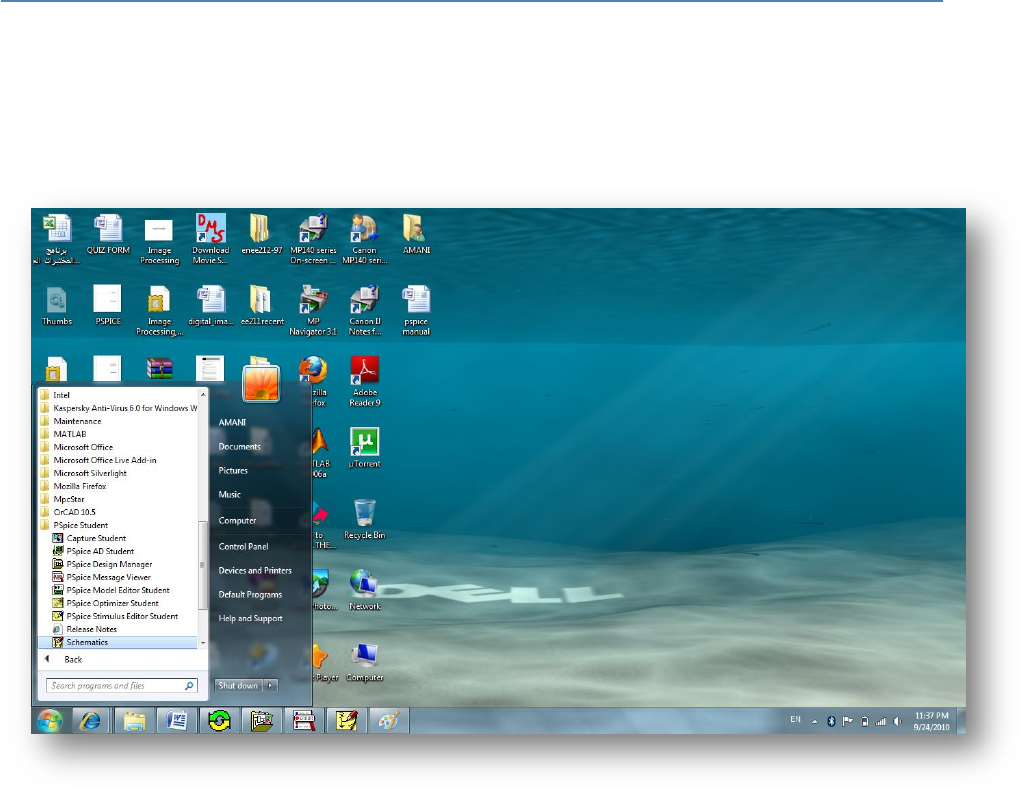
Step1 (Fig2.2.1): Go to Satrt <<All Programs<< PSpice Student
<<Schematics:
Fig.2.2.1: How to open a new Schematics design
8
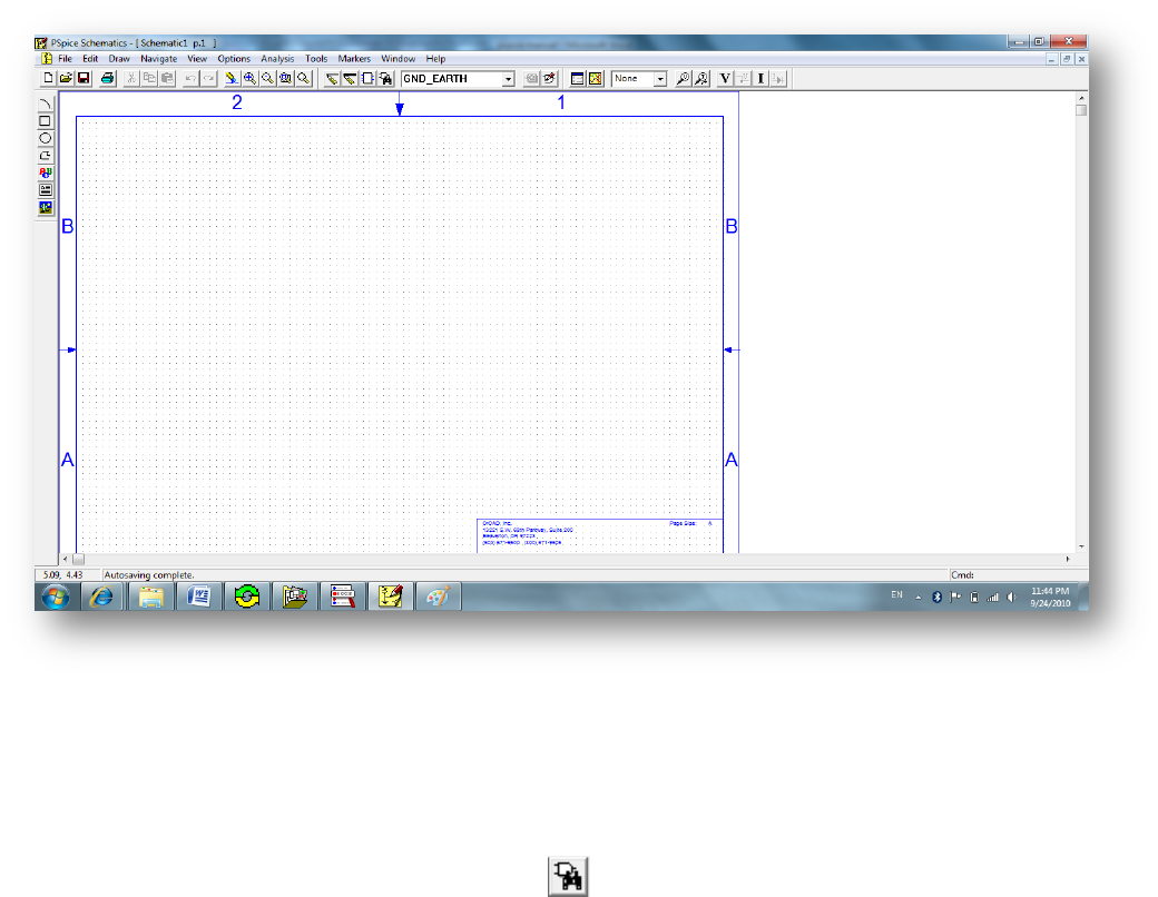
After you click on Schematics icon ,you can see the following:
Fig.2.2.2: A new Schematics design page.
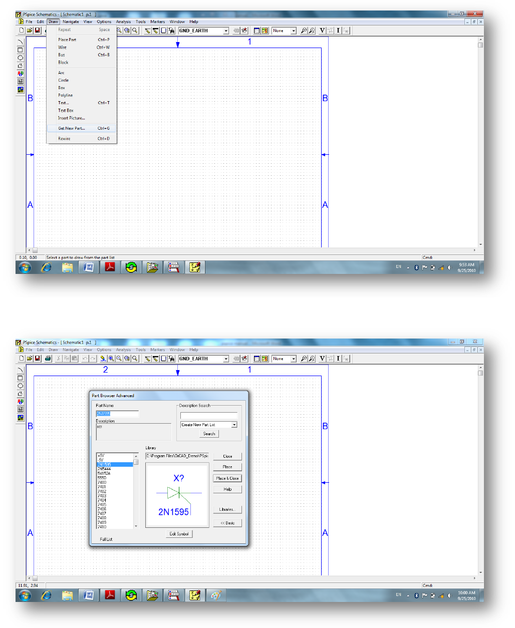
Step2:Selecting and Placing Parts
From the Draw menu, select Get New Part to display the Part Browser dialog box,
as shown in Fig2.2.3, or you can click on directly from the menu toolbar. Then
the Part Browser dialog box will appear .
Note: One of two Part Browser dialog boxes may appear: the Part Browser
Advanced or the Part Browser Basic. If in the Part Browser Advanced dialog
appears, click <<Basic to display the Part Browser Basic and vice versa.
Note: The Full List in the Part Browser dialog box represents all the parts in the
configured symbol libraries that are available for your use.
9
Fig2.2.3: How can you getting your design parts.
Fig2.2.4: Parts Browser Dialog Box.
10
There are several ways to select a part in the Part Browser dialog box:
If you know the name of the part, type the name in the Part Name text box.
Select the part name from the Full List of part names.
Click Libraries to view the Library Browser dialog box, select a library, and
select the part name from that library’s list of parts.
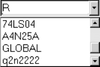
Note: Another method of selecting a part is to use the Get Recent Part list box on
the toolbar. You can scroll and select a previously placed part, or you can type the
name of the part you want to place as shown below:
Fig.2.2.5: The Get Recent Part list box.
To Placing Parts:
Click Place to place the part (with the browser remaining open) or click Place &
Close (to place the part and close the browser).
If you leave the browser open, click the title bar of the dialog box and drag it to
a new location. The Full List in the Part Browser dialog box represents all the
parts in the configured symbol libraries that are available for your use.
11
Chapter3
Simple Example:
The following example demonstrates the basic drawing features for drawing a
schematic.
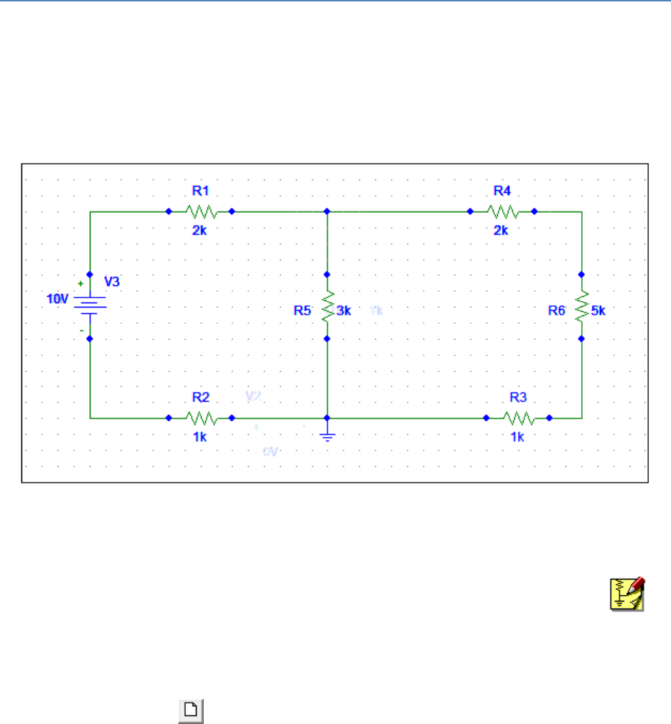
Question.1 : Draw the following circuit using PSpice , then find the voltages and
currents at all nodes.
Fig3.1: Question.1
Solution:
1- Start the schematic editor by double-clicking on the Schematics icon in
the Orcad program group. An empty schematic page displays.
2- If you already have Schematics running with another displayed, click the
New File icon to start a new schematic.
12
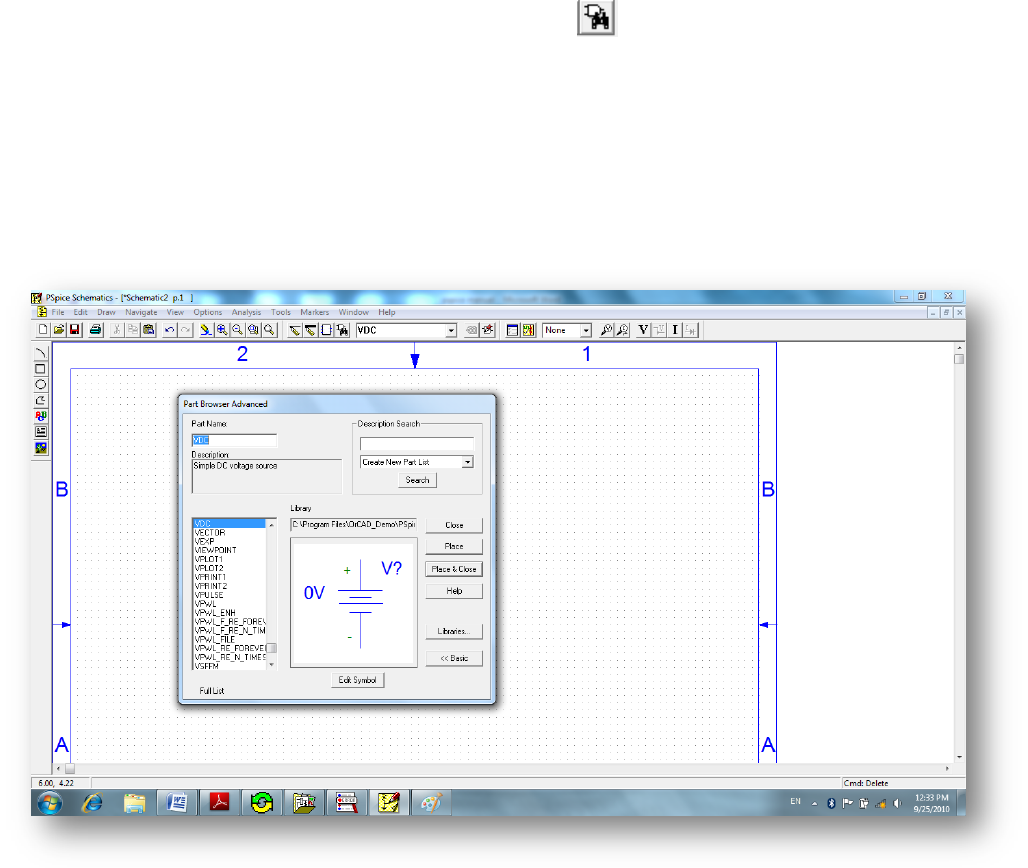
3- From the Draw menu, select Get New Part to display the Part Browser
dialog box.
4- Start placing the dc voltage for example. To place Vdc type VDC under
the part name space in the Part Browser dialog box. Then the available
VDC sources will be appeared as shown below:
Fig 3.2: Placing the DC Voltage Source.
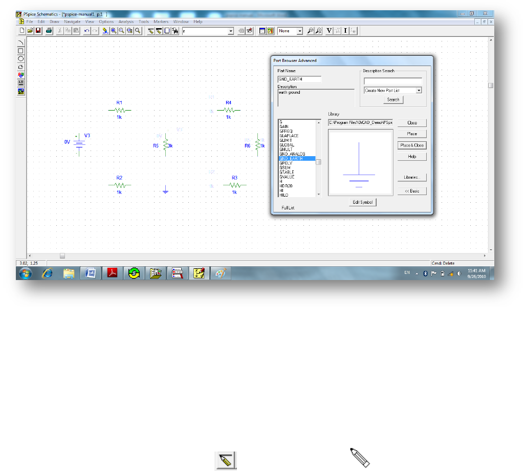
5- Do the same to place the resistors by typing R in the part name space then
place how many resistors you need.you can rotate any one of the circuit
components by pressing (Ctrl+R)you also need to determine the circuit
ground, to place the ground type GND as shown in the following Fig3.3.
13
Fig.3.3: Placing the earth ground.
After this step, all of your design elements are placed you need now to connect
between them by wires.
Drawing and Labeling Wires:
Continue working on the same example (i.e: example 1), to draw the wires:
1- Click the Draw Wire button ,The pencil pointer indicates that you
are ready to draw a wire.
2- Click where you want each vertex of the wire. Each click ends a wire
segment and starts a new one.
Note: Notice that the wire is now ended where you clicked to place a pin. The
pointer remains in the shape of a pencil and you are ready to start another wire.
3- Wire the rest of the schematic. Right-click to stop drawing wires.
14
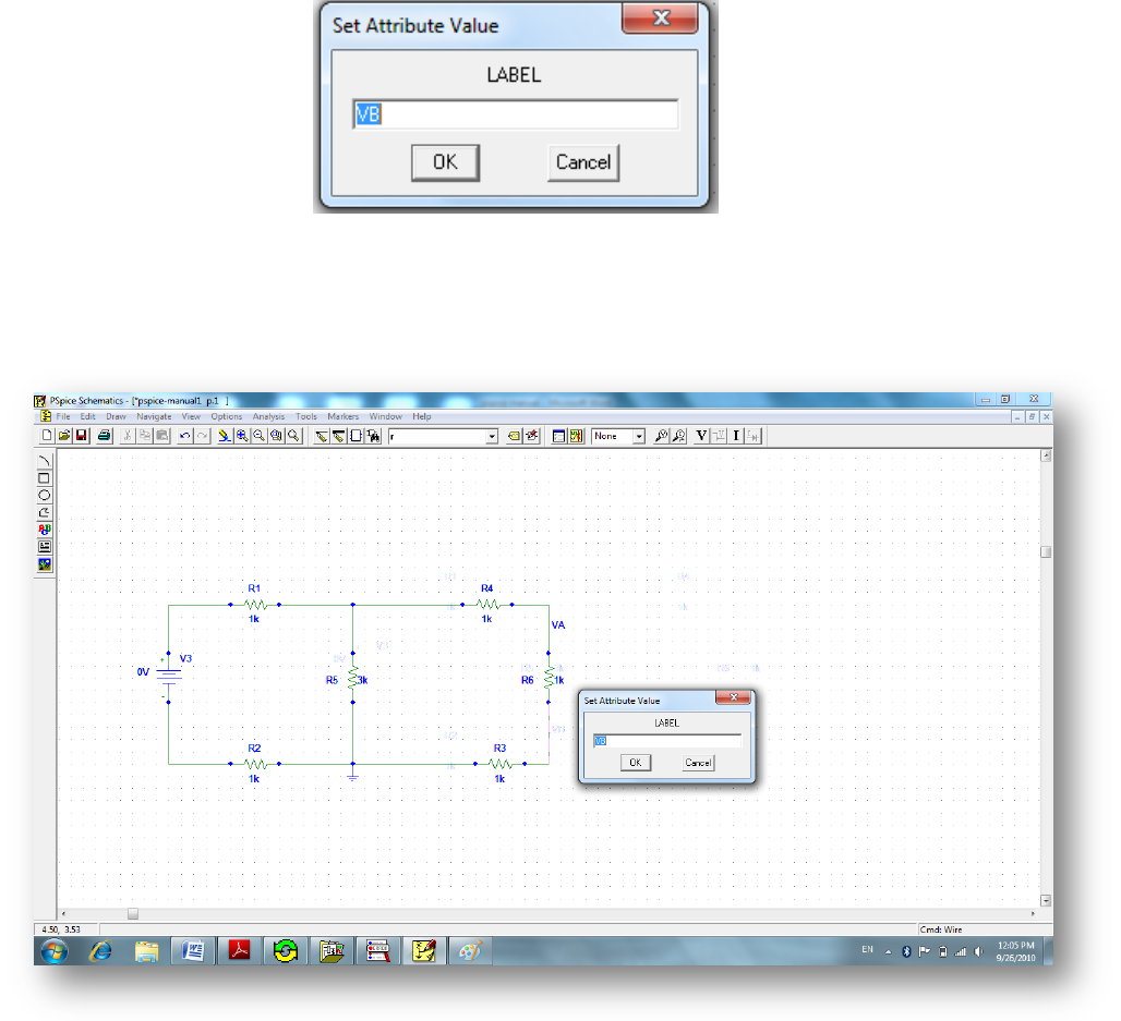
4- To label any wire segment :
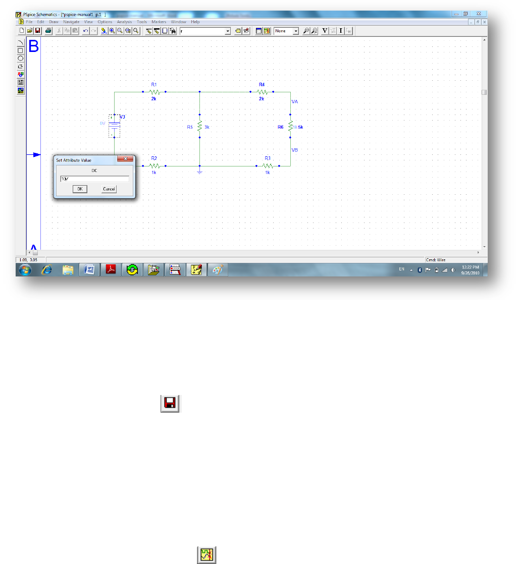
Double-click any segment of the wire to display the Set Attribute Value
dialog box.
Type in the LABEL text box then click OK.
Fig.3.4: The Set Attribute Value dialog box.
For the example above, I want to label the voltage across R6 as VABthis was
done as shown in the figure below:
Fig.3.5: Labeling the wires.
15
Changing Reference Designators and Part Values:
Change part values and reference designators by double-clicking them and typing a
new value in the dialog box.
Fig.3.6:Change the part values.
Saving Your Work:
After you changed all the values of the parts as you want in the design , you need
now to save your work.
Click the File Save button , or select Save (or Save As) from the File menu
to save the schematic.
Simulate your Circuit:
In order to find the voltages and currents all circuit’s nodes you need to simulate
your circuit.
Click on Simulate button in the toolbar.
16
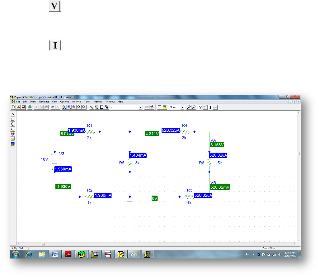
To display the voltage values click on Enable Bias Voltage Display
button . (All voltages displayed are with respect to ground)
To display the current values click on Enable Bias Current Display
button .
The values for all currents and voltages are displayed in Fig.3.7.
Fig.3.7: The Circuit Simulation.
Note: If you click on one of the current values you can determine it is direction in
the branch as explained in Fig.3.8:
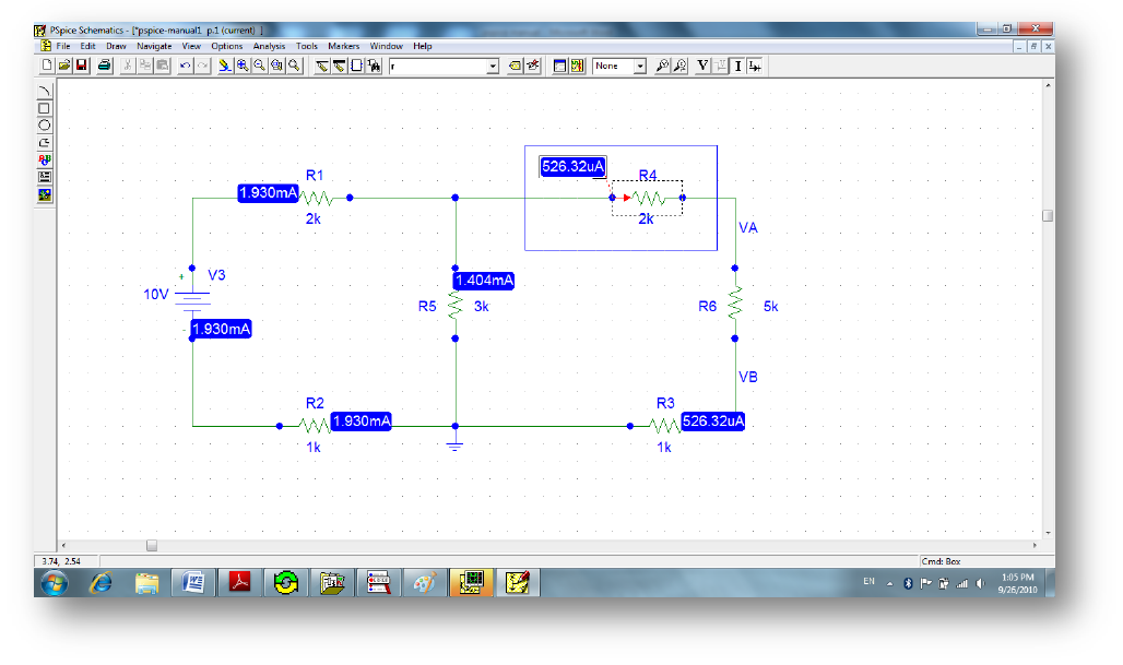
17
Fig.3.8: Determine the current direction.

18
Chapter4
Plotting Traces:
The PSpice Schematics has the ability to draw traces for voltages and currents in
your design. There are different types of Plotting Analysis which the PSpice can
deal with but in this manual we will explain only three types:
DC sweep
AC sweep
Transient Analysis
19
4.1:Overview of DC Sweep:
What is DC sweep?
The DC sweep analysis causes a DC sweep to be performed on the circuit. DC
sweep allows you to sweep a source (voltage or current), a global parameter, a
model parameter, or the temperature through a range of values.
Let us know how the voltage across R5 changes as the DC voltage source V3
sweeps from 0V to 10V in Example(page 12).To do this:
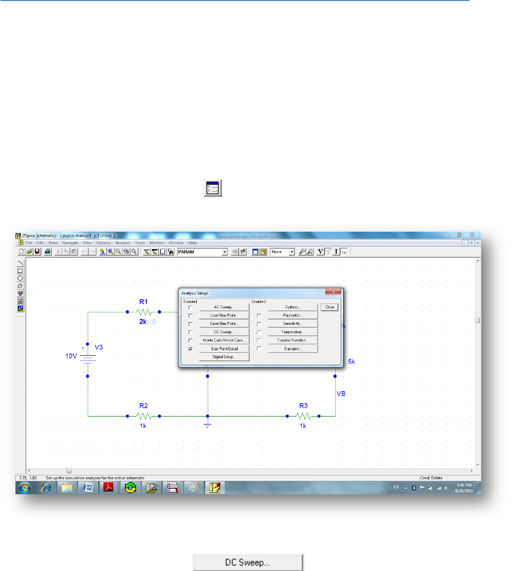
1- Click on Setup Analysis button . A small window will be opened as shown
below:
Fig.4.1.1: DC sweep Analysis.
2- Click on the DC sweep button then the DC sweep
window appears.
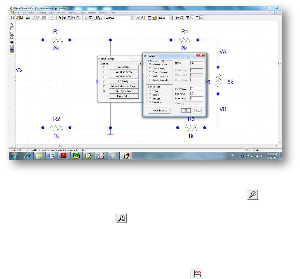
20
3- Choose Voltage Source Type<< Name:V3<< Linear sweep << Start
Value=0,End Value=10,Increment =1 then click OK (Show Fig.4.1.2).
4- Checked the DC Sweep box keeping the Bias Point Detail Checked.
5- Click Close to close the window.
Fig.4.1.2:Set the DC Sweep Parameters.
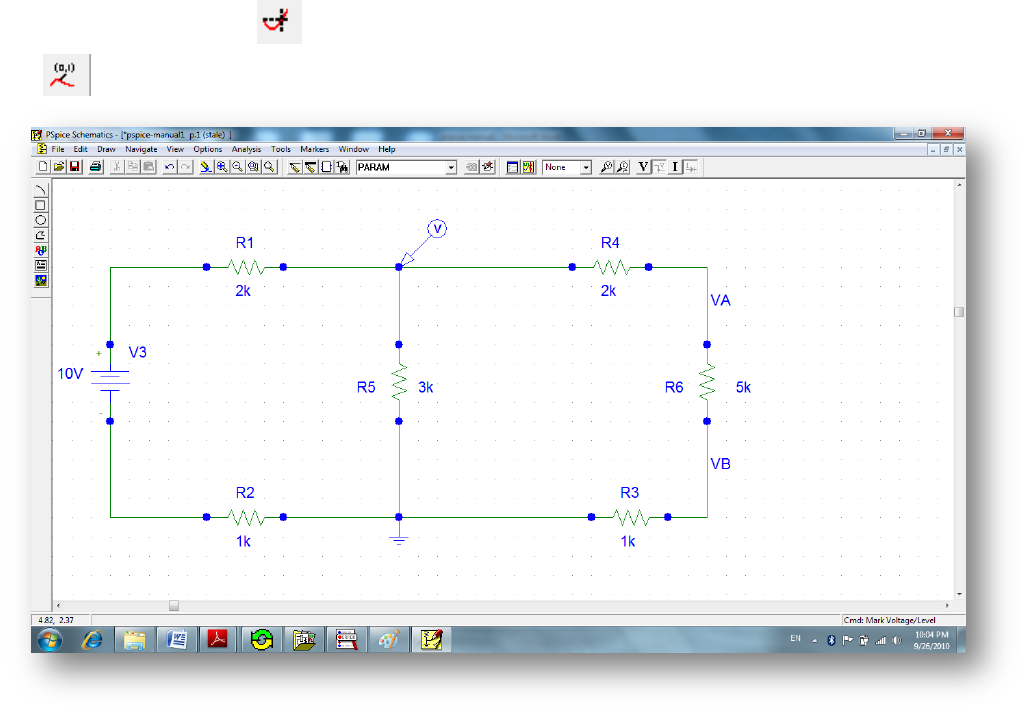
6- To display the voltage across R5 click on Volatge/Level Marker and
place it where you want as shown in Fig.4.1.3. You can do the same thing by
clicking upon Current Maker .
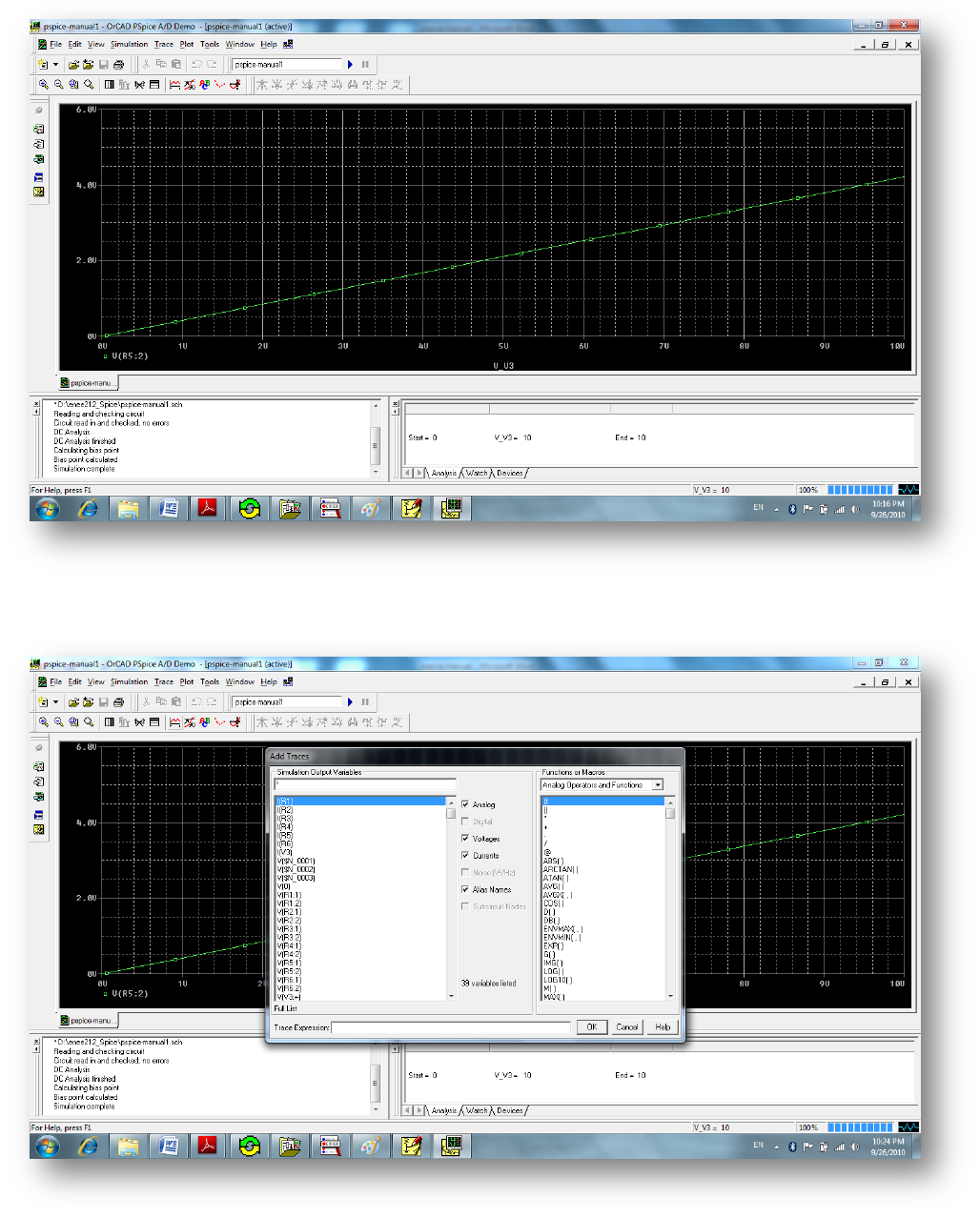
7- Click on Save again then click Simulate.
8- A black window appears plotted the voltage across R5 as the dc voltage source
V3 changes from 0V to 10V. (As shown in Fig.4.1.4)
9- After the simulation window opened you can click on to add a new trace on
the same plot. A new window will be opened listing all the variables that can be
plotted, choose for example V(VA) which plots VA.
21
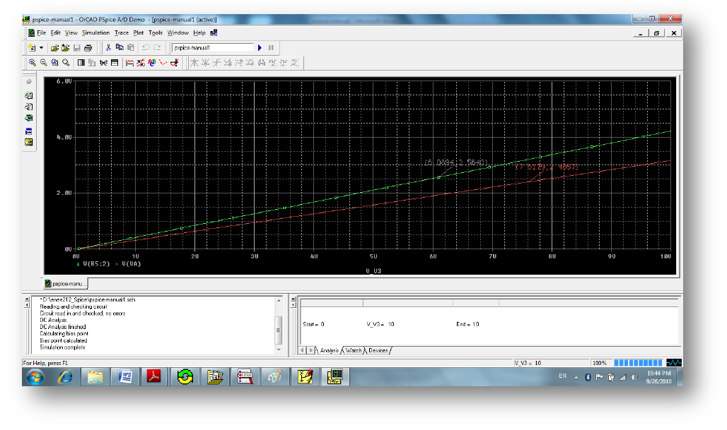
10- Click on Plot << Add plot to window to divide the black window to a
multiple plots as you want.
11- By clicking on you can determine the point on the graph then click on
to display its value.
Fig.4.1.3: How to use the Voltage/Current Makers.
22
Fig.4.1.4: Simulation results Screen.
Fig.4.1.5:How can you add a Trace.
23
Fig.4.1.6: Plotting VA on the same plot.

24
3.2: Overview of AC Sweep:
What is AC sweep?
AC sweep is a frequency response analysis. PSpice calculates the small-signal
response of the circuit to a combination of inputs by transforming it around the
bias point and treating it as a linear circuit.
To set up and run an AC sweep:
1- Place and connect a voltage or current source with an AC input signal.
2- Choose AC Sweep Analysis.
3- Specify the required parameters for the AC sweep analysis you want to run.
4- Click OK to save.
5- Select Simulate to start the simulation.
25
AC Sweep (Frequency Response)
To study the steady state behavior of circuits often the frequency response is
analyzed. One area of interest is the gain of the voltage at different frequencies;
recall that voltage gain is the ratio of the output voltage with respect to the input
voltage.
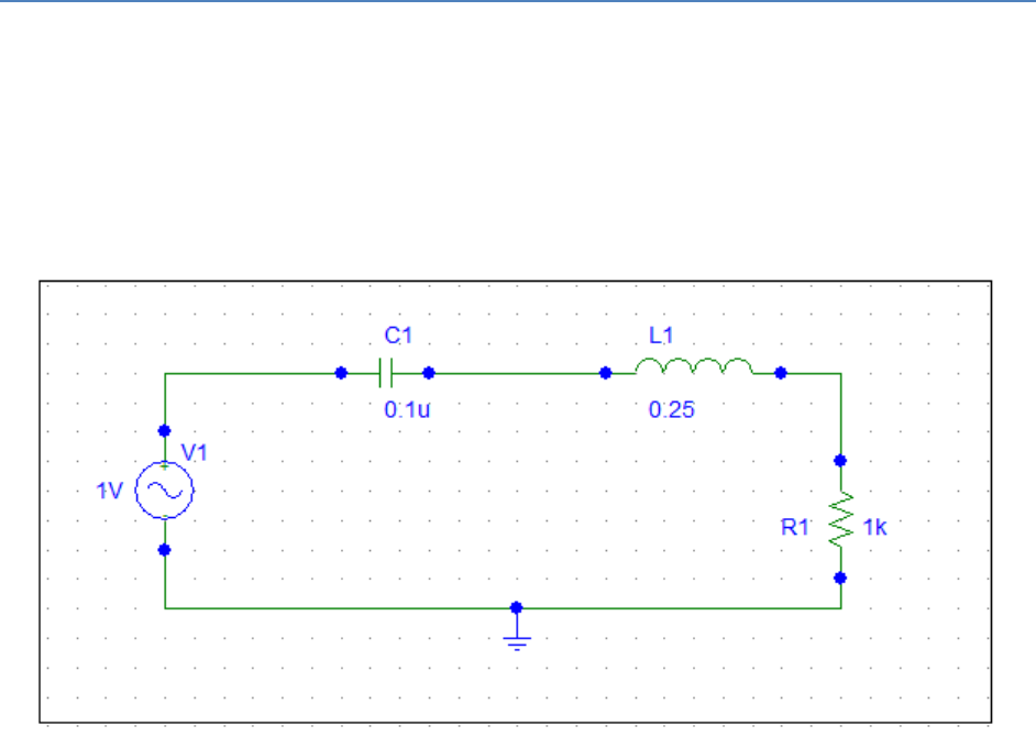
Let us explain the AC Sweep considering the following second order RLC circuit .
Fig.4.2.1: 2nd Order series RLC circuits (Example).
1- Draw the above circuit after you choose New Schematics, then place the R,
L,C,VAC parts by clicking on Get New Part.
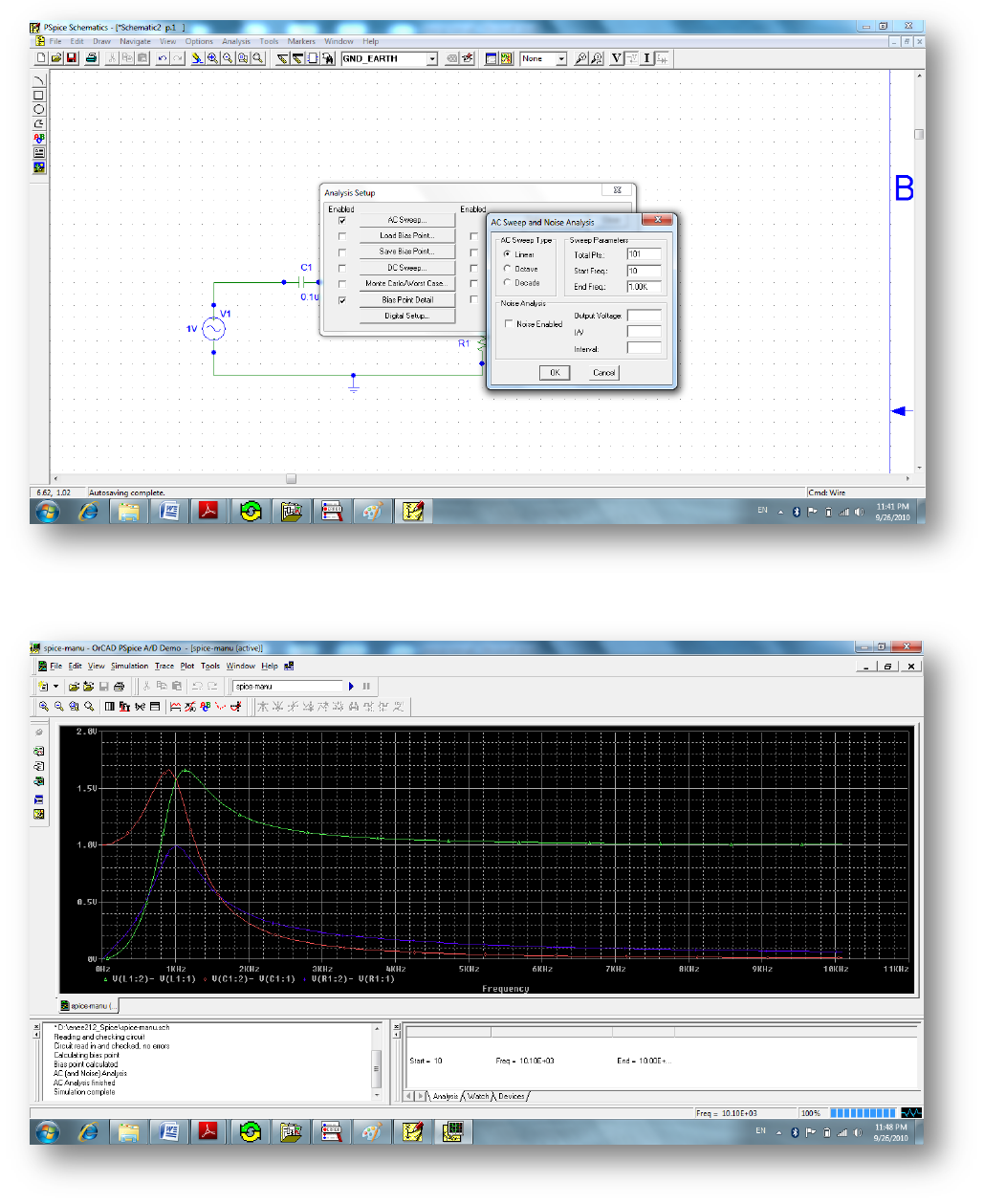
2- Click on Analysis Setup<< AC Sweep.
3- Set the AC Sweep parameters as shown in Fig.4.2.2.
4- Click on Simulate.
The following figures finds the voltages across R,L and C as a function of
frequency (Fig.3.2.3)
26
Fig.4.2.2: AC Sweep Analysis.
Fig.4.2.3: The Simulation Results.

27
3.3: Overview of Transient Analysis:
What is the Transient Sweep?
Transient Sweep is a time response sweep which calculates the circuit response at a
specific time interval determined by the Transient Sweep Analysis.
Minimum circuit design requirements:
To do a Transient Sweep, a Circuit should contain one of the following:
- An independent source with a transient specification.
- An initial condition on a reactive element.
- A controlled source that is a function of time.
To set up and run an AC sweep:
1- Place and connect a voltage or current source with a Transient input signal
(Like VSIN,Vpulse).
2- Choose Transient Sweep Analysis from the Setup Analysis menu.
3- Specify the required parameters for the Transient sweep analysis you want to
run.
4- Click OK to save then select Simulate to start the simulation.
28
Transient Analysis Example
Let Us apply the Transient response on the following circuit but do not forget to
use a voltage source with transient specification as VPULSE.
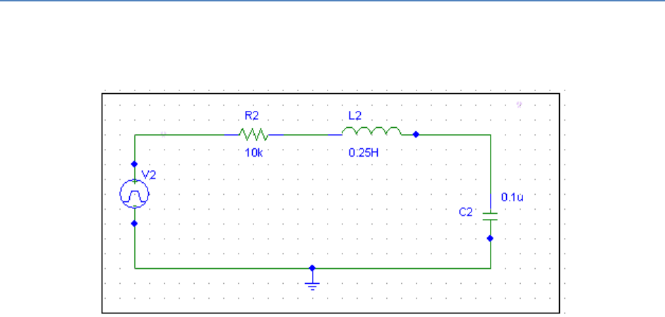
Fig.4.3.1: Plotting step response for RLC circuit (Example).
1- Draw the above circuit after you choose New Schematics, then place the R,
L,C,VAC parts by clicking on Get New Part.
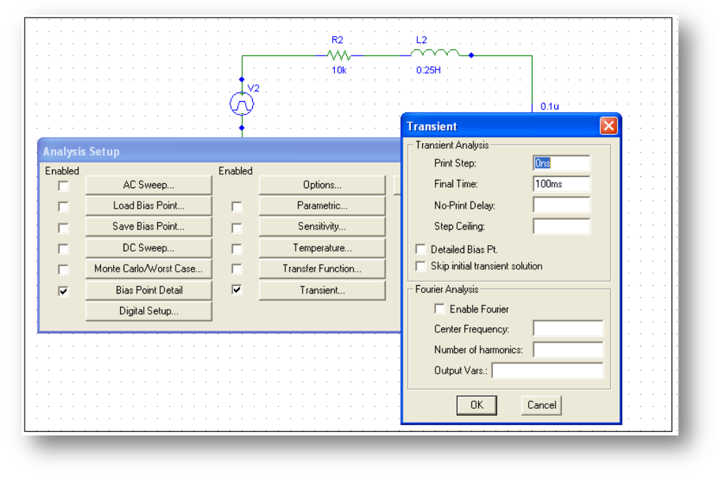
2- Click on Analysis Setup << Transient .
3- Set the Transient Sweep parameters as shown in Fig.4.3.2.
4- Click on Simulate.
The following figures find the voltages across C as a function of Time (Fig.4.3.3)
29
Fig.4.3.2: Setting Transient Analysis Parameters.
30
Fig.4.3.3: Transient Simulation Results.
31
Chapter5
More Examples and Exercises
Example 5.1: Construct the following RLC circuit in PSpice and display the
voltage waveform (step response) across the capacitor.
Fig 5.1: Series RLC circuit (example 5.1).
Answer: As you know the step response of this circuit varies as L or C or R varies.
The step response for this series RLC circuit has three cases:
1- Over damping
2- Critical damping
3- Under damping
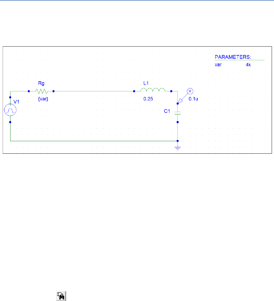
Let us discover the effect of changing R on the circuit response. To do this:
1- Construct the circuit which is shown in fig 5.1 using PSpice. (Initially
neglect the parameters list on the right). Let L=0.25 H, C=0.1uF and Vpulse
(V1=2, V2=0, Tf=Tr=Td=0, PER=0.02,PW=0.01).
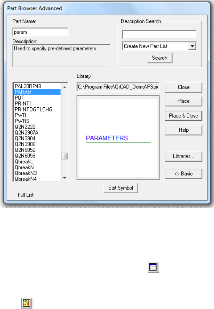
2- Click on to get part, then the part browser window will open, type
PARAM (i.e.: parameters) which is used to specify predefined parameter,
choose place and close.
32
Fig 5.2: Part browser window.
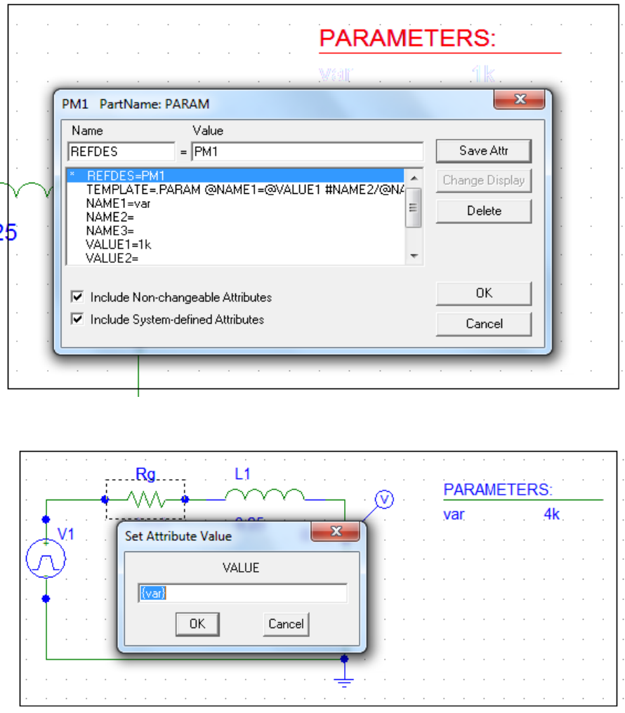
3- Double click on parameters the following window will appear, type var
under NAME1 and 4k for VALUE1 field (Fig 5.3), and then press OK.
4- Double click on the value of Rg and change it to {var} as in figure 5.4.
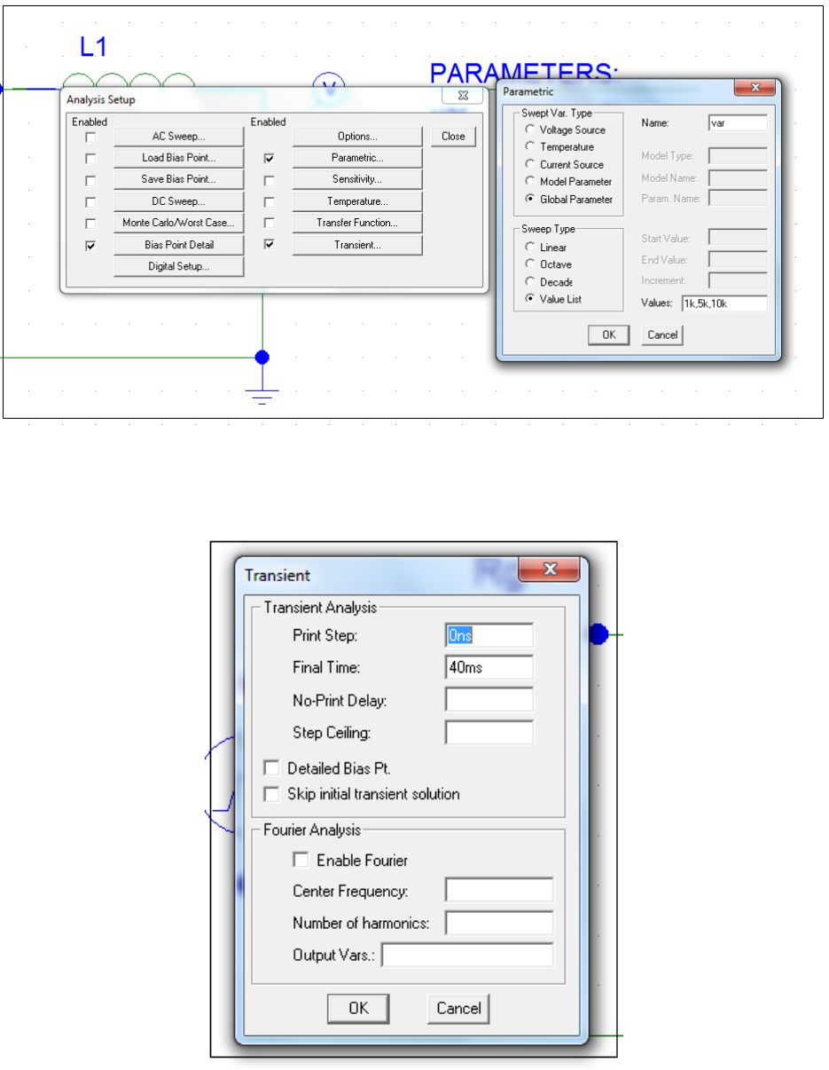
5- In order to show the simulation result, go to (Analysis Setup ) , Check
Transient, Parametric. Then fill the parametric window as shown in fig 5.5.
6- Finally, enter the transient setting which are shown in fig 5.6.
7- Go to (Simulate) in order to run the circuit simulation, the result will be
3 traces on the same plots since the value list for R is 1k, 5k, and 10k.
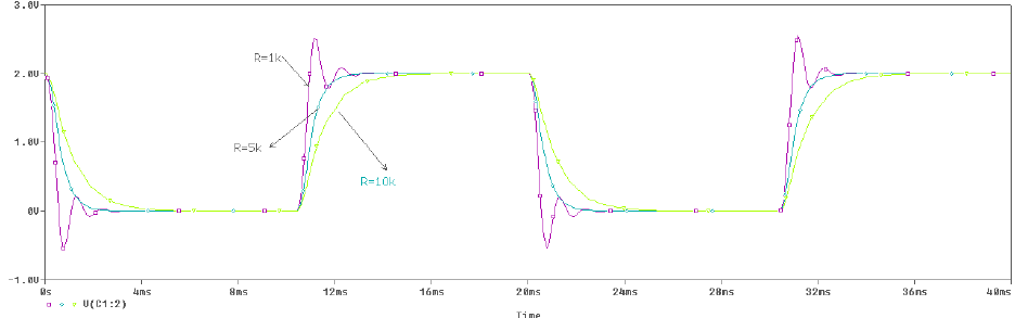
The result is shown in fig 5.7.
33
Fig 5.3: Parameters window.
Fig 5.4: Set the attribute value for Rg.
34
Fig 5.5: Analysis Setup.
Fig 5.6: Transient Analysis window.
35
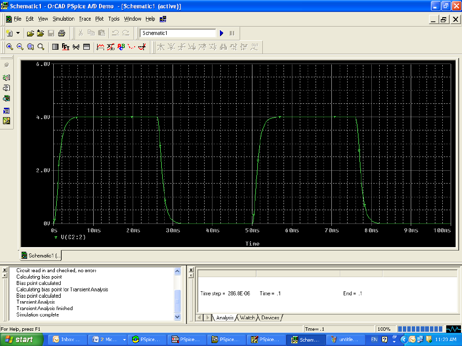
Fig 5.7: Simulation Results.
Note: from the above plot we can find that the step response for this system is
under damping when R=1k ohm, over damping when R=5k and 10k ohm.
36
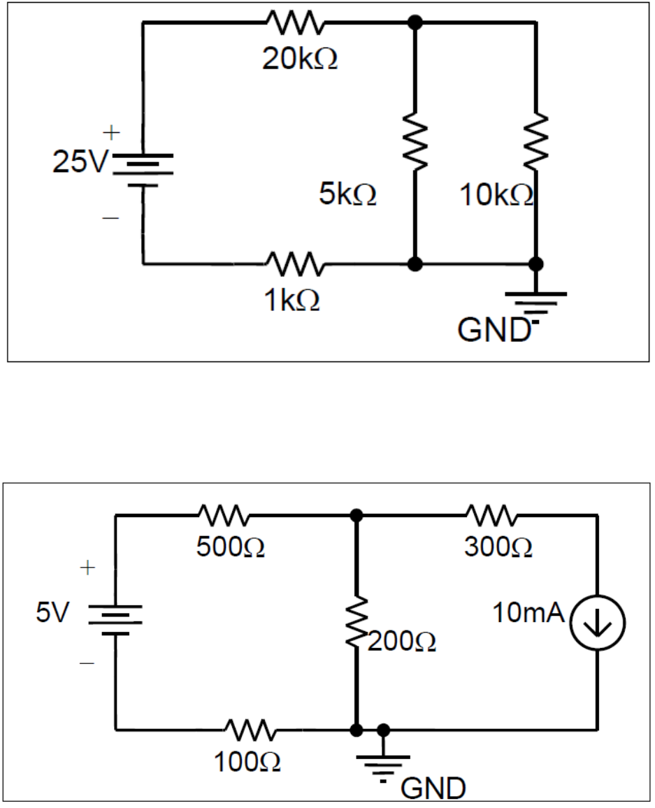
Exercise 1: Construct the following circuit using PSpice. Then run the Bias Point
Analysis to find the current in each branch.
Fig 5.8: Exercise 1.
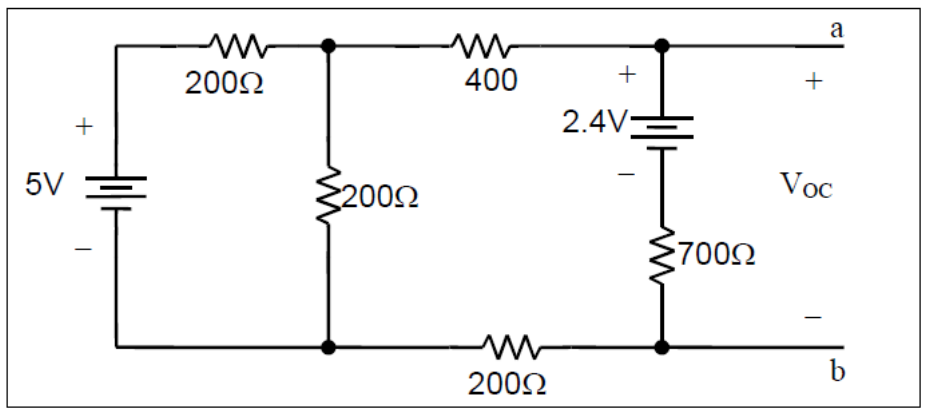
Exercise 2: Construct the following circuit using PSpice. Then run the Bias Point
Analysis to find the voltage across 300Ω.
Fig 5.9: Exercise 2.
37
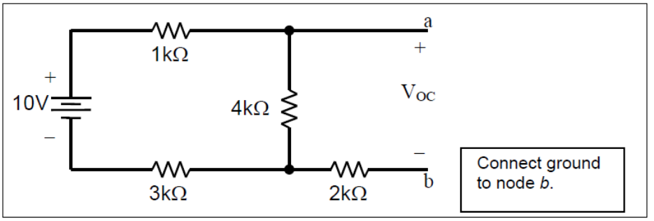
Example 5.2: Thevenin Equivalent
In PSpice you cannot calculate the Thevenin equivalent with respect to a pair of
nodes directly. In order to replace a circuit with its Thevenin equivalent at a pair of
nodes, one needs the open circuit voltage, VOC, and the short circuit current, ISC.
Construct the following circuit in PSpice.
Fig 5.10: Example 5.2.
In this example to find the short circuit current and the open circuit voltage;
- Place circuit ground at node b.
- Create a short circuit between nodes a, b and run Bias Point analysis to find
the voltage across the 2kΩ resistor. Then use Ohm’s law to find the short
circuit current. The short circuit current should be 1.25mA.
- Keep the circuit ground at node b.
- Create an open circuit between nodes a, b and run Bias Point analysis to
find the open circuit voltage. This is the voltage from node a to ground
(node b), and it should be 5V.
A second approach to find the Thevenin equivalent with respect to nodes
(terminals) a, b is to simulate a short circuit and an open circuit in PSpice.
- You may need to use this approach because sometimes when you create an
open circuit between nodes a and b, PSpice will not run the simulation
because of the presence of open-ended circuit elements and nodes (see
exercise 3).
- In other cases if you directly place a short circuit between nodes a, b and run
the analysis, the process of finding the short circuit current using the results
of the simulation can be complicated (see exercise4).
38
- For the circuit in figure 5.10, find the short circuit current by placing a
resistor between nodes a and b whose resistance is much smaller than the
resistance of the other resistors in the circuit.
- In this case a 10-6Ω resistor between nodes a and b will be sufficient in
simulating a short circuit.
- Choose circuit ground to be at node b, this way you can obtain the voltage
Vab directly and then use Ohm’s law to find the short circuit current.
- Using Bias Point analysis you should obtain a short circuit current of
1.25mA.
Note: In all DC circuit analyses an inductor can be used as a short circuit.
- The voltage drop across the inductor is zero so you must use the voltage
drops across the other nodes to solve for the short circuit current.
- Replace the 10-6Ω resistor with an inductor of any value and confirm that the
result remains 1.25mA.
To find the open circuit voltage, place a resistor between nodes a and b whose
resistance is much larger than the resistance of the other resistors in the circuit.
- For the circuit in figure 5.10, a 1012W resistor between nodes a and b will
be sufficient in simulating an open circuit.
- Again choose circuit ground at node b.
- You should obtain an open circuit voltage of 5V.
Note: In all DC circuit analyses a capacitor can be used as an open circuit. The
voltage drop across the capacitor is the open circuit voltage, since a capacitor
behaves as an open circuit in DC.
- Replace the 1012Ω resistor with a capacitor of any value, and confirm that
the result remains 5V.
- When finding the Thevenin equivalent with respect to a pair of nodes in
PSpice, you should always place circuit ground at one of those nodes. This
will simplify your analysis.
With an open circuit voltage of 5V and a short circuit current of 1.25mA the
Thevenin equivalent with respect to nodes a, b is a 5V DC voltage source in series
with a 4kΩ resistor. This is shown in figure 5.11.
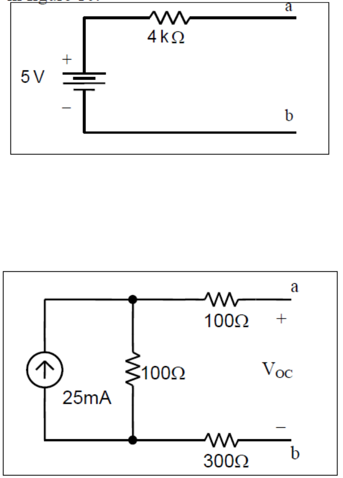
39
Fig 5.11: Thevenin Equivalent circuit of Example 5.2.
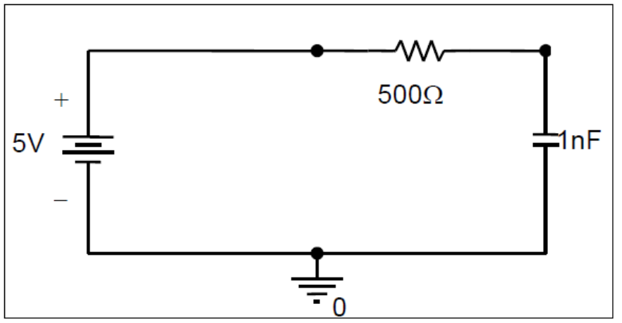
Exercise 3: Find the Thevenin equivalent with respect to nodes a, b of the
following circuit:
Fig 5.12: Exercise 3.
In this exercise you cannot simply create an open circuit between nodes a, b in
PSpice and run the simulation. PSpice will give you a ―Less than two connections
at node N_______ ‖ error if you try to run the simulation with an open circuit.
You need to place a resistor with a very large resistance between nodes a, b in
order to simulate an open circuit. The correct open circuit voltage is 2.5V and the
correct short circuit current is 5mA.
40
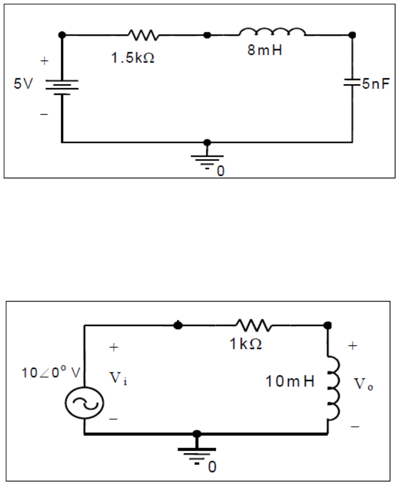
Exercise 4 :Find the Thevenin equivalent with respect to nodes a, b of the
following circuit:
Fig 5.13: Exercise 4.
In this exercise if you place a very small resistance between nodes a and b, you
will get the voltage at node a directly. Using Ohm’s law you can then find the short
circuit current. If instead you had placed a short circuit between nodes a and b, you
would have to do a calculation to find the short circuit current – in this case a
simple one, but still introducing an opportunity for error. You should also bear in
mind that PSpice only gives you results to four significant digits, so you may lose
precision if you have to go through more calculations to get to the answer.
For this circuit you should find the open circuit voltage is 2.45V, and the short
circuit current is 7mA.
When finding the Thevenin equivalent you can use any of the methods described.
However you should realize simulating open circuits and short circuits using very
large and very small resistances will work every time, though it takes slightly
longer to design a circuit.
41
Transient Analysis:
Exercise 5 (Step Response): Construct the following RC circuit in PSpice and
display the voltage waveforms across all the circuit components.
Fig 5.14: Exercise 5.
Once you constructed the circuit create a new simulation .
- In the Simulation Settings dialog window, under the Analysis tab select
Time Domain (Transient) as the Analysis Type.
- In the General Settings option, specify start time of the simulation. This
should usually be set to 0.
- Specify the end time of the simulation in the Run to time dialog box. This
should usually be set to about 5τ to 6τ, where t is the time constant of your
circuit. When analyzing RLC circuits, where the time constant is not
available, you will have to play around with end time to get a good plot of
the response.
- Check the Skip the initial transient bias point calculation box.
- Once you have made all the adjustments click OK and run the simulation.
The voltage across the resistor should show an exponential voltage decay
starting from 5V and the voltage across the capacitor should show an
exponential rise from 0V.
42
Exercise 6: Construct the following RLC circuit in PSpice and display the voltage
waveforms across all the circuit components.
Fig 5.15: Exercise 6.
Frequency Response
Exercise 7: Construct the follow series RL circuit in PSpice and generate a Bode
Plot of H(jω) dB versus f. Vo is taken across the inductor.
Fig 5.16: Exercise 7.
The plot of the gain should rise to 0dB. Check that the 3dB frequency is
approximately 16kHz. You can do this easily with the cursor. Then Plot θ(ω)
versus f.
43
Exercise 8 : Construct the following RLC circuit in PSpice and then generate the
gain plot and the phase angle plot. In this circuit Vo is taken across the resistor.
Fig 5.17: Exercise 8.
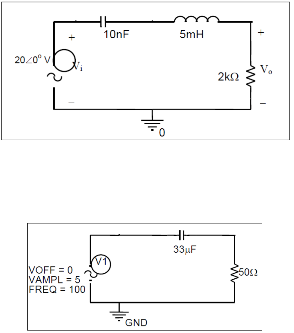
Sinusoidal Steady State Analysis : PSpice can also display the waveform of a
sinusoidal signal at a fixed frequency. To perform this analysis, we need a new
voltage source with a fixed frequency. Construct the following circuit in PSpice.
Fig 5.18: Steady State Analysis (Example 5.3).
44
- The voltage source used in this circuit is called VSIN and can be found in
the SOURCE library. You should see three labels next to the symbol;
VOFF =, VAMPL =, and FREQ =. These labels indicate the DC offset
voltage, the amplitude of the voltage signal and the frequency (in Hertz) of
the signal respectively. Double click on each of these labels to change the
values.
- In the Simulation Settings dialog window, go to the Analysis tab and chose
Time Domain (Transient) as the Analysis type.
- In the General Settings options, set the Run to Time text box to 0.02
seconds. Note that at a frequency of 100 Hz, the period is 0.01 seconds. We
should get two full waveforms on the display. In the Transient Options
box, set the Maximum step size to 1/100 of the period of the signal. In this
case, this is 0.1ms.
- Click on OK and run the simulation.
- Plot the voltage across the capacitor then plot the voltage across the resistor.

45
REFRENCES:
http://www.orcad.com
