6430F SAM3U User Guide
User Manual: Pdf
Open the PDF directly: View PDF ![]() .
.
Page Count: 1187 [warning: Documents this large are best viewed by clicking the View PDF Link!]
- Features
- 1. ATSAM3U4/2/1 Description
- 2. ATSAM3U4/2/1 Block Diagram
- 3. Signal Description
- 4. Package and Pinout
- 5. Power Considerations
- 6. Input/Output Lines
- 7. Processor and Architecture
- 8. Product Mapping
- 9. Memories
- 10. System Controller
- 10.1 System Controller and Peripheral Mapping
- 10.2 Power-on-Reset, Brownout and Supply Monitor
- 10.3 Reset Controller
- 10.4 Supply Controller
- 10.5 Clock Generator
- 10.6 Power Management Controller
- 10.7 Watchdog Timer
- 10.8 SysTick Timer
- 10.9 Real-time Timer
- 10.10 Real-time Clock
- 10.11 General-Purpose Back-up Registers
- 10.12 Nested Vectored Interrupt Controller
- 10.13 Chip Identification
- 10.14 PIO Controllers
- 11. Peripherals
- 12. Embedded Peripherals Overview
- 12.1 Serial Peripheral Interface (SPI)
- 12.2 Two Wire Interface (TWI)
- 12.3 Universal Asynchronous Receiver Transceiver (UART)
- 12.4 Universal Synchronous Asynchronous Receiver Transmitter (USART)
- 12.5 Serial Synchronous Controller (SSC)
- 12.6 Timer Counter (TC)
- 12.7 Pulse Width Modulation Controller (PWM)
- 12.8 High Speed Multimedia Card Interface (HSMCI)
- 12.9 USB High Speed Device Port (UDPHS)
- 12.10 Analog-to-Digital Converter (ADC)
- 13. ARM Cortex® M3 Processor
- 13.1 About this section
- 13.2 About the Cortex-M3 processor and core peripherals
- 13.3 Programmers model
- 13.3.1 Processor mode and privilege levels for software execution
- 13.3.2 Stacks
- 13.3.3 Core registers
- 13.3.3.1 General-purpose registers
- 13.3.3.2 Stack Pointer
- 13.3.3.3 Link Register
- 13.3.3.4 Program Counter
- 13.3.3.5 Program Status Register
- 13.3.3.6 Application Program Status Register
- 13.3.3.7 Interrupt Program Status Register
- 13.3.3.8 Execution Program Status Register
- 13.3.3.9 Interruptible-continuable instructions
- 13.3.3.10 If-Then block
- 13.3.3.11 Exception mask registers
- 13.3.3.12 Priority Mask Register
- 13.3.3.13 Fault Mask Register
- 13.3.3.14 Base Priority Mask Register
- 13.3.3.15 CONTROL register
- 13.3.4 Exceptions and interrupts
- 13.3.5 Data types
- 13.3.6 The Cortex Microcontroller Software Interface Standard
- 13.4 Memory model
- 13.4.1 Memory regions, types and attributes
- 13.4.2 Memory system ordering of memory accesses
- 13.4.3 Behavior of memory accesses
- 13.4.4 Software ordering of memory accesses
- 13.4.5 Bit-banding
- 13.4.6 Memory endianness
- 13.4.7 Synchronization primitives
- 13.4.8 Programming hints for the synchronization primitives
- 13.5 Exception model
- 13.6 Fault handling
- 13.7 Power management
- 13.8 Instruction set summary
- 13.9 Intrinsic functions
- 13.10 About the instruction descriptions
- 13.11 Memory access instructions
- 13.12 General data processing instructions
- 13.13 Multiply and divide instructions
- 13.14 Saturating instructions
- 13.15 Bitfield instructions
- 13.16 Branch and control instructions
- 13.17 Miscellaneous instructions
- 13.18 About the Cortex-M3 peripherals
- 13.19 Nested Vectored Interrupt Controller
- 13.19.1 The CMSIS mapping of the Cortex-M3 NVIC registers
- 13.19.2 Interrupt Set-enable Registers
- 13.19.3 Interrupt Clear-enable Registers
- 13.19.4 Interrupt Set-pending Registers
- 13.19.5 Interrupt Clear-pending Registers
- 13.19.6 Interrupt Active Bit Registers
- 13.19.7 Interrupt Priority Registers
- 13.19.8 Software Trigger Interrupt Register
- 13.19.9 Level-sensitive interrupts
- 13.19.10 NVIC design hints and tips
- 13.20 System control block
- 13.20.1 The CMSIS mapping of the Cortex-M3 SCB registers
- 13.20.2 Auxiliary Control Register
- 13.20.3 CPUID Base Register
- 13.20.4 Interrupt Control and State Register
- 13.20.5 Vector Table Offset Register
- 13.20.6 Application Interrupt and Reset Control Register
- 13.20.7 System Control Register
- 13.20.8 Configuration and Control Register
- 13.20.9 System Handler Priority Registers
- 13.20.10 System Handler Control and State Register
- 13.20.11 Configurable Fault Status Register
- 13.20.12 Hard Fault Status Register
- 13.20.13 Memory Management Fault Address Register
- 13.20.14 Bus Fault Address Register
- 13.20.15 Auxiliary Fault Status Register
- 13.20.16 System control block design hints and tips
- 13.21 System timer, SysTick
- 13.22 Memory protection unit
- 13.23 Glossary
- 14. Debug and Test Features
- 14.1 Overview
- 14.2 Application Examples
- 14.3 Debug and Test Pin Description
- 14.4 Functional Description
- 15. Watchdog Timer (WDT)
- 16. Reset Controller (RSTC)
- 17. Real-time Timer (RTT)
- 18. Real Time Clock (RTC)
- 18.1 Description
- 18.2 Block Diagram
- 18.3 Product Dependencies
- 18.4 Functional Description
- 18.5 Real Time Clock (RTC) User Interface
- 18.5.1 RTC Control Register
- 18.5.2 RTC Mode Register
- 18.5.3 RTC Time Register
- 18.5.4 RTC Calendar Register
- 18.5.5 RTC Time Alarm Register
- 18.5.6 RTC Calendar Alarm Register
- 18.5.7 RTC Status Register
- 18.5.8 RTC Status Clear Command Register
- 18.5.9 RTC Interrupt Enable Register
- 18.5.10 RTC Interrupt Disable Register
- 18.5.11 RTC Interrupt Mask Register
- 18.5.12 RTC Valid Entry Register
- 18.5.13 RTC Write Protect Mode Register
- 19. Supply Controller (SUPC)
- 19.1 Description
- 19.2 Embedded Characteristics
- 19.3 Block Diagram
- 19.4 Supply Controller Functional Description
- 19.5 Supply Controller (SUPC) User Interface
- 19.5.1 System Controller (SYSC) User Interface
- 19.5.2 Supply Controller (SUPC) User Interface
- 19.5.3 Supply Controller Control Register
- 19.5.4 Supply Controller Supply Monitor Mode Register
- 19.5.5 Supply Controller Mode Register
- 19.5.6 Supply Controller Wake Up Mode Register
- 19.5.7 System Controller Wake Up Inputs Register
- 19.5.8 Supply Controller Status Register
- 20. General Purpose Backup Registers (GPBR)
- 21. Enhanced Embedded Flash Controller (EEFC)
- 22. Fast Flash Programming Interface (FFPI)
- 22.1 Overview
- 22.2 Parallel Fast Flash Programming
- 22.2.1 Device Configuration
- 22.2.2 Signal Names
- 22.2.3 Entering Programming Mode
- 22.2.4 Programmer Handshaking
- 22.2.5 Device Operations
- 22.2.5.1 Flash Read Command
- 22.2.5.2 Flash Write Command
- 22.2.5.3 Flash Full Erase Command
- 22.2.5.4 Flash Lock Commands
- 22.2.5.5 Flash General-purpose NVM Commands
- 22.2.5.6 Flash Security Bit Command
- 22.2.5.7 SAM3U 256 Kbytes Flash Select EEFC Command
- 22.2.5.8 Memory Write Command
- 22.2.5.9 Get Version Command
- 23. SAM3U4/2/1 Boot Program
- 24. Bus Matrix (MATRIX)
- 25. Static Memory Controller (SMC)
- 25.1 Description
- 25.2 Embedded Characteristics
- 25.3 Block Diagram
- 25.4 I/O Lines Description
- 25.5 Multiplexed Signals
- 25.6 Application Example
- 25.7 Product Dependencies
- 25.8 External Memory Mapping
- 25.9 Connection to External Devices
- 25.10 Standard Read and Write Protocols
- 25.11 Scrambling/Unscrambling Function
- 25.12 Automatic Wait States
- 25.13 Data Float Wait States
- 25.14 External Wait
- 25.15 Slow Clock Mode
- 25.16 NAND Flash Controller Operations
- 25.17 SMC Error Correcting Code Functional Description
- 25.18 Power Management Controller (PMC) User Interface
- 25.18.1 SMC NFC Configuration Register
- 25.18.2 SMC NFC Control Register
- 25.18.3 SMC NFC Status Register
- 25.18.4 SMC NFC Interrupt Enable Register
- 25.18.5 SMC NFC Interrupt Disable Register
- 25.18.6 SMC NFC Interrupt Mask Register
- 25.18.7 SMC NFC Address Cycle Zero Register
- 25.18.8 SMC NFC Bank Register
- 25.18.9 SMC ECC Control Register
- 25.18.10 SMC ECC MODE Register
- 25.18.11 SMC ECC Status Register 1
- 25.18.12 SMC ECC Status Register 2
- 25.18.13 SMC ECC Parity Register 0 for a Page of 512/1024/2048/4096 Bytes
- 25.18.14 SMC ECC Parity Register 1 for a Page of 512/1024/2048/4096 Bytes
- 25.18.15 SMC ECC Parity Registers for 1 ECC per 512 Bytes for a Page of 512/2048/4096 Bytes, 9-bit Word
- 25.18.16 SMC ECC Parity Registers for 1 ECC per 256 Bytes for a Page of 512/2048/4096 Bytes, 8-bit Word
- 25.18.17 SMC Setup Register
- 25.18.18 SMC Pulse Register
- 25.18.19 SMC Cycle Register
- 25.18.20 SMC Timings Register
- 25.18.21 SMC Mode Register
- 25.18.22 SMC OCMS Register
- 25.18.23 SMC OCMS Key1 Register
- 25.18.24 SMC OCMS Key2 Register
- 25.18.25 SMC Write Protection Control
- 25.18.26 SMC Write Protection Status
- 26. Peripheral DMA Controller (PDC)
- 26.1 Description
- 26.2 Embedded Characteristics
- 26.3 Block Diagram
- 26.4 Functional Description
- 26.5 Peripheral DMA Controller (PDC) User Interface
- 26.5.1 Receive Pointer Register
- 26.5.2 Receive Counter Register
- 26.5.3 Transmit Pointer Register
- 26.5.4 Transmit Counter Register
- 26.5.5 Receive Next Pointer Register
- 26.5.6 Receive Next Counter Register
- 26.5.7 Transmit Next Pointer Register
- 26.5.8 Transmit Next Counter Register
- 26.5.9 Transfer Control Register
- 26.5.10 Transfer Status Register
- 27. Clock Generator
- 28. Power Management Controller (PMC)
- 28.1 Description
- 28.2 Block Diagram
- 28.3 Master Clock Controller
- 28.4 Processor Clock Controller
- 28.5 SysTick Clock
- 28.6 Peripheral Clock Controller
- 28.7 Free Running Processor Clock
- 28.8 Programmable Clock Output Controller
- 28.9 Fast Startup
- 28.10 Clock Failure Detector
- 28.11 Programming Sequence
- 28.12 Clock Switching Details
- 28.13 Write Protection Registers
- 28.14 Power Management Controller (PMC) User Interface
- 28.14.1 PMC System Clock Enable Register
- 28.14.2 PMC System Clock Disable Register
- 28.14.3 PMC System Clock Status Register
- 28.14.4 PMC Peripheral Clock Enable Register
- 28.14.5 PMC Peripheral Clock Disable Register
- 28.14.6 PMC Peripheral Clock Status Register
- 28.14.7 PMC UTMI Clock Configuration Register
- 28.14.8 PMC Clock Generator Main Oscillator Register
- 28.14.9 PMC Clock Generator Main Clock Frequency Register
- 28.14.10 PMC Clock Generator PLLA Register
- 28.14.11 PMC Master Clock Register
- 28.14.12 PMC Programmable Clock Register
- 28.14.13 PMC Interrupt Enable Register
- 28.14.14 PMC Interrupt Disable Register
- 28.14.15 PMC Status Register
- 28.14.16 PMC Interrupt Mask Register
- 28.14.17 PMC Fast Startup Mode Register
- 28.14.18 PMC Fast Startup Polarity Register
- 28.14.19 PMC Fault Output Clear Register
- 28.14.20 PMC Write Protect Mode Register
- 28.14.21 PMC Write Protect Status Register
- 29. Chip Identifier (CHIPID)
- 30. Parallel Input/Output Controller (PIO)
- 30.1 Description
- 30.2 Embedded Characteristics
- 30.3 Block Diagram
- 30.4 Product Dependencies
- 30.5 Functional Description
- 30.5.1 Pull-up Resistor Control
- 30.5.2 I/O Line or Peripheral Function Selection
- 30.5.3 Peripheral A or B Selection
- 30.5.4 Output Control
- 30.5.5 Synchronous Data Output
- 30.5.6 Multi Drive Control (Open Drain)
- 30.5.7 Output Line Timings
- 30.5.8 Inputs
- 30.5.9 Input Glitch and Debouncing Filters
- 30.5.10 Input Edge/Level Interrupt
- 30.5.11 I/O Lines Lock
- 30.6 I/O Lines Programming Example
- 30.7 Parallel Input/Output Controller (PIO) User Interface
- 30.7.1 PIO Controller PIO Enable Register
- 30.7.2 PIO Controller PIO Disable Register
- 30.7.3 PIO Controller PIO Status Register
- 30.7.4 PIO Controller Output Enable Register
- 30.7.5 PIO Controller Output Disable Register
- 30.7.6 PIO Controller Output Status Register
- 30.7.7 PIO Controller Input Filter Enable Register
- 30.7.8 PIO Controller Input Filter Disable Register
- 30.7.9 PIO Controller Input Filter Status Register
- 30.7.10 PIO Controller Set Output Data Register
- 30.7.11 PIO Controller Clear Output Data Register
- 30.7.12 PIO Controller Output Data Status Register
- 30.7.13 PIO Controller Pin Data Status Register
- 30.7.14 PIO Controller Interrupt Enable Register
- 30.7.15 PIO Controller Interrupt Disable Register
- 30.7.16 PIO Controller Interrupt Mask Register
- 30.7.17 PIO Controller Interrupt Status Register
- 30.7.18 PIO Multi-driver Enable Register
- 30.7.19 PIO Multi-driver Disable Register
- 30.7.20 PIO Multi-driver Status Register
- 30.7.21 PIO Pull Up Disable Register
- 30.7.22 PIO Pull Up Enable Register
- 30.7.23 PIO Pull Up Status Register
- 30.7.24 PIO Peripheral AB Select Register
- 30.7.25 PIO System Clock Glitch Input Filtering Select Register
- 30.7.26 PIO Debouncing Input Filtering Select Register
- 30.7.27 PIO Glitch or Debouncing Input Filter Selection Status Register
- 30.7.28 PIO Slow Clock Divider Debouncing Register
- 30.7.29 PIO Output Write Enable Register
- 30.7.30 PIO Output Write Disable Register
- 30.7.31 PIO Output Write Status Register
- 30.7.32 Additional Interrupt Modes Enable Register
- 30.7.33 Additional Interrupt Modes Disable Register
- 30.7.34 Additional Interrupt Modes Mask Register
- 30.7.35 Edge Select Register
- 30.7.36 Level Select Register
- 30.7.37 Edge/Level Status Register
- 30.7.38 Falling Edge/Low Level Select Register
- 30.7.39 Rising Edge/High Level Select Register
- 30.7.40 Fall/Rise - Low/High Status Register
- 30.7.41 Lock Status Register
- 30.7.42 PIO Write Protect Mode Register
- 30.7.43 PIO Write Protect Status Register
- 31. Synchronous Serial Controller (SSC)
- 31.1 Description
- 31.2 Embedded Characteristics
- 31.3 Block Diagram
- 31.4 Application Block Diagram
- 31.5 Pin Name List
- 31.6 Product Dependencies
- 31.7 Functional Description
- 31.8 SSC Application Examples
- 31.9 Synchronous Serial Controller (SSC) User Interface
- 31.9.1 SSC Control Register
- 31.9.2 SSC Clock Mode Register
- 31.9.3 SSC Receive Clock Mode Register
- 31.9.4 SSC Receive Frame Mode Register
- 31.9.5 SSC Transmit Clock Mode Register
- 31.9.6 SSC Transmit Frame Mode Register
- 31.9.7 SSC Receive Holding Register
- 31.9.8 SSC Transmit Holding Register
- 31.9.9 SSC Receive Synchronization Holding Register
- 31.9.10 SSC Transmit Synchronization Holding Register
- 31.9.11 SSC Receive Compare 0 Register
- 31.9.12 SSC Receive Compare 1 Register
- 31.9.13 SSC Status Register
- 31.9.14 SSC Interrupt Enable Register
- 31.9.15 SSC Interrupt Disable Register
- 31.9.16 SSC Interrupt Mask Register
- 31.9.17 SSC Write Protect Mode Register
- 31.9.18 SSC Write Protect Status Register
- 32. Serial Peripheral Interface (SPI) Programmer Datasheet
- 32.1 Description
- 32.2 Embedded Characteristics
- 32.3 Block Diagram
- 32.4 Application Block Diagram
- 32.5 Signal Description
- 32.6 Product Dependencies
- 32.7 Functional Description
- 32.7.1 Modes of Operation
- 32.7.2 Data Transfer
- 32.7.3 Master Mode Operations
- 32.7.3.1 Master Mode Block Diagram
- 32.7.3.2 Master Mode Flow Diagram
- 32.7.3.3 Clock Generation
- 32.7.3.4 Transfer Delays
- 32.7.3.5 Peripheral Selection
- 32.7.3.6 SPI Direct Access Memory Controller (DMAC)
- 32.7.3.7 Peripheral Chip Select Decoding
- 32.7.3.8 Peripheral Deselection without DMAC
- 32.7.3.9 Peripheral Deselection with DMAC
- 32.7.3.10 Mode Fault Detection
- 32.7.4 SPI Slave Mode
- 32.7.5 Write Protected Registers
- 32.8 Serial Peripheral Interface (SPI) User Interface
- 32.8.1 SPI Control Register
- 32.8.2 SPI Mode Register
- 32.8.3 SPI Receive Data Register
- 32.8.4 SPI Transmit Data Register
- 32.8.5 SPI Status Register
- 32.8.6 SPI Interrupt Enable Register
- 32.8.7 SPI Interrupt Disable Register
- 32.8.8 SPI Interrupt Mask Register
- 32.8.9 SPI Chip Select Register
- 32.8.10 SPI Write Protection Mode Register
- 32.8.11 SPI Write Protection Status Register
- 33. Two-wire Interface (TWI)
- 33.1 Description
- 33.2 Embedded Characteristics
- 33.3 List of Abbreviations
- 33.4 Block Diagram
- 33.5 Application Block Diagram
- 33.6 Product Dependencies
- 33.7 Functional Description
- 33.8 Master Mode
- 33.9 Multi-master Mode
- 33.10 Slave Mode
- 33.11 Two-wire Interface (TWI) User Interface
- 33.11.1 TWI Control Register
- 33.11.2 TWI Master Mode Register
- 33.11.3 TWI Slave Mode Register
- 33.11.4 TWI Internal Address Register
- 33.11.5 TWI Clock Waveform Generator Register
- 33.11.6 TWI Status Register
- 33.11.7 TWI Interrupt Enable Register
- 33.11.8 TWI Interrupt Disable Register
- 33.11.9 TWI Interrupt Mask Register
- 33.11.10 TWI Receive Holding Register
- 33.11.11 TWI Transmit Holding Register
- 34. Universal Asynchronous Receiver Transceiver (UART)
- 34.1 Description
- 34.2 Embedded Characteristics
- 34.3 Block Diagram
- 34.4 Product Dependencies
- 34.5 UART Operations
- 34.6 Universal Asynchronous Receiver Transceiver (UART) User Interface
- 34.6.1 UART Control Register
- 34.6.2 UART Mode Register
- 34.6.3 UART Interrupt Enable Register
- 34.6.4 UART Interrupt Disable Register
- 34.6.5 UART Interrupt Mask Register
- 34.6.6 UART Status Register
- 34.6.7 UART Receiver Holding Register
- 34.6.8 UART Transmit Holding Register
- 34.6.9 UART Baud Rate Generator Register
- 35. Universal Synchronous Asynchronous Receiver Transmitter (USART)
- 35.1 Description
- 35.2 Embedded Characteristics
- 35.3 Block Diagram
- 35.4 Application Block Diagram
- 35.5 I/O Lines Description
- 35.6 Product Dependencies
- 35.7 Functional Description
- 35.7.1 Baud Rate Generator
- 35.7.2 Receiver and Transmitter Control
- 35.7.3 Synchronous and Asynchronous Modes
- 35.7.3.1 Transmitter Operations
- 35.7.3.2 Manchester Encoder
- 35.7.3.3 Asynchronous Receiver
- 35.7.3.4 Manchester Decoder
- 35.7.3.5 Radio Interface: Manchester Encoded USART Application
- 35.7.3.6 Synchronous Receiver
- 35.7.3.7 Receiver Operations
- 35.7.3.8 Parity
- 35.7.3.9 Multidrop Mode
- 35.7.3.10 Transmitter Timeguard
- 35.7.3.11 Receiver Time-out
- 35.7.3.12 Framing Error
- 35.7.3.13 Transmit Break
- 35.7.3.14 Receive Break
- 35.7.3.15 Hardware Handshaking
- 35.7.4 ISO7816 Mode
- 35.7.5 IrDA Mode
- 35.7.6 RS485 Mode
- 35.7.7 Modem Mode
- 35.7.8 SPI Mode
- 35.7.9 Test Modes
- 35.7.10 Write Protection Registers
- 35.8 Universal Synchronous Asynchronous Receiver Transmitter (USART) User Interface
- 35.8.1 USART Control Register
- 35.8.2 USART Mode Register
- 35.8.3 USART Interrupt Enable Register
- 35.8.4 USART Interrupt Disable Register
- 35.8.5 USART Interrupt Mask Register
- 35.8.6 USART Channel Status Register
- 35.8.7 USART Receive Holding Register
- 35.8.8 USART Transmit Holding Register
- 35.8.9 USART Baud Rate Generator Register
- 35.8.10 USART Receiver Time-out Register
- 35.8.11 USART Transmitter Timeguard Register
- 35.8.12 USART FI DI RATIO Register
- 35.8.13 USART Number of Errors Register
- 35.8.14 USART IrDA FILTER Register
- 35.8.15 USART Manchester Configuration Register
- 35.8.16 USART Write Protect Mode Register
- 35.8.17 USART Write Protect Status Register
- 36. Timer Counter (TC)
- 36.1 Description
- 36.2 Embedded Characteristics
- 36.3 Block Diagram
- 36.4 Pin Name List
- 36.5 Product Dependencies
- 36.6 Functional Description
- 36.6.1 TC Description
- 36.6.2 16-bit Counter
- 36.6.3 Clock Selection
- 36.6.4 Clock Control
- 36.6.5 TC Operating Modes
- 36.6.6 Trigger
- 36.6.7 Capture Operating Mode
- 36.6.8 Capture Registers A and B
- 36.6.9 Trigger Conditions
- 36.6.10 Waveform Operating Mode
- 36.6.11 Waveform Selection
- 36.6.12 External Event/Trigger Conditions
- 36.6.13 Output Controller
- 36.6.14 Quadrature Decoder Logic
- 36.7 Timer Counter (TC) User Interface
- 36.7.1 TC Block Control Register
- 36.7.2 TC Block Mode Register
- 36.7.3 TC Channel Control Register
- 36.7.4 TC QDEC Interrupt Enable Register
- 36.7.5 TC QDEC Interrupt Disable Register
- 36.7.6 TC QDEC Interrupt Mask Register
- 36.7.7 TC QDEC Interrupt Status Register
- 36.7.8 TC Channel Mode Register: Capture Mode
- 36.7.9 TC Channel Mode Register: Waveform Mode
- 36.7.10 TC Counter Value Register
- 36.7.11 TC Register A
- 36.7.12 TC Register B
- 36.7.13 TC Register C
- 36.7.14 TC Status Register
- 36.7.15 TC Interrupt Enable Register
- 36.7.16 TC Interrupt Disable Register
- 36.7.17 TC Interrupt Mask Register
- 37. High Speed Multimedia Card Interface (HSMCI)
- 37.1 Description
- 37.2 Embedded Characteristics
- 37.3 Block Diagram
- 37.4 Application Block Diagram
- 37.5 Pin Name List
- 37.6 Product Dependencies
- 37.7 Bus Topology
- 37.8 High Speed MultiMediaCard Operations
- 37.9 SD/SDIO Card Operation
- 37.10 CE-ATA Operation
- 37.11 HSMCI Boot Operation Mode
- 37.12 HSMCI Transfer Done Timings
- 37.13 Write Protection Registers
- 37.14 High Speed Multimedia Card Interface (HSMCI) User Interface
- 37.14.1 HSMCI Control Register
- 37.14.2 HSMCI Mode Register
- 37.14.3 HSMCI Data Timeout Register
- 37.14.4 HSMCI SDCard/SDIO Register
- 37.14.5 HSMCI Argument Register
- 37.14.6 HSMCI Command Register
- 37.14.7 HSMCI Block Register
- 37.14.8 HSMCI Completion Signal Timeout Register
- 37.14.9 HSMCI Response Register
- 37.14.10 HSMCI Receive Data Register
- 37.14.11 HSMCI Transmit Data Register
- 37.14.12 HSMCI Status Register
- 37.14.13 HSMCI Interrupt Enable Register
- 37.14.14 HSMCI Interrupt Disable Register
- 37.14.15 HSMCI Interrupt Mask Register
- 37.14.16 HSMCI DMA Configuration Register
- 37.14.17 HSMCI Configuration Register
- 37.14.18 HSMCI Write Protect Mode Register
- 37.14.19 HSMCI Write Protect Status Register
- 37.14.20 HSMCI FIFOx Memory Aperture
- 38. Pulse Width Modulation (PWM)
- 38.1 Description
- 38.2 Embedded Characteristics
- 38.3 Block Diagram
- 38.4 I/O Lines Description
- 38.5 Product Dependencies
- 38.6 Functional Description
- 38.6.1 PWM Clock Generator
- 38.6.2 PWM Channel
- 38.6.3 PWM Comparison Units
- 38.6.4 PWM Event Lines
- 38.6.5 PWM Controller Operations
- 38.6.5.1 Initialization
- 38.6.5.2 Source Clock Selection Criteria
- 38.6.5.3 Changing the Duty-Cycle, the Period and the Dead-Times
- 38.6.5.4 Changing the Synchronous Channels Update Period
- 38.6.5.5 Changing the Comparison Value and the Comparison Configuration
- 38.6.5.6 Interrupts
- 38.6.5.7 Write Protect Registers
- 38.7 Pulse Width Modulation (PWM) User Interface
- 38.7.1 PWM Clock Register
- 38.7.2 PWM Enable Register
- 38.7.3 PWM Disable Register
- 38.7.4 PWM Status Register
- 38.7.5 PWM Interrupt Enable Register 1
- 38.7.6 PWM Interrupt Disable Register 1
- 38.7.7 PWM Interrupt Mask Register 1
- 38.7.8 PWM Interrupt Status Register 1
- 38.7.9 PWM Sync Channels Mode Register
- 38.7.10 PWM Sync Channels Update Control Register
- 38.7.11 PWM Sync Channels Update Period Register
- 38.7.12 PWM Sync Channels Update Period Update Register
- 38.7.13 PWM Interrupt Enable Register 2
- 38.7.14 PWM Interrupt Disable Register 2
- 38.7.15 PWM Interrupt Mask Register 2
- 38.7.16 PWM Interrupt Status Register 2
- 38.7.17 PWM Output Override Value Register
- 38.7.18 PWM Output Selection Register
- 38.7.19 PWM Output Selection Set Register
- 38.7.20 PWM Output Selection Clear Register
- 38.7.21 PWM Output Selection Set Update Register
- 38.7.22 PWM Output Selection Clear Update Register
- 38.7.23 PWM Fault Mode Register
- 38.7.24 PWM Fault Status Register
- 38.7.25 PWM Fault Clear Register
- 38.7.26 PWM Fault Protection Value Register
- 38.7.27 PWM Fault Protection Enable Register
- 38.7.28 PWM Event Line x Register
- 38.7.29 PWM Write Protect Control Register
- 38.7.30 PWM Write Protect Status Register
- 38.7.31 PWM Comparison x Value Register
- 38.7.32 PWM Comparison x Value Update Register
- 38.7.33 PWM Comparison x Mode Register
- 38.7.34 PWM Comparison x Mode Update Register
- 38.7.35 PWM Channel Mode Register
- 38.7.36 PWM Channel Duty Cycle Register
- 38.7.37 PWM Channel Duty Cycle Update Register
- 38.7.38 PWM Channel Period Register
- 38.7.39 PWM Channel Period Update Register
- 38.7.40 PWM Channel Counter Register
- 38.7.41 PWM Channel Dead Time Register
- 38.7.42 PWM Channel Dead Time Update Register
- 39. USB High Speed Device Port (UDPHS)
- 39.1 Description
- 39.2 Embedded Characteristics
- 39.3 Block Diagram
- 39.4 Typical Connection
- 39.5 Product Dependencies
- 39.6 Functional Description
- 39.6.1 USB V2.0 High Speed Device Port Introduction
- 39.6.2 USB V2.0 High Speed Transfer Types
- 39.6.3 USB Transfer Event Definitions
- 39.6.4 USB V2.0 High Speed BUS Transactions
- 39.6.5 Endpoint Configuration
- 39.6.6 DPRAM Management
- 39.6.7 Transfer With DMA
- 39.6.8 Transfer Without DMA
- 39.6.9 Handling Transactions with USB V2.0 Device Peripheral
- 39.6.9.1 Setup Transaction
- 39.6.9.2 NYET
- 39.6.9.3 Data IN
- 39.6.9.4 Bulk IN or Interrupt IN
- 39.6.9.5 Bulk IN or Interrupt IN: Sending a Packet Under Application Control (Device to Host)
- 39.6.9.6 Bulk IN or Interrupt IN: Sending a Buffer Using DMA (Device to Host)
- 39.6.9.7 Isochronous IN
- 39.6.9.8 High Bandwidth Isochronous Endpoint Handling: IN Example
- 39.6.9.9 Data OUT
- 39.6.9.10 Bulk OUT or Interrupt OUT
- 39.6.9.11 Bulk OUT or Interrupt OUT: Receiving a Packet Under Application Control (Host to Device)
- 39.6.9.12 Bulk OUT or Interrupt OUT: Sending a Buffer Using DMA (Host To Device)
- 39.6.9.13 High Bandwidth Isochronous Endpoint OUT
- 39.6.9.14 Isochronous Endpoint Handling: OUT Example
- 39.6.9.15 STALL
- 39.6.10 Speed Identification
- 39.6.11 USB V2.0 High Speed Global Interrupt
- 39.6.12 Endpoint Interrupts
- 39.6.13 Power Modes
- 39.6.13.1 Controlling Device States
- 39.6.13.2 Not Powered State
- 39.6.13.3 Entering Attached State
- 39.6.13.4 From Powered State to Default State (Reset)
- 39.6.13.5 From Default State to Address State (Address Assigned)
- 39.6.13.6 From Address State to Configured State (Device Configured)
- 39.6.13.7 Entering Suspend State (Bus Activity)
- 39.6.13.8 Receiving a Host Resume
- 39.6.13.9 Sending an External Resume
- 39.6.14 Test Mode
- 39.7 USB High Speed Device Port (UDPHS) User Interface
- 39.7.1 UDPHS Control Register
- 39.7.2 UDPHS Frame Number Register
- 39.7.3 UDPHS Interrupt Enable Register
- 39.7.4 UDPHS Interrupt Status Register
- 39.7.5 UDPHS Clear Interrupt Register
- 39.7.6 UDPHS Endpoints Reset Register
- 39.7.7 UDPHS Test Register
- 39.7.8 UDPHS Name1 Register
- 39.7.9 UDPHS Name2 Register
- 39.7.10 UDPHS Features Register
- 39.7.11 UDPHS Endpoint Configuration Register
- 39.7.12 UDPHS Endpoint Control Enable Register
- 39.7.13 UDPHS Endpoint Control Disable Register
- 39.7.14 UDPHS Endpoint Control Register
- 39.7.15 UDPHS Endpoint Set Status Register
- 39.7.16 UDPHS Endpoint Clear Status Register
- 39.7.17 UDPHS Endpoint Status Register
- 39.7.18 UDPHS DMA Channel Transfer Descriptor
- 39.7.19 UDPHS DMA Next Descriptor Address Register
- 39.7.20 UDPHS DMA Channel Address Register
- 39.7.21 UDPHS DMA Channel Control Register
- 39.7.22 UDPHS DMA Channel Status Register
- 40. DMA Controller (DMAC)
- 40.1 Description
- 40.2 Block Diagram
- 40.3 Functional Description
- 40.4 DMAC Software Requirements
- 40.5 DMA Controller (DMAC) User Interface
- 40.5.1 DMAC Global Configuration Register
- 40.5.2 DMAC Enable Register
- 40.5.3 DMAC Software Single Request Register
- 40.5.4 DMAC Software Chunk Transfer Request Register
- 40.5.5 DMAC Software Last Transfer Flag Register
- 40.5.6 DMAC Error, Buffer Transfer and Chained Buffer Transfer Interrupt Enable Register
- 40.5.7 DMAC Error, Buffer Transfer and Chained Buffer Transfer Interrupt Disable Register
- 40.5.8 DMAC Error, Buffer Transfer and Chained Buffer Transfer Interrupt Mask Register
- 40.5.9 DMAC Error, Buffer Transfer and Chained Buffer Transfer Status Register
- 40.5.10 DMAC Channel Handler Enable Register
- 40.5.11 DMAC Channel Handler Disable Register
- 40.5.12 DMAC Channel Handler Status Register
- 40.5.13 DMAC Channel x [x = 0..3] Source Address Register
- 40.5.14 DMAC Channel x [x = 0..3] Destination Address Register
- 40.5.15 DMAC Channel x [x = 0..3] Descriptor Address Register
- 40.5.16 DMAC Channel x [x = 0..3] Control A Register
- 40.5.17 DMAC Channel x [x = 0..3] Control B Register
- 40.5.18 DMAC Channel x [x = 0..3] Configuration Register
- 41. 12-bit Analog-to-Digital Converter (ADC12B)
- 41.1 Description
- 41.2 Block Diagram
- 41.3 Signal Description
- 41.4 Product Dependencies
- 41.5 Functional Description
- 41.6 12-bit Analog-to-Digital Converter (ADC12B) User Interface
- 41.6.1 ADC12B Control Register
- 41.6.2 ADC12B Mode Register
- 41.6.3 ADC12B Channel Enable Register
- 41.6.4 ADC12B Channel Disable Register
- 41.6.5 ADC12B Channel Status Register
- 41.6.6 ADC12B Analog Control Register
- 41.6.7 ADC12B Extended Mode Register
- 41.6.8 ADC12B Status Register
- 41.6.9 ADC12B Last Converted Data Register
- 41.6.10 ADC12B Interrupt Enable Register
- 41.6.11 ADC12B Interrupt Disable Register
- 41.6.12 ADC12B Interrupt Mask Register
- 41.6.13 ADC12B Channel Data Register
- 42. Analog-to-Digital Converter (ADC)
- 42.1 Description
- 42.2 Block Diagram
- 42.3 Signal Description
- 42.4 Product Dependencies
- 42.5 Functional Description
- 42.6 Analog-to-Digital Converter (ADC) User Interface
- 42.6.1 ADC Control Register
- 42.6.2 ADC Mode Register
- 42.6.3 ADC Channel Enable Register
- 42.6.4 ADC Channel Disable Register
- 42.6.5 ADC Channel Status Register
- 42.6.6 ADC Status Register
- 42.6.7 ADC Last Converted Data Register
- 42.6.8 ADC Interrupt Enable Register
- 42.6.9 ADC Interrupt Disable Register
- 42.6.10 ADC Interrupt Mask Register
- 42.6.11 ADC Channel Data Register
- 43. SAM3U4/2/1 Electrical Characteristics
- 43.1 Absolute Maximum Ratings
- 43.2 DC Characteristics
- 43.3 Power Consumption
- 43.4 Crystal Oscillators Characteristics
- 43.4.1 32 kHz RC Oscillator Characteristics
- 43.4.2 4/8/12 MHz RC Oscillators Characteristics
- 43.4.3 32.768 kHz Crystal Oscillator Characteristics
- 43.4.4 32.768 kHz Crystal Characteristics
- 43.4.5 32.768 kHz XIN32 Clock Input Characteristics in Bypass Mode
- 43.4.6 3 to 20 MHz Crystal Oscillator Characteristics
- 43.4.7 3 to 20 MHz Crystal Characteristics
- 43.4.8 3 to 20 MHz XIN Clock Input Characteristics in Bypass Mode
- 43.4.9 Crystal Oscillators Design Consideration Information
- 43.5 UPLL, PLLA Characteristics
- 43.6 USB High Speed Port
- 43.7 12-Bit ADC Characteristics
- 43.8 AC Characteristics
- 44. SAM3U4/2/1 Mechanical Characteristics
- 45. Ordering Information
- 46. SAM3U Series Errata
- 47. Revision History

Features
•Core
– ARM® Cortex®-M3 revision 2.0 running at up to 96 MHz
– Memory Protection Unit (MPU)
–Thumb
®-2 instruction set
•Memories
– From 64 to 256 Kbytes embedded Flash, 128-bit wide access, memory accelerator,
dual bank
– From 16 to 48 Kbytes embedded SRAM with dual banks
– 16 Kbytes ROM with embedded bootloader routines (UART, USB) and IAP routines
– Static Memory Controller (SMC): SRAM, NOR, NAND support. NAND Flash
controller with 4 Kbytes RAM buffer and ECC
•System
– Embedded voltage regulator for single supply operation
– POR, BOD and Watchdog for safe reset
– Quartz or resonator oscillators: 3 to 20 MHz main and optional low power 32.768
kHz for RTC or device clock.
– High precision 8/12 MHz factory trimmed internal RC oscillator with 4 MHz Default
Frequency for fast device startup
– Slow Clock Internal RC oscillator as permanent clock for device clock in low power
mode
– One PLL for device clock and one dedicated PLL for USB 2.0 High Speed Device
– Up to 17 peripheral DMA (PDC) channels and 4-channel central DMA
•Low Power Modes
– Sleep and Backup modes, down to 2.5 µA in Backup mode
– Backup domain: VDDBU pin, RTC, 32 backup registers
– Ultra low power RTC: 0.6 µA
•Peripherals
– USB 2.0 Device: 480 Mbps, 4-kbyte FIFO, up to 7 bidirectional Endpoints,
dedicated DMA
– Up to 4 USARTs (ISO7816, IrDA®, Flow Control, SPI, Manchester support) and one
UART
– Up to 2 TWI (I2C compatible), 1 SPI, 1 SSC (I2S), 1 HSMCI (SDIO/SD/MMC)
– 3-Channel 16-bit Timer/Counter (TC) for capture, compare and PWM
– 4-channel 16-bit PWM (PWMC)
– 32-bit Real Time Timer (RTT) and RTC with calendar and alarm features
– 8-channel 12-bit 1MSPS ADC with differential input mode and programmable gain
stage, 8-channel 10-bit ADC
•I/O
– Up to 96 I/O lines with external interrupt capability (edge or level sensitivity),
debouncing, glitch filtering and on-die Series Resistor Termination
– Three 32-bit Parallel Input/Outputs (PIO)
•Packages
– 100-lead LQFP, 14 x 14 mm, pitch 0.5 mm
– 100-ball TFBGA, 9 x 9 mm, pitch 0.8 mm
– 144-lead LQFP, 20 x 20 mm, pitch 0.5 mm
– 144-ball LFBGA, 10 x 10 mm, pitch 0.8 mm
AT91SAM
ARM-based
Flash MCU
SAM3U Series
6430F–ATARM–21-Feb-12

2
6430F–ATARM–21-Feb-12
SAM3U Series
1. ATSAM3U4/2/1 Description
Atmel's SAM3U series is a member of a family of Flash microcontrollers based on the high per-
formance 32-bit ARM Cortex-M3 RISC processor. It operates at a maximum speed of 96 MHz
and features up to 256 Kbytes of Flash and up to 52 Kbytes of SRAM. The peripheral set
includes a High Speed USB Device port with embedded transceiver, a High Speed MCI for
SDIO/SD/MMC, an External Bus Interface with NAND Flash controller, up to 4xUSARTs
(SAM3U1C/2C/4C have 3), up to 2xTWIs (SAM3U1C/2C/4C have 1), up to 5xSPIs
SAM3U1C/2C/4C have 4), as well as 4xPWM timers, 3xgeneral purpose 16-bit timers, an RTC,
a 12-bit ADC and a 10-bit ADC.
The SAM3U architecture is specifically designed to sustain high speed data transfers. It includes
a multi-layer bus matrix as well as multiple SRAM banks, PDC and DMA channels that enable it
to run tasks in parallel and maximize data throughput.
It can operate from 1.62V to 3.6V and comes in 100-pin and 144-pin LQFP and BGA packages.
The SAM3U device is particularly well suited for USB applications: data loggers, PC peripherals
and any high speed bridge (USB to SDIO, USB to SPI, USB to External Bus Interface).
1.1 Configuration Summary
The ATSAM3U4/2/1 series differ in memory sizes, package and features list. Table 1-1 summa-
rizes the configurations of the six devices.
Note: 1. The SRAM size takes into account the 4-Kbyte RAM buffer of the NAND Flash Controller (NFC) which can be used by the
core if not used by the NFC.
Table 1-1. Configuration Summary
Device Flash
Flash
Organization SRAM
Number
of PIOs
Number
of
USARTs
Number
of TWI
FWUP,
SHDN
pins
External Bus
Interface
HSMCI
data
size Package ADC
SAM3U4E 2x128
Kbytes dual plane 52
Kbytes 96 4 2 Yes
8 or 16 bits,
4 chip selects,
24-bit address
8 bits LQFP144
BGA144
2 (8+ 8
channels)
SAM3U2E 128
Kbytes single plane 36
Kbytes 96 4 2 Yes
8 or 16 bits,
4 chip selects
24-bit address
8 bits LQFP144
BGA144
2 (8+ 8
channels)
SAM3U1E 64
Kbytes single plane 20
Kbytes 96 4 2 Yes
8 or 16 bits,
4 chip selects,
24-bit address
8 bits LQFP144
BGA144
2 (8+ 8
channels)
SAM3U4C 2 x 128
Kbytes dual plane 52
Kbytes 57 3 1 FWUP
8 bits,
2 chip selects,
8-bit address
4 bits LQFP100
BGA100
2 (4+ 4
channels)
SAM3U2C 128
Kbytes single plane 36
Kbytes 57 3 1 FWUP
8 bits,
2 chip selects, 8-
bit address
4 bits LQFP100
BGA100
2 (4+ 4
channels)
SAM3U1C 64
Kbytes single plane 20
Kbytes 57 3 1 FWUP
8 bits
2 chip selects,
8-bit address
4 bits LQFP100
BGA100
2 (4+ 4
channels)
3
6430F–ATARM–21-Feb-12
SAM3U Series
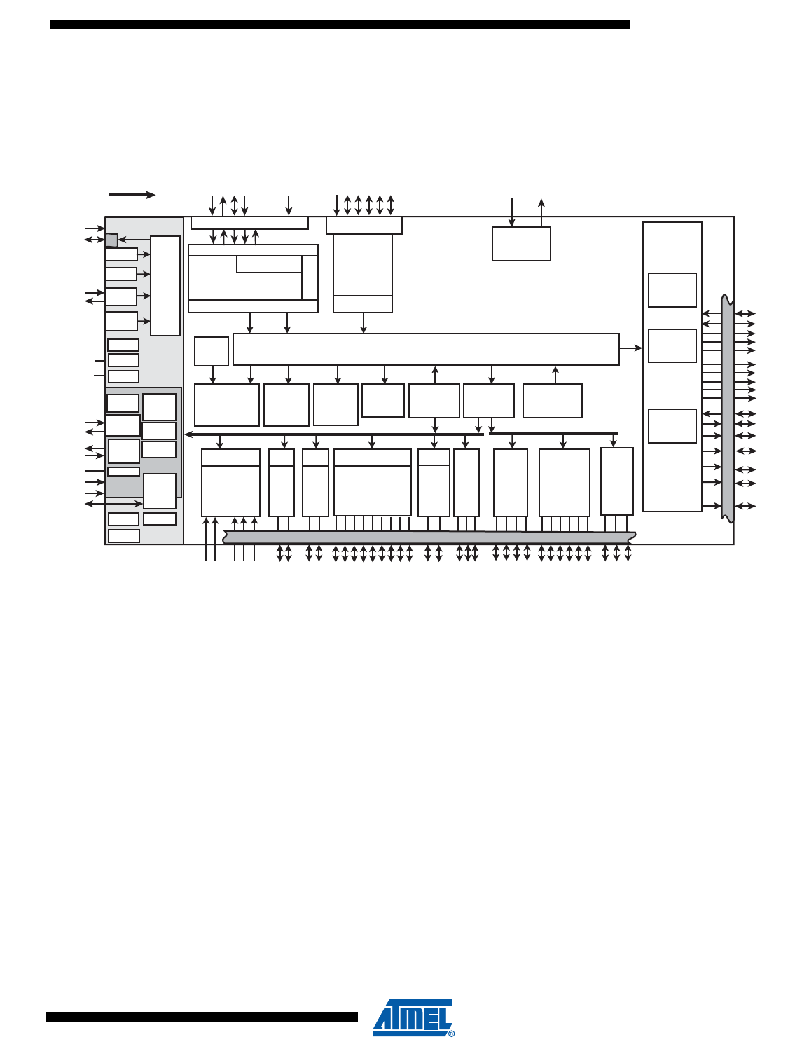
2. ATSAM3U4/2/1 Block Diagram
Figure 2-1. 144-pin SAM3U4/2/1E Block Diagram
D0-D15
A0/NBS0
A2-A20
NCS0
NCS1
NRD
NWR0/NWE
NWR1/NBS1
APB
A1
SHDN
FWUP
NANDOE,
NANDWE
SLAVE
MASTER
A23
NWAIT
EBI
Static
Memory
Controller
NAND Flash
Controller
& ECC
NCS2
NCS3
HSMCI
TWI0
TWI1
USART0
USART1
USART2
USART3
PWM
TC0
TC1
TC2
SSC
DMA
USB
Device
HS
8-channel
12-bit ADC
10-bit ADC
DA0-DA7
CDA
CK
TWCK0-TWCK1
CTS0-CTS3
RTSO-RTS3
SCK0-SCK3
RDX0-RDX3
TXD0-TXD3
NPCS0-NPCS3
SPCK
MOSI
MISO
PWMH0-PWMH3
TCLK0-TCLK2
TIOA0-TIOA2
TIOB0-TIOB2
TK
TF
TD
RD
RF
RK
ADTRG-AD12BTRG
AD0-AD7
VD
D
ANA
VBG
DFSDP
DFSDM
DHSDP
DHSDM
VDDUTMII
In-Circuit Emulator
TDI
TDO/TRACESWO
TMS/SWDIO
TCK/SWCLK
JTAGSEL
I/D
A21/
NANDALE
A22/
NANDCLE
DCD0
DTR0
RI0
PDC
5-layer AHB Bus Matrix
SPI
MPU DMA
PDC
DSR0
N
V
I
C
S
PDC PDC
Voltage
Regulator
VDDIN
VDDOUT
TWD0-TWD1
PWML0-PWML3
NANDRDY
NAND Flash
SRAM
(4KBytes)
ADVREF-AD12BVREF
AD12B0-AD12B7
Flash
Unique
Identifier
UART
URXD
UTXD
PDC
PLLA
TST
PCK0
-PCK2
System Controller
VDDBU
XIN
NRST
PMC
UPLL
XOUT
WDT
RTT
OSC
32K
XIN32
XOUT32
SUPC
RSTC
8
GPBREG
OSC
3-20 M
PIOA
PIOC
PIOB
POR
RTC
RC 32K
SM
BOD
VDDCORE
VDDUTMI
RC Osc.
12/8/4 M
ERASE
NRSTB
Cortex-M3 Processor
Fmax 96 MHz
SysTick Counter
JTAG & Serial Wire HS UTMI
Transceiver
Peripheral
DMA
Controller
Peripheral
Bridge
ROM
16 KBytes
4-Channel
DMA
SRAM0
32 KBytes
16 KBytes
8 KBytes
FLASH
2x128 KBytes
1x128 KBytes
1x64 KBytes
SRAM1
16 KBytes
16 KBytes
4
6430F–ATARM–21-Feb-12
SAM3U Series
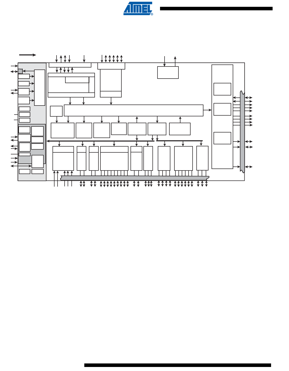
Figure 2-2. 100-pin SAM3U4/2/1C Block Diagram
D0-D7
A0
A2-A7
NCS0
NCS1
NRD
NWE
APB
A1
SHDN
FWUP
NANDOE,
NANDWE
SLAVE
MASTER
EBI
Static
Memory
Controller
NAND Flash
Controller
& ECC
HSMCI
TWI USART0
USART1
USART2
PWM
TC0
TC1
TC2
SSC
Peripheral
DMA
Controller
Peripheral
Bridge
ROM
16 KBytes
4-Channel
DMA
DMA
USB
Device
HS
4-channel
12-bit ADC
10-bit ADC
DA0-DA3
CDA
CK
TWCK0
CTS0-CTS2
RTSO-RTS2
SCK0-SCK2
RDX0-RDX2
TXD0-TXD2
NPCS0-NPCS3
SPCK
MOSI
MISO
PWMH0-PWMH3
TCLK0-TCLK2
TIOA0-TIOA2
TIOB0-TIOB2
TK
TF
TD
RD
RF
RK
ADTRG-AD12BTRG
AD0-AD3
VDDANA
VBG
DFSDP
DFSDM
SRAM0
32 KBytes
16 KBytes
8 KBytes
DHSDP
DHSDM
VDDUTMII
In-Circuit Emulator
TDI
TDO/TRACESWO
TMS/SWDIO
TCK/SWCLK
JTAGSEL
I/D
DCD0
DTR0
RI0
PDC
5-layer AHB Bus Matrix
SPI
MPU DMA
PDC
DSR0
N
V
I
C
FLASH
2x128 KBytes
1x128 KBytes
1x64 KBytes
S
SRAM1
16 KBytes
16 KBytes
PDC PDC
Voltage
Regulator
VDDIN
VDDOUT
TWD0
PWML0-PWML3
NANDRDY
NAND Flash
SRAM
(4KBytes)
ADVREF-AD12BVREF
AD12B0-AD12B3
Flash
Unique
Identifier
UART
URXD
UTXD
PDC
PLLA
TST
PCK0
-PCK2
System Controller
VDDBU
XIN
NRST
PMC
UPLL
XOUT
WDT
RTT
OSC
32K
XIN32
XOUT32
SUPC
RSTC
8
GPBREG
OSC
3-20 M
PIOA PIOB
POR
RTC
RC 32K
SM
BOD
VDDCORE
VDDUTMI
RC Osc.
12/8/4 M
ERASE
NRSTB
Cortex-M3 Processor
Fmax 96 MHz
SysTick Counter
JTAG & Serial Wire HS UTMI
Transceiver
NANDCLE
NANDALE

5
6430F–ATARM–21-Feb-12
SAM3U Series
3. Signal Description
Table 3-1 gives details on the signal names classified by peripheral.
Table 3-1. Signal Description List
Signal Name Function Type
Active
Level
Voltage
Reference Comments
Power Supplies
VDDIO Peripherals I/O Lines Power Supply Power 1.62V to 3.6V
VDDIN Voltage Regulator Input Power 1.8V to 3.6V
VDDOUT Voltage Regulator Output Power 1.8V
VDDUTMII USB UTMI+ Interface Power Supply Power 3.0V to 3.6V
GNDUTMII USB UTMI+ Interface Ground Ground
VDDBU Backup I/O Lines Power Supply Power 1.62V to 3.6V
GNDBU Backup Ground Ground
VDDPLL
PLL A, UPLL and OSC 3-20 MHz Power Supply
Power 1.62 V to 1.95V
GNDPLL PLL A, UPLL and OSC 3-20 MHz Ground Ground
VDDANA ADC Analog Power Supply Power 2.0V to 3.6V
GNDANA ADC Analog Ground Ground
VDDCORE Core, Memories and Peripherals Chip Power
Supply Power 1.62V to 1.95V
GND Ground Ground
Clocks, Oscillators and PLLs
XIN Main Oscillator Input Input VDDPLL
XOUT Main Oscillator Output Output
XIN32 Slow Clock Oscillator Input Input VDDBU
XOUT32 Slow Clock Oscillator Output Output
VBG Bias Voltage Reference Analog
PCK0 - PCK2 Programmable Clock Output Output VDDIO
Shutdown, Wakeup Logic
SHDN Shut-Down Control Output VDDBU
push/pull
0: The device is in
backup mode
1: The device is running
(not in backup mode)
FWUP Force Wake-Up Input Input Low Needs external pull-up
Serial Wire/JTAG Debug Port (SWJ-DP)
TCK/SWCLK Test Clock/Serial Wire Clock Input
VDDIO
No pull-up resistor
TDI Test Data In Input No pull-up resistor
TDO/TRACESWO Test Data Out/Trace Asynchronous Data Out Output(4)
TMS/SWDIO Test Mode Select/Serial Wire Input/Output Input No pull-up resistor
JTAGSEL JTAG Selection Input High VDDBU Internal permanent
pull-down

6
6430F–ATARM–21-Feb-12
SAM3U Series
Flash Memory
ERASE Flash and NVM Configuration Bits Erase
Command
Input High VDDBU Internal permanent 15K
pulldown
Reset/Test
NRST Microcontroller Reset I/O Low VDDIO Internal permanent
pullup
NRSTB Asynchronous Microcontroller Reset Input Low
VDDBU
Internal permanent
pullup
TST Test Select Input Internal permanent
pulldown
Universal Asynchronous Receiver Transceiver - UART
URXD UART Receive Data Input
UTXD UART Transmit Data Output
PIO Controller - PIOA - PIOB - PIOC
PA0 - PA31 Parallel IO Controller A I/O
VDDIO
•Schmitt Trigger (1)
Reset State:
•PIO Input
•Internal pullup enabled
PB0 - PB31 Parallel IO Controller B I/O
•Schmitt Trigger (2)
Reset State:
•PIO Input
•Internal pullup enabled
PC0 - PC31 Parallel IO Controller C I/O
•Schmitt Trigger(3)
Reset State:
•PIO Input
•Internal pullup enabled
External Bus Interface
D0 - D15 Data Bus I/O
A0 - A23 Address Bus Output
NWAIT External Wait Signal Input Low
Static Memory Controller - SMC
NCS0 - NCS3 Chip Select Lines Output Low
NWR0 - NWR1 Write Signal Output Low
NRD Read Signal Output Low
NWE Write Enable Output Low
NBS0 - NBS1 Byte Mask Signal Output Low
NAND Flash Controller - NFC
NANDOE NAND Flash Output Enable Output Low
NANDWE NAND Flash Write Enable Output Low
NANDRDY NAND Ready Input
Table 3-1. Signal Description List (Continued)
Signal Name Function Type
Active
Level
Voltage
Reference Comments

7
6430F–ATARM–21-Feb-12
SAM3U Series
High Speed Multimedia Card Interface - HSMCI
CK Multimedia Card Clock I/O
CDA Multimedia Card Slot A Command I/O
DA0 - DA7 Multimedia Card Slot A Data I/O
Universal Synchronous Asynchronous Receiver Transmitter - USARTx
SCKx USARTx Serial Clock I/O
TXDx USARTx Transmit Data I/O
RXDx USARTx Receive Data Input
RTSx USARTx Request To Send Output
CTSx USARTx Clear To Send Input
DTR0 USART0 Data Terminal Ready I/O
DSR0 USART0 Data Set Ready Input
DCD0 USART0 Data Carrier Detect Input
RI0 USART0 Ring Indicator Input
Synchronous Serial Controller - SSC
TD SSC Transmit Data Output
RD SSC Receive Data Input
TK SSC Transmit Clock I/O
RK SSC Receive Clock I/O
TF SSC Transmit Frame Sync I/O
RF SSC Receive Frame Sync I/O
Timer/Counter - TC
TCLKx TC Channel x External Clock Input Input
TIOAx TC Channel x I/O Line A I/O
TIOBx TC Channel x I/O Line B I/O
Pulse Width Modulation Controller- PWMC
PWMHx PWM Waveform Output High for channel x Output
PWMLx
PWM Waveform Output Low for channel x
Output
only output in
complementary mode
when dead time
insertion is enabled
PWMFI0-2 PWM Fault Input Input
Serial Peripheral Interface - SPI
MISO Master In Slave Out I/O
MOSI Master Out Slave In I/O
SPCK SPI Serial Clock I/O
NPCS0 SPI Peripheral Chip Select 0 I/O Low
NPCS1 - NPCS3 SPI Peripheral Chip Select Output Low
Table 3-1. Signal Description List (Continued)
Signal Name Function Type
Active
Level
Voltage
Reference Comments

8
6430F–ATARM–21-Feb-12
SAM3U Series
Notes: 1. PIOA: Schmitt Trigger on all except PA14 on 100 and 144 packages.
2. PIOB: Schmitt Trigger on all except PB9 to PB16, PB25 to PB31 on 100 and 144 packages.
3. PIOC: Schmitt Trigger on all except PC20 to PC27 on 144 package.
4. TDO pin is set in input mode when the Cortex-M3 Core is not in debug mode. Thus an external pull-up (100 kΩ) must be
added to avoid current consumption due to floating input.
3.1 Design Considerations
In order to facilitate schematic capture when using a SAM3U design, Atmel provides a “Sche-
matics Checklist” Application note.
Please visit http://www.atmel.com/products/AT91/ for additional documentation.
Two-Wire Interface - TWI
TWDx TWIx Two-wire Serial Data I/O
TWCKx TWIx Two-wire Serial Clock I/O
12-bit Analog-to-Digital Converter - ADC12B
AD12Bx Analog Inputs Analog
AD12BTRG ADC Trigger Input
AD12BVREF ADC Reference Analog
10-bit Analog-to-Digital Converter - ADC
ADx Analog Inputs Analog
ADTRG ADC Trigger Input
ADVREF ADC Reference Analog
Fast Flash Programming Interface - FFPI
PGMEN0-PGMEN2 Programming Enabling Input
VDDIO
PGMM0-PGMM3 Programming Mode Input
PGMD0-PGMD15 Programming Data I/O
PGMRDY Programming Ready Output High
PGMNVALID Data Direction Output Low
PGMNOE Programming Read Input Low
PGMCK Programming Clock Input
PGMNCMD Programming Command Input Low
USB High Speed Device - UDPHS
DFSDM USB Device Full Speed Data - Analog
VDDUTMII
DFSDP USB Device Full Speed Data + Analog
DHSDM USB Device High Speed Data - Analog
DHSDP USB Device High Speed Data + Analog
Table 3-1. Signal Description List (Continued)
Signal Name Function Type
Active
Level
Voltage
Reference Comments
9
6430F–ATARM–21-Feb-12
SAM3U Series
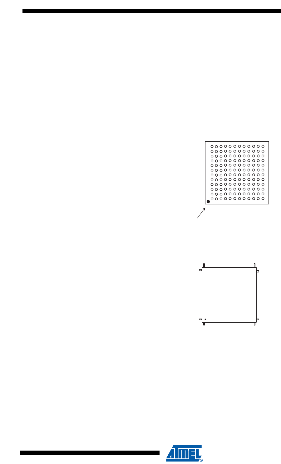
4. Package and Pinout
The SAM3U4/2/1E is available in 144-lead LQFP and 144-ball LFBGA packages.
The SAM3U4/2/1C is available in 100-lead LQFP and 100-ball TFBGA packages.
4.1 SAM3U4/2/1E Package and Pinout
4.1.1 144-ball LFBGA Package Outline
The 144-Ball LFBGA package has a 0.8 mm ball pitch and respects Green Standards. Its dimen-
sions are 10 x 10 x 1.4 mm.
Figure 4-1. Orientation of the 144-ball LFBGA Package
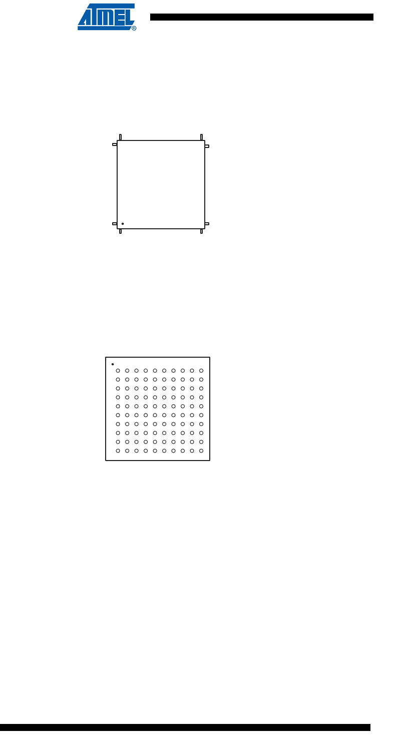
4.1.2 144-lead LQFP Package Outline
Figure 4-2. Orientation of the 144-lead LQFP Package
TOP VIEW
BALL A1
12
1
2
3
4
5
6
7
8
9
10
11
ABCDEF GHJ KL M
73
109
108
72
37
36
1
144

10
6430F–ATARM–21-Feb-12
SAM3U Series
4.1.3 144-lead LQFP Pinout
Table 4-1. 144-pin SAM3U4/2/1E Pinout
1 TDI 37 DHSDP 73 VDDANA 109 PA0/PGMNCMD
2 VDDOUT 38 DHSDM 74 ADVREF 110 PC0
3 VDDIN 39 VBG 75 GNDANA 111 PA1/PGMRDY
4TDO/TRACESWO 40 VDDUTMI 76 AD12BVREF 112 PC1
5 PB31 41 DFSDM 77 PA22/PGMD14 113 PA2/PGMNOE
6 PB30 42 DFSDP 78 PA30 114 PC2
7TMS/SWDIO 43 GNDUTMI 79 PB3 115 PA3/PGMNVALID
8 PB29 44 VDDCORE 80 PB4 116 PC3
9TCK/SWCLK 45 PA28 81 PC15 117 PA4/PGMM0
10 PB28 46 PA29 82 PC16 118 PC4
11 NRST 47 PC22 83 PC17 119 PA5/PGMM1
12 PB27 48 PA31 84 PC18 120 PC5
13 PB26 49 PC23 85 VDDIO 121 PA6/PGMM2
14 PB25 50 VDDCORE 86 VDDCORE 122 PC6
15 PB24 51 VDDIO 87 PA13/PGMD5 123 PA7/PGMM3
16 VDDCORE 52 GND 88 PA14/PGMD6 124 PC7
17 VDDIO 53 PB0 89 PC10 125 VDDCORE
18 GND 54 PC24 90 GND 126 GND
19 PB23 55 PB1 91 PA15/PGMD7 127 VDDIO
20 PB22 56 PC25 92 PC11 128 PA8/PGMD0
21 PB21 57 PB2 93 PA16/PGMD8 129 PC8
22 PC21 58 PC26 94 PC12 130 PA9/PGMD1
23 PB20 59 PB11 95 PA17/PGMD9 131 PC9
24 PB19 60 GND 96 PB16 132 PA10/PGMD2
25 PB18 61 PB12 97 PB15 133 PA11/PGMD3
26 PB17 62 PB13 98 PC13 134 PA12/PGMD4
27 VDDCORE 63 PC27 99 PA18/PGMD10 135 FWUP
28 PC14 64 PA27 100 PA19/PGMD11 136 SHDN
29 PB14 65 PB5 101 PA20/PGMD12 137 ERASE
30 PB10 66 PB6 102 PA21/PGMD13 138 TST
31 PB9 67 PB7 103 PA23/PGMD15 139 VDDBU
32 PC19 68 PB8 104 VDDIO 140 GNDBU
33 GNDPLL 69 PC28 105 PA24 141 NRSTB
34 VDDPLL 70 PC29 106 PA25 142 JTAGSEL
35 XOUT 71 PC30 107 PA26 143 XOUT32
36 XIN 72 PC31 108 PC20 144 XIN32

11
6430F–ATARM–21-Feb-12
SAM3U Series
4.1.4 144-ball LFBGA Pinout
Table 4-2. 144-ball SAM3U4/2/1E Pinout
A1 VBG D1 DFSDM G1 PB0 K1 PB7
A2 VDDUTMI D2 DHSDM G2 PC26 K2 PC31
A3 PB9 D3 GNDPLL G3 PB2 K3 PC29
A4 PB10 D4 PC14 G4 PC25 K4 PB3
A5 PB19 D5 PB21 G5 PB1 K5 PB4
A6 PC21 D6 PB23 G6 GND K6 PA14/PGMD6
A7 PB26 D7 PB24 G7 GND K7 PA16/PGMD8
A8 TCK/SWCLK D8 PB28 G8 VDDCORE K8 PA18/PGMD10
A9 PB30 D9 TDI G9 PC4 K9 PC20
A10 TDO/TRACESWO D10 VDDBU G10 PA6/PGMM2 K10 PA1/PGMRDY
A11 XIN32 D11 PA10/PGMD2 G11 PA7/PGMM3 K11 PC1
A12 XOUT32 D12 PA11/PGMD3 G12 PC6 K12 PC2
B1 VDDCORE E1 PC22 H1 PC24 L1 PC30
B2 GNDUTMI E2 PA28 H2 PC27 L2 ADVREF
B3 XOUT E3 PC19 H3 PA27 L3 AD12BVREF
B4 PB14 E4 VDDCORE H4 PB12 L4 PA22/PGMD14
B5 PB17 E5 GND H5 PB11 L5 PC17
B6 PB22 E6 VDDIO H6 GND L6 PC10
B7 PB25 E7 GNDBU H7 VDDCORE L7 PC12
B8 PB29 E8 NRST H8 PB16 L8 PA19/PGMD11
B9 VDDIN E9 PB31 H9 PB15 L9 PA23/PGMD15
B10 JTAGSEL E10 PA12/PGMD4 H10 PC3 L10 PA0/PGMNCMD
B11 ERASE E11 PA8/PGMD0 H11 PA5/PGMM1 L11 PA26
B12 SHDN E12 PC8 H12 PC5 L12 PC0
C1 DFSDP F1 PA31 J1 PB5 M1 VDDANA
C2 DHSDP F2 PA29 J2 PB6 M2 GNDANA
C3 XIN F3 PC23 J3 PC28 M3 PA30
C4 VDDPLL F4 VDDCORE J4 PB8 M4 PC15
C5 PB18 F5 VDDIO J5 PB13 M5 PC16
C6 PB20 F6 GND J6 VDDIO M6 PC18
C7 PB27 F7 GND J7 PA13/PGMD5 M7 PA15/PGMD7
C8 TMS/SWDIO F8 VDDIO J8 PA17/PGMD9 M8 PC11
C9 VDDOUT F9 PC9 J9 PC13 M9 PA20/PGMD12
C10 NRSTB F10 PA9/PGMD1 J10 PA2/PGMNOE M10 PA21/PGMD13
C11 TST F11 VDDCORE J11 PA3/PGMNVALID M11 PA24
C12 FWUP F12 PC7 J12 PA4/PGMM0 M12 PA25
12
6430F–ATARM–21-Feb-12
SAM3U Series
4.2 SAM3U4/2/1C Package and Pinout
4.2.1 100-lead LQFP Package Outline
Figure 4-3. Orientation of the 100-lead LQFP Package
4.2.2 100-ball TFBGA Package Outline
Figure 4-4. Orientation of the 100-ball TFBGA Package
51
76
75
50
26
25
1
100
1
2 3 4 5 6 7 8 9 10
A
B
C
D
E
F
G
H
J
K
TOP VIEW

13
6430F–ATARM–21-Feb-12
SAM3U Series
4.2.3 100-lead LQFP Pinout
Table 4-3. 100-pin SAM3U4/2/1C1 Pinout
1 VDDANA 26 PA0/PGMNCMD 51 TDI 76 DHSDP
2 ADVREF 27 PA1/PGMRDY 52 VDDOUT 77 DHSDM
3GNDANA 28PA2/PGMNOE 53 VDDIN 78 VBG
4 AD12BVREF 29 PA3/PGMNVALID 54 TDO/TRACESWO 79 VDDUTMI
5PA22/PGMD14 30 PA4/PGMM0 55 TMS/SWDIO 80 DFSDM
6 PA30 31 PA5/PGMM1 56 TCK/SWCLK 81 DFSDP
7 PB3 32 PA6/PGMM2 57 NRST 82 GNDUTMI
8 PB4 33 PA7/PGMM3 58 PB24 83 VDDCORE
9 VDDCORE 34 VDDCORE 59 VDDCORE 84 PA28
10 PA13/PGMD5 35 GND 60 VDDIO 85 PA29
11 PA14/PGMD6 36 VDDIO 61 GND 86 PA31
12 PA15/PGMD7 37 PA8/PGMD0 62 PB23 87 VDDCORE
13 PA16/PGMD8 38 PA9/PGMD1 63 PB22 88 VDDIO
14 PA17/PGMD9 39 PA10/PGMD2 64 PB21 89 GND
15 PB16 40 PA11/PGMD3 65 PB20 90 PB0
16 PB15 41 PA12/PGMD4 66 PB19 91 PB1
17 PA18/PGMD10 42 FWUP 67 PB18 92 PB2
18 PA19/PGMD11 43 ERASE 68 PB17 93 PB11
19 PA20/PGMD12 44 TST 69 PB14 94 PB12
20 PA21/PGMD13 45 VDDBU 70 PB10 95 PB13
21 PA23/PGMD15 46 GNDBU 71 PB9 96 PA27
22 VDDIO 47 NRSTB 72 GNDPLL 97 PB5
23 PA24 48 JTAGSEL 73 VDDPLL 98 PB6
24 PA25 49 XOUT32 74 XOUT 99 PB7
25 PA26 50 XIN32 75 XIN 100 PB8

14
6430F–ATARM–21-Feb-12
SAM3U Series
4.2.4 100-ball TFBGA Pinout
Table 4-4. 100-ball SAM3U4/2/1C Pinout
A1 VBG C6 PB22 F1 PB1 H6 PA15/PGMD7
A2 XIN C7 TMS/SWDIO F2 PB12 H7 PA18/PGMD10
A3 XOUT C8 NRSTB F3 VDDIO H8 PA24
A4 PB17 C9 JTAGSEL F4 PA31 H9 PA1/PGMRDY
A5 PB21 C10 VDDBU F5 VDDIO H10 PA2/PGMNOE
A6 PB23 D1 DFSDM F6 GND J1 PB6
A7 TCK/SWCLK D2 DHSDM F7 PB16 J2 PB8
A8 VDDIN D3 VDDPLL F8 PA6/PGMM2 J3 ADVREF
A9 VDDOUT D4 VDDCORE F9 VDDCORE J4 PA30
A10 XIN32 D5 PB20 F10 PA7/PGMM3 J5 PB3
B1 VDDCORE D6 ERASE G1 PB11 J6 PA16/PGMD8
B2 GNDUTMI D7 TST G2 PB2 J7 PA19/PGMD11
B3 VDDUTMI D8 FWUP G3 PB0 J8 PA21/PGMD13
B4 PB10 D9 PA11/PGMD3 G4 PB13 J9 PA26
B5 PB18 D10 PA12/PGMD4 G5 VDDCORE J10 PA0/PGMNCMD
B6 PB24 E1 PA29 G6 GND K1 PB7
B7 NRST E2 GND G7 PB15 K2 VDDANA
B8 TDO/TRACESWO E3 PA28 G8 PA3/PGMNVALID K3 GNDANA
B9 TDI E4 PB9 G9 PA5/PGMM1 K4 AD12BVREF
B10 XOUT32 E5 GNDBU G10 PA4/PGMM0 K5 PB4
C1 DFSDP E6 VDDIO H1 VDDCORE K6 PA14/PGMD6
C2 DHSDP E7 VDDCORE H2 PB5 K7 PA17/PGMD9
C3 GNDPLL E8 PA10/PGMD2 H3 PA27 K8 PA20/PGMD12
C4 PB14 E9 PA9/PGMD1 H4 PA22/PGMD14 K9 PA23/PGMD15
C5 PB19 E10 PA8/PGMD0 H5 PA13/PGMD5 K10 PA25

15
6430F–ATARM–21-Feb-12
SAM3U Series
5. Power Considerations
5.1 Power Supplies
The ATSAM3U4/2/1 product has several types of power supply pins:
• VDDCORE pins: Power the core, the embedded memories and the peripherals; voltage
ranges from 1.62V to 1.95V.
• VDDIO pins: Power the Peripherals I/O lines; voltage ranges from 1.62V to 3.6V.
• VDDIN pin: Powers the Voltage regulator
• VDDOUT pin: It is the output of the voltage regulator.
• VDDBU pin: Powers the Slow Clock oscillator and a part of the System Controller; voltage
ranges from 1.62V to 3.6V. VDDBU must be supplied before or at the same time than VDDIO
and VDDCORE.
• VDDPLL pin: Powers the PLL A, UPLL and 3-20 MHz Oscillator; voltage ranges from 1.62V
to 1.95V.
• VDDUTMI pin: Powers the UTMI+ interface; voltage ranges from 3.0V to 3.6V, 3.3V nominal.
• VDDANA pin: Powers the ADC cells; voltage ranges from 2.0V to 3.6V.
Ground pins GND are common to VDDCORE and VDDIO pins power supplies.
Separated ground pins are provided for VDDBU, VDDPLL, VDDUTMI and VDDANA. These
ground pins are respectively GNDBU, GNDPLL, GNDUTMI and GNDANA.
5.2 Voltage Regulator
The ATSAM3U4/2/1 embeds a voltage regulator that is managed by the Supply Controller.
This internal regulator is intended to supply the internal core of ATSAM3U4/2/1 but can be used
to supply other parts in the application. It features two different operating modes:
• In Normal mode, the voltage regulator consumes less than 700 µA static current and draws
150 mA of output current. Internal adaptive biasing adjusts the regulator quiescent current
depending on the required load current. In Wait Mode or when the output current is low,
quiescent current is only 7µA.
• In Shutdown mode, the voltage regulator consumes less than 1 µA while its output is driven
internally to GND. The default output voltage is 1.80V and the start-up time to reach Normal
mode is inferior to 400 µs.
For adequate input and output power supply decoupling/bypassing, refer to “Voltage Regulator”
in the “Electrical Characteristics” section of the product datasheet.
5.3 Typical Powering Schematics
The ATSAM3U4/2/1 supports a 1.8V-3.6V single supply mode. The internal regulator input con-
nected to the source and its output feed VDDCORE. Figure 5-1, Figure 5-2, Figure 5-3 show the
power schematics.
16
6430F–ATARM–21-Feb-12
SAM3U Series
Figure 5-1. Single Supply
Note: Restrictions
With Main Supply < 2.0 V, USB and ADC are not usable.
With Main Supply ≥ 2.4V and < 3V, USB is not usable.
With Main Supply ≥ 3V, all peripherals are usable.
VDDIN
Voltage
Regulator
VDDOUT
Main Supply (1.8V-3.6V)
VDDCORE
VDDBU
VDDUTMI
VDDIO
VDDANA
VDDPLL
17
6430F–ATARM–21-Feb-12
SAM3U Series
Figure 5-2. Core Externally Supplied
Note: Restrictions
With Main Supply < 2.0 V, USB and ADC are not usable.
With Main Supply ≥ 2.4V and < 3V, USB is not usable.
With Main Supply ≥ 3V, all peripherals are usable.
VDDIN
Voltage
Regulator
VDDOUT
Main Supply (1.62V-3.6V)
VDDCORE
VDDCORE Supply (1.62V-1.95V)
VDDBU
VDDIO
VDDANA
VDDUTMI
VDDPLL
18
6430F–ATARM–21-Feb-12
SAM3U Series
Figure 5-3. Backup Batteries Used
Note: Restrictions
With Main Supply < 2.0 V, USB and ADC are not usable.
With Main Supply ≥ 2.4V and < 3V, USB is not usable.
With Main Supply ≥ 3V, all peripherals are usable.
VDDIN
Voltage
Regulator
VDDOUT
Main Supply (1.62V-3.6V)
VDDCORE
Backup Batteries VDDBU
VDDIO
VDDANA
VDDUTMI
VDDPLL
FWUP
SHDN

19
6430F–ATARM–21-Feb-12
SAM3U Series
5.4 Active Mode
Active mode is the normal running mode with the core clock running from the fast RC oscillator,
the main crystal oscillator or the PLLA. The power management controller can be used to adapt
the frequency and to disable the peripheral clocks.
5.5 Low Power Modes
The various low power modes of the ATSAM3U4/2/1 are described below:
5.5.1 Backup Mode
The purpose of backup mode is to achieve the lowest power consumption possible in a system
which is performing periodic wake-ups to perform tasks but not requiring fast startup time
(<0.5ms).
The Supply Controller, zero-power power-on reset, RTT, RTC, Backup registers and 32 kHz
Oscillator (RC or crystal oscillator selected by software in the Supply Controller) are running.
The regulator and the core supply are off.
Backup Mode is based on the Cortex-M3 deep-sleep mode with the voltage regulator disabled.
The SAM3U Series can be awakened from this mode through the Force Wake-Up pin (FWUP),
and Wake-Up input pins WKUP0 to WKUP15, Supply Monitor, RTT or RTC wake-up event. Cur-
rent Consumption is 2.5 µA typical on VDDBU.
Backup mode is entered by using WFE instructions with the SLEEPDEEP bit in the System Con-
trol Register of the Cortex-M3 set to 1. (See the “Power Management” description in The “ARM
Cortex M3 Processor” section of the product datasheet).
Exit from Backup mode happens if one of the following enable wake up events occurs:
• FWUP pin (low level, configurable debouncing)
• WKUPEN0-15 pins (level transition, configurable debouncing)
•SM alarm
•RTC alarm
• RTT alarm
5.5.2 Wait Mode
The purpose of the wait mode is to achieve very low power consumption while maintaining the
whole device in a powered state for a startup time of less than 10 µs.
In this mode, the clocks of the core, peripherals and memories are stopped. However, the core,
peripherals and memories power supplies are still powered. From this mode, a fast start up is
available.
This mode is entered via Wait for Event (WFE) instructions with LPM = 1 (Low Power Mode bit in
PMC_FSMR). The Cortex-M3 is able to handle external events or internal events in order to
wake-up the core (WFE). This is done by configuring the external lines WKUP0-15 as fast
startup wake-up pins (refer to Section 5.7 “Fast Start-Up”). RTC or RTT Alarm and USB wake-up
events can be used to wake up the CPU (exit from WFE).
Current Consumption in Wait mode is typically 15 µA on VDDIN if the internal voltage regulator
is used or 8 µA on VDDCORE if an external regulator is used.

20
6430F–ATARM–21-Feb-12
SAM3U Series
Entering Wait Mode:
• Select the 4/8/12 MHz Fast RC Oscillator as Main Clock
• Set the LPM bit in the PMC Fast Startup Mode Register (PMC_FSMR)
• Execute the Wait-For-Event (WFE) instruction of the processor
Note: Internal Main clock resynchronization cycles are necessary between the writing of MOSCRCEN
bit and the effective entry in Wait mode. Depending on the user application, Waiting for
MOSCRCEN bit to be cleared is recommended to ensure that the core will not execute undesired
instructions.
5.5.3 Sleep Mode
The purpose of sleep mode is to optimize power consumption of the device versus response
time. In this mode, only the core clock is stopped. The peripheral clocks can be enabled. This
mode is entered via Wait for Interrupt (WFI) or Wait for Event (WFE) instructions with LPM = 0 in
PMC_FSMR.
The processor can be awakened from an interrupt if WFI instruction of the Cortex M3 is used, or
from an event if the WFE instruction is used to enter this mode.

21
6430F–ATARM–21-Feb-12
SAM3U Series
5.5.4 Low Power Mode Summary Table
The modes detailed above are the main low power modes. Each part can be set to on or off sep-
arately and wake up sources can be individually configured. Table 5-1 below shows a summary
of the configurations of the low power modes.
Notes: 1. When considering wake-up time, the time required to start the PLL is not taken into account. Once started, the device works
with the 4/8/12 MHz Fast RC oscillator. The user has to add the PLL start-up time if it is needed in the system. The wake-up
time is defined as the time taken for wake up until the first instruction is fetched.
2. The external loads on PIOs are not taken into account in the calculation.
3. BOD current consumption is not included.
4. Current consumption on VDDBU.
5. 13 µA total current consumption - without using internal voltage regulator.
20 µA total current consumption - using internal voltage regulator.
6. Depends on MCK frequency.
7. In this mode the core is supplied and not clocked but some peripherals can be clocked.
Table 5-1. Low Power Mode Configuration Summary
Mode
SUPC,
32 kHz
Oscillator
RTC RTT
Backup
Registers,
POR
(VDDBU
Region) Regulator
Core
Memory
Peripherals Mode Entry
Potential Wake Up
Sources
Core at
Wake Up
PIO State
while in Low
Power Mode
PIO State
at Wake Up
Consumption
(2)
(3)
Wake-up
Time(1)
Backup
Mode ON OFF
SHDN =0
OFF
(Not powered)
WFE
+SLEEPDEEP
bit = 1
FWUP pin
WKUP0-15 pins
BOD alarm
RTC alarm
RTT alarm
Reset Previous
state saved
PIOA &
PIOB &
PIOC
Inputs with
pull ups
2.5 µA typ(4) < 0.5 ms
Wait
Mode ON ON
SHDN =1
Powered
(Not clocked)
WFE
+SLEEPDEEP
bit = 0
+LPM bit = 1
Any Event from: Fast
startup through
WKUP0-15 pins
RTC alarm
RTT alarm
USB wake-up
Clocked
back
Previous
state saved Unchanged 13 µA/20 µA (5) < 10 µs
Sleep
Mode ON ON
SHDN =1
Powered(7)
(Not clocked)
WFE or WFI
+SLEEPDEEP
bit = 0
+LPM bit = 0
Entry mode =WFI
Interrupt Only; Entry
mode =WFE Any
Enabled Interrupt
and/or Any Event
from: Fast start-up
through WKUP0-15
pins
RTC alarm
RTT alarm
USB wake-up
Clocked
back
Previous
state saved Unchanged (6) (6)
22
6430F–ATARM–21-Feb-12
SAM3U Series
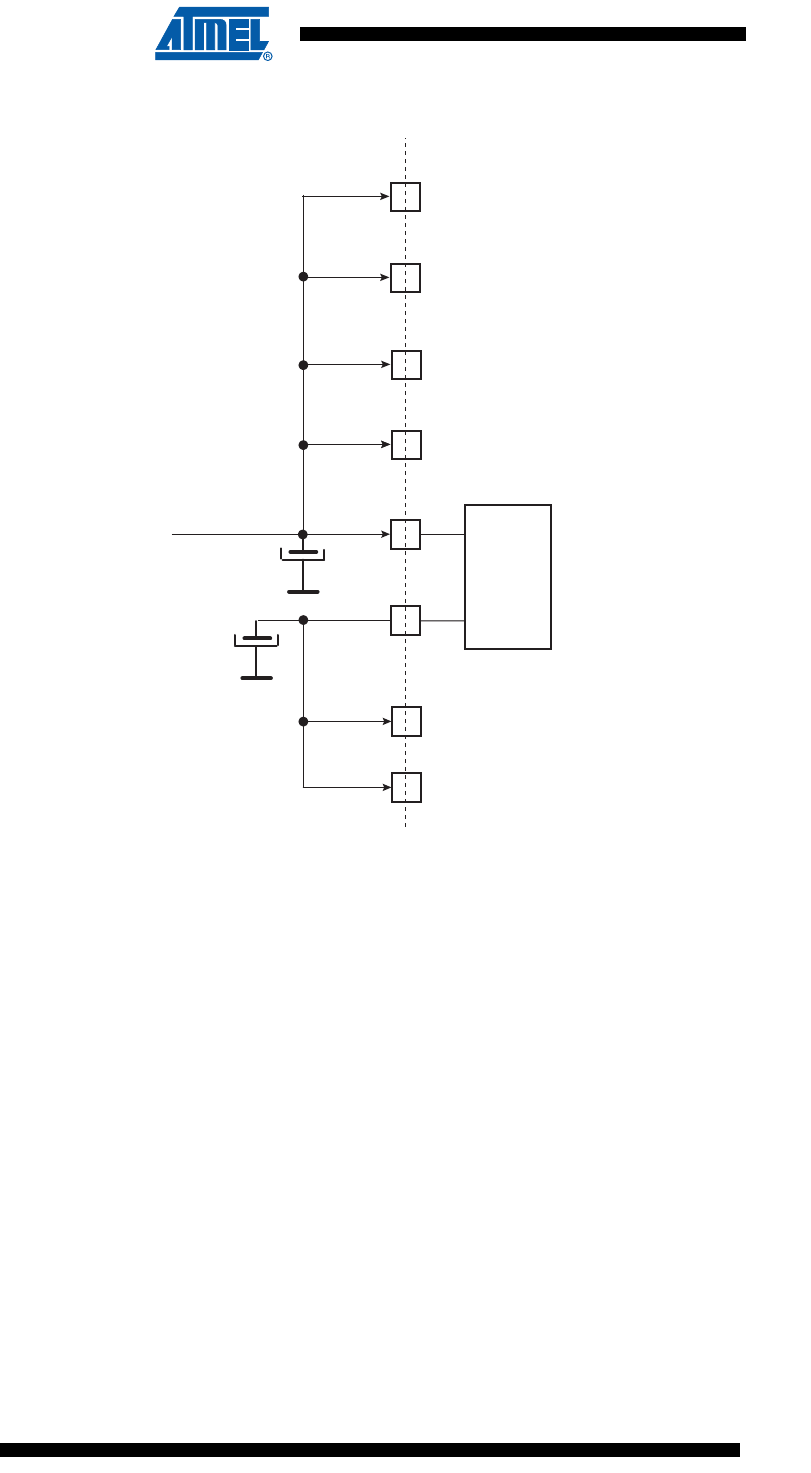
5.6 Wake-up Sources
The wake-up events allow the device to exit backup mode. When a wake-up event is detected,
the Supply Controller performs a sequence which automatically reenables the core power
supply.
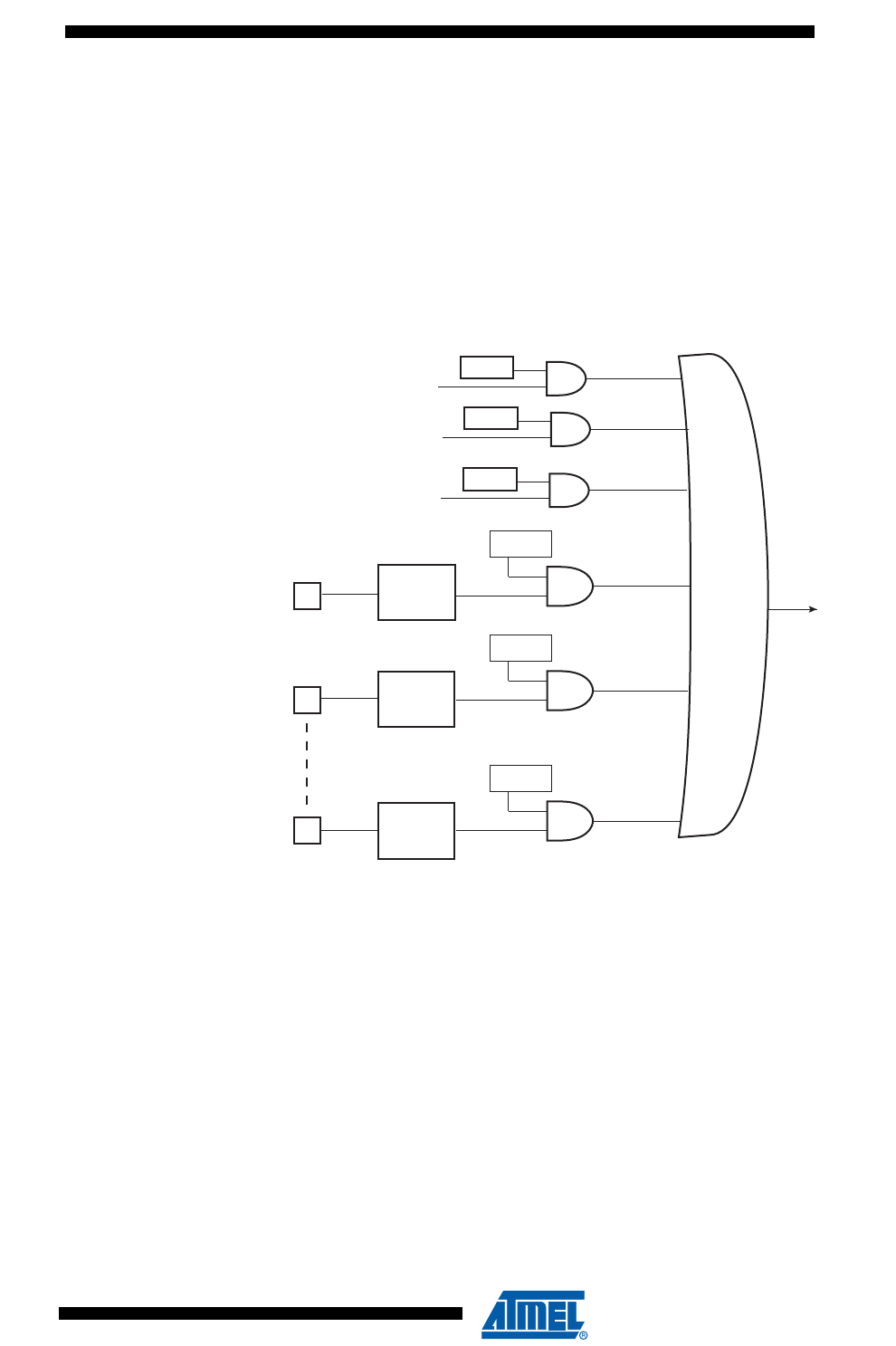
Figure 5-4. Wake-up Source
WKUP15
FWUP
rtt_alarm
rtc_alarm
sm_int
WKUP0
WKUP1
WKUPT1
Core
Supply
Restart
Debouncer
WKUPDBC
WKUPS
Debouncer
FWUPDBC
FWUP
WKUPIS0
WKUPIS1
WKUPIS15
RTTEN
RTCEN
SMEN
WKUPEN15
WKUPEN1
WKUPEN0
FWUPEN
WKUPT15
Falling/Rising
Edge
Detector
WKUPT0
Falling/Rising
Edge
Detector
Falling/Rising
Edge
Detector
Falling
Edge
Detector
SLCK
SLCK
23
6430F–ATARM–21-Feb-12
SAM3U Series
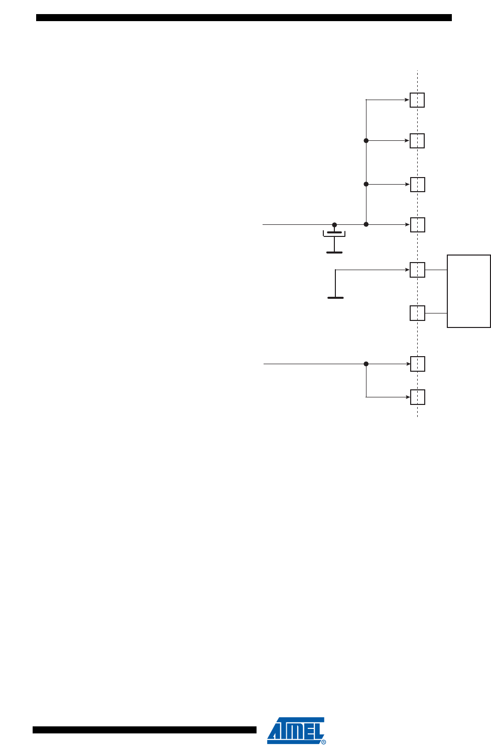
5.7 Fast Start-Up
The ATSAM3U4/2/1 device allows the processor to restart in a few microseconds while the pro-
cessor is in wait mode. A fast start up can occur upon detection of a low level on one of the 19
wake-up inputs.
The fast restart circuitry, as shown in Figure 5-5, is fully asynchronous and provides a fast start-
up signal to the Power Management Controller. As soon as the fast start-up signal is asserted,
the PMC automatically restarts the embedded 4/8/12 MHz fast RC oscillator, switches the mas-
ter clock on this 4/8/12 MHz clock and reenables the processor clock.
Figure 5-5. Fast Start-Up Sources
RTCEN
rtc_alarm
RTTEN
rtt_alarm
USBEN
usb_wakeup
fast_restart
WKUP15
FSTT15
WKUP1
WKUP0
FSTT0
FSTT1
High/Low
Level
Detector
High/Low
Level
Detector
High/Low
Level
Detector
24
6430F–ATARM–21-Feb-12
SAM3U Series
6. Input/Output Lines
The SAM3U has different kinds of input/output (I/O) lines, such as general purpose I/Os (GPIO)
and system I/Os. GPIOs can have alternate functions thanks to multiplexing capabilities of the
PIO controllers. The same GPIO line can be used whether it is in IO mode or used by the multi-
plexed peripheral. System I/Os are pins such as test pin, oscillators, erase pin, analog inputs or
debug pins.
With a few exceptions, the I/Os have input schmitt triggers. Refer to the footnotes associated
with “PIO Controller - PIOA - PIOB - PIOC” on page 6 within Table 3-1, “Signal Description List”.
6.1 General Purpose I/O Lines (GPIO)
GPIO Lines are managed by PIO Controllers. All I/Os have several input or output modes such
as, pull-up, input schmitt triggers, multi-drive (open-drain), glitch filters, debouncing or input
change interrupt. Programming of these modes is performed independently for each I/O line
through the PIO controller user interface. For more details, refer to the “PIO Controller” section
of the product datasheet.
The input output buffers of the PIO lines are supplied through VDDIO power supply rail.
The SAM3U embeds high speed pads able to handle up to 65 MHz for HSMCI and SPI clock
lines and 35 MHz on other lines. See “AC Characteristics” of the product datasheet for more
details. Typical pull-up value is 100 kΩ for all I/Os.
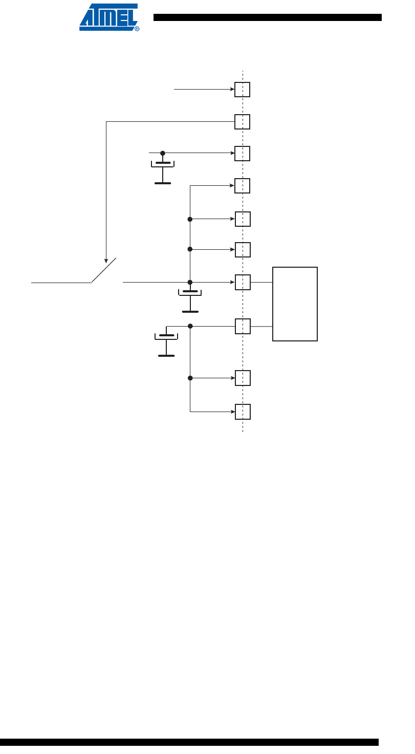
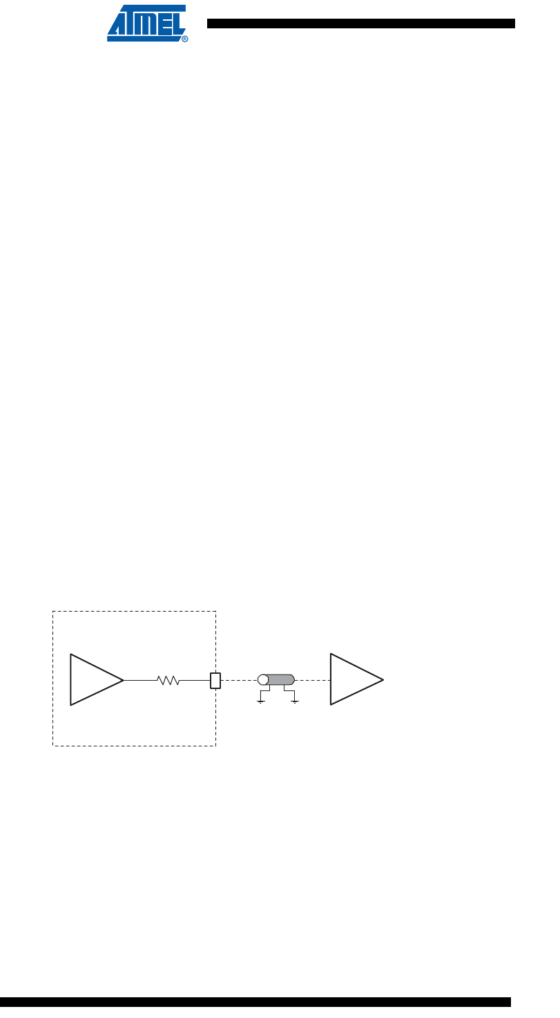
Each I/O line also embeds an ODT (On-Die Termination), (see Figure 6-1 below). ODT consists
of an internal series resistor termination scheme for impedance matching between the driver
output (SAM3) and the PCB track impedance preventing signal reflection. The series resistor
helps to reduce I/Os switching current (di/dt) thereby reducing in turn, EMI. It also decreases
overshoot and undershoot (ringing) due to inductance of interconnect between devices or
between boards. In conclusion, ODT helps reducing signal integrity issues.
Figure 6-1. On-Die Termination schematic
6.2 System I/O Lines
System I/O lines are pins used by oscillators, test mode, reset, flash erase and JTAG to name
but a few.
6.3 Serial Wire JTAG Debug Port (SWJ-DP)
The SWJ-DP pins are TCK/SWCLK, TMS/SWDIO, TDO/SWO, TDI and commonly provided on
a standard 20-pin JTAG connector defined by ARM. For more details about voltage reference
and reset state, refer to Table 3-1, “Signal Description List”
PCB Trace
Z0 ~ 50 Ohms
Receiver
SAM3 Driver with
Rodt
Zout ~ 10 Ohms
Z0 ~ Zout + Rodt
ODT
36 Ohms Ty p.

25
6430F–ATARM–21-Feb-12
SAM3U Series
The JTAGSEL pin is used to select the JTAG boundary scan when asserted at a high level. It
integrates a permanent pull-down resistor of about 15 kΩ to GNDBU, so that it can be left uncon-
nected for normal operations.
By default, the JTAG Debug Port is active. If the debugger host wants to switch to the Serial
Wire Debug Port, it must provide a dedicated JTAG sequence on TMS/SWDIO and
TCK/SWCLK which disables the JTAG-DP and enables the SW-DP. When the Serial Wire
Debug Port is active, TDO/TRACESWO can be used for trace.
The asynchronous TRACE output (TRACESWO) is multiplexed with TDO. So the asynchronous
trace can only be used with SW-DP, not JTAG-DP.
All the JTAG signals are supplied with VDDIO except JTAGSEL, supplied by VDDBU.
6.4 Test Pin
The TST pin is used for JTAG Boundary Scan Manufacturing Test or fast flash programming
mode of the ATSAM3U4/2/1 series. The TST pin integrates a permanent pull-down resistor of
about 15 kΩ to GND, so that it can be left unconnected for normal operations. To enter fast pro-
gramming mode, see the “Fast Flash Programming Interface” section of the product datasheet.
For more on the manufacturing and test mode, refer to the “Debug and Test” section of the prod-
uct datasheet.
6.5 NRST Pin
The NRST pin is bidirectional. It is handled by the on-chip reset controller and can be driven low
to provide a reset signal to the external components or asserted low externally to reset the
microcontroller. It will reset the Core and the peripherals, except the Backup region (RTC, RTT
and Supply Controller). There is no constraint on the length of the reset pulse and the reset con-
troller can guarantee a minimum pulse length.
The NRST pin integrates a permanent pull-up resistor to VDDIO of about 100 kΩ.
6.6 NRSTB Pin
The NRSTB pin is input only and enables asynchronous reset of the ATSAM3U4/2/1 when
asserted low. The NRSTB pin integrates a permanent pull-up resistor of about 15 kΩ. This allows
connection of a simple push button on the NRSTB pin as a system-user reset. In all modes, this
pin will reset the chip including the Backup region (RTC, RTT and Supply Controller). It reacts as
the Power-on reset. It can be used as an external system reset source. In harsh environments, it
is recommended to add an external capacitor (10 nF) between NRSTB and VDDBU. (For filter-
ing values refer to “I/O Characteristics” in the “Electrical Characteristics” section of the product
datasheet.)
It embeds an anti-glitch filter.
6.7 ERASE Pin
The ERASE pin is used to reinitialize the Flash content and some of its NVM bits. It integrates a
permanent pull-down resistor of about 15 kΩ to GND, so that it can be left unconnected for nor-
mal operations.
This pin is debounced by SCLK to improve the glitch tolerance. When the ERASE pin is tied high
during less than 100 ms, it is not taken into account. The pin must be tied high during more than
220 ms to perform the reinitialization of the Flash.

26
6430F–ATARM–21-Feb-12
SAM3U Series
Even in all low power modes, asserting the pin will automatically start-up the chip and erase the
Flash.
7. Processor and Architecture
7.1 ARM Cortex-M3 Processor
• Version 2.0
• Thumb-2 (ISA) subset consisting of all base Thumb-2 instructions, 16-bit and 32-bit.
• Harvard processor architecture enabling simultaneous instruction fetch with data load/store.
• Three-stage pipeline.
• Single cycle 32-bit multiply.
• Hardware divide.
• Thumb and Debug states.
• Handler and Thread modes.
• Low latency ISR entry and exit.
7.2 APB/AHB Bridges
The ATSAM3U4/2/1 product embeds two separated APB/AHB bridges:
• low speed bridge
• high speed bridge
This architecture enables to make concurrent accesses on both bridges.
All the peripherals are on the low-speed bridge except SPI, SSC and HSMCI.
The UART, 10-bit ADC (ADC), 12-bit ADC (ADC12B), TWI0-1, USART0-3, PWM have dedicated
channels for the Peripheral DMA Channels (PDC). These peripherals can not use the DMA
Controller.
The high speed bridge regroups the SSC, SPI and HSMCI. These three peripherals do not have
PDC channels but can use the DMA with the internal FIFO for Channel buffering.
Note that the peripherals of the two bridges are clocked by the same source: MCK.
7.3 Matrix Masters
The Bus Matrix of the ATSAM3U4/2/1 device manages 5 masters, which means that each mas-
ter can perform an access concurrently with others to an available slave.
Each master has its own decoder and specifically defined bus. In order to simplify the address-
ing, all the masters have the same decoding.
Table 7-1. List of Bus Matrix Masters
Master 0 Cortex-M3 Instruction/Data
Master 1 Cortex-M3 System
Master 2 Peripheral DMA Controller (PDC)
Master 3 USB Device High Speed DMA
Master 4 DMA Controller

27
6430F–ATARM–21-Feb-12
SAM3U Series
7.4 Matrix Slaves
The Bus Matrix of the ATSAM3U4/2/1 manages 10 slaves. Each slave has its own arbiter, allow-
ing a different arbitration per slave.
7.5 Master to Slave Access
All the Masters can normally access all the Slaves. However, some paths do not make sense,
for example allowing access from the USB Device High speed DMA to the Internal Peripherals.
Thus, these paths are forbidden or simply not wired, and shown as “–” in Table 7-3 below.
Table 7-2. List of Bus Matrix Slaves
Slave 0 Internal SRAM0
Slave 1 Internal SRAM1
Slave 2 Internal ROM
Slave 3 Internal Flash 0
Slave 4 Internal Flash 1
Slave 5 USB Device High Speed Dual Port RAM (DPR)
Slave 6 NAND Flash Controller RAM
Slave 7 External Bus Interface
Slave 8 Low Speed Peripheral Bridge
Slave 9 High Speed Peripheral Bridge
Table 7-3. ATSAM3U4/2/1 Master to Slave Access
Slaves Masters
0 1 234
Cortex-M3
I/D Bus
Cortex-M3 S
Bus PDC
USB Device
High Speed
DMA
DMA
Controller
0 Internal SRAM0 –XXXX
1 Internal SRAM1 –XXXX
2 Internal ROM X – X X X
3 Internal Flash 0 X––––
4 Internal Flash 1 X––––
5 USB Device High Speed Dual Port RAM (DPR) – X – – –
6 NAND Flash Controller RAM –XXXX
7 External Bus Interface –XXXX
8 Low Speed Peripheral Bridge – X X – –
9 High Speed Peripheral Bridge – X X – –

28
6430F–ATARM–21-Feb-12
SAM3U Series
7.6 DMA Controller
• Acting as one Matrix Master
• Embeds 4 channels:
– 3 channels with 8 bytes/FIFO for Channel Buffering
– 1 channel with 32 bytes/FIFO for Channel Buffering
• Linked List support with Status Write Back operation at End of Transfer
• Word, HalfWord, Byte transfer support.
• Handles high speed transfer of SPI, SSC and HSMCI (peripheral to memory, memory to
peripheral)
• Memory to memory transfer
• Can be triggered by PWM and T/C which enables to generate waveforms though the
External Bus Interface
The DMA controller can handle the transfer between peripherals and memory and so receives
the triggers from the peripherals listed below. The hardware interface numbers are also given in
Table 7-4 below.
7.7 Peripheral DMA Controller
• Handles data transfer between peripherals and memories
• Nineteen channels
– Two for each USART
– Two for the UART
– Two for each Two Wire Interface
– One for the PWM
– One for each Analog-to-digital Converter
• Low bus arbitration overhead
– One Master Clock cycle needed for a transfer from memory to peripheral
– Two Master Clock cycles needed for a transfer from peripheral to memory
• Next Pointer management for reducing interrupt latency requirement
Table 7-4. DMA Controller
Instance name Channel T/R
DMA Channel HW interface
Number
HSMCI Transmit/Receive 0
SPI Transmit 1
SPI Receive 2
SSC Transmit 3
SSC Receive 4
PWM Event Line 0 Trigger 5
PWM Event Line 1 Trigger 6
TIO Output of TImer
Counter Channel 0 Trigger 7

29
6430F–ATARM–21-Feb-12
SAM3U Series
The Peripheral DMA Controller handles transfer requests from the channel according to the fol-
lowing priorities (Low to High priorities):
7.8 Debug and Test Features
• Debug access to all memory and registers in the system, including Cortex-M3 register bank
when the core is running, halted, or held in reset.
• Serial Wire Debug Port (SW-DP) and Serial Wire JTAG Debug Port (SWJ-DP) debug access
• Flash Patch and Breakpoint (FPB) unit for implementing break points and code patches
• Data Watchpoint and Trace (DWT) unit for implementing watch points, data tracing, and
system profiling
• Instrumentation Trace Macrocell (ITM) for support of printf style debugging
•IEEE
® 1149.1 JTAG Boundary-scan on all digital pins
Table 7-5. Peripheral DMA Controller
Instance name Channel T/R
TWI1 Transmit
TWI0 Transmit
PWM Transmit
UART Transmit
USART3 Transmit
USART2 Transmit
USART1 Transmit
USART0 Transmit
TWI0 Receive
TWI1 Receive
UART Receive
USART3 Receive
USART2 Receive
USART1 Receive
USART0 Receive
ADC Receive
ADC12B Receive
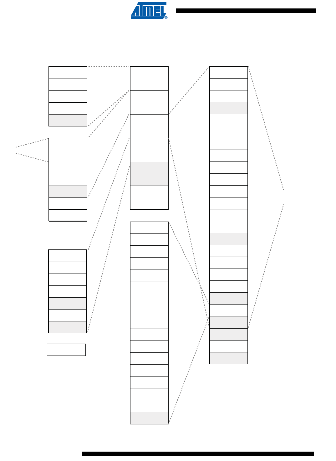
30
6430F–ATARM–21-Feb-12
SAM3U Series
8. Product Mapping
Figure 8-1. ATSAM3U4/2/1 Memory Mapping
Address memory space
Code
0x00000000
Internal SRAM
0x20000000
Peripherals
0x40000000
External SRAM
0x60000000
Reserved
0xA0000000
System
0xE0000000
0xFFFFFFFF
Code
1 MByte
bit band
region
1 MByte
bit band
region
Boot Memory
0x00000000
Internal Flash 0
0x00080000
Internal Flash 1
0x00100000
Internal ROM
0x00180000
Reserved
0x00200000
0x1FFFFFFF
Internal SRAM
SRAM0
0x20000000
SRAM1
0x20080000
NFC (SRAM)
0x20100000
UDPHS (DMA)
32 MBytes
bit band alias
Undefined
0x20180000
0x20200000
0x22000000
0x240000000x24000000
0x40000000
External SRAM
Chip Select 0
0x60000000
Chip Select 1
0x61000000
Chip Select 2
0x62000000
Chip Select 3
0x63000000
reserved
0x64000000
NFC
0x68000000
reserved
0x69000000
0x9FFFFFFF
System Controller
SMC
0x400E0000
MATRIX
0x400E0200
PMC
5
0x400E0400
UART
8
0x400E0600
CHIPID
0x400E0740
EFC0
6
0x400E0800
EFC1
7
0x400E0A00
PIOA
10
0x400E0C00
PIOB
11
0x400E0E00
PIOC
12
0x400E1000
RSTC
0x400E1200
1
SUPC
+0x10
RTT
+0x30
3
WDT
+0x50
4
RTC
+0x60
2
SYSC GPBR
+0x90
reserved
0x400E1400
0x4007FFFF
offset
ID
peripheral
block
Peripherals
MCI
17
0x40000000
SSC
21
0x40004000
SPI
20
0x40008000
Reserved
0x4000C000
TC0 TC0
0x40080000
22
TC0 TC1
+0x40
23
TC0 TC2
+0x80
24
TWI0
18
0x40084000
TWI1
19
0x40088000
PWM
25
0x4008C000
USART0
13
0x40090000
USART1
14
0x40094000
USART2
15
0x40098000
USART3
16
0x4009C000
Reserved
0x400A0000
UDPHS
29
0x400A4000
ADC12B
26
0x400A8000
ADC
27
0x400AC000
DMAC
28
0x400B0000
Reserved
0x400B3FFF
System Controller
0x400E0000
0x400E2600
0x40100000
0x42000000
0x44000000
0x60000000
Undefined
Reserved
Reserved
Reserved
32 MBytes
bit band alias

31
6430F–ATARM–21-Feb-12
SAM3U Series
9. Memories
The embedded and external memories are described below.
9.1 Embedded Memories
9.1.1 Internal SRAM
The SAM3U4 (256 KBytes internal Flash version) embeds a total of 48 Kbytes high-speed
SRAM (32 Kbytes SRAM0 and 16 Kbytes SRAM1).
The SAM3U2 (128 KBytes internal Flash version) embeds a total of 32 Kbytes high-speed
SRAM (16 Kbytes SRAM0 and 16 Kbytes SRAM1).
The SAM3U1 (64 KBytes internal Flash version) embeds a total of 16 Kbytes high-speed SRAM
(8 Kbytes SRAM0 and 8 Kbytes SRAM1).
The SRAM0 is accessible over System Cortex-M3 bus at address 0x2000 0000 and SRAM1 at
address 0x2008 0000. The user can see the SRAM as contiguous at 0x20078000-0x20083FFF
(SAM3U4), 0x2007C000-0x20083FFFF (SAM3U2) or 0x2007E000-0x20081FFFF (SAM3U1).
The SRAM0 and SRAM1 are in the bit band region. The bit band alias region is from 0x2200
0000 and 0x23FF FFFF.
The NAND Flash Controller embeds 4224 bytes of internal SRAM. If the NAND Flash controller
is not used, these 4224 bytes of SRAM can be used as general purpose. It can be seen at
address 0x2010 0000.
9.1.2 Internal ROM
The ATSAM3U4/2/1 product embeds an Internal ROM, which contains the SAM-BA Boot and
FFPI program.
At any time, the ROM is mapped at address 0x0018 0000.
9.1.3 Embedded Flash
9.1.3.1 Flash Overview
The Flash of the SAM3U4 (256 KBytes internal Flash version) is organized in two banks of 512
pages (dual plane) of 256 bytes.
The Flash of the SAM3U2 (128 KBytes internal Flash version) is organized in one bank of 512
pages (single plane) of 256 bytes.
The Flash of the SAM3U1 (64 KBytes internal Flash version) is organized in one bank of 256
pages (single plane) of 256 bytes.
The Flash contains a 128-byte write buffer, accessible through a 32-bit interface.
9.1.3.2 Flash Power Supply
The Flash is supplied by VDDCORE.
9.1.3.3 Enhanced Embedded Flash Controller
The Enhanced Embedded Flash Controller (EEFC) manages accesses performed by the mas-
ters of the system. It enables reading the Flash and writing the write buffer. It also contains a
User Interface, mapped within the Memory Controller on the APB.

32
6430F–ATARM–21-Feb-12
SAM3U Series
The Enhanced Embedded Flash Controller ensures the interface of the Flash block with the 32-
bit internal bus. Its 128-bit wide memory interface increases performance.
The user can choose between high performance or lower current consumption by selecting
either 128-bit or 64-bit access. It also manages the programming, erasing, locking and unlocking
sequences of the Flash using a full set of commands.
One of the commands returns the embedded Flash descriptor definition that informs the system
about the Flash organization, thus making the software generic.
The SAM3U4 (256 KBytes internal Flash version) embeds two EEFC (EEFC0 for Flash0 and
EEFC1 for Flash1) whereas the SAM3U2/1 embeds one EEFC.
9.1.3.4 Lock Regions
In the SAM3U4 (256 KBytes internal Flash version) two Enhanced Embedded Flash Controllers
each manage 16 lock bits to protect 32 regions of the flash against inadvertent flash erasing or
programming commands.
The SAM3U4 (256 KBytes internal Flash version) contains 32 lock regions and each lock region
contains 32 pages of 256 bytes. Each lock region has a size of 8 Kbytes.
The SAM3U2 (128 KBytes internal Flash version) Enhanced Embedded Flash Controller man-
ages 16 lock bits to protect 32 regions of the flash against inadvertent flash erasing or
programming commands.
The SAM3U2 (128 KBytes internal Flash version) contains 16 lock regions and each lock region
contains 32 pages of 256 bytes. Each lock region has a size of 8 Kbytes.
The SAM3U1(64 KBytes internal Flash version) Embedded Flash Controller manages 8 lock bits
to protect 8 regions of the flash against inadvertent flash erasing or programming commands.
The SAM3U1(64 KBytes internal Flash version) contains 8 lock regions and each lock region
contains 32 pages of 256 bytes. Each lock region has a size of 8 Kbytes.
If a locked-region’s erase or program command occurs, the command is aborted and the EEFC
triggers an interrupt.
The lock bits are software programmable through the EEFC User Interface. The command “Set
Lock Bit” enables the protection. The command “Clear Lock Bit” unlocks the lock region.
Asserting the ERASE pin clears the lock bits, thus unlocking the entire Flash.
9.1.3.5 Security Bit Feature
The ATSAM3U4/2/1 features a security bit, based on a specific General Purpose NVM bit
(GPNVM bit 0). When the security is enabled, any access to the Flash, SRAM, Core Registers
and Internal Peripherals either through the ICE interface or through the Fast Flash Programming
Interface, is forbidden. This ensures the confidentiality of the code programmed in the Flash.
This security bit can only be enabled, through the command “Set General Purpose NVM Bit 0” of
the EEFC User Interface. Disabling the security bit can only be achieved by asserting the
ERASE pin at 1, and after a full Flash erase is performed. When the security bit is deactivated,
all accesses to the Flash, SRAM, Core Registers and Internal Peripherals either through the ICE
interface or through the Fast Flash Programming Interface are permitted.
It is important to note that the assertion of the ERASE pin should always be longer than 200 ms.
As the ERASE pin integrates a permanent pull-down, it can be left unconnected during normal

33
6430F–ATARM–21-Feb-12
SAM3U Series
operation. However, it is safer to connect it directly to GND for the final application.
9.1.3.6 Calibration Bits
NVM bits are used to calibrate the brownout detector and the voltage regulator. These bits are
factory configured and cannot be changed by the user. The ERASE pin has no effect on the cal-
ibration bits.
9.1.3.7 Unique Identifier
Each device integrates its own 128-bit unique identifier. These bits are factory configured and
cannot be changed by the user. The ERASE pin has no effect on the unique identifier.
9.1.3.8 Fast Flash Programming Interface
The Fast Flash Programming Interface allows programming the device through either a serial
JTAG interface or through a multiplexed fully-handshaked parallel port. It allows gang program-
ming with market-standard industrial programmers.
The FFPI supports read, page program, page erase, full erase, lock, unlock and protect
commands.
The Fast Flash Programming Interface is enabled and the Fast Programming Mode is entered
when TST, NRSTB and FWUP pins are tied high during power up sequence and if all supplies
are provided externally (do not use internal regulator for VDDCORE). Please note that since the
FFPI is a part of the SAM-BA Boot Application, the device must boot from the ROM.
9.1.3.9 SAM-BA® Boot
The SAM-BA Boot is a default Boot Program which provides an easy way to program in-situ the
on-chip Flash memory.
The SAM-BA Boot Assistant supports serial communication via the UART and USB.
The SAM-BA Boot provides an interface with SAM-BA Graphic User Interface (GUI).
The SAM-BA Boot is in ROM and is mapped in Flash at address 0x0 when GPNVM bit 1 is set
to 0.
9.1.3.10 GPNVM Bits
The ATSAM3U4/2/1 features three GPNVM bits that can be cleared or set respectively through
the commands “Clear GPNVM Bit” and “Set GPNVM Bit” of the EEFC User Interface.
The SAM3U4 is equipped with two EEFC, EEFC0 and EEFC1. EEFC1 does not feature the
GPNVM bits. The GPNVM embedded on EEFC0 applies to the two blocks in the SAM3U4.
Table 9-1. General-purpose Non-volatile Memory Bits
GPNVMBit[#] Function
0 Security bit
1 Boot mode selection
2Flash selection (Flash 0 or Flash 1) Only on SAM3U4 (256 Kbytes internal
Flash version)

34
6430F–ATARM–21-Feb-12
SAM3U Series
9.1.4 Boot Strategies
The system always boots at address 0x0. To ensure a maximum boot possibilities the memory
layout can be changed via GPNVM.
A general purpose NVM (GPNVM1) bit is used to boot either on the ROM (default) or from the
Flash.
The GPNVM bit can be cleared or set respectively through the commands “Clear General-pur-
pose NVM Bit” and “Set General-purpose NVM Bit” of the EEFC User Interface.
Setting the GPNVM Bit 1 selects the boot from the Flash, clearing it selects the boot from the
ROM. Asserting ERASE clears the GPNVM Bit 1 and thus selects the boot from the ROM by
default.
GPNVM2 enables to select if Flash 0 or Flash 1 is used for the boot. Setting the GPNVM2 bit
selects the boot from Flash 1, clearing it selects the boot from Flash 0.
9.2 External Memories
The ATSAM3U4/2/1 offers an interface to a wide range of external memories and to any parallel
peripheral.
9.2.1 Static Memory Controller
• 8- or 16- bit Data Bus
• Up to 24-bit Address Bus (up to 16 MBytes linear per chip select)
• Up to 4 chips selects, Configurable Assignment
• Multiple Access Modes supported
– Byte Write or Byte Select Lines
• Multiple device adaptability
– Control signals programmable setup, pulse and hold time for each Memory Bank
• Multiple Wait State Management
– Programmable Wait State Generation
– External Wait Request
– Programmable Data Float Time
• Slow Clock mode supported
9.2.2 NAND Flash Controller
• Handles automatic Read/Write transfer through 4224 bytes SRAM buffer
• DMA support
• Supports SLC NAND Flash technology
• Programmable timing on a per chip select basis
• Programmable Flash Data width 8-bit or 16-bit
9.2.3 NAND Flash Error Corrected Code Controller
• Integrated in the NAND Flash Controller
• Single bit error correction and 2-bit Random detection.
• Automatic Hamming Code Calculation while writing
– ECC value available in a register
• Automatic Hamming Code Calculation while reading

35
6430F–ATARM–21-Feb-12
SAM3U Series
– Error Report, including error flag, correctable error flag and word address being
detected erroneous
– Supports 8- or 16-bit NAND Flash devices with 512-, 1024-, 2048- or 4096-byte
pages

36
6430F–ATARM–21-Feb-12
SAM3U Series
10. System Controller
The System Controller is a set of peripherals, which allow handling of key elements of the sys-
tem, such as power, resets, clocks, time, interrupts, watchdog, etc...
The System Controller User Interface also embeds the registers used to configure the Matrix.
See the system controller block diagram in Figure 10-1 on page 37.
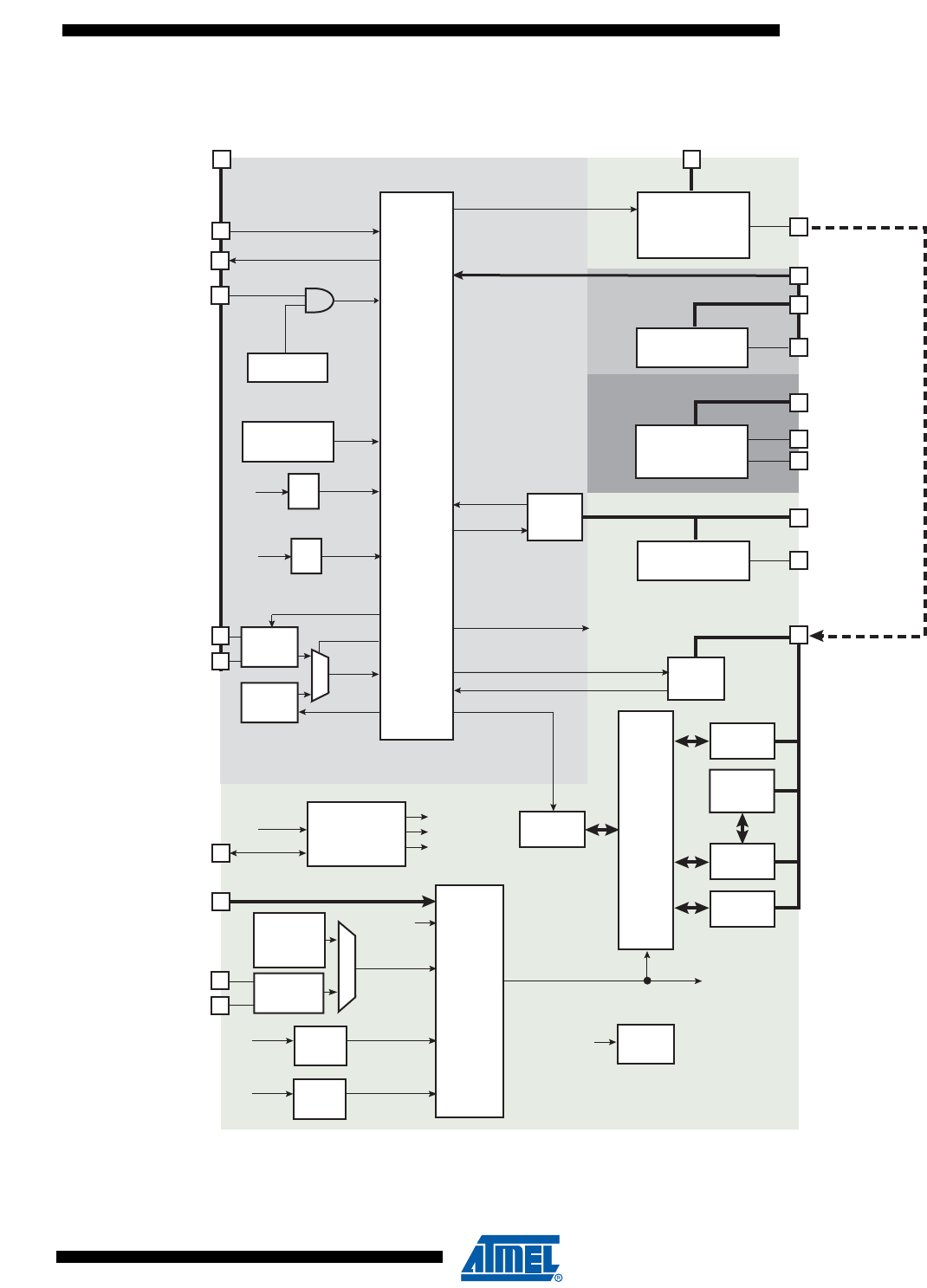
37
6430F–ATARM–21-Feb-12
SAM3U Series
Figure 10-1. System Controller Block Diagram
Software Controlled
Voltage Regulator
ADC (front-end)
Matrix
SRAM
Watchdog
Timer
Flash
Peripherals
Peripheral
Bridge
Zero-Power
Power-on Reset
Supply
Monitor
RTC
Power
Management
Controller
Embedded
32 kHz RC
Oscillator
Xtal 32 kHz
Oscillator
Supply
Controller
Embedded
12 / 8 / 4 MHz
RC
Oscillator
Brownout
Detector
General Purpose
Backup Registers
Cortex-M3
Reset
Controller
Backup Power Supply
Core Power Supply
PLLA
vr_standby
rtc_alarm
SLCK
proc_nreset
periph_nreset
ice_nreset
Master Clock
MCK
SLCK
vddcore_nreset
Main Clock
MAINCK
SLCK
NRST
MAINCK PLLACK
FSTT0 - FSTT15(1)
XIN32
XOUT32
osc32k_xtal_en
XTALSEL
Slow Clock
SLCK
osc32k_rc_en
vddcore_nreset
VDDIO
VDDCORE
VDDOUT
ADVREF
ADx
FWUP
bodcore_on
bodcore_in
RTT
rtt_alarm
SLCK
XIN
XOUT
VDDBU VDDIN
SHDN
PIOx
VDDANA
USB
VDDUTMI
USBx
bodbup_on
bodbup_in
supc_interrupt
3 - 20 MHz
XTAL Oscillator
WKUP0 - WKUP15
NRSTB
PIOA/B/C
Input / Output Buffers
FSTT0 - FSTT15 are possible Fast Startup Sources, generated by WKUP0-WKUP15 Pins,
but are not physical pins.
UPLL
MAINCK UPLLCK

38
6430F–ATARM–21-Feb-12
SAM3U Series
10.1 System Controller and Peripheral Mapping
Please refer to Figure 8-1“ATSAM3U4/2/1 Memory Mapping” on page 30 .
All the peripherals are in the bit band region and are mapped in the bit band alias region.
10.2 Power-on-Reset, Brownout and Supply Monitor
The SAM3U embeds three features to monitor, warn and/or reset the chip:
• Power-on-Reset on VDDBU
• Brownout Detector on VDDCORE
• Supply Monitor on VDDUTMI
10.2.1 Power-on-Reset on VDDBU
The Power-on-Reset monitors VDDBU. It is always activated and monitors voltage at start up
but also during power down. If VDDBU goes below the threshold voltage, the entire chip is reset.
For more information, refer to the “Electrical Characteristics” section of the datasheet.
10.2.2 Brownout Detector on VDDCORE
The Brownout Detector monitors VDDCORE. It is active by default. It can be deactivated by soft-
ware through the Supply Controller (SUPC_MR). It is especially recommended to disable it
during low-power modes such as wait or sleep modes.
If VDDCORE goes below the threshold voltage, the reset of the core is asserted. For more infor-
mation, refer to the “Supply Controller” and “Electrical Characteristics” sections of the product
datasheet.
10.2.3 Supply Monitor on VDDUTMI
The Supply Monitor monitors VDDUTMI. It is not active by default. It can be activated by soft-
ware and is fully programmable with 16 steps for the threshold (between 1.9V to 3.4V). It is
controlled by the Supply Controller. A sample mode is possible. It allows to divide the supply
monitor power consumption by a factor of up to 2048. For more information, refer to the “Supply
Controller” and “Electrical Characteristics” sections of the product datasheet.
10.3 Reset Controller
The Reset Controller is capable to return to the software the source of the last reset, either a
general reset, a wake-up reset, a software reset, a user reset or a watchdog reset.
The Reset Controller controls the internal resets of the system and the NRST pin output. It is
capable to shape a reset signal for the external devices, simplifying to a minimum connection of
a push-button on the NRST pin to implement a manual reset.
10.4 Supply Controller
The Supply Controller controls the power supplies of each section of the processor and the
peripherals (via Voltage regulator control).
The Supply Controller has its own reset circuitry and is clocked by the 32 kHz Slow clock
generator.
The reset circuitry is based on a zero-power power-on reset cell. The zero-power power-on reset
allows the Supply Controller to start properly.
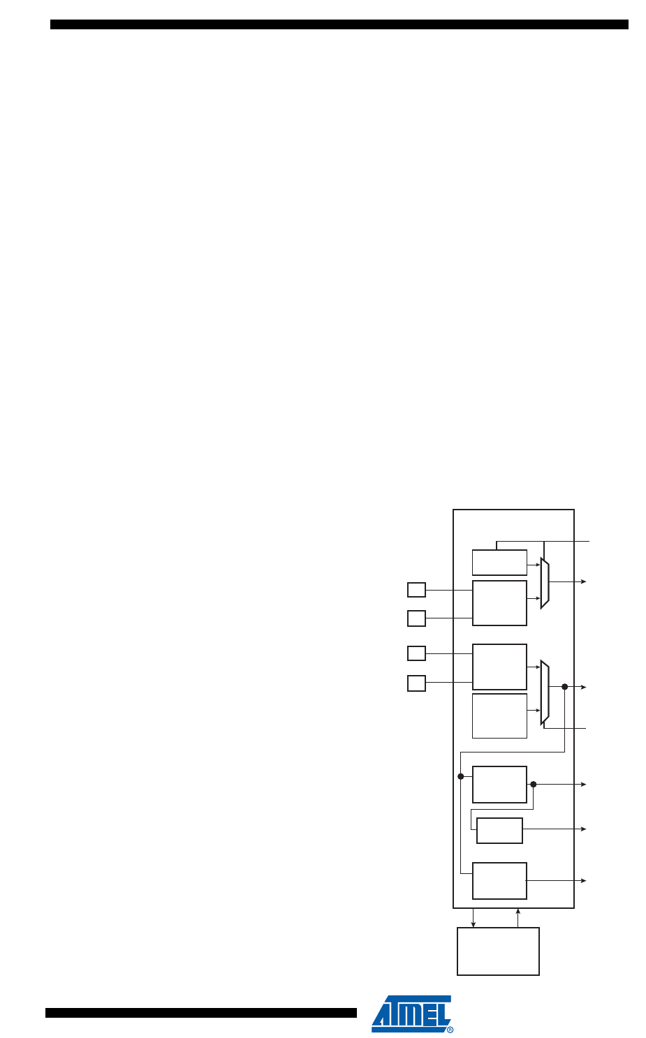
39
6430F–ATARM–21-Feb-12
SAM3U Series
The Slow Clock generator is based on a 32 kHz crystal oscillator and an embedded 32 kHz RC
oscillator. The Slow Clock defaults to the RC oscillator, but the software can enable the crystal
oscillator and select it as the Slow Clock source.
The Supply Controller starts up the device by enabling the Voltage Regulator, then it generates
the proper reset signals to the core power supply.
It also enables to set the system in different low power modes and to wake it up from a wide
range of events.
10.5 Clock Generator
The Clock Generator is made up of:
• One Low Power 32768 Hz Slow Clock Oscillator with bypass mode
• One Low Power RC Oscillator
• One 3 to 20 MHz Crystal Oscillator, which can be bypassed
• One Fast RC Oscillator factory programmed, 3 output frequencies can be selected: 4, 8 or 12
MHz. By default 4 MHz is selected. 8 MHz and 12 MHz output are factory calibrated.
• One 480 MHz UPLL providing a clock for the USB High Speed Device Controller. Input
frequency is 12 MHz (only).
• One 96 to 192 MHz programmable PLL (PLL A), capable to provide the clock MCK to the
processor and to the peripherals. The input frequency of the PLL A is between 8 and 16 MHz.
Figure 10-2. Clock Generator Block Diagram
Power
Management
Controller
XIN
XOUT Main Clock
MAINCK
UPLL Clock
UPLLCK
ControlStatus
PLL and
Divider A
PLLA Clock
PLLACK
12M Main
Oscillator
PLL B
On Chip
32k RC OSC
Slow Clock
SLCK
XIN32
XOUT32
Slow Clock
Oscillator
Clock Generator
XTALSEL
HSCK
Divider
/6 /8
On Chip
12/8/4 MHz
RC OSC MAINSEL
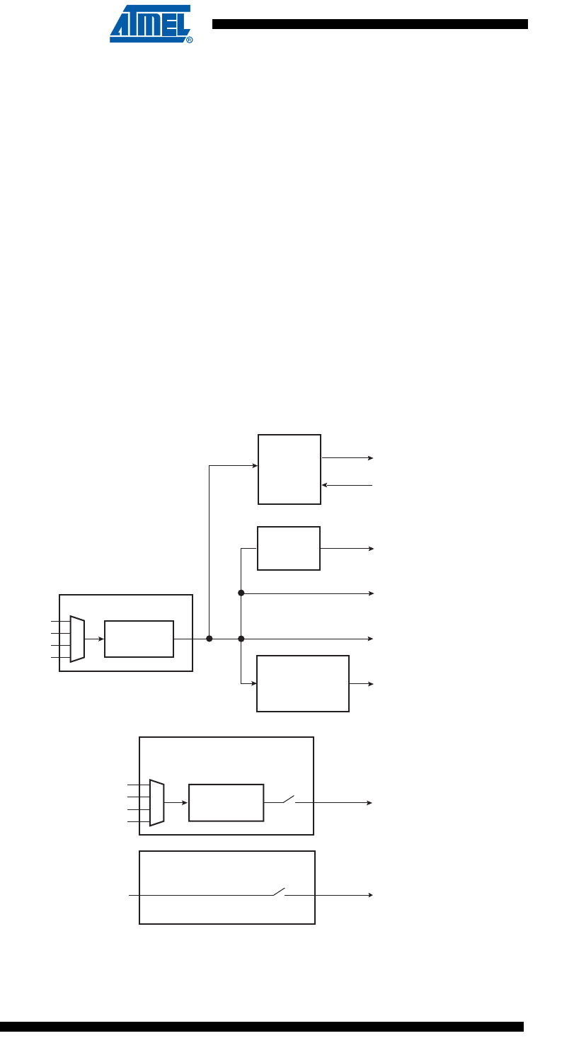
40
6430F–ATARM–21-Feb-12
SAM3U Series
10.6 Power Management Controller
The Power Management Controller provides all the clock signals to the system. It provides:
• the Processor Clock HCLK
• the Free running processor clock FCLK
• the Cortex SysTick external clock
• the Master Clock MCK, in particular to the Matrix and the memory interfaces
• the USB Device HS Clock UDPCK
• independent peripheral clocks, typically at the frequency of MCK
• three programmable clock outputs: PCK0, PCK1 and PCK2
The Supply Controller selects between the 32 kHz RC oscillator or the crystal oscillator. The
unused oscillator is disabled automatically so that power consumption is optimized.
By default, at startup the chip runs out of the Master Clock using the Fast RC Oscillator running
at 4 MHz.
Figure 10-3. Power Management Controller Block Diagram
The SysTick calibration value is fixed at 10500, which allows the generation of a time base of
1 ms with SystTick clock to 10.5 MHz (max HCLK/8).
MCK
periph_clk[..]
int
SLCK
MAINCK
PLLACK
Prescaler
/1,/2,/4,...,/64
HCK
Processor
Clock
Controller
Sleep Mode
Master Clock Controller
Peripherals
Clock Controller
ON/OFF
USB Clock Controller
SLCK
MAINCK
PLLACK
Prescaler
/1,/2,/4,...,/64
Programmable Clock Controller
HSCK
pck[..]
PLLBCK
PLLBCK
UDPCK
ON/OFF
ON/OFF
FCLK
SystTick
Divider
/8

41
6430F–ATARM–21-Feb-12
SAM3U Series
10.7 Watchdog Timer
• 16-bit key-protected once-only Programmable Counter
• Windowed, prevents the processor from being in a dead-lock on the watchdog access
10.8 SysTick Timer
• 24-bit down counter
• Self-reload capability
• Flexible system timer
10.9 Real-time Timer
• Real-time Timer, allowing backup of time with different accuracies
– 32-bit Free-running back-up Counter
– Integrates a 16-bit programmable prescaler running on slow clock
– Alarm Register capable to generate a wake-up of the system
10.10 Real-time Clock
• Low power consumption
• Full asynchronous design
• Two hundred year calendar
• Programmable Periodic Interrupt
• Alarm and update parallel load
• Control of alarm and update Time/Calendar Data In
10.11 General-Purpose Back-up Registers
• Eight 32-bit general-purpose backup registers
10.12 Nested Vectored Interrupt Controller
• Thirty maskable interrupts
• Sixteen priority levels
• Dynamic reprioritization of interrupts
• Priority grouping
– selection of preempting interrupt levels and non preempting interrupt levels.
• Support for tail-chaining and late arrival of interrupts.
– back-to-back interrupt processing without the overhead of state saving and
restoration between interrupts.
• Processor state automatically saved on interrupt entry, and restored on
– interrupt exit, with no instruction overhead.

42
6430F–ATARM–21-Feb-12
SAM3U Series
10.13 Chip Identification
• Chip Identifier (CHIPID) registers permit recognition of the device and its revision.
• JTAG ID: 0x0582A03F
• JTAG ID: 0x0582A03F
10.14 PIO Controllers
• 3 PIO Controllers, PIOA, PIOB, and PIOC, controlling a maximum of 96 I/O Lines
• Each PIO Controller controls up to 32 programmable I/O Lines
– PIOA has 32 I/O Lines
– PIOB has 32 I/O Lines
– PIOC has 32 I/O Lines
• Fully programmable through Set/Clear Registers
• Multiplexing of two peripheral functions per I/O Line
• For each I/O Line (whether assigned to a peripheral or used as general purpose I/O)
– Input change, rising edge, falling edge, low level and level interrupt
– Debouncing and Glitch filter
– Multi-drive option enables driving in open drain
– Programmable pull up on each I/O line
– Pin data status register, supplies visibility of the level on the pin at any time
• Synchronous output, provides Set and Clear of several I/O lines in a single write
Table 10-1. ATSAM3U4/2/1 Chip IDs Register - Engineering Samples
Chip Name
Flash Size
KByte Pin Count CHIPID_CIDR CHIPID_EXID
SAM3U4C 256 100 0x28000960 0x0
SAM3U2C 128 100 0x280A0760 0x0
SAM3U1C 64 100 0x28090560 0x0
SAM3U4E 256 144 0x28100960 0x0
SAM3U2E 128 144 0x281A0760 0x0
SAM3U1E 64 144 0x28190560 0x0
Table 10-2. ATSAM3U4/2/1 Chip IDs Register - Revision A Parts
Chip Name
Flash Size
KByte Pin Count CHIPID_CIDR CHIPID_EXID
SAM3U4C (Rev A) 256 100 0x28000961 0x0
SAM3U2C (Rev A) 128 100 0x280A0761 0x0
SAM3U1C (Rev A) 64 100 0x28090561 0x0
SAM3U4E (Rev A) 256 144 0x28100961 0x0
SAM3U2E (Rev A) 128 144 0x281A0761 0x0
SAM3U1E (Rev A) 64 144 0x28190561 0x0

43
6430F–ATARM–21-Feb-12
SAM3U Series
11. Peripherals
11.1 Peripheral Identifiers
Table 11-1 defines the Peripheral Identifiers of the ATSAM3U4/2/1. A peripheral identifier is
required for the control of the peripheral interrupt with the Nested Vectored Interrupt Controller
and for the control of the peripheral clock with the Power Management Controller.
Note that some Peripherals are always clocked. Please refer to the table below.
Table 11-1. Peripheral Identifiers
Instance ID Instance Name
NVIC
Interrupt
PMC
Clock Control Instance Description
0SUPCX Supply Controller
1RSTCX Reset Controller
2RTCX Real Time Clock
3RTTX Real Time Timer
4WDTX Watchdog Timer
5PMCX Power Management Controller
6 EEFC0 X Enhanced Embedded Flash Controller 0
7 EEFC1 X Enhanced Embedded Flash Controller 1
8UARTX XUniversal Asynchronous Receiver Transmitter
9SMCX XStatic Memory Controller
10 PIOA X X Parallel I/O Controller A,
11 PIOB X X Parallel I/O Controller B
12 PIOC X X Parallel I/O Controller C
13 USART0 X X USART 0
14 USART1 X X USART 1
15 USART2 X X USART 2
16 USART3 X X USART 3
17 HSMCI X X High Speed Multimedia Card Interface
18 TWI0 X X Two-Wire Interface 0
19 TWI1 X X Two-Wire Interface 1
20 SPI X X Serial Peripheral Interface
21 SSC X X Synchronous Serial Controller
22 TC0 X X Timer Counter 0
23 TC1 X X Timer Counter 1
24 TC2 X X Timer Counter 2
25 PWM X X Pulse Width Modulation Controller
26 ADC12B X X 12-bit ADC Controller
27 ADC X X 10-bit ADC Controller
28 DMAC X X DMA Controller
29 UDPHS X X USB Device High Speed

44
6430F–ATARM–21-Feb-12
SAM3U Series
11.2 Peripheral Signal Multiplexing on I/O Lines
The ATSAM3U4/2/1 features 3 PIO controllers, PIOA, PIOB and PIOC that multiplex the I/O
lines of the peripheral set.
Each PIO Controller controls up to 32 lines. Each line can be assigned to one of two peripheral
functions, A or B. The multiplexing tables in the following pages define how the I/O lines of
peripherals A and B are multiplexed on the PIO Controllers. The two columns “Extra Function”
and “Comments” have been inserted in this table for the user’s own comments, they may be
used to track how pins are defined in an application.
Note that some peripheral functions which are output only, might be duplicated within the tables.

45
6430F–ATARM–21-Feb-12
SAM3U Series
11.2.1 PIO Controller A Multiplexing
Notes: 1. Wake-Up source in Backup mode (managed by the SUPC).
2. Fast Start-Up source in Wait mode (managed by the PMC).
3. Only on 144-pin version
Table 11-2. Multiplexing on PIO Controller A (PIOA)
I/O Line Peripheral A Peripheral B Extra Function Comments
PA0 TIOB0 NPCS1 WKUP0(1)(2)
PA1 TIOA0 NPCS2 WKUP1(1)(2)
PA2 TCLK0 ADTRG WKUP2(1)(2)
PA3 MCCK PCK1
PA4 MCCDA PWMH0
PA5 MCDA0 PWMH1
PA 6 M C D A 1 PWMH2
PA7 MCDA2 PWML0
PA8 MCDA3 PWML1
PA9 TWD0 PWML2 WKUP3(1)(2)
PA 1 0 T W C K 0 P W M L 3 W K U P 4 (1)(2)
PA11 URXD PWMFI0
PA 1 2 U T X D P W M F I 1
PA 1 3 M I S O
PA 1 4 M O S I
PA15 SPCK PWMH2
PA16 NPCS0 NCS1 WKUP5(1)(2)
PA17 SCK0 AD12BTRG WKUP6(1)(2)
PA 1 8 T X D 0 P W M F I 2 W K U P 7 (1)(2)
PA19 RXD0 NPCS3 WKUP8(1)(2)
PA20 TXD1 PWMH3 WKUP9(1)(2)
PA21 RXD1 PCK0 WKUP10(1)(2)
PA22 TXD2 RTS1 AD12B0
PA23 RXD2 CTS1
PA 2 4 T W D 1 (3) SCK1 WKUP11(1)(2)
PA 2 5 T W C K 1 (3) SCK2 WKUP12(1)(2)
PA26 TD TCLK2
PA27 RD PCK0
PA 2 8 TK PWMH0
PA 2 9 R K P W M H 1
PA30 TF TIOA2 AD12B1
PA 3 1 R F T I O B 2

46
6430F–ATARM–21-Feb-12
SAM3U Series
11.2.2 PIO Controller B Multiplexing
Notes: 1. Wake-Up source in Backup mode (managed by the SUPC).
2. Fast Start-Up source in Wait mode (managed by the PMC).
Table 11-3. Multiplexing on PIO Controller B (PIOB)
I/O Line Peripheral A Peripheral B Extra Function Comments
PB0 PWMH0 A2 WKUP13(1)(2)
PB1 PWMH1 A3 WKUP14(1)(2)
PB2 PWMH2 A4 WKUP15(1)(2)
PB3 PWMH3 A5 AD12B2
PB4 TCLK1 A6 AD12B3
PB5 TIOA1 A7 AD0
PB6 TIOB1 D15 AD1
PB7 RTS0 A0/NBS0 AD2
PB8 CTS0 A1 AD3
PB9 D0 DTR0
PB10 D1 DSR0
PB11 D2 DCD0
PB12 D3 RI0
PB13 D4 PWMH0
PB14 D5 PWMH1
PB15 D6 PWMH2
PB16 D7 PWMH3
PB17 NANDOE PWML0
PB18 NANDWE PWML1
PB19 NRD PWML2
PB20 NCS0 PWML3
PB21 A21/NANDALE RTS2
PB22 A22/NANDCLE CTS2
PB23 NWR0/NWE PCK2
PB24 NANDRDY PCK1
PB25 D8 PWML0 Only on 144-pin version
PB26 D9 PWML1 Only on 144-pin version
PB27 D10 PWML2 Only on 144-pin version
PB28 D11 PWML3 Only on 144-pin version
PB29 D12 Only on 144-pin version
PB30 D13 Only on 144-pin version
PB31 D14 Only on 144-pin version

47
6430F–ATARM–21-Feb-12
SAM3U Series
11.2.3 PIO Controller C Multiplexing
Notes: 1. Wake-Up source in Backup mode (managed by the SUPC).
2. Fast Start-Up source in Wait mode (managed by the PMC).
Table 11-4. Multiplexing on PIO Controller C (PIOC)
I/O Line Peripheral A Peripheral B Extra function Comments
PC0 A2 Only on 144-pin version
PC1 A3 Only on 144-pin version
PC2 A4 Only on 144-pin version
PC3 A5 NPCS1 Only on 144-pin version
PC4 A6 NPCS2 Only on 144-pin version
PC5 A7 NPCS3 Only on 144-pin version
PC6 A8 PWML0 Only on 144-pin version
PC7 A9 PWML1 Only on 144-pin version
PC8 A10 PWML2 Only on 144-pin version
PC9 A11 PWML3 Only on 144-pin version
PC10 A12 CTS3 Only on 144-pin version
PC11 A13 RTS3 Only on 144-pin version
PC12 NCS1 TXD3 Only on 144-pin version
PC13 A2 RXD3 Only on 144-pin version
PC14 A3 NPCS2 Only on 144-pin version
PC15 NWR1/NBS1 AD12B4 Only on 144-pin version
PC16 NCS2 PWML3 AD12B5 Only on 144-pin version
PC17 NCS3 AD12B6 Only on 144-pin version
PC18 NWAIT AD12B7 Only on 144-pin version
PC19 SCK3 NPCS1 Only on 144-pin version
PC20 A14 Only on 144-pin version
PC21 A15 Only on 144-pin version
PC22 A16 Only on 144-pin version
PC23 A17 Only on 144-pin version
PC24 A18 PWMH0 Only on 144-pin version
PC25 A19 PWMH1 Only on 144-pin version
PC26 A20 PWMH2 Only on 144-pin version
PC27 A23 PWMH3 Only on 144-pin version
PC28 MCDA4 AD4 Only on 144-pin version
PC29 PWML0 MCDA5 AD5 Only on 144-pin version
PC30 PWML1 MCDA6 AD6 Only on 144-pin version
PC31 PWML2 MCDA7 AD7 Only on 144-pin version

48
6430F–ATARM–21-Feb-12
SAM3U Series
12. Embedded Peripherals Overview
12.1 Serial Peripheral Interface (SPI)
• Supports communication with serial external devices
– Four chip selects with external decoder support allow communication with up to 15
peripherals
– Serial memories, such as DataFlash and 3-wire EEPROMs
– Serial peripherals, such as ADCs, DACs, LCD Controllers, CAN Controllers and
Sensors
– External co-processors
• Master or slave serial peripheral bus interface
– 8- to 16-bit programmable data length per chip select
– Programmable phase and polarity per chip select
– Programmable transfer delays between consecutive transfers and between clock
and data per chip select
– Programmable delay between consecutive transfers
– Selectable mode fault detection
• Very fast transfers supported
– Transfers with baud rates up to MCK
– The chip select line may be left active to speed up transfers on the same device
12.2 Two Wire Interface (TWI)
• Master, Multi-Master and Slave Mode Operation
• Compatibility with Atmel two-wire interface, serial memory and I2C compatible devices
• One, two or three bytes for slave address
• Sequential read/write operations
• Bit Rate: Up to 400 kbit/s
• General Call Supported in Slave Mode
• Connecting to PDC channel capabilities optimizes data transfers in Master Mode only
– One channel for the receiver, one channel for the transmitter
– Next buffer support
12.3 Universal Asynchronous Receiver Transceiver (UART)
•Two-pin UART
– Implemented features are 100% compatible with the standard Atmel USART
– Independent receiver and transmitter with a common programmable Baud Rate
Generator
– Even, Odd, Mark or Space Parity Generation
– Parity, Framing and Overrun Error Detection
– Automatic Echo, Local Loopback and Remote Loopback Channel Modes
– Support for two PDC channels with connection to receiver and transmitter

49
6430F–ATARM–21-Feb-12
SAM3U Series
12.4 Universal Synchronous Asynchronous Receiver Transmitter (USART)
• Programmable Baud Rate Generator
• 5- to 9-bit full-duplex synchronous or asynchronous serial communications
– 1, 1.5 or 2 stop bits in Asynchronous Mode or 1 or 2 stop bits in Synchronous Mode
– Parity generation and error detection
– Framing error detection, overrun error detection
– MSB- or LSB-first
– Optional break generation and detection
– By 8 or by-16 over-sampling receiver frequency
– Hardware handshaking RTS-CTS
– Receiver time-out and transmitter timeguard
– Optional Multi-drop Mode with address generation and detection
– Optional Manchester Encoding
• RS485 with driver control signal
• ISO7816, T = 0 or T = 1 Protocols for interfacing with smart cards
– NACK handling, error counter with repetition and iteration limit
• SPI Mode
–Master or Slave
– Serial Clock programmable Phase and Polarity
– SPI Serial Clock (SCK) Frequency up to MCK/6
• IrDA modulation and demodulation
– Communication at up to 115.2 Kbps
• Test Modes
– Remote Loopback, Local Loopback, Automatic Echo
12.5 Serial Synchronous Controller (SSC)
• Provides serial synchronous communication links used in audio and telecom applications
(with CODECs in Master or Slave Modes, I2S, TDM Buses, Magnetic Card Reader, ...)
• Contains an independent receiver and transmitter and a common clock divider
• Offers a configurable frame sync and data length
• Receiver and transmitter can be programmed to start automatically or on detection of
different event on the frame sync signal
• Receiver and transmitter include a data signal, a clock signal and a frame synchronization
signal
12.6 Timer Counter (TC)
• Three 16-bit Timer Counter Channels
• Wide range of functions including:
– Frequency Measurement
– Event Counting
– Interval Measurement

50
6430F–ATARM–21-Feb-12
SAM3U Series
– Pulse Generation
–Delay Timing
– Pulse Width Modulation
– Up/Down Capabilities
– Quadrature Decoder Logic
• Each channel is user-configurable and contains:
– Three external clock inputs
– Five internal clock inputs
– Two multi-purpose input/output signals
• Two global registers that act on all three TC Channels
12.7 Pulse Width Modulation Controller (PWM)
• 4 channels, one 16-bit counter per channel
• Common clock generator, providing Thirteen Different Clocks
– A Modulo n counter providing eleven clocks
– Two independent Linear Dividers working on modulo n counter outputs
– High Frequency Asynchronous clocking mode
• Independent channel programming
– Independent Enable Disable Commands
– Independent Clock Selection
– Independent Period and Duty Cycle, with Double Buffering
– Programmable selection of the output waveform polarity
– Programmable center or left aligned output waveform
– Independent Output Override for each channel
– Independent complementary Outputs with 12-bit dead time generator for each
channel
– Independent Enable Disable Commands
– Independent Clock Selection
– Independent Period and Duty Cycle, with Double Buffering
• Synchronous Channel mode
– Synchronous Channels share the same counter
– Mode to update the synchronous channels registers after a programmable number
of periods
• Connection to one PDC channel
– Offers Buffer transfer without Processor Intervention, to update duty cycle of
synchronous channels
• Two independent event lines which can send up to 8 triggers on ADC within a period
• Four programmable Fault Inputs providing asynchronous protection of outputs

51
6430F–ATARM–21-Feb-12
SAM3U Series
12.8 High Speed Multimedia Card Interface (HSMCI)
• Compatibility with MultiMedia Card Specification Version 4.3
• Compatibility with SD Memory Card Specification Version 2.0
• Compatibility with SDIO Specification Version V2.0.
• Compatibility with CE-ATA Specification 1.1
• Cards clock rate up to Master Clock divided by 2
• Boot Operation Mode support
• High Speed mode support
• Embedded power management to slow down clock rate when not used
• HSMCI has one slot supporting
– One MultiMediaCard bus (up to 30 cards) or
– One SD Memory Card
– One SDIO Card
• Support for stream, block and multi-block data read and write
• Supports Connection to DMA controller
– Minimizes Processor intervention for large buffer transfers
• Built in FIFO (32 bytes) with large Memory Aperture Supporting Incremental access
• Support for CE-ATA Completion Signal Disable Command
12.9 USB High Speed Device Port (UDPHS)
• USB V2.0 high-speed compliant, 480 MBits per second
• Embedded USB V2.0 UTMI+ high-speed transceiver
• Embedded 4-Kbyte dual-port RAM for endpoints
• Embedded 6 channels DMA controller
• Suspend/Resume logic
• Up to 2 or 3 banks for isochronous and bulk endpoints
• Seven endpoints, configurable by software
• Maximum configuration: seven endpoints:
– Endpoint 0: 64 bytes, 1 bank mode
– Endpoint 1 & 2: 512 bytes, 2 banks mode, HS isochronous capable
– Endpoint 3 & 4:64 bytes, 3 banks mode
– Endpoint 5 & 6: 1024 bytes, 3 banks mode, HS isochronous capable
12.10 Analog-to-Digital Converter (ADC)
Two ADCs are embedded in the product.
12.10.1 12-bit High Speed ADC
• 8-channel ADC
• 12-bit 1 Msamples/sec. Cyclic Pipeline ADC
• Integrated 8-to-1 multiplexer
• 12-bit resolution

52
6430F–ATARM–21-Feb-12
SAM3U Series
• Selectable single ended or differential input voltage
• Programmable gain for maximum full scale input range
• External voltage reference for better accuracy on low voltage inputs
• Individual enable and disable of each channel
• Multiple trigger sources
– Hardware or software trigger
– External trigger pin
– Timer Counter 0 to 2 outputs TIOA0 to TIOA2 trigger
– PWM trigger
• Sleep Mode and conversion sequencer
– Automatic wakeup on trigger and back to sleep mode after conversions of all
enabled channels
12.10.2 10-bit Low Power ADC
• 8-channel ADC
• 10-bit 384 Ksamples/sec. or 8-bit 533 Ksamples/sec. Successive Approximation Register
ADC
• -2/+2 LSB Integral Non Linearity, -1/+1 LSB Differential Non Linearity
• Integrated 8-to-1 multiplexer
• External voltage reference for better accuracy on low voltage inputs
• Individual enable and disable of each channel
• Multiple trigger sources
– Hardware or software trigger
– External trigger pin
– Timer Counter 0 to 2 outputs TIOA0 to TIOA2 trigger
– PWM trigger
• Sleep Mode and conversion sequencer
– Automatic wakeup on trigger and back to sleep mode after conversions of all
enabled channels
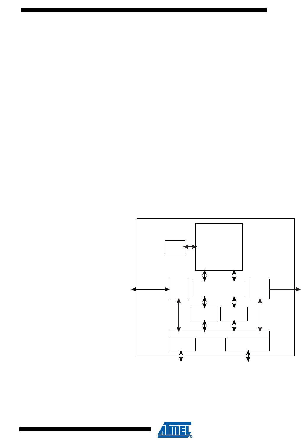
53
6430F–ATARM–21-Feb-12
SAM3U Series
13. ARM Cortex® M3 Processor
13.1 About this section
This section provides the information required for application and system-level software devel-
opment. It does not provide information on debug components, features, or operation.
This material is for microcontroller software and hardware engineers, including those who have
no experience of ARM products.
Note: The information in this section is reproduced from source material provided to Atmel by
ARM Ltd. in terms of Atmel’s license for the ARM Cortex™-M3 processor core. This information
is copyright ARM Ltd., 2008 - 2009.
13.2 About the Cortex-M3 processor and core peripherals
• The Cortex-M3 processor is a high performance 32-bit processor designed for the
microcontroller market. It offers significant benefits to developers, including:
• outstanding processing performance combined with fast interrupt handling
• enhanced system debug with extensive breakpoint and trace capabilities
• efficient processor core, system and memories
• ultra-low power consumption with integrated sleep modes
• platform security, with integrated memory protection unit (MPU).
Figure 13-1. Typical Cortex-M3 implementation
The Cortex-M3 processor is built on a high-performance processor core, with a 3-stage pipeline
Harvard architecture, making it ideal for demanding embedded applications. The processor
delivers exceptional power efficiency through an efficient instruction set and extensively opti-
Processor
Core
NVIC
Debug
Access
Port
Memory
Protection Unit
Serial
Wire
Viewer
Bus Matrix
Code
Interface
SRAM and
Peripheral Interface
Data
Watchpoints
Flash
Patch
Cortex-M3
Processor

54
6430F–ATARM–21-Feb-12
SAM3U Series
mized design, providing high-end processing hardware including single-cycle 32x32
multiplication and dedicated hardware division.
To facilitate the design of cost-sensitive devices, the Cortex-M3 processor implements tightly-
coupled system components that reduce processor area while significantly improving interrupt
handling and system debug capabilities. The Cortex-M3 processor implements a version of the
Thumb® instruction set, ensuring high code density and reduced program memory requirements.
The Cortex-M3 instruction set provides the exceptional performance expected of a modern 32-
bit architecture, with the high code density of 8-bit and 16-bit microcontrollers.
The Cortex-M3 processor closely integrates a configurable nested interrupt controller (NVIC), to
deliver industry-leading interrupt performance. The NVIC provides up to 16 interrupt priority lev-
els. The tight integration of the processor core and NVIC provides fast execution of interrupt
service routines (ISRs), dramatically reducing the interrupt latency. This is achieved through the
hardware stacking of registers, and the ability to suspend load-multiple and store-multiple opera-
tions. Interrupt handlers do not require any assembler stubs, removing any code overhead from
the ISRs. Tail-chaining optimization also significantly reduces the overhead when switching from
one ISR to another.
To optimize low-power designs, the NVIC integrates with the sleep modes, that include a deep
sleep function that enables the entire device to be rapidly powered down.
13.2.1 System level interface
The Cortex-M3 processor provides multiple interfaces using AMBA® technology to provide high
speed, low latency memory accesses. It supports unaligned data accesses and implements
atomic bit manipulation that enables faster peripheral controls, system spinlocks and thread-safe
Boolean data handling.
The Cortex-M3 processor has a memory protection unit (MPU) that provides fine grain memory
control, enabling applications to implement security privilege levels, separating code, data and
stack on a task-by-task basis. Such requirements are becoming critical in many embedded
applications.
13.2.2 Integrated configurable debug
The Cortex-M3 processor implements a complete hardware debug solution. This provides high
system visibility of the processor and memory through either a traditional JTAG port or a 2-pin
Serial Wire Debug (SWD) port that is ideal for microcontrollers and other small package devices.
For system trace the processor integrates an Instrumentation Trace Macrocell (ITM) alongside
data watchpoints and a profiling unit. To enable simple and cost-effective profiling of the system
events these generate, a Serial Wire Viewer (SWV) can export a stream of software-generated
messages, data trace, and profiling information through a single pin.
13.2.3 Cortex-M3 processor features and benefits summary
• tight integration of system peripherals reduces area and development costs
• Thumb instruction set combines high code density with 32-bit performance
• code-patch ability for ROM system updates
• power control optimization of system components
• integrated sleep modes for low power consumption
• fast code execution permits slower processor clock or increases sleep mode time
• hardware division and fast multiplier

55
6430F–ATARM–21-Feb-12
SAM3U Series
• deterministic, high-performance interrupt handling for time-critical applications
•memory protection unit (MPU) for safety-critical applications
• extensive debug and trace capabilities:
– Serial Wire Debug and Serial Wire Trace reduce the number of pins required for
debugging and tracing.
13.2.4 Cortex-M3 core peripherals
These are:
13.2.4.1 Nested Vectored Interrupt Controller
The Nested Vectored Interrupt Controller (NVIC) is an embedded interrupt controller that sup-
ports low latency interrupt processing.
13.2.4.2 System control block
The System control block (SCB) is the programmers model interface to the processor. It pro-
vides system implementation information and system control, including configuration, control,
and reporting of system exceptions.
13.2.4.3 System timer
The system timer, SysTick, is a 24-bit count-down timer. Use this as a Real Time Operating Sys-
tem (RTOS) tick timer or as a simple counter.
13.2.4.4 Memory protection unit
The Memory protection unit (MPU) improves system reliability by defining the memory attributes
for different memory regions. It provides up to eight different regions, and an optional predefined
background region.
13.3 Programmers model
This section describes the Cortex-M3 programmers model. In addition to the individual core reg-
ister descriptions, it contains information about the processor modes and privilege levels for
software execution and stacks.
13.3.1 Processor mode and privilege levels for software execution
The processor modes are:
13.3.1.1 Thread mode
Used to execute application software. The processor enters Thread mode when it comes out of
reset.
13.3.1.2 Handler mode
Used to handle exceptions. The processor returns to Thread mode when it has finished excep-
tion processing.
The privilege levels for software execution are:
13.3.1.3 Unprivileged
The software:
• has limited access to the MSR and MRS instructions, and cannot use the CPS instruction

56
6430F–ATARM–21-Feb-12
SAM3U Series
• cannot access the system timer, NVIC, or system control block
• might have restricted access to memory or peripherals.
Unprivileged software executes at the unprivileged level.
13.3.1.4 Privileged
The software can use all the instructions and has access to all resources.
Privileged software executes at the privileged level.
In Thread mode, the CONTROL register controls whether software execution is privileged or
unprivileged, see “CONTROL register” on page 65. In Handler mode, software execution is
always privileged.
Only privileged software can write to the CONTROL register to change the privilege level for
software execution in Thread mode. Unprivileged software can use the SVC instruction to make
a supervisor call to transfer control to privileged software.
13.3.2 Stacks
The processor uses a full descending stack. This means the stack pointer indicates the last
stacked item on the stack memory. When the processor pushes a new item onto the stack, it
decrements the stack pointer and then writes the item to the new memory location. The proces-
sor implements two stacks, the main stack and the process stack, with independent copies of
the stack pointer, see “Stack Pointer” on page 58.
In Thread mode, the CONTROL register controls whether the processor uses the main stack or
the process stack, see “CONTROL register” on page 65. In Handler mode, the processor always
uses the main stack. The options for processor operations are:
Table 13-1. Summary of processor mode, execution privilege level, and stack use options
Processor
mode
Used to
execute
Privilege level for
software execution Stack used
Thread Applications Privileged or
unprivileged (1)
1. See “CONTROL register” on page 65.
Main stack or process
stack(1)
Handler Exception
handlers Always privileged Main stack
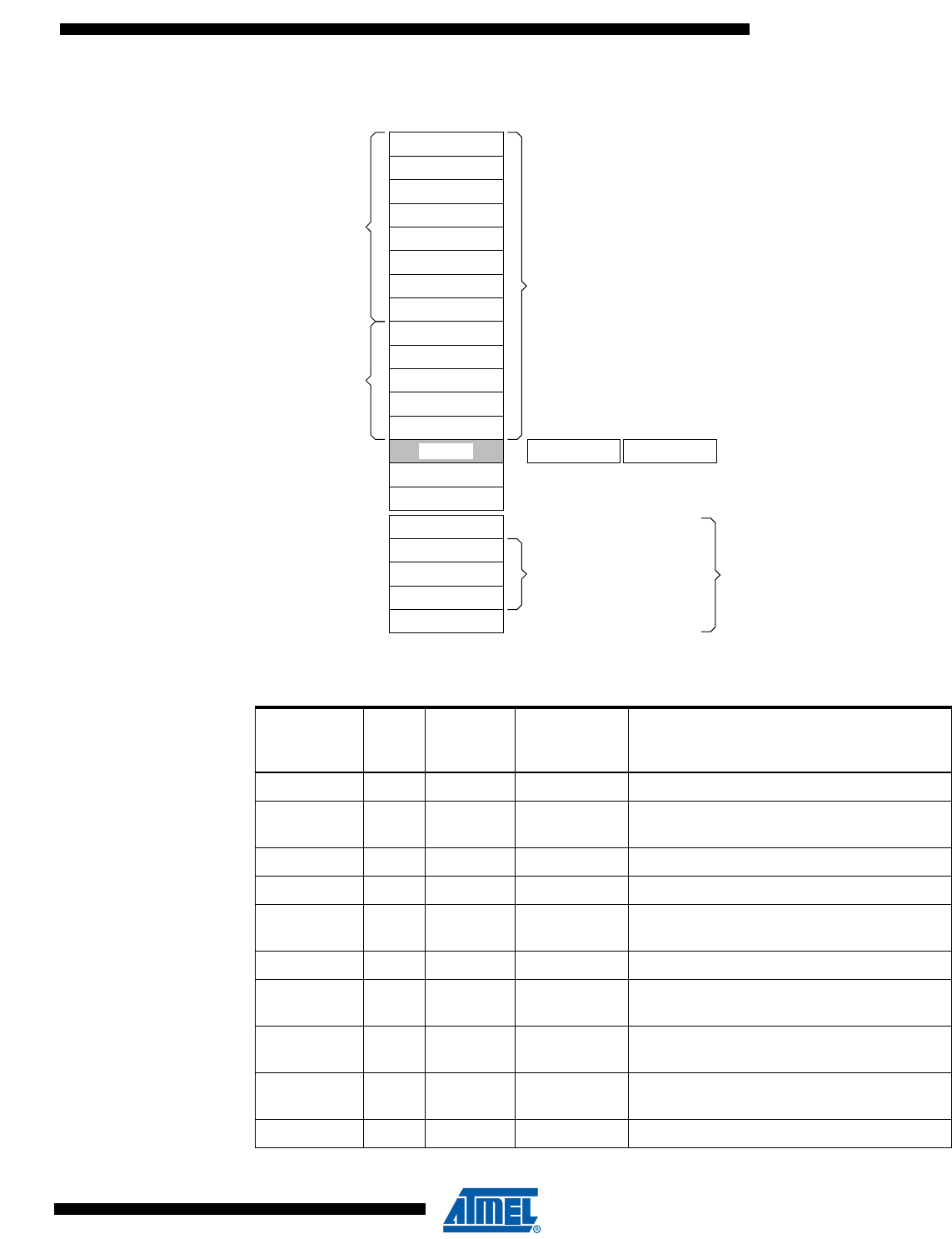
57
6430F–ATARM–21-Feb-12
SAM3U Series
13.3.3 Core registers
The processor core registers are:
Table 13-2. Core register set summary
Name
Type
(1)
Required
privilege
(2)
Reset
value Description
R0-R12 RW Either Unknown “General-purpose registers” on page 58
MSP RW Privileged See
description “Stack Pointer” on page 58
PSP RW Either Unknown “Stack Pointer” on page 58
LR RW Either 0xFFFFFFFF “Link Register” on page 58
PC RW Either See
description “Program Counter” on page 58
PSR RW Privileged
0x01000000
“Program Status Register” on page 59
ASPR RW Either 0x00000000 “Application Program Status Register” on
page 60
IPSR RO Privileged 0x00000000 “Interrupt Program Status Register” on page
61
EPSR RO Privileged 0x01000000 “Execution Program Status Register” on page
62
PRIMASK RW Privileged 0x00000000 “Priority Mask Register” on page 63
SP (R13)
LR (R14)
PC (R15)
R5
R6
R7
R0
R1
R3
R4
R2
R10
R11
R12
R8
R9
Low registers
High registers
MSP‡
PSP‡
PSR
PRIMASK
FAULTMASK
BASEPRI
CONTROL
General-purpose registers
Stack Pointer
Link Register
Program Counter
Program status register
Exception mask registers
CONTROL register
Special registers
‡Banked version of SP

58
6430F–ATARM–21-Feb-12
SAM3U Series
13.3.3.1 General-purpose registers
R0-R12 are 32-bit general-purpose registers for data operations.
13.3.3.2 Stack Pointer
The Stack Pointer (SP) is register R13. In Thread mode, bit[1] of the CONTROL register indi-
cates the stack pointer to use:
•0 = Main Stack Pointer (MSP). This is the reset value.
•1 = Process Stack Pointer (PSP).
On reset, the processor loads the MSP with the value from address
0x00000000
.
13.3.3.3 Link Register
The Link Register (LR) is register R14. It stores the return information for subroutines, function
calls, and exceptions. On reset, the processor loads the LR value
0xFFFFFFFF
.
13.3.3.4 Program Counter
The Program Counter (PC) is register R15. It contains the current program address. Bit[0] is
always 0 because instruction fetches must be halfword aligned. On reset, the processor loads
the PC with the value of the reset vector, which is at address
0x00000004
.
FAULTMASK RW Privileged 0x00000000 “Fault Mask Register” on page 63
BASEPRI RW Privileged 0x00000000 “Base Priority Mask Register” on page 64
CONTROL RW Privileged 0x00000000 “CONTROL register” on page 65
1. Describes access type during program execution in thread mode and Handler mode. Debug
access can differ.
2. An entry of Either means privileged and unprivileged software can access the register.
Table 13-2. Core register set summary (Continued)
Name
Type
(1)
Required
privilege
(2)
Reset
value Description
59
6430F–ATARM–21-Feb-12
SAM3U Series
13.3.3.5 Program Status Register
The Program Status Register (PSR) combines:
•Application Program Status Register (APSR)
•Interrupt Program Status Register (IPSR)
•Execution Program Status Register (EPSR).
These registers are mutually exclusive bitfields in the 32-bit PSR. The bit assignments are:
• APSR:
• IPSR:
• EPSR:
31 30 29 28 27 26 25 24
N Z C V Q Reserved
23 22 21 20 19 18 17 16
Reserved
15 14 13 12 11 10 9 8
Reserved
76543210
Reserved
31 30 29 28 27 26 25 24
Reserved
23 22 21 20 19 18 17 16
Reserved
15 14 13 12 11 10 9 8
Reserved ISR_NUMBER
76543210
ISR_NUMBER
31 30 29 28 27 26 25 24
Reserved ICI/IT T
23 22 21 20 19 18 17 16
Reserved
15 14 13 12 11 10 9 8
ICI/IT Reserved
76543210
Reserved
60
6430F–ATARM–21-Feb-12
SAM3U Series
The PSR bit assignments are:
Access these registers individually or as a combination of any two or all three registers, using
the register name as an argument to the MSR or MRS instructions. For example:
• read all of the registers using PSR with the MRS instruction
• write to the APSR using APSR with the MSR instruction.
The PSR combinations and attributes are:
See the instruction descriptions “MRS” on page 157 and “MSR” on page 158 for more informa-
tion about how to access the program status registers.
13.3.3.6 Application Program Status Register
The APSR contains the current state of the condition flags from previous instruction executions.
See the register summary in Table 13-2 on page 57 for its attributes. The bit assignments are:
•N
Negative or less than flag:
0 = operation result was positive, zero, greater than, or equal
1 = operation result was negative or less than.
•Z
Zero flag:
0 = operation result was not zero
1 = operation result was zero.
31 30 29 28 27 26 25 24
N Z C V Q ICI/IT T
23 22 21 20 19 18 17 16
Reserved
15 14 13 12 11 10 9 8
ICI/IT Reserved ISR_NUMBER
76543210
ISR_NUMBER
Table 13-3. PSR register combinations
Register Type Combination
PSR RW (1), (2)
1. The processor ignores writes to the IPSR bits.
2. Reads of the EPSR bits return zero, and the proces-
sor ignores writes to the these bits.
APSR, EPSR, and IPSR
IEPSR RO EPSR and IPSR
IAPSR RW(1) APSR and IPSR
EAPSR RW(2) APSR and EPSR

61
6430F–ATARM–21-Feb-12
SAM3U Series
•C
Carry or borrow flag:
0 = add operation did not result in a carry bit or subtract operation resulted in a borrow bit
1 = add operation resulted in a carry bit or subtract operation did not result in a borrow bit.
•V
Overflow flag:
0 = operation did not result in an overflow
1 = operation resulted in an overflow.
•Q
Sticky saturation flag:
0 = indicates that saturation has not occurred since reset or since the bit was last cleared to zero
1 = indicates when an
SSAT
or
USAT
instruction results in saturation.
This bit is cleared to zero by software using an
MRS
instruction.
13.3.3.7 Interrupt Program Status Register
The IPSR contains the exception type number of the current Interrupt Service Routine (ISR).
See the register summary in Table 13-2 on page 57 for its attributes. The bit assignments are:
•ISR_NUMBER
This is the number of the current exception:
0 = Thread mode
1 = Reserved
2 = NMI
3 = Hard fault
4 = Memory management fault
5 = Bus fault
6 = Usage fault
7-10 = Reserved
11 = SVCall
12 = Reserved for Debug
13 = Reserved
14 = PendSV
15 = SysTick
16 = IRQ0
45 = IRQ29
see “Exception types” on page 77 for more information.

62
6430F–ATARM–21-Feb-12
SAM3U Series
13.3.3.8 Execution Program Status Register
The EPSR contains the Thumb state bit, and the execution state bits for either the:
•If-Then (IT) instruction
•Interruptible-Continuable Instruction (ICI) field for an interrupted load multiple or store
multiple instruction.
See the register summary in Table 13-2 on page 57 for the EPSR attributes. The bit assign-
ments are:
•ICI
Interruptible-continuable instruction bits, see “Interruptible-continuable instructions” on page 62.
•IT
Indicates the execution state bits of the
IT
instruction, see “IT” on page 147.
•T
Always set to 1.
Attempts to read the EPSR directly through application software using the MSR instruction
always return zero. Attempts to write the EPSR using the MSR instruction in application software
are ignored. Fault handlers can examine EPSR value in the stacked PSR to indicate the opera-
tion that is at fault. See “Exception entry and return” on page 82
13.3.3.9 Interruptible-continuable instructions
When an interrupt occurs during the execution of an LDM or STM instruction, the processor:
• stops the load multiple or store multiple instruction operation temporarily
• stores the next register operand in the multiple operation to EPSR bits[15:12].
After servicing the interrupt, the processor:
• returns to the register pointed to by bits[15:12]
• resumes execution of the multiple load or store instruction.
When the EPSR holds ICI execution state, bits[26:25,11:10] are zero.
13.3.3.10 If-Then block
The If-Then block contains up to four instructions following a 16-bit IT instruction. Each instruc-
tion in the block is conditional. The conditions for the instructions are either all the same, or
some can be the inverse of others. See “IT” on page 147 for more information.
13.3.3.11 Exception mask registers
The exception mask registers disable the handling of exceptions by the processor. Disable
exceptions where they might impact on timing critical tasks.
To access the exception mask registers use the MSR and MRS instructions, or the CPS instruc-
tion to change the value of PRIMASK or FAULTMASK. See “MRS” on page 157, “MSR” on page
158, and “CPS” on page 153 for more information.
63
6430F–ATARM–21-Feb-12
SAM3U Series
13.3.3.12 Priority Mask Register
The PRIMASK register prevents activation of all exceptions with configurable priority. See the
register summary in Table 13-2 on page 57 for its attributes. The bit assignments are:
•PRIMASK
0 = no effect
1 = prevents the activation of all exceptions with configurable priority.
13.3.3.13 Fault Mask Register
The FAULTMASK register prevents activation of all exceptions. See the register summary in
Table 13-2 on page 57 for its attributes. The bit assignments are:
•FAULTMASK
0 = no effect
1 = prevents the activation of all exceptions.
The processor clears the FAULTMASK bit to 0 on exit from any exception handler except the NMI handler.
31 30 29 28 27 26 25 24
Reserved
23 22 21 20 19 18 17 16
Reserved
15 14 13 12 11 10 9 8
Reserved
76543210
Reserved PRIMASK
31 30 29 28 27 26 25 24
Reserved
23 22 21 20 19 18 17 16
Reserved
15 14 13 12 11 10 9 8
Reserved
76543210
Reserved FAULTMASK

64
6430F–ATARM–21-Feb-12
SAM3U Series
13.3.3.14 Base Priority Mask Register
The BASEPRI register defines the minimum priority for exception processing. When BASEPRI is
set to a nonzero value, it prevents the activation of all exceptions with same or lower priority
level as the BASEPRI value. See the register summary in Table 13-2 on page 57 for its attri-
butes. The bit assignments are:
• BASEPRI
Priority mask bits:
0x0000
= no effect
Nonzero = defines the base priority for exception processing.
The processor does not process any exception with a priority value greater than or equal to BASEPRI.
This field is similar to the priority fields in the interrupt priority registers. The processor implements only bits[7:4] of this field,
bits[3:0] read as zero and ignore writes. See “Interrupt Priority Registers” on page 172 for more information. Remember
that higher priority field values correspond to lower exception priorities.
31 30 29 28 27 26 25 24
Reserved
23 22 21 20 19 18 17 16
Reserved
15 14 13 12 11 10 9 8
Reserved
76543210
BASEPRI

65
6430F–ATARM–21-Feb-12
SAM3U Series
13.3.3.15 CONTROL register
The CONTROL register controls the stack used and the privilege level for software execution
when the processor is in Thread mode. See the register summary in Table 13-2 on page 57 for
its attributes. The bit assignments are:
• Active stack pointer
Defines the current stack:
0 = MSP is the current stack pointer
1 = PSP is the current stack pointer.
In Handler mode this bit reads as zero and ignores writes.
• Thread mode privilege level
Defines the Thread mode privilege level:
0 = privileged
1 = unprivileged.
Handler mode always uses the MSP, so the processor ignores explicit writes to the active stack pointer bit of the CON-
TROL register when in Handler mode. The exception entry and return mechanisms update the CONTROL register.
In an OS environment, ARM recommends that threads running in Thread mode use the process stack and the kernel and
exception handlers use the main stack.
By default, Thread mode uses the MSP. To switch the stack pointer used in Thread mode to the PSP, use the MSR instruc-
tion to set the Active stack pointer bit to 1, see “MSR” on page 158.
When changing the stack pointer, software must use an ISB instruction immediately after the MSR instruction. This
ensures that instructions after the ISB execute using the new stack pointer. See “ISB” on page 156
31 30 29 28 27 26 25 24
Reserved
23 22 21 20 19 18 17 16
Reserved
15 14 13 12 11 10 9 8
Reserved
76543210
Reserved Active Stack
Pointer
Thread Mode
Privilege
Level

66
6430F–ATARM–21-Feb-12
SAM3U Series
13.3.4 Exceptions and interrupts
The Cortex-M3 processor supports interrupts and system exceptions. The processor and the
Nested Vectored Interrupt Controller (NVIC) prioritize and handle all exceptions. An exception
changes the normal flow of software control. The processor uses handler mode to handle all
exceptions except for reset. See “Exception entry” on page 83 and “Exception return” on page
84 for more information.
The NVIC registers control interrupt handling. See “Nested Vectored Interrupt Controller” on
page 165 for more information.
13.3.5 Data types
The processor:
• supports the following data types:
– 32-bit words
– 16-bit halfwords
– 8-bit bytes
• supports 64-bit data transfer instructions.
• manages all data memory accesses as little-endian. Instruction memory and Private
Peripheral Bus (PPB) accesses are always little-endian. See “Memory regions, types and
attributes” on page 68 for more information.
13.3.6 The Cortex Microcontroller Software Interface Standard
For a Cortex-M3 microcontroller system, the Cortex Microcontroller Software Interface Standard
(CMSIS) defines:
• a common way to:
– access peripheral registers
– define exception vectors
• the names of:
– the registers of the core peripherals
– the core exception vectors
• a device-independent interface for RTOS kernels, including a debug channel.
The CMSIS includes address definitions and data structures for the core peripherals in the Cor-
tex-M3 processor. It also includes optional interfaces for middleware components comprising a
TCP/IP stack and a Flash file system.
CMSIS simplifies software development by enabling the reuse of template code and the combi-
nation of CMSIS-compliant software components from various middleware vendors. Software
vendors can expand the CMSIS to include their peripheral definitions and access functions for
those peripherals.
This document includes the register names defined by the CMSIS, and gives short descriptions
of the CMSIS functions that address the processor core and the core peripherals.
This document uses the register short names defined by the CMSIS. In a few cases these differ
from the architectural short names that might be used in other documents.
The following sections give more information about the CMSIS:
•“Power management programming hints” on page 88

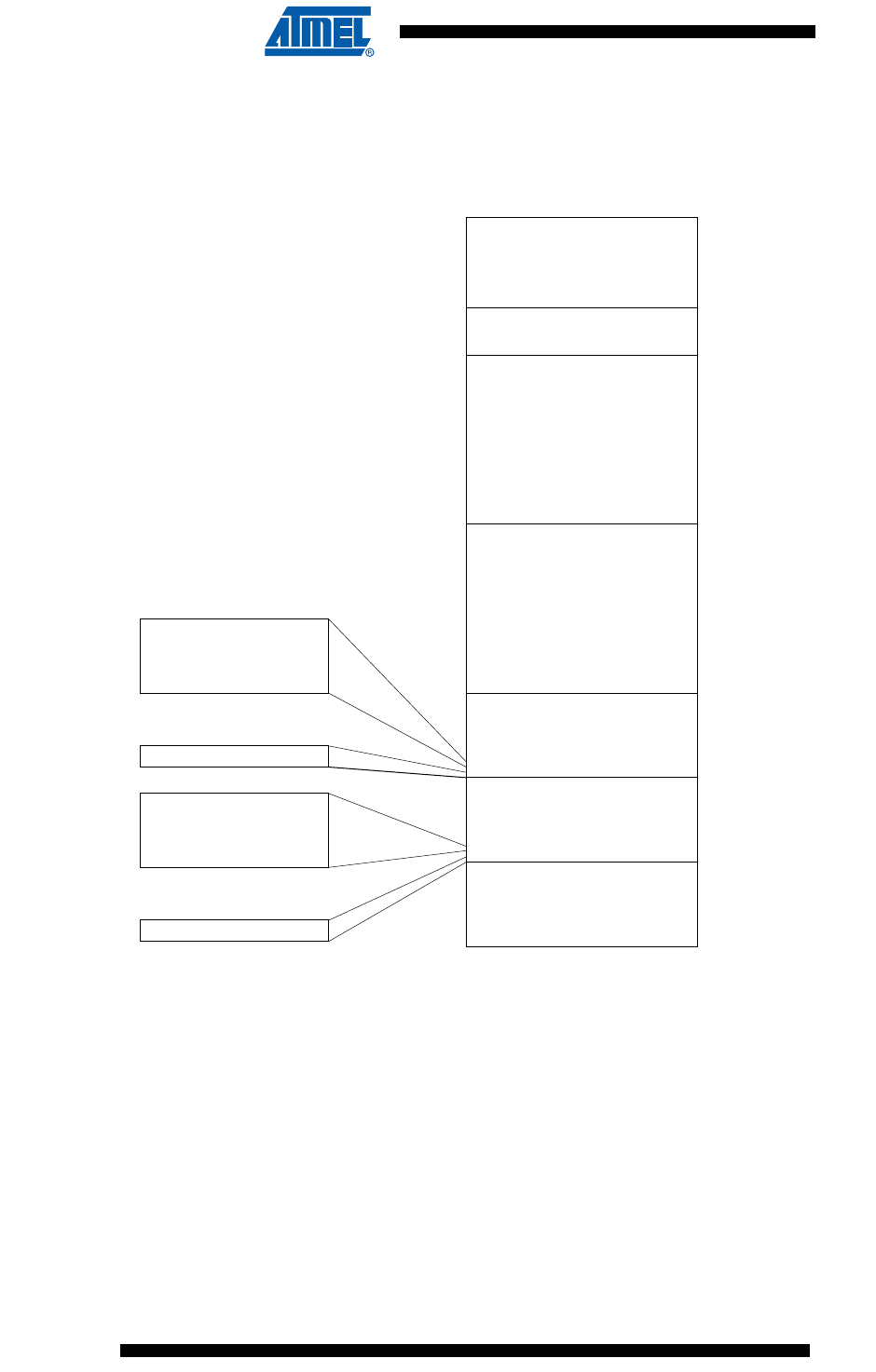
68
6430F–ATARM–21-Feb-12
SAM3U Series
13.4 Memory model
This section describes the processor memory map, the behavior of memory accesses, and the
bit-banding features. The processor has a fixed memory map that provides up to 4GB of
addressable memory. The memory map is:
The regions for SRAM and peripherals include bit-band regions. Bit-banding provides atomic
operations to bit data, see “Bit-banding” on page 72.
The processor reserves regions of the Private peripheral bus (PPB) address range for core
peripheral registers, see “About the Cortex-M3 peripherals” on page 164.
This memory mapping is generic to ARM Cortex-M3 products. To get the specific memory map-
ping of this product, refer to the Memories section of the datasheet.
13.4.1 Memory regions, types and attributes
The memory map and the programming of the MPU split the memory map into regions. Each
region has a defined memory type, and some regions have additional memory attributes. The
memory type and attributes determine the behavior of accesses to the region.
The memory types are:
Vendor-specific
memory
External device
External RAM
Peripheral
SRAM
Code
0xFFFFFFFF
Private peripheral
bus
0xE0100000
0xE00FFFFF
0x9FFFFFFF
0xA0000000
0x5FFFFFFF
0x60000000
0x3FFFFFFF
0x40000000
0x1FFFFFFF
0x20000000
0x00000000
0x40000000 Bit band region
Bit band alias
32MB
1MB
0x400FFFFF
0x42000000
0x43FFFFFF
Bit band region
Bit band alias
32MB
1MB
0x20000000
0x200FFFFF
0x22000000
0x23FFFFFF
1.0GB
1.0GB
0.5GB
0.5GB
0.5GB
0xDFFFFFFF
0xE0000000
1.0MB
511MB

69
6430F–ATARM–21-Feb-12
SAM3U Series
13.4.1.1 Normal
The processor can re-order transactions for efficiency, or perform speculative reads.
13.4.1.2 Device
The processor preserves transaction order relative to other transactions to Device or Strongly-
ordered memory.
13.4.1.3 Strongly-ordered
The processor preserves transaction order relative to all other transactions.
The different ordering requirements for Device and Strongly-ordered memory mean that the
memory system can buffer a write to Device memory, but must not buffer a write to Strongly-
ordered memory.
The additional memory attributes include.
13.4.1.4 Shareable
For a shareable memory region, the memory system provides data synchronization between
bus masters in a system with multiple bus masters, for example, a processor with a DMA
controller.
Strongly-ordered memory is always shareable.
If multiple bus masters can access a non-shareable memory region, software must ensure data
coherency between the bus masters.
13.4.1.5 Execute Never (XN)
Means the processor prevents instruction accesses. Any attempt to fetch an instruction from an
XN region causes a memory management fault exception.
13.4.2 Memory system ordering of memory accesses
For most memory accesses caused by explicit memory access instructions, the memory system
does not guarantee that the order in which the accesses complete matches the program order of
the instructions, providing this does not affect the behavior of the instruction sequence. Nor-
mally, if correct program execution depends on two memory accesses completing in program
order, software must insert a memory barrier instruction between the memory access instruc-
tions, see “Software ordering of memory accesses” on page 71.
However, the memory system does guarantee some ordering of accesses to Device and
Strongly-ordered memory. For two memory access instructions A1 and A2, if A1 occurs before
A2 in program order, the ordering of the memory accesses caused by two instructions is:
Where:
- Means that the memory system does not guarantee the ordering of the accesses.
Normal access
Device access, non-shareable
Device access, shareable
Strongly-ordered access
Normal
access Non-shareable Shareable
Strongly-
ordered
access
Device access
A1
A2
-
-
-
-
-
<
-
<
-
-
<
<
-
<
<
<

70
6430F–ATARM–21-Feb-12
SAM3U Series
< Means that accesses are observed in program order, that is, A1 is always observed before A2.
13.4.3 Behavior of memory accesses
The behavior of accesses to each region in the memory map is:
The Code, SRAM, and external RAM regions can hold programs. However, ARM recommends
that programs always use the Code region. This is because the processor has separate buses
that enable instruction fetches and data accesses to occur simultaneously.
The MPU can override the default memory access behavior described in this section. For more
information, see “Memory protection unit” on page 210.
13.4.3.1 Additional memory access constraints for shared memory
When a system includes shared memory, some memory regions have additional access con-
straints, and some regions are subdivided, as Table 13-5 shows:
Table 13-4. Memory access behavior
Address
range
Memory
region
Memory
type XN Description
0x00000000
-
0x1FFFFFFF
Code Normal (1)
1. See “Memory regions, types and attributes” on page 68 for more information.
-Executable region for program code. You can also put
data here.
0x20000000
-
0x3FFFFFFF
SRAM Normal(1) -
Executable region for data. You can also put code
here.
This region includes bit band and bit band alias areas,
see Table 13-6 on page 72.
0x40000000
-
0x5FFFFFFF
Peripheral Device(1) XN This region includes bit band and bit band alias areas,
see Table 13-6 on page 72.
0x60000000
-
0x9FFFFFFF
External
RAM Normal(1) - Executable region for data.
0xA0000000
-
0xDFFFFFFF
External
device Device(1) XN External Device memory
0xE0000000
-
0xE00FFFFF
Private
Peripheral
Bus
Strongly-
ordered(1) XN This region includes the NVIC, System timer, and
system control block.
0xE0100000
-
0xFFFFFFFF
Reserved Device(1) XN Reserved
Table 13-5. Memory region share ability policies
Address range Memory region Memory type Shareability
0x00000000
-
0x1FFFFFFF
Code Normal (1) -
0x20000000
-
0x3FFFFFFF
SRAM Normal(1) -
0x40000000
-
0x5FFFFFFF
Peripheral (2) Device(1) -

71
6430F–ATARM–21-Feb-12
SAM3U Series
13.4.4 Software ordering of memory accesses
The order of instructions in the program flow does not always guarantee the order of the corre-
sponding memory transactions. This is because:
• the processor can reorder some memory accesses to improve efficiency, providing this does
not affect the behavior of the instruction sequence.
• the processor has multiple bus interfaces
• memory or devices in the memory map have different wait states
• some memory accesses are buffered or speculative.
“Memory system ordering of memory accesses” on page 69 describes the cases where the
memory system guarantees the order of memory accesses. Otherwise, if the order of memory
accesses is critical, software must include memory barrier instructions to force that ordering. The
processor provides the following memory barrier instructions:
13.4.4.1
DMB
The Data Memory Barrier (DMB) instruction ensures that outstanding memory transactions com-
plete before subsequent memory transactions. See “DMB” on page 154.
13.4.4.2
DSB
The Data Synchronization Barrier (DSB) instruction ensures that outstanding memory transac-
tions complete before subsequent instructions execute. See “DSB” on page 155.
13.4.4.3
ISB
The Instruction Synchronization Barrier (ISB) ensures that the effect of all completed memory
transactions is recognizable by subsequent instructions. See “ISB” on page 156.
Use memory barrier instructions in, for example:
• MPU programming:
– Use a DSB instruction to ensure the effect of the MPU takes place immediately at
the end of context switching.
0x60000000
-
0x7FFFFFFF
External RAM Normal(1) -
WBWA(2)
0x80000000
-
0x9FFFFFFF
WT(2)
0xA0000000
-
0xBFFFFFFF
External device Device(1)
Shareable(1)
-
0xC0000000
-
0xDFFFFFFF
Non-
shareable(1)
0xE0000000
-
0xE00FFFFF
Private Peripheral
Bus
Strongly-
ordered(1) Shareable(1) -
0xE0100000
-
0xFFFFFFFF
Vendor-specific
device(2) Device(1) --
1. See “Memory regions, types and attributes” on page 68 for more information.
2. The Peripheral and Vendor-specific device regions have no additional access constraints.
Table 13-5. Memory region share ability policies (Continued)
Address range Memory region Memory type Shareability

72
6430F–ATARM–21-Feb-12
SAM3U Series
– Use an ISB instruction to ensure the new MPU setting takes effect immediately after
programming the MPU region or regions, if the MPU configuration code was
accessed using a branch or call. If the MPU configuration code is entered using
exception mechanisms, then an ISB instruction is not required.
• Vector table. If the program changes an entry in the vector table, and then enables the
corresponding exception, use a DMB instruction between the operations. This ensures that if
the exception is taken immediately after being enabled the processor uses the new exception
vector.
• Self-modifying code. If a program contains self-modifying code, use an ISB instruction
immediately after the code modification in the program. This ensures subsequent instruction
execution uses the updated program.
• Memory map switching. If the system contains a memory map switching mechanism, use a
DSB instruction after switching the memory map in the program. This ensures subsequent
instruction execution uses the updated memory map.
• Dynamic exception priority change. When an exception priority has to change when the
exception is pending or active, use DSB instructions after the change. This ensures the
change takes effect on completion of the DSB instruction.
• Using a semaphore in multi-master system. If the system contains more than one bus
master, for example, if another processor is present in the system, each processor must use
a DMB instruction after any semaphore instructions, to ensure other bus masters see the
memory transactions in the order in which they were executed.
Memory accesses to Strongly-ordered memory, such as the system control block, do not require
the use of DMB instructions.
13.4.5 Bit-banding
A bit-band region maps each word in a bit-band alias region to a single bit in the bit-band region.
The bit-band regions occupy the lowest 1MB of the SRAM and peripheral memory regions.
The memory map has two 32MB alias regions that map to two 1MB bit-band regions:
• accesses to the 32MB SRAM alias region map to the 1MB SRAM bit-band region, as shown
in Table 13-6
• accesses to the 32MB peripheral alias region map to the 1MB peripheral bit-band region, as
shown in Table 13-7.
Table 13-6. SRAM memory bit-banding regions
Address
range
Memory
region Instruction and data accesses
0x20000000
-
0x200FFFFF
SRAM bit-band
region
Direct accesses to this memory range behave as SRAM
memory accesses, but this region is also bit addressable
through bit-band alias.
0x22000000
-
0x23FFFFFF SRAM bit-band alias
Data accesses to this region are remapped to bit band
region. A write operation is performed as read-modify-write.
Instruction accesses are not remapped.

73
6430F–ATARM–21-Feb-12
SAM3U Series
A word access to the SRAM or peripheral bit-band alias regions map to a single bit in the SRAM
or peripheral bit-band region.
The following formula shows how the alias region maps onto the bit-band region:
bit_word_offset = (byte_offset x 32) + (bit_number x 4)
bit_word_addr = bit_band_base + bit_word_offset
where:
•
Bit_word_offset
is the position of the target bit in the bit-band memory region.
•
Bit_word_addr
is the address of the word in the alias memory region that maps to the
targeted bit.
•
Bit_band_base
is the starting address of the alias region.
•
Byte_offset
is the number of the byte in the bit-band region that contains the targeted bit.
•
Bit_number
is the bit position, 0-7, of the targeted bit.
Figure 13-2 shows examples of bit-band mapping between the SRAM bit-band alias region and
the SRAM bit-band region:
• The alias word at
0x23FFFFE0
maps to bit[0] of the bit-band byte at
0x200FFFFF
:
0x23FFFFE0
=
0x22000000
+ (
0xFFFFF
*32) + (0*4).
• The alias word at
0x23FFFFFC
maps to bit[7] of the bit-band byte at
0x200FFFFF
:
0x23FFFFFC
=
0x22000000
+ (
0xFFFFF
*32) + (7*4).
• The alias word at
0x22000000
maps to bit[0] of the bit-band byte at
0x20000000
:
0x22000000
=
0x22000000
+ (0*32) + (0 *4).
• The alias word at
0x2200001C
maps to bit[7] of the bit-band byte at
0x20000000
:
0x2200001C
=
0x22000000
+ (0*32) + (7*4).
Table 13-7. Peripheral memory bit-banding regions
Address
range
Memory
region Instruction and data accesses
0x40000000-
0x400FFFFF
Peripheral bit-band
alias
Direct accesses to this memory range behave as peripheral
memory accesses, but this region is also bit addressable
through bit-band alias.
0x42000000-
0x43FFFFFF
Peripheral bit-band
region
Data accesses to this region are remapped to bit band
region. A write operation is performed as read-modify-write.
Instruction accesses are not permitted.
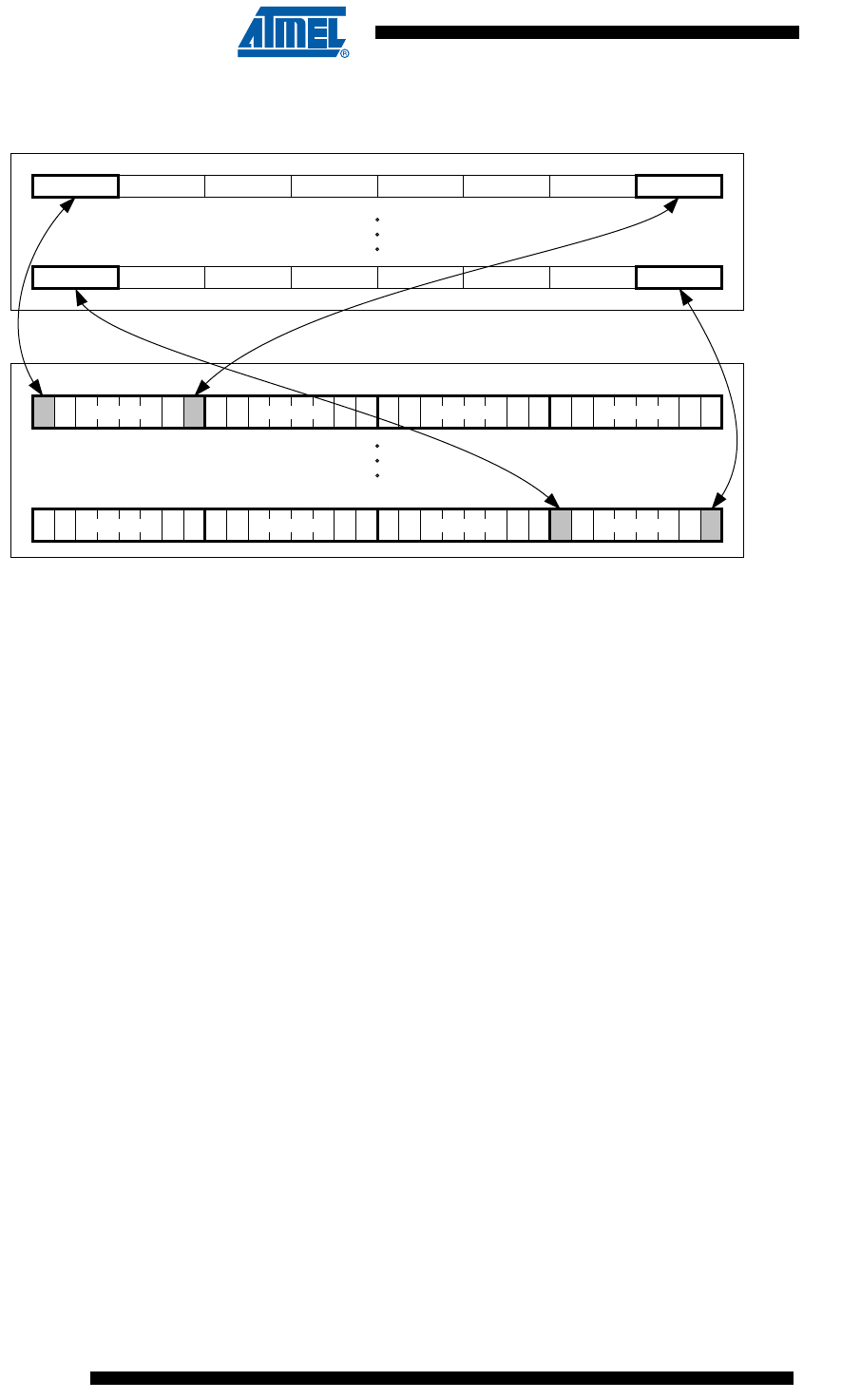
74
6430F–ATARM–21-Feb-12
SAM3U Series
Figure 13-2. Bit-band mapping
13.4.5.1 Directly accessing an alias region
Writing to a word in the alias region updates a single bit in the bit-band region.
Bit[0] of the value written to a word in the alias region determines the value written to the tar-
geted bit in the bit-band region. Writing a value with bit[0] set to 1 writes a 1 to the bit-band bit,
and writing a value with bit[0] set to 0 writes a 0 to the bit-band bit.
Bits[31:1] of the alias word have no effect on the bit-band bit. Writing
0x01
has the same effect as
writing
0xFF
. Writing
0x00
has the same effect as writing
0x0E
.
Reading a word in the alias region:
•
0x00000000
indicates that the targeted bit in the bit-band region is set to zero
•
0x00000001
indicates that the targeted bit in the bit-band region is set to 1
13.4.5.2 Directly accessing a bit-band region
“Behavior of memory accesses” on page 70 describes the behavior of direct byte, halfword, or
word accesses to the bit-band regions.
13.4.6 Memory endianness
The processor views memory as a linear collection of bytes numbered in ascending order from
zero. For example, bytes 0-3 hold the first stored word, and bytes 4-7 hold the second stored
word. or “Little-endian format” describes how words of data are stored in memory.
0x23FFFFE4
0x22000004
0x23FFFFE00x23FFFFE80x23FFFFEC0x23FFFFF00x23FFFFF40x23FFFFF80x23FFFFFC
0x220000000x220000140x220000180x2200001C 0x220000080x22000010 0x2200000C
32MB alias region
0
7 0
07
0x200000000x200000010x200000020x20000003
6 5 4 3 2 1 07 6 5 4 3 2 1 7 6 5 4 3 2 1 07 6 5 4 3 2 1
07 6 5 4 3 2 1 6 5 4 3 2 107 6 5 4 3 2 1 07 6 5 4 3 2 1
0x200FFFFC0x200FFFFD0x200FFFFE0x200FFFFF
1MB SRAM bit-band region

75
6430F–ATARM–21-Feb-12
SAM3U Series
13.4.6.1 Little-endian format
In little-endian format, the processor stores the least significant byte of a word at the lowest-
numbered byte, and the most significant byte at the highest-numbered byte. For example:
13.4.7 Synchronization primitives
The Cortex-M3 instruction set includes pairs of synchronization primitives. These provide a non-
blocking mechanism that a thread or process can use to obtain exclusive access to a memory
location. Software can use them to perform a guaranteed read-modify-write memory update
sequence, or for a semaphore mechanism.
A pair of synchronization primitives comprises:
13.4.7.1 A Load-Exclusive instruction
Used to read the value of a memory location, requesting exclusive access to that location.
13.4.7.2 A Store-Exclusive instruction
Used to attempt to write to the same memory location, returning a status bit to a register. If this
bit is:
0: it indicates that the thread or process gained exclusive access to the memory, and the write
succeeds,
1: it indicates that the thread or process did not gain exclusive access to the memory, and no
write is performed,
The pairs of Load-Exclusive and Store-Exclusive instructions are:
• the word instructions LDREX and STREX
• the halfword instructions LDREXH and STREXH
• the byte instructions LDREXB and STREXB.
Software must use a Load-Exclusive instruction with the corresponding Store-Exclusive
instruction.
To perform a guaranteed read-modify-write of a memory location, software must:
• Use a Load-Exclusive instruction to read the value of the location.
• Update the value, as required.
• Use a Store-Exclusive instruction to attempt to write the new value back to the memory
location, and tests the returned status bit. If this bit is:
0: The read-modify-write completed successfully,
Memory Register
Address A
A+1
lsbyte
msbyte
A+2
A+3
07
B0B1B3 B2
31 24 23 16 15 8 7 0
B0
B1
B2
B3

76
6430F–ATARM–21-Feb-12
SAM3U Series
1: No write was performed. This indicates that the value returned the first step might be out
of date. The software must retry the read-modify-write sequence,
Software can use the synchronization primitives to implement a semaphores as follows:
• Use a Load-Exclusive instruction to read from the semaphore address to check whether the
semaphore is free.
• If the semaphore is free, use a Store-Exclusive to write the claim value to the semaphore
address.
• If the returned status bit from the second step indicates that the Store-Exclusive succeeded
then the software has claimed the semaphore. However, if the Store-Exclusive failed, another
process might have claimed the semaphore after the software performed the first step.
The Cortex-M3 includes an exclusive access monitor, that tags the fact that the processor has
executed a Load-Exclusive instruction. If the processor is part of a multiprocessor system, the
system also globally tags the memory locations addressed by exclusive accesses by each
processor.
The processor removes its exclusive access tag if:
• It executes a CLREX instruction
• It executes a Store-Exclusive instruction, regardless of whether the write succeeds.
• An exception occurs. This means the processor can resolve semaphore conflicts between
different threads.
In a multiprocessor implementation:
• executing a CLREX instruction removes only the local exclusive access tag for the processor
• executing a Store-Exclusive instruction, or an exception. removes the local exclusive access
tags, and all global exclusive access tags for the processor.
For more information about the synchronization primitive instructions, see “LDREX and STREX”
on page 114 and “CLREX” on page 116.
13.4.8 Programming hints for the synchronization primitives
ANSI C cannot directly generate the exclusive access instructions. Some C compilers provide
intrinsic functions for generation of these instructions:
The actual exclusive access instruction generated depends on the data type of the pointer
passed to the intrinsic function. For example, the following C code generates the require
LDREXB operation:
__ldrex((volatile char *) 0xFF);
Table 13-8. C compiler intrinsic functions for exclusive access instructions
Instruction Intrinsic function
LDREX
,
LDREXH
, or
LDREXB
unsigned int __ldrex(volatile void *ptr)
STREX
,
STREXH
, or
STREXB
int __strex(unsigned int val, volatile void *ptr)
CLREX void __clrex(void)

77
6430F–ATARM–21-Feb-12
SAM3U Series
13.5 Exception model
This section describes the exception model.
13.5.1 Exception states
Each exception is in one of the following states:
13.5.1.1 Inactive
The exception is not active and not pending.
13.5.1.2 Pending
The exception is waiting to be serviced by the processor.
An interrupt request from a peripheral or from software can change the state of the correspond-
ing interrupt to pending.
13.5.1.3 Active
An exception that is being serviced by the processor but has not completed.
An exception handler can interrupt the execution of another exception handler. In this case both
exceptions are in the active state.
13.5.1.4 Active and pending
The exception is being serviced by the processor and there is a pending exception from the
same source.
13.5.2 Exception types
The exception types are:
13.5.2.1 Reset
Reset is invoked on power up or a warm reset. The exception model treats reset as a special
form of exception. When reset is asserted, the operation of the processor stops, potentially at
any point in an instruction. When reset is deasserted, execution restarts from the address pro-
vided by the reset entry in the vector table. Execution restarts as privileged execution in Thread
mode.
13.5.2.2 Non Maskable Interrupt (NMI)
A non maskable interrupt (NMI) can be signalled by a peripheral or triggered by software. This is
the highest priority exception other than reset. It is permanently enabled and has a fixed priority
of -2.
NMIs cannot be:
• Masked or prevented from activation by any other exception.
• Preempted by any exception other than Reset.
13.5.2.3 Hard fault
A hard fault is an exception that occurs because of an error during exception processing, or
because an exception cannot be managed by any other exception mechanism. Hard faults have
a fixed priority of -1, meaning they have higher priority than any exception with configurable
priority.

78
6430F–ATARM–21-Feb-12
SAM3U Series
13.5.2.4 Memory management fault
A memory management fault is an exception that occurs because of a memory protection
related fault. The MPU or the fixed memory protection constraints determines this fault, for both
instruction and data memory transactions. This fault is used to abort instruction accesses to
Execute Never (XN) memory regions, even if the MPU is disabled.
13.5.2.5 Bus fault
A bus fault is an exception that occurs because of a memory related fault for an instruction or
data memory transaction. This might be from an error detected on a bus in the memory system.
13.5.2.6 Usage fault
A usage fault is an exception that occurs because of a fault related to instruction execution. This
includes:
• an undefined instruction
• an illegal unaligned access
• invalid state on instruction execution
• an error on exception return.
The following can cause a usage fault when the core is configured to report them:
• an unaligned address on word and halfword memory access
• division by zero.
13.5.2.7 SVCall
A supervisor call (SVC) is an exception that is triggered by the SVC instruction. In an OS envi-
ronment, applications can use SVC instructions to access OS kernel functions and device
drivers.
13.5.2.8 PendSV
PendSV is an interrupt-driven request for system-level service. In an OS environment, use
PendSV for context switching when no other exception is active.
13.5.2.9 SysTick
A SysTick exception is an exception the system timer generates when it reaches zero. Software
can also generate a SysTick exception. In an OS environment, the processor can use this
exception as system tick.

79
6430F–ATARM–21-Feb-12
SAM3U Series
13.5.2.10 Interrupt (IRQ)
A interrupt, or IRQ, is an exception signalled by a peripheral, or generated by a software
request. All interrupts are asynchronous to instruction execution. In the system, peripherals use
interrupts to communicate with the processor.
For an asynchronous exception, other than reset, the processor can execute another instruction
between when the exception is triggered and when the processor enters the exception handler.
Privileged software can disable the exceptions that Table 13-9 on page 79 shows as having con-
figurable priority, see:
•“System Handler Control and State Register” on page 193
Table 13-9. Properties of the different exception types
Exception
number (1)
1. To simplify the software layer, the CMSIS only uses IRQ numbers and therefore uses negative
values for exceptions other than interrupts. The IPSR returns the Exception number, see
“Interrupt Program Status Register” on page 61.
IRQ
number(
1)
Exception
type Priority
Vector address
or offset (2)
2. See “Vector table” on page 81 for more information.
Activation
1-Reset -3, the
highest 0x00000004 Asynchronous
2 -14 NMI -2 0x00000008 Asynchronous
3 -13 Hard fault -1 0x0000000C -
4 -12
Memory
management
fault
Configurable
(3)
3. See “System Handler Priority Registers” on page 190.
0x00000010 Synchronous
5-11Bus fault Configurable
(3) 0x00000014
Synchronous when
precise,
asynchronous when
imprecise
6 -10 Usage fault Configurable
(3) 0x00000018 Synchronous
7-10 - - - Reserved -
11 -5 SVCall Configurable
(3) 0x0000002C Synchronous
12-13 - - - Reserved -
14 -2 PendSV Configurable
(3) 0x00000038 Asynchronous
15 -1 SysTick Configurable
(3)
0x0000003C
Asynchronous
16 and
above
0 and
above (4)
4. See the “Peripheral Identifiers” section of the datasheet.
Interrupt (IRQ) Configurable
(5)
5. See “Interrupt Priority Registers” on page 172.
0x00000040
and
above (6)
6. Increasing in steps of 4.
Asynchronous

80
6430F–ATARM–21-Feb-12
SAM3U Series
•“Interrupt Clear-enable Registers” on page 168.
For more information about hard faults, memory management faults, bus faults, and usage
faults, see “Fault handling” on page 84.
13.5.3 Exception handlers
The processor handles exceptions using:
13.5.3.1 Interrupt Service Routines (ISRs)
Interrupts IRQ0 to IRQ29 are the exceptions handled by ISRs.
13.5.3.2 Fault handlers
Hard fault, memory management fault, usage fault, bus fault are fault exceptions handled by the
fault handlers.
13.5.3.3 System handlers
NMI, PendSV, SVCall SysTick, and the fault exceptions are all system exceptions that are han-
dled by system handlers.
13.5.4 Vector table
The vector table contains the reset value of the stack pointer, and the start addresses, also
called exception vectors, for all exception handlers. Figure 13-3 on page 81 shows the order of
the exception vectors in the vector table. The least-significant bit of each vector must be 1, indi-
cating that the exception handler is Thumb code.

81
6430F–ATARM–21-Feb-12
SAM3U Series
Figure 13-3. Vector table
On system reset, the vector table is fixed at address
0x00000000
. Privileged software can write to
the VTOR to relocate the vector table start address to a different memory location, in the range
0x00000080
to
0x3FFFFF80
, see “Vector Table Offset Register” on page 184.
13.5.5 Exception priorities
As Table 13-9 on page 79 shows, all exceptions have an associated priority, with:
• a lower priority value indicating a higher priority
• configurable priorities for all exceptions except Reset, Hard fault.
If software does not configure any priorities, then all exceptions with a configurable priority have
a priority of 0. For information about configuring exception priorities see
•“System Handler Priority Registers” on page 190
•“Interrupt Priority Registers” on page 172.
Initial SP value
Reset
Hard fault
Reserved
Memory management fault
Usage fault
Bus fault
0x0000
0x0004
0x0008
0x000C
0x0010
0x0014
0x0018
Reserved
SVCall
PendSV
Reserved for Debug
Systick
IRQ0
Reserved
0x002C
0x0038
0x003C
0x0040
OffsetException number
2
3
4
5
6
11
12
14
15
16
18
13
7
10
1
Vector
.
.
.
8
9
IRQ1
IRQ2
0x0044
IRQ29
17
0x0048
0x004C
45
.
.
.
.
.
.
0x00B4
IRQ number
-14
-13
-12
-11
-10
-5
-2
-1
0
2
1
29

82
6430F–ATARM–21-Feb-12
SAM3U Series
Configurable priority values are in the range 0-15. This means that the Reset, Hard fault, and
NMI exceptions, with fixed negative priority values, always have higher priority than any other
exception.
For example, assigning a higher priority value to IRQ[0] and a lower priority value to IRQ[1]
means that IRQ[1] has higher priority than IRQ[0]. If both IRQ[1] and IRQ[0] are asserted, IRQ[1]
is processed before IRQ[0].
If multiple pending exceptions have the same priority, the pending exception with the lowest
exception number takes precedence. For example, if both IRQ[0] and IRQ[1] are pending and
have the same priority, then IRQ[0] is processed before IRQ[1].
When the processor is executing an exception handler, the exception handler is preempted if a
higher priority exception occurs. If an exception occurs with the same priority as the exception
being handled, the handler is not preempted, irrespective of the exception number. However,
the status of the new interrupt changes to pending.
13.5.6 Interrupt priority grouping
To increase priority control in systems with interrupts, the NVIC supports priority grouping. This
divides each interrupt priority register entry into two fields:
• an upper field that defines the group priority
• a lower field that defines a subpriority within the group.
Only the group priority determines preemption of interrupt exceptions. When the processor is
executing an interrupt exception handler, another interrupt with the same group priority as the
interrupt being handled does not preempt the handler,
If multiple pending interrupts have the same group priority, the subpriority field determines the
order in which they are processed. If multiple pending interrupts have the same group priority
and subpriority, the interrupt with the lowest IRQ number is processed first.
For information about splitting the interrupt priority fields into group priority and subpriority, see
“Application Interrupt and Reset Control Register” on page 185.
13.5.7 Exception entry and return
Descriptions of exception handling use the following terms:
13.5.7.1 Preemption
When the processor is executing an exception handler, an exception can preempt the exception
handler if its priority is higher than the priority of the exception being handled. See “Interrupt pri-
ority grouping” on page 82 for more information about preemption by an interrupt.
When one exception preempts another, the exceptions are called nested exceptions. See
“Exception entry” on page 83 more information.
13.5.7.2 Return
This occurs when the exception handler is completed, and:
• there is no pending exception with sufficient priority to be serviced
• the completed exception handler was not handling a late-arriving exception.
The processor pops the stack and restores the processor state to the state it had before the
interrupt occurred. See “Exception return” on page 84 for more information.

83
6430F–ATARM–21-Feb-12
SAM3U Series
13.5.7.3 Tail-chaining
This mechanism speeds up exception servicing. On completion of an exception handler, if there
is a pending exception that meets the requirements for exception entry, the stack pop is skipped
and control transfers to the new exception handler.
13.5.7.4 Late-arriving
This mechanism speeds up preemption. If a higher priority exception occurs during state saving
for a previous exception, the processor switches to handle the higher priority exception and initi-
ates the vector fetch for that exception. State saving is not affected by late arrival because the
state saved is the same for both exceptions. Therefore the state saving continues uninterrupted.
The processor can accept a late arriving exception until the first instruction of the exception han-
dler of the original exception enters the execute stage of the processor. On return from the
exception handler of the late-arriving exception, the normal tail-chaining rules apply.
13.5.7.5 Exception entry
Exception entry occurs when there is a pending exception with sufficient priority and either:
• the processor is in Thread mode
• the new exception is of higher priority than the exception being handled, in which case the
new exception preempts the original exception.
When one exception preempts another, the exceptions are nested.
Sufficient priority means the exception has more priority than any limits set by the mask regis-
ters, see “Exception mask registers” on page 62. An exception with less priority than this is
pending but is not handled by the processor.
When the processor takes an exception, unless the exception is a tail-chained or a late-arriving
exception, the processor pushes information onto the current stack. This operation is referred as
stacking and the structure of eight data words is referred as stack frame. The stack frame con-
tains the following information:
•R0-R3, R12
• Return address
• PSR
•LR.
Immediately after stacking, the stack pointer indicates the lowest address in the stack frame.
Unless stack alignment is disabled, the stack frame is aligned to a double-word address. If the
STKALIGN bit of the Configuration Control Register (CCR) is set to 1, stack align adjustment is
performed during stacking.
The stack frame includes the return address. This is the address of the next instruction in the
interrupted program. This value is restored to the PC at exception return so that the interrupted
program resumes.
In parallel to the stacking operation, the processor performs a vector fetch that reads the excep-
tion handler start address from the vector table. When stacking is complete, the processor starts
executing the exception handler. At the same time, the processor writes an EXC_RETURN
value to the LR. This indicates which stack pointer corresponds to the stack frame and what
operation mode the was processor was in before the entry occurred.

84
6430F–ATARM–21-Feb-12
SAM3U Series
If no higher priority exception occurs during exception entry, the processor starts executing the
exception handler and automatically changes the status of the corresponding pending interrupt
to active.
If another higher priority exception occurs during exception entry, the processor starts executing
the exception handler for this exception and does not change the pending status of the earlier
exception. This is the late arrival case.
13.5.7.6 Exception return
Exception return occurs when the processor is in Handler mode and executes one of the follow-
ing instructions to load the EXC_RETURN value into the PC:
•a
POP
instruction that includes the PC
•a
BX
instruction with any register.
•an
LDR
or
LDM
instruction with the PC as the destination.
EXC_RETURN is the value loaded into the LR on exception entry. The exception mechanism
relies on this value to detect when the processor has completed an exception handler. The low-
est four bits of this value provide information on the return stack and processor mode. Table 13-
10 shows the EXC_RETURN[3:0] values with a description of the exception return behavior.
The processor sets EXC_RETURN bits[31:4] to
0xFFFFFFF
. When this value is loaded into the PC
it indicates to the processor that the exception is complete, and the processor initiates the
exception return sequence.
13.6 Fault handling
Faults are a subset of the exceptions, see “Exception model” on page 77. The following gener-
ate a fault:
– a bus error on:
– an instruction fetch or vector table load
– a data access
Table 13-10. Exception return behavior
EXC_RETURN[3:0] Description
bXXX0 Reserved.
b0001
Return to Handler mode.
Exception return gets state from MSP.
Execution uses MSP after return.
b0011 Reserved.
b01X1 Reserved.
b1001
Return to Thread mode.
Exception return gets state from MSP.
Execution uses MSP after return.
b1101
Return to Thread mode.
Exception return gets state from PSP.
Execution uses PSP after return.
b1X11 Reserved.

85
6430F–ATARM–21-Feb-12
SAM3U Series
• an internally-detected error such as an undefined instruction or an attempt to change state
with a BX instruction
• attempting to execute an instruction from a memory region marked as Non-Executable (XN).
• an MPU fault because of a privilege violation or an attempt to access an unmanaged region.
13.6.1 Fault types
Table 13-11 shows the types of fault, the handler used for the fault, the corresponding fault sta-
tus register, and the register bit that indicates that the fault has occurred. See “Configurable
Fault Status Register” on page 195 for more information about the fault status registers.
13.6.2 Fault escalation and hard faults
All faults exceptions except for hard fault have configurable exception priority, see “System Han-
dler Priority Registers” on page 190. Software can disable execution of the handlers for these
faults, see “System Handler Control and State Register” on page 193.
Table 13-11. Faults
Fault Handler Bit name Fault status register
Bus error on a vector read Hard fault VECTTBL “Hard Fault Status
Register” on page 201
Fault escalated to a hard fault FORCED
MPU mismatch:
Memory
managem
ent fault
--
on instruction access IACCVIOL (1)
1. Occurs on an access to an XN region even if the MPU is disabled.
“Memory Management
Fault Address Register” on
page 202
on data access DACCVIOL
during exception stacking MSTKERR
during exception unstacking MUNSKERR
Bus error:
Bus fault
--
during exception stacking STKERR
“Bus Fault Status Register”
on page 197
during exception unstacking UNSTKERR
during instruction prefetch IBUSERR
Precise data bus error PRECISERR
Imprecise data bus error IMPRECISER
R
Attempt to access a coprocessor
Usage
fault
NOCP
“Usage Fault Status
Register” on page 199
Undefined instruction UNDEFINSTR
Attempt to enter an invalid instruction
set state (2)
2. Attempting to use an instruction set other than the Thumb instruction set.
INVSTATE
Invalid EXC_RETURN value INVPC
Illegal unaligned load or store UNALIGNED
Divide By 0 DIVBYZERO

86
6430F–ATARM–21-Feb-12
SAM3U Series
Usually, the exception priority, together with the values of the exception mask registers, deter-
mines whether the processor enters the fault handler, and whether a fault handler can preempt
another fault handler. as described in “Exception model” on page 77.
In some situations, a fault with configurable priority is treated as a hard fault. This is called prior-
ity escalation, and the fault is described as escalated to hard fault. Escalation to hard fault
occurs when:
• A fault handler causes the same kind of fault as the one it is servicing. This escalation to hard
fault occurs because a fault handler cannot preempt itself because it must have the same
priority as the current priority level.
• A fault handler causes a fault with the same or lower priority as the fault it is servicing. This is
because the handler for the new fault cannot preempt the currently executing fault handler.
• An exception handler causes a fault for which the priority is the same as or lower than the
currently executing exception.
• A fault occurs and the handler for that fault is not enabled.
If a bus fault occurs during a stack push when entering a bus fault handler, the bus fault does not
escalate to a hard fault. This means that if a corrupted stack causes a fault, the fault handler
executes even though the stack push for the handler failed. The fault handler operates but the
stack contents are corrupted.
Only Reset and NMI can preempt the fixed priority hard fault. A hard fault can preempt any
exception other than Reset, NMI, or another hard fault.
13.6.3 Fault status registers and fault address registers
The fault status registers indicate the cause of a fault. For bus faults and memory management
faults, the fault address register indicates the address accessed by the operation that caused
the fault, as shown in Table 13-12.
13.6.4 Lockup
The processor enters a lockup state if a hard fault occurs when executing the hard fault han-
dlers. When the processor is in lockup state it does not execute any instructions. The processor
remains in lockup state until:
• it is reset
Table 13-12. Fault status and fault address registers
Handler
Status register
name
Address register
name Register description
Hard fault HFSR - “Hard Fault Status Register” on page
201
Memory
management fault MMFSR MMFAR
“Memory Management Fault Status
Register” on page 196
“Memory Management Fault Address
Register” on page 202
Bus fault BFSR BFAR
“Bus Fault Status Register” on page 197
“Bus Fault Address Register” on page
203
Usage fault UFSR - “Usage Fault Status Register” on page
199

87
6430F–ATARM–21-Feb-12
SAM3U Series
13.7 Power management
The Cortex-M3 processor sleep modes reduce power consumption:
• Backup Mode
•Wait Mode
• Sleep Mode
The SLEEPDEEP bit of the SCR selects which sleep mode is used, see “System Control Regis-
ter” on page 187. For more information about the behavior of the sleep modes see “Low Power
Modes” in the PMC section of the datasheet.
This section describes the mechanisms for entering sleep mode, and the conditions for waking
up from sleep mode.
13.7.1 Entering sleep mode
This section describes the mechanisms software can use to put the processor into sleep mode.
The system can generate spurious wakeup events, for example a debug operation wakes up the
processor. Therefore software must be able to put the processor back into sleep mode after
such an event. A program might have an idle loop to put the processor back to sleep mode.
13.7.1.1 Wait for interrupt
The wait for interrupt instruction, WFI, causes immediate entry to sleep mode. When the proces-
sor executes a WFI instruction it stops executing instructions and enters sleep mode. See “WFI”
on page 163 for more information.
13.7.1.2 Wait for event
The wait for event instruction, WFE, causes entry to sleep mode conditional on the value of an
one-bit event register. When the processor executes a WFE instruction, it checks this register:
• if the register is 0 the processor stops executing instructions and enters sleep mode
• if the register is 1 the processor clears the register to 0 and continues executing instructions
without entering sleep mode.
See “WFE” on page 162 for more information.
13.7.1.3 Sleep-on-exit
If the SLEEPONEXIT bit of the SCR is set to 1, when the processor completes the execution of
an exception handler it returns to Thread mode and immediately enters sleep mode. Use this
mechanism in applications that only require the processor to run when an exception occurs.
13.7.2 Wakeup from sleep mode
The conditions for the processor to wakeup depend on the mechanism that cause it to enter
sleep mode.
13.7.2.1 Wakeup from WFI or sleep-on-exit
Normally, the processor wakes up only when it detects an exception with sufficient priority to
cause exception entry.
Some embedded systems might have to execute system restore tasks after the processor
wakes up, and before it executes an interrupt handler. To achieve this set the PRIMASK bit to 1
and the FAULTMASK bit to 0. If an interrupt arrives that is enabled and has a higher priority than
current exception priority, the processor wakes up but does not execute the interrupt handler

88
6430F–ATARM–21-Feb-12
SAM3U Series
until the processor sets PRIMASK to zero. For more information about PRIMASK and FAULT-
MASK see “Exception mask registers” on page 62.
13.7.2.2 Wakeup from WFE
The processor wakes up if:
• it detects an exception with sufficient priority to cause exception entry
In addition, if the SEVONPEND bit in the SCR is set to 1, any new pending interrupt triggers an
event and wakes up the processor, even if the interrupt is disabled or has insufficient priority to
cause exception entry. For more information about the SCR see “System Control Register” on
page 187.
13.7.3 Power management programming hints
ANSI C cannot directly generate the WFI and WFE instructions. The CMSIS provides the follow-
ing intrinsic functions for these instructions:
void __WFE(void) // Wait for Event
void __WFE(void) // Wait for Interrupt

89
6430F–ATARM–21-Feb-12
SAM3U Series
13.8 Instruction set summary
The processor implements a version of the Thumb instruction set. Table 13-13 lists the sup-
ported instructions.
In Table 13-13:
• angle brackets, <>, enclose alternative forms of the operand
• braces, {}, enclose optional operands
• the Operands column is not exhaustive
• Op2 is a flexible second operand that can be either a register or a constant
• most instructions can use an optional condition code suffix.
For more information on the instructions and operands, see the instruction descriptions.
Table 13-13. Cortex-M3 instructions
Mnemonic Operands Brief description Flags Page
ADC, ADCS {Rd,} Rn, Op2 Add with Carry N,Z,C,V page 119
ADD, ADDS {Rd,} Rn, Op2 Add N,Z,C,V page 119
ADD, ADDW {Rd,} Rn, #imm12 Add N,Z,C,V page 119
ADR Rd, label Load PC-relative address - page 102
AND, ANDS {Rd,} Rn, Op2 Logical AND N,Z,C page 122
ASR, ASRS Rd, Rm, <Rs|#n> Arithmetic Shift Right N,Z,C page 124
B label Branch - page 144
BFC Rd, #lsb, #width Bit Field Clear - page 140
BFI Rd, Rn, #lsb, #width Bit Field Insert - page 140
BIC, BICS
{Rd,}
Rn, Op2
Bit Clear N,Z,C page 122
BKPT #imm Breakpoint - page 152
BL label Branch with Link - page 144
BLX Rm Branch indirect with Link - page 144
BX Rm Branch indirect - page 144
CBNZ Rn, label Compare and Branch if Non Zero - page 146
CBZ Rn, label Compare and Branch if Zero - page 146
CLREX - Clear Exclusive - page 116
CLZ Rd, Rm Count leading zeros - page 126
CMN, CMNS Rn, Op2 Compare Negative N,Z,C,V page 127
CMP, CMPS Rn, Op2 Compare N,Z,C,V page 127
CPSID iflags Change Processor State, Disable
Interrupts -page 153
CPSIE iflags Change Processor State, Enable
Interrupts -page 153
DMB - Data Memory Barrier - page 154
DSB - Data Synchronization Barrier - page 155
EOR, EORS {Rd,} Rn, Op2 Exclusive OR N,Z,C page 122

90
6430F–ATARM–21-Feb-12
SAM3U Series
ISB - Instruction Synchronization Barrier - page 156
IT - If-Then condition block - page 147
LDM Rn{!}, reglist Load Multiple registers, increment after - page 111
LDMDB,
LDMEA Rn{!}, reglist Load Multiple registers, decrement
before -page 111
LDMFD,
LDMIA Rn{!}, reglist Load Multiple registers, increment after - page 111
LDR Rt, [Rn, #offset] Load Register with word - page 106
LDRB,
LDRBT Rt, [Rn, #offset] Load Register with byte - page 106
LDRD Rt, Rt2, [Rn, #offset] Load Register with two bytes - page 106
LDREX Rt, [Rn, #offset] Load Register Exclusive - page 106
LDREXB Rt, [Rn] Load Register Exclusive with byte - page 106
LDREXH Rt, [Rn] Load Register Exclusive with halfword - page 106
LDRH,
LDRHT Rt, [Rn, #offset] Load Register with halfword - page 106
LDRSB,
LDRSBT Rt, [Rn, #offset] Load Register with signed byte - page 106
LDRSH,
LDRSHT Rt, [Rn, #offset] Load Register with signed halfword - page 106
LDRT Rt, [Rn, #offset] Load Register with word - page 106
LSL, LSLS Rd, Rm, <Rs|#n> Logical Shift Left N,Z,C page 124
LSR, LSRS Rd, Rm, <Rs|#n> Logical Shift Right N,Z,C page 124
MLA Rd, Rn, Rm, Ra Multiply with Accumulate, 32-bit result - page 134
MLS Rd, Rn, Rm, Ra Multiply and Subtract, 32-bit result - page 134
MOV, MOVS Rd, Op2 Move N,Z,C page 128
MOVT Rd, #imm16 Move Top - page 130
MOVW, MOV Rd, #imm16 Move 16-bit constant N,Z,C page 128
MRS Rd, spec_reg Move from special register to general
register -page 157
MSR spec_reg, Rm Move from general register to special
register N,Z,C,V page 158
MUL, MULS {Rd,} Rn, Rm Multiply, 32-bit result N,Z page 134
MVN, MVNS Rd, Op2 Move NOT N,Z,C page 128
NOP - No Operation - page 159
ORN, ORNS {Rd,} Rn, Op2 Logical OR NOT N,Z,C page 122
ORR, ORRS {Rd,} Rn, Op2 Logical OR N,Z,C page 122
POP reglist Pop registers from stack - page 113
PUSH reglist Push registers onto stack - page 113
Table 13-13. Cortex-M3 instructions (Continued)
Mnemonic Operands Brief description Flags Page

91
6430F–ATARM–21-Feb-12
SAM3U Series
RBIT Rd, Rn Reverse Bits - page 131
REV Rd, Rn Reverse byte order in a word - page 131
REV16 Rd, Rn Reverse byte order in each halfword - page 131
REVSH Rd, Rn Reverse byte order in bottom halfword
and sign extend -page 131
ROR, RORS Rd, Rm, <Rs|#n> Rotate Right N,Z,C page 124
RRX, RRXS Rd, Rm Rotate Right with Extend N,Z,C page 124
RSB, RSBS {Rd,} Rn, Op2 Reverse Subtract N,Z,C,V page 119
SBC, SBCS {Rd,} Rn, Op2 Subtract with Carry N,Z,C,V page 119
SBFX Rd, Rn, #lsb, #width Signed Bit Field Extract - page 141
SDIV {Rd,} Rn, Rm Signed Divide - page 136
SEV - Send Event - page 160
SMLAL RdLo, RdHi, Rn, Rm Signed Multiply with Accumulate (32 x
32 + 64), 64-bit result -page 135
SMULL RdLo, RdHi, Rn, Rm Signed Multiply (32 x 32), 64-bit result - page 135
SSAT Rd, #n, Rm {,shift #s} Signed Saturate Q page 137
STM Rn{!}, reglist Store Multiple registers, increment after - page 111
STMDB,
STMEA Rn{!}, reglist Store Multiple registers, decrement
before -page 111
STMFD,
STMIA Rn{!}, reglist Store Multiple registers, increment after - page 111
STR Rt, [Rn, #offset] Store Register word - page 106
STRB,
STRBT Rt, [Rn, #offset] Store Register byte - page 106
STRD Rt, Rt2, [Rn, #offset] Store Register two words - page 106
STREX Rd, Rt, [Rn, #offset] Store Register Exclusive - page 114
STREXB Rd, Rt, [Rn] Store Register Exclusive byte - page 114
STREXH Rd, Rt, [Rn] Store Register Exclusive halfword - page 114
STRH,
STRHT Rt, [Rn, #offset] Store Register halfword - page 106
STRT Rt, [Rn, #offset] Store Register word - page 106
SUB, SUBS {Rd,} Rn, Op2 Subtract N,Z,C,V page 119
SUB, SUBW {Rd,} Rn, #imm12 Subtract N,Z,C,V page 119
SVC #imm Supervisor Call - page 161
SXTB {Rd,} Rm {,ROR #n} Sign extend a byte - page 142
SXTH {Rd,} Rm {,ROR #n} Sign extend a halfword - page 142
TBB [Rn, Rm] Table Branch Byte - page 149
TBH [Rn, Rm, LSL #1] Table Branch Halfword - page 149
Table 13-13. Cortex-M3 instructions (Continued)
Mnemonic Operands Brief description Flags Page

92
6430F–ATARM–21-Feb-12
SAM3U Series
13.9 Intrinsic functions
ANSI cannot directly access some Cortex-M3 instructions. This section describes intrinsic func-
tions that can generate these instructions, provided by the CMIS and that might be provided by a
C compiler. If a C compiler does not support an appropriate intrinsic function, you might have to
use inline assembler to access some instructions.
The CMSIS provides the following intrinsic functions to generate instructions that ANSI cannot
directly access:
TEQ Rn, Op2 Test Equivalence N,Z,C page 132
TST Rn, Op2 Test N,Z,C page 132
UBFX Rd, Rn, #lsb, #width Unsigned Bit Field Extract - page 141
UDIV {Rd,} Rn, Rm Unsigned Divide - page 136
UMLAL RdLo, RdHi, Rn, Rm Unsigned Multiply with Accumulate
(32 x 32 + 64), 64-bit result -page 135
UMULL RdLo, RdHi, Rn, Rm Unsigned Multiply (32 x 32), 64-bit
result -page 135
USAT Rd, #n, Rm {,shift #s} Unsigned Saturate Q page 137
UXTB {Rd,} Rm {,ROR #n} Zero extend a byte - page 142
UXTH {Rd,} Rm {,ROR #n} Zero extend a halfword - page 142
WFE - Wait For Event - page 162
WFI - Wait For Interrupt - page 163
Table 13-13. Cortex-M3 instructions (Continued)
Mnemonic Operands Brief description Flags Page
Table 13-14. CMSIS intrinsic functions to generate some Cortex-M3 instructions
Instruction CMSIS intrinsic function
CPSIE I void __enable_irq(void)
CPSID I void __disable_irq(void)
CPSIE F void __enable_fault_irq(void)
CPSID F void __disable_fault_irq(void)
ISB void __ISB(void)
DSB void __DSB(void)
DMB void __DMB(void)
REV uint32_t __REV(uint32_t int value)
REV16 uint32_t __REV16(uint32_t int value)
REVSH uint32_t __REVSH(uint32_t int value)
RBIT uint32_t __RBIT(uint32_t int value)
SEV void __SEV(void)
WFE void __WFE(void)
WFI void __WFI(void)
93
6430F–ATARM–21-Feb-12
SAM3U Series
The CMSIS also provides a number of functions for accessing the special registers using MRS
and MSR instructions:
13.10 About the instruction descriptions
The following sections give more information about using the instructions:
•“Operands” on page 93
•“Restrictions when using PC or SP” on page 93
•“Flexible second operand” on page 94
•“Shift Operations” on page 95
•“Address alignment” on page 97
•“PC-relative expressions” on page 98
•“Conditional execution” on page 98
•“Instruction width selection” on page 100.
13.10.1 Operands
An instruction operand can be an ARM register, a constant, or another instruction-specific
parameter. Instructions act on the operands and often store the result in a destination register.
When there is a destination register in the instruction, it is usually specified before the operands.
Operands in some instructions are flexible in that they can either be a register or a constant. See
“Flexible second operand”.
13.10.2 Restrictions when using PC or SP
Many instructions have restrictions on whether you can use the Program Counter (PC) or Stack
Pointer (SP) for the operands or destination register. See instruction descriptions for more
information.
Table 13-15. CMSIS intrinsic functions to access the special registers
Special register Access CMSIS function
PRIMASK Read uint32_t __get_PRIMASK (void)
Write void __set_PRIMASK (uint32_t value)
FAULTMASK Read uint32_t __get_FAULTMASK (void)
Write void __set_FAULTMASK (uint32_t value)
BASEPRI Read uint32_t __get_BASEPRI (void)
Write void __set_BASEPRI (uint32_t value)
CONTROL Read uint32_t __get_CONTROL (void)
Write void __set_CONTROL (uint32_t value)
MSP Read uint32_t __get_MSP (void)
Write void __set_MSP (uint32_t TopOfMainStack)
PSP Read uint32_t __get_PSP (void)
Write void __set_PSP (uint32_t TopOfProcStack)

94
6430F–ATARM–21-Feb-12
SAM3U Series
Bit[0] of any address you write to the PC with a BX, BLX, LDM, LDR, or POP instruction must be
1 for correct execution, because this bit indicates the required instruction set, and the Cortex-M3
processor only supports Thumb instructions.
13.10.3 Flexible second operand
Many general data processing instructions have a flexible second operand. This is shown as
Operand2 in the descriptions of the syntax of each instruction.
Operand2 can be a:
•“Constant”
•“Register with optional shift” on page 94
13.10.3.1 Constant
You specify an Operand2 constant in the form:
#constant
where constant can be:
• any constant that can be produced by shifting an 8-bit value left by any number of bits within
a 32-bit word
• any constant of the form 0x00XY00XY
• any constant of the form 0xXY00XY00
• any constant of the form 0xXYXYXYXY.
In the constants shown above, X and Y are hexadecimal digits.
In addition, in a small number of instructions, constant can take a wider range of values.
These are described in the individual instruction descriptions.
When an Operand2 constant is used with the instructions MOVS, MVNS, ANDS, ORRS, ORNS,
EORS, BICS, TEQ or TST, the carry flag is updated to bit[31] of the constant, if the constant is
greater than 255 and can be produced by shifting an 8-bit value. These instructions do not affect
the carry flag if Operand2 is any other constant.
13.10.3.2 Instruction substitution
Your assembler might be able to produce an equivalent instruction in cases where you specify a
constant that is not permitted. For example, an assembler might assemble the instruction CMP
Rd
, #0xFFFFFFFE as the equivalent instruction CMN Rd, #0x2.
13.10.3.3 Register with optional shift
You specify an Operand2 register in the form:
Rm {, shift}
where:
Rm is the register holding the data for the second operand.
shift is an optional shift to be applied to Rm. It can be one of:
ASR #narithmetic shift right n bits, 1 ≤ n ≤ 32.
LSL #nlogical shift left n bits, 1 ≤ n ≤ 31.
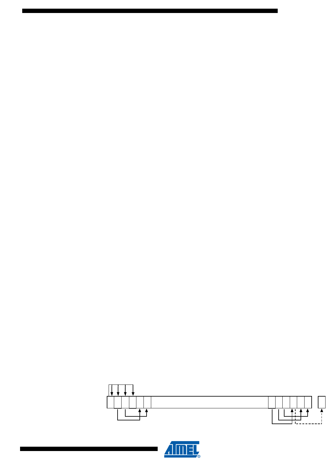
95
6430F–ATARM–21-Feb-12
SAM3U Series
LSR #nlogical shift right n bits, 1 ≤ n ≤ 32.
ROR #nrotate right n bits, 1 ≤ n ≤ 31.
RRX rotate right one bit, with extend.
- if omitted, no shift occurs, equivalent to LSL #0.
If you omit the shift, or specify LSL #0, the instruction uses the value in Rm.
If you specify a shift, the shift is applied to the value in Rm, and the resulting 32-bit value is used
by the instruction. However, the contents in the register Rm remains unchanged. Specifying a
register with shift also updates the carry flag when used with certain instructions. For information
on the shift operations and how they affect the carry flag, see “Shift Operations”
13.10.4 Shift Operations
Register shift operations move the bits in a register left or right by a specified number of bits, the
shift length. Register shift can be performed:
• directly by the instructions ASR, LSR, LSL, ROR, and RRX, and the result is written to a
destination register
• during the calculation of Operand2 by the instructions that specify the second operand as a
register with shift, see “Flexible second operand” on page 94. The result is used by the
instruction.
The permitted shift lengths depend on the shift type and the instruction, see the individual
instruction description or “Flexible second operand” on page 94. If the shift length is 0, no shift
occurs. Register shift operations update the carry flag except when the specified shift length is 0.
The following sub-sections describe the various shift operations and how they affect the carry
flag. In these descriptions, Rm is the register containing the value to be shifted, and n is the shift
length.
13.10.4.1 ASR
Arithmetic shift right by n bits moves the left-hand 32-n bits of the register Rm, to the right by n
places, into the right-hand 32-n bits of the result. And it copies the original bit[31] of the register
into the left-hand n bits of the result. See Figure 13-4 on page 95.
You can use the ASR #n operation to divide the value in the register Rm by 2n, with the result
being rounded towards negative-infinity.
When the instruction is ASRS or when ASR #n is used in Operand2 with the instructions MOVS,
MVNS, ANDS, ORRS, ORNS, EORS, BICS, TEQ or TST, the carry flag is updated to the last bit
shifted out, bit[n-1], of the register Rm.
•If n is 32 or more, then all the bits in the result are set to the value of bit[31] of Rm.
•If n is 32 or more and the carry flag is updated, it is updated to the value of bit[31] of Rm.
Figure 13-4. ASR #3
31 10
Carry
Flag
...
2345
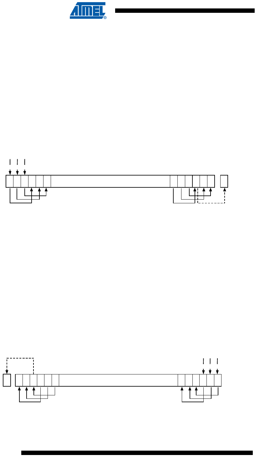
96
6430F–ATARM–21-Feb-12
SAM3U Series
13.10.4.2 LSR
Logical shift right by n bits moves the left-hand 32-n bits of the register Rm, to the right by n
places, into the right-hand 32-n bits of the result. And it sets the left-hand n bits of the result to 0.
See Figure 13-5.
You can use the LSR #n operation to divide the value in the register Rm by 2n, if the value is
regarded as an unsigned integer.
When the instruction is LSRS or when LSR #n is used in Operand2 with the instructions MOVS,
MVNS, ANDS, ORRS, ORNS, EORS, BICS, TEQ or TST, the carry flag is updated to the last bit
shifted out, bit[n-1], of the register Rm.
•If n is 32 or more, then all the bits in the result are cleared to 0.
•If n is 33 or more and the carry flag is updated, it is updated to 0.
Figure 13-5. LSR #3
13.10.4.3 LSL
Logical shift left by n bits moves the right-hand 32-n bits of the register Rm, to the left by n
places, into the left-hand 32-n bits of the result. And it sets the right-hand n bits of the result to 0.
See Figure 13-6 on page 96.
You can use he LSL #n operation to multiply the value in the register Rm by 2n, if the value is
regarded as an unsigned integer or a two’s complement signed integer. Overflow can occur
without warning.
When the instruction is LSLS or when LSL #n, with non-zero n, is used in Operand2 with the
instructions MOVS, MVNS, ANDS, ORRS, ORNS, EORS, BICS, TEQ or TST, the carry flag is
updated to the last bit shifted out, bit[32-n], of the register Rm. These instructions do not affect
the carry flag when used with LSL #0.
•If n is 32 or more, then all the bits in the result are cleared to 0.
•If n is 33 or more and the carry flag is updated, it is updated to 0.
Figure 13-6. LSL #3
31 10
Carry
Flag
...
000
2345
31 10
Carry
Flag ...
000
2345
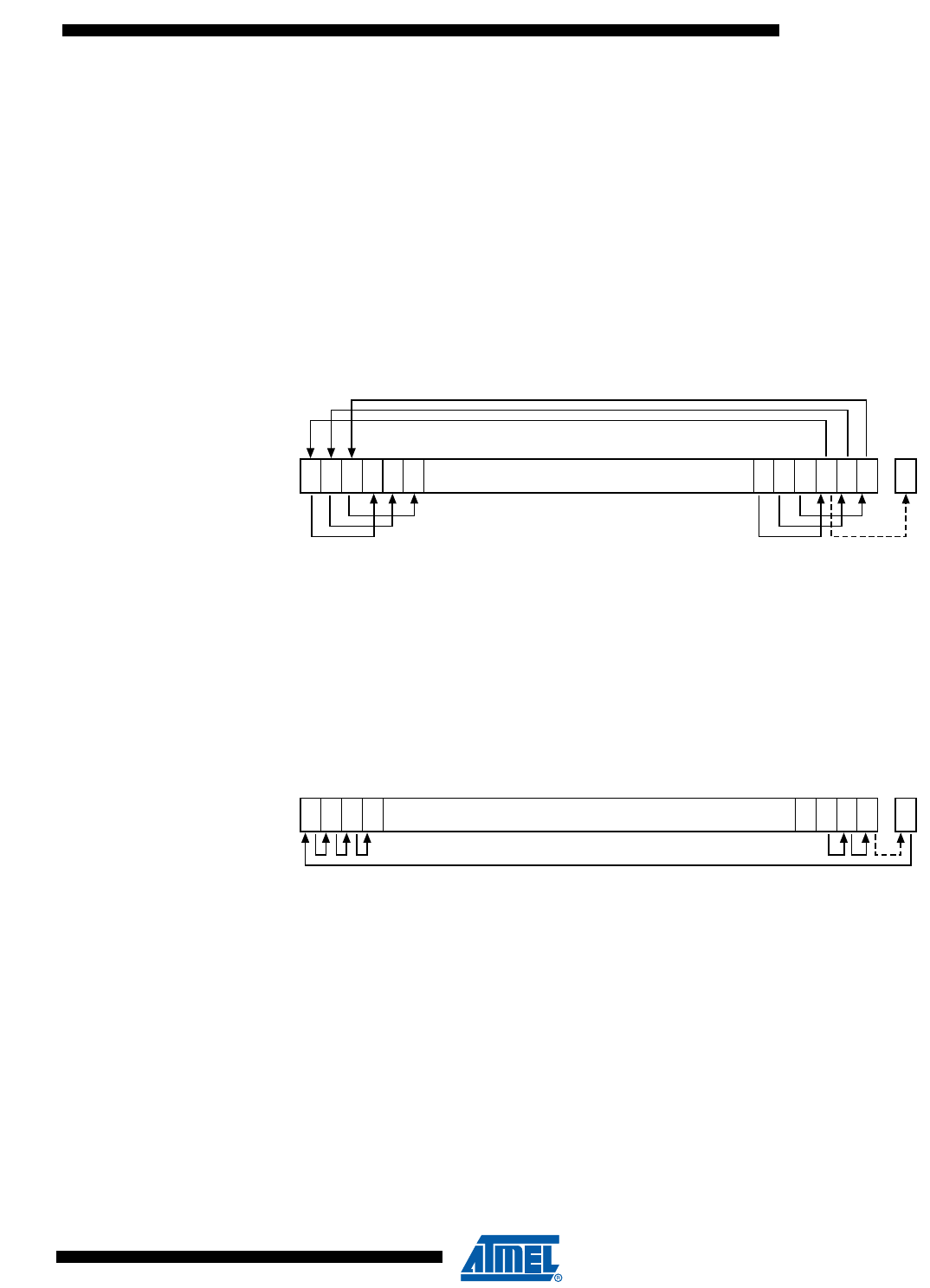
97
6430F–ATARM–21-Feb-12
SAM3U Series
13.10.4.4 ROR
Rotate right by n bits moves the left-hand 32-n bits of the register Rm, to the right by n places,
into the right-hand 32-n bits of the result. And it moves the right-hand n bits of the register into
the left-hand n bits of the result. See Figure 13-7.
When the instruction is RORS or when ROR #n is used in Operand2 with the instructions MOVS,
MVNS, ANDS, ORRS, ORNS, EORS, BICS, TEQ or TST, the carry flag is updated to the last bit
rotation, bit[n-1], of the register Rm.
•If n is 32, then the value of the result is same as the value in Rm, and if the carry flag is
updated, it is updated to bit[31] of Rm.
• ROR with shift length, n, more than 32 is the same as ROR with shift length n-32.
Figure 13-7. ROR #3
13.10.4.5 RRX
Rotate right with extend moves the bits of the register Rm to the right by one bit. And it copies
the carry flag into bit[31] of the result. See Figure 13-8 on page 97.
When the instruction is RRXS or when RRX is used in Operand2 with the instructions MOVS,
MVNS, ANDS, ORRS, ORNS, EORS, BICS, TEQ or TST, the carry flag is updated to bit[0] of
the register Rm.
Figure 13-8. RRX
13.10.5 Address alignment
An aligned access is an operation where a word-aligned address is used for a word, dual word,
or multiple word access, or where a halfword-aligned address is used for a halfword access.
Byte accesses are always aligned.
The Cortex-M3 processor supports unaligned access only for the following instructions:
• LDR, LDRT
• LDRH, LDRHT
• LDRSH, LDRSHT
•STR, STRT
• STRH, STRHT
31 10
Carry
Flag
...
2345
31 30 10
Carry
Flag
... ...

98
6430F–ATARM–21-Feb-12
SAM3U Series
All other load and store instructions generate a usage fault exception if they perform an
unaligned access, and therefore their accesses must be address aligned. For more information
about usage faults see “Fault handling” on page 84.
Unaligned accesses are usually slower than aligned accesses. In addition, some memory
regions might not support unaligned accesses. Therefore, ARM recommends that programmers
ensure that accesses are aligned. To avoid accidental generation of unaligned accesses, use
the UNALIGN_TRP bit in the Configuration and Control Register to trap all unaligned accesses,
see “Configuration and Control Register” on page 188.
13.10.6 PC-relative expressions
A PC-relative expression or label is a symbol that represents the address of an instruction or lit-
eral data. It is represented in the instruction as the PC value plus or minus a numeric offset. The
assembler calculates the required offset from the label and the address of the current instruc-
tion. If the offset is too big, the assembler produces an error.
• For B, BL, CBNZ, and CBZ instructions, the value of the PC is the address of the current
instruction plus 4 bytes.
• For all other instructions that use labels, the value of the PC is the address of the current
instruction plus 4 bytes, with bit[1] of the result cleared to 0 to make it word-aligned.
• Your assembler might permit other syntaxes for PC-relative expressions, such as a label plus
or minus a number, or an expression of the form [PC, #number].
13.10.7 Conditional execution
Most data processing instructions can optionally update the condition flags in the Application
Program Status Register (APSR) according to the result of the operation, see “Application Pro-
gram Status Register” on page 60. Some instructions update all flags, and some only update a
subset. If a flag is not updated, the original value is preserved. See the instruction descriptions
for the flags they affect.
You can execute an instruction conditionally, based on the condition flags set in another instruc-
tion, either:
• immediately after the instruction that updated the flags
• after any number of intervening instructions that have not updated the flags.
Conditional execution is available by using conditional branches or by adding condition code
suffixes to instructions. See Table 13-16 on page 99 for a list of the suffixes to add to instructions
to make them conditional instructions. The condition code suffix enables the processor to test a
condition based on the flags. If the condition test of a conditional instruction fails, the instruction:
• does not execute
• does not write any value to its destination register
• does not affect any of the flags
• does not generate any exception.
Conditional instructions, except for conditional branches, must be inside an If-Then instruction
block. See “IT” on page 147 for more information and restrictions when using the IT instruction.
Depending on the vendor, the assembler might automatically insert an IT instruction if you have
conditional instructions outside the IT block.
Use the CBZ and CBNZ instructions to compare the value of a register against zero and branch
on the result.

99
6430F–ATARM–21-Feb-12
SAM3U Series
This section describes:
•“The condition flags”
•“Condition code suffixes”.
13.10.7.1 The condition flags
The APSR contains the following condition flags:
N Set to 1 when the result of the operation was negative, cleared to 0 otherwise.
Z Set to 1 when the result of the operation was zero, cleared to 0 otherwise.
C Set to 1 when the operation resulted in a carry, cleared to 0 otherwise.
V Set to 1 when the operation caused overflow, cleared to 0 otherwise.
For more information about the APSR see “Program Status Register” on page 59.
A carry occurs:
• if the result of an addition is greater than or equal to 232
• if the result of a subtraction is positive or zero
• as the result of an inline barrel shifter operation in a move or logical instruction.
Overflow occurs if the result of an add, subtract, or compare is greater than or equal to 231, or
less than –231.
Most instructions update the status flags only if the S suffix is specified. See the instruction
descriptions for more information.
13.10.7.2 Condition code suffixes
The instructions that can be conditional have an optional condition code, shown in syntax
descriptions as {cond}. Conditional execution requires a preceding IT instruction. An instruction
with a condition code is only executed if the condition code flags in the APSR meet the specified
condition. Table 13-16 shows the condition codes to use.
You can use conditional execution with the IT instruction to reduce the number of branch instruc-
tions in code.
Table 13-16 also shows the relationship between condition code suffixes and the N, Z, C, and V
flags.
Table 13-16. Condition code suffixes
Suffix Flags Meaning
EQ Z = 1 Equal
NE Z = 0 Not equal
CS or
HS C = 1 Higher or same, unsigned ≥
CC or
LO C = 0 Lower, unsigned <
MI N = 1 Negative
PL N = 0 Positive or zero
VS V = 1 Overflow

100
6430F–ATARM–21-Feb-12
SAM3U Series
13.10.7.3 Absolute value
The example below shows the use of a conditional instruction to find the absolute value of a number. R0 = ABS(R1).
MOVS R0, R1 ; R0 = R1, setting flags
IT MI ; IT instruction for the negative condition
RSBMI R0, R1, #0 ; If negative, R0 = -R1
13.10.7.4 Compare and update value
The example below shows the use of conditional instructions to update the value of R4 if the signed values R0 is greater
than R1 and R2 is greater than R3.
CMP R0, R1 ; Compare R0 and R1, setting flags
ITT GT ; IT instruction for the two GT conditions
CMPGT R2, R3 ; If 'greater than', compare R2 and R3, setting flags
MOVGT R4, R5 ; If still 'greater than', do R4 = R5
13.10.8 Instruction width selection
There are many instructions that can generate either a 16-bit encoding or a 32-bit encoding
depending on the operands and destination register specified. For some of these instructions,
you can force a specific instruction size by using an instruction width suffix. The .W suffix forces
a 32-bit instruction encoding. The .N suffix forces a 16-bit instruction encoding.
If you specify an instruction width suffix and the assembler cannot generate an instruction
encoding of the requested width, it generates an error.
In some cases it might be necessary to specify the .W suffix, for example if the operand is the
label of an instruction or literal data, as in the case of branch instructions. This is because the
assembler might not automatically generate the right size encoding.
13.10.8.1 Instruction width selection
To use an instruction width suffix, place it immediately after the instruction mnemonic and condition code, if any. The exam-
ple below shows instructions with the instruction width suffix.
BCS.W label ; creates a 32-bit instruction even for a short branch
ADDS.W R0, R0, R1 ; creates a 32-bit instruction even though the same
; operation can be done by a 16-bit instruction
VC V = 0 No overflow
HI C = 1 and Z = 0 Higher, unsigned >
LS C = 0 or Z = 1 Lower or same, unsigned ≤
GE N = V Greater than or equal, signed ≥
LT N != V Less than, signed <
GT Z = 0 and N = V Greater than, signed >
LE Z = 1 and N != V Less than or equal, signed ≤
AL Can have any
value
Always. This is the default when no suffix is
specified.
Table 13-16. Condition code suffixes (Continued)
Suffix Flags Meaning

101
6430F–ATARM–21-Feb-12
SAM3U Series
13.11 Memory access instructions
Table 13-17 shows the memory access instructions:
Table 13-17. Memory access instructions
Mnemonic Brief description See
ADR Load PC-relative address “ADR” on page 102
CLREX Clear Exclusive “CLREX” on page 116
LDM{mode} Load Multiple registers “LDM and STM” on page 111
LDR{type} Load Register using immediate
offset
“LDR and STR, immediate offset” on
page 103
LDR{type} Load Register using register offset “LDR and STR, register offset” on page
106
LDR{type}T Load Register with unprivileged
access
“LDR and STR, unprivileged” on page
108
LDR Load Register using PC-relative
address “LDR, PC-relative” on page 109
LDREX{type} Load Register Exclusive “LDREX and STREX” on page 114
POP Pop registers from stack “PUSH and POP” on page 113
PUSH Push registers onto stack “PUSH and POP” on page 113
STM{mode} Store Multiple registers “LDM and STM” on page 111
STR{type} Store Register using immediate
offset
“LDR and STR, immediate offset” on
page 103
STR{type} Store Register using register offset “LDR and STR, register offset” on page
106
STR{type}T Store Register with unprivileged
access
“LDR and STR, unprivileged” on page
108
STREX{type} Store Register Exclusive “LDREX and STREX” on page 114

102
6430F–ATARM–21-Feb-12
SAM3U Series
13.11.1 ADR
Load PC-relative address.
13.11.1.1 Syntax
ADR{cond} Rd, label
where:
cond is an optional condition code, see “Conditional execution” on page 98.
Rd is the destination register.
label is a PC-relative expression. See “PC-relative expressions” on page 98.
13.11.1.2 Operation
ADR determines the address by adding an immediate value to the PC, and writes the result to
the destination register.
ADR produces position-independent code, because the address is PC-relative.
If you use ADR to generate a target address for a BX or BLX instruction, you must ensure that
bit[0] of the address you generate is set to1 for correct execution.
Values of label must be within the range of −4095 to +4095 from the address in the PC.
You might have to use the .W suffix to get the maximum offset range or to generate addresses
that are not word-aligned. See “Instruction width selection” on page 100.
13.11.1.3 Restrictions
Rd must not be SP and must not be PC.
13.11.1.4 Condition flags
This instruction does not change the flags.
13.11.1.5 Examples
ADR R1, TextMessage ; Write address value of a location labelled as
; TextMessage to R1

103
6430F–ATARM–21-Feb-12
SAM3U Series
13.11.2 LDR and STR, immediate offset
Load and Store with immediate offset, pre-indexed immediate offset, or post-indexed immediate
offset.
13.11.2.1 Syntax
op{type}{cond} Rt, [Rn {, #offset}] ; immediate offset
op{type}{cond} Rt, [Rn, #offset]! ; pre-indexed
op{type}{cond} Rt, [Rn], #offset ; post-indexed
opD{cond} Rt, Rt2, [Rn {, #offset}] ; immediate offset, two words
opD{cond} Rt, Rt2, [Rn, #offset]! ; pre-indexed, two words
opD{cond} Rt, Rt2, [Rn], #offset ; post-indexed, two words
where:
op is one of:
LDR Load Register.
STR Store Register.
type is one of:
B unsigned byte, zero extend to 32 bits on loads.
SB signed byte, sign extend to 32 bits (LDR only).
H unsigned halfword, zero extend to 32 bits on loads.
SH signed halfword, sign extend to 32 bits (LDR only).
- omit, for word.
cond is an optional condition code, see “Conditional execution” on page 98.
Rt is the register to load or store.
Rn is the register on which the memory address is based.
offset is an offset from Rn. If offset is omitted, the address is the contents of Rn.
Rt2 is the additional register to load or store for two-word operations.
13.11.2.2 Operation
LDR instructions load one or two registers with a value from memory.
STR instructions store one or two register values to memory.
Load and store instructions with immediate offset can use the following addressing modes:
13.11.2.3 Offset addressing
The offset value is added to or subtracted from the address obtained from the register Rn. The
result is used as the address for the memory access. The register Rn is unaltered. The assem-
bly language syntax for this mode is:
[Rn, #offset]
13.11.2.4 Pre-indexed addressing
The offset value is added to or subtracted from the address obtained from the register Rn. The
result is used as the address for the memory access and written back into the register Rn. The
assembly language syntax for this mode is:

104
6430F–ATARM–21-Feb-12
SAM3U Series
[Rn, #offset]!
13.11.2.5 Post-indexed addressing
The address obtained from the register Rn is used as the address for the memory access. The
offset value is added to or subtracted from the address, and written back into the register Rn.
The assembly language syntax for this mode is:
[Rn], #offset
The value to load or store can be a byte, halfword, word, or two words. Bytes and halfwords can
either be signed or unsigned. See “Address alignment” on page 97.
Table 13-18 shows the ranges of offset for immediate, pre-indexed and post-indexed forms.
13.11.2.6 Restrictions
For load instructions:
•Rt can be SP or PC for word loads only
•Rt must be different from Rt2 for two-word loads
•Rn must be different from Rt and Rt2 in the pre-indexed or post-indexed forms.
When Rt is PC in a word load instruction:
• bit[0] of the loaded value must be 1 for correct execution
• a branch occurs to the address created by changing bit[0] of the loaded value to 0
• if the instruction is conditional, it must be the last instruction in the IT block.
For store instructions:
•Rt can be SP for word stores only
•Rt must not be PC
•Rn must not be PC
•Rn must be different from Rt and Rt2 in the pre-indexed or post-indexed forms.
13.11.2.7 Condition flags
These instructions do not change the flags.
Table 13-18. Offset ranges
Instruction type Immediate offset Pre-indexed Post-indexed
Word, halfword, signed
halfword, byte, or signed
byte
−255 to 4095 −255 to 255 −255 to 255
Two w or d s
multiple of 4 in the
range −1020 to
1020
multiple of 4 in the
range −1020 to
1020
multiple of 4 in the
range −1020 to
1020

105
6430F–ATARM–21-Feb-12
SAM3U Series
13.11.2.8 Examples
LDR R8, [R10] ; Loads R8 from the address in R10.
LDRNE R2, [R5, #960]! ; Loads (conditionally) R2 from a word
; 960 bytes above the address in R5, and
; increments R5 by 960.
STR R2, [R9,#const-struc] ; const-struc is an expression evaluating
; to a constant in the range 0-4095.
STRH R3, [R4], #4 ; Store R3 as halfword data into address in
; R4, then increment R4 by 4
LDRD R8, R9, [R3, #0x20] ; Load R8 from a word 32 bytes above the
; address in R3, and load R9 from a word 36
; bytes above the address in R3
STRD R0, R1, [R8], #-16 ; Store R0 to address in R8, and store R1 to
; a word 4 bytes above the address in R8,
; and then decrement R8 by 16.

106
6430F–ATARM–21-Feb-12
SAM3U Series
13.11.3 LDR and STR, register offset
Load and Store with register offset.
13.11.3.1 Syntax
op{type}{cond} Rt, [Rn, Rm {, LSL #n}]
where:
op is one of:
LDR Load Register.
STR Store Register.
type is one of:
B unsigned byte, zero extend to 32 bits on loads.
SB signed byte, sign extend to 32 bits (LDR only).
H unsigned halfword, zero extend to 32 bits on loads.
SH signed halfword, sign extend to 32 bits (LDR only).
- omit, for word.
cond is an optional condition code, see “Conditional execution” on page 98.
Rt is the register to load or store.
Rn is the register on which the memory address is based.
Rm is a register containing a value to be used as the offset.
LSL #nis an optional shift, with n in the range 0 to 3.
13.11.3.2 Operation
LDR instructions load a register with a value from memory.
STR instructions store a register value into memory.
The memory address to load from or store to is at an offset from the register Rn. The offset is
specified by the register Rm and can be shifted left by up to 3 bits using LSL.
The value to load or store can be a byte, halfword, or word. For load instructions, bytes and half-
words can either be signed or unsigned. See “Address alignment” on page 97.
13.11.3.3 Restrictions
In these instructions:
•Rn must not be PC
•Rm must not be SP and must not be PC
•Rt can be SP only for word loads and word stores
•Rt can be PC only for word loads.
When Rt is PC in a word load instruction:
• bit[0] of the loaded value must be 1 for correct execution, and a branch occurs to this
halfword-aligned address
• if the instruction is conditional, it must be the last instruction in the IT block.

107
6430F–ATARM–21-Feb-12
SAM3U Series
13.11.3.4 Condition flags
These instructions do not change the flags.
13.11.3.5 Examples
STR R0, [R5, R1] ; Store value of R0 into an address equal to
; sum of R5 and R1
LDRSB R0, [R5, R1, LSL #1] ; Read byte value from an address equal to
; sum of R5 and two times R1, sign extended it
; to a word value and put it in R0
STR R0, [R1, R2, LSL #2] ; Stores R0 to an address equal to sum of R1
; and four times R2

108
6430F–ATARM–21-Feb-12
SAM3U Series
13.11.4 LDR and STR, unprivileged
Load and Store with unprivileged access.
13.11.4.1 Syntax
op{type}T{cond} Rt, [Rn {, #offset}] ; immediate offset
where:
op is one of:
LDR Load Register.
STR Store Register.
type is one of:
B unsigned byte, zero extend to 32 bits on loads.
SB signed byte, sign extend to 32 bits (LDR only).
H unsigned halfword, zero extend to 32 bits on loads.
SH signed halfword, sign extend to 32 bits (LDR only).
- omit, for word.
cond is an optional condition code, see “Conditional execution” on page 98.
Rt is the register to load or store.
Rn is the register on which the memory address is based.
offset is an offset from Rn and can be 0 to 255.
If offset is omitted, the address is the value in Rn.
13.11.4.2 Operation
These load and store instructions perform the same function as the memory access instructions
with immediate offset, see “LDR and STR, immediate offset” on page 103. The difference is that
these instructions have only unprivileged access even when used in privileged software.
When used in unprivileged software, these instructions behave in exactly the same way as nor-
mal memory access instructions with immediate offset.
13.11.4.3 Restrictions
In these instructions:
•Rn must not be PC
•Rt must not be SP and must not be PC.
13.11.4.4 Condition flags
These instructions do not change the flags.
13.11.4.5 Examples
STRBTEQ R4, [R7] ; Conditionally store least significant byte in
; R4 to an address in R7, with unprivileged access
LDRHT R2, [R2, #8] ; Load halfword value from an address equal to
; sum of R2 and 8 into R2, with unprivileged access

109
6430F–ATARM–21-Feb-12
SAM3U Series
13.11.5 LDR, PC-relative
Load register from memory.
13.11.5.1 Syntax
LDR{type}{cond} Rt, label
LDRD{cond} Rt, Rt2, label ; Load two words
where:
type is one of:
B unsigned byte, zero extend to 32 bits.
SB signed byte, sign extend to 32 bits.
H unsigned halfword, zero extend to 32 bits.
SH signed halfword, sign extend to 32 bits.
- omit, for word.
cond is an optional condition code, see “Conditional execution” on page 98.
Rt is the register to load or store.
Rt2 is the second register to load or store.
label is a PC-relative expression. See “PC-relative expressions” on page 98.
13.11.5.2 Operation
LDR loads a register with a value from a PC-relative memory address. The memory address is
specified by a label or by an offset from the PC.
The value to load or store can be a byte, halfword, or word. For load instructions, bytes and half-
words can either be signed or unsigned. See “Address alignment” on page 97.
label must be within a limited range of the current instruction. Table 13-19 shows the possible
offsets between label and the PC.
You might have to use the .W suffix to get the maximum offset range. See “Instruction width
selection” on page 100.
13.11.5.3 Restrictions
In these instructions:
•Rt can be SP or PC only for word loads
•Rt2 must not be SP and must not be PC
•Rt must be different from Rt2.
When Rt is PC in a word load instruction:
Table 13-19. Offset ranges
Instruction type Offset range
Word, halfword, signed halfword, byte, signed
byte −4095 to 4095
Two w or d s −1020 to 1020

110
6430F–ATARM–21-Feb-12
SAM3U Series
• bit[0] of the loaded value must be 1 for correct execution, and a branch occurs to this
halfword-aligned address
• if the instruction is conditional, it must be the last instruction in the IT block.
13.11.5.4 Condition flags
These instructions do not change the flags.
13.11.5.5 Examples
LDR R0, LookUpTable ; Load R0 with a word of data from an address
; labelled as LookUpTable
LDRSB R7, localdata ; Load a byte value from an address labelled
; as localdata, sign extend it to a word
; value, and put it in R7

111
6430F–ATARM–21-Feb-12
SAM3U Series
13.11.6 LDM and STM
Load and Store Multiple registers.
13.11.6.1 Syntax
op{addr_mode}{cond} Rn{!}, reglist
where:
op is one of:
LDM Load Multiple registers.
STM Store Multiple registers.
addr_mode is any one of the following:
IA Increment address After each access. This is the default.
DB Decrement address Before each access.
cond is an optional condition code, see “Conditional execution” on page 98.
Rn is the register on which the memory addresses are based.
! is an optional writeback suffix.
If ! is present the final address, that is loaded from or stored to, is written back into Rn.
reglist is a list of one or more registers to be loaded or stored, enclosed in braces. It can
contain register ranges. It must be comma separated if it contains more than one register or reg-
ister range, see “Examples” on page 112.
LDM and LDMFD are synonyms for LDMIA. LDMFD refers to its use for popping data from Full
Descending stacks.
LDMEA is a synonym for LDMDB, and refers to its use for popping data from Empty Ascending
stacks.
STM and STMEA are synonyms for STMIA. STMEA refers to its use for pushing data onto
Empty Ascending stacks.
STMFD is s synonym for STMDB, and refers to its use for pushing data onto Full Descending
stacks
13.11.6.2 Operation
LDM instructions load the registers in reglist with word values from memory addresses based on
Rn.
STM instructions store the word values in the registers in reglist to memory addresses based on
Rn.
For LDM, LDMIA, LDMFD, STM, STMIA, and STMEA the memory addresses used for the
accesses are at 4-byte intervals ranging from Rn to Rn + 4 * (n-1), where n is the number of reg-
isters in reglist. The accesses happens in order of increasing register numbers, with the lowest
numbered register using the lowest memory address and the highest number register using the
highest memory address. If the writeback suffix is specified, the value of Rn + 4 * (n-1) is written
back to Rn.
For LDMDB, LDMEA, STMDB, and STMFD the memory addresses used for the accesses are at
4-byte intervals ranging from Rn to Rn - 4 * (n-1), where n is the number of registers in reglist.

112
6430F–ATARM–21-Feb-12
SAM3U Series
The accesses happen in order of decreasing register numbers, with the highest numbered regis-
ter using the highest memory address and the lowest number register using the lowest memory
address. If the writeback suffix is specified, the value of Rn - 4 * (n-1) is written back to Rn.
The PUSH and POP instructions can be expressed in this form. See “PUSH and POP” on page
113 for details.
13.11.6.3 Restrictions
In these instructions:
•Rn must not be PC
•reglist must not contain SP
• in any STM instruction, reglist must not contain PC
• in any LDM instruction, reglist must not contain PC if it contains LR
•reglist must not contain Rn if you specify the writeback suffix.
When PC is in reglist in an LDM instruction:
• bit[0] of the value loaded to the PC must be 1 for correct execution, and a branch occurs to
this halfword-aligned address
• if the instruction is conditional, it must be the last instruction in the IT block.
13.11.6.4 Condition flags
These instructions do not change the flags.
13.11.6.5 Examples
LDM R8,{R0,R2,R9} ; LDMIA is a synonym for LDM
STMDB R1!,{R3-R6,R11,R12}
13.11.6.6 Incorrect examples
STM R5!,{R5,R4,R9} ; Value stored for R5 is unpredictable
LDM R2, {} ; There must be at least one register in the list

113
6430F–ATARM–21-Feb-12
SAM3U Series
13.11.7 PUSH and POP
Push registers onto, and pop registers off a full-descending stack.
13.11.7.1 Syntax
PUSH{cond} reglist
POP{cond} reglist
where:
cond is an optional condition code, see “Conditional execution” on page 98.
reglist is a non-empty list of registers, enclosed in braces. It can contain register ranges.
It must be comma separated if it contains more than one register or register range.
PUSH and POP are synonyms for STMDB and LDM (or LDMIA) with the memory addresses for
the access based on SP, and with the final address for the access written back to the SP. PUSH
and POP are the preferred mnemonics in these cases.
13.11.7.2 Operation
PUSH stores registers on the stack in order of decreasing the register numbers, with the highest
numbered register using the highest memory address and the lowest numbered register using
the lowest memory address.
POP loads registers from the stack in order of increasing register numbers, with the lowest num-
bered register using the lowest memory address and the highest numbered register using the
highest memory address.
See “LDM and STM” on page 111 for more information.
13.11.7.3 Restrictions
In these instructions:
•reglist must not contain SP
• for the PUSH instruction, reglist must not contain PC
• for the POP instruction, reglist must not contain PC if it contains LR.
When PC is in reglist in a POP instruction:
• bit[0] of the value loaded to the PC must be 1 for correct execution, and a branch occurs to
this halfword-aligned address
• if the instruction is conditional, it must be the last instruction in the IT block.
13.11.7.4 Condition flags
These instructions do not change the flags.
13.11.7.5 Examples
PUSH {R0,R4-R7}
PUSH {R2,LR}
POP {R0,R10,PC}

114
6430F–ATARM–21-Feb-12
SAM3U Series
13.11.8 LDREX and STREX
Load and Store Register Exclusive.
13.11.8.1 Syntax
LDREX{cond} Rt, [Rn {, #offset}]
STREX{cond} Rd, Rt, [Rn {, #offset}]
LDREXB{cond} Rt, [Rn]
STREXB{cond} Rd, Rt, [Rn]
LDREXH{cond} Rt, [Rn]
STREXH{cond} Rd, Rt, [Rn]
where:
cond is an optional condition code, see “Conditional execution” on page 98.
Rd is the destination register for the returned status.
Rt is the register to load or store.
Rn is the register on which the memory address is based.
offset is an optional offset applied to the value in Rn.
If offset is omitted, the address is the value in Rn.
13.11.8.2 Operation
LDREX, LDREXB, and LDREXH load a word, byte, and halfword respectively from a memory
address.
STREX, STREXB, and STREXH attempt to store a word, byte, and halfword respectively to a
memory address. The address used in any Store-Exclusive instruction must be the same as the
address in the most recently executed Load-exclusive instruction. The value stored by the Store-
Exclusive instruction must also have the same data size as the value loaded by the preceding
Load-exclusive instruction. This means software must always use a Load-exclusive instruction
and a matching Store-Exclusive instruction to perform a synchronization operation, see “Syn-
chronization primitives” on page 75
If an Store-Exclusive instruction performs the store, it writes 0 to its destination register. If it does
not perform the store, it writes 1 to its destination register. If the Store-Exclusive instruction
writes 0 to the destination register, it is guaranteed that no other process in the system has
accessed the memory location between the Load-exclusive and Store-Exclusive instructions.
For reasons of performance, keep the number of instructions between corresponding Load-
Exclusive and Store-Exclusive instruction to a minimum.
The result of executing a Store-Exclusive instruction to an address that is different from that
used in the preceding Load-Exclusive instruction is unpredictable.
13.11.8.3 Restrictions
In these instructions:
• do not use PC
• do not use SP for Rd and Rt
• for STREX, Rd must be different from both Rt and Rn
• the value of offset must be a multiple of four in the range 0-1020.

115
6430F–ATARM–21-Feb-12
SAM3U Series
13.11.8.4 Condition flags
These instructions do not change the flags.
13.11.8.5 Examples
MOV R1, #0x1 ; Initialize the ‘lock taken’ value
try
LDREX R0, [LockAddr] ; Load the lock value
CMP R0, #0 ; Is the lock free?
ITT EQ ; IT instruction for STREXEQ and CMPEQ
STREXEQ R0, R1, [LockAddr] ; Try and claim the lock
CMPEQ R0, #0 ; Did this succeed?
BNE try ; No – try again
.... ; Yes – we have the lock

116
6430F–ATARM–21-Feb-12
SAM3U Series
13.11.9 CLREX
Clear Exclusive.
13.11.9.1 Syntax
CLREX{cond}
where:
cond is an optional condition code, see “Conditional execution” on page 98.
13.11.9.2 Operation
Use CLREX to make the next STREX, STREXB, or STREXH instruction write 1 to its destination
register and fail to perform the store. It is useful in exception handler code to force the failure of
the store exclusive if the exception occurs between a load exclusive instruction and the match-
ing store exclusive instruction in a synchronization operation.
See “Synchronization primitives” on page 75 for more information.
13.11.9.3 Condition flags
These instructions do not change the flags.
13.11.9.4 Examples
CLREX

117
6430F–ATARM–21-Feb-12
SAM3U Series
13.12 General data processing instructions
Table 13-20 shows the data processing instructions:
Table 13-20. Data processing instructions
Mnemonic Brief description See
ADC Add with Carry “ADD, ADC, SUB, SBC, and RSB” on
page 119
ADD Add “ADD, ADC, SUB, SBC, and RSB” on
page 119
ADDW Add “ADD, ADC, SUB, SBC, and RSB” on
page 119
AND Logical AND “AND, ORR, EOR, BIC, and ORN” on
page 122
ASR Arithmetic Shift Right “ASR, LSL, LSR, ROR, and RRX” on page
124
BIC Bit Clear “AND, ORR, EOR, BIC, and ORN” on
page 122
CLZ Count leading zeros “CLZ” on page 126
CMN Compare Negative “CMP and CMN” on page 127
CMP Compare “CMP and CMN” on page 127
EOR Exclusive OR “AND, ORR, EOR, BIC, and ORN” on
page 122
LSL Logical Shift Left “ASR, LSL, LSR, ROR, and RRX” on page
124
LSR Logical Shift Right “ASR, LSL, LSR, ROR, and RRX” on page
124
MOV Move “MOV and MVN” on page 128
MOVT Move Top “MOVT” on page 130
MOVW Move 16-bit constant “MOV and MVN” on page 128
MVN Move NOT “MOV and MVN” on page 128
ORN Logical OR NOT “AND, ORR, EOR, BIC, and ORN” on
page 122
ORR Logical OR “AND, ORR, EOR, BIC, and ORN” on
page 122
RBIT Reverse Bits “REV, REV16, REVSH, and RBIT” on
page 131
REV Reverse byte order in a word “REV, REV16, REVSH, and RBIT” on
page 131
REV16 Reverse byte order in each halfword “REV, REV16, REVSH, and RBIT” on
page 131
REVSH Reverse byte order in bottom halfword and
sign extend
“REV, REV16, REVSH, and RBIT” on
page 131
ROR Rotate Right “ASR, LSL, LSR, ROR, and RRX” on page
124

118
6430F–ATARM–21-Feb-12
SAM3U Series
RRX Rotate Right with Extend “ASR, LSL, LSR, ROR, and RRX” on page
124
RSB Reverse Subtract “ADD, ADC, SUB, SBC, and RSB” on
page 119
SBC Subtract with Carry “ADD, ADC, SUB, SBC, and RSB” on
page 119
SUB Subtract “ADD, ADC, SUB, SBC, and RSB” on
page 119
SUBW Subtract “ADD, ADC, SUB, SBC, and RSB” on
page 119
TEQ Test Equivalence “TST and TEQ” on page 132
TST Test “TST and TEQ” on page 132
Table 13-20. Data processing instructions (Continued)
Mnemonic Brief description See

119
6430F–ATARM–21-Feb-12
SAM3U Series
13.12.1 ADD, ADC, SUB, SBC, and RSB
Add, Add with carry, Subtract, Subtract with carry, and Reverse Subtract.
13.12.1.1 Syntax
op{S}{cond} {Rd,} Rn, Operand2
op{cond} {Rd,} Rn, #imm12 ; ADD and SUB only
where:
op is one of:
ADD Add.
ADC Add with Carry.
SUB Subtract.
SBC Subtract with Carry.
RSB Reverse Subtract.
S is an optional suffix. If S is specified, the condition code flags are updated on the
result of the operation, see “Conditional execution” on page 98.
cond is an optional condition code, see “Conditional execution” on page 98.
Rd is the destination register. If Rd is omitted, the destination register is Rn.
Rn is the register holding the first operand.
Operand2 is a flexible second operand.
See “Flexible second operand” on page 94 for details of the options.
imm12 is any value in the range 0-4095.
13.12.1.2 Operation
The ADD instruction adds the value of Operand2 or imm12 to the value in Rn.
The ADC instruction adds the values in Rn and Operand2, together with the carry flag.
The SUB instruction subtracts the value of Operand2 or imm12 from the value in Rn.
The SBC instruction subtracts the value of Operand2 from the value in Rn. If the carry flag is
clear, the result is reduced by one.
The RSB instruction subtracts the value in Rn from the value of Operand2. This is useful
because of the wide range of options for Operand2.
Use ADC and SBC to synthesize multiword arithmetic, see “Multiword arithmetic examples” on
page 121.
See also “ADR” on page 102.
ADDW is equivalent to the ADD syntax that uses the imm12 operand. SUBW is equivalent to the
SUB syntax that uses the imm12 operand.
13.12.1.3 Restrictions
In these instructions:
•Operand2 must not be SP and must not be PC

120
6430F–ATARM–21-Feb-12
SAM3U Series
•Rd can be SP only in ADD and SUB, and only with the additional restrictions:
–Rn must also be SP
– any shift in Operand2 must be limited to a maximum of 3 bits using LSL
•Rn can be SP only in ADD and SUB
•Rd can be PC only in the ADD{cond} PC, PC, Rm instruction where:
– you must not specify the S suffix
–Rm must not be PC and must not be SP
– if the instruction is conditional, it must be the last instruction in the IT block
• with the exception of the ADD{cond} PC, PC, Rm instruction, Rn can be PC only in ADD and
SUB, and only with the additional restrictions:
– you must not specify the S suffix
– the second operand must be a constant in the range 0 to 4095.
–
– When using the PC for an addition or a subtraction, bits[1:0] of the PC are rounded
to b00 before performing the calculation, making the base address for the calculation
word-aligned.
– If you want to generate the address of an instruction, you have to adjust the constant
based on the value of the PC. ARM recommends that you use the ADR instruction
instead of ADD or SUB with Rn equal to the PC, because your assembler
automatically calculates the correct constant for the ADR instruction.
When Rd is PC in the ADD{cond} PC, PC, Rm instruction:
• bit[0] of the value written to the PC is ignored
• a branch occurs to the address created by forcing bit[0] of that value to 0.
13.12.1.4 Condition flags
If S is specified, these instructions update the N, Z, C and V flags according to the result.
13.12.1.5 Examples
ADD R2, R1, R3
SUBS R8, R6, #240 ; Sets the flags on the result
RSB R4, R4, #1280 ; Subtracts contents of R4 from 1280
ADCHI R11, R0, R3 ; Only executed if C flag set and Z
; flag clear

121
6430F–ATARM–21-Feb-12
SAM3U Series
13.12.1.6 Multiword arithmetic examples
13.12.1.7 64-bit addition
The example below shows two instructions that add a 64-bit integer contained in R2 and R3 to another 64-bit integer con-
tained in R0 and R1, and place the result in R4 and R5.
ADDS R4, R0, R2 ; add the least significant words
ADC R5, R1, R3 ; add the most significant words with carry
13.12.1.8 96-bit subtraction
Multiword values do not have to use consecutive registers. The example below shows instructions that subtract a 96-bit
integer contained in R9, R1, and R11 from another contained in R6, R2, and R8. The example stores the result in R6, R9,
and R2.
SUBS R6, R6, R9 ; subtract the least significant words
SBCS R9, R2, R1 ; subtract the middle words with carry
SBC R2, R8, R11 ; subtract the most significant words with carry

122
6430F–ATARM–21-Feb-12
SAM3U Series
13.12.2 AND, ORR, EOR, BIC, and ORN
Logical AND, OR, Exclusive OR, Bit Clear, and OR NOT.
13.12.2.1 Syntax
op{S}{cond} {Rd,} Rn, Operand2
where:
op is one of:
AND logical AND.
ORR logical OR, or bit set.
EOR logical Exclusive OR.
BIC logical AND NOT, or bit clear.
ORN logical OR NOT.
S is an optional suffix. If S is specified, the condition code flags are updated on the
result of the operation, see “Conditional execution” on page 98.
cond is an optional condition code, see See “Conditional execution” on page 98..
Rd is the destination register.
Rn is the register holding the first operand.
Operand2 is a flexible second operand. See “Flexible second operand” on page 94 for
details of the options.
13.12.2.2 Operation
The AND, EOR, and ORR instructions perform bitwise AND, Exclusive OR, and OR operations
on the values in Rn and Operand2.
The BIC instruction performs an AND operation on the bits in Rn with the complements of the
corresponding bits in the value of Operand2.
The ORN instruction performs an OR operation on the bits in Rn with the complements of the
corresponding bits in the value of Operand2.
13.12.2.3 Restrictions
Do not use SP and do not use PC.
13.12.2.4 Condition flags
If S is specified, these instructions:
• update the N and Z flags according to the result
• can update the C flag during the calculation of Operand2, see “Flexible second operand” on
page 94
• do not affect the V flag.

123
6430F–ATARM–21-Feb-12
SAM3U Series
13.12.2.5 Examples
AND R9, R2, #0xFF00
ORREQ R2, R0, R5
ANDS R9, R8, #0x19
EORS R7, R11, #0x18181818
BIC R0, R1, #0xab
ORN R7, R11, R14, ROR #4
ORNS R7, R11, R14, ASR #32

124
6430F–ATARM–21-Feb-12
SAM3U Series
13.12.3 ASR, LSL, LSR, ROR, and RRX
Arithmetic Shift Right, Logical Shift Left, Logical Shift Right, Rotate Right, and Rotate Right with
Extend.
13.12.3.1 Syntax
op{S}{cond} Rd, Rm, Rs
op{S}{cond} Rd, Rm, #n
RRX{S}{cond} Rd, Rm
where:
op is one of:
ASR Arithmetic Shift Right.
LSL Logical Shift Left.
LSR Logical Shift Right.
ROR Rotate Right.
S is an optional suffix. If S is specified, the condition code flags are updated on the
result of the operation, see “Conditional execution” on page 98.
Rd is the destination register.
Rm is the register holding the value to be shifted.
Rs is the register holding the shift length to apply to the value in Rm. Only the least
significant byte is used and can be in the range 0 to 255.
n is the shift length. The range of shift length depends on the instruction:
ASR shift length from 1 to 32
LSL shift length from 0 to 31
LSR shift length from 1 to 32
ROR shift length from 1 to 31.
MOV{S}{cond} Rd, Rm is the preferred syntax for LSL{S}{cond} Rd, Rm, #0.
13.12.3.2 Operation
ASR, LSL, LSR, and ROR move the bits in the register Rm to the left or right by the number of
places specified by constant n or register Rs.
RRX moves the bits in register Rm to the right by 1.
In all these instructions, the result is written to Rd, but the value in register Rm remains
unchanged. For details on what result is generated by the different instructions, see “Shift Oper-
ations” on page 95.
13.12.3.3 Restrictions
Do not use SP and do not use PC.
13.12.3.4 Condition flags
If S is specified:
• these instructions update the N and Z flags according to the result

125
6430F–ATARM–21-Feb-12
SAM3U Series
• the C flag is updated to the last bit shifted out, except when the shift length is 0, see “Shift
Operations” on page 95.
13.12.3.5 Examples
ASR R7, R8, #9 ; Arithmetic shift right by 9 bits
LSLS R1, R2, #3 ; Logical shift left by 3 bits with flag update
LSR R4, R5, #6 ; Logical shift right by 6 bits
ROR R4, R5, R6 ; Rotate right by the value in the bottom byte of R6
RRX R4, R5 ; Rotate right with extend

126
6430F–ATARM–21-Feb-12
SAM3U Series
13.12.4 CLZ
Count Leading Zeros.
13.12.4.1 Syntax
CLZ{cond} Rd, Rm
where:
cond is an optional condition code, see “Conditional execution” on page 98.
Rd is the destination register.
Rm is the operand register.
13.12.4.2 Operation
The CLZ instruction counts the number of leading zeros in the value in Rm and returns the result
in Rd. The result value is 32 if no bits are set in the source register, and zero if bit[31] is set.
13.12.4.3 Restrictions
Do not use SP and do not use PC.
13.12.4.4 Condition flags
This instruction does not change the flags.
13.12.4.5 Examples
CLZ R4,R9
CLZNE R2,R3

127
6430F–ATARM–21-Feb-12
SAM3U Series
13.12.5 CMP and CMN
Compare and Compare Negative.
13.12.5.1 Syntax
CMP{cond} Rn, Operand2
CMN{cond} Rn, Operand2
where:
cond is an optional condition code, see “Conditional execution” on page 98.
Rn is the register holding the first operand.
Operand2 is a flexible second operand. See “Flexible second operand” on page 94 for
details of the options.
13.12.5.2 Operation
These instructions compare the value in a register with Operand2. They update the condition
flags on the result, but do not write the result to a register.
The CMP instruction subtracts the value of Operand2 from the value in Rn. This is the same as
a SUBS instruction, except that the result is discarded.
The CMN instruction adds the value of Operand2 to the value in Rn. This is the same as an
ADDS instruction, except that the result is discarded.
13.12.5.3 Restrictions
In these instructions:
• do not use PC
•Operand2 must not be SP.
13.12.5.4 Condition flags
These instructions update the N, Z, C and V flags according to the result.
13.12.5.5 Examples
CMP R2, R9
CMN R0, #6400
CMPGT SP, R7, LSL #2

128
6430F–ATARM–21-Feb-12
SAM3U Series
13.12.6 MOV and MVN
Move and Move NOT.
13.12.6.1 Syntax
MOV{S}{cond} Rd, Operand2
MOV{cond} Rd, #imm16
MVN{S}{cond} Rd, Operand2
where:
S is an optional suffix. If S is specified, the condition code flags are updated on the
result of the operation, see “Conditional execution” on page 98.
cond is an optional condition code, see “Conditional execution” on page 98.
Rd is the destination register.
Operand2 is a flexible second operand. See “Flexible second operand” on page 94 for
details of the options.
imm16 is any value in the range 0-65535.
13.12.6.2 Operation
The MOV instruction copies the value of Operand2 into Rd.
When Operand2 in a MOV instruction is a register with a shift other than LSL #0, the preferred
syntax is the corresponding shift instruction:
• ASR{S}{cond} Rd, Rm, #n is the preferred syntax for MOV{S}{cond} Rd, Rm, ASR #n
• LSL{S}{cond} Rd, Rm, #n is the preferred syntax for MOV{S}{cond} Rd, Rm, LSL #n if n!= 0
• LSR{S}{cond} Rd, Rm, #n is the preferred syntax for MOV{S}{cond} Rd, Rm, LSR #n
• ROR{S}{cond} Rd, Rm, #n is the preferred syntax for MOV{S}{cond} Rd, Rm, ROR #n
• RRX{S}{cond} Rd, Rm is the preferred syntax for MOV{S}{cond} Rd, Rm, RRX.
Also, the MOV instruction permits additional forms of Operand2 as synonyms for shift
instructions:
• MOV{S}{cond} Rd, Rm, ASR Rs is a synonym for ASR{S}{cond} Rd, Rm, Rs
• MOV{S}{cond} Rd, Rm, LSL Rs is a synonym for LSL{S}{cond} Rd, Rm, Rs
• MOV{S}{cond} Rd, Rm, LSR Rs is a synonym for LSR{S}{cond} Rd, Rm, Rs
• MOV{S}{cond} Rd, Rm, ROR Rs is a synonym for ROR{S}{cond} Rd, Rm, Rs
See “ASR, LSL, LSR, ROR, and RRX” on page 124.
The MVN instruction takes the value of Operand2, performs a bitwise logical NOT operation on
the value, and places the result into Rd.
The MOVW instruction provides the same function as MOV, but is restricted to using the imm16
operand.
13.12.6.3 Restrictions
You can use SP and PC only in the MOV instruction, with the following restrictions:
• the second operand must be a register without shift
• you must not specify the S suffix.
When Rd is PC in a MOV instruction:

129
6430F–ATARM–21-Feb-12
SAM3U Series
• bit[0] of the value written to the PC is ignored
• a branch occurs to the address created by forcing bit[0] of that value to 0.
Though it is possible to use MOV as a branch instruction, ARM strongly recommends the use of
a BX or BLX instruction to branch for software portability to the ARM instruction set.
13.12.6.4 Condition flags
If S is specified, these instructions:
• update the N and Z flags according to the result
• can update the C flag during the calculation of Operand2, see “Flexible second operand” on
page 94
• do not affect the V flag.
13.12.6.5 Example
MOVS R11, #0x000B ; Write value of 0x000B to R11, flags get updated
MOV R1, #0xFA05 ; Write value of 0xFA05 to R1, flags are not updated
MOVS R10, R12 ; Write value in R12 to R10, flags get updated
MOV R3, #23 ; Write value of 23 to R3
MOV R8, SP ; Write value of stack pointer to R8
MVNS R2, #0xF ; Write value of 0xFFFFFFF0 (bitwise inverse of 0xF)
; to the R2 and update flags

130
6430F–ATARM–21-Feb-12
SAM3U Series
13.12.7 MOVT
Move Top.
13.12.7.1 Syntax
MOVT{cond} Rd, #imm16
where:
cond is an optional condition code, see “Conditional execution” on page 98.
Rd is the destination register.
imm16 is a 16-bit immediate constant.
13.12.7.2 Operation
MOVT writes a 16-bit immediate value, imm16, to the top halfword, Rd[31:16], of its destination
register. The write does not affect Rd[15:0].
The MOV, MOVT instruction pair enables you to generate any 32-bit constant.
13.12.7.3 Restrictions
Rd must not be SP and must not be PC.
13.12.7.4 Condition flags
This instruction does not change the flags.
13.12.7.5 Examples
MOVT R3, #0xF123 ; Write 0xF123 to upper halfword of R3, lower halfword
; and APSR are unchanged

131
6430F–ATARM–21-Feb-12
SAM3U Series
13.12.8 REV, REV16, REVSH, and RBIT
Reverse bytes and Reverse bits.
13.12.8.1 Syntax
op{cond} Rd, Rn
where:
op is any of:
REV
Reverse byte order in a word.
REV16
Reverse byte order in each halfword independently.
REVSH
Reverse byte order in the bottom halfword, and sign extend to 32 bits.
RBIT
Reverse the bit order in a 32-bit word.
cond is an optional condition code, see “Conditional execution” on page 98.
Rd is the destination register.
Rn is the register holding the operand.
13.12.8.2 Operation
Use these instructions to change endianness of data:
REV
converts 32-bit big-endian data into little-endian data or 32-bit little-endian data
into big-endian data.
REV16
converts 16-bit big-endian data into little-endian data or 16-bit little-endian data
into big-endian data.
REVSH
converts either:
16-bit signed big-endian data into 32-bit signed little-endian data
16-bit signed little-endian data into 32-bit signed big-endian data.
13.12.8.3 Restrictions
Do not use SP and do not use PC
.
13.12.8.4 Condition flags
These instructions do not change the flags.
13.12.8.5 Examples
REV R3, R7 ; Reverse byte order of value in R7 and write it to R3
REV16 R0, R0 ; Reverse byte order of each 16-bit halfword in R0
REVSH R0, R5 ; Reverse Signed Halfword
REVHS R3, R7 ; Reverse with Higher or Same condition
RBIT R7, R8 ; Reverse bit order of value in R8 and write the result to R7

132
6430F–ATARM–21-Feb-12
SAM3U Series
13.12.9 TST and TEQ
Test bits and Test Equivalence.
13.12.9.1 Syntax
TST{cond} Rn, Operand2
TEQ{cond} Rn, Operand2
where:
cond is an optional condition code, see “Conditional execution” on page 98.
Rn is the register holding the first operand.
Operand2 is a flexible second operand. See “Flexible second operand” on page 94 for
details of the options.
13.12.9.2 Operation
These instructions test the value in a register against Operand2. They update the condition flags
based on the result, but do not write the result to a register.
The TST instruction performs a bitwise AND operation on the value in Rn and the value of
Operand2. This is the same as the ANDS instruction, except that it discards the result.
To test whether a bit of Rn is 0 or 1, use the TST instruction with an Operand2 constant that has
that bit set to 1 and all other bits cleared to 0.
The TEQ instruction performs a bitwise Exclusive OR operation on the value in Rn and the value
of Operand2. This is the same as the EORS instruction, except that it discards the result.
Use the TEQ instruction to test if two values are equal without affecting the V or C flags.
TEQ is also useful for testing the sign of a value. After the comparison, the N flag is the logical
Exclusive OR of the sign bits of the two operands.
13.12.9.3 Restrictions
Do not use SP and do not use PC
.
13.12.9.4 Condition flags
These instructions:
• update the N and Z flags according to the result
• can update the C flag during the calculation of Operand2, see “Flexible second operand” on
page 94
• do not affect the V flag.
13.12.9.5 Examples
TST R0, #0x3F8 ; Perform bitwise AND of R0 value to 0x3F8,
; APSR is updated but result is discarded
TEQEQ R10, R9 ; Conditionally test if value in R10 is equal to
; value in R9, APSR is updated but result is discarded

133
6430F–ATARM–21-Feb-12
SAM3U Series
13.13 Multiply and divide instructions
Table 13-21 shows the multiply and divide instructions:
Table 13-21. Multiply and divide instructions
Mnemonic Brief description See
MLA Multiply with Accumulate, 32-bit result “MUL, MLA, and MLS” on page 134
MLS Multiply and Subtract, 32-bit result “MUL, MLA, and MLS” on page 134
MUL Multiply, 32-bit result “MUL, MLA, and MLS” on page 134
SDIV Signed Divide “SDIV and UDIV” on page 136
SMLAL Signed Multiply with Accumulate
(32x32+64), 64-bit result
“UMULL, UMLAL, SMULL, and SMLAL” on
page 135
SMULL Signed Multiply (32x32), 64-bit result “UMULL, UMLAL, SMULL, and SMLAL” on
page 135
UDIV Unsigned Divide “SDIV and UDIV” on page 136
UMLAL Unsigned Multiply with Accumulate
(32x32+64), 64-bit result
“UMULL, UMLAL, SMULL, and SMLAL” on
page 135
UMULL Unsigned Multiply (32x32), 64-bit
result
“UMULL, UMLAL, SMULL, and SMLAL” on
page 135

134
6430F–ATARM–21-Feb-12
SAM3U Series
13.13.1 MUL, MLA, and MLS
Multiply, Multiply with Accumulate, and Multiply with Subtract, using 32-bit operands, and pro-
ducing a 32-bit result.
13.13.1.1 Syntax
MUL{S}{cond} {Rd,} Rn, Rm ; Multiply
MLA{cond} Rd, Rn, Rm, Ra ; Multiply with accumulate
MLS{cond} Rd, Rn, Rm, Ra ; Multiply with subtract
where:
cond is an optional condition code, see “Conditional execution” on page 98.
S is an optional suffix. If S is specified, the condition code flags are updated on the
result of the operation, see “Conditional execution” on page 98.
Rd is the destination register. If Rd is omitted, the destination register is Rn.
Rn, Rm are registers holding the values to be multiplied.
Ra is a register holding the value to be added or subtracted from.
13.13.1.2 Operation
The MUL instruction multiplies the values from Rn and Rm, and places the least significant 32
bits of the result in Rd.
The MLA instruction multiplies the values from Rn and Rm, adds the value from Ra, and places
the least significant 32 bits of the result in Rd.
The MLS instruction multiplies the values from Rn and Rm, subtracts the product from the value
from Ra, and places the least significant 32 bits of the result in Rd.
The results of these instructions do not depend on whether the operands are signed or
unsigned.
13.13.1.3 Restrictions
In these instructions, do not use SP and do not use PC.
If you use the S suffix with the MUL instruction:
•Rd, Rn, and Rm must all be in the range R0 to R7
•Rd must be the same as Rm
• you must not use the cond suffix.
13.13.1.4 Condition flags
If S is specified, the MUL instruction:
• updates the N and Z flags according to the result
• does not affect the C and V flags.
13.13.1.5 Examples
MUL R10, R2, R5 ; Multiply, R10 = R2 x R5
MLA R10, R2, R1, R5 ; Multiply with accumulate, R10 = (R2 x R1) + R5
MULS R0, R2, R2 ; Multiply with flag update, R0 = R2 x R2
MULLT R2, R3, R2 ; Conditionally multiply, R2 = R3 x R2
MLS R4, R5, R6, R7 ; Multiply with subtract, R4 = R7 - (R5 x R6)

135
6430F–ATARM–21-Feb-12
SAM3U Series
13.13.2 UMULL, UMLAL, SMULL, and SMLAL
Signed and Unsigned Long Multiply, with optional Accumulate, using 32-bit operands and pro-
ducing a 64-bit result.
13.13.2.1 Syntax
op{cond} RdLo, RdHi, Rn, Rm
where:
op is one of:
UMULL Unsigned Long Multiply.
UMLAL Unsigned Long Multiply, with Accumulate.
SMULL Signed Long Multiply.
SMLAL Signed Long Multiply, with Accumulate.
cond is an optional condition code, see “Conditional execution” on page 98.
RdHi, RdLo are the destination registers.
For UMLAL and SMLAL they also hold the accumulating value.
Rn, Rm are registers holding the operands.
13.13.2.2 Operation
The UMULL instruction interprets the values from Rn and Rm as unsigned integers. It multiplies
these integers and places the least significant 32 bits of the result in RdLo, and the most signifi-
cant 32 bits of the result in RdHi.
The UMLAL instruction interprets the values from Rn and Rm as unsigned integers. It multiplies
these integers, adds the 64-bit result to the 64-bit unsigned integer contained in RdHi and RdLo,
and writes the result back to RdHi and RdLo.
The SMULL instruction interprets the values from Rn and Rm as two’s complement signed inte-
gers. It multiplies these integers and places the least significant 32 bits of the result in RdLo, and
the most significant 32 bits of the result in RdHi.
The SMLAL instruction interprets the values from Rn and Rm as two’s complement signed inte-
gers. It multiplies these integers, adds the 64-bit result to the 64-bit signed integer contained in
RdHi and RdLo, and writes the result back to RdHi and RdLo.
13.13.2.3 Restrictions
In these instructions:
• do not use SP and do not use PC
•RdHi and RdLo must be different registers.
13.13.2.4 Condition flags
These instructions do not affect the condition code flags.
13.13.2.5 Examples
UMULL R0, R4, R5, R6 ; Unsigned (R4,R0) = R5 x R6
SMLAL R4, R5, R3, R8 ; Signed (R5,R4) = (R5,R4) + R3 x R8

136
6430F–ATARM–21-Feb-12
SAM3U Series
13.13.3 SDIV and UDIV
Signed Divide and Unsigned Divide.
13.13.3.1 Syntax
SDIV{cond} {Rd,} Rn, Rm
UDIV{cond} {Rd,} Rn, Rm
where:
cond is an optional condition code, see “Conditional execution” on page 98.
Rd is the destination register. If Rd is omitted, the destination register is Rn.
Rn is the register holding the value to be divided.
Rm is a register holding the divisor.
13.13.3.2 Operation
SDIV performs a signed integer division of the value in Rn by the value in Rm.
UDIV performs an unsigned integer division of the value in Rn by the value in Rm.
For both instructions, if the value in Rn is not divisible by the value in Rm, the result is rounded
towards zero.
13.13.3.3 Restrictions
Do not use SP and do not use PC
.
13.13.3.4 Condition flags
These instructions do not change the flags.
13.13.3.5 Examples
SDIV R0, R2, R4 ; Signed divide, R0 = R2/R4
UDIV R8, R8, R1 ; Unsigned divide, R8 = R8/R1

137
6430F–ATARM–21-Feb-12
SAM3U Series
13.14 Saturating instructions
This section describes the saturating instructions, SSAT and USAT.
13.14.1 SSAT and USAT
Signed Saturate and Unsigned Saturate to any bit position, with optional shift before saturating.
13.14.1.1 Syntax
op{cond} Rd, #n, Rm {, shift #s}
where:
op is one of:
SSAT Saturates a signed value to a signed range.
USAT Saturates a signed value to an unsigned range.
cond is an optional condition code, see “Conditional execution” on page 98.
Rd is the destination register.
n specifies the bit position to saturate to:
n ranges from 1 to 32 for SSAT
n ranges from 0 to 31 for USAT.
Rm is the register containing the value to saturate.
shift #s is an optional shift applied to Rm before saturating. It must be one of the following:
ASR #s where s is in the range 1 to 31
LSL #s where s is in the range 0 to 31.
13.14.1.2 Operation
These instructions saturate to a signed or unsigned n-bit value.
The SSAT instruction applies the specified shift, then saturates to the signed range −
2n–1 ≤x≤2n–1−1.
The USAT instruction applies the specified shift, then saturates to the unsigned range 0 ≤x≤2n−1.
For signed n-bit saturation using SSAT, this means that:
• if the value to be saturated is less than −2n−1, the result returned is −2n-1
• if the value to be saturated is greater than 2n−1−1, the result returned is 2n-1−1
• otherwise, the result returned is the same as the value to be saturated.
For unsigned n-bit saturation using USAT, this means that:
• if the value to be saturated is less than 0, the result returned is 0
• if the value to be saturated is greater than 2n−1, the result returned is 2n−1
• otherwise, the result returned is the same as the value to be saturated.
If the returned result is different from the value to be saturated, it is called saturation. If satura-
tion occurs, the instruction sets the Q flag to 1 in the APSR. Otherwise, it leaves the Q flag
unchanged. To clear the Q flag to 0, you must use the MSR instruction, see “MSR” on page 158.
To read the state of the Q flag, use the MRS instruction, see “MRS” on page 157.

138
6430F–ATARM–21-Feb-12
SAM3U Series
13.14.1.3 Restrictions
Do not use SP and do not use PC
.
13.14.1.4 Condition flags
These instructions do not affect the condition code flags.
If saturation occurs, these instructions set the Q flag to 1.
13.14.1.5 Examples
SSAT R7, #16, R7, LSL #4 ; Logical shift left value in R7 by 4, then
; saturate it as a signed 16-bit value and
; write it back to R7
USATNE R0, #7, R5 ; Conditionally saturate value in R5 as an
; unsigned 7 bit value and write it to R0

139
6430F–ATARM–21-Feb-12
SAM3U Series
13.15 Bitfield instructions
Table 13-22 shows the instructions that operate on adjacent sets of bits in registers or bitfields:
Table 13-22. Packing and unpacking instructions
Mnemonic Brief description See
BFC Bit Field Clear “BFC and BFI” on page 140
BFI Bit Field Insert “BFC and BFI” on page 140
SBFX Signed Bit Field Extract “SBFX and UBFX” on page 141
SXTB Sign extend a byte “SXT and UXT” on page 142
SXTH Sign extend a halfword “SXT and UXT” on page 142
UBFX Unsigned Bit Field Extract “SBFX and UBFX” on page 141
UXTB Zero extend a byte “SXT and UXT” on page 142
UXTH Zero extend a halfword “SXT and UXT” on page 142

140
6430F–ATARM–21-Feb-12
SAM3U Series
13.15.1 BFC and BFI
Bit Field Clear and Bit Field Insert.
13.15.1.1 Syntax
BFC{cond} Rd, #lsb, #width
BFI{cond} Rd, Rn, #lsb, #width
where:
cond is an optional condition code, see “Conditional execution” on page 98.
Rd is the destination register.
Rn is the source register.
lsb is the position of the least significant bit of the bitfield.
lsb must be in the range 0 to 31.
width is the width of the bitfield and must be in the range 1 to 32−lsb.
13.15.1.2 Operation
BFC clears a bitfield in a register. It clears width bits in Rd, starting at the low bit position lsb.
Other bits in Rd are unchanged.
BFI copies a bitfield into one register from another register. It replaces width bits in Rd starting at
the low bit position lsb, with width bits from Rn starting at bit[0]. Other bits in Rd are unchanged.
13.15.1.3 Restrictions
Do not use SP and do not use PC.
13.15.1.4 Condition flags
These instructions do not affect the flags.
13.15.1.5 Examples
BFC R4, #8, #12 ; Clear bit 8 to bit 19 (12 bits) of R4 to 0
BFI R9, R2, #8, #12 ; Replace bit 8 to bit 19 (12 bits) of R9 with
; bit 0 to bit 11 from R2

141
6430F–ATARM–21-Feb-12
SAM3U Series
13.15.2 SBFX and UBFX
Signed Bit Field Extract and Unsigned Bit Field Extract.
13.15.2.1 Syntax
SBFX{cond} Rd, Rn, #lsb, #width
UBFX{cond} Rd, Rn, #lsb, #width
where:
cond is an optional condition code, see “Conditional execution” on page 98.
Rd is the destination register.
Rn is the source register.
lsb is the position of the least significant bit of the bitfield.
lsb must be in the range 0 to 31.
width is the width of the bitfield and must be in the range 1 to 32−lsb.
13.15.2.2 Operation
SBFX extracts a bitfield from one register, sign extends it to 32 bits, and writes the result to the
destination register.
UBFX extracts a bitfield from one register, zero extends it to 32 bits, and writes the result to the
destination register.
13.15.2.3 Restrictions
Do not use SP and do not use PC
.
13.15.2.4 Condition flags
These instructions do not affect the flags.
13.15.2.5 Examples
SBFX R0, R1, #20, #4 ; Extract bit 20 to bit 23 (4 bits) from R1 and sign
; extend to 32 bits and then write the result to R0.
UBFX R8, R11, #9, #10 ; Extract bit 9 to bit 18 (10 bits) from R11 and zero
; extend to 32 bits and then write the result to R8

142
6430F–ATARM–21-Feb-12
SAM3U Series
13.15.3 SXT and UXT
Sign extend and Zero extend.
13.15.3.1 Syntax
SXTextend{cond} {Rd,} Rm {, ROR #n}
UXTextend{cond} {Rd}, Rm {, ROR #n}
where:
extend is one of:
B Extends an 8-bit value to a 32-bit value.
H Extends a 16-bit value to a 32-bit value.
cond is an optional condition code, see “Conditional execution” on page 98.
Rd is the destination register.
Rm is the register holding the value to extend.
ROR #nis one of:
ROR #8 Value from Rm is rotated right 8 bits.
ROR #16 Value from Rm is rotated right 16 bits.
ROR #24 Value from Rm is rotated right 24 bits.
If ROR #n is omitted, no rotation is performed.
13.15.3.2 Operation
These instructions do the following:
• Rotate the value from
Rm
right by 0, 8, 16 or 24 bits.
• Extract bits from the resulting value:
SXTB extracts bits[7:0] and sign extends to 32 bits.
UXTB extracts bits[7:0] and zero extends to 32 bits.
SXTH extracts bits[15:0] and sign extends to 32 bits.
UXTH extracts bits[15:0] and zero extends to 32 bits.
13.15.3.3 Restrictions
Do not use SP and do not use PC.
13.15.3.4 Condition flags
These instructions do not affect the flags.
13.15.3.5 Examples
SXTH R4, R6, ROR #16 ; Rotate R6 right by 16 bits, then obtain the lower
; halfword of the result and then sign extend to
; 32 bits and write the result to R4.
UXTB R3, R10 ; Extract lowest byte of the value in R10 and zero
; extend it, and write the result to R3

143
6430F–ATARM–21-Feb-12
SAM3U Series
13.16 Branch and control instructions
Table 13-23 shows the branch and control instructions:
Table 13-23. Branch and control instructions
Mnemonic Brief description See
BBranch “B, BL, BX, and BLX” on page 144
BL Branch with Link “B, BL, BX, and BLX” on page 144
BLX Branch indirect with Link “B, BL, BX, and BLX” on page 144
BX Branch indirect “B, BL, BX, and BLX” on page 144
CBNZ Compare and Branch if Non Zero “CBZ and CBNZ” on page 146
CBZ Compare and Branch if Non Zero “CBZ and CBNZ” on page 146
IT If-Then “IT” on page 147
TBB Table Branch Byte “TBB and TBH” on page 149
TBH Table Branch Halfword “TBB and TBH” on page 149

144
6430F–ATARM–21-Feb-12
SAM3U Series
13.16.1 B, BL, BX, and BLX
Branch instructions.
13.16.1.1 Syntax
B{cond} label
BL{cond} label
BX{cond} Rm
BLX{cond} Rm
where:
B is branch (immediate).
BL is branch with link (immediate).
BX is branch indirect (register).
BLX is branch indirect with link (register).
cond is an optional condition code, see “Conditional execution” on page 98.
label is a PC-relative expression. See “PC-relative expressions” on page 98.
Rm is a register that indicates an address to branch to. Bit[0] of the value in Rm must
be 1, but the address to branch to is created by changing bit[0] to 0.
13.16.1.2 Operation
All these instructions cause a branch to label, or to the address indicated in Rm. In addition:
• The BL and BLX instructions write the address of the next instruction to LR (the link register,
R14).
• The BX and BLX instructions cause a UsageFault exception if bit[0] of Rm is 0.
Bcond label is the only conditional instruction that can be either inside or outside an IT block. All
other branch instructions must be conditional inside an IT block, and must be unconditional out-
side the IT block, see “IT” on page 147.
Table 13-24 shows the ranges for the various branch instructions.
You might have to use the .W suffix to get the maximum branch range. See “Instruction width
selection” on page 100.
13.16.1.3 Restrictions
The restrictions are:
Table 13-24. Branch ranges
Instruction Branch range
B label −16 MB to +16 MB
B
cond
label
(outside IT block) −1 MB to +1 MB
B
cond
label
(inside IT block) −16 MB to +16 MB
BL{cond} label −16 MB to +16 MB
BX{cond} Rm Any value in register
BLX{cond} Rm Any value in register

145
6430F–ATARM–21-Feb-12
SAM3U Series
• do not use PC in the BLX instruction
• for BX and BLX, bit[0] of Rm must be 1 for correct execution but a branch occurs to the target
address created by changing bit[0] to 0
• when any of these instructions is inside an IT block, it must be the last instruction of the IT
block.
Bcond is the only conditional instruction that is not required to be inside an IT block. However, it
has a longer branch range when it is inside an IT block.
13.16.1.4 Condition flags
These instructions do not change the flags.
13.16.1.5 Examples
B loopA ; Branch to loopA
BLE ng ; Conditionally branch to label ng
B.W target ; Branch to target within 16MB range
BEQ target ; Conditionally branch to target
BEQ.W target ; Conditionally branch to target within 1MB
BL funC ; Branch with link (Call) to function funC, return address
; stored in LR
BX LR ; Return from function call
BXNE R0 ; Conditionally branch to address stored in R0
BLX R0 ; Branch with link and exchange (Call) to a address stored
; in R0

146
6430F–ATARM–21-Feb-12
SAM3U Series
13.16.2 CBZ and CBNZ
Compare and Branch on Zero, Compare and Branch on Non-Zero.
13.16.2.1 Syntax
CBZ Rn, label
CBNZ Rn, label
where:
Rn is the register holding the operand.
label is the branch destination.
13.16.2.2 Operation
Use the CBZ or CBNZ instructions to avoid changing the condition code flags and to reduce the
number of instructions.
CBZ Rn, label does not change condition flags but is otherwise equivalent to:
CMP Rn, #0
BEQ label
CBNZ Rn, label does not change condition flags but is otherwise equivalent to:
CMP Rn, #0
BNE label
13.16.2.3 Restrictions
The restrictions are:
•Rn must be in the range of R0 to R7
• the branch destination must be within 4 to 130 bytes after the instruction
• these instructions must not be used inside an IT block.
13.16.2.4 Condition flags
These instructions do not change the flags.
13.16.2.5 Examples
CBZ R5, target ; Forward branch if R5 is zero
CBNZ R0, target ; Forward branch if R0 is not zero

147
6430F–ATARM–21-Feb-12
SAM3U Series
13.16.3 IT
If-Then condition instruction.
13.16.3.1 Syntax
IT{x{y{z}}} cond
where:
x specifies the condition switch for the second instruction in the IT block.
y specifies the condition switch for the third instruction in the IT block.
z specifies the condition switch for the fourth instruction in the IT block.
cond specifies the condition for the first instruction in the IT block.
The condition switch for the second, third and fourth instruction in the IT block can be either:
T Then. Applies the condition cond to the instruction.
E Else. Applies the inverse condition of cond to the instruction.
It is possible to use AL (the always condition) for cond in an IT instruction. If this is done, all of
the instructions in the IT block must be unconditional, and each of x, y, and z must be T or omit-
ted but not E.
13.16.3.2 Operation
The IT instruction makes up to four following instructions conditional. The conditions can be all
the same, or some of them can be the logical inverse of the others. The conditional instructions
following the IT instruction form the IT block.
The instructions in the IT block, including any branches, must specify the condition in the {cond}
part of their syntax.
Your assembler might be able to generate the required IT instructions for conditional instructions
automatically, so that you do not need to write them yourself. See your assembler documenta-
tion for details.
A BKPT instruction in an IT block is always executed, even if its condition fails.
Exceptions can be taken between an IT instruction and the corresponding IT block, or within an
IT block. Such an exception results in entry to the appropriate exception handler, with suitable
return information in LR and stacked PSR.
Instructions designed for use for exception returns can be used as normal to return from the
exception, and execution of the IT block resumes correctly. This is the only way that a PC-modi-
fying instruction is permitted to branch to an instruction in an IT block.
13.16.3.3 Restrictions
The following instructions are not permitted in an IT block:
•IT
• CBZ and CBNZ
• CPSID and CPSIE.
Other restrictions when using an IT block are:

148
6430F–ATARM–21-Feb-12
SAM3U Series
• a branch or any instruction that modifies the PC must either be outside an IT block or must be
the last instruction inside the IT block. These are:
– ADD PC, PC, Rm
– MOV PC, Rm
– B, BL, BX, BLX
– any LDM, LDR, or POP instruction that writes to the PC
– TBB and TBH
• do not branch to any instruction inside an IT block, except when returning from an exception
handler
• all conditional instructions except Bcond must be inside an IT block. Bcond can be either
outside or inside an IT block but has a larger branch range if it is inside one
• each instruction inside the IT block must specify a condition code suffix that is either the
same or logical inverse as for the other instructions in the block.
Your assembler might place extra restrictions on the use of IT blocks, such as prohibiting the
use of assembler directives within them.
13.16.3.4 Condition flags
This instruction does not change the flags.
13.16.3.5 Example
ITTE NE ; Next 3 instructions are conditional
ANDNE R0, R0, R1 ; ANDNE does not update condition flags
ADDSNE R2, R2, #1 ; ADDSNE updates condition flags
MOVEQ R2, R3 ; Conditional move
CMP R0, #9 ; Convert R0 hex value (0 to 15) into ASCII
; ('0'-'9', 'A'-'F')
ITE GT ; Next 2 instructions are conditional
ADDGT R1, R0, #55 ; Convert 0xA -> 'A'
ADDLE R1, R0, #48 ; Convert 0x0 -> '0'
IT GT ; IT block with only one conditional instruction
ADDGT R1, R1, #1 ; Increment R1 conditionally
ITTEE EQ ; Next 4 instructions are conditional
MOVEQ R0, R1 ; Conditional move
ADDEQ R2, R2, #10 ; Conditional add
ANDNE R3, R3, #1 ; Conditional AND
BNE.W dloop ; Branch instruction can only be used in the last
; instruction of an IT block
IT NE ; Next instruction is conditional
ADD R0, R0, R1 ; Syntax error: no condition code used in IT block

149
6430F–ATARM–21-Feb-12
SAM3U Series
13.16.4 TBB and TBH
Table Branch Byte and Table Branch Halfword.
13.16.4.1 Syntax
TBB [Rn, Rm]
TBH [Rn, Rm, LSL #1]
where:
Rn is the register containing the address of the table of branch lengths. If Rn is PC,
then the address of the table is the address of the byte immediately following the TBB or TBH
instruction.
Rm is the index register. This contains an index into the table. For halfword tables,
LSL #1 doubles the value in Rm to form the right offset into the table.
13.16.4.2 Operation
These instructions cause a PC-relative forward branch using a table of single byte offsets for
TBB, or halfword offsets for TBH. Rn provides a pointer to the table, and Rm supplies an index
into the table. For TBB the branch offset is twice the unsigned value of the byte returned from
the table. and for TBH the branch offset is twice the unsigned value of the halfword returned
from the table. The branch occurs to the address at that offset from the address of the byte
immediately after the TBB or TBH instruction.
13.16.4.3 Restrictions
The restrictions are:
•Rn must not be SP
•Rm must not be SP and must not be PC
• when any of these instructions is used inside an IT block, it must be the last instruction of the
IT block.
13.16.4.4 Condition flags
These instructions do not change the flags.

150
6430F–ATARM–21-Feb-12
SAM3U Series
13.16.4.5 Examples
ADR.W R0, BranchTable_Byte
TBB [R0, R1] ; R1 is the index, R0 is the base address of the
; branch table
Case1
; an instruction sequence follows
Case2
; an instruction sequence follows
Case3
; an instruction sequence follows
BranchTable_Byte
DCB 0 ; Case1 offset calculation
DCB ((Case2-Case1)/2) ; Case2 offset calculation
DCB ((Case3-Case1)/2) ; Case3 offset calculation
TBH [PC, R1, LSL #1] ; R1 is the index, PC is used as base of the
; branch table
BranchTable_H
DCI ((CaseA - BranchTable_H)/2) ; CaseA offset calculation
DCI ((CaseB - BranchTable_H)/2) ; CaseB offset calculation
DCI ((CaseC - BranchTable_H)/2) ; CaseC offset calculation
CaseA
; an instruction sequence follows
CaseB
; an instruction sequence follows
CaseC
; an instruction sequence follows

151
6430F–ATARM–21-Feb-12
SAM3U Series
13.17 Miscellaneous instructions
Table 13-25 shows the remaining Cortex-M3 instructions:
Table 13-25. Miscellaneous instructions
Mnemonic Brief description See
BKPT Breakpoint “BKPT” on page 152
CPSID Change Processor State, Disable
Interrupts “CPS” on page 153
CPSIE Change Processor State, Enable
Interrupts “CPS” on page 153
DMB Data Memory Barrier “DMB” on page 154
DSB Data Synchronization Barrier “DSB” on page 155
ISB Instruction Synchronization Barrier “ISB” on page 156
MRS Move from special register to register “MRS” on page 157
MSR Move from register to special register “MSR” on page 158
NOP No Operation “NOP” on page 159
SEV Send Event “SEV” on page 160
SVC Supervisor Call “SVC” on page 161
WFE Wait For Event “WFE” on page 162
WFI Wait For Interrupt “WFI” on page 163

152
6430F–ATARM–21-Feb-12
SAM3U Series
13.17.1 BKPT
Breakpoint.
13.17.1.1 Syntax
BKPT #imm
where:
imm is an expression evaluating to an integer in the range 0-255 (8-bit value).
13.17.1.2 Operation
The BKPT instruction causes the processor to enter Debug state. Debug tools can use this to
investigate system state when the instruction at a particular address is reached.
imm is ignored by the processor. If required, a debugger can use it to store additional informa-
tion about the breakpoint.
The BKPT instruction can be placed inside an IT block, but it executes unconditionally, unaf-
fected by the condition specified by the IT instruction.
13.17.1.3 Condition flags
This instruction does not change the flags.
13.17.1.4 Examples
BKPT 0xAB ; Breakpoint with immediate value set to 0xAB (debugger can
; extract the immediate value by locating it using the PC)

153
6430F–ATARM–21-Feb-12
SAM3U Series
13.17.2 CPS
Change Processor State.
13.17.2.1 Syntax
CPSeffect iflags
where:
effect is one of:
IE Clears the special purpose register.
ID Sets the special purpose register.
iflags is a sequence of one or more flags:
i Set or clear PRIMASK.
f Set or clear FAULTMASK.
13.17.2.2 Operation
CPS changes the PRIMASK and FAULTMASK special register values. See “Exception mask
registers” on page 62 for more information about these registers.
13.17.2.3 Restrictions
The restrictions are:
• use CPS only from privileged software, it has no effect if used in unprivileged software
• CPS cannot be conditional and so must not be used inside an IT block.
13.17.2.4 Condition flags
This instruction does not change the condition flags.
13.17.2.5 Examples
CPSID i ; Disable interrupts and configurable fault handlers (set PRIMASK)
CPSID f ; Disable interrupts and all fault handlers (set FAULTMASK)
CPSIE i ; Enable interrupts and configurable fault handlers (clear PRIMASK)
CPSIE f ; Enable interrupts and fault handlers (clear FAULTMASK)

154
6430F–ATARM–21-Feb-12
SAM3U Series
13.17.3 DMB
Data Memory Barrier.
13.17.3.1 Syntax
DMB{cond}
where:
cond is an optional condition code, see “Conditional execution” on page 98.
13.17.3.2 Operation
DMB acts as a data memory barrier. It ensures that all explicit memory accesses that appear, in
program order, before the DMB instruction are completed before any explicit memory accesses
that appear, in program order, after the DMB instruction. DMB does not affect the ordering or
execution of instructions that do not access memory.
13.17.3.3 Condition flags
This instruction does not change the flags.
13.17.3.4 Examples
DMB ; Data Memory Barrier

155
6430F–ATARM–21-Feb-12
SAM3U Series
13.17.4 DSB
Data Synchronization Barrier.
13.17.4.1 Syntax
DSB{cond}
where:
cond is an optional condition code, see “Conditional execution” on page 98.
13.17.4.2 Operation
DSB acts as a special data synchronization memory barrier. Instructions that come after the
DSB, in program order, do not execute until the DSB instruction completes. The DSB instruction
completes when all explicit memory accesses before it complete.
13.17.4.3 Condition flags
This instruction does not change the flags.
13.17.4.4 Examples
DSB ; Data Synchronisation Barrier

156
6430F–ATARM–21-Feb-12
SAM3U Series
13.17.5 ISB
Instruction Synchronization Barrier.
13.17.5.1 Syntax
ISB{cond}
where:
cond is an optional condition code, see “Conditional execution” on page 98.
13.17.5.2 Operation
ISB acts as an instruction synchronization barrier. It flushes the pipeline of the processor, so that
all instructions following the ISB are fetched from memory again, after the ISB instruction has
been completed.
13.17.5.3 Condition flags
This instruction does not change the flags.
13.17.5.4 Examples
ISB ; Instruction Synchronisation Barrier

157
6430F–ATARM–21-Feb-12
SAM3U Series
13.17.6 MRS
Move the contents of a special register to a general-purpose register.
13.17.6.1 Syntax
MRS{cond} Rd, spec_reg
where:
cond is an optional condition code, see “Conditional execution” on page 98.
Rd is the destination register.
spec_reg can be any of: APSR, IPSR, EPSR, IEPSR, IAPSR, EAPSR, PSR, MSP, PSP,
PRIMASK, BASEPRI, BASEPRI_MAX, FAULTMASK, or CONTROL.
13.17.6.2 Operation
Use MRS in combination with MSR as part of a read-modify-write sequence for updating a PSR,
for example to clear the Q flag.
In process swap code, the programmers model state of the process being swapped out must be
saved, including relevant PSR contents. Similarly, the state of the process being swapped in
must also be restored. These operations use MRS in the state-saving instruction sequence and
MSR in the state-restoring instruction sequence.
BASEPRI_MAX is an alias of BASEPRI when used with the MRS instruction.
See “MSR” on page 158.
13.17.6.3 Restrictions
Rd must not be SP and must not be PC.
13.17.6.4 Condition flags
This instruction does not change the flags.
13.17.6.5 Examples
MRS R0, PRIMASK ; Read PRIMASK value and write it to R0

158
6430F–ATARM–21-Feb-12
SAM3U Series
13.17.7 MSR
Move the contents of a general-purpose register into the specified special register.
13.17.7.1 Syntax
MSR{cond} spec_reg, Rn
where:
cond is an optional condition code, see “Conditional execution” on page 98.
Rn is the source register.
spec_reg can be any of: APSR, IPSR, EPSR, IEPSR, IAPSR, EAPSR, PSR, MSP, PSP,
PRIMASK, BASEPRI, BASEPRI_MAX, FAULTMASK, or CONTROL.
13.17.7.2 Operation
The register access operation in MSR depends on the privilege level. Unprivileged software can
only access the APSR, see “Application Program Status Register” on page 60. Privileged soft-
ware can access all special registers.
In unprivileged software writes to unallocated or execution state bits in the PSR are ignored.
When you write to BASEPRI_MAX, the instruction writes to BASEPRI only if either:
•Rn is non-zero and the current BASEPRI value is 0
•Rn is non-zero and less than the current BASEPRI value.
See “MRS” on page 157.
13.17.7.3 Restrictions
Rn must not be SP and must not be PC.
13.17.7.4 Condition flags
This instruction updates the flags explicitly based on the value in Rn.
13.17.7.5 Examples
MSR CONTROL, R1 ; Read R1 value and write it to the CONTROL register

159
6430F–ATARM–21-Feb-12
SAM3U Series
13.17.8 NOP
No Operation.
13.17.8.1 Syntax
NOP{cond}
where:
cond is an optional condition code, see “Conditional execution” on page 98.
13.17.8.2 Operation
NOP does nothing. NOP is not necessarily a time-consuming NOP. The processor might
remove it from the pipeline before it reaches the execution stage.
Use NOP for padding, for example to place the following instruction on a 64-bit boundary.
13.17.8.3 Condition flags
This instruction does not change the flags.
13.17.8.4 Examples
NOP ; No operation

160
6430F–ATARM–21-Feb-12
SAM3U Series
13.17.9 SEV
Send Event.
13.17.9.1 Syntax
SEV{cond}
where:
cond is an optional condition code, see “Conditional execution” on page 98.
13.17.9.2 Operation
SEV is a hint instruction that causes an event to be signaled to all processors within a multipro-
cessor system. It also sets the local event register to 1, see “Power management” on page 87.
13.17.9.3 Condition flags
This instruction does not change the flags.
13.17.9.4 Examples
SEV ; Send Event

161
6430F–ATARM–21-Feb-12
SAM3U Series
13.17.10 SVC
Supervisor Call.
13.17.10.1 Syntax
SVC{cond} #imm
where:
cond is an optional condition code, see “Conditional execution” on page 98.
imm is an expression evaluating to an integer in the range 0-255 (8-bit value).
13.17.10.2 Operation
The SVC instruction causes the SVC exception.
imm is ignored by the processor. If required, it can be retrieved by the exception handler to
determine what service is being requested.
13.17.10.3 Condition flags
This instruction does not change the flags.
13.17.10.4 Examples
SVC 0x32 ; Supervisor Call (SVC handler can extract the immediate value
; by locating it via the stacked PC)

162
6430F–ATARM–21-Feb-12
SAM3U Series
13.17.11 WFE
Wait For Event.
13.17.11.1 Syntax
WFE{cond}
where:
cond is an optional condition code, see “Conditional execution” on page 98.
13.17.11.2 Operation
WFE is a hint instruction.
If the event register is 0, WFE suspends execution until one of the following events occurs:
• an exception, unless masked by the exception mask registers or the current priority level
• an exception enters the Pending state, if SEVONPEND in the System Control Register is set
• a Debug Entry request, if Debug is enabled
• an event signaled by a peripheral or another processor in a multiprocessor system using the
SEV instruction.
If the event register is 1, WFE clears it to 0 and returns immediately.
For more information see “Power management” on page 87.
13.17.11.3 Condition flags
This instruction does not change the flags.
13.17.11.4 Examples
WFE ; Wait for event

163
6430F–ATARM–21-Feb-12
SAM3U Series
13.17.12 WFI
Wait for Interrupt.
13.17.12.1 Syntax
WFI{cond}
where:
cond is an optional condition code, see “Conditional execution” on page 98.
13.17.12.2 Operation
WFI is a hint instruction that suspends execution until one of the following events occurs:
•an exception
• a Debug Entry request, regardless of whether Debug is enabled.
13.17.12.3 Condition flags
This instruction does not change the flags.
13.17.12.4 Examples
WFI ; Wait for interrupt

164
6430F–ATARM–21-Feb-12
SAM3U Series
13.18 About the Cortex-M3 peripherals
The address map of the Private peripheral bus (PPB) is:
In register descriptions:
• the register type is described as follows:
RW Read and write.
RO Read-only.
WO Write-only.
• the required privilege gives the privilege level required to access the register, as follows:
Privileged Only privileged software can access the register.
Unprivileged Both unprivileged and privileged software can access the register.
Table 13-26. Core peripheral register regions
Address Core peripheral Description
0xE000E008
-
0xE000E00F
System control block Table 13-30 on page 178
0xE000E010
-
0xE000E01F
System timer Table 13-33 on page 205
0xE000E100
-
0xE000E4EF
Nested Vectored Interrupt
Controller Table 13-27 on page 165
0xE000ED00
-
0xE000ED3F
System control block Table 13-30 on page 178
0xE000ED90
-
0xE000EDB8
Memory protection unit Table 13-35 on page 211
0xE000EF00
-
0xE000EF03
Nested Vectored Interrupt
Controller Table 13-27 on page 165

165
6430F–ATARM–21-Feb-12
SAM3U Series
13.19 Nested Vectored Interrupt Controller
This section describes the Nested Vectored Interrupt Controller (NVIC) and the registers it uses.
The NVIC supports:
• 1 to 30 interrupts.
• A programmable priority level of 0-15 for each interrupt. A higher level corresponds to a lower
priority, so level 0 is the highest interrupt priority.
• Level detection of interrupt signals.
• Dynamic reprioritization of interrupts.
• Grouping of priority values into group priority and subpriority fields.
• Interrupt tail-chaining.
The processor automatically stacks its state on exception entry and unstacks this state on
exception exit, with no instruction overhead. This provides low latency exception handling. The
hardware implementation of the NVIC registers is:
13.19.1 The CMSIS mapping of the Cortex-M3 NVIC registers
To improve software efficiency, the CMSIS simplifies the NVIC register presentation. In the
CMSIS:
• the Set-enable, Clear-enable, Set-pending, Clear-pending and Active Bit registers map to
arrays of 32-bit integers, so that:
– the array
ISER[0]
corresponds to the registers ISER0
– the array
ICER[0]
corresponds to the registers ICER0
– the array
ISPR[0]
corresponds to the registers ISPR0
– the array
ICPR[0]
corresponds to the registers ICPR0
– the array
IABR[0]
corresponds to the registers IABR0
Table 13-27. NVIC register summary
Address Name Type
Required
privilege
Reset
value Description
0xE000E100
ISER0 RW Privileged 0x00000000 “Interrupt Set-enable Registers” on page 167
0xE000E180 ICER0 RW Privileged 0x00000000 “Interrupt Clear-enable Registers” on page 168
0xE000E200 ISPR0 RW Privileged 0x00000000 “Interrupt Set-pending Registers” on page 169
0xE000E280 ICPR0 RW Privileged 0x00000000 “Interrupt Clear-pending Registers” on page 170
0xE000E300 IABR0 RO Privileged 0x00000000 “Interrupt Active Bit Registers” on page 171
0xE000E400-
0xE000E41C
IPR0-
IPR7 RW Privileged 0x00000000 “Interrupt Priority Registers” on page 172
0xE000EF00 STIR WO Configurable
(1) 0x00000000 “Software Trigger Interrupt Register” on page
175
1. See the register description for more information.

166
6430F–ATARM–21-Feb-12
SAM3U Series
• the 4-bit fields of the Interrupt Priority Registers map to an array of 4-bit integers, so that the
array IP[0] to IP[29] corresponds to the registers IPR0-IPR7, and the array entry IP[n] holds
the interrupt priority for interrupt n.
The CMSIS provides thread-safe code that gives atomic access to the Interrupt Priority Regis-
ters. For more information see the description of the NVIC_SetPriority function in “NVIC
programming hints” on page 177. Table 13-28 shows how the interrupts, or IRQ numbers, map
onto the interrupt registers and corresponding CMSIS variables that have one bit per interrupt.
Table 13-28. Mapping of interrupts to the interrupt variables
Interrupts
CMSIS array elements (1)
1. Each array element corresponds to a single NVIC register, for example the element
ICER[0]
corresponds to the ICER0 register.
Set-enable Clear-enable Set-pending Clear-pending Active Bit
0-29 ISER[0] ICER[0] ISPR[0] ICPR[0] IABR[0]

167
6430F–ATARM–21-Feb-12
SAM3U Series
13.19.2 Interrupt Set-enable Registers
The ISER0 register enables interrupts, and show which interrupts are enabled. See:
• the register summary in Table 13-27 on page 165 for the register attributes
•Table 13-28 on page 166 for which interrupts are controlled by each register.
The bit assignments are:
• SETENA
Interrupt set-enable bits.
Write:
0 = no effect
1 = enable interrupt.
Read:
0 = interrupt disabled
1 = interrupt enabled.
If a pending interrupt is enabled, the NVIC activates the interrupt based on its priority. If an interrupt is not enabled, assert-
ing its interrupt signal changes the interrupt state to pending, but the NVIC never activates the interrupt, regardless of its
priority.
31 30 29 28 27 26 25 24
SETENA bits
23 22 21 20 19 18 17 16
SETENA bits
15 14 13 12 11 10 9 8
SETENA bits
76543210
SETENA bits

168
6430F–ATARM–21-Feb-12
SAM3U Series
13.19.3 Interrupt Clear-enable Registers
The ICER0 register disables interrupts, and shows which interrupts are enabled. See:
• the register summary in Table 13-27 on page 165 for the register attributes
•Table 13-28 on page 166 for which interrupts are controlled by each register
The bit assignments are:
•CLRENA
Interrupt clear-enable bits.
Write:
0 = no effect
1 = disable interrupt.
Read:
0 = interrupt disabled
1 = interrupt enabled.
31 30 29 28 27 26 25 24
CLRENA
23 22 21 20 19 18 17 16
CLRENA
15 14 13 12 11 10 9 8
CLRENA
76543210
CLRENA

169
6430F–ATARM–21-Feb-12
SAM3U Series
13.19.4 Interrupt Set-pending Registers
The ISPR0 register forces interrupts into the pending state, and shows which interrupts are
pending. See:
• the register summary in Table 13-27 on page 165 for the register attributes
•Table 13-28 on page 166 for which interrupts are controlled by each register.
The bit assignments are:
• SETPEND
Interrupt set-pending bits.
Write:
0 = no effect.
1 = changes interrupt state to pending.
Read:
0 = interrupt is not pending.
1 = interrupt is pending.
Writing 1 to the ISPR bit corresponding to:
• an interrupt that is pending has no effect
• a disabled interrupt sets the state of that interrupt to pending
31 30 29 28 27 26 25 24
SETPEND
23 22 21 20 19 18 17 16
SETPEND
15 14 13 12 11 10 9 8
SETPEND
76543210
SETPEND

170
6430F–ATARM–21-Feb-12
SAM3U Series
13.19.5 Interrupt Clear-pending Registers
The ICPR0 register removes the pending state from interrupts, and show which interrupts are
pending. See:
• the register summary in Table 13-27 on page 165 for the register attributes
•Table 13-28 on page 166 for which interrupts are controlled by each register.
The bit assignments are:
• CLRPEND
Interrupt clear-pending bits.
Write:
0 = no effect.
1 = removes pending state an interrupt.
Read:
0 = interrupt is not pending.
1 = interrupt is pending.
Writing 1 to an ICPR bit does not affect the active state of the corresponding interrupt.
31 30 29 28 27 26 25 24
CLRPEND
23 22 21 20 19 18 17 16
CLRPEND
15 14 13 12 11 10 9 8
CLRPEND
76543210
CLRPEND

171
6430F–ATARM–21-Feb-12
SAM3U Series
13.19.6 Interrupt Active Bit Registers
The IABR0 register indicates which interrupts are active. See:
• the register summary in Table 13-27 on page 165 for the register attributes
•Table 13-28 on page 166 for which interrupts are controlled by each register.
The bit assignments are:
•ACTIVE
Interrupt active flags:
0 = interrupt not active
1 = interrupt active.
A bit reads as one if the status of the corresponding interrupt is active or active and pending.
31 30 29 28 27 26 25 24
ACTIVE
23 22 21 20 19 18 17 16
ACTIVE
15 14 13 12 11 10 9 8
ACTIVE
76543210
ACTIVE
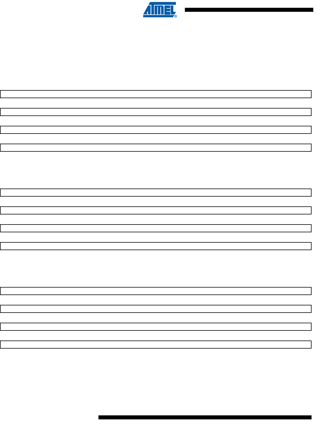
172
6430F–ATARM–21-Feb-12
SAM3U Series
13.19.7 Interrupt Priority Registers
The IPR0-IPR7 registers provide a 4-bit priority field for each interrupt (See the “Peripheral Iden-
tifiers” section of the datasheet for more details). These registers are byte-accessible. See the
register summary in Table 13-27 on page 165 for their attributes. Each register holds four priority
fields, that map up to four elements in the CMSIS interrupt priority array
IP[0]
to
IP[29]
, as shown:
13.19.7.1 IPRm
13.19.7.2 IPR4
13.19.7.3 IPR3
31 30 29 28 27 26 25 24
IP[4m+3]
23 22 21 20 19 18 17 16
IP[4m+2]
15 14 13 12 11 10 9 8
IP[4m+1]
76543210
IP[4m]
31 30 29 28 27 26 25 24
IP[19]
23 22 21 20 19 18 17 16
IP[18]
15 14 13 12 11 10 9 8
IP[17]
76543210
IP[16]
31 30 29 28 27 26 25 24
IP[15]
23 22 21 20 19 18 17 16
IP[14]
15 14 13 12 11 10 9 8
IP[13]
76543210
IP[12]
173
6430F–ATARM–21-Feb-12
SAM3U Series
13.19.7.4 IPR2
13.19.7.5 IPR1
13.19.7.6 IPR0
• Priority, byte offset 3
• Priority, byte offset 2
• Priority, byte offset 1
• Priority, byte offset 0
Each priority field holds a priority value, 0-15. The lower the value, the greater the priority of the corresponding interrupt.
The processor implements only bits[7:4] of each field, bits[3:0] read as zero and ignore writes.
See “The CMSIS mapping of the Cortex-M3 NVIC registers” on page 165 for more information about the IP[0] to IP[29]
interrupt priority array, that provides the software view of the interrupt priorities.
31 30 29 28 27 26 25 24
IP[11]
23 22 21 20 19 18 17 16
IP[10]
15 14 13 12 11 10 9 8
IP[9]
76543210
IP[8]
31 30 29 28 27 26 25 24
IP[7]
23 22 21 20 19 18 17 16
IP[6]
15 14 13 12 11 10 9 8
IP[5]
76543210
IP[4]
31 30 29 28 27 26 25 24
IP[3]
23 22 21 20 19 18 17 16
IP[2]
15 14 13 12 11 10 9 8
IP[1]
76543210
IP[0]

174
6430F–ATARM–21-Feb-12
SAM3U Series
Find the IPR number and byte offset for interrupt N as follows:
• the corresponding IPR number, M, is given by M = N DIV 4
• the byte offset of the required Priority field in this register is N MOD 4, where:
– byte offset 0 refers to register bits[7:0]
– byte offset 1 refers to register bits[15:8]
– byte offset 2 refers to register bits[23:16]
– byte offset 3 refers to register bits[31:24].
175
6430F–ATARM–21-Feb-12
SAM3U Series
13.19.8 Software Trigger Interrupt Register
Write to the STIR to generate a Software Generated Interrupt (SGI). See the register summary
in Table 13-27 on page 165 for the STIR attributes.
When the USERSETMPEND bit in the SCR is set to 1, unprivileged software can access the
STIR, see “System Control Register” on page 187.
Only privileged software can enable unprivileged access to the STIR.
The bit assignments are:
•INTID
Interrupt ID of the required SGI, in the range 0-239. For example, a value of b000000011 specifies interrupt IRQ3.
31 30 29 28 27 26 25 24
Reserved
23 22 21 20 19 18 17 16
Reserved
15 14 13 12 11 10 9 8
Reserved INTID
76543210
INTID

176
6430F–ATARM–21-Feb-12
SAM3U Series
13.19.9 Level-sensitive interrupts
The processor supports level-sensitive interrupts.
A level-sensitive interrupt is held asserted until the peripheral deasserts the interrupt signal. Typ-
ically this happens because the ISR accesses the peripheral, causing it to clear the interrupt
request.
When the processor enters the ISR, it automatically removes the pending state from the inter-
rupt, see “Hardware and software control of interrupts”. For a level-sensitive interrupt, if the
signal is not deasserted before the processor returns from the ISR, the interrupt becomes pend-
ing again, and the processor must execute its ISR again. This means that the peripheral can
hold the interrupt signal asserted until it no longer needs servicing.
13.19.9.1 Hardware and software control of interrupts
The Cortex-M3 latches all interrupts. A peripheral interrupt becomes pending for one of the fol-
lowing reasons:
• the NVIC detects that the interrupt signal is HIGH and the interrupt is not active
• the NVIC detects a rising edge on the interrupt signal
• software writes to the corresponding interrupt set-pending register bit, see “Interrupt Set-
pending Registers” on page 169, or to the STIR to make an SGI pending, see “Software
Trigger Interrupt Register” on page 175.
A pending interrupt remains pending until one of the following:
The processor enters the ISR for the interrupt. This changes the state of the interrupt from pend-
ing to active. Then:
– For a level-sensitive interrupt, when the processor returns from the ISR, the NVIC
samples the interrupt signal. If the signal is asserted, the state of the interrupt
changes to pending, which might cause the processor to immediately re-enter the
ISR. Otherwise, the state of the interrupt changes to inactive.
– If the interrupt signal is not pulsed while the processor is in the ISR, when the
processor returns from the ISR the state of the interrupt changes to inactive.
• Software writes to the corresponding interrupt clear-pending register bit.
For a level-sensitive interrupt, if the interrupt signal is still asserted, the state of the interrupt
does not change. Otherwise, the state of the interrupt changes to inactive.

177
6430F–ATARM–21-Feb-12
SAM3U Series
13.19.10 NVIC design hints and tips
Ensure software uses correctly aligned register accesses. The processor does not support
unaligned accesses to NVIC registers. See the individual register descriptions for the supported
access sizes.
A interrupt can enter pending state even it is disabled.
Before programming VTOR to relocate the vector table, ensure the vector table entries of the
new vector table are setup for fault handlers and all enabled exception like interrupts. For more
information see “Vector Table Offset Register” on page 184.
13.19.10.1 NVIC programming hints
Software uses the CPSIE I and CPSID I instructions to enable and disable interrupts. The
CMSIS provides the following intrinsic functions for these instructions:
void __disable_irq(void) // Disable Interrupts
void __enable_irq(void) // Enable Interrupts
In addition, the CMSIS provides a number of functions for NVIC control, including:
For more information about these functions see the CMSIS documentation.
Table 13-29. CMSIS functions for NVIC control
CMSIS interrupt control function Description
void NVIC_SetPriorityGrouping(uint32_t
priority_grouping) Set the priority grouping
void NVIC_EnableIRQ(IRQn_t IRQn) Enable IRQn
void NVIC_DisableIRQ(IRQn_t IRQn) Disable IRQn
uint32_t NVIC_GetPendingIRQ (IRQn_t IRQn) Return true if IRQn is pending
void NVIC_SetPendingIRQ (IRQn_t IRQn) Set IRQn pending
void NVIC_ClearPendingIRQ (IRQn_t IRQn) Clear IRQn pending status
uint32_t NVIC_GetActive (IRQn_t IRQn) Return the IRQ number of the active
interrupt
void NVIC_SetPriority (IRQn_t IRQn, uint32_t priority) Set priority for IRQn
uint32_t NVIC_GetPriority (IRQn_t IRQn) Read priority of IRQn
void NVIC_SystemReset (void) Reset the system

178
6430F–ATARM–21-Feb-12
SAM3U Series
13.20 System control block
The System control block (SCB) provides system implementation information, and system con-
trol. This includes configuration, control, and reporting of the system exceptions. The system
control block registers are:
Notes: 1. See the register description for more information.
2. A subregister of the CFSR.
13.20.1 The CMSIS mapping of the Cortex-M3 SCB registers
To improve software efficiency, the CMSIS simplifies the SCB register presentation. In the
CMSIS, the byte array SHP[0] to SHP[12] corresponds to the registers SHPR1-SHPR3.
Table 13-30. Summary of the system control block registers
Address Name Type
Required
privilege
Reset
value Description
0xE000E008 ACTLR RW Privileged 0x00000000 “Auxiliary Control Register” on page 179
0xE000ED00 CPUID RO Privileged 0x412FC230 “CPUID Base Register” on page 180
0xE000ED04 ICSR RW(1) Privileged 0x00000000 “Interrupt Control and State Register” on page 181
0xE000ED08 VTOR RW Privileged 0x00000000 “Vector Table Offset Register” on page 184
0xE000ED0C AIRCR RW(1) Privileged 0xFA050000 “Application Interrupt and Reset Control Register” on page
185
0xE000ED10 SCR RW Privileged 0x00000000 “System Control Register” on page 187
0xE000ED14 CCR RW Privileged 0x00000200 “Configuration and Control Register” on page 188
0xE000ED18 SHPR1 RW Privileged 0x00000000 “System Handler Priority Register 1” on page 191
0xE000ED1C SHPR2 RW Privileged 0x00000000 “System Handler Priority Register 2” on page 192
0xE000ED20 SHPR3 RW Privileged 0x00000000 “System Handler Priority Register 3” on page 192
0xE000ED24 SHCRS RW Privileged 0x00000000 “System Handler Control and State Register” on page 193
0xE000ED28 CFSR RW Privileged 0x00000000 “Configurable Fault Status Register” on page 195
0xE000ED28 MMSR(2) RW Privileged 0x00 “Memory Management Fault Address Register” on page
202
0xE000ED29 BFSR(2) RW Privileged 0x00 “Bus Fault Status Register” on page 197
0xE000ED2A UFSR(2) RW Privileged 0x0000 “Usage Fault Status Register” on page 199
0xE000ED2C HFSR RW Privileged 0x00000000 “Hard Fault Status Register” on page 201
0xE000ED34 MMAR RW Privileged Unknown “Memory Management Fault Address Register” on page
202
0xE000ED38 BFAR RW Privileged Unknown “Bus Fault Address Register” on page 203
0xE000ED3C AFSR RW Privileged 0x00000000 “Auxiliary Fault Status Register” on page 204

179
6430F–ATARM–21-Feb-12
SAM3U Series
13.20.2 Auxiliary Control Register
The ACTLR provides disable bits for the following processor functions:
• IT folding
• write buffer use for accesses to the default memory map
• interruption of multi-cycle instructions.
See the register summary in Table 13-30 on page 178 for the ACTLR attributes. The bit assign-
ments are:
•DISFOLD
When set to 1, disables IT folding. see “About IT folding” on page 179 for more information.
•DISDEFWBUF
When set to 1, disables write buffer use during default memory map accesses. This causes all bus faults to be precise bus
faults but decreases performance because any store to memory must complete before the processor can execute the next
instruction.
This bit only affects write buffers implemented in the Cortex-M3 processor.
• DISMCYCINT
When set to 1, disables interruption of load multiple and store multiple instructions. This increases the interrupt latency of
the processor because any LDM or STM must complete before the processor can stack the current state and enter the
interrupt handler.
13.20.2.1 About IT folding
In some situations, the processor can start executing the first instruction in an IT block while it is
still executing the IT instruction. This behavior is called IT folding, and improves performance,
However, IT folding can cause jitter in looping. If a task must avoid jitter, set the DISFOLD bit to
1 before executing the task, to disable IT folding.
31 30 29 28 27 26 25 24
Reserved
23 22 21 20 19 18 17 16
Reserved
15 14 13 12 11 10 9 8
Reserved
76543210
Reserved DISFOLD DISDEFWBUF DISMCYCINT

180
6430F–ATARM–21-Feb-12
SAM3U Series
13.20.3 CPUID Base Register
The CPUID register contains the processor part number, version, and implementation informa-
tion. See the register summary in Table 13-30 on page 178 for its attributes. The bit assignments
are:
• Implementer
Implementer code:
0x41 = ARM
•Variant
Variant number, the r value in the rnpn product revision identifier:
0x2 = r2p0
• Constant
Reads as 0xF
•PartNo
Part number of the processor:
0xC23 = Cortex-M3
• Revision
Revision number, the p value in the rnpn product revision identifier:
0x0 = r2p0
31 30 29 28 27 26 25 24
Implementer
23 22 21 20 19 18 17 16
Variant Constant
15 14 13 12 11 10 9 8
PartNo
76543210
PartNo Revision
181
6430F–ATARM–21-Feb-12
SAM3U Series
13.20.4 Interrupt Control and State Register
The ICSR:
• provides:
– set-pending and clear-pending bits for the PendSV and SysTick exceptions
• indicates:
– the exception number of the exception being processed
– whether there are preempted active exceptions
– the exception number of the highest priority pending exception
– whether any interrupts are pending.
See the register summary in Table 13-30 on page 178, and the Type descriptions in Table 13-33
on page 205, for the ICSR attributes. The bit assignments are:
• PENDSVSET
RW
PendSV set-pending bit.
Write:
0 = no effect
1 = changes PendSV exception state to pending.
Read:
0 = PendSV exception is not pending
1 = PendSV exception is pending.
Writing 1 to this bit is the only way to set the PendSV exception state to pending.
• PENDSVCLR
WO
PendSV clear-pending bit.
Write:
0 = no effect
1 = removes the pending state from the PendSV exception.
31 30 29 28 27 26 25 24
Reserved Reserved PENDSVSET PENDSVCLR PENDSTSET PENDSTCLR Reserved
23 22 21 20 19 18 17 16
Reserved for
Debug ISRPENDING VECTPENDING
15 14 13 12 11 10 9 8
VECTPENDING RETTOBASE Reserved VECTACTIVE
76543210
VECTACTIVE

182
6430F–ATARM–21-Feb-12
SAM3U Series
• PENDSTSET
RW
SysTick exception set-pending bit.
Write:
0 = no effect
1 = changes SysTick exception state to pending.
Read:
0 = SysTick exception is not pending
1 = SysTick exception is pending.
• PENDSTCLR
WO
SysTick exception clear-pending bit.
Write:
0 = no effect
1 = removes the pending state from the SysTick exception.
This bit is WO. On a register read its value is Unknown.
• Reserved for Debug use
RO
This bit is reserved for Debug use and reads-as-zero when the processor is not in Debug.
• ISRPENDING
RO
Interrupt pending flag, excluding Faults:
0 = interrupt not pending
1 = interrupt pending.
• VECTPENDING
RO
Indicates the exception number of the highest priority pending enabled exception:
0 = no pending exceptions
Nonzero = the exception number of the highest priority pending enabled exception.
The value indicated by this field includes the effect of the BASEPRI and FAULTMASK registers, but not any effect of the
PRIMASK register.

183
6430F–ATARM–21-Feb-12
SAM3U Series
• RETTOBASE
RO
Indicates whether there are preempted active exceptions:
0 = there are preempted active exceptions to execute
1 = there are no active exceptions, or the currently-executing exception is the only active exception.
• VECTACTIVE
RO
Contains the active exception number:
0 = Thread mode
Nonzero = The exception number (1) of the currently active exception.
Subtract 16 from this value to obtain the IRQ number required to index into the Interrupt Clear-Enable, Set-Enable, Clear-
Pending, Set-Pending, or Priority Registers, see “Interrupt Program Status Register” on page 61.
When you write to the ICSR, the effect is Unpredictable if you:
• write 1 to the PENDSVSET bit and write 1 to the PENDSVCLR bit
• write 1 to the PENDSTSET bit and write 1 to the PENDSTCLR bit.
Note: 1. This is the same value as IPSR bits [8:0] see “Interrupt Program Status Register” on page 61.

184
6430F–ATARM–21-Feb-12
SAM3U Series
13.20.5 Vector Table Offset Register
The VTOR indicates the offset of the vector table base address from memory address
0x00000000. See the register summary in Table 13-30 on page 178 for its attributes.
The bit assignments are:
•TBLOFF
Vector table base offset field. It contains bits[29:7] of the offset of the table base from the bottom of the memory map.
Bit[29] determines whether the vector table is in the code or SRAM memory region:
0 = code
1 = SRAM.
Bit[29] is sometimes called the TBLBASE bit.
When setting TBLOFF, you must align the offset to the number of exception entries in the vector table. The minimum align-
ment is 32 words, enough for up to 16 interrupts. For more interrupts, adjust the alignment by rounding up to the next power
of two. For example, if you require 21 interrupts, the alignment must be on a 64-word boundary because the required table
size is 37 words, and the next power of two is 64.
Table alignment requirements mean that bits[6:0] of the table offset are always zero.
31 30 29 28 27 26 25 24
Reserved TBLOFF
23 22 21 20 19 18 17 16
TBLOFF
15 14 13 12 11 10 9 8
TBLOFF
76543210
TBLOFF Reserved
185
6430F–ATARM–21-Feb-12
SAM3U Series
13.20.6 Application Interrupt and Reset Control Register
The AIRCR provides priority grouping control for the exception model, endian status for data
accesses, and reset control of the system. See the register summary in Table 13-30 on page
178 and Table 13-33 on page 205 for its attributes.
To write to this register, you must write
0x05FA
to the VECTKEY field, otherwise the processor
ignores the write.
The bit assignments are:
• VECTKEYSTAT
Register Key:
Reads as 0xFA05
• VECTKEY
Register key:
On writes, write 0x5FA to VECTKEY, otherwise the write is ignored.
• ENDIANESS
RO
Data endianness bit:
0 = Little-endian
ENDIANESS is set from the BIGEND configuration signal during reset.
•PRIGROUP
R/W
Interrupt priority grouping field. This field determines the split of group priority from subpriority, see “Binary point” on page
186.
• SYSRESETREQ
WO
System reset request:
0 = no effect
1 = asserts a proc_reset_signal.
This is intended to force a large system reset of all major components except for debug.
This bit reads as 0.
31 30 29 28 27 26 25 24
On Read: VECTKEYSTAT, On Write: VECTKEY
23 22 21 20 19 18 17 16
On Read: VECTKEYSTAT, On Write: VECTKEY
15 14 13 12 11 10 9 8
ENDIANESS Reserved PRIGROUP
76543210
Reserved
SYSRESETREQ
VECTCLR-
ACTIVE VECTRESET

186
6430F–ATARM–21-Feb-12
SAM3U Series
• VECTCLRACTIVE
WO
Reserved for Debug use. This bit reads as 0. When writing to the register you must write 0 to this bit, otherwise behavior is
Unpredictable.
• VECTRESET
WO
Reserved for Debug use. This bit reads as 0. When writing to the register you must write 0 to this bit, otherwise behavior is
Unpredictable.
13.20.6.1 Binary point
The PRIGROUP field indicates the position of the binary point that splits the PRI_n fields in the
Interrupt Priority Registers into separate group priority and subpriority fields. Table 13-31 shows
how the PRIGROUP value controls this split.
Determining preemption of an exception uses only the group priority field, see “Interrupt priority
grouping” on page 82.
Table 13-31. Priority grouping
Interrupt priority level value, PRI_N[7:0] Number of
PRIGROUP
Binary
point (1)
1. PRI_n[7:0] field showing the binary point. x denotes a group priority field bit, and y denotes a sub-
priority field bit.
Group priority
bits
Subpriority
bits
Group
priorities Subpriorities
b011 bxxxx.0000 [7:4] None 16 1
b100 bxxx.y0000 [7:5] [4] 8 2
b101 bxx.yy0000 [7:6] [5:4] 4 4
b110 bx.yyy0000 [7] [6:4] 2 8
b111 b.yyyy0000 None [7:4] 1 16

187
6430F–ATARM–21-Feb-12
SAM3U Series
13.20.7 System Control Register
The SCR controls features of entry to and exit from low power state. See the register summary
in Table 13-30 on page 178 for its attributes. The bit assignments are:
• SEVONPEND
Send Event on Pending bit:
0 = only enabled interrupts or events can wakeup the processor, disabled interrupts are excluded
1 = enabled events and all interrupts, including disabled interrupts, can wakeup the processor.
When an event or interrupt enters pending state, the event signal wakes up the processor from WFE. If the processor is not
waiting for an event, the event is registered and affects the next WFE.
The processor also wakes up on execution of an
SEV
instruction or an external event.
• SLEEPDEEP
Controls whether the processor uses sleep or deep sleep as its low power mode:
0 = sleep
1 = deep sleep.
• SLEEPONEXIT
Indicates sleep-on-exit when returning from Handler mode to Thread mode:
0 = do not sleep when returning to Thread mode.
1 = enter sleep, or deep sleep, on return from an ISR.
Setting this bit to 1 enables an interrupt driven application to avoid returning to an empty main application.
31 30 29 28 27 26 25 24
Reserved
23 22 21 20 19 18 17 16
Reserved
15 14 13 12 11 10 9 8
Reserved
76543210
Reserved SEVONPEND Reserved SLEEPDEEP SLEEONEXIT Reserved
188
6430F–ATARM–21-Feb-12
SAM3U Series
13.20.8 Configuration and Control Register
The CCR controls entry to Thread mode and enables:
• the handlers for hard fault and faults escalated by FAULTMASK to ignore bus faults
• trapping of divide by zero and unaligned accesses
• access to the STIR by unprivileged software, see “Software Trigger Interrupt Register” on
page 175.
See the register summary in Table 13-30 on page 178 for the CCR attributes.
The bit assignments are:
• STKALIGN
Indicates stack alignment on exception entry:
0 = 4-byte aligned
1 = 8-byte aligned.
On exception entry, the processor uses bit[9] of the stacked PSR to indicate the stack alignment. On return from the excep-
tion it uses this stacked bit to restore the correct stack alignment.
• BFHFNMIGN
Enables handlers with priority -1 or -2 to ignore data bus faults caused by load and store instructions. This applies to the
hard fault and FAULTMASK escalated handlers:
0 = data bus faults caused by load and store instructions cause a lock-up
1 = handlers running at priority -1 and -2 ignore data bus faults caused by load and store instructions.
Set this bit to 1 only when the handler and its data are in absolutely safe memory. The normal use of this bit is to probe sys-
tem devices and bridges to detect control path problems and fix them.
• DIV_0_TRP
Enables faulting or halting when the processor executes an SDIV or UDIV instruction with a divisor of 0:
0 = do not trap divide by 0
1 = trap divide by 0.
When this bit is set to 0,a divide by zero returns a quotient of 0.
• UNALIGN_TRP
Enables unaligned access traps:
0 = do not trap unaligned halfword and word accesses
31 30 29 28 27 26 25 24
Reserved
23 22 21 20 19 18 17 16
Reserved
15 14 13 12 11 10 9 8
Reserved STKALIGN BFHFNMIGN
76543210
Reserved DIV_0_TRP UNALIGN_T
RP Reserved USERSETM
PEND NONBASET
HRDENA

189
6430F–ATARM–21-Feb-12
SAM3U Series
1 = trap unaligned halfword and word accesses.
If this bit is set to 1, an unaligned access generates a usage fault.
Unaligned LDM, STM, LDRD, and STRD instructions always fault irrespective of whether UNALIGN_TRP is set to 1.
• USERSETMPEND
Enables unprivileged software access to the STIR, see “Software Trigger Interrupt Register” on page 175:
0 = disable
1 = enable.
• NONEBASETHRDENA
Indicates how the processor enters Thread mode:
0 = processor can enter Thread mode only when no exception is active.
1 = processor can enter Thread mode from any level under the control of an EXC_RETURN value, see “Exception return”
on page 84.

190
6430F–ATARM–21-Feb-12
SAM3U Series
13.20.9 System Handler Priority Registers
The SHPR1-SHPR3 registers set the priority level, 0 to 15 of the exception handlers that have
configurable priority.
SHPR1-SHPR3 are byte accessible. See the register summary in Table 13-30 on page 178 for
their attributes.
The system fault handlers and the priority field and register for each handler are:
Each PRI_N field is 8 bits wide, but the processor implements only bits[7:4] of each field, and
bits[3:0] read as zero and ignore writes.
Table 13-32. System fault handler priority fields
Handler Field Register description
Memory management
fault PRI_4
“System Handler Priority Register 1” on page 191
Bus fault PRI_5
Usage fault PRI_6
SVCall PRI_11 “System Handler Priority Register 2” on page 192
PendSV PRI_14 “System Handler Priority Register 3” on page 192
SysTick PRI_15

191
6430F–ATARM–21-Feb-12
SAM3U Series
13.20.9.1 System Handler Priority Register 1
The bit assignments are:
•PRI_7
Reserved
•PRI_6
Priority of system handler 6, usage fault
•PRI_5
Priority of system handler 5, bus fault
•PRI_4
Priority of system handler 4, memory management fault
31 30 29 28 27 26 25 24
PRI_7: Reserved
23 22 21 20 19 18 17 16
PRI_6
15 14 13 12 11 10 9 8
PRI_5
76543210
PRI_4

192
6430F–ATARM–21-Feb-12
SAM3U Series
13.20.9.2 System Handler Priority Register 2
The bit assignments are:
•PRI_11
Priority of system handler 11, SVCall
13.20.9.3 System Handler Priority Register 3
The bit assignments are:
•PRI_15
Priority of system handler 15, SysTick exception
•PRI_14
Priority of system handler 14, PendSV
31 30 29 28 27 26 25 24
PRI_11
23 22 21 20 19 18 17 16
Reserved
15 14 13 12 11 10 9 8
Reserved
76543210
Reserved
31 30 29 28 27 26 25 24
PRI_15
23 22 21 20 19 18 17 16
PRI_14
15 14 13 12 11 10 9 8
Reserved
76543210
Reserved

193
6430F–ATARM–21-Feb-12
SAM3U Series
13.20.10 System Handler Control and State Register
The SHCSR enables the system handlers, and indicates:
• the pending status of the bus fault, memory management fault, and SVC exceptions
• the active status of the system handlers.
See the register summary in Table 13-30 on page 178 for the SHCSR attributes. The bit assign-
ments are:
• USGFAULTENA
Usage fault enable bit, set to 1 to enable (1)
• BUSFAULTENA
Bus fault enable bit, set to 1 to enable(3)
• MEMFAULTENA
Memory management fault enable bit, set to 1 to enable(3)
• SVCALLPENDED
SVC call pending bit, reads as 1 if exception is pending (2)
• BUSFAULTPENDED
Bus fault exception pending bit, reads as 1 if exception is pending(2)
• MEMFAULTPENDED
Memory management fault exception pending bit, reads as 1 if exception is pending(2)
• USGFAULTPENDED
Usage fault exception pending bit, reads as 1 if exception is pending(2)
• SYSTICKACT
SysTick exception active bit, reads as 1 if exception is active (3)
• PENDSVACT
PendSV exception active bit, reads as 1 if exception is active
31 30 29 28 27 26 25 24
Reserved
23 22 21 20 19 18 17 16
Reserved USGFAULTENA BUSFAULTENA MEMFAULTENA
15 14 13 12 11 10 9 8
SVCALLPENDE
D
BUSFAULTPEND
ED
MEMFAULTPEN
DED
USGFAULTPEND
ED SYSTICKACT PENDSVACT Reserved MONITORACT
76543210
SVCALLAVCT Reserved USGFAULTACT Reserved BUSFAULTACT MEMFAULTACT
1. Enable bits, set to 1 to enable the exception, or set to 0 to disable the exception.
2. Pending bits, read as 1 if the exception is pending, or as 0 if it is not pending. You can write to these bits to change the pending
status of the exceptions.
3. Active bits, read as 1 if the exception is active, or as 0 if it is not active. You can write to these bits to change the active status of
the exceptions, but see the Caution in this section.

194
6430F–ATARM–21-Feb-12
SAM3U Series
• MONITORACT
Debug monitor active bit, reads as 1 if Debug monitor is active
• SVCALLACT
SVC call active bit, reads as 1 if SVC call is active
•USGFAULTACT
Usage fault exception active bit, reads as 1 if exception is active
• BUSFAULTACT
Bus fault exception active bit, reads as 1 if exception is active
• MEMFAULTACT
Memory management fault exception active bit, reads as 1 if exception is active
If you disable a system handler and the corresponding fault occurs, the processor treats the fault as a hard fault.
You can write to this register to change the pending or active status of system exceptions. An OS kernel can write to the
active bits to perform a context switch that changes the current exception type.
• Software that changes the value of an active bit in this register without correct adjustment to the stacked content can
cause the processor to generate a fault exception. Ensure software that writes to this register retains and subsequently
restores the current active status.
• After you have enabled the system handlers, if you have to change the value of a bit in this register you must use a read-
modify-write procedure to ensure that you change only the required bit.

195
6430F–ATARM–21-Feb-12
SAM3U Series
13.20.11 Configurable Fault Status Register
The CFSR indicates the cause of a memory management fault, bus fault, or usage fault. See the
register summary in Table 13-30 on page 178 for its attributes. The bit assignments are:
The following subsections describe the subregisters that make up the CFSR:
•“Memory Management Fault Status Register” on page 196
•“Bus Fault Status Register” on page 197
•“Usage Fault Status Register” on page 199.
The CFSR is byte accessible. You can access the CFSR or its subregisters as follows:
• access the complete CFSR with a word access to 0xE000ED28
• access the MMFSR with a byte access to 0xE000ED28
• access the MMFSR and BFSR with a halfword access to 0xE000ED28
• access the BFSR with a byte access to 0xE000ED29
• access the UFSR with a halfword access to 0xE000ED2A.
31 30 29 28 27 26 25 24
Usage Fault Status Register: UFSR
23 22 21 20 19 18 17 16
Usage Fault Status Register: UFSR
15 14 13 12 11 10 9 8
Bus Fault Status Register: BFSR
76543210
Memory Management Fault Status Register: MMFSR

196
6430F–ATARM–21-Feb-12
SAM3U Series
13.20.11.1 Memory Management Fault Status Register
The flags in the MMFSR indicate the cause of memory access faults. The bit assignments are:
•MMARVALID
Memory Management Fault Address Register (MMAR) valid flag:
0 = value in MMAR is not a valid fault address
1 = MMAR holds a valid fault address.
If a memory management fault occurs and is escalated to a hard fault because of priority, the hard fault handler must set
this bit to 0. This prevents problems on return to a stacked active memory management fault handler whose MMAR value
has been overwritten.
• MSTKERR
Memory manager fault on stacking for exception entry:
0 = no stacking fault
1 = stacking for an exception entry has caused one or more access violations.
When this bit is 1, the SP is still adjusted but the values in the context area on the stack might be incorrect. The processor
has not written a fault address to the MMAR.
• MUNSTKERR
Memory manager fault on unstacking for a return from exception:
0 = no unstacking fault
1 = unstack for an exception return has caused one or more access violations.
This fault is chained to the handler. This means that when this bit is 1, the original return stack is still present. The proces-
sor has not adjusted the SP from the failing return, and has not performed a new save. The processor has not written a
fault address to the MMAR.
•DACCVIOL
Data access violation flag:
0 = no data access violation fault
1 = the processor attempted a load or store at a location that does not permit the operation.
When this bit is 1, the PC value stacked for the exception return points to the faulting instruction. The processor has loaded
the MMAR with the address of the attempted access.
• IACCVIOL
Instruction access violation flag:
0 = no instruction access violation fault
1 = the processor attempted an instruction fetch from a location that does not permit execution.
This fault occurs on any access to an XN region, even when the MPU is disabled or not present.
When this bit is 1, the PC value stacked for the exception return points to the faulting instruction. The processor has not
written a fault address to the MMAR.
76543210
MMARVALID Reserved MSTKERR MUNSTKERR Reserved DACCVIOL IACCVIOL

197
6430F–ATARM–21-Feb-12
SAM3U Series
13.20.11.2 Bus Fault Status Register
The flags in the BFSR indicate the cause of a bus access fault. The bit assignments are:
•BFARVALID
Bus Fault Address Register (BFAR) valid flag:
0 = value in BFAR is not a valid fault address
1 = BFAR holds a valid fault address.
The processor sets this bit to 1 after a bus fault where the address is known. Other faults can set this bit to 0, such as a
memory management fault occurring later.
If a bus fault occurs and is escalated to a hard fault because of priority, the hard fault handler must set this bit to 0. This pre-
vents problems if returning to a stacked active bus fault handler whose BFAR value has been overwritten.
•STKERR
Bus fault on stacking for exception entry:
0 = no stacking fault
1 = stacking for an exception entry has caused one or more bus faults.
When the processor sets this bit to 1, the SP is still adjusted but the values in the context area on the stack might be incor-
rect. The processor does not write a fault address to the BFAR.
• UNSTKERR
Bus fault on unstacking for a return from exception:
0 = no unstacking fault
1 = unstack for an exception return has caused one or more bus faults.
This fault is chained to the handler. This means that when the processor sets this bit to 1, the original return stack is still
present. The processor does not adjust the SP from the failing return, does not performed a new save, and does not write
a fault address to the BFAR.
• IMPRECISERR
Imprecise data bus error:
0 = no imprecise data bus error
1 = a data bus error has occurred, but the return address in the stack frame is not related to the instruction that caused the
error.
When the processor sets this bit to 1, it does not write a fault address to the BFAR.
This is an asynchronous fault. Therefore, if it is detected when the priority of the current process is higher than the bus fault
priority, the bus fault becomes pending and becomes active only when the processor returns from all higher priority pro-
cesses. If a precise fault occurs before the processor enters the handler for the imprecise bus fault, the handler detects
both IMPRECISERR set to 1 and one of the precise fault status bits set to 1.
76543210
BFRVALID Reserved STKERR UNSTKERR IMPRECISERR PRECISERR IBUSERR

198
6430F–ATARM–21-Feb-12
SAM3U Series
• PRECISERR
Precise data bus error:
0 = no precise data bus error
1 = a data bus error has occurred, and the PC value stacked for the exception return points to the instruction that caused
the fault.
When the processor sets this bit is 1, it writes the faulting address to the BFAR.
• IBUSERR
Instruction bus error:
0 = no instruction bus error
1 = instruction bus error.
The processor detects the instruction bus error on prefetching an instruction, but it sets the IBUSERR flag to 1 only if it
attempts to issue the faulting instruction.
When the processor sets this bit is 1, it does not write a fault address to the BFAR.

199
6430F–ATARM–21-Feb-12
SAM3U Series
13.20.11.3 Usage Fault Status Register
The UFSR indicates the cause of a usage fault. The bit assignments are:
•DIVBYZERO
Divide by zero usage fault:
0 = no divide by zero fault, or divide by zero trapping not enabled
1 = the processor has executed an SDIV or UDIV instruction with a divisor of 0.
When the processor sets this bit to 1, the PC value stacked for the exception return points to the instruction that performed
the divide by zero.
Enable trapping of divide by zero by setting the DIV_0_TRP bit in the CCR to 1, see “Configuration and Control Register”
on page 188.
• UNALIGNED
Unaligned access usage fault:
0 = no unaligned access fault, or unaligned access trapping not enabled
1 = the processor has made an unaligned memory access.
Enable trapping of unaligned accesses by setting the UNALIGN_TRP bit in the CCR to 1, see “Configuration and Control
Register” on page 188.
Unaligned LDM, STM, LDRD, and STRD instructions always fault irrespective of the setting of UNALIGN_TRP.
•NOCP
No coprocessor usage fault. The processor does not support coprocessor instructions:
0 = no usage fault caused by attempting to access a coprocessor
1 = the processor has attempted to access a coprocessor.
•INVPC
Invalid PC load usage fault, caused by an invalid PC load by EXC_RETURN:
0 = no invalid PC load usage fault
1 = the processor has attempted an illegal load of EXC_RETURN to the PC, as a result of an invalid context, or an invalid
EXC_RETURN value.
When this bit is set to 1, the PC value stacked for the exception return points to the instruction that tried to perform the ille-
gal load of the PC.
•INVSTATE
Invalid state usage fault:
0 = no invalid state usage fault
1 = the processor has attempted to execute an instruction that makes illegal use of the EPSR.
15 14 13 12 11 10 9 8
Reserved DIVBYZERO UNALIGNED
76543210
Reserved NOCP INVPC INVSTATE UNDEFINSTR

200
6430F–ATARM–21-Feb-12
SAM3U Series
When this bit is set to 1, the PC value stacked for the exception return points to the instruction that attempted the illegal use
of the EPSR.
This bit is not set to 1 if an undefined instruction uses the EPSR.
• UNDEFINSTR
Undefined instruction usage fault:
0 = no undefined instruction usage fault
1 = the processor has attempted to execute an undefined instruction.
When this bit is set to 1, the PC value stacked for the exception return points to the undefined instruction.
An undefined instruction is an instruction that the processor cannot decode.
The UFSR bits are sticky. This means as one or more fault occurs, the associated bits are set to 1. A bit that is set to 1 is
cleared to 0 only by writing 1 to that bit, or by a reset.

201
6430F–ATARM–21-Feb-12
SAM3U Series
13.20.12 Hard Fault Status Register
The HFSR gives information about events that activate the hard fault handler. See the register
summary in Table 13-30 on page 178 for its attributes.
This register is read, write to clear. This means that bits in the register read normally, but writing
1 to any bit clears that bit to 0. The bit assignments are:
• DEBUGEVT
Reserved for Debug use. When writing to the register you must write 0 to this bit, otherwise behavior is Unpredictable.
•FORCED
Indicates a forced hard fault, generated by escalation of a fault with configurable priority that cannot be handles, either
because of priority or because it is disabled:
0 = no forced hard fault
1 = forced hard fault.
When this bit is set to 1, the hard fault handler must read the other fault status registers to find the cause of the fault.
• VECTTBL
Indicates a bus fault on a vector table read during exception processing:
0 = no bus fault on vector table read
1 = bus fault on vector table read.
This error is always handled by the hard fault handler.
When this bit is set to 1, the PC value stacked for the exception return points to the instruction that was preempted by the
exception.
The HFSR bits are sticky. This means as one or more fault occurs, the associated bits are set to 1. A bit that is set to 1 is
cleared to 0 only by writing 1 to that bit, or by a reset.
31 30 29 28 27 26 25 24
DEBUGEVT FORCED Reserved
23 22 21 20 19 18 17 16
Reserved
15 14 13 12 11 10 9 8
Reserved
76543210
Reserved VECTTBL Reserved

202
6430F–ATARM–21-Feb-12
SAM3U Series
13.20.13 Memory Management Fault Address Register
The MMFAR contains the address of the location that generated a memory management fault.
See the register summary in Table 13-30 on page 178 for its attributes. The bit assignments are:
• ADDRESS
When the MMARVALID bit of the MMFSR is set to 1, this field holds the address of the location that generated the memory
management fault
When an unaligned access faults, the address is the actual address that faulted. Because a single read or write instruction
can be split into multiple aligned accesses, the fault address can be any address in the range of the requested access size.
Flags in the MMFSR indicate the cause of the fault, and whether the value in the MMFAR is valid. See “Memory Manage-
ment Fault Status Register” on page 196.
31 30 29 28 27 26 25 24
ADDRESS
23 22 21 20 19 18 17 16
ADDRESS
15 14 13 12 11 10 9 8
ADDRESS
76543210
ADDRESS

203
6430F–ATARM–21-Feb-12
SAM3U Series
13.20.14 Bus Fault Address Register
The BFAR contains the address of the location that generated a bus fault. See the register sum-
mary in Table 13-30 on page 178 for its attributes. The bit assignments are:
• ADDRESS
When the BFARVALID bit of the BFSR is set to 1, this field holds the address of the location that generated the bus fault
When an unaligned access faults the address in the BFAR is the one requested by the instruction, even if it is not the
address of the fault.
Flags in the BFSR indicate the cause of the fault, and whether the value in the BFAR is valid. See “Bus Fault Status Regis-
ter” on page 197.
31 30 29 28 27 26 25 24
ADDRESS
23 22 21 20 19 18 17 16
ADDRESS
15 14 13 12 11 10 9 8
ADDRESS
76543210
ADDRESS

204
6430F–ATARM–21-Feb-12
SAM3U Series
13.20.15 Auxiliary Fault Status Register
The AFSR contains additional system fault information. See the register summary in Table 13-
30 on page 178 for its attributes.
This register is read, write to clear. This means that bits in the register read normally, but writing
1 to any bit clears that bit to 0.
The bit assignments are:
•IMPDEF
Implementation defined. The bits map to the AUXFAULT input signals.
Each AFSR bit maps directly to an AUXFAULT input of the processor, and a single-cycle HIGH signal on the input sets the
corresponding AFSR bit to one. It remains set to 1 until you write 1 to the bit to clear it to zero.
When an AFSR bit is latched as one, an exception does not occur. Use an interrupt if an exception is required.
13.20.16 System control block design hints and tips
Ensure software uses aligned accesses of the correct size to access the system control block
registers:
• except for the CFSR and SHPR1-SHPR3, it must use aligned word accesses
• for the CFSR and SHPR1-SHPR3 it can use byte or aligned halfword or word accesses.
The processor does not support unaligned accesses to system control block registers.
In a fault handler. to determine the true faulting address:
• Read and save the MMFAR or BFAR value.
• Read the MMARVALID bit in the MMFSR, or the BFARVALID bit in the BFSR. The MMFAR or
BFAR address is valid only if this bit is 1.
Software must follow this sequence because another higher priority exception might change the
MMFAR or BFAR value. For example, if a higher priority handler preempts the current fault han-
dler, the other fault might change the MMFAR or BFAR value.
31 30 29 28 27 26 25 24
IMPDEF
23 22 21 20 19 18 17 16
IMPDEF
15 14 13 12 11 10 9 8
IMPDEF
76543210
IMPDEF

205
6430F–ATARM–21-Feb-12
SAM3U Series
13.21 System timer, SysTick
The processor has a 24-bit system timer, SysTick, that counts down from the reload value to
zero, reloads (wraps to) the value in the LOAD register on the next clock edge, then counts
down on subsequent clocks.
When the processor is halted for debugging the counter does not decrement.
The system timer registers are:
Table 13-33. System timer registers summary
Address Name Type
Required
privilege
Reset
value Description
0xE000E010 CTRL RW Privileged 0x00000004 “SysTick Control and Status Register” on page 206
0xE000E014 LOAD RW Privileged 0x00000000 “SysTick Reload Value Register” on page 207
0xE000E018 VAL RW Privileged 0x00000000 “SysTick Current Value Register” on page 208
0xE000E01C CALIB RO Privileged 0x0002904 (1) “SysTick Calibration Value Register” on page 209
1. SysTick calibration value.

206
6430F–ATARM–21-Feb-12
SAM3U Series
13.21.1 SysTick Control and Status Register
The SysTick CTRL register enables the SysTick features. See the register summary in Table 13-
33 on page 205 for its attributes. The bit assignments are:
• COUNTFLAG
Returns 1 if timer counted to 0 since last time this was read.
• CLKSOURCE
Indicates the clock source:
0 = MCK/8
1 = MCK
•TICKINT
Enables SysTick exception request:
0 = counting down to zero does not assert the SysTick exception request
1 = counting down to zero to asserts the SysTick exception request.
Software can use COUNTFLAG to determine if SysTick has ever counted to zero.
• ENABLE
Enables the counter:
0 = counter disabled
1 = counter enabled.
When ENABLE is set to 1, the counter loads the RELOAD value from the LOAD register and then counts down. On reach-
ing 0, it sets the COUNTFLAG to 1 and optionally asserts the SysTick depending on the value of TICKINT. It then loads the
RELOAD value again, and begins counting.
31 30 29 28 27 26 25 24
Reserved
23 22 21 20 19 18 17 16
Reserved COUNTFLAG
15 14 13 12 11 10 9 8
Reserved
76543210
Reserved CLKSOURCE TICKINT ENABLE

207
6430F–ATARM–21-Feb-12
SAM3U Series
13.21.2 SysTick Reload Value Register
The LOAD register specifies the start value to load into the VAL register. See the register sum-
mary in Table 13-33 on page 205 for its attributes. The bit assignments are:
•RELOAD
Value to load into the VAL register when the counter is enabled and when it reaches 0, see “Calculating the RELOAD
value”.
13.21.2.1 Calculating the RELOAD value
The RELOAD value can be any value in the range 0x00000001-0x00FFFFFF. A start value of 0
is possible, but has no effect because the SysTick exception request and COUNTFLAG are acti-
vated when counting from 1 to 0.
The RELOAD value is calculated according to its use:
• To generate a multi-shot timer with a period of N processor clock cycles, use a RELOAD
value of N-1. For example, if the SysTick interrupt is required every 100 clock pulses, set
RELOAD to 99.
• To deliver a single SysTick interrupt after a delay of N processor clock cycles, use a RELOAD
of value N. For example, if a SysTick interrupt is required after 400 clock pulses, set RELOAD
to 400.
31 30 29 28 27 26 25 24
Reserved
23 22 21 20 19 18 17 16
RELOAD
15 14 13 12 11 10 9 8
RELOAD
76543210
-RELOAD

208
6430F–ATARM–21-Feb-12
SAM3U Series
13.21.3 SysTick Current Value Register
The VAL register contains the current value of the SysTick counter. See the register summary in
Table 13-33 on page 205 for its attributes. The bit assignments are:
• CURRENT
Reads return the current value of the SysTick counter.
A write of any value clears the field to 0, and also clears the SysTick CTRL.COUNTFLAG bit to 0.
31 30 29 28 27 26 25 24
Reserved
23 22 21 20 19 18 17 16
CURRENT
15 14 13 12 11 10 9 8
CURRENT
76543210
CURRENT

209
6430F–ATARM–21-Feb-12
SAM3U Series
13.21.4 SysTick Calibration Value Register
The CALIB register indicates the SysTick calibration properties. See the register summary in
Table 13-33 on page 205 for its attributes. The bit assignments are:
•NOREF
Reads as zero.
•SKEW
Reads as zero
•TENMS
Read as 0x0002904. The SysTick calibration value is fixed at 0x0002904 (10500), which allows the generation of a time
base of 1 ms with SysTick clock at 10.5 MHz (84/8 = 10.5 MHz)
13.21.5 SysTick design hints and tips
The SysTick counter runs on the processor clock. If this clock signal is stopped for low power
mode, the SysTick counter stops.
Ensure software uses aligned word accesses to access the SysTick registers.
31 30 29 28 27 26 25 24
NOREF SKEW Reserved
23 22 21 20 19 18 17 16
TENMS
15 14 13 12 11 10 9 8
TENMS
76543210
TENMS

210
6430F–ATARM–21-Feb-12
SAM3U Series
13.22 Memory protection unit
This section describes the Memory protection unit (MPU).
The MPU divides the memory map into a number of regions, and defines the location, size,
access permissions, and memory attributes of each region. It supports:
• independent attribute settings for each region
• overlapping regions
• export of memory attributes to the system.
The memory attributes affect the behavior of memory accesses to the region. The Cortex-M3
MPU defines:
• eight separate memory regions, 0-7
• a background region.
When memory regions overlap, a memory access is affected by the attributes of the region with
the highest number. For example, the attributes for region 7 take precedence over the attributes
of any region that overlaps region 7.
The background region has the same memory access attributes as the default memory map, but
is accessible from privileged software only.
The Cortex-M3 MPU memory map is unified. This means instruction accesses and data
accesses have same region settings.
If a program accesses a memory location that is prohibited by the MPU, the processor generates
a memory management fault. This causes a fault exception, and might cause termination of the
process in an OS environment.
In an OS environment, the kernel can update the MPU region setting dynamically based on the
process to be executed. Typically, an embedded OS uses the MPU for memory protection.
Configuration of MPU regions is based on memory types, see “Memory regions, types and attri-
butes” on page 68.
Table 13-34 shows the possible MPU region attributes. These include Share ability and cache
behavior attributes that are not relevant to most microcontroller implementations. See “MPU
configuration for a microcontroller” on page 223 for guidelines for programming such an
implementation.
Table 13-34. Memory attributes summary
Memory
type Shareability Other attributes Description
Strongly-
ordered --
All accesses to Strongly-ordered memory occur
in program order. All Strongly-ordered regions
are assumed to be shared.
Device Shared - Memory-mapped peripherals that several
processors share.

211
6430F–ATARM–21-Feb-12
SAM3U Series
Use the MPU registers to define the MPU regions and their attributes. The MPU registers are:
Non-shared - Memory-mapped peripherals that only a single
processor uses.
Normal Shared Normal memory that is shared between several
processors.
Non-shared Normal memory that only a single processor
uses.
Table 13-34. Memory attributes summary (Continued)
Memory
type Shareability Other attributes Description
Table 13-35. MPU registers summary
Address Name Type
Required
privilege
Reset
value Description
0xE000ED90 TYPE RO Privileged 0x00000800 “MPU Type Register” on page 212
0xE000ED94 CTRL RW Privileged 0x00000000 “MPU Control Register” on page 213
0xE000ED98 RNR RW Privileged 0x00000000 “MPU Region Number Register” on page 215
0xE000ED9C RBAR RW Privileged 0x00000000 “MPU Region Base Address Register” on page 216
0xE000EDA0 RASR RW Privileged 0x00000000 “MPU Region Attribute and Size Register” on page 217
0xE000EDA4 RBAR_A1 RW Privileged 0x00000000 Alias of RBAR, see “MPU Region Base Address
Register” on page 216
0xE000EDA8 RASR_A1 RW Privileged 0x00000000 Alias of RASR, see “MPU Region Attribute and Size
Register” on page 217
0xE000EDAC RBAR_A2 RW Privileged 0x00000000 Alias of RBAR, see “MPU Region Base Address
Register” on page 216
0xE000EDB0 RASR_A2 RW Privileged 0x00000000 Alias of RASR, see “MPU Region Attribute and Size
Register” on page 217
0xE000EDB4 RBAR_A3 RW Privileged 0x00000000 Alias of RBAR, see “MPU Region Base Address
Register” on page 216
0xE000EDB8 RASR_A3 RW Privileged 0x00000000 Alias of RASR, see “MPU Region Attribute and Size
Register” on page 217

212
6430F–ATARM–21-Feb-12
SAM3U Series
13.22.1 MPU Type Register
The TYPE register indicates whether the MPU is present, and if so, how many regions it sup-
ports. See the register summary in Table 13-35 on page 211 for its attributes. The bit
assignments are:
• IREGION
Indicates the number of supported MPU instruction regions.
Always contains 0x00. The MPU memory map is unified and is described by the DREGION field.
• DREGION
Indicates the number of supported MPU data regions:
0x08 = Eight MPU regions.
• SEPARATE
Indicates support for unified or separate instruction and date memory maps:
0 = unified.
31 30 29 28 27 26 25 24
Reserved
23 22 21 20 19 18 17 16
IREGION
15 14 13 12 11 10 9 8
DREGION
76543210
Reserved SEPARATE

213
6430F–ATARM–21-Feb-12
SAM3U Series
13.22.2 MPU Control Register
The MPU CTRL register:
• enables the MPU
• enables the default memory map background region
• enables use of the MPU when in the hard fault, Non-maskable Interrupt (NMI), and
FAULTMASK escalated handlers.
See the register summary in Table 13-35 on page 211 for the MPU CTRL attributes. The bit
assignments are:
• PRIVDEFENA
Enables privileged software access to the default memory map:
0 = If the MPU is enabled, disables use of the default memory map. Any memory access to a location not covered by any
enabled region causes a fault.
1 = If the MPU is enabled, enables use of the default memory map as a background region for privileged software
accesses.
When enabled, the background region acts as if it is region number -1. Any region that is defined and enabled has priority
over this default map.
If the MPU is disabled, the processor ignores this bit.
•HFNMIENA
Enables the operation of MPU during hard fault, NMI, and FAULTMASK handlers.
When the MPU is enabled:
0 = MPU is disabled during hard fault, NMI, and FAULTMASK handlers, regardless of the value of the ENABLE bit
1 = the MPU is enabled during hard fault, NMI, and FAULTMASK handlers.
When the MPU is disabled, if this bit is set to 1 the behavior is Unpredictable.
• ENABLE
Enables the MPU:
0 = MPU disabled
1 = MPU enabled.
When ENABLE and PRIVDEFENA are both set to 1:
For privileged accesses, the default memory map is as described in “Memory model” on page 68. Any access by privileged
software that does not address an enabled memory region behaves as defined by the default memory map.
31 30 29 28 27 26 25 24
Reserved
23 22 21 20 19 18 17 16
Reserved
15 14 13 12 11 10 9 8
Reserved
76543210
Reserved PRIVDEFENA HFNMIENA ENABLE

214
6430F–ATARM–21-Feb-12
SAM3U Series
Any access by unprivileged software that does not address an enabled memory region causes a memory management
fault.
XN and Strongly-ordered rules always apply to the System Control Space regardless of the value of the ENABLE bit.
When the ENABLE bit is set to 1, at least one region of the memory map must be enabled for the system to function unless
the PRIVDEFENA bit is set to 1. If the PRIVDEFENA bit is set to 1 and no regions are enabled, then only privileged soft-
ware can operate.
When the ENABLE bit is set to 0, the system uses the default memory map. This has the same memory attributes as if the
MPU is not implemented, see Table 13-34 on page 210. The default memory map applies to accesses from both privileged
and unprivileged software.
When the MPU is enabled, accesses to the System Control Space and vector table are always permitted. Other areas are
accessible based on regions and whether PRIVDEFENA is set to 1.
Unless HFNMIENA is set to 1, the MPU is not enabled when the processor is executing the handler for an exception with
priority –1 or –2. These priorities are only possible when handling a hard fault or NMI exception, or when FAULTMASK is
enabled. Setting the HFNMIENA bit to 1 enables the MPU when operating with these two priorities.

215
6430F–ATARM–21-Feb-12
SAM3U Series
13.22.3 MPU Region Number Register
The RNR selects which memory region is referenced by the RBAR and RASR registers. See the
register summary in Table 13-35 on page 211 for its attributes. The bit assignments are:
•REGION
Indicates the MPU region referenced by the RBAR and RASR registers.
The MPU supports 8 memory regions, so the permitted values of this field are 0-7.
Normally, you write the required region number to this register before accessing the RBAR or RASR. However you can
change the region number by writing to the RBAR with the VALID bit set to 1, see “MPU Region Base Address Register” on
page 216. This write updates the value of the REGION field.
31 30 29 28 27 26 25 24
Reserved
23 22 21 20 19 18 17 16
Reserved
15 14 13 12 11 10 9 8
Reserved
76543210
REGION

216
6430F–ATARM–21-Feb-12
SAM3U Series
13.22.4 MPU Region Base Address Register
The RBAR defines the base address of the MPU region selected by the RNR, and can update
the value of the RNR. See the register summary in Table 13-35 on page 211 for its attributes.
Write RBAR with the VALID bit set to 1 to change the current region number and update the
RNR. The bit assignments are:
• ADDR
Region base address field. The value of N depends on the region size. For more information see “The ADDR field”.
•VALID
MPU Region Number valid bit:
Write:
0 = RNR not changed, and the processor:
updates the base address for the region specified in the RNR
ignores the value of the REGION field
1 = the processor:
updates the value of the RNR to the value of the REGION field
updates the base address for the region specified in the REGION field.
Always reads as zero.
•REGION
MPU region field:
For the behavior on writes, see the description of the VALID field.
On reads, returns the current region number, as specified by the RNR.
13.22.4.1 The ADDR field
The ADDR field is bits[31:N] of the RBAR. The region size, as specified by the SIZE field in the
RASR, defines the value of N:
N = Log2(Region size in bytes),
If the region size is configured to 4GB, in the RASR, there is no valid ADDR field. In this case,
the region occupies the complete memory map, and the base address is 0x00000000.
The base address is aligned to the size of the region. For example, a 64KB region must be
aligned on a multiple of 64KB, for example, at 0x00010000 or 0x00020000.
31 30 29 28 27 26 25 24
ADDR
23 22 21 20 19 18 17 16
ADDR
15 14 13 12 11 10 9 N
ADDR
N-16543210
Reserved VALID REGION
217
6430F–ATARM–21-Feb-12
SAM3U Series
13.22.5 MPU Region Attribute and Size Register
The RASR defines the region size and memory attributes of the MPU region specified by the
RNR, and enables that region and any subregions. See the register summary in Table 13-35 on
page 211 for its attributes.
RASR is accessible using word or halfword accesses:
• the most significant halfword holds the region attributes
• the least significant halfword holds the region size and the region and subregion enable bits.
The bit assignments are:
•XN
Instruction access disable bit:
0 = instruction fetches enabled
1 = instruction fetches disabled.
•AP
Access permission field, see Table 13-39 on page 219.
• TEX, C, B
Memory access attributes, see Table 13-37 on page 218.
•S
Shareable bit, see Table 13-36 on page 218.
•SRD
Subregion disable bits. For each bit in this field:
0 = corresponding sub-region is enabled
1 = corresponding sub-region is disabled
See “Subregions” on page 222 for more information.
Region sizes of 128 bytes and less do not support subregions. When writing the attributes for such a region, write the SRD
field as 0x00.
•SIZE
Specifies the size of the MPU protection region. The minimum permitted value is 3 (b00010), see See “SIZE field values”
on page 218 for more information.
• ENABLE
31 30 29 28 27 26 25 24
Reserved XN Reserved AP
23 22 21 20 19 18 17 16
Reserved TEX S C B
15 14 13 12 11 10 9 8
SRD
76543210
Reserved SIZE ENABLE

218
6430F–ATARM–21-Feb-12
SAM3U Series
Region enable bit.
For information about access permission, see “MPU access permission attributes”.
13.22.5.1 SIZE field values
The SIZE field defines the size of the MPU memory region specified by the RNR. as follows:
(Region size in bytes) = 2(SIZE+1)
The smallest permitted region size is 32B, corresponding to a SIZE value of 4. Table 13-36 gives
example SIZE values, with the corresponding region size and value of N in the RBAR.
13.22.6 MPU access permission attributes
This section describes the MPU access permission attributes. The access permission bits, TEX,
C, B, S, AP, and XN, of the RASR, control access to the corresponding memory region. If an
access is made to an area of memory without the required permissions, then the MPU generates
a permission fault.
Table 13-37 shows the encodings for the TEX, C, B, and S access permission bits.
Table 13-36. Example SIZE field values
SIZE value Region size
Value of
N (1)
1. In the RBAR, see “MPU Region Base Address Register” on
page 216.
Note
b00100 (4) 32B 5 Minimum permitted
size
b01001 (9) 1KB 10 -
b10011 (19) 1MB 20 -
b11101 (29) 1GB 30 -
b11111 (31) 4GB b01100 Maximum possible
size
Table 13-37. TEX, C, B, and S encoding
TEX C B S Memory type Shareability Other attributes
b000
0
0 x (1) Strongly-
ordered Shareable -
1 x(1) Device Shareable -
1
0 0Normal
Not
shareable Outer and inner write-through. No write
allocate.
1 Shareable
1 0Normal
Not
shareable Outer and inner write-back. No write
allocate.
1 Shareable
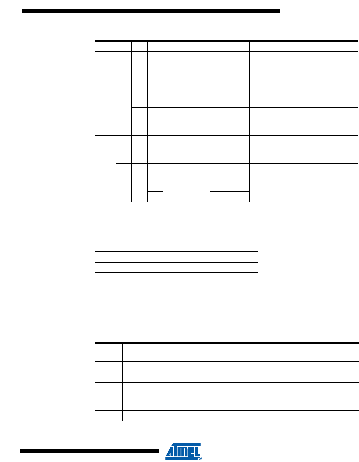
219
6430F–ATARM–21-Feb-12
SAM3U Series
Table 13-38 shows the cache policy for memory attribute encodings with a TEX value is in the
range 4-7.
Table 13-39 shows the AP encodings that define the access permissions for privileged and
unprivileged software.
b001
0
0 0Normal
Not
shareable
1 Shareable
1 x(1) Reserved encoding -
1
0 x(1) Implementation defined
attributes. -
1 0Normal
Not
shareable Outer and inner write-back. Write and
read allocate.
1 Shareable
b010 00 x(1) Device Not
shareable Nonshared Device.
1 x(1) Reserved encoding -
1x
(1) x(1) Reserved encoding -
b1B
BAA0Normal
Not
shareable
1 Shareable
1. The MPU ignores the value of this bit.
Table 13-38. Cache policy for memory attribute encoding
Encoding, AA or BB Corresponding cache policy
00 Non-cacheable
01 Write back, write and read allocate
10 Write through, no write allocate
11 Write back, no write allocate
Table 13-39. AP encoding
AP[2:0]
Privileged
permissions
Unprivileged
permissions Description
000 No access No access All accesses generate a permission fault
001 RW No access Access from privileged software only
010 RW RO Writes by unprivileged software generate a permission
fault
011 RW RW Full access
100 Unpredictable Unpredictable Reserved
Table 13-37. TEX, C, B, and S encoding (Continued)
TEX C B S Memory type Shareability Other attributes

220
6430F–ATARM–21-Feb-12
SAM3U Series
13.22.7 MPU mismatch
When an access violates the MPU permissions, the processor generates a memory manage-
ment fault, see “Exceptions and interrupts” on page 66. The MMFSR indicates the cause of the
fault. See “Memory Management Fault Status Register” on page 196 for more information.
13.22.8 Updating an MPU region
To update the attributes for an MPU region, update the RNR, RBAR and RASR registers. You
can program each register separately, or use a multiple-word write to program all of these regis-
ters. You can use the RBAR and RASR aliases to program up to four regions simultaneously
using an STM instruction.
13.22.8.1 Updating an MPU region using separate words
Simple code to configure one region:
; R1 = region number
; R2 = size/enable
; R3 = attributes
; R4 = address
LDR R0,=MPU_RNR ; 0xE000ED98, MPU region number register
STR R1, [R0, #0x0] ; Region Number
STR R4, [R0, #0x4] ; Region Base Address
STRH R2, [R0, #0x8] ; Region Size and Enable
STRH R3, [R0, #0xA] ; Region Attribute
Disable a region before writing new region settings to the MPU if you have previously enabled
the region being changed. For example:
; R1 = region number
; R2 = size/enable
; R3 = attributes
; R4 = address
LDR R0,=MPU_RNR ; 0xE000ED98, MPU region number register
STR R1, [R0, #0x0] ; Region Number
BIC R2, R2, #1 ; Disable
STRH R2, [R0, #0x8] ; Region Size and Enable
STR R4, [R0, #0x4] ; Region Base Address
STRH R3, [R0, #0xA] ; Region Attribute
ORR R2, #1 ; Enable
STRH R2, [R0, #0x8] ; Region Size and Enable
Software must use memory barrier instructions:
101 RO No access Reads by privileged software only
110 RO RO Read only, by privileged or unprivileged software
111 RO RO Read only, by privileged or unprivileged software
Table 13-39. AP encoding (Continued)
AP[2:0]
Privileged
permissions
Unprivileged
permissions Description

221
6430F–ATARM–21-Feb-12
SAM3U Series
• before MPU setup if there might be outstanding memory transfers, such as buffered writes,
that might be affected by the change in MPU settings
• after MPU setup if it includes memory transfers that must use the new MPU settings.
However, memory barrier instructions are not required if the MPU setup process starts by enter-
ing an exception handler, or is followed by an exception return, because the exception entry and
exception return mechanism cause memory barrier behavior.
Software does not need any memory barrier instructions during MPU setup, because it accesses
the MPU through the PPB, which is a Strongly-Ordered memory region.
For example, if you want all of the memory access behavior to take effect immediately after the
programming sequence, use a DSB instruction and an ISB instruction. A DSB is required after
changing MPU settings, such as at the end of context switch. An ISB is required if the code that
programs the MPU region or regions is entered using a branch or call. If the programming
sequence is entered using a return from exception, or by taking an exception, then you do not
require an ISB.
13.22.8.2 Updating an MPU region using multi-word writes
You can program directly using multi-word writes, depending on how the information is divided.
Consider the following reprogramming:
; R1 = region number
; R2 = address
; R3 = size, attributes in one
LDR R0, =MPU_RNR ; 0xE000ED98, MPU region number register
STR R1, [R0, #0x0] ; Region Number
STR R2, [R0, #0x4] ; Region Base Address
STR R3, [R0, #0x8] ; Region Attribute, Size and Enable
Use an STM instruction to optimize this:
; R1 = region number
; R2 = address
; R3 = size, attributes in one
LDR R0, =MPU_RNR ; 0xE000ED98, MPU region number register
STM R0, {R1-R3} ; Region Number, address, attribute, size and enable
You can do this in two words for pre-packed information. This means that the RBAR contains the
required region number and had the VALID bit set to 1, see “MPU Region Base Address Regis-
ter” on page 216. Use this when the data is statically packed, for example in a boot loader:
; R1 = address and region number in one
; R2 = size and attributes in one
LDR R0, =MPU_RBAR ; 0xE000ED9C, MPU Region Base register
STR R1, [R0, #0x0] ; Region base address and
; region number combined with VALID (bit 4) set to 1
STR R2, [R0, #0x4] ; Region Attribute, Size and Enable
Use an STM instruction to optimize this:
; R1 = address and region number in one
; R2 = size and attributes in one
LDR R0,=MPU_RBAR ; 0xE000ED9C, MPU Region Base register
STM R0, {R1-R2} ; Region base address, region number and VALID bit,

222
6430F–ATARM–21-Feb-12
SAM3U Series
; and Region Attribute, Size and Enable
13.22.8.3 Subregions
Regions of 256 bytes or more are divided into eight equal-sized subregions. Set the correspond-
ing bit in the SRD field of the RASR to disable a subregion, see “MPU Region Attribute and Size
Register” on page 217. The least significant bit of SRD controls the first subregion, and the most
significant bit controls the last subregion. Disabling a subregion means another region overlap-
ping the disabled range matches instead. If no other enabled region overlaps the disabled
subregion the MPU issues a fault.
Regions of 32, 64, and 128 bytes do not support subregions, With regions of these sizes, you
must set the SRD field to 0x00, otherwise the MPU behavior is Unpredictable.
13.22.8.4 Example of SRD use
Two regions with the same base address overlap. Region one is 128KB, and region two is
512KB. To ensure the attributes from region one apply to the first128KB region, set the SRD
field for region two to b00000011 to disable the first two subregions, as Figure 13-9 shows
Figure 13-9. SRD use
13.22.9 MPU design hints and tips
To avoid unexpected behavior, disable the interrupts before updating the attributes of a region
that the interrupt handlers might access.
Ensure software uses aligned accesses of the correct size to access MPU registers:
• except for the RASR, it must use aligned word accesses
• for the RASR it can use byte or aligned halfword or word accesses.
The processor does not support unaligned accesses to MPU registers.
When setting up the MPU, and if the MPU has previously been programmed, disable unused
regions to prevent any previous region settings from affecting the new MPU setup.
Region 1
Disabled subregion
Disabled subregion
Region 2, with
subregions
Base address of both regions
Offset from
base address
0
64KB
128KB
192KB
256KB
320KB
384KB
448KB
512KB
223
6430F–ATARM–21-Feb-12
SAM3U Series
13.22.9.1 MPU configuration for a microcontroller
Usually, a microcontroller system has only a single processor and no caches. In such a system,
program the MPU as follows:
In most microcontroller implementations, the share ability and cache policy attributes do not
affect the system behavior. However, using these settings for the MPU regions can make the
application code more portable. The values given are for typical situations. In special systems,
such as multiprocessor designs or designs with a separate DMA engine, the share ability attri-
bute might be important. In these cases refer to the recommendations of the memory device
manufacturer.
Table 13-40. Memory region attributes for a microcontroller
Memory region TEX C B S Memory type and attributes
Flash memory b000 1 0 0 Normal memory, Non-shareable, write-through
Internal SRAM b000 1 0 1 Normal memory, Shareable, write-through
External SRAM b000 1 1 1 Normal memory, Shareable, write-back, write-allocate
Peripherals b000 0 1 1 Device memory, Shareable

224
6430F–ATARM–21-Feb-12
SAM3U Series
13.23 Glossary
This glossary describes some of the terms used in technical documents from ARM.
Abort
A mechanism that indicates to a processor that the value associated with a memory access is
invalid. An abort can be caused by the external or internal memory system as a result of
attempting to access invalid instruction or data memory.
Aligned
A data item stored at an address that is divisible by the number of bytes that defines the data
size is said to be aligned. Aligned words and halfwords have addresses that are divisible by four
and two respectively. The terms word-aligned and halfword-aligned therefore stipulate
addresses that are divisible by four and two respectively.
Banked register
A register that has multiple physical copies, where the state of the processor determines which
copy is used. The Stack Pointer, SP (R13) is a banked register.
Base register
In instruction descriptions, a register specified by a load or store instruction that is used to hold
the base value for the instruction’s address calculation. Depending on the instruction and its
addressing mode, an offset can be added to or subtracted from the base register value to form
the address that is sent to memory.
See also “Index register”
Breakpoint
A breakpoint is a mechanism provided by debuggers to identify an instruction at which program
execution is to be halted. Breakpoints are inserted by the programmer to enable inspection of
register contents, memory locations, variable values at fixed points in the program execution to
test that the program is operating correctly. Breakpoints are removed after the program is suc-
cessfully tested.
Condition field
A four-bit field in an instruction that specifies a condition under which the instruction can
execute.
Conditional execution
If the condition code flags indicate that the corresponding condition is true when the instruction
starts executing, it executes normally. Otherwise, the instruction does nothing.
Context
The environment that each process operates in for a multitasking operating system. In ARM pro-
cessors, this is limited to mean the physical address range that it can access in memory and the
associated memory access permissions.
Coprocessor
A processor that supplements the main processor. Cortex-M3 does not support any
coprocessors.
Debugger

225
6430F–ATARM–21-Feb-12
SAM3U Series
A debugging system that includes a program, used to detect, locate, and correct software faults,
together with custom hardware that supports software debugging.
Direct Memory Access (DMA)
An operation that accesses main memory directly, without the processor performing any
accesses to the data concerned.
Doubleword
A 64-bit data item. The contents are taken as being an unsigned integer unless otherwise
stated.
Doubleword-aligned
A data item having a memory address that is divisible by eight.
Endianness
Byte ordering. The scheme that determines the order that successive bytes of a data word are
stored in memory. An aspect of the system’s memory mapping.
See also “Little-endian (LE)”
Exception
An event that interrupts program execution. When an exception occurs, the processor suspends
the normal program flow and starts execution at the address indicated by the corresponding
exception vector. The indicated address contains the first instruction of the handler for the
exception.
An exception can be an interrupt request, a fault, or a software-generated system exception.
Faults include attempting an invalid memory access, attempting to execute an instruction in an
invalid processor state, and attempting to execute an undefined instruction.
Exception service routine
See “Interrupt handler”.
Exception vector
See “Interrupt vector”.
Flat address mapping
A system of organizing memory in which each physical address in the memory space is the
same as the corresponding virtual address.
Halfword
A 16-bit data item.
Illegal instruction
An instruction that is architecturally Undefined.
Implementation-defined
The behavior is not architecturally defined, but is defined and documented by individual
implementations.
Implementation-specific

226
6430F–ATARM–21-Feb-12
SAM3U Series
The behavior is not architecturally defined, and does not have to be documented by individual
implementations. Used when there are a number of implementation options available and the
option chosen does not affect software compatibility.
Index register
In some load and store instruction descriptions, the value of this register is used as an offset to
be added to or subtracted from the base register value to form the address that is sent to mem-
ory. Some addressing modes optionally enable the index register value to be shifted prior to the
addition or subtraction.
See also “Base register”
Instruction cycle count
The number of cycles that an instruction occupies the Execute stage of the pipeline.
Interrupt handler
A program that control of the processor is passed to when an interrupt occurs.
Interrupt vector
One of a number of fixed addresses in low memory, or in high memory if high vectors are config-
ured, that contains the first instruction of the corresponding interrupt handler.
Little-endian (LE)
Byte ordering scheme in which bytes of increasing significance in a data word are stored at
increasing addresses in memory.
See also “Condition field”, “Endianness”.
Little-endian memory
Memory in which:
a byte or halfword at a word-aligned address is the least significant byte or halfword within the
word at that address
a byte at a halfword-aligned address is the least significant byte within the halfword at that
address.
Load/store architecture
A processor architecture where data-processing operations only operate on register contents,
not directly on memory contents.
Memory Protection Unit (MPU)
Hardware that controls access permissions to blocks of memory. An MPU does not perform any
address translation.
Prefetching
In pipelined processors, the process of fetching instructions from memory to fill up the pipeline
before the preceding instructions have finished executing. Prefetching an instruction does not
mean that the instruction has to be executed.
Read
Reads are defined as memory operations that have the semantics of a load. Reads include the
Thumb instructions LDM, LDR, LDRSH, LDRH, LDRSB, LDRB, and POP.

227
6430F–ATARM–21-Feb-12
SAM3U Series
Region
A partition of memory space.
Reserved
A field in a control register or instruction format is reserved if the field is to be defined by the
implementation, or produces Unpredictable results if the contents of the field are not zero. These
fields are reserved for use in future extensions of the architecture or are implementation-specific.
All reserved bits not used by the implementation must be written as 0 and read as 0.
Should Be One (SBO)
Write as 1, or all 1s for bit fields, by software. Writing as 0 produces Unpredictable results.
Should Be Zero (SBZ)
Write as 0, or all 0s for bit fields, by software. Writing as 1 produces Unpredictable results.
Should Be Zero or Preserved (SBZP)
Write as 0, or all 0s for bit fields, by software, or preserved by writing the same value back that
has been previously read from the same field on the same processor.
Thread-safe
In a multi-tasking environment, thread-safe functions use safeguard mechanisms when access-
ing shared resources, to ensure correct operation without the risk of shared access conflicts.
Thumb instruction
One or two halfwords that specify an operation for a processor to perform. Thumb instructions
must be halfword-aligned.
Unaligned
A data item stored at an address that is not divisible by the number of bytes that defines the data
size is said to be unaligned. For example, a word stored at an address that is not divisible by
four.
Undefined
Indicates an instruction that generates an Undefined instruction exception.
Unpredictable (UNP)
You cannot rely on the behavior. Unpredictable behavior must not represent security holes.
Unpredictable behavior must not halt or hang the processor, or any parts of the system.
Warm reset
Also known as a core reset. Initializes the majority of the processor excluding the debug control-
ler and debug logic. This type of reset is useful if you are using the debugging features of a
processor.
Word
A 32-bit data item.
Write
Writes are defined as operations that have the semantics of a store. Writes include the Thumb
instructions STM, STR, STRH, STRB, and PUSH.

228
6430F–ATARM–21-Feb-12
SAM3U Series
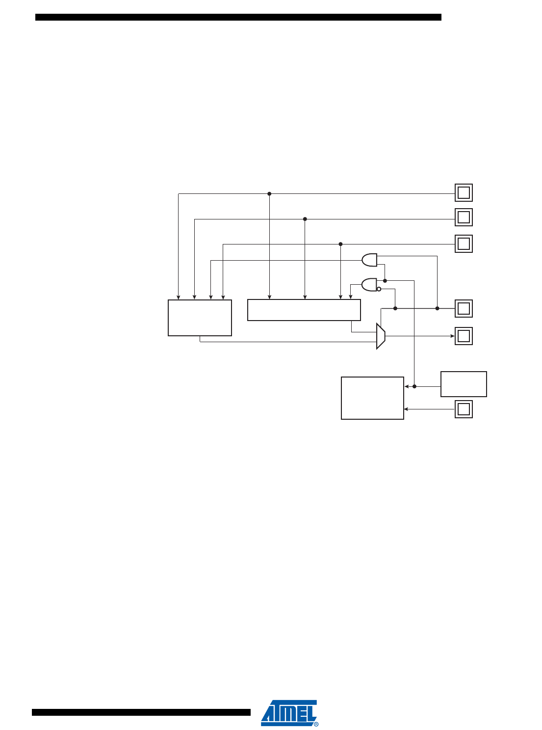
229
6430F–ATARM–21-Feb-12
SAM3U Series
14. Debug and Test Features
14.1 Overview
The SAM3U Series Microcontrollers feature a number of complementary debug and test
capabilities. The Serial Wire/JTAG Debug Port (SWJ-DP) combining a Serial Wire Debug Port
(SW-DP) and JTAG Debug (JTAG-DP) port is used for standard debugging functions, such as
downloading code and single-stepping through programs. It also embeds a serial wire trace.
Figure 14-1. Debug and Test Block Diagram
TST
TMS
TCK/SWCLK
TDI
JTAGSEL
TDO/TRACESWO
Boundary
TA P
SWJ-DP
Reset
and
Test
POR
230
6430F–ATARM–21-Feb-12
SAM3U Series
14.2 Application Examples
14.2.1 Debug Environment
Figure 14-2 shows a complete debug environment example. The SWJ-DP interface is used for
standard debugging functions, such as downloading code and single-stepping through the pro-
gram and viewing core and peripheral registers.
Figure 14-2. Application Debug Environment Example
14.2.2 Test Environment
Figure 14-3 shows a test environment example (JTAG Boundary scan). Test vectors are sent
and interpreted by the tester. In this example, the “board in test” is designed using a number of
JTAG-compliant devices. These devices can be connected to form a single scan chain.
SAM3
Host Debugger
PC
SAM3-based Application Board
SWJ-DP
Connector
SWJ-DP
Emulator/Probe
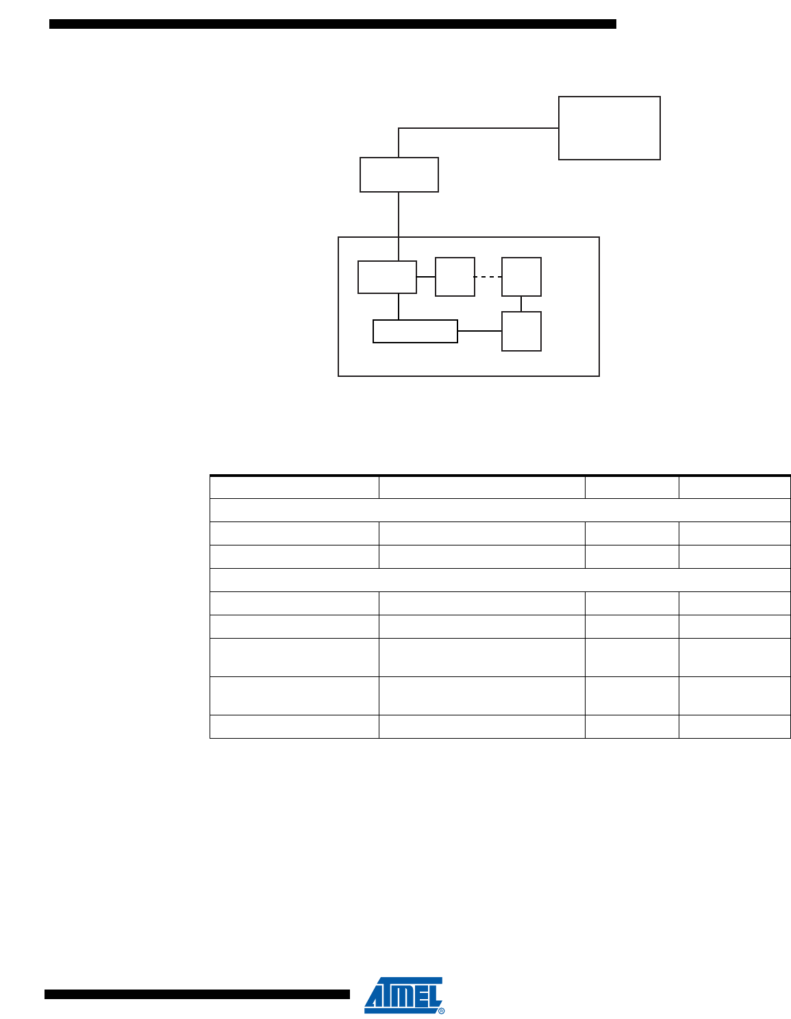
231
6430F–ATARM–21-Feb-12
SAM3U Series
Figure 14-3. Application Test Environment Example
14.3 Debug and Test Pin Description
Note: 1. TDO pin is set in input mode when the Cortex-M3 Core is not in debug mode. Thus an external
pull-up (100 kΩ) must be added to avoid current consumption due to floating input.
14.4 Functional Description
14.4.1 Test Pin
One dedicated pin, TST, is used to define the device operating mode. When this pin is at low
level during power-up, the device is in normal operating mode. When at high level, the device is
in test mode or FFPI mode. The TST pin integrates a permanent pull-down resistor of about
15 kΩ, so that it can be left unconnected for normal operation. Note that when setting the TST pin
Chip 2
Chip n
Chip 1
SAM3
SAM3-based Application Board In Test
JTAG
Connector
Te ster
Te st Adaptor
JTAG
Probe
Table 14-1. Debug and Test Signal List
Signal Name Function Type Active Level
Reset/Test
NRST Microcontroller Reset Input/Output Low
TST Test Select Input
SWD/JTAG
TCK/SWCLK Test Clock/Serial Wire Clock Input
TDI Test Data In Input
TDO/TRACESWO Test Data Out/Trace Asynchronous
Data Out Output(1)
TMS/SWDIO Test Mode Select/Serial Wire
Input/Output Input
JTAGSEL JTAG Selection Input High
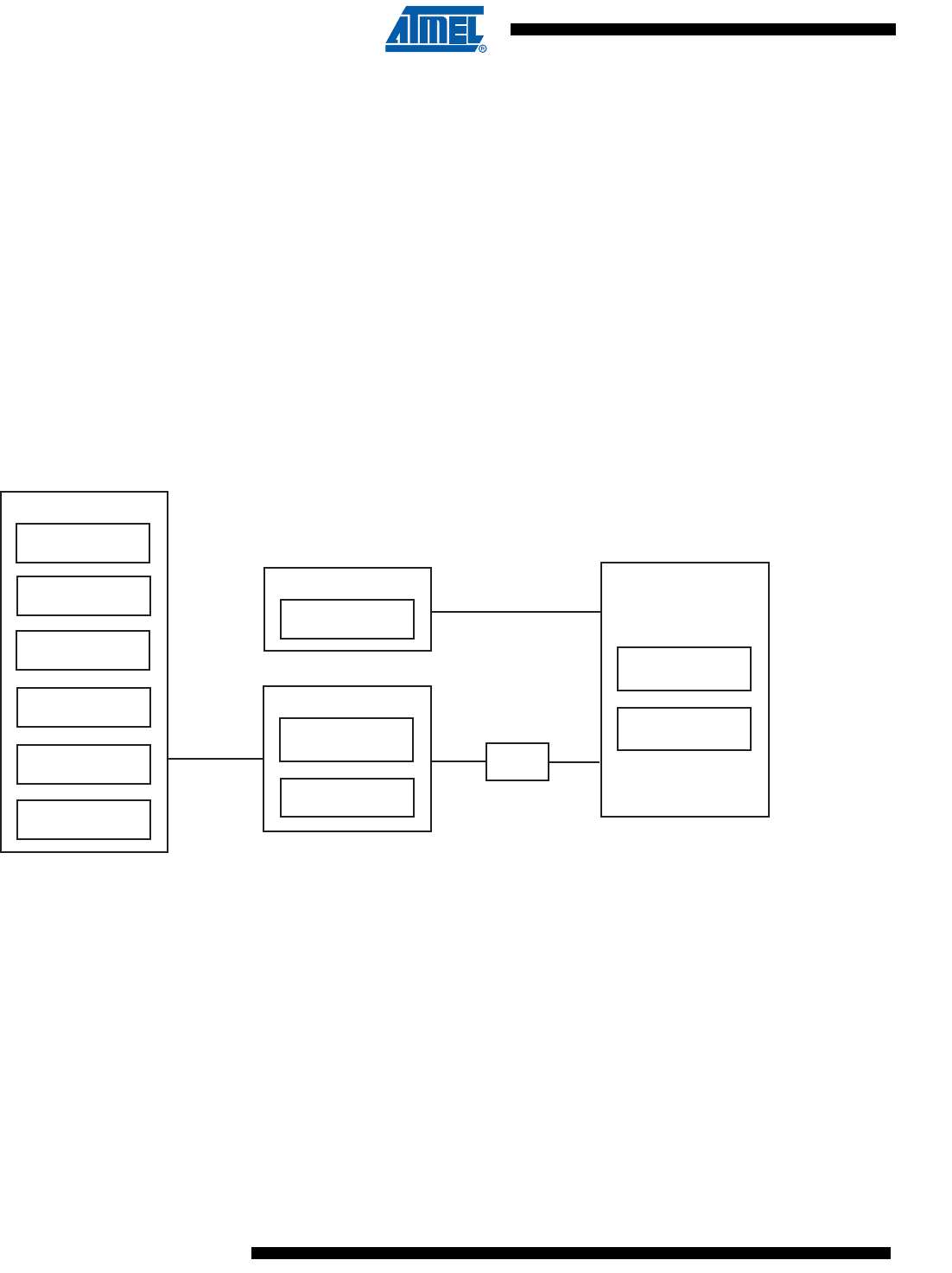
232
6430F–ATARM–21-Feb-12
SAM3U Series
to low or high level at power up, it must remain in the same state during the duration of the whole
operation.
14.4.2 Debug Architecture
Figure 14-4 shows the Debug Architecture used in the SAM3. The Cortex-M3 embeds four func-
tional units for debug:
• SWJ-DP (Serial Wire/JTAG Debug Port)
• FPB (Flash Patch Breakpoint)
• DWT (Data Watchpoint and Trace)
• ITM (Instrumentation Trace Macrocell)
• TPIU (Trace Port Interface Unit)
The debug architecture information that follows is mainly dedicated to developers of SWJ-DP
Emulators/Probes and debugging tool vendors for Cortex M3-based microcontrollers. For further
details on SWJ-DP see the Cortex M3 technical reference manual.
Figure 14-4. Debug Architecture
14.4.3 Serial Wire/JTAG Debug Port (SWJ-DP)
The Cortex-M3 embeds a SWJ-DP Debug port which is the standard CoreSight™ debug port. It
combines Serial Wire Debug Port (SW-DP), from 2 to 3 pins and JTAG debug Port (JTAG-DP),
5 pins.
By default, the JTAG Debug Port is active. If the host debugger wants to switch to the Serial
Wire Debug Port, it must provide a dedicated JTAG sequence on TMS/SWDIO and
TCK/SWCLK which disables JTAG-DP and enables SW-DP.
4 watchpoints
PC sampler
data address sampler
data sampler
interrupt trace
CPU statistics
DWT
6 breakpoints
FPB
software trace
32 channels
time stamping
ITM
SWD/JTAG
SWJ-DP
SWO trace
TPIU
233
6430F–ATARM–21-Feb-12
SAM3U Series
When the Serial Wire Debug Port is active, TDO/TRACESWO can be used for trace. The asyn-
chronous TRACE output (TRACESWO) is multiplexed with TDO. So the asynchronous trace
can only be used with SW-DP, not JTAG-DP.
SW-DP or JTAG-DP mode is selected when JTAGSEL is low. It is not possible to switch directly
between SWJ-DP and JTAG boundary scan operations. A chip reset must be performed after
JTAGSEL is changed.
14.4.3.1 SW-DP and JTAG-DP Selection Mechanism
Debug port selection mechanism is done by sending specific SWDIOTMS sequence. The JTAG-
DP is selected by default after reset.
• Switch from JTAG-DP to SW-DP. The sequence is:
– Send more than 50 SWCLKTCK cycles with SWDIOTMS = 1
– Send the 16-bit sequence on SWDIOTMS = 0111100111100111 (0x79E7 MSB first)
– Send more than 50 SWCLKTCK cycles with SWDIOTMS = 1
• Switch from SWD to JTAG. The sequence is:
– Send more than 50 SWCLKTCK cycles with SWDIOTMS = 1
– Send the
16-bit
sequence on
SWDIOTMS
= 0011110011100111 (0x3CE7 MSB first)
– Send more than 50 SWCLKTCK cycles with SWDIOTMS = 1
14.4.4 FPB (Flash Patch Breakpoint)
The FPB:
• Implements hardware breakpoints
• Patches code and data from code space to system space.
The FPB unit contains:
• Two literal comparators for matching against literal loads from Code space, and remapping to
a corresponding area in System space.
• Six instruction comparators for matching against instruction fetches from Code space and
remapping to a corresponding area in System space.
• Alternatively, comparators can also be configured to generate a Breakpoint instruction to the
processor core on a match.
14.4.5 DWT (Data Watchpoint and Trace)
The DWT contains four comparators which can be configured to generate the following:
• PC sampling packets at set intervals
• PC or Data watchpoint packets
Table 14-2. SWJ-DP Pin List
Pin Name JTAG Port Serial Wire Debug Port
TMS/SWDIO TMS SWDIO
TCK/SWCLK TCK SWCLK
TDI TDI -
TDO/TRACESWO TDO TRACESWO (optional: trace)

234
6430F–ATARM–21-Feb-12
SAM3U Series
• Watchpoint event to halt core
The DWT contains counters for the items that follow:
• Clock cycle (CYCCNT)
• Folded instructions
• Load Store Unit (LSU) operations
• Sleep Cycles
• CPI (all instruction cycles except for the first cycle)
• Interrupt overhead
14.4.6 ITM (Instrumentation Trace Macrocell)
The ITM is an application driven trace source that supports printf style debugging to trace Oper-
ating System (OS) and application events, and emits diagnostic system information. The ITM
emits trace information as packets which can be generated by three different sources with sev-
eral priority levels:
•Software trace: Software can write directly to ITM stimulus registers. This can be done
thanks to the “printf” function. For more information, refer to Section 14.4.6.1 “How to
Configure the ITM”.
•Hardware trace: The ITM emits packets generated by the DWT.
•Time stamping: Timestamps are emitted relative to packets. The ITM contains a 21-bit
counter to generate the timestamp.
14.4.6.1 How to Configure the ITM
The following example describes how to output trace data in asynchronous trace mode.
• Configure the TPIU for asynchronous trace mode (refer to Section 14.4.6.3 “5.4.3. How to
Configure the TPIU”)
• Enable the write accesses into the ITM registers by writing “0xC5ACCE55” into the
Lock Access Register (Address: 0xE0000FB0)
• Write 0x00010015 into the Trace Control Register:
–Enable ITM
– Enable Synchronization packets
– Enable SWO behavior
– Fix the ATB ID to 1
• Write 0x1 into the Trace Enable Register:
– Enable the Stimulus port 0
• Write 0x1 into the Trace Privilege Register:
– Stimulus port 0 only accessed in privileged mode (Clearing a bit in this register will
result in the corresponding stimulus port being accessible in user mode.)
• Write into the Stimulus port 0 register: TPIU (Trace Port Interface Unit)
The TPIU acts as a bridge between the on-chip trace data and the Instruction Trace Macro-
cell (ITM).
The TPIU formats and transmits trace data off-chip at frequencies asynchronous to the core.

235
6430F–ATARM–21-Feb-12
SAM3U Series
14.4.6.2 Asynchronous Mode
The TPIU is configured in asynchronous mode, trace data are output using the single TRAC-
ESWO pin. The TRACESWO signal is multiplexed with the TDO signal of the JTAG Debug Port.
As a consequence, asynchronous trace mode is only available when the Serial Wire Debug
mode is selected since TDO signal is used in JTAG debug mode.
Two encoding formats are available for the single pin output:
• Manchester encoded stream. This is the reset value.
• NRZ_based UART byte structure
14.4.6.3 5.4.3. How to Configure the TPIU
This example only concerns the asynchronous trace mode.
• Set the TRCENA bit to 1 into the Debug Exception and Monitor Register (0xE000EDFC) to
enable the use of trace and debug blocks.
• Write 0x2 into the Selected Pin Protocol Register
– Select the Serial Wire Output – NRZ
• Write 0x100 into the Formatter and Flush Control Register
• Set the suitable clock prescaler value into the Async Clock Prescaler Register to scale the
baud rate of the asynchronous output (this can be done automatically by the debugging tool).
14.4.7 IEEE 1149.1 JTAG Boundary Scan
IEEE 1149.1 JTAG Boundary Scan allows pin-level access independent of the device packaging
technology.
IEEE 1149.1 JTAG Boundary Scan is enabled when FWUP, NRSTB and JTAGSEL are high
while TST is tied low during power-up and must be kept in this state during the whole boundary
scan operation. The SAMPLE, EXTEST and BYPASS functions are implemented. In
SWD/JTAG debug mode, the ARM processor responds with a non-JTAG chip ID that identifies
the processor. This is not IEEE 1149.1 JTAG-compliant.
It is not possible to switch directly between JTAG Boundary Scan and SWJ Debug Port opera-
tions. A chip reset must be performed after JTAGSEL is changed.
A Boundary-scan Descriptor Language (BSDL) file is provided on Atmel’s web site to set up the
test.
14.4.7.1 JTAG Boundary-scan Register
The Boundary-scan Register (BSR) contains a number of bits which correspond to active pins
and associated control signals.
Each SAM3 input/output pin corresponds to a 3-bit register in the BSR. The OUTPUT bit con-
tains data that can be forced on the pad. The INPUT bit facilitates the observability of data
applied to the pad. The CONTROL bit selects the direction of the pad.
For more information, please refer to BDSL files available for the SAM3U Series.
236
6430F–ATARM–21-Feb-12
SAM3U Series
14.4.8 ID Code Register
Access: Read-only
• VERSION[31:28]: Product Version Number
Set to 0x0.
• PART NUMBER[27:12]: Product Part Number
• MANUFACTURER IDENTITY[11:1]
Set to 0x01F.
• Bit[0] Required by IEEE Std. 1149.1
Set to 0x1.
31 30 29 28 27 26 25 24
VERSION PART NUMBER
23 22 21 20 19 18 17 16
PART NUMBER
15 14 13 12 11 10 9 8
PART NUMBER MANUFACTURER IDENTITY
76543210
MANUFACTURER IDENTITY 1
Chip Name Chip ID
SAM3U 0x5B2A
Chip Name JTAG ID Code
SAM3U 05B2_A03F
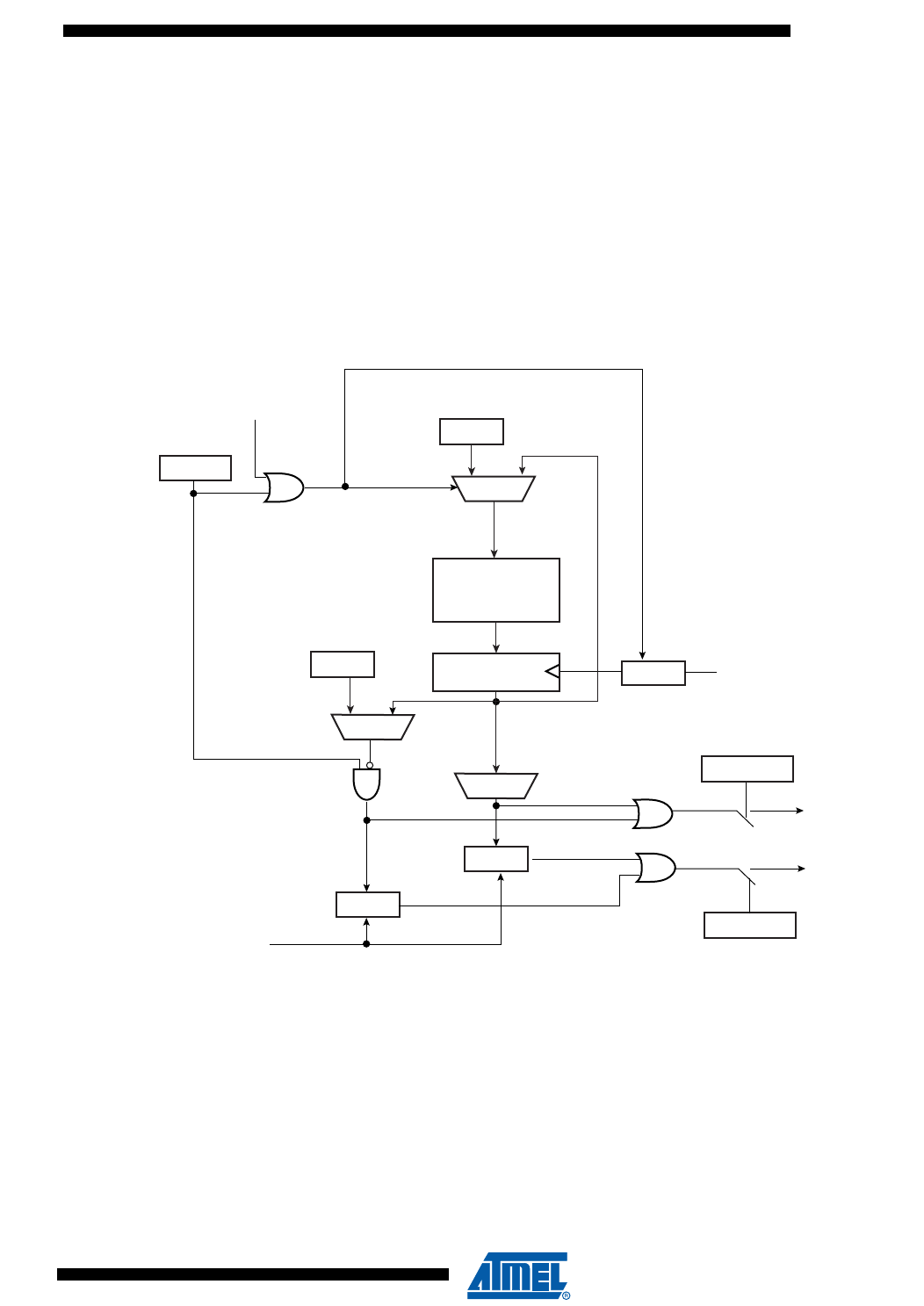
237
6430F–ATARM–21-Feb-12
SAM3U Series
15. Watchdog Timer (WDT)
15.1 Description
The Watchdog Timer can be used to prevent system lock-up if the software becomes trapped in
a deadlock. It features a 12-bit down counter that allows a watchdog period of up to 16 seconds
(slow clock at 32.768 kHz). It can generate a general reset or a processor reset only. In addition,
it can be stopped while the processor is in debug mode or idle mode.
15.2 Block Diagram
Figure 15-1. Watchdog Timer Block Diagram
=0
10
set
reset
read WDT_SR
or
reset
wdt_fault
(to Reset Controller)
set
reset
WDFIEN
wdt_int
WDT_MR
SLCK
1/128
12-bit Down
Counter
Current
Value
WDD
WDT_MR
<= WDD
WDV
WDRSTT
WDT_MR
WDT_CR
reload
WDUNF
WDERR
reload
write WDT_MR
WDT_MR
WDRSTEN

238
6430F–ATARM–21-Feb-12
SAM3U Series
15.3 Functional Description
The Watchdog Timer can be used to prevent system lock-up if the software becomes trapped in
a deadlock. It is supplied with VDDCORE. It restarts with initial values on processor reset.
The Watchdog is built around a 12-bit down counter, which is loaded with the value defined in
the field WDV of the Mode Register (WDT_MR). The Watchdog Timer uses the Slow Clock
divided by 128 to establish the maximum Watchdog period to be 16 seconds (with a typical Slow
Clock of 32.768 kHz).
After a Processor Reset, the value of WDV is 0xFFF, corresponding to the maximum value of
the counter with the external reset generation enabled (field WDRSTEN at 1 after a Backup
Reset). This means that a default Watchdog is running at reset, i.e., at power-up. The user must
either disable it (by setting the WDDIS bit in WDT_MR) if he does not expect to use it or must
reprogram it to meet the maximum Watchdog period the application requires.
The Watchdog Mode Register (WDT_MR) can be written only once. Only a processor reset
resets it. Writing the WDT_MR register reloads the timer with the newly programmed mode
parameters.
In normal operation, the user reloads the Watchdog at regular intervals before the timer under-
flow occurs, by writing the Control Register (WDT_CR) with the bit WDRSTT to 1. The
Watchdog counter is then immediately reloaded from WDT_MR and restarted, and the Slow
Clock 128 divider is reset and restarted. The WDT_CR register is write-protected. As a result,
writing WDT_CR without the correct hard-coded key has no effect. If an underflow does occur,
the “wdt_fault” signal to the Reset Controller is asserted if the bit WDRSTEN is set in the Mode
Register (WDT_MR). Moreover, the bit WDUNF is set in the Watchdog Status Register
(WDT_SR).
To prevent a software deadlock that continuously triggers the Watchdog, the reload of the
Watchdog must occur while the Watchdog counter is within a window between 0 and WDD,
WDD is defined in the WatchDog Mode Register WDT_MR.
Any attempt to restart the Watchdog while the Watchdog counter is between WDV and WDD
results in a Watchdog error, even if the Watchdog is disabled. The bit WDERR is updated in the
WDT_SR and the “wdt_fault” signal to the Reset Controller is asserted.
Note that this feature can be disabled by programming a WDD value greater than or equal to the
WDV value. In such a configuration, restarting the Watchdog Timer is permitted in the whole
range [0; WDV] and does not generate an error. This is the default configuration on reset (the
WDD and WDV values are equal).
The status bits WDUNF (Watchdog Underflow) and WDERR (Watchdog Error) trigger an inter-
rupt, provided the bit WDFIEN is set in the mode register. The signal “wdt_fault” to the reset
controller causes a Watchdog reset if the WDRSTEN bit is set as already explained in the reset
controller programmer Datasheet. In that case, the processor and the Watchdog Timer are
reset, and the WDERR and WDUNF flags are reset.
If a reset is generated or if WDT_SR is read, the status bits are reset, the interrupt is cleared,
and the “wdt_fault” signal to the reset controller is deasserted.
Writing the WDT_MR reloads and restarts the down counter.
While the processor is in debug state or in idle mode, the counter may be stopped depending on
the value programmed for the bits WDIDLEHLT and WDDBGHLT in the WDT_MR.
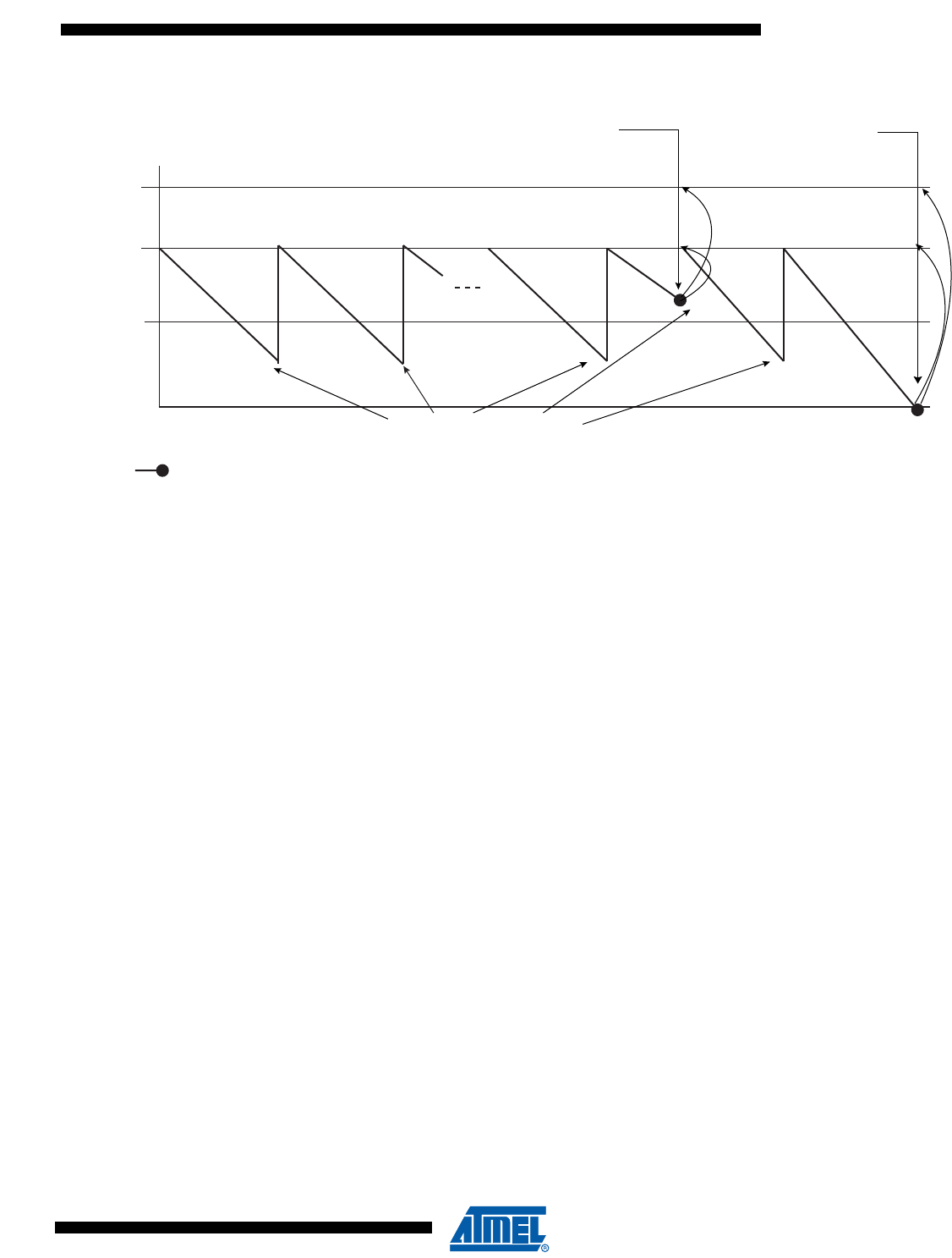
239
6430F–ATARM–21-Feb-12
SAM3U Series
Figure 15-2. Watchdog Behavior
0
WDV
WDD
WDT_CR = WDRSTT
Watchdog
Fault
Normal behavior
Watchdog Error Watchdog Underflow
FFF
if WDRSTEN is 1
if WDRSTEN is 0
Forbidden
Window
Permitted
Window

240
6430F–ATARM–21-Feb-12
SAM3U Series
15.4 Watchdog Timer (WDT) User Interface
Table 15-1. Register Mapping
Offset Register Name Access Reset
0x00 Control Register WDT_CR Write-only -
0x04 Mode Register WDT_MR Read-write Once 0x3FFF_2FFF
0x08 Status Register WDT_SR Read-only 0x0000_0000

241
6430F–ATARM–21-Feb-12
SAM3U Series
15.4.1 Watchdog Timer Control Register
Register Name: WDT_CR
Address: 0x400E1250
Access Type: Write-only
• WDRSTT: Watchdog Restart
0: No effect.
1: Restarts the Watchdog.
•KEY: Password
Should be written at value 0xA5. Writing any other value in this field aborts the write operation.
31 30 29 28 27 26 25 24
KEY
23 22 21 20 19 18 17 16
––––––––
15 14 13 12 11 10 9 8
––––––––
76543210
–––––––WDRSTT

242
6430F–ATARM–21-Feb-12
SAM3U Series
15.4.2 Watchdog Timer Mode Register
Register Name: WDT_MR
Address: 0x400E1254
Access Type: Read-write Once
• WDV: Watchdog Counter Value
Defines the value loaded in the 12-bit Watchdog Counter.
• WDFIEN: Watchdog Fault Interrupt Enable
0: A Watchdog fault (underflow or error) has no effect on interrupt.
1: A Watchdog fault (underflow or error) asserts interrupt.
• WDRSTEN: Watchdog Reset Enable
0: A Watchdog fault (underflow or error) has no effect on the resets.
1: A Watchdog fault (underflow or error) triggers a Watchdog reset.
• WDRPROC: Watchdog Reset Processor
0: If WDRSTEN is 1, a Watchdog fault (underflow or error) activates all resets.
1: If WDRSTEN is 1, a Watchdog fault (underflow or error) activates the processor reset.
• WDD: Watchdog Delta Value
Defines the permitted range for reloading the Watchdog Timer.
If the Watchdog Timer value is less than or equal to WDD, writing WDT_CR with WDRSTT = 1 restarts the timer.
If the Watchdog Timer value is greater than WDD, writing WDT_CR with WDRSTT = 1 causes a Watchdog error.
• WDDBGHLT: Watchdog Debug Halt
0: The Watchdog runs when the processor is in debug state.
1: The Watchdog stops when the processor is in debug state.
• WDIDLEHLT: Watchdog Idle Halt
0: The Watchdog runs when the system is in idle mode.
1: The Watchdog stops when the system is in idle state.
• WDDIS: Watchdog Disable
0: Enables the Watchdog Timer.
1: Disables the Watchdog Timer.
31 30 29 28 27 26 25 24
WDIDLEHLT WDDBGHLT WDD
23 22 21 20 19 18 17 16
WDD
15 14 13 12 11 10 9 8
WDDIS WDRPROC WDRSTEN WDFIEN WDV
76543210
WDV

243
6430F–ATARM–21-Feb-12
SAM3U Series
15.4.3 Watchdog Timer Status Register
Register Name: WDT_SR
Address: 0x400E1258
Access Type: Read-only
• WDUNF: Watchdog Underflow
0: No Watchdog underflow occurred since the last read of WDT_SR.
1: At least one Watchdog underflow occurred since the last read of WDT_SR.
• WDERR: Watchdog Error
0: No Watchdog error occurred since the last read of WDT_SR.
1: At least one Watchdog error occurred since the last read of WDT_SR.
31 30 29 28 27 26 25 24
––––––––
23 22 21 20 19 18 17 16
––––––––
15 14 13 12 11 10 9 8
––––––––
76543210
––––––WDERRWDUNF

244
6430F–ATARM–21-Feb-12
SAM3U Series
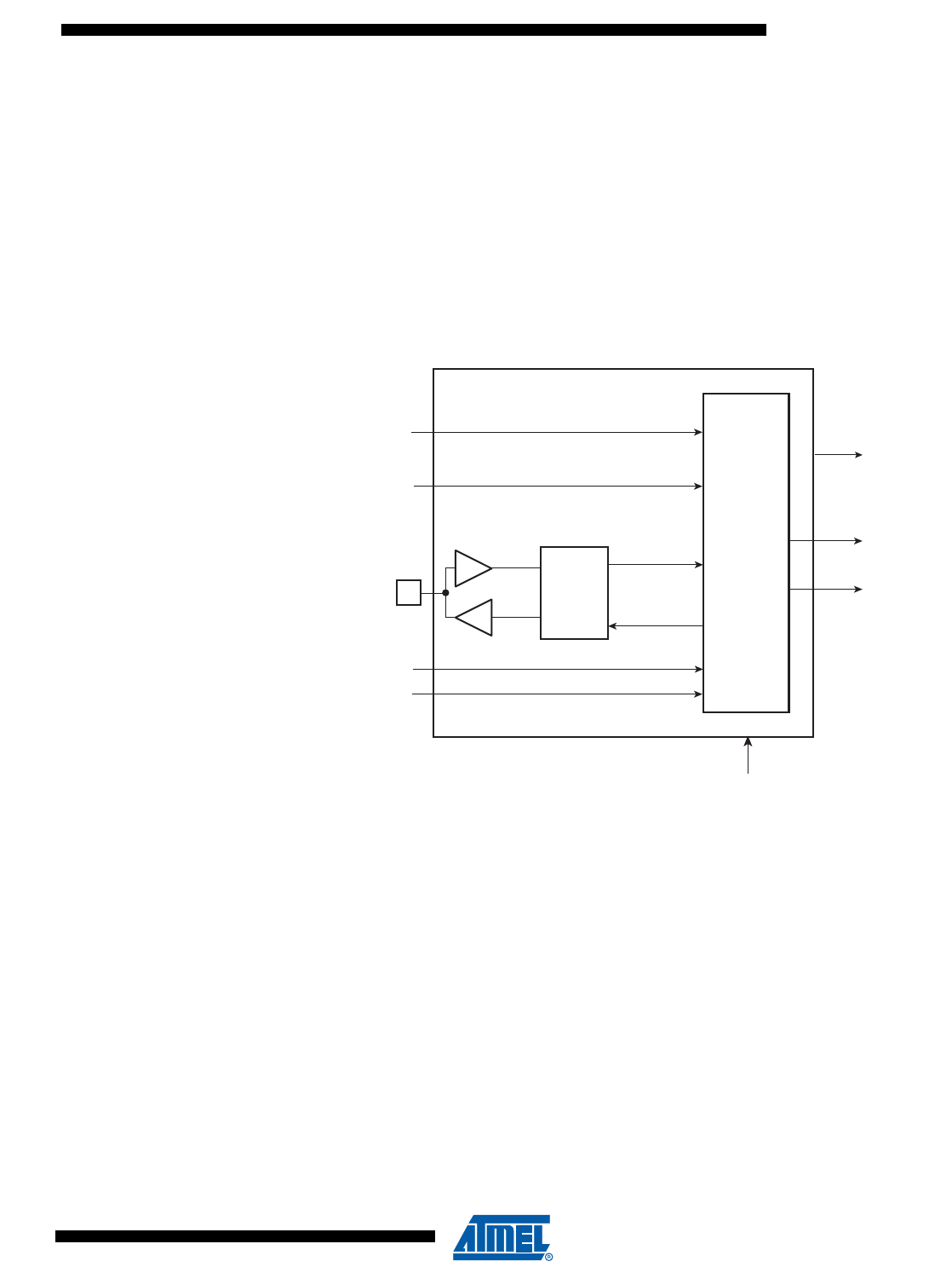
245
6430F–ATARM–21-Feb-12
SAM3U Series
16. Reset Controller (RSTC)
16.1 Overview
The Reset Controller (RSTC), based on power-on reset cells, handles all the resets of the sys-
tem without any external components. It reports which reset occurred last.
The Reset Controller also drives independently or simultaneously the external reset and the
peripheral and processor resets.
16.2 Block Diagram
Figure 16-1. Reset Controller Block Diagram
16.3 Functional Description
16.3.1 Reset Controller Overview
The Reset Controller is made up of an NRST Manager and a Reset State Manager. It runs at
Slow Clock and generates the following reset signals:
• proc_nreset: Processor reset line. It also resets the Watchdog Timer.
• periph_nreset: Affects the whole set of embedded peripherals.
• nrst_out: Drives the NRST pin.
These reset signals are asserted by the Reset Controller, either on external events or on soft-
ware action. The Reset State Manager controls the generation of reset signals and provides a
signal to the NRST Manager when an assertion of the NRST pin is required.
The NRST Manager shapes the NRST assertion during a programmable time, thus controlling
external device resets.
NRST
proc_nreset
wd_fault
periph_nreset
SLCK
Reset
State
Manager
Reset Controller
rstc_irq
NRST
Manager
exter_nreset
nrst_out
core_backup_reset
WDRPROC
user_reset
vddcore_nreset
246
6430F–ATARM–21-Feb-12
SAM3U Series
The Reset Controller Mode Register (RSTC_MR), allowing the configuration of the Reset Con-
troller, is powered with VDDBU, so that its configuration is saved as long as VDDBU is on.
16.3.2 NRST Manager
The NRST Manager samples the NRST input pin and drives this pin low when required by the
Reset State Manager. Figure 16-2 shows the block diagram of the NRST Manager.
Figure 16-2. NRST Manager
16.3.2.1 NRST Signal or Interrupt
The NRST Manager samples the NRST pin at Slow Clock speed. When the line is detected low,
a User Reset is reported to the Reset State Manager.
However, the NRST Manager can be programmed to not trigger a reset when an assertion of
NRST occurs. Writing the bit URSTEN at 0 in RSTC_MR disables the User Reset trigger.
The level of the pin NRST can be read at any time in the bit NRSTL (NRST level) in RSTC_SR.
As soon as the pin NRST is asserted, the bit URSTS in RSTC_SR is set. This bit clears only
when RSTC_SR is read.
The Reset Controller can also be programmed to generate an interrupt instead of generating a
reset. To do so, the bit URSTIEN in RSTC_MR must be written at 1.
16.3.2.2 NRST External Reset Control
The Reset State Manager asserts the signal ext_nreset to assert the NRST pin. When this
occurs, the “nrst_out” signal is driven low by the NRST Manager for a time programmed by the
field ERSTL in RSTC_MR. This assertion duration, named EXTERNAL_RESET_LENGTH, lasts
2(ERSTL+1) Slow Clock cycles. This gives the approximate duration of an assertion between 60 µs
and 2 seconds. Note that ERSTL at 0 defines a two-cycle duration for the NRST pulse.
This feature allows the Reset Controller to shape the NRST pin level, and thus to guarantee that
the NRST line is driven low for a time compliant with potential external devices connected on the
system reset.
As the ERSTL field is within RSTC_MR register, which is backed-up, it can be used to shape the
system power-up reset for devices requiring a longer startup time than the Slow Clock Oscillator.
External Reset Timer
URSTS
URSTEN
ERSTL
exter_nreset
URSTIEN
RSTC_MR
RSTC_MR
RSTC_MR
RSTC_SR
NRSTL
nrst_out
NRST
rstc_irq
Other
interrupt
sources
user_reset
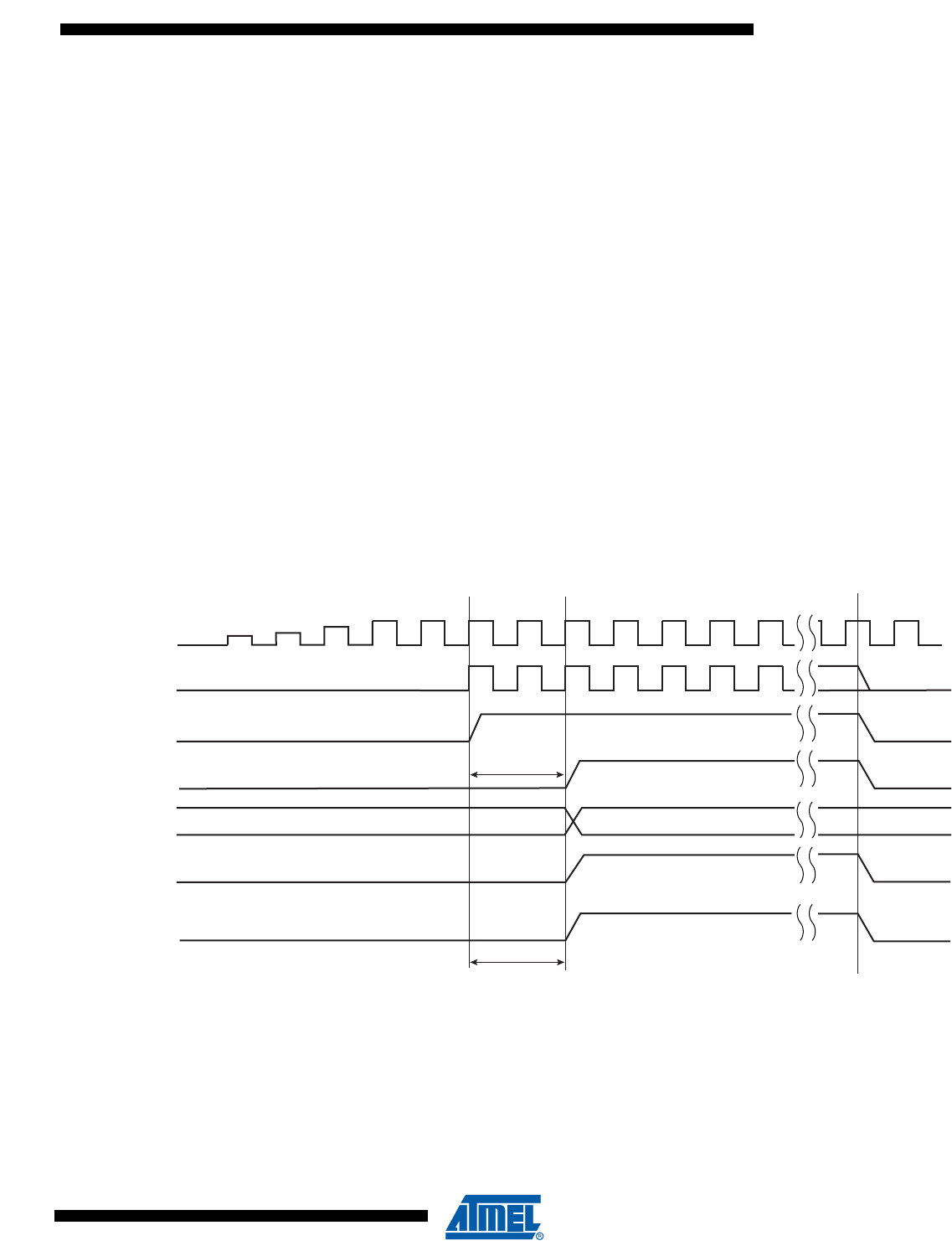
247
6430F–ATARM–21-Feb-12
SAM3U Series
Please note that the NRST output is in high impedance state when the chip is in OFF mode.
16.3.3 Brownout Manager
The Brownout manager is embedded within the Supply Controller, please refer to the Supply
Controller section for a detailed description.
16.3.4 Reset States
The Reset State Manager handles the different reset sources and generates the internal reset
signals. It reports the reset status in the field RSTTYP of the Status Register (RSTC_SR). The
update of the field RSTTYP is performed when the processor reset is released.
16.3.4.1 General Reset
A general reset occurs when a Power-on-reset is detected, an Asynchronous Master Reset
(NRSTB pin) is requested, a Brownout or a Voltage regulation loss is detected by the Supply
controller. The vddcore_nreset signal is asserted by the Supply Controller when a general reset
occurs.
All the reset signals are released and the field RSTTYP in RSTC_SR reports a General Reset.
As the RSTC_MR is reset, the NRST line rises 2 cycles after the vddcore_nreset, as ERSTL
defaults at value 0x0.
Figure 16-3 shows how the General Reset affects the reset signals.
Figure 16-3. General Reset State
SLCK
periph_nreset
proc_nreset
NRST
(nrst_out)
EXTERNAL RESET LENGTH
= 2 cycles
MCK
Processor Startup
= 2 cycles
backup_nreset
Any
Freq.
RSTTYP XXX 0x0 = General Reset XXX
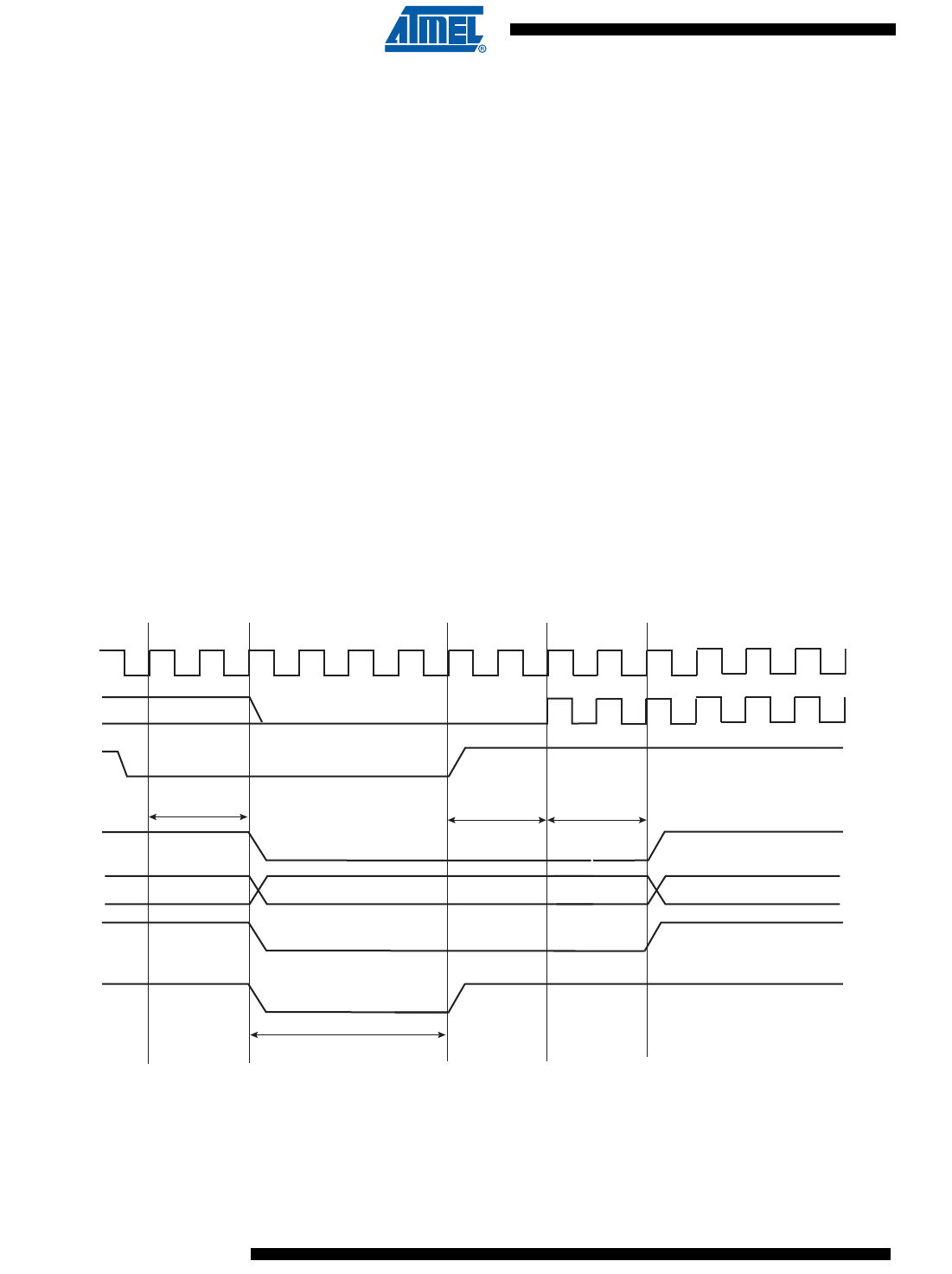
248
6430F–ATARM–21-Feb-12
SAM3U Series
16.3.4.2 Backup Reset
A Backup reset occurs when the chip returns from Backup mode. The vddcore_nreset signal is
asserted by the Supply Controller when a Backup reset occurs.
The field RSTTYP in RSTC_SR is updated to report a Backup Reset.
16.3.4.3 User Reset
The User Reset is entered when a low level is detected on the NRST pin and the bit URSTEN in
RSTC_MR is at 1. The NRST input signal is resynchronized with SLCK to insure proper behav-
ior of the system.
The User Reset is entered as soon as a low level is detected on NRST. The Processor Reset
and the Peripheral Reset are asserted.
The User Reset is left when NRST rises, after a two-cycle resynchronization time and a 3-cycle
processor startup. The processor clock is re-enabled as soon as NRST is confirmed high.
When the processor reset signal is released, the RSTTYP field of the Status Register
(RSTC_SR) is loaded with the value 0x4, indicating a User Reset.
The NRST Manager guarantees that the NRST line is asserted for
EXTERNAL_RESET_LENGTH Slow Clock cycles, as programmed in the field ERSTL. How-
ever, if NRST does not rise after EXTERNAL_RESET_LENGTH because it is driven low
externally, the internal reset lines remain asserted until NRST actually rises.
Figure 16-4. User Reset State
SLCK
periph_nreset
proc_nreset
NRST
NRST
(nrst_out)
>= EXTERNAL RESET LENGTH
MCK
Processor Startup
= 2 cycles
Any
Freq.
Resynch.
2 cycles
RSTTYP Any XXX
Resynch.
2 cycles
0x4 = User Reset

249
6430F–ATARM–21-Feb-12
SAM3U Series
16.3.4.4 Software Reset
The Reset Controller offers several commands used to assert the different reset signals. These
commands are performed by writing the Control Register (RSTC_CR) with the following bits at
1:
• PROCRST: Writing PROCRST at 1 resets the processor and the watchdog timer.
• PERRST: Writing PERRST at 1 resets all the embedded peripherals, including the memory
system, and, in particular, the Remap Command. The Peripheral Reset is generally used for
debug purposes.
• EXTRST: Writing EXTRST at 1 asserts low the NRST pin during a time defined by the field
ERSTL in the Mode Register (RSTC_MR).
The software reset is entered if at least one of these bits is set by the software. All these com-
mands can be performed independently or simultaneously. The software reset lasts 3 Slow
Clock cycles.
The internal reset signals are asserted as soon as the register write is performed. This is
detected on the Master Clock (MCK). They are released when the software reset is left, i.e.; syn-
chronously to SLCK.
If EXTRST is set, the nrst_out signal is asserted depending on the programming of the field
ERSTL. However, the resulting falling edge on NRST does not lead to a User Reset.
If and only if the PROCRST bit is set, the Reset Controller reports the software status in the field
RSTTYP of the Status Register (RSTC_SR). Other Software Resets are not reported in
RSTTYP.
As soon as a software operation is detected, the bit SRCMP (Software Reset Command in Prog-
ress) is set in the Status Register (RSTC_SR). It is cleared as soon as the software reset is left.
No other software reset can be performed while the SRCMP bit is set, and writing any value in
RSTC_CR has no effect.
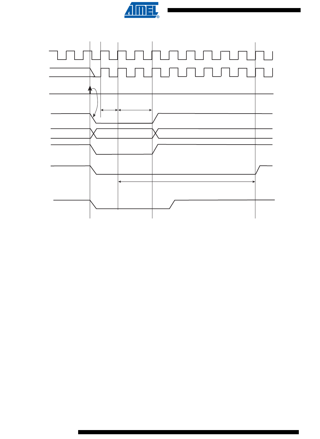
250
6430F–ATARM–21-Feb-12
SAM3U Series
Figure 16-5. Software Reset
16.3.4.5 Watchdog Reset
The Watchdog Reset is entered when a watchdog fault occurs. This state lasts 3 Slow Clock
cycles.
When in Watchdog Reset, assertion of the reset signals depends on the WDRPROC bit in
WDT_MR:
• If WDRPROC is 0, the Processor Reset and the Peripheral Reset are asserted. The NRST
line is also asserted, depending on the programming of the field ERSTL. However, the
resulting low level on NRST does not result in a User Reset state.
• If WDRPROC = 1, only the processor reset is asserted.
The Watchdog Timer is reset by the proc_nreset signal. As the watchdog fault always causes a
processor reset if WDRSTEN is set, the Watchdog Timer is always reset after a Watchdog
Reset, and the Watchdog is enabled by default and with a period set to a maximum.
When the WDRSTEN in WDT_MR bit is reset, the watchdog fault has no impact on the reset
controller.
SLCK
periph_nreset
if PERRST=1
proc_nreset
if PROCRST=1
Write RSTC_CR
NRST
(nrst_out)
if EXTRST=1
EXTERNAL RESET LENGTH
8 cycles (ERSTL=2)
MCK
Processor Startup
= 2 cycles
Any
Freq.
RSTTYP Any XXX 0x3 = Software Reset
Resynch.
1 cycle
SRCMP in RSTC_SR
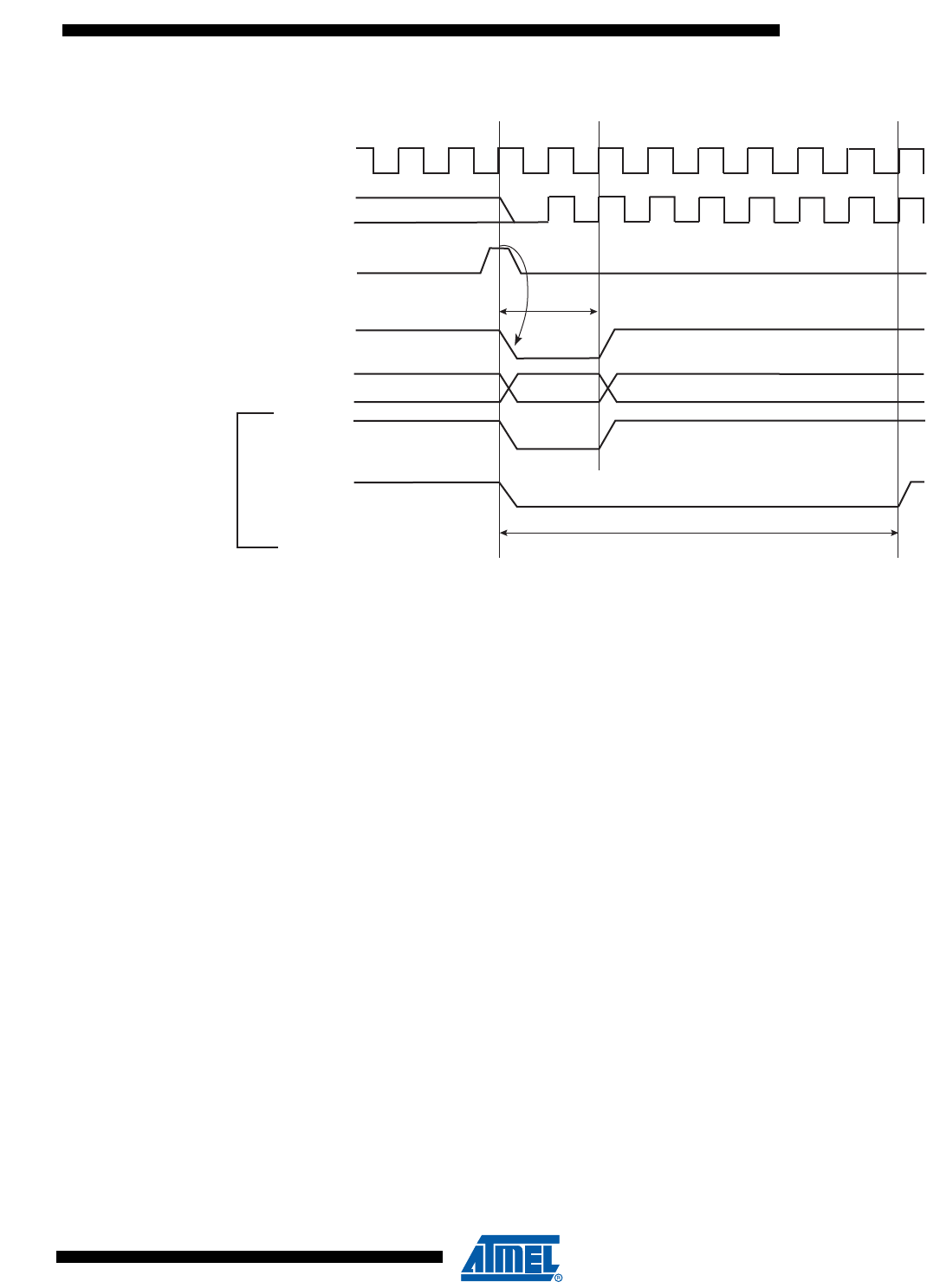
251
6430F–ATARM–21-Feb-12
SAM3U Series
Figure 16-6. Watchdog Reset
16.3.5 Reset State Priorities
The Reset State Manager manages the following priorities between the different reset sources,
given in descending order:
• General Reset
• Backup Reset
• Watchdog Reset
• Software Reset
• User Reset
Particular cases are listed below:
• When in User Reset:
– A watchdog event is impossible because the Watchdog Timer is being reset by the
proc_nreset signal.
– A software reset is impossible, since the processor reset is being activated.
• When in Software Reset:
– A watchdog event has priority over the current state.
– The NRST has no effect.
• When in Watchdog Reset:
– The processor reset is active and so a Software Reset cannot be programmed.
– A User Reset cannot be entered.
16.3.6 Reset Controller Status Register
The Reset Controller status register (RSTC_SR) provides several status fields:
• RSTTYP field: This field gives the type of the last reset, as explained in previous sections.
Only if
WDRPROC = 0
SLCK
periph_nreset
proc_nreset
wd_fault
NRST
(nrst_out)
EXTERNAL RESET LENGTH
8 cycles (ERSTL=2)
MCK
Processor Startup
= 2 cycles
Any
Freq.
RSTTYP Any XXX 0x2 = Watchdog Reset
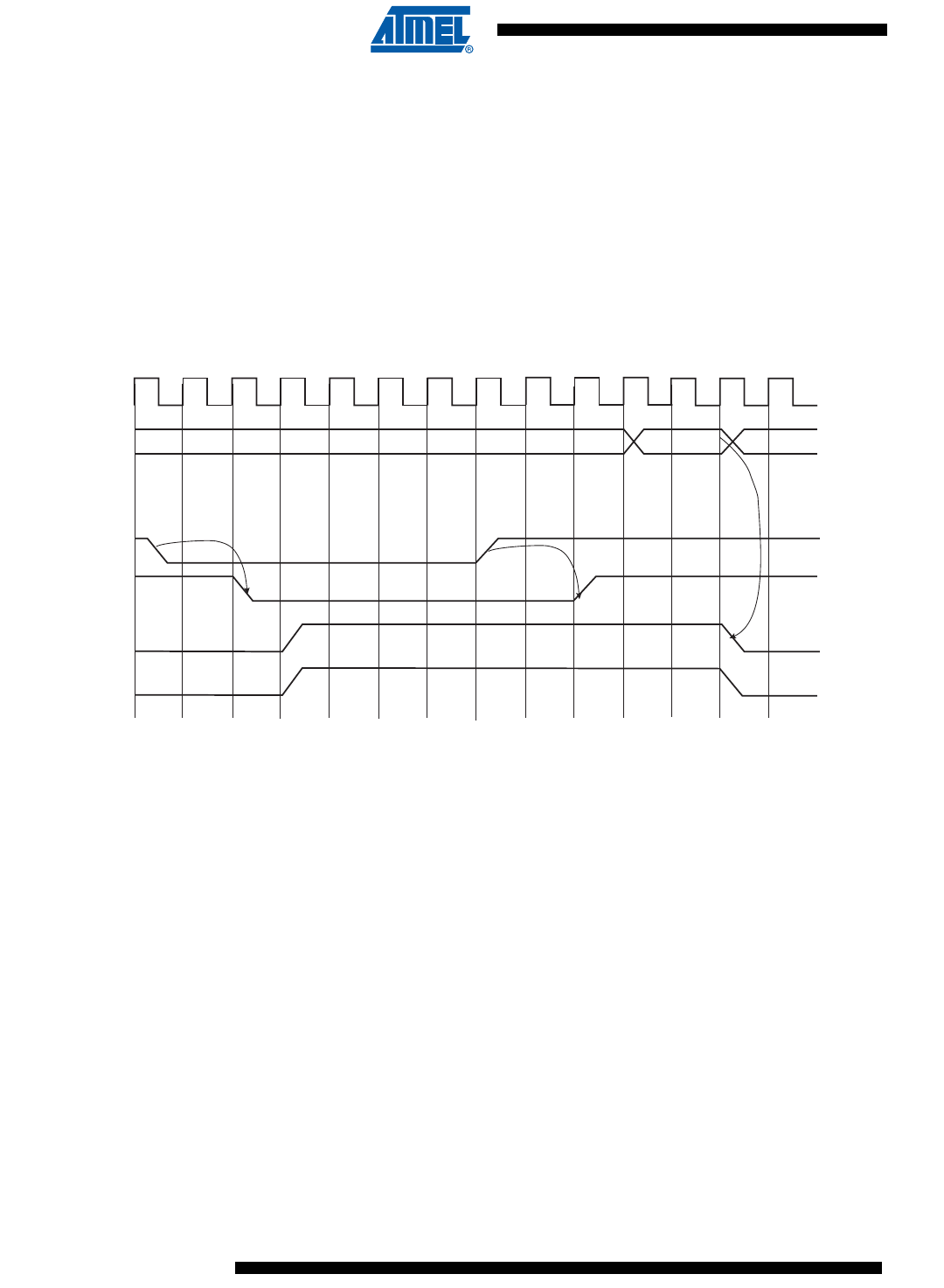
252
6430F–ATARM–21-Feb-12
SAM3U Series
• SRCMP bit: This field indicates that a Software Reset Command is in progress and that no
further software reset should be performed until the end of the current one. This bit is
automatically cleared at the end of the current software reset.
• NRSTL bit: The NRSTL bit of the Status Register gives the level of the NRST pin sampled on
each MCK rising edge.
• URSTS bit: A high-to-low transition of the NRST pin sets the URSTS bit of the RSTC_SR
register. This transition is also detected on the Master Clock (MCK) rising edge (see Figure
16-7). If the User Reset is disabled (URSTEN = 0) and if the interruption is enabled by the
URSTIEN bit in the RSTC_MR register, the URSTS bit triggers an interrupt. Reading the
RSTC_SR status register resets the URSTS bit and clears the interrupt.
Figure 16-7. Reset Controller Status and Interrupt
MCK
NRST
NRSTL
2 cycle
resynchronization
2 cycle
resynchronization
URSTS
read
RSTC_SR
Peripheral Access
rstc_irq
if (URSTEN = 0) and
(URSTIEN = 1)

253
6430F–ATARM–21-Feb-12
SAM3U Series
16.4 Reset Controller (RSTC) User Interface
Table 16-1. Register Mapping
Offset Register Name Access Reset
0x00 Control Register RSTC_CR Write-only -
0x04 Status Register RSTC_SR Read-only 0x0000_0000
0x08 Mode Register RSTC_MR Read-write 0x0000_0000

254
6430F–ATARM–21-Feb-12
SAM3U Series
16.4.1 Reset Controller Control Register
Name: RSTC_CR
Address: 0x400E1200
Access Type: Write-only
• PROCRST: Processor Reset
0 = No effect.
1 = If KEY is correct, resets the processor.
• PERRST: Peripheral Reset
0 = No effect.
1 = If KEY is correct, resets the peripherals.
• EXTRST: External Reset
0 = No effect.
1 = If KEY is correct, asserts the NRST pin.
•KEY: Password
Should be written at value 0xA5. Writing any other value in this field aborts the write operation.
31 30 29 28 27 26 25 24
KEY
23 22 21 20 19 18 17 16
––––––––
15 14 13 12 11 10 9 8
–––––– –
76543210
––––EXTRSTPERRST–PROCRST
255
6430F–ATARM–21-Feb-12
SAM3U Series
16.4.2 Reset Controller Status Register
Name: RSTC_SR
Address: 0x400E1204
Access Type: Read-only
• URSTS: User Reset Status
0 = No high-to-low edge on NRST happened since the last read of RSTC_SR.
1 = At least one high-to-low transition of NRST has been detected since the last read of RSTC_SR.
• RSTTYP: Reset Type
Reports the cause of the last processor reset. Reading this RSTC_SR does not reset this field.
• NRSTL: NRST Pin Level
Registers the NRST Pin Level at Master Clock (MCK).
• SRCMP: Software Reset Command in Progress
0 = No software command is being performed by the reset controller. The reset controller is ready for a software command.
1 = A software reset command is being performed by the reset controller. The reset controller is busy.
31 30 29 28 27 26 25 24
––––––––
23 22 21 20 19 18 17 16
––––––SRCMPNRSTL
15 14 13 12 11 10 9 8
––––– RSTTYP
76543210
–––––––URSTS
RSTTYP Reset Type Comments
0 0 0 General Reset First power-up Reset
0 0 1 Backup Reset Return from Backup mode
0 1 0 Watchdog Reset Watchdog fault occurred
0 1 1 Software Reset Processor reset required by the software
1 0 0 User Reset NRST pin detected low

256
6430F–ATARM–21-Feb-12
SAM3U Series
16.4.3 Reset Controller Mode Register
Name: RSTC_MR
Address: 0x400E1208
Access Type: Read-write
• URSTEN: User Reset Enable
0 = The detection of a low level on the pin NRST does not generate a User Reset.
1 = The detection of a low level on the pin NRST triggers a User Reset.
• URSTIEN: User Reset Interrupt Enable
0 = USRTS bit in RSTC_SR at 1 has no effect on rstc_irq.
1 = USRTS bit in RSTC_SR at 1 asserts rstc_irq if URSTEN = 0.
• ERSTL: External Reset Length
This field defines the external reset length. The external reset is asserted during a time of 2(ERSTL+1) Slow Clock cycles. This
allows assertion duration to be programmed between 60 µs and 2 seconds.
•KEY: Password
Should be written at value 0xA5. Writing any other value in this field aborts the write operation.
31 30 29 28 27 26 25 24
KEY
23 22 21 20 19 18 17 16
––––––––
15 14 13 12 11 10 9 8
–––– ERSTL
76543210
– – URSTIEN – – – URSTEN
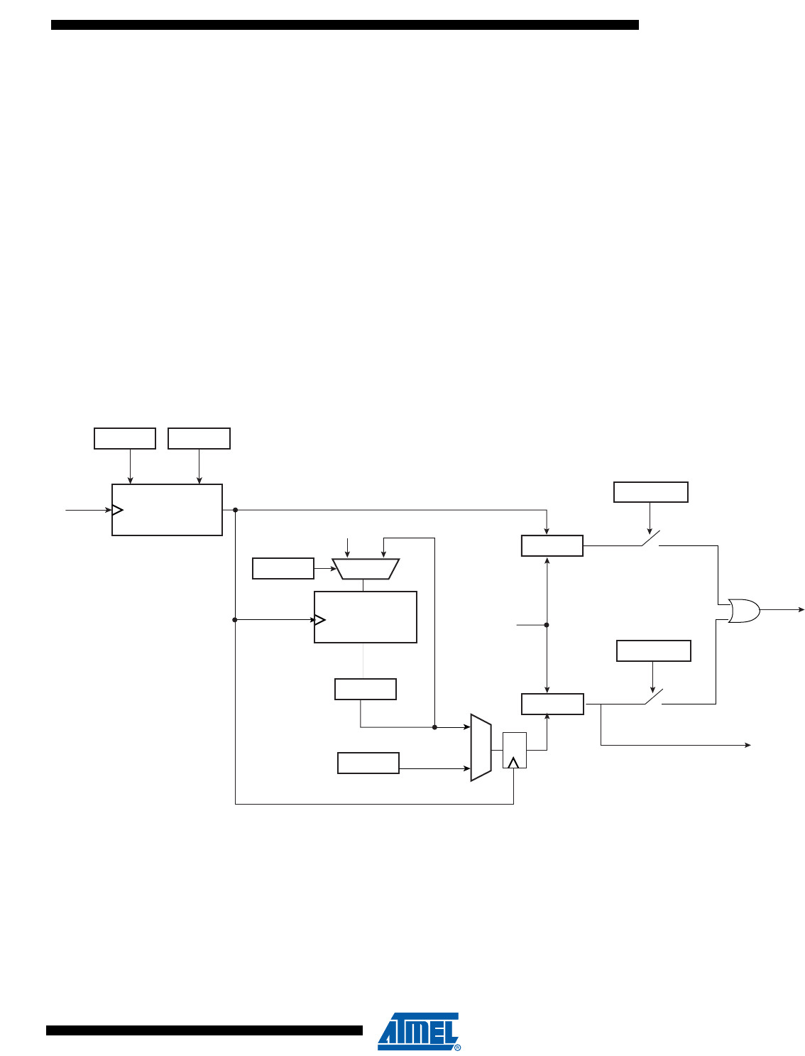
257
6430F–ATARM–21-Feb-12
SAM3U Series
257
6430F–ATARM–21-Feb-12
SAM3U Series
17. Real-time Timer (RTT)
17.1 Description
The Real-time Timer is built around a 32-bit counter used to count roll-over events of the pro-
grammable 16-bit prescaler which enables counting elapsed seconds from a 32 kHz slow clock
source. It generates a periodic interrupt and/or triggers an alarm on a programmed value.
17.2 Embedded Characteristics
• 32-bit Free-running Counter on prescaled slow clock
• 16-bit Configurable Prescaler
• Interrupt on Alarm
17.3 Block Diagram
Figure 17-1. Real-time Timer
SLCK
RTPRES
RTTINC
ALMS
16-bit
Divider
32-bit
Counter
ALMV
=
CRTV
RTT_MR
RTT_VR
RTT_AR
RTT_SR
RTTINCIEN
RTT_MR
0
10
ALMIEN
rtt_int
RTT_MR
set
set
RTT_SR
read
RTT_SR
reset
reset
RTT_MR
reload
rtt_alarm
RTTRST
RTT_MR
RTTRST

258
6430F–ATARM–21-Feb-12
SAM3U Series
258
6430F–ATARM–21-Feb-12
SAM3U Series
17.4 Functional Description
The Real-time Timer can be used to count elapsed seconds. It is built around a 32-bit counter
fed by Slow Clock divided by a programmable 16-bit value. The value can be programmed in the
field RTPRES of the Real-time Mode Register (RTT_MR).
Programming RTPRES at 0x00008000 corresponds to feeding the real-time counter with a 1 Hz
signal (if the Slow Clock is 32.768 kHz). The 32-bit counter can count up to 232 seconds, corre-
sponding to more than 136 years, then roll over to 0.
The Real-time Timer can also be used as a free-running timer with a lower time-base. The best
accuracy is achieved by writing RTPRES to 3. Programming RTPRES to 1 or 2 is possible, but
may result in losing status events because the status register is cleared two Slow Clock cycles
after read. Thus if the RTT is configured to trigger an interrupt, the interrupt occurs during 2 Slow
Clock cycles after reading RTT_SR. To prevent several executions of the interrupt handler, the
interrupt must be disabled in the interrupt handler and re-enabled when the status register is
clear.
The Real-time Timer value (CRTV) can be read at any time in the register RTT_VR (Real-time
Value Register). As this value can be updated asynchronously from the Master Clock, it is advis-
able to read this register twice at the same value to improve accuracy of the returned value.
The current value of the counter is compared with the value written in the alarm register
RTT_AR (Real-time Alarm Register). If the counter value matches the alarm, the bit ALMS in
RTT_SR is set. The alarm register is set to its maximum value, corresponding to 0xFFFF_FFFF,
after a reset.
The bit RTTINC in RTT_SR is set each time the Real-time Timer counter is incremented. This bit
can be used to start a periodic interrupt, the period being one second when the RTPRES is pro-
grammed with 0x8000 and Slow Clock equal to 32.768 Hz.
Reading the RTT_SR status register resets the RTTINC and ALMS fields.
Writing the bit RTTRST in RTT_MR immediately reloads and restarts the clock divider with the
new programmed value. This also resets the 32-bit counter.
Note: Because of the asynchronism between the Slow Clock (SCLK) and the System Clock (MCK):
1) The restart of the counter and the reset of the RTT_VR current value register is effective only 2
slow clock cycles after the write of the RTTRST bit in the RTT_MR register.
2) The status register flags reset is taken into account only 2 slow clock cycles after the read of the
RTT_SR (Status Register).
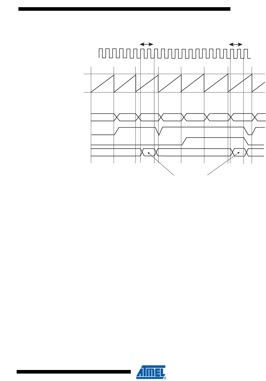
259
6430F–ATARM–21-Feb-12
SAM3U Series
259
6430F–ATARM–21-Feb-12
SAM3U Series
Figure 17-2. RTT Counting
Prescaler
ALMVALMV-10 ALMV+1
0
RTPRES - 1
RTT
APB cycle
read RTT_SR
ALMS (RTT_SR)
APB Interface
SCLK
RTTINC (RTT_SR)
ALMV+2 ALMV+3
...
APB cycle

260
6430F–ATARM–21-Feb-12
SAM3U Series
260
6430F–ATARM–21-Feb-12
SAM3U Series
17.5 Real-time Timer (RTT) User Interface
Table 17-1. Register Mapping
Offset Register Name Access Reset
0x00 Mode Register RTT_MR Read-write 0x0000_8000
0x04 Alarm Register RTT_AR Read-write 0xFFFF_FFFF
0x08 Value Register RTT_VR Read-only 0x0000_0000
0x0C Status Register RTT_SR Read-only 0x0000_0000

261
6430F–ATARM–21-Feb-12
SAM3U Series
261
6430F–ATARM–21-Feb-12
SAM3U Series
17.5.1 Real-time Timer Mode Register
Name: RTT_MR
Address: 0x400E1230
Access: Read-write
• RTPRES: Real-time Timer Prescaler Value
Defines the number of SLCK periods required to increment the Real-time timer. RTPRES is defined as follows:
RTPRES = 0: The prescaler period is equal to 216 * SCLK period.
RTPRES ≠ 0: The prescaler period is equal to RTPRES * SCLK period.
• ALMIEN: Alarm Interrupt Enable
0 = The bit ALMS in RTT_SR has no effect on interrupt.
1 = The bit ALMS in RTT_SR asserts interrupt.
• RTTINCIEN: Real-time Timer Increment Interrupt Enable
0 = The bit RTTINC in RTT_SR has no effect on interrupt.
1 = The bit RTTINC in RTT_SR asserts interrupt.
• RTTRST: Real-time Timer Restart
0 = No effect.
1 = Reloads and restarts the clock divider with the new programmed value. This also resets the 32-bit counter.
31 30 29 28 27 26 25 24
––––––––
23 22 21 20 19 18 17 16
–––––RTTRSTRTTINCIENALMIEN
15 14 13 12 11 10 9 8
RTPRES
76543210
RTPRES

262
6430F–ATARM–21-Feb-12
SAM3U Series
262
6430F–ATARM–21-Feb-12
SAM3U Series
17.5.2 Real-time Timer Alarm Register
Name: RTT_AR
Address: 0x400E1234
Access: Read-write
• ALMV: Alarm Value
Defines the alarm value (ALMV+1) compared with the Real-time Timer.
31 30 29 28 27 26 25 24
ALMV
23 22 21 20 19 18 17 16
ALMV
15 14 13 12 11 10 9 8
ALMV
76543210
ALMV

263
6430F–ATARM–21-Feb-12
SAM3U Series
263
6430F–ATARM–21-Feb-12
SAM3U Series
17.5.3 Real-time Timer Value Register
Name: RTT_VR
Address: 0x400E1238
Access: Read-only
• CRTV: Current Real-time Value
Returns the current value of the Real-time Timer.
31 30 29 28 27 26 25 24
CRTV
23 22 21 20 19 18 17 16
CRTV
15 14 13 12 11 10 9 8
CRTV
76543210
CRTV

264
6430F–ATARM–21-Feb-12
SAM3U Series
264
6430F–ATARM–21-Feb-12
SAM3U Series
17.5.4 Real-time Timer Status Register
Name: RTT_SR
Address: 0x400E123C
Access: Read-only
• ALMS: Real-time Alarm Status
0 = The Real-time Alarm has not occurred since the last read of RTT_SR.
1 = The Real-time Alarm occurred since the last read of RTT_SR.
• RTTINC: Real-time Timer Increment
0 = The Real-time Timer has not been incremented since the last read of the RTT_SR.
1 = The Real-time Timer has been incremented since the last read of the RTT_SR.
31 30 29 28 27 26 25 24
––––––––
23 22 21 20 19 18 17 16
––––––––
15 14 13 12 11 10 9 8
––––––––
76543210
––––––RTTINCALMS
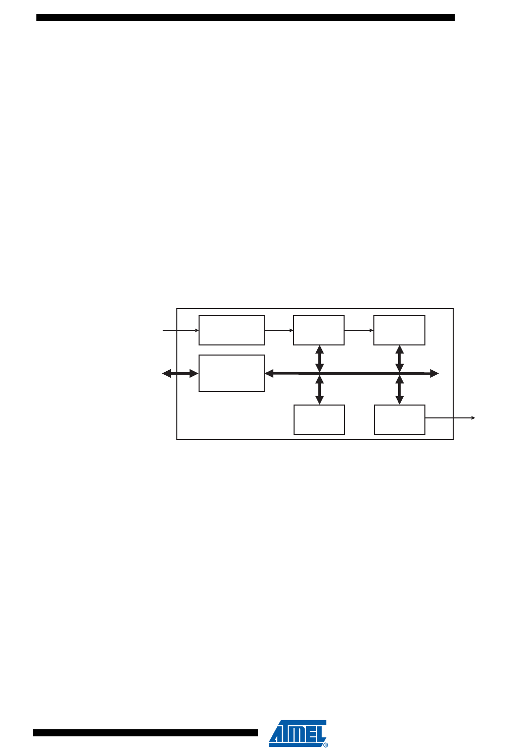
265
6430F–ATARM–21-Feb-12
SAM3U Series
18. Real Time Clock (RTC)
18.1 Description
The Real-time Clock (RTC) peripheral is designed for very low power consumption.
It combines a complete time-of-day clock with alarm and a two-hundred-year Gregorian calen-
dar, complemented by a programmable periodic interrupt. The alarm and calendar registers are
accessed by a 32-bit data bus.
The time and calendar values are coded in binary-coded decimal (BCD) format. The time format
can be 24-hour mode or 12-hour mode with an AM/PM indicator.
Updating time and calendar fields and configuring the alarm fields are performed by a parallel
capture on the 32-bit data bus. An entry control is performed to avoid loading registers with
incompatible BCD format data or with an incompatible date according to the current
month/year/century.
18.2 Block Diagram
Figure 18-1. RTC Block Diagram
18.3 Product Dependencies
18.3.1 Power Management
The Real-time Clock is continuously clocked at 32768 Hz. The Power Management Controller
has no effect on RTC behavior.
18.3.2 Interrupt
RTC interrupt line is connected on one of the internal sources of the interrupt controller. RTC
interrupt requires the interrupt controller to be programmed first.
Bus Interface
32768 Divider TimeSlow Clock: SLCK
Bus Interface
Date
RTC Interrupt
Entry
Control
Interrupt
Control

266
6430F–ATARM–21-Feb-12
SAM3U Series
18.4 Functional Description
The RTC provides a full binary-coded decimal (BCD) clock that includes century (19/20), year
(with leap years), month, date, day, hours, minutes and seconds.
The valid year range is 1900 to 2099 in Gregorian mode, a two-hundred-year calendar.
The RTC can operate in 24-hour mode or in 12-hour mode with an AM/PM indicator.
Corrections for leap years are included (all years divisible by 4 being leap years). This is correct
up to the year 2099.
18.4.1 Reference Clock
The reference clock is Slow Clock (SLCK). It can be driven internally or by an external 32.768
kHz crystal.
During low power modes of the processor, the oscillator runs and power consumption is critical.
The crystal selection has to take into account the current consumption for power saving and the
frequency drift due to temperature effect on the circuit for time accuracy.
18.4.2 Timing
The RTC is updated in real time at one-second intervals in normal mode for the counters of sec-
onds, at one-minute intervals for the counter of minutes and so on.
Due to the asynchronous operation of the RTC with respect to the rest of the chip, to be certain
that the value read in the RTC registers (century, year, month, date, day, hours, minutes, sec-
onds) are valid and stable, it is necessary to read these registers twice. If the data is the same
both times, then it is valid. Therefore, a minimum of two and a maximum of three accesses are
required.
18.4.3 Alarm
The RTC has five programmable fields: month, date, hours, minutes and seconds.
Each of these fields can be enabled or disabled to match the alarm condition:
• If all the fields are enabled, an alarm flag is generated (the corresponding flag is asserted
and an interrupt generated if enabled) at a given month, date, hour/minute/second.
• If only the “seconds” field is enabled, then an alarm is generated every minute.
Depending on the combination of fields enabled, a large number of possibilities are available to
the user ranging from minutes to 365/366 days.
18.4.4 Error Checking
Verification on user interface data is performed when accessing the century, year, month, date,
day, hours, minutes, seconds and alarms. A check is performed on illegal BCD entries such as
illegal date of the month with regard to the year and century configured.
If one of the time fields is not correct, the data is not loaded into the register/counter and a flag is
set in the validity register. The user can not reset this flag. It is reset as soon as an acceptable
value is programmed. This avoids any further side effects in the hardware. The same procedure
is done for the alarm.
The following checks are performed:
1. Century (check if it is in range 19 - 20)
2. Year (BCD entry check)

267
6430F–ATARM–21-Feb-12
SAM3U Series
3. Date (check range 01 - 31)
4. Month (check if it is in BCD range 01 - 12, check validity regarding “date”)
5. Day (check range 1 - 7)
6. Hour (BCD checks: in 24-hour mode, check range 00 - 23 and check that AM/PM flag is
not set if RTC is set in 24-hour mode; in 12-hour mode check range 01 - 12)
7. Minute (check BCD and range 00 - 59)
8. Second (check BCD and range 00 - 59)
Note: If the 12-hour mode is selected by means of the RTC_MODE register, a 12-hour value can be pro-
grammed and the returned value on RTC_TIME will be the corresponding 24-hour value. The
entry control checks the value of the AM/PM indicator (bit 22 of RTC_TIME register) to determine
the range to be checked.
18.4.5 Updating Time/Calendar
To update any of the time/calendar fields, the user must first stop the RTC by setting the corre-
sponding field in the Control Register. Bit UPDTIM must be set to update time fields (hour,
minute, second) and bit UPDCAL must be set to update calendar fields (century, year, month,
date, day).
Then the user must poll or wait for the interrupt (if enabled) of bit ACKUPD in the Status Regis-
ter. Once the bit reads 1, it is mandatory to clear this flag by writing the corresponding bit in
RTC_SCCR. The user can now write to the appropriate Time and Calendar register.
Once the update is finished, the user must reset (0) UPDTIM and/or UPDCAL in the Control
When entering programming mode of the calendar fields, the time fields remain enabled. When
entering the programming mode of the time fields, both time and calendar fields are stopped.
This is due to the location of the calendar logic circuity (downstream for low-power consider-
ations). It is highly recommended to prepare all the fields to be updated before entering
programming mode. In successive update operations, the user must wait at least one second
after resetting the UPDTIM/UPDCAL bit in the RTC_CR (Control Register) before setting these
bits again. This is done by waiting for the SEC flag in the Status Register before setting
UPDTIM/UPDCAL bit. After resetting UPDTIM/UPDCAL, the SEC flag must also be cleared.
268
6430F–ATARM–21-Feb-12
SAM3U Series
Figure 18-2. Update Sequence
Prepare TIme or Calendar Fields
Set UPDTIM and/or UPDCAL
bit(s) in RTC_CR
Read RTC_SR
ACKUPD
= 1 ?
Clear ACKUPD bit in RTC_SCCR
Update Time and/or Calendar values in
RTC_TIMR/RTC_CALR
Clear UPDTIM and/or UPDCAL bit in
RTC_CR
No
Ye s
Begin
End
Polling or
IRQ (if enabled)

269
6430F–ATARM–21-Feb-12
SAM3U Series
18.5 Real Time Clock (RTC) User Interface
Note: if an offset is not listed in the table it must be considered as reserved.
Table 18-1. Register Mapping
Offset Register Name Access Reset
0x00 Control Register RTC_CR Read-write 0x0
0x04 Mode Register RTC_MR Read-write 0x0
0x08 Time Register RTC_TIMR Read-write 0x0
0x0C Calendar Register RTC_CALR Read-write 0x01210720
0x10 Time Alarm Register RTC_TIMALR Read-write 0x0
0x14 Calendar Alarm Register RTC_CALALR Read-write 0x01010000
0x18 Status Register RTC_SR Read-only 0x0
0x1C Status Clear Command Register RTC_SCCR Write-only –
0x20 Interrupt Enable Register RTC_IER Write-only –
0x24 Interrupt Disable Register RTC_IDR Write-only –
0x28 Interrupt Mask Register RTC_IMR Read-only 0x0
0x2C Valid Entry Register RTC_VER Read-only 0x0
0x30–0xE0 Reserved Register – – –
0xE4 Write Protect Mode Register RTC_WPMR Read-write 0x00000000
0xE8–0xF8 Reserved Register – – –
0xFC Reserved Register – – –
270
6430F–ATARM–21-Feb-12
SAM3U Series
18.5.1 RTC Control Register
Name: RTC_CR
Address: 0x400E1260
Access: Read-write
This register can only be written if the WPEN bit is cleared in “RTC Write Protect Mode Register” on page 282.
• UPDTIM: Update Request Time Register
0 = No effect.
1 = Stops the RTC time counting.
Time counting consists of second, minute and hour counters. Time counters can be programmed once this bit is set and
acknowledged by the bit ACKUPD of the Status Register.
• UPDCAL: Update Request Calendar Register
0 = No effect.
1 = Stops the RTC calendar counting.
Calendar counting consists of day, date, month, year and century counters. Calendar counters can be programmed once
this bit is set.
• TIMEVSEL: Time Event Selection
The event that generates the flag TIMEV in RTC_SR (Status Register) depends on the value of TIMEVSEL.
• CALEVSEL: Calendar Event Selection
The event that generates the flag CALEV in RTC_SR depends on the value of CALEVSEL
31 30 29 28 27 26 25 24
––––––––
23 22 21 20 19 18 17 16
–––––– CALEVSEL
15 14 13 12 11 10 9 8
–––––– TIMEVSEL
76543210
––––––UPDCALUPDTIM
Value Name Description
0 MINUTE Minute change
1 HOUR Hour change
2 MIDNIGHT Every day at midnight
3 NOON Every day at noon
Value Name Description
0 WEEK Week change (every Monday at time 00:00:00)
1 MONTH Month change (every 01 of each month at time 00:00:00)
2 YEAR Year change (every January 1 at time 00:00:00)
3–

271
6430F–ATARM–21-Feb-12
SAM3U Series
18.5.2 RTC Mode Register
Name: RTC_MR
Address: 0x400E1264
Access: Read-write
• HRMOD: 12-/24-hour Mode
0 = 24-hour mode is selected.
1 = 12-hour mode is selected.
All non-significant bits read zero.
31 30 29 28 27 26 25 24
––––––––
23 22 21 20 19 18 17 16
––––––––
15 14 13 12 11 10 9 8
––––––––
76543210
–––––––HRMOD

272
6430F–ATARM–21-Feb-12
SAM3U Series
18.5.3 RTC Time Register
Name: RTC_TIMR
Address: 0x400E1268
Access: Read-write
• SEC: Current Second
The range that can be set is 0 - 59 (BCD).
The lowest four bits encode the units. The higher bits encode the tens.
• MIN: Current Minute
The range that can be set is 0 - 59 (BCD).
The lowest four bits encode the units. The higher bits encode the tens.
• HOUR: Current Hour
The range that can be set is 1 - 12 (BCD) in 12-hour mode or 0 - 23 (BCD) in 24-hour mode.
• AMPM: Ante Meridiem Post Meridiem Indicator
This bit is the AM/PM indicator in 12-hour mode.
0 = AM.
1 = PM.
All non-significant bits read zero.
31 30 29 28 27 26 25 24
––––––––
23 22 21 20 19 18 17 16
–AMPM HOUR
15 14 13 12 11 10 9 8
–MIN
76543210
–SEC

273
6430F–ATARM–21-Feb-12
SAM3U Series
18.5.4 RTC Calendar Register
Name: RTC_CALR
Address: 0x400E126C
Access: Read-write
• CENT: Current Century
The range that can be set is 19 - 20 (BCD).
The lowest four bits encode the units. The higher bits encode the tens.
• YEAR: Current Year
The range that can be set is 00 - 99 (BCD).
The lowest four bits encode the units. The higher bits encode the tens.
• MONTH: Current Month
The range that can be set is 01 - 12 (BCD).
The lowest four bits encode the units. The higher bits encode the tens.
• DAY: Current Day in Current Week
The range that can be set is 1 - 7 (BCD).
The coding of the number (which number represents which day) is user-defined as it has no effect on the date counter.
• DATE: Current Day in Current Month
The range that can be set is 01 - 31 (BCD).
The lowest four bits encode the units. The higher bits encode the tens.
All non-significant bits read zero.
31 30 29 28 27 26 25 24
–– DATE
23 22 21 20 19 18 17 16
DAY MONTH
15 14 13 12 11 10 9 8
YEAR
76543210
–CENT

274
6430F–ATARM–21-Feb-12
SAM3U Series
18.5.5 RTC Time Alarm Register
Name: RTC_TIMALR
Address: 0x400E1270
Access: Read-write
This register can only be written if the WPEN bit is cleared in “RTC Write Protect Mode Register” on page 282.
• SEC: Second Alarm
This field is the alarm field corresponding to the BCD-coded second counter.
• SECEN: Second Alarm Enable
0 = The second-matching alarm is disabled.
1 = The second-matching alarm is enabled.
• MIN: Minute Alarm
This field is the alarm field corresponding to the BCD-coded minute counter.
• MINEN: Minute Alarm Enable
0 = The minute-matching alarm is disabled.
1 = The minute-matching alarm is enabled.
• HOUR: Hour Alarm
This field is the alarm field corresponding to the BCD-coded hour counter.
• AMPM: AM/PM Indicator
This field is the alarm field corresponding to the BCD-coded hour counter.
• HOUREN: Hour Alarm Enable
0 = The hour-matching alarm is disabled.
1 = The hour-matching alarm is enabled.
31 30 29 28 27 26 25 24
––––––––
23 22 21 20 19 18 17 16
HOUREN AMPM HOUR
15 14 13 12 11 10 9 8
MINEN MIN
76543210
SECEN SEC

275
6430F–ATARM–21-Feb-12
SAM3U Series
18.5.6 RTC Calendar Alarm Register
Name: RTC_CALALR
Address: 0x400E1274
Access: Read-write
This register can only be written if the WPEN bit is cleared in “RTC Write Protect Mode Register” on page 282.
• MONTH: Month Alarm
This field is the alarm field corresponding to the BCD-coded month counter.
• MTHEN: Month Alarm Enable
0 = The month-matching alarm is disabled.
1 = The month-matching alarm is enabled.
•DATE: Date Alarm
This field is the alarm field corresponding to the BCD-coded date counter.
• DATEEN: Date Alarm Enable
0 = The date-matching alarm is disabled.
1 = The date-matching alarm is enabled.
31 30 29 28 27 26 25 24
DATEEN – DATE
23 22 21 20 19 18 17 16
MTHEN – – MONTH
15 14 13 12 11 10 9 8
––––––––
76543210
––––––––

276
6430F–ATARM–21-Feb-12
SAM3U Series
18.5.7 RTC Status Register
Name: RTC_SR
Address: 0x400E1278
Access: Read-only
• ACKUPD: Acknowledge for Update
0 = Time and calendar registers cannot be updated.
1 = Time and calendar registers can be updated.
• ALARM: Alarm Flag
0 = No alarm matching condition occurred.
1 = An alarm matching condition has occurred.
• SEC: Second Event
0 = No second event has occurred since the last clear.
1 = At least one second event has occurred since the last clear.
• TIMEV: Time Event
0 = No time event has occurred since the last clear.
1 = At least one time event has occurred since the last clear.
The time event is selected in the TIMEVSEL field in RTC_CR (Control Register) and can be any one of the following
events: minute change, hour change, noon, midnight (day change).
• CALEV: Calendar Event
0 = No calendar event has occurred since the last clear.
1 = At least one calendar event has occurred since the last clear.
The calendar event is selected in the CALEVSEL field in RTC_CR and can be any one of the following events: week
change, month change and year change.
31 30 29 28 27 26 25 24
––––––––
23 22 21 20 19 18 17 16
––––––––
15 14 13 12 11 10 9 8
––––––––
76543210
– – – CALEV TIMEV SEC ALARM ACKUPD

277
6430F–ATARM–21-Feb-12
SAM3U Series
18.5.8 RTC Status Clear Command Register
Name: RTC_SCCR
Address: 0x400E127C
Access: Write-only
• ACKCLR: Acknowledge Clear
0 = No effect.
1 = Clears corresponding status flag in the Status Register (RTC_SR).
• ALRCLR: Alarm Clear
0 = No effect.
1 = Clears corresponding status flag in the Status Register (RTC_SR).
• SECCLR: Second Clear
0 = No effect.
1 = Clears corresponding status flag in the Status Register (RTC_SR).
• TIMCLR: Time Clear
0 = No effect.
1 = Clears corresponding status flag in the Status Register (RTC_SR).
• CALCLR: Calendar Clear
0 = No effect.
1 = Clears corresponding status flag in the Status Register (RTC_SR).
31 30 29 28 27 26 25 24
––––––––
23 22 21 20 19 18 17 16
––––––––
15 14 13 12 11 10 9 8
––––––––
76543210
– – – CALCLR TIMCLR SECCLR ALRCLR ACKCLR

278
6430F–ATARM–21-Feb-12
SAM3U Series
18.5.9 RTC Interrupt Enable Register
Name: RTC_IER
Address: 0x400E1280
Access: Write-only
• ACKEN: Acknowledge Update Interrupt Enable
0 = No effect.
1 = The acknowledge for update interrupt is enabled.
• ALREN: Alarm Interrupt Enable
0 = No effect.
1 = The alarm interrupt is enabled.
• SECEN: Second Event Interrupt Enable
0 = No effect.
1 = The second periodic interrupt is enabled.
• TIMEN: Time Event Interrupt Enable
0 = No effect.
1 = The selected time event interrupt is enabled.
• CALEN: Calendar Event Interrupt Enable
0 = No effect.
• 1 = The selected calendar event interrupt is enabled.
31 30 29 28 27 26 25 24
––––––––
23 22 21 20 19 18 17 16
––––––––
15 14 13 12 11 10 9 8
––––––––
76543210
– – – CALEN TIMEN SECEN ALREN ACKEN

279
6430F–ATARM–21-Feb-12
SAM3U Series
18.5.10 RTC Interrupt Disable Register
Name: RTC_IDR
Address: 0x400E1284
Access: Write-only
• ACKDIS: Acknowledge Update Interrupt Disable
0 = No effect.
1 = The acknowledge for update interrupt is disabled.
• ALRDIS: Alarm Interrupt Disable
0 = No effect.
1 = The alarm interrupt is disabled.
• SECDIS: Second Event Interrupt Disable
0 = No effect.
1 = The second periodic interrupt is disabled.
• TIMDIS: Time Event Interrupt Disable
0 = No effect.
1 = The selected time event interrupt is disabled.
• CALDIS: Calendar Event Interrupt Disable
0 = No effect.
1 = The selected calendar event interrupt is disabled.
31 30 29 28 27 26 25 24
––––––––
23 22 21 20 19 18 17 16
––––––––
15 14 13 12 11 10 9 8
––––––––
76543210
– – – CALDIS TIMDIS SECDIS ALRDIS ACKDIS

280
6430F–ATARM–21-Feb-12
SAM3U Series
18.5.11 RTC Interrupt Mask Register
Name: RTC_IMR
Address: 0x400E1288
Access: Read-only
• ACK: Acknowledge Update Interrupt Mask
0 = The acknowledge for update interrupt is disabled.
1 = The acknowledge for update interrupt is enabled.
• ALR: Alarm Interrupt Mask
0 = The alarm interrupt is disabled.
1 = The alarm interrupt is enabled.
• SEC: Second Event Interrupt Mask
0 = The second periodic interrupt is disabled.
1 = The second periodic interrupt is enabled.
• TIM: Time Event Interrupt Mask
0 = The selected time event interrupt is disabled.
1 = The selected time event interrupt is enabled.
• CAL: Calendar Event Interrupt Mask
0 = The selected calendar event interrupt is disabled.
1 = The selected calendar event interrupt is enabled.
31 30 29 28 27 26 25 24
––––––––
23 22 21 20 19 18 17 16
––––––––
15 14 13 12 11 10 9 8
––––––––
76543210
–––CALTIMSECALRACK

281
6430F–ATARM–21-Feb-12
SAM3U Series
18.5.12 RTC Valid Entry Register
Name: RTC_VER
Address: 0x400E128C
Access: Read-only
• NVTIM: Non-valid Time
0 = No invalid data has been detected in RTC_TIMR (Time Register).
1 = RTC_TIMR has contained invalid data since it was last programmed.
• NVCAL: Non-valid Calendar
0 = No invalid data has been detected in RTC_CALR (Calendar Register).
1 = RTC_CALR has contained invalid data since it was last programmed.
• NVTIMALR: Non-valid Time Alarm
0 = No invalid data has been detected in RTC_TIMALR (Time Alarm Register).
1 = RTC_TIMALR has contained invalid data since it was last programmed.
• NVCALALR: Non-valid Calendar Alarm
0 = No invalid data has been detected in RTC_CALALR (Calendar Alarm Register).
1 = RTC_CALALR has contained invalid data since it was last programmed.
31 30 29 28 27 26 25 24
––––––––
23 22 21 20 19 18 17 16
––––––––
15 14 13 12 11 10 9 8
––––––––
76543210
––––NVCALALRNVTIMALRNVCALNVTIM

282
6430F–ATARM–21-Feb-12
SAM3U Series
18.5.13 RTC Write Protect Mode Register
Name: RTC_WPMR
Address: 0x400E1344
Access: Read-write
• WPEN: Write Protect Enable
0 = Disables the Write Protect if WPKEY corresponds to 0x525443 (“RTC” in ASCII).
1 = Enables the Write Protect if WPKEY corresponds to 0x525443 (“RTC” in ASCII).
Protects the registers:
“RTC Mode Register” on page 271
“RTC Time Alarm Register” on page 274
“RTC Calendar Alarm Register” on page 275
31 30 29 28 27 26 25 24
WPKEY
23 22 21 20 19 18 17 16
WPKEY
15 14 13 12 11 10 9 8
WPKEY
76543210
———————WPEN

283
6430F–ATARM–21-Feb-12
SAM3U Series
283
6430F–ATARM–21-Feb-12
SAM3U Series
19. Supply Controller (SUPC)
19.1 Description
The Supply Controller (SUPC) controls the supply voltage of the Core of the system and man-
ages the Backup Low Power Mode. In this mode, the current consumption is reduced to a few
microamps for Backup power retention. Exit from this mode is possible on multiple wake-up
sources including events on FWUP or WKUP pins, or a Clock alarm. The SUPC also generates
the Slow Clock by selecting either the Low Power RC oscillator or the Low Power Crystal
oscillator.
19.2 Embedded Characteristics
• Manages the Core Power Supply VDDCORE and the Backup Low Power Mode by
Controlling the Embedded Voltage Regulator
• Generates the Slow Clock SLCK, by Selecting Either the 22-42 kHz Low Power RC Oscillator
or the 32 kHz Low Power Crystal Oscillator
• Supports Multiple Wake Up Sources, for Exit from Backup Low Power Mode
– Force Wake Up Pin, with Programmable Debouncing
– 16 Wake Up Inputs, with Programmable Debouncing
– Real Time Clock Alarm
– Real Time Timer Alarm
– Supply Monitor Detection on VDDUTMI, with Programmable Scan Period and
Voltage Threshold
• A Supply Monitor Detection on VDDUTMI or a Brownout Detection on VDDCORE can Trigger
a Core Reset
• Embeds:
– One 22 to 42 kHz Low Power RC Oscillator
– One 32 kHz Low Power Crystal Oscillator
– One Zero-Power Power-On Reset Cell
– One Software Programmable Supply Monitor, on VDDUTMI Located in Backup
Section
– One Brownout Detector on VDDCORE Located in the Core
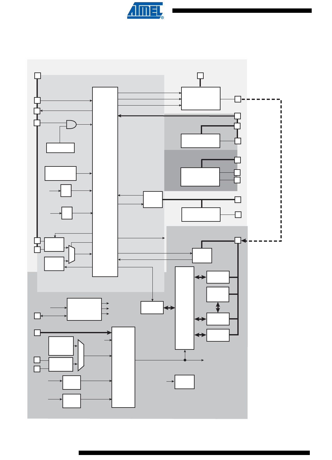
284
6430F–ATARM–21-Feb-12
SAM3U Series
284
6430F–ATARM–21-Feb-12
SAM3U Series
19.3 Block Diagram
Figure 19-1. Supply Controller Block Diagram
Software Controlled
Voltage Regulator
ADC (front-end)
Matrix
SRAM
Watchdog
Timer
Flash
Peripherals
Peripheral
Bridge
Zero-Power
Power-on Reset
Supply
Monitor
RTC
Power
Management
Controller
Embedded
32 kHz RC
Oscillator
Xtal 32 kHz
Oscillator
Supply
Controller
Embedded
12 / 8 / 4 MHz
RC
Oscillator
Brownout
Detector
General Purpose
Backup Registers
Cortex-M3
Reset
Controller
Backup Power Supply
Core Power Supply
PLLA
vr_standby
vr_vdd
rtc_alarm
SLCK
proc_nreset
periph_nreset
ice_nreset
Master Clock
MCK
SLCK
vddcore_nreset
Main Clock
MAINCK
SLCK
NRST
MAINCK PLLACK
FSTT0 - FSTT15(1)
XIN32
XOUT32
osc32k_xtal_en
XTALSEL
Slow Clock
SLCK
osc32k_rc_en
vddcore_nreset
VDDIO
VDDCORE
VDDOUT
ADVREF
ADx
FWUP
bodcore_on
bodcore_in
RTT
rtt_alarm
SLCK
XIN
XOUT
VDDBU VDDIN
SHDN
PIOx
VDDANA
USB
VDDUTMI
USBx
vr_deep
sm_in
sm_on
supc_interrupt
3 - 20 MHz
XTAL Oscillator
WKUP0 - WKUP15
NRSTB
PIOA/B/C
Input / Output Buffers
FSTT0 - FSTT15 are possible Fast Startup Sources, generated by WKUP0-WKUP15 Pins,
but are not physical pins.
UPLL
MAINCK UPLLCK

285
6430F–ATARM–21-Feb-12
SAM3U Series
285
6430F–ATARM–21-Feb-12
SAM3U Series
19.4 Supply Controller Functional Description
19.4.1 Supply Controller Overview
The device can be divided into two power supply areas:
• The Backup VDDBU Power Supply: including the Supply Controller, a part of the Reset
Controller, the Slow Clock switch, the General Purpose Backup Registers, the Supply
Monitor and the Clock which includes the Real Time Timer and the Real Time Clock
• The Core Power Supply: including the other part of the Reset Controller, the Brownout
Detector, the Processor, the SRAM memory, the FLASH memory and the Peripherals
The Supply Controller (SUPC) controls the supply voltage of the core power supply. The SUPC
intervenes when the VDDUTMI power supply rises (when the system is starting) or when the
Backup Low Power Mode is entered.
The SUPC also integrates the Slow Clock generator which is based on a 32 kHz crystal oscilla-
tor and an embedded 32 kHz RC oscillator. The Slow Clock defaults to the RC oscillator, but the
software can enable the crystal oscillator and select it as the Slow Clock source.
The Supply Controller and the VDDUTMI power supply have a reset circuitry based on the
NRSTB pin and a zero-power power-on reset cell. The zero-power power-on reset allows the
SUPC to start properly as soon as the VDDUTMI voltage becomes valid. The NRSTB pin allows
to reset the system from outside.
At startup of the system, once the backup voltage VDDUTMI is valid and the reset pin NRSTB is
not driven low and the embedded 32 kHz RC oscillator is stabilized, the SUPC starts up the core
by sequentially enabling the internal Voltage Regulator, waiting that the core voltage VDDCORE
is valid, then releasing the reset signal of the core “vddcore_nreset” signal.
Once the system has started, the user can program a supply monitor and/or a brownout detec-
tor. If the supply monitor detects a voltage on VDDUTMI that is too low, the SUPC can assert the
reset signal of the core “vddcore_nreset” signal until VDDUTMI is valid. Likewise, if the brownout
detector detects a core voltage VDDCORE that is too low, the SUPC can assert the reset signal
“vddcore_nreset” until VDDCORE is valid.
When the Backup Low Power Mode is entered, the SUPC sequentially asserts the reset signal
of the core power supply “vddcore_nreset” and disables the voltage regulator, in order to supply
only the VDDUTMI power supply. In this mode the current consumption is reduced to a few
microamps for Backup part retention. Exit from this mode is possible on multiple wake-up
sources including an event on FWUP pin or WKUP pins, or a Clock alarm. To exit this mode, the
SUPC operates in the same way as system startup.

286
6430F–ATARM–21-Feb-12
SAM3U Series
286
6430F–ATARM–21-Feb-12
SAM3U Series
19.4.2 Slow Clock Generator
The Supply Controller embeds a slow clock generator that is supplied with the VDDUTMI power
supply. As soon as the VDDUTMI is supplied, both the crystal oscillator and the embedded RC
oscillator are powered up, but only the embedded RC oscillator is enabled. This allows the slow
clock to be valid in a short time (about 100 µs).
The user can select the crystal oscillator to be the source of the slow clock, as it provides a more
accurate frequency. The command is made by writing the Supply Controller Control Register
(SUPC_CR) with the XTALSEL bit at 1. This results in a sequence which first enables the crystal
oscillator, then waits for 32,768 slow clock cycles, then switches the slow clock on the output of
the crystal oscillator and then disables the RC oscillator to save power. The switch of the slow
clock source is glitch free. The OSCSEL bit of the Supply Controller Status Register (SUPC_SR)
allows knowing when the switch sequence is done.
Coming back on the RC oscillator is only possible by shutting down the VDDUTMI power supply.
If the user does not need the crystal oscillator, the XIN32 and XOUT32 pins should be left
unconnected.
The user can also set the crystal oscillator in bypass mode instead of connecting a crystal. In
this case, the user has to provide the external clock signal on XIN32. The input characteristics of
the XIN32 pin are given in the product electrical characteristics section. In order to set the
bypass mode, the OSCBYPASS bit of the Supply Controller Mode Register (SUPC_MR) needs
to be set at 1.
19.4.3 Voltage Regulator Control/Backup Low Power Mode
The Supply Controller can be used to control the embedded 1.8V voltage regulator.
The voltage regulator automatically adapts its quiescent current depending on the required load
current. Please refer to the electrical characteristics section.
The programmer can switch off the voltage regulator, and thus put the device in Backup mode,
by writing the Supply Controller Control Register (SUPC_CR) with the VROFF bit at 1.
This can be done also by using WFE (Wait for Event) Cortex-M3 instruction with the deep mode
bit set to 1.
The Backup mode can also be entered by executing the WFI (Wait for Interrupt) or WFE (Wait for
Event) Cortex-M3 instructions. To select the Backup mode entry mechanism, two options are
available, depending on the SLEEPONEXIT bit in the Cortex-M3 System Control register:
• Sleep-now: if the SLEEPONEXIT bit is cleared, the device enters Backup mode as soon as
the WFI or WFE instruction is executed.
• Sleep-on-exit: if the SLEEPONEXIT bit is set when the WFI instruction is executed, the
device enters Backup mode as soon as it exits the lowest priority ISR.
This asserts the vddcore_nreset signal after the write resynchronization time which lasts, in the
worse case, two slow clock cycles. Once the vddcore_nreset signal is asserted, the processor
and the peripherals are stopped one slow clock cycle before the core power supply shuts off.
When the user does not use the internal voltage regulator and wants to supply VDDCORE by an
external supply, it is possible to disable the voltage regulator. Note that it is different from the
Backup mode. Depending on the application, disabling the voltage regulator can reduce power
consumption as the voltage regulator input (VDDIN) is shared with the ADC and DAC. This is
done through ONREG bit in SUPC_MR.
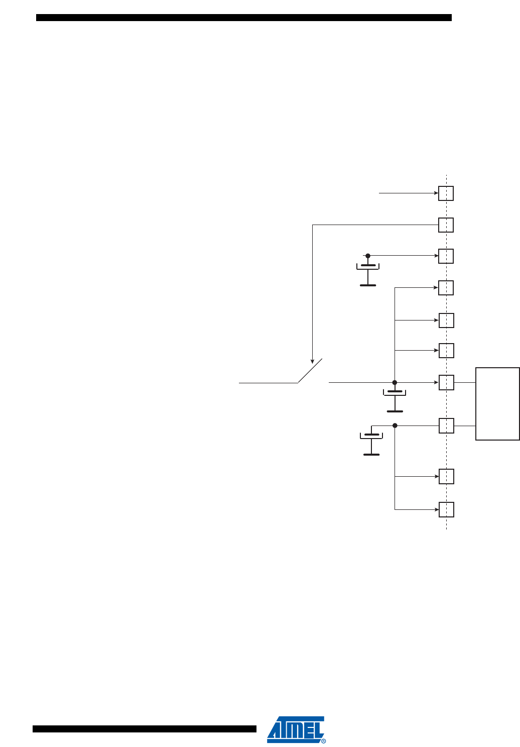
287
6430F–ATARM–21-Feb-12
SAM3U Series
287
6430F–ATARM–21-Feb-12
SAM3U Series
19.4.4 Using Backup Batteries/Backup Supply
The product can be used with or without backup batteries, or more generally a backup supply.
When a backup supply is used (See Figure 19-2), only VDDBU voltage is present in Backup
mode and no other external supply is applied on the chip. In this case the user needs to clear
VDDIORDY bit in the Supply Controller Mode Register (SUPC_MR) at least two slow clock peri-
ods before VDDIO voltage is removed. When waking up from Backup mode, the programmer
needs to set VDDIORDY.
Figure 19-2. Separated Backup Supply Powering Scheme
Note: Restrictions: With Main Supply < 3V, some peripherals such as USB and ADC might not be oper-
ational. Refer to the DC Characteristics of the product for actual possible ranges for such
peripherals.
When a separated backup supply for VDDBU is not used (See Figure 19-3), since the external
voltage applied on VDDIO is kept, all of the I/O configurations (i.e. WKUP pin configuration) are
kept during backup mode. When not using backup batteries, VDDIORDY is set so the user does
not need to program it.
VDDBU
VDDIN
Voltage
Regulator
VDDOUT
Main Supply (1.8V-3.6V)
VDDCORE
Backup Batteries
VDDIO
VDDANA
VDDUTMI
VDDPLL
FWUP
SHDN

288
6430F–ATARM–21-Feb-12
SAM3U Series
288
6430F–ATARM–21-Feb-12
SAM3U Series
Figure 19-3. No Separated Backup Supply Powering Scheme
Note: Restrictions: With Main Supply < 3V, some peripherals such as USB and ADC might not be oper-
ational. Refer to the DC Characteristics of the product for actual possible ranges for such
peripherals.
19.4.5 Supply Monitor
The Supply Controller embeds a supply monitor which is located in the VDDBU Backup Power
Supply and which monitors VDDUTMI power supply.
The supply monitor can be used to prevent the processor from falling into an unpredictable state
if the Main power supply drops below a certain level.
The threshold of the supply monitor is programmable. It can be selected from 1.9V to 3.4V by
steps of 100 mV. This threshold is programmed in the SMTH field of the Supply Controller Sup-
ply Monitor Mode Register (SUPC_SMMR).
The supply monitor can also be enabled during one slow clock period on every one of either 32,
256 or 2048 slow clock periods, according to the choice of the user. This can be configured by
programming the SMSMPL field in SUPC_SMMR.
Enabling the supply monitor for such reduced times allows to divide the typical supply monitor
power consumption respectively by factors of 32, 256 or 2048, if the user does not need a con-
tinuous monitoring of the VDDUTMI power supply.
VDDBU
VDDIN
Voltage
Regulator
VDDOUT
Main Supply (1.8V-3.6V)
VDDCORE
VDDIO
VDDANA
VDDUTMI
VDDPLL
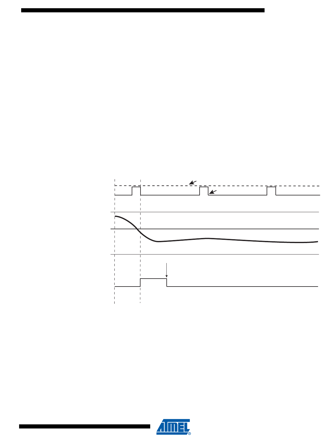
289
6430F–ATARM–21-Feb-12
SAM3U Series
289
6430F–ATARM–21-Feb-12
SAM3U Series
A supply monitor detection can either generate a reset of the core power supply or a wake up of
the core power supply. Generating a core reset when a supply monitor detection occurs is
enabled by writing the SMRSTEN bit to 1 in SUPC_SMMR.
Waking up the core power supply when a supply monitor detection occurs can be enabled by
programming the SMEN bit to 1 in the Supply Controller Wake Up Mode Register
(SUPC_WUMR).
The Supply Controller provides two status bits in the Supply Controller Status Register for the
supply monitor which allows to determine whether the last wake up was due to the supply
monitor:
• The SMOS bit provides real time information, which is updated at each measurement cycle
or updated at each Slow Clock cycle, if the measurement is continuous.
• The SMS bit provides saved information and shows a supply monitor detection has occurred
since the last read of SUPC_SR.
The SMS bit can generate an interrupt if the SMIEN bit is set to 1 in the Supply Controller Supply
Monitor Mode Register (SUPC_SMMR).
Figure 19-4. Supply Monitor Status Bit and Associated Interrupt
Supply Monitor ON
3.3 V
0 V
Threshold
SMS and SUPC interrupt
Read SUPC_SR
Periodic Sampling
Continuous Sampling (SMSMPL = 1)
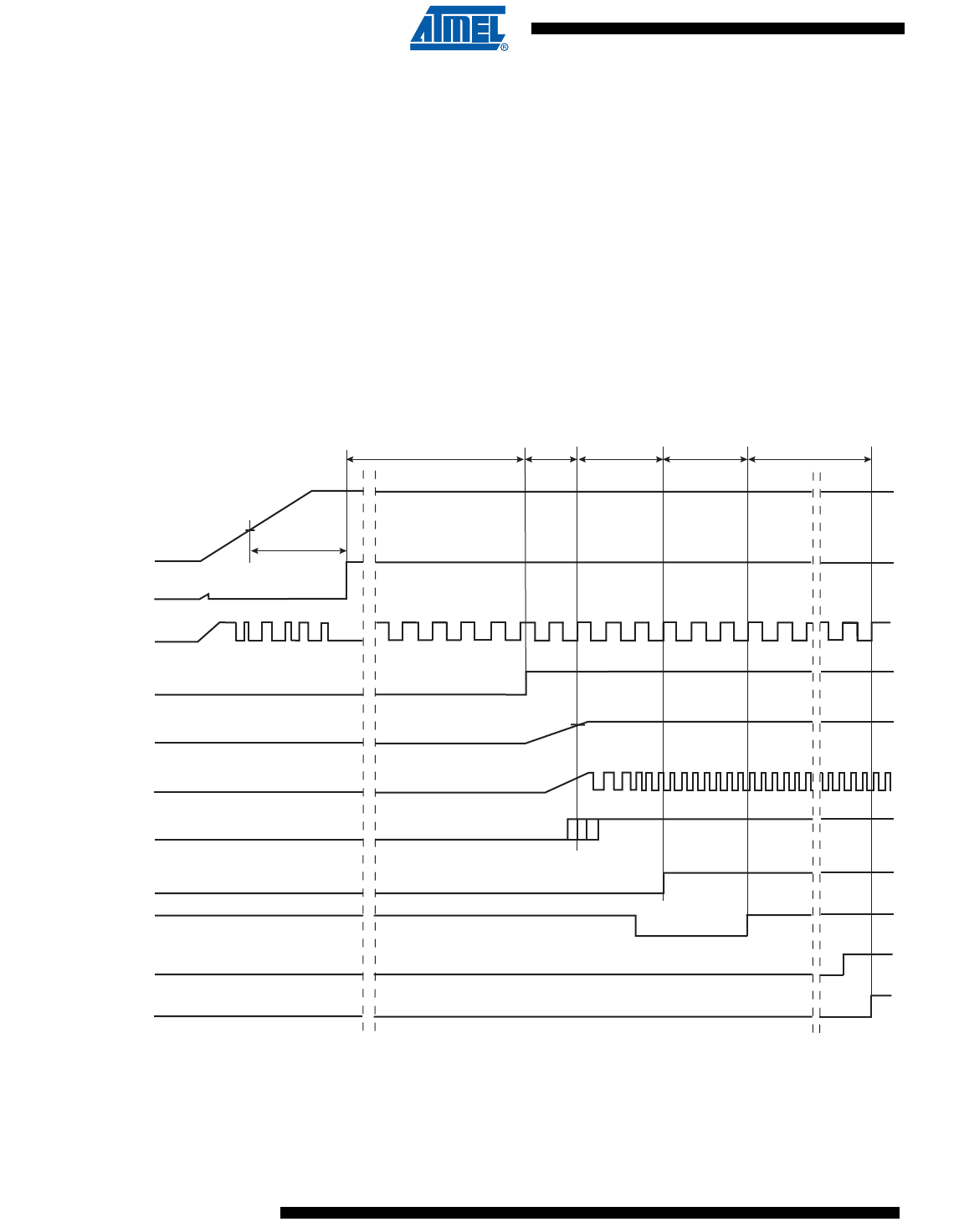
290
6430F–ATARM–21-Feb-12
SAM3U Series
290
6430F–ATARM–21-Feb-12
SAM3U Series
19.4.6 Backup Power Supply Reset
19.4.6.1 Raising the Backup Power Supply
As soon as the backup voltage VDDUTMI rises, the RC oscillator is powered up and the zero-
power power-on reset cell maintains its output low as long as VDDUTMI has not reached its tar-
get voltage. During this time, the Supply Controller is entirely reset. When the VDDUTMI voltage
becomes valid and zero-power power-on reset signal is released, a counter is started for 5 slow
clock cycles. This is the time it takes for the 32 kHz RC oscillator to stabilize.
After this time, the SHDN pin is asserted and the voltage regulator is enabled. The core power
supply rises and the brownout detector provides the bodcore_in signal as soon as the core volt-
age VDDCORE is valid. This results in releasing the vddcore_nreset signal to the Reset
Controller after the bodcore_in signal has been confirmed as being valid for at least one slow
clock cycle.
Figure 19-5. Raising the VDDUTMI Power Supply
Zero-Power Power-On
Reset Cell output
22 - 42 kHz RC
Oscillator output
Fast RC
Oscillator output
Backup Power Supply
SHDN / vr_on
bodcore_in
vddcore_nreset
NRST
proc_nreset
Note: After “proc_nreset” rising, the core starts fecthing instructions from Flash at 4 MHz.
periph_nreset
7 x Slow Clock Cycles3 x Slow Clock
Cycles
3 x Slow Clock
Cycles
6.5 x Slow Clock
Cycles
TON Voltage
Regulator
Zero-Power POR
Core Power Supply
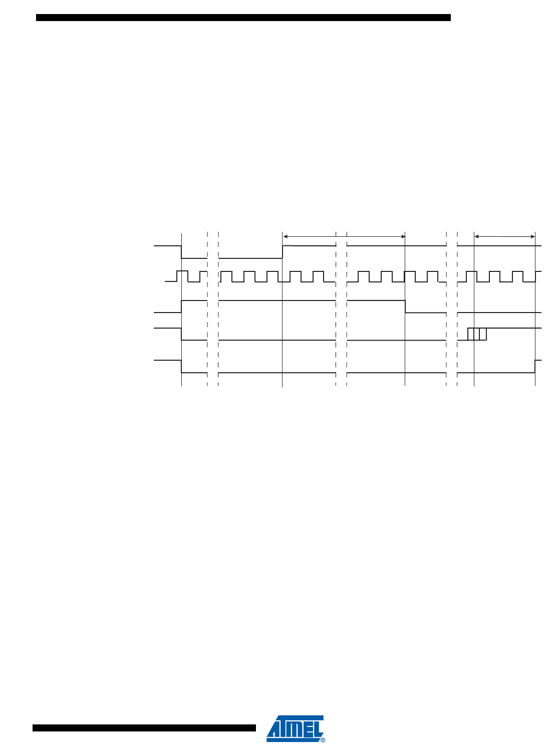
291
6430F–ATARM–21-Feb-12
SAM3U Series
291
6430F–ATARM–21-Feb-12
SAM3U Series
19.4.6.2 NRSTB Asynchronous Reset Pin
The NRSTB pin is an asynchronous reset input, which acts exactly like the zero-power power-on
reset cell.
As soon as NRSTB is tied to GND, the supply controller is reset generating in turn, a reset of the
whole system.
When NRSTB is released, the system can start as described in Section 19.4.6.1 ”Raising the
Backup Power Supply”.
The NRSTB pin does not need to be driven during power-up phase to allow a reset of the sys-
tem, it is done by the zero-power power-on cell.
Figure 19-6. NRSTB Reset
Note: periph_nreset, ice_reset and proc_nreset are not shown, but are asserted low thanks to the vddcore_nreset signal controlling
the Reset controller.
19.4.6.3 SHDN output pin
As shown in Figure 19-6, the SHDN pin acts like the vr_standby signal making it possible to use
the SHDN pin to control external voltage regulator with shutdown capabilities.
19.4.7 Core Reset
The Supply Controller manages the vddcore_nreset signal to the Reset Controller, as described
previously in Section 19.4.6 ”Backup Power Supply Reset”. The vddcore_nreset signal is nor-
mally asserted before shutting down the core power supply and released as soon as the core
power supply is correctly regulated.
There are two additional sources which can be programmed to activate vddcore_nreset:
• a supply monitor detection
• a brownout detection
19.4.7.1 Supply Monitor Reset
The supply monitor is capable of generating a reset of the system. This can be enabled by set-
ting the SMRSTEN bit in the Supply Controller Supply Monitor Mode Register (SUPC_SMMR).
If SMRSTEN is set and if a supply monitor detection occurs, the vddcore_nreset signal is imme-
diately activated for a minimum of 1 slow clock cycle.
30 Slow Clock Cycles = about 1msbetween 2 and 3 Slow Clock Cycles
32 kHz Low Power Crystal
Oscillator output
NRSTB
SHDN / vr_standby
bodcore_in
vddcore_nreset
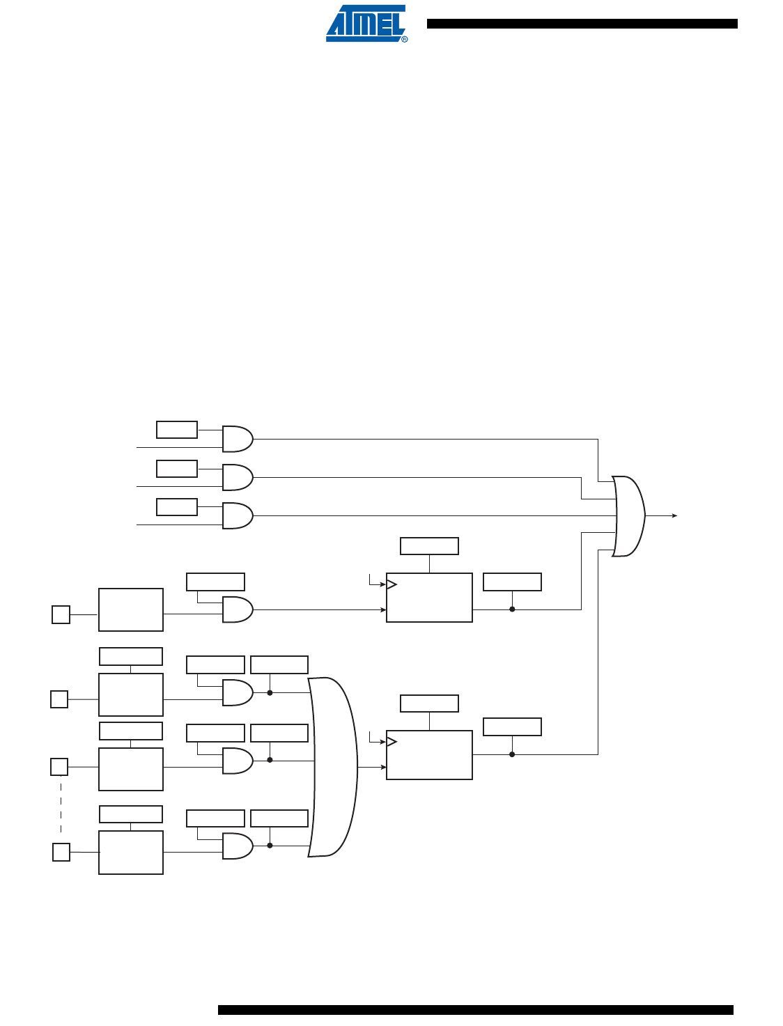
292
6430F–ATARM–21-Feb-12
SAM3U Series
292
6430F–ATARM–21-Feb-12
SAM3U Series
19.4.7.2 Brownout Detector Reset
The brownout detector provides the bodcore_in signal to the SUPC which indicates that the volt-
age regulation is operating as programmed. If this signal is lost for longer than 1 slow clock
period while the voltage regulator is enabled, the Supply Controller can assert vddcore_nreset.
This feature is enabled by writing the bit, BODRSTEN (Brownout Detector Reset Enable) to 1 in
the Supply Controller Mode Register (SUPC_MR).
If BODRSTEN is set and the voltage regulation is lost (output voltage of the regulator too low),
the vddcore_nreset signal is asserted for a minimum of 1 slow clock cycle and then released if
bodcore_in has been reactivated. The BODRSTS bit is set in the Supply Controller Status Reg-
ister (SUPC_SR) so that the user can know the source of the last reset.
Until bodcore_in is deactivated, the vddcore_nreset signal remains active.
19.4.8 Wake Up Sources
The wake up events allow the device to exit backup mode. When a wake up event is detected,
the Supply Controller performs a sequence which automatically reenables the core power
supply.
Figure 19-7. Wake Up Sources
WKUP15
FWUP
rtt_alarm
rtc_alarm
sm_int
WKUP0
WKUP1
WKUPT1
Core
Supply
Restart
Debouncer
WKUPDBC
WKUPS
Debouncer
FWUPDBC
FWUP
WKUPIS0
WKUPIS1
WKUPIS15
RTTEN
RTCEN
SMEN
WKUPEN15
WKUPEN1
WKUPEN0
FWUPEN
WKUPT15
Falling/Rising
Edge
Detector
WKUPT0
Falling/Rising
Edge
Detector
Falling/Rising
Edge
Detector
Falling
Edge
Detector
SLCK
SLCK

293
6430F–ATARM–21-Feb-12
SAM3U Series
293
6430F–ATARM–21-Feb-12
SAM3U Series
19.4.8.1 Force Wake Up
The FWUP pin is enabled as a wake up source by writing the FWUPEN bit to 1 in the Supply
Controller Wake Up Mode Register (SUPC_WUMR). Then, the FWUPDBC field in the same
register selects the debouncing period, which can be selected between 3, 32, 512, 4,096 or
32,768 slow clock cycles. This corresponds respectively to about 100 µs, about 1 ms, about 16
ms, about 128 ms and about 1 second (for a typical slow clock frequency of 32 kHz). Program-
ming FWUPDBC to 0x0 selects an immediate wake up, i.e., the FWUP must be low during a
minimum of one slow clock period to wake up the core power supply.
If the FWUP pin is asserted for a time longer than the debouncing period, a wake up of the core
power supply is started and the FWUP bit in the Supply Controller Status Register (SUPC_SR)
is set and remains high until the register is read.
19.4.8.2 Wake Up Inputs
The wake up inputs, WKUP0 to WKUP15, can be programmed to perform a wake up of the core
power supply. Each input can be enabled by writing to 1 the corresponding bit, WKUPEN0 to
WKUPEN 15, in the Wake Up Inputs Register (SUPC_WUIR). The wake up level can be
selected with the corresponding polarity bit, WKUPPL0 to WKUPPL15, also located in
SUPC_WUIR.
All the resulting signals are wired-ORed to trigger a debounce counter, which can be pro-
grammed with the WKUPDBC field in the Supply Controller Wake Up Mode Register
(SUPC_WUMR). The WKUPDBC field can select a debouncing period of 3, 32, 512, 4,096 or
32,768 slow clock cycles. This corresponds respectively to about 100 µs, about 1 ms, about
16 ms, about 128 ms and about 1 second (for a typical slow clock frequency of 32 kHz). Pro-
gramming WKUPDBC to 0x0 selects an immediate wake up, i.e., an enabled WKUP pin must be
active according to its polarity during a minimum of one slow clock period to wake up the core
power supply.
If an enabled WKUP pin is asserted for a time longer than the debouncing period, a wake up of
the core power supply is started and the signals, WKUP0 to WKUP15 as shown in Figure 19-7,
are latched in the Supply Controller Status Register (SUPC_SR). This allows the user to identify
the source of the wake up, however, if a new wake up condition occurs, the primary information
is lost. No new wake up can be detected since the primary wake up condition has disappeared.
19.4.8.3 Clock Alarms
The RTC and the RTT alarms can generate a wake up of the core power supply. This can be
enabled by writing respectively, the bits RTCEN and RTTEN to 1 in the Supply Controller Wake
Up Mode Register (SUPC_WUMR).
The Supply Controller does not provide any status as the information is available in the User
Interface of either the Real Time Timer or the Real Time Clock.
19.4.8.4 Supply Monitor Detection
The supply monitor can generate a wakeup of the core power supply. See Section 19.4.5 ”Sup-
ply Monitor”.

294
6430F–ATARM–21-Feb-12
SAM3U Series
294
6430F–ATARM–21-Feb-12
SAM3U Series
19.5 Supply Controller (SUPC) User Interface
The User Interface of the Supply Controller is part of the System Controller User Interface.
19.5.1 System Controller (SYSC) User Interface
19.5.2 Supply Controller (SUPC) User Interface
Table 19-1. System Controller Registers
Offset System Controller Peripheral Name
0x00-0x0c Reset Controller RSTC
0x10-0x2C Supply Controller SUPC
0x30-0x3C Real Time Timer RTT
0x50-0x5C Watchdog Tiler WDT
0x60-0x7C Real Time Clock RTC
0x90-0xDC General Purpose Backup Register GPBR
Table 19-2. Register Mapping
Offset Register Name Access Reset
0x00 Supply Controller Control Register SUPC_CR Write-only N/A
0x04 Supply Controller Supply Monitor Mode Register SUPC_SMMR Read-write 0x0000_0000
0x08 Supply Controller Mode Register SUPC_MR Read-write 0x0000_5A00
0x0C Supply Controller Wake Up Mode Register SUPC_WUMR Read-write 0x0000_0000
0x10 Supply Controller Wake Up Inputs Register SUPC_WUIR Read-write 0x0000_0000
0x14 Supply Controller Status Register SUPC_SR Read-only 0x0000_0800
0x18 Reserved

295
6430F–ATARM–21-Feb-12
SAM3U Series
295
6430F–ATARM–21-Feb-12
SAM3U Series
19.5.3 Supply Controller Control Register
Name: SUPC_CR
Address: 0x400E1210
Access: Write-only
• VROFF: Voltage Regulator Off
0 (NO_EFFECT) = no effect.
1 (STOP_VREG) = if KEY is correct, asserts vddcore_nreset and stops the voltage regulator.
• XTALSEL: Crystal Oscillator Select
0 (NO_EFFECT) = no effect.
1 (CRYSTAL_SEL) = if KEY is correct, switches the slow clock on the crystal oscillator output.
•KEY: Password
Should be written to value 0xA5. Writing any other value in this field aborts the write operation.
31 30 29 28 27 26 25 24
KEY
23 22 21 20 19 18 17 16
––––––––
15 14 13 12 11 10 9 8
–––––– –
76543210
––––XTALSELVROFF––

296
6430F–ATARM–21-Feb-12
SAM3U Series
296
6430F–ATARM–21-Feb-12
SAM3U Series
19.5.4 Supply Controller Supply Monitor Mode Register
Name: SUPC_SMMR
Address: 0x400E1214
Access: Read-write
• SMTH: Supply Monitor Threshold
31 30 29 28 27 26 25 24
––––––––
23 22 21 20 19 18 17 16
––––––––
15 14 13 12 11 10 9 8
– – SMIEN SMRSTEN – SMSMPL
76543210
–––– SMTH
Value Name Description
0x0 1_9V 1.9 V
0x1 2_0V 2.0 V
0x2 2_1V 2.1 V
0x3 2_2V 2.2 V
0x4 2_3V 2.3 V
0x5 2_4V 2.4 V
0x6 2_5V 2.5 V
0x7 2_6V 2.6 V
0x8 2_7V 2.7 V
0x9 2_8V 2.8 V
0xA 2_9V 2.9 V
0xB 3_0V 3.0 V
0xC 3_1V 3.1 V
0xD 3_2V 3.2 V
0xE 3_3V 3.3 V
0xF 3_4V 3.4 V

297
6430F–ATARM–21-Feb-12
SAM3U Series
297
6430F–ATARM–21-Feb-12
SAM3U Series
• SMSMPL: Supply Monitor Sampling Period
• SMRSTEN: Supply Monitor Reset Enable
0 (NOT_ENABLE) = the core reset signal “vddcore_nreset” is not affected when a supply monitor detection occurs.
1 (ENABLE) = the core reset signal, vddcore_nreset is asserted when a supply monitor detection occurs.
• SMIEN: Supply Monitor Interrupt Enable
0 (NOT_ENABLE) = the SUPC interrupt signal is not affected when a supply monitor detection occurs.
1 (ENABLE) = the SUPC interrupt signal is asserted when a supply monitor detection occurs.
Value Name Description
0x0 SMD Supply Monitor disabled
0x1 CSM Continuous Supply Monitor
0x2 32SLCK Supply Monitor enabled one SLCK period every 32 SLCK periods
0x3 256SLCK Supply Monitor enabled one SLCK period every 256 SLCK periods
0x4 2048SLCK Supply Monitor enabled one SLCK period every 2,048 SLCK periods
0x5-0x7 Reserved Reserved
298
6430F–ATARM–21-Feb-12
SAM3U Series
298
6430F–ATARM–21-Feb-12
SAM3U Series
19.5.5 Supply Controller Mode Register
Name: SUPC_MR
Address: 0x400E1218
Access: Read-write
• BODRSTEN: Brownout Detector Reset Enable
0 (NOT_ENABLE) = the core reset signal “vddcore_nreset” is not affected when a brownout detection occurs.
1 (ENABLE) = the core reset signal, vddcore_nreset is asserted when a brownout detection occurs.
• BODDIS: Brownout Detector Disable
0 (ENABLE) = the core brownout detector is enabled.
1 (DISABLE) = the core brownout detector is disabled.
• VDDIORDY: VDDIO Ready
0 (VDDIO_REMOVED) = VDDIO is removed (used before going to backup mode when backup batteries are used)
1 (VDDIO_PRESENT) = VDDIO is present (used before going to backup mode when backup batteries are used)
If the backup batteries are not used, VDDIORDY must be kept set to 1.
• ONREG: Voltage Regulator enable
0 (ONREG_UNUSED) = Voltage Regulator is not used
1 (ONREG_USED) = Voltage Regulator is used
• OSCBYPASS: Oscillator Bypass
0 (NO_EFFECT) = no effect. Clock selection depends on XTALSEL value.
1 (BYPASS) = the 32-KHz XTAL oscillator is selected and is put in bypass mode.
•KEY: Password Key
Should be written to value 0xA5. Writing any other value in this field aborts the write operation.
31 30 29 28 27 26 25 24
KEY
23 22 21 20 19 18 17 16
–––OSCBYPASS––––
15 14 13 12 11 10 9 8
–VDDIORDY
ONREG BODDISBODRSTEN––––
76543210
––––––––
299
6430F–ATARM–21-Feb-12
SAM3U Series
299
6430F–ATARM–21-Feb-12
SAM3U Series
19.5.6 Supply Controller Wake Up Mode Register
Name: SUPC_WUMR
Address: 0x400E121C
Access: Read-write
• FWUPEN: Force Wake Up Enable
0 (NOT_ENABLE) = the Force Wake Up pin has no wake up effect.
1 (ENABLE) = the Force Wake Up pin low forces the wake up of the core power supply.
• SMEN: Supply Monitor Wake Up Enable
0 (NOT_ENABLE) = the supply monitor detection has no wake up effect.
1 (ENABLE) = the supply monitor detection forces the wake up of the core power supply.
• RTTEN: Real Time Timer Wake Up Enable
0 (NOT_ENABLE) = the RTT alarm signal has no wake up effect.
1 (ENABLE) = the RTT alarm signal forces the wake up of the core power supply.
• RTCEN: Real Time Clock Wake Up Enable
0 (NOT_ENABLE) = the RTC alarm signal has no wake up effect.
1 (ENABLE) = the RTC alarm signal forces the wake up of the core power supply.
• FWUPDBC: Force Wake Up Debouncer Period
31 30 29 28 27 26 25 24
––––––––
23 22 21 20 19 18 17 16
––––––––
15 14 13 12 11 10 9 8
– WKUPDBC – FWUPDBC
76543210
––––RTCENRTTENSMENFWUPEN
Value Name Description
0 IMMEDIATE Immediate, no debouncing, detected active at least on one Slow Clock edge.
1 3_SCLK FWUP shall be low for at least 3 SLCK periods
2 32_SCLK FWUP shall be low for at least 32 SLCK periods
3 512_SCLK FWUP shall be low for at least 512 SLCK periods
4 4096_SCLK FWUP shall be low for at least 4,096 SLCK periods
5 32768_SCLK FWUP shall be low for at least 32,768 SLCK periods
6 Reserved Reserved
7 Reserved Reserved

300
6430F–ATARM–21-Feb-12
SAM3U Series
300
6430F–ATARM–21-Feb-12
SAM3U Series
• WKUPDBC: Wake Up Inputs Debouncer Period
Value Name Description
0 IMMEDIATE Immediate, no debouncing, detected active at least on one Slow Clock edge.
1 3_SCLK WKUPx shall be in its active state for at least 3 SLCK periods
2 32_SCLK WKUPx shall be in its active state for at least 32 SLCK periods
3 512_SCLK WKUPx shall be in its active state for at least 512 SLCK periods
4 4096_SCLK WKUPx shall be in its active state for at least 4,096 SLCK periods
5 32768_SCLK WKUPx shall be in its active state for at least 32,768 SLCK periods
6 Reserved Reserved
7 Reserved Reserved

301
6430F–ATARM–21-Feb-12
SAM3U Series
301
6430F–ATARM–21-Feb-12
SAM3U Series
19.5.7 System Controller Wake Up Inputs Register
Name: SUPC_WUIR
Address: 0x400E1220
Access: Read-write
• WKUPEN0 - WKUPEN15: Wake Up Input Enable 0 to 15
0 (NOT_ENABLE) = the corresponding wake-up input has no wake up effect.
1 (ENABLE) = the corresponding wake-up input forces the wake up of the core power supply.
• WKUPT0 - WKUPT15: Wake Up Input Transition 0 to 15
0 (HIGH_TO_LOW) = a high to low level transition on the corresponding wake-up input forces the wake up of the core
power supply.
1 (LOW_TO_HIGH) = a low to high level transition on the corresponding wake-up input forces the wake up of the core
power supply.
31 30 29 28 27 26 25 24
WKUPT15 WKUPT14 WKUPT13 WKUPT12 WKUPT11 WKUPT10 WKUPT9 WKUPT8
23 22 21 20 19 18 17 16
WKUPT7 WKUPT6 WKUPT5 WKUPT4 WKUPT3 WKUPT2 WKUPT1 WKUPT0
15 14 13 12 11 10 9 8
WKUPEN15 WKUPEN14 WKUPEN13 WKUPEN12 WKUPEN11 WKUPEN10 WKUPEN9 WKUPEN8
76543210
WKUPEN7 WKUPEN6 WKUPEN5 WKUPEN4 WKUPEN3 WKUPEN2 WKUPEN1 WKUPEN0

302
6430F–ATARM–21-Feb-12
SAM3U Series
302
6430F–ATARM–21-Feb-12
SAM3U Series
19.5.8 Supply Controller Status Register
Name: SUPC_SR
Address: 0x400E1224
Access: Read-write
Note: Because of the asynchronism between the Slow Clock (SCLK) and the System Clock (MCK), the status register flag reset is
taken into account only 2 slow clock cycles after the read of the SUPC_SR.
• FWUPS: FWUP Wake Up Status
0 (NO) = no wake up due to the assertion of the FWUP pin has occurred since the last read of SUPC_SR.
1 (PRESENT) = at least one wake up due to the assertion of the FWUP pin has occurred since the last read of SUPC_SR.
• WKUPS: WKUP Wake Up Status
0 (NO) = no wake up due to the assertion of the WKUP pins has occurred since the last read of SUPC_SR.
1 (PRESENT) = at least one wake up due to the assertion of the WKUP pins has occurred since the last read of SUPC_SR.
• SMWS: Supply Monitor Detection Wake Up Status
0 (NO) = no wake up due to a supply monitor detection has occurred since the last read of SUPC_SR.
1 (PRESENT) = at least one wake up due to a supply monitor detection has occurred since the last read of SUPC_SR.
• BODRSTS: Brownout Detector Reset Status
0 (NO) = no core brownout rising edge event has been detected since the last read of the SUPC_SR.
1 (PRESENT) = at least one brownout output rising edge event has been detected since the last read of the SUPC_SR.
When the voltage remains below the defined threshold, there is no rising edge event at the output of the brownout detec-
tion cell. The rising edge event occurs only when there is a voltage transition below the threshold.
• SMRSTS: Supply Monitor Reset Status
0 (NO) = no supply monitor detection has generated a core reset since the last read of the SUPC_SR.
1 (PRESENT) = at least one supply monitor detection has generated a core reset since the last read of the SUPC_SR.
• SMS: Supply Monitor Status
0 (NO) = no supply monitor detection since the last read of SUPC_SR.
1 (PRESENT) = at least one supply monitor detection since the last read of SUPC_SR.
31 30 29 28 27 26 25 24
WKUPIS15 WKUPIS14 WKUPIS13 WKUPIS12 WKUPIS11 WKUPIS10 WKUPIS9 WKUPIS8
23 22 21 20 19 18 17 16
WKUPIS7 WKUPIS6 WKUPIS5 WKUPIS4 WKUPIS3 WKUPIS2 WKUPIS1 WKUPIS0
15 14 13 12 11 10 9 8
–––FWUPIS––––
76543210
OSCSEL SMOS SMS SMRSTS BODRSTS SMWS WKUPS FWUPS

303
6430F–ATARM–21-Feb-12
SAM3U Series
303
6430F–ATARM–21-Feb-12
SAM3U Series
• SMOS: Supply Monitor Output Status
0 (HIGH) = the supply monitor detected VDDUTMI higher than its threshold at its last measurement.
1 (LOW) = the supply monitor detected VDDUTMI lower than its threshold at its last measurement.
• OSCSEL: 32-kHz Oscillator Selection Status
0 (RC) = the slow clock, SLCK is generated by the embedded 32-kHz RC oscillator.
1 (CRYST) = the slow clock, SLCK is generated by the 32-kHz crystal oscillator.
• FWUPIS: FWUP Input Status
0 (LOW) = FWUP input is tied low.
1 (HIGH) = FWUP input is tied high.
• WKUPIS0-WKUPIS15: WKUP Input Status 0 to 15
0 (DIS) = the corresponding wake-up input is disabled, or was inactive at the time the debouncer triggered a wake up
event.
1 (EN) = the corresponding wake-up input was active at the time the debouncer triggered a wake up event.

304
6430F–ATARM–21-Feb-12
SAM3U Series
304
6430F–ATARM–21-Feb-12
SAM3U Series

305
6430F–ATARM–21-Feb-12
SAM3U Series
305
6430F–ATARM–21-Feb-12
SAM3U Series
20. General Purpose Backup Registers (GPBR)
20.1 Embedded Characteristics
• Four 32-bit General Purpose Backup Registers
20.2 Description
The System Controller embeds Four general-purpose backup registers.
20.2.1 Power Management Controller (PMC) User Interface
Table 20-1. Register Mapping
Offset Register Name Access Reset
0x0 General Purpose Backup Register 0 SYS_GPBR0 Read-write –
... ... ... ... ...
0xc General Purpose Backup Register 3 SYS_GPBR3 Read-write –

306
6430F–ATARM–21-Feb-12
SAM3U Series
306
6430F–ATARM–21-Feb-12
SAM3U Series
20.2.1.1 General Purpose Backup Register x
Name: SYS_GPBRx
Address: 0x400E1290 [0] .. 0x400E129C [3]
Access: Read-write
• GPBR_VALUEx: Value of GPBR x
31 30 29 28 27 26 25 24
GPBR_VALUEx
23 22 21 20 19 18 17 16
GPBR_VALUEx
15 14 13 12 11 10 9 8
GPBR_VALUEx
76543210
GPBR_VALUEx

307
6430F–ATARM–21-Feb-12
SAM3U Series
307
6430F–ATARM–21-Feb-12
SAM3U Series
21. Enhanced Embedded Flash Controller (EEFC)
21.1 Description
The Enhanced Embedded Flash Controller (EEFC) ensures the interface of the Flash block with
the 32-bit internal bus.
Its 128-bit or 64-bit wide memory interface increases performance. It also manages the pro-
gramming, erasing, locking and unlocking sequences of the Flash using a full set of commands.
One of the commands returns the embedded Flash descriptor definition that informs the system
about the Flash organization, thus making the software generic.
21.2 Embedded Characteristics
• Interface of the Flash Block with the 32-bit Internal Bus
• Increases Performance in Thumb2 Mode with 128-bit or -64 bit Wide Memory Interface up to
24 MHz
• 32 Lock Bits, Each Protecting a Lock Region
• GPNVMx General-purpose GPNVM Bits
• One-by-one Lock Bit Programming
• Commands Protected by a Keyword
• Erases the Entire Flash
• Erases by Plane
• Possibility of Erasing before Programming
• Locking and Unlocking Operations
• Consecutive Programming and Locking Operations
21.3 Product Dependencies
21.3.1 Power Management
The Enhanced Embedded Flash Controller (EEFC) is continuously clocked. The Power Man-
agement Controller has no effect on its behavior.
21.3.2 Interrupt Sources
The Enhanced Embedded Flash Controller (EEFC) interrupt line is connected to the Nested
Vectored Interrupt Controller (NVIC). Using the Enhanced Embedded Flash Controller (EEFC)
interrupt requires the NVIC to be programmed first. The EEFC interrupt is generated only on
FRDY bit rising.
21.4 Functional Description
21.4.1 Embedded Flash Organization
The embedded Flash interfaces directly with the 32-bit internal bus. The embedded Flash is
composed of:
• One memory plane organized in several pages of the same size.
• Two 128-bit or 64-bit read buffers used for code read optimization.
• One 128-bit or 64-bit read buffer used for data read optimization.
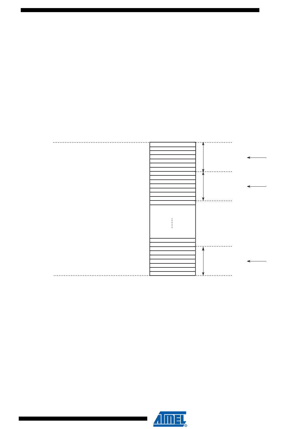
308
6430F–ATARM–21-Feb-12
SAM3U Series
308
6430F–ATARM–21-Feb-12
SAM3U Series
• One write buffer that manages page programming. The write buffer size is equal to the page
size. This buffer is write-only and accessible all along the 1 MByte address space, so that
each word can be written to its final address.
• Several lock bits used to protect write/erase operation on several pages (lock region). A lock
bit is associated with a lock region composed of several pages in the memory plane.
• Several bits that may be set and cleared through the Enhanced Embedded Flash Controller
(EEFC) interface, called General Purpose Non Volatile Memory bits (GPNVM bits).
The embedded Flash size, the page size, the lock regions organization and GPNVM bits defini-
tion are described in the product definition section. The Enhanced Embedded Flash Controller
(EEFC) returns a descriptor of the Flash controlled after a get descriptor command issued by the
application (see “Getting Embedded Flash Descriptor” on page 312).
Figure 21-1. Embedded Flash Organization
Start Address
Page 0
Lock Region 0
Lock Region 1
Memory Plane
Page (m-1)
Lock Region (n-1)
Page (n*m-1)
Start Address + Flash size -1
Lock Bit 0
Lock Bit 1
Lock Bit (n-1)
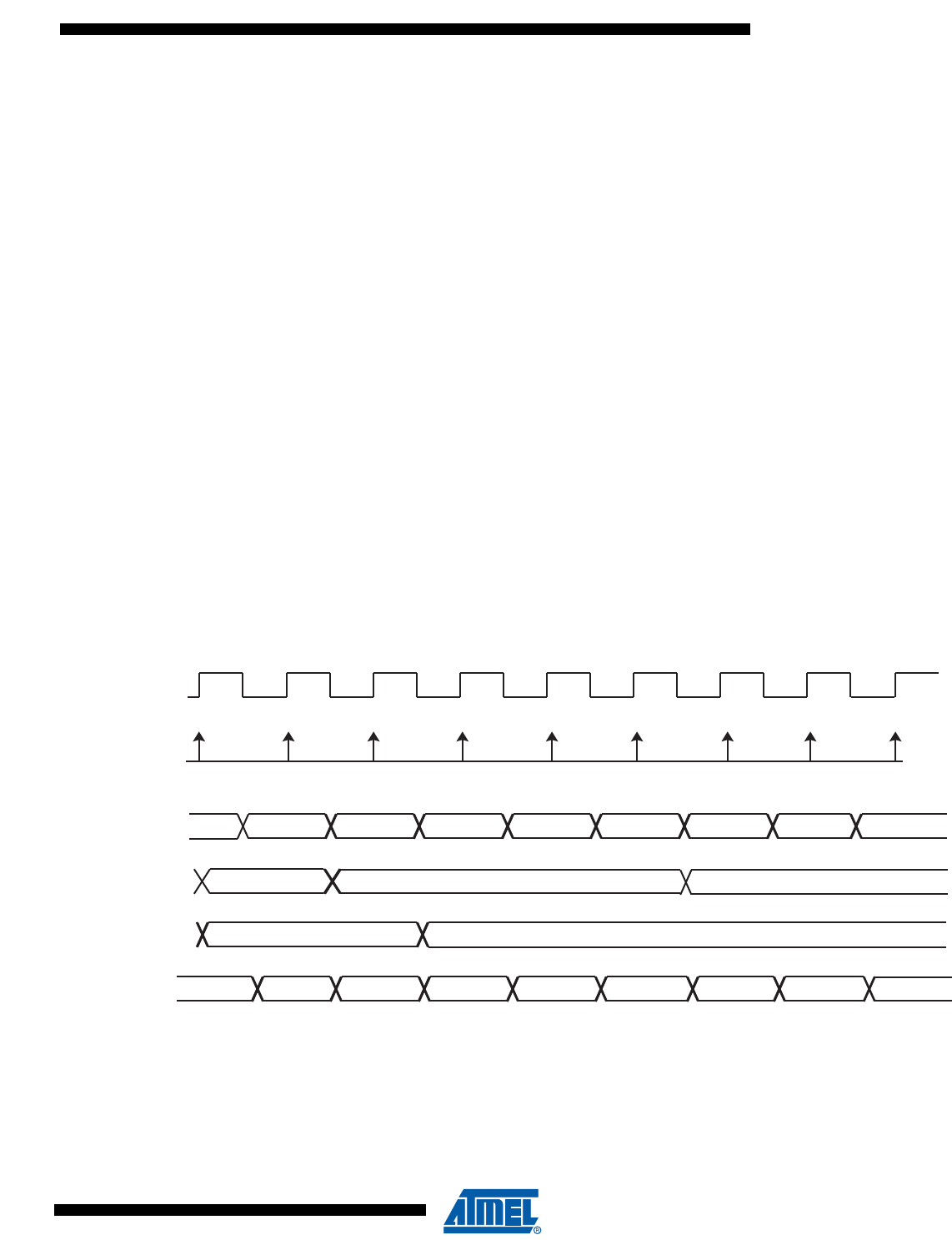
309
6430F–ATARM–21-Feb-12
SAM3U Series
309
6430F–ATARM–21-Feb-12
SAM3U Series
21.4.2 Read Operations
An optimized controller manages embedded Flash reads, thus increasing performance when the
processor is running in Thumb2 mode by means of the 128- or 64- bit wide memory interface.
The Flash memory is accessible through 8-, 16- and 32-bit reads.
As the Flash block size is smaller than the address space reserved for the internal memory area,
the embedded Flash wraps around the address space and appears to be repeated within it.
The read operations can be performed with or without wait states. Wait states must be pro-
grammed in the field FWS (Flash Read Wait State) in the Flash Mode Register (EEFC_FMR).
Defining FWS to be 0 enables the single-cycle access of the embedded Flash. Refer to the Elec-
trical Characteristics for more details.
21.4.2.1 128-bit or 64-bit Access Mode
By default the read accesses of the Flash are performed through a 128-bit wide memory inter-
face. It enables better system performance especially when 2 or 3 wait state needed.
For systems requiring only 1 wait state, or to privilege current consumption rather than perfor-
mance, the user can select a 64-bit wide memory access via the FAM bit in the Flash Mode
Register (EEFC_FMR)
Please refer to the electrical characteristics section of the product datasheet for more details.
21.4.2.2 Code Read Optimization
A system of 2 x 128-bit or 2 x 64-bit buffers is added in order to optimize sequential Code Fetch.
Note: Immediate consecutive code read accesses are not mandatory to benefit from this optimization.
Figure 21-2. Code Read Optimization for FWS = 0
Note: When FWS is equal to 0, all the accesses are performed in a single-cycle access.
Flash Access
Buffer 0 (128bits)
Master Clock
ARM Request
(32-bit)
XXX
Data To ARM
Bytes 0-15 Bytes 16-31 Bytes 32-47
Bytes 0-15
Buffer 1 (128bits)
Bytes 32-47
Bytes 0-3 Bytes 4-7 Bytes 8-11 Bytes 12-15 Bytes 16-19 Bytes 20-23 Bytes 24-27
XXX
XXX Bytes 16-31
@Byte 0 @Byte 4 @Byte 8 @Byte 12 @Byte 16 @Byte 20 @Byte 24 @Byte 28 @Byte 32
Bytes 28-31
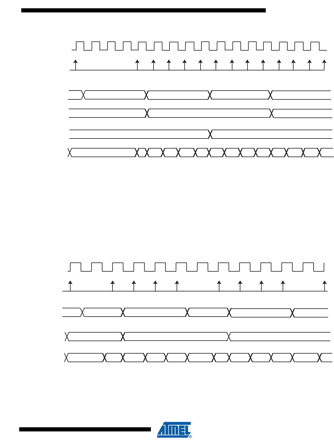
310
6430F–ATARM–21-Feb-12
SAM3U Series
310
6430F–ATARM–21-Feb-12
SAM3U Series
Figure 21-3. Code Read Optimization for FWS = 3
Note: When FWS is included between 1 and 3, in case of sequential reads, the first access takes (FWS+1) cycles, the other ones only
1 cycle.
21.4.2.3 Data Read Optimization
The organization of the Flash in 128 bits (or 64 bits) is associated with two 128-bit (or 64-bit)
prefetch buffers and one 128-bit (or 64-bit) data read buffer, thus providing maximum system
performance. This buffer is added in order to store the requested data plus all the data contained
in the 128-bit (64-bit) aligned data. This speeds up sequential data reads if, for example, FWS is
equal to 1 (see Figure 21-4).
Note: No consecutive data read accesses are mandatory to benefit from this optimization.
Figure 21-4. Data Read Optimization for FWS = 1
Flash Access
Buffer 0 (128bits)
Master Clock
ARM Request
(32-bit)
Data To ARM
Buffer 1 (128bits)
0-3
XXX
XXX
Bytes 16-31
@Byte 0 @4 @8
Bytes 0-15 Bytes 16-31 Bytes 32-47 Bytes 48-63
XXX Bytes 0-15
4-7 8-11 12-15
@12 @16 @20
24-27 28-31 32-35 36-3916-19 20-23 40-43 44-47
@24 @28 @32 @36 @40 @44 @48 @52
Bytes 32-47
48-51
Flash Access
Buffer (128bits)
Master Clock
ARM Request
(32-bit)
XXX
Data To ARM
Bytes 0-15 Bytes 16-31
Bytes 0-15
Bytes 0-3 4-7 8-11 12-15 16-19 20-23
XXX
Bytes 16-31
@Byte 0 @ 4 @ 8 @ 12 @ 16 @ 20 @ 24 @ 28 @ 32 @ 36
XXX Bytes 32-47
24-27 28-31 32-35

311
6430F–ATARM–21-Feb-12
SAM3U Series
311
6430F–ATARM–21-Feb-12
SAM3U Series
21.4.3 Flash Commands
The Enhanced Embedded Flash Controller (EEFC) offers a set of commands such as program-
ming the memory Flash, locking and unlocking lock regions, consecutive programming and
locking and full Flash erasing, etc.
In order to perform one of these commands, the Flash Command Register (EEFC_FCR) has to
be written with the correct command using the FCMD field. As soon as the EEFC_FCR register
is written, the FRDY flag and the FVALUE field in the EEFC_FRR register are automatically
cleared. Once the current command is achieved, then the FRDY flag is automatically set. If an
interrupt has been enabled by setting the FRDY bit in EEFC_FMR, the corresponding interrupt
line of the NVIC is activated. (Note that this is true for all commands except for the STUI Com-
mand. The FRDY flag is not set when the STUI command is achieved.)
All the commands are protected by the same keyword, which has to be written in the 8 highest
bits of the EEFC_FCR register.
Writing EEFC_FCR with data that does not contain the correct key and/or with an invalid com-
mand has no effect on the whole memory plane, but the FCMDE flag is set in the EEFC_FSR
register. This flag is automatically cleared by a read access to the EEFC_FSR register.
When the current command writes or erases a page in a locked region, the command has no
effect on the whole memory plane, but the FLOCKE flag is set in the EEFC_FSR register. This
flag is automatically cleared by a read access to the EEFC_FSR register.
Table 21-1. Set of Commands
Command Value Mnemonic
Get Flash Descriptor 0x00 GETD
Write page 0x01 WP
Write page and lock 0x02 WPL
Erase page and write page 0x03 EWP
Erase page and write page then lock 0x04 EWPL
Erase all 0x05 EA
Set Lock Bit 0x08 SLB
Clear Lock Bit 0x09 CLB
Get Lock Bit 0x0A GLB
Set GPNVM Bit 0x0B SGPB
Clear GPNVM Bit 0x0C CGPB
Get GPNVM Bit 0x0D GGPB
Start Read Unique Identifier 0x0E STUI
Stop Read Unique Identifier 0x0F SPUI
312
6430F–ATARM–21-Feb-12
SAM3U Series
312
6430F–ATARM–21-Feb-12
SAM3U Series
Figure 21-5. Command State Chart
21.4.3.1 Getting Embedded Flash Descriptor
This command allows the system to learn about the Flash organization. The system can take full
advantage of this information. For instance, a device could be replaced by one with more Flash
capacity, and so the software is able to adapt itself to the new configuration.
To get the embedded Flash descriptor, the application writes the GETD command in the
EEFC_FCR register. The first word of the descriptor can be read by the software application in
the EEFC_FRR register as soon as the FRDY flag in the EEFC_FSR register rises. The next
reads of the EEFC_FRR register provide the following word of the descriptor. If extra read oper-
Check if FRDY flag Set
No
Yes
Read Status: MC_FSR
Write FCMD and PAGENB in Flash Command Register
Check if FLOCKE flag Set
Check if FRDY flag Set
No
Read Status: MC_FSR
Yes
Yes Locking region violation
No
Check if FCMDE flag Set Yes
No
Bad keyword violation
Command Successfull

313
6430F–ATARM–21-Feb-12
SAM3U Series
313
6430F–ATARM–21-Feb-12
SAM3U Series
ations to the EEFC_FRR register are done after the last word of the descriptor has been
returned, then the EEFC_FRR register value is 0 until the next valid command.
21.4.3.2 Write Commands
Several commands can be used to program the Flash.
Flash technology requires that an erase be done before programming. The full memory plane
can be erased at the same time, or several pages can be erased at the same time (refer to Fig-
ure 21-6, "Example of Partial Page Programming", and the paragraph below the figure.). Also, a
page erase can be automatically done before a page write using EWP or EWPL commands.
After programming, the page (the whole lock region) can be locked to prevent miscellaneous
write or erase sequences. The lock bit can be automatically set after page programming using
WPL or EWPL commands.
Data to be written are stored in an internal latch buffer. The size of the latch buffer corresponds
to the page size. The latch buffer wraps around within the internal memory area address space
and is repeated as many times as the number of pages within this address space.
Note: Writing of 8-bit and 16-bit data is not allowed and may lead to unpredictable data corruption.
Write operations are performed in a number of wait states equal to the number of wait states for
read operations.
Data are written to the latch buffer before the programming command is written to the Flash
Command Register EEFC_FCR. The sequence is as follows:
• Write the full page, at any page address, within the internal memory area address space.
• Programming starts as soon as the page number and the programming command are written
to the Flash Command Register. The FRDY bit in the Flash Programming Status Register
(EEFC_FSR) is automatically cleared.
• When programming is completed, the FRDY bit in the Flash Programming Status Register
(EEFC_FSR) rises. If an interrupt has been enabled by setting the bit FRDY in EEFC_FMR,
the corresponding interrupt line of the NVIC is activated.
Two errors can be detected in the EEFC_FSR register after a programming sequence:
Table 21-2. Flash Descriptor Definition
Symbol Word Index Description
FL_ID 0 Flash Interface Description
FL_SIZE 1 Flash size in bytes
FL_PAGE_SIZE 2 Page size in bytes
FL_NB_PLANE 3 Number of planes.
FL_PLANE[0] 4 Number of bytes in the first plane.
...
FL_PLANE[FL_NB_PLANE-1] 4 + FL_NB_PLANE - 1 Number of bytes in the last plane.
FL_NB_LOCK 4 + FL_NB_PLANE
Number of lock bits. A bit is associated
with a lock region. A lock bit is used to
prevent write or erase operations in the
lock region.
FL_LOCK[0] 4 + FL_NB_PLANE + 1 Number of bytes in the first lock region.
...
314
6430F–ATARM–21-Feb-12
SAM3U Series
314
6430F–ATARM–21-Feb-12
SAM3U Series
• Command Error: a bad keyword has been written in the EEFC_FCR register.
• Lock Error: the page to be programmed belongs to a locked region. A command must be
previously run to unlock the corresponding region.
By using the WP command, a page can be programmed in several steps if it has been erased
before (see Figure 21-6 below).
Figure 21-6. Example of Partial Page Programming
The Partial Programming mode works only with 128-bit (or higher) boundaries. It cannot be used
with boundaries lower than 128 bits (8, 16 or 32-bit for example).
21.4.3.3 Erase Commands
Erase commands are allowed only on unlocked regions. Depending on the Flash memory, sev-
eral commands can be used to erase the Flash:
• Erase all memory (EA): all memory is erased. The processor must not fetch code from the
Flash memory.
The erase sequence is:
• Erase starts as soon as one of the erase commands and the FARG field are written in the
Flash Command Register.
• When the programming completes, the FRDY bit in the Flash Programming Status Register
(EEFC_FSR) rises. If an interrupt has been enabled by setting the FRDY bit in EEFC_FMR,
the interrupt line of the NVIC is activated.
Two errors can be detected in the EEFC_FSR register after a programming sequence:
• Command Error: a bad keyword has been written in the EEFC_FCR register.
• Lock Error: at least one page to be erased belongs to a locked region. The erase command
has been refused, no page has been erased. A command must be run previously to unlock
the corresponding region.
Erase All Flash Programming of the second part of Page Y Programming of the third part of Page Y
32-bit wide 32-bit wide 32-bit wide
X words
FF FF FF FF
FF FF FF FF
FF FF FF FF
FF FF FF FF
FF FF FF FF
FF FF FF FF
FF FF FF FF
FF FF FF FF
FF FF FF FF
FF FF FF FF
FF FF FF FF
FF FF FF FF
...
CA FE CA FE
CA FE CA FE
CA FE CA FE
FF FF FF FF
FF FF FF FF
FF FF FF FF
FF FF FF FF
FF FF FF FF
FF FF FF FF
FF FF FF FF
FF FF FF FF
FF FF FF FF
CA FE CA FE
CA FE CA FE
CA FE CA FE
DE CA DE CA
DE CA DE CA
DE CA DE CA
FF FF FF FF
FF FF FF FF
FF FF FF FF
FF FF FF FF
FF FF FF FF
FF FF FF FF
Step 1. Step 2. Step 3.
...
...
...
...
...
...
...
...
...
...
...
X words
X words
X words
So Page Y erased

315
6430F–ATARM–21-Feb-12
SAM3U Series
315
6430F–ATARM–21-Feb-12
SAM3U Series
21.4.3.4 Lock Bit Protection
Lock bits are associated with several pages in the embedded Flash memory plane. This defines
lock regions in the embedded Flash memory plane. They prevent writing/erasing protected
pages.
The lock sequence is:
• The Set Lock command (SLB) and a page number to be protected are written in the Flash
Command Register.
• When the locking completes, the FRDY bit in the Flash Programming Status Register
(EEFC_FSR) rises. If an interrupt has been enabled by setting the FRDY bit in EEFC_FMR,
the interrupt line of the NVIC is activated.
• If the lock bit number is greater than the total number of lock bits, then the command has no
effect. The result of the SLB command can be checked running a GLB (Get Lock Bit)
command.
One error can be detected in the EEFC_FSR register after a programming sequence:
• Command Error: a bad keyword has been written in the EEFC_FCR register.
It is possible to clear lock bits previously set. Then the locked region can be erased or pro-
grammed. The unlock sequence is:
• The Clear Lock command (CLB) and a page number to be unprotected are written in the
Flash Command Register.
• When the unlock completes, the FRDY bit in the Flash Programming Status Register
(EEFC_FSR) rises. If an interrupt has been enabled by setting the FRDY bit in EEFC_FMR,
the interrupt line of the NVIC is activated.
• If the lock bit number is greater than the total number of lock bits, then the command has no
effect.
One error can be detected in the EEFC_FSR register after a programming sequence:
• Command Error: a bad keyword has been written in the EEFC_FCR register.
The status of lock bits can be returned by the Enhanced Embedded Flash Controller (EEFC).
The Get Lock Bit status sequence is:
• The Get Lock Bit command (GLB) is written in the Flash Command Register, FARG field is
meaningless.
• Lock bits can be read by the software application in the EEFC_FRR register. The first word
read corresponds to the 32 first lock bits, next reads providing the next 32 lock bits as long as
it is meaningful. Extra reads to the EEFC_FRR register return 0.
For example, if the third bit of the first word read in the EEFC_FRR is set, then the third lock
region is locked.
One error can be detected in the EEFC_FSR register after a programming sequence:
• Command Error: a bad keyword has been written in the EEFC_FCR register.
Note: Access to the Flash in read is permitted when a set, clear or get lock bit command is performed.
21.4.3.5 GPNVM Bit
GPNVM bits do not interfere with the embedded Flash memory plane. Refer to the product defi-
nition section for information on the GPNVM Bit Action.

316
6430F–ATARM–21-Feb-12
SAM3U Series
316
6430F–ATARM–21-Feb-12
SAM3U Series
The set GPNVM bit sequence is:
• Start the Set GPNVM Bit command (SGPB) by writing the Flash Command Register with the
SGPB command and the number of the GPNVM bit to be set.
• When the GPVNM bit is set, the bit FRDY in the Flash Programming Status Register
(EEFC_FSR) rises. If an interrupt was enabled by setting the FRDY bit in EEFC_FMR, the
interrupt line of the NVIC is activated.
• If the GPNVM bit number is greater than the total number of GPNVM bits, then the command
has no effect. The result of the SGPB command can be checked by running a GGPB (Get
GPNVM Bit) command.
One error can be detected in the EEFC_FSR register after a programming sequence:
• Command Error: a bad keyword has been written in the EEFC_FCR register.
It is possible to clear GPNVM bits previously set. The clear GPNVM bit sequence is:
• Start the Clear GPNVM Bit command (CGPB) by writing the Flash Command Register with
CGPB and the number of the GPNVM bit to be cleared.
• When the clear completes, the FRDY bit in the Flash Programming Status Register
(EEFC_FSR) rises. If an interrupt has been enabled by setting the FRDY bit in EEFC_FMR,
the interrupt line of the NVIC is activated.
• If the GPNVM bit number is greater than the total number of GPNVM bits, then the command
has no effect.
One error can be detected in the EEFC_FSR register after a programming sequence:
• Command Error: a bad keyword has been written in the EEFC_FCR register.
The status of GPNVM bits can be returned by the Enhanced Embedded Flash Controller
(EEFC). The sequence is:
• Start the Get GPNVM bit command by writing the Flash Command Register with GGPB. The
FARG field is meaningless.
• GPNVM bits can be read by the software application in the EEFC_FRR register. The first
word read corresponds to the 32 first GPNVM bits, following reads provide the next 32
GPNVM bits as long as it is meaningful. Extra reads to the EEFC_FRR register return 0.
For example, if the third bit of the first word read in the EEFC_FRR is set, then the third GPNVM
bit is active.
One error can be detected in the EEFC_FSR register after a programming sequence:
• Command Error: a bad keyword has been written in the EEFC_FCR register.
Note: Access to the Flash in read is permitted when a set, clear or get GPNVM bit command is
performed.
21.4.3.6 Security Bit Protection
When the security is enabled, access to the Flash, either through the JTAG/SWD interface or
through the Fast Flash Programming Interface, is forbidden. This ensures the confidentiality of
the code programmed in the Flash.
The security bit is GPNVM0.
Disabling the security bit can only be achieved by asserting the ERASE pin at 1, and after a full
Flash erase is performed. When the security bit is deactivated, all accesses to the Flash are
permitted.

317
6430F–ATARM–21-Feb-12
SAM3U Series
317
6430F–ATARM–21-Feb-12
SAM3U Series
21.4.3.7 Unique Identifier
Each part is programmed with a 128-bit Unique Identifier. It can be used to generate keys for
example.
To read the Unique Identifier the sequence is:
• Send the Start Read unique Identifier command (STUI) by writing the Flash Command
Register with the STUI command.
• When the Unique Identifier is ready to be read, the FRDY bit in the Flash Programming
Status Register (EEFC_FSR) falls.
• The Unique Identifier is located in the first 128 bits of the Flash memory mapping, thus, at the
address 0x80000-0x8000F.
• To stop the Unique Identifier mode, the user needs to send the Stop Read unique Identifier
command (SPUI) by writing the Flash Command Register with the SPUI command.
• When the Stop read Unique Identifier command (SPUI) has been performed, the FRDY bit in
the Flash Programming Status Register (EEFC_FSR) rises. If an interrupt was enabled by
setting the FRDY bit in EEFC_FMR, the interrupt line of the NVIC is activated.
Note that during the sequence, the software can not run out of Flash (or the second plane in
case of dual plane).
21.5 Enhanced Embedded Flash Controller (EEFC) User Interface
The User Interface of the Enhanced Embedded Flash Controller (EEFC) is integrated within the System Controller with
base address 0x400E0800.
Table 21-3. Register Mapping
Offset Register Name Access Reset State
0x00 EEFC Flash Mode Register EEFC_FMR Read-write 0x0
0x04 EEFC Flash Command Register EEFC_FCR Write-only –
0x08 EEFC Flash Status Register EEFC_FSR Read-only 0x00000001
0x0C EEFC Flash Result Register EEFC_FRR Read-only 0x0
0x10 Reserved – – –

318
6430F–ATARM–21-Feb-12
SAM3U Series
318
6430F–ATARM–21-Feb-12
SAM3U Series
21.5.1 EEFC Flash Mode Register
Name: EEFC_FMR
Address: 0x400E0800 (0), 0x400E0A00 (1)
Access: Read-write
Offset:0x00
• FRDY: Ready Interrupt Enable
0: Flash Ready does not generate an interrupt.
1: Flash Ready (to accept a new command) generates an interrupt.
• FWS: Flash Wait State
This field defines the number of wait states for read and write operations:
Number of cycles for Read/Write operations = FWS+1
• SCOD: Sequential Code Optimization Disable
0: The sequential code optimization is enabled.
1: The sequential code optimization is disabled.
No Flash read should be done during change of this register.
• FAM: Flash Access Mode
0: 128-bit access in read Mode only, to enhance access speed.
1: 64-bit access in read Mode only, to enhance power consumption.
No Flash read should be done during change of this register.
31 30 29 28 27 26 25 24
–––––––FAM
23 22 21 20 19 18 17 16
–––––––SCOD
15 14 13 12 11 10 9 8
–––– FWS
76543210
– –––––FRDY
319
6430F–ATARM–21-Feb-12
SAM3U Series
319
6430F–ATARM–21-Feb-12
SAM3U Series
21.5.2 EEFC Flash Command Register
Name: EEFC_FCR
Address: 0x400E0804 (0), 0x400E0A04 (1)
Access: Write-only
Offset:0x04
• FCMD: Flash Command
This field defines the Flash commands. Refer to “Flash Commands” on page 311.
• FARG: Flash Command Argument
• FKEY: Flash Writing Protection Key
This field should be written with the value 0x5A to enable the command defined by the bits of the register. If the field is writ-
ten with a different value, the write is not performed and no action is started.
31 30 29 28 27 26 25 24
FKEY
23 22 21 20 19 18 17 16
FARG
15 14 13 12 11 10 9 8
FARG
76543210
FCMD
Erase all command Field is meaningless.
Programming command FARG defines the page number to be programmed.
Lock command FARG defines the page number to be locked.

320
6430F–ATARM–21-Feb-12
SAM3U Series
320
6430F–ATARM–21-Feb-12
SAM3U Series
21.5.3 EEFC Flash Status Register
Name: EEFC_FSR
Address: 0x400E0808 (0), 0x400E0A08 (1)
Access: Read-only
Offset:0x08
• FRDY: Flash Ready Status
0: The Enhanced Embedded Flash Controller (EEFC) is busy.
1: The Enhanced Embedded Flash Controller (EEFC) is ready to start a new command.
When it is set, this flags triggers an interrupt if the FRDY flag is set in the EEFC_FMR register.
This flag is automatically cleared when the Enhanced Embedded Flash Controller (EEFC) is busy.
• FCMDE: Flash Command Error Status
0: No invalid commands and no bad keywords were written in the Flash Mode Register EEFC_FMR.
1: An invalid command and/or a bad keyword was/were written in the Flash Mode Register EEFC_FMR.
This flag is automatically cleared when EEFC_FSR is read or EEFC_FCR is written.
• FLOCKE: Flash Lock Error Status
0: No programming/erase of at least one locked region has happened since the last read of EEFC_FSR.
1: Programming/erase of at least one locked region has happened since the last read of EEFC_FSR.
This flag is automatically cleared when EEFC_FSR is read or EEFC_FCR is written.
31 30 29 28 27 26 25 24
––––––––
23 22 21 20 19 18 17 16
––––––––
15 14 13 12 11 10 9 8
––––––––
76543210
–––––FLOCKEFCMDEFRDY

321
6430F–ATARM–21-Feb-12
SAM3U Series
321
6430F–ATARM–21-Feb-12
SAM3U Series
21.5.4 EEFC Flash Result Register
Name: EEFC_FRR
Address: 0x400E080C (0), 0x400E0A0C (1)
Access: Read-only
Offset:0x0C
• FVALUE: Flash Result Value
The result of a Flash command is returned in this register. If the size of the result is greater than 32 bits, then the next
resulting value is accessible at the next register read.
31 30 29 28 27 26 25 24
FVALUE
23 22 21 20 19 18 17 16
FVALUE
15 14 13 12 11 10 9 8
FVALUE
76543210
FVALUE

322
6430F–ATARM–21-Feb-12
SAM3U Series
322
6430F–ATARM–21-Feb-12
SAM3U Series
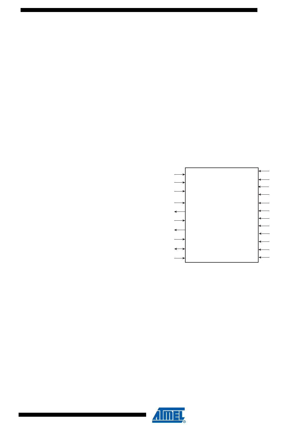
323
6430F–ATARM–21-Feb-12
SAM3U Series
22. Fast Flash Programming Interface (FFPI)
22.1 Overview
The Fast Flash Programming Interface provides solutions for high-volume programming using a
standard gang programmer. The parallel interface is fully handshaked and the device is consid-
ered to be a standard EEPROM. Additionally, the parallel protocol offers an optimized access to
all the embedded Flash functionalities.
Although the Fast Flash Programming Mode is a dedicated mode for high volume programming,
this mode is not designed for in-situ programming.
22.2 Parallel Fast Flash Programming
22.2.1 Device Configuration
In Fast Flash Programming Mode, the device is in a specific test mode. Only a certain set of pins
is significant. Other pins must be left unconnected.
Figure 22-1. Parallel Programming Interface
DATA[15:0]
PGMNCMD
PGMRDY
PGMNOE
PGMNVALID
PGMM[3:0]
PGMD[15:0]
XIN
TST
NRSTB
FWUP
NCMD
RDY
NOE
NVALID
MODE[3:0]
VDDBU
0 - 50MHz (VDDCORE)
VDDBU
VDDBU
VDDIO
GND
VDDBU
GNDBU
GNDANA
GNDPLL
VDDCORE
VDDPLL
VDDANA
VDDUTMI
GNDUTMI
VDDIN

324
6430F–ATARM–21-Feb-12
SAM3U Series
Table 22-1. Signal Description List
Signal Name Function Type
Active
Level Comments
Power
VDDIO I/O Lines Power Supply Power Apply external 3.0V-3.6V
VDDBU Backup I/O Lines Power Supply Power Apply external 3.0V-3.6V
VDDUTMI UTMI+ Interface Power Supply Power Apply external 3.0V-3.6V
VDDANA ADC Analog Power Supply Power Apply external 3.0V-3.6V
VDDIN Voltage Regulator Input Power Apply external 3.0V-3.6V
VDDCORE Core Power Supply Power Apply external 1.65V-1.95V
VDDPLL PLLs and Oscillator Power Supply Power Apply external 1.65V-1.95V
GND Ground Ground
GNDPLL Ground Ground
GNDBU Ground Ground
GNDANA Ground Ground
GNDUTMI Ground Ground
Clocks
XIN Clock Input Input 0 to 50MHz (0-VDDCORE square
wave)
Test
TST Test Mode Select Input High Must be connected to VDDIO
NRSTB Asynchronous Microcontroller Reset Input High Must be connected to VDDIO
FWUP Wake-up pin Input High Must be connected to VDDIO
PIO
PGMNCMD Valid command available Input Low Pulled-up input at reset
PGMRDY 0: Device is busy
1: Device is ready for a new command Output High Pulled-up input at reset
PGMNOE Output Enable (active high) Input Low Pulled-up input at reset
PGMNVALID 0: DATA[15:0] is in input mode
1: DATA[15:0] is in output mode Output Low Pulled-up input at reset
PGMM[3:0] Specifies DATA type (See Table 22-2) Input Pulled-up input at reset
PGMD[15:0] Bi-directional data bus Input/Output Pulled-up input at reset

325
6430F–ATARM–21-Feb-12
SAM3U Series
22.2.2 Signal Names
Depending on the MODE settings, DATA is latched in different internal registers.
When MODE is equal to CMDE, then a new command (strobed on DATA[15:0] signals) is stored
in the command register.
Note: 1. Applies to 256 kbytes Flash version (dual EEFC)
22.2.3 Entering Programming Mode
The following algorithm puts the device in Parallel Programming Mode:
• Apply GND, TST, NRTSB, FWUP and the supplies as described in Table 22-1, “Signal
Description List,” on page 324.
Table 22-2. Mode Coding
MODE[3:0] Symbol Data
0000 CMDE Command Register
0001 ADDR0 Address Register LSBs
0010 ADDR1 Address Register MSBs
0101 DATA Data Register
Default IDLE No register
Table 22-3. Command Bit Coding
DATA[15:0] Symbol Command Executed
0x0011 READ Read Flash
0x0012 WP Write Page Flash
0x0022 WPL Write Page and Lock Flash
0x0032 EWP Erase Page and Write Page
0x0042 EWPL Erase Page and Write Page then Lock
0x0013 EA Erase All
0x0014 SLB Set Lock Bit
0x0024 CLB Clear Lock Bit
0x0015 GLB Get Lock Bit
0x0034 SGPB Set General Purpose NVM bit
0x0044 CGPB Clear General Purpose NVM bit
0x0025 GGPB Get General Purpose NVM bit
0x0054 SSE Set Security Bit
0x0035 GSE Get Security Bit
0x001F WRAM Write Memory
0x0016 SEFC Select EEFC Controller(1)
0x001E GVE Get Version
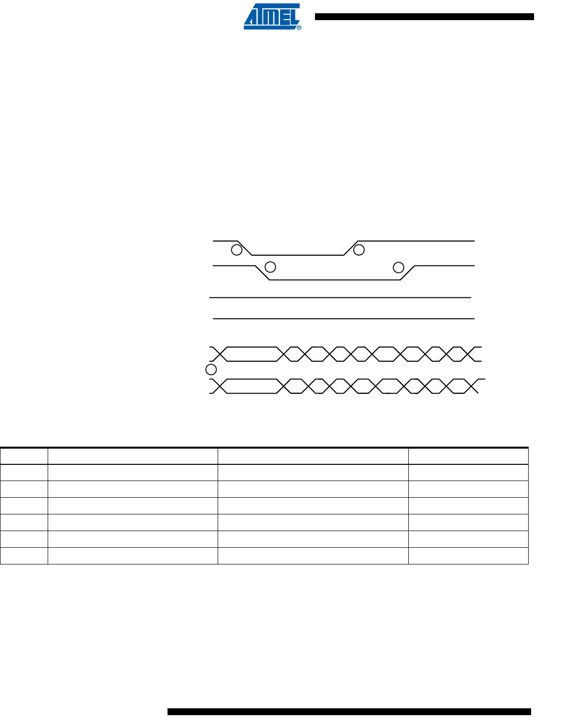
326
6430F–ATARM–21-Feb-12
SAM3U Series
• Apply XIN clock
• Wait for 20 ms
• Start a read or write handshaking.
22.2.4 Programmer Handshaking
A handshake is defined for read and write operations. When the device is ready to start a new
operation (RDY signal set), the programmer starts the handshake by clearing the NCMD signal.
The handshaking is achieved once NCMD signal is high and RDY is high.
22.2.4.1 Write Handshaking
For details on the write handshaking sequence, refer to Figure 22-2 and Table 22-4.
Figure 22-2. Parallel Programming Timing, Write Sequence
22.2.4.2 Read Handshaking
For details on the read handshaking sequence, refer to Figure 22-3 and Table 22-5.
NCMD
RDY
NOE
NVALID
DATA[15:0]
MODE[3:0]
1
2
3
4
5
Table 22-4. Write Handshake
Step Programmer Action Device Action Data I/O
1 Sets MODE and DATA signals Waits for NCMD low Input
2 Clears NCMD signal Latches MODE and DATA Input
3 Waits for RDY low Clears RDY signal Input
4 Releases MODE and DATA signals Executes command and polls NCMD high Input
5 Sets NCMD signal Executes command and polls NCMD high Input
6 Waits for RDY high Sets RDY Input
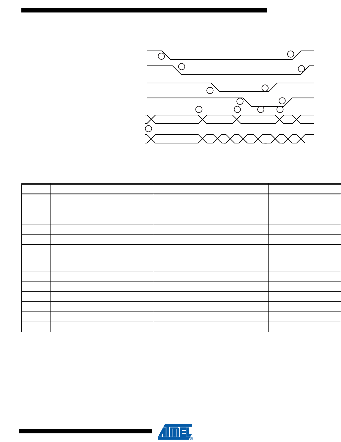
327
6430F–ATARM–21-Feb-12
SAM3U Series
Figure 22-3. Parallel Programming Timing, Read Sequence
22.2.5 Device Operations
Several commands on the Flash memory are available. These commands are summarized in
Table 22-3 on page 325. Each command is driven by the programmer through the parallel inter-
face running several read/write handshaking sequences.
When a new command is executed, the previous one is automatically achieved. Thus, chaining
a read command after a write automatically flushes the load buffer in the Flash.
NCMD
RDY
NOE
NVALID
DATA[15:0]
MODE[3:0]
Adress IN Z Data OUT X IN
ADDR
1
2
3
4
5
6
7
9
8 10
11
12
13
Table 22-5. Read Handshake
Step Programmer Action Device Action DATA I/O
1 Sets MODE and DATA signals Waits for NCMD low Input
2 Clears NCMD signal Latch MODE and DATA Input
3 Waits for RDY low Clears RDY signal Input
4 Sets DATA signal in tristate Waits for NOE Low Input
5 Clears NOE signal Tr i s t a t e
6 Waits for NVALID low Sets DATA bus in output mode and outputs
the flash contents. Output
7 Clears NVALID signal Output
8 Reads value on DATA Bus Waits for NOE high Output
9 Sets NOE signal Output
10 Waits for NVALID high Sets DATA bus in input mode X
11 Sets DATA in output mode Sets NVALID signal Input
12 Sets NCMD signal Waits for NCMD high Input
13 Waits for RDY high Sets RDY signal Input

328
6430F–ATARM–21-Feb-12
SAM3U Series
22.2.5.1 Flash Read Command
This command is used to read the contents of the Flash memory. The read command can start
at any valid address in the memory plane and is optimized for consecutive reads. Read hand-
shaking can be chained; an internal address buffer is automatically increased.
22.2.5.2 Flash Write Command
This command is used to write the Flash contents.
The Flash memory plane is organized into several pages. Data to be written are stored in a load
buffer that corresponds to a Flash memory page. The load buffer is automatically flushed to the
Flash:
• before access to any page other than the current one
• when a new command is validated (MODE = CMDE)
The Write Page command (WP) is optimized for consecutive writes. Write handshaking can be
chained; an internal address buffer is automatically increased.
Table 22-6. Read Command
Step Handshake Sequence MODE[3:0] DATA[15:0]
1 Write handshaking CMDE READ
2 Write handshaking ADDR0 Memory Address LSB
3 Write handshaking ADDR1 Memory Address
4 Read handshaking DATA *Memory Address++
5 Read handshaking DATA *Memory Address++
... ... ... ...
n Write handshaking ADDR0 Memory Address LSB
n+1 Write handshaking ADDR1 Memory Address
n+2 Read handshaking DATA *Memory Address++
n+3 Read handshaking DATA *Memory Address++
... ... ... ...
Table 22-7. Write Command
Step Handshake Sequence MODE[3:0] DATA[15:0]
1 Write handshaking CMDE WP or WPL or EWP or EWPL
2 Write handshaking ADDR0 Memory Address LSB
3 Write handshaking ADDR1 Memory Address
4 Write handshaking DATA *Memory Address++
5 Write handshaking DATA *Memory Address++
... ... ... ...
n Write handshaking ADDR0 Memory Address LSB
n+1 Write handshaking ADDR1 Memory Address
329
6430F–ATARM–21-Feb-12
SAM3U Series
The Flash command Write Page and Lock (WPL) is equivalent to the Flash Write Command.
However, the lock bit is automatically set at the end of the Flash write operation. As a lock region
is composed of several pages, the programmer writes to the first pages of the lock region using
Flash write commands and writes to the last page of the lock region using a Flash write and lock
command.
The Flash command Erase Page and Write (EWP) is equivalent to the Flash Write Command.
However, before programming the load buffer, the page is erased.
The Flash command Erase Page and Write the Lock (EWPL) combines EWP and WPL
commands.
22.2.5.3 Flash Full Erase Command
This command is used to erase the Flash memory planes.
All lock regions must be unlocked before the Full Erase command by using the CLB command.
Otherwise, the erase command is aborted and no page is erased.
22.2.5.4 Flash Lock Commands
Lock bits can be set using WPL or EWPL commands. They can also be set by using the Set
Lock command (SLB). With this command, several lock bits can be activated. A Bit Mask is pro-
vided as argument to the command. When bit 0 of the bit mask is set, then the first lock bit is
activated.
Likewise, the Clear Lock command (CLB) is used to clear lock bits.
n+2 Write handshaking DATA *Memory Address++
n+3 Write handshaking DATA *Memory Address++
... ... ... ...
Table 22-7. Write Command (Continued)
Step Handshake Sequence MODE[3:0] DATA[15:0]
Table 22-8. Full Erase Command
Step Handshake Sequence MODE[3:0] DATA[15:0]
1 Write handshaking CMDE EA
2 Write handshaking DATA 0
Table 22-9. Set and Clear Lock Bit Command
Step Handshake Sequence MODE[3:0] DATA[15:0]
1 Write handshaking CMDE SLB or CLB
2 Write handshaking DATA Bit Mask
330
6430F–ATARM–21-Feb-12
SAM3U Series
Lock bits can be read using Get Lock Bit command (GLB). The nth lock bit is active when the bit
n of the bit mask is set..
22.2.5.5 Flash General-purpose NVM Commands
General-purpose NVM bits (GP NVM bits) can be set using the Set GPNVM command (SGPB).
This command also activates GP NVM bits. A bit mask is provided as argument to the com-
mand. When bit 0 of the bit mask is set, then the first GP NVM bit is activated.
Likewise, the Clear GPNVM command (CGPB) is used to clear general-purpose NVM bits. All
the general-purpose NVM bits are also cleared by the EA command. The general-purpose NVM
bit is deactivated when the corresponding bit in the pattern value is set to 1.
General-purpose NVM bits can be read using the Get GPNVM Bit command (GGPB). The nth
GP NVM bit is active when bit n of the bit mask is set..
22.2.5.6 Flash Security Bit Command
A security bit can be set using the Set Security Bit command (SSE). Once the security bit is
active, the Fast Flash programming is disabled. No other command can be run. An event on the
Erase pin can erase the security bit once the contents of the Flash have been erased.
The AT9SAM3U256 security bit is controlled by the EEFC0. To use the Set Security Bit com-
mand, the EEFC0 must be selected using the Select EFC command.
Table 22-10. Get Lock Bit Command
Step Handshake Sequence MODE[3:0] DATA[15:0]
1 Write handshaking CMDE GLB
2 Read handshaking DATA
Lock Bit Mask Status
0 = Lock bit is cleared
1 = Lock bit is set
Table 22-11. Set/Clear GP NVM Command
Step Handshake Sequence MODE[3:0] DATA[15:0]
1 Write handshaking CMDE SGPB or CGPB
2 Write handshaking DATA GP NVM bit pattern value
Table 22-12. Get GP NVM Bit Command
Step Handshake Sequence MODE[3:0] DATA[15:0]
1 Write handshaking CMDE GGPB
2 Read handshaking DATA
GP NVM Bit Mask Status
0 = GP NVM bit is cleared
1 = GP NVM bit is set
331
6430F–ATARM–21-Feb-12
SAM3U Series
Once the security bit is set, it is not possible to access FFPI. The only way to erase the security
bit is to erase the Flash.
In order to erase the Flash, the user must perform the following:
• Power-off the chip
• Power-on the chip with TST = 0
• Assert Erase during a period of more than 220 ms
• Power-off the chip
Then it is possible to return to FFPI mode and check that Flash is erased.
22.2.5.7 SAM3U 256 Kbytes Flash Select EEFC Command
The commands WPx, EA, xLB, xFB are executed using the current EFC controller. The default
EEFC controller is EEFC0. The Select EEFC command (SEFC) allows selection of the current
EEFC controller.
22.2.5.8 Memory Write Command
This command is used to perform a write access to any memory location.
The Memory Write command (WRAM) is optimized for consecutive writes. Write handshaking
can be chained; an internal address buffer is automatically increased.
Table 22-13. Set Security Bit Command
Step Handshake Sequence MODE[3:0] DATA[15:0]
1 Write handshaking CMDE SSE
2 Write handshaking DATA 0
Table 22-14. Select EFC Command
Step Handshake Sequence MODE[3:0] DATA[15:0]
1 Write handshaking CMDE SEFC
2 Write handshaking DATA 0 = Select EEFC0
1 = Select EEFC1
Table 22-15. Write Command
Step Handshake Sequence MODE[3:0] DATA[15:0]
1 Write handshaking CMDE WRAM
2 Write handshaking ADDR0 Memory Address LSB
3 Write handshaking ADDR1 Memory Address
4 Write handshaking DATA *Memory Address++
5 Write handshaking DATA *Memory Address++
... ... ... ...
n Write handshaking ADDR0 Memory Address LSB
n+1 Write handshaking ADDR1 Memory Address

332
6430F–ATARM–21-Feb-12
SAM3U Series
22.2.5.9 Get Version Command
The Get Version (GVE) command retrieves the version of the FFPI interface.
n+2 Write handshaking DATA *Memory Address++
n+3 Write handshaking DATA *Memory Address++
... ... ... ...
Table 22-15. Write Command (Continued)
Step Handshake Sequence MODE[3:0] DATA[15:0]
Table 22-16. Get Version Command
Step Handshake Sequence MODE[3:0] DATA[15:0]
1 Write handshaking CMDE GVE
2 Write handshaking DATA Version
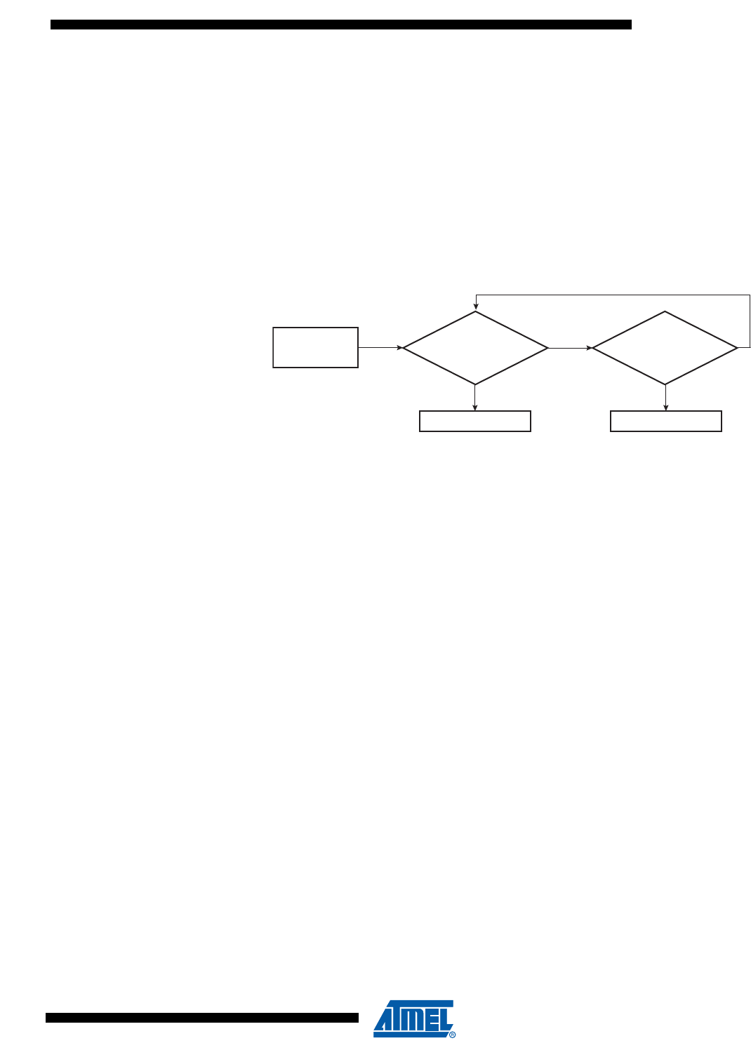
333
6430F–ATARM–21-Feb-12
SAM3U Series
23. SAM3U4/2/1 Boot Program
23.1 Description
The SAM-BA® Boot Program integrates an array of programs permitting download and/or upload
into the different memories of the product.
23.2 Flow Diagram
The Boot Program implements the algorithm in Figure 23-1.
Figure 23-1. Boot Program Algorithm Flow Diagram
The SAM-BA Boot program seeks to detect a source clock either from the embedded main oscil-
lator with external crystal (main osccillator enabled) or from a 12 MHz signal applied to the XIN
pin (Main oscillator in bypass mode).
If a clock is found from the two possible sources above, the boot program checks to verify that
the frequency is 12 MHz (taking into account the frequency range of the 32 kHz RC oscillator). If
the frequency is 12 MHz, USB activation is allowed, else (no clock or frequency other than
12MHz), the internal 12 MHz RC oscilator is used as main clock and USB clock is not allowed
due to frequency drift of the 12 MHz RC oscillator.
23.3 Device Initialization
Initialization follows the steps described below:
1. Stack setup
2. Setup the Embedded Flash Controller
3. External Clock detection (Quartz or external clock on XIN)
4. If Quartz or external clock is 12.000 MHz, allow USB activation
5. Else, does not allow USB activation and use internal RC 12 MHz
6. Main oscillator frequency detection if no external clock detected
7. Switch Master Clock on Main Oscillator
8. C variable initialization
9. PLLA setup: PLLA is initialized to generate a 48 MHz clock
10. UPLL setup in case of USB activation allowed
11. Disable of the Watchdog
12. Initialization of the UART (115200 bauds, 8, N, 1)
13. Initialization of the USB Device Port (in case of USB activation allowed)
14. Wait for one of the following events
Device
Setup
Character # received
from UART?
Run SAM-BA Monitor
USB Enumeration
Successful ?
Ye s
Run SAM-BA Monitor
Ye s
No
No

334
6430F–ATARM–21-Feb-12
SAM3U Series
a. check if USB device enumeration has occured
b. check if characters have been received in the UART
15. Jump to SAM-BA Monitor (see Section 23.4 ”SAM-BA Monitor”)
23.4 SAM-BA Monitor
The SAM-BA boot principle:
Once the communication interface is identified, to run in an infinite loop waiting for different com-
mands as shown in Table 23-1.
• Write commands: Write a byte (O), a halfword (H) or a word (W) to the target.
–Address: Address in hexadecimal.
–Value: Byte, halfword or word to write in hexadecimal.
–Output: ‘>’.
• Read commands: Read a byte (o), a halfword (h) or a word (w) from the target.
–Address: Address in hexadecimal
–Output: The byte, halfword or word read in hexadecimal following by ‘>’
• Send a file (S): Send a file to a specified address
–Address: Address in hexadecimal
–Output: ‘>’.
Note: There is a time-out on this command which is reached when the prompt ‘>’ appears before the
end of the command execution.
• Receive a file (R): Receive data into a file from a specified address
–Address: Address in hexadecimal
–NbOfBytes: Number of bytes in hexadecimal to receive
–Output: ‘>’
•Go (G): Jump to a specified address and execute the code
–Address: Address to jump in hexadecimal
–Output: ‘>’
• Get Version (V): Return the SAM-BA boot version
–Output: ‘>’
Table 23-1. Commands Available through the SAM-BA Boot
Command Action Argument(s) Example
Owrite a byte Address, Value# O200001,CA#
oread a byte Address,# o200001,#
Hwrite a half word Address, Value# H200002,CAFE#
hread a half word Address,# h200002,#
Wwrite a word Address, Value# W200000,CAFEDECA#
wread a word Address,# w200000,#
Ssend a file Address,# S200000,#
Rreceive a file Address, NbOfBytes# R200000,1234#
Ggo Address# G200200#
Vdisplay version No argument V#
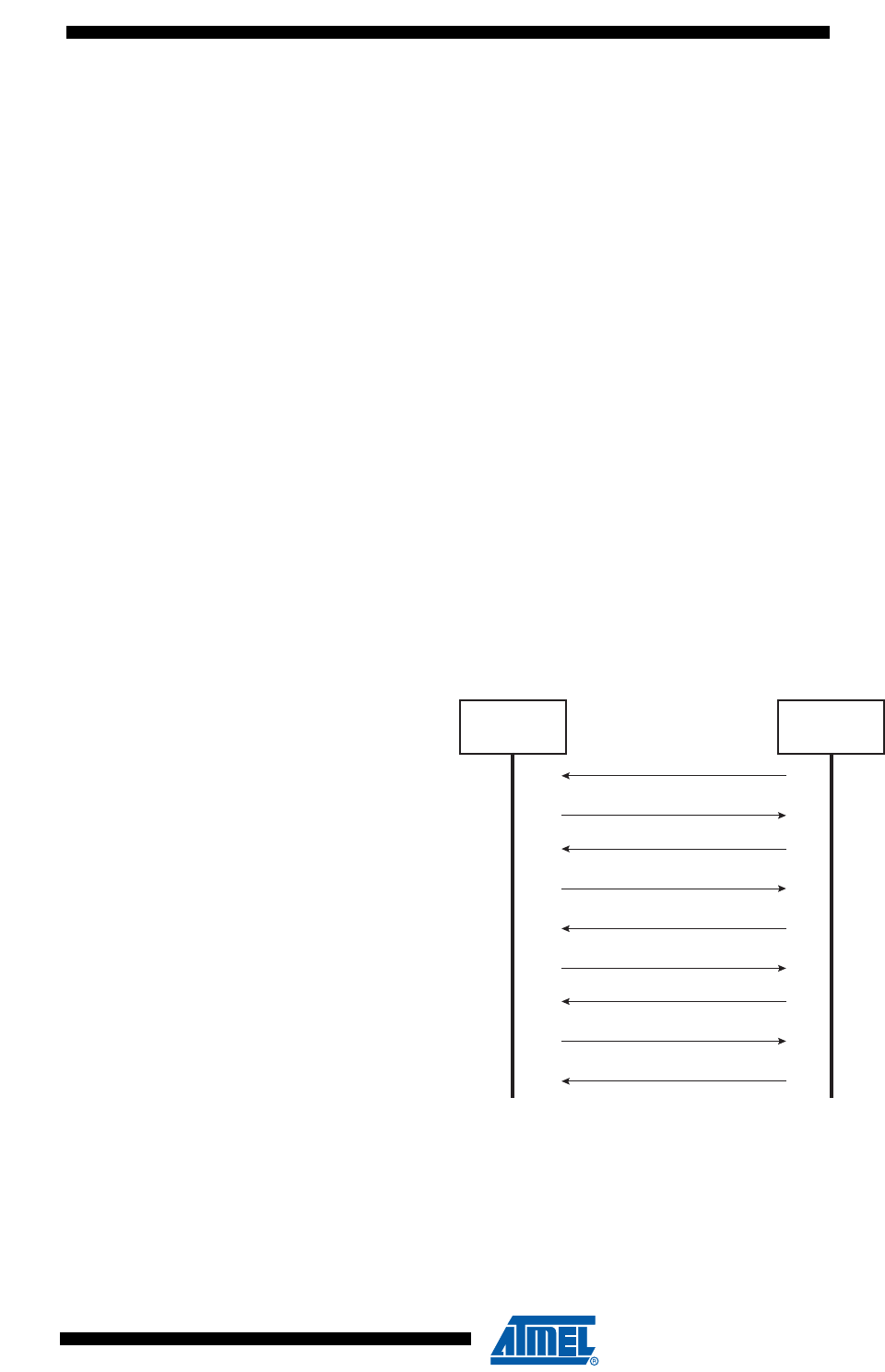
335
6430F–ATARM–21-Feb-12
SAM3U Series
23.4.1 UART Serial Port
Communication is performed through the UART initialized to 115200 Baud, 8, n, 1.
The Send and Receive File commands use the Xmodem protocol to communicate. Any terminal
performing this protocol can be used to send the application file to the target. The size of the
binary file to send depends on the SRAM size embedded in the product. In all cases, the size of
the binary file must be lower than the SRAM size because the Xmodem protocol requires some
SRAM memory to work. See, Section 23.5 ”Hardware and Software Constraints”
23.4.2 Xmodem Protocol
The Xmodem protocol supported is the 128-byte length block. This protocol uses a two-charac-
ter CRC-16 to guarantee detection of a maximum bit error.
Xmodem protocol with CRC is accurate provided both sender and receiver report successful
transmission. Each block of the transfer looks like:
<SOH><blk #><255-blk #><--128 data bytes--><checksum> in which:
– <SOH> = 01 hex
– <blk #> = binary number, starts at 01, increments by 1, and wraps 0FFH to 00H (not
to 01)
– <255-blk #> = 1’s complement of the blk#.
– <checksum> = 2 bytes CRC16
Figure 23-2 shows a transmission using this protocol.
Figure 23-2. Xmodem Transfer Example
Host Device
SOH 01 FE Data[128] CRC CRC
C
ACK
SOH 02 FD Data[128] CRC CRC
ACK
SOH 03 FC Data[100] CRC CRC
ACK
EOT
ACK

336
6430F–ATARM–21-Feb-12
SAM3U Series
23.4.3 USB Device Port
A 12.000 MHz Crystal (or 12.000 MHz external clock on XIN) is necessary to use the USB
Device port.
The device uses the USB communication device class (CDC) drivers to take advantage of the
installed PC RS-232 software to talk over the USB. The CDC class is implemented in all
releases of Windows®, from Windows 98SE® to Windows XP®. The CDC document, available at
www.usb.org, describes a way to implement devices such as ISDN modems and virtual COM
ports.
The Vendor ID (VID) is Atmel’s vendor ID 0x03EB. The product ID (PID) is 0x6124. These refer-
ences are used by the host operating system to mount the correct driver. On Windows systems,
the INF files contain the correspondence between vendor ID and product ID.
For More details about VID/PID for End Product/Systems, please refer to the Vendor ID form
available from the USB Implementers Forum:
http://www.usb.org/developers/vendor/VID_Only_Form_withCCAuth_102407b.pdf
"Unauthorized use of assigned or unassigned USB Vendor ID Numbers and associated Product
ID Numbers is strictly prohibited."
Atmel provides an INF example to see the device as a new serial port and also provides another
custom driver used by the SAM-BA application: atm6124.sys. Refer to the document “USB Basic
Application”, literature number 6123, for more details.
23.4.3.1 Enumeration Process
The USB protocol is a master/slave protocol. This is the host that starts the enumeration send-
ing requests to the device through the control endpoint. The device handles standard requests
as defined in the USB Specification.
Table 23-2. Handled Standard Requests
Request Definition
GET_DESCRIPTOR Returns the current device configuration value.
SET_ADDRESS Sets the device address for all future device access.
SET_CONFIGURATION Sets the device configuration.
GET_CONFIGURATION Returns the current device configuration value.
GET_STATUS Returns status for the specified recipient.
SET_FEATURE Set or Enable a specific feature.
CLEAR_FEATURE Clear or Disable a specific feature.

337
6430F–ATARM–21-Feb-12
SAM3U Series
The device also handles some class requests defined in the CDC class.
Unhandled requests are STALLed.
23.4.3.2 Communication Endpoints
There are two communication endpoints and endpoint 0 is used for the enumeration process.
Endpoint 1 is a 64-byte Bulk OUT endpoint and endpoint 2 is a 64-byte Bulk IN endpoint. SAM-
BA Boot commands are sent by the host through endpoint 1. If required, the message is split by
the host into several data payloads by the host driver.
If the command requires a response, the host can send IN transactions to pick up the response.
23.4.4 In Application Programming (IAP) Feature
The IAP feature is a function located in ROM that can be called by any software application.
When called, this function sends the desired FLASH command to the EEFC and waits for the
Flash to be ready (looping while the FRDY bit is not set in the MC_FSR register).
Since this function is executed from ROM, this allows Flash programming (such as sector write)
to be done by code running in Flash.
The IAP function entry point is retrieved by reading the NMI vector in ROM (0x00180008).
This function takes one argument in parameter: the command to be sent to the EEFC.
This function returns the value of the MC_FSR register.
IAP software code example:
(unsigned int) (*IAP_Function)(unsigned long);
void main (void){
unsigned long FlashSectorNum = 200; //
unsigned long flash_cmd = 0;
unsigned long flash_status = 0;
unsigned long EFCIndex = 0; // 0:EEFC0, 1: EEFC1
/* Initialize the function pointer (retrieve function address from NMI
vector) */
IAP_Function = ((unsigned long) (*)(unsigned long)) 0x00180008;
/* Send your data to the sector here */
Table 23-3. Handled Class Requests
Request Definition
SET_LINE_CODING Configures DTE rate, stop bits, parity and number of
character bits.
GET_LINE_CODING Requests current DTE rate, stop bits, parity and number of
character bits.
SET_CONTROL_LINE_STATE RS-232 signal used to tell the DCE device the DTE device
is now present.
338
6430F–ATARM–21-Feb-12
SAM3U Series
/* build the command to send to EEFC */
flash_cmd = (0x5A << 24) | (FlashSectorNum << 8) | AT91C_MC_FCMD_EWP;
/* Call the IAP function with appropriate command */
flash_status = IAP_Function (EFCIndex, flash_cmd);
}
23.5 Hardware and Software Constraints
• SAM-BA Boot uses the first 2048 bytes of the SRAM for variables and stacks. The remaining
available size can be used for user's code.
• USB requirements:
– 12.000 MHz Quartz or 12.000 MHz external clock on XIN. 12 MHz must be
±500 ppm and 1.8V Square Wave Signal.
Table 23-4. Pins Driven during Boot Program Execution
Peripheral Pin PIO Line
UART URXD PA11
UART UTXD PA12

339
6430F–ATARM–21-Feb-12
SAM3U Series
24. Bus Matrix (MATRIX)
24.1 Description
Bus Matrix implements a multi-layer AHB, based on AHB-Lite protocol, that enables parallel
access paths between multiple AHB masters and slaves in a system, which increases the over-
all bandwidth. Bus Matrix interconnects 5 AHB Masters to 10 AHB Slaves. The normal latency to
connect a master to a slave is one cycle except for the default master of the accessed slave
which is connected directly (zero cycle latency).
The Bus Matrix user interface is compliant with ARM® Advance Peripheral Bus and provides a
Chip Configuration User Interface with Registers that allow the Bus Matrix to support application
specific features.
24.2 Memory Mapping
Bus Matrix provides one decoder for every AHB Master Interface. The decoder offers each AHB
Master several memory mappings. In fact, depending on the product, each memory area may be
assigned to several slaves. Booting at the same address while using different AHB slaves (i.e.
internal ROM or internal Flash ) becomes possible.
The Bus Matrix user interface provides Master Remap Control Register (MATRIX_MRCR) that
allows to perform remap action for every master independently.
24.3 Special Bus Granting Techniques
The Bus Matrix provides some speculative bus granting techniques in order to anticipate access
requests from some masters. This mechanism allows to reduce latency at first accesses of a
burst or single transfer. The bus granting mechanism allows to set a default master for every
slave.
At the end of the current access, if no other request is pending, the slave remains connected to
its associated default master. A slave can be associated with three kinds of default masters: no
default master, last access master and fixed default master.
24.3.1 No Default Master
At the end of the current access, if no other request is pending, the slave is disconnected from
all masters. No Default Master suits low power mode.
24.3.2 Last Access Master
At the end of the current access, if no other request is pending, the slave remains connected to
the last master that performed an access request.
24.3.3 Fixed Default Master
At the end of the current access, if no other request is pending, the slave connects to its fixed
default master. Unlike last access master, the fixed master doesn’t change unless the user mod-
ifies it by a software action (field FIXED_DEFMSTR of the related MATRIX_SCFG).
To change from one kind of default master to another, the Bus Matrix user interface provides the
Slave Configuration Registers, one for each slave, that allow to set a default master for each
slave. The Slave Configuration Register contains two fields:
DEFMSTR_TYPE and FIXED_DEFMSTR. The 2-bit DEFMSTR_TYPE field allows to choose
the default master type (no default, last access master, fixed default master) whereas the 4-bit

340
6430F–ATARM–21-Feb-12
SAM3U Series
FIXED_DEFMSTR field allows to choose a fixed default master provided that DEFMSTR_TYPE
is set to fixed default master. Please refer to the Bus Matrix user interface description.
24.4 Arbitration
The Bus Matrix provides an arbitration mechanism that allows to reduce latency when conflict
cases occur, basically when two or more masters try to access the same slave at the same time.
One arbiter per AHB slave is provided, allowing to arbitrate each slave differently.
The Bus Matrix provides to the user the possibility to choose between 2 arbitration types, and
this for each slave:
1. Round-Robin Arbitration (the default)
2. Fixed Priority Arbitration
This choice is given through the field ARBT of the Slave Configuration Registers
(MATRIX_SCFG).
Each algorithm may be complemented by selecting a default master configuration for each
slave.
When a re-arbitration has to be done, it is realized only under some specific conditions detailed
in the following paragraph.
24.4.1 Arbitration Rules
Each arbiter has the ability to arbitrate between two or more different master’s requests. In order
to avoid burst breaking and also to provide the maximum throughput for slave interfaces, arbitra-
tion may only take place during the following cycles:
1. Idle Cycles: when a slave is not connected to any master or is connected to a master which is
not currently accessing it.
2. Single Cycles: when a slave is currently doing a single access.
3. End of Burst Cycles: when the current cycle is the last cycle of a burst transfer. For defined
length burst, predicted end of burst matches the size of the transfer but is managed differently
for undefined length burst (See Section 24.4.1.1 “Undefined Length Burst Arbitration” on page
340“).
4. Slot Cycle Limit: when the slot cycle counter has reached the limit value indicating that the
current master access is too long and must be broken (See Section 24.4.1.2 “Slot Cycle Limit
Arbitration” on page 341).
24.4.1.1 Undefined Length Burst Arbitration
In order to avoid too long slave handling during undefined length bursts (INCR), the Bus Matrix
provides specific logic in order to re-arbitrate before the end of the INCR transfer.
A predicted end of burst is used as for defined length burst transfer, which is selected between
the following:
1. Infinite: no predicted end of burst is generated and therefore INCR burst transfer will never be
broken.
2. Four beat bursts: predicted end of burst is generated at the end of each four beat boundary
inside INCR transfer.

341
6430F–ATARM–21-Feb-12
SAM3U Series
3. Eight beat bursts: predicted end of burst is generated at the end of each eight beat boundary
inside INCR transfer.
4. Sixteen beat bursts: predicted end of burst is generated at the end of each sixteen beat
boundary inside INCR transfer.
This selection can be done through the field ULBT of the Master Configuration Registers
(MATRIX_MCFG).
24.4.1.2 Slot Cycle Limit Arbitration
The Bus Matrix contains specific logic to break too long accesses such as very long bursts on a
very slow slave (e.g. an external low speed memory). At the beginning of the burst access, a
counter is loaded with the value previously written in the SLOT_CYCLE field of the related Slave
Configuration Register (MATRIX_SCFG) and decreased at each clock cycle. When the counter
reaches zero, the arbiter has the ability to re-arbitrate at the end of the current byte, half word or
word transfer.
24.4.2 Round-Robin Arbitration
This algorithm allows the Bus Matrix arbiters to dispatch the requests from different masters to
the same slave in a round-robin manner. If two or more master’s requests arise at the same
time, the master with the lowest number is first serviced then the others are serviced in a round-
robin manner.
There are three round-robin algorithm implemented:
• Round-Robin arbitration without default master
• Round-Robin arbitration with last access master
• Round-Robin arbitration with fixed default master
24.4.2.1 Round-Robin arbitration without default master
This is the main algorithm used by Bus Matrix arbiters. It allows the Bus Matrix to dispatch
requests from different masters to the same slave in a pure round-robin manner. At the end of
the current access, if no other request is pending, the slave is disconnected from all masters.
This configuration incurs one latency cycle for the first access of a burst. Arbitration without
default master can be used for masters that perform significant bursts.
24.4.2.2 Round-Robin arbitration with last access master
This is a biased round-robin algorithm used by Bus Matrix arbiters. It allows the Bus Matrix to
remove the one latency cycle for the last master that accessed the slave. In fact, at the end of
the current transfer, if no other master request is pending, the slave remains connected to the
last master that performs the access. Other non privileged masters will still get one latency cycle
if they want to access the same slave. This technique can be used for masters that mainly per-
form single accesses.
24.4.2.3 Round-Robin arbitration with fixed default master
This is another biased round-robin algorithm, it allows the Bus Matrix arbiters to remove the one
latency cycle for the fixed default master per slave. At the end of the current access, the slave
remains connected to its fixed default master. Every request attempted by this fixed default mas-
ter will not cause any latency whereas other non privileged masters will still get one latency
cycle. This technique can be used for masters that mainly perform single accesses.

342
6430F–ATARM–21-Feb-12
SAM3U Series
24.4.3 Fixed Priority Arbitration
This algorithm allows the Bus Matrix arbiters to dispatch the requests from different masters to
the same slave by using the fixed priority defined by the user. If two or more master’s requests
are active at the same time, the master with the highest priority number is serviced first. If two or
more master’s requests with the same priority are active at the same time, the master with the
highest number is serviced first.
For each slave, the priority of each master may be defined through the Priority Registers for
Slaves (MATRIX_PRAS and MATRIX_PRBS).
24.5 Write Protect Registers
To prevent any single software error that may corrupt MATRIX behavior, the entire MATRIX
address space from address offset 0x000 to 0x1FC can be write-protected by setting the WPEN
bit in the MATRIX Write Protect Mode Register (MATRIX_WPMR).
If a write access to anywhere in the MATRIX address space from address offset 0x000 to 0x1FC
is detected, then the WPVS flag in the MATRIX Write Protect Status Register (MATRIX_WPSR)
is set and the field WPVSRC indicates in which register the write access has been attempted.
The WPVS flag is reset by writing the MATRIX Write Protect Mode Register (MATRIX_WPMR)
with the appropriate access key WPKEY.
The protected registers are:
“Bus Matrix Master Configuration Registers”
“Bus Matrix Slave Configuration Registers”
“Bus Matrix Priority Registers For Slaves”
“Bus Matrix Master Remap Control Register”
“Bus Matrix Master Remap Control Register”

343
6430F–ATARM–21-Feb-12
SAM3U Series
24.6 Bus Matrix (MATRIX) User Interface
Table 24-1. Register Mapping
Offset Register Name Access Reset
0x0000 Master Configuration Register 0 MATRIX_MCFG0 Read-write 0x00000000
0x0004 Master Configuration Register 1 MATRIX_MCFG1 Read-write 0x00000000
0x0008 Master Configuration Register 2 MATRIX_MCFG2 Read-write 0x00000000
0x000C Master Configuration Register 3 MATRIX_MCFG3 Read-write 0x00000000
0x0010 Master Configuration Register 4 MATRIX_MCFG4 Read-write 0x00000000
0x0014 - 0x003C Reserved – – –
0x0040 Slave Configuration Register 0 MATRIX_SCFG0 Read-write 0x00010010
0x0044 Slave Configuration Register 1 MATRIX_SCFG1 Read-write 0x00050010
0x0048 Slave Configuration Register 2 MATRIX_SCFG2 Read-write 0x00000010
0x004C Slave Configuration Register 3 MATRIX_SCFG3 Read-write 0x00000010
0x0050 Slave Configuration Register 4 MATRIX_SCFG4 Read-write 0x00000010
0x0054 Slave Configuration Register 5 MATRIX_SCFG5 Read-write 0x00000010
0x0058 Slave Configuration Register 6 MATRIX_SCFG6 Read-write 0x00000010
0x005C Slave Configuration Register 7 MATRIX_SCFG7 Read-write 0x00000010
0x0060 Slave Configuration Register 8 MATRIX_SCFG8 Read-write 0x00000010
0x0064 Slave Configuration Register 9 MATRIX_SCFG9 Read-write 0x00000010
0x0068 - 0x007C Reserved – – –
0x0080 Priority Register A for Slave 0 MATRIX_PRAS0 Read-write 0x00000000
0x0084 Reserved – – –
0x0088 Priority Register A for Slave 1 MATRIX_PRAS1 Read-write 0x00000000
0x008C Reserved – – –
0x0090 Priority Register A for Slave 2 MATRIX_PRAS2 Read-write 0x00000000
0x0094 Reserved – – –
0x0098 Priority Register A for Slave 3 MATRIX_PRAS3 Read-write 0x00000000
0x009C Reserved – – –
0x00A0 Priority Register A for Slave 4 MATRIX_PRAS4 Read-write 0x00000000
0x00A4 Reserved – – –
0x00A8 Priority Register A for Slave 5 MATRIX_PRAS5 Read-write 0x00000000
0x00AC Reserved – – –
0x00B0 Priority Register A for Slave 6 MATRIX_PRAS6 Read-write 0x00000000
0x00B4 Reserved – – –
0x00B8 Priority Register A for Slave 7 MATRIX_PRAS7 Read-write 0x00000000
0x00BC Reserved – – –
0x00C0 Priority Register A for Slave 8 MATRIX_PRAS8 Read-write 0x00000000

344
6430F–ATARM–21-Feb-12
SAM3U Series
0x00C4 Reserved – – –
0x00C8 Priority Register A for Slave 9 MATRIX_PRAS9 Read-write 0x00000000
0x00CC- 0x00FC Reserved – – –
0x0100 Master Remap Control Register MATRIX_MRCR Read-write 0x00000000
0x0104 - 0x010C Reserved – – –
0x1E4 Write Protect Mode Register MATRIX_WPMR Read-write 0x0
0x1E8 Write Protect Status Register MATRIX_WPSR Read-only 0x0
0x0110 - 0x01FC Reserved – – –
Table 24-1. Register Mapping (Continued)
Offset Register Name Access Reset

345
6430F–ATARM–21-Feb-12
SAM3U Series
24.6.1 Bus Matrix Master Configuration Registers
Name: MATRIX_MCFG0..MATRIX_MCFG4
Address: 0x400E0200
Access: Read-write
This register can only be written if the WPEN bit is cleared in the “Write Protect Mode Register”.
• ULBT: Undefined Length Burst Type
0: Infinite Length Burst
No predicted end of burst is generated and therefore INCR bursts coming from this master cannot be broken.
1: Single Access
The undefined length burst is treated as a succession of single access allowing rearbitration at each beat of the INCR
burst.
2: Four Beat Burst
The undefined length burst is split into 4 beats burst allowing rearbitration at each 4 beats burst end.
3: Eight Beat Burst
The undefined length burst is split into 8 beats burst allowing rearbitration at each 8 beats burst end.
4: Sixteen Beat Burst
The undefined length burst is split into 16 beats burst allowing rearbitration at each 16 beats burst end.
31 30 29 28 27 26 25 24
––––––––
23 22 21 20 19 18 17 16
––––––––
15 14 13 12 11 10 9 8
––––––––
76543210
––––– ULBT

346
6430F–ATARM–21-Feb-12
SAM3U Series
24.6.2 Bus Matrix Slave Configuration Registers
Name: MATRIX_SCFG0..MATRIX_SCFG9
Address: 0x400E0240
Access: Read-write
This register can only be written if the WPEN bit is cleared in the “Write Protect Mode Register”.
• SLOT_CYCLE: Maximum Number of Allowed Cycles for a Burst
When the SLOT_CYCLE limit is reach for a burst it may be broken by another master trying to access this slave.
This limit has been placed to avoid locking very slow slave by when very long burst are used.
This limit should not be very small though. Unreasonable small value will break every burst and Bus Matrix will spend its
time to arbitrate without performing any data transfer. 16 cycles is a reasonable value for SLOT_CYCLE.
• DEFMSTR_TYPE: Default Master Type
0: No Default Master
At the end of current slave access, if no other master request is pending, the slave is disconnected from all masters.
This results in having a one cycle latency for the first acccess of a burst transfer or for a single access.
1: Last Default Master
At the end of current slave access, if no other master request is pending, the slave stay connected with the last master hav-
ing accessed it.
This results in not having the one cycle latency when the last master re-tries access on the slave again.
2: Fixed Default Master
At the end of the current slave access, if no other master request is pending, the slave connects to the fixed master which
number has been written in the FIXED_DEFMSTR field.
This results in not having the one cycle latency when the fixed master re-tries access on the slave again.
• FIXED_DEFMSTR: Fixed Default Master
This is the number of the Default Master for this slave. Only used if DEFMSTR_TYPE is 2. Specifying the number of a mas-
ter which is not connected to the selected slave is equivalent to setting DEFMSTR_TYPE to 0.
31 30 29 28 27 26 25 24
–––––– ARBT
23 22 21 20 19 18 17 16
– – – FIXED_DEFMSTR DEFMSTR_TYPE
15 14 13 12 11 10 9 8
––––––––
76543210
SLOT_CYCLE

347
6430F–ATARM–21-Feb-12
SAM3U Series
• ARBT: Arbitration Type
0: Round-Robin Arbitration
1: Fixed Priority Arbitration
2: Reserved
3: Reserved
348
6430F–ATARM–21-Feb-12
SAM3U Series
24.6.3 Bus Matrix Priority Registers For Slaves
Name: MATRIX_PRAS0..MATRIX_PRAS9
Addresses: 0x400E0280 [0], 0x400E0288 [1], 0x400E0290 [2], 0x400E0298 [3], 0x400E02A0 [4], 0x400E02A8 [5],
0x400E02B0 [6], 0x400E02B8 [7], 0x400E02C0 [8], 0x400E02C8 [9]
Access: Read-write
This register can only be written if the WPEN bit is cleared in the “Write Protect Mode Register”.
• MxPR: Master x Priority
Fixed prority of Master x for accessing to the selected slave.The higher the number, the higher the priority.
31 30 29 28 27 26 25 24
––––––––
23 22 21 20 19 18 17 16
–––––– M4PR
15 14 13 12 11 10 9 8
–– M3PR –– M2PR
76543210
–– M1PR –– M0PR

349
6430F–ATARM–21-Feb-12
SAM3U Series
24.6.4 Bus Matrix Master Remap Control Register
Name: MATRIX_MRCR
Address: 0x400E0300
Access: Read-write
Reset: 0x0000_0000
This register can only be written if the WPEN bit is cleared in the “Write Protect Mode Register”.
• RCBx: Remap Command Bit for AHB Master x
0: Disable remaped address decoding for the selected Master
1: Enable remaped address decoding for the selected Master
31 30 29 28 27 26 25 24
––––––––
23 22 21 20 19 18 17 16
––––––––
15 14 13 12 11 10 9 8
––––––––
76543210
– – – RCB4 RCB3 RCB2 RCB1 RCB0

350
6430F–ATARM–21-Feb-12
SAM3U Series
24.6.5 Write Protect Mode Register
Name: MATRIX_WPMR
Address: 0x400E03E4
Access: Read-write
For more details on MATRIX_WPMR, refer to Section 24.5 “Write Protect Registers” on page 342.
• WPEN: Write Protect ENable
0 = Disables the Write Protect if WPKEY corresponds to 0x4D4154 (“MAT” in ASCII).
1 = Enables the Write Protect if WPKEY corresponds to 0x4D4154 (“MAT” in ASCII).
Protects the entire MATRIX address space from address offset 0x000 to 0x1FC.
• WPKEY: Write Protect KEY (Write-only)
Should be written at value 0x4D4154 (“MAT”in ASCII). Writing any other value in this field aborts the write operation of the
WPEN bit. Always reads as 0.
31 30 29 28 27 26 25 24
WPKEY
23 22 21 20 19 18 17 16
WPKEY
15 14 13 12 11 10 9 8
WPKEY
76543210
–––––––WPEN

351
6430F–ATARM–21-Feb-12
SAM3U Series
24.6.6 Write Protect Status Register
Name: MATRIX_WPSR
Address: 0x400E03E8
Access: Read-only
For more details on MATRIX_WPSR, refer to Section 24.5 “Write Protect Registers” on page 342.
• WPVS: Write Protect Violation Status
0: No Write Protect Violation has occurred since the last write of MATRIX_WPMR.
1: At least one Write Protect Violation has occurred since the last write of MATRIX_WPMR.
• WPVSRC: Write Protect Violation Source
Should be written at value 0x4D4154 (“MAT”in ASCII). Writing any other value in this field aborts the write operation of the
WPEN bit. Always reads as 0.
The protected registers are:
•“Bus Matrix Master Configuration Registers”
•“Bus Matrix Slave Configuration Registers”
•“Bus Matrix Priority Registers For Slaves”
•“Bus Matrix Master Remap Control Register”
•“Bus Matrix Master Remap Control Register”
31 30 29 28 27 26 25 24
––––––––
23 22 21 20 19 18 17 16
WPVSRC
15 14 13 12 11 10 9 8
WPVSRC
76543210
–––––––WPVS

352
6430F–ATARM–21-Feb-12
SAM3U Series

353
6430F–ATARM–21-Feb-12
SAM3U Series
353
6430F–ATARM–21-Feb-12
SAM3U Series
25. Static Memory Controller (SMC)
25.1 Description
The External Bus Interface is designed to ensure the successful data transfer between several
external devices and the Cortex-M3 based device. The External Bus Interface of the SAM3U
consists of a Static Memory Controller (SMC).
This SMC is capable of handling several types of external memory and peripheral devices, such
as SRAM, PSRAM, PROM, EPROM, EEPROM, LCD Module, NOR Flash and NAND Flash.
The SMC generates the signals that control the access to external memory devices or peripheral
devices. It has 4 Chip Selects and a 24-bit address bus. The 16-bit data bus can be configured
to interface with 8- or 16-bit external devices. Separate read and write control signals allow for
direct memory and peripheral interfacing. Read and write signal waveforms are fully
parametrizable.
The SMC can manage wait requests from external devices to extend the current access. The
SMC is provided with an automatic slow clock mode. In slow clock mode, it switches from user-
programmed waveforms to slow-rate specific waveforms on read and write signals.
The SMC embeds a NAND Flash Controller (NFC). The NFC can handle automatic transfers,
sending the commands and address cycles to the NAND Flash and transferring the contents of
the page (for read and write) to the NFC SRAM. It minimizes the CPU overhead.
The SMC includes programmable hardware error correcting code with one bit error correction
capability and supports two bits error detection. In order to improve overall system performance
the DATA phase of the transfer can be DMA assisted.
The External Data Bus can be scrambled/unscrambled by means of user keys.
25.2 Embedded Characteristics
• 16-Mbyte Address Space per Chip Select
• 8- or 16-bit Data Bus
• Word, Halfword, Byte Transfers
• Byte Write or Byte Select Lines
• Programmable Setup, Pulse and Hold Time for Read Signals per Chip Select
• Programmable Setup, Pulse and Hold Time for Write Signals per Chip Select
• Programmable Data Float Time per Chip Select
• External Data Bus Scrambling/Unscrambling Function
• External Wait Request
• Automatic Switch to Slow Clock Mode
• NAND Flash Controller Supporting NAND Flash with Multiplexed Data/Address Buses
• Supports SLC NAND Flash Technology
• Hardware Configurable Number of Chip Selects from 1 to 4
• Programmable Timing on a per Chip Select Basis
• AHB Slave Interface
• Atmel APB Configuration Interface
• Programmable Flash Data Width 8 Bits or 16 Bits
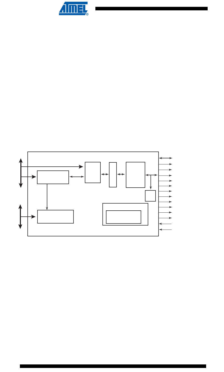
354
6430F–ATARM–21-Feb-12
SAM3U Series
354
6430F–ATARM–21-Feb-12
SAM3U Series
• Supports Hardware Error Correcting Code (ECC), 1-bit Error Correction, 2-bit Error Detection
• Detection and Correction by Software
• Supports NAND Flash and SmartMedia™ Devices with 8- or 16-bit Data Path
• Supports NAND Flash/SmartMedia with Page Sizes of 528, 1056, 2112 and 4224 Bytes,
Specified by Software
•Supports 1-bit Correction for a Page of 512, 1024, 2048 and 4096 Bytes with 8- or 16-bit
Data Path
•Supports 1-bit Correction per 512 Bytes of Data for a Page Size of 512, 2048 and 4096 Bytes
with 8-bit Data Path
•Supports 1-bit Correction per 256 Bytes of Data for a Page Size of 512, 2048 and 4096 Bytes
with 8-bit Data Path
25.3 Block Diagram
Figure 25-1. Block Diagram
SMC
Interface
NANDRDY
D[15:0]
NFC
Internal SRAM
NAND Flash
Controller (NFC)
ECC
NWR0/NWE
NCS[3:0]
NWAIT
NANDOE
NANDWE
A23
NRD
A[0]/NBS0
A[20:1]
NWR1/NBS1
A21/NANDALE
A22/NANDCLE
Control & Status
Registers
SRAM
AHB
Interface
AHB
arbiter
Scrambler
SMC
AHB
Interface
(4 K bytes)
User Interface

355
6430F–ATARM–21-Feb-12
SAM3U Series
355
6430F–ATARM–21-Feb-12
SAM3U Series
25.4 I/O Lines Description
25.5 Multiplexed Signals
Table 25-1. I/O Line Description
Name Description Type Active Level
NCS[3:0] Static Memory Controller Chip Select Lines Output Low
NRD Read Signal Output Low
NWR0/NWE Write 0/Write Enable Signal Output Low
A0/NBS0 Address Bit 0/Byte 0 Select Signal Output Low
NWR1/NBS1 Write 1/Byte 1 Select Signal Output Low
A1 Address Bit 1 Output Low
A[23:2] Address Bus Output
D[15:0] Data Bus I/O
NWAIT External Wait Signal Input Low
NANDRDY NAND Flash Ready/Busy Input
NANDWE NAND Flash Write Enable Output Low
NANDOE NAND Flash Output Enable Output Low
NANDALE NAND Flash Address Latch Enable Output
NANDCLE NAND Flash Command Latch Enable Output
Table 25-2. Static Memory Controller (SMC) Multiplexed Signals
Multiplexed Signals Related Function
NWR0 NWE Byte-write or byte-select access, see Figure 25-4 "Memory Connection for an 8-bit Data
Bus" and Figure 25-5 "Memory Connection for a 16-bit Data Bus"
A0 NBS0 8-bit or 16-bit data bus, see Section 25.9.1 ”Data Bus Width”
A22 NANDCLE NAND Flash Command Latch Enable
A21 NANDALE NAND Flash Address Latch Enable
NWR1 NBS1 Byte-write or byte-select access, see Figure 25-4 and Figure 25-5
A1 – 8-/16-bit data bus, see Section 25.9.1 ”Data Bus Width”
Byte-write or byte-select access, see Figure 25-4 and Figure 25-5
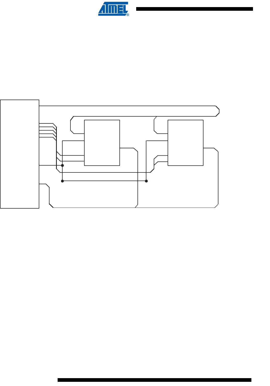
356
6430F–ATARM–21-Feb-12
SAM3U Series
356
6430F–ATARM–21-Feb-12
SAM3U Series
25.6 Application Example
25.6.1 Implementation Examples
For Hardware implementation examples, refer to ATSAM3U-EK schematics which show exam-
ples of connection to an LCD module, PSRAM and NAND Flash.
25.6.2 Hardware Interface
Figure 25-2. SMC Connections to Static Memory Devices
25.7 Product Dependencies
25.7.1 I/O Lines
The pins used for interfacing the Static Memory Controller are multiplexed with the PIO lines.
The programmer must first program the PIO controller to assign the Static Memory Controller
pins to their peripheral function. If I/O Lines of the SMC are not used by the application, they can
be used for other purposes by the PIO Controller.
25.7.2 Power Management
The SMC is clocked through the Power Management Controller (PMC), thus the programmer
must first configure the PMC to enable the SMC clock.
Static Memory
Controller
D0-D15
A2 - A23
A0/NBS0
NWR0/NWE
NWR1/NBS1
A1
128K x 8
SRAM
D0 - D7
A0 - A16
OE
WE
CS
D0 - D7 D8-D15
A2 - A18
128K x 8
SRAM
D0-D7
CS
NWR1/NBS1
NRD
NWR0/NWE
NCS0
NCS1
NCS2
NCS3
NRD OE
WE
A2 - A18
A0 - A16
357
6430F–ATARM–21-Feb-12
SAM3U Series
357
6430F–ATARM–21-Feb-12
SAM3U Series
25.7.3 Interrupt
The SMC has an interrupt line connected to the Nested Vector Interrupt Controller (NVIC). Han-
dling the SMC interrupt requires programming the NVIC before configuring the SMC.
25.8 External Memory Mapping
Note: 1. See Section 25.16.2 ”NFC Control Registers”, i.e., CMD_ADDR description.
The SMC provides up to 24 address lines, A[23:0]. This allows each chip select line to address
up to 16 Mbytes of memory.
If the physical memory device connected on one chip select is smaller than 16 Mbytes, it wraps
around and appears to be repeated within this space. The SMC correctly handles any valid
access to the memory device within the page (see Figure ).
A[23:0] is only significant for 8-bit memory, A[23:1] is used for 16-bit memory.
Figure 25-3. Memory Connections for External Devices
Table 25-3. Peripheral IDs
Instance ID
SMC 9
Table 25-4. External Memory Mapping
Address Use Access
0x60000000-0x60FFFFFF Chip Select 0 (16 MB) Read-write
0x61000000-0x61FFFFFF Chip Select 1 Read-write
0x62000000-0x62FFFFFF Chip Select 2 Read-write
0x63000000-0x63FFFFFF Chip Select 3 Read-write
0x04000000-0x07FFFFFF Undefined Area
0x68000000-0x6FFFFFFF NFC Command Registers(1) Read-write
NRD
NWE
A[23:0]
D[15:0]
8 or 16
Memory Enable
Memory Enable
Memory Enable
Memory Enable
Output Enable
Write Enable
A[25:0]
D[15:0] or D[7:0]
NCS3
NCS0
NCS1
NCS2
NCS[0] - NCS[3]
SMC
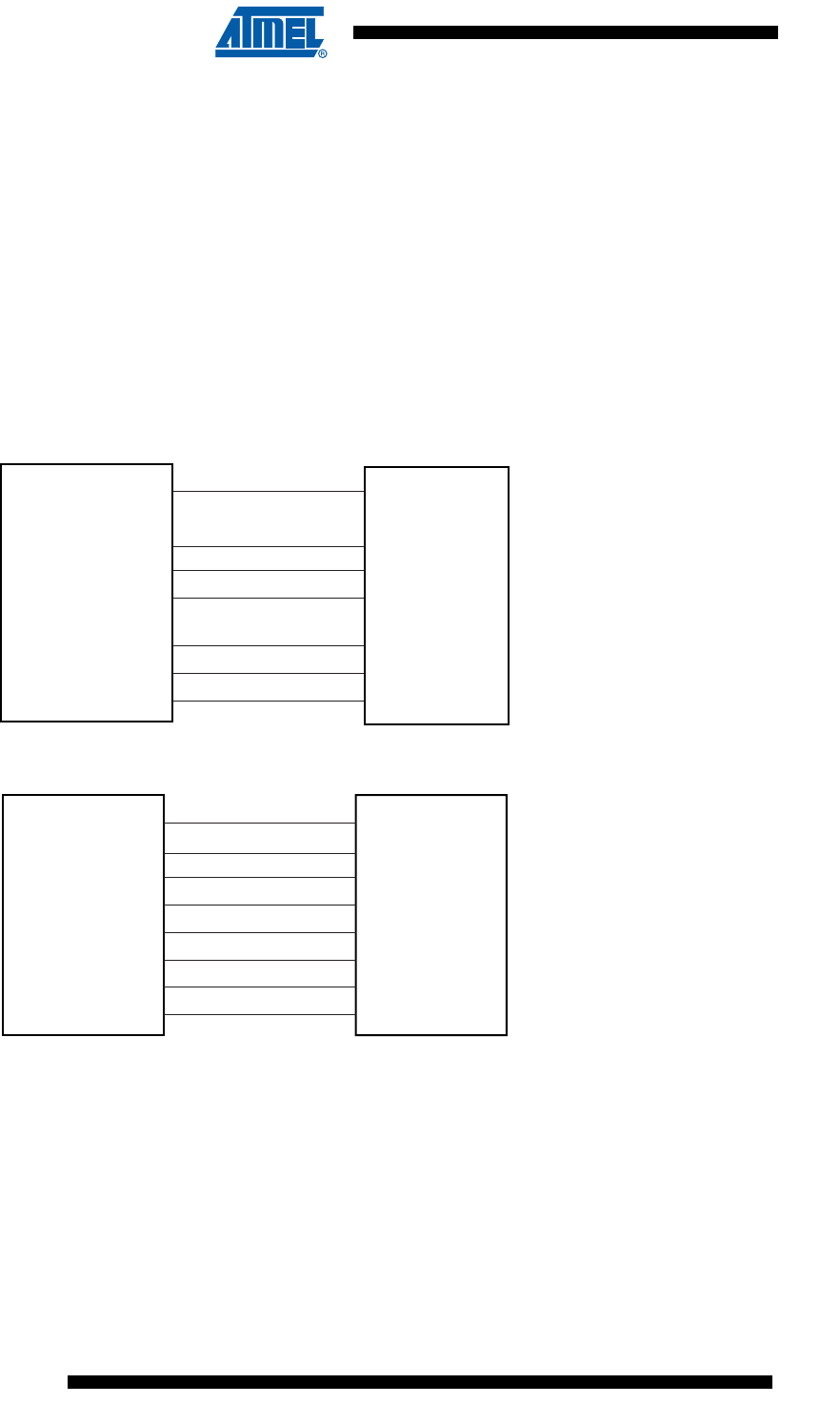
358
6430F–ATARM–21-Feb-12
SAM3U Series
358
6430F–ATARM–21-Feb-12
SAM3U Series
25.9 Connection to External Devices
25.9.1 Data Bus Width
A data bus width of 8 or 16 bits can be selected for each chip select. This option is controlled by
the field DBW in SMC_MODE (Mode Register) for the corresponding chip select.
Figure 25-4 shows how to connect a 512K x 8-bit memory on NCS2. Figure 25-5 shows how to
connect a 512K x 16-bit memory on NCS2.
25.9.2 Byte Write or Byte Select Access
Each chip select with a 16-bit data bus can operate with one of two different types of write
access: byte write or byte select access. This is controlled by the BAT field of the SMC_MODE
register for the corresponding chip select.
Figure 25-4. Memory Connection for an 8-bit Data Bus
Figure 25-5. Memory Connection for a 16-bit Data Bus
25.9.2.1 Byte Write Access
Byte write access supports one byte write signal per byte of the data bus and a single read
signal.
Note that the SMC does not allow boot in Byte Write Access mode.
• For 16-bit devices: the SMC provides NWR0 and NWR1 write signals for respectively, byte0
(lower byte) and byte1 (upper byte) of a 16-bit bus. One single read signal (NRD) is provided.
Byte Write Access is used to connect 2 x 8-bit devices as a 16-bit memory.
SMC
A0
NWE
NRD
NCS[2]
A0
Write Enable
Output Enable
Memory Enable
D[7:0] D[7:0]
A[18:2]
A[18:2]
A1 A1
SMC NBS0
NWE
NRD
NCS[2]
Low Byte Enable
Write Enable
Output Enable
Memory Enable
NBS1 High Byte Enable
D[15:0] D[15:0]
A[19:2] A[18:1]
A[0]A1
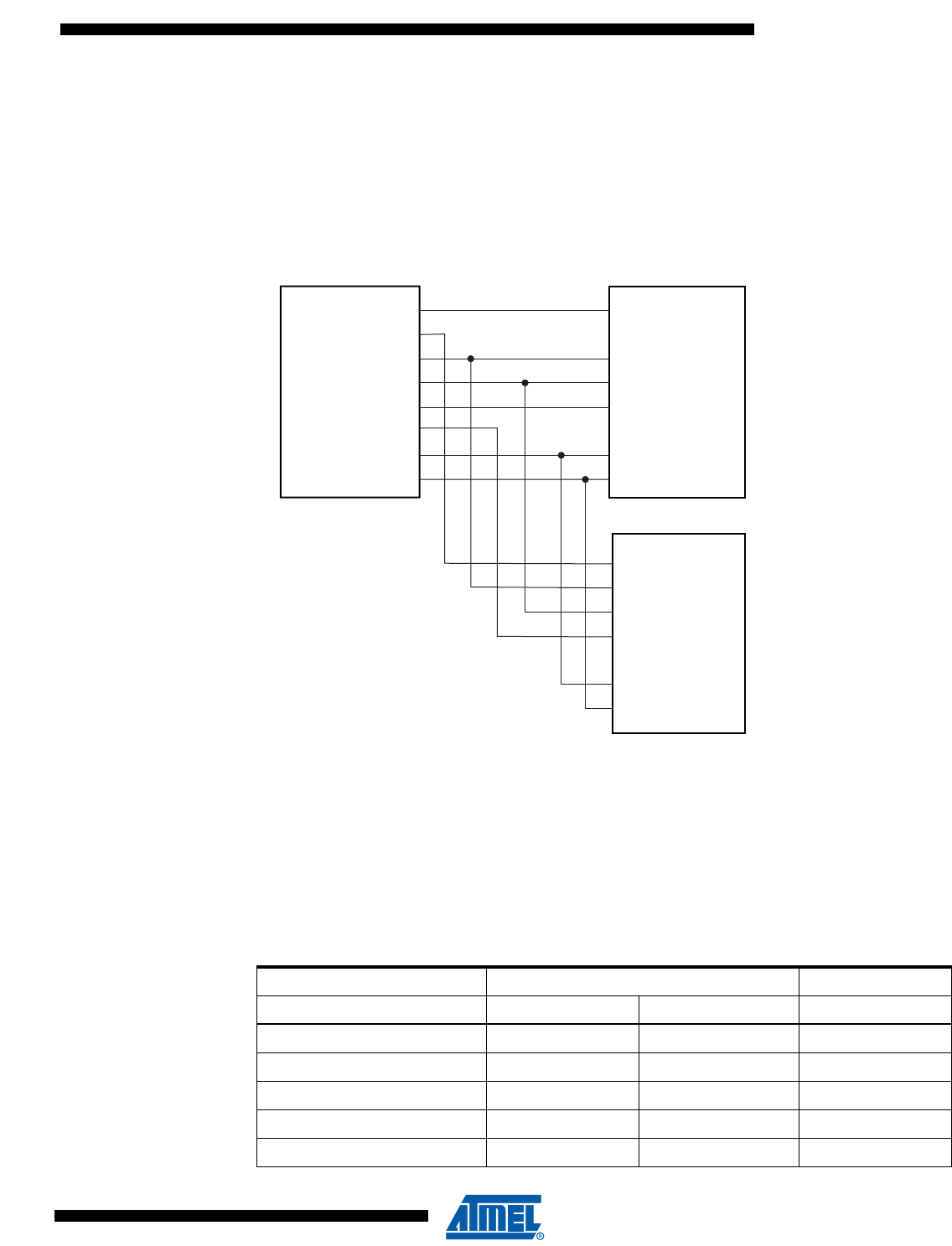
359
6430F–ATARM–21-Feb-12
SAM3U Series
359
6430F–ATARM–21-Feb-12
SAM3U Series
25.9.2.2 Byte Select Access
In this mode, read/write operations can be enabled/disabled at byte level. One byte-select line
per byte of the data bus is provided. One NRD and one NWE signal control read and write.
• For 16-bit devices: the SMC provides NBS0 and NBS1 selection signals for respectively
byte0 (lower byte) and byte1 (upper byte) of a 16-bit bus.
Byte Select Access is used to connect one 16-bit device.
Figure 25-6. Connection of 2 x 8-bit Devices on a 16-bit Bus: Byte Write Option
25.9.2.3 Signal Multiplexing
Depending on the byte access type (BAT), only the write signals or the byte select signals are
used. To save IOs at the external bus interface, control signals at the SMC interface are multi-
plexed. Table 25-5 shows signal multiplexing depending on the data bus width and the byte
access type.
For 16-bit devices, bit A0 of address is unused. When Byte Select Option is selected, NWR1 is
unused. When Byte Write option is selected, NBS0 is unused.
SMC A1
NWR0
NRD
NCS[3]
Write Enable
Read Enable
Memory Enable
NWR1
Write Enable
Read Enable
Memory Enable
D[7:0] D[7:0]
D[15:8]
D[15:8]
A[24:2]
A[23:1]
A[23:1]
A[0]
A[0]
Table 25-5. SMC Multiplexed Signal Translation
Signal Name 16-bit Bus 8-bit Bus
Device Type 1x16-bit 2 x 8-bit 1 x 8-bit
Byte Access Type (BAT) Byte Select Byte Write
NBS0_A0 NBS0 A0
NWE_NWR0 NWE NWR0 NWE
NBS1_NWR1 NBS1 NWR1
A1 A1 A1 A1
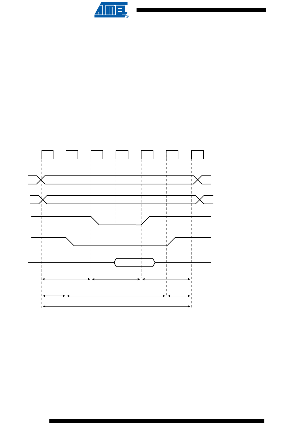
360
6430F–ATARM–21-Feb-12
SAM3U Series
360
6430F–ATARM–21-Feb-12
SAM3U Series
25.10 Standard Read and Write Protocols
In the following sections, the byte access type is not considered. Byte select lines (NBS0 to
NBS1) always have the same timing as the A address bus. NWE represents either the NWE sig-
nal in byte select access type or one of the byte write lines (NWR0 to NWR1) in byte write
access type. NWR0 to NWR3 have the same timings and protocol as NWE. In the same way,
NCS represents one of the NCS[0..3] chip select lines.
25.10.1 Read Waveforms
The read cycle is shown on Figure 25-7.
The read cycle starts with the address setting on the memory address bus, i.e.:
{A[23:2], A1, A0} for 8-bit devices
{A[23:2], A1} for 16-bit devices
Figure 25-7. Standard Read Cycle
25.10.1.1 NRD Waveform
The NRD signal is characterized by a setup timing, a pulse width and a hold timing.
1. NRD_SETUP: the NRD setup time is defined as the setup of address before the NRD
falling edge.
2. NRD_PULSE: the NRD pulse length is the time between NRD falling edge and NRD
rising edge.
3. NRD_HOLD: the NRD hold time is defined as the hold time of address after the NRD
rising edge.
A[23:2]
NBS0,NBS1,
A0, A1
NCS
NRD_SETUP NRD_PULSE NRD_HOLD
MCK
NRD
D[15:0]
NCS_RD_SETUP NCS_RD_PULSE NCS_RD_HOLD
NRD_CYCLE

361
6430F–ATARM–21-Feb-12
SAM3U Series
361
6430F–ATARM–21-Feb-12
SAM3U Series
25.10.1.2 NCS Waveform
Similarly, the NCS signal can be divided into a setup time, pulse length and hold time:
1. NCS_RD_SETUP: the NCS setup time is defined as the setup time of address before
the NCS falling edge.
2. NCS_RD_PULSE: the NCS pulse length is the time between NCS falling edge and
NCS rising edge.
3. NCS_RD_HOLD: the NCS hold time is defined as the hold time of address after the
NCS rising edge.
25.10.1.3 Read Cycle
The NRD_CYCLE time is defined as the total duration of the read cycle, i.e., from the time where
address is set on the address bus to the point where address may change. The total read cycle
time is equal to:
NRD_CYCLE = NRD_SETUP + NRD_PULSE + NRD_HOLD
= NCS_RD_SETUP + NCS_RD_PULSE + NCS_RD_HOLD
All NRD and NCS timings are defined separately for each chip select as an integer number of
Master Clock cycles. To ensure that the NRD and NCS timings are coherent, the user must
define the total read cycle instead of the hold timing. NRD_CYCLE implicitly defines the NRD
hold time and NCS hold time as:
NRD_HOLD = NRD_CYCLE - NRD SETUP - NRD PULSE
NCS_RD_HOLD = NRD_CYCLE - NCS_RD_SETUP - NCS_RD_PULSE
25.10.2 Read Mode
As NCS and NRD waveforms are defined independently of one other, the SMC needs to know
when the read data is available on the data bus. The SMC does not compare NCS and NRD tim-
ings to know which signal rises first. The READ_MODE parameter in the SMC_MODE register
of the corresponding chip select indicates which signal of NRD and NCS controls the read
operation.
25.10.2.1 Read is Controlled by NRD (READ_MODE = 1):
Figure 25-8 shows the waveforms of a read operation of a typical asynchronous RAM. The read
data is available tPACC after the falling edge of NRD, and turns to ‘Z’ after the rising edge of NRD.
In this case, the READ_MODE must be set to 1 (read is controlled by NRD), to indicate that data
is available with the rising edge of NRD. The SMC samples the read data internally on the rising
edge of Master Clock that generates the rising edge of NRD, whatever the programmed wave-
form of NCS may be.
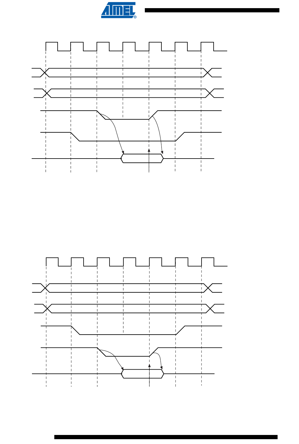
362
6430F–ATARM–21-Feb-12
SAM3U Series
362
6430F–ATARM–21-Feb-12
SAM3U Series
Figure 25-8. READ_MODE = 1: Data is sampled by SMC before the rising edge of NRD
25.10.2.2 Read is Controlled by NCS (READ_MODE = 0)
Figure 25-9 shows the typical read cycle. The read data is valid tPACC after the falling edge of the
NCS signal and remains valid until the rising edge of NCS. Data must be sampled when NCS is
raised. In that case, the READ_MODE must be set to 0 (read is controlled by NCS): the SMC
internally samples the data on the rising edge of Master Clock that generates the rising edge of
NCS, whatever the programmed waveform of NRD may be.
Figure 25-9. READ_MODE = 0: Data is sampled by SMC before the rising edge of NCS
Data Sampling
tPACC
MCK
A[23:2]
NBS0,NBS1,
A0, A1
NCS
NRD
D[15:0]
Data Sampling
tPACC
MCK
D[15:0]
A[23:2]
NBS0,NBS1,
A0, A1
NCS
NRD
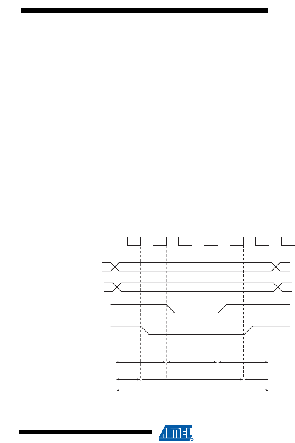
363
6430F–ATARM–21-Feb-12
SAM3U Series
363
6430F–ATARM–21-Feb-12
SAM3U Series
25.10.3 Write Waveforms
The write protocol is similar to the read protocol. It is depicted in Figure 25-10. The write cycle
starts with the address setting on the memory address bus.
25.10.3.1 NWE Waveforms
The NWE signal is characterized by a setup timing, a pulse width and a hold timing.
1. NWE_SETUP: the NWE setup time is defined as the setup of address and data before
the NWE falling edge.
2. NWE_PULSE: The NWE pulse length is the time between NWE falling edge and NWE
rising edge.
3. NWE_HOLD: The NWE hold time is defined as the hold time of address and data after
the NWE rising edge.
The NWE waveforms apply to all byte-write lines in Byte Write access mode: NWR0 to NWR3.
25.10.3.2 NCS Waveforms
The NCS signal waveforms in write operation are not the same as those applied in read opera-
tions, but are separately defined:
1. NCS_WR_SETUP: the NCS setup time is defined as the setup time of address before
the NCS falling edge.
2. NCS_WR_PULSE: the NCS pulse length is the time between NCS falling edge and
NCS rising edge.
3. NCS_WR_HOLD: the NCS hold time is defined as the hold time of address after the
NCS rising edge.
Figure 25-10. Write Cycle
A
[23:2]
NBS0, NBS1,
A0, A1
NCS
NWE_SETUP NWE_PULSE NWE_HOLD
MCK
NWE
NCS_WR_SETUP NCS_WR_PULSENCS_WR_HOLD
NWE_CYCLE
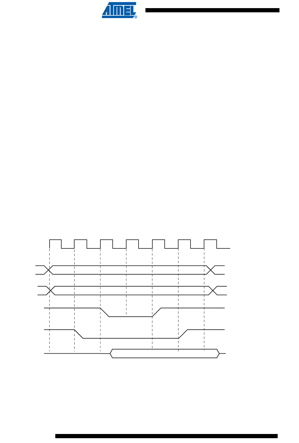
364
6430F–ATARM–21-Feb-12
SAM3U Series
364
6430F–ATARM–21-Feb-12
SAM3U Series
25.10.3.3 Write Cycle
The write cycle time is defined as the total duration of the write cycle, that is, from the time where
address is set on the address bus to the point where address may change. The total write cycle
time is equal to:
NWE_CYCLE = NWE_SETUP + NWE_PULSE + NWE_HOLD
= NCS_WR_SETUP + NCS_WR_PULSE + NCS_WR_HOLD
All NWE and NCS (write) timings are defined separately for each chip select as an integer num-
ber of Master Clock cycles. To ensure that the NWE and NCS timings are coherent, the user
must define the total write cycle instead of the hold timing. This implicitly defines the NWE hold
time and NCS (write) hold times as:
NWE_HOLD = NWE_CYCLE - NWE_SETUP - NWE_PULSE
NCS_WR_HOLD = NWE_CYCLE - NCS_WR_SETUP - NCS_WR_PULSE
25.10.4 Write Mode
The WRITE_MODE parameter in the SMC_MODE register of the corresponding chip select indi-
cates which signal controls the write operation.
25.10.4.1 Write is Controlled by NWE (WRITE_MODE = 1)
Figure 25-11 shows the waveforms of a write operation with WRITE_MODE set to 1. The data is
put on the bus during the pulse and hold steps of the NWE signal. The internal data buffers are
turned out after the NWE_SETUP time, and until the end of the write cycle, regardless of the
programmed waveform on NCS.
Figure 25-11. WRITE_MODE = 1. The write operation is controlled by NWE
25.10.4.2 Write is Controlled by NCS (WRITE_MODE = 0)
Figure 25-12 shows the waveforms of a write operation with WRITE_MODE set to 0. The data is
put on the bus during the pulse and hold steps of the NCS signal. The internal data buffers are
turned out after the NCS_WR_SETUP time, and until the end of the write cycle, regardless of
the programmed waveform on NWE.
MCK
D[15:0]
NCS
A
[23:2]
NBS0, NBS1,
A0, A1
NWE,
NWR0, NWR1
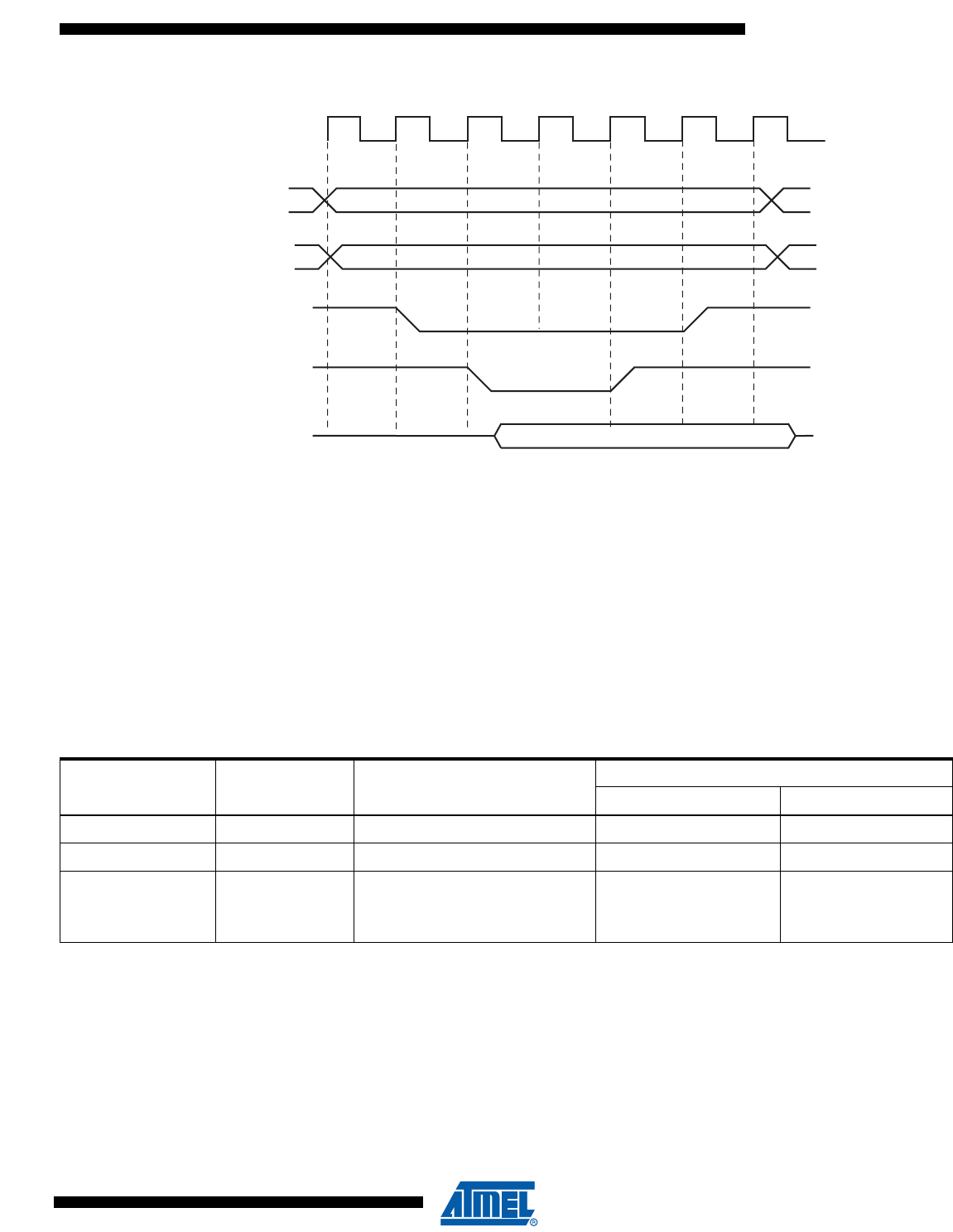
365
6430F–ATARM–21-Feb-12
SAM3U Series
365
6430F–ATARM–21-Feb-12
SAM3U Series
Figure 25-12. WRITE_MODE = 0. The write operation is controlled by NCS
25.10.5 Coding Timing Parameters
All timing parameters are defined for one chip select and are grouped together in one
SMC_REGISTER according to their type.
• The SMC_SETUP register groups the definition of all setup parameters: NRD_SETUP,
NCS_RD_SETUP, NWE_SETUP, NCS_WR_SETUP
• The SMC_PULSE register groups the definition of all pulse parameters: NRD_PULSE,
NCS_RD_PULSE, NWE_PULSE, NCS_WR_PULSE
• The SMC_CYCLE register groups the definition of all cycle parameters: NRD_CYCLE,
NWE_CYCLE
Table 25-6 shows how the timing parameters are coded and their permitted range.
MCK
D[15:0]
NCS
NWE,
NWR0, NWR1
A
[23:2]
NBS0, NBS1,
A0, A1
Table 25-6. Coding and Range of Timing Parameters
Coded Value Number of Bits Effective Value
Permitted Range
Coded Value Effective Value
setup [5:0] 6 128 x setup[5] + setup[4:0] 0 ≤ setup ≤ 31 128..(128+31)
pulse [6:0] 7 256 x pulse[6] + pulse[5:0] 0 ≤ pulse ≤63 256..(256+63)
cycle [8:0] 9 256 x cycle[8:7] + cycle[6:0] 0 ≤ cycle ≤ 127
256.. (256+127)
512.. (512+127)
768..(768+127)

366
6430F–ATARM–21-Feb-12
SAM3U Series
366
6430F–ATARM–21-Feb-12
SAM3U Series
25.10.6 Reset Values of Timing Parameters
Table 25-7 gives the default value of timing parameters at reset.
25.10.7 Usage Restriction
The SMC does not check the validity of the user-programmed parameters. If the sum of SETUP
and PULSE parameters is larger than the corresponding CYCLE parameter, this leads to unpre-
dictable behavior of the SMC.
25.10.7.1 For Read Operations
Null but positive setup and hold of address and NRD and/or NCS can not be guaranteed at the
memory interface because of the propagation delay of theses signals through external logic and
pads. If positive setup and hold values must be verified, then it is strictly recommended to pro-
gram non-null values so as to cover possible skews between address, NCS and NRD signals.
25.10.7.2 For Write Operations
If a null hold value is programmed on NWE, the SMC can guarantee a positive hold of address,
byte select lines, and NCS signal after the rising edge of NWE. This is true for WRITE_MODE =
1 only. See “Early Read Wait State” on page 368.
For read and write operations: a null value for pulse parameters is forbidden and may lead to
unpredictable behavior.
In read and write cycles, the setup and hold time parameters are defined in reference to the
address bus. For external devices that require setup and hold time between NCS and NRD sig-
nals (read), or between NCS and NWE signals (write), these setup and hold times must be
converted into setup and hold times in reference to the address bus.
25.11 Scrambling/Unscrambling Function
The external data bus D[15:0] can be scrambled in order to prevent intellectual property data
located in off-chip memories from being easily recovered by analyzing data at the package pin
level of either microcontroller or memory device.
The scrambling and unscrambling are performed on-the-fly without additional wait states.
The scrambling method depends on two user-configurable key registers, SMC_KEY1 and
SMC_KEY2. These key registers are only accessible in write mode.
The key must be securely stored in a reliable non-volatile memory in order to recover data from
the off-chip memory. Any data scrambled with a given key cannot be recovered if the key is lost.
The scrambling/unscrambling function can be enabled or disabled by programming the
SMC_OCMS register.
Table 25-7. Reset Values of Timing Parameters
Register Reset Value Description
SMC_SETUP 0x01010101 All setup timings are set to 1
SMC_PULSE 0x01010101 All pulse timings are set to 1
SMC_CYCLE 0x00030003 The read and write operation last 3 Master Clock cycles
and provide one hold cycle
WRITE_MODE 1 Write is controlled with NWE
READ_MODE 1 Read is controlled with NRD
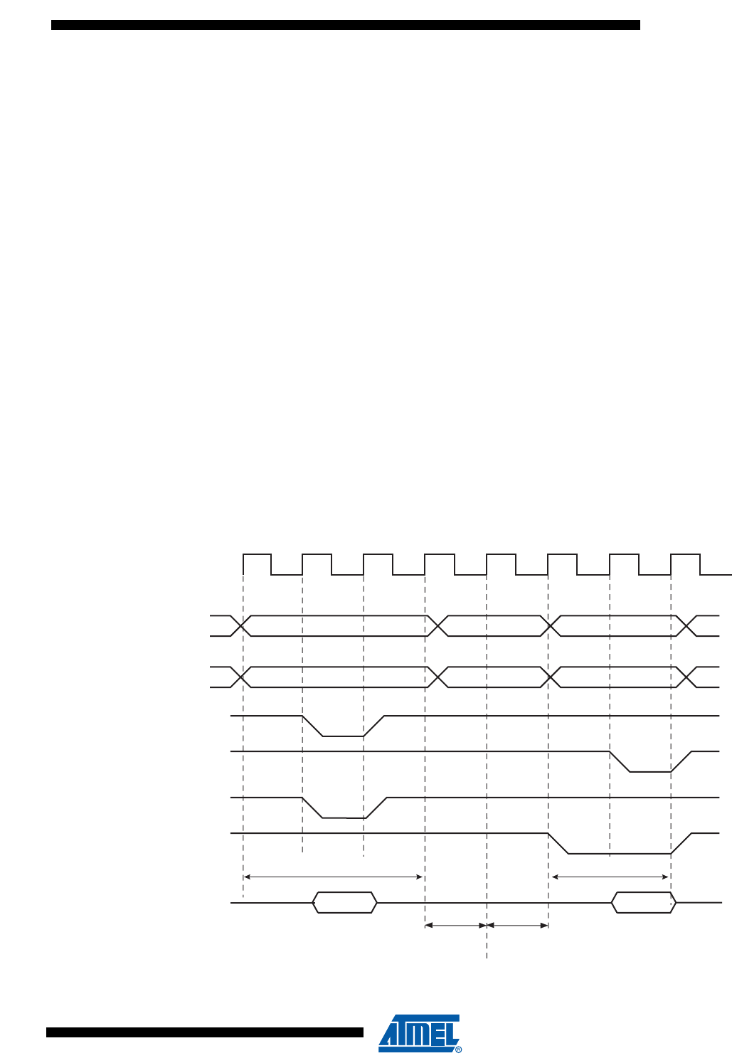
367
6430F–ATARM–21-Feb-12
SAM3U Series
367
6430F–ATARM–21-Feb-12
SAM3U Series
One bit is dedicated to enable/disable NAND Flash scrambling and one bit is dedicated
enable/disable scrambling the off chip SRAM. When at least one external SRAM is scrambled,
the SMSC field must be set in the SMC_OCMS register.
When multiple chip selects (external SRAM) are handled, it is possible to configure the scram-
bling function per chip select using the OCMS field in the SMC_TIMINGS registers.
To scramble the NAND Flash contents, the SRSE field must be set in the SMC_OCMS register.
When NAND Flash memory content is scrambled, the on-chip SRAM page buffer associated for
the transfer is also scrambled.
25.12 Automatic Wait States
Under certain circumstances, the SMC automatically inserts idle cycles between accesses to
avoid bus contention or operation conflict.
25.12.1 Chip Select Wait States
The SMC always inserts an idle cycle between 2 transfers on separate chip selects. This idle
cycle ensures that there is no bus contention between the de-activation of one device and the
activation of the next one.
During chip select wait state, all control lines are turned inactive: NBS0 to NBS1, NWR0 to
NWR1, NCS[0..3], and NRD lines. They are all set to 1.
Figure 25-13 illustrates a chip select wait state between access on Chip Select 0 and Chip
Select 2.
Figure 25-13. Chip Select Wait State between a Read Access on NCS0 and a Write Access on NCS2
A[23:2]
NBS0, NBS1,
A0,A1
NCS0
NRD_CYCLE
Chip Select
Wait State
NWE_CYCLE
MCK
NCS2
NRD
NWE
D[15:0]
Read to Write
Wait State
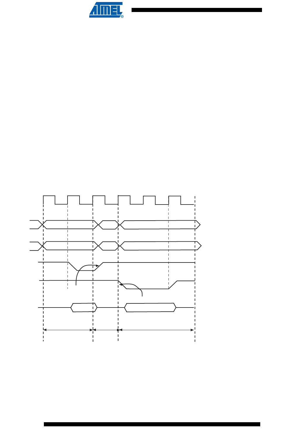
368
6430F–ATARM–21-Feb-12
SAM3U Series
368
6430F–ATARM–21-Feb-12
SAM3U Series
25.12.2 Early Read Wait State
In some cases, the SMC inserts a wait state cycle between a write access and a read access to
allow time for the write cycle to end before the subsequent read cycle begins. This wait state is
not generated in addition to a chip select wait state. The early read cycle thus only occurs
between a write and read access to the same memory device (same chip select).
An early read wait state is automatically inserted if at least one of the following conditions is
valid:
• if the write controlling signal has no hold time and the read controlling signal has no setup
time (Figure 25-14).
• in NCS write controlled mode (WRITE_MODE = 0), if there is no hold timing on the NCS
signal and the NCS_RD_SETUP parameter is set to 0, regardless of the read mode (Figure
25-15). The write operation must end with a NCS rising edge. Without an Early Read Wait
State, the write operation could not complete properly.
• in NWE controlled mode (WRITE_MODE = 1) and if there is no hold timing (NWE_HOLD =
0), the feedback of the write control signal is used to control address, data, chip select and
byte select lines. If the external write control signal is not inactivated as expected due to load
capacitances, an Early Read Wait State is inserted and address, data and control signals are
maintained one more cycle. See Figure 25-16.
Figure 25-14. Early Read Wait State: Write with No Hold Followed by Read with No Setup
write cycle Early Read
wait state
MCK
NRD
NWE
read cycle
no setup
no hold
D[15:0]
NBS0, NBS1,
A0, A1
A[23:2]
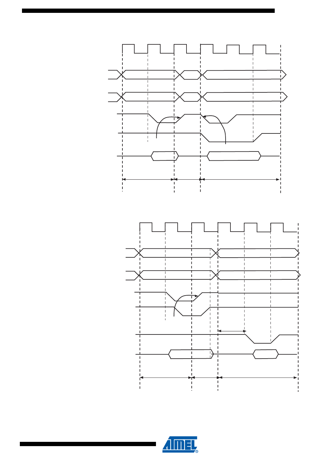
369
6430F–ATARM–21-Feb-12
SAM3U Series
369
6430F–ATARM–21-Feb-12
SAM3U Series
Figure 25-15. Early Read Wait State: NCS Controlled Write with No Hold Followed by a Read with No NCS Setup
Figure 25-16. Early Read Wait State: NWE-controlled Write with No Hold Followed by a Read with one Set-up Cycle
write cycle
(WRITE_MODE = 0)
Early Read
wait state
MCK
NRD
NCS
read cycle
(READ_MODE = 0 or READ_MODE = 1)
no setup
no hold
D[15:0]
NBS0, NBS1,
A0,A1
A[23:2]
A
[23:2]
NBS0, NBS1,
A0, A1
write cycle
(WRITE_MODE = 1)
Early Read
wait state
MCK
NRD
internal write controlling signal
external write controlling signal
(NWE)
D[15:0]
read cycle
(READ_MODE = 0 or READ_MODE = 1)
no hold read setup = 1

370
6430F–ATARM–21-Feb-12
SAM3U Series
370
6430F–ATARM–21-Feb-12
SAM3U Series
25.12.3 Reload User Configuration Wait State
The user may change any of the configuration parameters by writing the SMC user interface.
When detecting that a new user configuration has been written in the user interface, the SMC
inserts a wait state before starting the next access. The so called “Reload User Configuration
Wait State” is used by the SMC to load the new set of parameters to apply to next accesses.
The Reload Configuration Wait State is not applied in addition to the Chip Select Wait State. If
accesses before and after re-programming the user interface are made to different devices
(Chip Selects), then one single Chip Select Wait State is applied.
On the other hand, if accesses before and after writing the user interface are made to the same
device, a Reload Configuration Wait State is inserted, even if the change does not concern the
current Chip Select.
25.12.3.1 User Procedure
To insert a Reload Configuration Wait State, the SMC detects a write access to any
SMC_MODE register of the user interface. If only the timing registers are modified
(SMC_SETUP, SMC_PULSE, SMC_CYCLE registers) in the user interface, the user must vali-
date the modification by writing the SMC_MODE register, even if no change was made on the
mode parameters.
25.12.3.2 Slow Clock Mode Transition
A Reload Configuration Wait State is also inserted when the Slow Clock Mode is entered or
exited, after the end of the current transfer (see “Slow Clock Mode” on page 381).
25.12.4 Read to Write Wait State
Due to an internal mechanism, a wait cycle is always inserted between consecutive read and
write SMC accesses.
This wait cycle is referred to as a read to write wait state in this document.
This wait cycle is applied in addition to chip select and reload user configuration wait states
when they are to be inserted. See Figure 25-13 on page 367.
25.13 Data Float Wait States
Some memory devices are slow to release the external bus. For such devices, it is necessary to
add wait states (data float wait states) after a read access:
• before starting a read access to a different external memory,
• before starting a write access to the same device or to a different external one.
The Data Float Output Time (tDF) for each external memory device is programmed in the
TDF_CYCLES field of the SMC_MODE register for the corresponding chip select. The value of
TDF_CYCLES indicates the number of data float wait cycles (between 0 and 15) before the
external device releases the bus, and represents the time allowed for the data output to go to
high impedance after the memory is disabled.
Data float wait states do not delay internal memory accesses. Hence, a single access to an
external memory with long tDF will not slow down the execution of a program from internal
memory.
The data float wait states management depends on the READ_MODE and the TDF_MODE
fields of the SMC_MODE register for the corresponding chip select.
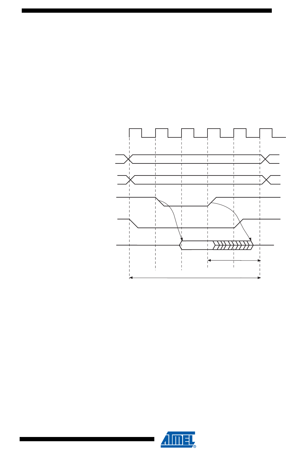
371
6430F–ATARM–21-Feb-12
SAM3U Series
371
6430F–ATARM–21-Feb-12
SAM3U Series
25.13.1 READ_MODE
Setting READ_MODE to 1 indicates to the SMC that the NRD signal is responsible for turning off
the tri-state buffers of the external memory device. The Data Float Period then begins after the
rising edge of the NRD signal and lasts TDF_CYCLES MCK cycles.
When the read operation is controlled by the NCS signal (READ_MODE = 0), the TDF field gives
the number of MCK cycles during which the data bus remains busy after the rising edge of NCS.
Figure 25-17 illustrates the Data Float Period in NRD-controlled mode (READ_MODE =1),
assuming a data float period of 2 cycles (TDF_CYCLES = 2). Figure 25-18 shows the read oper-
ation when controlled by NCS (READ_MODE = 0) and the TDF_CYCLES parameter equals 3.
Figure 25-17. TDF Period in NRD Controlled Read Access (TDF = 2)
NBS0, NBS1,
A0, A1
NCS
NRD controlled read operation
tpacc
MCK
NRD
D[15:0]
TDF = 2 clock cycles
A[23:2]
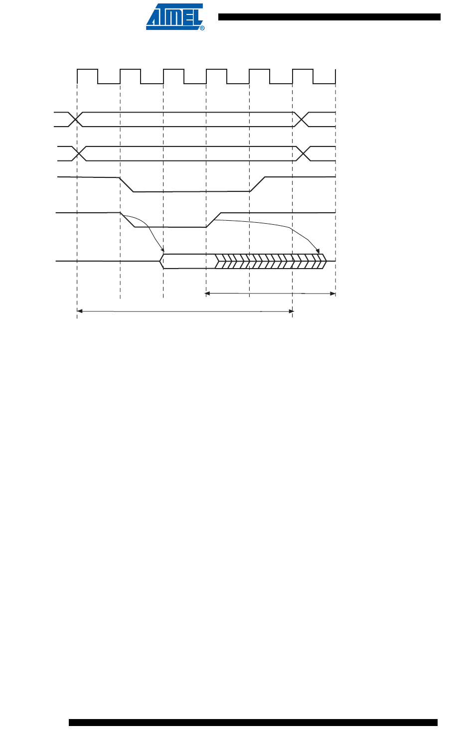
372
6430F–ATARM–21-Feb-12
SAM3U Series
372
6430F–ATARM–21-Feb-12
SAM3U Series
Figure 25-18. TDF Period in NCS Controlled Read Operation (TDF = 3)
25.13.2 TDF Optimization Enabled (TDF_MODE = 1)
When the TDF_MODE of the SMC_MODE register is set to 1 (TDF optimization is enabled), the
SMC takes advantage of the setup period of the next access to optimize the number of wait
states cycle to insert.
Figure 25-19 shows a read access controlled by NRD, followed by a write access controlled by
NWE, on Chip Select 0. Chip Select 0 has been programmed with:
NRD_HOLD = 4; READ_MODE = 1 (NRD controlled)
NWE_SETUP = 3; WRITE_MODE = 1 (NWE controlled)
TDF_CYCLES = 6; TDF_MODE = 1 (optimization enabled).
NCS
TDF = 3 clock cycles
tpacc
MCK
D[15:0]
NCS controlled read operation
A[23:2]
NBS0, NBS1,
A0,A1
NRD
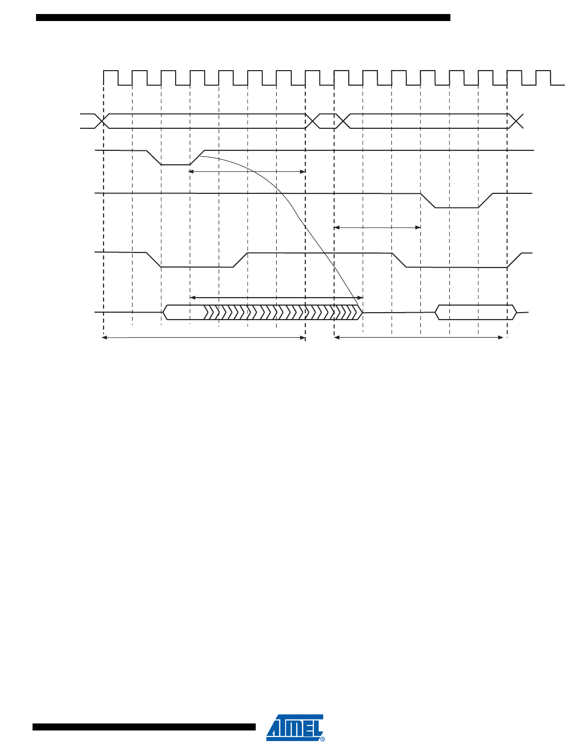
373
6430F–ATARM–21-Feb-12
SAM3U Series
373
6430F–ATARM–21-Feb-12
SAM3U Series
Figure 25-19. TDF Optimization: No TDF wait states are inserted if the TDF period is over when the next access begins
25.13.3 TDF Optimization Disabled (TDF_MODE = 0)
When optimization is disabled, tdf wait states are inserted at the end of the read transfer, so that
the data float period ends when the second access begins. If the hold period of the read1 con-
trolling signal overlaps the data float period, no additional tdf wait states will be inserted.
Figure 25-20, Figure 25-21 and Figure 25-22 illustrate the cases:
• read access followed by a read access on another chip select,
• read access followed by a write access on another chip select,
• read access followed by a write access on the same chip select,
with no TDF optimization.
A
[23:2]
NCS0
MCK
NRD
NWE
D[15:0]
Read to Write
Wait State
TDF_CYCLES = 6
read access on NCS0 (NRD controlled)
NRD_HOLD= 4
NWE_SETUP= 3
write access on NCS0 (NWE controlled)
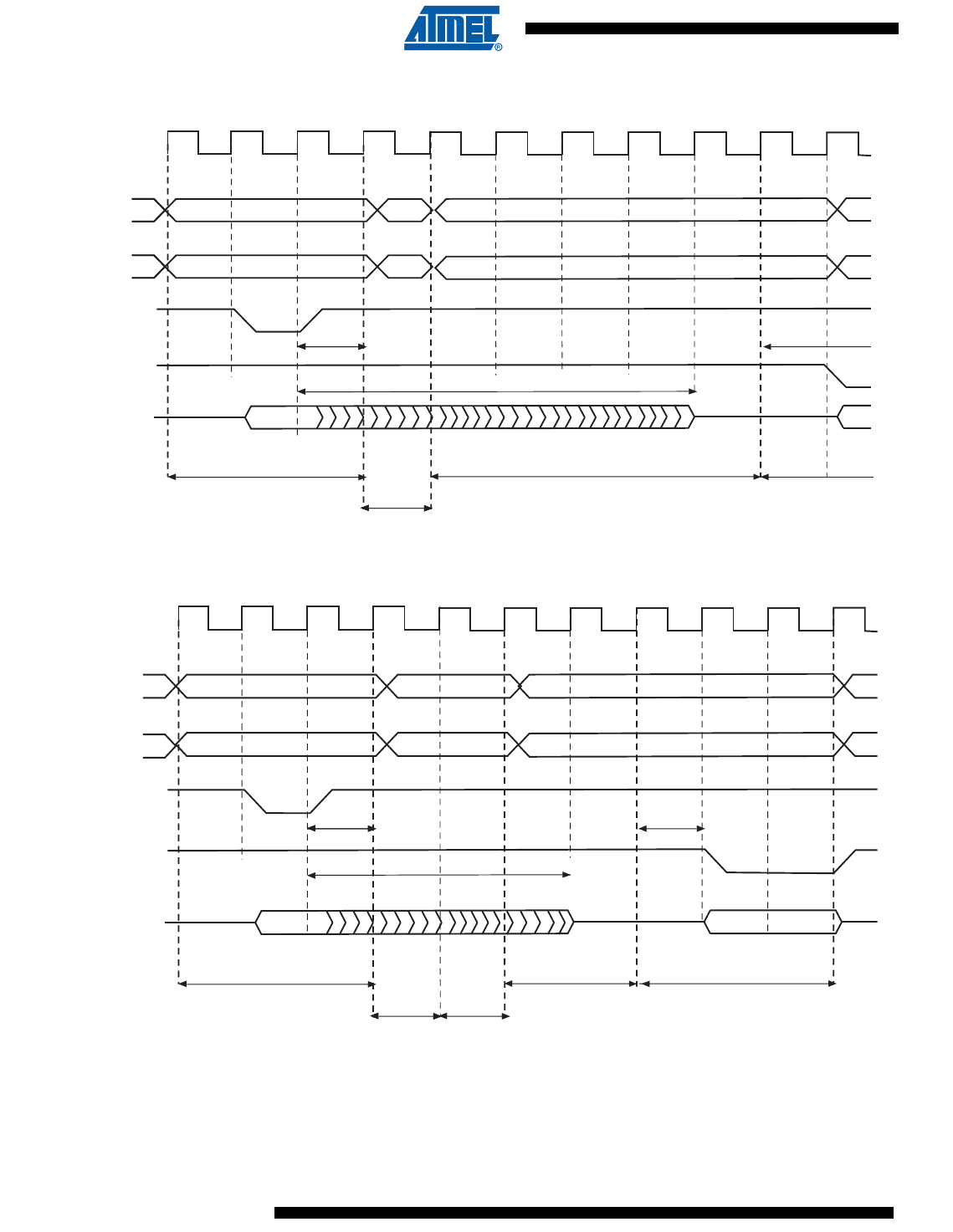
374
6430F–ATARM–21-Feb-12
SAM3U Series
374
6430F–ATARM–21-Feb-12
SAM3U Series
Figure 25-20. TDF Optimization Disabled (TDF Mode = 0). TDF wait states between 2 read accesses on different chip
selects
Figure 25-21. TDF Mode = 0: TDF wait states between a read and a write access on different chip selects
TDF_CYCLES = 6
TDF_CYCLES = 6 TDF_MODE = 0
(optimization disabled)
A[
23:2]
read1 cycle
Chip Select Wait State
MCK
read1 controlling signal
(NRD)
read2 controlling signal
(NRD)
D[15:0]
read1 hold = 1
read 2 cycle
read2 setup = 1
5 TDF WAIT STATES
NBS0, NBS1,
A0, A1
TDF_CYCLES = 4
TDF_CYCLES = 4 TDF_MODE = 0
(optimization disabled)
A
[23:2]
read1 cycle
Chip Select
Wait State
Read to Write
Wait State
MCK
read1 controlling signal
(NRD)
write2 controlling signal
(NWE)
D[15:0]
read1 hold = 1
write2 cycle
write2 setup = 1
2 TDF WAIT STATES
NBS0, NBS1,
A0, A1
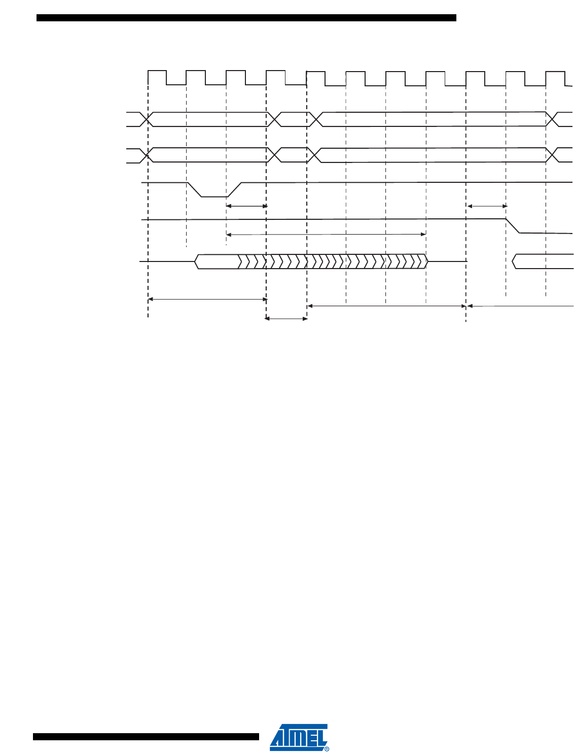
375
6430F–ATARM–21-Feb-12
SAM3U Series
375
6430F–ATARM–21-Feb-12
SAM3U Series
Figure 25-22. TDF Mode = 0: TDF wait states between read and write accesses on the same chip select
25.14 External Wait
Any access can be extended by an external device using the NWAIT input signal of the SMC.
The EXNW_MODE field of the SMC_MODE register on the corresponding chip select must be
set to either to “10” (frozen mode) or “11” (ready mode). When the EXNW_MODE is set to “00”
(disabled), the NWAIT signal is simply ignored on the corresponding chip select. The NWAIT
signal delays the read or write operation in regards to the read or write controlling signal,
depending on the read and write modes of the corresponding chip select.
25.14.1 Restriction
When one of the EXNW_MODE is enabled, it is mandatory to program at least one hold cycle
for the read/write controlling signal. For that reason, the NWAIT signal cannot be used in Slow
Clock Mode (“Slow Clock Mode” on page 381).
The NWAIT signal is assumed to be a response of the external device to the read/write request
of the SMC. Then NWAIT is examined by the SMC only in the pulse state of the read or write
controlling signal. The assertion of the NWAIT signal outside the expected period has no impact
on SMC behavior.
25.14.2 Frozen Mode
When the external device asserts the NWAIT signal (active low), and after internal synchroniza-
tion of this signal, the SMC state is frozen, i.e., SMC internal counters are frozen, and all control
signals remain unchanged. When the resynchronized NWAIT signal is deasserted, the SMC
completes the access, resuming the access from the point where it was stopped. See Figure 25-
23. This mode must be selected when the external device uses the NWAIT signal to delay the
access and to freeze the SMC.
TDF_CYCLES = 5
TDF_CYCLES = 5
TDF_MODE = 0
(optimization disabled)
A
[23:2]
read1 cycle
Read to Write
Wait State
MCK
read1 controlling signal
(NRD)
write2 controlling signal
(NWE)
D[15:0]
read1 hold = 1
write2 cycle
write2 setup = 1
4 TDF WAIT STATES
NBS0, NBS1,
A0, A1
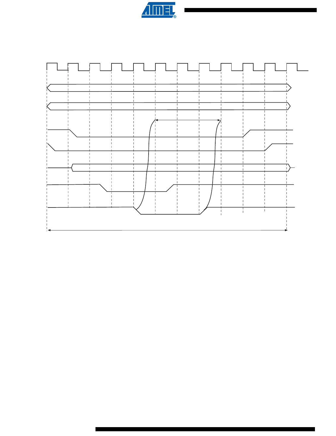
376
6430F–ATARM–21-Feb-12
SAM3U Series
376
6430F–ATARM–21-Feb-12
SAM3U Series
The assertion of the NWAIT signal outside the expected period is ignored as illustrated in Figure
25-24.
Figure 25-23. Write Access with NWAIT Assertion in Frozen Mode (EXNW_MODE = 10)
EXNW_MODE = 10 (Frozen)
WRITE_MODE = 1 (NWE_controlled)
NWE_PULSE = 5
NCS_WR_PULSE = 7
A
[23:2]
MCK
NWE
NCS
4321 1101
456 322221 0
Write cycle
D[15:0]
NWAIT
FROZEN STATE
NBS0, NBS1,
A0,A1
internally synchronized
NWAIT signal

377
6430F–ATARM–21-Feb-12
SAM3U Series
377
6430F–ATARM–21-Feb-12
SAM3U Series
Figure 25-24. Read Access with NWAIT Assertion in Frozen Mode (EXNW_MODE = 10)
EXNW_MODE = 10 (Frozen)
READ_MODE = 0 (NCS_controlled)
NRD_PULSE = 2, NRD_HOLD = 6
NCS_RD_PULSE =5, NCS_RD_HOLD =3
A
[23:2]
MCK
NCS
NRD
10
43
43
2
555
22 0
210
210
1
Read cycle
Assertion is ignored
NWAIT
internally synchronized
NWAIT signal
FROZEN STATE
NBS0, NBS1,
A0,A1
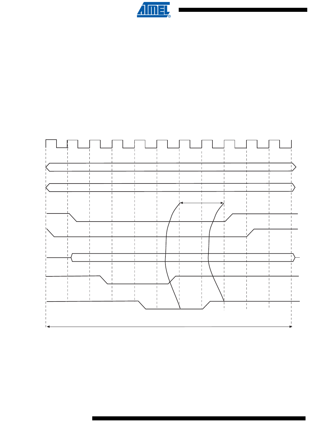
378
6430F–ATARM–21-Feb-12
SAM3U Series
378
6430F–ATARM–21-Feb-12
SAM3U Series
25.14.3 Ready Mode
In Ready mode (EXNW_MODE = 11), the SMC behaves differently. Normally, the SMC begins
the access by down counting the setup and pulse counters of the read/write controlling signal. In
the last cycle of the pulse phase, the resynchronized NWAIT signal is examined.
If asserted, the SMC suspends the access as shown in Figure 25-25 and Figure 25-26. After
deassertion, the access is completed: the hold step of the access is performed.
This mode must be selected when the external device uses deassertion of the NWAIT signal to
indicate its ability to complete the read or write operation.
If the NWAIT signal is deasserted before the end of the pulse, or asserted after the end of the
pulse of the controlling read/write signal, it has no impact on the access length as shown in Fig-
ure 25-26.
Figure 25-25. NWAIT Assertion in Write Access: Ready Mode (EXNW_MODE = 11)
EXNW_MODE = 11 (Ready mode)
WRITE_MODE = 1 (NWE_controlled)
NWE_PULSE = 5
NCS_WR_PULSE = 7
A
[23:2]
MCK
NWE
NCS
4321 000
456 321110
Write cycle
D[15:0]
NWAIT
internally synchronized
NWAIT signal
Wait STATE
NBS0, NBS1,
A0,A1
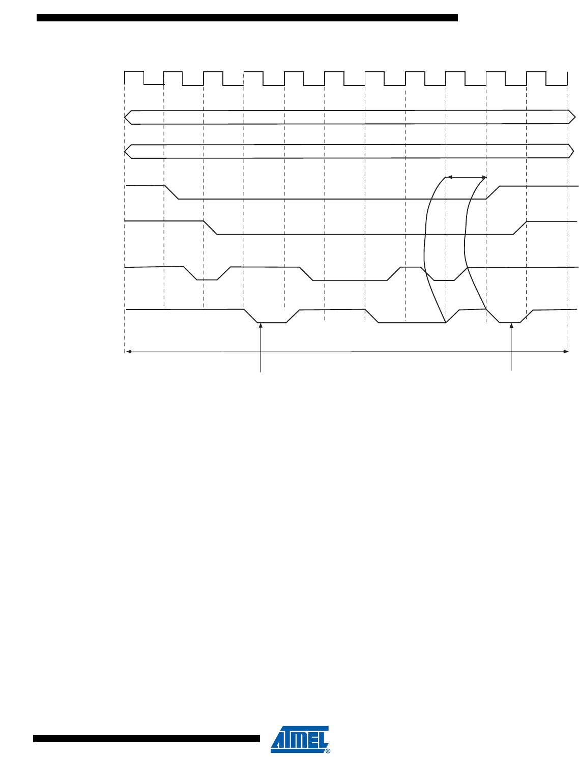
379
6430F–ATARM–21-Feb-12
SAM3U Series
379
6430F–ATARM–21-Feb-12
SAM3U Series
Figure 25-26. NWAIT Assertion in Read Access: Ready Mode (EXNW_MODE = 11)
EXNW_MODE = 11(Ready mode)
READ_MODE = 0 (NCS_controlled)
NRD_PULSE = 7
NCS_RD_PULSE =7
A[23:2]
MCK
NCS
NRD
456 3200
0
1
456 3211
Read cycle
Assertion is ignored
NWAIT
internally synchronized
NWAIT signal
Wait STATE
Assertion is ignored
NBS0, NBS1,
A0,A1
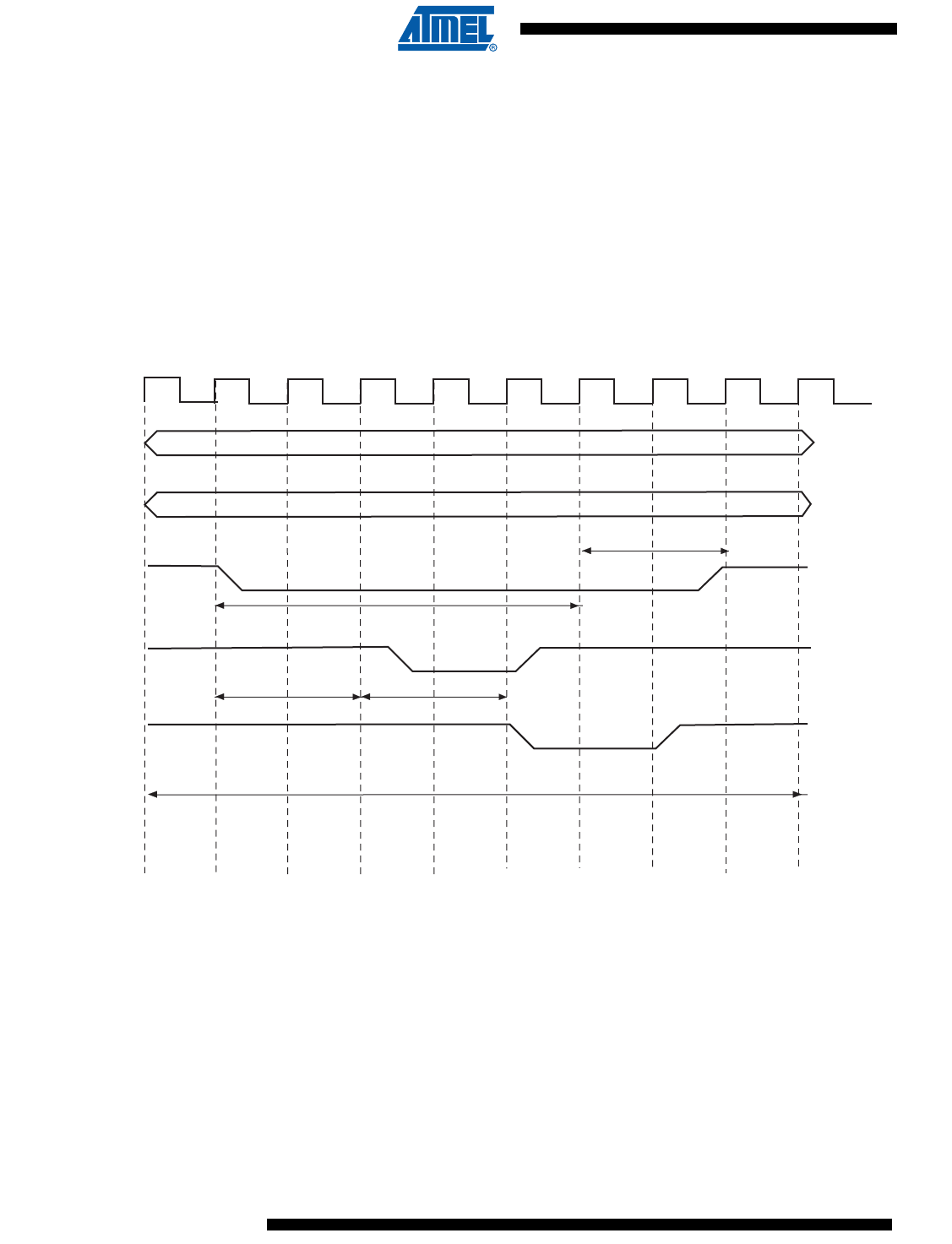
380
6430F–ATARM–21-Feb-12
SAM3U Series
380
6430F–ATARM–21-Feb-12
SAM3U Series
25.14.4 NWAIT Latency and Read/Write Timings
There may be a latency between the assertion of the read/write controlling signal and the asser-
tion of the NWAIT signal by the device. The programmed pulse length of the read/write
controlling signal must be at least equal to this latency plus the 2 cycles of resynchronization + 1
cycle. Otherwise, the SMC may enter the hold state of the access without detecting the NWAIT
signal assertion. This is true in frozen mode as well as in ready mode. This is illustrated on Fig-
ure 25-27.
When EXNW_MODE is enabled (ready or frozen), the user must program a pulse length of the
read and write controlling signal of at least:
minimal pulse length = NWAIT latency + 2 resynchronization cycles + 1 cycle
Figure 25-27. NWAIT Latency
EXNW_MODE = 10 or 11
READ_MODE = 1 (NRD_controlled)
NRD_PULSE = 5
A
[23:2]
MCK
NRD
43210 00
Read cycle
minimal pulse length
NWAIT latency
NWAIT
intenally synchronized
NWAIT signal
WAIT STATE
2 cycle resynchronization
NBS0, NBS1,
A0,A1
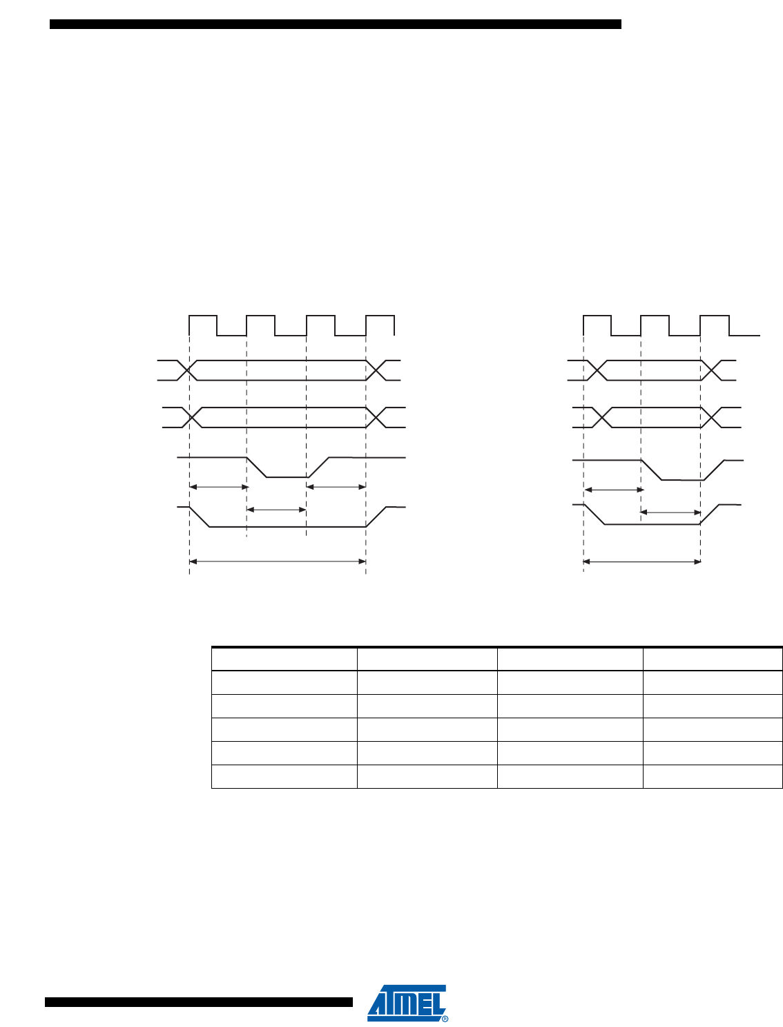
381
6430F–ATARM–21-Feb-12
SAM3U Series
381
6430F–ATARM–21-Feb-12
SAM3U Series
25.15 Slow Clock Mode
The SMC is able to automatically apply a set of “slow clock mode” read/write waveforms when
an internal signal driven by the Power Management Controller is asserted because MCK has
been turned to a very slow clock rate (typically 32 kHz clock rate). In this mode, the user-pro-
grammed waveforms are ignored and the slow clock mode waveforms are applied. This mode is
provided so as to avoid reprogramming the User Interface with appropriate waveforms at very
slow clock rate. When activated, the slow mode is active on all chip selects.
25.15.1 Slow Clock Mode Waveforms
Figure 25-28 illustrates the read and write operations in slow clock mode. They are valid on all
chip selects. Table 25-8 indicates the value of read and write parameters in slow clock mode.
Figure 25-28. Read/Write Cycles in Slow Clock Mode
A[
23:2]
NCS
1
MCK
NWE 1
1
NWE_CYCLE = 3
A
[23:2]
MCK
NRD
NRD_CYCLE = 2
1
1
NCS
SLOW CLOCK MODE WRITE SLOW CLOCK MODE READ
NBS0, NBS1,
A0,A1
NBS0, NBS1,
A0,A1
Table 25-8. Read and Write Timing Parameters in Slow Clock Mode
Read Parameters Duration (cycles) Write Parameters Duration (cycles)
NRD_SETUP 1 NWE_SETUP 1
NRD_PULSE 1 NWE_PULSE 1
NCS_RD_SETUP 0 NCS_WR_SETUP 0
NCS_RD_PULSE 2 NCS_WR_PULSE 3
NRD_CYCLE 2 NWE_CYCLE 3
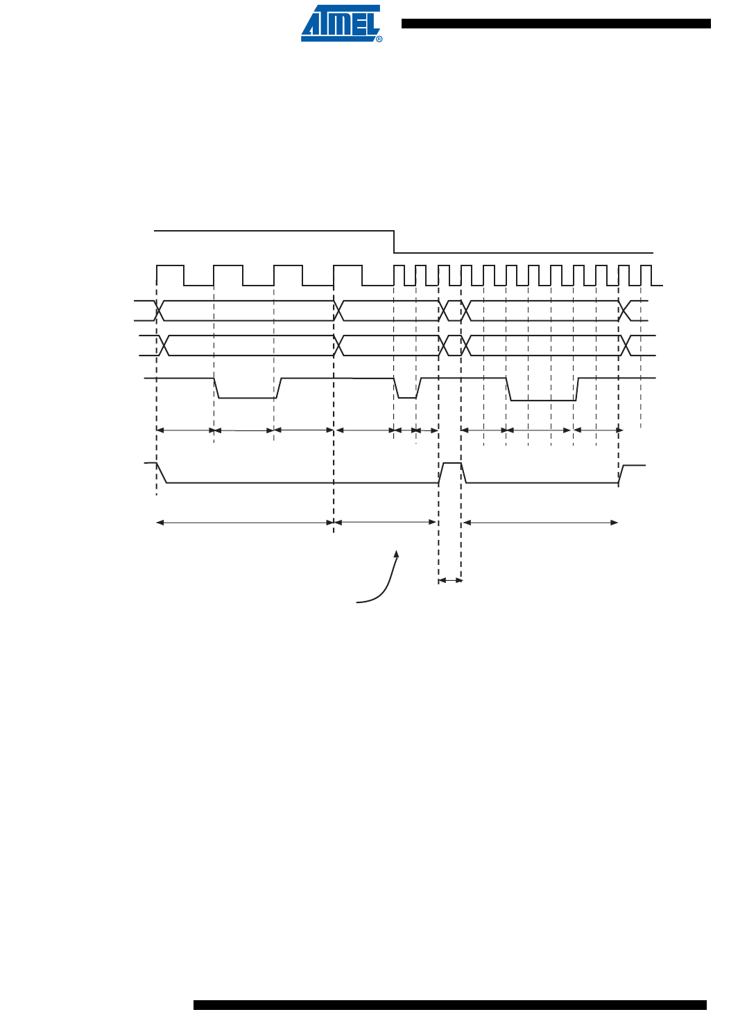
382
6430F–ATARM–21-Feb-12
SAM3U Series
382
6430F–ATARM–21-Feb-12
SAM3U Series
25.15.2 Switching from (to) Slow Clock Mode to (from) Normal Mode
When switching from slow clock mode to normal mode, the current slow clock mode transfer is
completed at high clock rate, with the set of slow clock mode parameters. See Figure 25-29. The
external device may not be fast enough to support such timings.
Figure 25-30 illustrates the recommended procedure to properly switch from one mode to the
other.
Figure 25-29. Clock Rate Transition Occurs while the SMC is Performing a Write Operation
A
[23:2]
NCS
1
MCK
NWE
1
1
NWE_CYCLE = 3
SLOW CLOCK MODE WRITE
Slow Clock Mode
internal signal from PMC
111 2 32
NWE_CYCLE = 7
NORMAL MODE WRITE
Slow clock mode transition is detected:
Reload Configuration Wait State
This write cycle finishes with the slow clock mode set
of parameters after the clock rate transition
SLOW CLOCK MODE WRITE
NBS0, NBS1,
A0, A1
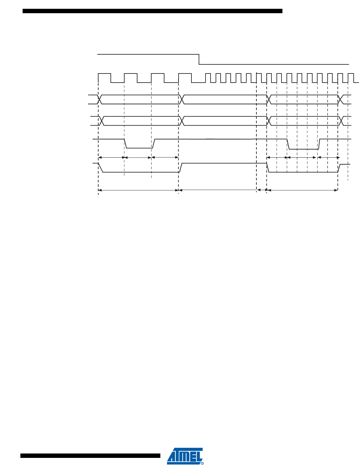
383
6430F–ATARM–21-Feb-12
SAM3U Series
383
6430F–ATARM–21-Feb-12
SAM3U Series
Figure 25-30. Recommended Procedure to Switch from Slow Clock Mode to Normal Mode or from Normal Mode to Slow
Clock Mode
A
[23:2]
NCS
1
MCK
NWE
1
1
SLOW CLOCK MODE WRITE
Slow Clock Mode
internal signal from PMC
232
NORMAL MODE WRITEIDLE STATE
Reload Configuration
Wait State
NBS0, NBS1,
A0, A1
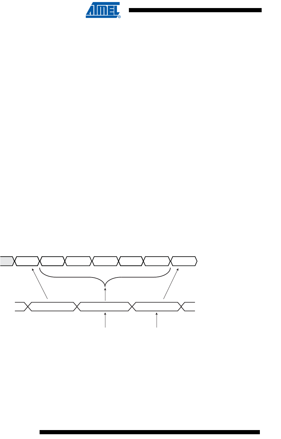
384
6430F–ATARM–21-Feb-12
SAM3U Series
384
6430F–ATARM–21-Feb-12
SAM3U Series
25.16 NAND Flash Controller Operations
25.16.1 NFC Overview
The NFC can handle automatic transfers, sending the commands and address to the NAND
Flash and transferring the contents of the page (for read and write) to the NFC SRAM. It mini-
mizes the CPU overhead.
25.16.2 NFC Control Registers
NAND Flash Read and NAND Flash Program operations can be performed through the NFC
Command Registers. In order to minimize CPU intervention and latency, commands are posted
in a command buffer. This buffer provides zero wait state latency. The detailed description of the
command encoding scheme is explained below.
The NFC handles automatic transfer between the external NAND Flash and the chip via the
NFC SRAM. It is done via NFC Command Registers.
The NFC Command Registers are very efficient to use. When writing to these registers:
• the address of the register (NFCADDR_CMD) contains the command used,
• the data of the register (NFCDATA_ADDT) contains the address to be sent to the NAND
Flash.
So, in one single access the command is sent and immediately executed by the NFC. Even two
commands can be programmed within a single access (CMD1, CMD2) depending on the
VCMD2 value.
The NFC can send up to 5 Address cycles.
Figure 25-31 below shows a typical NAND Flash Page Read Command of a NAND Flash Mem-
ory and correspondence with NFC Address Command Register.
Figure 25-31. NFC/NAND Flash Access Example
For more details refer to “NFC Address Command” on page 386.
The NFC Command Registers can be found at address 0x68000000 - 0x6FFFFFFF. (See
Table 25-4, “External Memory Mapping”.)
Reading the NFC command register (to any address) will give the status of the NFC. Especially
useful to know if the NFC is busy, for example.
Depends on ACYCLE value
CMD1 ADD cycles (0 to 5) CMD2
If VCMD2 = 1
00h Col. Add1 Col. Add2 Row Add1 Row Add2 Row Add330h
Column Address Row Address

385
6430F–ATARM–21-Feb-12
SAM3U Series
385
6430F–ATARM–21-Feb-12
SAM3U Series
25.16.2.1 Building NFC Address Command Example
The base address is made of address 0x60000000 + NFCCMD bit set = 0x68000000.
Page read operation example:
// Build the Address Command (NFCADDR_CMD)
AddressCommand = (0x60000000 |
NFCCMD=1 | // NFC Command Enable
NFCWR=0 |// NFC Read Data from NAND Flash
NFCEN=1 | // NFC Enable.
CSID=1 | // Chip Select ID = 1
ACYCLE= 5 | // Number of address cycle.
VCMD2=1 | // CMD2 is sent after Address Cycles
CMD2=0x30 | // CMD2 = 30h
CMD1=0x0) // CMD1 = Read Command = 00h
// Set the Address for Cycle 0
SMC_ADDR = Col. Add1
// Write command with the Address Command built above
*AddressCommand = (Col. Add2 |// ADDR_CYCLE1
Row Add1 | // ADDR_CYCLE2
Row Add2 |// ADDR_CYCLE3
Row Add3 )// ADDR_CYCLE4

386
6430F–ATARM–21-Feb-12
SAM3U Series
386
6430F–ATARM–21-Feb-12
SAM3U Series
25.16.2.2 NFC Address Command
• Name: NFCADDR_CMD
• Access: Read-write
• Reset: 0x00000000
• CMD1: Command Register Value for Cycle 1
If NFCCMD is set, when a read or write access occurs, the NFC sends this command.
• CMD2: Command Register Value for Cycle 2
If NFCCMD and VCMD2 field are set to one, the NFC sends this command after CMD1.
• VCMD2: Valid Cycle 2 Command
When set to true, the CMD2 field is issued after the address cycle.
• ACYCLE: Number of Address required for the current command
When ACYCLE field is different from zero, ACYCLE Address cycles are performed after Command Cycle 1. The maximum
number of cycles is 5.
• CSID: Chip Select Identifier
Chip select used
• NFCEN: NFC Enable
When set to true, the NFC will automatically read or write data after the command.
• NFCWR: NFC Write Enable
0: The NFC reads data from the NAND Flash.
1: The NFC writes data into the NAND Flash.
• NFCCMD: NFC Command Enable
If set to true, CMD indicates that the NFC shall execute the command encoded in the NFCADDR_CMD.
31 30 29 28 27 26 25 24
––––NFCCMDNFCWRNFCENCSID
23 22 21 20 19 18 17 16
CSID ACYCLE VCMD2 CMD2
15 14 13 12 11 10 9 8
CMD2 CMD1
76543210
CMD1 – –

387
6430F–ATARM–21-Feb-12
SAM3U Series
387
6430F–ATARM–21-Feb-12
SAM3U Series
25.16.2.3 NFC Data Address
• Name: NFCDATA_ADDT
• Access: Write
• Reset: 0x00000000
• ADDR_CYCLE1: NAND Flash Array Address Cycle 1
When less than 5 address cycles are used, ADDR_CYCLE1 is the first byte written to NAND Flash
When 5 address cycles are used, ADDR_CYCLE1 is the second byte written to NAND Flash
• ADDR_CYCLE2: NAND Flash Array Address Cycle 2
When less than 5 address cycles are used, ADDR_CYCLE2 is the second byte written to NAND Flash
When 5 address cycles are used, ADDR_CYCLE2 is the third byte written to NAND Flash
• ADDR_CYCLE3: NAND Flash Array Address Cycle 3
When less than 5 address cycles are used, ADDR_CYCLE3 is the third byte written to NAND Flash
When 5 address cycles are used, ADDR_CYCLE3 is the fourth byte written to NAND Flash
• ADDR_CYCLE4: NAND Flash Array Address Cycle 4
When less than 5 address cycles are used, ADDR_CYCLE4 is the fourth byte written to NAND Flash
When 5 address cycles are used, ADDR_CYCLE4 is the fifth byte written to NAND Flash
Note: If 5 address cycles are used, the first address cycle is ADDR_CYCLE0. Refer to SMC_ADDR register.
31 30 29 28 27 26 25 24
ADDR_CYCLE4
23 22 21 20 19 18 17 16
ADDR_CYCLE3
15 14 13 12 11 10 9 8
ADDR_CYCLE2
76543210
ADDR_CYCLE1

388
6430F–ATARM–21-Feb-12
SAM3U Series
388
6430F–ATARM–21-Feb-12
SAM3U Series
25.16.2.4 NFC DATA Status
• Name: NFCDATA_Status
• Access: Read
• Reset: 0x00000000
• CMD1: Command Register Value for Cycle 1
When a Read or Write Access occurs, the Physical Memory Interface drives the IO bus with CMD1 field during the Com-
mand Latch cycle 1.
• CMD2: Command Register Value for Cycle 2
When VCMD2 field is set to true, the Physical Memory Interface drives the IO bus with CMD2 field during the Command
Latch cycle 2.
• VCMD2: Valid Cycle 2 Command
When set to true, the CMD2 field is issued after addressing cycle.
• ACYCLE: Number of Address required for the current command
When ACYCLE field is different from zero, ACYCLE Address cycles are performed after Command Cycle 1.
• CSID: Chip Select Identifier
Chip select used
• NFCEN: NFC Enable
When set to true, The NFC is enabled.
• NFCWR: NFC Write Enable
0: The NFC is in read mode.
1: The NFC is in write mode.
• NFCBUSY: NFC Busy Status Flag
If set to true, it indicates that the NFC is busy.
31 30 29 28 27 26 25 24
––––NFCBUSYNFCWRNFCENCSID
23 22 21 20 19 18 17 16
CSID ACYCLE VCMD2 CMD2
15 14 13 12 11 10 9 8
CMD2 CMD1
76543210
CMD1 – –
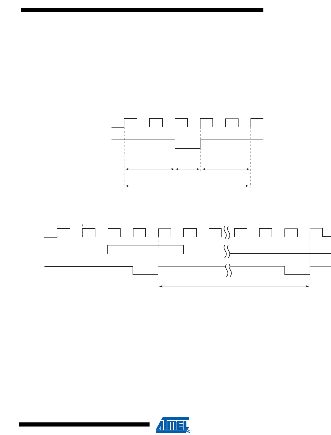
389
6430F–ATARM–21-Feb-12
SAM3U Series
389
6430F–ATARM–21-Feb-12
SAM3U Series
25.16.3 NFC Initialization
Prior to any Command and Data Transfer, the SMC User Interface must be configured to meet
the device timing requirements.
• Write enable Configuration
Use NWE_SETUP, NWE_PULSE and NWE_CYCLE to define the write enable waveform
according to the device datasheet.
Use TADL field in the SMC_TIMINGS register to configure the timing between the last address
latch cycle and the first rising edge of WEN for data input.
Figure 25-32. Write Enable Timing Configuration
Figure 25-33. Write Enable Timing for NAND Flash Device Data Input Mode.
• Read Enable Configuration
Use NRD_SETUP, NRD_PULSE and NRD_CYCLE to define the read enable waveform accord-
ing to the device datasheet.
Use TAR field in the SMC_TIMINGS register to configure the timings between address latch
enable falling edge to read enable falling edge.
Use TCLR field in the SMC_TIMINGS register to configure the timings between the command
latch enable falling edge to the read enable falling edge.
mck
wen
tWEN_PULSEtWEN_SETUP tWEN_HOLD
tWEN_CYCLES
t
ADL
mck
ale
wen
390
6430F–ATARM–21-Feb-12
SAM3U Series
390
6430F–ATARM–21-Feb-12
SAM3U Series
Figure 25-34. Read Enable Timing Configuration Working with NAND Flash Device
• Ready/Busy Signal Timing configuration working with a NAND Flash device
Use TWB field in SMC_TIMINGS register to configure the maximum elapsed time between the
rising edge of wen signal and the falling edge of rbn signal. Use TRR field in the SMC_TIMINGS
register to program the number of clock cycle between the rising edge of the rbn signal and the
falling edge of ren signal.
Figure 25-35. Ready/Busy Timing Configuration
mck
cle
ale
cen
ren
tREN_PULSE tREHtREN_SETUP
tREN_CYCLE
tCLR
tAR
mck
wen
ren
rbn
t
RR
t
WB
busy
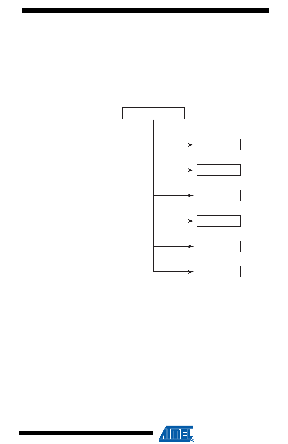
391
6430F–ATARM–21-Feb-12
SAM3U Series
391
6430F–ATARM–21-Feb-12
SAM3U Series
25.16.3.1 NAND Flash Controller Timing Engine
When the NFC Command register is written, the NFC issues a NAND Flash Command and
optionally performs a data transfer between the NFC SRAM and the NAND Flash device. The
NAND Flash Controller Timing Engine guarantees valid NAND Flash timings, depending on the
set of parameters decoded from the address bus. These timings are defined in the
SMC_TIMINGS register.
For information on the timing used depending on the command, see Figure 25-36:
Figure 25-36. NAND Flash Controller Timing Engine
See ”NFC Address Command” register description and ”SMC Timings Register”.
NFCEN=1 NFCWR =1 TADL =1
NFCEN=1 NFCWR=0 TWB != 0
NFCEN=0 VCMD2=1 TCLR != 0
!NFCEN=1 VCMD2=0 ACYCLE!=0 NFCWR=1 TADL != 0
!NFCEN=1 VCMD2=0 ACYCLE!=0 NFCWR=0 TAR != 0
!NFCEN=1 VCMD2=0 ACYCLE!=0 TCLR != 0
Wai t TADL
Wai t TADL
Wai t TAR
Wai t TWB
Wai t TCLR
Wai t TCLR
Ti m i n g Check En g i n e

392
6430F–ATARM–21-Feb-12
SAM3U Series
392
6430F–ATARM–21-Feb-12
SAM3U Series
25.16.4 NFC SRAM
25.16.4.1 NFC SRAM Mapping
If the NFC is used to read and write Data from and to the NAND Flash, the configuration
depends on the page size. See Table 25-9 and Table 25-10 for detailed mapping.
The NFC SRAM size is 4 Kbytes. The NFC can handle NAND Flash with a page size of 4 Kbytes
or of a lower size (such as 2 Kbytes for example). In case of a 2-KByte or lower page size, the
NFC SRAM can be split into several banks. The SMC_BANK field enables to select the bank
used.
Note that a “ping-pong” mode (write or read to a bank while the NFC writes or reads to another
bank) is not accessible with the NFC (using 2 different banks).
If the NFC is not used, the NFC SRAM can be used for a general purpose by the application.
Table 25-9. NFC SRAM Mapping with NAND Flash Page Size of 2 Kbytes + 64 bytes
Offset Use Access
0x00000000-0x000001FF Bank 0 Main Area Buffer 0 Read-write
0x00000200-0x000003FF Bank 0 Main Area Buffer 1 Read-write
0x00000400-0x000005FF Bank 0 Main Area Buffer 2 Read-write
0x00000600-0x000007FF Bank 0 Main Area Buffer 3 Read-write
0x00000800-0x0000080F Bank 0 Spare Area 0 Read-write
0x00000810-0x0000081F Bank 0 Spare Area 1 Read-write
0x00000820-0x0000082F Bank 0 Spare Area 2 Read-write
0x00000830-0x0000083F Bank 0 Spare Area 3 Read-write
0x00000840-0x00000A3F Bank 1 Main Area Buffer 0 Read-write
0x00000A40-0x00000C3F Bank 1 Main Area Buffer 1 Read-write
0x00000C40-0x00000E3F Bank 1 Main Area Buffer 2 Read-write
0x00000E40-0x0000103F Bank 1 Main Area Buffer 3 Read-write
0x00001040-0x0000104F Bank 1 Spare Area 0 Read-write
0x00001050-0x0000105F Bank 1 Spare Area 1 Read-write
0x00001060-0x0000106F Bank 1 Spare Area 2 Read-write
0x00001070-0x0000107F Bank 1 Spare Area 3 Read-write
0x00001080-0x00001FFF Reserved –
Table 25-10. NFC SRAM Mapping with NAND Flash Page Size of 4 Kbytes + 128 bytes
Offset Use Access
0x00000000-0x000001FF Bank 0 Main Area Buffer 0 Read-write
0x00000200-0x000003FF Bank 0 Main Area Buffer 1 Read-write
0x00000400-0x000005FF Bank 0 Main Area Buffer 2 Read-write
0x00000600-0x000007FF Bank 0 Main Area Buffer 3 Read-write
0x00000800-0x000009FF Bank 0 Main Area Buffer 4 Read-write
0x00000A00-0x00000BFF Bank 0 Main Area Buffer 5 Read-write
0x00000C00-0x00000DFF Bank 0 Main Area Buffer 6 Read-write
0x00000E00-0x00000FFF Bank 0 Main Area Buffer 7 Read-write

393
6430F–ATARM–21-Feb-12
SAM3U Series
393
6430F–ATARM–21-Feb-12
SAM3U Series
25.16.4.2 NFC SRAM Access Prioritization Algorithm
When the NAND Flash Controller (NFC) is reading from or writing to the NFC SRAM, the internal
memory is no longer accessible. If an NFC SRAM access occurs when the NFC performs a read
or write operation then the access is discarded. The write operation is not performed. The read
operation returns undefined data. If this situation is encountered, the status flag AWB located in
the NFC status Register is raised and indicates that a shared resource access violation has
occurred.
25.16.5 NAND Flash Operations
This section describes the software operations needed to issue commands to the NAND Flash
device and perform data transfers using NFC.
0x00001000-0x0000100F Bank 0 Spare Area 0 Read-write
0x00001010-0x0000101F Bank 0 Spare Area 1 Read-write
0x00001020-0x0000102F Bank 0 Spare Area 2 Read-write
0x00001030-0x0000103F Bank 0 Spare Area 3 Read-write
0x00001040-0x0000104F Bank 0 Spare Area 4 Read-write
0x00001050-0x0000105F Bank 0 Spare Area 5 Read-write
0x00001060-0x0000106F Bank 0 Spare Area 6 Read-write
0x00001070-0x0000107F Bank 0 Spare Area 7 Read-write
0x00001080-0x00001FFF Reserved –
Table 25-10. NFC SRAM Mapping with NAND Flash Page Size of 4 Kbytes + 128 bytes
Offset Use Access
394
6430F–ATARM–21-Feb-12
SAM3U Series
394
6430F–ATARM–21-Feb-12
SAM3U Series
25.16.5.1 Page Read
Figure 25-37. Page Read Flow Chart
Note that instead of using the interrupt one can poll the NFCBUSY Flag.
For more information on the NFC Control Register, see Section 25.16.2.2 ”NFC Address
Command”.
Congure Device,
writing in theUser Interface
Write the NFC
Command registers
Enable XFRDONE
interrupt (SMC_IER)
Wait for Interrupt
Copy the data from NFC
SRAM to application
memory (via DMA for example)
Using NFC
Check Error
Correcting Codes
395
6430F–ATARM–21-Feb-12
SAM3U Series
395
6430F–ATARM–21-Feb-12
SAM3U Series
25.16.5.2 Program Page
Figure 25-38. Program Page Flow Chart
Writing the ECC can not be done using the NFC so it needs to be done “manually”.
Note that instead of using the interrupt one can poll the NFCBUSY Flag.
For more information on the NFC Control Register, see Section 25.16.2.2 ”NFC Address
Command”.
Co n g u r e Dev i ce,
writing in the User
interface
Write Data in the NFC
SRAM (CPU or DMA)
En a b l e XFRDON E
Writ e t he Command
Register through the
AHB int erface
Wri t e ECC
Wait for interrupt
wait for Ready/Busy
interrupt

396
6430F–ATARM–21-Feb-12
SAM3U Series
396
6430F–ATARM–21-Feb-12
SAM3U Series
25.17 SMC Error Correcting Code Functional Description
A page in NAND Flash and SmartMedia memories contains an area for main data and an addi-
tional area used for redundancy (ECC). The page is organized in 8-bit or 16-bit words. The page
size corresponds to the number of words in the main area plus the number of words in the extra
area used for redundancy.
Over time, some memory locations may fail to program or erase properly. In order to ensure that
data is stored properly over the life of the NAND Flash device, NAND Flash providers recom-
mend to utilize either 1 ECC per 256 bytes of data, 1 ECC per 512 bytes of data or 1 ECC for all
of the page.
The only configurations required for ECC are the NAND Flash or the SmartMedia page size
(528/2112/4224) and the type of correction wanted (1 ECC for all the page/1 ECC per 256 bytes
of data /1 ECC per 512 bytes of data). Page size is configured setting the PAGESIZE field in the
ECC Mode Register (ECC_MR). Type of correction is configured setting the TYPCORRECT
field in the ECC Mode Register (ECC_MR).
Note: There is a limitation when using a 16-bit NAND Flash: only 1 ECC for a whole page is possible.
There is no limitation when using an 8-bit NAND Flash.
ECC is automatically computed as soon as a read (00h)/write (80h) command to the NAND
Flash or the SmartMedia is detected. Read and write access must start at a page boundary.
ECC results are available as soon as the counter reaches the end of the main area. Values in
the ECC Parity Registers (ECC_PR0 to ECC_PR15) are then valid and locked until a new start
condition occurs (read/write command followed by address cycles).
25.17.1 Write Access
Once the Flash memory page is written, the computed ECC codes are available in the ECC Par-
ity (ECC_PR0 to ECC_PR15) registers. The ECC code values must be written by the software
application in the extra area used for redundancy. The number of write accesses in the extra
area is a function of the value of the type of correction field. For example, for 1 ECC per 256
bytes of data for a page of 512 bytes, only the values of ECC_PR0 and ECC_PR1 must be writ-
ten by the software application. Other registers are meaningless.
25.17.2 Read Access
After reading the whole data in the main area, the application must perform read accesses to the
extra area where ECC code has been previously stored. Error detection is automatically per-
formed by the ECC controller.
Note: It is mandatory to read consecutively the entire main area and the locations where Parity and
NParity values have been previously stored, to let the ECC controller perform error detection.
The application can check the ECC Status Registers (ECC_SR1/ECC_SR2) for any detected
errors. It is up to the application to correct any detected error. ECC computation can detect four
different circumstances:
• No error: XOR between the ECC computation and the ECC code stored at the end of the
NAND Flash or SmartMedia page is equal to 0. No error flags in the ECC Status Registers
(ECC_SR1/ECC_SR2).
• Recoverable error: Only the RECERR flags in the ECC Status registers
(ECC_SR1/ECC_SR2) are set. The corrupted word offset in the read page is defined by the
WORDADDR field in the ECC Parity Registers (ECC_PR0 to ECC_PR15). The corrupted bit
position in the concerned word is defined in the BITADDR field in the ECC Parity Registers
(ECC_PR0 to ECC_PR15).
397
6430F–ATARM–21-Feb-12
SAM3U Series
397
6430F–ATARM–21-Feb-12
SAM3U Series
• ECC error: The ECCERR flag in the ECC Status Registers (ECC_SR1/ECC_SR2) is set. An
error has been detected in the ECC code stored in the Flash memory. The position of the
corrupted bit can be found by the application performing an XOR between the Parity and the
NParity contained in the ECC code stored in the Flash memory.
• Non correctable error: The MULERR flag in the ECC Status Registers
(ECC_SR1/ECC_SR2) is set. Several unrecoverable errors have been detected in the Flash
memory page.
ECC Status Registers, ECC Parity Registers are cleared when a read/write command is
detected or a software reset is performed.
For Single-bit Error Correction and Double-bit Error Detection (SEC-DED) Hsiao code is used.
24-bit ECC is generated in order to perform one bit correction per 256 or 512 bytes for pages of
512/2048/4096 8-bit words. 32-bit ECC is generated in order to perform one bit correction per
512/1024/2048/4096 8- or 16-bit words. They are generated according to the schemes shown in
Figure 25-39 and Figure 25-40.
Figure 25-39. Parity Generation for 512/1024/2048/4096 8-bit Words
To calculate P8’ to PX’ and P8 to PX, apply the algorithm that follows.
Page size = 2n
for i =0 to n
Bit7 Bit6 Bit5 Bit4 Bit3 Bit2 Bit1 Bit0
Bit7 Bit6 Bit5 Bit4 Bit3 Bit2 Bit1 Bit0
P8
P8'
Bit7 Bit6 Bit5 Bit4 Bit3 Bit2 Bit1 Bit0
Bit7 Bit6 Bit5 Bit4 Bit3 Bit2 Bit1 Bit0
P8
P8'
P16
P16'
Bit7 Bit6 Bit5 Bit4 Bit3 Bit2 Bit1 Bit0
Bit7 Bit6 Bit5 Bit4 Bit3 Bit2 Bit1 Bit0
P8
P8'
Bit7 Bit6 Bit5 Bit4 Bit3 Bit2 Bit1 Bit0
Bit7 Bit6 Bit5 Bit4 Bit3 Bit2 Bit1 Bit0
P8
P8'
P16
P16'
P32
P32
1st byte
P32
2nd byte
3rd byte
4 th byte
Page size th byte
(page size -1 )th byte
PX
PX'
Page size = 512 Px = 2048
Page size = 1024 Px = 4096
Page size = 2048 Px = 8192
Page size = 4096 Px = 16384
(page size -2 )th byte
(page size -3 )th byte
P1 P1' P1'
P1 P1 P1' P1'
P1
P2 P2' P2 P2'
P4 P4'
P1=bit7(+)bit5(+)bit3(+)bit1(+)P1
P2=bit7(+)bit6(+)bit3(+)bit2(+)P2
P4=bit7(+)bit6(+)bit5(+)bit4(+)P4
P1'=bit6(+)bit4(+)bit2(+)bit0(+)P1'
P2'=bit5(+)bit4(+)bit1(+)bit0(+)P2'
P4'=bit7(+)bit6(+)bit5(+)bit4(+)P4'

398
6430F–ATARM–21-Feb-12
SAM3U Series
398
6430F–ATARM–21-Feb-12
SAM3U Series
begin
for (j = 0 to page_size_byte)
begin
if(j[i] ==1)
P[2i+3]=bit7(+)bit6(+)bit5(+)bit4(+)bit3(+)
bit2(+)bit1(+)bit0(+)P[2i+3]
else
P[2i+3]’=bit7(+)bit6(+)bit5(+)bit4(+)bit3(+)
bit2(+)bit1(+)bit0(+)P[2i+3]'
end
end
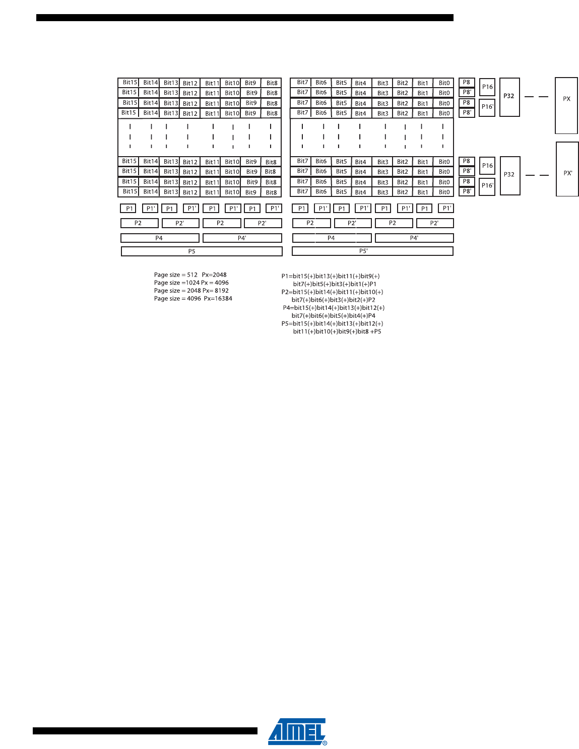
399
6430F–ATARM–21-Feb-12
SAM3U Series
399
6430F–ATARM–21-Feb-12
SAM3U Series
Figure 25-40. Parity Generation for 512/1024/2048/4096 16-bit Words
To calculate P8’ to PX’ and P8 to PX, apply the algorithm that follows.
Page size = 2n
for i =0 to n
begin
for (j = 0 to page_size_word)
begin
if(j[i] ==1)
P[2i+3]= bit15(+)bit14(+)bit13(+)bit12(+)
bit11(+)bit10(+)bit9(+)bit8(+)
bit7(+)bit6(+)bit5(+)bit4(+)bit3(+)
bit2(+)bit1(+)bit0(+)P[2n+3]
else
P[2i+3]’=bit15(+)bit14(+)bit13(+)bit12(+)
bit11(+)bit10(+)bit9(+)bit8(+)
bit7(+)bit6(+)bit5(+)bit4(+)bit3(+)
bit2(+)bit1(+)bit0(+)P[2i+3]'
end
end
1st word
2nd word
3rd word
4th word
(Page size -3 )th word
(Page size -2 )th word
(Page size -1 )th word
Page size th word (+)(+)

400
6430F–ATARM–21-Feb-12
SAM3U Series
400
6430F–ATARM–21-Feb-12
SAM3U Series
25.18 Power Management Controller (PMC) User Interface
The SMC is programmed using the fields listed in Table 25-11. For each chip, select a set of 4
registers is used to program the parameters of the external device. In Table 25-11,
“CS_number” denotes the chip select number. 16 Bytes per chip select are required.
Table 25-11. Register Mapping
Offset Register Name Access Reset
0x000 SMC NFC Configuration Register SMC_CFG Read-write 0x0
0x004 SMC NFC Control Register SMC_CTRL Write-only 0x0
0x008 SMC NFC Status Register SMC_SR Read-only 0x0
0x00C SMC NFC Interrupt Enable Register SMC_IER Write-only 0x0
0x010 SMC NFC Interrupt Disable Register SMC_IDR Write-only 0x0
0x014 SMC NFC Interrupt Mask Register SMC_IMR Read-only 0x0
0x018 SMC NFC Address Cycle Zero Register SMC_ADDR Read-write 0x0
0x01C SMC Bank Address Register SMC_BANK Read-write 0x0
0x020 SMC ECC Control Register SMC_ECC_CTRL Write-only 0x0
0x024 SMC ECC Mode Register SMC_ECC_MD Read-write 0x0
0x028 SMC ECC Status 1 Register SMC_ECC_SR1 Read-only 0x0
0x02C SMC ECC Parity 0 Register SMC_ECC_PR0 Read-only 0x0
0x030 SMC ECC parity 1 Register SMC_ECC_PR1 Read-only 0x0
0x034 SMC ECC status 2 Register SMC_ECC_SR2 Read-only 0x0
0x038 SMC ECC parity 2 Register SMC_ECC_PR2 Read-only 0x0
0x03C SMC ECC parity 3 Register SMC_ECC_PR3 Read-only 0x0
0x040 SMC ECC parity 4 Register SMC_ECC_PR4 Read-only 0x0
0x044 SMC ECC parity 5 Register SMC_ECC_PR5 Read-only 0x0
0x048 SMC ECC parity 6 Register SMC_ECC_PR6 Read-only 0x0
0x04C SMC ECC parity 7 Register SMC_ECC_PR7 Read-only 0x0
0x050 SMC ECC parity 8 Register SMC_ECC_PR8 Read-only 0x0
0x054 SMC ECC parity 9 Register SMC_ECC_PR9 Read-only 0x0
0x058 SMC ECC parity 10 Register SMC_ECC_PR10 Read-only 0x0
0x05C SMC ECC parity 11 Register SMC_ECC_PR11 Read-only 0x0
0x060 SMC ECC parity 12 Register SMC_ECC_PR12 Read-only 0x0
0x064 SMC ECC parity 13 Register SMC_ECC_PR13 Read-only 0x0
0x068 SMC ECC parity 14 Register SMC_ECC_PR14 Read-only 0x0
0x06C SMC ECC parity 15 Register SMC_ECC_PR15 Read-only 0x0
0x14*CS_number+0x070 SMC Setup Register SMC_SETUP Read-write 0x01010101
0x14*CS_number+0x074 SMC Pulse Register SMC_PULSE Read-write 0x01010101
0x14*CS_number+0x078 SMC Cycle Register SMC_CYCLE Read-write 0x00030003
0x14*CS_number+0x7C SMC Timings Register SMC_TIMINGS Read-write 0x00000000

401
6430F–ATARM–21-Feb-12
SAM3U Series
401
6430F–ATARM–21-Feb-12
SAM3U Series
0x14*CS_number+0x80 SMC Mode Register SMC_MODE Read-write 0x10000003
0x110 SMC OCMS Register SMC_OCMS Read-write 0x0
0x114 SMC OCMS KEY1 Register SMC_KEY1 Write-once 0x0
0x118 SMC OCMS KEY2 Register SMC_KEY2 Write-once 0x0
0x1E4 Write Protection Control Register SMC_WPCR Write-only 0x0
0x1E8 Write Protection Status Register SMC_WPSR Read-only 0x0
0x1FC Reserved – – –
Table 25-11. Register Mapping (Continued)
Offset Register Name Access Reset
402
6430F–ATARM–21-Feb-12
SAM3U Series
402
6430F–ATARM–21-Feb-12
SAM3U Series
25.18.1 SMC NFC Configuration Register
Name:SMC_CFG
Address: 0x400E0000
Access: Read-write
Reset: 0x00000000
• PAGESIZE
This field defines the page size of the NAND Flash device.
• WSPARE: Write Spare Area
0: The NFC skips the spare area in write mode.
1: The NFC writes both main area and spare area in write mode.
• RSPARE: Read Spare Area
0: The NFC skips the spare area in read mode.
1: The NFC reads both main area and spare area in read mode.
• EDGECTRL: Rising/Falling Edge Detection Control
0: Rising edge is detected.
1: Falling edge is detected.
• RBEDGE: Ready/Busy Signal Edge Detection
0: When set to zero, RB_EDGE fields indicate the level of the Ready/Busy lines.
1: When set to one, RB_EDGE fields indicate only transition on Ready/Busy lines.
• DTOCYC: Data Timeout Cycle Number
31 30 29 28 27 26 25 24
––––––––
23 22 21 20 19 18 17 16
– DTOMUL DTOCYC
15 14 13 12 11 10 9 8
– – RBEDGE EDGECTRL – – RSPARE WSPARE
76543210
–––––– PAGESIZE
Value Name Description
0 PS512_16 Main area 512 Bytes + Spare area 16 Bytes = 528 Bytes
1 PS1024_32 Main area 1024 Bytes + Spare area 32 Bytes = 1056 Bytes
2 PS2048_64 Main area 2048 Bytes + Spare area 64 Bytes = 2112 Bytes
3 PS4096_128 Main area 4096 Bytes + Spare area 128 Bytes = 4224 Bytes

403
6430F–ATARM–21-Feb-12
SAM3U Series
403
6430F–ATARM–21-Feb-12
SAM3U Series
• DTOMUL: Data Timeout Multiplier
These fields determine the maximum number of Master Clock cycles that the SMC waits until the detection of a rising edge
on Ready/Busy signal.
Data Timeout Multiplier is defined by DTOMUL as shown in the following table:
If the data timeout set by DTOCYC and DTOMUL has been exceeded, the Data Timeout Error flag (DTOE) in the SMC Sta-
tus Register (SMC_SR) raises.
Value Name Description
0X1DTOCYC
1 X16 DTOCYC x 16
2 X128 DTOCYC x 128
3 X256 DTOCYC x 256
4 X1024 DTOCYC x 1024
5 X4096 DTOCYC x 4096
6 X65536 DTOCYC x 65536
7 X1048576 DTOCYC x 1048576

404
6430F–ATARM–21-Feb-12
SAM3U Series
404
6430F–ATARM–21-Feb-12
SAM3U Series
25.18.2 SMC NFC Control Register
Name: SMC_CTRL
Address: 0x400E0004
Access: Write-only
Reset: 0x00000000
• NFCEN: NAND Flash Controller Enable
0: no effect.
1: Enable the NAND Flash controller.
• NFCDIS: NAND Flash Controller Disable
0: no effect
1: Disable the NAND Flash controller.
31 30 29 28 27 26 25 24
––––––––
23 22 21 20 19 18 17 16
––––––––
15 14 13 12 11 10 9 8
––––––––
76543210
––––––NFCDISNFCEN

405
6430F–ATARM–21-Feb-12
SAM3U Series
405
6430F–ATARM–21-Feb-12
SAM3U Series
25.18.3 SMC NFC Status Register
Name: SMC_SR
Address: 0x400E0008
Access: Read-only
Reset: 0x00000000
• SMCSTS: NAND Flash Controller status (this field cannot be reset)
0: NAND Flash Controller is disabled.
1: NAND Flash Controller is enabled.
• RB_RISE: Selected Ready Busy Rising Edge Detected
When set to one, this flag indicates that a rising edge on Ready/Busy Line has been detected. This flag is reset after a sta-
tus read operation. The Ready/Busy line selected is the decoding of the set NFCCSID, RBNSEL fields.
• RB_FALL: Selected Ready Busy Falling Edge Detected
When set to one, this flag indicates that a falling edge on Ready/Busy Line has been detected. This flag is reset after a sta-
tus read operation. The Ready/Busy line is selected through the decoding of the set NFCSID, RBNSEL fields.
• NFCBUSY: NFC Busy (this field cannot be reset)
When set to one this flag indicates that the Controller is activated and accesses the memory device.
• NFCWR: NFC Write/Read Operation (this field cannot be reset)
When a command is issued, this field indicates the current Read or Write Operation. This field can be manually updated
with the use of the SMC_CTRL register.
• NFCSID: NFC Chip Select ID (this field cannot be reset)
When a command is issued, this field indicates the value of the targeted chip select. This field can be manually updated
with the use of the SMC_CTRL register.
• XFRDONE: NFC Data Transfer Terminated
When set to one, this flag indicates that the NFC has terminated the Data Transfer. This flag is reset after a status read
operation.
• CMDDONE: Command Done
When set to one, this flag indicates that the NFC has terminated the Command. This flag is reset after a status read
operation.
31 30 29 28 27 26 25 24
–––––––RB_EDGE0
23 22 21 20 19 18 17 16
NFCASE AWB UNDEF DTOE – – CMDDONE XFRDONE
15 14 13 12 11 10 9 8
– NFCSID NFCWR – – NFCBUSY
76543210
– – RB_FALL RB_RISE – – – SMCSTS

406
6430F–ATARM–21-Feb-12
SAM3U Series
406
6430F–ATARM–21-Feb-12
SAM3U Series
• DTOE: Data Timeout Error
When set to one this flag indicates that the Data timeout set be by DTOMUL and DTOCYC has been exceeded. This flag is
reset after a status read operation.
• UNDEF: Undefined Area Error
When set to one this flag indicates that the processor performed an access in an undefined memory area. This flag is reset
after a status read operation.
• AWB: Accessing While Busy
If set to one this flag indicates that an AHB master has performed an access during the busy phase. This flag is reset after
a status read operation.
• NFCASE: NFC Access Size Error
If set to one, this flag indicates that an illegal access has been detected in the NFC Memory Area. Only Word Access is
allowed within the NFC memory area. This flag is reset after a status read operation.
• RB_EDGEx: Ready/Busy Line x Edge Detected
If set to one, this flag indicates that an edge has been detected on the Ready/Busy Line x. Depending on the EDGE CTRL
field located in the SMC_MODE register, only rising or falling edge is detected. This flag is reset after a status read
operation.

407
6430F–ATARM–21-Feb-12
SAM3U Series
407
6430F–ATARM–21-Feb-12
SAM3U Series
25.18.4 SMC NFC Interrupt Enable Register
Name: SMC_IER
Address: 0x400E000C
Access: Write-only
Reset: 0x00000000
• RB_RISE: Ready Busy Rising Edge Detection Interrupt Enable
0: No effect.
1: Interrupt source is enabled.
• RB_FALL: Ready Busy Falling Edge Detection Interrupt Enable
0: No effect.
1: Interrupt source is enabled.
• XFRDONE: Transfer Done Interrupt Enable
0: No effect.
1: Interrupt source is enabled.
• CMDDONE: Command Done Interrupt Enable
0: No effect.
1: Interrupt source is enabled.
• DTOE: Data Timeout Error Interrupt Enable
0: No effect.
1: Interrupt source is enabled.
• UNDEF: Undefined Area Access Interrupt Enable
0: No effect.
1: Interrupt source is enabled.
• AWB: Accessing While Busy Interrupt Enable
0: No effect.
1: Interrupt source is enabled.
31 30 29 28 27 26 25 24
–––––––RB_EDGE0
23 22 21 20 19 18 17 16
NFCASE AWB UNDEF DTOE – – CMDDONE XFRDONE
15 14 13 12 11 10 9 8
––––––––
76543210
––RB_FALLRB_RISE––––

408
6430F–ATARM–21-Feb-12
SAM3U Series
408
6430F–ATARM–21-Feb-12
SAM3U Series
• NFCASE: NFC Access Size Error Interrupt Enable
0: No effect.
1: Interrupt source is enabled.
• RB_EDGEx: Ready/Busy Line x Interrupt Enable
0: No effect.
1: Interrupt source is enabled.

409
6430F–ATARM–21-Feb-12
SAM3U Series
409
6430F–ATARM–21-Feb-12
SAM3U Series
25.18.5 SMC NFC Interrupt Disable Register
Name: SMC_IDR
Address: 0x400E0010
Access: Write-only
Reset: 0x00000000
• RB_RISE: Ready Busy Rising Edge Detection Interrupt Disable
0: No effect.
1: Interrupt source is disabled.
• RB_FALL: Ready Busy Falling Edge Detection Interrupt Disable
0: No effect.
1: Interrupt source is disabled.
• XFRDONE: Transfer Done Interrupt Disable
0: No effect.
1: Interrupt source is disabled.
• CMDDONE: Command Done Interrupt Disable
0: No effect.
1: Interrupt source is disabled.
• DTOE: Data Timeout Error Interrupt Disable
0: No effect.
1: Interrupt source is disabled.
• UNDEF: Undefined Area Access Interrupt Disable
0: No effect.
1: Interrupt source is disabled.
• AWB: Accessing While Busy Interrupt Disable
0: No effect.
1: Interrupt source is disabled.
31 30 29 28 27 26 25 24
–––––––RB_EDGE0
23 22 21 20 19 18 17 16
NFCASE AWB UNDEF DTOE – – CMDDONE XFRDONE
15 14 13 12 11 10 9 8
––––––––
76543210
––RB_FALLRB_RISE––––

410
6430F–ATARM–21-Feb-12
SAM3U Series
410
6430F–ATARM–21-Feb-12
SAM3U Series
• NFCASE: NFC Access Size Error Interrupt Disable
0: No effect.
1: Interrupt source is disabled.
• RB_EDGEx: Ready/Busy Line x Interrupt Disable
0: No effect.
1: Interrupt source is disabled.

411
6430F–ATARM–21-Feb-12
SAM3U Series
411
6430F–ATARM–21-Feb-12
SAM3U Series
25.18.6 SMC NFC Interrupt Mask Register
Name:SMC_IMR
Address: 0x400E0014
Access: Read-only
Reset: 0x00000000
• RB_RISE: Ready Busy Rising Edge Detection Interrupt Mask
0: Interrupt source is disabled.
1: Interrupt source is enabled.
• RB_FALL: Ready Busy Falling Edge Detection Interrupt Mask
0: Interrupt source is disabled.
1: Interrupt source is enabled.
• XFRDONE: Transfer Done Interrupt Mask
0: Interrupt source is disabled.
1: Interrupt source is enabled.
• CMDDONE: Command Done Interrupt Mask
0: Interrupt source is disabled.
1: Interrupt source is enabled.
• DTOE: Data Timeout Error Interrupt Mask
0: Interrupt source is disabled.
1: Interrupt source is enabled.
• UNDEF: Undefined Area Access Interrupt Mask5
0: Interrupt source is disabled.
1: Interrupt source is enabled.
• AWB: Accessing While Busy Interrupt Mask
0: Interrupt source is disabled.
1: Interrupt source is enabled.
31 30 29 28 27 26 25 24
–––––––RB_EDGE0
23 22 21 20 19 18 17 16
NFCASE AWB UNDEF DTOE – – CMDDONE XFRDONE
15 14 13 12 11 10 9 8
––––––––
76543210
––RB_FALLRB_RISE––––

412
6430F–ATARM–21-Feb-12
SAM3U Series
412
6430F–ATARM–21-Feb-12
SAM3U Series
• NFCASE: NFC Access Size Error Interrupt Mask
0: Interrupt source is disabled.
1: Interrupt source is enabled.
• RB_EDGEx: Ready/Busy Line x Interrupt Mask
0: Interrupt source is disabled.
1: Interrupt source is enabled.

413
6430F–ATARM–21-Feb-12
SAM3U Series
413
6430F–ATARM–21-Feb-12
SAM3U Series
25.18.7 SMC NFC Address Cycle Zero Register
Name: SMC_ADDR
Address: 0x400E0018
Access: Read-Write
Reset: 0x00000000
• ADDR_CYCLE0: NAND Flash Array Address cycle 0
When 5 address cycles are used, ADDR_CYCLE0 is the first byte written to the NAND Flash (used by the NFC).
31 30 29 28 27 26 25 24
––––––––
23 22 21 20 19 18 17 16
––––––––
15 14 13 12 11 10 9 8
––––––––
76543210
ADDR_CYCLE0

414
6430F–ATARM–21-Feb-12
SAM3U Series
414
6430F–ATARM–21-Feb-12
SAM3U Series
25.18.8 SMC NFC Bank Register
Name: SMC_BANK
Address: 0x400E001C
Access: Read-write
Reset: 0x00000000
• BANK: Bank Identifier
Number of the bank used
31 30 29 28 27 26 25 24
––––––––
23 22 21 20 19 18 17 16
––––––––
15 14 13 12 11 10 9 8
––––––––
76543210
––––– BANK

415
6430F–ATARM–21-Feb-12
SAM3U Series
415
6430F–ATARM–21-Feb-12
SAM3U Series
25.18.9 SMC ECC Control Register
Name: SMC_ECC_CTRL
Address: 0x400E0020
Access: Write-only
Reset: 0x00000000
• RST: Reset ECC
0: No effect.
1: Reset ECC parity registers.
• SWRST: Software Reset
0: No effect.
1: Reset all registers.
31 30 29 28 27 26 25 24
––––––––
23 22 21 20 19 18 17 16
––––––––
15 14 13 12 11 10 9 8
––––––––
76543210
––––––SWRSTRST

416
6430F–ATARM–21-Feb-12
SAM3U Series
416
6430F–ATARM–21-Feb-12
SAM3U Series
25.18.10 SMC ECC MODE Register
Name: SMC_ECC_MD
Address: 0x400E0024
Access: Read-write
Reset: 0x00000000
• ECC_PAGESIZE: ECC Page Size
This field defines the page size of the NAND Flash device.
• TYPCORREC: Type of Correction
31 30 29 28 27 26 25 24
––––––––
23 22 21 20 19 18 17 16
––––––––
15 14 13 12 11 10 9 8
––––––––
76543210
– – TYPCORREC – – ECC_PAGESIZE
Value Name Description
0 PS512_16 Main area 512 Bytes + Spare area 16 Bytes = 528 Bytes
1 PS1024_32 Main area 1024 Bytes + Spare area 32 Bytes = 1056 Bytes
2 PS2048_64 Main area 2048 Bytes + Spare area 64 Bytes = 2112 Bytes
3 PS4096_128 Main area 4096 Bytes + Spare area 128 Bytes = 4224 Bytes
Value Name Description
0CPAGE
1 bit correction for a page of 512/1024/2048/4096 Bytes
(for 8 or 16-bit NAND Flash)
1 C256B 1 bit correction for 256 Bytes of data for a page of 512/2048/4096 bytes
(for 8-bit NAND Flash only)
2 C512B 1 bit correction for 512 Bytes of data for a page of 512/2048/4096 bytes
(for 8-bit NAND Flash only)
417
6430F–ATARM–21-Feb-12
SAM3U Series
417
6430F–ATARM–21-Feb-12
SAM3U Series
25.18.11 SMC ECC Status Register 1
Name: SMC_ECC_SR1
Address: 0x400E0028
Access: Read-only
Reset: 0x00000000
• RECERR0: Recoverable Error
0: No Errors Detected.
1: Errors Detected. If MUL_ERROR is 0, a single correctable error was detected. Otherwise multiple uncorrected errors
were detected.
• ECCERR0: ECC Error
0: No Errors Detected.
1: A single bit error occurred in the ECC bytes.
If TYPECORRECT = 0, read both ECC Parity 0 and ECC Parity 1 registers, the error occurred at the location which con-
tains a 1 in the least significant 16 bits; else read ECC Parity 0 register, the error occurred at the location which contains a
1 in the least significant 24 bits.
• MULERR0: Multiple Error
0: No Multiple Errors Detected.
1: Multiple Errors Detected.
• RECERR1: Recoverable Error in the page between the 256th and the 511th bytes or the 512nd and the 1023rd
bytes
Fixed to 0 if TYPECORREC = 0.
0: No Errors Detected.
1: Errors Detected. If MUL_ERROR is 0, a single correctable error was detected. Otherwise multiple uncorrected errors
were detected.
• ECCERR1: ECC Error in the page between the 256th and the 511th bytes or between the 512nd and the 1023rd
bytes
Fixed to 0 if TYPECORREC = 0
0: No Errors Detected.
1: A single bit error occurred in the ECC bytes.
Read ECC Parity 1 register, the error occurred at the location which contains a 1 in the least significant 24 bits.
31 30 29 28 27 26 25 24
– ECCERR7 ECCERR7 RECERR7 – ECCERR6 ECCERR6 RECERR6
23 22 21 20 19 18 17 16
– ECCERR5 ECCERR5 RECERR5 – ECCERR4 ECCERR4 RECERR4
15 14 13 12 11 10 9 8
– MULERR3 ECCERR3 RECERR3 – MULERR2 ECCERR2 RECERR2
76543210
– MULERR1 ECCERR1 RECERR1 – ECCERR0 ECCERR0 RECERR0

418
6430F–ATARM–21-Feb-12
SAM3U Series
418
6430F–ATARM–21-Feb-12
SAM3U Series
• MULERR1: Multiple Error in the page between the 256th and the 511th bytes or between the 512nd and the
1023rd bytes
Fixed to 0 if TYPECORREC = 0.
0: No Multiple Errors Detected.
1: Multiple Errors Detected.
• RECERR2: Recoverable Error in the page between the 512nd and the 767th bytes or between the 1024th and the
1535th bytes
Fixed to 0 if TYPECORREC = 0.
0: No Errors Detected.
1: Errors Detected. If MUL_ERROR is 0, a single correctable error was detected. Otherwise, multiple uncorrected errors
were detected.
• ECCERR2: ECC Error in the page between the 512nd and the 767th bytes or between the 1024th and the 1535th
bytes
Fixed to 0 if TYPECORREC = 0.
0: No Errors Detected.
1: A single bit error occurred in the ECC bytes.
Read ECC Parity 2 register, the error occurred at the location which contains a 1 in the least significant 24 bits.
• MULERR2: Multiple Error in the page between the 512nd and the 767th bytes or between the 1024th and the
1535th bytes
Fixed to 0 if TYPECORREC = 0.
0: No Multiple Errors Detected.
1: Multiple Errors Detected.
• RECERR3: Recoverable Error in the page between the 768th and the 1023rd bytes or between the 1536th and the
2047th bytes
Fixed to 0 if TYPECORREC = 0.
0: No Errors Detected.
1: Errors Detected. If MUL_ERROR is 0, a single correctable error was detected. Otherwise multiple uncorrected errors
were detected.
• ECCERR3: ECC Error in the page between the 768th and the 1023rd bytes or between the 1536th and the 2047th
bytes
Fixed to 0 if TYPECORREC = 0.
0: No Errors Detected.
1: A single bit error occurred in the ECC bytes.
Read ECC Parity 3 register, the error occurred at the location which contains a 1 in the least significant 24 bits.
• MULERR3: Multiple Error in the page between the 768th and the 1023rd bytes or between the 1536th and the
2047th bytes
Fixed to 0 if TYPECORREC = 0.

419
6430F–ATARM–21-Feb-12
SAM3U Series
419
6430F–ATARM–21-Feb-12
SAM3U Series
0: No Multiple Errors Detected.
1: Multiple Errors Detected.
• RECERR4: Recoverable Error in the page between the 1024th and the 1279th bytes or between the 2048th and
the 2559th bytes
Fixed to 0 if TYPECORREC = 0.
0: No Errors Detected.
1: Errors Detected. If MUL_ERROR is 0, a single correctable error was detected. Otherwise multiple uncorrected errors
were detected.
• ECCERR4: ECC Error in the page between the 1024th and the 1279th bytes or between the 2048th and the 2559th
bytes
Fixed to 0 if TYPECORREC = 0.
0: No Errors Detected.
1: A single bit error occurred in the ECC bytes.
Read ECC Parity 4 register, the error occurred at the location which contains a 1 in the least significant 24 bits.
• MULERR4: Multiple Error in the page between the 1024th and the 1279th bytes or between the 2048th and the
2559th bytes
Fixed to 0 if TYPECORREC = 0.
0: No Multiple Errors Detected.
1: Multiple Errors Detected.
• RECERR5: Recoverable Error in the page between the 1280th and the 1535th bytes or between the 2560th and
the 3071st bytes
Fixed to 0 if TYPECORREC = 0.
0: No Errors Detected.
1: Errors Detected. If MUL_ERROR is 0, a single correctable error was detected. Otherwise multiple uncorrected errors
were detected
• ECCERR5: ECC Error in the page between the 1280th and the 1535th bytes or between the 2560th and the 3071st
bytes
Fixed to 0 if TYPECORREC = 0.
0: No Errors Detected.
1: A single bit error occurred in the ECC bytes.
Read ECC Parity 5 register, the error occurred at the location which contains a 1 in the least significant 24 bits.
• MULERR5: Multiple Error in the page between the 1280th and the 1535th bytes or between the 2560th and the
3071st bytes
Fixed to 0 if TYPECORREC = 0.
0: No Multiple Errors Detected.
1: Multiple Errors Detected.

420
6430F–ATARM–21-Feb-12
SAM3U Series
420
6430F–ATARM–21-Feb-12
SAM3U Series
• RECERR6: Recoverable Error in the page between the 1536th and the 1791st bytes or between the 3072nd and
the 3583rd bytes
Fixed to 0 if TYPECORREC = 0.
0: No Errors Detected.
1: Errors Detected. If MUL_ERROR is 0, a single correctable error was detected. Otherwise multiple uncorrected errors
were detected.
• ECCERR6: ECC Error in the page between the 1536th and the 1791st bytes or between the 3072nd and the
3583rd bytes
Fixed to 0 if TYPECORREC = 0.
0: No Errors Detected.
1: A single bit error occurred in the ECC bytes.
Read ECC Parity 6 register, the error occurred at the location which contains a 1 in the least significant 24 bits.
• MULERR6: Multiple Error in the page between the 1536th and the 1791st bytes or between the 3072nd and the
3583rd bytes
Fixed to 0 if TYPECORREC = 0.
0: No Multiple Errors Detected.
1: Multiple Errors Detected.
• RECERR7: Recoverable Error in the page between the 1792nd and the 2047th bytes or between the 3584th and
the 4095th bytes
Fixed to 0 if TYPECORREC = 0.
0: No Errors Detected.
1: Errors Detected. If MUL_ERROR is 0, a single correctable error was detected. Otherwise, multiple uncorrected errors
were detected.
• ECCERR7: ECC Error in the page between the 1792nd and the 2047th bytes or between the 3584th and the
4095th bytes
Fixed to 0 if TYPECORREC = 0.
0: No Errors Detected.
1: A single bit error occurred in the ECC bytes.
Read ECC Parity 7 register, the error occurred at the location which contains a 1 in the least significant 24 bits.
• MULERR7: Multiple Error in the page between the 1792nd and the 2047th bytes or between the 3584th and the
4095th bytes
Fixed to 0 if TYPECORREC = 0.
0: No Multiple Errors Detected.
1: Multiple Errors Detected.

421
6430F–ATARM–21-Feb-12
SAM3U Series
421
6430F–ATARM–21-Feb-12
SAM3U Series
25.18.12 SMC ECC Status Register 2
Name: SMC_ECC_SR2
Address: 0x400E0034
Access: Read-only
Reset: 0x00000000
• RECERR8: Recoverable Error in the page between the 2048th and the 2303rd bytes
Fixed to 0 if TYPECORREC = 0.
0: No Errors Detected.
1: Errors Detected. If MUL_ERROR is 0, a single correctable error was detected. Otherwise multiple uncorrected errors
were detected
• ECCERR8: ECC Error in the page between the 2048th and the 2303rd bytes
Fixed to 0 if TYPECORREC = 0.
0: No Errors Detected.
1: A single bit error occurred in the ECC bytes.
Read ECC Parity 8 register, the error occurred at the location which contains a 1 in the least significant 24 bits.
• MULERR8: Multiple Error in the page between the 2048th and the 2303rd bytes
Fixed to 0 if TYPECORREC = 0.
0: No Multiple Errors Detected.
1: Multiple Errors Detected.
• RECERR9: Recoverable Error in the page between the 2304th and the 2559th bytes
Fixed to 0 if TYPECORREC = 0.
0: No Errors Detected.
1: Errors Detected. If MUL_ERROR is 0, a single correctable error was detected. Otherwise multiple uncorrected errors
were detected.
• ECCERR9: ECC Error in the page between the 2304th and the 2559th bytes
Fixed to 0 if TYPECORREC = 0.
0: No Errors Detected.
1: A single bit error occurred in the ECC bytes.
Read ECC Parity 9 register, the error occurred at the location which contains a 1 in the least significant 24 bits.
31 30 29 28 27 26 25 24
– ECCERR15 ECCERR15 RECERR15 – ECCERR14 ECCERR14 RECERR14
23 22 21 20 19 18 17 16
– ECCERR13 ECCERR13 RECERR13 – ECCERR12 ECCERR12 RECERR12
15 14 13 12 11 10 9 8
– MULERR11 ECCERR11 RECERR11 – MULERR10 ECCERR10 RECERR10
76543210
– MULERR9 ECCERR9 RECERR9 – ECCERR8 ECCERR8 RECERR8

422
6430F–ATARM–21-Feb-12
SAM3U Series
422
6430F–ATARM–21-Feb-12
SAM3U Series
• MULERR9: Multiple Error in the page between the 2304th and the 2559th bytes
Fixed to 0 if TYPECORREC = 0.
0: No Multiple Errors Detected.
1: Multiple Errors Detected.
• RECERR10: Recoverable Error in the page between the 2560th and the 2815th bytes
Fixed to 0 if TYPECORREC = 0.
0: No Errors Detected.
1: Errors Detected. If MUL_ERROR is 0, a single correctable error was detected. Otherwise, multiple uncorrected errors
were detected.
• ECCERR10: ECC Error in the page between the 2560th and the 2815th bytes
Fixed to 0 if TYPECORREC = 0.
0: No Errors Detected.
1: A single bit error occurred in the ECC bytes.
Read ECC Parity 10 register, the error occurred at the location which contains a 1 in the least significant 24 bits.
• MULERR10: Multiple Error in the page between the 2560th and the 2815th bytes
Fixed to 0 if TYPECORREC = 0.
0: No Multiple Errors Detected.
1: Multiple Errors Detected.
• RECERR11: Recoverable Error in the page between the 2816th and the 3071st bytes
Fixed to 0 if TYPECORREC = 0.
0: No Errors Detected.
1: Errors Detected. If MUL_ERROR is 0, a single correctable error was detected. Otherwise, multiple uncorrected errors
were detected
• ECCERR11: ECC Error in the page between the 2816th and the 3071st bytes
Fixed to 0 if TYPECORREC = 0.
0: No Errors Detected.
1: A single bit error occurred in the ECC bytes.
Read ECC Parity 11 register, the error occurred at the location which contains a 1 in the least significant 24 bits.
• MULERR11: Multiple Error in the page between the 2816th and the 3071st bytes
Fixed to 0 if TYPECORREC = 0.
0: No Multiple Errors Detected.
1: Multiple Errors Detected.
• RECERR12: Recoverable Error in the page between the 3072nd and the 3327th bytes
Fixed to 0 if TYPECORREC = 0
0: No Errors Detected

423
6430F–ATARM–21-Feb-12
SAM3U Series
423
6430F–ATARM–21-Feb-12
SAM3U Series
1: Errors Detected. If MUL_ERROR is 0, a single correctable error was detected. Otherwise multiple uncorrected errors
were detected
• ECCERR12: ECC Error in the page between the 3072nd and the 3327th bytes
Fixed to 0 if TYPECORREC = 0
0: No Errors Detected
1: A single bit error occurred in the ECC bytes.
Read ECC Parity 12 register, the error occurred at the location which contains a 1 in the least significant 24 bits.
• MULERR12: Multiple Error in the page between the 3072nd and the 3327th bytes
Fixed to 0 if TYPECORREC = 0.
0: No Multiple Errors Detected.
1: Multiple Errors Detected.
• RECERR13: Recoverable Error in the page between the 3328th and the 3583rd bytes
Fixed to 0 if TYPECORREC = 0.
0: No Errors Detected.
1: Errors Detected. If MUL_ERROR is 0, a single correctable error was detected. Otherwise multiple uncorrected errors
were detected.
• ECCERR13: ECC Error in the page between the 3328th and the 3583rd bytes
Fixed to 0 if TYPECORREC = 0.
0: No Errors Detected.
1: A single bit error occurred in the ECC bytes.
Read ECC Parity 13 register, the error occurred at the location which contains a 1 in the least significant 24 bits.
• MULERR13: Multiple Error in the page between the 3328th and the 3583rd bytes
Fixed to 0 if TYPECORREC = 0.
0: No Multiple Errors Detected.
1: Multiple Errors Detected.
• RECERR14: Recoverable Error in the page between the 3584th and the 3839th bytes
Fixed to 0 if TYPECORREC = 0.
0: No Errors Detected.
1: Errors Detected. If MUL_ERROR is 0, a single correctable error was detected. Otherwise, multiple uncorrected errors
were detected.
• ECCERR14: ECC Error in the page between the 3584th and the 3839th bytes
Fixed to 0 if TYPECORREC = 0.
0: No Errors Detected.
1: A single bit error occurred in the ECC bytes.
Read ECC Parity 14 register, the error occurred at the location which contains a 1 in the least significant 24 bits.

424
6430F–ATARM–21-Feb-12
SAM3U Series
424
6430F–ATARM–21-Feb-12
SAM3U Series
• MULERR14: Multiple Error in the page between the 3584th and the 3839th bytes
Fixed to 0 if TYPECORREC = 0.
0: No Multiple Errors Detected.
1: Multiple Errors Detected.
• RECERR15: Recoverable Error in the page between the 3840th and the 4095th bytes
Fixed to 0 if TYPECORREC = 0.
0: No Errors Detected.
1: Errors Detected. If MUL_ERROR is 0, a single correctable error was detected. Otherwise, multiple uncorrected errors
were detected.
• ECCERR15: ECC Error in the page between the 3840th and the 4095th bytes
Fixed to 0 if TYPECORREC = 0.
0: No Errors Detected.
1: A single bit error occurred in the ECC bytes.
Read ECC Parity 15 register, the error occurred at the location which contains a 1 in the least significant 24 bits.
• MULERR15: Multiple Error in the page between the 3840th and the 4095th bytes
Fixed to 0 if TYPECORREC = 0.
0: No Multiple Errors Detected.
1: Multiple Errors Detected.
425
6430F–ATARM–21-Feb-12
SAM3U Series
425
6430F–ATARM–21-Feb-12
SAM3U Series
25.18.13 SMC ECC Parity Register 0 for a Page of 512/1024/2048/4096 Bytes
Name: SMC_ECC_PR0
Address: 0x400E002C
Access: Read-only
Reset: 0x00000000
Once the entire main area of a page is written with data, the register content must be stored at any free location of the
spare area.
• BITADDR: Bit Address
During a page read, this value contains the corrupted bit offset where an error occurred, if a single error was detected. If
multiple errors were detected, this value is meaningless.
• WORDADDR: Word Address
During a page read, this value contains the word address (8-bit or 16-bit word depending on the memory plane organiza-
tion).where an error occurred, if a single error was detected. If multiple errors were detected, this value is meaningless.
31 30 29 28 27 26 25 24
––––––––
23 22 21 20 19 18 17 16
––––––––
15 14 13 12 11 10 9 8
WORDADDR
76543210
WORDADDR BITADDR
426
6430F–ATARM–21-Feb-12
SAM3U Series
426
6430F–ATARM–21-Feb-12
SAM3U Series
25.18.14 SMC ECC Parity Register 1 for a Page of 512/1024/2048/4096 Bytes
Name: SMC_ECC_PR1
Address: 0x400E0030
Access: Read-only
Reset: 0x00000000
• NPARITY: Parity N
31 30 29 28 27 26 25 24
––––––––
23 22 21 20 19 18 17 16
––––––––
15 14 13 12 11 10 9 8
NPARITY
76543210
NPARITY

427
6430F–ATARM–21-Feb-12
SAM3U Series
427
6430F–ATARM–21-Feb-12
SAM3U Series
25.18.15 SMC ECC Parity Registers for 1 ECC per 512 Bytes for a Page of 512/2048/4096 Bytes, 9-bit Word
Name: SMC_ECC_PRx [x=0..7] (W9BIT)
Address: 0x400E0038 [2] .. 0x400E006C [15]
Access: Read-only
Reset: 0x00000000
Once the entire main area of a page is written with data, the register content must be stored at any free location of the
spare area.
• BITADDR: Corrupted Bit Address in the Page between (i x 512) and ((i + 1) x 512) - 1) Bytes
During a page read, this value contains the corrupted bit offset where an error occurred, if a single error was detected. If
multiple errors were detected, this value is meaningless.
• WORDADDR: Corrupted Word Address in the Page between (i x 512) and ((i + 1) x 512) - 1) Bytes
During a page read, this value contains the word address (9-bit word) where an error occurred, if a single error was
detected. If multiple errors were detected, this value is meaningless.
• NPARITY: Parity N
31 30 29 28 27 26 25 24
– – ––––––
23 22 21 20 19 18 17 16
NPARITY
15 14 13 12 11 10 9 8
NPARITY WORDADDR
7 6 543210
WORDADDR BITADDR

428
6430F–ATARM–21-Feb-12
SAM3U Series
428
6430F–ATARM–21-Feb-12
SAM3U Series
25.18.16 SMC ECC Parity Registers for 1 ECC per 256 Bytes for a Page of 512/2048/4096 Bytes, 8-bit Word
Name: SMC_ECC_PRx [x=0..15] (W8BIT)
Address: 0x400E0038 [2] .. 0x400E006C [15]
Access: Read-only
Reset: 0x00000000
Once the entire main area of a page is written with data, the register content must be stored at any free location of the
spare area.
• BITADDR: Corrupted Bit Address in the Page between (i x 256) and ((i + 1) x 512) - 1) Bytes
• During a page read, this value contains the corrupted bit offset where an error occurred, if a single error was
detected. If multiple errors were detected, this value is meaningless.
• WORDADDR: Corrupted Word Address in the Page between (i x 256) and ((i + 1) x 512) - 1) Bytes
During a page read, this value contains the word address (8-bit word) where an error occurred, if a single error was
detected. If multiple errors were detected, this value is meaningless.
• NPARITY: Parity N
31 30 29 28 27 26 25 24
– – ––––––
23 22 21 20 19 18 17 16
0NPARITY
15 14 13 12 11 10 9 8
NPARITY 0 WORDADDR
7 6 543210
WORDADDR BITADDR
429
6430F–ATARM–21-Feb-12
SAM3U Series
429
6430F–ATARM–21-Feb-12
SAM3U Series
25.18.17 SMC Setup Register
Name: SMC_SETUPx [x=0..3]
Address: 0x400E0070 [0], 0x400E0084 [1], 0x400E0098 [2], 0x400E00AC [3]
Access: Read-write
Reset: 0x01010101
• NWE_SETUP: NWE Setup Length
The NWE signal setup length is defined as:
NWE setup length = (128 * NWE_SETUP[5] + NWE_SETUP[4:0]) clock cycles.
• NCS_WR_SETUP: NCS Setup Length in Write Access
In write access, the NCS signal setup length is defined as:
NCS setup length = (128 * NCS_WR_SETUP[5] + NCS_WR_SETUP[4:0]) clock cycles.
• NRD_SETUP: NRD Setup Length
The NRD signal setup length is defined as:
NRD setup length = (128 * NRD_SETUP[5] + NRD_SETUP[4:0]) clock cycles.
• NCS_RD_SETUP: NCS Setup Length in Read Access
In Read access, the NCS signal setup length is defined as:
NCS setup length = (128 * NCS_RD_SETUP[5] + NCS_RD_SETUP[4:0]) clock cycles.
31 30 29 28 27 26 25 24
– – NCS_RD_SETUP
23 22 21 20 19 18 17 16
– – NRD_SETUP
15 14 13 12 11 10 9 8
– – NCS_WR_SETUP
76543210
– – NWE_SETUP

430
6430F–ATARM–21-Feb-12
SAM3U Series
430
6430F–ATARM–21-Feb-12
SAM3U Series
25.18.18 SMC Pulse Register
Name: SMC_PULSEx [x=0..3]
Address: 0x400E0074 [0], 0x400E0088 [1], 0x400E009C [2], 0x400E00B0 [3]
Access: Read-write
Reset: 0x01010101
• NWE_PULSE: NWE Pulse Length
The NWE signal pulse length is defined as:
NWE pulse length = (256 * NWE_PULSE[6]+NWE_PULSE[5:0]) clock cycles.
The NWE pulse must be at least one clock cycle.
• NCS_WR_PULSE: NCS Pulse Length in WRITE Access
In Write access, The NCS signal pulse length is defined as:
NCS pulse length = (256 * NCS_WR_PULSE[6] + NCS_WR_PULSE[5:0]) clock cycles.
the NCS pulse must be at least one clock cycle.
• NRD_PULSE: NRD Pulse Length
The NRD signal pulse length is defined as:
NRD pulse length = (256 * NRD_PULSE[6] + NRD_PULSE[5:0]) clock cycles.
The NRD pulse width must be as least 1 clock cycle.
• NCS_RD_PULSE: NCS Pulse Length in READ Access
In READ mode, The NCS signal pulse length is defined as:
NCS pulse length = (256 * NCS_RD_PULSE[6] + NCS_RD_PULSE[5:0]) clock cycles.
31 30 29 28 27 26 25 24
– – NCS_RD_PULSE
23 22 21 20 19 18 17 16
– – NRD_PULSE
15 14 13 12 11 10 9 8
– – NCS_WR_PULSE
76543210
– – NWE_PULSE
431
6430F–ATARM–21-Feb-12
SAM3U Series
431
6430F–ATARM–21-Feb-12
SAM3U Series
25.18.19 SMC Cycle Register
Name: SMC_CYCLEx [x=0..3]
Address: 0x400E0078 [0], 0x400E008C [1], 0x400E00A0 [2], 0x400E00B4 [3]
Access: Read-write
Reset: 0x00030003
• NWE_CYCLE: Total Write Cycle Length
The total write cycle length is the total duration in clock cycles of the write cycle. It is equal to the sum of the setup, pulse
and hold steps of the NWE and NCS signals. It is defined as:
Write cycle length = (NWE_CYCLE[8:7] * 256) + NWE_CYCLE[6:0] clock cycles.
• NRD_CYCLE: Total Read Cycle Length
The total read cycle length is the total duration in clock cycles of the read cycle. It is equal to the sum of the setup, pulse
and hold steps of the NRD and NCS signals. It is defined as:
Read cycle length = (NRD_CYCLE[8:7] * 256) + NRD_CYCLE[6:0] clock cycles.
31 30 29 28 27 26 25 24
–––––––NRD_CYCLE
23 22 21 20 19 18 17 16
NRD_CYCLE
15 14 13 12 11 10 9 8
–––––––NWE_CYCLE
76543210
NWE_CYCLE

432
6430F–ATARM–21-Feb-12
SAM3U Series
432
6430F–ATARM–21-Feb-12
SAM3U Series
25.18.20 SMC Timings Register
Name: SMC_TIMINGSx [x=0..3]
Address: 0x400E007C [0], 0x400E0090 [1], 0x400E00A4 [2], 0x400E00B8 [3]
Access: Read-write
Reset: 0x00000000
• TCLR: CLE to REN Low Delay
Command Latch Enable falling edge to Read Enable falling edge timing.
Latch Enable Falling to Read Enable Falling = (TCLR[3] * 64) + TCLR[2:0] clock cycles.
• TADL: ALE to Data Start
Last address latch cycle to the first rising edge of WEN for data input.
Last address latch to first rising edge of WEN = (TADL[3] * 64) + TADL[2:0] clock cycles.
• TAR: ALE to REN Low Delay
Address Latch Enable falling edge to Read Enable falling edge timing.
Address Latch Enable to Read Enable = (TAR[3] * 64) + TAR[2:0] clock cycles.
• OCMS: Off Chip Memory Scrambling Enable
When set to one, the memory scrambling is activated.
• TRR: Ready to REN Low Delay
Ready/Busy signal to Read Enable falling edge timing.
Read to REN = (TRR[3] * 64) + TRR[2:0] clock cycles.
• TWB: WEN High to REN to Busy
Write Enable rising edge to Ready/Busy falling edge timing.
Write Enable to Read/Busy = (TWB[3] * 64) + TWB[2:0] clock cycles.
• RBNSEL: Ready/Busy Line Selection
This field indicates the selected Ready/Busy Line from the RBN bundle.
• NFSEL: NAND Flash Selection
If this bit is set to one, the chip select is assigned to NAND Flash write enable and read enable lines drive the Error Correct-
ing Code module.
31 30 29 28 27 26 25 24
NFSEL RBNSEL TWB
23 22 21 20 19 18 17 16
–––– TRR
15 14 13 12 11 10 9 8
–––OCMS TAR
76543210
TA D L T C L R
433
6430F–ATARM–21-Feb-12
SAM3U Series
433
6430F–ATARM–21-Feb-12
SAM3U Series
25.18.21 SMC Mode Register
Name: SMC_MODEx [x=0..3]
Address: 0x400E0080 [0], 0x400E0094 [1], 0x400E00A8 [2], 0x400E00BC [3]
Access: Read-write
Reset: 0x10000003
• READ_MODE
1 (NRD_CTRL): The Read operation is controlled by the NRD signal.
0 (NCS_CTRL): The Read operation is controlled by the NCS signal.
•WRITE_MODE
1 (NWE_CTRL): The Write operation is controlled by the NWE signal.
0 (NCS_CTRL): The Write operation is controller by the NCS signal.
• EXNW_MODE: NWAIT Mode
The NWAIT signal is used to extend the current read or write signal. It is only taken into account during the pulse phase
Read and Write controlling signal. When the use of NWAIT is enabled, at least one cycle hold duration must be pro-
grammed for the read and write controlling signal
• Disabled: The NWAIT input signal is ignored on the corresponding Chip Select.
• Frozen Mode: If asserted, the NWAIT signal freezes the current read or write cycle. After deassertion, the read/write
cycle is resumed from the point where it was stopped.
• Ready Mode: The NWAIT signal indicates the availability of the external device at the end of the pulse of the controlling
read or write signal, to complete the access. If high, the access normally completes. If low, the access is extended until
NWAIT returns high.
• BAT: Byte Access Type
This field is used only if DBW defines a 16-bit data bus.
31 30 29 28 27 26 25 24
––––––––
23 22 21 20 19 18 17 16
– – – TDF_MODE TDF_CYCLES
15 14 13 12 11 10 9 8
–––DBW–––BAT
76543210
– – EXNW_MODE – – WRITE_MODE READ_MODE
Value Name Description
0 DISABLED Disabled
1 Reserved
2 FROZEN Frozen Mode
3 READY Ready Mode

434
6430F–ATARM–21-Feb-12
SAM3U Series
434
6430F–ATARM–21-Feb-12
SAM3U Series
1 (BYTE_WRITE): Byte write access type:
– Write operation is controlled using NCS, NWR0, NWR1.
– Read operation is controlled using NCS and NRD.
0 (BYTE_SELECT): Byte select access type:
– Write operation is controlled using NCS, NWE, NBS0, NBS1.
– Read operation is controlled using NCS, NRD, NBS0, NBS1.
• DBW: Data Bus Width
• TDF_CYCLES: Data Float Time
This field gives the integer number of clock cycles required by the external device to release the data after the rising edge
of the read controlling signal. The SMC always provide one full cycle of bus turnaround after the TDF_CYCLES period. The
external bus cannot be used by another chip select during TDF_CYCLES + 1 cycles. From 0 up to 15 TDF_CYCLES can
be set.
• TDF_MODE: TDF Optimization
1: TDF optimization is enabled.
– The number of TDF wait states is optimized using the setup period of the next read/write access.
0: TDF optimization is disabled.
– The number of TDF wait states is inserted before the next access begins.
Value Name Description
0 BIT_8 8-bit bus
1 BIT_16 16-bit bus

435
6430F–ATARM–21-Feb-12
SAM3U Series
435
6430F–ATARM–21-Feb-12
SAM3U Series
25.18.22 SMC OCMS Register
Name: SMC_OCMS
Address: 0x400E0110
Access: Read-write
Reset: 0x00000000
• SMSE: Static Memory Controller Scrambling Enable
0: Disable “Off Chip” Scrambling for SMC access.
1: Enable “Off Chip” Scrambling for SMC access. (If OCMS field is set to 1 in the relevant SMC_TIMINGS register.)
• SRSE: SRAM Scrambling Enable
0: Disable SRAM Scrambling for SRAM access.
1: Enable SRAM Scrambling for SRAM access. (If OCMS field is set to 1 in the relevant SMC_TIMINGS register.)
31 30 29 28 27 26 25 24
––––––––
23 22 21 20 19 18 17 16
––––––––
15 14 13 12 11 10 9 8
––––––––
76543210
––––––SRSESMSE

436
6430F–ATARM–21-Feb-12
SAM3U Series
436
6430F–ATARM–21-Feb-12
SAM3U Series
25.18.23 SMC OCMS Key1 Register
Name: SMC_KEY1
Address: 0x400E0114
Access: Write-once
Reset: 0x00000000
• KEY1: Off Chip Memory Scrambling (OCMS) Key Part 1
When Off Chip Memory Scrambling is enabled by setting the SMC_OMCS and SMC_TIMINGS registers in accordance,
the data scrambling depends on KEY1 and KEY2 values.
31 30 29 28 27 26 25 24
KEY1
23 22 21 20 19 18 17 16
KEY1
15 14 13 12 11 10 9 8
KEY1
76543210
KEY1

437
6430F–ATARM–21-Feb-12
SAM3U Series
437
6430F–ATARM–21-Feb-12
SAM3U Series
25.18.24 SMC OCMS Key2 Register
Name: SMC_KEY2
Address: 0x400E0118
Access: Write-once
Reset: 0x00000000
• KEY2: Off Chip Memory Scrambling (OCMS) Key Part 2
When Off Chip Memory Scrambling is enabled by setting the SMC_OMCS and SMC_TIMINGS registers in accordance,
the data scrambling depends on KEY2 and KEY1 values.
31 30 29 28 27 26 25 24
KEY2
23 22 21 20 19 18 17 16
KEY2
15 14 13 12 11 10 9 8
KEY2
76543210
KEY2

438
6430F–ATARM–21-Feb-12
SAM3U Series
438
6430F–ATARM–21-Feb-12
SAM3U Series
25.18.25 SMC Write Protection Control
Name: SMC_WPCR
Address: 0x400E01E4
Access: Write-only
• WP_EN: Write Protection Enable
0: Disables the Write Protection if WP_KEY corresponds.
1: Enables the Write Protection if WP_KEY corresponds.
• WP_KEY: Write Protection KEY password
Should be written at value 0x534D43 (ASCII code for “SMC”). Writing any other value in this field has no effect.
31 30 29 28 27 26 25 24
WP_KEY
23 22 21 20 19 18 17 16
WP_KEY
15 14 13 12 11 10 9 8
WP_KEY
76543210
WP_EN

439
6430F–ATARM–21-Feb-12
SAM3U Series
439
6430F–ATARM–21-Feb-12
SAM3U Series
25.18.26 SMC Write Protection Status
Name: SMC_WPSR
Address: 0x400E01E8
Access: Read-only
• WP_VS: Write Protection Violation Status
0: No Write Protect Violation has occurred since the last read of the SMC_WPSR register.
1: A Write Protect Violation has occurred since the last read of the SMC_WPSR register. If this violation is an unauthorized
attempt to write a protected register, the associated violation is reported into field WP_VSRC.
• WP_VSRC: Write Protection Violation Source
WP_VSRC field Indicates the Register offset where the last violation occurred.
31 30 29 28 27 26 25 24
--------
23 22 21 20 19 18 17 16
WP_VSRC
15 14 13 12 11 10 9 8
WP_VSRC
76543210
---- WP_VS

440
6430F–ATARM–21-Feb-12
SAM3U Series
440
6430F–ATARM–21-Feb-12
SAM3U Series

441
6430F–ATARM–21-Feb-12
SAM3U Series
441
6430F–ATARM–21-Feb-12
SAM3U Series
26. Peripheral DMA Controller (PDC)
This document describes the AHB Peripheral DMA Controller (AHB PDC) version 1.0.0.
26.1 Description
The Peripheral DMA Controller (PDC) transfers data between on-chip serial peripherals and the
on- and/or off-chip memories. The link between the PDC and a serial peripheral is operated by
the AHB to APB bridge.
The user interface of each PDC channel is integrated into the user interface of the peripheral it
serves. The user interface of mono directional channels (receive only or transmit only), contains
two 32-bit memory pointers and two 16-bit counters, one set (pointer, counter) for current trans-
fer and one set (pointer, counter) for next transfer. The bi-directional channel user interface
contains four 32-bit memory pointers and four 16-bit counters. Each set (pointer, counter) is
used by current transmit, next transmit, current receive and next receive.
Using the PDC removes processor overhead by reducing its intervention during the transfer.
This significantly reduces the number of clock cycles required for a data transfer, which
improves microcontroller performance.
To launch a transfer, the peripheral triggers its associated PDC channels by using transmit and
receive signals. When the programmed data is transferred, an end of transfer interrupt is gener-
ated by the peripheral itself.
26.2 Embedded Characteristics
•AMBA
™ Advanced High-performance Bus (AHB Lite) Compliant Master
• Performs Transfers to/from APB Communication Serial Peripherals
• Supports Half-duplex and Full-duplex Peripherals
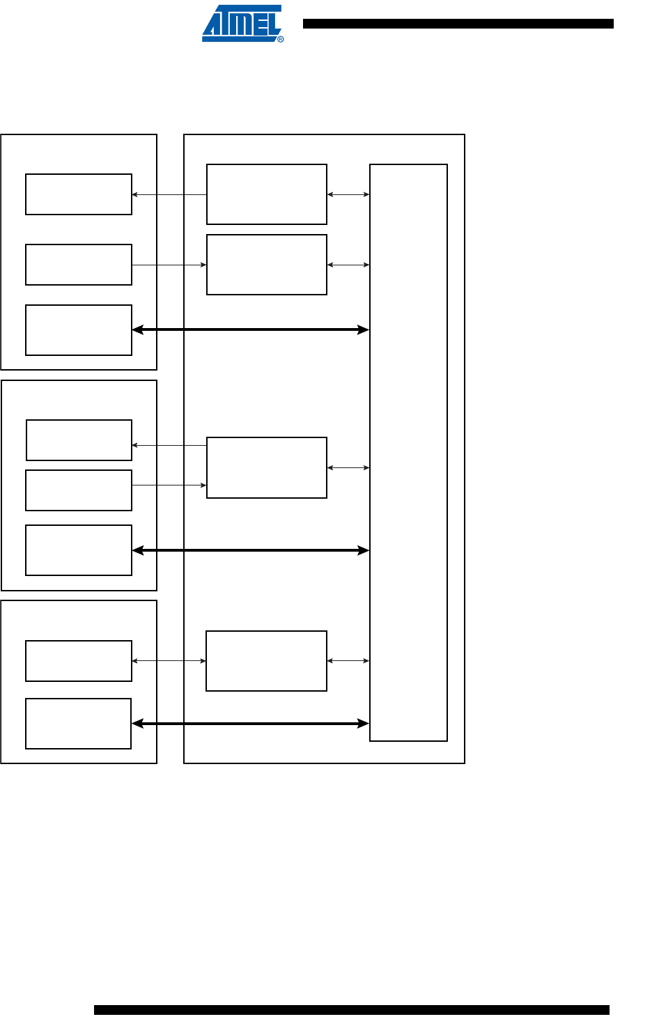
442
6430F–ATARM–21-Feb-12
SAM3U Series
442
6430F–ATARM–21-Feb-12
SAM3U Series
26.3 Block Diagram
Figure 26-1. Block Diagram
26.4 Functional Description
26.4.1 Configuration
The PDC channel user interface enables the user to configure and control data transfers for
each channel. The user interface of each PDC channel is integrated into the associated periph-
eral user interface.
The user interface of a serial peripheral, whether it is full or half duplex, contains four 32-bit
pointers (RPR, RNPR, TPR, TNPR) and four 16-bit counter registers (RCR, RNCR, TCR,
TNCR). However, the transmit and receive parts of each type are programmed differently: the
PDC
FULL DUPLEX
PERIPHERAL
THR
RHR
PDC Channel A
PDC Channel B
Control
Status & Control
Control
PDC Channel C
HALF DUPLEX
PERIPHERAL
THR
Status & Control
RECEIVE or TRANSMIT
PERIPHERAL
RHR or THR
Control
Control
RHR
PDC Channel D
Status & Control

443
6430F–ATARM–21-Feb-12
SAM3U Series
443
6430F–ATARM–21-Feb-12
SAM3U Series
transmit and receive parts of a full duplex peripheral can be programmed at the same time,
whereas only one part (transmit or receive) of a half duplex peripheral can be programmed at a
time.
32-bit pointers define the access location in memory for current and next transfer, whether it is
for read (transmit) or write (receive). 16-bit counters define the size of current and next transfers.
It is possible, at any moment, to read the number of transfers left for each channel.
The PDC has dedicated status registers which indicate if the transfer is enabled or disabled for
each channel. The status for each channel is located in the associated peripheral status register.
Transfers can be enabled and/or disabled by setting TXTEN/TXTDIS and RXTEN/RXTDIS in
the peripheral’s Transfer Control Register.
At the end of a transfer, the PDC channel sends status flags to its associated peripheral. These
flags are visible in the peripheral status register (ENDRX, ENDTX, RXBUFF, and TXBUFE).
Refer to Section 26.4.3 and to the associated peripheral user interface.
26.4.2 Memory Pointers
Each full duplex peripheral is connected to the PDC by a receive channel and a transmit chan-
nel. Both channels have 32-bit memory pointers that point respectively to a receive area and to
a transmit area in on- and/or off-chip memory.
Each half duplex peripheral is connected to the PDC by a bidirectional channel. This channel
has two 32-bit memory pointers, one for current transfer and the other for next transfer. These
pointers point to transmit or receive data depending on the operating mode of the peripheral.
Depending on the type of transfer (byte, half-word or word), the memory pointer is incremented
respectively by 1, 2 or 4 bytes.
If a memory pointer address changes in the middle of a transfer, the PDC channel continues
operating using the new address.
26.4.3 Transfer Counters
Each channel has two 16-bit counters, one for current transfer and the other one for next trans-
fer. These counters define the size of data to be transferred by the channel. The current transfer
counter is decremented first as the data addressed by current memory pointer starts to be trans-
ferred. When the current transfer counter reaches zero, the channel checks its next transfer
counter. If the value of next counter is zero, the channel stops transferring data and sets the
appropriate flag. But if the next counter value is greater then zero, the values of the next
pointer/next counter are copied into the current pointer/current counter and the channel resumes
the transfer whereas next pointer/next counter get zero/zero as values. At the end of this trans-
fer the PDC channel sets the appropriate flags in the Peripheral Status Register.
The following list gives an overview of how status register flags behave depending on the coun-
ters’ values:
• ENDRX flag is set when the PERIPH_RCR register reaches zero.
• RXBUFF flag is set when both PERIPH_RCR and PERIPH_RNCR reach zero.
• ENDTX flag is set when the PERIPH_TCR register reaches zero.
• TXBUFE flag is set when both PERIPH_TCR and PERIPH_TNCR reach zero.
These status flags are described in the Peripheral Status Register.

444
6430F–ATARM–21-Feb-12
SAM3U Series
444
6430F–ATARM–21-Feb-12
SAM3U Series
26.4.4 Data Transfers
The serial peripheral triggers its associated PDC channels’ transfers using transmit enable
(TXEN) and receive enable (RXEN) flags in the transfer control register integrated in the periph-
eral’s user interface.
When the peripheral receives an external data, it sends a Receive Ready signal to its PDC
receive channel which then requests access to the Matrix. When access is granted, the PDC
receive channel starts reading the peripheral Receive Holding Register (RHR). The read data
are stored in an internal buffer and then written to memory.
When the peripheral is about to send data, it sends a Transmit Ready to its PDC transmit chan-
nel which then requests access to the Matrix. When access is granted, the PDC transmit
channel reads data from memory and puts them to Transmit Holding Register (THR) of its asso-
ciated peripheral. The same peripheral sends data according to its mechanism.
26.4.5 PDC Flags and Peripheral Status Register
Each peripheral connected to the PDC sends out receive ready and transmit ready flags and the
PDC sends back flags to the peripheral. All these flags are only visible in the Peripheral Status
Register.
Depending on the type of peripheral, half or full duplex, the flags belong to either one single
channel or two different channels.
26.4.5.1 Receive Transfer End
This flag is set when PERIPH_RCR register reaches zero and the last data has been transferred
to memory.
It is reset by writing a non zero value in PERIPH_RCR or PERIPH_RNCR.
26.4.5.2 Transmit Transfer End
This flag is set when PERIPH_TCR register reaches zero and the last data has been written into
peripheral THR.
It is reset by writing a non zero value in PERIPH_TCR or PERIPH_TNCR.
26.4.5.3 Receive Buffer Full
This flag is set when PERIPH_RCR register reaches zero with PERIPH_RNCR also set to zero
and the last data has been transferred to memory.
It is reset by writing a non zero value in PERIPH_TCR or PERIPH_TNCR.
26.4.5.4 Transmit Buffer Empty
This flag is set when PERIPH_TCR register reaches zero with PERIPH_TNCR also set to zero
and the last data has been written into peripheral THR.
It is reset by writing a non zero value in PERIPH_TCR or PERIPH_TNCR.

445
6430F–ATARM–21-Feb-12
SAM3U Series
445
6430F–ATARM–21-Feb-12
SAM3U Series
26.5 Peripheral DMA Controller (PDC) User Interface
Note: 1. PERIPH: Ten registers are mapped in the peripheral memory space at the same offset. These can be defined by the user
according to the function and the desired peripheral.)
Table 26-1. Register Mapping
Offset Register Name Access Reset
0x100 Receive Pointer Register PERIPH(1)_RPR Read-write 0
0x104 Receive Counter Register PERIPH_RCR Read-write 0
0x108 Transmit Pointer Register PERIPH_TPR Read-write 0
0x10C Transmit Counter Register PERIPH_TCR Read-write 0
0x110 Receive Next Pointer Register PERIPH_RNPR Read-write 0
0x114 Receive Next Counter Register PERIPH_RNCR Read-write 0
0x118 Transmit Next Pointer Register PERIPH_TNPR Read-write 0
0x11C Transmit Next Counter Register PERIPH_TNCR Read-write 0
0x120 Transfer Control Register PERIPH_PTCR Write-only 0
0x124 Transfer Status Register PERIPH_PTSR Read-only 0

446
6430F–ATARM–21-Feb-12
SAM3U Series
446
6430F–ATARM–21-Feb-12
SAM3U Series
26.5.1 Receive Pointer Register
Name: PERIPH_RPR
Access: Read-write
• RXPTR: Receive Pointer Register
RXPTR must be set to receive buffer address.
When a half duplex peripheral is connected to the PDC, RXPTR = TXPTR.
31 30 29 28 27 26 25 24
RXPTR
23 22 21 20 19 18 17 16
RXPTR
15 14 13 12 11 10 9 8
RXPTR
76543210
RXPTR

447
6430F–ATARM–21-Feb-12
SAM3U Series
447
6430F–ATARM–21-Feb-12
SAM3U Series
26.5.2 Receive Counter Register
Name: PERIPH_RCR
Access: Read-write
• RXCTR: Receive Counter Register
RXCTR must be set to receive buffer size.
When a half duplex peripheral is connected to the PDC, RXCTR = TXCTR.
0 = Stops peripheral data transfer to the receiver
1 - 65535 = Starts peripheral data transfer if corresponding channel is active
31 30 29 28 27 26 25 24
––––––––
23 22 21 20 19 18 17 16
––––––––
15 14 13 12 11 10 9 8
RXCTR
76543210
RXCTR

448
6430F–ATARM–21-Feb-12
SAM3U Series
448
6430F–ATARM–21-Feb-12
SAM3U Series
26.5.3 Transmit Pointer Register
Name: PERIPH_TPR
Access: Read-write
• TXPTR: Transmit Counter Register
TXPTR must be set to transmit buffer address.
When a half duplex peripheral is connected to the PDC, RXPTR = TXPTR.
31 30 29 28 27 26 25 24
TXPTR
23 22 21 20 19 18 17 16
TXPTR
15 14 13 12 11 10 9 8
TXPTR
76543210
TXPTR

449
6430F–ATARM–21-Feb-12
SAM3U Series
449
6430F–ATARM–21-Feb-12
SAM3U Series
26.5.4 Transmit Counter Register
Name: PERIPH_TCR
Access: Read-write
• TXCTR: Transmit Counter Register
TXCTR must be set to transmit buffer size.
When a half duplex peripheral is connected to the PDC, RXCTR = TXCTR.
0 = Stops peripheral data transfer to the transmitter
1- 65535 = Starts peripheral data transfer if corresponding channel is active
31 30 29 28 27 26 25 24
––––––––
23 22 21 20 19 18 17 16
––––––––
15 14 13 12 11 10 9 8
TXCTR
76543210
TXCTR

450
6430F–ATARM–21-Feb-12
SAM3U Series
450
6430F–ATARM–21-Feb-12
SAM3U Series
26.5.5 Receive Next Pointer Register
Name: PERIPH_RNPR
Access: Read-write
• RXNPTR: Receive Next Pointer
RXNPTR contains next receive buffer address.
When a half duplex peripheral is connected to the PDC, RXNPTR = TXNPTR.
31 30 29 28 27 26 25 24
RXNPTR
23 22 21 20 19 18 17 16
RXNPTR
15 14 13 12 11 10 9 8
RXNPTR
76543210
RXNPTR

451
6430F–ATARM–21-Feb-12
SAM3U Series
451
6430F–ATARM–21-Feb-12
SAM3U Series
26.5.6 Receive Next Counter Register
Name: PERIPH_RNCR
Access: Read-write
• RXNCTR: Receive Next Counter
RXNCTR contains next receive buffer size.
When a half duplex peripheral is connected to the PDC, RXNCTR = TXNCTR.
31 30 29 28 27 26 25 24
––––––––
23 22 21 20 19 18 17 16
––––––––
15 14 13 12 11 10 9 8
RXNCTR
76543210
RXNCTR

452
6430F–ATARM–21-Feb-12
SAM3U Series
452
6430F–ATARM–21-Feb-12
SAM3U Series
26.5.7 Transmit Next Pointer Register
Name: PERIPH_TNPR
Access: Read-write
• TXNPTR: Transmit Next Pointer
TXNPTR contains next transmit buffer address.
When a half duplex peripheral is connected to the PDC, RXNPTR = TXNPTR.
31 30 29 28 27 26 25 24
TXNPTR
23 22 21 20 19 18 17 16
TXNPTR
15 14 13 12 11 10 9 8
TXNPTR
76543210
TXNPTR

453
6430F–ATARM–21-Feb-12
SAM3U Series
453
6430F–ATARM–21-Feb-12
SAM3U Series
26.5.8 Transmit Next Counter Register
Name: PERIPH_TNCR
Access: Read-write
• TXNCTR: Transmit Counter Next
TXNCTR contains next transmit buffer size.
When a half duplex peripheral is connected to the PDC, RXNCTR = TXNCTR.
31 30 29 28 27 26 25 24
––––––––
23 22 21 20 19 18 17 16
––––––––
15 14 13 12 11 10 9 8
TXNCTR
76543210
TXNCTR

454
6430F–ATARM–21-Feb-12
SAM3U Series
454
6430F–ATARM–21-Feb-12
SAM3U Series
26.5.9 Transfer Control Register
Name: PERIPH_PTCR
Access: Write-only
• RXTEN: Receiver Transfer Enable
0 = No effect.
1 = Enables PDC receiver channel requests if RXTDIS is not set.
When a half duplex peripheral is connected to the PDC, enabling the receiver channel requests automatically disables the
transmitter channel requests. It is forbidden to set both TXTEN and RXTEN for a half duplex peripheral.
• RXTDIS: Receiver Transfer Disable
0 = No effect.
1 = Disables the PDC receiver channel requests.
When a half duplex peripheral is connected to the PDC, disabling the receiver channel requests also disables the transmit-
ter channel requests.
• TXTEN: Transmitter Transfer Enable
0 = No effect.
1 = Enables the PDC transmitter channel requests.
When a half duplex peripheral is connected to the PDC, it enables the transmitter channel requests only if RXTEN is not
set. It is forbidden to set both TXTEN and RXTEN for a half duplex peripheral.
• TXTDIS: Transmitter Transfer Disable
0 = No effect.
1 = Disables the PDC transmitter channel requests.
When a half duplex peripheral is connected to the PDC, disabling the transmitter channel requests disables the receiver
channel requests.
31 30 29 28 27 26 25 24
––––––––
23 22 21 20 19 18 17 16
––––––––
15 14 13 12 11 10 9 8
––––––TXTDISTXTEN
76543210
––––––RXTDISRXTEN
455
6430F–ATARM–21-Feb-12
SAM3U Series
455
6430F–ATARM–21-Feb-12
SAM3U Series
26.5.10 Transfer Status Register
Name: PERIPH_PTSR
Access: Read-only
• RXTEN: Receiver Transfer Enable
0 = PDC Receiver channel requests are disabled.
1 = PDC Receiver channel requests are enabled.
• TXTEN: Transmitter Transfer Enable
0 = PDC Transmitter channel requests are disabled.
1 = PDC Transmitter channel requests are enabled.
31 30 29 28 27 26 25 24
––––––––
23 22 21 20 19 18 17 16
––––––––
15 14 13 12 11 10 9 8
–––––––TXTEN
76543210
–––––––RXTEN

456
6430F–ATARM–21-Feb-12
SAM3U Series
456
6430F–ATARM–21-Feb-12
SAM3U Series

457
6430F–ATARM–21-Feb-12
SAM3U Series
27. Clock Generator
27.1 Description
The Clock Generator is made up of:
• A Low Power 32,768 Hz Slow Clock Oscillator with bypass mode
• A Low Power RC Oscillator
• A 3 to 20 MHz Crystal Oscillator (12 MHz needed in case of USB), which can be bypassed
• A factory programmed Fast RC Oscillator, 3 output frequencies can be selected: 4, 8 or
12 MHz. By default 4 MHz is selected.
• A 480 MHz UTMI PLL providing a clock for the USB High Speed Device Controller
• A 96 to 192 MHz programmable PLL (input from 8 to 16 MHz), capable of providing the clock
MCK to the processor and to the peripherals.
It provides the following clocks:
• SLCK, the Slow Clock, which is the only permanent clock within the system
• MAINCK is the output of the Main Clock Oscillator selection: either Crystal Oscillator or
4/8/12 MHz Fast RC Oscillator
• PLLACK is the output of the Divider and 96 to 192 MHz programmable PLL (PLLA)
• UPLLCK is the output of the 480 MHz UTMI PLL (UPLL)
The Clock Generator User Interface is embedded within the Power Management Controller and
is described in Section 28.14 ”Power Management Controller (PMC) User Interface”. However,
the Clock Generator registers are named CKGR_.
458
6430F–ATARM–21-Feb-12
SAM3U Series
27.2 Block Diagram
Figure 27-1. Clock Generator Block Diagram
Power
Management
Controller
Main Clock
MAINCK
PLLA Clock
PLLACK
ControlStatus
3-20 MHz
Crystal
Oscillator
MOSCSEL
Clock Generator
PLLA and
Divider
Embedded
12/8/4 MHz
Fast
RC Oscillator
XIN
XOUT
XIN32
XOUT32
Slow Clock
SLCK
XTALSEL
(Supply Controller)
Embedded
32 kHz RC
Oscillator
32768 Hz
Crystal
Oscillator
UPLL Clock
UPLLCK
USB UTMI
PLL
0
1
0
1
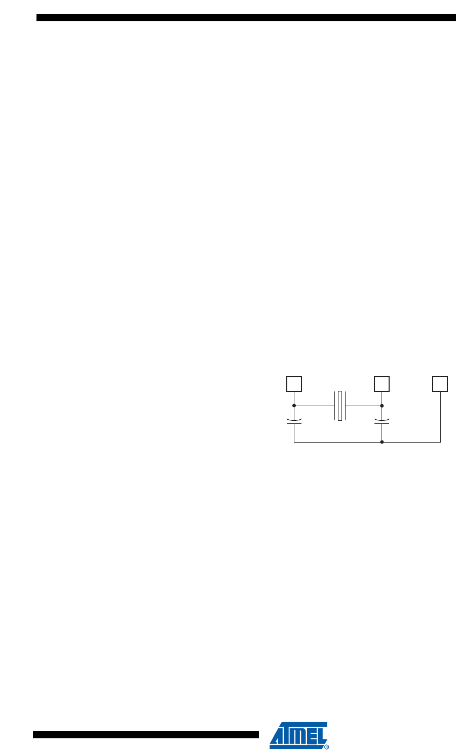
459
6430F–ATARM–21-Feb-12
SAM3U Series
27.3 Slow Clock
The Slow Clock is generated either by the Slow Clock Crystal Oscillator or by the Slow Clock RC
Oscillator.
The selection is made by writing the XTALSEL bit in the Supply Controller Control Register
(SUPC_CR).
By default, the RC Oscillator is selected.
27.3.1 Slow Clock RC Oscillator
By default, the Slow Clock RC Oscillator is enabled and selected. The user has to take into
account the possible drifts of the RC Oscillator. More details are given in the section “DC Char-
acteristics” of the product datasheet.
It can be disabled via the XTALSEL bit in the Supply Controller Control Register (SUPC_CR).
27.3.2 Slow Clock Crystal Oscillator
The Clock Generator integrates a 32,768 Hz low-power oscillator.The XIN and XOUT pins must
be connected to a 32,768 Hz crystal. Two external capacitors must be wired as shown in Figure
27-2.More details are given in the section “DC Characteristics” of the product datasheet.
Note that the user is not obliged to use the Slow Clock Crystal and can use the RC Oscillator
instead. In this case, XIN and XOUT can be left unconnected.
Figure 27-2. Typical Slow Clock Crystal Oscillator Connection
The user can set the Slow Clock Crystal Oscillator in bypass mode instead of connecting a crys-
tal. In this case, the user has to provide the external clock signal on XIN32. The input
characteristics of the XIN pin under these conditions are given in the product electrical charac-
teristics section.
The programmer has to be sure to set the OSCBYPASS bit in the Supply Controller Mode Reg-
ister (SUPC_MR) and XTALSEL bit in the Supply Controller Control Register (SUPC_CR).
XIN32 XOUT32 GNDBU
32,768 Hz
Crystal
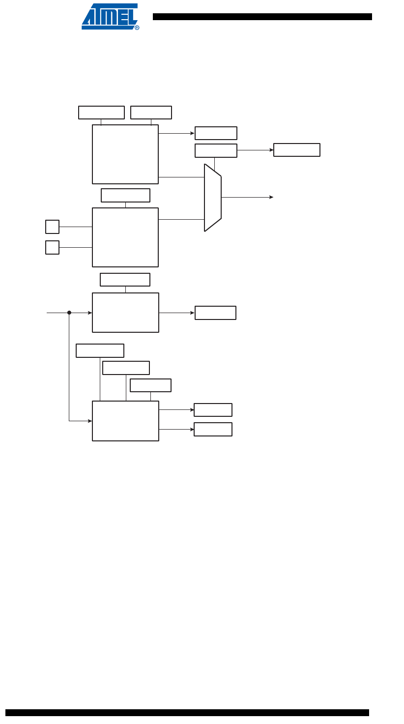
460
6430F–ATARM–21-Feb-12
SAM3U Series
27.4 Main Clock
Figure 27-3 shows the Main Clock block diagram.
Figure 27-3. Main Clock Block Diagram
The Main Clock has two sources:
• 4/8/12 MHz Fast RC Oscillator which starts very quickly and is used at startup
• 3 to 20 MHz Crystal Oscillator, which can be bypassed
27.4.1 4/8/12 MHz Fast RC Oscillator
After reset, the 4/8/12 MHz Fast RC Oscillator is enabled with the 4 MHz frequency selected and
it is selected as the source of MAINCK. MAINCK is the default clock selected to start up the
system.
The Fast RC Oscillator 8 and 12 MHz frequencies are calibrated in production. Note that is not
the case for the 4 MHz frequency.
Please refer to the “DC Characteristics” section of the product datasheet.
The software can disable or enable the 4/8/12 MHz Fast RC Oscillator with the MOSCRCEN bit
in the Clock Generator Main Oscillator Register (CKGR_MOR).
The user can also select the output frequency of the Fast RC Oscillator: either 4 MHz, 8 MHz or
12 MHz are available. It can be done through MOSCRCF bits in CKGR_MOR. When changing
XIN
XOUT
MOSCXTEN
MOSCXTCNT
MOSCXTS
Main Clock
Frequency
Counter
MAINF
MAINRDY
SLCK
Slow Clock
3-20 MHz
Crystal
Oscillator
3-20 MHz Crystal
Oscillator
Counter
MOSCRCEN
4/8/12 MHz
Fast RC
Oscillator
MOSCRCS
MOSCRCF
MOSCRCEN
MOSCXTEN
MOSCSEL
MOSCSEL MOSCSELS
1
0
MAINCK
Main Clock

461
6430F–ATARM–21-Feb-12
SAM3U Series
this frequency selection, the MOSCRCS bit in the Power Management Controller Status Regis-
ter (PMC_SR) is automatically cleared and MAINCK is stopped until the oscillator is stabilized.
Once the oscillator is stabilized, MAINCK restarts and MOSCRCS is set.
When disabling the Main Clock by clearing the MOSCRCEN bit in CKGR_MOR, the MOSCRCS
bit in the Power Management Controller Status Register (PMC_SR) is automatically cleared,
indicating the Main Clock is off.
Setting the MOSCRCS bit in the Power Management Controller Interrupt Enable Register
(PMC_IER) can trigger an interrupt to the processor.
27.4.2 3 to 20 MHz Crystal Oscillator
After reset, the 3 to 20 MHz Crystal Oscillator is disabled and it is not selected as the source of
MAINCK.
The user can select the 3 to 20 MHz crystal oscillator to be the source of MAINCK, as it provides
a more accurate frequency. The software enables or disables the main oscillator so as to reduce
power consumption by clearing the MOSCXTEN bit in the Main Oscillator Register
(CKGR_MOR).
When disabling the main oscillator by clearing the MOSCXTEN bit in CKGR_MOR, the
MOSCXTS bit in PMC_SR is automatically cleared, indicating the Main Clock is off.
When enabling the main oscillator, the user must initiate the main oscillator counter with a value
corresponding to the startup time of the oscillator. This startup time depends on the crystal fre-
quency connected to the oscillator.
When the MOSCXTEN bit and the MOSCXTCNT are written in CKGR_MOR to enable the main
oscillator, the MOSCXTS bit in the Power Management Controller Status Register (PMC_SR) is
cleared and the counter starts counting down on the slow clock divided by 8 from the MOSCX-
TCNT value. Since the MOSCXTCNT value is coded with 8 bits, the maximum startup time is
about 62 ms.
When the counter reaches 0, the MOSCXTS bit is set, indicating that the main clock is valid.
Setting the MOSCXTS bit in PMC_IMR can trigger an interrupt to the processor.
27.4.3 Main Clock Oscillator Selection
The user can select either the 4/8/12 MHz Fast RC Oscillator or the 3 to 20 MHz Crystal Oscilla-
tor to be the source of Main Clock.
The advantage of the 4/8/12 MHz Fast RC Oscillator is to have fast startup time, this is why it is
selected by default (to start up the system) and when entering in Wait Mode.
The advantage of the 3 to 20 MHz Crystal Oscillator is that it is very accurate.
The selection is made by writing the MOSCSEL bit in the Main Oscillator Register
(CKGR_MOR). The switch of the Main Clock source is glitch free, so there is no need to run out
of SLCK, PLLACK or UPLLCK in order to change the selection. The MOSCSELS bit of the
Power Management Controller Status Register (PMC_SR) allows knowing when the switch
sequence is done.
Setting the MOSCSELS bit in PMC_IMR can trigger an interrupt to the processor.

462
6430F–ATARM–21-Feb-12
SAM3U Series
27.4.4 Main Clock Frequency Counter
The device features a Main Clock frequency counter that provides the frequency of the Main
Clock.
The Main Clock frequency counter is reset and starts incrementing at the Main Clock speed after
the next rising edge of the Slow Clock in the following cases:
• when the 4/8/12 MHz Fast RC Oscillator clock is selected as the source of Main Clock and
when this oscillator becomes stable (i.e., when the MOSCRCS bit is set)
• when the 3 to 20 MHz Crystal Oscillator is selected as the source of Main Clock and when
this oscillator becomes stable (i.e., when the MOSCXTS bit is set)
• when the Main Clock Oscillator selection is modified
Then, at the 16th falling edge of Slow Clock, the MAINFRDY bit in the Clock Generator Main
Clock Frequency Register (CKGR_MCFR) is set and the counter stops counting. Its value can
be read in the MAINF field of CKGR_MCFR and gives the number of Main Clock cycles during
16 periods of Slow Clock, so that the frequency of the 4/8/12 MHz Fast RC Oscillator or 3 to 20
MHz Crystal Oscillator can be determined.
463
6430F–ATARM–21-Feb-12
SAM3U Series
27.5 Divider and PLLA Block
The PLLA embeds an input divider to increase the accuracy of the resulting clock signals. How-
ever, the user must respect the PLLA minimum input frequency when programming the divider.
Figure 27-4 shows the block diagram of the divider and PLLA block.
Figure 27-4. Divider and PLLA Block Diagram
27.5.1 Divider and Phase Lock Loop Programming
The divider can be set between 1 and 255 in steps of 1. When a divider field (DIV) is set to 0, the
output of the corresponding divider and the PLL output is a continuous signal at level 0. On
reset, each DIV field is set to 0, thus the corresponding PLL input clock is set to 0.
The PLLA allows multiplication of the divider’s outputs. The PLLA clock signal has a frequency
that depends on the respective source signal frequency and on the parameters DIVA and
MULA. The factor applied to the source signal frequency is (MULA + 1)/DIVA. When MULA is
written to 0, the PLLA is disabled and its power consumption is saved. Re-enabling the PLLA
can be performed by writing a value higher than 0 in the MULA field.
Whenever the PLLA is re-enabled or one of its parameters is changed, the LOCKA bit in
PMC_SR is automatically cleared. The values written in the PLLACOUNT field in CKGR_PLLAR
are loaded in the PLLA counter. The PLLA counter then decrements at the speed of the Slow
Clock until it reaches 0. At this time, the LOCK bit is set in PMC_SR and can trigger an interrupt
to the processor. The user has to load the number of Slow Clock cycles required to cover the
PLLA transient time into the PLLACOUNT field.
Divider
DIVA
PLLA
MULA
PLLACOUNT
LOCKA
OUTA
SLCK
MAINCK PLLACK
PLLA
Counter

464
6430F–ATARM–21-Feb-12
SAM3U Series
27.6 UTMI Phase Lock Loop Programming
The clock source of the UTMI PLL is the 3-20 MHz Crystal Oscillator. When the 4/8/12 MHz Fast
RC Oscillator is selected as the source of MAINCK, the 12 MHz frequency must also be selected
because the UTMI PLL multiplier contains a built-in multiplier of x 40 to obtain the USB High
Speed 480 MHz.
A 12 MHz crystal is needed to use the USB.
Figure 27-5. UTMI PLL Block Diagram
Whenever the UTMI PLL is enabled by writing UPLLEN in CKGR_UCKR, the LOCKU bit in
PMC_SR is automatically cleared. The values written in the PLLCOUNT field in CKGR_UCKR
are loaded in the UTMI PLL counter. The UTMI PLL counter then decrements at the speed of
the Slow Clock divided by 8 until it reaches 0. At this time, the LOCKU bit is set in PMC_SR and
can trigger an interrupt to the processor. The user has to load the number of Slow Clock cycles
required to cover the UTMI PLL transient time into the PLLCOUNT field.
UTMI PLL
UPLLEN
UPLLCOUNT
LOCKU
SLCK
3-20 MHz Crystal UPLLCK
UTMI PLL
Counter

465
6430F–ATARM–21-Feb-12
SAM3U Series
28. Power Management Controller (PMC)
28.1 Description
The Power Management Controller (PMC) optimizes power consumption by controlling all sys-
tem and user peripheral clocks. The PMC enables/disables the clock inputs to many of the
peripherals and the Cortex-M3 Processor.
The Power Management Controller provides the following clocks:
• MCK, the Master Clock, programmable from a few hundred Hz to the maximum operating
frequency of the device. It is available to the modules running permanently, such as the
Enhanced Embedded Flash Controller.
• Processor Clock (HCLK) is automatically switched off when the processor enters Sleep
Mode.
• Free running processor Clock (FCLK)
• the Cortex-M3 SysTick external clock
• the USB Device HS Clock (UDPCK)
• Peripheral Clocks, typically MCK, provided to the embedded peripherals (USART, PMC, SPI,
TWI, TC, HSMCI, etc.) and independently controllable. In order to reduce the number of clock
names in a product, the Peripheral Clocks are named MCK in the product datasheet.
• Programmable Clock Outputs can be selected from the clocks provided by the clock
generator and driven on the PCKx pins.
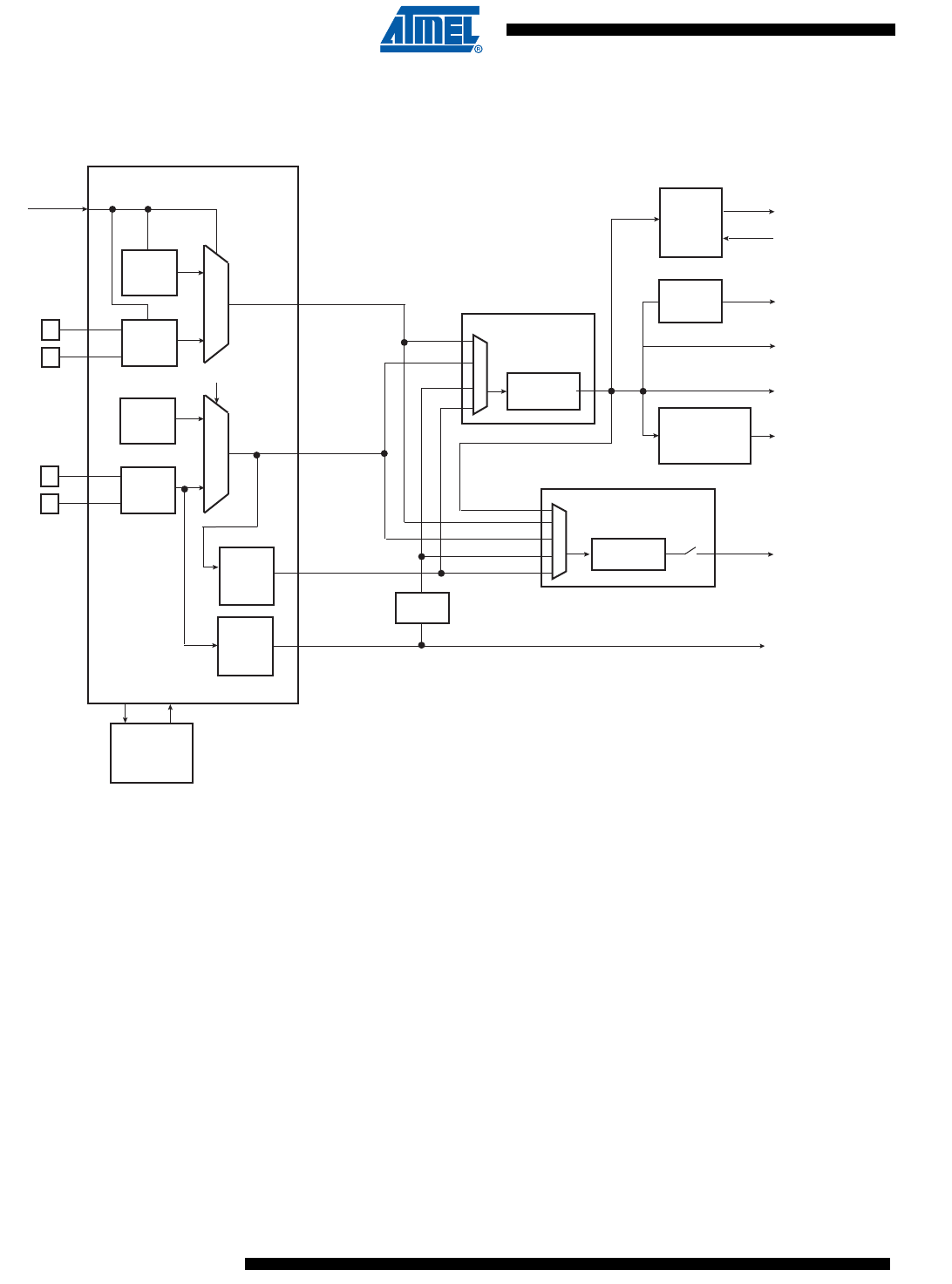
466
6430F–ATARM–21-Feb-12
SAM3U Series
28.2 Block Diagram
Figure 28-1. General Clock Block Diagram
28.3 Master Clock Controller
The Master Clock Controller provides selection and division of the Master Clock (MCK). MCK is
the clock provided to all the peripherals and the memory controller.
The Master Clock is selected from one of the clocks provided by the Clock Generator. Selecting
the Slow Clock provides a Slow Clock signal to the whole device. Selecting the Main Clock
saves power consumption of the PLLs.
The Master Clock Controller is made up of a clock selector and a prescaler.
The Master Clock selection is made by writing the CSS field (Clock Source Selection) in
PMC_MCKR (Master Clock Register). The prescaler supports the division by a power of 2 of the
selected clock between 1 and 64, and the division by 3. The PRES field in PMC_MCKR pro-
grams the prescaler.
Each time PMC_MCKR is written to define a new Master Clock, the MCKRDY bit is cleared in
PMC_SR. It reads 0 until the Master Clock is established. Then, the MCKRDY bit is set and can
trigger an interrupt to the processor. This feature is useful when switching from a high-speed
clock to a lower one to inform the software when the change is actually done.
Power
Management
Controller
Main Clock
MAINCK
PLLA Clock
PLLACK
ControlStatus
3-20 MHz
Crystal
Oscillator
MOSCSEL
Clock Generator
PLLA and
Divider
Embedded
12/8/4 MHz
Fast
RC Oscillator
XIN
XOUT
XIN32
XOUT32
Slow Clock
SLCK
XTALSEL
(Supply Controller)
Embedded
32 kHz RC
Oscillator
32768 Hz
Crystal
Oscillator
UPLL Clock
UPLLCK
USB UTMI
PLL
0
1
0
1
MCK
periph_clk[..]
int
SLCK
MAINCK
PLLACK
Prescaler
/1,/2,/4,...,/64
HCLK
Processor
Clock
Controller
Sleep Mode
Master Clock Controller
Peripherals
Clock Controller
ON/OFF
USB Clock
Prescaler
/1,/2,/3,/4,...,/64
Programmable Clock Controller
pck[..]
UPLLCK/2
UDPCK
ON/OFF
FCLK
SysTick
Divider
/8
SLCK
MAINCK
PLLACK
UPLLCK/2
Processor Clock
Free Running Clock
Master Clock
MCK
Divider
/2

467
6430F–ATARM–21-Feb-12
SAM3U Series
Figure 28-2. Master Clock Controller
28.4 Processor Clock Controller
The PMC features a Processor Clock Controller (HCLK) that implements the Processor Sleep
Mode. The Processor Clock can be disabled by executing the WFI (WaitForInterrupt) or the
WFE (WaitForEvent) processor instruction while the LPM bit is at 0 in the PMC Fast Startup
Mode Register (PMC_FSMR).
The Processor Clock HCLK is enabled after a reset and is automatically re-enabled by any
enabled interrupt. The Processor Sleep Mode is achieved by disabling the Processor Clock,
which is automatically re-enabled by any enabled fast or normal interrupt, or by the reset of the
product.
When Processor Sleep Mode is entered, the current instruction is finished before the clock is
stopped, but this does not prevent data transfers from other masters of the system bus.
28.5 SysTick Clock
The SysTick calibration value is fixed to 10500 which allows the generation of a time base of
1 ms with SysTick clock at 10.5 MHz (max HCLK/8).
28.6 Peripheral Clock Controller
The Power Management Controller controls the clocks of each embedded peripheral by the way
of the Peripheral Clock Controller. The user can individually enable and disable the Master
Clock on the peripherals by writing into the Peripheral Clock Enable (PMC_PCER) and Periph-
eral Clock Disable (PMC_PCDR) registers. The status of the peripheral clock activity can be
read in the Peripheral Clock Status Register (PMC_PCSR).
When a peripheral clock is disabled, the clock is immediately stopped. The peripheral clocks are
automatically disabled after a reset.
In order to stop a peripheral, it is recommended that the system software wait until the peripheral
has executed its last programmed operation before disabling the clock. This is to avoid data cor-
ruption or erroneous behavior of the system.
The bit number within the Peripheral Clock Control registers (PMC_PCER, PMC_PCDR, and
PMC_PCSR) is the Peripheral Identifier defined at the product level. Generally, the bit number
corresponds to the interrupt source number assigned to the peripheral.
28.7 Free Running Processor Clock
The free running processor clock (FCLK) used for sampling interrupts and clocking debug blocks
ensures that interrupts can be sampled, and sleep events can be traced while the processor is
sleeping. It is connected to Master Clock (MCK).
SLCK
Master Clock
Prescaler MCK
PRESCSS
MAINCK
PLLACK
UPLLCK
To the Processor
Clock Controller (PCK)
PMC_MCKR PMC_MCKR

468
6430F–ATARM–21-Feb-12
SAM3U Series
28.8 Programmable Clock Output Controller
The PMC controls 3 signals to be output on external pins, PCKx. Each signal can be indepen-
dently programmed via the PMC_PCKx registers.
PCKx can be independently selected between the Slow Clock (SLCK), the Main Clock
(MAINCK), the PLLA Clock (PLLACK), the UTMI PLL Clock (UPLLCK/2) and the Master Clock
(MCK) by writing the CSS field in PMC_PCKx. Each output signal can also be divided by a
power of 2 between 1 and 64 by writing the PRES (Prescaler) field in PMC_PCKx.
Each output signal can be enabled and disabled by writing 1 in the corresponding bit, PCKx of
PMC_SCER and PMC_SCDR, respectively. Status of the active programmable output clocks
are given in the PCKx bits of PMC_SCSR (System Clock Status Register).
Moreover, like the PCK, a status bit in PMC_SR indicates that the Programmable Clock is actu-
ally what has been programmed in the Programmable Clock registers.
As the Programmable Clock Controller does not manage with glitch prevention when switching
clocks, it is strongly recommended to disable the Programmable Clock before any configuration
change and to re-enable it after the change is actually performed.
28.9 Fast Startup
The SAM3U device allows the processor to restart in less than six microseconds while the
device is in Wait mode. The system enters Wait mode either by writing the WAITMODE bit at 1
in the PMC Clock Generator Main Oscillator Register (CKGR_MOR), of by executing the Wait-
ForEvent (WFE) instruction of the processor while the LPM bit is at 1 in the PMC Fast Startup
Mode Register (PMC_FSMR).
Important: Prior to asserting any WFE instruction to the processor, the internal sources of
wakeup provided by RTT, RTC and USB must be cleared and verified too, that none of the
enabled external wakeup inputs (WKUP) hold an active polarity.
A Fast Startup is enabled upon the detection of a programmed level on one of the 19 wake-up
inputs (WKUP) or upon an active alarm form the RTC, RTT and USB High Speed Device Con-
troller. The polarity of the 16 wake-up inputs is programmable by writing the PMC Fast Startup
Polarity Register (PMC_FSPR).
The Fast Restart circuitry, as shown in Figure 28-3, is fully asynchronous and provides a fast
startup signal to the Power Management Controller. As soon as the fast startup signal is
asserted, this automatically restarts the embedded 4/8/12 MHz Fast RC oscillator.
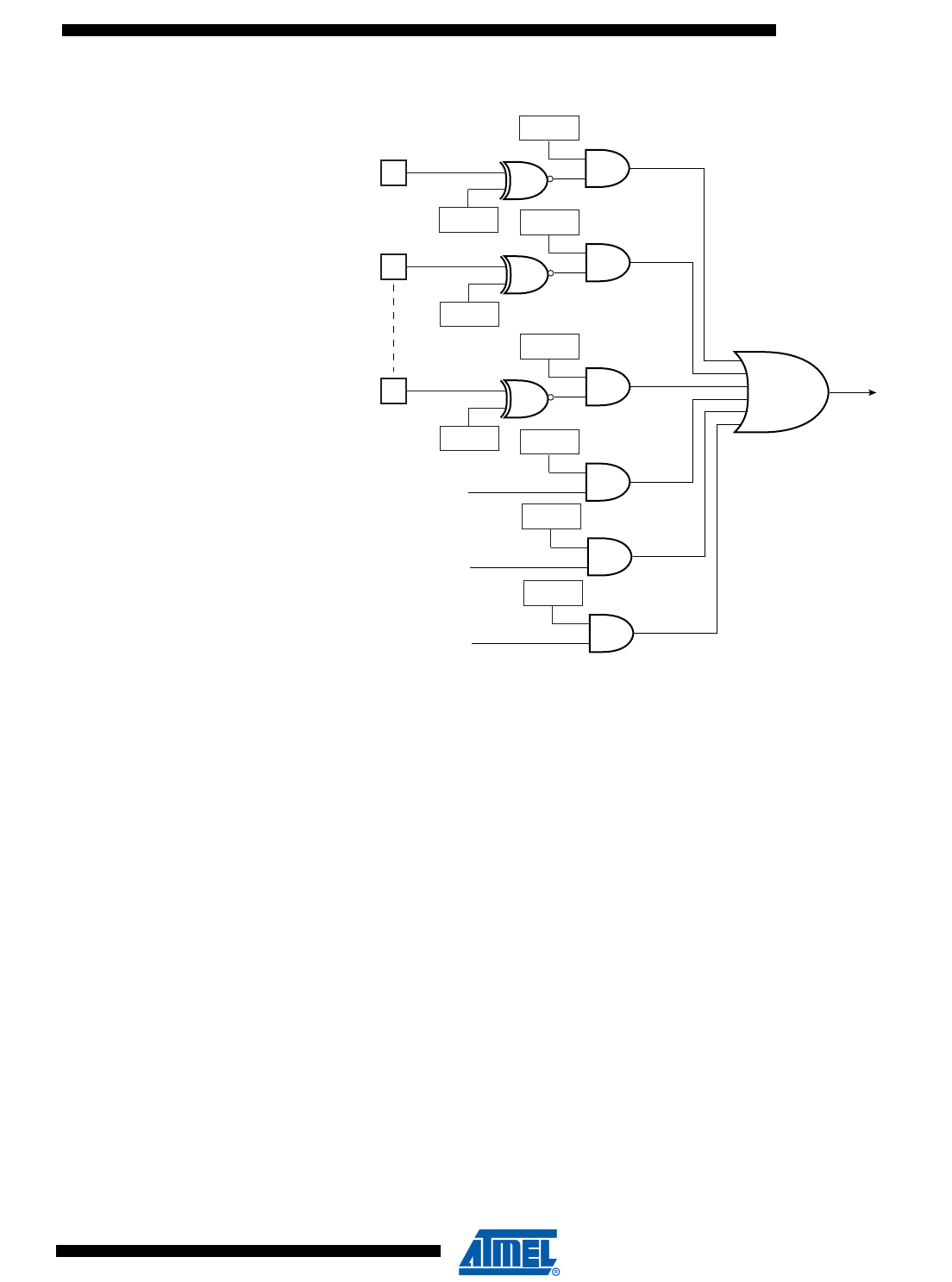
469
6430F–ATARM–21-Feb-12
SAM3U Series
Figure 28-3. Fast Startup Circuitry
Each wake-up input pin and alarm can be enabled to generate a Fast Startup event by writing at
1 the corresponding bit in the Fast Startup Mode Register PMC_FSMR.
The user interface does not provide any status for Fast Startup, but the user can easily recover
this information by reading the PIO Controller, and the status registers of the RTC, RTT and
USB High Speed Device Controller.
fast_restart
WKUP15
FSTT15
FSTP15
WKUP1
FSTT1
FSTP1
WKUP0
FSTT0
FSTP0
RTTAL
RTCAL
USBAL
RTT Alarm
RTC Alarm
USB Alarm

470
6430F–ATARM–21-Feb-12
SAM3U Series
28.10 Clock Failure Detector
The clock failure detector allows to monitor the 3 to 20 MHz Crystal Oscillator and to detect an
eventual defect of this oscillator (for example if the crystal is disconnected).
The clock failure detector can be enabled or disabled by means of the CFDEN bit in the PMC
Clock Generator Main Oscillator Register (CKGR_MOR). After reset, the detector is disabled.
However, if the 3 to 20 MHz Crystal Oscillator is disabled, the clock failure detector is disabled
too.
A failure is detected by means of a counter incrementing on the 3 to 20 MHzCrystal oscillator or
Ceramic Resonator-based oscillator clock edge and timing logic clocked on the slow clock RC
oscillator controlling the counter. The counter is cleared when the slow clock RC oscillator signal
is low and enabled when the slow clock RC oscillator is high. Thus the failure detection time is 1
slow clock RC oscillator clock period. If, during the high level period of slow clock RC oscillator,
less than 8 fast crystal clock periods have been counted, then a failure is declared.
If a failure of the 3 to 20 MHz Crystal Oscillator clock is detected, the CFDEV flag is set in the
PMC Status Register (PMC_SR), and can generate an interrupt if it is not masked. The interrupt
remains active until a read operation in the PMC_SR register. The user can know the status of
the clock failure detector at any time by reading the CFDS bit in the PMC_SR register.
If the 3 to 20 MHz Crystal Oscillator clock is selected as the source clock of MAINCK (MOSC-
SEL = 1), and if the Master Clock Source is PLLACK or UPLLCK (CSS = 2 or 3), then a clock
failure detection switches automatically the Master Clock on MAINCK. Then whatever the PMC
configuration is, a clock failure detection switches automatically MAINCK on the 4/8/12 MHz
Fast RC Oscillator clock. If the Fast RC Oscillator is disabled when a clock failure detection
occurs, it is automatically re-enabled by the clock failure detection mechanism.
A clock failure detection activates a fault output that is connected to the Pulse Width Modulator
(PWM) Controller. With this connection, the PWM controller is able to force its outputs and to
protect the driven device, if a clock failure is detected. This fault output remains active until the
defect is detected and until it is not cleared by the bit FOCLR in the PMC Fault Output Clear
Register (PMC_FOCR).
It takes 2 slow clock RC oscillator cycles to detect and switch from the 3 to 20 MHz Crystal or
Ceramic Resonator-based oscillator to the 4/8/12 MHz Fast RC Oscillator if the Master Clock
source is Main Clock, or 3 slow clock RC oscillator cycles if the Master Clock source is PLL.
The user can know the status of the fault output at any time by reading the FOS bit in the
PMC_SR register.

471
6430F–ATARM–21-Feb-12
SAM3U Series
28.11 Programming Sequence
1. Enabling the Main Oscillator:
The main oscillator is enabled by setting the MOSCXTEN field in the CKGR_MOR register.
The user can define a start-up time. This can be achieved by writing a value in the
MOSCXTST field in the CKGR_MOR register.
Once this register has been correctly configured, the user must wait for MOSCXTS field in
the PMC_SR register to be set. This can be done either by polling the status register or by
waiting the interrupt line to be raised if the associated interrupt to MOSCXTS has been
enabled in the PMC_IER register.
Start Up Time = 8 * MOSCXTST / SLCK = 56 Slow Clock Cycles.
So, the main oscillator will be enabled (MOSCXTS bit set) after 56 Slow Clock Cycles.
2. Checking the Main Oscillator Frequency (Optional):
In some situations the user may need an accurate measure of the main clock frequency.
This measure can be accomplished via the CKGR_MCFR register.
Once the MAINFRDY field is set in CKGR_MCFR register, the user may read the MAINF
field in CKGR_MCFR register. This provides the number of main clock cycles within sixteen
slow clock cycles.
3. Setting PLL and Divider:
All parameters needed to configure PLLA and the divider are located in the CKGR_PLLAR
register.
The DIVA field is used to control the divider itself. It must be set to 1 when PLLA is used. By
default, DIVA parameter is set to 0 which means that the divider is turned off.
The MULA field is the PLLA multiplier factor. This parameter can be programmed between 0
and 2047. If MULA is set to 0, PLLA will be turned off, otherwise the PLLA output frequency
is PLLA input frequency multiplied by (MULA + 1).
The PLLACOUNT field specifies the number of slow clock cycles before LOCKA bit is set in
the PMC_SR register after CKGR_PLLAR register has been written.
Once the CKGR_PLLA register has been written, the user must wait for the LOCKA bit to be
set in the PMC_SR register. This can be done either by polling the status register or by wait-
ing the interrupt line to be raised if the associated interrupt to LOCKA has been enabled in
the PMC_IER register. All parameters in CKGR_PLLAR can be programmed in a single
write operation. If at some stage one of the following parameters, MULA, DIVA is modified,
LOCKA bit will go low to indicate that PLLA is not ready yet. When PLLA is locked, LOCKA
will be set again. The user is constrained to wait for LOCKA bit to be set before using the
PLLA output clock.
4. Selection of Master Clock and Processor Clock
The Master Clock and the Processor Clock are configurable via the PMC_MCKR register.
The CSS field is used to select the Master Clock divider source. By default, the selected
clock source is main clock.
The PRES field is used to control the Master Clock prescaler. The user can choose between
different values. Master Clock output is prescaler input divided by PRES parameter. By
default, PRES parameter is set to 1 which means that master clock is equal to main clock.

472
6430F–ATARM–21-Feb-12
SAM3U Series
Once the PMC_MCKR register has been written, the user must wait for the MCKRDY bit to
be set in the PMC_SR register. This can be done either by polling the status register or by
waiting for the interrupt line to be raised if the associated interrupt to MCKRDY has been
enabled in the PMC_IER register.
The PMC_MCKR register must not be programmed in a single write operation. The pre-
ferred programming sequence for the PMC_MCKR register is as follows:
• If a new value for CSS field corresponds to PLL Clock,
– Program the PRES field in the PMC_MCKR register.
– Wait for the MCKRDY bit to be set in the PMC_SR register.
– Program the CSS field in the PMC_MCKR register.
– Wait for the MCKRDY bit to be set in the PMC_SR register.
• If a new value for CSS field corresponds to Main Clock or Slow Clock,
– Program the CSS field in the PMC_MCKR register.
– Wait for the MCKRDY bit to be set in the PMC_SR register.
– Program the PRES field in the PMC_MCKR register.
– Wait for the MCKRDY bit to be set in the PMC_SR register.
If at some stage one of the following parameters, CSS or PRES, is modified, the MCKRDY
bit will go low to indicate that the Master Clock and the Processor Clock are not ready yet.
The user must wait for MCKRDY bit to be set again before using the Master and Processor
Clocks.
Note: IF PLLx clock was selected as the Master Clock and the user decides to modify it by writing in
CKGR_PLLR, the MCKRDY flag will go low while PLL is unlocked. Once PLL is locked again,
LOCK goes high and MCKRDY is set.
While PLL is unlocked, the Master Clock selection is automatically changed to Slow Clock. For fur-
ther information, see Section 28.12.2 “Clock Switching Waveforms” on page 475.
Code Example:
write_register(PMC_MCKR,0x00000001)
wait (MCKRDY=1)
write_register(PMC_MCKR,0x00000011)
wait (MCKRDY=1)
The Master Clock is main clock divided by 16.
The Processor Clock is the Master Clock.
5. Selection of Programmable Clocks
Programmable clocks are controlled via registers; PMC_SCER, PMC_SCDR and
PMC_SCSR.
Programmable clocks can be enabled and/or disabled via the PMC_SCER and PMC_SCDR
registers. 3 Programmable clocks can be enabled or disabled. The PMC_SCSR provides a
clear indication as to which Programmable clock is enabled. By default all Programmable
clocks are disabled.
PMC_PCKx registers are used to configure Programmable clocks.

473
6430F–ATARM–21-Feb-12
SAM3U Series
The CSS field is used to select the Programmable clock divider source. Four clock options
are available: main clock, slow clock, PLLACK and UPLLCK. By default, the clock source
selected is main clock.
The PRES field is used to control the Programmable clock prescaler. It is possible to choose
between different values (1, 2, 4, 8, 16, 32, 64). Programmable clock output is prescaler
input divided by PRES parameter. By default, the PRES parameter is set to 0 which means
that master clock is equal to slow clock.
Once the PMC_PCKx register has been programmed, The corresponding Programmable
clock must be enabled and the user is constrained to wait for the PCKRDYx bit to be set in
the PMC_SR register. This can be done either by polling the status register or by waiting the
interrupt line to be raised if the associated interrupt to PCKRDYx has been enabled in the
PMC_IER register. All parameters in PMC_PCKx can be programmed in a single write
operation.
If the CSS and PRES parameters are to be modified, the corresponding Programmable
clock must be disabled first. The parameters can then be modified. Once this has been
done, the user must re-enable the Programmable clock and wait for the PCKRDYx bit to be
set.
Code Example:
write_register(PMC_PCK0,0x00000015)
Programmable clock 0 is main clock divided by 32.
6. Enabling Peripheral Clocks
Once all of the previous steps have been completed, the peripheral clocks can be enabled
and/or disabled via registers PMC_PCER and PMC_PCDR.
15 peripheral clocks can be enabled or disabled. The PMC_PCSR provides a clear view as
to which peripheral clock is enabled.
Note: Each enabled peripheral clock corresponds to Master Clock.
Code Examples:
write_register(PMC_PCER,0x00000110)
Peripheral clocks 4 and 8 are enabled.
write_register(PMC_PCDR,0x00000010)
Peripheral clock 4 is disabled.

474
6430F–ATARM–21-Feb-12
SAM3U Series
28.12 Clock Switching Details
28.12.1 Master Clock Switching Timings
Table 28-1 and Table 28-2 give the worst case timings required for the Master Clock to switch
from one selected clock to another one. This is in the event that the prescaler is de-activated.
When the prescaler is activated, an additional time of 64 clock cycles of the new selected clock
has to be added.
Notes: 1. PLL designates either the PLLA or the UPLL Clock.
2. PLLCOUNT designates either PLLACOUNT or UPLLCOUNT.
Table 28-1. Clock Switching Timings (Worst Case)
From Main Clock SLCK PLL Clock
To
Main Clock – 4 x SLCK +
2.5 x Main Clock
3 x PLL Clock +
4 x SLCK +
1 x Main Clock
SLCK 0.5 x Main Clock +
4.5 x SLCK –3 x PLL Clock +
5 x SLCK
PLL Clock
0.5 x Main Clock +
4 x SLCK +
PLLCOUNT x SLCK +
2.5 x PLLx Clock
2.5 x PLL Clock +
5 x SLCK +
PLLCOUNT x SLCK
2.5 x PLL Clock +
4 x SLCK +
PLLCOUNT x SLCK
Table 28-2. Clock Switching Timings between Two PLLs (Worst Case)
From PLLA Clock UPLL Clock
To
PLLA Clock
2.5 x PLLA Clock +
4 x SLCK +
PLLACOUNT x SLCK
3 x PLLA Clock +
4 x SLCK +
1.5 x PLLA Clock
UPLL Clock
3 x UPLL Clock +
4 x SLCK +
1.5 x UPLL Clock
2.5 x UPLL Clock +
4 x SLCK +
UPLLCOUNT x SLCK
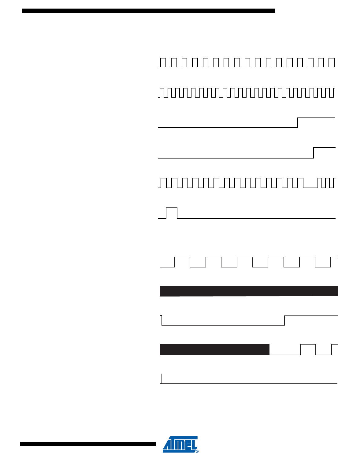
475
6430F–ATARM–21-Feb-12
SAM3U Series
28.12.2 Clock Switching Waveforms
Figure 28-4. Switch Master Clock from Slow Clock to PLL Clock
Figure 28-5. Switch Master Clock from Main Clock to Slow Clock
Slow Clock
LOCK
MCKRDY
Master Clock
Write PMC_MCKR
PLL Clock
Slow Clock
Main Clock
MCKRDY
Master Clock
Write PMC_MCKR
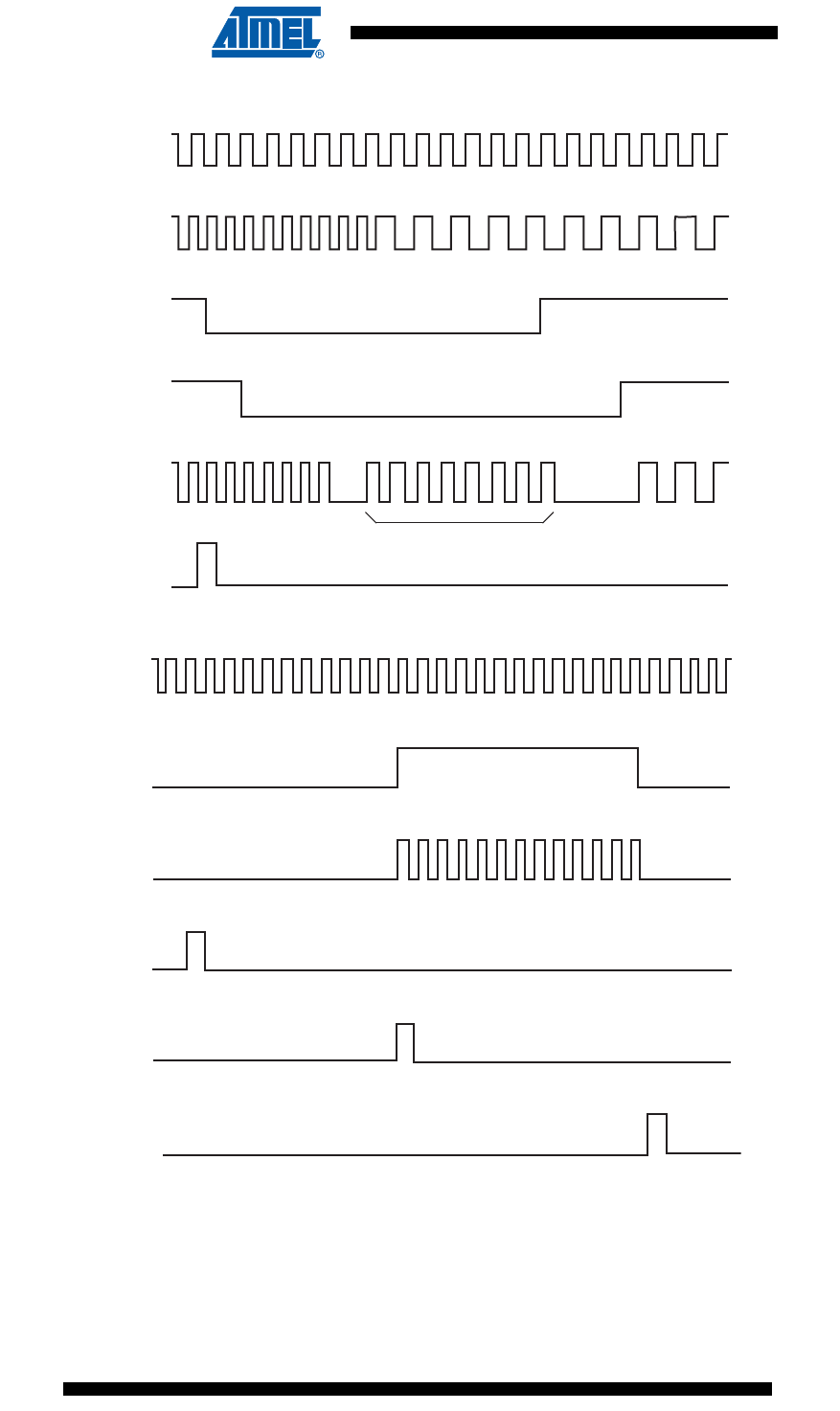
476
6430F–ATARM–21-Feb-12
SAM3U Series
Figure 28-6. Change PLLA Programming
Figure 28-7. Programmable Clock Output Programming
Slow Clock
Slow Clock
PLLA Clock
LOCKA
MCKRDY
Master Clock
Write CKGR_PLLAR
PLL Clock
PCKRDY
PCKx Output
Write PMC_PCKx
Write PMC_SCER
Write PMC_SCDR PCKx is disabled
PCKx is enabled
PLL Clock is selected

477
6430F–ATARM–21-Feb-12
SAM3U Series
28.13 Write Protection Registers
To prevent any single software error that may corrupt PMC behavior, certain address spaces
can be write-protected by setting the WPEN bit in the “PMC Write Protect Mode Register”
(PMC_WPMR).
If a write access to the protected registers is detected, then the WPVS flag in the PMC Write
Protect Status Register (US_WPSR) is set and the field WPVSRC indicates in which register the
write access has been attempted.
The WPVS flag is reset by writing the PMC Write Protect Mode Register (PMC_WPMR) with the
appropriate access key, WPKEY.
The protected registers are:
•“PMC System Clock Enable Register” on page 479
•“PMC System Clock Disable Register” on page 480
•“PMC Peripheral Clock Enable Register” on page 481
•“PMC Peripheral Clock Disable Register” on page 482
•“PMC UTMI Clock Configuration Register” on page 484
•“PMC Clock Generator Main Oscillator Register” on page 485
•“PMC Clock Generator PLLA Register” on page 488
•“PMC Programmable Clock Register” on page 490
•“PMC Fast Startup Mode Register” on page 496
•“PMC Fast Startup Polarity Register” on page 497

478
6430F–ATARM–21-Feb-12
SAM3U Series
28.14 Power Management Controller (PMC) User Interface
Table 28-3. Register Mapping
Offset Register Name Access Reset
0x0000 System Clock Enable Register PMC_SCER Write-only –
0x0004 System Clock Disable Register PMC_SCDR Write-only –
0x0008 System Clock Status Register PMC _SCSR Read-only 0x0000_0001
0x000C Reserved – – –
0x0010 Peripheral Clock Enable Register PMC _PCER Write-only N.A.
0x0014 Peripheral Clock Disable Register PMC_PCDR Write-only –
0x0018 Peripheral Clock Status Register PMC_PCSR Read-only 0x0000_0000
0x001C UTMI Clock Register CKGR_UCKR Read-write 0x1020_0800
0x0020 Main Oscillator Register CKGR_MOR Read-write 0x0000_0001
0x0024 Main Clock Frequency Register CKGR_MCFR Read-only 0x0000_0000
0x0028 PLLA Register CKGR_PLLAR Read-write 0x0000_3F00
0x002C Reserved – – –
0x0030 Master Clock Register PMC_MCKR Read-write 0x0000_0001
0x0034 - 0x003C Reserved – – –
0x0040 Programmable Clock 0 Register PMC_PCK0 Read-write 0x0000_0000
0x0044 Programmable Clock 1 Register PMC_PCK1 Read-write 0x0000_0000
0x0048 Programmable Clock 2 Register PMC_PCK2 Read-write 0x0000_0000
0x004C - 0x005C Reserved – – –
0x0060 Interrupt Enable Register PMC_IER Write-only –
0x0064 Interrupt Disable Register PMC_IDR Write-only –
0x0068 Status Register PMC_SR Read-only 0x0001_0008
0x006C Interrupt Mask Register PMC_IMR Read-only 0x0000_0000
0x0070 Fast Startup Mode Register PMC_FSMR Read-write 0x0000_0000
0x0074 Fast Startup Polarity Register PMC_FSPR Read-write 0x0000_0000
0x0078 Fault Output Clear Register PMC_FOCR Write-only –
0x007C- 0x00FC Reserved – – –
0xE4 Write Protect Mode Register PMC_WPMR Read-write 0x0
0xE8 Write Protect Status Register PMC_WPSR Read-only 0x0

479
6430F–ATARM–21-Feb-12
SAM3U Series
28.14.1 PMC System Clock Enable Register
Name: PMC_SCER
Address: 0x400E0400
Access: Write-only
• PCKx: Programmable Clock x Output Enable
0 = No effect.
1 = Enables the corresponding Programmable Clock output.
This register can only be written if the WPEN bit is cleared in the “PMC Write Protect Mode Register”.
31 30 29 28 27 26 25 24
––––––––
23 22 21 20 19 18 17 16
––––––––
15 14 13 12 11 10 9 8
–––––PCK2PCK1PCK0
76543210
––––––––
480
6430F–ATARM–21-Feb-12
SAM3U Series
28.14.2 PMC System Clock Disable Register
Name: PMC_SCDR
Address: 0x400E0404
Access: Write-only
• PCKx: Programmable Clock x Output Disable
0 = No effect.
1 = Disables the corresponding Programmable Clock output.
This register can only be written if the WPEN bit is cleared in the “PMC Write Protect Mode Register”.
28.14.3 PMC System Clock Status Register
Name: PMC_SCSR
Address: 0x400E0408
Access: Read-only
• PCKx: Programmable Clock x Output Status
0 = The corresponding Programmable Clock output is disabled.
1 = The corresponding Programmable Clock output is enabled.
31 30 29 28 27 26 25 24
––––––––
23 22 21 20 19 18 17 16
––––––––
15 14 13 12 11 10 9 8
–––––PCK2PCK1PCK0
76543210
––––––––
31 30 29 28 27 26 25 24
––––––––
23 22 21 20 19 18 17 16
––––––––
15 14 13 12 11 10 9 8
–––––PCK2PCK1PCK0
76543210
––––––––

481
6430F–ATARM–21-Feb-12
SAM3U Series
28.14.4 PMC Peripheral Clock Enable Register
Name: PMC_PCER
Address: 0x400E0410
Access: Write-only
This register can only be written if the WPEN bit is cleared in the “PMC Write Protect Mode Register”.
• PIDx: Peripheral Clock x Enable
0 = No effect.
1 = Enables the corresponding peripheral clock.
Note: PID2 to PID31 refer to identifiers as defined in the section “Peripheral Identifiers” in the product datasheet.
Note: Programming the control bits of the Peripheral ID that are not implemented has no effect on the behavior of the PMC.
31 30 29 28 27 26 25 24
PID31 PID30 PID29 PID28 PID27 PID26 PID25 PID24
23 22 21 20 19 18 17 16
PID23 PID22 PID21 PID20 PID19 PID18 PID17 PID16
15 14 13 12 11 10 9 8
PID15 PID14 PID13 PID12 PID11 PID10 PID9 PID8
76543210
PID7 PID6 PID5 PID4 PID3 PID2 - -

482
6430F–ATARM–21-Feb-12
SAM3U Series
28.14.5 PMC Peripheral Clock Disable Register
Name: PMC_PCDR
Address: 0x400E0414
Access: Write-only
This register can only be written if the WPEN bit is cleared in the “PMC Write Protect Mode Register”.
• PIDx: Peripheral Clock x Disable
0 = No effect.
1 = Disables the corresponding peripheral clock.
Note: PID2 to PID31 refer to identifiers as defined in the section “Peripheral Identifiers” in the product datasheet.
31 30 29 28 27 26 25 24
PID31 PID30 PID29 PID28 PID27 PID26 PID25 PID24
23 22 21 20 19 18 17 16
PID23 PID22 PID21 PID20 PID19 PID18 PID17 PID16
15 14 13 12 11 10 9 8
PID15 PID14 PID13 PID12 PID11 PID10 PID9 PID8
76543210
PID7 PID6 PID5 PID4 PID3 PID2 - -

483
6430F–ATARM–21-Feb-12
SAM3U Series
28.14.6 PMC Peripheral Clock Status Register
Name: PMC_PCSR
Address: 0x400E0418
Access: Read-only
• PIDx: Peripheral Clock x Status
0 = The corresponding peripheral clock is disabled.
1 = The corresponding peripheral clock is enabled.
Note: PID2 to PID31 refer to identifiers as defined in the section “Peripheral Identifiers” in the product datasheet.
31 30 29 28 27 26 25 24
PID31 PID30 PID29 PID28 PID27 PID26 PID25 PID24
23 22 21 20 19 18 17 16
PID23 PID22 PID21 PID20 PID19 PID18 PID17 PID16
15 14 13 12 11 10 9 8
PID15 PID14 PID13 PID12 PID11 PID10 PID9 PID8
76543210
PID7 PID6 PID5 PID4 PID3 PID2 – –

484
6430F–ATARM–21-Feb-12
SAM3U Series
28.14.7 PMC UTMI Clock Configuration Register
Name: CKGR_UCKR
Address: 0x400E041C
Access: Read-write
This register can only be written if the WPEN bit is cleared in the “PMC Write Protect Mode Register”.
• UPLLEN: UTMI PLL Enable
0 = The UTMI PLL is disabled.
1 = The UTMI PLL is enabled.
When UPLLEN is set, the LOCKU flag is set once the UTMI PLL startup time is achieved.
• UPLLCOUNT: UTMI PLL Start-up Time
Specifies the number of Slow Clock cycles multiplied by 8 for the UTMI PLL start-up time.
31 30 29 28 27 26 25 24
––– ––––
23 22 21 20 19 18 17 16
UPLLCOUNT – – – UPLLEN
15 14 13 12 11 10 9 8
––––––––
76543210
––––––––

485
6430F–ATARM–21-Feb-12
SAM3U Series
28.14.8 PMC Clock Generator Main Oscillator Register
Name: CKGR_MOR
Address: 0x400E0420
Access: Read-write
This register can only be written if the WPEN bit is cleared in the “PMC Write Protect Mode Register”.
•KEY: Password
Should be written at value 0x37. Writing any other value in this field aborts the write operation.
• MOSCXTEN: Main Crystal Oscillator Enable
A crystal must be connected between XIN and XOUT.
0 = The Main Crystal Oscillator is disabled.
1 = The Main Crystal Oscillator is enabled. MOSCXTBY must be set to 0.
When MOSCXTEN is set, the MOSCXTS flag is set once the Main Crystal Oscillator startup time is achieved.
• MOSCXTBY: Main Crystal Oscillator Bypass
0 = No effect.
1 = The Main Crystal Oscillator is bypassed. MOSCXTEN must be set to 0. An external clock must be connected on XIN.
When MOSCXTBY is set, the MOSCXTS flag in PMC_SR is automatically set.
Clearing MOSCXTEN and MOSCXTBY bits allows resetting the MOSCXTS flag.
• WAITMODE: Wait Mode Command
0 = No effect.
1 = Enters the device in Wait mode.
Note: The bit WAITMODE is write-only
• MOSCRCEN: Main On-Chip RC Oscillator Enable
0 = The Main On-Chip RC Oscillator is disabled.
1 = The Main On-Chip RC Oscillator is enabled.
When MOSCRCEN is set, the MOSCRCS flag is set once the Main On-Chip RC Oscillator startup time is achieved.
31 30 29 28 27 26 25 24
––––––CFDENMOSCSEL
23 22 21 20 19 18 17 16
KEY
15 14 13 12 11 10 9 8
MOSCXTST
76543210
– MOSCRCF MOSCRCEN WAITMODE MOSCXTBY MOSCXTEN

486
6430F–ATARM–21-Feb-12
SAM3U Series
• MOSCRCF: Main On-Chip RC Oscillator Frequency Selection
At start-up, the Main On-Chip RC Oscillator frequency is 4 MHz.
0 = The Fast RC Oscillator Frequency is at 4 MHz (default).
1 = The Fast RC Oscillator Frequency is at 8 MHz.
2 = The Fast RC Oscillator Frequency is at 12 MHz.
3 = Reserved.
• MOSCXTST: Main Crystal Oscillator Start-up Time
Specifies the number of Slow Clock cycles multiplied by 8 for the Main Crystal Oscillator start-up time.
• MOSCSEL: Main Oscillator Selection
0 = The Main On-Chip RC Oscillator is selected.
1 = The Main Crystal Oscillator is selected.
• CFDEN: Clock Failure Detector Enable
0 = The Clock Failure Detector is disabled.
1 = The Clock Failure Detector is enabled.

487
6430F–ATARM–21-Feb-12
SAM3U Series
28.14.9 PMC Clock Generator Main Clock Frequency Register
Name: CKGR_MCFR
Address: 0x400E0424
Access: Read-only
• MAINF: Main Clock Frequency
Gives the number of Main Clock cycles within 16 Slow Clock periods.
• MAINFRDY: Main Clock Ready
0 = MAINF value is not valid or the Main Oscillator is disabled.
1 = The Main Oscillator has been enabled previously and MAINF value is available.
31 30 29 28 27 26 25 24
––––––––
23 22 21 20 19 18 17 16
–––––––MAINFRDY
15 14 13 12 11 10 9 8
MAINF
76543210
MAINF
488
6430F–ATARM–21-Feb-12
SAM3U Series
28.14.10 PMC Clock Generator PLLA Register
Name: CKGR_PLLAR
Address: 0x400E0428
Access: Read-write
This register can only be written if the WPEN bit is cleared in the “PMC Write Protect Mode Register”.
Possible limitations on PLLA input frequencies and multiplier factors should be checked before using the PMC.
Warning: Bit 29 must always be set to 1 when programming the CKGR_PLLAR register.
• DIVA: Divider
• PLLACOUNT: PLLA Counter
Specifies the number of Slow Clock cycles x8 before the LOCKA bit is set in PMC_SR after CKGR_PLLAR is written.
• MULA: PLLA Multiplier
0 = The PLLA is deactivated.
1 up to 2047 = The PLLA Clock frequency is the PLLA input frequency multiplied by MULA + 1.
31 30 29 28 27 26 25 24
––1–– MULA
23 22 21 20 19 18 17 16
MULA
15 14 13 12 11 10 9 8
––PLLACOUNT
76543210
DIVA
DIVA Divider Selected
0 Divider output is 0
1 Divider is bypassed (DIVA=1)
2 - 255 Divider output is the selected clock divided by DIVA
489
6430F–ATARM–21-Feb-12
SAM3U Series
28.14.11 PMC Master Clock Register
Name: PMC_MCKR
Address: 0x400E0430
Access: Read-write
• CSS: Master Clock Source Selection
• PRES: Processor Clock Prescaler
• UPLLDIV: UPLL Divider
0: UPLLDIV = 1 (clock is not divided).
1: UPLLDIV = 2 (clock is divided by 2).
UPLLDIV must be set (clock divided by 2) when UPLL is selected as source of clock for MCK or PCK.
31 30 29 28 27 26 25 24
––––––––
23 22 21 20 19 18 17 16
––––––––
15 14 13 12 11 10 9 8
––UPLLDIV–––––
76543210
–PRES––CSS
Value Name Description
0 SLOW_CLK Slow Clock is selected
1 MAIN_CLK Main Clock is selected
2 PLLA_CLK PLLA Clock is selected
3 UPLL_CLK UPLL/2 Clock is selected
Value Name Description
0 CLK_1 Selected clock
1 CLK_2 Selected clock divided by 2
2 CLK_4 Selected clock divided by 4
3 CLK_8 Selected clock divided by 8
4 CLK_16 Selected clock divided by 16
5 CLK_32 Selected clock divided by 32
6 CLK_64 Selected clock divided by 64
7 CLK_3 Selected clock divided by 3
490
6430F–ATARM–21-Feb-12
SAM3U Series
28.14.12 PMC Programmable Clock Register
Name: PMC_PCKx
Address: 0x400E0440
Access: Read-write
This register can only be written if the WPEN bit is cleared in the “PMC Write Protect Mode Register”.
• CSS: Master Clock Source Selection
• PRES: Programmable Clock Prescaler
31 30 29 28 27 26 25 24
––––––––
23 22 21 20 19 18 17 16
––––––––
15 14 13 12 11 10 9 8
––––––––
76543210
–PRES– CSS
Value Name Description
0 SLOW_CLK Slow Clock is selected
1 MAIN_CLK Main Clock is selected
2 PLLA_CLK PLLA Clock is selected
3 UPLL_CLK UPLL/2 Clock is selected
4 MCK Master Clock is selected
Value Name Description
0 CLK_1 Selected clock
1 CLK_2 Selected clock divided by 2
2 CLK_4 Selected clock divided by 4
3 CLK_8 Selected clock divided by 8
4 CLK_16 Selected clock divided by 16
5 CLK_32 Selected clock divided by 32
6 CLK_64 Selected clock divided by 64
491
6430F–ATARM–21-Feb-12
SAM3U Series
28.14.13 PMC Interrupt Enable Register
Name: PMC_IER
Address: 0x400E0460
Access: Write-only
0 = No effect.
1 = Enables the corresponding interrupt.
• MOSCXTS: Main Crystal Oscillator Status Interrupt Enable
• LOCKA: PLL A Lock Interrupt Enable
• MCKRDY: Master Clock Ready Interrupt Enable
• LOCKU: UTMI PLL Lock Interrupt Enable
• PCKRDYx: Programmable Clock Ready x Interrupt Enable
• MOSCSELS: Main Oscillator Selection Status Interrupt Enable
• MOSCRCS: Main On-Chip RC Status Interrupt Enable
• CFDEV: Clock Failure Detector Event Interrupt Enable
31 30 29 28 27 26 25 24
––––––––
23 22 21 20 19 18 17 16
–––––CFDEVMOSCRCSMOSCSELS
15 14 13 12 11 10 9 8
–––––PCKRDY2PCKRDY1PCKRDY0
76543210
– LOCKU – – MCKRDY – LOCKA MOSCXTS

492
6430F–ATARM–21-Feb-12
SAM3U Series
28.14.14 PMC Interrupt Disable Register
Name: PMC_IDR
Address: 0x400E0464
Access: Write-only
0 = No effect.
1 = Disables the corresponding interrupt.
• MOSCXTS: Main Crystal Oscillator Status Interrupt Disable
• LOCKA: PLL A Lock Interrupt Disable
• MCKRDY: Master Clock Ready Interrupt Disable
• LOCKU: UTMI PLL Lock Interrupt Disable
• PCKRDYx: Programmable Clock Ready x Interrupt Disable
• MOSCSELS: Main Oscillator Selection Status Interrupt Disable
• MOSCRCS: Main On-Chip RC Status Interrupt Disable
• CFDEV: Clock Failure Detector Event Interrupt Disable
31 30 29 28 27 26 25 24
––––––––
23 22 21 20 19 18 17 16
–––––CFDEVMOSCRCSMOSCSELS
15 14 13 12 11 10 9 8
–––––PCKRDY2PCKRDY1PCKRDY0
76543210
– LOCKU – – MCKRDY – LOCKA MOSCXTS

493
6430F–ATARM–21-Feb-12
SAM3U Series
28.14.15 PMC Status Register
Name: PMC_SR
Address: 0x400E0468
Access: Read-only
• MOSCXTS: Main XTAL Oscillator Status
0 = Main XTAL oscillator is not stabilized.
1 = Main XTAL oscillator is stabilized.
• LOCKA: PLL A Lock Status
0 = PLL A is not locked
1 = PLL A is locked.
• MCKRDY: Master Clock Status
0 = Master Clock is not ready.
1 = Master Clock is ready.
• LOCKU: UTMI PLL Lock Status
0 = UTMI PLL is not locked.
1 = UTMI PLL is locked.
• OSCSELS: Slow Clock Oscillator Selection
0 = Internal slow clock RC oscillator is selected.
1 = External slow clock 32 kHz oscillator is selected.
• PCKRDYx: Programmable Clock Ready Status
0 = Programmable Clock x is not ready.
1 = Programmable Clock x is ready.
• MOSCSELS: Main Oscillator Selection Status
0 = Selection is in progress.
1 = Selection is done.
• MOSCRCS: Main On-Chip RC Oscillator Status
0 = Main on-chip RC oscillator is not stabilized.
1 = Main on-chip RC oscillator is stabilized.
31 30 29 28 27 26 25 24
––––––––
23 22 21 20 19 18 17 16
– – – FOS CFDS CFDEV MOSCRCS MOSCSELS
15 14 13 12 11 10 9 8
–––––PCKRDY2PCKRDY1PCKRDY0
76543210
OSCSELS LOCKU – – MCKRDY – LOCKA MOSCXTS

494
6430F–ATARM–21-Feb-12
SAM3U Series
• CFDEV: Clock Failure Detector Event
0 = No clock failure detection of the main on-chip RC oscillator clock has occurred since the last read of PMC_SR.
1 = At least one clock failure detection of the main on-chip RC oscillator clock has occurred since the last read of PMC_SR.
• CFDS: Clock Failure Detector Status
0 = A clock failure of the main on-chip RC oscillator clock is not detected.
1 = A clock failure of the main on-chip RC oscillator clock is detected.
• FOS: Clock Failure Detector Fault Output Status
0 = The fault output of the clock failure detector is inactive.
0 = The fault output of the clock failure detector is active.

495
6430F–ATARM–21-Feb-12
SAM3U Series
28.14.16 PMC Interrupt Mask Register
Name: PMC_IMR
Address: 0x400E046C
Access: Read-only
0 = The corresponding interrupt is disabled.
1 = The corresponding interrupt is enabled.
• MOSCXTS: Main Crystal Oscillator Status Interrupt Mask
• LOCKA: PLL A Lock Interrupt Mask
• MCKRDY: Master Clock Ready Interrupt Mask
• LOCKU: UTMI PLL Lock Interrupt Mask
• PCKRDYx: Programmable Clock Ready x Interrupt Mask
• MOSCSELS: Main Oscillator Selection Status Interrupt Mask
• MOSCRCS: Main On-Chip RC Status Interrupt Mask
• CFDEV: Clock Failure Detector Event Interrupt Mask
31 30 29 28 27 26 25 24
––––––––
23 22 21 20 19 18 17 16
–––––CFDEVMOSCRCSMOSCSELS
15 14 13 12 11 10 9 8
–––––PCKRDY2PCKRDY1PCKRDY0
76543210
– LOCKU – – MCKRDY – LOCKA MOSCXTS

496
6430F–ATARM–21-Feb-12
SAM3U Series
28.14.17 PMC Fast Startup Mode Register
Name: PMC_FSMR
Address: 0x400E0470
Access: Read-write
This register can only be written if the WPEN bit is cleared in the “PMC Write Protect Mode Register”.
• FSTT0 - FSTT15: Fast Startup Input Enable 0 to 15
0 = The corresponding wake up input has no effect on the Power Management Controller.
1 = The corresponding wake up input enables a fast restart signal to the Power Management Controller.
• RTTAL: RTT Alarm Enable
0 = The RTT alarm has no effect on the Power Management Controller.
1 = The RTT alarm enables a fast restart signal to the Power Management Controller.
• RTCAL: RTC Alarm Enable
0 = The RTC alarm has no effect on the Power Management Controller.
1 = The RTC alarm enables a fast restart signal to the Power Management Controller.
• USBAL: USB Alarm Enable
0 = The USB alarm has no effect on the Power Management Controller.
1 = The USB alarm enables a fast restart signal to the Power Management Controller.
• LPM: Low Power Mode
0 = The WaitForInterrupt (WFI) or WaitForEvent (WFE) instruction of the processor makes the processor enter in Idle
Mode.
1 = The WaitForEvent (WFE) instruction of the processor makes the system enter in Wait Mode.
31 30 29 28 27 26 25 24
––––––––
23 22 21 20 19 18 17 16
– – – LPM – USBAL RTCAL RTTAL
15 14 13 12 11 10 9 8
FSTT15 FSTT14 FSTT13 FSTT12 FSTT11 FSTT10 FSTT9 FSTT8
76543210
FSTT7 FSTT6 FSTT5 FSTT4 FSTT3 FSTT2 FSTT1 FSTT0

497
6430F–ATARM–21-Feb-12
SAM3U Series
28.14.18 PMC Fast Startup Polarity Register
Name: PMC_FSPR
Address: 0x400E0474
Access: Read-write
This register can only be written if the WPEN bit is cleared in the “PMC Write Protect Mode Register”.
• FSTPx: Fast Startup Input Polarityx
Defines the active polarity of the corresponding wake up input. If the corresponding wake up input is enabled and at the
FSTP level, it enables a fast restart signal.
31 30 29 28 27 26 25 24
––––––––
23 22 21 20 19 18 17 16
––––––––
15 14 13 12 11 10 9 8
FSTP15 FSTP14 FSTP13 FSTP12 FSTP11 FSTP10 FSTP9 FSTP8
76543210
FSTP7 FSTP6 FSTP5 FSTP4 FSTP3 FSTP2 FSTP1 FSTP0

498
6430F–ATARM–21-Feb-12
SAM3U Series
28.14.19 PMC Fault Output Clear Register
Name: PMC_FOCR
Address: 0x400E0478
Access: Write-only
• FOCLR: Fault Output Clear
Clears the clock failure detector fault output.
31 30 29 28 27 26 25 24
––––––––
23 22 21 20 19 18 17 16
––––––––
15 14 13 12 11 10 9 8
––––––––
76543210
–––––––FOCLR

499
6430F–ATARM–21-Feb-12
SAM3U Series
28.14.20 PMC Write Protect Mode Register
Name: PMC_WPMR
Address: 0x400E04E4
Access: Read-write
Reset: See Table 28-3
• WPEN: Write Protect Enable
0 = Disables the Write Protect if WPKEY corresponds to 0x504D43 (“PMC” in ASCII).
1 = Enables the Write Protect if WPKEY corresponds to 0x504D43 (“PMC” in ASCII).
Protects the registers:
•“PMC System Clock Enable Register” on page 479
•“PMC System Clock Disable Register” on page 480
•“PMC Peripheral Clock Enable Register” on page 481
•“PMC Peripheral Clock Disable Register” on page 482
•“PMC UTMI Clock Configuration Register” on page 484
•“PMC Clock Generator Main Oscillator Register” on page 485
•“PMC Clock Generator PLLA Register” on page 488
•“PMC Programmable Clock Register” on page 490
•“PMC Fast Startup Mode Register” on page 496
•“PMC Fast Startup Polarity Register” on page 497
• WPKEY: Write Protect KEY
Should be written at value 0x504D43 (“PMC” in ASCII). Writing any other value in this field aborts the write operation of the
WPEN bit. Always reads as 0.
31 30 29 28 27 26 25 24
WPKEY
23 22 21 20 19 18 17 16
WPKEY
15 14 13 12 11 10 9 8
WPKEY
76543210
–––––––WPEN

500
6430F–ATARM–21-Feb-12
SAM3U Series
28.14.21 PMC Write Protect Status Register
Name: PMC_WPSR
Address: 0x400E04E8
Access: Read-only
Reset: See Table 28-3
• WPVS: Write Protect Violation Status
0 = No Write Protect Violation has occurred since the last read of the PMC_WPSR register.
1 = A Write Protect Violation has occurred since the last read of the PMC_WPSR register. If this violation is an unauthor-
ized attempt to write a protected register, the associated violation is reported into field WPVSRC.
• WPVSRC: Write Protect Violation Source
When WPVS is active, this field indicates the write-protected register (through address offset or code) in which a write
access has been attempted.
Reading PMC_WPSR automatically clears all fields.
31 30 29 28 27 26 25 24
––––––––
23 22 21 20 19 18 17 16
WPVSRC
15 14 13 12 11 10 9 8
WPVSRC
76543210
–––––––WPVS

501
6430F–ATARM–21-Feb-12
SAM3U Series
501
6430F–ATARM–21-Feb-12
SAM3U Series
29. Chip Identifier (CHIPID)
29.1 Description
Chip Identifier registers permit recognition of the device and its revision. These registers provide
the sizes and types of the on-chip memories, as well as the set of embedded peripherals.
Two chip identifier registers are embedded: CHIPID_CIDR (Chip ID Register) and CHIPID_EXID
(Extension ID). Both registers contain a hard-wired value that is read-only. The first register con-
tains the following fields:
• EXT - shows the use of the extension identifier register
• NVPTYP and NVPSIZ - identifies the type of embedded non-volatile memory and its size
• ARCH - identifies the set of embedded peripherals
• SRAMSIZ - indicates the size of the embedded SRAM
• EPROC - indicates the embedded ARM processor
• VERSION - gives the revision of the silicon
The second register is device-dependent and reads 0 if the bit EXT is 0.
29.2 Embedded Characteristics
• Chip ID Registers
– Identification of the Device Revision, Sizes of the Embedded Memories, Set of
Peripherals, Embedded Processor
Table 29-1. ATSAM3U Chip IDs Register
Chip Name CHIPID_CIDR CHIPID_EXID
AT91SAM3U4C (Rev A) 0x28000961 0x0
AT91SAM3U2C (Rev A) 0x280A0761 0x0
AT91SAM3U1C (Rev A) 0x28090561 0x0
AT91SAM3U4E (Rev A) 0x28100961 0x0
AT91SAM3U2E (Rev A) 0x281A0761 0x0
AT91SAM3U1E (Rev A) 0x28190561 0x0

502
6430F–ATARM–21-Feb-12
SAM3U Series
502
6430F–ATARM–21-Feb-12
SAM3U Series
29.3 Chip Identifier (CHIPID) User Interface
Table 29-2. Register Mapping
Offset Register Name Access Reset
0x0 Chip ID Register CHIPID_CIDR Read-only –
0x4 Chip ID Extension Register CHIPID_EXID Read-only –
503
6430F–ATARM–21-Feb-12
SAM3U Series
503
6430F–ATARM–21-Feb-12
SAM3U Series
29.3.1 Chip ID Register
Name: CHIPID_CIDR
Address: 0x400E0740
Access: Read-only
• VERSION: Version of the Device
Current version of the device.
• EPROC: Embedded Processor
• NVPSIZ: Nonvolatile Program Memory Size
31 30 29 28 27 26 25 24
EXT NVPTYP ARCH
23 22 21 20 19 18 17 16
ARCH SRAMSIZ
15 14 13 12 11 10 9 8
NVPSIZ2 NVPSIZ
76543210
EPROC VERSION
Value Name Description
1 ARM946ES ARM946ES
2 ARM7TDMI ARM7TDMI
3 CM3 Cortex-M3
4 ARM920T ARM920T
5 ARM926EJS ARM926EJS
6CA5 Cortex-A5
7 CM4 Cortex-M4
Value Name Description
0NONE None
18K 8K bytes
2 16K 16K bytes
3 32K 32K bytes
4Reserved
5 64K 64K bytes
6Reserved
7 128K 128K bytes
8Reserved
9 256K 256K bytes
10 512K 512K bytes
11 Reserved
12 1024K 1024K bytes

504
6430F–ATARM–21-Feb-12
SAM3U Series
504
6430F–ATARM–21-Feb-12
SAM3U Series
• NVPSIZ2: Second Nonvolatile Program Memory Size
• SRAMSIZ: Internal SRAM Size
13 Reserved
14 2048K 2048K bytes
15 Reserved
Value Name Description
0 NONE None
18K 8K bytes
216K 16K bytes
332K 32K bytes
4 Reserved
564K 64K bytes
6 Reserved
7 128K 128K bytes
8 Reserved
9 256K 256K bytes
10 512K 512K bytes
11 Reserved
12 1024K 1024K bytes
13 Reserved
14 2048K 2048K bytes
15 Reserved
Value Name Description
048K 48K bytes
11K 1K bytes
22K 2K bytes
36K 6K bytes
424K 24K bytes
54K 4K bytes
680K 80K bytes
7 160K 160K bytes
88K 8K bytes
916K 16K bytes
10 32K 32K bytes
11 64K 64K bytes
12 128K 128K bytes
Value Name Description

505
6430F–ATARM–21-Feb-12
SAM3U Series
505
6430F–ATARM–21-Feb-12
SAM3U Series
• ARCH: Architecture Identifier
13 256K 256K bytes
14 96K 96K bytes
15 512K 512K bytes
Value Name Description
0x19 AT91SAM9xx AT91SAM9xx Series
0x29 AT91SAM9XExx AT91SAM9XExx Series
0x34 AT91x34 AT91x34 Series
0x37 CAP7 CAP7 Series
0x39 CAP9 CAP9 Series
0x3B CAP11 CAP11 Series
0x40 AT91x40 AT91x40 Series
0x42 AT91x42 AT91x42 Series
0x55 AT91x55 AT91x55 Series
0x60 AT91SAM7Axx AT91SAM7Axx Series
0x61 AT91SAM7AQxx AT91SAM7AQxx Series
0x63 AT91x63 AT91x63 Series
0x70 AT91SAM7Sxx AT91SAM7Sxx Series
0x71 AT91SAM7XCxx AT91SAM7XCxx Series
0x72 AT91SAM7SExx AT91SAM7SExx Series
0x73 AT91SAM7Lxx AT91SAM7Lxx Series
0x75 AT91SAM7Xxx AT91SAM7Xxx Series
0x76 AT91SAM7SLxx AT91SAM7SLxx Series
0x80 SAM3UxC SAM3UxC Series (100-pin version)
0x81 SAM3UxE SAM3UxE Series (144-pin version)
0x83 SAM3AxC SAM3AxC Series (100-pin version)
0x83 SAM4AxC SAM4AxC Series (100-pin version)
0x84 SAM3XxC SAM3XxC Series (100-pin version)
0x84 SAM4XxC SAM4XxC Series (100-pin version)
0x85 SAM3XxE SAM3XxE Series (144-pin version)
0x85 SAM4XxE SAM4XxE Series (144-pin version)
0x86 SAM3XxG SAM3XxG Series (208/217-pin version)
0x86 SAM4XxG SAM4XxG Series (208/217-pin version)
0x88 SAM3SxA SAM3SxASeries (48-pin version)
0x88 SAM4SxA SAM4SxA Series (48-pin version)
0x89 SAM3SxB SAM3SxB Series (64-pin version)
Value Name Description

506
6430F–ATARM–21-Feb-12
SAM3U Series
506
6430F–ATARM–21-Feb-12
SAM3U Series
• NVPTYP: Nonvolatile Program Memory Type
• EXT: Extension Flag
0 = Chip ID has a single register definition without extension
1 = An extended Chip ID exists.
0x89 SAM4SxB SAM4SxB Series (64-pin version)
0x8A SAM3SxC SAM3SxC Series (100-pin version)
0x8A SAM4SxC SAM4SxC Series (100-pin version)
0x92 AT91x92 AT91x92 Series
0x93 SAM3NxA SAM3NxA Series (48-pin version)
0x94 SAM3NxB SAM3NxB Series (64-pin version)
0x95 SAM3NxC SAM3NxC Series (100-pin version)
0x99 SAM3SDxB SAM3SDxB Series (64-pin version)
0x9A SAM3SDxC SAM3SDxC Series (100-pin version)
0xA5 SAM5A SAM5A
0xF0 AT75Cxx AT75Cxx Series
Value Name Description
0ROM ROM
1 ROMLESS ROMless or on-chip Flash
4 SRAM SRAM emulating ROM
2 FLASH Embedded Flash Memory
3 ROM_FLASH
ROM and Embedded Flash Memory
NVPSIZ is ROM size
NVPSIZ2 is Flash size
Value Name Description

507
6430F–ATARM–21-Feb-12
SAM3U Series
507
6430F–ATARM–21-Feb-12
SAM3U Series
29.3.2 Chip ID Extension Register
Name: CHIPID_EXID
Address: 0x400E0744
Access: Read-only
• EXID: Chip ID Extension
Reads 0 if the bit EXT in CHIPID_CIDR is 0.
31 30 29 28 27 26 25 24
EXID
23 22 21 20 19 18 17 16
EXID
15 14 13 12 11 10 9 8
EXID
76543210
EXID

508
6430F–ATARM–21-Feb-12
SAM3U Series
508
6430F–ATARM–21-Feb-12
SAM3U Series

509
6430F–ATARM–21-Feb-12
SAM3U Series
509
6430F–ATARM–21-Feb-12
SAM3U Series
30. Parallel Input/Output Controller (PIO)
30.1 Description
The Parallel Input/Output Controller (PIO) manages up to 32 fully programmable input/output
lines. Each I/O line may be dedicated as a general-purpose I/O or be assigned to a function of
an embedded peripheral. This assures effective optimization of the pins of a product.
Each I/O line is associated with a bit number in all of the 32-bit registers of the 32-bit wide User
Interface.
Each I/O line of the PIO Controller features:
• An input change interrupt enabling level change detection on any I/O line.
• Additional Interrupt modes enabling rising edge, falling edge, low level or high level detection
on any I/O line.
• A glitch filter providing rejection of glitches lower than one-half of system clock cycle.
• A debouncing filter providing rejection of unwanted pulses from key or push button
operations.
• Multi-drive capability similar to an open drain I/O line.
• Control of the pull-up of the I/O line.
• Input visibility and output control.
The PIO Controller also features a synchronous output providing up to 32 bits of data output in a
single write operation.
30.2 Embedded Characteristics
• Up to 32 Programmable I/O Lines
• Fully Programmable through Set/Clear Registers
• Multiplexing of Two Peripheral Functions per I/O Line
• For each I/O Line (Whether Assigned to a Peripheral or Used as General Purpose I/O)
– Input Change Interrupt
– Programmable Glitch Filter
– Programmable Debouncing Filter
– Multi-drive Option Enables Driving in Open Drain
– Programmable Pull Up on Each I/O Line
– Pin Data Status Register, Supplies Visibility of the Level on the Pin at Any Time
– Additional Interrupt Modes on a Programmable Event: Rising Edge, Falling Edge,
Low Level or High Level
– Lock of the Configuration by the Connected Peripheral
• Synchronous Output, Provides Set and Clear of Several I/O lines in a Single Write
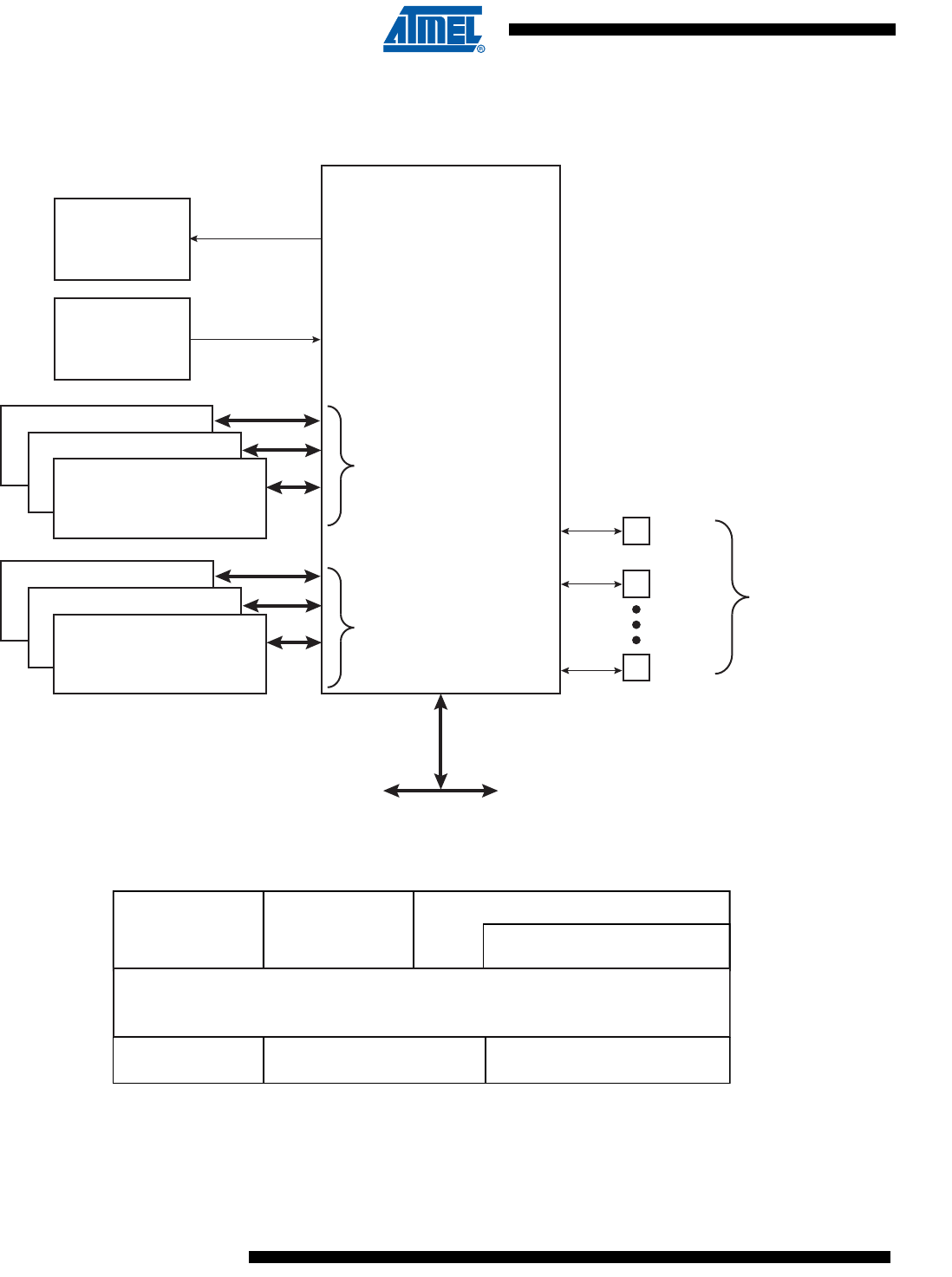
510
6430F–ATARM–21-Feb-12
SAM3U Series
510
6430F–ATARM–21-Feb-12
SAM3U Series
30.3 Block Diagram
Figure 30-1. Block Diagram
Figure 30-2. Application Block Diagram
Embedded
Peripheral
Embedded
Peripheral
PIO Interrupt
PIO Controller
Up to 32 pins
PMC
Up to 32
peripheral IOs
Up to 32
peripheral IOs
PIO Clock
APB
NVIC
Data, Enable
PIN 31
PIN 1
PIN 0
Data, Enable
On-Chip Peripherals
PIO Controller
On-Chip Peripheral Drivers
Control & Command
Driver
Keyboard Driver
Keyboard Driver General Purpose I/Os External Devices

511
6430F–ATARM–21-Feb-12
SAM3U Series
511
6430F–ATARM–21-Feb-12
SAM3U Series
30.4 Product Dependencies
30.4.1 Pin Multiplexing
Each pin is configurable, according to product definition as either a general-purpose I/O line
only, or as an I/O line multiplexed with one or two peripheral I/Os. As the multiplexing is hard-
ware defined and thus product-dependent, the hardware designer and programmer must
carefully determine the configuration of the PIO controllers required by their application. When
an I/O line is general-purpose only, i.e. not multiplexed with any peripheral I/O, programming of
the PIO Controller regarding the assignment to a peripheral has no effect and only the PIO Con-
troller can control how the pin is driven by the product.
30.4.2 Power Management
The Power Management Controller controls the PIO Controller clock in order to save power.
Writing any of the registers of the user interface does not require the PIO Controller clock to be
enabled. This means that the configuration of the I/O lines does not require the PIO Controller
clock to be enabled.
However, when the clock is disabled, not all of the features of the PIO Controller are available,
including glitch filtering. Note that the Input Change Interrupt, Interrupt Modes on a programma-
ble event and the read of the pin level require the clock to be validated.
After a hardware reset, the PIO clock is disabled by default.
The user must configure the Power Management Controller before any access to the input line
information.
30.4.3 Interrupt Generation
The PIO COntroller is connected on one of the sources of the Nested Vectored Interrupt Control-
ler (NVIC). Using the PIO Controller requires the NVIC to be programmed first.
The PIO Controller interrupt can be generated only if the PIO Controller clock is enabled.
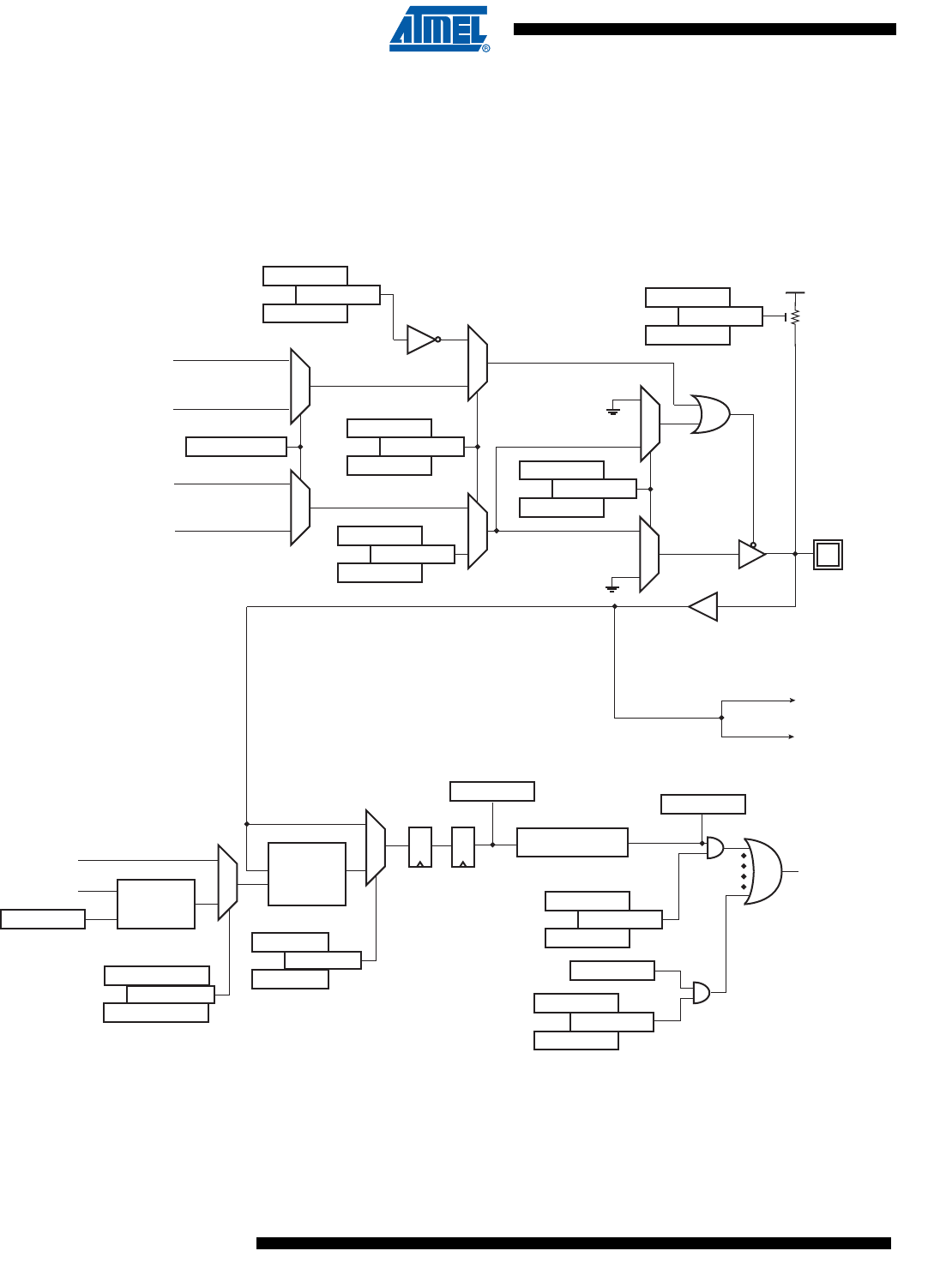
512
6430F–ATARM–21-Feb-12
SAM3U Series
512
6430F–ATARM–21-Feb-12
SAM3U Series
30.5 Functional Description
The PIO Controller features up to 32 fully-programmable I/O lines. Most of the control logic asso-
ciated to each I/O is represented in Figure 30-3. In this description each signal shown
represents but one of up to 32 possible indexes.
Figure 30-3. I/O Line Control Logic
1
0
1
0
1
0
1
0
DQ DQ
DFF
1
0
1
0
1
0
1
0
Programmable
Glitch
or
Debouncing
Filter
Peripheral A
Input
PIO_PDSR[0]
PIO_ISR[0]
PIO_IDR[0]
PIO_IMR[0]
PIO_IER[0]
PIO Interrupt
(Up to 32 possible inputs)
PIO_ISR[31]
PIO_IDR[31]
PIO_IMR[31]
PIO_IER[31]
Pad
PIO_PUDR[0]
PIO_PUSR[0]
PIO_PUER[0]
PIO_MDDR[0]
PIO_MDSR[0]
PIO_MDER[0]
PIO_CODR[0]
PIO_ODSR[0]
PIO_SODR[0]
PIO_PDR[0]
PIO_PSR[0]
PIO_PER[0]
PIO_ABSR[0]
PIO_ODR[0]
PIO_OSR[0]
PIO_OER[0]
Resynchronization
Stage
Peripheral B
Input
Peripheral B
Output Enable
Peripheral A
Output Enable
Peripheral B
Output
Peripheral A
Output
EVENT
DETECTOR
DFF
PIO_IFDR[0]
PIO_IFSR[0]
PIO_IFER[0]
System Clock
Clock
Divider
PIO_IFSCR[0]
PIO_DCIFSR[0]
PIO_SCIFSR[0]
PIO_SCDR
Slow Clock

513
6430F–ATARM–21-Feb-12
SAM3U Series
513
6430F–ATARM–21-Feb-12
SAM3U Series
30.5.1 Pull-up Resistor Control
Each I/O line is designed with an embedded pull-up resistor. The pull-up resistor can be enabled
or disabled by writing respectively PIO_PUER (Pull-up Enable Register) and PIO_PUDR (Pull-
up Disable Resistor). Writing in these registers results in setting or clearing the corresponding bit
in PIO_PUSR (Pull-up Status Register). Reading a 1 in PIO_PUSR means the pull-up is dis-
abled and reading a 0 means the pull-up is enabled.
Control of the pull-up resistor is possible regardless of the configuration of the I/O line.
After reset, all of the pull-ups are enabled, i.e. PIO_PUSR resets at the value 0x0.
30.5.2 I/O Line or Peripheral Function Selection
When a pin is multiplexed with one or two peripheral functions, the selection is controlled with
the registers PIO_PER (PIO Enable Register) and PIO_PDR (PIO Disable Register). The regis-
ter PIO_PSR (PIO Status Register) is the result of the set and clear registers and indicates
whether the pin is controlled by the corresponding peripheral or by the PIO Controller. A value of
0 indicates that the pin is controlled by the corresponding on-chip peripheral selected in the
PIO_ABSR (AB Select Register). A value of 1 indicates the pin is controlled by the PIO
controller.
If a pin is used as a general purpose I/O line (not multiplexed with an on-chip peripheral),
PIO_PER and PIO_PDR have no effect and PIO_PSR returns 1 for the corresponding bit.
After reset, most generally, the I/O lines are controlled by the PIO controller, i.e. PIO_PSR
resets at 1. However, in some events, it is important that PIO lines are controlled by the periph-
eral (as in the case of memory chip select lines that must be driven inactive after reset or for
address lines that must be driven low for booting out of an external memory). Thus, the reset
value of PIO_PSR is defined at the product level, depending on the multiplexing of the device.
30.5.3 Peripheral A or B Selection
The PIO Controller provides multiplexing of up to two peripheral functions on a single pin. The
selection is performed by writing PIO_ABSR (AB Select Register). For each pin, the correspond-
ing bit at level 0 means peripheral A is selected whereas the corresponding bit at level 1
indicates that peripheral B is selected.
Note that multiplexing of peripheral lines A and B only affects the output line. The peripheral
input lines are always connected to the pin input.
After reset, PIO_ABSR is 0, thus indicating that all the PIO lines are configured on peripheral A.
However, peripheral A generally does not drive the pin as the PIO Controller resets in I/O line
mode.
Writing in PIO_ABSR manages the multiplexing regardless of the configuration of the pin. How-
ever, assignment of a pin to a peripheral function requires a write in the peripheral selection
register (PIO_ABSR) in addition to a write in PIO_PDR.

514
6430F–ATARM–21-Feb-12
SAM3U Series
514
6430F–ATARM–21-Feb-12
SAM3U Series
30.5.4 Output Control
When the I/0 line is assigned to a peripheral function, i.e. the corresponding bit in PIO_PSR is at
0, the drive of the I/O line is controlled by the peripheral. Peripheral A or B depending on the
value in PIO_ABSR (AB Select Register) determines whether the pin is driven or not.
When the I/O line is controlled by the PIO controller, the pin can be configured to be driven. This
is done by writing PIO_OER (Output Enable Register) and PIO_ODR (Output Disable Register).
The results of these write operations are detected in PIO_OSR (Output Status Register). When
a bit in this register is at 0, the corresponding I/O line is used as an input only. When the bit is at
1, the corresponding I/O line is driven by the PIO controller.
The level driven on an I/O line can be determined by writing in PIO_SODR (Set Output Data
Register) and PIO_CODR (Clear Output Data Register). These write operations respectively set
and clear PIO_ODSR (Output Data Status Register), which represents the data driven on the I/O
lines. Writing in PIO_OER and PIO_ODR manages PIO_OSR whether the pin is configured to
be controlled by the PIO controller or assigned to a peripheral function. This enables configura-
tion of the I/O line prior to setting it to be managed by the PIO Controller.
Similarly, writing in PIO_SODR and PIO_CODR effects PIO_ODSR. This is important as it
defines the first level driven on the I/O line.
30.5.5 Synchronous Data Output
Clearing one (or more) PIO line(s) and setting another one (or more) PIO line(s) synchronously
cannot be done by using PIO_SODR and PIO_CODR registers. It requires two successive write
operations into two different registers. To overcome this, the PIO Controller offers a direct con-
trol of PIO outputs by single write access to PIO_ODSR (Output Data Status Register).Only bits
unmasked by PIO_OWSR (Output Write Status Register) are written. The mask bits in
PIO_OWSR are set by writing to PIO_OWER (Output Write Enable Register) and cleared by
writing to PIO_OWDR (Output Write Disable Register).
After reset, the synchronous data output is disabled on all the I/O lines as PIO_OWSR resets at
0x0.
30.5.6 Multi Drive Control (Open Drain)
Each I/O can be independently programmed in Open Drain by using the Multi Drive feature. This
feature permits several drivers to be connected on the I/O line which is driven low only by each
device. An external pull-up resistor (or enabling of the internal one) is generally required to guar-
antee a high level on the line.
The Multi Drive feature is controlled by PIO_MDER (Multi-driver Enable Register) and
PIO_MDDR (Multi-driver Disable Register). The Multi Drive can be selected whether the I/O line
is controlled by the PIO controller or assigned to a peripheral function. PIO_MDSR (Multi-driver
Status Register) indicates the pins that are configured to support external drivers.
After reset, the Multi Drive feature is disabled on all pins, i.e. PIO_MDSR resets at value 0x0.
30.5.7 Output Line Timings
Figure 30-4 shows how the outputs are driven either by writing PIO_SODR or PIO_CODR, or by
directly writing PIO_ODSR. This last case is valid only if the corresponding bit in PIO_OWSR is
set. Figure 30-4 also shows when the feedback in PIO_PDSR is available.
515
6430F–ATARM–21-Feb-12
SAM3U Series
515
6430F–ATARM–21-Feb-12
SAM3U Series
Figure 30-4. Output Line Timings
30.5.8 Inputs
The level on each I/O line can be read through PIO_PDSR (Pin Data Status Register). This reg-
ister indicates the level of the I/O lines regardless of their configuration, whether uniquely as an
input or driven by the PIO controller or driven by a peripheral.
Reading the I/O line levels requires the clock of the PIO controller to be enabled, otherwise
PIO_PDSR reads the levels present on the I/O line at the time the clock was disabled.
30.5.9 Input Glitch and Debouncing Filters
Optional input glitch and debouncing filters are independently programmable on each I/O line.
The glitch filter can filter a glitch with a duration of less than 1/2 Master Clock (MCK) and the
debouncing filter can filter a pulse of less than 1/2 Period of a Programmable Divided Slow
Clock.
The selection between glitch filtering or debounce filtering is done by writing in the registers
PIO_SCIFSR (System Clock Glitch Input Filter Select Register) and PIO_DIFSR (Debouncing
Input Filter Select Register). Writing PIO_SCIFSR and PIO_DIFSR respectively, sets and clears
bits in PIO_IFDGSR.
The current selection status can be checked by reading the register PIO_IFDGSR (Glitch or
Debouncing Input Filter Selection Status Register).
• If PIO_IFDGSR[i] = 0: The glitch filter can filter a glitch with a duration of less than 1/2 Period
of Master Clock.
• If PIO_IFDGSR[i] = 1: The debouncing filter can filter a pulse with a duration of less than 1/2
Period of the Programmable Divided Slow Clock.
For the debouncing filter, the Period of the Divided Slow Clock is performed by writing in the DIV
field of the PIO_SCDR (Slow Clock Divider Register)
Tdiv_slclk = ( (DIV+1)*2).Tslow_clock
When the glitch or debouncing filter is enabled, a glitch or pulse with a duration of less than 1/2
Selected Clock Cycle (Selected Clock represents MCK or Divided Slow Clock depending on
PIO_SCIFSR and PIO_DIFSR programming) is automatically rejected, while a pulse with a
duration of 1 Selected Clock (MCK or Divided Slow Clock) cycle or more is accepted. For pulse
durations between 1/2 Selected Clock cycle and 1 Selected Clock cycle the pulse may or may
2 cycles
APB Access
2 cycles
APB Access
MCK
Write PIO_SODR
Write PIO_ODSR at 1
PIO_ODSR
PIO_PDSR
Write PIO_CODR
Write PIO_ODSR at 0
516
6430F–ATARM–21-Feb-12
SAM3U Series
516
6430F–ATARM–21-Feb-12
SAM3U Series
not be taken into account, depending on the precise timing of its occurrence. Thus for a pulse to
be visible it must exceed 1 Selected Clock cycle, whereas for a glitch to be reliably filtered out,
its duration must not exceed 1/2 Selected Clock cycle.
The filters also introduce some latencies, this is illustrated in Figure 30-5 and Figure 30-6.
The glitch filters are controlled by the register set: PIO_IFER (Input Filter Enable Register),
PIO_IFDR (Input Filter Disable Register) and PIO_IFSR (Input Filter Status Register). Writing
PIO_IFER and PIO_IFDR respectively sets and clears bits in PIO_IFSR. This last register
enables the glitch filter on the I/O lines.
When the glitch and/or debouncing filter is enabled, it does not modify the behavior of the inputs
on the peripherals. It acts only on the value read in PIO_PDSR and on the input change interrupt
detection. The glitch and debouncing filters require that the PIO Controller clock is enabled.
Figure 30-5. Input Glitch Filter Timing
Figure 30-6. Input Debouncing Filter Timing
30.5.10 Input Edge/Level Interrupt
The PIO Controller can be programmed to generate an interrupt when it detects an edge or a
level on an I/O line. The Input Edge/Level Interrupt is controlled by writing PIO_IER (Interrupt
Enable Register) and PIO_IDR (Interrupt Disable Register), which respectively enable and dis-
able the input change interrupt by setting and clearing the corresponding bit in PIO_IMR
(Interrupt Mask Register). As Input change detection is possible only by comparing two succes-
MCK
Pin Level
PIO_PDSR
if PIO_IFSR = 0
PIO_PDSR
if PIO_IFSR = 1
1 cycle 1 cycle 1 cycle
up to 1.5 cycles
2 cycles
up to 2.5 cycles
up to 2 cycles
1 cycle
1 cycle
PIO_IFCSR = 0
Divided Slow Clock
Pin Level
PIO_PDSR
if PIO_IFSR = 0
PIO_PDSR
if PIO_IFSR = 1
1 cycle Tdiv_slclk
up to 1.5 cycles Tdiv_slclk
1 cycle Tdiv_slclk
up to 2 cycles Tmck up to 2 cycles Tmck
up to 2 cycles Tmck
up to 2 cycles Tmck
up to 1.5 cycles Tdiv_slclk
PIO_IFCSR = 1

517
6430F–ATARM–21-Feb-12
SAM3U Series
517
6430F–ATARM–21-Feb-12
SAM3U Series
sive samplings of the input of the I/O line, the PIO Controller clock must be enabled. The Input
Change Interrupt is available, regardless of the configuration of the I/O line, i.e. configured as an
input only, controlled by the PIO Controller or assigned to a peripheral function.
By default, the interrupt can be generated at any time an edge is detected on the input.
Some additional Interrupt modes can be enabled/disabled by writing in the PIO_AIMER (Addi-
tional Interrupt Modes Enable Register) and PIO_AIMDR (Additional Interrupt Modes Disable
Register). The current state of this selection can be read through the PIO_AIMMR (Additional
Interrupt Modes Mask Register)
These Additional Modes are:
• Rising Edge Detection
• Falling Edge Detection
• Low Level Detection
• High Level Detection
In order to select an Additional Interrupt Mode:
• The type of event detection (Edge or Level) must be selected by writing in the set of registers;
PIO_ESR (Edge Select Register) and PIO_LSR (Level Select Register) which enable
respectively, the Edge and Level Detection. The current status of this selection is accessible
through the PIO_ELSR (Edge/Level Status Register).
• The Polarity of the event detection (Rising/Falling Edge or High/Low Level) must be selected
by writing in the set of registers; PIO_FELLSR (Falling Edge /Low Level Select Register) and
PIO_REHLSR (Rising Edge/High Level Select Register) which allow to select Falling or
Rising Edge (if Edge is selected in the PIO_ELSR) Edge or High or Low Level Detection (if
Level is selected in the PIO_ELSR). The current status of this selection is accessible through
the PIO_FRLHSR (Fall/Rise - Low/High Status Register).
When an input Edge or Level is detected on an I/O line, the corresponding bit in PIO_ISR (Inter-
rupt Status Register) is set. If the corresponding bit in PIO_IMR is set, the PIO Controller
interrupt line is asserted. The interrupt signals of the thirty-two channels are ORed-wired
together to generate a single interrupt signal to the Nested Vector Interrupt Controller (NVIC).
When the software reads PIO_ISR, all the interrupts are automatically cleared. This signifies that
all the interrupts that are pending when PIO_ISR is read must be handled. When an Interrupt is
enabled on a “Level”, the interrupt is generated as long as the interrupt source is not cleared,
even if some read accesses in PIO_ISR are performed.
518
6430F–ATARM–21-Feb-12
SAM3U Series
518
6430F–ATARM–21-Feb-12
SAM3U Series
Figure 30-7. Event Detector on Input Lines (Figure represents line 0)
30.5.10.1 Example
If generating an interrupt is required on the following:
• Rising edge on PIO line 0
• Falling edge on PIO line 1
• Rising edge on PIO line 2
• Low Level on PIO line 3
• High Level on PIO line 4
• High Level on PIO line 5
• Falling edge on PIO line 6
• Rising edge on PIO line 7
• Any edge on the other lines
The configuration required is described below.
30.5.10.2 Interrupt Mode Configuration
All the interrupt sources are enabled by writing 32’hFFFF_FFFF in PIO_IER.
Then the Additional Interrupt Mode is enabled for line 0 to 7 by writing 32’h0000_00FF in
PIO_AIMER.
30.5.10.3 Edge or Level Detection Configuration
Lines 3, 4 and 5 are configured in Level detection by writing 32’h0000_0038 in PIO_LSR.
The other lines are configured in Edge detection by default, if they have not been previously con-
figured. Otherwise, lines 0, 1, 2, 6 and 7 must be configured in Edge detection by writing
32’h0000_00C7 in PIO_ESR.
30.5.10.4 Falling/Rising Edge or Low/High Level Detection Configuration.
Lines 0, 2, 4, 5 and 7 are configured in Rising Edge or High Level detection by writing
32’h0000_00B5 in PIO_REHLSR.
Event Detector
0
1
0
1
1
0
0
1
Edge
Detector
Falling Edge
Detector
Rising Edge
Detector
PIO_FELLSR[0]
PIO_FRLHSR[0]
PIO_REHLSR[0]
Low Level
Detector
High Level
Detector
PIO_ESR[0]
PIO_ELSR[0]
PIO_LSR[0]
PIO_AIMDR[0]
PIO_AIMMR[0]
PIO_AIMER[0]
Event detection on line 0
Resynchronized input on line 0
519
6430F–ATARM–21-Feb-12
SAM3U Series
519
6430F–ATARM–21-Feb-12
SAM3U Series
The other lines are configured in Falling Edge or Low Level detection by default, if they have not
been previously configured. Otherwise, lines 1, 3 and 6 must be configured in Falling Edge/Low
Level detection by writing 32’h0000_004A in PIO_FELLSR.
Figure 30-8. Input Change Interrupt Timings if there are no Additional Interrupt Modes
30.5.11 I/O Lines Lock
When an I/O line is controlled by a peripheral (particularly the Pulse Width Modulation Controller
PWM), it can become locked by the action of this peripheral via an input of the PIO controller.
When an I/O line is locked, the write of the corresponding bit in the registers PIO_PER,
PIO_PDR, PIO_MDER, PIO_MDDR, PIO_PUDR, PIO_PUER and PIO_ABSR is discarded in
order to lock its configuration. The user can know at anytime which I/O line is locked by reading
the PIO Lock Status register PIO_LOCKSR. Once an I/O line is locked, the only way to unlock it
is to apply an hardware reset to the PIO Controller.
MCK
Pin Level
Read PIO_ISR APB Access
PIO_ISR
APB Access

520
6430F–ATARM–21-Feb-12
SAM3U Series
520
6430F–ATARM–21-Feb-12
SAM3U Series
30.6 I/O Lines Programming Example
The programing example as shown in Table 30-1 below is used to obtain the following
configuration.
• 4-bit output port on I/O lines 0 to 3, (should be written in a single write operation), open-drain,
with pull-up resistor
• Four output signals on I/O lines 4 to 7 (to drive LEDs for example), driven high and low, no
pull-up resistor
• Four input signals on I/O lines 8 to 11 (to read push-button states for example), with pull-up
resistors, glitch filters and input change interrupts
• Four input signals on I/O line 12 to 15 to read an external device status (polled, thus no input
change interrupt), no pull-up resistor, no glitch filter
• I/O lines 16 to 19 assigned to peripheral A functions with pull-up resistor
• I/O lines 20 to 23 assigned to peripheral B functions, no pull-up resistor
• I/O line 24 to 27 assigned to peripheral A with Input Change Interrupt and pull-up resistor
Table 30-1. Programming Example
Register Value to be Written
PIO_PER 0x0000 FFFF
PIO_PDR 0xFFFF 0000
PIO_OER 0x0000 00FF
PIO_ODR 0xFFFF FF00
PIO_IFER 0x0000 0F00
PIO_IFDR 0xFFFF F0FF
PIO_SODR 0x0000 0000
PIO_CODR 0x0FFF FFFF
PIO_IER 0x0F00 0F00
PIO_IDR 0xF0FF F0FF
PIO_MDER 0x0000 000F
PIO_MDDR 0xFFFF FFF0
PIO_PUDR 0xF0F0 00F0
PIO_PUER 0x0F0F FF0F
PIO_ABSR 0x00F0 0000
PIO_OWER 0x0000 000F
PIO_OWDR 0x0FFF FFF0

521
6430F–ATARM–21-Feb-12
SAM3U Series
521
6430F–ATARM–21-Feb-12
SAM3U Series
30.6.1 Write Protection Registers
To prevent any single software error that may corrupt PIO behavior, certain address spaces can
be write-protected by setting the WPEN bit in the “PIO Write Protect Mode Register”
(PIO_WPMR).
If a write access to the protected registers is detected, then the WPVS flag in the PIO Write Pro-
tect Status Register (PIO_WPSR) is set and the field WPVSRC indicates in which register the
write access has been attempted.
The WPVS flag is reset by writing the PIO Write Protect Mode Register (PIO_WPMR) with the
appropriate access key, WPKEY.
The protected registers are:
•“PIO Controller PIO Enable Register” on page 524
•“PIO Controller PIO Disable Register” on page 524
•“PIO Controller Output Enable Register” on page 525
•“PIO Controller Output Disable Register” on page 526
•“PIO Controller Input Filter Enable Register” on page 527
•“PIO Controller Input Filter Disable Register” on page 527
•“PIO Multi-driver Enable Register” on page 532
•“PIO Multi-driver Disable Register” on page 533
•“PIO Pull Up Disable Register” on page 534
•“PIO Pull Up Enable Register” on page 534
•“PIO Peripheral AB Select Register” on page 535
•“PIO Output Write Enable Register” on page 538
•“PIO Output Write Disable Register” on page 538

522
6430F–ATARM–21-Feb-12
SAM3U Series
522
6430F–ATARM–21-Feb-12
SAM3U Series
30.7 Parallel Input/Output Controller (PIO) User Interface
Each I/O line controlled by the PIO Controller is associated with a bit in each of the PIO Controller
User Interface registers. Each register is 32 bits wide. If a parallel I/O line is not defined, writing to the
corresponding bits has no effect. Undefined bits read zero. If the I/O line is not multiplexed with any
peripheral, the I/O line is controlled by the PIO Controller and PIO_PSR returns 1 systematically.
Table 30-2. Register Mapping
Offset Register Name Access Reset
0x0000 PIO Enable Register PIO_PER Write-only –
0x0004 PIO Disable Register PIO_PDR Write-only –
0x0008 PIO Status Register PIO_PSR Read-only (1)
0x000C Reserved
0x0010 Output Enable Register PIO_OER Write-only –
0x0014 Output Disable Register PIO_ODR Write-only –
0x0018 Output Status Register PIO_OSR Read-only 0x0000 0000
0x001C Reserved
0x0020 Glitch Input Filter Enable Register PIO_IFER Write-only –
0x0024 Glitch Input Filter Disable Register PIO_IFDR Write-only –
0x0028 Glitch Input Filter Status Register PIO_IFSR Read-only 0x0000 0000
0x002C Reserved
0x0030 Set Output Data Register PIO_SODR Write-only –
0x0034 Clear Output Data Register PIO_CODR Write-only
0x0038 Output Data Status Register PIO_ODSR
Read-only
or(2)
Read-write
–
0x003C Pin Data Status Register PIO_PDSR Read-only (3)
0x0040 Interrupt Enable Register PIO_IER Write-only –
0x0044 Interrupt Disable Register PIO_IDR Write-only –
0x0048 Interrupt Mask Register PIO_IMR Read-only 0x00000000
0x004C Interrupt Status Register(4) PIO_ISR Read-only 0x00000000
0x0050 Multi-driver Enable Register PIO_MDER Write-only –
0x0054 Multi-driver Disable Register PIO_MDDR Write-only –
0x0058 Multi-driver Status Register PIO_MDSR Read-only 0x00000000
0x005C Reserved
0x0060 Pull-up Disable Register PIO_PUDR Write-only –
0x0064 Pull-up Enable Register PIO_PUER Write-only –
0x0068 Pad Pull-up Status Register PIO_PUSR Read-only 0x00000000
0x006C Reserved

523
6430F–ATARM–21-Feb-12
SAM3U Series
523
6430F–ATARM–21-Feb-12
SAM3U Series
Notes: 1. Reset value of PIO_PSR depends on the product implementation.
2. PIO_ODSR is Read-only or Read/Write depending on PIO_OWSR I/O lines.
3. Reset value of PIO_PDSR depends on the level of the I/O lines. Reading the I/O line levels requires the clock of the PIO
Controller to be enabled, otherwise PIO_PDSR reads the levels present on the I/O line at the time the clock was disabled.
4.
PIO_ISR is reset at 0x0. However, the first read of the register may read a different value as input changes may have occurred.
5.
Only this set of registers clears the status by writing 1 in the first register and sets the status by writing 1 in the second register.
0x0070 Peripheral AB Select Register(5) PIO_ABSR Read-Write 0x00000000
0x0074
to
0x007C
Reserved
0x0080 System Clock Glitch Input Filter Select Register PIO_SCIFSR Write-Only –
0x0084 Debouncing Input Filter Select Register PIO_DIFSR Write-Only –
0x0088 Glitch or Debouncing Input Filter Clock Selection Status Register PIO_IFDGSR Read-Only 0x00000000
0x008C Slow Clock Divider Debouncing Register PIO_SCDR Read-Write 0x00000000
0x0090
to
0x009C
Reserved
0x00A0 Output Write Enable PIO_OWER Write-only –
0x00A4 Output Write Disable PIO_OWDR Write-only –
0x00A8 Output Write Status Register PIO_OWSR Read-only 0x00000000
0x00AC Reserved
0x00B0 Additional Interrupt Modes Enable Register PIO_AIMER Write-Only –
0x00B4 Additional Interrupt Modes Disables Register PIO_AIMDR Write-Only –
0x00B8 Additional Interrupt Modes Mask Register PIO_AIMMR Read-Only 0x00000000
0x00BC Reserved
0x00C0 Edge Select Register PIO_ESR Write-Only –
0x00C4 Level Select Register PIO_LSR Write-Only –
0x00C8 Edge/Level Status Register PIO_ELSR Read-Only 0x00000000
0x00CC Reserved
0x00D0 Falling Edge/Low Level Select Register PIO_FELLSR Write-Only –
0x00D4 Rising Edge/ High Level Select Register PIO_REHLSR Write-Only –
0x00D8 Fall/Rise - Low/High Status Register PIO_FRLHSR Read-Only 0x00000000
0x00DC Reserved
0x00E0 Lock Status PIO_LOCKSR Read-Only 0x00000000
0x00E4 Write Protect Mode Register PIO_WPMR Read-write 0x0
0x00E8 Write Protect Status Register PIO_WPSR Read-only 0x0
0x00EC
to
0x00F8
Reserved
0x0100
to
0x0144
Reserved
Table 30-2. Register Mapping (Continued)
Offset Register Name Access Reset
524
6430F–ATARM–21-Feb-12
SAM3U Series
524
6430F–ATARM–21-Feb-12
SAM3U Series
30.7.1 PIO Controller PIO Enable Register
Name: PIO_PER
Address: 0x400E0C00 (PIOA), 0x400E0E00 (PIOB), 0x400E1000 (PIOC)
Access: Write-only
This register can only be written if the WPEN bit is cleared in “PIO Write Protect Mode Register”.
• P0-P31: PIO Enable
0 = No effect.
1 = Enables the PIO to control the corresponding pin (disables peripheral control of the pin).
30.7.2 PIO Controller PIO Disable Register
Name: PIO_PDR
Address: 0x400E0C04 (PIOA), 0x400E0E04 (PIOB), 0x400E1004 (PIOC)
Access: Write-only
This register can only be written if the WPEN bit is cleared in “PIO Write Protect Mode Register”.
• P0-P31: PIO Disable
0 = No effect.
1 = Disables the PIO from controlling the corresponding pin (enables peripheral control of the pin).
31 30 29 28 27 26 25 24
P31 P30 P29 P28 P27 P26 P25 P24
23 22 21 20 19 18 17 16
P23 P22 P21 P20 P19 P18 P17 P16
15 14 13 12 11 10 9 8
P15 P14 P13 P12 P11 P10 P9 P8
76543210
P7 P6 P5 P4 P3 P2 P1 P0
31 30 29 28 27 26 25 24
P31 P30 P29 P28 P27 P26 P25 P24
23 22 21 20 19 18 17 16
P23 P22 P21 P20 P19 P18 P17 P16
15 14 13 12 11 10 9 8
P15 P14 P13 P12 P11 P10 P9 P8
76543210
P7 P6 P5 P4 P3 P2 P1 P0

525
6430F–ATARM–21-Feb-12
SAM3U Series
525
6430F–ATARM–21-Feb-12
SAM3U Series
30.7.3 PIO Controller PIO Status Register
Name: PIO_PSR
Address: 0x400E0C08 (PIOA), 0x400E0E08 (PIOB), 0x400E1008 (PIOC)
Access: Read-only
• P0-P31: PIO Status
0 = PIO is inactive on the corresponding I/O line (peripheral is active).
1 = PIO is active on the corresponding I/O line (peripheral is inactive).
30.7.4 PIO Controller Output Enable Register
Name: PIO_OER
Address: 0x400E0C10 (PIOA), 0x400E0E10 (PIOB), 0x400E1010 (PIOC)
Access: Write-only
This register can only be written if the WPEN bit is cleared in “PIO Write Protect Mode Register”.
• P0-P31: Output Enable
0 = No effect.
1 = Enables the output on the I/O line.
31 30 29 28 27 26 25 24
P31 P30 P29 P28 P27 P26 P25 P24
23 22 21 20 19 18 17 16
P23 P22 P21 P20 P19 P18 P17 P16
15 14 13 12 11 10 9 8
P15 P14 P13 P12 P11 P10 P9 P8
76543210
P7 P6 P5 P4 P3 P2 P1 P0
31 30 29 28 27 26 25 24
P31 P30 P29 P28 P27 P26 P25 P24
23 22 21 20 19 18 17 16
P23 P22 P21 P20 P19 P18 P17 P16
15 14 13 12 11 10 9 8
P15 P14 P13 P12 P11 P10 P9 P8
76543210
P7 P6 P5 P4 P3 P2 P1 P0

526
6430F–ATARM–21-Feb-12
SAM3U Series
526
6430F–ATARM–21-Feb-12
SAM3U Series
30.7.5 PIO Controller Output Disable Register
Name: PIO_ODR
Address: 0x400E0C14 (PIOA), 0x400E0E14 (PIOB), 0x400E1014 (PIOC)
Access: Write-only
This register can only be written if the WPEN bit is cleared in “PIO Write Protect Mode Register”.
• P0-P31: Output Disable
0 = No effect.
1 = Disables the output on the I/O line.
30.7.6 PIO Controller Output Status Register
Name: PIO_OSR
Address: 0x400E0C18 (PIOA), 0x400E0E18 (PIOB), 0x400E1018 (PIOC)
Access: Read-only
• P0-P31: Output Status
0 = The I/O line is a pure input.
1 = The I/O line is enabled in output.
31 30 29 28 27 26 25 24
P31 P30 P29 P28 P27 P26 P25 P24
23 22 21 20 19 18 17 16
P23 P22 P21 P20 P19 P18 P17 P16
15 14 13 12 11 10 9 8
P15 P14 P13 P12 P11 P10 P9 P8
76543210
P7 P6 P5 P4 P3 P2 P1 P0
31 30 29 28 27 26 25 24
P31 P30 P29 P28 P27 P26 P25 P24
23 22 21 20 19 18 17 16
P23 P22 P21 P20 P19 P18 P17 P16
15 14 13 12 11 10 9 8
P15 P14 P13 P12 P11 P10 P9 P8
76543210
P7 P6 P5 P4 P3 P2 P1 P0
527
6430F–ATARM–21-Feb-12
SAM3U Series
527
6430F–ATARM–21-Feb-12
SAM3U Series
30.7.7 PIO Controller Input Filter Enable Register
Name: PIO_IFER
Address: 0x400E0C20 (PIOA), 0x400E0E20 (PIOB), 0x400E1020 (PIOC)
Access: Write-only
This register can only be written if the WPEN bit is cleared in “PIO Write Protect Mode Register”.
• P0-P31: Input Filter Enable
0 = No effect.
1 = Enables the input glitch filter on the I/O line.
30.7.8 PIO Controller Input Filter Disable Register
Name: PIO_IFDR
Address: 0x400E0C24 (PIOA), 0x400E0E24 (PIOB), 0x400E1024 (PIOC)
Access: Write-only
This register can only be written if the WPEN bit is cleared in “PIO Write Protect Mode Register”.
• P0-P31: Input Filter Disable
0 = No effect.
1 = Disables the input glitch filter on the I/O line.
31 30 29 28 27 26 25 24
P31 P30 P29 P28 P27 P26 P25 P24
23 22 21 20 19 18 17 16
P23 P22 P21 P20 P19 P18 P17 P16
15 14 13 12 11 10 9 8
P15 P14 P13 P12 P11 P10 P9 P8
76543210
P7 P6 P5 P4 P3 P2 P1 P0
31 30 29 28 27 26 25 24
P31 P30 P29 P28 P27 P26 P25 P24
23 22 21 20 19 18 17 16
P23 P22 P21 P20 P19 P18 P17 P16
15 14 13 12 11 10 9 8
P15 P14 P13 P12 P11 P10 P9 P8
76543210
P7 P6 P5 P4 P3 P2 P1 P0

528
6430F–ATARM–21-Feb-12
SAM3U Series
528
6430F–ATARM–21-Feb-12
SAM3U Series
30.7.9 PIO Controller Input Filter Status Register
Name: PIO_IFSR
Address: 0x400E0C28 (PIOA), 0x400E0E28 (PIOB), 0x400E1028 (PIOC)
Access: Read-only
• P0-P31: Input Filer Status
0 = The input glitch filter is disabled on the I/O line.
1 = The input glitch filter is enabled on the I/O line.
30.7.10 PIO Controller Set Output Data Register
Name: PIO_SODR
Address: 0x400E0C30 (PIOA), 0x400E0E30 (PIOB), 0x400E1030 (PIOC)
Access: Write-only
• P0-P31: Set Output Data
0 = No effect.
1 = Sets the data to be driven on the I/O line.
31 30 29 28 27 26 25 24
P31 P30 P29 P28 P27 P26 P25 P24
23 22 21 20 19 18 17 16
P23 P22 P21 P20 P19 P18 P17 P16
15 14 13 12 11 10 9 8
P15 P14 P13 P12 P11 P10 P9 P8
76543210
P7 P6 P5 P4 P3 P2 P1 P0
31 30 29 28 27 26 25 24
P31 P30 P29 P28 P27 P26 P25 P24
23 22 21 20 19 18 17 16
P23 P22 P21 P20 P19 P18 P17 P16
15 14 13 12 11 10 9 8
P15 P14 P13 P12 P11 P10 P9 P8
76543210
P7 P6 P5 P4 P3 P2 P1 P0

529
6430F–ATARM–21-Feb-12
SAM3U Series
529
6430F–ATARM–21-Feb-12
SAM3U Series
30.7.11 PIO Controller Clear Output Data Register
Name: PIO_CODR
Address: 0x400E0C34 (PIOA), 0x400E0E34 (PIOB), 0x400E1034 (PIOC)
Access: Write-only
• P0-P31: Clear Output Data
0 = No effect.
1 = Clears the data to be driven on the I/O line.
30.7.12 PIO Controller Output Data Status Register
Name: PIO_ODSR
Address: 0x400E0C38 (PIOA), 0x400E0E38 (PIOB), 0x400E1038 (PIOC)
Access: Read-only or Read/Write
• P0-P31: Output Data Status
0 = The data to be driven on the I/O line is 0.
1 = The data to be driven on the I/O line is 1.
31 30 29 28 27 26 25 24
P31 P30 P29 P28 P27 P26 P25 P24
23 22 21 20 19 18 17 16
P23 P22 P21 P20 P19 P18 P17 P16
15 14 13 12 11 10 9 8
P15 P14 P13 P12 P11 P10 P9 P8
76543210
P7 P6 P5 P4 P3 P2 P1 P0
31 30 29 28 27 26 25 24
P31 P30 P29 P28 P27 P26 P25 P24
23 22 21 20 19 18 17 16
P23 P22 P21 P20 P19 P18 P17 P16
15 14 13 12 11 10 9 8
P15 P14 P13 P12 P11 P10 P9 P8
76543210
P7 P6 P5 P4 P3 P2 P1 P0

530
6430F–ATARM–21-Feb-12
SAM3U Series
530
6430F–ATARM–21-Feb-12
SAM3U Series
30.7.13 PIO Controller Pin Data Status Register
Name: PIO_PDSR
Address: 0x400E0C3C (PIOA), 0x400E0E3C (PIOB), 0x400E103C (PIOC)
Access: Read-only
• P0-P31: Output Data Status
0 = The I/O line is at level 0.
1 = The I/O line is at level 1.
30.7.14 PIO Controller Interrupt Enable Register
Name: PIO_IER
Address: 0x400E0C40 (PIOA), 0x400E0E40 (PIOB), 0x400E1040 (PIOC)
Access: Write-only
• P0-P31: Input Change Interrupt Enable
0 = No effect.
1 = Enables the Input Change Interrupt on the I/O line.
31 30 29 28 27 26 25 24
P31 P30 P29 P28 P27 P26 P25 P24
23 22 21 20 19 18 17 16
P23 P22 P21 P20 P19 P18 P17 P16
15 14 13 12 11 10 9 8
P15 P14 P13 P12 P11 P10 P9 P8
76543210
P7 P6 P5 P4 P3 P2 P1 P0
31 30 29 28 27 26 25 24
P31 P30 P29 P28 P27 P26 P25 P24
23 22 21 20 19 18 17 16
P23 P22 P21 P20 P19 P18 P17 P16
15 14 13 12 11 10 9 8
P15 P14 P13 P12 P11 P10 P9 P8
76543210
P7 P6 P5 P4 P3 P2 P1 P0

531
6430F–ATARM–21-Feb-12
SAM3U Series
531
6430F–ATARM–21-Feb-12
SAM3U Series
30.7.15 PIO Controller Interrupt Disable Register
Name: PIO_IDR
Address: 0x400E0C44 (PIOA), 0x400E0E44 (PIOB), 0x400E1044 (PIOC)
Access: Write-only
• P0-P31: Input Change Interrupt Disable
0 = No effect.
1 = Disables the Input Change Interrupt on the I/O line.
30.7.16 PIO Controller Interrupt Mask Register
Name: PIO_IMR
Address: 0x400E0C48 (PIOA), 0x400E0E48 (PIOB), 0x400E1048 (PIOC)
Access: Read-only
• P0-P31: Input Change Interrupt Mask
0 = Input Change Interrupt is disabled on the I/O line.
1 = Input Change Interrupt is enabled on the I/O line.
31 30 29 28 27 26 25 24
P31 P30 P29 P28 P27 P26 P25 P24
23 22 21 20 19 18 17 16
P23 P22 P21 P20 P19 P18 P17 P16
15 14 13 12 11 10 9 8
P15 P14 P13 P12 P11 P10 P9 P8
76543210
P7 P6 P5 P4 P3 P2 P1 P0
31 30 29 28 27 26 25 24
P31 P30 P29 P28 P27 P26 P25 P24
23 22 21 20 19 18 17 16
P23 P22 P21 P20 P19 P18 P17 P16
15 14 13 12 11 10 9 8
P15 P14 P13 P12 P11 P10 P9 P8
76543210
P7 P6 P5 P4 P3 P2 P1 P0

532
6430F–ATARM–21-Feb-12
SAM3U Series
532
6430F–ATARM–21-Feb-12
SAM3U Series
30.7.17 PIO Controller Interrupt Status Register
Name: PIO_ISR
Address: 0x400E0C4C (PIOA), 0x400E0E4C (PIOB), 0x400E104C (PIOC)
Access: Read-only
• P0-P31: Input Change Interrupt Status
0 = No Input Change has been detected on the I/O line since PIO_ISR was last read or since reset.
1 = At least one Input Change has been detected on the I/O line since PIO_ISR was last read or since reset.
30.7.18 PIO Multi-driver Enable Register
Name: PIO_MDER
Address: 0x400E0C50 (PIOA), 0x400E0E50 (PIOB), 0x400E1050 (PIOC)
Access: Write-only
This register can only be written if the WPEN bit is cleared in “PIO Write Protect Mode Register”.
• P0-P31: Multi Drive Enable.
0 = No effect.
1 = Enables Multi Drive on the I/O line.
31 30 29 28 27 26 25 24
P31 P30 P29 P28 P27 P26 P25 P24
23 22 21 20 19 18 17 16
P23 P22 P21 P20 P19 P18 P17 P16
15 14 13 12 11 10 9 8
P15 P14 P13 P12 P11 P10 P9 P8
76543210
P7 P6 P5 P4 P3 P2 P1 P0
31 30 29 28 27 26 25 24
P31 P30 P29 P28 P27 P26 P25 P24
23 22 21 20 19 18 17 16
P23 P22 P21 P20 P19 P18 P17 P16
15 14 13 12 11 10 9 8
P15 P14 P13 P12 P11 P10 P9 P8
76543210
P7 P6 P5 P4 P3 P2 P1 P0

533
6430F–ATARM–21-Feb-12
SAM3U Series
533
6430F–ATARM–21-Feb-12
SAM3U Series
30.7.19 PIO Multi-driver Disable Register
Name: PIO_MDDR
Address: 0x400E0C54 (PIOA), 0x400E0E54 (PIOB), 0x400E1054 (PIOC)
Access: Write-only
This register can only be written if the WPEN bit is cleared in “PIO Write Protect Mode Register”.
• P0-P31: Multi Drive Disable.
0 = No effect.
1 = Disables Multi Drive on the I/O line.
30.7.20 PIO Multi-driver Status Register
Name: PIO_MDSR
Address: 0x400E0C58 (PIOA), 0x400E0E58 (PIOB), 0x400E1058 (PIOC)
Access: Read-only
• P0-P31: Multi Drive Status.
0 = The Multi Drive is disabled on the I/O line. The pin is driven at high and low level.
1 = The Multi Drive is enabled on the I/O line. The pin is driven at low level only.
31 30 29 28 27 26 25 24
P31 P30 P29 P28 P27 P26 P25 P24
23 22 21 20 19 18 17 16
P23 P22 P21 P20 P19 P18 P17 P16
15 14 13 12 11 10 9 8
P15 P14 P13 P12 P11 P10 P9 P8
76543210
P7 P6 P5 P4 P3 P2 P1 P0
31 30 29 28 27 26 25 24
P31 P30 P29 P28 P27 P26 P25 P24
23 22 21 20 19 18 17 16
P23 P22 P21 P20 P19 P18 P17 P16
15 14 13 12 11 10 9 8
P15 P14 P13 P12 P11 P10 P9 P8
76543210
P7 P6 P5 P4 P3 P2 P1 P0

534
6430F–ATARM–21-Feb-12
SAM3U Series
534
6430F–ATARM–21-Feb-12
SAM3U Series
30.7.21 PIO Pull Up Disable Register
Name: PIO_PUDR
Address: 0x400E0C60 (PIOA), 0x400E0E60 (PIOB), 0x400E1060 (PIOC)
Access: Write-only
This register can only be written if the WPEN bit is cleared in “PIO Write Protect Mode Register”.
• P0-P31: Pull Up Disable.
0 = No effect.
1 = Disables the pull up resistor on the I/O line.
30.7.22 PIO Pull Up Enable Register
Name: PIO_PUER
Address: 0x400E0C64 (PIOA), 0x400E0E64 (PIOB), 0x400E1064 (PIOC)
Access: Write-only
This register can only be written if the WPEN bit is cleared in “PIO Write Protect Mode Register”.
• P0-P31: Pull Up Enable.
0 = No effect.
1 = Enables the pull up resistor on the I/O line.
31 30 29 28 27 26 25 24
P31 P30 P29 P28 P27 P26 P25 P24
23 22 21 20 19 18 17 16
P23 P22 P21 P20 P19 P18 P17 P16
15 14 13 12 11 10 9 8
P15 P14 P13 P12 P11 P10 P9 P8
76543210
P7 P6 P5 P4 P3 P2 P1 P0
31 30 29 28 27 26 25 24
P31 P30 P29 P28 P27 P26 P25 P24
23 22 21 20 19 18 17 16
P23 P22 P21 P20 P19 P18 P17 P16
15 14 13 12 11 10 9 8
P15 P14 P13 P12 P11 P10 P9 P8
76543210
P7 P6 P5 P4 P3 P2 P1 P0

535
6430F–ATARM–21-Feb-12
SAM3U Series
535
6430F–ATARM–21-Feb-12
SAM3U Series
30.7.23 PIO Pull Up Status Register
Name: PIO_PUSR
Address: 0x400E0C68 (PIOA), 0x400E0E68 (PIOB), 0x400E1068 (PIOC)
Access: Read-only
• P0-P31: Pull Up Status.
0 = Pull Up resistor is enabled on the I/O line.
1 = Pull Up resistor is disabled on the I/O line.
30.7.24 PIO Peripheral AB Select Register
Name: PIO_ABSR
Address: 0x400E0C70 (PIOA), 0x400E0E70 (PIOB), 0x400E1070 (PIOC)
Access: Read-Write
This register can only be written if the WPEN bit is cleared in “PIO Write Protect Mode Register”.
• P0-P31: Peripheral A Select.
0 = Assigns the I/O line to the Peripheral A function.
1 = Assigns the I/O line to the Peripheral B function.
31 30 29 28 27 26 25 24
P31 P30 P29 P28 P27 P26 P25 P24
23 22 21 20 19 18 17 16
P23 P22 P21 P20 P19 P18 P17 P16
15 14 13 12 11 10 9 8
P15 P14 P13 P12 P11 P10 P9 P8
76543210
P7 P6 P5 P4 P3 P2 P1 P0
31 30 29 28 27 26 25 24
P31 P30 P29 P28 P27 P26 P25 P24
23 22 21 20 19 18 17 16
P23 P22 P21 P20 P19 P18 P17 P16
15 14 13 12 11 10 9 8
P15 P14 P13 P12 P11 P10 P9 P8
76543210
P7 P6 P5 P4 P3 P2 P1 P0

536
6430F–ATARM–21-Feb-12
SAM3U Series
536
6430F–ATARM–21-Feb-12
SAM3U Series
30.7.25 PIO System Clock Glitch Input Filtering Select Register
Name: PIO_SCIFSR
Address: 0x400E0C80 (PIOA), 0x400E0E80 (PIOB), 0x400E1080 (PIOC)
Access: Write-only
• P0-P31: System Clock Glitch Filtering Select.
0 = No Effect.
1 = The Glitch Filter is able to filter glitches with a duration < Tmck/2.
30.7.26 PIO Debouncing Input Filtering Select Register
Name: PIO_DIFSR
Address: 0x400E0C84 (PIOA), 0x400E0E84 (PIOB), 0x400E1084 (PIOC)
Access: Write-only
• P0-P31: Debouncing Filtering Select.
0 = No Effect.
1 = The Debouncing Filter is able to filter pulses with a duration < Tdiv_slclk/2.
31 30 29 28 27 26 25 24
P31 P30 P29 P28 P27 P26 P25 P24
23 22 21 20 19 18 17 16
P23 P22 P21 P20 P19 P18 P17 P16
15 14 13 12 11 10 9 8
P15 P14 P13 P12 P11 P10 P9 P8
76543210
P7 P6 P5 P4 P3 P2 P1 P0
31 30 29 28 27 26 25 24
P31 P30 P29 P28 P27 P26 P25 P24
23 22 21 20 19 18 17 16
P23 P22 P21 P20 P19 P18 P17 P16
15 14 13 12 11 10 9 8
P15 P14 P13 P12 P11 P10 P9 P8
76543210
P7 P6 P5 P4 P3 P2 P1 P0
537
6430F–ATARM–21-Feb-12
SAM3U Series
537
6430F–ATARM–21-Feb-12
SAM3U Series
30.7.27 PIO Glitch or Debouncing Input Filter Selection Status Register
Name: PIO_IFDGSR
Address: 0x400E0C88 (PIOA), 0x400E0E88 (PIOB), 0x400E1088 (PIOC)
Access: Read-only
• P0-P31: Glitch or Debouncing Filter Selection Status
0 = The Glitch Filter is able to filter glitches with a duration < Tmck2.
1 = The Debouncing Filter is able to filter pulses with a duration < Tdiv_slclk/2.
30.7.28 PIO Slow Clock Divider Debouncing Register
Name: PIO_SCDR
Address: 0x400E0C8C (PIOA), 0x400E0E8C (PIOB), 0x400E108C (PIOC)
Access: Read-Write
• DIV: Slow Clock Divider Selection for Debouncing
Tdiv_slclk = 2*(DIV+1)*Tslow_clock.
31 30 29 28 27 26 25 24
P31 P30 P29 P28 P27 P26 P25 P24
23 22 21 20 19 18 17 16
P23 P22 P21 P20 P19 P18 P17 P16
15 14 13 12 11 10 9 8
P15 P14 P13 P12 P11 P10 P9 P8
76543210
P7 P6 P5 P4 P3 P2 P1 P0
31 30 29 28 27 26 25 24
––––––––
23 22 21 20 19 18 17 16
––––––––
15 14 13 12 11 10 9 8
–– DIV
76543210
DIV

538
6430F–ATARM–21-Feb-12
SAM3U Series
538
6430F–ATARM–21-Feb-12
SAM3U Series
30.7.29 PIO Output Write Enable Register
Name: PIO_OWER
Address: 0x400E0CA0 (PIOA), 0x400E0EA0 (PIOB), 0x400E10A0 (PIOC)
Access: Write-only
This register can only be written if the WPEN bit is cleared in “PIO Write Protect Mode Register”.
• P0-P31: Output Write Enable.
0 = No effect.
1 = Enables writing PIO_ODSR for the I/O line.
30.7.30 PIO Output Write Disable Register
Name: PIO_OWDR
Address: 0x400E0CA4 (PIOA), 0x400E0EA4 (PIOB), 0x400E10A4 (PIOC)
Access: Write-only
This register can only be written if the WPEN bit is cleared in “PIO Write Protect Mode Register”.
• P0-P31: Output Write Disable.
0 = No effect.
1 = Disables writing PIO_ODSR for the I/O line.
31 30 29 28 27 26 25 24
P31 P30 P29 P28 P27 P26 P25 P24
23 22 21 20 19 18 17 16
P23 P22 P21 P20 P19 P18 P17 P16
15 14 13 12 11 10 9 8
P15 P14 P13 P12 P11 P10 P9 P8
76543210
P7 P6 P5 P4 P3 P2 P1 P0
31 30 29 28 27 26 25 24
P31 P30 P29 P28 P27 P26 P25 P24
23 22 21 20 19 18 17 16
P23 P22 P21 P20 P19 P18 P17 P16
15 14 13 12 11 10 9 8
P15 P14 P13 P12 P11 P10 P9 P8
76543210
P7 P6 P5 P4 P3 P2 P1 P0
539
6430F–ATARM–21-Feb-12
SAM3U Series
539
6430F–ATARM–21-Feb-12
SAM3U Series
30.7.31 PIO Output Write Status Register
Name: PIO_OWSR
Address: 0x400E0CA8 (PIOA), 0x400E0EA8 (PIOB), 0x400E10A8 (PIOC)
Access: Read-only
• P0-P31: Output Write Status.
0 = Writing PIO_ODSR does not affect the I/O line.
1 = Writing PIO_ODSR affects the I/O line.
30.7.32 Additional Interrupt Modes Enable Register
Name: PIO_AIMER
Address: 0x400E0CB0 (PIOA), 0x400E0EB0 (PIOB), 0x400E10B0 (PIOC)
Access: Write-only
• P0-P31: Additional Interrupt Modes Enable.
0 = No effect.
1 = The interrupt source is the event described in PIO_ELSR and PIO_FRLHSR.
31 30 29 28 27 26 25 24
P31 P30 P29 P28 P27 P26 P25 P24
23 22 21 20 19 18 17 16
P23 P22 P21 P20 P19 P18 P17 P16
15 14 13 12 11 10 9 8
P15 P14 P13 P12 P11 P10 P9 P8
76543210
P7 P6 P5 P4 P3 P2 P1 P0
31 30 29 28 27 26 25 24
P31 P30 P29 P28 P27 P26 P25 P24
23 22 21 20 19 18 17 16
P23 P22 P21 P20 P19 P18 P17 P16
15 14 13 12 11 10 9 8
P15 P14 P13 P12 P11 P10 P9 P8
76543210
P7 P6 P5 P4 P3 P2 P1 P0
540
6430F–ATARM–21-Feb-12
SAM3U Series
540
6430F–ATARM–21-Feb-12
SAM3U Series
30.7.33 Additional Interrupt Modes Disable Register
Name: PIO_AIMDR
Address: 0x400E0CB4 (PIOA), 0x400E0EB4 (PIOB), 0x400E10B4 (PIOC)
Access: Write-only
• P0-P31: Additional Interrupt Modes Disable.
0 = No effect.
1 = The interrupt mode is set to the default interrupt mode (Both Edge detection).
30.7.34 Additional Interrupt Modes Mask Register
Name: PIO_AIMMR
Address: 0x400E0CB8 (PIOA), 0x400E0EB8 (PIOB), 0x400E10B8 (PIOC)
Access: Read-only
• P0-P31: Peripheral CD Status.
0 = The interrupt source is a Both Edge detection event
1 = The interrupt source is described by the registers PIO_ELSR and PIO_FRLHSR
31 30 29 28 27 26 25 24
P31 P30 P29 P28 P27 P26 P25 P24
23 22 21 20 19 18 17 16
P23 P22 P21 P20 P19 P18 P17 P16
15 14 13 12 11 10 9 8
P15 P14 P13 P12 P11 P10 P9 P8
76543210
P7 P6 P5 P4 P3 P2 P1 P0
31 30 29 28 27 26 25 24
P31 P30 P29 P28 P27 P26 P25 P24
23 22 21 20 19 18 17 16
P23 P22 P21 P20 P19 P18 P17 P16
15 14 13 12 11 10 9 8
P15 P14 P13 P12 P11 P10 P9 P8
76543210
P7 P6 P5 P4 P3 P2 P1 P0

541
6430F–ATARM–21-Feb-12
SAM3U Series
541
6430F–ATARM–21-Feb-12
SAM3U Series
30.7.35 Edge Select Register
Name: PIO_ESR
Address: 0x400E0CC0 (PIOA), 0x400E0EC0 (PIOB), 0x400E10C0 (PIOC)
Access: Write-only
• P0-P31: Edge Interrupt Selection.
0 = No effect.
1 = The interrupt source is an Edge detection event.
30.7.36 Level Select Register
Name: PIO_LSR
Address: 0x400E0CC4 (PIOA), 0x400E0EC4 (PIOB), 0x400E10C4 (PIOC)
Access: Write-only
• P0-P31: Level Interrupt Selection.
0 = No effect.
1 = The interrupt source is a Level detection event.
31 30 29 28 27 26 25 24
P31 P30 P29 P28 P27 P26 P25 P24
23 22 21 20 19 18 17 16
P23 P22 P21 P20 P19 P18 P17 P16
15 14 13 12 11 10 9 8
P15 P14 P13 P12 P11 P10 P9 P8
76543210
P7 P6 P5 P4 P3 P2 P1 P0
31 30 29 28 27 26 25 24
P31 P30 P29 P28 P27 P26 P25 P24
23 22 21 20 19 18 17 16
P23 P22 P21 P20 P19 P18 P17 P16
15 14 13 12 11 10 9 8
P15 P14 P13 P12 P11 P10 P9 P8
76543210
P7 P6 P5 P4 P3 P2 P1 P0

542
6430F–ATARM–21-Feb-12
SAM3U Series
542
6430F–ATARM–21-Feb-12
SAM3U Series
30.7.37 Edge/Level Status Register
Name: PIO_ELSR
Address: 0x400E0CC8 (PIOA), 0x400E0EC8 (PIOB), 0x400E10C8 (PIOC)
Access: Read-only
• P0-P31: Edge/Level Interrupt source selection.
0 = The interrupt source is an Edge detection event.
1 = The interrupt source is a Level detection event.
30.7.38 Falling Edge/Low Level Select Register
Name: PIO_FELLSR
Address: 0x400E0CD0 (PIOA), 0x400E0ED0 (PIOB), 0x400E10D0 (PIOC)
Access: Write-only
• P0-P31: Falling Edge/Low Level Interrupt Selection.
0 = No effect.
1 = The interrupt source is set to a Falling Edge detection or Low Level detection event, depending on PIO_ELSR.
31 30 29 28 27 26 25 24
P31 P30 P29 P28 P27 P26 P25 P24
23 22 21 20 19 18 17 16
P23 P22 P21 P20 P19 P18 P17 P16
15 14 13 12 11 10 9 8
P15 P14 P13 P12 P11 P10 P9 P8
76543210
P7 P6 P5 P4 P3 P2 P1 P0
31 30 29 28 27 26 25 24
P31 P30 P29 P28 P27 P26 P25 P24
23 22 21 20 19 18 17 16
P23 P22 P21 P20 P19 P18 P17 P16
15 14 13 12 11 10 9 8
P15 P14 P13 P12 P11 P10 P9 P8
76543210
P7 P6 P5 P4 P3 P2 P1 P0

543
6430F–ATARM–21-Feb-12
SAM3U Series
543
6430F–ATARM–21-Feb-12
SAM3U Series
30.7.39 Rising Edge/High Level Select Register
Name: PIO_REHLSR
Address: 0x400E0CD4 (PIOA), 0x400E0ED4 (PIOB), 0x400E10D4 (PIOC)
Access: Write-only
• P0-P31: Rising Edge /High Level Interrupt Selection.
0 = No effect.
1 = The interrupt source is set to a Rising Edge detection or High Level detection event, depending on PIO_ELSR.
30.7.40 Fall/Rise - Low/High Status Register
Name: PIO_FRLHSR
Address: 0x400E0CD8 (PIOA), 0x400E0ED8 (PIOB), 0x400E10D8 (PIOC)
Access: Read-only
• P0-P31: Edge /Level Interrupt Source Selection.
0 = The interrupt source is a Falling Edge detection (if PIO_ELSR = 0) or Low Level detection event (if PIO_ELSR = 1).
1 = The interrupt source is a Rising Edge detection (if PIO_ELSR = 0) or High Level detection event (if PIO_ELSR = 1).
31 30 29 28 27 26 25 24
P31 P30 P29 P28 P27 P26 P25 P24
23 22 21 20 19 18 17 16
P23 P22 P21 P20 P19 P18 P17 P16
15 14 13 12 11 10 9 8
P15 P14 P13 P12 P11 P10 P9 P8
76543210
P7 P6 P5 P4 P3 P2 P1 P0
31 30 29 28 27 26 25 24
P31 P30 P29 P28 P27 P26 P25 P24
23 22 21 20 19 18 17 16
P23 P22 P21 P20 P19 P18 P17 P16
15 14 13 12 11 10 9 8
P15 P14 P13 P12 P11 P10 P9 P8
76543210
P7 P6 P5 P4 P3 P2 P1 P0

544
6430F–ATARM–21-Feb-12
SAM3U Series
544
6430F–ATARM–21-Feb-12
SAM3U Series
30.7.41 Lock Status Register
Name: PIO_LOCKSR
Address: 0x400E0CE0 (PIOA), 0x400E0EE0 (PIOB), 0x400E10E0 (PIOC)
Access: Read-only
• P0-P31: Lock Status.
0 = The I/O line is not locked.
1 = The I/O line is locked.
31 30 29 28 27 26 25 24
P31 P30 P29 P28 P27 P26 P25 P24
23 22 21 20 19 18 17 16
P23 P22 P21 P20 P19 P18 P17 P16
15 14 13 12 11 10 9 8
P15 P14 P13 P12 P11 P10 P9 P8
76543210
P7 P6 P5 P4 P3 P2 P1 P0

545
6430F–ATARM–21-Feb-12
SAM3U Series
545
6430F–ATARM–21-Feb-12
SAM3U Series
30.7.42 PIO Write Protect Mode Register
Name: PIO_WPMR
Address: 0x400E0CE4 (PIOA), 0x400E0EE4 (PIOB), 0x400E10E4 (PIOC)
Access: Read-write
Reset: See Table 30-2
For more information on Write Protection Registers, refer to Section 30.6.1 ”Write Protection Registers”.
• WPEN: Write Protect Enable
0 = Disables the Write Protect if WPKEY corresponds to 0x50494F (“PIO” in ASCII).
1 = Enables the Write Protect if WPKEY corresponds to 0x50494F (“PIO” in ASCII).
Protects the registers:
•“PIO Controller PIO Enable Register” on page 524
•“PIO Controller PIO Disable Register” on page 524
•“PIO Controller Output Enable Register” on page 525
•“PIO Controller Output Disable Register” on page 526
•“PIO Controller Input Filter Enable Register” on page 527
•“PIO Controller Input Filter Disable Register” on page 527
•“PIO Multi-driver Enable Register” on page 532
•“PIO Multi-driver Disable Register” on page 533
•“PIO Pull Up Disable Register” on page 534
•“PIO Pull Up Enable Register” on page 534
•“PIO Peripheral AB Select Register” on page 535
•“PIO Output Write Enable Register” on page 538
•“PIO Output Write Disable Register” on page 538
• WPKEY: Write Protect KEY
Should be written at value 0x50494F (“PIO” in ASCII). Writing any other value in this field aborts the write operation of the
WPEN bit. Always reads as 0.
31 30 29 28 27 26 25 24
WPKEY
23 22 21 20 19 18 17 16
WPKEY
15 14 13 12 11 10 9 8
WPKEY
76543210
———————WPEN

546
6430F–ATARM–21-Feb-12
SAM3U Series
546
6430F–ATARM–21-Feb-12
SAM3U Series
30.7.43 PIO Write Protect Status Register
Name: PIO_WPSR
Address: 0x400E0CE8 (PIOA), 0x400E0EE8 (PIOB), 0x400E10E8 (PIOC)
Access: Read-only
Reset: See Table 30-2
• WPVS: Write Protect Violation Status
0 = No Write Protect Violation has occurred since the last read of the PIO_WPSR register.
1 = A Write Protect Violation has occurred since the last read of the PIO_WPSR register. If this violation is an unauthorized
attempt to write a protected register, the associated violation is reported into field WPVSRC.
• WPVSRC: Write Protect Violation Source
When WPVS is active, this field indicates the write-protected register (through address offset or code) in which a write
access has been attempted.
Note: Reading PIO_WPSR automatically clears all fields.
31 30 29 28 27 26 25 24
————————
23 22 21 20 19 18 17 16
WPVSRC
15 14 13 12 11 10 9 8
WPVSRC
76543210
———————WPVS

547
6430F–ATARM–21-Feb-12
SAM3U Series
547
6430F–ATARM–21-Feb-12
SAM3U Series
31. Synchronous Serial Controller (SSC)
31.1 Description
The Atmel Synchronous Serial Controller (SSC) provides a synchronous communication link
with external devices. It supports many serial synchronous communication protocols generally
used in audio and telecom applications such as I2S, Short Frame Sync, Long Frame Sync, etc.
The SSC contains an independent receiver and transmitter and a common clock divider. The
receiver and the transmitter each interface with three signals: the TD/RD signal for data, the
TK/RK signal for the clock and the TF/RF signal for the Frame Sync. The transfers can be pro-
grammed to start automatically or on different events detected on the Frame Sync signal.
The SSC’s high-level of programmability and its use of DMA permit a continuous high bit rate
data transfer without processor intervention.
Featuring connection to the DMA, the SSC permits interfacing with low processor overhead to
the following:
• CODEC’s in master or slave mode
• DAC through dedicated serial interface, particularly I2S
• Magnetic card reader
31.2 Embedded Characteristics
• Provides Serial Synchronous Communication Links Used in Audio and Telecom Applications
• Contains an Independent Receiver and Transmitter and a Common Clock Divider
• Interfaced with the DMA Controller (DMAC) to Reduce Processor Overhead
• Offers a Configurable Frame Sync and Data Length
• Receiver and Transmitter Can be Programmed to Start Automatically or on Detection of
Different Events on the Frame Sync Signal
• Receiver and Transmitter Include a Data Signal, a Clock Signal and a Frame Synchronization
Signal
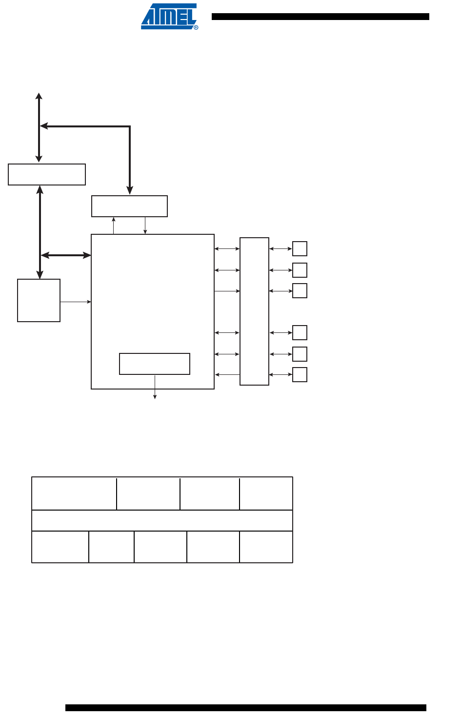
548
6430F–ATARM–21-Feb-12
SAM3U Series
548
6430F–ATARM–21-Feb-12
SAM3U Series
31.3 Block Diagram
Figure 31-1. Block Diagram
31.4 Application Block Diagram
Figure 31-2. Application Block Diagram
SSC Interface PIO
DMA
APB Bridge
MCK
System
Bus
Peripheral
Bus
TF
TK
TD
RF
RK
RD
Interrupt Control
SSC Interrupt
PMC
Interrupt
Management
Power
Management
Test
Management
SSC
Serial AUDIO
OS or RTOS Driver
Codec Frame
Management Line Interface
Time Slot
Management
549
6430F–ATARM–21-Feb-12
SAM3U Series
549
6430F–ATARM–21-Feb-12
SAM3U Series
31.5 Pin Name List
31.6 Product Dependencies
31.6.1 I/O Lines
The pins used for interfacing the compliant external devices may be multiplexed with PIO lines.
Before using the SSC receiver, the PIO controller must be configured to dedicate the SSC
receiver I/O lines to the SSC peripheral mode.
Before using the SSC transmitter, the PIO controller must be configured to dedicate the SSC
transmitter I/O lines to the SSC peripheral mode.
31.6.2 Power Management
The SSC is not continuously clocked. The SSC interface may be clocked through the Power
Management Controller (PMC), therefore the programmer must first configure the PMC to
enable the SSC clock.
31.6.3 Interrupt
The SSC interface has an interrupt line connected to the Nested Vector Interrupt Controller
(NVIC). Handling interrupts requires programming the NVIC before configuring the SSC.
Table 31-1. I/O Lines Description
Pin Name Pin Description Type
RF Receiver Frame Synchro Input/Output
RK Receiver Clock Input/Output
RD Receiver Data Input
TF Transmitter Frame Synchro Input/Output
TK Transmitter Clock Input/Output
TD Transmitter Data Output
Table 31-2. I/O Lines
Instance Signal I/O Line Peripheral
SSC RD PA27 A
SSC RF PA31 A
SSC RK PA29 A
SSC TD PA26 A
SSC TF PA30 A
SSC TK PA28 A

550
6430F–ATARM–21-Feb-12
SAM3U Series
550
6430F–ATARM–21-Feb-12
SAM3U Series
All SSC interrupts can be enabled/disabled configuring the SSC Interrupt mask register. Each
pending and unmasked SSC interrupt will assert the SSC interrupt line. The SSC interrupt ser-
vice routine can get the interrupt origin by reading the SSC interrupt status register.
Table 31-3. Peripheral IDs
Instance ID
SSC 21
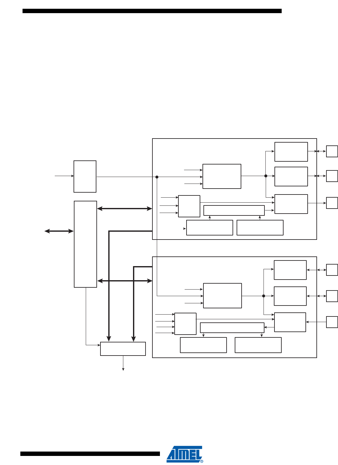
551
6430F–ATARM–21-Feb-12
SAM3U Series
551
6430F–ATARM–21-Feb-12
SAM3U Series
31.7 Functional Description
This chapter contains the functional description of the following: SSC Functional Block, Clock
Management, Data format, Start, Transmitter, Receiver and Frame Sync.
The receiver and transmitter operate separately. However, they can work synchronously by pro-
gramming the receiver to use the transmit clock and/or to start a data transfer when transmission
starts. Alternatively, this can be done by programming the transmitter to use the receive clock
and/or to start a data transfer when reception starts. The transmitter and the receiver can be pro-
grammed to operate with the clock signals provided on either the TK or RK pins. This allows the
SSC to support many slave-mode data transfers. The maximum clock speed allowed on the TK
and RK pins is the master clock divided by 2.
Figure 31-3. SSC Functional Block Diagram
31.7.1 Clock Management
The transmitter clock can be generated by:
• an external clock received on the TK I/O pad
• the receiver clock
• the internal clock divider
NVIC
Frame Sync
Controller
Clock Output
Controller
Data
Controller
Start
Selector
Start
Selector
RF
RXEN
RC0R
TX Start
TXEN
TF
RX Start
TX Start
Interrupt Control
User
Interface
APB
MCK
Receive Clock
Controller
TX Clock
RK Input
Transmit Clock
Controller
Transmit Shift Register
Transmit Sync
Holding Register
Transmit Holding
Register
RX clock
TX clock
TK Input
RD
RF
RK
Clock Output
Controller
Frame Sync
Controller
Receive Shift Register
Receive Sync
Holding Register
Receive Holding
Register
TD
TF
TK
RX Clock
Receiver
Transmitter
Data
Controller
Clock
Divider
RX Start
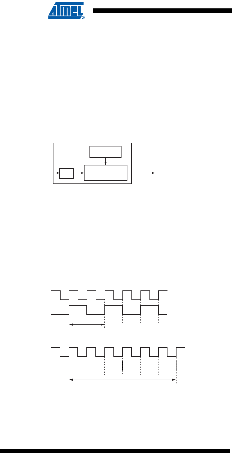
552
6430F–ATARM–21-Feb-12
SAM3U Series
552
6430F–ATARM–21-Feb-12
SAM3U Series
The receiver clock can be generated by:
• an external clock received on the RK I/O pad
• the transmitter clock
• the internal clock divider
Furthermore, the transmitter block can generate an external clock on the TK I/O pad, and the
receiver block can generate an external clock on the RK I/O pad.
This allows the SSC to support many Master and Slave Mode data transfers.
31.7.1.1 Clock Divider
Figure 31-4. Divided Clock Block Diagram
The Master Clock divider is determined by the 12-bit field DIV counter and comparator (so its
maximal value is 4095) in the Clock Mode Register SSC_CMR, allowing a Master Clock division
by up to 8190. The Divided Clock is provided to both the Receiver and Transmitter. When this
field is programmed to 0, the Clock Divider is not used and remains inactive.
When DIV is set to a value equal to or greater than 1, the Divided Clock has a frequency of Mas-
ter Clock divided by 2 times DIV. Each level of the Divided Clock has a duration of the Master
Clock multiplied by DIV. This ensures a 50% duty cycle for the Divided Clock regardless of
whether the DIV value is even or odd.
Figure 31-5. Divided Clock Generation
MCK
Divided Clock
Clock Divider
/ 2 12-bit Counter
SSC_CMR
Master Clock
Divided Clock
DIV = 1
Master Clock
Divided Clock
DIV = 3
Divided Clock Frequency = MCK/2
Divided Clock Frequency = MCK/6
553
6430F–ATARM–21-Feb-12
SAM3U Series
553
6430F–ATARM–21-Feb-12
SAM3U Series
31.7.1.2 Transmitter Clock Management
The transmitter clock is generated from the receiver clock or the divider clock or an external
clock scanned on the TK I/O pad. The transmitter clock is selected by the CKS field in
SSC_TCMR (Transmit Clock Mode Register). Transmit Clock can be inverted independently by
the CKI bits in SSC_TCMR.
The transmitter can also drive the TK I/O pad continuously or be limited to the actual data trans-
fer. The clock output is configured by the SSC_TCMR register. The Transmit Clock Inversion
(CKI) bits have no effect on the clock outputs. Programming the TCMR register to select TK pin
(CKS field) and at the same time Continuous Transmit Clock (CKO field) might lead to unpredict-
able results.
Figure 31-6. Transmitter Clock Management
31.7.1.3 Receiver Clock Management
The receiver clock is generated from the transmitter clock or the divider clock or an external
clock scanned on the RK I/O pad. The Receive Clock is selected by the CKS field in
SSC_RCMR (Receive Clock Mode Register). Receive Clocks can be inverted independently by
the CKI bits in SSC_RCMR.
The receiver can also drive the RK I/O pad continuously or be limited to the actual data transfer.
The clock output is configured by the SSC_RCMR register. The Receive Clock Inversion (CKI)
bits have no effect on the clock outputs. Programming the RCMR register to select RK pin (CKS
field) and at the same time Continuous Receive Clock (CKO field) can lead to unpredictable
results.
Table 31-4.
Maximum Minimum
MCK / 2 MCK / 8190
TK (pin)
Receiver
Clock
Divider
Clock
CKS
CKO Data Transfer
CKI CKG
Transmitter
Clock
Clock
Output
MUX Tri_state
Controller
Tri-state
Controller
INV
MUX

554
6430F–ATARM–21-Feb-12
SAM3U Series
554
6430F–ATARM–21-Feb-12
SAM3U Series
Figure 31-7. Receiver Clock Management
31.7.1.4 Serial Clock Ratio Considerations
The Transmitter and the Receiver can be programmed to operate with the clock signals provided
on either the TK or RK pins. This allows the SSC to support many slave-mode data transfers. In
this case, the maximum clock speed allowed on the RK pin is:
– Master Clock divided by 2 if Receiver Frame Synchro is input
– Master Clock divided by 3 if Receiver Frame Synchro is output
In addition, the maximum clock speed allowed on the TK pin is:
– Master Clock divided by 6 if Transmit Frame Synchro is input
– Master Clock divided by 2 if Transmit Frame Synchro is output
31.7.2 Transmitter Operations
A transmitted frame is triggered by a start event and can be followed by synchronization data
before data transmission.
The start event is configured by setting the Transmit Clock Mode Register (SSC_TCMR). See
“Start” on page 556.
The frame synchronization is configured setting the Transmit Frame Mode Register
(SSC_TFMR). See “Frame Sync” on page 558.
To transmit data, the transmitter uses a shift register clocked by the transmitter clock signal and
the start mode selected in the SSC_TCMR. Data is written by the application to the SSC_THR
register then transferred to the shift register according to the data format selected.
When both the SSC_THR and the transmit shift register are empty, the status flag TXEMPTY is
set in SSC_SR. When the Transmit Holding register is transferred in the Transmit shift register,
the status flag TXRDY is set in SSC_SR and additional data can be loaded in the holding
register.
RK (pin)
Transmitter
Clock
Divider
Clock
CKS
CKO Data Transfer
CKI CKG
Receiver
Clock
Clock
Output
MUX Tri-state
Controller
Tri-state
Controller
INV
MUX
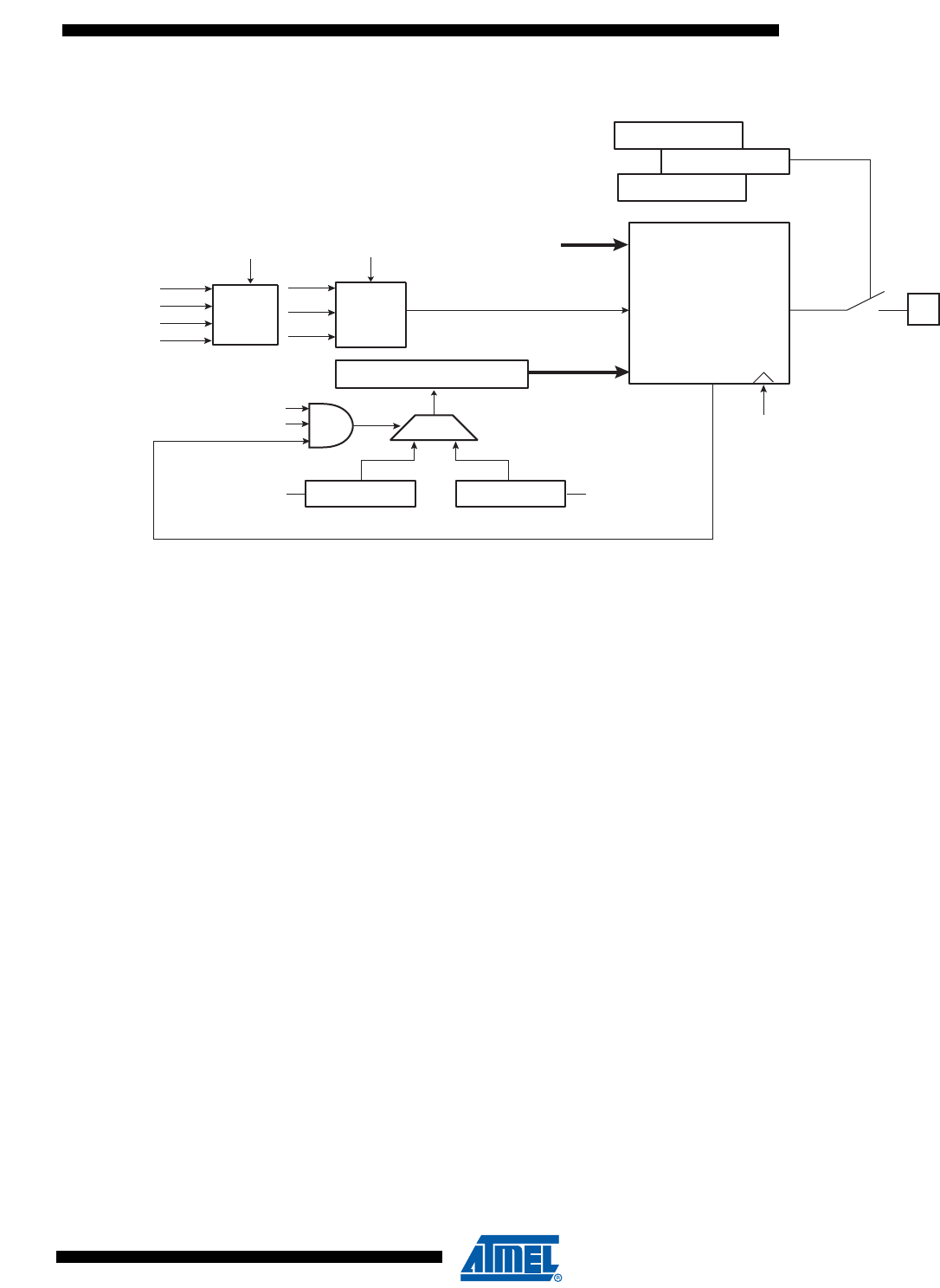
555
6430F–ATARM–21-Feb-12
SAM3U Series
555
6430F–ATARM–21-Feb-12
SAM3U Series
Figure 31-8. Transmitter Block Diagram
31.7.3 Receiver Operations
A received frame is triggered by a start event and can be followed by synchronization data
before data transmission.
The start event is configured setting the Receive Clock Mode Register (SSC_RCMR). See
“Start” on page 556.
The frame synchronization is configured setting the Receive Frame Mode Register
(SSC_RFMR). See “Frame Sync” on page 558.
The receiver uses a shift register clocked by the receiver clock signal and the start mode
selected in the SSC_RCMR. The data is transferred from the shift register depending on the
data format selected.
When the receiver shift register is full, the SSC transfers this data in the holding register, the sta-
tus flag RXRDY is set in SSC_SR and the data can be read in the receiver holding register. If
another transfer occurs before read of the RHR register, the status flag OVERUN is set in
SSC_SR and the receiver shift register is transferred in the RHR register.
Transmit Shift Register
TD
SSC_TFMR.FSLENSSC_TFMR.DATLEN
SSC_TCMR.STTDLY
SSC_TFMR.FSDEN
SSC_TFMR.DATNB
SSC_TFMR.DATDEF
SSC_TFMR.MSBF
SSC_TCMR.STTDLY != 0
SSC_TFMR.FSDEN
10
TX Controller
SSC_TCMR.START
RF
Start
Selector
TXEN
RX Start
TXEN
RF
Start
Selector
RXEN
RC0R
TX Start TX Start
Transmitter Clock
TX Controller counter reached STTDLY
SSC_RCMR.START
SSC_THR SSC_TSHR
SSC_CRTXEN
SSC_SRTXEN
SSC_CRTXDIS
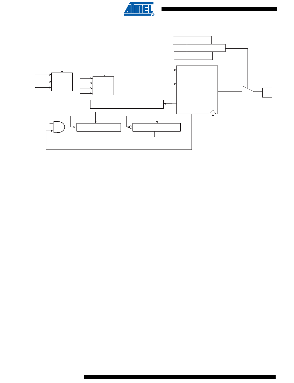
556
6430F–ATARM–21-Feb-12
SAM3U Series
556
6430F–ATARM–21-Feb-12
SAM3U Series
Figure 31-9. Receiver Block Diagram
31.7.4 Start
The transmitter and receiver can both be programmed to start their operations when an event
occurs, respectively in the Transmit Start Selection (START) field of SSC_TCMR and in the
Receive Start Selection (START) field of SSC_RCMR.
Under the following conditions the start event is independently programmable:
• Continuous. In this case, the transmission starts as soon as a word is written in SSC_THR
and the reception starts as soon as the Receiver is enabled.
• Synchronously with the transmitter/receiver
• On detection of a falling/rising edge on TF/RF
• On detection of a low level/high level on TF/RF
• On detection of a level change or an edge on TF/RF
A start can be programmed in the same manner on either side of the Transmit/Receive Clock
Register (RCMR/TCMR). Thus, the start could be on TF (Transmit) or RF (Receive).
Moreover, the Receiver can start when data is detected in the bit stream with the Compare
Functions.
Detection on TF/RF input/output is done by the field FSOS of the Transmit/Receive Frame Mode
Register (TFMR/RFMR).
SSC_RFMR.MSBF
SSC_RFMR.DATNB
SSC_TCMR.START
SSC_RCMR.START
SSC_RHRSSC_RSHR
SSC_RFMR.FSLEN SSC_RFMR.DATLEN
RX Controller counter reached STTDLY
RX Controller
RD
SSC_CR.RXEN
SSC_CR.RXDIS
SSC_SR.RXEN
Receiver Clock
RF
TXEN
RX Start
RF
RXEN
RC0R
SSC_RCMR.STTDLY != 0
Receive Shift Register
Start
Selector Start
Selector
RX Start
load load
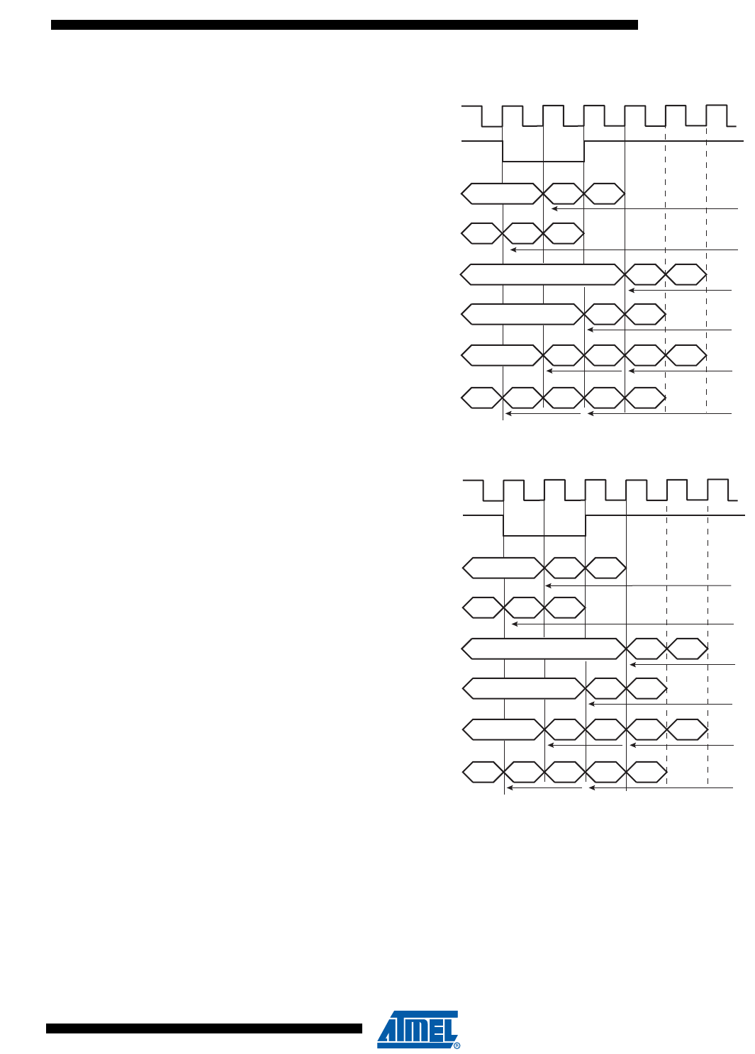
557
6430F–ATARM–21-Feb-12
SAM3U Series
557
6430F–ATARM–21-Feb-12
SAM3U Series
Figure 31-10. Transmit Start Mode
Figure 31-11. Receive Pulse/Edge Start Modes
X
TK
TF
(Input)
TD
(Output)
TD
(Output)
TD
(Output)
TD
(Output)
TD
(Output)
TD
(Output)
XBOB1
XBO B1
BO B1
BO B1
BO B1BO B1
BO B1B1
BO
X
X
X
STTDLY
STTDLY
STTDLY
STTDLY
STTDLY
STTDLY
Start = Falling Edge on TF
Start = Rising Edge on TF
Start = Low Level on TF
Start = High Level on TF
Start = Any Edge on TF
Start = Level Change on TF
X
RK
RF
(Input)
RD
(Input)
RD
(Input)
RD
(Input)
RD
(Input)
RD
(Input)
RD
(Input)
XBOB1
XBO B1
BO B1
BO B1
BO B1BO B1
BO B1B1
BO
X
X
X
STTDLY
STTDLY
STTDLY
STTDLY
STTDLY
STTDLY
Start = Falling Edge on RF
Start = Rising Edge on RF
Start = Low Level on RF
Start = High Level on RF
Start = Any Edge on RF
Start = Level Change on RF

558
6430F–ATARM–21-Feb-12
SAM3U Series
558
6430F–ATARM–21-Feb-12
SAM3U Series
31.7.5 Frame Sync
The Transmitter and Receiver Frame Sync pins, TF and RF, can be programmed to generate
different kinds of frame synchronization signals. The Frame Sync Output Selection (FSOS) field
in the Receive Frame Mode Register (SSC_RFMR) and in the Transmit Frame Mode Register
(SSC_TFMR) are used to select the required waveform.
• Programmable low or high levels during data transfer are supported.
• Programmable high levels before the start of data transfers or toggling are also supported.
If a pulse waveform is selected, the Frame Sync Length (FSLEN) field in SSC_RFMR and
SSC_TFMR programs the length of the pulse, from 1 bit time up to 256 bit time.
The periodicity of the Receive and Transmit Frame Sync pulse output can be programmed
through the Period Divider Selection (PERIOD) field in SSC_RCMR and SSC_TCMR.
31.7.5.1 Frame Sync Data
Frame Sync Data transmits or receives a specific tag during the Frame Sync signal.
During the Frame Sync signal, the Receiver can sample the RD line and store the data in the
Receive Sync Holding Register and the transmitter can transfer Transmit Sync Holding Register
in the Shifter Register. The data length to be sampled/shifted out during the Frame Sync signal
is programmed by the FSLEN field in SSC_RFMR/SSC_TFMR and has a maximum value of 16.
Concerning the Receive Frame Sync Data operation, if the Frame Sync Length is equal to or
lower than the delay between the start event and the actual data reception, the data sampling
operation is performed in the Receive Sync Holding Register through the Receive Shift Register.
The Transmit Frame Sync Operation is performed by the transmitter only if the bit Frame Sync
Data Enable (FSDEN) in SSC_TFMR is set. If the Frame Sync length is equal to or lower than
the delay between the start event and the actual data transmission, the normal transmission has
priority and the data contained in the Transmit Sync Holding Register is transferred in the Trans-
mit Register, then shifted out.
31.7.5.2 Frame Sync Edge Detection
The Frame Sync Edge detection is programmed by the FSEDGE field in
SSC_RFMR/SSC_TFMR. This sets the corresponding flags RXSYN/TXSYN in the SSC Status
Register (SSC_SR) on frame synchro edge detection (signals RF/TF).
31.7.6 Receive Compare Modes
Figure 31-12. Receive Compare Modes
CMP0 CMP3
CMP2
CMP1 Ignored B0 B2
B1
Start
RK
RD
(Input)
FSLEN
Up to 16 Bits
(4 in This Example)
STDLY DATLEN

559
6430F–ATARM–21-Feb-12
SAM3U Series
559
6430F–ATARM–21-Feb-12
SAM3U Series
31.7.6.1 Compare Functions
Length of the comparison patterns (Compare 0, Compare 1) and thus the number of bits they
are compared to is defined by FSLEN, but with a maximum value of 16 bits. Comparison is
always done by comparing the last bits received with the comparison pattern. Compare 0 can be
one start event of the Receiver. In this case, the receiver compares at each new sample the last
bits received at the Compare 0 pattern contained in the Compare 0 Register (SSC_RC0R).
When this start event is selected, the user can program the Receiver to start a new data transfer
either by writing a new Compare 0, or by receiving continuously until Compare 1 occurs. This
selection is done with the bit (STOP) in SSC_RCMR.
31.7.7 Data Format
The data framing format of both the transmitter and the receiver are programmable through the
Transmitter Frame Mode Register (SSC_TFMR) and the Receiver Frame Mode Register
(SSC_RFMR). In either case, the user can independently select:
• the event that starts the data transfer (START)
• the delay in number of bit periods between the start event and the first data bit (STTDLY)
• the length of the data (DATLEN)
• the number of data to be transferred for each start event (DATNB).
• the length of synchronization transferred for each start event (FSLEN)
• the bit sense: most or lowest significant bit first (MSBF)
Additionally, the transmitter can be used to transfer synchronization and select the level driven
on the TD pin while not in data transfer operation. This is done respectively by the Frame Sync
Data Enable (FSDEN) and by the Data Default Value (DATDEF) bits in SSC_TFMR.
560
6430F–ATARM–21-Feb-12
SAM3U Series
560
6430F–ATARM–21-Feb-12
SAM3U Series
Figure 31-13. Transmit and Receive Frame Format in Edge/Pulse Start Modes
Note: 1. Example of input on falling edge of TF/RF.
Figure 31-14. Transmit Frame Format in Continuous Mode
Table 31-5. Data Frame Registers
Transmitter Receiver Field Length Comment
SSC_TFMR SSC_RFMR DATLEN Up to 32 Size of word
SSC_TFMR SSC_RFMR DATNB Up to 16 Number of words transmitted in frame
SSC_TFMR SSC_RFMR MSBF Most significant bit first
SSC_TFMR SSC_RFMR FSLEN Up to 16 Size of Synchro data register
SSC_TFMR DATDEF 0 or 1 Data default value ended
SSC_TFMR FSDEN Enable send SSC_TSHR
SSC_TCMR SSC_RCMR PERIOD Up to 512 Frame size
SSC_TCMR SSC_RCMR STTDLY Up to 255 Size of transmit start delay
Sync Data
Default
STTDLY
Sync Data Ignored
RD
Default
Data
DATLEN
Data
Data
Data
DATLEN
Data
Data Default
Default
Ignored
Sync Data
Sync Data
FSLEN
TF/RF
(1)
Start
Start
From SSC_TSHR From SSC_THR
From SSC_THR
From SSC_THR
From SSC_THR
To SSC_RHR To SSC_RHRTo SSC_RSHR
TD
(If FSDEN = 0)
TD
(If FSDEN = 1)
DATNB
PERIOD
FromDATDEF FromDATDEF
From DATDEF From DATDEF
DATLEN
Data
DATLEN
Data Default
Start
From SSC_THR From SSC_THR
TD
Start: 1. TXEMPTY set to 1
2. Write into the SSC_THR
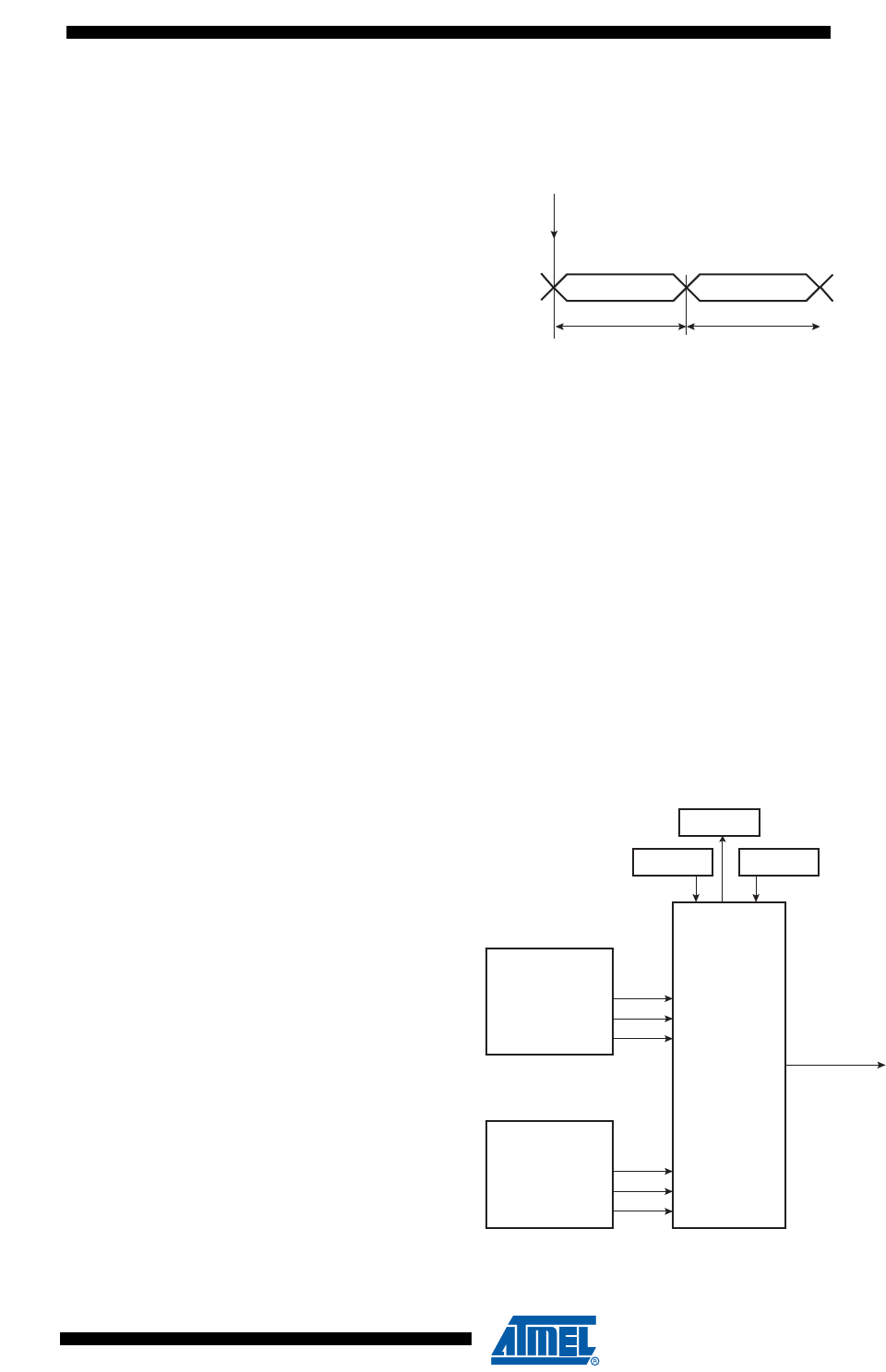
561
6430F–ATARM–21-Feb-12
SAM3U Series
561
6430F–ATARM–21-Feb-12
SAM3U Series
Note: 1. STTDLY is set to 0. In this example, SSC_THR is loaded twice. FSDEN value has no effect on
the transmission. SyncData cannot be output in continuous mode.
Figure 31-15. Receive Frame Format in Continuous Mode
Note: 1. STTDLY is set to 0.
31.7.8 Loop Mode
The receiver can be programmed to receive transmissions from the transmitter. This is done by
setting the Loop Mode (LOOP) bit in SSC_RFMR. In this case, RD is connected to TD, RF is
connected to TF and RK is connected to TK.
31.7.9 Interrupt
Most bits in SSC_SR have a corresponding bit in interrupt management registers.
The SSC can be programmed to generate an interrupt when it detects an event. The interrupt is
controlled by writing SSC_IER (Interrupt Enable Register) and SSC_IDR (Interrupt Disable Reg-
ister) These registers enable and disable, respectively, the corresponding interrupt by setting
and clearing the corresponding bit in SSC_IMR (Interrupt Mask Register), which controls the
generation of interrupts by asserting the SSC interrupt line connected to the NVIC.
Figure 31-16. Interrupt Block Diagram
Data
DATLEN
Data
DATLEN
Start = Enable Receiver
To SSC_RHR To SSC_RHR
RD
SSC_IMR
Interrupt
Control
SSC Interrupt
Set
RXRDY
OVRUN
RXSYNC
Receiver
Transmitter
TXRDY
TXEMPTY
TXSYNC
Clear
SSC_IER SSC_IDR
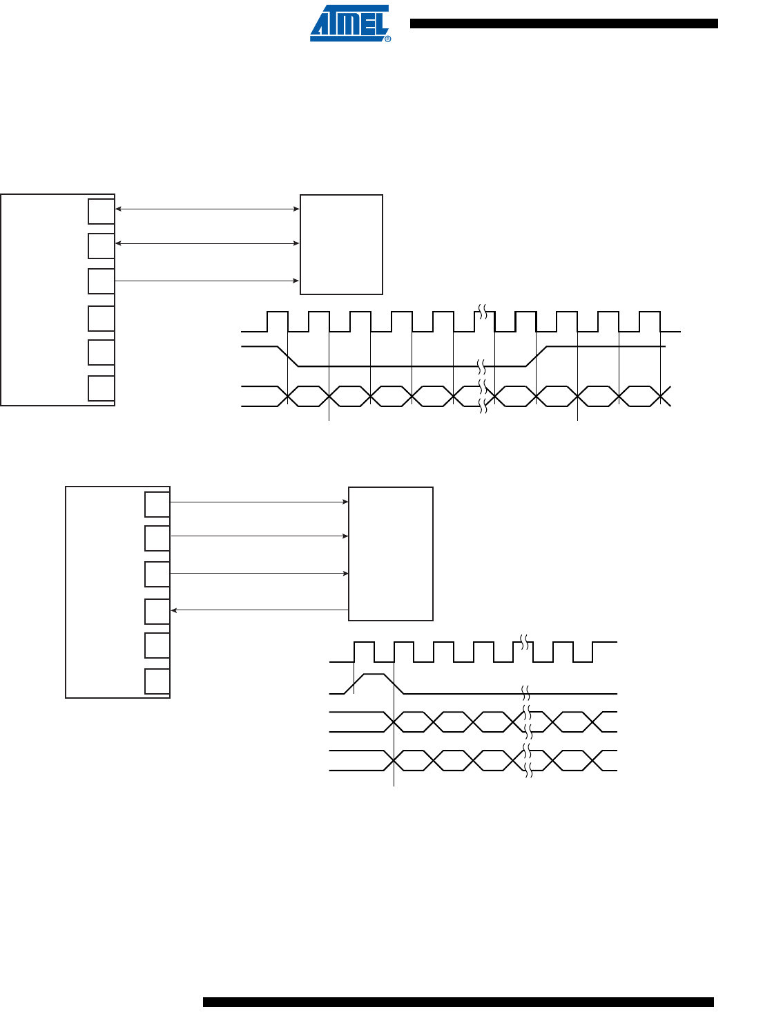
562
6430F–ATARM–21-Feb-12
SAM3U Series
562
6430F–ATARM–21-Feb-12
SAM3U Series
31.8 SSC Application Examples
The SSC can support several serial communication modes used in audio or high speed serial
links. Some standard applications are shown in the following figures. All serial link applications
supported by the SSC are not listed here.
Figure 31-17. Audio Application Block Diagram
Figure 31-18. Codec Application Block Diagram
SSC
RK
RF
RD
TD
TF
TK
Clock SCK
Word Select WS
Data SD
I2S
RECEIVER
Clock SCK
Word Select WS
Data SD
Right Channel
Left Channel
MSB MSB
LSB
SSC
RK
RF
RD
TD
TF
TK
Serial Data Clock (SCLK)
Frame sync (FSYNC)
Serial Data Out
Serial Data In
CODEC
Serial Data Clock (SCLK)
Frame sync (FSYNC)
Serial Data Out
Serial Data In
First Time Slot
Dstart Dend
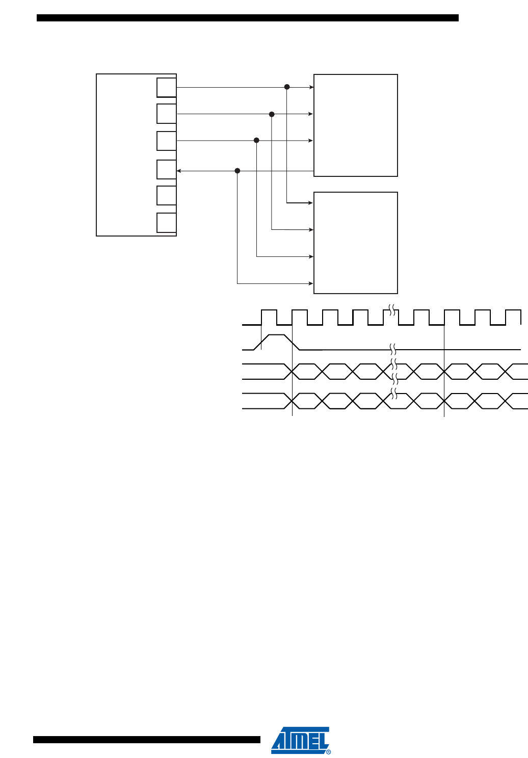
563
6430F–ATARM–21-Feb-12
SAM3U Series
563
6430F–ATARM–21-Feb-12
SAM3U Series
Figure 31-19. Time Slot Application Block Diagram
SSC
RK
RF
RD
TD
TF
TK
SCLK
FSYNC
Data Out
Data in
CODEC
First
Time Slot
Serial Data Clock (SCLK)
Frame sync (FSYNC)
Serial Data Out
Serial Data in
CODEC
Second
Time Slot
First Time Slot Second Time Slot
Dstart Dend

564
6430F–ATARM–21-Feb-12
SAM3U Series
564
6430F–ATARM–21-Feb-12
SAM3U Series
31.8.1 Write Protection Registers
To prevent any single software error that may corrupt SSC behavior, certain address spaces can
be write-protected by setting the WPEN bit in the “SSC Write Protect Mode Register”
(SSC_WPMR).
If a write access to the protected registers is detected, then the WPVS flag in the SSC Write Pro-
tect Status Register (US_WPSR) is set and the field WPVSRC indicates in which register the
write access has been attempted.
The WPVS flag is reset by writing the SSC Write Protect Mode Register (SSC_WPMR) with the
appropriate access key, WPKEY.
The protected registers are:
•“SSC Clock Mode Register” on page 567
•“SSC Receive Clock Mode Register” on page 568
•“SSC Receive Frame Mode Register” on page 570
•“SSC Transmit Clock Mode Register” on page 572
•“SSC Transmit Frame Mode Register” on page 574
•“SSC Receive Compare 0 Register” on page 580
•“SSC Receive Compare 1 Register” on page 581

565
6430F–ATARM–21-Feb-12
SAM3U Series
565
6430F–ATARM–21-Feb-12
SAM3U Series
31.9 Synchronous Serial Controller (SSC) User Interface
Table 31-6. Register Mapping
Offset Register Name Access Reset
0x0 Control Register SSC_CR Write-only –
0x4 Clock Mode Register SSC_CMR Read-write 0x0
0x8 Reserved – – –
0xC Reserved – – –
0x10 Receive Clock Mode Register SSC_RCMR Read-write 0x0
0x14 Receive Frame Mode Register SSC_RFMR Read-write 0x0
0x18 Transmit Clock Mode Register SSC_TCMR Read-write 0x0
0x1C Transmit Frame Mode Register SSC_TFMR Read-write 0x0
0x20 Receive Holding Register SSC_RHR Read-only 0x0
0x24 Transmit Holding Register SSC_THR Write-only –
0x28 Reserved – – –
0x2C Reserved – – –
0x30 Receive Sync. Holding Register SSC_RSHR Read-only 0x0
0x34 Transmit Sync. Holding Register SSC_TSHR Read-write 0x0
0x38 Receive Compare 0 Register SSC_RC0R Read-write 0x0
0x3C Receive Compare 1 Register SSC_RC1R Read-write 0x0
0x40 Status Register SSC_SR Read-only 0x000000CC
0x44 Interrupt Enable Register SSC_IER Write-only –
0x48 Interrupt Disable Register SSC_IDR Write-only –
0x4C Interrupt Mask Register SSC_IMR Read-only 0x0
0xE4 Write Protect Mode Register SSC_WPMR Read-write 0x0
0xE8 Write Protect Status Register SSC_WPSR Read-only 0x0
0x50-0xFC Reserved – – –
0x100- 0x124 Reserved – – –

566
6430F–ATARM–21-Feb-12
SAM3U Series
566
6430F–ATARM–21-Feb-12
SAM3U Series
31.9.1 SSC Control Register
Name: SSC_CR
Address: 0x40004000
Access: Write-only
• RXEN: Receive Enable
0 = No effect.
1 = Enables Receive if RXDIS is not set.
• RXDIS: Receive Disable
0 = No effect.
1 = Disables Receive. If a character is currently being received, disables at end of current character reception.
• TXEN: Transmit Enable
0 = No effect.
1 = Enables Transmit if TXDIS is not set.
• TXDIS: Transmit Disable
0 = No effect.
1 = Disables Transmit. If a character is currently being transmitted, disables at end of current character transmission.
• SWRST: Software Reset
0 = No effect.
1 = Performs a software reset. Has priority on any other bit in SSC_CR.
31 30 29 28 27 26 25 24
––––––––
23 22 21 20 19 18 17 16
––––––––
15 14 13 12 11 10 9 8
SWRST–––––TXDISTXEN
76543210
––––––RXDISRXEN

567
6430F–ATARM–21-Feb-12
SAM3U Series
567
6430F–ATARM–21-Feb-12
SAM3U Series
31.9.2 SSC Clock Mode Register
Name: SSC_CMR
Address: 0x40004004
Access: Read-write
This register can only be written if the WPEN bit is cleared in “SSC Write Protect Mode Register” .
• DIV: Clock Divider
0 = The Clock Divider is not active.
Any Other Value: The Divided Clock equals the Master Clock divided by 2 times DIV. The maximum bit rate is MCK/2. The
minimum bit rate is MCK/2 x 4095 = MCK/8190.
31 30 29 28 27 26 25 24
––––––––
23 22 21 20 19 18 17 16
––––––––
15 14 13 12 11 10 9 8
–––– DIV
76543210
DIV
568
6430F–ATARM–21-Feb-12
SAM3U Series
568
6430F–ATARM–21-Feb-12
SAM3U Series
31.9.3 SSC Receive Clock Mode Register
Name: SSC_RCMR
Address: 0x40004010
Access: Read-write
This register can only be written if the WPEN bit is cleared in “SSC Write Protect Mode Register” .
• CKS: Receive Clock Selection
• CKO: Receive Clock Output Mode Selection
• CKI: Receive Clock Inversion
0 = The data inputs (Data and Frame Sync signals) are sampled on Receive Clock falling edge. The Frame Sync signal
output is shifted out on Receive Clock rising edge.
1 = The data inputs (Data and Frame Sync signals) are sampled on Receive Clock rising edge. The Frame Sync signal out-
put is shifted out on Receive Clock falling edge.
CKI affects only the Receive Clock and not the output clock signal.
31 30 29 28 27 26 25 24
PERIOD
23 22 21 20 19 18 17 16
STTDLY
15 14 13 12 11 10 9 8
– – – STOP START
76543210
CKG CKI CKO CKS
Value Name Description
0 MCK Divided Clock
1TK TK Clock signal
2RK RK pin
3Reserved
Value Name Description RK Pin
0 NONE None Input-only
1 CONTINUOUS Continuous Receive Clock Output
2 TRANSFER Receive Clock only during data transfers Output
3-7 Reserved

569
6430F–ATARM–21-Feb-12
SAM3U Series
569
6430F–ATARM–21-Feb-12
SAM3U Series
• CKG: Receive Clock Gating Selection
• START: Receive Start Selection
• STOP: Receive Stop Selection
0 = After completion of a data transfer when starting with a Compare 0, the receiver stops the data transfer and waits for a
new compare 0.
1 = After starting a receive with a Compare 0, the receiver operates in a continuous mode until a Compare 1 is detected.
• STTDLY: Receive Start Delay
If STTDLY is not 0, a delay of STTDLY clock cycles is inserted between the start event and the actual start of reception.
When the Receiver is programmed to start synchronously with the Transmitter, the delay is also applied.
Note: It is very important that STTDLY be set carefully. If STTDLY must be set, it should be done in relation to TAG
(Receive Sync Data) reception.
• PERIOD: Receive Period Divider Selection
This field selects the divider to apply to the selected Receive Clock in order to generate a new Frame Sync Signal. If 0, no
PERIOD signal is generated. If not 0, a PERIOD signal is generated each 2 x (PERIOD+1) Receive Clock.
Value Name Description RK Pin
0 NONE None Input-only
1 CONTINUOUS Continuous Receive Clock Output
2 TRANSFER Receive Clock only during data transfers Output
3-7 Reserved
Value Name Description
0 CONTINUOUS Continuous, as soon as the receiver is enabled, and
immediately after the end of transfer of the previous data.
1TRANSMIT Transmit start
2 RF_LOW Detection of a low level on RF signal
3RF_HIGH Detection of a high level on RF signal
4RF_FALLING
Detection of a falling edge on RF signal
5 RF_RISING Detection of a rising edge on RF signal
6 RF_LEVEL Detection of any level change on RF signal
7RF_EDGE Detection of any edge on RF signal
8CMP_0 Compare 0

570
6430F–ATARM–21-Feb-12
SAM3U Series
570
6430F–ATARM–21-Feb-12
SAM3U Series
31.9.4 SSC Receive Frame Mode Register
Name: SSC_RFMR
Address: 0x40004014
Access: Read-write
This register can only be written if the WPEN bit is cleared in “SSC Write Protect Mode Register” .
• DATLEN: Data Length
0 = Forbidden value (1-bit data length not supported).
Any other value: The bit stream contains DATLEN + 1 data bits.
• LOOP: Loop Mode
0 = Normal operating mode.
1 = RD is driven by TD, RF is driven by TF and TK drives RK.
• MSBF: Most Significant Bit First
0 = The lowest significant bit of the data register is sampled first in the bit stream.
1 = The most significant bit of the data register is sampled first in the bit stream.
• DATNB: Data Number per Frame
This field defines the number of data words to be received after each transfer start, which is equal to (DATNB + 1).
• FSLEN: Receive Frame Sync Length
This field defines the number of bits sampled and stored in the Receive Sync Data Register. When this mode is selected by
the START field in the Receive Clock Mode Register, it also determines the length of the sampled data to be compared to
the Compare 0 or Compare 1 register.
This field is used with FSLEN_EXT to determine the pulse length of the Receive Frame Sync signal.
Pulse length is equal to FSLEN + (FSLEN_EXT * 16) + 1 Receive Clock periods.
31 30 29 28 27 26 25 24
FSLEN_EXT FSLEN_EXT FSLEN_EXT FSLEN_EXT –––FSEDGE
23 22 21 20 19 18 17 16
– FSOS FSLEN
15 14 13 12 11 10 9 8
––– – DATNB
765 4 3210
MSBF – LOOP DATLEN
571
6430F–ATARM–21-Feb-12
SAM3U Series
571
6430F–ATARM–21-Feb-12
SAM3U Series
• FSOS: Receive Frame Sync Output Selection
• FSEDGE: Frame Sync Edge Detection
Determines which edge on Frame Sync will generate the interrupt RXSYN in the SSC Status Register.
• FSLEN_EXT: FSLEN Field Extension
Extends FSLEN field. For details, refer to FSLEN bit description on page 570.
Value Name Description RF Pin
0 NONE None Input-only
1NEGATIVE Negative Pulse Output
2 POSITIVE Positive Pulse Output
3LOW Driven Low during data transfer Output
4HIGH Driven High during data transfer Output
5 TOGGLING Toggling at each start of data transfer Output
6-7 Reserved Undefined
Value Name Description
0 POSITIVE Positive Edge Detection
1NEGATIVE Negative Edge Detection

572
6430F–ATARM–21-Feb-12
SAM3U Series
572
6430F–ATARM–21-Feb-12
SAM3U Series
31.9.5 SSC Transmit Clock Mode Register
Name: SSC_TCMR
Address: 0x40004018
Access: Read-write
This register can only be written if the WPEN bit is cleared in “SSC Write Protect Mode Register” .
• CKS: Transmit Clock Selection
• CKO: Transmit Clock Output Mode Selection
• CKI: Transmit Clock Inversion
0 = The data outputs (Data and Frame Sync signals) are shifted out on Transmit Clock falling edge. The Frame sync signal
input is sampled on Transmit clock rising edge.
1 = The data outputs (Data and Frame Sync signals) are shifted out on Transmit Clock rising edge. The Frame sync signal
input is sampled on Transmit clock falling edge.
CKI affects only the Transmit Clock and not the output clock signal.
31 30 29 28 27 26 25 24
PERIOD
23 22 21 20 19 18 17 16
STTDLY
15 14 13 12 11 10 9 8
–––– START
76543210
CKG CKI CKO CKS
Value Name Description
0 MCK Divided Clock
1TK TK Clock signal
2RK RK pin
3Reserved
Value Name Description TK Pin
0 NONE None Input-only
1 CONTINUOUS Continuous Receive Clock Output
2 TRANSFER Transmit Clock only during data transfers Output
3-7 Reserved

573
6430F–ATARM–21-Feb-12
SAM3U Series
573
6430F–ATARM–21-Feb-12
SAM3U Series
• CKG: Transmit Clock Gating Selection
• START: Transmit Start Selection
• STTDLY: Transmit Start Delay
If STTDLY is not 0, a delay of STTDLY clock cycles is inserted between the start event and the actual start of transmission
of data. When the Transmitter is programmed to start synchronously with the Receiver, the delay is also applied.
Note: STTDLY must be set carefully. If STTDLY is too short in respect to TAG (Transmit Sync Data) emission, data is emit-
ted instead of the end of TAG.
• PERIOD: Transmit Period Divider Selection
This field selects the divider to apply to the selected Transmit Clock to generate a new Frame Sync Signal. If 0, no period
signal is generated. If not 0, a period signal is generated at each 2 x (PERIOD+1) Transmit Clock.
Value Name Description
0 NONE None
1 CONTINUOUS Transmit Clock enabled only if TF Low
2 TRANSFER Transmit Clock enabled only if TF High
Value Name Description
0 CONTINUOUS Continuous, as soon as a word is written in the SSC_THR Register (if Transmit is enabled), and
immediately after the end of transfer of the previous data.
1 RECEIVE Receive start
2 RF_LOW Detection of a low level on TF signal
3RF_HIGH Detection of a high level on TF signal
4RF_FALLING
Detection of a falling edge on TF signal
5 RF_RISING Detection of a rising edge on TF signal
6 RF_LEVEL Detection of any level change on TF signal
7RF_EDGE Detection of any edge on TF signal
8CMP_0 Compare 0

574
6430F–ATARM–21-Feb-12
SAM3U Series
574
6430F–ATARM–21-Feb-12
SAM3U Series
31.9.6 SSC Transmit Frame Mode Register
Name: SSC_TFMR
Address: 0x4000401C
Access: Read-write
This register can only be written if the WPEN bit is cleared in “SSC Write Protect Mode Register” .
• DATLEN: Data Length
0 = Forbidden value (1-bit data length not supported).
Any other value: The bit stream contains DATLEN + 1 data bits.
• DATDEF: Data Default Value
This bit defines the level driven on the TD pin while out of transmission. Note that if the pin is defined as multi-drive by the
PIO Controller, the pin is enabled only if the SCC TD output is 1.
• MSBF: Most Significant Bit First
0 = The lowest significant bit of the data register is shifted out first in the bit stream.
1 = The most significant bit of the data register is shifted out first in the bit stream.
• DATNB: Data Number per frame
This field defines the number of data words to be transferred after each transfer start, which is equal to (DATNB +1).
• FSLEN: Transmit Frame Sync Length
This field defines the length of the Transmit Frame Sync signal and the number of bits shifted out from the Transmit Sync
Data Register if FSDEN is 1.
This field is used with FSLEN_EXT to determine the pulse length of the Transmit Frame Sync signal.
Pulse length is equal to FSLEN + (FSLEN_EXT * 16) + 1 Transmit Clock period.
31 30 29 28 27 26 25 24
FSLEN_EXT FSLEN_EXT FSLEN_EXT FSLEN_EXT –––FSEDGE
23 22 21 20 19 18 17 16
FSDEN FSOS FSLEN
15 14 13 12 11 10 9 8
––– – DATNB
765 4 3210
M S B F – DAT D E F D AT L E N
575
6430F–ATARM–21-Feb-12
SAM3U Series
575
6430F–ATARM–21-Feb-12
SAM3U Series
• FSOS: Transmit Frame Sync Output Selection
• FSDEN: Frame Sync Data Enable
0 = The TD line is driven with the default value during the Transmit Frame Sync signal.
1 = SSC_TSHR value is shifted out during the transmission of the Transmit Frame Sync signal.
• FSEDGE: Frame Sync Edge Detection
Determines which edge on frame sync will generate the interrupt TXSYN (Status Register).
• FSLEN_EXT: FSLEN Field Extension
Extends FSLEN field. For details, refer to FSLEN bit description on page 574.
Value Name Description RF Pin
0 NONE None Input-only
1NEGATIVE Negative Pulse Output
2 POSITIVE Positive Pulse Output
3LOW Driven Low during data transfer Output
4HIGH Driven High during data transfer Output
5 TOGGLING Toggling at each start of data transfer Output
6-7 Reserved Undefined
Value Name Description
0 POSITIVE Positive Edge Detection
1NEGATIVE Negative Edge Detection

576
6430F–ATARM–21-Feb-12
SAM3U Series
576
6430F–ATARM–21-Feb-12
SAM3U Series
31.9.7 SSC Receive Holding Register
Name: SSC_RHR
Address: 0x40004020
Access: Read-only
• RDAT: Receive Data
Right aligned regardless of the number of data bits defined by DATLEN in SSC_RFMR.
31 30 29 28 27 26 25 24
RDAT
23 22 21 20 19 18 17 16
RDAT
15 14 13 12 11 10 9 8
RDAT
76543210
RDAT

577
6430F–ATARM–21-Feb-12
SAM3U Series
577
6430F–ATARM–21-Feb-12
SAM3U Series
31.9.8 SSC Transmit Holding Register
Name: SSC_THR
Address: 0x40004024
Access: Write-only
• TDAT: Transmit Data
Right aligned regardless of the number of data bits defined by DATLEN in SSC_TFMR.
31 30 29 28 27 26 25 24
TDAT
23 22 21 20 19 18 17 16
TDAT
15 14 13 12 11 10 9 8
TDAT
76543210
TDAT

578
6430F–ATARM–21-Feb-12
SAM3U Series
578
6430F–ATARM–21-Feb-12
SAM3U Series
31.9.9 SSC Receive Synchronization Holding Register
Name: SSC_RSHR
Address: 0x40004030
Access: Read-only
• RSDAT: Receive Synchronization Data
31 30 29 28 27 26 25 24
––––––––
23 22 21 20 19 18 17 16
––––––––
15 14 13 12 11 10 9 8
RSDAT
76543210
RSDAT

579
6430F–ATARM–21-Feb-12
SAM3U Series
579
6430F–ATARM–21-Feb-12
SAM3U Series
31.9.10 SSC Transmit Synchronization Holding Register
Name: SSC_TSHR
Address: 0x40004034
Access: Read-write
• TSDAT: Transmit Synchronization Data
31 30 29 28 27 26 25 24
––––––––
23 22 21 20 19 18 17 16
––––––––
15 14 13 12 11 10 9 8
TSDAT
76543210
TSDAT

580
6430F–ATARM–21-Feb-12
SAM3U Series
580
6430F–ATARM–21-Feb-12
SAM3U Series
31.9.11 SSC Receive Compare 0 Register
Name: SSC_RC0R
Address: 0x40004038
Access: Read-write
This register can only be written if the WPEN bit is cleared in “SSC Write Protect Mode Register” .
• CP0: Receive Compare Data 0
31 30 29 28 27 26 25 24
––––––––
23 22 21 20 19 18 17 16
––––––––
15 14 13 12 11 10 9 8
CP0
76543210
CP0

581
6430F–ATARM–21-Feb-12
SAM3U Series
581
6430F–ATARM–21-Feb-12
SAM3U Series
31.9.12 SSC Receive Compare 1 Register
Name: SSC_RC1R
Address: 0x4000403C
Access: Read-write
This register can only be written if the WPEN bit is cleared in “SSC Write Protect Mode Register” .
• CP1: Receive Compare Data 1
31 30 29 28 27 26 25 24
––––––––
23 22 21 20 19 18 17 16
––––––––
15 14 13 12 11 10 9 8
CP1
76543210
CP1

582
6430F–ATARM–21-Feb-12
SAM3U Series
582
6430F–ATARM–21-Feb-12
SAM3U Series
31.9.13 SSC Status Register
Name: SSC_SR
Address: 0x40004040
Access: Read-only
• TXRDY: Transmit Ready
0 = Data has been loaded in SSC_THR and is waiting to be loaded in the Transmit Shift Register (TSR).
1 = SSC_THR is empty.
• TXEMPTY: Transmit Empty
0 = Data remains in SSC_THR or is currently transmitted from TSR.
1 = Last data written in SSC_THR has been loaded in TSR and last data loaded in TSR has been transmitted.
• RXRDY: Receive Ready
0 = SSC_RHR is empty.
1 = Data has been received and loaded in SSC_RHR.
• OVRUN: Receive Overrun
0 = No data has been loaded in SSC_RHR while previous data has not been read since the last read of the Status
Register.
1 = Data has been loaded in SSC_RHR while previous data has not yet been read since the last read of the Status
Register.
•CP0: Compare 0
0 = A compare 0 has not occurred since the last read of the Status Register.
1 = A compare 0 has occurred since the last read of the Status Register.
•CP1: Compare 1
0 = A compare 1 has not occurred since the last read of the Status Register.
1 = A compare 1 has occurred since the last read of the Status Register.
• TXSYN: Transmit Sync
0 = A Tx Sync has not occurred since the last read of the Status Register.
1 = A Tx Sync has occurred since the last read of the Status Register.
31 30 29 28 27 26 25 24
––––––––
23 22 21 20 19 18 17 16
––––––RXENTXEN
15 14 13 12 11 10 9 8
––––RXSYNTXSYN CP1 CP0
76543210
– – OVRUN RXRDY – – TXEMPTY TXRDY

583
6430F–ATARM–21-Feb-12
SAM3U Series
583
6430F–ATARM–21-Feb-12
SAM3U Series
• RXSYN: Receive Sync
0 = An Rx Sync has not occurred since the last read of the Status Register.
1 = An Rx Sync has occurred since the last read of the Status Register.
• TXEN: Transmit Enable
0 = Transmit is disabled.
1 = Transmit is enabled.
• RXEN: Receive Enable
0 = Receive is disabled.
1 = Receive is enabled.

584
6430F–ATARM–21-Feb-12
SAM3U Series
584
6430F–ATARM–21-Feb-12
SAM3U Series
31.9.14 SSC Interrupt Enable Register
Name: SSC_IER
Address: 0x40004044
Access: Write-only
• TXRDY: Transmit Ready Interrupt Enable
0 = 0 = No effect.
1 = Enables the Transmit Ready Interrupt.
• TXEMPTY: Transmit Empty Interrupt Enable
0 = No effect.
1 = Enables the Transmit Empty Interrupt.
• RXRDY: Receive Ready Interrupt Enable
0 = No effect.
1 = Enables the Receive Ready Interrupt.
• OVRUN: Receive Overrun Interrupt Enable
0 = No effect.
1 = Enables the Receive Overrun Interrupt.
• CP0: Compare 0 Interrupt Enable
0 = No effect.
1 = Enables the Compare 0 Interrupt.
• CP1: Compare 1 Interrupt Enable
0 = No effect.
1 = Enables the Compare 1 Interrupt.
• TXSYN: Tx Sync Interrupt Enable
0 = No effect.
1 = Enables the Tx Sync Interrupt.
• RXSYN: Rx Sync Interrupt Enable
31 30 29 28 27 26 25 24
––––––––
23 22 21 20 19 18 17 16
––––––––
15 14 13 12 11 10 9 8
––––RXSYNTXSYN CP1 CP0
76543210
– – OVRUN RXRDY – – TXEMPTY TXRDY

585
6430F–ATARM–21-Feb-12
SAM3U Series
585
6430F–ATARM–21-Feb-12
SAM3U Series
0 = No effect.
1 = Enables the Rx Sync Interrupt.

586
6430F–ATARM–21-Feb-12
SAM3U Series
586
6430F–ATARM–21-Feb-12
SAM3U Series
31.9.15 SSC Interrupt Disable Register
Name: SSC_IDR
Address: 0x40004048
Access: Write-only
• TXRDY: Transmit Ready Interrupt Disable
0 = No effect.
1 = Disables the Transmit Ready Interrupt.
• TXEMPTY: Transmit Empty Interrupt Disable
0 = No effect.
1 = Disables the Transmit Empty Interrupt.
• RXRDY: Receive Ready Interrupt Disable
0 = No effect.
1 = Disables the Receive Ready Interrupt.
• OVRUN: Receive Overrun Interrupt Disable
0 = No effect.
1 = Disables the Receive Overrun Interrupt.
• CP0: Compare 0 Interrupt Disable
0 = No effect.
1 = Disables the Compare 0 Interrupt.
• CP1: Compare 1 Interrupt Disable
0 = No effect.
1 = Disables the Compare 1 Interrupt.
• TXSYN: Tx Sync Interrupt Enable
0 = No effect.
1 = Disables the Tx Sync Interrupt.
31 30 29 28 27 26 25 24
––––––––
23 22 21 20 19 18 17 16
––––––––
15 14 13 12 11 10 9 8
––––RXSYNTXSYN CP1 CP0
76543210
– – OVRUN RXRDY – – TXEMPTY TXRDY

587
6430F–ATARM–21-Feb-12
SAM3U Series
587
6430F–ATARM–21-Feb-12
SAM3U Series
• RXSYN: Rx Sync Interrupt Enable
0 = No effect.
1 = Disables the Rx Sync Interrupt.

588
6430F–ATARM–21-Feb-12
SAM3U Series
588
6430F–ATARM–21-Feb-12
SAM3U Series
31.9.16 SSC Interrupt Mask Register
Name: SSC_IMR
Address: 0x4000404C
Access: Read-only
• TXRDY: Transmit Ready Interrupt Mask
0 = The Transmit Ready Interrupt is disabled.
1 = The Transmit Ready Interrupt is enabled.
• TXEMPTY: Transmit Empty Interrupt Mask
0 = The Transmit Empty Interrupt is disabled.
1 = The Transmit Empty Interrupt is enabled.
• RXRDY: Receive Ready Interrupt Mask
0 = The Receive Ready Interrupt is disabled.
1 = The Receive Ready Interrupt is enabled.
• OVRUN: Receive Overrun Interrupt Mask
0 = The Receive Overrun Interrupt is disabled.
1 = The Receive Overrun Interrupt is enabled.
• CP0: Compare 0 Interrupt Mask
0 = The Compare 0 Interrupt is disabled.
1 = The Compare 0 Interrupt is enabled.
• CP1: Compare 1 Interrupt Mask
0 = The Compare 1 Interrupt is disabled.
1 = The Compare 1 Interrupt is enabled.
• TXSYN: Tx Sync Interrupt Mask
0 = The Tx Sync Interrupt is disabled.
1 = The Tx Sync Interrupt is enabled.
31 30 29 28 27 26 25 24
––––––––
23 22 21 20 19 18 17 16
––––––––
15 14 13 12 11 10 9 8
––––RXSYNTXSYN CP1 CP0
76543210
– – OVRUN RXRDY – – TXEMPTY TXRDY

589
6430F–ATARM–21-Feb-12
SAM3U Series
589
6430F–ATARM–21-Feb-12
SAM3U Series
• RXSYN: Rx Sync Interrupt Mask
0 = The Rx Sync Interrupt is disabled.
1 = The Rx Sync Interrupt is enabled.

590
6430F–ATARM–21-Feb-12
SAM3U Series
590
6430F–ATARM–21-Feb-12
SAM3U Series
31.9.17 SSC Write Protect Mode Register
Name: SSC_WPMR
Address: 0x400040E4
Access: Read-write
Reset: See Table 31-6
• WPEN: Write Protect Enable
0 = Disables the Write Protect if WPKEY corresponds to 0x535343 (“SSC” in ASCII).
1 = Enables the Write Protect if WPKEY corresponds to 0x535343 (“SSC” in ASCII).
Protects the registers:
•“SSC Clock Mode Register” on page 567
•“SSC Receive Clock Mode Register” on page 568
•“SSC Receive Frame Mode Register” on page 570
•“SSC Transmit Clock Mode Register” on page 572
•“SSC Transmit Frame Mode Register” on page 574
•“SSC Receive Compare 0 Register” on page 580
•“SSC Receive Compare 1 Register” on page 581
• WPKEY: Write Protect KEY
Should be written at value 0x535343 (“SSC” in ASCII). Writing any other value in this field aborts the write operation of the
WPEN bit. Always reads as 0.
31 30 29 28 27 26 25 24
WPKEY
23 22 21 20 19 18 17 16
WPKEY
15 14 13 12 11 10 9 8
WPKEY
76543210
———————WPEN

591
6430F–ATARM–21-Feb-12
SAM3U Series
591
6430F–ATARM–21-Feb-12
SAM3U Series
31.9.18 SSC Write Protect Status Register
Name: SSC_WPSR
Address: 0x400040E8
Access: Read-only
Reset: See Table 31-6
• WPVS: Write Protect Violation Status
0 = No Write Protect Violation has occurred since the last read of the SSC_WPSR register.
1 = A Write Protect Violation has occurred since the last read of the SSC_WPSR register. If this violation is an unauthorized
attempt to write a protected register, the associated violation is reported into field WPVSRC.
• WPVSRC: Write Protect Violation Source
When WPVS is active, this field indicates the write-protected register (through address offset or code) in which a write
access has been attempted.
Note: Reading SSC_WPSR automatically clears all fields.
31 30 29 28 27 26 25 24
————————
23 22 21 20 19 18 17 16
WPVSRC
15 14 13 12 11 10 9 8
WPVSRC
76543210
———————WPVS

592
6430F–ATARM–21-Feb-12
SAM3U Series
592
6430F–ATARM–21-Feb-12
SAM3U Series

593
6430F–ATARM–21-Feb-12
SAM3U Series
593
6430F–ATARM–21-Feb-12
SAM3U Series
32. Serial Peripheral Interface (SPI) Programmer Datasheet
32.1 Description
The Serial Peripheral Interface (SPI) circuit is a synchronous serial data link that provides com-
munication with external devices in Master or Slave Mode. It also enables communication
between processors if an external processor is connected to the system.
The Serial Peripheral Interface is essentially a shift register that serially transmits data bits to
other SPIs. During a data transfer, one SPI system acts as the “master”' which controls the data
flow, while the other devices act as “slaves'' which have data shifted into and out by the master.
Different CPUs can take turn being masters (Multiple Master Protocol opposite to Single Master
Protocol where one CPU is always the master while all of the others are always slaves) and one
master may simultaneously shift data into multiple slaves. However, only one slave may drive its
output to write data back to the master at any given time.
A slave device is selected when the master asserts its NSS signal. If multiple slave devices
exist, the master generates a separate slave select signal for each slave (NPCS).
The SPI system consists of two data lines and two control lines:
• Master Out Slave In (MOSI): This data line supplies the output data from the master shifted
into the input(s) of the slave(s).
• Master In Slave Out (MISO): This data line supplies the output data from a slave to the input
of the master. There may be no more than one slave transmitting data during any particular
transfer.
• Serial Clock (SPCK): This control line is driven by the master and regulates the flow of the
data bits. The master may transmit data at a variety of baud rates; the SPCK line cycles once
for each bit that is transmitted.
• Slave Select (NSS): This control line allows slaves to be turned on and off by hardware.
32.2 Embedded Characteristics
• Supports Communication with Serial External Devices
– Four Chip Selects with External Decoder Support Allow Communication with Up to
15 Peripherals
– Serial Memories, such as DataFlash and 3-wire EEPROMs
– Serial Peripherals, such as ADCs, DACs, LCD Controllers, CAN Controllers and
Sensors
– External Co-processors
• Master or Slave Serial Peripheral Bus Interface
– 8- to 16-bit Programmable Data Length Per Chip Select
– Programmable Phase and Polarity Per Chip Select
– Programmable Transfer Delay Between Consecutive Transfers and Delay Before SPI
Clock per Chip Select
– Programmable Delay Between Chip Selects
– Selectable Mode Fault Detection
• Connection to DMA Channel Capabilities Optimizes Data Transfers
– One channel for the Receiver, One Channel for the Transmitter
594
6430F–ATARM–21-Feb-12
SAM3U Series
594
6430F–ATARM–21-Feb-12
SAM3U Series
32.3 Block Diagram
Figure 32-1. Block Diagram
SPI Interface
Interrupt Control
PIO
Peripheral Bridge
DMA Ch.
AHB Matrix
PMC MCK
SPI Interrupt
SPCK
MISO
MOSI
NPCS0/NSS
NPCS1
NPCS2
NPCS3
APB
595
6430F–ATARM–21-Feb-12
SAM3U Series
595
6430F–ATARM–21-Feb-12
SAM3U Series
32.4 Application Block Diagram
Figure 32-2. Application Block Diagram: Single Master/Multiple Slave Implementation
32.5 Signal Description
Table 32-1. Signal Description
Pin Name Pin Description
Type
Master Slave
MISO Master In Slave Out Input Output
MOSI Master Out Slave In Output Input
SPCK Serial Clock Output Input
NPCS1-NPCS3 Peripheral Chip Selects Output Unused
NPCS0/NSS Peripheral Chip Select/Slave Select Output Input
SPI Master
SPCK
MISO
MOSI
NPCS0
NPCS1
NPCS2
SPCK
MISO
MOSI
NSS
Slave 0
SPCK
MISO
MOSI
NSS
Slave 1
SPCK
MISO
MOSI
NSS
Slave 2
NC
NPCS3

596
6430F–ATARM–21-Feb-12
SAM3U Series
596
6430F–ATARM–21-Feb-12
SAM3U Series
32.6 Product Dependencies
32.6.1 I/O Lines
The pins used for interfacing the compliant external devices may be multiplexed with PIO lines.
The programmer must first program the PIO controllers to assign the SPI pins to their peripheral
functions.
32.6.2 Power Management
The SPI may be clocked through the Power Management Controller (PMC), thus the program-
mer must first configure the PMC to enable the SPI clock.
32.6.3 Interrupt
The SPI interface has an interrupt line connected to the Interrupt Controller. Handling the SPI
interrupt requires programming the interrupt controller before configuring the SPI.
Table 32-2. I/O Lines
Instance Signal I/O Line Peripheral
SPI MISO PA13 A
SPI MOSI PA14 A
SPI NPCS0 PA16 A
SPI NPCS1 PA0 B
SPI NPCS1 PC3 B
SPI NPCS1 PC19 B
SPI NPCS2 PA1 B
SPI NPCS2 PC4 B
SPI NPCS2 PC14 B
SPI NPCS3 PA19 B
SPI NPCS3 PC5 B
SPI SPCK PA15 A
Table 32-3. Peripheral IDs
Instance ID
SPI 20

597
6430F–ATARM–21-Feb-12
SAM3U Series
597
6430F–ATARM–21-Feb-12
SAM3U Series
32.7 Functional Description
32.7.1 Modes of Operation
The SPI operates in Master Mode or in Slave Mode.
Operation in Master Mode is programmed by writing at 1 the MSTR bit in the Mode Register.
The pins NPCS0 to NPCS3 are all configured as outputs, the SPCK pin is driven, the MISO line
is wired on the receiver input and the MOSI line driven as an output by the transmitter.
If the MSTR bit is written at 0, the SPI operates in Slave Mode. The MISO line is driven by the
transmitter output, the MOSI line is wired on the receiver input, the SPCK pin is driven by the
transmitter to synchronize the receiver. The NPCS0 pin becomes an input, and is used as a
Slave Select signal (NSS). The pins NPCS1 to NPCS3 are not driven and can be used for other
purposes.
The data transfers are identically programmable for both modes of operations. The baud rate
generator is activated only in Master Mode.
32.7.2 Data Transfer
Four combinations of polarity and phase are available for data transfers. The clock polarity is
programmed with the CPOL bit in the Chip Select Register. The clock phase is programmed with
the NCPHA bit. These two parameters determine the edges of the clock signal on which data is
driven and sampled. Each of the two parameters has two possible states, resulting in four possi-
ble combinations that are incompatible with one another. Thus, a master/slave pair must use the
same parameter pair values to communicate. If multiple slaves are used and fixed in different
configurations, the master must reconfigure itself each time it needs to communicate with a dif-
ferent slave.
Table 32-4 shows the four modes and corresponding parameter settings.
Figure 32-3 and Figure 32-4 show examples of data transfers.
Table 32-4. SPI Bus Protocol Mode
SPI Mode CPOL NCPHA Shift SPCK Edge Capture SPCK Edge SPCK Inactive Level
0 0 1 Falling Rising Low
1 0 0 Rising Falling Low
2 1 1 Rising Falling High
3 1 0 Falling Rising High
598
6430F–ATARM–21-Feb-12
SAM3U Series
598
6430F–ATARM–21-Feb-12
SAM3U Series
Figure 32-3. SPI Transfer Format (NCPHA = 1, 8 bits per transfer)
Figure 32-4. SPI Transfer Format (NCPHA = 0, 8 bits per transfer)
6
*
SPCK
(CPOL = 0)
SPCK
(CPOL = 1)
MOSI
(from master)
MISO
(from slave)
NSS
(to slave)
SPCK cycle (for reference)
MSB
MSB
LSB
LSB
6
6
5
5
4
4
3
3
2
2
1
1
* Not defined, but normally MSB of previous character received.
1 2345 786
*
SPCK
(CPOL = 0)
SPCK
(CPOL = 1)
1 2345 7
MOSI
(from master)
MISO
(from slave)
NSS
(to slave)
SPCK cycle (for reference) 8
MSB
MSB
LSB
LSB
6
6
5
5
4
4
3
3
1
1
* Not defined but normally LSB of previous character transmitted.
2
2
6

599
6430F–ATARM–21-Feb-12
SAM3U Series
599
6430F–ATARM–21-Feb-12
SAM3U Series
32.7.3 Master Mode Operations
When configured in Master Mode, the SPI operates on the clock generated by the internal pro-
grammable baud rate generator. It fully controls the data transfers to and from the slave(s)
connected to the SPI bus. The SPI drives the chip select line to the slave and the serial clock
signal (SPCK).
The SPI features two holding registers, the Transmit Data Register and the Receive Data Regis-
ter, and a single Shift Register. The holding registers maintain the data flow at a constant rate.
After enabling the SPI, a data transfer begins when the processor writes to the SPI_TDR (Trans-
mit Data Register). The written data is immediately transferred in the Shift Register and transfer
on the SPI bus starts. While the data in the Shift Register is shifted on the MOSI line, the MISO
line is sampled and shifted in the Shift Register. Receiving data cannot occur without transmit-
ting data. If receiving mode is not needed, for example when communicating with a slave
receiver only (such as an LCD), the receive status flags in the status register can be discarded.
Before writing the TDR, the PCS field in the SPI_MR register must be set in order to select a
slave.
After enabling the SPI, a data transfer begins when the processor writes to the SPI_TDR (Trans-
mit Data Register). The written data is immediately transferred in the Shift Register and transfer
on the SPI bus starts. While the data in the Shift Register is shifted on the MOSI line, the MISO
line is sampled and shifted in the Shift Register. Transmission cannot occur without reception.
Before writing the TDR, the PCS field must be set in order to select a slave.
If new data is written in SPI_TDR during the transfer, it stays in it until the current transfer is
completed. Then, the received data is transferred from the Shift Register to SPI_RDR, the data
in SPI_TDR is loaded in the Shift Register and a new transfer starts.
The transfer of a data written in SPI_TDR in the Shift Register is indicated by the TDRE bit
(Transmit Data Register Empty) in the Status Register (SPI_SR). When new data is written in
SPI_TDR, this bit is cleared. The TDRE bit is used to trigger the Transmit DMA channel.
The end of transfer is indicated by the TXEMPTY flag in the SPI_SR register. If a transfer delay
(DLYBCT) is greater than 0 for the last transfer, TXEMPTY is set after the completion of said
delay. The master clock (MCK) can be switched off at this time.
The transfer of received data from the Shift Register in SPI_RDR is indicated by the RDRF bit
(Receive Data Register Full) in the Status Register (SPI_SR). When the received data is read,
the RDRF bit is cleared.
If the SPI_RDR (Receive Data Register) has not been read before new data is received, the
Overrun Error bit (OVRES) in SPI_SR is set. As long as this flag is set, data is loaded in
SPI_RDR. The user has to read the status register to clear the OVRES bit.
Figure 32-5, shows a block diagram of the SPI when operating in Master Mode. Figure 32-6 on
page 601 shows a flow chart describing how transfers are handled.
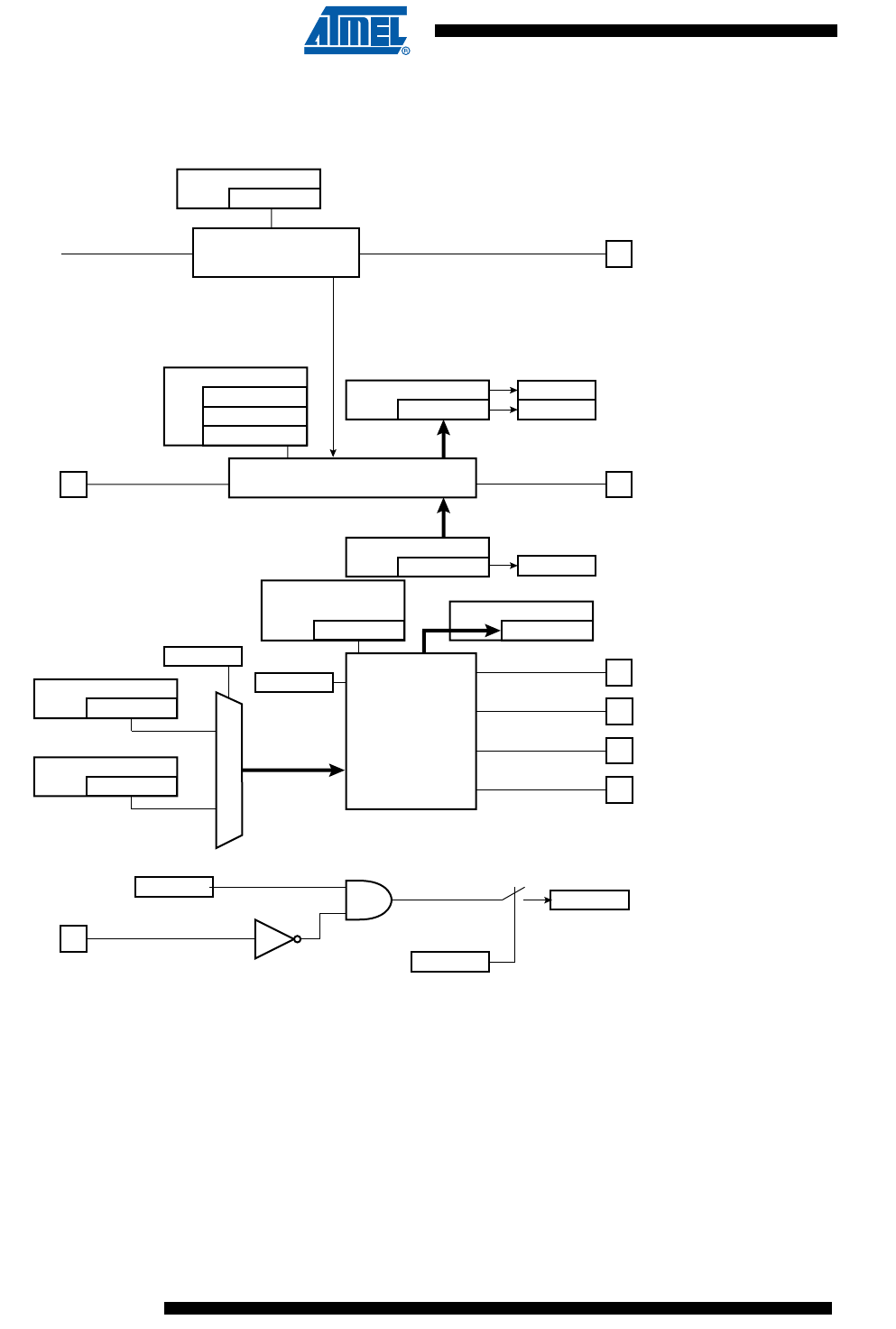
600
6430F–ATARM–21-Feb-12
SAM3U Series
600
6430F–ATARM–21-Feb-12
SAM3U Series
32.7.3.1 Master Mode Block Diagram
Figure 32-5. Master Mode Block Diagram
Shift Register
SPCK
MOSI
LSB MSB
MISO
SPI_RDR
RD
SPI
Clock
TDRE
SPI_TDR
TD
RDRF
OVRES
SPI_CSR0..3
CPOL
NCPHA
BITS
MCK Baud Rate Generator
SPI_CSR0..3
SCBR
NPCS3
NPCS0
NPCS2
NPCS1
NPCS0
0
1
PS
SPI_MR
PCS
SPI_TDR
PCS
MODF
Current
Peripheral
SPI_RDR
PCS
SPI_CSR0..3
CSAAT
PCSDEC
MODFDIS
MSTR
601
6430F–ATARM–21-Feb-12
SAM3U Series
601
6430F–ATARM–21-Feb-12
SAM3U Series
32.7.3.2 Master Mode Flow Diagram
Figure 32-6. Master Mode Flow Diagram
SPI Enable
CSAAT ?
PS ?
1
0
0
1
1
NPCS = SPI_TDR(PCS) NPCS = SPI_MR(PCS)
Delay DLYBS
Serializer = SPI_TDR(TD)
TDRE = 1
Data Transfer
SPI_RDR(RD) = Serializer
RDRF = 1
TDRE ?
NPCS = 0xF
Delay DLYBCS
Fixed
peripheral
Variable
peripheral
Delay DLYBCT
0
1
CSAAT ?
0
TDRE ?
1
0
PS ?
0
1
SPI_TDR(PCS)
= NPCS ?
no
yes SPI_MR(PCS)
= NPCS ?
no
NPCS = 0xF
Delay DLYBCS
NPCS = SPI_TDR(PCS)
NPCS = 0xF
Delay DLYBCS
NPCS = SPI_MR(PCS),
SPI_TDR(PCS)
Fixed
peripheral
Variable
peripheral
- NPCS defines the current Chip Select
- CSAAT, DLYBS, DLYBCT refer to the fields of the
Chip Select Register corresponding to the Current Chip Select
- When NPCS is 0xF, CSAAT is 0.
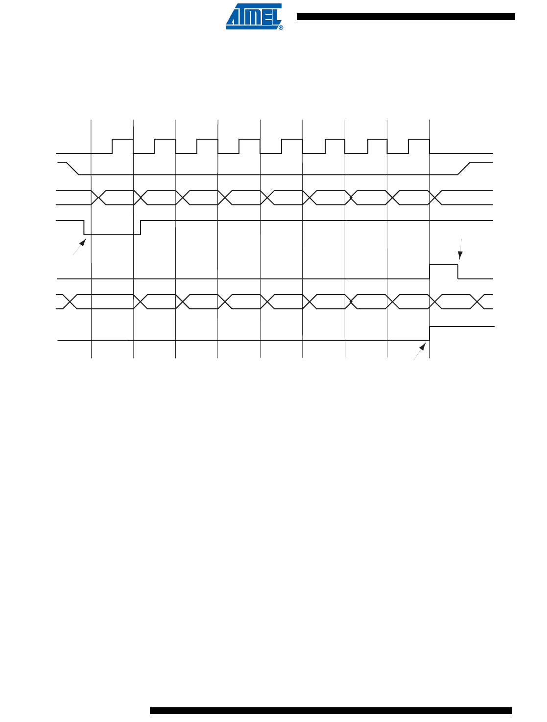
602
6430F–ATARM–21-Feb-12
SAM3U Series
602
6430F–ATARM–21-Feb-12
SAM3U Series
Figure 32-7 shows Transmit Data Register Empty (TDRE), Receive Data Register (RDRF) and
Transmission Register Empty (TXEMPTY) status flags behavior within the SPI_SR (Status Reg-
ister) during an 8-bit data transfer in fixed mode and no Peripheral Data Controller involved.
Figure 32-7. Status Register Flags Behavior
32.7.3.3 Clock Generation
The SPI Baud rate clock is generated by dividing the Master Clock (MCK), by a value between 1
and 255.
This allows a maximum operating baud rate at up to Master Clock and a minimum operating
baud rate of MCK divided by 255.
Programming the SCBR field at 0 is forbidden. Triggering a transfer while SCBR is at 0 can lead
to unpredictable results.
At reset, SCBR is 0 and the user has to program it at a valid value before performing the first
transfer.
The divisor can be defined independently for each chip select, as it has to be programmed in the
SCBR field of the Chip Select Registers. This allows the SPI to automatically adapt the baud
rate for each interfaced peripheral without reprogramming.
32.7.3.4 Transfer Delays
Figure 32-8 shows a chip select transfer change and consecutive transfers on the same chip
select. Three delays can be programmed to modify the transfer waveforms:
• The delay between chip selects, programmable only once for all the chip selects by writing
the DLYBCS field in the Mode Register. Allows insertion of a delay between release of one
chip select and before assertion of a new one.
6
SPCK
MOSI
(from master)
MISO
(from slave)
NPCS0
MSB
MSB
LSB
LSB
6
6
5
5
4
4
3
3
2
2
1
1
1 2345 786
RDRF
TDRE
TXEMPTY
Write in
SPI_TDR
RDR read
shift register empty
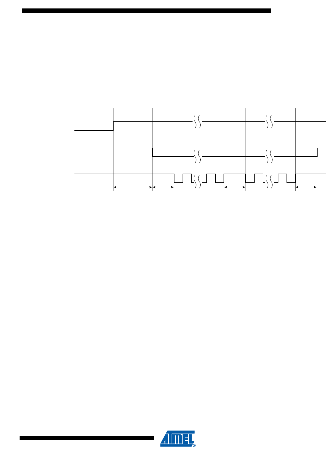
603
6430F–ATARM–21-Feb-12
SAM3U Series
603
6430F–ATARM–21-Feb-12
SAM3U Series
• The delay before SPCK, independently programmable for each chip select by writing the field
DLYBS. Allows the start of SPCK to be delayed after the chip select has been asserted.
• The delay between consecutive transfers, independently programmable for each chip select
by writing the DLYBCT field. Allows insertion of a delay between two transfers occurring on
the same chip select
These delays allow the SPI to be adapted to the interfaced peripherals and their speed and bus
release time.
Figure 32-8. Programmable Delays
32.7.3.5 Peripheral Selection
The serial peripherals are selected through the assertion of the NPCS0 to NPCS3 signals. By
default, all the NPCS signals are high before and after each transfer.
• Fixed Peripheral Select: SPI exchanges data with only one peripheral
Fixed Peripheral Select is activated by writing the PS bit to zero in SPI_MR (Mode Register). In
this case, the current peripheral is defined by the PCS field in SPI_MR and the PCS field in the
SPI_TDR has no effect.
• Variable Peripheral Select: Data can be exchanged with more than one peripheral without
having to reprogram the NPCS field in the SPI_MR register.
Variable Peripheral Select is activated by setting PS bit to one. The PCS field in SPI_TDR is
used to select the current peripheral. This means that the peripheral selection can be defined for
each new data. The value to write in the SPI_TDR register as the following format.
[xxxxxxx(7-bit) + LASTXFER(1-bit)(1)+ xxxx(4-bit) + PCS (4-bit) + DATA (8 to 16-bit)] with PCS
equals to the chip select to assert as defined in Section 32.8.4 (SPI Transmit Data Register) and
LASTXFER bit at 0 or 1 depending on CSAAT bit.
Note: 1. Optional.
CSAAT, LASTXFER and CSNAAT bits are discussed in Section 32.7.3.9 ”Peripheral Deselec-
tion with DMAC” .
If LASTXFER is used, the command must be issued before writing the last character. Instead of
LASTXFER, the user can use the SPIDIS command. After the end of the DMA transfer, wait for
the TXEMPTY flag, then write SPIDIS into the SPI_CR register (this will not change the configu-
ration register values); the NPCS will be deactivated after the last character transfer. Then,
another DMA transfer can be started if the SPIEN was previously written in the SPI_CR register.
DLYBCS DLYBS DLYBCT DLYBCT
Chip Select 1
Chip Select 2
SPCK

604
6430F–ATARM–21-Feb-12
SAM3U Series
604
6430F–ATARM–21-Feb-12
SAM3U Series
32.7.3.6 SPI Direct Access Memory Controller (DMAC)
In both fixed and variable mode the Direct Memory Access Controller (DMAC) can be used to
reduce processor overhead.
The Fixed Peripheral Selection allows buffer transfers with a single peripheral. Using the DMAC
is an optimal means, as the size of the data transfer between the memory and the SPI is either 8
bits or 16 bits. However, changing the peripheral selection requires the Mode Register to be
reprogrammed.
The Variable Peripheral Selection allows buffer transfers with multiple peripherals without repro-
gramming the Mode Register. Data written in SPI_TDR is 32 bits wide and defines the real data
to be transmitted and the peripheral it is destined to. Using the DMAC in this mode requires 32-
bit wide buffers, with the data in the LSBs and the PCS and LASTXFER fields in the MSBs, how-
ever the SPI still controls the number of bits (8 to16) to be transferred through MISO and MOSI
lines with the chip select configuration registers. This is not the optimal means in term of mem-
ory size for the buffers, but it provides a very effective means to exchange data with several
peripherals without any intervention of the processor.
32.7.3.7 Peripheral Chip Select Decoding
The user can program the SPI to operate with up to 15 peripherals by decoding the four Chip
Select lines, NPCS0 to NPCS3 with 1 of up to 16 decoder/demultiplexer. This can be enabled by
writing the PCSDEC bit at 1 in the Mode Register (SPI_MR).
When operating without decoding, the SPI makes sure that in any case only one chip select line
is activated, i.e., one NPCS line driven low at a time. If two bits are defined low in a PCS field,
only the lowest numbered chip select is driven low.
When operating with decoding, the SPI directly outputs the value defined by the PCS field on
NPCS lines of either the Mode Register or the Transmit Data Register (depending on PS).
As the SPI sets a default value of 0xF on the chip select lines (i.e. all chip select lines at 1) when
not processing any transfer, only 15 peripherals can be decoded.
The SPI has only four Chip Select Registers, not 15. As a result, when decoding is activated,
each chip select defines the characteristics of up to four peripherals. As an example, SPI_CRS0
defines the characteristics of the externally decoded peripherals 0 to 3, corresponding to the
PCS values 0x0 to 0x3. Thus, the user has to make sure to connect compatible peripherals on
the decoded chip select lines 0 to 3, 4 to 7, 8 to 11 and 12 to 14. Figure 32-9 below shows such
an implementation.
If the CSAAT bit is used, with or without the DMAC, the Mode Fault detection for NPCS0 line
must be disabled. This is not needed for all other chip select lines since Mode Fault Detection is
only on NPCS0.
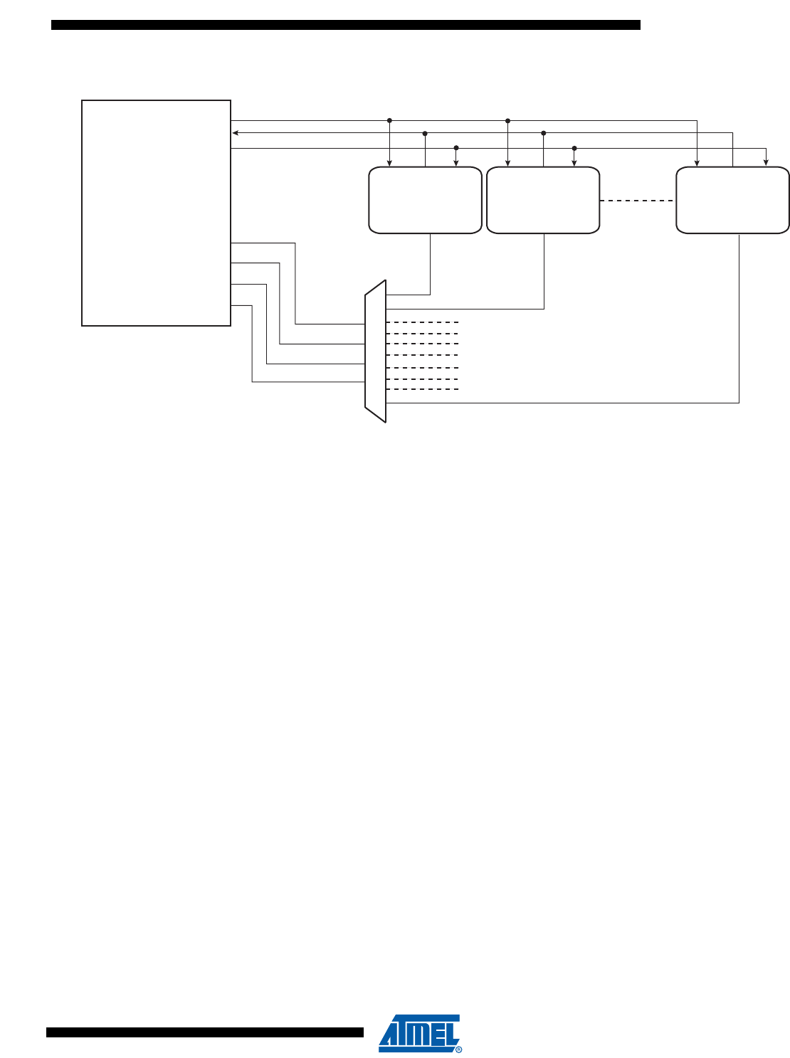
605
6430F–ATARM–21-Feb-12
SAM3U Series
605
6430F–ATARM–21-Feb-12
SAM3U Series
Figure 32-9. Chip Select Decoding Application Block Diagram: Single Master/Multiple Slave Implementation
32.7.3.8 Peripheral Deselection without DMAC
During a transfer of more than one data on a Chip Select without the DMAC, the SPI_TDR is
loaded by the processor, the flag TDRE rises as soon as the content of the SPI_TDR is trans-
ferred into the internal shift register. When this flag is detected high, the SPI_TDR can be
reloaded. If this reload by the processor occurs before the end of the current transfer and if the
next transfer is performed on the same chip select as the current transfer, the Chip Select is not
de-asserted between the two transfers. But depending on the application software handling the
SPI status register flags (by interrupt or polling method) or servicing other interrupts or other
tasks, the processor may not reload the SPI_TDR in time to keep the chip select active (low). A
null Delay Between Consecutive Transfer (DLYBCT) value in the SPI_CSR register, will give
even less time for the processor to reload the SPI_TDR. With some SPI slave peripherals,
requiring the chip select line to remain active (low) during a full set of transfers might lead to
communication errors.
To facilitate interfacing with such devices, the Chip Select Register [CSR0...CSR3] can be pro-
grammed with the CSAAT bit (Chip Select Active After Transfer) at 1. This allows the chip select
lines to remain in their current state (low = active) until transfer to another chip select is required.
Even if the SPI_TDR is not reloaded the chip select will remain active. To have the chip select
line to raise at the end of the transfer the Last transfer Bit (LASTXFER) in the SPI_MR register
must be set at 1 before writing the last data to transmit into the SPI_TDR.
SPI Master
SPCK
MISO
MOSI
NPCS0
NPCS1
NPCS2
SPCK
1-of-n Decoder/Demultiplexer
MISO MOSI
NSS
Slave 0
SPCK MISO MOSI
NSS
Slave 1
SPCK MISO MOSI
NSS
Slave 14
NPCS3

606
6430F–ATARM–21-Feb-12
SAM3U Series
606
6430F–ATARM–21-Feb-12
SAM3U Series
32.7.3.9 Peripheral Deselection with DMAC
When the Direct Memory Access Controller is used, the chip select line will remain low during
the whole transfer since the TDRE flag is managed by the DMAC itself. The reloading of the
SPI_TDR by the DMAC is done as soon as TDRE flag is set to one. In this case the use of
CSAAT bit might not be needed. However, it may happen that when other DMAC channels con-
nected to other peripherals are in use as well, the SPI DMAC might be delayed by another
(DMAC with a higher priority on the bus). Having DMAC buffers in slower memories like flash
memory or SDRAM compared to fast internal SRAM, may lengthen the reload time of the
SPI_TDR by the DMAC as well. This means that the SPI_TDR might not be reloaded in time to
keep the chip select line low. In this case the chip select line may toggle between data transfer
and according to some SPI Slave devices, the communication might get lost. The use of the
CSAAT bit might be needed.
When the CSAAT bit is set at 0, the NPCS does not rise in all cases between two transfers on
the same peripheral. During a transfer on a Chip Select, the flag TDRE rises as soon as the con-
tent of the SPI_TDR is transferred into the internal shifter. When this flag is detected the
SPI_TDR can be reloaded. If this reload occurs before the end of the current transfer and if the
next transfer is performed on the same chip select as the current transfer, the Chip Select is not
de-asserted between the two transfers. This might lead to difficulties for interfacing with some
serial peripherals requiring the chip select to be de-asserted after each transfer. To facilitate
interfacing with such devices, the Chip Select Register can be programmed with the CSNAAT bit
(Chip Select Not Active After Transfer) at 1. This allows to de-assert systematically the chip
select lines during a time DLYBCS. (The value of the CSNAAT bit is taken into account only if
the CSAAT bit is set at 0 for the same Chip Select).
Figure 32-10 shows different peripheral deselection cases and the effect of the CSAAT and
CSNAAT bits.
607
6430F–ATARM–21-Feb-12
SAM3U Series
607
6430F–ATARM–21-Feb-12
SAM3U Series
Figure 32-10. Peripheral Deselection
A
NPCS[0..3]
Write SPI_TDR
TDRE
NPCS[0..3]
Write SPI_TDR
TDRE
NPCS[0..3]
Write SPI_TDR
TDRE
DLYBCS
PCS = A
DLYBCS
DLYBCT
A
PCS = B
B
DLYBCS
PCS = A
DLYBCS
DLYBCT
A
PCS = B
B
DLYBCS
DLYBCT
PCS=A
A
DLYBCS
DLYBCT
A
PCS = A
AA
DLYBCT
AA
CSAAT = 0 and CSNAAT = 0
DLYBCT
AA
CSAAT = 1 and CSNAAT= 0 / 1
A
DLYBCS
PCS = A
DLYBCT
AA
CSAAT = 0 and CSNAAT = 1
NPCS[0..3]
Write SPI_TDR
TDRE
PCS = A
DLYBCT
AA
CSAAT = 0 and CSNAAT = 0

608
6430F–ATARM–21-Feb-12
SAM3U Series
608
6430F–ATARM–21-Feb-12
SAM3U Series
32.7.3.10 Mode Fault Detection
A mode fault is detected when the SPI is programmed in Master Mode and a low level is driven
by an external master on the NPCS0/NSS signal. In this case, multi-master configuration,
NPCS0, MOSI, MISO and SPCK pins must be configured in open drain (through the PIO control-
ler). When a mode fault is detected, the MODF bit in the SPI_SR is set until the SPI_SR is read
and the SPI is automatically disabled until re-enabled by writing the SPIEN bit in the SPI_CR
(Control Register) at 1.
By default, the Mode Fault detection circuitry is enabled. The user can disable Mode Fault
detection by setting the MODFDIS bit in the SPI Mode Register (SPI_MR).
32.7.4 SPI Slave Mode
When operating in Slave Mode, the SPI processes data bits on the clock provided on the SPI
clock pin (SPCK).
The SPI waits for NSS to go active before receiving the serial clock from an external master.
When NSS falls, the clock is validated on the serializer, which processes the number of bits
defined by the BITS field of the Chip Select Register 0 (SPI_CSR0). These bits are processed
following a phase and a polarity defined respectively by the NCPHA and CPOL bits of the
SPI_CSR0. Note that BITS, CPOL and NCPHA of the other Chip Select Registers have no
effect when the SPI is programmed in Slave Mode.
The bits are shifted out on the MISO line and sampled on the MOSI line.
(For more information on BITS field, see also, the (Note:) below the register table; Section 32.8.9
“SPI Chip Select Register” on page 622.)
When all the bits are processed, the received data is transferred in the Receive Data Register
and the RDRF bit rises. If the SPI_RDR (Receive Data Register) has not been read before new
data is received, the Overrun Error bit (OVRES) in SPI_SR is set. As long as this flag is set, data
is loaded in SPI_RDR. The user has to read the status register to clear the OVRES bit.
When a transfer starts, the data shifted out is the data present in the Shift Register. If no data
has been written in the Transmit Data Register (SPI_TDR), the last data received is transferred.
If no data has been received since the last reset, all bits are transmitted low, as the Shift Regis-
ter resets at 0.
When a first data is written in SPI_TDR, it is transferred immediately in the Shift Register and the
TDRE bit rises. If new data is written, it remains in SPI_TDR until a transfer occurs, i.e. NSS falls
and there is a valid clock on the SPCK pin. When the transfer occurs, the last data written in
SPI_TDR is transferred in the Shift Register and the TDRE bit rises. This enables frequent
updates of critical variables with single transfers.
Then, a new data is loaded in the Shift Register from the Transmit Data Register. In case no
character is ready to be transmitted, i.e. no character has been written in SPI_TDR since the last
load from SPI_TDR to the Shift Register, the Shift Register is not modified and the last received
character is retransmitted. In this case the Underrun Error Status Flag (UNDES) is set in the
SPI_SR.
Figure 32-11 shows a block diagram of the SPI when operating in Slave Mode.
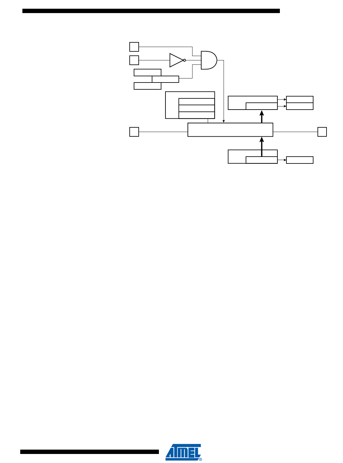
609
6430F–ATARM–21-Feb-12
SAM3U Series
609
6430F–ATARM–21-Feb-12
SAM3U Series
Figure 32-11. Slave Mode Functional Bloc Diagram
Shift Register
SPCK
SPIENS
LSB MSB
NSS
MOSI
SPI_RDR
RD
SPI
Clock
TDRE
SPI_TDR
TD
RDRF
OVRES
SPI_CSR0
CPOL
NCPHA
BITS
SPIEN
SPIDIS
MISO

610
6430F–ATARM–21-Feb-12
SAM3U Series
610
6430F–ATARM–21-Feb-12
SAM3U Series
32.7.5 Write Protected Registers
To prevent any single software error that may corrupt SPI behavior, the registers listed below
can be write-protected by setting the WPEN bit in the SPI Write Protection Mode Register
(SPI_WPMR).
If a write access in a write-protected register is detected, then the WPVS flag in the SPI Write
Protection Status Register (SPI_WPSR) is set and the field WPVSRC indicates in which register
the write access has been attempted.
The WPVS flag is automatically reset after reading the SPI Write Protection Status Register
(SPI_WPSR).
List of the write-protected registers:
Section 32.8.2 ”SPI Mode Register”
Section 32.8.9 ”SPI Chip Select Register”

611
6430F–ATARM–21-Feb-12
SAM3U Series
611
6430F–ATARM–21-Feb-12
SAM3U Series
32.8 Serial Peripheral Interface (SPI) User Interface
Table 32-5. Register Mapping
Offset Register Name Access Reset
0x00 Control Register SPI_CR Write-only ---
0x04 Mode Register SPI_MR Read-write 0x0
0x08 Receive Data Register SPI_RDR Read-only 0x0
0x0C Transmit Data Register SPI_TDR Write-only ---
0x10 Status Register SPI_SR Read-only 0x000000F0
0x14 Interrupt Enable Register SPI_IER Write-only ---
0x18 Interrupt Disable Register SPI_IDR Write-only ---
0x1C Interrupt Mask Register SPI_IMR Read-only 0x0
0x20 - 0x2C Reserved
0x30 Chip Select Register 0 SPI_CSR0 Read-write 0x0
0x34 Chip Select Register 1 SPI_CSR1 Read-write 0x0
0x38 Chip Select Register 2 SPI_CSR2 Read-write 0x0
0x3C Chip Select Register 3 SPI_CSR3 Read-write 0x0
0x4C - 0xE0 Reserved – – –
0xE4 Write Protection Control Register SPI_WPMR Read-write 0x0
0xE8 Write Protection Status Register SPI_WPSR Read-only 0x0
0x00E8 - 0x00F8 Reserved – – –
0x00FC Reserved – – –

612
6430F–ATARM–21-Feb-12
SAM3U Series
612
6430F–ATARM–21-Feb-12
SAM3U Series
32.8.1 SPI Control Register
Name: SPI_CR
Address: 0x40008000
Access: Write-only
• SPIEN: SPI Enable
0 = No effect.
1 = Enables the SPI to transfer and receive data.
• SPIDIS: SPI Disable
0 = No effect.
1 = Disables the SPI.
As soon as SPIDIS is set, SPI finishes its transfer.
All pins are set in input mode and no data is received or transmitted.
If a transfer is in progress, the transfer is finished before the SPI is disabled.
If both SPIEN and SPIDIS are equal to one when the control register is written, the SPI is disabled.
• SWRST: SPI Software Reset
0 = No effect.
1 = Reset the SPI. A software-triggered hardware reset of the SPI interface is performed.
The SPI is in slave mode after software reset.
DMAC channels are not affected by software reset.
• LASTXFER: Last Transfer
0 = No effect.
1 = The current NPCS will be deasserted after the character written in TD has been transferred. When CSAAT is set, this
allows to close the communication with the current serial peripheral by raising the corresponding NPCS line as soon as TD
transfer has completed.
Refer to Section 32.7.3.5 ”Peripheral Selection” for more details.
31 30 29 28 27 26 25 24
–––––––LASTXFER
23 22 21 20 19 18 17 16
––––––––
15 14 13 12 11 10 9 8
––––––––
76543210
SWRST–––––SPIDISSPIEN
613
6430F–ATARM–21-Feb-12
SAM3U Series
613
6430F–ATARM–21-Feb-12
SAM3U Series
32.8.2 SPI Mode Register
Name: SPI_MR
Address: 0x40008004
Access: Read-write
This register can only be written if the WPEN bit is cleared in ”SPI Write Protection Mode Register”.
• MSTR: Master/Slave Mode
0 = SPI is in Slave mode.
1 = SPI is in Master mode.
• PS: Peripheral Select
0 = Fixed Peripheral Select.
1 = Variable Peripheral Select.
• PCSDEC: Chip Select Decode
0 = The chip selects are directly connected to a peripheral device.
1 = The four chip select lines are connected to a 4- to 16-bit decoder.
When PCSDEC equals one, up to 15 Chip Select signals can be generated with the four lines using an external 4- to 16-bit
decoder. The Chip Select Registers define the characteristics of the 15 chip selects according to the following rules:
SPI_CSR0 defines peripheral chip select signals 0 to 3.
SPI_CSR1 defines peripheral chip select signals 4 to 7.
SPI_CSR2 defines peripheral chip select signals 8 to 11.
SPI_CSR3 defines peripheral chip select signals 12 to 14.
• MODFDIS: Mode Fault Detection
0 = Mode fault detection is enabled.
1 = Mode fault detection is disabled.
• WDRBT: Wait Data Read Before Transfer
0 = No Effect. In master mode, a transfer can be initiated whatever the state of the Receive Data Register is.
1 = In Master Mode, a transfer can start only if the Receive Data Register is empty, i.e. does not contain any unread data.
This mode prevents overrun error in reception.
• LLB: Local Loopback Enable
31 30 29 28 27 26 25 24
DLYBCS
23 22 21 20 19 18 17 16
–––– PCS
15 14 13 12 11 10 9 8
––––––––
76543210
LLB – WDRBT MODFDIS – PCSDEC PS MSTR

614
6430F–ATARM–21-Feb-12
SAM3U Series
614
6430F–ATARM–21-Feb-12
SAM3U Series
0 = Local loopback path disabled.
1 = Local loopback path enabled
LLB controls the local loopback on the data serializer for testing in Master Mode only. (MISO is internally connected on
MOSI.)
• PCS: Peripheral Chip Select
This field is only used if Fixed Peripheral Select is active (PS = 0).
If PCSDEC = 0:
PCS = xxx0 NPCS[3:0] = 1110
PCS = xx01 NPCS[3:0] = 1101
PCS = x011 NPCS[3:0] = 1011
PCS = 0111 NPCS[3:0] = 0111
PCS = 1111 forbidden (no peripheral is selected)
(x = don’t care)
If PCSDEC = 1:
NPCS[3:0] output signals = PCS.
• DLYBCS: Delay Between Chip Selects
This field defines the delay from NPCS inactive to the activation of another NPCS. The DLYBCS time guarantees non-over-
lapping chip selects and solves bus contentions in case of peripherals having long data float times.
If DLYBCS is less than or equal to six, six MCK periods will be inserted by default.
Otherwise, the following equation determines the delay:
Delay Between Chip Selects DLYBCS
MCK
-----------------------=

615
6430F–ATARM–21-Feb-12
SAM3U Series
615
6430F–ATARM–21-Feb-12
SAM3U Series
32.8.3 SPI Receive Data Register
Name: SPI_RDR
Address: 0x40008008
Access: Read-only
• RD: Receive Data
Data received by the SPI Interface is stored in this register right-justified. Unused bits read zero.
• PCS: Peripheral Chip Select
In Master Mode only, these bits indicate the value on the NPCS pins at the end of a transfer. Otherwise, these bits read
zero.
Note: When using variable peripheral select mode (PS = 1 in SPI_MR) it is mandatory to also set the WDRBT field to 1 if the
SPI_RDR PCS field is to be processed.
31 30 29 28 27 26 25 24
––––––––
23 22 21 20 19 18 17 16
–––– PCS
15 14 13 12 11 10 9 8
RD
76543210
RD

616
6430F–ATARM–21-Feb-12
SAM3U Series
616
6430F–ATARM–21-Feb-12
SAM3U Series
32.8.4 SPI Transmit Data Register
Name: SPI_TDR
Address: 0x4000800C
Access: Write-only
• TD: Transmit Data
Data to be transmitted by the SPI Interface is stored in this register. Information to be transmitted must be written to the
transmit data register in a right-justified format.
• PCS: Peripheral Chip Select
This field is only used if Variable Peripheral Select is active (PS = 1).
If PCSDEC = 0:
PCS = xxx0 NPCS[3:0] = 1110
PCS = xx01 NPCS[3:0] = 1101
PCS = x011 NPCS[3:0] = 1011
PCS = 0111 NPCS[3:0] = 0111
PCS = 1111 forbidden (no peripheral is selected)
(x = don’t care)
If PCSDEC = 1:
NPCS[3:0] output signals = PCS
• LASTXFER: Last Transfer
0 = No effect.
1 = The current NPCS will be deasserted after the character written in TD has been transferred. When CSAAT is set, this
allows to close the communication with the current serial peripheral by raising the corresponding NPCS line as soon as TD
transfer has completed.
This field is only used if Variable Peripheral Select is active (PS = 1).
31 30 29 28 27 26 25 24
–––––––LASTXFER
23 22 21 20 19 18 17 16
–––– PCS
15 14 13 12 11 10 9 8
TD
76543210
TD

617
6430F–ATARM–21-Feb-12
SAM3U Series
617
6430F–ATARM–21-Feb-12
SAM3U Series
32.8.5 SPI Status Register
Name: SPI_SR
Address: 0x40008010
Access: Read-only
• RDRF: Receive Data Register Full
0 = No data has been received since the last read of SPI_RDR
1 = Data has been received and the received data has been transferred from the serializer to SPI_RDR since the last read
of SPI_RDR.
• TDRE: Transmit Data Register Empty
0 = Data has been written to SPI_TDR and not yet transferred to the serializer.
1 = The last data written in the Transmit Data Register has been transferred to the serializer.
TDRE equals zero when the SPI is disabled or at reset. The SPI enable command sets this bit to one.
• MODF: Mode Fault Error
0 = No Mode Fault has been detected since the last read of SPI_SR.
1 = A Mode Fault occurred since the last read of the SPI_SR.
• OVRES: Overrun Error Status
0 = No overrun has been detected since the last read of SPI_SR.
1 = An overrun has occurred since the last read of SPI_SR.
An overrun occurs when SPI_RDR is loaded at least twice from the serializer since the last read of the SPI_RDR.
• NSSR: NSS Rising
0 = No rising edge detected on NSS pin since last read.
1 = A rising edge occurred on NSS pin since last read.
• TXEMPTY: Transmission Registers Empty
0 = As soon as data is written in SPI_TDR.
1 = SPI_TDR and internal shifter are empty. If a transfer delay has been defined, TXEMPTY is set after the completion of
such delay.
• UNDES: Underrun Error Status (Slave Mode Only)
0 = No underrun has been detected since the last read of SPI_SR.
31 30 29 28 27 26 25 24
––––––––
23 22 21 20 19 18 17 16
–––––––SPIENS
15 14 13 12 11 10 9 8
–––––UNDES TXEMPTY NSSR
76543210
––––OVRESMODFTDRERDRF

618
6430F–ATARM–21-Feb-12
SAM3U Series
618
6430F–ATARM–21-Feb-12
SAM3U Series
1 = A transfer begins whereas no data has been loaded in the Transmit Data Register.
• SPIENS: SPI Enable Status
0 = SPI is disabled.
1 = SPI is enabled.

619
6430F–ATARM–21-Feb-12
SAM3U Series
619
6430F–ATARM–21-Feb-12
SAM3U Series
32.8.6 SPI Interrupt Enable Register
Name: SPI_IER
Address: 0x40008014
Access: Write-only
0 = No effect.
1 = Enables the corresponding interrupt.
• RDRF: Receive Data Register Full Interrupt Enable
• TDRE: SPI Transmit Data Register Empty Interrupt Enable
• MODF: Mode Fault Error Interrupt Enable
• OVRES: Overrun Error Interrupt Enable
• NSSR: NSS Rising Interrupt Enable
• TXEMPTY: Transmission Registers Empty Enable
• UNDES: Underrun Error Interrupt Enable
31 30 29 28 27 26 25 24
––––––––
23 22 21 20 19 18 17 16
––––––––
15 14 13 12 11 10 9 8
–––––UNDES TXEMPTY NSSR
76543210
––––OVRESMODFTDRERDRF

620
6430F–ATARM–21-Feb-12
SAM3U Series
620
6430F–ATARM–21-Feb-12
SAM3U Series
32.8.7 SPI Interrupt Disable Register
Name: SPI_IDR
Address: 0x40008018
Access: Write-only
0 = No effect.
1 = Disables the corresponding interrupt.
• RDRF: Receive Data Register Full Interrupt Disable
• TDRE: SPI Transmit Data Register Empty Interrupt Disable
• MODF: Mode Fault Error Interrupt Disable
• OVRES: Overrun Error Interrupt Disable
• NSSR: NSS Rising Interrupt Disable
• TXEMPTY: Transmission Registers Empty Disable
• UNDES: Underrun Error Interrupt Disable
31 30 29 28 27 26 25 24
––––––––
23 22 21 20 19 18 17 16
––––––––
15 14 13 12 11 10 9 8
–––––UNDES TXEMPTY NSSR
76543210
––––OVRESMODFTDRERDRF

621
6430F–ATARM–21-Feb-12
SAM3U Series
621
6430F–ATARM–21-Feb-12
SAM3U Series
32.8.8 SPI Interrupt Mask Register
Name: SPI_IMR
Address: 0x4000801C
Access: Read-only
0 = The corresponding interrupt is not enabled.
1 = The corresponding interrupt is enabled.
• RDRF: Receive Data Register Full Interrupt Mask
• TDRE: SPI Transmit Data Register Empty Interrupt Mask
• MODF: Mode Fault Error Interrupt Mask
• OVRES: Overrun Error Interrupt Mask
• NSSR: NSS Rising Interrupt Mask
• TXEMPTY: Transmission Registers Empty Mask
• UNDES: Underrun Error Interrupt Mask
31 30 29 28 27 26 25 24
––––––––
23 22 21 20 19 18 17 16
––––––––
15 14 13 12 11 10 9 8
–––––UNDES TXEMPTY NSSR
76543210
––––OVRESMODFTDRERDRF

622
6430F–ATARM–21-Feb-12
SAM3U Series
622
6430F–ATARM–21-Feb-12
SAM3U Series
32.8.9 SPI Chip Select Register
Name: SPI_CSRx[x=0..3]
Address: 0x40008030
Access: Read/Write
This register can only be written if the WPEN bit is cleared in ”SPI Write Protection Mode Register”.
Note: SPI_CSRx registers must be written even if the user wants to use the defaults. The BITS field will not be updated with the trans-
lated value unless the register is written.
• CPOL: Clock Polarity
0 = The inactive state value of SPCK is logic level zero.
1 = The inactive state value of SPCK is logic level one.
CPOL is used to determine the inactive state value of the serial clock (SPCK). It is used with NCPHA to produce the
required clock/data relationship between master and slave devices.
• NCPHA: Clock Phase
0 = Data is changed on the leading edge of SPCK and captured on the following edge of SPCK.
1 = Data is captured on the leading edge of SPCK and changed on the following edge of SPCK.
NCPHA determines which edge of SPCK causes data to change and which edge causes data to be captured. NCPHA is
used with CPOL to produce the required clock/data relationship between master and slave devices.
• CSNAAT: Chip Select Not Active After Transfer (Ignored if CSAAT = 1)
0 = The Peripheral Chip Select does not rise between two transfers if the SPI_TDR is reloaded before the end of the first
transfer and if the two transfers occur on the same Chip Select.
1 = The Peripheral Chip Select rises systematically after each transfer performed on the same slave. It remains active after
the end of transfer for a minimal duration of:
– (if DLYBCT field is different from 0)
– (if DLYBCT field equals 0)
• CSAAT: Chip Select Active After Transfer
0 = The Peripheral Chip Select Line rises as soon as the last transfer is achieved.
1 = The Peripheral Chip Select does not rise after the last transfer is achieved. It remains active until a new transfer is
requested on a different chip select.
31 30 29 28 27 26 25 24
DLYBCT
23 22 21 20 19 18 17 16
DLYBS
15 14 13 12 11 10 9 8
SCBR
76543210
BITS CSAAT CSNAAT NCPHA CPOL
DLYBCT
MCK
-----------------------
DLYBCT 1+
MCK
---------------------------------

623
6430F–ATARM–21-Feb-12
SAM3U Series
623
6430F–ATARM–21-Feb-12
SAM3U Series
• BITS: Bits Per Transfer
(See the (Note:) below the register table; Section 32.8.9 “SPI Chip Select Register” on page 622.)
The BITS field determines the number of data bits transferred. Reserved values should not be used.
• SCBR: Serial Clock Baud Rate
In Master Mode, the SPI Interface uses a modulus counter to derive the SPCK baud rate from the Master Clock MCK. The
Baud rate is selected by writing a value from 1 to 255 in the SCBR field. The following equations determine the SPCK baud
rate:
Programming the SCBR field at 0 is forbidden. Triggering a transfer while SCBR is at 0 can lead to unpredictable results.
At reset, SCBR is 0 and the user has to program it at a valid value before performing the first transfer.
Note: If one of the SCBR fields inSPI_CSRx is set to 1, the other SCBR fields in SPI_CSRx must be set to 1 as well, if they are
required to process transfers. If they are not used to transfer data, they can be set at any value.
• DLYBS: Delay Before SPCK
This field defines the delay from NPCS valid to the first valid SPCK transition.
When DLYBS equals zero, the NPCS valid to SPCK transition is 1/2 the SPCK clock period.
Otherwise, the following equations determine the delay:
Value Name Description
0 8_BIT 8 bits for transfer
1 9_BIT 9 bits for transfer
2 10_BIT 10 bits for transfer
3 11_BIT 11 bits for transfer
4 12_BIT 12 bits for transfer
5 13_BIT 13 bits for transfer
6 14_BIT 14 bits for transfer
7 15_BIT 15 bits for transfer
8 16_BIT 16 bits for transfer
9– Reserved
10 – Reserved
11 – Reserved
12 – Reserved
13 – Reserved
14 – Reserved
15 – Reserved
SPCK Baudrate MCK
SCBR
---------------=
Delay Before SPCK DLYBS
MCK
-------------------=

624
6430F–ATARM–21-Feb-12
SAM3U Series
624
6430F–ATARM–21-Feb-12
SAM3U Series
• DLYBCT: Delay Between Consecutive Transfers
This field defines the delay between two consecutive transfers with the same peripheral without removing the chip select.
The delay is always inserted after each transfer and before removing the chip select if needed.
When DLYBCT equals zero, no delay between consecutive transfers is inserted and the clock keeps its duty cycle over the
character transfers.
Otherwise, the following equation determines the delay:
Delay Between Consecutive Transfers 32 DLYBCT×MCK
-------------------------------------=

625
6430F–ATARM–21-Feb-12
SAM3U Series
625
6430F–ATARM–21-Feb-12
SAM3U Series
32.8.10 SPI Write Protection Mode Register
Name: SPI_WPMR
Address: 0x400080E4
Access: Read-write
• WPEN: Write Protection Enable
0: The Write Protection is Disabled
1: The Write Protection is Enabled
• WPKEY: Write Protection Key Password
If a value is written in WPEN, the value is taken into account only if WPKEY is written with “SPI” (SPI written in ASCII Code,
ie 0x535049 in hexadecimal).
List of the write-protected registers:
Section 32.8.2 ”SPI Mode Register”
Section 32.8.9 ”SPI Chip Select Register”
31 30 29 28 27 26 25 24
WPKEY
23 22 21 20 19 18 17 16
WPKEY
15 14 13 12 11 10 9 8
WPKEY
76543210
-------WPEN

626
6430F–ATARM–21-Feb-12
SAM3U Series
626
6430F–ATARM–21-Feb-12
SAM3U Series
32.8.11 SPI Write Protection Status Register
Name: SPI_WPSR
Address: 0x400080E8
Access: Read-only
• WPVS: Write Protection Violation Status
0 = No Write Protect Violation has occurred since the last read of the SPI_WPSR register.
1 = A Write Protect Violation has occurred since the last read of the SPI_WPSR register. If this violation is an unauthorized
attempt to write a protected register, the associated violation is reported into field WPVSRC.
• WPVSRC: Write Protection Violation Source
This Field indicates the APB Offset of the register concerned by the violation (SPI_MR or SPI_CSRx)
31 30 29 28 27 26 25 24
––––––––
23 22 21 20 19 18 17 16
––––––––
15 14 13 12 11 10 9 8
WPVSRC
76543210
–––––––
WPVS

627
6430F–ATARM–21-Feb-12
SAM3U Series
627
6430F–ATARM–21-Feb-12
SAM3U Series
33. Two-wire Interface (TWI)
33.1 Description
The Atmel Two-wire Interface (TWI) interconnects components on a unique two-wire bus, made
up of one clock line and one data line with speeds of up to 400 Kbits per second, based on a
byte-oriented transfer format. It can be used with any Atmel Two-wire Interface bus Serial
EEPROM and I²C compatible device such as Real Time Clock (RTC), Dot Matrix/Graphic LCD
Controllers and Temperature Sensor, to name but a few. The TWI is programmable as a master
or a slave with sequential or single-byte access. Multiple master capability is supported. 20
Arbitration of the bus is performed internally and puts the TWI in slave mode automatically if the
bus arbitration is lost.
A configurable baud rate generator permits the output data rate to be adapted to a wide range of
core clock frequencies.
Below, Table 33-1 lists the compatibility level of the Atmel Two-wire Interface in Master Mode and
a full I2C compatible device.
Note: 1. START + b000000001 + Ack + Sr
33.2 Embedded Characteristics
• Compatible with Atmel Two-wire Interface Serial Memory and I²C Compatible Devices(1)
• One, Two or Three Bytes for Slave Address
• Sequential Read-write Operations
• Master, Multi-master and Slave Mode Operation
• Bit Rate: Up to 400 Kbits
• General Call Supported in Slave mode
• SMBUS Quick Command Supported in Master Mode
• Connection to Peripheral DMA Controller (PDC) Channel Capabilities Optimizes Data
Transfers in Master Mode Only
– One Channel for the Receiver, One Channel for the Transmitter
– Next Buffer Support
Note: 1. See Table 33-1 for details on compatibility with I²C Standard.
Table 33-1. Atmel TWI compatibility with I2C Standard
I2C Standard Atmel TWI
Standard Mode Speed (100 KHz) Supported
Fast Mode Speed (400 KHz) Supported
7 or 10 bits Slave Addressing Supported
START BYTE(1) Not Supported
Repeated Start (Sr) Condition Supported
ACK and NACK Management Supported
Slope control and input filtering (Fast mode) Not Supported
Clock stretching Supported
Multi Master Capability Supported
628
6430F–ATARM–21-Feb-12
SAM3U Series
628
6430F–ATARM–21-Feb-12
SAM3U Series
33.3 List of Abbreviations
33.4 Block Diagram
Figure 33-1. Block Diagram
Table 33-2. Abbreviations
Abbreviation Description
TWI Two-wire Interface
A Acknowledge
NA Non Acknowledge
PStop
SStart
Sr Repeated Start
SADR Slave Address
ADR Any address except SADR
R Read
WWrite
APB Bridge
PMC MCK
Two-wire
Interface
PIO
Interrupt
Controller
TWI
Interrupt
TWCK
TWD
629
6430F–ATARM–21-Feb-12
SAM3U Series
629
6430F–ATARM–21-Feb-12
SAM3U Series
33.5 Application Block Diagram
Figure 33-2. Application Block Diagram
33.5.1 I/O Lines Description
33.6 Product Dependencies
33.6.1 I/O Lines
Both TWD and TWCK are bidirectional lines, connected to a positive supply voltage via a current
source or pull-up resistor (see Figure 33-2 on page 629). When the bus is free, both lines are
high. The output stages of devices connected to the bus must have an open-drain or open-col-
lector to perform the wired-AND function.
TWD and TWCK pins may be multiplexed with PIO lines. To enable the TWI, the programmer
must perform the following step:
• Program the PIO controller to dedicate TWD and TWCK as peripheral lines.
The user must not program TWD and TWCK as open-drain. It is already done by the hardware.
Host with
TWI
Interface
TWD
TWCK
Atmel TWI
Serial EEPROM I²C RTC I²C LCD
Controller
Slave 1 Slave 2 Slave 3
VDD
I²C Temp.
Sensor
Slave 4
Rp: Pull up value as given by the I²C Standard
Rp Rp
Table 33-3. I/O Lines Description
Pin Name Pin Description Type
TWD Two-wire Serial Data Input/Output
TWCK Two-wire Serial Clock Input/Output
Table 33-4. I/O Lines
Instance Signal I/O Line Peripheral
TWI0 TWCK0 PA10 A
TWI0 TWD0 PA9 A
TWI1 TWCK1 PA25 A
TWI1 TWD1 PA24 A
630
6430F–ATARM–21-Feb-12
SAM3U Series
630
6430F–ATARM–21-Feb-12
SAM3U Series
33.6.2 Power Management
• Enable the peripheral clock.
The TWI interface may be clocked through the Power Management Controller (PMC), thus the
programmer must first configure the PMC to enable the TWI clock.
33.6.3 Interrupt
The TWI interface has an interrupt line connected to the Interrupt Controller. In order to handle
interrupts, the Interrupt Controller must be programmed before configuring the TWI.
33.7 Functional Description
33.7.1 Transfer Format
The data put on the TWD line must be 8 bits long. Data is transferred MSB first; each byte must
be followed by an acknowledgement. The number of bytes per transfer is unlimited (see Figure
33-4).
Each transfer begins with a START condition and terminates with a STOP condition (see Figure
33-3).
• A high-to-low transition on the TWD line while TWCK is high defines the START condition.
• A low-to-high transition on the TWD line while TWCK is high defines a STOP condition.
Figure 33-3. START and STOP Conditions
Figure 33-4. Transfer Format
33.7.2 Modes of Operation
The TWI has different modes of operations:
• Master transmitter mode
• Master receiver mode
• Multi-master transmitter mode
• Multi-master receiver mode
• Slave transmitter mode
• Slave receiver mode
TWD
TWCK
Start Stop
TWD
TWCK
Start Address R/W Ack Data Ack Data Ack Stop
631
6430F–ATARM–21-Feb-12
SAM3U Series
631
6430F–ATARM–21-Feb-12
SAM3U Series
These modes are described in the following chapters.
33.8 Master Mode
33.8.1 Definition
The Master is the device that starts a transfer, generates a clock and stops it.
33.8.2 Application Block Diagram
Figure 33-5. Master Mode Typical Application Block Diagram
33.8.3 Programming Master Mode
The following registers have to be programmed before entering Master mode:
1. DADR (+ IADRSZ + IADR if a 10 bit device is addressed): The device address is used
to access slave devices in read or write mode.
2. CKDIV + CHDIV + CLDIV: Clock Waveform.
3. SVDIS: Disable the slave mode.
4. MSEN: Enable the master mode.
33.8.4 Master Transmitter Mode
After the master initiates a Start condition when writing into the Transmit Holding Register,
TWI_THR, it sends a 7-bit slave address, configured in the Master Mode register (DADR in
TWI_MMR), to notify the slave device. The bit following the slave address indicates the transfer
direction, 0 in this case (MREAD = 0 in TWI_MMR).
The TWI transfers require the slave to acknowledge each received byte. During the acknowl-
edge clock pulse (9th pulse), the master releases the data line (HIGH), enabling the slave to pull
it down in order to generate the acknowledge. The master polls the data line during this clock
pulse and sets the Not Acknowledge bit (NACK) in the status register if the slave does not
acknowledge the byte. As with the other status bits, an interrupt can be generated if enabled in
the interrupt enable register (TWI_IER). If the slave acknowledges the byte, the data written in
the TWI_THR, is then shifted in the internal shifter and transferred. When an acknowledge is
detected, the TXRDY bit is set until a new write in the TWI_THR.
TXRDY is used as Transmit Ready for the PDC transmit channel.
Host with
TWI
Interface
TWD
TWCK
Atmel TWI
Serial EEPROM I²C RTC I²C LCD
Controller
Slave 1 Slave 2 Slave 3
VDD
I²C Temp.
Sensor
Slave 4
Rp: Pull up value as given by the I²C Standard
Rp Rp
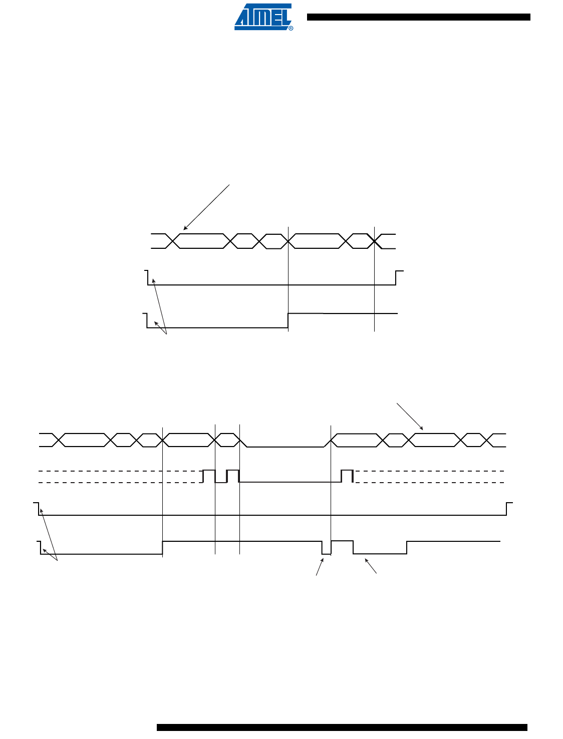
632
6430F–ATARM–21-Feb-12
SAM3U Series
632
6430F–ATARM–21-Feb-12
SAM3U Series
While no new data is written in the TWI_THR, the Serial Clock Line is tied low. When new data is
written in the TWI_THR, the SCL is released and the data is sent. To generate a STOP event,
the STOP command must be performed by writing in the STOP field of TWI_CR.
After a Master Write transfer, the Serial Clock line is stretched (tied low) while no new data is
written in the TWI_THR or until a STOP command is performed.
See Figure 33-6, Figure 33-7, and Figure 33-8.
Figure 33-6. Master Write with One Data Byte
Figure 33-7. Master Write with Multiple Data Bytes
TXCOMP
TXRDY
Write THR (DATA)
STOP Command sent (write in TWI_CR)
TWD A DATA AS DADR W P
A DATA n AS DADR W DATA n+1 A PDATA n+2 A
TXCOMP
TXRDY
Write THR (Data n)
Write THR (Data n+1) Write THR (Data n+2)
Last data sent
STOP command performed
(by writing in the TWI_CR)
TWD
TWCK
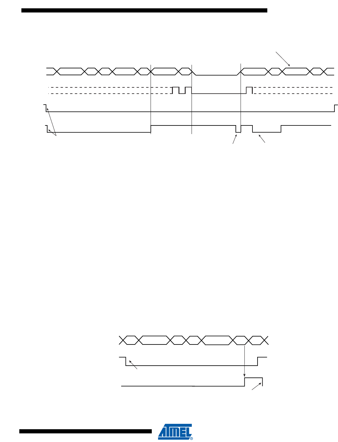
633
6430F–ATARM–21-Feb-12
SAM3U Series
633
6430F–ATARM–21-Feb-12
SAM3U Series
Figure 33-8. Master Write with One Byte Internal Address and Multiple Data Bytes
33.8.5 Master Receiver Mode
The read sequence begins by setting the START bit. After the start condition has been sent, the
master sends a 7-bit slave address to notify the slave device. The bit following the slave address
indicates the transfer direction, 1 in this case (MREAD = 1 in TWI_MMR). During the acknowl-
edge clock pulse (9th pulse), the master releases the data line (HIGH), enabling the slave to pull
it down in order to generate the acknowledge. The master polls the data line during this clock
pulse and sets the NACK bit in the status register if the slave does not acknowledge the byte.
If an acknowledge is received, the master is then ready to receive data from the slave. After data
has been received, the master sends an acknowledge condition to notify the slave that the data
has been received except for the last data, after the stop condition. See Figure 33-9. When the
RXRDY bit is set in the status register, a character has been received in the receive-holding reg-
ister (TWI_RHR). The RXRDY bit is reset when reading the TWI_RHR.
When a single data byte read is performed, with or without internal address (IADR), the START
and STOP bits must be set at the same time. See Figure 33-9. When a multiple data byte read is
performed, with or without internal address (IADR), the STOP bit must be set after the next-to-
last data received. See Figure 33-10. For Internal Address usage see Section 33.8.6.
Figure 33-9. Master Read with One Data Byte
A DATA n AS DADR W DATA n+1 A PDATA n+2 A
TXCOMP
TXRDY
Write THR (Data n)
Write THR (Data n+1) Write THR (Data n+2)
Last data sent
STOP command performed
(by writing in the TWI_CR)
TWD IADR A
TWCK
AS DADR R DATA N P
TXCOMP
Write START &
STOP Bit
RXRDY
Read RHR
TWD

634
6430F–ATARM–21-Feb-12
SAM3U Series
634
6430F–ATARM–21-Feb-12
SAM3U Series
Figure 33-10. Master Read with Multiple Data Bytes
RXRDY is used as Receive Ready for the PDC receive channel.
33.8.6 Internal Address
The TWI interface can perform various transfer formats: Transfers with 7-bit slave address
devices and 10-bit slave address devices.
33.8.6.1 7-bit Slave Addressing
When Addressing 7-bit slave devices, the internal address bytes are used to perform random
address (read or write) accesses to reach one or more data bytes, within a memory page loca-
tion in a serial memory, for example. When performing read operations with an internal address,
the TWI performs a write operation to set the internal address into the slave device, and then
switch to Master Receiver mode. Note that the second start condition (after sending the IADR) is
sometimes called “repeated start” (Sr) in I2C fully-compatible devices. See Figure 33-12. See
Figure 33-11 and Figure 33-13 for Master Write operation with internal address.
The three internal address bytes are configurable through the Master Mode register
(TWI_MMR).
If the slave device supports only a 7-bit address, i.e. no internal address, IADRSZ must be set to
0.
In the figures below the following abbreviations are used:
N
AS DADR R DATA n A ADATA (n+1) A DATA (n+m)DATA (n+m)-1 PTWD
TXCOMP
Write START Bit
RXRDY
Write STOP Bit
after next-to-last data read
Read RHR
DATA n
Read RHR
DATA (n+1)
Read RHR
DATA (n+m)-1
Read RHR
DATA (n+m)
•S Start
•Sr Repeated Start
•P Stop
•W Write
•R Read
•A Acknowledge
•N Not Acknowledge
•DADR Device Address
•IADR Internal Address
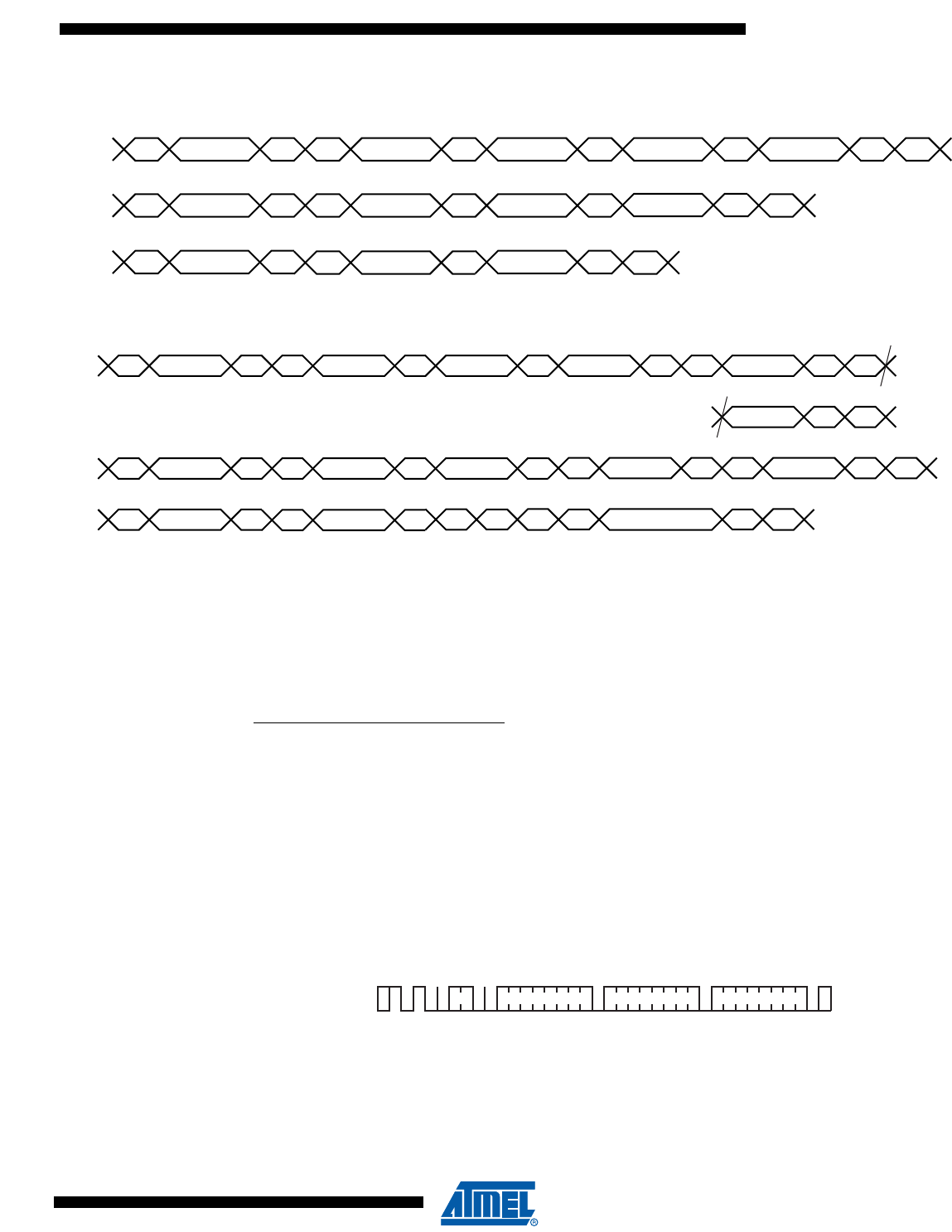
635
6430F–ATARM–21-Feb-12
SAM3U Series
635
6430F–ATARM–21-Feb-12
SAM3U Series
Figure 33-11. Master Write with One, Two or Three Bytes Internal Address and One Data Byte
Figure 33-12. Master Read with One, Two or Three Bytes Internal Address and One Data Byte
33.8.6.2 10-bit Slave Addressing
For a slave address higher than 7 bits, the user must configure the address size (IADRSZ) and
set the other slave address bits in the internal address register (TWI_IADR). The two remaining
Internal address bytes, IADR[15:8] and IADR[23:16] can be used the same as in 7-bit Slave
Addressing.
Example: Address a 10-bit device (10-bit device address is b1 b2 b3 b4 b5 b6 b7 b8 b9 b10)
1. Program IADRSZ = 1,
2. Program DADR with 1 1 1 1 0 b1 b2 (b1 is the MSB of the 10-bit address, b2, etc.)
3. Program TWI_IADR with b3 b4 b5 b6 b7 b8 b9 b10 (b10 is the LSB of the 10-bit
address)
Figure 33-13 below shows a byte write to an Atmel AT24LC512 EEPROM. This demonstrates
the use of internal addresses to access the device.
Figure 33-13. Internal Address Usage
S DADR W A IADR(23:16) A IADR(15:8) A IADR(7:0) A DATA A P
S DADR W A IADR(15:8) A IADR(7:0) A P
DATA A
A IADR(7:0) A P
DATA AS DADR W
TWD
Three bytes internal address
Two bytes internal address
One byte internal address
TWD
TWD
S DADR WA IADR(23:16) A IADR(15:8) AIADR(7:0) A
S DADR W A IADR(15:8) A IADR(7:0) A
AIADR(7:0) A
S DADR W
DATA N P
Sr DADR R A
Sr DADR R A DATA N P
Sr DADR RA DATA NP
TWD
TWD
TWD
Three bytes internal address
Two bytes internal address
One byte internal address
S
T
A
R
T
M
S
B
Device
Address
0
L
S
B
R
/
W
A
C
K
M
S
B
W
R
I
T
E
A
C
K
A
C
K
L
S
B
A
C
K
FIRST
WORD ADDRESS
SECOND
WORD ADDRESS DATA
S
T
O
P
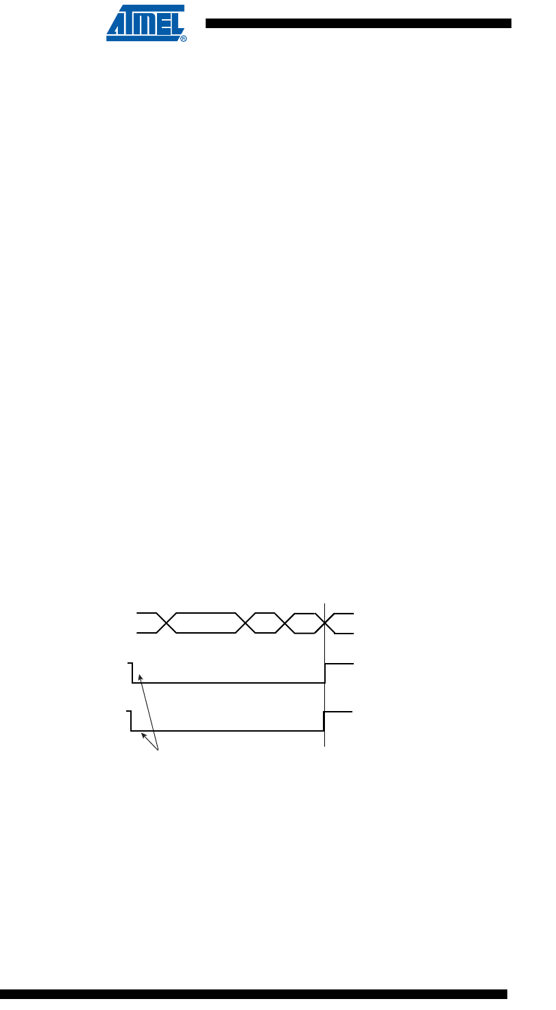
636
6430F–ATARM–21-Feb-12
SAM3U Series
636
6430F–ATARM–21-Feb-12
SAM3U Series
33.8.7 Using the Peripheral DMA Controller (PDC)
The use of the PDC significantly reduces the CPU load.
To assure correct implementation, respect the following programming sequences:
33.8.7.1 Data Transmit with the PDC
1. Initialize the transmit PDC (memory pointers, transfer size).
2. Configure the master mode.
3. Start the transfer by setting the PDC TXTEN bit.
4. Wait for the PDC ENDTX Flag either by using the polling method or ENDTX interrupt.
5. Disable the PDC by setting the PDC TXDIS bit.
33.8.7.2 Data Receive with the PDC
1. Initialize the receive PDC (memory pointers, transfer size - 1).
2. Configure the master mode (DADR, CKDIV, etc.).
3. Start the transfer by setting the PDC RXTEN bit.
4. Wait for the PDC ENDRX Flag either by using polling method or ENDRX interrupt.
5. Disable the PDC by setting the PDC RXDIS bit.
33.8.8 SMBUS Quick Command (Master Mode Only)
The TWI interface can perform a Quick Command:
1. Configure the master mode (DADR, CKDIV, etc.).
2. Write the MREAD bit in the TWI_MMR register at the value of the one-bit command to
be sent.
3. Start the transfer by setting the QUICK bit in the TWI_CR.
Figure 33-14. SMBUS Quick Command
33.8.9 Read-write Flowcharts
The following flowcharts shown in Figure 33-16 on page 638, Figure 33-17 on page 639, Figure
33-18 on page 640, Figure 33-19 on page 641 and Figure 33-20 on page 642 give examples for
read and write operations. A polling or interrupt method can be used to check the status bits.
The interrupt method requires that the interrupt enable register (TWI_IER) be configured first.
TXCOMP
TXRDY
Write QUICK command in TWI_CR
TWD AS DADR R/W P

637
6430F–ATARM–21-Feb-12
SAM3U Series
637
6430F–ATARM–21-Feb-12
SAM3U Series
Figure 33-15. TWI Write Operation with Single Data Byte without Internal Address
Set TWI clock
(CLDIV, CHDIV, CKDIV) in TWI_CWGR
(Needed only once)
Set the Control register:
- Master enable
TWI_CR = MSEN + SVDIS
Set the Master Mode register:
- Device slave address (DADR)
- Transfer direction bit
Write ==> bit MREAD = 0
Load Transmit register
TWI_THR = Data to send
Read Status register
TXRDY = 1?
Read Status register
TXCOMP = 1?
Transfer finished
Ye s
Ye s
BEGIN
No
No
Write STOP Command
TWI_CR = STOP
638
6430F–ATARM–21-Feb-12
SAM3U Series
638
6430F–ATARM–21-Feb-12
SAM3U Series
Figure 33-16. TWI Write Operation with Single Data Byte and Internal Address
BEGIN
Set TWI clock
(CLDIV, CHDIV, CKDIV) in TWI_CWGR
(Needed only once)
Set the Control register:
- Master enable
TWI_CR = MSEN + SVDIS
Set the Master Mode register:
- Device slave address (DADR)
- Internal address size (IADRSZ)
- Transfer direction bit
Write ==> bit MREAD = 0
Load transmit register
TWI_THR = Data to send
Read Status register
TXRDY = 1?
Read Status register
TXCOMP = 1?
Transfer finished
Set the internal address
TWI_IADR = address
Yes
Yes
No
No
Write STOP command
TWI_CR = STOP
639
6430F–ATARM–21-Feb-12
SAM3U Series
639
6430F–ATARM–21-Feb-12
SAM3U Series
Figure 33-17. TWI Write Operation with Multiple Data Bytes with or without Internal Address
Set the Control register:
- Master enable
TWI_CR = MSEN + SVDIS
Set the Master Mode register:
- Device slave address
- Internal address size (if IADR used)
- Transfer direction bit
Write ==> bit MREAD = 0
Internal address size = 0?
Load Transmit register
TWI_THR = Data to send
Read Status register
TXRDY = 1?
Data to send?
Read Status register
TXCOMP = 1?
END
BEGIN
Set the internal address
TWI_IADR = address
Ye s
TWI_THR = data to send
Ye s
Ye s
Ye s
No
No
No
Write STOP Command
TWI_CR = STOP
Set TWI clock
(CLDIV, CHDIV, CKDIV) in TWI_CWGR
(Needed only once)
640
6430F–ATARM–21-Feb-12
SAM3U Series
640
6430F–ATARM–21-Feb-12
SAM3U Series
Figure 33-18. TWI Read Operation with Single Data Byte without Internal Address
Set the Control register:
- Master enable
TWI_CR = MSEN + SVDIS
Set the Master Mode register:
- Device slave address
- Transfer direction bit
Read ==> bit MREAD = 1
Start the transfer
TWI_CR = START | STOP
Read status register
RXRDY = 1?
Read Status register
TXCOMP = 1?
END
BEGIN
Ye s
Ye s
Set TWI clock
(CLDIV, CHDIV, CKDIV) in TWI_CWGR
(Needed only once)
Read Receive Holding Register
No
No
641
6430F–ATARM–21-Feb-12
SAM3U Series
641
6430F–ATARM–21-Feb-12
SAM3U Series
Figure 33-19. TWI Read Operation with Single Data Byte and Internal Address
Set the Control register:
- Master enable
TWI_CR = MSEN + SVDIS
Set the Master Mode register:
- Device slave address
- Internal address size (IADRSZ)
- Transfer direction bit
Read ==> bit MREAD = 1
Read Status register
TXCOMP = 1?
END
BEGIN
Ye s
Set TWI clock
(CLDIV, CHDIV, CKDIV) in TWI_CWGR
(Needed only once)
Ye s
Set the internal address
TWI_IADR = address
Start the transfer
TWI_CR = START | STOP
Read Status register
RXRDY = 1?
Read Receive Holding register
No
No
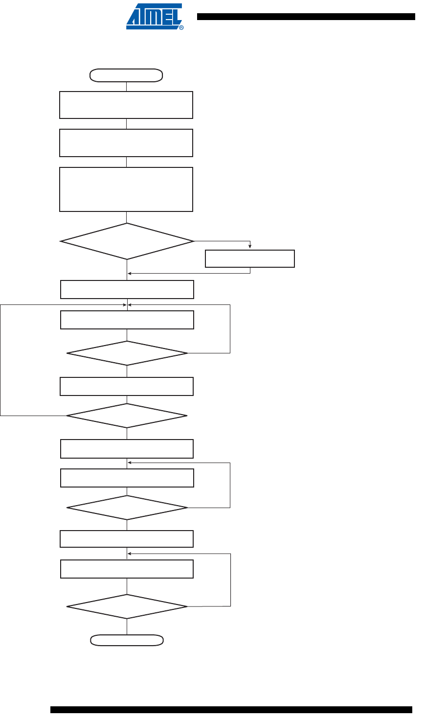
642
6430F–ATARM–21-Feb-12
SAM3U Series
642
6430F–ATARM–21-Feb-12
SAM3U Series
Figure 33-20. TWI Read Operation with Multiple Data Bytes with or without Internal Address
Internal address size = 0?
Start the transfer
TWI_CR = START
Stop the transfer
TWI_CR = STOP
Read Status register
RXRDY = 1?
Last data to read
but one?
Read status register
TXCOMP = 1?
END
Set the internal address
TWI_IADR = address
Ye s
Ye s
Ye s
No
Ye s
Read Receive Holding register (TWI_RHR)
No
Set the Control register:
- Master enable
TWI_CR = MSEN + SVDIS
Set the Master Mode register:
- Device slave address
- Internal address size (if IADR used)
- Transfer direction bit
Read ==> bit MREAD = 1
BEGIN
Set TWI clock
(CLDIV, CHDIV, CKDIV) in TWI_CWGR
(Needed only once)
No
Read Status register
RXRDY = 1?
Ye s
Read Receive Holding register (TWI_RHR)
No

643
6430F–ATARM–21-Feb-12
SAM3U Series
643
6430F–ATARM–21-Feb-12
SAM3U Series
33.9 Multi-master Mode
33.9.1 Definition
More than one master may handle the bus at the same time without data corruption by using
arbitration.
Arbitration starts as soon as two or more masters place information on the bus at the same time,
and stops (arbitration is lost) for the master that intends to send a logical one while the other
master sends a logical zero.
As soon as arbitration is lost by a master, it stops sending data and listens to the bus in order to
detect a stop. When the stop is detected, the master who has lost arbitration may put its data on
the bus by respecting arbitration.
Arbitration is illustrated in Figure 33-22 on page 644.
33.9.2 Different Multi-master Modes
Two multi-master modes may be distinguished:
1. TWI is considered as a Master only and will never be addressed.
2. TWI may be either a Master or a Slave and may be addressed.
Note: In both Multi-master modes arbitration is supported.
33.9.2.1 TWI as Master Only
In this mode, TWI is considered as a Master only (MSEN is always at one) and must be driven
like a Master with the ARBLST (ARBitration Lost) flag in addition.
If arbitration is lost (ARBLST = 1), the programmer must reinitiate the data transfer.
If the user starts a transfer (ex.: DADR + START + W + Write in THR) and if the bus is busy, the
TWI automatically waits for a STOP condition on the bus to initiate the transfer (see Figure 33-
21 on page 644).
Note: The state of the bus (busy or free) is not indicated in the user interface.
33.9.2.2 TWI as Master or Slave
The automatic reversal from Master to Slave is not supported in case of a lost arbitration.
Then, in the case where TWI may be either a Master or a Slave, the programmer must manage
the pseudo Multi-master mode described in the steps below.
1. Program TWI in Slave mode (SADR + MSDIS + SVEN) and perform Slave Access (if
TWI is addressed).
2. If TWI has to be set in Master mode, wait until TXCOMP flag is at 1.
3. Program Master mode (DADR + SVDIS + MSEN) and start the transfer (ex: START +
Write in THR).
4. As soon as the Master mode is enabled, TWI scans the bus in order to detect if it is
busy or free. When the bus is considered as free, TWI initiates the transfer.
5. As soon as the transfer is initiated and until a STOP condition is sent, the arbitration
becomes relevant and the user must monitor the ARBLST flag.
6. If the arbitration is lost (ARBLST is set to 1), the user must program the TWI in Slave
mode in the case where the Master that won the arbitration wanted to access the TWI.
7. If TWI has to be set in Slave mode, wait until TXCOMP flag is at 1 and then program the
Slave mode.
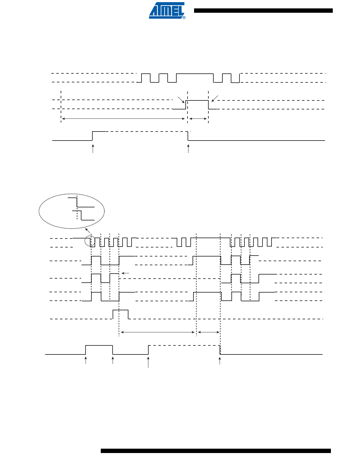
644
6430F–ATARM–21-Feb-12
SAM3U Series
644
6430F–ATARM–21-Feb-12
SAM3U Series
Note: In the case where the arbitration is lost and TWI is addressed, TWI will not acknowledge even if it
is programmed in Slave mode as soon as ARBLST is set to 1. Then, the Master must repeat
SADR.
Figure 33-21. Programmer Sends Data While the Bus is Busy
Figure 33-22. Arbitration Cases
The flowchart shown in Figure 33-23 on page 645 gives an example of read and write operations
in Multi-master mode.
TWCK
TWD DATA sent by a master
STOP sent by the master START sent by the TWI
DATA sent by the TWI
Bus is busy
Bus is free
A transfer is programmed
(DADR + W + START + Write THR) Transfer is initiated
TWI DATA transfer Transfer is kept
Bus is considered as free
TWCK
Bus is busy Bus is free
A transfer is programmed
(DADR + W + START + Write THR) Transfer is initiated
TWI DATA transfer Transfer is kept
Bus is considered as free
Data from a Master
Data from TWI S0
S00
1
1
1
ARBLST
S0
S00
1
1
1
TWD S00
1
11
11
Arbitration is lost
TWI stops sending data
P
S0
1
P0
11
11
Data from the master Data from the TWI
Arbitration is lost
The master stops sending data
Transfer is stopped
Transfer is programmed again
(DADR + W + START + Write THR)
TWCK
TWD
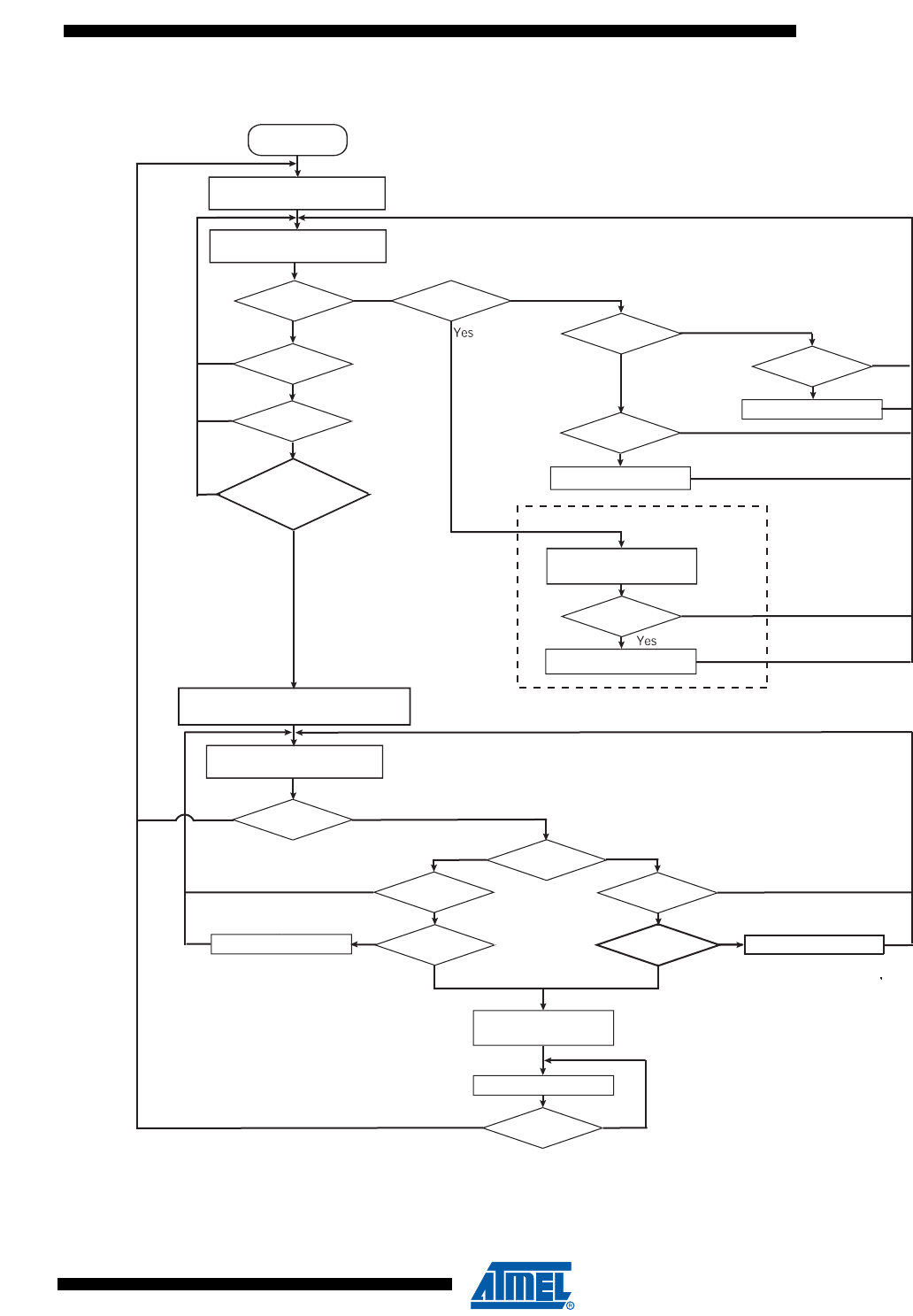
645
6430F–ATARM–21-Feb-12
SAM3U Series
645
6430F–ATARM–21-Feb-12
SAM3U Series
Figure 33-23. Multi-master Flowchart
Programm the SLAVE mode:
SADR + MSDIS + SVEN
SVACC = 1 ?
TXCOMP = 1 ?
GACC = 1 ?
Decoding of the
programming sequence
Prog seq
OK ?
Change SADR
SVREAD = 1 ?
Read Status Register
RXRDY= 1 ?
Read TWI_RHR
TXRDY= 1 ?
EOSACC = 1 ?
Write in TWI_THR
Need to perform
a master access ?
Program the Master mode
DADR + SVDIS + MSEN + CLK + R / W
Read Status Register
ARBLST = 1 ?
MREAD = 1 ?
TXRDY= 0 ?
Write in TWI_THR
Data to send ?
RXRDY= 0 ?
Read TWI_RHR Data to read?
Read Status Register
TXCOMP = 0 ?
GENERAL CALL TREATMENT
Ye s
Ye s
Ye s
Ye s
Ye s
Ye s
Ye s
Ye s
Ye s
Ye s
Ye s
Ye s
Ye s
Ye s
Stop Transfer
TWI_CR = STOP
No
No No
No
No
No
No
No
No
No
No
No
No
No No
No
START
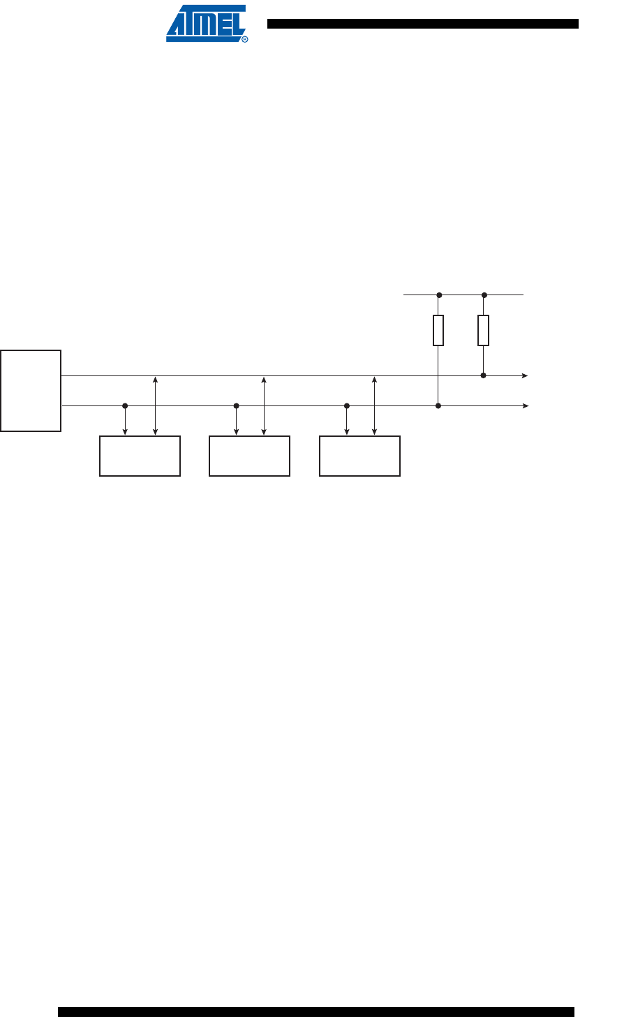
646
6430F–ATARM–21-Feb-12
SAM3U Series
646
6430F–ATARM–21-Feb-12
SAM3U Series
33.10 Slave Mode
33.10.1 Definition
The Slave Mode is defined as a mode where the device receives the clock and the address from
another device called the master.
In this mode, the device never initiates and never completes the transmission (START,
REPEATED_START and STOP conditions are always provided by the master).
33.10.2 Application Block Diagram
Figure 33-24. Slave Mode Typical Application Block Diagram
33.10.3 Programming Slave Mode
The following fields must be programmed before entering Slave mode:
1. SADR (TWI_SMR): The slave device address is used in order to be accessed by mas-
ter devices in read or write mode.
2. MSDIS (TWI_CR): Disable the master mode.
3. SVEN (TWI_CR): Enable the slave mode.
As the device receives the clock, values written in TWI_CWGR are not taken into account.
33.10.4 Receiving Data
After a Start or Repeated Start condition is detected and if the address sent by the Master
matches with the Slave address programmed in the SADR (Slave ADdress) field, SVACC (Slave
ACCess) flag is set and SVREAD (Slave READ) indicates the direction of the transfer.
SVACC remains high until a STOP condition or a repeated START is detected. When such a
condition is detected, EOSACC (End Of Slave ACCess) flag is set.
33.10.4.1 Read Sequence
In the case of a Read sequence (SVREAD is high), TWI transfers data written in the TWI_THR
(TWI Transmit Holding Register) until a STOP condition or a REPEATED_START + an address
different from SADR is detected. Note that at the end of the read sequence TXCOMP (Transmis-
sion Complete) flag is set and SVACC reset.
As soon as data is written in the TWI_THR, TXRDY (Transmit Holding Register Ready) flag is
reset, and it is set when the shift register is empty and the sent data acknowledged or not. If the
data is not acknowledged, the NACK flag is set.
Host with
TWI
Interface
TWD
TWCK
LCD Controller
Slave 1 Slave 2 Slave 3
RR
VDD
Host with TWI
Interface
Host with TWI
Interface
Master

647
6430F–ATARM–21-Feb-12
SAM3U Series
647
6430F–ATARM–21-Feb-12
SAM3U Series
Note that a STOP or a repeated START always follows a NACK.
See Figure 33-25 on page 648.
33.10.4.2 Write Sequence
In the case of a Write sequence (SVREAD is low), the RXRDY (Receive Holding Register
Ready) flag is set as soon as a character has been received in the TWI_RHR (TWI Receive
Holding Register). RXRDY is reset when reading the TWI_RHR.
TWI continues receiving data until a STOP condition or a REPEATED_START + an address dif-
ferent from SADR is detected. Note that at the end of the write sequence TXCOMP flag is set
and SVACC reset.
See Figure 33-26 on page 648.
33.10.4.3 Clock Synchronization Sequence
In the case where TWI_THR or TWI_RHR is not written/read in time, TWI performs a clock
synchronization.
Clock stretching information is given by the SCLWS (Clock Wait state) bit.
See Figure 33-28 on page 650 and Figure 33-29 on page 651.
33.10.4.4 General Call
In the case where a GENERAL CALL is performed, GACC (General Call ACCess) flag is set.
After GACC is set, it is up to the programmer to interpret the meaning of the GENERAL CALL
and to decode the new address programming sequence.
See Figure 33-27 on page 649.
33.10.5 Data Transfer
33.10.5.1 Read Operation
The read mode is defined as a data requirement from the master.
After a START or a REPEATED START condition is detected, the decoding of the address
starts. If the slave address (SADR) is decoded, SVACC is set and SVREAD indicates the direc-
tion of the transfer.
Until a STOP or REPEATED START condition is detected, TWI continues sending data loaded
in the TWI_THR register.
If a STOP condition or a REPEATED START + an address different from SADR is detected,
SVACC is reset.
Figure 33-25 on page 648 describes the write operation.
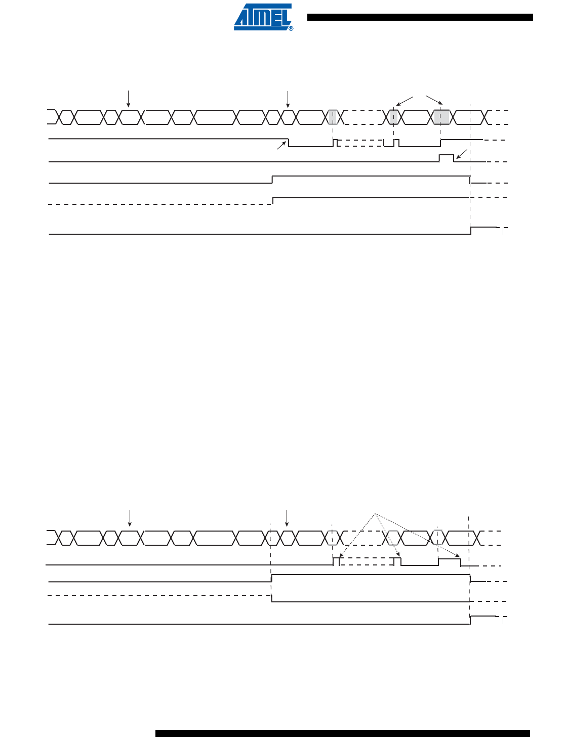
648
6430F–ATARM–21-Feb-12
SAM3U Series
648
6430F–ATARM–21-Feb-12
SAM3U Series
Figure 33-25. Read Access Ordered by a MASTER
Notes: 1. When SVACC is low, the state of SVREAD becomes irrelevant.
2. TXRDY is reset when data has been transmitted from TWI_THR to the shift register and set when this data has been
acknowledged or non acknowledged.
33.10.5.2 Write Operation
The write mode is defined as a data transmission from the master.
After a START or a REPEATED START, the decoding of the address starts. If the slave address
is decoded, SVACC is set and SVREAD indicates the direction of the transfer (SVREAD is low in
this case).
Until a STOP or REPEATED START condition is detected, TWI stores the received data in the
TWI_RHR register.
If a STOP condition or a REPEATED START + an address different from SADR is detected,
SVACC is reset.
Figure 33-26 on page 648 describes the Write operation.
Figure 33-26. Write Access Ordered by a Master
Notes: 1. When SVACC is low, the state of SVREAD becomes irrelevant.
2. RXRDY is set when data has been transmitted from the shift register to the TWI_RHR and reset when this data is read.
Write THR Read RHR
SVREAD has to be taken into account only while SVACC is active
TWD
TXRDY
NACK
SVACC
SVREAD
EOSVACC
SADRS ADR R NA R A DATA A A DATA NA S/SrDATA NA P/S/Sr
SADR matches,
TWI answers with an ACK
SADR does not match,
TWI answers with a NACK ACK/NACK from the Master
RXRDY
Read RHR
SVREAD has to be taken into account only while SVACC is active
TWD
SVACC
SVREAD
EOSVACC
SADR does not match,
TWI answers with a NACK
SADRS ADR W NA W A DATA A A DATA NA S/SrDATA NA P/S/Sr
SADR matches,
TWI answers with an ACK
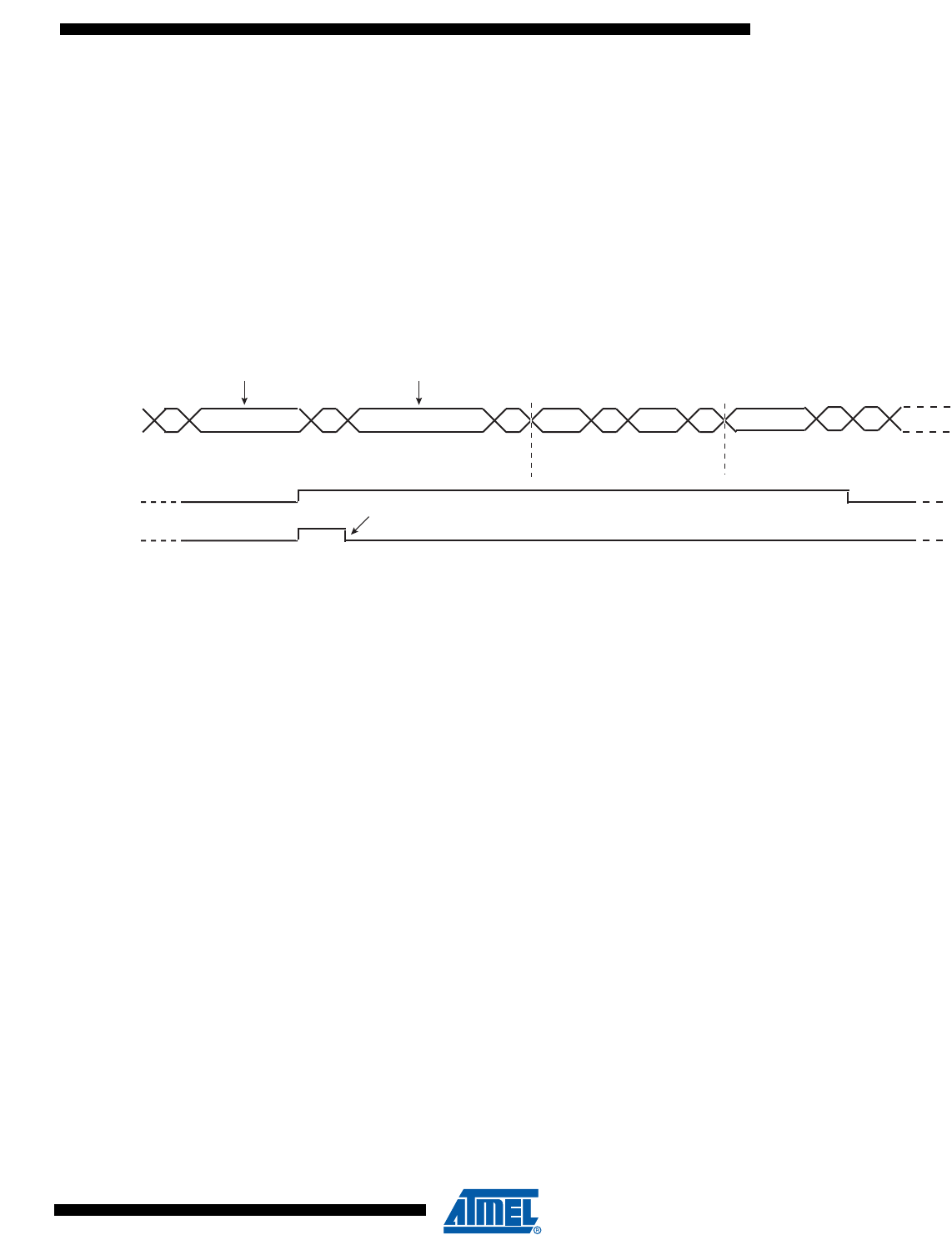
649
6430F–ATARM–21-Feb-12
SAM3U Series
649
6430F–ATARM–21-Feb-12
SAM3U Series
33.10.5.3 General Call
The general call is performed in order to change the address of the slave.
If a GENERAL CALL is detected, GACC is set.
After the detection of General Call, it is up to the programmer to decode the commands which
come afterwards.
In case of a WRITE command, the programmer has to decode the programming sequence and
program a new SADR if the programming sequence matches.
Figure 33-27 on page 649 describes the General Call access.
Figure 33-27. Master Performs a General Call
Note: This method allows the user to create an own programming sequence by choosing the program-
ming bytes and the number of them. The programming sequence has to be provided to the
master.
0000000 + W
GENERAL CALL P
SA
GENERAL CALL Reset or write DADD A New SADR
DATA1 A DATA2 A
A
New SADR
Programming sequence
TXD
GCACC
SVACC
RESET command = 00000110X
WRITE command = 00000100X
Reset after read
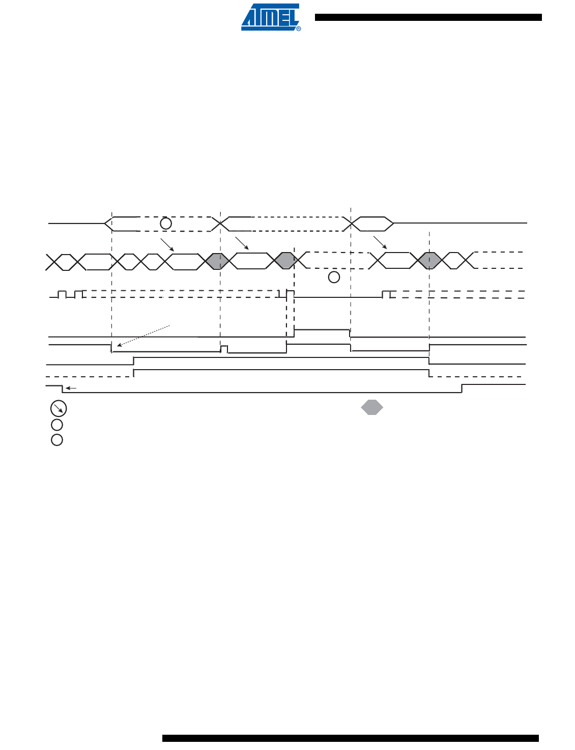
650
6430F–ATARM–21-Feb-12
SAM3U Series
650
6430F–ATARM–21-Feb-12
SAM3U Series
33.10.5.4 Clock Synchronization
In both read and write modes, it may happen that TWI_THR/TWI_RHR buffer is not filled /emp-
tied before the emission/reception of a new character. In this case, to avoid sending/receiving
undesired data, a clock stretching mechanism is implemented.
Clock Synchronization in Read Mode
The clock is tied low if the shift register is empty and if a STOP or REPEATED START condition
was not detected. It is tied low until the shift register is loaded.
Figure 33-28 on page 650 describes the clock synchronization in Read mode.
Figure 33-28. Clock Synchronization in Read Mode
Notes: 1. TXRDY is reset when data has been written in the TWI_THR to the shift register and set when this data has been acknowl-
edged or non acknowledged.
2. At the end of the read sequence, TXCOMP is set after a STOP or after a REPEATED_START + an address different from
SADR.
3. SCLWS is automatically set when the clock synchronization mechanism is started.
DATA 1
The clock is stretched after the ACK, the state of TWD is undefined during clock stretching
SCLWS
SVACC
SVREAD
TXRDY
TWCK
TWI_THR
TXCOMP
The data is memorized in TWI_THR until a new value is written
TWI_THR is transmitted to the shift register Ack or Nack from the master
DATA 0D ATA 0 DATA 2
1
2
1
CLOCK is tied low by the TWI
as long as THR is empty
SSADR
SRDATA 0AADATA 1 ADATA 2 NA S
XXXXXXX
2
Write THR
As soon as a START is detected
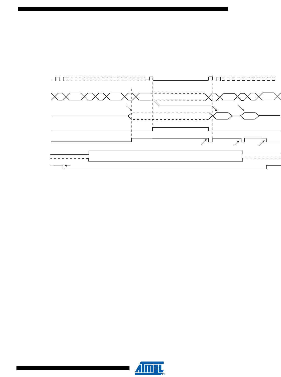
651
6430F–ATARM–21-Feb-12
SAM3U Series
651
6430F–ATARM–21-Feb-12
SAM3U Series
Clock Synchronization in Write Mode
The clock is tied low if the shift register and the TWI_RHR is full. If a STOP or
REPEATED_START condition was not detected, it is tied low until TWI_RHR is read.
Figure 33-29 on page 651 describes the clock synchronization in Read mode.
Figure 33-29. Clock Synchronization in Write Mode
Notes: 1. At the end of the read sequence, TXCOMP is set after a STOP or after a REPEATED_START + an address different from
SADR.
2. SCLWS is automatically set when the clock synchronization mechanism is started and automatically reset when the mecha-
nism is finished.
Rd DATA0 Rd DATA1 Rd DATA2
SVACC
SVREAD
RXRDY
SCLWS
TXCOMP
DATA 1 DATA 2
SCL is stretched on the last bit of DATA1
As soon as a START is detected
TWCK
TWD
TWI_RHR
CLOCK is tied low by the TWI as long as RHR is full
DATA0 is not read in the RHR
ADRS SADR W ADATA 0A A D ATA 2DATA 1 S
NA
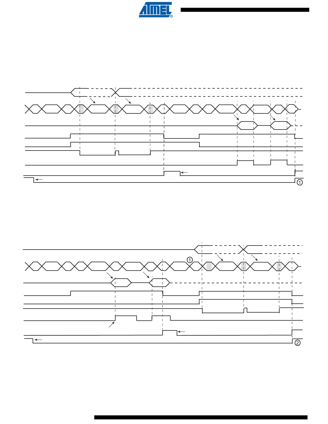
652
6430F–ATARM–21-Feb-12
SAM3U Series
652
6430F–ATARM–21-Feb-12
SAM3U Series
33.10.5.5 Reversal after a Repeated Start
Reversal of Read to Write
The master initiates the communication by a read command and finishes it by a write command.
Figure 33-30 on page 652 describes the repeated start + reversal from Read to Write mode.
Figure 33-30. Repeated Start + Reversal from Read to Write Mode
1. TXCOMP is only set at the end of the transmission because after the repeat ed start, SADR is detected again.
Reversal of Write to Read
The master initiates the communication by a write command and finishes it by a read command.
Figure 33-31 on page 652 describes the repeated start + reversal from Write to Read mode.
Figure 33-31. Repeated Start + Reversal from Write to Read Mode
Notes: 1. In this case, if TWI_THR has not been written at the end of the read command, the clock is automatically stretched before
the ACK.
2. TXCOMP is only set at the end of the transmission because after the repeated start, SADR is detected again.
S SADR R AD ATA 0A DATA 1 SADRSr
NA
W A D ATA 2 A D ATA 3 A P
Cleared after read
DATA 0 D ATA 1
DATA 2 DATA 3
SVACC
SVREAD
TWD
TWI_THR
TWI_RHR
EOSACC
TXRDY
RXRDY
TXCOMP
As soon as a START is detected
S SADR W AD ATA 0A DATA 1 SADRSr
A
R A D ATA 2 A D ATA 3 N A P
Cleared after read
DATA 0
DATA 2 D ATA 3
DATA 1
TXCOMP
TXRDY
RXRDY
As soon as a START is detected
Read TWI_RHR
SVACC
SVREAD
TWD
TWI_RHR
TWI_THR
EOSACC
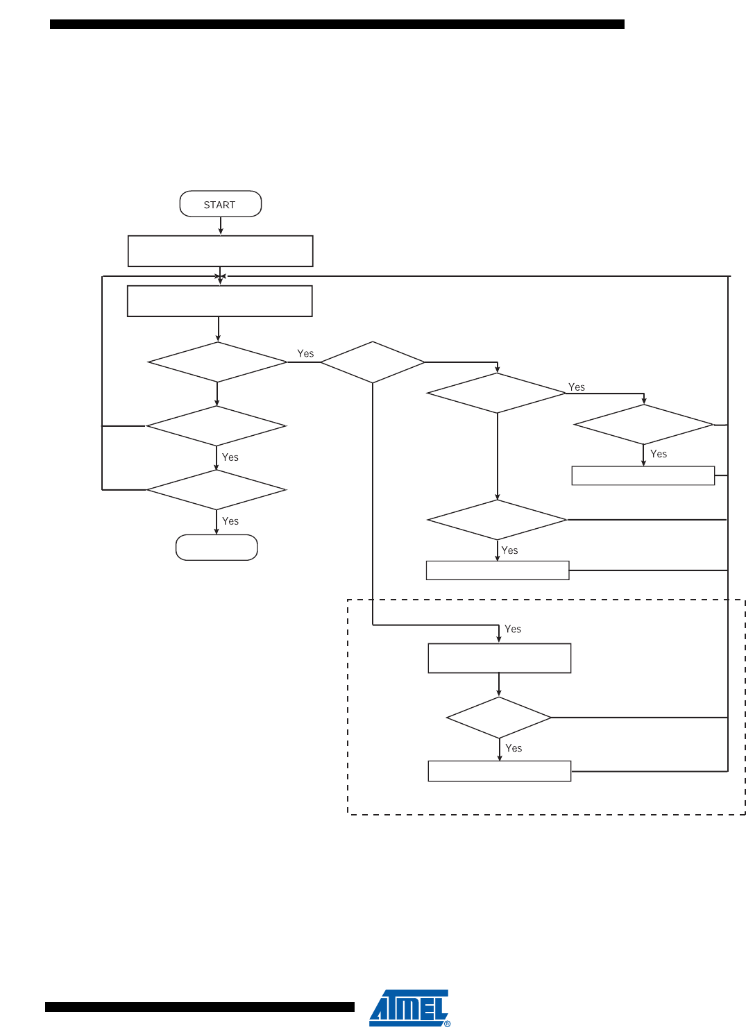
653
6430F–ATARM–21-Feb-12
SAM3U Series
653
6430F–ATARM–21-Feb-12
SAM3U Series
33.10.6 Read Write Flowcharts
The flowchart shown in Figure 33-32 on page 653 gives an example of read and write operations
in Slave mode. A polling or interrupt method can be used to check the status bits. The interrupt
method requires that the interrupt enable register (TWI_IER) be configured first.
Figure 33-32. Read Write Flowchart in Slave Mode
Set the SLAVE mode:
SADR + MSDIS + SVEN
SVACC = 1 ?
TXCOMP = 1 ?
GACC = 1 ?
Decoding of the
programming sequence
Prog seq
OK ?
Change SADR
SVREAD = 0 ?
Read Status Register
RXRDY= 0 ?
Read TWI_RHR
TXRDY= 1 ?
EOSACC = 1 ?
Write in TWI_THR
END
GENERAL CALL TREATMENT
No
No
No
No
No
No
No
No

654
6430F–ATARM–21-Feb-12
SAM3U Series
654
6430F–ATARM–21-Feb-12
SAM3U Series
33.11 Two-wire Interface (TWI) User Interface
Note: 1. All unlisted offset values are considered as “reserved”.
Table 33-5. Register Mapping
Offset Register Name Access Reset
0x00 Control Register TWI_CR Write-only N / A
0x04 Master Mode Register TWI_MMR Read-write 0x00000000
0x08 Slave Mode Register TWI_SMR Read-write 0x00000000
0x0C Internal Address Register TWI_IADR Read-write 0x00000000
0x10 Clock Waveform Generator Register TWI_CWGR Read-write 0x00000000
0x14 - 0x1C Reserved – – –
0x20 Status Register TWI_SR Read-only 0x0000F009
0x24 Interrupt Enable Register TWI_IER Write-only N / A
0x28 Interrupt Disable Register TWI_IDR Write-only N / A
0x2C Interrupt Mask Register TWI_IMR Read-only 0x00000000
0x30 Receive Holding Register TWI_RHR Read-only 0x00000000
0x34 Transmit Holding Register TWI_THR Write-only 0x00000000
0xEC - 0xFC(1) Reserved – – –
0x100 - 0x124 Reserved for the PDC – – –

655
6430F–ATARM–21-Feb-12
SAM3U Series
655
6430F–ATARM–21-Feb-12
SAM3U Series
33.11.1 TWI Control Register
Name: TWI_CR
Address: 0x40084000 (0), 0x40088000 (1)
Access: Write-only
Reset: 0x00000000
• START: Send a START Condition
0 = No effect.
1 = A frame beginning with a START bit is transmitted according to the features defined in the mode register.
This action is necessary when the TWI peripheral wants to read data from a slave. When configured in Master Mode with a
write operation, a frame is sent as soon as the user writes a character in the Transmit Holding Register (TWI_THR).
• STOP: Send a STOP Condition
0 = No effect.
1 = STOP Condition is sent just after completing the current byte transmission in master read mode.
– In single data byte master read, the START and STOP must both be set.
– In multiple data bytes master read, the STOP must be set after the last data received but one.
– In master read mode, if a NACK bit is received, the STOP is automatically performed.
– In master data write operation, a STOP condition will be sent after the transmission of the current data is
finished.
• MSEN: TWI Master Mode Enabled
0 = No effect.
1 = If MSDIS = 0, the master mode is enabled.
Note: Switching from Slave to Master mode is only permitted when TXCOMP = 1.
• MSDIS: TWI Master Mode Disabled
0 = No effect.
1 = The master mode is disabled, all pending data is transmitted. The shifter and holding characters (if it contains data) are
transmitted in case of write operation. In read operation, the character being transferred must be completely received
before disabling.
31 30 29 28 27 26 25 24
––––––––
23 22 21 20 19 18 17 16
––––––––
15 14 13 12 11 10 9 8
––––––––
76543210
SWRST QUICK SVDIS SVEN MSDIS MSEN STOP START

656
6430F–ATARM–21-Feb-12
SAM3U Series
656
6430F–ATARM–21-Feb-12
SAM3U Series
• SVEN: TWI Slave Mode Enabled
0 = No effect.
1 = If SVDIS = 0, the slave mode is enabled.
Note: Switching from Master to Slave mode is only permitted when TXCOMP = 1.
• SVDIS: TWI Slave Mode Disabled
0 = No effect.
1 = The slave mode is disabled. The shifter and holding characters (if it contains data) are transmitted in case of read oper-
ation. In write operation, the character being transferred must be completely received before disabling.
• QUICK: SMBUS Quick Command
0 = No effect.
1 = If Master mode is enabled, a SMBUS Quick Command is sent.
• SWRST: Software Reset
0 = No effect.
1 = Equivalent to a system reset.
657
6430F–ATARM–21-Feb-12
SAM3U Series
657
6430F–ATARM–21-Feb-12
SAM3U Series
33.11.2 TWI Master Mode Register
Name: TWI_MMR
Address: 0x40084004 (0), 0x40088004 (1)
Access: Read-write
Reset: 0x00000000
• IADRSZ: Internal Device Address Size
• MREAD: Master Read Direction
0 = Master write direction.
1 = Master read direction.
• DADR: Device Address
The device address is used to access slave devices in read or write mode. Those bits are only used in Master mode.
31 30 29 28 27 26 25 24
––––––––
23 22 21 20 19 18 17 16
–DADR
15 14 13 12 11 10 9 8
–––MREAD–– IADRSZ
76543210
––––––––
Value Name Description
0 NONE No internal device address
1 1_BYTE One-byte internal device address
2 2_BYTE Two-byte internal device address
3 3_BYTE Three-byte internal device address

658
6430F–ATARM–21-Feb-12
SAM3U Series
658
6430F–ATARM–21-Feb-12
SAM3U Series
33.11.3 TWI Slave Mode Register
Name: TWI_SMR
Address: 0x40084008 (0), 0x40088008 (1)
Access: Read-write
Reset: 0x00000000
• SADR: Slave Address
The slave device address is used in Slave mode in order to be accessed by master devices in read or write mode.
SADR must be programmed before enabling the Slave mode or after a general call. Writes at other times have no effect.
31 30 29 28 27 26 25 24
––––––––
23 22 21 20 19 18 17 16
–SADR
15 14 13 12 11 10 9 8
––––––
76543210
––––––––

659
6430F–ATARM–21-Feb-12
SAM3U Series
659
6430F–ATARM–21-Feb-12
SAM3U Series
33.11.4 TWI Internal Address Register
Name: TWI_IADR
Address: 0x4008400C (0), 0x4008800C (1)
Access: Read-write
Reset: 0x00000000
• IADR: Internal Address
0, 1, 2 or 3 bytes depending on IADRSZ.
31 30 29 28 27 26 25 24
––––––––
23 22 21 20 19 18 17 16
IADR
15 14 13 12 11 10 9 8
IADR
76543210
IADR

660
6430F–ATARM–21-Feb-12
SAM3U Series
660
6430F–ATARM–21-Feb-12
SAM3U Series
33.11.5 TWI Clock Waveform Generator Register
Name: TWI_CWGR
Address: 0x40084010 (0), 0x40088010 (1)
Access: Read-write
Reset: 0x00000000
TWI_CWGR is only used in Master mode.
• CLDIV: Clock Low Divider
The SCL low period is defined as follows:
• CHDIV: Clock High Divider
The SCL high period is defined as follows:
• CKDIV: Clock Divider
The CKDIV is used to increase both SCL high and low periods.
31 30 29 28 27 26 25 24
––––––––
23 22 21 20 19 18 17 16
CKDIV
15 14 13 12 11 10 9 8
CHDIV
76543210
CLDIV
Tlow CLDIV(2CKDIV
×()4)+TMCK
×=
Thigh CHDIV(2CKDIV
×()4)+TMCK
×=

661
6430F–ATARM–21-Feb-12
SAM3U Series
661
6430F–ATARM–21-Feb-12
SAM3U Series
33.11.6 TWI Status Register
Name: TWI_SR
Address: 0x40084020 (0), 0x40088020 (1)
Access: Read-only
Reset: 0x0000F009
• TXCOMP: Transmission Completed (automatically set / reset)
TXCOMP used in Master mode:
0 = During the length of the current frame.
1 = When both holding and shifter registers are empty and STOP condition has been sent.
TXCOMP behavior in Master mode can be seen in Figure 33-8 on page 633 and in Figure 33-10 on page 634.
TXCOMP used in Slave mode:
0 = As soon as a Start is detected.
1 = After a Stop or a Repeated Start + an address different from SADR is detected.
TXCOMP behavior in Slave mode can be seen in Figure 33-28 on page 650, Figure 33-29 on page 651, Figure 33-30 on
page 652 and Figure 33-31 on page 652.
• RXRDY: Receive Holding Register Ready (automatically set / reset)
0 = No character has been received since the last TWI_RHR read operation.
1 = A byte has been received in the TWI_RHR since the last read.
RXRDY behavior in Master mode can be seen in Figure 33-10 on page 634.
RXRDY behavior in Slave mode can be seen in Figure 33-26 on page 648, Figure 33-29 on page 651, Figure 33-30 on
page 652 and Figure 33-31 on page 652.
• TXRDY: Transmit Holding Register Ready (automatically set / reset)
TXRDY used in Master mode:
0 = The transmit holding register has not been transferred into shift register. Set to 0 when writing into TWI_THR register.
1 = As soon as a data byte is transferred from TWI_THR to internal shifter or if a NACK error is detected, TXRDY is set at
the same time as TXCOMP and NACK. TXRDY is also set when MSEN is set (enable TWI).
TXRDY behavior in Master mode can be seen in Figure 33-8 on page 633.
31 30 29 28 27 26 25 24
––––––––
23 22 21 20 19 18 17 16
––––––––
15 14 13 12 11 10 9 8
TXBUFE RXBUFF ENDTX ENDRX EOSACC SCLWS ARBLST NACK
76543210
– OVRE GACC SVACC SVREAD TXRDY RXRDY TXCOMP

662
6430F–ATARM–21-Feb-12
SAM3U Series
662
6430F–ATARM–21-Feb-12
SAM3U Series
TXRDY used in Slave mode:
0 = As soon as data is written in the TWI_THR, until this data has been transmitted and acknowledged (ACK or NACK).
1 = It indicates that the TWI_THR is empty and that data has been transmitted and acknowledged.
If TXRDY is high and if a NACK has been detected, the transmission will be stopped. Thus when TRDY = NACK = 1, the
programmer must not fill TWI_THR to avoid losing it.
TXRDY behavior in Slave mode can be seen in Figure 33-25 on page 648, Figure 33-28 on page 650, Figure 33-30 on
page 652 and Figure 33-31 on page 652.
• SVREAD: Slave Read (automatically set / reset)
This bit is only used in Slave mode. When SVACC is low (no Slave access has been detected) SVREAD is irrelevant.
0 = Indicates that a write access is performed by a Master.
1 = Indicates that a read access is performed by a Master.
SVREAD behavior can be seen in Figure 33-25 on page 648, Figure 33-26 on page 648, Figure 33-30 on page 652 and
Figure 33-31 on page 652.
• SVACC: Slave Access (automatically set / reset)
This bit is only used in Slave mode.
0 = TWI is not addressed. SVACC is automatically cleared after a NACK or a STOP condition is detected.
1 = Indicates that the address decoding sequence has matched (A Master has sent SADR). SVACC remains high until a
NACK or a STOP condition is detected.
SVACC behavior can be seen in Figure 33-25 on page 648, Figure 33-26 on page 648, Figure 33-30 on page 652 and Fig-
ure 33-31 on page 652.
• GACC: General Call Access (clear on read)
This bit is only used in Slave mode.
0 = No General Call has been detected.
1 = A General Call has been detected. After the detection of General Call, if need be, the programmer may acknowledge
this access and decode the following bytes and respond according to the value of the bytes.
GACC behavior can be seen in Figure 33-27 on page 649.
• OVRE: Overrun Error (clear on read)
This bit is only used in Master mode.
0 = TWI_RHR has not been loaded while RXRDY was set
1 = TWI_RHR has been loaded while RXRDY was set. Reset by read in TWI_SR when TXCOMP is set.
• NACK: Not Acknowledged (clear on read)
NACK used in Master mode:
0 = Each data byte has been correctly received by the far-end side TWI slave component.
1 = A data byte has not been acknowledged by the slave component. Set at the same time as TXCOMP.

663
6430F–ATARM–21-Feb-12
SAM3U Series
663
6430F–ATARM–21-Feb-12
SAM3U Series
NACK used in Slave Read mode:
0 = Each data byte has been correctly received by the Master.
1 = In read mode, a data byte has not been acknowledged by the Master. When NACK is set the programmer must not fill
TWI_THR even if TXRDY is set, because it means that the Master will stop the data transfer or re initiate it.
Note that in Slave Write mode all data are acknowledged by the TWI.
• ARBLST: Arbitration Lost (clear on read)
This bit is only used in Master mode.
0: Arbitration won.
1: Arbitration lost. Another master of the TWI bus has won the multi-master arbitration. TXCOMP is set at the same time.
• SCLWS: Clock Wait State (automatically set / reset)
This bit is only used in Slave mode.
0 = The clock is not stretched.
1 = The clock is stretched. TWI_THR / TWI_RHR buffer is not filled / emptied before the emission / reception of a new
character.
SCLWS behavior can be seen in Figure 33-28 on page 650 and Figure 33-29 on page 651.
• EOSACC: End Of Slave Access (clear on read)
This bit is only used in Slave mode.
0 = A slave access is being performing.
1 = The Slave Access is finished. End Of Slave Access is automatically set as soon as SVACC is reset.
EOSACC behavior can be seen in Figure 33-30 on page 652 and Figure 33-31 on page 652
• ENDRX: End of RX buffer
0 = The Receive Counter Register has not reached 0 since the last write in TWI_RCR or TWI_RNCR.
1 = The Receive Counter Register has reached 0 since the last write in TWI_RCR or TWI_RNCR.
• ENDTX: End of TX buffer
0 = The Transmit Counter Register has not reached 0 since the last write in TWI_TCR or TWI_TNCR.
1 = The Transmit Counter Register has reached 0 since the last write in TWI_TCR or TWI_TNCR.
• RXBUFF: RX Buffer Full
0 = TWI_RCR or TWI_RNCR have a value other than 0.
1 = Both TWI_RCR and TWI_RNCR have a value of 0.
• TXBUFE: TX Buffer Empty
0 = TWI_TCR or TWI_TNCR have a value other than 0.
1 = Both TWI_TCR and TWI_TNCR have a value of 0.

664
6430F–ATARM–21-Feb-12
SAM3U Series
664
6430F–ATARM–21-Feb-12
SAM3U Series
33.11.7 TWI Interrupt Enable Register
Name: TWI_IER
Address: 0x40084024 (0), 0x40088024 (1)
Access: Write-only
Reset: 0x00000000
• TXCOMP: Transmission Completed Interrupt Enable
• RXRDY: Receive Holding Register Ready Interrupt Enable
• TXRDY: Transmit Holding Register Ready Interrupt Enable
• SVACC: Slave Access Interrupt Enable
• GACC: General Call Access Interrupt Enable
• OVRE: Overrun Error Interrupt Enable
• NACK: Not Acknowledge Interrupt Enable
• ARBLST: Arbitration Lost Interrupt Enable
• SCL_WS: Clock Wait State Interrupt Enable
• EOSACC: End Of Slave Access Interrupt Enable
• ENDRX: End of Receive Buffer Interrupt Enable
• ENDTX: End of Transmit Buffer Interrupt Enable
• RXBUFF: Receive Buffer Full Interrupt Enable
• TXBUFE: Transmit Buffer Empty Interrupt Enable
0 = No effect.
1 = Enables the corresponding interrupt.
31 30 29 28 27 26 25 24
––––––––
23 22 21 20 19 18 17 16
––––––––
15 14 13 12 11 10 9 8
TXBUFE RXBUFF ENDTX ENDRX EOSACC SCL_WS ARBLST NACK
76543210
– OVRE GACC SVACC – TXRDY RXRDY TXCOMP

665
6430F–ATARM–21-Feb-12
SAM3U Series
665
6430F–ATARM–21-Feb-12
SAM3U Series
33.11.8 TWI Interrupt Disable Register
Name: TWI_IDR
Address: 0x40084028 (0), 0x40088028 (1)
Access: Write-only
Reset: 0x00000000
• TXCOMP: Transmission Completed Interrupt Disable
• RXRDY: Receive Holding Register Ready Interrupt Disable
• TXRDY: Transmit Holding Register Ready Interrupt Disable
• SVACC: Slave Access Interrupt Disable
• GACC: General Call Access Interrupt Disable
• OVRE: Overrun Error Interrupt Disable
• NACK: Not Acknowledge Interrupt Disable
• ARBLST: Arbitration Lost Interrupt Disable
• SCL_WS: Clock Wait State Interrupt Disable
• EOSACC: End Of Slave Access Interrupt Disable
• ENDRX: End of Receive Buffer Interrupt Disable
• ENDTX: End of Transmit Buffer Interrupt Disable
• RXBUFF: Receive Buffer Full Interrupt Disable
• TXBUFE: Transmit Buffer Empty Interrupt Disable
0 = No effect.
1 = Disables the corresponding interrupt.
31 30 29 28 27 26 25 24
––––––––
23 22 21 20 19 18 17 16
––––––––
15 14 13 12 11 10 9 8
TXBUFE RXBUFF ENDTX ENDRX EOSACC SCL_WS ARBLST NACK
76543210
– OVRE GACC SVACC – TXRDY RXRDY TXCOMP

666
6430F–ATARM–21-Feb-12
SAM3U Series
666
6430F–ATARM–21-Feb-12
SAM3U Series
33.11.9 TWI Interrupt Mask Register
Name: TWI_IMR
Address: 0x4008402C (0), 0x4008802C (1)
Access: Read-only
Reset: 0x00000000
• TXCOMP: Transmission Completed Interrupt Mask
• RXRDY: Receive Holding Register Ready Interrupt Mask
• TXRDY: Transmit Holding Register Ready Interrupt Mask
• SVACC: Slave Access Interrupt Mask
• GACC: General Call Access Interrupt Mask
• OVRE: Overrun Error Interrupt Mask
• NACK: Not Acknowledge Interrupt Mask
• ARBLST: Arbitration Lost Interrupt Mask
• SCL_WS: Clock Wait State Interrupt Mask
• EOSACC: End Of Slave Access Interrupt Mask
• ENDRX: End of Receive Buffer Interrupt Mask
• ENDTX: End of Transmit Buffer Interrupt Mask
• RXBUFF: Receive Buffer Full Interrupt Mask
• TXBUFE: Transmit Buffer Empty Interrupt Mask
0 = The corresponding interrupt is disabled.
1 = The corresponding interrupt is enabled.
31 30 29 28 27 26 25 24
––––––––
23 22 21 20 19 18 17 16
––––––––
15 14 13 12 11 10 9 8
TXBUFE RXBUFF ENDTX ENDRX EOSACC SCL_WS ARBLST NACK
76543210
– OVRE GACC SVACC – TXRDY RXRDY TXCOMP

667
6430F–ATARM–21-Feb-12
SAM3U Series
667
6430F–ATARM–21-Feb-12
SAM3U Series
33.11.10 TWI Receive Holding Register
Name: TWI_RHR
Address: 0x40084030 (0), 0x40088030 (1)
Access: Read-only
Reset: 0x00000000
• RXDATA: Master or Slave Receive Holding Data
31 30 29 28 27 26 25 24
––––––––
23 22 21 20 19 18 17 16
––––––––
15 14 13 12 11 10 9 8
––––––––
76543210
RXDATA

668
6430F–ATARM–21-Feb-12
SAM3U Series
668
6430F–ATARM–21-Feb-12
SAM3U Series
33.11.11 TWI Transmit Holding Register
Name: TWI_THR
Address: 0x40084034 (0), 0x40088034 (1)
Access: Read-write
Reset: 0x00000000
• TXDATA: Master or Slave Transmit Holding Data
31 30 29 28 27 26 25 24
––––––––
23 22 21 20 19 18 17 16
––––––––
15 14 13 12 11 10 9 8
––––––––
76543210
TXDATA

669
6430F–ATARM–21-Feb-12
SAM3U Series
669
6430F–ATARM–21-Feb-12
SAM3U Series
34. Universal Asynchronous Receiver Transceiver (UART)
34.1 Description
The Universal Asynchronous Receiver Transmitter features a two-pin UART that can be used for
communication and trace purposes and offers an ideal medium for in-situ programming solu-
tions. Moreover, the association with two peripheral DMA controller (PDC) channels permits
packet handling for these tasks with processor time reduced to a minimum.
34.2 Embedded Characteristics
•Two-pin UART
– Implemented Features are USART Compatible
– Independent Receiver and Transmitter with a Common Programmable Baud Rate
Generator
– Even, Odd, Mark or Space Parity Generation
– Parity, Framing and Overrun Error Detection
– Automatic Echo, Local Loopback and Remote Loopback Channel Modes
– Interrupt Generation
– Support for Two PDC Channels with Connection to Receiver and Transmitter
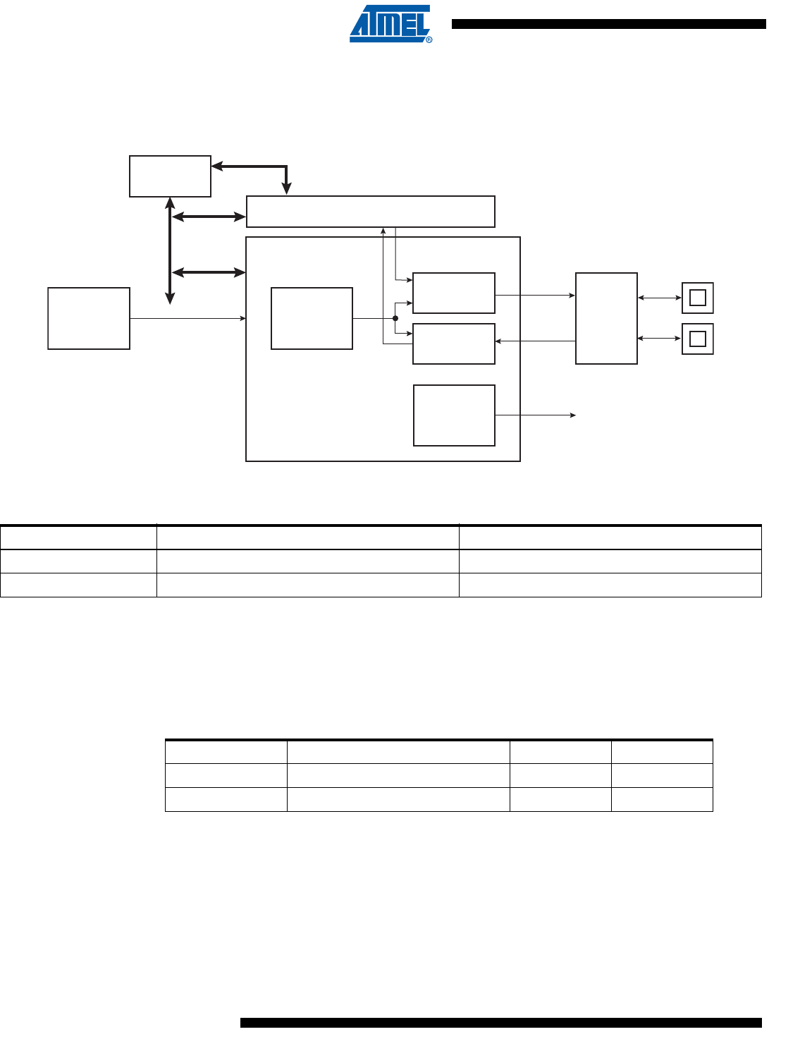
670
6430F–ATARM–21-Feb-12
SAM3U Series
670
6430F–ATARM–21-Feb-12
SAM3U Series
34.3 Block Diagram
Figure 34-1. UART Functional Block Diagram
34.4 Product Dependencies
34.4.1 I/O Lines
The UART pins are multiplexed with PIO lines. The programmer must first configure the corre-
sponding PIO Controller to enable I/O line operations of the UART.
34.4.2 Power Management
The UART clock is controllable through the Power Management Controller. In this case, the pro-
grammer must first configure the PMC to enable the UART clock. Usually, the peripheral
identifier used for this purpose is 1.
Peripheral DMA Controller
Baud Rate
Generator
Transmit
Receive
Interrupt
Control
Peripheral
Bridge
Parallel
Input/
Output
UTXD
URXD
Power
Management
Controller
MCK
uart_irq
APB UART
Table 34-1. UART Pin Description
Pin Name Description Type
URXD UART Receive Data Input
UTXD UART Transmit Data Output
Table 34-2. I/O Lines
Instance Signal I/O Line Peripheral
UART URXD PA11 A
UART UTXD PA12 A
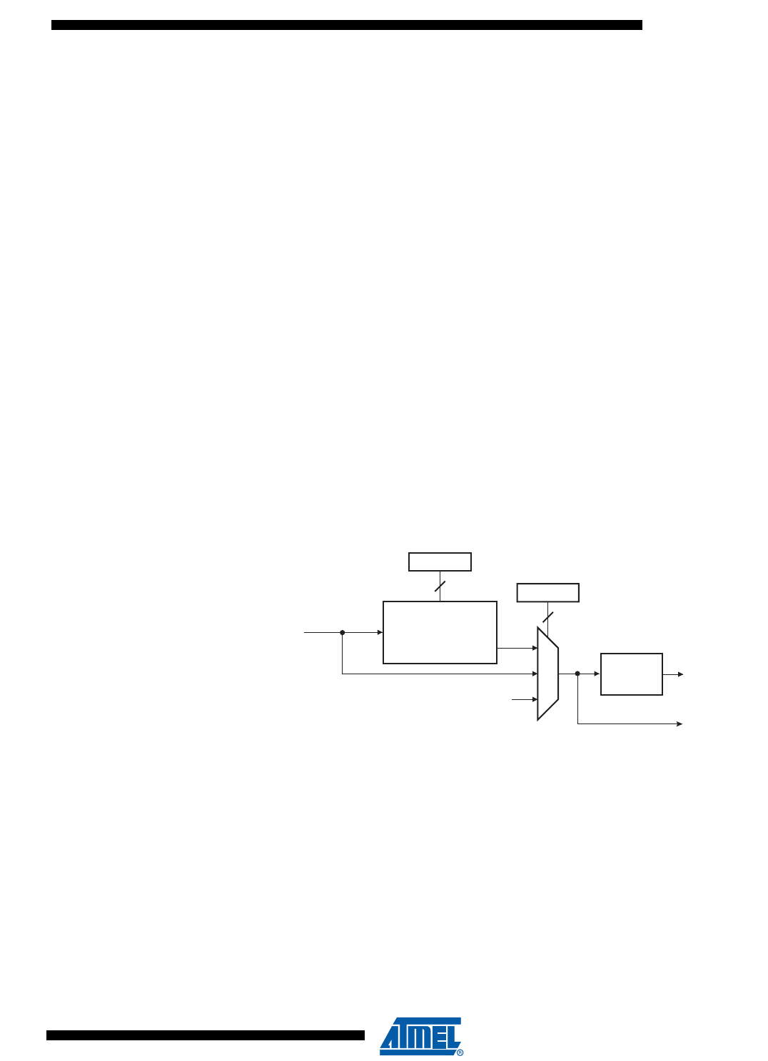
671
6430F–ATARM–21-Feb-12
SAM3U Series
671
6430F–ATARM–21-Feb-12
SAM3U Series
34.4.3 Interrupt Source
The UART interrupt line is connected to one of the interrupt sources of the Nested Vectored
Interrupt Controller (NVIC). Interrupt handling requires programming of the NVIC before config-
uring the UART.
34.5 UART Operations
The UART operates in asynchronous mode only and supports only 8-bit character handling (with
parity). It has no clock pin.
The UART is made up of a receiver and a transmitter that operate independently, and a common
baud rate generator. Receiver timeout and transmitter time guard are not implemented. How-
ever, all the implemented features are compatible with those of a standard USART.
34.5.1 Baud Rate Generator
The baud rate generator provides the bit period clock named baud rate clock to both the receiver
and the transmitter.
The baud rate clock is the master clock divided by 16 times the value (CD) written in
UART_BRGR (Baud Rate Generator Register). If UART_BRGR is set to 0, the baud rate clock is
disabled and the UART remains inactive. The maximum allowable baud rate is Master Clock
divided by 16. The minimum allowable baud rate is Master Clock divided by (16 x 65536).
Figure 34-2. Baud Rate Generator
34.5.2 Receiver
34.5.2.1 Receiver Reset, Enable and Disable
After device reset, the UART receiver is disabled and must be enabled before being used. The
receiver can be enabled by writing the control register UART_CR with the bit RXEN at 1. At this
command, the receiver starts looking for a start bit.
The programmer can disable the receiver by writing UART_CR with the bit RXDIS at 1. If the
receiver is waiting for a start bit, it is immediately stopped. However, if the receiver has already
detected a start bit and is receiving the data, it waits for the stop bit before actually stopping its
operation.
Baud Rate MCK
16 CD ×
------------------------ =
MCK 16-bit Counter
0
Baud Rate
Clock
CD
CD
OUT
Divide
by 16
0
1
>1
Receiver
Sampling Clock
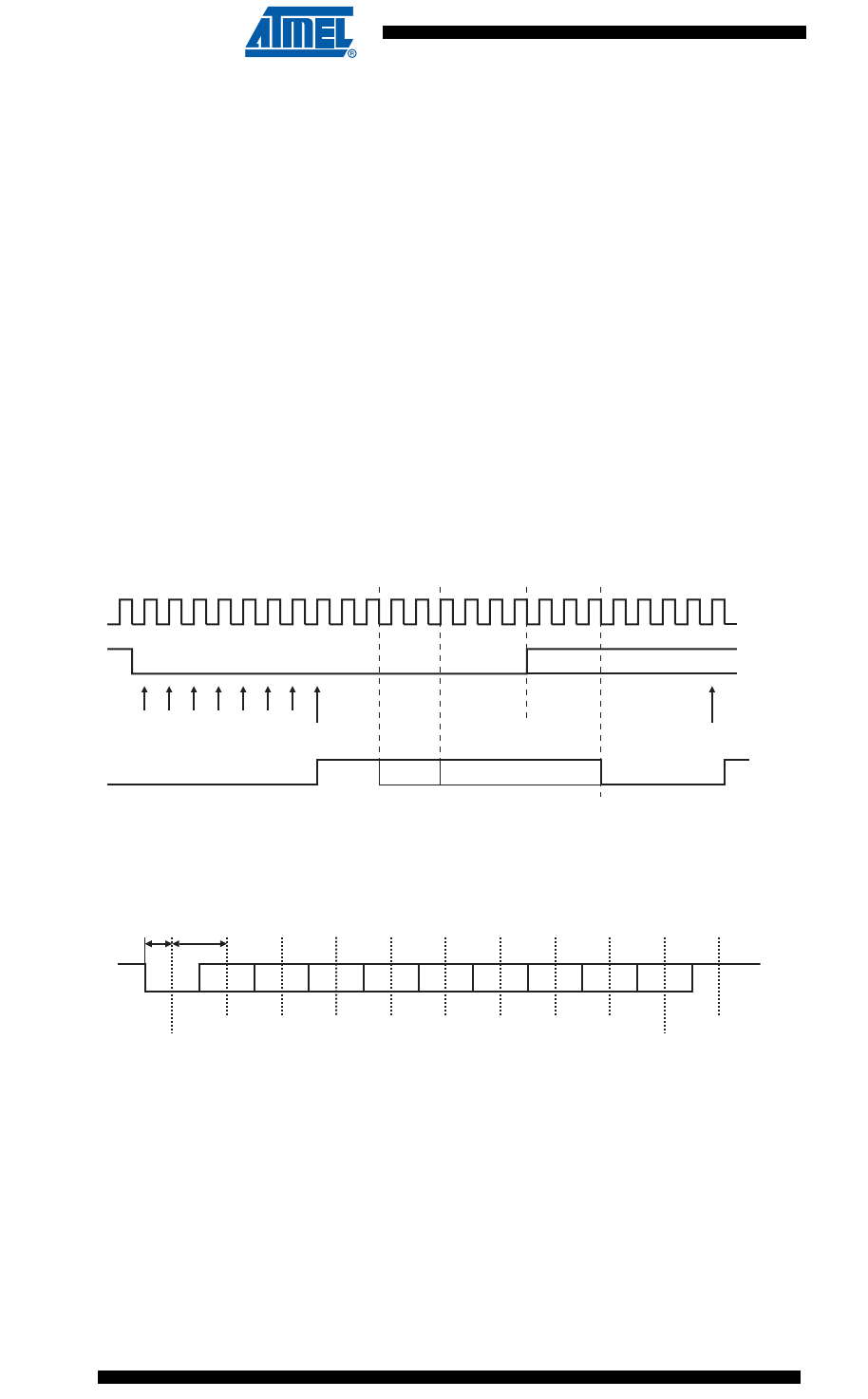
672
6430F–ATARM–21-Feb-12
SAM3U Series
672
6430F–ATARM–21-Feb-12
SAM3U Series
The programmer can also put the receiver in its reset state by writing UART_CR with the bit
RSTRX at 1. In doing so, the receiver immediately stops its current operations and is disabled,
whatever its current state. If RSTRX is applied when data is being processed, this data is lost.
34.5.2.2 Start Detection and Data Sampling
The UART only supports asynchronous operations, and this affects only its receiver. The UART
receiver detects the start of a received character by sampling the URXD signal until it detects a
valid start bit. A low level (space) on URXD is interpreted as a valid start bit if it is detected for
more than 7 cycles of the sampling clock, which is 16 times the baud rate. Hence, a space that is
longer than 7/16 of the bit period is detected as a valid start bit. A space which is 7/16 of a bit
period or shorter is ignored and the receiver continues to wait for a valid start bit.
When a valid start bit has been detected, the receiver samples the URXD at the theoretical mid-
point of each bit. It is assumed that each bit lasts 16 cycles of the sampling clock (1-bit period)
so the bit sampling point is eight cycles (0.5-bit period) after the start of the bit. The first sampling
point is therefore 24 cycles (1.5-bit periods) after the falling edge of the start bit was detected.
Each subsequent bit is sampled 16 cycles (1-bit period) after the previous one.
Figure 34-3. Start Bit Detection
Figure 34-4. Character Reception
34.5.2.3 Receiver Ready
When a complete character is received, it is transferred to the UART_RHR and the RXRDY sta-
tus bit in UART_SR (Status Register) is set. The bit RXRDY is automatically cleared when the
receive holding register UART_RHR is read.
Sampling Clock
URXD
True Start
Detection
D0
Baud Rate
Clock
D0 D1 D2 D3 D4 D5 D6 D7
URXD
True Start Detection
Sampling
Parity Bit
Stop Bit
Example: 8-bit, parity enabled 1 stop
1 bit
period
0.5 bit
period
673
6430F–ATARM–21-Feb-12
SAM3U Series
673
6430F–ATARM–21-Feb-12
SAM3U Series
Figure 34-5. Receiver Ready
34.5.2.4 Receiver Overrun
If UART_RHR has not been read by the software (or the Peripheral Data Controller or DMA
Controller) since the last transfer, the RXRDY bit is still set and a new character is received, the
OVRE status bit in UART_SR is set. OVRE is cleared when the software writes the control regis-
ter UART_CR with the bit RSTSTA (Reset Status) at 1.
Figure 34-6. Receiver Overrun
34.5.2.5 Parity Error
Each time a character is received, the receiver calculates the parity of the received data bits, in
accordance with the field PAR in UART_MR. It then compares the result with the received parity
bit. If different, the parity error bit PARE in UART_SR is set at the same time the RXRDY is set.
The parity bit is cleared when the control register UART_CR is written with the bit RSTSTA
(Reset Status) at 1. If a new character is received before the reset status command is written,
the PARE bit remains at 1.
Figure 34-7. Parity Error
34.5.2.6 Receiver Framing Error
When a start bit is detected, it generates a character reception when all the data bits have been
sampled. The stop bit is also sampled and when it is detected at 0, the FRAME (Framing Error)
bit in UART_SR is set at the same time the RXRDY bit is set. The FRAME bit remains high until
the control register UART_CR is written with the bit RSTSTA at 1.
D0 D1 D2 D3 D4 D5 D6 D7 PS SD0 D1 D2 D3 D4 D5 D6 D7 P
URXD
Read UART_RHR
RXRDY
D0 D1 D2 D3 D4 D5 D6 D7 PS SD0 D1 D2 D3 D4 D5 D6 D7 P
URXD
RSTSTA
RXRDY
OVRE
stop stop
stop
D0 D1 D2 D3 D4 D5 D6 D7 PS
URXD
RSTSTA
RXRDY
PARE
Wrong Parity Bit
674
6430F–ATARM–21-Feb-12
SAM3U Series
674
6430F–ATARM–21-Feb-12
SAM3U Series
Figure 34-8. Receiver Framing Error
34.5.3 Transmitter
34.5.3.1 Transmitter Reset, Enable and Disable
After device reset, the UART transmitter is disabled and it must be enabled before being used.
The transmitter is enabled by writing the control register UART_CR with the bit TXEN at 1. From
this command, the transmitter waits for a character to be written in the Transmit Holding Register
(UART_THR) before actually starting the transmission.
The programmer can disable the transmitter by writing UART_CR with the bit TXDIS at 1. If the
transmitter is not operating, it is immediately stopped. However, if a character is being pro-
cessed into the Shift Register and/or a character has been written in the Transmit Holding
Register, the characters are completed before the transmitter is actually stopped.
The programmer can also put the transmitter in its reset state by writing the UART_CR with the
bit RSTTX at 1. This immediately stops the transmitter, whether or not it is processing
characters.
34.5.3.2 Transmit Format
The UART transmitter drives the pin UTXD at the baud rate clock speed. The line is driven
depending on the format defined in the Mode Register and the data stored in the Shift Register.
One start bit at level 0, then the 8 data bits, from the lowest to the highest bit, one optional parity
bit and one stop bit at 1 are consecutively shifted out as shown in the following figure. The field
PARE in the mode register UART_MR defines whether or not a parity bit is shifted out. When a
parity bit is enabled, it can be selected between an odd parity, an even parity, or a fixed space or
mark bit.
Figure 34-9. Character Transmission
34.5.3.3 Transmitter Control
When the transmitter is enabled, the bit TXRDY (Transmitter Ready) is set in the status register
UART_SR. The transmission starts when the programmer writes in the Transmit Holding Regis-
ter (UART_THR), and after the written character is transferred from UART_THR to the Shift
D0 D1 D2 D3 D4 D5 D6 D7 PS
URXD
RSTSTA
RXRDY
FRAME
Stop Bit
Detected at 0
stop
D0 D1 D2 D3 D4 D5 D6 D7
UTXD
Start
Bit
Parity
Bit
Stop
Bit
Example: Parity enabled
Baud Rate
Clock
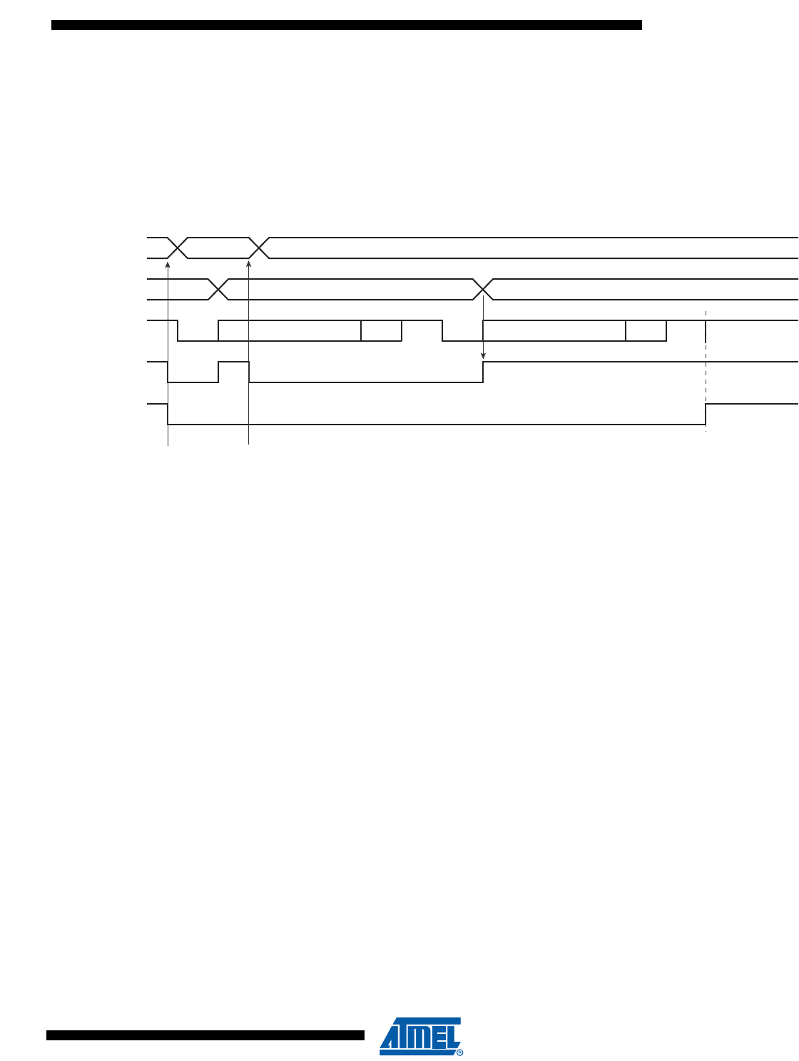
675
6430F–ATARM–21-Feb-12
SAM3U Series
675
6430F–ATARM–21-Feb-12
SAM3U Series
Register. The TXRDY bit remains high until a second character is written in UART_THR. As
soon as the first character is completed, the last character written in UART_THR is transferred
into the shift register and TXRDY rises again, showing that the holding register is empty.
When both the Shift Register and UART_THR are empty, i.e., all the characters written in
UART_THR have been processed, the TXEMPTY bit rises after the last stop bit has been
completed.
Figure 34-10. Transmitter Control
34.5.4 Peripheral DMA Controller
Both the receiver and the transmitter of the UART are connected to a Peripheral DMA Controller
(PDC) channel.
The peripheral data controller channels are programmed via registers that are mapped within
the UART user interface from the offset 0x100. The status bits are reported in the UART status
register (UART_SR) and can generate an interrupt.
The RXRDY bit triggers the PDC channel data transfer of the receiver. This results in a read of
the data in UART_RHR. The TXRDY bit triggers the PDC channel data transfer of the transmit-
ter. This results in a write of data in UART_THR.
34.5.5 Test Modes
The UART supports three test modes. These modes of operation are programmed by using the
field CHMODE (Channel Mode) in the mode register (UART_MR).
The Automatic Echo mode allows bit-by-bit retransmission. When a bit is received on the URXD
line, it is sent to the UTXD line. The transmitter operates normally, but has no effect on the
UTXD line.
The Local Loopback mode allows the transmitted characters to be received. UTXD and URXD
pins are not used and the output of the transmitter is internally connected to the input of the
receiver. The URXD pin level has no effect and the UTXD line is held high, as in idle state.
The Remote Loopback mode directly connects the URXD pin to the UTXD line. The transmitter
and the receiver are disabled and have no effect. This mode allows a bit-by-bit retransmission.
UART_THR
Shift Register
UTXD
TXRDY
TXEMPTY
Data 0 Data 1
Data 0
Data 0
Data 1
Data 1SSPP
Write Data 0
in UART_THR
Write Data 1
in UART_THR
stop
stop
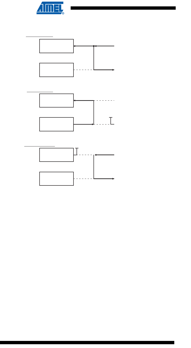
676
6430F–ATARM–21-Feb-12
SAM3U Series
676
6430F–ATARM–21-Feb-12
SAM3U Series
Figure 34-11. Test Modes
Receiver
Transmitter Disabled
RXD
TXD
Receiver
Transmitter Disabled
RXD
TXD
VDD
Disabled
Receiver
Transmitter Disabled
RXD
TXD
Disabled
Automatic Echo
Local Loopback
Remote Loopback VDD

677
6430F–ATARM–21-Feb-12
SAM3U Series
677
6430F–ATARM–21-Feb-12
SAM3U Series
34.6 Universal Asynchronous Receiver Transceiver (UART) User Interface
Table 34-3. Register Mapping
Offset Register Name Access Reset
0x0000 Control Register UART_CR Write-only –
0x0004 Mode Register UART_MR Read-write 0x0
0x0008 Interrupt Enable Register UART_IER Write-only –
0x000C Interrupt Disable Register UART_IDR Write-only –
0x0010 Interrupt Mask Register UART_IMR Read-only 0x0
0x0014 Status Register UART_SR Read-only –
0x0018 Receive Holding Register UART_RHR Read-only 0x0
0x001C Transmit Holding Register UART_THR Write-only –
0x0020 Baud Rate Generator Register UART_BRGR Read-write 0x0
0x0024 - 0x003C Reserved – – –
0x004C - 0x00FC Reserved – – –
0x0100 - 0x0124 PDC Area – – –

678
6430F–ATARM–21-Feb-12
SAM3U Series
678
6430F–ATARM–21-Feb-12
SAM3U Series
34.6.1 UART Control Register
Name: UART_CR
Address: 0x400E0600
Access: Write-only
• RSTRX: Reset Receiver
0 = No effect.
1 = The receiver logic is reset and disabled. If a character is being received, the reception is aborted.
• RSTTX: Reset Transmitter
0 = No effect.
1 = The transmitter logic is reset and disabled. If a character is being transmitted, the transmission is aborted.
• RXEN: Receiver Enable
0 = No effect.
1 = The receiver is enabled if RXDIS is 0.
• RXDIS: Receiver Disable
0 = No effect.
1 = The receiver is disabled. If a character is being processed and RSTRX is not set, the character is completed before the
receiver is stopped.
• TXEN: Transmitter Enable
0 = No effect.
1 = The transmitter is enabled if TXDIS is 0.
• TXDIS: Transmitter Disable
0 = No effect.
1 = The transmitter is disabled. If a character is being processed and a character has been written in the UART_THR and
RSTTX is not set, both characters are completed before the transmitter is stopped.
• RSTSTA: Reset Status Bits
0 = No effect.
1 = Resets the status bits PARE, FRAME and OVRE in the UART_SR.
31 30 29 28 27 26 25 24
––––––––
23 22 21 20 19 18 17 16
––––––––
15 14 13 12 11 10 9 8
–––––––
RSTSTA
76543210
TXDIS TXEN RXDIS RXEN RSTTX RSTRX ––

679
6430F–ATARM–21-Feb-12
SAM3U Series
679
6430F–ATARM–21-Feb-12
SAM3U Series
34.6.2 UART Mode Register
Name: UART_MR
Address: 0x400E0604
Access: Read-write
• PAR: Parity Type
• CHMODE: Channel Mode
31 30 29 28 27 26 25 24
––––––––
23 22 21 20 19 18 17 16
––––––––
15 14 13 12 11 10 9 8
CHMODE –– PAR –
76543210
––––––––
Value Name Description
0 EVEN Even parity
1 ODD Odd parity
2 SPACE Space: parity forced to 0
3 MARK Mark: parity forced to 1
4 NO No parity
Value Name Description
0 NORMAL Normal Mode
1 AUTOMATIC Automatic Echo
2 LOCAL_LOOPBACK Local Loopback
3 REMOTE_LOOPBACK Remote Loopback

680
6430F–ATARM–21-Feb-12
SAM3U Series
680
6430F–ATARM–21-Feb-12
SAM3U Series
34.6.3 UART Interrupt Enable Register
Name: UART_IER
Address: 0x400E0608
Access: Write-only
• RXRDY: Enable RXRDY Interrupt
• TXRDY: Enable TXRDY Interrupt
• ENDRX: Enable End of Receive Transfer Interrupt
• ENDTX: Enable End of Transmit Interrupt
• OVRE: Enable Overrun Error Interrupt
• FRAME: Enable Framing Error Interrupt
• PARE: Enable Parity Error Interrupt
• TXEMPTY: Enable TXEMPTY Interrupt
• TXBUFE: Enable Buffer Empty Interrupt
• RXBUFF: Enable Buffer Full Interrupt
0 = No effect.
1 = Enables the corresponding interrupt.
31 30 29 28 27 26 25 24
––––––––
23 22 21 20 19 18 17 16
––––––––
15 14 13 12 11 10 9 8
–––
RXBUFF TXBUFE –TXEMPTY –
76543210
PARE FRAME OVRE ENDTX ENDRX –TXRDY RXRDY

681
6430F–ATARM–21-Feb-12
SAM3U Series
681
6430F–ATARM–21-Feb-12
SAM3U Series
34.6.4 UART Interrupt Disable Register
Name: UART_IDR
Address: 0x400E060C
Access: Write-only
• RXRDY: Disable RXRDY Interrupt
• TXRDY: Disable TXRDY Interrupt
• ENDRX: Disable End of Receive Transfer Interrupt
• ENDTX: Disable End of Transmit Interrupt
• OVRE: Disable Overrun Error Interrupt
• FRAME: Disable Framing Error Interrupt
• PARE: Disable Parity Error Interrupt
• TXEMPTY: Disable TXEMPTY Interrupt
• TXBUFE: Disable Buffer Empty Interrupt
• RXBUFF: Disable Buffer Full Interrupt
0 = No effect.
1 = Disables the corresponding interrupt.
31 30 29 28 27 26 25 24
––––––––
23 22 21 20 19 18 17 16
––––––––
15 14 13 12 11 10 9 8
–––
RXBUFF TXBUFE –TXEMPTY –
76543210
PARE FRAME OVRE ENDTX ENDRX –TXRDY RXRDY

682
6430F–ATARM–21-Feb-12
SAM3U Series
682
6430F–ATARM–21-Feb-12
SAM3U Series
34.6.5 UART Interrupt Mask Register
Name: UART_IMR
Address: 0x400E0610
Access: Read-only
• RXRDY: Mask RXRDY Interrupt
• TXRDY: Disable TXRDY Interrupt
• ENDRX: Mask End of Receive Transfer Interrupt
• ENDTX: Mask End of Transmit Interrupt
• OVRE: Mask Overrun Error Interrupt
• FRAME: Mask Framing Error Interrupt
• PARE: Mask Parity Error Interrupt
• TXEMPTY: Mask TXEMPTY Interrupt
• TXBUFE: Mask TXBUFE Interrupt
• RXBUFF: Mask RXBUFF Interrupt
0 = The corresponding interrupt is disabled.
1 = The corresponding interrupt is enabled.
31 30 29 28 27 26 25 24
––––––––
23 22 21 20 19 18 17 16
––––––––
15 14 13 12 11 10 9 8
–––
RXBUFF TXBUFE –TXEMPTY –
76543210
PARE FRAME OVRE ENDTX ENDRX –TXRDY RXRDY

683
6430F–ATARM–21-Feb-12
SAM3U Series
683
6430F–ATARM–21-Feb-12
SAM3U Series
34.6.6 UART Status Register
Name: UART_SR
Address: 0x400E0614
Access: Read-only
• RXRDY: Receiver Ready
0 = No character has been received since the last read of the UART_RHR or the receiver is disabled.
1 = At least one complete character has been received, transferred to UART_RHR and not yet read.
• TXRDY: Transmitter Ready
0 = A character has been written to UART_THR and not yet transferred to the Shift Register, or the transmitter is disabled.
1 = There is no character written to UART_THR not yet transferred to the Shift Register.
• ENDRX: End of Receiver Transfer
0 = The End of Transfer signal from the receiver Peripheral Data Controller channel is inactive.
1 = The End of Transfer signal from the receiver Peripheral Data Controller channel is active.
• ENDTX: End of Transmitter Transfer
0 = The End of Transfer signal from the transmitter Peripheral Data Controller channel is inactive.
1 = The End of Transfer signal from the transmitter Peripheral Data Controller channel is active.
• OVRE: Overrun Error
0 = No overrun error has occurred since the last RSTSTA.
1 = At least one overrun error has occurred since the last RSTSTA.
• FRAME: Framing Error
0 = No framing error has occurred since the last RSTSTA.
1 = At least one framing error has occurred since the last RSTSTA.
• PARE: Parity Error
0 = No parity error has occurred since the last RSTSTA.
1 = At least one parity error has occurred since the last RSTSTA.
31 30 29 28 27 26 25 24
––––––––
23 22 21 20 19 18 17 16
––––––––
15 14 13 12 11 10 9 8
–––
RXBUFF TXBUFE –TXEMPTY –
76543210
PARE FRAME OVRE ENDTX ENDRX –TXRDY RXRDY

684
6430F–ATARM–21-Feb-12
SAM3U Series
684
6430F–ATARM–21-Feb-12
SAM3U Series
• TXEMPTY: Transmitter Empty
0 = There are characters in UART_THR, or characters being processed by the transmitter, or the transmitter is disabled.
1 = There are no characters in UART_THR and there are no characters being processed by the transmitter.
• TXBUFE: Transmission Buffer Empty
0 = The buffer empty signal from the transmitter PDC channel is inactive.
1 = The buffer empty signal from the transmitter PDC channel is active.
• RXBUFF: Receive Buffer Full
0 = The buffer full signal from the receiver PDC channel is inactive.
1 = The buffer full signal from the receiver PDC channel is active.

685
6430F–ATARM–21-Feb-12
SAM3U Series
685
6430F–ATARM–21-Feb-12
SAM3U Series
34.6.7 UART Receiver Holding Register
Name: UART_RHR
Address: 0x400E0618
Access: Read-only
• RXCHR: Received Character
Last received character if RXRDY is set.
31 30 29 28 27 26 25 24
––––––––
23 22 21 20 19 18 17 16
––––––––
15 14 13 12 11 10 9 8
––––––––
76543210
RXCHR

686
6430F–ATARM–21-Feb-12
SAM3U Series
686
6430F–ATARM–21-Feb-12
SAM3U Series
34.6.8 UART Transmit Holding Register
Name: UART_THR
Address: 0x400E061C
Access: Write-only
• TXCHR: Character to be Transmitted
Next character to be transmitted after the current character if TXRDY is not set.
31 30 29 28 27 26 25 24
––––––––
23 22 21 20 19 18 17 16
––––––––
15 14 13 12 11 10 9 8
––––––––
76543210
TXCHR

687
6430F–ATARM–21-Feb-12
SAM3U Series
687
6430F–ATARM–21-Feb-12
SAM3U Series
34.6.9 UART Baud Rate Generator Register
Name: UART_BRGR
Address: 0x400E0620
Access: Read-write
• CD: Clock Divisor
0 = Baud Rate Clock is disabled
1 to 65,535 = MCK / (CD x 16)
31 30 29 28 27 26 25 24
––––––––
23 22 21 20 19 18 17 16
––––––––
15 14 13 12 11 10 9 8
CD
76543210
CD

688
6430F–ATARM–21-Feb-12
SAM3U Series
688
6430F–ATARM–21-Feb-12
SAM3U Series

689
6430F–ATARM–21-Feb-12
SAM3U Series
689
6430F–ATARM–21-Feb-12
SAM3U Series
35. Universal Synchronous Asynchronous Receiver Transmitter (USART)
35.1 Description
The Universal Synchronous Asynchronous Receiver Transceiver (USART) provides one full
duplex universal synchronous asynchronous serial link. Data frame format is widely programma-
ble (data length, parity, number of stop bits) to support a maximum of standards. The receiver
implements parity error, framing error and overrun error detection. The receiver time-out enables
handling variable-length frames and the transmitter timeguard facilitates communications with
slow remote devices. Multidrop communications are also supported through address bit han-
dling in reception and transmission.
The USART features three test modes: remote loopback, local loopback and automatic echo.
The USART supports specific operating modes providing interfaces on RS485 and SPI buses,
with ISO7816 T = 0 or T = 1 smart card slots, infrared transceivers and connection to modem
ports. The hardware handshaking feature enables an out-of-band flow control by automatic
management of the pins RTS and CTS.
The USART supports the connection to the Peripheral DMA Controller, which enables data
transfers to the transmitter and from the receiver. The PDC provides chained buffer manage-
ment without any intervention of the processor.
35.2 Embedded Characteristics
• Programmable Baud Rate Generator
• 5- to 9-bit Full-duplex Synchronous or Asynchronous Serial Communications
– 1, 1.5 or 2 Stop Bits in Asynchronous Mode or 1 or 2 Stop Bits in Synchronous Mode
– Parity Generation and Error Detection
– Framing Error Detection, Overrun Error Detection
– MSB- or LSB-first
– Optional Break Generation and Detection
– By 8 or by 16 Over-sampling Receiver Frequency
– Optional Hardware Handshaking RTS-CTS
– Optional Modem Signal Management DTR-DSR-DCD-RI
– Receiver Time-out and Transmitter Timeguard
– Optional Multidrop Mode with Address Generation and Detection
• RS485 with Driver Control Signal
• ISO7816, T = 0 or T = 1 Protocols for Interfacing with Smart Cards
– NACK Handling, Error Counter with Repetition and Iteration Limit
• IrDA Modulation and Demodulation
– Communication at up to 115.2 Kbps
• SPI Mode
–Master or Slave
– Serial Clock Programmable Phase and Polarity
– SPI Serial Clock (SCK) Frequency up to Internal Clock Frequency MCK/6
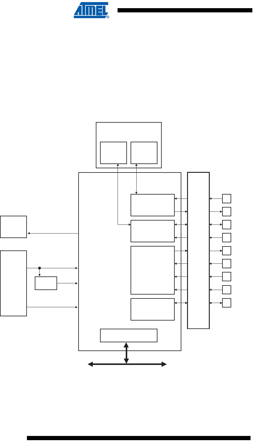
690
6430F–ATARM–21-Feb-12
SAM3U Series
690
6430F–ATARM–21-Feb-12
SAM3U Series
• Test Modes
– Remote Loopback, Local Loopback, Automatic Echo
• Supports Connection of:
– Two Peripheral DMA Controller Channels (PDC)
• Offers Buffer Transfer without Processor Intervention
35.3 Block Diagram
Figure 35-1. USART Block Diagram
(Peripheral) DMA
Controller
Channel Channel
Interrupt
Controller
Receiver
USART
Interrupt
RXD
TXD
SCK
USART PIO
Controller
CTS
RTS
DTR
DSR
DCD
RI
Transmitter
Modem
Signals
Control
Baud Rate
Generator
User Interface
PMC
MCK
SLCK
DIV MCK/DIV
APB
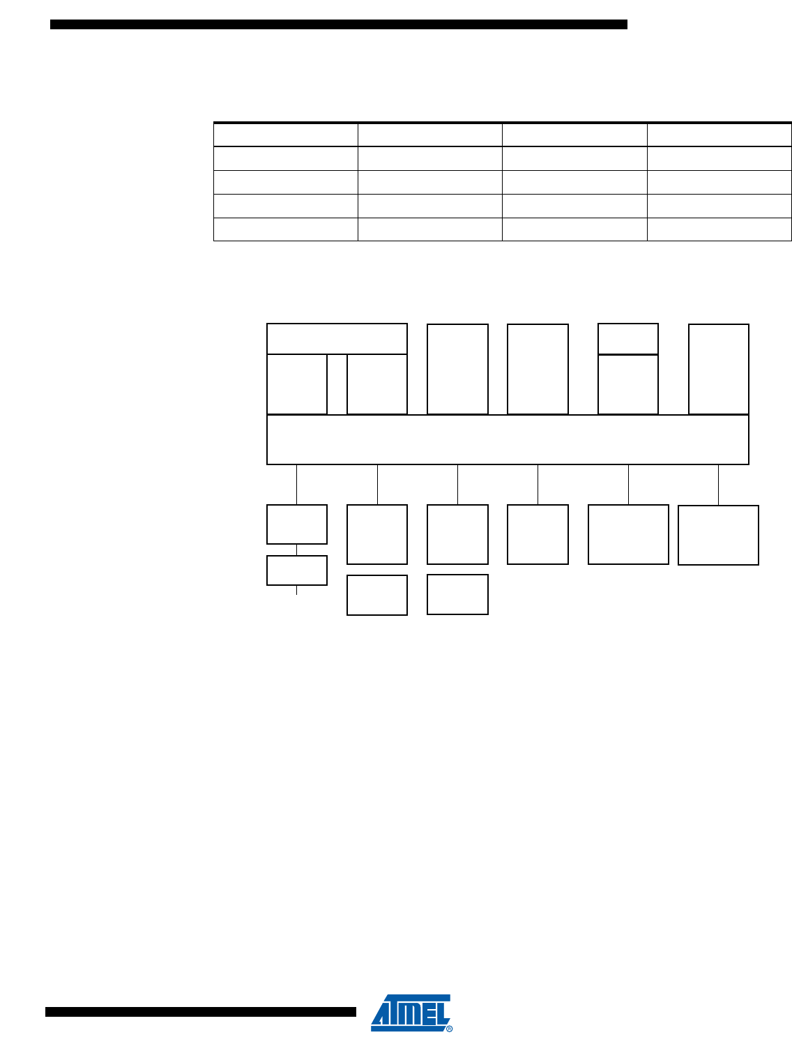
691
6430F–ATARM–21-Feb-12
SAM3U Series
691
6430F–ATARM–21-Feb-12
SAM3U Series
35.4 Application Block Diagram
Figure 35-2. Application Block Diagram
Table 35-1. SPI Operating Mode
PIN USART SPI Slave SPI Master
RXD RXD MOSI MISO
TXD TXD MISO MOSI
RTS RTS – CS
CTS CTS CS –
Smart
Card
Slot
USART
RS232
Drivers
Modem
RS485
Drivers
Differential
Bus
IrDA
Transceivers
Modem
Driver
Field Bus
Driver
EMV
Driver IrDA
Driver
IrLAP
RS232
Drivers
Serial
Port
Serial
Driver
PPP
PSTN
SPI
Driver
SPI
Transceiver

692
6430F–ATARM–21-Feb-12
SAM3U Series
692
6430F–ATARM–21-Feb-12
SAM3U Series
35.5 I/O Lines Description
Table 35-2. I/O Line Description
Name Description Type Active Level
SCK Serial Clock I/O
TXD
Transmit Serial Data
or Master Out Slave In (MOSI) in SPI Master Mode
or Master In Slave Out (MISO) in SPI Slave Mode
I/O
RXD
Receive Serial Data
or Master In Slave Out (MISO) in SPI Master Mode
or Master Out Slave In (MOSI) in SPI Slave Mode
Input
RI Ring Indicator Input Low
DSR Data Set Ready Input Low
DCD Data Carrier Detect Input Low
DTR Data Terminal Ready Output Low
CTS Clear to Send
or Slave Select (NSS) in SPI Slave Mode Input Low
RTS Request to Send
or Slave Select (NSS) in SPI Master Mode Output Low

693
6430F–ATARM–21-Feb-12
SAM3U Series
693
6430F–ATARM–21-Feb-12
SAM3U Series
35.6 Product Dependencies
35.6.1 I/O Lines
The pins used for interfacing the USART may be multiplexed with the PIO lines. The program-
mer must first program the PIO controller to assign the desired USART pins to their peripheral
function. If I/O lines of the USART are not used by the application, they can be used for other
purposes by the PIO Controller.
To prevent the TXD line from falling when the USART is disabled, the use of an internal pull up
is mandatory. If the hardware handshaking feature or Modem mode is used, the internal pull up
on TXD must also be enabled.
All the pins of the modems may or may not be implemented on the USART. On USARTs not
equipped with the corresponding pin, the associated control bits and statuses have no effect on
the behavior of the USART.
Table 35-3. I/O Lines
Instance Signal I/O Line Peripheral
USART0 CTS0 PB8 A
USART0 DCD0 PB11 B
USART0 DSR0 PB10 B
USART0 DTR0 PB9 B
USART0 RI0 PB12 B
USART0 RTS0 PB7 A
USART0 RXD0 PA19 A
USART0 SCK0 PA17 A
USART0 TXD0 PA18 A
USART1 CTS1 PA23 B
USART1 RTS1 PA22 B
USART1 RXD1 PA21 A
USART1 SCK1 PA24 B
USART1 TXD1 PA20 A
USART2 CTS2 PB22 B
USART2 RTS2 PB21 B
USART2 RXD2 PA23 A
USART2 SCK2 PA25 B
USART2 TXD2 PA22 A
USART3 CTS3 PC10 B
USART3 RTS3 PC11 B
USART3 RXD3 PC13 B
USART3 SCK3 PC19 A
USART3 TXD3 PC12 B

694
6430F–ATARM–21-Feb-12
SAM3U Series
694
6430F–ATARM–21-Feb-12
SAM3U Series
35.6.2 Power Management
The USART is not continuously clocked. The programmer must first enable the USART Clock in
the Power Management Controller (PMC) before using the USART. However, if the application
does not require USART operations, the USART clock can be stopped when not needed and be
restarted later. In this case, the USART will resume its operations where it left off.
Configuring the USART does not require the USART clock to be enabled.
35.6.3 Interrupt
The USART interrupt line is connected on one of the internal sources of the Interrupt Controller.
Using the USART interrupt requires the Interrupt Controller to be programmed first. Note that it is
not recommended to use the USART interrupt line in edge sensitive mode.

695
6430F–ATARM–21-Feb-12
SAM3U Series
695
6430F–ATARM–21-Feb-12
SAM3U Series
35.7 Functional Description
The USART is capable of managing several types of serial synchronous or asynchronous
communications.
It supports the following communication modes:
• 5- to 9-bit full-duplex asynchronous serial communication
– MSB- or LSB-first
– 1, 1.5 or 2 stop bits
– Parity even, odd, marked, space or none
– By 8 or by 16 over-sampling receiver frequency
– Optional hardware handshaking
– Optional modem signals management
– Optional break management
– Optional multidrop serial communication
• High-speed 5- to 9-bit full-duplex synchronous serial communication
– MSB- or LSB-first
– 1 or 2 stop bits
– Parity even, odd, marked, space or none
– By 8 or by 16 over-sampling frequency
– Optional hardware handshaking
– Optional modem signals management
– Optional break management
– Optional multidrop serial communication
• RS485 with driver control signal
• ISO7816, T0 or T1 protocols for interfacing with smart cards
– NACK handling, error counter with repetition and iteration limit, inverted data.
• InfraRed IrDA Modulation and Demodulation
• SPI Mode
–Master or Slave
– Serial Clock Programmable Phase and Polarity
– SPI Serial Clock (SCK) Frequency up to Internal Clock Frequency MCK/6
• Test modes
– Remote loopback, local loopback, automatic echo
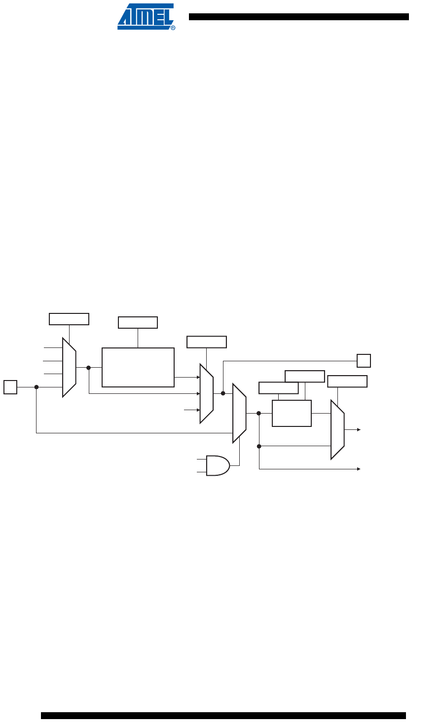
696
6430F–ATARM–21-Feb-12
SAM3U Series
696
6430F–ATARM–21-Feb-12
SAM3U Series
35.7.1 Baud Rate Generator
The Baud Rate Generator provides the bit period clock named the Baud Rate Clock to both the
receiver and the transmitter.
The Baud Rate Generator clock source can be selected by setting the USCLKS field in the Mode
Register (US_MR) between:
• the Master Clock MCK
• a division of the Master Clock, the divider being product dependent, but generally set to 8
• the external clock, available on the SCK pin
The Baud Rate Generator is based upon a 16-bit divider, which is programmed with the CD field
of the Baud Rate Generator Register (US_BRGR). If CD is programmed to 0, the Baud Rate
Generator does not generate any clock. If CD is programmed to 1, the divider is bypassed and
becomes inactive.
If the external SCK clock is selected, the duration of the low and high levels of the signal pro-
vided on the SCK pin must be longer than a Master Clock (MCK) period. The frequency of the
signal provided on SCK must be at least 3 times lower than MCK in USART mode, or 6 in SPI
mode.
Figure 35-3. Baud Rate Generator
35.7.1.1 Baud Rate in Asynchronous Mode
If the USART is programmed to operate in asynchronous mode, the selected clock is first
divided by CD, which is field programmed in the Baud Rate Generator Register (US_BRGR).
The resulting clock is provided to the receiver as a sampling clock and then divided by 16 or 8,
depending on the programming of the OVER bit in US_MR.
If OVER is set to 1, the receiver sampling is 8 times higher than the baud rate clock. If OVER is
cleared, the sampling is performed at 16 times the baud rate clock.
The following formula performs the calculation of the Baud Rate.
MCK/DIV
16-bit Counter
0
Baud Rate
Clock
CD
CD
Sampling
Divider
0
1
>1
Sampling
Clock
Reserved
MCK
SCK
USCLKS
OVER
SCK
SYNC
SYNC
USCLKS = 3
1
0
2
3
0
1
0
1
FIDI

697
6430F–ATARM–21-Feb-12
SAM3U Series
697
6430F–ATARM–21-Feb-12
SAM3U Series
This gives a maximum baud rate of MCK divided by 8, assuming that MCK is the highest possi-
ble clock and that OVER is programmed to 1.
Baud Rate Calculation Example
Table 35-4 shows calculations of CD to obtain a baud rate at 38400 bauds for different source
clock frequencies. This table also shows the actual resulting baud rate and the error.
The baud rate is calculated with the following formula:
The baud rate error is calculated with the following formula. It is not recommended to work with
an error higher than 5%.
Baudrate SelectedClock
82 Over–()CD()
--------------------------------------------=
Table 35-4. Baud Rate Example (OVER = 0)
Source Clock
Expected Baud
Rate Calculation Result CD Actual Baud Rate Error
MHz Bit/s Bit/s
3 686 400 38 400 6.00 6 38 400.00 0.00%
4 915 200 38 400 8.00 8 38 400.00 0.00%
5 000 000 38 400 8.14 8 39 062.50 1.70%
7 372 800 38 400 12.00 12 38 400.00 0.00%
8 000 000 38 400 13.02 13 38 461.54 0.16%
12 000 000 38 400 19.53 20 37 500.00 2.40%
12 288 000 38 400 20.00 20 38 400.00 0.00%
14 318 180 38 400 23.30 23 38 908.10 1.31%
14 745 600 38 400 24.00 24 38 400.00 0.00%
18 432 000 38 400 30.00 30 38 400.00 0.00%
24 000 000 38 400 39.06 39 38 461.54 0.16%
24 576 000 38 400 40.00 40 38 400.00 0.00%
25 000 000 38 400 40.69 40 38 109.76 0.76%
32 000 000 38 400 52.08 52 38 461.54 0.16%
32 768 000 38 400 53.33 53 38 641.51 0.63%
33 000 000 38 400 53.71 54 38 194.44 0.54%
40 000 000 38 400 65.10 65 38 461.54 0.16%
50 000 000 38 400 81.38 81 38 580.25 0.47%
BaudRate MCK CD 16×⁄=
Error 1ExpectedBaudRate
ActualBaudRate
---------------------------------------------------
⎝⎠
⎛⎞
–=
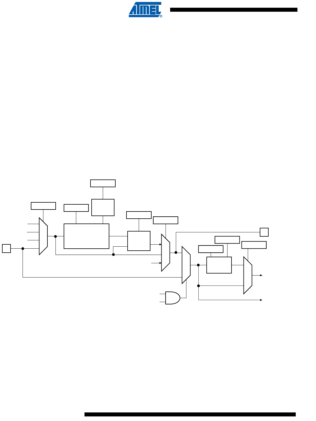
698
6430F–ATARM–21-Feb-12
SAM3U Series
698
6430F–ATARM–21-Feb-12
SAM3U Series
35.7.1.2 Fractional Baud Rate in Asynchronous Mode
The Baud Rate generator previously defined is subject to the following limitation: the output fre-
quency changes by only integer multiples of the reference frequency. An approach to this
problem is to integrate a fractional N clock generator that has a high resolution. The generator
architecture is modified to obtain Baud Rate changes by a fraction of the reference source clock.
This fractional part is programmed with the FP field in the Baud Rate Generator Register
(US_BRGR). If FP is not 0, the fractional part is activated. The resolution is one eighth of the
clock divider. This feature is only available when using USART normal mode. The fractional
Baud Rate is calculated using the following formula:
The modified architecture is presented below:
Figure 35-4. Fractional Baud Rate Generator
35.7.1.3 Baud Rate in Synchronous Mode or SPI Mode
If the USART is programmed to operate in synchronous mode, the selected clock is simply
divided by the field CD in US_BRGR.
In synchronous mode, if the external clock is selected (USCLKS = 3), the clock is provided
directly by the signal on the USART SCK pin. No division is active. The value written in
US_BRGR has no effect. The external clock frequency must be at least 3 times lower than the
Baudrate SelectedClock
82 Over–()CD FP
8
-------+
⎝⎠
⎛⎞
⎝⎠
⎛⎞
-----------------------------------------------------------------=
MCK/DIV
16-bit Counter
0
Baud Rate
Clock
CD
CD
Sampling
Divider
0
1
>1
Sampling
Clock
Reserved
MCK
SCK
USCLKS
OVER
SCK
SYNC
SYNC
USCLKS = 3
1
0
2
3
0
1
0
1
FIDI
glitch-free
logic
Modulus
Control
FP
FP
BaudRate SelectedClock
CD
--------------------------------------=

699
6430F–ATARM–21-Feb-12
SAM3U Series
699
6430F–ATARM–21-Feb-12
SAM3U Series
system clock. In synchronous mode master (USCLKS = 0 or 1, CLK0 set to 1), the receive part
limits the SCK maximum frequency to MCK/3 in USART mode, or MCK/6 in SPI mode.
When either the external clock SCK or the internal clock divided (MCK/DIV) is selected, the
value programmed in CD must be even if the user has to ensure a 50:50 mark/space ratio on the
SCK pin. If the internal clock MCK is selected, the Baud Rate Generator ensures a 50:50 duty
cycle on the SCK pin, even if the value programmed in CD is odd.
35.7.1.4 Baud Rate in ISO 7816 Mode
The ISO7816 specification defines the bit rate with the following formula:
where:
• B is the bit rate
• Di is the bit-rate adjustment factor
• Fi is the clock frequency division factor
• f is the ISO7816 clock frequency (Hz)
Di is a binary value encoded on a 4-bit field, named DI, as represented in Table 35-5.
Fi is a binary value encoded on a 4-bit field, named FI, as represented in Table 35-6.
Table 35-7 shows the resulting Fi/Di Ratio, which is the ratio between the ISO7816 clock and the
baud rate clock.
If the USART is configured in ISO7816 Mode, the clock selected by the USCLKS field in the
Mode Register (US_MR) is first divided by the value programmed in the field CD in the Baud
BDi
Fi
------f×=
Table 35-5. Binary and Decimal Values for Di
DI field 0001 0010 0011 0100 0101 0110 1000 1001
Di (decimal)1 2 4 8 163212 20
Table 35-6. Binary and Decimal Values for Fi
FI field 0000 0001 0010 0011 0100 0101 0110 1001 1010 1011 1100 1101
Fi (decimal) 372 372 558 744 1116 1488 1860 512 768 1024 1536 2048
Table 35-7. Possible Values for the Fi/Di Ratio
Fi/Di 372 558 774 1116 1488 1806 512 768 1024 1536 2048
1 372 558 744 1116 1488 1860 512 768 1024 1536 2048
2 186 279 372 558 744 930 256 384 512 768 1024
4 93 139.5 186 279 372 465 128 192 256 384 512
8 46.5 69.75 93 139.5 186 232.5 64 96 128 192 256
16 23.25 34.87 46.5 69.75 93 116.2 32 48 64 96 128
32 11.62 17.43 23.25 34.87 46.5 58.13 16 24 32 48 64
12 31 46.5 62 93 124 155 42.66 64 85.33 128 170.6
20 18.6 27.9 37.2 55.8 74.4 93 25.6 38.4 51.2 76.8 102.4
700
6430F–ATARM–21-Feb-12
SAM3U Series
700
6430F–ATARM–21-Feb-12
SAM3U Series
Rate Generator Register (US_BRGR). The resulting clock can be provided to the SCK pin to
feed the smart card clock inputs. This means that the CLKO bit can be set in US_MR.
This clock is then divided by the value programmed in the FI_DI_RATIO field in the FI_DI_Ratio
register (US_FIDI). This is performed by the Sampling Divider, which performs a division by up
to 2047 in ISO7816 Mode. The non-integer values of the Fi/Di Ratio are not supported and the
user must program the FI_DI_RATIO field to a value as close as possible to the expected value.
The FI_DI_RATIO field resets to the value 0x174 (372 in decimal) and is the most common
divider between the ISO7816 clock and the bit rate (Fi = 372, Di = 1).
Figure 35-5 shows the relation between the Elementary Time Unit, corresponding to a bit time,
and the ISO 7816 clock.
Figure 35-5. Elementary Time Unit (ETU)
35.7.2 Receiver and Transmitter Control
After reset, the receiver is disabled. The user must enable the receiver by setting the RXEN bit
in the Control Register (US_CR). However, the receiver registers can be programmed before the
receiver clock is enabled.
After reset, the transmitter is disabled. The user must enable it by setting the TXEN bit in the
Control Register (US_CR). However, the transmitter registers can be programmed before being
enabled.
The Receiver and the Transmitter can be enabled together or independently.
At any time, the software can perform a reset on the receiver or the transmitter of the USART by
setting the corresponding bit, RSTRX and RSTTX respectively, in the Control Register
(US_CR). The software resets clear the status flag and reset internal state machines but the
user interface configuration registers hold the value configured prior to software reset. Regard-
less of what the receiver or the transmitter is performing, the communication is immediately
stopped.
The user can also independently disable the receiver or the transmitter by setting RXDIS and
TXDIS respectively in US_CR. If the receiver is disabled during a character reception, the
USART waits until the end of reception of the current character, then the reception is stopped. If
the transmitter is disabled while it is operating, the USART waits the end of transmission of both
the current character and character being stored in the Transmit Holding Register (US_THR). If
a timeguard is programmed, it is handled normally.
1 ETU
ISO7816 Clock
on SCK
ISO7816 I/O Line
on TXD
FI_DI_RATIO
ISO7816 Clock Cycles
701
6430F–ATARM–21-Feb-12
SAM3U Series
701
6430F–ATARM–21-Feb-12
SAM3U Series
35.7.3 Synchronous and Asynchronous Modes
35.7.3.1 Transmitter Operations
The transmitter performs the same in both synchronous and asynchronous operating modes
(SYNC = 0 or SYNC = 1). One start bit, up to 9 data bits, one optional parity bit and up to two
stop bits are successively shifted out on the TXD pin at each falling edge of the programmed
serial clock.
The number of data bits is selected by the CHRL field and the MODE 9 bit in the Mode Register
(US_MR). Nine bits are selected by setting the MODE 9 bit regardless of the CHRL field. The
parity bit is set according to the PAR field in US_MR. The even, odd, space, marked or none
parity bit can be configured. The MSBF field in US_MR configures which data bit is sent first. If
written to 1, the most significant bit is sent first. If written to 0, the less significant bit is sent first.
The number of stop bits is selected by the NBSTOP field in US_MR. The 1.5 stop bit is sup-
ported in asynchronous mode only.
Figure 35-6. Character Transmit
The characters are sent by writing in the Transmit Holding Register (US_THR). The transmitter
reports two status bits in the Channel Status Register (US_CSR): TXRDY (Transmitter Ready),
which indicates that US_THR is empty and TXEMPTY, which indicates that all the characters
written in US_THR have been processed. When the current character processing is completed,
the last character written in US_THR is transferred into the Shift Register of the transmitter and
US_THR becomes empty, thus TXRDY rises.
Both TXRDY and TXEMPTY bits are low when the transmitter is disabled. Writing a character in
US_THR while TXRDY is low has no effect and the written character is lost.
Figure 35-7. Transmitter Status
D0 D1 D2 D3 D4 D5 D6 D7
TXD
Start
Bit
Parity
Bit
Stop
Bit
Example: 8-bit, Parity Enabled One Stop
Baud Rate
Clock
D0 D1 D2 D3 D4 D5 D6 D7
TXD
Start
Bit
Parity
Bit
Stop
Bit
Baud Rate
Clock
Start
Bit
Write
US_THR
D0 D1 D2 D3 D4 D5 D6 D7 Parity
Bit
Stop
Bit
TXRDY
TXEMPTY

702
6430F–ATARM–21-Feb-12
SAM3U Series
702
6430F–ATARM–21-Feb-12
SAM3U Series
35.7.3.2 Manchester Encoder
When the Manchester encoder is in use, characters transmitted through the USART are
encoded based on biphase Manchester II format. To enable this mode, set the MAN field in the
US_MR register to 1. Depending on polarity configuration, a logic level (zero or one), is transmit-
ted as a coded signal one-to-zero or zero-to-one. Thus, a transition always occurs at the
midpoint of each bit time. It consumes more bandwidth than the original NRZ signal (2x) but the
receiver has more error control since the expected input must show a change at the center of a
bit cell. An example of Manchester encoded sequence is: the byte 0xB1 or 10110001 encodes
to 10 01 10 10 01 01 01 10, assuming the default polarity of the encoder. Figure 35-8 illustrates
this coding scheme.
Figure 35-8. NRZ to Manchester Encoding
The Manchester encoded character can also be encapsulated by adding both a configurable
preamble and a start frame delimiter pattern. Depending on the configuration, the preamble is a
training sequence, composed of a pre-defined pattern with a programmable length from 1 to 15
bit times. If the preamble length is set to 0, the preamble waveform is not generated prior to any
character. The preamble pattern is chosen among the following sequences: ALL_ONE,
ALL_ZERO, ONE_ZERO or ZERO_ONE, writing the field TX_PP in the US_MAN register, the
field TX_PL is used to configure the preamble length. Figure 35-9 illustrates and defines the
valid patterns. To improve flexibility, the encoding scheme can be configured using the
TX_MPOL field in the US_MAN register. If the TX_MPOL field is set to zero (default), a logic
zero is encoded with a zero-to-one transition and a logic one is encoded with a one-to-zero tran-
sition. If the TX_MPOL field is set to one, a logic one is encoded with a one-to-zero transition
and a logic zero is encoded with a zero-to-one transition.
NRZ
encoded
data
Manchester
encoded
data
10110001
Txd

703
6430F–ATARM–21-Feb-12
SAM3U Series
703
6430F–ATARM–21-Feb-12
SAM3U Series
Figure 35-9. Preamble Patterns, Default Polarity Assumed
A start frame delimiter is to be configured using the ONEBIT field in the US_MR register. It con-
sists of a user-defined pattern that indicates the beginning of a valid data. Figure 35-10
illustrates these patterns. If the start frame delimiter, also known as start bit, is one bit, (ONEBIT
to 1), a logic zero is Manchester encoded and indicates that a new character is being sent seri-
ally on the line. If the start frame delimiter is a synchronization pattern also referred to as sync
(ONEBIT to 0), a sequence of 3 bit times is sent serially on the line to indicate the start of a new
character. The sync waveform is in itself an invalid Manchester waveform as the transition
occurs at the middle of the second bit time. Two distinct sync patterns are used: the command
sync and the data sync. The command sync has a logic one level for one and a half bit times,
then a transition to logic zero for the second one and a half bit times. If the MODSYNC field in
the US_MR register is set to 1, the next character is a command. If it is set to 0, the next charac-
ter is a data. When direct memory access is used, the MODSYNC field can be immediately
updated with a modified character located in memory. To enable this mode, VAR_SYNC field in
US_MR register must be set to 1. In this case, the MODSYNC field in US_MR is bypassed and
the sync configuration is held in the TXSYNH in the US_THR register. The USART character for-
mat is modified and includes sync information.
Manchester
encoded
data Txd SFD DATA
8 bit width "ALL_ONE" Preamble
Manchester
encoded
data Txd SFD DATA
8 bit width "ALL_ZERO" Preamble
Manchester
encoded
data Txd SFD DATA
8 bit width "ZERO_ONE" Preamble
Manchester
encoded
data Txd SFD DATA
8 bit width "ONE_ZERO" Preamble
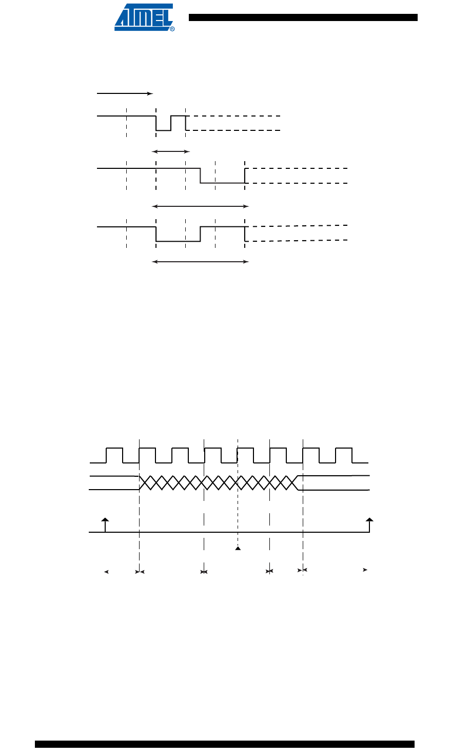
704
6430F–ATARM–21-Feb-12
SAM3U Series
704
6430F–ATARM–21-Feb-12
SAM3U Series
Figure 35-10. Start Frame Delimiter
Drift Compensation
Drift compensation is available only in 16X oversampling mode. An hardware recovery system
allows a larger clock drift. To enable the hardware system, the bit in the USART_MAN register
must be set. If the RXD edge is one 16X clock cycle from the expected edge, this is considered
as normal jitter and no corrective actions is taken. If the RXD event is between 4 and 2 clock
cycles before the expected edge, then the current period is shortened by one clock cycle. If the
RXD event is between 2 and 3 clock cycles after the expected edge, then the current period is
lengthened by one clock cycle. These intervals are considered to be drift and so corrective
actions are automatically taken.
Figure 35-11. Bit Resynchronization
35.7.3.3 Asynchronous Receiver
If the USART is programmed in asynchronous operating mode (SYNC = 0), the receiver over-
samples the RXD input line. The oversampling is either 16 or 8 times the Baud Rate clock,
depending on the OVER bit in the Mode Register (US_MR).
Manchester
encoded
data Txd
SFD
DATA
One bit start frame delimiter
Preamble Length
is set to 0
Manchester
encoded
data Txd
SFD
DATA
Command Sync
start frame delimiter
Manchester
encoded
data Txd
SFD
DATA
Data Sync
start frame delimiter
RXD
Oversampling
16x Clock
Sampling
point
Expected edge
Tolerance
Synchro.
Jump
Sync
Jump
Synchro.
Error
Synchro.
Error
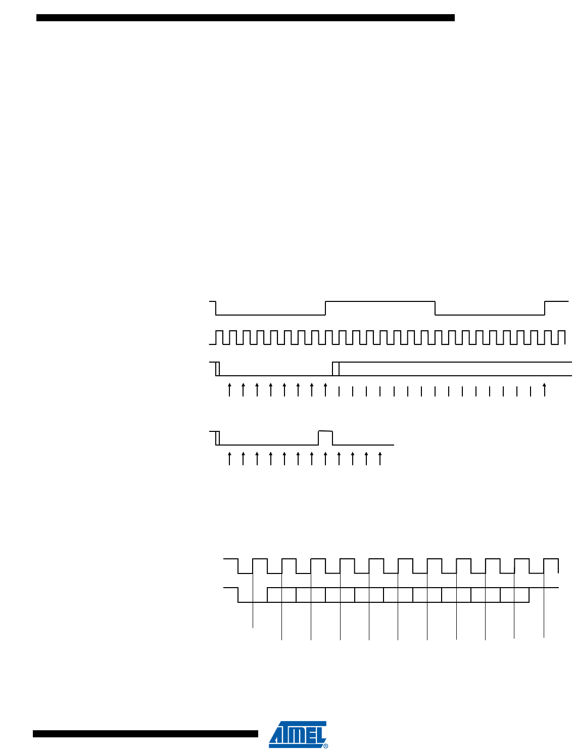
705
6430F–ATARM–21-Feb-12
SAM3U Series
705
6430F–ATARM–21-Feb-12
SAM3U Series
The receiver samples the RXD line. If the line is sampled during one half of a bit time to 0, a start
bit is detected and data, parity and stop bits are successively sampled on the bit rate clock.
If the oversampling is 16, (OVER to 0), a start is detected at the eighth sample to 0. Then, data
bits, parity bit and stop bit are sampled on each 16 sampling clock cycle. If the oversampling is 8
(OVER to 1), a start bit is detected at the fourth sample to 0. Then, data bits, parity bit and stop
bit are sampled on each 8 sampling clock cycle.
The number of data bits, first bit sent and parity mode are selected by the same fields and bits
as the transmitter, i.e. respectively CHRL, MODE9, MSBF and PAR. For the synchronization
mechanism only, the number of stop bits has no effect on the receiver as it considers only one
stop bit, regardless of the field NBSTOP, so that resynchronization between the receiver and the
transmitter can occur. Moreover, as soon as the stop bit is sampled, the receiver starts looking
for a new start bit so that resynchronization can also be accomplished when the transmitter is
operating with one stop bit.
Figure 35-12 and Figure 35-13 illustrate start detection and character reception when USART
operates in asynchronous mode.
Figure 35-12. Asynchronous Start Detection
Figure 35-13. Asynchronous Character Reception
Sampling
Clock (x16)
RXD
Start
Detection
Sampling
Baud Rate
Clock
RXD
Start
Rejection
Sampling
12345678
123456701234
123456789 10111213141516D0
Sampling
D0 D1 D2 D3 D4 D5 D6 D7
RXD
Parity
Bit
Stop
Bit
Example: 8-bit, Parity Enabled
Baud Rate
Clock
Start
Detection
16
samples
16
samples
16
samples
16
samples
16
samples
16
samples
16
samples
16
samples
16
samples
16
samples
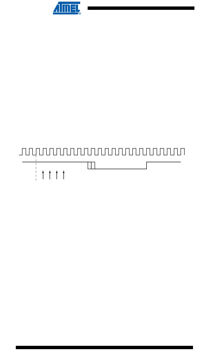
706
6430F–ATARM–21-Feb-12
SAM3U Series
706
6430F–ATARM–21-Feb-12
SAM3U Series
35.7.3.4 Manchester Decoder
When the MAN field in US_MR register is set to 1, the Manchester decoder is enabled. The
decoder performs both preamble and start frame delimiter detection. One input line is dedicated
to Manchester encoded input data.
An optional preamble sequence can be defined, its length is user-defined and totally indepen-
dent of the emitter side. Use RX_PL in US_MAN register to configure the length of the preamble
sequence. If the length is set to 0, no preamble is detected and the function is disabled. In addi-
tion, the polarity of the input stream is programmable with RX_MPOL field in US_MAN register.
Depending on the desired application the preamble pattern matching is to be defined via the
RX_PP field in US_MAN. See Figure 35-9 for available preamble patterns.
Unlike preamble, the start frame delimiter is shared between Manchester Encoder and Decoder.
So, if ONEBIT field is set to 1, only a zero encoded Manchester can be detected as a valid start
frame delimiter. If ONEBIT is set to 0, only a sync pattern is detected as a valid start frame
delimiter. Decoder operates by detecting transition on incoming stream. If RXD is sampled dur-
ing one quarter of a bit time to zero, a start bit is detected. See Figure 35-14. The sample pulse
rejection mechanism applies.
Figure 35-14. Asynchronous Start Bit Detection
The receiver is activated and starts Preamble and Frame Delimiter detection, sampling the data
at one quarter and then three quarters. If a valid preamble pattern or start frame delimiter is
detected, the receiver continues decoding with the same synchronization. If the stream does not
match a valid pattern or a valid start frame delimiter, the receiver re-synchronizes on the next
valid edge.The minimum time threshold to estimate the bit value is three quarters of a bit time.
If a valid preamble (if used) followed with a valid start frame delimiter is detected, the incoming
stream is decoded into NRZ data and passed to USART for processing. Figure 35-15 illustrates
Manchester pattern mismatch. When incoming data stream is passed to the USART, the
receiver is also able to detect Manchester code violation. A code violation is a lack of transition
in the middle of a bit cell. In this case, MANE flag in US_CSR register is raised. It is cleared by
writing the Control Register (US_CR) with the RSTSTA bit to 1. See Figure 35-16 for an exam-
ple of Manchester error detection during data phase.
Manchester
encoded
data Txd
1234
Sampling
Clock
(16 x)
Start
Detection
707
6430F–ATARM–21-Feb-12
SAM3U Series
707
6430F–ATARM–21-Feb-12
SAM3U Series
Figure 35-15. Preamble Pattern Mismatch
Figure 35-16. Manchester Error Flag
When the start frame delimiter is a sync pattern (ONEBIT field to 0), both command and data
delimiter are supported. If a valid sync is detected, the received character is written as RXCHR
field in the US_RHR register and the RXSYNH is updated. RXCHR is set to 1 when the received
character is a command, and it is set to 0 if the received character is a data. This mechanism
alleviates and simplifies the direct memory access as the character contains its own sync field in
the same register.
As the decoder is setup to be used in unipolar mode, the first bit of the frame has to be a zero-to-
one transition.
35.7.3.5 Radio Interface: Manchester Encoded USART Application
This section describes low data rate RF transmission systems and their integration with a Man-
chester encoded USART. These systems are based on transmitter and receiver ICs that support
ASK and FSK modulation schemes.
The goal is to perform full duplex radio transmission of characters using two different frequency
carriers. See the configuration in Figure 35-17.
Manchester
encoded
data Txd SFD DATA
Preamble Length is set to 8
Preamble Mismatch
invalid pattern
Preamble Mismatch
Manchester coding error
Manchester
encoded
data Txd
SFD
Preamble Length
is set to 4
Elementary character bit time
Manchester
Coding Error
detected
sampling points
Preamble subpacket
and Start Frame Delimiter
were successfully
decoded
Entering USART character area
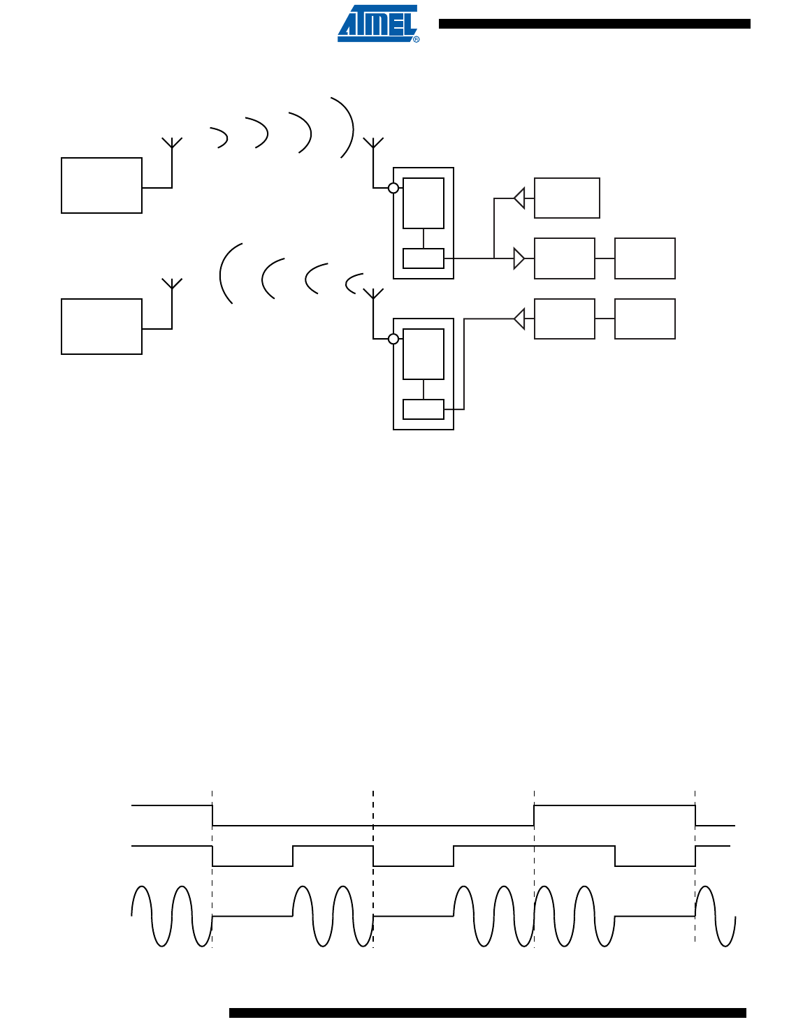
708
6430F–ATARM–21-Feb-12
SAM3U Series
708
6430F–ATARM–21-Feb-12
SAM3U Series
Figure 35-17. Manchester Encoded Characters RF Transmission
The USART module is configured as a Manchester encoder/decoder. Looking at the down-
stream communication channel, Manchester encoded characters are serially sent to the RF
emitter. This may also include a user defined preamble and a start frame delimiter. Mostly, pre-
amble is used in the RF receiver to distinguish between a valid data from a transmitter and
signals due to noise. The Manchester stream is then modulated. See Figure 35-18 for an exam-
ple of ASK modulation scheme. When a logic one is sent to the ASK modulator, the power
amplifier, referred to as PA, is enabled and transmits an RF signal at downstream frequency.
When a logic zero is transmitted, the RF signal is turned off. If the FSK modulator is activated,
two different frequencies are used to transmit data. When a logic 1 is sent, the modulator out-
puts an RF signal at frequency F0 and switches to F1 if the data sent is a 0. See Figure 35-19.
From the receiver side, another carrier frequency is used. The RF receiver performs a bit check
operation examining demodulated data stream. If a valid pattern is detected, the receiver
switches to receiving mode. The demodulated stream is sent to the Manchester decoder.
Because of bit checking inside RF IC, the data transferred to the microcontroller is reduced by a
user-defined number of bits. The Manchester preamble length is to be defined in accordance
with the RF IC configuration.
Figure 35-18. ASK Modulator Output
LNA
VCO
RF filter
Demod
control
bi-dir
line
PA
RF filter
Mod
VCO
control
Manchester
decoder
Manchester
encoder
USART
Receiver
USART
Emitter
ASK/FSK
Upstream Receiver
ASK/FSK
downstream transmitter
Upstream
Emitter
Downstream
Receiver
Serial
Configuration
Interface
Fup frequency Carrier
Fdown frequency Carrier
Manchester
encoded
data
default polarity
unipolar output
Txd
ASK Modulator
Output
Uptstream Frequency F0
NRZ stream
10 0 1
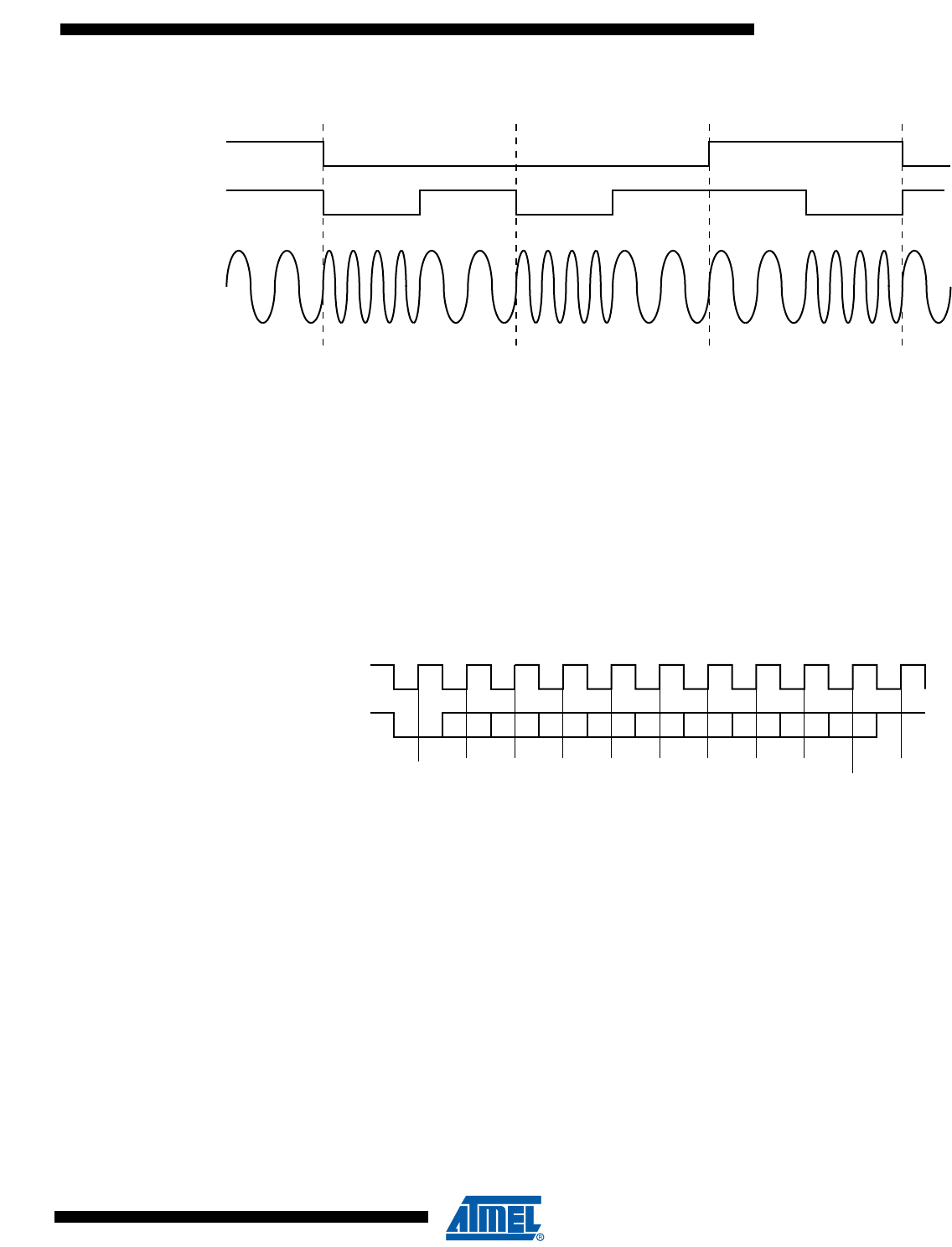
709
6430F–ATARM–21-Feb-12
SAM3U Series
709
6430F–ATARM–21-Feb-12
SAM3U Series
Figure 35-19. FSK Modulator Output
35.7.3.6 Synchronous Receiver
In synchronous mode (SYNC = 1), the receiver samples the RXD signal on each rising edge of
the Baud Rate Clock. If a low level is detected, it is considered as a start. All data bits, the parity
bit and the stop bits are sampled and the receiver waits for the next start bit. Synchronous mode
operations provide a high speed transfer capability.
Configuration fields and bits are the same as in asynchronous mode.
Figure 35-20 illustrates a character reception in synchronous mode.
Figure 35-20. Synchronous Mode Character Reception
35.7.3.7 Receiver Operations
When a character reception is completed, it is transferred to the Receive Holding Register
(US_RHR) and the RXRDY bit in the Status Register (US_CSR) rises. If a character is com-
pleted while the RXRDY is set, the OVRE (Overrun Error) bit is set. The last character is
transferred into US_RHR and overwrites the previous one. The OVRE bit is cleared by writing
the Control Register (US_CR) with the RSTSTA (Reset Status) bit to 1.
Manchester
encoded
data
default polarity
unipolar output
Txd
FSK Modulator
Output
Uptstream Frequencies
[F0, F0+offset]
NRZ stream
10 0 1
D0 D1 D2 D3 D4 D5 D6 D7
RXD
Start
Sampling
Parity Bit
Stop Bit
Example: 8-bit, Parity Enabled 1 Stop
Baud Rate
Clock
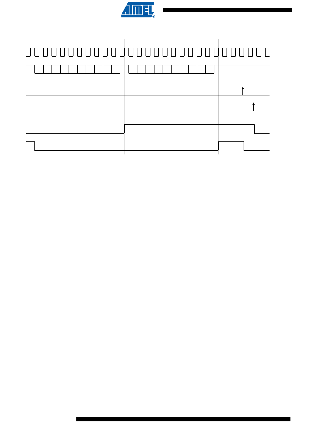
710
6430F–ATARM–21-Feb-12
SAM3U Series
710
6430F–ATARM–21-Feb-12
SAM3U Series
Figure 35-21. Receiver Status
D0 D1 D2 D3 D4 D5 D6 D7
RXD
Start
Bit
Parity
Bit
Stop
Bit
Baud Rate
Clock
Write
US_CR
RXRDY
OVRE
D0 D1 D2 D3 D4 D5 D6 D7
Start
Bit
Parity
Bit
Stop
Bit
RSTSTA = 1
Read
US_RHR

711
6430F–ATARM–21-Feb-12
SAM3U Series
711
6430F–ATARM–21-Feb-12
SAM3U Series
35.7.3.8 Parity
The USART supports five parity modes selected by programming the PAR field in the Mode
Register (US_MR). The PAR field also enables the Multidrop mode, see “Multidrop Mode” on
page 712. Even and odd parity bit generation and error detection are supported.
If even parity is selected, the parity generator of the transmitter drives the parity bit to 0 if a num-
ber of 1s in the character data bit is even, and to 1 if the number of 1s is odd. Accordingly, the
receiver parity checker counts the number of received 1s and reports a parity error if the sam-
pled parity bit does not correspond. If odd parity is selected, the parity generator of the
transmitter drives the parity bit to 1 if a number of 1s in the character data bit is even, and to 0 if
the number of 1s is odd. Accordingly, the receiver parity checker counts the number of received
1s and reports a parity error if the sampled parity bit does not correspond. If the mark parity is
used, the parity generator of the transmitter drives the parity bit to 1 for all characters. The
receiver parity checker reports an error if the parity bit is sampled to 0. If the space parity is
used, the parity generator of the transmitter drives the parity bit to 0 for all characters. The
receiver parity checker reports an error if the parity bit is sampled to 1. If parity is disabled, the
transmitter does not generate any parity bit and the receiver does not report any parity error.
Table 35-8 shows an example of the parity bit for the character 0x41 (character ASCII “A”)
depending on the configuration of the USART. Because there are two bits to 1, 1 bit is added
when a parity is odd, or 0 is added when a parity is even.
When the receiver detects a parity error, it sets the PARE (Parity Error) bit in the Channel Status
Register (US_CSR). The PARE bit can be cleared by writing the Control Register (US_CR) with
the RSTSTA bit to 1. Figure 35-22 illustrates the parity bit status setting and clearing.
Table 35-8. Parity Bit Examples
Character Hexa Binary Parity Bit Parity Mode
A 0x41 0100 0001 1 Odd
A 0x41 0100 0001 0 Even
A 0x41 0100 0001 1 Mark
A 0x41 0100 0001 0 Space
A 0x41 0100 0001 None None

712
6430F–ATARM–21-Feb-12
SAM3U Series
712
6430F–ATARM–21-Feb-12
SAM3U Series
Figure 35-22. Parity Error
35.7.3.9 Multidrop Mode
If the PAR field in the Mode Register (US_MR) is programmed to the value 0x6 or 0x07, the
USART runs in Multidrop Mode. This mode differentiates the data characters and the address
characters. Data is transmitted with the parity bit to 0 and addresses are transmitted with the
parity bit to 1.
If the USART is configured in multidrop mode, the receiver sets the PARE parity error bit when
the parity bit is high and the transmitter is able to send a character with the parity bit high when
the Control Register is written with the SENDA bit to 1.
To handle parity error, the PARE bit is cleared when the Control Register is written with the bit
RSTSTA to 1.
The transmitter sends an address byte (parity bit set) when SENDA is written to US_CR. In this
case, the next byte written to US_THR is transmitted as an address. Any character written in
US_THR without having written the command SENDA is transmitted normally with the parity to
0.
35.7.3.10 Transmitter Timeguard
The timeguard feature enables the USART interface with slow remote devices.
The timeguard function enables the transmitter to insert an idle state on the TXD line between
two characters. This idle state actually acts as a long stop bit.
The duration of the idle state is programmed in the TG field of the Transmitter Timeguard Regis-
ter (US_TTGR). When this field is programmed to zero no timeguard is generated. Otherwise,
the transmitter holds a high level on TXD after each transmitted byte during the number of bit
periods programmed in TG in addition to the number of stop bits.
As illustrated in Figure 35-23, the behavior of TXRDY and TXEMPTY status bits is modified by
the programming of a timeguard. TXRDY rises only when the start bit of the next character is
sent, and thus remains to 0 during the timeguard transmission if a character has been written in
US_THR. TXEMPTY remains low until the timeguard transmission is completed as the time-
guard is part of the current character being transmitted.
D0 D1 D2 D3 D4 D5 D6 D7
RXD
Start
Bit
Bad
Parity
Bit
Stop
Bit
Baud Rate
Clock
Write
US_CR
PARE
RXRDY
RSTSTA = 1
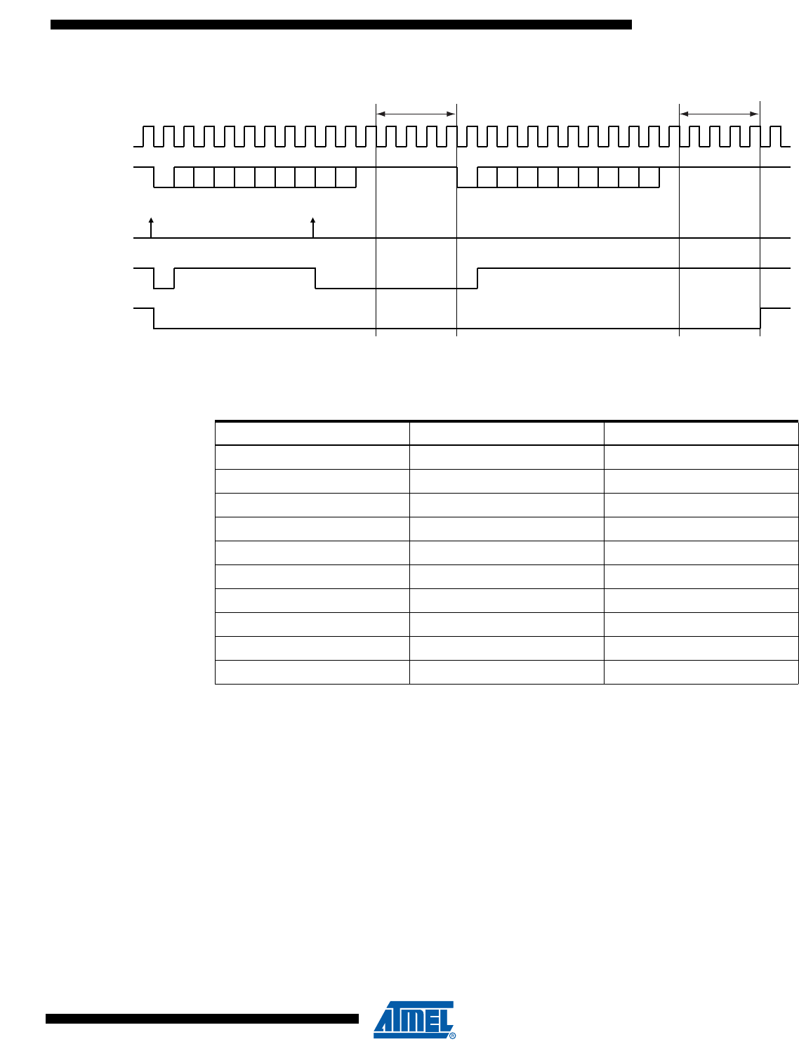
713
6430F–ATARM–21-Feb-12
SAM3U Series
713
6430F–ATARM–21-Feb-12
SAM3U Series
Figure 35-23. Timeguard Operations
Table 35-9 indicates the maximum length of a timeguard period that the transmitter can handle
in relation to the function of the Baud Rate.
35.7.3.11 Receiver Time-out
The Receiver Time-out provides support in handling variable-length frames. This feature detects
an idle condition on the RXD line. When a time-out is detected, the bit TIMEOUT in the Channel
Status Register (US_CSR) rises and can generate an interrupt, thus indicating to the driver an
end of frame.
The time-out delay period (during which the receiver waits for a new character) is programmed
in the TO field of the Receiver Time-out Register (US_RTOR). If the TO field is programmed to
0, the Receiver Time-out is disabled and no time-out is detected. The TIMEOUT bit in US_CSR
remains to 0. Otherwise, the receiver loads a 16-bit counter with the value programmed in TO.
This counter is decremented at each bit period and reloaded each time a new character is
received. If the counter reaches 0, the TIMEOUT bit in the Status Register rises. Then, the user
can either:
• Stop the counter clock until a new character is received. This is performed by writing the
Control Register (US_CR) with the STTTO (Start Time-out) bit to 1. In this case, the idle state
D0 D1 D2 D3 D4 D5 D6 D7
TXD
Start
Bit
Parity
Bit
Stop
Bit
Baud Rate
Clock
Start
Bit
TG = 4
Write
US_THR
D0 D1 D2 D3 D4 D5 D6 D7 Parity
Bit
Stop
Bit
TXRDY
TXEMPTY
TG = 4
Table 35-9. Maximum Timeguard Length Depending on Baud Rate
Baud Rate Bit time Timeguard
Bit/sec µs ms
1 200 833 212.50
9 600 104 26.56
14400 69.4 17.71
19200 52.1 13.28
28800 34.7 8.85
33400 29.9 7.63
56000 17.9 4.55
57600 17.4 4.43
115200 8.7 2.21
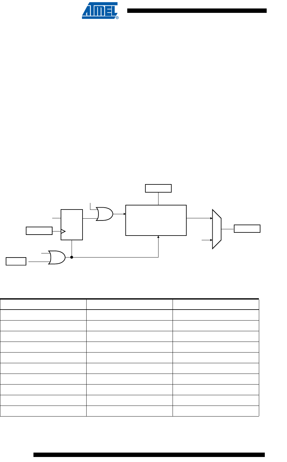
714
6430F–ATARM–21-Feb-12
SAM3U Series
714
6430F–ATARM–21-Feb-12
SAM3U Series
on RXD before a new character is received will not provide a time-out. This prevents having
to handle an interrupt before a character is received and allows waiting for the next idle state
on RXD after a frame is received.
• Obtain an interrupt while no character is received. This is performed by writing US_CR with
the RETTO (Reload and Start Time-out) bit to 1. If RETTO is performed, the counter starts
counting down immediately from the value TO. This enables generation of a periodic interrupt
so that a user time-out can be handled, for example when no key is pressed on a keyboard.
If STTTO is performed, the counter clock is stopped until a first character is received. The idle
state on RXD before the start of the frame does not provide a time-out. This prevents having to
obtain a periodic interrupt and enables a wait of the end of frame when the idle state on RXD is
detected.
If RETTO is performed, the counter starts counting down immediately from the value TO. This
enables generation of a periodic interrupt so that a user time-out can be handled, for example
when no key is pressed on a keyboard.
Figure 35-24 shows the block diagram of the Receiver Time-out feature.
Figure 35-24. Receiver Time-out Block Diagram
Table 35-10 gives the maximum time-out period for some standard baud rates.
Table 35-10. Maximum Time-out Period
Baud Rate Bit Time Time-out
bit/sec µs ms
600 1 667 109 225
1 200 833 54 613
2 400 417 27 306
4 800 208 13 653
9 600 104 6 827
14400 69 4 551
19200 52 3 413
28800 35 2 276
33400 30 1 962
16-bit Time-out
Counter
0
TO
TIMEOUT
Baud Rate
Clock
=
Character
Received
RETTO
Load
Clock
16-bit
Value
STTTO
DQ
1
Clear
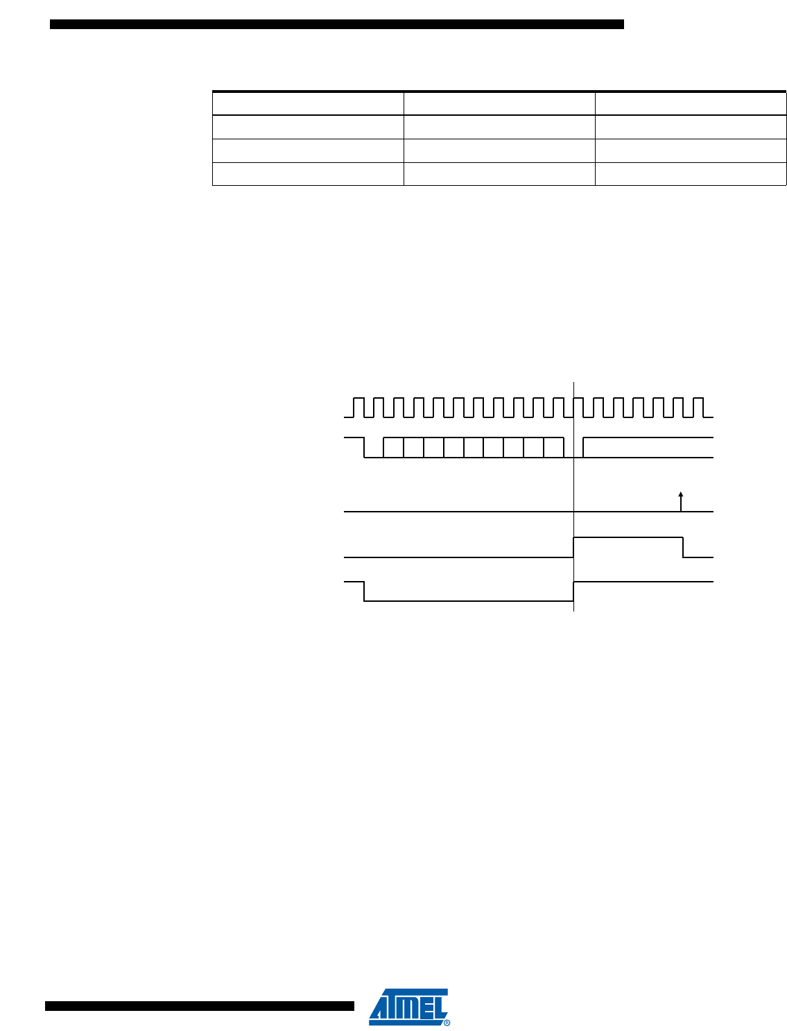
715
6430F–ATARM–21-Feb-12
SAM3U Series
715
6430F–ATARM–21-Feb-12
SAM3U Series
35.7.3.12 Framing Error
The receiver is capable of detecting framing errors. A framing error happens when the stop bit of
a received character is detected at level 0. This can occur if the receiver and the transmitter are
fully desynchronized.
A framing error is reported on the FRAME bit of the Channel Status Register (US_CSR). The
FRAME bit is asserted in the middle of the stop bit as soon as the framing error is detected. It is
cleared by writing the Control Register (US_CR) with the RSTSTA bit to 1.
Figure 35-25. Framing Error Status
35.7.3.13 Transmit Break
The user can request the transmitter to generate a break condition on the TXD line. A break con-
dition drives the TXD line low during at least one complete character. It appears the same as a
0x00 character sent with the parity and the stop bits to 0. However, the transmitter holds the
TXD line at least during one character until the user requests the break condition to be removed.
A break is transmitted by writing the Control Register (US_CR) with the STTBRK bit to 1. This
can be performed at any time, either while the transmitter is empty (no character in either the
Shift Register or in US_THR) or when a character is being transmitted. If a break is requested
while a character is being shifted out, the character is first completed before the TXD line is held
low.
Once STTBRK command is requested further STTBRK commands are ignored until the end of
the break is completed.
The break condition is removed by writing US_CR with the STPBRK bit to 1. If the STPBRK is
requested before the end of the minimum break duration (one character, including start, data,
parity and stop bits), the transmitter ensures that the break condition completes.
56000 18 1 170
57600 17 1 138
200000 5 328
Table 35-10. Maximum Time-out Period (Continued)
Baud Rate Bit Time Time-out
D0 D1 D2 D3 D4 D5 D6 D7
RXD
Start
Bit
Parity
Bit
Stop
Bit
Baud Rate
Clock
Write
US_CR
FRAME
RXRDY
RSTSTA = 1
716
6430F–ATARM–21-Feb-12
SAM3U Series
716
6430F–ATARM–21-Feb-12
SAM3U Series
The transmitter considers the break as though it is a character, i.e. the STTBRK and STPBRK
commands are taken into account only if the TXRDY bit in US_CSR is to 1 and the start of the
break condition clears the TXRDY and TXEMPTY bits as if a character is processed.
Writing US_CR with both STTBRK and STPBRK bits to 1 can lead to an unpredictable result. All
STPBRK commands requested without a previous STTBRK command are ignored. A byte writ-
ten into the Transmit Holding Register while a break is pending, but not started, is ignored.
After the break condition, the transmitter returns the TXD line to 1 for a minimum of 12 bit times.
Thus, the transmitter ensures that the remote receiver detects correctly the end of break and the
start of the next character. If the timeguard is programmed with a value higher than 12, the TXD
line is held high for the timeguard period.
After holding the TXD line for this period, the transmitter resumes normal operations.
Figure 35-26 illustrates the effect of both the Start Break (STTBRK) and Stop Break (STPBRK)
commands on the TXD line.
Figure 35-26. Break Transmission
35.7.3.14 Receive Break
The receiver detects a break condition when all data, parity and stop bits are low. This corre-
sponds to detecting a framing error with data to 0x00, but FRAME remains low.
When the low stop bit is detected, the receiver asserts the RXBRK bit in US_CSR. This bit may
be cleared by writing the Control Register (US_CR) with the bit RSTSTA to 1.
An end of receive break is detected by a high level for at least 2/16 of a bit period in asynchro-
nous operating mode or one sample at high level in synchronous operating mode. The end of
break detection also asserts the RXBRK bit.
35.7.3.15 Hardware Handshaking
The USART features a hardware handshaking out-of-band flow control. The RTS and CTS pins
are used to connect with the remote device, as shown in Figure 35-27.
D0 D1 D2 D3 D4 D5 D6 D7
TXD
Start
Bit
Parity
Bit
Stop
Bit
Baud Rate
Clock
Write
US_CR
TXRDY
TXEMPTY
STPBRK = 1
STTBRK = 1
Break Transmission End of Break
717
6430F–ATARM–21-Feb-12
SAM3U Series
717
6430F–ATARM–21-Feb-12
SAM3U Series
Figure 35-27. Connection with a Remote Device for Hardware Handshaking
Setting the USART to operate with hardware handshaking is performed by writing the
USART_MODE field in the Mode Register (US_MR) to the value 0x2.
The USART behavior when hardware handshaking is enabled is the same as the behavior in
standard synchronous or asynchronous mode, except that the receiver drives the RTS pin as
described below and the level on the CTS pin modifies the behavior of the transmitter as
described below. Using this mode requires using the PDC channel for reception. The transmitter
can handle hardware handshaking in any case.
Figure 35-28 shows how the receiver operates if hardware handshaking is enabled. The RTS
pin is driven high if the receiver is disabled and if the status RXBUFF (Receive Buffer Full) com-
ing from the PDC channel is high. Normally, the remote device does not start transmitting while
its CTS pin (driven by RTS) is high. As soon as the Receiver is enabled, the RTS falls, indicating
to the remote device that it can start transmitting. Defining a new buffer to the PDC clears the
status bit RXBUFF and, as a result, asserts the pin RTS low.
Figure 35-28. Receiver Behavior when Operating with Hardware Handshaking
Figure 35-29 shows how the transmitter operates if hardware handshaking is enabled. The CTS
pin disables the transmitter. If a character is being processing, the transmitter is disabled only
after the completion of the current character and transmission of the next character happens as
soon as the pin CTS falls.
Figure 35-29. Transmitter Behavior when Operating with Hardware Handshaking
USART
TXD
CTS
Remote
Device
RXD
TXDRXD
RTS
RTS
CTS
RTS
RXBUFF
Write
US_CR
RXEN = 1
RXD
RXDIS = 1
CTS
TXD
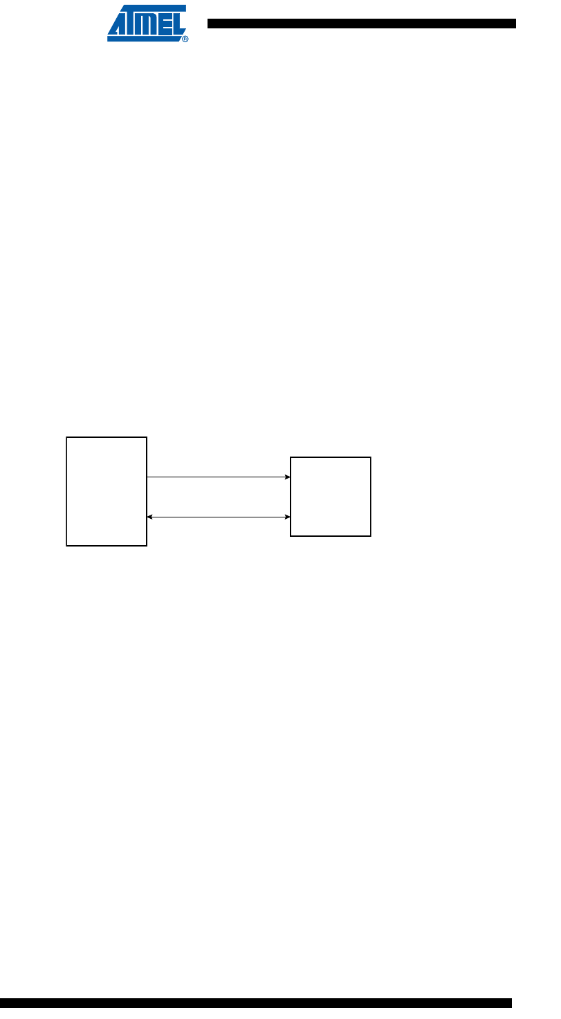
718
6430F–ATARM–21-Feb-12
SAM3U Series
718
6430F–ATARM–21-Feb-12
SAM3U Series
35.7.4 ISO7816 Mode
The USART features an ISO7816-compatible operating mode. This mode permits interfacing
with smart cards and Security Access Modules (SAM) communicating through an ISO7816 link.
Both T = 0 and T = 1 protocols defined by the ISO7816 specification are supported.
Setting the USART in ISO7816 mode is performed by writing the USART_MODE field in the
Mode Register (US_MR) to the value 0x4 for protocol T = 0 and to the value 0x5 for protocol T =
1.
35.7.4.1 ISO7816 Mode Overview
The ISO7816 is a half duplex communication on only one bidirectional line. The baud rate is
determined by a division of the clock provided to the remote device (see “Baud Rate Generator”
on page 696).
The USART connects to a smart card as shown in Figure 35-30. The TXD line becomes bidirec-
tional and the Baud Rate Generator feeds the ISO7816 clock on the SCK pin. As the TXD pin
becomes bidirectional, its output remains driven by the output of the transmitter but only when
the transmitter is active while its input is directed to the input of the receiver. The USART is con-
sidered as the master of the communication as it generates the clock.
Figure 35-30. Connection of a Smart Card to the USART
When operating in ISO7816, either in T = 0 or T = 1 modes, the character format is fixed. The
configuration is 8 data bits, even parity and 1 or 2 stop bits, regardless of the values pro-
grammed in the CHRL, MODE9, PAR and CHMODE fields. MSBF can be used to transmit LSB
or MSB first. Parity Bit (PAR) can be used to transmit in normal or inverse mode. Refer to
“USART Mode Register” on page 737 and “PAR: Parity Type” on page 738.
The USART cannot operate concurrently in both receiver and transmitter modes as the commu-
nication is unidirectional at a time. It has to be configured according to the required mode by
enabling or disabling either the receiver or the transmitter as desired. Enabling both the receiver
and the transmitter at the same time in ISO7816 mode may lead to unpredictable results.
The ISO7816 specification defines an inverse transmission format. Data bits of the character
must be transmitted on the I/O line at their negative value. The USART does not support this for-
mat and the user has to perform an exclusive OR on the data before writing it in the Transmit
Holding Register (US_THR) or after reading it in the Receive Holding Register (US_RHR).
35.7.4.2 Protocol T = 0
In T = 0 protocol, a character is made up of one start bit, eight data bits, one parity bit and one
guard time, which lasts two bit times. The transmitter shifts out the bits and does not drive the
I/O line during the guard time.
If no parity error is detected, the I/O line remains to 1 during the guard time and the transmitter
can continue with the transmission of the next character, as shown in Figure 35-31.
Smart
Card
SCK CLK
TXD I/O
USART

719
6430F–ATARM–21-Feb-12
SAM3U Series
719
6430F–ATARM–21-Feb-12
SAM3U Series
If a parity error is detected by the receiver, it drives the I/O line to 0 during the guard time, as
shown in Figure 35-32. This error bit is also named NACK, for Non Acknowledge. In this case,
the character lasts 1 bit time more, as the guard time length is the same and is added to the
error bit time which lasts 1 bit time.
When the USART is the receiver and it detects an error, it does not load the erroneous character
in the Receive Holding Register (US_RHR). It appropriately sets the PARE bit in the Status Reg-
ister (US_SR) so that the software can handle the error.
Figure 35-31. T = 0 Protocol without Parity Error
Figure 35-32. T = 0 Protocol with Parity Error
Receive Error Counter
The USART receiver also records the total number of errors. This can be read in the Number of
Error (US_NER) register. The NB_ERRORS field can record up to 255 errors. Reading US_NER
automatically clears the NB_ERRORS field.
Receive NACK Inhibit
The USART can also be configured to inhibit an error. This can be achieved by setting the
INACK bit in the Mode Register (US_MR). If INACK is to 1, no error signal is driven on the I/O
line even if a parity bit is detected.
Moreover, if INACK is set, the erroneous received character is stored in the Receive Holding
Register, as if no error occurred and the RXRDY bit does rise.
Transmit Character Repetition
When the USART is transmitting a character and gets a NACK, it can automatically repeat the
character before moving on to the next one. Repetition is enabled by writing the
MAX_ITERATION field in the Mode Register (US_MR) at a value higher than 0. Each character
can be transmitted up to eight times; the first transmission plus seven repetitions.
If MAX_ITERATION does not equal zero, the USART repeats the character as many times as
the value loaded in MAX_ITERATION.
D0 D1 D2 D3 D4 D5 D6 D7
RXD
Parity
Bit
Baud Rate
Clock
Start
Bit
Guard
Time 1
Next
Start
Bit
Guard
Time 2
D0 D1 D2 D3 D4 D5 D6 D7
I/O
Parity
Bit
Baud Rate
Clock
Start
Bit
Guard
Time 1
Start
Bit
Guard
Time 2
D0 D1
Error
Repetition
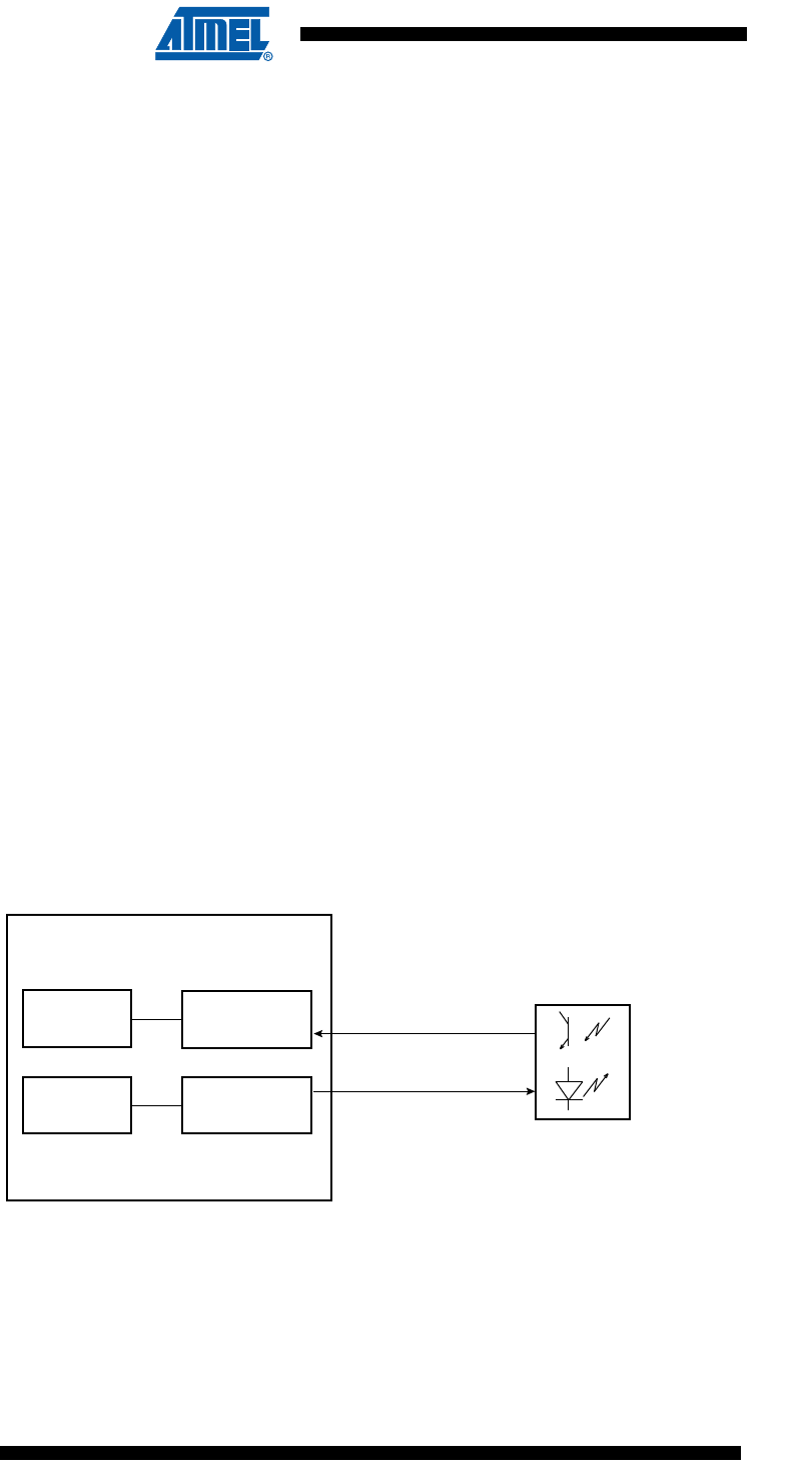
720
6430F–ATARM–21-Feb-12
SAM3U Series
720
6430F–ATARM–21-Feb-12
SAM3U Series
When the USART repetition number reaches MAX_ITERATION, the ITERATION bit is set in the
Channel Status Register (US_CSR). If the repetition of the character is acknowledged by the
receiver, the repetitions are stopped and the iteration counter is cleared.
The ITERATION bit in US_CSR can be cleared by writing the Control Register with the RSIT bit
to 1.
Disable Successive Receive NACK
The receiver can limit the number of successive NACKs sent back to the remote transmitter.
This is programmed by setting the bit DSNACK in the Mode Register (US_MR). The maximum
number of NACK transmitted is programmed in the MAX_ITERATION field. As soon as
MAX_ITERATION is reached, the character is considered as correct, an acknowledge is sent on
the line and the ITERATION bit in the Channel Status Register is set.
35.7.4.3 Protocol T = 1
When operating in ISO7816 protocol T = 1, the transmission is similar to an asynchronous for-
mat with only one stop bit. The parity is generated when transmitting and checked when
receiving. Parity error detection sets the PARE bit in the Channel Status Register (US_CSR).
35.7.5 IrDA Mode
The USART features an IrDA mode supplying half-duplex point-to-point wireless communica-
tion. It embeds the modulator and demodulator which allows a glueless connection to the
infrared transceivers, as shown in Figure 35-33. The modulator and demodulator are compliant
with the IrDA specification version 1.1 and support data transfer speeds ranging from 2.4 Kb/s to
115.2 Kb/s.
The USART IrDA mode is enabled by setting the USART_MODE field in the Mode Register
(US_MR) to the value 0x8. The IrDA Filter Register (US_IF) allows configuring the demodulator
filter. The USART transmitter and receiver operate in a normal asynchronous mode and all
parameters are accessible. Note that the modulator and the demodulator are activated.
Figure 35-33. Connection to IrDA Transceivers
The receiver and the transmitter must be enabled or disabled according to the direction of the
transmission to be managed.
To receive IrDA signals, the following needs to be done:
• Disable TX and Enable RX
IrDA
Transceivers
RXD RX
TXD
TX
USART
Demodulator
Modulator
Receiver
Transmitter
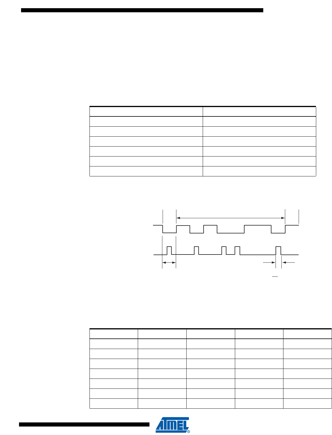
721
6430F–ATARM–21-Feb-12
SAM3U Series
721
6430F–ATARM–21-Feb-12
SAM3U Series
• Configure the TXD pin as PIO and set it as an output to 0 (to avoid LED emission). Disable
the internal pull-up (better for power consumption).
• Receive data
35.7.5.1 IrDA Modulation
For baud rates up to and including 115.2 Kbits/sec, the RZI modulation scheme is used. “0” is
represented by a light pulse of 3/16th of a bit time. Some examples of signal pulse duration are
shown in Table 35-11.
Figure 35-34 shows an example of character transmission.
Figure 35-34. IrDA Modulation
35.7.5.2 IrDA Baud Rate
Table 35-12 gives some examples of CD values, baud rate error and pulse duration. Note that
the requirement on the maximum acceptable error of ±1.87% must be met.
Table 35-11. IrDA Pulse Duration
Baud Rate Pulse Duration (3/16)
2.4 Kb/s 78.13 µs
9.6 Kb/s 19.53 µs
19.2 Kb/s 9.77 µs
38.4 Kb/s 4.88 µs
57.6 Kb/s 3.26 µs
115.2 Kb/s 1.63 µs
Bit Period Bit Period
3
16
Start
Bit
Data Bits Stop
Bit
00
000
111 1
1
Transmitter
Output
TXD
Table 35-12. IrDA Baud Rate Error
Peripheral Clock Baud Rate CD Baud Rate Error Pulse Time
3 686 400 115 200 2 0.00% 1.63
20 000 000 115 200 11 1.38% 1.63
32 768 000 115 200 18 1.25% 1.63
40 000 000 115 200 22 1.38% 1.63
3 686 400 57 600 4 0.00% 3.26
20 000 000 57 600 22 1.38% 3.26
32 768 000 57 600 36 1.25% 3.26
722
6430F–ATARM–21-Feb-12
SAM3U Series
722
6430F–ATARM–21-Feb-12
SAM3U Series
35.7.5.3 IrDA Demodulator
The demodulator is based on the IrDA Receive filter comprised of an 8-bit down counter which is
loaded with the value programmed in US_IF. When a falling edge is detected on the RXD pin,
the Filter Counter starts counting down at the Master Clock (MCK) speed. If a rising edge is
detected on the RXD pin, the counter stops and is reloaded with US_IF. If no rising edge is
detected when the counter reaches 0, the input of the receiver is driven low during one bit time.
Figure 35-35 illustrates the operations of the IrDA demodulator.
Figure 35-35. IrDA Demodulator Operations
As the IrDA mode uses the same logic as the ISO7816, note that the FI_DI_RATIO field in
US_FIDI must be set to a value higher than 0 in order to assure IrDA communications operate
correctly.
40 000 000 57 600 43 0.93% 3.26
3 686 400 38 400 6 0.00% 4.88
20 000 000 38 400 33 1.38% 4.88
32 768 000 38 400 53 0.63% 4.88
40 000 000 38 400 65 0.16% 4.88
3 686 400 19 200 12 0.00% 9.77
20 000 000 19 200 65 0.16% 9.77
32 768 000 19 200 107 0.31% 9.77
40 000 000 19 200 130 0.16% 9.77
3 686 400 9 600 24 0.00% 19.53
20 000 000 9 600 130 0.16% 19.53
32 768 000 9 600 213 0.16% 19.53
40 000 000 9 600 260 0.16% 19.53
3 686 400 2 400 96 0.00% 78.13
20 000 000 2 400 521 0.03% 78.13
32 768 000 2 400 853 0.04% 78.13
Table 35-12. IrDA Baud Rate Error (Continued)
Peripheral Clock Baud Rate CD Baud Rate Error Pulse Time
MCK
RXD
Receiver
Input
Pulse
Rejected
65432 61
65432 0
Pulse
Accepted
Counter
Value
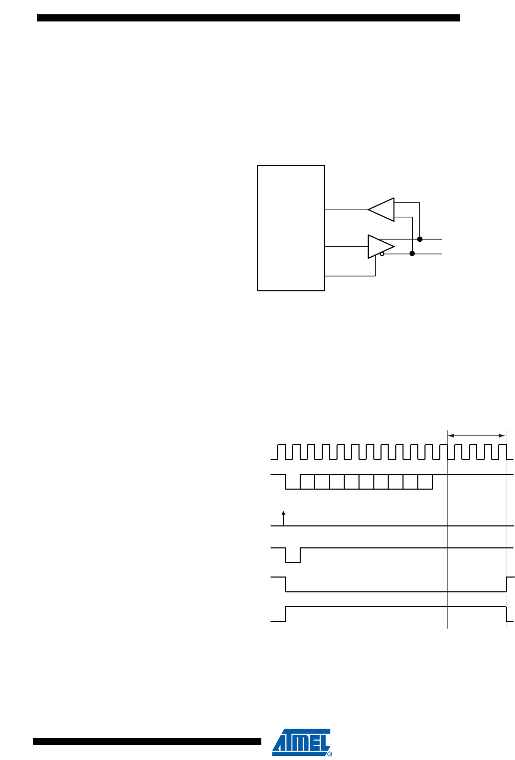
723
6430F–ATARM–21-Feb-12
SAM3U Series
723
6430F–ATARM–21-Feb-12
SAM3U Series
35.7.6 RS485 Mode
The USART features the RS485 mode to enable line driver control. While operating in RS485
mode, the USART behaves as though in asynchronous or synchronous mode and configuration
of all the parameters is possible. The difference is that the RTS pin is driven high when the
transmitter is operating. The behavior of the RTS pin is controlled by the TXEMPTY bit. A typical
connection of the USART to a RS485 bus is shown in Figure 35-36.
Figure 35-36. Typical Connection to a RS485 Bus
The USART is set in RS485 mode by programming the USART_MODE field in the Mode Regis-
ter (US_MR) to the value 0x1.
The RTS pin is at a level inverse to the TXEMPTY bit. Significantly, the RTS pin remains high
when a timeguard is programmed so that the line can remain driven after the last character com-
pletion. Figure 35-37 gives an example of the RTS waveform during a character transmission
when the timeguard is enabled.
Figure 35-37. Example of RTS Drive with Timeguard
USART
RTS
TXD
RXD
Differential
Bus
D0 D1 D2 D3 D4 D5 D6 D7
TXD
Start
Bit
Parity
Bit
Stop
Bit
Baud Rate
Clock
TG = 4
Write
US_THR
TXRDY
TXEMPTY
RTS

724
6430F–ATARM–21-Feb-12
SAM3U Series
724
6430F–ATARM–21-Feb-12
SAM3U Series
35.7.7 Modem Mode
The USART features modem mode, which enables control of the signals: DTR (Data Terminal
Ready), DSR (Data Set Ready), RTS (Request to Send), CTS (Clear to Send), DCD (Data Car-
rier Detect) and RI (Ring Indicator). While operating in modem mode, the USART behaves as a
DTE (Data Terminal Equipment) as it drives DTR and RTS and can detect level change on DSR,
DCD, CTS and RI.
Setting the USART in modem mode is performed by writing the USART_MODE field in the Mode
Register (US_MR) to the value 0x3. While operating in modem mode the USART behaves as
though in asynchronous mode and all the parameter configurations are available.
Table 35-13 gives the correspondence of the USART signals with modem connection standards.
The control of the DTR output pin is performed by writing the Control Register (US_CR) with the
DTRDIS and DTREN bits respectively to 1. The disable command forces the corresponding pin
to its inactive level, i.e. high. The enable command forces the corresponding pin to its active
level, i.e. low. RTS output pin is automatically controlled in this mode
The level changes are detected on the RI, DSR, DCD and CTS pins. If an input change is
detected, the RIIC, DSRIC, DCDIC and CTSIC bits in the Channel Status Register (US_CSR)
are set respectively and can trigger an interrupt. The status is automatically cleared when
US_CSR is read. Furthermore, the CTS automatically disables the transmitter when it is
detected at its inactive state. If a character is being transmitted when the CTS rises, the charac-
ter transmission is completed before the transmitter is actually disabled.
Table 35-13. Circuit References
USART Pin V24 CCITT Direction
TXD 2 103 From terminal to modem
RTS 4 105 From terminal to modem
DTR 20 108.2 From terminal to modem
RXD 3 104 From modem to terminal
CTS 5 106 From terminal to modem
DSR 6 107 From terminal to modem
DCD 8 109 From terminal to modem
RI 22 125 From terminal to modem

725
6430F–ATARM–21-Feb-12
SAM3U Series
725
6430F–ATARM–21-Feb-12
SAM3U Series
35.7.8 SPI Mode
The Serial Peripheral Interface (SPI) Mode is a synchronous serial data link that provides com-
munication with external devices in Master or Slave Mode. It also enables communication
between processors if an external processor is connected to the system.
The Serial Peripheral Interface is essentially a shift register that serially transmits data bits to
other SPIs. During a data transfer, one SPI system acts as the “master” which controls the data
flow, while the other devices act as “slaves'' which have data shifted into and out by the master.
Different CPUs can take turns being masters and one master may simultaneously shift data into
multiple slaves. (Multiple Master Protocol is the opposite of Single Master Protocol, where one
CPU is always the master while all of the others are always slaves.) However, only one slave
may drive its output to write data back to the master at any given time.
A slave device is selected when its NSS signal is asserted by the master. The USART in SPI
Master mode can address only one SPI Slave because it can generate only one NSS signal.
The SPI system consists of two data lines and two control lines:
• Master Out Slave In (MOSI): This data line supplies the output data from the master shifted
into the input of the slave.
• Master In Slave Out (MISO): This data line supplies the output data from a slave to the input
of the master.
• Serial Clock (SCK): This control line is driven by the master and regulates the flow of the data
bits. The master may transmit data at a variety of baud rates. The SCK line cycles once for
each bit that is transmitted.
• Slave Select (NSS): This control line allows the master to select or deselect the slave.
35.7.8.1 Modes of Operation
The USART can operate in SPI Master Mode or in SPI Slave Mode.
Operation in SPI Master Mode is programmed by writing to 0xE the USART_MODE field in the
Mode Register. In this case the SPI lines must be connected as described below:
• the MOSI line is driven by the output pin TXD
• the MISO line drives the input pin RXD
• the SCK line is driven by the output pin SCK
• the NSS line is driven by the output pin RTS
Operation in SPI Slave Mode is programmed by writing to 0xF the USART_MODE field in the
Mode Register. In this case the SPI lines must be connected as described below:
• the MOSI line drives the input pin RXD
• the MISO line is driven by the output pin TXD
• the SCK line drives the input pin SCK
• the NSS line drives the input pin CTS
In order to avoid unpredicted behavior, any change of the SPI Mode must be followed by a soft-
ware reset of the transmitter and of the receiver (except the initial configuration after a hardware
reset). (See Section 35.7.2 ”Receiver and Transmitter Control”).

726
6430F–ATARM–21-Feb-12
SAM3U Series
726
6430F–ATARM–21-Feb-12
SAM3U Series
35.7.8.2 Baud Rate
In SPI Mode, the baudrate generator operates in the same way as in USART synchronous
mode: See “Baud Rate in Synchronous Mode or SPI Mode” on page 698. However, there are
some restrictions:
In SPI Master Mode:
• the external clock SCK must not be selected (USCLKS ≠ 0x3), and the bit CLKO must be set
to “1” in the Mode Register (US_MR), in order to generate correctly the serial clock on the
SCK pin.
• to obtain correct behavior of the receiver and the transmitter, the value programmed in CD
must be superior or equal to 6.
• if the internal clock divided (MCK/DIV) is selected, the value programmed in CD must be
even to ensure a 50:50 mark/space ratio on the SCK pin, this value can be odd if the internal
clock is selected (MCK).
In SPI Slave Mode:
• the external clock (SCK) selection is forced regardless of the value of the USCLKS field in the
Mode Register (US_MR). Likewise, the value written in US_BRGR has no effect, because
the clock is provided directly by the signal on the USART SCK pin.
• to obtain correct behavior of the receiver and the transmitter, the external clock (SCK)
frequency must be at least 6 times lower than the system clock.
727
6430F–ATARM–21-Feb-12
SAM3U Series
727
6430F–ATARM–21-Feb-12
SAM3U Series
35.7.8.3 Data Transfer
Up to 9 data bits are successively shifted out on the TXD pin at each rising or falling edge
(depending of CPOL and CPHA) of the programmed serial clock. There is no Start bit, no Parity
bit and no Stop bit.
The number of data bits is selected by the CHRL field and the MODE 9 bit in the Mode Register
(US_MR). The 9 bits are selected by setting the MODE 9 bit regardless of the CHRL field. The
MSB data bit is always sent first in SPI Mode (Master or Slave).
Four combinations of polarity and phase are available for data transfers. The clock polarity is
programmed with the CPOL bit in the Mode Register. The clock phase is programmed with the
CPHA bit. These two parameters determine the edges of the clock signal upon which data is
driven and sampled. Each of the two parameters has two possible states, resulting in four possi-
ble combinations that are incompatible with one another. Thus, a master/slave pair must use the
same parameter pair values to communicate. If multiple slaves are used and fixed in different
configurations, the master must reconfigure itself each time it needs to communicate with a dif-
ferent slave.
Table 35-14. SPI Bus Protocol Mode
SPI Bus Protocol Mode CPOL CPHA
001
100
211
310
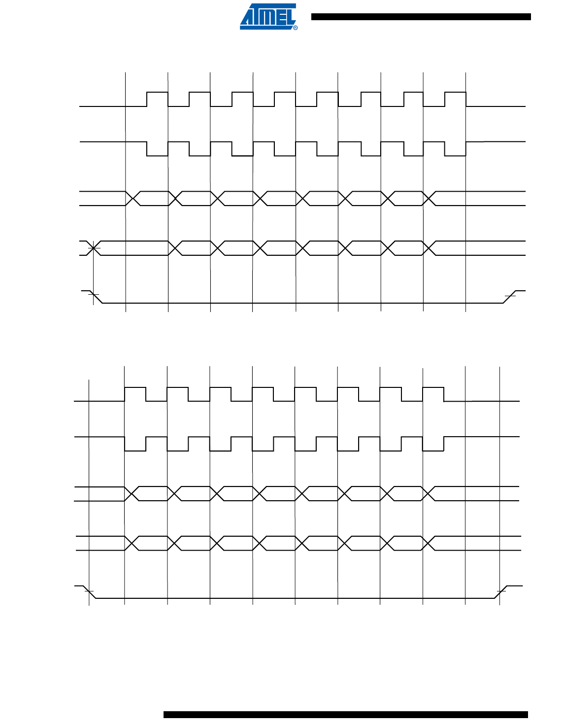
728
6430F–ATARM–21-Feb-12
SAM3U Series
728
6430F–ATARM–21-Feb-12
SAM3U Series
Figure 35-38. SPI Transfer Format (CPHA=1, 8 bits per transfer)
Figure 35-39. SPI Transfer Format (CPHA=0, 8 bits per transfer)
6
SCK
(CPOL = 0)
SCK
(CPOL = 1)
MOSI
SPI Master ->TXD
SPI Slave -> RXD
NSS
SPI Master -> RTS
SPI Slave -> CTS
SCK cycle (for reference)
MSB
MSB
LSB
LSB
6
6
5
5
4
4
3
3
2
2
1
1
1 2345 786
MISO
SPI Master ->RXD
SPI Slave -> TXD
SCK
(CPOL = 0)
SCK
(CPOL = 1)
1 2345 7
MOSI
SPI Master -> TXD
SPI Slave -> RXD
MISO
SPI Master -> RXD
SPI Slave -> TXD
NSS
SPI Master -> RTS
SPI Slave -> CTS
SCK cycle (for reference) 8
MSB
MSB
LSB
LSB
6
6
5
5
4
4
3
3
1
1
2
2
6

729
6430F–ATARM–21-Feb-12
SAM3U Series
729
6430F–ATARM–21-Feb-12
SAM3U Series
35.7.8.4 Receiver and Transmitter Control
See “Receiver and Transmitter Control” on page 700.
35.7.8.5 Character Transmission
The characters are sent by writing in the Transmit Holding Register (US_THR). An additional
condition for transmitting a character can be added when the USART is configured in SPI mas-
ter mode. In the USART_MR register, the value configured on INACK field can prevent any
character transmission (even if US_THR has been written) while the receiver side is not ready
(character not read). When INACK equals 0, the character is transmitted whatever the receiver
status. If INACK is set to 1, the transmitter waits for the receiver holding register to be read
before transmitting the character (RXRDY flag cleared), thus preventing any overflow (character
loss) on the receiver side.
The transmitter reports two status bits in the Channel Status Register (US_CSR): TXRDY
(Transmitter Ready), which indicates that US_THR is empty and TXEMPTY, which indicates
that all the characters written in US_THR have been processed. When the current character pro-
cessing is completed, the last character written in US_THR is transferred into the Shift Register
of the transmitter and US_THR becomes empty, thus TXRDY rises.
Both TXRDY and TXEMPTY bits are low when the transmitter is disabled. Writing a character in
US_THR while TXRDY is low has no effect and the written character is lost.
If the USART is in SPI Slave Mode and if a character must be sent while the Transmit Holding
Register (US_THR) is empty, the UNRE (Underrun Error) bit is set. The TXD transmission line
stays at high level during all this time. The UNRE bit is cleared by writing the Control Register
(US_CR) with the RSTSTA (Reset Status) bit to 1.
In SPI Master Mode, the slave select line (NSS) is asserted at low level 1 Tbit (Time bit) before
the transmission of the MSB bit and released at high level 1 Tbit after the transmission of the
LSB bit. So, the slave select line (NSS) is always released between each character transmission
and a minimum delay of 3 Tbits always inserted. However, in order to address slave devices
supporting the CSAAT mode (Chip Select Active After Transfer), the slave select line (NSS) can
be forced at low level by writing the Control Register (US_CR) with the RTSEN bit to 1. The
slave select line (NSS) can be released at high level only by writing the Control Register
(US_CR) with the RTSDIS bit to 1 (for example, when all data have been transferred to the slave
device).
In SPI Slave Mode, the transmitter does not require a falling edge of the slave select line (NSS)
to initiate a character transmission but only a low level. However, this low level must be present
on the slave select line (NSS) at least 1 Tbit before the first serial clock cycle corresponding to
the MSB bit.
35.7.8.6 Character Reception
When a character reception is completed, it is transferred to the Receive Holding Register
(US_RHR) and the RXRDY bit in the Status Register (US_CSR) rises. If a character is com-
pleted while RXRDY is set, the OVRE (Overrun Error) bit is set. The last character is transferred
into US_RHR and overwrites the previous one. The OVRE bit is cleared by writing the Control
Register (US_CR) with the RSTSTA (Reset Status) bit to 1.
To ensure correct behavior of the receiver in SPI Slave Mode, the master device sending the
frame must ensure a minimum delay of 1 Tbit between each character transmission. The
receiver does not require a falling edge of the slave select line (NSS) to initiate a character
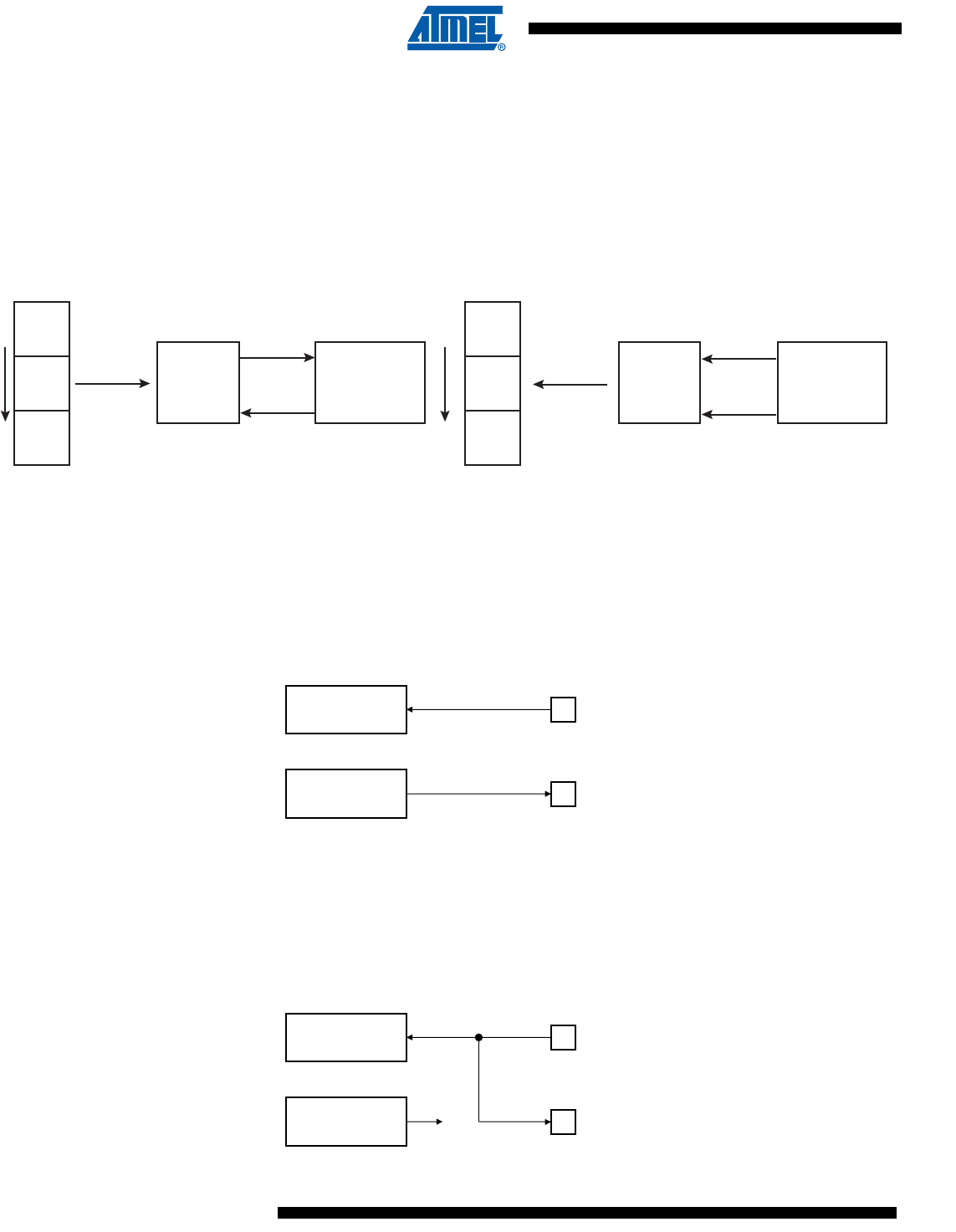
730
6430F–ATARM–21-Feb-12
SAM3U Series
730
6430F–ATARM–21-Feb-12
SAM3U Series
reception but only a low level. However, this low level must be present on the slave select line
(NSS) at least 1 Tbit before the first serial clock cycle corresponding to the MSB bit.
35.7.8.7 Receiver Timeout
Because the receiver baudrate clock is active only during data transfers in SPI Mode, a receiver
timeout is impossible in this mode, whatever the Time-out value is (field TO) in the Time-out
Register (US_RTOR).
35.7.9 Test Modes
The USART can be programmed to operate in three different test modes. The internal loopback
capability allows on-board diagnostics. In the loopback mode the USART interface pins are dis-
connected or not and reconfigured for loopback internally or externally.
35.7.9.1 Normal Mode
Normal mode connects the RXD pin on the receiver input and the transmitter output on the TXD
pin.
Figure 35-40. Normal Mode Configuration
35.7.9.2 Automatic Echo Mode
Automatic echo mode allows bit-by-bit retransmission. When a bit is received on the RXD pin, it
is sent to the TXD pin, as shown in Figure 35-41. Programming the transmitter has no effect on
the TXD pin. The RXD pin is still connected to the receiver input, thus the receiver remains
active.
Figure 35-41. Automatic Echo Mode Configuration
|
|
|
|
|
|
|
|
DATA 0
DATA N
RXRDY
USART3
LIN CONTROLLER
APB bus
READ BUFFER
NACT = SUBSCRIBE
DATA 0
DATA N
TXRDY
USART3
LIN CONTROLLER
APB bus
WRITE BUFFER
(Peripheral) DMA
Controller
(Peripheral) DMA
Controller
Receiver
Transmitter
RXD
TXD
Receiver
Transmitter
RXD
TXD
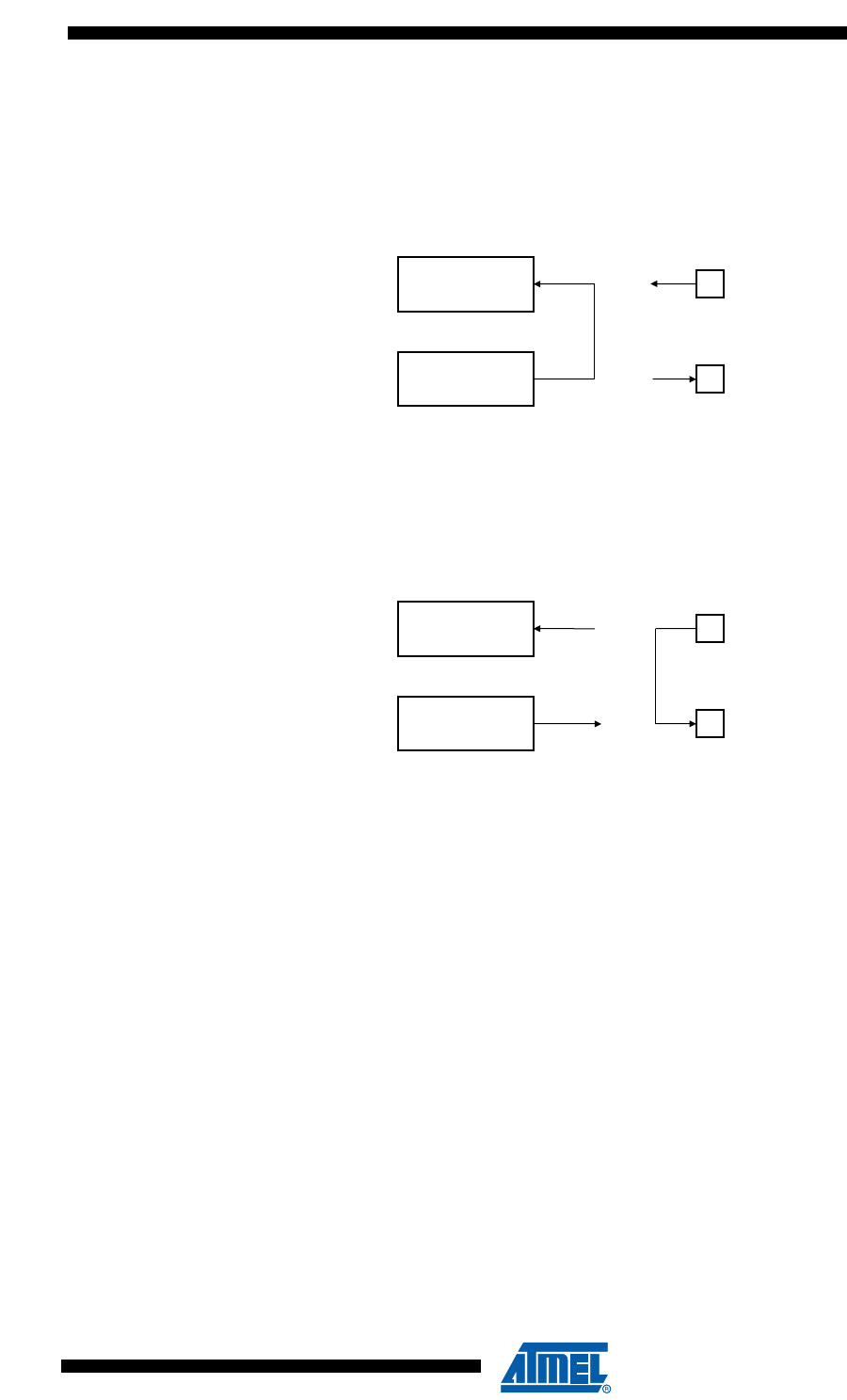
731
6430F–ATARM–21-Feb-12
SAM3U Series
731
6430F–ATARM–21-Feb-12
SAM3U Series
35.7.9.3 Local Loopback Mode
Local loopback mode connects the output of the transmitter directly to the input of the receiver,
as shown in Figure 35-42. The TXD and RXD pins are not used. The RXD pin has no effect on
the receiver and the TXD pin is continuously driven high, as in idle state.
Figure 35-42. Local Loopback Mode Configuration
35.7.9.4 Remote Loopback Mode
Remote loopback mode directly connects the RXD pin to the TXD pin, as shown in Figure 35-43.
The transmitter and the receiver are disabled and have no effect. This mode allows bit-by-bit
retransmission.
Figure 35-43. Remote Loopback Mode Configuration
Receiver
Transmitter
RXD
TXD
1
Receiver
Transmitter
RXD
TXD
1

732
6430F–ATARM–21-Feb-12
SAM3U Series
732
6430F–ATARM–21-Feb-12
SAM3U Series
35.7.10 Write Protection Registers
To prevent any single software error that may corrupt USART behavior, certain address spaces
can be write-protected by setting the WPEN bit in the USART Write Protect Mode Register
(US_WPMR).
If a write access to the protected registers is detected, then the WPVS flag in the USART Write
Protect Status Register (US_WPSR) is set and the field WPVSRC indicates in which register the
write access has been attempted.
The WPVS flag is reset by writing the USART Write Protect Mode Register (US_WPMR) with
the appropriate access key, WPKEY.
The protected registers are:
•“USART Mode Register”
•“USART Baud Rate Generator Register”
•“USART Receiver Time-out Register”
•“USART Transmitter Timeguard Register”
•“USART FI DI RATIO Register”
•“USART IrDA FILTER Register”
•“USART Manchester Configuration Register”

733
6430F–ATARM–21-Feb-12
SAM3U Series
733
6430F–ATARM–21-Feb-12
SAM3U Series
35.8 Universal Synchronous Asynchronous Receiver Transmitter (USART) User Interface
Table 35-15. Register Mapping
Offset Register Name Access Reset
0x0000 Control Register US_CR Write-only –
0x0004 Mode Register US_MR Read-write –
0x0008 Interrupt Enable Register US_IER Write-only –
0x000C Interrupt Disable Register US_IDR Write-only –
0x0010 Interrupt Mask Register US_IMR Read-only 0x0
0x0014 Channel Status Register US_CSR Read-only –
0x0018 Receiver Holding Register US_RHR Read-only 0x0
0x001C Transmitter Holding Register US_THR Write-only –
0x0020 Baud Rate Generator Register US_BRGR Read-write 0x0
0x0024 Receiver Time-out Register US_RTOR Read-write 0x0
0x0028 Transmitter Timeguard Register US_TTGR Read-write 0x0
0x2C - 0x3C Reserved – – –
0x0040 FI DI Ratio Register US_FIDI Read-write 0x174
0x0044 Number of Errors Register US_NER Read-only –
0x0048 Reserved – – –
0x004C IrDA Filter Register US_IF Read-write 0x0
0x0050 Manchester Encoder Decoder Register US_MAN Read-write 0x30011004
0xE4 Write Protect Mode Register US_WPMR Read-write 0x0
0xE8 Write Protect Status Register US_WPSR Read-only 0x0
0x5C - 0xFC Reserved – – –
0x100 - 0x128 Reserved for PDC Registers – – –

734
6430F–ATARM–21-Feb-12
SAM3U Series
734
6430F–ATARM–21-Feb-12
SAM3U Series
35.8.1 USART Control Register
Name: US_CR
Address: 0x40090000 (0), 0x40094000 (1), 0x40098000 (2), 0x4009C000 (3)
Access: Write-only
• RSTRX: Reset Receiver
0: No effect.
1: Resets the receiver.
• RSTTX: Reset Transmitter
0: No effect.
1: Resets the transmitter.
• RXEN: Receiver Enable
0: No effect.
1: Enables the receiver, if RXDIS is 0.
• RXDIS: Receiver Disable
0: No effect.
1: Disables the receiver.
• TXEN: Transmitter Enable
0: No effect.
1: Enables the transmitter if TXDIS is 0.
• TXDIS: Transmitter Disable
0: No effect.
1: Disables the transmitter.
31 30 29 28 27 26 25 24
––––––––
23 22 21 20 19 18 17 16
––––RTSDIS/RCSRTSEN/FCSDTRDISDTREN
15 14 13 12 11 10 9 8
RETTO RSTNACK RSTIT SENDA STTTO STPBRK STTBRK RSTSTA
76543210
TXDIS TXEN RXDIS RXEN RSTTX RSTRX – –

735
6430F–ATARM–21-Feb-12
SAM3U Series
735
6430F–ATARM–21-Feb-12
SAM3U Series
• RSTSTA: Reset Status Bits
0: No effect.
1: Resets the status bits PARE, FRAME, OVRE, MANERR, UNRE and RXBRK in US_CSR.
• STTBRK: Start Break
0: No effect.
1: Starts transmission of a break after the characters present in US_THR and the Transmit Shift Register have been trans-
mitted. No effect if a break is already being transmitted.
• STPBRK: Stop Break
0: No effect.
1: Stops transmission of the break after a minimum of one character length and transmits a high level during 12-bit periods.
No effect if no break is being transmitted.
• STTTO: Start Time-out
0: No effect.
1: Starts waiting for a character before clocking the time-out counter. Resets the status bit TIMEOUT in US_CSR.
• SENDA: Send Address
0: No effect.
1: In Multidrop Mode only, the next character written to the US_THR is sent with the address bit set.
• RSTIT: Reset Iterations
0: No effect.
1: Resets ITERATION in US_CSR. No effect if the ISO7816 is not enabled.
• RSTNACK: Reset Non Acknowledge
0: No effect
1: Resets NACK in US_CSR.
• RETTO: Rearm Time-out
0: No effect
1: Restart Time-out
• DTREN: Data Terminal Ready Enable
0: No effect.
1: Drives the pin DTR to 0.
• DTRDIS: Data Terminal Ready Disable
0: No effect.
1: Drives the pin DTR to 1.

736
6430F–ATARM–21-Feb-12
SAM3U Series
736
6430F–ATARM–21-Feb-12
SAM3U Series
• RTSEN: Request to Send Enable
0: No effect.
1: Drives the pin RTS to 0.
• FCS: Force SPI Chip Select
– Applicable if USART operates in SPI Master Mode (USART_MODE = 0xE):
FCS = 0: No effect.
FCS = 1: Forces the Slave Select Line NSS (RTS pin) to 0, even if USART is no transmitting, in order to address SPI slave
devices supporting the CSAAT Mode (Chip Select Active After Transfer).
• RTSDIS: Request to Send Disable
0: No effect.
1: Drives the pin RTS to 1.
• RCS: Release SPI Chip Select
– Applicable if USART operates in SPI Master Mode (USART_MODE = 0xE):
RCS = 0: No effect.
RCS = 1: Releases the Slave Select Line NSS (RTS pin).
737
6430F–ATARM–21-Feb-12
SAM3U Series
737
6430F–ATARM–21-Feb-12
SAM3U Series
35.8.2 USART Mode Register
Name: US_MR
Address: 0x40090004 (0), 0x40094004 (1), 0x40098004 (2), 0x4009C004 (3)
Access: Read-write
This register can only be written if the WPEN bit is cleared in “USART Write Protect Mode Register” on page 760.
• USART_MODE
• USCLKS: Clock Selection
31 30 29 28 27 26 25 24
ONEBIT MODSYNC MAN FILTER – MAX_ITERATION
23 22 21 20 19 18 17 16
INVDATA VAR_SYNC DSNACK INACK OVER CLKO MODE9 MSBF/CPOL
15 14 13 12 11 10 9 8
CHMODE NBSTOP PAR SYNC/CPHA
76543210
CHRL USCLKS USART_MODE
Value Name Description
0x0 NORMAL Normal mode
0x1 RS485 RS485
0x2 HW_HANDSHAKING Hardware Handshaking
0x3 MODEM Modem
0x4 IS07816_T_0 IS07816 Protocol: T = 0
0x6 IS07816_T_1 IS07816 Protocol: T = 1
0x8 IRDA IrDA
0xE SPI_MASTER SPI Master
0xF SPI_SLAVE SPI Slave
Value Name Description
0 MCK Master Clock MCK is selected
1 DIV Internal Clock Divided MCK/DIV (DIV=8) is selected
3 SCK Serial Clock SLK is selected
738
6430F–ATARM–21-Feb-12
SAM3U Series
738
6430F–ATARM–21-Feb-12
SAM3U Series
• CHRL: Character Length.
• SYNC: Synchronous Mode Select
0: USART operates in Asynchronous Mode.
1: USART operates in Synchronous Mode.
• CPHA: SPI Clock Phase
– Applicable if USART operates in SPI Mode (USART_MODE = 0xE or 0xF):
CPHA = 0: Data is changed on the leading edge of SPCK and captured on the following edge of SPCK.
CPHA = 1: Data is captured on the leading edge of SPCK and changed on the following edge of SPCK.
CPHA determines which edge of SPCK causes data to change and which edge causes data to be captured. CPHA is used
with CPOL to produce the required clock/data relationship between master and slave devices.
• PAR: Parity Type
• NBSTOP: Number of Stop Bits
Value Name Description
0 5_BIT Character length is 5 bits
1 6_BIT Character length is 6 bits
2 7_BIT Character length is 7 bits
3 8_BIT Character length is 8 bits
Value Name Description
0 EVEN Even parity
1 ODD Odd parity
2 SPACE Parity forced to 0 (Space)
3 MARK Parity forced to 1 (Mark)
4 NO No parity
6 MULTIDROP Multidrop mode
Value Name Description
0 1_BIT 1 stop bit
1 1_5_BIT 1.5 stop bit (SYNC = 0) or reserved (SYNC = 1)
2 2_BIT 2 stop bits

739
6430F–ATARM–21-Feb-12
SAM3U Series
739
6430F–ATARM–21-Feb-12
SAM3U Series
• CHMODE: Channel Mode
• MSBF: Bit Order
0: Least Significant Bit is sent/received first.
1: Most Significant Bit is sent/received first.
• CPOL: SPI Clock Polarity
– Applicable if USART operates in SPI Mode (Slave or Master, USART_MODE = 0xE or 0xF):
CPOL = 0: The inactive state value of SPCK is logic level zero.
CPOL = 1: The inactive state value of SPCK is logic level one.
CPOL is used to determine the inactive state value of the serial clock (SPCK). It is used with CPHA to produce the required
clock/data relationship between master and slave devices.
• MODE9: 9-bit Character Length
0: CHRL defines character length.
1: 9-bit character length.
• CLKO: Clock Output Select
0: The USART does not drive the SCK pin.
1: The USART drives the SCK pin if USCLKS does not select the external clock SCK.
• OVER: Oversampling Mode
0: 16x Oversampling.
1: 8x Oversampling.
• INACK: Inhibit Non Acknowledge
0: The NACK is generated.
1: The NACK is not generated.
Note: In SPI master mode, if INACK = 0 the character transmission starts as soon as a character is written into US_THR
register (assuming TXRDY was set). When INACK is 1, an additional condition must be met. The character transmission
starts when a character is written and only if RXRDY flag is cleared (Receiver Holding Register has been read).
• DSNACK: Disable Successive NACK
0: NACK is sent on the ISO line as soon as a parity error occurs in the received character (unless INACK is set).
1: Successive parity errors are counted up to the value specified in the MAX_ITERATION field. These parity errors gener-
ate a NACK on the ISO line. As soon as this value is reached, no additional NACK is sent on the ISO line. The flag
ITERATION is asserted.
Value Name Description
0 NORMAL Normal Mode
1 AUTOMATIC Automatic Echo. Receiver input is connected to the TXD pin.
2 LOCAL_LOOPBACK Local Loopback. Transmitter output is connected to the Receiver Input.
3 REMOTE_LOOPBACK Remote Loopback. RXD pin is internally connected to the TXD pin.

740
6430F–ATARM–21-Feb-12
SAM3U Series
740
6430F–ATARM–21-Feb-12
SAM3U Series
•INVDATA: INverted Data
0: The data field transmitted on TXD line is the same as the one written in US_THR register or the content read in US_RHR
is the same as RXD line. Normal mode of operation.
1: The data field transmitted on TXD line is inverted (voltage polarity only) compared to the value written on US_THR regis-
ter or the content read in US_RHR is inverted compared to what is received on RXD line (or ISO7816 IO line). Inverted
Mode of operation, useful for contactless card application. To be used with configuration bit MSBF.
• VAR_SYNC: Variable Synchronization of Command/Data Sync Start Frame Delimiter
0: User defined configuration of command or data sync field depending on MODSYNC value.
1: The sync field is updated when a character is written into US_THR register.
• MAX_ITERATION
Defines the maximum number of iterations in mode ISO7816, protocol T= 0.
• FILTER: Infrared Receive Line Filter
0: The USART does not filter the receive line.
1: The USART filters the receive line using a three-sample filter (1/16-bit clock) (2 over 3 majority).
• MAN: Manchester Encoder/Decoder Enable
0: Manchester Encoder/Decoder are disabled.
1: Manchester Encoder/Decoder are enabled.
• MODSYNC: Manchester Synchronization Mode
0:The Manchester Start bit is a 0 to 1 transition
1: The Manchester Start bit is a 1 to 0 transition.
• ONEBIT: Start Frame Delimiter Selector
0: Start Frame delimiter is COMMAND or DATA SYNC.
1: Start Frame delimiter is One Bit.

741
6430F–ATARM–21-Feb-12
SAM3U Series
741
6430F–ATARM–21-Feb-12
SAM3U Series
35.8.3 USART Interrupt Enable Register
Name: US_IER
Address: 0x40090008 (0), 0x40094008 (1), 0x40098008 (2), 0x4009C008 (3)
Access: Write-only
0: No effect
1: Enables the corresponding interrupt.
• RXRDY: RXRDY Interrupt Enable
• TXRDY: TXRDY Interrupt Enable
• RXBRK: Receiver Break Interrupt Enable
• ENDRX: End of Receive Transfer Interrupt Enable
• ENDTX: End of Transmit Interrupt Enable
• OVRE: Overrun Error Interrupt Enable
• FRAME: Framing Error Interrupt Enable
• PARE: Parity Error Interrupt Enable
• TIMEOUT: Time-out Interrupt Enable
• TXEMPTY: TXEMPTY Interrupt Enable
• ITER: Max number of Repetitions Reached
• UNRE: SPI Underrun Error
• TXBUFE: Buffer Empty Interrupt Enable
• RXBUFF: Buffer Full Interrupt Enable
• NACK: Non AcknowledgeInterrupt Enable
• RIIC: Ring Indicator Input Change Enable
31 30 29 28 27 26 25 24
–––––––MANE
23 22 21 20 19 18 17 16
––––CTSICDCDIC DSRIC RIIC
15 14 13 12 11 10 9 8
– – NACK RXBUFF TXBUFE ITER/UNRE TXEMPTY TIMEOUT
76543210
PARE FRAME OVRE ENDTX ENDRX RXBRK TXRDY RXRDY

742
6430F–ATARM–21-Feb-12
SAM3U Series
742
6430F–ATARM–21-Feb-12
SAM3U Series
• DSRIC: Data Set Ready Input Change Enable
• DCDIC: Data Carrier Detect Input Change Interrupt Enable
• CTSIC: Clear to Send Input Change Interrupt Enable
• MANE: Manchester Error Interrupt Enable

743
6430F–ATARM–21-Feb-12
SAM3U Series
743
6430F–ATARM–21-Feb-12
SAM3U Series
35.8.4 USART Interrupt Disable Register
Name: US_IDR
Address: 0x4009000C (0), 0x4009400C (1), 0x4009800C (2), 0x4009C00C (3)
Access: Write-only
0: No effect
1: Disables the corresponding interrupt.
• RXRDY: RXRDY Interrupt Disable
• TXRDY: TXRDY Interrupt Disable
• RXBRK: Receiver Break Interrupt Disable
• ENDRX: End of Receive Transfer Interrupt Disable
• ENDTX: End of Transmit Interrupt Disable
• OVRE: Overrun Error Interrupt Disable
• FRAME: Framing Error Interrupt Disable
• PARE: Parity Error Interrupt Disable
• TIMEOUT: Time-out Interrupt Disable
• TXEMPTY: TXEMPTY Interrupt Disable
• ITER: Max number of Repetitions Reached Disable
• UNRE: SPI Underrun Error Disable
• TXBUFE: Buffer Empty Interrupt Disable
• RXBUFF: Buffer Full Interrupt Disable
• NACK: Non AcknowledgeInterrupt Disable
• RIIC: Ring Indicator Input Change Disable
31 30 29 28 27 26 25 24
–––––––MANE
23 22 21 20 19 18 17 16
––––CTSICDCDIC DSRIC RIIC
15 14 13 12 11 10 9 8
– – NACK RXBUFF TXBUFE ITER/UNRE TXEMPTY TIMEOUT
76543210
PARE FRAME OVRE ENDTX ENDRX RXBRK TXRDY RXRDY

744
6430F–ATARM–21-Feb-12
SAM3U Series
744
6430F–ATARM–21-Feb-12
SAM3U Series
• DSRIC: Data Set Ready Input Change Disable
• DCDIC: Data Carrier Detect Input Change Interrupt Disable
• CTSIC: Clear to Send Input Change Interrupt Disable
• MANE: Manchester Error Interrupt Disable

745
6430F–ATARM–21-Feb-12
SAM3U Series
745
6430F–ATARM–21-Feb-12
SAM3U Series
35.8.5 USART Interrupt Mask Register
Name: US_IMR
Address: 0x40090010 (0), 0x40094010 (1), 0x40098010 (2), 0x4009C010 (3)
Access: Read-only
0: The corresponding interrupt is not enabled.
1: The corresponding interrupt is enabled.
• RXRDY: RXRDY Interrupt Mask
• TXRDY: TXRDY Interrupt Mask
• RXBRK: Receiver Break Interrupt Mask
• ENDRX: End of Receive Transfer Interrupt Mask
• ENDTX: End of Transmit Interrupt Mask
• OVRE: Overrun Error Interrupt Mask
• FRAME: Framing Error Interrupt Mask
• PARE: Parity Error Interrupt Mask
• TIMEOUT: Time-out Interrupt Mask
• TXEMPTY: TXEMPTY Interrupt Mask
• ITER: Max number of Repetitions Reached Mask
• UNRE: SPI Underrun Error Mask
• TXBUFE: Buffer Empty Interrupt Mask
• RXBUFF: Buffer Full Interrupt Mask
• NACK: Non AcknowledgeInterrupt Mask
• RIIC: Ring Indicator Input Change Mask
31 30 29 28 27 26 25 24
–––––––MANE
23 22 21 20 19 18 17 16
––––CTSICDCDIC DSRIC RIIC
15 14 13 12 11 10 9 8
– – NACK RXBUFF TXBUFE ITER/UNRE TXEMPTY TIMEOUT
76543210
PARE FRAME OVRE ENDTX ENDRX RXBRK TXRDY RXRDY

746
6430F–ATARM–21-Feb-12
SAM3U Series
746
6430F–ATARM–21-Feb-12
SAM3U Series
• DSRIC: Data Set Ready Input Change Mask
• DCDIC: Data Carrier Detect Input Change Interrupt Mask
• CTSIC: Clear to Send Input Change Interrupt Mask
• MANE: Manchester Error Interrupt Mask

747
6430F–ATARM–21-Feb-12
SAM3U Series
747
6430F–ATARM–21-Feb-12
SAM3U Series
35.8.6 USART Channel Status Register
Name: US_CSR
Address: 0x40090014 (0), 0x40094014 (1), 0x40098014 (2), 0x4009C014 (3)
Access: Read-only
• RXRDY: Receiver Ready
0: No complete character has been received since the last read of US_RHR or the receiver is disabled. If characters were
being received when the receiver was disabled, RXRDY changes to 1 when the receiver is enabled.
1: At least one complete character has been received and US_RHR has not yet been read.
• TXRDY: Transmitter Ready
0: A character is in the US_THR waiting to be transferred to the Transmit Shift Register, or an STTBRK command has been
requested, or the transmitter is disabled. As soon as the transmitter is enabled, TXRDY becomes 1.
1: There is no character in the US_THR.
• RXBRK: Break Received/End of Break
0: No Break received or End of Break detected since the last RSTSTA.
1: Break Received or End of Break detected since the last RSTSTA.
• ENDRX: End of Receiver Transfer
0: The End of Transfer signal from the Receive PDC channel is inactive.
1: The End of Transfer signal from the Receive PDC channel is active.
• ENDTX: End of Transmitter Transfer
0: The End of Transfer signal from the Transmit PDC channel is inactive.
1: The End of Transfer signal from the Transmit PDC channel is active.
• OVRE: Overrun Error
0: No overrun error has occurred since the last RSTSTA.
1: At least one overrun error has occurred since the last RSTSTA.
• FRAME: Framing Error
0: No stop bit has been detected low since the last RSTSTA.
1: At least one stop bit has been detected low since the last RSTSTA.
31 30 29 28 27 26 25 24
–––––––MANERR
23 22 21 20 19 18 17 16
CTS DCD DSR RI CTSIC DCDIC DSRIC RIIC
15 14 13 12 11 10 9 8
– – NACK RXBUFF TXBUFE ITER/UNRE TXEMPTY TIMEOUT
76543210
PARE FRAME OVRE ENDTX ENDRX RXBRK TXRDY RXRDY

748
6430F–ATARM–21-Feb-12
SAM3U Series
748
6430F–ATARM–21-Feb-12
SAM3U Series
• PARE: Parity Error
0: No parity error has been detected since the last RSTSTA.
1: At least one parity error has been detected since the last RSTSTA.
• TIMEOUT: Receiver Time-out
0: There has not been a time-out since the last Start Time-out command (STTTO in US_CR) or the Time-out Register is 0.
1: There has been a time-out since the last Start Time-out command (STTTO in US_CR).
• TXEMPTY: Transmitter Empty
0: There are characters in either US_THR or the Transmit Shift Register, or the transmitter is disabled.
1: There are no characters in US_THR, nor in the Transmit Shift Register.
• ITER: Max number of Repetitions Reached
0: Maximum number of repetitions has not been reached since the last RSTSTA.
1: Maximum number of repetitions has been reached since the last RSTSTA.
• UNRE: SPI Underrun Error
– Applicable if USART operates in SPI Slave Mode (USART_MODE = 0xF):
UNRE = 0: No SPI underrun error has occurred since the last RSTSTA.
UNRE = 1: At least one SPI underrun error has occurred since the last RSTSTA.
• TXBUFE: Transmission Buffer Empty
0: The signal Buffer Empty from the Transmit PDC channel is inactive.
1: The signal Buffer Empty from the Transmit PDC channel is active.
• RXBUFF: Reception Buffer Full
0: The signal Buffer Full from the Receive PDC channel is inactive.
1: The signal Buffer Full from the Receive PDC channel is active.
• NACK: Non AcknowledgeInterrupt
0: Non Acknowledge has not been detected since the last RSTNACK.
1: At least one Non Acknowledge has been detected since the last RSTNACK.
• RIIC: Ring Indicator Input Change Flag
0: No input change has been detected on the RI pin since the last read of US_CSR.
1: At least one input change has been detected on the RI pin since the last read of US_CSR.
• DSRIC: Data Set Ready Input Change Flag
0: No input change has been detected on the DSR pin since the last read of US_CSR.
1: At least one input change has been detected on the DSR pin since the last read of US_CSR.
• DCDIC: Data Carrier Detect Input Change Flag
0: No input change has been detected on the DCD pin since the last read of US_CSR.
1: At least one input change has been detected on the DCD pin since the last read of US_CSR.

749
6430F–ATARM–21-Feb-12
SAM3U Series
749
6430F–ATARM–21-Feb-12
SAM3U Series
• CTSIC: Clear to Send Input Change Flag
0: No input change has been detected on the CTS pin since the last read of US_CSR.
1: At least one input change has been detected on the CTS pin since the last read of US_CSR.
• RI: Image of RI Input
0: RI is set to 0.
1: RI is set to 1.
• DSR: Image of DSR Input
0: DSR is set to 0
1: DSR is set to 1.
• DCD: Image of DCD Input
0: DCD is set to 0.
1: DCD is set to 1.
• CTS: Image of CTS Input
0: CTS is set to 0.
1: CTS is set to 1.
• MANERR: Manchester Error
0: No Manchester error has been detected since the last RSTSTA.
1: At least one Manchester error has been detected since the last RSTSTA.

750
6430F–ATARM–21-Feb-12
SAM3U Series
750
6430F–ATARM–21-Feb-12
SAM3U Series
35.8.7 USART Receive Holding Register
Name: US_RHR
Address: 0x40090018 (0), 0x40094018 (1), 0x40098018 (2), 0x4009C018 (3)
Access: Read-only
• RXCHR: Received Character
Last character received if RXRDY is set.
• RXSYNH: Received Sync
0: Last Character received is a Data.
1: Last Character received is a Command.
31 30 29 28 27 26 25 24
––––––––
23 22 21 20 19 18 17 16
––––––––
15 14 13 12 11 10 9 8
RXSYNH ––––––RXCHR
76543210
RXCHR

751
6430F–ATARM–21-Feb-12
SAM3U Series
751
6430F–ATARM–21-Feb-12
SAM3U Series
35.8.8 USART Transmit Holding Register
Name: US_THR
Address: 0x4009001C (0), 0x4009401C (1), 0x4009801C (2), 0x4009C01C (3)
Access: Write-only
• TXCHR: Character to be Transmitted
Next character to be transmitted after the current character if TXRDY is not set.
• TXSYNH: Sync Field to be transmitted
0: The next character sent is encoded as a data. Start Frame Delimiter is DATA SYNC.
1: The next character sent is encoded as a command. Start Frame Delimiter is COMMAND SYNC.
31 30 29 28 27 26 25 24
––––––––
23 22 21 20 19 18 17 16
––––––––
15 14 13 12 11 10 9 8
TXSYNH ––––––TXCHR
76543210
TXCHR

752
6430F–ATARM–21-Feb-12
SAM3U Series
752
6430F–ATARM–21-Feb-12
SAM3U Series
35.8.9 USART Baud Rate Generator Register
Name: US_BRGR
Address: 0x40090020 (0), 0x40094020 (1), 0x40098020 (2), 0x4009C020 (3)
Access: Read-write
This register can only be written if the WPEN bit is cleared in “USART Write Protect Mode Register” on page 760.
• CD: Clock Divider
• FP: Fractional Part
0: Fractional divider is disabled.
1 - 7: Baudrate resolution, defined by FP x 1/8.
31 30 29 28 27 26 25 24
––––––––
23 22 21 20 19 18 17 16
––––– FP
15 14 13 12 11 10 9 8
CD
76543210
CD
CD
USART_MODE ≠ ISO7816
USART_MODE =
ISO7816
SYNC = 0
SYNC = 1
or
USART_MODE = SPI
(Master or Slave)
OVER = 0 OVER = 1
0 Baud Rate Clock Disabled
1 to 65535 Baud Rate =
Selected Clock/(16*CD)
Baud Rate =
Selected Clock/(8*CD)
Baud Rate =
Selected Clock /CD
Baud Rate = Selected
Clock/(FI_DI_RATIO*CD)

753
6430F–ATARM–21-Feb-12
SAM3U Series
753
6430F–ATARM–21-Feb-12
SAM3U Series
35.8.10 USART Receiver Time-out Register
Name: US_RTOR
Address: 0x40090024 (0), 0x40094024 (1), 0x40098024 (2), 0x4009C024 (3)
Access: Read-write
This register can only be written if the WPEN bit is cleared in “USART Write Protect Mode Register” on page 760.
• TO: Time-out Value
0: The Receiver Time-out is disabled.
1 - 65535: The Receiver Time-out is enabled and the Time-out delay is TO x Bit Period.
31 30 29 28 27 26 25 24
––––––––
23 22 21 20 19 18 17 16
––––––––
15 14 13 12 11 10 9 8
TO
76543210
TO

754
6430F–ATARM–21-Feb-12
SAM3U Series
754
6430F–ATARM–21-Feb-12
SAM3U Series
35.8.11 USART Transmitter Timeguard Register
Name: US_TTGR
Address: 0x40090028 (0), 0x40094028 (1), 0x40098028 (2), 0x4009C028 (3)
Access: Read-write
This register can only be written if the WPEN bit is cleared in “USART Write Protect Mode Register” on page 760.
• TG: Timeguard Value
0: The Transmitter Timeguard is disabled.
1 - 255: The Transmitter timeguard is enabled and the timeguard delay is TG x Bit Period.
31 30 29 28 27 26 25 24
––––––––
23 22 21 20 19 18 17 16
––––––––
15 14 13 12 11 10 9 8
––––––––
76543210
TG

755
6430F–ATARM–21-Feb-12
SAM3U Series
755
6430F–ATARM–21-Feb-12
SAM3U Series
35.8.12 USART FI DI RATIO Register
Name: US_FIDI
Address: 0x40090040 (0), 0x40094040 (1), 0x40098040 (2), 0x4009C040 (3)
Access: Read-write
Reset Value: 0x174
This register can only be written if the WPEN bit is cleared in “USART Write Protect Mode Register” on page 760.
• FI_DI_RATIO: FI Over DI Ratio Value
0: If ISO7816 mode is selected, the Baud Rate Generator generates no signal.
1 - 2047: If ISO7816 mode is selected, the Baud Rate is the clock provided on SCK divided by FI_DI_RATIO.
31 30 29 28 27 26 25 24
––––––––
23 22 21 20 19 18 17 16
––––––––
15 14 13 12 11 10 9 8
––––– FI_DI_RATIO
76543210
FI_DI_RATIO

756
6430F–ATARM–21-Feb-12
SAM3U Series
756
6430F–ATARM–21-Feb-12
SAM3U Series
35.8.13 USART Number of Errors Register
Name: US_NER
Address: 0x40090044 (0), 0x40094044 (1), 0x40098044 (2), 0x4009C044 (3)
Access: Read-only
• NB_ERRORS: Number of Errors
Total number of errors that occurred during an ISO7816 transfer. This register automatically clears when read.
31 30 29 28 27 26 25 24
––––––––
23 22 21 20 19 18 17 16
––––––––
15 14 13 12 11 10 9 8
––––––––
76543210
NB_ERRORS

757
6430F–ATARM–21-Feb-12
SAM3U Series
757
6430F–ATARM–21-Feb-12
SAM3U Series
35.8.14 USART IrDA FILTER Register
Name: US_IF
Address: 0x4009004C (0), 0x4009404C (1), 0x4009804C (2), 0x4009C04C (3)
Access: Read-write
This register can only be written if the WPEN bit is cleared in “USART Write Protect Mode Register” on page 760.
• IRDA_FILTER: IrDA Filter
Sets the filter of the IrDA demodulator.
31 30 29 28 27 26 25 24
––––––––
23 22 21 20 19 18 17 16
––––––––
15 14 13 12 11 10 9 8
––––––––
76543210
IRDA_FILTER
758
6430F–ATARM–21-Feb-12
SAM3U Series
758
6430F–ATARM–21-Feb-12
SAM3U Series
35.8.15 USART Manchester Configuration Register
Name: US_MAN
Address: 0x40090050 (0), 0x40094050 (1), 0x40098050 (2), 0x4009C050 (3)
Access: Read-write
This register can only be written if the WPEN bit is cleared in “USART Write Protect Mode Register” on page 760.
• TX_PL: Transmitter Preamble Length
0: The Transmitter Preamble pattern generation is disabled
1 - 15: The Preamble Length is TX_PL x Bit Period
• TX_PP: Transmitter Preamble Pattern
The following values assume that TX_MPOL field is not set:
• TX_MPOL: Transmitter Manchester Polarity
0: Logic Zero is coded as a zero-to-one transition, Logic One is coded as a one-to-zero transition.
1: Logic Zero is coded as a one-to-zero transition, Logic One is coded as a zero-to-one transition.
• RX_PL: Receiver Preamble Length
0: The receiver preamble pattern detection is disabled
1 - 15: The detected preamble length is RX_PL x Bit Period
31 30 29 28 27 26 25 24
– DRIFT 1 RX_MPOL – – RX_PP
23 22 21 20 19 18 17 16
–––– RX_PL
15 14 13 12 11 10 9 8
– – – TX_MPOL – – TX_PP
76543210
–––– TX_PL
Value Name Description
00 ALL_ONE The preamble is composed of ‘1’s
01 ALL_ZERO The preamble is composed of ‘0’s
10 ZERO_ONE The preamble is composed of ‘01’s
11 ONE_ZERO The preamble is composed of ‘10’s

759
6430F–ATARM–21-Feb-12
SAM3U Series
759
6430F–ATARM–21-Feb-12
SAM3U Series
• RX_PP: Receiver Preamble Pattern detected
The following values assume that RX_MPOL field is not set:
• RX_MPOL: Receiver Manchester Polarity
0: Logic Zero is coded as a zero-to-one transition, Logic One is coded as a one-to-zero transition.
1: Logic Zero is coded as a one-to-zero transition, Logic One is coded as a zero-to-one transition.
• DRIFT: Drift compensation
0: The USART can not recover from an important clock drift
1: The USART can recover from clock drift. The 16X clock mode must be enabled.
Value Name Description
00 ALL_ONE The preamble is composed of ‘1’s
01 ALL_ZERO The preamble is composed of ‘0’s
10 ZERO_ONE The preamble is composed of ‘01’s
11 ONE_ZERO The preamble is composed of ‘10’s

760
6430F–ATARM–21-Feb-12
SAM3U Series
760
6430F–ATARM–21-Feb-12
SAM3U Series
35.8.16 USART Write Protect Mode Register
Name: US_WPMR
Address: 0x400900E4 (0), 0x400940E4 (1), 0x400980E4 (2), 0x4009C0E4 (3)
Access: Read-write
Reset: See Table 35-15
• WPEN: Write Protect Enable
0 = Disables the Write Protect if WPKEY corresponds to 0x555341 (“USA” in ASCII).
1 = Enables the Write Protect if WPKEY corresponds to 0x555341 (“USA” in ASCII).
Protects the registers:
•“USART Mode Register” on page 737
•“USART Baud Rate Generator Register” on page 752
•“USART Receiver Time-out Register” on page 753
•“USART Transmitter Timeguard Register” on page 754
•“USART FI DI RATIO Register” on page 755
•“USART IrDA FILTER Register” on page 757
•“USART Manchester Configuration Register” on page 758
• WPKEY: Write Protect KEY
Should be written at value 0x555341 (“USA” in ASCII). Writing any other value in this field aborts the write operation of the
WPEN bit. Always reads as 0.
31 30 29 28 27 26 25 24
WPKEY
23 22 21 20 19 18 17 16
WPKEY
15 14 13 12 11 10 9 8
WPKEY
76543210
———————WPEN

761
6430F–ATARM–21-Feb-12
SAM3U Series
761
6430F–ATARM–21-Feb-12
SAM3U Series
35.8.17 USART Write Protect Status Register
Name: US_WPSR
Address: 0x400900E8 (0), 0x400940E8 (1), 0x400980E8 (2), 0x4009C0E8 (3)
Access: Read-only
Reset: See Table 35-15
• WPVS: Write Protect Violation Status
0 = No Write Protect Violation has occurred since the last read of the US_WPSR register.
1 = A Write Protect Violation has occurred since the last read of the US_WPSR register. If this violation is an unauthorized
attempt to write a protected register, the associated violation is reported into field WPVSRC.
• WPVSRC: Write Protect Violation Source
When WPVS is active, this field indicates the write-protected register (through address offset or code) in which a write
access has been attempted.
Note: Reading US_WPSR automatically clears all fields.
31 30 29 28 27 26 25 24
————————
23 22 21 20 19 18 17 16
WPVSRC
15 14 13 12 11 10 9 8
WPVSRC
76543210
———————WPVS

762
6430F–ATARM–21-Feb-12
SAM3U Series
762
6430F–ATARM–21-Feb-12
SAM3U Series

763
6430F–ATARM–21-Feb-12
SAM3U Series
763
6430F–ATARM–21-Feb-12
SAM3U Series
36. Timer Counter (TC)
36.1 Description
The Timer Counter (TC) includes 9 identical 16-bit Timer Counter channels.
Each channel can be independently programmed to perform a wide range of functions including
frequency measurement, event counting, interval measurement, pulse generation, delay timing
and pulse width modulation.
Each channel has three external clock inputs, five internal clock inputs and two multi-purpose
input/output signals which can be configured by the user. Each channel drives an internal inter-
rupt signal which can be programmed to generate processor interrupts.
The Timer Counter (TC) embeds a quadrature decoder logic connected in front of the timers and
driven by TIOA0, TIOB0 and TIOA1 inputs. When enabled, the quadrature decoder performs the
input lines filtering, decoding of quadrature signals and connects to the timers/counters in order
to read the position and speed of the motor through the user interface.
The Timer Counter block has two global registers which act upon all TC channels.
The Block Control Register allows the channels to be started simultaneously with the same
instruction.
The Block Mode Register defines the external clock inputs for each channel, allowing them to be
chained.
Table 36-1 gives the assignment of the device Timer Counter clock inputs common to Timer
Counter 0 to 2.
Note: 1. When Slow Clock is selected for Master Clock (CSS = 0 in PMC Master Clock Register),
TIMER_CLOCK5 input is equivalent to Master Clock.
36.2 Embedded Characteristics
• Provides 9 16-bit Timer Counter channels
• Wide range of functions including:
– Frequency measurement
– Event counting
– Interval measurement
– Pulse generation
– Delay timing
– Pulse Width Modulation
– Up/down capabilities
Table 36-1. Timer Counter Clock Assignment
Name Definition
TIMER_CLOCK1 MCK/2
TIMER_CLOCK2 MCK/8
TIMER_CLOCK3 MCK/32
TIMER_CLOCK4 MCK/128
TIMER_CLOCK5(1) SLCK
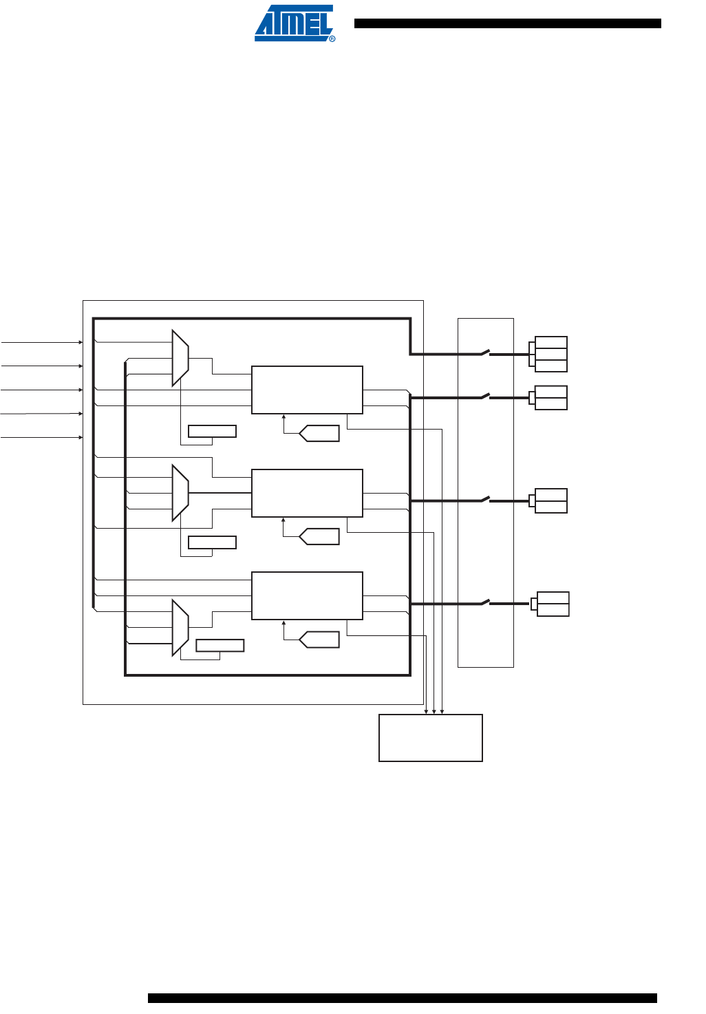
764
6430F–ATARM–21-Feb-12
SAM3U Series
764
6430F–ATARM–21-Feb-12
SAM3U Series
– Quadrature decoder logic
• Each channel is user-configurable and contains:
– Three external clock inputs
– Five Internal clock inputs
– Two multi-purpose input/output signals
• Internal interrupt signal
• Two global registers that act on all TC channels
36.3 Block Diagram
Figure 36-1. Timer Counter Block Diagram
Timer/Counter
Channel 0
Timer/Counter
Channel 1
Timer/Counter
Channel 2
SYNC
Parallel I/O
Controller
TC1XC1S
TC0XC0S
TC2XC2S
INT0
INT1
INT2
TIOA0
TIOA1
TIOA2
TIOB0
TIOB1
TIOB2
XC0
XC1
XC2
XC0
XC1
XC2
XC0
XC1
XC2
TCLK0
TCLK1
TCLK2
TCLK0
TCLK1
TCLK2
TCLK0
TCLK1
TCLK2
TIOA1
TIOA2
TIOA0
TIOA2
TIOA0
TIOA1
Interrupt
Controller
TCLK0
TCLK1
TCLK2
TIOA0
TIOB0
TIOA1
TIOB1
TIOA2
TIOB2
Timer Counter
TIOA
TIOB
TIOA
TIOB
TIOA
TIOB
SYNC
SYNC
TIMER_CLOCK2
TIMER_CLOCK3
TIMER_CLOCK4
TIMER_CLOCK5
TIMER_CLOCK1

765
6430F–ATARM–21-Feb-12
SAM3U Series
765
6430F–ATARM–21-Feb-12
SAM3U Series
36.4 Pin Name List
36.5 Product Dependencies
36.5.1 I/O Lines
The pins used for interfacing the compliant external devices may be multiplexed with PIO lines.
The programmer must first program the PIO controllers to assign the TC pins to their peripheral
functions.
36.5.2 Power Management
The TC is clocked through the Power Management Controller (PMC), thus the programmer must
first configure the PMC to enable the Timer Counter clock.
Table 36-2. Signal Name Description
Block/Channel Signal Name Description
Channel Signal
XC0, XC1, XC2 External Clock Inputs
TIOA Capture Mode: Timer Counter Input
Waveform Mode: Timer Counter Output
TIOB Capture Mode: Timer Counter Input
Waveform Mode: Timer Counter Input/Output
INT Interrupt Signal Output
SYNC Synchronization Input Signal
Table 36-3. TC pin list
Pin Name Description Type
TCLK0-TCLK2 External Clock Input Input
TIOA0-TIOA2 I/O Line A I/O
TIOB0-TIOB2 I/O Line B I/O
Table 36-4. I/O Lines
Instance Signal I/O Line Peripheral
TC0 TCLK0 PA2 A
TC0 TCLK1 PB4 A
TC0 TCLK2 PA26 B
TC0 TIOA0 PA1 A
TC0 TIOA1 PB5 A
TC0 TIOA2 PA30 B
TC0 TIOB0 PA0 A
TC0 TIOB1 PB6 A
TC0 TIOB2 PA31 B

766
6430F–ATARM–21-Feb-12
SAM3U Series
766
6430F–ATARM–21-Feb-12
SAM3U Series
36.5.3 Interrupt
The TC has an interrupt line connected to the Interrupt Controller (IC). Handling the TC interrupt
requires programming the IC before configuring the TC.
36.6 Functional Description
36.6.1 TC Description
The 9 channels of the Timer Counter are independent and identical in operation except when
quadrature decoder is enabled. The registers for channel programming are listed in Table 36-5
on page 785.
36.6.2 16-bit Counter
Each channel is organized around a 16-bit counter. The value of the counter is incremented at
each positive edge of the selected clock. When the counter has reached the value 0xFFFF and
passes to 0x0000, an overflow occurs and the COVFS bit in TC_SR (Status Register) is set.
The current value of the counter is accessible in real time by reading the Counter Value Regis-
ter, TC_CV. The counter can be reset by a trigger. In this case, the counter value passes to
0x0000 on the next valid edge of the selected clock.
36.6.3 Clock Selection
At block level, input clock signals of each channel can either be connected to the external inputs
TCLK0, TCLK1 or TCLK2, or be connected to the internal I/O signals TIOA0, TIOA1 or TIOA2
for chaining by programming the TC_BMR (Block Mode). See Figure 36-2 ”Clock Chaining
Selection”.
Each channel can independently select an internal or external clock source for its counter:
• Internal clock signals: TIMER_CLOCK1, TIMER_CLOCK2, TIMER_CLOCK3,
TIMER_CLOCK4, TIMER_CLOCK5
• External clock signals: XC0, XC1 or XC2
This selection is made by the TCCLKS bits in the TC Channel Mode Register.
The selected clock can be inverted with the CLKI bit in TC_CMR. This allows counting on the
opposite edges of the clock.
The burst function allows the clock to be validated when an external signal is high. The BURST
parameter in the Mode Register defines this signal (none, XC0, XC1, XC2). See Figure 36-3
”Clock Selection”
Note: In all cases, if an external clock is used, the duration of each of its levels must be longer than the
master clock period. The external clock frequency must be at least 2.5 times lower than the mas-
ter clock
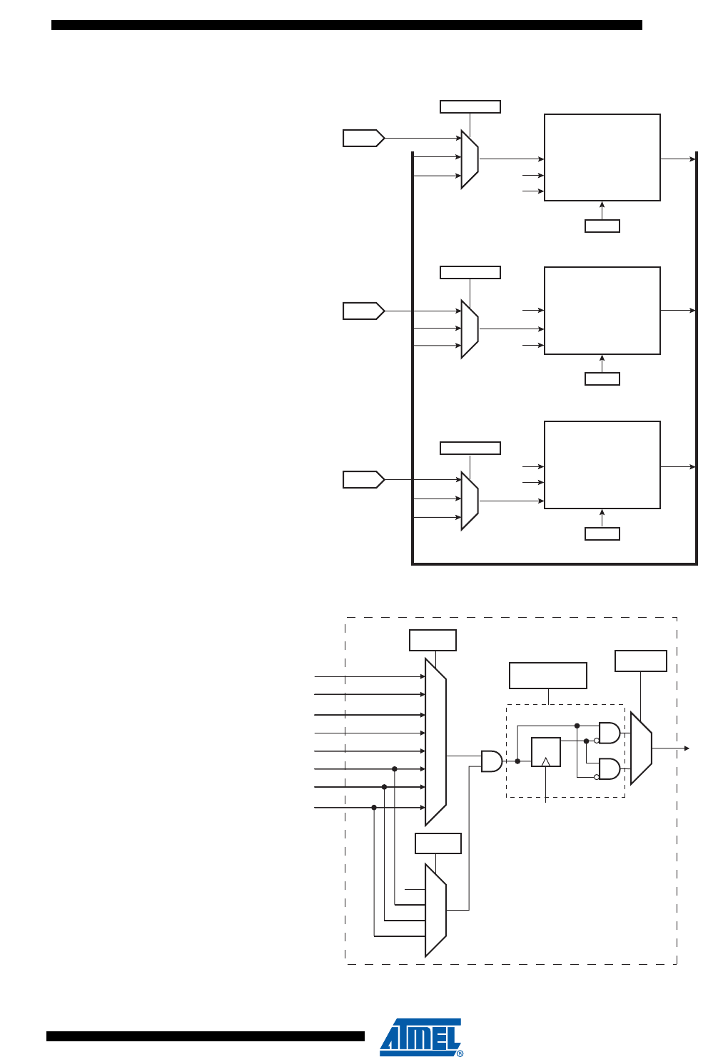
767
6430F–ATARM–21-Feb-12
SAM3U Series
767
6430F–ATARM–21-Feb-12
SAM3U Series
Figure 36-2. Clock Chaining Selection
Figure 36-3. Clock Selection
Timer/Counter
Channel 0
SYNC
TC0XC0S
TIOA0
TIOB0
XC0
XC1 = TCLK1
XC2 = TCLK2
TCLK0
TIOA1
TIOA2
Timer/Counter
Channel 1
SYNC
TC1XC1S
TIOA1
TIOB1
XC0 = TCLK0
XC1
XC2 = TCLK2
TCLK1
TIOA0
TIOA2
Timer/Counter
Channel 2
SYNC
TC2XC2S
TIOA2
TIOB2
XC0 = TCLK0
XC1 = TCLK1
XC2
TCLK2
TIOA0
TIOA1
TIMER_CLOCK1
TIMER_CLOCK2
TIMER_CLOCK3
TIMER_CLOCK4
TIMER_CLOCK5
XC0
XC1
XC2
TCCLKS
CLKI
Synchronous
Edge Detection
BURST
MCK
1
Selected
Clock
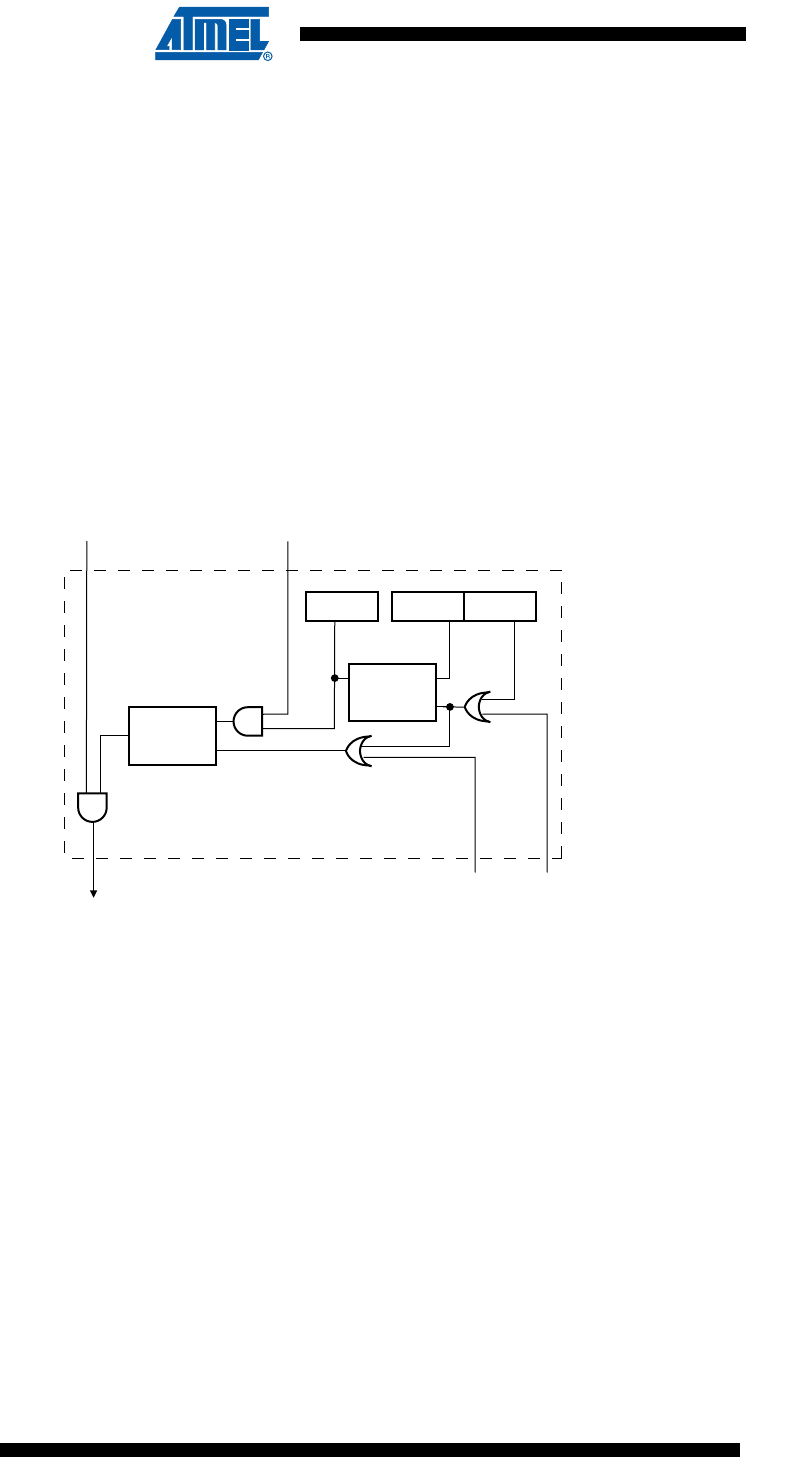
768
6430F–ATARM–21-Feb-12
SAM3U Series
768
6430F–ATARM–21-Feb-12
SAM3U Series
36.6.4 Clock Control
The clock of each counter can be controlled in two different ways: it can be enabled/disabled
and started/stopped. See Figure 36-4.
• The clock can be enabled or disabled by the user with the CLKEN and the CLKDIS
commands in the Control Register. In Capture Mode it can be disabled by an RB load event
if LDBDIS is set to 1 in TC_CMR. In Waveform Mode, it can be disabled by an RC Compare
event if CPCDIS is set to 1 in TC_CMR. When disabled, the start or the stop actions have no
effect: only a CLKEN command in the Control Register can re-enable the clock. When the
clock is enabled, the CLKSTA bit is set in the Status Register.
• The clock can also be started or stopped: a trigger (software, synchro, external or compare)
always starts the clock. The clock can be stopped by an RB load event in Capture Mode
(LDBSTOP = 1 in TC_CMR) or a RC compare event in Waveform Mode (CPCSTOP = 1 in
TC_CMR). The start and the stop commands have effect only if the clock is enabled.
Figure 36-4. Clock Control
36.6.5 TC Operating Modes
Each channel can independently operate in two different modes:
• Capture Mode provides measurement on signals.
• Waveform Mode provides wave generation.
The TC Operating Mode is programmed with the WAVE bit in the TC Channel Mode Register.
In Capture Mode, TIOA and TIOB are configured as inputs.
In Waveform Mode, TIOA is always configured to be an output and TIOB is an output if it is not
selected to be the external trigger.
36.6.6 Trigger
A trigger resets the counter and starts the counter clock. Three types of triggers are common to
both modes, and a fourth external trigger is available to each mode.
QS
R
S
R
Q
CLKSTA CLKEN CLKDIS
Stop
Event
Disable
Event
Counter
Clock
Selected
Clock Trigger

769
6430F–ATARM–21-Feb-12
SAM3U Series
769
6430F–ATARM–21-Feb-12
SAM3U Series
Regardless of the trigger used, it will be taken into account at the following active edge of the
selected clock. This means that the counter value can be read differently from zero just after a
trigger, especially when a low frequency signal is selected as the clock.
The following triggers are common to both modes:
• Software Trigger: Each channel has a software trigger, available by setting SWTRG in
TC_CCR.
• SYNC: Each channel has a synchronization signal SYNC. When asserted, this signal has
the same effect as a software trigger. The SYNC signals of all channels are asserted
simultaneously by writing TC_BCR (Block Control) with SYNC set.
• Compare RC Trigger: RC is implemented in each channel and can provide a trigger when
the counter value matches the RC value if CPCTRG is set in TC_CMR.
The channel can also be configured to have an external trigger. In Capture Mode, the external
trigger signal can be selected between TIOA and TIOB. In Waveform Mode, an external event
can be programmed on one of the following signals: TIOB, XC0, XC1 or XC2. This external
event can then be programmed to perform a trigger by setting ENETRG in TC_CMR.
If an external trigger is used, the duration of the pulses must be longer than the master clock
period in order to be detected.
36.6.7 Capture Operating Mode
This mode is entered by clearing the WAVE parameter in TC_CMR (Channel Mode Register).
Capture Mode allows the TC channel to perform measurements such as pulse timing, fre-
quency, period, duty cycle and phase on TIOA and TIOB signals which are considered as
inputs.
Figure 36-5 shows the configuration of the TC channel when programmed in Capture Mode.
36.6.8 Capture Registers A and B
Registers A and B (RA and RB) are used as capture registers. This means that they can be
loaded with the counter value when a programmable event occurs on the signal TIOA.
The LDRA parameter in TC_CMR defines the TIOA selected edge for the loading of register A,
and the LDRB parameter defines the TIOA selected edge for the loading of Register B.
RA is loaded only if it has not been loaded since the last trigger or if RB has been loaded since
the last loading of RA.
RB is loaded only if RA has been loaded since the last trigger or the last loading of RB.
Loading RA or RB before the read of the last value loaded sets the Overrun Error Flag (LOVRS)
in TC_SR (Status Register). In this case, the old value is overwritten.
36.6.9 Trigger Conditions
In addition to the SYNC signal, the software trigger and the RC compare trigger, an external trig-
ger can be defined.
The ABETRG bit in TC_CMR selects TIOA or TIOB input signal as an external trigger. The
ETRGEDG parameter defines the edge (rising, falling or both) detected to generate an external
trigger. If ETRGEDG = 0 (none), the external trigger is disabled.
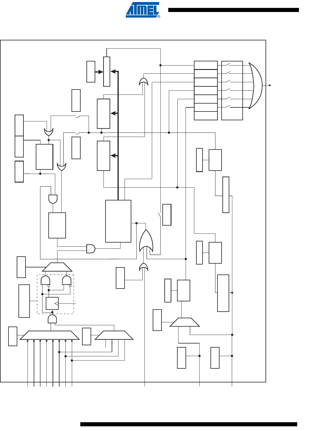
770
6430F–ATARM–21-Feb-12
SAM3U Series
770
6430F–ATARM–21-Feb-12
SAM3U Series
Figure 36-5. Capture Mode
TIMER_CLOCK1
TIMER_CLOCK2
TIMER_CLOCK3
TIMER_CLOCK4
TIMER_CLOCK5
XC0
XC1
XC2
TCCLKS
CLKI
QS
R
S
R
Q
CLKSTA CLKEN CLKDIS
BURST
TIOB
Register C
Capture
Register A
Capture
Register B Compare RC =
Counter
ABETRG
SWTRG
ETRGEDG CPCTRG
TC1_IMR
Trig
LDRBS
LDRAS
ETRGS
TC1_SR
LOVRS
COVFS
SYNC
1
MTIOB
TIOA
MTIOA
LDRA
LDBSTOP
If RA is not loaded
or RB is Loaded If RA is Loaded
LDBDIS
CPCS
INT
Edge
Detector
Edge
Detector
LDRB
Edge
Detector
CLK OVF
RESET
Timer/Counter Channel
MCK
Synchronous
Edge Detection

771
6430F–ATARM–21-Feb-12
SAM3U Series
771
6430F–ATARM–21-Feb-12
SAM3U Series
36.6.10 Waveform Operating Mode
Waveform operating mode is entered by setting the WAVE parameter in TC_CMR (Channel
Mode Register).
In Waveform Operating Mode the TC channel generates 1 or 2 PWM signals with the same fre-
quency and independently programmable duty cycles, or generates different types of one-shot
or repetitive pulses.
In this mode, TIOA is configured as an output and TIOB is defined as an output if it is not used
as an external event (EEVT parameter in TC_CMR).
Figure 36-6 shows the configuration of the TC channel when programmed in Waveform Operat-
ing Mode.
36.6.11 Waveform Selection
Depending on the WAVSEL parameter in TC_CMR (Channel Mode Register), the behavior of
TC_CV varies.
With any selection, RA, RB and RC can all be used as compare registers.
RA Compare is used to control the TIOA output, RB Compare is used to control the TIOB output
(if correctly configured) and RC Compare is used to control TIOA and/or TIOB outputs.
772
6430F–ATARM–21-Feb-12
SAM3U Series
772
6430F–ATARM–21-Feb-12
SAM3U Series
Figure 36-6. Waveform Mode
TCCLKS
CLKI
QS
R
S
R
Q
CLKSTA CLKEN CLKDIS
CPCDIS
BURST
TIOB
Register A Register B Register C
Compare RA = Compare RB = Compare RC =
CPCSTOP
Counter
EEVT
EEVTEDG
SYNC
SWTRG
ENETRG
WAVSEL
TC1_IMR
Trig
ACPC
ACPA
AEEVT
ASWTRG
BCPC
BCPB
BEEVT
BSWTRG
TIOA
MTIOA
TIOB
MTIOB
CPAS
COVFS
ETRGS
TC1_SR
CPCS
CPBS
CLK
OVF
RESET
Output ControllerOutput Controller
INT
1
Edge
Detector
Timer/Counter Channel
TIMER_CLOCK1
TIMER_CLOCK2
TIMER_CLOCK3
TIMER_CLOCK4
TIMER_CLOCK5
XC0
XC1
XC2
WAVSEL
MCK
Synchronous
Edge Detection

773
6430F–ATARM–21-Feb-12
SAM3U Series
773
6430F–ATARM–21-Feb-12
SAM3U Series
36.6.11.1 WAVSEL = 00
When WAVSEL = 00, the value of TC_CV is incremented from 0 to 0xFFFF. Once 0xFFFF has
been reached, the value of TC_CV is reset. Incrementation of TC_CV starts again and the cycle
continues. See Figure 36-7.
An external event trigger or a software trigger can reset the value of TC_CV. It is important to
note that the trigger may occur at any time. See Figure 36-8.
RC Compare cannot be programmed to generate a trigger in this configuration. At the same
time, RC Compare can stop the counter clock (CPCSTOP = 1 in TC_CMR) and/or disable the
counter clock (CPCDIS = 1 in TC_CMR).
Figure 36-7. WAVSEL= 00 without trigger
Time
Counter Value
RC
RB
RA
TIOB
TIOA
Counter cleared by compare match with 0xFFFF
0xFFFF
Waveform Examples
774
6430F–ATARM–21-Feb-12
SAM3U Series
774
6430F–ATARM–21-Feb-12
SAM3U Series
Figure 36-8. WAVSEL= 00 with trigger
36.6.11.2 WAVSEL = 10
When WAVSEL = 10, the value of TC_CV is incremented from 0 to the value of RC, then auto-
matically reset on a RC Compare. Once the value of TC_CV has been reset, it is then
incremented and so on. See Figure 36-9.
It is important to note that TC_CV can be reset at any time by an external event or a software
trigger if both are programmed correctly. See Figure 36-10.
In addition, RC Compare can stop the counter clock (CPCSTOP = 1 in TC_CMR) and/or disable
the counter clock (CPCDIS = 1 in TC_CMR).
Figure 36-9. WAVSEL = 10 Without Trigger
Time
Counter Value
RC
RB
RA
TIOB
TIOA
Counter cleared by compare match with 0xFFFF
0xFFFF
Waveform Examples
Counter cleared by trigger
Time
Counter Value
R
C
R
B
R
A
TIOB
TIOA
Counter cleared by compare match with RC
0xFFFF
Waveform Examples
775
6430F–ATARM–21-Feb-12
SAM3U Series
775
6430F–ATARM–21-Feb-12
SAM3U Series
Figure 36-10. WAVSEL = 10 With Trigger
36.6.11.3 WAVSEL = 01
When WAVSEL = 01, the value of TC_CV is incremented from 0 to 0xFFFF. Once 0xFFFF is
reached, the value of TC_CV is decremented to 0, then re-incremented to 0xFFFF and so on.
See Figure 36-11.
A trigger such as an external event or a software trigger can modify TC_CV at any time. If a trig-
ger occurs while TC_CV is incrementing, TC_CV then decrements. If a trigger is received while
TC_CV is decrementing, TC_CV then increments. See Figure 36-12.
RC Compare cannot be programmed to generate a trigger in this configuration.
At the same time, RC Compare can stop the counter clock (CPCSTOP = 1) and/or disable the
counter clock (CPCDIS = 1).
Time
Counter Value
R
C
R
B
R
A
TIOB
TIOA
Counter cleared by compare match with RC
0xFFFF
Waveform Examples
Counter cleared by trigger

776
6430F–ATARM–21-Feb-12
SAM3U Series
776
6430F–ATARM–21-Feb-12
SAM3U Series
Figure 36-11. WAVSEL = 01 Without Trigger
Figure 36-12. WAVSEL = 01 With Trigger
36.6.11.4 WAVSEL = 11
When WAVSEL = 11, the value of TC_CV is incremented from 0 to RC. Once RC is reached, the
value of TC_CV is decremented to 0, then re-incremented to RC and so on. See Figure 36-13.
A trigger such as an external event or a software trigger can modify TC_CV at any time. If a trig-
ger occurs while TC_CV is incrementing, TC_CV then decrements. If a trigger is received while
TC_CV is decrementing, TC_CV then increments. See Figure 36-14.
RC Compare can stop the counter clock (CPCSTOP = 1) and/or disable the counter clock
(CPCDIS = 1).
Time
Counter Value
RC
RB
RA
TIOB
TIOA
Counter decremented by compare match with 0xFFFF
0xFFFF
Waveform Examples
Time
Counter Value
TIOB
TIOA
Counter decremented by compare match with 0xFFFF
0xFFFF
Waveform Examples
Counter decremented
by trigger
Counter incremented
by trigger
RC
RB
RA
777
6430F–ATARM–21-Feb-12
SAM3U Series
777
6430F–ATARM–21-Feb-12
SAM3U Series
Figure 36-13. WAVSEL = 11 Without Trigger
Figure 36-14. WAVSEL = 11 With Trigger
Time
Counter Value
RC
RB
RA
TIOB
TIOA
Counter decremented by compare match with RC
0xFFFF
Waveform Examples
Time
Counter Value
TIOB
TIOA
Counter decremented by compare match with RC
0xFFFF
Waveform Examples
Counter decremented
by trigger
Counter incremented
by trigger
RC
RB
RA

778
6430F–ATARM–21-Feb-12
SAM3U Series
778
6430F–ATARM–21-Feb-12
SAM3U Series
36.6.12 External Event/Trigger Conditions
An external event can be programmed to be detected on one of the clock sources (XC0, XC1,
XC2) or TIOB. The external event selected can then be used as a trigger.
The EEVT parameter in TC_CMR selects the external trigger. The EEVTEDG parameter defines
the trigger edge for each of the possible external triggers (rising, falling or both). If EEVTEDG is
cleared (none), no external event is defined.
If TIOB is defined as an external event signal (EEVT = 0), TIOB is no longer used as an output
and the compare register B is not used to generate waveforms and subsequently no IRQs. In
this case the TC channel can only generate a waveform on TIOA.
When an external event is defined, it can be used as a trigger by setting bit ENETRG in
TC_CMR.
As in Capture Mode, the SYNC signal and the software trigger are also available as triggers. RC
Compare can also be used as a trigger depending on the parameter WAVSEL.
36.6.13 Output Controller
The output controller defines the output level changes on TIOA and TIOB following an event.
TIOB control is used only if TIOB is defined as output (not as an external event).
The following events control TIOA and TIOB: software trigger, external event and RC compare.
RA compare controls TIOA and RB compare controls TIOB. Each of these events can be pro-
grammed to set, clear or toggle the output as defined in the corresponding parameter in
TC_CMR.
36.6.14 Quadrature Decoder Logic
36.6.14.1 Description
The quadrature decoder logic is driven by TIOA0, TIOB0, TIOA1 input pins and drives the
timer/counter of channel 0 and 1. Channel 2 can be used as a time base in case of speed mea-
surement requirements (refer to Figure 36.7 ”Timer Counter (TC) User Interface”).
When writing 0 in the QDEN field of the TC_BMR register, the quadrature decoder logic is totally
transparent.
TIOA0 and TIOB0 are to be driven by the 2 dedicated quadrature signals from a rotary sensor
mounted on the shaft of the off-chip motor.
A third signal from the rotary sensor can be processed through pin TIOA1 and is typically dedi-
cated to be driven by an index signal if it is provided by the sensor. This signal is not required to
decode the quadrature signals PHA, PHB.
TCCLKS field of TC_CMR channels must be configured to select XC0 input (i.e. 0x101).
TC0XC0S field has no effect as soon as quadrature decoder is enabled.
Either speed or position/revolution can be measured. Position channel 0 accumulates the edges
of PHA, PHB input signals giving a high accuracy on motor position whereas channel 1 accumu-
lates the index pulses of the sensor, therefore the number of rotations. Concatenation of both
values provides a high level of precision on motion system position.
In speed mode, position cannot be measured but revolution can be measured.
Inputs from the rotary sensor can be filtered prior to down-stream processing. Accommodation
of input polarity, phase definition and other factors are configurable.
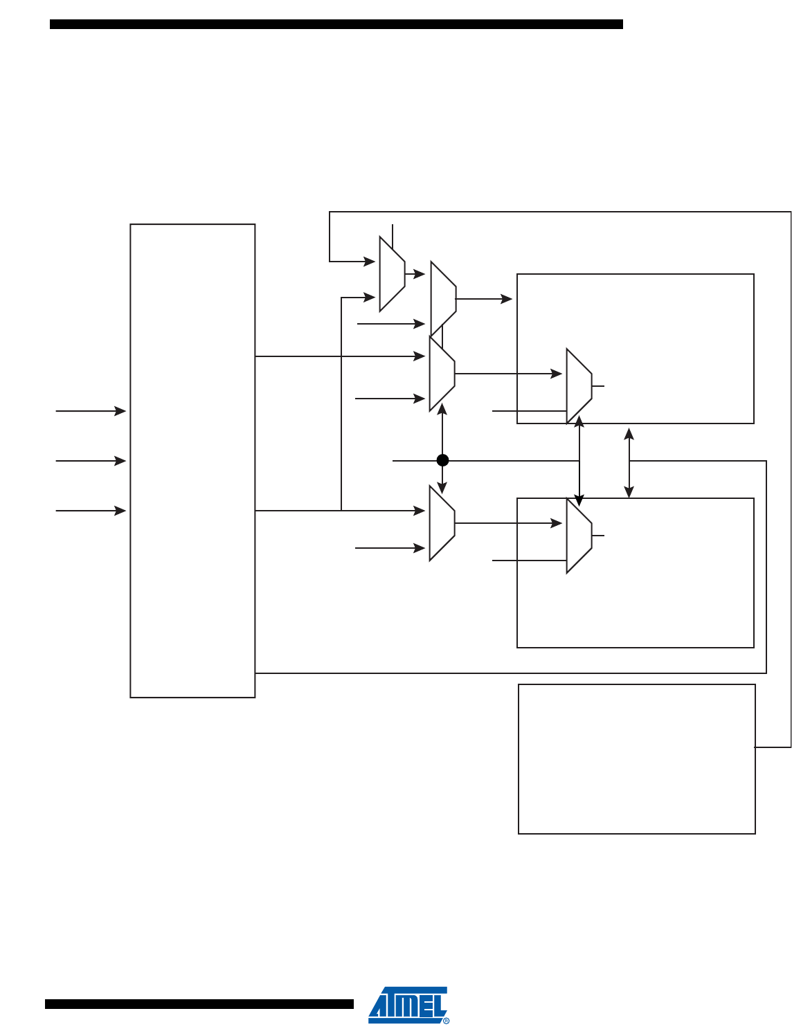
779
6430F–ATARM–21-Feb-12
SAM3U Series
779
6430F–ATARM–21-Feb-12
SAM3U Series
Interruptions can be generated on different events.
A compare function (using TC_RC register) is available on channel 0 (speed/position) or chan-
nel 1 (rotation) and can generate an interrupt by means of the CPCS flag in the TC_SR
registers.
Figure 36-15. Predefined Connection of the Quadrature Decoder with Timer Counters
36.6.14.2 Input Pre-processing
Input pre-processing consists of capabilities to take into account rotary sensor factors such as
polarities and phase definition followed by configurable digital filtering.
Each input can be negated and swapping PHA, PHB is also configurable.
Timer/Counter
Channel 0
1
XC0
TIOA
TIOB
Timer/Counter
Channel 1
1
XC0
TIOB
QDEN
Timer/Counter
Channel 2
1
TIOB0 XC0
1
1
SPEEDEN
1
XC0
Quadrature
Decoder
(Filter + Edge
Detect + QD)
PHA
PHB
IDX
TIOA0
TIOB0
TIOB1
TIOB1
TIOA0
Index
Speed/Position
Rotation
Speed Time Base
Reset pulse
Direction
PHEdgesQDEN
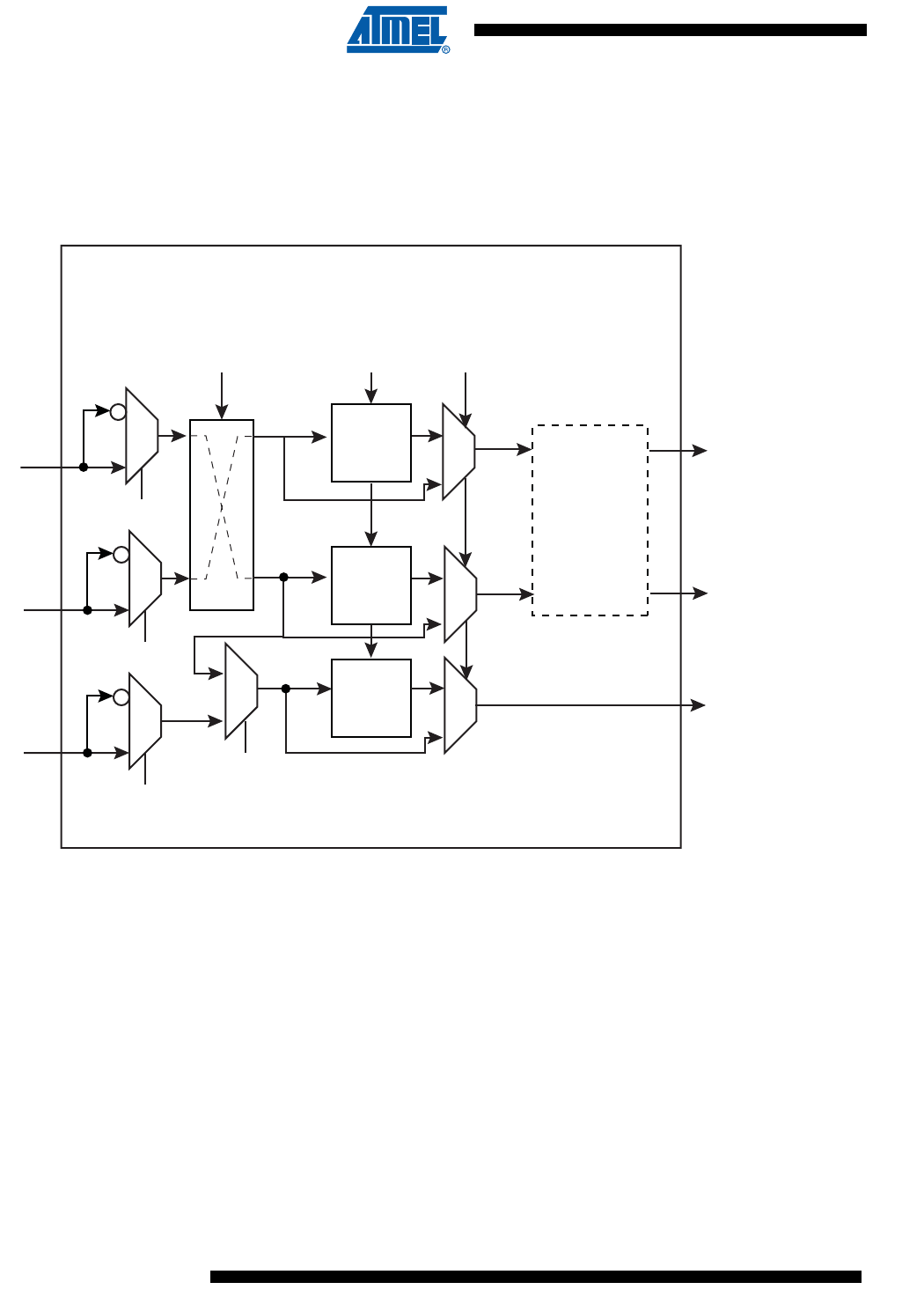
780
6430F–ATARM–21-Feb-12
SAM3U Series
780
6430F–ATARM–21-Feb-12
SAM3U Series
By means of the MAXFILT field in TC_BMR, it is possible to configure a minimum duration for
which the pulse is stated as valid. When the filter is active, pulses with a duration lower than
MAXFILT+1 * tMCK ns are not passed to down-stream logic.
Filters can be disabled using the FILTER field in the TC_BMR register.
Figure 36-16. Input Stage
Input filtering can efficiently remove spurious pulses that might be generated by the presence of
particulate contamination on the optical or magnetic disk of the rotary sensor.
Spurious pulses can also occur in environments with high levels of electro-magnetic interfer-
ence. Or, simply if vibration occurs even when rotation is fully stopped and the shaft of the motor
is in such a position that the beginning of one of the reflective or magnetic bars on the rotary
sensor disk is aligned with the light or magnetic (Hall) receiver cell of the rotary sensor. Any
vibration can make the PHA, PHB signals toggle for a short duration.
1
1
1
MAXFILT
PHA
PHB
IDX
TIOA0
TIOB0
TIOB1
INVA
1
INVB
1
INVIDX
SWAP
1
IDXPHB
Filter
Filter
Filter 1
FILTER
Direction
and
Edge
Detection
IDX
PHedge
DIR
Input Pre-Processing
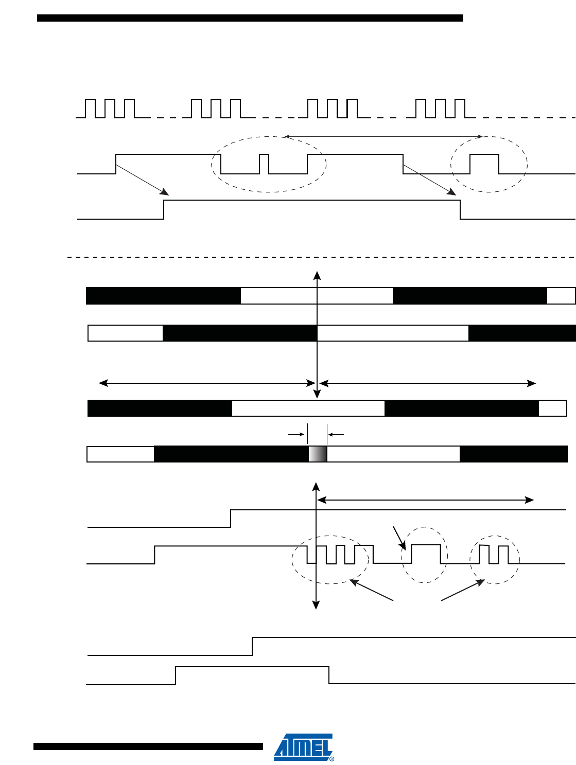
781
6430F–ATARM–21-Feb-12
SAM3U Series
781
6430F–ATARM–21-Feb-12
SAM3U Series
Figure 36-17. Filtering Examples
PHA,B
Filter Out
MCK MAXFILT=2
particulate contamination
PHA
PHB
motor shaft stopped in such a position that
rotary sensor cell is aligned with an edge of the disk
rotation
PHA
PHB
PHB Edge area due to system vibration
Resulting PHA, PHB electrical waveforms
PHA
Optical/Magnetic disk strips
stop
PHB
mechanical shock on system
vibration
stop
PHA, PHB electrical waveforms after filtering
PHA
PHB
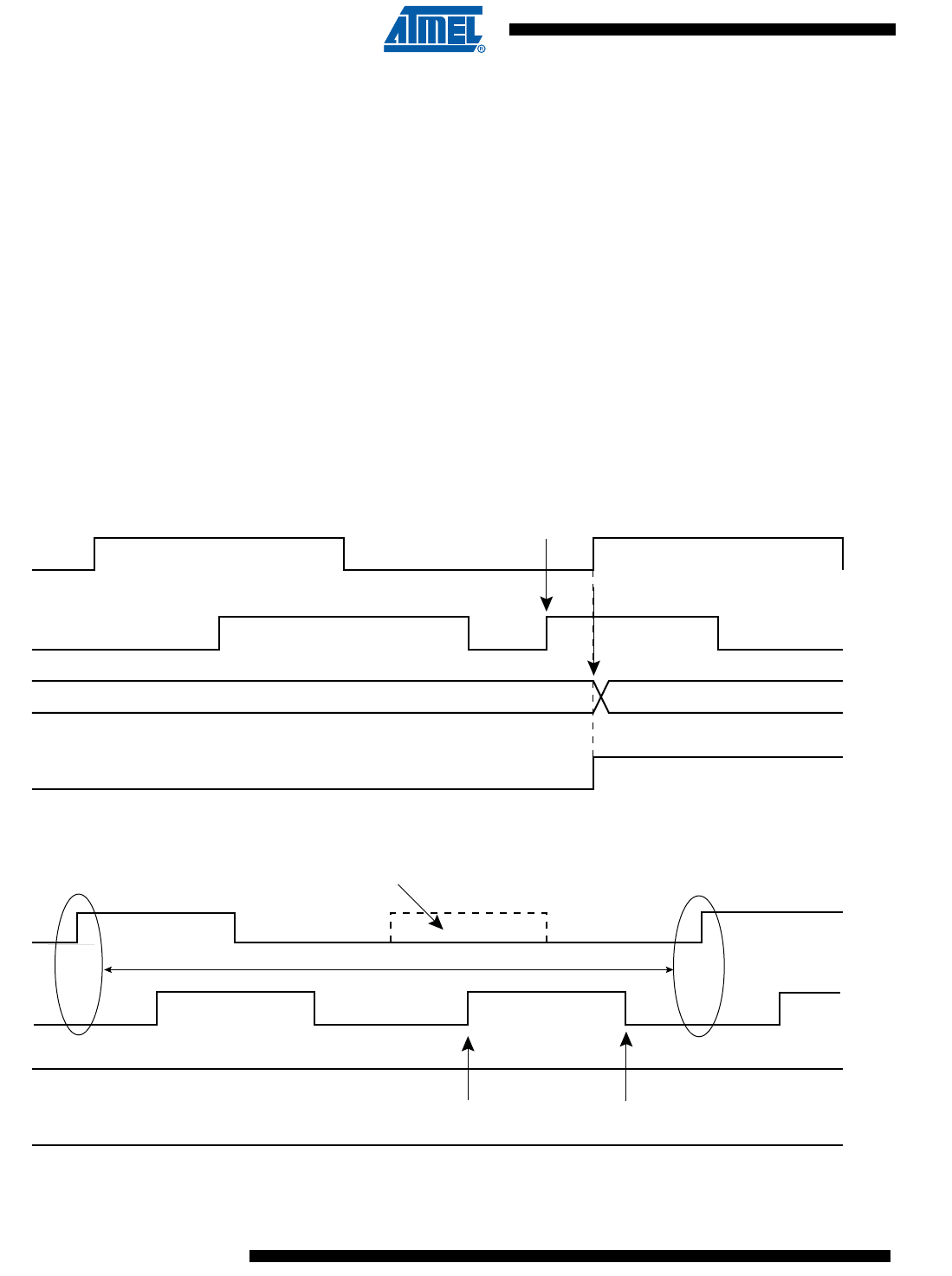
782
6430F–ATARM–21-Feb-12
SAM3U Series
782
6430F–ATARM–21-Feb-12
SAM3U Series
36.6.14.3 Direction Status and Change Detection
After filtering, the quadrature signals are analyzed to extract the rotation direction and edges of
the 2 quadrature signals detected in order to be counted by timer/counter logic downstream.
The direction status can be directly read at anytime on TC_QISR register. The polarity of the
direction flag status depends on the configuration written in TC_BMR register. INVA, INVB,
INVIDX, SWAP modify the polarity of DIR flag.
Any change in rotation direction is reported on TC_QISR register and can generate an interrupt.
The direction change condition is reported as soon as 2 consecutive edges on a phase signal
have sampled the same value on the other phase signal and there is an edge on the other sig-
nal. The 2 consecutive edges of 1 phase signal sampling the same value on other phase signal
is not sufficient to declare a direction change, for the reason that particulate contamination may
mask one or more reflective bar on the optical or magnetic disk of the sensor. (Refer to Figure
36-18 ”Rotation Change Detection” for waveforms.)
Figure 36-18. Rotation Change Detection
The direction change detection is disabled when QDTRANS is set to 1 in TC_BMR. In this case
the DIR flag report must not be used.
PHA
PHB
Direction Change under normal conditions
DIR
DIRCHG
change condition
Report Time
No direction change due to particulate contamination masking a reflective bar
PHA
PHB
DIR
DIRCHG
spurious change condition (if detected in a simple way)
same phase
missing pulse
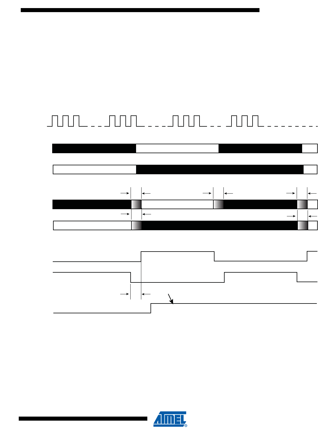
783
6430F–ATARM–21-Feb-12
SAM3U Series
783
6430F–ATARM–21-Feb-12
SAM3U Series
A quadrature error is also reported by the quadrature decoder logic. Rather than reporting an
error only when 2 edges occur at the same time on PHA and PHB, which is unlikely to occur in
real life, there is a report if the time difference between 2 edges on PHA, PHB is lower than a
predefined value. This predefined value is configurable and corresponds to (MAXFILT+1) *
tMCK ns. After being filtered there is no reason to have 2 edges closer than (MAXFILT+1) *
tMCK ns under normal mode of operation. In the instance an anomaly occurs, a quadrature error
is reported on QERR flag on TC_QISR register.
Figure 36-19. Quadrature Error Detection
MAXFILT must be tuned according to several factors such as the system clock frequency
(MCK), type of rotary sensor and rotation speed to be achieved.
36.6.14.4 Position and Rotation Measurement
When POSEN is set in TC_BMR register, position is processed on channel 0 (by means of the
PHA,PHB edge detections) and motor revolutions are accumulated in channel 1 timer/counter
and can be read through TC_CV0 and/or TC_CV1 register if the IDX signal is provided on
TIOA1 input.
Channel 0 and 1 must be configured in capture mode (WAVE = 0 in TC_CMR0).
MCK MAXFILT = 2
PHA
PHB
Abnormally formatted optical disk strips (theoretical view)
PHA
PHB
strip edge inaccurary due to disk etching/printing process
resulting PHA, PHB electrical waveforms
PHA
PHB
Even with an abnorrmaly formatted disk, there is no occurence of PHA, PHB switching at the same time.
QERR
duration < MAXFILT

784
6430F–ATARM–21-Feb-12
SAM3U Series
784
6430F–ATARM–21-Feb-12
SAM3U Series
In parallel, the number of edges are accumulated on timer/counter channel 0 and can be read on
the TC_CV0 register.
Therefore, the accurate position can be read on both TC_CV registers and concatenated to form
a 32-bit word.
The timer/counter channel 0 is cleared for each increment of IDX count value.
Depending on the quadrature signals, the direction is decoded and allows to count up or down in
timer/counter channels 0 and 1. The direction status is reported on TC_QISR register.
36.6.14.5 Speed Measurement
When SPEEDEN is set in TC_BMR register, the speed measure is enabled on channel 0.
A time base must be defined on channel 2 by writing the TC_RC2 period register. Channel 2
must be configured in waveform mode (WAVE bit field set) in TC_CMR2 register. WAVSEL bit
field must be defined with 0x10 to clear the counter by comparison and matching with TC_RC
value. ACPC field must be defined at 0x11 to toggle TIOA output.
This time base is automatically fed back to TIOA of channel 0 when QDEN and SPEEDEN are
set.
Channel 0 must be configured in capture mode (WAVE = 0 in TC_CMR0). ABETRG bit field of
TC_CMR0 must be configured at 1 to get TIOA as a trigger for this channel.
EDGTRG can be set to 0x01, to clear the counter on a rising edge of the TIOA signal and LDRA
field must be set accordingly to 0x01, to load TC_RA0 at the same time as the counter is cleared
(LDRB must be set to 0x01). As a consequence, at the end of each time base period the differ-
entiation required for the speed calculation is performed.
The process must be started by configuring the TC_CR register with CLKEN and SWTRG.
The speed can be read on TC_RA0 register in TC_CMR0.
Channel 1 can still be used to count the number of revolutions of the motor.

785
6430F–ATARM–21-Feb-12
SAM3U Series
785
6430F–ATARM–21-Feb-12
SAM3U Series
36.7 Timer Counter (TC) User Interface
Notes: 1. Channel index ranges from 0 to 2.
2. Read-only if WAVE = 0
Table 36-5. Register Mapping
Offset(1) Register Name Access Reset
0x00 + channel * 0x40 + 0x00 Channel Control Register TC_CCR Write-only –
0x00 + channel * 0x40 + 0x04 Channel Mode Register TC_CMR Read-write 0
0x00 + channel * 0x40 + 0x08 Reserved
0x00 + channel * 0x40 + 0x0C Reserved
0x00 + channel * 0x40 + 0x10 Counter Value TC_CV Read-only 0
0x00 + channel * 0x40 + 0x14 Register A TC_RA Read-write(2) 0
0x00 + channel * 0x40 + 0x18 Register B TC_RB Read-write(2) 0
0x00 + channel * 0x40 + 0x1C Register C TC_RC Read-write 0
0x00 + channel * 0x40 + 0x20 Status Register TC_SR Read-only 0
0x00 + channel * 0x40 + 0x24 Interrupt Enable Register TC_IER Write-only –
0x00 + channel * 0x40 + 0x28 Interrupt Disable Register TC_IDR Write-only –
0x00 + channel * 0x40 + 0x2C Interrupt Mask Register TC_IMR Read-only 0
0xC0 Block Control Register TC_BCR Write-only –
0xC4 Block Mode Register TC_BMR Read-write 0
0xC8 QDEC Interrupt Enable Register TC_QIER Write-only –
0xCC QDEC Interrupt Disable Register TC_QIDR Write-only –
0xD0 QDEC Interrupt Mask Register TC_QIMR Read-only 0
0xD4 QDEC Interrupt Status Register TC_QISR Read-only 0
0xD8 Reserved
0xE4 Reserved
0xFC Reserved – – –

786
6430F–ATARM–21-Feb-12
SAM3U Series
786
6430F–ATARM–21-Feb-12
SAM3U Series
36.7.1 TC Block Control Register
Name: TC_BCR
Address: 0x400800C0
Access: Write-only
• SYNC: Synchro Command
0 = no effect.
1 = asserts the SYNC signal which generates a software trigger simultaneously for each of the channels.
31 30 29 28 27 26 25 24
––––––––
23 22 21 20 19 18 17 16
––––––––
15 14 13 12 11 10 9 8
––––––––
76543210
–––––––SYNC
787
6430F–ATARM–21-Feb-12
SAM3U Series
787
6430F–ATARM–21-Feb-12
SAM3U Series
36.7.2 TC Block Mode Register
Name: TC_BMR
Address: 0x400800C4
Access: Read-write
• TC0XC0S: External Clock Signal 0 Selection
• TC1XC1S: External Clock Signal 1 Selection
• TC2XC2S: External Clock Signal 2 Selection
• QDEN: Quadrature Decoder ENabled
0 = disabled.
1 = enables the quadrature decoder logic (filter, edge detection and quadrature decoding).
quadrature decoding (direction change) can be disabled using QDTRANS bit.
One of the POSEN or SPEEDEN bits must be also enabled.
31 30 29 28 27 26 25 24
–––––– MAXFILT
23 22 21 20 19 18 17 16
MAXFILT FILTER – IDXPHB SWAP
15 14 13 12 11 10 9 8
INVIDX INVB INVA EDGPHA QDTRANS SPEEDEN POSEN QDEN
76543210
– – TC2XC2S TC1XC1S TC0XC0S
Value Name Description
0 TCLK0 Signal connected to XC0: TCLK0
1– Reserved
2 TIOA1 Signal connected to XC0: TIOA1
3 TIOA2 Signal connected to XC0: TIOA2
Value Name Description
0 TCLK1 Signal connected to XC1: TCLK1
1– Reserved
2 TIOA0 Signal connected to XC1: TIOA0
3 TIOA2 Signal connected to XC1: TIOA2
Value Name Description
0 TCLK2 Signal connected to XC2: TCLK2
1– Reserved
2 TIOA1 Signal connected to XC2: TIOA1
3 TIOA2 Signal connected to XC2: TIOA2

788
6430F–ATARM–21-Feb-12
SAM3U Series
788
6430F–ATARM–21-Feb-12
SAM3U Series
• POSEN: POSition ENabled
0 = disable position.
1 = enables the position measure on channel 0 and 1
• SPEEDEN: SPEED ENabled
0 = disabled.
1 = enables the speed measure on channel 0, the time base being provided by channel 2.
• QDTRANS: Quadrature Decoding TRANSparent
0 = full quadrature decoding logic is active (direction change detected).
1 = quadrature decoding logic is inactive (direction change inactive) but input filtering and edge detection are performed.
• EDGPHA: EDGe on PHA count mode
0 = edges are detected on both PHA and PHB.
1 = edges are detected on PHA only.
• INVA: INVerted phA
0 = PHA (TIOA0) is directly driving quadrature decoder logic.
1 = PHA is inverted before driving quadrature decoder logic.
• INVB: INVerted phB
0 = PHB (TIOB0) is directly driving quadrature decoder logic.
1 = PHB is inverted before driving quadrature decoder logic.
• SWAP: SWAP PHA and PHB
0 = no swap between PHA and PHB.
1 = swap PHA and PHB internally, prior to driving quadrature decoder logic.
• INVIDX: INVerted InDeX
0 = IDX (TIOA1) is directly driving quadrature logic.
1 = IDX is inverted before driving quadrature logic.
• IDXPHB: InDeX pin is PHB pin
0 = IDX pin of the rotary sensor must drive TIOA1.
1 = IDX pin of the rotary sensor must drive TIOB0.
•FILTER:
0 = IDX,PHA, PHB input pins are not filtered.
1 = IDX,PHA, PHB input pins are filtered using MAXFILT value.
• MAXFILT: MAXimum FILTer
1.. 63: defines the filtering capabilities
Pulses with a period shorter than MAXFILT+1 MCK clock cycles are discarded.

789
6430F–ATARM–21-Feb-12
SAM3U Series
789
6430F–ATARM–21-Feb-12
SAM3U Series
36.7.3 TC Channel Control Register
Name: TC_CCRx [x=0..2]
Address: 0x40080000 (0)[0], 0x40080040 (0)[1], 0x40080080 (0)[2]
Access: Write-only
• CLKEN: Counter Clock Enable Command
0 = no effect.
1 = enables the clock if CLKDIS is not 1.
• CLKDIS: Counter Clock Disable Command
0 = no effect.
1 = disables the clock.
• SWTRG: Software Trigger Command
0 = no effect.
1 = a software trigger is performed: the counter is reset and the clock is started.
31 30 29 28 27 26 25 24
––––––––
23 22 21 20 19 18 17 16
––––––––
15 14 13 12 11 10 9 8
––––––––
76543210
–––––SWTRGCLKDISCLKEN

790
6430F–ATARM–21-Feb-12
SAM3U Series
790
6430F–ATARM–21-Feb-12
SAM3U Series
36.7.4 TC QDEC Interrupt Enable Register
Name: TC_QIER
Address: 0x400800C8
Access: Write-only
•IDX: InDeX
0 = no effect.
1 = enables the interrupt when a rising edge occurs on IDX input.
• DIRCHG: DIRection CHanGe
0 = no effect.
1 = enables the interrupt when a change on rotation direction is detected.
• QERR: Quadrature ERRor
0 = no effect.
1 = enables the interrupt when a quadrature error occurs on PHA,PHB.
31 30 29 28 27 26 25 24
––––––––
23 22 21 20 19 18 17 16
––––––––
15 14 13 12 11 10 9 8
––––––––
76543210
– – – – – QERR DIRCHG IDX

791
6430F–ATARM–21-Feb-12
SAM3U Series
791
6430F–ATARM–21-Feb-12
SAM3U Series
36.7.5 TC QDEC Interrupt Disable Register
Name: TC_QIDR
Address: 0x400800CC
Access: Write-only
•IDX: InDeX
0 = no effect.
1 = disables the interrupt when a rising edge occurs on IDX input.
• DIRCHG: DIRection CHanGe
0 = no effect.
1 = disables the interrupt when a change on rotation direction is detected.
• QERR: Quadrature ERRor
0 = no effect.
1 = disables the interrupt when a quadrature error occurs on PHA, PHB.
31 30 29 28 27 26 25 24
––––––––
23 22 21 20 19 18 17 16
––––––––
15 14 13 12 11 10 9 8
––––––––
76543210
– – – – – QERR DIRCHG IDX

792
6430F–ATARM–21-Feb-12
SAM3U Series
792
6430F–ATARM–21-Feb-12
SAM3U Series
36.7.6 TC QDEC Interrupt Mask Register
Name: TC_QIMR
Address: 0x400800D0
Access: Read-only
•IDX: InDeX
0 = the interrupt on IDX input is disabled.
1 = the interrupt on IDX input is enabled.
• DIRCHG: DIRection CHanGe
0 = the interrupt on rotation direction change is disabled.
1 = the interrupt on rotation direction change is enabled.
• QERR: Quadrature ERRor
0 = the interrupt on quadrature error is disabled.
1 = the interrupt on quadrature error is enabled.
31 30 29 28 27 26 25 24
––––––––
23 22 21 20 19 18 17 16
––––––––
15 14 13 12 11 10 9 8
––––––––
76543210
– – – – – QERR DIRCHG IDX

793
6430F–ATARM–21-Feb-12
SAM3U Series
793
6430F–ATARM–21-Feb-12
SAM3U Series
36.7.7 TC QDEC Interrupt Status Register
Name: TC_QISR
Address: 0x400800D4
Access: Read-only
•IDX: InDeX
0 = no Index input change since the last read of TC_QISR.
1 = the IDX input has change since the last read of TC_QISR.
• DIRCHG: DIRection CHanGe
0 = no change on rotation direction since the last read of TC_QISR.
1 = the rotation direction changed since the last read of TC_QISR.
• QERR: Quadrature ERRor
0 = no quadrature error since the last read of TC_QISR.
1 = A quadrature error occurred since the last read of TC_QISR.
• DIR: Direction
Returns an image of the actual rotation direction.
31 30 29 28 27 26 25 24
––––––––
23 22 21 20 19 18 17 16
––––––––
15 14 13 12 11 10 9 8
–––––––DIR
76543210
– – – – – QERR DIRCHG IDX

794
6430F–ATARM–21-Feb-12
SAM3U Series
794
6430F–ATARM–21-Feb-12
SAM3U Series
36.7.8 TC Channel Mode Register: Capture Mode
Name: TC_CMRx [x=0..2] (WAVE = 0)
Address: 0x40080004 (0)[0], 0x40080044 (0)[1], 0x40080084 (0)[2]
Access: Read-write
• TCCLKS: Clock Selection
• CLKI: Clock Invert
0 = counter is incremented on rising edge of the clock.
1 = counter is incremented on falling edge of the clock.
• BURST: Burst Signal Selection
• LDBSTOP: Counter Clock Stopped with RB Loading
0 = counter clock is not stopped when RB loading occurs.
1 = counter clock is stopped when RB loading occurs.
31 30 29 28 27 26 25 24
––––––––
23 22 21 20 19 18 17 16
– – – – LDRB LDRA
15 14 13 12 11 10 9 8
WAVE CPCTRG – – – ABETRG ETRGEDG
76543210
LDBDIS LDBSTOP BURST CLKI TCCLKS
Value Name Description
0 TIMER_CLOCK1 Clock selected: TCLK1
1 TIMER_CLOCK2 Clock selected: TCLK2
2 TIMER_CLOCK3 Clock selected: TCLK3
3 TIMER_CLOCK4 Clock selected: TCLK4
4 TIMER_CLOCK5 Clock selected: TCLK5
5 XC0 Clock selected: XC0
6 XC1 Clock selected: XC1
7 XC2 Clock selected: XC2
Value Name Description
0 NONE The clock is not gated by an external signal.
1 XC0 XC0 is ANDed with the selected clock.
2 XC1 XC1 is ANDed with the selected clock.
3 XC2 XC2 is ANDed with the selected clock.
795
6430F–ATARM–21-Feb-12
SAM3U Series
795
6430F–ATARM–21-Feb-12
SAM3U Series
• LDBDIS: Counter Clock Disable with RB Loading
0 = counter clock is not disabled when RB loading occurs.
1 = counter clock is disabled when RB loading occurs.
• ETRGEDG: External Trigger Edge Selection
• ABETRG: TIOA or TIOB External Trigger Selection
0 = TIOB is used as an external trigger.
1 = TIOA is used as an external trigger.
• CPCTRG: RC Compare Trigger Enable
0 = RC Compare has no effect on the counter and its clock.
1 = RC Compare resets the counter and starts the counter clock.
• WAVE: Waveform Mode
0 = Capture Mode is enabled.
1 = Capture Mode is disabled (Waveform Mode is enabled).
• LDRA: RA Loading Edge Selection
• LDRB: RB Loading Edge Selection
Value Name Description
0 NONE The clock is not gated by an external signal.
1 RISING Rising edge
2 FALLING Falling edge
3 EDGE Each edge
Value Name Description
0NONE None
1 RISING Rising edge of TIOA
2 FALLING Falling edge of TIOA
3 EDGE Each edge of TIOA
Value Name Description
0NONE None
1 RISING Rising edge of TIOA
2 FALLING Falling edge of TIOA
3 EDGE Each edge of TIOA
796
6430F–ATARM–21-Feb-12
SAM3U Series
796
6430F–ATARM–21-Feb-12
SAM3U Series
36.7.9 TC Channel Mode Register: Waveform Mode
Name: TC_CMRx [x=0..2] (WAVE = 1)
Address: 0x40080004 (0)[0], 0x40080044 (0)[1], 0x40080084 (0)[2]
Access: Read-write
• TCCLKS: Clock Selection
• CLKI: Clock Invert
0 = counter is incremented on rising edge of the clock.
1 = counter is incremented on falling edge of the clock.
• BURST: Burst Signal Selection
• CPCSTOP: Counter Clock Stopped with RC Compare
0 = counter clock is not stopped when counter reaches RC.
1 = counter clock is stopped when counter reaches RC.
31 30 29 28 27 26 25 24
BSWTRG BEEVT BCPC BCPB
23 22 21 20 19 18 17 16
ASWTRG AEEVT ACPC ACPA
15 14 13 12 11 10 9 8
WAVE WAVSEL ENETRG EEVT EEVTEDG
76543210
CPCDIS CPCSTOP BURST CLKI TCCLKS
Value Name Description
0 TIMER_CLOCK1 Clock selected: TCLK1
1 TIMER_CLOCK2 Clock selected: TCLK2
2 TIMER_CLOCK3 Clock selected: TCLK3
3 TIMER_CLOCK4 Clock selected: TCLK4
4 TIMER_CLOCK5 Clock selected: TCLK5
5 XC0 Clock selected: XC0
6 XC1 Clock selected: XC1
7 XC2 Clock selected: XC2
Value Name Description
0 NONE The clock is not gated by an external signal.
1 XC0 XC0 is ANDed with the selected clock.
2 XC1 XC1 is ANDed with the selected clock.
3 XC2 XC2 is ANDed with the selected clock.
797
6430F–ATARM–21-Feb-12
SAM3U Series
797
6430F–ATARM–21-Feb-12
SAM3U Series
• CPCDIS: Counter Clock Disable with RC Compare
0 = counter clock is not disabled when counter reaches RC.
1 = counter clock is disabled when counter reaches RC.
• EEVTEDG: External Event Edge Selection
• EEVT: External Event Selection
Signal selected as external event.
Note: 1. If TIOB is chosen as the external event signal, it is configured as an input and no longer generates waveforms and subse-
quently no IRQs.
• ENETRG: External Event Trigger Enable
0 = the external event has no effect on the counter and its clock. In this case, the selected external event only controls the
TIOA output.
1 = the external event resets the counter and starts the counter clock.
• WAVSEL: Waveform Selection
• WAVE: Waveform Mode
0 = Waveform Mode is disabled (Capture Mode is enabled).
1 = Waveform Mode is enabled.
Value Name Description
0NONE None
1 RISING Rising edge
2 FALLING Falling edge
3 EDGE Each edge
Value Name Description TIOB Direction
0 TIOB TIOB(1) input
1 XC0 XC0 output
2 XC1 XC1 output
3 XC2 XC2 output
Value Name Description
0 UP UP mode without automatic trigger on RC Compare
1 UPDOWN UPDOWN mode without automatic trigger on RC Compare
2 UP_RC UP mode with automatic trigger on RC Compare
3 UPDOWN_RC UPDOWN mode with automatic trigger on RC Compare
798
6430F–ATARM–21-Feb-12
SAM3U Series
798
6430F–ATARM–21-Feb-12
SAM3U Series
• ACPA: RA Compare Effect on TIOA
• ACPC: RC Compare Effect on TIOA
• AEEVT: External Event Effect on TIOA
• ASWTRG: Software Trigger Effect on TIOA
• BCPB: RB Compare Effect on TIOB
Value Name Description
0NONE None
1 SET Set
2 CLEAR Clear
3 TOGGLE Toggle
Value Name Description
0NONE None
1 SET Set
2 CLEAR Clear
3 TOGGLE Toggle
Value Name Description
0NONE None
1 SET Set
2 CLEAR Clear
3 TOGGLE Toggle
Value Name Description
0NONE None
1 SET Set
2 CLEAR Clear
3 TOGGLE Toggle
Value Name Description
0NONE None
1 SET Set
2 CLEAR Clear
3 TOGGLE Toggle
799
6430F–ATARM–21-Feb-12
SAM3U Series
799
6430F–ATARM–21-Feb-12
SAM3U Series
• BCPC: RC Compare Effect on TIOB
• BEEVT: External Event Effect on TIOB
• BSWTRG: Software Trigger Effect on TIOB
Value Name Description
0NONE None
1 SET Set
2 CLEAR Clear
3 TOGGLE Toggle
Value Name Description
0NONE None
1 SET Set
2 CLEAR Clear
3 TOGGLE Toggle
Value Name Description
0NONE None
1 SET Set
2 CLEAR Clear
3 TOGGLE Toggle

800
6430F–ATARM–21-Feb-12
SAM3U Series
800
6430F–ATARM–21-Feb-12
SAM3U Series
36.7.10 TC Counter Value Register
Name: TC_CVx [x=0..2]
Address: 0x40080010 (0)[0], 0x40080050 (0)[1], 0x40080090 (0)[2]
Access: Read-only
• CV: Counter Value
CV contains the counter value in real time.
31 30 29 28 27 26 25 24
CV
23 22 21 20 19 18 17 16
CV
15 14 13 12 11 10 9 8
CV
76543210
CV

801
6430F–ATARM–21-Feb-12
SAM3U Series
801
6430F–ATARM–21-Feb-12
SAM3U Series
36.7.11 TC Register A
Name: TC_RAx [x=0..2]
Address: 0x40080014 (0)[0], 0x40080054 (0)[1], 0x40080094 (0)[2]
Access: Read-only if WAVE = 0, Read-write if WAVE = 1
• RA: Register A
RA contains the Register A value in real time.
31 30 29 28 27 26 25 24
RA
23 22 21 20 19 18 17 16
RA
15 14 13 12 11 10 9 8
RA
76543210
RA

802
6430F–ATARM–21-Feb-12
SAM3U Series
802
6430F–ATARM–21-Feb-12
SAM3U Series
36.7.12 TC Register B
Name: TC_RBx [x=0..2]
Address: 0x40080018 (0)[0], 0x40080058 (0)[1], 0x40080098 (0)[2]
Access: Read-only if WAVE = 0, Read-write if WAVE = 1
• RB: Register B
RB contains the Register B value in real time.
31 30 29 28 27 26 25 24
RB
23 22 21 20 19 18 17 16
RB
15 14 13 12 11 10 9 8
RB
76543210
RB

803
6430F–ATARM–21-Feb-12
SAM3U Series
803
6430F–ATARM–21-Feb-12
SAM3U Series
36.7.13 TC Register C
Name: TC_RCx [x=0..2]
Address: 0x4008001C (0)[0], 0x4008005C (0)[1], 0x4008009C (0)[2]
Access: Read-write
• RC: Register C
RC contains the Register C value in real time.
31 30 29 28 27 26 25 24
RC
23 22 21 20 19 18 17 16
RC
15 14 13 12 11 10 9 8
RC
76543210
RC

804
6430F–ATARM–21-Feb-12
SAM3U Series
804
6430F–ATARM–21-Feb-12
SAM3U Series
36.7.14 TC Status Register
Name: TC_SRx [x=0..2]
Address: 0x40080020 (0)[0], 0x40080060 (0)[1], 0x400800A0 (0)[2]
Access: Read-only
• COVFS: Counter Overflow Status
0 = no counter overflow has occurred since the last read of the Status Register.
1 = a counter overflow has occurred since the last read of the Status Register.
• LOVRS: Load Overrun Status
0 = Load overrun has not occurred since the last read of the Status Register or WAVE = 1.
1 = RA or RB have been loaded at least twice without any read of the corresponding register since the last read of the Sta-
tus Register, if WAVE = 0.
• CPAS: RA Compare Status
0 = RA Compare has not occurred since the last read of the Status Register or WAVE = 0.
1 = RA Compare has occurred since the last read of the Status Register, if WAVE = 1.
• CPBS: RB Compare Status
0 = RB Compare has not occurred since the last read of the Status Register or WAVE = 0.
1 = RB Compare has occurred since the last read of the Status Register, if WAVE = 1.
• CPCS: RC Compare Status
0 = RC Compare has not occurred since the last read of the Status Register.
1 = RC Compare has occurred since the last read of the Status Register.
• LDRAS: RA Loading Status
0 = RA Load has not occurred since the last read of the Status Register or WAVE = 1.
1 = RA Load has occurred since the last read of the Status Register, if WAVE = 0.
• LDRBS: RB Loading Status
0 = RB Load has not occurred since the last read of the Status Register or WAVE = 1.
1 = RB Load has occurred since the last read of the Status Register, if WAVE = 0.
31 30 29 28 27 26 25 24
––––––––
23 22 21 20 19 18 17 16
–––––MTIOBMTIOACLKSTA
15 14 13 12 11 10 9 8
––––––––
76543210
ETRGS LDRBS LDRAS CPCS CPBS CPAS LOVRS COVFS

805
6430F–ATARM–21-Feb-12
SAM3U Series
805
6430F–ATARM–21-Feb-12
SAM3U Series
• ETRGS: External Trigger Status
0 = external trigger has not occurred since the last read of the Status Register.
1 = external trigger has occurred since the last read of the Status Register.
• CLKSTA: Clock Enabling Status
0 = clock is disabled.
1 = clock is enabled.
• MTIOA: TIOA Mirror
0 = TIOA is low. If WAVE = 0, this means that TIOA pin is low. If WAVE = 1, this means that TIOA is driven low.
1 = TIOA is high. If WAVE = 0, this means that TIOA pin is high. If WAVE = 1, this means that TIOA is driven high.
• MTIOB: TIOB Mirror
0 = TIOB is low. If WAVE = 0, this means that TIOB pin is low. If WAVE = 1, this means that TIOB is driven low.
1 = TIOB is high. If WAVE = 0, this means that TIOB pin is high. If WAVE = 1, this means that TIOB is driven high.

806
6430F–ATARM–21-Feb-12
SAM3U Series
806
6430F–ATARM–21-Feb-12
SAM3U Series
36.7.15 TC Interrupt Enable Register
Name: TC_IERx [x=0..2]
Address: 0x40080024 (0)[0], 0x40080064 (0)[1], 0x400800A4 (0)[2]
Access: Write-only
• COVFS: Counter Overflow
0 = no effect.
1 = enables the Counter Overflow Interrupt.
• LOVRS: Load Overrun
0 = no effect.
1 = enables the Load Overrun Interrupt.
• CPAS: RA Compare
0 = no effect.
1 = enables the RA Compare Interrupt.
• CPBS: RB Compare
0 = no effect.
1 = enables the RB Compare Interrupt.
• CPCS: RC Compare
0 = no effect.
1 = enables the RC Compare Interrupt.
• LDRAS: RA Loading
0 = no effect.
1 = enables the RA Load Interrupt.
• LDRBS: RB Loading
0 = no effect.
1 = enables the RB Load Interrupt.
• ETRGS: External Trigger
0 = no effect.
1 = enables the External Trigger Interrupt.
31 30 29 28 27 26 25 24
––––––––
23 22 21 20 19 18 17 16
––––––––
15 14 13 12 11 10 9 8
––––––––
76543210
ETRGS LDRBS LDRAS CPCS CPBS CPAS LOVRS COVFS

807
6430F–ATARM–21-Feb-12
SAM3U Series
807
6430F–ATARM–21-Feb-12
SAM3U Series
36.7.16 TC Interrupt Disable Register
Name: TC_IDRx [x=0..2]
Address: 0x40080028 (0)[0], 0x40080068 (0)[1], 0x400800A8 (0)[2]
Access: Write-only
• COVFS: Counter Overflow
0 = no effect.
1 = disables the Counter Overflow Interrupt.
• LOVRS: Load Overrun
0 = no effect.
1 = disables the Load Overrun Interrupt (if WAVE = 0).
• CPAS: RA Compare
0 = no effect.
1 = disables the RA Compare Interrupt (if WAVE = 1).
• CPBS: RB Compare
0 = no effect.
1 = disables the RB Compare Interrupt (if WAVE = 1).
• CPCS: RC Compare
0 = no effect.
1 = disables the RC Compare Interrupt.
• LDRAS: RA Loading
0 = no effect.
1 = disables the RA Load Interrupt (if WAVE = 0).
• LDRBS: RB Loading
0 = no effect.
1 = disables the RB Load Interrupt (if WAVE = 0).
• ETRGS: External Trigger
0 = no effect.
1 = disables the External Trigger Interrupt.
31 30 29 28 27 26 25 24
––––––––
23 22 21 20 19 18 17 16
––––––––
15 14 13 12 11 10 9 8
––––––––
76543210
ETRGS LDRBS LDRAS CPCS CPBS CPAS LOVRS COVFS

808
6430F–ATARM–21-Feb-12
SAM3U Series
808
6430F–ATARM–21-Feb-12
SAM3U Series
36.7.17 TC Interrupt Mask Register
Name: TC_IMRx [x=0..2]
Address: 0x4008002C (0)[0], 0x4008006C (0)[1], 0x400800AC (0)[2]
Access: Read-only
• COVFS: Counter Overflow
0 = the Counter Overflow Interrupt is disabled.
1 = the Counter Overflow Interrupt is enabled.
• LOVRS: Load Overrun
0 = the Load Overrun Interrupt is disabled.
1 = the Load Overrun Interrupt is enabled.
• CPAS: RA Compare
0 = the RA Compare Interrupt is disabled.
1 = the RA Compare Interrupt is enabled.
• CPBS: RB Compare
0 = the RB Compare Interrupt is disabled.
1 = the RB Compare Interrupt is enabled.
• CPCS: RC Compare
0 = the RC Compare Interrupt is disabled.
1 = the RC Compare Interrupt is enabled.
• LDRAS: RA Loading
0 = the Load RA Interrupt is disabled.
1 = the Load RA Interrupt is enabled.
• LDRBS: RB Loading
0 = the Load RB Interrupt is disabled.
1 = the Load RB Interrupt is enabled.
• ETRGS: External Trigger
0 = the External Trigger Interrupt is disabled.
1 = the External Trigger Interrupt is enabled.
31 30 29 28 27 26 25 24
––––––––
23 22 21 20 19 18 17 16
––––––––
15 14 13 12 11 10 9 8
––––––––
76543210
ETRGS LDRBS LDRAS CPCS CPBS CPAS LOVRS COVFS

809
6430F–ATARM–21-Feb-12
SAM3U Series
809
6430F–ATARM–21-Feb-12
SAM3U Series
37. High Speed Multimedia Card Interface (HSMCI)
37.1 Description
The High Speed Multimedia Card Interface (HSMCI) supports the MultiMedia Card (MMC)
Specification V4.3, the SD Memory Card Specification V2.0, the SDIO V2.0 specification and
CE-ATA V1.1.
The HSMCI includes a command register, response registers, data registers, timeout counters
and error detection logic that automatically handle the transmission of commands and, when
required, the reception of the associated responses and data with a limited processor overhead.
The HSMCI supports stream, block and multi block data read and write, and is compatible with
the DMA Controller (DMAC), minimizing processor intervention for large buffer transfers.
The HSMCI operates at a rate of up to Master Clock divided by 2 and supports the interfacing of
1 slot(s). Each slot may be used to interface with a High Speed MultiMediaCard bus (up to 30
Cards) or with an SD Memory Card. Only one slot can be selected at a time (slots are multi-
plexed). A bit field in the SD Card Register performs this selection.
The SD Memory Card communication is based on a 9-pin interface (clock, command, four data
and three power lines) and the High Speed MultiMedia Card on a 7-pin interface (clock, com-
mand, one data, three power lines and one reserved for future use).
The SD Memory Card interface also supports High Speed MultiMedia Card operations. The
main differences between SD and High Speed MultiMedia Cards are the initialization process
and the bus topology.
HSMCI fully supports CE-ATA Revision 1.1, built on the MMC System Specification v4.0. The
module includes dedicated hardware to issue the command completion signal and capture the
host command completion signal disable.
37.2 Embedded Characteristics
• Compatible with MultiMedia Card Specification Version 4.3
• Compatible with SD Memory Card Specification Version 2.0
• Compatible with SDIO Specification Version 2.0
• Compatible with CE-ATA Specification 1.1
• Cards Clock Rate Up to Master Clock Divided by 2
• Boot Operation Mode Support
• High Speed Mode Support
• Embedded Power Management to Slow Down Clock Rate When Not Used
• Supports 1 Multiplexed Slot(s)
– Each Slot for either a High Speed MultiMediaCard Bus (Up to 30 Cards) or an SD
Memory Card
• Support for Stream, Block and Multi-block Data Read and Write
• Supports Connection to DMA Controller (DMAC)
– Minimizes Processor Intervention for Large Buffer Transfers
• Built in FIFO (from 16 to 256 bytes) with Large Memory Aperture Supporting Incremental
Access
• Support for CE-ATA Completion Signal Disable Command
• Protection Against Unexpected Modification On-the-Fly of the Configuration Registers
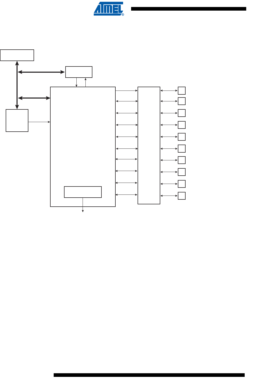
810
6430F–ATARM–21-Feb-12
SAM3U Series
810
6430F–ATARM–21-Feb-12
SAM3U Series
37.3 Block Diagram
Figure 37-1. Block Diagram
Note: 1. When several HSMCI (x HSMCI) are embedded in a product, MCCK refers to HSMCIx_CK, MCCDA to HSMCIx_CDA,
MCDAy to HSMCIx_DAy.
MCDA3
(1)
MCDA2
(1)
MCDA1
(1)
MCDA0
(1)
MCCDA
(1)
MCCK
(1)
HSMCI Interface
Interrupt Control
HSMCI Interrupt
PIO
APB Bridge
PMC MCK
APB
MCDA7
(1)
MCDA6
(1)
MCDA5
(1)
MCDA4
(1)
DMAC
811
6430F–ATARM–21-Feb-12
SAM3U Series
811
6430F–ATARM–21-Feb-12
SAM3U Series
37.4 Application Block Diagram
Figure 37-2. Application Block Diagram
37.5 Pin Name List
Notes: 1. I: Input, O: Output, PP: Push/Pull, OD: Open Drain.
2. When several HSMCI (x HSMCI) are embedded in a product, MCCK refers to HSMCIx_CK, MCCDA to HSMCIx_CDA,
MCCDB to HSMCIx_CDB, MCCDC to HSMCIx_CDC, MCCDD to HSMCIx_CDD, MCDAy to HSMCIx_DAy, MCDBy to
HSMCIx_DBy, MCDCy to HSMCIx_DCy, MCDDy to HSMCIx_DDy.
2345617
MMC
23456178
SDCard
9
Physical Layer
HSMCI Interface
Application Layer
ex: File System, Audio, Security, etc.
9 1011 1213 8
Table 37-1. I/O Lines Description for 8-bit Configuration
Pin Name(2) Pin Description Type(1) Comments
MCCDA Command/response I/O/PP/OD CMD of an MMC or SDCard/SDIO
MCCK Clock I/O CLK of an MMC or SD Card/SDIO
MCDA0 - MCDA7 Data 0..7 of Slot A I/O/PP DAT[0..7] of an MMC
DAT[0..3] of an SD Card/SDIO
MCDB0 - MCDB7 Data 0..7 of Slot B I/O/PP DAT[0..7] of an MMC
DAT[0..3] of an SD Card/SDIO
MCDC0 - MCDC7 Data 0..7 of Slot C I/O/PP DAT[0..7] of an MMC
DAT[0..3] of an SD Card/SDIO
MCDD0 - MCDD7 Data 0..7 of Slot D I/O/PP DAT[0..7] of an MMC
DAT[0..3] of an SD Card/SDIO
812
6430F–ATARM–21-Feb-12
SAM3U Series
812
6430F–ATARM–21-Feb-12
SAM3U Series
37.6 Product Dependencies
37.6.1 I/O Lines
The pins used for interfacing the High Speed MultiMedia Cards or SD Cards are multiplexed with
PIO lines. The programmer must first program the PIO controllers to assign the peripheral func-
tions to HSMCI pins.
37.6.2 Power Management
The HSMCI is clocked through the Power Management Controller (PMC), so the programmer
must first configure the PMC to enable the HSMCI clock.
37.6.3 Interrupt
The HSMCI interface has an interrupt line connected to the Nested Vector Interrupt Controller
(NVIC).
Handling the HSMCI interrupt requires programming the NVIC before configuring the HSMCI.
37.7 Bus Topology
Figure 37-3. High Speed MultiMedia Memory Card Bus Topology
Table 37-2. I/O Lines
Instance Signal I/O Line Peripheral
HSMCI MCCDA PA4 A
HSMCI MCCK PA3 A
HSMCI MCDA0 PA5 A
HSMCI MCDA1 PA6 A
HSMCI MCDA2 PA7 A
HSMCI MCDA3 PA8 A
HSMCI MCDA4 PC28 B
HSMCI MCDA5 PC29 B
HSMCI MCDA6 PC30 B
HSMCI MCDA7 PC31 B
2345617
MMC
91011 12138
813
6430F–ATARM–21-Feb-12
SAM3U Series
813
6430F–ATARM–21-Feb-12
SAM3U Series
The High Speed MultiMedia Card communication is based on a 13-pin serial bus interface. It has
three communication lines and four supply lines.
Notes: 1. I: Input, O: Output, PP: Push/Pull, OD: Open Drain.
2. When several HSMCI (x HSMCI) are embedded in a product, MCCK refers to HSMCIx_CK,
MCCDA to HSMCIx_CDA, MCDAy to HSMCIx_DAy.
Figure 37-4. MMC Bus Connections (One Slot)
Note: When several HSMCI (x HSMCI) are embedded in a product, MCCK refers to HSMCIx_CK,
MCCDA to HSMCIx_CDA MCDAy to HSMCIx_DAy.
Table 37-3. Bus Topology
Pin
Number Name Type(1) Description
HSMCI Pin Name(2)
(Slot z)
1 DAT[3] I/O/PP Data MCDz3
2 CMD I/O/PP/OD Command/response MCCDz
3 VSS1 S Supply voltage ground VSS
4 VDD S Supply voltage VDD
5 CLK I/O Clock MCCK
6 VSS2 S Supply voltage ground VSS
7 DAT[0] I/O/PP Data 0 MCDz0
8 DAT[1] I/O/PP Data 1 MCDz1
9 DAT[2] I/O/PP Data 2 MCDz2
10 DAT[4] I/O/PP Data 4 MCDz4
11 DAT[5] I/O/PP Data 5 MCDz5
12 DAT[6] I/O/PP Data 6 MCDz6
13 DAT[7] I/O/PP Data 7 MCDz7
MCCDA
MCDA0
MCCK
HSMCI
2345617
MMC1
9 1011 1213 8
2345617
MMC2
9 1011 1213 8
2345617
MMC3
9 1011 1213 8
814
6430F–ATARM–21-Feb-12
SAM3U Series
814
6430F–ATARM–21-Feb-12
SAM3U Series
Figure 37-5. SD Memory Card Bus Topology
The SD Memory Card bus includes the signals listed in Table 37-4.
Notes: 1. I: input, O: output, PP: Push Pull, OD: Open Drain.
2. When several HSMCI (x HSMCI) are embedded in a product, MCCK refers to HSMCIx_CK,
MCCDA to HSMCIx_CDA, MCDAy to HSMCIx_DAy.
Figure 37-6. SD Card Bus Connections with One Slot
Note: When several HSMCI (x HSMCI) are embedded in a product, MCCK refers to HSMCIx_CK,
MCCDA to HSMCIx_CDA MCDAy to HSMCIx_DAy.
When the HSMCI is configured to operate with SD memory cards, the width of the data bus can
be selected in the HSMCI_SDCR register. Clearing the SDCBUS bit in this register means that
the width is one bit; setting it means that the width is four bits. In the case of High Speed Multi-
Media cards, only the data line 0 is used. The other data lines can be used as independent
PIOs.
Table 37-4. SD Memory Card Bus Signals
Pin
Number Name Type(1) Description
HSMCI Pin Name(2)
(Slot z)
1 CD/DAT[3] I/O/PP Card detect/ Data line Bit 3 MCDz3
2 CMD PP Command/response MCCDz
3 VSS1 S Supply voltage ground VSS
4 VDD S Supply voltage VDD
5 CLK I/O Clock MCCK
6 VSS2 S Supply voltage ground VSS
7 DAT[0] I/O/PP Data line Bit 0 MCDz0
8 DAT[1] I/O/PP Data line Bit 1 or Interrupt MCDz1
9 DAT[2] I/O/PP Data line Bit 2 MCDz2
23456178
SD CARD
9
2345617
MCDA0 - MCDA3
MCCDA
MCCK
8
SD CARD
9

815
6430F–ATARM–21-Feb-12
SAM3U Series
815
6430F–ATARM–21-Feb-12
SAM3U Series
37.8 High Speed MultiMediaCard Operations
After a power-on reset, the cards are initialized by a special message-based High Speed Multi-
MediaCard bus protocol. Each message is represented by one of the following tokens:
• Command: A command is a token that starts an operation. A command is sent from the host
either to a single card (addressed command) or to all connected cards (broadcast
command). A command is transferred serially on the CMD line.
• Response: A response is a token which is sent from an addressed card or (synchronously)
from all connected cards to the host as an answer to a previously received command. A
response is transferred serially on the CMD line.
• Data: Data can be transferred from the card to the host or vice versa. Data is transferred via
the data line.
Card addressing is implemented using a session address assigned during the initialization
phase by the bus controller to all currently connected cards. Their unique CID number identifies
individual cards.
The structure of commands, responses and data blocks is described in the High Speed MultiMe-
dia-Card System Specification. See also Table 37-5 on page 816.
High Speed MultiMediaCard bus data transfers are composed of these tokens.
There are different types of operations. Addressed operations always contain a command and a
response token. In addition, some operations have a data token; the others transfer their infor-
mation directly within the command or response structure. In this case, no data token is present
in an operation. The bits on the DAT and the CMD lines are transferred synchronous to the clock
HSMCI Clock.
Two types of data transfer commands are defined:
• Sequential commands: These commands initiate a continuous data stream. They are
terminated only when a stop command follows on the CMD line. This mode reduces the
command overhead to an absolute minimum.
• Block-oriented commands: These commands send a data block succeeded by CRC bits.
Both read and write operations allow either single or multiple block transmission. A multiple
block transmission is terminated when a stop command follows on the CMD line similarly to the
sequential read or when a multiple block transmission has a pre-defined block count (See “Data
Transfer Operation” on page 818.).
The HSMCI provides a set of registers to perform the entire range of High Speed MultiMedia
Card operations.
37.8.1 Command - Response Operation
After reset, the HSMCI is disabled and becomes valid after setting the MCIEN bit in the
HSMCI_CR Control Register.
The PWSEN bit saves power by dividing the HSMCI clock by 2PWSDIV + 1 when the bus is
inactive.
The two bits, RDPROOF and WRPROOF in the HSMCI Mode Register (HSMCI_MR) allow
stopping the HSMCI Clock during read or write access if the internal FIFO is full. This will guar-
antee data integrity, not bandwidth.
All the timings for High Speed MultiMedia Card are defined in the High Speed MultiMediaCard
System Specification.

816
6430F–ATARM–21-Feb-12
SAM3U Series
816
6430F–ATARM–21-Feb-12
SAM3U Series
The two bus modes (open drain and push/pull) needed to process all the operations are defined
in the HSMCI command register. The HSMCI_CMDR allows a command to be carried out.
For example, to perform an ALL_SEND_CID command:
The command ALL_SEND_CID and the fields and values for the HSMCI_CMDR Control Regis-
ter are described in Table 37-5 and Table 37-6.
Note: 1. bcr means broadcast command with response.
The HSMCI_ARGR contains the argument field of the command.
To send a command, the user must perform the following steps:
• Fill the argument register (HSMCI_ARGR) with the command argument.
• Set the command register (HSMCI_CMDR) (see Table 37-6).
The command is sent immediately after writing the command register.
While the card maintains a busy indication (at the end of a STOP_TRANSMISSION command
CMD12, for example), a new command shall not be sent. The NOTBUSY flag in the status regis-
ter (HSMCI_SR) is asserted when the card releases the busy indication.
If the command requires a response, it can be read in the HSMCI response register
(HSMCI_RSPR). The response size can be from 48 bits up to 136 bits depending on the com-
mand. The HSMCI embeds an error detection to prevent any corrupted data during the transfer.
Host Command NID Cycles CID
CMD S T Content CRC E Z ****** Z S T Content Z Z Z
Table 37-5. ALL_SEND_CID Command Description
CMD Index Type Argument Resp Abbreviation
Command
Description
CMD2 bcr(1) [31:0] stuff bits R2 ALL_SEND_CID
Asks all cards to send
their CID numbers on
the CMD line
Table 37-6. Fields and Values for HSMCI_CMDR Command Register
Field Value
CMDNB (command number) 2 (CMD2)
RSPTYP (response type) 2 (R2: 136 bits response)
SPCMD (special command) 0 (not a special command)
OPCMD (open drain command) 1
MAXLAT (max latency for command to response) 0 (NID cycles ==> 5 cycles)
TRCMD (transfer command) 0 (No transfer)
TRDIR (transfer direction) X (available only in transfer command)
TRTYP (transfer type) X (available only in transfer command)
IOSPCMD (SDIO special command) 0 (not a special command)
817
6430F–ATARM–21-Feb-12
SAM3U Series
817
6430F–ATARM–21-Feb-12
SAM3U Series
The following flowchart shows how to send a command to the card and read the response if
needed. In this example, the status register bits are polled but setting the appropriate bits in the
interrupt enable register (HSMCI_IER) allows using an interrupt method.
Figure 37-7. Command/Response Functional Flow Diagram
RETURN OK
RETURN ERROR(1)
RETURN OK
Set the command argument
HSMCI_ARGR = Argument
(1)
Set the command
HSMCI_CMDR = Command
Read HSMCI_SR
CMDRDY
Status error flags?
Read response if required
Ye s
Wait for command
ready status flag
Check error bits in the
status register
(1)
0
1
Does the command involve
a busy indication?
No
Read HSMCI_SR
0
NOTBUSY
1

818
6430F–ATARM–21-Feb-12
SAM3U Series
818
6430F–ATARM–21-Feb-12
SAM3U Series
Note: 1. If the command is SEND_OP_COND, the CRC error flag is always present (refer to R3 response in the High Speed MultiMe-
dia Card specification).
37.8.2 Data Transfer Operation
The High Speed MultiMedia Card allows several read/write operations (single block, multiple
blocks, stream, etc.). These kinds of transfer can be selected setting the Transfer Type (TRTYP)
field in the HSMCI Command Register (HSMCI_CMDR).
These operations can be done using the features of the DMA Controller.
In all cases, the block length (BLKLEN field) must be defined either in the mode register
HSMCI_MR, or in the Block Register HSMCI_BLKR. This field determines the size of the data
block.
Consequent to MMC Specification 3.1, two types of multiple block read (or write) transactions
are defined (the host can use either one at any time):
• Open-ended/Infinite Multiple block read (or write):
The number of blocks for the read (or write) multiple block operation is not defined. The card
will continuously transfer (or program) data blocks until a stop transmission command is
received.
• Multiple block read (or write) with pre-defined block count (since version 3.1 and higher):
The card will transfer (or program) the requested number of data blocks and terminate the
transaction. The stop command is not required at the end of this type of multiple block read
(or write), unless terminated with an error. In order to start a multiple block read (or write)
with pre-defined block count, the host must correctly program the HSMCI Block Register
(HSMCI_BLKR). Otherwise the card will start an open-ended multiple block read. The BCNT
field of the Block Register defines the number of blocks to transfer (from 1 to 65535 blocks).
Programming the value 0 in the BCNT field corresponds to an infinite block transfer.
37.8.3 Read Operation
The following flowchart (Figure 37-8) shows how to read a single block with or without use of
DMAC facilities. In this example, a polling method is used to wait for the end of read. Similarly,
the user can configure the interrupt enable register (HSMCI_IER) to trigger an interrupt at the
end of read.
819
6430F–ATARM–21-Feb-12
SAM3U Series
819
6430F–ATARM–21-Feb-12
SAM3U Series
Figure 37-8. Read Functional Flow Diagram
Notes: 1. It is assumed that this command has been correctly sent (see Figure 37-7).
2. This field is also accessible in the HSMCI Block Register (HSMCI_BLKR).
Read status register HSMCI_SR
Send SELECT/DESELECT_CARD
command(1) to select the card
Send SET_BLOCKLEN command(1)
Read with DMAC
Number of words to read = 0 ?
Poll the bit
RXRDY = 0?
Read data = HSMCI_RDR
Number of words to read =
Number of words to read -1
Send READ_SINGLE_BLOCK
command(1)
Ye s
Set the DMAEN bit
HSMCI_DMA |= DMAEN
Set the block length (in bytes)
HSMCI_BLKR |= (BlockLength << 16)(2)
Configure the DMA channel X
DMAC_SADDRx = Data Address
DMAC_BTSIZE = BlockLength/4
DMACHEN[X] = TRUE
Send READ_SINGLE_BLOCK
command(1)
Read status register HSMCI_SR
Poll the bit
XFRDONE = 0?
Ye s
RETURN
RETURN
Ye sNo
No
No
Ye s
No
Number of words to read = BlockLength/4
Reset the DMAEN bit
HSMCI_DMA &= ~DMAEN
Set the block length (in bytes)
HSMCI_MR l= (BlockLength<<16) (2)
Set the block count (if neccessary)
HSMCI_BLKR l= (BlockCount<<0)

820
6430F–ATARM–21-Feb-12
SAM3U Series
820
6430F–ATARM–21-Feb-12
SAM3U Series
37.8.4 Write Operation
In write operation, the HSMCI Mode Register (HSMCI_MR) is used to define the padding value
when writing non-multiple block size. If the bit PADV is 0, then 0x00 value is used when padding
data, otherwise 0xFF is used.
If set, the bit DMAEN in the HSMCI_DMA register enables DMA transfer.
The following flowchart (Figure 37-9) shows how to write a single block with or without use of
DMA facilities. Polling or interrupt method can be used to wait for the end of write according to
the contents of the Interrupt Mask Register (HSMCI_IMR).
821
6430F–ATARM–21-Feb-12
SAM3U Series
821
6430F–ATARM–21-Feb-12
SAM3U Series
Figure 37-9. Write Functional Flow Diagram
Note: 1. It is assumed that this command has been correctly sent (see Figure 37-7).
2. This field is also accessible in the HSMCI Block Register (HSMCI_BLKR).
Send SELECT/DESELECT_CARD
command(1) to select the card
Send SET_BLOCKLEN command(1)
Write using DMAC
Send WRITE_SINGLE_BLOCK
command(1)
Configure the DMA channel X
DMAC_DADDRx = Data Address to write
DMAC_BTSIZE = BlockLength/4
Send WRITE_SINGLE_BLOCK
command(1)
Read status register HSMCI_SR
Poll the bit
XFRDONE = 0?
Ye s
No Ye s
No
Read status register HSMCI_SR
Number of words to write = 0 ?
Poll the bit
TXRDY = 0?
HSMCI_TDR = Data to write
Number of words to write =
Number of words to write -1
Ye s
RETURN
No
Ye s
No
Number of words to write = BlockLength/4
DMAC_CHEN[X] = TRUE
Reset theDMAEN bit
HSMCI_DMA &= ~DMAEN
Set the block length (in bytes)
HSMCI_MR |= (BlockLength) <<16)(2)
Set the block count (if necessary)
HSMCI_BLKR |= (BlockCount << 0)
Set the DMAEN bit
HSMCI_DMA |= DMAEN
Set the block length (in bytes)
HSMCI_BLKR |= (BlockLength << 16)(2)
RETURN
822
6430F–ATARM–21-Feb-12
SAM3U Series
822
6430F–ATARM–21-Feb-12
SAM3U Series
The following flowchart (Figure 37-10) shows how to manage read multiple block and write mul-
tiple block transfers with the DMA Controller. Polling or interrupt method can be used to wait for
the end of write according to the contents of the Interrupt Mask Register (HSMCI_IMR).
Figure 37-10. Read Multiple Block and Write Multiple Block
Notes: 1. It is assumed that this command has been correctly sent (see Figure 37-7).
2. Handle errors reported in HSMCI_SR.
Send SELECT/DESELECT_CARD
command(1) to select the card
Send SET_BLOCKLEN command(1)
Set the block length
HSMCI_MR |= (BlockLength << 16)
Set the DMAEN bit
HSMCI_DMA |= DMAEN
Configure the HDMA channel X
DMAC_SADDRx and DMAC_DADDRx
DMAC_BTSIZE = BlockLength/4
Send WRITE_MULTIPLE_BLOCK or
READ_MULTIPLE_BLOCK command(1)
Read status register DMAC_EBCISR
and Poll Bit CBTC[X]
New Buffer ?(2)
No
DMAC_CHEN[X] = TRUE
Poll the bit
XFRDONE = 1 No
RETURN
Ye s
Send STOP_TRANSMISSION
command(1)
Ye s
Read status register HSMCI_SR
and Poll Bit FIFOEMPTY

823
6430F–ATARM–21-Feb-12
SAM3U Series
823
6430F–ATARM–21-Feb-12
SAM3U Series
37.8.5 WRITE_SINGLE_BLOCK Operation using DMA Controller
1. Wait until the current command execution has successfully terminated.
c. Check that CMDRDY and NOTBUSY fields are asserted in HSMCI_SR
2. Program the block length in the card. This value defines the value block_length.
3. Program the block length in the HSMCI configuration register with block_length value.
4. Program HSMCI_DMA register with the following fields:
– OFFSET field with dma_offset.
– CHKSIZE is user defined and set according to DMAC_DCSIZE.
– DMAEN is set to true to enable DMA hardware handshaking in the HSMCI. This bit
was previously set to false.
5. Issue a WRITE_SINGLE_BLOCK command writing HSMCI_ARG then HSMCI_CMDR.
6. Program the DMA Controller.
a. Read the channel Register to choose an available (disabled) channel.
b. Clear any pending interrupts on the channel from the previous DMAC transfer by
reading the DMAC_EBCISR register.
c. Program the channel registers.
d. The DMAC_SADDRx register for channel x must be set to the location of the
source data. When the first data location is not word aligned, the two LSB bits
define the temporary value called dma_offset. The two LSB bits of
DMAC_SADDRx must be set to 0.
e. The DMAC_DADDRx register for channel x must be set with the starting address of
the HSMCI_FIFO address.
f. Program DMAC_CTRLAx register of channel x with the following field’s values:
–DST_WIDTH is set to WORD.
–SRC_WIDTH is set to WORD.
–DCSIZE must be set according to the value of HSMCI_DMA, CHKSIZE field.
–BTSIZE is programmed with CEILING((block_length + dma_offset) / 4), where
the ceiling function is the function that returns the smallest integer not less than
x.
g. Program DMAC_CTRLBx register for channel x with the following field’s values:
–DST_INCR is set to INCR, the block_length value must not be larger than the
HSMCI_FIFO aperture.
–SRC_INCR is set to INCR.
–FC field is programmed with memory to peripheral flow control mode.
–both DST_DSCR and SRC_DSCR are set to 1 (descriptor fetch is disabled).
–DIF and SIF are set with their respective layer ID. If SIF is different from DIF, the
DMA controller is able to prefetch data and write HSMCI simultaneously.
h. Program DMAC_CFGx register for channel x with the following field’s values:
–FIFOCFG defines the watermark of the DMAC channel FIFO.
–DST_H2SEL is set to true to enable hardware handshaking on the destination.
–DST_PER is programmed with the hardware handshaking ID of the targeted
HSMCI Host Controller.

824
6430F–ATARM–21-Feb-12
SAM3U Series
824
6430F–ATARM–21-Feb-12
SAM3U Series
i. Enable Channel x, writing one to DMAC_CHER[x]. The DMAC is ready and waiting
for request.
7. Wait for XFRDONE in HSMCI_SR register.
37.8.6 READ_SINGLE_BLOCK Operation using DMA Controller
37.8.6.1 Block Length is Multiple of 4
1. Wait until the current command execution has successfully completed.
a. Check that CMDRDY and NOTBUSY are asserted in HSMCI_SR.
2. Program the block length in the card. This value defines the value block_length.
3. Program the block length in the HSMCI configuration register with block_length value.
4. Set RDPROOF bit in HSMCI_MR to avoid overflow.
5. Program HSMCI_DMA register with the following fields:
– ROPT field is set to 0.
– OFFSET field is set to 0.
– CHKSIZE is user defined.
– DMAEN is set to true to enable DMAC hardware handshaking in the HSMCI. This bit
was previously set to false.
6. Issue a READ_SINGLE_BLOCK command.
7. Program the DMA controller.
a. Read the channel Register to choose an available (disabled) channel.
b. Clear any pending interrupts on the channel from the previous DMA transfer by
reading the DMAC_EBCISR register.
c. Program the channel registers.
d. The DMAC_SADDRx register for channel x must be set with the starting address of
the HSMCI_FIFO address.
e. The DMAC_DADDRx register for channel x must be word aligned.
f. Program DMAC_CTRLAx register of channel x with the following field’s values:
–DST_WIDTH is set to WORD.
–SRC_WIDTH is set to WORD.
–SCSIZE must be set according to the value of HSMCI_DMA, CHKSIZE field.
–BTSIZE is programmed with block_length/4.
g. Program DMAC_CTRLBx register for channel x with the following field’s values:
–DST_INCR is set to INCR.
–SRC_INCR is set to INCR.
–FC field is programmed with peripheral to memory flow control mode.
–both DST_DSCR and SRC_DSCR are set to 1 (descriptor fetch is disabled).
–DIF and SIF are set with their respective layer ID. If SIF is different from DIF, the
DMA controller is able to prefetch data and write HSMCI simultaneously.
h. Program DMAC_CFGx register for channel x with the following field’s values:
–FIFOCFG defines the watermark of the DMA channel FIFO.
–SRC_H2SEL is set to true to enable hardware handshaking on the destination.
–SRC_PER is programmed with the hardware handshaking ID of the targeted
HSMCI Host Controller.

825
6430F–ATARM–21-Feb-12
SAM3U Series
825
6430F–ATARM–21-Feb-12
SAM3U Series
–Enable Channel x, writing one to DMAC_CHER[x]. The DMAC is ready and
waiting for request.
8. Wait for XFRDONE in HSMCI_SR register.
37.8.6.2 Block Length is Not Multiple of 4 and Padding Not Used (ROPT field in HSMCI_DMA register set to 0)
In the previous DMA transfer flow (block length multiple of 4), the DMA controller is configured to
use only WORD AHB access. When the block length is no longer a multiple of 4 this is no longer
true. The DMA controller is programmed to copy exactly the block length number of bytes using
2 transfer descriptors.
1. Use the previous step until READ_SINGLE_BLOCK then
2. Program the DMA controller to use a two descriptors linked list.
a. Read the channel Register to choose an available (disabled) channel.
b. Clear any pending interrupts on the channel from the previous DMA transfer by
reading the DMAC_EBCISR register.
c. Program the channel registers in the Memory for the first descriptor. This descriptor
will be word oriented. This descriptor is referred to as LLI_W, standing for LLI word
oriented transfer.
d. The LLI_W.DMAC_SADDRx field in memory must be set with the starting address
of the HSMCI_FIFO address.
e. The LLI_W.DMAC_DADDRx field in the memory must be word aligned.
f. Program LLI_W.DMAC_CTRLAx with the following field’s values:
–DST_WIDTH is set to WORD.
–SRC_WIDTH is set to WORD.
–SCSIZE must be set according to the value of HSMCI_DMA, CHKSIZE field.
–BTSIZE is programmed with block_length/4. If BTSIZE is zero, this descriptor is
skipped later.
g. Program LLI_W.DMAC_CTRLBx with the following field’s values:
–DST_INCR is set to INCR
–SRC_INCR is set to INCR
–FC field is programmed with peripheral to memory flow control mode.
–SRC_DSCR is set to zero. (descriptor fetch is enabled for the SRC)
–DST_DSCR is set to one. (descriptor fetch is disabled for the DST)
–DIF and SIF are set with their respective layer ID. If SIF is different from DIF, DMA
controller is able to prefetch data and write HSMCI simultaneously.
h. Program LLI_W.DMAC_CFGx register for channel x with the following field’s
values:
–FIFOCFG defines the watermark of the DMA channel FIFO.
–DST_REP is set to zero meaning that address are contiguous.
–SRC_H2SEL is set to true to enable hardware handshaking on the destination.
–SRC_PER is programmed with the hardware handshaking ID of the targeted
HSMCI Host Controller.
i. Program LLI_W.DMAC_DSCRx with the address of LLI_B descriptor. And set
DSCRx_IF to the AHB Layer ID. This operation actually links the Word oriented

826
6430F–ATARM–21-Feb-12
SAM3U Series
826
6430F–ATARM–21-Feb-12
SAM3U Series
descriptor on the second byte oriented descriptor. When block_length[1:0] is equal
to 0 (multiple of 4) LLI_W.DMAC_DSCRx points to 0, only LLI_W is relevant.
j. Program the channel registers in the Memory for the second descriptor. This
descriptor will be byte oriented. This descriptor is referred to as LLI_B, standing for
LLI Byte oriented.
k. The LLI_B.DMAC_SADDRx field in memory must be set with the starting address
of the HSMCI_FIFO address.
l. The LLI_B.DMAC_DADDRx is not relevant if previous word aligned descriptor was
enabled. If 1, 2 or 3 bytes are transferred that address is user defined and not word
aligned.
m. Program LLI_B.DMAC_CTRLAx with the following field’s values:
–DST_WIDTH is set to BYTE.
–SRC_WIDTH is set to BYTE.
–SCSIZE must be set according to the value of HSMCI_DMA, CHKSIZE field.
–BTSIZE is programmed with block_length[1:0]. (last 1, 2, or 3 bytes of the buffer).
n. Program LLI_B.DMAC_CTRLBx with the following field’s values:
–DST_INCR is set to INCR
–SRC_INCR is set to INCR
–FC field is programmed with peripheral to memory flow control mode.
–Both SRC_DSCR and DST_DSCR are set to 1 (descriptor fetch is disabled) or
Next descriptor location points to 0.
–DIF and SIF are set with their respective layer ID. If SIF is different from DIF, DMA
Controller is able to prefetch data and write HSMCI simultaneously.
o. Program LLI_B.DMAC_CFGx memory location for channel x with the following
field’s values:
–FIFOCFG defines the watermark of the DMA channel FIFO.
–SRC_H2SEL is set to true to enable hardware handshaking on the destination.
–SRC_PER is programmed with the hardware handshaking ID of the targeted
HSMCI Host Controller.
p. Program LLI_B.DMAC_DSCR with 0.
q. Program DMAC_CTRLBx register for channel x with 0. its content is updated with
the LLI fetch operation.
r. Program DMAC_DSCRx with the address of LLI_W if block_length greater than 4
else with address of LLI_B.
s. Enable Channel x writing one to DMAC_CHER[x]. The DMAC is ready and waiting
for request.
3. Wait for XFRDONE in HSMCI_SR register.
37.8.6.3 Block Length is Not Multiple of 4, with Padding Value (ROPT field in HSMCI_DMA register set to 1)
When the ROPT field is set to one, The DMA Controller performs only WORD access on the bus
to transfer a non-multiple of 4 block length. Unlike previous flow, in which the transfer size is
rounded to the nearest multiple of 4.
1. Program the HSMCI Interface, see previous flow.
– ROPT field is set to 1.
2. Program the DMA Controller

827
6430F–ATARM–21-Feb-12
SAM3U Series
827
6430F–ATARM–21-Feb-12
SAM3U Series
a. Read the channel Register to choose an available (disabled) channel.
b. Clear any pending interrupts on the channel from the previous DMA transfer by
reading the DMAC_EBCISR register.
c. Program the channel registers.
d. The DMAC_SADDRx register for channel x must be set with the starting address of
the HSMCI_FIFO address.
e. The DMAC_DADDRx register for channel x must be word aligned.
f. Program DMAC_CTRLAx register of channel x with the following field’s values:
–DST_WIDTH is set to WORD
–SRC_WIDTH is set to WORD
–SCSIZE must be set according to the value of HSMCI_DMA.CHKSIZE Field.
–BTSIZE is programmed with CEILING(block_length/4).
g. Program DMAC_CTRLBx register for channel x with the following field’s values:
–DST_INCR is set to INCR
–SRC_INCR is set to INCR
–FC field is programmed with peripheral to memory flow control mode.
–both DST_DSCR and SRC_DSCR are set to 1. (descriptor fetch is disabled)
–DIF and SIF are set with their respective layer ID. If SIF is different from DIF, the
DMA Controller is able to prefetch data and write HSMCI simultaneously.
h. Program DMAC_CFGx register for channel x with the following field’s values:
–FIFOCFG defines the watermark of the DMA channel FIFO.
–SRC_H2SEL is set to true to enable hardware handshaking on the destination.
–SRC_PER is programmed with the hardware handshaking ID of the targeted
HSMCI Host Controller.
–Enable Channel x writing one to DMAC_CHER[x]. The DMAC is ready and
waiting for request.
3. Wait for XFRDONE in HSMCI_SR register.
37.8.7 WRITE_MULTIPLE_BLOCK
37.8.7.1 One Block per Descriptor
1. Wait until the current command execution has successfully terminated.
a. Check that CMDRDY and NOTBUSY are asserted in HSMCI_SR.
2. Program the block length in the card. This value defines the value block_length.
3. Program the block length in the HSMCI configuration register with block_length value.
4. Program HSMCI_DMA register with the following fields:
– OFFSET field with dma_offset.
– CHKSIZE is user defined.
– DMAEN is set to true to enable DMAC hardware handshaking in the HSMCI. This bit
was previously set to false.
5. Issue a WRITE_MULTIPLE_BLOCK command.
6. Program the DMA Controller to use a list of descriptors. Each descriptor transfers one
block of data. Block n of data is transferred with descriptor LLI(n).

828
6430F–ATARM–21-Feb-12
SAM3U Series
828
6430F–ATARM–21-Feb-12
SAM3U Series
a. Read the channel Register to choose an available (disabled) channel.
b. Clear any pending interrupts on the channel from the previous DMAC transfer by
reading the DMAC_EBCISR register.
c. Program a List of descriptors.
d. The LLI(n).DMAC_SADDRx memory location for channel x must be set to the loca-
tion of the source data. When the first data location is not word aligned, the two
LSB bits define the temporary value called dma_offset. The two LSB bits of
LLI(n).DMAC_SADDRx must be set to 0.
e. The LLI(n).DMAC_DADDRx register for channel x must be set with the starting
address of the HSMCI_FIFO address.
f. Program LLI(n).DMAC_CTRLAx register of channel x with the following field’s
values:
–DST_WIDTH is set to WORD.
–SRC_WIDTH is set to WORD.
–DCSIZE must be set according to the value of HSMCI_DMA, CHKSIZE field.
–BTSIZE is programmed with CEILING((block_length + dma_offset)/4).
g. Program LLI(n).DMAC_CTRLBx register for channel x with the following field’s
values:
–DST_INCR is set to INCR.
–SRC_INCR is set to INCR.
–DST_DSCR is set to 0 (fetch operation is enabled for the destination).
–SRC_DSCR is set to 1 (source address is contiguous).
–FC field is programmed with memory to peripheral flow control mode.
–Both DST_DSCR and SRC_DSCR are set to 1 (descriptor fetch is disabled).
–DIF and SIF are set with their respective layer ID. If SIF is different from DIF, DMA
Controller is able to prefetch data and write HSMCI simultaneously.
h. Program LLI(n).DMAC_CFGx register for channel x with the following field’s values:
–FIFOCFG defines the watermark of the DMA channel FIFO.
–DST_H2SEL is set to true to enable hardware handshaking on the destination.
–SRC_REP is set to 0. (contiguous memory access at block boundary)
–DST_PER is programmed with the hardware handshaking ID of the targeted
HSMCI Host Controller.
i. If LLI(n) is the last descriptor, then LLI(n).DSCR points to 0 else LLI(n) points to the
start address of LLI(n+1).
j. Program DMAC_CTRLBx for channel register x with 0. Its content is updated with
the LLI fetch operation.
k. Program DMAC_DSCRx for channel register x with the address of the first descrip-
tor LLI(0).
l. Enable Channel x writing one to DMAC_CHER[x]. The DMA is ready and waiting
for request.
7. Poll CBTC[x] bit in the DMAC_EBCISR Register.
8. If a new list of buffers shall be transferred, repeat step 6. Check and handle HSMCI
errors.
9. Poll FIFOEMPTY field in the HSMCI_SR.

829
6430F–ATARM–21-Feb-12
SAM3U Series
829
6430F–ATARM–21-Feb-12
SAM3U Series
10. Send The STOP_TRANSMISSION command writing HSMCI_ARG then
HSMCI_CMDR.
11. Wait for XFRDONE in HSMCI_SR register.
37.8.8 READ_MULTIPLE_BLOCK
37.8.8.1 Block Length is a Multiple of 4
1. Wait until the current command execution has successfully terminated.
a. Check that CMDRDY and NOTBUSY are asserted in HSMCI_SR.
2. Program the block length in the card. This value defines the value block_length.
3. Program the block length in the HSMCI configuration register with block_length value.
4. Set RDPROOF bit in HSMCI_MR to avoid overflow.
5. Program HSMCI_DMA register with the following fields:
– ROPT field is set to 0.
– OFFSET field is set to 0.
– CHKSIZE is user defined.
– DMAEN is set to true to enable DMAC hardware handshaking in the HSMCI. This bit
was previously set to false.
6. Issue a READ_MULTIPLE_BLOCK command.
7. Program the DMA Controller to use a list of descriptors:
a. Read the channel Register to choose an available (disabled) channel.
b. Clear any pending interrupts on the channel from the previous DMA transfer by
reading the DMAC_EBCISR register.
c. Program the channel registers in the Memory with the first descriptor. This descrip-
tor will be word oriented. This descriptor is referred to as LLI_W(n), standing for LLI
word oriented transfer for block n.
d. The LLI_W(n).DMAC_SADDRx field in memory must be set with the starting
address of the HSMCI_FIFO address.
e. The LLI_W(n).DMAC_DADDRx field in the memory must be word aligned.
f. Program LLI_W(n).DMAC_CTRLAx with the following field’s values:
–DST_WIDTH is set to WORD
–SRC_WIDTH is set to WORD
–SCSIZE must be set according to the value of HSMCI_DMA, CHKSIZE field.
–BTSIZE is programmed with block_length/4.
g. Program LLI_W(n).DMAC_CTRLBx with the following field’s values:
–DST_INCR is set to INCR.
–SRC_INCR is set to INCR.
–FC field is programmed with peripheral to memory flow control mode.
–SRC_DSCR is set to 0 (descriptor fetch is enabled for the SRC).
–DST_DSCR is set to TRUE (descriptor fetch is disabled for the DST).
–DIF and SIF are set with their respective layer ID. If SIF is different from DIF, the
DMA Controller is able to prefetch data and write HSMCI simultaneously.

830
6430F–ATARM–21-Feb-12
SAM3U Series
830
6430F–ATARM–21-Feb-12
SAM3U Series
h. Program LLI_W(n).DMAC_CFGx register for channel x with the following field’s
values:
–FIFOCFG defines the watermark of the DMA channel FIFO.
–DST_REP is set to zero. Addresses are contiguous.
–SRC_H2SEL is set to true to enable hardware handshaking on the destination.
–SRC_PER is programmed with the hardware handshaking ID of the targeted
HSMCI Host Controller.
i. Program LLI_W(n).DMAC_DSCRx with the address of LLI_W(n+1) descriptor. And
set the DSCRx_IF to the AHB Layer ID. This operation actually links descriptors
together. If LLI_W(n) is the last descriptor then LLI_W(n).DMAC_DSCRx points to
0.
j. Program DMAC_CTRLBx register for channel x with 0. its content is updated with
the LLI Fetch operation.
k. Program DMAC_DSCRx register for channel x with the address of LLI_W(0).
l. Enable Channel x writing one to DMAC_CHER[x]. The DMA is ready and waiting
for request.
8. Poll CBTC[x] bit in the DMAC_EBCISR Register.
9. If a new list of buffer shall be transferred repeat step 6. Check and handle HSMCI
errors.
10. Poll FIFOEMPTY field in the HSMCI_SR.
11. Send The STOP_TRANSMISSION command writing the HSMCI_ARG then the
HSMCI_CMDR.
12. Wait for XFRDONE in HSMCI_SR register.
37.8.8.2 Block Length is Not Multiple of 4. (ROPT field in HSMCI_DMA register set to 0)
Two DMA Transfer descriptors are used to perform the HSMCI block transfer.
1. Use the previous step to configure the HSMCI to perform a READ_MULTIPLE_BLOCK
command.
2. Issue a READ_MULTIPLE_BLOCK command.
3. Program the DMA Controller to use a list of descriptors.
a. Read the channel register to choose an available (disabled) channel.
b. Clear any pending interrupts on the channel from the previous DMAC transfer by
reading the DMAC_EBCISR register.
c. For every block of data repeat the following procedure:
d. Program the channel registers in the Memory for the first descriptor. This descriptor
will be word oriented. This descriptor is referred to as LLI_W(n) standing for LLI
word oriented transfer for block n.
e. The LLI_W(n).DMAC_SADDRx field in memory must be set with the starting
address of the HSMCI_FIFO address.
f. The LLI_W(n).DMAC_DADDRx field in the memory must be word aligned.
g. Program LLI_W(n).DMAC_CTRLAx with the following field’s values:
–DST_WIDTH is set to WORD.
–SRC_WIDTH is set to WORD.
–SCSIZE must be set according to the value of HSMCI_DMA, CHKSIZE field.
–BTSIZE is programmed with block_length/4. If BTSIZE is zero, this descriptor is
skipped later.

831
6430F–ATARM–21-Feb-12
SAM3U Series
831
6430F–ATARM–21-Feb-12
SAM3U Series
h. Program LLI_W(n).DMAC_CTRLBx with the following field’s values:
–DST_INCR is set to INCR.
–SRC_INCR is set to INCR.
–FC field is programmed with peripheral to memory flow control mode.
–SRC_DSCR is set to 0 (descriptor fetch is enabled for the SRC).
–DST_DSCR is set to TRUE (descriptor fetch is disabled for the DST).
–DIF and SIF are set with their respective layer ID. If SIF is different from DIF, the
DMA Controller is able to prefetch data and write HSMCI simultaneously.
i. Program LLI_W(n).DMAC_CFGx register for channel x with the following field’s
values:
–FIFOCFG defines the watermark of the DMA channel FIFO.
–DST_REP is set to zero. Address are contiguous.
–SRC_H2SEL is set to true to enable hardware handshaking on the destination.
–SRC_PER is programmed with the hardware handshaking ID of the targeted
HSMCI Host Controller.
j. Program LLI_W(n).DMAC_DSCRx with the address of LLI_B(n) descriptor. And set
the DSCRx_IF to the AHB Layer ID. This operation actually links the Word oriented
descriptor on the second byte oriented descriptor. When block_length[1:0] is equal
to 0 (multiple of 4) LLI_W(n).DMAC_DSCRx points to 0, only LLI_W(n) is relevant.
k. Program the channel registers in the Memory for the second descriptor. This
descriptor will be byte oriented. This descriptor is referred to as LLI_B(n), standing
for LLI Byte oriented.
l. The LLI_B(n).DMAC_SADDRx field in memory must be set with the starting
address of the HSMCI_FIFO address.
m. The LLI_B(n).DMAC_DADDRx is not relevant if previous word aligned descriptor
was enabled. If 1, 2 or 3 bytes are transferred, that address is user defined and not
word aligned.
n. Program LLI_B(n).DMAC_CTRLAx with the following field’s values:
–DST_WIDTH is set to BYTE.
–SRC_WIDTH is set to BYTE.
–SCSIZE must be set according to the value of HSMCI_DMA, CHKSIZE field.
–BTSIZE is programmed with block_length[1:0]. (last 1, 2, or 3 bytes of the buffer).
o. Program LLI_B(n).DMAC_CTRLBx with the following field’s values:
–DST_INCR is set to INCR.
–SRC_INCR is set to INCR.
–FC field is programmed with peripheral to memory flow control mode.
–Both SRC_DSCR and DST_DSCR are set to 1 (descriptor fetch is disabled) or
Next descriptor location points to 0.
–DIF and SIF are set with their respective layer ID. If SIF is different from DIF, the
DMA Controller is able to prefetch data and write HSMCI simultaneously.
p. Program LLI_B(n).DMAC_CFGx memory location for channel x with the following
field’s values:
–FIFOCFG defines the watermark of the DMAC channel FIFO.
–SRC_H2SEL is set to true to enable hardware handshaking on the destination.

832
6430F–ATARM–21-Feb-12
SAM3U Series
832
6430F–ATARM–21-Feb-12
SAM3U Series
–SRC_PER is programmed with the hardware handshaking ID of the targeted
HSMCI Host Controller
q. Program LLI_B(n).DMAC_DSCR with address of descriptor LLI_W(n+1). If
LLI_B(n) is the last descriptor, then program LLI_B(n).DMAC_DSCR with 0.
r. Program DMAC_CTRLBx register for channel x with 0, its content is updated with
the LLI Fetch operation.
s. Program DMAC_DSCRx with the address of LLI_W(0) if block_length is greater
than 4 else with address of LLI_B(0).
t. Enable Channel x writing one to DMAC_CHER[x]. The DMAC is ready and waiting
for request.
4. Enable DMADONE interrupt in the HSMCI_IER register.
5. Poll CBTC[x] bit in the DMAC_EBCISR Register.
6. If a new list of buffers shall be transferred, repeat step 7. Check and handle HSMCI
errors.
7. Poll FIFOEMPTY field in the HSMCI_SR.
8. Send The STOP_TRANSMISSION command writing HSMCI_ARG then
HSMCI_CMDR.
9. Wait for XFRDONE in HSMCI_SR register.
37.8.8.3 Block Length is Not a Multiple of 4. (ROPT field in HSMCI_DMA register set to 1)
One DMA Transfer descriptor is used to perform the HSMCI block transfer, the DMA writes a
rounded up value to the nearest multiple of 4.
1. Use the previous step to configure the HSMCI to perform a READ_MULTIPLE_BLOCK.
2. Set the ROPT field to 1 in the HSMCI_DMA register.
3. Issue a READ_MULTIPLE_BLOCK command.
4. Program the DMA controller to use a list of descriptors:
a. Read the channel Register to choose an available (disabled) channel.
b. Clear any pending interrupts on the channel from the previous DMAC transfer by
reading the DMAC_EBCISR register.
c. Program the channel registers in the Memory with the first descriptor. This descrip-
tor will be word oriented. This descriptor is referred to as LLI_W(n), standing for LLI
word oriented transfer for block n.
d. The LLI_W(n).DMAC_SADDRx field in memory must be set with the starting
address of the HSMCI_FIFO address.
e. The LLI_W(n).DMAC_DADDRx field in the memory must be word aligned.
f. Program LLI_W(n).DMAC_CTRLAx with the following field’s values:
–DST_WIDTH is set to WORD.
–SRC_WIDTH is set to WORD.
–SCSIZE must be set according to the value of HSMCI_DMA, CHKSIZE field.
–BTSIZE is programmed with Ceiling(block_length/4).
g. Program LLI_W(n).DMAC_CTRLBx with the following field’s values:
–DST_INCR is set to INCR
–SRC_INCR is set to INCR
–FC field is programmed with peripheral to memory flow control mode.
–SRC_DSCR is set to 0. (descriptor fetch is enabled for the SRC)

833
6430F–ATARM–21-Feb-12
SAM3U Series
833
6430F–ATARM–21-Feb-12
SAM3U Series
–DST_DSCR is set to TRUE. (descriptor fetch is disabled for the DST)
–DIF and SIF are set with their respective layer ID. If SIF is different from DIF, the
DMA Controller is able to prefetch data and write HSMCI simultaneously.
h. Program LLI_W(n).DMAC_CFGx register for channel x with the following field’s
values:
–FIFOCFG defines the watermark of the DMA channel FIFO.
–DST_REP is set to zero. Address are contiguous.
–SRC_H2SEL is set to true to enable hardware handshaking on the destination.
–SRC_PER is programmed with the hardware handshaking ID of the targeted
HSMCI Host Controller.
i. Program LLI_W(n).DMAC_DSCRx with the address of LLI_W(n+1) descriptor. And
set the DSCRx_IF to the AHB Layer ID. This operation actually links descriptors
together. If LLI_W(n) is the last descriptor then LLI_W(n).DMAC_DSCRx points to
0.
j. Program DMAC_CTRLBx register for channel x with 0. its content is updated with
the LLI Fetch operation.
k. Program DMAC_DSCRx register for channel x with the address of LLI_W(0).
l. Enable Channel x writing one to DMAC_CHER[x]. The DMAC is ready and waiting
for request.
5. Poll CBTC[x] bit in the DMAC_EBCISR Register.
6. If a new list of buffers shall be transferred repeat step 7. Check and handle HSMCI
errors.
7. Poll FIFOEMPTY field in the HSMCI_SR.
8. Send The STOP_TRANSMISSION command writing the HSMCI_ARG then the
HSMCI_CMDR.
9. Wait for XFRDONE in HSMCI_SR register.
37.9 SD/SDIO Card Operation
The High Speed MultiMedia Card Interface allows processing of SD Memory (Secure Digital
Memory Card) and SDIO (SD Input Output) Card commands.
SD/SDIO cards are based on the Multi Media Card (MMC) format, but are physically slightly
thicker and feature higher data transfer rates, a lock switch on the side to prevent accidental
overwriting and security features. The physical form factor, pin assignment and data transfer
protocol are forward-compatible with the High Speed MultiMedia Card with some additions. SD
slots can actually be used for more than flash memory cards. Devices that support SDIO can
use small devices designed for the SD form factor, such as GPS receivers, Wi-Fi or Bluetooth
adapters, modems, barcode readers, IrDA adapters, FM radio tuners, RFID readers, digital cam-
eras and more.
SD/SDIO is covered by numerous patents and trademarks, and licensing is only available
through the Secure Digital Card Association.
The SD/SDIO Card communication is based on a 9-pin interface (Clock, Command, 4 x Data
and 3 x Power lines). The communication protocol is defined as a part of this specification. The
main difference between the SD/SDIO Card and the High Speed MultiMedia Card is the initial-
ization process.

834
6430F–ATARM–21-Feb-12
SAM3U Series
834
6430F–ATARM–21-Feb-12
SAM3U Series
The SD/SDIO Card Register (HSMCI_SDCR) allows selection of the Card Slot and the data bus
width.
The SD/SDIO Card bus allows dynamic configuration of the number of data lines. After power
up, by default, the SD/SDIO Card uses only DAT0 for data transfer. After initialization, the host
can change the bus width (number of active data lines).
37.9.1 SDIO Data Transfer Type
SDIO cards may transfer data in either a multi-byte (1 to 512 bytes) or an optional block format
(1 to 511 blocks), while the SD memory cards are fixed in the block transfer mode. The TRTYP
field in the HSMCI Command Register (HSMCI_CMDR) allows to choose between SDIO Byte or
SDIO Block transfer.
The number of bytes/blocks to transfer is set through the BCNT field in the HSMCI Block Regis-
ter (HSMCI_BLKR). In SDIO Block mode, the field BLKLEN must be set to the data block size
while this field is not used in SDIO Byte mode.
An SDIO Card can have multiple I/O or combined I/O and memory (called Combo Card). Within
a multi-function SDIO or a Combo card, there are multiple devices (I/O and memory) that share
access to the SD bus. In order to allow the sharing of access to the host among multiple devices,
SDIO and combo cards can implement the optional concept of suspend/resume (Refer to the
SDIO Specification for more details). To send a suspend or a resume command, the host must
set the SDIO Special Command field (IOSPCMD) in the HSMCI Command Register.
37.9.2 SDIO Interrupts
Each function within an SDIO or Combo card may implement interrupts (Refer to the SDIO
Specification for more details). In order to allow the SDIO card to interrupt the host, an interrupt
function is added to a pin on the DAT[1] line to signal the card’s interrupt to the host. An SDIO
interrupt on each slot can be enabled through the HSMCI Interrupt Enable Register. The SDIO
interrupt is sampled regardless of the currently selected slot.
37.10 CE-ATA Operation
CE-ATA maps the streamlined ATA command set onto the MMC interface. The ATA task file is
mapped onto MMC register space.
CE-ATA utilizes five MMC commands:
• GO_IDLE_STATE (CMD0): used for hard reset.
• STOP_TRANSMISSION (CMD12): causes the ATA command currently executing to be
aborted.
• FAST_IO (CMD39): Used for single register access to the ATA taskfile registers, 8 bit access
only.
• RW_MULTIPLE_REGISTERS (CMD60): used to issue an ATA command or to access the
control/status registers.
• RW_MULTIPLE_BLOCK (CMD61): used to transfer data for an ATA command.
CE-ATA utilizes the same MMC command sequences for initialization as traditional MMC
devices.
37.10.1 Executing an ATA Polling Command
1. Issue READ_DMA_EXT with RW_MULTIPLE_REGISTER (CMD60) for 8kB of DATA.
2. Read the ATA status register until DRQ is set.

835
6430F–ATARM–21-Feb-12
SAM3U Series
835
6430F–ATARM–21-Feb-12
SAM3U Series
3. Issue RW_MULTIPLE_BLOCK (CMD61) to transfer DATA.
4. Read the ATA status register until DRQ && BSY are set to 0.
37.10.2 Executing an ATA Interrupt Command
1. Issue READ_DMA_EXT with RW_MULTIPLE_REGISTER (CMD60) for 8kB of DATA
with nIEN field set to zero to enable the command completion signal in the device.
2. Issue RW_MULTIPLE_BLOCK (CMD61) to transfer DATA.
3. Wait for Completion Signal Received Interrupt.
37.10.3 Aborting an ATA Command
If the host needs to abort an ATA command prior to the completion signal it must send a special
command to avoid potential collision on the command line. The SPCMD field of the
HSMCI_CMDR must be set to 3 to issue the CE-ATA completion Signal Disable Command.
37.10.4 CE-ATA Error Recovery
Several methods of ATA command failure may occur, including:
• No response to an MMC command, such as RW_MULTIPLE_REGISTER (CMD60).
• CRC is invalid for an MMC command or response.
• CRC16 is invalid for an MMC data packet.
• ATA Status register reflects an error by setting the ERR bit to one.
• The command completion signal does not arrive within a host specified time out period.
Error conditions are expected to happen infrequently. Thus, a robust error recovery mechanism
may be used for each error event. The recommended error recovery procedure after a timeout
is:
• Issue the command completion signal disable if nIEN was cleared to zero and the
RW_MULTIPLE_BLOCK (CMD61) response has been received.
• Issue STOP_TRANSMISSION (CMD12) and successfully receive the R1 response.
• Issue a software reset to the CE-ATA device using FAST_IO (CMD39).
If STOP_TRANMISSION (CMD12) is successful, then the device is again ready for ATA com-
mands. However, if the error recovery procedure does not work as expected or there is another
timeout, the next step is to issue GO_IDLE_STATE (CMD0) to the device. GO_IDLE_STATE
(CMD0) is a hard reset to the device and completely resets all device states.
Note that after issuing GO_IDLE_STATE (CMD0), all device initialization needs to be completed
again. If the CE-ATA device completes all MMC commands correctly but fails the ATA command
with the ERR bit set in the ATA Status register, no error recovery action is required. The ATA
command itself failed implying that the device could not complete the action requested, how-
ever, there was no communication or protocol failure. After the device signals an error by setting
the ERR bit to one in the ATA Status register, the host may attempt to retry the command.
37.11 HSMCI Boot Operation Mode
In boot operation mode, the processor can read boot data from the slave (MMC device) by keep-
ing the CMD line low after power-on before issuing CMD1. The data can be read from either the
boot area or user area, depending on register setting. As it is not possible to boot directly on SD-
CARD, a preliminary boot code must be stored in internal Flash.

836
6430F–ATARM–21-Feb-12
SAM3U Series
836
6430F–ATARM–21-Feb-12
SAM3U Series
37.11.1 Boot Procedure, Processor Mode
1. Configure the HSMCI data bus width programming SDCBUS Field in the
HSMCI_SDCR register. The BOOT_BUS_WIDTH field located in the device Extended
CSD register must be set accordingly.
2. Set the byte count to 512 bytes and the block count to the desired number of blocks,
writing BLKLEN and BCNT fields of the HSMCI_BLKR Register.
3. Issue the Boot Operation Request command by writing to the HSMCI_CMDR register
with SPCMD field set to BOOTREQ, TRDIR set to READ and TRCMD set to “start data
transfer”.
4. The BOOT_ACK field located in the HSMCI_CMDR register must be set to one, if the
BOOT_ACK field of the MMC device located in the Extended CSD register is set to one.
5. Host processor can copy boot data sequentially as soon as the RXRDY flag is
asserted.
6. When Data transfer is completed, host processor shall terminate the boot stream by
writing the HSMCI_CMDR register with SPCMD field set to BOOTEND.
37.11.2 Boot Procedure DMA Mode
1. Configure the HSMCI data bus width by programming SDCBUS Field in the
HSMCI_SDCR register. The BOOT_BUS_WIDTH field in the device Extended CSD
register must be set accordingly.
2. Set the byte count to 512 bytes and the block count to the desired number of blocks by
writing BLKLEN and BCNT fields of the HSMCI_BLKR Register.
3. Enable DMA transfer in the HSMCI_DMA register.
4. Configure DMA controller, program the total amount of data to be transferred and
enable the relevant channel.
5. Issue the Boot Operation Request command by writing to the HSMCI_CMDR register
with SPCND set to BOOTREQ, TRDIR set to READ and TRCMD set to “start data
transfer”.
6. DMA controller copies the boot partition to the memory.
7. When DMA transfer is completed, host processor shall terminate the boot stream by
writing the HSMCI_CMDR register with SPCMD field set to BOOTEND.
37.12 HSMCI Transfer Done Timings
37.12.1 Definition
The XFRDONE flag in the HSMCI_SR indicates exactly when the read or write sequence is
finished.
37.12.2 Read Access
During a read access, the XFRDONE flag behaves as shown in Figure 37-11.
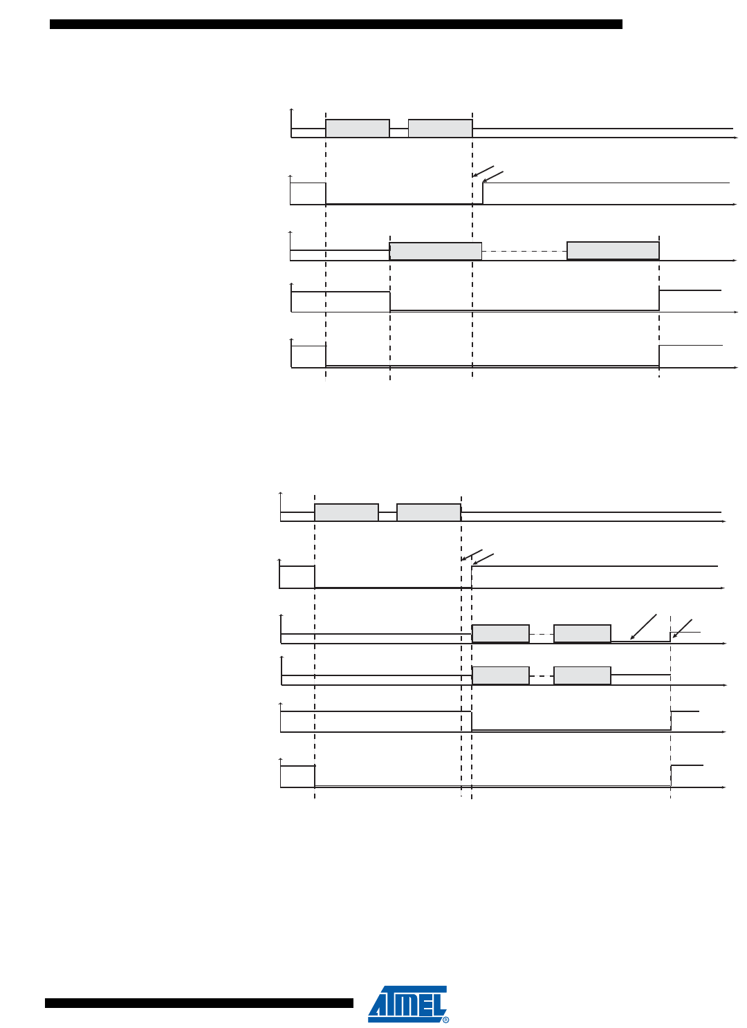
837
6430F–ATARM–21-Feb-12
SAM3U Series
837
6430F–ATARM–21-Feb-12
SAM3U Series
Figure 37-11. XFRDONE During a Read Access
37.12.3 Write Access
During a write access, the XFRDONE flag behaves as shown in Figure 37-12.
Figure 37-12. XFRDONE During a Write Access
CMD line
HSMCI read CMD
Card response
CMDRDY flag
Data
1st Block Last Block
Not busy flag
XFRDONE flag
The CMDRDY flag is released 8 tbit after the end of the card response.
CMD line
Card response
CMDRDY flag
Data bus - D0
1st Block
Not busy flag
XFRDONE flag
The CMDRDY flag is released 8 tbit after the end of the card response.
Last Block
D0
1st Block Last Block
D0 is tied by the card
D0 is released
HSMCI write CMD

838
6430F–ATARM–21-Feb-12
SAM3U Series
838
6430F–ATARM–21-Feb-12
SAM3U Series
37.13 Write Protection Registers
To prevent any single software error that may corrupt HSMCI behavior, the entire HSMCI
address space from address offset 0x000 to 0x00FC can be write-protected by setting the
WPEN bit in the “HSMCI Write Protect Mode Register” (HSMCI_WPMR).
If a write access to anywhere in the HSMCI address space from address offset 0x000 to 0x00FC
is detected, then the WPVS flag in the HSMCI Write Protect Status Register (HSMCI_WPSR) is
set and the field WPVSRC indicates in which register the write access has been attempted.
The WPVS flag is reset by writing the HSMCI Write Protect Mode Register (HSMCI_WPMR)
with the appropriate access key, WPKEY.
The protected registers are:
•“HSMCI Mode Register” on page 841
•“HSMCI Data Timeout Register” on page 843
•“HSMCI SDCard/SDIO Register” on page 844
•“HSMCI Completion Signal Timeout Register” on page 850
•“HSMCI DMA Configuration Register” on page 864
•“HSMCI Configuration Register” on page 865

839
6430F–ATARM–21-Feb-12
SAM3U Series
839
6430F–ATARM–21-Feb-12
SAM3U Series
37.14 High Speed Multimedia Card Interface (HSMCI) User Interface
Note: 1. The response register can be read by N accesses at the same HSMCI_RSPR or at consecutive addresses (0x20 to 0x2C).
N depends on the size of the response.
Table 37-7. Register Mapping
Offset Register Name Access Reset
0x00 Control Register HSMCI_CR Write –
0x04 Mode Register HSMCI_MR Read-write 0x0
0x08 Data Timeout Register HSMCI_DTOR Read-write 0x0
0x0C SD/SDIO Card Register HSMCI_SDCR Read-write 0x0
0x10 Argument Register HSMCI_ARGR Read-write 0x0
0x14 Command Register HSMCI_CMDR Write –
0x18 Block Register HSMCI_BLKR Read-write 0x0
0x1C Completion Signal Timeout Register HSMCI_CSTOR Read-write 0x0
0x20 Response Register(1) HSMCI_RSPR Read 0x0
0x24 Response Register(1) HSMCI_RSPR Read 0x0
0x28 Response Register(1) HSMCI_RSPR Read 0x0
0x2C Response Register(1) HSMCI_RSPR Read 0x0
0x30 Receive Data Register HSMCI_RDR Read 0x0
0x34 Transmit Data Register HSMCI_TDR Write –
0x38 - 0x3C Reserved – – –
0x40 Status Register HSMCI_SR Read 0xC0E5
0x44 Interrupt Enable Register HSMCI_IER Write –
0x48 Interrupt Disable Register HSMCI_IDR Write –
0x4C Interrupt Mask Register HSMCI_IMR Read 0x0
0x50 DMA Configuration Register HSMCI_DMA Read-write 0x00
0x54 Configuration Register HSMCI_CFG Read-write 0x00
0x58-0xE0 Reserved – – –
0xE4 Write Protection Mode Register HSMCI_WPMR Read-write –
0xE8 Write Protection Status Register HSMCI_WPSR Read-only –
0xEC - 0xFC Reserved – – –
0x100-0x1FC Reserved – – –
0x200 FIFO Memory Aperture0 HSMCI_FIFO0 Read-write 0x0
... ... ... ... ...
0x5FC FIFO Memory Aperture255 HSMCI_FIFO255 Read-write 0x0

840
6430F–ATARM–21-Feb-12
SAM3U Series
840
6430F–ATARM–21-Feb-12
SAM3U Series
37.14.1 HSMCI Control Register
Name: HSMCI_CR
Address: 0x40000000
Access: Write-only
• MCIEN: Multi-Media Interface Enable
0 = No effect.
1 = Enables the Multi-Media Interface if MCDIS is 0.
• MCIDIS: Multi-Media Interface Disable
0 = No effect.
1 = Disables the Multi-Media Interface.
• PWSEN: Power Save Mode Enable
0 = No effect.
1 = Enables the Power Saving Mode if PWSDIS is 0.
Warning: Before enabling this mode, the user must set a value different from 0 in the PWSDIV field (Mode Register,
HSMCI_MR).
• PWSDIS: Power Save Mode Disable
0 = No effect.
1 = Disables the Power Saving Mode.
• SWRST: Software Reset
0 = No effect.
1 = Resets the HSMCI. A software triggered hardware reset of the HSMCI interface is performed.
31 30 29 28 27 26 25 24
––––––––
23 22 21 20 19 18 17 16
––––––––
15 14 13 12 11 10 9 8
––––––––
76543210
SWRST – – – PWSDIS PWSEN MCIDIS MCIEN

841
6430F–ATARM–21-Feb-12
SAM3U Series
841
6430F–ATARM–21-Feb-12
SAM3U Series
37.14.2 HSMCI Mode Register
Name: HSMCI_MR
Address: 0x40000004
Access: Read-write
This register can only be written if the WPEN bit is cleared in “HSMCI Write Protect Mode Register” on page 866.
• CLKDIV: Clock Divider
High Speed MultiMedia Card Interface clock (MCCK or HSMCI_CK) is Master Clock (MCK) divided by (2*(CLKDIV+1)).
• PWSDIV: Power Saving Divider
High Speed MultiMedia Card Interface clock is divided by 2(PWSDIV) + 1 when entering Power Saving Mode.
Warning: This value must be different from 0 before enabling the Power Save Mode in the HSMCI_CR (HSMCI_PWSEN
bit).
• RDPROOF Read Proof Enable
Enabling Read Proof allows to stop the HSMCI Clock during read access if the internal FIFO is full. This will guarantee data
integrity, not bandwidth.
0 = Disables Read Proof.
1 = Enables Read Proof.
• WRPROOF Write Proof Enable
Enabling Write Proof allows to stop the HSMCI Clock during write access if the internal FIFO is full. This will guarantee data
integrity, not bandwidth.
0 = Disables Write Proof.
1 = Enables Write Proof.
• FBYTE: Force Byte Transfer
Enabling Force Byte Transfer allow byte transfers, so that transfer of blocks with a size different from modulo 4 can be
supported.
Warning: BLKLEN value depends on FBYTE.
0 = Disables Force Byte Transfer.
1 = Enables Force Byte Transfer.
31 30 29 28 27 26 25 24
BLKLEN
23 22 21 20 19 18 17 16
BLKLEN
15 14 13 12 11 10 9 8
– PADV FBYTE WRPROOF RDPROOF PWSDIV
76543210
CLKDIV

842
6430F–ATARM–21-Feb-12
SAM3U Series
842
6430F–ATARM–21-Feb-12
SAM3U Series
• PADV: Padding Value
0 = 0x00 value is used when padding data in write transfer.
1 = 0xFF value is used when padding data in write transfer.
PADV may be only in manual transfer.
• BLKLEN: Data Block Length
This field determines the size of the data block.
This field is also accessible in the HSMCI Block Register (HSMCI_BLKR).
Bits 16 and 17 must be set to 0 if FBYTE is disabled.
Note: In SDIO Byte mode, BLKLEN field is not used.
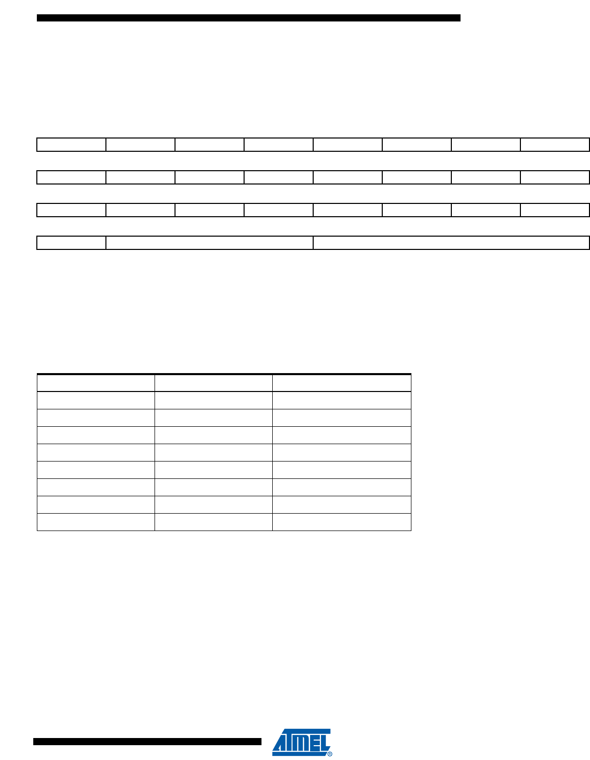
843
6430F–ATARM–21-Feb-12
SAM3U Series
843
6430F–ATARM–21-Feb-12
SAM3U Series
37.14.3 HSMCI Data Timeout Register
Name: HSMCI_DTOR
Address: 0x40000008
Access: Read-write
This register can only be written if the WPEN bit is cleared in “HSMCI Write Protect Mode Register” on page 866.
• DTOCYC: Data Timeout Cycle Number
These fields determine the maximum number of Master Clock cycles that the HSMCI waits between two data block trans-
fers. It equals (DTOCYC x Multiplier).
• DTOMUL: Data Timeout Multiplier
Multiplier is defined by DTOMUL as shown in the following table:
If the data time-out set by DTOCYC and DTOMUL has been exceeded, the Data Time-out Error flag (DTOE) in the HSMCI
Status Register (HSMCI_SR) rises.
31 30 29 28 27 26 25 24
––––––––
23 22 21 20 19 18 17 16
––––––––
15 14 13 12 11 10 9 8
––––––––
76543210
– DTOMUL DTOCYC
Value Name Description
01DTOCYC
1 16 DTOCYC x 16
2 128 DTOCYC x 128
3 256 DTOCYC x 256
4 1024 DTOCYC x 1024
5 4096 DTOCYC x 4096
6 65536 DTOCYC x 65536
7 1048576 DTOCYC x 1048576
844
6430F–ATARM–21-Feb-12
SAM3U Series
844
6430F–ATARM–21-Feb-12
SAM3U Series
37.14.4 HSMCI SDCard/SDIO Register
Name: HSMCI_SDCR
Address: 0x4000000C
Access: Read-write
This register can only be written if the WPEN bit is cleared in “HSMCI Write Protect Mode Register” on page 866.
• SDCSEL: SDCard/SDIO Slot
• SDCBUS: SDCard/SDIO Bus Width
31 30 29 28 27 26 25 24
––––––––
23 22 21 20 19 18 17 16
––––––––
15 14 13 12 11 10 9 8
––––––––
76543210
SDCBUS –––– SDCSEL
Value Name Description
0SLOTA
Slot A is selected.
1SLOTB–
2SLOTC–
3SLOTD–
Value Name Description
01
1 bit
1–
Reserved
244 bit
388 bit

845
6430F–ATARM–21-Feb-12
SAM3U Series
845
6430F–ATARM–21-Feb-12
SAM3U Series
37.14.5 HSMCI Argument Register
Name: HSMCI_ARGR
Address: 0x40000010
Access: Read-write
• ARG: Command Argument
31 30 29 28 27 26 25 24
ARG
23 22 21 20 19 18 17 16
ARG
15 14 13 12 11 10 9 8
ARG
76543210
ARG
846
6430F–ATARM–21-Feb-12
SAM3U Series
846
6430F–ATARM–21-Feb-12
SAM3U Series
37.14.6 HSMCI Command Register
Name: HSMCI_CMDR
Address: 0x40000014
Access: Write-only
This register is write-protected while CMDRDY is 0 in HSMCI_SR. If an Interrupt command is sent, this register is only writ-
able by an interrupt response (field SPCMD). This means that the current command execution cannot be interrupted or
modified.
• CMDNB: Command Number
This is the command index.
• RSPTYP: Response Type
• SPCMD: Special Command
31 30 29 28 27 26 25 24
––––BOOT_ACKATACS IOSPCMD
23 22 21 20 19 18 17 16
– – TRTYP TRDIR TRCMD
15 14 13 12 11 10 9 8
– – – MAXLAT OPDCMD SPCMD
76543210
RSPTYP CMDNB
Value Name Description
0 NORESP No response.
1 48_BIT 48-bit response.
2 136_BIT 136-bit response.
3 R1B R1b response type
Value Name Description
0 STD Not a special CMD.
1INIT
Initialization CMD:
74 clock cycles for initialization sequence.
2 SYNC Synchronized CMD:
Wait for the end of the current data block transfer before sending the pending command.
3CE_ATA
CE-ATA Completion Signal disable Command.
The host cancels the ability for the device to return a command completion signal on the
command line.
4IT_CMD
Interrupt command:
Corresponds to the Interrupt Mode (CMD40).

847
6430F–ATARM–21-Feb-12
SAM3U Series
847
6430F–ATARM–21-Feb-12
SAM3U Series
• OPDCMD: Open Drain Command
0 (PUSHPULL) = Push pull command.
1 (OPENDRAIN) = Open drain command.
• MAXLAT: Max Latency for Command to Response
0 (5) = 5-cycle max latency.
1 (64) = 64-cycle max latency.
• TRCMD: Transfer Command
• TRDIR: Transfer Direction
0 (WRITE) = Write.
1 (READ) = Read.
• TRTYP: Transfer Type
• IOSPCMD: SDIO Special Command
5 IT_RESP Interrupt response:
Corresponds to the Interrupt Mode (CMD40).
6BOR
Boot Operation Request.
Start a boot operation mode, the host processor can read boot data from the MMC device directly.
7EBO
End Boot Operation.
This command allows the host processor to terminate the boot operation mode.
Value Name Description
0 NO_DATA No data transfer
1 START_DATA Start data transfer
2 STOP_DATA Stop data transfer
3–Reserved
Value Name Description
0 SINGLE MMC/SDCard Single Block
1 MULTIPLE MMC/SDCard Multiple Block
2 STREAM MMC Stream
4 BYTE SDIO Byte
5 BLOCK SDIO Block
Value Name Description
0 STD Not an SDIO Special Command
1 SUSPEND SDIO Suspend Command
2 RESUME SDIO Resume Command
Value Name Description

848
6430F–ATARM–21-Feb-12
SAM3U Series
848
6430F–ATARM–21-Feb-12
SAM3U Series
• ATACS: ATA with Command Completion Signal
0 (NORMAL) = Normal operation mode.
1 (COMPLETION) = This bit indicates that a completion signal is expected within a programmed amount of time
(HSMCI_CSTOR).
• BOOT_ACK: Boot Operation Acknowledge.
The master can choose to receive the boot acknowledge from the slave when a Boot Request command is issued. When
set to one this field indicates that a Boot acknowledge is expected within a programmable amount of time defined with
DTOMUL and DTOCYC fields located in the HSMCI_DTOR register. If the acknowledge pattern is not received then an
acknowledge timeout error is raised. If the acknowledge pattern is corrupted then an acknowledge pattern error is set.

849
6430F–ATARM–21-Feb-12
SAM3U Series
849
6430F–ATARM–21-Feb-12
SAM3U Series
37.14.7 HSMCI Block Register
Name: HSMCI_BLKR
Address: 0x40000018
Access: Read-write
• BCNT: MMC/SDIO Block Count - SDIO Byte Count
This field determines the number of data byte(s) or block(s) to transfer.
The transfer data type and the authorized values for BCNT field are determined by the TRTYP field in the HSMCI Com-
mand Register (HSMCI_CMDR):
Warning: In SDIO Byte and Block modes, writing to the 7 last bits of BCNT field is forbidden and may lead to unpredictable
results.
• BLKLEN: Data Block Length
This field determines the size of the data block.
This field is also accessible in the HSMCI Mode Register (HSMCI_MR).
Bits 16 and 17 must be set to 0 if FBYTE is disabled.
Note: In SDIO Byte mode, BLKLEN field is not used.
31 30 29 28 27 26 25 24
BLKLEN
23 22 21 20 19 18 17 16
BLKLEN
15 14 13 12 11 10 9 8
BCNT
76543210
BCNT
Value Name Description
0MULTIPLE MMC/SDCARD Multiple Block
From 1 to 65635: Value 0 corresponds to an infinite block transfer.
4 BYTE
SDIO Byte
From 1 to 512 bytes: Value 0 corresponds to a 512-byte transfer.
Values from 0x200 to 0xFFFF are forbidden.
5BLOCK
SDIO Block
From 1 to 511 blocks: Value 0 corresponds to an infinite block transfer.
Values from 0x200 to 0xFFFF are forbidden.
850
6430F–ATARM–21-Feb-12
SAM3U Series
850
6430F–ATARM–21-Feb-12
SAM3U Series
37.14.8 HSMCI Completion Signal Timeout Register
Name: HSMCI_CSTOR
Address: 0x4000001C
Access: Read-write
This register can only be written if the WPEN bit is cleared in “HSMCI Write Protect Mode Register” on page 866.
• CSTOCYC: Completion Signal Timeout Cycle Number
These fields determine the maximum number of Master Clock cycles that the HSMCI waits between two data block trans-
fers. Its value is calculated by (CSTOCYC x Multiplier).
• CSTOMUL: Completion Signal Timeout Multiplier
These fields determine the maximum number of Master Clock cycles that the HSMCI waits between two data block trans-
fers. Its value is calculated by (CSTOCYC x Multiplier).
These fields determine the maximum number of Master Clock cycles that the HSMCI waits between the end of the data
transfer and the assertion of the completion signal. The data transfer comprises data phase and the optional busy phase. If
a non-DATA ATA command is issued, the HSMCI starts waiting immediately after the end of the response until the comple-
tion signal.
Multiplier is defined by CSTOMUL as shown in the following table:
If the data time-out set by CSTOCYC and CSTOMUL has been exceeded, the Completion Signal Time-out Error flag
(CSTOE) in the HSMCI Status Register (HSMCI_SR) rises.
31 30 29 28 27 26 25 24
––––––––
23 22 21 20 19 18 17 16
––––––––
15 14 13 12 11 10 9 8
––––––––
76543210
– CSTOMUL CSTOCYC
Value Name Description
0 1 CSTOCYC x 1
1 16 CSTOCYC x 16
2 128 CSTOCYC x 128
3 256 CSTOCYC x 256
4 1024 CSTOCYC x 1024
5 4096 CSTOCYC x 4096
6 65536 CSTOCYC x 65536
7 1048576 CSTOCYC x 1048576

851
6430F–ATARM–21-Feb-12
SAM3U Series
851
6430F–ATARM–21-Feb-12
SAM3U Series
37.14.9 HSMCI Response Register
Name: HSMCI_RSPR
Address: 0x40000020
Access: Read-only
• RSP: Response
Note: 1. The response register can be read by N accesses at the same HSMCI_RSPR or at consecutive addresses (0x20 to 0x2C).
N depends on the size of the response.
31 30 29 28 27 26 25 24
RSP
23 22 21 20 19 18 17 16
RSP
15 14 13 12 11 10 9 8
RSP
76543210
RSP

852
6430F–ATARM–21-Feb-12
SAM3U Series
852
6430F–ATARM–21-Feb-12
SAM3U Series
37.14.10 HSMCI Receive Data Register
Name: HSMCI_RDR
Address: 0x40000030
Access: Read-only
• DATA: Data to Read
31 30 29 28 27 26 25 24
DATA
23 22 21 20 19 18 17 16
DATA
15 14 13 12 11 10 9 8
DATA
76543210
DATA

853
6430F–ATARM–21-Feb-12
SAM3U Series
853
6430F–ATARM–21-Feb-12
SAM3U Series
37.14.11 HSMCI Transmit Data Register
Name: HSMCI_TDR
Address: 0x40000034
Access: Write-only
• DATA: Data to Write
31 30 29 28 27 26 25 24
DATA
23 22 21 20 19 18 17 16
DATA
15 14 13 12 11 10 9 8
DATA
76543210
DATA

854
6430F–ATARM–21-Feb-12
SAM3U Series
854
6430F–ATARM–21-Feb-12
SAM3U Series
37.14.12 HSMCI Status Register
Name: HSMCI_SR
Address: 0x40000040
Access: Read-only
• CMDRDY: Command Ready
0 = A command is in progress.
1 = The last command has been sent. Cleared when writing in the HSMCI_CMDR.
• RXRDY: Receiver Ready
0 = Data has not yet been received since the last read of HSMCI_RDR.
1 = Data has been received since the last read of HSMCI_RDR.
• TXRDY: Transmit Ready
0= The last data written in HSMCI_TDR has not yet been transferred in the Shift Register.
1= The last data written in HSMCI_TDR has been transferred in the Shift Register.
• BLKE: Data Block Ended
This flag must be used only for Write Operations.
0 = A data block transfer is not yet finished. Cleared when reading the HSMCI_SR.
1 = A data block transfer has ended, including the CRC16 Status transmission.
the flag is set for each transmitted CRC Status.
Refer to the MMC or SD Specification for more details concerning the CRC Status.
• DTIP: Data Transfer in Progress
0 = No data transfer in progress.
1 = The current data transfer is still in progress, including CRC16 calculation. Cleared at the end of the CRC16 calculation.
• NOTBUSY: HSMCI Not Busy
This flag must be used only for Write Operations.
A block write operation uses a simple busy signalling of the write operation duration on the data (DAT0) line: during a data
transfer block, if the card does not have a free data receive buffer, the card indicates this condition by pulling down the data
line (DAT0) to LOW. The card stops pulling down the data line as soon as at least one receive buffer for the defined data
transfer block length becomes free.
31 30 29 28 27 26 25 24
UNRE OVRE ACKRCVE ACKRCV XFRDONE FIFOEMPTY DMADONE BLKOVRE
23 22 21 20 19 18 17 16
CSTOE DTOE DCRCE RTOE RENDE RCRCE RDIRE RINDE
15 14 13 12 11 10 9 8
––CSRCVSDIOWAIT–––
MCI_SDIOIR
QA
76543210
– – NOTBUSY DTIP BLKE TXRDY RXRDY CMDRDY

855
6430F–ATARM–21-Feb-12
SAM3U Series
855
6430F–ATARM–21-Feb-12
SAM3U Series
The NOTBUSY flag allows to deal with these different states.
0 = The HSMCI is not ready for new data transfer. Cleared at the end of the card response.
1 = The HSMCI is ready for new data transfer. Set when the busy state on the data line has ended. This corresponds to a
free internal data receive buffer of the card.
Refer to the MMC or SD Specification for more details concerning the busy behavior.
For all the read operations, the NOTBUSY flag is cleared at the end of the host command.
For the Infinite Read Multiple Blocks, the NOTBUSY flag is set at the end of the STOP_TRANSMISSION host command
(CMD12).
For the Single Block Reads, the NOTBUSY flag is set at the end of the data read block.
For the Multiple Block Reads with pre-defined block count, the NOTBUSY flag is set at the end of the last received data
block.
• SDIOIRQA: SDIO Interrupt for Slot A
0 = No interrupt detected on SDIO Slot A.
1 = An SDIO Interrupt on Slot A occurred. Cleared when reading the HSMCI_SR.
• SDIOWAIT: SDIO Read Wait Operation Status
0 = Normal Bus operation.
1 = The data bus has entered IO wait state.
• CSRCV: CE-ATA Completion Signal Received
0 = No completion signal received since last status read operation.
1 = The device has issued a command completion signal on the command line. Cleared by reading in the HSMCI_SR
register.
• RINDE: Response Index Error
0 = No error.
1 = A mismatch is detected between the command index sent and the response index received. Cleared when writing in
the HSMCI_CMDR.
• RDIRE: Response Direction Error
0 = No error.
1 = The direction bit from card to host in the response has not been detected.
• RCRCE: Response CRC Error
0 = No error.
1 = A CRC7 error has been detected in the response. Cleared when writing in the HSMCI_CMDR.
• RENDE: Response End Bit Error
0 = No error.
1 = The end bit of the response has not been detected. Cleared when writing in the HSMCI_CMDR.

856
6430F–ATARM–21-Feb-12
SAM3U Series
856
6430F–ATARM–21-Feb-12
SAM3U Series
• RTOE: Response Time-out Error
0 = No error.
1 = The response time-out set by MAXLAT in the HSMCI_CMDR has been exceeded. Cleared when writing in the
HSMCI_CMDR.
• DCRCE: Data CRC Error
0 = No error.
1 = A CRC16 error has been detected in the last data block. Cleared by reading in the HSMCI_SR register.
• DTOE: Data Time-out Error
0 = No error.
1 = The data time-out set by DTOCYC and DTOMUL in HSMCI_DTOR has been exceeded. Cleared by reading in the
HSMCI_SR register.
• CSTOE: Completion Signal Time-out Error
0 = No error.
1 = The completion signal time-out set by CSTOCYC and CSTOMUL in HSMCI_CSTOR has been exceeded. Cleared by
reading in the HSMCI_SR register. Cleared by reading in the HSMCI_SR register.
• BLKOVRE: DMA Block Overrun Error
0 = No error.
1 = A new block of data is received and the DMA controller has not started to move the current pending block, a block over-
run is raised. Cleared by reading in the HSMCI_SR register.
• DMADONE: DMA Transfer done
0 = DMA buffer transfer has not completed since the last read of HSMCI_SR register.
1 = DMA buffer transfer has completed.
• FIFOEMPTY: FIFO empty flag
0 = FIFO contains at least one byte.
1 = FIFO is empty.
• XFRDONE: Transfer Done flag
0 = A transfer is in progress.
1 = Command register is ready to operate and the data bus is in the idle state.
• ACKRCV: Boot Operation Acknowledge Received
0 = No Boot acknowledge received since the last read of the status register.
1 = A Boot acknowledge signal has been received. Cleared by reading the HSMCI_SR register.
• ACKRCVE: Boot Operation Acknowledge Error
0 = No error
1 = Corrupted Boot Acknowledge signal received.

857
6430F–ATARM–21-Feb-12
SAM3U Series
857
6430F–ATARM–21-Feb-12
SAM3U Series
• OVRE: Overrun
0 = No error.
1 = At least one 8-bit received data has been lost (not read). Cleared when sending a new data transfer command.
When FERRCTRL in HSMCI_CFG is set to 1, OVRE becomes reset after read.
• UNRE: Underrun
0 = No error.
1 = At least one 8-bit data has been sent without valid information (not written). Cleared when sending a new data transfer
command or when setting FERRCTRL in HSMCI_CFG to 1.
When FERRCTRL in HSMCI_CFG is set to 1, UNRE becomes reset after read.

858
6430F–ATARM–21-Feb-12
SAM3U Series
858
6430F–ATARM–21-Feb-12
SAM3U Series
37.14.13 HSMCI Interrupt Enable Register
Name: HSMCI_IER
Address: 0x40000044
Access: Write-only
• CMDRDY: Command Ready Interrupt Enable
• RXRDY: Receiver Ready Interrupt Enable
• TXRDY: Transmit Ready Interrupt Enable
• BLKE: Data Block Ended Interrupt Enable
• DTIP: Data Transfer in Progress Interrupt Enable
• NOTBUSY: Data Not Busy Interrupt Enable
• SDIOIRQA: SDIO Interrupt for Slot A Interrupt Enable
• SDIOIRQD: SDIO Interrupt for Slot D Interrupt Enable
• SDIOWAIT: SDIO Read Wait Operation Status Interrupt Enable
• CSRCV: Completion Signal Received Interrupt Enable
• RINDE: Response Index Error Interrupt Enable
• RDIRE: Response Direction Error Interrupt Enable
• RCRCE: Response CRC Error Interrupt Enable
• RENDE: Response End Bit Error Interrupt Enable
• RTOE: Response Time-out Error Interrupt Enable
• DCRCE: Data CRC Error Interrupt Enable
• DTOE: Data Time-out Error Interrupt Enable
• CSTOE: Completion Signal Timeout Error Interrupt Enable
31 30 29 28 27 26 25 24
UNRE OVRE ACKRCVE ACKRCV XFRDONE FIFOEMPTY DMADONE BLKOVRE
23 22 21 20 19 18 17 16
CSTOE DTOE DCRCE RTOE RENDE RCRCE RDIRE RINDE
15 14 13 12 11 10 9 8
––CSRCVSDIOWAIT–––
MCI_SDIOIR
QA
76543210
– – NOTBUSY DTIP BLKE TXRDY RXRDY CMDRDY

859
6430F–ATARM–21-Feb-12
SAM3U Series
859
6430F–ATARM–21-Feb-12
SAM3U Series
• BLKOVRE: DMA Block Overrun Error Interrupt Enable
• DMADONE: DMA Transfer completed Interrupt Enable
• FIFOEMPTY: FIFO empty Interrupt enable
• XFRDONE: Transfer Done Interrupt enable
• ACKRCV: Boot Acknowledge Interrupt Enable
• ACKRCVE: Boot Acknowledge Error Interrupt Enable
• OVRE: Overrun Interrupt Enable
• UNRE: Underrun Interrupt Enable
0 = No effect.
1 = Enables the corresponding interrupt.

860
6430F–ATARM–21-Feb-12
SAM3U Series
860
6430F–ATARM–21-Feb-12
SAM3U Series
37.14.14 HSMCI Interrupt Disable Register
Name: HSMCI_IDR
Address: 0x40000048
Access: Write-only
• CMDRDY: Command Ready Interrupt Disable
• RXRDY: Receiver Ready Interrupt Disable
• TXRDY: Transmit Ready Interrupt Disable
• BLKE: Data Block Ended Interrupt Disable
• DTIP: Data Transfer in Progress Interrupt Disable
• NOTBUSY: Data Not Busy Interrupt Disable
• SDIOIRQA: SDIO Interrupt for Slot A Interrupt Disable
• SDIOWAIT: SDIO Read Wait Operation Status Interrupt Disable
• CSRCV: Completion Signal received interrupt Disable
• RINDE: Response Index Error Interrupt Disable
• RDIRE: Response Direction Error Interrupt Disable
• RCRCE: Response CRC Error Interrupt Disable
• RENDE: Response End Bit Error Interrupt Disable
• RTOE: Response Time-out Error Interrupt Disable
• DCRCE: Data CRC Error Interrupt Disable
• DTOE: Data Time-out Error Interrupt Disable
• CSTOE: Completion Signal Time out Error Interrupt Disable
• BLKOVRE: DMA Block Overrun Error Interrupt Disable
31 30 29 28 27 26 25 24
UNRE OVRE ACKRCVE ACKRCV XFRDONE FIFOEMPTY DMADONE BLKOVRE
23 22 21 20 19 18 17 16
CSTOE DTOE DCRCE RTOE RENDE RCRCE RDIRE RINDE
15 14 13 12 11 10 9 8
––CSRCVSDIOWAIT–––
MCI_SDIOIR
QA
76543210
– – NOTBUSY DTIP BLKE TXRDY RXRDY CMDRDY

861
6430F–ATARM–21-Feb-12
SAM3U Series
861
6430F–ATARM–21-Feb-12
SAM3U Series
• DMADONE: DMA Transfer completed Interrupt Disable
• FIFOEMPTY: FIFO empty Interrupt Disable
• XFRDONE: Transfer Done Interrupt Disable
• ACKRCV: Boot Acknowledge Interrupt Disable
• ACKRCVE: Boot Acknowledge Error Interrupt Disable
• OVRE: Overrun Interrupt Disable
• UNRE: Underrun Interrupt Disable
0 = No effect.
1 = Disables the corresponding interrupt.

862
6430F–ATARM–21-Feb-12
SAM3U Series
862
6430F–ATARM–21-Feb-12
SAM3U Series
37.14.15 HSMCI Interrupt Mask Register
Name: HSMCI_IMR
Address: 0x4000004C
Access: Read-only
• CMDRDY: Command Ready Interrupt Mask
• RXRDY: Receiver Ready Interrupt Mask
• TXRDY: Transmit Ready Interrupt Mask
• BLKE: Data Block Ended Interrupt Mask
• DTIP: Data Transfer in Progress Interrupt Mask
• NOTBUSY: Data Not Busy Interrupt Mask
• SDIOIRQA: SDIO Interrupt for Slot A Interrupt Mask
• SDIOWAIT: SDIO Read Wait Operation Status Interrupt Mask
• CSRCV: Completion Signal Received Interrupt Mask
• RINDE: Response Index Error Interrupt Mask
• RDIRE: Response Direction Error Interrupt Mask
• RCRCE: Response CRC Error Interrupt Mask
• RENDE: Response End Bit Error Interrupt Mask
• RTOE: Response Time-out Error Interrupt Mask
• DCRCE: Data CRC Error Interrupt Mask
• DTOE: Data Time-out Error Interrupt Mask
• CSTOE: Completion Signal Time-out Error Interrupt Mask
• BLKOVRE: DMA Block Overrun Error Interrupt Mask
31 30 29 28 27 26 25 24
UNRE OVRE ACKRCVE ACKRCV XFRDONE FIFOEMPTY DMADONE BLKOVRE
23 22 21 20 19 18 17 16
CSTOE DTOE DCRCE RTOE RENDE RCRCE RDIRE RINDE
15 14 13 12 11 10 9 8
––CSRCVSDIOWAIT–––
MCI_SDIOIR
QA
76543210
– – NOTBUSY DTIP BLKE TXRDY RXRDY CMDRDY

863
6430F–ATARM–21-Feb-12
SAM3U Series
863
6430F–ATARM–21-Feb-12
SAM3U Series
• DMADONE: DMA Transfer Completed Interrupt Mask
• FIFOEMPTY: FIFO Empty Interrupt Mask
• XFRDONE: Transfer Done Interrupt Mask
• ACKRCV: Boot Operation Acknowledge Received Interrupt Mask
• ACKRCVE: Boot Operation Acknowledge Error Interrupt Mask
• OVRE: Overrun Interrupt Mask
• UNRE: Underrun Interrupt Mask
0 = The corresponding interrupt is not enabled.
1 = The corresponding interrupt is enabled.
864
6430F–ATARM–21-Feb-12
SAM3U Series
864
6430F–ATARM–21-Feb-12
SAM3U Series
37.14.16 HSMCI DMA Configuration Register
Name: HSMCI_DMA
Address: 0x40000050
Access: Read-write
This register can only be written if the WPEN bit is cleared in “HSMCI Write Protect Mode Register” on page 866.
• OFFSET: DMA Write Buffer Offset
This field indicates the number of discarded bytes when the DMA writes the first word of the transfer.
• CHKSIZE: DMA Channel Read and Write Chunk Size
The CHKSIZE field indicates the number of data available when the DMA chunk transfer request is asserted.
• DMAEN: DMA Hardware Handshaking Enable
0 = DMA interface is disabled.
1 = DMA Interface is enabled.
Note: To avoid unpredictable behavior, DMA hardware handshaking must be disabled when CPU transfers are performed.
• ROPT: Read Optimization with padding
0: BLKLEN bytes are moved from the Memory Card to the system memory, two DMA descriptors are used when the trans-
fer size is not a multiple of 4.
1: Ceiling(BLKLEN/4) * 4 bytes are moved from the Memory Card to the system memory, only one DMA descriptor is used.
31 30 29 28 27 26 25 24
––––––
23 22 21 20 19 18 17 16
––––––––
15 14 13 12 11 10 9 8
–––ROPT–––DMAEN
76543210
– – – CHKSIZE – – OFFSET
Value Name Description
0 1 1 data available
1 4 4 data available

865
6430F–ATARM–21-Feb-12
SAM3U Series
865
6430F–ATARM–21-Feb-12
SAM3U Series
37.14.17 HSMCI Configuration Register
Name: HSMCI_CFG
Address: 0x40000054
Access: Read-write
This register can only be written if the WPEN bit is cleared in “HSMCI Write Protect Mode Register” on page 866.
• FIFOMODE: HSMCI Internal FIFO control mode
0 = A write transfer starts when a sufficient amount of data is written into the FIFO.
When the block length is greater than or equal to 3/4 of the HSMCI internal FIFO size, then the write transfer starts as soon
as half the FIFO is filled. When the block length is greater than or equal to half the internal FIFO size, then the write transfer
starts as soon as one quarter of the FIFO is filled. In other cases, the transfer starts as soon as the total amount of data is
written in the internal FIFO.
1 = A write transfer starts as soon as one data is written into the FIFO.
• FERRCTRL: Flow Error flag reset control mode
0= When an underflow/overflow condition flag is set, a new Write/Read command is needed to reset the flag.
1= When an underflow/overflow condition flag is set, a read status resets the flag.
• HSMODE: High Speed Mode
0= Default bus timing mode.
1= If set to one, the host controller outputs command line and data lines on the rising edge of the card clock. The Host
driver shall check the high speed support in the card registers.
• LSYNC: Synchronize on the last block
0= The pending command is sent at the end of the current data block.
1= The pending command is sent at the end of the block transfer when the transfer length is not infinite. (block count shall
be different from zero)
31 30 29 28 27 26 25 24
––––––
23 22 21 20 19 18 17 16
––––––––
15 14 13 12 11 10 9 8
–––LSYNC–––HSMODE
76543210
– – – FERRCTRL – – – FIFOMODE

866
6430F–ATARM–21-Feb-12
SAM3U Series
866
6430F–ATARM–21-Feb-12
SAM3U Series
37.14.18 HSMCI Write Protect Mode Register
Name: HSMCI_WPMR
Address: 0x400000E4
Access: Read-write
• WP_EN: Write Protection Enable
0 = Disables the Write Protection if WP_KEY corresponds to 0x4D4349 (“MCI’ in ASCII).
1 = Enables the Write Protection if WP_KEY corresponds to 0x4D4349 (“MCI’ in ASCII).
• WP_KEY: Write Protection Key password
Should be written at value 0x4D4349 (ASCII code for “MCI”). Writing any other value in this field has no effect.
Protects the registers:
•“HSMCI Mode Register” on page 841
•“HSMCI Data Timeout Register” on page 843
•“HSMCI SDCard/SDIO Register” on page 844
•“HSMCI Completion Signal Timeout Register” on page 850
•“HSMCI DMA Configuration Register” on page 864
•“HSMCI Configuration Register” on page 865
31 30 29 28 27 26 25 24
WP_KEY (0x4D => “M”)
23 22 21 20 19 18 17 16
WP_KEY (0x43 => C”)
15 14 13 12 11 10 9 8
WP_KEY (0x49 => “I”)
76543210
WP_EN
867
6430F–ATARM–21-Feb-12
SAM3U Series
867
6430F–ATARM–21-Feb-12
SAM3U Series
37.14.19 HSMCI Write Protect Status Register
Name: HSMCI_WPSR
Address: 0x400000E8
Access: Read-only
• WP_VS: Write Protection Violation Status
• WP_VSRC: Write Protection Violation SouRCe
When WPVS is active, this field indicates the write-protected register (through address offset or code) in which a write
access has been attempted.
31 30 29 28 27 26 25 24
––––––––
23 22 21 20 19 18 17 16
WP_VSRC
15 14 13 12 11 10 9 8
WP_VSRC
76543210
–––– WP_VS
Value Name Description
0NONE
No Write Protection Violation occurred since the last read of this
register (WP_SR)
1WRITE
Write Protection detected unauthorized attempt to write a control
register had occurred (since the last read.)
2 RESET Software reset had been performed while Write Protection was
enabled (since the last read).
3BOTH
Both Write Protection violation and software reset with Write
Protection enabled have occurred since the last read.

868
6430F–ATARM–21-Feb-12
SAM3U Series
868
6430F–ATARM–21-Feb-12
SAM3U Series
37.14.20 HSMCI FIFOx Memory Aperture
Name: HSMCI_FIFOx[x=0..255]
Address: 0x40000200
Access: Read-write
• DATA: Data to Read or Data to Write
31 30 29 28 27 26 25 24
DATA
23 22 21 20 19 18 17 16
DATA
15 14 13 12 11 10 9 8
DATA
76543210
DATA

869
6430F–ATARM–21-Feb-12
SAM3U Series
869
6430F–ATARM–21-Feb-12
SAM3U Series
38. Pulse Width Modulation (PWM)
38.1 Description
The PWM macrocell controls 4 channels independently. Each channel controls two complemen-
tary square output waveforms. Characteristics of the output waveforms such as period, duty-
cycle, polarity and dead-times (also called dead-bands or non-overlapping times) are configured
through the user interface. Each channel selects and uses one of the clocks provided by the
clock generator. The clock generator provides several clocks resulting from the division of the
PWM master clock (MCK).
All PWM macrocell accesses are made through registers mapped on the peripheral bus. All
channels integrate a double buffering system in order to prevent an unexpected output wave-
form while modifying the period, the duty-cycle or the dead-times.
Channels can be linked together as synchronous channels to be able to update their duty-cycle
or dead-times at the same time.
The update of duty-cycles of synchronous channels can be performed by the Peripheral DMA
Controller Channel (PDC) which offers buffer transfer without processor Intervention.
The PWM macrocell provides 8 independent comparison units capable of comparing a pro-
grammed value to the counter of the synchronous channels (counter of channel 0). These
comparisons are intended to generate software interrupts, to trigger pulses on the 2 indepen-
dent event lines (in order to synchronize ADC conversions with a lot of flexibility independently of
the PWM outputs), and to trigger PDC transfer requests.
The PWM outputs can be overridden synchronously or asynchronously to their channel counter.
The PWM block provides a fault protection mechanism with 4 fault inputs, capable of detecting a
fault condition and to override the PWM outputs asynchronously.
For safety usage, some control registers are write-protected.
38.2 Embedded Characteristics
• 4 Channels
• Common Clock Generator Providing Thirteen Different Clocks
– A Modulo n Counter Providing Eleven Clocks
– Two Independent Linear Dividers Working on Modulo n Counter Outputs
• Independent Channels
– Independent 16-bit Counter for Each Channel
– Independent Complementary Outputs with 12-bit Dead-Time Generator (Also Called
Dead-Band or Non-Overlapping Time) for Each Channel
– Independent Enable Disable Command for Each Channel
– Independent Clock Selection for Each Channel
– Independent Period, Duty-Cycle and Dead-Time for Each Channel
– Independent Double Buffering of Period, Duty-Cycle and Dead-Times for Each
Channel
– Independent Programmable Selection of The Output Waveform Polarity for Each
Channel

870
6430F–ATARM–21-Feb-12
SAM3U Series
870
6430F–ATARM–21-Feb-12
SAM3U Series
– Independent Programmable Center or Left Aligned Output Waveform for Each
Channel
– Independent Output Override for Each Channel
• Synchronous Channel Mode
– Synchronous Channels Share the Same Counter
– Mode to Update the Synchronous Channels Registers after a Programmable
Number of Periods
– Synchronous Channels Supports Connection of one Peripheral DMA Controller
Channel (PDC) Which Offers Buffer Transfer Without Processor Intervention To
Update Duty-Cycle Registers
• 2 Independent Events Lines Intended to Synchronize ADC Conversions
• 8 Comparison Units Intended to Generate Interrupts, Pulses on Event Lines and PDC
Transfer Requests
• 4 Programmable Fault Inputs Providing an Asynchronous Protection of PWM Outputs
– User Driven through PIO inputs
– PMC Driven when Crystal Oscillator Clock Fails
– ADC Controller Driven through Configurable Comparison Function
• Write-Protect Registers
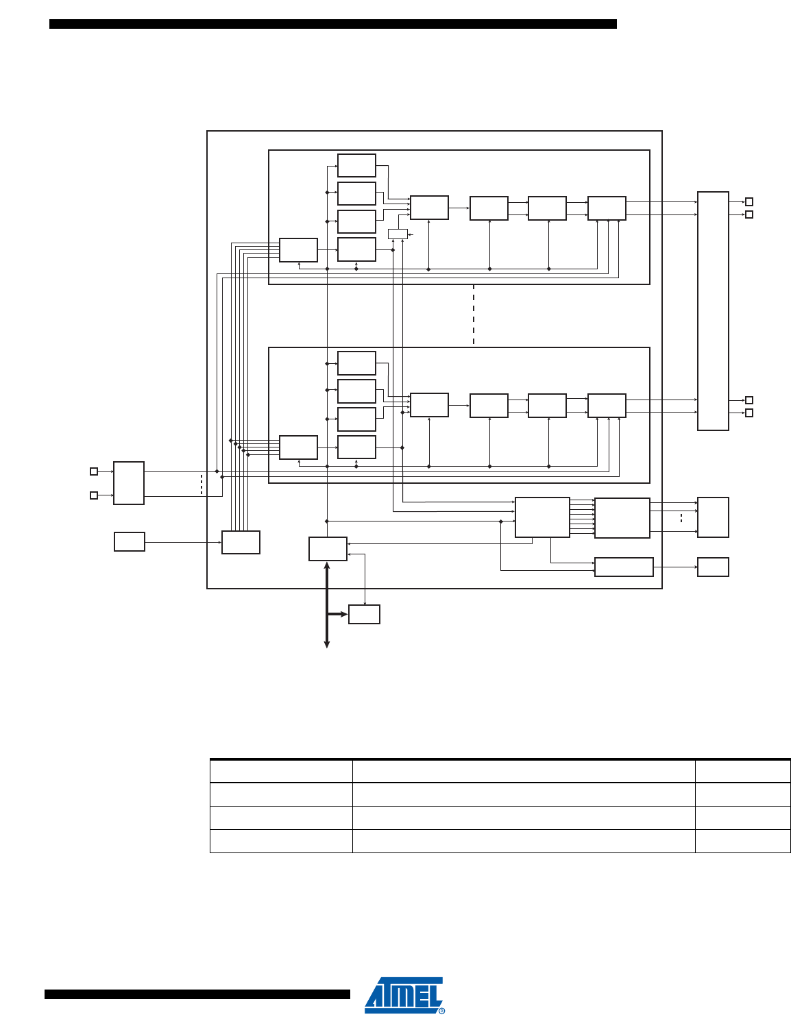
871
6430F–ATARM–21-Feb-12
SAM3U Series
871
6430F–ATARM–21-Feb-12
SAM3U Series
38.3 Block Diagram
Figure 38-1. Pulse Width Modulation Controller Block Diagram
38.4 I/O Lines Description
Each channel outputs two complementary external I/O lines.
APB
ADC
Comparison
Units
PDC
Interrupt
Controller
Interrupt Generator
event line 0
event line 1
Events
Generator
event line x
Comparator
Clock
Selector
Counter
Channel 0
Duty-Cycle
Period
Update
APB
Interface
CLOCK
Generator
PIO
PMC
Dead-Time
Generator
Output
Override
Fault
Protection
PIO
Comparator Dead-Time
Generator
Output
Override
Fault
Protection
Counter
Channel x
Duty-Cycle
Period
Update
Clock
Selector
Channel x
OCx
DTOHx
DTOLx
OOOHx PWMHx
PWMLx
OOOLx
MUX
SYNCx
PWM Controller
MCK
Channel 0
OC0
DTOH0
DTOL0
OOOH0 PWMH0
PWML0
OOOL0
PWMHx
PWMLx
PWMH0
PWML0
PWMFI0
PWMFIx
Table 38-1. I/O Line Description
Name Description Type
PWMHx PWM Waveform Output High for channel x Output
PWMLx PWM Waveform Output Low for channel x Output
PWMFIx PWM Fault Input x Input

872
6430F–ATARM–21-Feb-12
SAM3U Series
872
6430F–ATARM–21-Feb-12
SAM3U Series
38.5 Product Dependencies
38.5.1 I/O Lines
The pins used for interfacing the PWM are multiplexed with PIO lines. The programmer must first
program the PIO controller to assign the desired PWM pins to their peripheral function. If I/O
lines of the PWM are not used by the application, they can be used for other purposes by the PIO
controller.
All of the PWM outputs may or may not be enabled. If an application requires only four channels,
then only four PIO lines will be assigned to PWM outputs.
Table 38-2. I/O Lines
Instance Signal I/O Line Peripheral
PWM PWMFI0 PA11 B
PWM PWMFI1 PA12 B
PWM PWMFI2 PA18 B
PWM PWMH0 PA4 B
PWM PWMH0 PA28 B
PWM PWMH0 PB0 A
PWM PWMH0 PB13 B
PWM PWMH0 PC24 B
PWM PWMH1 PA5 B
PWM PWMH1 PA29 B
PWM PWMH1 PB1 A
PWM PWMH1 PB14 B
PWM PWMH1 PC25 B
PWM PWMH2 PA6 B
PWM PWMH2 PA15 B
PWM PWMH2 PB2 A
PWM PWMH2 PB15 B
PWM PWMH2 PC26 B
PWM PWMH3 PA20 B
PWM PWMH3 PB3 A
PWM PWMH3 PB16 B
PWM PWMH3 PC27 B
PWM PWML0 PA7 B
PWM PWML0 PB17 B
PWM PWML0 PB25 B
PWM PWML0 PC6 B
PWM PWML0 PC29 A
PWM PWML1 PA8 B

873
6430F–ATARM–21-Feb-12
SAM3U Series
873
6430F–ATARM–21-Feb-12
SAM3U Series
38.5.2 Power Management
The PWM is not continuously clocked. The programmer must first enable the PWM clock in the
Power Management Controller (PMC) before using the PWM. However, if the application does
not require PWM operations, the PWM clock can be stopped when not needed and be restarted
later. In this case, the PWM will resume its operations where it left off.
In the PWM description, Master Clock (MCK) is the clock of the peripheral bus to which the PWM
is connected.
38.5.3 Interrupt Sources
The PWM interrupt line is connected on one of the internal sources of the Interrupt Controller.
Using the PWM interrupt requires the Interrupt Controller to be programmed first. Note that it is
not recommended to use the PWM interrupt line in edge sensitive mode.
38.5.4 Fault Inputs
The PWM has the FAULT inputs connected to the different modules. Please refer to the imple-
mentation of these module within the product for detailed information about the fault generation
procedure. The PWM receives faults from PIO inputs, PMC, ADC controller,
Note: 1. FPOL bit in PWMC_FMR.
PWM PWML1 PB18 B
PWM PWML1 PB26 B
PWM PWML1 PC7 B
PWM PWML1 PC30 A
PWM PWML2 PA9 B
PWM PWML2 PB19 B
PWM PWML2 PB27 B
PWM PWML2 PC8 B
PWM PWML2 PC31 A
PWM PWML3 PA10 B
PWM PWML3 PB20 B
PWM PWML3 PB28 B
PWM PWML3 PC9 B
PWM PWML3 PC16 B
Table 38-2. I/O Lines
Table 38-3. Fault Inputs
Fault Inputs External PWM Fault Input Number Polarity Level(1) Fault Input ID
Main OSC – 1 0
PA18 PWMFI2 User Defined 1
PA11 PWMFI0 User Defined 2
PA12 PWMFI1 User Defined 3
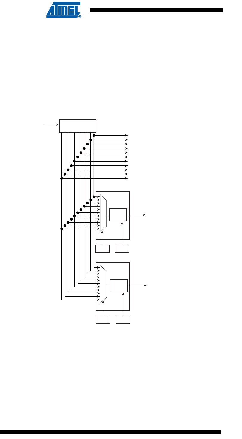
874
6430F–ATARM–21-Feb-12
SAM3U Series
874
6430F–ATARM–21-Feb-12
SAM3U Series
38.6 Functional Description
The PWM macrocell is primarily composed of a clock generator module and 4 channels.
• Clocked by the master clock (MCK), the clock generator module provides 13 clocks.
• Each channel can independently choose one of the clock generator outputs.
• Each channel generates an output waveform with attributes that can be defined
independently for each channel through the user interface registers.
38.6.1 PWM Clock Generator
Figure 38-2. Functional View of the Clock Generator Block Diagram
The PWM master clock (MCK) is divided in the clock generator module to provide different
clocks available for all channels. Each channel can independently select one of the divided
clocks.
The clock generator is divided in three blocks:
– a modulo n counter which provides 11 clocks: FMCK, FMCK/2, FMCK/4, FMCK/8,
FMCK/16, FMCK/32, FMCK/64, FMCK/128, FMCK/256, FMCK/512, FMCK/1024
– two linear dividers (1, 1/2, 1/3, ... 1/255) that provide two separate clocks: clkA and
clkB
modulo n counter
MCK/2
MCK/4
MCK/16
MCK/32
MCK/64
MCK/8
Divider A clkA
DIVA
PWM_MR
MCK
MCK/128
MCK/256
MCK/512
MCK/1024
PREA
Divider B clkB
DIVB
PWM_MR
PREB
MCK

875
6430F–ATARM–21-Feb-12
SAM3U Series
875
6430F–ATARM–21-Feb-12
SAM3U Series
Each linear divider can independently divide one of the clocks of the modulo n counter. The
selection of the clock to be divided is made according to the PREA (PREB) field of the PWM
Clock register (PWM_CLK). The resulting clock clkA (clkB) is the clock selected divided by DIVA
(DIVB) field value.
After a reset of the PWM controller, DIVA (DIVB) and PREA (PREB) are set to 0. This implies
that after reset clkA (clkB) are turned off.
At reset, all clocks provided by the modulo n counter are turned off except clock ”MCK”. This sit-
uation is also true when the PWM master clock is turned off through the Power Management
Controller.
CAUTION:
• Before using the PWM macrocell, the programmer must first enable the PWM clock in the
Power Management Controller (PMC).

876
6430F–ATARM–21-Feb-12
SAM3U Series
876
6430F–ATARM–21-Feb-12
SAM3U Series
38.6.2 PWM Channel
38.6.2.1 Channel Block Diagram
Figure 38-3. Functional View of the Channel Block Diagram
Each of the 4 channels is composed of six blocks:
• A clock selector which selects one of the clocks provided by the clock generator (described in
Section 38.6.1 on page 874).
• A counter clocked by the output of the clock selector. This counter is incremented or
decremented according to the channel configuration and comparators matches. The size of
the counter is 16 bits.
• A comparator used to compute the OCx output waveform according to the counter value and
the configuration. The counter value can be the one of the channel counter or the one of the
channel 0 counter according to SYNCx bit in the “PWM Sync Channels Mode Register” on
page 913 (PWM_SCM).
• A dead-time generator providing two complementary outputs (DTOHx/DTOLx) which allows
to drive external power control switches safely.
• An output override block that can force the two complementary outputs to a programmed
value (OOOHx/OOOLx).
• An asynchronous fault protection mechanism that has the highest priority to override the two
complementary outputs in case of fault detection (PWMHx/PWMLx).
Comparator
Clock
Selector
Channel x
Dead-Time
Generator
Output
Override
OCx
DTOHx
DTOLx
Fault
Protection
OOOHx
PWMHx
PWMLx
OOOLx
Counter
Channel x
Duty-Cycle
Period
Update
Counter
Channel 0
MUX SYNCx
from
Clock
Generator
from APB
Peripheral Bus

877
6430F–ATARM–21-Feb-12
SAM3U Series
877
6430F–ATARM–21-Feb-12
SAM3U Series
38.6.2.2 Comparator
The comparator continuously compares its counter value with the channel period defined by
CPRD in the “PWM Channel Period Register” on page 945 (PWM_CPRDx) and the duty-cycle
defined by CDTY in the “PWM Channel Duty Cycle Register” on page 943 (PWM_CDTYx) to
generate an output signal OCx accordingly.
The different properties of the waveform of the output OCx are:
• the clock selection. The channel counter is clocked by one of the clocks provided by the
clock generator described in the previous section. This channel parameter is defined in the
CPRE field of the “PWM Channel Mode Register” on page 941 (PWM_CMRx). This field is
reset at 0.
• the waveform period. This channel parameter is defined in the CPRD field of the
PWM_CPRDx register.
If the waveform is left aligned, then the output waveform period depends on the counter
source clock and can be calculated:
By using the PWM master clock (MCK) divided by an X given prescaler value (with X being 1,
2, 4, 8, 16, 32, 64, 128, 256, 512, or 1024), the resulting period formula will be:
By using the PWM master clock (MCK) divided by one of both DIVA or DIVB divider, the
formula becomes, respectively:
or
If the waveform is center aligned then the output waveform period depends on the counter
source clock and can be calculated:
By using the PWM master clock (MCK) divided by an X given prescaler value
(with X being 1, 2, 4, 8, 16, 32, 64, 128, 256, 512, or 1024). The resulting period formula will
be:
By using the PWM master clock (MCK) divided by one of both DIVA or DIVB divider, the
formula becomes, respectively:
or
• the waveform duty-cycle. This channel parameter is defined in the CDTY field of the
PWM_CDTYx register.
If the waveform is left aligned then:
If the waveform is center aligned, then:
X CPRD×()
MCK
--------------------------------
CRPD DIVA×()
MCK
-------------------------------------------
CRPD DIVB×()
MCK
-------------------------------------------
2XCPRD××()
MCK
-------------------------------------------
2CPRD DIVA××()
MCK
------------------------------------------------------
2CPRD×DIVB×()
MCK
------------------------------------------------------
duty cycle period 1 fchannel_x_clock CDTY×⁄–()
period
------------------------------------------------------------------------------------------------------------=
duty cycle period 2⁄()1 fchannel_x_clock CDTY×⁄–())
period 2⁄()
------------------------------------------------------------------------------------------------------------------------------=

878
6430F–ATARM–21-Feb-12
SAM3U Series
878
6430F–ATARM–21-Feb-12
SAM3U Series
• the waveform polarity. At the beginning of the period, the signal can be at high or low level.
This property is defined in the CPOL field of the PWM_CMRx register. By default the signal
starts by a low level.
• the waveform alignment. The output waveform can be left or center aligned. Center aligned
waveforms can be used to generate non overlapped waveforms. This property is defined in
the CALG field of the PWM_CMRx register. The default mode is left aligned.
Figure 38-4. Non Overlapped Center Aligned Waveforms
Note: 1. See Figure 38-5 on page 879 for a detailed description of center aligned waveforms.
When center aligned, the channel counter increases up to CPRD and decreases down to 0. This
ends the period.
When left aligned, the channel counter increases up to CPRD and is reset. This ends the period.
Thus, for the same CPRD value, the period for a center aligned channel is twice the period for a
left aligned channel.
Waveforms are fixed at 0 when:
• CDTY = CPRD and CPOL = 0
• CDTY = 0 and CPOL = 1
Waveforms are fixed at 1 (once the channel is enabled) when:
• CDTY = 0 and CPOL = 0
• CDTY = CPRD and CPOL = 1
The waveform polarity must be set before enabling the channel. This immediately affects the
channel output level. Changes on channel polarity are not taken into account while the channel
is enabled.
Besides generating output signals OCx, the comparator generates interrupts in function of the
counter value. When the output waveform is left aligned, the interrupt occurs at the end of the
counter period. When the output waveform is center aligned, the bit CES of the PWM_CMRx
register defines when the channel counter interrupt occurs. If CES is set to 0, the interrupt
occurs at the end of the counter period. If CES is set to 1, the interrupt occurs at the end of the
counter period and at half of the counter period.
Figure 38-5 “Waveform Properties” illustrates the counter interrupts in function of the
configuration.
OC0
OC1
Period
No overlap
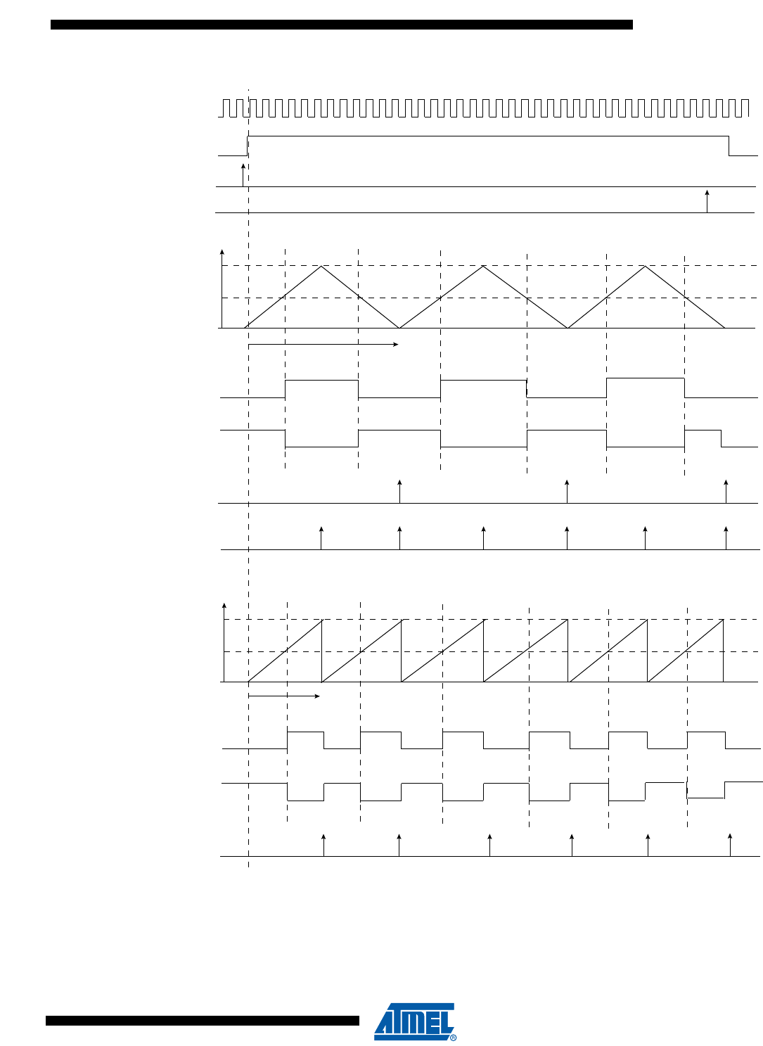
879
6430F–ATARM–21-Feb-12
SAM3U Series
879
6430F–ATARM–21-Feb-12
SAM3U Series
Figure 38-5. Waveform Properties
Channel x
slected clock
CHIDx(PWM_SR)
Center Aligned
CPRD(PWM_CPRDx)
CDTY(PWM_CDTYx)
PWM_CCNTx
Output Waveform OCx
CPOL(PWM_CMRx) = 0
Output Waveform OCx
CPOL(PWM_CMRx) = 1
Counter Event
CHIDx(PWM_ISR)
CES(PWM_CMRx) = 0
Left Aligned
CPRD(PWM_CPRDx)
CDTY(PWM_CDTYx)
PWM_CCNTx
Output Waveform OCx
CPOL(PWM_CMRx) = 0
Output Waveform OCx
CPOL(PWM_CMRx) = 1
CALG(PWM_CMRx) = 0
CALG(PWM_CMRx) = 1
Period
Period
CHIDx(PWM_ENA)
CHIDx(PWM_DIS)
Counter Event
CHIDx(PWM_ISR)
CES(PWM_CMRx) = 1
Counter Event
CHIDx(PWM_ISR)
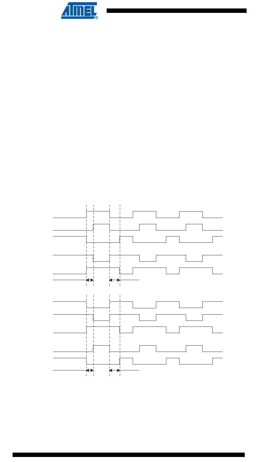
880
6430F–ATARM–21-Feb-12
SAM3U Series
880
6430F–ATARM–21-Feb-12
SAM3U Series
38.6.2.3 Dead-Time Generator
The dead-time generator uses the comparator output OCx to provide the two complementary
outputs DTOHx and DTOLx, which allows the PWM macrocell to drive external power control
switches safely. When the dead-time generator is enabled by setting the bit DTE to 1 or 0 in the
“PWM Channel Mode Register” (PWM_CMRx), dead-times (also called dead-bands or non-
overlapping times) are inserted between the edges of the two complementary outputs DTOHx
and DTOLx. Note that enabling or disabling the dead-time generator is allowed only if the chan-
nel is disabled.
The dead-time is adjustable by the “PWM Channel Dead Time Register” (PWM_DTx). Both out-
puts of the dead-time generator can be adjusted separately by DTH and DTL. The dead-time
values can be updated synchronously to the PWM period by using the “PWM Channel Dead
Time Update Register” (PWM_DTUPDx).
The dead-time is based on a specific counter which uses the same selected clock that feeds the
channel counter of the comparator. Depending on the edge and the configuration of the dead-
time, DTOHx and DTOLx are delayed until the counter has reached the value defined by DTH or
DTL. An inverted configuration bit (DTHI and DTLI bit in the PWM_CMRx register) is provided
for each output to invert the dead-time outputs. The following figure shows the waveform of the
dead-time generator.
Figure 38-6. Complementary Output Waveforms
DTHx DTLx
output waveform OCx
CPOLx = 0
output waveform DTOHx
DTHIx = 0
output waveform DTOLx
DTLIx = 0
output waveform DTOHx
DTHIx = 1
output waveform DTOLx
DTLIx = 1
DTHx DTLx
output waveform OCx
CPOLx = 1
output waveform DTOHx
DTHIx = 0
output waveform DTOLx
DTLIx = 0
output waveform DTOHx
DTHIx = 1
output waveform DTOLx
DTLIx = 1
881
6430F–ATARM–21-Feb-12
SAM3U Series
881
6430F–ATARM–21-Feb-12
SAM3U Series
38.6.2.4 Output Override
The two complementary outputs DTOHx and DTOLx of the dead-time generator can be forced
to a value defined by the software.
Figure 38-7. Override Output Selection
The fields OSHx and OSLx in the “PWM Output Selection Register” (PWM_OS) allow the out-
puts of the dead-time generator DTOHx and DTOLx to be overridden by the value defined in the
fields OOVHx and OOVLx in the“PWM Output Override Value Register” (PWM_OOV).
The set registers “PWM Output Selection Set Register” and “PWM Output Selection Set Update
Register” (PWM_OSS and PWM_OSSUPD) enable the override of the outputs of a channel
regardless of other channels. In the same way, the clear registers “PWM Output Selection Clear
Register” and “PWM Output Selection Clear Update Register” (PWM_OSC and
PWM_OSCUPD) disable the override of the outputs of a channel regardless of other channels.
By using buffer registers PWM_OSSUPD and PWM_OSCUPD, the output selection of PWM
outputs is done synchronously to the channel counter, at the beginning of the next PWM period.
By using registers PWM_OSS and PWM_OSC, the output selection of PWM outputs is done
asynchronously to the channel counter, as soon as the register is written.
The value of the current output selection can be read in PWM_OS.
While overriding PWM outputs, the channel counters continue to run, only the PWM outputs are
forced to user defined values.
DTOHx
OOVHx
OOOHx
OSHx
0
1
DTOLx
OOVLx
OOOLx
OSLx
0
1
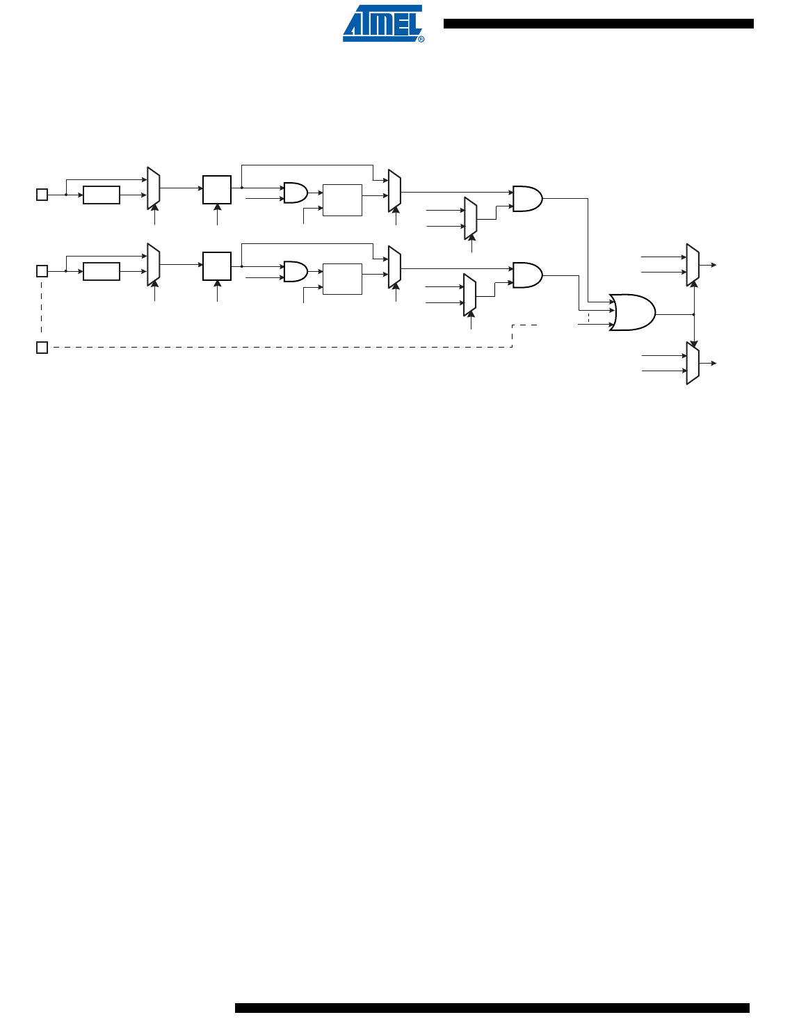
882
6430F–ATARM–21-Feb-12
SAM3U Series
882
6430F–ATARM–21-Feb-12
SAM3U Series
38.6.2.5 Fault Protection
4 inputs provide fault protection which can force any of the PWM output pair to a programmable
value. This mechanism has priority over output overriding.
Figure 38-8. Fault Protection
The polarity level of the fault inputs is configured by the FPOL field in the “PWM Fault Mode
Register” (PWM_FMR). For fault inputs coming from internal peripherals such as ADC, Timer
Counter, to name but a few, the polarity level must be FPOL = 1. For fault inputs coming from
external GPIO pins the polarity level depends on the user's implementation.
The configuration of the Fault Activation Mode (FMOD bit in PWMC_FMR) depends on the
peripheral generating the fault. If the corresponding peripheral does not have “Fault Clear” man-
agement, then the FMOD configuration to use must be FMOD = 1, to avoid spurious fault
detection. Check the corresponding peripheral documentation for details on handling fault
generation.
The fault inputs can be glitch filtered or not in function of the FFIL field in the PWM_FMR regis-
ter. When the filter is activated, glitches on fault inputs with a width inferior to the PWM master
clock (MCK) period are rejected.
A fault becomes active as soon as its corresponding fault input has a transition to the pro-
grammed polarity level. If the corresponding bit FMOD is set to 0 in the PWM_FMR register, the
fault remains active as long as the fault input is at this polarity level. If the corresponding FMOD
bit is set to 1, the fault remains active until the fault input is not at this polarity level anymore and
until it is cleared by writing the corresponding bit FCLR in the “PWM Fault Clear Register”
(PWM_FSCR). By reading the “PWM Fault Status Register” (PWM_FSR), the user can read the
current level of the fault inputs by means of the field FIV, and can know which fault is currently
active thanks to the FS field.
Each fault can be taken into account or not by the fault protection mechanism in each channel.
To be taken into account in the channel x, the fault y must be enabled by the bit FPEx[y] in the
“PWM Fault Protection Enable Registers” (PWM_FPE1). However the synchronous channels
(see Section 38.6.2.6 “Synchronous Channels”) do not use their own fault enable bits, but those
of the channel 0 (bits FPE0[y]).
The fault protection on a channel is triggered when this channel is enabled and when any one of
the faults that are enabled for this channel is active. It can be triggered even if the PWM master
clock (MCK) is not running but only by a fault input that is not glitch filtered.
FIV0
fault input 0
Fault protection
on PWM
channel x
Glitch
Filter
FFIL0
from fault 0
from fault y
1
0
=
FPOL0 FMOD0
1
0Fault 0 Status
FS0
FIV1
Glitch
Filter
FFIL1
1
0
=
FPOL1
SET
CLR
FMOD1
1
0
OUT
Fault 1 Status
FS1
fault input 1 from fault 1 1
0
0
1
From Output
Override
OOHx
OOLx
From Output
Override
FPVHx
FPVLx
PWMHx
PWMLx
fault input y
FMOD1
SET
CLR
Write FCLR0 at 1
OUT
FMOD0
Write FCLR1 at 1
SYNCx
1
0
FPEx[0]
FPE0[0]
SYNCx
1
0
FPEx[1]
FPE0[1]

883
6430F–ATARM–21-Feb-12
SAM3U Series
883
6430F–ATARM–21-Feb-12
SAM3U Series
When the fault protection is triggered on a channel, the fault protection mechanism forces the
channel outputs to the values defined by the fields FPVHx and FPVLx in the “PWM Fault Protec-
tion Value Register” (PWM_FPV) and leads to a reset of the counter of this channel. The output
forcing is made asynchronously to the channel counter.
CAUTION:
• To prevent an unexpected activation of the status flag FSy in the PWM_FSR register, the
FMODy bit can be set to “1” only if the FPOLy bit has been previously configured to its final
value.
• To prevent an unexpected activation of the Fault Protection on the channel x, the bit FPEx[y]
can be set to “1” only if the FPOLy bit has been previously configured to its final value.
If a comparison unit is enabled (see Section 38.6.3 “PWM Comparison Units”) and if a fault is
triggered in the channel 0, in this case the comparison cannot match.
As soon as the fault protection is triggered on a channel, an interrupt (different from the interrupt
generated at the end of the PWM period) can be generated but only if it is enabled and not
masked. The interrupt is reset by reading the interrupt status register, even if the fault which has
caused the trigger of the fault protection is kept active.

884
6430F–ATARM–21-Feb-12
SAM3U Series
884
6430F–ATARM–21-Feb-12
SAM3U Series
38.6.2.6 Synchronous Channels
Some channels can be linked together as synchronous channels. They have the same source
clock, the same period, the same alignment and are started together. In this way, their counters
are synchronized together.
The synchronous channels are defined by the SYNCx bits in the “PWM Sync Channels Mode
Register” (PWM_SCM). Only one group of synchronous channels is allowed.
When a channel is defined as a synchronous channel, the channel 0 is automatically defined as
a synchronous channel too, because the channel 0 counter configuration is used by all the syn-
chronous channels.
If a channel x is defined as a synchronous channel, it uses the following configuration fields of
the channel 0 instead of its own:
• CPRE0 field in PWM_CMR0 register instead of CPREx field in PWM_CMRx register (same
source clock)
• CPRD0 field in PWM_CMR0 register instead of CPRDx field in PWM_CMRx register (same
period)
• CALG0 field in PWM_CMR0 register instead of CALGx field in PWM_CMRx register (same
alignment)
Thus writing these fields of a synchronous channel has no effect on the output waveform of this
channel (except channel 0 of course).
Because counters of synchronous channels must start at the same time, they are all enabled
together by enabling the channel 0 (by the CHID0 bit in PWM_ENA register). In the same way,
they are all disabled together by disabling channel 0 (by the CHID0 bit in PWM_DIS register).
However, a synchronous channel x different from channel 0 can be enabled or disabled inde-
pendently from others (by the CHIDx bit in PWM_ENA and PWM_DIS registers).
Defining a channel as a synchronous channel while it is an asynchronous channel (by writing the
bit SYNCx to 1 while it was at 0) is allowed only if the channel is disabled at this time (CHIDx = 0
in PWM_SR register). In the same way, defining a channel as an asynchronous channel while it is
a synchronous channel (by writing the SYNCx bit to 0 while it was 1) is allowed only if the chan-
nel is disabled at this time.
The field UPDM (Update Mode) in the PWM_SCM register allow to select one of the three meth-
ods to update the registers of the synchronous channels:
• Method 1 (UPDM = 0): the period value, the duty-cycle values and the dead-time values must
be written by the CPU in their respective update registers (respectively PWM_CPRDUPDx,
PWM_CDTYUPDx and PWM_DTUPDx).The update is triggered at the next PWM period as
soon as the bit UPDULOCK in the “PWM Sync Channels Update Control Register”
(PWM_SCUC) is set to 1 (see “Method 1: Manual write of duty-cycle values and manual
trigger of the update” on page 886).
• Method 2 (UPDM = 1): the period value, the duty-cycle values, the dead-time values and the
update period value must be written by the CPU in their respective update registers
(respectively PWM_CPRDUPDx, PWM_CDTYUPDx and PWM_DTUPD). The update of the
period value and of the dead-time values is triggered at the next PWM period as soon as the
bit UPDULOCK in the “PWM Sync Channels Update Control Register” (PWM_SCUC) is set
to 1. The update of the duty-cycle values and the update period value is triggered
automatically after an update period defined by the field UPR in the “PWM Sync Channels

885
6430F–ATARM–21-Feb-12
SAM3U Series
885
6430F–ATARM–21-Feb-12
SAM3U Series
Update Period Register” (PWM_SCUP) (see “Method 2: Manual write of duty-cycle values
and automatic trigger of the update” on page 887).
• Method 3 (UPDM = 2): same as Method 2 apart from the fact that the duty-cycle values of
ALL synchronous channels are written by the Peripheral DMA Controller (PDC) (see “Method
3: Automatic write of duty-cycle values and automatic trigger of the update” on page 889).
The user can choose to synchronize the PDC transfer request with a comparison match (see
Section 38.6.3 “PWM Comparison Units”), by the fields PTRM and PTRCS in the PWM_SCM
register.
Table 38-4. Summary of the Update of Registers of Synchronous Channels
UPDM=0 UPDM=1 UPDM=2
Period Value
(PWM_CPRDUPDx)
Write by the CPU
Update is triggered at the
next PWM period as soon as
the bit UPDULOCK is set to 1
Dead-Time Values
(PWM_DTUPDx)
Write by the CPU
Update is triggered at the
next PWM period as soon as
the bit UPDULOCK is set to 1
Duty-Cycle Values
(PWM_CDTYUPDx)
Write by the CPU Write by the CPU Write by the PDC
Update is triggered at the next
PWM period as soon as the bit
UPDULOCK is set to 1
Update is triggered at the next
PWM period as soon as the update period
counter has reached the value UPR
Update Period Value
(PWM_SCUPUPD)
Not applicable Write by the CPU
Not applicable
Update is triggered at the next
PWM period as soon as the update period
counter has reached the value UPR
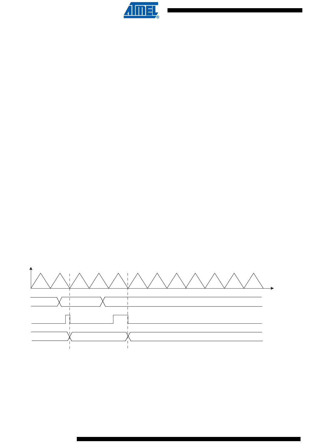
886
6430F–ATARM–21-Feb-12
SAM3U Series
886
6430F–ATARM–21-Feb-12
SAM3U Series
Method 1: Manual write of duty-cycle values and manual trigger of the update
In this mode, the update of the period value, the duty-cycle values and the dead-time values
must be done by writing in their respective update registers with the CPU (respectively
PWM_CPRDUPDx, PWM_CDTYUPDx and PWM_DTUPDx).
To trigger the update, the user must use the bit UPDULOCK of the “PWM Sync Channels
Update Control Register” (PWM_SCUC) which allows to update synchronously (at the same
PWM period) the synchronous channels:
• If the bit UPDULOCK is set to 1, the update is done at the next PWM period of the
synchronous channels.
• If the UPDULOCK bit is not set to 1, the update is locked and cannot be performed.
After writing the UPDULOCK bit to 1, it is held at this value until the update occurs, then it is read
0.
Sequence for Method 1:
1. Select the manual write of duty-cycle values and the manual update by setting the
UPDM field to 0 in the PWM_SCM register
2. Define the synchronous channels by the SYNCx bits in the PWM_SCM register.
3. Enable the synchronous channels by writing CHID0 in the PWM_ENA register.
4. If an update of the period value and/or the duty-cycle values and/or the dead-time val-
ues is required, write registers that need to be updated (PWM_CPRDUPDx,
PWM_CDTYUPDx and PWM_DTUPDx).
5. Set UPDULOCK to 1 in PWM_SCUC.
6. The update of the registers will occur at the beginning of the next PWM period. At this
moment the UPDULOCK bit is reset, go to Step 4.) for new values.
Figure 38-9. Method 1 (UPDM = 0)
CCNT0
CDTYUPD 0x20 0x40 0x60
UPDULOCK
CDTY 0x20 0x40 0x60

887
6430F–ATARM–21-Feb-12
SAM3U Series
887
6430F–ATARM–21-Feb-12
SAM3U Series
Method 2: Manual write of duty-cycle values and automatic trigger of the update
In this mode, the update of the period value, the duty-cycle values, the dead-time values and the
update period value must be done by writing in their respective update registers with the CPU
(respectively PWM_CPRDUPDx, PWM_CDTYUPDx, PWM_DTUPDx and PWM_SCUPUPD).
To trigger the update of the period value and the dead-time values, the user must use the bit
UPDULOCK of the “PWM Sync Channels Update Control Register” (PWM_SCUC) which
allows to update synchronously (at the same PWM period) the synchronous channels:
• If the bit UPDULOCK is set to 1, the update is done at the next PWM period of the
synchronous channels.
• If the UPDULOCK bit is not set to 1, the update is locked and cannot be performed.
After writing the UPDULOCK bit to 1, it is held at this value until the update occurs, then it is read
0.
The update of the duty-cycle values and the update period is triggered automatically after an
update period.
To configure the automatic update, the user must define a value for the Update Period by the
UPR field in the “PWM Sync Channels Update Period Register” (PWM_SCUP). The PWM con-
troller waits UPR+1 period of synchronous channels before updating automatically the duty
values and the update period value.
The status of the duty-cycle value write is reported in the “PWM Interrupt Status Register 2”
(PWM_ISR2) by the following flags:
• WRDY: this flag is set to 1 when the PWM Controller is ready to receive new duty-cycle
values and a new update period value. It is reset to 0 when the PWM_ISR2 register is read.
Depending on the interrupt mask in the PWM_IMR2 register, an interrupt can be generated by
these flags.
Sequence for Method 2:
1. Select the manual write of duty-cycle values and the automatic update by setting the
field UPDM to 1 in the PWM_SCM register
2. Define the synchronous channels by the bits SYNCx in the PWM_SCM register.
3. Define the update period by the field UPR in the PWM_SCUP register.
4. Enable the synchronous channels by writing CHID0 in the PWM_ENA register.
5. If an update of the period value and/or of the dead-time values is required, write regis-
ters that need to be updated (PWM_CPRDUPDx, PWM_DTUPDx), else go to Step 8.
6. Set UPDULOCK to 1 in PWM_SCUC.
7. The update of these registers will occur at the beginning of the next PWM period. At
this moment the bit UPDULOCK is reset, go to Step 5. for new values.
8. If an update of the duty-cycle values and/or the update period is required, check first
that write of new update values is possible by polling the flag WRDY (or by waiting for
the corresponding interrupt) in the PWM_ISR2 register.
9. Write registers that need to be updated (PWM_CDTYUPDx, PWM_SCUPUPD).
10. The update of these registers will occur at the next PWM period of the synchronous
channels when the Update Period is elapsed. Go to Step 8. for new values.
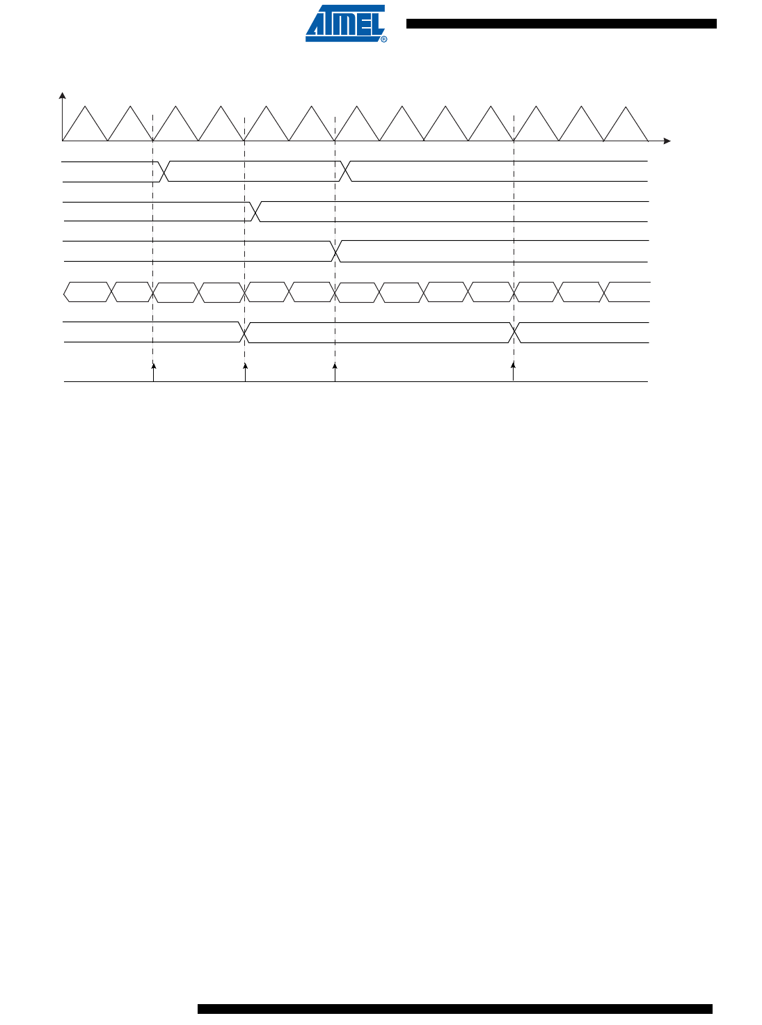
888
6430F–ATARM–21-Feb-12
SAM3U Series
888
6430F–ATARM–21-Feb-12
SAM3U Series
Figure 38-10. Method 2 (UPDM=1)
CCNT0
CDTYUPD 0x20 0x40 0x60
UPRCNT 0x0 0x1 0x0 0x1 0x0 0x1
CDTY 0x20 0x40
UPRUPD 0x1 0x3
WRDY
0x60
0x0 0x1 0x2 0x3 0x0 0x1 0x2
UPR 0x1 0x3

889
6430F–ATARM–21-Feb-12
SAM3U Series
889
6430F–ATARM–21-Feb-12
SAM3U Series
Method 3: Automatic write of duty-cycle values and automatic trigger of the update
In this mode, the update of the duty cycle values is made automatically by the Peripheral DMA
Controller (PDC). The update of the period value, the dead-time values and the update period
value must be done by writing in their respective update registers with the CPU (respectively
PWM_CPRDUPDx, PWM_DTUPDx and PWM_SCUPUPD).
To trigger the update of the period value and the dead-time values, the user must use the bit
UPDULOCK which allows to update synchronously (at the same PWM period) the synchronous
channels:
• If the bit UPDULOCK is set to 1, the update is done at the next PWM period of the
synchronous channels.
• If the UPDULOCK bit is not set to 1, the update is locked and cannot be performed.
After writing the UPDULOCK bit to 1, it is held at this value until the update occurs, then it is read
0.
The update of the duty-cycle values and the update period value is triggered automatically after
an update period.
To configure the automatic update, the user must define a value for the Update Period by the
field UPR in the “PWM Sync Channels Update Period Register” (PWM_SCUP). The PWM con-
troller waits UPR+1 periods of synchronous channels before updating automatically the duty
values and the update period value.
Using the PDC removes processor overhead by reducing its intervention during the transfer.
This significantly reduces the number of clock cycles required for a data transfer, which
improves microcontroller performance.
The PDC must write the duty-cycle values in the synchronous channels index order. For exam-
ple if the channels 0, 1 and 3 are synchronous channels, the PDC must write the duty-cycle of
the channel 0 first, then the duty-cycle of the channel 1, and finally the duty-cycle of the channel
3.
The status of the PDC transfer is reported in the “PWM Interrupt Status Register 2”
(PWM_ISR2) by the following flags:
• WRDY: this flag is set to 1 when the PWM Controller is ready to receive new duty-cycle
values and a new update period value. It is reset to 0 when the PWM_ISR2 register is read.
The user can choose to synchronize the WRDY flag and the PDC transfer request with a
comparison match (see Section 38.6.3 “PWM Comparison Units”), by the fields PTRM and
PTRCS in the PWM_SCM register.
• ENDTX: this flag is set to 1 when a PDC transfer is completed
• TXBUFE: this flag is set to 1 when the PDC buffer is empty (no pending PDC transfers)
• UNRE: this flag is set to 1 when the update period defined by the UPR field has elapsed
while the whole data has not been written by the PDC. It is reset to 0 when the PWM_ISR2
register is read.
Depending on the interrupt mask in the PWM_IMR2 register, an interrupt can be generated by
these flags.

890
6430F–ATARM–21-Feb-12
SAM3U Series
890
6430F–ATARM–21-Feb-12
SAM3U Series
Sequence for Method 3:
1. Select the automatic write of duty-cycle values and automatic update by setting the field
UPDM to 2 in the PWM_SCM register.
2. Define the synchronous channels by the bits SYNCx in the PWM_SCM register.
3. Define the update period by the field UPR in the PWM_SCUP register.
4. Define when the WRDY flag and the corresponding PDC transfer request must be set in
the update period by the PTRM bit and the PTRCS field in the PWM_SCM register (at
the end of the update period or when a comparison matches).
5. Define the PDC transfer settings for the duty-cycle values and enable it in the PDC
registers
6. Enable the synchronous channels by writing CHID0 in the PWM_ENA register.
7. If an update of the period value and/or of the dead-time values is required, write regis-
ters that need to be updated (PWM_CPRDUPDx, PWM_DTUPDx), else go to Step 10.
8. Set UPDULOCK to 1 in PWM_SCUC.
9. The update of these registers will occur at the beginning of the next PWM period. At
this moment the bit UPDULOCK is reset, go to Step 7. for new values.
10. If an update of the update period value is required, check first that write of a new update
value is possible by polling the flag WRDY (or by waiting for the corresponding inter-
rupt) in the PWM_ISR2 register, else go to Step 13.
11. Write the register that needs to be updated (PWM_SCUPUPD).
12. The update of this register will occur at the next PWM period of the synchronous chan-
nels when the Update Period is elapsed. Go to Step 10. for new values.
13. Check the end of the PDC transfer by the flag ENDTX. If the transfer has ended, define
a new PDC transfer in the PDC registers for new duty-cycle values. Go to Step 5.
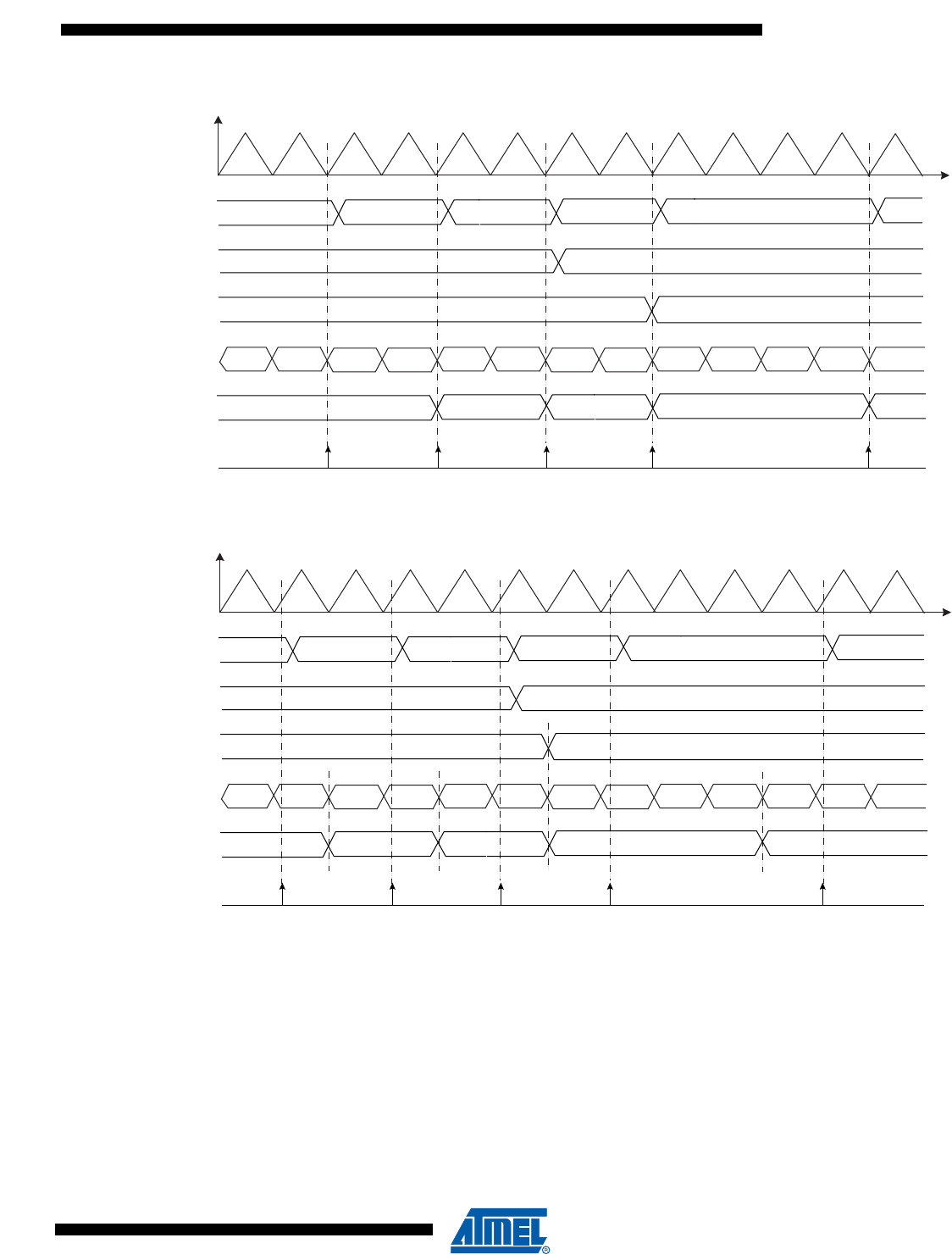
891
6430F–ATARM–21-Feb-12
SAM3U Series
891
6430F–ATARM–21-Feb-12
SAM3U Series
Figure 38-11. Method 3 (UPDM=2 and PTRM=0)
Figure 38-12. Method 3 (UPDM=2 and PTRM=1 and PTRCS=0)
CCNT0
CDTYUPD 0x20 0x40 0x60
UPRCNT 0x0 0x1 0x0 0x1 0x0 0x1
CDTY
UPRUPD 0x1 0x3
PDC transfer request
WRDY
0x0 0x1 0x2 0x3 0x0 0x1 0x2
UPR 0x1 0x3
0x80 0xA0 0xB0
0x20 0x40 0x60 0x80 0xA0
CCNT0
CDTYUPD 0x20 0x40 0x60
UPRCNT 0x0 0x1 0x0 0x1 0x0 0x1
CDTY
UPRUPD 0x1 0x3
CMP0 match
PDC transfer request
WRDY
0x0 0x1 0x2 0x3 0x0 0x1 0x2
UPR 0x1 0x3
0x80 0xA0 0xB0
0x20 0x40 0x60 0x80 0xA0
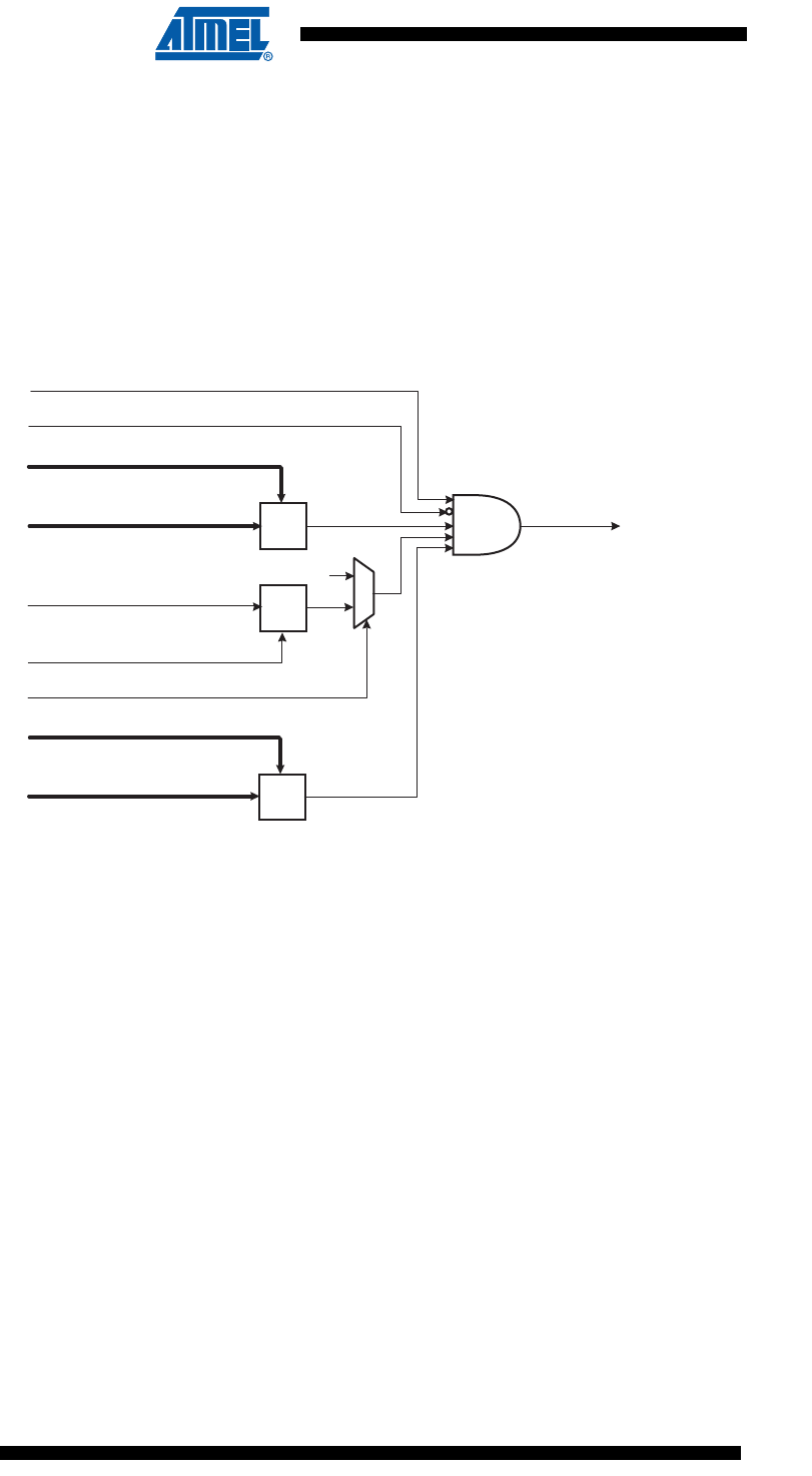
892
6430F–ATARM–21-Feb-12
SAM3U Series
892
6430F–ATARM–21-Feb-12
SAM3U Series
38.6.3 PWM Comparison Units
The PWM provides 8 independent comparison units able to compare a programmed value with
the current value of the channel 0 counter (which is the channel counter of all synchronous
channels, Section 38.6.2.6 “Synchronous Channels”). These comparisons are intended to gen-
erate pulses on the event lines (used to synchronize ADC, see Section 38.6.4 “PWM Event
Lines”), to generate software interrupts and to trigger PDC transfer requests for the synchronous
channels (see “Method 3: Automatic write of duty-cycle values and automatic trigger of the
update” on page 889).
Figure 38-13. Comparison Unit Block Diagram
The comparison x matches when it is enabled by the bit CEN in the “PWM Comparison x Mode
Register” (PWM_CMPMx for the comparison x) and when the counter of the channel 0 reaches
the comparison value defined by the field CV in “PWM Comparison x Value Register”
(PWM_CMPVx for the comparison x). If the counter of the channel 0 is center aligned (CALG =
1 in “PWM Channel Mode Register” ), the bit CVM (in PWM_CMPVx) defines if the comparison
is made when the counter is counting up or counting down (in left alignment mode CALG=0, this
bit is useless).
If a fault is active on the channel 0, the comparison is disabled and cannot match (see Section
38.6.2.5 “Fault Protection”).
The user can define the periodicity of the comparison x by the fields CTR and CPR (in
PWM_CMPVx). The comparison is performed periodically once every CPR+1 periods of the
counter of the channel 0, when the value of the comparison period counter CPRCNT (in
PWM_CMPMx) reaches the value defined by CTR. CPR is the maximum value of the compari-
son period counter CPRCNT. If CPR=CTR=0, the comparison is performed at each period of the
counter of the channel 0.
The comparison x configuration can be modified while the channel 0 is enabled by using the
“PWM Comparison x Mode Update Register” (PWM_CMPMUPDx registers for the comparison
x). In the same way, the comparison x value can be modified while the channel 0 is enabled by
using the “PWM Comparison x Value Update Register” (PWM_CMPVUPDx registers for the
comparison x).
=
fault on channel 0
CNT [PWM_CCNT0]
CNT [PWM_CCNT0] is decrementing
CALG [PWM_CMR0]
CV [PWM_CMPVx]
=1
0
1
Comparison x
CVM [PWM_CMPVx]
=
CPRCNT [PWM_CMPMx]
CTR [PWM_CMPMx]
CEN [PWM_CMPM]x
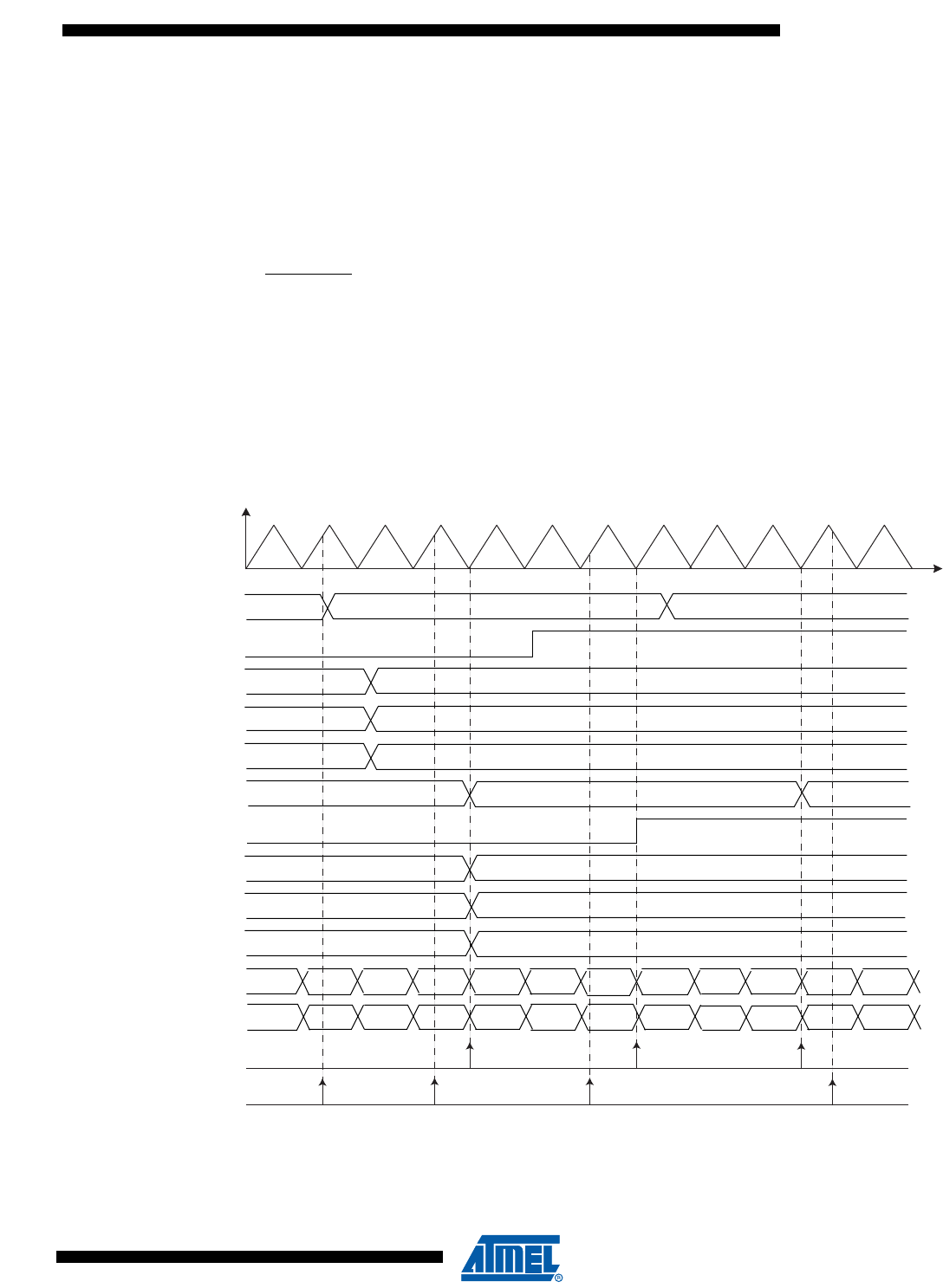
893
6430F–ATARM–21-Feb-12
SAM3U Series
893
6430F–ATARM–21-Feb-12
SAM3U Series
The update of the comparison x configuration and the comparison x value is triggered periodi-
cally after the comparison x update period. It is defined by the field CUPR in the PWM_CMPMx.
The comparison unit has an update period counter independent from the period counter to trig-
ger this update. When the value of the comparison update period counter CUPRCNT (in
PWM_CMPMx) reaches the value defined by CUPR, the update is triggered. The comparison x
update period CUPR itself can be updated while the channel 0 is enabled by using the
PWM_CMPMUPDx register.
CAUTION: to be taken into account, the write of the register PWM_CMPVUPDx must be fol-
lowed by a write of the register PWM_CMPMUPDx.
The comparison match and the comparison update can be source of an interrupt, but only if it is
enabled and not masked. These interrupts can be enabled by the “PWM Interrupt Enable Regis-
ter 2” and disabled by the “PWM Interrupt Disable Register 2” . The comparison match interrupt
and the comparison update interrupt are reset by reading the “PWM Interrupt Status Register 2”
.
Figure 38-14. Comparison Waveform
CCNT0
CVUPD
0x6 0x2
CVMVUPD
CV
0x6 0x2
0x6
0x6
CVM
Comparison Update
CMPU
CTRUPD
0x1 0x2
CPR
0x1 0x3
0x0 0x1 0x0 0x1 0x0 0x1 0x2 0x3 0x0 0x1 0x2 0x3
CPRCNT
0x0 0x1 0x2 0x3 0x0 0x1 0x2
0x0
0x1 0x2 0x0 0x1
CUPRCNT
CPRUPD
0x1 0x3
CUPRUPD
0x3 0x2
CTR
0x1 0x2
CUPR
0x3 0x2
Comparison Match
CMPM
894
6430F–ATARM–21-Feb-12
SAM3U Series
894
6430F–ATARM–21-Feb-12
SAM3U Series
38.6.4 PWM Event Lines
The PWM provides 2 independent event lines intended to trigger actions in other peripherals (in
particular for ADC (Analog-to-Digital Converter)).
A pulse (one cycle of the master clock (MCK)) is generated on an event line, when at least one
of the selected comparisons is matching. The comparisons can be selected or unselected inde-
pendently by the CSEL bits in the “PWM Event Line x Register” (PWM_ELMRx for the Event
Line x).
Figure 38-15. Event Line Block Diagram
PULSE
GENERATOR
Event Line x
CSEL0 (PWM_ELMRx)
CMPS0 (PWM_ISR2)
CSEL1 (PWM_ELMRx)
CMPS1 (PWM_ISR2)
CSEL2 (PWM_ELMRx)
CMPS2 (PWM_ISR2)
CSEL7 (PWM_ELMRx)
CMPS7 (PWM_ISR2)

895
6430F–ATARM–21-Feb-12
SAM3U Series
895
6430F–ATARM–21-Feb-12
SAM3U Series
38.6.5 PWM Controller Operations
38.6.5.1 Initialization
Before enabling the channels, they must have been configured by the software application:
• Unlock User Interface by writing the WPCMD field in the PWM_WPCR Register.
• Configuration of the clock generator (DIVA, PREA, DIVB, PREB in the PWM_CLK register if
required).
• Selection of the clock for each channel (CPRE field in the PWM_CMRx register)
• Configuration of the waveform alignment for each channel (CALG field in the PWM_CMRx
register)
• Selection of the counter event selection (if CALG = 1) for each channel (CES field in the
PWM_CMRx register)
• Configuration of the output waveform polarity for each channel (CPOL in the PWM_CMRx
register)
• Configuration of the period for each channel (CPRD in the PWM_CPRDx register). Writing in
PWM_CPRDx register is possible while the channel is disabled. After validation of the
channel, the user must use PWM_CPRDUPDx register to update PWM_CPRDx as
explained below.
• Configuration of the duty-cycle for each channel (CDTY in the PWM_CDTYx register).
Writing in PWM_CDTYx register is possible while the channel is disabled. After validation of
the channel, the user must use PWM_CDTYUPDx register to update PWM_CDTYx as
explained below.
• Configuration of the dead-time generator for each channel (DTH and DTL in PWM_DTx) if
enabled (DTE bit in the PWM_CMRx register). Writing in the PWM_DTx register is possible
while the channel is disabled. After validation of the channel, the user must use
PWM_DTUPDx register to update PWM_DTx
• Selection of the synchronous channels (SYNCx in the PWM_SCM register)
• Selection of the moment when the WRDY flag and the corresponding PDC transfer request
are set (PTRM and PTRCS in the PWM_SCM register)
• Configuration of the update mode (UPDM in the PWM_SCM register)
• Configuration of the update period (UPR in the PWM_SCUP register) if needed.
• Configuration of the comparisons (PWM_CMPVx and PWM_CMPMx).
• Configuration of the event lines (PWM_ELMRx).
• Configuration of the fault inputs polarity (FPOL in PWM_FMR)
• Configuration of the fault protection (FMOD and FFIL in PWM_FMR, PWM_FPV and
PWM_FPE1)
• Enable of the Interrupts (writing CHIDx and FCHIDx in PWM_IER1 register, and writing
WRDYE, ENDTXE, TXBUFE, UNRE, CMPMx and CMPUx in PWM_IER2 register)
• Enable of the PWM channels (writing CHIDx in the PWM_ENA register)

896
6430F–ATARM–21-Feb-12
SAM3U Series
896
6430F–ATARM–21-Feb-12
SAM3U Series
38.6.5.2 Source Clock Selection Criteria
The large number of source clocks can make selection difficult. The relationship between the
value in the “PWM Channel Period Register” (PWM_CPRDx) and the “PWM Channel Duty
Cycle Register” (PWM_CDTYx) can help the user in choosing. The event number written in the
Period Register gives the PWM accuracy. The Duty-Cycle quantum cannot be lower than
1/CPRDx value. The higher the value of PWM_CPRDx, the greater the PWM accuracy.
For example, if the user sets 15 (in decimal) in PWM_CPRDx, the user is able to set a value
from between 1 up to 14 in PWM_CDTYx Register. The resulting duty-cycle quantum cannot be
lower than 1/15 of the PWM period.
38.6.5.3 Changing the Duty-Cycle, the Period and the Dead-Times
It is possible to modulate the output waveform duty-cycle, period and dead-times.
To prevent unexpected output waveform, the user must use the “PWM Channel Duty Cycle
Update Register” , the “PWM Channel Period Update Register” and the “PWM Channel Dead
Time Update Register” (PWM_CDTYUPDx, PWM_CPRDUPDx and PWM_DTUPDx) to change
waveform parameters while the channel is still enabled.
• If the channel is an asynchronous channel (SYNCx = 0 in “PWM Sync Channels Mode
Register” (PWM_SCM)), these registers hold the new period, duty-cycle and dead-times
values until the end of the current PWM period and update the values for the next period.
• If the channel is a synchronous channel and update method 0 is selected (SYNCx = 1 and
UPDM = 0 in PWM_SCM register), these registers hold the new period, duty-cycle and dead-
times values until the bit UPDULOCK is written at “1” (in “PWM Sync Channels Update
Control Register” (PWM_SCUC)) and the end of the current PWM period, then update the
values for the next period.
• If the channel is a synchronous channel and update method 1 or 2 is selected (SYNCx=1 and
UPDM=1 or 2 in PWM_SCM register):
– registers PWM_CPRDUPDx and PWM_DTUPDx hold the new period and dead-
times values until the bit UPDULOCK is written at “1” (in PWM_SCUC register) and
the end of the current PWM period, then update the values for the next period.
– register PWM_CDTYUPDx holds the new duty-cycle value until the end of the
update period of synchronous channels (when UPRCNT is equal to UPR in “PWM
Sync Channels Update Period Register” (PWM_SCUP)) and the end of the current
PWM period, then updates the value for the next period.
Note: If the update registers PWM_CDTYUPDx, PWM_CPRDUPDx and PWM_DTUPDx are written
several times between two updates, only the last written value is taken into account.
897
6430F–ATARM–21-Feb-12
SAM3U Series
897
6430F–ATARM–21-Feb-12
SAM3U Series
Figure 38-16. Synchronized Period, Duty-Cycle and Dead-Times Update
PWM_CPRDUPDx Value
PWM_CPRDx PWM_CDTYx
- If Asynchronous Channel
-> End of PWM period
- If Synchronous Channel
-> End of PWM period and UPDULOCK = 1
User's Writing
PWM_DTUPDx Value
User's Writing
PWM_DTx
- If Asynchronous Channel
-> End of PWM period
- If Synchronous Channel
- If UPDM = 0
-> End of PWM period and UPDULOCK = 1
- If UPDM = 1 or 2
-> End of PWM period and end of Update Period
PWM_CDTYUPDx Value
User's Writing
898
6430F–ATARM–21-Feb-12
SAM3U Series
898
6430F–ATARM–21-Feb-12
SAM3U Series
38.6.5.4 Changing the Synchronous Channels Update Period
It is possible to change the update period of synchronous channels while they are enabled. (See
“Method 2: Manual write of duty-cycle values and automatic trigger of the update” on page 887
and “Method 3: Automatic write of duty-cycle values and automatic trigger of the update” on
page 889.)
To prevent an unexpected update of the synchronous channels registers, the user must use the
“PWM Sync Channels Update Period Update Register” (PWM_SCUPUPD) to change the
update period of synchronous channels while they are still enabled. This register holds the new
value until the end of the update period of synchronous channels (when UPRCNT is equal to
UPR in “PWM Sync Channels Update Period Register” (PWM_SCUP)) and the end of the cur-
rent PWM period, then updates the value for the next period.
Note: If the update register PWM_SCUPUPD is written several times between two updates, only the last
written value is taken into account.
Note: Changing the update period does make sense only if there is one or more synchronous channels
and if the update method 1 or 2 is selected (UPDM = 1 or 2 in “PWM Sync Channels Mode Regis-
ter” ).
Figure 38-17. Synchronized Update of Update Period Value of Synchronous Channels
End of PWM period and
end of Update Period
of Synchronous Channels
PWM_SCUPUPD Value
User's Writing
PWM_SCUP
899
6430F–ATARM–21-Feb-12
SAM3U Series
899
6430F–ATARM–21-Feb-12
SAM3U Series
38.6.5.5 Changing the Comparison Value and the Comparison Configuration
It is possible to change the comparison values and the comparison configurations while the
channel 0 is enabled (see Section 38.6.3 “PWM Comparison Units”).
To prevent unexpected comparison match, the user must use the “PWM Comparison x Value
Update Register” and the “PWM Comparison x Mode Update Register” (PWM_CMPVUPDx
and PWM_CMPMUPDx) to change respectively the comparison values and the comparison
configurations while the channel 0 is still enabled. These registers hold the new values until the
end of the comparison update period (when CUPRCNT is equal to CUPR in “PWM Comparison
x Mode Register” (PWM_CMPMx) and the end of the current PWM period, then update the val-
ues for the next period.
CAUTION: to be taken into account, the write of the register PWM_CMPVUPDx must be fol-
lowed by a write of the register PWM_CMPMUPDx.
Note: If the update registers PWM_CMPVUPDx and PWM_CMPMUPDx are written several times
between two updates, only the last written value are taken into account.
Figure 38-18. Synchronized Update of Comparison Values and Configurations
PWM_CMPVUPDx Value
Comparison Value
for comparison x
User's Writing
PWM_CMPVx
End of channel0 PWM period and
end of Comparison Update Period
PWM_CMPMUPDx Value
Comparison configuration
for comparison x
PWM_CMPMx
User's Writing
End of channel0 PWM period and
end of Comparison Update Period and
and PWM_CMPMx written

900
6430F–ATARM–21-Feb-12
SAM3U Series
900
6430F–ATARM–21-Feb-12
SAM3U Series
38.6.5.6 Interrupts
Depending on the interrupt mask in the PWM_IMR1 and PWM_IMR2 registers, an interrupt can
be generated at the end of the corresponding channel period (CHIDx in the PWM_ISR1 regis-
ter), after a fault event (FCHIDx in the PWM_ISR1 register), after a comparison match (CMPMx
in the PWM_ISR2 register), after a comparison update (CMPUx in the PWM_ISR2 register) or
according to the transfer mode of the synchronous channels (WRDY, ENDTX, TXBUFE and
UNRE in the PWM_ISR2 register).
If the interrupt is generated by the flags CHIDx or FCHIDx, the interrupt remains active until a
read operation in the PWM_ISR1 register occurs.
If the interrupt is generated by the flags WRDY or UNRE or CMPMx or CMPUx, the interrupt
remains active until a read operation in the PWM_ISR2 register occurs.
A channel interrupt is enabled by setting the corresponding bit in the PWM_IER1 and
PWM_IER2 registers. A channel interrupt is disabled by setting the corresponding bit in the
PWM_IDR1 and PWM_IDR2 registers.
38.6.5.7 Write Protect Registers
To prevent any single software error that may corrupt PWM behavior, the registers listed below
can be write-protected by writing the field WPCMD in the “PWM Write Protect Control Register”
on page 934 (PWM_WPCR). They are divided into 6 groups:
• Register group 0:
–“PWM Clock Register” on page 905
• Register group 1:
–“PWM Disable Register” on page 907
• Register group 2:
–“PWM Sync Channels Mode Register” on page 913
–“PWM Channel Mode Register” on page 941
–
• Register group 3:
–“PWM Channel Period Register” on page 945
–“PWM Channel Period Update Register” on page 946
• Register group 4:
–“PWM Channel Dead Time Register” on page 948
–“PWM Channel Dead Time Update Register” on page 949
• Register group 5:
–“PWM Fault Mode Register” on page 928
–“PWM Fault Protection Value Register” on page 931
–
There are two types of Write Protect:
• Write Protect SW, which can be enabled or disabled.
• Write Protect HW, which can just be enabled, only a hardware reset of the PWM controller
can disable it.

901
6430F–ATARM–21-Feb-12
SAM3U Series
901
6430F–ATARM–21-Feb-12
SAM3U Series
Both types of Write Protect can be applied independently to a particular register group by means
of the WPCMD and WPRG fields in PWM_WPCR register. If at least one Write Protect is active,
the register group is write-protected. The field WPCMD allows to perform the following actions
depending on its value:
• 0 = Disabling the Write Protect SW of the register groups of which the bit WPRG is at 1.
• 1 = Enabling the Write Protect SW of the register groups of which the bit WPRG is at 1.
• 2 = Enabling the Write Protect HW of the register groups of which the bit WPRG is at 1.
At any time, the user can determine which Write Protect is active in which register group by the
fields WPSWS and WPHWS in the “PWM Write Protect Status Register” on page 936
(PWM_WPSR).
If a write access in a write-protected register is detected, then the WPVS flag in the
PWM_WPSR register is set and the field WPVSRC indicates in which register the write access
has been attempted, through its address offset without the two LSBs.
The WPVS and PWM_WPSR fields are automatically reset after reading the PWM_WPSR
register.

902
6430F–ATARM–21-Feb-12
SAM3U Series
902
6430F–ATARM–21-Feb-12
SAM3U Series
38.7 Pulse Width Modulation (PWM) User Interface
Table 38-5. Register Mapping
Offset Register Name Access Reset
0x00 PWM Clock Register PWM_CLK Read-write 0x0
0x04 PWM Enable Register PWM_ENA Write-only –
0x08 PWM Disable Register PWM_DIS Write-only –
0x0C PWM Status Register PWM_SR Read-only 0x0
0x10 PWM Interrupt Enable Register 1 PWM_IER1 Write-only –
0x14 PWM Interrupt Disable Register 1 PWM_IDR1 Write-only –
0x18 PWM Interrupt Mask Register 1 PWM_IMR1 Read-only 0x0
0x1C PWM Interrupt Status Register 1 PWM_ISR1 Read-only 0x0
0x20 PWM Sync Channels Mode Register PWM_SCM Read-write 0x0
0x24 Reserved – – –
0x28 PWM Sync Channels Update Control Register PWM_SCUC Read-write 0x0
0x2C PWM Sync Channels Update Period Register PWM_SCUP Read-write 0x0
0x30 PWM Sync Channels Update Period Update Register PWM_SCUPUPD Write-only 0x0
0x34 PWM Interrupt Enable Register 2 PWM_IER2 Write-only –
0x38 PWM Interrupt Disable Register 2 PWM_IDR2 Write-only –
0x3C PWM Interrupt Mask Register 2 PWM_IMR2 Read-only 0x0
0x40 PWM Interrupt Status Register 2 PWM_ISR2 Read-only 0x0
0x44 PWM Output Override Value Register PWM_OOV Read-write 0x0
0x48 PWM Output Selection Register PWM_OS Read-write 0x0
0x4C PWM Output Selection Set Register PWM_OSS Write-only –
0x50 PWM Output Selection Clear Register PWM_OSC Write-only –
0x54 PWM Output Selection Set Update Register PWM_OSSUPD Write-only –
0x58 PWM Output Selection Clear Update Register PWM_OSCUPD Write-only –
0x5C PWM Fault Mode Register PWM_FMR Read-write 0x0
0x60 PWM Fault Status Register PWM_FSR Read-only 0x0
0x64 PWM Fault Clear Register PWM_FCR Write-only –
0x68 PWM Fault Protection Value Register PWM_FPV Read-write 0x0
0x6C PWM Fault Protection Enable Register PWM_FPE Read-write 0x0
0x70-0x78 Reserved – – –
0x7C PWM Event Line 0 Mode Register PWM_ELMR0 Read-write 0x0
0x80 PWM Event Line 1 Mode Register PWM_ELMR1 Read-write 0x0
0x84-AC Reserved – – –
0xB4-E0 Reserved – – –
0xE4 PWM Write Protect Control Register PWM_WPCR Write-only –

903
6430F–ATARM–21-Feb-12
SAM3U Series
903
6430F–ATARM–21-Feb-12
SAM3U Series
0xE8 PWM Write Protect Status Register PWM_WPSR Read-only 0x0
0xEC - 0xFC Reserved – – –
0x100 - 0x128 Reserved for PDC registers – – –
0x12C Reserved – – –
0x130 PWM Comparison 0 Value Register PWM_CMPV0 Read-write 0x0
0x134 PWM Comparison 0 Value Update Register PWM_CMPVUPD0 Write-only –
0x138 PWM Comparison 0 Mode Register PWM_CMPM0 Read-write 0x0
0x13C PWM Comparison 0 Mode Update Register PWM_CMPMUPD0 Write-only –
0x140 PWM Comparison 1 Value Register PWM_CMPV1 Read-write 0x0
0x144 PWM Comparison 1 Value Update Register PWM_CMPVUPD1 Write-only –
0x148 PWM Comparison 1 Mode Register PWM_CMPM1 Read-write 0x0
0x14C PWM Comparison 1 Mode Update Register PWM_CMPMUPD1 Write-only –
0x150 PWM Comparison 2 Value Register PWM_CMPV2 Read-write 0x0
0x154 PWM Comparison 2 Value Update Register PWM_CMPVUPD2 Write-only –
0x158 PWM Comparison 2 Mode Register PWM_CMPM2 Read-write 0x0
0x15C PWM Comparison 2 Mode Update Register PWM_CMPMUPD2 Write-only –
0x160 PWM Comparison 3 Value Register PWM_CMPV3 Read-write 0x0
0x164 PWM Comparison 3 Value Update Register PWM_CMPVUPD3 Write-only –
0x168 PWM Comparison 3 Mode Register PWM_CMPM3 Read-write 0x0
0x16C PWM Comparison 3 Mode Update Register PWM_CMPMUPD3 Write-only –
0x170 PWM Comparison 4 Value Register PWM_CMPV4 Read-write 0x0
0x174 PWM Comparison 4 Value Update Register PWM_CMPVUPD4 Write-only –
0x178 PWM Comparison 4 Mode Register PWM_CMPM4 Read-write 0x0
0x17C PWM Comparison 4 Mode Update Register PWM_CMPMUPD4 Write-only –
0x180 PWM Comparison 5 Value Register PWM_CMPV5 Read-write 0x0
0x184 PWM Comparison 5 Value Update Register PWM_CMPVUPD5 Write-only –
0x188 PWM Comparison 5 Mode Register PWM_CMPM5 Read-write 0x0
0x18C PWM Comparison 5 Mode Update Register PWM_CMPMUPD5 Write-only –
0x190 PWM Comparison 6 Value Register PWM_CMPV6 Read-write 0x0
0x194 PWM Comparison 6 Value Update Register PWM_CMPVUPD6 Write-only –
0x198 PWM Comparison 6 Mode Register PWM_CMPM6 Read-write 0x0
0x19C PWM Comparison 6 Mode Update Register PWM_CMPMUPD6 Write-only –
0x1A0 PWM Comparison 7 Value Register PWM_CMPV7 Read-write 0x0
0x1A4 PWM Comparison 7 Value Update Register PWM_CMPVUPD7 Write-only –
0x1A8 PWM Comparison 7 Mode Register PWM_CMPM7 Read-write 0x0
0x1AC PWM Comparison 7 Mode Update Register PWM_CMPMUPD7 Write-only –
Table 38-5. Register Mapping (Continued)
Offset Register Name Access Reset

904
6430F–ATARM–21-Feb-12
SAM3U Series
904
6430F–ATARM–21-Feb-12
SAM3U Series
Notes: 1. Some registers are indexed with “ch_num” index ranging from 0 to 3.
0x1B0 - 0x1FC Reserved – – –
0x200 + ch_num *
0x20 + 0x00 PWM Channel Mode Register(1) PWM_CMR Read-write 0x0
0x200 + ch_num *
0x20 + 0x04 PWM Channel Duty Cycle Register(1) PWM_CDTY Read-write 0x0
0x200 + ch_num *
0x20 + 0x08 PWM Channel Duty Cycle Update Register(1) PWM_CDTYUPD Write-only –
0x200 + ch_num *
0x20 + 0x0C PWM Channel Period Register(1) PWM_CPRD Read-write 0x0
0x200 + ch_num *
0x20 + 0x10 PWM Channel Period Update Register(1) PWM_CPRDUPD Write-only –
0x200 + ch_num *
0x20 + 0x14 PWM Channel Counter Register(1) PWM_CCNT Read-only 0x0
0x200 + ch_num *
0x20 + 0x18 PWM Channel Dead Time Register(1) PWM_DT Read-write 0x0
0x200 + ch_num *
0x20 + 0x1C PWM Channel Dead Time Update Register(1) PWM_DTUPD Write-only –
Table 38-5. Register Mapping (Continued)
Offset Register Name Access Reset
905
6430F–ATARM–21-Feb-12
SAM3U Series
905
6430F–ATARM–21-Feb-12
SAM3U Series
38.7.1 PWM Clock Register
Name: PWM_CLK
Address: 0x4008C000
Access: Read-write
This register can only be written if the bits WPSWS0 and WPHWS0 are cleared in “PWM Write Protect Status Register” on
page 936.
• DIVA, DIVB: CLKA, CLKB Divide Factor
• PREA, PREB: CLKA, CLKB Source Clock Selection
31 30 29 28 27 26 25 24
–––– PREB
23 22 21 20 19 18 17 16
DIVB
15 14 13 12 11 10 9 8
–––– PREA
76543210
DIVA
DIVA, DIVB CLKA, CLKB
0 CLKA, CLKB clock is turned off
1 CLKA, CLKB clock is clock selected by PREA, PREB
2-255 CLKA, CLKB clock is clock selected by PREA, PREB divided by DIVA, DIVB factor.
PREA, PREB Divider Input Clock
0000MCK
0001MCK/2
0010MCK/4
0011MCK/8
0100MCK/16
0101MCK/32
0110MCK/64
0111MCK/128
1000MCK/256
1001MCK/512
1010MCK/1024
Other Reserved

906
6430F–ATARM–21-Feb-12
SAM3U Series
906
6430F–ATARM–21-Feb-12
SAM3U Series
38.7.2 PWM Enable Register
Name: PWM_ENA
Address: 0x4008C004
Access: Write-only
• CHIDx: Channel ID
0 = No effect.
1 = Enable PWM output for channel x.
31 30 29 28 27 26 25 24
––––––––
23 22 21 20 19 18 17 16
––––––––
15 14 13 12 11 10 9 8
––––––––
76543210
––––CHID3CHID2CHID1CHID0

907
6430F–ATARM–21-Feb-12
SAM3U Series
907
6430F–ATARM–21-Feb-12
SAM3U Series
38.7.3 PWM Disable Register
Name: PWM_DIS
Address: 0x4008C008
Access: Write-only
This register can only be written if the bits WPSWS1 and WPHWS1 are cleared in “PWM Write Protect Status Register” on
page 936.
• CHIDx: Channel ID
0 = No effect.
1 = Disable PWM output for channel x.
31 30 29 28 27 26 25 24
––––––––
23 22 21 20 19 18 17 16
––––––––
15 14 13 12 11 10 9 8
––––––––
76543210
––––CHID3CHID2CHID1CHID0

908
6430F–ATARM–21-Feb-12
SAM3U Series
908
6430F–ATARM–21-Feb-12
SAM3U Series
38.7.4 PWM Status Register
Name: PWM_SR
Address: 0x4008C00C
Access: Read-only
• CHIDx: Channel ID
0 = PWM output for channel x is disabled.
1 = PWM output for channel x is enabled.
31 30 29 28 27 26 25 24
––––––––
23 22 21 20 19 18 17 16
––––––––
15 14 13 12 11 10 9 8
––––––––
76543210
––––CHID3CHID2CHID1CHID0

909
6430F–ATARM–21-Feb-12
SAM3U Series
909
6430F–ATARM–21-Feb-12
SAM3U Series
38.7.5 PWM Interrupt Enable Register 1
Name: PWM_IER1
Address: 0x4008C010
Access: Write-only
• CHIDx: Counter Event on Channel x Interrupt Enable
• FCHIDx: Fault Protection Trigger on Channel x Interrupt Enable
31 30 29 28 27 26 25 24
––––––––
23 22 21 20 19 18 17 16
––––FCHID3FCHID2FCHID1FCHID0
15 14 13 12 11 10 9 8
––––––––
76543210
––––CHID3CHID2CHID1CHID0

910
6430F–ATARM–21-Feb-12
SAM3U Series
910
6430F–ATARM–21-Feb-12
SAM3U Series
38.7.6 PWM Interrupt Disable Register 1
Name: PWM_IDR1
Address: 0x4008C014
Access: Write-only
• CHIDx: Counter Event on Channel x Interrupt Disable
• FCHIDx: Fault Protection Trigger on Channel x Interrupt Disable
31 30 29 28 27 26 25 24
––––––––
23 22 21 20 19 18 17 16
––––FCHID3FCHID2FCHID1FCHID0
15 14 13 12 11 10 9 8
––––––––
76543210
––––CHID3CHID2CHID1CHID0

911
6430F–ATARM–21-Feb-12
SAM3U Series
911
6430F–ATARM–21-Feb-12
SAM3U Series
38.7.7 PWM Interrupt Mask Register 1
Name: PWM_IMR1
Address: 0x4008C018
Access: Read-only
• CHIDx: Counter Event on Channel x Interrupt Mask
• FCHIDx: Fault Protection Trigger on Channel x Interrupt Mask
31 30 29 28 27 26 25 24
––––––––
23 22 21 20 19 18 17 16
––––FCHID3FCHID2FCHID1FCHID0
15 14 13 12 11 10 9 8
––––––––
76543210
––––CHID3CHID2CHID1CHID0

912
6430F–ATARM–21-Feb-12
SAM3U Series
912
6430F–ATARM–21-Feb-12
SAM3U Series
38.7.8 PWM Interrupt Status Register 1
Name: PWM_ISR1
Address: 0x4008C01C
Access: Read-only
• CHIDx: Counter Event on Channel x
0 = No new counter event has occurred since the last read of the PWM_ISR1 register.
1 = At least one counter event has occurred since the last read of the PWM_ISR1 register.
• FCHIDx: Fault Protection Trigger on Channel x
0 = No new trigger of the fault protection since the last read of the PWM_ISR1 register.
1 = At least one trigger of the fault protection since the last read of the PWM_ISR1 register.
Note: Reading PWM_ISR1 automatically clears CHIDx and FCHIDx flags.
31 30 29 28 27 26 25 24
––––––––
23 22 21 20 19 18 17 16
––––FCHID3FCHID2FCHID1FCHID0
15 14 13 12 11 10 9 8
––––––––
76543210
––––CHID3CHID2CHID1CHID0
913
6430F–ATARM–21-Feb-12
SAM3U Series
913
6430F–ATARM–21-Feb-12
SAM3U Series
38.7.9 PWM Sync Channels Mode Register
Name: PWM_SCM
Address: 0x4008C020
Access: Read-write
This register can only be written if the bits WPSWS2 and WPHWS2 are cleared in “PWM Write Protect Status Register” on
page 936.
• SYNCx: Synchronous Channel x
0 = Channel x is not a synchronous channel.
1 = Channel x is a synchronous channel.
• UPDM: Synchronous Channels Update Mode
Notes: 1. The update occurs at the beginning of the next PWM period, when the UPDULOCK bit in “PWM Sync Channels Update
Control Register” is set.
2. The update occurs when the Update Period is elapsed.
• PTRM: PDC Transfer Request Mode
31 30 29 28 27 26 25 24
––––––––
23 22 21 20 19 18 17 16
PTRCS PTRM – – UPDM
15 14 13 12 11 10 9 8
––––––––
76543210
––––SYNC3SYNC2SYNC1SYNC0
Value Name Description
0 MODE0 Manual write of double buffer registers and manual update of synchronous channels(1)
1 MODE1 Manual write of double buffer registers and automatic update of synchronous channels(2)
2MODE2
Automatic write of duty-cycle update registers by the PDC and automatic update of synchronous
channels(2)
3–Reserved
UPDM PTRM WRDY Flag and PDC Transfer Request
0x
The WRDY flag in “PWM Interrupt Status Register 2” on page 921 and the PDC transfer request
are never set to 1.
1x
The WRDY flag in “PWM Interrupt Status Register 2” on page 921 is set to 1 as soon as the
update period is elapsed, the PDC transfer request is never set to 1.
2
0The WRDY flag in “PWM Interrupt Status Register 2” on page 921 and the PDC transfer request
are set to 1 as soon as the update period is elapsed.
1The WRDY flag in “PWM Interrupt Status Register 2” on page 921 and the PDC transfer request
are set to 1 as soon as the selected comparison matches.

914
6430F–ATARM–21-Feb-12
SAM3U Series
914
6430F–ATARM–21-Feb-12
SAM3U Series
• PTRCS: PDC Transfer Request Comparison Selection
Selection of the comparison used to set the flag WRDY and the corresponding PDC transfer request.

915
6430F–ATARM–21-Feb-12
SAM3U Series
915
6430F–ATARM–21-Feb-12
SAM3U Series
38.7.10 PWM Sync Channels Update Control Register
Name: PWM_SCUC
Address: 0x4008C028
Access: Read-write
• UPDULOCK: Synchronous Channels Update Unlock
0 = No effect
1 = If the UPDM field is set to “0” in “PWM Sync Channels Mode Register” on page 913, writing the UPDULOCK bit to “1”
triggers the update of the period value, the duty-cycle and the dead-time values of synchronous channels at the beginning
of the next PWM period. If the field UPDM is set to “1” or “2”, writing the UPDULOCK bit to “1” triggers only the update of
the period value and of the dead-time values of synchronous channels.
This bit is automatically reset when the update is done.
31 30 29 28 27 26 25 24
––––––––
23 22 21 20 19 18 17 16
––––––––
15 14 13 12 11 10 9 8
––––––––
76543210
–––––––UPDULOCK

916
6430F–ATARM–21-Feb-12
SAM3U Series
916
6430F–ATARM–21-Feb-12
SAM3U Series
38.7.11 PWM Sync Channels Update Period Register
Name: PWM_SCUP
Address: 0x4008C02C
Access: Read-write
• UPR: Update Period
Defines the time between each update of the synchronous channels if automatic trigger of the update is activated
(UPDM = 1 or UPDM = 2 in “PWM Sync Channels Mode Register” on page 913). This time is equal to UPR+1 periods of
the synchronous channels.
• UPRCNT: Update Period Counter
Reports the value of the Update Period Counter.
31 30 29 28 27 26 25 24
––––––––
23 22 21 20 19 18 17 16
––––––––
15 14 13 12 11 10 9 8
––––––––
76543210
UPRCNT UPR

917
6430F–ATARM–21-Feb-12
SAM3U Series
917
6430F–ATARM–21-Feb-12
SAM3U Series
38.7.12 PWM Sync Channels Update Period Update Register
Name: PWM_SCUPUPD
Address: 0x4008C030
Access: Write-only
This register acts as a double buffer for the UPR value. This prevents an unexpected automatic trigger of the update of syn-
chronous channels.
• UPRUPD: Update Period Update
Defines the wanted time between each update of the synchronous channels if automatic trigger of the update is activated
(UPDM = 1 or UPDM = 2 in “PWM Sync Channels Mode Register” on page 913). This time is equal to UPR+1 periods of
the synchronous channels.
31 30 29 28 27 26 25 24
––––––––
23 22 21 20 19 18 17 16
––––––––
15 14 13 12 11 10 9 8
––––––––
76543210
–––– UPRUPD

918
6430F–ATARM–21-Feb-12
SAM3U Series
918
6430F–ATARM–21-Feb-12
SAM3U Series
38.7.13 PWM Interrupt Enable Register 2
Name: PWM_IER2
Address: 0x4008C034
Access: Write-only
• WRDY: Write Ready for Synchronous Channels Update Interrupt Enable
• ENDTX: PDC End of TX Buffer Interrupt Enable
• TXBUFE: PDC TX Buffer Empty Interrupt Enable
• UNRE: Synchronous Channels Update Underrun Error Interrupt Enable
• CMPMx: Comparison x Match Interrupt Enable
• CMPUx: Comparison x Update Interrupt Enable
31 30 29 28 27 26 25 24
––––––––
23 22 21 20 19 18 17 16
CMPU7 CMPU6 CMPU5 CMPU4 CMPU3 CMPU2 CMPU1 CMPU0
15 14 13 12 11 10 9 8
CMPM7 CMPM6 CMPM5 CMPM4 CMPM3 CMPM2 CMPM1 CMPM0
76543210
––––UNRETXBUFEENDTXWRDY

919
6430F–ATARM–21-Feb-12
SAM3U Series
919
6430F–ATARM–21-Feb-12
SAM3U Series
38.7.14 PWM Interrupt Disable Register 2
Name: PWM_IDR2
Address: 0x4008C038
Access: Write-only
• WRDY: Write Ready for Synchronous Channels Update Interrupt Disable
• ENDTX: PDC End of TX Buffer Interrupt Disable
• TXBUFE: PDC TX Buffer Empty Interrupt Disable
• UNRE: Synchronous Channels Update Underrun Error Interrupt Disable
• CMPMx: Comparison x Match Interrupt Disable
• CMPUx: Comparison x Update Interrupt Disable
31 30 29 28 27 26 25 24
––––––––
23 22 21 20 19 18 17 16
CMPU7 CMPU6 CMPU5 CMPU4 CMPU3 CMPU2 CMPU1 CMPU0
15 14 13 12 11 10 9 8
CMPM7 CMPM6 CMPM5 CMPM4 CMPM3 CMPM2 CMPM1 CMPM0
76543210
––––UNRETXBUFEENDTXWRDY

920
6430F–ATARM–21-Feb-12
SAM3U Series
920
6430F–ATARM–21-Feb-12
SAM3U Series
38.7.15 PWM Interrupt Mask Register 2
Name: PWM_IMR2
Address: 0x4008C03C
Access: Read-only
• WRDY: Write Ready for Synchronous Channels Update Interrupt Mask
• ENDTX: PDC End of TX Buffer Interrupt Mask
• TXBUFE: PDC TX Buffer Empty Interrupt Mask
• UNRE: Synchronous Channels Update Underrun Error Interrupt Mask
• CMPMx: Comparison x Match Interrupt Mask
• CMPUx: Comparison x Update Interrupt Mask
31 30 29 28 27 26 25 24
––––––––
23 22 21 20 19 18 17 16
CMPU7 CMPU6 CMPU5 CMPU4 CMPU3 CMPU2 CMPU1 CMPU0
15 14 13 12 11 10 9 8
CMPM7 CMPM6 CMPM5 CMPM4 CMPM3 CMPM2 CMPM1 CMPM0
76543210
––––UNRETXBUFEENDTXWRDY

921
6430F–ATARM–21-Feb-12
SAM3U Series
921
6430F–ATARM–21-Feb-12
SAM3U Series
38.7.16 PWM Interrupt Status Register 2
Name: PWM_ISR2
Address: 0x4008C040
Access: Read-only
• WRDY: Write Ready for Synchronous Channels Update
0 = New duty-cycle and dead-time values for the synchronous channels cannot be written.
1 = New duty-cycle and dead-time values for the synchronous channels can be written.
• ENDTX: PDC End of TX Buffer
0 = The Transmit Counter register has not reached 0 since the last write of the PDC.
1 = The Transmit Counter register has reached 0 since the last write of the PDC.
• TXBUFE: PDC TX Buffer Empty
0 = PWM_TCR or PWM_TCNR has a value other than 0.
1 = Both PWM_TCR and PWM_TCNR have a value other than 0.
• UNRE: Synchronous Channels Update Underrun Error
0 = No Synchronous Channels Update Underrun has occurred since the last read of the PWM_ISR2 register.
1 = At least one Synchronous Channels Update Underrun has occurred since the last read of the PWM_ISR2 register.
• CMPMx: Comparison x Match
0 = The comparison x has not matched since the last read of the PWM_ISR2 register.
1 = The comparison x has matched at least one time since the last read of the PWM_ISR2 register.
• CMPUx: Comparison x Update
0 = The comparison x has not been updated since the last read of the PWM_ISR2 register.
1 = The comparison x has been updated at least one time since the last read of the PWM_ISR2 register.
Note: Reading PWM_ISR2 automatically clears flags WRDY, UNRE and CMPSx.
31 30 29 28 27 26 25 24
––––––––
23 22 21 20 19 18 17 16
CMPU7 CMPU6 CMPU5 CMPU4 CMPU3 CMPU2 CMPU1 CMPU0
15 14 13 12 11 10 9 8
CMPM7 CMPM6 CMPM5 CMPM4 CMPM3 CMPM2 CMPM1 CMPM0
76543210
––––UNRETXBUFEENDTXWRDY

922
6430F–ATARM–21-Feb-12
SAM3U Series
922
6430F–ATARM–21-Feb-12
SAM3U Series
38.7.17 PWM Output Override Value Register
Name: PWM_OOV
Address: 0x4008C044
Access: Read-write
• OOVHx: Output Override Value for PWMH output of the channel x
0 = Override value is 0 for PWMH output of channel x.
1 = Override value is 1 for PWMH output of channel x.
• OOVLx: Output Override Value for PWML output of the channel x
0 = Override value is 0 for PWML output of channel x.
1 = Override value is 1 for PWML output of channel x.
31 30 29 28 27 26 25 24
––––––––
23 22 21 20 19 18 17 16
––––OOVL3OOVL2OOVL1OOVL0
15 14 13 12 11 10 9 8
––––––––
76543210
––––OOVH3OOVH2OOVH1OOVH0
923
6430F–ATARM–21-Feb-12
SAM3U Series
923
6430F–ATARM–21-Feb-12
SAM3U Series
38.7.18 PWM Output Selection Register
Name: PWM_OS
Address: 0x4008C048
Access: Read-write
• OSHx: Output Selection for PWMH output of the channel x
0 = Dead-time generator output DTOHx selected as PWMH output of channel x.
1 = Output override value OOVHx selected as PWMH output of channel x.
• OSLx: Output Selection for PWML output of the channel x
0 = Dead-time generator output DTOLx selected as PWML output of channel x.
1 = Output override value OOVLx selected as PWML output of channel x.
31 30 29 28 27 26 25 24
––––––––
23 22 21 20 19 18 17 16
––––OSL3OSL2OSL1OSL0
15 14 13 12 11 10 9 8
––––––––
76543210
––––OSH3OSH2OSH1OSH0

924
6430F–ATARM–21-Feb-12
SAM3U Series
924
6430F–ATARM–21-Feb-12
SAM3U Series
38.7.19 PWM Output Selection Set Register
Name: PWM_OSS
Address: 0x4008C04C
Access: Write-only
• OSSHx: Output Selection Set for PWMH output of the channel x
0 = No effect.
1 = Output override value OOVHx selected as PWMH output of channel x.
• OSSLx: Output Selection Set for PWML output of the channel x
0 = No effect.
1 = Output override value OOVLx selected as PWML output of channel x.
31 30 29 28 27 26 25 24
––––––––
23 22 21 20 19 18 17 16
––––OSSL3OSSL2OSSL1OSSL0
15 14 13 12 11 10 9 8
––––––––
76543210
––––OSSH3OSSH2OSSH1OSSH0

925
6430F–ATARM–21-Feb-12
SAM3U Series
925
6430F–ATARM–21-Feb-12
SAM3U Series
38.7.20 PWM Output Selection Clear Register
Name: PWM_OSC
Address: 0x4008C050
Access: Write-only
• OSCHx: Output Selection Clear for PWMH output of the channel x
0 = No effect.
1 = Dead-time generator output DTOHx selected as PWMH output of channel x.
• OSCLx: Output Selection Clear for PWML output of the channel x
0 = No effect.
1 = Dead-time generator output DTOLx selected as PWML output of channel x.
31 30 29 28 27 26 25 24
––––––––
23 22 21 20 19 18 17 16
––––OSCL3OSCL2OSCL1OSCL0
15 14 13 12 11 10 9 8
––––––––
76543210
––––OSCH3OSCH2OSCH1OSCH0

926
6430F–ATARM–21-Feb-12
SAM3U Series
926
6430F–ATARM–21-Feb-12
SAM3U Series
38.7.21 PWM Output Selection Set Update Register
Name: PWM_OSSUPD
Address: 0x4008C054
Access: Write-only
• OSSUPHx: Output Selection Set for PWMH output of the channel x
0 = No effect.
1 = Output override value OOVHx selected as PWMH output of channel x at the beginning of the next channel x PWM
period.
• OSSUPLx: Output Selection Set for PWML output of the channel x
0 = No effect.
1 = Output override value OOVLx selected as PWML output of channel x at the beginning of the next channel x PWM
period.
31 30 29 28 27 26 25 24
––––––––
23 22 21 20 19 18 17 16
––––OSSUPL3OSSUPL2OSSUPL1OSSUPL0
15 14 13 12 11 10 9 8
––––––––
76543210
––––OSSUPH3OSSUPH2OSSUPH1OSSUPH0

927
6430F–ATARM–21-Feb-12
SAM3U Series
927
6430F–ATARM–21-Feb-12
SAM3U Series
38.7.22 PWM Output Selection Clear Update Register
Name: PWM_OSCUPD
Address: 0x4008C058
Access: Write-only
• OSCUPHx: Output Selection Clear for PWMH output of the channel x
0 = No effect.
1 = Dead-time generator output DTOHx selected as PWMH output of channel x at the beginning of the next channel x
PWM period.
• OSCUPLx: Output Selection Clear for PWML output of the channel x
0 = No effect.
1 = Dead-time generator output DTOLx selected as PWML output of channel x at the beginning of the next channel x PWM
period.
31 30 29 28 27 26 25 24
––––––––
23 22 21 20 19 18 17 16
––––OSCUPL3OSCUPL2OSCUPL1OSCUPL0
15 14 13 12 11 10 9 8
––––––––
76543210
––––OSCUPH3OSCUPH2OSCUPH1OSCUPH0

928
6430F–ATARM–21-Feb-12
SAM3U Series
928
6430F–ATARM–21-Feb-12
SAM3U Series
38.7.23 PWM Fault Mode Register
Name: PWM_FMR
Address: 0x4008C05C
Access: Read-write
This register can only be written if the bits WPSWS5 and WPHWS5 are cleared in “PWM Write Protect Status Register” on
page 936.
• FPOL: Fault Polarity (fault input bit varies from 0 to 3)
For each field bit y (fault input number):
0 = The fault y becomes active when the fault input y is at 0.
1 = The fault y becomes active when the fault input y is at 1.
• FMOD: Fault Activation Mode (fault input bit varies from 0 to 3)
For each field bit y (fault input number):
0 = The fault y is active until the Fault condition is removed at the peripheral(1) level.
1 = The fault y stays active until the Fault condition is removed at the peripheral(1) level AND until it is cleared in the
“PWM Fault Clear Register” .
Note: 1. The Peripheral generating the fault.
• FFIL: Fault Filtering (fault input bit varies from 0 to 3)
For each field bit y (fault input number):
0 = The fault input y is not filtered.
1 = The fault input y is filtered.
CAUTION: To prevent an unexpected activation of the status flag FSy in the “PWM Fault Status Register” on page 929, the
bit FMODy can be set to “1” only if the FPOLy bit has been previously configured to its final value.
31 30 29 28 27 26 25 24
–
23 22 21 20 19 18 17 16
FFIL
15 14 13 12 11 10 9 8
FMOD
76543210
FPOL

929
6430F–ATARM–21-Feb-12
SAM3U Series
929
6430F–ATARM–21-Feb-12
SAM3U Series
38.7.24 PWM Fault Status Register
Name: PWM_FSR
Address: 0x4008C060
Access: Read-only
• FIV: Fault Input Value (fault input bit varies from 0 to 3)
For each field bit y (fault input number):
0 = The current sampled value of the fault input y is 0 (after filtering if enabled).
1 = The current sampled value of the fault input y is 1 (after filtering if enabled).
• FS: Fault Status (fault input bit varies from 0 to 3)
For each field bit y (fault input number):
0 = The fault y is not currently active.
1 = The fault y is currently active.
31 30 29 28 27 26 25 24
–
23 22 21 20 19 18 17 16
–
15 14 13 12 11 10 9 8
FS
76543210
FIV

930
6430F–ATARM–21-Feb-12
SAM3U Series
930
6430F–ATARM–21-Feb-12
SAM3U Series
38.7.25 PWM Fault Clear Register
Name: PWM_FCR
Address: 0x4008C064
Access: Write-only
• FCLR: Fault Clear (fault input bit varies from 0 to 3)
For each field bit y (fault input number):
0 = No effect.
1 = If bit y of FMOD field is set to 1 and if the fault input y is not at the level defined by the bit y of FPOL field, the fault y
is cleared and becomes inactive (FMOD and FPOL fields belong to “PWM Fault Mode Register” on page 928), else
writing this bit to 1 has no effect.
31 30 29 28 27 26 25 24
–
23 22 21 20 19 18 17 16
–
15 14 13 12 11 10 9 8
–
76543210
FCLR

931
6430F–ATARM–21-Feb-12
SAM3U Series
931
6430F–ATARM–21-Feb-12
SAM3U Series
38.7.26 PWM Fault Protection Value Register
Name: PWM_FPV
Address: 0x4008C068
Access: Read-write
This register can only be written if the bits WPSWS5 and WPHWS5 are cleared in “PWM Write Protect Status Register” on
page 936.
• FPVHx: Fault Protection Value for PWMH output on channel x
0 = PWMH output of channel x is forced to 0 when fault occurs.
1 = PWMH output of channel x is forced to 1 when fault occurs.
• FPVLx: Fault Protection Value for PWML output on channel x
0 = PWML output of channel x is forced to 0 when fault occurs.
1 = PWML output of channel x is forced to 1 when fault occurs.
31 30 29 28 27 26 25 24
––––––––
23 22 21 20 19 18 17 16
––––FPVL3FPVL2FPVL1FPVL0
15 14 13 12 11 10 9 8
––––––––
76543210
––––FPVH3FPVH2FPVH1FPVH0

932
6430F–ATARM–21-Feb-12
SAM3U Series
932
6430F–ATARM–21-Feb-12
SAM3U Series
38.7.27 PWM Fault Protection Enable Register
Name: PWM_FPE
Address: 0x4008C06C
Access: Read-write
This register can only be written if the bits WPSWS5 and WPHWS5 are cleared in “PWM Write Protect Status Register” on
page 936.
Only the first 4 bits (number of fault input pins) of fields FPE0, FPE1, FPE2 and FPE3 are significant.
• FPEx: Fault Protection Enable for channel x (fault input bit varies from 0 to 3)
For each field bit y (fault input number):
0 = Fault y is not used for the Fault Protection of channel x.
1 = Fault y is used for the Fault Protection of channel x.
CAUTION: To prevent an unexpected activation of the Fault Protection, the bit y of FPEx field can be set to “1” only if the
corresponding FPOL bit has been previously configured to its final value in “PWM Fault Mode Register” on page 928.
31 30 29 28 27 26 25 24
FPE3
23 22 21 20 19 18 17 16
FPE2
15 14 13 12 11 10 9 8
FPE1
76543210
FPE0

933
6430F–ATARM–21-Feb-12
SAM3U Series
933
6430F–ATARM–21-Feb-12
SAM3U Series
38.7.28 PWM Event Line x Register
Name: PWM_ELMRx
Address: 0x4008C07C
Access: Read-write
• CSELy: Comparison y Selection
0 = A pulse is not generated on the event line x when the comparison y matches.
1 = A pulse is generated on the event line x when the comparison y match.
31 30 29 28 27 26 25 24
––––––––
23 22 21 20 19 18 17 16
––––––––
15 14 13 12 11 10 9 8
––––––––
76543210
CSEL7 CSEL6 CSEL5 CSEL4 CSEL3 CSEL2 CSEL1 CSEL0

934
6430F–ATARM–21-Feb-12
SAM3U Series
934
6430F–ATARM–21-Feb-12
SAM3U Series
38.7.29 PWM Write Protect Control Register
Name: PWM_WPCR
Address: 0x4008C0E4
Access: Write-only
• WPCMD: Write Protect Command
This command is performed only if the WPKEY value is correct.
0 = Disable the Write Protect SW of the register groups of which the bit WPRGx is at 1.
1 = Enable the Write Protect SW of the register groups of which the bit WPRGx is at 1.
2 = Enable the Write Protect HW of the register groups of which the bit WPRGx is at 1.
Moreover, to meet security requirements, in this mode of operation, the PIO lines associated with PWM can not be con-
figured through the PIO interface, not even by the PIO controller.
3 = No effect.
Note: Only a hardware reset of the PWM controller can disable the Write Protect HW.
• WPRGx: Write Protect Register Group x
0 = The WPCMD command has no effect on the register group x.
1 = The WPCMD command is applied to the register group x.
• WPKEY: Write Protect Key
Should be written at value 0x50574D (“PWM” in ASCII). Writing any other value in this field aborts the write operation of the
WPCMD field. Always reads as 0.
List of register groups:
• Register group 0:
–“PWM Clock Register” on page 905
• Register group 1:
–“PWM Disable Register” on page 907
• Register group 2:
–“PWM Sync Channels Mode Register” on page 913
–“PWM Channel Mode Register” on page 941
–
31 30 29 28 27 26 25 24
WPKEY
23 22 21 20 19 18 17 16
WPKEY
15 14 13 12 11 10 9 8
WPKEY
76543210
WPRG5 WPRG4 WPRG3 WPRG2 WPRG1 WPRG0 WPCMD

935
6430F–ATARM–21-Feb-12
SAM3U Series
935
6430F–ATARM–21-Feb-12
SAM3U Series
• Register group 3:
–“PWM Channel Period Register” on page 945
–“PWM Channel Period Update Register” on page 946
• Register group 4:
–“PWM Channel Dead Time Register” on page 948
–“PWM Channel Dead Time Update Register” on page 949
• Register group 5:
–“PWM Fault Mode Register” on page 928
–“PWM Fault Protection Value Register” on page 931

936
6430F–ATARM–21-Feb-12
SAM3U Series
936
6430F–ATARM–21-Feb-12
SAM3U Series
38.7.30 PWM Write Protect Status Register
Name: PWM_WPSR
Address: 0x4008C0E8
Access: Read-only
• WPSWSx: Write Protect SW Status
0 = The Write Protect SW x of the register group x is disabled.
1 = The Write Protect SW x of the register group x is enabled.
• WPHWSx: Write Protect HW Status
0 = The Write Protect HW x of the register group x is disabled.
1 = The Write Protect HW x of the register group x is enabled.
• WPVS: Write Protect Violation Status
0 = No Write Protect violation has occurred since the last read of the PWM_WPSR register.
1 = At least one Write Protect violation has occurred since the last read of the PWM_WPSR register. If this violation is an
unauthorized attempt to write a protected register, the associated violation is reported into field WPVSRC.
• WPVSRC: Write Protect Violation Source
When WPVS is active, this field indicates the write-protected register (through address offset) in which a write access has
been attempted.
Note: The two LSBs of the address offset of the write-protected register are not reported
Note: Reading PWM_WPSR automatically clears WPVS and WPVSRC fields.
31 30 29 28 27 26 25 24
WPVSRC
23 22 21 20 19 18 17 16
WPVSRC
15 14 13 12 11 10 9 8
– – WPHWS5 WPHWS4 WPHWS3 WPHWS2 WPHWS1 WPHWS0
76543210
WPVS – WPSWS5 WPSWS4 WPSWS3 WPSWS2 WPSWS1 WPSWS0

937
6430F–ATARM–21-Feb-12
SAM3U Series
937
6430F–ATARM–21-Feb-12
SAM3U Series
38.7.31 PWM Comparison x Value Register
Name: PWM_CMPVx
Address: 0x4008C130 [0], 0x4008C140 [1], 0x4008C150 [2], 0x4008C160 [3], 0x4008C170 [4], 0x4008C180 [5],
0x4008C190 [6], 0x4008C1A0 [7]
Access: Read-write
Only the first 16 bits (channel counter size) of field CV are significant.
• CV: Comparison x Value
Define the comparison x value to be compared with the counter of the channel 0.
• CVM: Comparison x Value Mode
0 = The comparison x between the counter of the channel 0 and the comparison x value is performed when this counter is
incrementing.
1 = The comparison x between the counter of the channel 0 and the comparison x value is performed when this counter is
decrementing.
Note: This bit is useless if the counter of the channel 0 is left aligned (CALG = 0 in “PWM Channel Mode Register” on page 941)
31 30 29 28 27 26 25 24
–––––––CVM
23 22 21 20 19 18 17 16
CV
15 14 13 12 11 10 9 8
CV
76543210
CV

938
6430F–ATARM–21-Feb-12
SAM3U Series
938
6430F–ATARM–21-Feb-12
SAM3U Series
38.7.32 PWM Comparison x Value Update Register
Name: PWM_CMPVUPDx
Address: 0x4008C134 [0], 0x4008C144 [1], 0x4008C154 [2], 0x4008C164 [3], 0x4008C174 [4], 0x4008C184 [5],
0x4008C194 [6], 0x4008C1A4 [7]
Access: Write-only
This register acts as a double buffer for the CV and CVM values. This prevents an unexpected comparison x match.
Only the first 16 bits (channel counter size) of field CVUPD are significant.
• CVUPD: Comparison x Value Update
Define the comparison x value to be compared with the counter of the channel 0.
• CVMUPD: Comparison x Value Mode Update
0 = The comparison x between the counter of the channel 0 and the comparison x value is performed when this counter is
incrementing.
1 = The comparison x between the counter of the channel 0 and the comparison x value is performed when this counter is
decrementing.
Note: This bit is useless if the counter of the channel 0 is left aligned (CALG = 0 in “PWM Channel Mode Register” on page 941)
CAUTION: to be taken into account, the write of the register PWM_CMPVUPDx must be followed by a write of the register
PWM_CMPMUPDx.
31 30 29 28 27 26 25 24
–––––––CVMUPD
23 22 21 20 19 18 17 16
CVUPD
15 14 13 12 11 10 9 8
CVUPD
76543210
CVUPD
939
6430F–ATARM–21-Feb-12
SAM3U Series
939
6430F–ATARM–21-Feb-12
SAM3U Series
38.7.33 PWM Comparison x Mode Register
Name: PWM_CMPMx
Address: 0x4008C138 [0], 0x4008C148 [1], 0x4008C158 [2], 0x4008C168 [3], 0x4008C178 [4], 0x4008C188 [5],
0x4008C198 [6], 0x4008C1A8 [7]
Access: Read-write
• CEN: Comparison x Enable
0 = The comparison x is disabled and can not match.
1 = The comparison x is enabled and can match.
• CTR: Comparison x Trigger
The comparison x is performed when the value of the comparison x period counter (CPRCNT) reaches the value defined
by CTR.
• CPR: Comparison x Period
CPR defines the maximum value of the comparison x period counter (CPRCNT). The comparison x value is performed
periodically once every CPR+1 periods of the channel 0 counter.
• CPRCNT: Comparison x Period Counter
Reports the value of the comparison x period counter.
Note: The field CPRCNT is read-only
• CUPR: Comparison x Update Period
Defines the time between each update of the comparison x mode and the comparison x value. This time is equal to
CUPR+1 periods of the channel 0 counter.
• CUPRCNT: Comparison x Update Period Counter
Reports the value of the comparison x update period counter.
Note: The field CUPRCNT is read-only
31 30 29 28 27 26 25 24
––––––––
23 22 21 20 19 18 17 16
CUPRCNT CUPR
15 14 13 12 11 10 9 8
CPRCNT CPR
76543210
CTR – – – CEN

940
6430F–ATARM–21-Feb-12
SAM3U Series
940
6430F–ATARM–21-Feb-12
SAM3U Series
38.7.34 PWM Comparison x Mode Update Register
Name: PWM_CMPMUPDx
Address: 0x4008C13C [0], 0x4008C14C [1], 0x4008C15C [2], 0x4008C16C [3], 0x4008C17C [4], 0x4008C18C [5],
0x4008C19C [6], 0x4008C1AC [7]
Access: Write-only
This register acts as a double buffer for the CEN, CTR, CPR and CUPR values. This prevents an unexpected comparison
x match.
• CENUPD: Comparison x Enable Update
0 = The comparison x is disabled and can not match.
1 = The comparison x is enabled and can match.
• CTRUPD: Comparison x Trigger Update
The comparison x is performed when the value of the comparison x period counter (CPRCNT) reaches the value defined
by CTR.
• CPRUPD: Comparison x Period Update
CPR defines the maximum value of the comparison x period counter (CPRCNT). The comparison x value is performed
periodically once every CPR+1 periods of the channel 0 counter.
• CUPRUPD: Comparison x Update Period Update
Defines the time between each update of the comparison x mode and the comparison x value. This time is equal to
CUPR+1 periods of the channel 0 counter.
31 30 29 28 27 26 25 24
––––––––
23 22 21 20 19 18 17 16
–––– CUPRUPD
15 14 13 12 11 10 9 8
–––– CPRUPD
76543210
CTRUPD – – – CENUPD
941
6430F–ATARM–21-Feb-12
SAM3U Series
941
6430F–ATARM–21-Feb-12
SAM3U Series
38.7.35 PWM Channel Mode Register
Name: PWM_CMRx [x=0..3]
Address: 0x4008C200 [0], 0x4008C220 [1], 0x4008C240 [2], 0x4008C260 [3]
Access: Read-write
This register can only be written if the bits WPSWS2 and WPHWS2 are cleared in “PWM Write Protect Status Register” on
page 936.
• CPRE: Channel Pre-scaler
• CALG: Channel Alignment
0 = The period is left aligned.
1 = The period is center aligned.
• CPOL: Channel Polarity
0 = The OCx output waveform (output from the comparator) starts at a low level.
1 = The OCx output waveform (output from the comparator) starts at a high level.
31 30 29 28 27 26 25 24
––––––––
23 22 21 20 19 18 17 16
–––––DTLIDTHIDTE
15 14 13 12 11 10 9 8
–––––CESCPOLCALG
76543210
–––– CPRE
Value Name Description
0b0000 MCK Master clock
0b0001 MCK_DIV_2 Master clock/2
0b0010 MCK_DIV_4 Master clock/4
0b0011 MCK_DIV_8 Master clock/8
0b0100 MCK_DIV_16 Master clock/16
0b0101 MCK_DIV_32 Master clock/32
0b0110 MCK_DIV_64 Master clock/64
0b0111 MCK_DIV_128 Master clock/128
0b1000 MCK_DIV_256 Master clock/256
0b1001 MCK_DIV_512 Master clock/512
0b1010 MCK_DIV_1024 Master clock/1024
0b1011 CLKA Clock A
0b1100 CLKB Clock B

942
6430F–ATARM–21-Feb-12
SAM3U Series
942
6430F–ATARM–21-Feb-12
SAM3U Series
• CES: Counter Event Selection
The bit CES defines when the channel counter event occurs when the period is center aligned (flag CHIDx in the “PWM
Interrupt Status Register 1” on page 912).
CALG = 0 (Left Alignment):
0/1 = The channel counter event occurs at the end of the PWM period.
CALG = 1 (Center Alignment):
0 = The channel counter event occurs at the end of the PWM period.
1 = The channel counter event occurs at the end of the PWM period and at half the PWM period.
• DTE: Dead-Time Generator Enable
0 = The dead-time generator is disabled.
1 = The dead-time generator is enabled.
• DTHI: Dead-Time PWMHx Output Inverted
0 = The dead-time PWMHx output is not inverted.
1 = The dead-time PWMHx output is inverted.
• DTLI: Dead-Time PWMLx Output Inverted
0 = The dead-time PWMLx output is not inverted.
1 = The dead-time PWMLx output is inverted.

943
6430F–ATARM–21-Feb-12
SAM3U Series
943
6430F–ATARM–21-Feb-12
SAM3U Series
38.7.36 PWM Channel Duty Cycle Register
Name: PWM_CDTYx [x=0..3]
Address: 0x4008C204 [0], 0x4008C224 [1], 0x4008C244 [2], 0x4008C264 [3]
Access: Read-write
Only the first 16 bits (channel counter size) are significant.
• CDTY: Channel Duty-Cycle
Defines the waveform duty-cycle. This value must be defined between 0 and CPRD (PWM_CPRx).
31 30 29 28 27 26 25 24
––––––––
23 22 21 20 19 18 17 16
CDTY
15 14 13 12 11 10 9 8
CDTY
76543210
CDTY

944
6430F–ATARM–21-Feb-12
SAM3U Series
944
6430F–ATARM–21-Feb-12
SAM3U Series
38.7.37 PWM Channel Duty Cycle Update Register
Name: PWM_CDTYUPDx [x=0..3]
Address: 0x4008C208 [0], 0x4008C228 [1], 0x4008C248 [2], 0x4008C268 [3]
Access: Write-only.
This register acts as a double buffer for the CDTY value. This prevents an unexpected waveform when modifying the wave-
form duty-cycle.
Only the first 16 bits (channel counter size) are significant.
• CDTYUPD: Channel Duty-Cycle Update
Defines the waveform duty-cycle. This value must be defined between 0 and CPRD (PWM_CPRx).
31 30 29 28 27 26 25 24
––––––––
23 22 21 20 19 18 17 16
CDTYUPD
15 14 13 12 11 10 9 8
CDTYUPD
76543210
CDTYUPD

945
6430F–ATARM–21-Feb-12
SAM3U Series
945
6430F–ATARM–21-Feb-12
SAM3U Series
38.7.38 PWM Channel Period Register
Name: PWM_CPRDx [x=0..3]
Address: 0x4008C20C [0], 0x4008C22C [1], 0x4008C24C [2], 0x4008C26C [3]
Access: Read-write
This register can only be written if the bits WPSWS3 and WPHWS3 are cleared in “PWM Write Protect Status Register” on
page 936.
Only the first 16 bits (channel counter size) are significant.
• CPRD: Channel Period
If the waveform is left-aligned, then the output waveform period depends on the channel counter source clock and can be
calculated:
– By using the PWM master clock (MCK) divided by an X given prescaler value (with X being 1, 2, 4, 8, 16, 32,
64, 128, 256, 512, or 1024). The resulting period formula will be:
– By using the PWM master clock (MCK) divided by one of both DIVA or DIVB divider, the formula becomes,
respectively:
or
If the waveform is center-aligned, then the output waveform period depends on the channel counter source clock and can
be calculated:
– By using the PWM master clock (MCK) divided by an X given prescaler value (with X being 1, 2, 4, 8, 16, 32,
64, 128, 256, 512, or 1024). The resulting period formula will be:
– By using the PWM master clock (MCK) divided by one of both DIVA or DIVB divider, the formula becomes,
respectively:
or
31 30 29 28 27 26 25 24
––––––––
23 22 21 20 19 18 17 16
CPRD
15 14 13 12 11 10 9 8
CPRD
76543210
CPRD
X CPRD×()
MCK
--------------------------------
CRPD DIVA×()
MCK
-------------------------------------------
CRPD DIVB×()
MCK
-------------------------------------------
2XCPRD××()
MCK
-------------------------------------------
2CPRD DIVA××()
MCK
------------------------------------------------------
2CPRD×DIVB×()
MCK
------------------------------------------------------

946
6430F–ATARM–21-Feb-12
SAM3U Series
946
6430F–ATARM–21-Feb-12
SAM3U Series
38.7.39 PWM Channel Period Update Register
Name: PWM_CPRDUPDx [x=0..3]
Address: 0x4008C210 [0], 0x4008C230 [1], 0x4008C250 [2], 0x4008C270 [3]
Access: Write-only
This register can only be written if the bits WPSWS3 and WPHWS3 are cleared in “PWM Write Protect Status Register” on
page 936.
This register acts as a double buffer for the CPRD value. This prevents an unexpected waveform when modifying the
waveform period.
Only the first 16 bits (channel counter size) are significant.
• CPRDUPD: Channel Period Update
If the waveform is left-aligned, then the output waveform period depends on the channel counter source clock and can be
calculated:
– By using the PWM master clock (MCK) divided by an X given prescaler value (with X being 1, 2, 4, 8, 16, 32,
64, 128, 256, 512, or 1024). The resulting period formula will be:
– By using the PWM master clock (MCK) divided by one of both DIVA or DIVB divider, the formula becomes,
respectively:
or
If the waveform is center-aligned, then the output waveform period depends on the channel counter source clock and can
be calculated:
– By using the PWM master clock (MCK) divided by an X given prescaler value (with X being 1, 2, 4, 8, 16, 32,
64, 128, 256, 512, or 1024). The resulting period formula will be:
– By using the PWM master clock (MCK) divided by one of both DIVA or DIVB divider, the formula becomes,
respectively:
or
31 30 29 28 27 26 25 24
––––––––
23 22 21 20 19 18 17 16
CPRDUPD
15 14 13 12 11 10 9 8
CPRDUPD
76543210
CPRDUPD
X CPRDUPD×()
MCK
---------------------------------------------
CRPDUPD DIVA×()
MCK
---------------------------------------------------------
CRPDUPD DIVB×()
MCK
---------------------------------------------------------
2X CPRDUPD××()
MCK
--------------------------------------------------------
2CPRDUPD DIVA××()
MCK
-------------------------------------------------------------------
2CPRDUPD×DIVB×()
MCK
-------------------------------------------------------------------

947
6430F–ATARM–21-Feb-12
SAM3U Series
947
6430F–ATARM–21-Feb-12
SAM3U Series
38.7.40 PWM Channel Counter Register
Name: PWM_CCNTx [x=0..3]
Address: 0x4008C214 [0], 0x4008C234 [1], 0x4008C254 [2], 0x4008C274 [3]
Access: Read-only
Only the first 16 bits (channel counter size) are significant.
• CNT: Channel Counter Register
Channel counter value. This register is reset when:
• the channel is enabled (writing CHIDx in the PWM_ENA register).
• the channel counter reaches CPRD value defined in the PWM_CPRDx register if the waveform is left aligned.
31 30 29 28 27 26 25 24
––––––––
23 22 21 20 19 18 17 16
CNT
15 14 13 12 11 10 9 8
CNT
76543210
CNT

948
6430F–ATARM–21-Feb-12
SAM3U Series
948
6430F–ATARM–21-Feb-12
SAM3U Series
38.7.41 PWM Channel Dead Time Register
Name: PWM_DTx [x=0..3]
Address: 0x4008C218 [0], 0x4008C238 [1], 0x4008C258 [2], 0x4008C278 [3]
Access: Read-write
This register can only be written if the bits WPSWS4 and WPHWS4 are cleared in “PWM Write Protect Status Register” on
page 936.
Only the first 12 bits (dead-time counter size) of fields DTH and DTL are significant.
• DTH: Dead-Time Value for PWMHx Output
Defines the dead-time value for PWMHx output. This value must be defined between 0 and CPRD-CDTY (PWM_CPRx
and PWM_CDTYx).
• DTL: Dead-Time Value for PWMLx Output
Defines the dead-time value for PWMLx output. This value must be defined between 0 and CDTY (PWM_CDTYx).
31 30 29 28 27 26 25 24
DTL
23 22 21 20 19 18 17 16
DTL
15 14 13 12 11 10 9 8
DTH
76543210
DTH

949
6430F–ATARM–21-Feb-12
SAM3U Series
949
6430F–ATARM–21-Feb-12
SAM3U Series
38.7.42 PWM Channel Dead Time Update Register
Name: PWM_DTUPDx [x=0..3]
Address: 0x4008C21C [0], 0x4008C23C [1], 0x4008C25C [2], 0x4008C27C [3]
Access: Write-only
This register can only be written if the bits WPSWS4 and WPHWS4 are cleared in “PWM Write Protect Status Register” on
page 936.
This register acts as a double buffer for the DTH and DTL values. This prevents an unexpected waveform when modifying
the dead-time values.
Only the first 12 bits (dead-time counter size) of fields DTHUPD and DTLUPD are significant.
• DTHUPD: Dead-Time Value Update for PWMHx Output
Defines the dead-time value for PWMHx output. This value must be defined between 0 and CPRD-CDTY (PWM_CPRx
and PWM_CDTYx). This value is applied only at the beginning of the next channel x PWM period.
• DTLUPD: Dead-Time Value Update for PWMLx Output
Defines the dead-time value for PWMLx output. This value must be defined between 0 and CDTY (PWM_CDTYx). This
value is applied only at the beginning of the next channel x PWM period.
31 30 29 28 27 26 25 24
DTLUPD
23 22 21 20 19 18 17 16
DTLUPD
15 14 13 12 11 10 9 8
DTHUPD
76543210
DTHUPD

950
6430F–ATARM–21-Feb-12
SAM3U Series
950
6430F–ATARM–21-Feb-12
SAM3U Series

951
6430F–ATARM–21-Feb-12
SAM3U Series
951
6430F–ATARM–21-Feb-12
SAM3U Series
39. USB High Speed Device Port (UDPHS)
39.1 Description
The USB High Speed Device Port (UDPHS) is compliant with the Universal Serial Bus (USB),
rev 2.0 High Speed device specification.
Each endpoint can be configured in one of several USB transfer types. It can be associated with
one, two or three banks of a Dual-port RAM used to store the current data payload. If two or
three banks are used, one DPR bank is read or written by the processor, while the other is read
or written by the USB device peripheral. This feature is mandatory for isochronous endpoints.
39.2 Embedded Characteristics
• 1 Device High Speed
• USB v2.0 High Speed Compliant, 480 Mbits Per Second
• UTMI Compliant
• 7 Endpoints
• Embedded Dual-port RAM for Endpoints
• Suspend/Resume Logic (Command of UTMI)
• Up to Three Memory Banks for Endpoints (Not for Control Endpoint)
• 4 KBytes of DPRAM

952
6430F–ATARM–21-Feb-12
SAM3U Series
952
6430F–ATARM–21-Feb-12
SAM3U Series
Note: 1. In Isochronous Mode (Iso), it is preferable that High Band Width capability is available.
The size of internal DPRAM is 4 KB.
Suspend and resume are automatically detected by the UDPHS device, which notifies the pro-
cessor by raising an interrupt.
Table 39-1. UDPHS Endpoint Description
Endpoint # Mnemonic Nb Bank DMA
High Band
Width Max. Endpoint Size Endpoint Type
0 EPT_0 1 N N 64 Control
1 EPT_1 2 Y Y 512 Ctrl/Bulk/Iso(1)/Interrupt
2 EPT_2 2 Y Y 512 Ctrl/Bulk/Iso(1)/Interrupt
3 EPT_3 3 Y N 64 Ctrl/Bulk/Iso(1)/Interrupt
4 EPT_4 3 Y N 64 Ctrl/Bulk/Iso(1)/Interrupt
5 EPT_5 3 Y Y 1024 Ctrl/Bulk/Iso(1)/Interrupt
6 EPT_6 3 Y Y 1024 Ctrl/Bulk/Iso(1)/Interrupt
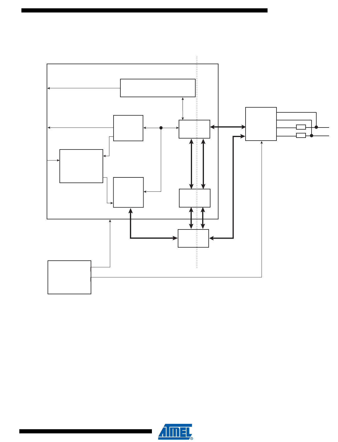
953
6430F–ATARM–21-Feb-12
SAM3U Series
953
6430F–ATARM–21-Feb-12
SAM3U Series
39.3 Block Diagram
Figure 39-1. Block Diagram
32 bits
System Clock
Domain
USB Clock
Domain
Rd/Wr/Ready
APB
Interface
USB2.0
CORE
EPT
Alloc
AHB1
DMA
AHB0
Local
AHB
Slave
interface
Master
AHB
Multiplexeur
Slave
DPRAM
UTMI
16/8 bits
APB bus
AHB bus
APB bus
PMC
DP
DM
DFSDM
DFSDP
DHSDM
DHSDP
ctrl
status
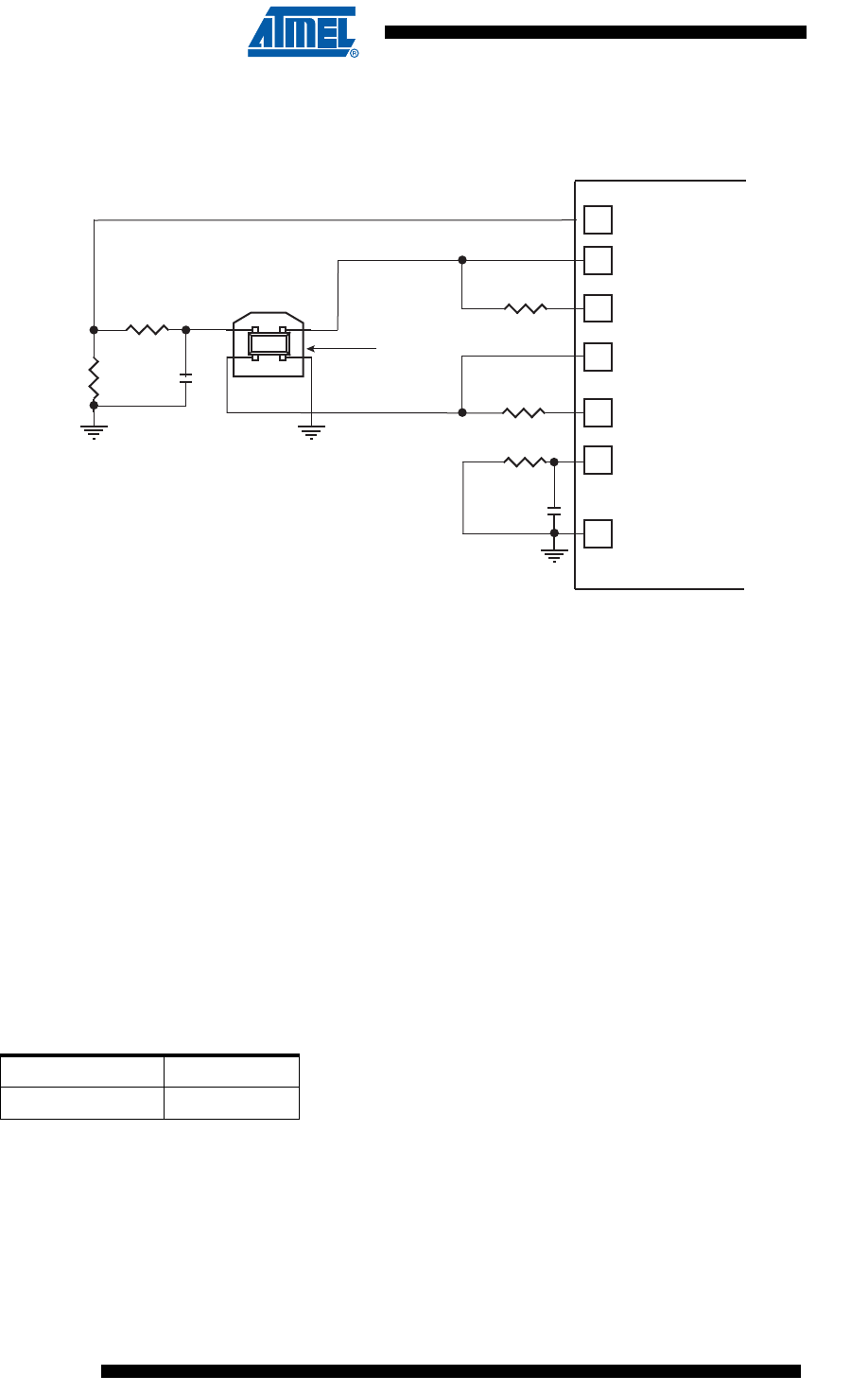
954
6430F–ATARM–21-Feb-12
SAM3U Series
954
6430F–ATARM–21-Feb-12
SAM3U Series
39.4 Typical Connection
Figure 39-2. Board Schematic
Note: The values shown on the 22 kΩ and 15 kΩ resistors are only valid with 3V3 supplied PIOs.
Both 39 Ω resistors need to be placed as close to the device pins as possible.
39.5 Product Dependencies
39.5.1 Power Management
The UDPHS is not continuously clocked.
For using the UDPHS, the programmer must first enable the UDPHS Clock in the Power Man-
agement Controller (PMC_PCER register). Then enable the PLL (PMC_UCKR register).
However, if the application does not require UDPHS operations, the UDPHS clock can be
stopped when not needed and restarted later.
39.5.2 Interrupt
The UDPHS interrupt line is connected on one of the internal sources of the Interrupt Controller.
Using the UDPHS interrupt requires the Interrupt Controller to be programmed first.
39.6 Functional Description
39.6.1 USB V2.0 High Speed Device Port Introduction
The USB V2.0 High Speed Device Port provides communication services between host and
attached USB devices. Each device is offered with a collection of communication flows (pipes)
associated with each endpoint. Software on the host communicates with a USB Device through
a set of communication flows.
PIO (VBUS DETECT)
DHSDP
DHSDM
DFSDM
DFSDP
VBG
GNDUTMI
C
RPB
:1µF to 10µF
C
RPB
1
4
2
3
10 pF
"B" Receptacle
1 = VBUS
2 = D-
3 = D+
4 = GND
Ω
Ω
Shell = Shield
15k
22k
39 ± 1% Ω
39 ± 1% Ω
6K8 ± 1% Ω
(1)
(1)
Table 39-2. Peripheral IDs
Instance ID
UDPHS 29

955
6430F–ATARM–21-Feb-12
SAM3U Series
955
6430F–ATARM–21-Feb-12
SAM3U Series
39.6.2 USB V2.0 High Speed Transfer Types
A communication flow is carried over one of four transfer types defined by the USB device.
A device provides several logical communication pipes with the host. To each logical pipe is
associated an endpoint. Transfer through a pipe belongs to one of the four transfer types:
• Control Transfers: Used to configure a device at attach time and can be used for other device-
specific purposes, including control of other pipes on the device.
• Bulk Data Transfers: Generated or consumed in relatively large burst quantities and have
wide dynamic latitude in transmission constraints.
• Interrupt Data Transfers: Used for timely but reliable delivery of data, for example, characters
or coordinates with human-perceptible echo or feedback response characteristics.
• Isochronous Data Transfers: Occupy a prenegotiated amount of USB bandwidth with a
prenegotiated delivery latency. (Also called streaming real time transfers.)
As indicated below, transfers are sequential events carried out on the USB bus.
Endpoints must be configured according to the transfer type they handle.
39.6.3 USB Transfer Event Definitions
A transfer is composed of one or several transactions;
Notes: 1. Control transfer must use endpoints with one bank and can be aborted using a stall handshake.
2. Isochronous transfers must use endpoints configured with two or three banks.
An endpoint handles all transactions related to the type of transfer for which it has been
configured.
Table 39-3. USB Communication Flow
Transfer Direction Bandwidth Endpoint Size Error Detection Retrying
Control Bidirectional Not guaranteed 8, 16, 32, 64 Yes Automatic
Isochronous Unidirectional Guaranteed 8-1024 Yes No
Interrupt Unidirectional Not guaranteed 8-1024 Yes Yes
Bulk Unidirectional Not guaranteed 8-512 Yes Yes
Table 39-4. USB Transfer Events
CONTROL
(bidirectional)
Control Transfers (1) • Setup transaction → Data IN transactions ∅Status OUT transaction
• Setup transaction → Data OUT transactions ∅Status IN transaction
• Setup transaction → Status IN transaction
IN
(device toward host)
Bulk IN Transfer • Data IN transaction → Data IN transaction
Interrupt IN Transfer • Data IN transaction → Data IN transaction
Isochronous IN Transfer (2) • Data IN transaction → Data IN transaction
OUT
(host toward device)
Bulk OUT Transfer • Data OUT transaction → Data OUT transaction
Interrupt OUT Transfer • Data OUT transaction → Data OUT transaction
Isochronous OUT Transfer (2) • Data OUT transaction→ Data OUT transaction
956
6430F–ATARM–21-Feb-12
SAM3U Series
956
6430F–ATARM–21-Feb-12
SAM3U Series
39.6.4 USB V2.0 High Speed BUS Transactions
Each transfer results in one or more transactions over the USB bus.
There are five kinds of transactions flowing across the bus in packets:
1. Setup Transaction
2. Data IN Transaction
3. Data OUT Transaction
4. Status IN Transaction
5. Status OUT Transaction
Figure 39-3. Control Read and Write Sequences
A status IN or OUT transaction is identical to a data IN or OUT transaction.
39.6.5 Endpoint Configuration
The endpoint 0 is always a control endpoint, it must be programmed and active in order to be
enabled when the End Of Reset interrupt occurs.
To configure the endpoints:
• Fill the configuration register (UDPHS_EPTCFG) with the endpoint size, direction (IN or
OUT), type (CTRL, Bulk, IT, ISO) and the number of banks.
• Fill the number of transactions (NB_TRANS) for isochronous endpoints.
Note: For control endpoints the direction has no effect.
• Verify that the EPT_MAPD flag is set. This flag is set if the endpoint size and the number of
banks are correct compared to the FIFO maximum capacity and the maximum number of
allowed banks.
• Configure control flags of the endpoint and enable it in UDPHS_EPTCTLENBx according to
“UDPHS Endpoint Control Register” on page 1002.
Control endpoints can generate interrupts and use only 1 bank.
Control Write Setup TX Data OUT TX Data OUT TX
Data Stage
Control Read
Setup Stage
Setup Stage
Setup TX
Setup TX
No Data
Control
Data IN TX Data IN TX
Status Stage
Status Stage
Status IN TX
Status OUT TX
Status IN TX
Data Stage
Setup Stage Status Stage
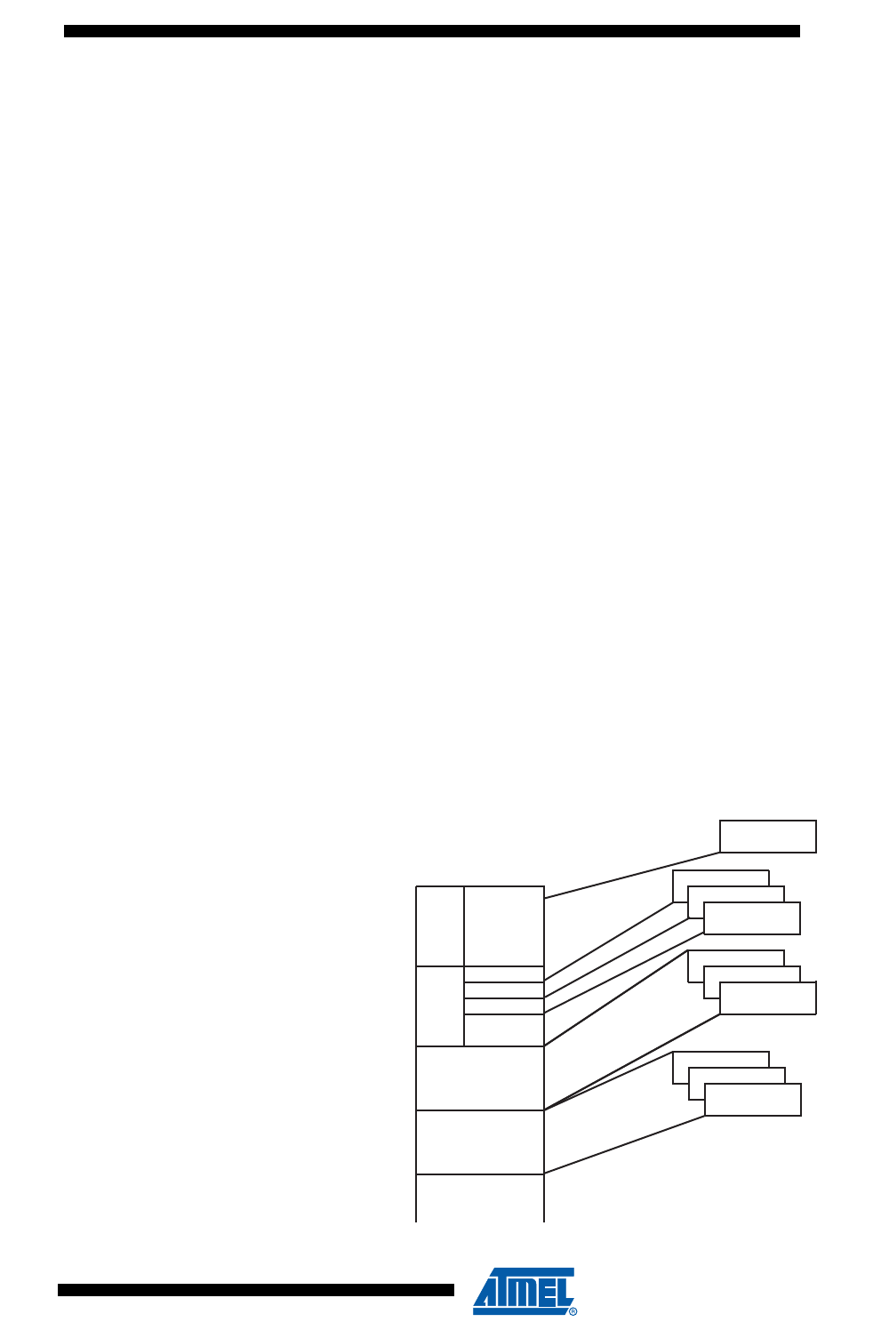
957
6430F–ATARM–21-Feb-12
SAM3U Series
957
6430F–ATARM–21-Feb-12
SAM3U Series
All endpoints (except endpoint 0) can be configured either as Bulk, Interrupt or Isochronous. See
Table 39-1. UDPHS Endpoint Description.
The maximum packet size they can accept corresponds to the maximum endpoint size.
Note: The endpoint size of 1024 is reserved for isochronous endpoints.
The size of the DPRAM is 4 KB. The DPR is shared by all active endpoints. The memory size
required by the active endpoints must not exceed the size of the DPRAM.
SIZE_DPRAM = SIZE _EPT0
+ NB_BANK_EPT1 x SIZE_EPT1
+ NB_BANK_EPT2 x SIZE_EPT2
+ NB_BANK_EPT3 x SIZE_EPT3
+ NB_BANK_EPT4 x SIZE_EPT4
+ NB_BANK_EPT5 x SIZE_EPT5
+ NB_BANK_EPT6 x SIZE_EPT6
+... (refer to 39.7.11 UDPHS Endpoint Configuration Register)
If a user tries to configure endpoints with a size the sum of which is greater than the DPRAM,
then the EPT_MAPD is not set.
The application has access to the physical block of DPR reserved for the endpoint through a 64
KB logical address space.
The physical block of DPR allocated for the endpoint is remapped all along the 64 KB logical
address space. The application can write a 64 KB buffer linearly.
Figure 39-4. Logical Address Space for DPR Access
64 KB
EP0
64 KB
EP1
64 KB
EP2
DPR
Logical address 8 to 64 B
8 to1024 B
8 to1024 B8 to1024 B
8 to1024 B
64 KB
EP3
...
8 to 64 B
...
1 bank
x banks
y banks
z banks
8 to1024 B
8 to1024 B
8 to1024 B

958
6430F–ATARM–21-Feb-12
SAM3U Series
958
6430F–ATARM–21-Feb-12
SAM3U Series
Configuration examples of UDPHS_EPTCTLx (UDPHS Endpoint Control Register) for Bulk IN
endpoint type follow below.
•With DMA
– AUTO_VALID: Automatically validate the packet and switch to the next bank.
– EPT_ENABL: Enable endpoint.
• Without DMA:
– TX_BK_RDY: An interrupt is generated after each transmission.
– EPT_ENABL: Enable endpoint.
Configuration examples of Bulk OUT endpoint type follow below.
•With DMA
– AUTO_VALID: Automatically validate the packet and switch to the next bank.
– EPT_ENABL: Enable endpoint.
• Without DMA
– RX_BK_RDY: An interrupt is sent after a new packet has been stored in the endpoint
FIFO.
– EPT_ENABL: Enable endpoint.
959
6430F–ATARM–21-Feb-12
SAM3U Series
959
6430F–ATARM–21-Feb-12
SAM3U Series
39.6.6 DPRAM Management
Endpoints can only be allocated in ascending order, from the endpoint 0 to the last endpoint to
be allocated. The user shall therefore configure them in the same order.
The allocation of an endpoint x starts when the Number of Banks field in the UDPHS Endpoint
Configuration Register (UDPHS_EPTCFGx.BK_NUMBER) is different from zero. Then, the
hardware allocates a memory area in the DPRAM and inserts it between the x-1 and x+1 end-
points. The x+1 endpoint memory window slides up and its data is lost. Note that the following
endpoint memory windows (from x+2) do not slide.
Disabling an endpoint, by writing a one to the Endpoint Disable bit in the UDPHS Endpoint Con-
trol Disable Register (UDPHS_EPTCTLDISx.EPT_DISABL), does not reset its configuration:
• the Endpoint Banks (UDPHS_EPTCFGx.BK_NUMBER),
• the Endpoint Size (UDPHS_EPTCFGx.EPT_SIZE),
• the Endpoint Direction (UDPHS_EPTCFGx.EPT_DIR),
• and the Endpoint Type (UDPHS_EPTCFGx.EPT_TYPE).
To free its memory, the user shall write a zero to the UDPHS_EPTCFGx.BK_NUMBER field.
The x+1 endpoint memory window then slides down and its data is lost. Note that the following
endpoint memory windows (from x+2) do not slide.
Figure 39-5 on page 959 illustrates the allocation and reorganization of the DPRAM in a typical
example.
Figure 39-5. Allocation and Reorganization of the DPRAM
1. The endpoints 0 to 5 are enabled, configured and allocated in ascending order. Each
endpoint then owns a memory area in the DPRAM.
2. The endpoint 3 is disabled, but its memory is kept allocated by the controller.
3. In order to free its memory, its UDPHS_EPTCFGx.BK_NUMBER field is written to zero.
The endpoint 4 memory window slides down, but the endpoint 5 does not move.
4. If the user chooses to reconfigure the endpoint 3 with a larger size, the controller allo-
cates a memory area after the endpoint 2 memory area and automatically slides up the
Free Memory
EPT0
EPT1
EPT2
EPT3
EPT4
EPT5
Free Memory
EPT0
EPT1
EPT2
EPT4
EPT5
Free Memory
EPT0
EPT1
EPT2
EPT4
EPT5
Endpoint 3
Disabled
Endpoint 3
Memory Freed
Free Memory
EPT0
EPT1
EPT2
EPT3 (larger size)
EPT5
Endpoint 3
Activated
EPT4 Lost Memory
EPT4 Conflict
EPT3
(always allocated)
Endpoints 0..5
Activated
Device:
UDPHS_EPTCTLENBx.EPT_ENABL = 1
Device: Device: Device:
UDPHS_EPTCTLDIS3.EPT_DISABL = 1 UDPHS_EPTCFG3.BK_NUMBER = 0UDPHS_EPTCTLENB3.EPT_ENABL = 1
UDPHS_EPTCFGx.BK_NUMBER <> 0 UDPHS_EPTCFG3.BK_NUMBER <> 0

960
6430F–ATARM–21-Feb-12
SAM3U Series
960
6430F–ATARM–21-Feb-12
SAM3U Series
endpoint 4 memory window. The endpoint 5 does not move and a memory conflict
appears as the memory windows of the endpoints 4 and 5 overlap. The data of these
endpoints is potentially lost.
Notes: 1. There is no way the data of the endpoint 0 can be lost (except if it is de-allocated) as the mem-
ory allocation and de-allocation may affect only higher endpoints.
2. Deactivating then reactivating the same endpoint with the same configuration only modifies
temporarily the controller DPRAM pointer and size for this endpoint. Nothing changes in the
DPRAM, higher endpoints seem not to have been moved and their data is preserved as far as
nothing has been written or received into them while changing the allocation state of the first
endpoint.
3. When the user writes a value different from zero to the UDPHS_EPTCFGx.BK_NUMBER
field, the Endpoint Mapped bit (UDPHS_EPTCFGx.EPT_MAPD) is set only if the configured
size and number of banks are correct as compared to the endpoint maximal allowed values
and to the maximal FIFO size (i.e. the DPRAM size). The UDPHS_EPTCFGx.EPT_MAPD
value does not consider memory allocation conflicts.
39.6.7 Transfer With DMA
USB packets of any length may be transferred when required by the UDPHS Device. These
transfers always feature sequential addressing.
Packet data AHB bursts may be locked on a DMA buffer basis for drastic overall AHB bus band-
width performance boost with paged memories. These clock-cycle consuming memory row (or
bank) changes will then likely not occur, or occur only once instead of dozens times, during a
single big USB packet DMA transfer in case another AHB master addresses the memory. This
means up to 128-word single-cycle unbroken AHB bursts for Bulk endpoints and 256-word sin-
gle-cycle unbroken bursts for isochronous endpoints. This maximum burst length is then
controlled by the lowest programmed USB endpoint size (EPT_SIZE field in the
UDPHS_EPTCFGx register) and DMA Size (BUFF_LENGTH field in the
UDPHS_DMACONTROLx register).
The USB 2.0 device average throughput may be up to nearly 60 MBytes. Its internal slave aver-
age access latency decreases as burst length increases due to the 0 wait-state side effect of
unchanged endpoints. If at least 0 wait-state word burst capability is also provided by the exter-
nal DMA AHB bus slaves, each of both DMA AHB busses need less than 50% bandwidth
allocation for full USB 2.0 bandwidth usage at 30 MHz, and less than 25% at 60 MHz.
The UDPHS DMA Channel Transfer Descriptor is described in “UDPHS DMA Channel Transfer
Descriptor” on page 1013.
Note: In case of debug, be careful to address the DMA to an SRAM address even if a remap is done.
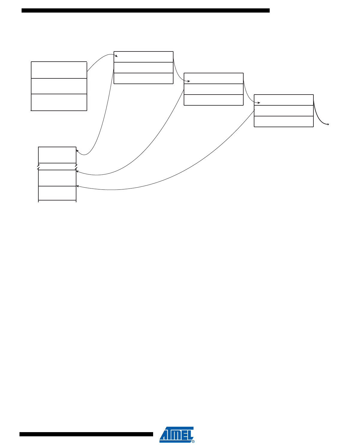
961
6430F–ATARM–21-Feb-12
SAM3U Series
961
6430F–ATARM–21-Feb-12
SAM3U Series
Figure 39-6. Example of DMA Chained List
39.6.8 Transfer Without DMA
Important. If the DMA is not to be used, it is necessary that it be disabled because otherwise it
can be enabled by previous versions of software without warning. If this should occur, the DMA
can process data before an interrupt without knowledge of the user.
The recommended means to disable DMA is as follows:
// Reset IP UDPHS
AT91C_BASE_UDPHS->UDPHS_CTRL &= ~AT91C_UDPHS_EN_UDPHS;
AT91C_BASE_UDPHS->UDPHS_CTRL |= AT91C_UDPHS_EN_UDPHS;
// With OR without DMA !!!
for( i=1; i<=((AT91C_BASE_UDPHS->UDPHS_IPFEATURES &
AT91C_UDPHS_DMA_CHANNEL_NBR)>>4); i++ ) {
// RESET endpoint canal DMA:
// DMA stop channel command
AT91C_BASE_UDPHS->UDPHS_DMA[i].UDPHS_DMACONTROL = 0; // STOP
command
// Disable endpoint
AT91C_BASE_UDPHS->UDPHS_EPT[i].UDPHS_EPTCTLDIS |= 0XFFFFFFFF;
// Reset endpoint config
AT91C_BASE_UDPHS->UDPHS_EPT[i].UDPHS_EPTCTLCFG = 0;
// Reset DMA channel (Buff count and Control field)
AT91C_BASE_UDPHS->UDPHS_DMA[i].UDPHS_DMACONTROL = 0x02; // NON
STOP command
// Reset DMA channel 0 (STOP)
Data Buff 1
Data Buff 2
Data Buff 3
Memory Area
Transfer Descriptor
Next Descriptor Address
DMA Channel Address
DMA Channel Control
Transfer Descriptor
Next Descriptor Address
DMA Channel Address
DMA Channel Control
Transfer Descriptor
Next Descriptor Address
DMA Channel Address
DMA Channel Control
UDPHS Registers
(Current Transfer Descriptor)
UDPHS Next Descriptor
DMA Channel Address
DMA Channel Control
Null

962
6430F–ATARM–21-Feb-12
SAM3U Series
962
6430F–ATARM–21-Feb-12
SAM3U Series
AT91C_BASE_UDPHS->UDPHS_DMA[i].UDPHS_DMACONTROL = 0; // STOP
command
// Clear DMA channel status (read the register for clear it)
AT91C_BASE_UDPHS->UDPHS_DMA[i].UDPHS_DMASTATUS =
AT91C_BASE_UDPHS->UDPHS_DMA[i].UDPHS_DMASTATUS;
}
39.6.9 Handling Transactions with USB V2.0 Device Peripheral
39.6.9.1 Setup Transaction
The setup packet is valid in the DPR while RX_SETUP is set. Once RX_SETUP is cleared by
the application, the UDPHS accepts the next packets sent over the device endpoint.
When a valid setup packet is accepted by the UDPHS:
• the UDPHS device automatically acknowledges the setup packet (sends an ACK response)
• payload data is written in the endpoint
• sets the RX_SETUP interrupt
• the BYTE_COUNT field in the UDPHS_EPTSTAx register is updated
An endpoint interrupt is generated while RX_SETUP in the UDPHS_EPTSTAx register is not
cleared. This interrupt is carried out to the microcontroller if interrupts are enabled for this
endpoint.
Thus, firmware must detect RX_SETUP polling UDPHS_EPTSTAx or catching an interrupt, read
the setup packet in the FIFO, then clear the RX_SETUP bit in the UDPHS_EPTCLRSTA register
to acknowledge the setup stage.
If STALL_SNT was set to 1, then this bit is automatically reset when a setup token is detected by
the device. Then, the device still accepts the setup stage. (See Section 39.6.9.15 “STALL” on
page 973).
39.6.9.2 NYET
NYET is a High Speed only handshake. It is returned by a High Speed endpoint as part of the
PING protocol.
High Speed devices must support an improved NAK mechanism for Bulk OUT and control end-
points (except setup stage). This mechanism allows the device to tell the host whether it has
sufficient endpoint space for the next OUT transfer (see USB 2.0 spec 8.5.1 NAK Limiting via
Ping Flow Control).
The NYET/ACK response to a High Speed Bulk OUT transfer and the PING response are auto-
matically handled by hardware in the UDPHS_EPTCTLx register (except when the user wants to
force a NAK response by using the NYET_DIS bit).
If the endpoint responds instead to the OUT/DATA transaction with an NYET handshake, this
means that the endpoint accepted the data but does not have room for another data payload.
The host controller must return to using a PING token until the endpoint indicates it has space
available.
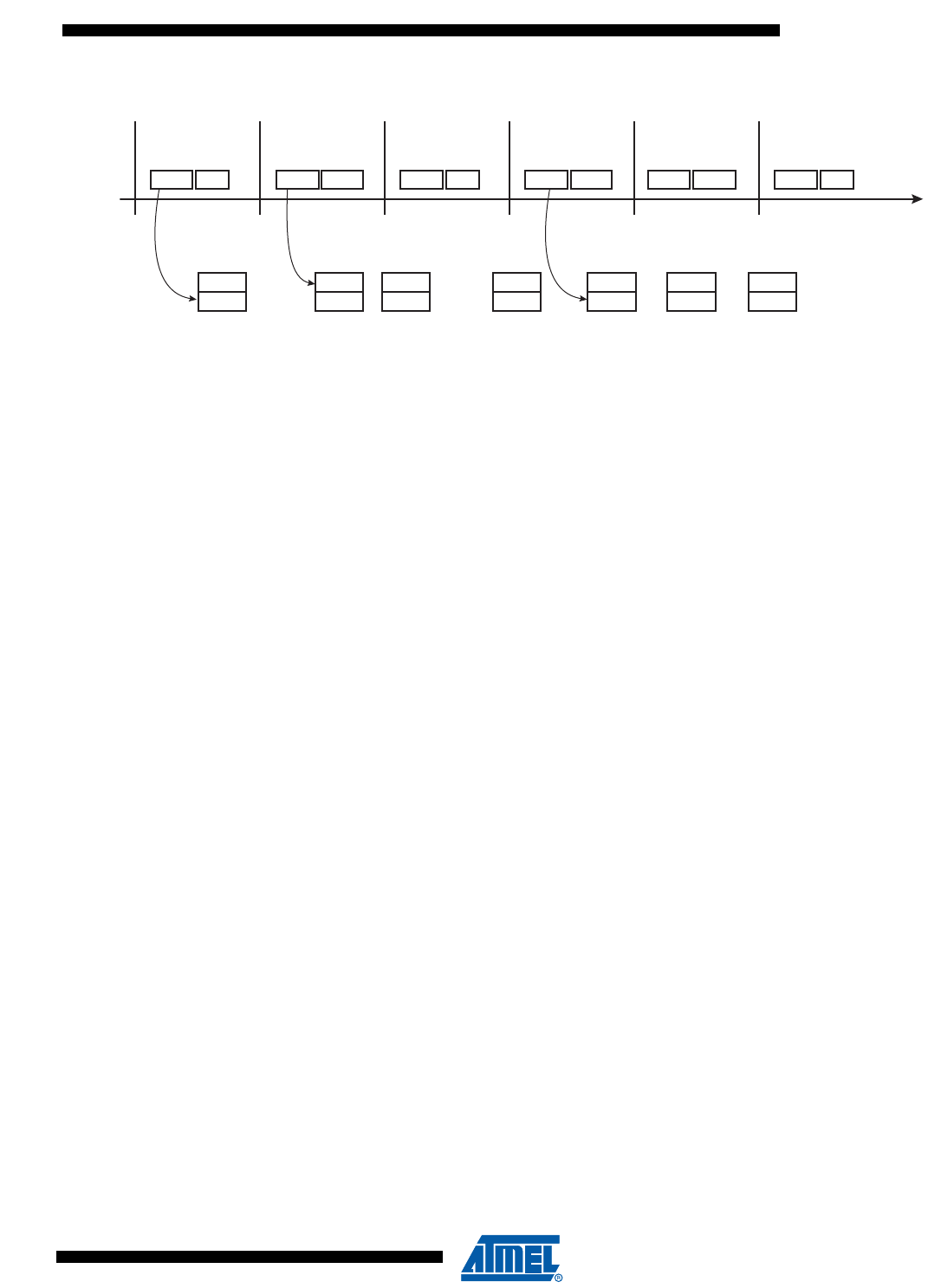
963
6430F–ATARM–21-Feb-12
SAM3U Series
963
6430F–ATARM–21-Feb-12
SAM3U Series
Figure 39-7. NYET Example with Two Endpoint Banks
39.6.9.3 Data IN
39.6.9.4 Bulk IN or Interrupt IN
Data IN packets are sent by the device during the data or the status stage of a control transfer or
during an (interrupt/bulk/isochronous) IN transfer. Data buffers are sent packet by packet under
the control of the application or under the control of the DMA channel.
There are three ways for an application to transfer a buffer in several packets over the USB:
• packet by packet (see 39.6.9.5 below)
•64 KB (see 39.6.9.5 below)
• DMA (see 39.6.9.6 below)
39.6.9.5 Bulk IN or Interrupt IN: Sending a Packet Under Application Control (Device to Host)
The application can write one or several banks.
A simple algorithm can be used by the application to send packets regardless of the number of
banks associated to the endpoint.
Algorithm Description for Each Packet:
• The application waits for TX_PK_RDY flag to be cleared in the UDPHS_EPTSTAx register
before it can perform a write access to the DPR.
• The application writes one USB packet of data in the DPR through the 64 KB endpoint logical
memory window.
• The application sets TX_PK_RDY flag in the UDPHS_EPTSETSTAx register.
The application is notified that it is possible to write a new packet to the DPR by the
TX_PK_RDY interrupt. This interrupt can be enabled or masked by setting the TX_PK_RDY bit
in the UDPHS_EPTCTLENB/UDPHS_EPTCTLDIS register.
Algorithm Description to Fill Several Packets:
Using the previous algorithm, the application is interrupted for each packet. It is possible to
reduce the application overhead by writing linearly several banks at the same time. The
AUTO_VALID bit in the UDPHS_EPTCTLx must be set by writing the AUTO_VALID bit in the
UDPHS_EPTCTLENBx register.
The auto-valid-bank mechanism allows the transfer of data (IN and OUT) without the interven-
tion of the CPU. This means that bank validation (set TX_PK_RDY or clear the RX_BK_RDY bit)
is done by hardware.
t = 0 t = 125 µs t = 250 µs t = 375 µs t = 500 µs t = 625 µs
data 0 ACK data 1 NYET PING ACK data 0 NYET PING NACK PING ACK
Bank 1
Bank 0 Bank 0
Bank 1
Bank 0
Bank 1
Bank 0
Bank 1
Bank 0
Bank 1
Bank 0
Bank 1
Bank 0
Bank 1E
F
F
E
F
E'
F
E
F
F
E'
F
E
F
E: empty
E': begin to empty
F: full

964
6430F–ATARM–21-Feb-12
SAM3U Series
964
6430F–ATARM–21-Feb-12
SAM3U Series
• The application checks the BUSY_BANK_STA field in the UDPHS_EPTSTAx register. The
application must wait that at least one bank is free.
• The application writes a number of bytes inferior to the number of free DPR banks for the
endpoint. Each time the application writes the last byte of a bank, the TX_PK_RDY signal is
automatically set by the UDPHS.
• If the last packet is incomplete (i.e., the last byte of the bank has not been written) the
application must set the TX_PK_RDY bit in the UDPHS_EPTSETSTAx register.
The application is notified that all banks are free, so that it is possible to write another burst of
packets by the BUSY_BANK interrupt. This interrupt can be enabled or masked by setting the
BUSY_BANK flag in the UDPHS_EPTCTLENB and UDPHS_EPTCTLDIS registers.
This algorithm must not be used for isochronous transfer. In this case, the ping-pong mechanism
does not operate.
A Zero Length Packet can be sent by setting just the TX_PKTRDY flag in the
UDPHS_EPTSETSTAx register.
39.6.9.6 Bulk IN or Interrupt IN: Sending a Buffer Using DMA (Device to Host)
The UDPHS integrates a DMA host controller. This DMA controller can be used to transfer a buf-
fer from the memory to the DPR or from the DPR to the processor memory under the UDPHS
control. The DMA can be used for all transfer types except control transfer.
Example DMA configuration:
1. Program UDPHS_DMAADDRESS x with the address of the buffer that should be
transferred.
2. Enable the interrupt of the DMA in UDPHS_IEN
3. Program UDPHS_ DMACONTROLx:
– Size of buffer to send: size of the buffer to be sent to the host.
– END_B_EN: The endpoint can validate the packet (according to the values
programmed in the AUTO_VALID and SHRT_PCKT fields of UDPHS_EPTCTLx.)
(See “UDPHS Endpoint Control Register” on page 1002 and Figure 39-12. Autovalid
with DMA)
– END_BUFFIT: generate an interrupt when the BUFF_COUNT in
UDPHS_DMASTATUSx reaches 0.
– CHANN_ENB: Run and stop at end of buffer
The auto-valid-bank mechanism allows the transfer of data (IN & OUT) without the intervention
of the CPU. This means that bank validation (set TX_PK_RDY or clear the RX_BK_RDY bit) is
done by hardware.
A transfer descriptor can be used. Instead of programming the register directly, a descriptor
should be programmed and the address of this descriptor is then given to
UDPHS_DMANXTDSC to be processed after setting the LDNXT_DSC field (Load Next Descrip-
tor Now) in UDPHS_DMACONTROLx register.
The structure that defines this transfer descriptor must be aligned.
Each buffer to be transferred must be described by a DMA Transfer descriptor (see “UDPHS
DMA Channel Transfer Descriptor” on page 1013). Transfer descriptors are chained. Before
executing transfer of the buffer, the UDPHS may fetch a new transfer descriptor from the mem-
965
6430F–ATARM–21-Feb-12
SAM3U Series
965
6430F–ATARM–21-Feb-12
SAM3U Series
ory address pointed by the UDPHS_DMANXTDSCx register. Once the transfer is complete, the
transfer status is updated in the UDPHS_DMASTATUSx register.
To chain a new transfer descriptor with the current DMA transfer, the DMA channel must be
stopped. To do so, INTDIS_DMA and TX_BK_RDY may be set in the UDPHS_EPTCTLENBx
register. It is also possible for the application to wait for the completion of all transfers. In this
case the LDNXT_DSC field in the last transfer descriptor UDPHS_DMACONTROLx register
must be set to 0 and CHANN_ENB set to 1.
Then the application can chain a new transfer descriptor.
The INTDIS_DMA can be used to stop the current DMA transfer if an enabled interrupt is trig-
gered. This can be used to stop DMA transfers in case of errors.
The application can be notified at the end of any buffer transfer (ENB_BUFFIT bit in the
UDPHS_DMACONTROLx register).
Figure 39-8. Data IN Transfer for Endpoint with One Bank
USB Bus
Packets
FIFO
Content
TX_COMPLT Flag
(UDPHS_EPTSTAx)
TX_PK_RDY
Flag
(UDPHS_EPTSTAx)
Prevous Data IN TX Microcontroller Loads Data in FIFO Data is Sent on USB Bus
Interrupt Pending
Set by firmware Cleared by hardware Set by the firmware Cleared by hardware
Interrupt Pending
Cleared by firmware
DPR access by firmware DPR access by hardware
Cleared by firmware
Payload in FIFO
Set by hardware
Data IN 2Token IN NAKACKData IN 1Token IN Token IN ACK
Data IN 1 Load in progress Data IN 2
966
6430F–ATARM–21-Feb-12
SAM3U Series
966
6430F–ATARM–21-Feb-12
SAM3U Series
Figure 39-9. Data IN Transfer for Endpoint with Two Banks
Figure 39-10. Data IN Followed By Status OUT Transfer at the End of a Control Transfer
Note: A NAK handshake is always generated at the first status stage token.
Read by USB Device
Read by UDPHS Device
FIFO
(DPR)
Bank 0
TX_COMPLT
Flag
(UDPHS_EPTSTAx) Interrupt Cleared by Firmware
Virtual TX_PK_RDY
bank 1
(UDPHS_EPTSTAx)
ACK Token IN ACK
Set by Firmware,
Data Payload Written in FIFO Bank 1
Cleared by Hardware
Data Payload Fully Transmitted
Token IN
USB Bus
Packets
Set by HardwareSet by Hardware
Set by Firmware,
Data Payload Written
in FIFO Bank 0
Written by
FIFO
(DPR)
Bank1
Microcontroller
Written by
Microcontroller
Written by
Microcontroller
Microcontroller
Load Data IN Bank 0
Microcontroller Load Data IN Bank 1
UDPHS Device Send Bank 0
Microcontroller Load Data IN Bank 0
UDPHS Device Send Bank 1
Interrupt Pending
Data INData IN
Cleared by Hardware
switch to next bank
Virtual TX_PK_RDY
bank 0
(UDPHS_EPTSTAx)
Token OUT
Data IN
Token IN ACK
ACK Data OUT (ZLP)
RX_BK_RDY
(UDPHS_EPTSTAx)
TX_COMPLT
(UDPHS_EPTSTAx)
Set by Hardware
Set by Hardware
USB Bus
Packets
Cleared by Firmware
Cleared by Firmware
Device Sends a
Status OUT to Host
Device Sends the Last
Data Payload to Host
Interrupt
Pending
Token OUT ACK
Data OUT (ZLP)
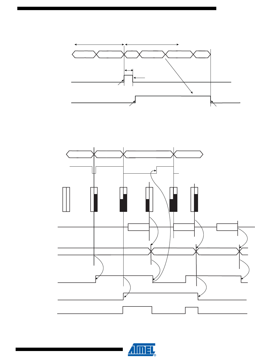
967
6430F–ATARM–21-Feb-12
SAM3U Series
967
6430F–ATARM–21-Feb-12
SAM3U Series
Figure 39-11. Data OUT Followed by Status IN Transfer
Note: Before proceeding to the status stage, the software should determine that there is no risk of extra data from the host (data
stage). If not certain (non-predictable data stage length), then the software should wait for a NAK-IN interrupt before proceeding
to the status stage. This precaution should be taken to avoid collision in the FIFO.
Figure 39-12. Autovalid with DMA
Note: In the illustration above Autovalid validates a bank as full, although this might not be the case, in order to continue processing
data and to send to DMA.
Token INACKData OUTToken OUT ACKData IN
USB Bus
Packets
RX_BK_RDY
(UDPHS_EPTSTAx) Cleared by Firmware
Set by Hardware
Clear by Hardware
TX_PK_RDY
(UDPHS_EPTSTAx)
Set by Firmware
Host Sends the Last
Data Payload to the Device
Device Sends a Status IN
to the Host
Interrupt Pending
Bank 0 Bank 1 Bank 0Bank (usb)
Write write bank 0 write bank 1 write bank 0
Bank 0Bank (system) Bank 1 Bank 0 Bank 1
Virtual TX_PK_RDY Bank 0
Virtual TX_PK_RDY Bank 1
TX_PK_RDY
(Virtual 0 & Virtual 1)
bank 0 is full bank 1 is full bank 0 is full
IN data 0 IN data 1 IN data 0
Bank 1
Bank 1 Bank 0

968
6430F–ATARM–21-Feb-12
SAM3U Series
968
6430F–ATARM–21-Feb-12
SAM3U Series
39.6.9.7 Isochronous IN
Isochronous-IN is used to transmit a stream of data whose timing is implied by the delivery rate.
Isochronous transfer provides periodic, continuous communication between host and device.
It guarantees bandwidth and low latencies appropriate for telephony, audio, video, etc.
If the endpoint is not available (TX_PK_RDY = 0), then the device does not answer to the host.
An ERR_FL_ISO interrupt is generated in the UDPHS_EPTSTAx register and once enabled,
then sent to the CPU.
The STALL_SNT command bit is not used for an ISO-IN endpoint.
39.6.9.8 High Bandwidth Isochronous Endpoint Handling: IN Example
For high bandwidth isochronous endpoints, the DMA can be programmed with the number of
transactions (BUFF_LENGTH field in UDPHS_DMACONTROLx) and the system should provide
the required number of packets per microframe, otherwise, the host will notice a sequencing
problem.
A response should be made to the first token IN recognized inside a microframe under the fol-
lowing conditions:
• If at least one bank has been validated, the correct DATAx corresponding to the programmed
Number Of Transactions per Microframe (NB_TRANS) should be answered. In case of a
subsequent missed or corrupted token IN inside the microframe, the USB 2.0 Core available
data bank(s) that should normally have been transmitted during that microframe shall be
flushed at its end. If this flush occurs, an error condition is flagged (ERR_FLUSH is set in
UDPHS_EPTSTAx).
• If no bank is validated yet, the default DATA0 ZLP is answered and underflow is flagged
(ERR_FL_ISO is set in UDPHS_EPTSTAx). Then, no data bank is flushed at microframe
end.
• If no data bank has been validated at the time when a response should be made for the
second transaction of NB_TRANS = 3 transactions microframe, a DATA1 ZLP is answered
and underflow is flagged (ERR_FL_ISO is set in UDPHS_EPTSTAx). If and only if remaining
untransmitted banks for that microframe are available at its end, they are flushed and an error
condition is flagged (ERR_FLUSH is set in UDPHS_EPTSTAx).
• If no data bank has been validated at the time when a response should be made for the last
programmed transaction of a microframe, a DATA0 ZLP is answered and underflow is flagged
(ERR_FL_ISO is set in UDPHS_EPTSTAx). If and only if the remaining untransmitted data
bank for that microframe is available at its end, it is flushed and an error condition is flagged
(ERR_FLUSH is set in UDPHS_EPTSTAx).
• If at the end of a microframe no valid token IN has been recognized, no data bank is flushed
and no error condition is reported.
At the end of a microframe in which at least one data bank has been transmitted, if less than
NB_TRANS banks have been validated for that microframe, an error condition is flagged
(ERR_TRANS is set in UDPHS_EPTSTAx).
Cases of Error (in UDPHS_EPTSTAx)
• ERR_FL_ISO: There was no data to transmit inside a microframe, so a ZLP is answered by
default.

969
6430F–ATARM–21-Feb-12
SAM3U Series
969
6430F–ATARM–21-Feb-12
SAM3U Series
• ERR_FLUSH: At least one packet has been sent inside the microframe, but the number of
token IN received is lesser than the number of transactions actually validated (TX_BK_RDY)
and likewise with the NB_TRANS programmed.
• ERR_TRANS: At least one packet has been sent inside the microframe, but the number of
token IN received is lesser than the number of programmed NB_TRANS transactions and the
packets not requested were not validated.
• ERR_FL_ISO + ERR_FLUSH: At least one packet has been sent inside the microframe, but
the data has not been validated in time to answer one of the following token IN.
• ERR_FL_ISO + ERR_TRANS: At least one packet has been sent inside the microframe, but
the data has not been validated in time to answer one of the following token IN and the data
can be discarded at the microframe end.
• ERR_FLUSH + ERR_TRANS: The first token IN has been answered and it was the only one
received, a second bank has been validated but not the third, whereas NB_TRANS was
waiting for three transactions.
• ERR_FL_ISO + ERR_FLUSH + ERR_TRANS: The first token IN has been treated, the data
for the second Token IN was not available in time, but the second bank has been validated
before the end of the microframe. The third bank has not been validated, but three
transactions have been set in NB_TRANS.
39.6.9.9 Data OUT
39.6.9.10 Bulk OUT or Interrupt OUT
Like data IN, data OUT packets are sent by the host during the data or the status stage of con-
trol transfer or during an interrupt/bulk/isochronous OUT transfer. Data buffers are sent packet
by packet under the control of the application or under the control of the DMA channel.
39.6.9.11 Bulk OUT or Interrupt OUT: Receiving a Packet Under Application Control (Host to Device)
Algorithm Description for Each Packet:
• The application enables an interrupt on RX_BK_RDY.
• When an interrupt on RX_BK_RDY is received, the application knows that UDPHS_EPTSTAx
register BYTE_COUNT bytes have been received.
• The application reads the BYTE_COUNT bytes from the endpoint.
• The application clears RX_BK_RDY.
Note: If the application does not know the size of the transfer, it may not be a good option to use
AUTO_VALID. Because if a zero-length-packet is received, the RX_BK_RDY is automatically
cleared by the AUTO_VALID hardware and if the endpoint interrupt is triggered, the software will
not find its originating flag when reading the UDPHS_EPTSTAx register.
Algorithm to Fill Several Packets:
• The application enables the interrupts of BUSY_BANK and AUTO_VALID.
• When a BUSY_BANK interrupt is received, the application knows that all banks available for
the endpoint have been filled. Thus, the application can read all banks available.
If the application doesn’t know the size of the receive buffer, instead of using the BUSY_BANK
interrupt, the application must use RX_BK_RDY.
39.6.9.12 Bulk OUT or Interrupt OUT: Sending a Buffer Using DMA (Host To Device)
To use the DMA setting, the AUTO_VALID field is mandatory.
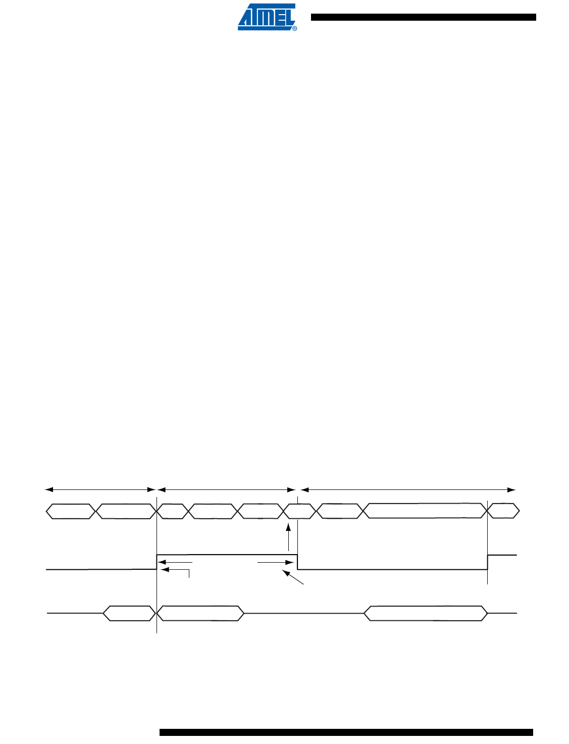
970
6430F–ATARM–21-Feb-12
SAM3U Series
970
6430F–ATARM–21-Feb-12
SAM3U Series
See 39.6.9.6 Bulk IN or Interrupt IN: Sending a Buffer Using DMA (Device to Host) for more
information.
DMA Configuration Example:
1. First program UDPHS_DMAADDRESSx with the address of the buffer that should be
transferred.
2. Enable the interrupt of the DMA in UDPHS_IEN
3. Program the DMA Channelx Control Register:
– Size of buffer to be sent.
– END_B_EN: Can be used for OUT packet truncation (discarding of unbuffered
packet data) at the end of DMA buffer.
– END_BUFFIT: Generate an interrupt when BUFF_COUNT in the
UDPHS_DMASTATUSx register reaches 0.
– END_TR_EN: End of transfer enable, the UDPHS device can put an end to the
current DMA transfer, in case of a short packet.
– END_TR_IT: End of transfer interrupt enable, an interrupt is sent after the last USB
packet has been transferred by the DMA, if the USB transfer ended with a short
packet. (Beneficial when the receive size is unknown.)
– CHANN_ENB: Run and stop at end of buffer.
For OUT transfer, the bank will be automatically cleared by hardware when the application has
read all the bytes in the bank (the bank is empty).
Notes: 1. When a zero-length-packet is received, RX_BK_RDY bit in UDPHS_EPTSTAx is cleared auto-
matically by AUTO_VALID, and the application knows of the end of buffer by the presence of
the END_TR_IT.
2. If the host sends a zero-length packet, and the endpoint is free, then the device sends an ACK.
No data is written in the endpoint, the RX_BY_RDY interrupt is generated, and the
BYTE_COUNT field in UDPHS_EPTSTAx is null.
Figure 39-13. Data OUT Transfer for Endpoint with One Bank
ACKToken OUTNAKToken OUTACK
Token OUT Data OUT 1
USB Bus
Packets
RX_BK_RDY
Set by Hardware Cleared by Firmware,
Data Payload Written in FIFO
FIFO (DPR)
Content
Written by UDPHS Device Microcontroller Read
Data OUT 1 Data OUT 1 Data OUT 2
Host Resends the Next Data Payload
Microcontroller Transfers Data
Host Sends Data Payload
Data OUT 2 Data OUT 2
Host Sends the Next Data Payload
Written by UDPHS Device
(UDPHS_EPTSTAx)
Interrupt Pending
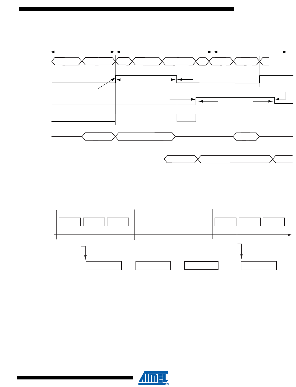
971
6430F–ATARM–21-Feb-12
SAM3U Series
971
6430F–ATARM–21-Feb-12
SAM3U Series
Figure 39-14. Data OUT Transfer for an Endpoint with Two Banks
39.6.9.13 High Bandwidth Isochronous Endpoint OUT
Figure 39-15. Bank Management, Example of Three Transactions per Microframe
USB 2.0 supports individual High Speed isochronous endpoints that require data rates up to 192
Mb/s (24 MB/s): 3x1024 data bytes per microframe.
To support such a rate, two or three banks may be used to buffer the three consecutive data
packets. The microcontroller (or the DMA) should be able to empty the banks very rapidly (at
least 24 MB/s on average).
NB_TRANS field in UDPHS_EPTCFGx register = Number Of Transactions per Microframe.
If NB_TRANS > 1 then it is High Bandwidth.
Example:
Token OUT ACK Data OUT 3Token OUTData OUT 2Token OUTData OUT 1
Data OUT 1
Data OUT 2 Data OUT 2
ACK
Cleared by Firmware
USB Bus
Packets
Virtual RX_BK_RDY
Bank 0
Virtual RX_BK_RDY
Bank 1
Set by Hardware
Data Payload written
in FIFO endpoint bank 1
FIFO (DPR)
Bank 0
Bank 1
Write by UDPHS Device Write in progress
Read by Microcontroller
Read by Microcontroller
Set by Hardware,
Data payload written
in FIFO endpoint bank 0
Host sends first data payload
Microcontroller reads Data 1 in bank 0,
Host sends second data payload
Microcontroller reads Data 2 in bank 1,
Host sends third data payload
Cleared by Firmware
Write by Hardware
FIFO (DPR)
(UDPHS_EPTSTAx)
Interrupt pending
Interrupt pending
RX_BK_RDY = (virtual bank 0 | virtual bank 1)
Data OUT 1 Data OUT 3
M DATA 0 M DATA 0 M DATA 1 D ATA 2DATA 2M DATA 1
t = 0 t = 52.5 µs
(40% of 125 µs)
RX_BK_RDY
t = 125 µs
RX_BK_RDY
USB line
Read Bank 3Read Bank 2Read Bank 1 Read Bank 1
USB bus
Transactions
Microcontroller FIFO
(DPR) Access

972
6430F–ATARM–21-Feb-12
SAM3U Series
972
6430F–ATARM–21-Feb-12
SAM3U Series
• If NB_TRANS = 3, the sequence should be either
–MData0
– MData0/Data1
– MData0/Data1/Data2
• If NB_TRANS = 2, the sequence should be either
–MData0
– MData0/Data1
• If NB_TRANS = 1, the sequence should be
– Data0
39.6.9.14 Isochronous Endpoint Handling: OUT Example
The user can ascertain the bank status (free or busy), and the toggle sequencing of the data
packet for each bank with the UDPHS_EPTSTAx register in the three bit fields as follows:
• TOGGLESQ_STA: PID of the data stored in the current bank
• CURRENT_BANK: Number of the bank currently being accessed by the microcontroller.
• BUSY_BANK_STA: Number of busy bank
This is particularly useful in case of a missing data packet.
If the inter-packet delay between the OUT token and the Data is greater than the USB standard,
then the ISO-OUT transaction is ignored. (Payload data is not written, no interrupt is generated
to the CPU.)
If there is a data CRC (Cyclic Redundancy Check) error, the payload is, none the less, written in
the endpoint. The ERR_CRISO flag is set in UDPHS_EPTSTAx register.
If the endpoint is already full, the packet is not written in the DPRAM. The ERR_FL_ISO flag is
set in UDPHS_EPTSTAx.
If the payload data is greater than the maximum size of the endpoint, then the ERR_OVFLW flag
is set. It is the task of the CPU to manage this error. The data packet is written in the endpoint
(except the extra data).
If the host sends a Zero Length Packet, and the endpoint is free, no data is written in the end-
point, the RX_BK_RDY flag is set, and the BYTE_COUNT field in UDPHS_EPTSTAx register is
null.
The FRCESTALL command bit is unused for an isochonous endpoint.
Otherwise, payload data is written in the endpoint, the RX_BK_RDY interrupt is generated and
the BYTE_COUNT in UDPHS_EPTSTAx register is updated.
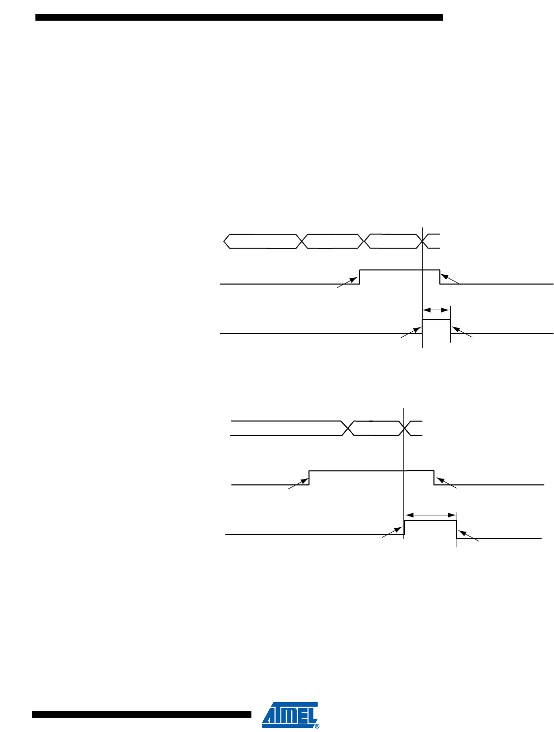
973
6430F–ATARM–21-Feb-12
SAM3U Series
973
6430F–ATARM–21-Feb-12
SAM3U Series
39.6.9.15 STALL
STALL is returned by a function in response to an IN token or after the data phase of an OUT or
in response to a PING transaction. STALL indicates that a function is unable to transmit or
receive data, or that a control pipe request is not supported.
•OUT
To stall an endpoint, set the FRCESTALL bit in UDPHS_EPTSETSTAx register and after the
STALL_SNT flag has been set, set the TOGGLE_SEG bit in the UDPHS_EPTCLRSTAx
register.
•IN
Set the FRCESTALL bit in UDPHS_EPTSETSTAx register.
Figure 39-16. Stall Handshake Data OUT Transfer
Figure 39-17. Stall Handshake Data IN Transfer
Token OUT Stall PID
Data OUT
USB Bus
Packets
Cleared by Firmware
Set by Firmware
FRCESTALL
STALL_SNT
Set by Hardware
Interrupt Pending
Cleared by Firmware
Token IN Stall PID
USB Bus
Packets
Cleared by Firmware
Set by Firmware
FRCESTALL
STALL_SNT
Set by Hardware Cleared by Firmware
Interrupt Pending

974
6430F–ATARM–21-Feb-12
SAM3U Series
974
6430F–ATARM–21-Feb-12
SAM3U Series
39.6.10 Speed Identification
The high speed reset is managed by the hardware.
At the connection, the host makes a reset which could be a classic reset (full speed) or a high
speed reset.
At the end of the reset process (full or high), the ENDRESET interrupt is generated.
Then the CPU should read the SPEED bit in UDPHS_INTSTAx to ascertain the speed mode of
the device.
39.6.11 USB V2.0 High Speed Global Interrupt
Interrupts are defined in Section 39.7.3 ”UDPHS Interrupt Enable Register” (UDPHS_IEN) and
in Section 39.7.4 ”UDPHS Interrupt Status Register” (UDPHS_INTSTA).
39.6.12 Endpoint Interrupts
Interrupts are enabled in UDPHS_IEN (see Section 39.7.3 ”UDPHS Interrupt Enable Register”)
and individually masked in UDPHS_EPTCTLENBx (see Section 39.7.12 ”UDPHS Endpoint
Control Enable Register”).
Table 39-5. Endpoint Interrupt Source Masks
SHRT_PCKT Short Packet Interrupt
BUSY_BANK Busy Bank Interrupt
NAK_OUT NAKOUT Interrupt
NAK_IN/ERR_FLUSH NAKIN/Error Flush Interrupt
STALL_SNT/ERR_CRISO/ERR_NB_TRA Stall Sent/CRC error/Number of Transaction
Error Interrupt
RX_SETUP/ERR_FL_ISO Received SETUP/Error Flow Interrupt
TX_PK_RD /ERR_TRANS TX Packet Read/Transaction Error Interrupt
TX_COMPLT Transmitted IN Data Complete Interrupt
RX_BK_RDY Received OUT Data Interrupt
ERR_OVFLW Overflow Error Interrupt
MDATA_RX MDATA Interrupt
DATAX_RX DATAx Interrupt
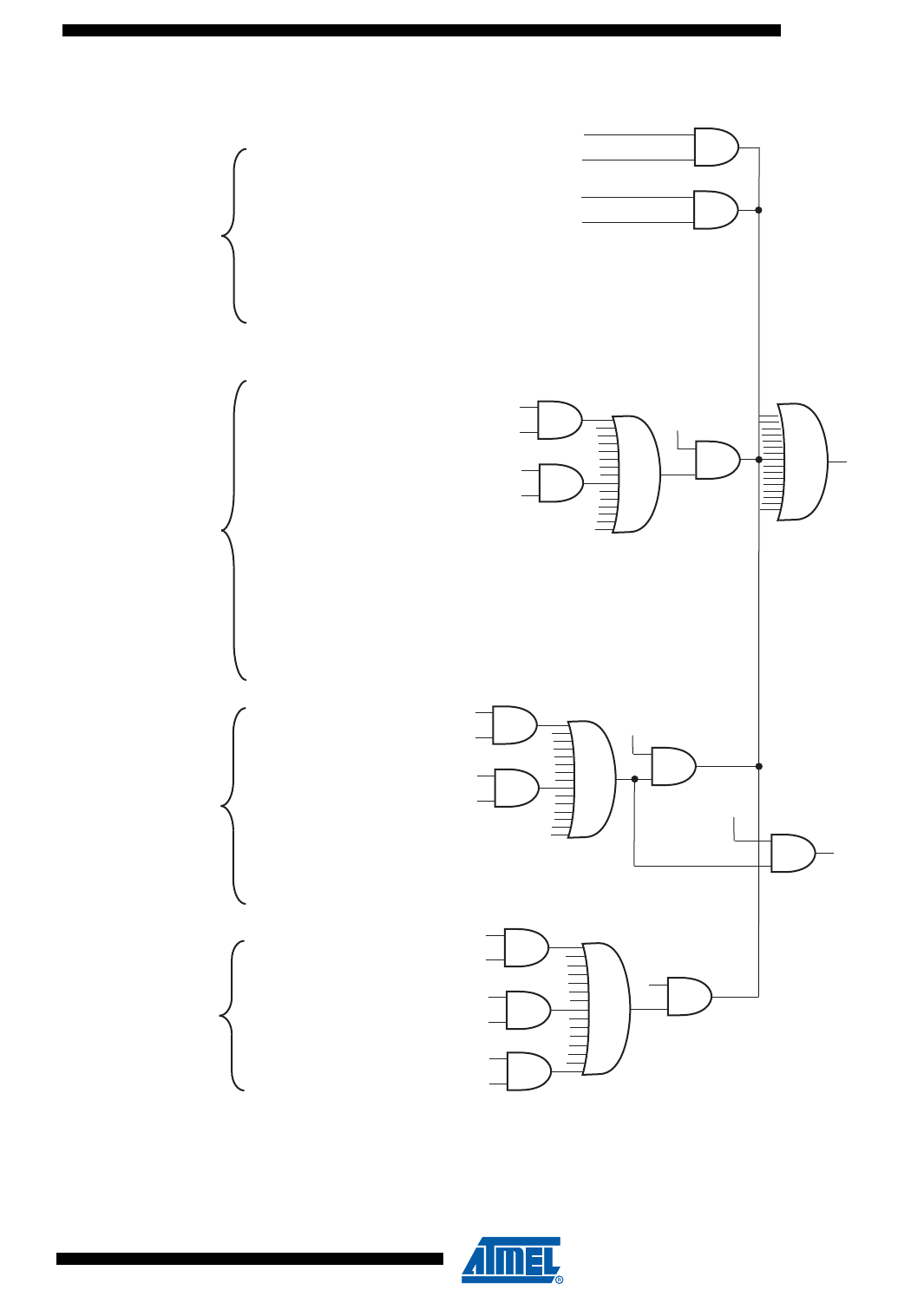
975
6430F–ATARM–21-Feb-12
SAM3U Series
975
6430F–ATARM–21-Feb-12
SAM3U Series
Figure 39-18. UDPHS Interrupt Control Interface
DET_SUSPD
MICRO_SOF
INT_SOF
ENDRESET
WAKE_UP
ENDOFRSM
UPSTR_RES
USB Global
IT Sources
EPT0 IT
Sources
BUSY_BANK
NAK_OUT
(UDPHS_EPTCTLENBx)
NAK_IN/ERR_FLUSH
STALL_SNT/ERR_CRISO/ERR_NBTRA
RX_SETUP/ERR_FL_ISO
TX_BK_RDY/ERR_TRANS
TX_COMPLT
RX_BK_RDY
ERR_OVFLW
MDATA_RX
DATAX_RX
(UDPHS_IEN)
EPT1-6 IT
Sources
Global IT mask
Global IT sources
EP mask
EP sources
(UDPHS_IEN)
EPT_0
EP mask
EP sources
(UDPHS_IEN)
EPT_x
(UDPHS_EPTCTLx)
INTDIS_DMA
DMA CH x
(UDPHS_DMACONTROLx)
EN_BUFFIT
END_TR_IT
DESC_LD_IT
mask
mask
mask
(UDPHS_IEN)
DMA_x
SHRT_PCKT
husb2dev
interrupt
disable DMA
channelx request
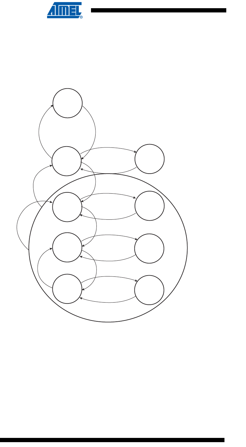
976
6430F–ATARM–21-Feb-12
SAM3U Series
976
6430F–ATARM–21-Feb-12
SAM3U Series
39.6.13 Power Modes
39.6.13.1 Controlling Device States
A USB device has several possible states. Refer to Chapter 9 (USB Device Framework) of the
Universal Serial Bus Specification, Rev 2.0.
Figure 39-19. UDPHS Device State Diagram
Movement from one state to another depends on the USB bus state or on standard requests
sent through control transactions via the default endpoint (endpoint 0).
After a period of bus inactivity, the USB device enters Suspend Mode. Accepting Sus-
pend/Resume requests from the USB host is mandatory. Constraints in Suspend Mode are very
strict for bus-powered applications; devices may not consume more than 500 µA on the USB
bus.
While in Suspend Mode, the host may wake up a device by sending a resume signal (bus activ-
ity) or a USB device may send a wake-up request to the host, e.g., waking up a PC by moving a
USB mouse.
The wake-up feature is not mandatory for all devices and must be negotiated with the host.
Attached
Suspended
Suspended
Suspended
Suspended
Hub Reset
or
Deconfigured
Hub
Configured
Bus Inactive
Bus Activity
Bus Inactive
Bus Activity
Bus Inactive
Bus Activity
Bus Inactive
Bus Activity
Reset
Reset
Address
Assigned
Device
Deconfigured
Device
Configured
Powered
Default
Address
Configured
Power
Interruption

977
6430F–ATARM–21-Feb-12
SAM3U Series
977
6430F–ATARM–21-Feb-12
SAM3U Series
39.6.13.2 Not Powered State
Self powered devices can detect 5V VBUS using a PIO. When the device is not connected to a
host, device power consumption can be reduced by the DETACH bit in UDPHS_CTRL. Dis-
abling the transceiver is automatically done. HSDM, HSDP, FSDP and FSDP lines are tied to
GND pull-downs integrated in the hub downstream ports.
39.6.13.3 Entering Attached State
When no device is connected, the USB FSDP and FSDM signals are tied to GND by 15 KΩ pull-
downs integrated in the hub downstream ports. When a device is attached to an hub down-
stream port, the device connects a 1.5 KΩ pull-up on FSDP. The USB bus line goes into IDLE
state, FSDP is pulled-up by the device 1.5 KΩ resistor to 3.3V and FSDM is pulled-down by the
15 KΩ resistor to GND of the host.
After pull-up connection, the device enters the powered state. The transceiver remains disabled
until bus activity is detected.
In case of low power consumption need, the device can be stopped. When the device detects
the VBUS, the software must enable the USB transceiver by enabling the EN_UDPHS bit in
UDPHS_CTRL register.
The software can detach the pull-up by setting DETACH bit in UDPHS_CTRL register.
39.6.13.4 From Powered State to Default State (Reset)
After its connection to a USB host, the USB device waits for an end-of-bus reset. The unmasked
flag ENDRESET is set in the UDPHS_IEN register and an interrupt is triggered.
Once the ENDRESET interrupt has been triggered, the device enters Default State. In this state,
the UDPHS software must:
• Enable the default endpoint, setting the EPT_ENABL flag in the UDPHS_EPTCTLENB[0]
register and, optionally, enabling the interrupt for endpoint 0 by writing 1 in EPT_0 of the
UDPHS_IEN register. The enumeration then begins by a control transfer.
• Configure the Interrupt Mask Register which has been reset by the USB reset detection
• Enable the transceiver.
In this state, the EN_UDPHS bit in UDPHS_CTRL register must be enabled.
39.6.13.5 From Default State to Address State (Address Assigned)
After a Set Address standard device request, the USB host peripheral enters the address state.
Warning: before the device enters address state, it must achieve the Status IN transaction of
the control transfer, i.e., the UDPHS device sets its new address once the TX_COMPLT flag in
the UDPHS_EPTCTL[0] register has been received and cleared.
To move to address state, the driver software sets the DEV_ADDR field and the FADDR_EN
flag in the UDPHS_CTRL register.
39.6.13.6 From Address State to Configured State (Device Configured)
Once a valid Set Configuration standard request has been received and acknowledged, the
device enables endpoints corresponding to the current configuration. This is done by setting the
BK_NUMBER, EPT_TYPE, EPT_DIR and EPT_SIZE fields in the UDPHS_EPTCFGx registers
and enabling them by setting the EPT_ENABL flag in the UDPHS_EPTCTLENBx registers, and,
optionally, enabling corresponding interrupts in the UDPHS_IEN register.

978
6430F–ATARM–21-Feb-12
SAM3U Series
978
6430F–ATARM–21-Feb-12
SAM3U Series
39.6.13.7 Entering Suspend State (Bus Activity)
When a Suspend (no bus activity on the USB bus) is detected, the DET_SUSPD signal in the
UDPHS_STA register is set. This triggers an interrupt if the corresponding bit is set in the
UDPHS_IEN register. This flag is cleared by writing to the UDPHS_CLRINT register. Then the
device enters Suspend Mode.
In this state bus powered devices must drain less than 500 µA from the 5V VBUS. As an exam-
ple, the microcontroller switches to slow clock, disables the PLL and main oscillator, and goes
into Idle Mode. It may also switch off other devices on the board.
The UDPHS device peripheral clocks can be switched off. Resume event is asynchronously
detected.
39.6.13.8 Receiving a Host Resume
In Suspend mode, a resume event on the USB bus line is detected asynchronously, transceiver
and clocks disabled (however the pull-up should not be removed).
Once the resume is detected on the bus, the signal WAKE_UP in the UDPHS_INTSTA is set. It
may generate an interrupt if the corresponding bit in the UDPHS_IEN register is set. This inter-
rupt may be used to wake-up the core, enable PLL and main oscillators and configure clocks.
39.6.13.9 Sending an External Resume
In Suspend State it is possible to wake-up the host by sending an external resume.
The device waits at least 5 ms after being entered in Suspend State before sending an external
resume.
The device must force a K state from 1 to 15 ms to resume the host.

979
6430F–ATARM–21-Feb-12
SAM3U Series
979
6430F–ATARM–21-Feb-12
SAM3U Series
39.6.14 Test Mode
A device must support the TEST_MODE feature when in the Default, Address or Configured
High Speed device states.
TEST_MODE can be:
•Test_J
•Test_K
• Test_Packet
• Test_SEO_NAK
(See Section 39.7.7 “UDPHS Test Register” on page 990 for definitions of each test mode.)
const char test_packet_buffer[] = {
0x00,0x00,0x00,0x00,0x00,0x00,0x00,0x00,0x00, // JKJKJKJK *
9
0xAA,0xAA,0xAA,0xAA,0xAA,0xAA,0xAA,0xAA, // JJKKJJKK *
8
0xEE,0xEE,0xEE,0xEE,0xEE,0xEE,0xEE,0xEE, // JJKKJJKK *
8
0xFE,0xFF,0xFF,0xFF,0xFF,0xFF,0xFF,0xFF,0xFF,0xFF,0xFF,0xFF, //
JJJJJJJKKKKKKK * 8
0x7F,0xBF,0xDF,0xEF,0xF7,0xFB,0xFD, // JJJJJJJK * 8
0xFC,0x7E,0xBF,0xDF,0xEF,0xF7,0xFB,0xFD,0x7E // {JKKKKKKK
* 10}, JK
};

980
6430F–ATARM–21-Feb-12
SAM3U Series
980
6430F–ATARM–21-Feb-12
SAM3U Series
39.7 USB High Speed Device Port (UDPHS) User Interface
Notes: 1. The reset value for UDPHS_EPTCTL0 is 0x0000_0001.
2. The addresses for the UDPHS Endpoint registers shown here are for UDPHS Endpoint0. The structure of this group of reg-
isters is repeated successively for each endpoint according to the consecution of endpoint registers located between 0x120
and 0x1DC.
3. The DMA channel index refers to the corresponding EP number. When no DMA channel is assigned to one EP, the associ-
ated registers are reserved. This is the case for EP0, so DMA Channel 0 registers are reserved.
Table 39-6. Register Mapping
Offset Register Name Access Reset
0x00 UDPHS Control Register UDPHS_CTRL Read-write 0x0000_0200
0x04 UDPHS Frame Number Register UDPHS_FNUM Read-only 0x0000_0000
0x08 - 0x0C Reserved – – –
0x10 UDPHS Interrupt Enable Register UDPHS_IEN Read-write 0x0000_0010
0x14 UDPHS Interrupt Status Register UDPHS_INTSTA Read-only 0x0000_0000
0x18 UDPHS Clear Interrupt Register UDPHS_CLRINT Write-only –
0x1C UDPHS Endpoints Reset Register UDPHS_EPTRST Write-only –
0x20 - 0xCC Reserved – – –
0xE0 UDPHS Test Register UDPHS_TST Read-write 0x0000_0000
0xE4 - 0xE8 Reserved – – –
0xF0 UDPHS Name1 Register UDPHS_IPNAME1 Read-only 0x4855_5342
0xF4 UDPHS Name2 Register UDPHS_IPNAME2 Read-only 0x3244_4556
0xF8 UDPHS Features Register UDPHS_IPFEATURES Read-only
0x100 + endpoint * 0x20 + 0x00 UDPHS Endpoint Configuration Register UDPHS_EPTCFG Read-write 0x0000_0000
0x100 + endpoint * 0x20 + 0x04 UDPHS Endpoint Control Enable Register UDPHS_EPTCTLENB Write-only –
0x100 + endpoint * 0x20 + 0x08 UDPHS Endpoint Control Disable Register UDPHS_EPTCTLDIS Write-only –
0x100 + endpoint * 0x20 + 0x0C UDPHS Endpoint Control Register UDPHS_EPTCTL Read-only 0x0000_0000(1)
0x100 + endpoint * 0x20 + 0x10 Reserved (for endpoint) – – –
0x100 + endpoint * 0x20 + 0x14 UDPHS Endpoint Set Status Register UDPHS_EPTSETSTA Write-only –
0x100 + endpoint * 0x20 + 0x18 UDPHS Endpoint Clear Status Register UDPHS_EPTCLRSTA Write-only –
0x100 + endpoint * 0x20 + 0x1C UDPHS Endpoint Status Register UDPHS_EPTSTA Read-only 0x0000_0040
0x120 - 0x1DC UDPHS Endpoint1 to 6 (2) Registers
0x300 + channel * 0x10 + 0x00 UDPHS DMA Next Descriptor Address Register UDPHS_DMANXTDSC Read-write 0x0000_0000
0x300 + channel * 0x10 + 0x04 UDPHS DMA Channel Address Register UDPHS_DMAADDRESS Read-write 0x0000_0000
0x300 + channel * 0x10 + 0x08 UDPHS DMA Channel Control Register UDPHS_DMACONTROL Read-write 0x0000_0000
0x300 + channel * 0x10 + 0x0C UDPHS DMA Channel Status Register UDPHS_DMASTATUS Read-write 0x0000_0000
0x310 - 0x370 DMA Channel1 to 5 (3) Registers

981
6430F–ATARM–21-Feb-12
SAM3U Series
981
6430F–ATARM–21-Feb-12
SAM3U Series
39.7.1 UDPHS Control Register
Name: UDPHS_CTRL
Address: 0x400A4000
Access: Read-write
• DEV_ADDR: UDPHS Address
This field contains the default address (0) after power-up or UDPHS bus reset (read), or it is written with the value set by a
SET_ADDRESS request received by the device firmware (write).
• FADDR_EN: Function Address Enable
0 = Device is not in address state (read), or only the default function address is used (write).
1 = Device is in address state (read), or this bit is set by the device firmware after a successful status phase of a
SET_ADDRESS transaction (write). When set, the only address accepted by the UDPHS controller is the one stored in the
UDPHS Address field. It will not be cleared afterwards by the device firmware. It is cleared by hardware on hardware reset,
or when UDPHS bus reset is received.
• EN_UDPHS: UDPHS Enable
0 = UDPHS is disabled (read), or this bit disables and resets the UDPHS controller (write). Disable the UTMI transceiver.
The UTMI may disable the pull-up.
1 = UDPHS is enabled (read), or this bit enables the UDPHS controller (write).
• DETACH: Detach Command
0 = UDPHS is attached (read), or this bit pulls up the DP line (attach command) (write).
1 = UDPHS is detached, UTMI transceiver is suspended (read), or this bit simulates a detach on the UDPHS line and
forces the UTMI transceiver into suspend state (Suspend M = 0) (write).
See PULLD_DIS description below.
•REWAKEUP: Send Remote Wake Up
0 = Remote Wake Up is disabled (read), or this bit has no effect (write).
1 = Remote Wake Up is enabled (read), or this bit forces an external interrupt on the UDPHS controller for Remote Wake
UP purposes.
An Upstream Resume is sent only after the UDPHS bus has been in SUSPEND state for at least 5 ms.
This bit is automatically cleared by hardware at the end of the Upstream Resume.
31 30 29 28 27 26 25 24
––––––––
23 22 21 20 19 18 17 16
––––––––
15 14 13 12 11 10 9 8
––––PULLD_DISREWAKEUPDETACHEN_UDPHS
76543210
FADDR_EN DEV_ADDR

982
6430F–ATARM–21-Feb-12
SAM3U Series
982
6430F–ATARM–21-Feb-12
SAM3U Series
• PULLD_DIS: Pull-Down Disable
When set, there is no pull-down on DP & DM. (DM Pull-Down = DP Pull-Down = 0).
Note: If the DETACH bit is also set, device DP & DM are left in high impedance state.
(See DETACH description above.)
DETACH PULLD_DIS DP DM Condition
0 0 Pull up Pull down not recommended
0 1 Pull up High impedance
state VBUS present
1 0 Pull down Pull down No VBUS
11High impedance
state
High impedance
state
VBUS present &
software disconnect

983
6430F–ATARM–21-Feb-12
SAM3U Series
983
6430F–ATARM–21-Feb-12
SAM3U Series
39.7.2 UDPHS Frame Number Register
Name: UDPHS_FNUM
Address: 0x400A4004
Access: Read-only
• MICRO_FRAME_NUM: Microframe Number
Number of the received microframe (0 to 7) in one frame.This field is reset at the beginning of each new frame (1 ms).
One microframe is received each 125 microseconds (1 ms/8).
• FRAME_NUMBER: Frame Number as defined in the Packet Field Formats
This field is provided in the last received SOF packet (see INT_SOF in the UDPHS Interrupt Status Register).
• FNUM_ERR: Frame Number CRC Error
This bit is set by hardware when a corrupted Frame Number in Start of Frame packet (or Micro SOF) is received.
This bit and the INT_SOF (or MICRO_SOF) interrupt are updated at the same time.
31 30 29 28 27 26 25 24
FNUM_ERR–––––––
23 22 21 20 19 18 17 16
––––––––
15 14 13 12 11 10 9 8
– – FRAME_NUMBER
76543210
FRAME_NUMBER MICRO_FRAME_NUM

984
6430F–ATARM–21-Feb-12
SAM3U Series
984
6430F–ATARM–21-Feb-12
SAM3U Series
39.7.3 UDPHS Interrupt Enable Register
Name: UDPHS_IEN
Address: 0x400A4010
Access: Read-write
• DET_SUSPD: Suspend Interrupt Enable
0 = disable Suspend Interrupt.
1 = enable Suspend Interrupt.
• MICRO_SOF: Micro-SOF Interrupt Enable
0 = disable Micro-SOF Interrupt.
1 = enable Micro-SOF Interrupt.
• INT_SOF: SOF Interrupt Enable
0 = disable SOF Interrupt.
1 = enable SOF Interrupt.
• ENDRESET: End Of Reset Interrupt Enable
0 = disable End Of Reset Interrupt.
1 = enable End Of Reset Interrupt. Automatically enabled after USB reset.
• WAKE_UP: Wake Up CPU Interrupt Enable
0 = disable Wake Up CPU Interrupt.
1 = enable Wake Up CPU Interrupt.
• ENDOFRSM: End Of Resume Interrupt Enable
0 = disable Resume Interrupt.
1 = enable Resume Interrupt.
• UPSTR_RES: Upstream Resume Interrupt Enable
0 = disable Upstream Resume Interrupt.
1 = enable Upstream Resume Interrupt.
31 30 29 28 27 26 25 24
– DMA_6 DMA_5 DMA_4 DMA_3 DMA_2 DMA_1 –
23 22 21 20 19 18 17 16
––––––––
15 14 13 12 11 10 9 8
– EPT_6 EPT_5 EPT_4 EPT_3 EPT_2 EPT_1 EPT_0
76543210
UPSTR_RES ENDOFRSM WAKE_UP ENDRESET INT_SOF MICRO_SOF DET_SUSPD –

985
6430F–ATARM–21-Feb-12
SAM3U Series
985
6430F–ATARM–21-Feb-12
SAM3U Series
• EPT_x: Endpoint x Interrupt Enable
0 = disable the interrupts for this endpoint.
1 = enable the interrupts for this endpoint.
• DMA_x: DMA Channel x Interrupt Enable
0 = disable the interrupts for this channel.
1 = enable the interrupts for this channel.

986
6430F–ATARM–21-Feb-12
SAM3U Series
986
6430F–ATARM–21-Feb-12
SAM3U Series
39.7.4 UDPHS Interrupt Status Register
Name: UDPHS_INTSTA
Address: 0x400A4014
Access: Read-only
• SPEED: Speed Status
0 = reset by hardware when the hardware is in Full Speed mode.
1 = set by hardware when the hardware is in High Speed mode
• DET_SUSPD: Suspend Interrupt
0 = cleared by setting the DET_SUSPD bit in UDPHS_CLRINT register
1 = set by hardware when a UDPHS Suspend (Idle bus for three frame periods, a J state for 3 ms) is detected. This triggers
a UDPHS interrupt when the DET_SUSPD bit is set in UDPHS_IEN register.
• MICRO_SOF: Micro Start Of Frame Interrupt
0 = cleared by setting the MICRO_SOF bit in UDPHS_CLRINT register.
1 = set by hardware when an UDPHS micro start of frame PID (SOF) has been detected (every 125 us) or synthesized by
the macro. This triggers a UDPHS interrupt when the MICRO_SOF bit is set in UDPHS_IEN. In case of detected SOF, the
MICRO_FRAME_NUM field in UDPHS_FNUM register is incremented and the FRAME_NUMBER field doesn’t change.
Note: The Micro Start Of Frame Interrupt (MICRO_SOF), and the Start Of Frame Interrupt (INT_SOF) are not generated at the same
time.
• INT_SOF: Start Of Frame Interrupt
0 = cleared by setting the INT_SOF bit in UDPHS_CLRINT.
1 = set by hardware when an UDPHS Start Of Frame PID (SOF) has been detected (every 1 ms) or synthesized by the
macro. This triggers a UDPHS interrupt when the INT_SOF bit is set in UDPHS_IEN register. In case of detected SOF, in
High Speed mode, the MICRO_FRAME_NUMBER field is cleared in UDPHS_FNUM register and the FRAME_NUMBER
field is updated.
• ENDRESET: End Of Reset Interrupt
0 = cleared by setting the ENDRESET bit in UDPHS_CLRINT.
1 = set by hardware when an End Of Reset has been detected by the UDPHS controller. This triggers a UDPHS interrupt
when the ENDRESET bit is set in UDPHS_IEN.
31 30 29 28 27 26 25 24
– DMA_6 DMA_5 DMA_4 DMA_3 DMA_2 DMA_1 –
23 22 21 20 19 18 17 16
––––––––
15 14 13 12 11 10 9 8
– EPT_6 EPT_5 EPT_4 EPT_3 EPT_2 EPT_1 EPT_0
76543210
UPSTR_RES ENDOFRSM WAKE_UP ENDRESET INT_SOF MICRO_SOF DET_SUSPD SPEED

987
6430F–ATARM–21-Feb-12
SAM3U Series
987
6430F–ATARM–21-Feb-12
SAM3U Series
• WAKE_UP: Wake Up CPU Interrupt
0 = cleared by setting the WAKE_UP bit in UDPHS_CLRINT.
1 = set by hardware when the UDPHS controller is in SUSPEND state and is re-activated by a filtered non-idle signal from
the UDPHS line (not by an upstream resume). This triggers a UDPHS interrupt when the WAKE_UP bit is set in
UDPHS_IEN register. When receiving this interrupt, the user has to enable the device controller clock prior to operation.
Note: this interrupt is generated even if the device controller clock is disabled.
• ENDOFRSM: End Of Resume Interrupt
0 = cleared by setting the ENDOFRSM bit in UDPHS_CLRINT.
1 = set by hardware when the UDPHS controller detects a good end of resume signal initiated by the host. This triggers a
UDPHS interrupt when the ENDOFRSM bit is set in UDPHS_IEN.
• UPSTR_RES: Upstream Resume Interrupt
0 = cleared by setting the UPSTR_RES bit in UDPHS_CLRINT.
1 = set by hardware when the UDPHS controller is sending a resume signal called “upstream resume”. This triggers a
UDPHS interrupt when the UPSTR_RES bit is set in UDPHS_IEN.
• EPT_x: Endpoint x Interrupt
0 = reset when the UDPHS_EPTSTAx interrupt source is cleared.
1 = set by hardware when an interrupt is triggered by the UDPHS_EPTSTAx register and this endpoint interrupt is enabled
by the EPT_x bit in UDPHS_IEN.
• DMA_x: DMA Channel x Interrupt
0 = reset when the UDPHS_DMASTATUSx interrupt source is cleared.
1 = set by hardware when an interrupt is triggered by the DMA Channelx and this endpoint interrupt is enabled by the
DMA_x bit in UDPHS_IEN.

988
6430F–ATARM–21-Feb-12
SAM3U Series
988
6430F–ATARM–21-Feb-12
SAM3U Series
39.7.5 UDPHS Clear Interrupt Register
Name: UDPHS_CLRINT
Address: 0x400A4018
Access: Write only
• DET_SUSPD: Suspend Interrupt Clear
0 = no effect.
1 = clear the DET_SUSPD bit in UDPHS_INTSTA.
• MICRO_SOF: Micro Start Of Frame Interrupt Clear
0 = no effect.
1 = clear the MICRO_SOF bit in UDPHS_INTSTA.
• INT_SOF: Start Of Frame Interrupt Clear
0 = no effect.
1 = clear the INT_SOF bit in UDPHS_INTSTA.
• ENDRESET: End Of Reset Interrupt Clear
0 = no effect.
1 = clear the ENDRESET bit in UDPHS_INTSTA.
• WAKE_UP: Wake Up CPU Interrupt Clear
0 = no effect.
1 = clear the WAKE_UP bit in UDPHS_INTSTA.
• ENDOFRSM: End Of Resume Interrupt Clear
0 = no effect.
1 = clear the ENDOFRSM bit in UDPHS_INTSTA.
• UPSTR_RES: Upstream Resume Interrupt Clear
0 = no effect.
1 = clear the UPSTR_RES bit in UDPHS_INTSTA.
31 30 29 28 27 26 25 24
––––––––
23 22 21 20 19 18 17 16
––––––––
15 14 13 12 11 10 9 8
––––––––
76543210
UPSTR_RES ENDOFRSM WAKE_UP ENDRESET INT_SOF MICRO_SOF DET_SUSPD –

989
6430F–ATARM–21-Feb-12
SAM3U Series
989
6430F–ATARM–21-Feb-12
SAM3U Series
39.7.6 UDPHS Endpoints Reset Register
Name: UDPHS_EPTRST
Address: 0x400A401C
Access: Write only
• EPT_x: Endpoint x Reset
0 = no effect.
1 = reset the Endpointx state.
Setting this bit clears the Endpoint status UDPHS_EPTSTAx register, except for the TOGGLESQ_STA field.
31 30 29 28 27 26 25 24
––––––––
23 22 21 20 19 18 17 16
––––––––
15 14 13 12 11 10 9 8
––––––––
76543210
– EPT_6 EPT_5 EPT_4 EPT_3 EPT_2 EPT_1 EPT_0
990
6430F–ATARM–21-Feb-12
SAM3U Series
990
6430F–ATARM–21-Feb-12
SAM3U Series
39.7.7 UDPHS Test Register
Name: UDPHS_TST
Address: 0x400A40E0
Access: Read-write
• SPEED_CFG: Speed Configuration
Speed Configuration:
• TST_J: Test J Mode
0 = no effect.
1 = set to send the J state on the UDPHS line. This enables the testing of the high output drive level on the D+ line.
• TST_K: Test K Mode
0 = no effect.
1 = set to send the K state on the UDPHS line. This enables the testing of the high output drive level on the D- line.
• TST_PKT: Test Packet Mode
0 = no effect.
1 = set to repetitively transmit the packet stored in the current bank. This enables the testing of rise and fall times, eye pat-
terns, jitter, and any other dynamic waveform specifications.
• OPMODE2: OpMode2
0 = no effect.
1 = set to force the OpMode signal (UTMI interface) to “10”, to disable the bit-stuffing and the NRZI encoding.
31 30 29 28 27 26 25 24
––––––––
23 22 21 20 19 18 17 16
––––––––
15 14 13 12 11 10 9 8
––––––––
76543210
– – OPMODE2 TST_PKT TST_K TST_J SPEED_CFG
Value Name Description2
0NORMAL Normal Mode: The macro is in Full Speed mode, ready to make a High Speed identification, if the host
supports it and then to automatically switch to High Speed mode
1 Reserved
2 HIGH_SPEED Force High Speed: Set this value to force the hardware to work in High Speed mode. Only for debug
or test purpose.
3 FULL_SPEED Force Full Speed: Set this value to force the hardware to work only in Full Speed mode. In this
configuration, the macro will not respond to a High Speed reset handshake.

991
6430F–ATARM–21-Feb-12
SAM3U Series
991
6430F–ATARM–21-Feb-12
SAM3U Series
Note: For the Test mode, Test_SE0_NAK (see Universal Serial Bus Specification, Revision 2.0: 7.1.20, Test Mode Support). Force the
device in High Speed mode, and configure a bulk-type endpoint. Do not fill this endpoint for sending NAK to the host.
Upon command, a port’s transceiver must enter the High Speed receive mode and remain in that mode until the exit action is
taken. This enables the testing of output impedance, low level output voltage and loading characteristics. In addition, while in
this mode, upstream facing ports (and only upstream facing ports) must respond to any IN token packet with a NAK handshake
(only if the packet CRC is determined to be correct) within the normal allowed device response time. This enables testing of the
device squelch level circuitry and, additionally, provides a general purpose stimulus/response test for basic functional testing.

992
6430F–ATARM–21-Feb-12
SAM3U Series
992
6430F–ATARM–21-Feb-12
SAM3U Series
39.7.8 UDPHS Name1 Register
Name: UDPHS_IPNAME1
Address: 0x400A40F0
Access: Read-only
• IP_NAME1
ASCII string “HUSB”
31 30 29 28 27 26 25 24
IP_NAME1
23 22 21 20 19 18 17 16
IP_NAME1
15 14 13 12 11 10 9 8
IP_NAME1
76543210
IP_NAME1

993
6430F–ATARM–21-Feb-12
SAM3U Series
993
6430F–ATARM–21-Feb-12
SAM3U Series
39.7.9 UDPHS Name2 Register
Name: UDPHS_IPNAME2
Address: 0x400A40F4
Access: Read-only
• IP_NAME2
ASCII string “2DEV”
31 30 29 28 27 26 25 24
IP_NAME2
23 22 21 20 19 18 17 16
IP_NAME2
15 14 13 12 11 10 9 8
IP_NAME2
76543210
IP_NAME2

994
6430F–ATARM–21-Feb-12
SAM3U Series
994
6430F–ATARM–21-Feb-12
SAM3U Series
39.7.10 UDPHS Features Register
Name: UDPHS_IPFEATURES
Address: 0x400A40F8
Access: Read-only
• EPT_NBR_MAX: Max Number of Endpoints
Give the max number of endpoints.
0 = if 16 endpoints are hardware implemented.
1 = if 1 endpoint is hardware implemented.
2 = if 2 endpoints are hardware implemented.
...
15 = if 15 endpoints are hardware implemented.
• DMA_CHANNEL_NBR: Number of DMA Channels
Give the number of DMA channels.
1 = if 1 DMA channel is hardware implemented.
2 = if 2 DMA channels are hardware implemented.
...
7 = if 7 DMA channels are hardware implemented.
• DMA_B_SIZ: DMA Buffer Size
0 = if the DMA Buffer size is 16 bits.
1 = if the DMA Buffer size is 24 bits.
• DMA_FIFO_WORD_DEPTH: DMA FIFO Depth in Words
0 = if FIFO is 16 words deep.
1 = if FIFO is 1 word deep.
2 = if FIFO is 2 words deep.
...
15 = if FIFO is 15 words deep.
31 30 29 28 27 26 25 24
ISO_EPT_15 ISO_EPT_14 ISO_EPT_13 ISO_EPT_12 ISO_EPT_11 ISO_EPT_10 ISO_EPT_9 ISO_EPT_8
23 22 21 20 19 18 17 16
ISO_EPT_7 ISO_EPT_6 ISO_EPT_5 ISO_EPT_4 ISO_EPT_3 ISO_EPT_2 ISO_EPT_1 DATAB16_8
15 14 13 12 11 10 9 8
BW_DPRAM FIFO_MAX_SIZE DMA_FIFO_WORD_DEPTH
76543210
DMA_B_SIZ DMA_CHANNEL_NBR EPT_NBR_MAX

995
6430F–ATARM–21-Feb-12
SAM3U Series
995
6430F–ATARM–21-Feb-12
SAM3U Series
• FIFO_MAX_SIZE: DPRAM Size
0 = if DPRAM is 128 bytes deep.
1 = if DPRAM is 256 bytes deep.
2 = if DPRAM is 512 bytes deep.
3 = if DPRAM is 1024 bytes deep.
4 = if DPRAM is 2048 bytes deep.
5 = if DPRAM is 4096 bytes deep.
6 = if DPRAM is 8192 bytes deep.
7 = if DPRAM is 16384 bytes deep.
• BW_DPRAM: DPRAM Byte Write Capability
0 = if DPRAM Write Data Shadow logic is implemented.
1 = if DPRAM is byte write capable.
• DATAB16_8: UTMI DataBus16_8
0 = if the UTMI uses an 8-bit parallel data interface (60 MHz, unidirectional).
1 = if the UTMI uses a 16-bit parallel data interface (30 MHz, bidirectional).
• ISO_EPT_x: Endpointx High Bandwidth Isochronous Capability
0 = if the endpoint does not have isochronous High Bandwidth Capability.
1 = if the endpoint has isochronous High Bandwidth Capability.
996
6430F–ATARM–21-Feb-12
SAM3U Series
996
6430F–ATARM–21-Feb-12
SAM3U Series
39.7.11 UDPHS Endpoint Configuration Register
Name: UDPHS_EPTCFGx [x=0..6]
Address: 0x400A4100 [0], 0x400A4120 [1], 0x400A4140 [2], 0x400A4160 [3], 0x400A4180 [4], 0x400A41A0 [5],
0x400A41C0 [6]
Access: Read-write
• EPT_SIZE: Endpoint Size
Set this field according to the endpoint size in bytes (see Section 39.6.5 ”Endpoint Configuration”).
Endpoint Size (1)
Note: 1. 1024 bytes is only for isochronous endpoint.
• EPT_DIR: Endpoint Direction
0 = Clear this bit to configure OUT direction for Bulk, Interrupt and Isochronous endpoints.
1 = set this bit to configure IN direction for Bulk, Interrupt and Isochronous endpoints.
For Control endpoints this bit has no effect and should be left at zero.
• EPT_TYPE: Endpoint Type
Set this field according to the endpoint type (see Section 39.6.5 ”Endpoint Configuration”).
(Endpoint 0 should always be configured as control)
31 30 29 28 27 26 25 24
EPT_MAPD–––––––
23 22 21 20 19 18 17 16
––––––––
15 14 13 12 11 10 9 8
–––––– NB_TRANS
76543210
BK_NUMBER EPT_TYPE EPT_DIR EPT_SIZE
Value Name Description
08 8 bytes
116 16 bytes
232 32 bytes
364 64 bytes
4 128 128 bytes
5 256 256 bytes
6 512 512 bytes
7 1024 1024 bytes

997
6430F–ATARM–21-Feb-12
SAM3U Series
997
6430F–ATARM–21-Feb-12
SAM3U Series
Endpoint Type
• BK_NUMBER: Number of Banks
Set this field according to the endpoint’s number of banks (see Section 39.6.5 ”Endpoint Configuration”).
Number of Banks
• NB_TRANS: Number Of Transaction per Microframe
The Number of transactions per microframe is set by software.
Note: Meaningful for high bandwidth isochronous endpoint only.
• EPT_MAPD: Endpoint Mapped
0 = the user should reprogram the register with correct values.
1 = set by hardware when the endpoint size (EPT_SIZE) and the number of banks (BK_NUMBER) are correct regarding:
– the fifo max capacity (FIFO_MAX_SIZE in UDPHS_IPFEATURES register)
– the number of endpoints/banks already allocated
– the number of allowed banks for this endpoint
Value Name Description
0 CTRL8 Control endpoint
1 ISO Isochronous endpoint
2 BULK Bulk endpoint
3 INT Interrupt endpoint
Value Name Description
0 0 Zero bank, the endpoint is not mapped in memory
1 1 One bank (bank 0)
2 2 Double bank (Ping-Pong: bank0/bank1)
3 3 Triple bank (bank0/bank1/bank2)

998
6430F–ATARM–21-Feb-12
SAM3U Series
998
6430F–ATARM–21-Feb-12
SAM3U Series
39.7.12 UDPHS Endpoint Control Enable Register
Name: UDPHS_EPTCTLENBx [x=0..6]
Address: 0x400A4104 [0], 0x400A4124 [1], 0x400A4144 [2], 0x400A4164 [3], 0x400A4184 [4], 0x400A41A4 [5],
0x400A41C4 [6]
Access: Write-only
For additional Information, see “UDPHS Endpoint Control Register” on page 1002.
• EPT_ENABL: Endpoint Enable
0 = no effect.
1 = enable endpoint according to the device configuration.
• AUTO_VALID: Packet Auto-Valid Enable
0 = no effect.
1 = enable this bit to automatically validate the current packet and switch to the next bank for both IN and OUT transfers.
• INTDIS_DMA: Interrupts Disable DMA
0 = no effect.
1 = If set, when an enabled endpoint-originated interrupt is triggered, the DMA request is disabled.
• NYET_DIS: NYET Disable (Only for High Speed Bulk OUT endpoints)
0 = no effect.
1 = forces an ACK response to the next High Speed Bulk OUT transfer instead of a NYET response.
• DATAX_RX: DATAx Interrupt Enable (Only for high bandwidth Isochronous OUT endpoints)
0 = no effect.
1 = enable DATAx Interrupt.
• MDATA_RX: MDATA Interrupt Enable (Only for high bandwidth Isochronous OUT endpoints)
0 = no effect.
1 = enable MDATA Interrupt.
31 30 29 28 27 26 25 24
SHRT_PCKT–––––––
23 22 21 20 19 18 17 16
–––––BUSY_BANK––
15 14 13 12 11 10 9 8
NAK_OUT NAK_IN/
ERR_FLUSH
STALL_SNT/
ERR_CRISO/
ERR_NBTRA
RX_SETUP/
ERR_FL_ISO
TX_PK_RDY/
ERR_TRANS TX_COMPLT RX_BK_RDY ERR_OVFLW
76543210
MDATA_RX DATAX_RX – NYET_DIS INTDIS_DMA – AUTO_VALID EPT_ENABL

999
6430F–ATARM–21-Feb-12
SAM3U Series
999
6430F–ATARM–21-Feb-12
SAM3U Series
• ERR_OVFLW: Overflow Error Interrupt Enable
0 = no effect.
1 = enable Overflow Error Interrupt.
• RX_BK_RDY: Received OUT Data Interrupt Enable
0 = no effect.
1 = enable Received OUT Data Interrupt.
• TX_COMPLT: Transmitted IN Data Complete Interrupt Enable
0 = no effect.
1 = enable Transmitted IN Data Complete Interrupt.
• TX_PK_RDY/ERR_TRANS: TX Packet Ready/Transaction Error Interrupt Enable
0 = no effect.
1 = enable TX Packet Ready/Transaction Error Interrupt.
• RX_SETUP/ERR_FL_ISO: Received SETUP/Error Flow Interrupt Enable
0 = no effect.
1 = enable RX_SETUP/Error Flow ISO Interrupt.
• STALL_SNT/ERR_CRISO/ERR_NBTRA: Stall Sent /ISO CRC Error/Number of Transaction Error Interrupt Enable
0 = no effect.
1 = enable Stall Sent/Error CRC ISO/Error Number of Transaction Interrupt.
• NAK_IN/ERR_FLUSH: NAKIN/Bank Flush Error Interrupt Enable
0 = no effect.
1 = enable NAKIN/Bank Flush Error Interrupt.
• NAK_OUT: NAKOUT Interrupt Enable
0 = no effect.
1 = enable NAKOUT Interrupt.
• BUSY_BANK: Busy Bank Interrupt Enable
0 = no effect.
1 = enable Busy Bank Interrupt.
• SHRT_PCKT: Short Packet Send/Short Packet Interrupt Enable
For OUT endpoints:
0 = no effect.
1 = enable Short Packet Interrupt.
For IN endpoints:
Guarantees short packet at end of DMA Transfer if the UDPHS_DMACONTROLx register END_B_EN and
UDPHS_EPTCTLx register AUTOVALID bits are also set.

1000
6430F–ATARM–21-Feb-12
SAM3U Series
1000
6430F–ATARM–21-Feb-12
SAM3U Series
39.7.13 UDPHS Endpoint Control Disable Register
Name: UDPHS_EPTCTLDISx [x=0..6]
Address: 0x400A4108 [0], 0x400A4128 [1], 0x400A4148 [2], 0x400A4168 [3], 0x400A4188 [4], 0x400A41A8 [5],
0x400A41C8 [6]
Access: Write-only
For additional Information, see “UDPHS Endpoint Control Register” on page 1002.
• EPT_DISABL: Endpoint Disable
0 = no effect.
1 = disable endpoint.
• AUTO_VALID: Packet Auto-Valid Disable
0 = no effect.
1 = disable this bit to not automatically validate the current packet.
• INTDIS_DMA: Interrupts Disable DMA
0 = no effect.
1 = disable the “Interrupts Disable DMA”.
• NYET_DIS: NYET Enable (Only for High Speed Bulk OUT endpoints)
0 = no effect.
1 = let the hardware handle the handshake response for the High Speed Bulk OUT transfer.
• DATAX_RX: DATAx Interrupt Disable (Only for High Bandwidth Isochronous OUT endpoints)
0 = no effect.
1 = disable DATAx Interrupt.
• MDATA_RX: MDATA Interrupt Disable (Only for High Bandwidth Isochronous OUT endpoints)
0 = no effect.
1 = disable MDATA Interrupt.
31 30 29 28 27 26 25 24
SHRT_PCKT–––––––
23 22 21 20 19 18 17 16
–––––BUSY_BANK––
15 14 13 12 11 10 9 8
NAK_OUT NAK_IN/
ERR_FLUSH
STALL_SNT/
ERR_CRISO/
ERR_NBTRA
RX_SETUP/
ERR_FL_ISO
TX_PK_RDY/
ERR_TRANS TX_COMPLT RX_BK_RDY ERR_OVFLW
76543210
MDATA_RX DATAX_RX – NYET_DIS INTDIS_DMA – AUTO_VALID EPT_DISABL

1001
6430F–ATARM–21-Feb-12
SAM3U Series
1001
6430F–ATARM–21-Feb-12
SAM3U Series
• ERR_OVFLW: Overflow Error Interrupt Disable
0 = no effect.
1 = disable Overflow Error Interrupt.
• RX_BK_RDY: Received OUT Data Interrupt Disable
0 = no effect.
1 = disable Received OUT Data Interrupt.
• TX_COMPLT: Transmitted IN Data Complete Interrupt Disable
0 = no effect.
1 = disable Transmitted IN Data Complete Interrupt.
• TX_PK_RDY/ERR_TRANS: TX Packet Ready/Transaction Error Interrupt Disable
0 = no effect.
1 = disable TX Packet Ready/Transaction Error Interrupt.
• RX_SETUP/ERR_FL_ISO: Received SETUP/Error Flow Interrupt Disable
0 = no effect.
1 = disable RX_SETUP/Error Flow ISO Interrupt.
• STALL_SNT/ERR_CRISO/ERR_NBTRA: Stall Sent/ISO CRC Error/Number of Transaction Error Interrupt Disable
0 = no effect.
1 = disable Stall Sent/Error CRC ISO/Error Number of Transaction Interrupt.
• NAK_IN/ERR_FLUSH: NAKIN/bank flush error Interrupt Disable
0 = no effect.
1 = disable NAKIN/ Bank Flush Error Interrupt.
• NAK_OUT: NAKOUT Interrupt Disable
0 = no effect.
1 = disable NAKOUT Interrupt.
• BUSY_BANK: Busy Bank Interrupt Disable
0 = no effect.
1 = disable Busy Bank Interrupt.
• SHRT_PCKT: Short Packet Interrupt Disable
For OUT endpoints:
0 = no effect.
1 = disable Short Packet Interrupt.
For IN endpoints:
Never automatically add a zero length packet at end of DMA transfer.

1002
6430F–ATARM–21-Feb-12
SAM3U Series
1002
6430F–ATARM–21-Feb-12
SAM3U Series
39.7.14 UDPHS Endpoint Control Register
Name: UDPHS_EPTCTLx [x=0..6]
Address: 0x400A410C [0], 0x400A412C [1], 0x400A414C [2], 0x400A416C [3], 0x400A418C [4], 0x400A41AC [5],
0x400A41CC [6]
Access: Read-only
• EPT_ENABL: Endpoint Enable
0 = If cleared, the endpoint is disabled according to the device configuration. Endpoint 0 should always be enabled after a
hardware or UDPHS bus reset and participate in the device configuration.
1 = If set, the endpoint is enabled according to the device configuration.
• AUTO_VALID: Packet Auto-Valid Enabled (Not for CONTROL Endpoints)
Set this bit to automatically validate the current packet and switch to the next bank for both IN and OUT endpoints.
For IN Transfer:
If this bit is set, then the UDPHS_EPTSTAx register TX_PK_RDY bit is set automatically when the current bank is full
and at the end of DMA buffer if the UDPHS_DMACONTROLx register END_B_EN bit is set.
The user may still set the UDPHS_EPTSTAx register TX_PK_RDY bit if the current bank is not full, unless the user
wants to send a Zero Length Packet by software.
For OUT Transfer:
If this bit is set, then the UDPHS_EPTSTAx register RX_BK_RDY bit is automatically reset for the current bank when
the last packet byte has been read from the bank FIFO or at the end of DMA buffer if the UDPHS_DMACONTROLx
register END_B_EN bit is set. For example, to truncate a padded data packet when the actual data transfer size is
reached.
The user may still clear the UDPHS_EPTSTAx register RX_BK_RDY bit, for example, after completing a DMA buffer
by software if UDPHS_DMACONTROLx register END_B_EN bit was disabled or in order to cancel the read of the
remaining data bank(s).
• INTDIS_DMA: Interrupt Disables DMA
If set, when an enabled endpoint-originated interrupt is triggered, the DMA request is disabled regardless of the
UDPHS_IEN register EPT_x bit for this endpoint. Then, the firmware will have to clear or disable the interrupt source or
clear this bit if transfer completion is needed.
31 30 29 28 27 26 25 24
SHRT_PCKT–––––––
23 22 21 20 19 18 17 16
–––––BUSY_BANK––
15 14 13 12 11 10 9 8
NAK_OUT NAK_IN/
ERR_FLUSH
STALL_SNT/
ERR_CRISO/
ERR_NBTRA
RX_SETUP/
ERR_FL_ISO
TX_PK_RDY/
ERR_TRANS TX_COMPLT RX_BK_RDY ERR_OVFLW
76543210
MDATA_RX DATAX_RX – NYET_DIS INTDIS_DMA – AUTO_VALID EPT_ENABL

1003
6430F–ATARM–21-Feb-12
SAM3U Series
1003
6430F–ATARM–21-Feb-12
SAM3U Series
If the exception raised is associated with the new system bank packet, then the previous DMA packet transfer is normally
completed, but the new DMA packet transfer is not started (not requested).
If the exception raised is not associated to a new system bank packet (NAK_IN, NAK_OUT, ERR_FL_ISO...), then the
request cancellation may happen at any time and may immediately stop the current DMA transfer.
This may be used, for example, to identify or prevent an erroneous packet to be transferred into a buffer or to complete a
DMA buffer by software after reception of a short packet, or to perform buffer truncation on ERR_FL_ISO interrupt for
adaptive rate.
• NYET_DIS: NYET Disable (Only for High Speed Bulk OUT endpoints)
0 = If clear, this bit lets the hardware handle the handshake response for the High Speed Bulk OUT transfer.
1 = If set, this bit forces an ACK response to the next High Speed Bulk OUT transfer instead of a NYET response.
Note: According to the Universal Serial Bus Specification, Rev 2.0 (8.5.1.1 NAK Responses to OUT/DATA During PING Protocol), a
NAK response to an HS Bulk OUT transfer is expected to be an unusual occurrence.
• DATAX_RX: DATAx Interrupt Enabled (Only for High Bandwidth Isochronous OUT endpoints)
0 = no effect.
1 = send an interrupt when a DATA2, DATA1 or DATA0 packet has been received meaning the whole microframe data
payload has been received.
• MDATA_RX: MDATA Interrupt Enabled (Only for High Bandwidth Isochronous OUT endpoints)
0 = no effect.
1 = send an interrupt when an MDATA packet has been received and so at least one packet of the microframe data pay-
load has been received.
• ERR_OVFLW: Overflow Error Interrupt Enabled
0 = Overflow Error Interrupt is masked.
1 = Overflow Error Interrupt is enabled.
• RX_BK_RDY: Received OUT Data Interrupt Enabled
0 = Received OUT Data Interrupt is masked.
1 = Received OUT Data Interrupt is enabled.
• TX_COMPLT: Transmitted IN Data Complete Interrupt Enabled
0 = Transmitted IN Data Complete Interrupt is masked.
1 = Transmitted IN Data Complete Interrupt is enabled.
• TX_PK_RDY/ERR_TRANS: TX Packet Ready/Transaction Error Interrupt Enabled
0 = TX Packet Ready/Transaction Error Interrupt is masked.
1 = TX Packet Ready/Transaction Error Interrupt is enabled.
Caution: Interrupt source is active as long as the corresponding UDPHS_EPTSTAx register TX_PK_RDY flag remains
low. If there are no more banks available for transmitting after the software has set UDPHS_EPTSTAx/TX_PK_RDY
for the last transmit packet, then the interrupt source remains inactive until the first bank becomes free again to transmit
at UDPHS_EPTSTAx/TX_PK_RDY hardware clear.

1004
6430F–ATARM–21-Feb-12
SAM3U Series
1004
6430F–ATARM–21-Feb-12
SAM3U Series
• RX_SETUP/ERR_FL_ISO: Received SETUP/Error Flow Interrupt Enabled
0 = Received SETUP/Error Flow Interrupt is masked.
1 = Received SETUP/Error Flow Interrupt is enabled.
• STALL_SNT/ERR_CRISO/ERR_NBTRA: Stall Sent/ISO CRC Error/Number of Transaction Error Interrupt Enabled
0 = Stall Sent/ISO CRC error/number of Transaction Error Interrupt is masked.
1 = Stall Sent /ISO CRC error/number of Transaction Error Interrupt is enabled.
• NAK_IN/ERR_FLUSH: NAKIN/Bank Flush Error Interrupt Enabled
0 = NAKIN Interrupt is masked.
1 = NAKIN/Bank Flush Error Interrupt is enabled.
• NAK_OUT: NAKOUT Interrupt Enabled
0 = NAKOUT Interrupt is masked.
1 = NAKOUT Interrupt is enabled.
• BUSY_BANK: Busy Bank Interrupt Enabled
0 = BUSY_BANK Interrupt is masked.
1 = BUSY_BANK Interrupt is enabled.
For OUT endpoints: an interrupt is sent when all banks are busy.
For IN endpoints: an interrupt is sent when all banks are free.
• SHRT_PCKT: Short Packet Interrupt Enabled
For OUT endpoints: send an Interrupt when a Short Packet has been received.
0 = Short Packet Interrupt is masked.
1 = Short Packet Interrupt is enabled.
For IN endpoints: a Short Packet transmission is guaranteed upon end of the DMA Transfer, thus signaling a BULK or
INTERRUPT end of transfer or an end of isochronous (micro-)frame data, but only if the UDPHS_DMACONTROLx
register END_B_EN and UDPHS_EPTCTLx register AUTO_VALID bits are also set.

1005
6430F–ATARM–21-Feb-12
SAM3U Series
1005
6430F–ATARM–21-Feb-12
SAM3U Series
39.7.15 UDPHS Endpoint Set Status Register
Name: UDPHS_EPTSETSTAx [x=0..6]
Address: 0x400A4114 [0], 0x400A4134 [1], 0x400A4154 [2], 0x400A4174 [3], 0x400A4194 [4], 0x400A41B4 [5],
0x400A41D4 [6]
Access: Write-only
• FRCESTALL: Stall Handshake Request Set
0 = no effect.
1 = set this bit to request a STALL answer to the host for the next handshake
Refer to chapters 8.4.5 (Handshake Packets) and 9.4.5 (Get Status) of the Universal Serial Bus Specification, Rev 2.0 for
more information on the STALL handshake.
• KILL_BANK: KILL Bank Set (for IN Endpoint)
0 = no effect.
1 = kill the last written bank.
• TX_PK_RDY: TX Packet Ready Set
0 = no effect.
1 = set this bit after a packet has been written into the endpoint FIFO for IN data transfers
– This flag is used to generate a Data IN transaction (device to host).
– Device firmware checks that it can write a data payload in the FIFO, checking that TX_PK_RDY is cleared.
– Transfer to the FIFO is done by writing in the “Buffer Address” register.
– Once the data payload has been transferred to the FIFO, the firmware notifies the UDPHS device setting
TX_PK_RDY to one.
– UDPHS bus transactions can start.
– TXCOMP is set once the data payload has been received by the host.
– Data should be written into the endpoint FIFO only after this bit has been cleared.
– Set this bit without writing data to the endpoint FIFO to send a Zero Length Packet.
31 30 29 28 27 26 25 24
––––––––
23 22 21 20 19 18 17 16
––––––––
15 14 13 12 11 10 9 8
––––TX_PK_RDY–KILL_BANK –
76543210
––FRCESTALL–––––

1006
6430F–ATARM–21-Feb-12
SAM3U Series
1006
6430F–ATARM–21-Feb-12
SAM3U Series
39.7.16 UDPHS Endpoint Clear Status Register
Name: UDPHS_EPTCLRSTAx [x=0..6]
Address: 0x400A4118 [0], 0x400A4138 [1], 0x400A4158 [2], 0x400A4178 [3], 0x400A4198 [4], 0x400A41B8 [5],
0x400A41D8 [6]
Access: Write-only
• FRCESTALL: Stall Handshake Request Clear
0 = no effect.
1 = clear the STALL request. The next packets from host will not be STALLed.
• TOGGLESQ: Data Toggle Clear
0 = no effect.
1 = clear the PID data of the current bank
For OUT endpoints, the next received packet should be a DATA0.
For IN endpoints, the next packet will be sent with a DATA0 PID.
• RX_BK_RDY: Received OUT Data Clear
0 = no effect.
1 = clear the RX_BK_RDY flag of UDPHS_EPTSTAx.
• TX_COMPLT: Transmitted IN Data Complete Clear
0 = no effect.
1 = clear the TX_COMPLT flag of UDPHS_EPTSTAx.
• RX_SETUP/ERR_FL_ISO: Received SETUP/Error Flow Clear
0 = no effect.
1 = clear the RX_SETUP/ERR_FL_ISO flags of UDPHS_EPTSTAx.
• STALL_SNT/ERR_NBTRA: Stall Sent/Number of Transaction Error Clear
0 = no effect.
1 = clear the STALL_SNT/ERR_NBTRA flags of UDPHS_EPTSTAx.
31 30 29 28 27 26 25 24
––––––––
23 22 21 20 19 18 17 16
––––––––
15 14 13 12 11 10 9 8
NAK_OUT NAK_IN/
ERR_FLUSH
STALL_SNT/
ERR_NBTRA
RX_SETUP/
ERR_FL_ISO – TX_COMPLT RX_BK_RDY –
76543210
–TOGGLESQFRCESTALL–––––

1007
6430F–ATARM–21-Feb-12
SAM3U Series
1007
6430F–ATARM–21-Feb-12
SAM3U Series
• NAK_IN/ERR_FLUSH: NAKIN/Bank Flush Error Clear
0 = no effect.
1 = clear the NAK_IN/ERR_FLUSH flags of UDPHS_EPTSTAx.
• NAK_OUT: NAKOUT Clear
0 = no effect.
1 = clear the NAK_OUT flag of UDPHS_EPTSTAx.
1008
6430F–ATARM–21-Feb-12
SAM3U Series
1008
6430F–ATARM–21-Feb-12
SAM3U Series
39.7.17 UDPHS Endpoint Status Register
Name: UDPHS_EPTSTAx [x=0..6]
Address: 0x400A411C [0], 0x400A413C [1], 0x400A415C [2], 0x400A417C [3], 0x400A419C [4], 0x400A41BC [5],
0x400A41DC [6]
Access: Read-only
• FRCESTALL: Stall Handshake Request
0 = no effect.
1= If set a STALL answer will be done to the host for the next handshake.
This bit is reset by hardware upon received SETUP.
• TOGGLESQ_STA: Toggle Sequencing
Toggle Sequencing:
–IN endpoint: it indicates the PID Data Toggle that will be used for the next packet sent. This is not relative to
the current bank.
– CONTROL and OUT endpoint:
These bits are set by hardware to indicate the PID data of the current bank:
Notes: 1. In OUT transfer, the Toggle information is meaningful only when the current bank is busy (Received OUT Data = 1).
2. These bits are updated for OUT transfer:
- a new data has been written into the current bank.
- the user has just cleared the Received OUT Data bit to switch to the next bank.
3. For High Bandwidth Isochronous Out endpoint, it is recommended to check the UDPHS_EPTSTAx/ERR_TRANS bit to know
if the toggle sequencing is correct or not.
4. This field is reset to DATA1 by the UDPHS_EPTCLRSTAx register TOGGLESQ bit, and by UDPHS_EPTCTLDISx (disable
endpoint).
31 30 29 28 27 26 25 24
SHRT_PCKT BYTE_COUNT
23 22 21 20 19 18 17 16
BYTE_COUNT BUSY_BANK_STA CURRENT_BANK/
CONTROL_DIR
15 14 13 12 11 10 9 8
NAK_OUT NAK_IN/
ERR_FLUSH
STALL_SNT/
ERR_CRISO/
ERR_NBTRA
RX_SETUP/
ERR_FL_ISO
TX_PK_RDY/
ERR_TRANS TX_COMPLT RX_BK_RDY/
KILL_BANK ERR_OVFLW
76543210
TOGGLESQ_STAFRCESTALL–––––
Value Name Description
0DATA0 DATA0
1DATA1 DATA1
2 DATA2 Data2 (only for High Bandwidth Isochronous Endpoint)
3 MDATA MData (only for High Bandwidth Isochronous Endpoint)

1009
6430F–ATARM–21-Feb-12
SAM3U Series
1009
6430F–ATARM–21-Feb-12
SAM3U Series
• ERR_OVFLW: Overflow Error
This bit is set by hardware when a new too-long packet is received.
Example: If the user programs an endpoint 64 bytes wide and the host sends 128 bytes in an OUT transfer, then the Over-
flow Error bit is set.
This bit is updated at the same time as the BYTE_COUNT field.
This bit is reset by UDPHS_EPTRST register EPT_x (reset endpoint) and by UDPHS_EPTCTLDISx (disable endpoint).
• RX_BK_RDY/KILL_BANK: Received OUT Data/KILL Bank
–Received OUT Data: (For OUT endpoint or Control endpoint)
This bit is set by hardware after a new packet has been stored in the endpoint FIFO.
This bit is cleared by the device firmware after reading the OUT data from the endpoint.
For multi-bank endpoints, this bit may remain active even when cleared by the device firmware, this if an other packet has
been received meanwhile.
Hardware assertion of this bit may generate an interrupt if enabled by the UDPHS_EPTCTLx register RX_BK_RDY bit.
This bit is reset by UDPHS_EPTRST register EPT_x (reset endpoint) and by UDPHS_EPTCTLDISx (disable endpoint).
–KILL Bank: (For IN endpoint)
– the bank is really cleared or the bank is sent, BUSY_BANK_STA is decremented.
– the bank is not cleared but sent on the IN transfer, TX_COMPLT
– the bank is not cleared because it was empty. The user should wait that this bit is cleared before trying to clear
another packet.
Note: “Kill a packet” may be refused if at the same time, an IN token is coming and the current packet is sent on the UDPHS line. In
this case, the TX_COMPLT bit is set. Take notice however, that if at least two banks are ready to be sent, there is no problem to
kill a packet even if an IN token is coming. In fact, in that case, the current bank is sent (IN transfer) and the last bank is killed.
• TX_COMPLT: Transmitted IN Data Complete
This bit is set by hardware after an IN packet has been transmitted for isochronous endpoints and after it has been
accepted (ACK’ed) by the host for Control, Bulk and Interrupt endpoints.
This bit is reset by UDPHS_EPTRST register EPT_x (reset endpoint), and by UDPHS_EPTCTLDISx (disable endpoint).
• TX_PK_RDY/ERR_TRANS: TX Packet Ready/Transaction Error
–TX Packet Ready:
This bit is cleared by hardware, as soon as the packet has been sent for isochronous endpoints, or after the host has
acknowledged the packet for Control, Bulk and Interrupt endpoints.
For Multi-bank endpoints, this bit may remain clear even after software is set if another bank is available to transmit.
Hardware clear of this bit may generate an interrupt if enabled by the UDPHS_EPTCTLx register TX_PK_RDY bit.
This bit is reset by UDPHS_EPTRST register EPT_x (reset endpoint), and by UDPHS_EPTCTLDISx (disable endpoint).
–Transaction Error: (For high bandwidth isochronous OUT endpoints) (Read-Only)
This bit is set by hardware when a transaction error occurs inside one microframe.
If one toggle sequencing problem occurs among the n-transactions (n = 1, 2 or 3) inside a microframe, then this bit is still
set as long as the current bank contains one “bad” n-transaction. (see “CURRENT_BANK/CONTROL_DIR: Current
Bank/Control Direction” on page 1011) As soon as the current bank is relative to a new “good” n-transactions, then this bit
is reset.

1010
6430F–ATARM–21-Feb-12
SAM3U Series
1010
6430F–ATARM–21-Feb-12
SAM3U Series
Notes: 1. A transaction error occurs when the toggle sequencing does not respect the Universal Serial Bus Specification, Rev 2.0
(5.9.2 High Bandwidth Isochronous endpoints) (Bad PID, missing data....)
2. When a transaction error occurs, the user may empty all the “bad” transactions by clearing the Received OUT Data flag
(RX_BK_RDY).
If this bit is reset, then the user should consider that a new n-transaction is coming.
This bit is reset by UDPHS_EPTRST register EPT_x (reset endpoint), and by UDPHS_EPTCTLDISx (disable endpoint).
• RX_SETUP/ERR_FL_ISO: Received SETUP/Error Flow
–Received SETUP: (for Control endpoint only)
This bit is set by hardware when a valid SETUP packet has been received from the host.
It is cleared by the device firmware after reading the SETUP data from the endpoint FIFO.
This bit is reset by UDPHS_EPTRST register EPT_x (reset endpoint), and by UDPHS_EPTCTLDISx (disable endpoint).
–Error Flow: (for isochronous endpoint only)
This bit is set by hardware when a transaction error occurs.
– Isochronous IN transaction is missed, the micro has no time to fill the endpoint (underflow).
– Isochronous OUT data is dropped because the bank is busy (overflow).
This bit is reset by UDPHS_EPTRST register EPT_x (reset endpoint) and by UDPHS_EPTCTLDISx (disable endpoint).
• STALL_SNT/ERR_CRISO/ERR_NBTRA: Stall Sent/CRC ISO Error/Number of Transaction Error
–STALL_SNT: (for Control, Bulk and Interrupt endpoints)
This bit is set by hardware after a STALL handshake has been sent as requested by the UDPHS_EPTSTAx register
FRCESTALL bit.
This bit is reset by UDPHS_EPTRST register EPT_x (reset endpoint) and by UDPHS_EPTCTLDISx (disable endpoint).
–ERR_CRISO: (for Isochronous OUT endpoints) (Read-only)
This bit is set by hardware if the last received data is corrupted (CRC error on data).
This bit is updated by hardware when new data is received (Received OUT Data bit).
–ERR_NBTRA: (for High Bandwidth Isochronous IN endpoints)
This bit is set at the end of a microframe in which at least one data bank has been transmitted, if less than the number of
transactions per micro-frame banks (UDPHS_EPTCFGx register NB_TRANS) have been validated for transmission inside
this microframe.
This bit is reset by UDPHS_EPTRST register EPT_x (reset endpoint) and by UDPHS_EPTCTLDISx (disable endpoint).
• NAK_IN/ERR_FLUSH: NAK IN/Bank Flush Error
–NAK_IN:
This bit is set by hardware when a NAK handshake has been sent in response to an IN request from the Host.
This bit is cleared by software.
–ERR_FLUSH: (for High Bandwidth Isochronous IN endpoints)
This bit is set when flushing unsent banks at the end of a microframe.
This bit is reset by UDPHS_EPTRST register EPT_x (reset endpoint) and by EPT_CTL_DISx (disable endpoint).
1011
6430F–ATARM–21-Feb-12
SAM3U Series
1011
6430F–ATARM–21-Feb-12
SAM3U Series
• NAK_OUT: NAK OUT
This bit is set by hardware when a NAK handshake has been sent in response to an OUT or PING request from the Host.
This bit is reset by UDPHS_EPTRST register EPT_x (reset endpoint) and by EPT_CTL_DISx (disable endpoint).
• CURRENT_BANK/CONTROL_DIR: Current Bank/Control Direction
–Current Bank: (all endpoints except Control endpoint)
These bits are set by hardware to indicate the number of the current bank.
Note: The current bank is updated each time the user:
- Sets the TX Packet Ready bit to prepare the next IN transfer and to switch to the next bank.
- Clears the received OUT data bit to access the next bank.
This bit is reset by UDPHS_EPTRST register EPT_x (reset endpoint) and by UDPHS_EPTCTLDISx (disable endpoint).
–Control Direction: (for Control endpoint only)
0 = a Control Write is requested by the Host.
1 = a Control Read is requested by the Host.
Notes: 1. This bit corresponds with the 7th bit of the bmRequestType (Byte 0 of the Setup Data).
2. This bit is updated after receiving new setup data.
• BUSY_BANK_STA: Busy Bank Number
These bits are set by hardware to indicate the number of busy banks.
IN endpoint: it indicates the number of busy banks filled by the user, ready for IN transfer.
OUT endpoint: it indicates the number of busy banks filled by OUT transaction from the Host.
• BYTE_COUNT: UDPHS Byte Count
Byte count of a received data packet.
This field is incremented after each write into the endpoint (to prepare an IN transfer).
This field is decremented after each reading into the endpoint (OUT transfer).
This field is also updated at RX_BK_RDY flag clear with the next bank.
This field is also updated at TX_PK_RDY flag set with the next bank.
This field is reset by EPT_x of UDPHS_EPTRST register.
Value Name Description
0 BANK0 Bank 0 (or single bank)
1 BANK1 Bank 1
2 BANK2 Bank 2
Value Name Description
0 1BUSYBANK 1 busy bank
1 2BUSYBANKS 2 busy banks
2 3BUSYBANKS 3 busy banks

1012
6430F–ATARM–21-Feb-12
SAM3U Series
1012
6430F–ATARM–21-Feb-12
SAM3U Series
• SHRT_PCKT: Short Packet
An OUT Short Packet is detected when the receive byte count is less than the configured UDPHS_EPTCFGx register
EPT_Size.
This bit is updated at the same time as the BYTE_COUNT field.
This bit is reset by UDPHS_EPTRST register EPT_x (reset endpoint) and by UDPHS_EPTCTLDISx (disable endpoint).

1013
6430F–ATARM–21-Feb-12
SAM3U Series
1013
6430F–ATARM–21-Feb-12
SAM3U Series
39.7.18 UDPHS DMA Channel Transfer Descriptor
The DMA channel transfer descriptor is loaded from the memory.
Be careful with the alignment of this buffer.
The structure of the DMA channel transfer descriptor is defined by three parameters as
described below:
Offset 0:
The address must be aligned: 0xXXXX0
Next Descriptor Address Register: UDPHS_DMANXTDSCx
Offset 4:
The address must be aligned: 0xXXXX4
DMA Channelx Address Register: UDPHS_DMAADDRESSx
Offset 8:
The address must be aligned: 0xXXXX8
DMA Channelx Control Register: UDPHS_DMACONTROLx
To use the DMA channel transfer descriptor, fill the structures with the correct value (as
described in the following pages).
Then write directly in UDPHS_DMANXTDSCx the address of the descriptor to be used first.
Then write 1 in the LDNXT_DSC bit of UDPHS_DMACONTROLx (load next channel transfer
descriptor). The descriptor is automatically loaded upon Endpointx request for packet transfer.

1014
6430F–ATARM–21-Feb-12
SAM3U Series
1014
6430F–ATARM–21-Feb-12
SAM3U Series
39.7.19 UDPHS DMA Next Descriptor Address Register
Name: UDPHS_DMANXTDSCx [x = 0..5]
Address: 0x400A4300 [0], 0x400A4310 [1], 0x400A4320 [2], 0x400A4330 [3], 0x400A4340 [4], 0x400A4350 [5]
Access: Read-write
Note: Channel 0 is not used.
• NXT_DSC_ADD
This field points to the next channel descriptor to be processed. This channel descriptor must be aligned, so bits 0 to 3 of
the address must be equal to zero.
31 30 29 28 27 26 25 24
NXT_DSC_ADD
23 22 21 20 19 18 17 16
NXT_DSC_ADD
15 14 13 12 11 10 9 8
NXT_DSC_ADD
76543210
NXT_DSC_ADD

1015
6430F–ATARM–21-Feb-12
SAM3U Series
1015
6430F–ATARM–21-Feb-12
SAM3U Series
39.7.20 UDPHS DMA Channel Address Register
Name: UDPHS_DMAADDRESSx [x = 0..5]
Address: 0x400A4304 [0], 0x400A4314 [1], 0x400A4324 [2], 0x400A4334 [3], 0x400A4344 [4], 0x400A4354 [5]
Access: Read-write
Note: Channel 0 is not used.
• BUFF_ADD
This field determines the AHB bus starting address of a DMA channel transfer.
Channel start and end addresses may be aligned on any byte boundary.
The firmware may write this field only when the UDPHS_DMASTATUS register CHANN_ENB bit is clear.
This field is updated at the end of the address phase of the current access to the AHB bus. It is incrementing of the access
byte width. The access width is 4 bytes (or less) at packet start or end, if the start or end address is not aligned on a word
boundary.
The packet start address is either the channel start address or the next channel address to be accessed in the channel
buffer.
The packet end address is either the channel end address or the latest channel address accessed in the channel buffer.
The channel start address is written by software or loaded from the descriptor, whereas the channel end address is either
determined by the end of buffer or the UDPHS device, USB end of transfer if the UDPHS_DMACONTROLx register
END_TR_EN bit is set.
31 30 29 28 27 26 25 24
BUFF_ADD
23 22 21 20 19 18 17 16
BUFF_ADD
15 14 13 12 11 10 9 8
BUFF_ADD
76543210
BUFF_ADD

1016
6430F–ATARM–21-Feb-12
SAM3U Series
1016
6430F–ATARM–21-Feb-12
SAM3U Series
39.7.21 UDPHS DMA Channel Control Register
Name: UDPHS_DMACONTROLx [x = 0..5]
Address: 0x400A4308 [0], 0x400A4318 [1], 0x400A4328 [2], 0x400A4338 [3], 0x400A4348 [4], 0x400A4358 [5]
Access: Read-write
Note: Channel 0 is not used.
• CHANN_ENB (Channel Enable Command)
0 = DMA channel is disabled at and no transfer will occur upon request. This bit is also cleared by hardware when the chan-
nel source bus is disabled at end of buffer.
If the UDPHS_DMACONTROL register LDNXT_DSC bit has been cleared by descriptor loading, the firmware will have to
set the corresponding CHANN_ENB bit to start the described transfer, if needed.
If the UDPHS_DMACONTROL register LDNXT_DSC bit is cleared, the channel is frozen and the channel registers may
then be read and/or written reliably as soon as both UDPHS_DMASTATUS register CHANN_ENB and CHANN_ACT flags
read as 0.
If a channel request is currently serviced when this bit is cleared, the DMA FIFO buffer is drained until it is empty, then the
UDPHS_DMASTATUS register CHANN_ENB bit is cleared.
If the LDNXT_DSC bit is set at or after this bit clearing, then the currently loaded descriptor is skipped (no data transfer
occurs) and the next descriptor is immediately loaded.
1 = UDPHS_DMASTATUS register CHANN_ENB bit will be set, thus enabling DMA channel data transfer. Then any pend-
ing request will start the transfer. This may be used to start or resume any requested transfer.
• LDNXT_DSC: Load Next Channel Transfer Descriptor Enable (Command)
0 = no channel register is loaded after the end of the channel transfer.
1 = the channel controller loads the next descriptor after the end of the current transfer, i.e. when the
UDPHS_DMASTATUS/CHANN_ENB bit is reset.
If the UDPHS_DMA CONTROL/CHANN_ENB bit is cleared, the next descriptor is immediately loaded upon transfer
request.
31 30 29 28 27 26 25 24
BUFF_LENGTH
23 22 21 20 19 18 17 16
BUFF_LENGTH
15 14 13 12 11 10 9 8
––––––––
76543210
BURST_LCK DESC_LD_IT END_BUFFIT END_TR_IT END_B_EN END_TR_EN LDNXT_DSC CHANN_ENB

1017
6430F–ATARM–21-Feb-12
SAM3U Series
1017
6430F–ATARM–21-Feb-12
SAM3U Series
DMA Channel Control Command Summary
• END_TR_EN: End of Transfer Enable (Control)
Used for OUT transfers only.
0 = USB end of transfer is ignored.
1 = UDPHS device can put an end to the current buffer transfer.
When set, a BULK or INTERRUPT short packet or the last packet of an ISOCHRONOUS (micro) frame (DATAX) will close
the current buffer and the UDPHS_DMASTATUSx register END_TR_ST flag will be raised.
This is intended for UDPHS non-prenegotiated end of transfer (BULK or INTERRUPT) or ISOCHRONOUS microframe
data buffer closure.
• END_B_EN: End of Buffer Enable (Control)
0 = DMA Buffer End has no impact on USB packet transfer.
1 = endpoint can validate the packet (according to the values programmed in the UDPHS_EPTCTLx register AUTO_VALID
and SHRT_PCKT fields) at DMA Buffer End, i.e. when the UDPHS_DMASTATUS register BUFF_COUNT reaches 0.
This is mainly for short packet IN validation initiated by the DMA reaching end of buffer, but could be used for OUT packet
truncation (discarding of unwanted packet data) at the end of DMA buffer.
• END_TR_IT: End of Transfer Interrupt Enable
0 = UDPHS device initiated buffer transfer completion will not trigger any interrupt at UDPHS_STATUSx/END_TR_ST
rising.
1 = an interrupt is sent after the buffer transfer is complete, if the UDPHS device has ended the buffer transfer.
Use when the receive size is unknown.
• END_BUFFIT: End of Buffer Interrupt Enable
0 = UDPHS_DMA_STATUSx/END_BF_ST rising will not trigger any interrupt.
1 = an interrupt is generated when the UDPHS_DMASTATUSx register BUFF_COUNT reaches zero.
• DESC_LD_IT: Descriptor Loaded Interrupt Enable
0 = UDPHS_DMASTATUSx/DESC_LDST rising will not trigger any interrupt.
1 = an interrupt is generated when a descriptor has been loaded from the bus.
• BURST_LCK: Burst Lock Enable
0 = the DMA never locks bus access.
1 = USB packets AHB data bursts are locked for maximum optimization of the bus bandwidth usage and maximization of
fly-by AHB burst duration.
LDNXT_DSC CHANN_ENB Description
0 0 Stop now
0 1 Run and stop at end of buffer
1 0 Load next descriptor now
1 1 Run and link at end of buffer

1018
6430F–ATARM–21-Feb-12
SAM3U Series
1018
6430F–ATARM–21-Feb-12
SAM3U Series
• BUFF_LENGTH: Buffer Byte Length (Write-only)
This field determines the number of bytes to be transferred until end of buffer. The maximum channel transfer size (64
KBytes) is reached when this field is 0 (default value). If the transfer size is unknown, this field should be set to 0, but the
transfer end may occur earlier under UDPHS device control.
When this field is written, The UDPHS_DMASTATUSx register BUFF_COUNT field is updated with the write value.
Notes: 1. Bits [31:2] are only writable when issuing a channel Control Command other than “Stop Now”.
2. For reliability it is highly recommended to wait for both UDPHS_DMASTATUSx register CHAN_ACT and CHAN_ENB flags
are at 0, thus ensuring the channel has been stopped before issuing a command other than “Stop Now”.

1019
6430F–ATARM–21-Feb-12
SAM3U Series
1019
6430F–ATARM–21-Feb-12
SAM3U Series
39.7.22 UDPHS DMA Channel Status Register
Name: UDPHS_DMASTATUSx [x = 0..5]
Address: 0x400A430C [0], 0x400A431C [1], 0x400A432C [2], 0x400A433C [3], 0x400A434C [4], 0x400A435C [5]
Access: Read-write
Note: Channel 0 is not used.
• CHANN_ENB: Channel Enable Status
0 = if cleared, the DMA channel no longer transfers data, and may load the next descriptor if the UDPHS_DMACONTROLx
register LDNXT_DSC bit is set.
When any transfer is ended either due to an elapsed byte count or a UDPHS device initiated transfer end, this bit is auto-
matically reset.
1 = if set, the DMA channel is currently enabled and transfers data upon request.
This bit is normally set or cleared by writing into the UDPHS_DMACONTROLx register CHANN_ENB bit field either by soft-
ware or descriptor loading.
If a channel request is currently serviced when the UDPHS_DMACONTROLx register CHANN_ENB bit is cleared, the
DMA FIFO buffer is drained until it is empty, then this status bit is cleared.
• CHANN_ACT: Channel Active Status
0 = the DMA channel is no longer trying to source the packet data.
When a packet transfer is ended this bit is automatically reset.
1 = the DMA channel is currently trying to source packet data, i.e. selected as the highest-priority requesting channel.
When a packet transfer cannot be completed due to an END_BF_ST, this flag stays set during the next channel descriptor
load (if any) and potentially until UDPHS packet transfer completion, if allowed by the new descriptor.
• END_TR_ST: End of Channel Transfer Status
0 = cleared automatically when read by software.
1 = set by hardware when the last packet transfer is complete, if the UDPHS device has ended the transfer.
Valid until the CHANN_ENB flag is cleared at the end of the next buffer transfer.
31 30 29 28 27 26 25 24
BUFF_COUNT
23 22 21 20 19 18 17 16
BUFF_COUNT
15 14 13 12 11 10 9 8
––––––––
76543210
– DESC_LDST END_BF_ST END_TR_ST – – CHANN_ACT CHANN_ENB

1020
6430F–ATARM–21-Feb-12
SAM3U Series
1020
6430F–ATARM–21-Feb-12
SAM3U Series
• END_BF_ST: End of Channel Buffer Status
0 = cleared automatically when read by software.
1 = set by hardware when the BUFF_COUNT downcount reach zero.
Valid until the CHANN_ENB flag is cleared at the end of the next buffer transfer.
• DESC_LDST: Descriptor Loaded Status
0 = cleared automatically when read by software.
1 = set by hardware when a descriptor has been loaded from the system bus.
Valid until the CHANN_ENB flag is cleared at the end of the next buffer transfer.
• BUFF_COUNT: Buffer Byte Count
This field determines the current number of bytes still to be transferred for this buffer.
This field is decremented from the AHB source bus access byte width at the end of this bus address phase.
The access byte width is 4 by default, or less, at DMA start or end, if the start or end address is not aligned on a word
boundary.
At the end of buffer, the DMA accesses the UDPHS device only for the number of bytes needed to complete it.
This field value is reliable (stable) only if the channel has been stopped or frozen (UDPHS_EPTCTLx register
NT_DIS_DMA bit is used to disable the channel request) and the channel is no longer active CHANN_ACT flag is 0.
Note: For OUT endpoints, if the receive buffer byte length (BUFF_LENGTH) has been defaulted to zero because the USB transfer
length is unknown, the actual buffer byte length received will be 0x10000-BUFF_COUNT.
1021
6430F–ATARM–21-Feb-12
SAM3U Series
40. DMA Controller (DMAC)
40.1 Description
The DMA Controller (DMAC) is an AHB-central DMA controller core that transfers data from a
source peripheral to a destination peripheral over one or more AMBA buses. One channel is
required for each source/destination pair. In the most basic configuration, the DMAC has one
master interface and one channel. The master interface reads the data from a source and writes
it to a destination. Two AMBA transfers are required for each DMAC data transfer. This is also
known as a dual-access transfer.
The DMAC is programmed via the APB interface.
The DMAC embeds four channels:
For hardware interface numbers, see Table 40-2, “Register Mapping,” on page 1040.
DMAC Channel Number FIFO Size
08 Bytes
18 Bytes
28 Bytes
3 32 Bytes
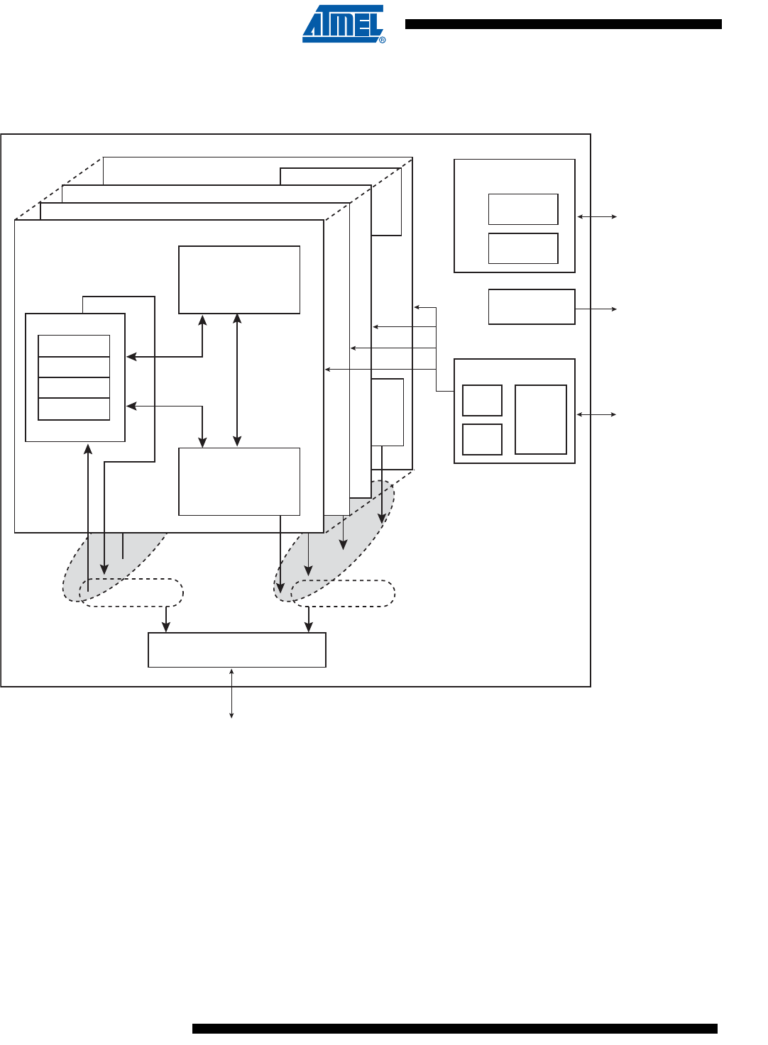
1022
6430F–ATARM–21-Feb-12
SAM3U Series
40.2 Block Diagram
Figure 40-1. DMA Controller (DMAC) Block Diagram
40.3 Functional Description
40.3.1 Basic Definitions
Source peripheral: Device on an AMBA layer from where the DMAC reads data, which is then
stored in the channel FIFO. The source peripheral teams up with a destination peripheral to form
a channel.
Destination peripheral: Device to which the DMAC writes the stored data from the FIFO (previ-
ously read from the source peripheral).
Memory: Source or destination that is always “ready” for a DMAC transfer and does not require
a handshaking interface to interact with the DMAC.
Channel: Read/write datapath between a source peripheral on one configured AMBA layer and
a destination peripheral on the same or different AMBA layer that occurs through the channel
DMA Destination
DMAC Channel 0
DMAC Destination
Control State Machine
Destination Pointer
Management
DMAC Source
Control State Machine
Source Pointer
Management
DMA FIFO Controller
DMA FIFO
DMAC Channel 0
Read data path
from source
DMAC Channel 0
Write data path
to destination
DMAC Channel 1
DMAC Channel 2
DMAC Channel n
External
Triggers
Soft
Triggers
DMAC
REQ/ACK
Interface
Trigger Manager
DMAC Interrupt
Controller
Status
Registers
Configuration
Registers
APB Interface
DMAC AHB Lite Master Interface
DMA Global Control
and Data Mux DMA Global
Request Arbiter
DMAC Write
Datapath Bundles
DMA Source
Requests Pool
DMAC Read
Datapath Bundles
DMAC
APB
Interface
DMAC Interrupt
DMAC
Hardware
Handshaking
Interface
AMBA AHB
1023
6430F–ATARM–21-Feb-12
SAM3U Series
FIFO. If the source peripheral is not memory, then a source handshaking interface is assigned to
the channel. If the destination peripheral is not memory, then a destination handshaking inter-
face is assigned to the channel. Source and destination handshaking interfaces can be assigned
dynamically by programming the channel registers.
Master interface: DMAC is a master on the AHB bus reading data from the source and writing it
to the destination over the AHB bus.
Slave interface: The APB interface over which the DMAC is programmed. The slave interface
in practice could be on the same layer as any of the master interfaces or on a separate layer.
Handshaking interface: A set of signal registers that conform to a protocol and handshake
between the DMAC and source or destination peripheral to control the transfer of a single or
chunk transfer between them. This interface is used to request, acknowledge, and control a
DMAC transaction. A channel can receive a request through one of two types of handshaking
interface: hardware or software.
Hardware handshaking interface: Uses hardware signals to control the transfer of a single or
chunk transfer between the DMAC and the source or destination peripheral.
Software handshaking interface: Uses software registers to contr5ol the transfer of a single or
chunk transfer between the DMAC and the source or destination peripheral. No special DMAC
handshaking signals are needed on the I/O of the peripheral. This mode is useful for interfacing
an existing peripheral to the DMAC without modifying it.
Flow controller: The device (either the DMAC or source/destination peripheral) that determines
the length of and terminates a DMAC buffer transfer. If the length of a buffer is known before
enabling the channel, then the DMAC should be programmed as the flow controller.
Transfer hierarchy: Figure 40-2 on page 1023 illustrates the hierarchy between DMAC trans-
fers, buffer transfers, chunk or single, and AMBA transfers (single or burst) for non-memory
peripherals. Figure 40-3 on page 1023 shows the transfer hierarchy for memory.
Figure 40-2. DMAC Transfer Hierarchy for Non-Memory Peripheral
Figure 40-3. DMAC Transfer Hierarchy for Memory
HDMA Transfer DMA Transfer
Level
Buffer Buffer Buffer Buffer Transfer
Level
Chunk
Transfer
Chunk
Transfer
Chunk
Transfer
Single
Transfer
DMA Transaction
Level
Burst
Transfer
AMBA
Burst
Transfer
AMBA
Burst
Transfer
AMBA
Single
Transfer
AMBA AMBA Transfer
Level
Single
Transfer
AMBA
1024
6430F–ATARM–21-Feb-12
SAM3U Series
Buffer: A buffer of DMAC data. The amount of data (length) is determined by the flow controller.
For transfers between the DMAC and memory, a buffer is broken directly into a sequence of
AMBA bursts and AMBA single transfers.
For transfers between the DMAC and a non-memory peripheral, a buffer is broken into a
sequence of DMAC transactions (single and chunks). These are in turn broken into a sequence
of AMBA transfers.
Transaction: A basic unit of a DMAC transfer as determined by either the hardware or software
handshaking interface. A transaction is only relevant for transfers between the DMAC and a
source or destination peripheral if the source or destination peripheral is a non-memory device.
There are two types of transactions: single transfer and chunk transfer.
–Single transfer: The length of a single transaction is always 1 and is converted to a
single AMBA access.
–Chunk transfer: The length of a chunk is programmed into the DMAC. The chunk is
then converted into a sequence of AHB access.DMAC executes each AMBA burst
transfer by performing incremental bursts that are no longer than 16 beats.
DMAC transfer: Software controls the number of buffers in a DMAC transfer. Once the DMAC
transfer has completed, then hardware within the DMAC disables the channel and can generate
an interrupt to signal the completion of the DMAC transfer. You can then re-program the channel
for a new DMAC transfer.
Single-buffer DMAC transfer: Consists of a single buffer.
Multi-buffer DMAC transfer: A DMAC transfer may consist of multiple DMAC buffers. Multi-buf-
fer DMAC transfers are supported through buffer chaining (linked list pointers), auto-reloading of
channel registers, and contiguous buffers. The source and destination can independently select
which method to use.
–Linked lists (buffer chaining) – A descriptor pointer (DSCR) points to the location
in system memory where the next linked list item (LLI) exists. The LLI is a set of
registers that describe the next buffer (buffer descriptor) and a descriptor pointer
register. The DMAC fetches the LLI at the beginning of every buffer when buffer
chaining is enabled.
–Contiguous buffers – Where the address of the next buffer is selected to be a
continuation from the end of the previous buffer.
Channel locking: Software can program a channel to keep the AHB master interface by locking
the arbitration for the master bus interface for the duration of a DMAC transfer, buffer, or chunk.
HDMA Transfer DMA Transfer
Level
Buffer Buffer Buffer Buffer Transfer
Level
Burst
Transfer
AMBA
Burst
Transfer
AMBA
Burst
Transfer
AMBA
Single
Transfer
AMBA AMBA Transfer
Level

1025
6430F–ATARM–21-Feb-12
SAM3U Series
Bus locking: Software can program a channel to maintain control of the AMBA bus by asserting
hmastlock for the duration of a DMAC transfer, buffer, or transaction (single or chunk). Channel
locking is asserted for the duration of bus locking at a minimum.
40.3.2 Memory Peripherals
Figure 40-3 on page 1023 shows the DMAC transfer hierarchy of the DMAC for a memory
peripheral. There is no handshaking interface with the DMAC, and therefore the memory periph-
eral can never be a flow controller. Once the channel is enabled, the transfer proceeds
immediately without waiting for a transaction request. The alternative to not having a transac-
tion-level handshaking interface is to allow the DMAC to attempt AMBA transfers to the
peripheral once the channel is enabled. If the peripheral slave cannot accept these AMBA trans-
fers, it inserts wait states onto the bus until it is ready; it is not recommended that more than 16
wait states be inserted onto the bus. By using the handshaking interface, the peripheral can sig-
nal to the DMAC that it is ready to transmit/receive data, and then the DMAC can access the
peripheral without the peripheral inserting wait states onto the bus.
40.3.3 Handshaking Interface
Handshaking interfaces are used at the transaction level to control the flow of single or chunk
transfers. The operation of the handshaking interface is different and depends on whether the
peripheral or the DMAC is the flow controller.
The peripheral uses the handshaking interface to indicate to the DMAC that it is ready to trans-
fer/accept data over the AMBA bus. A non-memory peripheral can request a DMAC transfer
through the DMAC using one of two handshaking interfaces:
• Hardware handshaking
• Software handshaking
Software selects between the hardware or software handshaking interface on a per-channel
basis. Software handshaking is accomplished through memory-mapped registers, while hard-
ware handshaking is accomplished using a dedicated handshaking interface.
40.3.3.1 Software Handshaking
When the slave peripheral requires the DMAC to perform a DMAC transaction, it communicates
this request by sending an interrupt to the CPU or interrupt controller.
The interrupt service routine then uses the software registers to initiate and control a DMAC
transaction. These software registers are used to implement the software handshaking
interface.
The SRC_H2SEL/DST_H2SEL bit in the DMAC_CFGx channel configuration register must be
set to zero to enable software handshaking.
When the peripheral is not the flow controller, then the last transaction register DMAC_LAST is
not used, and the values in these registers are ignored.
40.3.3.2 Chunk Transactions
Writing a 1 to the DMAC_CREQ[2x] register starts a source chunk transaction request, where x
is the channel number. Writing a 1 to the DMAC_CREQ[2x+1] register starts a destination chunk
transfer request, where x is the channel number.
Upon completion of the chunk transaction, the hardware clears the DMAC_CREQ[2x] or
DMAC_CREQ[2x+1].

1026
6430F–ATARM–21-Feb-12
SAM3U Series
40.3.3.3 Single Transactions
Writing a 1 to the DMAC_SREQ[2x] register starts a source single transaction request, where x
is the channel number. Writing a 1 to the DMAC_SREQ[2x+1] register starts a destination single
transfer request, where x is the channel number.
Upon completion of the chunk transaction, the hardware clears the DMAC_SREQ[x] or
DMAC_SREQ[2x+1].
Software can poll the relevant channel bit in the DMAC_CREQ[2x]/DMAC_CREQ[2x+1] and
DMAC_SREQ[x]/DMAC_SREQ[2x+1] registers. When both are 0, then either the requested
chunk or single transaction has completed.
40.3.4 DMAC Transfer Types
A DMAC transfer may consist of single or multi-buffers transfers. On successive buffers of a
multi-buffer transfer, the DMAC_SADDRx/DMAC_DADDRx registers in the DMAC are repro-
grammed using either of the following methods:
• Buffer chaining using linked lists
• Contiguous address between buffers
On successive buffers of a multi-buffer transfer, the DMAC_CTRLAx and DMAC_CTRLBx regis-
ters in the DMAC are re-programmed using either of the following methods:
• Buffer chaining using linked lists
When buffer chaining, using linked lists is the multi-buffer method of choice, and on successive
buffers, the DMAC_DSCRx register in the DMAC is re-programmed using the following method:
• Buffer chaining using linked lists
A buffer descriptor (LLI) consists of following registers, DMAC_SADDRx, DMAC_DADDRx,
DMAC_DSCRx, DMAC_CTRLAx, DMAC_CTRLBx.These registers, along with the
DMAC_CFGx register, are used by the DMAC to set up and describe the buffer transfer.
40.3.4.1 Multi-buffer Transfers
40.3.4.2 Buffer Chaining Using Linked Lists
In this case, the DMAC re-programs the channel registers prior to the start of each buffer by
fetching the buffer descriptor for that buffer from system memory. This is known as an LLI
update.
DMAC buffer chaining is supported by using a Descriptor Pointer register (DMAC_DSCRx) that
stores the address in memory of the next buffer descriptor. Each buffer descriptor contains the
corresponding buffer descriptor (DMAC_SADDRx, DMAC_DADDRx, DMAC_DSCRx,
DMAC_CTRLAx DMAC_CTRLBx).
To set up buffer chaining, a sequence of linked lists must be programmed in memory.
The DMAC_SADDRx, DMAC_DADDRx, DMAC_DSCRx, DMAC_CTRLAx and DMAC_CTRLBx
registers are fetched from system memory on an LLI update. The updated content of the
DMAC_CTRLAx register is written back to memory on buffer completion. Figure 40-4 on page
1027 shows how to use chained linked lists in memory to define multi-buffer transfers using buf-
fer chaining.
The Linked List multi-buffer transfer is initiated by programming DMAC_DSCRx with DSCRx(0)
(LLI(0) base address) and DMAC_CTRLBx register with both SRC_DSCR and DST_DSCR set
1027
6430F–ATARM–21-Feb-12
SAM3U Series
to 0. Other fields and registers are ignored and overwritten when the descriptor is retrieved from
memory.
The last transfer descriptor must be written to memory with its next descriptor address set to 0.
Figure 40-4. Multi Buffer Transfer Using Linked List
System Memory
SADDRx= DSCRx(0) + 0x0
DADDRx= DSCRx(0) + 0x4
CTRLAx= DSCRx(0) + 0x8
CTRLBx= DSCRx(0) + 0xC
DSCRx(1)= DSCRx(0) + 0x10
SADDRx= DSCRx(1) + 0x0
DADDRx= DSCRx(1) + 0x4
CTRLBx= DSCRx(1) + 0x8
CTRLBx= DSCRx(1) + 0xC
DSCRx(2)= DSCRx(1) + 0x10
DSCRx(0) DSCRx(2)
(points to 0 if
LLI(1) is the last
transfer descriptor
DSCRx(1)
LLI(0) LLI(1)

1028
6430F–ATARM–21-Feb-12
SAM3U Series
40.3.4.3 Programming DMAC for Multiple Buffer Transfers
Notes: 1. USR means that the register field is manually programmed by the user.
2. CONT means that address are contiguous.
3. LLI means that the register field is updated with the content of the linked list item.
40.3.4.4 Contiguous Address Between Buffers
In this case, the address between successive buffers is selected to be a continuation from the
end of the previous buffer. Enabling the source or destination address to be contiguous between
buffers is a function of DMAC_CTRLAx.SRC_DSCR and DMAC_CTRLAx.DST_DSCR
registers.
40.3.4.5 Suspension of Transfers Between buffers
At the end of every buffer transfer, an end of buffer interrupt is asserted if:
• the channel buffer interrupt is unmasked, DMAC_EBCIMR.BTC[n] = ‘1’, where n is the
channel number.
Note: The buffer complete interrupt is generated at the completion of the buffer transfer to the
destination.
At the end of a chain of multiple buffers, an end of linked list interrupt is asserted if:
• the channel end of chained buffer interrupt is unmasked, DMAC_EBCIMR.CBTC[n] = ‘1’,
when n is the channel number.
40.3.4.6 Ending Multi-buffer Transfers
All multi-buffer transfers must end as shown in Row 1 of Table 40-1 on page 1028. At the end of
every buffer transfer, the DMAC samples the row number, and if the DMAC is in Row 1 state,
then the previous buffer transferred was the last buffer and the DMAC transfer is terminated.
For rows 2, 3, and 4 the user must setup the last buffer descriptor in memory such that both
LLI.DMAC_CTRLBx.SRC_DSCR and LLI.DMAC_CTRLBx.DST_DSCR are one and
LLI.DMAC_DSCRx is set to 0.
Table 40-1. Multiple Buffers Transfer Management Table
Transfer Type AUTO SRC_REP DST_REP SRC_DSCR DST_DSCR BTSIZE SADDR DADDR
Other
Fields
1) Single Buffer or Last
buffer of a multiple buffer
transfer
0 – – 1 1 USR USR USR USR
2) Multi Buffer transfer
with contiguous DADDR 0 – 0 0 1 LLI LLI CONT LLI
3) Multi Buffer transfer
with contiguous SADDR 0 0 – 1 0 LLI CONT LLI LLI
4) Multi Buffer transfer
with LLI support 0 – – 0 0 LLI LLI LLI LLI

1029
6430F–ATARM–21-Feb-12
SAM3U Series
40.3.5 Programming a Channel
Four registers, the DMAC_DSCRx, the DMAC_CTRLAx, the DMAC_CTRLBx and
DMAC_CFGx, need to be programmed to set up whether single or multi-buffer transfers take
place, and which type of multi-buffer transfer is used. The different transfer types are shown in
Table 40-1 on page 1028.
The “BTSIZE, SADDR and DADDR” columns indicate where the values of DMAC_SARx,
DMAC_DARx, DMAC_CTLx, and DMAC_LLPx are obtained for the next buffer transfer when
multi-buffer DMAC transfers are enabled.
40.3.5.1 Programming Examples
40.3.5.2 Single-buffer Transfer (Row 1)
1. Read the Channel Handler Status Register DMAC_CHSR.ENABLE Field to choose a
free (disabled) channel.
2. Clear any pending interrupts on the channel from the previous DMAC transfer by read-
ing the interrupt status register, DMAC_EBCISR.
3. Program the following channel registers:
a. Write the starting source address in the DMAC_SADDRx register for channel x.
b. Write the starting destination address in the DMAC_DADDRx register for channel
x.
c. Program DMAC_CTRLAx, DMAC_CTRLBx and DMAC_CFGx according to Row 1
as shown in Table 40-1 on page 1028. Program the DMAC_CTRLBx register with
both DST_DSCR and SRC_DSCR fields set to one.
d. Write the control information for the DMAC transfer in the DMAC_CTRLAx and
DMAC_CTRLBx registers for channel x. For example, in the register, you can pro-
gram the following:
– i. Set up the transfer type (memory or non-memory peripheral for source and
destination) and flow control device by programming the FC of the DMAC_CTRLBx
register.
– ii. Set up the transfer characteristics, such as:
– Transfer width for the source in the SRC_WIDTH field.
– Transfer width for the destination in the DST_WIDTH field.
– Incrementing/decrementing or fixed address for source in SRC_INC field.
– Incrementing/decrementing or fixed address for destination in DST_INC field.
e. Write the channel configuration information into the DMAC_CFGx register for chan-
nel x.
– i. Designate the handshaking interface type (hardware or software) for the source
and destination peripherals. This is not required for memory. This step requires
programming the SRC_H2SEL/DST_H2SEL bits, respectively. Writing a ‘1’ activates
the hardware handshaking interface to handle source/destination requests. Writing a
‘0’ activates the software handshaking interface to handle source/destination
requests.
– ii. If the hardware handshaking interface is activated for the source or destination
peripheral, assign a handshaking interface to the source and destination peripheral.
This requires programming the SRC_PER and DST_PER bits, respectively.

1030
6430F–ATARM–21-Feb-12
SAM3U Series
4. After the DMAC selected channel has been programmed, enable the channel by writing
a ‘1’ to the DMAC_CHER.ENABLE[n] bit, where n is the channel number. Make sure
that bit 0 of DMAC_EN.ENABLE register is enabled.
5. Source and destination request single and chunk DMAC transactions to transfer the
buffer of data (assuming non-memory peripherals). The DMAC acknowledges at the
completion of every transaction (chunk and single) in the buffer and carry out the buffer
transfer.
6. Once the transfer completes, hardware sets the interrupts and disables the channel. At
this time you can either respond to the buffer Complete or Transfer Complete interrupts,
or poll for the Channel Handler Status Register (DMAC_CHSR.ENABLE[n]) bit until it is
cleared by hardware, to detect when the transfer is complete.
40.3.5.3 Multi-buffer Transfer with Linked List for Source and Linked List for Destination (Row 4)
1. Read the Channel Enable register to choose a free (disabled) channel.
2. Set up the chain of Linked List Items (otherwise known as buffer descriptors) in mem-
ory. Write the control information in the LLI.DMAC_CTRLAx and LLI.DMAC_CTRLBx
registers location of the buffer descriptor for each LLI in memory (see Figure 40-5 on
page 1032) for channel x. For example, in the register, you can program the following:
a. Set up the transfer type (memory or non-memory peripheral for source and desti-
nation) and flow control device by programming the FC of the DMAC_CTRLBx
register.
b. Set up the transfer characteristics, such as:
– i. Transfer width for the source in the SRC_WIDTH field.
– ii. Transfer width for the destination in the DST_WIDTH field.
– v. Incrementing/decrementing or fixed address for source in SRC_INCR field.
– vi. Incrementing/decrementing or fixed address for destination DST_INCR field.
3. Write the channel configuration information into the DMAC_CFGx register for channel
x.
a. Designate the handshaking interface type (hardware or software) for the source
and destination peripherals. This is not required for memory. This step requires pro-
gramming the SRC_H2SEL/DST_H2SEL bits, respectively. Writing a ‘1’ activates
the hardware handshaking interface to handle source/destination requests for the
specific channel. Writing a ‘0’ activates the software handshaking interface to han-
dle source/destination requests.
b. If the hardware handshaking interface is activated for the source or destination
peripheral, assign the handshaking interface to the source and destination periph-
eral. This requires programming the SRC_PER and DST_PER bits, respectively.
4. Make sure that the LLI.DMAC_CTRLBx register locations of all LLI entries in memory
(except the last) are set as shown in Row 4 of Table 40-1 on page 1028. The
LLI.DMAC_CTRLBx register of the last Linked List Item must be set as described in
Row 1 of Table 40-1. Figure 40-4 on page 1027 shows a Linked List example with two
list items.
5. Make sure that the LLI.DMAC_DSCRx register locations of all LLI entries in memory
(except the last) are non-zero and point to the base address of the next Linked List
Item.
6. Make sure that the LLI.DMAC_SADDRx/LLI.DMAC_DADDRx register locations of all
LLI entries in memory point to the start source/destination buffer address preceding
that LLI fetch.

1031
6430F–ATARM–21-Feb-12
SAM3U Series
7. Make sure that the LLI.DMAC_CTRLAx.DONE field of the LLI.DMAC_CTRLAx register
locations of all LLI entries in memory are cleared.
8. If source picture-picture mode is enabled (DMAC_CTRLBx.SRC_PIP is enabled), pro-
gram the DMAC_SPIPx register for channel x.
9. If destination picture-in-picture is enabled (DMAC_CTRLBx.DST_PIP is enabled), pro-
gram the DMAC_DPIPx register for channel x.
10. Clear any pending interrupts on the channel from the previous DMAC transfer by read-
ing the status register: DMAC_EBCISR.
11. Program the DMAC_CTRLBx, DMAC_CFGx registers according to Row 4 as shown in
Table 40-1 on page 1028.
12. Program the DMAC_DSCRx register with DMAC_DSCRx(0), the pointer to the first
Linked List item.
13. Finally, enable the channel by writing a ‘1’ to the DMAC_CHER.ENABLE[n] bit, where n
is the channel number. The transfer is performed.
14. The DMAC fetches the first LLI from the location pointed to by DMAC_DSCRx(0).
Note: The LLI.DMAC_SADDRx, LLI. DMAC_DADDRx, LLI.DMAC_DSCRx, LLI.DMAC_CTRLAx and
LLI.DMAC_CTRLBx registers are fetched. The DMAC automatically reprograms the
DMAC_SADDRx, DMAC_DADDRx, DMAC_DSCRx, DMAC_CTRLBx and DMAC_CTRLAx chan-
nel registers from the DMAC_DSCRx(0).
15. Source and destination request single and chunk DMAC transactions to transfer the
buffer of data (assuming non-memory peripheral). The DMAC acknowledges at the
completion of every transaction (chunk and single) in the buffer and carry out the buffer
transfer.
16. Once the buffer of data is transferred, the DMAC_CTRLAx register is written out to sys-
tem memory at the same location and on the same layer where it was originally
fetched, that is, the location of the DMAC_CTRLAx register of the linked list item
fetched prior to the start of the buffer transfer. Only DMAC_CTRLAx register is written
out because only the DMAC_CTRLAx.BTSIZE and DMAC_CTRLAX.DONE bits have
been updated by DMAC hardware. Additionally, the DMAC_CTRLAx.DONE bit is
asserted when the buffer transfer has completed.
Note: Do not poll the DMAC_CTRLAx.DONE bit in the DMAC memory map. Instead, poll the
LLI.DMAC_CTRLAx.DONE bit in the LLI for that buffer. If the poll LLI.DMAC_CTRLAx.DONE bit is
asserted, then this buffer transfer has completed. This LLI.DMAC_CTRLAx.DONE bit was cleared
at the start of the transfer.
17. The DMAC does not wait for the buffer interrupt to be cleared, but continues fetching
the next LLI from the memory location pointed to by current DMAC_DSCRx register
and automatically reprograms the DMAC_SADDRx, DMAC_DADDRx, DMAC_DSCRx,
DMAC_CTRLAx and DMAC_CTRLBx channel registers. The DMAC transfer continues
until the DMAC determines that the DMAC_CTRLBx and DMAC_DSCRx registers at
the end of a buffer transfer match described in Row 1 of Table 40-1 on page 1028. The
DMAC then knows that the previous buffer transferred was the last buffer in the DMAC
transfer. The DMAC transfer might look like that shown in Figure 40-5 on page 1032.
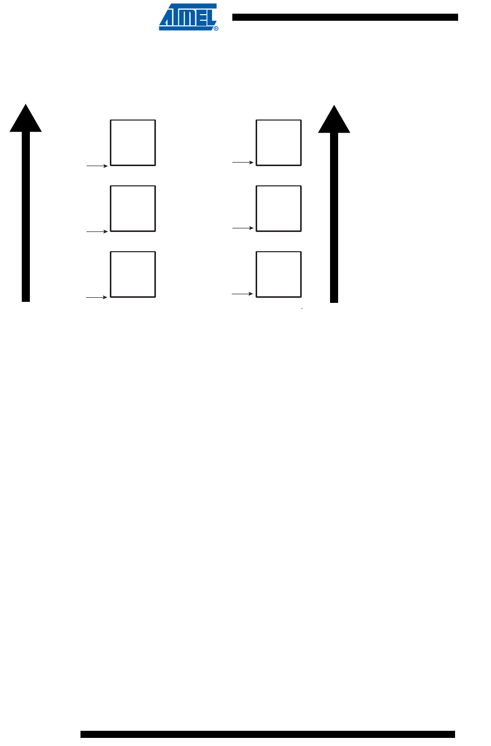
1032
6430F–ATARM–21-Feb-12
SAM3U Series
Figure 40-5. Multi-buffer with Linked List Address for Source and Destination
If the user needs to execute a DMAC transfer where the source and destination address are
contiguous but the amount of data to be transferred is greater than the maximum buffer size
DMAC_CTRLAx.BTSIZE, then this can be achieved using the type of multi-buffer transfer as
shown in Figure 40-6 on page 1033.
SADDR(2)
SADDR(1)
SADDR(0)
DADDR(2)
DADDR(1)
DADDR(0)
Buffer 2
Buffer 1
Buffer 0 Buffer 0
Buffer 1
Buffer 2
Address of
Source Layer
Address of
Destination Layer
Source Buffers Destination Buffers
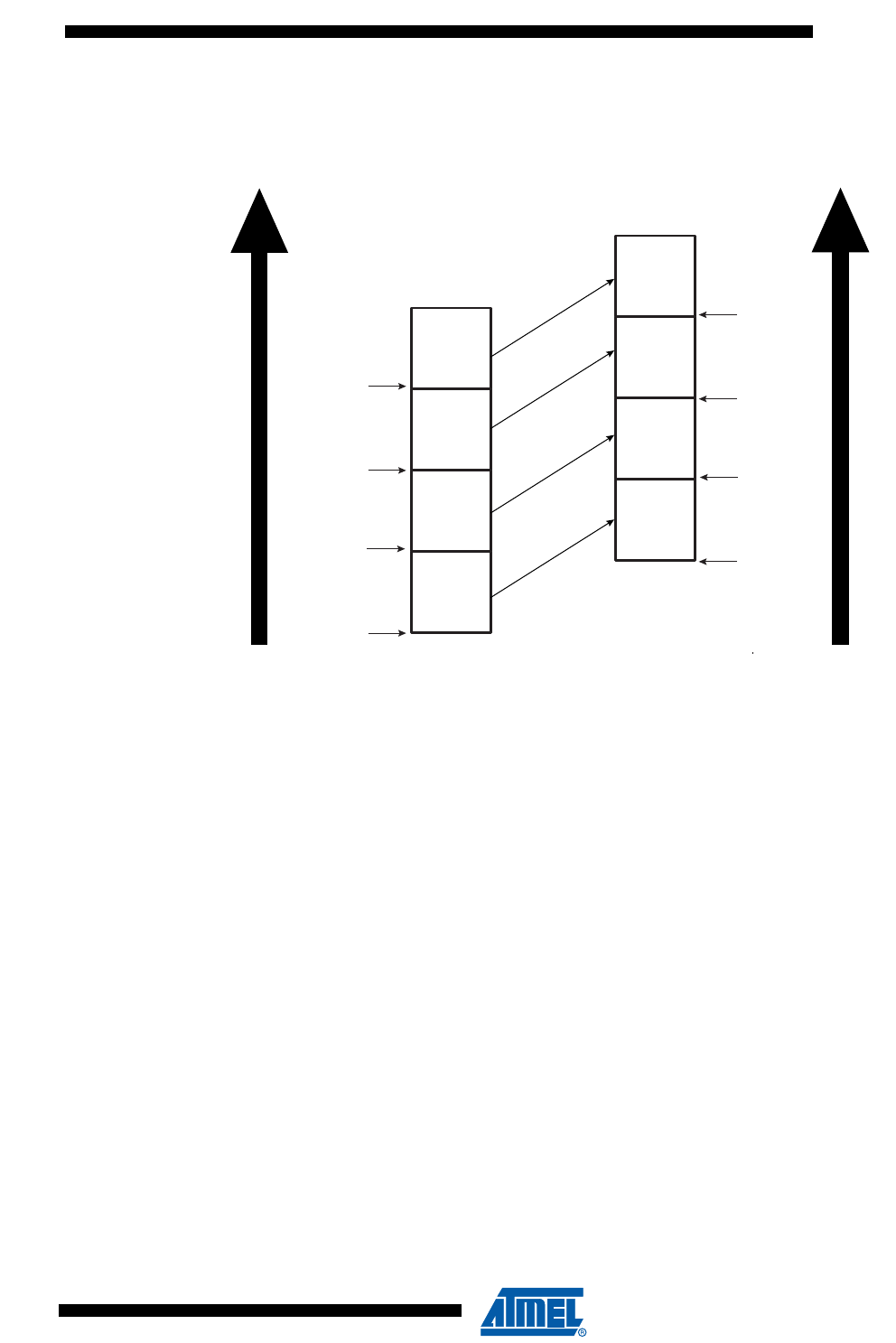
1033
6430F–ATARM–21-Feb-12
SAM3U Series
Figure 40-6. Multi-buffer with Linked Address for Source and Destination Buffers are Contiguous
The DMAC transfer flow is shown in Figure 40-7 on page 1034.
SADDR(2)
SADDR(1)
SADDR(0)
DADDR(2)
DADDR(1)
DADDR(0)
Buffer 2
Buffer 1
Buffer 0
Buffer 0
Buffer 1
Buffer 2
Address of
Source Layer
Address of
Destination Layer
Source Buffers Destination Buffers
SADDR(3)
Buffer 2
DADDR(3)
Buffer 2
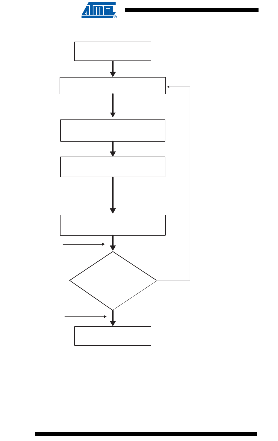
1034
6430F–ATARM–21-Feb-12
SAM3U Series
Figure 40-7. DMAC Transfer Flow for Source and Destination Linked List Address
40.3.5.4 Multi-buffer DMAC Transfer with Linked List for Source and Contiguous Destination Address (Row 2)
1. Read the Channel Enable register to choose a free (disabled) channel.
2. Set up the linked list in memory. Write the control information in the
LLI.DMAC_CTRLAx and LLI.DMAC_CTRLBx register location of the buffer descriptor
for each LLI in memory for channel x. For example, in the register, you can program the
following:
Channel enabled by
software
LLI Fetch
Hardware reprograms
SADDRx, DADDRx, CTRLA/Bx, DSCRx
DMAC buffer transfer
Writeback of HDMA_CTRLAx
register in system memory
Is HDMA in
Row1 of
HDMA State Machine Table?
Channel Disabled by
hardware
Buffer Complete interrupt
generated here
HDMA Transfer Complete
interrupt generated here
yes
no

1035
6430F–ATARM–21-Feb-12
SAM3U Series
a. Set up the transfer type (memory or non-memory peripheral for source and desti-
nation) and flow control device by programming the FC of the DMAC_CTRLBx
register.
b. Set up the transfer characteristics, such as:
– i. Transfer width for the source in the SRC_WIDTH field.
– ii. Transfer width for the destination in the DST_WIDTH field.
– v. Incrementing/decrementing or fixed address for source in SRC_INCR field.
– vi. Incrementing/decrementing or fixed address for destination DST_INCR field.
3. Write the starting destination address in the DMAC_DADDRx register for channel x.
Note: The values in the LLI.DMAC_DADDRx register location of each Linked List Item (LLI) in memory,
although fetched during an LLI fetch, are not used.
4. Write the channel configuration information into the DMAC_CFGx register for channel
x.
a. Designate the handshaking interface type (hardware or software) for the source
and destination peripherals. This is not required for memory. This step requires pro-
gramming the SRC_H2SEL/DST_H2SEL bits, respectively. Writing a ‘1’ activates
the hardware handshaking interface to handle source/destination requests for the
specific channel. Writing a ‘0’ activates the software handshaking interface to han-
dle source/destination requests.
b. If the hardware handshaking interface is activated for the source or destination
peripheral, assign handshaking interface to the source and destination peripherals.
This requires programming the SRC_PER and DST_PER bits, respectively.
5. Make sure that all LLI.DMAC_CTRLBx register locations of the LLI (except the last) are
set as shown in Row 2 of Table 40-1 on page 1028, while the LLI.DMAC_CTRLBx reg-
ister of the last Linked List item must be set as described in Row 1 of Table 40-1. Figure
40-4 on page 1027 shows a Linked List example with two list items.
6. Make sure that the LLI.DMAC_DSCRx register locations of all LLIs in memory (except
the last) are non-zero and point to the next Linked List Item.
7. Make sure that the LLI.DMAC_SADDRx register location of all LLIs in memory point to
the start source buffer address proceeding that LLI fetch.
8. Make sure that the LLI.DMAC_CTRLAx.DONE field of the LLI.DMAC_CTRLAx register
locations of all LLIs in memory is cleared.
9. Clear any pending interrupts on the channel from the previous DMAC transfer by read-
ing the interrupt status register.
10. Program the DMAC_CTRLAx, DMAC_CTRLBx and DMAC_CFGx registers according
to Row 2 as shown in Table 40-1 on page 1028
11. Program the DMAC_DSCRx register with DMAC_DSCRx(0), the pointer to the first
Linked List item.
12. Finally, enable the channel by writing a ‘1’ to the DMAC_CHER.ENABLE[n] bit. The
transfer is performed. Make sure that bit 0 of the DMAC_EN register is enabled.
13. The DMAC fetches the first LLI from the location pointed to by DMAC_DSCRx(0).
Note: The LLI.DMAC_SADDRx, LLI.DMAC_DADDRx, LLI.DMAC_DSCRx and LLI.DMAC_CTRLA/Bx
registers are fetched. The LLI.DMAC_DADDRx register location of the LLI although fetched is not
used. The DMAC_DADDRx register in the DMAC remains unchanged.
14. Source and destination requests single and chunk DMAC transactions to transfer the
buffer of data (assuming non-memory peripherals). The DMAC acknowledges at the
completion of every transaction (chunk and single) in the buffer and carry out the buffer
transfer
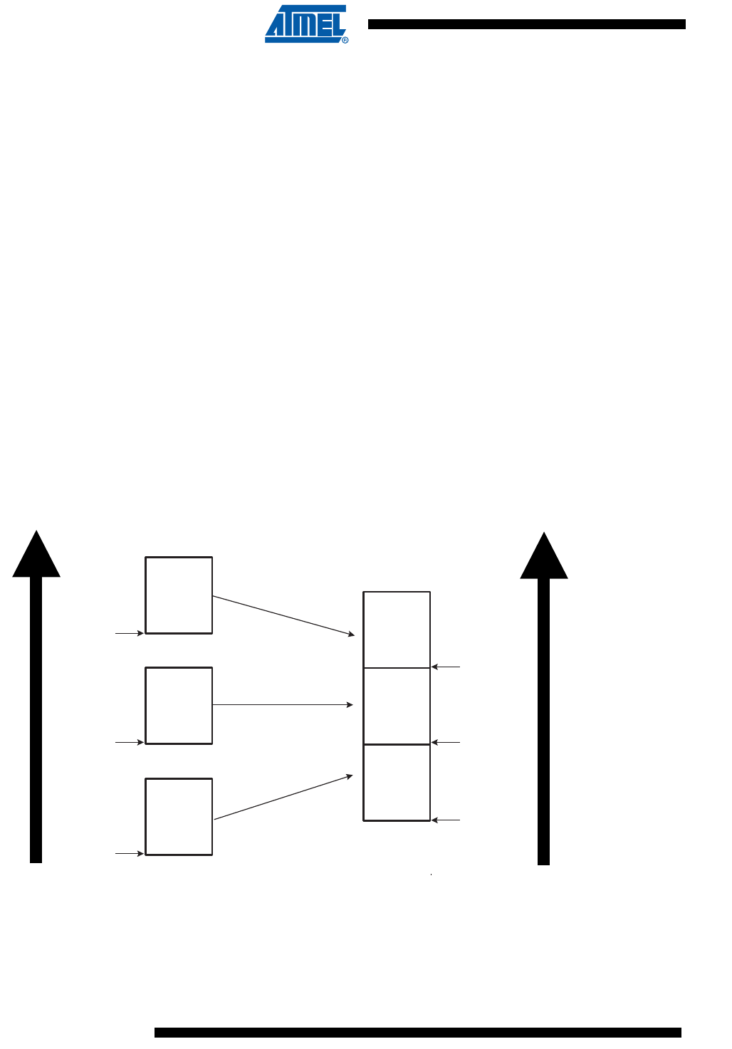
1036
6430F–ATARM–21-Feb-12
SAM3U Series
15. Once the buffer of data is transferred, the DMAC_CTRLAx register is written out to sys-
tem memory at the same location and on the same layer (DMAC_DSCRx.DSCR_IF)
where it was originally fetched, that is, the location of the DMAC_CTRLAx register of
the linked list item fetched prior to the start of the buffer transfer. Only DMAC_CTRLAx
register is written out because only the DMAC_CTRLAx.BTSIZE and
DMAC_CTRLAX.DONE fields have been updated by DMAC hardware. Additionally, the
DMAC_CTRLAx.DONE bit is asserted when the buffer transfer has completed.
Note: Do not poll the DMAC_CTRLAx.DONE bit in the DMAC memory map. Instead, poll the
LLI.DMAC_CTRLAx.DONE bit in the LLI for that buffer. If the poll LLI.DMAC_CTRLAx.DONE bit is
asserted, then this buffer transfer has completed. This LLI.DMAC_CTRLAx.DONE bit was cleared
at the start of the transfer.
16. The DMAC does not wait for the buffer interrupt to be cleared, but continues and
fetches the next LLI from the memory location pointed to by current DMAC_DSCRx
register and automatically reprograms the DMAC_SADDRx, DMAC_CTRLAx,
DMAC_CTRLBx and DMAC_DSCRx channel registers. The DMAC_DADDRx register
is left unchanged. The DMAC transfer continues until the DMAC samples the
DMAC_CTRLAx, DMAC_CTRLBx and DMAC_DSCRx registers at the end of a buffer
transfer match that described in Row 1 of Table 40-1 on page 1028. The DMAC then
knows that the previous buffer transferred was the last buffer in the DMAC transfer.
The DMAC transfer might look like that shown in Figure 40-8 on page 1036 Note that the desti-
nation address is decrementing.
Figure 40-8. DMAC Transfer with Linked List Source Address and Contiguous Destination Address
The DMAC transfer flow is shown in Figure 40-9 on page 1037.
SADDR(2)
SADDR(1)
SADDR(0)
DADDR(2)
DADDR(1)
DADDR(0)
Buffer 2
Buffer 1
Buffer 0
Buffer 0
Buffer 1
Buffer 2
Address of
Source Layer
Address of
Destination Layer
Source Buffers Destination Buffers

1037
6430F–ATARM–21-Feb-12
SAM3U Series
Figure 40-9. DMAC Transfer Flow for Linked List Source Address and Contiguous Destination Address
40.3.6 Disabling a Channel Prior to Transfer Completion
Under normal operation, software enables a channel by writing a ‘1’ to the Channel Handler
Enable Register, DMAC_CHER.ENABLE[n], and hardware disables a channel on transfer com-
pletion by clearing the DMAC_CHSR.ENABLE[n] register bit.
The recommended way for software to disable a channel without losing data is to use the SUS-
PEND[n] bit in conjunction with the EMPTY[n] bit in the Channel Handler Status Register.
Channel Enabled by
software
LLI Fetch
Hardware reprograms
SADDRx, CTRLAx,CTRLBx, DSCRx
HDMA buffer transfer
Writeback of control
information of LLI
Is HDMA in
Row 1 ?
Channel Disabled by
hardware
Buffer Complete interrupt
generated here
HDMA Transfer Complete
interrupt generated here yes
no

1038
6430F–ATARM–21-Feb-12
SAM3U Series
1. If software wishes to disable a channel n prior to the DMAC transfer completion, then it
can set the DMAC_CHER.SUSPEND[n] bit to tell the DMAC to halt all transfers from
the source peripheral. Therefore, the channel FIFO receives no new data.
2. Software can now poll the DMAC_CHSR.EMPTY[n] bit until it indicates that the channel
n FIFO is empty, where n is the channel number.
3. The DMAC_CHER.ENABLE[n] bit can then be cleared by software once the channel n
FIFO is empty, where n is the channel number.
When DMAC_CTRLAx.SRC_WIDTH is less than DMAC_CTRLAx.DST_WIDTH and the
DMAC_CHSRx.SUSPEND[n] bit is high, the DMAC_CHSRx.EMPTY[n] is asserted once the
contents of the FIFO do not permit a single word of DMAC_CTRLAx.DST_WIDTH to be formed.
However, there may still be data in the channel FIFO but not enough to form a single transfer of
DMAC_CTLx.DST_WIDTH width. In this configuration, once the channel is disabled, the remain-
ing data in the channel FIFO are not transferred to the destination peripheral. It is permitted to
remove the channel from the suspension state by writing a ‘1’ to the DMAC_CHER.RESUME[n]
field register. The DMAC transfer completes in the normal manner. n defines the channel
number.
Note: If a channel is disabled by software, an active single or chunk transaction is not guaranteed to
receive an acknowledgement.
40.3.6.1 Abnormal Transfer Termination
A DMAC transfer may be terminated abruptly by software by clearing the channel enable bit,
DMAC_CHDR.ENABLE[n] where n is the channel number. This does not mean that the channel
is disabled immediately after the DMAC_CHSR.ENABLE[n] bit is cleared over the APB inter-
face. Consider this as a request to disable the channel. The DMAC_CHSR.ENABLE[n] must be
polled and then it must be confirmed that the channel is disabled by reading back 0.
Software may terminate all channels abruptly by clearing the global enable bit in the DMAC Con-
figuration Register (DMAC_EN.ENABLE bit). Again, this does not mean that all channels are
disabled immediately after the DMAC_EN.ENABLE is cleared over the APB slave interface.
Consider this as a request to disable all channels. The DMAC_CHSR.ENABLE must be polled
and then it must be confirmed that all channels are disabled by reading back ‘0’.
Note: If the channel enable bit is cleared while there is data in the channel FIFO, this data is not sent to
the destination peripheral and is not present when the channel is re-enabled. For read sensitive
source peripherals, such as a source FIFO, this data is therefore lost. When the source is not a
read sensitive device (i.e., memory), disabling a channel without waiting for the channel FIFO to
empty may be acceptable as the data is available from the source peripheral upon request and is
not lost.
Note: If a channel is disabled by software, an active single or chunk transaction is not guaranteed to
receive an acknowledgement.
40.4 DMAC Software Requirements
• There must not be any write operation to Channel registers in an active channel after the
channel enable is made HIGH. If any channel parameters must be reprogrammed, this can
only be done after disabling the DMAC channel.
• You must program the DMAC_SADDRx and DMAC_DADDRx channel registers with a byte,
half-word and word aligned address depending on the source width and destination width.
• After the software disables a channel by writing into the channel disable register, it must re-
enable the channel only after it has polled a 0 in the corresponding channel enable status
register. This is because the current AHB Burst must terminate properly.

1039
6430F–ATARM–21-Feb-12
SAM3U Series
• If you program the BTSIZE field in the DMAC_CTRLA, as zero, and the DMAC is defined as
the flow controller, then the channel is automatically disabled.
• When hardware handshaking interface protocol is fully implemented, a peripheral is expected
to deassert any sreq or breq signals on receiving the ack signal irrespective of the request
the ack was asserted in response to.
• Multiple Transfers involving the same peripheral must not be programmed and enabled on
different channel, unless this peripheral integrates several hardware handshaking interface.
• When a Peripheral is flow controller, the targeted DMAC Channel must be enabled before the
Peripheral. If you do not ensure this the DMAC Channel might miss a Last Transfer Flag, if
the First DMAC request is also the last transfer.

1040
6430F–ATARM–21-Feb-12
SAM3U Series
40.5 DMA Controller (DMAC) User Interface
Note: 1. The addresses for the DMAC registers shown here are for DMA Channel 0. This sequence of registers is repeated succes-
sively for each DMA channel located between 0x064 and 0xC8.
Table 40-2. Register Mapping
Offset Register Name Access Reset
0x000 DMAC Global Configuration Register DMAC_GCFG Read-write 0x10
0x004 DMAC Enable Register DMAC_EN Read-write 0x0
0x008 DMAC Software Single Request Register DMAC_SREQ Read-write 0x0
0x00C DMAC Software Chunk Transfer Request Register DMAC_CREQ Read-write 0x0
0x010 DMAC Software Last Transfer Flag Register DMAC_LAST Read-write 0x0
0x014 Reserved – – –
0x018 DMAC Error, Chained Buffer transfer completed and Buffer
transfer completed Interrupt Enable register. DMAC_EBCIER Write-only –
0x01C DMAC Error, Chained Buffer transfer completed and Buffer
transfer completed Interrupt Disable register. DMAC_EBCIDR Write-only –
0x020 DMAC Error, Chained Buffer transfer completed and Buffer
transfer completed Mask Register. DMAC_EBCIMR Read-only 0x0
0x024 DMAC Error, Chained Buffer transfer completed and Buffer
transfer completed Status Register. DMAC_EBCISR Read-only 0x0
0x028 DMAC Channel Handler Enable Register DMAC_CHER Write-only –
0x02C DMAC Channel Handler Disable Register DMAC_CHDR Write-only –
0x030 DMAC Channel Handler Status Register DMAC_CHSR Read-only 0x00FF0000
0x034 Reserved – – –
0x038 Reserved – – –
0x03C+ch_num*(0x28)+(0x0) DMAC Channel Source Address Register DMAC_SADDR Read-write 0x0
0x03C+ch_num*(0x28)+(0x4) DMAC Channel Destination Address Register DMAC_DADDR Read-write 0x0
0x03C+ch_num*(0x28)+(0x8) DMAC Channel Descriptor Address Register DMAC_DSCR Read-write 0x0
0x03C+ch_num*(0x28)+(0xC) DMAC Channel Control A Register DMAC_CTRLA Read-write 0x0
0x03C+ch_num*(0x28)+(0x10) DMAC Channel Control B Register DMAC_CTRLB Read-write 0x0
0x03C+ch_num*(0x28)+(0x14) DMAC Channel Configuration Register DMAC_CFG Read-write 0x01000000
0x03C+ch_num*(0x28)+(0x18) Reserved – – –
0x03C+ch_num*(0x28)+(0x1C) Reserved – – –
0x03C+ch_num*(0x28)+(0x20) Reserved – – –
0x03C+ch_num*(0x28)+(0x24) Reserved – – –
0x064 - 0xC8 DMAC Channel 1 to 3 Register(1) Read-write 0x0
0x017C- 0x1FC Reserved – – –

1041
6430F–ATARM–21-Feb-12
SAM3U Series
40.5.1 DMAC Global Configuration Register
Name: DMAC_GCFG
Address: 0x400B0000
Access: Read-write
Reset: 0x00000010
• ARB_CFG
0: Fixed priority arbiter.
1: Modified round robin arbiter.
31 30 29 28 27 26 25 24
––––––––
23 22 21 20 19 18 17 16
––––––––
15 14 13 12 11 10 9 8
––––––––
76543210
–––ARB_CFG––––

1042
6430F–ATARM–21-Feb-12
SAM3U Series
40.5.2 DMAC Enable Register
Name: DMAC_EN
Address: 0x400B0004
Access: Read-write
Reset: 0x00000000
• ENABLE
0: DMA Controller is disabled.
1: DMA Controller is enabled.
31 30 29 28 27 26 25 24
––––––––
23 22 21 20 19 18 17 16
––––––––
15 14 13 12 11 10 9 8
––––––––
76543210
–––––––ENABLE
1043
6430F–ATARM–21-Feb-12
SAM3U Series
40.5.3 DMAC Software Single Request Register
Name: DMAC_SREQ
Address: 0x400B0008
Access: Read-write
Reset: 0x00000000
• DSREQx
Request a destination single transfer on channel i.
• SSREQx
Request a source single transfer on channel i.
31 30 29 28 27 26 25 24
––––––––
23 22 21 20 19 18 17 16
––––––––
15 14 13 12 11 10 9 8
––––––––
76543210
DSREQ3 SSREQ3 DSREQ2– SSREQ2– DSREQ1 SSREQ1 DSREQ0 SSREQ0

1044
6430F–ATARM–21-Feb-12
SAM3U Series
40.5.4 DMAC Software Chunk Transfer Request Register
Name: DMAC_CREQ
Address: 0x400B000C
Access: Read-write
Reset: 0x00000000
• DCREQx
Request a destination chunk transfer on channel i.
•SCREQx
Request a source chunk transfer on channel i.
31 30 29 28 27 26 25 24
––––––––
23 22 21 20 19 18 17 16
––––––––
15 14 13 12 11 10 9 8
––––––––
76543210
DCREQ3 SCREQ3 DCREQ2– SCREQ2– DCREQ1 SCREQ1 DCREQ0 SCREQ0

1045
6430F–ATARM–21-Feb-12
SAM3U Series
40.5.5 DMAC Software Last Transfer Flag Register
Name: DMAC_LAST
Address: 0x400B0010
Access: Read-write
Reset: 0x00000000
•DLASTx
Writing one to DLASTx prior to writing one to DSREQx or DCREQx indicates that this destination request is the last transfer
of the buffer.
•SLASTx
Writing one to SLASTx prior to writing one to SSREQx or SCREQx indicates that this source request is the last transfer of
the buffer.
31 30 29 28 27 26 25 24
––––––––
23 22 21 20 19 18 17 16
––––––––
15 14 13 12 11 10 9 8
––––––––
76543210
DLAST3 SLAST3 DLAST2 SLAST2 DLAST1 SLAST1 DLAST0 SLAST0

1046
6430F–ATARM–21-Feb-12
SAM3U Series
40.5.6 DMAC Error, Buffer Transfer and Chained Buffer Transfer Interrupt Enable Register
Name: DMAC_EBCIER
Address: 0x400B0018
Access: Write-only
Reset: 0x00000000
• BTC[3:0]
Buffer Transfer Completed Interrupt Enable Register. Set the relevant bit in the BTC field to enable the interrupt for
channel i.
• CBTC[3:0]
Chained Buffer Transfer Completed Interrupt Enable Register. Set the relevant bit in the CBTC field to enable the interrupt
for channel i.
• ERR[3:0]
Access Error Interrupt Enable Register. Set the relevant bit in the ERR field to enable the interrupt for channel i.
31 30 29 28 27 26 25 24
––––––––
23 22 21 20 19 18 17 16
––––ERR3ERR2ERR1ERR0
15 14 13 12 11 10 9 8
––––CBTC3CBTC2CBTC1CBTC0
76543210
––––BTC3BTC2BTC1BTC0

1047
6430F–ATARM–21-Feb-12
SAM3U Series
40.5.7 DMAC Error, Buffer Transfer and Chained Buffer Transfer Interrupt Disable Register
Name: DMAC_EBCIDR
Address: 0x400B001C
Access: Write-only
Reset: 0x00000000
• BTC[3:0]
Buffer transfer completed Disable Interrupt Register. When set, a bit of the BTC field disables the interrupt from the rele-
vant DMAC channel.
• CBTC[3:0]
Chained Buffer transfer completed Disable Register. When set, a bit of the CBTC field disables the interrupt from the rele-
vant DMAC channel.
• ERR[3:0]
Access Error Interrupt Disable Register. When set, a bit of the ERR field disables the interrupt from the relevant DMAC
channel.
31 30 29 28 27 26 25 24
––––––––
23 22 21 20 19 18 17 16
––––ERR3ERR2ERR1ERR0
15 14 13 12 11 10 9 8
––––CBTC3CBTC2CBTC1CBTC0
76543210
––––BTC3BTC2BTC1BTC0

1048
6430F–ATARM–21-Feb-12
SAM3U Series
40.5.8 DMAC Error, Buffer Transfer and Chained Buffer Transfer Interrupt Mask Register
Name: DMAC_EBCIMR
Address: 0x400B0020
Access: Read-only
Reset: 0x00000000
• BTC[3:0]
0: Buffer Transfer completed interrupt is disabled for channel i.
1: Buffer Transfer completed interrupt is enabled for channel i.
• CBTC[3:0]
0: Chained Buffer Transfer interrupt is disabled for channel i.
1: Chained Buffer Transfer interrupt is enabled for channel i.
• ERR[3:0]
0: Transfer Error Interrupt is disabled for channel i.
1: Transfer Error Interrupt is enabled for channel i.
31 30 29 28 27 26 25 24
––––––––
23 22 21 20 19 18 17 16
––––ERR3ERR2ERR1ERR0
15 14 13 12 11 10 9 8
––––CBTC3CBTC2CBTC1CBTC0
76543210
––––BTC3BTC2BTC1BTC0

1049
6430F–ATARM–21-Feb-12
SAM3U Series
40.5.9 DMAC Error, Buffer Transfer and Chained Buffer Transfer Status Register
Name: DMAC_EBCISR
Address: 0x400B0024
Access: Read-only
Reset: 0x00000000
• BTC[3:0]
When BTC[i] is set, Channel i buffer transfer has terminated.
• CBTC[3:0]
When CBTC[i] is set, Channel i Chained buffer has terminated. LLI Fetch operation is disabled.
• ERR[3:0]
When ERR[i] is set, Channel i has detected an AHB Read or Write Error Access.
31 30 29 28 27 26 25 24
––––––––
23 22 21 20 19 18 17 16
––––ERR3ERR2ERR1ERR0
15 14 13 12 11 10 9 8
––––CBTC3CBTC2CBTC1CBTC0
76543210
––––BTC3BTC2BTC1BTC0

1050
6430F–ATARM–21-Feb-12
SAM3U Series
40.5.10 DMAC Channel Handler Enable Register
Name: DMAC_CHER
Address: 0x400B0028
Access: Write-only
Reset: 0x00000000
• ENA[3:0]
When set, a bit of the ENA field enables the relevant channel.
• SUSP[3:0]
When set, a bit of the SUSP field freezes the relevant channel and its current context.
• KEEP[3:0]
When set, a bit of the KEEP field resumes the current channel from an automatic stall state.
31 30 29 28 27 26 25 24
––––KEEP3 KEEP2 KEEP1 KEEP0
23 22 21 20 19 18 17 16
––––––––
15 14 13 12 11 10 9 8
––––SUSP3SUSP2SUSP1SUSP0
76543210
––––ENA3ENA2ENA1ENA0

1051
6430F–ATARM–21-Feb-12
SAM3U Series
40.5.11 DMAC Channel Handler Disable Register
Name: DMAC_CHDR
Address: 0x400B002C
Access: Write-only
Reset: 0x00000000
• DIS[3:0]
Write one to this field to disable the relevant DMAC Channel. The content of the FIFO is lost and the current AHB access is
terminated. Software must poll DIS[3:0] field in the DMAC_CHSR register to be sure that the channel is disabled.
• RES[3:0]
Write one to this field to resume the channel transfer restoring its context.
31 30 29 28 27 26 25 24
––––––––
23 22 21 20 19 18 17 16
––––––––
15 14 13 12 11 10 9 8
––––RES3RES2RES1RES0
76543210
––––DIS3DIS2DIS1DIS0

1052
6430F–ATARM–21-Feb-12
SAM3U Series
40.5.12 DMAC Channel Handler Status Register
Name: DMAC_CHSR
Address: 0x400B0030
Access: Read-only
Reset: 0x00FF0000
• ENA[3:0]
A one in any position of this field indicates that the relevant channel is enabled.
• SUSP[3:0]
A one in any position of this field indicates that the channel transfer is suspended.
• EMPT[3:0]
A one in any position of this field indicates that the relevant channel is empty.
• STAL[3:0]
A one in any position of this field indicates that the relevant channel is stalling.
31 30 29 28 27 26 25 24
––––STAL3STAL2STAL1STAL0
23 22 21 20 19 18 17 16
––––EMPT3EMPT2EMPT1EMPT0
15 14 13 12 11 10 9 8
––––SUSP3SUSP2SUSP1SUSP0
76543210
––––ENA3ENA2ENA1ENA0
1053
6430F–ATARM–21-Feb-12
SAM3U Series
40.5.13 DMAC Channel x [x = 0..3] Source Address Register
Name: DMAC_SADDRx [x = 0..3]
Addresses: 0x400B003C [0], 0x400B0064 [1], 0x400B008C [2], 0x400B00B4 [3]
Access: Read-write
Reset: 0x00000000
• SADDRx
Channel x source address. This register must be aligned with the source transfer width.
31 30 29 28 27 26 25 24
SADDRx
23 22 21 20 19 18 17 16
SADDRx
15 14 13 12 11 10 9 8
SADDRx
76543210
SADDRx

1054
6430F–ATARM–21-Feb-12
SAM3U Series
40.5.14 DMAC Channel x [x = 0..3] Destination Address Register
Name: DMAC_DADDRx [x = 0..3]
Addresses: 0x400B0040 [0], 0x400B0068 [1], 0x400B0090 [2], 0x400B00B8 [3]
Access: Read-write
Reset: 0x00000000
• DADDRx
Channel x destination address. This register must be aligned with the destination transfer width.
31 30 29 28 27 26 25 24
DADDRx
23 22 21 20 19 18 17 16
DADDRx
15 14 13 12 11 10 9 8
DADDRx
76543210
DADDRx

1055
6430F–ATARM–21-Feb-12
SAM3U Series
40.5.15 DMAC Channel x [x = 0..3] Descriptor Address Register
Name: DMAC_DSCRx [x = 0..3]
Addresses: 0x400B0044 [0], 0x400B006C [1], 0x400B0094 [2], 0x400B00BC [3]
Access: Read-write
Reset: 0x00000000
•DSCRx
Buffer Transfer descriptor address. This address is word aligned.
31 30 29 28 27 26 25 24
DSCRx
23 22 21 20 19 18 17 16
DSCRx
15 14 13 12 11 10 9 8
DSCRx
76543210
DSCRx –
1056
6430F–ATARM–21-Feb-12
SAM3U Series
40.5.16 DMAC Channel x [x = 0..3] Control A Register
Name: DMAC_CTRLAx [x = 0..3]
Addresses: 0x400B0048 [0], 0x400B0070 [1], 0x400B0098 [2], 0x400B00C0 [3]
Access: Read-write
Reset: 0x00000000
•BTSIZE
Buffer Transfer Size. The transfer size relates to the number of transfers to be performed, that is, for writes it refers to the
number of source width transfers to perform when DMAC is flow controller. For Reads, BTSIZE refers to the number of
transfers completed on the Source Interface. When this field is set to 0, the DMAC module is automatically disabled when
the relevant channel is enabled.
•SCSIZE
Source Chunk Transfer Size.
• DCSIZE
Destination Chunk Transfer size.
•SRC_WIDTH
31 30 29 28 27 26 25 24
DONE – DST_WIDTH – – SRC_WIDTH
23 22 21 20 19 18 17 16
–––DCSIZE–––SCSIZE
15 14 13 12 11 10 9 8
BTSIZE
76543210
BTSIZE
SCSIZE value Number of data transferred
01
14
DCSIZE Number of data transferred
01
14
SRC_WIDTH Single Transfer Size
00 BYTE
01 HALF-WORD
1X WORD

1057
6430F–ATARM–21-Feb-12
SAM3U Series
•DST_WIDTH
•DONE
0: The transfer is performed.
1: If SOD field of DMAC_CFG register is set to true, then the DMAC is automatically disabled when an LLI updates the con-
tent of this register.
The DONE field is written back to memory at the end of the transfer.
DST_WIDTH Single Transfer Size
00 BYTE
01 HALF-WORD
1X WORD
1058
6430F–ATARM–21-Feb-12
SAM3U Series
40.5.17 DMAC Channel x [x = 0..3] Control B Register
Name: DMAC_CTRLBx [x = 0..3]
Addresses: 0x400B004C [0], 0x400B0074 [1], 0x400B009C [2], 0x400B00C4 [3]
Access: Read-write
Reset: 0x00000000
•SRC_DSCR
0: Source address is updated when the descriptor is fetched from the memory.
1: Buffer Descriptor Fetch operation is disabled for the source.
• DST_DSCR
0: Destination address is updated when the descriptor is fetched from the memory.
1: Buffer Descriptor Fetch operation is disabled for the destination.
•FC
This field defines which device controls the size of the buffer transfer, also referred as to the Flow Controller.
•SRC_INCR
31 30 29 28 27 26 25 24
– IEN DST_INCR – – SRC_INCR
23 22 21 20 19 18 17 16
– FC DST_DSCR – – – SRC_DSCR
15 14 13 12 11 10 9 8
––––––––
76543210
––––––––
FC Type of transfer Flow Controller
000 Memory-to-Memory DMA Controller
001 Memory-to-Peripheral DMA Controller
010 Peripheral-to-Memory DMA Controller
011 Peripheral-to-Peripheral DMA Controller
SRC_INCR Type of addressing mode
00 INCREMENTING
10 FIXED

1059
6430F–ATARM–21-Feb-12
SAM3U Series
• DST_INCR
•IEN
If this bit is cleared, when the buffer transfer is completed, the BTC[x] flag is set in the EBCISR status register. This bit is
active low.
DST_INCR Type of addressing scheme
00 INCREMENTING
10 FIXED

1060
6430F–ATARM–21-Feb-12
SAM3U Series
40.5.18 DMAC Channel x [x = 0..3] Configuration Register
Name: DMAC_CFGx [x = 0..3]
Addresses: 0x400B0050 [0], 0x400B0078 [1], 0x400B00A0 [2], 0x400B00C8 [3]
Access: Read-write
Reset: 0x0100000000
• SRC_PER
Channel x Source Request is associated with peripheral identifier coded SRC_PER handshaking interface.
• DST_PER
Channel x Destination Request is associated with peripheral identifier coded DST_PER handshaking interface.
• SRC_H2SEL
0: Software handshaking interface is used to trigger a transfer request.
1: Hardware handshaking interface is used to trigger a transfer request.
• DST_H2SEL
0: Software handshaking interface is used to trigger a transfer request.
1: Hardware handshaking interface is used to trigger a transfer request.
•SOD
0: STOP ON DONE disabled, the descriptor fetch operation ignores DONE Field of CTRLA register.
1: STOP ON DONE activated, the DMAC module is automatically disabled if DONE FIELD is set to 1.
•LOCK_IF
0: Interface Lock capability is disabled
1: Interface Lock capability is enabled
•LOCK_B
0: AHB Bus Locking capability is disabled.
1: AHB Bus Locking capability is enabled.
•LOCK_IF_L
0: The Master Interface Arbiter is locked by the channel x for a chunk transfer.
31 30 29 28 27 26 25 24
– – FIFOCFG – AHB_PROT
23 22 21 20 19 18 17 16
– LOCK_IF_L LOCK_B LOCK_IF – – – SOD
15 14 13 12 11 10 9 8
– – DST_H2SEL – – – SRC_H2SEL –
76543210
DST_PER SRC_PER

1061
6430F–ATARM–21-Feb-12
SAM3U Series
1: The Master Interface Arbiter is locked by the channel x for a buffer transfer.
• AHB_PROT
AHB_PROT field provides additional information about a bus access and is primarily used to implement some level of
protection.
• FIFOCFG
HPROT[3] HPROT[2] HPROT[1] HPROT[0] Description
1 Data access
AHB_PROT[0] 0: User Access
1: Privileged Access
AHB_PROT[1] 0: Not Bufferable
1: Bufferable
AHB_PROT[2] 0: Not cacheable
1: Cacheable
FIFOCFG FIFO request
00 The largest defined length AHB burst is performed on the destination AHB interface.
01 When half FIFO size is available/filled, a source/destination request is serviced.
10 When there is enough space/data available to perform a single AHB access, then the request is serviced.

1062
6430F–ATARM–21-Feb-12
SAM3U Series
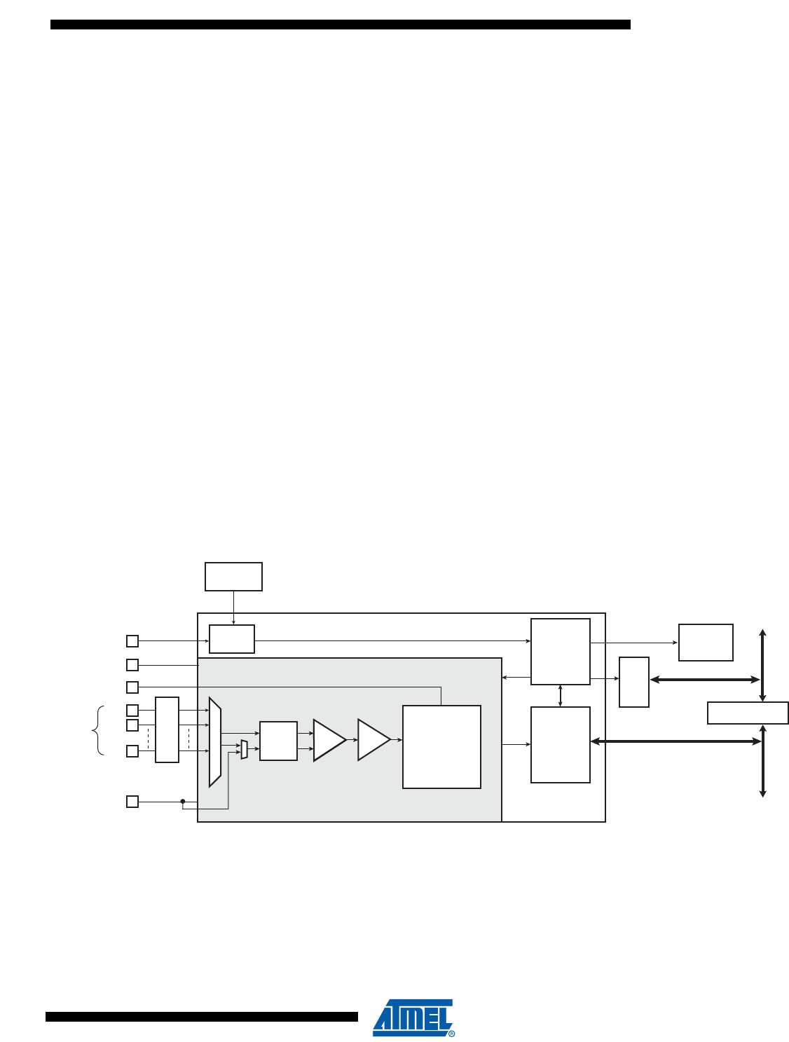
1063
6430F–ATARM–21-Feb-12
SAM3U Series
41. 12-bit Analog-to-Digital Converter (ADC12B)
41.1 Description
The ADC12B is based on a Cyclic Pipeline 12-bit Analog-to-Digital Converter (ADC12B).
It also integrates an 8-to-1 analog multiplexer, making possible the analog-to-digital conversions
of 8 analog lines. The conversions extend from 0V to AD12BVREF.
The ADC12B supports a 10-bit or 12-bit resolution mode, and conversion results are reported in
a common register for all channels, as well as in a channel-dedicated register. Software trigger,
external trigger on rising edge of the AD12BTRG pin, internal triggers from Timer Counter out-
put(s) or PWM Event lines are configurable.
The ADC12B also integrates a Sleep Mode and a conversion sequencer and connects with a
PDC channel. These features reduce both power consumption and processor intervention.
This ADC12B has a selectable single-ended or fully differential input and benefits from a 2-bit
programmable gain. A whole set of reference voltage is generated internally from a single exter-
nal reference voltage node that may be equal to the analog supply voltage. An external
decoupling capacitance is required for noise filtering.
A digital error correction circuit based on the multi-bit redundant signed digit (RSD) algorithm is
employed in order to reduce INL and DNL errors.
Finally, the user can configure ADC12B timings, such as Startup Time and Sample & Hold Time.
41.2 Block Diagram
Figure 41-1. Analog-to-Digital Converter Block Diagram
AD12BTRG
AD12BVREF
GND
VDDANA
Trigger
Selection
Timer
Counter
Channels
AD12B0
AD12B1
AD12Bn
Analog
Inputs
ADC12B Interrupt
ADC12B
Control
Logic
User
Interface
NVIC
Peripheral Bridge
APB
PDC
AHB
IN+
IN- S/H
OFFSET PGA
PIO
Cyclic Pipeline
12-bit Analog-to-Digital
Converter
1064
6430F–ATARM–21-Feb-12
SAM3U Series
41.3 Signal Description
41.4 Product Dependencies
41.4.1 Power Management
The ADC12B Controller is not continuously clocked. The programmer must first enable the
ADC12B Controller clock in the Power Management Controller (PMC) before using the ADC12B
Controller. However, if the application does not require ADC12B operations, the ADC12B Con-
troller clock can be stopped when not needed and restarted when necessary.
Configuring the ADC12B Controller does not require the ADC12B Controller clock to be
enabled.
41.4.2 Interrupt Sources
The ADC12B interrupt line is connected on one of the sources of the Nested Vectored Interrupt
Controller (NVIC). Using the ADC12B interrupt requires the NVIC to be programmed first.
41.4.3 Analog Inputs
The analog input pins are multiplexed with PIO lines. The assignment of the ADC12B input is
automatically done as soon as the corresponding channel is enabled by writing the register
ADC12B_CHER. By default, after reset, the PIO line is configured as an input with its pull-up
enabled and the ADC12B input is connected to the GND.
41.4.4 I/O Lines
The AD12BTRG pin is shared with other peripheral functions through the PIO Controller. In this
case, the PIO Controller needs to be set accordingly to assign the AD12BTRG pin to the
ADC12B function.
41.4.5 Timer Triggers
Timer Counters may or may not be used as hardware triggers depending on user requirements.
Thus, some or all of the timer counters may be non-connected.
41.4.6 PWM Event Lines
PWM Event Lines may or may not be used as hardware triggers depending on user
requirements.
Table 41-1. ADC12B Pin Description
Pin Name Description
AD12B0 - AD12B7Analog input channels
AD12BTRG External trigger
Table 41-2. Peripheral IDs
Instance ID
ADC12B 26
Table 41-3. I/O Lines
Instance Signal I/O Line Peripheral
ADC12B AD12BTRG PA2 B

1065
6430F–ATARM–21-Feb-12
SAM3U Series
41.4.7 Conversion Performances
For performance and electrical characteristics of the ADC12B, see the DC Characteristics sec-
tion of the product datasheet.
41.5 Functional Description
41.5.1 Analog-to-digital Conversion
The ADC12B uses the ADC12B Clock to perform conversions. Converting a single analog value
to 12-bit digital data requires Sample and Hold Clock cycles as defined in the SHTIM field of the
“ADC12B Mode Register” on page 1074 and 10 ADC12B Clock cycles. The ADC12B Clock fre-
quency is selected in the PRESCAL field of the Mode Register (ADC12B_MR).
The ADC12B clock range is between MCK/2, if PRESCAL is 0, and MCK/128, if PRESCAL is
set to 63 (0x3F). PRESCAL must be programmed in order to provide an ADC12B clock fre-
quency according to the parameters given in the Electrical Characteristics section of the product
datasheet.
41.5.2 Conversion Reference
The conversion is performed on a full range between 0V and the reference voltage pin
AD12BVREF Analog inputs between these voltages convert to values based on a linear
conversion.
41.5.3 Conversion Resolution
The ADC12B supports 10-bit or 12-bit resolution. The 10-bit selection is performed by setting the
LOWRES bit in the ADC12B Mode Register (ADC12B_MR). By default, after a reset, the resolu-
tion is the highest and the DATA field in the data registers is fully used. By setting the LOWRES
bit, the ADC12B switches in the lowest resolution and the conversion results can be read in the
eight lowest significant bits of the data registers. The two highest bits of the DATA field in the
corresponding ADC12B_CDR register and of the LDATA field in the ADC12B_LCDR register
read 0.
Moreover, when a PDC channel is connected to the ADC12B, 12-bit or 10-bit resolution sets the
transfer request size to 16 bits.
41.5.4 Differential Inputs
The ADC12B can be used either as a single ended ADC12B (DIFF bit equal to 0) or as a fully
differential ADC12B (DIFF bit equal to 1) as shown in Figure 41-2. By default, after a reset, the
ADC12B is in single ended mode.
The same inputs are used in single ended or differential mode.
In single ended mode, inputs are managed by an 8:1 channels analog multiplexer. In the fully
differential mode, inputs are managed by a 4:1 channels analog multiplexer. See Table 41-4 and
Table 41-5.

1066
6430F–ATARM–21-Feb-12
SAM3U Series
41.5.5 Input Gain and Offset
The ADC12B has a built in Programmable Gain Amplifier (PGA) and Programmable Offset.
The Programmable Gain Amplifier can be set to gains of 1/2, 1, 2 and 4. The Programmable
Gain Amplifier can be used either for single ended applications or for fully differential
applications.
The gain is configurable through the GAIN bit as shown in Table 41-6.
To allow full range, analog offset of the ADC12B can be configured by the OFFSET bit. The Off-
set can only be changed in single ended mode. In fully differential mode the offset is always set
to Vrefin/2.
Table 41-4. Input Pins and Channel Number in Single Ended Mode
Input Pins Channel Number
AD12B0 CH0
AD12B1 CH1
AD12B2 CH2
AD12B3 CH3
AD12B4 CH4
AD12B5 CH5
AD12B6 CH6
AD12B7 CH7
Table 41-5. Input Pins and Channel Number In Differential Mode
Input Pins Channel Number
AD12B0-AD12B1 CH0
AD12B2-AD12B3 CH2
AD12B4-AD125B CH4
AD12B6-AD12B7 CH6
Table 41-6. Gain of the Sample and Hold Unit: GAIN Bits and DIFF Bit.
GAIN<0:1> GAIN (DIFF = 0) GAIN (DIFF = 1)
00 1 0.5
01 1 1
10 2 2
11 4 2
Table 41-7. Offset of the Sample and Hold Unit: OFFSET DIFF and Gain (G)
OFFSET Bit OFFSET (DIFF = 0) OFFSET (DIFF = 1)
0 Vrefin/2G Vrefin/2
1Vrefin/2
1067
6430F–ATARM–21-Feb-12
SAM3U Series
Figure 41-2. Analog Full Scale Ranges in Single Ended/Differential Applications Versus Gain and Offset
VIN+
gain=0.5
gain=1
gain=2
gain=4
single ended
se0fd1=0
fully differential
se0fd1=1
same as
gain=1
same as
gain=2
0
vrefin
(½)vrefin
vrefin
0
(¾)vrefin
(¼)vrefin
(½)vrefin
vrefin
0
(5/8)vrefin
(3/8)vrefin
(½)vrefin
offset=0offset=1
offset=0offset=1
(¼)vrefin
vrefin
0
(5/8)vrefin
(3/8)vrefin
(½)vrefin
(¼)vrefin
(¾)vrefin
(1/8)vrefin
(00)
(01)
(10)
(11)
VIN+
VIN+
VIN+
VIN+
VIN+
VIN+
VIN-
VIN+
VIN-
VIN+
VIN-
VIN+
VIN-
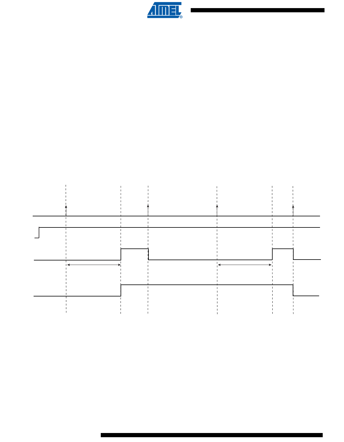
1068
6430F–ATARM–21-Feb-12
SAM3U Series
41.5.6 Power Consumption Adjustment
The power consumption of the ADC12B can be adjusted through a 2-bit bias control (IBCTL bit
in ADC12B_ACR register) providing possibilities for smart optimization of power and effective
resolution relative to the application speed request.
Please refer to the Electrical Characteristics of the product datasheet for further details.
41.5.7 Conversion Results
When a conversion is completed, the resulting 12-bit digital value is stored in the Channel Data
Register (ADC12B_CDR) of the current channel and in the ADC12B Last Converted Data Regis-
ter (ADC12B_LCDR).
The channel EOC bit in the Status Register (ADC12B_SR) is set and the DRDY bit is set. In the
case of a connected PDC channel, DRDY rising triggers a data transfer request. In any case,
either EOC and DRDY can trigger an interrupt.
Reading one of the ADC12B_CDR registers clears the corresponding EOC bit. Reading
ADC12B_LCDR clears the DRDY bit and the EOC bit corresponding to the last converted
channel.
Figure 41-3. EOCx and DRDY Flag Behavior
Conversion Time
Read the ADC_CDRx
EOCx
DRDY
Read the ADC_LCDR
CHx
(ADC_CHSR)
(ADC_SR)
(ADC_SR)
Write the ADC_CR
with START = 1
Conversion Time
Write the ADC_CR
with START = 1
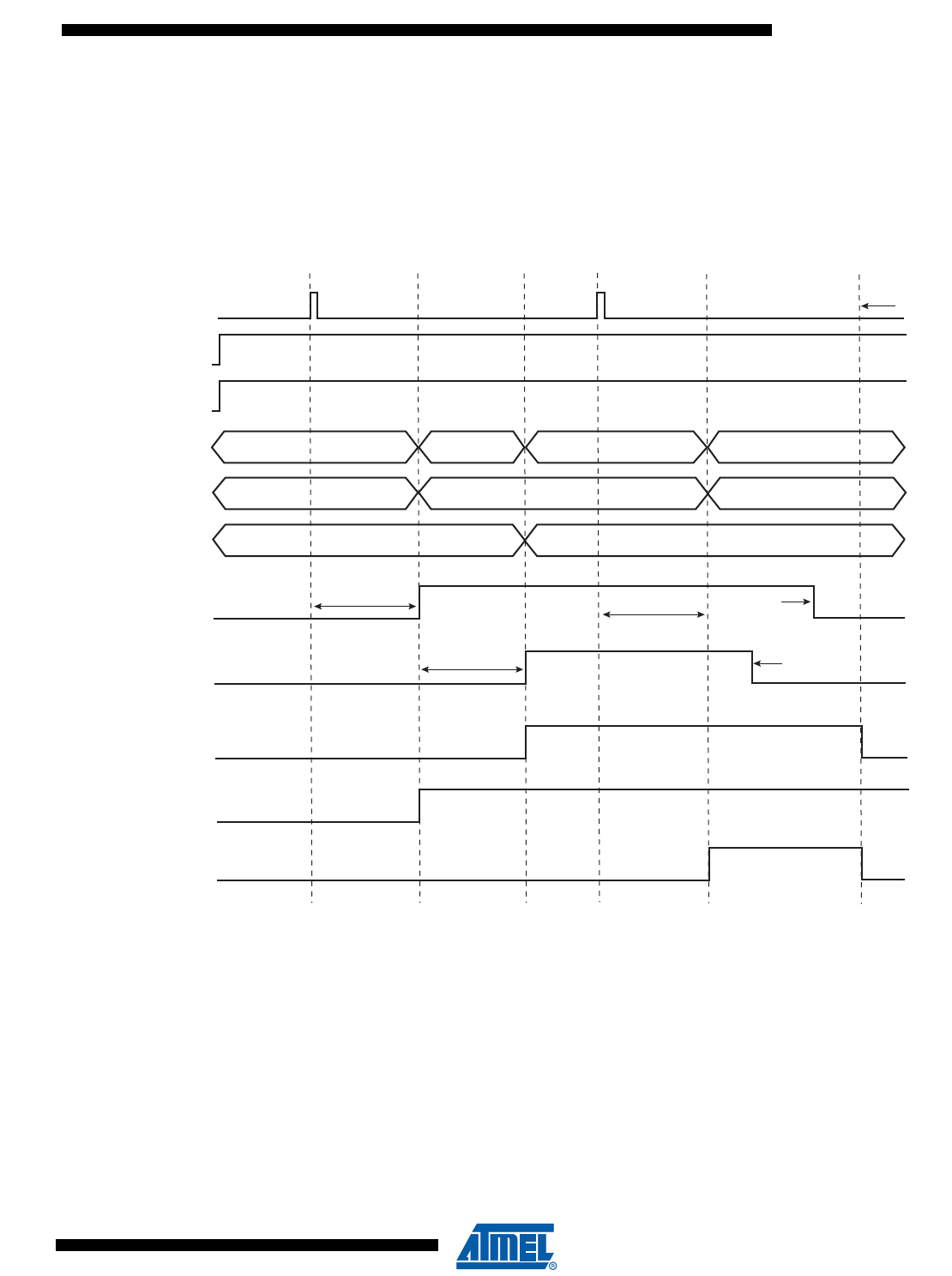
1069
6430F–ATARM–21-Feb-12
SAM3U Series
If the ADC12B_CDR is not read before further incoming data is converted, the corresponding
Overrun Error (OVRE) flag is set in the Status Register (ADC12B_SR).
Likewise, new data converted when DRDY is high sets the GOVRE bit (General Overrun Error)
in ADC12B_SR.
The OVRE and GOVRE flags are automatically cleared when ADC12B_SR is read.
Figure 41-4. GOVRE and OVREx Flag Behavior
Warning: If the corresponding channel is disabled during a conversion or if it is disabled and
then reenabled during a conversion, its associated data and its corresponding EOC and OVRE
flags in ADC12B_SR are unpredictable.
The ADC12B can be triggered externally by software or internally from the Timer Counter or
PWM.
EOC0
GOVRE
CH0
(ADC12B_CHSR)
(ADC12B_SR)
(ADC12B_SR)
Trigger
EOC1
CH1
(ADC12B_CHSR)
(ADC12B_SR)
OVRE0
(ADC12B_SR)
Undefined Data Data CH0 Data CH1
ADC12B_LCDR
Undefined Data Data CH0
ADC12B_CDR0
Undefined Data Data CH1
ADC12B_CDR1
Data CH0
Data CH0
Conversion
Conversion
Read ADC12B_SR
DRDY
(ADC12B_SR)
Read ADC12B_CDR1
Read ADC12B_CDR0
Conversion

1070
6430F–ATARM–21-Feb-12
SAM3U Series
41.5.8 Conversion Triggers
Conversions of the active analog channels are started with a software or a hardware trigger. The
software trigger is provided by writing the Control Register (ADC12B_CR) with the START bit at
1.
The hardware trigger can be one of the TIOA outputs of the Timer Counter channels, PWM
Event lines or the external trigger input of the ADC12B (AD12BTRG). The hardware trigger is
selected with the field TRGSEL in the Mode Register (ADC12B_MR). The selected hardware
trigger is enabled with the TRGEN bit in the Mode Register (ADC12B_MR).
If a hardware trigger is selected, the start of a conversion is triggered after a delay starting at
each rising edge of the selected signal. Due to asynchronous handling, the delay may vary in a
range of 2 MCK clock periods to 1 ADC12B clock period.
If one of the TIOA outputs is selected, the corresponding Timer Counter channel must be pro-
grammed in Waveform Mode.
Only one start command is necessary to initiate a conversion sequence on all the channels. The
ADC12B hardware logic automatically performs the conversions on the active channels, then
waits for a new request. The Channel Enable (ADC12B_CHER) and Channel Disable
(ADC12B_CHDR) Registers enable the analog channels to be enabled or disabled
independently.
If the ADC12B is used with a PDC, only the transfers of converted data from enabled channels
are performed and the resulting data buffers should be interpreted accordingly.
Warning: Enabling hardware triggers does not disable the software trigger functionality. Thus, if
a hardware trigger is selected, the start of a conversion can be initiated either by the hardware or
the software trigger.
41.5.9 Sleep Mode and Conversion Sequencer
The ADC12B Sleep Mode maximizes power saving by automatically deactivating the ADC12B
when it is not being used for conversions. Sleep Mode is selected by setting the SLEEP bit in the
Mode Register ADC12B_MR.
Two sleep Mode are selectable (OFFMODES): STANDBY Mode and OFF Mode. In Standby
Mode, the ADC12B is powered off except voltage reference to allow fast startup. In OFF Mode
the ADC12B is totally powered off.
The SLEEP mode is automatically managed by a conversion sequencer, which can automati-
cally process the conversions of all channels at lowest power consumption.
trigger
start
delay
Table 41-8. Low Power Modes According SLEEP Bit and OFFMODES Bit.
SLEEP Bit OFFMODES Bit Low Power Mode
0_Normal Mode
1 0 Standby Mode
1 1 Off Mode

1071
6430F–ATARM–21-Feb-12
SAM3U Series
When a start conversion request occurs, the ADC12B is automatically activated. As the analog
cell requires a start-up time, the logic waits during this time and starts the conversion on the
enabled channels. When all conversions are complete, the ADC12B is deactivated until the next
trigger. Triggers occurring during the sequence are not taken into account.
The conversion sequencer allows automatic processing with minimum processor intervention
and optimized power consumption. Conversion sequences can be performed periodically using
a Timer/Counter output or a PWM Event line. The periodic acquisition of several samples can be
processed automatically without any intervention of the processor thanks to the PDC.
The conversion sequencer can only be used if all ADC12B inputs have the same input configu-
ration, e.g. same PGA gain, same input type (differential or single ended) and same input offset.
If input have different configurations, sequencer can’t be used because PGA gain, input type
and input offset can’t be changed.
Note: The reference voltage pins always remain connected in normal mode as in sleep mode.
41.5.10 ADC12B Timings
Each ADC12B has its own minimal Startup Time that is programmed through the field
STARTUP in the Mode Register (ADC12B_MR).
In the same way, a minimal Sample and Hold Time is necessary for the ADC12B to guarantee
the best converted final value between the two channels selection. This time has to be pro-
grammed through the SHTIM bitfield in the Mode Register (ADC12B_MR).
Warning: No input buffer amplifier to isolate the source is included in the ADC12B. This must be
taken into consideration to program a precise value in the SHTIM field. See the section, ADC12B
Characteristics in the product datasheet.

1072
6430F–ATARM–21-Feb-12
SAM3U Series
41.6 12-bit Analog-to-Digital Converter (ADC12B) User Interface
Table 41-9. Register Mapping
Offset Register Name Access Reset
0x00 Control Register ADC12B_CR Write-only –
0x04 Mode Register ADC12B_MR Read-write 0x00000000
0x08 Reserved – – –
0x0C Reserved – – –
0x10 Channel Enable Register ADC12B_CHER Write-only –
0x14 Channel Disable Register ADC12B_CHDR Write-only –
0x18 Channel Status Register ADC12B_CHSR Read-only 0x00000000
0x1C Status Register ADC12B_SR Read-only 0x000C0000
0x20 Last Converted Data Register ADC12B_LCDR Read-only 0x00000000
0x24 Interrupt Enable Register ADC12B_IER Write-only –
0x28 Interrupt Disable Register ADC12B_IDR Write-only –
0x2C Interrupt Mask Register ADC12B_IMR Read-only 0x00000000
0x30 Channel Data Register 0 ADC12B_CDR0 Read-only 0x00000000
0x34 Channel Data Register 1 ADC12B_CDR1 Read-only 0x00000000
... ... ... ... ...
0x4C Channel Data Register 7 ADC12B_CDR7 Read-only 0x00000000
0x64 Analog Control Register ADC12B_ACR Read-write 0x00000000
0x68 Extended Mode Register ADC12B_EMR Read-write 0x00000000
0x50 - 0xFC Reserved – – –

1073
6430F–ATARM–21-Feb-12
SAM3U Series
41.6.1 ADC12B Control Register
Name: ADC12B_CR
Address: 0x400A8000
Access: Write-only
• SWRST: Software Reset
0 = No effect.
1 = Resets the ADC12B simulating a hardware reset.
• START: Start Conversion
0 = No effect.
1 = Begins analog-to-digital conversion.
31 30 29 28 27 26 25 24
––––––––
23 22 21 20 19 18 17 16
––––––––
15 14 13 12 11 10 9 8
––––––––
76543210
––––––STARTSWRST

1074
6430F–ATARM–21-Feb-12
SAM3U Series
41.6.2 ADC12B Mode Register
Name: ADC12B_MR
Address: 0x400A8004
Access: Read-write
• TRGEN: Trigger Enable
• TRGSEL: Trigger Selection
• LOWRES: Resolution
• SLEEP: Sleep Mode
31 30 29 28 27 26 25 24
–––– SHTIM
23 22 21 20 19 18 17 16
STARTUP
15 14 13 12 11 10 9 8
PRESCAL
76543210
– – SLEEP LOWRES TRGSEL TRGEN
TRGEN Selected TRGEN
0 Hardware triggers are disabled. Starting a conversion is only possible by software.
1 Hardware trigger selected by TRGSEL field is enabled.
TRGSEL Selected TRGSEL
0 0 0 External trigger
0 0 1 TIO Output of the Timer Counter Channel 0
0 1 0 TIO Output of the Timer Counter Channel 1
0 1 1 TIO Output of the Timer Counter Channel 2
1 0 0 PWM Event Line 0
1 0 1 PWM Event Line 1
110Reserved
111Reserved
LOWRES Selected Resolution
0 12-bit resolution
1 10-bit resolution
SLEEP Selected Mode
0 Normal Mode
1 Sleep Modes (see OFFMODES register)

1075
6430F–ATARM–21-Feb-12
SAM3U Series
• PRESCAL: Prescaler Rate Selection
ADC12BClock = MCK/( (PRESCAL+1) * 2 )
• STARTUP: Start Up Time
Startup Time = (STARTUP+1) * 8/ADC12BClock
• SHTIM: Sample & Hold Time
Sample and Hold Time = SHTIM/ADC12BClock

1076
6430F–ATARM–21-Feb-12
SAM3U Series
41.6.3 ADC12B Channel Enable Register
Name: ADC12B_CHER
Address: 0x400A8010
Access: Write-only
• CHx: Channel x Enable
0 = No effect.
1 = Enables the corresponding channel.
31 30 29 28 27 26 25 24
––––––––
23 22 21 20 19 18 17 16
––––––––
15 14 13 12 11 10 9 8
––––––––
76543210
CH7 CH6 CH5 CH4 CH3 CH2 CH1 CH0

1077
6430F–ATARM–21-Feb-12
SAM3U Series
41.6.4 ADC12B Channel Disable Register
Name: ADC12B_CHDR
Address: 0x400A8014
Access: Write-only
• x: Channel x Disable
0 = No effect.
1 = Disables the corresponding channel.
Warning: If the corresponding channel is disabled during a conversion or if it is disabled then reenabled during a conver-
sion, its associated data and its corresponding EOC and OVRE flags in ADC12B_SR are unpredictable.
31 30 29 28 27 26 25 24
––––––––
23 22 21 20 19 18 17 16
––––––––
15 14 13 12 11 10 9 8
––––––––
76543210
CH7 CH6 CH5 CH4 CH3 CH2 CH1 CH0

1078
6430F–ATARM–21-Feb-12
SAM3U Series
41.6.5 ADC12B Channel Status Register
Name: ADC12B_CHSR
Address: 0x400A8018
Access: Read-only
• CHx: Channel x Status
0 = Corresponding channel is disabled.
1 = Corresponding channel is enabled.
31 30 29 28 27 26 25 24
––––––––
23 22 21 20 19 18 17 16
––––––––
15 14 13 12 11 10 9 8
––––––––
76543210
CH7 CH6 CH5 CH4 CH3 CH2 CH1 CH0
1079
6430F–ATARM–21-Feb-12
SAM3U Series
41.6.6 ADC12B Analog Control Register
Name: ADC12B_ACR
Address: 0x400A8064
Access: Read-write
• GAIN: Input Gain
Gain of the sample and hold unit according to GAIN bits and DIFF bit
• IBCTL: Bias Current Control
Bias Current Control
• DIFF: Differential Mode
0 = Single Ended Mode
1 = Fully Differential Mode
• OFFSET: Input OFFSET
Offset of the sample and hold unit according to OFFSET bit, DIFF bit and Gain (G).
31 30 29 28 27 26 25 24
––––––––
23 22 21 20 19 18 17 16
––––––OFFSETDIFF
15 14 13 12 11 10 9 8
–––––– IBCTL
76543210
–––––– GAIN
GAIN<0:1> GAIN (DIFFx = 0) GAIN (DIFF = 1)
00 1 0.5
01 1 1
10 2 2
11 4 2
IBCTL<0:1> Current
00 typ - 20%
01 typ
10 typ + 20%
11 typ + 40%
OFFSET OFFSET (DIFF = 0) OFFSET (DIFF = 1)
0 Vrefin/2G Vrefin/2
1Vrefin/2
1080
6430F–ATARM–21-Feb-12
SAM3U Series
41.6.7 ADC12B Extended Mode Register
Name: ADC12B_EMR
Address: 0x400A8068
Access: Read-write
• OFFMODES: Off Mode if Sleep Bit (ADC12B_MR) = 1
0 = Standby Mode
1 = Off Mode
• OFF_MODE_STARTUP_TIME: Startup Time
Off Mode Startup Time = (OFF_MODE_STARTUP_TIME+1) * 8/ADC12BClock
31 30 29 28 27 26 25 24
––––––––
23 22 21 20 19 18 17 16
OFF_MODE_STARTUP_TIME
15 14 13 12 11 10 9 8
––––––––
76543210
–––––––OFFMODES

1081
6430F–ATARM–21-Feb-12
SAM3U Series
41.6.8 ADC12B Status Register
Name: ADC12B_SR
Address: 0x400A801C
Access: Read-only
• EOCx: End of Conversion x
0 = Corresponding analog channel is disabled, or the conversion is not finished.
1 = Corresponding analog channel is enabled and conversion is complete.
• OVREx: Overrun Error x
0 = No overrun error on the corresponding channel since the last read of ADC12B_SR.
1 = There has been an overrun error on the corresponding channel since the last read of ADC12B_SR.
• DRDY: Data Ready
0 = No data has been converted since the last read of ADC12B_LCDR.
1 = At least one data has been converted and is available in ADC12B_LCDR.
• GOVRE: General Overrun Error
0 = No General Overrun Error occurred since the last read of ADC12B_SR.
1 = At least one General Overrun Error has occurred since the last read of ADC12B_SR.
• ENDRX: End of RX Buffer
0 = The Receive Counter Register has not reached 0 since the last write in ADC12B_RCR or ADC12B_RNCR.
1 = The Receive Counter Register has reached 0 since the last write in ADC12B_RCR or ADC12B_RNCR.
• RXBUFF: RX Buffer Full
0 = ADC12B_RCR or ADC12B_RNCR have a value other than 0.
1 = Both ADC12B_RCR and ADC12B_RNCR have a value of 0.
31 30 29 28 27 26 25 24
––––––––
23 22 21 20 19 18 17 16
––––RXBUFFENDRXGOVREDRDY
15 14 13 12 11 10 9 8
OVRE7 OVRE6 OVRE5 OVRE4 OVRE3 OVRE2 OVRE1 OVRE0
76543210
EOC7 EOC6 EOC5 EOC4 EOC3 EOC2 EOC1 EOC0

1082
6430F–ATARM–21-Feb-12
SAM3U Series
41.6.9 ADC12B Last Converted Data Register
Name: ADC12B_LCDR
Address: 0x400A8020
Access: Read-only
• LDATA: Last Data Converted
The analog-to-digital conversion data is placed into this register at the end of a conversion and remains until a new conver-
sion is completed.
31 30 29 28 27 26 25 24
––––––––
23 22 21 20 19 18 17 16
––––––––
15 14 13 12 11 10 9 8
–––– LDATA
76543210
LDATA

1083
6430F–ATARM–21-Feb-12
SAM3U Series
41.6.10 ADC12B Interrupt Enable Register
Name: ADC12B_IER
Address: 0x400A8024
Access: Write-only
• EOCx: End of Conversion Interrupt Enable x
• OVREx: Overrun Error Interrupt Enable x
• DRDY: Data Ready Interrupt Enable
• GOVRE: General Overrun Error Interrupt Enable
• ENDRX: End of Receive Buffer Interrupt Enable
• RXBUFF: Receive Buffer Full Interrupt Enable
0 = No effect.
1 = Enables the corresponding interrupt.
31 30 29 28 27 26 25 24
––––––––
23 22 21 20 19 18 17 16
––––RXBUFFENDRXGOVREDRDY
15 14 13 12 11 10 9 8
OVRE7 OVRE6 OVRE5 OVRE4 OVRE3 OVRE2 OVRE1 OVRE0
76543210
EOC7 EOC6 EOC5 EOC4 EOC3 EOC2 EOC1 EOC0

1084
6430F–ATARM–21-Feb-12
SAM3U Series
41.6.11 ADC12B Interrupt Disable Register
Name: ADC12B_IDR
Address: 0x400A8028
Access: Write-only
• EOCx: End of Conversion Interrupt Disable x
• OVREx: Overrun Error Interrupt Disable x
• DRDY: Data Ready Interrupt Disable
• GOVRE: General Overrun Error Interrupt Disable
• ENDRX: End of Receive Buffer Interrupt Disable
• RXBUFF: Receive Buffer Full Interrupt Disable
0 = No effect.
1 = Disables the corresponding interrupt.
31 30 29 28 27 26 25 24
––––––––
23 22 21 20 19 18 17 16
––––RXBUFFENDRXGOVREDRDY
15 14 13 12 11 10 9 8
OVRE7 OVRE6 OVRE5 OVRE4 OVRE3 OVRE2 OVRE1 OVRE0
76543210
EOC7 EOC6 EOC5 EOC4 EOC3 EOC2 EOC1 EOC0

1085
6430F–ATARM–21-Feb-12
SAM3U Series
41.6.12 ADC12B Interrupt Mask Register
Name: ADC12B_IMR
Address: 0x400A802C
Access: Read-only
• EOCx: End of Conversion Interrupt Mask x
• OVREx: Overrun Error Interrupt Mask x
• DRDY: Data Ready Interrupt Mask
• GOVRE: General Overrun Error Interrupt Mask
• ENDRX: End of Receive Buffer Interrupt Mask
• RXBUFF: Receive Buffer Full Interrupt Mask
0 = The corresponding interrupt is disabled.
1 = The corresponding interrupt is enabled.
31 30 29 28 27 26 25 24
––––––––
23 22 21 20 19 18 17 16
––––RXBUFFENDRXGOVREDRDY
15 14 13 12 11 10 9 8
OVRE7 OVRE6 OVRE5 OVRE4 OVRE3 OVRE2 OVRE1 OVRE0
76543210
EOC7 EOC6 EOC5 EOC4 EOC3 EOC2 EOC1 EOC0

1086
6430F–ATARM–21-Feb-12
SAM3U Series
41.6.13 ADC12B Channel Data Register
Name: ADC12B_CDRx
Address: 0x400A8030
Access: Read-only
• DATA: Converted Data
The analog-to-digital conversion data is placed into this register at the end of a conversion and remains until a new conver-
sion is completed. The Convert Data Register (CDR) is only loaded if the corresponding analog channel is enabled.
31 30 29 28 27 26 25 24
––––––––
23 22 21 20 19 18 17 16
––––––––
15 14 13 12 11 10 9 8
–––– DATA
76543210
DATA
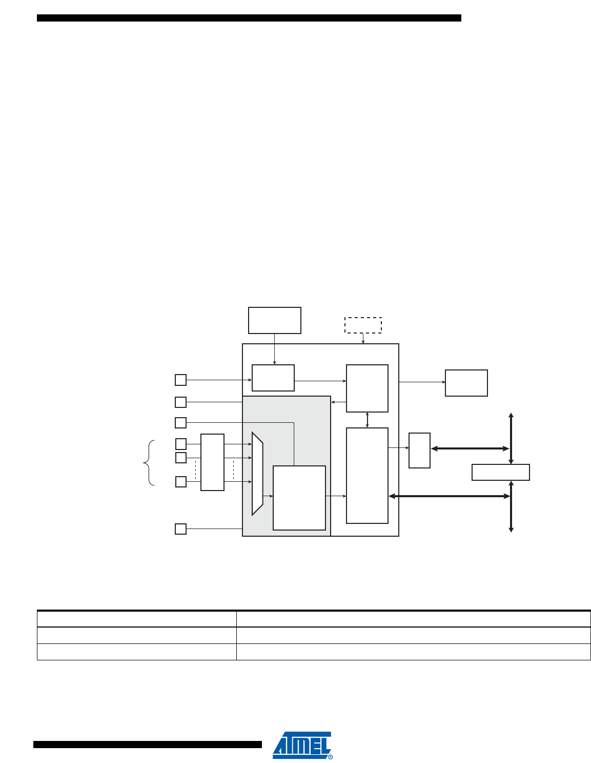
1087
6430F–ATARM–21-Feb-12
SAM3U Series
42. Analog-to-Digital Converter (ADC)
42.1 Description
The ADC is based on a Successive Approximation Register (SAR) 10-bit Analog-to-Digital Con-
verter (ADC). It also integrates an 8-to-1 analog multiplexer, making possible the analog-to-
digital conversions of 8 analog lines. The conversions extend from 0V to ADVREF. The ADC
supports an 8-bit or 10-bit resolution mode, and conversion results are reported in a common
register for all channels, as well as in a channel-dedicated register. Software trigger, external
trigger on rising edge of the ADTRG pin or internal triggers from Timer Counter output(s) or
PWM Event lines are configurable.
The ADC also integrates a Sleep Mode and a conversion sequencer and connects with a PDC
channel. These features reduce both power consumption and processor intervention.
Finally, the user can configure ADC timings, such as Startup Time and Sample & Hold Time.
42.2 Block Diagram
Figure 42-1. Analog-to-Digital Converter Block Diagram
42.3 Signal Description
ADC Interrupt
ADC Controller
ADTRG
ADVREF
GND
VDDANA
Trigger
Selection Control
Logic
Successive
Approximation
Register
Analog-to-Digital
Converter
Timer
Counter
Channels
User
Interface
PMC
NVIC
Peripheral Bridge
APB
PDC
System Bus
AD0
AD1
ADn
ADC cell
MCK
PIO
Analog Inputs
Multiplexed
with I/O lines
Table 42-1. ADC Pin Description
Pin Name Description
AD0 - AD7Analog input channels
ADTRG External trigger

1088
6430F–ATARM–21-Feb-12
SAM3U Series
42.4 Product Dependencies
42.4.1 Power Management
The MCK of the ADC Controller is not continuously clocked. The programmer must first enable
the ADC Controller MCK in the Power Management Controller (PMC) before using the ADC
Controller. However, if the application does not require ADC operations, the ADC Controller
clock can be stopped when not needed and restarted when necessary. Configuring the ADC
Controller does not require the ADC Controller clock to be enabled.
42.4.2 Interrupt Sources
The ADC interrupt line is connected on one of the internal sources of the Advanced Interrupt
Controller. Using the ADC interrupt requires the NVIC to be programmed first.
42.4.3 Analog Inputs
The analog input pins can be multiplexed with PIO lines. In this case, the assignment of the ADC
input is automatically done as soon as the corresponding channel is enabled by writing the reg-
ister ADC_CHER. By default, after reset, the PIO line is configured as input with its pull-up
enabled and the ADC input is connected to the GND.
42.4.4 I/O Lines
The pin ADTRG may be shared with other peripheral functions through the PIO Controller. In
this case, the PIO Controller should be set accordingly to assign the pin ADTRG to the ADC
function.
42.4.5 Timer Triggers
Timer Counters may or may not be used as hardware triggers depending on user requirements.
Thus, some or all of the timer counters may be non-connected.
42.4.6 PWM Event Lines
PWM Event Lines may or may not be used as hardware triggers depending on user
requirements.
42.4.7 Conversion Performances
For performance and electrical characteristics of the ADC, see the DC Characteristics section.
Table 42-2. Peripheral IDs
Instance ID
ADC 27

1089
6430F–ATARM–21-Feb-12
SAM3U Series
42.5 Functional Description
42.5.1 Analog-to-digital Conversion
The ADC uses the ADC Clock to perform conversions. Converting a single analog value to a 10-
bit digital data requires Sample and Hold Clock cycles as defined in the field SHTIM of the “ADC
Mode Register” on page 1096 and 10 ADC Clock cycles. The ADC Clock frequency is selected
in the PRESCAL field of the Mode Register (ADC_MR).
The ADC clock range is between MCK/2, if PRESCAL is 0, and MCK/128, if PRESCAL is set to
63 (0x3F). PRESCAL must be programmed in order to provide an ADC clock frequency accord-
ing to the parameters given in the Product definition section.
42.5.2 Conversion Reference
The conversion is performed on a full range between 0V and the reference voltage pin ADVREF
Analog inputs between these voltages convert to values based on a linear conversion.
42.5.3 Conversion Resolution
The ADC supports 8-bit or 10-bit resolutions. The 8-bit selection is performed by setting the bit
LOWRES in the ADC Mode Register (ADC_MR). By default, after a reset, the resolution is the
highest and the DATA field in the data registers is fully used. By setting the bit LOWRES, the
ADC switches in the lowest resolution and the conversion results can be read in the eight lowest
significant bits of the data registers. The two highest bits of the DATA field in the corresponding
ADC_CDR register and of the LDATA field in the ADC_LCDR register read 0.
Moreover, when a PDC channel is connected to the ADC, 10-bit resolution sets the transfer
request sizes to 16-bit. Setting the bit LOWRES automatically switches to 8-bit data transfers. In
this case, the destination buffers are optimized.
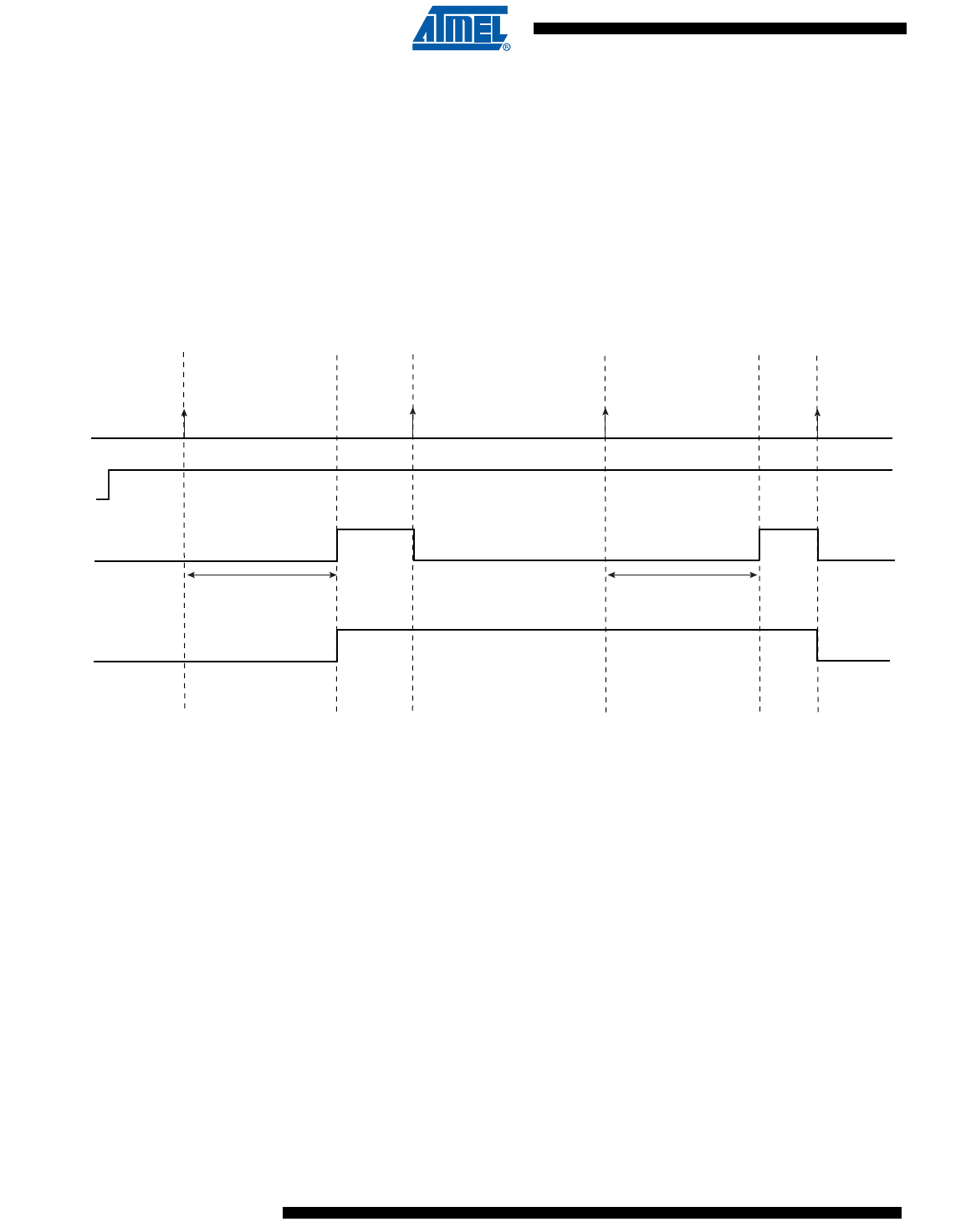
1090
6430F–ATARM–21-Feb-12
SAM3U Series
42.5.4 Conversion Results
When a conversion is completed, the resulting 10-bit digital value is stored in the Channel Data
Register (ADC_CDR) of the current channel and in the ADC Last Converted Data Register
(ADC_LCDR).
The channel EOC bit in the Status Register (ADC_SR) is set and the DRDY is set. In the case of
a connected PDC channel, DRDY rising triggers a data transfer request. In any case, either
EOC and DRDY can trigger an interrupt.
Reading one of the ADC_CDR registers clears the corresponding EOC bit. Reading ADC_LCDR
clears the DRDY bit and the EOC bit corresponding to the last converted channel.
Figure 42-2. EOCx and DRDY Flag Behavior
Conversion Time
Read the ADC_CDRx
EOCx
DRDY
Read the ADC_LCDR
CHx
(ADC_CHSR)
(ADC_SR)
(ADC_SR)
Write the ADC_CR
with START = 1
Conversion Time
Write the ADC_CR
with START = 1
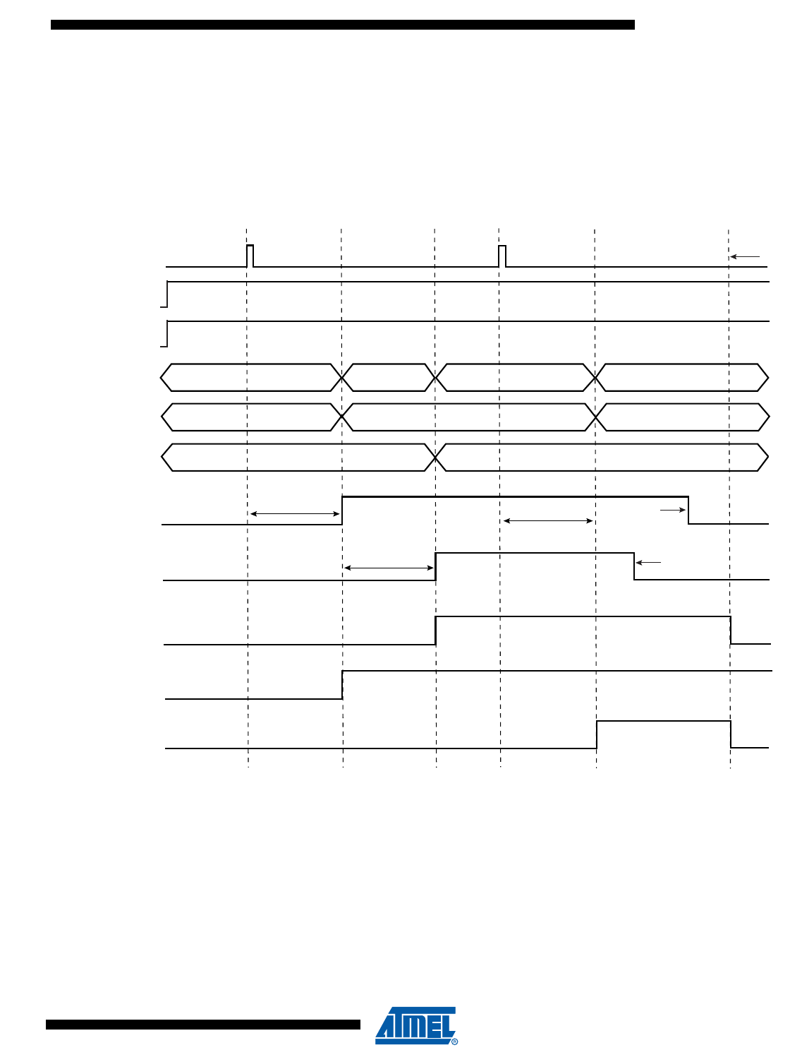
1091
6430F–ATARM–21-Feb-12
SAM3U Series
If the ADC_CDR is not read before further incoming data is converted, the corresponding Over-
run Error (OVRE) flag is set in the Status Register (ADC_SR).
In the same way, new data converted when DRDY is high sets the bit GOVRE (General Overrun
Error) in ADC_SR.
The OVRE and GOVRE flags are automatically cleared when ADC_SR is read.
Figure 42-3. GOVRE and OVREx Flag Behavior
Warning: If the corresponding channel is disabled during a conversion or if it is disabled and
then reenabled during a conversion, its associated data and its corresponding EOC and OVRE
flags in ADC_SR are unpredictable.
EOC0
GOVRE
CH0
(ADC_CHSR)
(ADC_SR)
(ADC_SR)
ADTRG
EOC1
CH1
(ADC_CHSR)
(ADC_SR)
OVRE0
(ADC_SR)
Undefined Data Data A Data B
ADC_LCDR
Undefined Data Data A
ADC_CDR0
Undefined Data Data B
ADC_CDR1
Data C
Data C
Conversion
Conversion
Read ADC_SR
DRDY
(ADC_SR)
Read ADC_CDR1
Read ADC_CDR0
Conversion

1092
6430F–ATARM–21-Feb-12
SAM3U Series
42.5.5 Conversion Triggers
Conversions of the active analog channels are started with a software or a hardware trigger. The
software trigger is provided by writing the Control Register (ADC_CR) with the bit START at 1.
The hardware trigger can be one of the TIOA outputs of the Timer Counter channels, PWM
Event lines or the external trigger input of the ADC (ADTRG). The hardware trigger is selected
with the field TRGSEL in the Mode Register (ADC_MR). The selected hardware trigger is
enabled with the bit TRGEN in the Mode Register (ADC_MR).
If a hardware trigger is selected, the start of a conversion is triggered after a delay starting at
each rising edge of the selected signal.Due to asynchronism handling, the delay may vary in a
range of 2 MCK clock periods to 1 ADC clock period.
If one of the TIOA outputs is selected, the corresponding Timer Counter channel must be pro-
grammed in Waveform Mode.
Only one start command is necessary to initiate a conversion sequence on all the channels. The
ADC hardware logic automatically performs the conversions on the active channels, then waits
for a new request. The Channel Enable (ADC_CHER) and Channel Disable (ADC_CHDR) Reg-
isters enable the analog channels to be enabled or disabled independently.
If the ADC is used with a PDC, only the transfers of converted data from enabled channels are
performed and the resulting data buffers should be interpreted accordingly.
Warning: Enabling hardware triggers does not disable the software trigger functionality. Thus, if
a hardware trigger is selected, the start of a conversion can be initiated either by the hardware or
the software trigger.
42.5.6 Sleep Mode and Conversion Sequencer
The ADC Sleep Mode maximizes power saving by automatically deactivating the ADC when it is
not being used for conversions. Sleep Mode is selected by setting the bit SLEEP in the Mode
Register ADC_MR.
The SLEEP mode is automatically managed by a conversion sequencer, which can automati-
cally process the conversions of all channels at lowest power consumption.
When a start conversion request occurs, the ADC is automatically activated. As the analog cell
requires a start-up time, the logic waits during this time and starts the conversion on the enabled
channels. When all conversions are complete, the ADC is deactivated until the next trigger. Trig-
gers occurring during the sequence are not taken into account.
The conversion sequencer allows automatic processing with minimum processor intervention
and optimized power consumption. Conversion sequences can be performed periodically using
a Timer/Counter output or a PWM Event line. The periodic acquisition of several samples can be
processed automatically without any intervention of the processor thanks to the PDC.
Note: The reference voltage pins always remain connected in normal mode as in sleep mode.
42.5.7 ADC Timings
Each ADC has its own minimal Startup Time that is programmed through the field STARTUP in
the Mode Register ADC_MR.
trigger
start
delay

1093
6430F–ATARM–21-Feb-12
SAM3U Series
In the same way, a minimal Sample and Hold Time is necessary for the ADC to guarantee the
best converted final value between two channels selection. This time has to be programmed
through the bitfield SHTIM in the Mode Register ADC_MR.
Warning: No input buffer amplifier to isolate the source is included in the ADC. This must be
taken into consideration to program a precise value in the SHTIM field. See the section, ADC
Characteristics in the product datasheet.

1094
6430F–ATARM–21-Feb-12
SAM3U Series
42.6 Analog-to-Digital Converter (ADC) User Interface
Table 42-3. Register Mapping
Offset Register Name Access Reset
0x00 Control Register ADC_CR Write-only –
0x04 Mode Register ADC_MR Read-write 0x00000000
0x08 Reserved – – –
0x0C Reserved – – –
0x10 Channel Enable Register ADC_CHER Write-only –
0x14 Channel Disable Register ADC_CHDR Write-only –
0x18 Channel Status Register ADC_CHSR Read-only 0x00000000
0x1C Status Register ADC_SR Read-only 0x000C0000
0x20 Last Converted Data Register ADC_LCDR Read-only 0x00000000
0x24 Interrupt Enable Register ADC_IER Write-only –
0x28 Interrupt Disable Register ADC_IDR Write-only –
0x2C Interrupt Mask Register ADC_IMR Read-only 0x00000000
0x30 Channel Data Register 0 ADC_CDR0 Read-only 0x00000000
0x34 Channel Data Register 1 ADC_CDR1 Read-only 0x00000000
... ... ... ... ...
0x4C Channel Data Register 7 ADC_CDR7 Read-only 0x00000000
0x50 - 0xFC Reserved – – –

1095
6430F–ATARM–21-Feb-12
SAM3U Series
42.6.1 ADC Control Register
Name: ADC_CR
Address: 0x400AC000
Access: Write-only
• SWRST: Software Reset
0 = No effect.
1 = Resets the ADC simulating a hardware reset.
• START: Start Conversion
0 = No effect.
1 = Begins analog-to-digital conversion.
31 30 29 28 27 26 25 24
––––––––
23 22 21 20 19 18 17 16
––––––––
15 14 13 12 11 10 9 8
––––––––
76543210
––––––STARTSWRST
1096
6430F–ATARM–21-Feb-12
SAM3U Series
42.6.2 ADC Mode Register
Name: ADC_MR
Address: 0x400AC004
Access: Read-write
• TRGEN: Trigger Enable
• TRGSEL: Trigger Selection
• LOWRES: Resolution
• SLEEP: Sleep Mode
31 30 29 28 27 26 25 24
–––– SHTIM
23 22 21 20 19 18 17 16
–STARTUP
15 14 13 12 11 10 9 8
PRESCAL
76543210
– – SLEEP LOWRES TRGSEL TRGEN
TRGEN Selected TRGEN
0 Hardware triggers are disabled. Starting a conversion is only possible by software.
1 Hardware trigger selected by TRGSEL field is enabled.
TRGSEL Selected TRGSEL
0 0 0 TIO Output of the Timer Counter Channel 0
0 0 1 TIO Output of the Timer Counter Channel 1
0 1 0 TIO Output of the Timer Counter Channel 2
0 1 1 PWM Event Line 0
1 0 0 PWM Event Line 1
101Reserved
1 1 0 External trigger
111Reserved
LOWRES Selected Resolution
0 10-bit resolution
1 8-bit resolution
SLEEP Selected Mode
0 Normal Mode
1 Sleep Mode

1097
6430F–ATARM–21-Feb-12
SAM3U Series
• PRESCAL: Prescaler Rate Selection
ADCClock = MCK / ( (PRESCAL+1) * 2 )
• STARTUP: Start Up Time
Startup Time = (STARTUP+1) * 8 / ADCClock
• SHTIM: Sample & Hold Time
Sample & Hold Time = SHTIM/ADCClock

1098
6430F–ATARM–21-Feb-12
SAM3U Series
42.6.3 ADC Channel Enable Register
Name: ADC_CHER
Address: 0x400AC010
Access: Write-only
• CHx: Channel x Enable
0 = No effect.
1 = Enables the corresponding channel.
31 30 29 28 27 26 25 24
––––––––
23 22 21 20 19 18 17 16
––––––––
15 14 13 12 11 10 9 8
––––––––
76543210
CH7 CH6 CH5 CH4 CH3 CH2 CH1 CH0

1099
6430F–ATARM–21-Feb-12
SAM3U Series
42.6.4 ADC Channel Disable Register
Name: ADC_CHDR
Address: 0x400AC014
Access: Write-only
• CHx: Channel x Disable
0 = No effect.
1 = Disables the corresponding channel.
Warning: If the corresponding channel is disabled during a conversion or if it is disabled then reenabled during a conver-
sion, its associated data and its corresponding EOC and OVRE flags in ADC_SR are unpredictable.
31 30 29 28 27 26 25 24
––––––––
23 22 21 20 19 18 17 16
––––––––
15 14 13 12 11 10 9 8
––––––––
76543210
CH7 CH6 CH5 CH4 CH3 CH2 CH1 CH0

1100
6430F–ATARM–21-Feb-12
SAM3U Series
42.6.5 ADC Channel Status Register
Name: ADC_CHSR
Address: 0x400AC018
Access: Read-only
• CHx: Channel x Status
0 = Corresponding channel is disabled.
1 = Corresponding channel is enabled.
31 30 29 28 27 26 25 24
––––––––
23 22 21 20 19 18 17 16
––––––––
15 14 13 12 11 10 9 8
––––––––
76543210
CH7 CH6 CH5 CH4 CH3 CH2 CH1 CH0

1101
6430F–ATARM–21-Feb-12
SAM3U Series
42.6.6 ADC Status Register
Name: ADC_SR
Address: 0x400AC01C
Access: Read-only
• EOCx: End of Conversion x
0 = Corresponding analog channel is disabled, or the conversion is not finished.
1 = Corresponding analog channel is enabled and conversion is complete.
• OVREx: Overrun Error x
0 = No overrun error on the corresponding channel since the last read of ADC_SR.
1 = There has been an overrun error on the corresponding channel since the last read of ADC_SR.
• DRDY: Data Ready
0 = No data has been converted since the last read of ADC_LCDR.
1 = At least one data has been converted and is available in ADC_LCDR.
• GOVRE: General Overrun Error
0 = No General Overrun Error occurred since the last read of ADC_SR.
1 = At least one General Overrun Error has occurred since the last read of ADC_SR.
• ENDRX: End of RX Buffer
0 = The Receive Counter Register has not reached 0 since the last write in ADC_RCR or ADC_RNCR.
1 = The Receive Counter Register has reached 0 since the last write in ADC_RCR or ADC_RNCR.
• RXBUFF: RX Buffer Full
0 = ADC_RCR or ADC_RNCR have a value other than 0.
1 = Both ADC_RCR and ADC_RNCR have a value of 0.
31 30 29 28 27 26 25 24
––––––––
23 22 21 20 19 18 17 16
––––RXBUFFENDRXGOVREDRDY
15 14 13 12 11 10 9 8
OVRE7 OVRE6 OVRE5 OVRE4 OVRE3 OVRE2 OVRE1 OVRE0
76543210
EOC7 EOC6 EOC5 EOC4 EOC3 EOC2 EOC1 EOC0

1102
6430F–ATARM–21-Feb-12
SAM3U Series
42.6.7 ADC Last Converted Data Register
Name: ADC_LCDR
Address: 0x400AC020
Access: Read-only
• LDATA: Last Data Converted
The analog-to-digital conversion data is placed into this register at the end of a conversion and remains until a new conver-
sion is completed.
31 30 29 28 27 26 25 24
––––––––
23 22 21 20 19 18 17 16
––––––––
15 14 13 12 11 10 9 8
–––––– LDATA
76543210
LDATA

1103
6430F–ATARM–21-Feb-12
SAM3U Series
42.6.8 ADC Interrupt Enable Register
Name: ADC_IER
Address: 0x400AC024
Access: Write-only
• EOCx: End of Conversion Interrupt Enable x
• OVREx: Overrun Error Interrupt Enable x
• DRDY: Data Ready Interrupt Enable
• GOVRE: General Overrun Error Interrupt Enable
• ENDRX: End of Receive Buffer Interrupt Enable
• RXBUFF: Receive Buffer Full Interrupt Enable
0 = No effect.
1 = Enables the corresponding interrupt.
31 30 29 28 27 26 25 24
––––––––
23 22 21 20 19 18 17 16
––––RXBUFFENDRXGOVREDRDY
15 14 13 12 11 10 9 8
OVRE7 OVRE6 OVRE5 OVRE4 OVRE3 OVRE2 OVRE1 OVRE0
76543210
EOC7 EOC6 EOC5 EOC4 EOC3 EOC2 EOC1 EOC0

1104
6430F–ATARM–21-Feb-12
SAM3U Series
42.6.9 ADC Interrupt Disable Register
Name: ADC_IDR
Address: 0x400AC028
Access: Write-only
• EOCx: End of Conversion Interrupt Disable x
• OVREx: Overrun Error Interrupt Disable x
• DRDY: Data Ready Interrupt Disable
• GOVRE: General Overrun Error Interrupt Disable
• ENDRX: End of Receive Buffer Interrupt Disable
• RXBUFF: Receive Buffer Full Interrupt Disable
0 = No effect.
1 = Disables the corresponding interrupt.
31 30 29 28 27 26 25 24
––––––––
23 22 21 20 19 18 17 16
––––RXBUFFENDRXGOVREDRDY
15 14 13 12 11 10 9 8
OVRE7 OVRE6 OVRE5 OVRE4 OVRE3 OVRE2 OVRE1 OVRE0
76543210
EOC7 EOC6 EOC5 EOC4 EOC3 EOC2 EOC1 EOC0

1105
6430F–ATARM–21-Feb-12
SAM3U Series
42.6.10 ADC Interrupt Mask Register
Name: ADC_IMR
Address: 0x400AC02C
Access: Read-only
• EOCx: End of Conversion Interrupt Mask x
• OVREx: Overrun Error Interrupt Mask x
• DRDY: Data Ready Interrupt Mask
• GOVRE: General Overrun Error Interrupt Mask
• ENDRX: End of Receive Buffer Interrupt Mask
• RXBUFF: Receive Buffer Full Interrupt Mask
0 = The corresponding interrupt is disabled.
1 = The corresponding interrupt is enabled.
31 30 29 28 27 26 25 24
––––––––
23 22 21 20 19 18 17 16
––––RXBUFFENDRXGOVREDRDY
15 14 13 12 11 10 9 8
OVRE7 OVRE6 OVRE5 OVRE4 OVRE3 OVRE2 OVRE1 OVRE0
76543210
EOC7 EOC6 EOC5 EOC4 EOC3 EOC2 EOC1 EOC0

1106
6430F–ATARM–21-Feb-12
SAM3U Series
42.6.11 ADC Channel Data Register
Name: ADC_CDRx
Address: 0x400AC030
Access: Read-only
• DATA: Converted Data
The analog-to-digital conversion data is placed into this register at the end of a conversion and remains until a new conver-
sion is completed. The Convert Data Register (CDR) is only loaded if the corresponding analog channel is enabled.
31 30 29 28 27 26 25 24
––––––––
23 22 21 20 19 18 17 16
––––––––
15 14 13 12 11 10 9 8
–––––– DATA
76543210
DATA

1107
6430F–ATARM–21-Feb-12
SAM3U Series
43. SAM3U4/2/1 Electrical Characteristics
43.1 Absolute Maximum Ratings
Table 43-1. Absolute Maximum Ratings*
Operating Temperature (Industrial) ................-40°C to + 85°C*NOTICE: Stresses beyond those listed under “Absolute Maximum
Ratings” may cause permanent damage to the device.
This is a stress rating only and functional operation of the
device at these or other conditions beyond those indi-
cated in the operational sections of this specification is
not implied. Exposure to absolute maximum rating
conditions for extended periods may affect device
reliability.
Storage Temperature.....................................-60°C to + 150°C
Voltage on Input Pins
with Respect to Ground...... ..............................-0.3V to + 4.0V
Maximum Operating Voltage
(VDDCORE) .....................................................................2.0V
Maximum Operating Voltage
(VDDIO) ..............................................................................4.0V
Total DC Output Current on all I/O lines
100-lead LQFP ..............................................................100 mA
144-lead LQFP ..............................................................130 mA
100-ball TFBGA .............................................................100 mA
144-ball LFBGA .............................................................130 mA

1108
6430F–ATARM–21-Feb-12
SAM3U Series
43.2 DC Characteristics
The following characteristics are applicable to the operating temperature range: TA = -40°C
to 85°C, unless otherwise specified.
Table 43-2. DC Characteristics
Symbol Parameter Conditions Min Typ Max Units
VDDCORE DC Supply Core 1.62 1.8 1.95 V
VVDDIO DC Supply I/Os 1.62 3.3 3.6 V
VVDDBU
Backup I/O Lines Power
Supply 1.62 3.6 V
VVDDUTMII
USB UTMI+ Interface
Power Supply 3.0 3.6 V
VVDDPLL
PLL A, UPLL and Main
Oscillator Supply 1.62 1.95 V
VVDDANA ADC Analog Power Supply (1) (1) V
VIL Input Low-level Voltage PIOA/B/C[0-31] -0.3 0.3 x
VVDDIO
V
VIH Input High-level Voltage PIOA/B/C[0-31] 0.7 x VVDDIO
VVDDIO
+0.3V V
VOH Output High-level Voltage
PIOA/B/C[0-31]
IOH ~ 0
IOH > 0 (See IOH details below)
VVDDIO -0.2V
VVDDIO -0.4V
V
VOL Output Low-level Voltage
PIOA/B/C[0-31]
IOH ~ 0
IOH > 0 (See IOL details below)
0.2
0.4
V
VHys Hysteresis Voltage
PIOA/B/C[0-31]
except PIOA[14], PB[9-16], PB[25-PB31]
and PC[20-27]
150 500 mV
ERASE, TST, FWUP, JTAGSEL 230 700 mV

1109
6430F–ATARM–21-Feb-12
SAM3U Series
Notes: 1. Refer to Section 43.7 “12-Bit ADC Characteristics” and Section 43.8 “AC Characteristics”
2. PA[0-2], PA[4-14], PA[16-31]; PB[0-31]; PC[0-31]
3. PA[0-31], PB[0-31], PC[0-31]
4. FWUP, JTAGSEL, NRSTB, ERASE, TST
IO
IOH (or ISOURCE)
1.62V < VDDIO < 1.95V; VOH = VVDDIO - 0.4
- PA3 (SPCK), PA15(MCCK) pins
- Other pins(2)
-8
-3
mA
3.0V < VDDIO < 3.6V; VOH = VVDDIO - 0.4
- PA3 (SPCK), PA15(MCCK) pins
- Other pins(2)
-15
-3
1.62V < VDDIO < 3.6V; VOH = VVDDIO - 0.4
- NRST, TDO -2
Relaxed Mode:
3.0V < VDDIO < 3.6V; VOH = 2.2V
- PA3 (SPCK), PA15(MCCK) pins
- Other pins(2)
-24
-9
IOL (or ISINK)
1.62V < VDDIO < 1.95V; VOL = 0.4V
- PA3 (SPCK), PA15(MCCK) pins
- Other pins(2)
8
4
mA
3.0V < VDDIO < 3.6V; VOL = 0.4V
- PA3 (SPCK), PA15(MCCK) pins
- Other pins(2)
9
6
1.62V < VDDIO < 3.6V; VOL = 0.4V
- NRST, TDO 2
Relaxed Mode:
3.0V < VDDIO < 3.6V; VOL = 0.6V
- PA3 (SPCK), PA15(MCCK) pins
- Other pins(2)
14
9
IIL
Input Low
Leakage Current
VVDDIO powered pins(3)
No pull-up or pull-down; VIN=GND; VDDIO Max.
(Typ: TA = 25°C, Max: TA = 85°C)
530nA
VDDBU powered pins(4)
No pull-up or pull-down; VIN=GND; VDDBU Max.
(Typ: TA = 25°C, Max: TA = 85°C)
1µA
IIH
Input High
Leakage Current
VVDDIO powered pins(3)
No pull-up or pull-down; VIN=VDD; VDDIO Max.
(Typ: TA = 25°C, Max: TA = 85°C)
218nA
VDDBU powered pins(4)
No pull-up or pull-down; VIN=VDD; VDDBU Max.
(Typ: TA = 25°C, Max: TA = 85°C)
1µA
RPULLUP Pull-up Resistor PA0-PA31, PB0-PB31, PC0-PC31 50 100 150 kΩ
NRSTB 10 20 kΩ
RPULLDOWN Pull-down Resistor TST, ERASE, JTAGSEL 10 20 kΩ
RODT
On-die Series Termination
Resistor PA0-PA31, PB0-PB31, PC0-PC31 36 Ω
CIN Input Capacitance Digital Inputs TBD pF
Table 43-2. DC Characteristics (Continued)
Symbol Parameter Conditions Min Typ Max Units

1110
6430F–ATARM–21-Feb-12
SAM3U Series
Notes: 1. A 10 µF or higher ceramic capacitor must be connected between VDDIN and the closest GND pin of the device.
This large decoupling capacitor is mandatory to reduce startup current, improving transient response and noise rejection.
2. To ensure stability, an external 4.7µF output capacitor, CDOUT must be connected between the VDDOUT and the closest
GND pin of the device. The ESR (Equivalent Series Resistance) of the capacitor must be in the range 0.5 to 10 Ohms.
Solid tantalum, and multilayer ceramic capacitors are all suitable as output capacitor.
A 100 nF bypass capacitor between VDDOUT and the closest GND pin of the device decreases output noise and improves
the load transient response.
3. Defined as the current needed to charge external bypass/decoupling capacitor network.
Table 43-3. 1.8V Voltage Regulator Characteristics
Symbol Parameter Conditions Min Typ Max Units
VVDDIN DC Input Voltage Range 1.8 3.3 3.6 V
VVDDOUT DC Output Voltage Normal Mode
Standby Mode
1.8
0V
VACCURACY Output Voltage Accuracy ILoad = 0.5mA to 150 mA -3 3 %
ILOAD
ILOAD-START
Maximum DC Output
Current
Maximum Peak Current
during startup(3)
VVDDIN > 2.2V
VVDDIN ≤ 2.2V
150
60 mA
See Note (3).300mA
DDROPOUT Dropout Voltage VVDDIN = 1.8V, ILoad = 60 mA 150 mV
VLINE
VLINE-TR
Line Regulation
Transient Line regulation
VVDDIN from 2.7V to 3.6V;
ILoad MAX
V
VDDIN
from 2.7V to 3.6V;
tr = tf = 5µs; I
Load
Max
CDOUT = 4.7µF
20
50
50
100
mV
VLOAD Load Regulation VVDDIN ≥ 2.2V;
ILoad = 10% to 90% MAX 20 50
mV
VLOAD-TR Transient Load Regulation VVDDIN ≥ 2.2V;
ILoad = 10% to 90% MAX
tr = tf = 5 µs
CDOUT = 4.7 µF
50 100
IQQuiescent Current
Normal Mode;
@ ILoad = 0 mA
@ ILoad = 150 mA
Standby Mode;
7
700
10
1200
1
µA
CDIN Input Decoupling Capacitor Cf. External Capacitor Requirements (1) 10 µF
CDOUT
Output Decoupling
Capacitor
Cf. External Capacitor Requirements (2)
ESR 0.5
4.7
10
µF
Ohm
TON Turn on Time
CDOUT= 4.7µF, VVDDOUT reaches VTH+
(core power brownout detector supply rising
threshold)
120 250 µs
TON Turn on Time CDOUT= 4.7µF, VVDDOUT reaches 1.8V (+/- 3%) 200 400 µs
1111
6430F–ATARM–21-Feb-12
SAM3U Series
Note: 1. The product is guaranteed to be functional at VTH-
Figure 43-1. Core Brownout Output Waveform
Table 43-4. Core Power Supply Brownout Detector Characteristics
Symbol Parameter Conditions Min Typ Max Units
VTH- Supply Falling Threshold(1) 1.52 1.55 1.58 V
VHYST- Hysteresis VTH- 25 38 mV
VTH+ Supply Rising Threshold 1.35 1.50 1.62 V
VHYST+ Hysteresis VTH+ 100 250 mV
IDDON
IDDOFF
Current Consumption on
VDDCORE
Brownout Detector enabled
Brownout Detector disabled
18
200
µA
nA
Td- VTH- detection propagation
time
VDDCORE = VTH+ to (VTH- - 100mV) 200 ns
Td+ VTH+ detection propagation
time 100 200 350 µs
TSTART Startup Time From disabled state to enabled state 100 200 µs
t
VDDCORE
Vth-
Vth+
BOD OUTPUT
t
td+td-
Table 43-5. VDDUTMI Supply Monitor
Symbol Parameter Conditions Min Typ Max Units
VTH Supply Monitor Threshold 16 selectable steps of 100mV 1.9 3.4 V
TACCURACY Threshold Level Accuracy -1.5 +1.5 %
VHYST Hysteresis 20 30 mV
IDDON
IDDOFF
Current Consumption on
VDDCORE
enabled
disabled
18 28
1
µA
TSTART Startup Time From disabled state to enabled state 140 µs
1112
6430F–ATARM–21-Feb-12
SAM3U Series
Figure 43-2. VDDUTMI Supply Monitor
Figure 43-3. Zero-Power-on Reset Characteristics
Vth
Vhyst
VDDUTMI
Reset
Vth+
Table 43-6. Backup Power Supply Zero-Power-on Reset Characteristics
Symbol Parameter Conditions Min Typ Max Units
Vth+ Threshold voltage rising At Startup 1.50 1.55 1.60 V
Vth- Threshold voltage falling 1.40 1.45 1.50 V
Tres Reset Time-out Period 40 90 150 µs
V
th-
V
th+
VDDBU
Reset

1113
6430F–ATARM–21-Feb-12
SAM3U Series
43.3 Power Consumption
• Power consumption of the device according to the different Low Power Mode Capabilities
(Backup, Wait, Sleep) and Active Mode.
• Power consumption on power supply in different modes: Backup, Wait, Sleep and Active.
• Power consumption by peripheral: calculated as the difference in current measurement after
having enabled then disabled the corresponding clock.
43.3.1 Backup Mode Current Consumption
The Backup Mode configuration and measurements are defined as follow.
43.3.1.1 Configuration A
• All Power supplies OFF, except VDDBU
• Supply Monitor on VDDUTMI is disabled
• RTT and RTC not used
• Embedded RC Oscillator used
• Wake-Up pin FWUP = VDDBU
• Current measurement on AMP1
Table 43-7. DC Flash Characteristics
Symbol Parameter Conditions Typ Max Units
ISB Standby current
@25°C onto VDDCORE = 1.8V
@85°C onto VDDCORE = 1.8V
@25°C onto VDDCORE = 1.95V
@85°C onto VDDCORE = 1.95V
<1
14
<1
15
1.5
40
1.8
50
µA
µA
µA
µA
ICC Active current
128-Bit Mode Read Access:
Maximum Read Frequency onto VDDCORE = 1.8V @ 25 °C
Maximum Read Frequency onto VDDCORE = 1.95V @ 25 °C
64-Bit Mode Read Access:
Maximum Read Frequency onto VDDCORE = 1.8V @ 25 °C
Maximum Read Frequency onto VDDCORE = 1.95V @ 25 °C
15
20
7.5
10
20
25
10
12.5
mA
mA
mA
mA
Write onto VDDCORE = 1.8V @ 25 °C
Write onto VDDCORE = 1.95V @ 25 °C
3.6
5.0
4.5
6.0
mA
mA
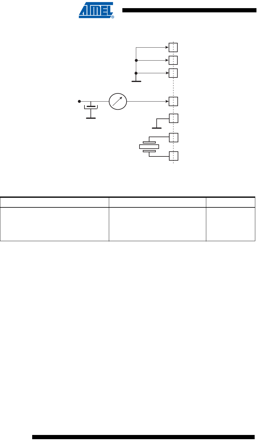
1114
6430F–ATARM–21-Feb-12
SAM3U Series
Figure 43-4. Measurement Setup
43.3.1.2 Configuration B
• All Power supplies OFF, except VDDBU and VDDIO
• Supply Monitor on VDDUTMI is disabled
• RTC ON, RTT ON
• 32 KHz Crystal Oscillator used
• FWUP pin = VDDBU
• Wake-up pins WKUP0 to 15 = VDDIO
• Current measurement on AMP1 and on AMP2
Table 43-8. Power Consumption for Backup Mode Configuration A
Conditions VDDBU Consumption (AMP1) Unit
VDDBU = 3.3V @25°C
VDDBU = 3.0V @25°C
VDDBU = 2.5V @25°C
VDDBU = 1.8V @25°C
3.0
2.7
2.2
1.6
µA
VDDBU
XOUT32
XIN32
VDDCORE,
VDDPLL
2.5, 3V, 3.3V
AMP1
VDDUTMI
VDDIO
VDDANA
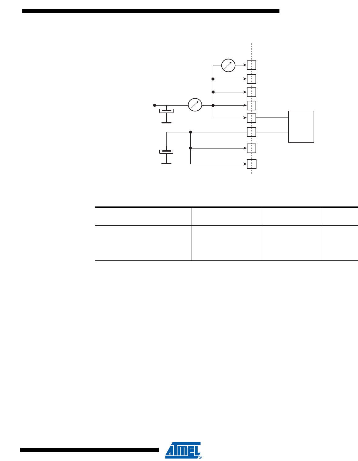
1115
6430F–ATARM–21-Feb-12
SAM3U Series
Figure 43-5. Measurement Setup
43.3.2 Wait and Sleep Mode Current Consumption
The Wait Mode and Sleep Mode configuration and measurements are defined below.
43.3.2.1 Sleep Mode
• All power supplies are powered
• Core Clock OFF
• Master Clock (MCK) running at various frequencies with PLLA or the fast RC oscillator.
• Fast start-up through WKUP0-15 pins
• Current measurement on AMP1 (VDDOUT=VDDCORE + VDDPLL)
• All peripheral clocks deactivated
Table 43-9. Power Consumption for Backup Mode Configuration B
Conditions
VDDBU Consumption
(AMP1)
Total Consumption
(AMP2) Unit
VDDBU = 3.3V @25°C
VDDBU = 3.0V @25°C
VDDBU = 2.5V @25°C
VDDBU = 1.8V @25°C
3.0
2.7
2.2
1.6
3.06
2.75
2.25
1.64
µA
VDDUTMI
VDDIO
VDDOUT
VDDCORE
VDDIN
Voltage
Regulator
VDDPLL
VDDANA
3.3V
AMP2
VDDBU
AMP1
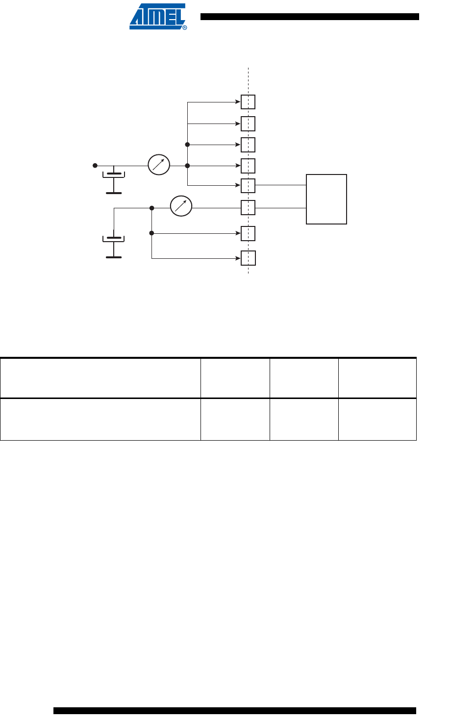
1116
6430F–ATARM–21-Feb-12
SAM3U Series
Figure 43-6. Measurement Setup for Sleep Mode
Table 43-10 gives current consumption in typical conditions.
Table 43-10. Typical Current Consumption for Sleep Mode
Conditions
VDDOUT
Consumption
(AMP1)
Total
Consumption
(AMP2) Unit
Figure 43-6 on page 1116 @25°C
MCK = 48 MHz
There is no activity on the I/Os of the device.
11.8 11.9 mA
VDDUTMI
VDDIO
VDDOUT
VDDCORE
VDDIN
Voltage
Regulator
VDDPLL
VDDANA
3.3V
AMP1
AMP2
VDDBU
1117
6430F–ATARM–21-Feb-12
SAM3U Series
Figure 43-7. Current Consumption in Sleep Mode (AMP1) versus Master Clock ranges (Condi-
tion from Table 43-10)
Table 43-11. Sleep mode Current consumption versus Master Clock (MCK) variation
Core Clock/MCK (MHz) AMP1 (VDDOUT) Consumption Unit
96 21.9 mA
84 20 mA
72 17.3 mA
60 14.5 mA
48 11.72 mA
36 9.6 mA
24 6.56 mA
18 4.8 mA
12 2.835 mA
81.937mA
41.013mA
20.567mA
10.343mA
0.5 0.23 mA
0.25 0.174 mA
0.125 0.146 mA
0
2
4
6
8
10
12
14
16
18
20
22
24
0 4 8 12 16 20 24 28 32 36 40 44 48 52 56 60 64 68 72 76 80 84 88 92 96
Processor and Peripheral Clocks in MHz
VDOUT (IDDCORE + IDDPLL) in mA
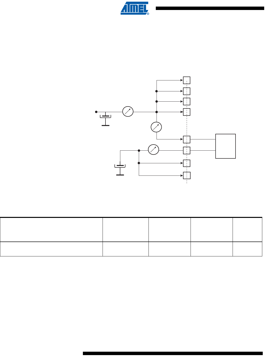
1118
6430F–ATARM–21-Feb-12
SAM3U Series
43.3.2.2 Wait Mode
• All power supplies are powered
• Core Clock and Master Clock Stopped
• Current measurement on AMP1, AMP2 and AMP3
• All Peripheral clocks deactivated
Figure 43-8. Measurement Setup for Wait Mode
Table 43-12 gives current consumption in typical conditions.
43.3.3 Active Mode Power Consumption
The Active Mode configuration and measurements are defined as follows:
•VDDIO
= 3.3V
• VDDCORE = 1.8V (Internal Voltage regulator used)
•T
A = 25°C
• Application Running from Flash Memory with 128-bit access Mode
• All Peripheral clocks are deactivated.
• Master Clock (MCK) running at various frequencies with PLLA or the fast RC oscillator.
• Current measurement on AMP1 (VDDOUT = VDDCORE + VDDPLL) and total current on
AMP2
VDDUTMI
VDDIO
VDDOUT
VDDCORE
VDDIN
Voltage
Regulator
VDDPLL
VDDANA
3.3V
AMP1
AMP2
VDDBU
AMP3
Table 43-12. Typical Current Consumption in Wait Mode
Conditions
VDDOUT
Consumption
(AMP1)
Total
Consumption
(AMP2)
Regulator and
Core
Consumption
(AMP3) Unit
See Figure 43-8 on page 1118 @25°C
There is no activity on the I/Os of the device. 15.4 27.3 23.4 µA
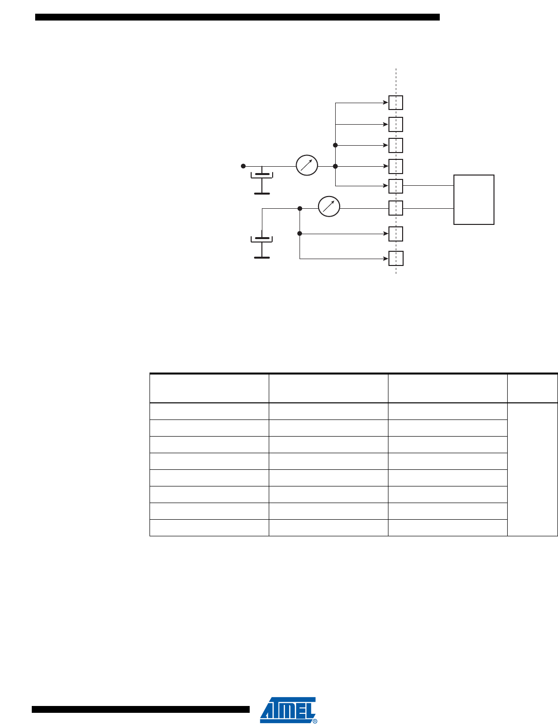
1119
6430F–ATARM–21-Feb-12
SAM3U Series
Figure 43-9. Active Mode Measurement Setup
Tables below give Active Mode Current Consumption in typical conditions.
• VDDCORE at 1.8V
• Temperature = 25°C
Table 43-13. Master Clock (MCK) variation with PLLA
Core Clock/MCK (MHz)
AMP1 (VDDOUT)
Consumption
AMP2 (total)
Consumption
Unit
96 48 48.3
mA
84 44 44.3
72 39.4 39.7
60 35.2 35.4
48 30.2 30.5
36 25.8 26.1
24 20.4 20.6
18 18.3 18.5
VDDUTMI
VDDIO
VDDOUT
VDDCORE
VDDIN
Voltage
Regulator
VDDPLL
VDDANA
3.3V
AMP1
AMP2
VDDBU

1120
6430F–ATARM–21-Feb-12
SAM3U Series
43.3.4 Peripheral Power Consumption in Active Mode
Note: 1. Note: VDDIO = 3.3V, VDDCORE = 1.80V, TA = 25°C
Table 43-14. Master Clock (MCK) Variation with Fast RC Oscillator
Core Clock/MCK (MHz)
AMP1 (VDDOUT)
Consumption
AMP2 (total)
Consumption
Unit
12 10 10.08
mA
8 7.5 7.54
455.03
2 2.68 2.70
1 1.4 1.42
0.5 0.77 0.78
0.25 0.44 0.45
0.125 0.28 0.29
0.032 0.046 0.061
Table 43-15. Power Consumption on VDDCORE(1)
Peripheral Consumption (Typ) Unit
PIO Controller 11
µA/MHz
USART 31.3
PWM 53.8
TWI 16
SPI 2.55
Timer Counter Channels 9.3
ADC12B 17.45
ADC 15.7
HSMCI 33
SMC 78.8
SSC 16.3
UDPHS 96

1121
6430F–ATARM–21-Feb-12
SAM3U Series
43.4 Crystal Oscillators Characteristics
43.4.1 32 kHz RC Oscillator Characteristics
43.4.2 4/8/12 MHz RC Oscillators Characteristics
Note: 1. Frequency range can be configured in the Supply Controller Registers.
2. Not trimmed from factory.
3. After Trimming from factory.
Table 43-16. 32 kHz RC Oscillator Characteristics
Symbol Parameter Conditions Min Typ Max Unit
RC Oscillator Frequency 20 32 44 kHz
Frequency Supply Dependency -3 3 %/V
Frequency Temperature Dependency Over temperature range (-40°C/
+85°C) versus 25°C -11 11 %
Duty Duty Cycle 45 50 55 %
TON Startup Time 100 µs
IDDON Current Consumption
After Startup Time
Temp. Range = -40°C to +85°C
Typical Consumption at 2.2V
Supply and Temp = 25°C
540 870 nA
Table 43-17. 4/8/12 MHz RC Oscillators Characteristics
Symbol Parameter Conditions Min Typ Max Unit
FRange RC Oscillator Frequency Range 4 12 MHz
FOUT Output Frequency(1)
1.62V<VDDPLL<1.95V,
-40°C<Temp<+85°C
4 MHz(2)
8 MHz(3)
12 MHz(3)
2.6
7.6
11.4
4
8
12
5.4
8.4
12.6
MHz
Frequency Temperature Dependency Over temperature range
(-40°C/ +85°C) versus 25°C TBD TBD %
Duty Duty Cycle 45 50 55 %
TON Startup Time 10 µs
IDDON Active Current Consumption
4 MHz
8 MHz
12 MHz
80
105
145
120
160
210
µA
IDDOFF Off Mode Current Consumption 0.2 µA
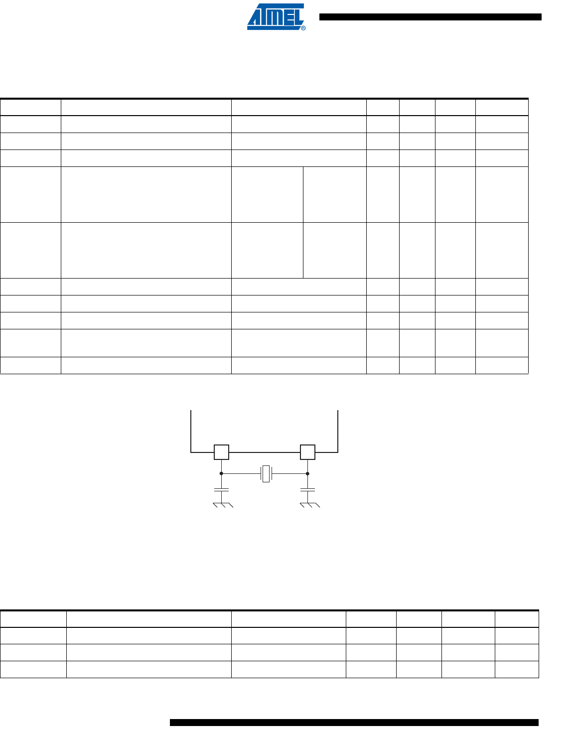
1122
6430F–ATARM–21-Feb-12
SAM3U Series
43.4.3 32.768 kHz Crystal Oscillator Characteristics
Notes: 1. RS is the series resistor.
CLEXT = 2x(CCRYSTAL – Cpara – CPCB).
Where CPCB is the capacitance of the printed circuit board (PCB) track layout from the crystal to the SAM3U pin.
43.4.4 32.768 kHz Crystal Characteristics
Table 43-18. 32.768 kHz Crystal Oscillator Characteristics
Symbol Parameter Conditions Min Typ Max Unit
Freq Operating Frequency Normal mode with crystal 32.768 KHz
Supply Ripple Voltage (on VDDBU) Rms value, 10 KHz to 10 MHz 30 mV
Duty Cycle 40 50 60 %
Startup Time
Rs < 50KΩ
Rs < 100KΩ
(1)
CL = 12.5pF
CL = 6pF
CL = 12.5pF
CL = 6pF
900
300
1200
500
ms
Current consumption
Rs < 50KΩ
Rs < 100KΩ
(1)
CL = 12.5pF
CL = 6pF
CL = 12.5pF
CL = 6pF
650
450
900
650
1400
1200
1600
1400
nA
IDDST Standby Current Consumption Standby mode @ 3.6V 5 nA
PON Drive level 0.1 µW
RfInternal resistor between XIN32 and XOUT32 10 MΩ
CLEXT
Maximum external capacitor
on XIN32 and XOUT32 22 pF
Cpara Internal Parasitic Capacitance 1.2 1.4 1.6 pF
XIN32XOUT32
C
LEXT
C
LEXT
SAM3U
Table 43-19. Crystal Characteristics
Symbol Parameter Conditions Min Typ Max Unit
ESR Equivalent Series Resistor Rs Crystal @ 32.768 KHz 50 100 KΩ
CMMotional capacitance Crystal @ 32.768 KHz 0.6 3 fF
CSHUNT Shunt capacitance Crystal @ 32.768 KHz 0.6 2 pF
1123
6430F–ATARM–21-Feb-12
SAM3U Series
43.4.5 32.768 kHz XIN32 Clock Input Characteristics in Bypass Mode
Note: 1. These characteristics apply only when the 32768 kHz XTAL Oscillator is in bypass mode (i.e., when OSCBYPASS: = 1 in
SUPC_MR and XTALSEL = 1 in the SUPC_CR registers.
Table 43-20. XIN32 Clock Electrical Characteristics (In Bypass Mode)
Symbol Parameter Conditions Min Max Units
1/(tCPXIN32) XIN32 Clock Frequency (1) 44 kHz
tCPXIN32 XIN32 Clock Period (1) 22 µs
tCHXIN32 XIN32 Clock High Half-period (1) 11 µs
tCLXIN32 XIN32 Clock Low Half-period (1) 11 µs
tCLCH Rise Time 400 ns
tCHCL Fall Time 400 ns
CIN XIN32 Input Capacitance 6 pF
RIN XIN32 Pull-down Resistor 3 5 MΩ
VXIN32_IL VXIN32 Input Low-level Voltage -0.3 0.3 x VVDDBU V
VXIN32_IH VXIN32 Input High-level Voltage 0.7 x VVDDBU VVDDBU+0.3 V
tCPXIN
tCPXIN
tCPXIN tCHXIN
tCLCH tCHCL
VXIN_IL
VXIN_IH
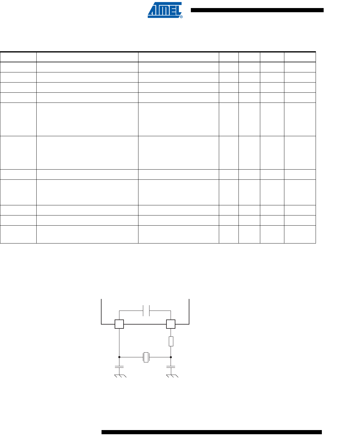
1124
6430F–ATARM–21-Feb-12
SAM3U Series
43.4.6 3 to 20 MHz Crystal Oscillator Characteristics
Notes: 1. RS is the series resistor
2. Rs = 100-200 Ohms; Cs = 2.0 - 2.5pF; Cm = 2 – 1.5 fF(typ, worst case) using 1 Kohm serial resistor on xout.
3. Rs = 50-100 Ohms; Cs = 2.0 - 2.5pF; Cm = 4 - 3 fF(typ, worst case).
4. Rs = 25-50 Ohms; Cs = 2.5 - 3.0pF; Cm = 7 - 5 fF (typ, worst case).
5. Rs = 20-50 Ohms; Cs = 3.2 - 4.0pF; Cm = 10 - 8 fF(typ, worst case).
CLEXT = 2x(CCRYSTAL – CL – CPCB).
Where CPCB is the capacitance of the printed circuit board (PCB) track layout from the crystal to the SAM3U pin.
Table 43-21. 3 to 20 MHz Crystal Oscillator Characteristics
Symbol Parameter Conditions Min Typ Max Unit
Freq Operating Frequency Normal mode with crystal 3 16 20 MHz
Freq_bypass Operating Frequency In Bypass Mode External Clock on XIN 50 MHz
Supply Ripple Voltage (on VDDPLL) Rms value, 10KHz to 10MHz 30 mV
Duty Cycle 40 50 60 %
TON Startup Time
3 MHz, CSHUNT = 3pF
8 MHz, CSHUNT = 7pF
12 to 16 MHz, CSHUNT = 7pF
20 MHz, CSHUNT = 7pF
14.5
4
1.4
1
ms
IDD_ON Current consumption
3 MHz(2)
8 MHz(3)
12 to 16 MHz(4)
20 MHz(5)
150
150
300
400
250
250
450
550
µA
IDD_ST Standby Current Consumption Standby mode @ 3.6V 5 nA
PON Drive level
3 MHz
8 MHz
1 2MHz, 16 MHz, 20 MHz
15
30
50
µW
RfInternal resistor between XIN and XOUT 1 MΩ
CLEXT External capacitor on XIN and XOUT 12.5 17.5 pF
CLInternal Equivalent Load Capacitance Integrated Load Capacitance
(XIN and XOUT in series) 7.5 9.5 11.5 pF
XIN XOUT
C
LEXT
C
L
C
LEXT
C
Crystal
SAM3U
R = 1K if Crystal Frequency
is lower than 8 MHz
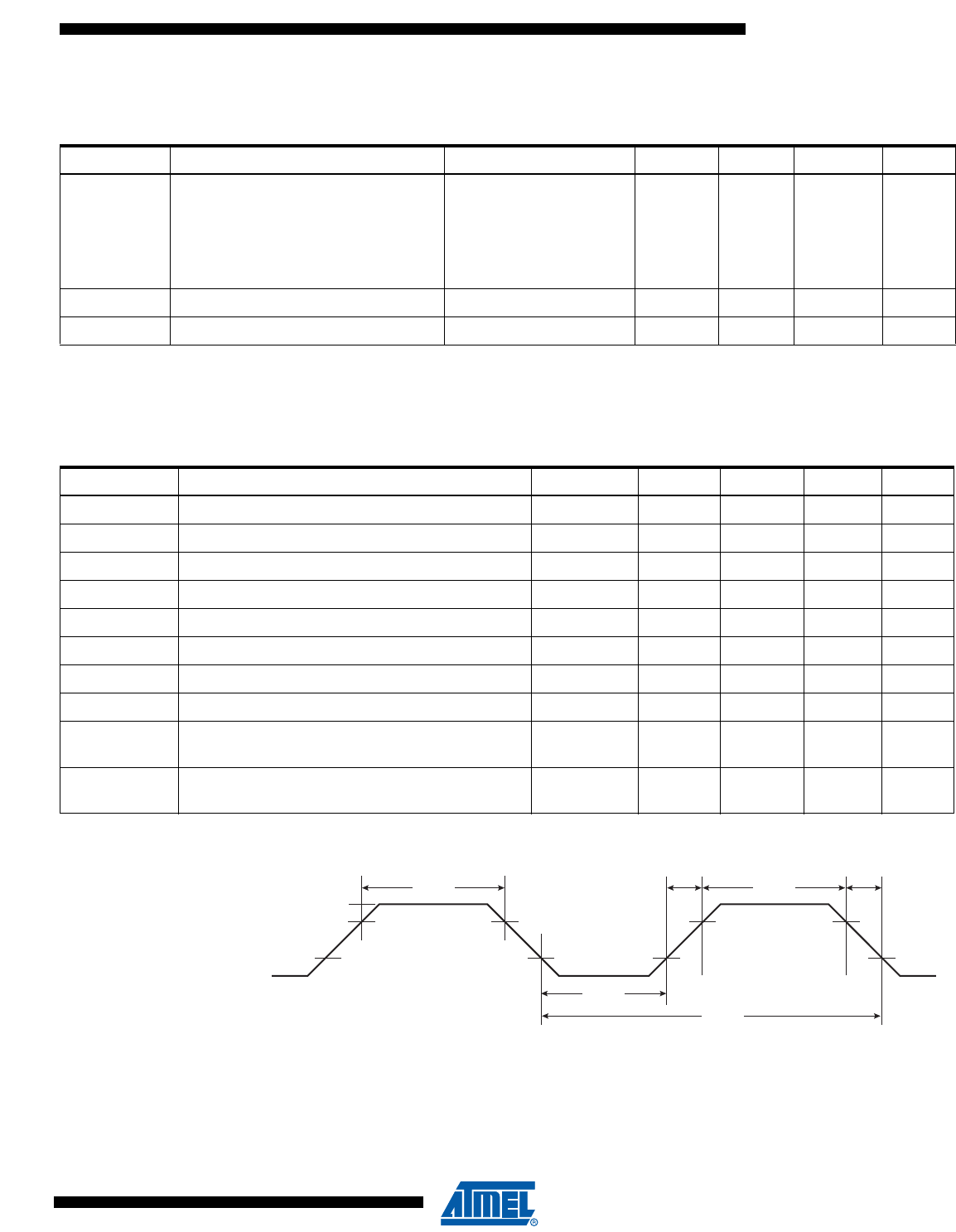
1125
6430F–ATARM–21-Feb-12
SAM3U Series
43.4.7 3 to 20 MHz Crystal Characteristics
43.4.8 3 to 20 MHz XIN Clock Input Characteristics in Bypass Mode
Note: 1. These characteristics apply only when the 3-20 MHz XTAL Oscillator is in bypass mode.
Table 43-22. Crystal Characteristics
Symbol Parameter Conditions Min Typ Max Unit
ESR Equivalent Series Resistor Rs
Fundamental @ 3MHz
Fundamental @ 8MHz
Fundamental @ 12MHz
Fundamental @ 16MHz
Fundamental @ 20MHz
200
100
80
80
50
Ω
CMMotional capacitance 8fF
CSHUNT Shunt capacitance 7pF
Table 43-23. XIN Clock Electrical Characteristics (In Bypass Mode)
Symbol Parameter Conditions Min Typ Max Units
1/(tCPXIN) XIN Clock Frequency (1) 50 MHz
tCPXIN XIN Clock Period (1) 20 ns
tCHXIN XIN Clock High Half-period (1) 8ns
tCLXIN XIN Clock Low Half-period (1) 8ns
tCLCH Rise Time (1) 400 ns
tCHCL Fall Time (1) 400 ns
CIN XIN Input Capacitance (1) 6pF
RIN XIN Pull-down Resistor (1) 1MΩ
VXIN_IL VXIN Input Low-level Voltage (1) -0.3 0.3 x
VVDDPLL
V
VXIN_IH VXIN Input High-level Voltage (1) 0.7 x
VVDDPLL
VVDDPLL
+0.3 V
tCPXIN
tCPXIN
tCPXIN tCHXIN
tCLCH tCHCL
VXIN_IL
VXIN_IH

1126
6430F–ATARM–21-Feb-12
SAM3U Series
43.4.9 Crystal Oscillators Design Consideration Information
43.4.9.1 Choosing a Crystal
When choosing a crystal for the 32768 Hz Slow Clock Oscillator or for the 3-20 MHz Oscillator,
several parameters must be taken into account. Important parameters between crystal and
SAM3U specifications are as follows:
• Load Capacitance
– This is the equivalent capacitor value the oscillator must “show” to the crystal in
order to oscillate at the target frequency. Crystal must be chosen according to the
internal load capacitance (CL)of the on-chip oscillator. Having a mismatch for the
load capacitance will result in a frequency drift.
• Drive Level
– Crystal drive level >= Oscillator Drive Level. Having a crystal drive level number
lower than the oscillator specification may damage the crystal.
• Equivalent Series Resistor (ESR)
– Crystal ESR <= Oscillator ESR Max. Having a crystal with ESR value higher than
the oscillator may cause the oscillator to not start.
• Shunt Capacitance
– Max. crystal Shunt capacitance <= Oscillator Shunt Capacitance (CSHUNT). Having a
crystal with ESR value higher than the oscillator may cause the oscillator to not start.
43.4.9.2 Printed Circuit Board (PCB)
SAM3U Oscillators are low power oscillators requiring particular attention when designing PCB
systems. A board design example is given on Atmel’s website in the MCU Technical Center
Section.
1127
6430F–ATARM–21-Feb-12
SAM3U Series
43.5 UPLL, PLLA Characteristics
Note: 1. Required for 12MHz Clock Signal injection on XIN pin (oscillator in bypass mode).
Table 43-24. Supply Voltage Phase Lock Loop Characteristics
Symbol Parameter Conditions Min Typ Max Unit
VDDPLL
Supply Voltage Range 1.6 1.8 2 V
Allowable Voltage Ripple RMS Value 10 kHz to 10 MHz
RMS Value > 10 MHz
30
10 mV
Table 43-25. PLLA Characteristics
Symbol Parameter Conditions Min Typ Max Unit
FIN Input Frequency 8 16 MHz
FOUT Output Frequency 96 192 MHz
IPLL Current Consumption
Active mode @ 96MHz @1.8V
Active mode @ 160MHz @1.8V
Active mode @ 192MHz @1.8V
1
1.6
2.4
1.3
2
3
mA
Standby mode 1 µA
TSTART PLLA Settling Time 200 µS
Table 43-26. UPLL Characteristics for USB High Speed Device Port
Symbol Parameter Conditions Min Typ Max Unit
FIN Input Frequency 12 MHz
Delta FIN Input Frequency Accuracy See note (1) -0.05 +0.05 %
FOUT Output Frequency 480 MHz
IPLL Current Consumption Active mode @ 480MHz @1.8V 2.5 5 mA
Standby mode TBD µA
1128
6430F–ATARM–21-Feb-12
SAM3U Series
43.6 USB High Speed Port
43.6.1 Typical Connection
For typical connection please refer to the USB Device Section.
43.6.2 Electrical Characteristics
43.6.2.1 USB Transceiver
USB 2.0 Compliant in full-speed and high-speed modes. Refer to Chapter 7 of the USB 2.0,
Revision 2.0 April 27, 2000.
43.6.3 Static Power Consumption
Note: 1. If cable is connected add 200 µA (Typical) due to Pull-up/Pull-down current consumption.
43.6.4 Dynamic Power Consumption
Note: 1. Including 1 mA due to Pull-up/Pull-down current consumption.
43.6.5 USB High Speed Design Guidelines
In order to facilitate hardware design around the SAM3U USB High Speed Port, Atmel provides
an application note on www.atmel.com.
Table 43-27. Electrical Parameters
Symbol Parameter Conditions Min Typ Max Unit
RPUI
Bus Pull-up Resistor on Upstream Port (idle
bus) in FS or HS Mode 1.5 kOhm
RPUA
Bus Pull-up Resistor on Upstream Port
(upstream port receiving) in FS or HS Mode 15 kOhm
Table 43-28. Static Power Consumption
Symbol Parameter Conditions Min Typ Max Unit
IBIAS Bias current consumption on VBG 1 µA
IVDDUTMII
HS Transceiver & I/O current consumption 8 µA
FS / HS Transceiver & I/O current consumption no connection(1) 3µA
Table 43-29. Dynamic Power Consumption
Symbol Parameter Conditions Min Typ Max Unit
IBIAS Bias current consumption on VBG 0.7 0.8 mA
IVDDUTMII
HS Transceiver current consumption HS transmission 47 60 mA
HS Transceiver current consumption HS reception 18 27 mA
FS/HS Transceiver current consumption FS transmission 0m
cable(1) 46mA
FS/HS Transceiver current consumption FS transmission 5m
cable(1) 26 30 mA
FS/HS Transceiver current consumption FS reception(1) 34.5mA

1129
6430F–ATARM–21-Feb-12
SAM3U Series
43.7 12-Bit ADC Characteristics
Note: Use IBCTL = 00 for Sampling Frequency below 500 kHz and IBCTL = 01 between 500 kHz and 1MHz.
Table 43-30. Analog Power Supply Characteristics
Symbol Parameter Conditions Min Typ Max Units
VVDDIN
ADC Analog Supply 12-bit or 10 bit resolution 2.4 3.0 3.6 V
ADC Analog Supply 10 bit resolution 2.0 3.6 V
Max. Voltage Ripple rms value, 10 kHz to 20 MHz 20 mV
IVDDIN Current Consumption
Sleep Mode
Fast Wake Up Mode
Normal Mode (IBCTL= 00)
Normal Mode (IBCTL= 01)
0.1
1.8
4.7
6
1
2.6
7.1
9
µA
mA
mA
mA
Table 43-31. Channel Conversion Time and ADC Clock
Symbol Parameter Conditions Min Typ Max Units
fADC ADC Clock Frequency 1 20 MHz
tCP_ADC ADC Clock Period 50 1000 ns
fSSampling Frequency 0.05 1 MHz
tSTART-UP ADC Startup time
From OFF Mode to Normal Mode:
- Voltage Reference OFF
- Analog Circuitry OFF
From Standby Mode to Normal Mode:
- Voltage Reference ON
- Analog Circuitry OFF
20
4
30
8
40
12
µs
tTRACKTIM Track and Hold Time
See Section “Track and Hold Time
versus Source Output Impedance” for
more details
160 ns
tCONV Conversion Time 20 TCP_ADC
tSETTLE Settling Time Settling time to change offset and gain 200 ns
Table 43-32. External Voltage Reference Input
Parameter Conditions Min Typ Max Units
ADVREF Input Voltage Range, 12-bit 2.4V < VVDDIN < 3.6V 2.4 - VDDIN V
ADVREF Input Voltage Range, 10-bit 2.0V < VVDDIN < 3.6V 2.0 - VDDIN V
ADVREF Current 250 µA
ADVREF Input DC impedance 14 kΩ

1130
6430F–ATARM–21-Feb-12
SAM3U Series
43.7.0.1 Static performance characteristics
Minimal code=0
Maximal code=4095
ADC resolution = 12 bits (4096)
In the following tables, the LSB is relative to analog scale:
• Single Ended (ex: ADVREF=3.0V),
– Gain = 1, LSB = (3.0V / 4096) = 732uV
– Gain = 2, LSB = (1.5V / 4096) = 366uV
– Gain = 4, LSB = (750mV / 4096) = 183uV
• Differential (ex: ADVREF=3.0V),
– Gain = 0.5, LSB = (6.0V / 4096) = 1465uV
– Gain = 1, LSB = (3.0V / 4096) = 732uV
– Gain = 2, LSB = (750mV / 4096) = 366uV
x stand for digital 0 or 1
Table 43-33. INL, DNL, 12-bit mode, VDDIN supply voltage conditions, Temperature range [-40°, +100°], FADC=2 MHz,
IBCTL=01.
Parameter Conditions Min Typ Max Units
Integral Non-linearity (INL) VDDIN 2.4V to <3.0V
Differential, DIFF=1, OFF=x, GAIN=xx -2.2 ±1 +2.2 LSB
Integral Non-linearity (INL) VDDIN 2.4V to <3.0V
Single ended, DIFF=0, OFF=x, GAIN=xx -6 ±1 +6 LSB
Integral Non-linearity (INL) VDDIN 3.0V to <3.6V
Differential, DIFF=1, OFF=x, GAIN=xx -1.5 ±1 +1.5 LSB
Integral Non-linearity (INL) VDDIN 3.0V to <3.6V
Single ended, DIFF=0, OFF=x, GAIN=xx -5 ±1 +5 LSB
Differential Non-linearity (DNL) VDDIN 2.4V to <3.0V
Differential, DIFF=1, OFF=x, GAIN=xx -1.5 ±0.5 +1.5 LSB
Differential Non-linearity (DNL) VDDIN 2.4V to <3.0V
Single ended, DIFF=0, OFF=x, GAIN=xx -2.2 ±0.5 +2.2 LSB
Differential Non-linearity (DNL) VDDIN 3.0V to <3.6V
Differential, DIFF=1, OFF=x, GAIN=xx -1.5 ±0.5 +1.5 LSB
Differential Non-linearity (DNL) VDDIN 3.0V to <3.6V
Single ended, DIFF=0, OFF=x, GAIN=xx -2.2 ±0.5 +2.2 LSB

1131
6430F–ATARM–21-Feb-12
SAM3U Series
x stand for digital 0 or 1
(1) Offset and Gain errors are given without calibration. A software calibration can be done to reduce Gain and offset
errors.
Figure 43-10. Offset and Gain Definitions
Table 43-34. Ge, Oe, 12-bit mode, VDDIN supply voltage conditions, Temperature range [-40°, +100°], FADC=2 MHz,
IBCTL=01.(1)
Parameter Conditions Min Typ Max Units
Gain error (Ge) VDDIN 2.4V to <3.6V
Differential, DIFF=1, OFF=x, GAIN=xx
-1.56
-64
-0.56
-23
+0.29
+12
%
LSB
Gain error (Ge) VDDIN 2.4V to <3.6V
Single ended, DIFF=0, OFF=x, GAIN=xx
-1.56
-64
-0.56
-23
+0.78
+32
%
LSB
Offset error (Oe) VDDIN 2.4V to <3.6V
Differential, DIFF=1, OFF=x, GAIN=xx -30 +64 LSB
Offset error (Oe) VDDIN 2.4V to <3.6V
Single ended, DIFF=0, OFF=x, GAIN=xx -60 +80 LSB
Single Ended case:
Offset and Gain
definitions
Vin
Ymax=4095
ADVref
0
Ga: actual gain
Ga=(YaH-YaL)/XiH
Ga=1+Ge(%)
Ge(%): gain error
Ge(lsb): Ge(%)×Xmax
YaL
YaH
ADVref/2
Ya=Ga×Xi+Oe
YiM=2047
Ya=actual adc codes
Oe=actual offset
Xi=ideal adc codes
Xmax=4095XiM=2047 XiH
XiL
VHVL
1132
6430F–ATARM–21-Feb-12
SAM3U Series
Note: 1. Single ended or differential mode, any gain values.
LSB of 10 bit ADC, LSB=3.0V/1024
Note: 1. ADC Clock (FADC) = 20MHz, Fs=1MHz, Fin = 127 kHz, IBCTL = 01, FFT using 1024 points or more, Frequency band =
[1kHz, 500kHz] – Nyquist conditions fulfilled.
Note: 1. ADC Clock (FADC)= 20MHz, Fs=1MHz, Fin=127kHz, IBCTL = 01, FFT using 1024 points or more, Frequency band = [1kHz,
500kHz] – Nyquist conditions fulfilled.
Track and Hold Time versus Source Output Impedance
The following figure gives a simplified acquisition path.
Table 43-35. Static Performance Characteristics -10 bits mode (1)
Parameter Conditions Min Typ Max Units
Resolution 10 Bit
Integral Non-linearity (INL) -1 ±0.5 +1 LSB
Differential Non-linearity (DNL) no missing code -1 ±0.5 +1 LSB
Offset Error all gain, Differential or Single ended, no
calibration -8 +3 +20 LSB
Gain Error without calibration all gain, Differential or Single ended, no
calibration -16 -6 +3 LSB
Table 43-36. Dynamic Performance Characteristics in Single ended and 12 bits mode (1)
Parameter Conditions Min Typ Max Units
Signal to Noise Ratio - SNR Single ended, DIFF=0, OFF=x, GAIN=xx 57 58 dB
Total Harmonic Distortion - THD Single ended, DIFF=0, OFF=x, GAIN=xx -66 -72 dB
Signal to Noise and Distortion - SINAD Single ended, DIFF=0, OFF=x, GAIN=xx 54 57 dB
ENOB Single ended, DIFF=0, OFF=x, GAIN=xx 9.0 10.0 Bits
Table 43-37. Dynamic Performance Characteristics in Differential and 12 bits mode(1)
Parameter Conditions Min Typ Max Units
Signal to Noise Ratio - SNR Differential, DIFF=1, OFF=x, GAIN=xx 59 64 dB
Total Harmonic Distortion - THD Differential, DIFF=1, OFF=x, GAIN=xx -69 -80 dB
Signal to Noise and Distortion - SINAD Differential, DIFF=1, OFF=x, GAIN=xx 59 64 dB
ENOB Differential, DIFF=1, OFF=x, GAIN=xx 9.5 10.3 Bits
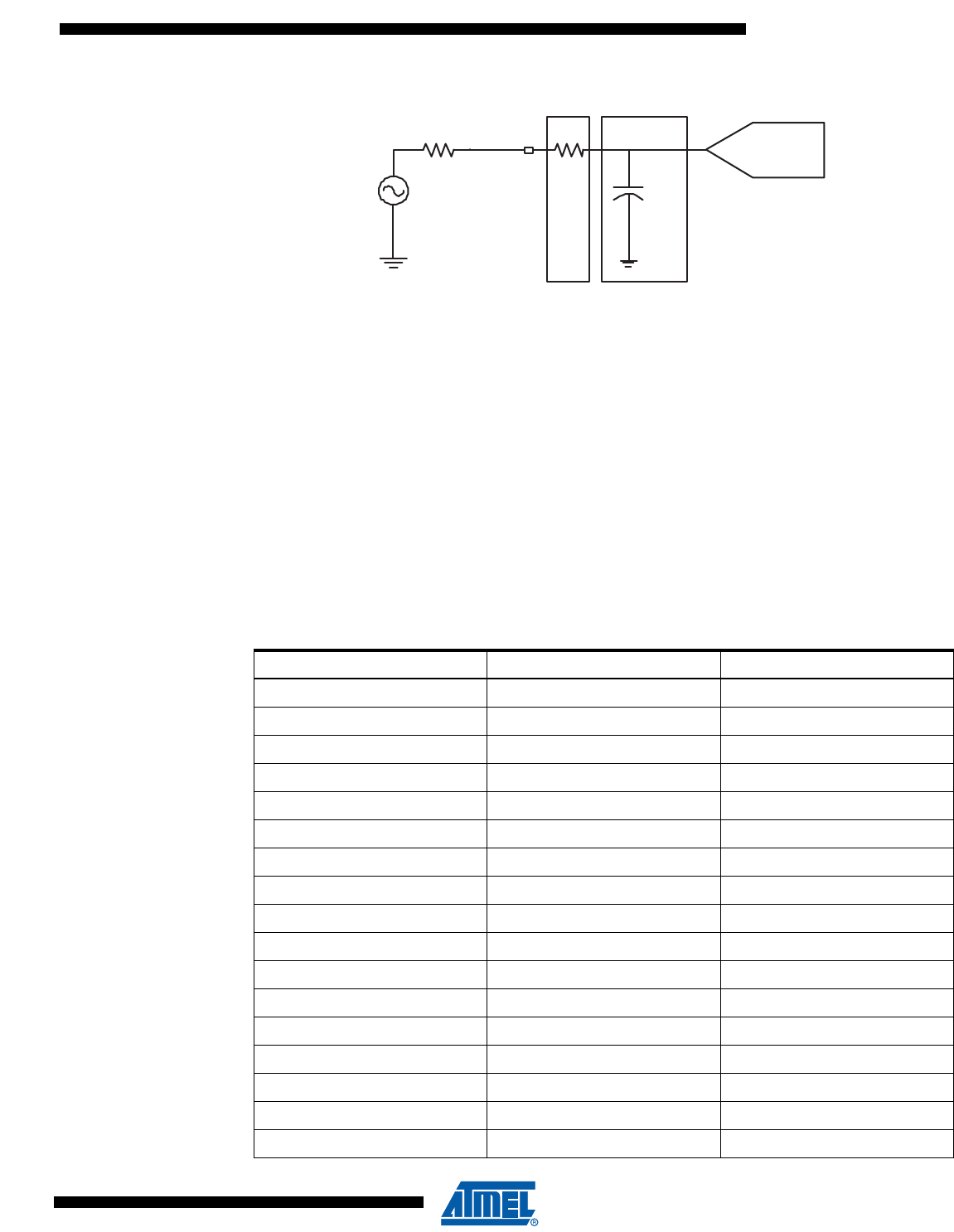
1133
6430F–ATARM–21-Feb-12
SAM3U Series
Figure 43-11. Simplified Acquisition Path
During the tracking phase the ADC needs to track the input signal during the tracking time
shown below:
• 10-bit mode: tTRACK = 0.042 x Zsource + 160
• 12-bit mode: tTRACK = 0.054 x Zsource + 205
With tTRACK expressed in ns and ZSOURCE expressed in Ohms.
Two cases must be considered:
1. The calculated tracking time (tTRACK) is lower than 15 tCP_ADC.
Set TRANSFER = 1 and TRACTIM = 0.
In this case, the allowed Zsource can be computed versus the ADC frequency with
the hypothesis of tTRACK = 15 × tCP_ADC:
Where tCP_ADC = 1/fADC . See Table 43-38 on page 1133.
Table 43-38. Source impedance values
fADC = ADC clock (MHz) ZSOURCE (kOhms) for 12 bits ZSOURCE (kOhms) for 10 bits
20.00 10 14
16.00 14 19
10.67 22 30
8.00 31 41
6.40 40 52
5.33 48 63
4.57 57 74
4.00 66 85
3.56 74 97
3.20 83 108
2.91 92 119
2.67 100 130
2.46 109 141
2.29 118 152
2.13 126 164
2.00 135 175
1.00 274 353
Sample & HoldMux.
Zsource Ron
Csample
ADC
Input12-bit
ADC
Core

1134
6430F–ATARM–21-Feb-12
SAM3U Series
2. The calculated tracking time (tTRACK) is higher than 15 tCP_ADC.
Set TRANSFER = 1 and TRACTIM = 0.
In this case, a timer will trigger the ADC in order to set the correct sampling rate according to the
Track time.
The maximum possible sampling frequency will be defined by tTRACK in nano seconds, computed
by the previous formula but with minus 15 × tCP_ADC and plus TRANSFER time.
• 10 bit mode: 1/fS = tTRACK - 15 × tCP_ADC + 5 tCP_ADC
• 12 bit mode: 1/fS = tTRACK - 15 × tCP_ADC + 5 tCP_ADC
Note: Csample and Ron are taken into account in the formulas
Note: 1. Input Voltage range can be up to VDDIN without destruction or over-consumption.
If VDDIO < VADVREF max input voltage is VDDIO.
ADC Application Information
For more information on data converter terminology, please refer to the application note:
Data Converter Terminology, Atmel lit° 6022.
http://www.atmel.com/dyn/resources/prod_documents/doc6022.pdf
Table 43-39. Analog Inputs
Parameter Min Typ Max Units
Input Voltage Range 0 VADVREF
Input Leakage Current ±0.5 µA
Input Capacitance 8 pF

1135
6430F–ATARM–21-Feb-12
SAM3U Series
43.8 AC Characteristics
43.8.1 Master Clock Characteristics
43.8.2 I/O Characteristics
Criteria used to define the maximum frequency of the I/Os:
– output duty cycle (40%-60%)
– minimum output swing: 100 mV to VDDIO - 100 mV
– minimum output swing: 100 mV to VDDIO - 100 mV
– Addition of rising and falling time inferior to 75% of the period
Notes: 1. Pin Group 1 = PA3, PA15
2. Pin Group 2 = PA[0-2], PA[4-14], PA[16-31], PB[0-31], PC[0-31]
Table 43-40. Master Clock Waveform Parameters
Symbol Parameter Conditions Min Max Units
1/(tCPMCK) Master Clock Frequency
VDDCORE @ 1.62V
VDDCORE @ 1.8V
84
96
MHz
Table 43-41. I/O Characteristics
Symbol Parameter Conditions Min Max Units
FreqMax1 Pin Group 1 (1) Maximum output frequency
30 pF VDDIO = 1.62V
VDDIO = 3.0V
45
65 MHz
45 pF VDDIO = 1.62V
VDDIO = 3.0V
34
45
PulseminH1Pin Group 1 (1) High Level Pulse Width
30 pF VDDIO = 1.62V
VDDIO = 3.0V
11
7.7 ns
45 pF VDDIO = 1.62V
VDDIO = 3.0V
14.7
11
PulseminL1Pin Group 1 (1) Low Level Pulse Width
30 pF VDDIO = 1.62V
VDDIO = 3.0V
11
7.7 ns
45 pF VDDIO = 1.62V
VDDIO = 3.0V
14.7
11
FreqMax2 Pin Group 2 (2) Maximum output frequency Load: 25 pF
1.62V < VDDIO < 3.6V 35 MHz
PulseminH2Pin Group 2 (2) High Level Pulse Width Load: 25pF
1.62V < VDDIO < 3.6V
14.5 ns
PulseminL2Pin Group 2 (2) Low Level Pulse Width Load: 25pF
1.62V < VDDIO < 3.6V
14.5 ns
Table 43-42. NRSTB
Symbol Parameter Conditions Min Typ Max Units
Tf Filtered Pulse Width 1µs
Tuf Unfiltered Pulse Width 100 µs
1136
6430F–ATARM–21-Feb-12
SAM3U Series
43.8.3 SPI Characteristics
Figure 43-12. SPI Master Mode with (CPOL= NCPHA = 0) or (CPOL= NCPHA= 1)
Figure 43-13. SPI Master Mode with (CPOL = 0 and NCPHA=1) or (CPOL=1 and NCPHA= 0)
Figure 43-14. SPI Slave Mode with (CPOL=0 and NCPHA=1) or (CPOL=1 and NCPHA=0)
SPCK
MISO
MOSI
SPI2
SPI0SPI1
SPCK
MISO
MOSI
SPI5
SPI3SPI4
SCK
MISO
MOSI
SPI6
SPI7SPI8
NPCS0
SPI12 SPI13
1137
6430F–ATARM–21-Feb-12
SAM3U Series
Figure 43-15. SPI Slave Mode with (CPOL = NCPHA = 0) or (CPOL= NCPHA= 1)
43.8.3.1 Maximum SPI Frequency
The following formulas give maximum SPI frequency in Master read and write modes and in
Slave read and write modes.
Master Write Mode
The SPI is only sending data to a slave device such as an LCD, for example. The limit is
given by SPI2 (or SPI5) timing. Since it gives a maximum frequency above the maximum pad
speed (see Section 43.8.2 “I/O Characteristics”), the max SPI frequency is the one from the
pad.
Master Read Mode
Tvalid is the slave time response to output data after detecting an SPCK edge. For Atmel SPI
DataFlash (AT45DB642D), Tvalid (orTv ) is 12 ns Max.
In the formula above, FSPCKMax = 38.5 MHz @ VDDIO = 3.3V.
Slave Read Mode
In slave mode, SPCK is the input clock for the SPI. The max SPCK frequency is given by
setup and hold timings SPI7/SPI8(or SPI10/SPI11). Since this gives a frequency well above
the pad limit, the limit in slave read mode is given by SPCK pad.
Slave Write Mode
For 3.3V I/O domain and SPI6, FSPCKMax = 33 MHz. Tsetup is the setup time from the master
before sampling data.
43.8.3.2 SPI Timings
SCK
MISO
MOSI
SPI
9
SPI
10
SPI
11
NPCS0
SPI
15
SPI
14
fSPCKMax 1
SPI0orSPI3
()Tvalid
+
--------------------------------------------------------=
fSPCKMax 1
SPI6orSPI9
()Tsetup
+
---------------------------------------------------------=
Table 43-43. SPI Timings
Symbol Parameter Conditions Min Max Units
SPI0MISO Setup time before SPCK rises (master) 3.3V domain(1) 14 ns
1.8V domain(2) 17 ns

1138
6430F–ATARM–21-Feb-12
SAM3U Series
Notes: 1. 3.3V domain: VVDDIO from 3.0V to 3.6V, maximum external capacitor = 30 pF.
2. 1.8V domain: VVDDIO from 1.65V to 1.95V, maximum external capacitor = 30 pF.
Note that in SPI master mode the SAM3U does not sample the data (MISO) on the opposite edge where data clocks out
(MOSI) but the same edge is used as shown in Figure 43-12 and Figure 43-13.
43.8.4 MCI Timings
The High Speed MultiMedia Card Interface (HSMCI) supports the MultiMedia Card (MMC)
Specification V4.3, the SD Memory Card Specification V2.0, the SDIO V2.0 specification and
CE-ATA V1.1.
43.8.5 SSC Timings
Timings are given assuming the following VDDIO supply and load.
VDDIO = 1.62V @25pF
SPI1MISO Hold time after SPCK rises (master) 3.3V domain(1) 0ns
1.8V domain(2) 0ns
SPI2SPCK rising to MOSI Delay (master) 3.3V domain(1) 3ns
1.8V domain(2) 3.5 ns
SPI3MISO Setup time before SPCK falls (master) 3.3V domain(1) 14 ns
1.8V domain(2) 17 ns
SPI4MISO Hold time after SPCK falls (master) 3.3V domain(1) 0ns
1.8V domain(2) 0ns
SPI5SPCK falling to MOSI Delay (master) 3.3V domain(1) 3ns
1.8V domain(2) 3.5 ns
SPI6SPCK falling to MISO Delay (slave) 3.3V domain(1) 14 ns
1.8V domain(2) 17 ns
SPI7MOSI Setup time before SPCK rises (slave) 3.3V domain(1) 0.5 ns
1.8V domain(2) 1ns
SPI8MOSI Hold time after SPCK rises (slave) 3.3V domain(1) 0.5 ns
1.8V domain(2) 1ns
SPI9SPCK rising to MISO Delay (slave) 3.3V domain(1) 14 ns
1.8V domain(2) 17 ns
SPI10 MOSI Setup time before SPCK falls (slave) 3.3V domain(1) 0ns
1.8V domain(2) 0
SPI11 MOSI Hold time after SPCK falls (slave) 3.3V domain(1) 1.5 ns
1.8V domain(2) 1.5 ns
SPI12 NPCS Setup time to SPCK (slave) 3.3V domain(1) 5.2 ns
1.8V domain(2) 5ns
SPI13 NPCS Hold time after SPCK (slave) 3.3V domain(1) 0ns
1.8V domain(2) 0ns
SPI14 NPCS Setup time to SPCK (slave) 3.3V domain(1) 4.2 ns
1.8V domain(2) 4ns
SPI15 NPCS Hold time after SPCK (slave) 3.3V domain(1) 0ns
1.8V domain(2) 0ns
Table 43-43. SPI Timings (Continued)
Symbol Parameter Conditions Min Max Units
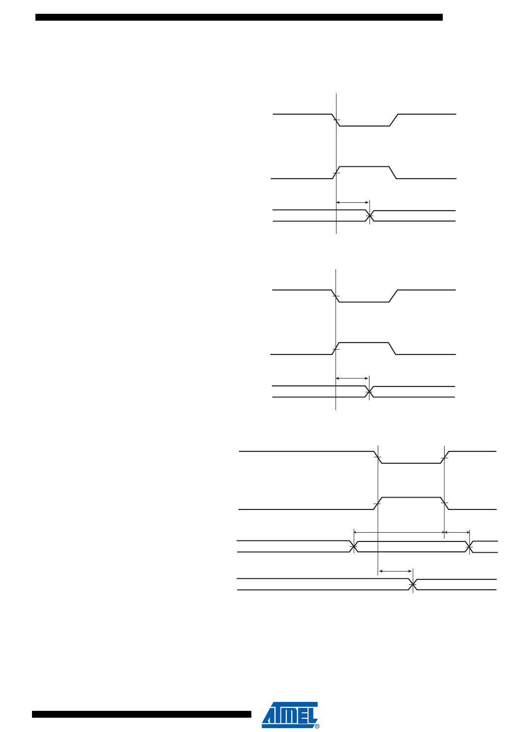
1139
6430F–ATARM–21-Feb-12
SAM3U Series
VDDIO = 3V @25pF
Figure 43-16. SSC Transmitter, TK and TF as output
Figure 43-17. SSC Transmitter, TK as input and TF as output
Figure 43-18. SSC Transmitter, TK as output and TF as input
TK (CKI =1)
TF/TD
SSC
0
TK (CKI =0)
TK (CKI =1)
TF/TD
SSC
1
TK (CKI =0)
TK (CKI=1)
TF
SSC
2
SSC
3
TK (CKI=0)
TD
SSC
4
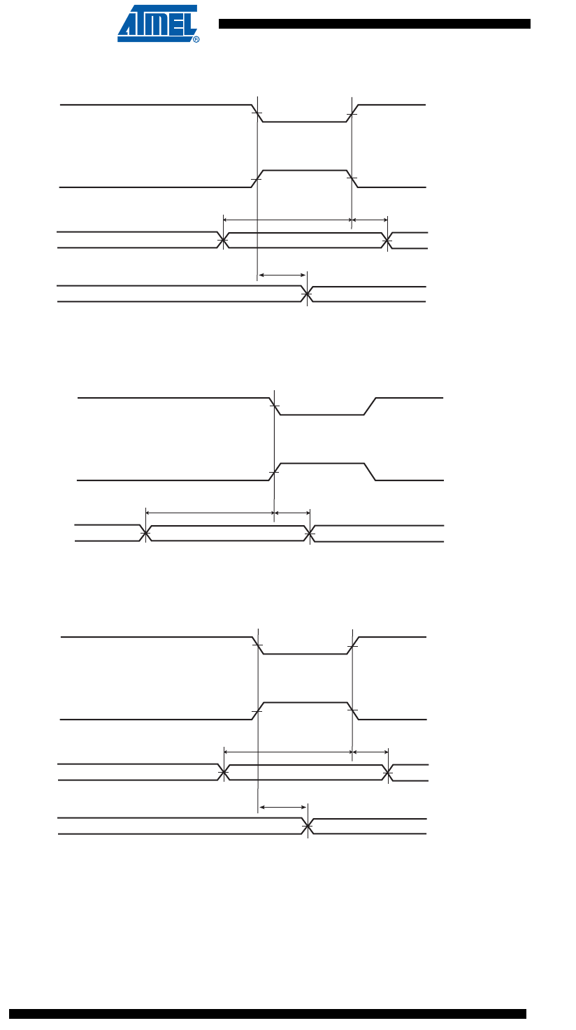
1140
6430F–ATARM–21-Feb-12
SAM3U Series
Figure 43-19. SSC Transmitter, TK and TF as input
Figure 43-20. SSC Receiver RK and RF as input
Figure 43-21. SSC Receiver, RK as input and RF as output
TK (CKI=0)
TF
SSC
5
SSC
6
TK (CKI=1)
TD
SSC
7
RK (CKI=1)
RF/RD
SSC8SSC9
RK (CKI=0)
RK (CKI=0)
RD
SSC
8
SSC
9
RK (CKI=1)
RF
SSC
10
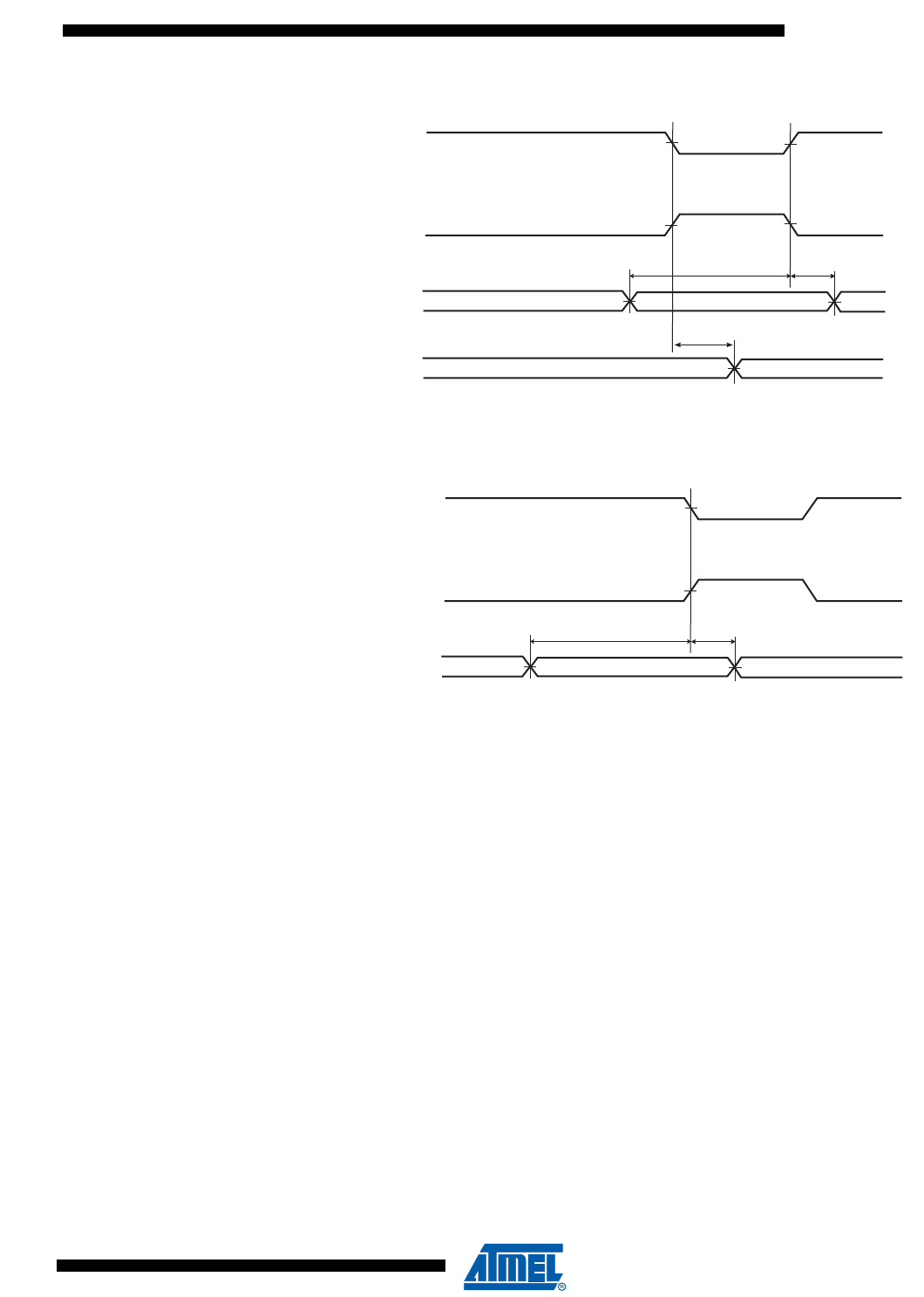
1141
6430F–ATARM–21-Feb-12
SAM3U Series
Figure 43-22. SSC Receiver, RK and RF as output
Figure 43-23. SSC Receiver, RK as output and RF as input
RK (CKI=0)
RD
SSC11 SSC12
RK (CKI=1)
RF
SSC13
RK (CKI=1)
RF/RD
SSC11 SSC12
RK (CKI=0)

1142
6430F–ATARM–21-Feb-12
SAM3U Series
43.8.5.1 SSC Timings
Notes: 1. Timings SSC4 and SSC7 depend on the start condition. When STTDLY = 0 (Receive start delay) and START = 4, or 5 or
7(Receive Start Selection), two Periods of the MCK must be added to timings.
2. For output signals (TF, TD, RF), Min and Max access times are defined. The Min access time is the time between the TK (or
RK) edge and the signal change. The Max access timing is the time between the TK edge and the signal stabilization. Figure
43-24 illustrates Min and Max accesses for SSC0. The same applies for SSC1, SSC4, and SSC7, SSC10 and SSC13.
3. 1.8V domain: VVDDIO from 1.65V to 1.95V, maximum external capacitor = 25 pF.
4. 3.3V domain: VVDDIO from 3.0V to 3.6V, maximum external capacitor = 25 pF.
Table 43-44. SSC Timings
Symbol Parameter Condition Min Max Units
Transmitter
SSC0TK edge to TF/TD (TK output, TF output) 1.8v domain(3)
3.3v domain(4)
0(2)
0(2)
2 (2)
1.5(2) ns
SSC1TK edge to TF/TD (TK input, TF output) 1.8v domain(3)
3.3v domain(4)
5(2)
5(2)
17.5 (2)
14.5(2) ns
SSC2TF setup time before TK edge (TK output) 1.8v domain(3)
3.3v domain(4)
17 - tCPMCK
15 - tCPMCK
ns
SSC3TF hold time after TK edge (TK output) 1.8v domain(3)
3.3v domain(4)
tCPMCK - 5
tCPMCK - 5 ns
SSC4(1) TK edge to TF/TD (TK output, TF input) 1.8v domain(3)
3.3v domain(4)
0 (+2*tCPMCK)(1)(2)
0 (+2*tCPMCK)(1)(2)
2 (+2*tCPMCK)(1)(2)
2 (+2*tCPMCK)(1)(2) ns
SSC5TF setup time before TK edge (TK input) 1.8v domain(3)
3.3v domain(4)
0
0ns
SSC6TF hold time after TK edge (TK input) 1.8v domain(3)
3.3v domain(4)
tCPMCK
tCPMCK
ns
SSC7(1) TK edge to TF/TD (TK input, TF input) 1.8v domain(3)
3.3v domain(4)
5 (+3*tCPMCK)(1)(2)
5 (+3*tCPMCK)(1)(2)
18 (+3*tCPMCK)(1)(2)
15 (+3*tCPMCK)(1)(2) ns
Receiver
SSC8RF/RD setup time before RK edge (RK input) 1.8v domain(3)
3.3v domain(4)
0
0ns
SSC9RF/RD hold time after RK edge (RK input) 1.8v domain(3)
3.3v domain(4)
tCPMCK
tCPMCK
ns
SSC10 RK edge to RF (RK input) 1.8v domain(3)
3.3v domain(4)
5(2)
5(2)
18(2)
15(2) ns
SSC11 RF/RD setup time before RK edge (RK output) 1.8v domain(3)
3.3v domain(4)
17 - tCPMCK
15 - tCPMCK
ns
SSC12 RF/RD hold time after RK edge (RK output) 1.8v domain(3)
3.3v domain(4)
tCPMCK - 5
tCPMCK - 5 ns
SSC13 RK edge to RF (RK output) 1.8v domain(3)
3.3v domain(4)
0(2)
0(2)
3(2)
2(2) ns
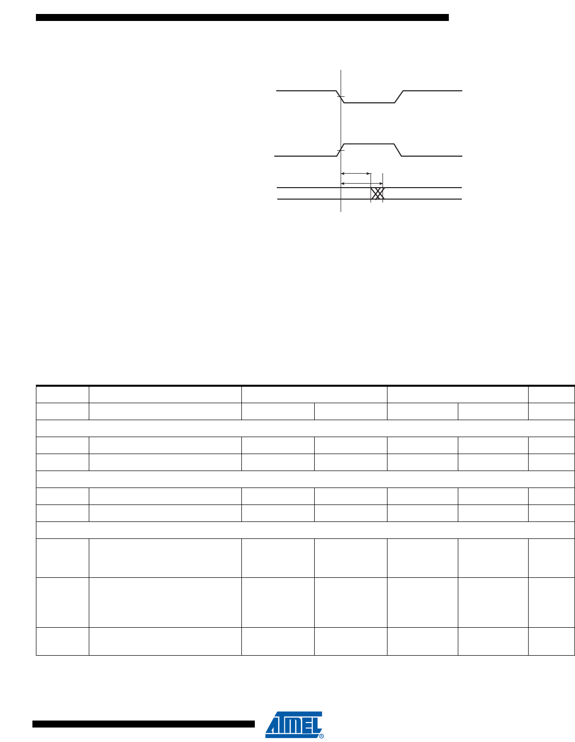
1143
6430F–ATARM–21-Feb-12
SAM3U Series
Figure 43-24. Min and Max Access Time of Output Signals
43.8.6 SMC Timings
SMC Timings are given with the following conditions.
VDDIO = 1.62V @ 30 pF
VDDIO = 3V @ 50 pF
Timings are given assuming a capacitance load on data, control and address pads:
In the following tables tCPMCK is MCK period. Timing extraction
43.8.6.1 Read Timings
TK (CKI =0)
TF/TD
SSC0min
TK (CKI =1)
SSC0max
Table 43-45. SMC Read Signals - NRD Controlled (READ_MODE = 1)
Symbol Parameter Min Max Units
VDDIO Supply 1.8V(2) 3.3V(3) 1.8V(2) 3.3V(3)
NO HOLD SETTINGS (nrd hold = 0)
SMC1Data Setup before NRD High 17.5 16 ns
SMC2Data Hold after NRD High 0 0 ns
HOLD SETTINGS (nrd hold ≠ 0)
SMC3Data Setup before NRD High 17 15 ns
SMC4Data Hold after NRD High 0 0 ns
HOLD or NO HOLD SETTINGS (nrd hold ≠ 0, nrd hold = 0)
SMC5
NBS0/A0, NBS1, NBS2/A1, NBS3,
A2 - A25 Valid before NRD High
(nrd setup +
nrd pulse)*
tCPMCK + 7
(nrd setup +
nrd pulse)*
tCPMCK + 6.5
ns
SMC6NCS low before NRD High
(nrd setup +
nrd pulse - ncs
rd setup) *
tCPMCK + 8
(nrd setup +
nrd pulse - ncs
rd setup) *
tCPMCK + 7
ns
SMC7NRD Pulse Width nrd pulse *
tCPMCK - 5
nrd pulse *
tCPMCK - 5 ns

1144
6430F–ATARM–21-Feb-12
SAM3U Series
43.8.6.2 Write Timings
Table 43-46. SMC Read Signals - NCS Controlled (READ_MODE= 0)
Symbol Parameter Min Max Units
VDDIO supply 1.8V(2) 3.3V(3) 1.8V(2) 3.3V(3)
NO HOLD SETTINGS (ncs rd hold = 0)
SMC8Data Setup before NCS High 20 16 ns
SMC9Data Hold after NCS High 0 0 ns
HOLD SETTINGS (ncs rd hold ≠ 0)
SMC10 Data Setup before NCS High 18 15 ns
SMC11 Data Hold after NCS High 0 0 ns
HOLD or NO HOLD SETTINGS (ncs rd hold ≠ 0, ncs rd hold = 0)
SMC12
NBS0/A0, NBS1, NBS2/A1, NBS3,
A2 - A25 valid before NCS High
(ncs rd setup +
ncs rd pulse)*
tCPMCK - 3.5
(ncs rd setup
+ ncs rd
pulse)* tCPMCK
- 3
ns
SMC13 NRD low before NCS High
(ncs rd setup +
ncs rd pulse -
nrd setup)*
tCPMCK - 2
(ncs rd setup
+ ncs rd pulse
- nrd setup)*
tCPMCK - 2
ns
SMC14 NCS Pulse Width
ncs rd pulse
length * tCPMCK
- 5
ncs rd pulse
length * tCPMCK
- 5
ns
Table 43-47. SMC Write Signals - NWE Controlled (WRITE_MODE = 1)
Symbol Parameter
Min Max
Units1.8V(2) 3.3V(3) 1.8V(2) 3.3V(3)
HOLD or NO HOLD SETTINGS (nwe hold ≠ 0, nwe hold = 0)
SMC15 Data Out Valid before NWE High nwe pulse *
tCPMCK - 4
nwe pulse *
tCPMCK - 3.5 ns
SMC16 NWE Pulse Width nwe pulse *
tCPMCK - 5
nwe pulse *
tCPMCK - 5 ns
SMC17
NBS0/A0 NBS1, NBS2/A1, NBS3,
A2 - A25 valid before NWE low
nwe setup *
tCPMCK + 8
nwe setup *
tCPMCK + 7 ns
SMC18 NCS low before NWE high
(nwe setup -
ncs rd setup +
nwe pulse) *
tCPMCK + 2
(nwe setup -
ncs rd setup +
nwe pulse) *
tCPMCK + 3
ns

1145
6430F–ATARM–21-Feb-12
SAM3U Series
Notes: 1. hold length = total cycle duration - setup duration - pulse duration. “hold length” is for “ncs wr hold length” or “NWE hold
length”.
2. 1.8V domain: VDDIO from 1.65V to 1.95V, maximum external capacitor = 25 pF
3. 3.3V domain: VDDIO from 3.0V to 3.6V, maximum external capacitor = 25 pF.
HOLD SETTINGS (nwe hold ≠ 0)
SMC19
NWE High to Data OUT, NBS0/A0
NBS1, NBS2/A1, NBS3, A2 - A25
change
nwe hold *
tCPMCK - 5.5
nwe hold *
tCPMCK - 5.5 ns
SMC20 NWE High to NCS Inactive (1)
(nwe hold - ncs
wr hold)* tCPMCK
- 3
(nwe hold - ncs
wr hold)*
tCPMCK - 3
ns
NO HOLD SETTINGS (nwe hold = 0)
SMC21
NWE High to Data OUT, NBS0/A0
NBS1, NBS2/A1, NBS3, A2 - A25,
NCS change(1)
44 ns
Table 43-47. SMC Write Signals - NWE Controlled (WRITE_MODE = 1) (Continued)
Symbol Parameter
Min Max
Units1.8V(2) 3.3V(3) 1.8V(2) 3.3V(3)
Table 43-48. SMC Write NCS Controlled (WRITE_MODE = 0)
Symbol Parameter
Min Max
Units1.8V(2) 3.3V(3) 1.8V(2) 3.3V(3)
SMC22 Data Out Valid before NCS High ncs wr pulse *
tCPMCK - 3
ncs wr pulse *
tCPMCK - 2 ns
SMC23 NCS Pulse Width ncs wr pulse *
tCPMCK - 5
ncs wr pulse *
tCPMCK - 5 ns
SMC24
NBS0/A0 NBS1, NBS2/A1, NBS3,
A2 - A25 valid before NCS low
ncs wr setup *
tCPMCK - 3
ncs wr setup *
tCPMCK - 2.5 ns
SMC25 NWE low before NCS high
(ncs wr setup -
nwe setup +
ncs pulse)*
tCPMCK - 2.5
(ncs wr setup -
nwe setup +
ncs pulse)*
tCPMCK - 2
ns
SMC26
NCS High to Data Out, NBS0/A0,
NBS1, NBS2/A1, NBS3, A2 - A25,
change
ncs wr hold *
tCPMCK - 6.5
ncs wr hold *
tCPMCK - 5.5 ns
SMC27 NCS High to NWE Inactive
(ncs wr hold -
nwe hold)*
tCPMCK - 5
(ncs wr hold -
nwe hold)*
tCPMCK - 4.5
ns
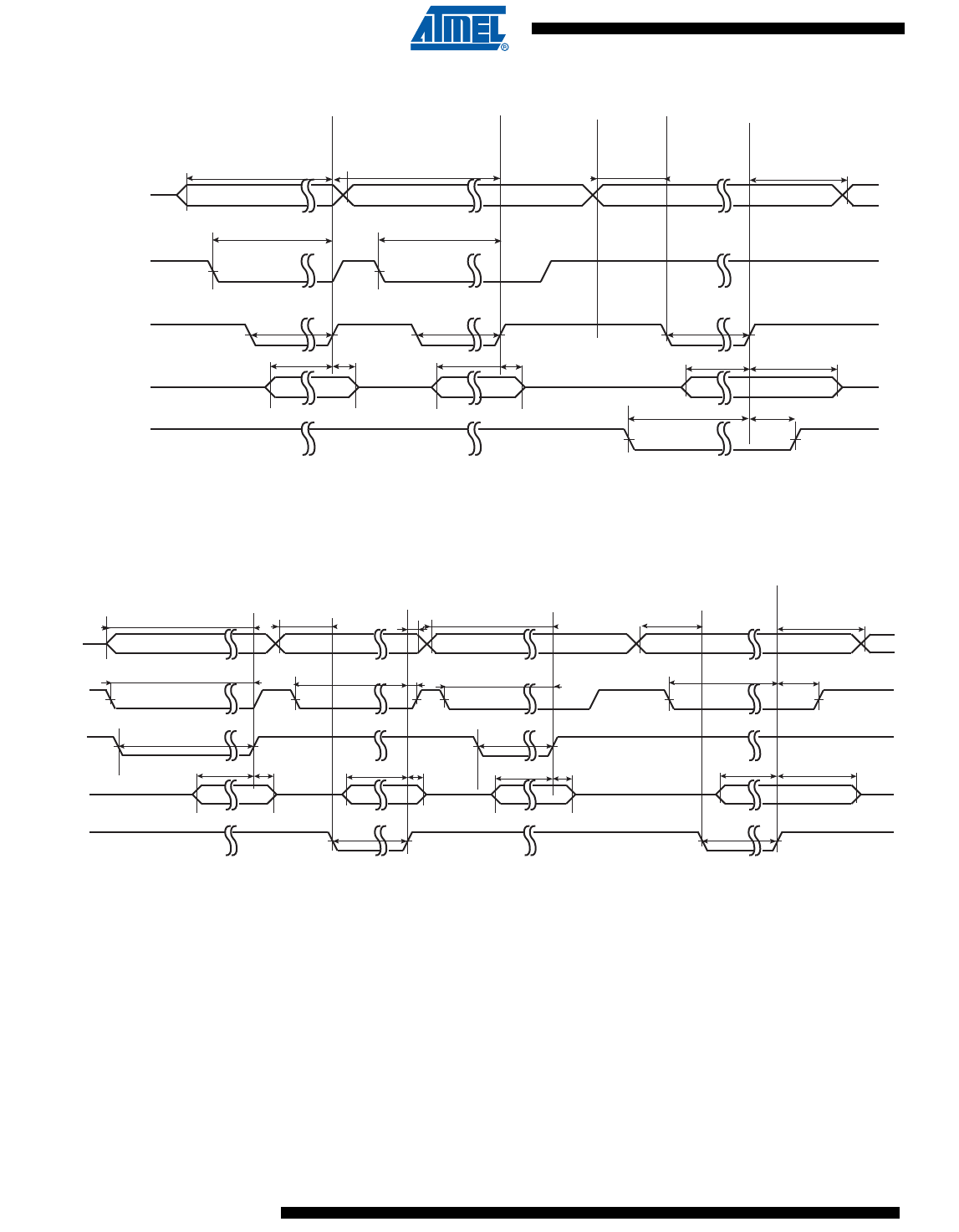
1146
6430F–ATARM–21-Feb-12
SAM3U Series
Figure 43-25. SMC Timings - NCS Controlled Read and Write
Figure 43-26. SMC Timings - NRD Controlled Read and NWE Controlled Write
NRD
NCS
D0 - D15
NWE
NCS Controlled READ
with NO HOLD
NCS Controlled READ
with HOLD
NCS Controlled WRITE
SMC22 SMC26
SMC10 SMC11
SMC12
SMC9
SMC8
SMC14 SMC14 SMC23
SMC27
SMC26
A0/A1/NBS[3:0]/A2-A25
SMC24
SMC25
SMC12
SMC13SMC13
NRD
NCS
D0 - D31
NWE
A0/A1/NBS[3:0]/
A2-A25
NRD Controlled READ
with NO HOLD
NWE Controlled WRITE
with NO HOLD
NRD Controlled READ
with HOLD
NWE Controlled WRITE
with HOLD
SMC1 SMC2 SMC15
SMC21
SMC3 SMC4 SMC15 SMC19
SMC20
SMC7
SMC21
SMC16
SMC7
SMC16
SMC19
SMC21
SMC17
SMC18
SMC5 SMC5
SMC6 SMC6
SMC17
SMC18
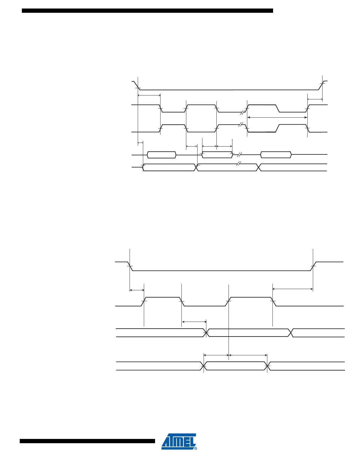
1147
6430F–ATARM–21-Feb-12
SAM3U Series
Timings are given with the following conditions.
VDDIO = 1.62V and 3V
SCK/MISO/MOSI Load = 30 pF
Figure 43-27. USART SPI Master Mode
• the MOSI line is driven by the output pin TXD
• the MISO line drives the input pin RXD
• the SCK line is driven by the output pin SCK
• the NSS line is driven by the output pin RTS
Figure 43-28.
USART SPI Slave mode (Mode 1 or 2)
• the MOSI line drives the input pin RXD
• the MISO line is driven by the output pin TXD
• the SCK line drives the input pin SCK
• the NSS line drives the input pin CTS
NPCSx
SPI0
MSBLSB
SPI1
CPOL=1
CPOL=0
MISO
MOSI
SCK
SPI5
SPI2
SPI3
SPI4
SPI4
SCK
MISO
MOSI
SPI6
SPI7SPI8
NPCS0
SPI12 SPI13
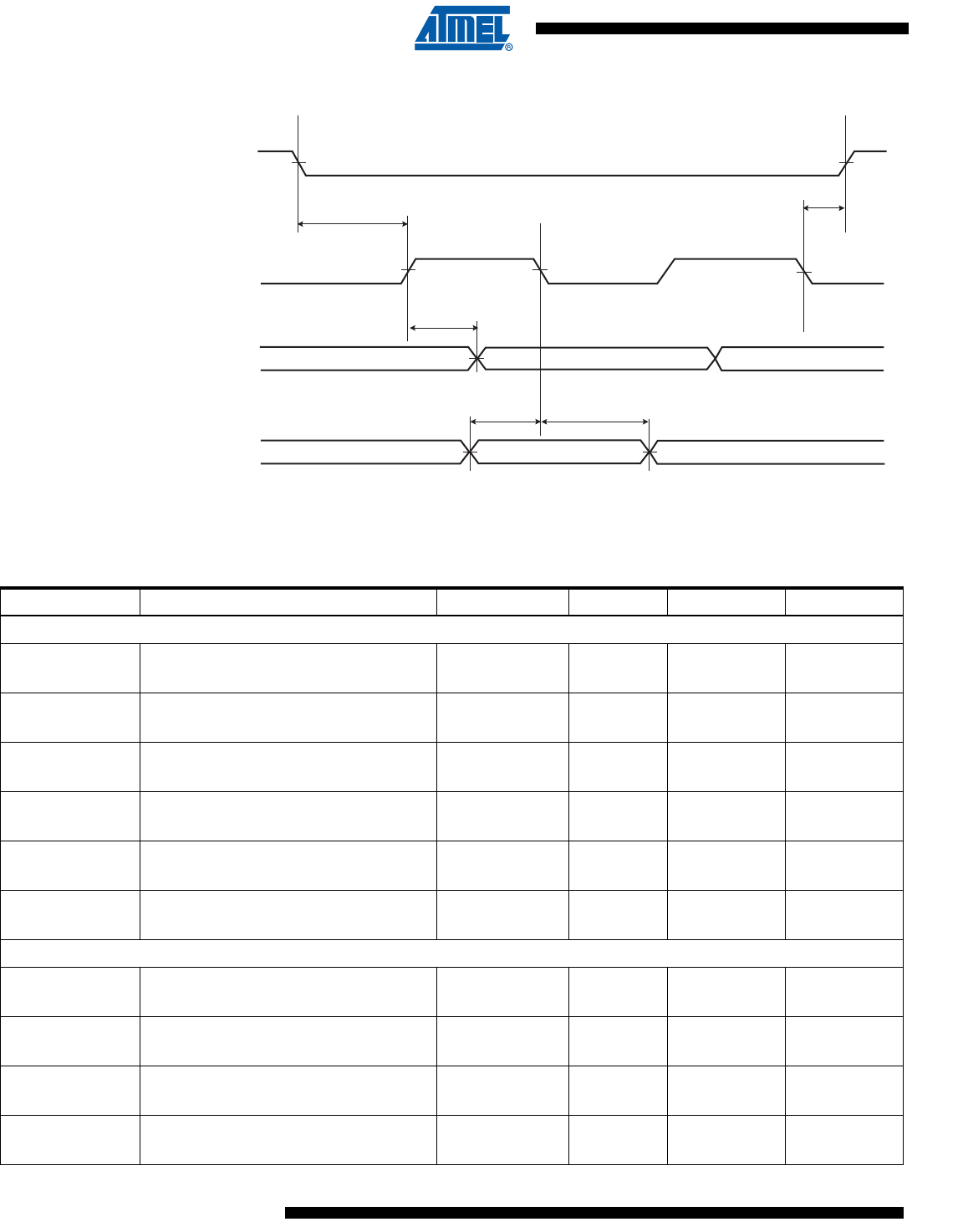
1148
6430F–ATARM–21-Feb-12
SAM3U Series
Figure 43-29. USART SPI Slave mode (Mode 0 or 3)
SCK
MISO
MOSI
SPI9
SPI10 SPI11
NPCS0
SPI15
SPI14
Table 43-49. USART SPI Timings
Symbol Parameter Conditions Min Max Units
Master Mode
SPI0SCK Period 1.8v domain
3.3v domain TBD ns
SPI1Input Data Setup Time 1.8v domain
3.3v domain TBD ns
SPI2Input Data Hold Time 1.8v domain
3.3v domain
TBD
TBD ns
SPI3Chip Select Active to Serial Clock 1.8v domain
3.3v domain
TBD
TBD ns
SPI4Output Data Setup Time 1.8v domain
3.3v domain
TBD
TBD ns
SPI5Serial Clock to Chip Select Inactive 1.8v domain
3.3v domain
TBD
TBD ns
Slave Mode
SPI6SCK falling to MISO 1.8V domain
3.3V domain
TBD
TBD
TBD
TBD ns
SPI7MOSI Setup time before SCK rises 1.8V domain
3.3V domain
TBD
TBD ns
SPI8MOSI Hold time after SCK rises 1.8v domain
3.3v domain
TBD
TBD ns
SPI9SCK rising to MISO 1.8v domain
3.3v domain
TBD
TBD
TBD ns

1149
6430F–ATARM–21-Feb-12
SAM3U Series
Notes: 1. 1.8V domain: VDDIO from 1.65V to 1.95V, maximum external capacitor = 25 pF
2. 3.3V domain: VDDIO from 3.0V to 3.6V, maximum external capacitor = 25 pF.
SPI10 MOSI Setup time before SCK falls 1.8v domain
3.3v domain
TBD
TBD ns
SPI11 MOSI Hold time after SCK falls 1.8v domain
3.3v domain
TBD
TBD ns
SPI12 NPCS0 setup to SCK rising 1.8v domain
3.3v domain
TBD
TBD ns
SPI13 NPCS0 hold after SCK falling 1.8v domain
3.3v domain
TBD
TBD ns
SPI14 NPCS0 setup to SCK falling 1.8v domain
3.3v domain
TBD
TBD ns
SPI15 NPCS0 hold after SCK rising 1.8v domain
3.3v domain
TBD
TBD ns
Table 43-49. USART SPI Timings
Symbol Parameter Conditions Min Max Units

1150
6430F–ATARM–21-Feb-12
SAM3U Series
43.8.7 Two-wire Serial Interface Characteristics
Table 30 describes the requirements for devices connected to the Two-wire Serial Bus. For timing symbols refer to Figure
43-30.
Note: 1. Required only for fTWCK > 100 kHz.
2. Cb = capacitance of one bus line in pF. Per I2C Standard compatibility, Cb Max = 400pF
3. The TWCK low Period is defined as follow:
4. The TWCK high period is defined as follows:
5. TCP_MCK = MCK Bus Period.
Table 43-50. Two-wire Serial Bus Requirements
Symbol Parameter Condition Min Max Units
VIL Input Low-voltage -0.3 0.3 VVDDIO V
VIH Input High-voltage 0.7xVVDDIO VCC + 0.3 V
Vhys Hysteresis of Schmitt Trigger Inputs 0.150 – V
VOL Output Low-voltage 3 mA sink current - 0.4 V
trRise Time for both TWD and TWCK 20 + 0.1Cb(1)(2) 300 ns
tof Output Fall Time from VIHmin to VILmax
10 pF < Cb < 400 pF
Figure 43-30 20 + 0.1Cb(1)(2) 250 ns
Ci(1) Capacitance for each I/O Pin – 10 pF
fTWCK TWCK Clock Frequency 0 400 kHz
Rp Value of Pull-up resistor
fTWCK ≤ 100 kHz
fTWCK > 100 kHz
tLOW Low Period of the TWCK clock fTWCK ≤ 100 kHz (3) –µs
fTWCK > 100 kHz (3) –µs
tHIGH High period of the TWCK clock fTWCK ≤ 100 kHz (4) –µs
fTWCK > 100 kHz (4) –µs
tHD;STA Hold Time (repeated) START Condition fTWCK ≤ 100 kHz tHIGH –µs
fTWCK > 100 kHz tHIGH –µs
tSU;STA Set-up time for a repeated START condition fTWCK ≤ 100 kHz tHIGH –µs
fTWCK > 100 kHz tHIGH –µs
tHD;DAT Data hold time fTWCK ≤ 100 kHz 0 3 x TCP_MCK µs
fTWCK > 100 kHz 0 3 x TCP_MCK µs
tSU;DAT Data setup time
fTWCK ≤ 100 kHz tLOW - 3 x
TCP_MCK
–ns
fTWCK > 100 kHz tLOW - 3 x
TCP_MCK
–ns
tSU;STO Setup time for STOP condition fTWCK ≤ 100 kHz tHIGH –µs
fTWCK > 100 kHz tHIGH –µs
tHD;STA Hold Time (repeated) START Condition fTWCK ≤ 100 kHz tHIGH –µs
fTWCK > 100 kHz tHIGH –µs
VVDDIO 0,4V–
3mA
--------------------------------------
1000ns
Cb
-------------------
Ω
VVDDIO 0,4V–
3mA
--------------------------------------
300ns
Cb
----------------
Ω
Tlow CLDIV(2CKDIV
×()4)+TMCK
×=
Thigh CHDIV(2CKDIV
×()4)+TMCK
×=
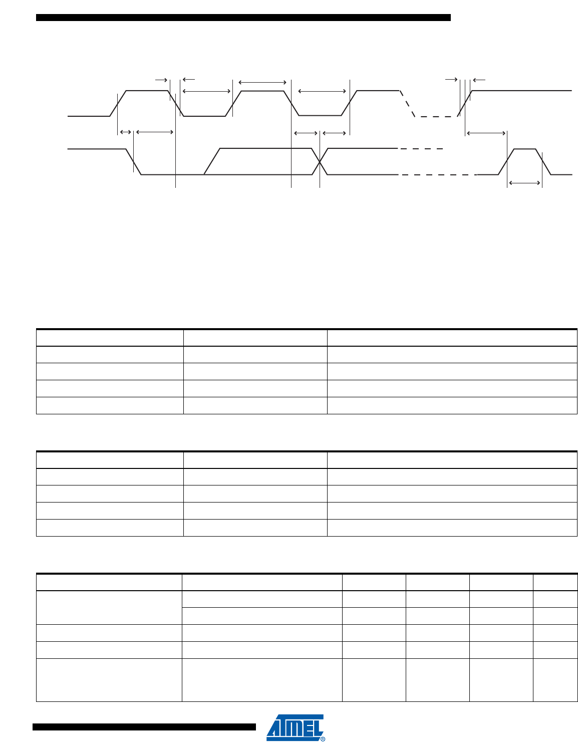
1151
6430F–ATARM–21-Feb-12
SAM3U Series
Figure 43-30. Two-wire Serial Bus Timing
43.8.8 Embedded Flash Characteristics
The maximum operating frequency is given in tables 43-51 and 43-52 below but is limited by the Embedded Flash access
time when the processor is fetching code out of it. The tables 43-51 and 43-52 below give the device maximum operating
frequency depending on the field FWS of the MC_FMR register. This field defines the number of wait states required to
access the Embedded Flash Memory.
Note: The embedded flash is fully tested during production test, the flash contents is not set to a known state prior to ship-
ment. Therefore, the flash contents should be erased prior to programming an application.
Table 43-51. Embedded Flash Wait State VDDCORE set at 1.62V
FWS Read Operations Maximum Operating Frequency (MHz)
0 1 cycle 24
1 2 cycles 40
2 3 cycles 72
3 4 cycles 84
t
SU;STA
t
LOW
t
HIGH
t
LOW
t
of
t
HD;STA
t
HD;DAT
t
SU;DAT
t
SU;STO
t
BUF
TWCK
TWD
t
r
Table 43-52. Embedded Flash Wait State VDDCORE set at 1.80V
FWS Read Operations Maximum Operating Frequency (MHz)
0 1 cycle 27
1 2 cycles 47
2 3 cycles 84
3 4 cycles 96
Table 43-53. AC Flash Characteristics
Parameter Conditions Min Typ Max Units
Program Cycle Time per page including auto-erase 4.6 ms
per page without auto-erase 2.3 ms
Full Chip Erase 10 11.5 ms
Data Retention Not Powered or Powered 10 Years
Endurance
Write/Erase cycles @ 25°C
Write/Erase cycles @ 85°C 10K
30K
cycles
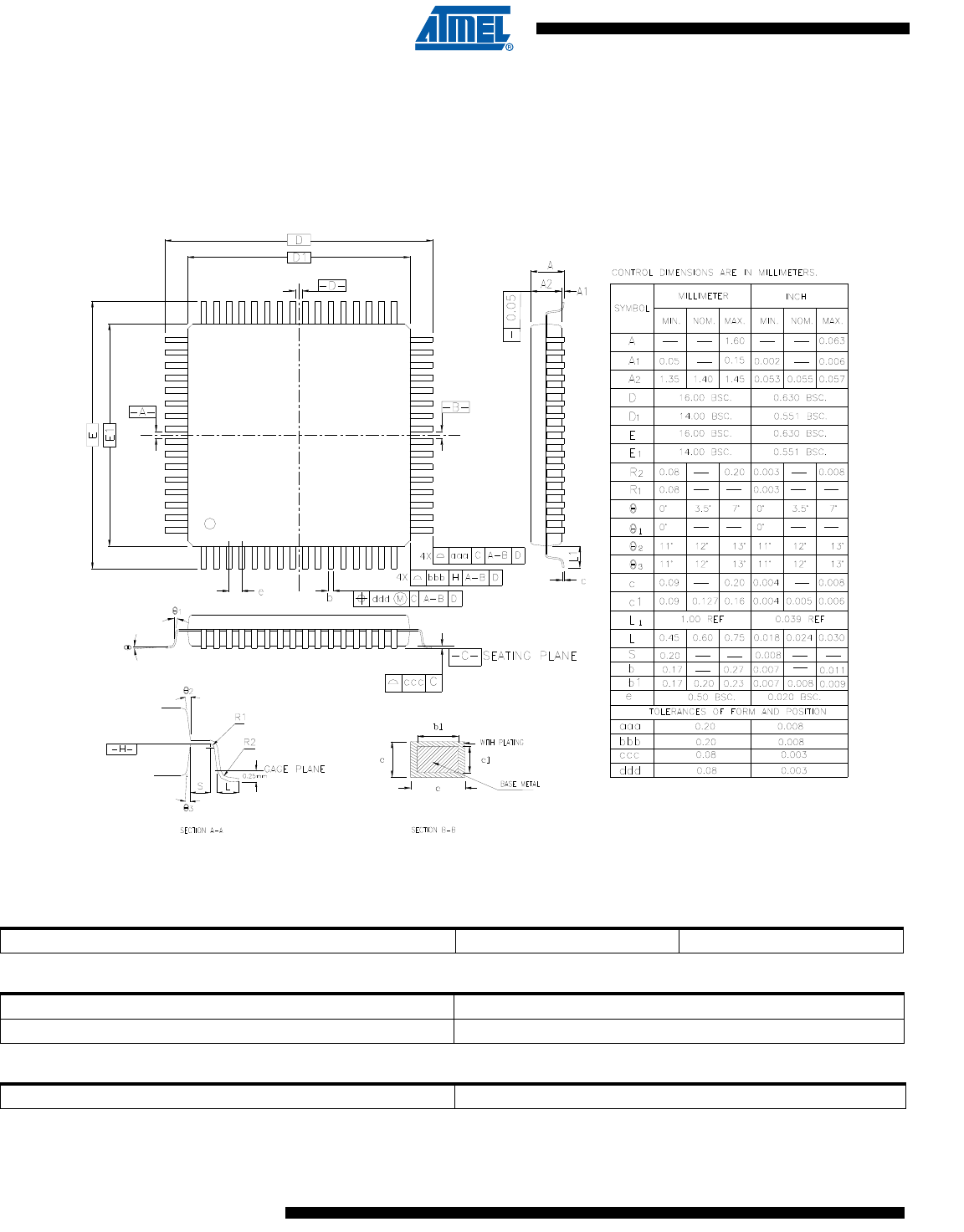
1152
6430F–ATARM–21-Feb-12
SAM3U Series
44. SAM3U4/2/1 Mechanical Characteristics
44.1 100-lead LQFP Package
Figure 44-1. 100-lead LQFP Package Drawing
This package respects the recommendations of the NEMI User Group.
Table 44-1. Device and LQFP Package Maximum Weight
SAM3UE4/2/1 800 mg
Table 44-2. Package Reference
JEDEC Drawing Reference MS-026
JESD97 Classification e3
Table 44-3. LQFP Package Characteristics
Moisture Sensitivity Level 3
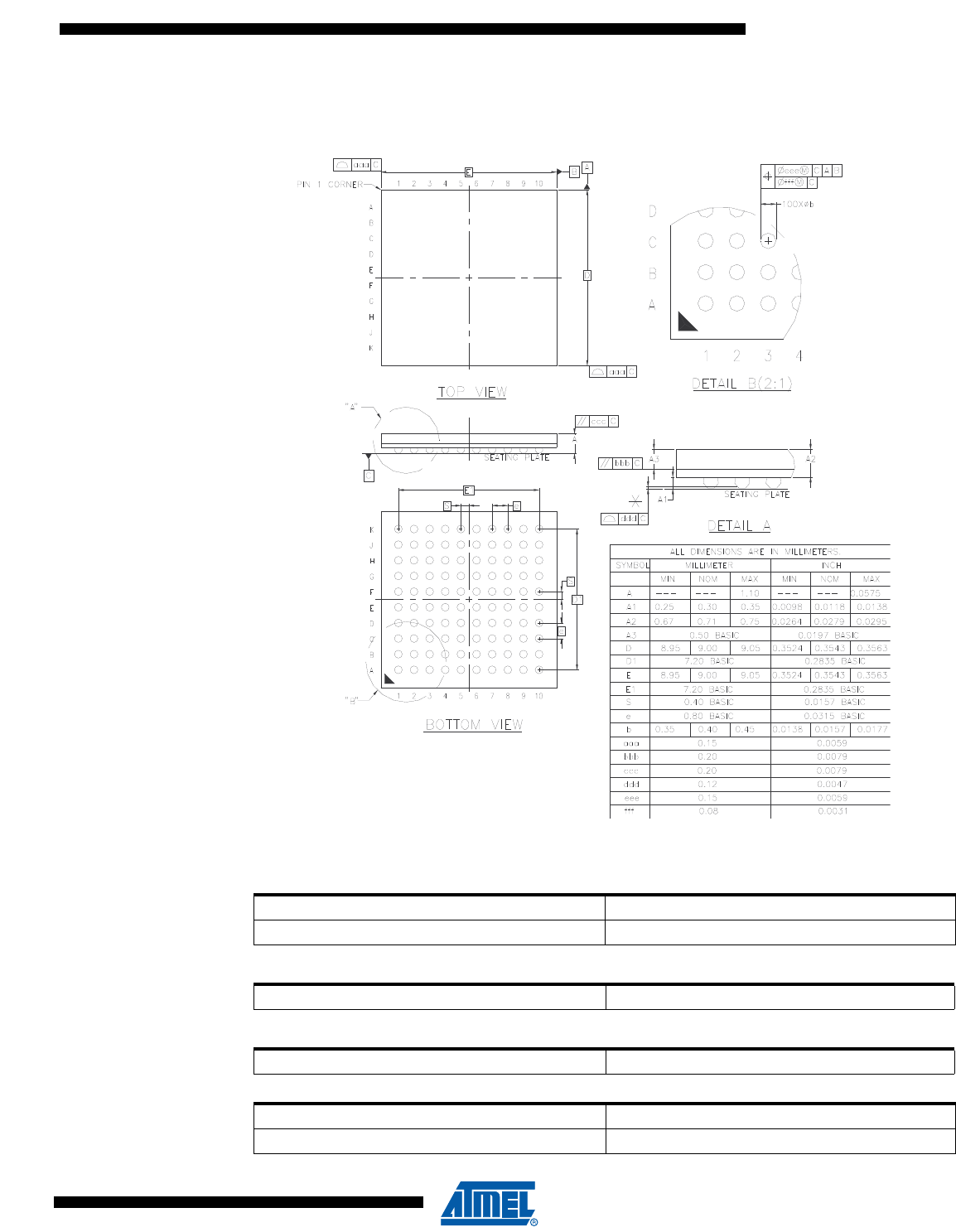
1153
6430F–ATARM–21-Feb-12
SAM3U Series
44.2 100-ball TFBGA Package
Figure 44-2. 100-ball TFBGA Package Drawing
Table 44-4. Soldering Information (Substrate Level)
Ball Land TBD
Soldering Mask Opening TBD
Table 44-5. Device Maximum Weight
TBD mg
Table 44-6. 100-ball Package Characteristics
Moisture Sensitivity Level 3
Table 44-7. Package Reference
JEDEC Drawing Reference TBD
JESD97 Classification e1
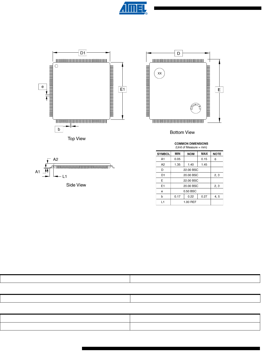
1154
6430F–ATARM–21-Feb-12
SAM3U Series
44.3 144-lead LQFP Package
Figure 44-3. 144-lead LQFP Package Drawing
Notes: 1. This drawing is for general information only; refer to JEDEe Drawing MS-026 for additional information.
2. The top package body size may be smaller than the bottom package size by as much as 0.15 mm.
3. Dimensions D1 and E1 do not include mold protrusions. Allowable protrusion is 0.25 mm per side. D1 and E1 are maximum
plastic body size dimensions including mold mismatch.
4. b dimension by more than 0.08 mm. Dambar cannot be located on the lower radius or the foot. Minimum space between pro-
trusion and an adjacent lead is 0.07 mm for 0.4 and 0.5 mm pitch packages.
5. These dimensions apply to the flat section of the lead between 0.10 mm and 0.25 mm from the lead tip.
6. A1 is defined as the distance from the seating place to the lowest point on the package body.
Table 44-8. Device Maximum Weight
TBD mg
Table 44-9. 144-lead Package Characteristics
Moisture Sensitivity Level 3
Table 44-10. Package Reference
JEDEC Drawing Reference MS-026
JESD97 Classification e3
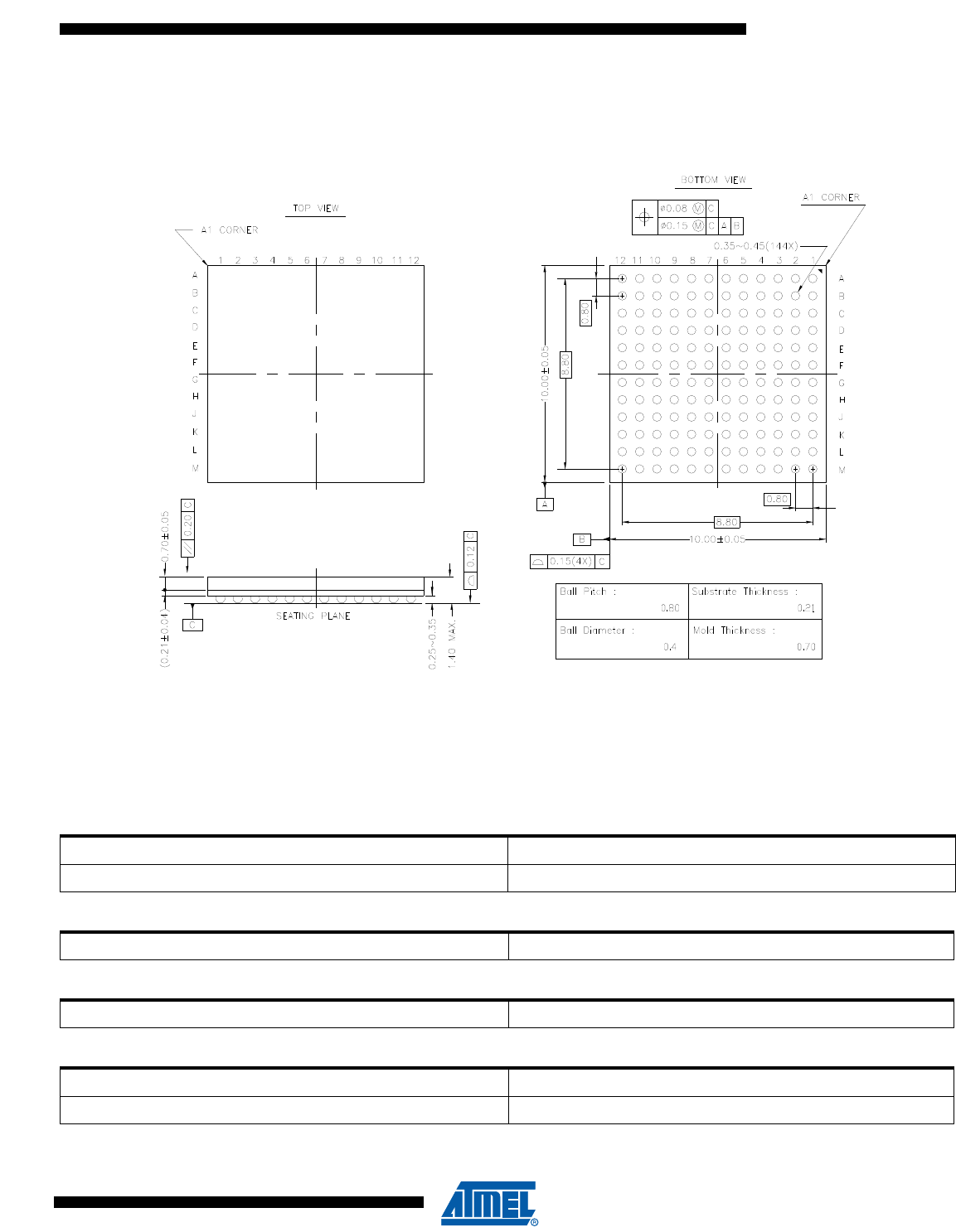
1155
6430F–ATARM–21-Feb-12
SAM3U Series
44.4 144-ball LFBGA Package
Figure 44-4. 144-ball LFBGA Package Drawing
All dimensions are in mm.
This package respects the recommendations of the NEMI User Group.
Table 44-11. Soldering Information (Substrate Level)
Ball Land 0.380 mm
Soldering Mask Opening 0.280 mm
Table 44-12. Device and 144-ball BGA Package Maximum Weight
300 mg
Table 44-13. 144-ball BGA Package Characteristics
Moisture Sensitivity Level 3
Table 44-14.
JEDEC Drawing Reference none
JESD97 Classification e1

1156
6430F–ATARM–21-Feb-12
SAM3U Series
44.5 Soldering Profile
Table 44-15 gives the recommended soldering profile from J-STD-020C.
Note: The package is certified to be backward compatible with Pb/Sn soldering profile.
A maximum of three reflow passes is allowed per component.
44.6 Packaging Resources
Land Pattern Definition.
Refer to the following IPC Standards:
• IPC-7351A and IPC-782 (Generic Requirements for Surface Mount Design and Land Pattern
Standards) http://landpatterns.ipc.org/default.asp
• Atmel Green and RoHS Policy and Package Material Declaration Data Sheet
http://www.atmel.com/green/
Table 44-15. Soldering Profile
Profile Feature Green Package
Average Ramp-up Rate (217°C to Peak) 3°C/sec. max.
Preheat Temperature 175°C ±25°C 180 sec. max.
Temperature Maintained Above 217°C 60 sec. to 150 sec.
Time within 5°C of Actual Peak Temperature 20 sec. to 40 sec.
Peak Temperature Range 260°C
Ramp-down Rate 6°C/sec. max.
Time 25°C to Peak Temperature 8 min. max.

1157
6430F–ATARM–21-Feb-12
SAM3U Series
45. Ordering Information
Table 45-1. ATSAM3U4/2/1 Ordering Information
Ordering Code MRL
Flash
(Kbytes) Package Package Type
Temperature
Operating Range
ATSAM3U4EA-AU A 256 LQFP144 Green Industrial
-40°C to 85°C
ATSAM3U4EA-CU A 256 LFBGA 144 Green Industrial
-40°C to 85°C
ATSAM3U4CA-AU A 256 LQFP 100 Green Industrial
-40°C to 85°C
ATSAM3U4CA-CU A 256 TFBGA100 Green Industrial
-40°C to 85°C
ATSAM3U2EA-AU A 128 LQFP144 Green Industrial
-40°C to 85°C
ATSAM3U2EA-CU A 128 LFBGA144 Green Industrial
-40°C to 85°C
ATSAM3U2CA-AU A 128 LQFP100 Green Industrial
-40°C to 85°C
ATSAM3U2CA-CU A 128 TFBGA100 Green Industrial
-40°C to 85°C
ATSAM3U1EA-AU A 64 LQFP144 Green Industrial
-40°C to 85°C
ATSAM3U1EA-CU A 64 LFBGA144 Green Industrial
-40°C to 85°C
ATSAM3U1CA-AU A 64 LQFP100 Green Industrial
-40°C to 85°C
ATSAM3U1CA-CU A 64 TFBGA100 Green Industrial
-40°C to 85°C
ATSAM3U1EB-AU B 64 LQFP144 Green Industrial
-40°C to 85°C
ATSAM3U1EB-CU B 64 LFBGA144 Green Industrial
-40°C to 85°C
ATSAM3U1CB-AU B 64 LQFP100 Green Industrial
-40°C to 85°C
ATSAM3U1CB-CU B 64 TFBGA100 Green Industrial
-40°C to 85°C

1158
6430F–ATARM–21-Feb-12
SAM3U Series

1159
6430F–ATARM–21-Feb-12
SAM3U Series
46. SAM3U Series Errata
46.1 Marking
All devices are marked with the Atmel logo and the ordering code.
Additional marking is as follows:
where
•“YY”: manufactory year
• “WW”: manufactory week
• “V”: revision
• “XXXXXXXXX”: lot number
At the time of publication, in addition to the following “SAM3U Errata - Rev. A Parts”, there is an
errata sheet on engineering samples of the SAM3U devices. This document is available on
Atmel’s web site:
http://www.atmel.com/dyn/resources/prod_documents/doc6483.pdf
YYWW V
XXXXXXXXX ARM

1160
6430F–ATARM–21-Feb-12
SAM3U Series
46.2 SAM3U Errata - Rev. A Parts
Revision A parts Chip IDs are as follows:
SAM3U4C (Rev A) 0x28000961
SAM3U2C (Rev A) 0x280A0761
SAM3U1C (Rev A) 0x28090561
SAM3U4E (Rev A) 0x28100961
SAM3U2E (Rev A) 0x281A0761
SAM3U1E (Rev A) 0x28190561
Refer also to Section 46.1 “Marking” on page 1159
46.2.1 Flash
46.2.1.1 Flash: Issue Running at Frequency Lower than 2.5 MHz
When the system clock (MCK) is lower than 2.5 MHz with 2 Wait States (WS) programmed in
the EEFC Flash Mode Register (EEFC_FMR), the Cortex fetches erroneous instructions.
Problem Fix/Workaround
Do not use 2 WS when running at a frequency lower than 2.5 MHz.
46.2.1.2 Flash: Read Flash in 64-bit Mode
Higher than expected power consumption can be seen when reading Flash in 64-bit mode.
Problem Fix/Workaround
Use 128-bit mode instead.
46.2.1.3 Flash: Flash Programming
When writing data into the Flash memory plane (either through the EEFC, using the IAP func-
tion, or FFPI), the data may not be correctly written (i.e the data written is not the one expected).
Problem Fix/Workaround
Set the number of Wait States (WS) to 6 (FWS=6) during the programming.
46.2.1.4 Flash: Fetching Error after Reading the Unique Identifier
After reading the Unique Identifier (or using the STUI/SPUI command), the processor may fetch
wrong instructions. It depends on the code and on the region of the code.
Problem Fix/Workaround
In order to avoid this problem, follow the steps below:
1. Set bit 16 of EEFC Flash Mode Register to 1
2. Send the Start Read Unique Identifier command (STUI) by writing the Flash Command
Register with the STUI command.
3. Wait for the FRDY bit to fall
4. Read the Unique ID (and next bits if required)
5. Send the Stop Read Unique Identifier command (SPUI) by writing the Flash Command
Register with the SPUI command.
6. Wait for the FRDY bit to rise
7. Clear bit 16 of EEFC Flash Mode Register
Note: During the sequence, the software cannot run out of Flash (so needs to run out of SRAM).

1161
6430F–ATARM–21-Feb-12
SAM3U Series
46.2.2 12-bit Analog-to-Digital Converter (ADC12B)
46.2.2.1 ADC12B: Current Consumption in Backup Mode on VDDANA
In Backup mode, the current consumption on VDDANA is around 1.0 mA instead of 0.1 µA
Problem Fix/Workaround
Four workarounds are possible:
1. Do not supply VDDANA and VDDIO in Backup mode using an external switch managed
by SHDN pin.
2. Do not supply VDDANA in Backup mode using an external switch managed by the
SHDN and set all PIOs with ADC inputs (PA22, PA30, PB3-PB8, PC15-PC18, PC28-
C21) at low level (either externally or by software).
3. Do not supply VDDANA in Backup mode using an external switch managed by any PIO
and set all PIOs with ADC inputs (PA22, PA30, PB3-PB8, PC15-PC18, PC28-C21) at
low level (either externally or by software). Since the PIO state is preserved when in
backup mode, any free PIO line can be used to switch off the external switch by driving
the PIO line at low level (PIO is input, pull-up enabled after backup reset).
4. Use wait mode instead of Backup mode.
46.2.2.2 ADC: Trigger Launches only One Conversion
A start command initiates a conversion sequence of one channel but not all activated channels
as expected.
Problem Fix/Workaround
Send as many start commands as the number of activated channels, or use free run mode.
46.2.2.3 ADC12B: Saturation
When the ADC12B works in saturation (measurements below 0V or above ADREF) the results
may be erratic, the value deviation can be around 30 LSB to the expected data.
Problem Fix/Workaround
None.

1162
6430F–ATARM–21-Feb-12
SAM3U Series
46.2.2.4 ADC: Wrong first Conversions
The first conversions done by the ADC may be erroneous if the maximum gain (x4 in single
ended or x2 in differential mode) is not used. The issue appears after the power-up or if a con-
version has not occured for 1 minute.
Problem Fix/Workaround
Three workarounds are possible :
1) Perform 16 dummy conversions on one channel (whatever conditions used in term of setup of
gain, single/differential, offset, and channel selected). The next conversions will be correct for
any channels and any settings. Note that these dummy conversions need to be performed if no
conversion has occured for 1 minute or for a new chip start-up.
2) Perform a dummy conversion on a single ended channel on which an external voltage of
ADVREF/2 (+/-10%) is applied. Use the following conditions for this conversion: gain at 4, offset
set at 1. The next conversions will be correct for any channels and any settings. Note that this
dummy conversion needs to be performed if no conversion has occured for 1 minute or for a
new chip start-up.
3) Perform a dummy conversion on a differential channel on which the two inputs are connected
together and connected to any voltage (from 0 to ADVREF). Use the following conditions for this
conversion: gain at 4, offset set at 1. The next conversions will be correct for any channels and
any settings. Note that this dummy conversion needs to be performed if no conversion has
occured for 1 minute or for a new chip start-up.
46.2.3 Power Management Controller (PMC)
46.2.3.1 PMC: Main Oscillator Frequency selection if the Main On-chip RC Oscillator is OFF
When the 4/8/12 MHz RC Oscillator is off, the frequency selection (MOSCRCF bitfield in
CKGR_MOR) can not be changed. The register can be written but the modification to
MOSCRCF will not be taken into account.
Problem Fix/Workaround
Modify MOSCRCF while 4/8/12 MHz RC Oscillator is on (MOSCREN = 1).

1163
6430F–ATARM–21-Feb-12
SAM3U Series
46.3 SAM3U Errata - Rev. B Parts
Revision B parts Chip IDs are as follows:
SAM3U1C (Rev B) 0x28090562
SAM3U1E (Rev B) 0x28190562
Refer also to Section 46.1 “Marking” on page 1159
46.3.1 Flash
46.3.1.1 Flash: Issue Running at Frequency Lower than 2.5 MHz
When the system clock (MCK) is lower than 2.5 MHz with 2 Wait States (WS) programmed in
the EEFC Flash Mode Register (EEFC_FMR), the Cortex fetches erroneous instructions.
Problem Fix/Workaround
Do not use 2 WS when running at a frequency lower than 2.5 MHz.
46.3.1.2 Flash: Flash Programming
When writing data into the Flash memory plane (either through the EEFC, using the IAP func-
tion, or FFPI), the data may not be correctly written (i.e the data written is not the one expected).
Problem Fix/Workaround
Set the number of Wait States (WS) to 6 (FWS=6) during the programming.
46.3.1.3 Flash: Fetching Error after Reading the Unique Identifier
After reading the Unique Identifier (or using the STUI/SPUI command), the processor may fetch
wrong instructions. It depends on the code and on the region of the code.
Problem Fix/Workaround
In order to avoid this problem, follow the steps below:
1. Set bit 16 of EEFC Flash Mode Register to 1
2. Send the Start Read Unique Identifier command (STUI) by writing the Flash Command
Register with the STUI command.
3. Wait for the FRDY bit to fall
4. Read the Unique ID (and next bits if required)
5. Send the Stop Read Unique Identifier command (SPUI) by writing the Flash Command
Register with the SPUI command.
6. Wait for the FRDY bit to rise
7. Clear bit 16 of EEFC Flash Mode Register
Note: During the sequence, the software cannot run out of Flash (so needs to run out of SRAM).

1164
6430F–ATARM–21-Feb-12
SAM3U Series
46.3.2 12-bit Analog-to-Digital Converter (ADC12B)
46.3.2.1 ADC12B: Current Consumption in Backup Mode on VDDANA
In Backup mode, the current consumption on VDDANA is around 1.0 mA instead of 0.1 µA
Problem Fix/Workaround
Four workarounds are possible:
1. Do not supply VDDANA and VDDIO in Backup mode using an external switch managed
by SHDN pin.
2. Do not supply VDDANA in Backup mode using an external switch managed by the
SHDN and set all PIOs with ADC inputs (PA22, PA30, PB3-PB8, PC15-PC18, PC28-
C21) at low level (either externally or by software).
3. Do not supply VDDANA in Backup mode using an external switch managed by any PIO
and set all PIOs with ADC inputs (PA22, PA30, PB3-PB8, PC15-PC18, PC28-C21) at
low level (either externally or by software). Since the PIO state is preserved when in
backup mode, any free PIO line can be used to switch off the external switch by driving
the PIO line at low level (PIO is input, pull-up enabled after backup reset).
4. Use wait mode instead of Backup mode.
46.3.2.2 ADC: Trigger Launches only One Conversion
A start command initiates a conversion sequence of one channel but not all activated channels
as expected.
Problem Fix/Workaround
Send as many start commands as the number of activated channels, or use free run mode.

1165
6430F–ATARM–21-Feb-12
SAM3U Series
46.3.2.3 ADC: Wrong first Conversions
The first conversions done by the ADC may be erroneous if the maximum gain (x4 in single
ended or x2 in differential mode) is not used. The issue appears after the power-up or if a con-
version has not occured for 1 minute.
Problem Fix/Workaround
Three workarounds are possible :
1) Perform 16 dummy conversions on one channel (whatever conditions used in term of setup of
gain, single/differential, offset, and channel selected). The next conversions will be correct for
any channels and any settings. Note that these dummy conversions need to be performed if no
conversion has occured for 1 minute or for a new chip start-up.
2) Perform a dummy conversion on a single ended channel on which an external voltage of
ADVREF/2 (+/-10%) is applied. Use the following conditions for this conversion: gain at 4, offset
set at 1. The next conversions will be correct for any channels and any settings. Note that this
dummy conversion needs to be performed if no conversion has occured for 1 minute or for a
new chip start-up.
3) Perform a dummy conversion on a differential channel on which the two inputs are connected
together and connected to any voltage (from 0 to ADVREF). Use the following conditions for this
conversion: gain at 4, offset set at 1. The next conversions will be correct for any channels and
any settings. Note that this dummy conversion needs to be performed if no conversion has
occured for 1 minute or for a new chip start-up.
46.3.3 Power Management Controller (PMC)
46.3.3.1 PMC: Main Oscillator Frequency selection if the Main On-chip RC Oscillator is OFF
When the 4/8/12 MHz RC Oscillator is off, the frequency selection (MOSCRCF bitfield in
CKGR_MOR) can not be changed. The register can be written but the modification to
MOSCRCF will not be taken into account.
Problem Fix/Workaround
Modify MOSCRCF while 4/8/12 MHz RC Oscillator is on (MOSCREN = 1).

1166
6430F–ATARM–21-Feb-12
SAM3U Series

1167
6430F–ATARM–21-Feb-12
SAM3U Series
47. Revision History
In the tables that follow, the most recent version of the document appears first.
Note: “rfo” indicates changes requested during document review and approval loop.
Doc.
Rev.
6430F Comments
Change
Request
Ref.
PMC:
Section 28.9 ”Fast Startup”, SUPC_FSMR --> PMC_FSMR and SUPC_FSPR --> PMC_FSPR
Section 28.3 ”Master Clock Controller”, removed bogus sentence about Master Clock divider functionality
Section 28.1 ”Description”, changed sentence “Processor Clock (HCLK), must be switched off...”
8010
rfo
8217
Memories:
Section 9.1.3.1 ”Flash Overview”, Flash size should be 64KBytes instead of 256KBytes 8029
Electrical Characteristics:
Section 43.7, 43.7.1 Gain and Offset Calibration removed
Section 43.4 ”Crystal Oscillators Characteristics”:
Table 43-16, “32 kHz RC Oscillator Characteristics”, changed parameter ‘Frequency Temperature Dependency’
Table 43-4, “Core Power Supply Brownout Detector Characteristics”, changed MAX value of VTH+
Section 43.8.8 ”Embedded Flash Characteristics”, added note regarding erasing Flash contents
8031
8174
8223
Errata:
Section 46.3 ”SAM3U Errata - Rev. B Parts”, added errata section for rev. B
Section 46.2 ”SAM3U Errata - Rev. A Parts”: Section 46.2.2.2 ”ADC: Trigger Launches only One Conversion”,
added errata
Section 46.3 ”SAM3U Errata - Rev. B Parts”: Section 46.3.2.2 ”ADC: Trigger Launches only One Conversion”,
added errata
Section 46.2 ”SAM3U Errata - Rev. A Parts”: Section 46.2.2.4 ”ADC: Wrong first Conversions”, added errata
Section 46.3 ”SAM3U Errata - Rev. B Parts”: Section 46.3.2.3 ”ADC: Wrong first Conversions”, added errata
8131
rfo
rfo
8164
Overview & Mechanical Characteristics:
Replaced all occurrences of '100-ball LFBGA' into '100-ball TFBGA' 8044
Ordering Information:
Table 45-1, “ATSAM3U4/2/1 Ordering Information”, updated with MRL B devices 8130
SPI:
Section 32.8.11 ”SPI Write Protection Status Register”, description of register simplified
Section 32.8.10 ”SPI Write Protection Mode Register”, removed ‘SPI’ from register description names
Section 32. ”Serial Peripheral Interface (SPI) Programmer Datasheet”, SPI version updated to version ‘R’
8136
rfo
rfo
TC:
Section 36.1 ”Description”: Table 36-1, “Timer Counter Clock Assignment”, footnote for table updated 8159

1168
6430F–ATARM–21-Feb-12
SAM3U Series
Doc.
Rev.
6430E Comments
Change
Request
Ref.
Overview:
Comment in front of rows PA24 and PA25 removed, and put as a footnote(3) for TWD1 and TWCK1.
Table 11-2, “Multiplexing on PIO Controller A (PIOA)”, “Peripheral B” column, PA2 and PA17 texts exchanged.
Figure 5-5 ”Fast Start-Up Sources”, ‘Falling/Rising Edge Detector’ changed to ‘High/Low Level Detector’ in 3
blocks.
Wait mode consumption updated in Table 5-1, “Low Power Mode Configuration Summary”
7724
7954
7922
rfo
Clock Generator:
Last sentence removed from Section 27.5.1 ”Divider and Phase Lock Loop Programming”, as PLLADIV2 does
not exist.
Third bullet edited in Section 27.1 ”Description”.
7751
7908
Electrical Characteristics:
3 values updated in Table 43-12, “Typical Current Consumption in Wait Mode”.
Section 43.7.1 ”Sample and Hold Time versus Source Output Impedance” created.
rfo
SUPC:
Section 19.3.2 ”Slow Clock Generator”, variable VDD_SUPPLY_MONITOR changed to VDD_Backup, in order
to get VDDBU instead of VDDUTMI.
7743
PMC:
Section 28.8 ”Programmable Clock Output Controller”, UPLLCK --> UPLLCK/2.
Figure 28-1, “General Clock Block Diagram” edited (UPLLCK --> UPLLCK/2, and UPLLDIV /1/2 --> Divider /2)
7898
7912
USART:
Section 35. ”Universal Synchronous Asynchronous Receiver Transmitter (USART)”, PDC condition shown
instead of DMA.
7804
Errata:
Section 46.2.1.4 ”Flash: Fetching Error after Reading the Unique Identifier” added. 7978
Doc.
Rev.
6430D Comments
Change
Request
Ref.
Overview:
Section 5.5.2 ”Wait Mode”, sentence starting with ‘By configuring...’ --> ‘This is done by configuring...’ 7492
Section 10.13 ”Chip Identification”, (Rev A) was removed from Table 10-1. 7642
TWD1 and TWCK1 removed from Figure 2-2, “100-pin SAM3U4/2/1C Block Diagram”. 7624
Table 3-1, “Signal Description List”, Note (4) added to TDO Output. 7635
A typo fixed in Section 9.1.1 ”Internal SRAM”: 4224 Kbytes --> 4224 bytes. 7305
Debug and Test Features:
Table 14-1, “Debug and Test Signal List”, Note (1) added to TDO Output.
Section 14.4.8 ”ID Code Register”, Chip ID and JTAG ID Code edited.
Section 14.4.7 ”IEEE 1149.1 JTAG Boundary Scan”, second paragraph updated.
7635
7543
7485
Chip ID:
CHIPID_CIDR column in Table 29-1, “ATSAM3U Chip IDs Register” updated as in Table 10-2 7642

1169
6430F–ATARM–21-Feb-12
SAM3U Series
Clock Generator:
Section 27.6 ”UTMI Phase Lock Loop Programming”, first sentence edited, together with Table 27-5, “UTMI PLL
Block Diagram”.7484
PMC:
Section 28.9 ”Fast Startup”, a sentence starting with ‘Important’ added as a second paragraph.
In the first paragraph, ‘LPM bit is at 0’ replaced by ‘LPM bit is at 1’. 7539
Section 28.14.15 ”PMC Status Register”, MOSCSELS bit descriptions reversed. 7389
Electrical Characteristics:
In Table 43-18, “32.768 kHz Crystal Oscillator Characteristics”, CLEXT Maximum value is 22 instead of 20. 7589
Section 43.8.7 ”USART in SPI Mode Timings” updated: UART --> USART, SPCK --> SCK, Figures and titles
updated. 7320
Errata:
Section 46.2.2.1 ”ADC12B: Current Consumption in Backup Mode on VDDANA” edited.
Section 46.2.1.3 ”Flash: Flash Programming” added.
7420
7205
Backpage:
A typo fixed: ‘tehincal’ --> ‘technical’ 7536
Doc.
Rev.
6430D Comments (Continued)
Change
Request
Ref.

1170
6430F–ATARM–21-Feb-12
SAM3U Series
Doc.
Rev.
6430C Comments
Change
Request
Ref.
Overview:
Section 2. ”SAM3U Block Diagram”, changed orientation of block diagrams.
Section 5. ”Power Considerations”, fixed grammar in Voltage ranges.
rfo
Section 3. ”Signal Description”, USART signal DCD0 is an Input 6681
Figure 5-1, “Single Supply”, Main supply range is 1.8V-3.6V.
Figure 5-1, Figure 5-2, Figure 5-3, updated “Note” below figures, “With Main Supply <2.0V USB and ADC are
not usable.
6698
Section 5.5 ”Low Power Modes”, stray references to WUPx pins, renamed WKUPx 6711
Table 5-1, “Low Power Mode Configuration Summary”, updated footnote “5”. 6964
Table 11-2, “Multiplexing on PIO Controller A (PIOA)”, TWD1 and TWCK1 only available on 144-pin version. 6686
Section 10.13 ”Chip Identification”
Table 10-2, “SAM3U Chip IDs Register - Revision A Parts”, added to datasheet.
Section 12.4 ”Universal Synchronous Asynchronous Receiver Transmitter (USART)”...”SCK up to MCK/6”
6951
rfo→7097
CHIP ID:
”ARCH: Architecture Identifier” bit field updated with SAM3S, SAM3N identifiers. Bitfield tables reorganized. 6967
CORTEX:
Section 13.19 ”Nested Vectored Interrupt Controller”, text on 3rd bullet updated: “Level detection of interrupt
signals.”
6823
EFC:
Section 21.3.3.7 ”Unique Identifier”, Unique Identifier is located ... 0x80000-0x8000F.
Figure 21-6, “Example of Partial Page Programming” text added below figure,..”works only with 128-bit (or
higher) boundaries...”
rfo
6827
HSMCI:
Section 37.10 ”HSMCI Boot Operation Mode”, added precision on boot from internal Flash.
”SDCBUS: SDCard/SDIO Bus Width”, bitfield table updated.
Values, Names, Descriptions updated in bitfield description tables. (global)
Section 37.13.18 ”HSMCI Write Protect Mode Register”, ASCI code is for MCI.
6745
7125
rfo
MATRIX:
Section 24.6.6 ”Write Protect Status Register”, WPVS identified in bitfield description.
6718
PMC:
“PMC Fast Startup Polarity Register”, FSTPx: bitfield typo fixed.
“PMC Clock Generator PLLA Register”, removed STMODE bitfield.
Section 28.11 ”Programming Sequence” Step 5 “Selection of Programmable Clocks”, updated: “Four clock
options are available: main clock, slow clock, PLLACK and UPLLCK. By default, the clock source selected is
main clock.”
Section 28.10 ”Clock Failure Detector”, updated with new information.
6688
6706
7128
PWM:
Section 38.6.23 ”PWM Fault Mode Register”, Section 38.6.24 ”PWM Fault Status Register”, Section 38.6.25
”PWM Fault Clear Register”, Section 38.6.27 ”PWM Fault Protection Enable Register”, bitfield descriptions
updated.
Table 38-2, “I/O Lines”, new to datasheet.
6824
rfo

1171
6430F–ATARM–21-Feb-12
SAM3U Series
RTC:
Section 18.3.2 ”Interrupt”, updated.
Section 18.5 ”Real Time Clock (RTC) User Interface”, the reset for RTC_CALR is 0x01210720.
TIMEVSEL, CALEVSEL bitfield descriptions reorganized.
7071
7046/7087
6796
SSC:
Redundant letter C removed from title. 6949
SUPC:
Section 19.4 ”Supply Controller (SUPC) User Interface”, offset updated for GPBR: 0x90-0xDC.
FWUPDBC, WUPDBC bitfield descriptions reorganized.
Backup supply is VDDBU
6950
6796
6714
TC:
Figure 36-2 ”Clock Chaining Selection”, channel 1 updated.
updated bitfields: TC0XC0S, TC1XC1S, TC2XC2S, TCCLKS, BURST, ETRGEDG, LDRA, LDRB, TCCLKS,
BURST, EEVTEDG, EEVT, WAVSEL, ACPA, ACPC, AEEVT, ASWTRG, BCPB, BCPC, BEEVT, BSWTRG
6687
6796
UDHP:
Figure 39-4 ”Logical Address Space for DPR Access”, EP0 has but 1 bank
Figure 39-1 ”Block Diagram”, 1 PMC to UTMI signal line. Notes removed.
Figure 39.4 ”Product Dependencies”, added to datasheet.
Figure 39-6 ”Register Mapping”, DMA offset updated to 0x300 + channel *...
6750
6792
rfo
6822
USART:
Section 35.6.7 ”Modem Mode”, is available.
Section 35.6 ”Functional Description”, ...SCK up to MCK/6
Section 35.6.8.2 ”Baud Rate”
SPI Master Mode: ...”the value programmed in CD must be superior or equal to 6.”
SPI Slave Mode:...”the external clock (SCK) frequency must be at least 6 times lower than the system clock.”
Section 35.6.1 ”Baud Rate Generator”,”...signal provided on SCK must be at least 3 times lower than MCK in
USART mode, or 6 in SPI mode.”
Section 35.6.1.3 ”Baud Rate in Synchronous Mode or SPI Mode”, ...”limits the SCK maximum frequency to
MCK/3 in USART mode, or MCK/6 in SPI mode.”
6791
rfo→7097
Doc.
Rev.
6430C Comments (Continued)
Change
Request
Ref.

1172
6430F–ATARM–21-Feb-12
SAM3U Series
Electrical Characteristics:
Table 43-18, “32.768 kHz Crystal Oscillator Characteristics”, last row of the table changed from CL to CPA R A
“Internal Parasitic Capacitance”. Schematic and Crystal formula updated
Table 43-21, “3 to 20 MHz Crystal Oscillator Characteristics”, CLEXT row, Parameter cell updated. Added 1K
resistor to Schematic and Crystal formula updated.
6701
Table 43-16, “32 kHz RC Oscillator Characteristics”, table updated.
Table 43-17, “4/8/12 MHz RC Oscillators Characteristics”, updated “Frequency Temperature Dependency”
Table 43-31, “Channel Conversion Time and ADC Clock”, TSTART-UP “From OFF mode...” startup times updated.
6951
Table 43-32, “External Voltage Reference Input”, ADVREF changed to AD12BVREF.
Table 43-37, “Analog Inputs”, VADVREF changed to VAD12BVREF
7098
Errata:
Section 46.2 ”SAM3U Errata - Rev. A Parts”, added to Errata. 6951
Doc.
Rev.
6430C Comments (Continued)
Change
Request
Ref.

1173
6430F–ATARM–21-Feb-12
SAM3U Series
.
Doc Rev
6430B Comments
Change
Request
Ref.
Introduction:
Section 1. ”SAM3U Description”, Updated: 52 Kbytes of SRAM. 4x USARTs (SAM3U1C/2C/4C have 3), up to
2x TWIs (SAM3U1C/2C/4C have 1), up to 5x SPIs SAM3U1C/2C/4C have 4),
Table 1-1, “Configuration Summary” EBI column updated, 8 bits for SAM3U1C/2C/4C
SAM3U4/3/2C rows FWUP replaces NO in FWUP,SHDN pins column.
6400
6642
Figure 2-1 ”144-pin SAM3U4/2/1E Block Diagram” and Figure 2-2 ”100-pin SAM3U4/2/1C Block Diagram”
updated, SM cell removed; UART moved to peripheral area, added Flash Unique block, removed 12B from
ADC block, added SysTick counter and Fmax 96MHz to M3 block. FWUP replaces WKUP in fig 2-1, FWUP
added to fig 2-2.
Figure 2-2 ”100-pin SAM3U4/2/1C Block Diagram”, NWR1/NBS1, NXRP0, A0 removed from block diagram,
6482/6642
rfo/
Table 3-1, “Signal Description List”, Schmit Trigger added ”PIO Controller - PIOA - PIOB - PIOC”. exception
details given in footnote.
VDDIN, VDDOUT added to table.
”Serial Wire/JTAG Debug Port (SWJ-DP)” replaced ICE and JTAG. This section of the table updated
status of pulldowns and pullups specified.
6480
rfo
Section 4. ”Package and Pinout”; reorganized according to product.
Section 4.1 ”SAM3U4/2/1E Package and Pinout”, Section 4.2 ”SAM3U4/2/1C Package and Pinout”, pinouts
finalized in datasheet.
6471/rfo
6607
Section 5.5.1 ”Backup Mode”, BOD replaced by Supply Monitor/SM.
Figure 5-4 ”Wake-up Source”, BODEN replaced by SMEN. FWUP → Falling Edge Detector.
Table 5-1, “Low Power Mode Configuration Summary”, PIO state in Low Power Mode, backup mode is;
“Previous state saved.”
Figure 5-3 ”Backup Batteries Used”, FWUP replaces FWKUP.
rfo
6645
6642
Section 6.6 ”NRSTB Pin”, VDDIO changed to VDDBU
Section 6. ”Input/Output Lines” replaces Section 5.8 “Programmable I/O Lines”.
Section 6.1 ”General Purpose I/O Lines (GPIO)” and Section 6.2 ”System I/O Lines” replace Section 6. “I/O
Line Considerations”.
Figure 6-1 ”On-Die Termination schematic”, added.
Section 6.8 “PIO Controllers”, removed.
Section 8. ”Product Mapping”, title changed from “Memories”.
Section 9. ”Memories”; now comprises Section 9.1 ”Embedded Memories” and Section 9.2 ”External
Memories”
Section 9.1.3.5 ”Security Bit Feature”, updated
6646
6481/rfo
Table 7-3, “SAM3U Master to Slave Access”, Slave 9, High Speed Peripheral Bridge line added.
Section 7.2 ”APB/AHB Bridges”, reference to ADC updated “10-bit ADC, 12-bit ADC (ADC12B)”.
Table 11-3, “Multiplexing on PIO Controller B (PIOB)” ADC12B2, ADC12B3 properly listed.
Section 12.10.1 ”12-bit High Speed ADC”, Section 12.10.2 ”10-bit Low Power ADC”, titles changed.
“Quadrature Decoder Logic” on page 51 properly stated in list of TC functions.
6663
6397
Section 12.10.1 ”12-bit High Speed ADC”, 2nd item on list updated.
Section 12.10.2 ”10-bit Low Power ADC”, Ksample values updated on 2nd item of list.
rfo
ADC12B:
Section 41.6.6 ”ADC12B Analog Control Register”,IBCTL reasigned to fields 8 and 9 6649

1174
6430F–ATARM–21-Feb-12
SAM3U Series
CORTEX-M3:
Table 13-31, “Priority grouping”updated.
Section 13.19.7.1 ”IP27”, title changed to IP27, value in bitfields 0 to 7 changed to IP28.
6394:
Section 13.20.6 ”Application Interrupt and Reset Control Register”read/write values to VECTKEY changed 6436
Section 13.5.2.2 ”Non Maskable Interrupt (NMI)” added to datasheet.
Section 13.6.2 ”Fault escalation and hard faults”, last sentence updated with NMI function.
Section 13.3.5 ”Data types” Condition tags sorted out.
Table 13-11, “Faults”updated footnote 1
Table 13-29, “CMSIS functions for NVIC control”Description in 4th row updated.
6483
on page 53, “...copyright ARM Ltd., 2008 - 2009.” precise years given.
Table 13-4, “Memory access behavior”last row assinged to Reserved in Memory Map.
Big Endien not used in this product.
rfo
Debug and Test:
Section 14.1 ”Overview”, SWJ-DP...also embeds a serial trace.
Table 14-1, “Debug and Test Signal List”, reorganized.
rfo
FFPI:
Section 22.2.5.4 ”Flash Lock Commands”, last sentence removed from 2nd paragraph (ref to EA command). 6677
HSMCI:
Section 37.12 ”Write Protection Registers”, Section 37.13.18 ”HSMCI Write Protect Mode Register” and
Section 37.13.19 ”HSMCI Write Protect Status Register”,added.
6432
MATRIX:
Table 24-1, “Register Mapping”, added offsets for Write Protection Registers
6431
PDC:
Section 26. ”Peripheral DMA Controller (PDC)” Section replaced.
6468
PIO:
Section 30.5.1 ”Write Protection Registers”, Section 30.6.42 ”PIO Write Protect Mode Register” and Section
30.6.43 ”PIO Write Protect Status Register” added with links to protected registers.
6430
PMC:
Section 28.14.16 ”PMC Interrupt Mask Register”, Section 28.14.13 ”PMC Interrupt Enable Register”, Section
28.14.14 ”PMC Interrupt Disable Register”, 0 and 1read or write values described.
Section 28.13 ”Write Protection Registers”, Section 28.14.20 ”PMC Write Protect Mode Register” and
Section 28.14.20 ”PMC Write Protect Mode Register” added with links to protected registers.
Section 28.10 ”Clock Failure Detector”, added sentence on Fast RC
Section 28.11 ”Programming Sequence”, added step 1 and reordered subsequent numbering sequence.
removed code example, bitfield names updated.
6311/rfo
6432
6469
6591
rfo
PWM:
Table 38-4, “Fault Inputs”, “PWM Fault Input Number” column, typos fixed
6397
RSTC:
Section 16.2 ”Block Diagram”, “backup_nreset” replaces “core_backup_reset”.
Section 16.3.1 ”Reset Controller Overview”, RSTC_MR...”is powered with VDDBU...”
Section 16.3.4.2 ”Backup Reset”, “The vddcore_nreset signal is asserted by the SUPC...” and
“backup_nreset” replaces “core_backup_reset”.
rfo
SMC:
Table 25-4, “External Memory Mapping”, restored rows for chip selects 0, 1, 2 to the table.
6397
Doc Rev
6430B Comments (Continued)
Change
Request
Ref.

1175
6430F–ATARM–21-Feb-12
SAM3U Series
SPI:
Section 32.7.10 ”SPI Write Protection Control Register” and Section 32.7.11 ”SPI Write Protection Status
Register”, added.
6432
SSC:
Section 31.7.1 ”Write Protection Registers”, Section 31.8.17 ”SSC Write Protect Mode Register” and Section
31.8.18 ”SSC Write Protect Status Register”
6429
SUPC:
Figure 19-5 ”Raising the VDDUTMI Power Supply”, updated, i.e., shutdown polarity changed, Fast RC
Oscillator, NRST, periph_nreset, proc_nreset signals added, detailed startup time added up to instruction
fetch.
Figure 19-6 ”NRSTB Reset”, updated SHDN / vr_standby waveform.
Section 19.4.8 ”Supply Controller Status Register”, added note concerning “status register flag reset”.
Figure 19-2 ”Separated Backup Supply Powering Scheme”
6604
rfo
6653
6642
USART:
Section 35.7.2 ”USART Mode Register”, VAR_SYNC bitfield description updated.
Section 35.7.1 ”USART Control Register” RSTSTA description updated with UNRE bit.
Section ”Receive NACK Inhibit”, updated. Section 35.7.1 ”USART Control Register”, NACK description,
grammar fixed.
Section 35.6.10 ”Write Protection Registers”, Section 35.7.16 ”USART Write Protect Mode Register” and
Section 35.7.17 ”USART Write Protect Status Register”, added.
6282
6283
6422
6432
Electrical Characteristics:
Section 43. ”SAM3U4/2/1 Electrical Characteristics”, updated
Section 43.8.3.1 ”Maximum SPI Frequency”, added
Figure 43-5 ”Measurement Setup”, updated.
Table 43-41, “I/O Characteristics”, in the Conditions column: VDDIO = 1.62V
rfo
6663
Mechanical Characteristics:
Section 44.5 ”Soldering Profile”, added. rfo
Doc Rev
6430B Comments (Continued)
Change
Request
Ref.

1176
6430F–ATARM–21-Feb-12
SAM3U Series
Doc.
Rev. Date Comments
Change
Request
Ref.
6430A 24-Mar-09 First Issue - advance information
16-May-09 Review
29-May-09 Approved

i
6430F–ATARM–21-Feb-12
SAM3U Series
Features ..................................................................................................... 1
1 ATSAM3U4/2/1 Description ..................................................................... 2
1.1 Configuration Summary ...........................................................................................2
2 ATSAM3U4/2/1 Block Diagram ................................................................ 3
3 Signal Description .................................................................................... 5
3.1 Design Considerations ............................................................................................8
4 Package and Pinout ................................................................................. 9
4.1 SAM3U4/2/1E Package and Pinout .........................................................................9
4.2 SAM3U4/2/1C Package and Pinout ......................................................................12
5 Power Considerations ........................................................................... 15
5.1 Power Supplies ......................................................................................................15
5.2 Voltage Regulator ..................................................................................................15
5.3 Typical Powering Schematics ................................................................................15
5.4 Active Mode ...........................................................................................................19
5.5 Low Power Modes .................................................................................................19
5.6 Wake-up Sources ..................................................................................................22
5.7 Fast Start-Up .........................................................................................................23
6 Input/Output Lines ................................................................................. 24
6.1 General Purpose I/O Lines (GPIO) ........................................................................24
6.2 System I/O Lines ...................................................................................................24
6.3 Serial Wire JTAG Debug Port (SWJ-DP) ..............................................................24
6.4 Test Pin .................................................................................................................25
6.5 NRST Pin ...............................................................................................................25
6.6 NRSTB Pin ............................................................................................................25
6.7 ERASE Pin ............................................................................................................25
7 Processor and Architecture .................................................................. 26
7.1 ARM Cortex-M3 Processor ....................................................................................26
7.2 APB/AHB Bridges ..................................................................................................26
7.3 Matrix Masters .......................................................................................................26
7.4 Matrix Slaves .........................................................................................................27
7.5 Master to Slave Access .........................................................................................27
7.6 DMA Controller ......................................................................................................28
7.7 Peripheral DMA Controller .....................................................................................28
7.8 Debug and Test Features ......................................................................................29

ii
6430F–ATARM–21-Feb-12
SAM3U Series
8 Product Mapping .................................................................................... 30
9 Memories ................................................................................................ 31
9.1 Embedded Memories ............................................................................................31
9.2 External Memories .................................................................................................34
10 System Controller .................................................................................. 36
10.1 System Controller and Peripheral Mapping .........................................................38
10.2 Power-on-Reset, Brownout and Supply Monitor .................................................38
10.3 Reset Controller ...................................................................................................38
10.4 Supply Controller .................................................................................................38
10.5 Clock Generator ..................................................................................................39
10.6 Power Management Controller ............................................................................40
10.7 Watchdog Timer ..................................................................................................41
10.8 SysTick Timer ......................................................................................................41
10.9 Real-time Timer ...................................................................................................41
10.10 Real-time Clock .................................................................................................41
10.11 General-Purpose Back-up Registers .................................................................41
10.12 Nested Vectored Interrupt Controller .................................................................41
10.13 Chip Identification ..............................................................................................42
10.14 PIO Controllers ..................................................................................................42
11 Peripherals .............................................................................................. 43
11.1 Peripheral Identifiers ............................................................................................43
11.2 Peripheral Signal Multiplexing on I/O Lines .........................................................44
12 Embedded Peripherals Overview ......................................................... 48
12.1 Serial Peripheral Interface (SPI) ..........................................................................48
12.2 Two Wire Interface (TWI) ....................................................................................48
12.3 Universal Asynchronous Receiver Transceiver (UART) ......................................48
12.4 Universal Synchronous Asynchronous Receiver Transmitter (USART) ..............49
12.5 Serial Synchronous Controller (SSC) ..................................................................49
12.6 Timer Counter (TC) .............................................................................................49
12.7 Pulse Width Modulation Controller (PWM) ..........................................................50
12.8 High Speed Multimedia Card Interface (HSMCI) .................................................51
12.9 USB High Speed Device Port (UDPHS) ..............................................................51
12.10 Analog-to-Digital Converter (ADC) ....................................................................51
13 ARM Cortex® M3 Processor .................................................................. 53

iii
6430F–ATARM–21-Feb-12
SAM3U Series
13.1 About this section ................................................................................................53
13.2 About the Cortex-M3 processor and core peripherals .........................................53
13.3 Programmers model ............................................................................................55
13.4 Memory model .....................................................................................................68
13.5 Exception model ..................................................................................................77
13.6 Fault handling ......................................................................................................84
13.7 Power management ............................................................................................87
13.8 Instruction set summary ......................................................................................89
13.9 Intrinsic functions .................................................................................................92
13.10 About the instruction descriptions ......................................................................93
13.11 Memory access instructions ............................................................................101
13.12 General data processing instructions ..............................................................117
13.13 Multiply and divide instructions ........................................................................133
13.14 Saturating instructions .....................................................................................137
13.15 Bitfield instructions ...........................................................................................139
13.16 Branch and control instructions .......................................................................143
13.17 Miscellaneous instructions ...............................................................................151
13.18 About the Cortex-M3 peripherals .....................................................................164
13.19 Nested Vectored Interrupt Controller ...............................................................165
13.20 System control block .......................................................................................178
13.21 System timer, SysTick .....................................................................................205
13.22 Memory protection unit ....................................................................................210
13.23 Glossary ..........................................................................................................224
14 Debug and Test Features .................................................................... 229
14.1 Overview ............................................................................................................229
14.2 Application Examples ........................................................................................230
14.3 Debug and Test Pin Description ........................................................................231
14.4 Functional Description .......................................................................................231
15 Watchdog Timer (WDT) ....................................................................... 237
15.1 Description .........................................................................................................237
15.2 Block Diagram ...................................................................................................237
15.3 Functional Description .......................................................................................238
15.4 Watchdog Timer (WDT) User Interface .............................................................240
16 Reset Controller (RSTC) ...................................................................... 245
16.1 Overview ............................................................................................................245

iv
6430F–ATARM–21-Feb-12
SAM3U Series
16.2 Block Diagram ...................................................................................................245
16.3 Functional Description .......................................................................................245
16.4 Reset Controller (RSTC) User Interface ............................................................253
17 Real-time Timer (RTT) .......................................................................... 257
17.1 Description .........................................................................................................257
17.2 Embedded Characteristics ................................................................................257
17.3 Block Diagram ...................................................................................................257
17.4 Functional Description .......................................................................................258
17.5 Real-time Timer (RTT) User Interface ...............................................................260
18 Real Time Clock (RTC) ......................................................................... 265
18.1 Description .........................................................................................................265
18.2 Block Diagram ...................................................................................................265
18.3 Product Dependencies ......................................................................................265
18.4 Functional Description .......................................................................................266
18.5 Real Time Clock (RTC) User Interface .............................................................269
19 Supply Controller (SUPC) .................................................................... 283
19.1 Description .........................................................................................................283
19.2 Embedded Characteristics ................................................................................283
19.3 Block Diagram ...................................................................................................284
19.4 Supply Controller Functional Description ..........................................................285
19.5 Supply Controller (SUPC) User Interface ..........................................................294
20 General Purpose Backup Registers (GPBR) ..................................... 305
20.1 Embedded Characteristics ................................................................................305
20.2 Description .........................................................................................................305
21 Enhanced Embedded Flash Controller (EEFC) ................................. 307
21.1 Description .......................................................................................................307
21.2 Embedded Characteristics .............................................................................307
21.3 Product Dependencies ......................................................................................307
21.4 Functional Description .......................................................................................307
21.5 Enhanced Embedded Flash Controller (EEFC) User Interface .........................317
22 Fast Flash Programming Interface (FFPI) .......................................... 323
22.1 Overview ............................................................................................................323
22.2 Parallel Fast Flash Programming ......................................................................323
23 SAM3U4/2/1 Boot Program .................................................................. 333

v
6430F–ATARM–21-Feb-12
SAM3U Series
23.1 Description .........................................................................................................333
23.2 Flow Diagram ....................................................................................................333
23.3 Device Initialization ............................................................................................333
23.4 SAM-BA Monitor ................................................................................................334
23.5 Hardware and Software Constraints ..................................................................338
24 Bus Matrix (MATRIX) ............................................................................ 339
24.1 Description .........................................................................................................339
24.2 Memory Mapping ...............................................................................................339
24.3 Special Bus Granting Techniques .....................................................................339
24.4 Arbitration ..........................................................................................................340
24.5 Write Protect Registers ......................................................................................342
24.6 Bus Matrix (MATRIX) User Interface .................................................................343
25 Static Memory Controller (SMC) ......................................................... 353
25.1 Description .........................................................................................................353
25.2 Embedded Characteristics ................................................................................353
25.3 Block Diagram ...................................................................................................354
25.4 I/O Lines Description .........................................................................................355
25.5 Multiplexed Signals ............................................................................................355
25.6 Application Example ..........................................................................................356
25.7 Product Dependencies ......................................................................................356
25.8 External Memory Mapping .................................................................................357
25.9 Connection to External Devices ........................................................................358
25.10 Standard Read and Write Protocols ................................................................360
25.11 Scrambling/Unscrambling Function .................................................................366
25.12 Automatic Wait States .....................................................................................367
25.13 Data Float Wait States .....................................................................................370
25.14 External Wait ...................................................................................................375
25.15 Slow Clock Mode .............................................................................................381
25.16 NAND Flash Controller Operations .................................................................384
25.17 SMC Error Correcting Code Functional Description ........................................396
25.18 Power Management Controller (PMC) User Interface .....................................400
26 Peripheral DMA Controller (PDC) ....................................................... 441
26.1 Description .........................................................................................................441
26.2 Embedded Characteristics ................................................................................441
26.3 Block Diagram ...................................................................................................442

vi
6430F–ATARM–21-Feb-12
SAM3U Series
26.4 Functional Description .......................................................................................442
26.5 Peripheral DMA Controller (PDC) User Interface ..............................................445
27 Clock Generator ................................................................................... 457
27.1 Description .........................................................................................................457
27.2 Block Diagram ...................................................................................................458
27.3 Slow Clock .........................................................................................................459
27.4 Main Clock .........................................................................................................460
27.5 Divider and PLLA Block .....................................................................................463
27.6 UTMI Phase Lock Loop Programming ..............................................................464
28 Power Management Controller (PMC) ................................................ 465
28.1 Description .........................................................................................................465
28.2 Block Diagram ...................................................................................................466
28.3 Master Clock Controller .....................................................................................466
28.4 Processor Clock Controller ................................................................................467
28.5 SysTick Clock ....................................................................................................467
28.6 Peripheral Clock Controller ................................................................................467
28.7 Free Running Processor Clock ..........................................................................467
28.8 Programmable Clock Output Controller .............................................................468
28.9 Fast Startup .......................................................................................................468
28.10 Clock Failure Detector .....................................................................................470
28.11 Programming Sequence ..................................................................................471
28.12 Clock Switching Details ...................................................................................474
28.13 Write Protection Registers ...............................................................................477
28.14 Power Management Controller (PMC) User Interface ....................................478
29 Chip Identifier (CHIPID) ....................................................................... 501
29.1 Description .........................................................................................................501
29.2 Embedded Characteristics ................................................................................501
29.3 Chip Identifier (CHIPID) User Interface ............................................................502
30 Parallel Input/Output Controller (PIO) ................................................ 509
30.1 Description .........................................................................................................509
30.2 Embedded Characteristics ................................................................................509
30.3 Block Diagram ...................................................................................................510
30.4 Product Dependencies ......................................................................................511
30.5 Functional Description .......................................................................................512
30.6 I/O Lines Programming Example .......................................................................520

vii
6430F–ATARM–21-Feb-12
SAM3U Series
30.7 Parallel Input/Output Controller (PIO) User Interface ........................................522
31 Synchronous Serial Controller (SSC) ................................................ 547
31.1 Description .........................................................................................................547
31.2 Embedded Characteristics .............................................................................547
31.3 Block Diagram ...................................................................................................548
31.4 Application Block Diagram .................................................................................548
31.5 Pin Name List ....................................................................................................549
31.6 Product Dependencies ......................................................................................549
31.7 Functional Description .......................................................................................551
31.8 SSC Application Examples ................................................................................562
31.9 Synchronous Serial Controller (SSC) User Interface ........................................565
32 Serial Peripheral Interface (SPI) Programmer Datasheet ................. 593
32.1 Description .........................................................................................................593
32.2 Embedded Characteristics ................................................................................593
32.3 Block Diagram ...................................................................................................594
32.4 Application Block Diagram .................................................................................595
32.5 Signal Description .............................................................................................595
32.6 Product Dependencies ......................................................................................596
32.7 Functional Description .......................................................................................597
32.8 Serial Peripheral Interface (SPI) User Interface ................................................611
33 Two-wire Interface (TWI) ...................................................................... 627
33.1 Description .........................................................................................................627
33.2 Embedded Characteristics ................................................................................627
33.3 List of Abbreviations ..........................................................................................628
33.4 Block Diagram ...................................................................................................628
33.5 Application Block Diagram .................................................................................629
33.6 Product Dependencies ......................................................................................629
33.7 Functional Description .......................................................................................630
33.8 Master Mode ......................................................................................................631
33.9 Multi-master Mode .............................................................................................643
33.10 Slave Mode ......................................................................................................646
33.11 Two-wire Interface (TWI) User Interface .........................................................654
34 Universal Asynchronous Receiver Transceiver (UART) .................. 669
34.1 Description .........................................................................................................669
34.2 Embedded Characteristics ................................................................................669

viii
6430F–ATARM–21-Feb-12
SAM3U Series
34.3 Block Diagram ...................................................................................................670
34.4 Product Dependencies ......................................................................................670
34.5 UART Operations ..............................................................................................671
34.6 Universal Asynchronous Receiver Transceiver (UART) User Interface ...........677
35 Universal Synchronous Asynchronous Receiver Transmitter (USART) 689
35.1 Description .........................................................................................................689
35.2 Embedded Characteristics ................................................................................689
35.3 Block Diagram ...................................................................................................690
35.4 Application Block Diagram .................................................................................691
35.5 I/O Lines Description ........................................................................................692
35.6 Product Dependencies ......................................................................................693
35.7 Functional Description .......................................................................................695
35.8 Universal Synchronous Asynchronous Receiver Transmitter (USART) User Interface 733
36 Timer Counter (TC) .............................................................................. 763
36.1 Description .........................................................................................................763
36.2 Embedded Characteristics ................................................................................763
36.3 Block Diagram ...................................................................................................764
36.4 Pin Name List ....................................................................................................765
36.5 Product Dependencies ......................................................................................765
36.6 Functional Description .......................................................................................766
36.7 Timer Counter (TC) User Interface ....................................................................785
37 High Speed Multimedia Card Interface (HSMCI) ............................... 809
37.1 Description .........................................................................................................809
37.2 Embedded Characteristics ................................................................................809
37.3 Block Diagram ...................................................................................................810
37.4 Application Block Diagram .................................................................................811
37.5 Pin Name List ....................................................................................................811
37.6 Product Dependencies ......................................................................................812
37.7 Bus Topology .....................................................................................................812
37.8 High Speed MultiMediaCard Operations ...........................................................815
37.9 SD/SDIO Card Operation ..................................................................................833
37.10 CE-ATA Operation ...........................................................................................834
37.11 HSMCI Boot Operation Mode ..........................................................................835
37.12 HSMCI Transfer Done Timings .......................................................................836
37.13 Write Protection Registers ...............................................................................838

ix
6430F–ATARM–21-Feb-12
SAM3U Series
37.14 High Speed Multimedia Card Interface (HSMCI) User Interface .....................839
38 Pulse Width Modulation (PWM) .......................................................... 869
38.1 Description .........................................................................................................869
38.2 Embedded Characteristics ................................................................................869
38.3 Block Diagram ...................................................................................................871
38.4 I/O Lines Description .........................................................................................871
38.5 Product Dependencies ......................................................................................872
38.6 Functional Description .......................................................................................874
38.7 Pulse Width Modulation (PWM) User Interface .................................................902
39 USB High Speed Device Port (UDPHS) .............................................. 951
39.1 Description .........................................................................................................951
39.2 Embedded Characteristics ................................................................................951
39.3 Block Diagram ...................................................................................................953
39.4 Typical Connection ............................................................................................954
39.5 Product Dependencies ......................................................................................954
39.6 Functional Description .......................................................................................954
39.7 USB High Speed Device Port (UDPHS) User Interface ....................................980
40 DMA Controller (DMAC) ..................................................................... 1021
40.1 Description .......................................................................................................1021
40.2 Block Diagram .................................................................................................1022
40.3 Functional Description .....................................................................................1022
40.4 DMAC Software Requirements .......................................................................1038
40.5 DMA Controller (DMAC) User Interface ..........................................................1040
41 12-bit Analog-to-Digital Converter (ADC12B) .................................. 1063
41.1 Description .......................................................................................................1063
41.2 Block Diagram .................................................................................................1063
41.3 Signal Description ............................................................................................1064
41.4 Product Dependencies ....................................................................................1064
41.5 Functional Description .....................................................................................1065
41.6 12-bit Analog-to-Digital Converter (ADC12B) User Interface ..........................1072
42 Analog-to-Digital Converter (ADC) ................................................... 1087
42.1 Description .......................................................................................................1087
42.2 Block Diagram .................................................................................................1087
42.3 Signal Description ............................................................................................1087

x
6430F–ATARM–21-Feb-12
SAM3U Series
42.4 Product Dependencies ....................................................................................1088
42.5 Functional Description .....................................................................................1089
42.6 Analog-to-Digital Converter (ADC) User Interface ...........................................1094
43 SAM3U4/2/1 Electrical Characteristics ............................................. 1107
43.1 Absolute Maximum Ratings .............................................................................1107
43.2 DC Characteristics ...........................................................................................1108
43.3 Power Consumption ........................................................................................1113
43.4 Crystal Oscillators Characteristics ...................................................................1121
43.5 UPLL, PLLA Characteristics ............................................................................1127
43.6 USB High Speed Port ......................................................................................1128
43.7 12-Bit ADC Characteristics ..............................................................................1129
43.8 AC Characteristics ...........................................................................................1135
44 SAM3U4/2/1 Mechanical Characteristics ......................................... 1152
44.1 100-lead LQFP Package .................................................................................1152
44.2 100-ball TFBGA Package ................................................................................1153
44.3 144-lead LQFP Package .................................................................................1154
44.4 144-ball LFBGA Package ................................................................................1155
44.5 Soldering Profile ..............................................................................................1156
44.6 Packaging Resources ......................................................................................1156
45 Ordering Information ......................................................................... 1157
46 SAM3U Series Errata ......................................................................... 1159
46.1 Marking ............................................................................................................1159
46.2 SAM3U Errata - Rev. A Parts ..........................................................................1160
46.3 SAM3U Errata - Rev. B Parts ..........................................................................1163
47 Revision History ................................................................................. 1167

6430F–ATARM–21-Feb-12
Headquarters International
Atmel Corporation
2325 Orchard Parkway
San Jose, CA 95131
USA
Tel: (+1) (408) 441-0311
Fax: (+1) (408) 487-2600
Atmel Asia Limited
Unit 01-5 & 16, 19F
BEA Tower, Millennium City 5
418 Kwun Tong Road
Kwun Tong, Kowloon
HONG KONG
Tel: (+852) 2245-6100
Fax: (+852) 2722-1369
Atmel Munich GmbH
Business Campus
Parkring 4
D-85748 Garching b. Munich
GERMANY
Tel: (+49) 89-31970-0
Fax: (+49) 89-3194621
Atmel Japan
9F, Tonetsu Shinkawa Bldg.
1-24-8 Shinkawa
Chuo-ku, Tokyo 104-0033
JAPAN
Tel: (81) 3-3523-3551
Fax: (81) 3-3523-7581
Product Contact
Web Site
www.atmel.com
www.atmel.com/AT91SAM
Technical Support
AT91SAM Support
Atmel technical support
Sales Contacts
www.atmel.com/contacts/
Literature Requests
www.atmel.com/literature
Disclaimer: The information in this document is provided in connection with Atmel products. No license, express or implied, by estoppel or otherwise, to any
intellectual property right is granted by this document or in connection with the sale of Atmel products. EXCEPT AS SET FORTH IN ATMEL’S TERMS AND CONDI-
TIONS OF SALE LOCATED ON ATMEL’S WEB SITE, ATMEL ASSUMES NO LIABILITY WHATSOEVER AND DISCLAIMS ANY EXPRESS, IMPLIED OR STATUTORY
WARRANTY RELATING TO ITS PRODUCTS INCLUDING, BUT NOT LIMITED TO, THE IMPLIED WARRANTY OF MERCHANTABILITY, FITNESS FOR A PARTICULAR
PURPOSE, OR NON-INFRINGEMENT. IN NO EVENT SHALL ATMEL BE LIABLE FOR ANY DIRECT, INDIRECT, CONSEQUENTIAL, PUNITIVE, SPECIAL OR INCIDEN-
TAL DAMAGES (INCLUDING, WITHOUT LIMITATION, DAMAGES FOR LOSS OF PROFITS, BUSINESS INTERRUPTION, OR LOSS OF INFORMATION) ARISING OUT
OF THE USE OR INABILITY TO USE THIS DOCUMENT, EVEN IF ATMEL HAS BEEN ADVISED OF THE POSSIBILITY OF SUCH DAMAGES. Atmel makes no
representations or warranties with respect to the accuracy or completeness of the contents of this document and reserves the right to make changes to specifica-
tions and product descriptions at any time without notice. Atmel does not make any commitment to update the information contained herein. Unless specifically pro-
vided otherwise, Atmel products are not suitable for, and shall not be used in, automotive applications. Atmel’s products are not intended, authorized, or warranted
for use as components in applications intended to support or sustain life.
© 2011 Atmel Corporation. All rights reserved. Atmel®, logo and combinations thereof DataFlash®, SAM-BA® and others are registered trade-
marks or trademarks of Atmel Corporation or its subsidiaries. ARM®, Thumb® and the ARMPowered logo® and others are registered trademarks
or trademarks ARM Ltd. Windows® and others are registered trademarks or trademarks of Microsoft Corporation in the US and/or other coun-
tries. Other terms and product names may be trademarks of others.
