Ultra Low Power 32 Bit MCU Arm® Based Cortex® M0+, Up To 192KB Flash, 20KB SRAM, 6KB EEPROM, USB, ADC, DACs STM32L072Z Reference Manual
User Manual: Pdf
Open the PDF directly: View PDF ![]() .
.
Page Count: 149 [warning: Documents this large are best viewed by clicking the View PDF Link!]
- 1 Introduction
- 2 Description
- 3 Functional overview
- 3.1 Low-power modes
- 3.2 Interconnect matrix
- 3.3 Arm® Cortex®-M0+ core with MPU
- 3.4 Reset and supply management
- 3.5 Clock management
- 3.6 Low-power real-time clock and backup registers
- 3.7 General-purpose inputs/outputs (GPIOs)
- 3.8 Memories
- 3.9 Boot modes
- 3.10 Direct memory access (DMA)
- 3.11 Analog-to-digital converter (ADC)
- 3.12 Temperature sensor
- 3.13 Digital-to-analog converter (DAC)
- 3.14 Ultra-low-power comparators and reference voltage
- 3.15 Touch sensing controller (TSC)
- 3.16 Timers and watchdogs
- 3.17 Communication interfaces
- 3.18 Clock recovery system (CRS)
- 3.19 Cyclic redundancy check (CRC) calculation unit
- 3.20 Serial wire debug port (SW-DP)
- 4 Pin descriptions
- 5 Memory mapping
- 6 Electrical characteristics
- 6.1 Parameter conditions
- 6.2 Absolute maximum ratings
- 6.3 Operating conditions
- 6.3.1 General operating conditions
- 6.3.2 Embedded reset and power control block characteristics
- 6.3.3 Embedded internal reference voltage
- 6.3.4 Supply current characteristics
- 6.3.5 Wakeup time from low-power mode
- 6.3.6 External clock source characteristics
- 6.3.7 Internal clock source characteristics
- 6.3.8 PLL characteristics
- 6.3.9 Memory characteristics
- 6.3.10 EMC characteristics
- 6.3.11 Electrical sensitivity characteristics
- 6.3.12 I/O current injection characteristics
- 6.3.13 I/O port characteristics
- 6.3.14 NRST pin characteristics
- 6.3.15 12-bit ADC characteristics
- 6.3.16 DAC electrical characteristics
- 6.3.17 Temperature sensor characteristics
- 6.3.18 Comparators
- 6.3.19 Timer characteristics
- 6.3.20 Communications interfaces
- 7 Package information
- 7.1 LQFP100 package information
- 7.2 UFBGA100 package information
- 7.3 LQFP64 package information
- 7.4 UFBGA64 package information
- 7.5 TFBGA64 package information
- 7.6 WLCSP49 package information
- 7.7 LQFP48 package information
- 7.8 LQFP32 package information
- 7.9 UFQFPN32 package information
- 7.10 Thermal characteristics
- 8 Ordering information
- 9 Revision history
This is information on a product in full production.
September 2017 DocID027100 Rev 4 1/149
STM32L072x8 STM32L072xB
STM32L072xZ
Ultra-low-power 32-bit MCU Arm
®
-based Cortex
®
-M0+, up to 192KB
Flash, 20KB SRAM, 6KB EEPROM, USB, ADC, DACs
Datasheet - production data
Features
•
Ultra-low-power platform
– 1.65 V to 3.6 V power supply
–
-
40 to 125 °C temperature range
– 0.29 µA Standby mode (3 wakeup pins)
– 0.43 µA Stop mode (16 wakeup lines)
– 0.86 µA Stop mode + RTC + 20 KB RAM
retention
– Down to 93 µA/MHz in Run mode
– 5 µs wakeup time (from Flash memory)
– 41 µA 12-bit ADC conversion at 10 ksps
•
Core: Arm
®
32-bit Cortex
®
-M0+ with MPU
– From 32 kHz up to 32 MHz max.
– 0.95 DMIPS/MHz
•
Memories
–
Up to
192 KB Flash memory with ECC(2 banks
with read-while-write capability)
–20 KB RAM
– 6 KB of data EEPROM with ECC
– 20-byte backup register
– Sector protection against R/W operation
•
Up to 84 fast I/Os (78 I/Os 5V tolerant)
•
Reset and supply management
– Ultra-safe, low-power BOR (brownout reset)
with 5 selectable thresholds
– Ultra-low-power POR/PDR
– Programmable voltage detector (PVD)
•
Clock sources
– 1 to 25 MHz crystal oscillator
– 32 kHz oscillator for RTC with calibration
– High speed internal 16 MHz factory-trimmed RC
(+/- 1%)
– Internal low-power 37 kHz RC
– Internal multispeed low-power 65 kHz to
4.2 MHz RC
– Internal self calibration of 48 MHz RC for USB
– PLL for CPU clock
•
Pre-programmed bootloader
– USB, USART supported
•
Development support
– Serial wire debug supported
•
Rich Analog peripherals
– 12-bit ADC 1.14 Msps up to 16 channels (down
to 1.65 V)
– 2 x 12-bit channel DACs with output buffers
(down to 1.8 V)
– 2x ultra-low-power comparators (window mode
and wake up capability, down to 1.65 V)
•
Up to 24 capacitive sensing channels supporting
touchkey, linear and rotary touch sensors
•
7-channel DMA controller, supporting ADC, SPI,
I2C, USART, DAC, Timers
•
11x peripheral communication interfaces
– 1x USB 2.0 crystal-less, battery charging
detection and LPM
–
4
x USART (
2 with
ISO 7816, IrDA), 1x UART
(low power)
– Up to 6x SPI 16 Mbits/s
–
3
x I2C (
2 with
SMBus/PMBus)
•
11x timers: 2x 16-bit with up to 4 channels, 2x 16-bit
with up to 2 channels, 1x 16-bit ultra-low-power
timer, 1x SysTick, 1x RTC, 2x 16-bit basic for DAC,
and 2x watchdogs (independent/window)
•
CRC calculation unit, 96-bit unique ID
•
True RNG and firewall protection
•
All packages are ECOPACK
®
2
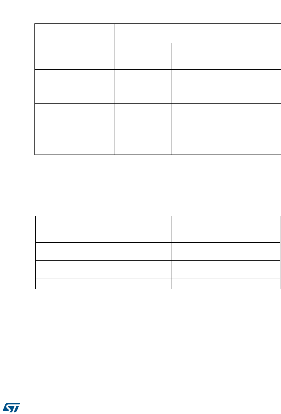
Table 1. Device summary
Reference Part number
STM32L072x8 STM32L072V8
STM32L072xB STM32L072VB, STM32L072RB,
STM32L072CB, STM32L072KB
STM32L072xZ STM32L072VZ, STM32L072RZ,
STM32L072CZ, STM32L072KZ
)%*$
LQFP32 7x7 mm
LQFP48 7x7 mm
LQFP64 10x10 mm
LQFP100 14x14 mm
WLCSP49
(3.294x3.258 mm)
UFBGA64
TFBGA64
5x5mm
UFBGA100
7x7 mm
)%*$
UFQFPN32
5x5 mm
www.st.com

Contents STM32L072xx
2/149 DocID027100 Rev 4
Contents
1 Introduction . . . . . . . . . . . . . . . . . . . . . . . . . . . . . . . . . . . . . . . . . . . . . . . 10
2 Description . . . . . . . . . . . . . . . . . . . . . . . . . . . . . . . . . . . . . . . . . . . . . . . . 11
2.1 Device overview . . . . . . . . . . . . . . . . . . . . . . . . . . . . . . . . . . . . . . . . . . . . 12
2.2 Ultra-low-power device continuum . . . . . . . . . . . . . . . . . . . . . . . . . . . . . . 14
3 Functional overview . . . . . . . . . . . . . . . . . . . . . . . . . . . . . . . . . . . . . . . . 15
3.1 Low-power modes . . . . . . . . . . . . . . . . . . . . . . . . . . . . . . . . . . . . . . . . . . 15
3.2 Interconnect matrix . . . . . . . . . . . . . . . . . . . . . . . . . . . . . . . . . . . . . . . . . . 20
3.3 Arm® Cortex®-M0+ core with MPU . . . . . . . . . . . . . . . . . . . . . . . . . . . . . 21
3.4 Reset and supply management . . . . . . . . . . . . . . . . . . . . . . . . . . . . . . . . 22
3.4.1 Power supply schemes . . . . . . . . . . . . . . . . . . . . . . . . . . . . . . . . . . . . . 22
3.4.2 Power supply supervisor . . . . . . . . . . . . . . . . . . . . . . . . . . . . . . . . . . . . 22
3.4.3 Voltage regulator . . . . . . . . . . . . . . . . . . . . . . . . . . . . . . . . . . . . . . . . . . 23
3.5 Clock management . . . . . . . . . . . . . . . . . . . . . . . . . . . . . . . . . . . . . . . . . 23
3.6 Low-power real-time clock and backup registers . . . . . . . . . . . . . . . . . . . 26
3.7 General-purpose inputs/outputs (GPIOs) . . . . . . . . . . . . . . . . . . . . . . . . . 26
3.8 Memories . . . . . . . . . . . . . . . . . . . . . . . . . . . . . . . . . . . . . . . . . . . . . . . . . 27
3.9 Boot modes . . . . . . . . . . . . . . . . . . . . . . . . . . . . . . . . . . . . . . . . . . . . . . . 27
3.10 Direct memory access (DMA) . . . . . . . . . . . . . . . . . . . . . . . . . . . . . . . . . 28
3.11 Analog-to-digital converter (ADC) . . . . . . . . . . . . . . . . . . . . . . . . . . . . . . 28
3.12 Temperature sensor . . . . . . . . . . . . . . . . . . . . . . . . . . . . . . . . . . . . . . . . . 28
3.12.1 Internal voltage reference (VREFINT) . . . . . . . . . . . . . . . . . . . . . . . . . . . 29
3.13 Digital-to-analog converter (DAC) . . . . . . . . . . . . . . . . . . . . . . . . . . . . . . 29
3.14 Ultra-low-power comparators and reference voltage . . . . . . . . . . . . . . . . 30
3.15 Touch sensing controller (TSC) . . . . . . . . . . . . . . . . . . . . . . . . . . . . . . . . 30
3.16 Timers and watchdogs . . . . . . . . . . . . . . . . . . . . . . . . . . . . . . . . . . . . . . . 31
3.16.1 General-purpose timers (TIM2, TIM3, TIM21 and TIM22) . . . . . . . . . . . 32
3.16.2 Low-power Timer (LPTIM) . . . . . . . . . . . . . . . . . . . . . . . . . . . . . . . . . . . 32
3.16.3 Basic timer (TIM6, TIM7) . . . . . . . . . . . . . . . . . . . . . . . . . . . . . . . . . . . . 32
3.16.4 SysTick timer . . . . . . . . . . . . . . . . . . . . . . . . . . . . . . . . . . . . . . . . . . . . . 33
3.16.5 Independent watchdog (IWDG) . . . . . . . . . . . . . . . . . . . . . . . . . . . . . . . 33

DocID027100 Rev 4 3/149
STM32L072xx Contents
4
3.16.6 Window watchdog (WWDG) . . . . . . . . . . . . . . . . . . . . . . . . . . . . . . . . . 33
3.17 Communication interfaces . . . . . . . . . . . . . . . . . . . . . . . . . . . . . . . . . . . . 33
3.17.1 I2C bus . . . . . . . . . . . . . . . . . . . . . . . . . . . . . . . . . . . . . . . . . . . . . . . . . 33
3.17.2 Universal synchronous/asynchronous receiver transmitter (USART) . . 34
3.17.3 Low-power universal asynchronous receiver transmitter (LPUART) . . . 35
3.17.4 Serial peripheral interface (SPI)/Inter-integrated sound (I2S) . . . . . . . . 35
3.17.5 Universal serial bus (USB) . . . . . . . . . . . . . . . . . . . . . . . . . . . . . . . . . . . 36
3.18 Clock recovery system (CRS) . . . . . . . . . . . . . . . . . . . . . . . . . . . . . . . . . 36
3.19 Cyclic redundancy check (CRC) calculation unit . . . . . . . . . . . . . . . . . . . 36
3.20 Serial wire debug port (SW-DP) . . . . . . . . . . . . . . . . . . . . . . . . . . . . . . . . 36
4 Pin descriptions . . . . . . . . . . . . . . . . . . . . . . . . . . . . . . . . . . . . . . . . . . . 37
5 Memory mapping . . . . . . . . . . . . . . . . . . . . . . . . . . . . . . . . . . . . . . . . . . . 57
6 Electrical characteristics . . . . . . . . . . . . . . . . . . . . . . . . . . . . . . . . . . . . 58
6.1 Parameter conditions . . . . . . . . . . . . . . . . . . . . . . . . . . . . . . . . . . . . . . . . 58
6.1.1 Minimum and maximum values . . . . . . . . . . . . . . . . . . . . . . . . . . . . . . . 58
6.1.2 Typical values . . . . . . . . . . . . . . . . . . . . . . . . . . . . . . . . . . . . . . . . . . . . 58
6.1.3 Typical curves . . . . . . . . . . . . . . . . . . . . . . . . . . . . . . . . . . . . . . . . . . . . 58
6.1.4 Loading capacitor . . . . . . . . . . . . . . . . . . . . . . . . . . . . . . . . . . . . . . . . . 58
6.1.5 Pin input voltage . . . . . . . . . . . . . . . . . . . . . . . . . . . . . . . . . . . . . . . . . . 58
6.1.6 Power supply scheme . . . . . . . . . . . . . . . . . . . . . . . . . . . . . . . . . . . . . . 59
6.1.7 Current consumption measurement . . . . . . . . . . . . . . . . . . . . . . . . . . . 59
6.2 Absolute maximum ratings . . . . . . . . . . . . . . . . . . . . . . . . . . . . . . . . . . . . 60
6.3 Operating conditions . . . . . . . . . . . . . . . . . . . . . . . . . . . . . . . . . . . . . . . . 62
6.3.1 General operating conditions . . . . . . . . . . . . . . . . . . . . . . . . . . . . . . . . . 62
6.3.2 Embedded reset and power control block characteristics . . . . . . . . . . . 64
6.3.3 Embedded internal reference voltage . . . . . . . . . . . . . . . . . . . . . . . . . . 65
6.3.4 Supply current characteristics . . . . . . . . . . . . . . . . . . . . . . . . . . . . . . . . 66
6.3.5 Wakeup time from low-power mode . . . . . . . . . . . . . . . . . . . . . . . . . . . 79
6.3.6 External clock source characteristics . . . . . . . . . . . . . . . . . . . . . . . . . . . 81
6.3.7 Internal clock source characteristics . . . . . . . . . . . . . . . . . . . . . . . . . . . 85
6.3.8 PLL characteristics . . . . . . . . . . . . . . . . . . . . . . . . . . . . . . . . . . . . . . . . 88
6.3.9 Memory characteristics . . . . . . . . . . . . . . . . . . . . . . . . . . . . . . . . . . . . . 89
6.3.10 EMC characteristics . . . . . . . . . . . . . . . . . . . . . . . . . . . . . . . . . . . . . . . . 90
6.3.11 Electrical sensitivity characteristics . . . . . . . . . . . . . . . . . . . . . . . . . . . . 92

Contents STM32L072xx
4/149 DocID027100 Rev 4
6.3.12 I/O current injection characteristics . . . . . . . . . . . . . . . . . . . . . . . . . . . . 93
6.3.13 I/O port characteristics . . . . . . . . . . . . . . . . . . . . . . . . . . . . . . . . . . . . . . 94
6.3.14 NRST pin characteristics . . . . . . . . . . . . . . . . . . . . . . . . . . . . . . . . . . . . 98
6.3.15 12-bit ADC characteristics . . . . . . . . . . . . . . . . . . . . . . . . . . . . . . . . . . . 99
6.3.16 DAC electrical characteristics . . . . . . . . . . . . . . . . . . . . . . . . . . . . . . . 105
6.3.17 Temperature sensor characteristics . . . . . . . . . . . . . . . . . . . . . . . . . . . 108
6.3.18 Comparators . . . . . . . . . . . . . . . . . . . . . . . . . . . . . . . . . . . . . . . . . . . . 108
6.3.19 Timer characteristics . . . . . . . . . . . . . . . . . . . . . . . . . . . . . . . . . . . . . . 110
6.3.20 Communications interfaces . . . . . . . . . . . . . . . . . . . . . . . . . . . . . . . . . 110
7 Package information . . . . . . . . . . . . . . . . . . . . . . . . . . . . . . . . . . . . . . . 121
7.1 LQFP100 package information . . . . . . . . . . . . . . . . . . . . . . . . . . . . . . . . 121
7.2 UFBGA100 package information . . . . . . . . . . . . . . . . . . . . . . . . . . . . . . 123
7.3 LQFP64 package information . . . . . . . . . . . . . . . . . . . . . . . . . . . . . . . . . 125
7.4 UFBGA64 package information . . . . . . . . . . . . . . . . . . . . . . . . . . . . . . . 128
7.5 TFBGA64 package information . . . . . . . . . . . . . . . . . . . . . . . . . . . . . . . 131
7.6 WLCSP49 package information . . . . . . . . . . . . . . . . . . . . . . . . . . . . . . . 134
7.7 LQFP48 package information . . . . . . . . . . . . . . . . . . . . . . . . . . . . . . . . . 137
7.8 LQFP32 package information . . . . . . . . . . . . . . . . . . . . . . . . . . . . . . . . . 139
7.9 UFQFPN32 package information . . . . . . . . . . . . . . . . . . . . . . . . . . . . . . 141
7.10 Thermal characteristics . . . . . . . . . . . . . . . . . . . . . . . . . . . . . . . . . . . . . 143
7.10.1 Reference document . . . . . . . . . . . . . . . . . . . . . . . . . . . . . . . . . . . . . . 144
8 Ordering information . . . . . . . . . . . . . . . . . . . . . . . . . . . . . . . . . . . . . . 145
9 Revision history . . . . . . . . . . . . . . . . . . . . . . . . . . . . . . . . . . . . . . . . . . 146

DocID027100 Rev 4 5/149
STM32L072xx List of tables
7
List of tables
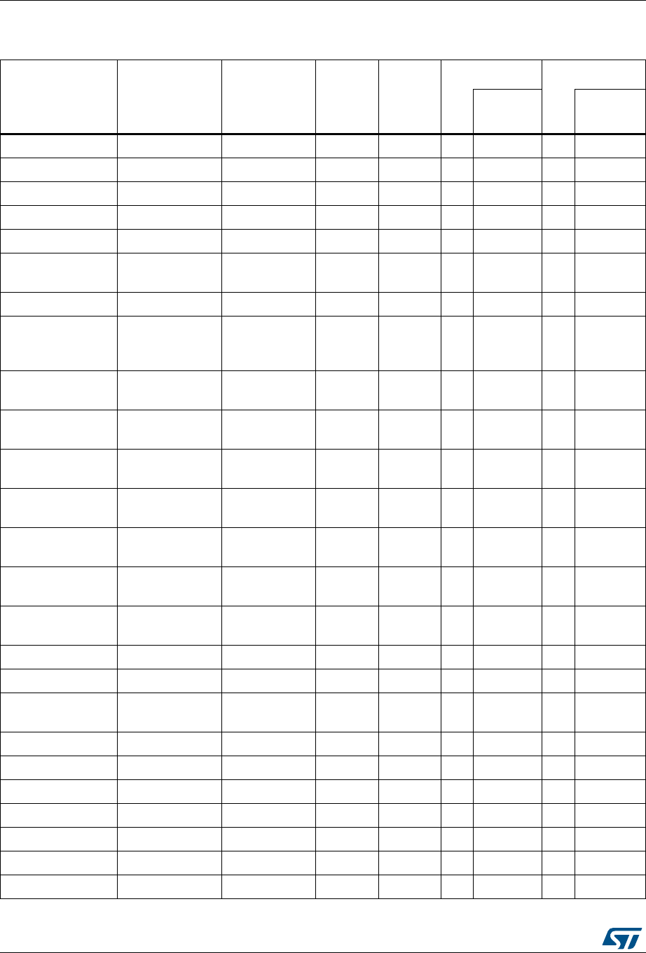
Table 1. Device summary . . . . . . . . . . . . . . . . . . . . . . . . . . . . . . . . . . . . . . . . . . . . . . . . . . . . . . . . . . 1
Table 2. Ultra-low-power STM32L072xx device features and peripheral counts . . . . . . . . . . . . . . . 12
Table 3. Functionalities depending on the operating power supply range . . . . . . . . . . . . . . . . . . . . 17
Table 4. CPU frequency range depending on dynamic voltage scaling . . . . . . . . . . . . . . . . . . . . . . 17
Table 5. Functionalities depending on the working mode
(from Run/active down to standby) . . . . . . . . . . . . . . . . . . . . . . . . . . . . . . . . . . . . . . . . . . 18
Table 6. STM32L0xx peripherals interconnect matrix . . . . . . . . . . . . . . . . . . . . . . . . . . . . . . . . . . . 20
Table 7. Temperature sensor calibration values. . . . . . . . . . . . . . . . . . . . . . . . . . . . . . . . . . . . . . . . 29
Table 8. Internal voltage reference measured values. . . . . . . . . . . . . . . . . . . . . . . . . . . . . . . . . . . . 29
Table 9. Capacitive sensing GPIOs available on STM32L072xx devices . . . . . . . . . . . . . . . . . . . . 31
Table 10. Timer feature comparison . . . . . . . . . . . . . . . . . . . . . . . . . . . . . . . . . . . . . . . . . . . . . . . . . . 31
Table 11. Comparison of I2C analog and digital filters . . . . . . . . . . . . . . . . . . . . . . . . . . . . . . . . . . . . 33
Table 12. STM32L072xx I2C implementation . . . . . . . . . . . . . . . . . . . . . . . . . . . . . . . . . . . . . . . . . . . 34
Table 13. USART implementation . . . . . . . . . . . . . . . . . . . . . . . . . . . . . . . . . . . . . . . . . . . . . . . . . . . 34
Table 14. SPI/I2S implementation . . . . . . . . . . . . . . . . . . . . . . . . . . . . . . . . . . . . . . . . . . . . . . . . . . . 36
Table 15. Legend/abbreviations used in the pinout table . . . . . . . . . . . . . . . . . . . . . . . . . . . . . . . . . . 43
Table 16. STM32L072xxx pin definition . . . . . . . . . . . . . . . . . . . . . . . . . . . . . . . . . . . . . . . . . . . . . . . 43
Table 17. Alternate functions port A . . . . . . . . . . . . . . . . . . . . . . . . . . . . . . . . . . . . . . . . . . . . . . . . . . 51
Table 18. Alternate functions port B . . . . . . . . . . . . . . . . . . . . . . . . . . . . . . . . . . . . . . . . . . . . . . . . . . 52
Table 19. Alternate functions port C . . . . . . . . . . . . . . . . . . . . . . . . . . . . . . . . . . . . . . . . . . . . . . . . . . 53
Table 20. Alternate functions port D . . . . . . . . . . . . . . . . . . . . . . . . . . . . . . . . . . . . . . . . . . . . . . . . . . 54
Table 21. Alternate functions port E . . . . . . . . . . . . . . . . . . . . . . . . . . . . . . . . . . . . . . . . . . . . . . . . . . 55
Table 22. Alternate functions port H . . . . . . . . . . . . . . . . . . . . . . . . . . . . . . . . . . . . . . . . . . . . . . . . . . 56
Table 23. Voltage characteristics . . . . . . . . . . . . . . . . . . . . . . . . . . . . . . . . . . . . . . . . . . . . . . . . . . . . 60
Table 24. Current characteristics . . . . . . . . . . . . . . . . . . . . . . . . . . . . . . . . . . . . . . . . . . . . . . . . . . . . 61
Table 25. Thermal characteristics. . . . . . . . . . . . . . . . . . . . . . . . . . . . . . . . . . . . . . . . . . . . . . . . . . . . 61
Table 26. General operating conditions . . . . . . . . . . . . . . . . . . . . . . . . . . . . . . . . . . . . . . . . . . . . . . . 62
Table 27. Embedded reset and power control block characteristics. . . . . . . . . . . . . . . . . . . . . . . . . . 64
Table 28. Embedded internal reference voltage calibration values . . . . . . . . . . . . . . . . . . . . . . . . . . 65
Table 29. Embedded internal reference voltage. . . . . . . . . . . . . . . . . . . . . . . . . . . . . . . . . . . . . . . . . 65
Table 30. Current consumption in Run mode, code with data processing running from
Flash memory . . . . . . . . . . . . . . . . . . . . . . . . . . . . . . . . . . . . . . . . . . . . . . . . . . . . . . . . . . . 67
Table 31. Current consumption in Run mode vs code type,
code with data processing running from Flash memory . . . . . . . . . . . . . . . . . . . . . . . . . . . 68
Table 32. Current consumption in Run mode, code with data processing running from RAM . . . . . . 69
Table 33. Current consumption in Run mode vs code type,
code with data processing running from RAM . . . . . . . . . . . . . . . . . . . . . . . . . . . . . . . . . . 70
Table 34. Current consumption in Sleep mode . . . . . . . . . . . . . . . . . . . . . . . . . . . . . . . . . . . . . . . . . 71
Table 35. Current consumption in Low-power run mode . . . . . . . . . . . . . . . . . . . . . . . . . . . . . . . . . . 72
Table 36. Current consumption in Low-power sleep mode . . . . . . . . . . . . . . . . . . . . . . . . . . . . . . . . 73
Table 37. Typical and maximum current consumptions in Stop mode . . . . . . . . . . . . . . . . . . . . . . . . 74
Table 38. Typical and maximum current consumptions in Standby mode . . . . . . . . . . . . . . . . . . . . . 75
Table 39. Average current consumption during Wakeup . . . . . . . . . . . . . . . . . . . . . . . . . . . . . . . . . . 76
Table 40. Peripheral current consumption in Run or Sleep mode . . . . . . . . . . . . . . . . . . . . . . . . . . . 77
Table 41. Peripheral current consumption in Stop and Standby mode . . . . . . . . . . . . . . . . . . . . . . . 79
Table 42. Low-power mode wakeup timings . . . . . . . . . . . . . . . . . . . . . . . . . . . . . . . . . . . . . . . . . . . 79
Table 43. High-speed external user clock characteristics. . . . . . . . . . . . . . . . . . . . . . . . . . . . . . . . . . 81
Table 44. Low-speed external user clock characteristics . . . . . . . . . . . . . . . . . . . . . . . . . . . . . . . . . . 82

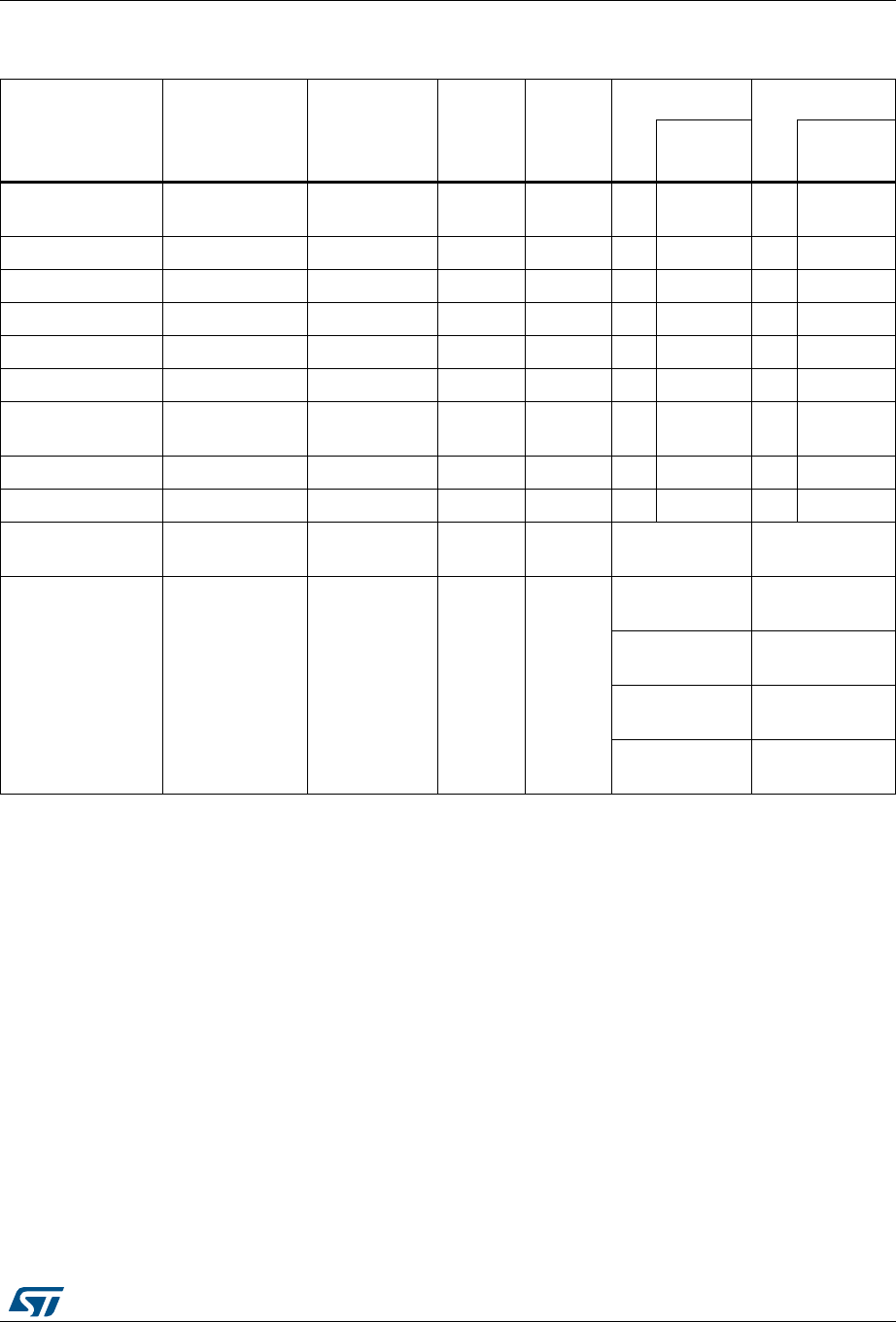
List of tables STM32L072xx
6/149 DocID027100 Rev 4
Table 45. HSE oscillator characteristics . . . . . . . . . . . . . . . . . . . . . . . . . . . . . . . . . . . . . . . . . . . . . . . 83
Table 46. LSE oscillator characteristics . . . . . . . . . . . . . . . . . . . . . . . . . . . . . . . . . . . . . . . . . . . . . . . 84
Table 47. 16 MHz HSI16 oscillator characteristics . . . . . . . . . . . . . . . . . . . . . . . . . . . . . . . . . . . . . . . 85
Table 48. HSI48 oscillator characteristics. . . . . . . . . . . . . . . . . . . . . . . . . . . . . . . . . . . . . . . . . . . . . . 86
Table 49. LSI oscillator characteristics . . . . . . . . . . . . . . . . . . . . . . . . . . . . . . . . . . . . . . . . . . . . . . . . 86
Table 50. MSI oscillator characteristics . . . . . . . . . . . . . . . . . . . . . . . . . . . . . . . . . . . . . . . . . . . . . . . 86
Table 51. PLL characteristics . . . . . . . . . . . . . . . . . . . . . . . . . . . . . . . . . . . . . . . . . . . . . . . . . . . . . . . 88
Table 52. RAM and hardware registers . . . . . . . . . . . . . . . . . . . . . . . . . . . . . . . . . . . . . . . . . . . . . . . 89
Table 53. Flash memory and data EEPROM characteristics . . . . . . . . . . . . . . . . . . . . . . . . . . . . . . . 89
Table 54. Flash memory and data EEPROM endurance and retention . . . . . . . . . . . . . . . . . . . . . . . 89
Table 55. EMS characteristics . . . . . . . . . . . . . . . . . . . . . . . . . . . . . . . . . . . . . . . . . . . . . . . . . . . . . . 90
Table 56. EMI characteristics . . . . . . . . . . . . . . . . . . . . . . . . . . . . . . . . . . . . . . . . . . . . . . . . . . . . . . . 91
Table 57. ESD absolute maximum ratings . . . . . . . . . . . . . . . . . . . . . . . . . . . . . . . . . . . . . . . . . . . . . 92
Table 58. Electrical sensitivities . . . . . . . . . . . . . . . . . . . . . . . . . . . . . . . . . . . . . . . . . . . . . . . . . . . . . 92
Table 59. I/O current injection susceptibility . . . . . . . . . . . . . . . . . . . . . . . . . . . . . . . . . . . . . . . . . . . . 93
Table 60. I/O static characteristics . . . . . . . . . . . . . . . . . . . . . . . . . . . . . . . . . . . . . . . . . . . . . . . . . . . 94
Table 61. Output voltage characteristics . . . . . . . . . . . . . . . . . . . . . . . . . . . . . . . . . . . . . . . . . . . . . . 96
Table 62. I/O AC characteristics . . . . . . . . . . . . . . . . . . . . . . . . . . . . . . . . . . . . . . . . . . . . . . . . . . . . . 97
Table 63. NRST pin characteristics . . . . . . . . . . . . . . . . . . . . . . . . . . . . . . . . . . . . . . . . . . . . . . . . . . 98
Table 64. ADC characteristics . . . . . . . . . . . . . . . . . . . . . . . . . . . . . . . . . . . . . . . . . . . . . . . . . . . . . . 99
Table 65. RAIN max for fADC = 16 MHz. . . . . . . . . . . . . . . . . . . . . . . . . . . . . . . . . . . . . . . . . . . . . . . 101
Table 66. ADC accuracy. . . . . . . . . . . . . . . . . . . . . . . . . . . . . . . . . . . . . . . . . . . . . . . . . . . . . . . . . . 101
Table 67. DAC characteristics . . . . . . . . . . . . . . . . . . . . . . . . . . . . . . . . . . . . . . . . . . . . . . . . . . . . . 105
Table 68. Temperature sensor calibration values. . . . . . . . . . . . . . . . . . . . . . . . . . . . . . . . . . . . . . . 108
Table 69. Temperature sensor characteristics . . . . . . . . . . . . . . . . . . . . . . . . . . . . . . . . . . . . . . . . . 108
Table 70. Comparator 1 characteristics . . . . . . . . . . . . . . . . . . . . . . . . . . . . . . . . . . . . . . . . . . . . . . 108
Table 71. Comparator 2 characteristics . . . . . . . . . . . . . . . . . . . . . . . . . . . . . . . . . . . . . . . . . . . . . . 109
Table 72. TIMx characteristics . . . . . . . . . . . . . . . . . . . . . . . . . . . . . . . . . . . . . . . . . . . . . . . . . . . . . 110
Table 73. I2C analog filter characteristics. . . . . . . . . . . . . . . . . . . . . . . . . . . . . . . . . . . . . . . . . . . . . 111
Table 74. SPI characteristics in voltage Range 1 . . . . . . . . . . . . . . . . . . . . . . . . . . . . . . . . . . . . . . 111
Table 75. SPI characteristics in voltage Range 2 . . . . . . . . . . . . . . . . . . . . . . . . . . . . . . . . . . . . . . 113
Table 76. SPI characteristics in voltage Range 3 . . . . . . . . . . . . . . . . . . . . . . . . . . . . . . . . . . . . . . 114
Table 77. I2S characteristics . . . . . . . . . . . . . . . . . . . . . . . . . . . . . . . . . . . . . . . . . . . . . . . . . . . . . . 117
Table 78. USB startup time. . . . . . . . . . . . . . . . . . . . . . . . . . . . . . . . . . . . . . . . . . . . . . . . . . . . . . . . 119
Table 79. USB DC electrical characteristics . . . . . . . . . . . . . . . . . . . . . . . . . . . . . . . . . . . . . . . . . . . 119
Table 80. USB: full speed electrical characteristics . . . . . . . . . . . . . . . . . . . . . . . . . . . . . . . . . . . . . 120
Table 81. LQPF100 - 100-pin, 14 x 14 mm low-profile quad flat package
mechanical data . . . . . . . . . . . . . . . . . . . . . . . . . . . . . . . . . . . . . . . . . . . . . . . . . . . . . . . . 121
Table 82. UFBGA100 - 100-pin, 7 x 7 mm, 0.50 mm pitch, ultra fine pitch ball grid array
package mechanical data . . . . . . . . . . . . . . . . . . . . . . . . . . . . . . . . . . . . . . . . . . . . . . . . . 123
Table 83. UFBGA100 recommended PCB design rules (0.5 mm pitch BGA) . . . . . . . . . . . . . . . . . 124
Table 84. LQFP64 - 64-pin, 10 x 10 mm low-profile quad flat
package mechanical data . . . . . . . . . . . . . . . . . . . . . . . . . . . . . . . . . . . . . . . . . . . . . . . . . 125
Table 85. UFBGA64 – 64-ball, 5 x 5 mm, 0.5 mm pitch ultra profile fine pitch
ball grid array package mechanical data . . . . . . . . . . . . . . . . . . . . . . . . . . . . . . . . . . . . . 128
Table 86. UFBGA64 recommended PCB design rules (0.5 mm pitch BGA) . . . . . . . . . . . . . . . . . . 129
Table 87. TFBGA64 – 64-ball, 5 x 5 mm, 0.5 mm pitch, thin profile fine pitch ball
grid array package mechanical data . . . . . . . . . . . . . . . . . . . . . . . . . . . . . . . . . . . . . . . . . 131
Table 88. TFBGA64 recommended PCB design rules (0.5 mm pitch BGA). . . . . . . . . . . . . . . . . . . 132
Table 89. WLCSP49 - 49-pin, 3.294 x 3.258 mm, 0.4 mm pitch wafer level chip scale
package mechanical data . . . . . . . . . . . . . . . . . . . . . . . . . . . . . . . . . . . . . . . . . . . . . . . . . 135
Table 90. WLCSP49 recommended PCB design rules (0.4 mm pitch) . . . . . . . . . . . . . . . . . . . . . . 136

DocID027100 Rev 4 7/149
STM32L072xx List of tables
7
Table 91. LQFP48 - 48-pin, 7 x 7 mm low-profile quad flat package mechanical data. . . . . . . . . . . 138
Table 92. LQFP32 - 32-pin, 7 x 7 mm low-profile quad flat package mechanical data. . . . . . . . . . . 140
Table 93. UFQFPN32 - 32-pin, 5x5 mm, 0.5 mm pitch ultra thin fine pitch quad flat
package mechanical data . . . . . . . . . . . . . . . . . . . . . . . . . . . . . . . . . . . . . . . . . . . . . . . . . 142
Table 94. Thermal characteristics. . . . . . . . . . . . . . . . . . . . . . . . . . . . . . . . . . . . . . . . . . . . . . . . . . . 143
Table 95. STM32L072xx ordering information scheme . . . . . . . . . . . . . . . . . . . . . . . . . . . . . . . . . . 145
Table 96. Document revision history . . . . . . . . . . . . . . . . . . . . . . . . . . . . . . . . . . . . . . . . . . . . . . . . 146

List of figures STM32L072xx
8/149 DocID027100 Rev 4
List of figures
Figure 1. STM32L072xx block diagram . . . . . . . . . . . . . . . . . . . . . . . . . . . . . . . . . . . . . . . . . . . . . . . 13
Figure 2. Clock tree . . . . . . . . . . . . . . . . . . . . . . . . . . . . . . . . . . . . . . . . . . . . . . . . . . . . . . . . . . . . . . 25
Figure 3. STM32L072xx LQFP100 pinout - 14 x 14 mm . . . . . . . . . . . . . . . . . . . . . . . . . . . . . . . . . 37
Figure 4. STM32L072xx UFBGA100 ballout - 7x 7 mm . . . . . . . . . . . . . . . . . . . . . . . . . . . . . . . . . . 38
Figure 5. STM32L072xx LQFP64 pinout - 10 x 10 mm . . . . . . . . . . . . . . . . . . . . . . . . . . . . . . . . . . 39
Figure 6. STM32L072xx UFBGA64/TFBGA64 ballout - 5x 5 mm . . . . . . . . . . . . . . . . . . . . . . . . . . 40
Figure 7. STM32L072xx WLCSP49 ballout . . . . . . . . . . . . . . . . . . . . . . . . . . . . . . . . . . . . . . . . . . . . 41
Figure 8. STM32L072xx LQFP48 pinout - 7 x 7 mm . . . . . . . . . . . . . . . . . . . . . . . . . . . . . . . . . . . . 41
Figure 9. STM32L072xx LQFP32 pinout . . . . . . . . . . . . . . . . . . . . . . . . . . . . . . . . . . . . . . . . . . . . . 42
Figure 10. STM32L072xx UFQFPN32 pinout . . . . . . . . . . . . . . . . . . . . . . . . . . . . . . . . . . . . . . . . . . . 42
Figure 11. Pin loading conditions . . . . . . . . . . . . . . . . . . . . . . . . . . . . . . . . . . . . . . . . . . . . . . . . . . . . . 58
Figure 12. Pin input voltage . . . . . . . . . . . . . . . . . . . . . . . . . . . . . . . . . . . . . . . . . . . . . . . . . . . . . . . . . 58
Figure 13. Power supply scheme. . . . . . . . . . . . . . . . . . . . . . . . . . . . . . . . . . . . . . . . . . . . . . . . . . . . . 59
Figure 14. Current consumption measurement scheme . . . . . . . . . . . . . . . . . . . . . . . . . . . . . . . . . . . 59
Figure 15. IDD vs VDD, at TA= 25/55/85/105 °C, Run mode, code running from
Flash memory, Range 2, HSE, 1WS . . . . . . . . . . . . . . . . . . . . . . . . . . . . . . . . . . . . . . . . . 68
Figure 16. IDD vs VDD, at TA= 25/55/85/105 °C, Run mode, code running from
Flash memory, Range 2, HSI16, 1WS . . . . . . . . . . . . . . . . . . . . . . . . . . . . . . . . . . . . . . . . 69
Figure 17. IDD vs VDD, at TA= 25 °C, Low-power run mode, code running
from RAM, Range 3, MSI (Range 0) at 64 KHz, 0 WS . . . . . . . . . . . . . . . . . . . . . . . . . . . . 73
Figure 18. IDD vs VDD, at TA= 25/55/ 85/105/125 °C, Stop mode with RTC enabled
and running on LSE Low drive . . . . . . . . . . . . . . . . . . . . . . . . . . . . . . . . . . . . . . . . . . . . . . 74
Figure 19. IDD vs VDD, at TA= 25/55/85/105/125 °C, Stop mode with RTC disabled,
all clocks OFF . . . . . . . . . . . . . . . . . . . . . . . . . . . . . . . . . . . . . . . . . . . . . . . . . . . . . . . . . . . 75
Figure 20. High-speed external clock source AC timing diagram . . . . . . . . . . . . . . . . . . . . . . . . . . . . 81
Figure 21. Low-speed external clock source AC timing diagram . . . . . . . . . . . . . . . . . . . . . . . . . . . . . 82
Figure 22. HSE oscillator circuit diagram . . . . . . . . . . . . . . . . . . . . . . . . . . . . . . . . . . . . . . . . . . . . . . . 83
Figure 23. Typical application with a 32.768 kHz crystal . . . . . . . . . . . . . . . . . . . . . . . . . . . . . . . . . . . 84
Figure 24. HSI16 minimum and maximum value versus temperature . . . . . . . . . . . . . . . . . . . . . . . . . 85
Figure 25. VIH/VIL versus VDD (CMOS I/Os) . . . . . . . . . . . . . . . . . . . . . . . . . . . . . . . . . . . . . . . . . . . 95
Figure 26. VIH/VIL versus VDD (TTL I/Os) . . . . . . . . . . . . . . . . . . . . . . . . . . . . . . . . . . . . . . . . . . . . . 95
Figure 27. I/O AC characteristics definition . . . . . . . . . . . . . . . . . . . . . . . . . . . . . . . . . . . . . . . . . . . . . 98
Figure 28. Recommended NRST pin protection . . . . . . . . . . . . . . . . . . . . . . . . . . . . . . . . . . . . . . . . . 99
Figure 29. ADC accuracy characteristics. . . . . . . . . . . . . . . . . . . . . . . . . . . . . . . . . . . . . . . . . . . . . . 102
Figure 30. Typical connection diagram using the ADC . . . . . . . . . . . . . . . . . . . . . . . . . . . . . . . . . . . 103
Figure 31. Power supply and reference decoupling (VREF+ not connected to VDDA) . . . . . . . . . . . . 103
Figure 32. Power supply and reference decoupling (VREF+ connected to VDDA). . . . . . . . . . . . . . . . 104
Figure 33. 12-bit buffered/non-buffered DAC. . . . . . . . . . . . . . . . . . . . . . . . . . . . . . . . . . . . . . . . . . . 107
Figure 34. SPI timing diagram - slave mode and CPHA = 0 . . . . . . . . . . . . . . . . . . . . . . . . . . . . . . . 115
Figure 35. SPI timing diagram - slave mode and CPHA = 1(1) . . . . . . . . . . . . . . . . . . . . . . . . . . . . . 115
Figure 36. SPI timing diagram - master mode(1) . . . . . . . . . . . . . . . . . . . . . . . . . . . . . . . . . . . . . . . . 116
Figure 37. I2S slave timing diagram (Philips protocol)(1) . . . . . . . . . . . . . . . . . . . . . . . . . . . . . . . . . . 118
Figure 38. I2S master timing diagram (Philips protocol)(1) . . . . . . . . . . . . . . . . . . . . . . . . . . . . . . . . . 118
Figure 39. USB timings: definition of data signal rise and fall time . . . . . . . . . . . . . . . . . . . . . . . . . . 119
Figure 40. LQFP100 - 100-pin, 14 x 14 mm low-profile quad flat package outline . . . . . . . . . . . . . . 121
Figure 41. LQFP100 - 100-pin, 14 x 14 mm low-profile quad flat
recommended footprint . . . . . . . . . . . . . . . . . . . . . . . . . . . . . . . . . . . . . . . . . . . . . . . . . . . 122
Figure 42. UFBGA100 - 100-pin, 7 x 7 mm, 0.50 mm pitch, ultra fine pitch ball

DocID027100 Rev 4 9/149
STM32L072xx List of figures
9
grid array package outline . . . . . . . . . . . . . . . . . . . . . . . . . . . . . . . . . . . . . . . . . . . . . . . . 123
Figure 43. UFBGA100 - 100-pin, 7 x 7 mm, 0.50 mm pitch, ultra fine pitch ball
grid array package recommended footprint . . . . . . . . . . . . . . . . . . . . . . . . . . . . . . . . . . . 124
Figure 44. LQFP64 - 64-pin, 10 x 10 mm low-profile quad flat package outline . . . . . . . . . . . . . . . . 125
Figure 45. LQFP64 - 64-pin, 10 x 10 mm low-profile quad flat recommended footprint . . . . . . . . . . 126
Figure 46. LQFP64 marking example (package top view). . . . . . . . . . . . . . . . . . . . . . . . . . . . . . . . . 127
Figure 47. UFBGA64 – 64-ball, 5 x 5 mm, 0.5 mm pitch ultra profile fine pitch
ball grid array package outline . . . . . . . . . . . . . . . . . . . . . . . . . . . . . . . . . . . . . . . . . . . . . 128
Figure 48. UFBGA64 – 64-ball, 5 x 5 mm, 0.5 mm pitch ultra profile fine pitch
ball grid array package recommended footprint . . . . . . . . . . . . . . . . . . . . . . . . . . . . . . . . 129
Figure 49. UFBGA64 marking example (package top view) . . . . . . . . . . . . . . . . . . . . . . . . . . . . . . . 130
Figure 50. TFBGA64 – 64-ball, 5 x 5 mm, 0.5 mm pitch thin profile fine pitch ball
grid array package outline . . . . . . . . . . . . . . . . . . . . . . . . . . . . . . . . . . . . . . . . . . . . . . . . 131
Figure 51. TFBGA64 – 64-ball, 5 x 5 mm, 0.5 mm pitch, thin profile fine pitch ball
,grid array recommended footprint . . . . . . . . . . . . . . . . . . . . . . . . . . . . . . . . . . . . . . . . . . 132
Figure 52. TFBGA64 marking example (package top view) . . . . . . . . . . . . . . . . . . . . . . . . . . . . . . 133
Figure 53. WLCSP49 - 49-pin, 3.294 x 3.258 mm, 0.4 mm pitch wafer level chip scale
package outline. . . . . . . . . . . . . . . . . . . . . . . . . . . . . . . . . . . . . . . . . . . . . . . . . . . . . . . . . 134
Figure 54. WLCSP49 - 49-pin, 3.294 x 3.258 mm, 0.4 mm pitch wafer level chip scale
recommended footprint . . . . . . . . . . . . . . . . . . . . . . . . . . . . . . . . . . . . . . . . . . . . . . . . . . . 135
Figure 55. WLCSP49 marking example (package top view) . . . . . . . . . . . . . . . . . . . . . . . . . . . . . . . 136
Figure 56. LQFP48 - 48-pin, 7 x 7 mm low-profile quad flat package outline . . . . . . . . . . . . . . . . . . 137
Figure 57. LQFP48 - 48-pin, 7 x 7 mm low-profile quad flat recommended footprint . . . . . . . . . . . . 138
Figure 58. LQFP32 - 32-pin, 7 x 7 mm low-profile quad flat package outline . . . . . . . . . . . . . . . . . . 139
Figure 59. LQFP32 - 32-pin, 7 x 7 mm low-profile quad flat recommended footprint . . . . . . . . . . . . 140
Figure 60. UFQFPN32 - 32-pin, 5x5 mm, 0.5 mm pitch ultra thin fine pitch quad flat
package outline. . . . . . . . . . . . . . . . . . . . . . . . . . . . . . . . . . . . . . . . . . . . . . . . . . . . . . . . . 141
Figure 61. UFQFPN32 - 32-pin, 5x5 mm, 0.5 mm pitch ultra thin fine pitch quad flat
recommended footprint . . . . . . . . . . . . . . . . . . . . . . . . . . . . . . . . . . . . . . . . . . . . . . . . . . . 142
Figure 62. Thermal resistance . . . . . . . . . . . . . . . . . . . . . . . . . . . . . . . . . . . . . . . . . . . . . . . . . . . . . 144

Introduction STM32L072xx
10/149 DocID027100 Rev 4
1 Introduction
The ultra-low-power STM32L072xx are offered in 9 different package typesfrom 32 pins to
100 pins. Depending on the device chosen, different sets of peripherals are included, the
description below gives an overview of the complete range of peripherals proposed in this
family.
These features make the ultra-low-power STM32L072xx microcontrollers suitable for a wide
range of applications:
•Gas/water meters and industrial sensors
•Healthcare and fitness equipment
•Remote control and user interface
•PC peripherals, gaming, GPS equipment
•Alarm system, wired and wireless sensors, video intercom
This STM32L072xx datasheet should be read in conjunction with the STM32L0x2xx
reference manual (RM0376).
For information on the Arm® Cortex
®
-M0+ core please refer to the Cortex
®
-M0+ Technical
Reference Manual, available from the www.arm.com website.
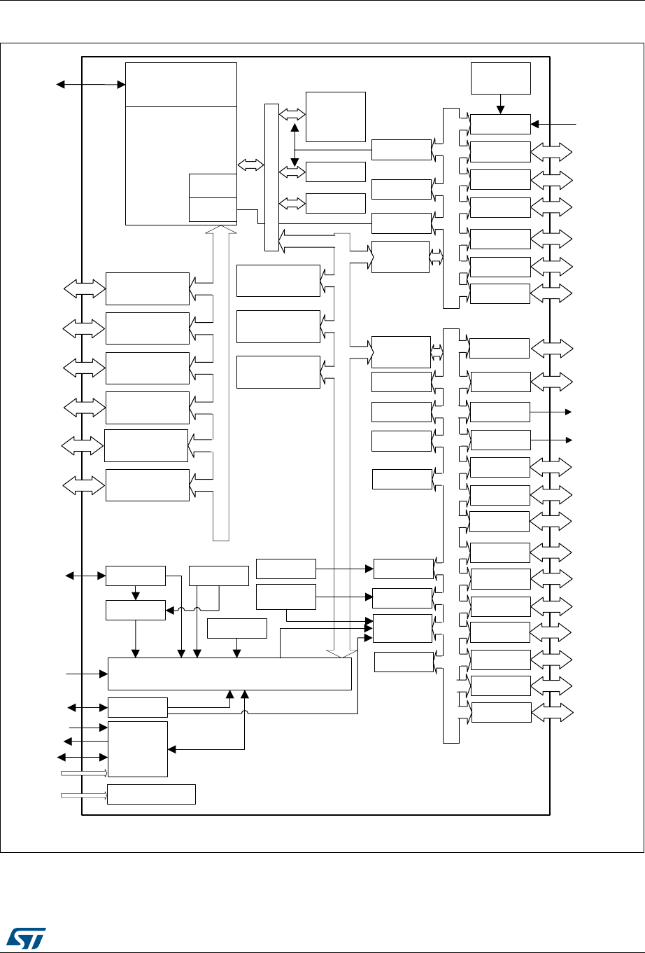
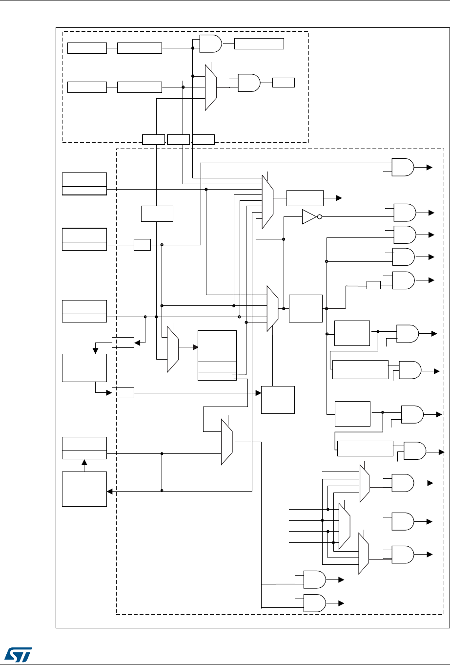
Figure 1 shows the general block diagram of the device family.
DocID027100 Rev 4 11/149
STM32L072xx Description
36
2 Description
The ultra-low-power STM32L072xx microcontrollers incorporate the connectivity power of
the universal serial bus (USB 2.0 crystal-less) with the high-performance Arm
®
Cortex
®
-M0+
32-bit RISC core operating at a 32 MHz frequency, a memory protection unit (MPU), high-
speed embedded memories (up to
192
Kbytes of Flash program memory,
6
Kbytes of data
EEPROM and
20
Kbytes of RAM) plus an extensive range of enhanced I/Os and
peripherals.
The STM32L072xx devices provide high power efficiency for a wide range of performance.
It is achieved with a large choice of internal and external clock sources, an internal voltage
adaptation and several low-power modes.
The STM32L072xx devices offer several analog features, one 12-bit ADC with hardware
oversampling, two DACs, two ultra-low-power comparators, several timers, one low-power
timer (LPTIM), four general-purpose 16-bit timers and two basic timer, one RTC and one
SysTick which can be used as timebases. They also feature two watchdogs, one watchdog
with independent clock and window capability and one window watchdog based on bus
clock.
Moreover, the STM32L072xx devices embed standard and advanced communication
interfaces: up to three I2Cs, two SPIs, one I2S, four USARTs, a low-power UART
(LPUART), and a crystal-less USB. The devices offer up to 24 capacitive sensing channels
to simply add touch sensing functionality to any application.
The STM32L072xx also include a real-time clock and a set of backup registers that remain
powered in Standby mode.
The ultra-low-power STM32L072xx devices operate from a 1.8 to 3.6 V power supply (down
to 1.65 V at power down) with BOR and from a 1.65 to 3.6 V power supply without BOR
option. They are available in the -40 to +125 °C temperature range. A comprehensive set of
power-saving modes allows the design of low-power applications.
Description STM32L072xx
12/149 DocID027100 Rev 4
2.1 Device overview
Table 2. Ultra-low-power STM32L072xx device features and peripheral counts
Peripheral STM32L07
2V8
STM32L07
2KB
STM32L07
2CB
STM32L07
2VB
STM32L07
2RB
STM32L07
2KZ
STM32L07
2CZ
STM32L07
2VZ
STM32L07
2RZ
Flash (Kbytes) 64 Kbytes 128 Kbytes 192 Kbytes
Data EEPROM (Kbytes) 3 Kbytes 6 Kbytes
RAM (Kbytes) 20 Kbytes
Timers
General-
purpose 4
Basic 2
LPTIMER 1
RTC/SYSTICK/IWDG/
WWDG 1/1/1/1
Com.
interfaces
SPI/I2S 6(4)(1)/1 4(3)(2)/0 6(4)(1)/1 4(3)(2)/0 6(4)(1)/1
I2C32 3 2 3
USART 44
(3) 44(3) 4
LPUART 1
USB
/(VDD_USB) 1/(1) 1/(0)(3) 1/(1) 1/(0)(3) 1/(1)
GPIOs 84 25(3) 40(4) 84 51(5) 25(3) 40(4) 84 51(5)
Clocks:
HSE/LSE/HSI/MSI/LSI 1/1/1/1/1
12-bit synchronized ADC
Number of channels
1
16
1
10
1
13(4) 1
16
1
16(5) 1
10
1
13(4) 1
16
1
16(5)
12-bit DAC
Number of channels
2
2
Comparators 2
Capacitive sensing
channels 24 13(3) 19(4) 24 24(5) 13(3) 19(4) 24 24(5)
Max. CPU frequency 32 MHz
Operating voltage 1.8 V to 3.6 V (down to 1.65 V at power-down) with BOR option 1.65 to 3.6 V without BOR option
Operating temperatures Ambient temperature: –40 to +125 °C
Junction temperature: –40 to +130 °C
Packages LQFP100
UFBGA100
UFQFPN32
LQFP32
LQFP48
WLCSP49
LQFP100
UFBGA100
LQFP64
TFBGA64
UFQFPN32
LQFP32
LQFP48
WLCSP49
LQFP100
UFBGA100
LQFP64
TFBGA64
UFBGA64
1. 4 SPI interfaces are USARTs operating in SPI master mode.
2. 3 SPI interfaces are USARTs operating in SPI master mode.
3. UFQFP32 has 2 GPIOs, 1 UART and 1 capacitive sensing channel less that LQFP32. However, UFQFP32 features a VDD_USB pin while
LQPF32 does not.
4. LQFP48 has three GPIOs, three ADC channels and two capacitive sensing channel less than WLCSP49.
5. TFBGA64 has one GPIO, one ADC input and one capacitive sensing channel less than LQFP64.
DocID027100 Rev 4 13/149
STM32L072xx Description
36
Figure 1. STM32L072xx block diagram
&257(;0&38
)PD[0+]
6:'
038
19,&
*3,23257$
*3,23257%
*3,23257&
*3,23257'
*3,23257+
7HPS
VHQVRU
5(6(7&/.
)/$6+
((3520
%227
5$0
'0$
$+%)PD[0+]
76&
&5&
51*
%5,'*(
$
3
%
),5(:$//
'%*
(;7,
$'&
63,
86$57
7,0
&203
/6(
7,0
%5,'*(
$
3
%
&56
7,0
5$0.
'$&
,&
,&
86$57
86%)6
/38$57
63,,6
7,0
,:'*
57&
::'*
/37,0
%&.35(*
+6( +6,0
3//
06,
/6,
+6,0
308
5(*8/$725
9''
9''$
95()B287
1567
39'B,1
26&B,1
26&B287
26&B,1
26&B287
:.83[
3$>@
3+>@>@
3'>@
3&>@
3%>@
$,1[
0,62026,
6&.166
5;7;576
&76&.
FK
FK
,13,10287
,1,1
(75287
'3'02(
&56B6<1&
9''B86%
287
6&/6'$
60%$
6&/6'$
5;7;576
&76&.
5;7;576
&76
0,620&.
026,6'
6&.&.166
:6
FK
6:'
06Y9
&203 ,13,10287
*3,23257(
3(>@ 7,0 '$& 287
,& 6&/6'$
60%$
86$57 5;7;576
&76&.
86$57 5;7;576
&76&.
7,0 FK

Description STM32L072xx
14/149 DocID027100 Rev 4
2.2 Ultra-low-power device continuum
The ultra-low-power family offers a large choice of core and features, from 8-bit proprietary
core up to Arm
®
Cortex
®
-M4, including Arm
®
Cortex
®
-M3 and Arm
®
Cortex
®
-M0+. The
STM32Lx series are the best choice to answer your needs in terms of ultra-low-power
features. The STM32 ultra-low-power series are the best solution for applications such as
gaz/water meter, keyboard/mouse or fitness and healthcare application. Several built-in
features like LCD drivers, dual-bank memory, low-power run mode, operational amplifiers,
128-bit AES, DAC, crystal-less USB and many other definitely help you building a highly
cost optimized application by reducing BOM cost. STMicroelectronics, as a reliable and
long-term manufacturer, ensures as much as possible pin-to-pin compatibility between all
STM8Lx and STM32Lx on one hand, and between all STM32Lx and STM32Fx on the other
hand. Thanks to this unprecedented scalability, your legacy application can be upgraded to
respond to the latest market feature and efficiency requirements.

DocID027100 Rev 4 15/149
STM32L072xx Functional overview
36
3 Functional overview
3.1 Low-power modes
The ultra-low-power STM32L072xx support dynamic voltage scaling to optimize its power
consumption in Run mode. The voltage from the internal low-drop regulator that supplies
the logic can be adjusted according to the system’s maximum operating frequency and the
external voltage supply.
There are three power consumption ranges:
•Range 1 (VDD range limited to 1.71-3.6 V), with the CPU running at up to 32 MHz
•Range 2 (full VDD range), with a maximum CPU frequency of 16 MHz
•Range 3 (full VDD range), with a maximum CPU frequency limited to 4.2 MHz
Seven low-power modes are provided to achieve the best compromise between low-power
consumption, short startup time and available wakeup sources:
•Sleep mode
In Sleep mode, only the CPU is stopped. All peripherals continue to operate and can
wake up the CPU when an interrupt/event occurs. Sleep mode power consumption at
16 MHz is about 1 mA with all peripherals off.
•Low-power run mode
This mode is achieved with the multispeed internal (MSI) RC oscillator set to the low-
speed clock (max 131 kHz), execution from SRAM or Flash memory, and internal
regulator in low-power mode to minimize the regulator's operating current. In Low-
power run mode, the clock frequency and the number of enabled peripherals are both
limited.
•Low-power sleep mode
This mode is achieved by entering Sleep mode with the internal voltage regulator in
low-power mode to minimize the regulator’s operating current. In Low-power sleep
mode, both the clock frequency and the number of enabled peripherals are limited; a
typical example would be to have a timer running at 32 kHz.
When wakeup is triggered by an event or an interrupt, the system reverts to the Run
mode with the regulator on.
Stop mode with RTC
The Stop mode achieves the lowest power consumption while retaining the RAM and
register contents and real time clock. All clocks in the VCORE domain are stopped, the
PLL, MSI RC, HSE crystal and HSI RC oscillators are disabled. The LSE or LSI is still
running. The voltage regulator is in the low-power mode.
Some peripherals featuring wakeup capability can enable the HSI RC during Stop
mode to detect their wakeup condition.
The device can be woken up from Stop mode by any of the EXTI line, in 3.5 µs, the
processor can serve the interrupt or resume the code. The EXTI line source can be any
GPIO. It can be the PVD output, the comparator 1 event or comparator 2 event
(if internal reference voltage is on), it can be the RTC alarm/tamper/timestamp/wakeup
events, the USB/USART/I2C/LPUART/LPTIMER wakeup events.

Functional overview STM32L072xx
16/149 DocID027100 Rev 4
•Stop mode without RTC
The Stop mode achieves the lowest power consumption while retaining the RAM and
register contents. All clocks are stopped, the PLL, MSI RC, HSI and LSI RC, HSE and
LSE crystal oscillators are disabled.
Some peripherals featuring wakeup capability can enable the HSI RC during Stop
mode to detect their wakeup condition.
The voltage regulator is in the low-power mode. The device can be woken up from Stop
mode by any of the EXTI line, in 3.5 µs, the processor can serve the interrupt or
resume the code. The EXTI line source can be any GPIO. It can be the PVD output, the
comparator 1 event or comparator 2 event (if internal reference voltage is on). It can
also be wakened by the USB/USART/I2C/LPUART/LPTIMER wakeup events.
•Standby mode with RTC
The Standby mode is used to achieve the lowest power consumption and real time
clock. The internal voltage regulator is switched off so that the entire VCORE domain is
powered off. The PLL, MSI RC, HSE crystal and HSI RC oscillators are also switched
off. The LSE or LSI is still running. After entering Standby mode, the RAM and register
contents are lost except for registers in the Standby circuitry (wakeup logic, IWDG,
RTC, LSI, LSE Crystal 32 KHz oscillator, RCC_CSR register).
The device exits Standby mode in 60 µs when an external reset (NRST pin), an IWDG
reset, a rising edge on one of the three WKUP pins, RTC alarm (Alarm A or Alarm B),
RTC tamper event, RTC timestamp event or RTC Wakeup event occurs.
•Standby mode without RTC
The Standby mode is used to achieve the lowest power consumption. The internal
voltage regulator is switched off so that the entire VCORE domain is powered off. The
PLL, MSI RC, HSI and LSI RC, HSE and LSE crystal oscillators are also switched off.
After entering Standby mode, the RAM and register contents are lost except for
registers in the Standby circuitry (wakeup logic, IWDG, RTC, LSI, LSE Crystal 32 KHz
oscillator, RCC_CSR register).
The device exits Standby mode in 60 µs when an external reset (NRST pin) or a rising
edge on one of the three WKUP pin occurs.
Note: The RTC, the IWDG, and the corresponding clock sources are not stopped automatically by
entering Stop or Standby mode.
DocID027100 Rev 4 17/149
STM32L072xx Functional overview
36
Table 3. Functionalities depending on the operating power supply range
Operating power supply
range(1)
1. GPIO speed depends on VDD voltage range. Refer to Table 62: I/O AC characteristics for more information
about I/O speed.
Functionalities depending on the operating power supply
range
DAC and ADC
operation
Dynamic voltage
scaling range USB
VDD = 1.65 to 1.71 V ADC only, conversion
time up to 570 ksps
Range 2 or
range 3 Not functional
VDD = 1.71 to 1.8 V(2)
2. CPU frequency changes from initial to final must respect "fcpu initial <4*fcpu final". It must also respect 5
μs delay between two changes. For example to switch from 4.2 MHz to 32 MHz, you can switch from 4.2
MHz to 16 MHz, wait 5 μs, then switch from 16 MHz to 32 MHz.
ADC only, conversion
time up to 1.14 Msps
Range 1, range 2 or
range 3 Functional(3)
VDD = 1.8 to 2.0 V(2) Conversion time up to
1.14 Msps
Range1, range 2 or
range 3 Functional(3)
VDD = 2.0 to 2.4 V Conversion time up to
1.14 Msps
Range 1, range 2 or
range 3 Functional(3)
3. To be USB compliant from the I/O voltage standpoint, the minimum VDD_USB is 3.0 V.
VDD = 2.4 to 3.6 V Conversion time up to
1.14 Msps
Range 1, range 2 or
range 3 Functional(3)
Table 4. CPU frequency range depending on dynamic voltage scaling
CPU frequency range Dynamic voltage scaling range
16 MHz to 32 MHz (1ws)
32 kHz to 16 MHz (0ws) Range 1
8 MHz to 16 MHz (1ws)
32 kHz to 8 MHz (0ws) Range 2
32 kHz to 4.2 MHz (0ws) Range 3
Functional overview STM32L072xx
18/149 DocID027100 Rev 4
Table 5. Functionalities depending on the working mode
(from Run/active down to standby) (1)(2)
IPs Run/Active Sleep
Low-
power
run
Low-
power
sleep
Stop Standby
Wakeup
capability
Wakeup
capability
CPU Y -- Y -- -- --
Flash memory O O O O -- --
RAM Y Y Y Y Y --
Backup registers Y Y Y Y Y Y
EEPROM O O O O -- --
Brown-out reset
(BOR) OOOOOOOO
DMA O O O O -- --
Programmable
Voltage Detector
(PVD)
OOOOOO-
Power-on/down
reset (POR/PDR) YYYYYYYY
High Speed
Internal (HSI) OO----
(3) --
High Speed
External (HSE) OOOO-- --
Low Speed Internal
(LSI) OOOOO O
Low Speed
External (LSE) OOOOO O
Multi-Speed
Internal (MSI) OOYY-- --
Inter-Connect
Controller YYYYY --
RTC O O O O O O O
RTC Tamper O O O O O O O O
Auto WakeUp
(AWU) OOOOOOOO
USB O O -- -- -- O --
USART O O O O O(4) O--
LPUART O O O O O(4) O--
SPI O O O O -- --
I2C O O O O O(5) O--
ADC O O -- -- -- --
DAC O O O O O --
DocID027100 Rev 4 19/149
STM32L072xx Functional overview
36
Temperature
sensor OOOOO --
Comparators O O O O O O --
16-bit timers O O O O -- --
LPTIMER O O O O O O
IWDG O O O O O O O O
WWDG O O O O -- --
Touch sensing
controller (TSC) O O -- -- -- --
SysTick Timer O O O O --
GPIOs O O O O O O 2 pins
Wakeup time to
Run mode 0 µs 0.36 µs 3 µs 32 µs 3.5 µs 50 µs
Consumption
VDD=1.8 to 3.6 V
(Typ)
Down to
140 µA/MHz
(from Flash
memory)
Down to
37 µA/MHz
(from Flash
memory)
Down to
8 µA
Down to
4.5 µA
0.4 µA (No
RTC) VDD=1.8 V
0.28 µA (No
RTC) VDD=1.8 V
0.8 µA (with
RTC) VDD=1.8 V
0.65 µA (with
RTC) VDD=1.8 V
0.4 µA (No
RTC) VDD=3.0 V
0.29 µA (No
RTC) VDD=3.0 V
1 µA (with RTC)
VDD=3.0 V
0.85 µA (with
RTC) VDD=3.0 V
1. Legend:
“Y” = Yes (enable).
“O” = Optional can be enabled/disabled by software)
“-” = Not available
2. The consumption values given in this table are preliminary data given for indication. They are subject to slight changes.
3. Some peripherals with wakeup from Stop capability can request HSI to be enabled. In this case, HSI is woken up by the
peripheral, and only feeds the peripheral which requested it. HSI is automatically put off when the peripheral does not need
it anymore.
4. UART and LPUART reception is functional in Stop mode. It generates a wakeup interrupt on Start. To generate a wakeup
on address match or received frame event, the LPUART can run on LSE clock while the UART has to wake up or keep
running the HSI clock.
5. I2C address detection is functional in Stop mode. It generates a wakeup interrupt in case of address match. It will wake up
the HSI during reception.
Table 5. Functionalities depending on the working mode
(from Run/active down to standby) (continued)(1)(2)
IPs Run/Active Sleep
Low-
power
run
Low-
power
sleep
Stop Standby
Wakeup
capability
Wakeup
capability
Functional overview STM32L072xx
20/149 DocID027100 Rev 4
3.2 Interconnect matrix
Several peripherals are directly interconnected. This allows autonomous communication
between peripherals, thus saving CPU resources and power consumption. In addition,
these hardware connections allow fast and predictable latency.
Depending on peripherals, these interconnections can operate in Run, Sleep, Low-power
run, Low-power sleep and Stop modes.
Table 6. STM32L0xx peripherals interconnect matrix
Interconnect
source
Interconnect
destination Interconnect action Run Sleep
Low-
power
run
Low-
power
sleep
Stop
COMPx
TIM2,TIM21,
TIM22
Timer input channel,
trigger from analog
signals comparison
YY Y Y -
LPTIM
Timer input channel,
trigger from analog
signals comparison
YY Y Y Y
TIMx TIMx Timer triggered by other
timer YY Y Y -
RTC
TIM21 Timer triggered by Auto
wake-up YY Y Y -
LPTIM Timer triggered by RTC
event YY Y Y Y
All clock
source TIMx
Clock source used as
input channel for RC
measurement and
trimming
YY Y Y -
USB
CRS/HSI48
the clock recovery
system trims the HSI48
based on USB SOF
YY - - -
TIM3 USB_SOF is channel
input for calibration YY - - -
GPIO
TIMx Timer input channel and
trigger YY Y Y -
LPTIM Timer input channel and
trigger YY Y Y Y
ADC,DAC Conversion trigger Y Y Y Y -

DocID027100 Rev 4 21/149
STM32L072xx Functional overview
36
3.3 Arm® Cortex
®
-M0+ core with MPU
The Cortex-M0+ processor is an entry-level 32-bit Arm Cortex processor designed for a
broad range of embedded applications. It offers significant benefits to developers, including:
•a simple architecture that is easy to learn and program
•ultra-low power, energy-efficient operation
•excellent code density
•deterministic, high-performance interrupt handling
•upward compatibility with Cortex-M processor family
•platform security robustness, with integrated Memory Protection Unit (MPU).
The Cortex-M0+ processor is built on a highly area and power optimized 32-bit processor
core, with a 2-stage pipeline Von Neumann architecture. The processor delivers exceptional
energy efficiency through a small but powerful instruction set and extensively optimized
design, providing high-end processing hardware including a single-cycle multiplier.
The Cortex-M0+ processor provides the exceptional performance expected of a modern 32-
bit architecture, with a higher code density than other 8-bit and 16-bit microcontrollers.
Owing to its embedded Arm core, the STM32L072xx are compatible with all Arm tools and
software.
Nested vectored interrupt controller (NVIC)
The ultra-low-power STM32L072xx embed a nested vectored interrupt controller able to
handle up to 32 maskable interrupt channels and 4 priority levels.
The Cortex-M0+ processor closely integrates a configurable Nested Vectored Interrupt
Controller (NVIC), to deliver industry-leading interrupt performance. The NVIC:
•includes a Non-Maskable Interrupt (NMI)
•provides zero jitter interrupt option
•provides four interrupt priority levels
The tight integration of the processor core and NVIC provides fast execution of Interrupt
Service Routines (ISRs), dramatically reducing the interrupt latency. This is achieved
through the hardware stacking of registers, and the ability to abandon and restart load-
multiple and store-multiple operations. Interrupt handlers do not require any assembler
wrapper code, removing any code overhead from the ISRs. Tail-chaining optimization also
significantly reduces the overhead when switching from one ISR to another.
To optimize low-power designs, the NVIC integrates with the sleep modes, that include a
deep sleep function that enables the entire device to enter rapidly stop or standby mode.
This hardware block provides flexible interrupt management features with minimal interrupt
latency.

Functional overview STM32L072xx
22/149 DocID027100 Rev 4
3.4 Reset and supply management
3.4.1 Power supply schemes
•VDD = 1.65 to 3.6 V: external power supply for I/Os and the internal regulator. Provided
externally through VDD pins.
•VSSA, VDDA = 1.65 to 3.6 V: external analog power supplies for ADC reset blocks, RCs
and PLL. VDDA and VSSA must be connected to VDD and VSS, respectively.
•VDD_USB = 1.65 to 3.6V: external power supply for USB transceiver, USB_DM (PA11)
and USB_DP (PA12). To guarantee a correct voltage level for USB communication
VDD_USB must be above 3.0V. If USB is not used this pin must be tied to VDD. On
packages without VDD_USB pin, VDD_USB voltage is internally connected to VDD
voltage.
3.4.2 Power supply supervisor
The devices have an integrated ZEROPOWER power-on reset (POR)/power-down reset
(PDR) that can be coupled with a brownout reset (BOR) circuitry.
Two versions are available:
•The version with BOR activated at power-on operates between 1.8 V and 3.6 V.
•The other version without BOR operates between 1.65 V and 3.6 V.
After the VDD threshold is reached (1.65 V or 1.8 V depending on the BOR which is active or
not at power-on), the option byte loading process starts, either to confirm or modify default
thresholds, or to disable the BOR permanently: in this case, the VDD min value becomes
1.65 V (whatever the version, BOR active or not, at power-on).
When BOR is active at power-on, it ensures proper operation starting from 1.8 V whatever
the power ramp-up phase before it reaches 1.8 V. When BOR is not active at power-up, the
power ramp-up should guarantee that 1.65 V is reached on VDD at least 1 ms after it exits
the POR area.
Five BOR thresholds are available through option bytes, starting from 1.8 V to 3 V. To
reduce the power consumption in Stop mode, it is possible to automatically switch off the
internal reference voltage (VREFINT) in Stop mode. The device remains in reset mode when
VDD is below a specified threshold, VPOR/PDR or VBOR, without the need for any external
reset circuit.
Note: The start-up time at power-on is typically 3.3 ms when BOR is active at power-up, the start-
up time at power-on can be decreased down to 1 ms typically for devices with BOR inactive
at power-up.
The devices feature an embedded programmable voltage detector (PVD) that monitors the
VDD/VDDA power supply and compares it to the VPVD threshold. This PVD offers 7 different
levels between 1.85 V and 3.05 V, chosen by software, with a step around 200 mV. An
interrupt can be generated when VDD/VDDA drops below the VPVD threshold and/or when
VDD/VDDA is higher than the VPVD threshold. The interrupt service routine can then generate
a warning message and/or put the MCU into a safe state. The PVD is enabled by software.

DocID027100 Rev 4 23/149
STM32L072xx Functional overview
36
3.4.3 Voltage regulator
The regulator has three operation modes: main (MR), low power (LPR) and power down.
•MR is used in Run mode (nominal regulation)
•LPR is used in the Low-power run, Low-power sleep and Stop modes
•Power down is used in Standby mode. The regulator output is high impedance, the
kernel circuitry is powered down, inducing zero consumption but the contents of the
registers and RAM are lost except for the standby circuitry (wakeup logic, IWDG, RTC,
LSI, LSE crystal 32 KHz oscillator, RCC_CSR).
3.5 Clock management
The clock controller distributes the clocks coming from different oscillators to the core and
the peripherals. It also manages clock gating for low-power modes and ensures clock
robustness. It features:
•Clock prescaler
To get the best trade-off between speed and current consumption, the clock frequency
to the CPU and peripherals can be adjusted by a programmable prescaler.
•Safe clock switching
Clock sources can be changed safely on the fly in Run mode through a configuration
register.
•Clock management
To reduce power consumption, the clock controller can stop the clock to the core,
individual peripherals or memory.
•System clock source
Three different clock sources can be used to drive the master clock SYSCLK:
– 1-25 MHz high-speed external crystal (HSE), that can supply a PLL
– 16 MHz high-speed internal RC oscillator (HSI), trimmable by software, that can
supply a PLLMultispeed internal RC oscillator (MSI), trimmable by software, able
to generate 7 frequencies (65 kHz, 131 kHz, 262 kHz, 524 kHz, 1.05 MHz, 2.1
MHz, 4.2 MHz). When a 32.768 kHz clock source is available in the system (LSE),
the MSI frequency can be trimmed by software down to a ±0.5% accuracy.
•Auxiliary clock source
Two ultra-low-power clock sources that can be used to drive the real-time clock:
– 32.768 kHz low-speed external crystal (LSE)
– 37 kHz low-speed internal RC (LSI), also used to drive the independent watchdog.
The LSI clock can be measured using the high-speed internal RC oscillator for
greater precision.
•RTC clock source
The LSI, LSE or HSE sources can be chosen to clock the RTC, whatever the system
clock.
•USB clock source
A 48 MHz clock trimmed through the USB SOF or LSE supplies the USB interface.

Functional overview STM32L072xx
24/149 DocID027100 Rev 4
•Startup clock
After reset, the microcontroller restarts by default with an internal 2.1 MHz clock (MSI).
The prescaler ratio and clock source can be changed by the application program as
soon as the code execution starts.
•Clock security system (CSS)
This feature can be enabled by software. If an HSE clock failure occurs, the master
clock is automatically switched to HSI and a software interrupt is generated if enabled.
Another clock security system can be enabled, in case of failure of the LSE it provides
an interrupt or wakeup event which is generated if enabled.
•Clock-out capability (MCO: microcontroller clock output)
It outputs one of the internal clocks for external use by the application.
Several prescalers allow the configuration of the AHB frequency, each APB (APB1 and
APB2) domains. The maximum frequency of the AHB and the APB domains is 32 MHz. See
Figure 2 for details on the clock tree.
DocID027100 Rev 4 25/149
STM32L072xx Functional overview
36
Figure 2. Clock tree
06Y9
/HJHQG
+6( +LJKVSHHGH[WHUQDOFORFNVLJQDO
+6, +LJKVSHHGLQWHUQDOFORFNVLJQDO
/6, /RZVSHHGLQWHUQDOFORFNVLJQDO
/6( /RZVSHHGH[WHUQDOFORFNVLJQDO
06, 0XOWLVSHHGLQWHUQDOFORFNVLJQDO
:DWFKGRJ/6
/6,5&
/6(26& 57&
/6,WHPSR
#9
+6,5&
/HYHOVKLIWHUV
+6(26&
/HYHOVKLIWHUV
5&0+]
/HYHOVKLIWHUV
/68
0+]&ORFN
'HWHFWRU
/6'
&ORFN
5HFRYHU\
6\VWHP
/6(WHPSR
06,5&
/HYHOVKLIWHUV
/HYHOVKLIWHUV
3//
;
$3%
35(6&
$+%
35(6&
«
&ORFN
6RXUFH
&RQWURO
XVEBHQ
#9
#9
#9
#9
#9
#9
#9
#9
#9
#9
UQJBHQ
0+]
86%&/.
0+]51*
,&&/.
/38$57
8$57&/.
/37,0&/.
/6(
+6,
6<6&/.
3&/.
/6,
3HULSKHUDO
FORFNHQDEOH
3&/.WR$3%
SHULSKHUDOV
QRWVOHHSRU
GHHSVOHHS
QRWVOHHSRU
GHHSVOHHS
QRWGHHSVOHHS
QRWGHHSVOHHS
+&/.
6\V7LFN
7LPHU
&.B3:5
)&/.
3//&/.
+6(
+6,
06,
/6(
/6,
'HGLFDWHG0+]3//RXWSXW
+6(SUHVHQWRUQRW
#9
#9''&25(
FNBUFKV +6,
+6,
06,
0+]
FNBSOOLQ
(QDEOH:DWFKGRJ
57&HQDEOH
$'&HQDEOH
$'&&/.
/68 /6' /6'
0&2
0&26(/
3//65&
+6,06(/
57&6(/
6\VWHP
&ORFN
0+]
PD[
,I$3%SUHVF [
HOVH[
WR7,0[
3HULSKHUDO
FORFNHQDEOH
3HULSKHUDO
FORFNHQDEOH
3HULSKHUDO
FORFNHQDEOH
$3%
35(6&
3HULSKHUDO
FORFNHQDEOH
3&/.WR$3%
SHULSKHUDOV
0+]
PD[
,I$3%SUHVF [
HOVH[
WR7,0[
3HULSKHUDO
FORFNHQDEOH

Functional overview STM32L072xx
26/149 DocID027100 Rev 4
3.6 Low-power real-time clock and backup registers
The real time clock (RTC) and the 5 backup registers are supplied in all modes including
standby mode. The backup registers are five 32-bit registers used to store 20 bytes of user
application data. They are not reset by a system reset, or when the device wakes up from
Standby mode.
The RTC is an independent BCD timer/counter. Its main features are the following:
•Calendar with subsecond, seconds, minutes, hours (12 or 24 format), week day, date,
month, year, in BCD (binary-coded decimal) format
•Automatically correction for 28, 29 (leap year), 30, and 31 day of the month
•Two programmable alarms with wake up from Stop and Standby mode capability
•Periodic wakeup from Stop and Standby with programmable resolution and period
•On-the-fly correction from 1 to 32767 RTC clock pulses. This can be used to
synchronize it with a master clock.
•Reference clock detection: a more precise second source clock (50 or 60 Hz) can be
used to enhance the calendar precision.
•Digital calibration circuit with 1 ppm resolution, to compensate for quartz crystal
inaccuracy
•2 anti-tamper detection pins with programmable filter. The MCU can be woken up from
Stop and Standby modes on tamper event detection.
•Timestamp feature which can be used to save the calendar content. This function can
be triggered by an event on the timestamp pin, or by a tamper event. The MCU can be
woken up from Stop and Standby modes on timestamp event detection.
The RTC clock sources can be:
•A 32.768 kHz external crystal
•A resonator or oscillator
•The internal low-power RC oscillator (typical frequency of 37 kHz)
•The high-speed external clock
3.7 General-purpose inputs/outputs (GPIOs)
Each of the GPIO pins can be configured by software as output (push-pull or open-drain), as
input (with or without pull-up or pull-down) or as peripheral alternate function. Most of the
GPIO pins are shared with digital or analog alternate functions, and can be individually
remapped using dedicated alternate function registers. All GPIOs are high current capable.
Each GPIO output, speed can be slowed (40 MHz, 10 MHz, 2 MHz, 400 kHz). The alternate
function configuration of I/Os can be locked if needed following a specific sequence in order
to avoid spurious writing to the I/O registers. The I/O controller is connected to a dedicated
IO bus with a toggling speed of up to 32 MHz.
Extended interrupt/event controller (EXTI)
The extended interrupt/event controller consists of 29 edge detector lines used to generate
interrupt/event requests. Each line can be individually configured to select the trigger event
(rising edge, falling edge, both) and can be masked independently. A pending register
maintains the status of the interrupt requests. The EXTI can detect an external line with a
pulse width shorter than the Internal APB2 clock period. Up to 84 GPIOs can be connected
to the 16 configurable interrupt/event lines. The 13 other lines are connected to PVD, RTC,
USB, USARTs, I2C, LPUART, LPTIMER or comparator events.

DocID027100 Rev 4 27/149
STM32L072xx Functional overview
36
3.8 Memories
The STM32L072xx devices have the following features:
•20 Kbytes of embedded SRAM accessed (read/write) at CPU clock speed with 0 wait
states. With the enhanced bus matrix, operating the RAM does not lead to any
performance penalty during accesses to the system bus (AHB and APB buses).
•The non-volatile memory is divided into three arrays:
– 64, 128 or 192 Kbytes of embedded Flash program memory
– 6 Kbytes of data EEPROM
– Information block containing 32 user and factory options bytes plus 8 Kbytes of
system memory
Flash program and data EEPROM are divided into two banks. This allows writing in one
bank while running code or reading data from the other bank.
The user options bytes are used to write-protect or read-out protect the memory (with
4 Kbyte granularity) and/or readout-protect the whole memory with the following options:
•Level 0: no protection
•Level 1: memory readout protected.
The Flash memory cannot be read from or written to if either debug features are
connected or boot in RAM is selected
•Level 2: chip readout protected, debug features (Cortex-M0+ serial wire) and boot in
RAM selection disabled (debugline fuse)
The firewall protects parts of code/data from access by the rest of the code that is executed
outside of the protected area. The granularity of the protected code segment or the non-
volatile data segment is 256 bytes (Flash memory or EEPROM) against 64 bytes for the
volatile data segment (RAM).
The whole non-volatile memory embeds the error correction code (ECC) feature.
3.9 Boot modes
At startup, BOOT0 pin and nBOOT1 option bit are used to select one of three boot options:
•Boot from Flash memory
•Boot from System memory
•Boot from embedded RAM
The boot loader is located in System memory. It is used to reprogram the Flash memory by
using USB (PA11, PA12), USART1(PA9, PA10) or USART2(PA2, PA3). See STM32™
microcontroller system memory boot mode AN2606 for details.

Functional overview STM32L072xx
28/149 DocID027100 Rev 4
3.10 Direct memory access (DMA)
The flexible 7-channel, general-purpose DMA is able to manage memory-to-memory,
peripheral-to-memory and memory-to-peripheral transfers. The DMA controller supports
circular buffer management, avoiding the generation of interrupts when the controller
reaches the end of the buffer.
Each channel is connected to dedicated hardware DMA requests, with software trigger
support for each channel. Configuration is done by software and transfer sizes between
source and destination are independent.
The DMA can be used with the main peripherals: SPI, I2C, USART, LPUART,
general-purpose timers, DAC, and ADC.
3.11 Analog-to-digital converter (ADC)
A native 12-bit, extended to 16-bit through hardware oversampling, analog-to-digital
converter is embedded into STM32L072xx device. It has up to 16 external channels and 3
internal channels (temperature sensor, voltage reference). Three channels, PA0, PA4 and
PA5, are fast channels, while the others are standard channels.
The ADC performs conversions in single-shot or scan mode. In scan mode, automatic
conversion is performed on a selected group of analog inputs.
The ADC frequency is independent from the CPU frequency, allowing maximum sampling
rate of 1.14 MSPS even with a low CPU speed. The ADC consumption is low at all
frequencies (~25 µA at 10 kSPS, ~240 µA at 1MSPS). An auto-shutdown function
guarantees that the ADC is powered off except during the active conversion phase.
The ADC can be served by the DMA controller. It can operate from a supply voltage down to
1.65 V.
The ADC features a hardware oversampler up to 256 samples, this improves the resolution
to 16 bits (see AN2668).
An analog watchdog feature allows very precise monitoring of the converted voltage of one,
some or all scanned channels. An interrupt is generated when the converted voltage is
outside the programmed thresholds.
The events generated by the general-purpose timers (TIMx) can be internally connected to
the ADC start triggers, to allow the application to synchronize A/D conversions and timers.
3.12 Temperature sensor
The temperature sensor (TSENSE) generates a voltage VSENSE that varies linearly with
temperature.
The temperature sensor is internally connected to the ADC_IN18 input channel which is
used to convert the sensor output voltage into a digital value.
The sensor provides good linearity but it has to be calibrated to obtain good overall
accuracy of the temperature measurement. As the offset of the temperature sensor varies
from chip to chip due to process variation, the uncalibrated internal temperature sensor is
suitable for applications that detect temperature changes only.
DocID027100 Rev 4 29/149
STM32L072xx Functional overview
36
To improve the accuracy of the temperature sensor measurement, each device is
individually factory-calibrated by ST. The temperature sensor factory calibration data are
stored by ST in the system memory area, accessible in read-only mode.
3.12.1 Internal voltage reference (VREFINT)
The internal voltage reference (VREFINT) provides a stable (bandgap) voltage output for the
ADC and Comparators. VREFINT is internally connected to the ADC_IN17 input channel. It
enables accurate monitoring of the VDD value (when no external voltage, VREF+, is available
for ADC). The precise voltage of VREFINT is individually measured for each part by ST during
production test and stored in the system memory area. It is accessible in read-only mode.
3.13 Digital-to-analog converter (DAC)
Two 12-bit buffered DACs can be used to convert digital signal into analog voltage signal
output. An optional amplifier can be used to reduce the output signal impedance.
This digital Interface supports the following features:
•One data holding register (for each channel)
•Left or right data alignment in 12-bit mode
•Synchronized update capability
•Noise-wave generation
•Triangular-wave generation
•Dual DAC channels with independent or simultaneous conversions
•DMA capability (including the underrun interrupt)
•External triggers for conversion
•Input reference voltage VREF+
Six DAC trigger inputs are used in the STM32L072xx. The DAC channels are triggered
through the timer update outputs that are also connected to different DMA channels.
Table 7. Temperature sensor calibration values
Calibration value name Description Memory address
TSENSE_CAL1
TS ADC raw data acquired at
temperature of 30 °C,
VDDA= 3 V
0x1FF8 007A - 0x1FF8 007B
TSENSE_CAL2
TS ADC raw data acquired at
temperature of 130 °C
VDDA= 3 V
0x1FF8 007E - 0x1FF8 007F
Table 8. Internal voltage reference measured values
Calibration value name Description Memory address
VREFINT_CAL
Raw data acquired at
temperature of 25 °C
VDDA = 3 V
0x1FF8 0078 - 0x1FF8 0079

Functional overview STM32L072xx
30/149 DocID027100 Rev 4
3.14 Ultra-low-power comparators and reference voltage
The STM32L072xx embed two comparators sharing the same current bias and reference
voltage. The reference voltage can be internal or external (coming from an I/O).
•One comparator with ultra low consumption
•One comparator with rail-to-rail inputs, fast or slow mode.
•The threshold can be one of the following:
– DAC output
– External I/O pins
– Internal reference voltage (VREFINT)
– submultiple of Internal reference voltage(1/4, 1/2, 3/4) for the rail to rail
comparator.
Both comparators can wake up the devices from Stop mode, and be combined into a
window comparator.
The internal reference voltage is available externally via a low-power / low-current output
buffer (driving current capability of 1 µA typical).
3.15 Touch sensing controller (TSC)
The STM32L072xx provide a simple solution for adding capacitive sensing functionality to
any application. These devices offer up to 24 capacitive sensing channels distributed over 8
analog I/O groups.
Capacitive sensing technology is able to detect the presence of a finger near a sensor which
is protected from direct touch by a dielectric (such as glass, plastic). The capacitive variation
introduced by the finger (or any conductive object) is measured using a proven
implementation based on a surface charge transfer acquisition principle. It consists of
charging the sensor capacitance and then transferring a part of the accumulated charges
into a sampling capacitor until the voltage across this capacitor has reached a specific
threshold. To limit the CPU bandwidth usage, this acquisition is directly managed by the
hardware touch sensing controller and only requires few external components to operate.
The touch sensing controller is fully supported by the STMTouch touch sensing firmware
library, which is free to use and allows touch sensing functionality to be implemented reliably
in the end application.
DocID027100 Rev 4 31/149
STM32L072xx Functional overview
36
3.16 Timers and watchdogs
The ultra-low-power STM32L072xx devices include three general-purpose timers, one low-
power timer (LPTIM), one basic timer, two watchdog timers and the SysTick timer.
Table 10 compares the features of the general-purpose and basic timers.
Table 9. Capacitive sensing GPIOs available on STM32L072xx devices
Group Capacitive sensing
signal name
Pin
name Group Capacitive sensing
signal name
Pin
name
1
TSC_G1_IO1 PA0
5
TSC_G5_IO1 PB3
TSC_G1_IO2 PA1 TSC_G5_IO2 PB4
TSC_G1_IO3 PA2 TSC_G5_IO3 PB6
TSC_G1_IO4 PA3 TSC_G5_IO4 PB7
2
TSC_G2_IO1 PA4(1)
1. This GPIO offers a reduced touch sensing sensitivity. It is thus recommended to use it as sampling
capacitor I/O.
6
TSC_G6_IO1 PB11
TSC_G2_IO2 PA5 TSC_G6_IO2 PB12
TSC_G2_IO3 PA6 TSC_G6_IO3 PB13
TSC_G2_IO4 PA7 TSC_G6_IO4 PB14
3
TSC_G3_IO1 PC5
7
TSC_G7_IO1 PC0
TSC_G3_IO2 PB0 TSC_G7_IO2 PC1
TSC_G3_IO3 PB1 TSC_G7_IO3 PC2
TSC_G3_IO4 PB2 TSC_G7_IO4 PC3
4
TSC_G4_IO1 PA9
8
TSC_G8_IO1 PC6
TSC_G4_IO2 PA10 TSC_G8_IO2 PC7
TSC_G4_IO3 PA11 TSC_G8_IO3 PC8
TSC_G4_IO4 PA12 TSC_G8_IO4 PC9
Table 10. Timer feature comparison
Timer Counter
resolution Counter type Prescaler factor
DMA
request
generation
Capture/compare
channels
Complementary
outputs
TIM2,
TIM3 16-bit Up, down,
up/down
Any integer between
1 and 65536 Ye s 4 No
TIM21,
TIM22 16-bit Up, down,
up/down
Any integer between
1 and 65536 No 2 No
TIM6,
TIM7 16-bit Up Any integer between
1 and 65536 Ye s 0 No

Functional overview STM32L072xx
32/149 DocID027100 Rev 4
3.16.1 General-purpose timers (TIM2, TIM3, TIM21 and TIM22)
There are four synchronizable general-purpose timers embedded in the STM32L072xx
device (see Table 10 for differences).
TIM2, TIM3
TIM2 and TIM3 are based on 16-bit auto-reload up/down counter. It includes a 16-bit
prescaler. It features four independent channels each for input capture/output compare,
PWM or one-pulse mode output.
The TIM2/TIM3 general-purpose timers can work together or with the TIM21 and TIM22
general-purpose timers via the Timer Link feature for synchronization or event chaining.
Their counter can be frozen in debug mode. Any of the general-purpose timers can be used
to generate PWM outputs.
TIM2/TIM3 have independent DMA request generation.
These timers are capable of handling quadrature (incremental) encoder signals and the
digital outputs from 1 to 3 hall-effect sensors.
TIM21 and TIM22
TIM21 and TIM22 are based on a 16-bit auto-reload up/down counter. They include a 16-bit
prescaler. They have two independent channels for input capture/output compare, PWM or
one-pulse mode output. They can work together and be synchronized with the TIM2/TIM3,
full-featured general-purpose timers.
They can also be used as simple time bases and be clocked by the LSE clock source
(32.768 kHz) to provide time bases independent from the main CPU clock.
3.16.2 Low-power Timer (LPTIM)
The low-power timer has an independent clock and is running also in Stop mode if it is
clocked by LSE, LSI or an external clock. It is able to wakeup the devices from Stop mode.
This low-power timer supports the following features:
•16-bit up counter with 16-bit autoreload register
•16-bit compare register
•Configurable output: pulse, PWM
•Continuous / one shot mode
•Selectable software / hardware input trigger
•Selectable clock source
– Internal clock source: LSE, LSI, HSI or APB clock
– External clock source over LPTIM input (working even with no internal clock
source running, used by the Pulse Counter Application)
•Programmable digital glitch filter
•Encoder mode
3.16.3 Basic timer (TIM6, TIM7)
These timers can be used as a generic 16-bit timebase.
DocID027100 Rev 4 33/149
STM32L072xx Functional overview
36
3.16.4 SysTick timer
This timer is dedicated to the OS, but could also be used as a standard downcounter. It is
based on a 24-bit downcounter with autoreload capability and a programmable clock
source. It features a maskable system interrupt generation when the counter reaches ‘0’.
3.16.5 Independent watchdog (IWDG)
The independent watchdog is based on a 12-bit downcounter and 8-bit prescaler. It is
clocked from an independent 37 kHz internal RC and, as it operates independently of the
main clock, it can operate in Stop and Standby modes. It can be used either as a watchdog
to reset the device when a problem occurs, or as a free-running timer for application timeout
management. It is hardware- or software-configurable through the option bytes. The counter
can be frozen in debug mode.
3.16.6 Window watchdog (WWDG)
The window watchdog is based on a 7-bit downcounter that can be set as free-running. It
can be used as a watchdog to reset the device when a problem occurs. It is clocked from
the main clock. It has an early warning interrupt capability and the counter can be frozen in
debug mode.
3.17 Communication interfaces
3.17.1 I2C bus
Up to three I2C interfaces (I2C1 and I2C3) can operate in multimaster or slave modes.
Each I2C interface can support Standard mode (Sm, up to 100 kbit/s), Fast mode (Fm, up to
400 kbit/s) and Fast Mode Plus (Fm+, up to 1 Mbit/s) with 20 mA output drive on some I/Os.
7-bit and 10-bit addressing modes, multiple 7-bit slave addresses (2 addresses, 1 with
configurable mask) are also supported as well as programmable analog and digital noise
filters.
In addition, I2C1 and I2C3 provide hardware support for SMBus 2.0 and PMBus 1.1: ARP
capability, Host notify protocol, hardware CRC (PEC) generation/verification, timeouts
verifications and ALERT protocol management. I2C1/I2C3 also have a clock domain
Table 11. Comparison of I2C analog and digital filters
Analog filter Digital filter
Pulse width of
suppressed spikes ≥ 50 ns Programmable length from 1 to 15
I2C peripheral clocks
Benefits Available in Stop mode
1. Extra filtering capability vs.
standard requirements.
2. Stable length
Drawbacks Variations depending on
temperature, voltage, process
Wakeup from Stop on address
match is not available when digital
filter is enabled.
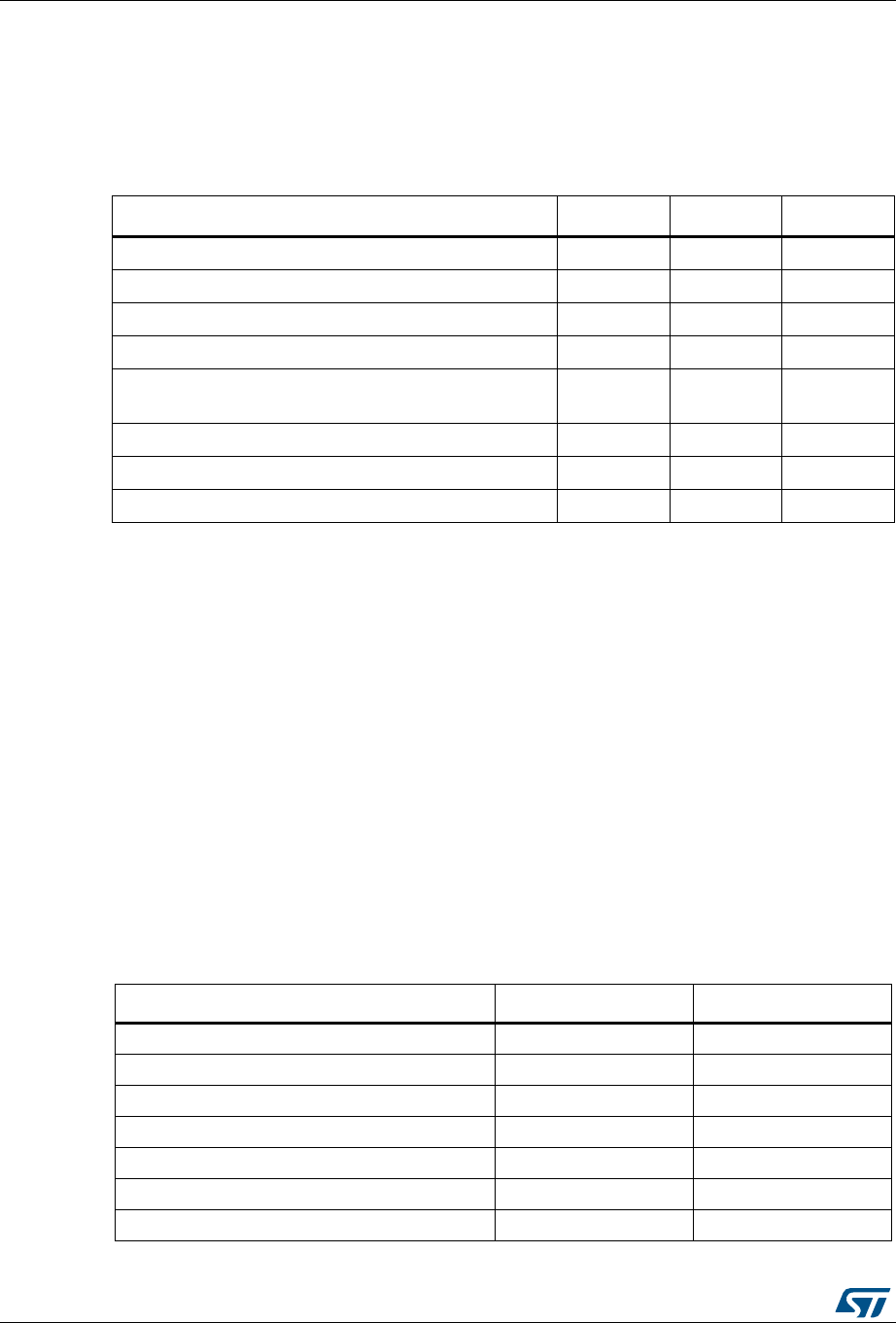
Functional overview STM32L072xx
34/149 DocID027100 Rev 4
independent from the CPU clock, allowing the I2C1/I2C3 to wake up the MCU from Stop
mode on address match.
Each I2C interface can be served by the DMA controller.
Refer to Table 12 for an overview of I2C interface features.
3.17.2 Universal synchronous/asynchronous receiver transmitter (USART)
The four USART interfaces (USART1, USART2, USART4 and USART5) are able to
communicate at speeds of up to 4 Mbit/s.
They provide hardware management of the CTS, RTS and RS485 driver enable (DE)
signals, multiprocessor communication mode, master synchronous communication and
single-wire half-duplex communication mode. USART1 and USART2 also support
SmartCard communication (ISO 7816), IrDA SIR ENDEC, LIN Master/Slave capability, auto
baud rate feature and has a clock domain independent from the CPU clock, allowing to
wake up the MCU from Stop mode using baudrates up to 42 Kbaud.
All USART interfaces can be served by the DMA controller.
Table 13 for the supported modes and features of USART interfaces.
Table 12. STM32L072xx I2C implementation
I2C features(1)
1. X = supported.
I2C1 I2C2 I2C3
7-bit addressing mode X X X
10-bit addressing mode X X X
Standard mode (up to 100 kbit/s) X X X
Fast mode (up to 400 kbit/s) X X X
Fast Mode Plus with 20 mA output drive I/Os (up to 1
Mbit/s) XX
(2)
2. See Table 16: STM32L072xxx pin definition on page 43 for the list of I/Os that feature Fast Mode Plus
capability
X
Independent clock X - X
SMBus X - X
Wakeup from STOP X - X
Table 13. USART implementation
USART modes/features(1) USART1 and USART2 USART4 and USART5
Hardware flow control for modem X X
Continuous communication using DMA X X
Multiprocessor communication X X
Synchronous mode(2) XX
Smartcard mode X -
Single-wire half-duplex communication X X
IrDA SIR ENDEC block X -
DocID027100 Rev 4 35/149
STM32L072xx Functional overview
36
3.17.3 Low-power universal asynchronous receiver transmitter (LPUART)
The devices embed one Low-power UART. The LPUART supports asynchronous serial
communication with minimum power consumption. It supports half duplex single wire
communication and modem operations (CTS/RTS). It allows multiprocessor
communication.
The LPUART has a clock domain independent from the CPU clock. It can wake up the
system from Stop mode using baudrates up to 46 Kbaud. The Wakeup events from Stop
mode are programmable and can be:
•Start bit detection
•Or any received data frame
•Or a specific programmed data frame
Only a 32.768 kHz clock (LSE) is needed to allow LPUART communication up to 9600
baud. Therefore, even in Stop mode, the LPUART can wait for an incoming frame while
having an extremely low energy consumption. Higher speed clock can be used to reach
higher baudrates.
LPUART interface can be served by the DMA controller.
3.17.4 Serial peripheral interface (SPI)/Inter-integrated sound (I2S)
Up to two SPIs are able to communicate at up to 16 Mbits/s in slave and master modes in
full-duplex and half-duplex communication modes. The 3-bit prescaler gives 8 master mode
frequencies and the frame is configurable to 8 bits or 16 bits. The hardware CRC
generation/verification supports basic SD Card/MMC modes.
The USARTs with synchronous capability can also be used as SPI master.
One standard I2S interfaces (multiplexed with SPI2) is available. It can operate in master or
slave mode, and can be configured to operate with a 16-/32-bit resolution as input or output
channels. Audio sampling frequencies from 8 kHz up to 192 kHz are supported. When the
I2S interfaces is configured in master mode, the master clock can be output to the external
DAC/CODEC at 256 times the sampling frequency.
The SPIs can be served by the DMA controller.
Refer to Table 14 for the differences between SPI1 and SPI2.
LIN mode X -
Dual clock domain and wakeup from Stop mode X -
Receiver timeout interrupt X -
Modbus communication X -
Auto baud rate detection (4 modes) X -
Driver Enable X X
1. X = supported.
2. This mode allows using the USART as an SPI master.
Table 13. USART implementation (continued)
USART modes/features(1) USART1 and USART2 USART4 and USART5
Functional overview STM32L072xx
36/149 DocID027100 Rev 4
3.17.5 Universal serial bus (USB)
The STM32L072xx embed a full-speed USB device peripheral compliant with the USB
specification version 2.0. The internal USB PHY supports USB FS signaling, embedded DP
pull-up and also battery charging detection according to Battery Charging Specification
Revision 1.2. The USB interface implements a full-speed (12 Mbit/s) function interface with
added support for USB 2.0 Link Power Management. It has software-configurable endpoint
setting with packet memory up to 1 KB and suspend/resume support. It requires a precise
48 MHz clock which can be generated from the internal main PLL (the clock source must
use a HSE crystal oscillator) or by the internal 48 MHz oscillator in automatic trimming
mode. The synchronization for this oscillator can be taken from the USB data stream itself
(SOF signalization) which allows crystal-less operation.
3.18 Clock recovery system (CRS)
The STM32L072xx embed a special block which allows automatic trimming of the internal
48 MHz oscillator to guarantee its optimal accuracy over the whole device operational
range. This automatic trimming is based on the external synchronization signal, which could
be either derived from USB SOF signalization, from LSE oscillator, from an external signal
on CRS_SYNC pin or generated by user software. For faster lock-in during startup it is also
possible to combine automatic trimming with manual trimming action.
3.19 Cyclic redundancy check (CRC) calculation unit
The CRC (cyclic redundancy check) calculation unit is used to get a CRC code using a
configurable generator polynomial value and size.
Among other applications, CRC-based techniques are used to verify data transmission or
storage integrity. In the scope of the EN/IEC 60335-1 standard, they offer a means of
verifying the Flash memory integrity. The CRC calculation unit helps compute a signature of
the software during runtime, to be compared with a reference signature generated at
linktime and stored at a given memory location.
3.20 Serial wire debug port (SW-DP)
An Arm SW-DP interface is provided to allow a serial wire debugging tool to be connected to
the MCU.
Table 14. SPI/I2S implementation
SPI features(1)
1. X = supported.
SPI1 SPI2
Hardware CRC calculation X X
I2S mode - X
TI mode X X
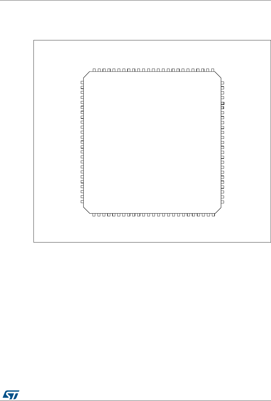
DocID027100 Rev 4 37/149
STM32L072xx Pin descriptions
56
4 Pin descriptions
Figure 3. STM32L072xx LQFP100 pinout - 14 x 14 mm
1. The above figure shows the package top view.
2. I/O pin supplied by VDD_USB.
06Y9
9''
ϭϬϬ
ϵϵ
ϵϴ
ϵϳ
ϵϲ
ϵϱ
ϵϰ
ϵϯ
ϵϮ
ϵϭ
ϵϬ
ϴϵ
ϴϴ
ϴϳ
ϴϲ
ϴϱ
ϴϰ
ϴϯ
ϴϮ
ϴϭ
ϴϬ
ϳϵ
ϳϴ
ϳϳ
ϳϲ
ϭ
Ϯ
ϯ
ϰ
ϱ
ϲ
ϳ
ϴ
ϵ
ϭϬ
ϭϭ
ϭϮ
ϭϯ
ϭϰ
ϭϱ
ϭϲ
ϭϳ
ϭϴ
ϭϵ
ϮϬ
Ϯϭ
ϮϮ
Ϯϯ
Ϯϰ
Ϯϱ
ϳϱ
ϳϰ
ϳϯ
ϳϮ
ϳϭ
ϳϬ
ϲϵ
ϲϴ
ϲϳ
ϲϲ
ϲϱ
ϲϰ
ϲϯ
ϲϮ
ϲϭ
ϲϬ
ϱϵ
ϱϴ
ϱϳ
ϱϲ
ϱϱ
ϱϰ
ϱϯ
ϱϮ
ϱϭ
WϮ
Wϯ
Wϰ
Wϱ
Wϲ
9''
Wϭϰ26&B,1
Wϭ26&B287
3+
3+
W,Ϭ26&B,1
EZ67
WϬ
Wϭ
WϮ
Wϯ
s^^
sZ&
95()
3$
3$
3$
sB86%
s^^
Wϭϯ
WϭϮ
W ϭϭ
WϭϬ
W
3$
Wϵ
Wϴ
Wϳ
Wϲ
Wϭϱ
Wϭϰ
Wϭϯ
WϭϮ
Wϭϭ
WϭϬ
Wϵ
Wϴ
W ϭϱ
W ϭϰ
W ϭϯ
W ϭϮ
3$
s^^
s
W
W
3$
3$
Wϰ
Wϱ
WϬ
Wϭ
WϮ
Wϳ
Wϴ
Wϵ
W ϭϬ
W ϭϭ
W ϭϮ
W ϭϯ
W ϭϰ
W ϭϱ
W ϭϬ
W ϭϭ
966
s
s
s^^
W ϭ
W
W
W
KK7
3%
3%
W
W
W
Wϳ
Wϲ
Wϱ
Wϰ
Wϯ
WϮ
Wϭ
WϬ
WϭϮ
Wϭϭ
WϭϬ
Wϭϱ
Wϭϰ
Ϯϲ
Ϯϳ
Ϯϴ
Ϯϵ
ϯϬ
ϯϭ
ϯϮ
ϯϯ
ϯϰ
ϯϱ
ϯϲ
ϯϳ
ϯϴ
ϯϵ
ϰϬ
ϰϭ
ϰϮ
ϰϯ
ϰϰ
ϰϱ
ϰϲ
ϰϳ
ϰϴ
ϰϵ
ϱϬ
>Y&WϭϬϬ
Wϭϯ
W,ϭ26&B287
9''$
9''
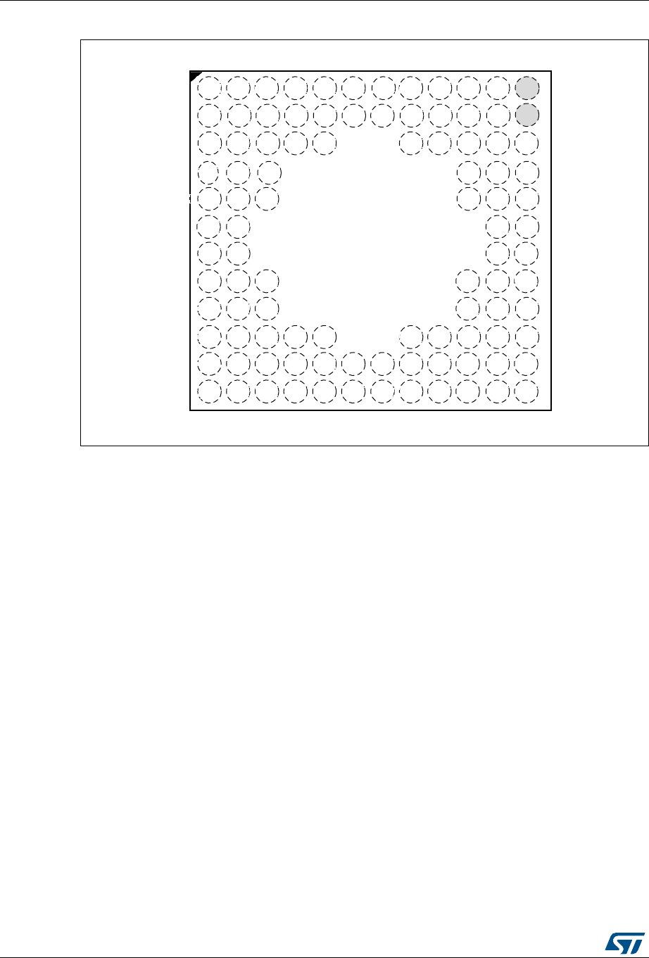
Pin descriptions STM32L072xx
38/149 DocID027100 Rev 4
Figure 4. STM32L072xx UFBGA100 ballout - 7x 7 mm
1. The above figure shows the package top view.
2. I/O pin supplied by VDD_USB.
06Y9
ϭϮϯ ϵ
ϭ ϭ
:
<
>
ϰϱϲϳϴ
&
'
,
D
3+
26&B,1
9''3&
3+
3+
26&B
287
1567
966$ 3&
95()
3&
3$
3$
95()
3'
3$
3$
3$
3&
3% 3%
3(
3(
3'
3(
3(
3( 3(
3%
3(
3%
3(
3%
3' 3' 3'
9''B
86% 9''
3'
3%
3( 3( 3% %227 3' 3' 3% 3% 3$ 3$ 3$ 3$
3$
3&
3&
3'
3'
3'
3'
3%3%
3%WϮ
3(
3& 3( 3( 9'' 3% 3' 3' 3& 9'' 3$
3&
3$3$
966
3(
3&
26&
B,1
3&
26&
B287
9'' 966 3& 3& 3&
966
9663+
3& 3'
3%3%3%3'3&3$
9''$
3$ 3$ 3(
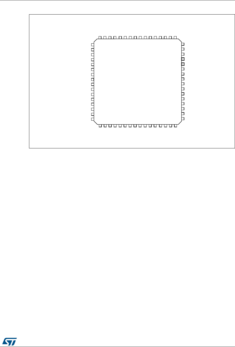
DocID027100 Rev 4 39/149
STM32L072xx Pin descriptions
56
Figure 5. STM32L072xx LQFP64 pinout - 10 x 10 mm
1. The above figure shows the package top view.
2. I/O pin supplied by VDD_USB.
9''
3&
3&26&B,1
3&26&B287
3+26&B,1
3+26&B287
1567
3&
3&
3&
3&
966$
9''$
3$
3$
3$
9''
966
3%
3%
%227
3%
3%
3%
3%
3%
3'
3&
3&
3&
3$
3$
9''B86%
966
3$
3$
3$
3$
3$
3$
3&
3&
3&
3&
3%
3%
3%
3%
3$
966
9''
3$
3$
3$
3$
3&
3&
3%
3%
3%
3%
3%
966
9''
/4)3
06Y9
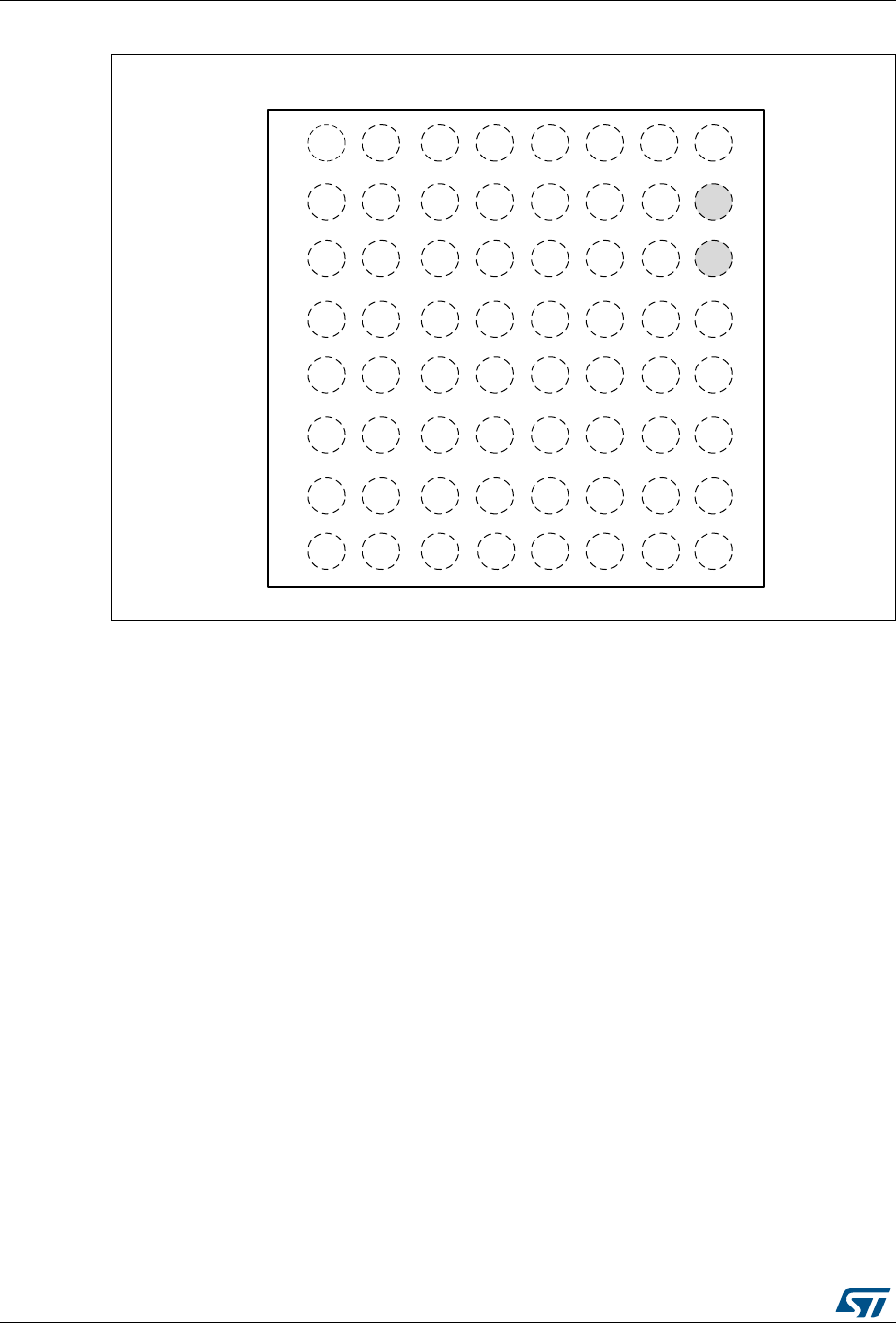
Pin descriptions STM32L072xx
40/149 DocID027100 Rev 4
Figure 6. STM32L072xx UFBGA64/TFBGA64 ballout - 5x 5 mm
1. The above figure shows the package top view.
2. I/O pin supplied by VDD_USB.
3+
26&B,1
3&
26&
B,1
06Y9
$
%
&
'
(
)
*
+
3&
26&
B287
3+
26&B
287
1567
966$
95()
9''$
3&
9''
966
9''
3&
3&
3$
3$
3% 3% 3% 3$ 3$ 3$
3% %227
3' 3& 3& 3$
3% 3% 3& 3$ 3$ 3$
3% 966 966 966 3$ 3&
3& 9'' 9'' 9''B
86% 3& 3&
3$ 3$ 3% 3& 3% 3%
3$ 3$ 3% 3% 3% 3%
3$ 3$ 3& 3& 3% 3%
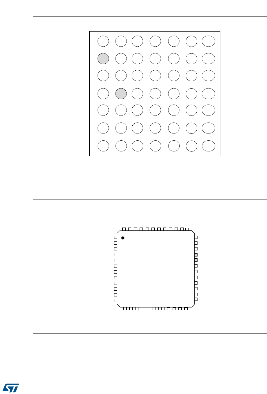
DocID027100 Rev 4 41/149
STM32L072xx Pin descriptions
56
Figure 7. STM32L072xx WLCSP49 ballout
1. The above figure shows the package top view.
2. I/O pin supplied by VDD_USB.
Figure 8. STM32L072xx LQFP48 pinout - 7 x 7 mm
1. The above figure shows the package top view.
2. I/O pin supplied by VDD_USB.
06Y9
3$
9''B
86%
$
%
&
'
(
)
3$
3$
3%
3%
3$
3$
3$
3$
3$
3%
3% 3% %227 9''
3% 3% 3% 3&
3% 3& 3& 3&
26&
B287
3% 966 1567
3+
26&B
287
3% 3$ 3$ 3&
3% 3$ 3$ 9''$
3%
9''
3&
26&
B,1
3+
26&B,1
95()
3$
*3% 9'' 3% 3% 3$ 3$
3$
06Y9
3$
3$
3$
3$
3%
3%
3%
3%
3%
966
9''
9''B86%
966
3$
3$
3$
3$
3$
3$
3%
3%
3%
3%
9''
3&
3&26&B287
3+26&B287
1567
966$
9''$
3$
3$
3$
9''
966
3%
3%
%227
3%
3%
3%
3%
3%
3$
3$
/4)3
3$
3+26&B,1
3&26&B,1
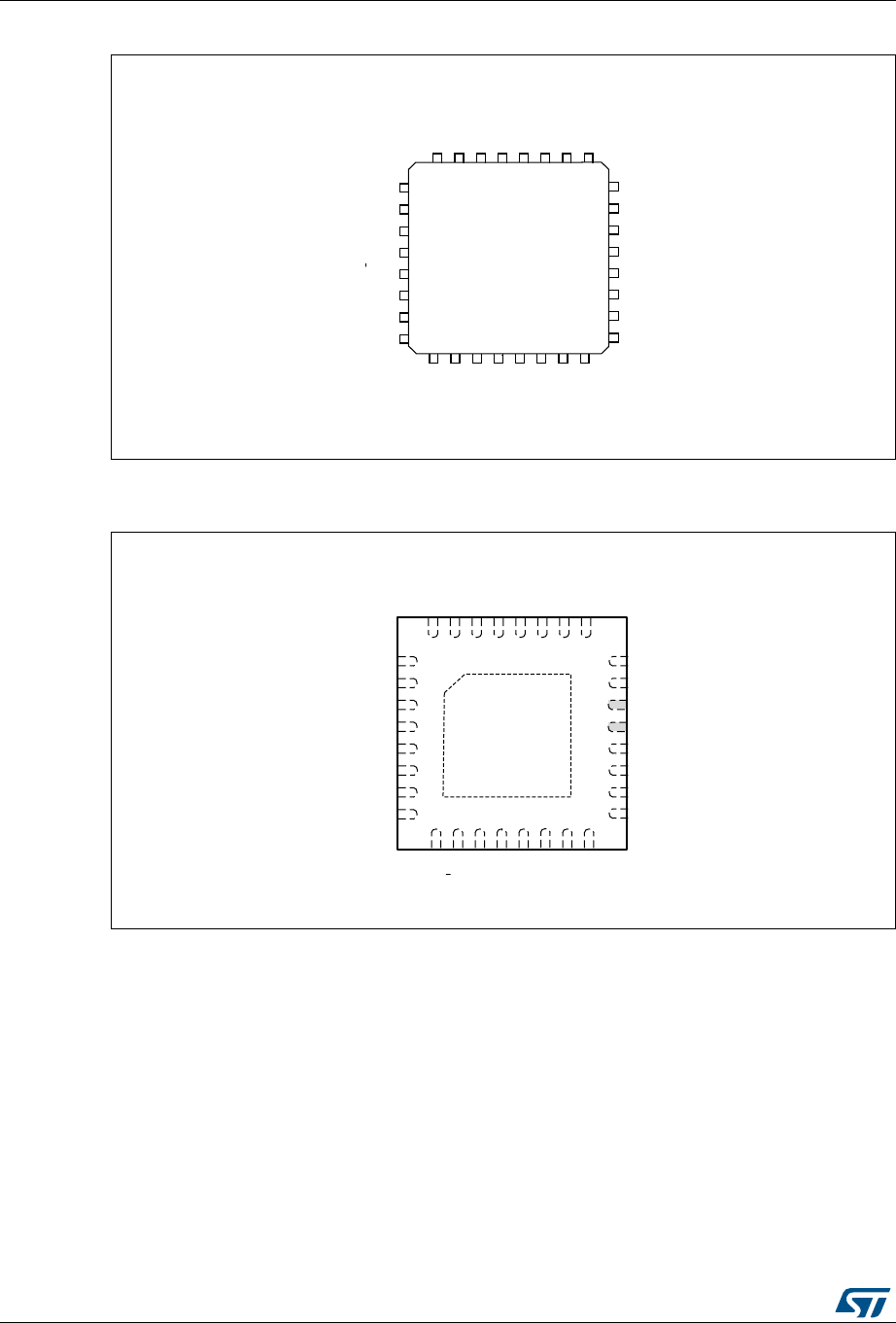
Pin descriptions STM32L072xx
42/149 DocID027100 Rev 4
Figure 9. STM32L072xx LQFP32 pinout
1. The above figure shows the package top view.
Figure 10. STM32L072xx UFQFPN32 pinout
1. The above figure shows the package top view.
2. I/O pin supplied by VDD_USB.
06Y9
3$
3$
3$
3$
3$
3%
3%
966
3$
3$
3$
3$
3$
3$
3$
9''
1567
9''$
3$
3$
3$
966
%227
3%
3%
3%
3%
3%
3$
3&26&B,1
3&26&B287
9''
/4)3
06Y9
3$
3$
3$
3$
3$
3%
3%
966
9''B86%
3$
3$
3$
3$
3$
3$
1567
9''$
3$
3$
3$
9''
966
%227
3%
3%
3%
3%
3$
3&26&B,1
3&26&B287
9''
966
966$
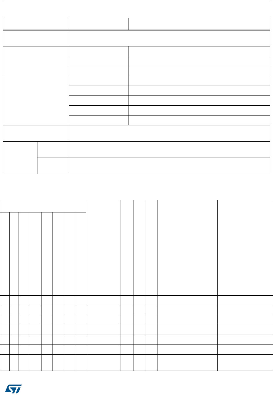
DocID027100 Rev 4 43/149
STM32L072xx Pin descriptions
56
Table 15. Legend/abbreviations used in the pinout table
Name Abbreviation Definition
Pin name Unless otherwise specified in brackets below the pin name, the pin function during
and after reset is the same as the actual pin name
Pin type
S Supply pin
I Input only pin
I/O Input / output pin
I/O structure
FT 5 V tolerant I/O
FTf 5 V tolerant I/O, FM+ capable
TC Standard 3.3V I/O
B Dedicated BOOT0 pin
RST Bidirectional reset pin with embedded weak pull-up resistor
Notes Unless otherwise specified by a note, all I/Os are set as floating inputs during and
after reset.
Pin functions
Alternate
functions Functions selected through GPIOx_AFR registers
Additional
functions Functions directly selected/enabled through peripheral registers
Table 16. STM32L072xxx pin definition
Pin number
Pin name
(function
after reset)
Pin type
I/O structure
Note
Alternate functions Additional functions
LQFP32
UFQFPN32(1)
LQFP48
LQFP64
UFBGA64/TFBGA64
WLCSP49
LQFP100
UFBG100
- - - - - - 1 B2 PE2 I/O FT - TIM3_ETR -
- - - - - - 2 A1 PE3 I/O FT - TIM22_CH1, TIM3_CH1 -
- - - - - - 3 B1 PE4 I/O FT - TIM22_CH2, TIM3_CH2 -
- - - - - - 4 C2 PE5 I/O FT - TIM21_CH1, TIM3_CH3 -
- - - - - - 5 D2 PE6 I/O FT - TIM21_CH2, TIM3_CH4 RTC_TAMP3/WKUP3
1 - 1 1 B2 B6 6 E2 VDD S - - -
- - 2 2 A2 B7 7 C1 PC13 I/O FT - - RTC_TAMP1/RTC_TS/
RTC_OUT/WKUP2
Pin descriptions STM32L072xx
44/149 DocID027100 Rev 4
21 3 3A1C68D1
PC14-
OSC32_IN
(PC14)
I/O FT - - OSC32_IN
32 4 4B1C79E1
PC15-
OSC32_OUT
(PC15)
I/O TC - - OSC32_OUT
------10F2 PH9 I/OFT- - -
------11G2 PH10 I/OFT- - -
- - 5 5 C1 D6 12 F1 PH0-OSC_IN
(PH0) I/O TC - USB_CRS_SYNC OSC_IN
- - 6 6 D1 D7 13 G1
PH1-
OSC_OUT
(PH1)
I/O TC - - OSC_OUT
4 3 7 7 E1 D5 14 H2 NRST I/O - - -
- - - 8 E3 C5 15 H1 PC0 I/O FTf -
LPTIM1_IN1,
EVENTOUT,
TSC_G7_IO1,
LPUART1_RX,
I2C3_SCL
ADC_IN10
- - - 9 E2 C4 16 J2 PC1 I/O FTf -
LPTIM1_OUT,
EVENTOUT,
TSC_G7_IO2,
LPUART1_TX,
I2C3_SDA
ADC_IN11
- - - 10 F2 E7 17 J3 PC2 I/O FTf -
LPTIM1_IN2,
SPI2_MISO/I2S2_MCK,
TSC_G7_IO3
ADC_IN12
- - - 11 - - 18 K2 PC3 I/O FT -
LPTIM1_ETR,
SPI2_MOSI/I2S2_SD,
TSC_G7_IO4
ADC_IN13
- 4 8 12 F1 - 19 J1 VSSA S - - -
- - - - - - 20 K1 VREF- S - - -
- - - - G1 E6 21 L1 VREF+ S - - -
Table 16. STM32L072xxx pin definition (continued)
Pin number
Pin name
(function
after reset)
Pin type
I/O structure
Note
Alternate functions Additional functions
LQFP32
UFQFPN32(1)
LQFP48
LQFP64
UFBGA64/TFBGA64
WLCSP49
LQFP100
UFBG100

DocID027100 Rev 4 45/149
STM32L072xx Pin descriptions
56
5 5 9 13 H1 F7 22 M1 VDDA S - - -
6 6 10 14 G2 E5 23 L2 PA0 I/O TTa -
TIM2_CH1,
TSC_G1_IO1,
USART2_CTS,
TIM2_ETR, USART4_TX,
COMP1_OUT
COMP1_INM,
ADC_IN0,
RTC_TAMP2/WKUP1
7 7 11 15 H2 E4 24 M2 PA1 I/O FT -
EVENTOUT, TIM2_CH2,
TSC_G1_IO2,
USART2_RTS,
TIM21_ETR,
USART4_RX
COMP1_INP, ADC_IN1
8 8 12 16 F3 F6 25 K3 PA2 I/O FT -
TIM21_CH1, TIM2_CH3,
TSC_G1_IO3,
USART2_TX,
LPUART1_TX,
COMP2_OUT
COMP2_INM,
ADC_IN2
9 9 13 17 G3 G7 26 L3 PA3 I/O FT -
TIM21_CH2, TIM2_CH4,
TSC_G1_IO4,
USART2_RX,
LPUART1_RX
COMP2_INP, ADC_IN3
- - - 18 C2 - 27 D3 VSS S - - - -
-- -19D2-28H3 VDD S - - - -
10 10 14 20 H3 F5 29 M3 PA4 I/O TC (2)
SPI1_NSS,
TSC_G2_IO1,
USART2_CK,
TIM22_ETR
COMP1_INM,
COMP2_INM,
ADC_IN4, DAC_OUT1
11 11 15 21 F4 G6 30 K4 PA5 I/O TC - SPI1_SCK, TIM2_ETR,
TSC_G2_IO2, TIM2_CH1
COMP1_INM,
COMP2_INM,
ADC_IN5, DAC_OUT2
12 12 16 22 G4 G5 31 L4 PA6 I/O FT -
SPI1_MISO, TIM3_CH1,
TSC_G2_IO3,
LPUART1_CTS,
TIM22_CH1,
EVENTOUT,
COMP1_OUT
ADC_IN6
Table 16. STM32L072xxx pin definition (continued)
Pin number
Pin name
(function
after reset)
Pin type
I/O structure
Note
Alternate functions Additional functions
LQFP32
UFQFPN32(1)
LQFP48
LQFP64
UFBGA64/TFBGA64
WLCSP49
LQFP100
UFBG100

Pin descriptions STM32L072xx
46/149 DocID027100 Rev 4
13 13 17 23 H4 F4 32 M4 PA7 I/O FT -
SPI1_MOSI, TIM3_CH2,
TSC_G2_IO4,
TIM22_CH2,
EVENTOUT,
COMP2_OUT
ADC_IN7
- - - 24 H5 - 33 K5 PC4 I/O FT - EVENTOUT,
LPUART1_TX ADC_IN14
- - - 25 H6 - 34 L5 PC5 I/O FT - LPUART1_RX,
TSC_G3_IO1 ADC_IN15
14 14 18 26 F5 G4 35 M5 PB0 I/O FT - EVENTOUT, TIM3_CH3,
TSC_G3_IO2 ADC_IN8, VREF_OUT
15 15 19 27 G5 D3 36 M6 PB1 I/O FT -
TIM3_CH4,
TSC_G3_IO3,
LPUART1_RTS
ADC_IN9, VREF_OUT
- - 20 28 G6 E3 37 L6 PB2 I/O FT -
LPTIM1_OUT,
TSC_G3_IO4,
I2C3_SMBA
-
------38M7 PE7 I/OFT-
USART5_CK/USART5_R
TS_DE -
- - - - - - 39 L7 PE8 I/O FT - USART4_TX -
------40M8 PE9 I/OFT-
TIM2_CH1, TIM2_ETR,
USART4_RX -
- - - - - - 41 L8 PE10 I/O FT - TIM2_CH2, USART5_TX -
- - - - - - 42 M9 PE11 I/O FT - TIM2_CH3, USART5_RX -
- - - - - - 43 L9 PE12 I/O FT - TIM2_CH4, SPI1_NSS -
- - - - - - 44 M10 PE13 I/O FT - SPI1_SCK -
- - - - - - 45 M11 PE14 I/O FT - SPI1_MISO -
- - - - - - 46 M12 PE15 I/O FT - SPI1_MOSI -
- - 21 29 G7 G3 47 L10 PB10 I/O FT -
TIM2_CH3, TSC_SYNC,
LPUART1_TX,
SPI2_SCK, I2C2_SCL,
LPUART1_RX
-
Table 16. STM32L072xxx pin definition (continued)
Pin number
Pin name
(function
after reset)
Pin type
I/O structure
Note
Alternate functions Additional functions
LQFP32
UFQFPN32(1)
LQFP48
LQFP64
UFBGA64/TFBGA64
WLCSP49
LQFP100
UFBG100
DocID027100 Rev 4 47/149
STM32L072xx Pin descriptions
56
- - 22 30 H7 F3 48 L11 PB11 I/O FT -
EVENTOUT, TIM2_CH4,
TSC_G6_IO1,
LPUART1_RX,
I2C2_SDA,
LPUART1_TX
-
16 16 23 31 D6 D4 49 F12 VSS S - - -
17 17 24 32 E5 G2 50 G12 VDD S - - -
- - 25 33 H8 G1 51 L12 PB12 I/O FT -
SPI2_NSS/I2S2_WS,
LPUART1_RTS_DE,
TSC_G6_IO2,
I2C2_SMBA,
EVENTOUT
-
- - 26 34 G8 F2 52 K12 PB13 I/O FTf -
SPI2_SCK/I2S2_CK,
MCO, TSC_G6_IO3,
LPUART1_CTS,
I2C2_SCL, TIM21_CH1
-
- - 27 35 F8 F1 53 K11 PB14 I/O FTf
SPI2_MISO/I2S2_MCK,
RTC_OUT,
TSC_G6_IO4,
LPUART1_RTS_DE,
I2C2_SDA, TIM21_CH2
-
- - 28 36 F7 E1 54 K10 PB15 I/O FT - SPI2_MOSI/I2S2_SD,
RTC_REFIN -
- - - - - - 55 K9 PD8 I/O FT - LPUART1_TX -
- - - - - - 56 K8 PD9 I/O FT - LPUART1_RX -
------57J12 PD10 I/OFT- - -
- - - - - - 58 J11 PD11 I/O FT - LPUART1_CTS -
- - - - - - 59 J10 PD12 I/O FT - LPUART1_RTS_DE -
- - - - - - 60 H12 PD13 I/O FT - - -
- - - - - - 61 H11 PD14 I/O FT - - -
- - - - - - 62 H10 PD15 I/O FT - USB_CRS_SYNC -
Table 16. STM32L072xxx pin definition (continued)
Pin number
Pin name
(function
after reset)
Pin type
I/O structure
Note
Alternate functions Additional functions
LQFP32
UFQFPN32(1)
LQFP48
LQFP64
UFBGA64/TFBGA64
WLCSP49
LQFP100
UFBG100
Pin descriptions STM32L072xx
48/149 DocID027100 Rev 4
- - - 37 F6 - 63 E12 PC6 I/O FT - TIM22_CH1, TIM3_CH1,
TSC_G8_IO1 -
- - - 38 E7 - 64 E11 PC7 I/O FT - TIM22_CH2, TIM3_CH2,
TSC_G8_IO2 -
- - - 39 E8 - 65 E10 PC8 I/O FT - TIM22_ETR, TIM3_CH3,
TSC_G8_IO3 -
- - - 40 D8 - 66 D12 PC9 I/O FTf -
TIM21_ETR,
USB_NOE/TIM3_CH4,
TSC_G8_IO4, I2C3_SDA
-
18 18 29 41 D7 D1 67 D11 PA8 I/O FTf -
MCO, USB_CRS_SYNC,
EVENTOUT,
USART1_CK, I2C3_SCL
-
19 19 30 42 C7 E2 68 D10 PA9 I/O FTf -
MCO, TSC_G4_IO1,
USART1_TX, I2C1_SCL,
I2C3_SMBA
-
20 20 31 43 C6 C1 69 C12 PA10 I/O FTf - TSC_G4_IO2,
USART1_RX, I2C1_SDA -
21 21 32 44 C8 D2 70 B12 PA11 I/O FT (3)
SPI1_MISO, EVENTOUT,
TSC_G4_IO3,
USART1_CTS,
COMP1_OUT
USB_DM
22 22 33 45 B8 B1 71 A12 PA12 I/O FT (3)
SPI1_MOSI, EVENTOUT,
TSC_G4_IO4,
USART1_RTS_DE,
COMP2_OUT
USB_DP
23 23 34 46 A8 C2 72 A11 PA13 I/O FT - SWDIO, USB_NOE,
LPUART1_RX -
- - - - - - 73 C11 VDD S - - -
- - 35 47 D5 - 74 F11 VSS S - - -
-243648E6A175G11VDD_USB S - - -
24 25 37 49 A7 B2 76 A10 PA14 I/O FT - SWCLK, USART2_TX,
LPUART1_TX -
Table 16. STM32L072xxx pin definition (continued)
Pin number
Pin name
(function
after reset)
Pin type
I/O structure
Note
Alternate functions Additional functions
LQFP32
UFQFPN32(1)
LQFP48
LQFP64
UFBGA64/TFBGA64
WLCSP49
LQFP100
UFBG100
DocID027100 Rev 4 49/149
STM32L072xx Pin descriptions
56
25 - 38 50 A6 A2 77 A9 PA15 I/O FT -
SPI1_NSS, TIM2_ETR,
EVENTOUT,
USART2_RX,
TIM2_CH1,
USART4_RTS_DE
-
- - - 51 B7 - 78 B11 PC10 I/O FT - LPUART1_TX,
USART4_TX -
- - - 52 B6 - 79 C10 PC11 I/O FT - LPUART1_RX,
USART4_RX -
- - - 53 C5 - 80 B10 PC12 I/O FT - USART5_TX,
USART4_CK -
------81C9 PD0 I/OFT- TIM21_CH1,
SPI2_NSS/I2S2_WS -
- - - - - - 82 B9 PD1 I/O FT - SPI2_SCK/I2S2_CK -
- - - 54 B5 - 83 C8 PD2 I/O FT - LPUART1_RTS_DE,
TIM3_ETR, USART5_RX -
- - - - - - 84 B8 PD3 I/O FT - USART2_CTS,
SPI2_MISO/I2S2_MCK -
- - - - - - 85 B7 PD4 I/O FT - USART2_RTS_DE,
SPI2_MOSI/I2S2_SD -
- - - - - - 86 A6 PD5 I/O FT - USART2_TX -
- - - - - - 87 B6 PD6 I/O FT - USART2_RX -
- - - - - - 88 A5 PD7 I/O FT - USART2_CK,
TIM21_CH2 -
26 - 39 55 A5 A3 89 A8 PB3 I/O FT -
SPI1_SCK, TIM2_CH2,
TSC_G5I_O1,
EVENTOUT,
USART1__RTS_DE,
USART5_TX
COMP2_INM
Table 16. STM32L072xxx pin definition (continued)
Pin number
Pin name
(function
after reset)
Pin type
I/O structure
Note
Alternate functions Additional functions
LQFP32
UFQFPN32(1)
LQFP48
LQFP64
UFBGA64/TFBGA64
WLCSP49
LQFP100
UFBG100
Pin descriptions STM32L072xx
50/149 DocID027100 Rev 4
27 26 40 56 A4 B3 90 A7 PB4 I/O FTf -
SPI1_MISO, TIM3_CH1,
TSC_G5_IO2,
TIM22_CH1,
USART1_CTS,
USART5_RX, I2C3_SDA
COMP2_INP
28 27 41 57 C4 A4 91 C5 PB5 I/O FT -
SPI1_MOSI,
LPTIM1_IN1,
I2C1_SMBA,
TIM3_CH2/TIM22_CH2,
USART1_CK,
USART5_CK/USART5_R
TS_DE
COMP2_INP
29 28 42 58 D3 B4 92 B5 PB6 I/O FTf -
USART1_TX, I2C1_SCL,
LPTIM1_ETR,
TSC_G5_IO3
COMP2_INP
30 29 43 59 C3 C3 93 B4 PB7 I/O FTf -
USART1_RX, I2C1_SDA,
LPTIM1_IN2,
TSC_G5_IO4,
USART4_CTS
COMP2_INP,
VREF_PVD_IN
31 30 44 60 B4 A5 94 A4 BOOT0 I - - -
- - 45 61 B3 B5 95 A3 PB8 I/O FTf - TSC_SYNC, I2C1_SCL -
- - 46 62 A3 A6 96 B3 PB9 I/O FTf - EVENTOUT, I2C1_SDA,
SPI2_NSS/I2S2_WS -
- - - - - - 97 C3 PE0 I/O FT - EVENTOUT -
- - - - - - 98 A2 PE1 I/O FT - EVENTOUT -
32 31 47 63 D4 - 99 D3 VSS S - - - -
-324864E4A7100C4 VDD S - - - -
1. UFQFPN32 pinout differs from other STM32 devices except STM32L07xxx and STM32L8xxx.
2. PA4 offers a reduced touch sensing sensitivity. It is thus recommended to use it as sampling capacitor I/O.
3. These pins are powered by VDD_USB. For all characteristics that refer to VDD, VDD_USB must be used instead.
Table 16. STM32L072xxx pin definition (continued)
Pin number
Pin name
(function
after reset)
Pin type
I/O structure
Note
Alternate functions Additional functions
LQFP32
UFQFPN32(1)
LQFP48
LQFP64
UFBGA64/TFBGA64
WLCSP49
LQFP100
UFBG100
STM32L072xx Pin descriptions
DocID027100 Rev 4 51/149
Table 17. Alternate functions port A
Port
AF0AF1AF2AF3AF4AF5AF6AF7
SPI1/SPI2/I2S2/U
SART1/2/
LPUART1/USB/L
PTIM1/TSC/
TIM2/21/22/
EVENTOUT/
SYS_AF
SPI1/SPI2/I2S2/I2
C1/TIM2/21
SPI1/SPI2/I2S2/L
PUART1/
USART5/USB/LP
TIM1/TIM2/3/EVE
NTOUT/
SYS_AF
I2C1/TSC/
EVENTOUT
I2C1/USART1/2/L
PUART1/
TIM3/22/
EVENTOUT
SPI2/I2S2/I2C2/
USART1/
TIM2/21/22
I2C1/2/
LPUART1/
USART4/
UASRT5/TIM21/
EVENTOUT
I2C3/LPUART1/
COMP1/2/
TIM3
Port A
PA0 - - TIM2_CH1 TSC_G1_IO1 USART2_CTS TIM2_ETR USART4_TX COMP1_OUT
PA1 EVENTOUT TIM2_CH2 TSC_G1_IO2 USART2_RTS_
DE TIM21_ETR USART4_RX -
PA2 TIM21_CH1 TIM2_CH3 TSC_G1_IO3 USART2_TX - LPUART1_TX COMP2_OUT
PA3 TIM21_CH2 TIM2_CH4 TSC_G1_IO4 USART2_RX - LPUART1_RX -
PA4 SPI1_NSS - - TSC_G2_IO1 USART2_CK TIM22_ETR - -
PA5 SPI1_SCK - TIM2_ETR TSC_G2_IO2 TIM2_CH1 - -
PA6 SPI1_MISO TIM3_CH1 TSC_G2_IO3 LPUART1_CTS TIM22_CH1 EVENTOUT COMP1_OUT
PA7 SPI1_MOSI TIM3_CH2 TSC_G2_IO4 - TIM22_CH2 EVENTOUT COMP2_OUT
PA8 MCO USB_CRS_
SYNC EVENTOUT USART1_CK - - I2C3_SCL
PA9 MCO - TSC_G4_IO1 USART1_TX - I2C1_SCL I2C3_SMBA
PA10 - - TSC_G4_IO2 USART1_RX - I2C1_SDA -
PA11 SPI1_MISO - EVENTOUT TSC_G4_IO3 USART1_CTS - - COMP1_OUT
PA12 SPI1_MOSI - EVENTOUT TSC_G4_IO4 USART1_RTS_
DE - - COMP2_OUT
PA13 SWDIO - USB_NOE - - - LPUART1_RX -
PA14 SWCLK - - - USART2_TX - LPUART1_TX -
PA15 SPI1_NSS TIM2_ETR EVENTOUT USART2_RX TIM2_CH1 USART4_RTS_
DE -
Pin descriptions STM32L072xx
52/149 DocID027100 Rev 4
Table 18. Alternate functions port B
Port
AF0 AF1 AF2 AF3 AF4 AF5 AF6 AF7
SPI1/SPI2/I2S2/
USART1/2/
LPUART1/USB/
LPTIM1/TSC/
TIM2/21/22/
EVENTOUT/
SYS_AF
SPI1/SPI2/I2S2/I
2C1/TIM2/21
SPI1/SPI2/I2S2/
LPUART1/
USART5/USB/L
PTIM1/TIM2/3/E
VENTOUT/
SYS_AF
I2C1/TSC/
EVENTOUT
I2C1/USART1/2/
LPUART1/
TIM3/22/
EVENTOUT
SPI2/I2S2/I2C2/
USART1/
TIM2/21/22
I2C1/2/
LPUART1/
USART4/
UASRT5/TIM21/
EVENTOUT
I2C3/LPUART1/
COMP1/2/
TIM3
Port B
PB0 EVENTOUT TIM3_CH3 TSC_G3_IO2 - - - -
PB1 - TIM3_CH4 TSC_G3_IO3 LPUART1_RTS_DE - - -
PB2 - - LPTIM1_OUT TSC_G3_IO4 - - - I2C3_SMBA
PB3 SPI1_SCK TIM2_CH2 TSC_G5_IO1 EVENTOUT USART1_RTS_DE USART5_TX -
PB4 SPI1_MISO TIM3_CH1 TSC_G5_IO2 TIM22_CH1 USART1_CTS USART5_RX I2C3_SDA
PB5 SPI1_MOSI LPTIM1_IN1 I2C1_SMBA TIM3_CH2/
TIM22_CH2 USART1_CK
USART5_CK/
USART5_RTS_
DE
-
PB6 USART1_TX I2C1_SCL LPTIM1_ETR TSC_G5_IO3 - - - -
PB7 USART1_RX I2C1_SDA LPTIM1_IN2 TSC_G5_IO4 - - USART4_CTS -
PB8 - - TSC_SYNC I2C1_SCL - - -
PB9 - EVENTOUT - I2C1_SDA SPI2_NSS/
I2S2_WS --
PB10 - TIM2_CH3 TSC_SYNC LPUART1_TX SPI2_SCK I2C2_SCL LPUART1_RX
PB11 EVENTOUT TIM2_CH4 TSC_G6_IO1 LPUART1_RX - I2C2_SDA LPUART1_TX
PB12 SPI2_NSS/I2S2_WS LPUART1_RTS_
DE TSC_G6_IO2 I2C2_SMBA EVENTOUT -
PB13 SPI2_SCK/I2S2_CK MCO TSC_G6_IO3 LPUART1_CTS I2C2_SCL TIM21_CH1 -
PB14 SPI2_MISO/
I2S2_MCK RTC_OUT TSC_G6_IO4 LPUART1_RTS_DE I2C2_SDA TIM21_CH2 -
PB15 SPI2_MOSI/
I2S2_SD RTC_REFIN - - - - -
STM32L072xx Pin descriptions
DocID027100 Rev 4 53/149
Table 19. Alternate functions port C
Port
AF0 AF1 AF2 AF3 AF4 AF5 AF6 AF7
SPI1/SPI2/I2S2/
USART1/2/
LPUART1/USB/
LPTIM1/TSC/
TIM2/21/22/
EVENTOUT/
SYS_AF
SPI1/SPI2/I2S2/I2C1/
TIM2/21
SPI1/SPI2/I2S2/
LPUART1/
USART5/USB/
LPTIM1/TIM2/3
/EVENTOUT/SYS_AF
I2C1/TSC/
EVENTOUT
I2C1/USART1/2/
LPUART1/
TIM3/22/
EVENTOUT
SPI2/I2S2
/I2C2/
USART1/
TIM2/21/22
I2C1/2/
LPUART1/
USART4/
UASRT5/TIM21/E
VENTOUT
I2C3/LPUART1/
COMP1/2/
TIM3
Port C
PC0 LPTIM1_IN1 EVENTOUT TSC_G7_IO1 LPUART1_RX I2C3_SCL
PC1 LPTIM1_OUT EVENTOUT TSC_G7_IO2 LPUART1_TX I2C3_SDA
PC2 LPTIM1_IN2 SPI2_MISO/
I2S2_MCK TSC_G7_IO3
PC3 LPTIM1_ETR SPI2_MOSI/
I2S2_SD TSC_G7_IO4
PC4 EVENTOUT LPUART1_TX
PC5 LPUART1_RX TSC_G3_IO1
PC6 TIM22_CH1 TIM3_CH1 TSC_G8_IO1
PC7 TIM22_CH2 TIM3_CH2 TSC_G8_IO2
PC8 TIM22_ETR TIM3_CH3 TSC_G8_IO3
PC9 TIM21_ETR USB_NOE/TIM3_CH4 TSC_G8_IO4 I2C3_SDA
PC10 LPUART1_TX USART4_TX
PC11 LPUART1_RX USART4_RX
PC12 USART5_TX USART4_CK
PC13
PC14
PC15
Pin descriptions STM32L072xx
54/149 DocID027100 Rev 4
Table 20. Alternate functions port D
Port
AF0 AF1 AF2 AF3 AF4 AF5 AF6 AF7
SPI1/SPI2/I2S2/
USART1/2/
LPUART1/USB/
LPTIM1/TSC/
TIM2/21/22/
EVENTOUT/
SYS_AF
SPI1/SPI2/I2S2/I2C1/
TIM2/21
SPI1/SPI2/I2S2/
LPUART1/
USART5/USB/
LPTIM1/TIM2/3
/EVENTOUT/
SYS_AF
I2C1/TSC/
EVENTOUT
I2C1/USART1/2/
LPUART1/
TIM3/22/
EVENTOUT
SPI2/I2S2
/I2C2/
USART1/
TIM2/21/22
I2C1/2/
LPUART1/
USART4/
UASRT5/TIM21/E
VENTOUT
I2C3/LPUART1/
COMP1/2/TIM3
Port D
PD0 TIM21_CH1 SPI2_NSS/I2S2_WS - - - - - -
PD1 - SPI2_SCK/I2S2_CK - - - - - -
PD2 LPUART1_RTS_
DE TIM3_ETR - - - USART5_RX -
PD3 USART2_CTS SPI2_MISO/
I2S2_MCK -- - - -
PD4 USART2_RTS_D
ESPI2_MOSI/I2S2_SD - - - - - -
PD5 USART2_TX - - - - - - -
PD6 USART2_RX - - - - - - -
PD7 USART2_CK TIM21_CH2 - - - - - -
PD8 LPUART1_TX - - - - - -
PD9 LPUART1_RX - - - - - -
PD10 - - - - - - -
PD11 LPUART1_CTS - - - - - -
PD12 LPUART1_RTS_
DE --- - - -
PD13 - - - - - - -
PD14 - - - - - - -
PD15 USB_CRS_SYNC - - - - - -
STM32L072xx Pin descriptions
DocID027100 Rev 4 55/149
Table 21. Alternate functions port E
Port
AF0 AF1 AF2 AF3 AF4 AF5 AF6 AF7
SPI1/SPI2/I2S2/
USART1/2/
LPUART1/USB/
LPTIM1/TSC/
TIM2/21/22/
EVENTOUT/
SYS_AF
SPI1/SPI2/I2S2/I2C1
/TIM2/21
SPI1/SPI2/I2S2/
LPUART1/
USART5/USB/
LPTIM1/TIM2/3
/EVENTOUT/
SYS_AF
I2C1/TSC/
EVENTOUT
I2C1/USART1/2/
LPUART1/
TIM3/22/
EVENTOUT
SPI2/I2S2
/I2C2/
USART1/
TIM2/21/22
I2C1/2/
LPUART1/
USART4/
UASRT5/TIM21/
EVENTOUT
I2C3/LPUART1/
COMP1/2/TIM3
Port E
PE0 - EVENTOUT - - - - -
PE1 - EVENTOUT - - - - -
PE2 - TIM3_ETR - - - - -
PE3 TIM22_CH1 TIM3_CH1 - - - - -
PE4 TIM22_CH2 - TIM3_CH2 - - - - -
PE5 TIM21_CH1 - TIM3_CH3 - - - - -
PE6 TIM21_CH2 - TIM3_CH4 - - - - -
PE7 - - - - -
USART5_CK/U
SART5_RTS_D
E
-
PE8 - - - - - USART4_TX -
PE9 TIM2_CH1 TIM2_ETR - - - USART4_RX -
PE10 TIM2_CH2 - - - - USART5_TX -
PE11 TIM2_CH3 - - - - - USART5_RX -
PE12 TIM2_CH4 - SPI1_NSS - - - - -
PE13 - SPI1_SCK - - - - -
PE14 - SPI1_MISO - - - - -
PE15 - SPI1_MOSI - - - - -
Pin descriptions STM32L072xx
56/149 DocID027100 Rev 4
Table 22. Alternate functions port H
Port
AF0 AF1 AF2 AF3 AF4 AF5 AF6 AF7
SPI1/SPI2/
I2S2/USART1/2/
LPUART1/USB/
LPTIM1/TSC/
TIM2/21/22/
EVENTOUT/
SYS_AF
SPI1/SPI2/I2S2
/I2C1/TIM2/21
SPI1/SPI2/I2S2/
LPUART1/
USART5/USB/
LPTIM1/TIM2/3/
EVENTOUT/
SYS_AF
I2C1/TSC/
EVENTOUT
I2C1/USART1/2/
LPUART1/
TIM3/22/
EVENTOUT
SPI2/I2S2/I2C2/
USART1/
TIM2/21/22
I2C1/2/
LPUART1/
USART4/
UASRT5/TIM21/
EVENTOUT
I2C3/
LPUART1/
COMP1/2/
TIM3
Port H
PH0 USB_CRS_SYNC - - - - - - -
PH1 - - - - - - - -

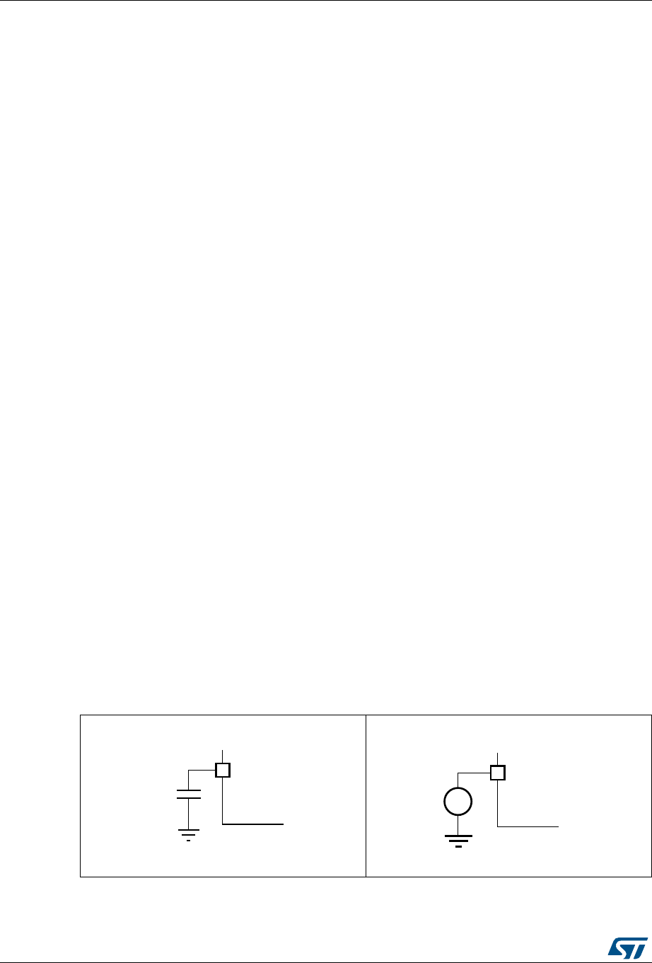
Electrical characteristics STM32L072xx
58/149 DocID027100 Rev 4
6 Electrical characteristics
6.1 Parameter conditions
Unless otherwise specified, all voltages are referenced to VSS.
6.1.1 Minimum and maximum values
Unless otherwise specified the minimum and maximum values are guaranteed in the worst
conditions of ambient temperature, supply voltage and frequencies by tests in production on
100% of the devices with an ambient temperature at TA = 25 °C and TA = TAmax (given by
the selected temperature range).
Data based on characterization results, design simulation and/or technology characteristics
are indicated in the table footnotes and are not tested in production. Based on
characterization, the minimum and maximum values refer to sample tests and represent the
mean value plus or minus three times the standard deviation (mean±3σ).
6.1.2 Typical values
Unless otherwise specified, typical data are based on TA = 25 °C, VDD = 3.6 V (for the
1.65 V ≤ VDD ≤ 3.6 V voltage range). They are given only as design guidelines and are not
tested.
Typical ADC accuracy values are determined by characterization of a batch of samples from
a standard diffusion lot over the full temperature range, where 95% of the devices have an
error less than or equal to the value indicated (mean±2σ).
6.1.3 Typical curves
Unless otherwise specified, all typical curves are given only as design guidelines and are
not tested.
6.1.4 Loading capacitor
The loading conditions used for pin parameter measurement are shown in Figure 11.
6.1.5 Pin input voltage
The input voltage measurement on a pin of the device is described in Figure 12.
Figure 11. Pin loading conditions Figure 12. Pin input voltage
DLF
& S)
0&8SLQ
DLF
0&8SLQ
9,1
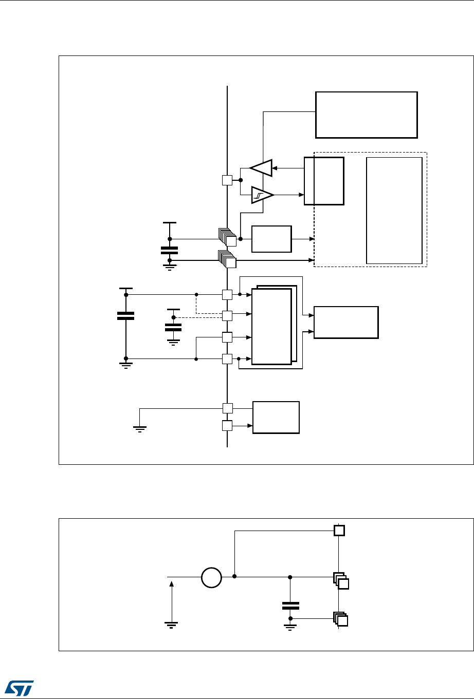
DocID027100 Rev 4 59/149
STM32L072xx Electrical characteristics
120
6.1.6 Power supply scheme
Figure 13. Power supply scheme
6.1.7 Current consumption measurement
Figure 14. Current consumption measurement scheme
06Y9
$QDORJ
5&3//&203
«
9''
*3,2V
287
,1 .HUQHOORJLF
&38
'LJLWDO
0HPRULHV
6WDQGE\SRZHUFLUFXLWU\
26&57&:DNHXS
ORJLF57&EDFNXS
UHJLVWHUV
1îQ)
î)
5HJXODWRU
966
9''$
95()
95()
966$
$'&
'$&
/HYHOVKLIWHU
,2
/RJLF
9''
Q)
)
95()
Q)
)
9''$
9''B86%
86%
WUDQVFHLYHU
966
06Y9
1[9''
,''
1îQ)
î) 1[966
9''$
Electrical characteristics STM32L072xx
60/149 DocID027100 Rev 4
6.2 Absolute maximum ratings
Stresses above the absolute maximum ratings listed in Table 23: Voltage characteristics,
Table 24: Current characteristics, and Table 25: Thermal characteristics may cause
permanent damage to the device. These are stress ratings only and functional operation of
the device at these conditions is not implied. Exposure to maximum rating conditions for
extended periods may affect device reliability. Device mission profile (application conditions)
is compliant with JEDEC JESD47 Qualification Standard. Extended mission profiles are
available on demand.
Table 23. Voltage characteristics
Symbol Definition Min Max Unit
VDD–VSS
External main supply voltage
(including VDDA, VDD_USB, VDD)(1)
1. All main power (VDD,VDD_USB, VDDA) and ground (VSS, VSSA) pins must always be connected to the
external power supply, in the permitted range.
–0.3 4.0
V
VIN(2)
2. VIN maximum must always be respected. Refer to Table 24 for maximum allowed injected current values.
Input voltage on FT and FTf pins VSS − 0.3 VDD+4.0
Input voltage on TC pins VSS − 0.3 4.0
Input voltage on BOOT0 VSS VDD + 4.0
Input voltage on any other pin VSS − 0.3 4.0
|ΔVDD| Variations between different VDDx power pins - 50
mV
|VDDA-VDDx|Variations between any VDDx and VDDA power
pins(3)
3. It is recommended to power VDD and VDDA from the same source. A maximum difference of 300 mV
between VDD and VDDA can be tolerated during power-up and device operation. VDD_USB is independent
from VDD and VDDA: its value does not need to respect this rule.
- 300
|ΔVSS|Variations between all different ground pins
including VREF- pin -50
VREF+ –VDDA Allowed voltage difference for VREF+ > VDDA -0.4V
VESD(HBM)
Electrostatic discharge voltage
(human body model) see Section 6.3.11
DocID027100 Rev 4 61/149
STM32L072xx Electrical characteristics
120
Table 24. Current characteristics
Symbol Ratings Max. Unit
ΣIVDD(2) Total current into sum of all VDD power lines (source)(1)
1. All main power (VDD, VDDA) and ground (VSS, VSSA) pins must always be connected to the external power
supply, in the permitted range.
105
mA
ΣIVSS(2)
2. This current consumption must be correctly distributed over all I/Os and control pins. The total output
current must not be sunk/sourced between two consecutive power supply pins referring to high pin count
LQFP packages.
Total current out of sum of all VSS ground lines (sink)(1) 105
ΣIVDD_USB Total current into VDD_USB power lines (source) 25
IVDD(PIN) Maximum current into each VDD power pin (source)(1) 100
IVSS(PIN) Maximum current out of each VSS ground pin (sink)(1) 100
IIO
Output current sunk by any I/O and control pin except FTf
pins 16
Output current sunk by FTf pins 22
Output current sourced by any I/O and control pin -16
ΣIIO(PIN)
Total output current sunk by sum of all IOs and control pins
except PA11 and PA12(2) 90
Total output current sunk by PA11 and PA12 25
Total output current sourced by sum of all IOs and control
pins(2) -90
IINJ(PIN)
Injected current on FT, FTf, RST and B pins -5/+0(3)
3. Positive current injection is not possible on these I/Os. A negative injection is induced by VIN<VSS. IINJ(PIN)
must never be exceeded. Refer to Table 23 for maximum allowed input voltage values.
Injected current on TC pin ± 5(4)
4. A positive injection is induced by VIN > VDD while a negative injection is induced by VIN < VSS. IINJ(PIN)
must never be exceeded. Refer to Table 23: Voltage characteristics for the maximum allowed input voltage
values.
ΣIINJ(PIN) Total injected current (sum of all I/O and control pins)(5)
5. When several inputs are submitted to a current injection, the maximum ΣIINJ(PIN) is the absolute sum of the
positive and negative injected currents (instantaneous values).
± 25
Table 25. Thermal characteristics
Symbol Ratings Value Unit
TSTG Storage temperature range –65 to +150 °C
TJMaximum junction temperature 150 °C
Electrical characteristics STM32L072xx
62/149 DocID027100 Rev 4
6.3 Operating conditions
6.3.1 General operating conditions
Table 26. General operating conditions
Symbol Parameter Conditions Min Max Unit
fHCLK Internal AHB clock frequency - 0 32
MHzfPCLK1 Internal APB1 clock frequency - 0 32
fPCLK2 Internal APB2 clock frequency - 0 32
VDD Standard operating voltage
BOR detector disabled 1.65 3.6
VBOR detector enabled, at power-on 1.8 3.6
BOR detector disabled, after power-on 1.65 3.6
VDDA
Analog operating voltage (DAC not
used) Must be the same voltage as VDD(1) 1.65 3.6 V
VDDA
Analog operating voltage (all
features) Must be the same voltage as VDD(1) 1.8 3.6 V
VDD_US
B
Standard operating voltage, USB
domain(2)
USB peripheral used 3.0 3.6
V
USB peripheral not used 1.65 3.6
VIN
Input voltage on FT, FTf and RST
pins(3)
2.0 V ≤ VDD ≤ 3.6 V -0.3 5.5
V
1.65 V ≤ VDD ≤ 2.0 V -0.3 5.2
Input voltage on BOOT0 pin - 0 5.5
Input voltage on TC pin - -0.3 VDD+0.3
DocID027100 Rev 4 63/149
STM32L072xx Electrical characteristics
120
PD
Power dissipation at TA = 85 °C
(range 6) or TA =105 °C (rage 7) (4)
UFBGA100 package - 351
mW
LQFP100 package - 488
UFBG64 package - 308
TFBGA64 package - 313
LQFP64 package - 435
WLCSP49 package - 417
LQFP48 package - 370
UFQFPN32 package - 556
LQFP32 package - 333
Power dissipation at TA = 125 °C
(range 3) (4)
UFBGA100 package - 88
LQFP100 package - 122
UFBG64 package - 77
TFBGA64 package - 78
LQFP64 package - 109
WLCSP49 package - 104
LQFP48 package - 93
UFQFPN32 package - 139
LQFP32 package - 83
TA Temperature range
Maximum power dissipation (range 6) –40 85
°C
Maximum power dissipation (range 7) –40 105
Maximum power dissipation (range 3) –40 125
TJ
Junction temperature range (range 6) -40 °C ≤ TA ≤ 85 ° –40 105
Junction temperature range (range 7) -40 °C ≤ TA ≤ 105 °C –40 125
Junction temperature range (range 3) -40 °C ≤ TA ≤ 125 °C –40 130
1. It is recommended to power VDD and VDDA from the same source. A maximum difference of 300 mV between VDD and VDDA
can be tolerated during power-up and normal operation.
2. VDD_USB must respect the following conditions:
- When VDD is powered-on (VDD < VDD_min), VDD_USB should be always lower than VDD.
- When VDD is powered-down (VDD < VDD_min), VDD_USB should be always lower than VDD.
- In operating mode, VDD_USB could be lower or higher VDD.
- If the USB is not used, VDD_USB must range from VDD_min to VDD_max to be able to use PA11 and PA12 as standard I/Os.
3. To sustain a voltage higher than VDD+0.3V, the internal pull-up/pull-down resistors must be disabled.
4. If TA is lower, higher PD values are allowed as long as TJ does not exceed TJ max (see Table 25: Thermal characteristics on
page 61).
Table 26. General operating conditions (continued)
Symbol Parameter Conditions Min Max Unit
Electrical characteristics STM32L072xx
64/149 DocID027100 Rev 4
6.3.2 Embedded reset and power control block characteristics
The parameters given in the following table are derived from the tests performed under the
ambient temperature condition summarized in Table 26.
Table 27. Embedded reset and power control block characteristics
Symbol Parameter Conditions Min Typ Max Unit
tVDD(1)
VDD rise time rate
BOR detector enabled 0 - ∞
µs/V
BOR detector disabled 0 - 1000
VDD fall time rate
BOR detector enabled 20 - ∞
BOR detector disabled 0 - 1000
TRSTTEMPO(1) Reset temporization
VDD rising, BOR enabled - 2 3.3
ms
VDD rising, BOR disabled(2) 0.4 0.7 1.6
VPOR/PDR
Power-on/power down reset
threshold
Falling edge 1 1.5 1.65
V
Rising edge 1.3 1.5 1.65
VBOR0 Brown-out reset threshold 0
Falling edge 1.67 1.7 1.74
Rising edge 1.69 1.76 1.8
VBOR1 Brown-out reset threshold 1
Falling edge 1.87 1.93 1.97
Rising edge 1.96 2.03 2.07
VBOR2 Brown-out reset threshold 2
Falling edge 2.22 2.30 2.35
Rising edge 2.31 2.41 2.44
VBOR3 Brown-out reset threshold 3
Falling edge 2.45 2.55 2.6
Rising edge 2.54 2.66 2.7
VBOR4 Brown-out reset threshold 4
Falling edge 2.68 2.8 2.85
Rising edge 2.78 2.9 2.95
VPVD0
Programmable voltage detector
threshold 0
Falling edge 1.8 1.85 1.88
Rising edge 1.88 1.94 1.99
VPVD1 PVD threshold 1
Falling edge 1.98 2.04 2.09
Rising edge 2.08 2.14 2.18
VPVD2 PVD threshold 2
Falling edge 2.20 2.24 2.28
Rising edge 2.28 2.34 2.38
VPVD3 PVD threshold 3
Falling edge 2.39 2.44 2.48
Rising edge 2.47 2.54 2.58
VPVD4 PVD threshold 4
Falling edge 2.57 2.64 2.69
Rising edge 2.68 2.74 2.79
VPVD5 PVD threshold 5
Falling edge 2.77 2.83 2.88
Rising edge 2.87 2.94 2.99
DocID027100 Rev 4 65/149
STM32L072xx Electrical characteristics
120
6.3.3 Embedded internal reference voltage
The parameters given in Table 29 are based on characterization results, unless otherwise
specified.
VPVD6 PVD threshold 6
Falling edge 2.97 3.05 3.09
V
Rising edge 3.08 3.15 3.20
Vhyst Hysteresis voltage
BOR0 threshold - 40 -
mV
All BOR and PVD thresholds
excepting BOR0 -100-
1. Guaranteed by characterization results.
2. Valid for device version without BOR at power up. Please see option "D" in Ordering information scheme for more details.
Table 27. Embedded reset and power control block characteristics (continued)
Symbol Parameter Conditions Min Typ Max Unit
Table 28. Embedded internal reference voltage calibration values
Calibration value name Description Memory address
VREFINT_CAL
Raw data acquired at
temperature of 25 °C
VDDA= 3 V
0x1FF8 0078 - 0x1FF8 0079
Table 29. Embedded internal reference voltage(1)
Symbol Parameter Conditions Min Typ Max Unit
VREFINT out(2) Internal reference voltage – 40 °C < TJ < +125 °C 1.202 1.224 1.242 V
TVREFINT Internal reference startup time - - 2 3 ms
VVREF_MEAS
VDDA and VREF+ voltage during
VREFINT factory measure -2.9933.01V
AVREF_MEAS
Accuracy of factory-measured
VREFINT value(3)
Including uncertainties
due to ADC and
VDDA/VREF+ values
-- ±5mV
TCoeff(4) Temperature coefficient –40 °C < TJ < +125 °C - 25 100 ppm/°C
ACoeff(4) Long-term stability 1000 hours, T= 25 °C - - 1000 ppm
VDDCoeff(4) Voltage coefficient 3.0 V < VDDA < 3.6 V - - 2000 ppm/V
TS_vrefint(4)(5)
ADC sampling time when
reading the internal reference
voltage
-510-µs
TADC_BUF(4) Startup time of reference
voltage buffer for ADC ---10µs
IBUF_ADC(4) Consumption of reference
voltage buffer for ADC - - 13.5 25 µA
IVREF_OUT(4) VREF_OUT output current(6) ---1µA
CVREF_OUT(4) VREF_OUT output load - - - 50 pF
Electrical characteristics STM32L072xx
66/149 DocID027100 Rev 4
6.3.4 Supply current characteristics
The current consumption is a function of several parameters and factors such as the
operating voltage, temperature, I/O pin loading, device software configuration, operating
frequencies, I/O pin switching rate, program location in memory and executed binary code.
The current consumption is measured as described in Figure 14: Current consumption
measurement scheme.
All Run-mode current consumption measurements given in this section are performed with a
reduced code that gives a consumption equivalent to Dhrystone 2.1 code if not specified
otherwise.
The current consumption values are derived from the tests performed under ambient
temperature and VDD supply voltage conditions summarized in Table 26: General operating
conditions unless otherwise specified.
The MCU is placed under the following conditions:
•All I/O pins are configured in analog input mode
•All peripherals are disabled except when explicitly mentioned
•The Flash memory access time and prefetch is adjusted depending on fHCLK
frequency and voltage range to provide the best CPU performance unless otherwise
specified.
•When the peripherals are enabled fAPB1 = fAPB2 = fAPB
•When PLL is ON, the PLL inputs are equal to HSI = 16 MHz (if internal clock is used) or
HSE = 16 MHz (if HSE bypass mode is used)
•The HSE user clock applied to OSCI_IN input follows the characteristic specified in
Table 43: High-speed external user clock characteristics
•For maximum current consumption VDD = VDDA = 3.6 V is applied to all supply pins
•For typical current consumption VDD = VDDA = 3.0 V is applied to all supply pins if not
specified otherwise
The parameters given in Table 51, Table 26 and Table 27 are derived from tests performed
under ambient temperature and VDD supply voltage conditions summarized in Table 26.
ILPBUF(4)
Consumption of reference
voltage buffer for VREF_OUT
and COMP
- - 730 1200 nA
VREFINT_DIV1(4) 1/4 reference voltage - 24 25 26
%
VREFINT
VREFINT_DIV2(4) 1/2 reference voltage - 49 50 51
VREFINT_DIV3(4) 3/4 reference voltage - 74 75 76
1. Refer to Table 41: Peripheral current consumption in Stop and Standby mode for the value of the internal reference current
consumption (IREFINT).
2. Guaranteed by test in production.
3. The internal VREF value is individually measured in production and stored in dedicated EEPROM bytes.
4. Guaranteed by design.
5. Shortest sampling time can be determined in the application by multiple iterations.
6. To guarantee less than 1% VREF_OUT deviation.
Table 29. Embedded internal reference voltage(1) (continued)
Symbol Parameter Conditions Min Typ Max Unit
DocID027100 Rev 4 67/149
STM32L072xx Electrical characteristics
120
Table 30. Current consumption in Run mode, code with data processing running from
Flash memory
Symbol Parameter Condition fHCLK
(MHz) Typ Max(1) Unit
IDD (Run
from Flash
memory)
Supply current in Run
mode code executed
from Flash memory
fHSE = fHCLK up to
16MHz included,
fHSE = fHCLK/2 above
16 MHz (PLL ON)(2)
Range3,
Vcore=1.2 V
VOS[1:0]=11
1 190 250
µA2 345 380
4 650 670
Range2,
Vcore=1.5 V
VOS[1:0]=10
4 0,8 0,86
mA
8 1,55 1,7
16 2,95 3,1
Range1,
Vcore=1.8 V
VOS[1:0]=01
81,92,1
16 3,55 3,8
32 6,65 7,2
MSI clock source
Range3,
Vcore=1.2 V
VOS[1:0]=11
0,065 39 130
µA0,524 115 210
4,2 700 770
HSI clock source
(16MHz)
Range2,
Vcore=1.5 V
VOS[1:0]=10
16 2,9 3,2
mA
Range1,
Vcore=1.8 V
VOS[1:0]=01
32 7,15 7,4
1. Guaranteed by characterization results at 125 °C, unless otherwise specified.
2. Oscillator bypassed (HSEBYP = 1 in RCC_CR register).
Electrical characteristics STM32L072xx
68/149 DocID027100 Rev 4
Figure 15. IDD vs VDD, at TA= 25/55/85/105 °C, Run mode, code running from
Flash memory, Range 2, HSE, 1WS
Table 31. Current consumption in Run mode vs code type,
code with data processing running from Flash memory
Symbol Parameter Conditions fHCLK Typ Unit
IDD
(Run
from
Flash
memory)
Supply
current in
Run mode,
code
executed
from Flash
memory
fHSE = fHCLK up to
16 MHz included, fHSE
= fHCLK/2 above 16
MHz (PLL ON)(1)
Range 3,
VCORE=1.2 V,
VOS[1:0]=11
Dhrystone
4 MHz
650
µA
CoreMark 655
Fibonacci 485
while(1) 385
while(1), 1WS,
prefetch OFF 375
Range 1,
VCORE=1.8 V,
VOS[1:0]=01
Dhrystone
32 MHz
6,65
mA
CoreMark 6,9
Fibonacci 6,75
while(1) 5,8
while(1), prefetch
OFF 5,5
1. Oscillator bypassed (HSEBYP = 1 in RCC_CR register).
06Y9
&
&
&
&
&
&
,''P$
9''9
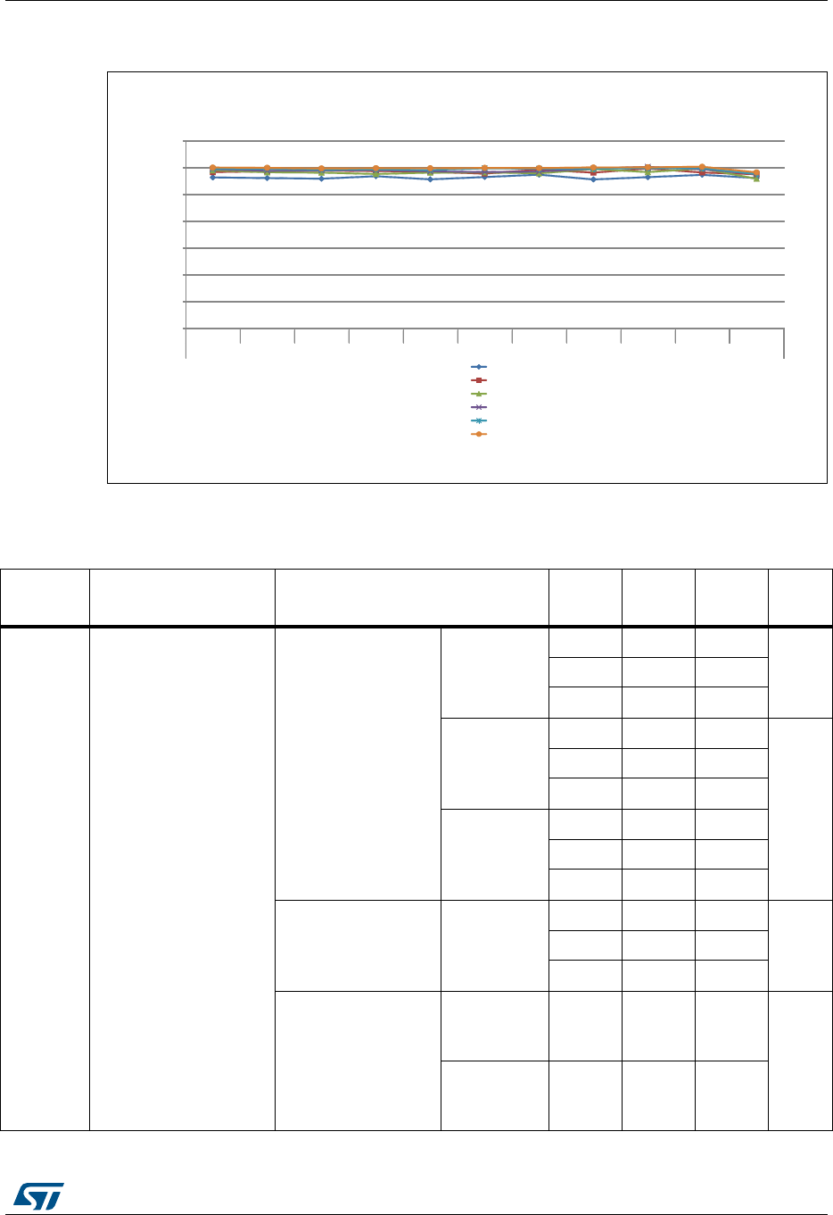
DocID027100 Rev 4 69/149
STM32L072xx Electrical characteristics
120
Figure 16. IDD vs VDD, at TA= 25/55/85/105 °C, Run mode, code running from
Flash memory, Range 2, HSI16, 1WS
06Y9
&
&
&
&
&
&
,''P$
9''9
Table 32. Current consumption in Run mode, code with data processing running from RAM
Symbol Parameter Condition fHCLK
(MHz) Typ Max(1) Unit
IDD (Run
from RAM)
Supply current in Run
mode code executed
from RAM, Flash
memory switched off
fHSE = fHCLK up to
16 MHz included,
fHSE = fHCLK/2 above
16 MHz (PLL ON)(2)
Range3,
Vcore=1.2 V
VOS[1:0]=11
1175230
µA2315360
4570630
Range2,
Vcore=1.5 V
VOS[1:0]=10
40,710,78
mA
81,351,6
16 2,7 3
Range1,
Vcore=1.8 V
VOS[1:0]=01
81,71,9
16 3,2 3,7
32 6,65 7,1
MSI clock
Range3,
Vcore=1.2 V
VOS[1:0]=11
0,065 38 98
µA0,524 105 160
4,2 615 710
HSI clock source
(16 MHz)
Range2,
Vcore=1.5 V
VOS[1:0]=10
16 2,85 3
mA
Range1,
Vcore=1.8 V
VOS[1:0]=01
32 6,85 7,3
1. Guaranteed by characterization results at 125 °C, unless otherwise specified.
Electrical characteristics STM32L072xx
70/149 DocID027100 Rev 4
2. Oscillator bypassed (HSEBYP = 1 in RCC_CR register).
Table 33. Current consumption in Run mode vs code type,
code with data processing running from RAM(1)
Symbol Parameter Conditions fHCLK Typ Unit
IDD (Run
from
RAM)
Supply current in
Run mode, code
executed from
RAM, Flash
memory switched
off
fHSE = fHCLK up to
16 MHz included,
fHSE = fHCLK/2 above
16 MHz (PLL ON)(2)
Range 3,
VCORE=1.2 V,
VOS[1:0]=11
Dhrystone
4 MHz
570
µA
CoreMark 670
Fibonacci 410
while(1) 375
Range 1,
VCORE=1.8 V,
VOS[1:0]=01
Dhrystone
32 MHz
6,65
mA
CoreMark 6,95
Fibonacci 5,9
while(1) 5,2
1. Guaranteed by characterization results, unless otherwise specified.
2. Oscillator bypassed (HSEBYP = 1 in RCC_CR register).
DocID027100 Rev 4 71/149
STM32L072xx Electrical characteristics
120
Table 34. Current consumption in Sleep mode
Symbol Parameter Condition fHCLK (MHz) Typ Max(1) Unit
IDD
(Sleep)
Supply current in
Sleep mode, Flash
memory switched
OFF
fHSE = fHCLK up to
16 MHz included,
fHSE = fHCLK/2 above
16 MHz (PLL ON)(2)
Range3,
Vcore=1.2 V
VOS[1:0]=11
1 43,5 110
µA
272140
4 130 200
Range2,
Vcore=1.5 V
VOS[1:0]=10
4 160 220
8 305 380
16 590 690
Range1,
Vcore=1.8 V
VOS[1:0]=01
8 370 460
16 715 840
32 1650 2000
MSI clock
Range3,
Vcore=1.2 V
VOS[1:0]=11
0,065 18 93
0,524 31,5 110
4,2 140 230
HSI clock source
(16 MHz)
Range2,
Vcore=1.5 V
VOS[1:0]=10
16 665 850
Range1,
Vcore=1.8 V
VOS[1:0]=01
32 1750 2100
Supply current in
Sleep mode, Flash
memory switched
ON
fHSE = fHCLK up to
16MHz included,
fHSE = fHCLK/2 above
16 MHz (PLL ON)(2)
Range3,
Vcore=1.2 V
VOS[1:0]=11
1 57,5 130
284160
4 150 220
Range2,
Vcore=1.5 V
VOS[1:0]=10
4 170 240
8 315 400
16 605 710
Range1,
Vcore=1.8 V
VOS[1:0]=01
8 380 470
16 730 860
32 1650 2000
MSI clock
Range3,
Vcore=1.2 V
VOS[1:0]=11
0,065 29,5 110
0,524 44,5 120
4,2 150 240
HSI clock source
(16MHz)
Range2,
Vcore=1.5 V
VOS[1:0]=10
16 680 930
Range1,
Vcore=1.8 V
VOS[1:0]=01
32 1750 2200
1. Guaranteed by characterization results at 125 °C, unless otherwise specified.
Electrical characteristics STM32L072xx
72/149 DocID027100 Rev 4
2. Oscillator bypassed (HSEBYP = 1 in RCC_CR register).
Table 35. Current consumption in Low-power run mode
Symbol Parameter Condition fHCLK
(MHz) Typ Max(1) Unit
IDD
(LP Run)
Supply
current in
Low-power
run mode
All peripherals
OFF, code
executed from
RAM, Flash
memory switched
OFF, VDD from
1.65 to 3.6 V
MSI clock = 65 kHz,
fHCLK= 32 kHz
TA = −40 to 25°C
0,032
9,45 12
µA
TA = 85°C 14 58
TA = 105°C 21 64
TA = 125°C 36,5 160
MSI clock = 65 kHz,
fHCLK= 65kHz
TA = −40 to 25°C
0,065
14,5 18
TA = 85°C 19,5 60
TA = 105°C 26 65
TA = 125°C 42 160
MSI clock=131 kHz,
fHCLK= 131 kHz
TA = −40 to 25°C
0,131
26,5 30
TA = 55°C 27,5 60
TA = 85°C 31 66
TA = 105°C 37,5 77
TA = 125°C 53,5 170
All peripherals
OFF, code
executed from
Flash memory,
VDD from 1.65 V
to 3.6 V
MSI clock = 65 kHz,
fHCLK= 32 kHz
TA = −40 to 25°C
0,032
24,5 34
TA = 85°C 30 82
TA = 105°C 38,5 90
TA = 125°C 58 120
MSI clock = 65 kHz,
fHCLK= 65 kHz
TA = −40 to 25°C
0,065
30,5 40
TA = 85°C 36,5 88
TA = 105°C 45 96
TA = 125°C 64,5 120
MSI clock =
131 kHz,
fHCLK= 131 kHz
TA = −40 to 25°C
0,131
45 56
TA = 55°C 48 96
TA = 85°C 51 110
TA = 105°C 59,5 120
TA = 125°C 79,5 150
1. Guaranteed by characterization results at 125 °C, unless otherwise specified.
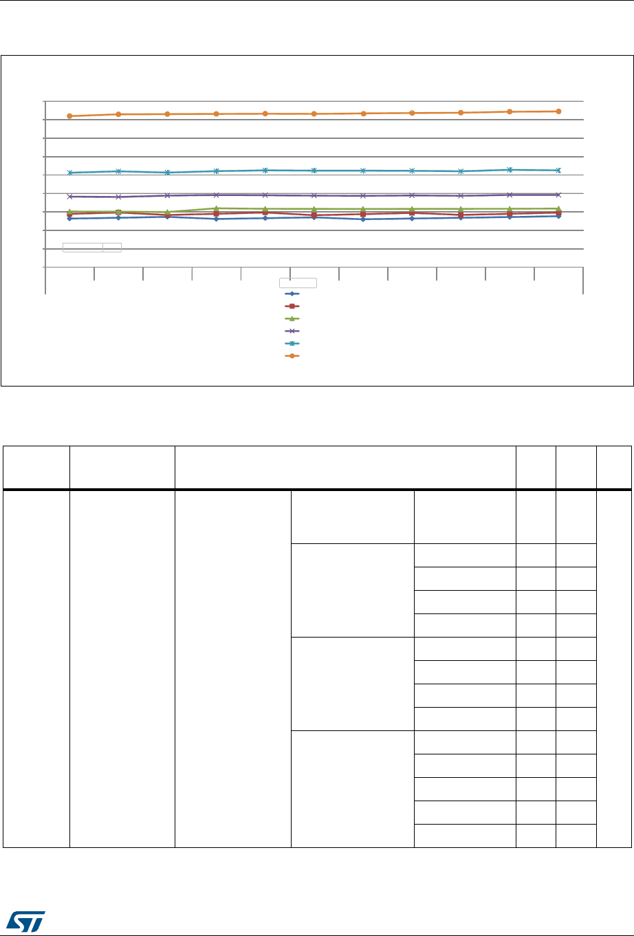
DocID027100 Rev 4 73/149
STM32L072xx Electrical characteristics
120
Figure 17. IDD vs VDD, at TA= 25 °C, Low-power run mode, code running
from RAM, Range 3, MSI (Range 0) at 64 KHz, 0 WS
06Y9
(
(
(
(
(
(
(
(
(
,''P$
9''9
Table 36. Current consumption in Low-power sleep mode
Symbol Parameter Condition Typ Max
(1) Unit
IDD
(LP Sleep)
Supply current in
Low-power sleep
mode
All peripherals
OFF, code
executed from
Flash memory, VDD
from 1.65 to 3.6 V
MSI clock = 65 kHz,
fHCLK= 32 kHz,
Flash memory OFF
TA = −40 to 25°C 4,7 -
µA
MSI clock = 65 kHz,
fHCLK= 32 kHz
TA = −40 to 25°C 17 24
TA = 85°C 19,5 30
TA= 105°C 23 47
TA= 125°C 32,5 70
MSI clock = 65 kHz,
fHCLK= 65 kHz
TA= −40 to 25°C 17 24
TA= 85°C 20 31
TA = 105°C 23,5 47
TA = 125°C 32,5 70
MSI clock = 131kHz,
fHCLK= 131 kHz
TA= −40 to 25°C 19,5 27
TA = 55°C 20,5 28
TA = 85°C 22,5 33
TA = 105°C 26 50
TA= 125°C 35 73
1. Guaranteed by characterization results at 125 °C, unless otherwise specified.
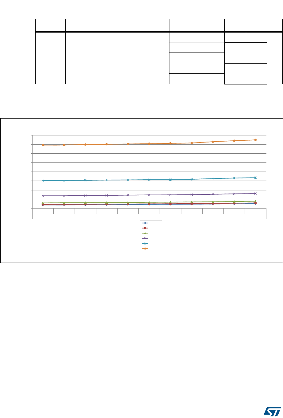
Electrical characteristics STM32L072xx
74/149 DocID027100 Rev 4
Figure 18. IDD vs VDD, at TA= 25/55/ 85/105/125 °C, Stop mode with RTC enabled
and running on LSE Low drive
Table 37. Typical and maximum current consumptions in Stop mode
Symbol Parameter Conditions Typ Max(1)
1. Guaranteed by characterization results at 125 °C, unless otherwise specified.
Unit
IDD (Stop) Supply current in Stop mode
TA = −40 to 25°C 0,43 1,00
µA
TA = 55°C 0,735 2,50
TA= 85°C 2,25 4,90
TA = 105°C 5,3 13,00
TA = 125°C 12,5 28,00
06Y9
(
(
(
(
(
(
(
(
&
&
&
&
&
&
,''P$
9''9
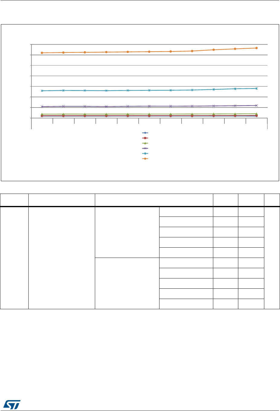
DocID027100 Rev 4 75/149
STM32L072xx Electrical characteristics
120
Figure 19. IDD vs VDD, at TA= 25/55/85/105/125 °C, Stop mode with RTC disabled,
all clocks OFF
06Y9
(
(
(
(
(
(
(
&
&
&
&
&
&
,''P$
9''9
Table 38. Typical and maximum current consumptions in Standby mode
Symbol Parameter Conditions Typ Max(1) Unit
IDD
(Standby)
Supply current in Standby
mode
Independent watchdog
and LSI enabled
TA = −40 to 25°C 0,855 1,70
µA
TA = 55 °C - 2,90
TA= 85 °C - 3,30
TA = 105 °C - 4,10
TA = 125 °C - 8,50
Independent watchdog
and LSI OFF
TA = −40 to 25°C 0,29 0,60
TA = 55 °C 0,32 1,20
TA = 85 °C 0,5 2,30
TA = 105 °C 0,94 3,00
TA = 125 °C 2,6 7,00
1. Guaranteed by characterization results at 125 °C, unless otherwise specified
Electrical characteristics STM32L072xx
76/149 DocID027100 Rev 4
Table 39. Average current consumption during Wakeup
Symbol parameter System frequency
Current
consumption
during wakeup
Unit
IDD (Wakeup from
Stop)
Supply current during Wakeup from
Stop mode
HSI 1
mA
HSI/4 0,7
MSI clock = 4,2 MHz 0,7
MSI clock = 1,05 MHz 0,4
MSI clock = 65 KHz 0,1
IDD (Reset) Reset pin pulled down - 0,21
IDD (Power-up) BOR ON - 0,23
IDD (Wakeup from
StandBy)
With Fast wakeup set MSI clock = 2,1 MHz 0,5
With Fast wakeup disabled MSI clock = 2,1 MHz 0,12
DocID027100 Rev 4 77/149
STM32L072xx Electrical characteristics
120
On-chip peripheral current consumption
The current consumption of the on-chip peripherals is given in the following tables. The
MCU is placed under the following conditions:
•all I/O pins are in input mode with a static value at VDD or VSS (no load)
•all peripherals are disabled unless otherwise mentioned
•the given value is calculated by measuring the current consumption
– with all peripherals clocked OFF
– with only one peripheral clocked on
Table 40. Peripheral current consumption in Run or Sleep mode(1)
Peripheral
Typical consumption, VDD = 3.0 V, TA = 25 °C
Unit
Range 1,
VCORE=1.8 V
VOS[1:0] = 01
Range 2,
VCORE=1.5 V
VOS[1:0] = 10
Range 3,
VCORE=1.2 V
VOS[1:0] = 11
Low-power
sleep and
run
APB1
CRS 2.5 2 2 2
µA/MHz
(fHCLK)
DAC1/2 4 3.5 3 2.5
I2C1 11 9.5 7.5 9
I2C3 11 9 7 9
LPTIM1 10 8.5 6.5 8
LPUART1 8 6.5 5.5 6
SPI2 9 4.5 3.5 4
USART2 14.5 12 9.5 11
USART4 5 4 3 5
USART5 5 4 3 5
USB 8.5 4.5 4 4.5
TIM2 10.5 8.5 7 9
TIM3 12 10 8 11
TIM6 3.5 3 2.5 2
TIM7 3.5 3 2.5 2
WWDG 3 2 2 2
APB2
ADC1(2) 5.5 5 3.5 4
µA/MHz
(fHCLK)
SPI1 4 3 3 2.5
USART1 14.5 11.5 9.5 12
TIM21 7.5 6 5 5.5
TIM22 7 6 5 6
FIREWALL 1.5 1 1 0.5
DBGMCU 1.5 1 1 0.5
SYSCFG 2.5 2 2 1.5

Electrical characteristics STM32L072xx
78/149 DocID027100 Rev 4
Cortex-
M0+ core
I/O port
GPIOA 3.5 3 2.5 2.5
µA/MHz
(fHCLK)
GPIOB 3.5 2.5 2 2.5
GPIOC 8.5 6.5 5.5 7
GPIOD 1 0.5 0.5 0.5
GPIOE 8 6 5 6
GPIOH 1.5 1 1 0.5
AHB
CRC 1.5 1 1 1
µA/MHz
(fHCLK)
FLASH 0(3) 0(3) 0(3) 0(3)
DMA1 10 8 6.5 8.5
RNG 5.5 1 0.5 0.5
TSC 3 2.5 2 3
All enabled 204 162 130 202 µA/MHz
(fHCLK)
PWR 2.5 2 2 1 µA/MHz
(fHCLK)
1. Data based on differential IDD measurement between all peripherals OFF an one peripheral with clock
enabled, in the following conditions: fHCLK = 32 MHz (range 1), fHCLK = 16 MHz (range 2), fHCLK = 4 MHz
(range 3), fHCLK = 64kHz (Low-power run/sleep), fAPB1 = fHCLK, fAPB2 = fHCLK, default prescaler value for
each peripheral. The CPU is in Sleep mode in both cases. No I/O pins toggling. Not tested in production.
2. HSI oscillator is OFF for this measure.
3. Current consumption is negligible and close to 0 µA.
Table 40. Peripheral current consumption in Run or Sleep mode(1) (continued)
Peripheral
Typical consumption, VDD = 3.0 V, TA = 25 °C
Unit
Range 1,
VCORE=1.8 V
VOS[1:0] = 01
Range 2,
VCORE=1.5 V
VOS[1:0] = 10
Range 3,
VCORE=1.2 V
VOS[1:0] = 11
Low-power
sleep and
run
DocID027100 Rev 4 79/149
STM32L072xx Electrical characteristics
120
6.3.5 Wakeup time from low-power mode
The wakeup times given in the following table are measured with the MSI or HSI16 RC
oscillator. The clock source used to wake up the device depends on the current operating
mode:
•Sleep mode: the clock source is the clock that was set before entering Sleep mode
•Stop mode: the clock source is either the MSI oscillator in the range configured before
entering Stop mode, the HSI16 or HSI16/4.
•Standby mode: the clock source is the MSI oscillator running at 2.1 MHz
All timings are derived from tests performed under ambient temperature and VDD supply
voltage conditions summarized in Table 26.
Table 41. Peripheral current consumption in Stop and Standby mode(1)
Symbol Peripheral
Typical consumption, TA = 25 °C
Unit
VDD=1.8 V VDD=3.0 V
IDD(PVD / BOR) -0.71.2
µA
IREFINT --1.7
- LSE Low drive(2) 0.11 0,13
- LSI 0.27 0.31
-IWDG0.2 0.3
- LPTIM1, Input 100 Hz 0.01 0,01
- LPTIM1, Input 1 MHz 11 12
- LPUART1 - 0,5
- RTC 0.16 0,3
1. LPTIM, LPUART peripherals can operate in Stop mode but not in Standby mode.
2. LSE Low drive consumption is the difference between an external clock on OSC32_IN and a quartz between OSC32_IN
and OSC32_OUT.-
Table 42. Low-power mode wakeup timings
Symbol Parameter Conditions Typ Max Unit
tWUSLEEP Wakeup from Sleep mode fHCLK = 32 MHz 7 8
Number
of clock
cycles
tWUSLEEP_
LP
Wakeup from Low-power sleep mode,
fHCLK = 262 kHz
fHCLK = 262 kHz
Flash memory enabled 78
fHCLK = 262 kHz
Flash memory switched OFF 910
Electrical characteristics STM32L072xx
80/149 DocID027100 Rev 4
tWUSTOP
Wakeup from Stop mode, regulator in Run
mode
fHCLK = fMSI = 4.2 MHz 5.0 8
µs
fHCLK = fHSI = 16 MHz 4.9 7
fHCLK = fHSI/4 = 4 MHz 8.0 11
Wakeup from Stop mode, regulator in low-
power mode
fHCLK = fMSI = 4.2 MHz
Voltage range 1 5.0 8
fHCLK = fMSI = 4.2 MHz
Voltage range 2 5.0 8
fHCLK = fMSI = 4.2 MHz
Voltage range 3 5.0 8
fHCLK = fMSI = 2.1 MHz 7.3 13
fHCLK = fMSI = 1.05 MHz 13 23
fHCLK = fMSI = 524 kHz 28 38
fHCLK = fMSI = 262 kHz 51 65
fHCLK = fMSI = 131 kHz 100 120
fHCLK = MSI = 65 kHz 190 260
fHCLK = fHSI = 16 MHz 4.9 7
fHCLK = fHSI/4 = 4 MHz 8.0 11
Wakeup from Stop mode, regulator in low-
power mode, code running from RAM
fHCLK = fHSI = 16 MHz 4.9 7
fHCLK = fHSI/4 = 4 MHz 7.9 10
fHCLK = fMSI = 4.2 MHz 4.7 8
tWUSTDBY
Wakeup from Standby mode
FWU bit = 1 fHCLK = MSI = 2.1 MHz 65 130
Wakeup from Standby mode
FWU bit = 0 fHCLK = MSI = 2.1 MHz 2.2 3 ms
Table 42. Low-power mode wakeup timings (continued)
Symbol Parameter Conditions Typ Max Unit
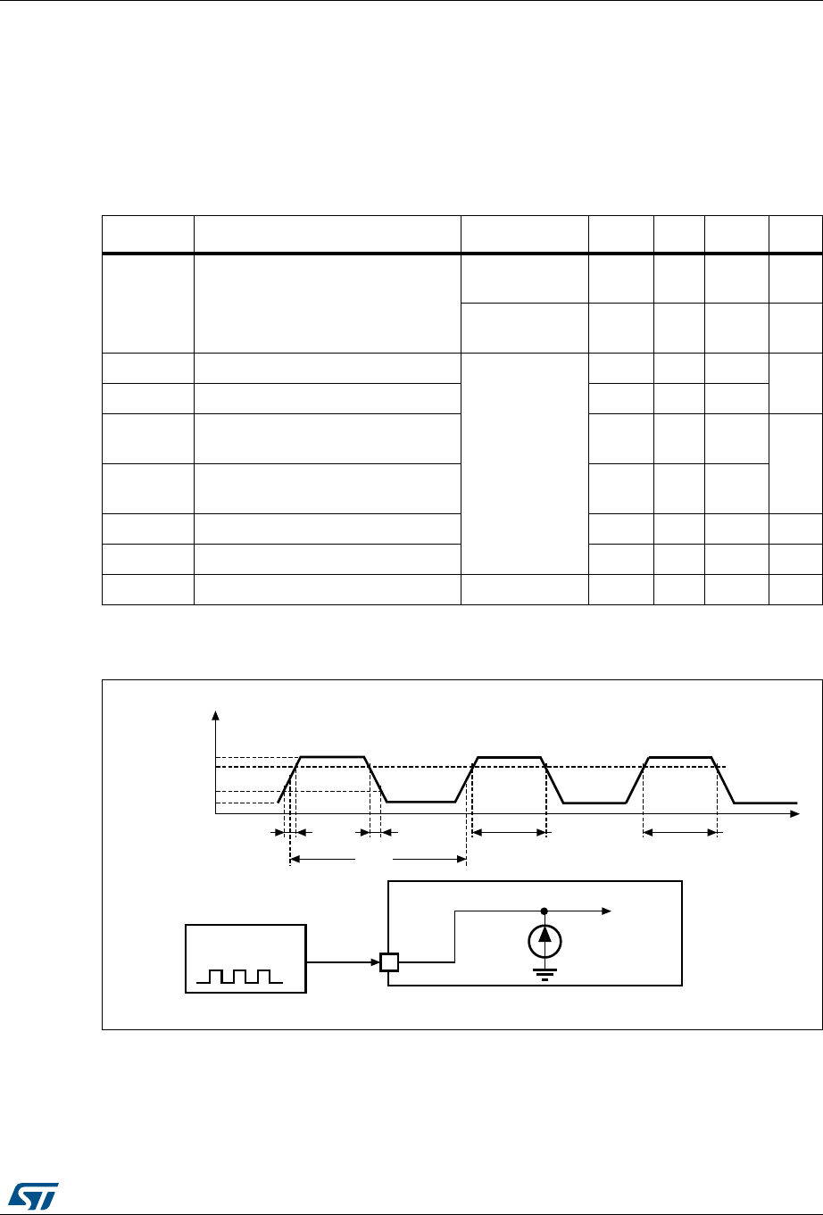
DocID027100 Rev 4 81/149
STM32L072xx Electrical characteristics
120
6.3.6 External clock source characteristics
High-speed external user clock generated from an external source
In bypass mode the HSE oscillator is switched off and the input pin is a standard GPIO.The
external clock signal has to respect the I/O characteristics in Section 6.3.12. However, the
recommended clock input waveform is shown in Figure 20.
Figure 20. High-speed external clock source AC timing diagram
Table 43. High-speed external user clock characteristics(1)
1. Guaranteed by design.
Symbol Parameter Conditions Min Typ Max Unit
fHSE_ext
User external clock source
frequency
CSS is ON or
PLL is used 1832MHz
CSS is OFF,
PLL not used 0832MHz
VHSEH OSC_IN input pin high level voltage
-
0.7VDD -V
DD V
VHSEL OSC_IN input pin low level voltage VSS -0.3V
DD
tw(HSE)
tw(HSE)
OSC_IN high or low time 12 - -
ns
tr(HSE)
tf(HSE)
OSC_IN rise or fall time - - 20
Cin(HSE) OSC_IN input capacitance - 2.6 - pF
DuCy(HSE) Duty cycle 45 - 55 %
ILOSC_IN Input leakage current VSS ≤ VIN ≤ VDD --±1µA
DLF
26& B ,1
(;7(51$/
670/[[
&/2&. 6285&(
9+6(+
WI+6( W:+6(
,/
7+6(
W
WU+6( W:+6(
I+6(BH[W
9+6(/
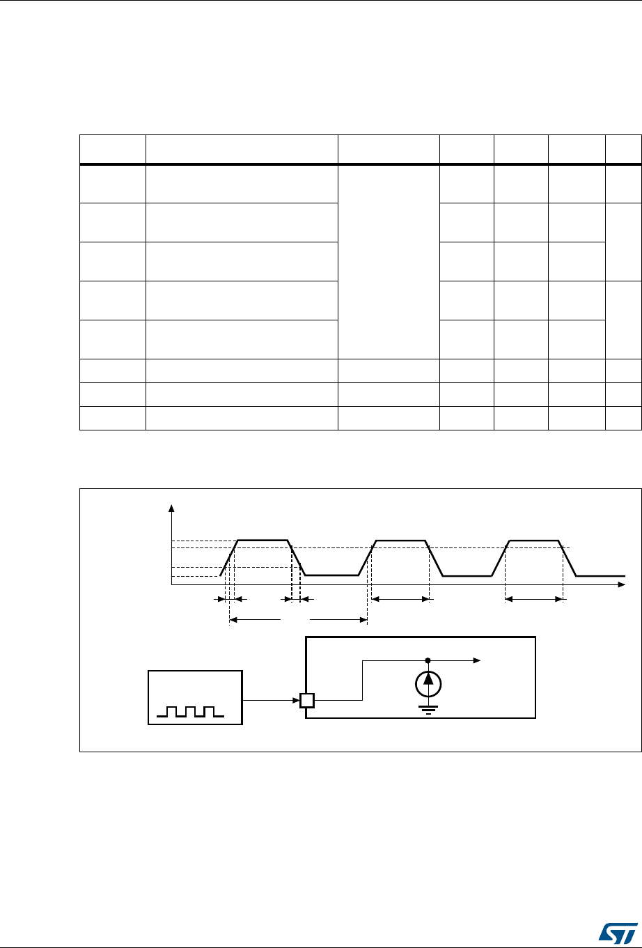
Electrical characteristics STM32L072xx
82/149 DocID027100 Rev 4
Low-speed external user clock generated from an external source
The characteristics given in the following table result from tests performed using a low-
speed external clock source, and under ambient temperature and supply voltage conditions
summarized in Table 26.
Figure 21. Low-speed external clock source AC timing diagram
Table 44. Low-speed external user clock characteristics(1)
1. Guaranteed by design, not tested in production
Symbol Parameter Conditions Min Typ Max Unit
fLSE_ext
User external clock source
frequency
-
1 32.768 1000 kHz
VLSEH
OSC32_IN input pin high level
voltage 0.7VDD -V
DD
V
VLSEL
OSC32_IN input pin low level
voltage VSS -0.3V
DD
tw(LSE)
tw(LSE)
OSC32_IN high or low time 465 - -
ns
tr(LSE)
tf(LSE)
OSC32_IN rise or fall time - - 10
CIN(LSE) OSC32_IN input capacitance - - 0.6 - pF
DuCy(LSE) Duty cycle - 45 - 55 %
ILOSC32_IN Input leakage current VSS ≤ VIN ≤ VDD --±1µA
DLF
26& B,1
(;7(51$/
670/[[
&/2&. 6285&(
9/6(+
WI/6( W:/6(
,/
7/6(
W
WU/6( W:/6(
I/6(BH[W
9/6(/
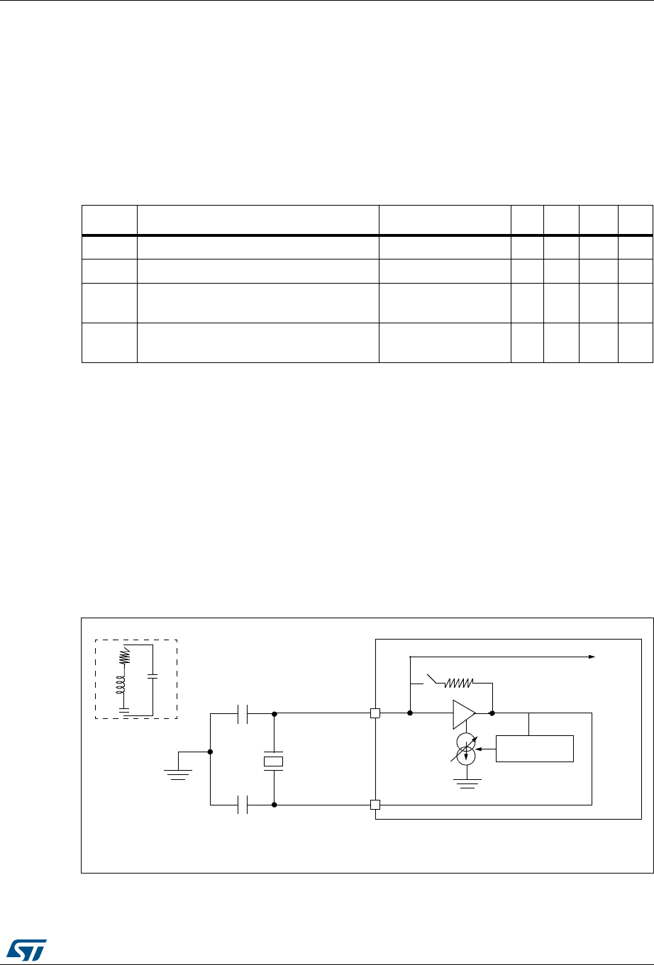
DocID027100 Rev 4 83/149
STM32L072xx Electrical characteristics
120
High-speed external clock generated from a crystal/ceramic resonator
The high-speed external (HSE) clock can be supplied with a 1 to 25 MHz crystal/ceramic
resonator oscillator. All the information given in this paragraph are based on
characterization results obtained with typical external components specified in Table 45. In
the application, the resonator and the load capacitors have to be placed as close as
possible to the oscillator pins in order to minimize output distortion and startup stabilization
time. Refer to the crystal resonator manufacturer for more details on the resonator
characteristics (frequency, package, accuracy).
For CL1 and CL2, it is recommended to use high-quality external ceramic capacitors in the
5 pF to 25 pF range (typ.), designed for high-frequency applications, and selected to match
the requirements of the crystal or resonator (see Figure 22). CL1 and CL2 are usually the
same size. The crystal manufacturer typically specifies a load capacitance which is the
series combination of CL1 and CL2. PCB and MCU pin capacitance must be included (10 pF
can be used as a rough estimate of the combined pin and board capacitance) when sizing
CL1 and CL2. Refer to the application note AN2867 “Oscillator design guide for ST
microcontrollers” available from the ST website www.st.com.
Figure 22. HSE oscillator circuit diagram
Table 45. HSE oscillator characteristics(1)
1. Guaranteed by design.
Symbol Parameter Conditions Min Typ Max Unit
fOSC_IN Oscillator frequency - 1 25 MHz
RFFeedback resistor - - 200 - kΩ
Gm
Maximum critical crystal
transconductance Startup - - 700 µA
/V
tSU(HSE)
(2)
2. Guaranteed by characterization results. tSU(HSE) is the startup time measured from the moment it is
enabled (by software) to a stabilized 8 MHz oscillation is reached. This value is measured for a standard
crystal resonator and it can vary significantly with the crystal manufacturer.
Startup time VDD is stabilized - 2 - ms
26&B287
26&B,1
I
+6(
WRFRUH
&
/
&
/
5
)
670
5HVRQDWRU
&RQVXPSWLRQ
FRQWURO
J
P
5
P
&
P
/
P
&
2
5HVRQDWRU
DLE
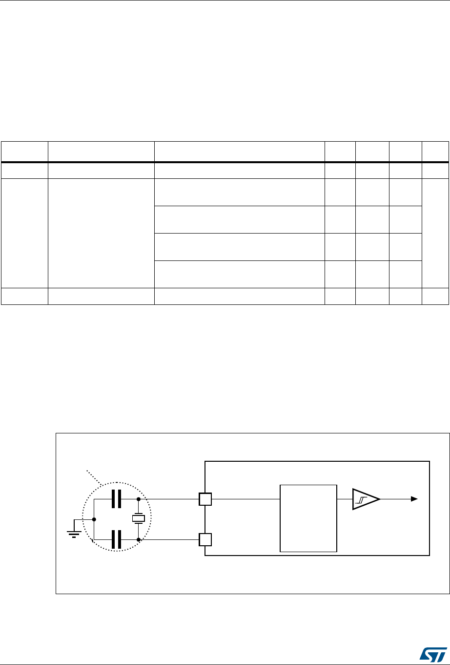
Electrical characteristics STM32L072xx
84/149 DocID027100 Rev 4
Low-speed external clock generated from a crystal/ceramic resonator
The low-speed external (LSE) clock can be supplied with a 32.768 kHz crystal/ceramic
resonator oscillator. All the information given in this paragraph are based on
characterization results obtained with typical external components specified in Table 46. In
the application, the resonator and the load capacitors have to be placed as close as
possible to the oscillator pins in order to minimize output distortion and startup stabilization
time. Refer to the crystal resonator manufacturer for more details on the resonator
characteristics (frequency, package, accuracy).
Note: For information on selecting the crystal, refer to the application note AN2867 “Oscillator
design guide for ST microcontrollers” available from the ST website www.st.com.
Figure 23. Typical application with a 32.768 kHz crystal
Note: An external resistor is not required between OSC32_IN and OSC32_OUT and it is forbidden
to add one.
Table 46. LSE oscillator characteristics(1)
Symbol Parameter Conditions(2) Min(2) Typ Max Unit
fLSE LSE oscillator frequency - 32.768 - kHz
Gm
Maximum critical crystal
transconductance
LSEDRV[1:0]=00
lower driving capability --0.5
µA/V
LSEDRV[1:0]= 01
medium low driving capability - - 0.75
LSEDRV[1:0] = 10
medium high driving capability --1.7
LSEDRV[1:0]=11
higher driving capability --2.7
tSU(LSE)(3) Startup time VDD is stabilized - 2 - s
1. Guaranteed by design.
2. Refer to the note and caution paragraphs below the table, and to the application note AN2867 “Oscillator design guide for
ST microcontrollers”.
3. Guaranteed by characterization results. tSU(LSE) is the startup time measured from the moment it is enabled (by software)
to a stabilized 32.768 kHz oscillation is reached. This value is measured for a standard crystal resonator and it can vary
significantly with the crystal manufacturer. To increase speed, address a lower-drive quartz with a high- driver mode.
069
26&B,1
26&B287
'ULYH
SURJUDPPDEOH
DPSOLILHU
I/6(
N+]
UHVRQDWRU
5HVRQDWRUZLWKLQWHJUDWHG
FDSDFLWRUV
&/
&/
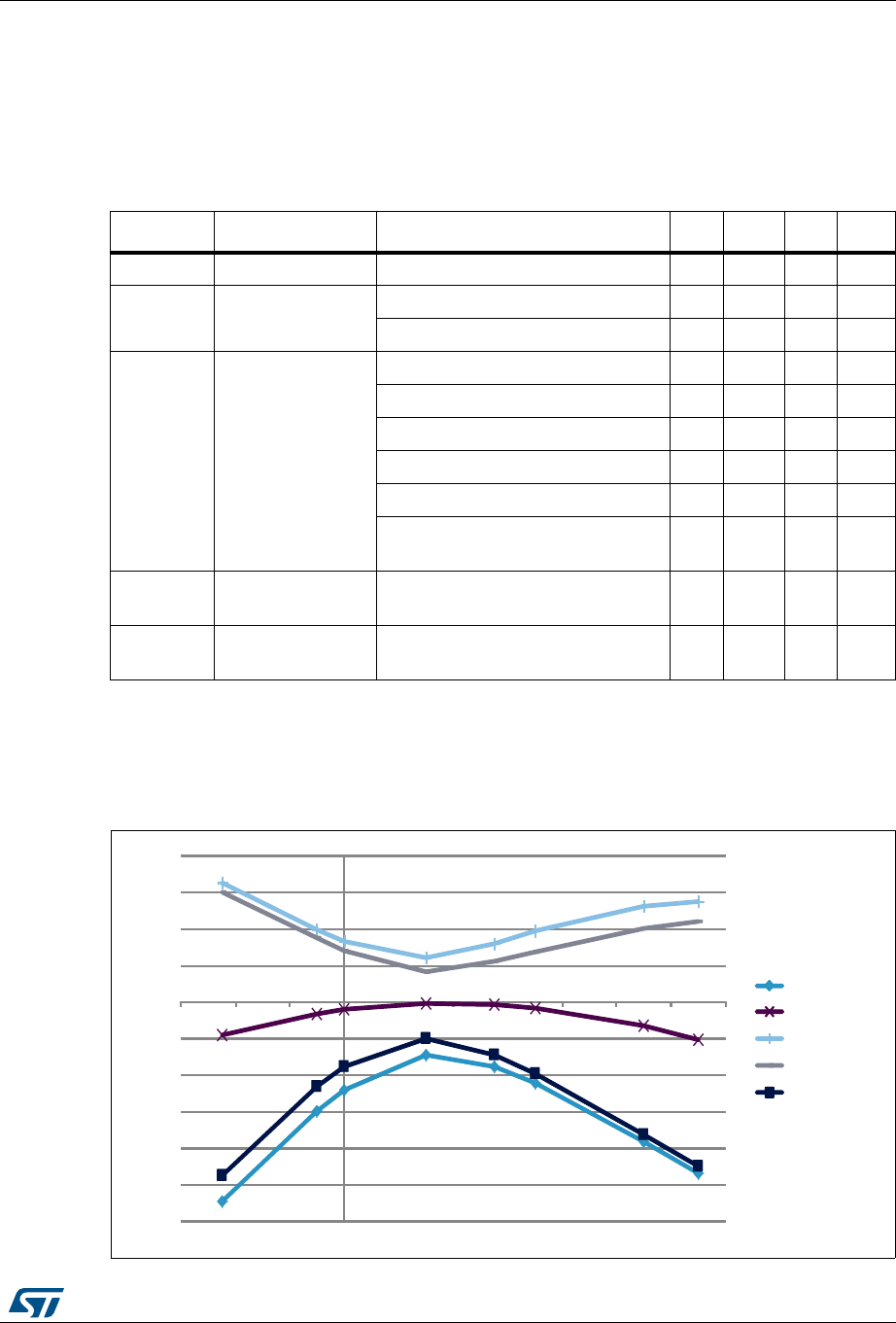
DocID027100 Rev 4 85/149
STM32L072xx Electrical characteristics
120
6.3.7 Internal clock source characteristics
The parameters given in Table 47 are derived from tests performed under ambient
temperature and VDD supply voltage conditions summarized in Table 26.
High-speed internal 16 MHz (HSI16) RC oscillator
Figure 24. HSI16 minimum and maximum value versus temperature
Table 47. 16 MHz HSI16 oscillator characteristics
Symbol Parameter Conditions Min Typ Max Unit
fHSI16 Frequency VDD = 3.0 V - 16 - MHz
TRIM(1)(2)
1. The trimming step differs depending on the trimming code. It is usually negative on the codes which are
multiples of 16 (0x00, 0x10, 0x20, 0x30...0xE0).
HSI16 user-
trimmed resolution
Trimming code is not a multiple of 16 - ± 0.4 0.7 %
Trimming code is a multiple of 16 - - ± 1.5 %
ACCHSI16
(2)
2. Guaranteed by characterization results.
Accuracy of the
factory-calibrated
HSI16 oscillator
VDDA = 3.0 V, TA = 25 °C -1(3)
3. Guaranteed by test in production.
-1
(3) %
VDDA = 3.0 V, TA = 0 to 55 °C -1.5 - 1.5 %
VDDA = 3.0 V, TA = -10 to 70 °C -2 - 2 %
VDDA = 3.0 V, TA = -10 to 85 °C -2.5 - 2 %
VDDA = 3.0 V, TA = -10 to 105 °C -4 - 2 %
VDDA = 1.65 V to 3.6 V
TA = −40 to 125 °C -5.45 - 3.25 %
tSU(HSI16)(2) HSI16 oscillator
startup time - - 3.7 6 µs
IDD(HSI16)(2) HSI16 oscillator
power consumption - - 100 140 µA
06Y9
9PLQ
9W\S
9PD[
9PD[
9PLQ
Electrical characteristics STM32L072xx
86/149 DocID027100 Rev 4
High-speed internal 48 MHz (HSI48) RC oscillator
Low-speed internal (LSI) RC oscillator
Multi-speed internal (MSI) RC oscillator
Table 48. HSI48 oscillator characteristics(1)
1. VDDA = 3.3 V, TA = –40 to 125 °C unless otherwise specified.
Symbol Parameter Conditions Min Typ Max Unit
fHSI48 Frequency - 48 - MHz
TRIM HSI48 user-trimming step 0.09(2) 0.14 0.2(2) %
DuCy(HSI48) Duty cycle 45(2)
2. Guaranteed by design.
-55
(2) %
ACCHSI48
Accuracy of the HSI48
oscillator (factory calibrated
before CRS calibration)
TA = 25 °C -4(3)
3. Guaranteed by characterization results.
-4
(3) %
tsu(HSI48) HSI48 oscillator startup time - - 6(2) µs
IDDA(HSI48)
HSI48 oscillator power
consumption - 330 380(2) µA
Table 49. LSI oscillator characteristics
Symbol Parameter Min Typ Max Unit
fLSI(1)
1. Guaranteed by test in production.
LSI frequency 26 38 56 kHz
DLSI(2)
2. This is a deviation for an individual part, once the initial frequency has been measured.
LSI oscillator frequency drift
0°C ≤ TA ≤ 85°C -10 - 4 %
tsu(LSI)(3)
3. Guaranteed by design.
LSI oscillator startup time - - 200 µs
IDD(LSI)(3) LSI oscillator power consumption - 400 510 nA
Table 50. MSI oscillator characteristics
Symbol Parameter Condition Typ Max Unit
fMSI
Frequency after factory calibration, done at
VDD= 3.3 V and TA = 25 °C
MSI range 0 65.5 -
kHz
MSI range 1 131 -
MSI range 2 262 -
MSI range 3 524 -
MSI range 4 1.05 -
MHzMSI range 5 2.1 -
MSI range 6 4.2 -
DocID027100 Rev 4 87/149
STM32L072xx Electrical characteristics
120
ACCMSI Frequency error after factory calibration - ±0.5 - %
DTEMP(MSI)(1)
MSI oscillator frequency drift
0 °C ≤ TA ≤ 85 °C -±3-
%
MSI oscillator frequency drift
VDD = 3.3 V, −40 °C ≤ TA ≤ 110 °C
MSI range 0 −8.9 +7.0
MSI range 1 −7.1 +5.0
MSI range 2 −6.4 +4.0
MSI range 3 −6.2 +3.0
MSI range 4 −5.2 +3.0
MSI range 5 −4.8 +2.0
MSI range 6 −4.7 +2.0
DVOLT(MSI)(1) MSI oscillator frequency drift
1.65 V ≤ VDD ≤ 3.6 V, TA = 25 °C --2.5%/V
IDD(MSI)(2) MSI oscillator power consumption
MSI range 0 0.75 -
µA
MSI range 1 1 -
MSI range 2 1.5 -
MSI range 3 2.5 -
MSI range 4 4.5 -
MSI range 5 8 -
MSI range 6 15 -
tSU(MSI) MSI oscillator startup time
MSI range 0 30 -
µs
MSI range 1 20 -
MSI range 2 15 -
MSI range 3 10 -
MSI range 4 6 -
MSI range 5 5 -
MSI range 6,
Voltage range 1
and 2
3.5 -
MSI range 6,
Voltage range 3 5-
Table 50. MSI oscillator characteristics (continued)
Symbol Parameter Condition Typ Max Unit
Electrical characteristics STM32L072xx
88/149 DocID027100 Rev 4
6.3.8 PLL characteristics
The parameters given in Table 51 are derived from tests performed under ambient
temperature and VDD supply voltage conditions summarized in Table 26.
tSTAB(MSI)(2) MSI oscillator stabilization time
MSI range 0 - 40
µs
MSI range 1 - 20
MSI range 2 - 10
MSI range 3 - 4
MSI range 4 - 2.5
MSI range 5 - 2
MSI range 6,
Voltage range 1
and 2
-2
MSI range 3,
Voltage range 3 -3
fOVER(MSI) MSI oscillator frequency overshoot
Any range to
range 5 -4
MHz
Any range to
range 6 -6
1. This is a deviation for an individual part, once the initial frequency has been measured.
2. Guaranteed by characterization results.
Table 50. MSI oscillator characteristics (continued)
Symbol Parameter Condition Typ Max Unit
Table 51. PLL characteristics
Symbol Parameter
Value
Unit
Min Typ Max(1)
1. Guaranteed by characterization results.
fPLL_IN
PLL input clock(2)
2. Take care of using the appropriate multiplier factors so as to have PLL input clock values compatible with
the range defined by fPLL_OUT
.
2- 24MHz
PLL input clock duty cycle 45 - 55 %
fPLL_OUT PLL output clock 2 - 32 MHz
tLOCK
PLL input = 16 MHz
PLL VCO = 96 MHz - 115 160 µs
Jitter Cycle-to-cycle jitter - ±
600 ps
IDDA(PLL) Current consumption on VDDA - 220 450
µA
IDD(PLL) Current consumption on VDD - 120 150
DocID027100 Rev 4 89/149
STM32L072xx Electrical characteristics
120
6.3.9 Memory characteristics
RAM memory
Flash memory and data EEPROM
Table 52. RAM and hardware registers
Symbol Parameter Conditions Min Typ Max Unit
VRM Data retention mode(1)
1. Minimum supply voltage without losing data stored in RAM (in Stop mode or under Reset) or in hardware
registers (only in Stop mode).
STOP mode (or RESET) 1.65 - - V
Table 53. Flash memory and data EEPROM characteristics
Symbol Parameter Conditions Min Typ Max(1)
1. Guaranteed by design.
Unit
VDD
Operating voltage
Read / Write / Erase -1.65-3.6V
tprog
Programming time for
word or half-page
Erasing - 3.28 3.94
ms
Programming - 3.28 3.94
IDD
Average current during
the whole programming /
erase operation
TA = 25 °C, VDD = 3.6 V
- 500 700 µA
Maximum current (peak)
during the whole
programming / erase
operation
-1.52.5mA
Table 54. Flash memory and data EEPROM endurance and retention
Symbol Parameter Conditions
Value
Unit
Min(1)
NCYC(2)
Cycling (erase / write)
Program memory
TA = -40°C to 105 °C
10
kcycles
Cycling (erase / write)
EEPROM data memory 100
Cycling (erase / write)
Program memory
TA = -40°C to 125 °C
0.2
Cycling (erase / write)
EEPROM data memory 2
Electrical characteristics STM32L072xx
90/149 DocID027100 Rev 4
6.3.10 EMC characteristics
Susceptibility tests are performed on a sample basis during device characterization.
Functional EMS (electromagnetic susceptibility)
While a simple application is executed on the device (toggling 2 LEDs through I/O ports).
the device is stressed by two electromagnetic events until a failure occurs. The failure is
indicated by the LEDs:
•Electrostatic discharge (ESD) (positive and negative) is applied to all device pins until
a functional disturbance occurs. This test is compliant with the IEC 61000-4-2 standard.
•FTB: A Burst of Fast Transient voltage (positive and negative) is applied to VDD and
VSS through a 100 pF capacitor, until a functional disturbance occurs. This test is
compliant with the IEC 61000-4-4 standard.
A device reset allows normal operations to be resumed.
The test results are given in Table 55. They are based on the EMS levels and classes
defined in application note AN1709.
tRET(2)
Data retention (program memory) after
10 kcycles at TA = 85 °C
TRET = +85 °C
30
years
Data retention (EEPROM data memory)
after 100 kcycles at TA = 85 °C 30
Data retention (program memory) after
10 kcycles at TA = 105 °C
TRET = +105 °C
10
Data retention (EEPROM data memory)
after 100 kcycles at TA = 105 °C
Data retention (program memory) after
200 cycles at TA = 125 °C
TRET = +125 °C
Data retention (EEPROM data memory)
after 2 kcycles at TA = 125 °C
1. Guaranteed by characterization results.
2. Characterization is done according to JEDEC JESD22-A117.
Table 54. Flash memory and data EEPROM endurance and retention (continued)
Symbol Parameter Conditions
Value
Unit
Min(1)
Table 55. EMS characteristics
Symbol Parameter Conditions Level/
Class
VFESD
Voltage limits to be applied on any I/O pin to
induce a functional disturbance
VDD = 3.3 V, LQFP100, TA = +25 °C,
fHCLK = 32 MHz
conforms to IEC 61000-4-2
3B
VEFTB
Fast transient voltage burst limits to be
applied through 100 pF on VDD and VSS
pins to induce a functional disturbance
VDD = 3.3 V, LQFP100, TA = +25
°C,
fHCLK = 32 MHz
conforms to IEC 61000-4-4
4A
DocID027100 Rev 4 91/149
STM32L072xx Electrical characteristics
120
Designing hardened software to avoid noise problems
EMC characterization and optimization are performed at component level with a typical
application environment and simplified MCU software. It should be noted that good EMC
performance is highly dependent on the user application and the software in particular.
Therefore it is recommended that the user applies EMC software optimization and
prequalification tests in relation with the EMC level requested for his application.
Software recommendations
The software flowchart must include the management of runaway conditions such as:
•Corrupted program counter
•Unexpected reset
•Critical data corruption (control registers...)
Prequalification trials
Most of the common failures (unexpected reset and program counter corruption) can be
reproduced by manually forcing a low state on the NRST pin or the oscillator pins for 1
second.
To complete these trials, ESD stress can be applied directly on the device, over the range of
specification values. When unexpected behavior is detected, the software can be hardened
to prevent unrecoverable errors occurring (see application note AN1015).
Electromagnetic Interference (EMI)
The electromagnetic field emitted by the device are monitored while a simple application is
executed (toggling 2 LEDs through the I/O ports). This emission test is compliant with
IEC 61967-2 standard which specifies the test board and the pin loading.
Table 56. EMI characteristics
Symbol Parameter Conditions Monitored
frequency band
Max vs.
frequency
range at
32 MHz
Unit
SEMI Peak level
VDD = 3.6 V,
TA = 25 °C,
LQFP100 package
compliant with IEC 61967-2
0.1 to 30 MHz -7
dBµV30 to 130 MHz 14
130 MHz to 1 GHz 9
EMI Level 2 -
Electrical characteristics STM32L072xx
92/149 DocID027100 Rev 4
6.3.11 Electrical sensitivity characteristics
Based on three different tests (ESD, LU) using specific measurement methods, the device is
stressed in order to determine its performance in terms of electrical sensitivity.
Electrostatic discharge (ESD)
Electrostatic discharges (a positive then a negative pulse separated by 1 second) are
applied to the pins of each sample according to each pin combination. The sample size
depends on the number of supply pins in the device (3 parts × (n+1) supply pins). This test
conforms to the ANSI/JEDEC standard.
Static latch-up
Two complementary static tests are required on six parts to assess the latch-up
performance:
•A supply overvoltage is applied to each power supply pin
•A current injection is applied to each input, output and configurable I/O pin
These tests are compliant with EIA/JESD 78A IC latch-up standard.
Table 57. ESD absolute maximum ratings
Symbol Ratings Conditions Class Maximum
value(1)
1. Guaranteed by characterization results.
Unit
VESD(HBM)
Electrostatic discharge
voltage (human body model)
TA = +25 °C,
conforming to
ANSI/JEDEC JS-001
22000
V
VESD(CDM)
Electrostatic discharge
voltage (charge device
model)
TA = +25 °C,
conforming to
ANSI/ESD STM5.3.1.
C4 500
Table 58. Electrical sensitivities
Symbol Parameter Conditions Class
LU Static latch-up class TA = +125 °C conforming to JESD78A II level A
DocID027100 Rev 4 93/149
STM32L072xx Electrical characteristics
120
6.3.12 I/O current injection characteristics
As a general rule, current injection to the I/O pins, due to external voltage below VSS or
above VDD (for standard pins) should be avoided during normal product operation.
However, in order to give an indication of the robustness of the microcontroller in cases
when abnormal injection accidentally happens, susceptibility tests are performed on a
sample basis during device characterization.
Functional susceptibility to I/O current injection
While a simple application is executed on the device, the device is stressed by injecting
current into the I/O pins programmed in floating input mode. While current is injected into
the I/O pin, one at a time, the device is checked for functional failures.
The failure is indicated by an out of range parameter: ADC error above a certain limit (higher
than 5 LSB TUE), out of conventional limits of induced leakage current on adjacent pins (out
of –5 µA/+0 µA range), or other functional failure (for example reset occurrence oscillator
frequency deviation).
The test results are given in the Table 59.
Table 59. I/O current injection susceptibility
Symbol Description
Functional susceptibility
Unit
Negative
injection
Positive
injection
IINJ
Injected current on BOOT0 -0 NA(1)
1. Current injection is not possible.
mA
Injected current on PA0, PA4, PA5, PC15,
PH0 and PH1 -5 0
Injected current on any other FT, FTf pins -5 (2)
2. It is recommended to add a Schottky diode (pin to ground) to analog pins which may potentially inject
negative currents.
NA(1)
Injected current on any other pins -5 (2) +5
Electrical characteristics STM32L072xx
94/149 DocID027100 Rev 4
6.3.13 I/O port characteristics
General input/output characteristics
Unless otherwise specified, the parameters given in Table 6 0 are derived from tests
performed under the conditions summarized in Table 26. All I/Os are CMOS and TTL
compliant.
Table 60. I/O static characteristics
Symbol Parameter Conditions Min Typ Max Unit
VIL Input low level voltage
TC, FT, FTf, RST
I/Os - - 0.3VDD
V
BOOT0 pin - - 0.14VDD(1)
VIH Input high level voltage All I/Os 0.7 VDD --
Vhys
I/O Schmitt trigger voltage hysteresis
(2)
Standard I/Os - 10% VDD(3) -
BOOT0 pin - 0.01 -
Ilkg Input leakage current (4)
VSS ≤ VIN ≤ VDD
All I/Os except for
PA11, PA12, BOOT0
and FTf I/Os
--±50
nA
VSS ≤ VIN ≤ VDD,
PA11 and PA12 I/Os - - -50/+250
VSS ≤ VIN ≤ VDD
FTf I/Os - - ±100
VDD≤ VIN ≤ 5 V
All I/Os except for
PA11, PA12, BOOT0
and FTf I/Os
- - 200
nA
VDD≤ VIN ≤ 5 V
FTf I/Os - - 500
VDD≤ VIN ≤ 5 V
PA11, PA12 and
BOOT0
--10µA
RPU Weak pull-up equivalent resistor(5) VIN = VSS 25 45 65 kΩ
RPD Weak pull-down equivalent resistor(5) VIN = VDD 25 45 65 kΩ
CIO I/O pin capacitance - - 5 - pF
1. Guaranteed by characterization.
2. Hysteresis voltage between Schmitt trigger switching levels. Guaranteed by characterization results.
3. With a minimum of 200 mV. Guaranteed by characterization results.
4. The max. value may be exceeded if negative current is injected on adjacent pins.
5. Pull-up and pull-down resistors are designed with a true resistance in series with a switchable PMOS/NMOS. This
MOS/NMOS contribution to the series resistance is minimum (~10% order).
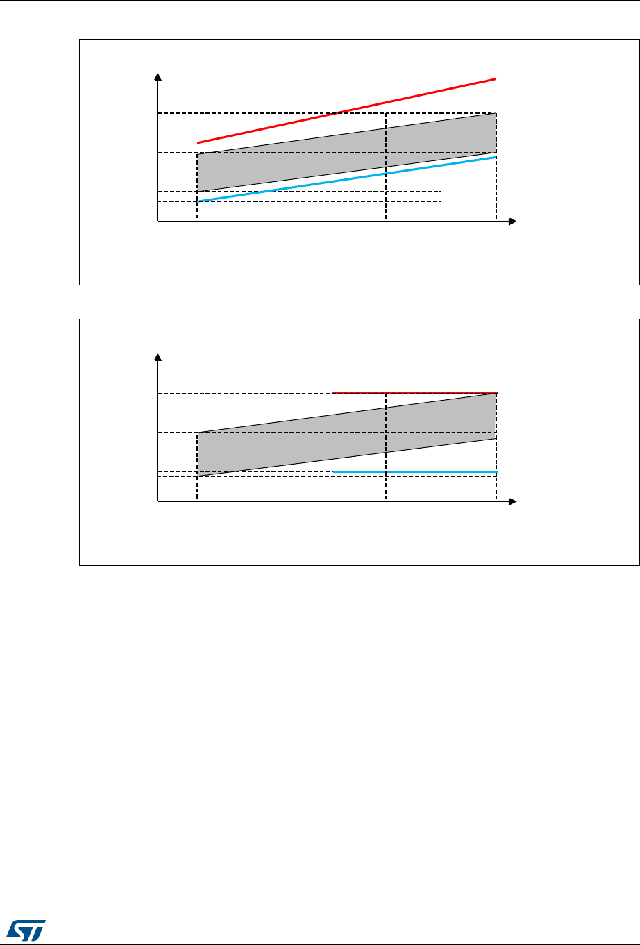
DocID027100 Rev 4 95/149
STM32L072xx Electrical characteristics
120
Figure 25. VIH/VIL versus VDD (CMOS I/Os)
Figure 26. VIH/VIL versus VDD (TTL I/Os)
Output driving current
The GPIOs (general purpose input/outputs) can sink or source up to ±8 mA, and sink or
source up to ±15 mA with the non-standard VOL/VOH specifications given in Table 61.
In the user application, the number of I/O pins which can drive current must be limited to
respect the absolute maximum rating specified in Section 6.2:
•The sum of the currents sourced by all the I/Os on VDD, plus the maximum Run
consumption of the MCU sourced on VDD, cannot exceed the absolute maximum rating
IVDD(Σ) (see Table 24).
•The sum of the currents sunk by all the I/Os on VSS plus the maximum Run
consumption of the MCU sunk on VSS cannot exceed the absolute maximum rating
IVSS(Σ) (see Table 24).
06Y9
9''9
9,+PLQ
9,/PD[
9,/9,+9
&026VWDQGDUGUHTXLUHPHQWV9
,+PLQ
9
''
9
,/PD[
9
''
&026VWDQGDUGUHTXLUHPHQWV9,/PD[ 9''
9
,+PLQ
9
''
DOOSLQV
H[FHSW%2273&3+
9
,+PLQ
9
''
IRU
%2273&3+
,QSXWUDQJHQRW
JXDUDQWHHG
06Y9
9''9
9,+PLQ
9,/PD[
9,/9,+9
77/VWDQGDUGUHTXLUHPHQWV9,+PLQ 9
9
,/PD[
9
''
77/VWDQGDUGUHTXLUHPHQWV9,/PD[ 9
,QSXWUDQJHQRW
JXDUDQWHHG
9
,+PLQ
9
''
DOOSLQV
H[FHSW%2273&3+
9
,+PLQ
9
''
IRU
%2273&3+
Electrical characteristics STM32L072xx
96/149 DocID027100 Rev 4
Output voltage levels
Unless otherwise specified, the parameters given in Table 6 1 are derived from tests
performed under ambient temperature and VDD supply voltage conditions summarized in
Table 26. All I/Os are CMOS and TTL compliant.
Table 61. Output voltage characteristics
Symbol Parameter Conditions Min Max Unit
VOL(1)
1. The IIO current sunk by the device must always respect the absolute maximum rating specified in Table 24.
The sum of the currents sunk by all the I/Os (I/O ports and control pins) must always be respected and
must not exceed ΣIIO(PIN).
Output low level voltage for an I/O
pin CMOS port(2),
IIO = +8 mA
2.7 V ≤ VDD ≤ 3.6 V
2. TTL and CMOS outputs are compatible with JEDEC standards JESD36 and JESD52.
-0.4
V
VOH(3)
3. The IIO current sourced by the device must always respect the absolute maximum rating specified in
Table 24. The sum of the currents sourced by all the I/Os (I/O ports and control pins) must always be
respected and must not exceed ΣIIO(PIN).
Output high level voltage for an I/O
pin VDD-0.4 -
VOL (1) Output low level voltage for an I/O
pin
TTL port(2),
IIO =+ 8 mA
2.7 V ≤ VDD ≤ 3.6 V
-0.4
VOH (3)(4)
4. Guaranteed by characterization results.
Output high level voltage for an I/O
pin
TTL port(2),
IIO = -6 mA
2.7 V ≤ VDD ≤ 3.6 V
2.4 -
VOL(1)(4) Output low level voltage for an I/O
pin
IIO = +15 mA
2.7 V ≤ VDD ≤ 3.6 V -1.3
VOH(3)(4) Output high level voltage for an I/O
pin
IIO = -15 mA
2.7 V ≤ VDD ≤ 3.6 V VDD-1.3 -
VOL(1)(4) Output low level voltage for an I/O
pin
IIO = +4 mA
1.65 V ≤ VDD < 3.6 V -0.45
VOH(3)(4) Output high level voltage for an I/O
pin
IIO = -4 mA
1.65 V ≤ VDD ≤ 3.6 V VDD-0.45 -
VOLFM+(1)(4) Output low level voltage for an FTf
I/O pin in Fm+ mode
IIO = 20 mA
2.7 V ≤ VDD ≤ 3.6 V -0.4
IIO = 10 mA
1.65 V ≤ VDD ≤ 3.6 V -0.4
DocID027100 Rev 4 97/149
STM32L072xx Electrical characteristics
120
Input/output AC characteristics
The definition and values of input/output AC characteristics are given in Figure 27 and
Table 62, respectively.
Unless otherwise specified, the parameters given in Table 6 2 are derived from tests
performed under ambient temperature and VDD supply voltage conditions summarized in
Table 26.
Table 62. I/O AC characteristics(1)
OSPEEDRx[1:0]
bit value(1) Symbol Parameter Conditions Min Max(2) Unit
00
fmax(IO)out Maximum frequency(3) CL = 50 pF, VDD = 2.7 V to 3.6 V - 400
kHz
CL = 50 pF, VDD = 1.65 V to 2.7 V - 100
tf(IO)out
tr(IO)out
Output rise and fall time
CL = 50 pF, VDD = 2.7 V to 3.6 V - 125
ns
CL = 50 pF, VDD = 1.65 V to 2.7 V - 320
01
fmax(IO)out Maximum frequency(3) CL = 50 pF, VDD = 2.7 V to 3.6 V - 2
MHz
CL = 50 pF, VDD = 1.65 V to 2.7 V - 0.6
tf(IO)out
tr(IO)out
Output rise and fall time
CL = 50 pF, VDD = 2.7 V to 3.6 V - 30
ns
CL = 50 pF, VDD = 1.65 V to 2.7 V - 65
10
Fmax(IO)out Maximum frequency(3) CL = 50 pF, VDD = 2.7 V to 3.6 V - 10
MHz
CL = 50 pF, VDD = 1.65 V to 2.7 V - 2
tf(IO)out
tr(IO)out
Output rise and fall time
CL = 50 pF, VDD = 2.7 V to 3.6 V - 13
ns
CL = 50 pF, VDD = 1.65 V to 2.7 V - 28
11
Fmax(IO)out Maximum frequency(3) CL = 30 pF, VDD = 2.7 V to 3.6 V - 35
MHz
CL = 50 pF, VDD = 1.65 V to 2.7 V - 10
tf(IO)out
tr(IO)out
Output rise and fall time
CL = 30 pF, VDD = 2.7 V to 3.6 V - 6
ns
CL = 50 pF, VDD = 1.65 V to 2.7 V - 17
Fm+
configuration(4)
fmax(IO)out Maximum frequency(3)
CL = 50 pF, VDD = 2.5 V to 3.6 V
-1MHz
tf(IO)out Output fall time - 10
ns
tr(IO)out Output rise time - 30
fmax(IO)out Maximum frequency(3)
CL = 50 pF, VDD = 1.65 V to 3.6 V
-350KHz
tf(IO)out Output fall time - 15
ns
tr(IO)out Output rise time - 60
-t
EXTIpw
Pulse width of external
signals detected by the
EXTI controller
-8-ns
1. The I/O speed is configured using the OSPEEDRx[1:0] bits. Refer to the line reference manual for a description of GPIO Port
configuration register.
2. Guaranteed by design.
3. The maximum frequency is defined in Figure 27.
4. When Fm+ configuration is set, the I/O speed control is bypassed. Refer to the line reference manual for a detailed
description of Fm+ I/O configuration.
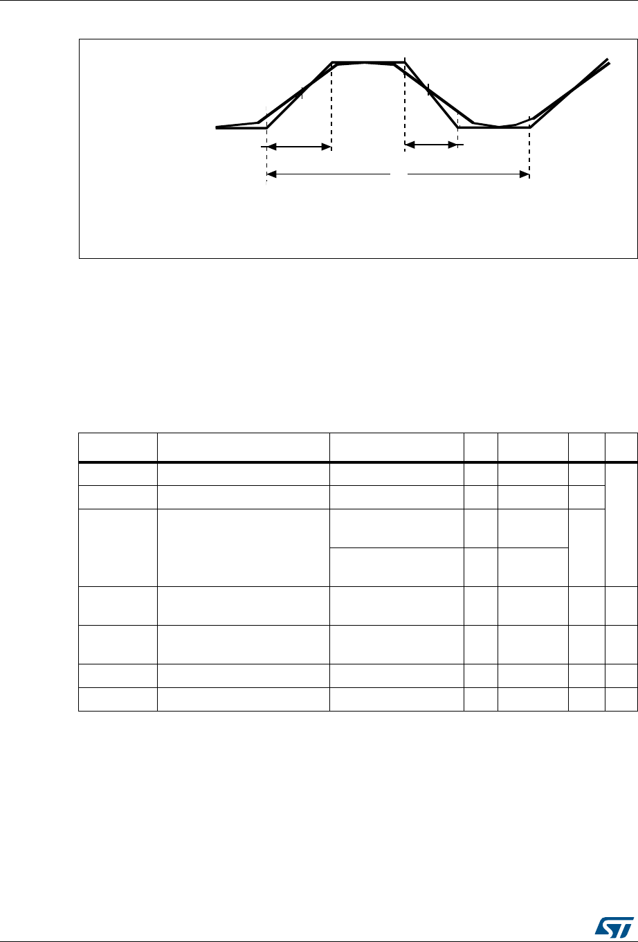
Electrical characteristics STM32L072xx
98/149 DocID027100 Rev 4
Figure 27. I/O AC characteristics definition
6.3.14 NRST pin characteristics
The NRST pin input driver uses CMOS technology. It is connected to a permanent pull-up
resistor, RPU , except when it is internally driven low (see Table 63).
Unless otherwise specified, the parameters given in Table 6 3 are derived from tests
performed under ambient temperature and VDD supply voltage conditions summarized in
Table 26.
DLG
WU,2RXW
287387
(;7(51$/
21&/
0D[LPXPIUHTXHQF\LVDFKLHYHGLIWUWI7DQGLIWKHGXW\F\FOHLV
ZKHQORDGHGE\&/VSHFLILHGLQWKHWDEOH³,2$&FKDUDFWHULVWLFV´
7
WI,2RXW
Table 63. NRST pin characteristics
Symbol Parameter Conditions Min Typ Max Unit
VIL(NRST)(1)
1. Guaranteed by design.
NRST input low level voltage - VSS -0.8
V
VIH(NRST)(1) NRST input high level voltage - 1.4 - VDD
VOL(NRST)(1) NRST output low level
voltage
IOL = 2 mA
2.7 V < VDD < 3.6 V --
0.4
IOL = 1.5 mA
1.65 V < VDD < 2.7 V --
Vhys(NRST)(1) NRST Schmitt trigger voltage
hysteresis --10%V
DD(2)
2. 200 mV minimum value
-mV
RPU
Weak pull-up equivalent
resistor(3)
3. The pull-up is designed with a true resistance in series with a switchable PMOS. This PMOS contribution to
the series resistance is around 10%.
VIN = VSS 25 45 65 kΩ
VF(NRST)(1) NRST input filtered pulse - - - 50 ns
VNF(NRST)(1) NRST input not filtered pulse - 350 - - ns
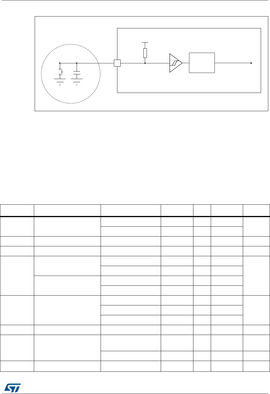
DocID027100 Rev 4 99/149
STM32L072xx Electrical characteristics
120
Figure 28. Recommended NRST pin protection
1. The reset network protects the device against parasitic resets.
2. The external capacitor must be placed as close as possible to the device.
3. The user must ensure that the level on the NRST pin can go below the VIL(NRST) max level specified in
Table 63. Otherwise the reset will not be taken into account by the device.
6.3.15 12-bit ADC characteristics
Unless otherwise specified, the parameters given in Table 6 4 are derived from tests
performed under ambient temperature, fPCLK frequency and VDDA supply voltage conditions
summarized in Table 26: General operating conditions.
Note: It is recommended to perform a calibration after each power-up.
069
538
9''
,QWHUQDOUHVHW
([WHUQDO
UHVHWFLUFXLW
1567
)LOWHU
)
Table 64. ADC characteristics
Symbol Parameter Conditions Min Typ Max Unit
VDDA
Analog supply voltage for
ADC ON
Fast channel 1.65 - 3.6
V
Standard channel 1.75(1) -3.6
VREF+ Positive reference voltage - 1.65 VDDA V
VREF- Negative reference voltage - - 0 -
IDDA (ADC)
Current consumption of the
ADC on VDDAand VREF+
1.14 Msps - 200 -
µA
10 ksps - 40 -
Current consumption of the
ADC on VDD(2)
1.14 Msps - 70 -
10 ksps - 1 -
fADC ADC clock frequency
Voltage scaling Range 1 0.14 - 16
MHzVoltage scaling Range 2 0.14 - 8
Voltage scaling Range 3 0.14 - 4
fS(3) Sampling rate 12-bit resolution 0.01 - 1.14 MHz
fTRIG(3) External trigger frequency
fADC = 16 MHz,
12-bit resolution - - 941 kHz
---171/f
ADC
VAIN Conversion voltage range - 0 - VREF+ V
Electrical characteristics STM32L072xx
100/149 DocID027100 Rev 4
RAIN(3) External input impedance See Equation 1 and
Table 65 for details --50kΩ
RADC(3)(4) Sampling switch resistance - - - 1 kΩ
CADC(3) Internal sample and hold
capacitor ---8pF
tCAL(3)(5) Calibration time
fADC = 16 MHz 5.2 µs
-831/f
ADC
WLATENCY(6) ADC_DR register write
latency
ADC clock = HSI16
1.5 ADC
cycles + 2
fPCLK cycles
-
1.5 ADC
cycles + 3
fPCLK cycles -
ADC clock = PCLK/2 - 4.5 - fPCLK
cycle
ADC clock = PCLK/4 - 8.5 - fPCLK
cycle
tlatr(3) Trigger conversion latency
fADC = fPCLK/2 = 16 MHz 0.266 µs
fADC = fPCLK/2 8.5 1/fPCLK
fADC = fPCLK/4 = 8 MHz 0.516 µs
fADC = fPCLK/4 16.5 1/fPCLK
fADC = fHSI16 = 16 MHz 0.252 - 0.260 µs
JitterADC ADC jitter on trigger
conversion fADC = fHSI16 -1-1/f
HSI16
tS(3) Sampling time
fADC = 16 MHz 0.093 - 10.03 µs
-1.5-160.51/f
ADC
tUP_LDO(3)(5) Internal LDO power-up time - - - 10 µs
tSTAB(3)(5) ADC stabilization time - 14 1/fADC
tConV(3) Total conversion time
(including sampling time)
fADC = 16 MHz,
12-bit resolution 0.875 - 10.81 µs
12-bit resolution 14 to 173 (tS for sampling +12.5
for successive approximation) 1/fADC
1. VDDA minimum value can be decreased in specific temperature conditions. Refer to Table 65: RAIN max for fADC = 16 MHz.
2. A current consumption proportional to the APB clock frequency has to be added (see Table 40: Peripheral current
consumption in Run or Sleep mode).
3. Guaranteed by design.
4. Standard channels have an extra protection resistance which depends on supply voltage. Refer to Table 65: RAIN max for
fADC = 16 MHz.
5. This parameter only includes the ADC timing. It does not take into account register access latency.
6. This parameter specifies the latency to transfer the conversion result into the ADC_DR register. EOC bit is set to indicate the
conversion is complete and has the same latency.
Table 64. ADC characteristics (continued)
Symbol Parameter Conditions Min Typ Max Unit
DocID027100 Rev 4 101/149
STM32L072xx Electrical characteristics
120
Equation 1: RAIN max formula
The simplified formula above (Equation 1) is used to determine the maximum external
impedance allowed for an error below 1/4 of LSB. Here N = 12 (from 12-bit resolution).
RAIN
TS
fADC CADC 2N2+
()ln××
----------------------------------------------------------------RADC
–<
Table 65. RAIN max for fADC = 16 MHz(1)
Ts
(cycles)
tS
(µs)
RAIN max for
fast channels
(kΩ)
RAIN max for standard channels (kΩ)
VDD >
2.7 V
VDD >
2.4 V
VDD >
2.0 V
VDD >
1.8 V
VDD >
1.75 V
VDD > 1.65 V
and
TA > −10 °C
VDD > 1.65 V
and
TA > 25 °C
1.5 0.09 0.5 < 0.1 NA NA NA NA NA NA
3.5 0.22 1 0.2 < 0.1 NA NA NA NA NA
7.5 0.47 2.5 1.7 1.5 < 0.1 NA NA NA NA
12.5 0.78 4 3.2 3 1 NA NA NA NA
19.5 1.22 6.5 5.7 5.5 3.5 NA NA NA < 0.1
39.5 2.47 13 12.2 12 10 NA NA NA 5
79.5 4.97 27 26.2 26 24 < 0.1 NA NA 19
160.5 10.03 50 49.2 49 47 32 < 0.1 < 0.1 42
1. Guaranteed by design.
Table 66. ADC accuracy(1)(2)(3)
Symbol Parameter Conditions Min Typ Max Unit
ET Total unadjusted error
1.65 V < VDDA = VREF+ < 3.6 V,
range 1/2/3
-2 4
LSB
EO Offset error - 1 2.5
EG Gain error - 1 2
EL Integral linearity error - 1.5 2.5
ED Differential linearity error - 1 1.5
ENOB
Effective number of bits 10.2 11
bits
Effective number of bits (16-bit mode
oversampling with ratio =256)(4) 11.3 12.1 -
SINAD Signal-to-noise distortion 63 69 -
dBSNR
Signal-to-noise ratio 63 69 -
Signal-to-noise ratio (16-bit mode
oversampling with ratio =256)(4) 70 76 -
THD Total harmonic distortion - -85 -73
Electrical characteristics STM32L072xx
102/149 DocID027100 Rev 4
Figure 29. ADC accuracy characteristics
ET Total unadjusted error
1.65 V < VREF+ <VDDA < 3.6 V,
range 1/2/3
-2 5
LSB
EO Offset error - 1 2.5
EG Gain error - 1 2
EL Integral linearity error - 1.5 3
ED Differential linearity error - 1 2
ENOB Effective number of bits 10.0 11.0 - bits
SINAD Signal-to-noise distortion 62 69 -
dBSNR Signal-to-noise ratio 61 69 -
THD Total harmonic distortion - -85 -65
1. ADC DC accuracy values are measured after internal calibration.
2. ADC Accuracy vs. Negative Injection Current: Injecting negative current on any of the standard (non-robust) analog input
pins should be avoided as this significantly reduces the accuracy of the conversion being performed on another analog
input. It is recommended to add a Schottky diode (pin to ground) to standard analog pins which may potentially inject
negative current.
Any positive injection current within the limits specified for IINJ(PIN) and ΣIINJ(PIN) in Section 6.3.12 does not affect the ADC
accuracy.
3. Better performance may be achieved in restricted VDDA, frequency and temperature ranges.
4. This number is obtained by the test board without additional noise, resulting in non-optimized value for oversampling mode.
Table 66. ADC accuracy(1)(2)(3) (continued)
Symbol Parameter Conditions Min Typ Max Unit
(7 7RWDO8QDMXVWHG(UURUPD[LPXPGHYLDWLRQ
EHWZHHQWKHDFWXDODQGLGHDOWUDQVIHUFXUYHV
(2 2IIVHW(UURUPD[LPXPGHYLDWLRQ
EHWZHHQWKHILUVWDFWXDOWUDQVLWLRQDQGWKHILUVW
LGHDORQH
(* *DLQ(UURUGHYLDWLRQEHWZHHQWKHODVW
LGHDOWUDQVLWLRQDQGWKHODVWDFWXDORQH
(' 'LIIHUHQWLDO/LQHDULW\(UURUPD[LPXP
GHYLDWLRQEHWZHHQDFWXDOVWHSVDQGWKHLGHDORQHV
(/ ,QWHJUDO/LQHDULW\(UURUPD[LPXPGHYLDWLRQ
EHWZHHQDQ\DFWXDOWUDQVLWLRQDQGWKHHQGSRLQW
FRUUHODWLRQOLQH
([DPSOHRIDQDFWXDOWUDQVIHUFXUYH
7KHLGHDOWUDQVIHUFXUYH
(QGSRLQWFRUUHODWLRQOLQH
9''$
966$
(2
(7
(/
(*
('
/6%,'($/
069
DocID027100 Rev 4 103/149
STM32L072xx Electrical characteristics
120
Figure 30. Typical connection diagram using the ADC
1. Refer to Table 64: ADC characteristics for the values of RAIN, RADC and CADC.
2. Cparasitic represents the capacitance of the PCB (dependent on soldering and PCB layout quality) plus the
pad capacitance (roughly 7 pF). A high Cparasitic value will downgrade conversion accuracy. To remedy
this, fADC should be reduced.
General PCB design guidelines
Power supply decoupling should be performed as shown in Figure 31 or Figure 32,
depending on whether VREF+ is connected to VDDA or not. The 10 nF capacitors should be
ceramic (good quality). They should be placed as close as possible to the chip.
Figure 31. Power supply and reference decoupling (VREF+ not connected to VDDA)
06Y9
9''$
$,1[
,/Q$
97
5$,1
&SDUDVLWLF
9
$,1
97
5$'& ELW
FRQYHUWHU
&
$'&
6DPSOHDQGKROG$'&
FRQYHUWHU
069
95()
670/[[
9''$
966$ 95()±
)Q)
)Q)
DocID027100 Rev 4 105/149
STM32L072xx Electrical characteristics
120
6.3.16 DAC electrical characteristics
Data guaranteed by design, not tested in production, unless otherwise specified.
Table 67. DAC characteristics
Symbol Parameter Conditions Min Typ Max Unit
VDDA Analog supply voltage - 1.8 - 3.6 V
VREF+ Reference supply voltage VREF+ must always be
below VDDA
1.8 - 3.6 V
VREF- Lower reference voltage - VSSA V
IDDVREF+(1)
Current consumption on VREF+
supply
VREF+ = 3.3 V
No load, middle code
(0x800) - 130 220
µA
No load, worst code
(0x000) - 220 350
IDDA (2)
Current consumption on VDDA
supply,
VDDA = 3.3 V
No load, middle code
(0x800) -
µA
No load, worst code
(0xF1C) -
RL(3) Resistive load DAC output
ON
RL
connected
to VSSA
5- -
kΩ
RL
connected
to VDDA
25 - -
CL(3) Capacitive load DAC output buffer ON - - 50 pF
ROOutput impedance DAC output buffer OFF 12 16 20 kΩ
VDAC_OUT Voltage on DAC_OUT output
DAC output buffer ON 0.2 - VDDA – 0.2 V
DAC output buffer OFF 0.5 - VREF+ –
1LSB mV
Electrical characteristics STM32L072xx
106/149 DocID027100 Rev 4
DNL(2) Differential non linearity(4)
CL ≤ 50 pF, RL ≥ 5 kΩ
DAC output buffer ON -1.5 3
LSB
No RLOAD, CL ≤ 50 pF
DAC output buffer OFF -1.5 3
INL(2) Integral non linearity(5)
CL ≤ 50 pF, RL ≥ 5 kΩ
DAC output buffer ON -2 4
No RLOAD, CL ≤ 50 pF
DAC output buffer OFF -2 4
Offset(2) Offset error at code 0x800 (6)
CL ≤ 50 pF, RL ≥ 5 kΩ
DAC output buffer ON -±10 ±25
No RLOAD, CL ≤ 50 pF
DAC output buffer OFF -±5 ±8
Offset1(2) Offset error at code 0x001(7) No RLOAD, CL ≤ 50 pF
DAC output buffer OFF -±1.5 ±5
dOffset/dT(2) Offset error temperature
coefficient (code 0x800)
VDDA = 3.3V
VREF+= 3.0 V
TA = 0 to 50 °C
DAC output buffer OFF
-20 -10 0
µV/°C
VDDA = 3.3V
VREF+= 3.0 V
TA = 0 to 50 °C
DAC output buffer ON
020 50
Gain(2) Gain error(8)
CL ≤ 50 pF, RL ≥ 5 kΩ
DAC output buffer ON - +0.1 / -0.2% +0.2 / -0.5%
%
No RLOAD, CL ≤ 50 pF
DAC output buffer OFF - +0 / -0.2% +0 / -0.4%
dGain/dT(2) Gain error temperature
coefficient
VDDA = 3.3V
VREF+= 3.0 V
TA = 0 to 50 °C
DAC output buffer OFF
-10 -2 0
µV/°C
VDDA = 3.3V
VREF+= 3.0 V
TA = 0 to 50 °C
DAC output buffer ON
-40 -8 0
TUE(2) Total unadjusted error
CL ≤ 50 pF, RL ≥ 5 kΩ
DAC output buffer ON -12 30
LSB
No RLOAD, CL ≤ 50 pF
DAC output buffer OFF -8 12
Table 67. DAC characteristics (continued)
Symbol Parameter Conditions Min Typ Max Unit
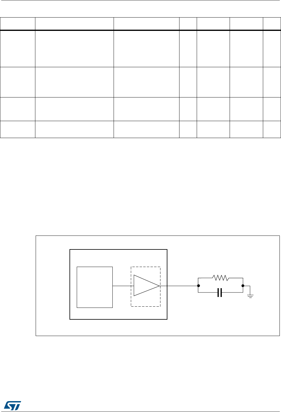
DocID027100 Rev 4 107/149
STM32L072xx Electrical characteristics
120
Figure 33. 12-bit buffered/non-buffered DAC
1. The DAC integrates an output buffer that can be used to reduce the output impedance and to drive external
loads directly without the use of an external operational amplifier. The buffer can be bypassed by
configuring the BOFFx bit in the DAC_CR register.
tSETTLING
Settling time (full scale: for a
12-bit code transition between
the lowest and the highest
input codes till DAC_OUT
reaches final value ±1LSB
CL ≤ 50 pF, RL ≥ 5 kΩ- 7 12 µs
Update rate
Max frequency for a correct
DAC_OUT change (95% of
final value) with 1 LSB
variation in the input code
CL ≤ 50 pF, RL ≥ 5 kΩ- - 1 Msps
tWAKEUP
Wakeup time from off state
(setting the ENx bit in the DAC
Control register)(9)
CL ≤ 50 pF, RL ≥ 5 kΩ- 9 15 µs
PSRR+ VDDA supply rejection ratio
(static DC measurement) CL ≤ 50 pF, RL ≥ 5 kΩ--60 -35dB
1. Guaranteed by characterization results.
2. Guaranteed by design, not tested in production.
3. Connected between DAC_OUT and VSSA.
4. Difference between two consecutive codes - 1 LSB.
5. Difference between measured value at Code i and the value at Code i on a line drawn between Code 0 and last Code 4095.
6. Difference between the value measured at Code (0x800) and the ideal value = VREF+/2.
7. Difference between the value measured at Code (0x001) and the ideal value.
8. Difference between ideal slope of the transfer function and measured slope computed from code 0x000 and 0xFFF when
buffer is OFF, and from code giving 0.2 V and (VDDA – 0.2) V when buffer is ON.
9. In buffered mode, the output can overshoot above the final value for low input code (starting from min value).
Table 67. DAC characteristics (continued)
Symbol Parameter Conditions Min Typ Max Unit
06Y9
5/
&/
%XIIHUHG1RQEXIIHUHG'$&
'$&B287[
%XIIHU
ELW
GLJLWDOWR
DQDORJ
FRQYHUWHU
Electrical characteristics STM32L072xx
108/149 DocID027100 Rev 4
6.3.17 Temperature sensor characteristics
6.3.18 Comparators
Table 68. Temperature sensor calibration values
Calibration value name Description Memory address
TS_CAL1 TS ADC raw data acquired at
temperature of 30 °C, VDDA= 3 V 0x1FF8 007A - 0x1FF8 007B
TS_CAL2 TS ADC raw data acquired at
temperature of 130 °C, VDDA= 3 V 0x1FF8 007E - 0x1FF8 007F
Table 69. Temperature sensor characteristics
Symbol Parameter Min Typ Max Unit
TL(1)
1. Guaranteed by characterization results.
VSENSE linearity with temperature - ±1±2°C
Avg_Slope(1) Average slope 1.48 1.61 1.75 mV/°C
V130 Voltage at 130°C ±5°C(2)
2. Measured at VDD = 3 V ±10 mV. V130 ADC conversion result is stored in the TS_CAL2 byte.
640 670 700 mV
IDDA(TEMP)(3) Current consumption - 3.4 6 µA
tSTART(3)
3. Guaranteed by design.
Startup time - - 10
µs
TS_temp(4)(3)
4. Shortest sampling time can be determined in the application by multiple iterations.
ADC sampling time when reading the temperature 10 - -
Table 70. Comparator 1 characteristics
Symbol Parameter Conditions Min(1) Typ Max(1) Unit
VDDA Analog supply voltage - 1.65 3.6 V
R400K R400K value - - 400 - kΩ
R10K R10K value - - 10 -
VIN
Comparator 1 input voltage
range -0.6-V
DDA V
tSTART Comparator startup time - - 7 10 µs
td Propagation delay(2) --310
Voffset Comparator offset - - ±3±10 mV
dVoffset/dt Comparator offset variation in
worst voltage stress conditions
VDDA = 3.6 V, VIN+ = 0 V,
VIN- = VREFINT
, TA = 25 °C0 1.5 10 mV/1000 h
ICOMP1 Current consumption(3) - - 160 260 nA
1. Guaranteed by characterization.
2. The delay is characterized for 100 mV input step with 10 mV overdrive on the inverting input, the non-inverting input set to
the reference.
3. Comparator consumption only. Internal reference voltage not included.
DocID027100 Rev 4 109/149
STM32L072xx Electrical characteristics
120
Table 71. Comparator 2 characteristics
Symbol Parameter Conditions Min Typ Max(1) Unit
VDDA Analog supply voltage - 1.65 - 3.6 V
VIN Comparator 2 input voltage range - 0 - VDDA V
tSTART Comparator startup time Fast mode - 15 20
µs
Slow mode - 20 25
td slow Propagation delay(2) in slow mode 1.65 V ≤ VDDA ≤ 2.7 V - 1.8 3.5
2.7 V ≤ VDDA ≤ 3.6 V - 2.5 6
td fast Propagation delay(2) in fast mode 1.65 V ≤ VDDA ≤ 2.7 V - 0.8 2
2.7 V ≤ VDDA ≤ 3.6 V - 1.2 4
Voffset Comparator offset error - ±4±20 mV
dThreshold/
dt
Threshold voltage temperature
coefficient
VDDA = 3.3V, TA = 0 to 50 °C,
V- = VREFINT
,
3/4 VREFINT
,
1/2 VREFINT
,
1/4 VREFINT
.
-15 30
ppm
/°C
ICOMP2 Current consumption(3) Fast mode - 3.5 5 µA
Slow mode - 0.5 2
1. Guaranteed by characterization results.
2. The delay is characterized for 100 mV input step with 10 mV overdrive on the inverting input, the non-inverting input set to
the reference.
3. Comparator consumption only. Internal reference voltage (required for comparator operation) is not included.
Electrical characteristics STM32L072xx
110/149 DocID027100 Rev 4
6.3.19 Timer characteristics
TIM timer characteristics
The parameters given in the Table 72 are guaranteed by design.
Refer to Section 6.3.13: I/O port characteristics for details on the input/output alternate
function characteristics (output compare, input capture, external clock, PWM output).
6.3.20 Communications interfaces
I2C interface characteristics
The I2C interface meets the timings requirements of the I2C-bus specification and user
manual rev. 03 for:
•Standard-mode (Sm) : with a bit rate up to 100 kbit/s
•Fast-mode (Fm) : with a bit rate up to 400 kbit/s
•Fast-mode Plus (Fm+) : with a bit rate up to 1 Mbit/s.
The I2C timing requirements are guaranteed by design when the I2C peripheral is properly
configured (refer to the reference manual for details). The SDA and SCL I/O requirements
are met with the following restrictions: the SDA and SCL I/O pins are not "true" open-drain.
When configured as open-drain, the PMOS connected between the I/O pin and VDDIOx is
disabled, but is still present. Only FTf I/O pins support Fm+ low level output current
maximum requirement (refer to Section 6.3.13: I/O port characteristics for the I2C I/Os
characteristics).
All I2C SDA and SCL I/Os embed an analog filter (see Table 73 for the analog filter
characteristics).
Table 72. TIMx characteristics(1)
Symbol Parameter Conditions Min Max Unit
tres(TIM) Timer resolution time
1-t
TIMxCLK
fTIMxCLK = 32 MHz 31.25 - ns
fEXT
Timer external clock frequency on CH1
to CH4
0f
TIMxCLK/2 MHz
fTIMxCLK = 32 MHz 0 16 MHz
ResTIM Timer resolution - 16 bit
tCOUNTER
16-bit counter clock period when
internal clock is selected (timer’s
prescaler disabled)
- 1 65536 tTIMxCLK
fTIMxCLK = 32 MHz 0.0312 2048 µs
tMAX_COUNT Maximum possible count
- - 65536 × 65536 tTIMxCLK
fTIMxCLK = 32 MHz - 134.2 s
1. TIMx is used as a general term to refer to the TIM2, TIM6, TIM21, and TIM22 timers.
DocID027100 Rev 4 111/149
STM32L072xx Electrical characteristics
120
The analog spike filter is compliant with I2C timings requirements only for the following
voltage ranges:
•Fast mode Plus: 2.7 V ≤
VDD ≤ 3.6 V and voltage scaling Range 1
•Fast mode:
–2 V ≤ VDD ≤ 3.6 V and voltage scaling Range 1 or Range 2.
–V
DD < 2 V, voltage scaling Range 1 or Range 2, Cload < 200 pF.
In other ranges, the analog filter should be disabled. The digital filter can be used instead.
Note: In Standard mode, no spike filter is required.
SPI characteristics
Unless otherwise specified, the parameters given in the following tables are derived from
tests performed under ambient temperature, fPCLKx frequency and VDD supply voltage
conditions summarized in Table 26.
Refer to Section 6.3.12: I/O current injection characteristics for more details on the
input/output alternate function characteristics (NSS, SCK, MOSI, MISO).
Table 73. I2C analog filter characteristics(1)
1. Guaranteed by characterization results.
Symbol Parameter Conditions Min Max Unit
tAF
Maximum pulse width of spikes that
are suppressed by the analog filter
Range 1
50(2)
2. Spikes with widths below tAF(min) are filtered.
260(3)
3. Spikes with widths above tAF(max) are not filtered
nsRange 2 -
Range 3 -
Table 74. SPI characteristics in voltage Range 1 (1)
Symbol Parameter Conditions Min Typ Max Unit
fSCK
1/tc(SCK)
SPI clock frequency
Master mode
--
16
MHz
Slave mode
receiver 16
Slave mode
Transmitter
1.71<VDD<3.6V
--12
(2)
Slave mode
Transmitter
2.7<VDD<3.6V
--16
(2)
Duty(SCK)
Duty cycle of SPI clock
frequency Slave mode 30 50 70 %
Electrical characteristics STM32L072xx
112/149 DocID027100 Rev 4
tsu(NSS) NSS setup time Slave mode, SPI
presc = 2 4*Tpclk - -
ns
th(NSS) NSS hold time Slave mode, SPI
presc = 2 2*Tpclk - -
tw(SCKH)
tw(SCKL)
SCK high and low time Master mode Tpclk-2 Tpclk Tpclk+
2
tsu(MI) Data input setup time
Master mode 0 - -
tsu(SI) Slave mode 3 - -
th(MI) Data input hold time
Master mode 7 - -
th(SI) Slave mode 3.5 - -
ta(SO Data output access time Slave mode 15 - 36
tdis(SO) Data output disable time Slave mode 10 - 30
tv(SO) Data output valid time
Slave mode
1.65 V<VDD<3.6 V -1841
Slave mode
2.7 V<VDD<3.6 V -1825
tv(MO) Master mode - 4 7
th(SO) Data output hold time
Slave mode 10 - -
th(MO) Master mode 0 - -
1. Guaranteed by characterization results.
2. The maximum SPI clock frequency in slave transmitter mode is determined by the sum of tv(SO) and tsu(MI)
which has to fit into SCK low or high phase preceding the SCK sampling edge. This value can be
achieved when the SPI communicates with a master having tsu(MI) = 0 while Duty(SCK) = 50%.
Table 74. SPI characteristics in voltage Range 1 (1) (continued)
Symbol Parameter Conditions Min Typ Max Unit
DocID027100 Rev 4 113/149
STM32L072xx Electrical characteristics
120
Table 75. SPI characteristics in voltage Range 2 (1)
Symbol Parameter Conditions Min Typ Max Unit
fSCK
1/tc(SCK)
SPI clock frequency
Master mode
--
8
MHz
Slave mode Transmitter
1.65<VDD<3.6V 8
Slave mode Transmitter
2.7<VDD<3.6V 8(2)
Duty(SCK)
Duty cycle of SPI clock
frequency Slave mode 30 50 70 %
tsu(NSS) NSS setup time Slave mode, SPI presc = 2 4*Tpclk - -
ns
th(NSS) NSS hold time Slave mode, SPI presc = 2 2*Tpclk - -
tw(SCKH)
tw(SCKL)
SCK high and low time Master mode Tpclk-2 Tpclk Tpclk+2
tsu(MI) Data input setup time
Master mode 0 - -
tsu(SI) Slave mode 3 - -
th(MI) Data input hold time
Master mode 11 - -
th(SI) Slave mode 4.5 - -
ta(SO Data output access time Slave mode 18 - 52
tdis(SO) Data output disable time Slave mode 12 - 42
tv(SO) Data output valid time
Slave mode - 20 56.5
tv(MO) Master mode - 5 9
th(SO) Data output hold time
Slave mode 13 - -
th(MO) Master mode 3 - -
1. Guaranteed by characterization results.
2. The maximum SPI clock frequency in slave transmitter mode is determined by the sum of tv(SO) and tsu(MI) which has to fit
into SCK low or high phase preceding the SCK sampling edge. This value can be achieved when the SPI communicates
with a master having tsu(MI) = 0 while Duty(SCK) = 50%.
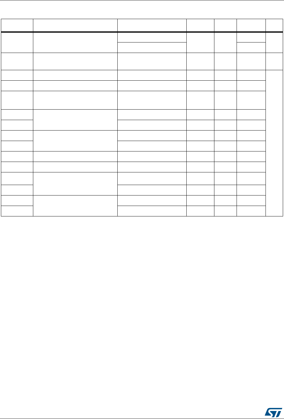
Electrical characteristics STM32L072xx
114/149 DocID027100 Rev 4
Table 76. SPI characteristics in voltage Range 3 (1)
Symbol Parameter Conditions Min Typ Max Unit
fSCK
1/tc(SCK)
SPI clock frequency
Master mode
--
2
MHz
Slave mode 2(2)
Duty(SCK)
Duty cycle of SPI clock
frequency Slave mode 30 50 70 %
tsu(NSS) NSS setup time Slave mode, SPI presc = 2 4*Tpclk - -
ns
th(NSS) NSS hold time Slave mode, SPI presc = 2 2*Tpclk - -
tw(SCKH)
tw(SCKL)
SCK high and low time Master mode Tpclk-2 Tpclk Tpclk+2
tsu(MI) Data input setup time
Master mode 1.5 - -
tsu(SI) Slave mode 6 - -
th(MI) Data input hold time
Master mode 13.5 - -
th(SI) Slave mode 16 - -
ta(SO Data output access time Slave mode 30 - 70
tdis(SO) Data output disable time Slave mode 40 - 80
tv(SO) Data output valid time
Slave mode - 30 70
tv(MO) Master mode - 7 9
th(SO) Data output hold time
Slave mode 25 - -
th(MO) Master mode 8 - -
1. Guaranteed by characterization results.
2. The maximum SPI clock frequency in slave transmitter mode is determined by the sum of tv(SO) and tsu(MI) which has to fit
into SCK low or high phase preceding the SCK sampling edge. This value can be achieved when the SPI communicates
with a master having tsu(MI) = 0 while Duty(SCK) = 50%.
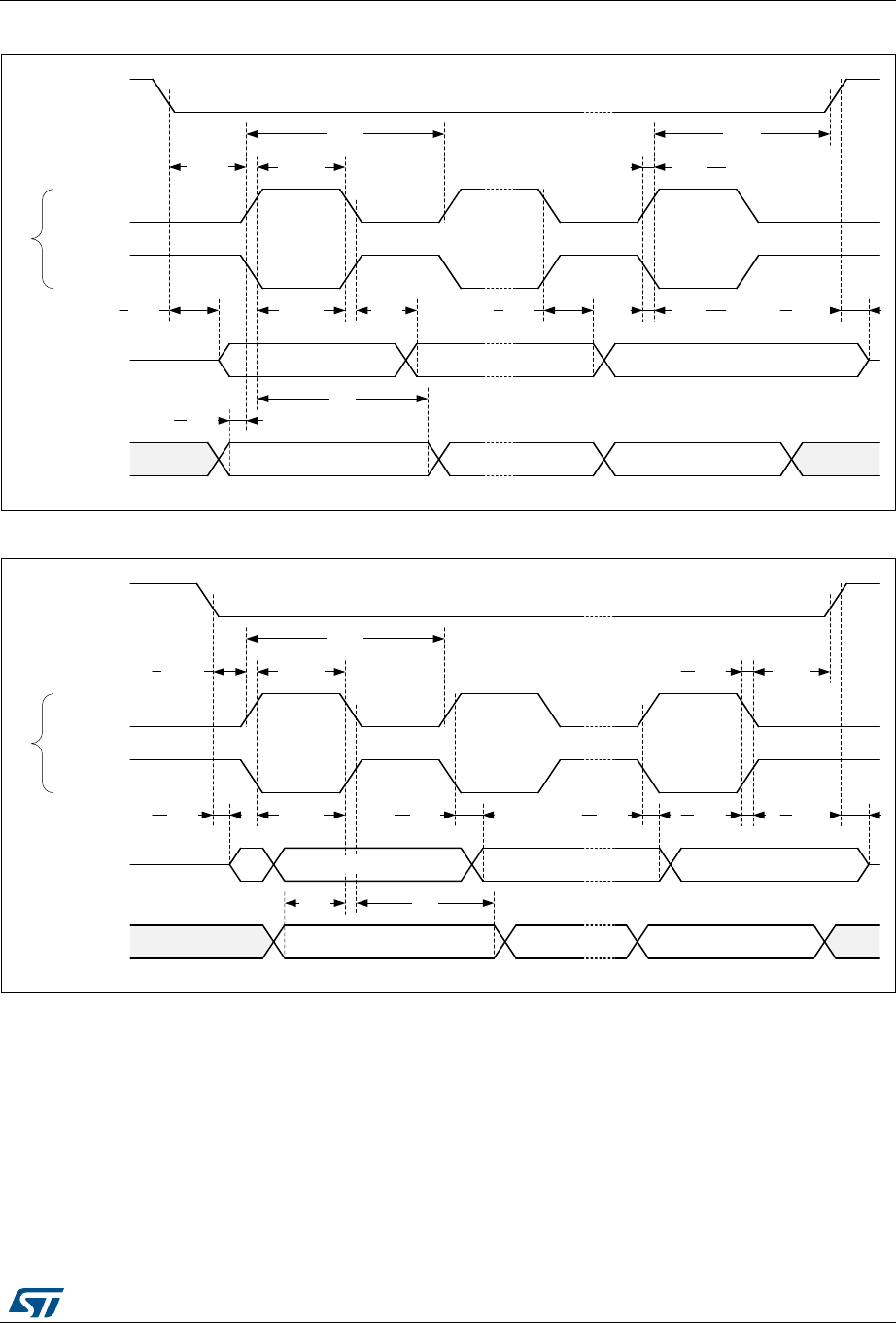
DocID027100 Rev 4 115/149
STM32L072xx Electrical characteristics
120
Figure 34. SPI timing diagram - slave mode and CPHA = 0
Figure 35. SPI timing diagram - slave mode and CPHA = 1(1)
1. Measurement points are done at CMOS levels: 0.3VDD and 0.7VDD.
06Y9
166LQSXW
&3+$
&32/
6&.LQSXW
&3+$
&32/
0,62RXWSXW
026,LQSXW
WVX6,
WK6,
WZ6&./
WZ6&.+
WF6&.
WU6&.
WK166
WGLV62
WVX166
WD62 WY62
1H[WELWV,1
/DVWELW287
)LUVWELW,1
)LUVWELW287 1H[WELWV287
WK62 WI6&.
/DVWELW,1
06Y9
166LQSXW
&3+$
&32/
6&.LQSXW
&3+$
&32/
0,62RXWSXW
026,LQSXW
WVX6, WK6,
WZ6&./
WZ6&.+
WVX166
WF6&.
WD62 WY62
)LUVWELW287 1H[WELWV287
1H[WELWV,1
/DVWELW287
WK62 WU6&.
WI6&. WK166
WGLV62
)LUVWELW,1 /DVWELW,1
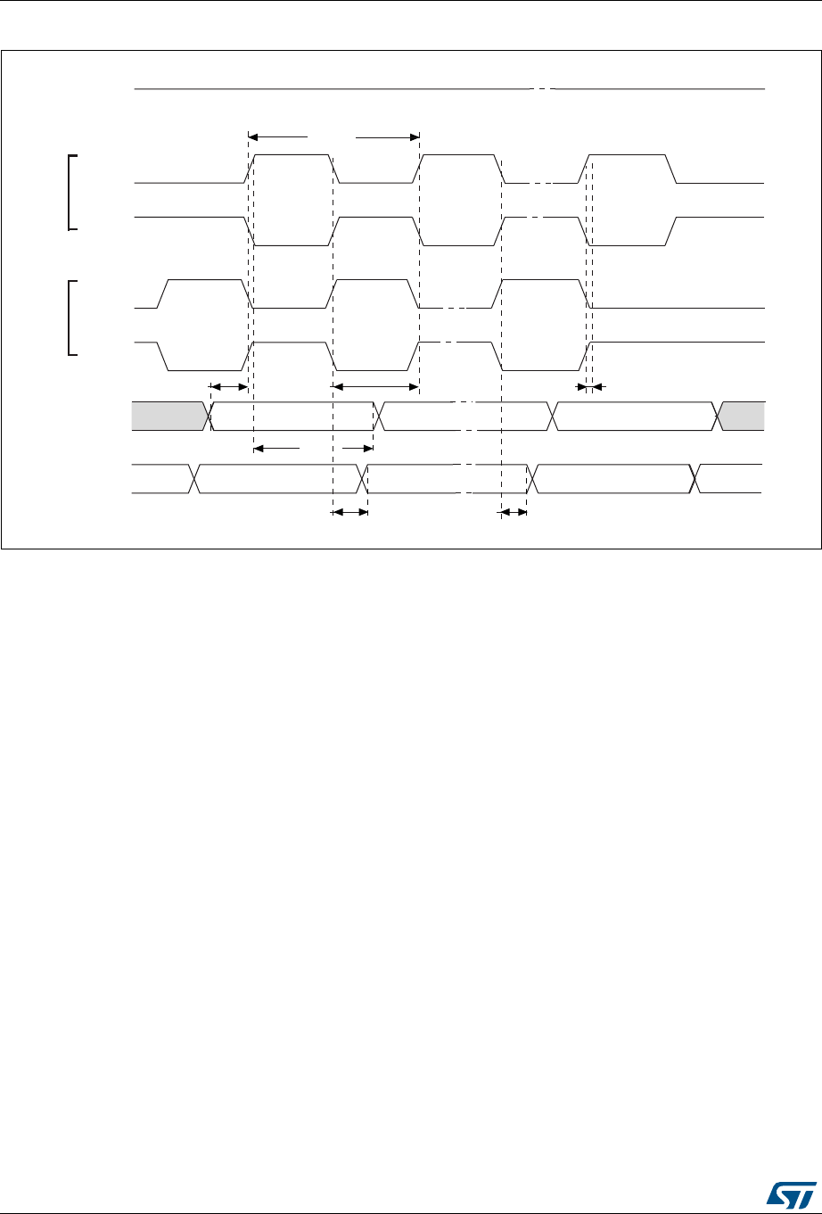
Electrical characteristics STM32L072xx
116/149 DocID027100 Rev 4
Figure 36. SPI timing diagram - master mode(1)
1. Measurement points are done at CMOS levels: 0.3VDD and 0.7VDD.
DLG
6&.2XWSXW
&3+$
026,
287387
0,62
,13 87
&3+$
/6%287
/6%,1
&32/
&32/
% , 7287
166LQSXW
WF6&.
WZ6&.+
WZ6&./
WU6&.
WI6&.
WK0,
+LJK
6&.2XWSXW
&3+$
&3+$
&32/
&32/
WVX0,
WY02 WK02
06%,1 %,7,1
06%287
DocID027100 Rev 4 117/149
STM32L072xx Electrical characteristics
120
I2S characteristics
Note: Refer to the I2S section of the product reference manual for more details about the sampling
frequency (Fs), fMCK, fCK and DCK values. These values reflect only the digital peripheral
behavior, source clock precision might slightly change them. DCK depends mainly on the
ODD bit value, digital contribution leads to a min of (I2SDIV/(2*I2SDIV+ODD) and a max of
(I2SDIV+ODD)/(2*I2SDIV+ODD). Fs max is supported for each mode/condition.
Table 77. I2S characteristics(1)
Symbol Parameter Conditions Min Max Unit
fMCK I2S Main clock output - 256 x 8K 256xFs (2) MHz
fCK I2S clock frequency
Master data: 32 bits - 64xFs
MHz
Slave data: 32 bits - 64xFs
DCK
I2S clock frequency duty
cycle Slave receiver 30 70 %
tv(WS) WS valid time Master mode - 15
ns
th(WS) WS hold time Master mode 11 -
tsu(WS) WS setup time Slave mode 6 -
th(WS) WS hold time Slave mode 2 -
tsu(SD_MR) Data input setup time
Master receiver 0 -
tsu(SD_SR) Slave receiver 6.5 -
th(SD_MR) Data input hold time
Master receiver 18 -
th(SD_SR) Slave receiver 15.5 -
tv(SD_ST) Data output valid time
Slave transmitter (after enable edge) - 77
tv(SD_MT) Master transmitter (after enable edge) - 8
th(SD_ST) Data output hold time
Slave transmitter (after enable edge) 18 -
th(SD_MT) Master transmitter (after enable edge) 1.5 -
1. Guaranteed by characterization results.
2. 256xFs maximum value is equal to the maximum clock frequency.
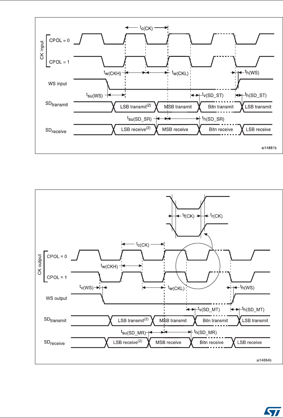
Electrical characteristics STM32L072xx
118/149 DocID027100 Rev 4
Figure 37. I2S slave timing diagram (Philips protocol)(1)
1. Measurement points are done at CMOS levels: 0.3 × VDD and 0.7 × VDD.
2. LSB transmit/receive of the previously transmitted byte. No LSB transmit/receive is sent before the first
byte.
Figure 38. I2S master timing diagram (Philips protocol)(1)
1. Guaranteed by characterization results.
2. LSB transmit/receive of the previously transmitted byte. No LSB transmit/receive is sent before the first
byte.
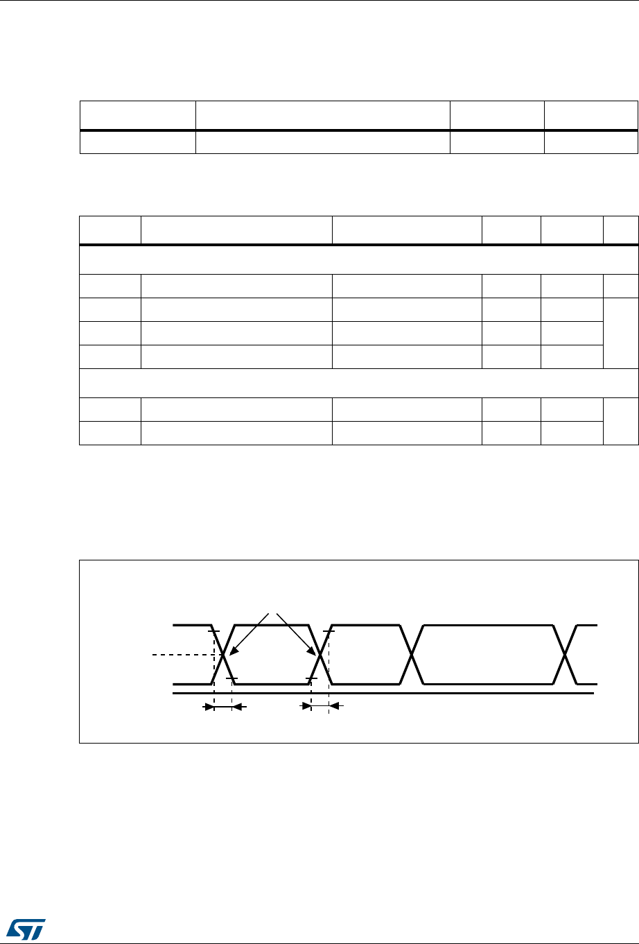
DocID027100 Rev 4 119/149
STM32L072xx Electrical characteristics
120
USB characteristics
The USB interface is USB-IF certified (full speed).
Figure 39. USB timings: definition of data signal rise and fall time
Table 78. USB startup time
Symbol Parameter Max Unit
tSTARTUP(1)
1. Guaranteed by design.
USB transceiver startup time 1 µs
Table 79. USB DC electrical characteristics
Symbol Parameter Conditions Min.(1)
1. All the voltages are measured from the local ground potential.
Max.(1) Unit
Input levels
VDD USB operating voltage - 3.0 3.6 V
VDI(2)
2. Guaranteed by characterization results.
Differential input sensitivity I(USB_DP, USB_DM) 0.2 -
VVCM(2) Differential common mode range Includes VDI range 0.8 2.5
VSE(2) Single ended receiver threshold - 1.3 2.0
Output levels
VOL(3)
3. Guaranteed by test in production.
Static output level low RL of 1.5 kΩ to 3.6 V(4)
4. RL is the load connected on the USB drivers.
-0.3
V
VOH(3) Static output level high RL of 15 kΩ to VSS(4) 2.8 3.6
DLE
&URVVRYHU
SRLQWV
'LIIHUHQWLDO
GDWDOLQHV
9&56
966
WIWU
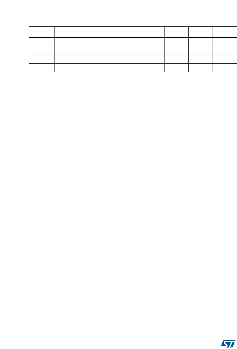
Electrical characteristics STM32L072xx
120/149 DocID027100 Rev 4
Table 80. USB: full speed electrical characteristics
Driver characteristics(1)
1. Guaranteed by design.
Symbol Parameter Conditions Min Max Unit
trRise time(2)
2. Measured from 10% to 90% of the data signal. For more detailed informations, please refer to USB
Specification - Chapter 7 (version 2.0).
CL = 50 pF 420ns
tfFall Time(2) CL = 50 pF 4 20 ns
trfm Rise/ fall time matching tr/tf90 110 %
VCRS Output signal crossover voltage 1.3 2.0 V
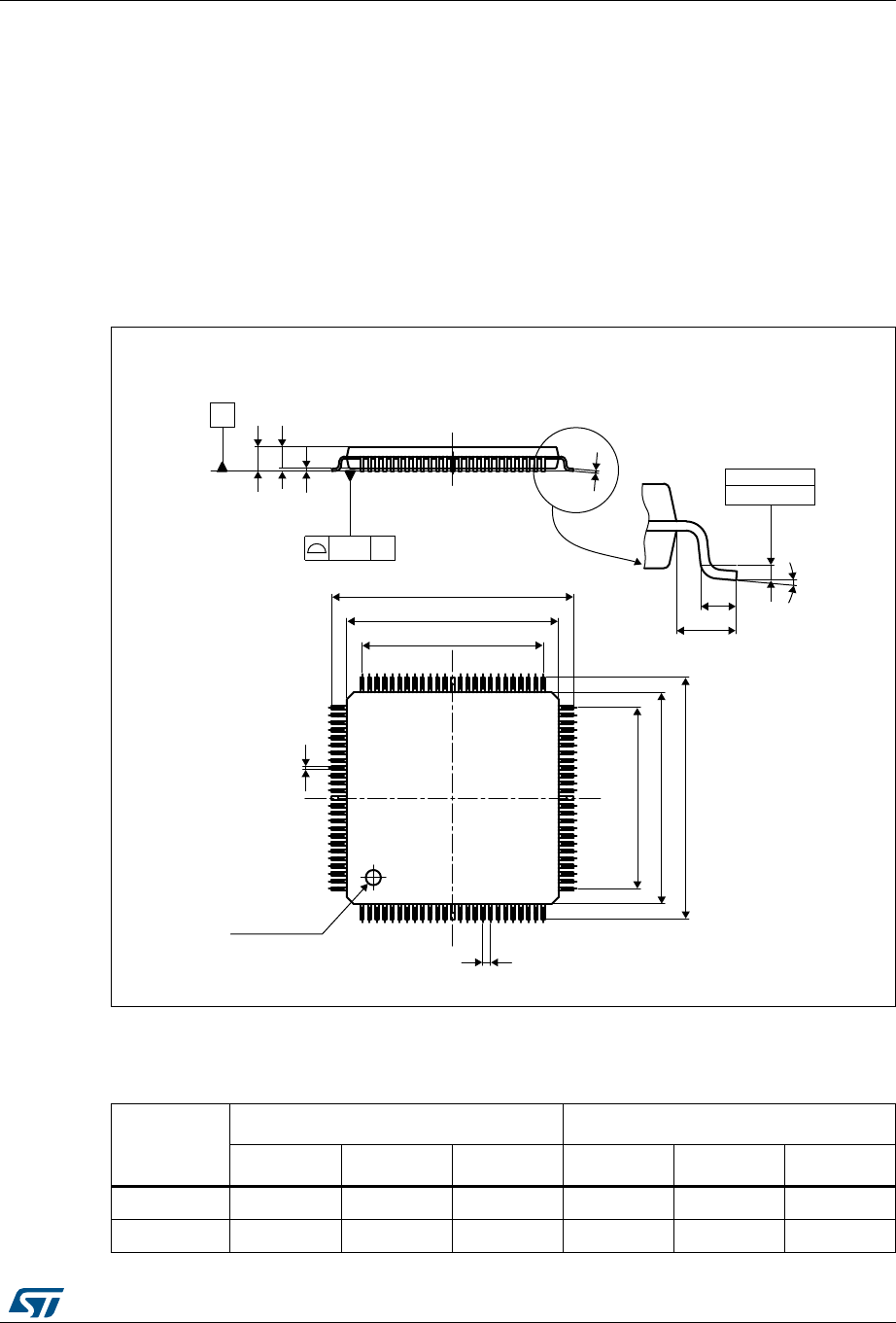
DocID027100 Rev 4 121/149
STM32L072xx Package information
145
7 Package information
In order to meet environmental requirements, ST offers these devices in different grades of
ECOPACK® packages, depending on their level of environmental compliance. ECOPACK®
specifications, grade definitions and product status are available at www.st.com.
ECOPACK® is an ST trademark.
7.1 LQFP100 package information
Figure 40. LQFP100 - 100-pin, 14 x 14 mm low-profile quad flat package outline
1. Drawing is not to scale. Dimensions are in millimeters.
Table 81. LQPF100 - 100-pin, 14 x 14 mm low-profile quad flat package
mechanical data
Symbol
millimeters inches(1)
Min Typ Max Min Typ Max
A - - 1.600 - - 0.0630
A1 0.050 - 0.150 0.0020 - 0.0059
E
)$%.4)&)#!4)/.
0).
'!5'%0,!.%
MM
3%!4).'0,!.%
$
$
$
%
%
%
+
CCC #
#
,?-%?6
!
!
!
,
,
C
B
!
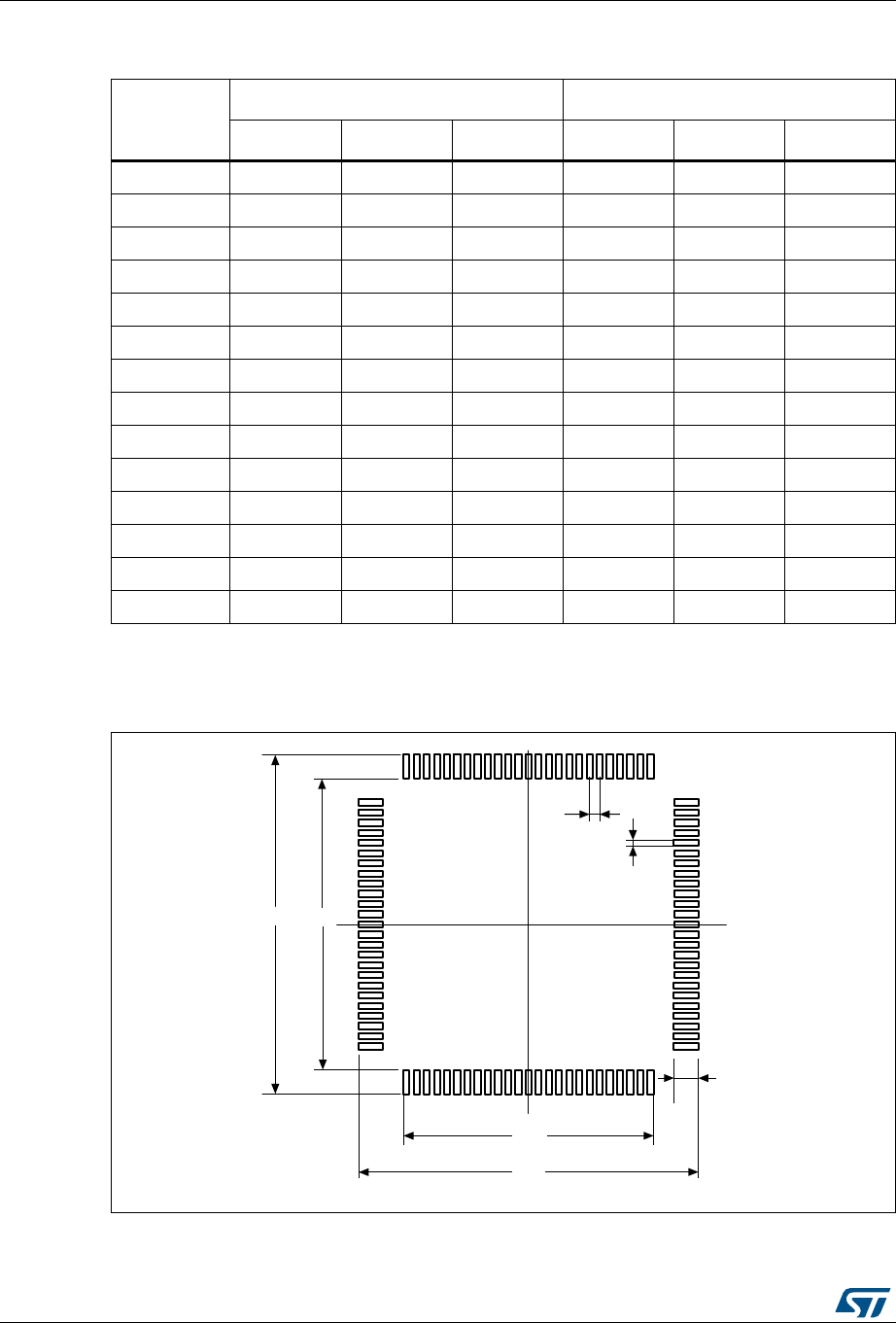
Package information STM32L072xx
122/149 DocID027100 Rev 4
Figure 41. LQFP100 - 100-pin, 14 x 14 mm low-profile quad flat
recommended footprint
1. Dimensions are expressed in millimeters.
A2 1.350 1.400 1.450 0.0531 0.0551 0.0571
b 0.170 0.220 0.270 0.0067 0.0087 0.0106
c 0.090 - 0.200 0.0035 - 0.0079
D 15.800 16.000 16.200 0.6220 0.6299 0.6378
D1 13.800 14.000 14.200 0.5433 0.5512 0.5591
D3 - 12.000 - - 0.4724 -
E 15.800 16.000 16.200 0.6220 0.6299 0.6378
E1 13.800 14.000 14.200 0.5433 0.5512 0.5591
E3 - 12.000 - - 0.4724 -
e - 0.500 - - 0.0197 -
L 0.450 0.600 0.750 0.0177 0.0236 0.0295
L1 - 1.000 - - 0.0394 -
k 0.0° 3.5° 7.0° 0.0° 3.5° 7.0°
ccc - - 0.080 - - 0.0031
1. Values in inches are converted from mm and rounded to 4 decimal digits.
Table 81. LQPF100 - 100-pin, 14 x 14 mm low-profile quad flat package
mechanical data (continued)
Symbol
millimeters inches(1)
Min Typ Max Min Typ Max
AIC
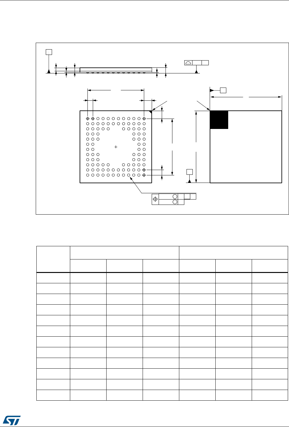
DocID027100 Rev 4 123/149
STM32L072xx Package information
145
7.2 UFBGA100 package information
Figure 42. UFBGA100 - 100-pin, 7 x 7 mm, 0.50 mm pitch, ultra fine pitch ball
grid array package outline
1. Drawing is not to scale.
Table 82. UFBGA100 - 100-pin, 7 x 7 mm, 0.50 mm pitch, ultra fine pitch ball grid array
package mechanical data
Symbol
millimeters inches(1)
Min. Typ. Max. Min. Typ. Max.
A - - 0.600 - - 0.0236
A1 - - 0.110 - - 0.0043
A2 - 0.450 - - 0.0177 -
A3 - 0.130 - - 0.0051 0.0094
A4 - 0.320 - - 0.0126 -
b 0.240 0.290 0.340 0.0094 0.0114 0.0134
D 6.850 7.000 7.150 0.2697 0.2756 0.2815
D1 - 5.500 - - 0.2165 -
E 6.850 7.000 7.150 0.2697 0.2756 0.2815
E1 - 5.500 - - 0.2165 -
e - 0.500 - - 0.0197 -
Z - 0.750 - - 0.0295 -
$&B0(B9
6HDWLQJSODQH
$
H=
=
'
0
EEDOOV
$
(
7239,(:%277209,(:
$EDOO
LGHQWLILHU
H
$
$
<
;
=
GGG =
'
(
HHH =<;
III
0
0=
$
$
$EDOO
LQGH[DUHD
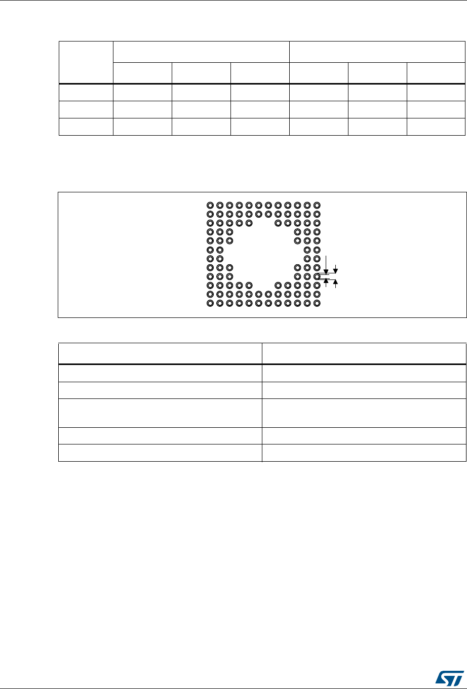
Package information STM32L072xx
124/149 DocID027100 Rev 4
Figure 43. UFBGA100 - 100-pin, 7 x 7 mm, 0.50 mm pitch, ultra fine pitch ball
grid array package recommended footprint
ddd - - 0.080 - - 0.0031
eee - - 0.150 - - 0.0059
fff - - 0.050 - - 0.0020
1. Values in inches are converted from mm and rounded to 4 decimal digits.
Table 83. UFBGA100 recommended PCB design rules (0.5 mm pitch BGA)
Dimension Recommended values
Pitch 0.5
Dpad 0.280 mm
Dsm 0.370 mm typ. (depends on the soldermask
registration tolerance)
Stencil opening 0.280 mm
Stencil thickness Between 0.100 mm and 0.125 mm
Table 82. UFBGA100 - 100-pin, 7 x 7 mm, 0.50 mm pitch, ultra fine pitch ball grid array
package mechanical data (continued)
Symbol
millimeters inches(1)
Min. Typ. Max. Min. Typ. Max.
$&B)3B9
'SDG
'VP
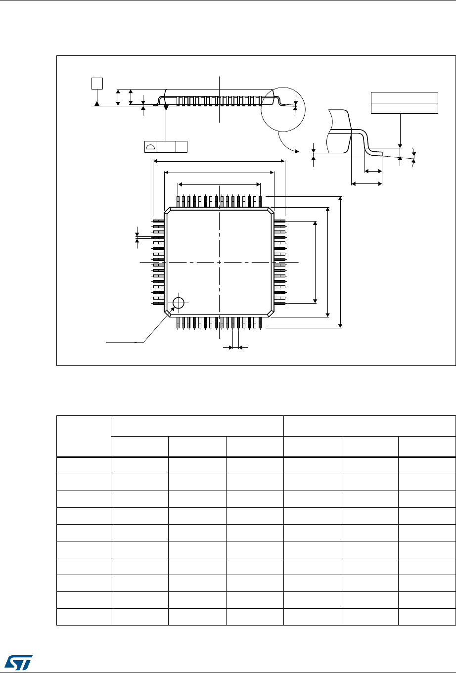
DocID027100 Rev 4 125/149
STM32L072xx Package information
145
7.3 LQFP64 package information
Figure 44. LQFP64 - 64-pin, 10 x 10 mm low-profile quad flat package outline
1. Drawing is not to scale.
Table 84. LQFP64 - 64-pin, 10 x 10 mm low-profile quad flat
package mechanical data
Symbol
millimeters inches(1)
Min Typ Max Min Typ Max
A - - 1.600 - - 0.0630
A1 0.050 - 0.150 0.0020 - 0.0059
A2 1.350 1.400 1.450 0.0531 0.0551 0.0571
b 0.170 0.220 0.270 0.0067 0.0087 0.0106
c 0.090 - 0.200 0.0035 - 0.0079
D - 12.000 - - 0.4724 -
D1 - 10.000 - - 0.3937 -
D3 - 7.500 - - 0.2953 -
E - 12.000 - - 0.4724 -
E1 - 10.000 - - 0.3937 -
:B0(B9
$
$
$
6($7,1*3/$1(
FFF &
E
&
F
$
/
/
.
,'(17,),&$7,21
3,1
'
'
'
H
(
(
(
*$8*(3/$1(
PP
Package information STM32L072xx
126/149 DocID027100 Rev 4
Figure 45. LQFP64 - 64-pin, 10 x 10 mm low-profile quad flat recommended footprint
1. Dimensions are expressed in millimeters.
E3 - 7.500 - - 0.2953 -
e - 0.500 - - 0.0197 -
K 0°3.5°7° 0°3.5°7°
L 0.450 0.600 0.750 0.0177 0.0236 0.0295
L1 - 1.000 - - 0.0394 -
ccc - - 0.080 - - 0.0031
1. Values in inches are converted from mm and rounded to 4 decimal digits.
Table 84. LQFP64 - 64-pin, 10 x 10 mm low-profile quad flat
package mechanical data (continued)
Symbol
millimeters inches(1)
Min Typ Max Min Typ Max
AIC
DocID027100 Rev 4 127/149
STM32L072xx Package information
145
Device marking for LQFP64
The following figure gives an example of topside marking versus pin 1 position identifier
location.
Other optional marking or inset/upset marks, which depend on supply chain operations, are
not indicated below.
Figure 46. LQFP64 marking example (package top view)
1. Parts marked as “ES”, “E” or accompanied by an Engineering Sample notification letter, are not yet
qualified and therefore not approved for use in production. ST is not responsible for any consequences
resulting from such use. In no event will ST be liable for the customer using any of these engineering
samples in production. ST’s Quality department must be contacted prior to any decision to use these
engineering samples to run a qualification activity.
06Y9
5HYLVLRQFRGH
670/
5%7
3URGXFWLGHQWLILFDWLRQ
'DWHFRGH
<::
3LQ
LQGHQWLILHU
5
Package information STM32L072xx
128/149 DocID027100 Rev 4
7.4 UFBGA64 package information
Figure 47. UFBGA64 – 64-ball, 5 x 5 mm, 0.5 mm pitch ultra profile fine pitch
ball grid array package outline
1. Drawing is not to scale.
Table 85. UFBGA64 – 64-ball, 5 x 5 mm, 0.5 mm pitch ultra profile fine pitch
ball grid array package mechanical data
Symbol
millimeters inches(1)
Min Typ Max Min Typ Max
A 0.460 0.530 0.600 0.0181 0.0209 0.0236
A1 0.050 0.080 0.110 0.0020 0.0031 0.0043
A2 0.400 0.450 0.500 0.0157 0.0177 0.0197
A3 0.080 0.130 0.180 0.0031 0.0051 0.0071
A4 0.270 0.320 0.370 0.0106 0.0126 0.0146
b 0.170 0.280 0.330 0.0067 0.0110 0.0130
D 4.850 5.000 5.150 0.1909 0.1969 0.2028
D1 3.450 3.500 3.550 0.1358 0.1378 0.1398
E 4.850 5.000 5.150 0.1909 0.1969 0.2028
E1 3.450 3.500 3.550 0.1358 0.1378 0.1398
e - 0.500 - - 0.0197 -
F 0.700 0.750 0.800 0.0276 0.0295 0.0315
$B0(B9
6HDWLQJSODQH
$
H)
)
'
+
EEDOOV
$
(
7239,(:%277209,(:
H
$
<
;
=
GGG =
'
(
HHH = < ;
III
0
0=
$
$
$EDOO
LGHQWLILHU
$EDOO
LQGH[DUHD
$
DocID027100 Rev 4 129/149
STM32L072xx Package information
145
Figure 48. UFBGA64 – 64-ball, 5 x 5 mm, 0.5 mm pitch ultra profile fine pitch
ball grid array package recommended footprint
ddd - - 0.080 - - 0.0031
eee - - 0.150 - - 0.0059
fff - - 0.050 - - 0.0020
1. Values in inches are converted from mm and rounded to 4 decimal digits.
Table 86. UFBGA64 recommended PCB design rules (0.5 mm pitch BGA)
Dimension Recommended values
Pitch 0.5
Dpad 0.280 mm
Dsm 0.370 mm typ. (depends on the soldermask
registration tolerance)
Stencil opening 0.280 mm
Stencil thickness Between 0.100 mm and 0.125 mm
Pad trace width 0.100 mm
Table 85. UFBGA64 – 64-ball, 5 x 5 mm, 0.5 mm pitch ultra profile fine pitch
ball grid array package mechanical data (continued)
Symbol
millimeters inches(1)
Min Typ Max Min Typ Max
$B)3B9
'SDG
'VP
Package information STM32L072xx
130/149 DocID027100 Rev 4
Device marking for UFBGA64
The following figure gives an example of topside marking versus ball A 1 position identifier
location.
Other optional marking or inset/upset marks, which depend on supply chain operations, are
not indicated below.
Figure 49. UFBGA64 marking example (package top view)
1. Parts marked as “ES”, “E” or accompanied by an Engineering Sample notification letter, are not yet
qualified and therefore not approved for use in production. ST is not responsible for any consequences
resulting from such use. In no event will ST be liable for the customer using any of these engineering
samples in production. ST’s Quality department must be contacted prior to any decision to use these
engineering samples to run a qualification activity.
/5=,
5
<::
06Y9
3URGXFWLGHQWLILFDWLRQ
'DWHFRGH <HDUZHHN
%DOO$
5HYLVLRQ
FRGH
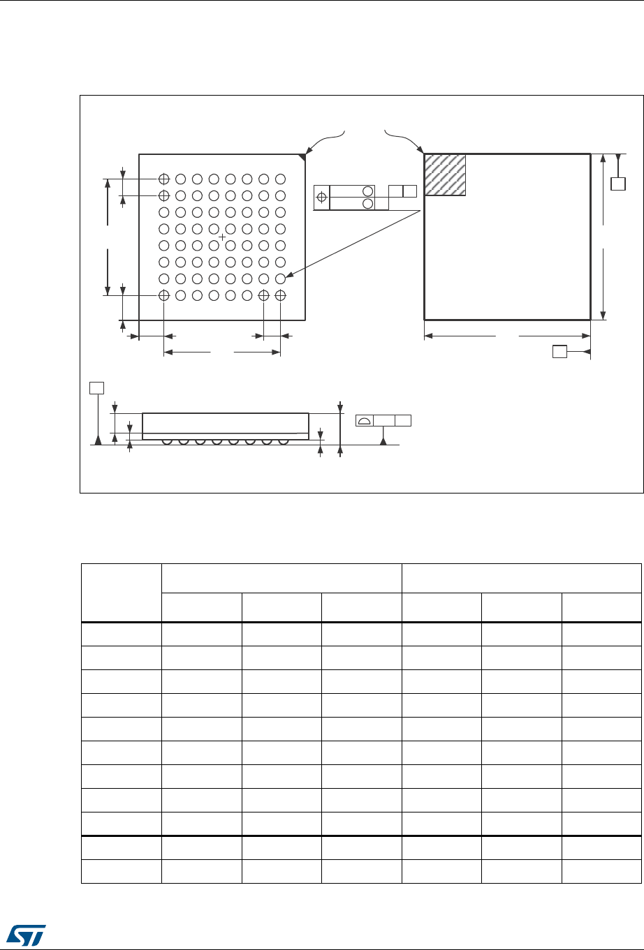
DocID027100 Rev 4 131/149
STM32L072xx Package information
145
7.5 TFBGA64 package information
Figure 50. TFBGA64 – 64-ball, 5 x 5 mm, 0.5 mm pitch thin profile fine pitch ball
grid array package outline
1. Drawing is not to scale.
Table 87. TFBGA64 – 64-ball, 5 x 5 mm, 0.5 mm pitch, thin profile fine pitch ball
grid array package mechanical data
Symbol
millimeters inches(1)
Min Typ Max Min Typ Max
A - - 1.200 - - 0.0472
A1 0.150 - - 0.0059 - -
A2 - 0.200 - - 0.0079 -
A4 - - 0.600 - - 0.0236
b 0.250 0.300 0.350 0.0098 0.0118 0.0138
D 4.850 5.000 5.150 0.1909 0.1969 0.2028
D1 - 3.500 - - 0.1378 -
E 4.850 5.000 5.150 0.1909 0.1969 0.2028
E1 - 3.500 - - 0.1378 -
e - 0.500 - - 0.0197 -
F - 0.750 - - 0.0295 -
5B0(B9
6HDWLQJSODQH
$ $
&
GGG &
$
$
6,'(9,(:
'
(
7239,(:
%
$
$EDOO
LQGH[DUHD
)
+
EEDOOV
$
%277209,(:
H
'
HHH & % $
III
0
0&
$EDOO
LGHQWLILHU
)H
(
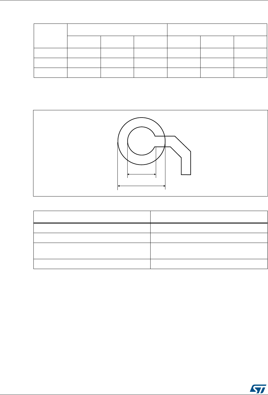
Package information STM32L072xx
132/149 DocID027100 Rev 4
Figure 51. TFBGA64 – 64-ball, 5 x 5 mm, 0.5 mm pitch, thin profile fine pitch ball
,grid array recommended footprint
Note: Non solder mask defined (NSMD) pads are recommended.
4 to 6 mils solder paste screen printing process.
ddd - - 0.080 - - 0.0031
eee - - 0.150 - - 0.0059
fff - - 0.050 - - 0.0020
1. Values in inches are converted from mm and rounded to 4 decimal digits.
Table 88. TFBGA64 recommended PCB design rules (0.5 mm pitch BGA)
Dimension Recommended values
Pitch 0.5
Dpad 0.27 mm
Dsm 0.35 mm typ. (depends on the soldermask
registration tolerance)
Solder paste 0.27 mm aperture diameter.
Table 87. TFBGA64 – 64-ball, 5 x 5 mm, 0.5 mm pitch, thin profile fine pitch ball
grid array package mechanical data (continued)
Symbol
millimeters inches(1)
Min Typ Max Min Typ Max
069
'VP
'SDG
DocID027100 Rev 4 133/149
STM32L072xx Package information
145
Device marking for TFBGA64
The following figure gives an example of topside marking versus ball A 1 position identifier
location.
Other optional marking or inset/upset marks, which depend on supply chain operations, are
not indicated below.
Figure 52. TFBGA64 marking example (package top view)
1. Parts marked as “ES”, “E” or accompanied by an Engineering Sample notification letter, are not yet
qualified and therefore not approved for use in production. ST is not responsible for any consequences
resulting from such use. In no event will ST be liable for the customer using any of these engineering
samples in production. ST’s Quality department must be contacted prior to any decision to use these
engineering samples to run a qualification activity.
/5='
5
<::
06Y9
3URGXFWLGHQWLILFDWLRQ
'DWHFRGH <HDUZHHN
%DOO$
5HYLVLRQ
FRGH
Package information STM32L072xx
134/149 DocID027100 Rev 4
7.6 WLCSP49 package information
Figure 53. WLCSP49 - 49-pin, 3.294 x 3.258 mm, 0.4 mm pitch wafer level chip scale
package outline
1. Drawing is not to scale.
%RWWRPYLHZ
%XPSVLGH 6LGHYLHZ
)URQWYLHZ
7RSYLHZ
:DIHUEDFNVLGH
$EDOOORFDWLRQ
H
)
*
H
H
H (
'
$
$
'HWDLO$
$
EEE =
'HWDLO$
URWDWHG
6HDWLQJSODQH
1RWH
1RWH
%XPS
[
HHH =
2ULHQWDWLRQ
UHIHUHQFH
$
[
'
(
$ $
E
$B0(B9
$
E
DDD
FFF
GGG
=
=
;<
=
DocID027100 Rev 4 135/149
STM32L072xx Package information
145
Figure 54. WLCSP49 - 49-pin, 3.294 x 3.258 mm, 0.4 mm pitch wafer level chip scale
recommended footprint
Table 89. WLCSP49 - 49-pin, 3.294 x 3.258 mm, 0.4 mm pitch wafer level chip scale
package mechanical data
Symbol
millimeters inches(1)
1. Values in inches are converted from mm and rounded to 4 decimal digits.
Min Typ Max Min Typ Max
A 0.525 0.555 0.585 0.0207 0.0219 0.0230
A1 - 0.175 - - 0.0069 -
A2 - 0.380 - - 0.0150 -
A3(2)
2. Back side coating
- 0.025 - - 0.0010 -
b(3)
3. Dimension is measured at the maximum bump diameter parallel to primary datum Z.
0.220 0.250 0.280 0.0087 0.0098 0.0110
D 3.259 3.294 3.329 0.1283 0.1297 0.1311
E 3.223 3.258 3.293 0.1269 0.1283 0.1296
e - 0.400 - - 0.0157 -
e1 - 2.400 - - 0.0945 -
e2 - 2.400 - - 0.0945 -
F - 0.447 - - 0.0176 -
G - 0.429 - - 0.0169 -
aaa - - 0.100 - - 0.0039
bbb - - 0.100 - - 0.0039
ccc - - 0.100 - - 0.0039
ddd - - 0.050 - - 0.0020
eee - - 0.050 - - 0.0020
069
'VP
'SDG
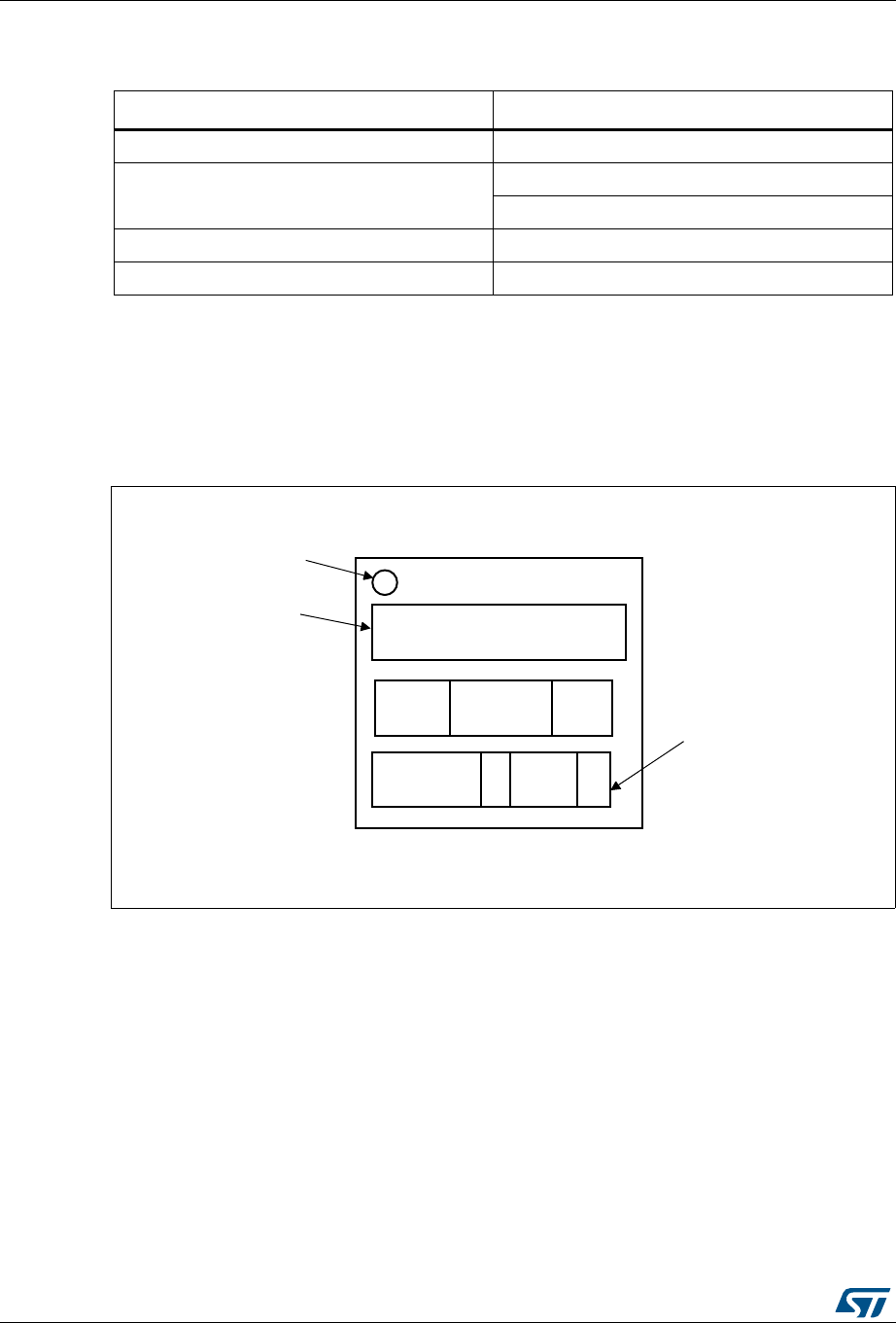
Package information STM32L072xx
136/149 DocID027100 Rev 4
Device marking for WLCSP49
The following figure gives an example of topside marking versus ball A 1 position identifier
location.
Other optional marking or inset/upset marks, which depend on supply chain operations, are
not indicated below.
Figure 55. WLCSP49 marking example (package top view)
1. Parts marked as “ES”, “E” or accompanied by an Engineering Sample notification letter, are not yet
qualified and therefore not approved for use in production. ST is not responsible for any consequences
resulting from such use. In no event will ST be liable for the customer using any of these engineering
samples in production. ST’s Quality department must be contacted prior to any decision to use these
engineering samples to run a qualification activity.
Table 90. WLCSP49 recommended PCB design rules (0.4 mm pitch)
Dimension Recommended values
Pitch 0.4
Dpad
260 µm max. (circular)
220 µm recommended
Dsm 300 µm min. (for 260 µm diameter pad)
PCB pad design Non-solder mask defined via underbump allowed.
06Y9
/&=
< ::
3URGXFWLGHQWLILFDWLRQ
%DOO
LQGHQWLILHU
'DWHFRGH 5HYLVLRQFRGH
5
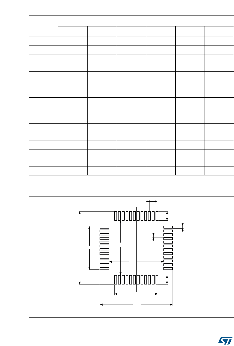
Package information STM32L072xx
138/149 DocID027100 Rev 4
Figure 57. LQFP48 - 48-pin, 7 x 7 mm low-profile quad flat recommended footprint
1. Dimensions are expressed in millimeters.
Table 91. LQFP48 - 48-pin, 7 x 7 mm low-profile quad flat package mechanical data
Symbol
millimeters inches(1)
1. Values in inches are converted from mm and rounded to 4 decimal digits.
Min Typ Max Min Typ Max
A - - 1.600 - - 0.0630
A1 0.050 - 0.150 0.0020 - 0.0059
A2 1.350 1.400 1.450 0.0531 0.0551 0.0571
b 0.170 0.220 0.270 0.0067 0.0087 0.0106
c 0.090 - 0.200 0.0035 - 0.0079
D 8.800 9.000 9.200 0.3465 0.3543 0.3622
D1 6.800 7.000 7.200 0.2677 0.2756 0.2835
D3 - 5.500 - - 0.2165 -
E 8.800 9.000 9.200 0.3465 0.3543 0.3622
E1 6.800 7.000 7.200 0.2677 0.2756 0.2835
E3 - 5.500 - - 0.2165 -
e - 0.500 - - 0.0197 -
L 0.450 0.600 0.750 0.0177 0.0236 0.0295
L1 - 1.000 - - 0.0394 -
k 0°3.5°7° 0°3.5°7°
ccc - - 0.080 - - 0.0031
AID
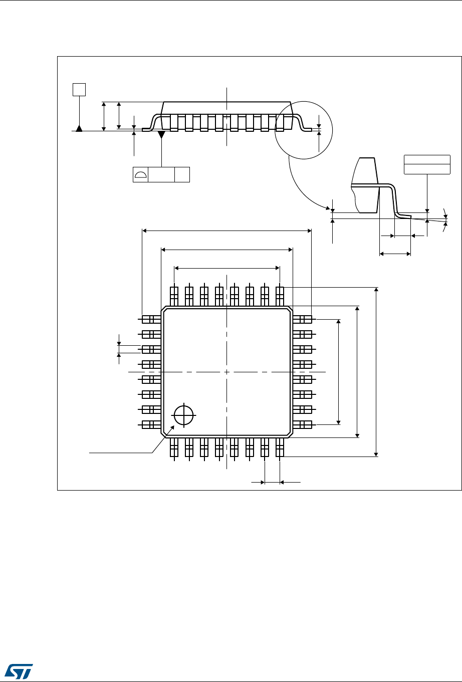
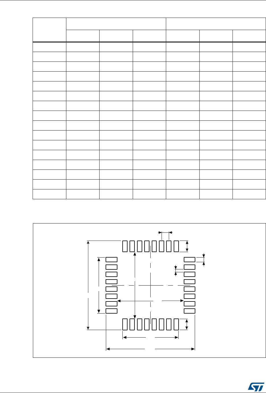
Package information STM32L072xx
140/149 DocID027100 Rev 4
Figure 59. LQFP32 - 32-pin, 7 x 7 mm low-profile quad flat recommended footprint
1. Dimensions are expressed in millimeters.
Table 92. LQFP32 - 32-pin, 7 x 7 mm low-profile quad flat package mechanical data
Symbol
millimeters inches(1)
1. Values in inches are converted from mm and rounded to 4 decimal digits.
Min Typ Max Min Typ Max
A - - 1.600 - - 0.0630
A1 0.050 - 0.150 0.0020 - 0.0059
A2 1.350 1.400 1.450 0.0531 0.0551 0.0571
b 0.300 0.370 0.450 0.0118 0.0146 0.0177
c 0.090 - 0.200 0.0035 - 0.0079
D 8.800 9.000 9.200 0.3465 0.3543 0.3622
D1 6.800 7.000 7.200 0.2677 0.2756 0.2835
D3 - 5.600 - - 0.2205 -
E 8.800 9.000 9.200 0.3465 0.3543 0.3622
E1 6.800 7.000 7.200 0.2677 0.2756 0.2835
E3 - 5.600 - - 0.2205 -
e - 0.800 - - 0.0315 -
L 0.450 0.600 0.750 0.0177 0.0236 0.0295
L1 - 1.000 - - 0.0394 -
k 0°3.5°7° 0°3.5°7°
ccc - - 0.100 - - 0.0039
6?&0?6
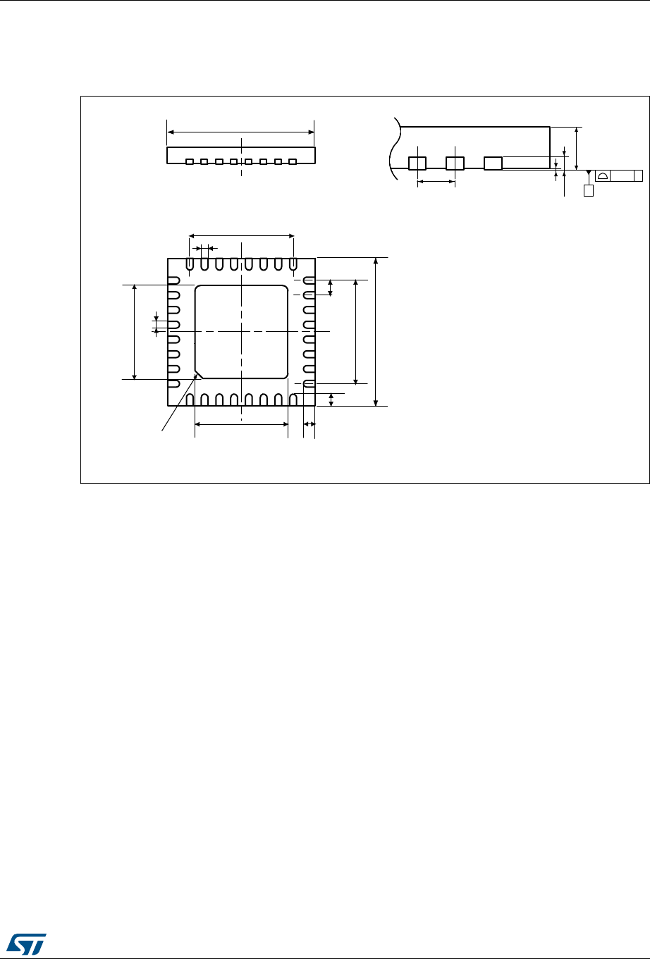
Package information STM32L072xx
142/149 DocID027100 Rev 4
Figure 61. UFQFPN32 - 32-pin, 5x5 mm, 0.5 mm pitch ultra thin fine pitch quad flat
recommended footprint
1. Dimensions are expressed in millimeters.
Table 93. UFQFPN32 - 32-pin, 5x5 mm, 0.5 mm pitch ultra thin fine pitch quad flat
package mechanical data
Symbol
millimeters inches(1)
1. Values in inches are converted from mm and rounded to 4 decimal digits.
Min Typ Max Min Typ Max
A 0.500 0.550 0.600 0.0197 0.0217 0.0236
A1 0.000 0.020 0.050 0.0000 0.0008 0.0020
A3 - 0.152 - - 0.0060 -
b 0.180 0.230 0.280 0.0071 0.0091 0.0110
D 4.900 5.000 5.100 0.1929 0.1969 0.2008
D1 3.400 3.500 3.600 0.1339 0.1378 0.1417
D2 3.400 3.500 3.600 0.1339 0.1378 0.1417
E 4.900 5.000 5.100 0.1929 0.1969 0.2008
E1 3.400 3.500 3.600 0.1339 0.1378 0.1417
E2 3.400 3.500 3.600 0.1339 0.1378 0.1417
e - 0.500 - - 0.0197 -
L 0.300 0.400 0.500 0.0118 0.0157 0.0197
ddd - - 0.080 - - 0.0031
$%B)3B9

DocID027100 Rev 4 143/149
STM32L072xx Package information
145
7.10 Thermal characteristics
The maximum chip-junction temperature, TJ max, in degrees Celsius, may be calculated
using the following equation:
TJ max = TA max + (PD max × Θ
JA)
Where:
•TA max is the maximum ambient temperature in °C,
•Θ
JA is the package junction-to-ambient thermal resistance, in °C/W,
•PD max is the sum of PINT max and PI/O max (PD max = PINT max + PI/Omax),
•PINT max is the product of IDD and VDD, expressed in Watts. This is the maximum chip
internal power.
PI/O max represents the maximum power dissipation on output pins where:
PI/O max = Σ (VOL × IOL) + Σ((VDD – VOH) × IOH),
taking into account the actual VOL / IOL and VOH / IOH of the I/Os at low and high level in the
application.
Table 94. Thermal characteristics
Symbol Parameter Value Unit
Θ
JA
Thermal resistance junction-ambient
UFQFPN32 - 5 x 5 mm / 0.5 mm pitch 36
°C/W
Thermal resistance junction-ambient
LQFP32 - 7 x 7 mm / 0.8 mm pitch 60
Thermal resistance junction-ambient
LQFP48 - 7 x 7 mm / 0.5 mm pitch 54
Thermal resistance junction-ambient
WLCSP49 - 0.4 mm pitch 48
Thermal resistance junction-ambient
TFBGA64 - 5 x 5 mm / 0.5 mm pitch 64
Thermal resistance junction-ambient
UFBGA64 - 5 x 5 mm / 0.5 mm pitch 65
Thermal resistance junction-ambient
LQFP64 - 10 x 10 mm / 0.5 mm pitch 46
Thermal resistance junction-ambient
LQFP100 - 14 x 14 mm / 0.5 mm pitch 41
Thermal resistance junction-ambient
UFBGA100 - 7 x 7 mm / 0.5 mm pitch 57
Package information STM32L072xx
144/149 DocID027100 Rev 4
Figure 62. Thermal resistance
7.10.1 Reference document
JESD51-2 Integrated Circuits Thermal Test Method Environment Conditions - Natural
Convection (Still Air). Available from www.jedec.org.
06Y9
7HPSHUDWXUH&
3'P:
Ϭ
ϱϬϬ
ϭϬϬϬ
ϭϱϬϬ
ϮϬϬϬ
ϮϱϬϬ
ϯϬϬϬ
ϯϱϬϬ
ϰϬϬϬ
ϭϮϱ ϭϬϬ ϳϱ ϱϬ Ϯϱ Ϭ
>Y&Wϲϰ
>Y&Wϰϴ
d&'ϲϰ
>Y&WϭϬϬ
h&'ϭϬϬ
t>^Wϰϵ
hY&EϯϮ
h&'ϲϰ
>Y&WEϯϮ
DocID027100 Rev 4 145/149
STM32L072xx Ordering information
145
8 Ordering information
For a list of available options (speed, package, etc.) or for further information on any aspect
of this device, please contact your nearest ST sales office.
Table 95. STM32L072xx ordering information scheme
Example: STM32 L 072 R 8 T 6 D TR
Device family
STM32 = Arm-based 32-bit microcontroller
Product type
L = Low power
Device subfamily
072 = USB
Pin count
K = 32 pins
C = 48/49 pins
R = 64 pins
V = 100 pins
Flash memory size
8 = 64 Kbytes
B = 128 Kbytes
Z = 192 Kbytes
Package
T = LQFP
H = TFBGA
I = UFBGA
U = UFQFPN
Y = Standard WLCSP pins
Temperature range
6 = Industrial temperature range, –40 to 85 °C
7 = Industrial temperature range, –40 to 105 °C
3 = Industrial temperature range, –40 to 125 °C
Options
No character = VDD range: 1.8 to 3.6 V and BOR enabled
D = VDD range: 1.65 to 3.6 V and BOR disabled
Packing
TR = tape and reel
No character = tray or tube
Revision history STM32L072xx
146/149 DocID027100 Rev 4
9 Revision history
Table 96. Document revision history
Date Revision Changes
02-Sep-2015 1 Initial release
26-Oct-2015 2
Changed confidentiality level to public.
Updated datasheet status to “production data”.
Modified ultra-low-power platform features on cover page.
Added note related to UFQFPN32 in Table 16: STM32L072xxx pin
definition.
In Section 6: Electrical characteristics, updated notes related to
values guaranteed by characterization.
Updated |ΔVSS| definition to include VREF- in Table 23: Voltage
characteristics.
Updated fTRIG and VAIN maximum value, added VREF+ and VREF- in
Table 64: ADC characteristics.
Updated Figure 42: UFBGA100 - 100-pin, 7 x 7 mm, 0.50 mm pitch,
ultra fine pitch ball grid array package outline and Table 82:
UFBGA100 - 100-pin, 7 x 7 mm, 0.50 mm pitch, ultra fine pitch ball
grid array package mechanical data.
Added Section : Device marking for LQFP64.
Add “U” package type in Section 8: Ordering information
DocID027100 Rev 4 147/149
STM32L072xx Revision history
148
22-Mar-2016 3
Updated number of SPIs on cover page and in Table 2: Ultra-low-
power STM32L072xx device features and peripheral counts.
Changed minimum comparator supply voltage to 1.65 V on cover
page. Added minimum DAC supply voltage on cover page.
Added number of fast and standard channels in Section 3.11:
Analog-to-digital converter (ADC).
Updated Section 3.17.2: Universal synchronous/asynchronous
receiver transmitter (USART) and Section 3.17.4: Serial peripheral
interface (SPI)/Inter-integrated sound (I2S) to mention the fact that
USARTs with synchronous mode feature can be used as SPI master
interfaces.
Added baudrate allowing to wake up the MCU from Stop mode in
Section 3.17.2: Universal synchronous/asynchronous receiver
transmitter (USART) and Section 3.17.3: Low-power universal
asynchronous receiver transmitter (LPUART).
Section 6.3.15: 12-bit ADC characteristics:
–Table 64: ADC characteristics:
Distinction made between VDDA for fast and standard channels;
added note 1.
Added note 4. related to RADC.
Updated fTRIG
..
Updated tS and tCONV
.
– Updated equation 1 description.
– Updated Table 65: RAIN max for fADC = 16 MHz for fADC =
16 MHz and distinction made between fast and standard channels.
Updated RO and added Note 2. in Table 67: DAC characteristics.
Added Table 71: USART/LPUART characteristics.
Table 96. Document revision history
Date Revision Changes
Revision history STM32L072xx
148/149 DocID027100 Rev 4
13-Sep-2017 4
Memories and I/Os moved after Core in Features.
Table 2: Ultra-low-power STM32L072xx device features and
peripheral counts: changed number of USART for
LQFP32/UFQFPN32 and added note 3.
Removed column "I/O operation" from Table 3: Functionalities
depending on the operating power supply range and added note
related to GPIO speed.
Updated VDD_USB in Section 3.4.1: Power supply schemes.
In Section 4: Pin descriptions, renamed USB_OE into USB_NOE.
In Section 5: Memory mapping, replaced memory mapping
schematic by reference to the reference manual.
Updated Figure 7: STM32L072xx WLCSP49 ballout.
Added mission profile compliance with JEDEC JESD47 in
Section 6.2: Absolute maximum ratings.
Updated minimum and maximum values of I/O weak pull-up
equivalent resistor (RPU) and weak pull-down equivalent resistor
(RPD) in Table 60: I/O static characteristics.
Updated minimum and maximum values of NRST weak pull-up
equivalent resistor (RPU) in Table 63: NRST pin characteristics.
Added note 2. related to the position of the external capacitor below
Figure 28: Recommended NRST pin protection.
Updated RAIN in Table 64: ADC characteristics.
Updated Figure 33: 12-bit buffered/non-buffered DAC and added
note below figure.
Updated tAF maximum value for range 1 in Table 73: I2C analog filter
characteristics.
Removed Table 90: USART/LPUART characteristics.
NSS timing waveforms updated in Figure 34: SPI timing diagram -
slave mode and CPHA = 0 and Figure 35: SPI timing diagram - slave
mode and CPHA = 1(1).
Updated Figure 50: TFBGA64 – 64-ball, 5 x 5 mm, 0.5 mm pitch thin
profile fine pitch ball grid array package outline.
Added reference to optional marking or inset/upset marks in all
package device marking sections.
Updated note below marking schematics.
Table 96. Document revision history
Date Revision Changes

DocID027100 Rev 4 149/149
STM32L072xx
149
IMPORTANT NOTICE – PLEASE READ CAREFULLY
STMicroelectronics NV and its subsidiaries (“ST”) reserve the right to make changes, corrections, enhancements, modifications, and
improvements to ST products and/or to this document at any time without notice. Purchasers should obtain the latest relevant information on
ST products before placing orders. ST products are sold pursuant to ST’s terms and conditions of sale in place at the time of order
acknowledgement.
Purchasers are solely responsible for the choice, selection, and use of ST products and ST assumes no liability for application assistance or
the design of Purchasers’ products.
No license, express or implied, to any intellectual property right is granted by ST herein.
Resale of ST products with provisions different from the information set forth herein shall void any warranty granted by ST for such product.
ST and the ST logo are trademarks of ST. All other product or service names are the property of their respective owners.
Information in this document supersedes and replaces information previously supplied in any prior versions of this document.
© 2017 STMicroelectronics – All rights reserved
