Jetson TX2 OEM Product Design Guide
User Manual: Pdf
Open the PDF directly: View PDF ![]() .
.
Page Count: 98

JETSON TX2 OEM PRODUCT | DESIGN GUIDE | 20170912 1
OEM PRODUCT DESIGN GUIDE
NVIDIA Jetson TX2
Abstract
This document contains recommendations and guidelines for Engineers to follow to create a product that is optimized
to achieve the best performance from the common interfaces supported by the NVIDIA® Jetson™ TX2 System-on-
Module (SOM).
Note:
Jetson TX2 utilizes Tegra X2 which is a Parker series SoC.

NVIDIA Jetson TX2 OEM Product Design Guide
JETSON TX2 OEM PRODUCT | DESIGN GUIDE | 20170912 2
Document Change History
Date
Description
MAY, 2017
Initial Release
SEP, 2017
Power
- Added pull-up mention for CARRIER_PWR_ON and updated for RESET_OUT# & SLEEP# in Power &
System Pin Descriptions (Table 5 & Table 90 in Appendix)
- Updated Power Block diagram to show pull-ups on CARRIER_PWR_ON, POWER_BTN# & SLEEP# and
added Auto-power-on block & pull-up for CHARGER_PRSNT#
- Added Deep Sleep (SC7) sequence
USB 3.0
- Added Electrical Spec section
- Updated impedance
- Added Trace Spacing for TX/RX non-interleaving section
PCIe
- Removed note under routing guidelines table related to max trace length as this was intended for chi-down
designs, not module based designs.
PCIe/SATA/HDMI
- Removed min spacing between turn requirement from Serpentine section
DSI/CSI guidelines
- Updated max frequency to include separate max speeds for DSI & CSI
- Updated reference plane
- Updated breakout impedance
- Updated main impedance
- Updated max trace delay to include different lengths for 1.0, 1.5 & 2.5 Gbps
HDMI
- Added pre HDMI 1.4b max length/delay requirements
I2C
- Updated notes under I2C signal Connections table to use E_IO_HV, not E_OD_HV.
UART
- Updated UART Connections figure to add strapping information and added caution note below figure
Debug
- Removed external pull-up on JTAG_GP0 (JTAG_TRST_N)
Strapping
- Updated figure, table & notes to remove mention of RAM_CODE[3:2] straps.
Pads
- Updated Schmitt Trigger Usage section to add caution when considering changing settings
Checklist
- Corrected on-module termination for CHARGER_PRSNT# & added RESET_OUT#
- Added check for using pins associated with Tegra straps

NVIDIA Jetson TX2 OEM Product Design Guide
JETSON TX2 OEM PRODUCT | DESIGN GUIDE | 20170912 3
Table of Contents
1.0 INTRODUCTION ....................................................................................................................................................................5
1.1 References .......................................................................................................................................................................5
1.2 Abbreviations and Definitions .......................................................................................................................................5
2.0 JETSON TX2 ..........................................................................................................................................................................6
2.1 Overview ..........................................................................................................................................................................6
3.0 POWER ..................................................................................................................................................................................8
3.1 Supply Allocation ............................................................................................................................................................9
3.2 Main Power Sources/Supplies ..................................................................................................................................... 10
3.3 Power Sequencing ........................................................................................................................................................ 10
3.4 Power Discharge ........................................................................................................................................................... 13
3.5 Power & Voltage Monitoring ........................................................................................................................................ 14
3.6 Deep Sleep (SC7) .......................................................................................................................................................... 15
3.7 Optional Auto-Power-On Support................................................................................................................................ 16
4.0 GENERAL ROUTING GUIDELINES .................................................................................................................................... 18
5.0 USB, PCIE & SATA ............................................................................................................................................................. 20
5.1 USB ................................................................................................................................................................................ 22
5.2 PCIe ................................................................................................................................................................................ 26
5.3 SATA .............................................................................................................................................................................. 30
6.0 GIGABIT ETHERNET .......................................................................................................................................................... 33
7.0 DISPLAY .............................................................................................................................................................................. 35
7.1 MIPI DSI .......................................................................................................................................................................... 35
7.2 eDP / DP / HDMI ............................................................................................................................................................. 38
8.0 MIPI CSI (VIDEO INPUT) ..................................................................................................................................................... 48
9.0 SDIO/SDCARD/EMMC ......................................................................................................................................................... 52
9.1 SD Card .......................................................................................................................................................................... 52
10.0 AUDIO ................................................................................................................................................................................ 55
11.0 WLAN / BT (INTEGRATED) ............................................................................................................................................... 57
12.0 MISCELLANEOUS INTERFACES ..................................................................................................................................... 58
12.1 I2C ................................................................................................................................................................................ 58
12.2 SPI ................................................................................................................................................................................ 60
12.3 UART ............................................................................................................................................................................ 62
12.4 Fan................................................................................................................................................................................ 63
12.5 CAN .............................................................................................................................................................................. 64
12.6 Debug ........................................................................................................................................................................... 66
12.7 Strapping Pins ............................................................................................................................................................. 68
13.0 PADS .................................................................................................................................................................................. 70
13.1 MPIO Pad Behavior when Associated Power Rail is Enabled ................................................................................. 70
13.2 Internal Pull-ups for CZ Type Pins at Power-on ....................................................................................................... 70
13.3 Schmitt Trigger Usage ................................................................................................................................................ 70
13.4 Pins Pulled/Driven High During Power-on ................................................................................................................ 70
13.5 Pad Drive Strength ...................................................................................................................................................... 71
14.0 UNUSED INTERFACE TERMINATIONS ........................................................................................................................... 72

NVIDIA Jetson TX2 OEM Product Design Guide
JETSON TX2 OEM PRODUCT | DESIGN GUIDE | 20170912 4
14.1 Unused MPIO Interfaces ............................................................................................................................................. 72
14.2 Unused SFIO Interface Pins ....................................................................................................................................... 72
15.0 DESIGN CHECKLIST ........................................................................................................................................................ 73
16.0 APPENDIX A: GENERAL LAYOUT GUIDELINES ........................................................................................................... 81
16.1 Overview ...................................................................................................................................................................... 81
16.2 Via Guidelines ............................................................................................................................................................. 81
16.3 Connecting Vias .......................................................................................................................................................... 82
16.4 Trace Guidelines ......................................................................................................................................................... 82
17.0 APPENDIX B: STACK-UPS .............................................................................................................................................. 84
17.1 Reference Design Stack-Ups ..................................................................................................................................... 84
18.0 APPENDIX C: TRANSMISSION LINE PRIMER ................................................................................................................ 85
18.1 Background ................................................................................................................................................................. 85
18.2 Physical Transmission Line Types ........................................................................................................................... 85
18.3 Driver Characteristics ................................................................................................................................................. 86
18.4 Receiver Characteristics ............................................................................................................................................ 86
18.5 Transmission Lines & Reference Planes .................................................................................................................. 86
19.0 APPENDIX D: DESIGN GUIDELINE GLOSSARY ........................................................................................................... 89
20.0 APPENDIX E: JETSON TX2 PIN DESCRIPTIONS .......................................................................................................... 90
NVIDIA Jetson TX2 OEM Product Design Guide
JETSON TX2 OEM PRODUCT | DESIGN GUIDE | 20170912 5
1.0 INTRODUCTION
1.1 References
Refer to the documents or models listed in Table 1 for more information. Use the latest revision of all documents at all times.
Table 1. List of Related Documents
Document
Jetson TX2 Module Data Sheet
Parker Series SoC Technical Reference Manual
Jetson TX1/TX2 Developer Kit Carrier Board Specification
Jetson TX2 Module Pinmux
Jetson TX2 Thermal Design Guide
Jetson TX1/TX2 Developer Kit Carrier Board Design Files
Jetson TX1/TX2 Developer Kit Carrier Board BOM
Jetson TX1/TX2 Developer Kit Camera Module Design Files
Jetson TX1/TX2 Supported Component List
1.2 Abbreviations and Definitions
Table 2 lists abbreviations that may be used throughout this document and their definitions.
Table 2. Abbreviations and Definitions
Abbreviation
Definition
BT
Bluetooth
CEC
Consumer Electronic Control
CAN
Controller Area Network
DP
Display Port
eDP
Embedded Display Port
eMMC
Embedded MMC
GPS
Global Positioning System
HDMI
High Definition Multimedia Interface
I2C
Inter IC
I2S
Inter IC Sound Interface
LCD
Liquid Crystal Display
LDO
Low Dropout (voltage regulator)
LPDDR4
Low Power Double Data Rate DRAM, Fourth-generation
PCIe (PEX)
Peripheral Component Interconnect Express interface
PCM
Pulse Code Modulation
PHY
Physical Interface (i.e. USB PHY)
PMC
Power Management Controller
PMIC
Power Management IC
RF
Radio Frequency
RTC
Real Time Clock
SATA
SDIO
Secure Digital I/O Interface
SPI
Serial Peripheral Interface
UART
Universal Asynchronous Receiver-Transmitter
USB
Universal Serial Bus
WLAN
Wireless Local Area Network
NVIDIA Jetson TX2 OEM Product Design Guide
JETSON TX2 OEM PRODUCT | DESIGN GUIDE | 20170912 6
2.0 JETSON TX2
2.1 Overview
The Jetson TX2 resides at the center of the embedded system solution and includes:
1. Power (PMIC/Regulators, etc.)
2. Ethernet PHY
3. DRAM (LPDDR4)
4. Power & Voltage Monitors
5. eMMC
6. Thermal Sensor
7. Connects to WLAN and Bluetooth enabled devices
In addition, a range of interfaces are available at the main connector for use on the carrier board as shown in the following table.
Table 3. Jetson TX2 Interfaces
Catagory
Function
Catagory
Function
USB
USB 2.0 (3x)
CAN
2x
USB 3.0 (up to 3x) see note
I2C
8x
PCIe
Control [x3] (shared Wake)
UART
5x
PCIe (3 root ports - See note)
SPI
3x
SATA
SATA & Device Sleep control
WLAN/BT/Modem
PEX/UART/I2S, Control/handshake
Camera
CSI (6 x2 or 3 x4), Control, Clock
Touch
Touch Clock, Interrupt & Reset
Display
2x eDP/DP/HDMI
Sensor
Control & Interrupt
DSI (2 x4), Display/Backlight Control
Fan
FAN PWM & Tach Input
Audio
I2S (4x), Control & Clock
Debug
JTAG, UART
Digital Mic & Speaker
System
Power Control, Reset, Alerts
SD Card
SD Card or SDIO
Power
Main Input
LAN
Gigabit Ethernet
Note:
Some USB 3.0 or PCIe instances are shared. Refer to Chapter 5.0 USB, PCIe & SATA for details.
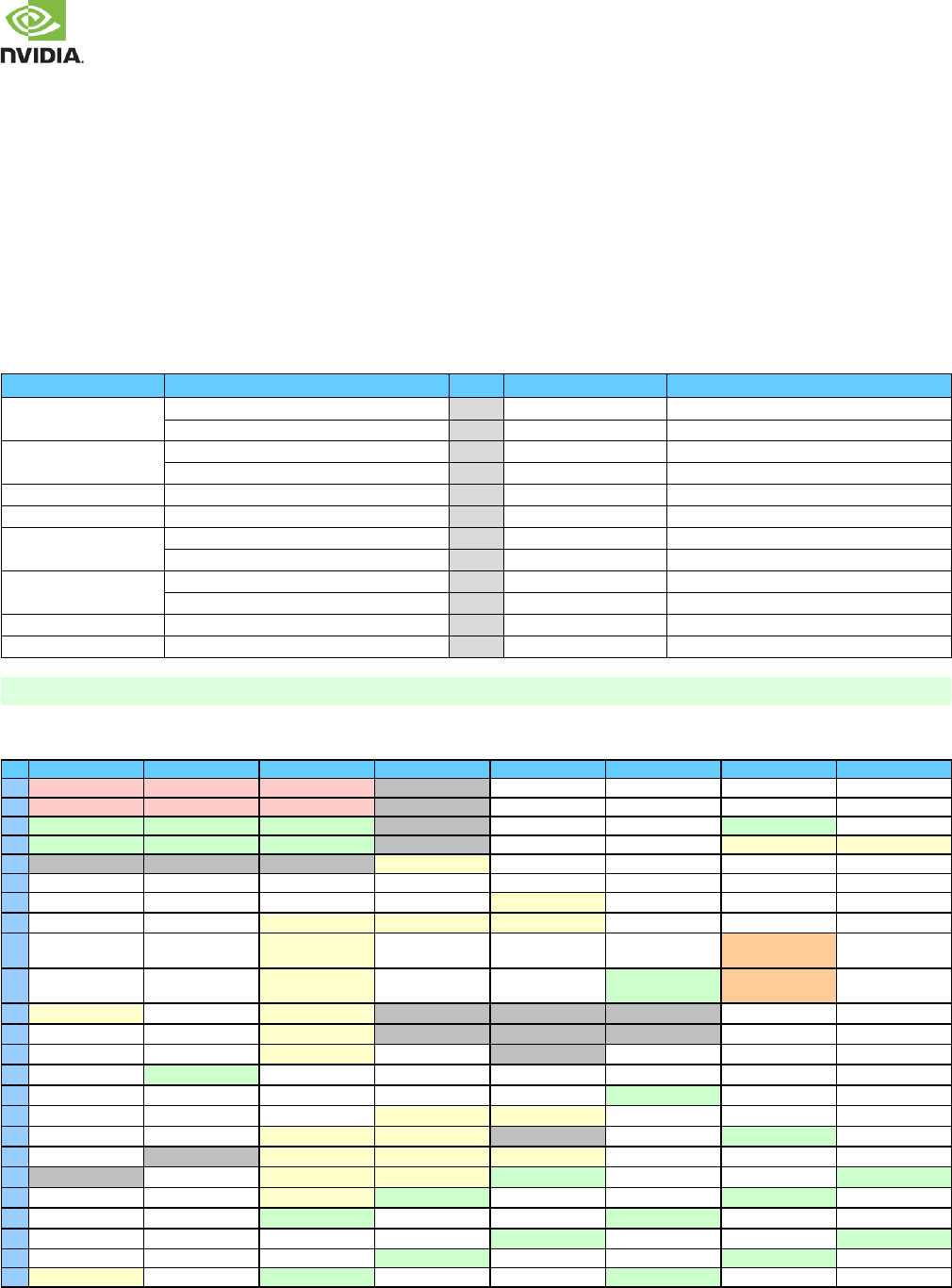
Table 4. Jetson TX2 Connector (8x50) Pin Out Matrix
A
B
C
D
E
F
G
H
1
VDD_IN
VDD_IN
VDD_IN
RSVD
FORCE_RECOV#
AUDIO_MCLK
I2S0_SDIN
I2S0_LRCLK
2
VDD_IN
VDD_IN
VDD_IN
RSVD
SLEEP#
GPIO19_AUD_RST
I2S0_CLK
I2S0_SDOUT
3
GND
GND
GND
RSVD
SPI0_CLK
SPI0_CS0#
GND
GPIO20_AUD_INT
4
GND
GND
GND
RSVD
SPI0_MISO
SPI0_MOSI
DSPK_OUT_CLK
DSPK_OUT_DAT
5
RSVD
RSVD
RSVD
UART7_RX
I2S3_SDIN
I2S3_LRCLK
I2S2_CLK
I2S2_LRCLK
6
I2C_PM_CLK
I2C_PM_DAT
I2C_CAM_CLK
I2C_CAM_DAT
I2S3_CLK
I2S3_SDOUT
I2S2_SDIN
I2S2_SDOUT
7
CHARGING#
CARRIER_STBY#
BATLOW#
GPIO5_CAM_FLASH_EN
CAM2_MCLK
GPIO1_CAM1_PWR#
GPIO4_CAM_STROBE
GPIO3_CAM1_RST#
8
GPIO14_AP_WAKE_MDM
VIN_PWR_BAD#
BATT_OC
UART7_TX
CAM_VSYNC
CAM1_MCLK
GPIO0_CAM0_PWR#
GPIO2_CAM0_RST#
9
GPIO15_AP2MDM_
READY
GPIO17_MDM2AP_
READY
WDT_TIME_OUT#
UART1_TX
UART1_RTS#
CAM0_MCLK
UART3_CTS#
UART3_RX
10
GPIO16_MDM_
WAKE_AP
GPIO18_MDM_COL
DBOOT
I2C_GP2_DAT
UART1_RX
UART1_CTS#
GND
UART3_RTS#
UART3_TX
11
JTAG_GP1
JTAG_TCK
I2C_GP2_CLK
RSVD
RSVD
RSVD
UART0_RTS#
UART0_CTS#
12
JTAG_TMS
JTAG_TDI
I2C_GP3_CLK
RSVD
RSVD
RSVD
UART0_RX
UART0_TX
13
JTAG_TDO
JTAG_GP0
I2C_GP3_DAT
I2S1_LRCLK
RSVD
SPI1_MOSI
SPI1_CLK
GPIO8_ALS_PROX_INT
14
JTAG_RTCK
GND
I2S1_SDIN
I2S1_SDOUT
SPI1_CS0#
SPI1_MISO
GPIO9_MOTION_INT
SPI2_CLK
15
UART2_CTS#
UART2_RX
I2S1_CLK
I2C_GP0_DAT
I2C_GP0_CLK
GND
SPI2_MOSI
SPI2_MISO
16
UART2_RTS#
UART2_TX
FAN_PWM
AO_DMIC_IN_DAT
AO_DMIC_IN_CLK
SPI2_CS1#
SPI2_CS0#
SDCARD_PWR_EN
17
USB0_EN_OC#
FAN_TACH
CAN1_STBY
CAN1_RX
RSVD
SDCARD_CD#
GND
SDCARD_D1
18
USB1_EN_OC#
RSVD
CAN1_TX
CAN0_RX
CAN0_ERR
SDCARD_D3
SDCARD_CLK
SDCARD_D0
19
RSVD
GPIO11_AP_WAKE_BT
CAN1_ERR
CAN0_TX
GND
SDCARD_D2
SDCARD_CMD
GND
20
I2C_GP1_DAT
GPIO10_WIFI_WAKE_AP
CAN_WAKE
GND
CSI5_D1-
SDCARD_WP
GND
CSI4_D1-
21
I2C_GP1_CLK
GPIO12_BT_EN
GND
CSI5_CLK-
CSI5_D1+
GND
CSI4_CLK-
CSI4_D1+
22
GPIO_EXP1_INT
GPIO13_BT_WAKE_AP
CSI5_D0-
CSI5_CLK+
GND
CSI4_D0-
CSI4_CLK+
GND
23
GPIO_EXP0_INT
GPIO7_TOUCH_RST
CSI5_D0+
GND
CSI3_D1-
CSI4_D0+
GND
CSI2_D1-
24
LCD1_BKLT_PWM
TOUCH_CLK
GND
CSI3_CLK-
CSI3_D1+
GND
CSI2_CLK-
CSI2_D1+
NVIDIA Jetson TX2 OEM Product Design Guide
JETSON TX2 OEM PRODUCT | DESIGN GUIDE | 20170912 7
A
B
C
D
E
F
G
H
25
LCD_TE
GPIO6_TOUCH_INT
CSI3_D0-
CSI3_CLK+
GND
CSI2_D0-
CSI2_CLK+
GND
26
GSYNC_HSYNC
LCD_VDD_EN
CSI3_D0+
GND
CSI1_D1-
CSI2_D0+
GND
CSI0_D1-
27
GSYNC_VSYNC
LCD0_BKLT_PWM
GND
CSI1_CLK-
CSI1_D1+
GND
CSI0_CLK-
CSI0_D1+
28
GND
LCD_BKLT_EN
CSI1_D0-
CSI1_CLK+
GND
CSI0_D0-
CSI0_CLK+
GND
29
SDIO_RST#
RSVD
CSI1_D0+
GND
DSI3_D1+
CSI0_D0+
GND
DSI2_D1+
30
RSVD
RSVD
GND
DSI3_CLK+
DSI3_D1-
GND
DSI2_CLK+
DSI2_D1-
31
RSVD
GND
DSI3_D0+
DSI3_CLK
GND
DSI2_D0+
DSI2_CLK-
GND
32
RSVD
RSVD
DSI3_D0-
GND
DSI1_D1+
DSI2_D0-
GND
DSI0_D1+
33
DP1_HPD
HDMI_CEC
GND
DSI1_CLK+
DSI1_D1-
GND
DSI0_CLK+
DSI0_D1-
34
DP1_AUX_CH-
DP0_AUX_CH-
DSI1_D0+
DSI1_CLK
GND
DSI0_D0+
DSI0_CLK-
GND
35
DP1_AUX_CH+
DP0_AUX_CH+
DSI1_D0-
GND
DP1_TX3-
DSI0_D0-
GND
DP0_TX3-
36
USB0_OTG_ID
DP0_HPD
GND
DP1_TX2-
DP1_TX3+
GND
DP0_TX2-
DP0_TX3+
37
GND
USB0_VBUS_DET
DP1_TX1-
DP1_TX2+
GND
DP0_TX1-
DP0_TX2+
GND
38
USB1_D+
GND
DP1_TX1+
GND
DP1_TX0-
DP0_TX1+
GND
DP0_TX0-
39
USB1_D
USB0_D+
GND
PEX_RFU_TX+
DP1_TX0+
GND
PEX_RFU_RX+
DP0_TX0+
40
GND
USB0_D-
PEX2_TX+
PEX_RFU_TX-
GND
PEX2_RX+
PEX_RFU_RX-
GND
41
PEX2_REFCLK+
GND
PEX2_TX-
GND
PEX1_TX+
PEX2_RX-
GND
PEX1_RX+
42
PEX2_REFCLK
USB2_D+
GND
USB_SS1_TX+
PEX1_TX-
GND
USB_SS1_RX+
PEX1_RX-
43
GND
USB2_D-
USB_SS0_TX+
USB_SS1_TX-
GND
USB_SS0_RX+
USB_SS1_RX-
GND
44
PEX0_REFCLK+
GND
USB_SS0_TX-
GND
PEX0_TX+
USB_SS0_RX-
GND
PEX0_RX+
45
PEX0_REFCLK
PEX1_REFCLK+
GND
SATA_TX+
PEX0_TX-
GND
SATA_RX+
PEX0_RX-
46
RESET_OUT#
PEX1_REFCLK-
PEX2_CLKREQ#
SATA_TX-
GND
GBE_LINK1000#
SATA_RX-
GND
47
RESET_IN#
GND
PEX1_CLKREQ#
SATA_DEV_SLP
GBE_LINK_ACT#
GBE_MDI1+
GND
GBE_MDI3+
48
CARRIER_PWR_ON
RSVD
PEX0_CLKREQ#
PEX_WAKE#
GBE_MDI0+
GBE_MDI1-
GBE_MDI2+
GBE_MDI3-
49
CHARGER_PRSNT#
RSVD
PEX0_RST#
PEX2_RST#
GBE_MDI0-
GND
GBE_MDI2-
GND
50
VDD_RTC
POWER_BTN#
RSVD
RSVD
PEX1_RST#
GBE_LINK100#
GND
RSVD
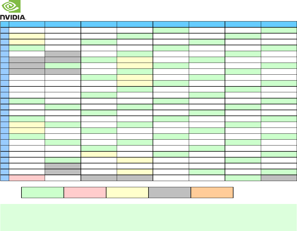
Legend
Ground
Power
Not available on Jetson
TX1
Reserved
Unassigned on carrier
board
Notes:
1. RSVD (Reserved) pins on Jetson TX2 must be left unconnected.
2. Signals starting with “GPIO_” are standard GPIOs that have been assigned recommended usage. If the assigned usage is
required in a design it is recommended the matching GPIO be used. If the assigned usage is not required, the pins may be
used as GPIOs for other purposes.
NVIDIA Jetson TX2 OEM Product Design Guide
JETSON TX2 OEM PRODUCT | DESIGN GUIDE | 20170912 8
3.0 POWER
Caution
Jetson TX2 is not hot-pluggable. Before installing or removing the module, the main power supply
(to VDD_IN pins) must be disconnected and adequate time (recommended > 1 minute) must be
allowed for the various power rails to fully discharge.
Table 5. Jetson TX2 Power & System Pin Descriptions
Pin #
Jetson TX2 Pin Name
Tegra Signal
Usage/Description
Usage on the
Carrier Board
Direction
Pin Type
A1
VDD_IN
Main power Supplies PMIC & external supplies
Main DC input
Input
5.5V-19.6V
A2
VDD_IN
B1
VDD_IN
B2
VDD_IN
C1
VDD_IN
C2
VDD_IN
C7
BATLOW#
(PMIC_GPIO6)
Battery Low (PMIC GPIO)
System
Input
CMOS 1.8V
A48
CARRIER_PWR_ON
Carrier Power On. Used as part of the power up sequence.
The module asserts this signal when it is safe for the carrier
board to power up. -up to VDD_3V3_SYS is
present on the module.
Output
Open-Collector 3.3V
B7
CARRIER_STBY#
SOC_PWR_REQ
Carrier Board Standby: The module drives this signal low
when it is in the standby power state.
Output
CMOS 1.8V
A49
CHARGER_PRSNT#
(PMIC ACOK)
Charger Present. Connected on module to PMIC ACOK
ll-up
internally to MBATT (VDD_5V0_SYS). Can optionally be used
to support auto-power-on where the module platform will
power-on when the main power source is connected instead
of waiting for a power button press.
Input
MBATT level 5.0V
(see note 2)
A7
CHARGING#
(PMIC GPIO5)
Charger Interrupt
Input
CMOS 1.8V
C16
FAN_PWM
GPIO_SEN6
Fan PWM
Fan
Output
CMOS 1.8V
B17
FAN_TACH
UART5_TX
Fan Tachometer
Input
CMOS 1.8V
E1
FORCE_RECOV#
GPIO_SW1
Force Recovery strap pin
System
Input
CMOS 1.8V
B50
POWER_BTN#
POWER_ON / (PMIC
EN0)
Power Button. Used to initiate a system power-on.
-up to
VDD_5V0_SYS. Also connected to Tegra POWER_ON pin
-up to VDD_1V8_AP near
Tegra.
Input
CMOS 5.0V
(see note 2)
A47
RESET_IN#
(PMIC NRST_IO)
Reset In. System Reset driven from PMIC to carrier board for
devices requiring full system reset. Also driven from carrier
board to initiate full system reset (i.e. RESET button). A pull-
up is present on module.
Bidir
Open Drain, 1.8V
A46
RESET_OUT#
SYS_RESET_N
Reset Out. Reset from PMIC (through diodes) to Tegra &
eMMC reset pins. Driven from carrier board to force reset of
Tegra & eMMC (not PMIC). An external 100pull-up to
1.8V near Tegra (module pin side) & external
pull-up to 1.8V on the other side of a diode (PMIC
side).
Bidir
CMOS 1.8V
E2
SLEEP#
GPIO_SW2
Sleep Request to the module from the carrier board. An
internal Tegra pull-up is present on the signal.
Sleep (VOL
DOWN) button
Input
CMOS 1.8V
(see note 2)
B8
VIN_PWR_BAD#
VDD_IN Power Bad. Carrier board indication to the module
that the VDD_IN power is not valid. Carrier board should de-
assert this (drive high) only when VDD_IN has reached its
required voltage level and is stable. This prevents Tegra from
powering up until the VDD_IN power is stable.
System
Input
CMOS 5.0V
C9
WDT_TIME_OUT#
GPIO_SEN7
Watchdog Timeout
Input
CMOS 1.8V
A50
VDD_RTC
(PMIC BBATT)
Real-Time-Clock. Optionally used to provide back-up power
for RTC. Connects to Lithium Cell or super capacitor on
Carrier Board. PMIC is supply when charging cap or coin cell.
Super cap or coin cell is source when system is disconnected
from power.
Battery Back-up
using Super-
capacitor
Bidir
1.65V-5.5V
C8
BATT_OC
BATT_OC
Battery Over-current (& Thermal) warning
Bidir
CMOS 1.8V
Note:
1. Power efficiency is higher when the input voltage is lower, such as 9V or 12V. At very low voltages (close to the 5.5V
minimum), the power supported by some of the supplies may be reduced.
2. These pins are handled as Open-Drain on the carrier board.
NVIDIA Jetson TX2 OEM Product Design Guide
JETSON TX2 OEM PRODUCT | DESIGN GUIDE | 20170912 9
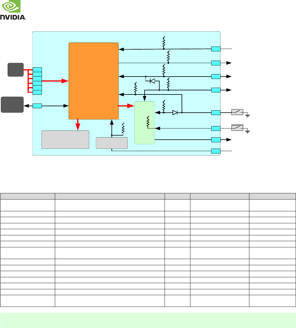
Figure 1. Power Block Diagram
Jetson TX2
DC
Jack A1
A2
B1
B2
C1
C2
A50
Memory/Peripherals
LPDDR4, eMMC,
Ethernet, WiFi / BT
Power Subsystem
5V/3.3V Pre-Regs
PMU Switchers/LDOs
CPU/GPU Regs
Ext. LDOs
Load Switches
Tegra
VDD_RTC
VDD_IN
B8
E2
B50
A47
A46
A48
VIN_PWR_BAD#
CARRIER_PWR_ON
RESET_IN#
RESET_OUT#
POWER_BTN#
SLEEP#
CARRIER_STBY#
CHARGER_PRSNT#
B7
From Carrier Board main
power input & discharge circuit
To Carrier Board power subsystem
System Reset to/from Carrier Board
Tegra Force Reset from Carrier Board
Optional Sleep Button
To Carrier Board to disable devices/
rails to be off in sleep mode
SLEEP
Optional Power Button
POWER
Super Cap
or Li Cell
(Optional)
A49 Optional signal from Carrier Board
to support Auto-Power-On
PU
PU
PU
Auto-power-
on Circuit
PU
ACOK
PU
PU
PU
PU
3.1 Supply Allocation
Table 6 Jetson TX2 Internal Power Subsystem Allocation
Power Rails
Usage
(V)
Power Supply
Source
VDD_5V0_SYS
Supplies various switchers & load switches that power
the various circuits & peripherals on Jetson TX2.
5.0
5V DC-DC
VDD_IN
VDD_CPU
Tegra MCPU/BCPU
1.0 (Var)
OpenVREG (uP1666QQKF)
VDD_5V0_SYS
VDD_GPU & VDD_SRAM
Tegra GPU & SRAM
1.0 (Var)
OpenVREG (uP1666QQKF)
VDD_5V0_SYS
VDD_SOC (CORE)
Tegra Core
1.0 (Var)
OpenVREG (uP1666QQKF)
VDD_5V0_SYS
VDD_DDR_1V1_PMIC
LPDDR4
1.125
PMIC Switcher SD0
VDD_5V0_SYS
AVDD_DSI_CSI_1V2
Source for some DSI/CSI blocks
1.2
PMIC Switcher SD1
VDD_5V0_SYS
VDD_1V8
Tegra, eMMC, WLAN
1.8
PMIC Switcher SD2
VDD_5V0_SYS
VDD_3V3_SYS
Supplies various LDOs & load switches that in turn
power the various circuits & peripherals on Jetson TX2.
3.3
PMIC Switcher SD3
VDD_5V0_SYS
VDDIO_3V3_AOHV
Tegra VDDIO_AO_HV rail
3.3
PMIC LDO 2
VDD_5V0_SYS
VDDIO_SDMMC1_AP
Tegra SD Card I/O rail
1.8/3.3
PMIC LDO 3
VDD_5V0_SYS
VDD_RTC (See note)
Tegra Real Time Clock/Always-on Rail
1.0 (Var)
PMIC LDO 4
VDD_1V8
VDDIO_SDMMC3_AP
Tegra SDIO rail
1.8/3.3
PMIC LDO 5
VDD_5V0_SYS
VDD_HDMI_1V05
Tegra HDMI / DP rail
1.0
PMIC LDO 7
AVDD_DSI_CSI_1V2
VDD_PEX_1V05
Tegra PCIe / USB 3.0 / SATA rail
1.0
PMIC LDO 8
AVDD_DSI_CSI_1V2
VDD_1V8_AP (&
VDD_1V8_AP_PLL)
Main 1.8V Tegra rail
1.8
Load Switch
VDD_1V8
Note:
This is the Tegra supply, and should not be confused with Jetson TX2 VDD_RTC pin which is the supply that connects to the
PMIC BBATT pin to keep the Real-Time Clock powered.
NVIDIA Jetson TX2 OEM Product Design Guide
JETSON TX2 OEM PRODUCT | DESIGN GUIDE | 20170912 10
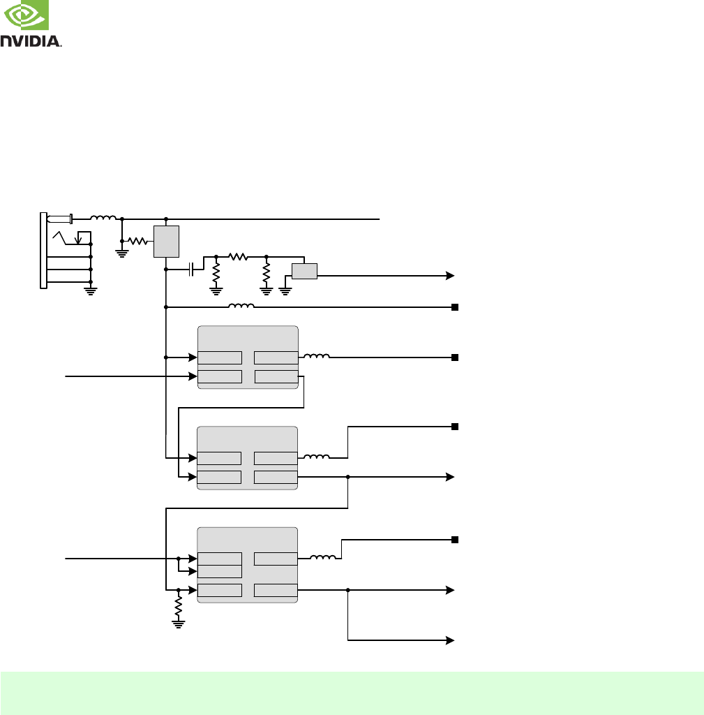
3.2 Main Power Sources/Supplies
The figure below shows the power connections used on the carrier board, including the DC Jack which connects to the 5.5V-
19.6V AC/DC adapter, and the main 5.0V, 3.3V and 1.8V supplies. Also shown are the power control signals that are used to
enable these supplies, or are used to communicate power sequence information to Jetson TX2 or other circuitry on the carrier
board (i.e. discharge circuits).
Figure 2. Main Power Source/Supply Connections
VDD_19V_IN
(5.5V-19.6V)
VIN_PWR_BAD#
VDD_MOD
TPS53015
DC-DC SWVIN
CARRIER_PWR_ON PGEN
3V3_SYS_BUCK_EN
TPS53015
DC-DC SWVIN
PGEN VDD_3V3_SYS_PG
VDD_3V3_SYS
To Jetson TX2 VDD_IN
From
Jetson TX2
To Jetson TX2 & Power
Discharge Circuitry
Main Carrier
Board 5V Supply
Main Carrier Board
3.3V Supply
Main 3.3V Power Good – Routed
to Power LED on Carrier board
DC Jack
G
DS FET
G
DS FET
APW8805
OpenVReg
VIN SW
PGOOD
VDD_5V0_IO_SYS
VCC
1V8_IO_PG
EN/FS
VDD_1V8
1V8_IO_VREG_EN
RESET_OUT#
Main Carrier Board
1.8V Supply
To Jetson TX2 (RESET_OUT#)
to keep Tegra in Reset until
1.8V rail Valid
Main 3.3V Power Good – Routed
to Power LED on Carrier board
From Main
5V supply
G
S
D
PWR
FET
G
S
D
PWR
FET
L7
L6
U31
U16
U9
VDD_5V0_IO_SYS
Note
The figure above is a high-level representation of the connections involved. Refer to the Jetson
TX1/TX2 carrier board reference design for details.
3.3 Power Sequencing
In order to ensure reliable and consistent power up sequencing, the pins VIN_PWR_BAD#, CARRIER_PWR_ON, and
RESET_OUT# on Jetson TX2 connector should be connected and used as described below:
VIN_PWR_BAD# signal is generated by the Carrier Board and passed to Jetson TX2 to keep the Tegra processor powered off
until the VDD_IN supply is stable and it is possible to power up any standby circuits on Jetson TX2. This signal prevents the
Tegra processor from powering up prematurely before the Carrier Board has charged up its decoupling capacitors and power to
Jetson TX2 is stable
CARRIER_PWR_ON signal is generated by Jetson TX2 and passed to the Carrier Board to indicate that Jetson TX2 is powered
up and that the power up sequence for the Carrier Board circuits can begin.
RESET_OUT# is de-asserted by the Carrier Board after a period sufficient to allow the Carrier Board circuits to power up.
NVIDIA Jetson TX2 OEM Product Design Guide
JETSON TX2 OEM PRODUCT | DESIGN GUIDE | 20170912 11
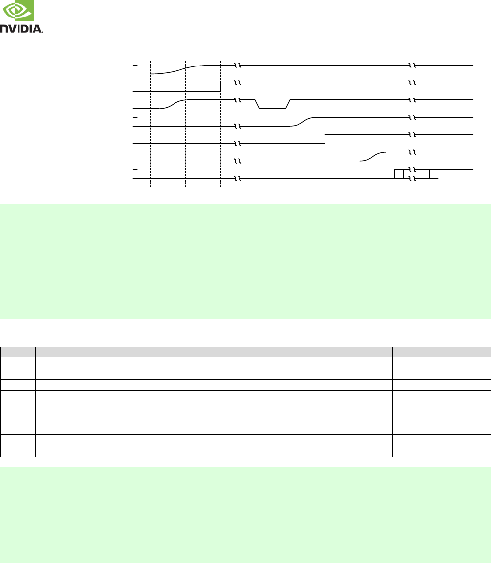
Figure 3. Power Up Sequence
CARRIER_PWR_ON
POWER_BTN#
VIN_PWR_BAD#
VDD_IN
Carrier Board VDD_1V8 (note 1)
Jetson TX2 System Power (Main 1.8V
rail most IF pins are associated with)
1234567
RESET_OUT# (note 2)
8
Note:
1. The 1.8V supply on the carrier board associated with MPIO pins common to Jetson TX2 must not be enabled unless the
Jetson TX2 main 1.8V rail is on. In addition, the carrier board should keep RESET_OUT# low until this 1.8V supply is valid.
On the P2597, this is accomplished by connecting the VDD_1V8 supply PGOOD signal to RESET_OUT#.
2. Inactive when both PMIC Reset is inactive (high) & VDD_1V8 PGOOD is active (high)
3. During run time if any Jetson TX2 I/O rail is switched OFF or ON, the following sequences should be performed. Violating
these sequences will result in extra in-rush current during the rail transition.
- OFF Sequence: The associated NO_IOPOWER bit in the PMC APBDEV_PMC_NO_IOPOWER_0 register must be enabled before the
I/O Rail is powered OFF
- ON Sequence. After an I/O Rail is powered ON, the associated NO_IOPOWER bit in the PMC APBDEV_PMC_NO_IOPOWER_0
Table 7. Power Up Sequence Timing Relationships
Timing
Parameter
Min
Typ
Max
Units
Notes
t1-2
VDD_IN On to POWER_BTN# Pull-up (PMIC) active
8.8
ms
1
t2-3
VDD_IN On to VIN_PWR_BAD# inactive
54
ms
2
t3-4
VIN_PWR_BAD# inactive to POWER_BTN# active
0
See Notes
ms
3
t4-5
POWER_BTN# active time
50
ms
3
t4-6
POWER_BTN# active to CARRIER_PWR_ON active
38.6
ms
t5-6
Jetson TX2 System Power On to CARRIER_PWR_ON
8
ms
t6-7
CARRIER_PWR_ON active to Carrier Board System Power Enabled
0
6.6
ms
4
t6-8
CARRIER_PWR_ON to On-Module PMIC Reset Inactive
77.4
ms
5
RESET_IN# active time
50
ms
6
Note:
1. Measured from VDD_IN ramp start to POWER_BTN# ramp start. Carrier board dependent.
2. Typical value using NVIDIA P2597, measured from VDD_IN ramp start to VIN_PWR_BAD# inactive start. Carrier board
dependent.
3. User Dependent if POWER_BTN# connected to button. Otherwise, carrier board dependent.
4. Typical value measured using NVIDIA P2597. Carrier board dependent
5. Typical value using P2597. Carrier board dependent.
6. User Dependent if RESET_IN# connected to button. Otherwise, carrier board dependent. Not shown in Power up
sequence figure.
NVIDIA Jetson TX2 OEM Product Design Guide
JETSON TX2 OEM PRODUCT | DESIGN GUIDE | 20170912 12
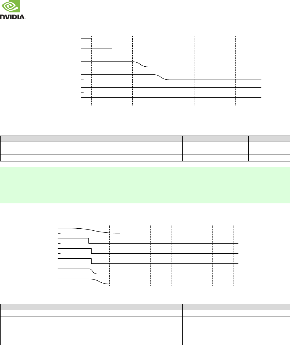
Figure 4. Power Down Sequence (Controlled Case)
CARRIER_PWR_ON
VIN_PWR_BAD#
VDD_IN
Carrier Board System Power (1.8V
used for pins shared w/Jetson TX2)
Jetson TX2 System Power (Main 1.8V rail
most IF pins are associated with)
RESET_OUT#
123456789
Table 8. Power Down Sequence Timing Relationships (Controlled Case)
Table 9. Power Down Sequence Timing Relationships (Controlled Case)
Timing
Parameter
Min
Typ
Max
Units
Notes
t1-2
RESET_OUT# active to CARRIER_PWR_ON inactive
3.76
mS
1
t2-3
CARRIER_PWR_ON inactive to carrier board system power off
0.46
ms
2
t2-4
CARRIER_PWR_ON inactive to Jetson TX2 System Power (main 1.8V rail) Off
1.24
mS
3
Note:
1. Measured from RESET_OUT# active to CARRIER_PWR_ON to inactive ramp down start.
2. Typical value measured using NVIDIA P2597. Measured from CARRIER_PWR_ON to carrier board VDD_1V8 ramp down
start. Carrier board dependent.
3. Typical value measured using NVIDIA P2597. Measured from CARRIER_PWR_ON ramp down start to Jetson TX2 main
1.8V ramp down start.
Figure 5. Power Down Sequence (Uncontrolled Power Removal Case)
CARRIER_PWR_ON
VIN_PWR_BAD#
VDD_IN
Carrier Board System Power
Jetson TX2 System Power
RESET_OUT#
123456789
Table 10. Power Down Sequence Timing Relationships (Uncontrolled Power Removal Case)
Timing
Parameter
Min
Typ
Max
Units
Notes
t1
VDD_IN Removed in uncontrolled manner
t2
asserted to start uncontrolled power-down sequence.
RESET_OUT# & CARRIER_PWR_ON are driven low via
PMIC sequence soon after. Carrier board power &
Jetson TX2 power begin to ramp down.
Carrier board power (mainly 1.8V rail
associated with interface pins connected to
Jetson TX2) should ramp down faster so it is
off before the Jetson TX2 main 1.8V rail is
off.
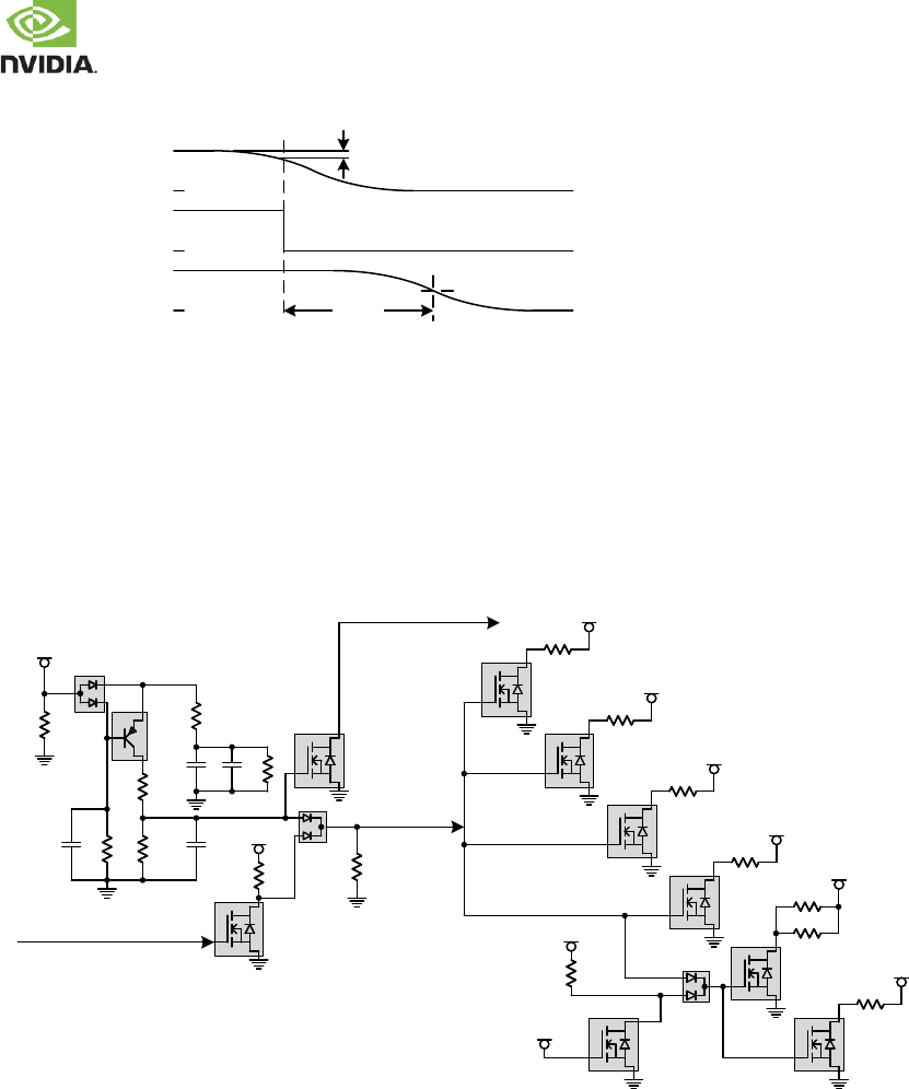
Removal of the VDD_IN/VDD_MUX supply causes VIN_PWR_BAD# to go active which causes Jetson TX2 to initiate a
controlled shut down. The controlled shut down takes ~20ms to complete so the internal PMIC supply needs to stay above
~2.9v for >~20ms. The USB0_OTG_ID pin is a pin which can be monitored to see the state of the internal PMIC supply level.
NVIDIA Jetson TX2 OEM Product Design Guide
JETSON TX2 OEM PRODUCT | DESIGN GUIDE | 20170912 13
Figure 6. VIN_PWR_BAD# Detection Test Circuit for Uncontrolled Power-down Case
VIN_PWR_BAD#
VDD_IN
~20%
droop
Voltage measured at
USB0_OTG_ID pin
2.9V
>20ms
3.4 Power Discharge
In order to meet the Power Down requirements, discharge circuitry is required. In the figure below the DISCHARGE signal is
generated, based on a transition of the CARRIER_POWER_ON signal or the removal of the main supply (VDD_MUX/VDD_IN).
When DISCHARGE is asserted, VDD_5V0_IO_SYS, VDD_3V3_SYS, VDD_1V8 and VDD_3V3_SLP are forced to GND in a
controlled manner. Removal of the VDD_MUX supply also causes VIN_PWR_BAD# to go active which causes Jetson TX2 to
initiate a controlled shut down.
Figure 7. Power Discharge
VDD_MUX
10uF
1uF
G
S
D
G
S
D
10k10k
10uF
10k10k
10M10M
0
100k100k
DISCHARGE
VIN_PWR_BAD#
(Jetson TX2 Pin B8)
47k47k
VDD_MUX
CARRIER_PWR_ON
(Jetson TX2 pin A48)
BAT54ALT1
BAT54CW
MMBT
4403
NTR4003
NT1G
NTR4001
NT1G
E
B
C
G
S
D
G
S
D
4.7uF
Tol.
100k100k
100k100k
G
S
D
G
S
D
G
S
D
G
S
D
G
S
D
G
S
D
G
S
D
G
S
D
G
S
D
G
S
D
G
S
D
G
S
D
G
S
D
G
S
D
G
S
D
G
S
D
G
S
D
G
S
D
100100
VDD_5V0_IO_SYS
4747
VDD_3V3_SYS
3636
VDD_1V8
4747
VDD_3V3_SLP
NTR4003
NT1G
NTR4003
NT1G
NTR4003
NT1G
NTR4003
NT1G
VDD_12V_SLP
VDD_5V0_IO_SLP
100100
G
S
D
G
S
D
G
S
D
470470
FDV301N
NTR4003
NT1G
NTR4003
NT1G
BAT54CW
470470
75k75k
VDD_3V3_SLP
VDD_5V0_IO_SYS
NVIDIA Jetson TX2 OEM Product Design Guide
JETSON TX2 OEM PRODUCT | DESIGN GUIDE | 20170912 14
3.5 Power & Voltage Monitoring
3.5.1 Power Monitor
Power monitors are provided on Jetson TX2. These monitor the main DC, CPU, GPU/SRAM, SOC (CORE) & DDR Supplies.
The monitors will toggle a WARN (warning) output, or a CRIT (critical) output, depending on the power “seen” at the sense
resistors and the thresholds set for each supply.
Figure 8. Power Monitor (GPU/SRAM, SOC & WLAN)
Sense
Resistors
GEN1_I2C_SDA
GEN1_I2C_SCL
INA3221AIRGVR
Power Monitor GPU_INA_P
0805
0.1uF
GPU_INA_M
VDD_3V3_SYS
GPU Supply Monitor
SOC Supply Monitor
Wi-Fi Supply Monitor
GEN1_I2C
(PU to 3.3V) SOC_INA_P
0805
SOC_INA_M
WIFI_INA_P
0603
WIFI_INA_M
1010
1010
1010
1010
1010
1010
VIN1P
VIN1N
WARN
CRIT
VS
AO
PV
TC
VPU
GND
SCL
SDA
PAD
VIN2P
VIN2N
VIN3P
VIN3N
Tegra GPIO_MDM6
VDD_IN
VDD_IN
VDD_SYS_SOC_IN
(SOC supply input)
VDD_SYS_GPU_IN
(GPU supply input)
VDD_3V8_WIFI_SENSE
VDD_5V0_SYS
1uF
1uF
1uF
100k100kVDD_1V8
INA_WIFI_THERM_WARN_L
Figure 9. Power Monitor (VDD_IN, CPU & DDR)
Sense
Resistors
GEN1_I2C_SDA
GEN1_I2C_SCL
INA3221AIRGVR
Power Monitor VDD_IN_SENSE
3012
0.1uF
VDD_IN_PREREG_SENSE
VDD_3V3_SYS
VDD_IN Supply Monitor
CPU Supply Monitor
DDR Supply Monitor
GEN1_I2C
(PU to 3.3V) CPU_INA_P
0805
CPU_INA_M
SRAM_INA_P
0603
SRAM_INA_M
1010
1010
1010
1010
1010
1010
VIN1P
VIN1N
WARN
CRIT
VS
AO
PV
TC
VPU
GND
SCL
SDA
PAD
VIN2P
VIN2N
VIN3P
VIN3N
Tegra BATT_OC
VDD_IN_RS
VDD_IN
VDD_SYS_CPU_IN
(CPU supply input)
VDD_IN
VDD_5V0_SD0
(DDR supply input)
VDD_5V0_SYS
1uF
1uF
1uF
100k100kVDD_1V8
INA_PREREG_THERM_WARN_L
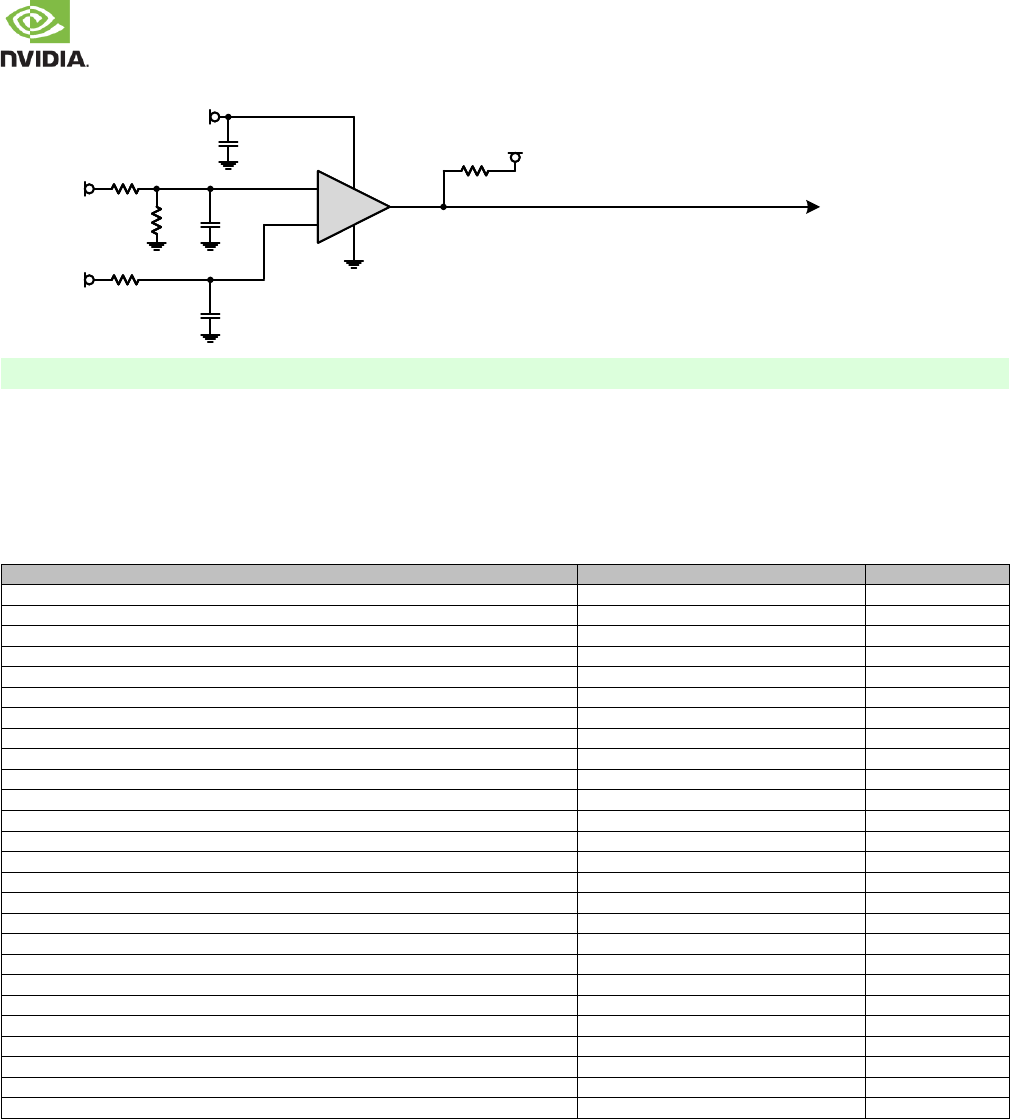
3.5.2 Voltage Monitor
A voltage monitor circuit is implemented on Jetson TX2 to indicate if the main DC input rail, VDD_IN, “droops” below an
acceptable level. The device used will react quickly and generate an alert to one of the Tegra SOC_THERM capable pins
(VCOMP_ALERT). The voltage monitor circuit is implemented with a fast voltage comparator supplied by VDD_IN with a 1.8V
(VDD_1V8) reference common with the Tegra IO domain that receives the output signal. This device has an open drain active
low output which is pulled low when the VDD_IN voltage drops below the selected threshold.
NVIDIA Jetson TX2 OEM Product Design Guide
JETSON TX2 OEM PRODUCT | DESIGN GUIDE | 20170912 15
Figure 10. Voltage Monitor Connections
VDD_IN
VDD_1V8
VDD_5V0_SYS
34k,1%34k,1%
49.9k
1%
49.9k
1%
110k,1%110k,1%
COMP_SOC_THERM* (Tegra VCOMP_ALERT)VOUT
IN_POS
IN_NEG
VCC
VEE
+
VOUT
IN_POS
IN_NEG
VCC
VEE
+
100k100k1.8V
Note:
The threshold for VDD_IN, determined by the voltage divider components used in the circuit above is 5.75V.
3.6 Deep Sleep (SC7)
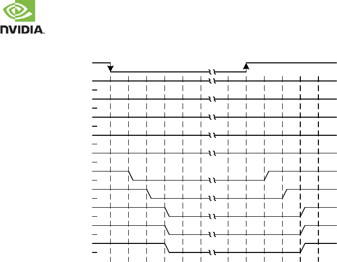
Jetson TX2 supports a low power state called Deep Sleep or SC7. This can be entered under software control, and exited using
various mechanisms, including wake capable pins that are listed in the table below.
Table 11. Jetson TX2 Signal Wake Events
Potential Wake Event (Reference Design Signal)
Jetson TX2 Pin Assigned
Wake #
PCIe Wake Request (PEX_WAKE#)
PEX_WAKE#
1
Bluetooth Wake AP (BT2_WAKE_AP Secondary)
GPIO13_BT_WAKE_AP
8
WLAN Wake AP (WIFI_WAKE_AP - Secondary)
GPIO10_WIFI_WAKE_AP
9
Thermal/Over-current Warning
BATT_OC
10
Audio Codec Interrupt (AUD_INT_L)
GPIO20_AUD_INT
12
DP 0 Hot Plug Detect (DP_AUX_CH0_HPD)
DP0_HPD
19
HDMI Consumer Electronic Control (HDMI_CEC)
HDMI_CEC
20
DP 1 Hot Plug Detect (DP_AUX_CH1_HPD)
DP1_HPD
21
Camera Vertical Sync (CAM_VSYNC)
CAM_VSYNC
23
POWER_BTN#
POWER_BTN#
29
Motion Interrupt (MOTION_INT)
GPIO9_MOTION_INT
46
CAN 1 Error (CAN1_ERR)
CAN1_ERR
47
CAN Wake (CAN_WAKE)
CAN_WAKE
48
CAN 0 Error (CAN0_ERR)
CAN0_ERR
49
Touch Interrupt (TOUCH_INT)
GPIO6_TOUCH_INT
51
USB VBUS Detect (USB_VBUS_DET)
USB0_VBUS_DET
53
GPIO Expansion 0 Interrupt (GPIO_EXP0_INT)
GPIO_EXP0_INT
54
Modem Wake AP (MDM_WAKE_AP)
GPIO16_MDM_WAKE_AP
55
Battery Low (BATLOW#)
BATLOW#
56
GPIO Expansion 1 Interrupt (GPIO_EXP1_INT)
GPIO_EXP1_INT
58
USB Vbus Enable 0 (USB_VBUS_EN0)
USB_VBUS_EN0
61
USB Vbus Enable 1 (USB_VBUS_EN1)
USB_VBUS_EN1
62
Ambient Light Proximity Interrupt (ALS_PROX_INT)
GPIO8_ALS_PROX_INT
63
Modem Coldboot (MDM_COLDBOOT)
GPIO18_MDM_COLDBOOT
64
Force Recovery (FORCE_RECOV#)
FORCE_RECOV#
67
Sleep (SLEEP_L)
SLEEP#
68
NVIDIA Jetson TX2 OEM Product Design Guide
JETSON TX2 OEM PRODUCT | DESIGN GUIDE | 20170912 16
Figure 11. Deep Sleep (SC7) Entry/Exit Sequence
CARRIER_PWR_ON
VIN_PWR_BAD#
VDD_IN
RESET_OUT#
SC7 Entry SC7 Exit
CARRIER_STBY#
(Tegra X2 SOC_PWR_REQ)
VDD_3V3_SLP
VDD_5V0_SLP
VDD_12V_SLP
VDD_5V0_HDMI_CON
SC7 Entry/Exit Trigger
Carrier Board VDD_1V8
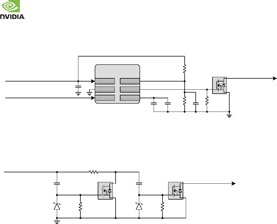
3.7 Optional Auto-Power-On Support
Jetson TX2 includes circuitry on the module to support Auto-Power-On. This allows the platform to power on when VDD_IN is
first powered, instead of waiting for a power button press. In order to enable this feature, the CHARGER_PRSNT# pin should
be tied to GND.
This section provides guidance for modifying a carrier board design to power the platform on when VDD_IN is first powered,
instead of waiting for a power button press. In order to power the system on without a power button, a specific sequence is
required between the time the VDD_IN power (5.5V-19.6V) is connected and the CHARGER_PRSNT# pin on Jetson TX2 is
driven low. The CHARGER_PRSNT# pin connects to the Jetson TX2 PMIC and requires a minimum delay of 300ms from the
point VDD_IN reaches its minimum level (5.5V) before it can be driven low. Four options to meet this requirement and allow
Auto-Power-On are described:
▪ Built-in Auto-Power-On circuit: Not available on Jetson TX1.
▪ Microcontroller: Recommended if a microcontroller is already being used to control power-on.
▪ Supervisor IC: Using a supervisor IC and related discrete devices to meet the sequencing requirements.
▪ Discrete Circuit: Circuit using only discrete devices to meet the sequencing requirements
Built-in Auto-Power-On circuit
Jetson TX2 includes circuitry on the module to support Auto-Power-On. In order to enable this feature, the
CHARGER_PRSNT# pin should be tied to GND. This option is not compatible with Jetson TX1 which does not have this
circuitry.
Microcontroller
If a microcontroller is already present on the carrier board and is used to power the system on when the main power source is
connected, then it can be used to support Auto-Power-On with the following conditions:
▪ After the microcontroller is out of reset wait 300ms before driving CHARGER_PRSNT# low or pulsing
POWER_BTN# low
▪ If the POWER_BTN# pin is used, it should be held low for a time period between 50ms & 5sec.
▪ If the CHARGER_PRSNT# pin is used, it should be held low for >200us
NVIDIA Jetson TX2 OEM Product Design Guide
JETSON TX2 OEM PRODUCT | DESIGN GUIDE | 20170912 17
Supervisor IC
The figure below shows a circuit that includes a supervisor IC. This circuit meets the sequence requirement to leave
CHARGER_PRSNT# floating until VDD_IN is on plus the delay mentioned above (>300ms) then driving the signal low. The
circuit works across the full range of VDD_IN (5.5V to 19.6V).
Supervisor
MAX16053AUT
IN
CDELAY
VCC
OUT
5.5V-19.6V Input Supply CHARGER_PRSNT#
EN
0.1uF22nF
0.1uF 2N7002W
SOT323
GND
VIN_PWR_BAD#
10nF
90.9k,1%
10k,1%
G
S
D
100k,1%
Discrete Circuit
The figure below shows a circuit using only discrete components. This circuit also meets the sequence requirement to keep
CHARGER_PRSNT# floating until VDD_IN is on plus the delay mentioned above (>300ms) before driving it low. The circuit
assumes the VDD_IN ramp slew rate is faster than 7 V/S. In order to meet the full supported range for VDD_IN (5.5V to 19.6V),
the turn-on delay can be as long as 4sec. For a narrower VDD_IN range, the delay can be optimized (reduced).
5.5V-19.6V Input Supply
CHARGER_PRSNT#
4.7uF G
S
D
470k
G
S
D
10k
470k
4.7uF
NTS4001
NT1G
SOT323
NTS4001
NT1G
SOT323
RB521S30
T1G, 30V
SOD523
RB521S30
T1G, 30V
SOD523
NVIDIA Jetson TX2 OEM Product Design Guide
JETSON TX2 OEM PRODUCT | DESIGN GUIDE | 20170912 18
4.0 GENERAL ROUTING GUIDELINES
Signal Name Conventions
The following conventions are used in describing the signals for Jetson TX2:
▪ Signal names use a mnemonic to represent the function of the signal. For example, Secure Digital Interface #3
Command signal is represented as SDCARD_CMD, written in bold to distinguish it from other text. All active low
signals are identified by a # or an underscore followed by capital N (_N) after the signal name. For example,
RESET_IN# indicates an active low signal. Active high signals do not have the underscore-N (_N) after the signal
names. For example, SDCARD_CMD indicates an active high signal. Differential signals are identified as a pair
with the same names that end with _P & _N, just P & N or + & - (for positive and negative, respectively). For
example, USB1_DP and USB1_DN indicate a differential signal pair.
▪ I/O Type The signal I/O type is represented as a code to indicate the operational characteristics of the signal. The
table below lists the I/O codes used in the signal description tables.
Table 12. Signal Type Codes
Code
Definition
A
Analog
DIFF I/O
Bidirectional Differential Input/Output
DIFF IN
Differential Input
DIFF OUT
Differential Output
I/O
Bidirectional Input/Output
I
Input
O
Output
OD
Open Drain Output
I/OD
Bidirectional Input / Open Drain Output
P
Power
Routing Guideline Format
The routing guidelines have the following format to specify how a signal should be routed.
▪ Breakout traces are traces routed from a BGA or other pin array, either to a point beyond the array, or to another
layer where full normal spacing guidelines can be met. Breakout trace delay limited to 500 mils unless otherwise
specified.
▪ After breakout, signal should be routed according to specified impedance for differential, single-ended, or both (for
example: HDMI). Trace spacing to other signals also specified.
▪ Follow max & min trace delays where specified. Trace delays are typically shown in mm or in terms of signal delay
in pico-seconds (ps) or both.
- For differential signals, trace spacing to other signals must be larger of specified × dielectric height or inter-
pair spacing
- Spacing to other signals/pairs cannot be smaller than spacing between complementary signals (intra-pair).
- Total trace delay depends on signal velocity which is different between outer (microstrip) & inner (stripline)
layers of a PCB.
NVIDIA Jetson TX2 OEM Product Design Guide
JETSON TX2 OEM PRODUCT | DESIGN GUIDE | 20170912 19
Signal Routing Conventions
Throughout this document, the following signal routing conventions are used:
SE Impedance (/ Diff Impedance) at x Dielectric Height Spacing
▪ Single-ended (SE) impedance of trace (along with differential impedance for diff pairs) is achieved by spacing
requirement. Spacing is multiple of dielectric height. Dielectric height is typically different for microstrip & stripline.
Note: 1 mil = 1/1000th of an inch.
Note:
Trace spacing requirement applies to SE traces or differential pairs to other SE traces or differential pairs. It does not apply to
traces making up a differential pair. For this case, spacing/trace widths are chosen to meet differential impedance
requirement.
General Routing Guidelines
Pay close attention when routing high speed interfaces, such as HDMI/DP, USB 3.0, PCIe or DSI/CSI. Each of these interfaces
has strict routing rules for the trace impedance, width, spacing, total delay, and delay/flight time matching. The following
guidelines provide an overview of the routing guidelines and notations used in this document.
▪ Controlled Impedance
Each interface has different trace impedance requirements & spacing to other traces. It is up to designer to
calculate trace width & spacing required to achieve specified single-ended (SE) & differential (Diff) impedances.
Unless otherwise noted, trace impedance values are ±15%.
▪ Max Trace Lengths/Delays
Trace lengths/delays should include main PCB routing and any additional routing on a Flex/ secondary PCB
segment connected to main PCB. The max length/delay should be from Jetson TX2 to the actual connector (i.e.
USB, HDMI, SD Card, etc.) or device (i.e. onboard USB device, Display driver IC, camera imager IC, etc.)
▪ Trace Delay/Flight Time Matching
Signal flight time is the time it takes for a signal to propagate from one end (driver) to other end (receiver). One
way to get same flight time for signal within signal group is to match trace lengths within specified delay in the
signal group.
- Total trace delay = Carrier PCB trace delay only. Do not exceed maximum trace delay specified.
- For six layers or more, it is recommended to match trace delays based on flight time of signals. For example,
outer-layer signal velocity could be 150psi (ps/inch) & inner-layer 180psi. If one signal is routed 10 inches on
outer layer & second signal is routed 10 inches in inner layer, difference in flight time between two signals will
be 300ps! That is a big difference if required matching is 15ps (trace delay matching). To fix this, inner trace
needs to be 1.7 inches shorter or outer trace needs to be 2 inches longer.
- In this design guide, terms such as intra-pair & inter-pair are used when describing differential pair delay.
Intra-pair refers to matching traces within differential pair (for example, true to complement trace matching).
Inter-pair matching refers to matching differential pairs average delays to other differential pairs average
delays.
General PCB Routing Guidelines
For GSSG stack-up to minimize crosstalk, signal should be routed in such a way that they are not on top of each
other in two routing layers (see diagram to right)
G
G
S
S
Do not route other signals or power traces/areas directly under or over critical high-speed interface signals.
Note:
The requiements detailed in the Interface Signal Routing Requirements tables must be met for
all interfaces implemented or proper operation cannot be guaranteed.
NVIDIA Jetson TX2 OEM Product Design Guide
JETSON TX2 OEM PRODUCT | DESIGN GUIDE | 20170912 20
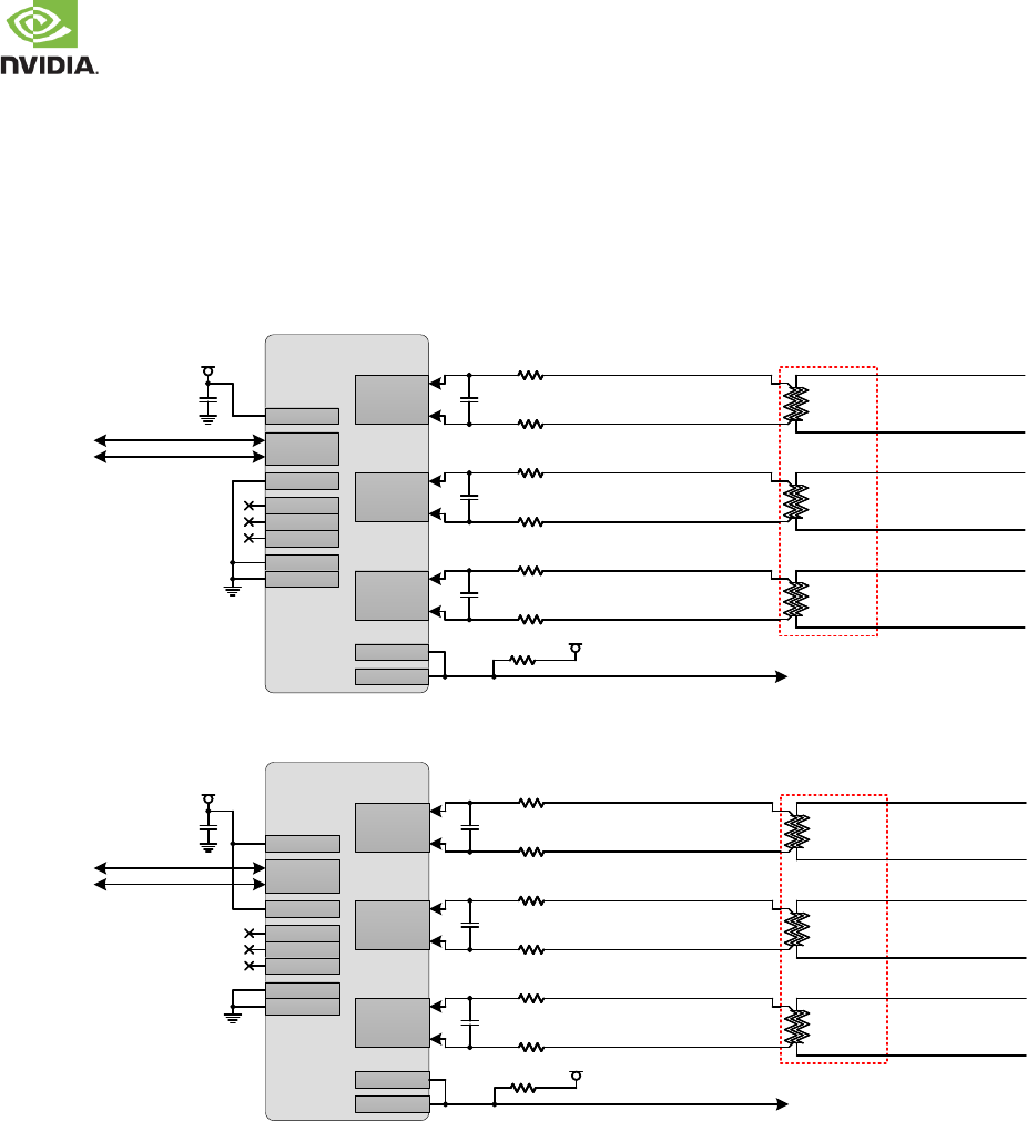
5.0 USB, PCIE & SATA
The Jetson TX2 allows multiple USB 3.0 & PCIe interfaces, and a single SATA interface to be brought out on the module. In
some cases, these interfaces are multiplexed on some of the module pins. The tables below show several ways to bring out as
many of the USB 3.0 or PCIe interfaces as possible to meet different design requirements. The first table covers many of the
combinations possible on designs built around Jetson TX2 only. The second table covers the combinations possible for both
Jetson TX2 and previous/future pin compatible modules.
Table 13. Jetson TX2 USB 2.0 Pin Descriptions
Pin #
Jetson TX2 Pin Name
Tegra Signal
Usage/Description
Usage on Carrier
Board
Direction
Pin Type
B40
USB0_D
USB0_DN
USB 2.0 Port 0 Data
USB 2.0 Micro AB
Bidir
USB PHY
B39
USB0_D+
USB0_DP
USB 2.0 Port 0 Data+
Bidir
A17
USB0_EN_OC#
USB_VBUS_EN0
USB VBUS Enable/Overcurrent 0
Bidir
Open Drain 3.3V
A36
USB0_OTG_ID
(PMIC GPIO0)
USB 0 ID
Input
Analog
B37
USB0_VBUS_DET
UART5_CTS
USB 0 VBUS Detect
Input
USB VBUS, 5V
A39
USB1_D
USB1_DN
USB 2.0, Port 1 Data
USB 3.0 Type A
Bidir
USB PHY
A38
USB1_D+
USB1_DP
USB 2.0, Port 1 Data+
Bidir
A18
USB1_EN_OC#
USB_VBUS_EN1
USB VBUS Enable/Overcurrent 1
Bidir
Open Drain 3.3V
B43
USB2_D
USB2_DN
USB 2.0, Port 2 Data
M.2 Key E
Bidir
USB PHY
B42
USB2_D+
USB2_DP
USB 2.0, Port 2 Data+
Bidir
Table 14. Jetson TX2 USB 3.0, PCIe & SATA Pin Descriptions
Pin #
Jetson TX2 Pin Name
Tegra Signal
Usage/Description
Usage on the Carrier
Board
Direction
Pin Type
A44
PEX0_REFCLK+
PEX_CLK1P
PCIe 0 Reference Clock+ (PCIe IF #0)
PCIe x4 Connector
Output
PCIe PHY
A45
PEX0_REFCLK
PEX_CLK1N
PCIe 0 Reference Clock (PCIe IF #0)
Output
C48
PEX0_CLKREQ#
PEX_L0_CLKREQ_N
PCIe 0 Clock Request (PCIe IF #0)
Bidir
Open Drain 3.3V, Pull-up on
the module
C49
PEX0_RST#
PEX_L0_RST_N
PCIe 0 Reset (PCIe IF #0)
Output
H44
PEX0_RX+
PEX_RX4P
PCIe 0 Lane 0 Receive+ (PCIe IF #0)
Input
PCIe PHY, AC-Coupled on
carrier board
H45
PEX0_RX
PEX_RX4N
PCIe 0 Lane 0 Receive (PCIe IF #0)
Input
E44
PEX0_TX+
PEX_TX4P
PCIe 0 Lane 0 Transmit+ (PCIe IF #0)
Output
E45
PEX0_TX
PEX_TX4N
PCIe 0 Lane 0 Transmit (PCIe IF #0)
Output
G42
USB_SS1_RX+
PEX_RX2P
USB SS 1 Receive+ (USB 3.0 Port #2 or
PCIe IF #0 Lane 1)
Input
G43
USB_SS1_RX
PEX_RX2N
USB SS 1 Receive (USB 3.0 Port #2 or
PCIe #0 Lane 1)
Input
D42
USB_SS1_TX+
PEX_TX2P
USB SS 1 Transmit+ (USB 3.0 Port #2 or
PCIe IF #0 Lane 1)
Output
D43
USB_SS1_TX
PEX_TX2N
USB SS 1 Transmit (USB 3.0 Port #2 or
PCIe #0 Lane 1)
Output
F40
PEX2_RX+
PEX_RX3P
PCIe 2 Receive+ (PCIe IF #0 Lane 2 or PCIe
IF #1 Lane 0)
Input
F41
PEX2_RX
PEX_RX3N
PCIe 2 Receive (PCIe IF #0 Lane 2 or PCIe
IF #1 Lane 0)
Input
C40
PEX2_TX+
PEX_TX3P
PCIe 2 Transmit+ (PCIe IF #0 Lane 2 or
PCIe IF #1 Lane 0)
Output
C41
PEX2_TX
PEX_TX3N
PCIe 2 Transmit (PCIe IF #0 Lane 2 or
PCIe IF #1 Lane 0)
Output
G39
PEX_RFU_RX+
PEX_RX1P
PCIe RFU Receive+ (PCIe IF #0 Lane 3 or
USB 3.0 Port #1)
Input
G40
PEX_RFU_RX
PEX_RX1N
PCIe RFU Receive (PCIe IF #0 Lane 3 or
USB 3.0 Port #1)
Input
D39
PEX_RFU_TX+
PEX_TX1P
PCIe RFU Transmit+ (PCIe IF #0 Lane 3 or
USB 3.0 Port #1)
Output
D40
PEX_RFU_TX
PEX_TX1N
PCIe RFU Transmit (PCIe IF #0 Lane 3 or
USB 3.0 Port #1)
Output
D48
PEX_WAKE#
PEX_WAKE_N
PCIe Wake
PCIe x4 conn & M.2
Input
Open Drain 3.3V, Pull-up on
the module
NVIDIA Jetson TX2 OEM Product Design Guide
JETSON TX2 OEM PRODUCT | DESIGN GUIDE | 20170912 21
Pin #
Jetson TX2 Pin Name
Tegra Signal
Usage/Description
Usage on the Carrier
Board
Direction
Pin Type
B45
PEX1_REFCLK+
PEX_CLK3P
PCIe Reference Clock 1+ (PCIe IF #2)
M.2 Key E
Output
PCIe PHY
B46
PEX1_REFCLK
PEX_CLK3N
PCIe Reference Clock 1 (PCIe IF #2)
Output
C47
PEX1_CLKREQ#
PEX_L2_CLKREQ_N
PCIE 1 Clock Request (mux option - PCIe IF
#2)
Bidir
Open Drain 3.3V, Pull-up on
the module
E50
PEX1_RST#
PEX_L2_RST_N
PCIe 1 Reset (PCIe IF #2)
Output
H41
PEX1_RX+
PEX_RX0P
PCIe 1 Receive+ (PCIe #2 Lane 0 muxed
w/USB 3.0 Port #0)
USB 3.0 Type A
(Default) or M.2 Key E
Input
PCIe PHY, AC-Coupled on
carrier board
H42
PEX1_RX
PEX_RX0N
PCIe 1 Receive (PCIe #2 Lane 0 muxed
w/USB 3.0 Port #0)
Input
E41
PEX1_TX+
PEX_TX0P
PCIe 1 Transmit+ (PCIe #2 Lane 0 muxed
w/USB 3.0 Port #0)
Output
E42
PEX1_TX
PEX_TX0N
PCIe 1 Transmit (PCIe #2 Lane 0 muxed
w/USB 3.0 Port #0)
Output
A41
PEX2_REFCLK+
PEX_CLK2P
PCIe 2 Reference Clock+ (PCIe IF #1)
Unassigned
Output
PCIe PHY
A42
PEX2_REFCLK
PEX_CLK2N
PCIe 2 Reference Clock (PCIe IF #1)
Output
C46
PEX2_CLKREQ#
PEX_L1_CLKREQ_N
PCIE 2 Clock Request (PCIe IF #1)
Bidir
Open Drain 3.3V, Pull-up on
the module
D49
PEX2_RST#
PEX_L1_RST_N
PCIe 2 Reset (PCIe IF #1)
Output
F43
USB_SS0_RX+
PEX_RX0P
USB SS 0 Receive+ (USB 3.0 Port #0 muxed
w/PCIe #2 Lane 0)
USB 3.0 Type A
Input
USB SS PHY, AC-Coupled
(off the module)
F44
USB_SS0_RX
PEX_RX0N
USB SS 0 Receive (USB 3.0 Port #0 muxed
w/PCIe #2 Lane 0)
Input
C43
USB_SS0_TX+
PEX_TX0P
USB SS 0 Transmit+ (USB 3.0 Port #0
muxed w/PCIe #2 Lane 0)
Output
USB SS PHY, AC-Coupled on
carrier board
C44
USB_SS0_TX
PEX_TX0N
USB SS 0 Transmit (USB 3.0 Port #0
muxed w/PCIe #2 Lane 0)
Output
G45
SATA_RX+
PEX_RX5P
SATA Receive+
SATA Connector
Input
SATA PHY, AC-Coupled on
carrier board
G46
SATA_RX
PEX_RX5N
SATA Receive
Input
D45
SATA_TX+
PEX_TX5P
SATA Transmit+
Output
D46
SATA_TX
PEX_TX5N
SATA Transmit
Output
D47
SATA_DEV_SLP
PEX_L2_CLKREQ_N
SATA Device Sleep or PEX1_CLKREQ#
(PCIe IF #2) depending on Mux setting
Input
Open Drain 3.3V, Pull-up on
the module
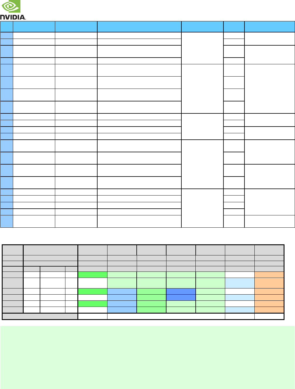
Table 15. Jetson TX2 USB 3.0, PCIe & SATA Lane Mapping Configurations
Jetson TX2 Pin Names
PEX1
PEX_RFU
PEX2
USB_SS1
PEX0
USB_SS0
(see note 1)
SATA
Tegra Lanes
Lane 0
Lane 1
Lane 3
Lane 2
Lane 4
Lane 5
Avail. Outputs from Jetson TX2
Configs
USB 3.0
PCIe
SATA
1
0
1x1 + 1x4
1
PCIe#2_0
PCIe#0_3
PCIe#0_2
PCIe#0_1
PCIe#0_0
SATA
2 (CB
Default)
1
1x4
1
PCIe#0_3
PCIe#0_2
PCIe#0_1
PCIe#0_0
USB_SS#0
SATA
3
2
3x1
1
PCIe#2_0
USB_SS#1
PCIe#1_0
USB_SS#2
PCIe#0_0
SATA
4
3
2x1
1
USB_SS#1
PCIe#1_0
USB_SS#2
PCIe#0_0
USB_SS#0
SATA
5
1
2x1 + 1x2
1
PCIe#2_0
USB_SS#1
PCIe#1_0
PCIe#0_1
PCIe#0_0
SATA
6
2
1x1 + 1x2
1
USB_SS#1
PCIe#1_0
PCIe#0_1
PCIe#0_0
USB_SS#0
SATA
Default Usage on CB (carrier board)
Unused
X4 PCIe Connector
USB 3 Type A
SATA
Note:
1. PCIe interface #2 can be brought to the PEX1 pins, or USB 3.0 port #1 to the USB_SS0 pins on Jetson TX2 depending on
the setting of a multiplexor on the module. The selection is controlled by QSPI_IO2 configured as a GPIO.
2. Jetson TX2 has been designed to enable use cases listed in the table above. However, released Software may not
support all configurations, nor has every configuration been validated.
o Configuration #1 & 2 represent the supported and validated Jetson TX2 Developer Kit configurations. These
configurations are supported by the released Software, and the PCIe, USB 3.0, and SATA interfaces have been
verified on the carrier board.
3. The cell colors highlight the different PCIe interfaces and USB 3.0 ports. Three shades of green are used for PCIe
interfaces #[2:0]. Three shades of blue are used for USB 3.0 ports #[2:0]. SATA is highlighted in orange.
NVIDIA Jetson TX2 OEM Product Design Guide
JETSON TX2 OEM PRODUCT | DESIGN GUIDE | 20170912 22
4. Any x4 configuration can be used as a single x2 using only lanes 0 & 1 or a single x1 using only lane 0. Any x2 configuration
can be used as a single x1 using only lane 0.
5. In order to ease routing, the order of lanes for PCIe #0 can either be as shown above, or the reverse (i.e., PCIE#0_3 on
PEX0, PCIE#0_2 on USB_SS1, PCIE#0_1 on PEX2 & PCIE#0_0 on PEX_RFU).
Table 16. Backward Compatible USB 3.0, PCIe & SATA Lane Mapping Configurations
Module Pin Names
PEX1
PEX_RFU
PEX2
USB_SS1
PEX0
USB_SS0
SATA
Avail. Outputs from Module
Configs
USB 3.0
PCIe
SATA
A
0
1x1 + 1x4
1
PCIe x1
PCIe x4 L3
PCIex4 L2
PCIex4 L1
PCIex4 L0
SATA
B (CB
Default)
1
1x4
1
PCIe x4 L3
PCIex4 L2
PCIex4 L1
PCIex4 L0
USB_SS (1)
SATA
C
1
2x1
1
PCIe x1
USB_SS (2)
PCIex4 L0
SATA
D
2
1x1
1
USB_SS (2)
PCIex4 L0
USB_SS (1)
SATA
Default Usage on CB (carrier board)
Unused
X4 PCIe Connector
USB 3 Type A
SATA
Note:
See notes under Table 15 related to color coding, PCIe x2/x1 support & lane reversal.
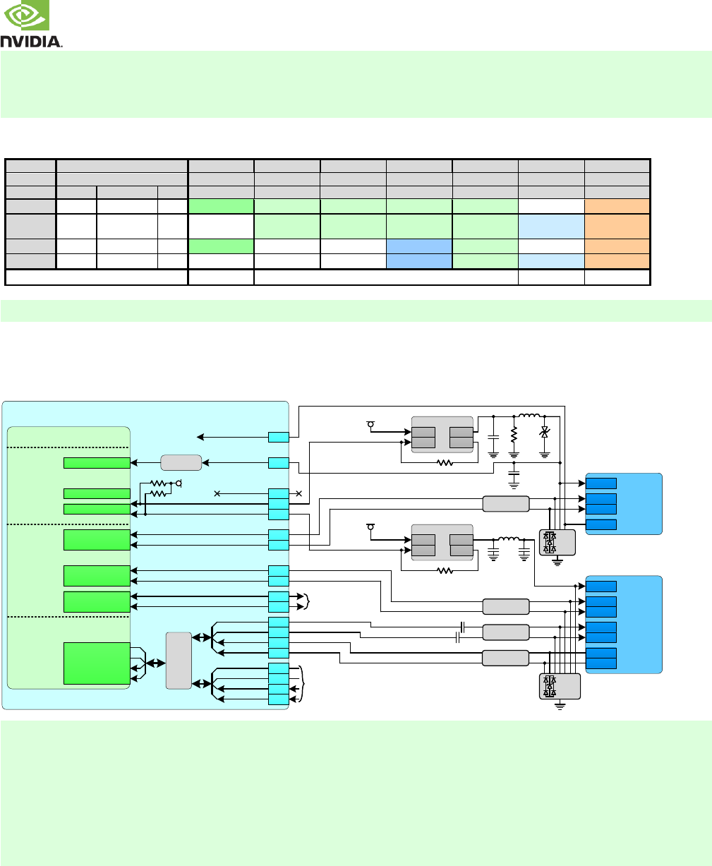
5.1 USB
Figure 12 USB Connection Example
Jetson TX2
USB 3.0
Type A
USB 2.0
Micro AB
VBUS
ID
D+
D–
VBUS
TX+
D+
D–
TX–
RX+
RX–
USB_VBUS_EN0
Tegra
USB 2.0 USB0_DP
USB0_DN
USB 3.0
& PEX
USB1_DP
USB1_DN
USB2_DP
USB2_DN
ESD
ESD
Common
Mode Choke
Load Switch
EN OC
IN OUT
VDD_5V0_IO_SYS
USB_VBUS_EN1
Load Switch
EN OC
IN OUT
VDD_5V0_IO_SYS
Common
Mode Choke
Common
Mode Choke
USB0_D+
USB0_D
USB1_D+
USB1_D
USB2_D+
USB2_D
USB_SS0_TX+
USB_SS0_TX
USB_SS0_RX+
USB_SS0_RX
PEX1_TX+
PEX1_TX
PEX1_RX+
PEX1_RX
USB0_OTG_ID
USB0_VBUS_DET
USB2_EN_OC#
USB0_EN_OC#
USB1_EN_OC#
Gate/LS
To PMIC GPIO0
(on Module)
VDD_3V3_SYS
To M.2 Module
on Carrier Board
A36
A17
A18
B39
B37
B40
A38
A39
B42
B43
C43
C44
F43
F44
A19
0.1uF
0.1uF
100kΩ100kΩ
PEX_TX0_P
PEX_TX0_N
PEX_RX0_P
PEX_RX0_N
UART5_CTS_N
UARTCAM
USB_VBUS_EN0
USB_VBUS_EN1
Common
Mode Choke
Mux
PCIe#2 (x1)
Default
100Ω100Ω
100Ω100Ω
E41
E42
H41
H42
Note:
1. Common mode filters on USB[2:0]_DP/DN (USB 2.0 interfaces) are optional. Place only as needed if EMI is an issue.
Common mode filters on USB3_TX/RX_P/N signals are not recommended. If common mode devices are placed, they
must be selected to minimize the impact to signal quality, which must meet the USB spec. signal requirements. See the
Common Mode Choke requirements in the USB 3.0 Interface Signal Routing Requirements table.
2. If USB 3.0 is routed to a connector, only AC caps on Jetson TX2 TX lines are required. If routed directly to a peripheral,
AC caps are needed for both Jetson TX2 TX lines (connected to device RX) & Device TX lines (connected to Jetson TX2
RX).
3. USB0 must be available to use as USB Device for USB Recovery Mode.
4. Connector used must be USB-IF certified if USB 3.0 implemented.
NVIDIA Jetson TX2 OEM Product Design Guide
JETSON TX2 OEM PRODUCT | DESIGN GUIDE | 20170912 23
USB 2.0 Design Guidelines
These requirements apply to the USB 2.0 controller PHY interfaces: USB[2:0]_D/D+
Table 17. USB 2.0 Interface Signal Routing Requirements
Parameter
Requirement
Units
Notes
Max Frequency (High Speed) Bit Rate/UI period/Frequency
480/2.083/240
Mbps/ns/MHz
Max Loading High Speed / Full Speed / Low Speed
10 / 150 / 600
pF
Reference plane
GND
Trace Impedance Diff pair / Single Ended
90 / 50
±15%
Via proximity (Signal to reference)
< 3.8 (24)
mm (ps)
See Note 2
Max Trace Delay With CMC or SW (Microstrip / Stripline)
Without CMC or SW (Microstrip / Stripline)
900/1050 (6)
1350/1575 (9)
ps (in)
Prop delay assumption: 175ps/in.
for stripline, 150ps/in. for
microstrip). See Note 3
Max Intra-Pair Skew between USBx_D+ & USBx_D–
7.5
ps
Note:
1. If portion of route is over a flex cable this length should be included in the Max Trace Delay/Length calculation & 85
Differential pair trace impedance is recommended.
2. Up to 4 signal Vias can share a single GND return Via.
3. CMC = Common-Mode-Choke. SW = Analog Switch
4. Adjustments to the USB drive strength, slew rate, termination value settings should not be necessary, but if any are
made, they MUST be done as an offset to default values instead of overwriting those values.
USB 3.0 Design Guidelines
The following requirements apply to the USB 3.0 PHY interfaces
Table 18. USB 3.0 Interface Signal Routing Requirements
Parameter
Requirement
Units
Notes
Specification
Data Rate / UI period
5.0 / 200
Gbps / ps
Max Number of Loads
1
load
Termination
90 differential
On-die termination at TX & RX
Reference plane
GND
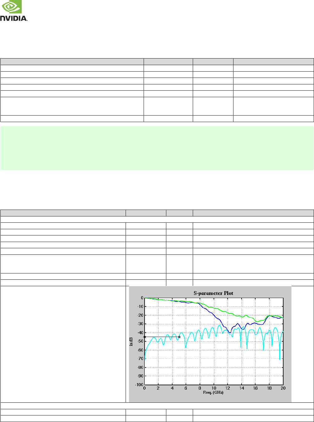
Electrical Specification
Insertion Loss @ 2.5GHz Type-C
Type A
Resonance dip frequency
<=2
<=7
>8
dB
dB
GHz
Only PCB with add-on components (connector
excluded) is considered
TDR dip
>= 75
Using TDR pulse with Tr (10%-90%) = 200ps
Near-end Crosstalk (NEXT) @ DC to 5GHz
<=-45
dB
For each TX-RX NEXT
IL/NEXT plot
Trace Impedance
Trace Impedance Diff pair / Single Ended
85-90 / 45-55
±15%
Reference plane
GND
NVIDIA Jetson TX2 OEM Product Design Guide
JETSON TX2 OEM PRODUCT | DESIGN GUIDE | 20170912 24
Trace Length/Skew
Trace loss characteristic @ 2.5GHz
< 0.7
dB/in
The following max length is derived based on this
characteristic. See Note 1.
Breakout Region Max trace length/delay
11 (73)
mm (ps)
Trace with minimum width and spacing
Max Trace Length
152.3 (1014)
mm (ps)
Max length assume USB3 Tx voltage swing set at 0.8V
MIN, length can increase if Tx swing increase.
Max Within Pair (Intra-Pair) Skew
0.15 (1)
mm (ps)
Do trace length matching before hitting discontinuities
Differential pair uncoupled length
6.29 (41.9)
mm (ps)
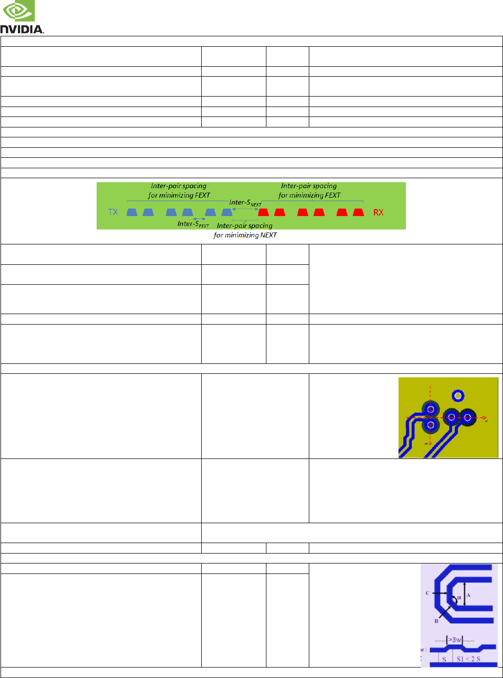
Trace Spacing – for TX/RX non-interleaving
TX-RX Xtalk is very critical in PCB trace routing. The ideal solution is to route TX and RX on different layers.
If routing on the same layer, strongly recommend not interleaving TX and RX lanes
If it is necessary to have interleaved routing in breakout, all the inter-pair spacing should follow the rule of inter-SNEXT
The breakout trace width is suggested to be the minimum to increase inter-pair spacing
Do not perform serpentine routing for intra-pair skew compensation in the breakout region
Min Inter-SNEXT Breakout
(between TX/RX) Main-route
4.85x
3x
Dielectric
height
- This is the recommended dimension for meeting
NEXT requirement
- Stripline structure in a GSSG structure is assumed; it
holds in broadside-coupled stripline structure
- All values are in terms of minimum dielectric height
Min Inter-SFEXT Breakout
(between TX/TX or RX/RX) Main-route
1x
1x
Inter-pair
spacing
Max length Breakout
Main-route
11
Max trace
length - LBRK
mm
Trace Spacing – for TX/RX interleaving
Trace Spacing
Pair-Pair (inter-pair) Microstrip / Stripline
To plane & capacitor pad Microstrip / Stripline
To unrelated high-speed signals Microstrip / Stripline
4x / 3x
4x / 3x
4x / 3x
dielectric
Via
Topology
- Y-pattern is
recommended
- Keep symmetry
Y-pattern helps with
Xtalk suppression. It
can also reduce the
limit of pair-pair
distance. Need review
(NEXT/FEXT check) if
via placement is not Y-
pattern.
GND via
- Place ground vias as
symmetrically as
possible to data pair
vias
- up to 4 signal vias (2
diff pairs) can share a
single GND return via
GND via is used to maintain return path, while its Xtalk
suppression is limited
Max # of Vias PTH vias
Micro Vias
4
Not limited as long as total channel loss meets IL spec
Max Via Stub Length
0.4
mm
long via stub requires review (IL & resonance dip check)
Serpentine
Min bend angle
135
deg ()
S1 must be taken care in order
to consider Xtalk to adjacent
pair
Dimension Min A Spacing
Min B, C Length
Min Jog Width
4x
1.5x
3x
Trace
width
Added-on Components
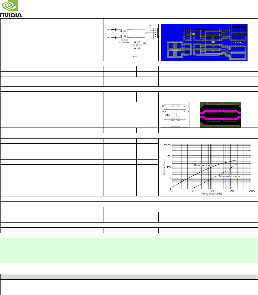
NVIDIA Jetson TX2 OEM Product Design Guide
JETSON TX2 OEM PRODUCT | DESIGN GUIDE | 20170912 25
Placement Order
Chip AC capacitor (TX only) common mode choke ESD Connector
AC Cap
Value Min/Max
0.1 / 0.2
uF
Only required for TX pair when routed to connector
Location (max length to adjacent discontinuity)
8
mm
Discontinuity is connector, via, or component pad
Voiding
GND/PWR void under/above
cap is preferred
Voiding is required if AC cap size is 0603 or larger
ESD (the usage of ESD is optional. A design should include the footprint for ESD as a stuffing option)
Preferred device
e.g. SEMTECH RClamp0524p
Max Junction capacitance (IO to GND)
0.8
pF
Footprint
Pad should be on the net
not trace stub
Location (max length to adjacent discontinuity)
8 (53)
mm (ps)
Discontinuity is connector, via, or component pad
Common-mode Choke (Only if needed. Place near connector.)
Common-mode impedance @100MHz Min/Max
65/90
TDK ACM2012D-900-2P
Max Rdc
0.3
Differential TDR impedance @TR-200ps (10%-90%)
90
Min Sdd21 @ 2.5GHz
2.22
dB
Max Scc21 @ 2.5GHz
19.2
dB
Routing length reduction
<= 3
in
FPC (Additional length of Flexible Printed Circuit Board)
The FPC routing should be included for PCB trace calculations (max length, etc.)
Characteristic Impedance
Same as PCB
Loss characteristic
Strongly recommend to be
the same as PCB or better
If worse than PCB, the PCB & FPC length must be re-
estimated
Connector
Connector used must be USB-IF certified
Note:
1. Longer trace lengths may be possible if the total trace loss is equal to or better than the target. If the loss is greater, the
max trace lengths will need to be reduced.
2. Recommend trace length matching to <1ps before Vias or any discontinuity to minimize common mode conversion.
3. Place GND Vias as symmetrically as possible to data pair Vias.
Common USB Routing Guidelines
Guideline
If routing to USB device or USB connector includes a flex or 2nd PCB, the total routing including all PCBs/flexes must be used for the max trace & skew
calculations.
Keep critical USB related traces away from other signal traces or unrelated power traces/areas or power supply components
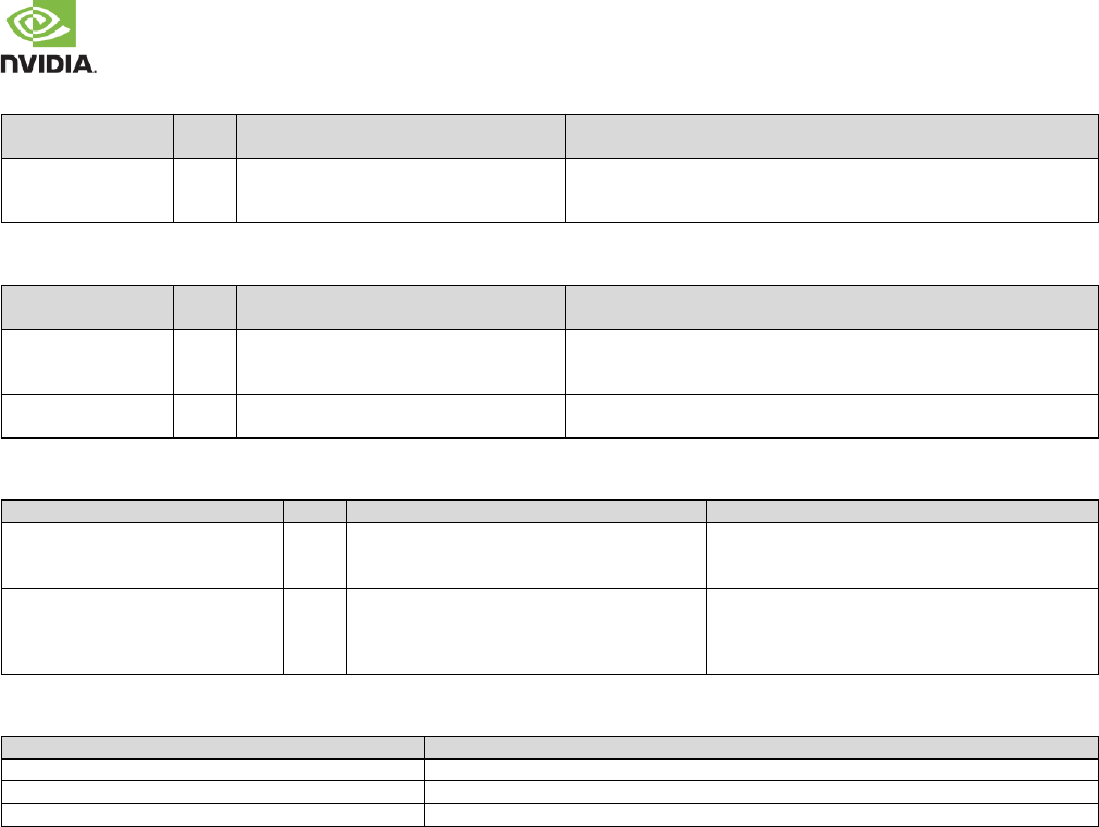
NVIDIA Jetson TX2 OEM Product Design Guide
JETSON TX2 OEM PRODUCT | DESIGN GUIDE | 20170912 26
Table 19. Jetson TX2 USB 2.0 Signal Connections
Jetson TX2 Ball
Name
Type
Termination
Description
USB[2:0]_D+
USB[2:0]_D–
DIFF
I/O
-mode chokes close to
connector. ESD Protection between choke
& connector on each line to GND
USB Differential Data Pair: Connect to USB connector, Mini-Card
Socket, Hub or other device on the PCB.
Table 20. Miscellaneous USB 2.0 Signal Connections
Jetson TX2 Pin
Name
Type
Termination
Description
USB0_VBUS_DET
A
. See reference
design for VBUS power filtering.
USB0 VBus Detect: Connect to VBUS pin of USB connector receiving
USB0_+/– interface. Also connects to VBUS power supply if host mode
supported.
USB0_OTG_ID
A
USB Identification: Connect to ID pin of USB OTG connector receiving
USB0_P/M interface.
Table 21. Jetson TX2 USB 3.0 Signal Connections
Jetson TX2 Pin Name
Type
Termination
Description
USB_SS0_TX+/– (USB 3.0 Port #0)
PEX_RFU_TX+/– (USB 3.0 Port #1)
USB_SS1_TX+/– (USB 3.0 Port #2)
DIFF
Out
Series 0.1uF caps. Common-mode chokes &
ESD protection if these are used.
USB 3.0 Differential Transmit Data Pairs: Connect
to USB 3.0 connectors, hubs or other devices on the
PCB.
USB_SS0_RX+/– (USB 3.0 Port #0)
PEX_RFU_RX+/– (USB 3.0 Port #1)
USB_SS1_RX+/– (USB 3.0 Port #2)
DIFF
In
If routed directly to a peripheral on the board,
AC caps are needed for the peripheral TX lines.
Common-mode chokes & ESD protection, if
these are used.
USB 3.0 Differential Receive Data Pairs: Connect
to USB 3.0 connectors, hubs or other devices on the
PCB.
Table 22. Recommended USB observation (test) points for initial boards
Test Points Recommended
Location
One for each of the USB 2.0 data lines (D+/-)
Near Jetson TX2 connector & USB device. USB connector pins can serve as test points.
One for each of the USB 3.0 output lines used (TXn_+/-)
Near USB device. USB connector pins can serve as test points
One for each of the USB 3.0 input lines (RX_+/-)
Near Jetson TX2 connector.
5.2 PCIe
Jetson TX2 contains a PCIe (PEX) controller that supports up to 5 lanes, and 3 separate interfaces. This narrow, high-speed
interface can be used to connect to a variety of high bandwidth devices.
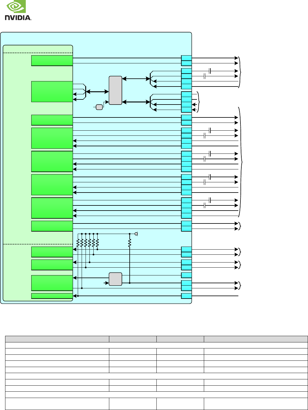
NVIDIA Jetson TX2 OEM Product Design Guide
JETSON TX2 OEM PRODUCT | DESIGN GUIDE | 20170912 27
Figure 13. PCIe Connection Example
Jetson TX2
Tegra - PCIe
PEX
PEX_TX0P
PEX_TX0N
PEX_RX0P
PEX_RX0N
PEX_L0_CLKREQ_N
PEX_L0_RST_N
PEX_L1_CLKREQ_N
PEX_L1_RST_N
PEX_WAKE_N
PEX
Control
PEX_CLK3_P
PEX_CLK3_N
PEX_CLK1_P
PEX_CLK1_N
PEX_TX1P
PEX_TX1N
PEX_RX1P
PEX_RX1N
PCIe – Single Lane (IF #2) or
(USB 3.0 Port #0). Used for M.2
Connector on Carrier Board
PCIe IF #0 Lane 3
PCIe IF #0 Lane 2
PCIe IF #0 Lane 1
PCIe IF #0 Lane 0
Shared
Control for PCIe
IF #1 Lane
Control for PCIe
IF #0 Lanes
PEX_TX2P
PEX_TX2N
PEX_RX2P
PEX_RX2N
PEX_TX3P
PEX_TX3N
PEX_RX3P
PEX_RX3N
PEX_TX4P
PEX_TX4N
PEX_RX4P
PEX_RX4N
PEX1_REFCLK+
PEX1_REFCLK
PEX1_TX+
PEX1_TX
PEX1_RX+
PEX1_RX
USB_SS0_TX+
USB_SS0_TX
USB_SS0_RX+
USB_SS0_RX
PEX0_REFCLK+
PEX0_REFCLK
PEX_RFU_TX+
PEX_RFU_TX
PEX_RFU_RX+
PEX_RFU_RX
USB_SS1_TX+
USB_SS1_TX
USB_SS1_RX+
USB_SS1_RX
PEX2_TX+
PEX2_TX
PEX2_RX+
PEX2_RX
PEX0_TX+
PEX0_TX
PEX0_RX+
PEX0_RX
PEX2_REFCLK+
PEX2_REFCLK
PEX0_CLKREQ#
PEX0_RST#
PEX2_CLKREQ#
PEX2_RST#
SATA_DEV_SLP
PEX1_CLKREQ#
PEX1_RST#
PEX_WAKE#
VDD_3V3_SYS
E41
E42
H41
H42
A44
A45
D39
D40
G39
G40
C40
C41
F40
F41
D42
D43
G42
G43
E44
E45
H44
H45
B4 5
B4 6
C48
C49
C46
D49
D48
C47
E50
A41
A42
0.1uF
0.1uF
0.1uF
0.1uF
0.1uF
0.1uF
0.1uF
0.1uF
0.1uF
0.1uF
Default: PCIe x1
(only PEX2_TX/RX lane used)
Alternate: PCIe x4
(Routed to PCIe Connector on
Carrier Board)
PEX_L2_CLKREQ_N
PEX_L2_RST_N
Control for PCIe
IF #2 Lane
PEX_CLK2_P
PEX_CLK2_N
Optionally used with PCIe
IF x1 on PEX2_TX/RX (PCIe
IF #1).
D47
Mux
SEL
PMIC
GPIO7
Mux
(Default)
Tegra
QSPI_IO2 LS SEL USB 3.0 (Port #1)
C43
C44
F43
F44
PCIE Design Guidelines
Table 23. PCIE Interface Signal Routing Requirements
Parameter
Requirement
Units
Notes
Specification
Data Rate / UI Period
5.0 / 200
Gbps / ps
2.5GHz, half-rate architecture
Configuration / Device Organization
1
Load
Topology
Point-point
Unidirectional, differential
Termination
50
To GND Single Ended for P & N
Impedance
Trace Impedance differential / Single Ended
85 / 50
±15%. See note 1
Reference plane
GND
Spacing
Trace Spacing (Stripline/Microstrip) Pair Pair
To plane & capacitor pad
3x / 4x
3x / 4x
Dielectric
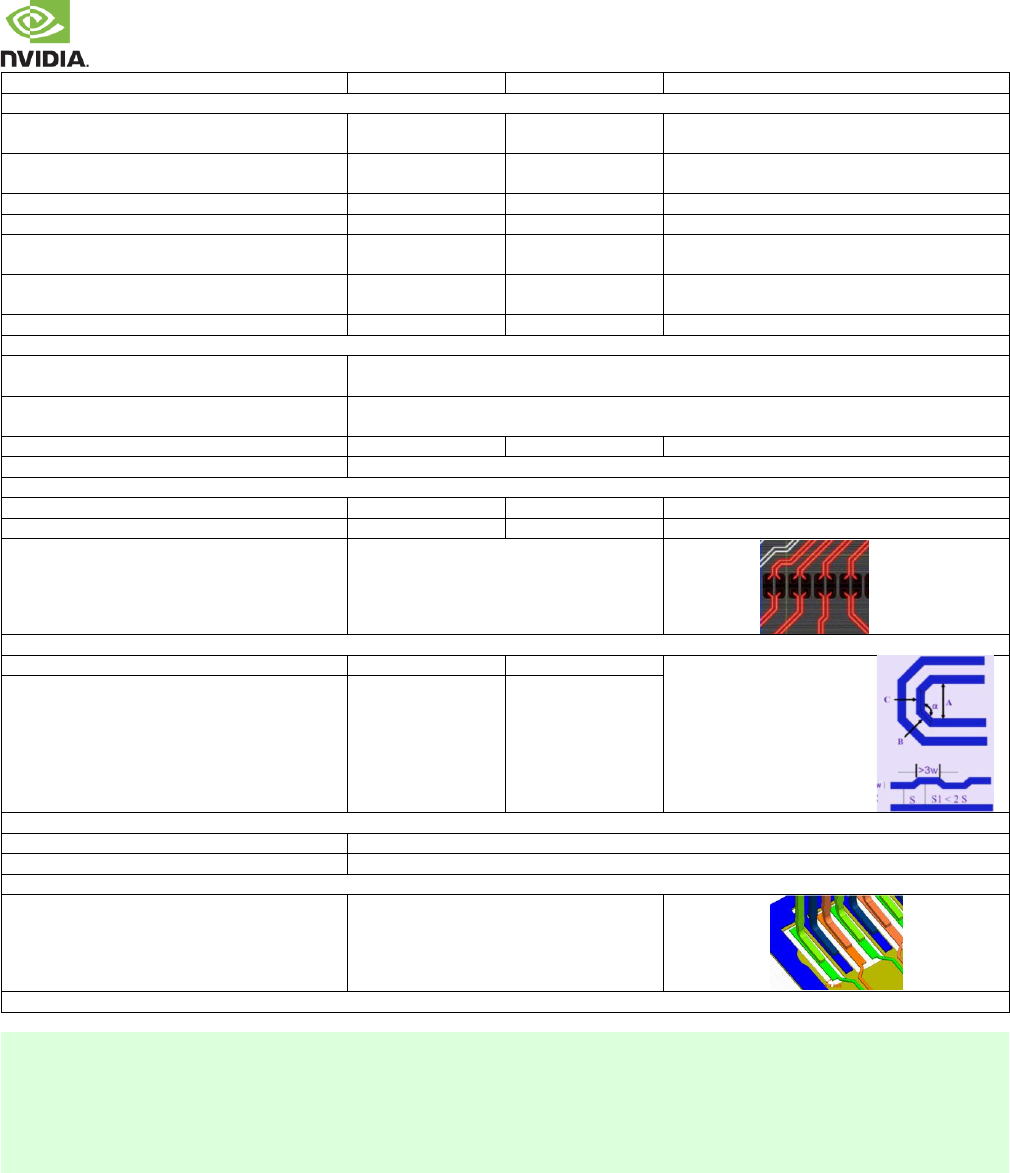
NVIDIA Jetson TX2 OEM Product Design Guide
JETSON TX2 OEM PRODUCT | DESIGN GUIDE | 20170912 28
To unrelated high-speed signals
3x / 4x
Length/Skew
Trace loss characteristic @ 2.5GHz
< 0.7
dB/in
The following max length is derived based on this
characteristic. See note 3
Breakout region (Max Length)
41.9
ps
Minimum width and spacing. 4x or wider
dielectric height spacing is preferred
Max trace length
5.5 (880)
in (ps)
Max PCB via distance from the BGA
41.9
ps
Max distance from BGA ball to first PCB via.
PCB within pair (intra-pair) skew
0.15 (0.5)
mm (ps)
Do trace length matching before hitting
discontinuities
Within pair (intra-pair) matching between
subsequent discontinuities
0.15 (0.5)
mm (ps)
Differential pair uncoupled length
41.9
ps
Via
Via placement
Place GND vias as symmetrically as possible to data pair vias. GND via distance should be placed
less than 1x the diff pair via pitch
Max # of Vias PTH Vias
Micro-Vias
2 for TX traces & 2 for RX trace
No requirement
Max Via stub length
0.4
mm
Longer via stubs would require review
Routing signals over antipads
Not allowed
AC Cap
Value Min/Max
0.075 / 0.2
uF
Only required for TX pair when routed to connector
Location (max length to adjacent discontinuity)
8
mm
Discontinuity such as edge finger, component pad
Voiding
Voiding the plane directly under the pad 3-4
mils larger than the pad size is
recommended.
Serpentine
Min bend angle
135
deg (a)
S1 must be taken care in
order to consider Xtalk to
adjacent pair
Dimension Min A Spacing
Min B, C Length
Min Jog Width
4x
1.5x
3x
Trace width
MIsc.
Routing signals over antipads
Not allowed
Routing over voids
When signal pair approaches Vias, the maximal trace length across the void on the plane is 50mil.
Connector
Voiding
Voiding the plane directly under the pad 5.7
mils larger than the pad size is
recommended.
Keep critical PCIe traces such as PEX_TX/RX, TERMP etc. away from other signal traces or unrelated power traces/areas or power supply components
Note:
1. The PCIe spec. has 40-60 absolute min/max trace impedance, which can be used instead of the 50, ± 15%.
2. If routing in the same layer is necessary, route group TX & RX separately without mixing RX/TX routes & keep distance
between nearest TX/RX trace & RX to other signals 3x RX-RX separation.
3. Longer trace lengths may be possible if the total trace loss is equal to or better than the target. If the loss is greater, the
max trace lengths will need to be reduced.
4. Do length matching before Via transitions to different layers or any discontinuity to minimize common mode conversion.
NVIDIA Jetson TX2 OEM Product Design Guide
JETSON TX2 OEM PRODUCT | DESIGN GUIDE | 20170912 29
Table 24. PCIE Signal Connections
Jetson TX2 Pin Name
Type
Termination
Description
PCIe Interface #0 (x1 default configuration – x4 optional.
PEX0_TX+/– (Lane 0)
USB_SS1_TX+/– (Lane 1)
PEX2_TX+/– (Lane 2)
PEX_RFU_TX+/– (Lane 3)
DIFF OUT
Series 0.1uF Capacitor
Differential Transmit Data Pairs: Connect to TX_P/N pins of PCIe
connector or RX_P/N pin of PCIe device through AC cap according to
supported configuration. Default configuration (x1) uses only Lane 0.
PEX0_RX_+/– (Lane 0)
USB_SS1_RX+/– (Lane 1)
PEX2_RX+/– (Lane 2)
PEX_RFU_RX+/– (Lane 3)
DIFF IN
Series 0.1uF capacitors if
device on main PCB.
Differential Receive Data Pairs: Connect to RX_P/N pins of PCIe
connector or TX_P/N pin of PCIe device through AC cap according to
supported configuration. Default configuration (x1) uses only Lane 0.
PEX0_REFCLK+/–
DIFF OUT
Differential Reference Clock Output: Connect to REFCLK_P/N pins of
PCIe device/connector
PEX0_CLKREQ#
I/O
56
VDD_3V3_SYS on each line
(exists on Jetson TX2)
PEX Clock Request for PEX0_REFCLK: Connect to CLKREQ pin on
device/connector.
PEX0_RST#
O
PEX Reset: Connect to PERST pin on device/connector.
PCIe Interface #1 (x1) – (Shared with PCIe Interface #0 lane 2)
PEX2_TX+/–
DIFF OUT
Series 0.1uF Capacitor
Differential Transmit Data Pairs: Connect to TX+/– pins of PCIe
connector or RX_+/– pin of PCIe device through AC cap according to
supported configuration.
PEX2_RX+/–
DIFF IN
Series 0.1uF capacitors if
device on main PCB.
Differential Receive Data Pairs: Connect to RX_+/– pins of PCIe
connector or TX_+/– pin of PCIe device through AC cap according to
supported configuration.
PEX2_REFCLK+/–
DIFF OUT
Differential Reference Clock Output: Connect to REFCLK_+/ pins of
PCIe device/connector.
PEX2_CLKREQ#
I/O
56
VDD_3V3_SYS on each line
(exists on Jetson TX2)
PEX Clock Request for PEX2_REFCLK: Connect to CLKREQ pin on
device/connector(s)
PEX2_RST#
O
PEX Reset: Connect to PERST pin on device/connector.
PCIe Interface #2 (x1) – Muxed with USB 3.0 Port #0 on USB_SS0
PEX1_TX+/–
DIFF OUT
Series 0.1uF Capacitor
Differential Transmit Data Pairs: Connect to TX+/– pins of PCIe
connector or RX_+/– pin of PCIe device through AC cap according to
supported configuration.
PEX1_RX+/–
DIFF IN
Series 0.1uF capacitors if
device on main PCB.
Differential Receive Data Pairs: Connect to RX_+/– pins of PCIe
connector or TX_+/– pin of PCIe device through AC cap according to
supported configuration.
PEX1_REFCLK+/–
DIFF OUT
Differential Reference Clock Output: Connect to REFCLK_+/ pins of
PCIe device/connector
PEX1_CLKREQ#
I/O
56
VDD_3V3_SYS on each line
(exists on Jetson TX2)
PEX Clock Request for PEX1_REFCLK: Connect to CLKREQ pin on
device/connector(s)
PEX1_RST#
O
PEX Reset: Connect to PERST pin on device/connector(s)
PEX_WAKE#
I
56
VDD_3V3_SYS (exists on
Jetson TX2)
PEX Wake: Connect to WAKE pins on devices or connectors
Note:
CIE IF mapping options.
Table 25. Recommended PCIe observation (test) points for initial boards
Test Points Recommended
Location
One for each of the PCIe TX_+/– output lines used.
Near PCIe device. Connector pins may serve as test points if accessible.
One for each of the PCIe RX_+/– input lines used.
Near Jetson TX2 connector.
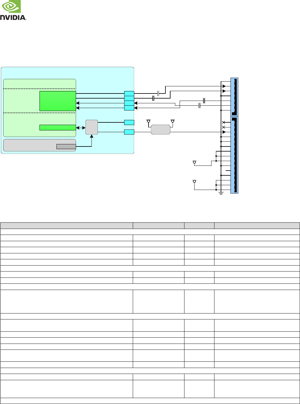
NVIDIA Jetson TX2 OEM Product Design Guide
JETSON TX2 OEM PRODUCT | DESIGN GUIDE | 20170912 30
5.3 SATA
A Gen 2 SATA controller is implemented on Jetson TX2. The interface is brought to Jetson TX2 edge connector as shown in
the figure below.
Figure 14. SATA Connection Example
Tegra
PEX_TX5P
PEX_TX5N
PEX_RX5P
PEX_RX5N
PEX, USB
3.0 & SATA
SATA_TX+
SATA_TX
SATA_RX+
SATA_RX
PEX1_CLKREQ#
SATA_DEV_SLP
D45
D46
G45
G46
1
2
3
4
5
6
7
1
2
3
4
5
6
7
8
9
10
11
12
13
14
15
16
17
18
19
20
21
22
D47
PEX_L2_CLKREQ_N Level
Shifter
VDD_1V8 VDD_3V3_SLP
PEXCTL
Mux
C47
PMIC GPIO7
SEL
VDD_12V_SLP
VDD_5V0_IO_SLP
0.01uF
0.01uF
0.01uF
0.01uF
Jetson TX2
SATA Design Guidelines
Table 26. SATA Signal Routing Requirements
Parameter
Requirement
Units
Notes
Specification
Max Frequency Bit Rate / UI
3.0 / 333.3
Gbps / ps
1.5GHz
Topology
Point to point
Unidirectional, differential
Configuration / Device Organization
1
load
Max Load (per pin)
0.5
pf
Termination
100
On die termination
Impedance
Reference plane
GND
Trace Impedance Differential Pair / Single Ended
95 / 45-55
±15%
Spacing
Trace Spacing
Pair-to-pair (inter-pair) Stripline / Microstrip
To plane & capacitor pad Stripline / Microstrip
To unrelated high-speed signals Stripline / Microstrip
3x / 4x
3x / 4x
3x / 4x
Dielectric
Length/Skew
Breakout region Max Length
Spacing
41.9
Min width/spacing
ps
4x or wider dielectric height spacing is
preferred
Max Trace Length/Delay
76.2 (480)
Mm (ps)
Max PCB Via distance from pin
6.29 (41.9)
mm (ps)
Max Within Pair (Intra-Pair) Skew
0.15 (0.5)
mm (ps)
Intra-pair matching between subsequent discontinuities
0.15 (0.5)
mm (ps)
Do trace length matching before hitting
discontinuities
Differential pair uncoupled length
6.29 (41.9)
mm (ps)
AC Cap
AC Cap Value typical (max)
0.01 (0.012)
uF
AC Cap Location (max distance from adjacent discontinuities)
8 (53.22)
mm (ps)
The AC cap location should be located as
close as possible to nearby
discontinuities.
Via
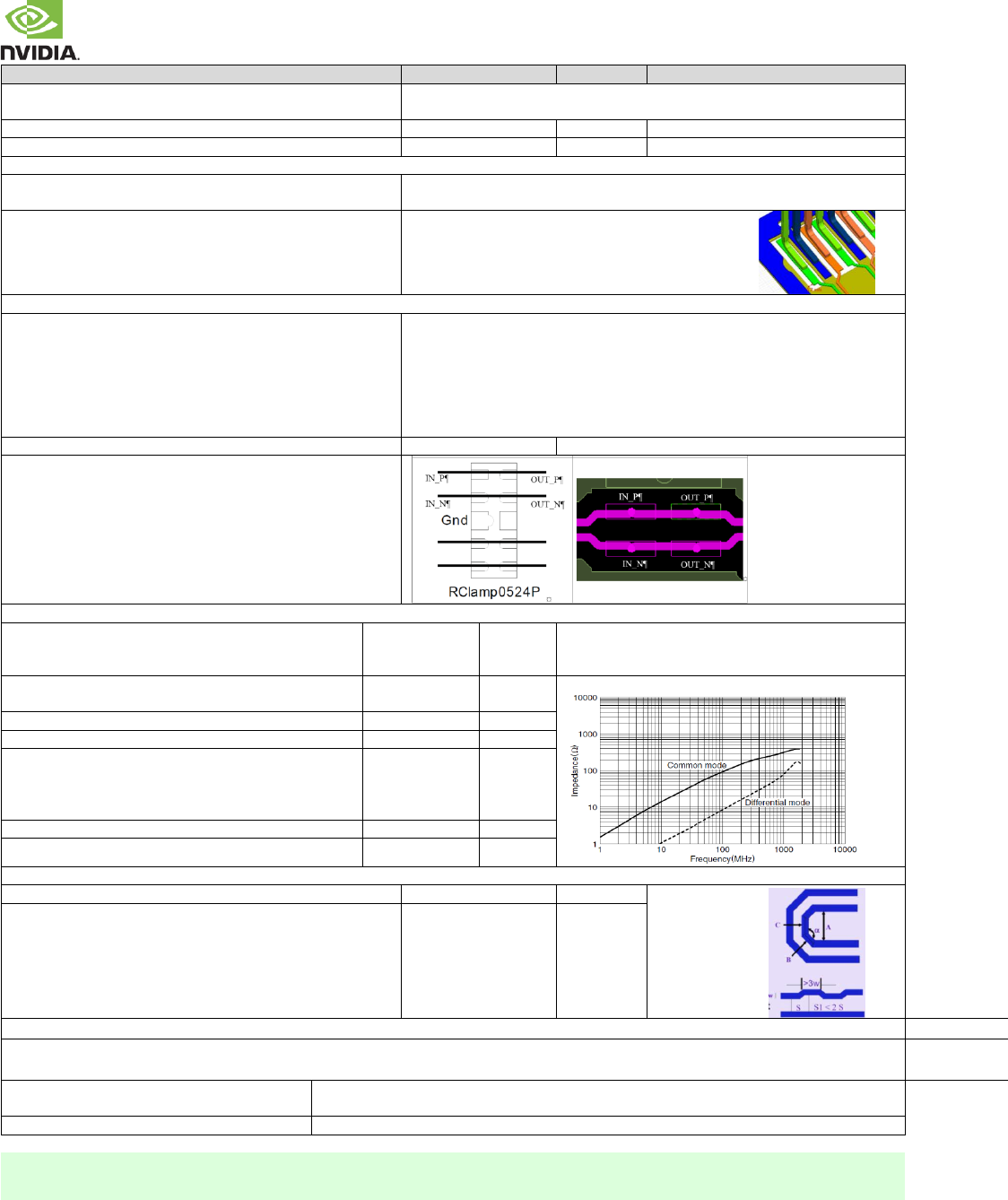
NVIDIA Jetson TX2 OEM Product Design Guide
JETSON TX2 OEM PRODUCT | DESIGN GUIDE | 20170912 31
Parameter
Requirement
Units
Notes
GND Via Placement
Place ground vias as symmetrically as possible to data pair vias
GND via distance should be placed less than 1x the diff pair via pitch
Max # of vias
3
If all are through-hole
Via stub length
< 0.4
mm
Voiding
AC cap pad voiding
Voiding the plane directly under the pad 3-4 mils larger than the pad size is
recommended
Connector voiding (Required)
The size of voiding can be same as the size of pin pad
ESD
ESD protection device (Optional)
Type: SEMTECH RClamp0524p. Place ESD component near connector.
A design may include the footprints for ESD as a stuffing option. The junction
an ESD component with low capacitance and whose package design is optimized
for high speed links. The SEMTECH ESD Rclamp0524p has been well verified with
its 0.3pF capacitance.
Max distance from ESD Device to Connector
8 (53)
mm (ps)
Recommended ESD layout
Choke
Preferred device
Type: TDK ACM2012D-900-2P. Only if needed. Place
near connector. Refer to Common Mode Choke
Requirement section.
Location - Max distance from to adjacent discontinuities
ex, connector, AC cap)
8 (53)
mm (ps)
TDK ACM2012D-900-2P
Common-mode impedance @ 100MHz Min/Max
65/90
Max Rdc
0.3
Differential TDR impedance
90
@TR-
200ps
(10%-
90%)
Min Sdd21 @ 2.5GHz
2.22
dB
Max Scc21 @ 2.5GHz
19.2
dB
Serpentine
Min bend angle
135
deg (a)
S1 must be
taken care in
order to
consider Xtalk
to adjacent pair
Dimension Min A Spacing
Min B, C Length
Min Jog Width
4x
1.5x
3x
Trace width
MIsc.
Routing over voids
Where signal pair approaches Vias, maximal trace length across void on plane is
1.27mm
Noise Coupling
Keep critical SATA related traces such as SATA_TX/RX, SATA_TERM etc. away from other signal
traces or unrelated power traces/areas or power supply components
Note:
If routing to SATA device or SATA connector includes a flex or 2nd PCB, the total routing including all PCBs/flexes must be used
for the max trace & skew calculations
NVIDIA Jetson TX2 OEM Product Design Guide
JETSON TX2 OEM PRODUCT | DESIGN GUIDE | 20170912 32
Table 27. SATA Signal Connections
Jetson TX2 Pin Name
Type
Termination
Description
SATA_TX+/–
DIFF OUT
Series 0.01uF Capacitor
Differential Transmit Data Pair: Connect to SATA+/– pins of SATA
device/connector through termination (capacitor)
SATA_RX+/–
DIFF IN
Series 0.01uF Capacitor
Differential Receive Data Pair: Connect to SATA+/– pins of SATA
device/connector through termination (capacitor)
SATA_DEV_SLP
O
1.8V to 3.3V level shifter
SATA Device Sleep: Connect through level shifter to matching pin
on device or connector (pin 10 of Connector show in example).
Table 28. Recommended SATA observation (test) points for initial boards
Test Points Recommended
Location
One for each of the SATA_TX_+/– output lines.
Near SATA device. Connector pins may serve as test points if accessible.
One for each of the SATA_RX_+/– input lines.
Near Jetson TX2 connector.
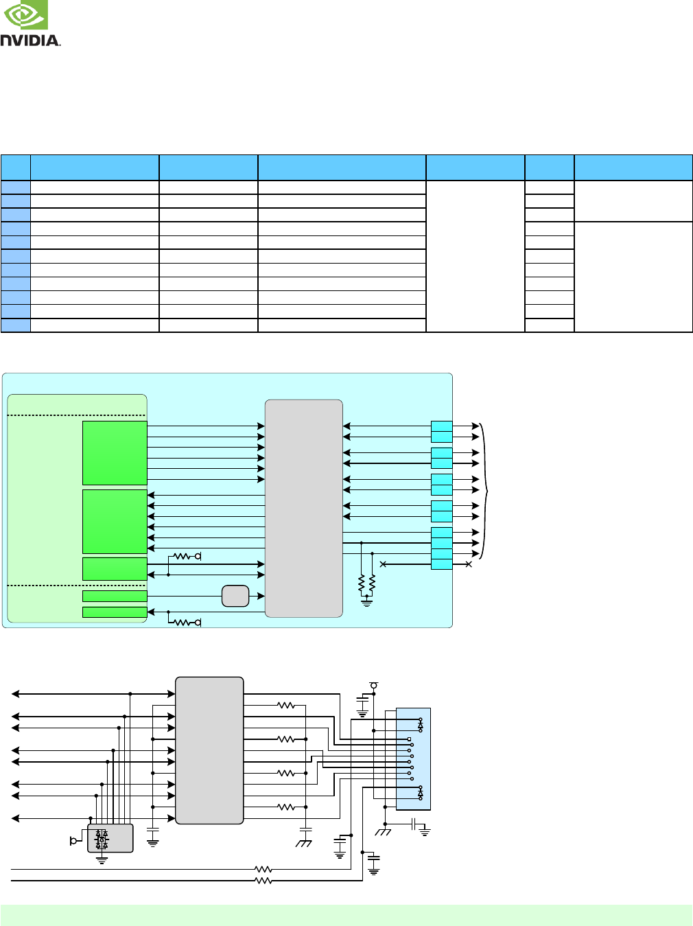
NVIDIA Jetson TX2 OEM Product Design Guide
JETSON TX2 OEM PRODUCT | DESIGN GUIDE | 20170912 33
6.0 GIGABIT ETHERNET
Jetson TX2 integrates a BCM54610C1IMLG Ethernet PHY. The magnetics & RJ45 connector are implemented on the Carrier
board. Contact Broadcom for the Carrier board placement/routing guidelines.
Table 29. Jetson TX2 Gigabit Ethernet Pin Descriptions
Pin #
Jetson TX2 Pin Name
Tegra Signal
Usage/Description
Usage on Carrier
Board
Direction
Pin Type
E47
GBE_LINK_ACT#
GbE RJ45 connector Link ACT (LED0)
LAN
Output
CMOS 3.3V tolerant
F50
GBE_LINK100#
GbE RJ45 connector Link 100 (LED1)
Output
F46
GBE_LINK1000#
GbE RJ45 connector Link 1000 (LED2)
Output
E49
GBE_MDI0
GbE Transformer Data 0
Bidir
MDI
E48
GBE_MDI0+
GbE Transformer Data 0+
Bidir
F48
GBE_MDI1
GbE Transformer Data 1
Bidir
F47
GBE_MDI1+
GbE Transformer Data 1+
Bidir
G49
GBE_MDI2
GbE Transformer Data 2
Bidir
G48
GBE_MDI2+
GbE Transformer Data 2+
Bidir
H48
GBE_MDI3
GbE Transformer Data 3
Bidir
H47
GBE_MDI3+
GbE Transformer Data 3+
Bidir
Figure 15. Ethernet Connections
Jetson TX2
GBE_MDI0+
GBE_MDI0
GBE_MDI1+
GBE_MDI1
GBE_MDI2+
GBE_MDI2
GBE_MDI3+
GBE_MDI3
GBE_LINK_ACT
GBE_LINK_100
GBE_LINK_1000
GBE_CTREF
E48
E49
F47
F48
G48
G49
H47
H48
E47
F50
F46
H50
Tegra
SDMMC2_HV
GbE
Tranceiver
EQOS_TXC
EQOS_TD0
EQOS_TD1
EQOS_TD2
EQOS_TD3
EQOS_TX_CTL
EQOS_RXC
EQOS_RD0
EQOS_RD1
EQOS_RD2
EQOS_RD3
EQOS_RX_CTL
EQOS_MDC
EQOS_MDIO
ENETPHY_RST
To Magnetics /
RJ45 Connector
ENETPHY_INT
AUDIO_HV
DMIC4_CLK
DMIC4_DAT LS
1.8V 3.3V
VDD_3V3_SYS
VDD_1V8
Figure 16. Gigabit Ethernet Magnetics & RJ45 Connections
Magnetics
+
CT
+
CT
+
CT
+
CT
+
CT
+
CT
+
CT
+
CT
10nF
75Ω
75Ω
1nF
75Ω
75Ω
GBE_LED0_SPICSB
0.1uF
VDD_3V3_SLP
GBE_LED1_SPISCK
681Ω,1%
0.1uF
0.1uF
RJ45
1
3
5
7
2
4
6
8
14
9
10
11
12
13
TDP
TDN
RDP
RDN
TDP1
TDN1
RDP1
RDN1100pF
GBE_MDI0+
GBE_MDI0
GBE_MDI1+
GBE_MDI1
GBE_MDI2+
GBE_MDI2
GBE_MDI3+
GBE_MDI3
GBE_LINK_ACT
GBE_LINK_100
ESD
681Ω,1%
VDD_3V3_SLP
Note:
The connections above match those used on the carrier board and are shown for reference.
NVIDIA Jetson TX2 OEM Product Design Guide
JETSON TX2 OEM PRODUCT | DESIGN GUIDE | 20170912 34
Table 30. Ethernet MDI Interface Signal Routing Requirements
Parameter
Requirement
Units
Notes
Reference plane
GND
Trace Impedance Diff pair / Single Ended
100 / 50
±15%. Differential impedance target is 100. 90can be used if 100
is not achievable
Min Trace Spacing (Pair-Pair)
0.763
mm
Max Trace Length
109 (690)
mm (ps)
Max Within Pair (Intra-Pair) Skew
0.15 (1)
mm (ps)
Number of Vias
minimum
Ideally there should be no vias, but if required for breakout to Ethernet
controller or magnetics, keep very close to either device.
Table 31. Ethernet Signal Connections
Jetson TX2 Pin
Name
Type
Termination
Description
GBE_MDI[3:0]+/–
DIFF
I/O
ESD device to GND per signal
Gigabit Ethernet MDI IF Pairs: Connect to Magnetics +/ pins
GBE_LINK_ACT
O
GND
Gigabit Ethernet ACT : Connect to LED1C on Ethernet connector.
GBE_LINK100
O
GND.
Pull-down to GND (exists on Jetson TX2)
Gigabit Ethernet Link 100 : Connect to LED2C on Ethernet connector.
Pulldown part of strapping to use 3.3V PHY mode.
GBE_LINK1000
O
GND
Gigabit Ethernet Link 1000 : Connect to Link 1000 LED on conn.
GBE_CTREF
na
Not used
Table 32. Recommended Gigabit Ethernet observation (test) points for initial boards
Test Points Recommended
Location
One for each of the MDI[3:0]+/– lines.
Near Jetson TX2 connector & Magnetics device.
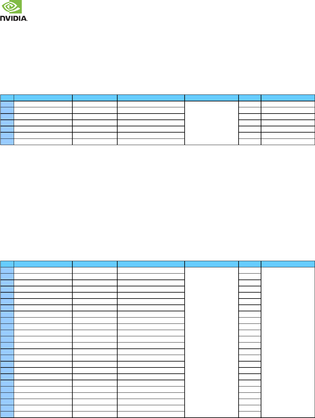
NVIDIA Jetson TX2 OEM Product Design Guide
JETSON TX2 OEM PRODUCT | DESIGN GUIDE | 20170912 35
7.0 DISPLAY
Jetson TX2 designs can select from several display options including MIPI DSI & eDP for embedded displays, and HDMI or DP
for external displays. Three display controllers are available, so the possible display combinations are:
▪ DP/HDMI + eDP + single/dual-link-DSI
▪ DP/HDMI + single-link-DSI + single-link-DSI
▪ DP/HDMI + DP/HDMI + single/dual-link-DSI
Table 33. Jetson TX2 Display General Pin Descriptions
Pin #
Jetson TX2 Pin Name
Tegra Signal
Usage/Description
Usage on Carrier Board
Direction
Pin Type
A26
GSYNC_HSYNC
GPIO_DIS4
GSYNC Horizontal Sync
Display Connector
Output
CMOS 1.8V
A27
GSYNC_VSYNC
GPIO_DIS2
GSYNC Vertical Sync
Output
CMOS 1.8V
A25
LCD_TE
GPIO_DIS1
Display Tearing Effect
Input
CMOS 1.8V
B26
LCD_VDD_EN
GPIO_EDP0
Display VDD Enable
Output
CMOS 1.8V
B28
LCD_BKLT_EN
GPIO_DIS3
Display Backlight Enable
Output
CMOS 1.8V
B27
LCD0_BKLT_PWM
GPIO_DIS0
Display Backlight PWM 0
Output
CMOS 1.8V
A24
LCD1_BKLT_PWM
GPIO_DIS5
Display Backlight PWM 1
Output
CMOS 1.8V
7.1 MIPI DSI
Jetson TX2 supports eight total MIPI DSI data lanes. Each data lane has a peak bandwidth up to 1.5Gbps. The lanes can be
configured in Dual Link & Split Link modes. The following configurations are possible:
Dual Link Mode (Up to 8 PHY lanes):
▪ DSI-A (1x4) + DSI-C (1x4) to single display
▪ DSI-A (1x4) to one display, DSI-C (1x4) to a second display
Split Link Mode (Up to 8 PHY lanes):
▪ Two Links with 1-lane each: DSI-A(1x1) + DSI-B (1x1) or DSI-C (1x1) + DSI-D (1x1)
▪ Two Links with 2-lane each: DSI-A(1x2) + DSI-B (1x2) or DSI-C (1x2) + DSI-D (1x2)
▪ Four Links with 1-lane each: DSI-A(1x1) + DSI-B (1x1) + DSI-C (1x1) + DSI-D (1x1)
▪ Four Links with 2-lane each: DSI-A(1x2) + DSI-B (1x2) + DSI-C (1x2) + DSI-D (1x2)
Table 34. Jetson TX2 DSI Pin Descriptions
Pin #
Jetson TX2 Pin Name
Tegra Signal
Usage/Description
Usage on Carrier Board
Direction
Pin Type
G34
DSI0_CLK
DSI_A_CLK_N
Display, DSI 0 Clock
Display Connector
Output
MIPI D-PHY
G33
DSI0_CLK+
DSI_A_CLK_P
Display, DSI 0 Clock+
Output
F35
DSI0_D0
DSI_A_D0_N
Display, DSI 0 Data 0
Output
F34
DSI0_D0+
DSI_A_D0_P
Display, DSI 0 Data 0+
Output
H33
DSI0_D1
DSI_A_D1_N
Display, DSI 0 Data 1
Output
H32
DSI0_D1+
DSI_A_D1_P
Display, DSI 0 Data 1+
Output
D34
DSI1_CLK
DSI_B_CLK_N
Display DSI 1 Clock
Output
D33
DSI1_CLK+
DSI_B_CLK_P
Display DSI 1 Clock+
Output
C35
DSI1_D0
DSI_B_D0_N
Display, DSI 1 Data 0
Output
C34
DSI1_D0+
DSI_B_D0_P
Display, DSI 1 Data 0+
Output
E33
DSI1_D1
DSI_B_D1_N
Display, DSI 1 Data 1
Output
E32
DSI1_D1+
DSI_B_D1_P
Display, DSI 1 Data 1+
Output
G31
DSI2_CLK
DSI_C_CLK_N
Display DSI 2 Clock
Output
G30
DSI2_CLK+
DSI_C_CLK_P
Display DSI 2 Clock+
Output
F32
DSI2_D0
DSI_C_D0_N
Display, DSI 2 Data 0
Output
F31
DSI2_D0+
DSI_C_D0_P
Display, DSI 2 Data 0+
Output
H30
DSI2_D1
DSI_C_D1_N
Display, DSI 2 Data 1
Output
H29
DSI2_D1+
DSI_C_D1_P
Display, DSI 2 Data 1+
Output
D31
DSI3_CLK
DSI_D_CLK_N
Display DSI 3 Clock
Output
D30
DSI3_CLK+
DSI_D_CLK_P
Display DSI 3 Clock+
Output
C32
DSI3_D0
DSI_D_D0_N
Display, DSI 3 Data 0
Output
C31
DSI3_D0+
DSI_D_D0_P
Display, DSI 3 Data 0+
Output
E30
DSI3_D1
DSI_D_D1_N
Display, DSI 3 Data 1
Output
E29
DSI3_D1+
DSI_D_D1_P
Display, DSI 3 Data 1+
Output
NVIDIA Jetson TX2 OEM Product Design Guide
JETSON TX2 OEM PRODUCT | DESIGN GUIDE | 20170912 36
Figure 17: DSI Dual Link Connections
Jetson TX2
Tegra
DSI/CSI DSI_A_CLK_P
DSI_A_CLK_N
DSI_A_D0_P
DSI_A_D0_N
DSI_A_D1_P
DSI_A_D1_N
Display
Connector (DSI)
A_D0P
A_D0N
A_D1P
A_D1N
A_D2P
A_D2N
A_D3P
A_D3N
A_CLKP
A_CLKN
B_D0P
B_D0N
B_D1P
B_D1N
B_D2P
B_D2N
B_D3P
B_D3N
B_CLKP
B_CLKN
EMI/ESD
G33
G34
F34
F35
C34
C35
E32
E33
G30
G31
F31
F32
H32
H33
D33
D34
H29
H30
D30
D31
C31
C32
E29
E30
DSI0_CK+
DSI0_CK
DSI0_D0+
DSI0_D0
DSI0_D1+
DSI0_D1
DSI1_CK+
DSI1_CK
DSI1_D0+
DSI1_D0
DSI1_D1+
DSI1_D1
DSI2_CK+
DSI2_CK
DSI2_D0+
DSI2_D0
DSI2_D1+
DSI2_D1
DSI3_CK+
DSI3_CK
DSI3_D0+
DSI3_D0
DSI3_D1+
DSI3_D1
4-Lane
4-Lane
Each 4-lane
interface can go to
a separate display,
or both can go to a
single display.
DSI_B_CLK_P
DSI_B_CLK_N
DSI_B_D0_P
DSI_B_D0_N
DSI_B_D1_P
DSI_B_D1_N
DSI_C_CLK_P
DSI_C_CLK_N
DSI_C_D0_P
DSI_C_D0_N
DSI_C_D1_P
DSI_C_D1_N
DSI_D_CLK_P
DSI_D_CLK_N
DSI_D_D0_P
DSI_D_D0_N
DSI_D_D1_P
DSI_D_D1_N
Note:
If EMI/ESD devices are necessary, they must be tuned to minimize impact to signal quality, which must meet the DSI spec.
requirements for the frequencies supported by the design.
Figure 18: DSI Split Link Connections
Jetson TX2
Tegra
DSI/CSI DSI_A_CLK_P
DSI_A_CLK_N
DSI_A_D0_P
DSI_A_D0_N
DSI_A_D1_P
DSI_A_D1_N
Display
Connector (DSI)
G33
G34
F34
F35
C34
C35
E32
E33
G30
G31
F31
F32
H32
H33
D33
D34
H29
H30
D30
D31
C31
C32
E29
E30
DSI0_CK+
DSI0_CK
DSI0_D0+
DSI0_D0
DSI0_D1+
DSI0_D1
DSI1_CK+
DSI1_CK
DSI1_D0+
DSI1_D0
DSI1_D1+
DSI1_D1
DSI2_CK+
DSI2_CK
DSI2_D0+
DSI2_D0
DSI2_D1+
DSI2_D1
DSI3_CK+
DSI3_CK
DSI3_D0+
DSI3_D0
DSI3_D1+
DSI3_D1
1-2
Lanes
DSI_B_CLK_P
DSI_B_CLK_N
DSI_B_D0_P
DSI_B_D0_N
DSI_B_D1_P
DSI_B_D1_N
DSI_C_CLK_P
DSI_C_CLK_N
DSI_C_D0_P
DSI_C_D0_N
DSI_C_D1_P
DSI_C_D1_N
DSI_D_CLK_P
DSI_D_CLK_N
DSI_D_D0_P
DSI_D_D0_N
DSI_D_D1_P
DSI_D_D1_N
EMI/ESD
CLK_P
CLK_N
D0_P
D0_N
D1_P
D1_N
1-2
Lanes
CLK_P
CLK_N
D0_P
D0_N
D1_P
D1_N
1-2
Lanes
CLK_P
CLK_N
D0_P
D0_N
D1_P
D1_N
1-2
Lanes
CLK_P
CLK_N
D0_P
D0_N
D1_P
D1_N
NVIDIA Jetson TX2 OEM Product Design Guide
JETSON TX2 OEM PRODUCT | DESIGN GUIDE | 20170912 37
Figure 19: Display Backlight/Control Connections
Jetson TX2
Tegra
LCD_BKLT_EN
LCD0_BKLT_PWM
LCD1_BKLT_PWM
LCD_TE
LCD_VDD_EN
eDP GPIO_EDP0
SYS GPIO_DIS3
GPIO_DIS0
GPIO_DIS5
GPIO_DIS1
Backlight
Control
B26
A25
B28
B27
A24
Tearing Effect
Display
Power Enable
MIPI DSI / CSI Design Guidelines
Table 35. MIPI DSI & CSI Interface Signal Routing Requirements
Parameter
Requirement
Units
Notes
Max Frequency/Data Rate (per data lane) HS (DSI)
HS (CSI)
LP
0.75 / 1.5
1.25 / 2.5
10
GHz/Gbps
MHz
Number of Loads
1
load
Max Loading (per pin)
10
pF
Reference plane
GND
See Note 1
Breakout Region Impedance (Single Ended)
45-50
±15%
Max PCB breakout delay
48
ps
Trace Impedance Diff pair / Single Ended
90-100 / 45-50
Via proximity (Signal to reference)
< 3.8 (24)
mm (ps)
See Note 2
Trace spacing Microstrip / Stripline
2x / 2x
dielectric
Max Trace Delay 1 Gbps
1.5 Gbps
2.5 Gbps
1100
800
350
mm (ps)
See Note 3
Max Intra-pair Skew
1
ps
See Note 3
Max Trace Delay Skew between DQ & CLK
5
ps
See Note 3
Keep critical DSI/CSI related traces including DSI/CSI clock/data traces & RDN/RUP traces away from other signal traces or unrelated power
traces/areas or power supply components
Note:
1. If PWR, 0.01uF decoupling cap required for return current
2. Up to 4 signal Vias can share a single GND return Via
3. If routing to device includes a flex or 2nd PCB, the max trace & skew calculations must include all the PCBs/flex routing
MIPI DSI / CSI Connection Guidelines
Table 36. MIPI DSI Signal Connections
Jetson TX2 Pin Name
Type
Termination
Description
DSI[3:0]_CK+/–
DIFF OUT
DSI Differential Clocks: Connect to CLKn & CLKp pins of receiver. See
connection diagrams for Dual & Split Link Mode configurations.
DSI[3:0]_D[1:0]+/–
DIFF OUT
DSI Differential Data Lanes: Connect to Dn & Dp pins of DSI display. See
connection diagrams for Dual & Split Link Mode configurations.
LCD_TE
I
LCD Tearing Effect: Connect to LCD Tearing Effect pin if supported
LCD_BL_EN
O
LCD Backlight Enable: Connect to LCD backlight solution enable if supported
LCD[1:0]_BKLT_PWM
O
LCD Backlight Pulse Width Modulation: Connect to LCD backlight solution PWM
input if supported
LCD_VDD_EN
O
LCD Power Enable: Connect as necessary to enable appropriate Display power
supply(ies).
Table 37. Recommended DSI observation (test) points for initial boards
Test Points Recommended
Location
One for each signal line.
Near display. Panel connector pins can be used if accessible.
Note:
Test points must be done carefully to minimize signal integrity impact. Avoid stubs & keep pads small & near signal traces
NVIDIA Jetson TX2 OEM Product Design Guide
JETSON TX2 OEM PRODUCT | DESIGN GUIDE | 20170912 38
7.2 eDP / DP / HDMI
Jetson TX2 includes two interfaces (DP0 & DP1). Both support eDP / DP or HDMI. See Jetson TX2 Data Sheet for the
maximum resolution supported.
Table 38. Jetson TX2 HDMI / eDP / DP Pin Descriptions
Pin #
Jetson TX2 Pin Name
Tegra Signal
Usage/Description
Usage on the Carrier
Board
Direction
Pin Type
B34
DP0_AUX_CH
DP_AUX_CH0_N
Display Port 0 Aux or HDMI DDC SDA
Display Connector
Bidir
AC-Coupled on Carrier
Board (eDP/DP) or Open-
Drain, 1.8V (3.3V tolerant -
DDC/I2C)
B35
DP0_AUX_CH+
DP_AUX_CH0_P
Display Port 0 Aux+ or HDMI DDC SCL
Bidir
H38
DP0_TX0
HDMI_DP0_TXDN2
DisplayPort 0 Lane 0 or HDMI Lane 2
Output
AC-Coupled on carrier
board
H39
DP0_TX0+
HDMI_DP0_TXDP2
DisplayPort 0 Lane 0+ or HDMI Lane 2+
Output
F37
DP0_TX1
HDMI_DP0_TXDN1
DisplayPort 0 Lane 1 or HDMI Lane 1
Output
F38
DP0_TX1+
HDMI_DP0_TXDP1
DisplayPort 0 Lane 1+or HDMI Lane 1+
Output
G36
DP0_TX2
HDMI_DP0_TXDN0
DisplayPort 0 Lane 2 or HDMI Lane 0
Output
G37
DP0_TX2+
HDMI_DP0_TXDP0
DisplayPort 0 Lane 2+ or HDMI Lane 0+
Output
H35
DP0_TX3
HDMI_DP0_TXDN3
DisplayPort 0 Lane 3 or HDMI Clk Lane
Output
H36
DP0_TX3+
HDMI_DP0_TXDP3
DisplayPort 0 Lane 3+ or HDMI Clk Lane+
Output
B36
DP0_HPD
DP_AUX_CH0_HPD
Display Port 0 Hot Plug Detect
Input
CMOS 1.8V
A34
DP1_AUX_CH
DP_AUX_CH1_N
Display Port 1 Aux or HDMI DDC SDA
HDMI Type A Conn.
Bidir
AC-Coupled on Carrier
Board (eDP/DP) or Open-
Drain, 1.8V (3.3V tolerant -
DDC/I2C)
A35
DP1_AUX_CH+
DP_AUX_CH1_P
Display Port 1 Aux+ or HDMI DDC SCL
Bidir
E38
DP1_TX0
HDMI_DP1_TXDN2
DisplayPort 1 Lane 0 or HDMI Lane 2
Output
AC-Coupled on carrier
board
E39
DP1_TX0+
HDMI_DP1_TXDP2
DisplayPort 1 Lane 0+ or HDMI Lane 2+
Output
C37
DP1_TX1
HDMI_DP1_TXDN1
DisplayPort 1 Lane 1 or HDMI Lane 1
Output
C38
DP1_TX1+
HDMI_DP1_TXDP1
DisplayPort 1 Lane 1+ or HDMI Lane 1+
Output
D36
DP1_TX2
HDMI_DP1_TXDN0
DisplayPort 1 Lane 2 or HDMI Lane 0
Output
D37
DP1_TX2+
HDMI_DP1_TXDP0
DisplayPort 1 Lane 2+ or HDMI Lane 0+
Output
E35
DP1_TX3
HDMI_DP1_TXDN3
DisplayPort 1 Lane 3 or HDMI Clk Lane
Output
E36
DP1_TX3+
HDMI_DP1_TXDP3
DisplayPort 1 Lane 3+ or HDMI Clk Lane+
Output
A33
DP1_HPD
DP_AUX_CH1_HPD
Display Port 1 Hot Plug Detect
Input
CMOS 1.8V
B33
HDMI_CEC
HDMI_CEC
HDMI CEC
Bidir
Open Drain, 3.3V
Note:
HDMI_DP0 or HDMI_DP1. The interface must include only signals from one or the other (not mixed).
Table 39. DP/HDMI Pin Mapping
Jetson TX2 Pin Name
Jetson TX2 Pin #s
Tegra Pin Name
Tegra Pin #s
HDMI
DP
DP0
DP0_TX0+
H39
HDMI_DP0_TXDP2
E4
TX2+
TX0+
DP0_TX0–
H38
HDMI_DP0_TXDN2
E5
TX2–
TX0–
DP0_TX1+
F38
HDMI_DP0_TXDP1
C3
TX1+
TX1+
DP0_TX1–
F37
HDMI_DP0_TXDN1
B3
TX1–
TX1–
DP0_TX2+
G37
HDMI_DP0_TXDP0
A3
TX0+
TX2+
DP0_TX2–
G36
HDMI_DP0_TXDN0
B4
TX0–
TX2–
DP0_TX3+
H36
HDMI_DP0_TXDP3
C1
TXC+
TX3+
DP0_TX3–
H35
HDMI_DP0_TXDN3
C2
TXC–
TX3–
DP1
DP1_TX0+
E39
HDMI_DP1_TXDP2
A5
TX2+
TX0+
DP1_TX0–
E38
HDMI_DP1_TXDN2
A6
TX2–
TX0–
DP1_TX1+
C38
HDMI_DP1_TXDP1
C5
TX1+
TX1+
DP1_TX1–
C37
HDMI_DP1_TXDN1
B5
TX1–
TX1–
DP1_TX2+
D37
HDMI_DP1_TXDP0
D5
TX0+
TX2+
DP1_TX2–
D36
HDMI_DP1_TXDN0
D6
TX0–
TX2–
DP1_TX3+
E36
HDMI_DP1_TXDP3
C6
TXC+
TX3+
DP1_TX3–
E35
HDMI_DP1_TXDN3
B6
TXC–
TX3–
NVIDIA Jetson TX2 OEM Product Design Guide
JETSON TX2 OEM PRODUCT | DESIGN GUIDE | 20170912 39
7.2.1 EDP/DP
Figure 20: eDP / DP Connection Example
Jetson TX2
Tegra
DPx_AUX_CH+
DPx_AUX_CH
DPx_HPD
DPx_TX2/HDMIx_TX0_P
DPx_TX2/HDMIx_TX0_N
DPx_TX1 / HDMIx_TX1_P
DPx_TX1 / HDMIx_TX1_N
DPx_TX0 / HDMIx_TX2_P
DPx_TX0 / HDMIx_TX2_N
DPx_TX3 / HDMIx_TXC_P
DPx_TX3 / HDMIx_TXC_N
HDMI_DPx_TXDP0
HDMI_DPx_TXDN0
HDMI_DPx_TXDP1
HDMI_DPx_TXDN1
HDMI_DPx_TXDP2
HDMI_DPx_TXDN2
HDMI_DPx_TXDP3
HDMI_DPx_TXDN3
DP_AUX_CHx_P
DP_AUX_CHx_N
EDP
DP[1:0]
DP_AUX_CHx_HPD
eDP / DP Connector
LN2+
LN2
HPD
0.1uF
0.1uF
0.1uF
0.1uF
0.1uF
LN1+
LN1
LN0+
LN0
LN3+
LN3
AUX+
AUX
2-lane 4-lane
EDP_TX2+
EDP_TX2
EDP_TX1+
EDP_TX1
EDP_TX0+
EDP_TX0
EDP_TX3+
EDP_TX3
Level Shifter
See Note 1
EMI/ESD
1k1k
EMI/
ESD
100k100k
100k100k
3.3V
0.1uF 10uF
See Note 2
+3.3V
0.1uF
0.1uF
0.1uF
0.1uF
0.1uF
B36/A33
B35/A35
B34/A34
G37/D37
G36/D36
F38/C38
F37/C37
H39/E39
H36/E36
H35/E35
H38/E38
DP0/DP1
TXD2_P
TXD2_N
TXD1_P
TXD1_N
TXD0_P
TXD0_N
TXD3_P
TXD3_N
Note:
1. A Level shifter is required on HPD to avoid the pin from being driven when Jetson TX2 is off. The level shifter must be non-
inverting (preserve the polarity of the HPD signal from the display).
2. Pull-up/down only required for DP – not for eDP.
3. If EMI devices are necessary, they must be tuned to minimize the impact to signal quality, which must meet the timing &
electrical requirements of the DisplayPort specification for the modes to be supported. Any ESD solution must also maintain
signal integrity & meet the DisplayPort requirements for the modes to be supported.
eDP Routing Guidelines
Figure 21: eDP / DP (Differential Main Link) Topology
Jetson TX2
eDP
Conn
Tegra
Pkg
DP
Driver
P
N
Common Mode
Chokes & ESD
Table 40. eDP / DP Main Link Signal Routing Requirements (Including DP_AUX)
Parameter
Requirement
Units
Notes
Specification
Max Data Rate / Min UI HBR2
HBR
RBR
5.4 / 185
2.7 / 370
1.62 / 617
Gbps / ps
Per data lane
Number of Loads / Topology
1
load
Point-Point, Differential, Unidirectional
Termination
100
On die at TX/RX
Electrical Spec
Insertion Loss E-HBR @ 0.675GHz
PBR 0.68GHz
HBR 1.35GHz
HBR2 @ 2.7GHz
<=0.7
<=0.7
<=1.2
<=2.4
dB
dB
dB
dB
Resonance dip frequency
>8
GHz
TDR dip
>85
@ Tr-200ps (10%-90%)
FEXT @ DC
@ 2.7GHz
<= -40dB
<= -30dB
IL/FEXT plot up to HBR2
NVIDIA Jetson TX2 OEM Product Design Guide
JETSON TX2 OEM PRODUCT | DESIGN GUIDE | 20170912 40
Parameter
Requirement
Units
Notes
Impedance
Trace Impedance Diff pair
100
90
85
(±10%)
- 100Ω is the spec. target. 95/85Ω are
implementation options (Zdiff does not
account for trace coupling)
- 95Ω should be used to support DP-HDMI co-
layout as HDMI 2.0 requires 100Ω impedance
(see HDMI section for addition of series
resistor RS).
- 85Ω can be used if eDP/DP only & is
preferable as it can provide better trace loss
characteristic performance. See Note 1.
Reference Plane
GND
Trace Length, Spacing & Skew
Trace loss characteristic @ 2.7GHz
< 0.81
dB/in
The following max length is derived based on this
characteristic. See note 2.
Max PCB Via dist. from module conn. RBR/HBR
HBR2
No requirement
7.63 (0.3)
mm (in)
Max trace length from module to connector
RBR/HBR (Stripline / Microstrip)
HBR2 (Stripline)
HBR2 (Microstrip, 5x / 7x)
165 (1137.5)/(975)
101.6 (700)
89 (525) / 101.6 (600)
mm (ps)
175ps/inch assumption for Stripline, 150ps/inch
for Microstrip.
Trace spacing (Pair-Pair) Stripline
Microstrip (HBR/RBR)
Microstrip (HBR2)
3x
4x
5x to 7x
dielectric
Trace spacing Stripline/Microstrip
(Main Link to AUX)
3x / 5x
dielectric
Max Intra-pair (within pair) Skew
0.15 (1)
mm (ps)
- Do not perform length matching within
breakout region
- Do trace length matching before hitting
discontinuity (i.e. matching to <1ps
before the vias or any discontinuity to
minimize common mode conversion).
Max Inter-pair (pair-pair) Skew
150
ps
Via
Max GND transition Via distance
< 1x
diff pair pitch
For signals switching reference layers, add
symmetrical GND stitching Via near signal Vias.
Via Structure
Impedance dip
Recommended via dimension Drill/Pad
for impedance control Antipad
Via pitch
97
92
200/400
>840
@ 200ps
@ 35ps
um
um
um
The via dimension must be required for the HDMI-
DP co-layout condition.
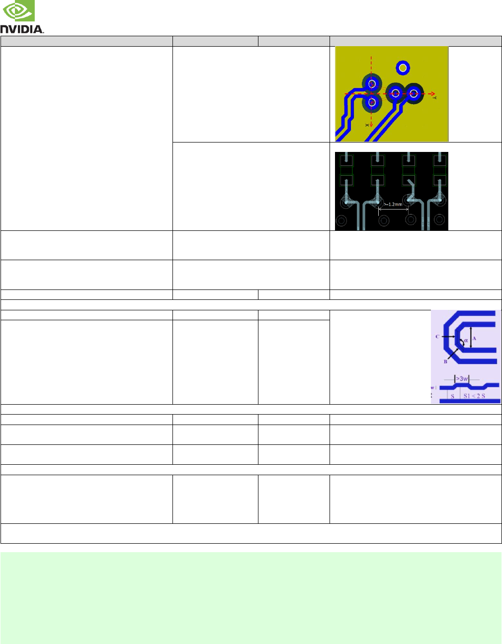
NVIDIA Jetson TX2 OEM Product Design Guide
JETSON TX2 OEM PRODUCT | DESIGN GUIDE | 20170912 41
Parameter
Requirement
Units
Notes
Topology
- Y-pattern is recommended
- keep symmetry
Xtalk suppression is best using the Y-pattern.
It can also reduce the limit of pair-pair
distance.
For in-line via, the distance from a via of one
lane to the adjacent via from other lane >=
1.2mm center-center.
GND via
Place GND via as symmetrically as possible to
data pair vias. Up to 4 signal vias (2 diff
pairs) can share a single GND return via
GND via is used to maintain return path, while its
Xtalk suppression is limited
Max # of Vias PTH vias
Micro Vias
4 if all vias are PTH via
Not limited as long as total channel loss
meets IL spec
Max Via Stub Length
0.4
mm
Serpentine
Min bend angle
135
deg (a)
S1 must be taken care in
order to consider Xtalk to
adjacent pair
Dimension Min A Spacing
Min B, C Length
Min Jog Width
4x
1.5x
3x
Trace width
AC Cap
Value
0.1
uF
Discrete 0402
Max Dist. from AC cap RBR/HBR
to connector HBR2
No requirement
0.5
in
Voiding RBR/HBR
HBR2
No requirement
Voiding required
HBR2: Voiding the plane directly under the pad 3-
4 mils larger than the pad size is recommended.
Connector
Voiding RBR/HBR
HBR2
No requirement
Voiding required
HBR2: Standard DP Connector: Voiding
requirement is stack-up dependent. For typical
stack-ups, voiding on the layer under the
connector pad is required to be 5.7mil larger than
the connector pad.
Keep critical eDP related traces including differential clock/data traces & RSET trace away from other signal traces or unrelated power traces/areas or
power supply components
Notes:
1. For eDP/DP, the spec puts a higher priority on the trace loss characteristic than on the impedance. However, before
selecting for impedance, it is important to make sure the selected stack-up, material & trace dimension can achieve
the needed low loss characteristic.
2. Longer trace lengths may be possible if the total trace loss is equal to or better than the target. If the loss is greater, the
max trace lengths will need to be reduced.
3. The average of the differential signals is used for length matching.
4. Do not perform length matching within breakout region. Recommend doing trace length matching to <1ps before Vias
or any discontinuity to minimize common mode conversion
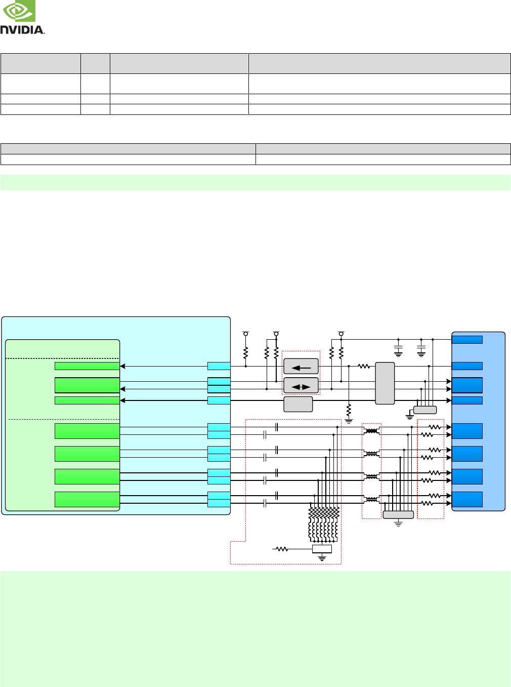
NVIDIA Jetson TX2 OEM Product Design Guide
JETSON TX2 OEM PRODUCT | DESIGN GUIDE | 20170912 42
Table 41. eDP Signal Connections
Jetson TX2 Pin
Name
Type
Termination
Description
DPx_TX[3:0]+/–
O
Series 0.1uF capacitors on all lines
eDP/DP Differential CLK/Data Lanes: Connect to matching pins on display
connector. See DP/HDMI Pin Mapping & connection diagram for details.
DPx_AUX+/–
I/OD
Series 0.1uF capacitors
eDP/DP: Auxiliary Channels: Connect to AUX_CH+/ on display connector.
DPx_HPD
I
eDP/DP: Hot Plug Detect: Connect to HPD pin on display connector.
Table 42. Recommended eDP/DP observation (test) points for initial boards
Test Points Recommended
Location
One for each signal line.
Near display connector. Connector pins can be used if accessible.
Note:
Test points must be done carefully to minimize signal integrity impact. Avoid stubs & keep pads small & near signal traces
7.2.2 HDMI
A standard DP 1.2a or HDMI V2.0 interface is supported. These share the same set of interface pins, so either Display Port or
HDMI can be supported natively. Dual-Mode DisplayPort(DP++ ) can be supported, in which the DisplayPort connector logically
outputs TMDS signaling to a DP-to-HDMI dongle.
7.2.3 HDMI
Figure 22: HDMI Connection Example
Jetson TX2
CEC Gating
Circuitry
10k10k
10k10k
VDD_3V3_SYS
1.8k1.8k
1.8k1.8k
VDD_5V0_HDMI
Tegra - HDMI
HDMI_DPx_TXDP3
HDMI_DPx_TXDN3
HDMI_DPx_TXDP2
HDMI_DPx_TXDN2
HDMI_DPx_TXDP1
HDMI_DPx_TXDN1
HDMI_DPx_TXDP0
HDMI_DPx_TXDN0
DP_AUX_CH1_P
DP_AUX_CH1_N
DP_AUX_CH1_HPD
eDP
HDMI_DPx
HDMI_CEC
10k10k
B3 6/A33
B3 5/A35
B3 4/A34
B3 3
G37/D37
G36/D36
F38/C38
F37/C37
H39/E3 9
H36/E3 6
H35/E3 5
H38/E3 8
DPx_HPD
DPx_AUX_CH+
DPx_AUX_CH
HDMI_CEC
DPx_TX2/HDMIx_TX0_P
DPx_TX2/HDMIx_TX0_N
DPx_TX1 / HDMIx_TX1_P
DPx_TX1 / HDMIx_TX1_N
DPx_TX0 / HDMIx_TX2_P
DPx_TX0 / HDMIx_TX2_N
DPx_TX3 / HDMIx_TXC_P
DPx_TX3 / HDMIx_TXC_N
FET
Enable
5V0_HDMI_EN
0.1uF
0.1uF
0.1uF
0.1uF
0.1uF
0.1uF
0.1uF
0.1uF
1%
@100MHz
See Note 1
Level Shifter
Level Shifter
VDD_1V8
DP0/DP1
TXD0_P
TXD0_N
TXD1_P
TXD1_N
TXD2_P
TXD2_N
TXC_P
TXC_N
SCL
SDA
HPD
CK+
CK-
D0+
D0-
D1+
D1-
D2+
D2-
CEC
+5V
ESD
100k100k
0.1uF
HDMI Connector
100k100k
10uF
EMI
See Note 2
See
Note 2
See Note 3
ESD
RS
RS
RS
RS
RS
RS
RS
RS
RS
RS
RS
RS
RS
RS
RS
RS
See
Note 4
CMC
Note:
1. Level shifters required on DDC/HPD. Jetson TX2 pads are not 5V tolerant & cannot directly meet HDMI VIL/VIH
requirements. HPD level shifter can be non-inverting or inverting.
2. If EMI/ESD devices are necessary, they must be tuned to minimize the impact to signal quality, which must meet the
timing & electrical requirements of the HDMI specification for the modes to be supported. See requirements &
recommendations in the related sections of the HDMI Interface Signal Routing Requirements table.
3. The HDMI_DP_TXx pads are native DP pads & require series AC capacitors (ACCAP) & pull-downs (RPD) to be HDMI
compliant. The 499, 1% pull-downs must be disabled when Tegra is off to meet the HDMI VOFF requirement. The
enable to the FET, enables the pull-downs when the HDMI interface is to be used. Chokes between pull-downs & FET are
required for Standard Technology designs and recommended for HDI designs.
4. Series resistors RS are required. See the RS section of the HDMI Interface Signal Routing Requirements table for details.
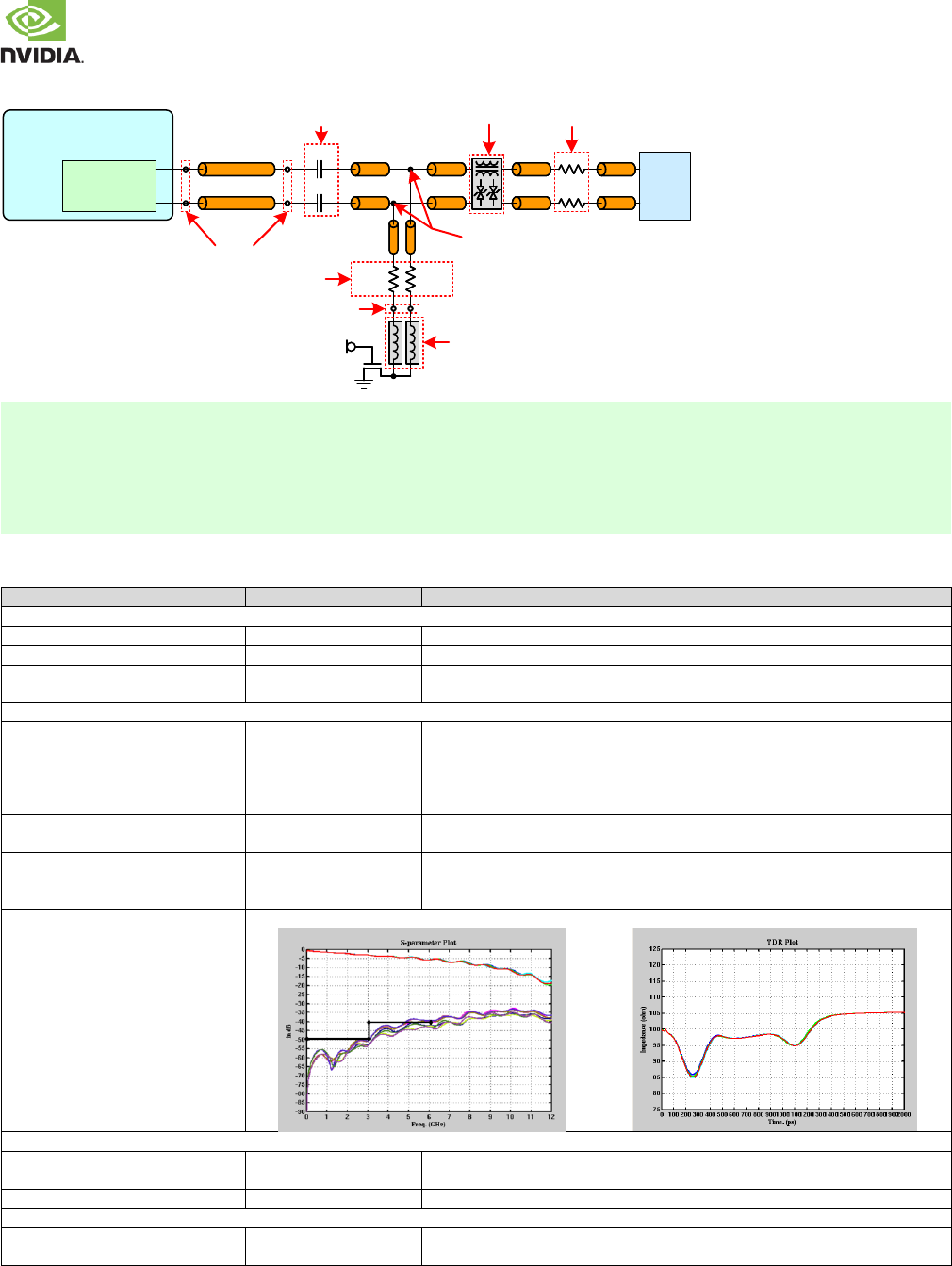
NVIDIA Jetson TX2 OEM Product Design Guide
JETSON TX2 OEM PRODUCT | DESIGN GUIDE | 20170912 43
Figure 23: HDMI Clk/Data Topology
Jetson TX2
HDMI
Conn
ACCAP
Seg D Seg F
3.3V
499Ω,
1%
PCB Vias
PCB Vias
0.1uF
0.1uF
RPD
Common Mode
Chokes & ESD
See Note 1
499Ω,
1%
Seg B Seg E
Seg C
Tegra --
--
Main Route –
Seg A
* Note 3 * Note 3* Note 3 * Note 3
RS
(See note 4)
Choke or Trace
See Note 2
Note:
1. RPD pad must be on the main trace. RPD & ACCAP must be on same layer.
2. -100MHz) between pull-downs & FET are required for Standard
Technology (through-hole) designs and recommended for HDI designs.
3. The trace after the main-route via should be routed on the Top or Bottom layer of the PCB, and either with 100ohm
differential impedance, or as uncoupled 50ohm Single Ended traces.
4. RS series resistor is required. See the RS section of the HDMI Interface Signal Routing Requirements table for details.
Table 43. HDMI Interface Signal Routing Requirements
Parameter
Requirement
Units
Notes
Specification
Max Frequency / UI
5.94 / 168
Gbps / ps
Per lane not total link bandwidth
Topology
Point to point
Unidirectional, Differential
Termination At Receiver
On-board
100
500
Differential To 3.3V at receiver
To GND near connector
Electrical Specification
IL
resonance dip frequency
<= 1.7
<= 2
<= 3
< 6
> 12
dB @ 1GHz
dB @ 1.5GHz
dB @ 3GHz
dB @ 6GHz
GHz
TDR dip
>= 85
@ Tr=200ps
10%-90%. If TDR dip is 75~85ohm that dip width
should < 250ps
FEXT (PSFEXT)
<= -50
<= -40
<= -40
dB at DC
dB at 3GHz
dB at 6GHz
PSNEXT is derived from an algebraic summation of the
individual NEXT effects on each pair by the other pairs
IL/FEXT plot
TDR plot
Impedance
Trace Impedance Diff pair
100
±10for the breakout & main
route is an implementation option.
Reference plane
GND
Trace spacing/Length/Skew
Trace loss characteristic:
< 0.8
< 0.4
dB/in. @ 3GHz
dB/in. @ 1.5GHz
The max length is derived based on this characteristic.
See note 1.
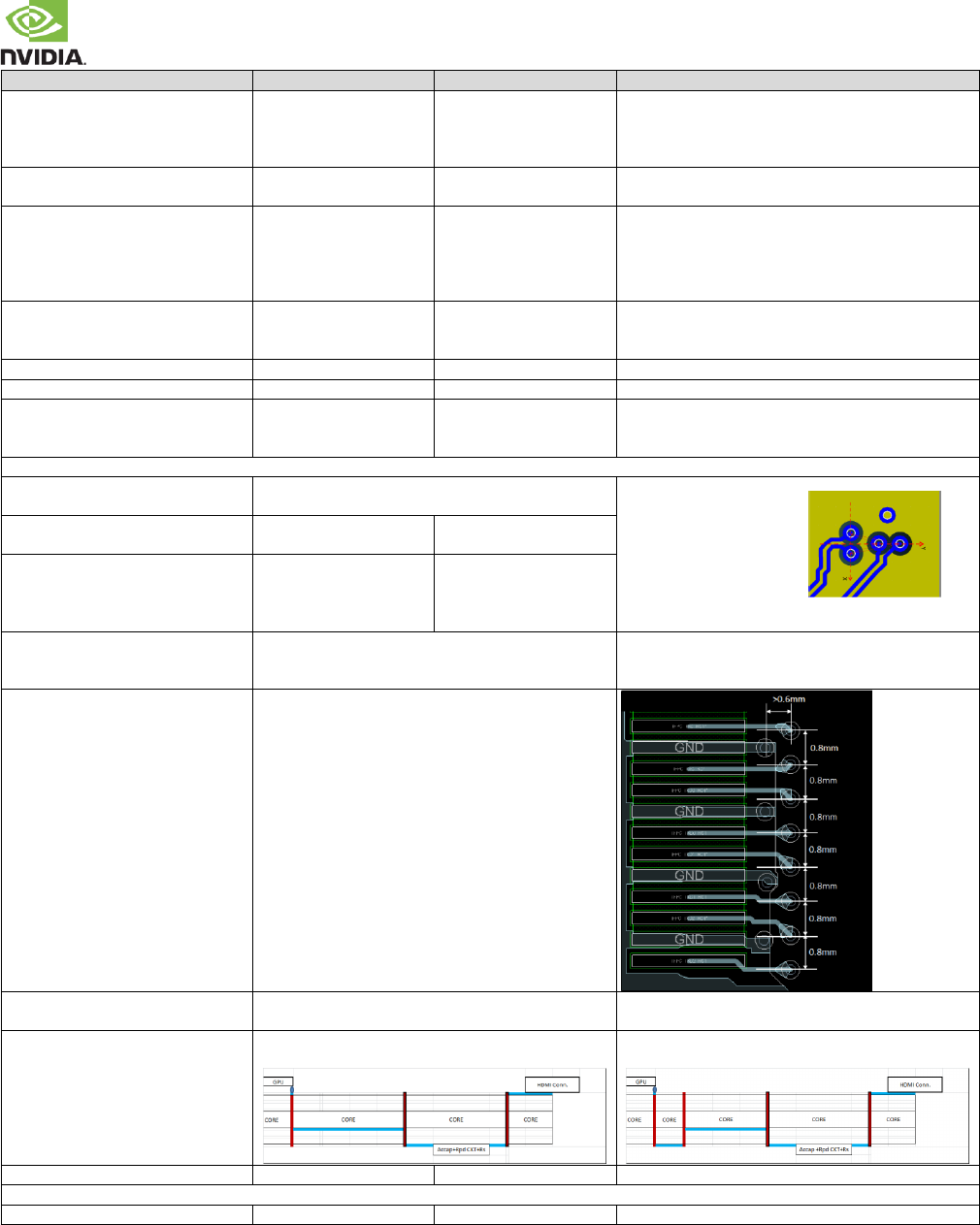
NVIDIA Jetson TX2 OEM Product Design Guide
JETSON TX2 OEM PRODUCT | DESIGN GUIDE | 20170912 44
Parameter
Requirement
Units
Notes
Trace spacing (Pair-Pair)
Stripline
Microstrip: pre 1.4b
Microstrip: 1.4b/2.0
3x
4x
5x to 7x
dielectric
For Stripline, this is 3x of the thinner of above and
below.
Trace spacing Stripline
(Main Link to DDC) Microstrip
3x
5x
dielectric
For Stripline, this is 3x of the thinner of above and
below.
Max Total Delay (1.4b/2.0 - up to
5.94Gbps)
Stripline
Microstrip (5x spacing)
Microstrip (7x spacing)
63.5/2.5 (437)
50.8/2.0 (300)
63.5/2.5 (375)
mm/in (ps)
Propagation delay: 175ps/in. for stripline, 150ps/in. for
microstrip).
Max Total Delay (Pre-1.4b)
(up to 165Mhz) Microstrip
Stripline
254/10 (1500)
225/8.5 (1500)
mm/in (ps)
Propagation delay: 175ps/in. for stripline, 150ps/in. for
microstrip).
Max Intra-Pair (within pair) Skew
0.15 (1)
Mm (ps)
See Notes 2, 3 & 4
Max Inter-Pair (pair to pair) Skew
150
ps
See Notes 2, 3 & 4
Max GND transition Via distance
1x
Diff pair via pitch
For signals switching reference layers, add one or two
ground stitching vias. It is recommended they be
symmetrical to signal vias.
Via
Topology
8. Y-pattern is recommended
9. keep symmetry
Xtalk suppression is the
best by Y-pattern. Also it
can reduce the limit of
pair-pair distance. Need
review (NEXT/FEXT check)
if via placement is not Y-
pattern.
Minimum Impedance Dip
97
92
@200ps
@35ps
Recommended Via Dimension
drill/pad
Antipad
Via pitch
200/400
840
880
uM
GND via
Place GND via as symmetrically as possible to data pair
vias. Up to 4 signal vias (2 diff pairs) can share a single
GND return via
GND via is used to maintain return path, while its Xtalk
suppression is limited
Connector pin via
- The break-in trace to the connector pin via should
be routed on the BOTTOM in order to avoid via stub
effect
- Equal spacing (0.8mm) between adjacent signal
vias.
- The x-axis distance between signal and GND via
should be > 0.6mm
Max # of Vias PTH via
u-via
4 if all vias are PTH via
Not limited as long as total channel loss meets IL spec.
No breakout: 3 vias
breakout on the same layer as main trunk: 4 vias
Max Via Stub Length
0.4
mm
long via stub requires review (IL & resonance dip check)
Serpentine
Min bend angle
135
deg (a)
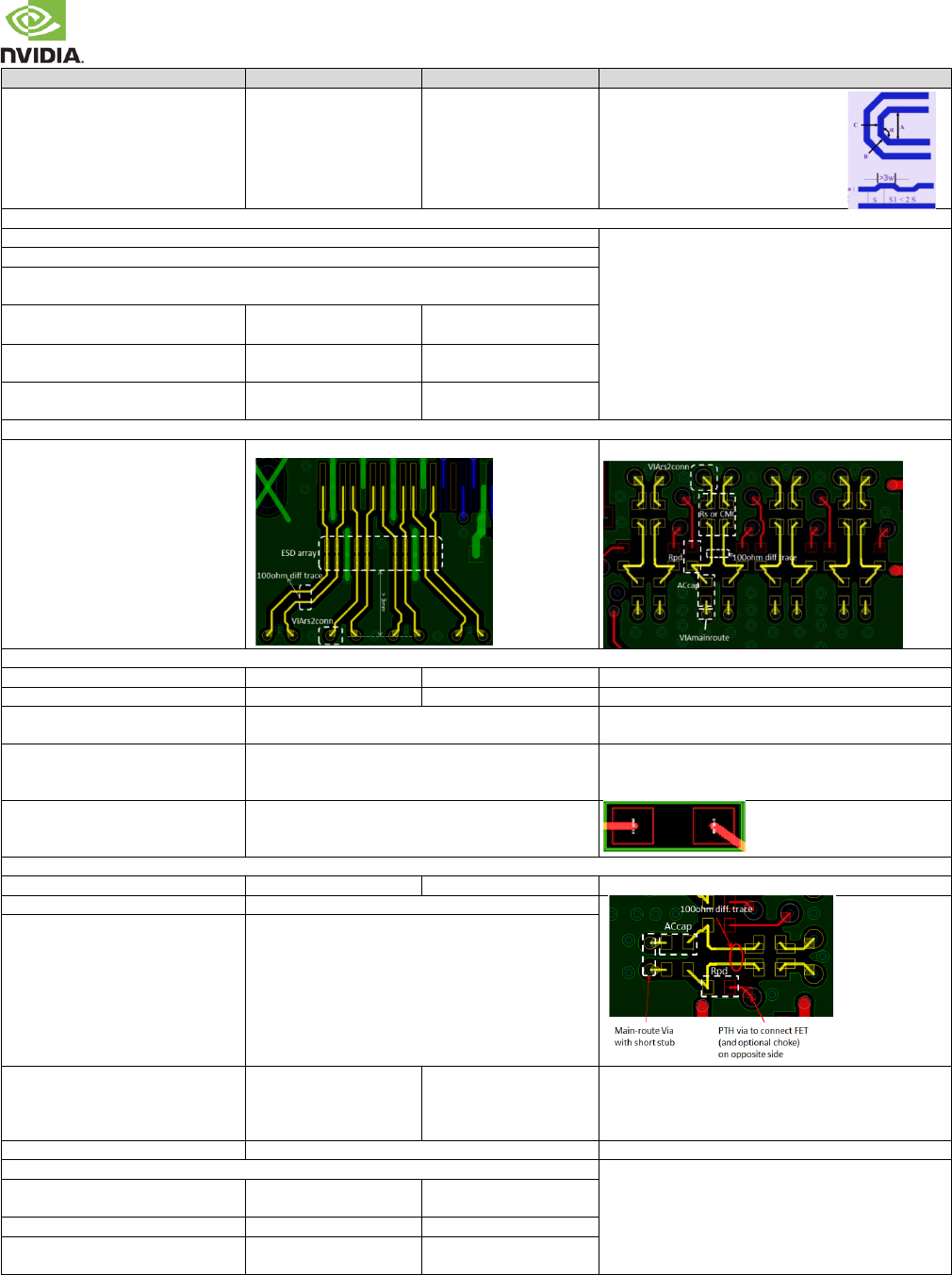
NVIDIA Jetson TX2 OEM Product Design Guide
JETSON TX2 OEM PRODUCT | DESIGN GUIDE | 20170912 45
Parameter
Requirement
Units
Notes
Dimension Min A Spacing
Min B, C Length
Min Jog Width
4x
1.5x
3x
Trace width
S1 must be taken care in order to
consider Xtalk to adjacent pair
Topology
The main-route via dimensions should comply with the via structure rules (See Via section)
See topology figure above table
For the connector pin vias, follow the rules for the connector pin vias (See Via section)
The traces after main-route via should be routed as 100as uncoupled 50ohm
Single-ended traces on PCB Top or Bottom.
Max distance from RPD to main
trace (seg B)
1
mm
Max distance from AC cap to RPD
stubbing point (seg A)
~0
mm
Max distance between ESD and
signal via
3
mm
Add-on Components
Example of a case where space is
limited for placing components.
Top
Bottom
AC Cap
Value
0.1
uF
Max via distance from BGA
7.62 (52.5)
mm (ps)
Location
must be placed before pull-down resistor
The distance between the AC cap and the HDMI
connector is not restricted.
Placement PTH design
Micro-Via design
Place cap on bottom layer if main-route above core
Place cap on top layer if main-route below core
Not Restricted
Void
GND (or PWR) void under/above the cap is needed.
Void size = SMT area + 1x dielectric height keepout
distance
Pull-down Resistor (RPD), choke/FET
Value
500
Location.
Must be placed after AC cap
Layer of placement
Same layer as AC cap. The FET & choke can be placed
on the opposite layer thru a PTH via
Choke between RPD & FET Choke
Max Trace Rdc
Max Trace length
600 or
1
20
4
@100MHz
uH@DC-100MHz
m
mm
Can be choke or Trace. Recommended option for
HDMI2.0 HF1-9 improvement.
Void
GND/PWR void under/above cap is preferred
Common-Mode Choke (Stuffing option – not added unless EMI issue is seen)
TDK ACM2012D-900-2P
Common-mode Min
impedance @ 100MHz Max
65
90
RDC
<=0.3ohm
Differential TDR impedance
90ohm +/-15% @
Tr=200ps (10%-90%)
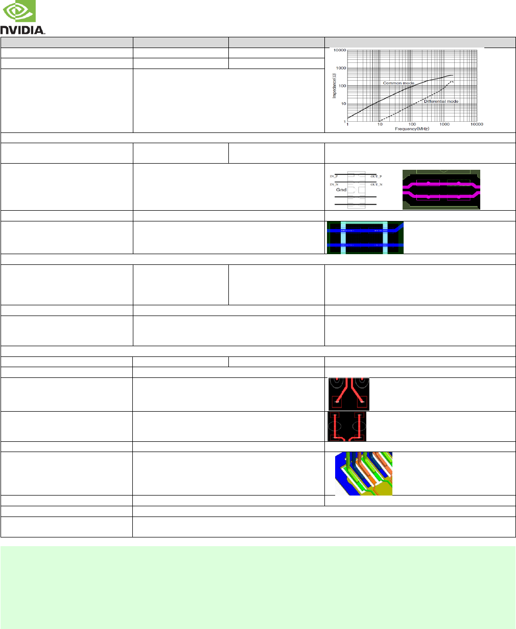
NVIDIA Jetson TX2 OEM Product Design Guide
JETSON TX2 OEM PRODUCT | DESIGN GUIDE | 20170912 46
Parameter
Requirement
Units
Notes
Min Sdd21 @ 2.5GHz
2.22
dB
Max Scc21 @ 2.5GHz
19.2
dB
Location
Close to any adjacent discontinuity (< 8mm) such as
connector, via, etc.
ESD (On-chip protection diode is able to withstand 2kV HMM. External ESD is optional. Designs should include ESD footprint as a stuffing option)
Max junction capacitance
(IO to GND)
0.35
pF
e.g. ON-semiconductor ESD8040
Footprint
Pad right on the net instead of trace stub
Location
After pull-down resistor/CMC and before RS
Void
GND/PWR void under/above the cap is needed. Void
size = 1mm x 2mm for 1 pair
Series Resistor (RS) Series resistor on P/N path for HDMI 2.0 (Mandatory)
Value
6
± 10%. 0ohm is acceptable if the design passes the
HDMI2.0 HF1-9 test. Otherwise, adjust the RS value to
ensure the HDMI2.0 tests pass: Eye diagram, Vlow test
and HF1-9 TDR test
Location
After all components and before HDMI connector
Void
GND/PWR void under/above the RS device is needed.
Void size = SMT area + 1x dielectric height keepout
distance.
Trace at Component Region
Value
100
± 10%
Location
At component region (Microstrip)
Trace entering the SMT pad
One 45°
Trace between components
Uncoupled structure
HDMI Connector
Connector Voiding
Voiding the ground below the signal lanes
0.1448(5.7mil) larger than the pin itself
General
Routing over Voids
Routing over voids not allowed except void around device ball/pin the signal is routed to.
Noise Coupling
Keep critical HDMI related traces including differential clock/data traces & RSET trace away from other signal
traces or unrelated power traces/areas or power supply components
Note:
1. Longer trace lengths may be possible if the total trace loss is equal to or better than the target. If the loss is greater, the
max trace lengths will need to be reduced.
2. The average of the differential signals is used for length matching.
3. Do not perform length matching within breakout region. Recommend doing trace length matching to <1ps before vias or
any discontinuity to minimize common mode conversion
4. If routing includes a flex or 2nd PCB, the max trace delay & skew calculations must include all the PCBs/flex routing.
Solutions with flex/2nd PCB may not achieve maximum frequency operation.
NVIDIA Jetson TX2 OEM Product Design Guide
JETSON TX2 OEM PRODUCT | DESIGN GUIDE | 20170912 47
Table 44. HDMI Signal Connections
Jetson TX2 Pin Name
Type
Termination (see note on ESD)
Description
DPx_TX3+/–
DIFF
OUT
0.1uF series ACCAP PD (controlled by FET)
EMI/ESD (if required),.S (series resistor)
HDMI Differential Clock: Connect to C–/C+ & pins on
HDMI Connector
DPx_TX[2:0] +/–
DIFF
OUT
HDMI Differential Data: Connect to D[2:0]+/– pins. See
DP/HDMI Pin Mapping table and connection diagram.
DPx_HPD
I
Jetson TX2 level
shifter 100GND on
connector side.
HDMI Hot Plug Detect: Connect to HPD pin on HDMI
Connector
HDMI_CEC
I/OD
Gating circuitry, See connection figure or reference
schematics for details.
HDMI Consumer Electronics Control: Connect to CEC
on HDMI Connector through circuitry.
DPx_AUX_CH+/–
I/OD
From Jetson TX2 level
shifter connector pin
HDMI: DDC Interface – Clock and Data: Connect
DP1_AUX_CH+ to SCL & DP1_AUX_CH– to SDA on
HDMI Connector
HDMI 5V Supply
P
Adequate decoupling (0.1uF & 10uF recommended) on
supply near connector.
HDMI 5V supply to connector: Connect to +5V on
HDMI Connector.
Note:
Any ESD and/or EMI solutions must support targeted modes (frequencies).
Table 45. Recommended HDMI / DP observation (test) points for initial boards
Test Points Recommended
Location
One for each signal line.
Near display connector. Connector pins can be used if accessible.
Note:
Test points must be done carefully to minimize signal integrity impact. Avoid stubs & keep pads small & near signal traces
Figure 24: Optional Dual-Mode (DP/HDMI) Connections
100kΩ100kΩ
100kΩ100kΩ
100kΩ100kΩ
100kΩ100kΩGated
3.3V
0.1uF
0.1uF
DP_MODE*
DP_MODE*
5.0V
10kΩ10kΩ10kΩ10kΩ
10kΩ10kΩ
10kΩ10kΩ
10nF
CONFIG1
To DP Connector
DP_AUX
DP_AUX*
DP_AUX_CHx_P
DP_AUX_CHx_N
To Jetson
TX2
DP Interface Signal Routing Requirements
See eDP/DP Signal Routing Requirements.
NVIDIA Jetson TX2 OEM Product Design Guide
JETSON TX2 OEM PRODUCT | DESIGN GUIDE | 20170912 48
8.0 MIPI CSI (VIDEO INPUT)
Jetson TX2 supports three MIPI CSI x4 bricks, allowing a variety of device types and combinations to be supported. Up to three
quad lane stereo cameras or 6 dual lane camera streams are available. Each data lane has a peak bandwidth of up to 2.5Gbps.
Note:
Maximum data rate may be limited by use case / memory bandwidth.
Table 46. Jetson TX2 CSI Pin Descriptions
Pin #
Jetson TX2 Pin Name
Tegra Signal
Usage/Description
Usage on the Carrier
Board
Direction
Pin Type
G27
CSI0_CLK
CSI_A_CLK_N
Camera, CSI 0 Clock
Camera Connector
Input
MIPI D-PHY
G28
CSI0_CLK+
CSI_A_CLK_P
Camera, CSI 0 Clock+
Input
F28
CSI0_D0
CSI_A_D0_N
Camera, CSI 0 Data 0
Input
F29
CSI0_D0+
CSI_A_D0_P
Camera, CSI 0 Data 0+
Input
H26
CSI0_D1
CSI_A_D1_N
Camera, CSI 0 Data 1
Input
H27
CSI0_D1+
CSI_A_D1_P
Camera, CSI 0 Data 1+
Input
D27
CSI1_CLK
CSI_B_CLK_N
Camera, CSI 1 Clock
Input
D28
CSI1_CLK+
CSI_B_CLK_P
Camera, CSI 1 Clock+
Input
C28
CSI1_D0
CSI_B_D0_N
Camera, CSI 1 Data 0
Input
C29
CSI1_D0+
CSI_B_D0_P
Camera, CSI 1 Data 0+
Input
E26
CSI1_D1
CSI_B_D1_N
Camera, CSI 1 Data 1
Input
E27
CSI1_D1+
CSI_B_D1_P
Camera, CSI 1 Data 1+
Input
G24
CSI2_CLK
CSI_C_CLK_N
Camera, CSI 2 Clock
Input
G25
CSI2_CLK+
CSI_C_CLK_P
Camera, CSI 2 Clock+
Input
F25
CSI2_D0
CSI_C_D0_N
Camera, CSI 2 Data 0
Input
F26
CSI2_D0+
CSI_C_D0_P
Camera, CSI 2 Data 0+
Input
H23
CSI2_D1
CSI_C_D1_N
Camera, CSI 2 Data 1
Input
H24
CSI2_D1+
CSI_C_D1_P
Camera, CSI 2 Data 1+
Input
D24
CSI3_CLK
CSI_D_CLK_N
Camera, CSI 3 Clock
Input
D25
CSI3_CLK+
CSI_D_CLK_P
Camera, CSI 3 Clock+
Input
C25
CSI3_D0
CSI_D_D0_N
Camera, CSI 3 Data 0
Input
C26
CSI3_D0+
CSI_D_D0_P
Camera, CSI 3 Data 0+
Input
E23
CSI3_D1
CSI_D_D1_N
Camera, CSI 3 Data 1
Input
E24
CSI3_D1+
CSI_D_D1_P
Camera, CSI 3 Data 1+
Input
G21
CSI4_CLK
CSI_E_CLK_N
Camera, CSI 4 Clock
Input
G22
CSI4_CLK+
CSI_E_CLK_P
Camera CSI 4 Clock+
Input
F22
CSI4_D0
CSI_E_D0_N
Camera, CSI 4 Data 0
Input
F23
CSI4_D0+
CSI_E_D0_P
Camera, CSI 4 Data 0+
Input
H20
CSI4_D1
CSI_E_D1_N
Camera, CSI 4 Data 1
Input
H21
CSI4_D1+
CSI_E_D1_P
Camera, CSI 4 Data 1+
Input
D21
CSI5_CLK
CSI_F_CLK_N
Camera, CSI 5 Clock
Input
D22
CSI5_CLK+
CSI_F_CLK_P
Camera, CSI 5 Clock+
Input
C22
CSI5_D0
CSI_F_D0_N
Camera, CSI 5 Data 0
Input
C23
CSI5_D0+
CSI_F_D0_P
Camera, CSI 5 Data 0+
Input
E20
CSI5_D1
CSI_F_D1_N
Camera, CSI 5 Data 1
Input
E21
CSI5_D1+
CSI_F_D1_P
Camera, CSI 5 Data 1+
Input
Table 47. Jetson TX2 Camera Miscellaneous Pin Descriptions
Pin #
Jetson TX2 Pin Name
Tegra Signal
Usage/Description
Usage on the Carrier
Board
Direction
Pin Type
F9
CAM0_MCLK
EXTPERIPH1_CLK
Camera 0 Reference Clock
Camera Connector
Output
CMOS 1.8V
F8
CAM1_MCLK
EXTPERIPH2_CLK
Camera 1 Reference Clock
Output
CMOS 1.8V
E7
CAM2_MCLK
GPIO_CAM2
Camera 2 Master Clock
Output
CMOS 1.8V
G8
GPIO0_CAM0_PWR#
QSPI_SCK
Camera 0 Powerdown or GPIO
Output
CMOS 1.8V
F7
GPIO1_CAM1_PWR#
GPIO_CAM3
Camera 1 Powerdown or GPIO
Output
CMOS 1.8V
H8
GPIO2_CAM0_RST#
QSPI_CS_N
Camera 0 Reset or GPIO
Output
CMOS 1.8V
H7
GPIO3_CAM1_RST#
QSPI_IO0
Camera 1 Reset or GPIO
Output
CMOS 1.8V
G7
GPIO4_CAM_STROBE
GPIO_SEN5
Camera Strobe or GPIO
Output
CMOS 1.8V
D7
GPIO5_CAM_FLASH_EN
UART5_RTS_N
Camera Flash Enable or GPIO
Output
CMOS 1.8V
E8
CAM_VSYNC
QSPI_IO1
Camera Vertical Sync
Output
CMOS 1.8V
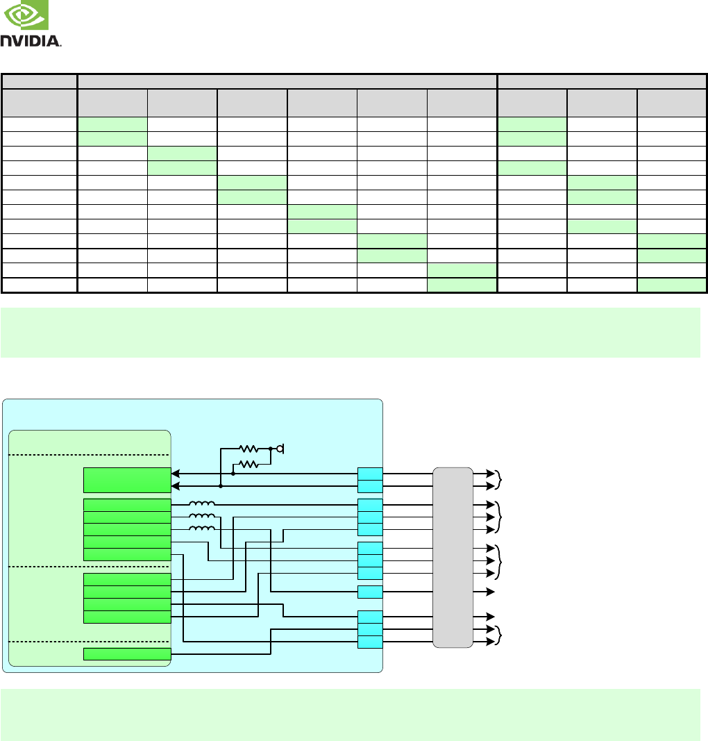
NVIDIA Jetson TX2 OEM Product Design Guide
JETSON TX2 OEM PRODUCT | DESIGN GUIDE | 20170912 49
Table 48. CSI Configurations
2-Lane Configurations
4-Lane Configurations
Camera #
CSI Lanes
#1
#2
#3
#4
#5
#6
#1
#2
#3
CSI_0_CLK
CSI_0_D[1:0]
CSI_1_CLK
CSI_1_D[1:0]
CSI_2_CLK
CSI_2_D[1:0]
CSI_3_CLK
CSI_3_D[1:0]
CSI_4_CLK
CSI_4_D[1:0]
CSI_5_CLK
CSI_5_D[1:0]
Note:
1. Each 2-lane options shown above can also be used for one single lane camera as well
2. Combinations of 1, 2 & 4-lane cameras are supported, as long as any 4-lane cameras match one of the three configurations
above
Figure 25: Camera Control Connections
EMI
&
ESD
Jetson TX2
1k1k
1k1kVDD_1V8
Camera
I2C
Camera 0
Clock/Control
Camera 1
Clock/Control
Camera
Strobe/Flash
CAM_AF_EN
I2C_CAM_CLK
I2C_CAM_DAT
CAM0_MCLK
GPIO0_CAM0_PWR#
GPIO2_CAM0_RST#
CAM1_MCLK
GPIO1_CAM1_PWR#
GPIO3_CAM1_RST#
CAM2_MCLK
CAM_VSYNC
GPIO4_CAM_STROBE
GPIO5_CAM_FLASH_EN
D6
F9
G8
G7
D7
C6
F7
F8
H7
H8
Tegra
UART/CAM CAM_I2C_SCL
CAM_I2C_SDA
EXTPERIPH1_CLK
UART5_RTS
GPIO_CAM3
QSPI_SCK
EXTPERIPH2_CLK
SPI QSPI_CS
QSPI_IO0
QSPI_IO1
E8
GPIO_CAM2
E7 Camera 2 Clock
Misc.
GPIO_SEN5
AO
Note:
1. If Jetson TX2 is providing flash control (as shown), GPIO5_CAM_FLASH_EN & GPIO4_CAM_STROBE must be used.
2. Any EMI/ESD devices must be tuned to minimize impact to signal quality and meet the timing & Vil/Vih requirements at
the receiver & maintain signal quality and meet requirements for the frequencies supported by the design.
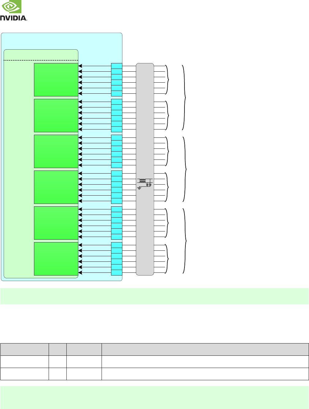
NVIDIA Jetson TX2 OEM Product Design Guide
JETSON TX2 OEM PRODUCT | DESIGN GUIDE | 20170912 50
Figure 26: Camera CSI Connections
Jetson TX2
Tegra
DSI/CSI CSI_A_CLK_P
CSI_A_CLK_N
CSI_A_D0_P
CSI_A_D0_N
CSI_A_D1_P
CSI_A_D1_N
EMI
&
ESD
CSI_C_CLK_P
CSI_C_CLK_N
CSI_C_D0_P
CSI_C_D0_N
CSI_C_D1_P
CSI_C_D1_N
CSI_B_CLK_P
CSI_B_CLK_N
CSI_B_D0_P
CSI_B_D0_N
CSI_B_D1_P
CSI_B_D1_N
CSI_D_CLK_P
CSI_D_CLK_N
CSI_D_D0_P
CSI_D_D0_N
CSI_D_D1_P
CSI_D_D1_N
CSI_F_CLK_P
CSI_F_CLK_N
CSI_F_D0_P
CSI_F_D0_N
CSI_F_D1_P
CSI_F_D1_N
CSI_E_CLK_P
CSI_E_CLK_N
CSI_E_D0_P
CSI_E_D0_N
CSI_E_D1_P
CSI_E_D1_N
CSI0_CK+
CSI0_CK
CSI0_D0+
CSI0_D0
CSI0_D1+
CSI0_D1
CSI1_CK+
CSI1_CK
CSI1_D0+
CSI1_D0
CSI1_D1+
CSI1_D1
CSI2_CK+
CSI2_CK
CSI2_D0+
CSI2_D0
CSI2_D1+
CSI2_D1
CSI3_CK+
CSI3_CK
CSI3_D0+
CSI3_D0
CSI3_D1+
CSI3_D1
CSI4_CK+
CSI4_CK
CSI4_D0+
CSI4_D0
CSI4_D1+
CSI4_D1
CSI5_CK+
CSI5_CK
CSI5_D0+
CSI5_D0
CSI5_D1+
CSI5_D1
G27
F29
F28
H27
H26
G28
D27
C29
C28
E27
E26
D28
G24
F26
F25
H24
H23
G25
D24
C26
C25
E24
E23
D25
G21
F23
F22
H21
H20
G22
D21
C23
C22
E21
E20
D22
4-Lane
(B_CLK not
used)
2-Lane
2-Lane
2-Lane
2-Lane
4-Lane
(D_CLK not
used)
2-Lane
2-Lane
4-Lane
(F_CLK not
used)
Note:
Any EMI/ESD devices must be tuned to minimize impact to signal quality and meet the timing & Vil/Vih requirements at the
receiver & maintain signal quality and meet requirements for the frequencies supported by the design.
CSI Design Guidelines
CSI & DSI use the MIPI D-PHY for the physical interface. The routing & connection requirements are found in the DSI section.
Table 49. MIPI CSI Signal Connections
Jetson TX2 Pin
Name
Type
Termination
Description
CSI[5:0]_CLK+/–
I
See note
CSI Differential Clocks: Connect to clock pins of camera. See the CSI Configurations tables for
details
CSI[5:0]_D[1:0]+/–
I/O
See note
CSI Differential Data Lanes: Connect to data pins of camera. See the CSI Configurations tables for
details
Note:
Depending on the mechanical design of the platform and camera modules, ESD protection may be necessary. In addition,
EMI control may be needed. Both are shown in the Camera Connection Example diagram. Any EMI/ESD solution must be
compatible with the frequency required by the design.
NVIDIA Jetson TX2 OEM Product Design Guide
JETSON TX2 OEM PRODUCT | DESIGN GUIDE | 20170912 51
Table 50. Miscellaneous Camera Connections
Jetson TX2 Pin Name
Type
Termination
Description
I2C_CAM_CLK
I2C_CAM_DAT
O
I/O
1k Pull-ups VDD_1V8 (on Jetson TX2).
See note related to EMI/ESD under MIPI
CSI Signal Connections tables.
Camera I2C Interface: Connect to I2C SCL & SDA pins of imager
CAM[2:0]_MCLK
O
120Jetson TX2) See
note related to EMI/ESD under MIPI CSI
Signal Connections tables.
Camera Master Clocks: Connect to Camera reference clock
inputs.
GPIO1_CAM1_PWR#
GPIO0_CAM0_PWR#
I/O
See note related to ESD under MIPI CSI
Signal Connections tables.
Camera Power Control signals (or GPIOs [1:0]): Connect to
powerdown pins on camera(s).
GPIO4_CAM_STROBE
Camera Strobe Enable (or GPIO 4): Connect to camera strobe
circuit unless strobe control comes from camera module.
GPIO5_CAM_FLASH_EN
O
Camera Flash Enable: Connect to enable of flash circuit
GPIO3_CAM1_RST#
GPIO2_CAM0_RST#
O
Camera Resets (or GPIO [3:2]): Connect to reset pin on any
cameras with this function. If AutoFocus Enable is required,
connect GPIO3_CAM1_RST# to AF_EN pin on camera module &
use GPIO2_CAM0_RST# as common reset line.
CAM_VSYNC
O
Camera Vertical Sync
Table 51. Recommended CSI observation (test) points for initial boards
Test Points Recommended
Location
One per signal line.
Near Jetson TX2 pins
Note:
Test points must be done carefully to minimize signal integrity impact. Avoid stubs & keep pads small & near signal traces
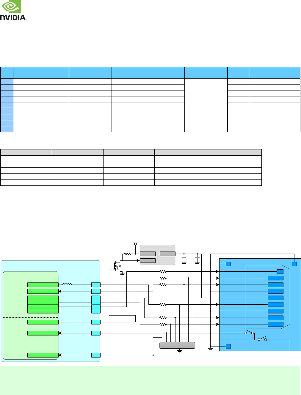
NVIDIA Jetson TX2 OEM Product Design Guide
JETSON TX2 OEM PRODUCT | DESIGN GUIDE | 20170912 52
9.0 SDIO/SDCARD/EMMC
Jetson TX2 has four SD/MMC interfaces. Three are used on Jetson TX2 for eMMC, WLAN/BT & Ethernet. One is brought to
the connector pins for SD Card or SDIO use.
Table 52. Jetson TX2 SDMMC Pin Descriptions
Pin #
Jetson TX2 Pin Name
Tegra Signal
Usage/Description
Usage on the Carrier
Board
Direction
Pin Type
G18
SDCARD_CLK
SDMMC1_CLK
SD Card (or SDIO) Clock
SD Card
Output
CMOS 3.3/1.8V
G19
SDCARD_CMD
SDMMC1_CMD
SD Card (or SDIO) Command
Bidir
CMOS 3.3/1.8V
H18
SDCARD_D0
SDMMC1_DAT0
SD Card (or SDIO) Data 0
Bidir
CMOS 3.3V/1.8V
H17
SDCARD_D1
SDMMC1_DAT1
SD Card (or SDIO) Data 1
Bidir
CMOS 3.3V/1.8V
F19
SDCARD_D2
SDMMC1_DAT2
SD Card (or SDIO) Data 2
Bidir
CMOS 3.3/1.8V
F18
SDCARD_D3
SDMMC1_DAT3
SD Card (or SDIO) Data 3
Bidir
CMOS 3.3/1.8V
F17
SDCARD_CD#
GPIO_EDP2
SD Card Card Detect
Input
CMOS 1.8V
H16
SDCARD_PWR_EN
GPIO_EDP3
SD Card power switch Enable
Output
CMOS 1.8V
F20
SDCARD_WP
GPIO_EDP1
SD Card Write Protect
Input
CMOS 1.8V
Table 53. SDIO / SD Card / eMMC Interface Mapping
Jetson TX2 Pins
Tegra Interface
Width
Usage
SDCARD
SDMMC1
4-bit
SD (Primary SD Card). Can be used instead for SDIO
interface.
N/A
SDMMC2
4-bit
Pins used for EQOS for Ethernet on Jetson TX2
N/A
SDMMC3
4-bit
Used on Jetson TX2 for WLAN/BT
N/A
SDMMC4
8-bit
Used on Jetson TX2 - eMMC
9.1 SD Card
The Figure shows a standard SD socket. Internal pull-up resistors are used for SDCARD Data/CMD lines, so external pull-ups
are not required.
Figure 27. SD Card Socket Connection Example
Jetson TX2
SDMMC1_ CD*
Tegra
SDMMC1 SDMMC1_CLK
SDMMC1_CMD
GPIO_EDP1
EDP
ESD
DATA2
DATA3
CMD
VDD
CLK
GND
DATA0
DATA1
C_DETECT
COMMON
VDD_3V3_SYS
SDMMC1_DAT3
Load Switch
VOUTVIN
ON
SDMMC_VDD_EN
GPIO_EDP2
GND
GPIO_EDP3
SDMMC1_ WP
C_WR_PROTECT
SDCARD_CLK
SDCARD_CMD
SDCARD_D0
SDCARD_D1
SDCARD_D2
SDCARD_D3
SDCARD_PWR_EN
SDCARD_CD#
SDCARD_WP
SDMMC1_DAT2
SDMMC1_DAT1
SDMMC1_DAT0
G19
G18
F17
H16
F20
H18
H17
F19
F18
1010
10
10
1010
00
1010
1010
MHz
4.7k
4.7k
GS
D
GS
D
Notes:
1. If EMI and/or ESD devices are necessary, they must be tuned to minimize the impact to signal quality, which must meet
the timing & Vil/Vih requirements at the receiver & maintain signal quality and meet requirements for the frequencies
supported by the design.
2. Supply (load switch, etc) used to provide power to the SD Card must be current limited if the supply is shorted to GND.
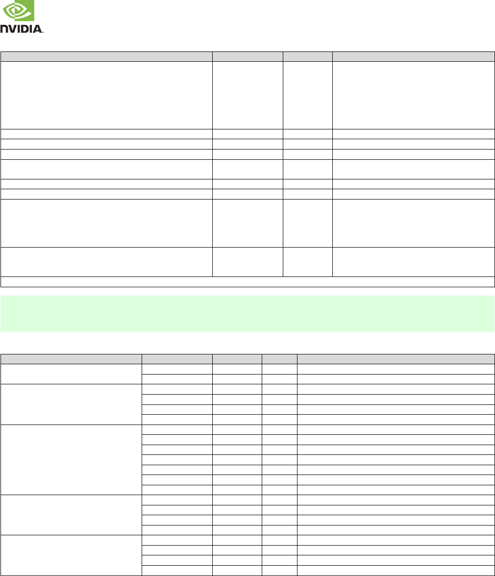
NVIDIA Jetson TX2 OEM Product Design Guide
JETSON TX2 OEM PRODUCT | DESIGN GUIDE | 20170912 53
Table 54. SDCARD Interface Signal Routing Requirements
Parameter
Requirement
Units
Notes
Max Frequency 3.3V Signaling DS
HS
1.8V Signaling SDR12
SDR25
SDR50
SDR104
DDR50
25 (12.5)
50 (25)
25 (12.5)
50 (25)
100 (50)
208 (104)
50 (50)
MHz (MB/s)
See Note 1
Topology
Point to point
Reference plane
GND or PWR
See Note 2
Trace Impedance
50
-up
Max Via Count PTH
HDI
4
10
Independand of stackup layers
Depends on stackup layers
Via proximity (Signal to reference)
< 3.8 (24)
mm (ps)
Up to 4 signal Vias can share 1 GND return Via
Trace spacing Microstrip / Stripline
4x / 3x
dielectric
Trace length
SDR50 / SDR25 / SDR12 / HS / DS Min
Max
SDR104 / DDR50 Min
Max
16 (100)
139 (876)
16 (100)
83 (521)
mm (ps)
Max Trace Delay Skew in/between CLK & CMD/DAT
SDR50 / SDR25 / SDR12 / HS / DS
SDR104 / DDR50
14 (87.5)
2 (12.5)
Mm (ps)
See Note 3
Keep CLK, CMD & DATA traces away from other signal traces or unrelated power traces/areas or power supply components
Note:
1. Actual frequencies may be lower due to clock source/divider limitations.
2. If PWR, 0.01uF decoupling cap required for return current.
3. If routing to SD Card socket includes a flex or 2nd PCB, max trace & skew calculations must include PCB & flex routing.
Table 55. SD Card Loading vs Drive Type
General SD Card Compliance
Parameter
Value
Units
Notes
CCARD (CDIE+CPKG)
Min
5
pF
Spec best case value
Max
10
pF
Spec worst case value
Drive Type
A
33
UHS50 Card = optional, UHS104 Card = mandatory
B
50
UHS50 Card = mandatory, UHS104 Card = mandatory
C
66
UHS50 Card = optional, UHS104 Card = mandatory
D
100
UHS50 Card = optional, UHS104 Card = mandatory
FMAX (CLK base frequency)
SDR104
208
MHz
Single data rate up to 104MB/sec
DDR50
50
MHz
Double data rate up to 50MB/sec
SDR50
100
MHz
Single data rate up to 50MB/sec
SDR25
50
MHz
Single data rate up to 25MB/sec
SDR12
25
MHz
Single data rate up to 12.5MB/sec
HS
50
MHz
Single data rate up to 25MB/sec
DS
25
MHz
Single data rate up to 12.5MB/sec
CLOAD (CCARD+CEQ)
(CLK freq = 208MHz)
Drive Type = A
21
pF
Total load capacitance supported
Drive Type = B
15
pF
Total load capacitance supported
Drive Type = C
11
pF
Total load capacitance supported
Drive Type = D
22
pF
Possibly 22pF+ depending on host system
CLOAD (CCARD+CEQ)
(CLK freq = 100/50/25MHz)
Drive Type = A
43
pF
Total load capacitance supported
Drive Type = B
30
pF
Total load capacitance supported
Drive Type = C
23
pF
Total load capacitance supported
Drive Type = D
22
pF
Possibly 22pF+ depending on host system
NVIDIA Jetson TX2 OEM Product Design Guide
JETSON TX2 OEM PRODUCT | DESIGN GUIDE | 20170912 54
Table 56. SDCARD Signal Connections
Function Signal Name
Type
Termination
Description
SDCARD_CLK
O
120 bead on module
for SDCARD_CLK. 0
series resistor on carrier
board as placeholder.
See note for EMI/ESD
SDIO/SD Card Clock: Connect to CLK pin of device or socket
SDCARD_CMD
I/O
10 series resistors for
SDCARD CMD/D[3:0].
See note for EMI/ESD
SDIO/SDMMC Command: Connect to CMD pin of device/socket
SDCARD_D[3:0]
I/O
SDIO/SDMMC Data: Connect to Data pins of device or socket
SDCARD_CD#
I
SDIO Card Detect: Connect to CD/C_DETECT pin on socket if required.
SDCARD_WP
I
SDIO Write Protect: Connect to WP/WR_PROTECT pin on socket if required.
SDIO_RST#
O
SDIO Reset: Connect to reset line on SDIO peripheral/connector.
SDCARD_PWR_EN
O
SDIO Supply/Load Switch Enable: Connect to enable of supply/load switch
supplying VDD on SD Card socket.
Note:
EMI/ESD may be required for SDIO when used as the SD Card socket interface. Any EMI/ESD device used must be able to meet signal
timing/quality requirements. The Carrier Board implements 10 series resistors on the SDCARD data lines and a 0 series resistor on the
clock line (for possible tuning if required).
Table 57. Recommended SDCARD observation (test) points for initial boards
Test Points Recommended
Location
One for SDCARD_CLK line.
Near Device/Connector pin. SD connector pin can be used for device end if accessible.
One SDCARD_DATx line & one for SDCARD_CMD.
Near Jetson TX2 & Device pins. SD connector pin can be used for device end if accessible.
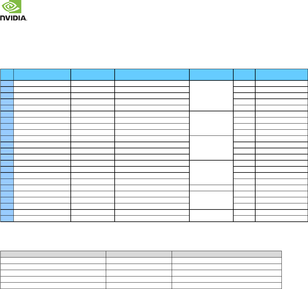
NVIDIA Jetson TX2 OEM Product Design Guide
JETSON TX2 OEM PRODUCT | DESIGN GUIDE | 20170912 55
10.0 AUDIO
Jetson TX2 brings four PCM/I2S audio interfaces to the module pins & includes a flexible audio-port switching architecture. In
addition, digital microphone & speaker interfaces are provided.
Table 58. Jetson TX2 Audio Pin Descriptions
Pin #
Jetson TX2 Pin Name
Tegra Signal
Usage/Description
Usage on the Carrier
Board
Direction
Pin Type
F1
AUDIO_MCLK
AUD_MCLK
Audio Codec Master Clock
Expansion Header
Output
CMOS 1.8V
G2
I2S0_CLK
DAP1_SCLK
I2S Audio Port 0 Clock
Bidir
CMOS 1.8V
H1
I2S0_LRCLK
DAP1_FS
I2S Audio Port 0 Left/Right Clock
Bidir
CMOS 1.8V
G1
I2S0_SDIN
DAP1_DIN
I2S Audio Port 0 Data In
Input
CMOS 1.8V
H2
I2S0_SDOUT
DAP1_DOUT
I2S Audio Port 0 Data Out
Bidir
CMOS 1.8V
C15
I2S1_CLK
DAP2_SCLK
I2S Audio Port 1 Clock
GPIO Expansion
Header
Bidir
CMOS 1.8V
D13
I2S1_LRCLK
DAP2_FS
I2S Audio Port 1 Left/Right Clock
Bidir
CMOS 1.8V
C14
I2S1_SDIN
DAP2_DIN
I2S Audio Port 1 Data In
Input
CMOS 1.8V
D14
I2S1_SDOUT
DAP2_DOUT
I2S Audio Port 1 Data Out
Bidir
CMOS 1.8V
G5
I2S2_CLK
DMIC2_DAT
I2S Audio Port 2 Clock
M.2 Key E
Bidir
CMOS 1.8V
H5
I2S2_LRCLK
DMIC1_CLK
I2S Audio Port 2 Left/Right Clock
Bidir
CMOS 1.8V
G6
I2S2_SDIN
DMIC1_DAT
I2S Audio Port 2 Data In
Input
CMOS 1.8V
H6
I2S2_SDOUT
DMIC2_CLK
I2S Audio Port 2 Data Out
Bidir
CMOS 1.8V
E6
I2S3_CLK
DAP4_SCLK
I2S Audio Port 3 Clock
Camera Connector
Bidir
CMOS 1.8V
F5
I2S3_LRCLK
DAP4_FS
I2S Audio Port 3 Left/Right Clock
Bidir
CMOS 1.8V
E5
I2S3_SDIN
DAP4_DIN
I2S Audio Port 3 Data In
Input
CMOS 1.8V
F6
I2S3_SDOUT
DAP4_DOUT
I2S Audio Port 3 Data Out
Bidir
CMOS 1.8V
E16
AO_DMIC_IN_CLK
CAN_GPIO1
Digital Mic Input Clock
Expansion Header
Output
CMOS 1.8V
D16
AO_DMIC_IN_DAT
CAN_GPIO0
Digital Mic Input Data
GPIO Expansion
Header
Input
CMOS 1.8V
G4
DSPK_OUT_CLK
GPIO_AUD3
Digital Speaker Output Clock
Output
CMOS 1.8V
H4
DSPK_OUT_DAT
GPIO_AUD2
Digital Speaker Output Data
Output
CMOS 1.8V
F2
GPIO19_AUD_RST
GPIO_AUD1
Audio Codec Reset or GPIO
Expansion Header
Output
CMOS 1.8V
H3
GPIO20_AUD_INT
GPIO_AUD0
Audio Codec Interrupt or GPIO
Input
CMOS 1.8V
When possible, the following assignments should be used for the I2Sx interfaces.
Table 59. I2S Interface Mapping
Jetson TX2 Pins (Tegra Functions)
I/O Block
Typical Usage
I2S0 (I2S1)
AUDIO
Available (Codec)
I2S1 (I2S2)
CONN
Available (Misc)
I2S2 (I2S3)
AUDIO_HV
Available (WLAN / BT, Modem)
I2S3 (I2S4)
AUDIO_HV
Available (Misc)
NA (I2S6)
DMIC_HV
Used for on-module WLAN / BT
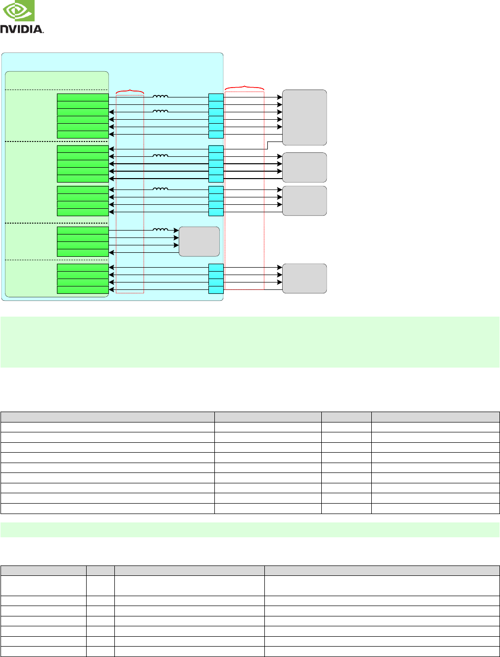
NVIDIA Jetson TX2 OEM Product Design Guide
JETSON TX2 OEM PRODUCT | DESIGN GUIDE | 20170912 56
Figure 28. Audio Device Connections
Jetson TX2
Audio
Codec
Tegra
DAP2_SCLK
DAP1_SCLK
GPIO_PQ0
AUDIO
DMIC_HV
2nd WiFi/BT,
Modem
Misc
DMIC2_DAT
DAP1_FS
DAP1_DOUT
DAP1_DIN
GPIO_PQ3
GPIO_PQ1
GPIO_PQ2
DMIC1_CLK
DMIC2_CLK
DMIC1_DAT
DAP2_FS
DAP2_DOUT
DAP2_DIN
AUDIO_MCLK
GPIO19_AUD_RST
I2S0_CLK
I2S0_LRCK
I2S0_SDOUT
I2S0_SDIN
GPIO20_AUD_INT
I2S2_CLK
I2S2_LRCK
I2S2_SDOUT
I2S2_SDIN
I2S3_CLK
I2S3_LRCK
I2S3_SDOUT
I2S3_SDIN
I2S1_CLK
I2S1_LRCK
I2S1_SDOUT
I2S1_SDIN
Primary
WiFi/BT
AUDIO_I2S_MCLK
GPIO_X1_AUD
DAP1_SCLK_AP
DAP1_FS_AP
DAP1_DOUT_AP
DAP1_DIN_AP
AUD_INT
DAP3_SCLK_AP
DAP3_FS_AP
DAP3_DOUT_AP
DAP3_DIN_AP
DAP4_SCLK_AP
DAP4_FS_AP
DAP4_DOUT_AP
DAP4_DIN_AP
DAP2_SCLK_AP
DAP2_FS_AP
DAP2_DOUT_AP
DAP2_DIN_AP
CONN
AUD_MCLK
GPIO_AUD0
GPIO_AUD1 F2
F1
D14
D13
C14
G2
H1
H2
G1
G5
H3
H5
H6
G6
C15
AUDIO_HV
I2S1_CLK
I2S1_LRCK
I2S1_SDOUT
I2S1_SDIN
I2S3_CLK
I2S3_LRCK
I2S3_SDOUT
I2S3_SDIN
I2S4_CLK
I2S4_LRCK
I2S4_SDOUT
I2S4_SDIN
I2S6_CLK
I2S6_LRCK
I2S6_SDOUT
I2S6_SDIN
I2S2_CLK
I2S2_LRCK
I2S2_SDOUT
I2S2_SDIN
Tegra
Function
DAP4_SCLK
DAP4_FS
DAP4_DOUT
DAP4_DIN
E6
F5
F6
E5
Misc
Nvidia
Carrier Board
Net Name
Note:
- The I2S interfaces can be used in either Master or Slave mode.
- A capacitor from DAPn_FS to GND is recommended if Tegra an I2S slave & the edge_cntrl configuration = 1 (SDATA
driven on positive edge of SCLK). The value of the capacitor should be chosen to provide a minimum of 2ns hold time for
the DAPn_FS edge after the rising edge of DAPn_SCLK.
I2S Design Guidelines
Table 60. I2S Interface Signal Routing Requirements
Parameter
Requirement
Units
Notes
Configuration / Device Organization
1
load
Max Loading
8
pF
Reference plane
GND
Breakout Region Impedance
Min width/spacing
Trace Impedance
50
±20%
Via proximity (Signal to reference)
< 3.8 (24)
mm (ps)
See Note 1
Trace spacing Microstrip or Stripline
2x
dielectric
Max Trace Delay
3600 (~22)
ps (in)
Max Trace Delay Skew between SCLK & SDATA_OUT/IN
250
ps (in)
Note:
Up to 4 signal Vias can share a single GND return Via
Table 61. Audio Signal Connections
Jetson TX2 Pin Name
Type
Termination
Description
I2S[3:0]_SCLK
I/O
I2S[2,0]_CLK have 75 beads & I2S3_CLK
has a 120Jetson TX2).
I2S Serial Clock: Connect to I2S/PCM CLK pin of audio device.
I2S[3:0]_LRCK
I/O
I2S Left/Right Clock: Connect to Left/Right Clock pin of audio device.
I2S[3:0]_SDATA_OUT
I/O
I2S Data Output: Connect to Data Input pin of audio device.
I2S[3:0]_SDATA_IN
I
I2S Data Input: Connect to Data Output pin of audio device.
AUD_MCLK
O
75Jetson TX2).
Audio Codec Master Clock: Connect to clock pin of Audio Codec.
GPIO19_AUD_RST
O
Audio Reset: Connect to reset pin of Audio Codec.
GPIO20_AUD_INT
I
Audio Interrupt: Connect to interrupt pin of Audio Codec.
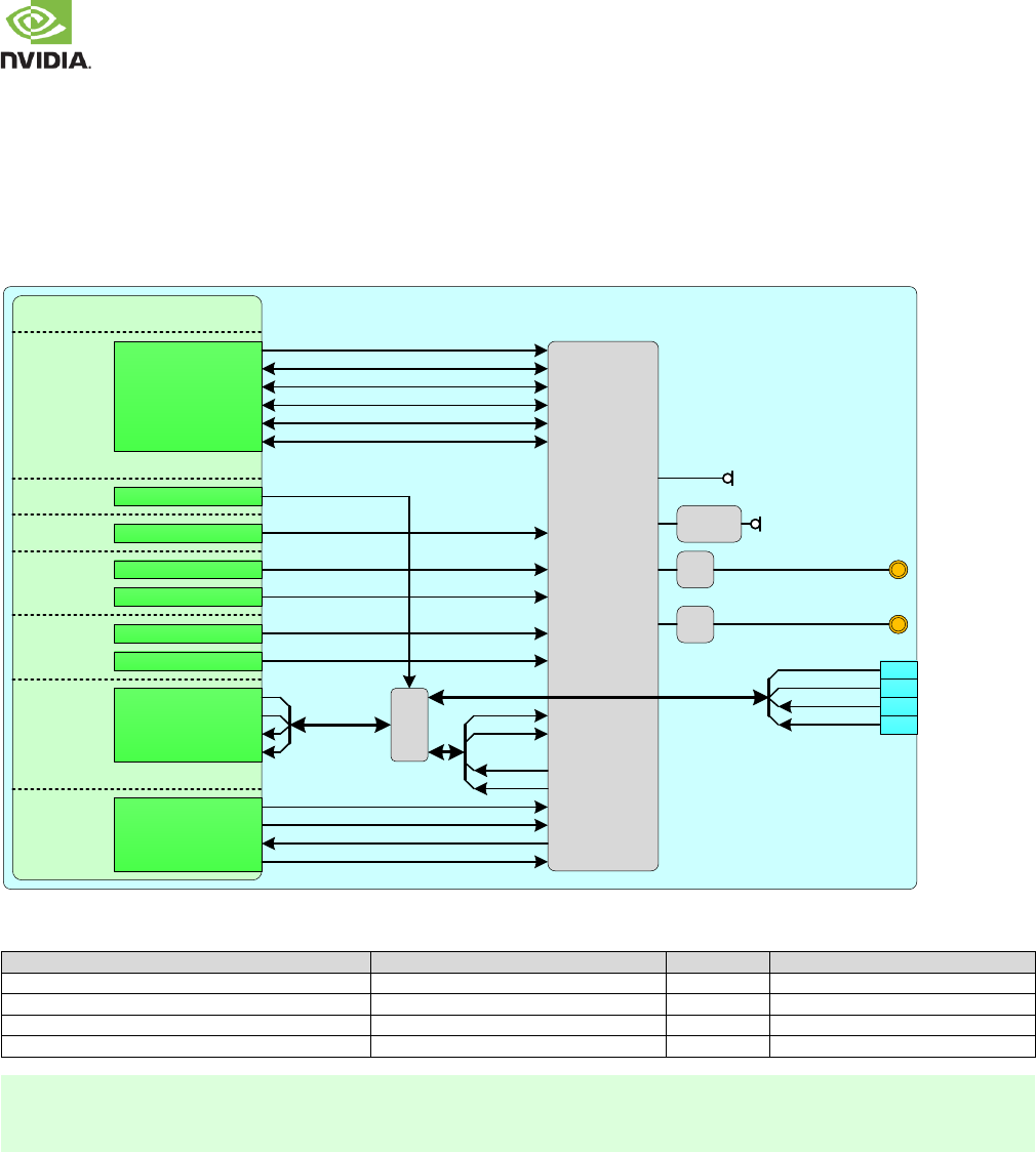
NVIDIA Jetson TX2 OEM Product Design Guide
JETSON TX2 OEM PRODUCT | DESIGN GUIDE | 20170912 57
11.0 WLAN / BT (INTEGRATED)
Jetson TX2 integrates a Broadcom BCM4354 WLAN / BT solution. Two Dual-band antenna connectors are located on the
module. The requirements are in the Antenna Requirements table below. The UART interface is multiplexed and either route
these to the WLAN/BT device or to the connector pins for use on the carrier board. The default selection for the multiplexers is
to the WLAN/BT device.
Figure 29. Integrated WLAN / BT
Jetson TX2
Tegra
SPI
WiFi / BT
QSPI_IO3
CAM GPIO_CAM1
VDD_3V3_SYS
Load
Switch VDD_1V8
RF
RF
Antenna
Connector #1
Antenna
Connector #2
SYS
GP_PWM7
UART
GPIO_MDM5
GPIO_SW4
CONN UART4_TX
UART4_RX
UART4_RTS_N
UART4_CTS_N
GPIO_PQ0
GPIO_PQ1
GPIO_PQ2
GPIO_PQ3
DMIC_HV
MUX_SEL
WIFI_EN
WIFI_WAKE_AP
BT2_WAKE_AP
BT_EN
AP2_WAKE_BT
DAP6_SCLK
DAP6_DOUT
DAP6_DIN
DAP6_FS
H10
H9
G10
G9
(Default)
Mux
UART3_TX
UART3_RX
UART3_RTS#
UART3_CTS#
SEL
SDMMC3 SDMMC3_CLK
SDMMC3_CMD
SDMMC3_DAT0
SDMMC3_DAT1
SDMMC3_DAT2
SDMMC3_DAT3
GPIO_SW3
Table 62. Antenna Requirements
Parameter
Requirement
Units
Notes
Type
Dual-Band (x2) Dipole
Frequency Band(s)
2.4 & 5.0
GHz
Impedance
50
Mating Connector
Plug: I-PEX U.FL series
See note 1
Note:
1. Receptacles on Jetson TX2 are from Hirose Electric (U.S.A). Part # is U.FL-R-SMT-1(10).
2. Antenna Manufacturer: Pulse, Part Number: W1043
3. Cable manufacturer: Pulse, part number: W9009
NVIDIA Jetson TX2 OEM Product Design Guide
JETSON TX2 OEM PRODUCT | DESIGN GUIDE | 20170912 58
12.0 MISCELLANEOUS INTERFACES
12.1 I2C
Tegra has nine I2C controllers. Jetson TX2 brings eight of the I2C interfaces out, which are shown in the tables below. The
assignments in Table 64 should be used for the I2C interfaces:
Table 63. Jetson TX2 I2C Pin Descriptions
Pin #
Jetson TX2 Pin Name
Tegra Signal
Usage/Description
Usage on the Carrier
Board
Direction
Pin Type
C6
I2C_CAM_CLK
CAM_I2C_SCL
Camera I2C Clock
Camera Connector
Bidir
Open Drain 1.8V
D6
I2C_CAM_DAT
CAM_I2C_SDA
Camera I2C Data
Bidir
Open Drain 1.8V
E15
I2C_GP0_CLK
GPIO_SEN8
General I2C 0 Clock
I2C (General)
Bidir
Open Drain 1.8V
D15
I2C_GP0_DAT
GPIO_SEN9
General I2C 0 Data
Bidir
Open Drain 1.8V
A21
I2C_GP1_CLK
GEN1_I2C_SCL
General I2C 1 Clock
Bidir
Open Drain 3.3V
A20
I2C_GP1_DAT
GEN1_I2C_SDA
General I2C 1 Data
Bidir
Open Drain 3.3V
C11
I2C_GP2_CLK
GEN7_I2C_SCL
General I2C 2 Clock
Bidir
Open Drain 1.8V
C10
I2C_GP2_DAT
GEN7_I2C_SDA
General I2C 2 Data
Bidir
Open Drain 1.8V
C12
I2C_GP3_CLK
GEN9_I2C_SCL
General I2C 3 Clock
Bidir
Open Drain 1.8V
C13
I2C_GP3_DAT
GEN9_I2C_SDA
General I2C 3 Data
Bidir
Open Drain 1.8V
A6
I2C_PM_CLK
GEN8_I2C_SCL
PM I2C Clock
Bidir
Open Drain 1.8V
B6
I2C_PM_DAT
GEN8_I2C_SDA
PM I2C Data
Bidir
Open Drain 1.8V
A34
DP1_AUX_CH
DP_AUX_CH1_N
Display Port 1 Aux or HDMI DDC SDA
HDMI Type A Conn.
Bidir
AC-Coupled on Carrier
Board (eDP/DP) or Open-
Drain, 1.8V (3.3V tolerant -
DDC/I2C)
A35
DP1_AUX_CH+
DP_AUX_CH1_P
Display Port 1 Aux+ or HDMI DDC SCL
Bidir
B34
DP0_AUX_CH
DP_AUX_CH0_N
Display Port 0 Aux or HDMI DDC SDA
Display Connector
Bidir
B35
DP0_AUX_CH+
DP_AUX_CH0_P
Display Port 0 Aux+ or HDMI DDC SCL
Bidir
Table 64. I2C Interface Mapping
Ctrlr
Jetson TX2 Pins
Names
Usage on Jetson
TX2
Typcial usage on Carrier board
On-Jetson TX2 Pull-up/voltage
I2C1
I2C_GP1_CLK/DAT
Power monitors
General I2C bus usage. 3.3V devices supported
1K on Jetson TX2 to 3.3V
I2C2
I2C_GP0_CLK/DAT
Audio Codec, general I2C. 1.8V devices supported
1K on Jetson TX2 to 1.8V
I2C3
I2C_CAM_CLK/DAT
Cameras & related functions. 1.8V devices supported
1K on Jetson TX2 to 1.8V
I2C4
DP1_AUX_CH_P/N
HDMI / DP / I2C. 1.8V / 3.3V devices supported.
None on Jetson TX2. I/F supports
pull-up to 1.8V or 3.3V (3.3V in
Open-drain mode only)
I2C5
na
Power control
On-Jetson TX2 use only
1K on Jetson TX2 to 1.8V
I2C6
DP0_AUX_CH_P/N
HDMI / DP / I2C. 1.8V / 3.3V devices supported.
None on Jetson TX2. I/F supports
pull-up to 1.8V or 3.3V (3.3V in
Open-drain mode only)
I2C7
I2C_GP2_CLK/DAT
General I2C bus. 1.8V devices supported
1K on Jetson TX2 to 1.8V
I2C8
I2C_PM_CLK/DAT
Thermal Sensor
General I2C bus. Only 1.8V devices supported
1K on Jetson TX2 to 1.8V
I2C9
I2C_GP3_CLK/DAT
General I2C bus. Only 1.8V devices supported
1K on Jetson TX2 to 1.8V
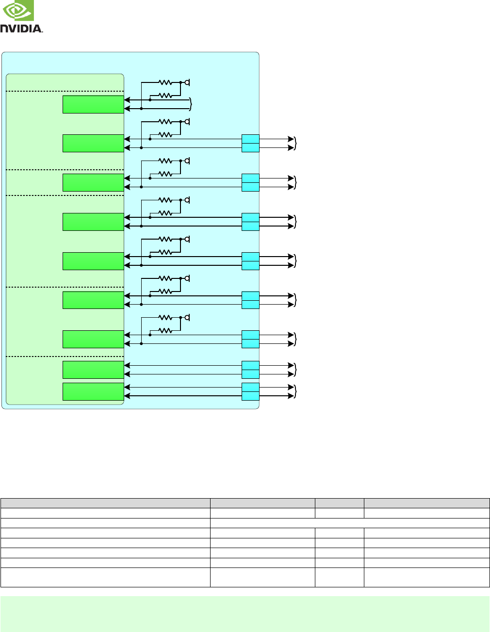
NVIDIA Jetson TX2 OEM Product Design Guide
JETSON TX2 OEM PRODUCT | DESIGN GUIDE | 20170912 59
Figure 30. I2C Connections
Jetson TX2
Tegra I2C
PWR_I2C_SCL
PWR_I2C_SDA
CAM_I2C_SCL
CAM_I2C_SDA
SYS
GEN9_I2C_SCL
GEN9_I2C_SDA
On-Module
Usage Only
VDD_1V8
CAM
UART
1k1k
GEN1_I2C_SCL
GEN1_I2C_SDA
AO GPIO_SEN8
GPIO_SEN9
DP_AUX_CH0_P
DP_AUX_CH0_N
DP
DP_AUX_CH1_P
DP_AUX_CH1_N
1k1k
VDD_1V8
1k1k
1k1k
VDD_1V8
1k1k
1k1k
VDD_1V8
1k1k
1k1k
VDD_3V3_SYS
1k1k
1k1k
Used as camera module
control interface
I2C_GP1_CLK
I2C_GP1_DAT
I2C_CAM_CLK
I2C_CAM_DAT
I2C_GP2_CLK
I2C_GP2_DAT
I2C_GP3_CLK
I2C_GP3_DAT
I2C_GP0_CLK
I2C_GP0_DAT
I2C_PM_CLK
I2C_PM_DAT
DP0_AUX_CH+
DP0_AUX_CH
DP1_AUX_CH+
DP1_AUX_CH
Available for misc.
1.8V I2C devices
Used on-module for power monitors, & typically off-
module for GPIO expansion or other misc 3.3V I2C usage
Typically used for eDP. Otherwise
available for Misc 1.8V/3.3V I2C usage.
Typically used for HDMI or DP. Otherwise
available for Misc 1.8V/3.3V I2C usage.
D6
C6
A6
B6
E15
D15
B35
B34
A34
A35
A21
A20
C11
C10
C12
C13
GEN8_I2C_SCL
GEN8_I2C_SDA
VDD_1V8
1k1k
1k1k
I2C2
I2C6
I2C5
I2C1
I2C3
I2C4
I2C9
I2C8
GEN7_I2C_SCL
GEN7_I2C_SDA
VDD_1V8
1k1k
1k1k
Available for misc.
1.8V I2C devices
I2C7
Available for misc.
1.8V I2C devices
Available for misc.
1.8V I2C devices
I2C Design Guidelines
Care must be taken to ensure I2C peripherals on same I2C bus connected to Jetson TX2 do not have duplicate addresses.
Addresses can be in two forms: 7-bit, with the Read/Write bit removed or 8-bit including the Read/Write bit. Be sure to compare
I2C device addresses using the same form (all 7-bit or all 8-bit format).
Table 65. I2C Interface Signal Routing Requirements
Parameter
Requirement
Units
Notes
Max Frequency Standard-mode / Fm / Fm+
100 / 400 / 1000
kHz
See Note 1
Topology
Single ended, bi-directional, multiple masters/slaves
Max Loading Standard-mode / Fm / Fm+
400
pF
Total of all loads
Reference plane
GND or PWR
Trace Impedance
50 60
±15%
Trace Spacing
1x
dielectric
Max Trace Delay Standard Mode
Fm & Fm+
3400 (~20)
1700 (~10)
ps (in)
Note:
1. Fm = Fast-mode, Fm+ = Fast-mode Plus
2. Avoid routing I2C signals near noisy traces, supplies or components such as a switching power regulator.
3. No requirement for decoupling caps for PWR reference
NVIDIA Jetson TX2 OEM Product Design Guide
JETSON TX2 OEM PRODUCT | DESIGN GUIDE | 20170912 60
Table 66. I2C Signal Connections
Jetson TX2 Pin
Name
Type
Termination
Description
I2C_GP0_CLK/DAT
I/OD
1k pull-ups to VDD_1V8 on Jetson TX2
General I2C 0 Clock\Data. Connect to CLK/Data pins of 1.8V devices
I2C_GP1_CLK/DAT
I/OD
1k pull-ups to VDD_3V3_SYS on Jetson TX2
General I2C 1 Clock\Data. Connect to CLK/Data pins of 3.3V devices.
I2C_GP2_CLK/DAT
I/OD
1k pull-ups to VDD_1V8 on Jetson TX2
General I2C 2 Clock\Data. Connect to CLK/Data pins of 1.8V devices
I2C_GP3_CLK/DAT
I/OD
1k pull-ups to VDD_1V8 on Jetson TX2
General I2C 3 Clock\Data. Connect to CLK/Data pins of 1.8V devices.
I2C_PM_CLK/DAT
I/OD
1k pull-ups to VDD_1V8 on Jetson TX2
Power Mon. I2C Clock\Data. Connect to CLK/Data pins of 1.8V
devices
I2C_CAM_CLK/DAT
I/OD
1k pull-ups to VDD_1V8 on Jetson TX2
Camera I2C Clock\Data. Connect to CLK/Data pins of any 1.8V devices
DP0_AUX_CH+/–
I/OD
See eDP/HDMI/DP sections for correct
termination
DP_AUX Channel (eDP/DP) or DDC I2C 2 Clock & Data (HDMI).
Connect to AUX_CH+/– (DP) or SCL/SDA (HDMI)
DP1_AUX_CH+/–
I/OD
See eDP/HDMI/DP sections for correct
termination
DP_AUX Channel (eDP/DP) or DDC I2C 2 Clock & Data (HDMI).
Connect to AUX_CH+/– (DP) or SCL/SDA (HDMI)
Note:
1. If some devices require a different voltage level than others connected to the same I2C bus, level shifters are required.
2. For I2C interfaces that are pulled up to 1.8V, disable the E_IO_HV option for these pads. For I2C interfaces that are
pulled up to 3.3V, enable the E_IO_HV option. The E_IO_HV option is selected in the Pinmux registers.
De-bounce
The tables below contain the allowable De-bounce settings for the various I2C Modes.
Table 67. De-bounce Settings (Fast Mode Plus, Fast Mode & Standard Mode)
I2C Mode
Clock Source
Source Clock Freq
I2C Source Divisor
Sm/Fm Divisor
De-bounce Value
I2C SCL Freq
Fm+
PLLP_OUT0
408MHz
5 (0x04)
10 (0x9)
0
1016KHz
5:1
905.8KHz
7:6
816KHz
Fm
PLLP_OUT0
408MHz
5 (0x4)
26 (0x19)
7:0
392KHz
Sm
PLLP_OUT0
408MHz
20 (0x13)
26 (0x19)
7:0
98KHz
Note:
Sm = Standard Mode.
12.2 SPI
Jetson TX2 brings out three of the Tegra SPI interfaces.
Table 68. Jetson TX2 SPI Pin Descriptions
Pin #
Jetson TX2 Pin Name
Tegra Signal
Usage/Description
Usage on the Carrier
Board
Direction
Pin Type
E3
SPI0_CLK
GPIO_SEN1
SPI 0 Clock
Display Connector
Bidir
CMOS 1.8V
F3
SPI0_CS0#
GPIO_SEN4
SPI 0 Chip Select 0
Bidir
CMOS 1.8V
E4
SPI0_MISO
GPIO_SEN2
SPI 0 Master In / Slave Out
Bidir
CMOS 1.8V
F4
SPI0_MOSI
GPIO_SEN3
SPI 0 Master Out / Slave In
Bidir
CMOS 1.8V
G13
SPI1_CLK
GPIO_CAM4
SPI 1 Clock
Expansion Header
Bidir
CMOS 1.8V
E14
SPI1_CS0#
GPIO_CAM7
SPI 1 Chip Select 0
Bidir
CMOS 1.8V
F14
SPI1_MISO
GPIO_CAM5
SPI 1 Master In / Slave Out
Bidir
CMOS 1.8V
F13
SPI1_MOSI
GPIO_CAM6
SPI 1 Master Out / Slave In
Bidir
CMOS 1.8V
H14
SPI2_CLK
GPIO_WAN5
SPI 2 Clock
Display/Camera Conns.
Bidir
CMOS 1.8V
G16
SPI2_CS0#
GPIO_WAN8
SPI 2 Chip Select 0
Bidir
CMOS 1.8V
F16
SPI2_CS1#
GPIO_MDM4
SPI 2 Chip Select 1
Bidir
CMOS 1.8V
H15
SPI2_MISO
GPIO_WAN6
SPI 2 Master In / Slave Out
Bidir
CMOS 1.8V
G15
SPI2_MOSI
GPIO_WAN7
SPI 2 Master Out / Slave In
Bidir
CMOS 1.8V
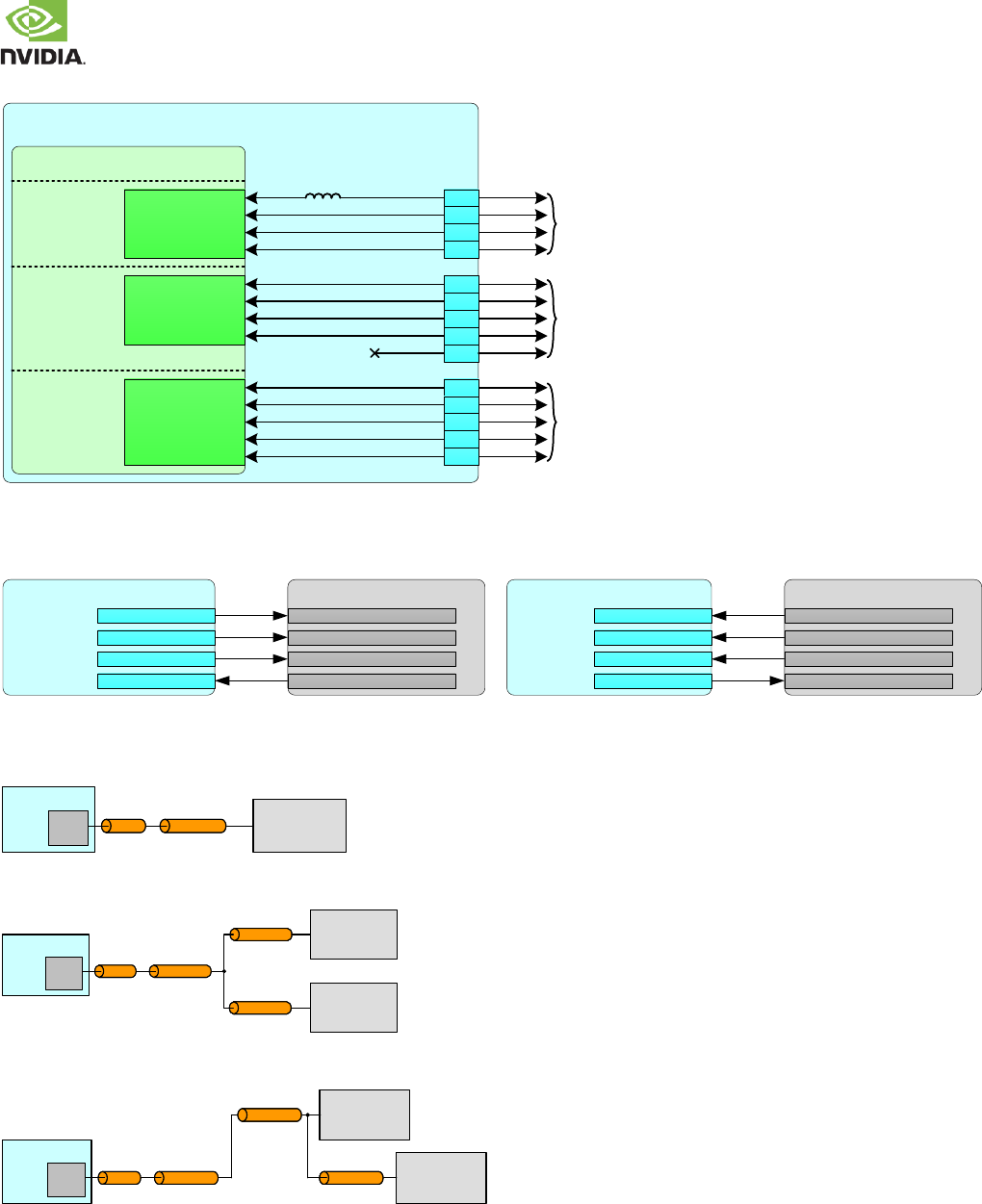
NVIDIA Jetson TX2 OEM Product Design Guide
JETSON TX2 OEM PRODUCT | DESIGN GUIDE | 20170912 61
Figure 31. SPI Connections
Jetson TX2
Tegra SPI
GPIO_SEN1
GPIO_SEN2
GPIO_SEN3
GPIO_SEN4
AO
Touch
SPI0_CLK
SPI0_MISO
SPI0_MOSI
SPI0_CS0#
SPI1_CLK
SPI1_MISO
SPI1_MOSI
SPI1_CS0#
SPI1_CS1#
SPI2_CLK
SPI2_MISO
SPI2_MOSI
SPI2_CS0#
SPI2_CS1#
GPIO_CAM4
GPIO_CAM5
GPIO_CAM6
GPIO_CAM7
MHz
Expansion
E4
E3
F4
F3
G13
F13
F14
E14
E13
GPIO_WAN5
GPIO_WAN6
GPIO_WAN7
GPIO_WAN8
GPIO_MDM4
H14
G15
H15
G16
F16
UART
Display (CS0)
Camera (CS1)
CAM
The figure below shows the basic connections used.
Figure 32. Basic SPI Master/Slave Connections
Jetson TX2 Master
SPIn_CSx#
SPIn_SCK
SPIn_MOSI
SPIn_MISO
SPI Slave Device
CS (Chip Select)
CLK (Clock)
MOSI (Master out, Slave in)
MISO (Master in, Slave out)
Jetson TX2 Slave
SPIn_CSx#
SPIn_SCK
SPIn_MOSI
SPIn_MISO
SPI Master Device
CS (Chip Select)
CLK (Clock)
MOSI (Master out, Slave in)
MISO (Master in, Slave out)
SPI Design Guidelines
Figure 33. SPI Point-Point Topology
Jetson TX2 SPI
Device
Main trunk
Die PKGPKG
Figure 34. SPI Star Topologies
Jetson TX2
SPI
Device #1
Main trunk SPI
Device #2
Die PKGPKG
Branch-ABranch-A
Branch-BBranch-B
Figure 35. SPI Daisy Topologies
Jetson TX2
SPI
Device #1
Main trunk
SPI
Device #2
Die PKGPKG
Branch-ABranch-A
Branch-BBranch-B
NVIDIA Jetson TX2 OEM Product Design Guide
JETSON TX2 OEM PRODUCT | DESIGN GUIDE | 20170912 62
Table 69. SPI Interface Signal Routing Requirements
Parameter
Requirement
Units
Notes
Max Frequency
65
MHz
Configuration / Device Organization
3
load
Max Loading (total of all loads)
15
pF
Reference plane
GND
Breakout Region Impedance
Minimum width & spacing
Max PCB breakout delay
75
ps
Trace Impedance
50 60
±15%
Via proximity (Signal to reference)
< 3.8 (24)
mm (ps)
See Note 1
Trace spacing Microstrip / Stripline
4x / 3x
dielectric
Max Trace Length/Delay (PCB Main Trunk) Point-Point
For MOSI, MISO, SCK & CS 2x-Load Star/Daisy
195 (1228)
120 (756)
mm (ps)
Max Trace Length/Delay (Branch-A) 2x-Load Star/Daisy
for MOSI, MISO, SCK & CS
75 (472)
mm (ps)
Max Trace Length/Delay (Branch-B) 2x-Load Star/Daisy
for MOSI, MISO, SCK & CS
75 (472)
mm (ps)
Max Trace Length/Delay Skew from MOSI, MISO & CS to SCK
16 (100)
mm (ps)
At any point
Note:
Up to 4 signal Vias can share a single GND return Via
Table 70. SPI Signal Connections
Jetson TX2 Pin Names
Type
Termination
Description
SPI[2:0]_CLK
I/O
SPI0_CLK has 120
(on Jetson TX2).
SPI Clock.: Connect to Peripheral CLK pin(s)
SPI[2:0]_MOSI
I/O
SPI Data Output: Connect to Slave Peripheral MOSI pin(s)
SPI[2:0]_MISO
I/O
SPI Data Input: Connect to Slave Peripheral MISO pin(s)
SPI[2:1]_CS[1:0]#
SPI0_CS0#
I/O
SPI Chip Selects.: Connect one CS_N pin per SPI IF to each Slave
Peripheral CS pin on the interface
Table 71. Recommended SPI observation (test) points for initial boards
Test Points Recommended
Location
One for each SPI signal line used
Near Jetson TX2 & Device pins.
12.3 UART
Jetson TX2 brings five UARTs out to the main connector. One of the UARTs is used for the WLAN/BT on Jetson TX2 or as
UART3 at the connector depending on the setting of a multiplexor. See Table 73 for typical assignments of the UARTs.
Table 72. Jetson TX2 UART Pin Descriptions
Pin #
Jetson TX2 Pin Name
Tegra Signal
Usage/Description
Usage on the Carrier
Board
Direction
Pin Type
H11
UART0_CTS#
UART1_CTS
UART 0 Clear to Send
Debug Header
Input
CMOS 1.8V
G11
UART0_RTS#
UART1_RTS
UART 0 Request to Send
Output
CMOS 1.8V
G12
UART0_RX
UART1_RX
UART 0 Receive
Input
CMOS 1.8V
H12
UART0_TX
UART1_TX
UART 0 Transmit
Output
CMOS 1.8V
E10
UART1_CTS#
UART3_CTS
UART 1 Clear to Send
Serial Port Header
Input
CMOS 1.8V
E9
UART1_RTS#
UART3_RTS
UART 1 Request to Send
Output
CMOS 1.8V
D10
UART1_RX
UART3_RX
UART 1 Receive
Input
CMOS 1.8V
D9
UART1_TX
UART3_TX
UART 1 Transmit
Output
CMOS 1.8V
A15
UART2_CTS#
UART2_CTS
UART 2 Clear to Send
M.2 Key E
Input
CMOS 1.8V
A16
UART2_RTS#
UART2_RTS
UART 2 Request to Send
Output
CMOS 1.8V
B15
UART2_RX
UART2_RX
UART 2 Receive
Input
CMOS 1.8V
B16
UART2_TX
UART2_TX
UART 2 Transmit
Output
CMOS 1.8V
G9
UART3_CTS#
UART4_CTS_N (via
mux)
UART 3 Clear to Send
Not assigned
Input
CMOS 1.8V
G10
UART3_RTS#
UART4_RTS_N (via
mux)
UART 3 Request to Send
Output
CMOS 1.8V
H9
UART3_RX
UART4_RX (via mux)
UART 3 Receive
Optional source of
UART on Exp. Header
Input
CMOS 1.8V
H10
UART3_TX
UART4_TX (via mux)
UART 3 Transmit
Output
CMOS 1.8V
NVIDIA Jetson TX2 OEM Product Design Guide
JETSON TX2 OEM PRODUCT | DESIGN GUIDE | 20170912 63
Pin #
Jetson TX2 Pin Name
Tegra Signal
Usage/Description
Usage on the Carrier
Board
Direction
Pin Type
D5
UART7_RX
UART7_RX
UART 7 Receive
Not Assigned
Input
CMOS 1.8V
D8
UART7_TX
UART7_TX
UART 7 Transmit
Output
CMOS 1.8V
Table 73. UART Interface Mapping
Jetson TX2 Pins (Tegra Functions)
I/O Block
Typical Usage
UART0 (UART1)
DEBUG
Debug
UART1 (UART3)
AO
Serial Port
UART2 (UART2)
UART
M.2 socket for external WLAN / BT
UART3 (UART4)
CONN
Misc. Available if not used for on-module WLAN /
BT (selected by on-module multiplexor)
UART7 (UART7)
AO
2nd Debug/Misc.
Figure 36. Jetson TX2 UART Connections
Jetson TX2
Tegra UART
UART3_TX
UART3_RX
UART3_RTS_N
UART3_CTS_N
AO Serial Port,
etc.
(RAM_CODE1 Strap) UART1_TX
UART1_RX
UART1_RTS#
UART1_CTS#
(RAM_CODE1 Strap) RSVD
RSVD
UART3_TX
UART3_RX
UART3_RTS#
UART3_CTS#
UART0_TX
UART0_RX
(RAM_CODE0 Strap) UART0_RTS#
UART0_CTS#
UART2_TX
UART2_RX
UART2_RTS#
UART2_CTS#
UART1_TX
UART1_RX
UART1_RTS_N
UART1_CTS_N
DEBUG
UART2_TX
UART2_RX
UART2_RTS_N
UART2_CTS_N
UART
UART4_TX
UART4_RX
UART4_RTS_N
UART4_CTS_N
Used for
Debug, etc.
M.2 Conn.
(2nd WiFi/Bt)
B1 5
B1 6
H12
G12
H10
G9
D9
D10
E9
E10
G10
H9
G11
H11
A16
A15
CONN
Mux WiFi / BT on
Jetson TX2
Misc.
UART7_TX
UART7_RX D5
D8 Misc.
UART7_TX_AP
UART7_RX_AP
Note:
Care should be taken when using UART pins that are associated with Tegra straps. See Strapping Pins section for details.
Table 74. UART Signal Connections
Ball Name
Type
Termination
Description
UART[7,3:0]_TX
O
UART Transmit: Connect to Peripheral RXD pin of device
UART[7,3:0]_RX
I
UART Receive: Connect to Peripheral TXD pin of device
UART[3:0]_CTS#
I
UART Clear to Send: Connect to Peripheral RTS_N pin of device
UART[3:0]_RTS#
O
UART Request to Send: Connect to Peripheral CTS pin of device
12.4 Fan
Jetson TX2 provides PWM and Tachometer functionality for controlling a fan as part of the thermal solution. Information on the
PWM and Tachometer pins/functions can be found in the following locations:
Jetson TX2 Module Pin Mux:
▪ This is used to configure the FAN_PWM & FAN_TACH pins. The FAN_PWM pin is configured as GP_PWM4.
The FAN_TACH pin is configured as NV_THERM_FAN_TACH.
NVIDIA Jetson TX2 OEM Product Design Guide
JETSON TX2 OEM PRODUCT | DESIGN GUIDE | 20170912 64
Tegra X2 Technical Reference Manual:
▪ Functional descriptions and related registers can be found in the TRM for the FAN_PWM (PWM chapter) &
FAN_TACH (Tachometer chapter) functions.
Jetson Developer Kit Carrier Board Specification:
▪ The document contains the maximum current capability of the VDD_5V0_IO_SYS supply in the Interface Power
chapter (VDDIO_5V0_IO_SLP comes from that supply). The fan is powered by this supply on the Jetson TX2
Developer Kit carrier board.
Table 75. Jetson TX2 Fan Pin Descriptions
Pin #
Jetson TX2 Pin Name
Tegra Signal
Usage/Description
Usage on the Carrier
Board
Direction
Pin Type
C16
FAN_PWM
GPIO_SEN6
Fan PWM
Fan
Output
CMOS 1.8V
B17
FAN_TACH
UART5_TX
Fan Tach
Input
CMOS 1.8V
Figure 37. Jetson TX2 Fan Connection Example
VDD_5V0_IO_SLPVDD_1V8
GS
D
GS
D
10pF
4
3
2
1
4
3
2
1
10pF
PS_VDD_FAN_DISABLE
(GPIO Expander P04) GS
D
GS
D
4.7k4.7k
100k100k
10k10k
10uF 0.1uF
100k100k
Fan
Header
100100
VDD_5V0_IO_SYS
Jetson TX2
Tegra Fan
GPIO_SEN6
AO FAN_PWM
FAN_TACH
UART5_TX
C16
B17
UART
Table 76. Fan Signal Connections
Ball Name
Type
Termination
Description
FAN_PWM
O
Fan Pulse Width Modulation: Connect through FET as shown in the
Jetson TX2 Fan Connections figure.
FAN_TACH
I
ESD diode to GND
Fan Tachometer: Connect to TACH pin on fan connector.
12.5 CAN
Jetson TX2 brings two CAN (Controller Area Network) interfaces out to the main connector.
Table 77. Jetson TX2 CAN Pin Descriptions
Pin #
Jetson TX2 Pin Name
Tegra Signal
Usage/Description
Usage on the Carrier
Board
Direction
Pin Type
C20
CAN_WAKE
CAN_GPIO4
CAN Wake
GPIO Expansion
Header
Input
CMOS 3.3V
E18
CAN0_ERR
CAN_GPIO5
CAN #0 Error
Input
CMOS 3.3V
D18
CAN0_RX
CAN0_DIN
CAN #0 Receive
Input
CMOS 3.3V
D19
CAN0_TX
CAN0_DOUT
CAN #0 Transmit
Output
CMOS 3.3V
C19
CAN1_ERR
CAN_GPIO3
CAN #1 Error
Input
CMOS 3.3V
D17
CAN1_RX
CAN1_DIN
CAN #1 Receive
Input
CMOS 3.3V
C17
CAN1_STBY
CAN_GPIO6
CAN #1 Standby
Output
CMOS 3.3V
C18
CAN1_TX
CAN1_DOUT
CAN #1 Transmit
Output
CMOS 3.3V
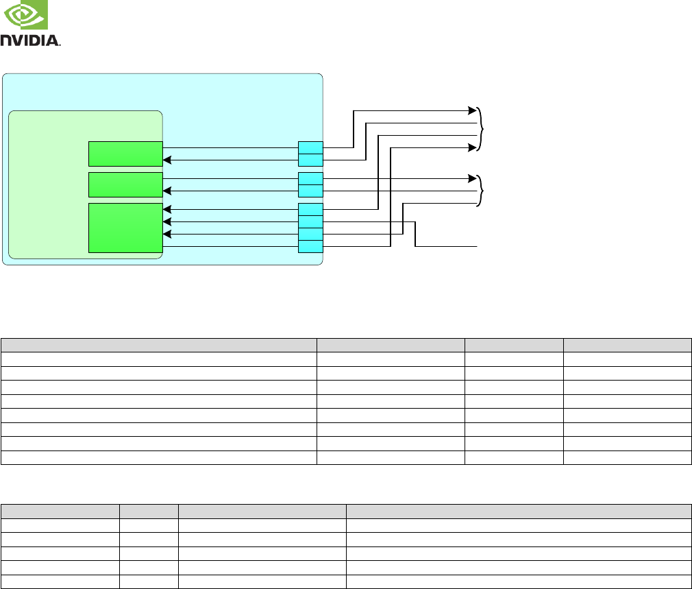
NVIDIA Jetson TX2 OEM Product Design Guide
JETSON TX2 OEM PRODUCT | DESIGN GUIDE | 20170912 65
Figure 38. Jetson TX2 CAN Connections
Jetson TX2
Tegra - CAN
AO_HV CAN1_DOUT
CAN1_DIN
CAN_GPIO3
CAN_GPIO4
CAN_GPIO5
CAN_GPIO6
CAN0_DOUT
CAN0_DIN
CAN1_TX
CAN1_RX
CAN0_TX
CAN0_RX
CAN1_ERR
CAN_WAKE
CAN0_ERR
CAN1_STBY
CAN #1
D17
C18
D19
D18
C19
C20
E18
C17
CAN #0
CAN Wake
Table 78. CAN Interface Signal Routing Requirements
Parameter
Requirement
Units
Notes
Max Data Rate / Frequency
1
Mbps / MHz
Configuration / Device Organization
1
load
Reference plane
GND
Trace Impedance
50
±15%
Via proximity (Signal via to GND return via)
< 3.8 (24)
mm (ps)
See Note 1
Trace spacing Microstrip / Stripline
4x / 3x
dielectric
Max Trace Length (for RX & TX only)
223 (1360)
mm (ps)
See Note 2
Max Trace Length/Delay Skew from RX to TX
8 (50)
mm (ps)
See Note 2
Table 79. CAN Signal Connections
Ball Name
Type
Termination
Description
CAN[1:0]_TX
O
CAN Transmit: Connect to matching pin of device
CAN[1:0]_RX
I
CAN Receive: Connect to Peripheral pin of device
CAN[1:0]_ERR
I
CAN Error: Connect to matching pin of device
CAN1_STBY
O
CAN Standby: Connect to matching pin of device
CAN_WAKE
I
CAN Wake: Connect to matching pin of device
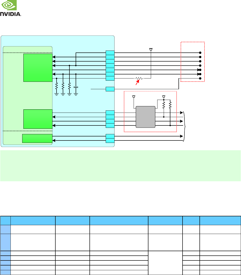
NVIDIA Jetson TX2 OEM Product Design Guide
JETSON TX2 OEM PRODUCT | DESIGN GUIDE | 20170912 66
12.6 Debug
Figure 39. Debug Connections
Jetson TX2
Tegra
JTAG_TMS
JTAG_TDI
JTAG_TCK
JTAG_TDO
JTAG_TRST_N
NVJTAG_SEL
100kΩ
UART1_TXD
UART1_RXD
UART1_RTS_N
UART1_CTS_N For Debug Use
DEBUG
0.1uF
A12
A14
B1 2
B1 1
A13
G12
H12
B1 3
JTAG_RTCK
JTAG_TMS
JTAG_TDI
JTAG_TCK
JTAG_TDO
JTAG_GP0
JTAG_GP1
RESET_IN
UART0_TX
UART0_RX
UART0_RTS#
UART0_CTS#
RSVD
RSVD
100kΩ
See Note 1
Optional JTAG
connections
0
A47
To PMIC
RTCK
TMS
TDI
TCLK
TDO
TRST_N
RST
A11
H11
G11
VDD_1V8
100kΩ
UART7_TX
UART7_RX
DP
D5
D8
See Note 2
Level
Shifter
100k
VDD_3V3_SYSVDD_1V8
100k
Notes:
1. JTAG_GP1 (Tegra NVJTAG_SEL) is left unconnected (pulled down on module) for normal operation and pulled to 1.8V for
Boundary Scan Mode.
2. If level shifter is implemented, pull-ups are required the RX & CTS lines on the non-Tegra side of the level shifter. This is
required to keep the inputs from floating and toggling when no device is connected to the debug UART.
3. Check preferred JTAG debugger documentation for JTAG PU/PD recommendations.
12.6.1 JTAG
JTAG is not required, but may be useful for new design bring-up or for Boundary Scan.
Table 80. Jetson TX2 JTAG Pin Descriptions
Pin #
Jetson TX2 Pin Name
Tegra Signal
Usage/Description
Usage on the Carrier
Board
Direction
Pin Type
B13
JTAG_GP0
JTAG_TRST_N
JTAG Test Reset
JTAG Header & Debug
Connector
Input
CMOS 1.8V
A11
JTAG_GP1
NVJTAG_SEL
JTAG General Purpose 1. Pulled low on
module for normal operation & pulled
high by test device for Boundary Scan
test mode.
JTAG
Input
CMOS 1.8V
A14
JTAG_RTCK
JTAG Return Clock
JTAG Header & Debug
Connector
Input
CMOS 1.8V
B11
JTAG_TCK
JTAG_TCK
JTAG Test Clock
Input
CMOS 1.8V
B12
JTAG_TDI
JTAG_TDI
JTAG Test Data In
Input
CMOS 1.8V
A13
JTAG_TDO
JTAG_TD0
JTAG Test Data Out
Output
CMOS 1.8V
A12
JTAG_TMS
JTAG_TMS
JTAG Test Mode Select
Input
CMOS 1.8V
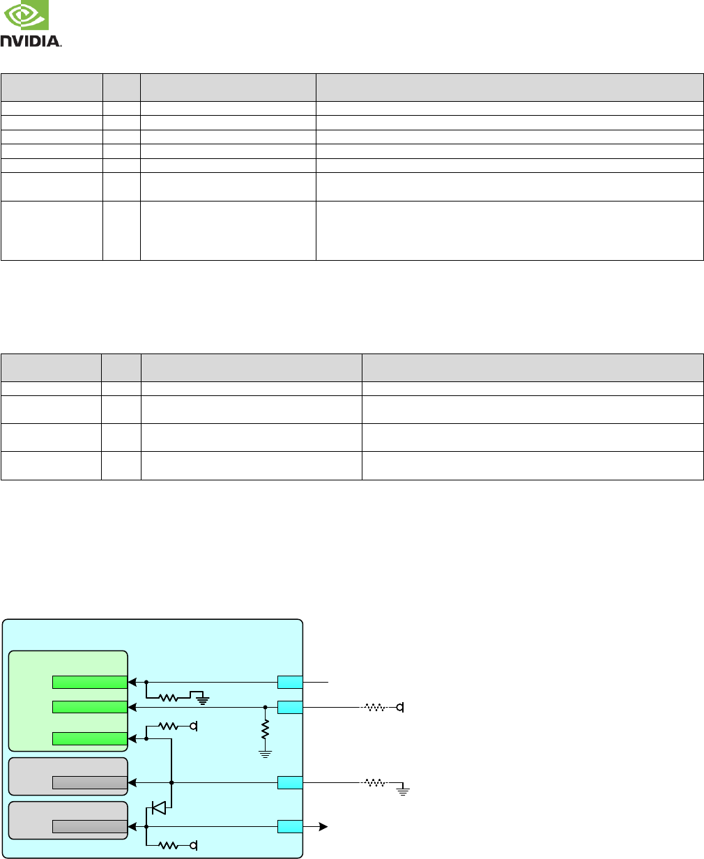
NVIDIA Jetson TX2 OEM Product Design Guide
JETSON TX2 OEM PRODUCT | DESIGN GUIDE | 20170912 67
Table 81. JTAG Signal Connections
Jetson TX2 Pin
(function) Name
Type
Termination
Description
JTAG_TMS
I
JTAG Mode Select: Connect to TMS pin of connector
JTAG_TCK
I
100GND (on Jetson TX2)
JTAG Clock: Connect to TCK pin of connector
JTAG_TDO
O
JTAG Data Out: Connect to TDO pin of connector
JTAG_TDI
I
JTAG Data In: Connect to TDI pin of connector
JTAG_RTCK
I
JTAG Return Clock: Connect to RTCK pin of connector
JTAG_GP0#
(JTAG_TRST_N)
I
GND &
0.1uF to GND (on Jetson TX2)
JTAG General Purpose Pin #0: Connect to TRST pin of connector
JTAG_GP1
GND (on Jetson TX2)
JTAG General Purpose Pin #1: Used as select
- Normal operation: Leave series resistor from NVJTAG_SEL not stuffed.
- Scan test mode: Connect NVJTAG_SEL to VDD_1V8 (install 0Ω resistor as
shown).
12.6.2 Debug UART
Jetson TX2 provides UART0 for debug purposes. The connections are shown in Figure 39 and described in the table below.
Table 82. Debug UART Connections
Jetson TX2 Pin
Name
Type
Termination
Description
UART0_TXD
O
UART #0 Transmit: Connect to RX pin of serial device
UART0_RXD
I
on the non-Jetson TX2 side of the device.
UART #0 Receive: Connect to TX pin of serial device
UART0_RTS#
O
GND or VDD_1V8 on Jetson TX2 for
RAM Code strapping
UART #0 Request to Send: Connect to CTS pin of serial device
UART0_CTS#
I
If level shi
on the non-Jetson TX2 side of the device.
UART #0 Clear to Send: Connect to RTS pin of serial device
12.6.3 Boundary Scan Test Mode
To support Boundary Scan Test mode, the Tegra NVJTAG_SEL pin must be pulled high and Tegra must be held in reset
without resetting the PMIC. The figure below illustrates this. Other requirements related to supporting Boundary Scan Test
mode are described in the “Tegra X2 Boundary Scan Requirements & Usage” document.
Figure 40. Boundary Scan Connections
Jetson TX2
PMIC
Tegra
Devices requiring system reset
& System Reset Sources
VDD_1V8
R1 - 0ΩR1 - 0Ω
Leave Resistors R1 & R2 uninstalled
for normal operation. Install both
for boundary scan test mode.
100kΩ100kΩ
100kΩ100kΩVDD_1V8
eMMC R2 - 0ΩR2 - 0Ω
JTAG_TRST_N
SYS_RESET_N
RESET*
RST I/O
JTAG_GP0
A46
RESET_OUT#
A47
RESET_IN#
10kΩ10kΩ1.8V
NVJTAG_SEL A11
JTAG_GP1
TRST on JTAG ConnectorB1 3
100kΩ100kΩ
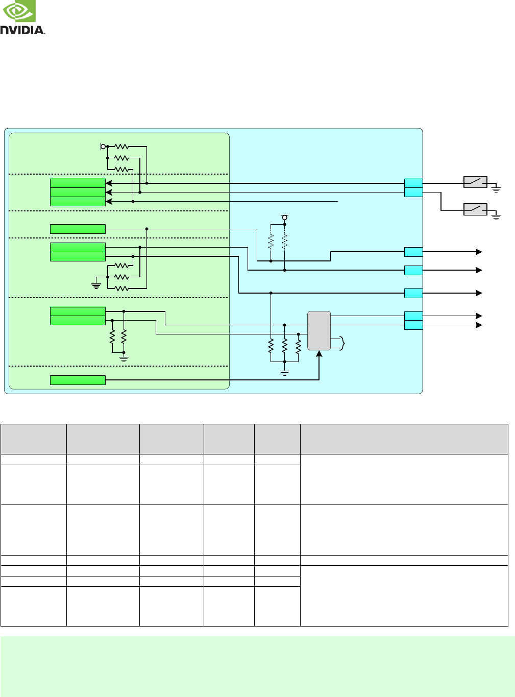
NVIDIA Jetson TX2 OEM Product Design Guide
JETSON TX2 OEM PRODUCT | DESIGN GUIDE | 20170912 68
12.7 Strapping Pins
Jetson TX2 has one strap (FORCE_RECOV#) that is intended to be used on the carrier board. That strap is used to enter
Force Recovery mode. The other straps mentioned in this section are for use on the module by Nvidia only. They are included
here as their state at power-on must be kept at the level selected on the module.
Figure 41. Jetson TX2 Strap Connections
Jetson TX2
Tegra
AO
UART7_TX
CONN UART4_TX
UART3_TX
UART1_RTS_N
DEBUG
4.7kΩ
4.7kΩ
4.7kΩ
1.8V
4.7kΩ
4.7kΩ
SYS GPIO_SW1
~100kΩ
1.8V
~100kΩ
~100kΩ
GPIO_SW2
GPIO_SW4
~100kΩ
~100kΩ
~100kΩ
~100kΩ
~100kΩ
UART4_RTS_N
RCM0 Strap
RCM1 Strap
RCM2 Strap
RAM_CODE0 Strap
RAM_CODE1 Strap
BOOT_SELECT2 Strap
BOOT_SELECT1 Strap
BOOT_SELECT0 Strap
E1
E2
G11
D9
D8
H10
G10
FORCE_RECOV#
SLEEP#
UART0_RTS
UART1_TX
UART7_TX
UART3_TX
UART3_RTS
BT Wake AP
(On-Module Bt/Wi-Fi)
Mux
SEL UART
(On-Module Bt/Wi-Fi)
SPI QSPI_IO2
RECOVERY
VOL DN / SLEEP
(See Note)
Table 83. Power-on Strapping Breakdown
Jetson TX2 Pin
Name
Tegra Ball Name
Strap Options
Tegra
Internal
PU/PD
Jetson
TX2
PU/PD
Description
FORCE_RECOV#
GPIO_SW1
RCM0
Recovery Mode [1:0]
x1: Normal boot from secondary device
10: Forced Recovery Mode
00: Reserved
See critical warning in note 1
SLEEP#
GPIO_SW2
RCM1
UART1_TX
UART3_TX
RAM_CODE1
[3:2] Selects secondary boot device configuration set
within the BCT. For Nvidia use only.
[1:0] Selects DRAM configuration set within the BCT. For
Nvidia use only.
See critical warning in Note 2.
UART0_RTS
UART1_RTS_N
RAM_CODE0
RSVD-D8
UART7_TX
BOOT_SELECT2
~100k
Software reads value and determines Boot device to be
configured and used
000 = eMMC x8 BootModeOFF, 512-byte page. Maps to
SDMMC w/config=0x0001 size. 26MHz
001 111 Reserved
See Note 3 & 5. See critical warning in Note 4.
NA (see note 5)
UART4_TX
BOOT_SELECT1
NA (see note 5)
UART4_RTS_N
BOOT_SELECT0
Note:
1. If the SLEEP# pin is used in a design, it must not be driven or pulled low during power-on at the same time as
FORCE_RECOV# is pulled low for Recovery Mode as this would change the strapping and select a reserved mode.
Violating this requirement will prevent the system from entering Recovery Mode.
2. If UART1_TX or UART0_RTS are used in a design, they must not be driven or pulled high or low during power-on.
Violating this requirement can change the RAM_CODE strapping & result in functional failures.

NVIDIA Jetson TX2 OEM Product Design Guide
JETSON TX2 OEM PRODUCT | DESIGN GUIDE | 20170912 69
3. The above BOOT_SELECT option is only in effect in "regular boot" conditions i.e. coldboot. If "Forced Recovery" mode is
detected (FORCE_RECOV# low at boot), that mode take precedence over the eMMC boot device choice.
4. If UART7_TX (on RSVD pin) is used in a design, it must not be driven or pulled high during power-on as this would affect
the BOOT_SELECT strapping. Violating this requirement will likely prevent the system from booting.
5. eMMC boot does not use either the normal boot mode or alternate boot mode supported by the eMMC spec. The Tegra
BootROM uses the Card Identification mode for booting from eMMC.
6. Tegra UART4_TX & UART4_RTS_N are routed to a mux on Jetson TX2 and directed to either UART3_TX/RTS or On-module WLAN/BT.
Since these pins are outputs, and the mux is in the path, Jetson TX2 UART3 pins will not affect the Boot Select [1:0] strapping.

NVIDIA Jetson TX2 OEM Product Design Guide
JETSON TX2 OEM PRODUCT | DESIGN GUIDE | 20170912 70
13.0 PADS
13.1 MPIO Pad Behavior when Associated Power Rail is Enabled
Jetson TX2 CZ (see note) type MPIOs pins may glitch when the associated power rail is enabled or disabled. Designers should
take this into account. MPIOs of this type that must maintain a low state even while the power rail is being ramped up or down
may require special handling. The CZ type pins are used on the following Jetson TX2 pins:
- I2S[3:2]_x
- AO_DMIC_IN_x
- SDCARD_x
- GPIO[18,17,11,9,8,6]/x
- CANx
Note:
The Pin Descriptions section of Jetson TX2 Data Sheet includes the pin type information.
13.2 Internal Pull-ups for CZ Type Pins at Power-on
The MPIO pads of type CZ (see note) are on blocks that can be powered at 1.8V or 3.3V. If the associated block is powered at
1.8V, the internal pull-up at initial power-on is not effective. The signal may only be pulled up a fraction of the 1.8V rail. Once
the system boots, software can configure the pins for 1.8V operation and the internal pull-ups will work correctly. Signals that
need the pull-ups during power-on should have external pull-up resistors added. If the associated block is powered at 3.3V by
default, the pull-ups work correctly. The affected pins listed below. These are the Jetson TX2 CZ Type Pins on blocks powered
at 1.8V with Power-on-Reset Default of Internal Pull-up Enabled. The SD_CARD pins are CZ type, but the associated power rail
is not enabled at power-on – software enables this at a later time. As long as the software configures the pins appropriately for
the voltage, the issue will not affect the SD_CARD pins.
- CAN1_DOUT
- CAN1_DIN
- CAN0_DOUT
- CAN0_DIN
Note:
The Pin Descriptions section of Jetson TX2 Data Sheet includes the pin type information.
13.3 Schmitt Trigger Usage
The MPIO pins have an option to enable or disable Schmitt Trigger mode on a per-pin basis. This mode is recommended for
pins used for edge-sensitive functions such as input clocks, or other functions where each edge detected will affect the
operation of a device. Schmitt Trigger mode provides better noise immunity, and can help avoid extra edges from being “seen”
by the Tegra inputs. Input clocks include the I2S & SPI clocks (I2Sx_SCLK & SPIx_SCK) when Tegra is in slave mode. The
FAN_TACH pin is another input that could be affected by noise on the signal edges. The SD_CARD pin (Tegra SDMMC1_CLK
function), while used to output the SD clock, also samples the clock at the input to help with read timing. Therefore, the
SD_CARD_CLK pin may benefit from enabling Schmitt Trigger mode. Care should be taken if the Schmitt Trigger mode setting
is changed from the default initialization mode as this can have an effect on interface timing.
13.4 Pins Pulled/Driven High During Power-on
The Jetson TX2 is powered up before the carrier board (See Power Sequencing section). The table below lists the pins on
Jetson TX2 that default to being pulled or driven high. Care must be taken on the carrier board design to ensure that any of
these pins that connect to devices on the carrier board (or devices connected to the carrier board) do not cause damage or
excessive leakage to those devices. The SD_CARD pins are not included because the associated power rail is not enabled at
power-on – software enables this at a later time. Some of the ways to avoid issues with sensitive devices are:
▪ External pull-downs on the carrier board that are strong enough to keep the signals low are one solution, given that
this does not affect the function of the pin. This will not work with RESET_IN# which is actively driven high.
NVIDIA Jetson TX2 OEM Product Design Guide
JETSON TX2 OEM PRODUCT | DESIGN GUIDE | 20170912 71
▪ Buffers or level shifters can be used to separate the signals from devices that may be affected. The buffer/shifter
should be disabled until the device power is enabled.
Table 84. Jetson TX2 Pins Pulled/Driven High by Tegra Prior to CARRIER_PWR_ON Active
Jetson TX2 Pin
Power-on Reset
Default
Pull-up Strength
(kΩ)
Jetson TX2 Pin
Power-on Reset
Default
Pull-up Strength
(kΩ)
DSPK_OUT_CLK
Internal Pull-up
~100
JTAG_TMS
Internal Pull-up
~100
SPI1_CS0#
Internal Pull-up
~100
JTAG_TDI
Internal Pull-up
~100
RESET_IN#
Driven High
na
UART1_RX
Internal Pull-up
~100
FORCE_RECOV#
Internal Pull-up
~100
SPI0_MISO
Internal Pull-up
~100
SLEEP#
Internal Pull-up
~100
SPI0_MOSI
Internal Pull-up
~100
GPIO7_TOUCH_RST
Driven High
na
CAN1_TX
Internal Pull-up
~20
CARRIER_STBY#
Driven High
na
CAN1_RX
Internal Pull-up
~20
GPIO5/CAM_FLASH_EN
Internal Pull-up
~100
CAN0_TX
Internal Pull-up
~20
USB0_VBUS_DET
Internal Pull-up
~100
CAN0_RX
Internal Pull-up
~20
SPI2_CS1#
Internal Pull-up
~100
GPIO6_TOUCH_INT
Driven High
na
SPI2_CS0#
Internal Pull-up
~100
GPIO3_CAM1_RST#
Internal Pull-up
~18
UART0_TX
Internal Pull-up
~100
CAM_VSYNC
Internal Pull-up
~18
UART0_RX
Internal Pull-up
~100
GPIO2_CAM0_RST#
Internal Pull-up
~18
WDT_TIME_OUT#
Driven High
na
Table 85. Jetson TX2 Pins Pulled High on the Module Prior to CARRIER_PWR_ON Active
Jetson TX2 Pin
Pull-up Supply
Voltage (V)
External
Pull-up (kΩ)
Jetson TX2 Pin
Pull-up Supply
Voltage (V)
External
Pull-up (kΩ)
VIN_PWR_BAD#
5.0
10
USB0_EN_OC#
3.3
100
RESET_OUT#
1.8
4.7
USB1_EN_OC#
3.3
100
I2C_GP0_CLK/DAT
1.8
1.0
PEX0_CLKREQ#
3.3
56
I2C_GP1_CLK/DAT
3.3
1.0
PEX0_RST#
3.3
56
I2C_GP2_CLK/DAT
1.8
1.0
PEX1_CLKREQ#
3.3
56
I2C_GP3_CLK/DAT
1.8
1.0
PEX1_RST#
3.3
56
I2C_PM_CLK/DAT
1.8
1.0
PEX2_CLKREQ#
3.3
56
I2C_CAM_CLK/DAT
1.8
1.0
PEX2_RST#
3.3
56
PEX_WAKE#
3.3
56
13.5 Pad Drive Strength
The table below provides the maximum MPIO pad output drive current when the pad is configured for the maximum
DRVUP/DRVDN values (11111b). The MPIO pad types include the ST, DD, CZ and LV_CZ type pads. The pad types can be
found in the Jetson TX2 Module Data Sheet.
Table 86. MPIO Maximum Output Drive Current
IOL/IOH
Pad Type
VOL
VOH
+/- 1mA
ST
0.15*VDD
0.825*VDD
+/- 1mA
DD
0.15*VDD
0.8*VDD
+/- 1mA
CZ (1.8V mode)
0.15*VDD
0.85*VDD
+/- 1mA
CZ (3.3V mode)
0.15*VDD
0.85*VDD
+/- 1mA
LV_CZ
0.15*VDD
0.85*VDD
+/- 2mA
ST
0.15*VDD
0.7*VDD
+/- 2mA
DD
0.175*VDD
0.7*VDD
+/- 2mA
CZ (1.8V mode)
0.25*VDD
0.75*VDD
+/- 2mA
CZ (3.3V mode)
0.15*VDD
0.75*VDD
+/- 2mA
LV_CZ
0.25*VDD
0.75*VDD
NVIDIA Jetson TX2 OEM Product Design Guide
JETSON TX2 OEM PRODUCT | DESIGN GUIDE | 20170912 72
14.0 UNUSED INTERFACE TERMINATIONS
14.1 Unused MPIO Interfaces
The following Jetson TX2 pins (& groups of pins) are Jetson TX2 MPIO (Multi-purpose Standard CMOS Pad) pins that support
either special function IOs (SFIO) and/or GPIO capabilities. Any unused pins or portions of pin groups listed below that are not
used can be left unconnected.
Table 87. Unused MPIO pins / Pin Groups
Jetson TX2 Pins / Pin Groups
Jetson TX2 Pins / Pin Groups
SLEEP#
SDIO, SDMMC
BATLOW#
AUDIO_x
FORCE_RECOV#
I2S
RESET_OUT#
DMIC
WDT_TIME_OUT#
DSPK
CARRIER_STBY#
UART
CHARGER_PRSNT#
I2C
CHARGING#
SPI
USBx_EN_OC#
TOUCH_x
PEXx_REFCLK/RST/CLKREQ/WAKE
WIFI_WAKE_x
LCD0_BKLT_PWM, FAN_PWM
MODEM_x, MDM2AP_x, AP2MDM_x
CAN
GPIO_EXP[1:0]_INT
LCD_x
ALS_PROX_INT, MOTION_INT
DP0_HPD, DP1_HPD, HDMI_CEC
JTAG
CAM Control, Clock
14.2 Unused SFIO Interface Pins
See the Unused SFIO (Special Function I/O) interface pins section in the Checklist at the end of this document.
NVIDIA Jetson TX2 OEM Product Design Guide
JETSON TX2 OEM PRODUCT | DESIGN GUIDE | 20170912 73
15.0 DESIGN CHECKLIST
The checklist below is intended to help ensure that the correct connections have been made in a design. The check items
describe connections for the various interfaces and the “Same/Diff/NA” column is intended to be used to indicate whether the
design matches the check item description, is different, or is not applicable to the design.
Table 88. Checklist
Check Item Description
Same/Diff/NA
Jetson TX2 Signal Terminations (Present on the module - shown for reference only)
Note: Internal refers to Tegra internal Pull-up/down resistors. External refers to resistors added on the module.
Parallel Termination
Series Termination
USB/PCIe
USB0_EN_OC#
External 100K pull-up to 3.3V
USB1_EN_OC#
External 100K pull-up to 3.3V
USB0_VBUS_DET
Level shifter between Tegra & Jetson TX2
USB0_VBUS_DET pin
PEX0_CLKREQ#
External 56K pull-up to 3.3V
PEX0_RST#
External 56K pull-up to 3.3V
PEX1_CLKREQ#
External 56K pull-up to 3.3V
PEX1_RST#
External 56K pull-up to 3.3V
PEX2_CLKREQ#
External 56K pull-up to 3.3V
PEX2_RST#
External 56K pull-up to 3.3V
PEX_WAKE#
External 56K pull-up to 3.3V
HDMI/DP/eDP
DP0_HPD
Internal pull-down
DP1_HPD
Internal pull-down
I2C
I2C_GP0_CLK/DAT
External 1K pull-up to 1.8V
I2C_GP1_CLK/DAT
External 1K pull-up to 3.3V
I2C_GP2_CLK/DAT
External 1K pull-up to 1.8V
I2C_GP3_CLK/DAT
External 1K pull-up to 1.8V
I2C_PM_CLK/DAT
External 1K pull-up to 1.8V
I2C_CAM_CLK/DAT
External 1K Pull Up to 1.8V
SPI
SPI0_MOSI
Internal pull-down
SPI0_MISO
Internal pull-down
SPI0_CLK
Internal pull-down
SPI0_CS0#
Internal pull-up to 1.8V
SPI1_MOSI
Internal pull-down
SPI1_MISO
Internal pull-down
SPI1_CLK
Internal pull-down
SPI1_CS0#
Internal pull-up to 1.8V
SPI1_CS1#
Internal pull-up to 1.8V
SPI2_MOSI
Internal Pull Down
SPI2_MISO
Internal Pull Down
SPI2_CLK
Internal Pull Down
SPI2_CS0#
Internal pull-up to 1.8V
SPI2_CS1#
Internal pull-up to 1.8V
SD Card
SDCARD_CMD
Internal pull-up to 1.8V/3.3V
SDCARD_D[3:0]
Internal pull-up to 1.8V/3.3V
SDCARD_CD#
Internal pull-up to 1.8V
SDCARD_WP
Internal pull-up to 1.8V
Embedded Display
LCD_TE
Internal pull-down
GPIO
GPIO0_CAM0_PWR
Internal pull-down to GND
GPIO1_CAM1_PWR
Internal pull-down to GND
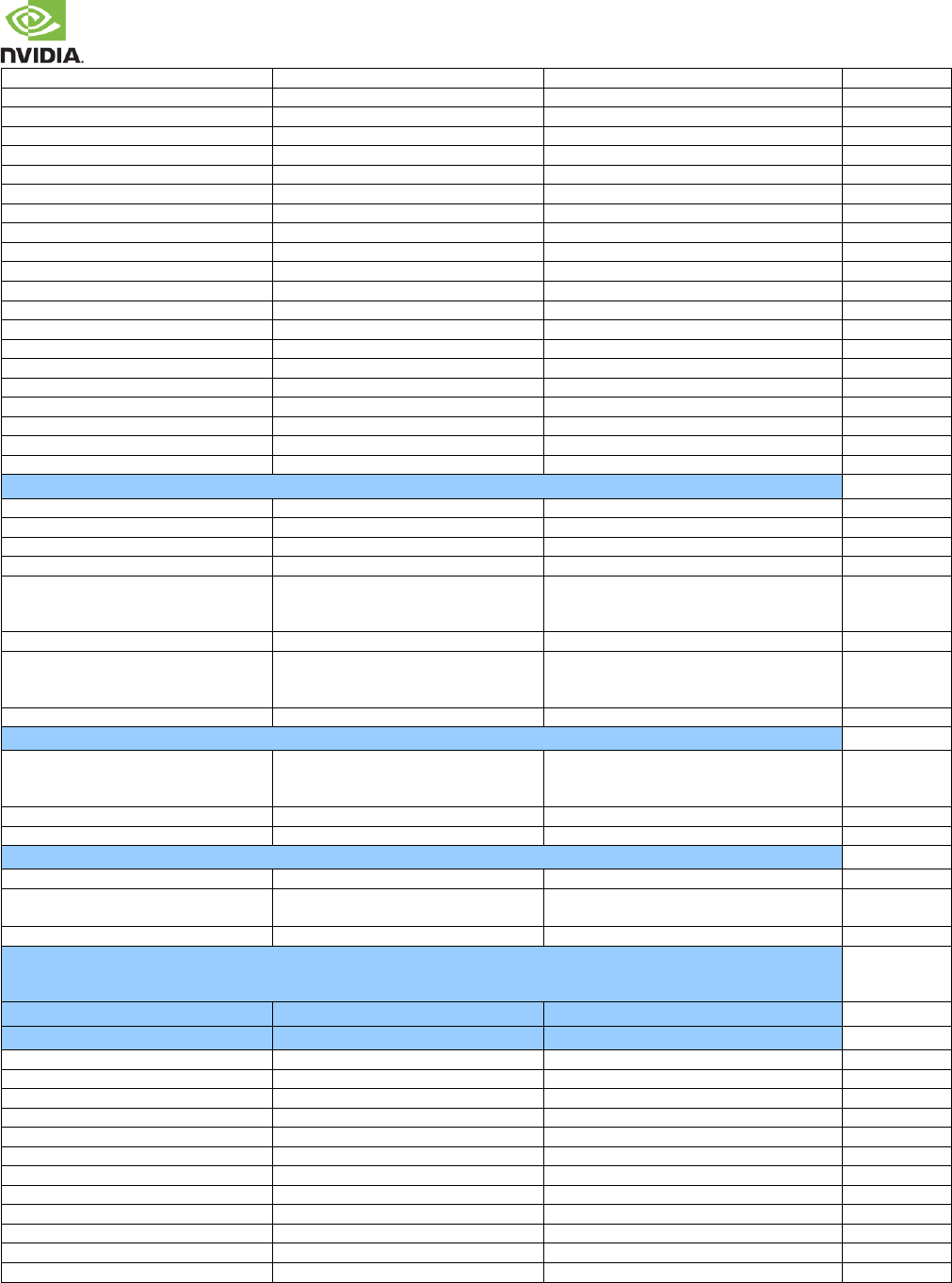
NVIDIA Jetson TX2 OEM Product Design Guide
JETSON TX2 OEM PRODUCT | DESIGN GUIDE | 20170912 74
GPIO2_CAM0_RST
Internal pull-up to 1.8V
GPIO3_CAM1_RST
Internal pull-up to 1.8V
GPIO4_CAM_STROBE
Internal pull-down to GND
GPIO5_CAM_FLASH_EN
Internal pull-up to 1.8V
GPIO6/TOUCH_INT
Internal pull-up to 1.8V
GPIO7/TOUCH_RST
(Driven high)
GPIO8/ALS_PROX_INT
Internal pull-up to 1.8V
GPIO9/MOTION_INT
Internal pull-up to 1.8V
GPIO10/WIFI_WAKE_AP
Internal pull-up to 1.8V
GPIO11_AP_WAKE_BT
Internal pull-down to GND
GPIO12_BT_EN
Internal pull-down to GND
GPIO13/BT_WAKE_AP
Internal pull-up to 1.8V
GPIO14_AP_WAKE_MDM
(Driven low)
GPIO15_AP2MDM_READY
(Driven low)
GPIO16/MDM_WAKE_AP
Internal pull-up to 1.8V
GPIO17/MDM2AP_READY
Internal pull-up to 1.8V
GPIO18/MDM_COLDBOOT
Internal pull-up to 1.8V
GPIO19/AUD_RST
Internal pull-up to 1.8V
GPIO20/AUD_INT
Internal pull-up to 1.8V
GPIO_EXP0_INT
Internal pull-up to 1.8V
GPIO_EXP1_INT
Internal pull-up to 1.8V
System Control
VIN_PWR_BAD#
External 10kpull-up to 3.8V
CARRIER_PWR_ON
External 10kpull-up to 3.3V
FORCE_RECOV#
Internal pull-up to 1.8V
SLEEP#
Internal pull-up to 1.8V
POWER_BTN#
Internal Pull Up to 1.8V near Tegra & PMIC
internal Pull-up to 5.0V on other side of
diodes (module pin side)
BAT54CW Schottky barrier diodes
RESET_IN#
External pull-up to 1.8V
RESET_OUT#
External 100pull-up to 1.8V near Tegra
(module pin side) & external pull-up
to 1.8V on the other side of a diode
FAN_TACH
Internal pull-up to 1.8V
Charging
CHARGER_PRSNT#
External 4.7k pull-up to 5V & Internal
PMIC pull-up to 5.0V once FET is enabled
by VDD_IN on & VIN_PWR_BAD# inactive.
CHARGING#
Internal pull-up to 1.8V
BATLOW#
Internal pull-up to 1.8V
JTAG
JTAG_TCK
External 100K pull-down to GND
JTAG_GP0
External 100K pull-down to GND & 0.1uF
capacitor to GND
JTAG_GP1
External 100K pull-down to GND
Carrier Board Signal Terminations
(To be implemented on the carrier board for interfaces that are used)
Parallel Termination
Series Termination
USB/PCIe/SATA
USB_SS0_TX+/-
0.1uF capacitors
USB_SS1_TX+/-
0.1uF capacitors
USB_SS0_RX+/-
0.1uF capacitors if directly connected
USB_SS1_RX+/-
0.1uF capacitors directly connected
PEX0_TX+/-
0.1uF capacitors
PEX1_TX+/-
0.1uF capacitors
PEX2_TX+/-
0.1uF capacitors
PEX_RFU_TX+/-
0.1uF capacitors
PEX0_RX+/-
0.1uF capacitors if directly connected
PEX1_RX+/-
0.1uF capacitors if directly connected
PEX2_RX+/-
0.1uF capacitors if directly connected
PEX_RFU_RX+/-
0.1uF capacitors
NVIDIA Jetson TX2 OEM Product Design Guide
JETSON TX2 OEM PRODUCT | DESIGN GUIDE | 20170912 75
SATA_TX+/-
0.01uF capacitors
SATA_RX+/-
0.01uF capacitors
SATA_DEV_SLP
1.8V to 3.3V Level Shifter
Ethernet
GBE_MDI0+/-
Magnetics near RJ45 connector
GBE_MDI1+/-
Magnetics near RJ45 connector
GBE_MDI2+/-
Magnetics near RJ45 connector
GBE_MDI3+/-
Magnetics near RJ45 connector
GBE_LINK100#
LED and pull-up Current Limiting Circuit
GBE_LINK1000#
LED and pull-up Current Limiting Circuit
GBE_LINK_ACT#
LED and pull-up Current Limiting Circuit
DP[1:0] for eDP/DP
DPx_TX3+/-
0.1uF capacitors
DPx_TX2+/-
0.1uF capacitors
DPx_TX1+/-
0.1uF capacitors
DPx_TX0+/-
0.1uF capacitors
DPx_AUX_CH+
-down to GND near connector
(DP only)
0.1uF capacitor
DPx_AUX_CH-
-up to 3.3V near connector (DP
only)
0.1uF capacitor
DPx_HPD
10k-up to 1.8V near main conn. &
-down to GND on DP side of
level shifter.
Level Shifter (w/output toward main
connector) near main connector & 100k
resistor to DP connector. Level shifter must be
non-inverting.
DP[1:0] for HDMI
DPx_TX3+/-
499GND
0.1uF capacitors
DPx_TX2+/-
499GND
0.1uF capacitors
DPx_TX1+/-
499GND
0.1uF capacitors
DPx_TX0+/-
499GND
0.1uF capacitors
DPx_AUX_CH+/-
10k Pull-up to 3.3V near main conn. &
-up to 5V near HDMI conn.
Bidirectional level shifter between Pull-ups in
Parallel Termination column
DPx_HPD
10k-up to 1.8V near main conn. &
-down to GND near HDMI conn.
Level shifter (w/output toward main connector)
between Pull-up & Pull-down in Parallel
Termination column. Level shifter can be
inverting or non-inverting.
resistor between pull-down & HDMI connector.
Power
Jetson TX2 Power Supplies
Supply (Carrier Board)
Usage
(V)
Supply Type
Source
Enable
VDD_IN
Main Supply from Adapter
5.5-
19.6
Adapter
na
na
VDD_RTC
Real-time clock supply
1.65-
5.5
PMIC is
supply when
charging cap
or coin cell
Super cap or coin
cell is source
when system
power removed
na
Carrier Board Supplies
VDD_MUX
Main power input from DC
Adapter
5.5-
19.6
FETs
DC Adapter
VDD_5V0_IO_SYS
Main 5V supply
5.0
DC/DC
VDD_MUX
CARRIER_PWR_ON
VDD_3V3_SYS
Main 3.3V supply
3.3
DC/DC
VDD_MUX
3V3_SYS_BUCK_EN
VDD_1V8
Main 1.8V supply
1.8
DC/DC
VDD_5V0_IO_SYS
1V8_IO_VREG_EN
(VDD_3V3_SYS_PG)
VDD_3V3_SLP
3.3V rail, off in Sleep
(various)
3.3
FETs/Load
Switch
VDD_3V3_SYS
SOC_PWR_REQ
VDD_5V0_IO_SLP
5V rail, off in Sleep
(SATA/FAN)
5
FETs/Load
Switch
VDD_5V0_IO_SYS
VDD_3V3_SLP
VDD_12V_SLP
PCIe & SATA connectors
12
Boost
VDD_5V0_IO_SYS
VDD_3V3_SLP
VDD_VBUS_CON
VBUS (USB 2.0 Type AB conn)
5.0
Load Switch
VDD_5V0_IO_SYS
USB_VBUS_EN0
USB_VBUS
VBUS (USB 3.0 Type A conn)
5.0
Load Switch
VDD_5V0_IO_SYS
USB_VBUS_EN1
SD_CARD_SW_PWR
SD Card power rail
3.3
Load Switch
VDD_3V3_SYS
SDCARD_VDD_EN
VDD_5V0_HDMI_CON
5V rail for HDMI connector
5.0
Load Switch
VDD_5V0_IO_SYS
GPIO Expander U29, P14
VDD_TS_1V8
1.8V rail for touch screen
1.8
Load Switch
VDD_1V8
GPIO Expander U29, P01
NVIDIA Jetson TX2 OEM Product Design Guide
JETSON TX2 OEM PRODUCT | DESIGN GUIDE | 20170912 76
AVDD_TS_DIS
High voltage rail for touch
screen
3.3
Load Switch
VDD_3V3_SLP
GPIO Expander U29, P02
VDD_LCD_1V8_DIS
1.8V rail for panel
1.8
Load Switch
VDD_1V8
GPIO Expander U29, P11
VDD_DIS_3V3_LCD
High voltage rail for panel
3.3
Load Switch
VDD_3V3_SYS
GPIO Expander U29, P03
VDD_1V2
Generic 1.2V display rail
1.2
LDO
VDD_1V8
GPIO Expander U29, P12
DVDD_CAM_IO_1V8
1.8V rail for camera I/O
1.8
Load Switch
VDD_1V8
GPIO Expander U28, P11
AVDD_CAM
High voltage rail for cameras
2.8
Load Switch
VDD_3V3_SLP
GPIO Expander U29, P15
DVDD_CAM_IO_1V2
1.2V rail for camera Core
1.2
LDO
VDD_1V8
GPIO Expander U28, P12
Power Control
VIN_PWR_BAD# connects to Carrier Board main power input & discharge circuit. Inactive when main supply is stable
CARRIER_PWR_ON used as enable for Carrier Board main 5V supply & discharge circuit
RESET_IN# to/from carrier board connects to devices requiring full system reset, and to system reset sources (reset button, etc.)
RESET_OUT# to Jetson TX2 from Carrier Board when a force reset is required (as for Boundary Scan test mode)
POWER_BTN# connects to button or similar to pull POWER_BTN# to GND when pressed/asserted to power system ON/OFF
SLEEP# connects to button or similar to pull SLEEP# to GND when pressed/asserted to put system in sleep mode
CARRIER_STBY# connects to enable of supplies that should be off in Sleep mode such as VDD_3V3_SLP
Power Discharge
VIN_PWR_BAD# connects to Carrier Board main power input & discharge circuit. Inactive when main supply is stable
VDD_5V0_IO_SYS Discharge implemented: FET enabled by DISCHARGE w/Source GNDVDD_5V0_IO_SYS
VDD_3V3_SYS Discharge implemented: FET enabled by DISCHARGE w/Source GNDVDD_3V3_SYS
VDD_1V8 Discharge implemented: FET enabled by DISCHARGE w/Source GNDVDD_1V8
VDD_3V3_SLP Discharge implemented: FET enabled by DISCHARGE w/Source GNDVDD_3V3_SLP
VDD_12V_SLP Discharge implemented: FET enabled by DISCHARGE & VDD_3V3_SLP w/Source GNDVDD_12V_SLP
VDD_5V0_IO_SLP Discharge implemented: FET enabled by DISCHARGE & VDD_3V3_SLP w/Source GNDVDD_5V0_IO_SLP
Wake Event Pins
If Audio Interrupt required, GPIO20_AUD_INT pin is used
If External BT Wake Request to AP required, GPIO13_BT_WAKE_AP pin is used
If External WLAN Wake Request to AP required, GPIO10_WIFI_WAKE_AP pin is used
If Modem to AP Ready required, GPIO17_MDM2AP_READY pin is used
If Modem Coldboot Alert required, GPIO18_MDM_COLDBOOT pin is used
If HDMI CEC required, HDMI_CEC pin is used
If GPIO Exapander 0 Interrupt required, GPIO_EXP0_INT pin is used
If Power Button On required, POWER_BTN# pin is used
If Charging Interrupt required, CHARGING# pin is used
If Sleep Request from Carrier Board required, SLEEP# pin is used
If Ambient/Proximity Interrupt required, GPIO8_ALS_PROX_INT pin is used
If HDMI Hot Plug Detect required, DP1_HPD pin is used
If Battery Low Warning required, BATLOW# pin is used
If Primary Modem Wake Request to AP required, GPIO16_MDM_WAKE_AP pin is used
If Touch Controller Interrupt required, GPIO6_TOUCH_INT pin is used
If Motion Sensor Interrupt required, GPIO9_MOTION_INT pin is used
USB/PEX/SATA Connections
USB 2.0
USB0 available to be used as device for USB recovery at a minimum
USB ID from connector, if used, connects to Jetson TX2 USB0_OTG_ID pin
VBUS from connector connects to load switch (if host supported) and USB0_VBUS_DET pin on Jetson TX2 (100k
required)
USB[2:0]_DP/DN connected to D+/D- pins on USB 2.0 connector/device.
Any EMI/ESD devices used are suitable for USB High-speed
USB 3.0
USB_SS0_RX+/– connected to RX+/- pins on USB 3.0 connector, Device, Hub, etc. (muxed w/PCIe #2 on module)
USB_SS0_TX+/– connected to TX+/- pins on USB 3.0 conn., Device, Hub, etc. (muxed w/PCIe #2 on module - See Signal Terminations)
Additional USB 3.0 interfaces taken from USB_SS1 or PEX_RFU (See Signal Terminations)
See USB 3.0 section for Common Mode Choke requirements if this is required. TDK ACM2012D-900-2P device is recommended
See USB 3.0 section for ESD requirements. SEMTECH ESD Rclamp0524p device is recommended
PCIe
PCIe Controller #0 (x1 by default – supports up to x4. Lanes [2:1] of x4 configuration shared w/USB_SS#[2:1]
PEX0 used for 3.3V single-lane device/connector (lane 0 of PCIe x1 connector on reference Carrier Board)
PEX0 & USB_SS1 used for 3.3V 2-lane device/connector
PEX0, USB_SS1, PEX2 & PEX_RFU used for 3.3V 4-lane device/connector
TX+/ connected to corresponding pins on connector, or RX+/ on device on the carrier board (See Signal Terminations)
NVIDIA Jetson TX2 OEM Product Design Guide
JETSON TX2 OEM PRODUCT | DESIGN GUIDE | 20170912 77
RX+/ connected to corresponding pins on connector, or TX+/ on device on the carrier board
AC caps are provided for device TX pins (those connected to Jetson TX2 RX+/) if device is on the carrier board (See Signal Terminations)
Reference clock used for PCIe Controller #0 (Up to x4 lane PCIe interface) is PEX0_REFCLK+/–
Clock Request & Reset for PCIe Controller #0 are PEX0_CLKREQ# & PEX0_RST#
PCIe Controller #1 (x1 – Shared with PCIe Controller #0 lane 2)
PEX2 used for 3.3V single-lane device/connector
TX+/ connected to corresponding pins on connector, or RX+/ on device on the carrier board (See Signal Terminations)
RX+/ connected to corresponding pins on connector, or TX+/ on device on the carrier board
AC caps are provided for device TX pins (those connected to Jetson TX2 RX+/) if device is on the carrier board (See Signal Terminations)
Reference clock used for PCIe Controller #1 (single-lane PCIe interface) is PEX2_REFCLK+/
Clock Request & Reset for PCIe Controller #1 are PEX2_CLKREQ# & PEX2_RST# (See Signal Terminations)
PCIe Controller #2 (x1)
PEX1 used for 3.3V single-lane device/connector (M.2 connector on Jetson carrier board) or USB_SS#0 (controlled by on module mux)
TX+/ connected to corresponding pins on connector, or RX+/ on device on the carrier board (See Signal Terminations)
RX+/ connected to corresponding pins on connector, or TX+/ on device on the carrier board
AC caps are provided for device TX pins (those connected to Jetson TX2 RX+/) if device is on the carrier board (See Signal Terminations)
Reference clock used for PCIe Controller #2 (single-lane PCIe interface) is PEX1_REFCLK+/
Clock Request & Reset for PCIe Controller #1 are PEX1_CLKREQ# & PEX1_RST# (PEX1_CLKREQ# muxed with SATA_DEV_SLP on module -
See Signal Terminations)
Common
PEX_WAKE# connected to WAKE pins on devices/connectors (See Signal Terminations)
SATA
SATA_TX+/– connected to TX_P/N pins of SATA connector (or RX+/ pins of onboard device) (See Signal Terminations)
SATA_RX+/– connected to RX_P/N pins of SATA connector (or TX+/ pins of onboard device) (See Signal Terminations)
See SATA section for Common Mode Choke requirements if they are required. TDK ACM2012D-900-2P device is recommended
See SATA section for ESD requirements. SEMTECH ESD Rclamp0524p device is recommended
SATA_DEV_SLP connected to matching pin on device or connector (pin 10 on conn. shown in SATA section See Signal Terminations)
Ethernet
GBE_MDI[3:0]+/ – connected to equivalent pins on magnetics device (See Signal Terminations)
GBE_LINK_ACT, GBE_LINK100 & GBE_LINK1000 connected to LED pins on connector (See Signal Terminations)
GBE_CTVREF Not used. Leave NC.
SDMMC Connections
SD Card
SDCARD_CLK connected to CLK pin of socket/device
SDCARD_CMD connected to CMD pin of socket/device. (See Signal Terminations)
SDCARD_D[3:0] connected to DATA[3:0] pins of socket/device. (See Signal Terminations)
SDCARD_CD connected to the SD Card Detect pin on socket
SDCARD_WP connected to the SD Card Write Protect pin on socket (if supported)
SDCARD_PWR_EN connected to SD Card VDD supply/load switch enable pin
Adequate bypass caps provided on SD Card VDD rail
Any EMI/ESD devices used are suitable for highest frequencies supported (low capacitive load: <1pf recommended).
Display Connections
DSI
DSI Dual Link Configurations
DSI0_CK+/– connected to CLKp/n pins of the lower x4 DSI interface of display
DSI0_D[1:0] +/– connected to lower 2 data lanes of the lower x4 DSI interface of display
DSI1_D[1:0] +/– connected to upper 2 data lanes of the lower x4 DSI interface of display
DSI2_CK+/– connected to CLKp/n pins of the upper x4 DSI interface of display or a x4 DSI interface of secondary display
DSI2_D[1:0] +/– connected to lower 2 data lanes of the upper x4 DSI interface of display or lower 2 lanes of secondary display
DSI3_D[1:0] +/– connected to upper 2 data lanes of the upper x4 DSI interface of display or upper 2 lanes of secondary display
Any EMI/ESD devices used on DSI signals are suitable for highest frequencies supported (low capacitive load: <1pf recommended)
DSI Split Link Configurations
DSI0_CK+/– connected to CLKp/n pins of the 1st x2 DSI interface of split link display
DSI0_D[1:0] +/– connected to up to 2 data lanes of the 1st x1/x2 DSI interface of split link display
DSI1_CK+/– connected to CLKp/n pins of the 2nd x2 DSI interface of split link display
DSI1_D[1:0] +/– connected to up to 2 data lanes of the 2nd x1/x2 DSI interface of split link display
DSI2_CK+/– connected to CLKp/n pins of the 3rd x2 DSI interface of split link display
DSI2_D[1:0] +/– connected to up to 2 data lanes of the 3rd x1/x2 DSI interface of split link display
DSI3_CK+/– connected to CLKp/n pins of the 4th x2 DSI interface of split link display
DSI3_D[1:0] +/– connected to up to 2 data lanes of the 4th x1/x2 DSI interface of split link display
Any EMI/ESD devices used on DSI signals are suitable for highest frequencies supported (low capacitive load: <1pf recommended)
NVIDIA Jetson TX2 OEM Product Design Guide
JETSON TX2 OEM PRODUCT | DESIGN GUIDE | 20170912 78
Display Control Connections
LCD_TE (used for Tearing Effect signal from display) connected to matching pin on display connector if supported
LCD_VDD_EN connected to enable of embedded display related power supply/load switch
LCD_BKLT_EN connected to enable of backlight solution(s)
LCD[1:0]_BKLT_PWM connected to PWM input(s) of backlight solution(s)
eDP / DP
DPx_TX[3:0]+/– connected to D[3:0]+/ pins on eDP/DP connector (See DP/HDMI Pin Mapping table & Signal Terminations)
DPx_AUX_CH+/– connected to Aux Lane of panel/connector (See Signal Terminations)
DPx_HPD connected to HPD pin of panel/connector
Any EMI/ESD devices used are suitable for highest frequencies supported (low capacitive load: <1pf recommended)
HDMI
DPx_TX3+/– connected to C/C+ & pins on HDMI Connector (See Signal Terminations)
DPx_TX[2:0]+/– connected to D[0:2]+/ pins (See DP/HDMI Pin Mapping table) (See Signal Terminations)
DPx_HPD connected to HPD pin on HDMI Connector (See Signal Terminations)
HDMI_CEC connected to CEC on HDMI Connector through gating circuitry.
DPx_AUX_CH+ connected to SCL & DPx_AUX_CH– to SDA on HDMI Connector (See Signal Terminations)
HDMI 5V Supply connected to +5V on HDMI Connector.
See HDMI section for Common Mode Choke requirements if this is required (not recommended unless EMI issues seen)
See HDMI section for ESD requirements. ON-Semiconductor ESD8040 device is recommended
Video Input
Camera (CSI)
CSI[5:0]_CLK+/– connected to clock pins of camera. See CSI D-PHY Configurations table for details
CSI[5:0]_D[1:0]+/– connected to data pins of camera. See CSI D-PHY Configurations table for details
Any EMI/ESD devices used are suitable for highest frequencies supported (low capacitive load: <1pf recommended)
Control
I2C_CAM_CK/DAT connected to I2C SCL & SDA pins of imager (See Signal Terminations).
CAM[1:0]_MCLK connected to Camera reference clock inputs.
GPIO1_CAM1_PWR# / GPIO0_CAM0_PWR# connected to powerdown pins on camera(s).
GPIO4_CAM_STROBE connected to camera strobe circuit unless strobe control comes from camera module.
CAM_FLASH_EN connected to enable of flash circuit
If a Jetson TX2 GPIO is used for flash control, CAM_FLASH_EN and/or CAMR_STROBE pins are used
GPIO3_CAM1_RST# / GPIO2_CAM0_RST# connected to reset pin on any cameras with this function.
If AutoFocus Enable is required, GPIO3_CAM1_RST# connected to AF_EN pin on camera module & GPIO2_CAM0_RST# used as
common reset line.
Audio
Codec/I2S/DMIC/DSPK
I2S0 used for Audio Codec if present in design
I2S2 used for BT if present in design
I2S[3:0]_SCLK Connect to I2S/PCM CLK pin of audio device.
I2S[3:0]_LRCK Connect to Left/Right Clock pin of audio device.
I2S[3:0]_SDATA_OUT Connect to Data Input pin of audio device.
I2S[3:0]_SDATA_IN Connect to Data Output pin of audio device.
AUD_MCLK Connect to clock pin of Audio Codec.
GPIO8_AUD_RST Connect to reset pin of Audio Codec.
GPIO9_AUD_INT Connect to interrupt pin of Audio Codec.
AO_DMIC_IN_CLK/DAT connect to CLK/DAT pins of digital mic
DSPK_OUT_CLK/DAT connect to CLK/DAT pins of digital speaker driver
I2C/SPI/UART
I2C
I2C devices on same I2C interface do not have address conflicts (comparisons are done 7-bit to 7-bit format or 8-bit to 8-bit format)
I2C_CAM, I2C_GP0, I2C_GP2, I2C_GP3 & I2C_PM (See Signal Terminations). Additional external pull-ups are not added unless stronger
pull-up than on module required. Devices on bus are 1.8V or level shifter is used.
I2C_GP1 (See Signal Terminations). Additional external pull-ups are not added unless stronger pull-up than on module required &
devices on bus are 3.3V or level shifter is used.
Pull-up resistors are provided on the non-Jetson TX2 side of any level shifters.
Pull-up resistor values based on frequency/load (check I2C Spec)
I2C_CAM_CK/DAT, I2C_GP[3:0]_CK/DAT & I2C_PM_CK/DAT connect to SCL/SDA pins of devices
SPI
SPI[2:0]_CLK connected to Peripheral CLK pin(s)
SPI[2:0]_MOSI connected to Slave Peripheral MOSI pin(s)
NVIDIA Jetson TX2 OEM Product Design Guide
JETSON TX2 OEM PRODUCT | DESIGN GUIDE | 20170912 79
SPI[2:0]_MISO connected to Slave Peripheral MISO pin(s)
SPI[2:1]_CS[1:0]# / SPI0_CS0# connected one CS# pin per SPI IF to each Slave Peripheral CS pin on the interface
CAN
CAN[1:0]_TX connected to input data (RX) pins of respective CAN device
CAN[1:0]_RX connected to output data (TX) pin of respective CAN device
CAN1_STBY connected to Standby pin of respective CAN device
CAN[1:0]_ERR connected to Error pin of respective CAN device
CAN_WAKE connected to Wake pin of CAN devices
UART
UARTx_TX connects to Peripheral RX pin of device
UARTx_RX connects to Peripheral TX pin of device
UARTx_CTS# connects to Peripheral RTS# pin of device
UARTx_RTS# connects to Peripheral CTS# pin of device
Miscellaneous
JTAG
JTAG_TMS Connect to TMS pin of connector
JTAG_TCK Connect to TCK pin of connector (See Signal Terminations).
JTAG_TDO Connect to TDO pin of connector
JTAG_TDI Connect to TDI pin of connector
JTAG_RTCLK Connect to RTCK pin of connector
JTAG_GP0 (JTAG_TRST#): Connect to TRST pin of connector
JTAG_GP1 (NVJTAG_SEL): For Boundary Scan test mode, NVJTAG_SEL is connected to VDD_1V8. (See Signal Terminations).
JTAG_GP1 (NVJTAG_SEL): For normal operation, NVJTAG_SEL is pullled down. (See Signal Terminations).
Strapping
FORCE_RECOV#: To enter Forced Recovery mode, pin is connected to GND when system is powered on.
All other module pins associated with strapping on Tegra X2: Ensure any devices connected to module pins associated with Tegra X2
straps do not affect the level of the straps at power-on. Module pins affected are: SLEEP#, UART1_TX, UART0_RTS, RSVD-D8
(UART7_TX)
Pin Selection
Pinmux completed including GPIO usage (direction, initial state, Ext. PU/PD resistors, Deep Sleep state).
SFIO usage matches reference platform where possible.
Each SFIO function assigned to only one pin, even if function selected in Pinmux registers is not used or pin used as GPIO
GPIO usage matches reference platform where possible.
Unused SFIO (Special Function I/O) Interface Pins
Ball Name
Termination
USB 2.0
USB[2:1]+/
Leave NC any unused pins
*USB 3.0 / PCIe
PEX_[2:0]_TX+/, USB_SS[1:0]_TX+/,
PEX_RFU_TX+/
Leave NC any unused TX lines
PEX_[2:0]_RX+/, USB_SS[1:0]_RX+/,
PEX_RFU_RX+/
Connect to GND any unused RX lines
PEX_[2:0]_REFCLK+/
Leave NC if not used
SATA
SATA_TX+/
Leave NC if not used.
SATA_RX+/
Connect to GND if SATA IF not used
DSI
DSI[3:0]_CK+/–
Leave NC any Clock lane not used.
DSI[3:0]_D[1:0]+/–
Leave NC any unused DSI Data lanes
CSI
CSI[5:0]_CK+/–
Leave NC any unused CSI Clock lanes
CSI[5:0]_D[1:0] +/–
Leave NC any unused CSI Data lanes
eDP/DP
DPx_TX[3:0] +/–
Leave NC any unused lanes
DPx_AUX_CH+/–
Leave NC if not used
DPx_HPD
Leave NC if not used
HDMI
DPx_TX[3:0] +/–
Leave NC if lanes not used for HDMI or DP
NVIDIA Jetson TX2 OEM Product Design Guide
JETSON TX2 OEM PRODUCT | DESIGN GUIDE | 20170912 80
DPx_AUX_CH+/–
Leave NC if not used
DPx_HPD
Leave NC if not used
HDMI_CEC
Leave NC if not used

NVIDIA Jetson TX2 OEM Product Design Guide
JETSON TX2 OEM PRODUCT | DESIGN GUIDE | 20170912 81
16.0 APPENDIX A: GENERAL LAYOUT GUIDELINES
16.1 Overview
Trace and via characteristics play an important role in signal integrity and power distribution on Jetson TX2. Vias can have a
strong impact on power distribution and signal noise, so careful planning must take place to ensure designs meet NVIDIA’s via
requirements. Trace length and impedance determine signal propagation time and reflections, both of which can greatly improve
or reduce the performance of Jetson TX2. Trace and via requirements for each signal type can be found in the corresponding
chapter; this appendix provides general guidelines for via and trace placement.
16.2 Via Guidelines
The number of vias in the path of a given signal, power supply line, or ground line can greatly affect the performance of the
trace. Via placement can make differences in current carrying capability, signal integrity (due to reflections and attenuation), and
noise generation, all of which can impact the overall performance of the trace. The following guidelines provide basic advice for
proper use of vias.
16.2.1 Via Count and Trace Width
As a general rule, each ampere of current requires at least two micro-vias.
16.2.2 Via Placement
If vias are not placed carefully, they can severely degrade the robustness of a board’s power plane. In standard deigns that don’t
use blind or buried vias, construction of a via entails drilling a hole that cuts into the power and ground planes. Thus, incorrect
via placement affects the amount of copper available to carry current to the power balls of the IC.
16.2.3 Via Placement and Power/Ground Corridors
Vias should be placed so that sufficiently wide power corridors are created for good power distribution, as show in Figure 42.
Figure 42. Via Placement for Good Power Distribution
Care should also be taken to avoid use of “thermal spokes” (also referred to as “thermal relief”) on power and ground vias.
Thermal spokes are not necessary for surface-mount components, and the narrow spoke widths contribute to increased
inductance. The metal on the inner layers between vias may not be flooded with copper if sufficient spacing is not provided. The
diminished spacing creates a blockage and forces the current to find another path due to lack of copper, as shown in Figure 43
and Figure 44. This leads to power delivery issues and impedance discontinuities when traces are routed over these plane
voids.
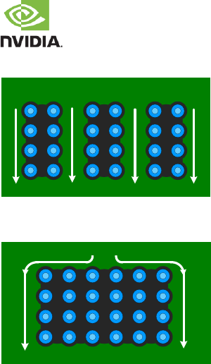
NVIDIA Jetson TX2 OEM Product Design Guide
JETSON TX2 OEM PRODUCT | DESIGN GUIDE | 20170912 82
Figure 43. Good Current Flow Resulting from Correct Via Placement
Current Flow
Current Flow
With sufficient via spacing
Correct via implementation
Figure 44. Poor Current Flow Resulting from Incorrect via Placement
Current Flow
Current Flow
With insufficient via spacing
Incorrect via implementation
In general, a dense via population should be avoided and good PCB design principles and analysis should be applied.
16.3 Connecting Vias
To be effective, vias must be connected properly to the signal and power planes. Poor via connections make the capacitor and
power planes less effective, leading to increased cost due to the need for additional capacitors to achieve equivalent
performance. This not only impacts the BOM (Bill of Material) cost of the design, but it can greatly impact quality and reliability of
the design.
16.4 Trace Guidelines
Trace length and impedance play a critical role in signal integrity between the driver and the receiver on Jetson TX2. Signal
trace requirements are determined by the driver characteristics, source characteristics, and signal frequency of the propagating
signal.
16.4.1 Layer Stack-Up
The number of layers required is determined by the number of memory signal layers needed to achieve the desired
performance, and the number of power rails required to achieve the optimum power delivery/noise floor. For example, high-
performance boards require four memory signal routing layers, with at least two GND planes for reference. This comes to six
layers; add another two for power, which gives eight layers minimum. Reduction from eight to six layers starts the trade-off of
cost versus performance.
Power and GND planes usually serve two purposes in PCB design: power distribution and providing a signal reference for high-
speed signals.
Either the power or the ground planes can be used for high-speed signal reference; this is particularly common for low-cost
designs with a low layer count. When both power and GND are used for signal reference, make sure you minimize the reference
plane transition for all high-speed signals. Decoupling caps or transition vias should be added close to the reference plane
transitions.

NVIDIA Jetson TX2 OEM Product Design Guide
JETSON TX2 OEM PRODUCT | DESIGN GUIDE | 20170912 83
16.4.2 Trace Length
The maximum trace length for a given signal is determined by the maximum allowable propagation delay and impedance for the
signal. Higher frequency signals must be treated as transmission lines (see “Appendix C – Transmission Line Primer”) to
determine proper trace characteristics for a signal.
All signals on the graphics card maintain different trace guidelines; please refer to the corresponding signal chapter in the
Design Guide to determine the guidelines for the signal.

NVIDIA Jetson TX2 OEM Product Design Guide
JETSON TX2 OEM PRODUCT | DESIGN GUIDE | 20170912 84
17.0 APPENDIX B: STACK-UPS
17.1 Reference Design Stack-Ups
17.1.1 Importance of Stack-Up Definition
Stack-ups define the number and order of Board layers. Stack-up definition is critical to the following design:
▪ Circuit routability
▪ Signal quality
▪ Cost
17.1.2 Impact of Stack-Up Definition on Design
Stack-Up Impact on Circuit Routability
If there are insufficient layers to maintain proper signal spacing, prevent discontinuities in reference planes, obstruct flow of
sufficient current, or avoid extra vias, circuit routing can become unnecessarily complex. Layer count must be minimally
appropriate for the circuit.
Stack-Up Impact on Signal Quality
Both layer count and layer order impact signal integrity. Proper inter-signal spacing must be achievable. Via count for critical
signals must be minimized. Current commensurate with the performance of the board must be carried. Critical signals must be
adjacent to major and minor reference planes, and adhere to proximity constraints with respect to those planes. The
recommended NVIDIA stack-ups achieve these requirements for the signal speeds supported by the board.
Stack-Up Impact on Cost
While defining extra layers can facilitate excellent signal integrity, current handling capability and routability, extra layers can
impede the goal of hitting cost targets. The art of stack-up definition is achieving all technical and reliability circuit requirements
in a cost efficient manner. The recommended NVIDIA stack-ups achieve these requirements with efficient use of board layers.
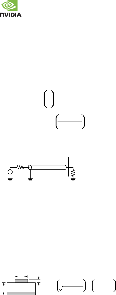
NVIDIA Jetson TX2 OEM Product Design Guide
JETSON TX2 OEM PRODUCT | DESIGN GUIDE | 20170912 85
18.0 APPENDIX C: TRANSMISSION LINE PRIMER
18.1 Background
NVIDIA maintains strict guidelines for high-frequency PCB transmission lines to ensure optimal signal integrity for data
transmission. This section provides a brief primer into basic board-level transmission line theory.
Characteristics
The most important PCB transmission line characteristics are listed in the following bullets:
▪ Trace width/height, PCB height and dielectric constant, and layer stack-up affect the characteristic trace
impedance of a transmission line.
Z0 = L
C
˜
1/2
▪ Signal rise time is proportional to the transmission line impedance and load capacitance.
* CLoad
RiseTime = Z0 * R
Term
Z0 + R
Term
˜
▪ Real transmission lines (Figure 45) have non-zero resistances that lead to attenuation and distortion, creating
signal integrity issues.
Figure 45. Typical Transmission Line Circuit
Transmission Line
ZSZ0ZL
LoadSource
Transmission lines are used to “transmit” the source signal to the load or destination with as little signal degradation or reflection
as possible. For this reason it is important to design the high-speed signal transmission line to fall within characteristic guidelines
based on the signal speed and type.
18.2 Physical Transmission Line Types
The two primary transmission line types often used for Jetson TX2 board designs are:
▪ Microstrip transmission line (Figure 46)
▪ Stripline transmission line (Figure 47)
The following sections describe each type of transmission.
Microstrip Transmission Line
Figure 46. Microstrip Transmission Line
Dielectric
W
TH Z0 = ln
87
Er + 1.414
5.98H
0.8W + T
▪ Z0: Impedance
▪ W: Trace width (inches)
▪ T: Trace thickness (inches)
▪ Er: Dielectric constant of substrate
▪ H: Distance between signal and reference plane
Stripline Transmission Line
NVIDIA Jetson TX2 OEM Product Design Guide
JETSON TX2 OEM PRODUCT | DESIGN GUIDE | 20170912 86
Figure 47. Stripline Transmission Line
W
T
BZ0 = ln
60
Er
4H
0.67πW 0.8 +
HT
W
▪ Z0: Impedance
▪ W: Trace width (inches)
▪ T: Trace thickness (inches)
▪ Er: Dielectric constant of substrate
▪ H: Distance between signal and reference plane
18.3 Driver Characteristics
Driver characteristics are important to the integrity and maximum speed of the signal. The following points identify key driver
equations and concepts used to improve signal integrity and transmission speed.
▪ The driver (source) has resistive output impedance ZS, which causes only a fraction of the signal voltage to
propagate down the transmission line to the receiver (load).
- • Transfer function at source:
T1 = Z0
ZS + Z0
- • Driver strength is inversely proportional to the source impedance, ZS.
▪ ZS also acts as the source termination, which helps dampen reflection.
- Source reflection coefficient:
R1 = (ZS – Z0)
(ZS + Z0)
18.4 Receiver Characteristics
Receiver characteristics are important to the integrity and detectability of the signal. The following points identify key receiver
concepts and equations for optimum signal integrity at the final destination.
▪ The receiver acts as a capacitive load and often has a high load impedance, ZL.
▪ Unterminated transmission lines cause overshoot and reflection at the receiver, which can cause data corruption.
- Output transfer function at load:
T2 = 2 * ZL
ZL + Z0
- Load reflection coefficient:
R2 = (ZL – Z0)
(ZL + Z0)
▪ Load impedance can be lowered with a termination resistor (RTerm) placed at the end of the transmission line.
- Reflection is minimized when ZL matches Z0
18.5 Transmission Lines & Reference Planes
Defining an appropriate reference plane is vital to transmission line performance due to crosstalk and EMI issues. The following
points explore appropriate reference plane identification and characteristics for optimal signal integrity:
▪ Transmission line return current (Figure 48)
- High-speed return current follows the path of least inductance.
- The lowest inductance path for a transmission line is right underneath the transmission line; i(D) is
proportional to:
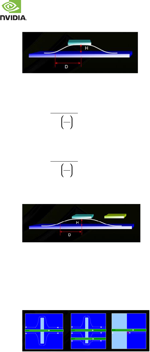
NVIDIA Jetson TX2 OEM Product Design Guide
JETSON TX2 OEM PRODUCT | DESIGN GUIDE | 20170912 87
Figure 48. Transmission Line Height
▪ Transmission line return current:
- High-speed return current follows the path of least inductance.
- The lowest inductance path for a transmission line is the portion of the line closest to the dielectric surface;
i(D) is proportional to
1
(1 + D
H
2)
▪ Crosstalk on solid reference plane (Figure 49):
- Crosstalk is caused by the mutual inductance of two parallel traces.
- Crosstalk at the second trace is proportional to
1
(1 + D
H
2)
- The signals need to be properly spaced to minimize crosstalk.
Figure 49. Crosstalk on Reference Plane
▪ Reference plane selection
- Solid ground is preferred as reference plane.
- Solid power can be used as reference plane with decoupling capacitors near driver and receiver.
- Reference plane cuts and layer changes need to be avoided.
▪ Power plane cut example (Figure 50)
- Power plane cuts will cause EMI issues.
- Power plane cuts also induce crosstalk to adjacent signals.
Figure 50. Example of Power Plane Cuts
▪ When cut is unavoidable:
- • Place decoupling capacitors near transition.
- • Place transition near source or receiver when decoupling capacitors are abundant (Figure 51).
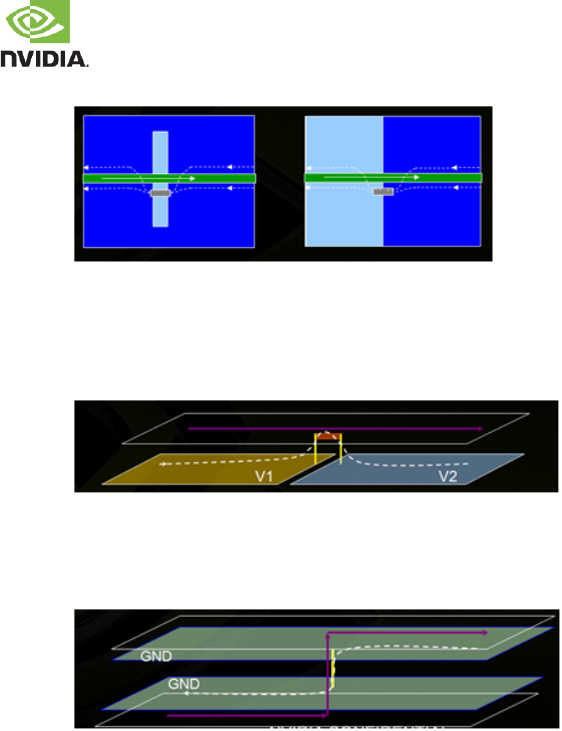
NVIDIA Jetson TX2 OEM Product Design Guide
JETSON TX2 OEM PRODUCT | DESIGN GUIDE | 20170912 88
Figure 51. Another Example of Power Plane Cuts
▪ When signal changes plane:
- Try not to change the reference plane, if possible.
- When a reference plane switches to different power rail, a stitching capacitor is required (Figure 52).
Figure 52. Switching Reference Planes
- When the same ground/power reference plane changes to a different layer, a stitching via is required (Figure
53).
Figure 53. Reference Plane Switch Using VIA

NVIDIA Jetson TX2 OEM Product Design Guide
JETSON TX2 OEM PRODUCT | DESIGN GUIDE | 20170912 89
19.0 APPENDIX D: DESIGN GUIDELINE GLOSSARY
The Design Guidelines include various terms. The descriptions in the table below are intended to show what these terms mean
and how they should be applied to a design.
Table 89 Layout Guideline Tutorial
Trace Delays
Max Breakout Delay
- Routing on Component layer: Maximum Trace Delay from module connector pin to point beyond pin array where normal trace spacing/impedance can be met.
Routing passes to layer other than Component layer: Beyond this, normal trace spacing/impedance must be met.
Max Total Trace Delay
- Trace from module connector pin to Device pin. This must include routing on the main PCB & any other Flex or secondary PCB. Delay is from Module connector to the
final connector/device.
Intra/Inter Pair Skews
Intra Pair Skew (within pair)
- Difference in delay between two traces in differential pair: Shorter routes may require indirect path to equalize delays
Inter Pair Skew (pair to pair)
- Difference between two (or possibly more) differential pairs
Impedance/Spacing
Microstrip vs Stripline
- Microstrip: Traces next to single ref. plane. Stripline: Traces between two ref planes
Trace Impedance
- Impedance of trace determined by width & height of trace, distance from ref. plane & dielectric constant of PCB material. For differential traces, space between pair
of traces is also a factor
Board trace spacing / Spacing to other nets
- Minimum distance between two traces. Usually specified in terms of dielectric height which is distance from trace to reference layers.
Pair to pair spacing
- Spacing between differential traces
Breakout spacing
- Possible exception to board trace spacing where different spacing rules are allowed under module connector pin in order to escape from the pin array. Outside device
boundary, normal spacing rules apply
Reference Return
Ground Reference Return Via & Via proximity (signal to reference)
- Signals changing layers & reference GND planes need similar return current path
- Accomplished by adding via, tying both GND layers together
Via proximity (sig to ref) is distance between signal & reference return vias
- GND reference via for Differential Pair
- Where a differential pair changes GND reference layers, return via should be placed close to & between signal vias (example to right)
Signal to return via ratio
- Number of Ground Return vias per Signal vias. For critical IFs, ratio is usually 1:1. For less critical IFs, several trace vias can share fewer return vias (i.e. 3:2 3 trace
vias & 2 return vias).
Slots in Ground Reference Layer
- When traces cross slots in adjacent power or ground plane
- Return current has longer path around slot
- Longer slots result in larger loop areas
- Avoid slots in GND planes or do not route across them
Routing over Split Power Layer Reference Layers
- When traces cross different power areas on power plane
- Return current must find longer path - usually a distant bypass cap
- If possible, route traces w/solid plane (GND or PWR) or keep routes across single area
- If traces must cross two or more power areas, use stitching capacitors
- Placing one cap across two PWR areas near where traces cross area boundaries provides high-frequency path for return current
- Cap value typically 0.1uF & should ideally be within 0.1" of crossing
NVIDIA Jetson TX2 OEM Product Design Guide
JETSON TX2 OEM PRODUCT | DESIGN GUIDE | 20170912 90
20.0 APPENDIX E: JETSON TX2 PIN DESCRIPTIONS
Table 90. Jetson TX2 Connector (8x50) Pin Descriptions
Pin #
Jetson TX2 Pin Name
Tegra Signal
Usage/Description
Usage on the Carrier
Board
Direction
Pin Type
A1
VDD_IN
Main power Supplies PMIC & external
supplies
Main DC input
Input
5.5V-19.6V
A2
VDD_IN
A3
GND
GND
GND
GND
A4
GND
GND
GND
GND
A5
RSVD
Not used
A6
I2C_PM_CLK
GEN8_I2C_SCL
PM I2C Clock
I2C (General)
Bidir
Open Drain 1.8V
A7
CHARGING#
(PMIC GPIO5)
Charger Interrupt
System
Input
CMOS 1.8V
A8
GPIO14_AP_WAKE_MDM
UFS0_RST
AP (Tegra) Wake Modem or GPIO
M.2 Key E
Output
CMOS 1.8V
A9
GPIO15_AP2MDM_READY
UFS0_REF_CLK
AP (Tegra) to Modem Ready or GPIO
Output
CMOS 1.8V
A10
GPIO16_MDM_WAKE_AP
GPIO_MDM2
Modem Wake AP (Tegra) or GPIO
Input
CMOS 1.8V
A11
JTAG_GP1
NVJTAG_SEL
JTAG General Purpose 1. Pulled low on
module for normal operation & pulled
high by test device for Boundary Scan
test mode.
JTAG
Input
CMOS 1.8V
A12
JTAG_TMS
JTAG_TMS
JTAG Test Mode Select
JTAG Header & Debug
Connector
Input
CMOS 1.8V
A13
JTAG_TDO
JTAG_TD0
JTAG Test Data Out
Output
CMOS 1.8V
A14
JTAG_RTCK
JTAG Return Clock
Input
CMOS 1.8V
A15
UART2_CTS#
UART2_CTS
UART 2 Clear to Send
M.2 Key E
Input
CMOS 1.8V
A16
UART2_RTS#
UART2_RTS
UART 2 Request to Send
Output
CMOS 1.8V
A17
USB0_EN_OC#
USB_VBUS_EN0
USB VBUS Enable/Overcurrent 0
USB 2.0 Micro AB
Bidir
Open Drain 3.3V
A18
USB1_EN_OC#
USB_VBUS_EN1
USB VBUS Enable/Overcurrent 1
USB 3.0 Type A
Bidir
Open Drain 3.3V
A19
RSVD
Not used
A20
I2C_GP1_DAT
GEN1_I2C_SDA
General I2C 1 Data
I2C (General)
Bidir
Open Drain 3.3V
A21
I2C_GP1_CLK
GEN1_I2C_SCL
General I2C 1 Clock
Bidir
Open Drain 3.3V
A22
GPIO_EXP1_INT
GPIO_MDM7
GPIO Expander 1 Interrupt or GPIO
GPIO Expander
Input
CMOS 1.8V
A23
GPIO_EXP0_INT
GPIO_MDM1
GPIO expander 0 Interrupt or GPIO
Input
CMOS 1.8V
A24
LCD1_BKLT_PWM
GPIO_DIS5
Display Backlight PWM 1
Display Connector
Output
CMOS 1.8V
A25
LCD_TE
GPIO_DIS1
Display Tearing Effect
Input
CMOS 1.8V
A26
GSYNC_HSYNC
GPIO_DIS4
GSYNC Horizontal Sync
Output
CMOS 1.8V
A27
GSYNC_VSYNC
GPIO_DIS2
GSYNC Vertical Sync
Output
CMOS 1.8V
A28
GND
GND
GND
GND
A29
SDIO_RST#
GPIO_WAN3
Secondary WLAN Enable
M.2 Key E
Output
CMOS 1.8V
A30
RSVD
Not used
A31
RSVD
Not used
A32
RSVD
Not used
A33
DP1_HPD
DP_AUX_CH1_HPD
Display Port 1 Hot Plug Detect
HDMI Type A Conn.
Input
CMOS 1.8V
A34
DP1_AUX_CH
DP_AUX_CH1_N
Display Port 1 Aux or HDMI DDC SDA
Bidir
AC-Coupled on Carrier
Board (eDP/DP) or Open-
Drain, 1.8V (3.3V tolerant -
DDC/I2C)
A35
DP1_AUX_CH+
DP_AUX_CH1_P
Display Port 1 Aux+ or HDMI DDC SCL
Bidir
A36
USB0_OTG_ID
(PMIC GPIO0)
USB 0 ID / VBUS EN
USB 2.0 Micro AB
Input
Analog
A37
GND
GND
GND
GND
A38
USB1_D+
USB1_DP
USB 2.0, Port 1 Data+
USB 3.0 Type A
Bidir
USB PHY
A39
USB1_D
USB1_DN
USB 2.0, Port 1 Data
Bidir
A40
GND
GND
GND
GND
A41
PEX2_REFCLK+
PEX_CLK2P
PCIe 2 Reference Clock+ (PCIe IF #1)
Unassigned
Output
PCIe PHY
A42
PEX2_REFCLK
PEX_CLK2N
PCIe 2 Reference Clock (PCIe IF #1)
Output
A43
GND
GND
GND
GND
A44
PEX0_REFCLK+
PEX_CLK1P
PCIe 0 Reference Clock+ (PCIe IF #0)
PCIe x4 Connector
Output
PCIe PHY
A45
PEX0_REFCLK
PEX_CLK1N
PCIe 0 Reference Clock (PCIe IF #0)
Output
A46
RESET_OUT#
SYS_RESET_N
Reset Out. Reset from PMIC (through
diodes) to Tegra & eMMC reset pins.
Driven from carrier board to force reset
of Tegra & eMMC (not PMIC). An
external 100pull-up to 1.8V near
Tegra (module pin side) & external
pull-up to 1.8V on the other
side of a diode (PMIC side).
System
Bidir
CMOS 1.8V
NVIDIA Jetson TX2 OEM Product Design Guide
JETSON TX2 OEM PRODUCT | DESIGN GUIDE | 20170912 91
Pin #
Jetson TX2 Pin Name
Tegra Signal
Usage/Description
Usage on the Carrier
Board
Direction
Pin Type
A47
RESET_IN#
(PMIC NRST_IO)
Reset In. System Reset driven from
PMIC to carrier board for devices
requiring full system reset. Also driven
from carrier board to initiate full system
reset (i.e. RESET button). A pull-up is
present on module.
Bidir
Open Drain, 1.8V
A48
CARRIER_PWR_ON
Carrier Power On. Used as part of the
power up sequence. The module asserts
this signal when it is safe for the carrier
-up to
VDD_3V3_SYS is present on the module.
Output
Open-Collector 3.3V
A49
CHARGER_PRSNT#
(PMIC ACOK)
Charger Present. Connected on module
-up
internally to MBATT (VDD_5V0_SYS).
Can optionally be used to support auto-
power-on where the module platform
will power-on when the main power
source is connected instead of waiting
for a power button press.
Input
MBATT level 5.0V (see
note 3)
A50
VDD_RTC
(PMIC BBATT)
Real-Time-Clock. Optionally used to
provide back-up power for RTC.
Connects to Lithium Cell or super
capacitor on Carrier Board. PMIC is
supply when charging cap or coin cell.
Super cap or coin cell is source when
system is disconnected from power.
Battery Back-up using
Super-capacitor
Bidir
1.65V-5.5V
B1
VDD_IN
Main power Supplies PMIC & external
supplies
Main DC input
Input
5.5V-19.6V
B2
VDD_IN
B3
GND
GND
GND
GND
B4
GND
GND
GND
GND
B5
RSVD
Not used
B6
I2C_PM_DAT
GEN8_I2C_SDA
PM I2C Data
I2C (General)
Bidir
Open Drain 1.8V
B7
CARRIER_STBY#
SOC_PWR_REQ
Carrier Board Standby: The module
drives this signal low when it is in the
standby power state.
System
Output
CMOS 1.8V
B8
VIN_PWR_BAD#
VDD_IN Power Bad. Carrier board
indication to the module that the
VDD_IN power is not valid. Carrier board
should de-assert this (drive high) only
when VDD_IN has reached its required
voltage level and is stable. This prevents
Tegra from powering up until the
VDD_IN power is stable.
Input
CMOS 5.0V
B9
GPIO17_MDM2AP_READY
GPIO_PQ7
Modem to AP (Tegra) Ready or GPIO
M.2 Key E
Input
CMOS 1.8V
B10
GPIO18_MDM_COLDBOOT
GPIO_PQ6
Modem Coldboot or GPIO
Input
CMOS 1.8V
B11
JTAG_TCK
JTAG_TCK
JTAG Test Clock
JTAG Header & Debug
Connector
Input
CMOS 1.8V
B12
JTAG_TDI
JTAG_TDI
JTAG Test Data In
Input
CMOS 1.8V
B13
JTAG_GP0
JTAG_TRST_N
JTAG General Purpose 0 (Test Reset)
Input
CMOS 1.8V
B14
GND
GND
GND
GND
B15
UART2_RX
UART2_RX
UART 2 Receive
M.2 Key E
Input
CMOS 1.8V
B16
UART2_TX
UART2_TX
UART 2 Transmit
Output
CMOS 1.8V
B17
FAN_TACH
UART5_TX
Fan Tachometer
Fan
Input
CMOS 1.8V
B18
RSVD
Not used
B19
GPIO11_AP_WAKE_BT
GPIO_PQ5
AP (Tegra) Wake Bluetooth or GPIO
Display Connector
Output
CMOS 1.8V
B20
GPIO10_WIFI_WAKE_AP
GPIO_WAN4
WLAN 2 Wake AP (Tegra) or GPIO
M.2 Key E
Input
CMOS 1.8V
B21
GPIO12_BT_EN
MCU_PWR_REQ
BT 2 Enable or GPIO
Output
CMOS 1.8V
B22
GPIO13_BT_WAKE_AP
GPIO_WAN2
BT 2 Wake AP (Tegra) or GPIO
Input
CMOS 1.8V
B23
GPIO7_TOUCH_RST
SAFE_STATE
Touch Reset or GPIO
Display Connector
Output
CMOS 1.8V
B24
TOUCH_CLK
TOUCH_CLK
Touch Clock
Output
CMOS 1.8V
B25
GPIO6_TOUCH_INT
CAN_GPIO7
Touch Interrupt or GPIO
Input
CMOS 1.8V
B26
LCD_VDD_EN
GPIO_EDP0
Display VDD Enable
Output
CMOS 1.8V
B27
LCD0_BKLT_PWM
GPIO_DIS0
Display Backlight PWM 0
Output
CMOS 1.8V
B28
LCD_BKLT_EN
GPIO_DIS3
Display Backlight Enable
Output
CMOS 1.8V
B29
RSVD
Not used
B30
RSVD
Not used
B31
GND
GND
GND
GND
NVIDIA Jetson TX2 OEM Product Design Guide
JETSON TX2 OEM PRODUCT | DESIGN GUIDE | 20170912 92
Pin #
Jetson TX2 Pin Name
Tegra Signal
Usage/Description
Usage on the Carrier
Board
Direction
Pin Type
B32
RSVD
Not used
B33
HDMI_CEC
HDMI_CEC
HDMI CEC
HDMI Type A Conn.
Bidir
Open Drain, 3.3V
B34
DP0_AUX_CH
DP_AUX_CH0_N
Display Port 0 Aux or HDMI DDC SDA
Display Connector
Bidir
AC-Coupled on Carrier
Board (eDP/DP) or Open-
Drain, 1.8V (3.3V tolerant -
DDC/I2C)
B35
DP0_AUX_CH+
DP_AUX_CH0_P
Display Port 0 Aux+ or HDMI DDC SCL
Bidir
B36
DP0_HPD
DP_AUX_CH0_HPD
Display Port 0 Hot Plug Detect
Input
CMOS 1.8V
B37
USB0_VBUS_DET
UART5_CTS
USB 0 VBUS Detect
USB 2.0 Micro AB
Input
USB VBUS, 5V
B38
GND
GND
GND
GND
B39
USB0_D+
USB0_DP
USB 2.0 Port 0 Data+
USB 2.0 Micro AB
Bidir
USB PHY
B40
USB0_D
USB0_DN
USB 2.0 Port 0 Data
Bidir
B41
GND
GND
GND
GND
B42
USB2_D+
USB2_DP
USB 2.0, Port 2 Data+
M.2 Key E
Bidir
USB PHY
B43
USB2_D
USB2_DN
USB 2.0, Port 2 Data
Bidir
B44
GND
GND
GND
GND
B45
PEX1_REFCLK+
PEX_CLK3P
PCIe 1 Reference Clock+ (PCIe IF #2)
M.2 Key E
Output
PCIe PHY
B46
PEX1_REFCLK
PEX_CLK3N
PCIe 1 Reference Clock (PCIe IF #2)
Output
B47
GND
GND
GND
GND
B48
RSVD
Not used
B49
RSVD
Not used
B50
POWER_BTN#
POWER_ON / (PMIC
EN0)
Power Button. Used to initiate a system
power-on. Connected to PMIC EN0
-up to
VDD_5V0_SYS. Also connected to Tegra
POWER_ON pin through Diode with
-up to VDD_1V8_AP near
Tegra.
System
Input
CMOS 5.0V (see note 3)
C1
VDD_IN
Main power Supplies PMIC & external
supplies
Main DC input
Input
5.5V-19.6V
C2
VDD_IN
C3
GND
GND
GND
GND
C4
GND
GND
GND
GND
C5
RSVD
Not used
C6
I2C_CAM_CLK
CAM_I2C_SCL
Camera I2C Clock
Camera Connector
Bidir
Open Drain 1.8V
C7
BATLOW#
(PMIC_GPIO6)
Battery Low (PMIC GPIO)
System
Input
CMOS 1.8V
C8
BATT_OC
BATT_OC
Battery Over-current (& Thermal)
warning
Bidir
CMOS 1.8V
C9
WDT_TIME_OUT#
GPIO_SEN7
Watchdog Timeout
Input
CMOS 1.8V
C10
I2C_GP2_DAT
GEN7_I2C_SDA
General I2C 2 Data
I2C (General)
Bidir
Open Drain 1.8V
C11
I2C_GP2_CLK
GEN7_I2C_SCL
General I2C 2 Clock
Bidir
Open Drain 1.8V
C12
I2C_GP3_CLK
GEN9_I2C_SCL
General I2C 3 Clock
Bidir
Open Drain 1.8V
C13
I2C_GP3_DAT
GEN9_I2C_SDA
General I2C 3 Data
Bidir
Open Drain 1.8V
C14
I2S1_SDIN
DAP2_DIN
I2S Audio Port 1 Data In
GPIO Expansion
Header
Input
CMOS 1.8V
C15
I2S1_CLK
DAP2_SCLK
I2S Audio Port 1 Clock
Bidir
CMOS 1.8V
C16
FAN_PWM
GPIO_SEN6
Fan PWM
Fan
Output
CMOS 1.8V
C17
CAN1_STBY
CAN_GPIO6
CAN 1 Standby
GPIO Expansion
Header
Output
CMOS 3.3V
C18
CAN1_TX
CAN1_DOUT
CAN 1 Transmit
Output
CMOS 3.3V
C19
CAN1_ERR
CAN_GPIO3
CAN 1 Error
Input
CMOS 3.3V
C20
CAN_WAKE
CAN_GPIO4
CAN Wake
Input
CMOS 3.3V
C21
GND
GND
GND
GND
C22
CSI5_D0
CSI_F_D0_N
Camera, CSI 5 Data 0
Camera Connector
Input
MIPI D-PHY
C23
CSI5_D0+
CSI_F_D0_P
Camera, CSI 5 Data 0+
Input
C24
GND
GND
GND
GND
C25
CSI3_D0
CSI_D_D0_N
Camera, CSI 3 Data 0
Camera Connector
Input
MIPI D-PHY
C26
CSI3_D0+
CSI_D_D0_P
Camera, CSI 3 Data 0+
Input
C27
GND
GND
GND
GND
C28
CSI1_D0
CSI_B_D0_N
Camera, CSI 1 Data 0
Camera Connector
Input
MIPI D-PHY
C29
CSI1_D0+
CSI_B_D0_P
Camera, CSI 1 Data 0+
Input
C30
GND
GND
GND
GND
C31
DSI3_D0+
DSI_D_D0_P
Display, DSI 3 Data 0+
Display Connector
Output
MIPI D-PHY
C32
DSI3_D0
DSI_D_D0_N
Display, DSI 3 Data 0
Output
C33
GND
GND
GND
GND
C34
DSI1_D0+
DSI_B_D0_P
Display, DSI 1 Data 0+
Display Connector
Output
MIPI D-PHY
C35
DSI1_D0
DSI_B_D0_N
Display, DSI 1 Data 0
Output
C36
GND
GND
GND
GND
NVIDIA Jetson TX2 OEM Product Design Guide
JETSON TX2 OEM PRODUCT | DESIGN GUIDE | 20170912 93
Pin #
Jetson TX2 Pin Name
Tegra Signal
Usage/Description
Usage on the Carrier
Board
Direction
Pin Type
C37
DP1_TX1
HDMI_DP1_TXDN1
DisplayPort 1 Lane 1 or HDMI Lane 1
HDMI Type A Conn.
Output
AC-Coupled on carrier
board
C38
DP1_TX1+
HDMI_DP1_TXDP1
DisplayPort 1 Lane 1+ or HDMI Lane 1+
Output
C39
GND
GND
GND
GND
C40
PEX2_TX+
PEX_TX3P
PCIe 2 Transmit+ (PCIe IF #0 Lane 2 or
PCIe IF #1 Lane 0)
PCIe x4 Connector
Output
PCIe PHY, AC-Coupled on
carrier board
C41
PEX2_TX
PEX_TX3N
PCIe 2 Transmit (PCIe IF #0 Lane 2 or
PCIe IF #1 Lane 0)
Output
C42
GND
GND
GND
GND
C43
USB_SS0_TX+
PEX_TX0P
USB SS 0 Transmit+ (USB 3.0 Port #0
muxed w/PCIe #2 Lane 0)
USB 3.0 Type A
Output
USB SS PHY, AC-Coupled on
carrier board
C44
USB_SS0_TX
PEX_TX0N
USB SS 0 Transmit (USB 3.0 Port #0
muxed w/PCIe #2 Lane 0)
Output
C45
GND
GND
GND
GND
C46
PEX2_CLKREQ#
PEX_L1_CLKREQ_N
PCIE 2 Clock Request (PCIe IF #1)
Unassigned
Bidir
Open Drain 3.3V, Pull-up on
the module
C47
PEX1_CLKREQ#
PEX_L2_CLKREQ_N
PCIE 1 Clock Request (mux option - PCIe
IF #2)
M.2 Key E
Bidir
C48
PEX0_CLKREQ#
PEX_L0_CLKREQ_N
PCIE 0 Clock Request (PCIe IF #0)
PCIe x4 Connector
Bidir
C49
PEX0_RST#
PEX_L0_RST_N
PCIe 0 Reset (PCIe IF #0)
Output
C50
RSVD
Not used
D1
RSVD
Not used
D2
RSVD
Not used
D3
RSVD
Not used
D4
RSVD
Not used
D5
UART7_RX
UART7_RX
UART 7 Receive
Not Assigned
Input
CMOS 1.8V
D6
I2C_CAM_DAT
CAM_I2C_SDA
Camera I2C Data
Camera Connector
Bidir
Open Drain 1.8V
D7
GPIO5_CAM_FLASH_EN
UART5_RTS_N
Camera Flash Enable or GPIO
Output
CMOS 1.8V
D8
UART7_TX
UART7_TX
UART 7 Transmit
Not Assigned
Output
CMOS 1.8V
D9
UART1_TX
UART3_TX
UART 1 Transmit
Serial Port Header
Output
CMOS 1.8V
D10
UART1_RX
UART3_RX
UART 1 Receive
Input
CMOS 1.8V
D11
RSVD
Not used
D12
RSVD
Not used
D13
I2S1_LRCLK
DAP2_FS
I2S Audio Port 1 Left/Right Clock
GPIO Expansion
Header
Bidir
CMOS 1.8V
D14
I2S1_SDOUT
DAP2_DOUT
I2S Audio Port 1 Data Out
Bidir
CMOS 1.8V
D15
I2C_GP0_DAT
GPIO_SEN9
General I2C 0 Data
I2C (General)
Bidir
Open Drain 1.8V
D16
AO_DMIC_IN_DAT
CAN_GPIO0
Digital Mic Input Data
GPIO Expansion
Header
Input
CMOS 1.8V
D17
CAN1_RX
CAN1_DIN
CAN 1 Receive
Input
CMOS 3.3V
D18
CAN0_RX
CAN0_DIN
CAN 0 Receive
Input
CMOS 3.3V
D19
CAN0_TX
CAN0_DOUT
CAN 0 Transmit
Output
CMOS 3.3V
D20
GND
GND
GND
GND
D21
CSI5_CLK
CSI_F_CLK_N
Camera, CSI 5 Clock
Camera Connector
Input
MIPI D-PHY
D22
CSI5_CLK+
CSI_F_CLK_P
Camera, CSI 5 Clock+
Input
D23
GND
GND
GND
GND
D24
CSI3_CLK
CSI_D_CLK_N
Camera, CSI 3 Clock
Camera Connector
Input
MIPI D-PHY
D25
CSI3_CLK+
CSI_D_CLK_P
Camera, CSI 3 Clock+
Input
D26
GND
GND
GND
GND
D27
CSI1_CLK
CSI_B_CLK_N
Camera, CSI 1 Clock
Camera Connector
Input
MIPI D-PHY
D28
CSI1_CLK+
CSI_B_CLK_P
Camera, CSI 1 Clock+
Input
D29
GND
GND
GND
GND
D30
DSI3_CLK+
DSI_D_CLK_P
Display DSI 3 Clock+
Display Connector
Output
MIPI D-PHY
D31
DSI3_CLK
DSI_D_CLK_N
Display DSI 3 Clock
Output
D32
GND
GND
GND
GND
D33
DSI1_CLK+
DSI_B_CLK_P
Display DSI 1 Clock+
Display Connector
Output
MIPI D-PHY
D34
DSI1_CLK
DSI_B_CLK_N
Display DSI 1 Clock
Output
D35
GND
GND
GND
GND
D36
DP1_TX2
HDMI_DP1_TXDN0
DisplayPort 1 Lane 2 or HDMI Lane 0
HDMI Type A Conn.
Output
AC-Coupled on carrier
board
D37
DP1_TX2+
HDMI_DP1_TXDP0
DisplayPort 1 Lane 2+ or HDMI Lane 0+
Output
D38
GND
GND
GND
GND
D39
PEX_RFU_TX+
PEX_TX1P
PCIe RFU Transmit+ (PCIe IF #0 Lane 3 or
USB 3.0 Port #1)
PCIe x4 Connector
Output
PCIe PHY, AC-Coupled on
carrier board
D40
PEX_RFU_TX
PEX_TX1N
PCIe RFU Transmit (PCIe IF #0 Lane 3
or USB 3.0 Port #1)
Output
D41
GND
GND
GND
GND
NVIDIA Jetson TX2 OEM Product Design Guide
JETSON TX2 OEM PRODUCT | DESIGN GUIDE | 20170912 94
Pin #
Jetson TX2 Pin Name
Tegra Signal
Usage/Description
Usage on the Carrier
Board
Direction
Pin Type
D42
USB_SS1_TX+
PEX_TX2P
USB SS 1 Transmit+ (USB 3.0 Port #2 or
PCIe IF #0 Lane 1)
PCIe x4 Connector
Output
USB SS PHY, AC-Coupled on
carrier board
D43
USB_SS1_TX
PEX_TX2N
USB SS 1 Transmit (USB 3.0 Port #2 or
PCIe #0 Lane 1)
Output
D44
GND
GND
GND
GND
D45
SATA_TX+
PEX_TX5P
SATA Transmit+
SATA Connector
Output
SATA PHY, AC-Coupled on
carrier board
D46
SATA_TX
PEX_TX5N
SATA Transmit
Output
D47
SATA_DEV_SLP
PEX_L2_CLKREQ_N
SATA Device Sleep or PEX1_CLKREQ#
(PCIe IF #2) depending on Mux setting
Input
Open Drain 3.3V, Pull-up on
the module
D48
PEX_WAKE#
PEX_WAKE_N
PCIe Wake
PCIe x4 conn & M.2
Input
Open Drain 3.3V, Pull-up on
the module
D49
PEX2_RST#
PEX_L1_RST_N
PCIe 2 Reset (PCIe IF #1)
Unassigned
Output
D50
RSVD
Not used
E1
FORCE_RECOV#
GPIO_SW1
Force Recovery strap pin
System
Input
CMOS 1.8V
E2
SLEEP#
GPIO_SW2
Sleep Request to the module from the
carrier board. An internal Tegra pull-up
is present on the signal.
Sleep (VOL DOWN)
button
Input
CMOS 1.8V (see note 3)
E3
SPI0_CLK
GPIO_SEN1
SPI 0 Clock
Display Connector
Bidir
CMOS 1.8V
E4
SPI0_MISO
GPIO_SEN2
SPI 0 Master In / Slave Out
Bidir
CMOS 1.8V
E5
I2S3_SDIN
DAP4_DIN
I2S Audio Port 3 Data In
Camera Connector
Input
CMOS 1.8V
E6
I2S3_CLK
DAP4_SCLK
I2S Audio Port 3 Clock
Bidir
CMOS 1.8V
E7
CAM2_MCLK
GPIO_CAM2
Camera 2 Master Clock
Output
CMOS 1.8V
E8
CAM_VSYNC
QSPI_IO1
Camera Vertical Sync
Output
CMOS 1.8V
E9
UART1_RTS#
UART3_RTS
UART 1 Request to Send
Serial Port Header
Output
CMOS 1.8V
E10
UART1_CTS#
UART3_CTS
UART 1 Clear to Send
Input
CMOS 1.8V
E11
RSVD
Not used
E12
RSVD
Not used
E13
RSVD
Not used
E14
SPI1_CS0#
GPIO_CAM7
SPI 1 Chip Select 0
Expansion Header
Bidir
CMOS 1.8V
E15
I2C_GP0_CLK
GPIO_SEN8
General I2C 0 Clock
I2C (General)
Bidir
Open Drain 1.8V
E16
AO_DMIC_IN_CLK
CAN_GPIO1
Digital Mic Input Clock
Expansion Header
Output
CMOS 1.8V
E17
RSVD
Not used
E18
CAN0_ERR
CAN_GPIO5
CAN 0 Error
GPIO Expansion
Header
Input
CMOS 3.3V
E19
GND
GND
GND
GND
E20
CSI5_D1
CSI_F_D1_N
Camera, CSI 5 Data 1
Camera Connector
Input
MIPI D-PHY
E21
CSI5_D1+
CSI_F_D1_P
Camera, CSI 5 Data 1+
Input
E22
GND
GND
GND
GND
E23
CSI3_D1
CSI_D_D1_N
Camera, CSI 3 Data 1
Camera Connector
Input
MIPI D-PHY
E24
CSI3_D1+
CSI_D_D1_P
Camera, CSI 3 Data 1+
Input
E25
GND
GND
GND
GND
E26
CSI1_D1
CSI_B_D1_N
Camera, CSI 1 Data 1
Camera Connector
Input
MIPI D-PHY
E27
CSI1_D1+
CSI_B_D1_P
Camera, CSI 1 Data 1+
Input
E28
GND
GND
GND
GND
E29
DSI3_D1+
DSI_D_D1_P
Display, DSI 3 Data 1+
Display Connector
Output
MIPI D-PHY
E30
DSI3_D1
DSI_D_D1_N
Display, DSI 3 Data 1
Output
E31
GND
GND
GND
GND
E32
DSI1_D1+
DSI_B_D1_P
Display, DSI 1 Data 1+
Display Connector
Output
MIPI D-PHY
E33
DSI1_D1
DSI_B_D1_N
Display, DSI 1 Data 1
Output
E34
GND
GND
GND
GND
E35
DP1_TX3
HDMI_DP1_TXDN3
DisplayPort 1 Lane 3 or HDMI Clk Lane
HDMI Type A Conn.
Output
AC-Coupled on carrier
board
E36
DP1_TX3+
HDMI_DP1_TXDP3
DisplayPort 1 Lane 3+ or HDMI Clk Lane+
Output
E37
GND
GND
GND
GND
E38
DP1_TX0
HDMI_DP1_TXDN2
DisplayPort 1 Lane 0 or HDMI Lane 2
HDMI Type A Conn.
Output
AC-Coupled on carrier
board
E39
DP1_TX0+
HDMI_DP1_TXDP2
DisplayPort 1 Lane 0+ or HDMI Lane 2+
Output
E40
GND
GND
GND
GND
E41
PEX1_TX+
PEX_TX0P
PCIe 1 Transmit+ (PCIe #2 Lane 0 muxed
w/USB 3.0 Port #0)
USB 3.0 Type A
(Default) or M.2 Key E
Output
PCIe PHY, AC-Coupled on
carrier board
E42
PEX1_TX
PEX_TX0N
PCIe 1 Transmit (PCIe #2 Lane 0 muxed
w/USB 3.0 Port #0)
Output
E43
GND
GND
GND
GND
E44
PEX0_TX+
PEX_TX4P
PCIe 0 Transmit+ (PCIe IF #0 Lane 0)
PCIe x4 Connector
Output
PCIe PHY, AC-Coupled on
carrier board
E45
PEX0_TX
PEX_TX4N
PCIe 0 Transmit (PCIe IF #0 Lane 0)
Output
E46
GND
GND
GND
GND
NVIDIA Jetson TX2 OEM Product Design Guide
JETSON TX2 OEM PRODUCT | DESIGN GUIDE | 20170912 95
Pin #
Jetson TX2 Pin Name
Tegra Signal
Usage/Description
Usage on the Carrier
Board
Direction
Pin Type
E47
GBE_LINK_ACT#
GbE RJ45 connector Link ACT (LED0)
LAN
Output
CMOS 3.3V tolerant
E48
GBE_MDI0+
GbE Transformer Data 0+
Bidir
MDI
E49
GBE_MDI0
GbE Transformer Data 0
Bidir
E50
PEX1_RST#
PEX_L2_RST_N
PCIe 1 Reset (PCIe IF #2)
M.2 Key E
Output
Open Drain 3.3V, Pull-up on
the module
F1
AUDIO_MCLK
AUD_MCLK
Audio Codec Master Clock
Expansion Header
Output
CMOS 1.8V
F2
GPIO19_AUD_RST
GPIO_AUD1
Audio Codec Reset or GPIO
Output
CMOS 1.8V
F3
SPI0_CS0#
GPIO_SEN4
SPI 0 Chip Select 0
Display Connector
Bidir
CMOS 1.8V
F4
SPI0_MOSI
GPIO_SEN3
SPI 0 Master Out / Slave In
Bidir
CMOS 1.8V
F5
I2S3_LRCLK
DAP4_FS
I2S Audio Port 3 Left/Right Clock
Camera Connector
Bidir
CMOS 1.8V
F6
I2S3_SDOUT
DAP4_DOUT
I2S Audio Port 3 Data Out
Bidir
CMOS 1.8V
F7
GPIO1_CAM1_PWR#
GPIO_CAM3
Camera 1 Powerdown or GPIO
Output
CMOS 1.8V
F8
CAM1_MCLK
EXTPERIPH2_CLK
Camera 1 Reference Clock
Output
CMOS 1.8V
F9
CAM0_MCLK
EXTPERIPH1_CLK
Camera 0 Reference Clock
Output
CMOS 1.8V
F10
GND
GND
GND
GND
F11
RSVD
Not used
F12
RSVD
Not used
F13
SPI1_MOSI
GPIO_CAM6
SPI 1 Master Out / Slave In
Expansion Header
Bidir
CMOS 1.8V
F14
SPI1_MISO
GPIO_CAM5
SPI 1 Master In / Slave Out
Bidir
CMOS 1.8V
F15
GND
GND
GND
GND
F16
SPI2_CS1#
GPIO_MDM4
SPI 2 Chip Select 1
Display/Camera Conns.
Bidir
CMOS 1.8V
F17
SDCARD_CD#
GPIO_EDP2
SD Card Card Detect
SD Card
Input
CMOS 1.8V
F18
SDCARD_D3
SDMMC1_DAT3
SD Card (or SDIO) Data 3
Bidir
CMOS 3.3/1.8V
F19
SDCARD_D2
SDMMC1_DAT2
SD Card (or SDIO) Data 2
Bidir
CMOS 3.3/1.8V
F20
SDCARD_WP
GPIO_EDP1
SD Card Write Protect
Input
CMOS 1.8V
F21
GND
GND
GND
GND
F22
CSI4_D0
CSI_E_D0_N
Camera, CSI 4 Data 0
Camera Connector
Input
MIPI D-PHY
F23
CSI4_D0+
CSI_E_D0_P
Camera, CSI 4 Data 0+
Input
F24
GND
GND
GND
GND
F25
CSI2_D0
CSI_C_D0_N
Camera, CSI 2 Data 0
Camera Connector
Input
MIPI D-PHY
F26
CSI2_D0+
CSI_C_D0_P
Camera, CSI 2 Data 0+
Input
F27
GND
GND
GND
GND
F28
CSI0_D0
CSI_A_D0_N
Camera, CSI 0 Data 0
Camera Connector
Input
MIPI D-PHY
F29
CSI0_D0+
CSI_A_D0_P
Camera, CSI 0 Data 0+
Input
F30
GND
GND
GND
GND
F31
DSI2_D0+
DSI_C_D0_P
Display, DSI 2 Data 0+
Display Connector
Output
MIPI D-PHY
F32
DSI2_D0
DSI_C_D0_N
Display, DSI 2 Data 0
Output
F33
GND
GND
GND
GND
F34
DSI0_D0+
DSI_A_D0_P
Display, DSI 0 Data 0+
Display Connector
Output
MIPI D-PHY
F35
DSI0_D0
DSI_A_D0_N
Display, DSI 0 Data 0
Output
F36
GND
GND
GND
GND
F37
DP0_TX1
HDMI_DP0_TXDN1
DisplayPort 0 Lane 1 or HDMI Lane 1
Display Connector
Output
AC-Coupled on carrier
board
F38
DP0_TX1+
HDMI_DP0_TXDP1
DisplayPort 0 Lane 1+or HDMI Lane 1+
Output
F39
GND
GND
GND
GND
F40
PEX2_RX+
PEX_RX3P
PCIe 2 Receive+ (PCIe IF #0 Lane 2 or
PCIe IF #1 Lane 0)
PCIe x4 Connector
Input
PCIe PHY, AC-Coupled on
carrier board
F41
PEX2_RX
PEX_RX3N
PCIe 2 Receive (PCIe IF #0 Lane 2 or
PCIe IF #1 Lane 0)
Input
F42
GND
GND
GND
GND
F43
USB_SS0_RX+
PEX_RX0P
USB SS 0 Receive+ (USB 3.0 Port #0
muxed w/PCIe #2 Lane 0)
USB 3.0 Type A
Input
USB SS PHY, AC-Coupled
(off the module)
F44
USB_SS0_RX
PEX_RX0N
USB SS 0 Receive (USB 3.0 Port #0
muxed w/PCIe #2 Lane 0)
Input
F45
GND
GND
GND
GND
F46
GBE_LINK1000#
GbE RJ45 connector Link 1000 (LED2)
LAN
Output
CMOS 3.3V Tolerant
F47
GBE_MDI1+
GbE Transformer Data 1+
Bidir
MDI
F48
GBE_MDI1
GbE Transformer Data 1
Bidir
F49
GND
GND
GND
GND
F50
GBE_LINK100#
GbE RJ45 connector Link 100 (LED1)
LAN
Output
CMOS 3.3V Tolerant
G1
I2S0_SDIN
DAP1_DIN
I2S Audio Port 0 Data In
Expansion Header
Input
CMOS 1.8V
G2
I2S0_CLK
DAP1_SCLK
I2S Audio Port 0 Clock
Bidir
CMOS 1.8V
G3
GND
GND
GND
GND
NVIDIA Jetson TX2 OEM Product Design Guide
JETSON TX2 OEM PRODUCT | DESIGN GUIDE | 20170912 96
Pin #
Jetson TX2 Pin Name
Tegra Signal
Usage/Description
Usage on the Carrier
Board
Direction
Pin Type
G4
DSPK_OUT_CLK
GPIO_AUD3
Digital Speaker Output Clock
GPIO Expansion
Header
Output
CMOS 1.8V
G5
I2S2_CLK
DMIC2_DAT
I2S Audio Port 2 Clock
M.2 Key E
Bidir
CMOS 1.8V
G6
I2S2_SDIN
DMIC1_DAT
I2S Audio Port 2 Data In
Input
CMOS 1.8V
G7
GPIO4_CAM_STROBE
GPIO_SEN5
Camera Strobe or GPIO
Camera Connector
Output
CMOS 1.8V
G8
GPIO0_CAM0_PWR#
QSPI_SCK
Camera 0 Powerdown or GPIO
Output
CMOS 1.8V
G9
UART3_CTS#
UART4_CTS_N (via
mux)
UART 3 Clear to Send
Not assigned
Input
CMOS 1.8V
G10
UART3_RTS#
UART4_RTS_N (via
mux)
UART 3 Request to Send
Output
CMOS 1.8V
G11
UART0_RTS#
UART1_RTS
UART 0 Request to Send
Debug Header
Output
CMOS 1.8V
G12
UART0_RX
UART1_RX
UART 0 Receive
Input
CMOS 1.8V
G13
SPI1_CLK
GPIO_CAM4
SPI 1 Clock
Expansion Header
Bidir
CMOS 1.8V
G14
GPIO9_MOTION_INT
CAN_GPIO2
Motion Interrupt or GPIO
Camera Conn & Exp.
Hdr.
Input
CMOS 1.8V
G15
SPI2_MOSI
GPIO_WAN7
SPI 2 Master Out / Slave In
Display/Camera Conns.
Bidir
CMOS 1.8V
G16
SPI2_CS0#
GPIO_WAN8
SPI 2 Chip Select 0
Bidir
CMOS 1.8V
G17
GND
GND
GND
GND
G18
SDCARD_CLK
SDMMC1_CLK
SD Card (or SDIO) Clock
SD Card
Output
CMOS 3.3/1.8V
G19
SDCARD_CMD
SDMMC1_CMD
SD Card (or SDIO) Command
Bidir
CMOS 3.3/1.8V
G20
GND
GND
GND
GND
G21
CSI4_CLK
CSI_E_CLK_N
Camera, CSI 4 Clock
Camera Connector
Input
MIPI D-PHY
G22
CSI4_CLK+
CSI_E_CLK_P
Camera CSI 4 Clock+
Input
G23
GND
GND
GND
GND
G24
CSI2_CLK
CSI_C_CLK_N
Camera, CSI 2 Clock
Camera Connector
Input
MIPI D-PHY
G25
CSI2_CLK+
CSI_C_CLK_P
Camera, CSI 2 Clock+
Input
G26
GND
GND
GND
GND
G27
CSI0_CLK
CSI_A_CLK_N
Camera, CSI 0 Clock
Camera Connector
Input
MIPI D-PHY
G28
CSI0_CLK+
CSI_A_CLK_P
Camera, CSI 0 Clock+
Input
G29
GND
GND
GND
GND
G30
DSI2_CLK+
DSI_C_CLK_P
Display DSI 2 Clock+
Display Connector
Output
MIPI D-PHY
G31
DSI2_CLK
DSI_C_CLK_N
Display DSI 2 Clock
Output
G32
GND
GND
GND
GND
G33
DSI0_CLK+
DSI_A_CLK_P
Display, DSI 0 Clock+
Display Connector
Output
MIPI D-PHY
G34
DSI0_CLK
DSI_A_CLK_N
Display, DSI 0 Clock
Output
G35
GND
GND
GND
GND
G36
DP0_TX2
HDMI_DP0_TXDN0
DisplayPort 0 Lane 2 or HDMI Lane 0
Display Connector
Output
AC-Coupled on carrier
board
G37
DP0_TX2+
HDMI_DP0_TXDP0
DisplayPort 0 Lane 2+ or HDMI Lane 0+
Output
G38
GND
GND
GND
GND
G39
PEX_RFU_RX+
PEX_RX1P
PCIe RFU Receive+ (PCIe IF #0 Lane 3 or
USB 3.0 Port #1)
PCIe x4 Connector
Input
PCIe PHY, AC-Coupled on
carrier board
G40
PEX_RFU_RX
PEX_RX1N
PCIe RFU Receive (PCIe IF #0 Lane 3 or
USB 3.0 Port #1)
Input
G41
GND
GND
GND
GND
G42
USB_SS1_RX+
PEX_RX2P
USB SS 1 Receive+ (USB 3.0 Port #2 or
PCIe IF #0 Lane 1)
PCIe x4 Connector
Input
USB SS PHY, AC-Coupled
(off the module)
G43
USB_SS1_RX
PEX_RX2N
USB SS 1 Receive (USB 3.0 Port #2 or
PCIe #0 Lane 1)
Input
G44
GND
GND
GND
GND
G45
SATA_RX+
PEX_RX5P
SATA Receive+
SATA Connector
Input
SATA PHY, AC-Coupled on
carrier board
G46
SATA_RX
PEX_RX5N
SATA Receive
Input
G47
GND
GND
GND
GND
G48
GBE_MDI2+
GbE Transformer Data 2+
LAN
Bidir
MDI
G49
GBE_MDI2
GbE Transformer Data 2
Bidir
G50
GND
GND
GND
GND
H1
I2S0_LRCLK
DAP1_FS
I2S Audio Port 0 Left/Right Clock
Expansion Header
Bidir
CMOS 1.8V
H2
I2S0_SDOUT
DAP1_DOUT
I2S Audio Port 0 Data Out
Bidir
CMOS 1.8V
H3
GPIO20_AUD_INT
GPIO_AUD0
Audio Codec Interrupt or GPIO
Input
CMOS 1.8V
H4
DSPK_OUT_DAT
GPIO_AUD2
Digital Speaker Output Data
GPIO Expansion
Header
Output
CMOS 1.8V
H5
I2S2_LRCLK
DMIC1_CLK
I2S Audio Port 2 Left/Right Clock
M.2 Key E
Bidir
CMOS 1.8V
H6
I2S2_SDOUT
DMIC2_CLK
I2S Audio Port 2 Data Out
Bidir
CMOS 1.8V
H7
GPIO3_CAM1_RST#
QSPI_IO0
Camera 1 Reset or GPIO
Camera Connector
Output
CMOS 1.8V
NVIDIA Jetson TX2 OEM Product Design Guide
JETSON TX2 OEM PRODUCT | DESIGN GUIDE | 20170912 97
Pin #
Jetson TX2 Pin Name
Tegra Signal
Usage/Description
Usage on the Carrier
Board
Direction
Pin Type
H8
GPIO2_CAM0_RST#
QSPI_CS_N
Camera 0 Reset or GPIO
Output
CMOS 1.8V
H9
UART3_RX
UART4_RX (via mux)
UART 3 Receive
Optional source of
UART on Exp. Header
Input
CMOS 1.8V
H10
UART3_TX
UART4_TX (via mux)
UART 3 Transmit
Output
CMOS 1.8V
H11
UART0_CTS#
UART1_CTS
UART 0 Clear to Send
Debug Header
Input
CMOS 1.8V
H12
UART0_TX
UART1_TX
UART 0 Transmit
Output
CMOS 1.8V
H13
GPIO8_ALS_PROX_INT
GPIO_PQ4
Proximity sensor Interrupt or GPIO
Sensor
Input
CMOS 1.8V
H14
SPI2_CLK
GPIO_WAN5
SPI 2 Clock
Display/Camera Conns.
Bidir
CMOS 1.8V
H15
SPI2_MISO
GPIO_WAN6
SPI 2 Master In / Slave Out
Bidir
CMOS 1.8V
H16
SDCARD_PWR_EN
GPIO_EDP3
SD Card power switch Enable
SD Card
Output
CMOS 1.8V
H17
SDCARD_D1
SDMMC1_DAT1
SD Card (or SDIO) Data 1
Bidir
CMOS 3.3V/1.8V
H18
SDCARD_D0
SDMMC1_DAT0
SD Card (or SDIO) Data 0
Bidir
CMOS 3.3V/1.8V
H19
GND
GND
GND
GND
H20
CSI4_D1
CSI_E_D1_N
Camera, CSI 4 Data 1
Camera Connector
Input
MIPI D-PHY
H21
CSI4_D1+
CSI_E_D1_P
Camera, CSI 4 Data 1+
Input
H22
GND
GND
GND
GND
H23
CSI2_D1
CSI_C_D1_N
Camera, CSI 2 Data 1
Camera Connector
Input
MIPI D-PHY
H24
CSI2_D1+
CSI_C_D1_P
Camera, CSI 2 Data 1+
Input
H25
GND
GND
GND
GND
H26
CSI0_D1
CSI_A_D1_N
Camera, CSI 0 Data 1
Camera Connector
Input
MIPI D-PHY
H27
CSI0_D1+
CSI_A_D1_P
Camera, CSI 0 Data 1+
Input
H28
GND
GND
GND
GND
H29
DSI2_D1+
DSI_C_D1_P
Display, DSI 2 Data 1+
Display Connector
Output
MIPI D-PHY
H30
DSI2_D1
DSI_C_D1_N
Display, DSI 2 Data 1
Output
H31
GND
GND
GND
GND
H32
DSI0_D1+
DSI_A_D1_P
Display, DSI 0 Data 1+
Display Connector
Output
MIPI D-PHY
H33
DSI0_D1
DSI_A_D1_N
Display, DSI 0 Data 1
Output
H34
GND
GND
GND
GND
H35
DP0_TX3
HDMI_DP0_TXDN3
DisplayPort 0 Lane 3 or HDMI Clk Lane
Display Connector
Output
AC-Coupled on carrier
board
H36
DP0_TX3+
HDMI_DP0_TXDP3
DisplayPort 0 Lane 3+ or HDMI Clk Lane+
Output
H37
GND
GND
GND
GND
H38
DP0_TX0
HDMI_DP0_TXDN2
DisplayPort 0 Lane 0 or HDMI Lane 2
Display Connector
Output
AC-Coupled on carrier
board
H39
DP0_TX0+
HDMI_DP0_TXDP2
DisplayPort 0 Lane 0+ or HDMI Lane 2+
Output
H40
GND
GND
GND
GND
H41
PEX1_RX+
PEX_RX0P
PCIe 1 Receive+ (PCIe #2 Lane 0 muxed
w/USB 3.0 Port #0)
USB 3.0 Type A
(Default) or M.2 Key E
Input
PCIe PHY, AC-Coupled on
carrier board
H42
PEX1_RX
PEX_RX0N
PCIe 1 Receive (PCIe #2 Lane 0 muxed
w/USB 3.0 Port #0)
Input
H43
GND
GND
GND
GND
H44
PEX0_RX+
PEX_RX4P
PCIe 0 Receive+ (PCIe IF #0 Lane 0)
PCIe x4 Connector
Input
PCIe PHY, AC-Coupled on
carrier board
H45
PEX0_RX
PEX_RX4N
PCIe 0 Receive (PCIe IF #0 Lane 0)
Input
H46
GND
GND
GND
GND
H47
GBE_MDI3+
GbE Transformer Data 3+
LAN
Bidir
MDI
H48
GBE_MDI3
GbE Transformer Data 3
Bidir
H49
GND
GND
GND
GND
H50
RSVD
Not used
Legend
Ground
Power
Not available on Jetson
TX1
Reserved
Unassigned on Carrier
Notes:
1. The Usage/Description column uses the Jetson TX2 port/lane/interface references.
2. In the Type/Dir column, Output is from Jetson TX2. Input is to Jetson TX2. Bidir is for Bidirectional signals.
3. These pins are handled as Open-Drain on the carrier board

Notice
The information provided in this specification is believed to be accurate and reliable as of the date provided. However, NVIDIA Corporation
("NVIDIA") does not give any representations or warranties, expressed or implied, as to the accuracy or completeness of such information.
NVIDIA shall have no liability for the consequences or use of such information or for any infringement of patents or other rights of third
parties that may result from its use. This publication supersedes and replaces all other specifications for the product that may have been
previously supplied.
NVIDIA reserves the right to make corrections, modifications, enhancements, improvements, and other changes to this specification, at any
time and/or to discontinue any product or service without notice. Customer should obtain the latest relevant specification before placing
orders and should verify that such information is current and complete.
NVIDIA products are sold subject to the NVIDIA standard terms and conditions of sale supplied at the time of order acknowledgment, unless
otherwise agreed in an individual sales agreement signed by authorized representatives of NVIDIA and customer. NVIDIA hereby expressly
objects to applying any customer general terms and conditions with regard to the purchase of the NVIDIA product referenced in this
specification.
NVIDIA products are not designed, authorized or warranted to be suitable for use in medical, military, aircraft, space or life support
equipment, nor in applications where failure or malfunction of the NVIDIA product can reasonably be expected to result in personal injury,
death or property or environmental damage. NVIDIA accepts no liability for inclusion and/or use of NVIDIA products in such equipment or
applications and therefore such inclusion and/or use is at customer's own risk.
NVIDIA makes no representation or warranty that products based on these specifications will be suitable for any specified use without
further testing or modification. Testing of all parameters of each product is not necessarily performed by NVIDIA. It is customer's sole
responsibility to ensure the product is suitable and fit for the application planned by customer and to do the necessary testing for the
application in order to avoid a default of the application or the product. Weaknesses in customer's product designs may affect the quality and
reliability of the NVIDIA product and may result in additional or different conditions and/or requirements beyond those contained in this
specification. NVIDIA does not accept any liability related to any default, damage, costs or problem which may be based on or attributable
to: (i) the use of the NVIDIA product in any manner that is contrary to this specification, or (ii) customer product designs.
No license, either expressed or implied, is granted under any NVIDIA patent right, copyright, or other NVIDIA intellectual property right
under this specification. Information published by NVIDIA regarding third-party products or services does not constitute a license from
NVIDIA to use such products or services or a warranty or endorsement thereof. Use of such information may require a license from a third
party under the patents or other intellectual property rights of the third party, or a license from NVIDIA under the patents or other intellectual
property rights of NVIDIA. Reproduction of information in this specification is permissible only if reproduction is approved by NVIDIA in
writing, is reproduced without alteration, and is accompanied by all associated conditions, limitations, and notices.
ALL NVIDIA DESIGN SPECIFICATIONS, REFERENCE BOARDS, FILES, DRAWINGS, DIAGNOSTICS, LISTS, AND OTHER
DOCUMENTS (TOGETHER AND SEPARATELY, "MATERIALS") ARE BEING PROVIDED "AS IS." NVIDIA MAKES NO
WARRANTIES, EXPRESSED, IMPLIED, STATUTORY, OR OTHERWISE WITH RESPECT TO THE MATERIALS, AND
EXPRESSLY DISCLAIMS ALL IMPLIED WARRANTIES OF NONINFRINGEMENT, MERCHANTABILITY, AND FITNESS FOR A
PARTICULAR PURPOSE. Notwithstanding any damages that customer might incur for any reason whatsoever, NVIDIA's aggregate and
cumulative liability towards customer for the products described herein shall be limited in accordance with the NVIDIA terms and conditions
of sale for the product.
VESA DisplayPort
DisplayPort and DisplayPort Compliance Logo, DisplayPort Compliance Logo for Dual-mode Sources, and DisplayPort Compliance Logo
for Active Cables are trademarks owned by the Video Electronics Standards Association in the United States and other countries.
HDMI
HDMI, the HDMI logo, and High-Definition Multimedia Interface are trademarks or registered trademarks of HDMI Licensing LLC.
Trademarks
NVIDIA, the NVIDIA logo, Tegra and Jetson are trademarks and/or registered trademarks of NVIDIA Corporation in the U.S. and other
countries. Other company and product names may be trademarks of the respective companies with which they are associated.
Copyright
© 2014, 2015, 2016, 2017 NVIDIA Corporation. All rights reserved.
