MCS 4 Msc4 Manual
User Manual: Pdf
Open the PDF directly: View PDF ![]() .
.
Page Count: 88
"1
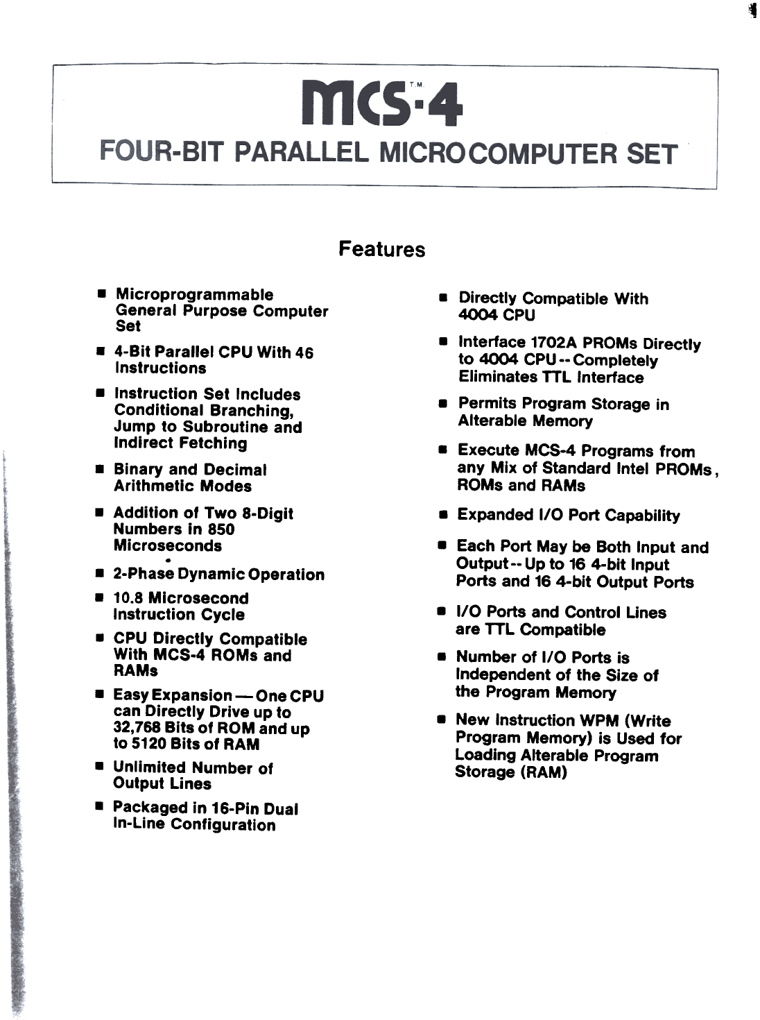
Features
. Directly Compatible With
4004 CPU
. Interface 1702A PROMs Directly
to 4004 CPU -- Completely
Eliminates TTL Interface
. Permits Program Storage in
Alterable Memory
. Execute MCS-4 Programs from
any Mix of Standard Intel PROMs,
ROMs and RAMs
. Expanded 1/0 Port Capability
. Each Port May be Both Input and
Output -- Up to 16 4-bit Input
Ports and 16 4-bit Output Ports
. I/O Ports and Control Lines
are TTL Compatible
. Number of I/O Ports is
Independent of the Size of
the Program Memory
. New Instruction WPM (Write
Program Memory) is Used for
Loading Alterable Program
Storage (RAM)
. Microprogrammable
General Purpose Computer
Set
. 4-Bit Parallel CPU With 46
Instructions
. Instruction Set Includes
Conditional Branching,
Jump to Subroutine and
Indirect Fetching
. Binary and Decimal
Arithmetic Modes
. Addition of Two 8-Digit
Numbers in 850
Microseconds
.
. 2-Phase Dynamic Operation
. 10.8 Microsecond
Instruction Cycle
. CPU Directly Compatible
With MCS-4 ROMs and
RAMs
. Easy Expansion - One CPU
can Directly Drive up to
32,768 Bits of ROM and up
to 5120 Bits of RAM
. Unlimited Number of
Output Lines
. Packaged in 16-Pin Dual
In-Line Configuration
.
~
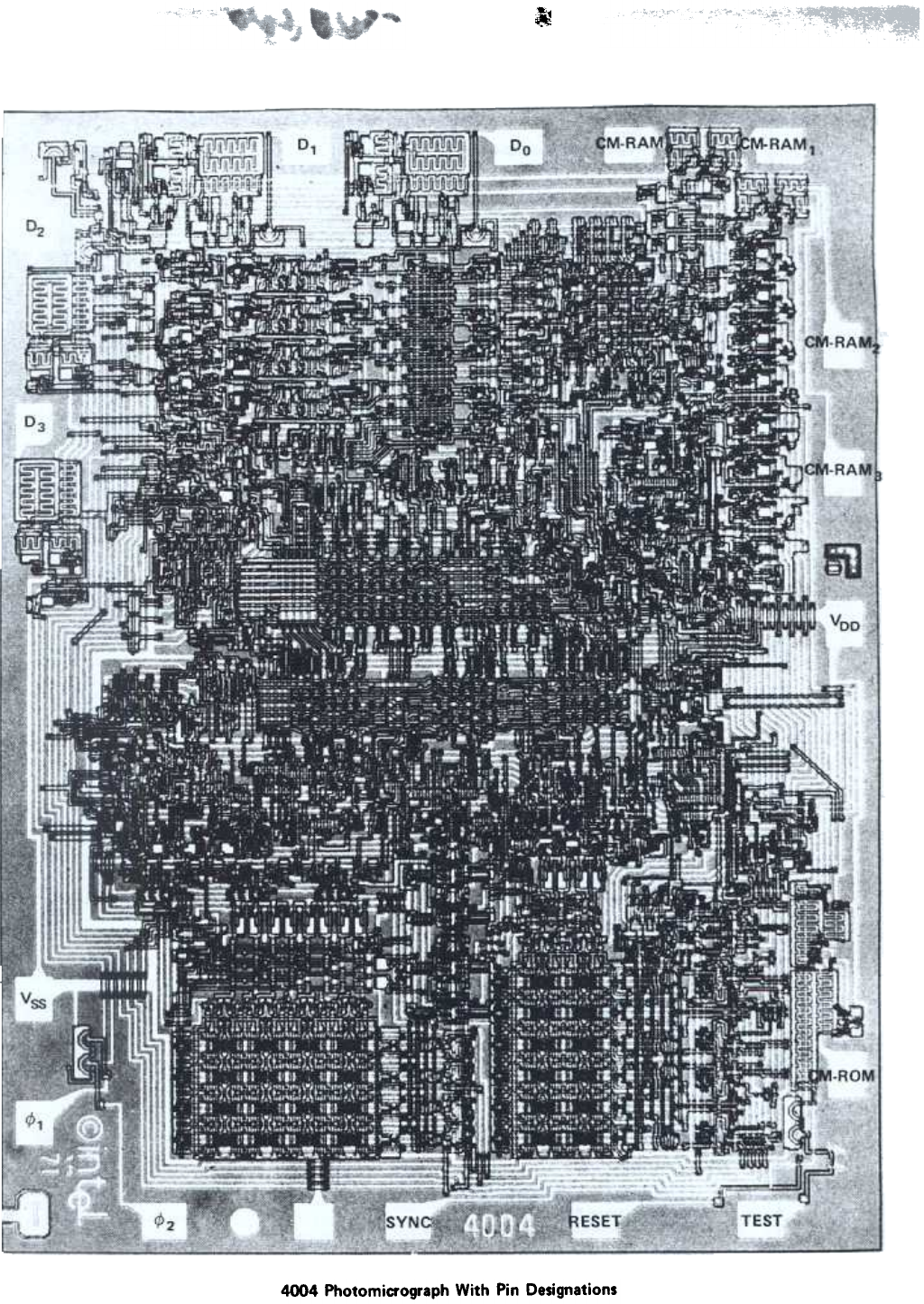
4004 Photomicrograph With Pin Designations
INTRODUCTION - THE ALTERNATIVE TO RANDOM lOGIC SYSTEMS
A. General Discussion
Since its inception, digital computer applications have evolved from
calculation through data processing and into control. The develop-
ment of the minicomputer has vastly increased the scope of computer
usage. In particular, the use of minicomputers in dedicated appli-
cations has had a profound effect on systems design.
Many engineers have found having a minicomputer at the heart of a
system offers significant advantages. Minicomputer systems are
more flexible, can be easily personalized for a particular customer's
requirements, and can be more easily changed or updated than fixed-
logic design systems. For most designers, the programming of a mini-
computer is a much easier and more straightforward procedure than
designing a controller with random logic.
Unfortunately, the size and cost of even the smallest minicomputer has
limited its use to relatively large and costly systems. This has
resulted in many smaller systems being implemented with complicated
random logic. INTEL NOW OFFERS ANOTHER ALTERNATIVE. . . THE MCS-4
MICRO COMPUTER SET.
This new concept in LSI technology makes the power of a general pur-
pose computer available to alDK>st every logic designer and represents
a strong attack on the dependency of systems manufacturers on compli-
cated random logic systems. This component computer from Intel can
provide the same arithmetic, control and computing functions of a
minicomputer in as few as two 16 pin DIP's and costs nearly 2 orders
of magnitude less.
The set is not designed to compete with the minicomputer, but rather
to extend the power of the concept into new ranges of applications.
For example, many systems now built of 55I and MSI TTL can now be.
implemented with a totally self-contained system built around this
set of devices.
Heart of each system is a single chip central processor unit (CPU)
which performs all control and data processing functions. Auxiliary
to the CPU are ROM's which store microprograms and data tables; RAM's
which store data and instructions. and Shift Registers which can
expand the I/O capacity of the system. The MCS-4 system communicates
with circuits and devices outside the family through "ports" provided
on each RAM and ROM.
A system using this set of devices will usually consist of one CPU,
from one to 16 ROM's, up to 16 RAM's and an arbitrary number of SR's.
A minimum system could be designed with just one CPU and one ROM.
With these components, you can build distributed computers, dedicated
computers, or personalized computers and utilize the almost infinite
combinations of microprogramming. The designer buys standard devices,
and with microprogramming of the ROM fulfills his own unique circuit
requirements.
1
~
The three major advantages of Intel microcomputers:
Qreat system flexibility, with easy program changes, ability
to expand or shrink the system, and small size and low power.
Expediency of design, because ROM programming is easier than
random circuit design, system checkout is easier using electri-
cally programmable and erasable ROM's, and ability to insert
new microprograms helps prevent system obsolescence.
Manufacturing economies come from simple DIP package design,
automatic insertion, lower labor costs, lower inventory of
parts and boards.
When designing with random logic (logic gates, flip flops, etc.),
the designer will usually start with a description of the desired
function and attempt to wire counters, gates, etc. to achieve this
function. Switches, displays, etc. are also connected to the logic
To correct errors or make changes in a design usually requires sig-
nificant changes in wiring, often requiring that circuit boards be
scrapped and replaced by new ones.
To do the same design with the HCS-4 Micro Computer Set, the designer
again starts with the functional description. However, he implements
these functions by encoding suitable sequences of instructions in ROM.
The MCS-4 instruction set is quite complete and allows a wide variety
of functions to be performed: decimal or binary arithmetic, counting,
decisions, table-lookup, etc. Switches, displays, etc. are connected
to the system via the input and output ports.
As a result of this organization. almost the entire logic. the entire
I'-personality" of the machine is determined by the instructions in ROM.
Very significant modifications of machine characteristics can be made
by changing or adding ROM's without making any changes in wiring or
circuit boards.
Thus the set offers tremendous flexibility of design and allows the
user to have many of the desirable features of a custom MaS LSI design--
small package count. a set of components which is uniquely his own
(for each user's program routines are his proprietary property)--
and yet have none of the disadvantages of long development cycle. high
development costs. etc. The short design cycle and flexibility asso-
ciated with ROM programming allows much more rapid response to market
demands than is possible with custom LSI and thus provides insurance
against obsolescence.
B. Applications for the MCS-4 Micro Computer Set
Heart of the MCS-4 micro computer set is the 4004 CPU. This device
has a powerful and versatile instruction set which allows the system
to perform a wide variety of arithmetic, control and decision functions
The microprograms stored in the ROM devices give the designer the
power of designing custom computers with standard components. You can
2
use the MCS-4 almost anywhere. Here are a few examples:
Control Functions - Because of low initial cost and flexibility
of programming, the MCS-4 can be used in place of random logic
in systems such as those in process control, numeric controls,
elevator controls, highway and rail traffic controls. By chang-
ing ROM microprograms the whole system can easily be modified
and updated.
Computer Peripherals - The system can be conveniently used in
peripheral equipment to control displays, keyboards, printers,
readers, plotters and to give intelligence to terminals.
Computing Systems - The MCS-4 system is ideally suited for such
devices as billing machines, cash registers, point of sale ter-
minals and accounting machines. For example, the adding of two
8-digit numbers can be done in 850 microseconds. In addition,
the MCS-4 can be efficiently used to decentralize central com-
,puter functions.
Other Applications - The elements of the MCS-4 have many applica-
tions within transportation, automotive, medical electronics and
test systems. where inexpensive dedicated computers can improve
system performance.
c. Features of the MCS-4
.
.
.
.
.
.
.
.
.
.
.
.
.
.
.
.
4-bit parallel CPU with 45 instructions
Decimal and binary arithmetic modes
10.8 ~ instruction cycle
Addition of TWo 8-digit numbers in 850 psec.
Sixteen 4-bit general purpose registers
Nesting of sUbroutines up to 3 levels
Instruction Set includes conditional branching, jump to subroutine,
and indirect fetching
2-phase dynamic operation
Synchronous operation wi th memories
Direct compatibility with 4001,4002 and 4003
No interface circuitry to memory and I/O required
Directly drives up to: 4K by 8 ROM (16 4001's)
1280 by 4 RAM (16 4002's)
128 I/O lines (without 4003)
Unlimited I/O (with 4003's)
Memory capacity expandable through bank switching
16-pin DIP package
P-channe1 Silicon Gate MaS
Minimum system: CPU and one ROM
3
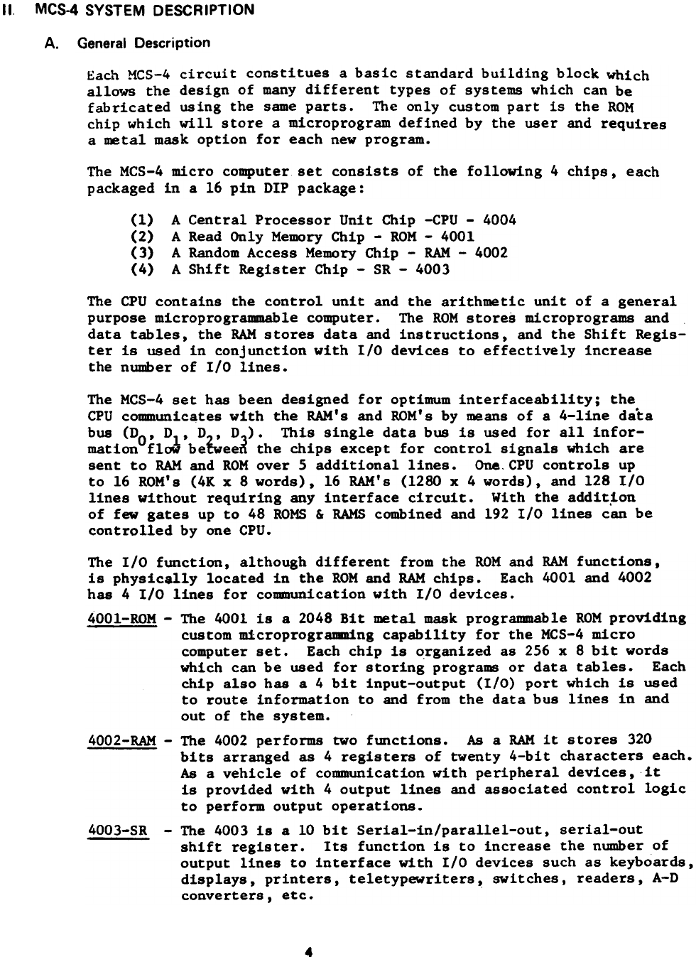
II, MCS-4 SYSTEM DESCRIPTION
General Description
A.
Each MCS-4 circuit constitues a basic standard building block which
allows the design of many different types of systems which can be
fabricated using the same parts. The only custom part is the ROM
chip which will store a microprogram defined by the user and requires
a metal mask option for each new program.
The MCS-4 micro computer set consists of the following 4 chips, each
packaged in a 16 pin DIP package:
(1)
(2)
(3)
(4)
A Central Processor Unit Chip -CPU - 4004
A Read Only Memory Chip - ROM - 4001
A Random Access Memory Chip - RAM - 4002
A Shift Register Chip - SR - 4003
The CPU contains the control unit and the arithmetic unit of a general
purpose microprogrammable computer. The ROM stores microprograms and
data tables, the RAM stores data and instructions, and the Shift Regis-
ter is used in conjunction with I/O devices to effectively increase
the number of I/O lines.
The MCS-4 set has been designed for optimum interfaceability; the
CPU communicates with the RAM's and ROM's by means of a 4-line data
bus (DO' Dl' D , D). This single data bus is used for all infor-
mation flow be~ee~ the chips except for control signals Which are
sent to RAM and ROM over 5 additional lines. One.CPU controls up
to 16 ROM's (4K x 8 words), 16 RAM's (1280 x 4 words), and 128 I/O
lines without requiring any interface circuit. With the addit,ion
of few gates up to 48 ROMS & RAMS combined and 192 I/O lines can be
controlled by one CPU.
The I/O function, although different from the ROM and RAM functions,
is physically located in the ROM and RAM chips. Each 4001 and 4002
has 4 I/O lines for communication with I/O devices.
4001-ROM - The 4001 is a 2048 Bit metal mask programmable ROM providing
custom microprogramming capability for the MCS-4 micro
computer set. Each chip is organized as 256 x 8 bit words
which can be used for storing programs or data tables. Each
chip also has a 4 bit input-output (I/O) port which is used
to route information to and from the data bus lines in and
out of the system.
4002-RAM - The 4002 performs two functions. As a RAM it stores 320
bits arranged as 4 registers of twenty 4-bit characters each.
As a vehicle of communication with peripheral devices,it
is provided with 4 output lines and associated contro110gic
to perform output operations.
4003-SR - The 4003 is a 10 bit Seria1-in/paralle1-out, serial-out
shift register. Its function is to increase the number of
output lines to interface with I/O devices such as keyboards,
displays, printers, te1etypewriters~ switches, readers, A-D
converters, etc.
4
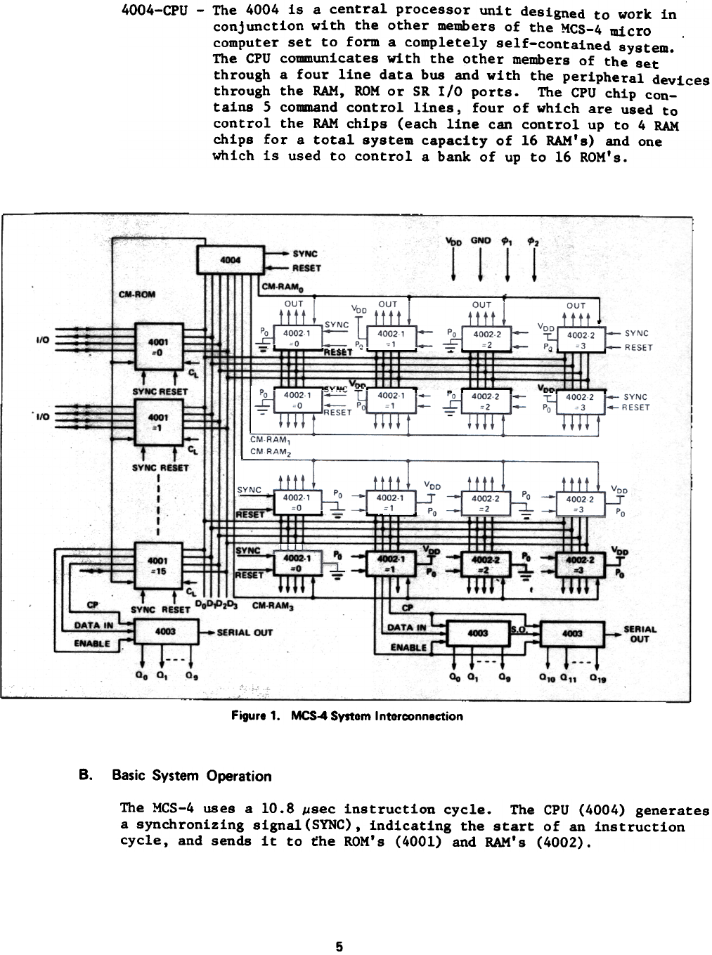
4004-CPU - The 4004 is a central processor unit designed to work in
conjunction with the other members of the MCS-4 micro
computer set to form a completely self-contained system.
The CPU communicates with the other members of the set
through a four line data bus and with the peripheral devices
through the RAM, ROM or SR I/O ports. The CPU chip con-
tains 5 command control lines, four of which are used to
control the RAM chips (each line can control up to 4 RAM
chips for a total system capacity of 16 RAM's) and one
which is used to control a bank of up to 16 ROM's.
~D GNO .,
1 1 1
,.
1.
4004
CM.ROM
1/0 4001 I
=0 I
.r-r ~
SYNC RESET
I
,-
I/O 4001
=1
-1~ CL
SYNC RESET
Figure 1. MCS-4 System Interconnection
B. Basic System Operation
The MCS-4 uses a 10.8 ~sec instruction cycle. The CPU (4004) generates
a synchronizing signal (SYNC), indicating the start of an instruction
cycle, and sends it to the ROM's (4001) and RAM's (4002).
5
I SYNC
I
L - RESET
I
':M-RAMo
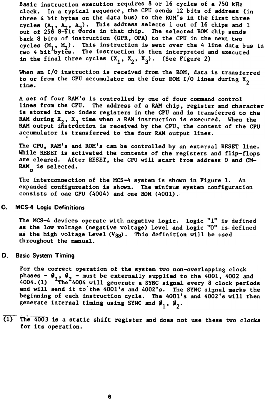
Basic instruction execution requires 8 or 16 cycles of a 750 kHz
clock. In a typical sequence, the CPU sends 12 bits of address (in
three 4 bit bytes on the data bus) to the ROM's in the first three
cycles (A , A ,A3). This address selects lout of 16 chips and 1
out of 256 8-~it words in that chip. The selected ROM chip sends
back 8 bits of instruction (OPR, OPA) to the CPU in the next two
cycles (ML' ~). This instruction is sent over the 4 line data bus in
two 4 bit~ytes. The instruction is then interpreted and executed
in the final three cycles (Xl' ~,X3). (See Figure 2)
When an r/o instruction is received from the ROM, data is transferred
to or from the CPU accumulator on the four ROM r/o lines during X2
time.
A set of four RAM's is controlled by one of four command control
lines from the CPU. The address of a RAM chip, register and character
is stored in two index registers in the CPU and is transferred to the
RAM during X2' X3 time when a RAM instruction is executed. When the
RAM output instruction is received by the CPU, the content of the CPU
accumulator is transferred to the four RAM output lines.
.
The CPU. RAM's and ROM's can be controlled by an external RESET line.
While RESET is activated the contents of the registers and flip-flops
are cleared. After RESET, the CPU will start from address 0 and CM-
RAM is selected.
0
The interconnection of the MCS-4 system is shown in Figure 1. An
expanded configureation is shown. The minimum system configuration
consists of one CPU (4004) and one ROM (4001).
c. MCS-4 Logic Definitions
The MCS-4 devices operate with negative Logic. Logic "1" is defined
as the low voltage (negative voltage) Level and Logic ItO" is- defined
as the high voltage Level (Vss>. This definition will be used
throughout the manual.
D. Basic System Timing
For the correct operation of the system two non-overlapping clock
phases - '1' ~2 - must be externally supplied to the 4001,4002 and
4004.(1) The 4004 will generate a SYNC signal every 8 clock periods
and will send it to'the 400l's and 4002's. The SYNC signal marks the
beginning of each instruction cycle. The 400l's and 4002's will then
generate internal timing using sn~c and ~1' Q2.
(I) The 4003 is a static shift register and does not use these two clocks
for its operation.
6
~~,...
c~
Figure 2. MCS-4 &.ic Instruction Cycle
Figure 2 shows how a basic instruction cycle is subdivided and what
the activity is on the data bus during each clock period. Each data
bus output buffer has three possible states: "1", "0" and floating.
At a given time, only 1 output buffer is allowed to drive a data
line, therefore all the other buffers must be in a floating condition
However, more than 1 input buffer per data line can receive data at
the same time.
III 4 BIT CENTRAL PROCESSOR UNIT (CPU) - 4004
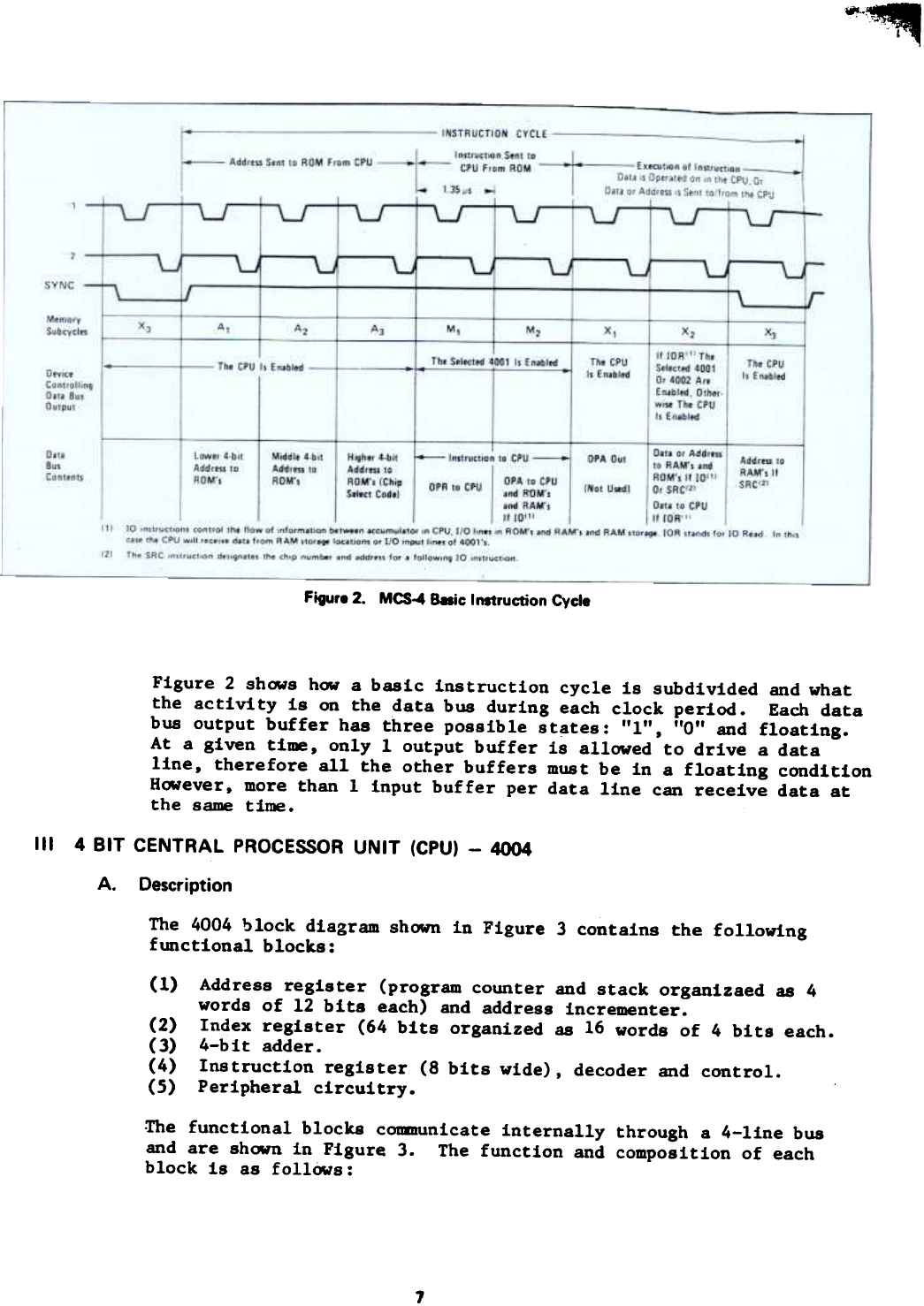
A. Description
The 4004 block diagram shown in Figure 3 contains the following
functional blocks:
(1)
(2)
(3)
(4)
(5)
Address register (program counter and stack organizaed as 4
words of 12 bits each) and address incrementer.
Index register (64 bits organized as 16 words of 4 bits each.
4-bit adder.
Instruction register (8 bits wide), decoder and control.
Peripheral circuitry.
Ihe functional blocks communicate internally through a 4-line bus
and are shown in Figure 3. The function and composition of each
block is as follOws:
7
.1. Address R ram counter & Stack & Address Incrementer
The address register is a dynamic RAM cell array of 4 x 12 bits.
It contains one level used to store the instruction address
(program counter) and 3 levels used as a stack for subroutine
calls. The stack address is provided by the effective address
counter and by the refresh counter, and it is multiplexed to the
decoder.
The address when read is stored in an address buffer and is
demultiplexed to the internal bus during A , A2' and AJ in three 4-
bit slices (see Figure 2 for basic instruc!ion cycle). The address
is incremented by a 4-bit carry look-ahead circuit (address incre-
menter) after each 4-bit slice is sent out on the data bus. The
incremented address is transferred back to the address buffer and
finally written back into the address register.
SYNC TOT RESET
CM CM CM CM
RAMo RAM, RAM, RAMJ
v. v.
r I
.. SYNC
OOTPVT
eufflR
..
INTERNAl
RElET
'IF
---T-
CM-RAM
OUTPUT BUFFERS TIMING
ADORE.
INCREMENTER
~~~
CC*TROL
REGISTER
~
h~ ~ CYCLE LOG~
'IP . 'IF
~
AW\.I.. MULTIPLEXER a-
ICX*TROL
FOR
THE
~RE8
MOISTER .
IMJeX
REGISTER
:;rtiR
lrC<*TROl
ADORE.
REGISTER
(PROGRAM
~ER
. STACK'
4 . 12 BIT
DYNAMIC
RAM
.-CIAL
~
~ER
~IVER
.
MUX
~
~IN-OUT
8UFFE~
.,
ACC~AT~
~ CMRY FIF ~A
DECOOER
~
DlmDER
ADGER
.
~
OONTROt.
~
MUX
. "IFTER
#2
j MJFFER .
r8"t REGISTER r-
---I REFRE84
.~R
I~UCTION ~R
~.3 ~ER ~EFFECTIVE A(X)RE8
~R
I I*TR~
orA
REGIsnR
~I
IEGI~R
~
,REGISTER
~
AW\.I.
.MUX
ADa
BUffER REG.
..
--L-
REFRE"
ICOUNTIR
DECOOER
DRIVER
.
MUX
INDEX
REGISTER
',.4 lIT
DYNAMIC RAM
~
INTERNAl. DATA IW
Figure 3. 4004 CPU Block Diagram
8
CM
~=
BUFFER
2. Index Register
The index register is a dynamic RAM cell array of 16 x 4 bits
and has two modes of operation. In one mode of operation the
index register provides 16 directly addressable storage loca-
tions for intermediate computation and control. In the second
mode, the index register provides 8 pairs of addressable stor-
age locations for addressing RAM and ROM as well as for storing
data fetched from ROM.
The index register address is provided by the internal bus
and by the refresh counter and is multiplexed to the index
register decoder.
The content of the index register is transferred to the internal
bus through a multiplexer. Writing into the register is accom-
plished by transferring the content of the internal bus into a
temporary register and then to the index register.
34-Bit Adder
The 4-bit adder is of the ripple-through carry type. One term of
the addition comes from the "ADB" register which coanunicates
with the internal bus on one side and can transfer data or QiEi
to the adder. The other term of the addition comes from the
accumulator and carry flip-flop. Both data and data can be
transferred. The output of the adder is transferred to the
accumulator and carry FF. The accumulator is provided with a
shifter to implement rotate right and rotate left instructions.
The accumulator also communicates with the command control
register, special ROM's, the condition flip-flop and the internal
bus. The command control register holds a 3-bit code used for
CM-RAM line switching. The special ROI~'s perform a code conver-
sion for DAA (decimal adjust accumulator) and KBP (Keyboard
Process) instructions. The special ROM's also communicate with
the internal bus. The condition logic senses ADD - 0 and
ACC - 0 conditions, the state of the carry FF, and the state of
an external signal (TEST) to implement JCN (jump on condition)
and ISZ (increment index register skip if zero) instructions.
4.
The instruction register (consisting of the OPR Register and
OPA Register each 4 bits wide) is loaded with the contents of
the internal bus (at ~ and ~ t~e in the instruction cycle)
through a multiplexer And hol&s the instruction fetched from
ROll. The instructions are decoded in the instruction decoder
and appropriately gated with timing signals to provide the con-
trol signals for the various functional blocks. A doUble cycle
FF is set from anyone of 5 double-length instructions. Double-
length instructions are instructions whose OP-code is 16 bits wide
(instead of 8 bits)and that require two system cycles (16 clock
cycles) for their execution. Double length instructions are stored
in two successive locations in ROl.I. A condition FF controls JCN
and ISZ instructions and is set by the condition logic. The state
of an external pin "test" can control one of the conditions in the
JCN instruction.
9
5. Peripheral Circuitry
This includes:
a. The data bus input-output buffers communicating between
data pads and internal bus.
b. Timing and SYNC generator.
c. 1 ROM command control (CM-ROM) and the 4 RAM command control
(C~RAMi) output buffers.
d. Reset flip-flop.
During reset (Reset pin low), all RAM's and static FF's are cleared,
and the data bus is set to "0". After reset, program control will
start from "0" step and CM-RAM is selected. To completely clear
all registers and RAM locationi in the CPU the reset signal must be applied
for at least 8 full instruction cycles (6-4 clock cycles) to allow the
index register refresh counter to scan all locations in memory.
(256 clock cycles for the 4002 RAM).
6.Instruction Repertoire
The instruction repertoire of the 4004 consists of:
a. 16 machine instructions (5 of which are doUble length)
b. 14 accumulator group instructions
c. 15 in~ut/outP.ut and RAM instructions
B.
The instruction set and its format will be briefly described in
the next section. Section VII will then describe each instruction
in detail.
CPU Instruction Set Format, Index Register Organization,
and Operation of 'the Address Register and Command Lines
1. Instruction Set Format
Machine Instructions
a.
. l-word instructions - 8 bits wide and requiring
8 clock periods (1 instruction cycle)
. 2-word instructions -16 bits wide and requiriag
16 clock periods (2 instruction cycles) for
execution
A l-word ins truction occupies one location in ROM
(each location can hold one 8-bit word) and s
2-word instruction occupies two successive loca-
tions in ROM. Esch instruction word is divided into
two 4-bit fields. The upper 4 bits is called the
OPR and contains the operation code. The lower 4
bits is called the OPA and contains the modifier.
For a single word machine instruction the operation
code (OPR) contains the code of the operation that
is to be performed (add. subtract. load. etc.). The
modifier (OPA) contains one of 4 things:
(1) A register address
(2) A register pair address
(3) 4 bits of data
(4) An instruction modifier
10
For a 2-word machine instruction the 1st word is similar
to a l-word instruction, however, the modifier (OPA)
contains one of 4 things:
(1) A register address
(2) A register pair address
(3) The upper portion of another ROM address
(4) A condition for jumping
ONE WORD INSTRUCTIONS
0, 0, 0, 0. 0, 0, 0, 0.
Ix/xlxlxJxlx/xlxl
~ DrA
nW> M>RD INSTRUCTIONS
lit INSTRtx:TION CYCLE 2oId INSTRtx:T1ON CYCLE
D, DJ D, De D, DJ D, De D, D, D, De D, DJ D, De
I X I X I X I X I X I X I X I ~l I X I X I X I X I X I X I X I Xl
~ ~A ~ ~A
( OP ~ I MODIFIER .J
I ~COOI I MOOIFIERI
I OP CODE I ~IFIER I
lx I x I x I x I ~NO~~A~E;;ERR INDEX REGISTER X X X X AO~ESS
R R R R
~
I X I X I X I X IIN:Ex.~~~S:S:R P:R INo X REGISTER PAIR
X X X X ADDRESS
R R R X
OR
1 X I X 1 X I X 1 DATA 1
1"1"1"1"100001
I w I w I w I v I ~R ADORE. I
I X I X I X I X I A, AJ AJ AJ I
OR
, v I v I v I v , CONDITION I
,X I X I X I X I c, C. CJ C. I
OR
Ix I x I x I x I ~NDE:'l.~~~;ER R INDEX REGISTER X X X X ADDRESS
R R
MIDOLE ADDRESS LOWER ADORE8
A, A, A, A, A, A, A, A,
OR
l x I x I x I x IIN~XA~~rs\R PA:IINDEX REGISTER PAIR
X X X X ADDRESS
R
I UPPER DATA I LOWER DATA I
I DZ OJ DZ OJ I D, D, D, D, I
T8bIo 1- M8d1ine Instruction F~
The 2nd word contains either the middle portion (in OPR) and
lower portion (in OPA) of another ROM address or 8 bits of
data (the upper 4 bits in OPR and the lower 4 bits in OPA).
The upper 4 bits of instruction (OPR) will always be fetched
before the lower 4 bits of instruction (OPA) during MI and
M2 times respectively. Table I illustrates the contents of
each 4-bit field in the machine instructions.
b. Input/Output & RAM Instructions and Accumulator Group
Instructions
In these instructions (which are all single word) the OPR
contains a 4-bit code which identifies either the I/O
instruction or the accumulator group instruction and the OPA
contains a 4-bit code which identifies the operation to be
performed. Table II illustrates the contents of each 4-bit field.
0, 0, Dt Dt Dt 0, Dt Dt
Lxlxlxlxlx!xlx!xl
~ ~
IWVY.QJTPUT . I . I . I . I a I - I - I - I - I
RAMIN8TR~~ I 1 I 1 I 1 I . I x I x I x I x I
~ULATO" GA~ . 1 I 1 I 1 I 1 I x I x I x I x I
INIT"~'OM ."'I'I'IAIAIAIAI
--AI X . EITHB A ~ A ..,-.
Table II - 1/0 and Accumulltor Group Instruction Formats
11
2. Index Register Oraanization
The index register can be addressed in two modes
By specifying lout of 16 possible locations with art OPA
code of the form RRRR(l) (See Table III).
a.
b. By specifying lout of 8 pairs with an OPA code of the
form RRRX{2) (See Table III).
When the index register is used as a pair register, the even
number register (RRRO) is used as the location of the middle
address or the upper data fetched from the ROM, the odd nwmer
register (RRRl) is used as the location of the lower address
or the lower data fetched from the RO~.
SINOLE REGISTER ADORE_NO
REGISTER 'AIR AOORESING
REGISTER
NU_ER
REGISTER
PAIR
N~ER
Teble III . Index Register Organization
3. Operation of the Address Register (Proaram Counter and Stack)
The address register contains four 12-bit registers; one register
is used as the program counter and stores the instruction address.
the other 3 registers make up the push down stack.
Initially anyone of the 4 registers can be used as the program
counter to store the instruction address. In a typical sequence
the program counter is incremented by 1 after the last address
is sent out. This new address then becomes the effective address
If a JMS (Jump to Subroutine) instruction is received by the CPUt
the program control is transferred to the address called out in
JMS instruction. This address is stored in the register just
above the old program counter which now saves the address of
the next instruction to be executed following the last ~ffi.(3)
This return address becomes the effective address following
the BBL(Branch back and load) instruction at the end of the
subroutine.
(-1) In this case the instruction is executed on the 4-bit content addressed
by RRRR.
In this case the instruction is executed on the a-bit content addressed
by RRRX, where X iR specified for e~~ instruction.
Since the JNS instruction is a 2-word instruction the old effective
address is incremented by 2 to correctly give the address of the next
instruction to be execute"d after the return from J~fS.
12
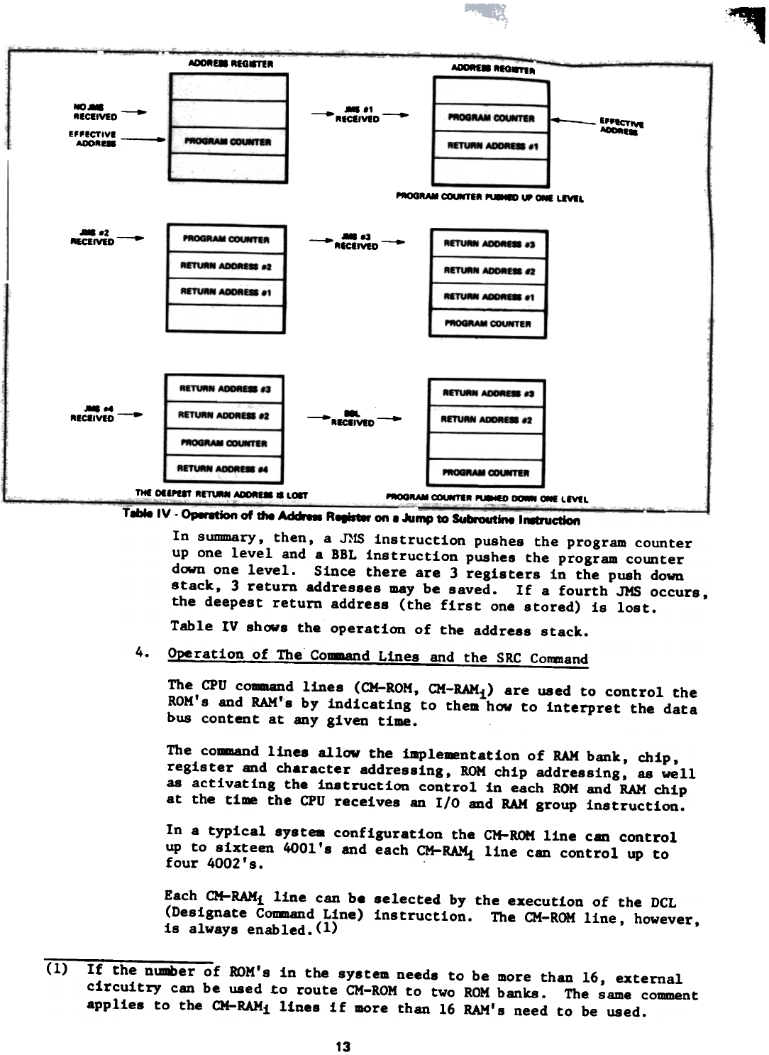
:~
~- RIG~R
~ RIG~R
- ~.1
~1CafYaO - ~~~R --=:-
~..
RIcaIWD --
EF,eCTlve -
AOOR"
'ROGRAM COt*TIR ~~_.,
PMJORAM ~R ~ W ~ Law..
"-2-
~IVED PROGRAM ~I~ '-83 -
- ~ICIIVID
~ETUM ~ .J
RmMN ADORa8 .~
AIT\MN ~E8 n
R~ ~E8 .1
AlTUM ~.. .,
~~IR
R~~.J
RmMN ~E8 n
MT~ ACORE8 .2
RlcalVEO - --.~ICIIVIO - ~~.2
~~R
R~ -£8 ..
~~R
nIE ~ , RET\MN ~ . L~ ~~ ax*TaR ~ ~ ~ llVll
-
T... IV. ~.afi of the Ad*-. ReIiIt8r on . .hAmp to Subroutine It.-ruction
In sununary, then, a J}fS instruction pushes the program counter
up one level and a BBL instruction pushes the program counter
down one level. Since there are J registers in the push down
stack, J return addresses may be saved. If a fourth JMS occurs,
the deepest return address (the first one stored) is lost.
Table IV shows the operation of the address stack.
4. ~ration of The Co~d Lines and the SRC Conma!}.!!
The CPU command linea (~ROH. CM-RAMi) are used to control the
ROM's and RAM'. by indicating to them how to interpret the data
bus content at any given time.
The command linea allow the implementation of RAM bank, chip,
register and character addressing, ROM chip addressing, as well
as activating the instruction control in each ROM and RAM chip
at the time the CPU receives an I/O and RAM group instruction.
In a typical systea configuration the ~ROH line can control
up to sixteen 4001' s and each ~RAMi line can control up to
four 4002'8. .
Each CM-RAMi line can b. selected by the execution of the DCL
(Designate Command Line) instruction. The CM-ROM line, however,
is always enabled.(l)
. -. ~
(1) If the number of ROM's in the system needs to be more than 16, external
circuitry can be used to route CM-ROM to two ROM banks. The same comment
applies to the ~RAMi lines if more than 16 RAM's need to be used.
13
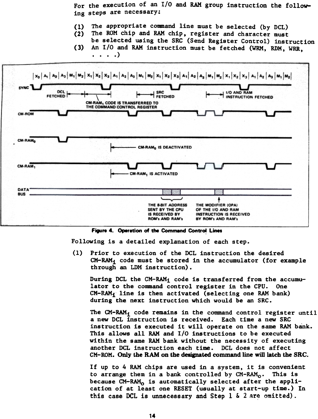
For the execution of an I/O and RAM group instruction the follow-
ing steps are necessary:
(1)
(2)
The appropriate command line must be selected (by DCL)
The ROM chip and RAM chiP. register and character must
be selected using the SRC (Send Register Control) instruction
An I/O and RAM instruction must be fetched (WRM. RDM. WRR,
. . . .)
(3)
Xsi ..1 Aa I AJ I-,!.., I X,I Xa1-J I A,I A21 Aa I M, I ~ I X,I X2/ XI! A,I At I A, 1-,1-2! X,I X21 XJ I A,I Aa I AJ I M,I ~:
SYNC 'U ~ U
DCL 1- _1- _I I J ~C
FETCHED r -,- \ -I FETCHED
CM.RAM, CODE IS TRANSFERRED TO
THE COMMAND CONTROL REGISTER
U
~
1- - I 110 AND RAM
1--' INSTRUCTION FETCHED
CM.ROM ,'-' '-'
CM.RAMo
~- CM.RAMO IS DEACTIVATED
u
CM-RAM1 u u
~ CM.AAM, IS ACTIVATED
DATA
BUS
' '
THE I.BIT ADDRESS
SENT BY THE CPU
IS RECEIVED BY
ROM', AND RAM',
t
THE MODIFIER 10PAI
OF THE If 0 AND RAM
INSTRUCTION IS RECEIVED
BY ROM's AND RAM',
F.". 4. Operation of the Comm.nd Control: Lines
Following is a detailed explanation of each step.
(1) Prior to execution of the DCL instruction the desired
~RAMi code must be stored in the accumulator (for example
through an LDM instruction).
During DCL the CM-RAMi code is transferred from the accumu-
lator to the command control register in the CPU. One
CM-RAMi line is then activated (selecting one RAM bank)
during the next instruction which would be an SRC.
The CM~RAMi code remains in the command control register until
a new DCL instruction is received. Each time a new SRC
instruction is executed it will operate on the same RAM bank.
This allows all RAM and 1/0 instructions to be executed
within the same RAM bank without the necessity of executing
another DCL instruction each time. DCL does not affect
CM-ROM. Only the RAM on the designated command line will latch the SRC.
If up to 4 RAM chips are used in a system, it is convenient
to arrange them in a bank controlled by CM-RAMo. This is
because CM-RAMo is automatically selected after the appli-
cation of at least one RESET (usually at start-up time.) In
this case DCL is unnecessary and Step 1 & 2 are omitted).
14
.,
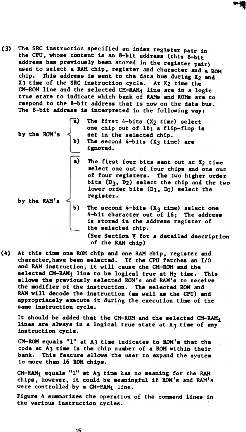
(3)
a)
The SRC instruction specified an index register pair in
the CPU, whose content is an 8-bit address (this 8-bit
address has previously been stored in the register pair)
used to select a RAM chip, register and character and a ROM
chip. This address is sent to the data bus during X2 and
X3 time of the SRC instruction cycle. At X2 time the
CM-ROK line and the selected CM-RAKi line are in a logic
true state to indicate which bank of RAMS and ROMS are to
respond to th~ 8-bit address that is now on the data bus.
The 8-bit address is interpreted in the following way:
The first 4-bits (X2 time) select
one chip out of 16; a flip-flop is
set in the selected chip.
b) The second 4-bits (X3 time) are
ignored.
by the ROM's
a) The first four bits sent out at X2 time
select one out of four chips and one out
of four registers. The two higher order
bits (D), D2) select the chip and the two
lower order bit. (Dl, no) select the
register.
by the RAM'.
b)
(4)
The second 4-bits (XJ time) select one
4-bit character out of 16; The address
is stored in the address register of
the selected chi~.
(See Section ~ for a detailed description
of the RAM chip)
At this time one ROM chip and one RAM chip, register and
character,have been selected. If the CPU fetches an I/O
and RAM in8truction, it will cause the CM-ROH and the
selected CM-RAMi line to be logical true at M2 time. This
all0W8 the previously selected ROM's and RAM's to receive
the modifier of the instruction.' The selected ROM and
RAM will decode the instruction (as well 88 the CPU) and
appropriately execute it during the execution time of the
same instruction cycle.
It should be added that the ~ROM and the selected ~RAMf
lines are always in a logical true state at AJ tiae of any
instruction cycle.
~ROK equals "1" at AJ ti~ indicates to ROM's that the
code at AJ time is the chip number of a ROM within their
bank. This feature allows the user to expand the system.
to more than 16 ROM chips.
Cli-RAMt equals "I" at AJ ti~ has no meanins for the RAM
chips, however, it could be meaningful if ROM's an4 RAM's
were controlled by a c)1-RAHi line.
Figure 4 summarizes the operation of the command lines in
the various instruction cycles.
15
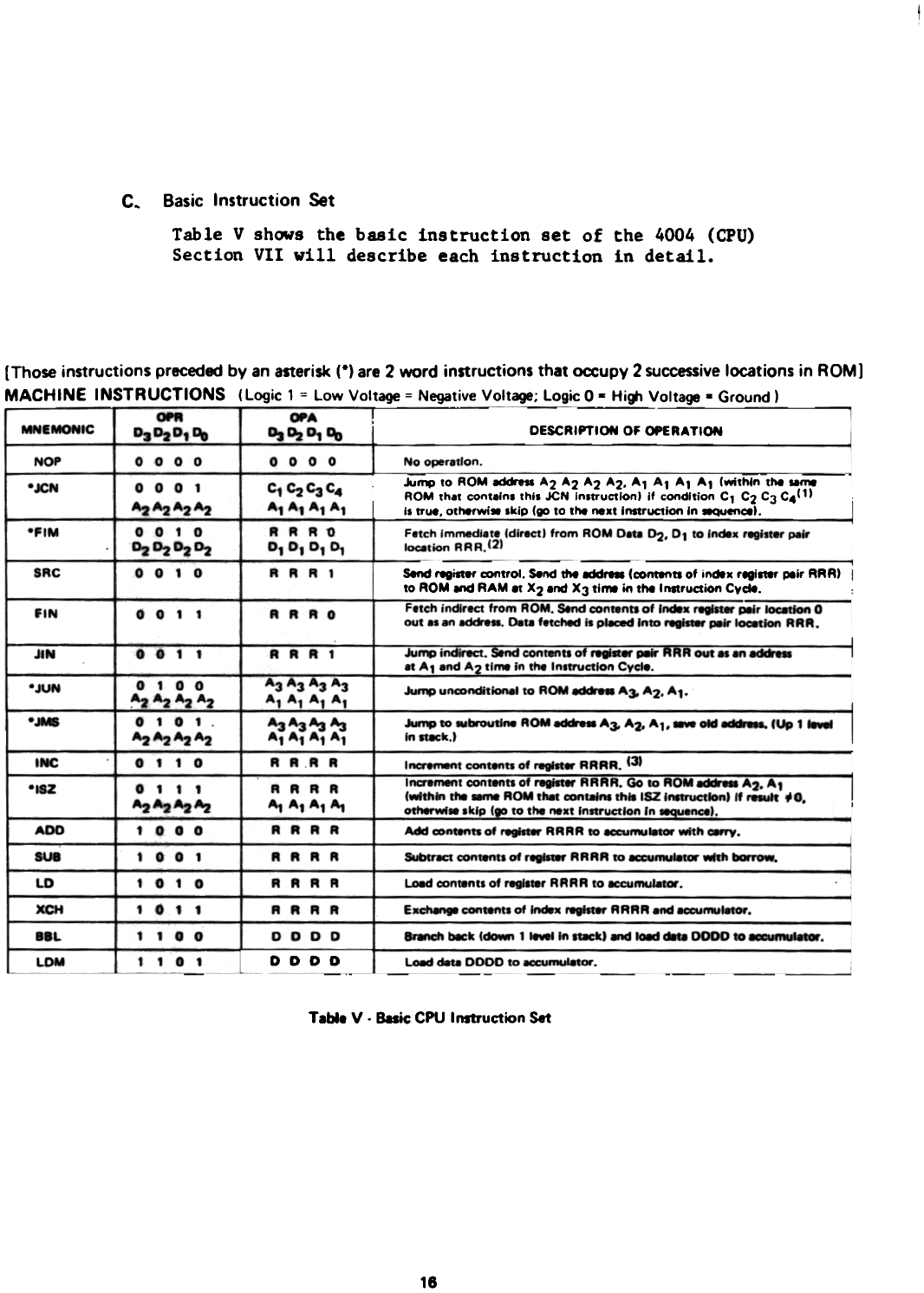
Basic I nstruction Set
c~
Table V shows the basic instruction set of the 4004 (CPU)
Section VII will describe each instruction in detail.
[Those instructions preceded by an asterisk (.) are 2 word instructions that occupy 2 successive locations in ROM]
MACHINE INSTRUCTIONS (Logic 1 = Low Voltage = Negative Voltage; Logic 0 & Hi~ Voltage. Ground)
MNEMONIC DESCRIPTION DF OPERATION
NOF
-JCN
OPR
~DzD'De
0 0 0 0
.
0 0 0 1
~~A2~
0 0 1 0
Dz~Dz~
0 0 1 0
MA
DJ~o,~
0 0 0 0
C1 ~C3C4
A1 A, A1 A~
~ R R 0
°1 °1 °1 0,
R R A 1
No operadon
- - - - -
Ju~ to ROM 8dfkeSI A2 A2 A2 A2. A1 A1 A1 A1 (within the ROM that contalnl thll JCN Inltructlonl If condition C1 C2 C3 C4111
II true, otherwi. Ikip (go to the next InltrUctlon In ~encel.
"FIM Fetch Immedle.. Idlrect) from ROM 0818 ~. D1 to Index register pelr
l0C8tion RRR.12)
SRC Send register ~trol. Send N .td,-. (contwntl of index r",ater peir RRRI
to ROM Ind RAM 8t X2 and X3 dIM in the Inttruction Cyde.
-- -- - -
r--Ffldlliidr"8ct-fromROM~n..nts of ".. ~j.lr ~n 0-
out.l.n 8ddreA. 0818 fet~ II pIKed IntO regll.., pelr l0C8tlon RRR.
Jump Indirect. re9iater pair RRR out.. en 8d«...
.t A1 end A? tln8 In the Instruction Cycle.
FIN 0 0 , , R R R 0
JIN 0 0 1 1 A A A 1
'JUN
Ju~ unmnditional to ROM -»- A30 A2. A1
-J" Jump to wbroutlne ROM addI'HI AJ. A2. A1. 8V8 old 8dd, (Up 1 level
In_k.1
Iftcr!nwntcontentl of_r8tI8t- RRRR. 131
INC
-ISZ
0 1 0 0
A2 A2 A2 A2
0 1 0 1
A2~~~
0 1 1 0
0 1 1 1
~~~~
1 0 0 0
1 0 0 1
A3A3A3A3
A1 A1 A1 A1
~A3~~
A1 A1 A1 A1
~ R R ~
lna-_t COi1ten.. of r8jst., RRRR. Go ro ROM 8dfk- A2. A,
(within rN .me ROM thet contain. chi. ISZ in.tructlon) If r..ult ~ 0
ot'--. .klp (~to tN next Instruction In 8qU8'-~.
ADD
StM
LD
XCH
IlL
LDM
A " A R
A, A1 A1 A,
R R R R
R R R R
Add mntentl of regilt. RRRR to ~mulator with carry.
SubtrKt contents of r8gi1- R R R R fO 8CCUmul8ror with borrow.
1011) A A A R
A R A A
0 0 0 0
LO8d ~n18nt. of ~r RRRR to 8CCUmulator.
, 0 , ,
, , 0 (
, , 0 ,
Excn.,. contentS of ~x register RRRR and 8CCUmllator.
a-IdI beck I~ 1 IewIln lt8Ck) ~ 1O8d ~. DDDD to ~mul.tor
D D D D I.oed d8t8 DODO to ~mu"tor .
Table V. Basic CPU Instruction Set
18
,.,
INPUT/OUTPUT AND RAM INSTRUCTIONS
(The RAM'I8nd ROM', ~8t8d on in the 1/0 8nd RAM inltructionl h_!.en ~8VlousiV lelect8d by the 181 SAC instruetlo.. 8x8CUttd.1
I DEKRIPTION OF ~R.T~
Wrile Ihe conlenll of lhe Kcumu18tM Inlo I e D'eY1ou V-
RAM ~n memoty cl\8l'Kter.
Wrlle lhe ~tenll of lhe __1M inlO tM Pl'8ViOuliV --- ~
RAM au t t. IOu t LInes!
Write the contents of the Kcumu tM nto t
ROM outPUI port. 11/0 Llnnl
Wri. the con18fttl of the -_tor intO the PIWioUllv -.. -
\ h8lf byte of rNd'-i. ~..~ me~y IfM '* with -.,-. Of*vl -
Write the contents of the Kcumu18tM Into the prwiOullV 8I8cted
RAM Itatul character O.
Write lhe contents of the KCUn-.18tor Into the pr8¥iOu"v -.ct8d
RAM ltatul char- 1.
Write the cont.nts of the acwmulatM Into the Pl'8ViouslV 8I8cted
RAM Iiatul ch8r8ct... 2.
Write lhe conten.. of the _n-.I8tM IntO the D'eYlouIIy 8I8ct8d
RAM statUI cI\8I'- 3.
SubtrKt the D'eYIouIlV 8lect8d RAM ~in -V cI\8I'- from
aeeurnulalor with bof'row.
R.~ the ptevfously 1818ct8d A meln ff8fr*Y ~
Into the KCUmu4ator. '
~~ -~~u-~i -the ..-vIo\Aly 8I8cted ROM Input POI't .
into lhe accumUIe\or.II/O.Unell_-
~ the ~8VIou"V -lee.- RAM m81n n.mory clw- to
I _rnulatM with ~y.
MNEMONIC
WRM
WMP
WRR
~
OJ ~ D", Do
, , , 0
, , , 0
, , , 0
CWA
o,~Dt~
0 0 0 0
0 0 0 1
0 0 1 0
0 0 1 1WPM t t t 0
W~141
WR1141
WAr41
WA3141
IBM
ADM
ADA
ADM
A~141
AD114)
ADr4)
AD~4J
0 t 0 4
t 1 , 0
1 1 1 0 0 tOt
0 1 1 0
. 1 t t
t . 0 (
, 1 , 0
, , , 0
, , , 0
, , 1 0
, , , 0
, 1 1 0
, 0 0 ,
, 0 t .
, 0 1 ,
1 1 1 0
. 1 1 0
1 1 0 0
1 1 0 1
R.-j the pnviouliV _lected RAM status c_- 0 Into _n-.18t0l'.
RNd the pr8¥I~"V 8tect8d RAM statUI C'-Kt8l' 1 into 8CCU~I.tor.
1 , 1 0
t , , 0
1 1 1 0
~ 1 1 .
RMd tN prwiously selected RAM status ctwKt8f 2 into -~a.-.
Read the ~lViOUsty .18ct8d RAM statUI c'-Kter 3 Into 8«u".,I8tor.
ACCUMULATOR GROUP INSTRUCTIONS
CL8
CLC
lAC
CMC
CMA
RAL
RAR
T~
DAC
-
TQ
STC
DAA
K8P
DCL
, , , ,
, , , ,
, , , ,
~ , , 1
0 0 0 0
0 0 0 1
0 0 1 0
0 0 1 1
0.1 0 0
0 1 0 1
0 1 1 0
0 1 1 1
1 0 0 C
1 0 0 1
1 0 1 0
1 0 1 1
1 1 0 0
1 1 0 1
t t t t
t f t t
-,
t t t t
, . . 1
, , 1 ,
0- bodt. IAccumul8tOl"'-rv1
0- -rv.
I t -.mII'-'.
.
~ ;;-~t~.
~ t -~.
Aoy.. left. IA~mu nd C8Ty1
~ ,...t. IAccu-'-.. ~I
Tr8ftfmlt C8rry to _mu18tor 8nd ct.- ~.
D8Cr8n8nt -mul8tOl'.
T~1fer ~ Iubtr8Ct 8M --~.
Set -rv.
t . 1 ~
1 1 ., 1
t 1 t t
I D8d"-, 8djust KaI --
KeybO8'd prOC88. Co_" lhe mftUn" of lhe Kaln-.I8tor fr- . --
I 018 ~I of f- ~ 10 . bln.-y ~.
1 i 1 1 0..,.- ~ line
NOTES: (11Th. condItion codellasI9n8d. follows:
~ . t Inwn jump concItlon ~ . 1 ~ If Is r- Cc . 1 Jump If t8l1 Iign8I II . 0
C, .0 Not Inwn jump condition ~ . 1 Jump if c.-rv/llnk II a 1
(2IRRR II the ~.. of 1 of 8 In~. '89111.. ~ In the CPU.
t3lRRRR II the ~ of 1 of 16 lna. r8III1W1ln the CPU.
(CIEech RAM chip h. C '89IIt.,l. each with t-tv 4-bit ch.'Kte'IIU~lvldld Into 18 main ~~ Ch8"Kt.,18nd C Itatul ch.,act.,l.
Chip numt.,. RAM '89IIt., and me.n ~~v ch.8C1.,.. 8dtke.-d by 8ft SAC Instructl_. F~ the .18C18d chip and ""11... ~.
IUtUI cwect., IoC8tionl.. -18C18d by the Instruction code tOPAI.
Table V - Basic CPU Instruction Set (Continued)
17
~
4001 - 256 x 8 MASK PROGRAMMABLE ROM AND 4 BIT I/O PORT
IV.
The 4001 performs tWo basic and distinct functions: As a ROM it stores
256 x 8 words of program or data table.; as a vehicle of communication
with peripheral devices it i. provided with 4 I/O pins and associated control
logic to perform input and output operations. (The block diagraa is shown
in Figure 5.)
In the ROM mode of operation the 4001 will receive an 8-bit address during
Al and A2 time (see Figure 2) and a chip number, together with CK-ROM
during AJ time. When CM-ROM 18 present, only the chip whose ~tal optioo
code matches the chip n\DDber code sent during AJ (CSE - "1") is allCNed
to send data out during the following two cycles: HI and H2. The activity
of the 4001 in the ROM mode ends at M2' Before going into the I/O mode
of operation we must first review two basic instructions used in conjunc-
tion with it.
1. SR~ Instruction. (Send addresa to ROM and RAM)
When the CPU executes an SRC instruction it will send out 8 bits of
data during X2 and X3 and will activate the CM-ROM and one CM-RAM(l)
line at X2. Data at X2, with simultaneous presence of CM-ROK, is in-
terpreted by the 4001 as the chip nU8ber of the unit that should later
perform an I/O operation. Data at X3 ia ignored. In the case of the
4002, data at X2 will designate the chip number (one out of 4 chips)
and the register number (one out of 4 regi8ters); data at X3 will desig-
nate the 4-bit character (one out of 16) to be operated upon. After
SRC only one 4001 and one 4002 will be ready to execute a following
I/O instruction.
2. I/O and RAM Instructions
1/0 and RAM instructions allow the CPU to communicate with the 1/0 port8
of the 4001'8 and 4O02's. When the CPU receives an 1/0 instruction it
will activate the CM-ROM and one CM-RAK line during M2, in time for
4001'8 and 4002'8 to receive the second part (OPA) of the 1/0
instruction. The OPA portion of the 1/0 instruction is a code
8pecifying which 1/0 operation should be performed; There are
15 different operations pos8ible. The only ones affecting the
4001 operation are RDR - read ROM port, and WRR - write ROM port.
In the I/O mode of operation. the selected 4001 (by SIC) after receiving
RDR will transfer the information preaent at its I/O pina to the data
bus at X2- If the instruction received waa WRR. the data pre8ent on
the data bus at X2 -~2 will be latched on the output flip-flop8 associated
with the I/O liMa.
m
--
Only one out of four CM-RAK lines is allowed to be activated at any given
time. CM-RAM line selection (RAM bank 8Witcbing) i8 acccupli8hed by the
CPU when a "designate couaand line" (DCL) instruction is executed. If no
DCL is executed prior to SRC. the ~RAKo will automatically be activated
at X2 provided that RESET was applied at l...t once to the System (most
likely at the start-up time). See detailed definition of system instruc-
tion in Section VII.
18
Figure 5 shows the block organization of the 4001. The ROM array has a
dynamic mode of operation ~nd is divided into two blocks of 16 x 64
cells each. Multiplexing is needed for both address to address register
and data to data bus output buffer operations.
~e HTC flip-~lop controls the outputting of data. It is set at A3'
(see Figure 2). if CM-ROM and CSE (chip select) are "1". CSE is a single
4-input AND gate of the 4 data bus lines, using Di or 151 according to
the chip number that the user wants to assign to the chip. This
is accomplished by metal mask option.
The SRC flip-flop is set by CM-ROM and CSE at X2' (see Figure 2), and
presets the I/O control logic for a following input or output operation.
TIMING generates all internal timing silnals for the ROM and I/O
control using SYNC. ~l and G2. A RESET(l) signal will clear all static
flip-flops and will inhibit data out.
The output flip-flops associated with I/O pins can a180 be cleared
usine an external CL pin.
-(l~T i~ed for the start-u? of the system.
IIWVT
~FEM
~'ARTIAL
~R
~
-
r-
DATA -
!4L-.
ICKmUT MlFFEAI
..,
t-- . 1- r
110 Ct»ITROL
~~
IK
,.
~~
'--
~
Of
0,
o.
Da
~
M~
CLQ8T ~
Fi~r. 5. 4001 ROM Block Di..m
19
f.
ROM Options and Ordenn! the ROM
Each 1/0 pin on each ROM can be uniquely
chosen to be either an input or output line
by metal option. Also each input or output
can either be inverted or direct. When the
pin is chosen as an input it may have an on.
chip resistor connected to either VDD or VSS.
Figure 6 shows the available options for each
1/0 pin.
When ordering a 4001 the following informa-
tion must be specified:
1. Chip number
2. All the metal options for each 1/0 pin
3. ROM pattern to be stored-'ineach of the
256 locations.
A blank customer truth table is available upon
request from Intel. A copy of this table is
shown in the appendix.
320 BIT RAM AND 4 BIT OUTPUT PORT
v. 4002
The 4002 performs two distinct functions. As a RAIl it stores 320 bits
arranged in 4 registers of twenty 4-bit characters each (16 main memory
chRracters and 4 status characters). As a vehicle of communication
with peripheral devices, it is provided with 4 output lines and associated
control lo~ic to perform output operations. (The block diagram is
shown in Figure 7).
In the RAM mode. the operation is as follows: When the CPU receives
an SRC instruction it will send out the content of the designated index
register pair during X2 and X3 and will activate one CM-RAM line at X2 for
the previously (1) selected RAM bank.
~1e data at X2 and X3 is interpreted as shown below:
- -
I ::='- ~ I ~~~;~~~ ~°No.1 Do 03 02 01 DO
RIgis18I' No. M8In M8mory Ch8f8ct8r No.
10 through 3) CO th,~ 161
°3 °2
Chip No.
.~
10 rhro.q. 31
The status character location (0 through 3) as well 88 the operation to be
performed on it are selected by the OPA portion of the I/O and RAM instructions.
Bank switching is accomplished by the CPU after receiving a "DCL"
(designate command line) instruction. Prior to execution of the
DCL instruction the desired ~RAM code has been stored in the ac-
cumulator (for example through an LDM instruction.) During DCL
the ~RAM code is transferred from the accumulato~ to the CM-RAM
register. The RAM bank is then selected starting with the next
instruction.
(1)
20
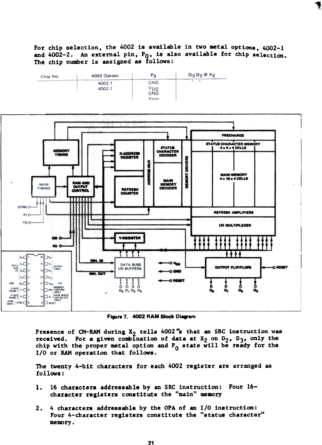
.,
For chip selection. the 4002 is available in two metal optiona, 4002-1
and 4002-2. An external pin. PO. is also available for chip selection.
The chip number is assigned as follows:
~ICHAAGI
. '-J
STAT\8 CHARACTER MIMORY
~ CI~ ~
ITATW
~ACTER
~R
M~Y
TIMING
,..-: X.ADOAE8
~EGI8TIR
MAIN .I~Y
..,...CELLS
MAIN
M~Y
~R
RAMAIC
0UTP\n
CX*T~
REFRE8f
~IR
~EF~IIM ~IFIEM
I~ MUioTIPLExaR
!~ t
~O--
Mo--'"
H Y~IGI8TIR
J .
. ...«If. --0
--0
--0
~ 'UP"L~ o~
"1 1 1 l'
0. 0. 0, 0,
Fi.,re 7. 4002 RAM Block Di...m
Presence of ~RAM during X2 tells 4002 ~8 that an SRC instruction was
received. For a given combination of data at X2 on D2- D3J only the
chip with the proper metal option and Po state will be ready for the
I/O or RAM operation that follows.
The twenty 4-bit characters for each 4002 register are arranged as
follCNs:
Four 16-
1. 16 characters addressable by an SRC instruction:
character registers con8titute the !'main" .mory
4 characters addressable by the OPA of an I/O in8truction:
Four 4-character registers constitute the "status character"
memry.
2.
21
v.
~
RI8T
Two separate X decoders switch between main and status characcer
memories.
When an I/O or RAM instruction is received by the CPU, the CPU
will activate one CH-RAM line during M2 ' in time for the 4002's
to receive the OPA (2nd part of the instruction), which will
specify the I/O or RAM operation to be performed. Shown below
is a list of the 15 possible I/O and RAM operations.
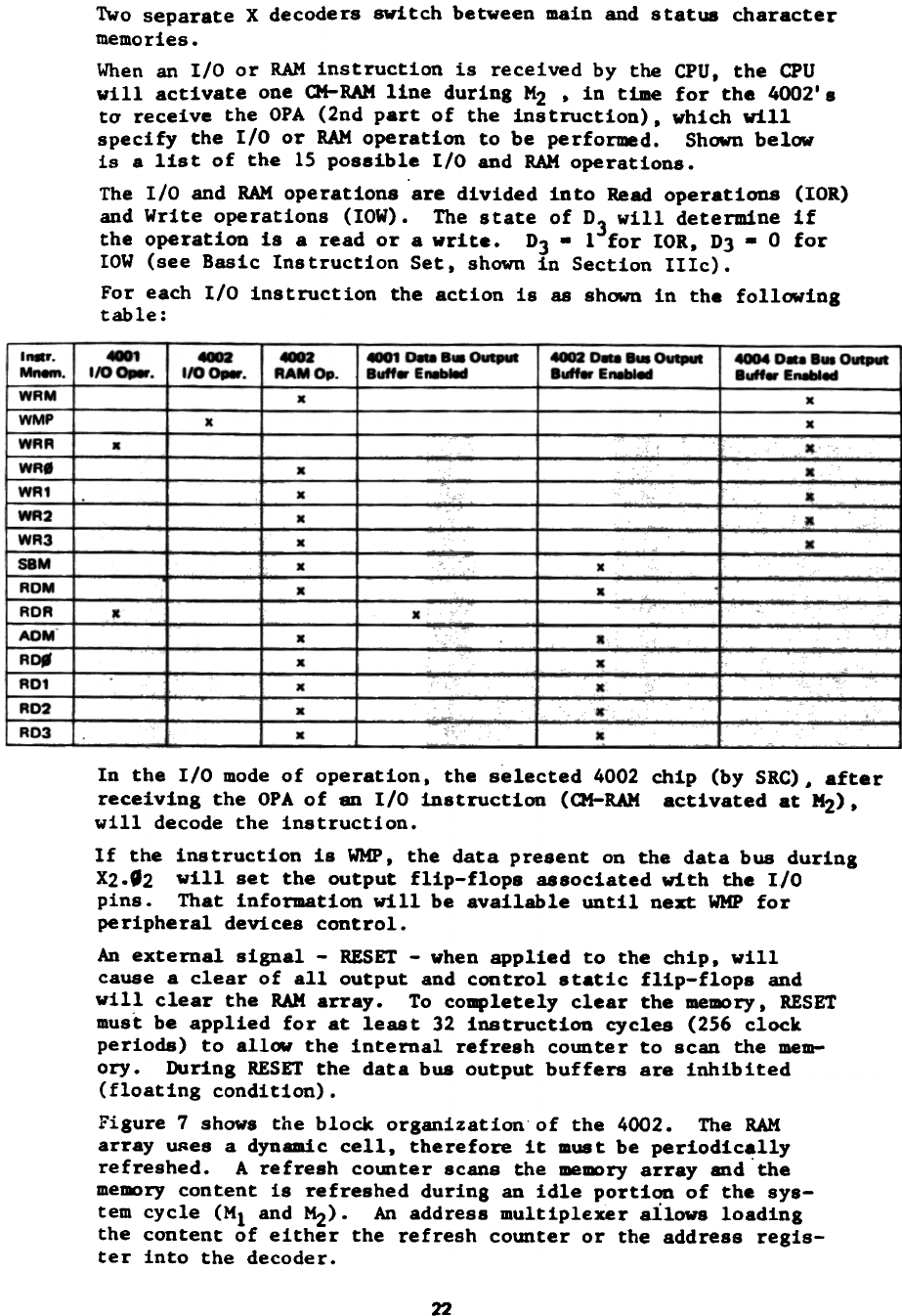
The I/O and RAM operations are divided into Read operations (lOR)
and Write operations (lOW). The state of DJ will determine if
the operation is a read or a write. DJ. 1 for lOR, DJ. 0 for
lOW (see Basic Instruction Set, shown in Section IIIc).
For each I/O instruction the action is 88 shown in the following
table:
~
RAM Op.
x
4001 0-. 8&8 Output
8uff.EMbled
11.cr. I ~ I 4m2
I ~., 11O0P8W. ~ 1100..
4002 Del. BI8 Dutput
Buff... Enebled
~ 0.. Bus Output
Buff.. En-..
r WRM
~
.
-
.
.
WAf
WA'
WR2
WA3 I
S8M
ADM
ADA
.
.
~
.
.
~
.
In the 1/0 mode of operation. the selected 4002 Chip (by SRC), after
receiving the OPA of an 1/0 instruction (CM-RAM activated at M2).
will decode the instruction.
If the instruction is WMP. the data present on the data bus during
x2.82 will set the outpu~ flip-flops aasociated with the 1/0
pins. That information will be available until next WMP for
peripheral devices control.
An external signal - RESET - when applied to the chiP. will
cause a clear of all output and control static flip-flops and
will clear the RAK array. To completely clear the memory. RESET
must be applied for at leaat 32 instruction cycles (256 clock
periods) to allow the internal refresh counter to scan the me~
ory. During RESET the data bus ou~put buffers are inhibited
(floating condition).
Figure 7 shows the block organization of the 4002. The RAM
array URes a dynamic cell. therefore it must be periodically
refreshed. A refresh counter scans the memory array and'the
memory content is refreshed during an idle portion of the sys-
tem cycle (HI and M2). An address multiplexer ailows loading
the content of either the refresh counter or the address regis-
ter into the decoder.
22
.
VI.
The RAM control is composed of an SRC flip-flop, chip selection
loaic, an instruction register, instruction decoder and I/O con-
trollogic. This block controls the loading of the addres8
register, the status and main memory decoder switching, the gen-
eration of memory timing, the enable of the data bus input-output
buffers, the RAM read/write operations, and the loading of the
output flip-flops.
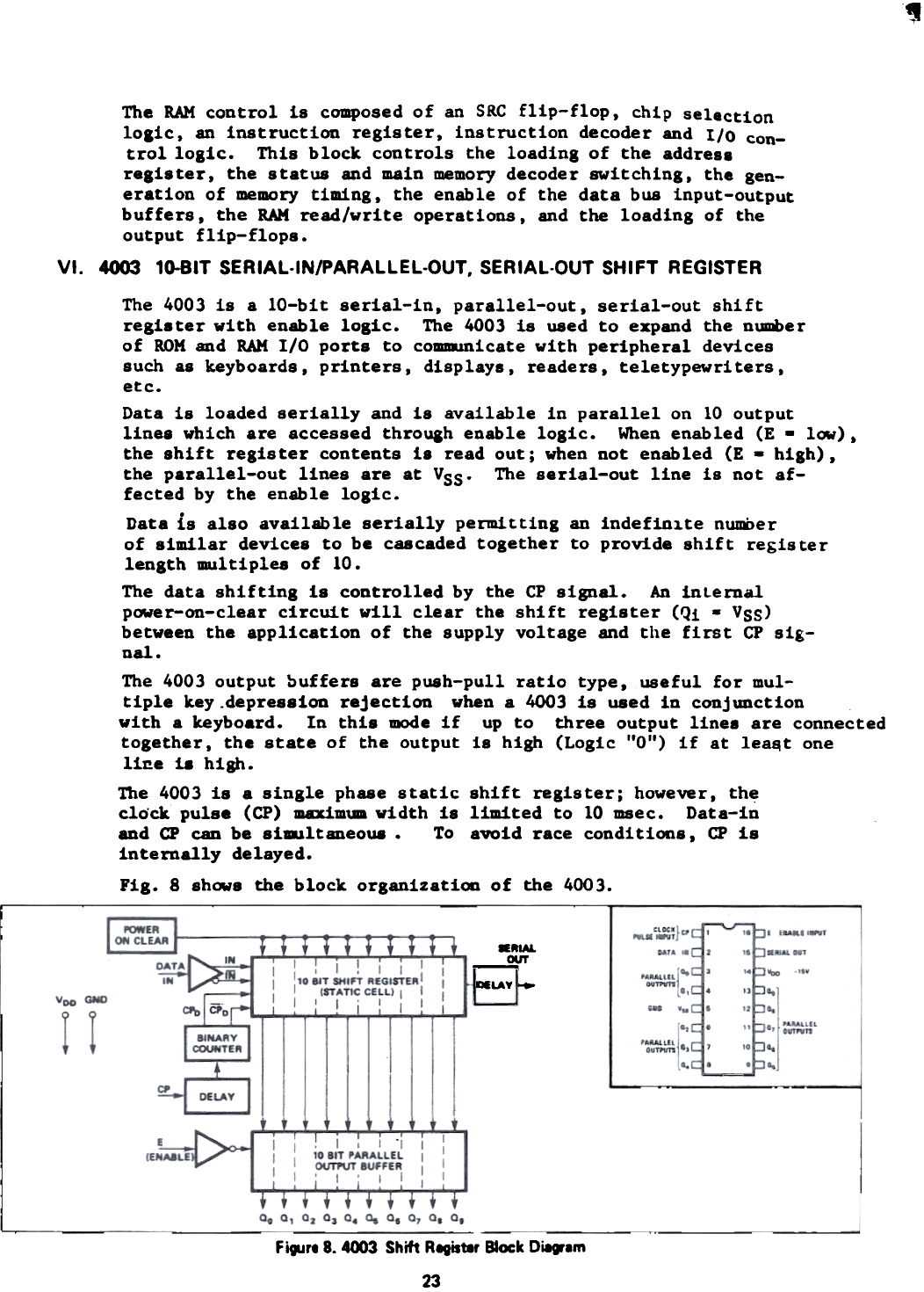
4003 1o-BIT SERIAL.IN/PARALLEL.OUT. SERIAL-OUT SHIFT REGISTER
The 4003 is a 10-bit serial-in, parallel-out, serial-out shift
register with enable logic. The 4003 is used to expand the number
of ROM and RAM I/O ports to communicate with peripheral devices
such as keyboards, printers, displays, readers, teletypewriters,
etc.
Data is loaded serially and is available in parallel on 10 output
line. which are accessed throuah enable logic. When enabled (E - low),
the shift register contents i8 read out; when not enabled (E - high),
the parallel-out lines are at VSS. The serial-out line is not af-
fected by the enable logic.
Data is also available serially permitting an indefin~te number
of similar device8 to be cascaded together to provide shift register
length multiples of 10.
The data shifting is controlled by the CP signal. An internal
power-on-clear circuit will clear the shift register (Qi . VSS)
between the application of the supply voltage and the first CP sig-
nal.
The 4003 output buffer8 are push-pull ratio type, useful for mul-
tiple key .depre88ion rejection when a 4003 is used in conjunction
with a keyboard. In thi8 mode if up to three output lines are connected
together, the state of the output Is high (Logic "0") if at lea~t one
1i!!.e 18 high.
The 4003 is a single phase static shift register; however, the
clock pulse (cp) ID8Xim\D width i8 limited to 10 msec. Data-in
and CP can be simultaneous. To avoid race condition8, CP is
internally delayed.
Fig. 8 show8 the block organization of the 4003.
_RIA&.
our
~
--LAY ~
F~r. 8.4003 Shift Register Block Di8gram
23
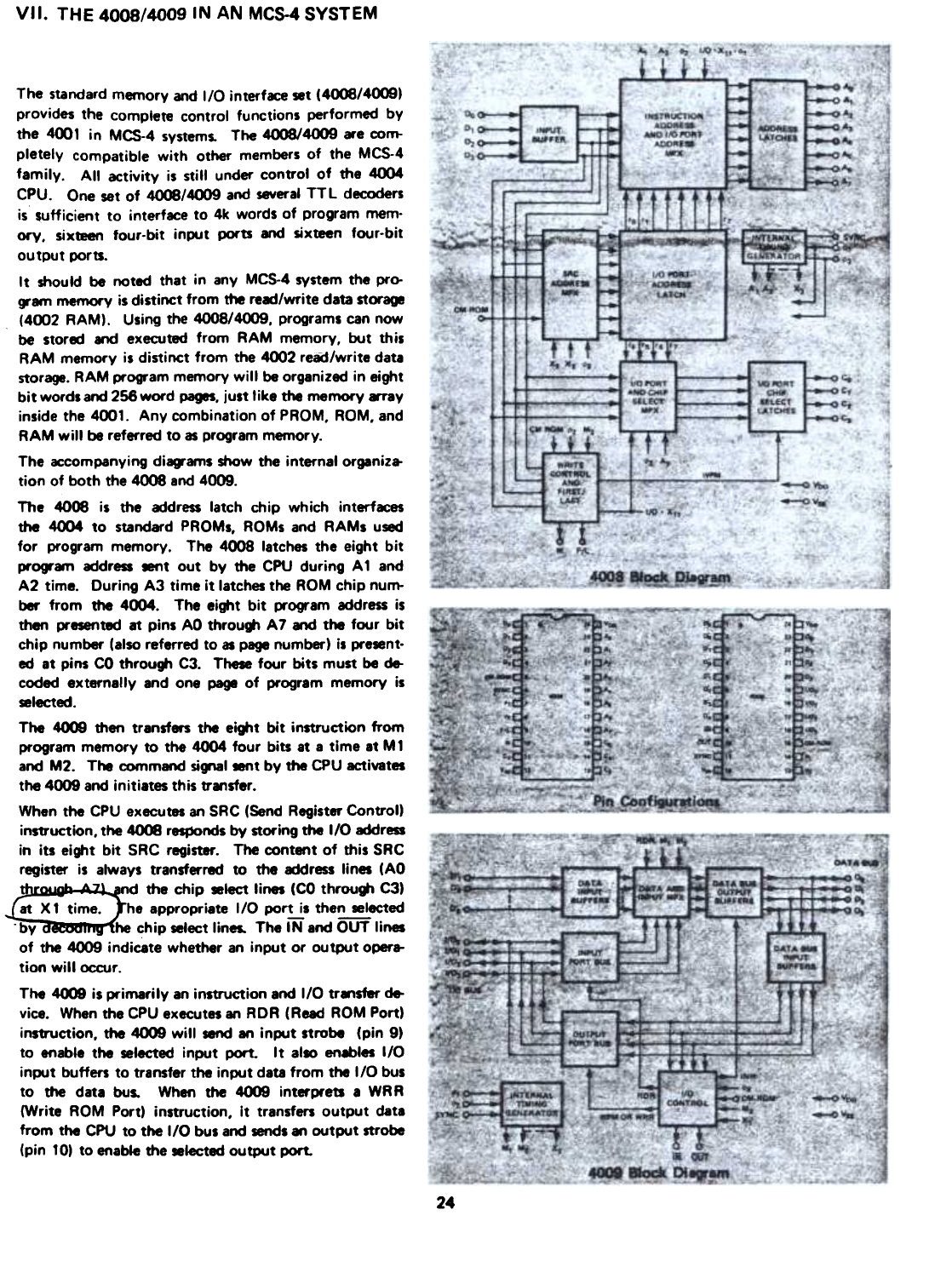
VII. THE 4008/4009 IN AN MCS-4 SYSTEM
The standard memory and I/O interf-=e set (4008/4()(m)
provides the complete control functions performed by
the 4001 in MCS-4 systems. The 4008/4009 are com-
pletely compatible with other members of the MCS-4
family. All activity is still under control of the 4004
CPU. One set of 4008/4009 and seYeral TTL decoders
is $ufficient to interface to 4k words of program mem-
ory, sixteen four-bit input ports and sixteen four-bit
output ports.
It should be noted that in any MCS-4 system the pro-
""am memory is distinct from the re.t/write data st~
(4002 RAM). Using the 4008/4009, programs can now
be stored and executed from RAM memory, but this
RAM memory is distinct from the 4002 read/write data
storage. RAM program memory will be organized in eight
bit words am 256 word pages, just like the memory 8Tay
inside the 4001. Any combination of PROM, ROM, and
RAM will be referred to as program memory.
The ~companying diagrams show the internal organiz.
tion of both the 4008 and 4009.
The 4008 is the address latch chip which interfaces
the 4004 to standard PROMs, ROMs and RAMs used
for program memory. The 4008 latches the eight bit
prO'#'~ address ..,t out by the CPU during A 1 and
A2 time. During A3 time it latches the ROM chip num-
ber from the 4004. The eight bit program address is
then presented at pins AO throu~ A 7 and the four bit
chip number (also referred to as page number) is pre.nt.
ed at pins CO throu~ C3. These four bits must be de-
coded externally and one page of program memory is
.Iected.
The 4CX» then transfers the ei~t bit instruction from
program memory to the 4004 four bits at a time at M 1
and M2. The command sipl ~t by the CPU activates
the 4009 and initiates this tr.,sfer.
When the CPU executes an SRC (Send Register Control)
instruction, the 4O(m responds by storing the 110 address
in its eight bit SRC register. The content of this SRC
register is always transferred to the address lines (AO
-! ~5iJd the chip .Iect lines (CO throu~ C3)
at X 1 time. he ~ppropria~ I/O POr!..!.s the~~ted
"by he chip .Iect lines. The IN and OUT lines
of the 4009 indicate whether an input or output oper.
tion will occur.
The 4CX» is primarily an instruction and I/O tr.,ster de-
vice. When the CPU executes an RDR (Read ROM Port)
instruction, the 4009 will 8nd an input strobe (pin 9)
to enable the .Iected input port. It aim en8bles I/O
input buffers to transfer the input data from the I/O bus
to the data bus. When the 4CX» interprets a WR R
(Write ROM Port) instruction, it transfers output data
from the CPU to the I/O bus and .oos ., output strobe
(pin 10) to enable the .lected output port.
24
..
A formerly undefined instruction is now used in conjunction with the 4008/4009 to write data into the RAM progr~ memory.
This new instruction is ~11ed WPM (Write Program Memory - 111000111. When an inStruCtion is to be stored in RAM
program memory, it is written in two four.bit segments. The F/L signal from the 4008 keeps track of which half is being
written. When the CPU executes a WPM instruction, the chip select lines of the 4~ are jammed with "1111". In the system
design this should be designated as the RAM channel. The W line"on the 4008 is also activated by the WPM instruction.
The previously .lected SRC address on line AO through A7 of the 4~ becomes the address of the RAM word being
written. By appropriately decoding the chip select lines, the W line, and F/l, the write strobes can be generated for the memory,
The F/L line is initially high when power comes on. It then pulses low when every ~nd WPM is executed. A high on the
F/L line means that, the first four bits are being written, and a low means that the last four bits are being written. The 4009
transfers the segment of the instruction to the I/O bus at X2 of the WPM instruction. The SRC address sent to RAM is only
8 bits. When more than one page of RAM (256 bytes) is being written, an output port must be used to supply additional
address lines for higher order addr~.
Definition of Write Propam Memory Instruction
Mnemonic: WPM Description: The chip select lines of the 4008 are forced to "1111"
OPA OPA: 11100011 at X1 time and the content of the -=cumulator is available on the
Symbolic: 4009 110 bus at X2. AAM prQ9'am memory can be loaded four
1111 C3C2C, Co of ~ bits at a time. The previous SAC address is .nt out on lines AO
ACC ""'1/031/~ 1/0,1/00 of 4009 through A7 of 4008.
SAC Address --- Ao - A7 of 4008
System Illustrations Using the 4008 8Id 4009
Four systems are shown where the MCS-4 components are used with standard Intel memory elements as the program memory.
Notice that several different approaches to chip .Iect. port decoding, and the 110 elements are shown.
Ex.",p'- 1: Four 17O2A PROM..,d Four 110 PtN'1a. Four 1702AI are u8d for program Itorage and four four.bit I/O ports
are used. In this caR D.type output latches are used and a one of eight decoder (3205) Is u8d to decode both the input and
output strobes. Note that the I/O bul is buffered from the outpJtI. Buffen are needed only when the current sinking requi~
ment on the bus exceeds 1.6mA. In small systems low power TTL could be used and buffers could be avoided.
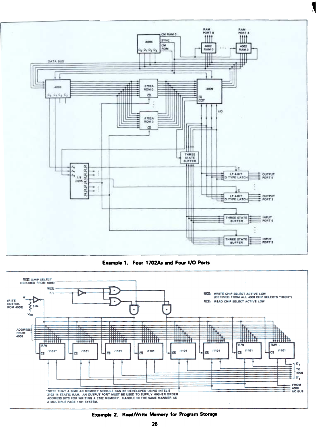
~xample 2: ReadtWrir. Memory for Pro,am Sror..
This example shows only the RAM portion of a system when RAM is used for program memory. Note that the chip selects
are tied t~ther in ,#,oups of four. The chip alects are gated with the F/L control line for writing only four bits at a time
.when executing a WPM instruction. They.e also gated with the decoding of the chip selects from the 4008 for normal program
execution. The 1101 1256 words x 1 bit) is shown. A similar system using the 2102 (1k words x 1 bit) could be dewloped.
Ex~p" 3: Se.." 17O2A PROMs, one RAM block, .,d..,." I/O Ports.
This example uses a single P9 of RAM program memory shown in Example 2 in a complete system. In this case the input
ports .e 8: 1 muhipiexes which are buffered from the I/O bul by a quad three state buffer. The input port sefection is then
the function of the multiplexers. The outpl.it ports are Intel 3404 latches and the port selection is done using an Intel
3205 decoder.
Example 4: EifIJt 1702A PROM" eigflt RAM Slocks, ."d eilht I/O Ports.
Pro".8m memory ~ized with 2k bytes in ROM m 2k bytes in RAM. EKh basic RAM block C8\ be organized - in Ex8nple
2. When more than one block of RAM is u~. the write chip select (WCS) for each RAM block is generated by properly
gating chip .I~t 15 with special decoding for P9 alection. Output port eight is dedicated to this _Iection function. This II
only necessary when the RAM prO9'am memory is being written. In this example standard TTL logic elements... used for
I/O port alection rather than decoders - shown in previous ex.nples. In this case all input portS are three state buffers.
IMPORTANT:
The followi", dlff ,.;. .xilt be~ ., MCS..f IYIMm urillf 4001 ~ nIenIOrY .nd . 'Y""" uI/"f 4«1B/4/D P'o,¥II /rI8mOI'Y.
,. FM normel oper8tbt, 4001 }tOMs --' be ~ In the ..,. ~ with ~/4009.
2. M-V MId~, memory d_, I/O~. Ind mntrollmer from both 4008 ~ 4(D ... defin.t with respect to potitiw logic. The Mcs.4 d..
8wJ comrolll~ from the 4004 ... defi- with ~ to neg8tiw logic. AI. r8JIt, in prQ9'lm memory used with the 4(D. pr~.1tIouIcI
be co-.wlttliogic "1" - hl~ '-I ~.. "0" -low '-I (i..., HOP - CDX)CDX) - NNNN NNNNI. Notethet prc.-8nI_"-1rI.t fa'
the 4001 In t8r1nS of negetiw logic ~ th8t NOP - CDX) CDX) - pppp PPPP. C8r8fully check all tapes .,bmittad fM metal m" ROMI to be
-- th8t the corrKt logic detklltl- - u8t.
3. I"""t"" ~tPlt d8t8 from the 4«» 1/0 ~ is d8fi- in -- of poIitiV8logic. If t'- interf- devi~ - u* fM prototyping . 4001
Pl'C9'8n m8n1a'Y, c.-eltlould be tMIn to be.,.. th.t the I/O ports fM the 40011... defin.t conlistant with the 4008/4(8 syItam.
4. An I/O ~ _i818d with the 4009 can ~ Ii,. with both input ~ OUtput c8P8bitity. On the 4001 88d\ I/O line may ~ only .Ii'"
function, 811'- i"tlUt or ~tIMIf.
5. The RAM prc.-.m memory cannot be u* - . .,bltitut. for the 4002 mdt-it. data ltor.. They ~orm distinctly d~t functioN.
8. CM-ROM ~ CM-RAMO --' be u8t to control GJ2I ~ CM-ROM il ~ fa' 4Ca/4008 ~ the WPM irwtNctlon il b8inI U-S. The
~ Is th8t the WPM Inl1ructlon II interpretad -. Writ. M-V (WRMI by 40021 connectad to the -- CM line - 4CXI8/4008.
CM.RAMo in ~ of. DCL b8f\8V818Xactly like CM-ROM.
25
,
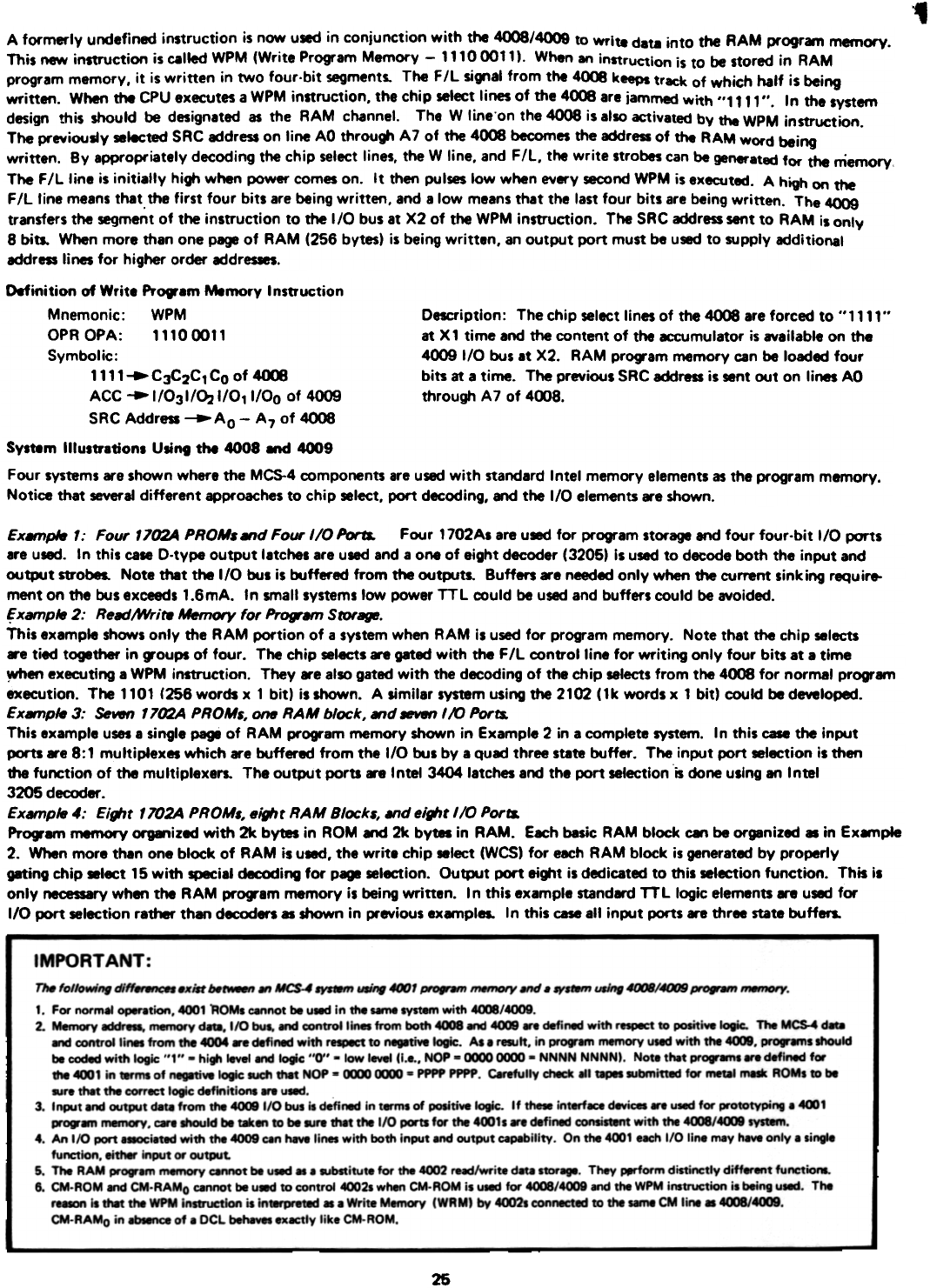
Eumple 1. Four 1102As - Four 1/0 Po.1I
Eump'- 2. Re./Write MemofY for Pro.--"' Stor.
26
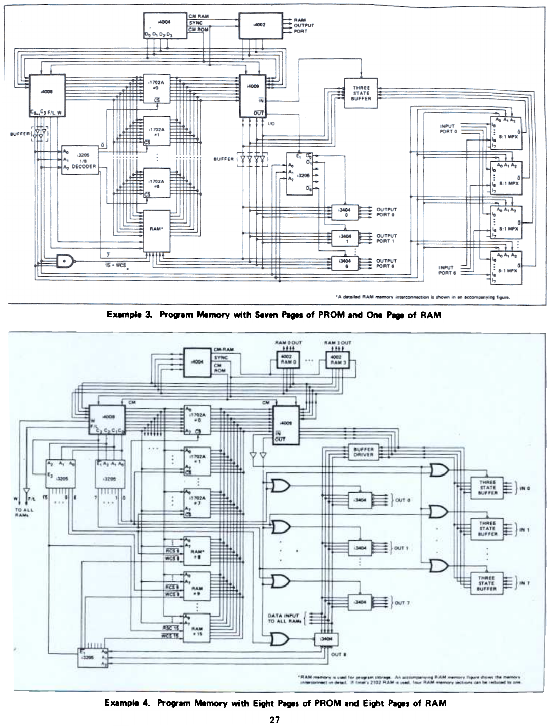
Eumple 3. PrOW8m Memory with Seven P8g8t of PROM 8nd One p. of RAM
Example 4. Pro".m Memory with Ei9ht P8geS of PROM .rId Eight P.~s of RAM
27
.~~ .
DETAILED INSTRUCTION REPERTOIRE OF THE MCS-4
VIII.
A. Instruction Format
As previously discussed, the MCS-4 micro computer set has two types
of instruction.
a) 1 word instruction with an 8-bit code and an execution time of
10.8 psec.
b) 2 word instruction with. 16-bit code and an execution time of
21.6 pa8C.
Due to the time multiplexed operation of the system, the 8-bit in-
struction 18 fetChed 4-bit. at a time on two successive clock periods.
The first 4-bit code i. called CPR, the second 4-bit code is called
CPA.
The instruction formats were illustrated in Tables I and II
B. Symbols and Abbreviations
The following SyDbol8 and abbreviations will be used thorughout the
next few sections:
( ) the content of
i8 transferred to
ACC Accumulator (4-bit)
CY Carry /link Flip-Flop
ACBR Accumulator Buffer Register (4-bit)
RRRR Index regi8ter addres8
RRR Index regia ter pair addres8
~ Low order program counter Field (4-bit)
~ Middle order prosram counter Field (4-bit)
PH High order progr.. counter Field (4-bit)
ai Order i content of the accumulator
CHi Order i content of the command register
M RAM main character location
~i RAM statua character i
DI (T) Data bus content at time T
Stack The 3 register8 in the address register other than
the program counter.
Throughout the text "pase" _ana a block. of 256 instructions whose ad-
dre8s differs only on the most 8ignificant 4 bits (all of the instruc-
tiona on one page are all stored in one ROM).
Example: page 7 means all locations having addresses between
0111 0000 0000 and 0111 1111 1111
28
..:'~
c. Format for Describing Each Instruction
Each iD8truct100 v111 b. de.cr1b.d .. follow.:
(1) ~_ic ."01 _d --in.
(2) OP" _d OPA cod.
(3) S,.olic repr..eotatiOD of the iD8tractiOD
(4) Deacript100 of the iD8truCtiOD (if n.ce..ery)
(5) ~le aDd/or excapt1oD8 (if nec..aery)
D. One Word Mad1ine Instructions
!t1_ic: NOP (No Operation)
on orA: 0000 0000
S,.oUc: Moc, ..,Uc81.
D88cri,c,I_a .. ...~18 ,.I'f.~.
MD88ODie: L~ (Load Data to AeCU8lator)
on OPAl 1101 DDOO
S,.olie: DODD .-. ACC
Deeeripti_: The 4 bit. of data. DODD atorecl iD the OPA fielcl of
iD8trueti~ vorcl are loaclecl iDto the ae~tor. The
previ0U8 e-teDt. of the aeCU8lator are loat. The
eury/liDk bit 18 unaffeetecl.
HD88ODic: LD (L084 indez re.i8ter to AccU8Ulator)
OPI. OPAl 1010 DB
S,.olic: (DB)--ACC
ne8criptiOD: The 4 bi~ coot8Dt of tbe da8iaaated indaz reliater (l.1l.I.)
18 loedecl into the ac~~or. The prerlo.- CODt8Dt8
of the accU8Ulator are loet. The 4 bit CODt8Dt of the
indaz reliater ad the carry/11IIk bit are IlDaffected.
MD_icl XCH (bch-.e index re.18ter cd acc\8lator)
opa OPAl 1011 IDa
S,-ol1c: (ACC>- ACU. (1Da>-- ACC. (ACBR)~ IDa
Deacriptioa: The 4 bit coat8Dt of the d..ilD&ted ind.. re.18ter 18
lo8d8d into the ac~ator. The prior coat_t of the
ac~ator 18 loaded into the de.ilDated re.18ter. The
carry/liDk bit 18 UDaffected.
*_ic: ADD (Add iDdu rep.ter to acc~ator with carry)
OPI. OPA: 1000 UI.I.
Sy8olic: (DII.) + (ACC) + (Cf) ~ ACC, Cf
ne.criptioo: The 4 bit coot8Dt of the de.ilDated iDdcz rel18ter i.
ad4ed to the ~teat of the 8C~ator with carry.
The re.lIlt 18 .tored iD the ac~ator. The carry/liDk
i. .et to 1 if a .ua ar..ter th8D 1S10 ... leDerated to
iDclicate a carry out; ot.he~e, the carry/liDk ia .et
to O. The 4 bit coateat of the iDdcz reliater 18 UD-
affected.
~
(DU)
I
~l.: Aua~
(ACC)
'"
(cr)
a3 a2 al ao
co +-_J
+) r) r2 rl ro ~
CADI - C4 83 82 81 ~ - StD(
<i,> L~~
29
.
HD88DDic: 5lnI (Subtract iDdex rea18ter fro. acCU8Ulator with
borr~)
on orA: 1001 lID
Sy8o1ic: (ACC) + (IDK) + ('ct") - ACC, CY
DescriptiOD: The 4 bit content of the de8ilnated iDdex relister is
cO8ple8ented (on.. ca8pl888Dt) 8Dd added to CODtCDt of
the ac~tor with bo~ _d the r..u1t 18 stored iD
the ac~tor. If a borr~ 18 geDerated, the carry
bit i8 set to 0; othervi.e, it 18 set to 1. The 4 bit
coatCDt of the 1Dd8z rea18ter 18 unaffected.
~l.: Subtr8bend
(RID.)
HiD_d
(ACC) (cr)
a3f2 al~ ~
+) r3 r2 rl "io
Io~ ~ 83 82 81 eo 4- "'u1t
.. ,- -- '
(Cf) (ACC)
MDe.onic: INN: (InCr888Dt 1D4ex resister)
OPI. OrA: 0110 un
S}8Iolic: (UD) +1 -.DD.
DeacriptiOD: The 4 bit coateDt of the deailD&ted indez reai8ter i.
inCr888Dted by 1. The index rea1eter i. .et to .ero
in c..e of overflow. The cerry/ltDk 18 unaffected.
~c: 88L (Brach back 8Dcl 1084 data to the ac~tor)
on orA: 1100 DODD
S,.bolic: (Stack)---J Pt- ~- PH; DODD ~ ACC
Deacr1pti_: The proar- CO18ter(addr... .tack)18 pU8bed dOIfD _e
level. Proar" c_trol tr8D8fer. to the D8Kt iD.tructiOD
foUov1Dl the lut j~ to .ubroutiD8 (J1tS) iD8tructi_.
The 4 b1t8 of data DODD .tored iD tb8 CWA porti-
of the iDatruct1- are loaded to tha accU8Ulator.
IBL 18 U8ed to retum f~ 81IbrwtiD8 to ~ proar...
~ic: JIN (J~ 1D~ct)
on. OPA: 0011 ID1
Sy8Iolic: (010) -. PM
(.u.l) -. 'L; PH _cb-.ecI
De8criptiaa: Tbe 8 bit caoteot of the d88i8Beteci 1DdcK rea18ter pair
i8 loedad into the low order 8 po.iti0D8 of the proar"
COIater. hoar- ~trol 18 treafea- to the 1D8true-
tiaa at thet addra. ~ the .- p... (.- I(J() where the JIB
1D8truCtiOD 18 loceted. The 8 bit CODteDt of the indcK
rel18ter 18 lmaffectecl.
Wbeo JIB t. located at the addr... (Pa) 1111 1111 pro-
ar- _trol t. tr..ferred to the D8Zt pq8 in nq_ce
_d Dot to the .- p... where the Jm iD8trvctiOD 1.
locat.d. That i., the Dazt addr... 1. (Pa + 1) (KIlO)
(1Dl) _d Dot (PH) (u..Q) (01.1)
1IC8P'rtC8:
__ic: SAC (Send reai8tu ~t.rol)
on OPA: 0010 IDl
Syllbolic: (010)-.- DB (Xv
(1Dl)-. DB (%y
Descript.i_: The 8 bit. ~t.-t. of t.be deei.-t.ed iAdez re&i8t.er pair
is S8Dt. t.o t.be lAM address relist.er at. X2 and X3' A
subseq-t. reacl. vr1t.e. or I/O operat.i- of t.be UK will
ut.1l1.e t.b18 address. Specifically, t.be f1rat. 2 b1t.s of
t.be address dee1lDat.e a aAH chip; t.be secODd 2 bit.a d..il-
nat.e 1 out. of 4 reliet.era wit.biA t.be chip; t.be laat. 4 bit.a
deai.-t.e 1 out. of 16 4-bit. ~ -1'1 ch-act.ar8 rit.biA
t.ba re.18t.er. Th18 c~d 18 8180 used t.o des1.-t.e .
ROM for a sUbseq~t ROM I/O port. op.rat.~_. The firat.
4 bit.a dee1.-t.e f.h8 ROM chip n,.ar t.o be s8lect.ed. The
addr..s iA ~ or UK 18 not. cleared _t.i1 t.be nest. s.c
iD8t.ruCt.iOD 18 uecut.ed. The 8 bit. CODt_t. of the, iAdex
reli8t.er is _affected.
30
~..,
~c: FIN (I'etcb 1D41rect f~ ->
on. orA: 0011 om
SY8bolicl (Pa) (0000) (0001) --. 10M addre..
(On.) - ~
(OlA) --91U1
D88criptioa: The 8 bit coateDt of the 0 index rel18ter pair (0000)
(0001) i. .eDt out .. 8D addre.. in the paae
where the FII 1D8tructioa i. located. The 8 bit word
at that locati~ u loaded into the d88ilDated in~
relute~ pair. The proar" COUDte~ 18 uaaffected; after
FII b.. beeD executed the next in.truction in .equence
vi1l be addr...ed. The conteDt of the 0 indez reli.ter
pair i. UDaltered UDl... indez re.uter 0 v.. d..ignated
UClPrII-. : a) Althouih FII 1a a 1-word ~truct1OD. ita ezecut1oa
requ1r.. two ..-ory cycle. (21.6 paec).
b) Wb8a FIB 18 located at a4dre.. (Pa) 1111 1111 4ata
will be fetched f~ the Dezt pqe (1mI) in .equence and
Dot f~ the pa.. (ao.o wh.re the FIR inetruct1oc 18
loc.ted. That 18. Dezt addre.. 1. (PH + 1) (0000)
(0001) and DOt (Pa) (0000) (0001).
E. Two Word Mdine Instruction
HD88ODic: JUN (JU8p unconditional)
l.t word on OPAl 0100 AJ AJ AJ AJ
2nd word on OPA: A2 A2 A2 A2 Al Al Al Al
S,.ol1c: Al Al Al Al --+Pt. A2 A2 A2 A2 -+PK. AJ AJ AJ AJ""" Pg
Deacription: Prolr.. control i. UDcoaditioaally traD8f.rred to the
1D8truction locater .t the addu.. AJ AJ AJ AJ. A2 A2 A2 A2.
Al Al Al AI-
~88ODic: JMS (JU8p ~o SubroutiDe)
18~ word OpR OPA: 0101 A] A] A] A]
2Dd word OpR OPA: A2 A2 A2 A2 Al Al Al
SY8bolic: (PH. PM. Pt + 2~Stack
Al Al Al Al - PL. A2 A2 A2 A2 -. PM.
A3 A3 A3 A] -+ PI
D88crlp~i_: 'nIe eddrea8 of the next. 1D8truc~i- iD 8equence foll~iDa
JNB (r8turD addr888) i8 88Ved iD the puah do.n st8ck.
P1'OI1'- control 18 traaferred to the 1D8tructi- located
at the 12 bit eddr"8 (AJAJA~JA2A2A~IA1A1AV. EaaCD-
ti- of a nt1lZD 1D8tructl- (IlL) will ~e the 8.-4
addre88 ~o be p~ed out of the 8tack. therefore. prolr..
c_trol 18 tr_ferred to the nest 8~t1al 1D8t1'UctiOD
after the l..t JNB.
'nIe p.-h do.n 8tack h.. 4 rel18ten. One of th- 18 \8ec1
.. the P1'Ol1'- COUD~er. therefore n..tiDa of JHS CaD occur
up to 3 1.-18.
~: Suck ~ Stack
RoJ18
nce1.-d -a. --. JIG 11
recelY8d
~
hoar- Co1mt..r
I.. t.1IZB -.r- , 1
Stack Stack
I Pr°lr- C_ter
1- - -
Ilat.1lZB ~ 13
I Proir- COImtu
I lat:ara ~ #2
-. J1tI 13
received
-+ JIm 12
"cd'" -. ~-.
lletum 8ddr... 12
, "tuzn addr... '1 I latum 8cldr... , 1
Stack
"tun 8ddr... ,.
I latum addr... ..,
.nm ,.
nee1v-'
-. IlL
-+ received
18t:UZD 8ddr... 12
rroar- Co8tu
'rb8 --_to r8toUrft add.-. f. t_..
31
*_1c: .K:N (J~ Caliit1CXi&l)
l.t word ora OPA: 0001 CICZC3C4
2nd word opa OPAl AZAZA2A2 AIAIAIAl
Sy8bolic: If CICZC3C4 1. t~, A2AZA2AZ --. PM
AIAIAIAI -. PL' PH unch8Dled
if CICZC3C4 1. f&18e,
(Pa) -t PH, ('K) -+ PM' (PL + Z)-. PL
De.criptiOD: If the duilDated cODAi1ti~ code 1. true, proar- ~tzo1
1. tr~ferTed to the ia8truct1~ locate' at the 8 bit
addre.. AZAZAZAZ' AIAIAIAl OD the PAle (ROM) where JC8 i.
located.
If the CODd1t1~ 18 Dot true the nest ia8truct1~ in
.eqU8Dce after JCN 18 ezecuted.
The ~d1t1~ b1t8 are ...iped .. fo11-.:
Cl . 0 Do Dot invert jU8p c~dit1OD
Cl . 1 Invert ju.p c~d1tiOD
Cz . 1 Ju.p if the ac~tor c~t_t 1. aero
C3 . 1 JU8p 1f the carry'link CODteDt 1. 1
C4 . 1 Ju.p if te.t .1IDal (pin 10 OD 4004) 1. zero.
~le: ~ 9!.!.
0001 0110 Ju.p 1f accU8Ulator 1. zero or carry . 1
S...r~ cond1t10ft8 CaD be tested e18ut8De0u81y.
The loaJ.c equat1OD ducr1b1a, the coodit1OD for a
jU8p 18 1198 belaw:
J1JHP . C1 . «ACC . 0) . C2 + (Cf . 1) . C3 + "TiiT . C4) +
Cl . «~ - 0) .-Cz+ (cr--;-l) . C3 + m! . C4)
aCIP'rI~ s If JCR i. located OD word. 254 and 255 of a 10M pale.
wben JCR 18 .-cuted and the coDditi- 18 true. prolr-
control 18 traaaferred to the 8-bit addr... on the next
PAle where Ja 18 located.
HD88Inic: ISZ (Iocr_at. indo rep.t.er .kip if .8ro)
lat. word on OPAl 0111 lIaR
2ac1 word on CWA: A.,~~ ~~A,A,
Sy8bol1c: {bIIJ + 1 -'11111. if r..ult. . 0
(PH) -. PH. (PM) --. PH. (~+ 2) -. PL I
if 1'88ul t. ~ 0 (Pa) PH.
A2A2A2A2..,.PM. AlAlAlAl-t PL
Deacript.ioal The coat.eat. of t.he cleai.-r.ed iDcIa re.18t.er 18 iDcr_t.ed
by 1. The accU8Ulat.or 804 carry/liDk are unaffect.ed.
If t.he re.ult. i8 .ero. the next. 1D8t.1'\Ictioa aft.er ISZ i.
--cut If the r..ult. 18 differ_t. fr~ O. pr°81'- cciDt.rol
18 tr8D8fe1'1'ed to the iDat.ructioa locat.ed at. t.he 8 bit.
acldre.. A,zAzA,zA,2. AlAlAlAl oa the .-- Pale (1(»1) where
the ISZ 1D8cructioa i. locat.ed.
Uc&PT1~S : If ISZ 18 locat.d on vorde 254 end 255 of a 10M pea.. wheD
ISZ 18 executed end the r..ulc 18 DOt ..ro. proar.. ooatrol
18 cr8D8f.rred Co cbe 8-bit eddr... located OR the D8Zt
p.,. iD ..qU8DC. end Dot on the p.,. where ISZ i.
located.
MD88oaic: FIM (retched 188ediate tr08 IOMO
!at word on CWA: OOlD ...
2nd word on orA: D2D202D2 D10101D1
S,.bo1ic: 02020202 ~ RRIO
01010101 .., u..l
Oeacription: The 2nd word repr-..nt. 8-bit. of data which are loaded
into the d..ianatad index rel18ter pair.
32
.,
F. Input/Output and RAM Instructions
(The RAM's and ROK's operated on in the I/O and RAN iD8tructi0D8 have
been previously selected by the last SIC iuatruction «Kecuted.)
~~nic: ADM (Read RAM character)
OPR OPA: 1110 1001
Sya,ol1c : (M) -+ ACC
Description: The cooteat of the previ0U8ly selected RAM ..in -..cry
character i. tr8D8ferred to the acc~tor. The carry/link
i. unaffected. The 4-bit data in memory 18 uoaffected.
Mne8DDic: RtN> (Read RAM statu. character 0)
ora orA: 1110 1100
Symollc: (Kso) ACC
Deacriptioa: The 4-bit. of statue character 0 for the prcv1oualy .elected
RAM regi8ter are transferred to the accU8Ulator. The
carry/link and the statue character are unaffected.
~~1c:
-OPI. OPAl
Sy8olic:
RD1 (lead RAM atatua character 1)
1110 1101
<Hsv - ACC
lt1_ic:
OPR OrA:
S,-olic:
RD2 (I.- lAM 8tatua characer 2)
1110 1110
<Ms2) -+ ACC
Im~ic:
OPI. OPA:
Sy8o1ic:
RD3 (lead RAM 8tatue character 3)
1110 1111
CKs3) -. ACC
~~ic:
OPI. OPA:
Symbolic:
Deacr1pt1OD:
EXAMPLE :
ADA (Read RC»t port)
1110 1010
(IOK input linea) --. ACC
The data present at the input lines of the previously
.elected 10M chip 18 tr8D8ferred to the accU8Ulator. The
carry/link i. unaffected.
If the I/O option h.. both input. aDd outputs within the 4 I/O lines, the U8er cm chOO8e to have either "0" or
"1" traoeferred to the .c~ator for thoee I/O pins
coded.. output., when 8D IDa instru~tiOD 18 ezecuted.
Given a 4001 with I/O coded with 2 inputa aDd 2 outputs,
when IDa 18 ~cuted the tr-.fer i. .. shown bel_:
1302
1 X
,
Input ~
(ACC)
1 (1 or 0) (1 or 0)
~ ~
U..r ca choo..
~~lc:
on orA:
Syeollc:
De8crlptl-
WRM (Writ. acc~tor into RAM character)
1110 0000
(ACC) -+ "
111. acc~ator contat 18 written into the prerto~ly
selected RAM 88iD 888Ory character locat~oa. l11e aceu-
8Ilator ad carry/link. are \maffected.
~e8)Dic: WAC (Write acc-utor into UK atatua character 0)
OPI. OrA: 1110 0100
Syllilol1c: (ACC) -+ Kso
Deacr1pt1oa: The coat8Dt of the accU8Ulator 1. vr1ttea into the IAK
.tatua character 0 of the prev1oua1y .elected UK register.
The accU8Ulator 8Dd the carry/link are uaaffected.
}t1~1c :
orR OrA:
Sy8o11c:
WR1 (Write accU8Ulator into lAM status character 1)
1110 0101
(ACC) -to "Sl
33
0110
x 0
1
; Data
.-,
WR2 (Writa ac~tor into lAM 8Utua chAracter 2)
1110 0110
(ACC) -. Hs2
!m~ic:
on orA:
Sy8o1ic:
WR3 (Writ. acc\8ll&tor iDto lAM .tat\18 character 3)
1110 0111
(ACC) -+ Hs3
~_ic:
OPI. OPA:
Sy8lolic:
}tn_ic: WAR (Write - port)
OPR OPAl 1110 0010
SySolic: (ACC) -. laM output liD..
DescriptiOD: The CODt_t of the acc\8&letor 18 trmaferred to the 10M
output port of the pr.v10U8ly selected ION chip. The data
18 available OD the output p1D8 _tll a n- WU is executed
OD the -- chip. l11e ACC conteot _d carry/l1Dk are --
affected. (l11e LSB bit of the acCU8Ulator appear. OD 1/00,
pin 16, of th. 4001). No oper.tion 18 perfor88d OD I/O
line- coded.. input..
Mn.-mic: WMP (Write -ry port)
OPt. OPA: 1110 0001
Sy8bolic: (ACC) --t I.AM output re.18ter
De8cripti=:: The CODt8Dt of the acc~ator 18 tt..ferred to the RAM
output port of the previoualy ..lected RAM chip. The data
18 aveliele OD the output piu atil e ow aG' i8 executed
OD the .- lAX chip. 'lb. ~t8Dt of th. ACC end the
carry/link are UDaffect.d. ('lb. LS. bit of th. accU8Ultor
appears OD 00. Pin 16. of the 4002.)
*_ic: ADM (Add f~ -ry rith CarI'}')
OPJ. OPA: Ilia 1011
Symolic: 01) + (ACC) + (CY) -+ ACt. CY
Description: The coot-t of the pr8Vi0U81y .elected .. ~ ~ry
character i. added to the ac~.tor with carry. The
RAH character 18 \maffected.
Im_ic: S8M (Subt.ract. fr~ -ry wit.b borr~)
OPI. alA: 1110 1000
Syeo1ic: 00 + (ACC) + ('a'") ACC. ct
De.criptioo: The coot.~t. of the pr.n0U81,. .elect." BAK character 18
aubt.ract.e4 fr~ t.be acc-.1at.or wit.b borr~. The BAK
charact.er 18 UD.tfect.H.
G. Accumulator Group Instructions
HD_ic: CLB (Clear both)
OP" OPA: llll 0000
Symbolic: 0 --. ACC, 0 --. CY
Deacripti~: Set acc18llator _d carry/11Dk to 0,
~~c: CLC (Clear cury)
on OPA: 1111 0001
Sy8o11c: 0 -. Cf
Ducr1pt~: Set cury/liDk to 0
~~c: CMC (~l~t carry)
on orA: 1111 0011
SyJlbolic: ('cy") -+ cr
~cr1pt1~: The carry/liDk c~t_t 18 c~l_te4
Ita_Ie: STC (Set cany)
On. OrA: 1111 1010
Sy8o1Ie: 1 -to cr
~erlptIOD: Set cany/1iDk to . 1
Mnemonic: CMA (Co8p1e88Dt AccU8Ulator)
OPI. OrA: 1111 0100
Sy8olic: aJ;2a1'80 -f' ACC
De8criptioa: Tba coat8Dt of the acCU8Ulator 18 c08p1e88Dted. The
carry /1 iDk 18 UD.af f e c t ecI.
34
Hne8ODic: lAC (Incr88eRt accu.ulator)
on OPA: 1111 0010
Syllbolic: (ACC) + 1 -i' ACC
Description: The c~t-t of the acc18llator 18 iDcr--ted by 1. No
overflow set. the C8rry 11ink to 0; overflow .et. the
C8rry/l~ to . 1.
._1c: DAC (dea_t ac~.tor)
OPB. OrA: 1111 1000
Sy8bo11c: (ACC) - 1 -to ACC
Descr1pt1OD: The CODt8Dt of the .C~tor 1s decremeoted by 1. A
borrow sets the carry 11iDk to 0; no borrow ssts the
carry 11iDk to . 1.
IIAHPL! : (ACt)
i
&3 &2 81 ao
+) 1 1 1 1
C4 5352 51 So
. 10 ...'
C1' ACC
~~ic: RAL (Iotate left)
OPI. orA: 1111 0101
Sy8o1ic: Co -+-0' 8i --+ ai+ 1, a3 - CY
Description: The cont8Dt of the accu8glator aDd carry/link are rotated
left.
!"-_ic: RAR (Rotate right)
orB. orA: 1111 0110
Sy801ic: so ~ CY, ai ~ ai-I' Co ~ a3
Deacriptioo: The cooteDt of the accumulator 8Dd carry/link are rotated
right.
MD88ODic: TCC (Tr8D88it carry 8Dd clear)
orl. OrA: llll Olll
Symolic: 0 -+ACC, (CY) ~ -0, 0 ~ CY
DescriptiOD: The accumulator is cleared. The l...t silDificaat poei-
tian of the acCU8Ulator 18 set to the value of the
carry/liDk. Tha carry/liDk is set to O.
Jm~1c: DAA (Dec18al adjuat acc~tor)
OP" OPAl 1111 1011
Sy8ol1c: (ACC) + 0000 ~ ACC
or
0110
Deacript1OD: The acCU8Ulator 18 1ncr888Dted by 6 if either the carry/1iDk
18 1 or if the accU8Ulator CODteDt 18 greater th8D 9. The
carry/liDk 18 set to a 1 if the result lenerat.. a carry,
othezw1ae it 18 uaaffected.
1ii_1c: TCS (TraDafer carry .ubtract)
opa OPAl 1111 1001
Sy8bo11c: 1001 ~ ACC if (cf) 8.0
1010 ~ ACC if (Cf) 8 1
O-Pcf
De.cr1pt1oo: The acCU8Ulator 1. ..t to 9 1f the carry/1iDk 1. O.
The accU8Ulator 1. ..t to 10 1f the carry/11Dk 1. a 1.
The carry/liDk 1. ..t to O.
35
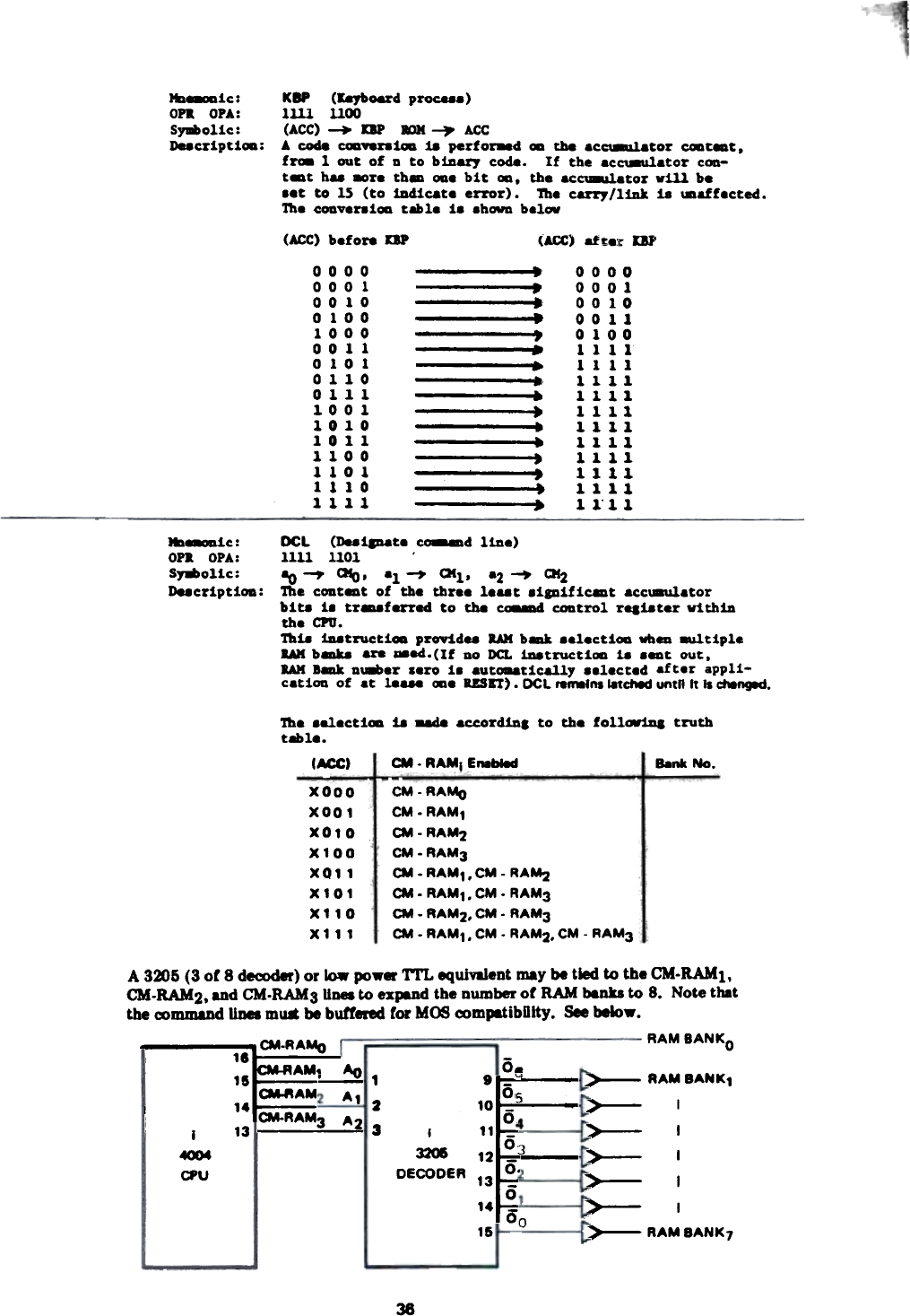
Ita_ic: KIP (Keyboard proC888)
on OPAl 1m 1100
Symbolic: (ACC) ~ lIP 10M ~ ACC
De8cripti~: A code ~~ 18 perfo~d ~ the 8c~tor ~t.ct.
fro. 1 out. of D to biDary code. If the acCU8Ulator COD-
tct. baa ~re t.bc ~e bit. ~. the ac~t.or v11l be
.et to IS (to 1Dd1cate error). 1be carry/liDk 18 uaaffect.ed.
1be cODvera1~ t.able 1. .bOWD below
(ACt) before lIP - - ;
000 0
0 0 0 1
0 0 1 0
0 1 0 0
1000
0 0 1 1
0 1 0 1
0 11 0
0 III
1.001
1010
1011
1100
1 1 0 1
1 1 1 0
1111
(ACC) aft.~
000
000
0 0 1
00 1
010
1 1 1
1 1 1
111
111
111
11 1
111
111
111
111
11"1
.
,
.
,
t
.
.
~
~
.
~
~
.
.
.
to
*~c: DCL (De8i1Date _cI line)
on OPA: llU 1101
Sy8olic: 80 ,. ~o al -to 0110 a2 -+ 012
De8criptiOD: The CODt8Dt of the three le..t .i8DifiC8Dt accU8Ulator
bit. i. tr..ferreci to the cC88Dd CODtro1 r..iater within
the CPU.
Thia iD8tructioa prOYid.. lAM baDk .e1ectiOD ¥beD ~tiple
lAM b8Dka are _ecl.(If DO DCL iD8tructiOD 18 ._t out.
lAM laDk uU8ber .ero i. auto.atically .elected after appli-
catiOG of .t 18... ODe USIT). DCL re-'ns I8tdted untn It Is dwng8d.
'lbe .e1ecti- 18 ~ accordiDa to the foUowiDI truth
t8ble.
(ACC) CM-AAMIEMbied Bank No.
x
x
x
x
x
x
x
x
CM-RAMo
CM.RAM,
CM-RAM2
CM.RAM3
CM.RAM,.CM-RA~
CM.RAM,.CM.RAM3
CM-RAM2.CM-RAM3
CM . RAM,. CM - RAM2. CM - RAM3
A 3205 (3 of 8 deooder) or low power nL eqwment may be tied to the CM-RAMl,
CM-RAM2. and CM-RAMS 8n. to uJ8nd the number of RAM banks to 8. Note that
the oommand nnes mua be buffered for MOB oompatibDity. See below.
RAM BANKO
~
A.11
1
12
3
-
1
I 1
3201 1
DECODER 13
14 0'
15
CM-AAMo
18 CM-AAM.
15 CM-RAM.
I14 CM-AAM3 A2
I 13
4004
CPU
~
>-- RAM BANK,
:>--1
>---1
>-1
.>- I
1>-- I
.>-- RAM BANK7
38
~Df
0
1
0
1
0
1
1
1
1
1
1
1
1
1
1
1
0
0
0
1
0
1
1
1
00
01
10
00
1 1
01
10
1 1
IX. AN INTRODUCTION TO PROGRAMMING THE MCS-4
A. Introduction
Writinl sequences of instructions for a computer is known as progr8m8-
ing. To be able to prolram a computer effectively, the programmer
must understand the action of each of the machine instructiona. (The
instruction set of the MCS-4 is described in detail in the last section.)
Each machine instruction manipulates data in some way. The data may
be the contents of the prograa counter WbiCh indicatee where the next
instruction i. to be found, the contents of one of the CPU registers,
accumulator, or carry flip-flop, the contents of RAM or ROM, or the
signals at a port.
Programming is probably most easily learned by use of examples. In the
pages that follow, a number of sample program segments are described.
In general, the examples are shown in order of increasing complexity.
These ex-.ple8 have been ch08en to illuatrate the use of the I/O ports,
basic program loops, multiple precision arithmetic, and the use of
subroutines.
EXAMPLE 11
Consider the case where it is desired to teat the status of a single
switch connected to the CPU (4004 chip) on the test input (pin 10).
A jump on condition instruction (JCN) can be used to perform this test.
Suppose the JCN instruction: JCN TEST, 16 (2 word instruction) is stored
at ROM memory locations 2 and J. The ins truction would look &8 follows:
OPA
OPR
Location 12 0001
(JOt)
CIC2C3C,
000 1
(Juaq» if test signal - Logic "0")
Location 13 0001 000 0
(Jump to ROM memory Location' 16)
When this instruction 18 executed, if the switch connects a logic "0"
(ground) to the test pto of the CPU, the program counter in the address
register to the CPU will jump to 16. (That is, the next iD8truction to
be executed would be fetched fro. ROM Meaory location 16). If the switch
had been connected to a logic "1" (negative voltage) the program counter
would not jump but would be incremented by 1 and hence the instruction
to ROM aeaory location 4 would be executed next. Thus the switch status
can be tested siaply with one instruction. Furthermore. if it were
desired to jump if a test signal equalled a logic "1", the JCN instruction
could be coded
CPR.
-
OPj.
CIC~JC4
1 0 0 1 Inverted jump condition
+ t-
000 0
Location 12 0001
0001
Location 13
37
In this case the invert condition bit Cl is used to ind~cate a jump
is to be made on a logic "1" on the test signal.
If more switches are required a ROM port may be used as shown in the
next example.
EXAMPLE '?
Consider the case where t is desired to test the status of a switch
connected to the port of ROM #2. To make access to the port, it is
necessary to execute and SRC instruction. The SRC instruction utilizes
the contents of a pair of registers, which must contain the proper n~
bers to select the desired port. Register pairs may be most easily
loaded using the FIM instruction.
Thus the sequence
Mnemonic DescriPtion
FIM 0
2 , 0
fletch immediate (direct) from ROM data (0010, 0000)
to index regiser pair O.
SRC 0/Send the contents of index register pair 0 to select
a ROM. The first 4 bits of data sent out at X2 time
(0010) select ROM 12.
RDR
/Read to contents of the previously selected ROM (ROM 12)
input port into the accumulator
has the effect of loading the accumulator with the values appearing at
ROM port 12. Individual bits may be tested by shifting them into the
carry flip-flop and using a jump on condition instruction. In this
manner up to 4 switches can be interrogated from one set of ROM input
ports (4 of them).
EXAMPLE , J
Suppose a series of 10 clock pulses must be generated, perhaps to drive
the clock line of a 4003 port expander. Let us assume that RAM 13 is
to be used. The high order 2 bits of data sent out at X2 time during
an SRC instruction selects the RAM chip. Hence 1100 (binary equivalent
of 12) is required at X2 to select RAM #3.
Since we must select the port on RAM 13 we will require
rIM 0
12,0
SRC 0
This pair of instructions sets up the desired port for use. To generate
the cloCk pulses. we must alternately write a 1 and an 0 into the appro-
priate port bit. Let us assume that we will only use the high order bit
of the port on RAM 13 and that it is initially set at zero (so that the
program does not have to reset it). Furthermore. let us assume that we
do not care about the other three bits of the port.
38
"':~
First let us set the accumulator to 0
/Set accumulator to 0
0
We may then complement the high order bi t of the accumulator by the
sequence
/Rotate left (accuaulator and carry)
/Complement carry
IRotate r18ht (ac~ator and carry)BAR
which achieves the operation by shiftina the bit into the carry flip-flop,
complementing it, and shiftina it baCk.
An alternate way to complement the high order bit i8 to add 8 (binary
1000) to the accumulator. We may set the contents of one register.
say register 15. to 8 by the sequence:
LDK 8 ILoad data DDDD (1000) to the accumulator.
/Exchange contents of index register 15 and accumulator
lS
ILoad (0000) to accumulator
0
The first instruction loads the binary number 1000 into the accumulator
and the second placee the contents of the accumulator into register 15.
Since the prior contents of register 15 are also placed in the accumula-
tor, an LDH instruction is then executed to clear the accu.ulator.
Now the operation ADD 15 will add the binary value 1000 to the accumula-
tor, because Regis ter 15 contains the value 8.
Note the difference in how the LDH and the XCB and ADD instructions
utilize the second half of the instruction. The LDM loads the accumu-
lator with the value carried by the instruction i.e. in binary code
LDM 8 appears.. 1101 1000 and loads the accumulator with 1000. How-
ever, the ADD and XCB select a register, and the contents of the regis-
ter are used.. data. That is, ADD 8 would add the contents of register
8 to the accumulator, not the value 8.
To generate the sequence of 10 clock pulses, one could repeat the
following 4 inatructions 10 ti88S.
IAdd contents of register 15 (1000
previoualy stored in the register)
to accUDllator
15
ADD
/Write the contents of the accumu-
lator into the previously selected
RAM output port
one clock pulse
generated
15
39
However, this would take some 40 instructions. The indexing operation
available with the ISZ instruction allows a program loop to be repeated
10 times.
The ISZ instruction increments a selected register. If the register
initially contained any value other than the value 15 (binary 1111)
the instruction performs a JUMP to an address specified by the in-
struction. This address must be on the same page (within the same
ROM) as the instruction immediately following the ISZ.
If however, the register originally contained 15, the CPU will proceed
to execute the next instruction in sequence.
By loading a register, say register 14, with the value 6, on the 10th
execution of an ISZ, the proces8or will proceed to the next instruction
in sequence rather than jump.
Execution of the ISZ does not affect the accumulator. 80 that the
accumulator does not have to be "saved" prior to its execution.
The p~ogram sequence whiCh performs the desired action i8 then
Address
N~
-
Description
Instruction' Mnemonic OPA
8
15
LDM
XCH
(1)
(2)
6
14
LDK
XCH
(3)
(4)
0
0
0
rIM
12,
SRC
(5)
0
15
LDK
ADD
(7)
(8) ~ LOOP
WHP
15
ADD
WHP
/Load 1000 to accumulator
/Exchange contents of index register 15
and accumulator
/Load 0110 to accumulator
/Exchange contents of index register 14
and acc\Dulator
/FetCh immediate fro. ROM, Data (1100 0000)
to index register pair location 0
/Send address (contents of index register
pair 0) to RAM
/Set accumulator to 0
/Add contents of register 15 to accumu-
lator
/Write contents of accumulator into RAM
output ports
/Add contents of Register 15 to accumu-
lator
/Write contents of acc\Dulator into RAM
output ports
/Increment contents of register 14. Go
to ROM address A2, Al (called Loop) if
result ~O, otherwise skip.
14
ISZ
LOOP
40
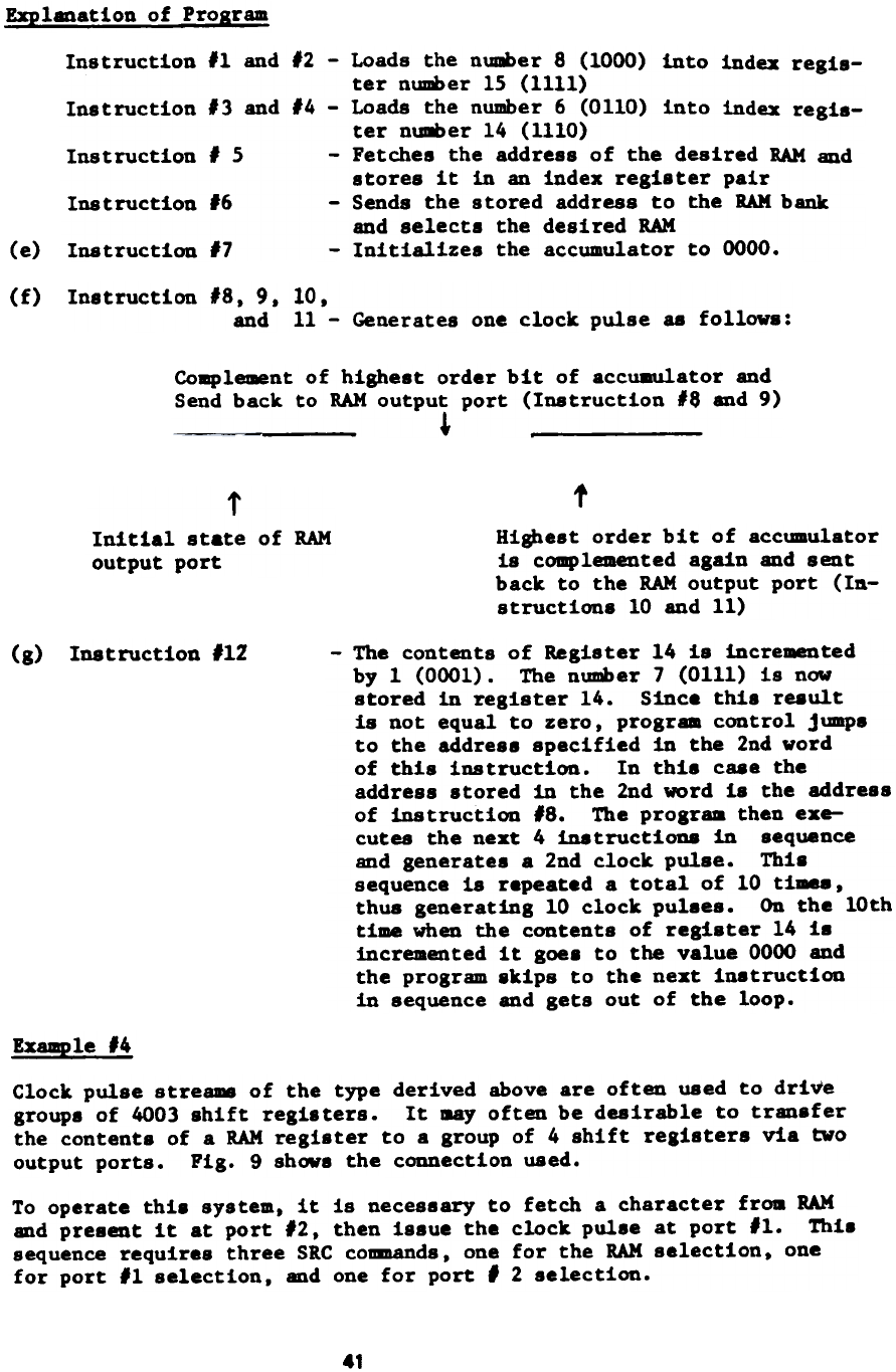
Ex:PlmatioD of Program
Instruction 11 and 12 - Loads the number 8 (1000) into index regis-
ter n~er 15 (1111)
Instruction 13 and 14 - Loads the number 6 (0110) into index regis-
ter numer 14 (1110)
Instruction I 5 - Fetches the address of the desired RAM and
stores it in an index regi8ter pair
Instruction #6 - Sends the stored address to the RAM bank
and selects the desired RAM
Instruction #7 - Initializes the accumulator to 0000.
(e)
(f) Instruction 18, 9,10,
and 11 - Generates one clock pulse 88 follows:
Complement of highest order bit of accuaulator and
Send back to RAM output port (Instruction 18 and 9)
~ ~ .
t
Highe8t order bit of accumulator
is complemented again and sent
back to the RAM output port (I~-
structiona 10 and 11)
f
Initial state of RAM
output port
Instruction #12
(8) - The contents of Register 14 is incremented
by 1 (0001). The number 7 (0111) is now
stored in register 14. Since thi8 reault
is not equal to zero, prograa control jump8
to the addre88 specified in the 2nd word
of thi8 ins truction. In thi8 C88e the
addres8 8tored in the 2nd word is the address
of instruction 18. The prograa then exe-
cutes the next 4 instructions in sequence
and generate8 a 2nd clock pulse. Thi.
sequence is repeated a total of 10 times,
thus generating 10 clock pu18es. On the 10th
time when the contents of regi8ter 14 i.
increaented it goe. to the value 0000 and
the program .kips to the next instruction
in 8equence and gets out of the loop.
Example 14
Clock pulse streams of the type derived above are often used to drive
groupe of 4003 shift regi8ters. It may often be desirable to tran8fer
the content8 of a RAM regi8ter to a group of 4 shift reaistere via two
output ports. Pig. 9 shows the connection used.
To operate thi8 system, it is necessary to fetch a character from RAM
and present it at port 12, then issue the clock pulse at port 11. Th18
sequence requires three SRC commands, one for the RAM selection, one
for port 11 selection. and one for port' 2 selection.
41
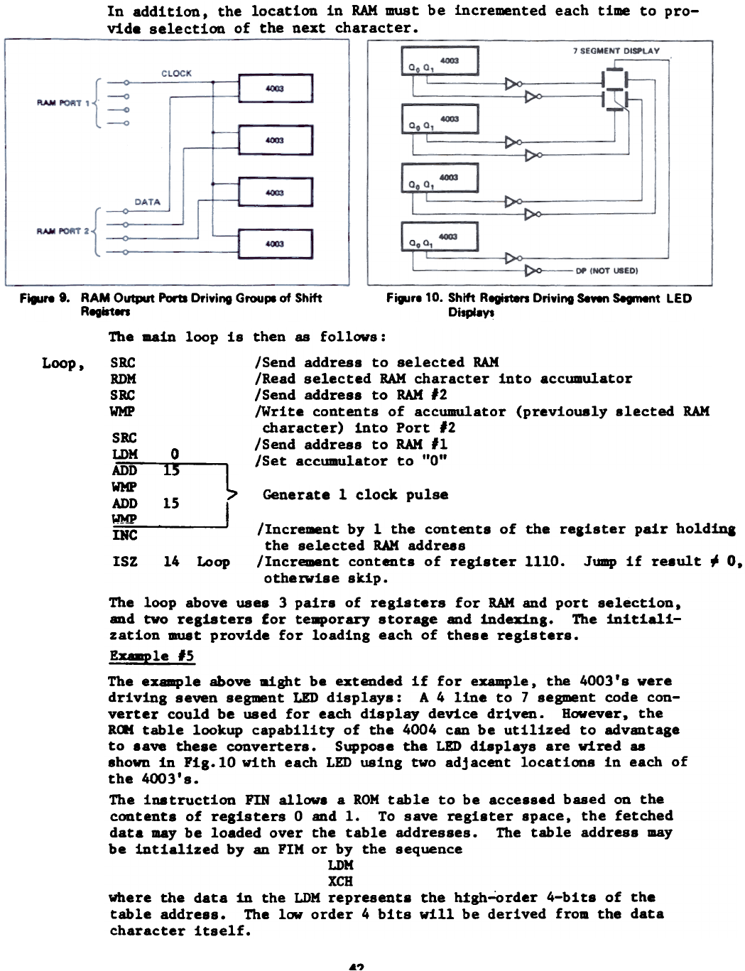
In addition, the location in RAM must be incremented each time to pro-
vide selection of the next character.
F.". 9. RAM OUtlMlt POI1s Driving Grou.. of Shift
Regilt...
Fi..,e10. Shift Registen Driving Sewn s..n.nt LED
Di.p.~
Loop,
The aain loop is then as follows:
sac /Send address to selected RAM
RDM /Read selected RAM character into accumulator
sac /Send addres8 to RAM #2
WMP /Write contents of accumulator (previously elected RAM
sac character) into Port #2
/Send address to RAM #1
LDM 0 /Set accumulator to "Q"
1~--~~.-'1
= 15 I Generate 1 clock pulse
!Nt I !Increment by 1 the contents of the resister pair holdina
the selected RAM addrees
ISZ 14 Loop !Increment contents of register 1110. Jump if reeult ~ O.
otheIWise skip.
The loop above uses 3 pairs of registers for RAM and port selection.
and two registers for temporary storage and indexing. The initiali-
zation must provide for loading each of these registers.
Ex.-ple #5
Tbe example above might be extended if for example. the 4003's were
driving seven segment LED displays: A 4 line to 7 segment code con-
verter could be used for eaCh display device drtven. However. the
RON table lookup capability of the 4004 can be utilized to advantage
to eave the8e converters. Suppose the LED displays are wired &8
ehoWD in Fig.l0 with eaCh LED using two adjacent locations in eaCh of
the 4003's.
The iD8truction FIN allowe a ROM table to be accessed based on the
contents of registers 0 and 1. To save regi8ter space, the fetChed
data may be loaded over the table addresses. The table address may
be intialized by an FIM or by the sequence
LDM
XCH
where the data in the LDM represent8 the hfgh~rder 4-bit8 of the
table address. The low order 4 bits will be derived fro. the data
character itself.
~.,
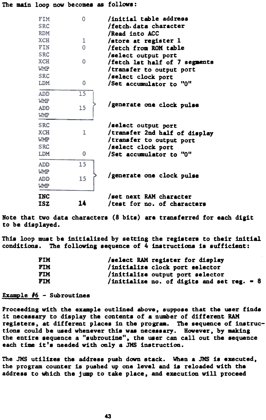
The main loop now becomes as follows:
!initial table address
!fetch.data character
!Read into ACC
!store at register 1
!fetch from ROM table
!select output port
!fetch 1st half of 7 seg88nts
!transfer to output port
!select clock port
!Set accuaulator to "0"
I generate one clock pulse
!select output port
!transfer 2nd half of di8play
! trans fer to output port
!select clock port
!Set acc\Dulator to "0"
/ generate one clock p~.e
INC
ISZ /set next RAM character
/test for no. of characters
14
Note that two data characters (8 bite) are transferred for each diait
to be displayed.
This loop must be initialized by settins the resisters to their initial
conditions. The follow1nS sequence of 4 instructions is sufficient:
FIH
FIH
FIM
FIM
/select RAM register for display
/initialize cloCk port selector
/initialize output port aelector
/initialize DO. of digit. and .et rei. . 8
Example #6 - Subroutines
Proceeding with the example outlined above, 8uppO8e that the user finds
it nece88ary to display the contents of a number of different RAM
registers, at different places in the prograa. The sequence of inatruc-
tiona could be used whenever thi8 Was necessary. However, by making
the entire sequence a "subroutine". the user can call out the sequence
each time it'. needed with only a JMS instruction.
The JMS utilizes the address push down stack. When a JMS i8 executed,
the program counter is pushed up one level and 18 reloaded with the
address to whiCh the jump to take place, and execution will proceed
43
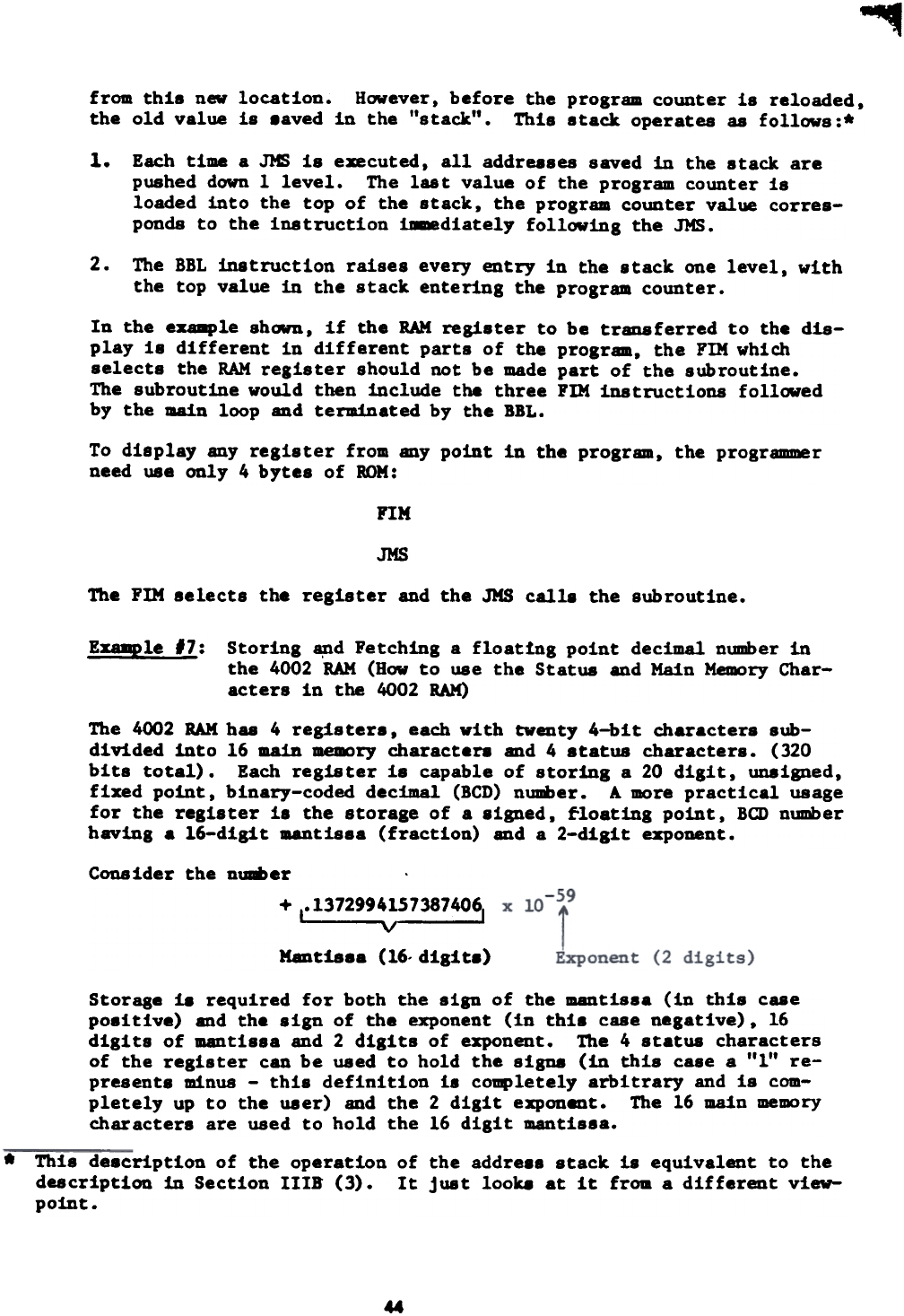
~
from this new location. However, before the program counter is reloaded,
the old value is .aved in the "stack". This stack operates as follows:.
1. Each time a JHS is executed, all addreases saved in the stack are
pushed down 1 level. The last value of the program counter is
loaded into the top of the stack, the program counter value corres-
ponds to the instruction immediately following the JHS.
2. The BBL instruction raises every entry in the stack one level, with
the top value in the stack entering the program counter.
In the exa.ple shown, if the RAM regi8ter to be transferred to the dis-
play i8 different in different part8 of the program, the FIM which
8elect8 the RAM regi8ter should not be made part of the sUbroutine.
The subroutine would then include the three rIM instructions followed
by the main loop and terminated by the BBL.
To display any register fro. any point in the program. the programmer
need use only 4 bytes of ROM:
FIM
JMS
The FIH selects the resister and the JHS calla the subroutine.
Example 17: Storing ~d Fetching a float1ng point decimal number in
the 4002 RAM (Row to use the Status and Main Memory Char-
acters in the 4002 RAM)
The 4002 RAM has 4 registers, each with twenty 4-bit characters sub-
divided into 16 main memory characters and 4 status characters. (320
bits total). Each register is capable of storing a 20 digit, unsigned,
fixed point, binary-coded decimal (BCD) number. A more practical usage
for the register is the storage of a signed, ~loating point, BCD number
having a 16-digit mantissa (fraction) and a 2-d1git exponent.
Consider the n\8er
+ L~~~~!!~~~~~~~
Mantis.. (16- digit.)
Storage 18 required for both the sign of the mantissa (in this C88e
positive) and the sign of the exponent (in thi. case negative), 16
digits of mantissa and 2 digits of exponent. The 4 status characters
of the register can be used to hold the signa (in thia case a "1" re-
presents minus - this definition 18 completely arbitrary and is com-
pletely up to the user) and the 2 digit exponent. The 16 main memory
characters are used to hold the 16 digit mantis.a.
*This de8cription of the operation of the addre8s stack i8 equivalent to the
description in Section IIIB (3). It just look. at it from a different view-
point.
44
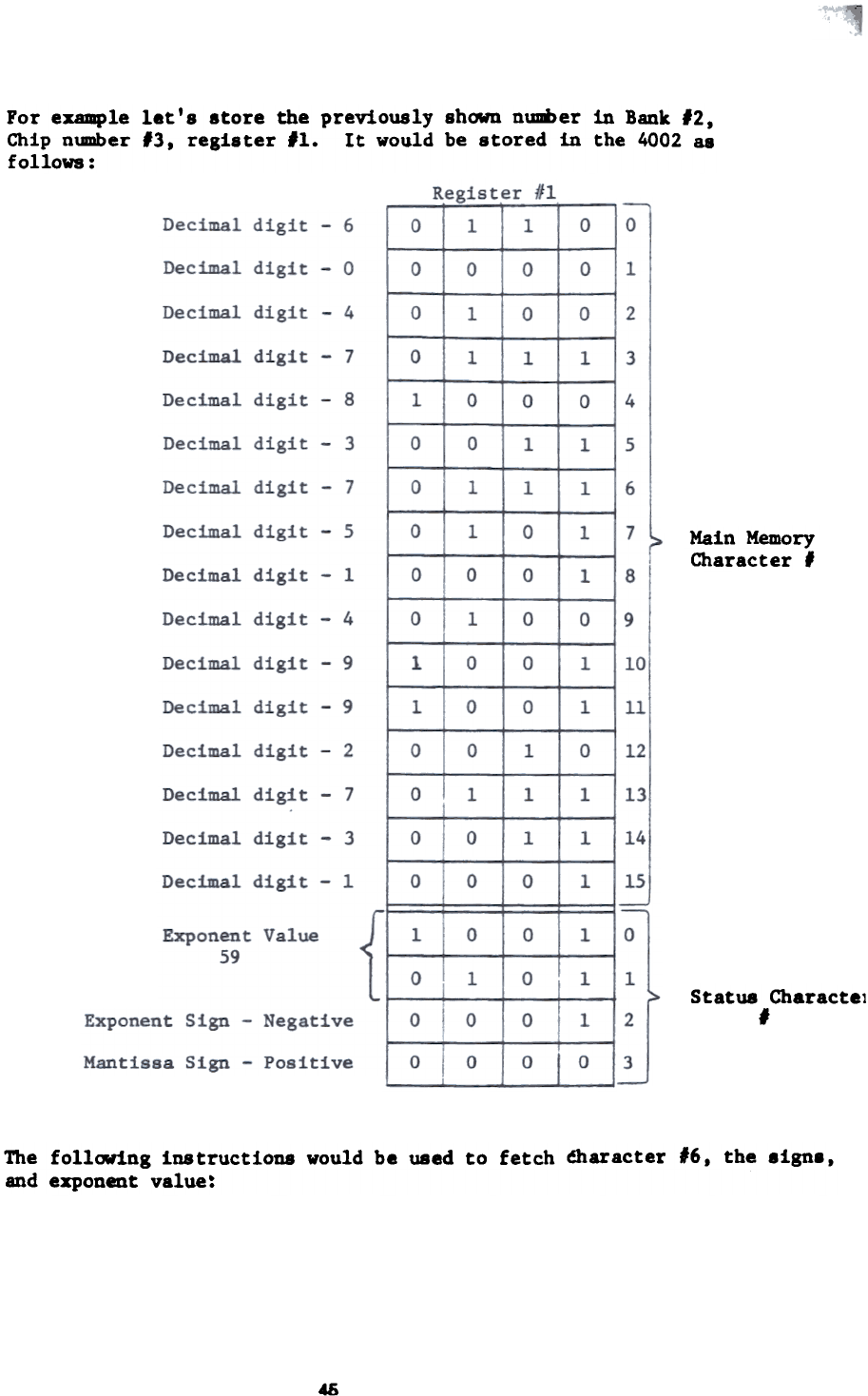
For example let' s store the previously shown number in Bank #2,
Chip number #3, register #1. It would be stored in the 4002 8.
follows:
Main Memory
Character'
~
Status Charact.1
,
The following instructions would be used to fetch ~aracter 16, the 8ign8 t
and exponent value:
46
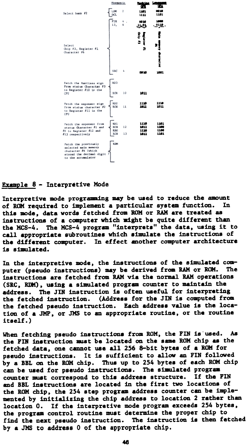
y
1181
U11
~W
~
21
. ~
= i
=
l-
i
i
*1
alO
1811
1118
I8U 1110
IOU
u.l
~
1100
1181
U18
I8U
1110
I8U
Example 8 - Interpretive Mode
Interpretive mode programming DaY be used to reduce the amount
of ROM required to implement a particular system function. In
this mode, data words fetChed from ROM or RAM are treated as
tu.tructions of a computer wbidb ~ght be quite different than
the MCS-4. The MCS-4 program "interprets" the data, using it to
call appropriate sUbroutines whiCh 8imu1ate the instructions of
the different computer. In effect another computer ardbitecture
is s181lated.
In the interpretive mode, the instructiona of the simulated com-
puter (pseudo instructions) may be derived from RAM or ROM. The
instructions are fetched from RAM via the normal RAM operations
(SRC, RDtO, using a simulated progr8m counter to maintain the
address. The JIM instruction is often useful for interpreting
the fetched instruction. (Address for the JIN is computed from
the fetched pseudo instruction. Each address value is the loca-
ti~ of a JMP, or JMS to aD appropriate routine, or the routine
itself.)
When fetChing pseudo instruction. from ROM, the FIN is'used. As
the FIN in.truction must be located on the same ROM chip as the
fetChed data, one cannot use all 256 8-bit bytes of a ROH for
pseudo instructions. It is sufficient to allow an FIN followed
by a BBL on the ROM Chip. Thus up to 254 bytes of eaCh ROM Chip
can be used for pseudo iDatructi0D8. The simulated progr..
counter must correspond to this address structure. If the FIN
and BBL instructions are located in the first two locations of
the ROM Chip, the 254 step program address counter can be imple-
mented by initializing the chip address to location 2 rather than
location O. If the interpretive mode program exceeds 254 bytes,
the program control routine must determine the proper chip to
find the next pseudo iDatruction. The lnetruction is then fetChed
by a JMS to address 0 of the appropriate chip.
48
~
...
1101
~
0 0110 .
-,,-
I
a)
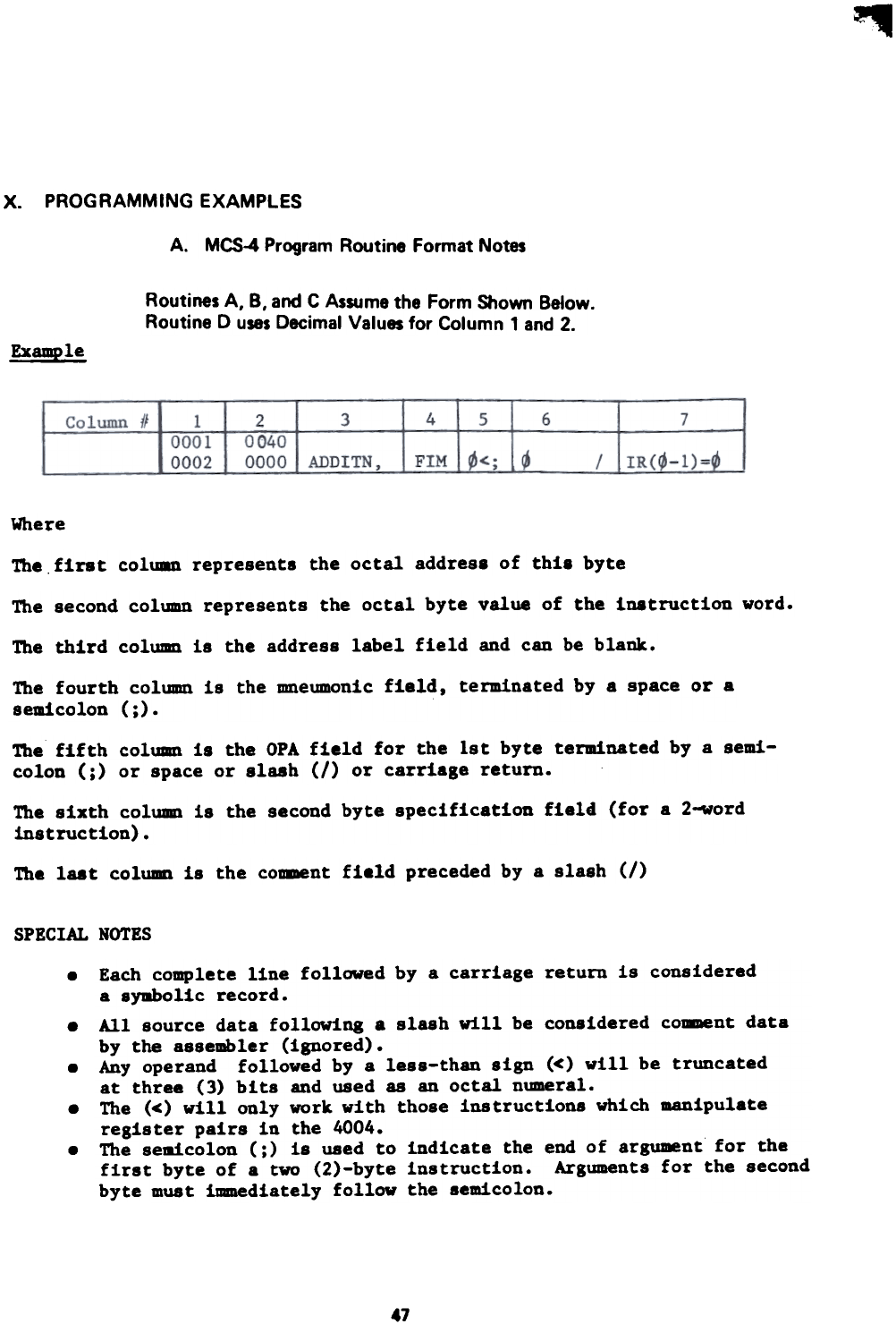
~
x. PROGRAMMING EXAMPLES
A. MCS-4 Program Routine Format Notes
Routines A, B, and C Assume the Form Shown BeJow.
Routine D uses Decimal Values for Column 1 and 2.
Example
Where
The. first COlU8D represents the octal addres8 of thi8 byte
The second column represents the octal byte value of the instruction word.
The third column is the address label field and can be blank.
The fourth column is the mneumonic field, terminated by a space or a
semicolon (;).
Tbe fifth column is the OPA field for the 1st byte terminated by a semi-
colon (;) or space or slash (I) or carriage return.
The sixth column is the second byte specification field (for a 2-word
instruction).
The last column is the comment field preceded by a slash (/)
SPECIAL NOTES
.
.
.
.
Each complete line followed by a carriage return is considered
a 8ymbolic record.
All source data following a slash will be considered comment data
by the assembler (ignored).
Any operand followed by a less-than sign «) will be truncated
at three (3) bits and used as an octal numeral.
The «) will only work with those instructions which manipulate
register pairs in the 4004.
The semicolon (;) is used to indicate the end of argument for the
first byte of a two (2)-byte instruction. Arguments for the second
byte must immediately follow the semicolon.
.
47
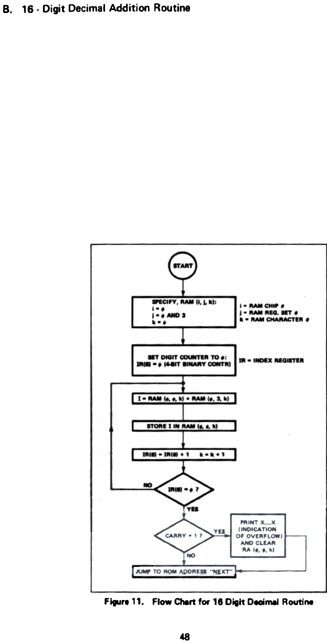
16 . Digit Decimal Addition Routine
B.
lie_ow.
J-_~IG.~.
k - - CMARACTE~ .
I- . 1-. MQ8TIA
:+ RAM c.:-J;kJ I
II.~t.."k
STORE I IN AAM If. ,. " I
Figure 11. Flow Chert for 18 Digit Dtdmel Routine
48
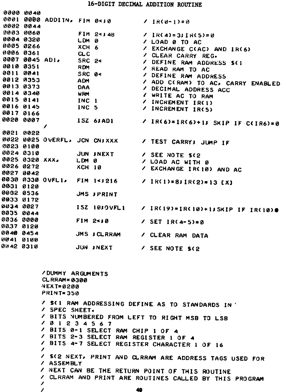
16-DIGIT DECIMAL ADDITION ROUTINE
/ IR(~-I)=0
0000 0040
00010000 ADDI1N. FIM 0<10
~002 0044
0003 0060 FII~ 2<J~8
0004 0320 l.~ 0
0005 0266 XCH 6
0006 0361 Cl.C
0001 0045 ADI. SRC 2<
0010 0351 R(XIot
0011 0041 SRC 0<
0012 A353 A~
0013 0313 DAA
0014 0340 w~
0015 0141 INC 1
0016 014~ INC 5
0011 0166
0020 0001
I IR<4)=3JIR<5)=1d
I LOAD 0 TO AC
I EXCHANGE C<AC) AND IR<6)
I CLEAR CARRY REG.
I DEFINE RAM ADDR~SS $<1
I READ RAM TO AC
I DEFINE RAM ADDRES5
I ADD C<RAM) TO AC. CARRY ENABLED
I DECIMAL ADDRESS ACC
J' WRITE AC TO RAM
I INCREMENT IR<I)
.I INCREMENT IR<S)
ISZ 61ADI I IRC6)=IRC6)+lJ SKIP I:FC(IR6>=0
/
/ TEST CARRYJ JUMP IF
0021 0022
~022 0025 OVERFL# JCN CNJXXX
0023 0100
0024 0310 JUN JNEXT
0025 0320 XXX# L~ 0
0026 0212 XCH 10
0027 00-42
0030 0330 OVFL1# F'IM I<J216
00310120
0062 0536 JMS JPRINT
0933 0172
00~-4 0021 ISZ 10JOVFLI
0035 00-4-4
0036 0000 F'IM 2~J0
00.37 0120
0048 0-454 JMS J CLRRAM
~0-41 01~0
0~42 031~ JUI~ JNEXT
.I SEE NOTE $(2
.I LOAD AC WITH 0
.I EXCHANGE IR(10) AND AC
.I IRCI)=8JIRC2)=13 [X]
/ IRC19>=IRC10>+lJSKIP IF IRC10>8
/ SET IRC4-S)80
I CLEAR RAM DATA
.I SEE NOTE $(2
/DUMMY AR~ENTS
CLRRAM=&300
,~EXT=0200
PRINT=350
/ $(1 RAM ADDRESSING DEFINE. AS TO STANDARDS IN'
/ SPEC SHEET. ,
/ BITS ~UMBERED FROM LEFT TO RIGHT MSB TO LSB
/01234567
/ BITS 0-1 SELECT RAM CHIP 1 OF 4
/ BITS 2-3 SELECT RAM REGISTER 1 OF -4
/ BITS 4-7 SELECT REGISTER CHARACTER 1 OF 16
/
/ $(2 NEXT, PRINT At~D a.RR~ ARE ADDRESS TAGS USED FOR
/ ASSEMBLY
I I~EXT CAN BE THE RETURN POINT OF' THIS ROUTINE
/ CLRRAM AND PRINT ARE ROUTII~ES CALLED BY THIS PROGRAM
/
I 48
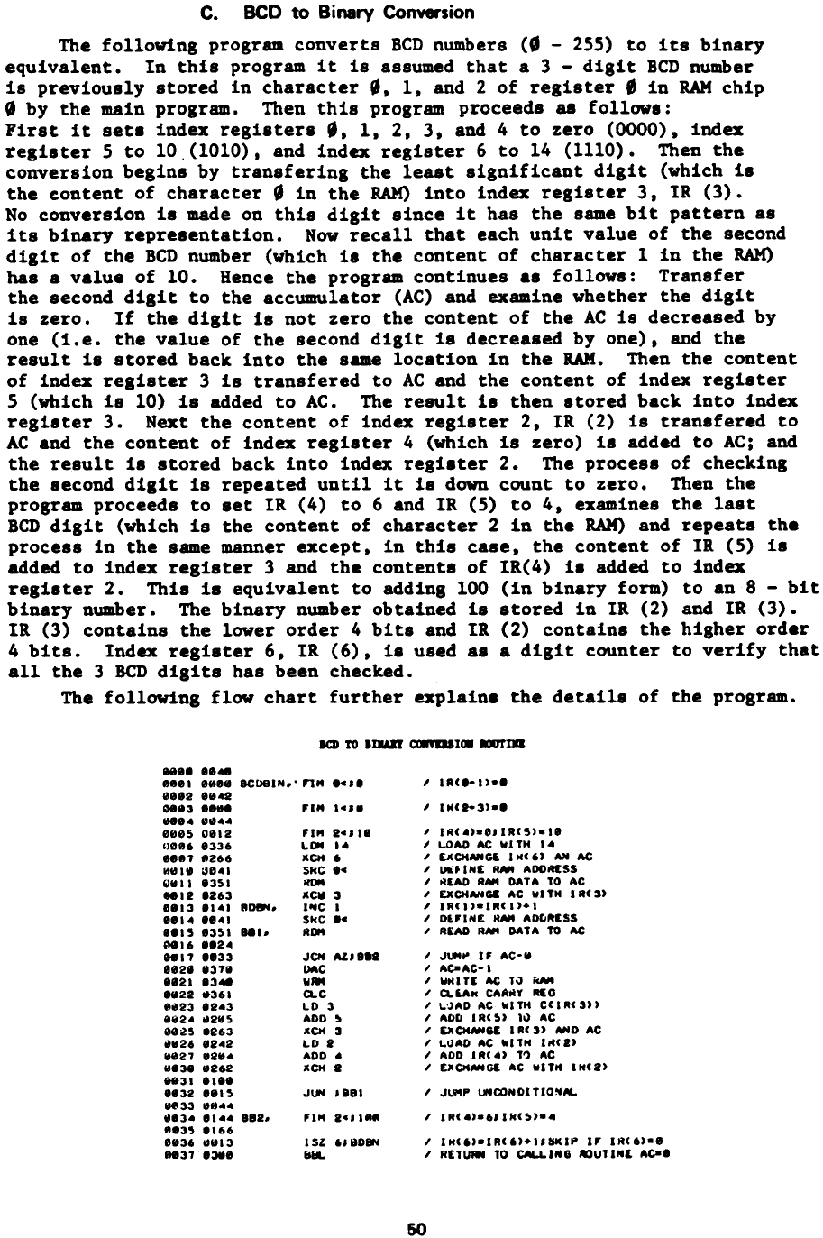
C. BCD to Binary Conversion
The following program converts BCD numbers (G - 255) to its binary
equivalent. In this program it is assumed that a 3 - digit BCD number
is previously stored in character ',1, and 2 of register' in RAM chip
, by the main program. Then this program proceeds 88 follow8:
First it set8 index registers ',1,2,3, and 4 to zero (0000), index
register 5 to 10.(1010), and index register 6 to 14 (1110). Then the
conversion begin8 by transfering the least significant digit (which i8
the eontent of character' in the ~ into index register 3, IR (3).
No conversion i8 made on this digit since it has the same bit pattern as
its binary repre8entation. Now recall that each unit value of the second
digit of the BCD number (which i8 the content of character lin the ~
has a value of 10. Hence the program continues a8 follows: Transfer
the second digit to the accumulator (AC) and examine whether the digit
is zero. If the digit i8 not zero the content of the AC is decreased by
one (i.e. the value of the second digit is decreased by one), and the
result is stored back into the same location in the RAM. Then the content
of index register 3 is transfered to AC and the content of index register
5 (which is 10) is added to AC. The result i8 then 8tored back into index
regi8ter 3. Next the content of index register 2, IR (2) is tran8fered to
AC and the content of index register 4 (which is zero) i8 added to AC; and
the result is stored back into index register 2. The proces8 of checking
the second digit is repeated until it is down count to zero. Then the
program proceeds to set IR (4) to 6 and IR (5) to 4, examines the last
BCD digit (which is the content of character 2 in the ~ and repeats the
process in the same manner except, in this case, the content of IR (5) is
added to index register 3 and the contents of IR(4) i. added to index
register 2. This is equivalent to adding 100 (in binary form) to an 8 - bit
binary number. The binary number obtained is stored in IR (2) and IR (3).
IR (3) contains the lower order 4 bits and IR (2) contains the higher order
4 bits. Index register 6, IR (6), is used as a digit counter to verify that
all the 3 BCD digits has been checked.
The following flow chart further explain. the details of the program.
IQ to ImAar ~Im DJrID
H81 Ie.
..el e.e8 BCoelH,' nM Ic'l
0082 8842
08831HI FIM ICI.
"84 8844
0005 0112 FIM 2cl18
110.' 0336 LOM I ~
e.818266 KCH ,
"81. 15841 5rcC Ic
11.11 e351 -
..12e263 KC¥ 3
881311..1 RDM, I~C I
0814 ee41 SkC 'c
IllS 13S' 881, ROM
"816.124
HI1..33 JCN u,...
e021 .31& UAC
182' .348 WM
..22.361 CLC
..2312..3 LO 3
8~24 ~2V5 ADD ~
08iS 1263 KCH 3
~V2' 0242 LD.
~021 ~2V" ADD.
VI3I V262 KCM .
883' 1'1.
1132 e&IS J~ '8B'
"33 ~1I"4
.e3" el..4 BB2, fl" 2c,,"
~.3S 1166
e83' ~~13 151 "BO8M
8831 8He 8iL
, IRC'-I).'
, I"C2-3).'
, lilC.).'JIRCS).le
, LOAD AC WITH I.
, UCHNtGI. IOCC 6) Nt AC
, u.:J INE RNf AOOItESS
, ill.AD RNI DATA TO AC
, EXCHMG& AC WI TH I MC 3)
, IRCI).IRCI)+I
, DL'INE MNt AD~~ESS
, READ RNf DATA TO AC
, J\»tl' IF AC-.
, ACeAC-1
, WHITE AC To) icM
, ca.,--" CAAIi't MG
, LJAD AC WITH CCIRC3))
, ADD IRC~) II> AC
, EXCHMGE I RC 3) NtD AC
, LIJA~ AC WI1OC IICC2)
, ADD IRC.) T? AC
, PCHNtG& AC WITH IOCCa)
, J~P ~CONDITIO~M.
, IRC.).6.IIcC~)..
, I"C6).IRC6)+IJSlCIP I' IItC6).e
, RE1UM TO c-.LING ~UTINE ACe'
50
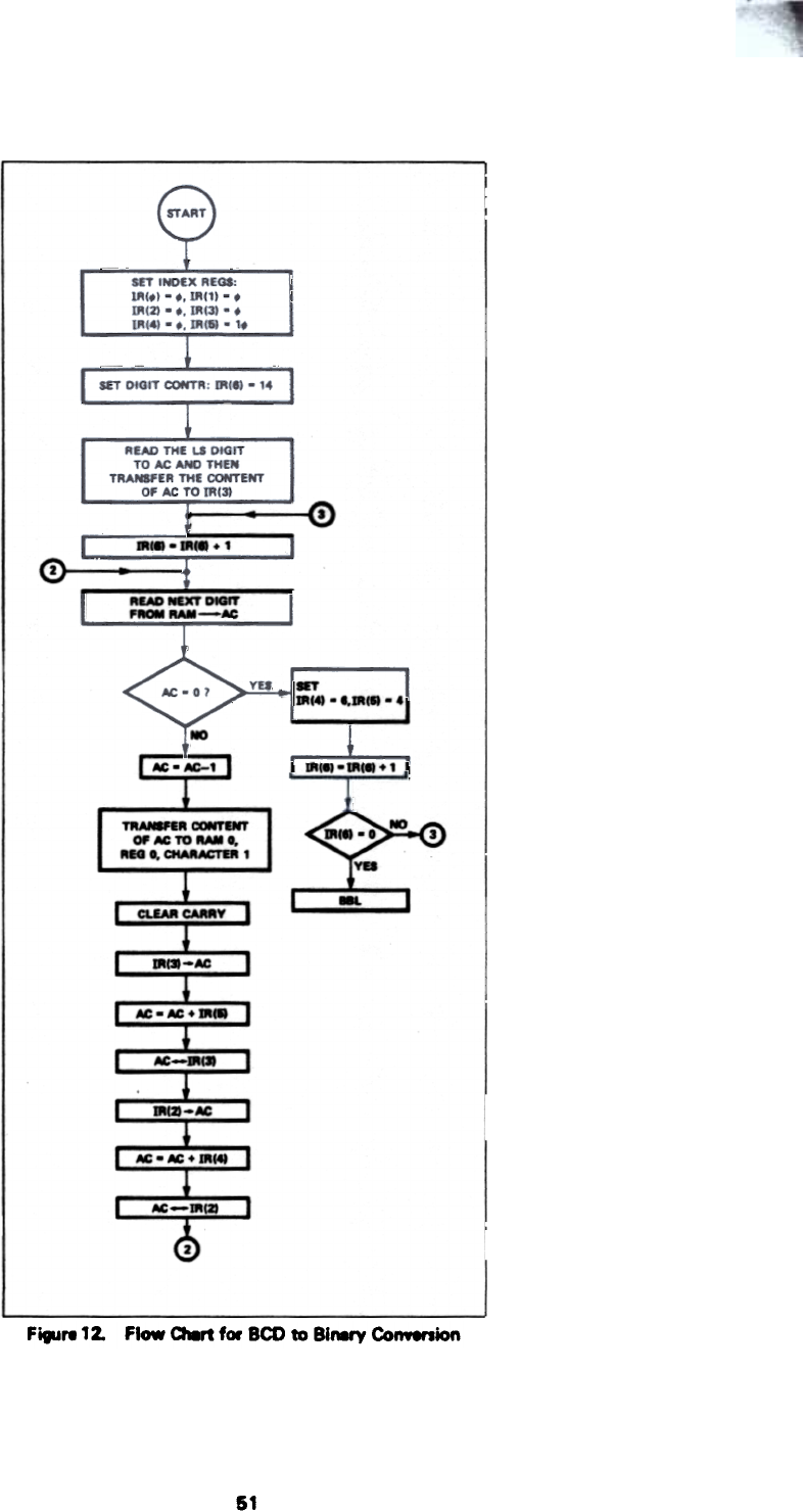
: .' 0
1
(!) .
I -=DtGIT
I ;-. -'-=,,~
1:;'41 . '.!RIII .4\
-"
~
.-;:'AC:;'i
--
'IR..' I
l~
.
.
~R~
OP~1ORM'.
RIG..~'
(
F.".12. Flow a.rt for BCD to Blrwy Comenion
51
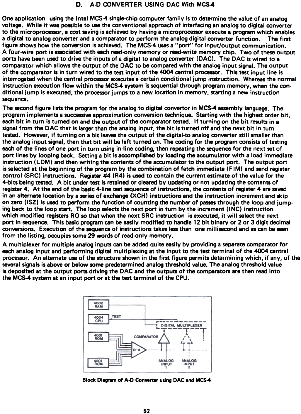
A-D CONVERTER USING DAC With MCS-4
D.
One application using the Intel MCS-4 single-chip computer family is to determine the value of an analog
voltage. While it was possible to use the conventional approach of interfacing an analog to digital converter
to the microprocessor, a cost saving is achieved by having a microprocessor execute a program which enables
a digital to analog converter and a comparator to perform the analog digital converter function. The first
figure shows how the conversion is achieved. The MCS-4 uses a "port" for input/output communication.
A four-wire port is associated with each read-only memory or read-write memory chip. Two of th~ output
ports have been used to drive the inputs of a digital to analog converter (DAC). The DAC is wired to a
comparator which allows the output of the DAC to be compared with the analog input signal. The output
of the comparator is in turn wired to the test input of the 4004 ~ntral procesmr. This test input line is
interrogated when the ~ntral processor executes a certain conditional jump instruction. Whereas the normal
instruction execution flow within the MCS-4 system is sequential through program memory, when the con-
ditional jump is executed, the processor jumps to a new location in memory, starting a new instruction
sequence.
The ~nd figure lists the program for the analog to digital convertor in MCS-4 as.mbly language. The
program implements a successive approximation conversion technique. Starting with the highest order bit,
each bit in turn is turned on and the output of the comparator tested. If turning on the bit results in a
signal from the DAC that is larger than the analog input, the bit is turned off and the next bit in turn
tested. However, if turning on a bit leaves the output of the digital-to analog converter still smaller than
the analog input signaJ, then that bit will be left turned on. The coding for the program consists of testing
each of the lines of one port in turn using in-line coding, then repeating the mquence for the next set of
port lines by looping back. Setting a bit is accomplished by loading the accumulator with a load immediate
instruction (LDM) and then writing the contents of the accumulator to the output port. The output port
is .Iected at the beginning of the program by the combination of fetch immediate (FIM) and send register
control (SAC) instructions. Aegister #4 (A4) is used to contain the current estimate of the value for the
4-bits being tested. A bit under test is retained or cleared by updating or not updating the contents of
register 4. At the end of the basic 4-line test sequen~ of instructions, the contents of register 4 are saved
in an alternate location by a .ries of exchange (XCH) instructions and the instruction increment and skip
on zero (ISZ) is used to perform the function of counting the number of passes through the loop and jump-
ing back to the loop start. The loop .Iects the next port in turn by the increment (I NC) instruction
which modified registers AO so that when the next SAC instruction is executed, it will .Iect the next
port in sequence. This basic program can be easily modified to handle 12 bit binary or 2 or 3 digit decimal
conversions. Execution of the ~uen~ of instructions takes less than one milli~nd and as can be seen
from the listing, occupies some 29 words of read-only memory.
A multiplexer for multiple analog inputs can be added quite easily by providing a separate comparator for
each analog input and performing digital multiplexing at the input to the test terminal of the 4004 central
processor. An alternate use of the structure shown in the first figure permits determining which, if any, of the
several si~als is above or below M>me predetermined analog threshold value. The analog threshold value
is deposited at the output ports driving the DAC and the outputs of the comparators are then read into
the MCS-4 system at an input port or at the test terminal of the CPU.
Block Di..m of A-D Conwrter uti"' DAC .nd MCS-4
52
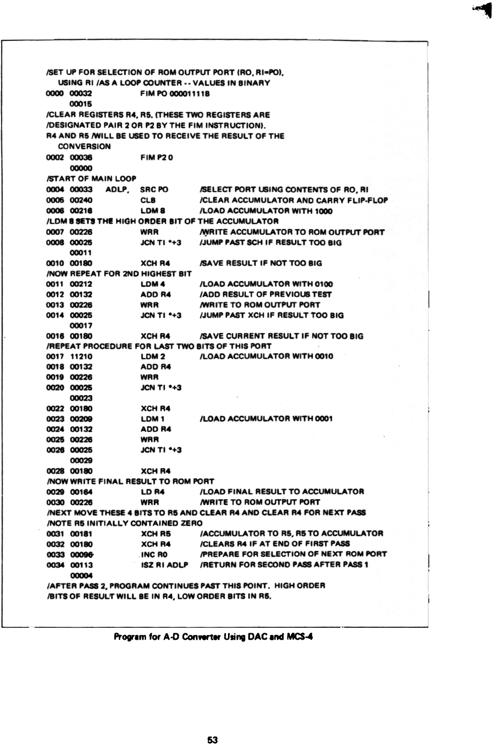
~
/SET UP FOR SELECTION OF ROM OUTPUT PORT IRO, RI.po).
USING RI/AS A LOOP COUNTER .. VALUES IN BINARY
(XXX) (XX)32 FIM PO (XXX)1111B
00015
/CLEAR REGISTERS R4, R5. (THESE TWO REGISTERS ARE
IDESIGNATED PAIR 2 OR P2 BY THE FIM INSTRUCTION).
R4 AND R5 /WILL BE USED TO RECEIVE THE RESULT OF THE
CONVERSION
0002 000:. F I M P2 0
~
/START OF MAIN LOOP
(XX)4 (XX)33 ADLP. SRC PO /SELECT PORT USING CONTENTS OF RO. RI
~ 00240 CLB ICLEAR ACCUMULATOR AND CARRY FLIP-FLOP
~ 00218 LDM' ILOAD ACCUMULATOR WITH 1~
ILDM 1.T1 THe HIGH OR:DER lIT Of THE ACCUMULATOR:
0007 00228 WRR N;iRITE ACCUMULATOR TO ROM OUTPUT PORT
DC.- ~ JCN TI -+3 IJUMP PAST SCH IF RESULT TOO BIG
00011
0010 001~ XCH R4 /SA VE RESULT IF NOT TOO IIG
INOW REPEAT FOR 2ND HIGHEST BIT
0011 00212 LDM4 ILOADACCUMULATORWITH0100
0012 00132 ADD R4 IADD RESULT OF PREVIO~ TEST
0013 00228 WRR /WRITE TO ROM OUTPUT PORT
0014 (XM)25 JCN TI -+3 IJUMP PAST XCH IF RESULT TOO BIG
00017
0018 001~ XCH R4 /SAVE CURRENT RESULT IF NOT TOO 81G
IREPEAT PROCEDURE FOR LAST TWO BITS OF THIS PORT
0017 11210 LDM2 ILOADACCUMULATORWITH0010
0018 00132 ADD R4
0018 cxrne WRR
0020 (XM)25 JCN TI -+3
(XMJ23
0022 001~ XCH R4
0023 002C» LDM 1 ILOAD ACCUMULATOR WITH 0001
0024 00132 ADD R4
0025 00228 WR R
0028 (XM)25 JCN TI -+3
00029
0028 001~ XCH R4
/NOW WRITE FINAL RESULT TO ROM PORT
0028 00184 LD R4 ILOAD FINAL RESULT TO ACCUMULATOR
00:-. 00228 WRR /WRITE TO ROM OUTPUT PORT
/NEXT MOVE THESE 4 BITS TO RS AND CLEAR R4 AND CLEAR R4 FOR NEXT PAS
/NOTE RS INITIALLY CONTAINED ZERO
0031 00181 XCH RS IACCUMULATOR TO RS. R5 TO ACCUMULATOR
0032 001~ XCH R4 ICLEARS R4 IF AT END OF FIRST PAS
0033 (XX)98' INC RO /PREPARE FOR SELECTION OF NEXT ROM PORT
0034 00113 ISZ RI ADLP IRETURN FOR SECOND PAS AFTER PASS 1
00004
IAFTER PAS 2. PROGRAM CONTINUES PAST THIS POINT. HIGH ORDER
/BITS OF RESULIf WILL BE IN R4. LOW ORDER BITS IN R5.
Program for A-D Con""- Using DAC and MCS-4
53
E. MCs.4 SOFTWARE LIBRARY
MCS-4 Cr08 All8m~.r 8nd Simul8tor Softwere P8Ck8.
Intel now offen an asembler and simulator softw8re pack. to help develop PfOW'ImS for microcomputer systems built
from Intel's MCS-4.t of integrated computer circuits. The MCS-4 cr08 assembter transf8tes a symbolic representation
of the instructions and d8ta into a form which can be lo8ded m OKUted by the MCS-4. By cros .-mbter, we me.,
an -.mbler executing on a mechine other than the MCS-4 which generates object code for the MCS-4. Initi81 develop.
ment time C81 be significantly reduced by taking .tv.,tege of a 1-. -=8Ie computer's proceuing, editing and hi~ speed
peripheral capability.
The software is written in general FORTRAN IV. The peck. consists of 8 simul8tlng rootine, which enab!. the
computer to simulate the oper8tlon of an MCS-4 microcomputer, and an aSIem~y rootln., u. primarily as an aid
to programming the simulated microcomputer.
The routin. may be procured from I ntel on m.,etic tape. Alternatively, desl~ may contxt nation-wlde com~ter
time-tharing MfVi~ - General Electric and Tymsh.- - for ~ to the P'09"8nL
MCS-4 u...'. Ubnry
. Cr~ .-nbl. end simulator for the MCS-4
th8t runs on the PDP-8.
. MCS-4 logic .,broutines AND, XOR, lOR, LOGIC.
. Sixteen digit D.:imal Addition Routine (AO700)(1)
. Cro8 ~bl.r for NOVA
. Q'8bychev polynomiMI ~roxim8tion .,broutines for
.tdition, aAbtrection, multiplication, division, sine,
COline, erctangent. exponenti81, and natUr8l1~
Th.- progrem listings... .,8ileble to ell memben of the microcomputer u.,.'slibrery. We encour. ell users to .,bmit
ell non-propriet8ry prQ9'8ml to Intel to .td to the ~8m libr8ry ~ that ~ mey malce them .,eileble to other u--.
54
~
XI INTERFACE DESIGN FOR THE MCS-4 SYSTEM
AGeneral Discussion
MCS-4 computer systems are often used to replace random logic
controllers in a wide variety of systems. In each of these sys-
tems a number of peripheral devices, such as keyboards, switches.
indicator lamps, numeral displays, printer mechanisms, relays.
solenoids, etc., may have to be interrogated or controlled. The
engineer who wishes to utilize an MCS-4 system must include, as
part of his design, suitable interface circuits and progr
Devices to be operated or interrogated by an MCS-4 computer are
attached to the system via the input and output data ports as-
sociated with the 4001 ROM and 4002 ROM. The design of an inter-
face consi. ts of the following s tepa:
1. Assign peripheral device connections to port connections.
If the number of available output ports is insufficient,
4003 output port expanders may be used. When the number
of input lines 1s insufficient, multiplexers must be added.
The.. multiplexers must be controlled by output ports.
2. Develop the necessary level conditioning circuits for eaCh
signal. Port inputs and outputs are at MaS levels (logic
. - OV with a series output res is tance of typically l~
logic 1 - -7v with a series resistance of typically 2k
for outputs. Inputs U8e the same levels, and appear.. a
capacitive load of approximately 5Pf). These levels aU8t
be converted to the levels necessary to drive solenoids,
nixies, etc. For TTL compatibility refer to Appendix A.
3. Write the programs necessary to interpret inputs and gen-
erate the output levels necessary for proper operatioa of
the peripherals.
Any interface design requires all three of these steps. Each
design will typically involve decisions concernins the inter-
action of the three areas. For ex..p1e. teChniques which reduce
the number of output lines may result in more complicated pro-
sr_.
The following sections describe typical interfaces for a number
of common peripheral device..
B. Keyboards
The MCS-4 can be pro.rammed to scan and deb ounce a keyboard or
can interface to a keyboard which presents precoded (such 88
ASCII) data. The output lines fro. a keyboard with precoded
data are read at one or more input ports. An input port line
or the test line of the 4004 CPU may be interrogated to deter-
mine if a key has been pressed.
66
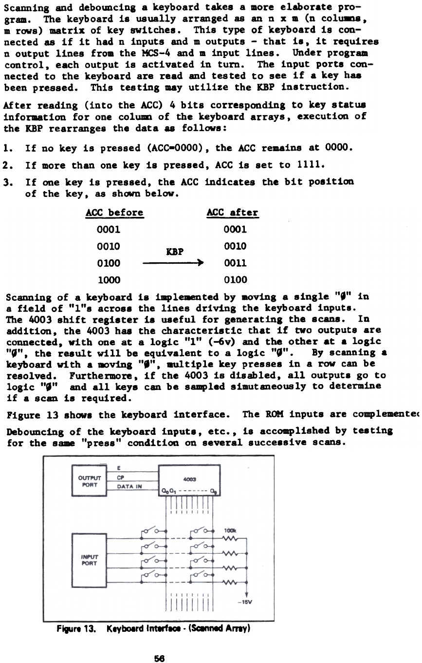
Scanning and debouncins a keyboard takes a more elaborate pro-
gram. The keyboard is usually arranged as an n x m (n colU8D8,
m rows) matrix of key switChes. This type of keyboard is con-
nected as if it had n inputs and m outputs - that is, it requires
n output lines from the MCS-4 and m input lines. Under program
control, each output is activated in turn. The input ports con-
nected to the keyboard are read and tested to see if a key haa
been pressed. This testing "y utilize the KBP instruction.
After reading (into the ACC) 4 bits corresponding to key status
information for one column of the keyboard arrays, execution of
the KBP rearranges the data 88 follows:
1.
2.
3.
If no key is pressed (ACC-OOOO) , the ACC remains at 0000.
If more than one key is pressed, ACC is set to 1111.
If one key is pressed, the ACC indicates the bit po8ition
of the key, as shown below.
ACC before ACC after
0001 0001
0010 DP 0010
0100 ~ 0011
1000 0100
Scanning of a keyboard i8 i8Pl~ted by aoving a single "f" in
a field of "l"s acrO8e the lines driving the keyboard inputs.
The 4003 8hift regieter 18 useful for generatin, the 8cans. In
addition, the 4003 haa the characteristic that if two outputs are
connected, with one at a logic "1" (-6v) and the other at a logic
'I~". the reeult will be equivalent to a logic "~". By scanning a
keyboard with a 8)v!ng ""', 8ultiple key pressee in a row can be
resolved. Furthermore, if the 4003 is disabled, all output. go to
logic "~" and all keye can be 8~1.d simutaneously to deter1Dine
if a scan is required.
Figure 13 showe the keyboard interface. The ROM inputs are complementec
Debouncing of the keYboard input., etc., is accomplished by teetinl
for the s~ "press" condition on several succe8sive scans.
K8ybolrd Inttrf8~' (SC8nned Amy)
F.,r. 13.
58
Display
c.
Display devices suCh as NIXIE tubes and LED arrays are easily
interfaced to the MCS-4 sys tea. These displays may be DC
driven or multiplexed. (In the multiplexed mode, a number of
display devices are activated one at a time in rapid sequence.
For sufficiently rapid scanning, the eye accepts the data as
a continuouS display.) To use the multiplexed mode, the dis-
play device usually requires some form of coincident selection
technique. For example, NIXIE tubes are activated only when
the anode supply is present at the same time that the appropri-
ate cathode is grounded (through the proper resistance). In
a multiplexed NIXIE array, one set of (10 or 11) cathode
drivers is used in combination with one anode driver for eaCh
NIXIE tube. Under prograa control, the array is scanned. One
tube is selected; the cathode driver corresponding to the
numeral for that posi tion is activated, and then the anode
driver for that position is activated for a period. The same
steps are executed for the next position in turn.
To avoid flicker, a scan rate of approximately 100 complete
scans per second (or higher) should be maintained. This figure
allows a scanning program to have up to 60 instruction execu-
tions per displayed digit, giving a l6-digit display.
Multiplexed displays typically require high peak driving cur-
rents to maintain reasonable average brightness. The drivers
used must be capable of supplying the peak currents.
Although the technique described above specifically mentioned
NIXIE tubes. the same technique can be applied to 7 segment
LED n~ral displays.
In systems which combine a numeric display and a keyboard,
considerable savings in program meaory space and external hard-
ware can be achieved by combining the display scan and keyboard
scan. The same loop control and output port logic can be used
for keyboard column selection and numeral digit position selec-
tion.
~7
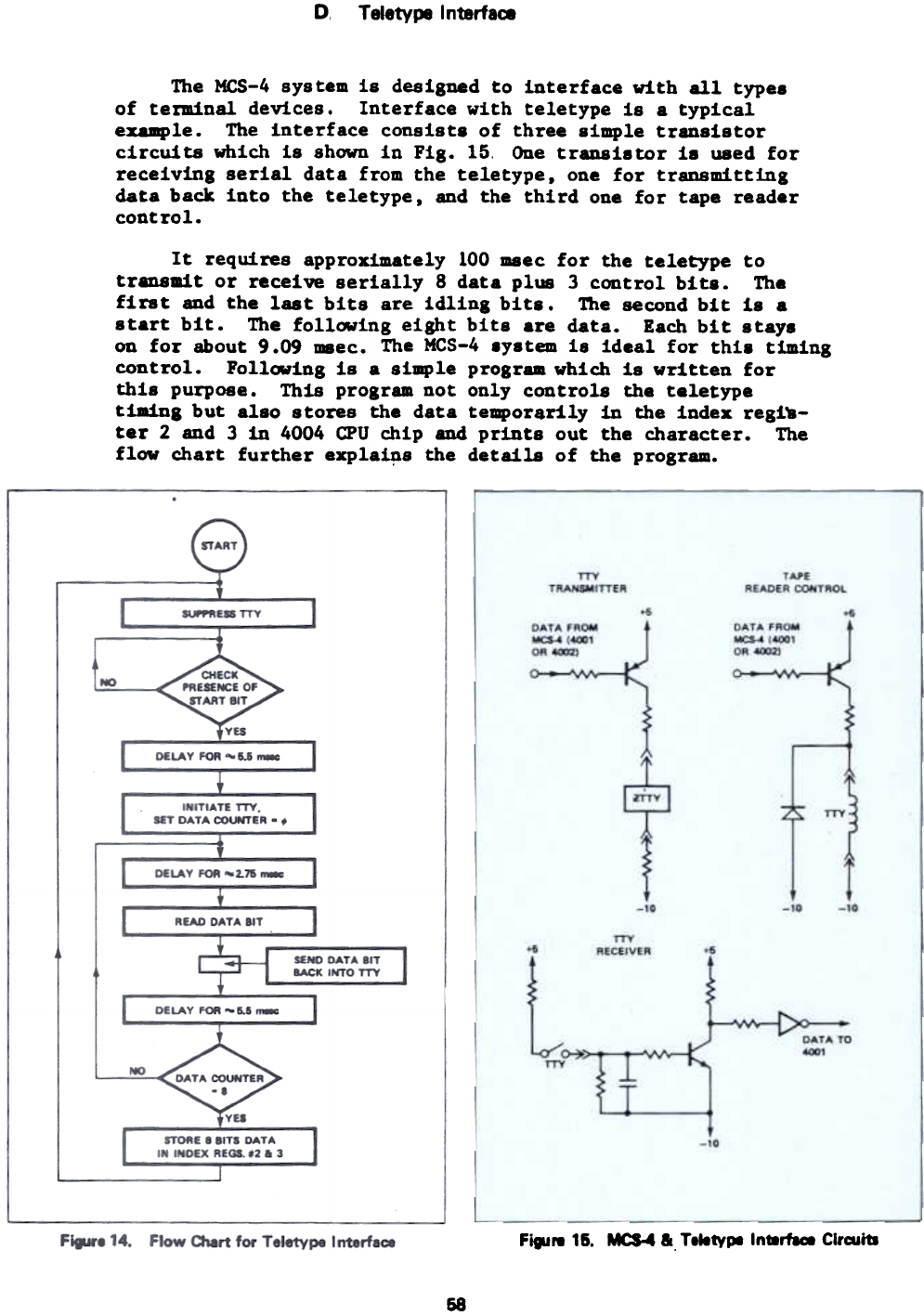
D. Teletype I nterfac»
The MCS-4 sys tam is designed to interface with all types
of terminal devices. Interface with teletype is a typical
example. The interface consist. of three simple transistor
circuits which is shown in Fig. 15. One transi8tor i8 used for
receiving serial data from the teletype, one for transmitting
data back into the teletype, and the third one for tape reader
control.
It requires approximately 100 msec for the teletype to
tr8D8mit or receive serially 8 data plus 3 control bite. The
first and the last bits are idling bits. The second bit i8 a
8tart bit. The following eight bits are data. Each bit 8tays
on for about 9.09 meec. The MCS-4 system i8 ideal for this timing
control. Following is a simple prograa which is written for
thi8 purpose. This program not only contro18 the teletype
timing but a180 s tares the data temporarily in the index regi~-
ter 2 and 3 in 4004 CPU chip and print8 out the character. The
flow chart further expla~s the details of the program.
Figu,. 16. MCS-4 A, T.letyl» In.~ Clraaitl
68

KEYBOARD INPUT ROUTINE
"0B9 8337 BEGIN.
e..,.,1 ee..
~"02 'IBee
"Oe30841
0004.3-41
~.~~ 0361
ee86 e821
8e31 1886 ST.
"~I~ ~12~
0"11 !6!665
.3128848
~.13 ~~I~
88148161
.815 ~814 TEST.
00160141
8.1183S2
8828 8364
8821 ~341
0322012i
~023 0074
"02. 0040
0~I!S 0~W"
~.26 6328
0027 0262
0030 032..
8131 ~263
0~32 i338
0833 e264
W93.1128
~~3~ ~~6S 5TI.
~836 8361
O.37 W841
Ii.. .3S2
ge41 e364
~~.2 0341
09438366
0"4.0242
a.A~ 8366
.846 8262
8047 e243
0~S~ .,366
19S10263
0952812.
e8S3 8e74
..e'54 "164
.,0SS 8834
00S68337
11I!)7084e
~968 Ieee
"061 0e41
0062 "341
"63 el~0
RW64 ~"~6
LI»t IS
F... 8c,.
SAC 8
~p
a.C
ISIL~C£ TT1
I 81 SETTINT 81T 30' 8-TO 310) I
I OE'IHE RAM AUORISS
I WRITE DATA TO MNI NHT
JCN Tl.JST
J~SJS8RI
FI" 8cJI3
ISZ IJT£ST
SAC Ic
NOH
CMA
~..
I WAI T 'lJR DATA 1."t'UT 51 OHM..
I 5.00 MS TIME OUT
I IRC8)-..INCI)-13
I COMPLETE TIMMING FOR 81' SMPLE
I DE'INE ROM PORT ADDRESS
I KEAD ROM INPUT TO AC
I COMPt.DtOtT DATA MD ECI«)
I 00 'INM.. TIME OUT 388 MS
I INC.-I)-.
I IRC2)-.
I IRC3)-.
I IRC4)-&
, ~D DATA INt'Ur
I SIUNE DATA 1~ CARRY
I LI)AD ACaIR(2)
I T 1CM~'EIt 81 T
I RES1-JRE NEW DATA ~RD
, EXTEND R£GISTEN TO "ME 8 BITS
J,"SJ
'1"
L 0."
XC"
LD4
XCH
LD4
XCii
S
CLC
SKC
RDR
OtA
~..
RAR
LD 2
RAR
XCii
LD 3
RAN
XC"
JMS
ISZ
L~
'1"
SRC
~p
JI.)'f 1ST
,
,
I
, SU8;")UTI."£~
,
, R[TU~ TO INPUT
,." I IMC.-I)..
15.47"5 TINI: 0"1
0065 00-0
~M66 0888 S~H1-
MM61 816~
.~1~ "~67 L.1-
kl071 0161
80120867
0873 8388
I~l ",LI
ISZ IILI
bM.
1t~1. 0..'
1t81~ ..11 SBR2.
11816 ~161
IA11 0116 L.2.
91"" 8161
~101 0~16
1t1l'203.8
, IH(').~,IR(I).~
, 2.75 MS 11"E IJUT
,
,
58
S8R2
8c,.
0
2
.
3
8
4
':S8RI
ec
.
3
'SBN2
4' Sf I
IS
0c'0
0c
'1" ~'8
ISZ 8'L2
IS~ "1.2
sa.
XII, DEVELOPMENT AIDS
A. Mcs.4 Standard Memory and Interface Set (4008/4009)
Prototype systems are designed to permit the use of 1702A PROMs instead of metal masked 4001 ROMs. The TTL
used in the prototype systems to simulate the control logic of the 4001 is now embodied in two special interf~ deviC8.
These new devices, the ~ and 4009, provide direct interface to standard program memory, either ROM or RAM,-!d
to TTL 1/0 ports.
The ~ is used . the address latching unit, accepting twelve bits of add,.. in each of thr- time periods A 1, A2, A3.
The add,.. is a'lailable to the pro~m memory during M 1 and M2 when the CPU accepts instructions and deta. The
Pl"owem memory may contain up to sixteen 256 byte p... The ~ also stores the 1/0 port se4ection code so the
~ropriate input or output port can be selected during the execution times X2 end X3. Demultiplexing of the el~t.bit
instruction word from prO'l'am memory and trW1smission to the data bus is carried out by the 4009 at M1 and M2 time.
By wey of e four-bit 1/0 bus which C81 communicate with up to sixteen input and output ports, data is transmitted to
W1d from the -=cumulator of the CPU via the 4009.
FEATURES
. Directly Compatible With 4004 CPU
. Interface 1702A PROMs Directly to 4004 CPU - Completely Eliminates TTL Interface
. Permits Program Storage in Alterable Memory
. Easily Combine PROMs (1702A), Metal Mask ROMs (1301), and RAMs (1101, 2102)
for Program Storage
. Expanded I/O Port Capability
. Ead1 Port May be Both I nput and Output - Up to 16 4-bit I nput Ports and 16 4-bit
Output Ports
. Number of I/O Ports is Independent of the Size of the Program Memory
. I/O Ports and Control Lines are TTL Compatible
. Execute MCS-4 Programs from any Mix of Standard Intel ROMs and RAMs
. New Instruction WPM (Write Program Memory) is Used for Loading Alterable Program
Storage (RAM)
~
~
~ 1'8 - MAXI_' r-: ~-.~-
\ @--
l. 118 IWUT PORTS
..-18OUTPUT
I -. . PORTS ~I_I
I::~=.~ =~
~ MY DATA" . .
, .
~ .
r~~-..
110 PORTS
~I.-.cr GATI.o
Besic MCS-4 System Using 4008 and 4009
60
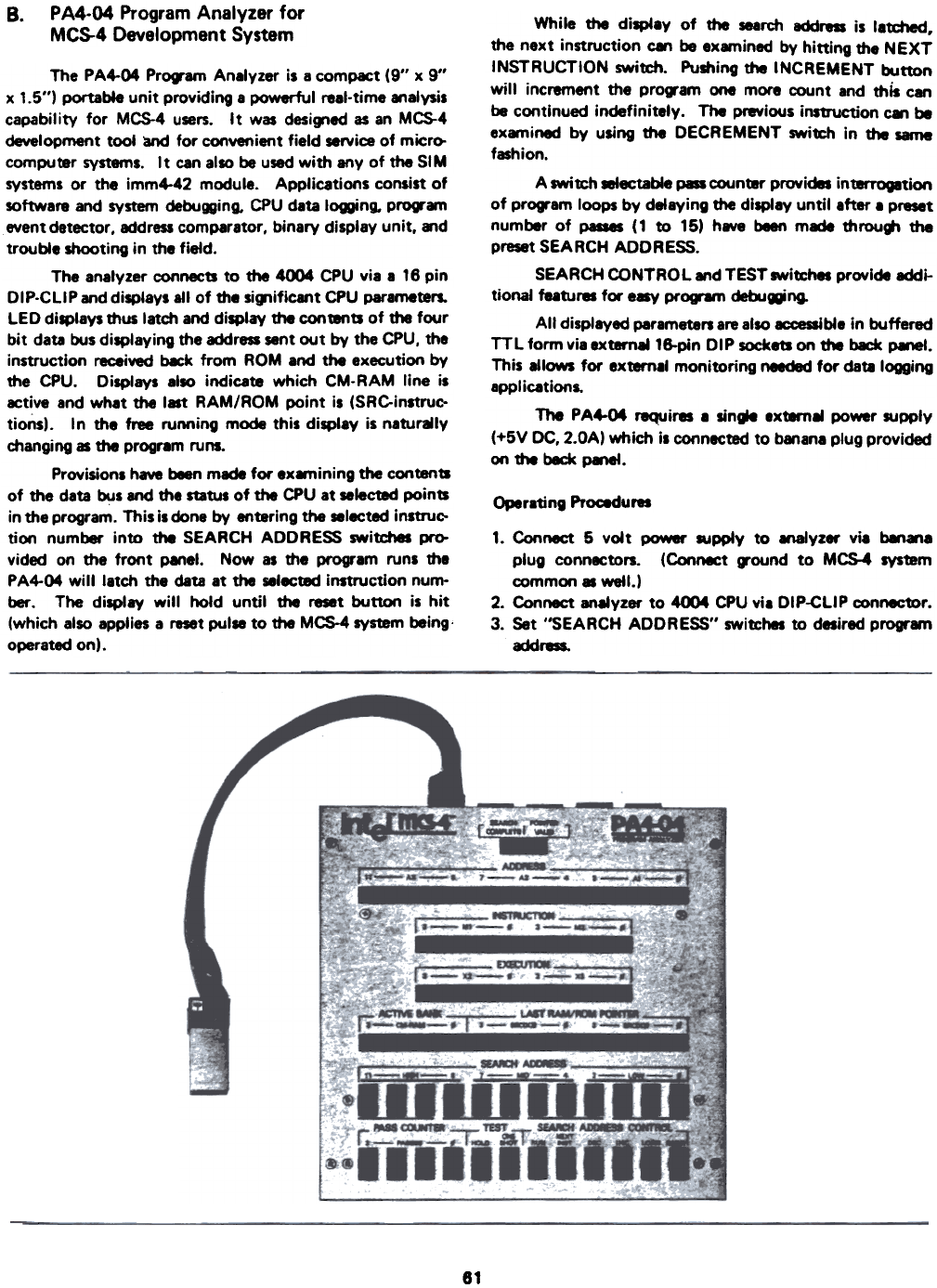
PA4.04 Program Analyzer for
MCS-4 Development System
B. While the disptay of the seard1 add,.. is latdwd.
the next instruction ~ be examined by hitting the NEXT
INSTRUCTION switch. Pushing the INCREMENT button
will increment the pr°'lam one more count and this can
be continued indefinitely. The previous instruction C81 be
ex~ined by using the DECREMENT swi1l:h in the same
fashion.
A swi1l:h "ectable pass counter provides interrOQation
of program loops by defaying the display until after a preset
number of paaes (1 to 15) h8V8 been made throu~ the
preset SEARCH ADDRESS.
SEARCH CONTROL and TEST switches provide addi-
tional features for e8y program debu8ng.
All displayed parameters are also accessible in buffered
TT L form via external 16-pin DIP sockets on the back ~I.
This allows for external monitoring needed for data logging
appl ications.
The PA4-04 requi~ a sin~ external power supply
(+5V DC, 2.0A) which is connected to banana plug provided
on the beck p81ei.
The PA4-04 Pr~ Analyzer is a compact (9" x 9"
x 1.5") portable unit providing a powerful real-time analysis
capability for MCS-4 u.rs. It was desi~ed as an MCS-4
development tool "and for convenient field .Nice of micro-
computer systems. It can also be used with any of the SIM
systems or the imm4-42 module. Applications consist of
software and system debu.ing, CPU data logging, prQ9"am
event detector, address comparator, binary display unit, and
trouble shooting in the field.
The analyzer connects to the 4004 CPU via a 16 pin
DIP-CLIP and displays all of the si~iflcant CPU parameters.
LED displays thus latd1 and display the contents of the four
bit data bus displaying the address .nt out by the CPU, the
instruction received b.:k from ROM and the execution by
the CPU. Displays also indicate which CM-RAM line is
active and what the last RAM/ROM point is (SRCinstruc-
tions). In the free running mode this display is natu~ly
d1anging as the program runs.
Provisions have been made for ex8nining the contents
of the data bus and the status of the CPU at .lected points
in the program. This is done by entering the .Iected instruc-
tion number into the SEARCH ADDRESS switdtes pr0-
vided on the front panel. Now as the program runs the
PA4-04 will latch the data at the .Iected instruction num-
ber. The display will hold until the ~ button is hit
(which also applies a reset pul. to the MCS-4 system being,
operated on).
Operating PrOC8dures
1. Connect 5 volt POWW' wpply to 8nalyzer vi. b8\.,.
plug connectors. (Connect ,#,ound to MCs.4 system
common - well.)
2. Connect analyzer to 4004 CPU vi. DIP-CLiP connector.
3. Set "SEARCH ADDRESS" switches to desired program
add,...
81
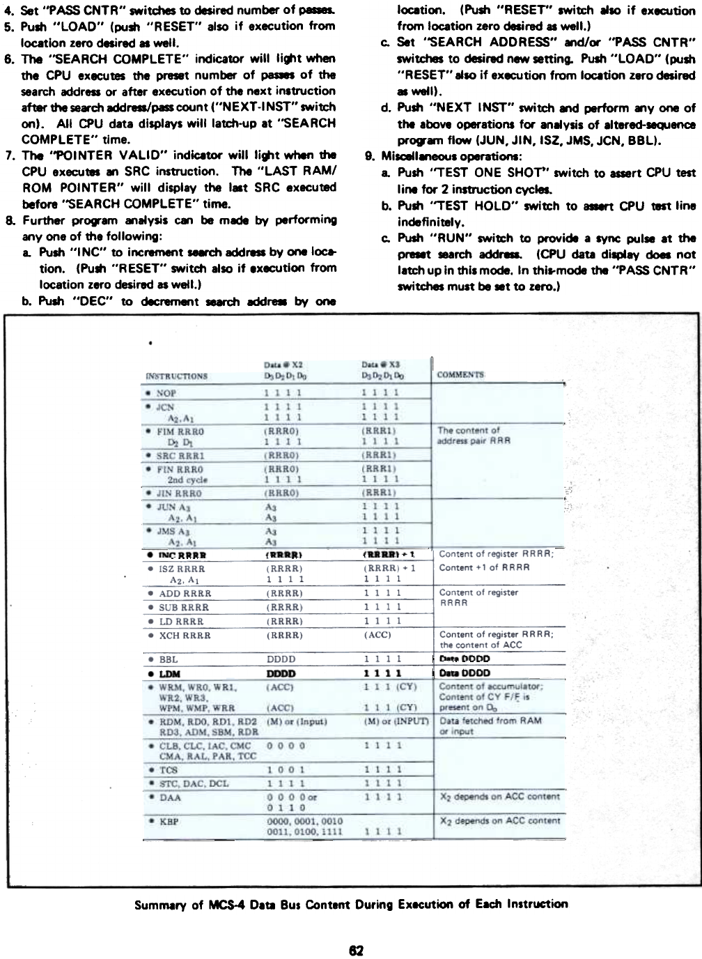
I~tion. (Push "RESEr' switch also if execution
from location zero desired as well.)
c. Set "SEARCH ADDRESS" .,d/or "PASS CNTR"
switd18S to desired new .tting. Push "lOAD" (push
"RESET" also if execution from I~tion zero desired
. well).
d. Push "NEXT INST" switch 81d perform .,y one of
the above operations for analysis of altered-sequence
prO9'aIn flow (JUN. JIN, ISZ, JMS, JCN, BBl).
9. Miscell81eoul operations:
a. Push "TEST ONE SHOr' switch to assert CPU test
line for 2 instruction cycles.
b. Push "TEST HOLD" switch to ~ CPU test line
indefinitely.
c. Push "RUN" switch to provide a sync pul. at the
preset ..rch addr-. (CPU data display does not
latch up in thil mode. In this-mode the "PASS CNTR"
switches must be .t to zero.)
4. Set "PASS CNTR" switd8 to desired number of p-.s.
5. Push "LOAD" (push "RESET" also if execution from
location zero desired as well.
6. The "SEARCH COMPLETE" indicator will li~t when
the CPU executes the preset number of pa-. of the
search address or after execution of the next instruction
after the search addrea!passcount ("NEXT -INST" switch
on). All CPU data displays willlatd\-up at "SEARCH
COMPLETE" time.
7. The "POINTER VALID" indicator will li~t when the
CPU executes ., SRC instruction. The "LAST RAMI
ROM POINTER" will display the last SRC executed
before "SEARCH COMPLETE" time.
8. Further prQ9'am "alysis C81 be made by performing
anyone of the following:
L Push "I NC" to increment Ie«ch add,.. by one I~
tion. (Pu., "RESET" switch also if .x~tion from
location zero desired as well.)
b. Push "DEC" to decrement ~ 8ddr88 by one
Summary of MCS-4 Dat8 Bus Content During Execution of Each Instruction
82
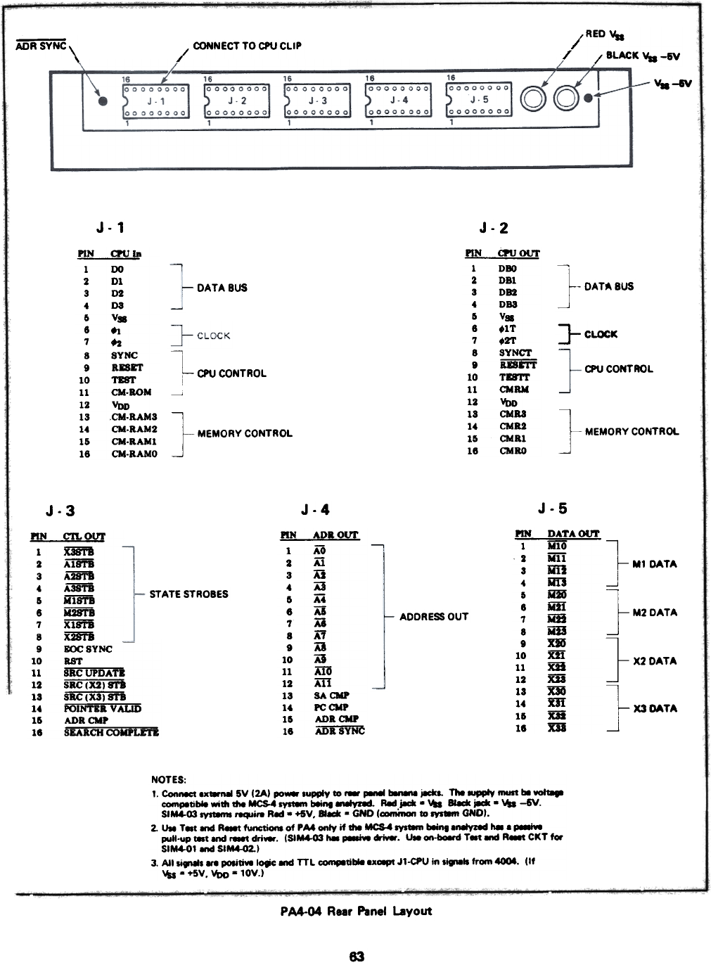
ADR"iY'NC, /
/ CONNECT TO CPU CLIP /
"RED Va
/ BLACK Va -6V
\.I
v.-6V
J-1 J-2
PIN crulJl
1 DO
2 01
3 D2
4 D3
& V.
6 ~
7 ~
8 SYNC
9aaET
10 TB8T
11 CM-RON
12 Voo
13 CM.RAM3
14 CM.RAM2
15 CM.RAMI
16 CM-RAMO
PIN CPt} 0fJf
1 DBO
2 DB1
3 DB2
4 DBa
6 V.
6 .1T
7 .2T
6 SYNCT
9iiiffi
10 T88'lT
11 CMRM
12 Vno
13 CMRa
14 CMR2
15 CM&l
16 <:MaG
OAT~8US
DATA BUS
}-CLOCK
CPU CONTROL
CPU CONTROL
MEMORY CONTROL
MEMORY CONTROL
J.5
J.4
J.3
PIN DATAOVI'
1 M'iO
2 Mil
3 Iii!
4 m
5 MB
8 MH
7 iiB
8 iiD
9 m
10 XII
11 XU
12 Xii
13 'i:iO
14 m
15 :i:ii
18 Xii
PIN AD" Ot7f
1 AO
2 Ai
3 Ai
4 A1
5 Ai
6 Ai
1 Ai
8 A1
9 AI
10 AI
11 m
12 An
13 SA ClIP
14 PC CUP
15 ADa ClIP
16 ADa SYNC
fIN cn. otn'
lXB'fi
2Ai'fii
3A2m
4A38fi
5Mii'fi
sii2ifi
7iiifi
sX2fii
9 BOC SYNC
10 RST
11 SRC UPDATE
12 SRC In) ST8
13 SRC(X3)ST8
14 POINTER VALID
15 ADR CUP
16 SEARCH COMPLETE
M1 DATA
STATE STROBES
M2 DATA
ADDRESS OUT
X2 DATA
X3 DATA
NOTES:
1. Con.-t exwn8l5V (2A1 po- supply to ~ ~ -- j8CkI. TIw MItIPIY nMIIIl8 ~
CGmpetibie wid! die Mcs.4 IyIt8n belng.wynd. Red j-* - \\I Bleck j-* - \\I -6V.
SIM4-031Y1t8m1 ~i,. A8d - +5V, -. - GND (conNnon to ~ GNDI.
2. u. T.t MId ~ functi- of PM only if die MCs.4sys- beln, 1n88yzed ha I ~
pull-up *t MId - dri_. (SIM4-03 ha p-.M «'-- U.. CInobO8rd T.t MId ~ CKT 108'
SIM4-01 MId SIM4.02.1
3. All sips - positive I. MId TTL competible ex.-pt J1-CPU in silnllalrom 400.. (If
~. +5V, Vno -10V.1
PA4-04 Rear Panel Layout
63
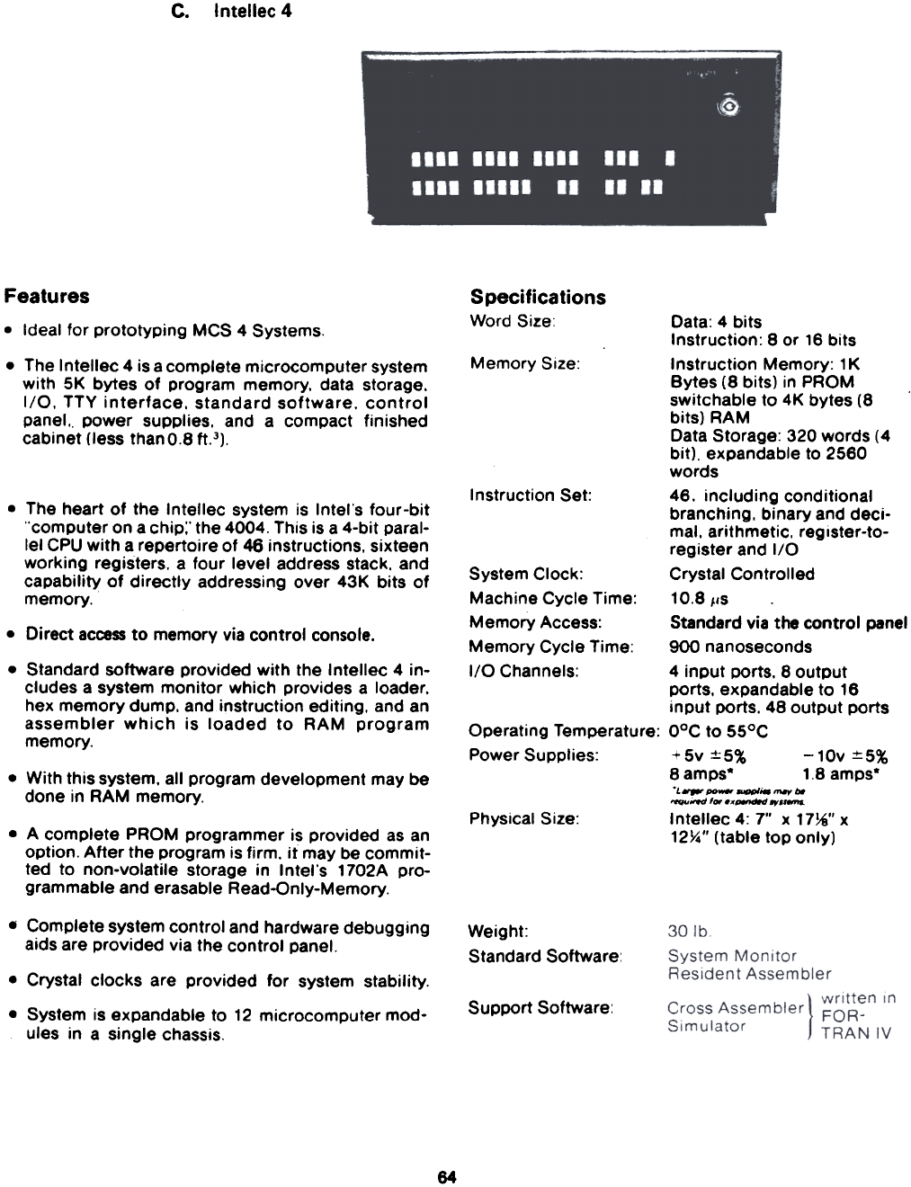
c. Intellec 4
Specifications
Word Si~e: Data: 4 bits
Instruction: 8 or 16 bits
Memory Size: Instruction Memory: 1 K
Bytes (8 bits) in PROM
switchable to 4K bytes (8
bits) RAM
Data Storage: 320 words (4
bit). expandable to 2560
words
Instruction Set: 46. including conditional
branching. binary and deci-
mal. arithmetic. reglster-to-
register and I/O
System Clock: Crystal Controlled
Machine Cycle Time: 10.8 liS
Memory Access: Standard via the control panel
Memory Cycle Time: 900 nanoseconds
I/O Channels: 4 input ports. 8 output
ports. expandable to 16
input ports. 48 output ports
Operating Temperature: OoC to 55°C
Power Supplies: +5v:::5% -10v:t:5%
8 amps. 1.8 amps.
.L~po '"
fM"_",-
Physical Size: Intellec 4: 7" x 17~" x
12Y4" (table top only)
Features
. Ideal for prototyping MCS 4 Systems.
. The Intellec 4 is a complete microcomputer system
with 5K bytes of program memory. data storage.
I/O, TTY interface. standard software. control
panel.. power supplies. and a compact finished
cabinet (less thanQ.S ft.3).
. The heart of the Intellec system is Intel's four-bit
"computer on a chip;' the 4004. This is a 4-bit paral-
lel CPU with a repertoire of 46 instructions. sixteen
working registers. a four level address stack. and
capability of directly addressing over 43K bits of
memory.
. Direct access to memory via control console.
. Standard software provided with the Intellec 4 in-
cludes a system monitor which provides a loader,
hex memory dump, and instruction editing, and an
assembler which is loaded to RAM program
memory.
. With this system. all program development may be
done in RAM memory.
. A complete PROM programmer is provided as an
option. After the program is firm. it may be commit-
ted to non-volatile storage in Intel's 1702A pro-
grammable and erasable Read-Qnly-Memory.
. Complete system control and hardware debugging
aids are provided via the control panel. Weight:
Standard Software:
Support Software:
. Crystal clocks are provided for system stability.
. System is expandable to 12 microcomputer mod-
ules in a single chassis.
64
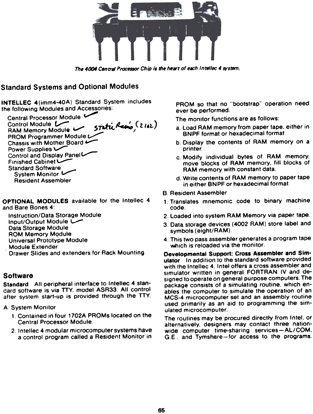
The 4004 Central Pr«essor Chip is the heart of e«:h Intellec 4 system.
Standard Systems and Optional Modules
INTELLEC 4{imm4-40A) Standard System includes
the following Modules and Accessories:
Central Processor Module c./
Control Module V- c...:..4..: ~ (t"L)
RAM Memory Module 4./ .7r~ c.(. I
PROM Programmer Module r,/
Chassis with Mother Board ~
Power Supplies V-
Control and Display Panel ~
Finished Cabinet~
Standard Software, .-
System Monitor Resident Assembler
OPTIONAL MODULES available for the Intellec 4
and Bare Bones 4:
Instruction/Data Storage Module
Input/Output Module \ '""'
Data Storage Module
ROM Memory MQdule
Universal Prototype Module
Module Extender
Drawer Slides and extenders for Rack Mounting
PROM so that no "bootstrap" operation need
ever be performed.
The monitor functions are as follows:
a. Load RAM memory from paper tape. either in
BNPF format or hexadecimal format.
b. Display the contents of RAM memory on a
printer.
c. Modify individual bytes of RAM memory.
move blocks of RAM memory. fill blocks of
RAM memory with constant data.
d. Write contents of RAM memory to paper tape
in either BNPF or hexadecimal format.
B. Resident Assembler
1. Translates mnemonic code to binary machine
code.
2. Loaded into system RAM Memory via paper tape.
3 Data storage devices (4002 RAM) store label and
symbols (eight/RAM).
4. This two pass assembter generates a program tape
~ich is reloaded via the monitor.
Developmental Support: Cross Assembler and Sim-
ulator In addition to the standard software provided
with the Intellec 4. Intel offers a cross assembler and
simulator written in general FORTRAN IV and de-
signed to operate on general purpose computers. The
package consists of a simu~ating routine. which en-
ables the computer to simulate the operation of an
MCS-4 microcomputer set and an assembly routine
used primarily as an aid to programming the sim-
ulated microcomputer.
The routines may be procured directly from Intel, or
alternatively. designers may contact three nation-
wide computer time-sharing services-AL/COM.
G.E. and Tymshare-for access to the programs.
Software
Standard All peripheral interface to Intellec 4 stan-
dard software is via TTY. model ASR33. All control
after system start-up is provided through the TTY.
A System Monitor
1 Contained in four 1702A PROMs located on the
Central Processor Modu.le.
2 Intellec 4 modular microcomputer systems have
a control program called a Resident Monitor in
65
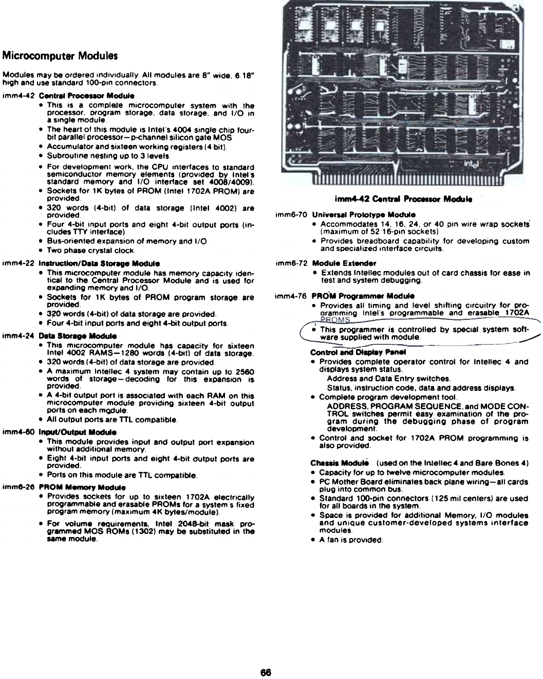
Microcomputer Modules
imm4-42 Centr81 P~1or M imm6-70 Universal Prototype Modute
. Accommodates 14, 16, 24, or 40 pin wire wrap sockets
(maximum of 52 16-pin sockets)
. Provides breadboard capability for developing custom
and specialized Interface Circuits
imm6-72 Module Extender
. Extends Intellec modules out of card chassis for ease in
test and system debugging
imm4-76 PAO'M Programmer Module
. Provides all timing and level shifting circuitry for pro-
Aramming Intels programmable and erasable 1702A
. This programmer is controlled by special system soft-
ware supplied with module ~
Control 8nd OfIPl8Y P8nel
. Provides complete operator control for Intellec 4 and
displays system status.
Address and Data Entry switches
Status. instruction code. data and address displays
. Complete program development tool
ADDRESS. PROGRAM SEQUENCE. and MODE CON.
TROL switches permit easy examination of the pro-
gram during the debugging phase of program
development
. Control and socket for 1702A PROM programming is
also provided.
Ch8ai1 Modu18 (used on the Inlellec 4 and Bare Bones 4)
. Capacity for up to twelve microcomputer modules
. PC Mother Board eliminates back plane wiring-all cards
plug into common bus.
. Standard 100-pin connectors (125 mil centers) are used
for all boards in the system.
. Space is provided for additional Memory, 1/0 modules
and unique customer-developed systems interface
modules
. A fan is provided
Modules may be ordered Individually All modules are 8" wide, 618"
high and use standard 10o-pin connectors
imm4-42 C~tr.' Proceaor Module
. This is a compleJe microcomputer system with the
processor, program storage, data storage, and 1/0 in
a single module
. The heart of this module is Intels 4004 single chip four-
bit parallel processor-p-channel silicon gate MOS
. Accumulator and sixteen working registers (4 bit)
. Subroutine nesting up to 3 levels
. For development work, the CPU Interfaces to standard
semiconductor memory elements (provided by Intel's
standard memory and 1/0 interface set 4008/4009).
. Sockets for 1K bytes of PROM (Intel 1702A PROM) are
provided
. 320 words (4-bit) of data storage (Intel 4002) are
provided
. Four 4-bit input ports and eight 4-bit outPut POrts (in-
cludes TTY interface)
. Bus-oriented expansion of memory and 1/0
. Two phase crystal clock
imm4-22 Instruction/D... Stor8ge Module
. This microcomputer module has memory capacity iden-
tical to the Central Processor Module and is used for
expanding memory and 1/0.
. Sockets for 1 K bytes of PROM program storage are
provided
. 3~0 words (4-bit) of data storage are provided.
. Four 4-bit input POrts and eight 4-bit output ports
imm4-24 0... Stor8ge Modul.
. This microcomputer module has capacity for sixteen
Intel 4002 RAMS-1280 words (4-bit) of data storage
. 320 words (4-bit) of data storage are provided
. A maximum Intellec 4 system may contain up to 2560
words of storage-decoding for this expansion is
provided
. A 4-bit output port is associated with each RAM on this
microcomputer module providing sixteen 4-bit output
ports on each mOdule
. All outPut ports are TTl compatible
imm4-60 Input/Output Module
. This module provides input and output port expansion
without additional memory
. Eight 4-bit input POrts and eight 4-bit output ports are
provided.
. Ports on this module are TTl compatible
imm6-26 PROM Memory Module
. Provides sockets for up to sixteen 1 702A electrically
programmable and erasable PROMs for a systems fixed
program memory (maximum 4K bytes/module)
. For volume requirements. Intel 2048-bit mask pro-
grammed MOS ROMs (1302) may be substituted in the
same module.
68
MCS-4 EVALUATION KIT USING THE 4001-0009
XIII.
This kit provides both a convenient way of evaluating the MCS-4 parts
and an educational vehicle to better understand the MCS-4 operation.
The 4001-009 stores a microprogram that exercises the 4004 and 4002's
and executes all of the 45 instructions in the MCS-4 instruction set.
Fig. 16 shows the hardware that should be used. The circuit for single pass/
continuous can be omitted if only continuous operation is sought. In this
case °0 (RAM 10) should be connected directly to TEST.
The RESET sianal can be provided by either a one-shot circuit or by a pulse
generator in the "single pulse" tOOde. The width of the RESET signal must
be at least 32 x 8 clock periods (=-350 llSec) to fully clear the RAM storage.
If the system is operated in the continuous mode, RESET needs to be applied
only at power on. If the system works in the single pass aode, when END of
SEQUENCE (Pin 03) is "1", the 4004 will "hang" on a loop where the address
to Jump to on a jump on TEST - I condition is the address of the same jump
on condition. To get out of the loop RESET must be applied.
To ~i tor the program operation. scope should be used in the I'B delayed
by AI' ~de. By using the delay ti~ multiplier the program execution can
be easily seen. The synchronization signals for the B and A traces are
pin 13 of 4002-1 10 and SYNC, pin 8 of the 4004, respectively.
The 4001-0009 has been coded with the internal chip 8e1ect circuit alwaY8
activated, therefore any address at A3 time will cause the 4001 to be
selected. This i8 different from the normal operation of the 4001 where
only one code (out of 16) at A3 time 8e1ects the 4001. The reason for doing
80 i8 that we can .how the execution of JMS and JUS instructions to any chip
number (the A3 time code) and still use only 1 ROM chip.
The I/O pins of the 4001-0009 are all connected as inverting inputs with no
resistor. copnected.
The two phase clocks, ('l and '2) must be supplied externally according to
the KCS-4 data sheet specs.
The program execution is 110 msec. using a clock period of 1.3 usec.
Although the CM-RAMi lines are not used in this configuration-, they are
being pulse4. If a scope is hooked up to these lines the waveforms may be
observed.
Both 4002-1's must be used in order to fully execute the prosraa stored
in the ROM.
Attached is the program flow (with comments) and the truth table.
87
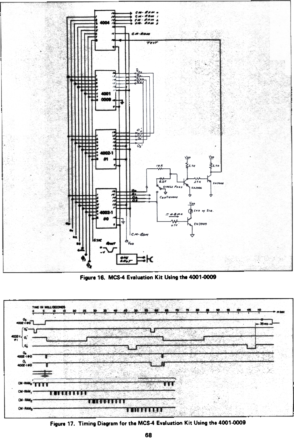
~ ".-~ ~ CA' ~.- ,
"..~A_&
,... I.. I4004
eA-6_-
~
rl.r
~
.."
0008
~
H
4002.1
#1
"!
-! -.. "
..
.J
Figure 16. MCS-4 Evaluation Kit Using the 4001-0009
~..~ - . . .. . .. ...~ " . . .. . ... ---
~ f ~ ~ T T T T . , , , . , . , ,
0.
-..
{at -.. 0;
.,
Oi
~
_-'.0
0.
"-180
==$= - c- . ..
~.-.' ~-
CM-- I
CM-~
CMo-,- llllf.'lll";:""
Figure 17. Timing Diagram for the MCS-4 Evaluation Kit Using the 4001-0009
68
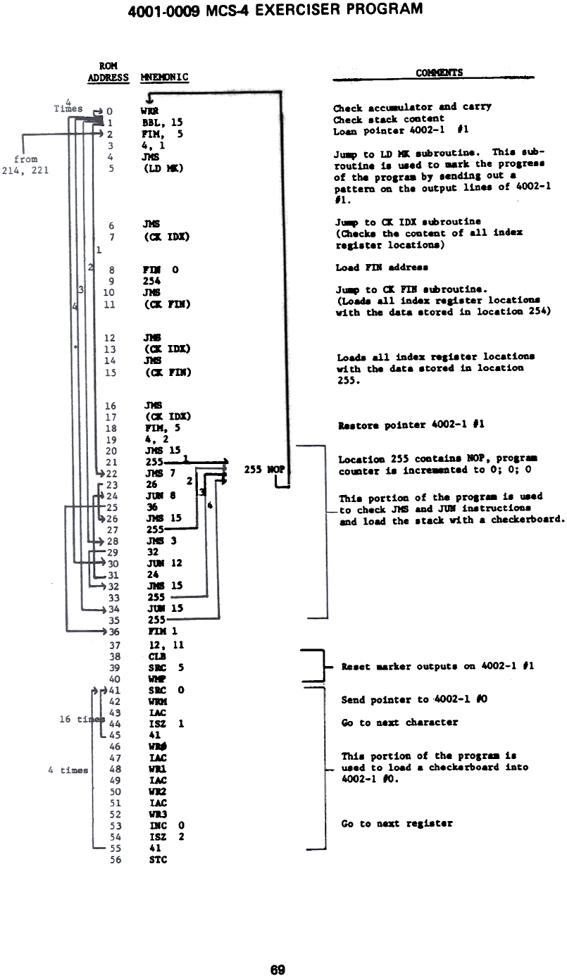
4001-0009 MCS-4 EXERCISER PROGRAM
ROM
ADDRESS ~IC
COlG4!NTS
Oleck acc~tor and carry
Oleck atack cootent
Loan pointer 4002-1 11
JU8p to LD M( aubroutiua. Thia .ub-
routine i. U8ed to .ark the prolre88
of the prolr.. by ..nclinl out a
pattern on the output line. of 4002-1
11.
WD
BBL, 15
nM, 5
4,1
.nm
(LD 1«)
J!§
(~ IDX)
J~ to (% IDX ._routine
(Checks the COGt8Gt of all indes
rea1.~er locationa)
Load FIR addrea.
J~ to (% FIR ._routine.
(Lo8d8 all ind.s r8&i.ter locatiO118
with the data .tored in locatiOG 254)
FDO
2.54
J}8
(~ FIB)
J!8
(~ 1m)
.JIm
(~ rIW)
Loada all indes A.tater locati0D8
with the data etored in location
255.
a..tore pointer 4002-1 II
Locat1OD 255 coata1D8 HOP. prOlr88
count8r 18 1ncre88Qt8d to 0; 0; 0
jim
«S IDX)
nN. 5
4.2
JlmLS
255 1 .
jim 7 IP26 2
JW8
36
jim 15
255-
3183
32
JW 12
24
318LS
255
JW 15
255
nN1
12. 11
CL8
S': 5
~
SIC 0
WIN
IAC
IU 1
41
VII
IAC
VIl
IAC
va
IAC
WR3
IKC 0
IU 2
41
STC
255 HOP
L
4Thi8 por~10D of ~he proar.. 18 uaed
~o check JI8 and .roB 1D8~ruc~1OD8
and load ~he 8~ack vi~h a checkerb08rd.
==t ae.et ..rker output. on 4002-1 Ii
Send pointer to -4002-1 10
Go to next cherecter
Thi. portion of the procr.. i.
uaed to l08d a checkerboard into
4002-1 10.
Go to ~ reliat8r
69
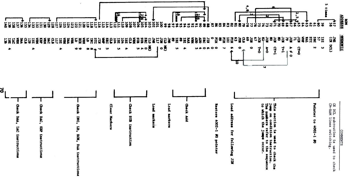
...
w,"',
["
,,- ~
"
"
"
"
, "
. ..
"
,.
..
70
n
"
"
'4
"
'4
77
::
.,
"
"
::
"
..
.,
~ ~
::
9'
..
..
::
'"
~
li'
li4
'"
li4
[ ::; ~ ::: li'
"4
li'
::~
li'
[ '" i~
:::
[!E
MDDIC
JIm
«% DCL)
ISZ 3
57
SKC 2
STC
IAL
w-.
J~ Ct-o
71
J~ A ~ 0
79 ~
J~ T-1
~
J~ Ct-1
~
J~ PO
~
J~ TwO
67
Jt80
69
CLl JJmO 63
nK6
102
nK7
89
nKO
0 0
JD 6
SKC 0
Am4
Am5
W8
BAa
ISZ 4
89
ISZ 5
89
ne
(LD ")
Jt80
i17
J18
(LD I&)
SKC 0
SUB 4
SUB 5
W8
CLI
15Z 4
104
ISZ 5
104
CLI
sac 5
~
JD 7
STC
DC 8
LD 8
W8
%a9
LD 9
WD.
DAA
W8
ISZ 4
117
CLI
MC
WIM
DP
W8
ISZ 4
129
CLI
DAA
W8
lAC
Iaz 4
136
17
Olea M4
Oieck mc, Ln, XCB, DAA inat.
~
~ addreaa for foll~ Jm
Clear HefteR
Load _rkera
Load _rken
Ie.tore 4002-1 10 pointer
Olea SUB 1netruct1OD
PoiDter to 4002-1 fa
tbj.e .ection 18 wed to check the
j~ OD COOdit1OD 1II8truct1OD.
The DU8bera refer to the aequence
to which the j~ occur.
~Ct10D8
1 O1.ck BAC. UP 1D8truct10118
1 Check DAA. IAC in8truCti0U8
-.J
70
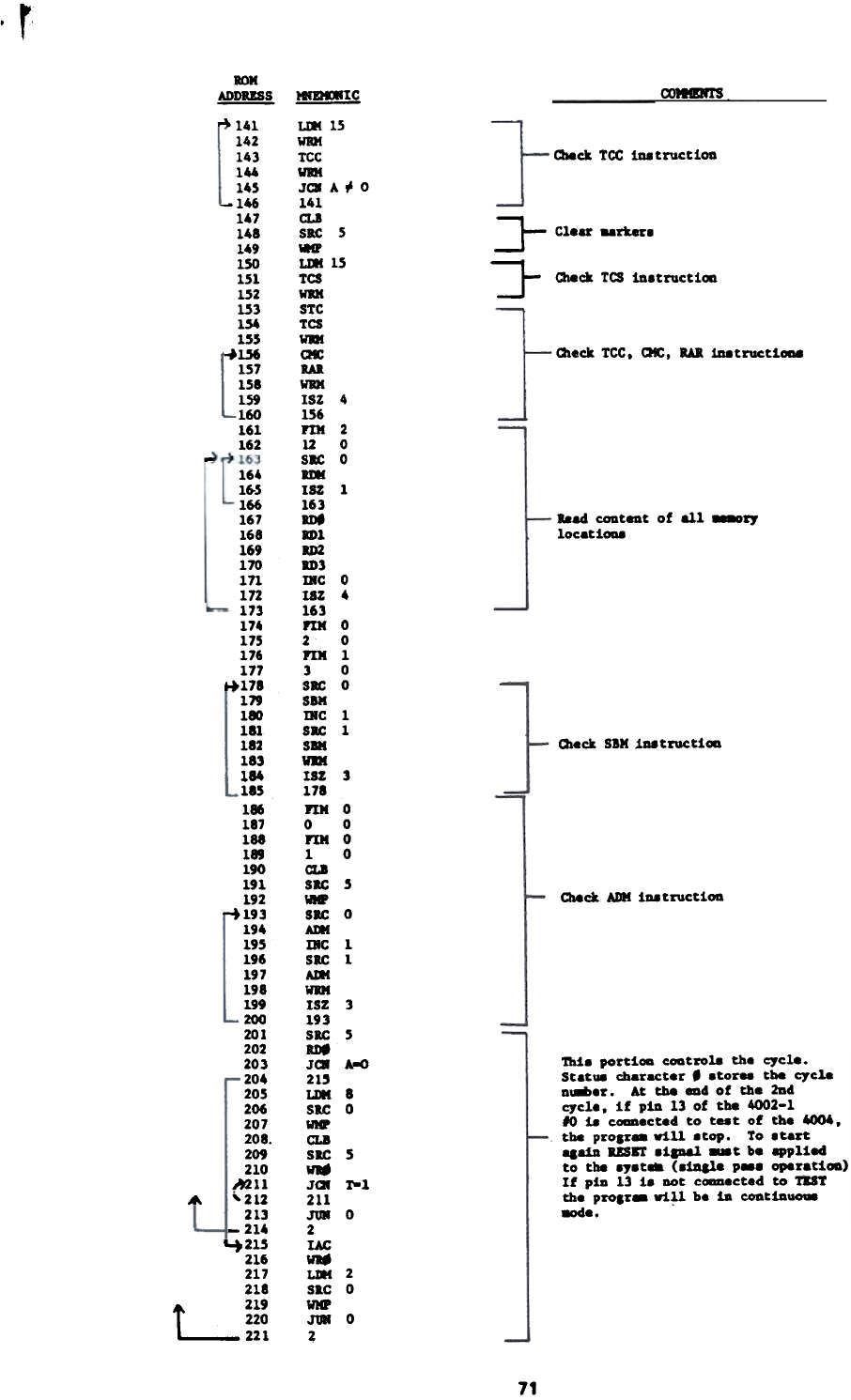
, r
(X)IIt!In$-
oIect TCC 1D8truct1ou
ROM
ADDRESS !lfE!dIC
"" 141 LI»I 15
142 WRK
143 TCC
144 Wmt
145 JC8 A ~ a
-146 141
147 CLI
148 sac 5
149 aa
150 L1»115
151 TCS
152 WRK
153 STC
1.54 TCS
155 WDI
...1.56 Q.:
157 RAa
158 WRK
159 ISZ 4
160 156
161 PIM 2
162 12 a
SIC a
..
IU 1
163
IDf
IDI
aDZ
1D3
DC a
UZ 4
163
PIMa
2 a
nJl1
3 a
SIC a
saM
DC 1
SIC 1
S.
WDI
UZ 3
178
nJla
a a
PIMa
1 0
a.I
SIC .5
~
SIC a
ArM
DC 1
sac 1
ArM
VB
ISZ 3
193
sac 5
IDf
JC8 A-o
21'
1.1»18
sac 0
ww
CLI
SIC S
-
J(3 r-l
211
JURO
2
lAC
WIf
L1»12
SI.C 0
ww
JTMO
2
:I- Clear ..rke~e
J- OIeck fCS 1n.truct1~
atea TCC. QfC. 1n8truct1-
~
164
16-5
166
167
168
169
170
1n
172
173
174
175
176
177
~178
179
1-
181
182
183
184
185
186
187
188
189
190
191
192
-'193
194
195
196
197
198
199
200
201
202
203
204
205
206
207
208
209
210
hlll
'212
213
-214
215
216
217
218
L 219 220
221
18ad coat_t of all -rr
locatt-
Oleck SBM J.utructi-
Oteck AD!! iD8truct1on
'DIJ.. porti~ ~trol8 the cycl8.
Statue char8Cter . .tora tbe cycle
nl8»er. At the _d of the 2nd
cycle, if pin 13 of the 4002-1
10 18 c_ected to t..t of the ~,
the proar" will .top. To .tart
aaaiD usn .ipal _t be applied
to the .y.ta (.iDale p.e operatiGD)
If pin 13 i. DOt c0aD8ctad to ~T
the proar- will be in contin-
8O4e. ....
71
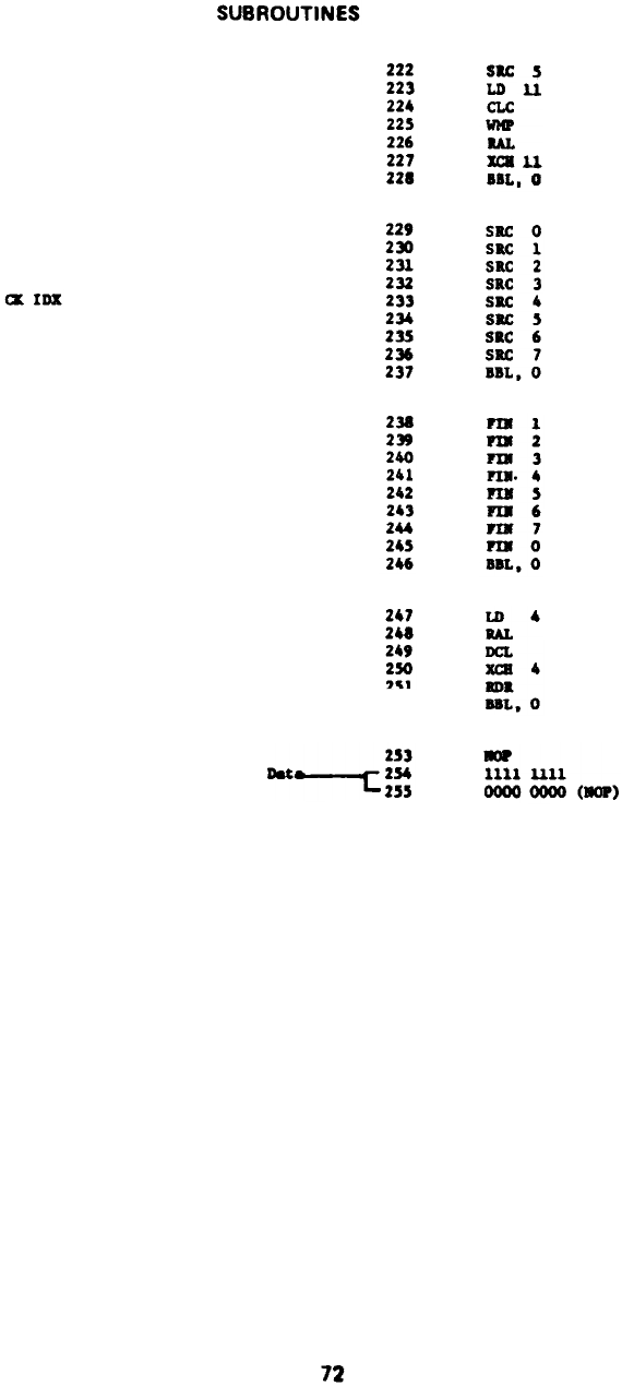
SUBROUTINES
222
223
224
225
226
227
228
SIC
LD
CLC
~
IAL
IC8
IlL
229
2~
231
232
233
234
235
236
237
SIC 0
sac 1
sac 2
sac 3
SIC 4
SIC .5
sac 6
SIC 7
BBL,O
IX IU
238
239
240
241
242
243
244
24.5
246
FIBl
FIB 2
FIB]
~. 4
~.s
~6
FIB 7
FIB 0
BBL,O
247
248
249
250
~~1
LD 4
RAL
DCL
XCB4
IDa
BBL. 0
nJ
2.54Dat- -'{: 255 .w
1111 Ull
0000 0000 (.w)
72
5
U
U
.0
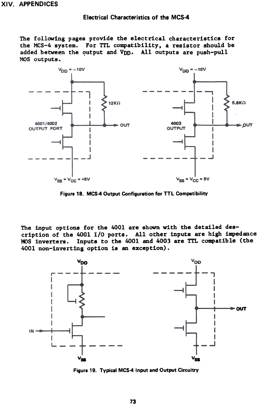
XIV. APPENDICES
Electrical Characteristics of the MCS-4
The following pages provide the electrical characteristics for
the MCS-4 system. For TTL compatibility, a resistor should be
added between the ~utput and VDD. All outputs are push-pull
HOS outputs.
Figure 18. MCS-4 Output Configuration for TTL Compatibility
The input options for the 4001 are shown with the detailed des-
cription of the 4001 I/O ports. All other inputs are high impedance
MOS inverters. Inputs to the 4001 and 4003 are TTL compatible (the
4001 non-inverting option is an exception).
Voo
OUT
v.
v.
Figure 19. Typical MCS-4 Input and Output Circuitry
73
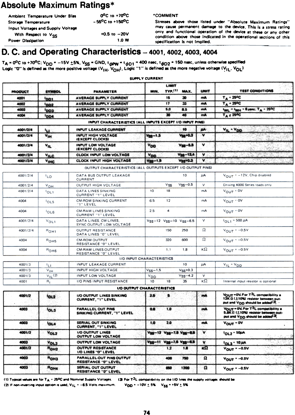
'COMMENT
Stresses above those listed under "Absolute Maximum Ratings"
may cause permanent d8ma~ to the device. Thills a stress rating
onlY and functional operation of the device at these or any other
condition above those indicated In the operational sections of this
specification is not Implied.
Absolute Maximum Ratings*
D. C. and Operating Characteristics - 4001,4002,4003,4004
S~LYCURRENT
LIMIT
TVP}" MAX
TEST CO~DtTIO~S
MIN ~T
mA
mA
mA
~
PR~
~1
4m2
~
---
'Y~L
'001
1002
; '003
InM
TA-aoc
TA-2IOC
,gA_TIN
AV~AGE IUWL Y CUR~ENT
AVI~AGI ~LY CUft~ENT
AVE~AGE ~LY CUA~ENT.
AVI~AGIIU"L Y C~ENT
,.
'ii'
U
.
~
8..
"4i
'WL' 'Wti' 8_; TA' 25Oc
TA~OC-
INPUT CHARACTERISTICS IALL I~ EXCEPT 1/0 INPUT PINSI
4001/2/4
4001/2/4
INPUT LEAKAGI CIMRINT
INPUT HIGH VOLTAGE
(EXCEPT CLOCKS!
INPUT LOW VOLTAGE
(EXCIPT CLOCK!)
CLOCK INPUT LOWVOLTAOI
CLOCK INPUT HIGH 'JOLTAGI
,.-
-yI VIL . VDD~".c~,...~,! I
!ilL
VIH
~ 0
¥840.3
V.-U
v.-t.5
VOO
~1/2/4 v
VIL
~
VIHC ,~.. ~~ I
,,~,.. Vw'O.3 I
41»1/2/4
4001/214
I/O OUTPUT CHARACTERISTICS
Your.ov. F. T2t. __Ibility .
121C 0 1!.1", IIUt_VOO~b8~3I. .
-
4001/2 110 0UT1'\IT LINES SINKING
CUMENT, "1" LEVEL
2.5 :a ..
IOU
4003 PARALLEL OUT PINS
SINKI~G CURRENT, "'" LEVEL
0.1 1.0 mA VOUT-OY.F_T2L _~ility.
5..nC~I",__out,
pUt.~ VOO _Id be .w:l.
OL3
1.0 2.0 VOUT . OV
IOU'~
4003 mA
~
You
4001/2 V.-12 V.-7.1 V.-u, v
VII-II V..-7.. V..-e.., V«»3
-.oom- [ VO'-3 !
j RoH2 I
SEAIAL O\n' SI"KING
CUAAEm. HIH LEVEL
110 OUTPUT LI"U
OUTPUT LOW VOLTAGE
OUTPUT L~ VOLTAGE
O\n'PUT AEIISTA"CE
110 LINES '-0-' LeVeL
PAAALLEL-OUT PI"' OUTPUT
AUtSTANCE "0" LEVEL
SEAIAL OUT OUTPUT
RESISTANCE "0" LEVEL
I.10 ... ' ,~
, '01.3 - ow-:"
, - ~,..,i
IV OUT ' -G.-V C ..
1.2 1.8 Kl1
4CKI3 AOH3
AOH4
n
400 JW VOUT . -G.5V
VOUT . -O.5V4003 n~
,~
(11 Typial - .. lor T A . 25OC - Nom.neI 5_"y VO'loget
(2)11 non.,"-,'.. "'lOUt opl_.. UI8d. VIL = -6.5 Vol.. _x,mum
I» Foo T2L _'OI,'V on ,h. I/O I.- supply .01'- _Id be
VOO' -IOY! 5~ VSS' +5V! 5~
74
Ambient Tem~rature Under BI.. OOC to +700C
Stor.ge Temperature -SSOC to +1soOC
Input VOlteges and Supply Voltage
WIth Respect to Vss +0.5 to -20V
Po_r Dissipation 1.0 W
T A - OOC to + 700C: VDD . -15V ~5"', Vss - GND, tiPPW - t ~D1 = 400 nMe, t~D2 - 150 nsec, unless otherwiw IP8cifJ8d
Logic "0" Is tMflned as the more posltillt voltage (VIH' VOH', Logic "1" is defined as the mort negatillt volt. (~IL' VOL'
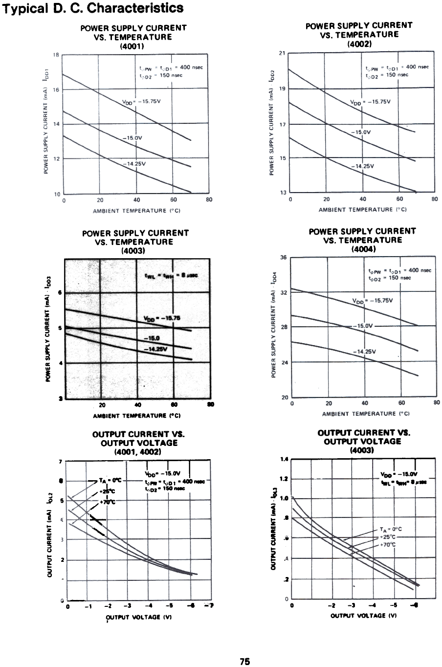
Typical D. C. Characteristics
POWER SUPPLY CURRENT
VS.TEMPERATURE
(4002)
POWER SUPPL V CURRENT
VS. TEMPERATURE
(4001)
POWER SUPPLY CURRENT
VS. TEMPERATURE
(4004)
POWER SUPPLY CURRENT
VS. TEMPERATURE
(4003)
'WI. . '- . .-
--~~. -,.."
f:::::::
1~1&.O -14.3V
I
--
S
.S'
- 6
1
...
z
...
~
~ 5
~
u
>
...
~
VI
~ .
...
~
I20 .0 80
AMBIENT TEMPERATURE I.CI .
OUTPUT CURRENT VI.
OUTPUT VOLTAGE
(4003)
1.4 I I
Voo" -11.OV
..\ 1.-
OUTPUT CURRENT vs.
OUTPUT VOLTAGE
(4001. 4002)
7 ~O- _,IS.av 1-
t"N"t"O,-48-
1,'OZ- '50-
1.2
11.0
I1 ..
i I
c
a.-!
i
a .' I
.21
~TA..O'C
/+~ I
;+7V'C
.
~
j 5
1
..
z
...
~
~
~
y
..
i 2
..
8
~
,
y-
o -1 -8 :00'7 0-2 -3 -4 '-5
OOTPUT VOlTAGE {VI
...
-2 -3 -4 -5
OUTPUT VOLTAGE (VI
I
75
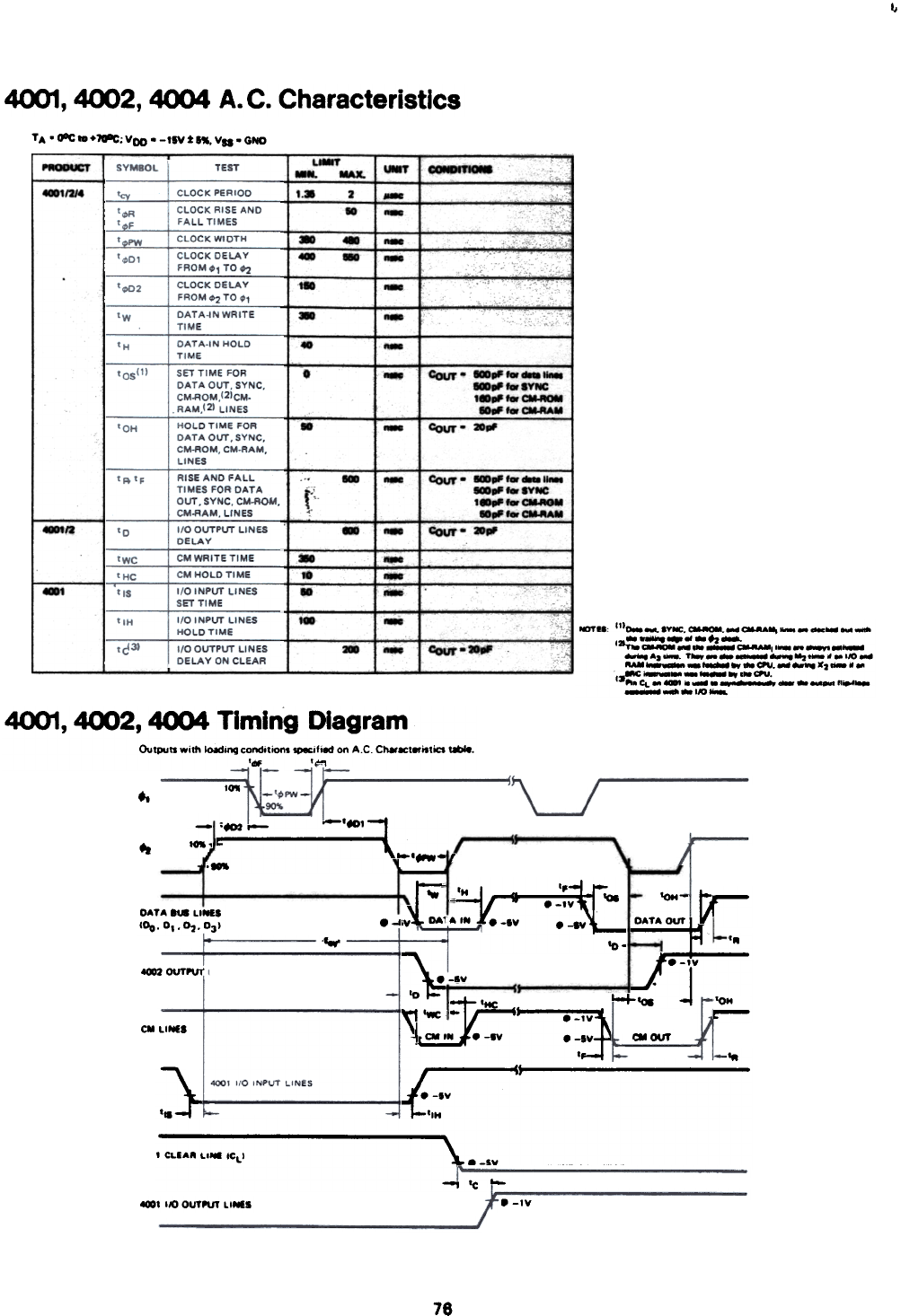
"
4001, 4002, 4004 A. C. Characteristics
TA' fP'C"+~;VDO" -I&ViR. VSS"GNO
LIMIT
MN. MAx.
~
~/2J4
UMT I -.TI~
,~ 2
.-
-
.,
-- 1-
--
'10 -
--
.-
.-
.Cour- y~
, ~
1O-"-CM.ftAM
CoUT - a..
-
--
t
-/2 -Cour - -pP f8 _1-
_ppf88YNC
'~ppf8CM-AOM
.ppf8C~M
Cour-app
-
~
t:i - 18
.~
_1
100 -OCTH CII__IVNC ft-
'~ c..-,I-"---
_A._. T", ",-,.,/O-
COU.-_x ~ cou.
, ".Ct ~-, n..-
___1/0-
~Cow-."
-
4001, 4002, 4004 Timing Diagram
Outpuu with ~jng condition. _ifiod on AC Ch8rKteriitici _.
'.. '
10.
.. -~- I- -'101 =1.- I- -'101
-, ,- r-"'"
.. ,
..f:.-:t:--.;~~p ow tM ~
.-IV
IV DAT.tN .-IV .-SV~
'0-
~
DATA_LINES
(00.D,.~.D3) .-1
fQH-
ft-o-TA our .~
.-IV
I-f-U. j
-'ow'
_OUTPUT
"OM
r--
CM LINES
~OUT
, .-IV
'D~
~ ;~~~:::-4HC 'wc 1- . -tV " CM IN . -tV ~---:~:\
.~::r OW
-;1~::: 4t
. --V
~ 'IH
t CLEAR LIM ICL) \. -IV
-I'c""
.-IV
-- 110 OUTPUT LINES
78
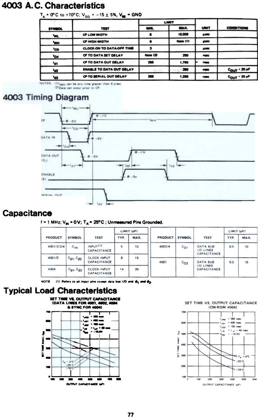
4003 A. C. Characteristics
TA. O"C to +70OC; Voo . -15.t. 5%, V.. GND
UWT --.
10'-
_111
.-y
~-
.,-
-
_.
-
-
-
-
~T~
~
~
~
1m
~
~
~
..
--
.
.
3
_at
,.
TWf
~L~-DTM
~ HIGH WlOTH
~~ TO DAT~' T-.
~YODATA8T_LAY
~ YO DATA our _LAY
1-.1 TO DATA our -LAY
~yo-our-LAY
-
'."
-~
'.
I ~.a..
I CouT.a..
-
Capacitance
f = 1 MHz; Vw a OV; T A. 26OC; Unnwalr8d Pins Groondld.
~
~
~
r-;:;-
, TYP. ~
~TaT I -x.
10
-
IWUTtll
CAP~A*I
~1WUf
CAPAcrT-
a.OCKlWUf
CAP~ANQ
~I--
01/2/3141 I
CIN .~/C
OATA -
110 LINEI
CAPACITA~I
~/2 I~.~ ."em
-, DATA -
.IOLI-
CAPACITA-
u,.
I~.c.,
-»
-
-
J
j-
!-
i-
~
~
~
I~I ~R~- I$-
~
..
. 1_! 'I
-. ~- ...,
77
NOTE 111 Rot.. 10..11-.1 Po... ""- a.. boa I/O - ~-.,.
Typical Load Characteristics
lET n- VI. OUTPUT ~AClT~
(DATA LIMaI F~ ~. ~ ~
. IYNC FOR ~I
... , 1 , I I
'-'--
.'- ._-
'- ._-
'. '... .--
".. .--
-J-~
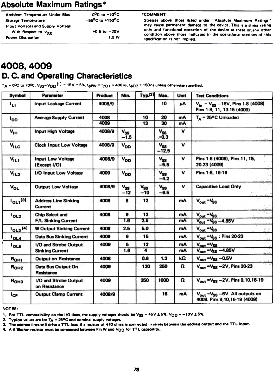
Absolute Maximum Ratings *
OOC to + 100C
-ssoC to +1SOOC
.COMMENT
Stm~ above those listed under ,. Absolute Maximum Ratings"
may cause permanent dam. to the device. This Is a stms rating
only and functional operation of the device at these or .any other
condition above those indicated in the operational sections of this
specification Is not implied.
Ambient Temt)8r8ture Und8r B18.
Star. Temper8ture
Input Volt.. 8nd Supply Volt8~
WIth ReSf)8Ct to Vss
Po_r DlsslP8tlon
+0.5 to -20'1
1.0 W
4008,4009
D. C. and Operating Characteristics
TA = ~ to 7~, VSS-VOO[1] = 15V:t 5%, ~~ = ~O1 = 400n5, ~O2 -150nlunlellotherwi.l~cified.
Typj2JI Max.
Symbol
ILl
Product
4008/9
Min. Unit
IJA
Paramete, Test Conditions
Vin =Vss-16V.Pins 1.S (4008)
Pins 1-S, 11, 13-15 (4(X»)
T A a 25°C Unloaded
I "put Leakage Current 10
4008
4009
4008/9
10
13
mA
mA
V
Average Supply Current
'DO
VIH Input High Voltage Vss
-1.5
VooVILC
Clock Input Low Voltage 4008/9
20
~
Vss
+0.3
Vss
-12.5
Vss
-5.5
Vss
-4.2
Vss
-8.5
v
V1L1 Input Low Voltage
(Except I/O)
4008/9 VDD vPins 1-6 (4008), Pins 11, 15,
20-23(4009)
Pins 1-8, 16-19
V1L2 1/0 Input Low Voltage 4009
VDD v
4008/9 Vss
-10
12
vCapacitive Load Only
VOL Output Low Voltage Vss
-12
8
IOL1(3J
Address Line Sinking
Current
4008 mA VoutSVss
4008 9
1.8
I 13
! 2.5 mA
mA
mA
mA
mA
"mA
kn
n
v =
-4.86V
VOUt=Vss ~~~
IOL2 Chip Select and
F Il Sinking Current
IOL3 [4)
~..Qb!--
IOU
4008
4009
4009
2.5
9
5
"[6
5.0
15
12
T
0.8
1:,)
W Output Sinking Current
Data Bus Sinking Current
1/0 and Strobe Outpjt
Sink ing Current
Vout =Vss : Pins 20-23
Vout =Vss
Vout ='18 -4.85V
Vout =Vss -O.5V
4008
4009
1.2
250
ROH1
ROH2
Output on Resistance
VO4It -Vss -2V. Pins 20-23
Data Bus Output On
R esiS1ance
250 1000 nVout =Vss -2V, Pins 9,10,16-19
ROH3 4009
I/O n Strobe OutpUt
on Resistance
Output Clamp Current 16 mA VOU! -Vss -6V. All outputs on
4008. Pins 9,10,16-19 (4009)
ICF 4008/9
NQTES:
1. For TTL ~lnPItibility on the 1/0 lines. the supply volt8get should be Vss a +5V :t; 5~. VOD - -10V t 5~.
2. Typic81 willes.. for TA a 250C M1d no~nallUpply wlf9S0
3. The add,.. li,.s will dri- a TTL 10-' if a resistor of 470 oh~ is o>nnec18d in -jet betWMn the add,.. outPut 8nd the TTL input.
4. A 6.8kohm resistor must be o>nnec18d be~n Pin W and VDD for TTL ~_ility.
78
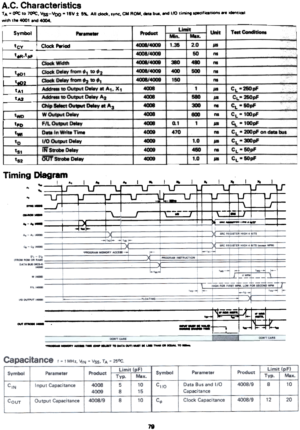
A.C. Characteristics
limit Test Conditions
Unit
Product
Symbol P..met8,
~
I 1.36'
~
4C8/4(X» .
4008/4CD
4CXMI 4fD -
4CXMI4CD ~ ~
4(X8/ 4fD 1 &0
4008
...
4cx.
4C8
... 0,1
4CX» ~,;;
..
4CX»
..
t~-
tfR~'"
\ Clock Period -
,.
,.
,.
,.
400
! C/odt ~
Clock Detey from, to,
Clodt Delay from ~ ~ .,
LfDf
r--~~..-; I CL -2&OpF ,
CL.25QpF
CL . 5OpF
CL = 100pF
~ . 1CK»pF
I
~~!~~I C L - 2(K) pF on d8t8 t...
CL - :DpF
CL.~pF
CL - 5OpF
I Add,.. toOutp.rt Delay . A,. X, ,..
lIS
,.
nI
lIS
"'
lIS
nI
lIS
I~
"300
r-a-
tA2. I "A:CtCt,. to OutJJUt DeI.y A2
I Otip Select Output D818y 8t A 3
I w OutJJUt DeI8y -
I F/L Output DeI8y
0... In Writ8 ~
I I/O Output Oel8y
twc
I tFD \
I~-
1.0
480
1.0
~
tl1
tl2
~Strobe~~ .
O'UT Strobe Delay
Timing Diagram
~ I A
.. ,
..
--
--
~-~-
--r-'~:~,
~4=
.: =- "=:.~~~=§~ t= - - . - . -
-
. --- .
---
-__'-__1GMTA~_. '--~_1G-
78
TA . ~ to 7~, VSS-Voo - 11V t 5"" All dock, sync. CM ROM, ~ b~.1nd 110 timng ..-cifiC8~ - id8ntiml
with the 4001 Ind 4004.
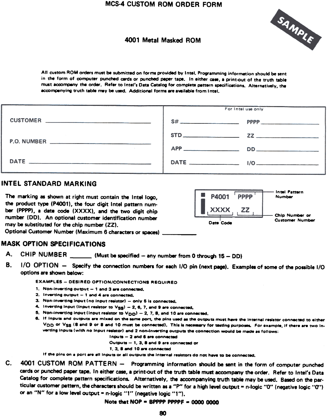
MCS-4 CUSTOM ROM ORDER FORM
4001 Metal Masked ROM
All custom ROM orders must be submitted on forms provided by Intel. Pr.ammlng information should be sent
in the form of computer punched cards or punched papet'ta.-. In either ce_, a print-out of the truth teble
must 8CU)mpenv the order. Refer to Intel's Dat8 Catalog for com~.te .-ttern Sf)8cifications. Alternativelv, the
accom.-nving truth t8ble n.V be u*. Additional forms ... awilable from Intel.
INTEL STANDARD MARKING
Int81 P8t18rn
Number
O1lp Number or
Customer Number
0- Code
The marking as shown at right must contain the Intel logo,
the product type (P4001), the four digit Intel pattern num-
ber (PPPP), a date code (XXXX), and the two digit chip
number (DD). An optional customer identification number
may be substituted for the chip number (ZZ).
Optional Customer Number (Maximum 6 characters or spaces)
MASK OPTION SPECIFICATIONS
A. CHIP NUMBER (Must be specified - any number from 0 through 15 - DD)
B. I/O OPTION - Specify the connection numbers for e~h 1/0 pin (next ~). Exampl. of some of the possible 1/0
options are shown below:
EXAMPLES - OESIREO OPTION/CONNECTIONS REQUIREO
1. Non-Inverting output - 1 and 3 - connec~.
2. Inverting output - 1 end 4.re con~t8d.
3. Non-inV8rtlng Input (no Input r...ltor) - only 6 I. connec~.
4. Inverting InpUt (Input r8ll8tor to VSS) - 2. e. 7. end g - cOnn8Ct8d.
5. Non-invertll)9 Input (Input r.~- to VOO) - 2, 7, 8, .nd 10 .r. COnn8Cted.
8. If Inpu1l .nd output. er. ml.ed on 111. ..me PO". ttIe pin. ul8d . ttIe OUtputs mutt hev. 111. Intlt'nel r.".tor connec~ to .11II.r
VOO or Vss (8 .nd g or 8 end 10 mUIt be connected), Ttli. II ft8C_ry for t88t1ng purpo... For ...mple, If ttler..,. tWo In-
vent"' Inputs (with no Input r8ll.or) .nd 2 nOn-fnverting outputs"" COnMction _uld be rn8d8.. followe:
Inputs- 2.nd 8.re connect8d
Outputs - 1, 3,8 .nd g .r. conn8Ct8d or
1.3.8 end 10 - connected
If 111. pin. on . PO" .,. ell Inputs or .11 outputs1fl8 In_ne! r."stor. do nOt tI- to be connected.
C. 4001 CUSTOM ROM PATTERN - Programming information should be sent in the form of computer punched
cards or punched paper tape. In either caR, a print-out of the truth table must accomp.,y the order. Refer to Intel's Data
Catalog for comptete pattern specificationL Alternatively, the ~companying truth table may be u~. Based on the par-
ticular customer pattern, the characters should be written as a "P" for a high level output - n-loglc "0" (negative logic "0")
or an "N" for a low level output - n-iogic "1" (negative logic "1").
Note that NOP . BPPPP PPPPF . ~ 0000
S)
DATA -
Otmtn
_FE~
~- ~.'OD, 'MIl
-Jou:;"
...0 I/O,
, 'M_'
.
r-o-:-
T2-- -4-- r ~
a
L--.9-.9 ~.
. .
~Ra v.
::-1
.
to---
v.
18
1/01 (PIN 15)
,
1/03 (PIN 13)
81
CONNECTIONS DESIRED (lIST NUMBERS. CIRCLE
CONNECTIONS ON SCHEMATIC)
8. For r2l compatibility on tIw I/O lines IN _Iy vall..- --ad be
Vco . -10V .5%. ~ . +5V .5%
b. II non-~.. '-' 0Pt* il~. V'L . -8.5 Yo"- --;.,.,.., (,* TTll
CONNECTIONS OESIREO (LIST NUMBERS a CIRCLE
CONNECTIONS ON SCHEMATIC)
8. For r2L competobility on the I/O "".. the ~y w~ --Id t»
Voo . -IOV .5%. Vss . +5V .5%
b. If ~~.. input ~ ',..-d. VOL. -e.S VoItI_~ ,.. TT1.1
CONNECTIONS OESIREO (LIST NUMBERS a CIRCLE
CONNECTIONS ON SCHEMATIC)
8. For T2L compatIbIlity on the 1/0 lInes the supply won.- ~Id be
Vco . -10V '5%. \/ss . +5V .5~
b. If 11«I.~ing inPUt Option , v.L . -U Voila --- (,* TTLI
CONNECTIONS DESIRED (LIST NUMBERS. CIRCLE
CONNECTIONS ON SCHEMATIC)
e. For T7l competib'I,ty on the 1/0 lines the supply volte.- -.ould be
Voo . -1OV t5%. Vss . '5V .5%
b. II .--~... inP"t Option it..-d. VIL . -e.& Volts --j~ In« TTll
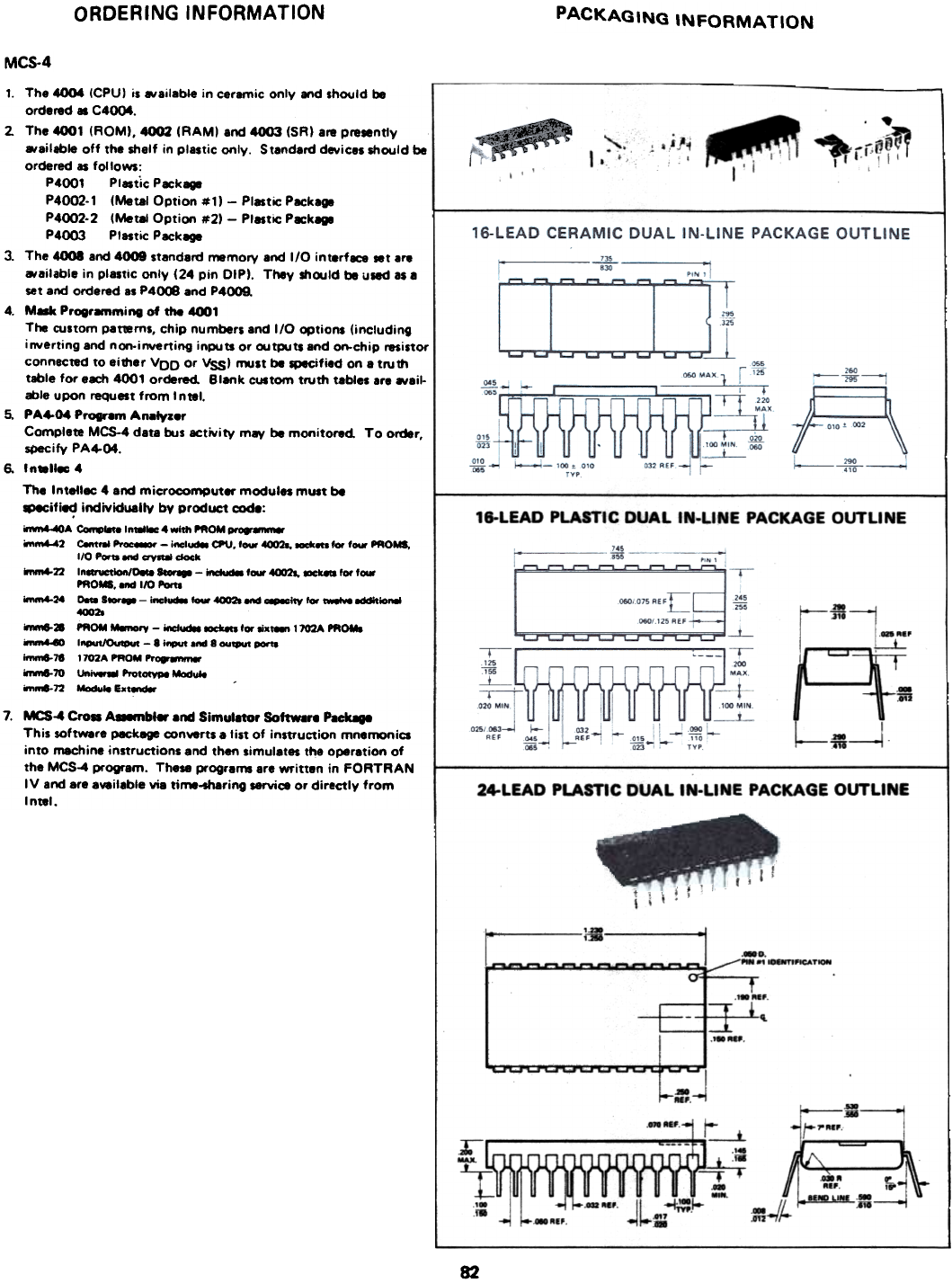
ORDERING INFORMATION PACKAGING INFORMATION
MC5-4
16-LEAD PLASTIC DUAL IN.lINE PACKAGE OUTLINE
,. The 4004 (CPU) is .,ailable in ceramic only and should be
ordered - C4004.
2. The 4001 (ROMI, 4002 (RAMI and 4003 (SRI are presently
.,ailable off the shelf in plastic only. Standard devices should be
ordered as follows:
P4001 PI_tic Pack.
P4002-1 (Metal Option #11 - PI_tic Package
P4002-2 (Metal Option #21 - Plastic Pack.
P4003 Plastic Pack.
3. The 4008 and 4009 standard ~mory and 1/0 interf- set are
.,ailable in plastic only (24 pin DIPI. They sh~ld be used as a
set and ordered as P4~ and P4009.
4. M- Proer8nmine of the 4001
The custom pat1Bms, chip numbers and 1/0 options (including
inverting and non-inverting inputs or ~tputs and on-chip resistor
connected to ei1f1er VDD or Vssl must be $p8Cified on e tru1f1
table for each 4001 ordered. Blank custom tru1f1 tables are .,eil-
able upon request from Intel.
5. PA4-04 Pr0gr8m An8iyzer
Complete MCS-4 data bus activity m8V be monitored. To order,
sPecify PA4-04.
6. In.11ec 4
The Intellec 4 and microcomputer modules must be
~ifi~ individually by product code:
~A C-- In_. 4 with ~OM pt ...m4--42 C8ttf8I Pr- - I~I- CPU, - 4002.. _oto for fa.. ~OMS.
IIOP_-~dock
_22 In_1oIIIO8t8 '-III - -- fa.. 4(XI2I, - for fa..
~OW, - I/O Pons
-24 D8t8 S-. - i~l- - 40021 - _itY for - _10...
4CXI2s
n...e.a ~OM M8tIory - IncI..- -.ckotI for oi.- 17O2A ~OMO
- 1~-8input...8QU_-
1mm8-78 1702A PROM ~
n...e.70 Un- Prot- 72 -Ie Ext-
7. MCS-4 Cro. ~b" end Simul8tor SohW8r8 P8Ckag8
This software pecltege conWrtS a tist of instruction mnemonics
into machine instructions and then simulates the operation of
the MCS-4 program. These prograrN are _itten in FORTRAN
IV and are available via time-sharing service or directly from
Intel.
r.~.
!~ '-~ I I I -
:iiI
~~-J
24-LEAD PLASTIC DUAL IN-LINE PACKAGE OUTLINE
.~"'.","
L---~~~~~~I I_D.
- - - - - - - - - - - - ciJ11--_"-"~T-
~
..M'
:I--'"
..-
1---8--1
.."..,...,
~~ --1-=1
mo.'1 ~
..
~
-
--
~
MAX.
-L.--
-l-
..
18
~ .
~... r..'
;j;..//.- ;;
Jl ~j..
01'
-
I I ""'t ,,""_oaf
--1 ~_R.'
82
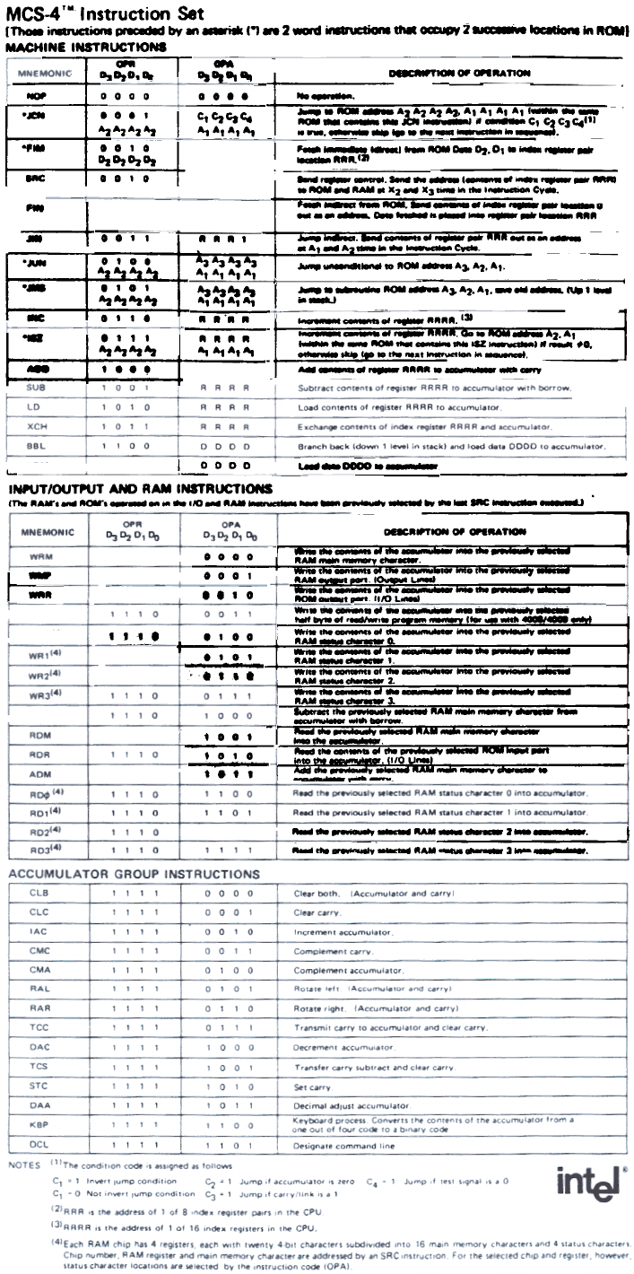
~
~~.,-.-
0 0 0 .
c,c,ea~
At A, A, At
_~W_RAn~
MCS-4 TM Instruction Set
.:-+
~~~~
R . 'R R
R R R R
At At At At
I~ I ~~~~ I"" At
~ t'"
~-
~___AI~~a,.A,A, A, A, ,---
a---C,c,CJC4"1
""" "-_.~'
-
, - -~ DJ.O, - ~.R..2t
-- -
,-~ -WOM- RAM. X2 - KJ -.. 1M ,- Cy*.
--- -~-~-_.
"_-~__M~
. -- .
A
-
.- . , . , AJ.A2.A,.-_~~,--
.,.,.,., ---'
~ . , , . - ~_-;--~;R~.I» -
I__"~ . - 2.A,
OSZ_.II- -0.
- .. ... ow., _ion '" _.
__~_RR.R - - -
-
~I 0000
L-- ~ -
INPUT/OUTPUT AM) RAM INSTRUCTIONS
In.. RAW. - --, - OR .. .. I/O - R- -- - - - - ~ .. .. ~ - ~
~~~; I 5=-~~::== Iwr_Of_UT- -- - 0 0 0 0 R_- --.
0001 . --. .
~ - ~-'-'--~---"-'
---~ --'~."/OL-
. . , 0
~or_.. . I 00 . I 0 I
to. ,
.'0 I 0 I~! ~~U..-:r IIO -
. -..
'-!..:!-'
~---
;. . . -*
~
-- .
. . t t
~~~__RAM__J_~--. I
,-~4M_--3-_~.
(1"- i~ P'-.d.t by ., ~ I") - 2 ~ ~ tII8t , 2 -- ~ .. ~I
MACHINE INSTRUCTIONS
- -
~Dt°.~
- 0000
.~ .0.. I.,AZA2"
.,. 0 0 I 0
DzD,DzDt
~ 0010
...~~.
Microcomputers. first from the beginning.
INTEL CORPORATION, 3065 Bowers Avenue, Santa Clara, California 95051 . (408) 246-7501
C> Intel 1974/Printed in U.S.A./MC5-219-oS74/25K
